Introduction to Water Resistive Barriers (WRBs) & Air Barriers
Upload
independentCategory
view
1download
0
V I S H A Y B C C O M P O N E N T S
Resistive Products Technical Note
Varistors Introduction
TE
CH
NIC
AL
NO
TE
Revision: 04-Sep-13 1 Document Number: 29079
For technical questions, contact: [email protected] DOCUMENT IS SUBJECT TO CHANGE WITHOUT NOTICE. THE PRODUCTS DESCRIBED HEREIN AND THIS DOCUMENT
ARE SUBJECT TO SPECIFIC DISCLAIMERS, SET FORTH AT www.vishay.com/doc?91000
www.vishay.com
GENERALVaristors provide reliable and economical protection against high voltage transients and surges which may be produced, for example, by lightning, switching or electrical noise on AC or DC power lines. They have the advantage over transient suppressor diodes in as much as they can absorb much higher transient energies and can suppress positive and negative transients.When a transient occurs, the varistor resistance changes from a very high stand-by value to a very low conducting value. The transient is thus absorbed and clamped to a safe level, protecting sensitive circuit components.Varistors are manufactured from a non-homogeneous material, giving a rectifying action at the contact points of two particles. Many series and parallel connections determine the voltage rating and the current capability of the varistor.
Manufacturing process flow chart
FEATURES• Wide voltage range selection - from 14 VRMS to 680 VRMS.
This allows easy selection of the correct component for the specific application.
• High energy absorption capability with respect to size of component.
• Response time of less than 20 ns, clamping the transient the instant it occurs.
• Low stand-by power - virtually no current is used in the stand-by condition.
• Low capacitance values, making the varistors suitable for the protection of digital switching circuitry.
• High body insulation - an ochre coating provides protection up to 2500 V, preventing short circuits to adjacent components or tracks.
• Available on tape with accurately defined dimensional tolerances, making the varistors ideal for automatic insertion.
• Approved to UL 1449 edition 3 (file number: E332800) and manufactured using UL approved flame retardant materials.
• Completely non flammable, in accordance with IEC, even under severe loading conditions.
• Non porous lacquer making the varistors safe for use in humid or toxic environments. The lacquer is also resistant to cleaning solvents in accordance with IEC 60068-2-45.
VARISTORS MANUFACTURING PROCESSIn order to guarantee top performance and maximum reliability, close in-line control is maintained over the automated manufacturing techniques. The manufacturing process flow chart shows each step of the manufacturing process, clearly indicating the emphasis on in-line control.Each major step in the manufacturing process shown in the Manufacturing process flow chart is described in the following sections:
MILLING AND MIXINGIncoming materials are checked, weighed, milled and mixed for several hours to make a homogeneous mixture.
GRANULATIONA binder is added to produce larger granules for processing.
PRESSINGThe surface area and thickness of the disc help to determine the final electrical characteristics of the varistor, therefore pressing is a very important stage in the manufacturing process. The granulated powder is fed into dies and formed into discs using a high speed rotary press.

Varistors Introduction
TE
CH
NIC
AL
NO
TE
Technical Notewww.vishay.com Vishay BCcomponents
Revision: 04-Sep-13 2 Document Number: 29079
For technical questions, contact: [email protected]
THIS DOCUMENT IS SUBJECT TO CHANGE WITHOUT NOTICE. THE PRODUCTS DESCRIBED HEREIN AND THIS DOCUMENTARE SUBJECT TO SPECIFIC DISCLAIMERS, SET FORTH AT www.vishay.com/doc?91000
FIRING
The pressed products are first pre-fired to burn out the binder. They are then fired for a controlled period and temperature until the required electrical characteristics are obtained. Regular visual and electrical checks are made on the fired batch.
METALLIZATION
The fired ceramic discs are metallized on both sides with a silver content layer to produce good low resisitive electrical contacts. Metallization is achieved by screen printing. Visual checks are made regularly and a solderability test is carried out in each production batch.
ATTACHING LEADS
Leads are automatically soldered to the metallized faces and regular strength tests are made. Three types of lead configuration are available; one with straight leads, one with straight leads and flange, and one with kinked leads.
LACQUERING
The components are coated by immersing them in a special non flammable ochre epoxy lacquer. Two coats are applied and the lacquer is cured. Regular tests to check the coating thickness are made.
ELECTRICAL TESTING (100 %)
The voltage of each component is normally checked at two reference currents (1 mA and another according to the application). Any rejects are automatically separated for further evaluation.
MARKING
All components are laser marked with type identification, voltage rating and date code.
QUALITY
APPROVALS• UL 1449 ed. 3 according file E332800• VDE following IEC 61051-1/2 according file 40002622 or
40013495• CSA file 219883 and cUL according file E332800
The term ‘QUALITY ASSESSMENT’ is defined as the continuous surveillance by the manufacturer of a product to ensure that it conforms to the requirements to which it was made.
PRODUCT AND PROCESS RELEASERecognized reliability criteria are designed into each new product and process from the beginning. Evaluation goes far beyond target specifications and heavy emphasis is placed upon reliability. Before production release, new varistors must successfully complete an extended series of life tests under extreme conditions.
MONITORING INCOMING MATERIALSApart from carrying out physical and chemical checks on incoming raw materials, a very close liaison with material suppliers is maintained. Incoming inspection and product results are gradually fed back to them, so ensuring that they also maintain the highest quality standards.
IN-LINE CONTROLThe manufacturing centre operates in accordance with the requirements of IEC 61051-1 and UL 1449 . Each operator is actively engaged in quality checking. In addition, in-line inspectors and manufacturing operators make regulated spot checks as a part of our Statistical Process Control (SPC).
FINAL INSPECTION AND TEST (100 %)At the end of production, each varistor is inspected and tested prior to packing.
LOT TESTINGBefore any lot is released, it undergoes a series of special lot tests under the supervision of the Quality department.
PERIODIC SAMPLE TESTINGComponent samples are periodically sent to the Quality laboratory for rigorous climatic and endurance tests to IEC/UL requirements. Data from these tests provide a valuable means of exposing long term trends that might otherwise pass unnoticed. The results of these tests are further used to improve the production process.
FIELD INFORMATIONThe most accurate method of assessing quality is monitoring performances of the devices in the field. Customer feedback is actively encouraged and the information is used to study how the components may be further improved. This close relationship with customers is based on mutual trust built up over many years of co-operation.
encapsulation electrodesintergranular boundary
leads
100
V(V)
I (µA)
3

Varistors Introduction
TE
CH
NIC
AL
NO
TE
Technical Notewww.vishay.com Vishay BCcomponents
Revision: 04-Sep-13 3 Document Number: 29079
For technical questions, contact: [email protected]
THIS DOCUMENT IS SUBJECT TO CHANGE WITHOUT NOTICE. THE PRODUCTS DESCRIBED HEREIN AND THIS DOCUMENTARE SUBJECT TO SPECIFIC DISCLAIMERS, SET FORTH AT www.vishay.com/doc?91000
DEFINITIONS
MAXIMUM CONTINUOUS VOLTAGEThe maximum voltage which may be applied continuously between the terminals of the component. For all types of AC voltages, the voltage level determination is given by the crest voltage x 0.707.
VOLTAGE AT 1 mA OR VARISTOR VOLTAGEThe voltage across a varistor when a current of 1 mA is passed through the component. The measurement shall be made in as short a time as possible to avoid heat perturbation.The varistor voltage is essentially a point on the V/I characteristic permitting easy comparison between models and types.
MAXIMUM CLAMPING VOLTAGEThe maximum voltage between two terminals when a standard pulse current of rise time 8 μs and decreasing time 20 μs (8 μs to 20 μs) is applied through the varistor in accordance with IEC 60060-2, section 6.The specified current for this measurement is the class current.
MAXIMUM NON REPETITIVE SURGE CURRENTThe maximum peak current allowable through the varistor is dependent on pulse shape, duty cycle and number of pulses. In order to characterize the ability of the varistor to withstand pulse currents, it is generally allowed to warrant a ‘maximum non repetitive surge current’. This is given for one pulse characterized by the shape of the pulse current of 8 μs to 20 μs following IEC 60060-2, with such an amplitude that the varistor voltage measured at 1 mA does not change by more than 10 % maximum.A surge in excess of the specified withstanding surge current may cause short circuits or package rupture with expulsion of material; it is therefore recommended that a fuse be put in the circuit using the varistor, or the varistor be used in a protective boxIf more than one pulse is applied or when the pulse is of a longer duration, derating curves are applied (see relevant information in the datasheet); these curves guarantee a maximum varistor voltage change of ± 10 % at 1 mA.
MAXIMUM ENERGYDuring the application of one pulse of current, a certain energy will be dissipated by the varistor. The quantity of dissipation energy is a function of:• The amplitude of the current• The voltage corresponding to the peak current• The rise time of the pulse• The decrease time of the pulse; most of the energy is
dissipated during the time between 100 % and 50 % of the peak current
• The non-linearity of the varistor
In order to calculate the energy dissipated during a pulse, reference is generally made to a standardized wave of current. The wave prescribed by IEC 60 060-2 section 6 has a shape which increases from zero to a peak value in a short time, and thereafter decreases to zero either at an approximate exponential rate, or in the manner of a heavily damped sinusoidal curve. This curve is defined by the virtual lead time (t1) and the virtual time to half value (t2) as shown in the maximum energy curve (page 5).The calculation of energy during application of such a pulse is given by the formula: E = (Vpeak x I peak) x t2 x Kwhere:
Ipeak = peak currentVpeak = voltage at peak current = given for I = ½ x Ipeak to Ipeak
K is a constant depending on t2, when t1 is 8 μs to 10 μs (see table on page 8).A low value of corresponds to a low value of Vpeak and then to a low value of E.The maximum energy published does not represent the quality of the varistor, but can be a valuable indication when comparing the various series of components which have the same varistor voltage. The maximum energy published is valid for a standard pulse of duration 10 μs to 1000 μs giving a maximum varistor voltage change of ± 10 % at 1 mAWhen more than one pulse is applied, the duty cycle must be so that the rated average dissipation is not exceeded. Values of the rated dissipation are:
0.1 W for series VDRS05/VDRH050.25 W for series VDRS07/VDRH070.4 W for series VDRS10/VDRH100.6 W for series VDRS14/VDRH141 W for series VDRS20/VDRH20
ELECTRICAL CHARACTERISTICSTypical V/I characteristic of a ZnO varistorThe relationship between voltage and current of a varistor can be approximated to: V = C x I
where:V = VoltageC = Varistor voltage at 1 AI = Actual working current = Tangent of angle curve deviating from the horizontal
ExamplesWhen:
C = 230 V at 1 A = 0.035 (ZnO)I = 10-3 A or 102 AV = C x I
so that for current of 10-3 A: V = 230 x (10-3)0.035 = 180 V and for a current of 102 A: V = 230 x (102)0.035 = 270 V

Varistors Introduction
TE
CH
NIC
AL
NO
TE
Technical Notewww.vishay.com Vishay BCcomponents
Revision: 04-Sep-13 4 Document Number: 29079
For technical questions, contact: [email protected]
THIS DOCUMENT IS SUBJECT TO CHANGE WITHOUT NOTICE. THE PRODUCTS DESCRIBED HEREIN AND THIS DOCUMENTARE SUBJECT TO SPECIFIC DISCLAIMERS, SET FORTH AT www.vishay.com/doc?91000
Varistor characteristics using different values
Maximum energy curve
Typical V/I curve
Pre-breakdown region: V I; highly temperature dependentNormal operating region: V = C x I
Up-turn region: V = C x I + I x Rs
SPCIFICATION OF A VARISTOR CURVE
Working points on a varistor curve
The drawing below shows the various working points on the varistor curve using the series VDRS07, 60 V type as an example. The electrical characteristic values are shown in the Electrical Characteristics table below.
Curve for varistor type VDRS07H060
log V
β = 1 = fixed resistor
β = 0.4 (SiC)
β = 0.03 (ZnO)
β = 0 = ideal varistor
log I
t
t2
t1
Ipeak
(%)
90
100
50
10
pre-breakdown region normal operating region up-turn region
103
102
1010-8 10-7 10-6 10-5 10-4 10-3 10-2 10-1 1 10 102 103 104 105
V(V)
I (A)
109 ΩSLOPE = β
V = Clβ
V = Clβ + IRS
RS = 0.05 Ω to 0.5 Ω
ELECTRICAL CHARACTERISTICS
PARAMETER VALUE
Maximum RMS voltage 60 V
Maximum DC working voltage 2 x 60 V = 85 V
Varistor voltage 100 V ± 10 %
Maximum clamping voltage at 10 A 165 V
Maximum non-repetitive current 1200 A
Leakage current at 85 VDC 10-5 A to 5 x 10⁻⁴ A
Transient energy 10 µs to 1000 µs: 8.3 J
log V
log I1 mA
max. leakagecurrent region
max. clampingvoltage region
up-turnregion
max.clampingvoltage
max.leakage current
tolerance band
+ 10 %
- 10 %
103
102
1010-5 10-4 10-3 10-2 10-1 1 10 102 103
V(V)
I (A)
max. leakage current max. clamping voltage

Varistors Introduction
TE
CH
NIC
AL
NO
TE
Technical Notewww.vishay.com Vishay BCcomponents
Revision: 04-Sep-13 5 Document Number: 29079
For technical questions, contact: [email protected]
THIS DOCUMENT IS SUBJECT TO CHANGE WITHOUT NOTICE. THE PRODUCTS DESCRIBED HEREIN AND THIS DOCUMENTARE SUBJECT TO SPECIFIC DISCLAIMERS, SET FORTH AT www.vishay.com/doc?91000
Definitions of the varistor curve
The points A, B and C shown on the curve are defined in the Varistor Curve Definitions table.
TRANSIENT VOLTAGE LIMITATIONS WITH ZnO VARISTORSPrinciples of voltage limitation
Voltage limitation using a varistor
In the Voltage limitation using a varistor drawing above, the supply voltage VI is derived by the resistance R (e.g. the line resistance) and the varistor (-U) selected for the application.
VI = VR + VO
VI = R x I + C x I
If the supply voltage varies by an amount of VI the current variation is I and the supply voltage may be expressed as:
(VI + VI) = R (I + I) + C (I + I)
Given the small value of (0.03 to 0.05), it is evident that the modification of C x I will be very small compared to the variation of R x I when VI is increased to VI + VI.
A large increase of VI will induce a large increase of VR and a small increase of VO.
Examples
The varistor is a typical component of the series VDR05C275 (C = 520; = 0.04) and R = 250 .
For VI = 315 V (crest voltage of the 220 V supply voltage): I = 10-5 A, VR = 2.5 x 10⁻³ V and VO = 315 V
For VI = 500 V: I = 10-1 A, VR = 25 V and VO = 475 V
For VI = 1000 V: I = 1.88 A, VR = 470 V and VO = 530 V
The influence of a series resistance on the varistor drawing shows the influence of different values of series resistors on the varistor efficiency.
By drawing the load line, it is also possible to estimate the variation of the voltages VR and VO when VI is increased to 500 V or 1000 V. This effect is shown in the graphs below.
Influence of a series resistance on the varistor
Influence on varistor when V1 is 500 V (R = 250 )
VARISTOR CURVE DEFINITIONS
POINT DESCRIPTION
ANormal working zone: current is kept as low as possible in order to have low dissipation during continuous operation (between 10 μA to 300 μA).
B
Maximum clamping voltage: the maximum voltage for a given (class) current (peak current based upon statistical probability determined by standardization authorities).
CMaximum withstanding surge current: the maximum peak current that the varistor can withstand (only) once in its lifetime.
10 µA 300 µA 10 A 1000 A100 A
protection zone
normalworking
condition(no spike)log V
A B C
I
R
I
- UVI
VR
VO
VO
(V)
2500
2000
1500
1000
500
2500200015001000500VI (V)
R = 0 Ω
1 Ω0.1 Ω
10 Ω
1000 Ω
100 Ω
VR
VOV1
V(V)
1000
800
600
400
200
00 2
I (A)4 6 8 10

Varistors Introduction
TE
CH
NIC
AL
NO
TE
Technical Notewww.vishay.com Vishay BCcomponents
Revision: 04-Sep-13 6 Document Number: 29079
For technical questions, contact: [email protected]
THIS DOCUMENT IS SUBJECT TO CHANGE WITHOUT NOTICE. THE PRODUCTS DESCRIBED HEREIN AND THIS DOCUMENTARE SUBJECT TO SPECIFIC DISCLAIMERS, SET FORTH AT www.vishay.com/doc?91000
Influence on varistor when V1 is 1000 V (R = 250 )
EQUIVALENT CIRCUIT MODELA simple equivalent circuit representing a metal oxide varistor as a capacitance in parallel with a voltage dependent resistor is shown in the Equivalent circuit model drawing. Cp and Rp are the capacitance and resistance of the intergranular layer respectively; Rg is the ZnO grain resistance. For low values of applied voltages, Rp behaves as an ohmic loss.
Equivalent circuit model
CAPACITANCEDepending on area and thickness of the device, the capacitance of the varistor increases with the diameter of the disc, and decreases with its thickness.
In DC circuits, the capacitance of the varistor remains approximately constant provided the applied voltage does not rise to the conduction zone, and drops abruptly near the rated maximum continuous DC voltage.
In AC circuits, the capacitance can affect the parallel resistance in the leakage region of the V/I characteristic. The relationship is approximately linear with the frequency and the resulting parallel resistance can be calculated from 1/C as for a usual capacitor.
Nevertheless, due to the structural characteristic of the zinc oxide varistors, the capacitance itself decreases slightly with an increase in frequency. This phenomenon is emphasized when the frequency reaches approximately 100 kHz. See the effect of HF alternating current on the varistor type VDRS14T250; C = 480 pF drawing.
Effect of HF alternating current on varistor type VDRS14T250; C = 480 pF
ENERGY HANDLINGMaximum allowable peak current and maximum allowable energy are standardized using defined pulses:
• Peak current (A); 8 μs to 20 μs, 1 pulse
• Energy (J); 10 μs to 1000 μs, 1 pulse
INTERNATIONALLY ACCEPTED PULSES
Standard pulse for current and maximum allowable energy calculation
VR
VO
V1
V(V)
1000
800
600
400
200
00 2
I (A)4 6 8 10
Rg
I
CpRp- U
10-2 10-1 1 10
103
102
10
V(V)
I (mA)
50 Hz 100 Hz 1 kHz 10 kHz
100 kHz
t
t2
t1
Ipeak
(%)
100
50
t1
8 µs
10 µs
t2
20 µs
1000 µs

Varistors Introduction
TE
CH
NIC
AL
NO
TE
Technical Notewww.vishay.com Vishay BCcomponents
Revision: 04-Sep-13 7 Document Number: 29079
For technical questions, contact: [email protected]
THIS DOCUMENT IS SUBJECT TO CHANGE WITHOUT NOTICE. THE PRODUCTS DESCRIBED HEREIN AND THIS DOCUMENTARE SUBJECT TO SPECIFIC DISCLAIMERS, SET FORTH AT www.vishay.com/doc?91000
Examples
Pulse life time rating of VDRS07H060, 60 V type.
Energy capability: E = K x Vp x Ip x t21 pulse; 8 µs to 20 µs: 1200 A = 1 x 8 J
10 pulses; 8 µs to 20 µs: 300 A = 10 x 1.45 J
1 pulse; 10 µs to 1000 µs: 33A = 1 x 8.3 J
10 pulses; 10 µs to 1000 µs: 11 A = 10 x 2.5 J
The maximum specified energy is defined for a maximum shift (V/V) 1 mA 10 %:
Ip = Pulse current
Vp = Corresponding clamping voltage
Typical surge life rating curves (number of surges allowed as a function of pulse time and maximum current) are shown in drawing below.
Maximum peak current for various number of pulses as a function of pulse duration
E = K x Vpeak x Ipeak x t2 = 1.4 x 700 x 33 x 10-3 = 32 J
Example of calculation of energy for a VDRS07H250 type, at the maximum peak current (33 A) for a duration t2 = 1000 μs (K = 1.4)
Maximum energy (10 x 1000 μs): 1 pulse
Example: VDRS07H250 (250 V)Example of selection of the maximum peak current as a function of pulse duration.
DISSIPATED POWERDC DISSIPATIONThe power dissipated in a varistor is equal to the product of the voltage and current, and may be written:W = I x V = C x I + 1 or K x V + 1
When the coefficient = 30 ( = 0.033), the power dissipated by the varistor is proportional to the 31st power of the voltage. A voltage increase of only 2.26 % will, in this case, double the dissipated power. Consequently, it is very important that the applied voltage does not rise above a certain maximum value, or the permissible rating will be exceeded.This is even more cogent as the varistors have a negative temperature coefficient, which means that at a higher dissipation (and accordingly at a higher temperature) the resistance value will decrease and the dissipated power will increase further.AC DISSIPATIONWhen a sinusoidal alternating voltage is applied to a varistor, the dissipation cannot be calculated from the same formula as in a DC application. The calculation requires an integration of the V x I product.The instantaneous dissipated power is given by:
In the above equation, the value V = Vpeak x sin t.During a half cycle, the dissipated power is given by:
Since Vpeak = VRMS x 2x
This integration is not easy to solve because of the exponent + 1) of sin t.
K DEPENDS ON t2 WHEN t1 IS 8 μs TO 10 μst2
(μs) K
20 1
50 1.2
100 1.3
1000 1.4
10-3
10-2
10-1
1
reduction factorof rated pulsepeak current
10 102 103 104
tp (µs)
100
106
1000
1
10
102
100
10-3
Vpeak
(V)429
690
1000
10-2 10-1 1 I (A) 3310
10 102 103 104tp (µs) 105
I(A)
33
Ipeak
PINST V x I V== K x V K= x V 1+
PRMS1---
0
K x Vpeak 1+ x tsin 1+ x d=
PRMS1--- x K x VRMS
1+ x 2 a 1+
x tsin
0
1+
x dt=

Varistors Introduction
TE
CH
NIC
AL
NO
TE
Technical Notewww.vishay.com Vishay BCcomponents
Revision: 04-Sep-13 8 Document Number: 29079
For technical questions, contact: [email protected]
THIS DOCUMENT IS SUBJECT TO CHANGE WITHOUT NOTICE. THE PRODUCTS DESCRIBED HEREIN AND THIS DOCUMENTARE SUBJECT TO SPECIFIC DISCLAIMERS, SET FORTH AT www.vishay.com/doc?91000
It is generally easier to use the quotient of the AC power on the DC power:
P = PAC/PDC
This quotient depends only on the value of and not more on the K value as shown in the formula:
P has been calculated by successive application of a reduction formula; see Power Ratios table.
TEMPERATURE COEFFICIENTIn the leakage current region of the V/I characteristic, the normal equation V = C x I of the varistor becomes less applicable.
This is due to a parallel resistance which shows a very important temperature coefficient, created by thermal conduction. This temperature coefficient decreases when the current density increases. Then, the temperature coefficient at 1 mA is higher for a large varistor than for a small varistor.
This phenomena induces an increase in leakage current when the varistor is used at high temperatures. The relationship between the temperature and the current at a given voltage can be expressed by:
I = I0 x eKT
where:
I0 is the limiting current at 0 K
K is a constant including the band gap energy of the zinc oxide and the Boltzmann’s constant.
Practically, the maximum temperature coefficient is guaranteed on the voltage for a current of 1 mA in % per K.
SURGE PROTECTIONVaristors provide protection against surges which may be generated in the following ways:
ELECTROMAGNETIC ENERGYAtmospheric, lightningSwitching of inductive loads:• Relays• Pumps• Actuators• Spot welders• Thermostats• Fluorescent chokes• Discharge lamps• Motors• Transformers• Air conditioning units• Fuses
ELECTROSTATIC DISCHARGESFor example, discharges caused by synthetic carpets (approximately 50 kV), due to the inductance of the connecting leadwires, the reaction time of leaded VDR’s might be too slow to clamp properly fast rising ESD pulses.
SOURCE OF TRANSIENTThe energy dissipated by switching of an inductive load is completely transferred into the capacitance of the coil which is generally very low.E = ½ x L x I2 = ½ x C x V2
P
1--- x K x Vrms
1+ x 2 a 1 2+ x tsin
0
1+
x dt
K x Va 1+-----------------------------------------------------------------------------------------------------------------------------=
P 1--- x 2 a 1 2+ x tsin
0
1+
x dt=
POWER RATIOS P P P P P
1 1.0 11 14.4 21 344 31 9135 41 255 6462 1.2 12 19.6 22 477 32 12 776 42 358 7783 1.5 13 26.8 23 658 33 17 734 43 499 6734 1.92 14 36.7 24 915 34 24 822 44 701 6115 2.5 15 50.3 25 1264 35 34 482 45 977 6226 3.29 16 69 26 1763 36 48 301 46 1 373 3657 4.375 17 95 27 2439 37 67 149 47 1 914 5108 5.85 18 131 28 3404 38 94 126 48 2 690 6759 7.875 19 180 29 4715 39 130 941 49 3 752 439
10 10.64 20 249 30 6587 40 183 660 50 5 275 834
Varistors Introduction
TE
CH
NIC
AL
NO
TE
Technical Notewww.vishay.com Vishay BCcomponents
Revision: 04-Sep-13 9 Document Number: 29079
For technical questions, contact: [email protected]
THIS DOCUMENT IS SUBJECT TO CHANGE WITHOUT NOTICE. THE PRODUCTS DESCRIBED HEREIN AND THIS DOCUMENTARE SUBJECT TO SPECIFIC DISCLAIMERS, SET FORTH AT www.vishay.com/doc?91000
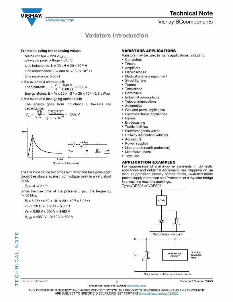
Examples, using the following values:
Mains voltage = 220 VRMS;allowable peak voltage = 340 V
Line inductance: L = 20 μH = 20 x 10-6 H
Line capacitance: C = 300 nF = 0.3 x 10⁻⁶ H
Line resistance: 0.68
In the event of a short circuit:
Load current:
Energy stored: E = ½ x 20 x 10-6 x 25 x 104 = 2.5 J (Ws)
In the event of a fuse going open circuit:
The energy goes from inductance L towards line capacitance:
Source of transient
The line impedance becomes high when the fuse goes open circuit (resistance against high voltage peak in a very short time).
Ri = L = 2 f L
Since the rise time of the pulse is 5 μs, the frequency f = 50 kHz.
Ri = 6.28 x 50 x 103 x 20 x 10-6 = 6.28
Zi = 6.28 + 0.68 = 6.96
VRi = 6.96 V x 500 V = 3480 V
VVDR = 4082 V - 3480 V = 602 V
VARISTORS APPLICATIONSVaristors may be used in many applications, including:• Computers• Timers• Amplifiers• Oscilloscopes• Medical analysis equipment• Street lighting• Tuners• Televisions• Controllers• Industrial power plants• Telecommunications• Automotive• Gas and petrol appliances• Electronic home appliances• Relays• Broadcasting• Traffic facilities• Electromagnetic valves• Railway distribution/vehicles• Agriculture• Power supplies• Line ground (earth protection)• Microwave ovens• Toys, etc.
APPLICATION EXAMPLESFor suppression of mains-borne transients in domestic appliances and industrial equipment, see Suppression via load, Suppression directly across mains, Switched-mode power supply protection and Protection of a thyristor bridge in a washing machine drawings.Type VDRS05 or VDRS07.
Suppression via load
Suppression directly across mains
ILVR---- 340 V
0.68 ------------------ 500 A= = =
VC2EC------- 2 x 2.5
0.3 x 10⁻⁶-------------------------- 4082 V===
Vpeak
5 t (µs)
Ipeak
Vpeak
Ri
ULOAD
LOAD
U
U
or motor,computer,radio
ELECTRONICCIRCUIT

Varistors Introduction
TE
CH
NIC
AL
NO
TE
Technical Notewww.vishay.com Vishay BCcomponents
Revision: 04-Sep-13 10 Document Number: 29079
For technical questions, contact: [email protected]
THIS DOCUMENT IS SUBJECT TO CHANGE WITHOUT NOTICE. THE PRODUCTS DESCRIBED HEREIN AND THIS DOCUMENTARE SUBJECT TO SPECIFIC DISCLAIMERS, SET FORTH AT www.vishay.com/doc?91000
Switched-mode power supply protection
Protection of a thyristor bridge in a washing machine
BEHAVIOUR OF THE CIRCUIT WITHOUT VARISTOR PROTECTIONThe measured peak current through the pump motor when S is closed is 1 A (see protection of a thyristor bridge in a washing machine drawing). The energy expended in establishing the electromagnetic field in the inductance of the motor is therefore:
Without varistor protection, an initial current of 1 A will flow through the thyristor bridge when S is opened, and a voltage sufficient to damage or destroy the thyristors will be developed. Arching will occur across the opening contacts of the switch.
BEHAVIOUR OF THE CIRCUIT WITH VARISTOR VDRS07H250 INSERTEDOn opening switch S, the peak voltage developed across the varistor is: V = Cmax. x I = 600 V
The thyristors in the bridge can withstand this voltage without damage.
The total energy returned to the circuit is 200 mJ. Of this 200 mJ. 15.1 mJ is dissipated in the heater, and 184.3 mJ is dissipated in the varistor. The varistor can withstand more than 105 transients containing this amount of energy.
For suppression of internally generated spikes in electronic circuits, see Varistor used across a transistor or coil in a television circuit and Varistor used across a switch or coil drawings.
In both examples shown in the drawings Varistor used across a transistor or coil in a television circuit and Varistor used across a switch or coil, type VDRS05 should be used for up to approximately 50 A, and type VDRS07 up to approximately 120 A.
Varistor used across a transistor or coil in a television circuit
Varistor used across a switch or coil
Influence of a transient on the mains voltage
fuseU
POWERSUPPLY
to drum motor
heater
PUMPMOTOR
U
S
220 V50 Hz
RH = 24 Ω
Rp
33 Ω
L0.4 H
backe.m.f.
I2 x L2--- 0.4
2-------- 200 mJ= =
U
U
VAB clampingvoltage
mains
safe voltage(with VDR)
dangerous voltage(without VDR)
shortcircuit
fuseopens
VABU
fuse
1.5 A shortcircuit
Mwashing machine motor
220 W
220 Vmains
I
lineinductance
linecapacitance
HOMECOMPUTER

Varistors Introduction
TE
CH
NIC
AL
NO
TE
Technical Notewww.vishay.com Vishay BCcomponents
Revision: 04-Sep-13 11 Document Number: 29079
For technical questions, contact: [email protected]
THIS DOCUMENT IS SUBJECT TO CHANGE WITHOUT NOTICE. THE PRODUCTS DESCRIBED HEREIN AND THIS DOCUMENTARE SUBJECT TO SPECIFIC DISCLAIMERS, SET FORTH AT www.vishay.com/doc?91000
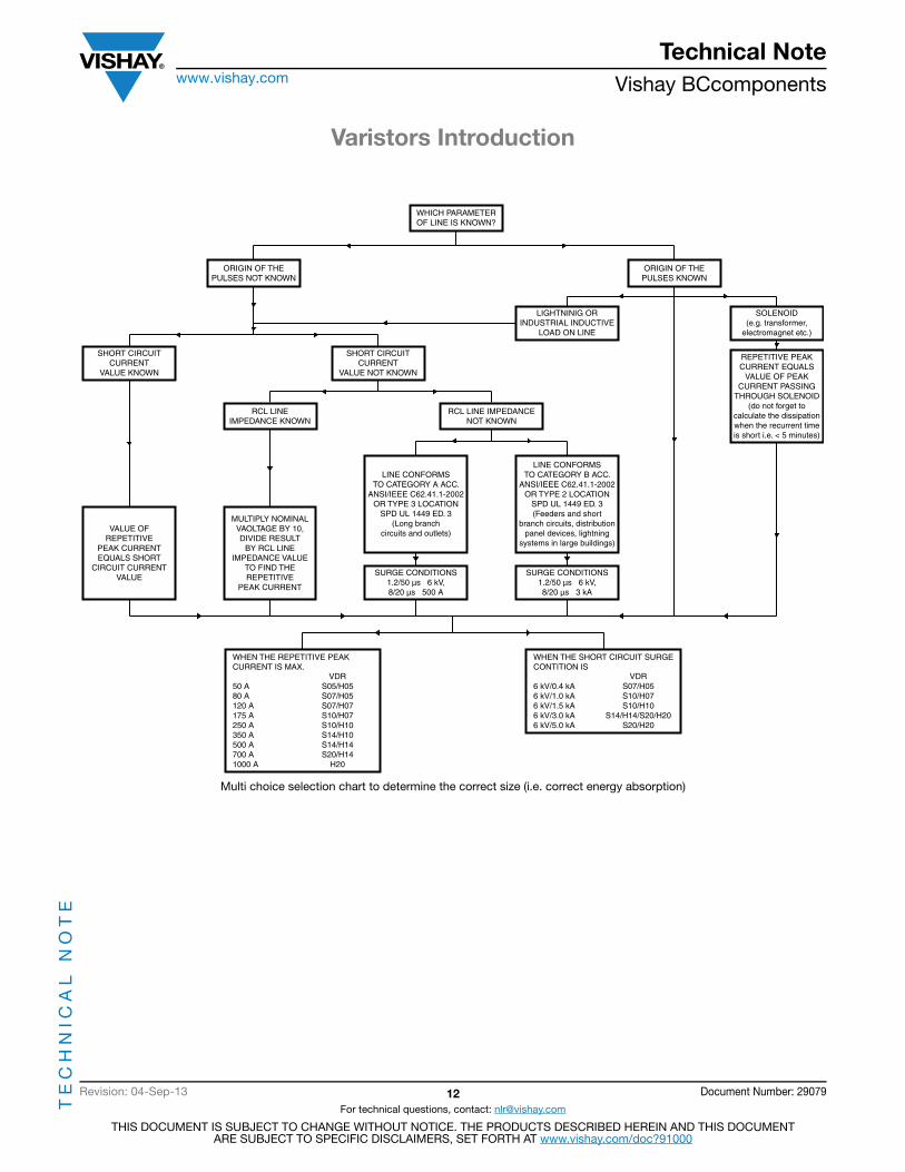
SELECTION OF THE CORRECT VARISTOR TYPEIn order to select a ZnO varistor for a specific application, the following points must first be considered:
1. The normal operating conditions of the apparatus or system, AC or DC voltage?
2. What is the maximum RMS or DC voltage?
To ensure correct selection of varistor type, two multi choice selection charts have been prepared, see charts below.
The first chart determines the necessary steady state voltage rating (i.e. working voltage) and the second chart determines the correct size (i.e. correct energy absorption).
Multi choice selection chart to determine the necessary steady state voltage rating (i.e. working voltage)
Varistors Introduction
TE
CH
NIC
AL
NO
TE
Technical Notewww.vishay.com Vishay BCcomponents
Revision: 04-Sep-13 12 Document Number: 29079
For technical questions, contact: [email protected]
THIS DOCUMENT IS SUBJECT TO CHANGE WITHOUT NOTICE. THE PRODUCTS DESCRIBED HEREIN AND THIS DOCUMENTARE SUBJECT TO SPECIFIC DISCLAIMERS, SET FORTH AT www.vishay.com/doc?91000
Multi choice selection chart to determine the correct size (i.e. correct energy absorption)
WHICH PARAMETEROF LINE IS KNOWN?
ORIGIN OF THEPULSES NOT KNOWN
ORIGIN OF THEPULSES KNOWN
LIGHTNINIG ORINDUSTRIAL INDUCTIVE
LOAD ON LINE
SOLENOID(e.g. transformer,
electromagnet etc.)
SHORT CIRCUITCURRENT
VALUE NOT KNOWN
SHORT CIRCUITCURRENT
VALUE KNOWN
REPETITIVE PEAKCURRENT EQUALS
VALUE OF PEAKCURRENT PASSING
THROUGH SOLENOID(do not forget to
calculate the dissipationwhen the recurrent timeis short i.e. < 5 minutes)
RCL LINEIMPEDANCE KNOWN
RCL LINE IMPEDANCENOT KNOWN
VALUE OFREPETITIVE
PEAK CURRENTEQUALS SHORT
CIRCUIT CURRENTVALUE
MULTIPLY NOMINALVAOLTAGE BY 10,DIVIDE RESULT
BY RCL LINEIMPEDANCE VALUE
TO FIND THEREPETITIVE
PEAK CURRENT
SURGE CONDITIONS1.2/50 µs 6 kV,8/20 µs 500 A
SURGE CONDITIONS1.2/50 µs 6 kV,8/20 µs 3 kA
LINE CONFORMSTO CATEGORY B ACC.
ANSI/IEEE C62.41.1-2002OR TYPE 2 LOCATION
SPD UL 1449 ED. 3(Feeders and short
branch circuits, distributionpanel devices, lightning
systems in large buildings)
LINE CONFORMSTO CATEGORY A ACC.
ANSI/IEEE C62.41.1-2002OR TYPE 3 LOCATION
SPD UL 1449 ED. 3(Long branch
circuits and outlets)
WHEN THE SHORT CIRCUIT SURGECONTITION IS VDR6 kV/0.4 kA S07/H056 kV/1.0 kA S10/H076 kV/1.5 kA S10/H106 kV/3.0 kA S14/H14/S20/H206 kV/5.0 kA S20/H20
WHEN THE REPETITIVE PEAKCURRENT IS MAX. VDR50 A S05/H0580 A S07/H05120 A S07/H07175 A S10/H07250 A S10/H10350 A S14/H10500 A S14/H14700 A S20/H141000 A H20
Copyright © 2022 FDOKUMEN