Introduction to Water Resistive Barriers (WRBs) & Air Barriers
Upload
khangminh22Category
view
1download
0
HAL Id: hal-01856939https://hal.archives-ouvertes.fr/hal-01856939
Submitted on 3 Feb 2019
HAL is a multi-disciplinary open accessarchive for the deposit and dissemination of sci-entific research documents, whether they are pub-lished or not. The documents may come fromteaching and research institutions in France orabroad, or from public or private research centers.
L’archive ouverte pluridisciplinaire HAL, estdestinée au dépôt et à la diffusion de documentsscientifiques de niveau recherche, publiés ou non,émanant des établissements d’enseignement et derecherche français ou étrangers, des laboratoirespublics ou privés.
Two-stage unbuffered CFOA based non-invertingresistive-feedback amplifier: a study based on thedescription of the operational transconductance
conveyor (OTC)Herve Barthelemy, Remy Vauche, Valentin Gies, Sylvain Bourdel, Jean
Gaubert
To cite this version:Herve Barthelemy, Remy Vauche, Valentin Gies, Sylvain Bourdel, Jean Gaubert. Two-stage un-buffered CFOA based non-inverting resistive-feedback amplifier: a study based on the description ofthe operational transconductance conveyor (OTC). Analog Integrated Circuits and Signal Processing,Springer Verlag, 2018, 97 (2), pp.243-252. �10.1007/s10470-018-1219-0�. �hal-01856939�

Analog Integrated Circuits and Signal Processing (2018) 97:243–252
https://doi.org/10.1007/s10470-018-1219-0
https://link.springer.com/epdf/10.1007/s10470-018-1219-
0?author_access_token=kgBJss3Sp0osxUuZUTQL5ve4RwlQNchNByi7wbcMAY4aZEjLid
NAjVlNgBa-
rhocx6_nWJbv3UGAydIAOYvatiWrQbCMn4JxTpJxhj9yfrMOyUSzokRMpKBQ9L2WevC
5VE5LPhp3dW6VUoxGbL45sw%3D%3D
Two-stage unbuffered CFA based non-inverting resistive-
feedback amplifier: a study based on the description of the
operational transconductance conveyor (OTC).
H. Barthélemy, R. Vauché, V. Giès, S. Bourdel, J. Gaubert
Abstract
A study of the non-inverting amplifier based on a two stages CMOS unbuffered current-feedback-
amplifier (UCFOA) is proposed in this paper. Using a small-signal equivalent circuit (macro-model) of
the non-inverting amplifier, a theoretical explanation of the closed loop gain is given. The opamp phase
margin and its bandwidth have been estimated from the quality factor Q of resonance and using a
novel description of the UCFOA input stage called Operational Transconductance Conveyor (OTC). The
OTC description can be viewed as an extension of type II second generation current conveyors. Based
on the fundamental parameters of the proposed OTC, a theoretical approach given in this paper
explains how to evaluate precisely the value of the UCFOA compensation capacitance. PSPICE was used
to simulate both the theoretical macro-model and the CMOS configuration from a 0.35m typical
BSIM3V3 transistor models.
Index Terms — opamp, current feedback amplifier, transconductance amplifier, diamond transistor,
current conveyor
1. INTRODUCTION
Since the discovery of the negative feedback amplifier by HS Black [1,2], a few number of feedback
amplifier topologies arose from industry. This is due to the fact that these topologies are synthesized
from the Voltage Controlled Current Sources (VCCS) which can be electrically simulated, historically by

vacuum tubes and more recently by Bipolar Junction Transistors (BJT) or Metal Oxide Semiconductor
(MOS) transistors. Today, two main types of voltage output operational amplifiers are available on the
market: i) Voltage Feedback Operational Amplifier (VFOA) [3,4] and ii) Current Feedback Operational
Amplifier (CFOA) [5-8]. The first sold VFOA was the K2-W operational amplifier produced in 1952 [2]
and the concept of the current-feedback was introduced around 1942 [9], while the first silicon
integrated CFOA topology was probably firstly suggested by D. J. Hamilton in 1964 [10]. The first
commercial silicon CFOA called CLC103, was produced by Comlinear corporation in 1982 [11], 20 years
after the first commercial silicon VFOA developed by Wildlar and Talbert [4]. The CFOA and the VFOA
provide both a voltage type output. However, when their output voltage amplifier (output voltage
buffer) is not implemented, they are called unbuffered VFOA (UFVOA) and unbuffered CFOA (UCFOA)
and provide both a current type output (high output impedance).
Fig.1. Typical two stages UVFOA and UCFOA CMOS topologies: (a) UVFOA : two stage CMOS Miller
OTA (ref. [16] with CM=0) (b) UCFOA two stage current mode operational amplifier.
Since the emergence of the CMOS technology, most of loading impedances are capacitive. In this case,
the unbuffered operational amplifier could also provide a higher DC open loop gain voltage. For this
reason, most analog IC designers use unbuffered feedback operational amplifiers [12] instead of
classical output voltage operational amplifiers. The Unbuffered VFOA (UVFOA) can be considered as
an Operational Transconductance Amplifier (OTA) since its input impedances are high [13-15].
However, the Unbuffered CFOA (UCFOA) can only be considered as a non-ideal OTA since its negative
input node does not provide a high input impedance [6-8]. Thus, use of the OTA acronym for UCFOA
can create a misunderstanding. For this reason, the term “Operational Transconductance Conveyor”
(OTC) is used in this paper to describe the UCFOA topologies. This proposed Operational

Transconductance Conveyor (OTC) is also an extension of the type II current conveyors and that it will
be useful in analog signal processing. Here, using VFOA, CFOA, OTA and OTC acronyms, Table I
summarizes the input and output types for the four operational amplifiers previously discussed.
Part (a) of Fig. 1 shows a typical CMOS configuration of a two-stage Miller OTC (two-stage UCFOA)
which is used in [16] to implement a high frequency gyrator. This circuit is part of the CFOA family since
the node in- is not voltage buffered and also, it exists an AC current flowing through the node in- and
the source of M2. Part (b) of Fig. 1 shows the CMOS classical two-stage Miller OTA (two-stage UVFOA)
using a traditional pair of two transistors (M1 and M2). This circuit is part of the VFOA family since the
nodes in+ and in- are connected to MOS gates. For both of them, the node Z is a High Impedance Node
(HIN) which allows an operational amplifier with high transconductance gain to be achieved thanks to
the second stage.
Fig. 2. Electrical description of the two stages unbuffered current feedback amplifier
(Ideal UCFOA for RX=0 and ZR ), the Miller capacitance is not represented.
The purpose of this paper introduces a general approach to study a non-inverting amplifier based on
two-stage UCFOA for which the topology is shown in Fig. 2. The study proposed here will differ from
traditional ones because the opamp output is not voltage buffered. The circuit is composed of an input
TABLE I Mains opamps topologies
(I : CURRENT TYPE V: VOLTAGE TYPE)
Opamps
Inputs Output
(in+) (in-) (out)
Voltage output types
VFOA V V V
CFOA V I V
Current output types (unbuffered opamps)
OTA V V I
OTC V I I

stage (OTC), a high impedance RZ at node Z (HIN), and a single output voltage controlled current source
called here Negative Transconductance Amplifier (NTA). In this representation, the node in+ of the
UCFOA is voltage buffered by a Unit Gain Voltage Amplifier (UGVA). Moreover, the node AC-GND is
supplied at the DC common mode-voltage of the operational amplifier. This common mode voltage is
generally chosen to obtain the maximum dynamic for output voltage. This leads to set VAC-GND to
(VDD+VSS)/2 where VDD and VSS are respectively the positive and negative supply voltages of the
operational amplifier. Then VAC-GND is equal to VDD/2 (resp. 0V) when VSS is set to 0V (resp. VDD). Finally,
an ideal UCFOA is obtained when RX is null and RZ infinite.
In section II, a discussion about the OTC is given. Using as a case study, a two-stage Miller OTC is
presented and simulated in section III. In section IV, a theoretical analysis of the non-inverting
amplifier is proposed. This analysis and theory are based on the proposed equivalent macro-model of
the CMOS configuration using small-signals. Simulation results, discussions, and comparison with
theory are given in section V before the conclusion in section VI.
2. OPERATIONAL TRANSCONDUCTANCE CONVEYOR
In Fig.2, when the current ration |IZ/IX|=1, the OTC can be designed from different popular active
elements like the 2nd generation Current Conveyor (CCII) [17], the 2nd generation current-controlled
current conveyor (CCCII) [18] or the diamond transistor [6,8] for examples. Using the OTC description
allows us to consider all possible topologies in terms of current gain (IZ/IX), i.e. equal or different than
1, in conjunction with different values of the equivalent resistance RX. Using a proposed symbol for
the OTC (input stage) and the NTA symbol (output stage) as ideal active elements, Fig.3a shows the
non-inverting amplifier configuration.
Fig. 3. Two-stage Miller UCFOA based non-inverting amplifier (a) Equivalent circuit using a one-stage
OTC as input stage and NTA as output stage (b) equivalent circuit based on a two stages high
GM OTC (Miller OTC).

Equation (1) shows that the two-stage OTC has the same order of magnitude than a classical two-stage
Miller OTA. Its transconductance gain GM which is given by:
0M m ZG g g R (1)
has the same order of magnitude than a classical two-stage Miller OTA. From Fig. 2, the following
formula of IX:
/X D XI V R (2)
and IZ:
Z m DI g V (3)
can be obtained. By defining a parameter equals to the current gain between IX and IZ as follows:
Z
X
I
I (4)
the parameter can be expressed from (2) and (3) as a function of gm and RX which gives:
m Xg R (5)
Table II gives some examples of correspondences with popular active elements according to RX and
values. As mentioned previously, the OTC also offers the great advantage of taking into account every
RX and current gain compared for example with CCII [6,17,18], or diamond transistor [6]. Thus, in the
same way that an OTA is a universal active element which permits to describe the VFOA input stage,
an OTC permits to describe all CFOA input stage.
TABLE II
OTC example of correspondences for ||=1 and ||>1
RX gm
-1 0 OTC = CCII+ [17]
+1 0 OTC = CCII- [17]
-1 0RX /RX OTC =CCCII+ [18] (diamond transistor [8])
+1 0RX /RX OTC = CCCII- [18]
<0 0RX /RX OTC ( positive output)
>0 0RX /RX OTC (negative output)

Fig.4. Example of: (a) OTC based OTA and UGVA (b) OTA based OTC and CM (Current Mirror).
To underline the difference between the OTA and the OTC, an OTA configured with an internal OTC,
and an OTC configured with an internal OTA are respectively shown in part (a) and (b) of Fig. 4. It is
possible to observe that in part (a) of Fig. 4, the OTA transconductance gm is the same than the internal
OTC, whereas in part (b) of Fig. 4, the OTC transconductance gain gm is given by gm =|.gmx where is
the gain of the current Mirror (CM) and it is the same coefficient used to define the OTC. The
commercial CFOA [6-8] exhibit very low RX in BJT technologies compared to CMOS technologies
operating at low-power. Consequently, the stability condition could differ in CMOS applications since
it is not possible to always consider RX very low [6-8].
3. STUDY OF A TWO-STAGE CMOS MILLER OTC
To illustrate the configuration shown in Fig.2 (or Fig.3), a CMOS Miller OTC loaded by the CL capacitance
is shown in Fig.5. Note that a class AB equivalent output could be constructed by designing an
additional high impedance node at the drain of M2 [16]. All simulation was performed for
VDD=VSS=1.5V.
Fig.5. A CMOS two-stage Miller OTC.

In Fig.5 M1 to M10 (except M7) simulate the OTC input stage (nodes in+, in- and Z) and M11 (biased by
M7) simulates the NTA (node Z and out). By considering M1 identical to M2, M3 and M4, their respective
transconductance gain gm1, gm2, gm3, and gm4 are identical for a given temperature. At a small-signal
amplitude and a low frequency of operation, the AC source-drain current of M4 is half of the AC current
IX passing through the node in- [18]. Consequently, the corresponding value of is +0.5 for this
topology.
Table III summarizes the MOS transistor size used for all the PSPICE-BSIM simulations of the circuit in
Fig.5 [19]. In Table III, an estimation of the drain and source areas (AD, AS) and perimeters (PD,PS)
permits to take into account the MOS junction capacitance effects [20]. The transistor sizes proposed
here have been fixed to provide similar transconductance and power consumption than the low power
CMOS Miller OTA studied in [21].
Fig.6. DC characteristics of the two stages Miller OTC in Fig.8, Vin-=0V.
TABLE III Transistors sizes and equivalent drain and source areas (AD, AS) and
perimeters (PD, PS) [16].
Transistors W
(m)
L
(m)
AD=AS (m2) PD=PS
(m)
M1,M2 108 1.5 189E-12 110E-6
M3,M4 54 1.5 94E-12 56E-6
M5,M6,M8,M9,M10 15 1.5 26E6-12 17E-6
M7 237 1.5 415E-12 240E-6
M11 154 1.5 270E-12 157E-6

The simulated DC differential characteristic of the operational amplifier is shown in Fig. 6 for Vin-=0 and
Table IV summarizes the main simulated performances (at this stage CM was fixed here from simulation
only. The DC input offset of -1.2mV seen in Fig. 6, which is high compared with a classical operational
amplifier based on the traditional differential pair of two transistors [14], is mainly due to the diodes
made by the transistors M1 and M3 since their drain are connected to their gate. In Table IV, AOPL is the
operational amplifier DC open-loop voltage gain and can be written as follows:
0 0 0OPL m Z MA g g R R G R (6)
where R0 is the equivalent output resistance of the operational amplifier, which is approximately
equals to the parallel association of drain-source resistors RDS of M7 and M11. AOPL is the open loop
voltage gain when not output current occurs, which will not be the case of the unbuffered opamp in
Fig.3.
4. THEORETICAL ANALYSIS OF THE NON-INVERTING AMPLIFIER CONFIGURATION
This section presents a theoretical analysis of the non-inverting amplifier using a two-stage Miller OTC
(UCFOA). The objective of this section is to present a versatile opamp macro-model and its associated
theory. We also aim at being able to estimate the value of the compensation capacitance CM for a
wanted phase margin and to demonstrate that “RX” and “” are the keys design parameters. The non-
inverting amplifier configuration is kept in the part (a) of Fig.7 while the part (b) of Fig.7 shows the
proposed equivalent macro-model of the non-inverting amplifier. This proposed macro-model takes
TABLE IV Main PSPICE simulated characteristics of the Two Stage Miller OTC in Fig.5
for VDD=VSS=1.5V, IBIAS=17A.
Parameters value Units
AOPL 58 000 [V/V]
THD% (out-
600mVpp)
6.2 %
TRMC (dB) 50.3 dB
GM 632 [m]
VOFF @ in+
(Vin-=0)
-1.2 [mV]
GBW(1) (G0=1)
(Vout=Vin-)
CM=50fF
94
[MHz]
ZIN+ 565k //0.7pF
ZIN- RX=1829.6 []
Total power supply 988 [W]
(1) CM is fixed to have no overshoot.

into account the main parasitic elements that appear when the OTC presented in the previous section
is designed in CMOS technologies.
Fig.7. OTC based Non-inverting amplifier (a) Circuit (b) Proposed equivalent
macro-model including the main parasitic elements of the circuits in Fig.8.
The impedances of the OTC macro-model in Fig.7b are defined as follows:
2//X XZ R C s (7)
//Z Z ZZ R C s (8)
1 1 1//Z R C s (9)
0 0 0//Z R C s (10)
where Z0 is the equivalent output impedance of the NTA.
Table V gives the correspondences between the macro-model and the transistors small-signal
parameters. Parameters of the macro-model has been extracted from the PSPICE “.AC” simulation of
the CMOS configuration around the DC operating point which is fixed in our case by the DC bias current
Ibias and the voltage supplies VDD and VSS (Ibias=17A). Expressions of RZ and CZ consider that the voltage
variations at node in- in Fig.5 are very small regarding the voltage variations at node Z (high impedance
node). For a transistor Mi, RDSi is the output resistance, gmi is the gate-source transconductance, CDBi
and CGSi are respectively the drain-bulk and gate-source equivalent capacitances.
Note that the parasitic resistance in parallel with R1 has been neglected and we assume that the effect
of the time constant ‘RXC2’ and ‘R1C1’ are far outside the frequencies of operation. Based on these
considerations and after analytical calculation, the voltage transfer function (closed-loop voltage gain)
is given by:

00
02
00
02 0
(1 )
(1 )(1 )
(1 ) 11 (1 )
(1 )(1 )
OUT Z
INX
Z
t sA
V t s t s
t sVA t s
t s t s K
(11)
where:
20
1
1R
KR
(12)
0
0
MCt
g (13)
02 02 0( )Mt R C C (14)
2 0( ).X MX
R K R Ct
(15)
( )Z Z M Zt R C C (16)
0 020
2 0([ / ] )
Z
X
g R RA
R K R
(17)
and:
0 202 0 2
0 2
( / / )R R
R R RR R
(18)
The analytical calculations given above have been performed considering the following conditions:
RX is non zero
1D/R1 and 1)]DR/(RR[ 2X1 with D=R1R2+RX[R1+R2]
In (11) A0 is the DC open loop gain and is different to the DC open-loop gain of the opamp AOPL given in
equation (6) because the resistive feedback consumes a current that could not be neglected. Since the
time constant t0=CM/g0 appears at very high frequency, the expression of VOUT/VIN can be reduced to:
2
Z02
0
0xZ02
0
0
R0
IN
OUT
sttA
Ks]t)tt(
A
K[1
K
V
V
(19)
where
0A
0
0
0R0 K]K
A1/[AK
0 (20)
Here, KOR is the effective DC gain of the transfer function and K0=1+(R2/R1) is the ideal DC gain when A0
tends to infinity. Equation (19) shows that the non-inverting amplifier operates like a second order
low-pass frequency filter for which the Q factor of resonance can be used as follows:

2
0
2
1
OR
2
0
2
0
OR
IN
OUT
f
f
f
jf1
K
s
Q
s1
K
V
V
(21)
with:
X0Z020
Z0200
0
1
tA)tt(K
ttKA
f
fQ
(22a)
or
)CRCR(KC)]RKR(A)RR(K[
C)CC(RRKA)C(Q
ZZ0020MX020Z020
M0MZ0200
M
(22b)
x0Z020
01
tA)tt(K
A
2
1f
(23)
and:
Z020
00
ttK
A
2
1f
(24)
The phase margin (M) of the effective open-loop gain can then be calculated [22], we have:
1Q41
2tan
2
1
M (25)
or
1]tA)tt(K[
ttKA41
2tan
2
x0Z020
Z0200
1
M (26)
Equations (22) and (26) allow to estimate the resonance factor and the phase margin. Note that
equation (26) shows that the phase margin (M) is function of A0 and not of not AOPL
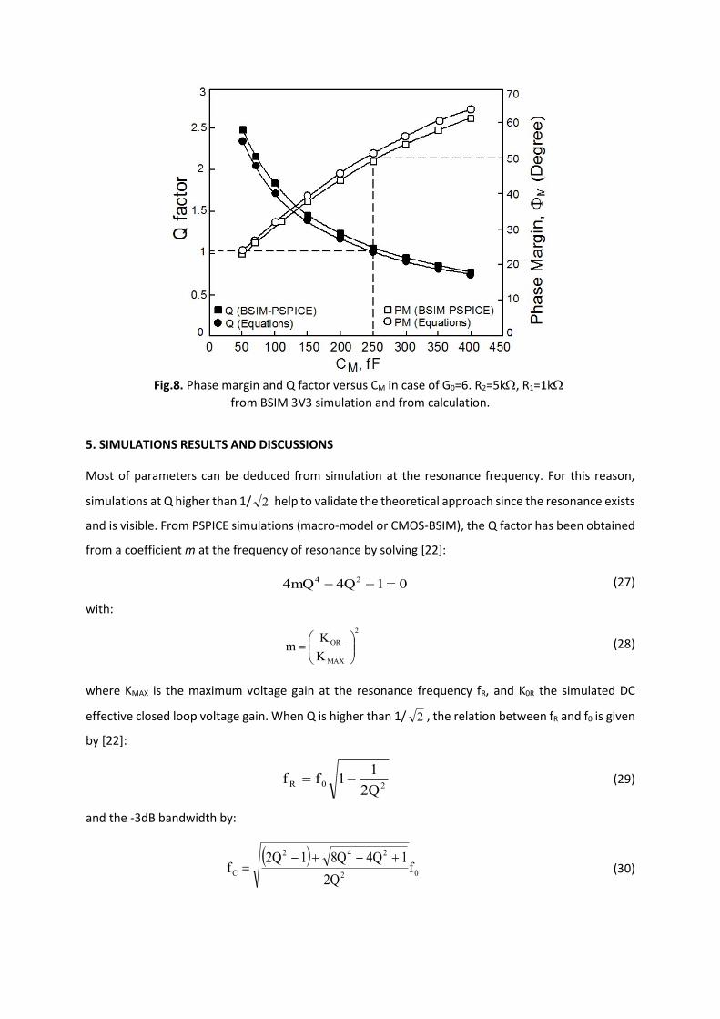
Fig.8. Phase margin and Q factor versus CM in case of G0=6. R2=5k, R1=1k
from BSIM 3V3 simulation and from calculation.
5. SIMULATIONS RESULTS AND DISCUSSIONS
Most of parameters can be deduced from simulation at the resonance frequency. For this reason,
simulations at Q higher than 1/ 2 help to validate the theoretical approach since the resonance exists
and is visible. From PSPICE simulations (macro-model or CMOS-BSIM), the Q factor has been obtained
from a coefficient m at the frequency of resonance by solving [22]:
01Q4mQ4 24 (27)
with:
2
MAX
OR
K
Km
(28)
where KMAX is the maximum voltage gain at the resonance frequency fR, and K0R the simulated DC
effective closed loop voltage gain. When Q is higher than 1/ 2 , the relation between fR and f0 is given
by [22]:
20RQ2
11ff (29)
and the -3dB bandwidth by:
02
242
C fQ2
1Q4Q81Q2f
(30)

Fig.9. Transient output response of the non-inverting OTC with a 2MHz, 20mV peak-to-peak input
pulse voltage at node in+, G0=6, R2=5k, R1=1k, CM=250fF, Q~1.
Fig.8 shows the equivalent Q factor and phase margin versus the capacitor CM obtained from the
presented theory and from simulation of the CMOS configurations in Fig.5 when R2=5k and R1=1k
(K0=6). In Fig. 8, “Equations” label means that Q and M have been calculated from equation (26) and
by using the parameters of the macro-model given in Table V. Moreover, the Q factor has been
computed from the simulated values of the ratio m=KOR/KMAX and by solving (27) and (28). The values
of Q and CM extracted from simulation of the macro-model and or computed from equations are very
close to the one obtained by simulation of the CMOS configuration using the BSIM models. To
underline this accuracy of the proposed macro-model and theory, Fig.9 shows the simulated transient
response of the CMOS-BSIM (Fig. 5, Table III) and MACRO-MODEL (part (b) of Fig.7, Table V). Note that
the proposed macro-model is valid at AC small signal amplitude only, consequently this simulation of
the macro-model shows any DC offset voltage.
Finally Table VI summarizes the main performances of the non-inverting amplifier when the phase
margin is around 50° (Q factor around Q=1), G0=6 with R2=5k and R1=1k. In this case, the
TABLE V Equivalence between the macro-model, CL and the transistor small-
signal parameters obtained from PSPICE (Fig.5),
VDD=VSS=1.5V, IBIAS=17A.
RX 1
4m2m )gg( 1829
RZ RDS4//RDS10 1110 k
R0 RDS7//RDS11 92.6 k
g0 gm11 2.65e-3
CZ CDB4+CDB10+CGS11 1.05 pF
C0 CDB7+CDB11+CL 10.8 pF
IZ/IX 0.39
GM Zm0M R.g.gG 632 m

compensation capacitor has been fixed to 250fF (see Fig.8) which corresponds to the one expected in
theory. Note that Fig.8 confirms that calculation (theory) and CMOS simulation match very well for
different value of CM between 50pF and 400pF.
6. CONCLUSION
This paper has introduced the operational transconductance conveyor and proposed a study of the
non-inverting amplifier based on a CMOS unbuffered current-feedback-amplifier. A precise macro-
model has been used and compared with theory and with an equivalent CMOS topology. We have
shown that the theoretical approach which consists in the definition of the Q factor allows to set the
Miller capacitance with precision, regarding the phase margin. The correlation between the Q factor
extracted from simulations and the Q factor computed from theory shows relevance of the proposed
approach. We hope that this study and its associated theory using the OTC description will be useful
for analog designers, especially for understanding the frequency performances of the operational
current feedback amplifiers. Moreover the Operational Transconductance Conveyor (OTC) is an
extension of all actual type II current conveyors (CCII, CCCII, diamond transistor).
REFERENCES
[1] Harold S. Black, “Inventing the negative feedback amplifier", IEEE Spectrum, vol. 14, pp. 54-60,
Dec. 1977. (50th anniversary of Black's invention of negative feedback amplifier).
[2] W. Jung: "Amp History", Analog Device, http://www.analog.com/media/en/training-
seminars/design-handbooks/Op-Amp-Applications/SectionH.pdf pp. H1-H70.
[3] W. G. Jung : “IC Op-Amp Cookbook”, by Howard W. Sams & CO., Publisher SAMS 1974.
TABLE VI
Main Performances of the Non-Inverting Amplifier R2=5K, R1=1K AND
CM=250FF
Equations
Theoretical
Macro-
model .AC PSPICE
BSIM
.AC PSPICE
fC (-3dB) 13.7 14 14 [MHz]
fR 7.69 8.11 8.11 [MHz]
KMAX 7 7.18 7.18 [V/V]
KOR 5.98 5.98 5.94 [V/V]
Q 1.02 1.06 1.07 -
Calculation using the theoretical equations
R02 4.74k [V]
AOPL 57.9k [V/V]
GM 626 [m1]
A0 2040 [V/V]
M 51.5 [Deg.]

[4] J.C Whitaker : “The Electronics handbook”, second edition, Ed. Taylor & Franci Group, CRC.
[5] R. Senani, D. Bhaskar, A. K. Singh, V. K. Singh : “Current Feedback Operational Amplifiers and
Their Applications”, Ed. Springer Science + Business Media New York 2013.
[6] Texas Instruments: “OPA 860: Wide bandwidth operational transconductance amplifier (OTA)
and Buffer”, SBOS331C- Revised august 2008, pp.1-27.
[7] Analog Devices : “AD844”, www.analog.com, Rev. F, pp. 1-20.
[8] Texas Instruments: “OPA 861: Wide bandwidth operational transconductance amplifier (OTA)”,
SBOS338G - Revised May 2013, pp.1-23.
[9] Members of the Staff of the Department of Electrical Engineering of the Massachusetts
Institute of Technology, Appl. Electron., New York: Wiley, p. 531, 1943.
[10] J. B. Downey : “Investigation of electronic switches for Analog Computer Applications”, M.S.
Thesis, University of Arizona, February, 1964.
[11] David Nelson and Kenneth Saller : “Settling time reduction in wide-band direct-coupled
transistor amplifier”, US patent n° US4502020, 1985.
[12] S. Bandyopadhyay1, D. Mukherjee, R. Chatterjee : “Design Of Two Stage CMOS Operational
Amplifier in 180nm Technology With Low Power and High CMRR”, International Journal of
Recent Trends in Engineering & Technology, Vol. 11, June 2014, pp. 239-247.
[13] J. Silva-Martínez, M. Steyaert, W. Sansen : “High-Performance CMOS Continuous-Time Filters:
Design Considerations for OTA-C Integrators and Full CMOS Resistors”, Vol. 223, the Springer
International Series in Engineering and Computer Science, 1993, pp. 67-119.
[14] R. M. Thanki, H. R. Sanghani, R. K. Lamba : “Design of Operational Transconductance Amplifier:
Analysis of Schematic Circuit and CMOS Layout of OTA”, Publisher Lambert Academic
Publishing 2011.
[15] Texas Instruments: “LM13700 Dual operational transconductance amplifier with linearizing
diodes and buffers”, SNOSBW2F – Revised November 2015.
[16] A. Thanachayanont, S.S. Ngow : “Class AB VHF CMOS active inductor”, 2002 45th Midwest
Symposium on Circuits and Systems, 2002, MWSCAS-2002, pp. 64-67.
[17] K.C. Smith,A. Sedra : “The current conveyor: a new circuit building block”. Proceeding IEEE CAS,
1968, vol. 56, no. 3, p. 1368-1369.
[18] A. Fabre, O. Saaid, F. Wiest, F. Boucheron : “High frequency applications based on a new
current-controlled conveyor”. IEEE Transactions on Circuits and Systems I: Fundamental Theory
and Applications, 1996, vol. 43, no. 2, p. 82-91.
[19] Multi-Project Circuits: “Products: IC Manufacturing : AMS 0.35 C35B4”,
cmp.imag.fr/product/ic, www.ams.com.
[20] P. Antognetti, G. Massobrio : “Semiconductor device modeling with spice”, Ed. Mc Graw-Hill,
New-York 1990.
[21] F. P. Cortes, E. Fabris, S. Bampi : ‘Analysis and design of amplifier and comparators in CMOS
0.35m technology’, Microelectronics Reliability,n°44, ed. Elsevier (2004), pp 657-664
[22] C. Basso : “Transient response counts when choosing phase margin”, Power Electronics
Technology, www.powerelectronics.com, November 2008, pp. 18-21.
Copyright © 2022 FDOKUMEN