Raman Enhancement of a Dipolar Molecule on Graphene
8
Raman Enhancement of a Dipolar Molecule on Graphene Changshui Huang, †,§ Myungwoong Kim, †,§ Bryan M. Wong, ‡ Nathaniel S. Safron, † Michael S. Arnold, † and Padma Gopalan* ,† † Department of Materials Science & Engineering, University of Wisconsin-Madison, Madison, Wisconsin 53706, United States ‡ Department of Chemistry and Department of Materials Science & Engineering, Drexel University, Philadelphia, Pennsylvania 19104, United States * S Supporting Information ABSTRACT: We show a large enhancement in the Raman signal from a highly polarizable molecule attached to single layer graphene. Through spatial mapping of the Raman signal and wavelength-dependent Raman measurements from a dipolar chromophore latched to a graphene/SiO 2 substrate and to a bare SiO 2 substrate, we show that strong electronic coupling in the hybrid structure contributes to the enhance- ment. The dipolar molecule is a pyrene tethered Disperse Red 1 (DR1P) that noncovalently binds to graphene. Upon comparison of the Raman signal of DR1P on single layer graphene with that on a bare SiO 2 /Si substrate, we found that the enhancement factor is in the range 29−69 at 532 nm excitation. As the surface coverage of DR1P on graphene increases, Raman intensity also increases and saturates at a certain concentration. The saturation of the Raman signal intensity at higher DR1P concentrations were accompanied by shifts in the G band and the 2D band of graphene due to p-doping. We further show that the Raman enhancement that occurs on single layer is larger than on few layer graphene. Quantitative analysis on the Raman scattering cross section of DR1P on graphene shows a higher Raman scattering cross section compared to that in solution confirming a strong electronic coupling. A series of all- electron ab initio calculations using density functional theory (DFT) modeled the noncovalent binding of DR1P on a large graphene fragment where the pyrene tether is interacting with the graphene fragment via π−π stacking interactions. The DR1P molecule has occupied energy levels that are close to the Fermi level of graphene, and these interact strongly with the semimetallic nature of graphene. As a consequence, in complete contrast to the isolated DR1P molecule, our time-dependent DFT calculations show that the orbital energies and densities for DR1P are significantly modified by the graphene substrate. ■ INTRODUCTION In recent years, there has been tremendous interest in creating a new material platform using hybrid organic molecules/ graphene interfaces. 1−3 One possible way organic molecules adsorbed on graphene electronically interact with graphene is through the dipole moment in the organic molecule, typically resulting in a large amplification of relatively small change in electrostatic potential from the dipole moment due to the high quantum capacitance of graphene. 2,4−6 Simultaneously, this interaction can also lead to the mixing of molecular orbitals of the molecule with graphene, thus altering the electronic and optical properties of the bound molecules. This has been observed with Raman spectroscopy, where the Raman scattering signal of the molecule adsorbed on graphene is greatly enhanced, commonly termed as graphene-enhanced Raman scattering (GERS). 7−9 In general, the enhancement of the Raman signal on a solid surface, called surface-enhanced Raman scattering (SERS), is a powerful analytical technique for chemical or biochemical analysis as the intensity enhancement factor is in the range 10− 10 7 . SERS occurs by two different mechanisms: the electro- magnetic enhancement mechanism (EM) and chemical enhancement mechanism (CM). 10 In the EM, the amplification of an electromagnetic field occurs by the generation of surface plasmon on metallic nanostructures. 10−13 The CM is mostly associated with changes in the electronic structure through the chemisorption of the molecules to the substrate, leading to more efficient charge transfer excitations and higher Raman scattering cross section. 10,12,14,15 In GERS, the molecule is adsorbed on graphene instead of a metal surface, leading to the enhancement in the Raman scattering signal similar to SERS, as the Raman scattering signal is enhanced if the molecule is placed on the surface of graphene. 9 Since graphene has completely different electronic structure and properties compared to the conventional surfaces for SERS, different mechanisms have been proposed in the literature, but the mechanism is not entirely understood. For example, it has been reported that charge transfer by interaction of the molecule with graphene or field effect in transistor geometry causes enhancement in Raman scattering. These results indicate that Received: October 31, 2013 Revised: December 26, 2013 Published: January 3, 2014 Article pubs.acs.org/JPCC © 2014 American Chemical Society 2077 dx.doi.org/10.1021/jp410749a | J. Phys. Chem. C 2014, 118, 2077−2084
-
Upload
ucriverside -
Category
Documents
-
view
2 -
download
0
Transcript of Raman Enhancement of a Dipolar Molecule on Graphene

Raman Enhancement of a Dipolar Molecule on GrapheneChangshui Huang,†,§ Myungwoong Kim,†,§ Bryan M. Wong,‡ Nathaniel S. Safron,† Michael S. Arnold,†
and Padma Gopalan*,†
†Department of Materials Science & Engineering, University of Wisconsin-Madison, Madison, Wisconsin 53706, United States‡Department of Chemistry and Department of Materials Science & Engineering, Drexel University, Philadelphia, Pennsylvania 19104,United States
*S Supporting Information
ABSTRACT: We show a large enhancement in the Ramansignal from a highly polarizable molecule attached to singlelayer graphene. Through spatial mapping of the Raman signaland wavelength-dependent Raman measurements from adipolar chromophore latched to a graphene/SiO2 substrateand to a bare SiO2 substrate, we show that strong electroniccoupling in the hybrid structure contributes to the enhance-ment. The dipolar molecule is a pyrene tethered Disperse Red1 (DR1P) that noncovalently binds to graphene. Uponcomparison of the Raman signal of DR1P on single layergraphene with that on a bare SiO2/Si substrate, we found that the enhancement factor is in the range 29−69 at 532 nmexcitation. As the surface coverage of DR1P on graphene increases, Raman intensity also increases and saturates at a certainconcentration. The saturation of the Raman signal intensity at higher DR1P concentrations were accompanied by shifts in the Gband and the 2D band of graphene due to p-doping. We further show that the Raman enhancement that occurs on single layer islarger than on few layer graphene. Quantitative analysis on the Raman scattering cross section of DR1P on graphene shows ahigher Raman scattering cross section compared to that in solution confirming a strong electronic coupling. A series of all-electron ab initio calculations using density functional theory (DFT) modeled the noncovalent binding of DR1P on a largegraphene fragment where the pyrene tether is interacting with the graphene fragment via π−π stacking interactions. The DR1Pmolecule has occupied energy levels that are close to the Fermi level of graphene, and these interact strongly with thesemimetallic nature of graphene. As a consequence, in complete contrast to the isolated DR1P molecule, our time-dependentDFT calculations show that the orbital energies and densities for DR1P are significantly modified by the graphene substrate.
■ INTRODUCTION
In recent years, there has been tremendous interest in creating anew material platform using hybrid organic molecules/graphene interfaces.1−3 One possible way organic moleculesadsorbed on graphene electronically interact with graphene isthrough the dipole moment in the organic molecule, typicallyresulting in a large amplification of relatively small change inelectrostatic potential from the dipole moment due to the highquantum capacitance of graphene.2,4−6 Simultaneously, thisinteraction can also lead to the mixing of molecular orbitals ofthe molecule with graphene, thus altering the electronic andoptical properties of the bound molecules. This has beenobserved with Raman spectroscopy, where the Ramanscattering signal of the molecule adsorbed on graphene isgreatly enhanced, commonly termed as graphene-enhancedRaman scattering (GERS).7−9
In general, the enhancement of the Raman signal on a solidsurface, called surface-enhanced Raman scattering (SERS), is apowerful analytical technique for chemical or biochemicalanalysis as the intensity enhancement factor is in the range 10−107. SERS occurs by two different mechanisms: the electro-magnetic enhancement mechanism (EM) and chemical
enhancement mechanism (CM).10 In the EM, the amplificationof an electromagnetic field occurs by the generation of surfaceplasmon on metallic nanostructures.10−13 The CM is mostlyassociated with changes in the electronic structure through thechemisorption of the molecules to the substrate, leading tomore efficient charge transfer excitations and higher Ramanscattering cross section.10,12,14,15 In GERS, the molecule isadsorbed on graphene instead of a metal surface, leading to theenhancement in the Raman scattering signal similar to SERS, asthe Raman scattering signal is enhanced if the molecule isplaced on the surface of graphene.9 Since graphene hascompletely different electronic structure and propertiescompared to the conventional surfaces for SERS, differentmechanisms have been proposed in the literature, but themechanism is not entirely understood. For example, it has beenreported that charge transfer by interaction of the moleculewith graphene or field effect in transistor geometry causesenhancement in Raman scattering. These results indicate that
Received: October 31, 2013Revised: December 26, 2013Published: January 3, 2014
Article
pubs.acs.org/JPCC
© 2014 American Chemical Society 2077 dx.doi.org/10.1021/jp410749a | J. Phys. Chem. C 2014, 118, 2077−2084
controlling the charge carrier concentration and Fermi level inthe system is likely the key parameter for Raman enhance-ment.9,16,17 Other possible mechanisms involve the combina-tion of resonance Raman scattering with excitation laser andstrong fluorescence quenching by graphene.18−20
We recently reported a hybrid material by noncovalentlylatching a dipolar chromophore, namely, a pyrene tetheredDisperse Red 1 (DR1P), to graphene that effectively p-dopedgraphene with a hole concentration of ∼5 × 1012 cm−2.4 Thisclass of dipolar molecule undergoes molecular transformation(trans to cis) with external stimuli such as UV light, which canbe used as an additional handle for effective control of dopingin graphene. In these studies, we detected intense Ramanmodes from the molecule even with submonolayer coverageimplying that the interaction of DR1P with graphenepotentially led to enhanced Raman signal.On the basis of our understanding of the electronic
properties of the DR1P/graphene hybrid, here, we probe thiseffect through systematic studies of Raman scattering from thehybrid by the variation of key parameters such as excitationwavelengths, the surface coverage of DR1P (from submono-layer to multilayer), and the number of layers in the graphenesubstrate from (single layer graphene (SLG) to graphite).DR1P was deposited homogeneously onto graphene/SiO2/Siand bare SiO2/Si substrates by spin-coating, and the Ramansignals were compared. In this study, we are predominantlyexploring the GERS for the trans form of DR1P. In ourprevious report,4 we presented Raman spectra of both cis and
trans forms of DR1P. The extent of Raman signal enhancementwas similar in both cases. Quantitative analysis of Ramanscattering cross section, the saturation of Raman intensity athigh DR1P concentration and the shifts in G band and 2Dband, as well as time-dependent density functional theory (TD-DFT) calculations on the electronic structure of DR1P/graphene hybrid, all strongly suggest electronic couplingbetween the highly polarizable molecule and graphene leadingto Raman enhancement.
■ EXPERIMENTAL SECTION
DR1P was synthesized based on previous literature.21,22
Graphene samples were prepared by conventional mechanicalexfoliation of graphite onto 89 nm SiO2/Si (p++) substrateswith a typical size of ∼1 cm × 1 cm. After exfoliation, thenumber of graphene layers was determined by examining thecolor contrast in an optical microscope image and the shape ofthe 2D band and the I2D/IG intensity ratio in Raman spectra.Few layer graphene in this study refers to bilayer or trilayergraphene. A 20 μL amount of DR1P solutions in dichloro-methane with concentrations ranging from 5 × 10⁻¹⁰ M to ∼5× 10⁻⁴ M were spin-coated onto prepared graphene samples at4000 rpm for 60 s. Raman spectra of DR1P/graphene sampleswere obtained using a Thermo Scientific DXR Ramanmicroscope. The 532 and 633 nm excitation laser sourceswere used with a 100× objective lens providing a probe size of∼1 μm2. Wavenumber calibration was carried out using a Si
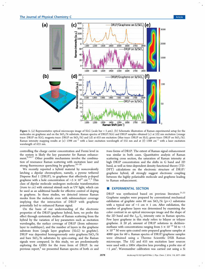
Figure 1. (a) Representative optical microscope image of SLG (scale bar = 5 μm). (b) Schematic illustration of Raman experimental setup for themolecules on graphene and on the SiO2/Si substrate. Raman spectra of DR1P/SLG and DR1P samples obtained (c) at 532 nm excitation (orangetrace: DR1P on SLG; magenta trace: DR1P on SiO2/Si) and (d) at 633 nm excitation (blue trace: DR1P on SLG; green trace: DR1P on SiO2/Si).Raman intensity mapping results at (e) 1398 cm−1 with a laser excitation wavelength of 532 nm and at (f) 1388 cm−1 with a laser excitationwavelength of 633 nm.
The Journal of Physical Chemistry C Article
dx.doi.org/10.1021/jp410749a | J. Phys. Chem. C 2014, 118, 2077−20842078

peak at 520 cm−1 as a reference. The spectra were deconvolutedby fitting with the Voigt function, and characteristic peaks wereidentified. X-ray photoelectron spectroscopy (XPS) spectra ofDR1P/graphene samples were measured with a Perkin−Elmer5400 ESCA spectrometer under Mg Kα X-ray emission. ForXPS studies, we utilized large-area graphene samplessynthesized by chemical vapor deposition on Cu. Synthesizedgraphene samples were transferred to the SiO2/Si substratefollowing the literature.23,24 DFT calculations were carried outwith the M06-L exchange-correlation functional, which isspecifically designed for noncovalent and π−π stackinginteractions. We note that the M06-L functional typically
underestimates excitation energies, since it does not take intoaccount nonlocal excitonic effects, leading to relatively red-shifted excitation energy values, but the overall trends aremeaningful for our purposes. Geometry optimizations for boththe isolated DR1P molecule and the DR1P/graphene systemwere performed, and a 6-31G(d,p) all-electron basis set wasused to calculate orbital energy levels and electron densities.For the DR1P/graphene system, we modeled the graphenesubstrate as a 5 × 5 rhombus fragment, which was sufficientlylarge enough to interact with the pyrene tether. At theoptimized geometries, a TD-DFT calculation was performed to
Figure 2. Raman spectra of different concentrations of DR1P spin-coated on graphene at (a) 532 nm and (d) 633 nm excitations (from bottom totop, the concentration was varied ranging from 5 × 10⁻¹⁰ M to 5 × 10⁻⁴ M); corresponding plots of Raman intensity as a function of concentrationat (b) 532 nm and (e) 633 nm excitations; and zoomed-in spectra of DR1P (c) 1 × 10⁻⁹ M at 532 nm excitation and (f) 5 × 10⁻⁸ M at 633 nmexcitation.
Figure 3. (a) Optical microscope image (scale bar = 5 μm) of SLG (yellow dotted circle) and FLG (red dotted circle). (b, d) Raman intensitymapping of the G band at 532 and 633 nm excitations, respectively. (c) Raman spectra of pristine SLG and FLG with 532 and 633 nm excitations. (e,g) Raman spectra of DR1P on graphene obtained with 532 and 633 nm excitations, respectively. (f, h) Raman intensity maps of (f) 1398 cm−1 peakat 532 nm excitation and (h) 1388 cm−1 peak at 633 nm excitation.
The Journal of Physical Chemistry C Article
dx.doi.org/10.1021/jp410749a | J. Phys. Chem. C 2014, 118, 2077−20842079

evaluate the lowest 20 excited states for both the isolated DR1Pmolecule and the DR1P/graphene system.
■ RESULTS AND DISCUSSIONEnhanced Raman Signal of DR1P on Graphene. Figure
1c,d shows representative Raman spectra from DR1P/SLG/SiO2 and DR1P/SiO2 regions, taken with two differentexcitation wavelengths of 532 and 633 nm, respectively. Ahomogeneous distribution of DR1P on graphene/SiO2 as wellas on SiO2 was achieved by the spin-coating method, confirmedby the XPS measurements. (Figure S1, Supporting Informa-tion) Upon excitation with the 532 nm laser, the peakintensities and the signal-to-noise ratio of DR1P on graphene(top panel in Figure 1c) are much stronger than the respectivevalues on the SiO2 surface (bottom panel in Figure 1c). Adifferent excitation wavelength (633 nm) also gave similarresults as shown in Figure 1d. Since 532 nm light falls withinthe absorption spectrum of DR1P, the overall intensity uponexcitation is higher than that of 633 nm excitation due to theresonant excitation effect.20 The enhancement of the Ramansignal is observed clearly using the spatial Raman mapping ofthe sample. Figure 1a,e,f displays the optical microscope imageof pristine graphene and the spatially resolved Raman signalmaps at ∼1398 cm−1 (532 nm excitation) and 1388 cm−1 (633nm excitation), respectively, which are assigned to ν(NN) ofDR1P. Since the surface coverage of the DR1P molecule ongraphene is controlled to be the same as that on SiO2, thedistinctively enhanced signal intensity from DR1P on grapheneis solely due to the graphene substrate.To examine the effect of different surface coverage on the
enhancement, DR1P solutions with 10 different concentrationsranging from 5 × 10⁻¹⁰ M to 5 × 10⁻⁴ M were deposited ontoSLG/SiO2/Si substrates. The intensity of the Raman signalsfrom DR1P molecules on SLG increases as the concentrationfor DR1P increases regardless of the excitation wavelengths(Figure 2a,d). In Figure 2b,e, the normalized intensity of theν(NN) mode (1398 and 1388 cm−1 for 532 and 633 nmexcitations, respectively) using a reference Si peak (520 cm−1)starts to plateau at the concentration of ∼1 × 10⁻⁴ M thatindicates the formation of the monolayer of chromophore ongraphene, following the Brunauer−Emmett−Teller model asshown in the literature.9,25 More importantly, Raman signalswere observed from very low concentrations of DR1Pmolecules, for example, 1 × 10⁻⁹ M with 532 nm excitation(Figure 2c) and 5 × 10⁻⁸ M at 633 nm excitation (Figure 2f).These concentrations are already hitting the lower limit ofconcentrations typically detected by SERS studies.9,26
Figure 3a displays the optical image of graphene pieces,showing two distinct contrasts corresponding to single layerand few layers. Raman mapping of this piece without anytreatment shows the typical characteristic signatures of G and2D bands of SLG and FLG. For example, FLG exhibits lower2D band to G band intensity ratio and a broader 2D band thanSLG, for both excitation wavelengths (Figure 3b−d). Ramanspectra taken after deposition of DR1P on the same graphenepiece clearly showed a stronger Raman signal from SLG thanthat from FLG regardless of excitation wavelength, as shown inFigure 3e,g. Raman mapping in Figure 3f,h also shows the sameclear trend in intensity of the ν(NN) mode between SLGand FLG, consistent with previous reports.9,18,27 Thesedifferences between SLG and FLG substrates could be eitherdue to differences in charge distribution through graphenelayers caused by doping, which is dependent on the number of
layers,28 or due to the changes in light reflection as the numberof graphene layers changes.18,19
From the Raman spectra, we calculated the Ramanenhancement factor for six different characteristic peaks ofDR1P. Normalized intensities of the peaks of DR1P on SLG,FLG, or graphite to the intensity on SiO2/Si without grapheneare plotted in Figure 4. For 532 nm excitation, the Raman
enhancement factors for six different peaks on SLG variedbetween 29 and 69. FLG and graphite show lower enhance-ment factors than the case of SLG. The highest values on FLGand graphite were ∼48 and ∼5, respectively. The enhancementfactors here are noteworthy when compared to the existingreports on GERS.7,9,29,30 Since the DR1 molecule has a strongdipole moment from the donor (amino group) to the acceptorend (nitro group), at 532 nm excitation, the chromophoreabsorbs the light and exhibits molecular resonance as theexcitation wavelength is within the molecular electronicabsorption,21 leading to increased molecular polarizability andincrease in the Raman scattering cross section.31,32 The sametrend was observed for 633 nm excitation, although it exhibitedlower enhancement factors.
Possible Mechanisms for Raman Enhancement inDR1P/Graphene. The Raman enhancement effect occurscommonly on the surface of metallic nanostructures such as Agor Au particles by the EM or in combination with the CM.10,11
In GERS, several experimental and theoretical studies haveshown that the electromagnetic field amplification by graphenerather than metal does not occur because strong surfaceplasmon excitation is not expected in the visible region.7,18,19
The second possible origin of the enhancement is the CMinvolving new electronic states created by the coupling of theelectronic structure of the adsorbate and the substrate.7,8,16,17
Generally, if the Fermi level of the substrate(metal) has afavorable energy such that it is symmetically located betweenthe highest occupied molecular orbital (HOMO) and thelowest unoccupied molecular orbital (LUMO) of the adsorbate,half the energy for a normal Raman excitation is needed, as thesubstrate plays an important role in forming a charge-transferintermediate.10 Another possible mechanism is a strongelectronic coupling of the adsorbate to graphene, leading tohybridization of the electronic states of the adsorbate withthose of graphene. The latter is a more feasible mechanism forDR1P/graphene hybrids due to the ability of DR1P to interactwith graphene, as mentioned earlier. Deposition of asubmonolayer of DR1P onto graphene induces charge transfer
Figure 4. Relative Raman intensity of DR1P on SLG, FLG, andgraphite with laser excitation wavelengths of (a) 532 nm and (b) 633nm for different peaks in the spectra. Blue, red, and green columnsrepresent SLG, FLG, and graphite as substrates, respectively.Intensities of peaks on SiO2/Si without graphene are set to “1”(purple column).
The Journal of Physical Chemistry C Article
dx.doi.org/10.1021/jp410749a | J. Phys. Chem. C 2014, 118, 2077−20842080

from DR1P to graphene, resulting in effective p-doping with ahole concentration of ∼5 × 1012 cm−2, estimated from theRaman spectrum.4 To gain mechanistic insight into the Ramanenhancement it is important to quantitatively examine theactual Raman scattering cross section of the adsorbate ongraphene.Quantitative Analysis of Raman Scattering Cross
Section of the Molecule on Graphene. We analyzed theRaman spectra to extract the actual Raman scattering crosssection of DR1P on graphene using a previously reportedmethod by Thrall et al.19 The characteristic peaks wereidentified by deconvolution of the Raman spectra. Figure 5
displays the Raman spectra acquired from the DR1P/SLGsample prepared from 1 × 10⁻⁴ M DR1P solution. The peakassignments are shown in Figure 5a for 532 nm excitation: NN stretch mode at 1398 cm−1, N−O stretch mode at 1335cm−1, C−C stretch modes at 1436, 1452, and 1621 cm−1, andC−O stretch modes at 1270 and 1307 cm−1.33−35 The peak at∼1590 cm−1 was assigned to the G band from graphene.36,37
The Raman scattering cross section of adsorbed DR1P ongraphene is given by the equation of
ββ
α α= · ·
+S
S D
D1( )DR1P
DR1P
G DR1P
G G
L R (1)
where βDR1P and βG are the differential Raman scattering crosssections, DDR1P and DG are the concentrations, and SDR1P andSG are the Raman intensities of DR1P and graphene,respectively.19,38 We fit the Raman spectrum of DR1P ongraphene with the Voigt function so that the integrated area ofthe deconvoluted peaks can be calculated. In order to avoidoverestimation of βDR1P, the contribution of the pyrene groupof DR1P to the G band was minimized during the
deconvolution process. The quantity SDR1P/SG was determinedfrom the ratio of the integrated intensities of the DR1P peak at1398 cm−1 to the graphene G peak to be 2.70 at 532 nmexcitation. The surface coverage of 0.88 DR1P molecules per100 carbon atoms in SLG was estimated from the intensityratio of the N(1s) peak to the C(1s) peak from XPS.4,21 Thisvalue was converted to a DDR1P value of 3.36 × 10¹³ molecules·cm−2 with the C−C bond length in SLG of 1.42 Å.39 Thequantities αL and αR are related to the finite penetration depthsof the excitation laser and the resulting light by Ramanscattering in carbon substrates. As described in the literature,19
the quantity βGDG/(αL + αR) in eq 1 has been determined byKagan et al.38 and Wada et al.40 using highly ordered pyrolyticgraphite (HOPG) and found to be 3.3−5.4 × 10⁻¹¹ sr−1. It hasbeen demonstrated that these values for HOPG can be utilizedto obtain βGDG/(αL + αR) for SLG by the multireflectionmodel of Raman scattered light, taking optical interferenceeffects into account when considering the intensity of Ramanscattering from graphene on a substrate.18,19,41 (Details of thismodel are in the Supporting Information.) Figure S2 in theSupporting Information shows the calculated G band intensitiesas a function of the number of graphene layers for bothexcitation wavelengths. Through this calculation, we found thatthe G band intensity of SLG is 1.22 times smaller than that ofthick graphite (N = 800) at 532 nm excitations. Therefore,dividing the value of 3.3−5.4 × 10⁻¹¹ sr−1 measured fromHOPG by 1.22 gives a βGDG/(αL + αR) value of 2.71−4.43 ×10⁻¹¹ sr−1 for SLG. Using these values in eq 1, we found thedifferential Raman scattering cross section of DR1P, βDR1P(532nm), to be 2.18−3.56 × 10⁻²⁴ cm2·sr−1·molecule−1.The integrated Raman scattering cross section was obtained
from the differential Raman scattering cross section bycorrecting for the collection angle in the microscope setupusing the following equations:19
θ θ
θ θ
= − −
+ − Δ
C [4 3cos cos
3(cos cos )cos ]/8
geom max3
max
3max max
2(2)
where θmax is a maximum collection angle and Δ is the angle ofthe dipole of the molecule with respect to the optical axis. Withthe parameters of θmax = 48.59° and Δ = 90° for DR1Padsorbed flat on SLG, we obtained a Cgeom value of 0.216 sr−1.By dividing the differential Raman scattering cross section byCgeom, the integrated cross section was found to be 1.01−1.65 ×10⁻²³ cm2·molecule−1 for 532 nm excitation. Although we donot have accurate information on the orientation of DR1P onSLG, the assumption of parallel orientation gives us themaximum value for Cgeom, resulting in the minimum value ofintegrated Raman scattering cross section. By using the sameprocedure, the integrated Raman scattering cross section with633 nm excitation was found to be 5.52−9.03 × 10⁻²⁴ cm2·molecule−1. As a comparison, the Raman scattering crosssections obtained from the ν(NN) mode in 4-nitro-4′-dimethylaminoazobenzene, which has the same pseudo-stilbenestructure as DR1P, were 2.59 × 10⁻²⁷ cm2·molecule−1 in n-hexane and 9.71 × 10⁻²⁶ cm2·molecule−1 in benzene for anexcitation wavelength of 530 nm,34 which is at least 2 orders ofmagnitude lower than the cross section value calculated fromDR1P/SLG. At 633 nm excitation, the Raman scattering crosssection of the ν(NN) mode for 4-nitro-4′-dimethylaminoa-zobenzene in solution34 is significantly lower than thecalculated cross section from DR1P/SLG. Since 633 nm lightis outside of the absorption window of DR1P in solution
Figure 5. Raman spectra of DR1P on SLG and the fitting resultsobtained at (a) 532 nm excitation and (b) 633 nm excitation. Theconcentration of the DR1P solution was 1 × 10⁻⁴ M.
The Journal of Physical Chemistry C Article
dx.doi.org/10.1021/jp410749a | J. Phys. Chem. C 2014, 118, 2077−20842081

(Figure S3, Supporting Information), the 1−2 orders ofmagnitude higher Raman cross section than reported maximumvalues (∼4 × 10⁻²⁵ cm2·molecule−1) in solution indicates twopossible scenarios: first, a possible shift in the absorptioncharacteristics of DR1P due to its interaction with graphene,leading to a significant resonance Raman effect, and second, asignificant contribution because of hybridization of DR1P withgraphene leading to changes in electronic structure. It shouldbe noted that, for molecules such as Rhodamine 6G (R6G), theRaman cross section decreased about three times compared tothe solution values.19 For this particular molecule, the authorsdemonstrated through detailed studies using contrast spectros-copy that the R6G absorption peak on graphene is in fact out ofresonance with the laser wavelength leading to this decrease.With DR1P, we have a unique dipolar molecule that p-dopesgraphene possibly leading to strong electronic coupling andhence an increase in the Raman cross section. DR1P is alsoquite stable to photobleaching, and therefore, the signalremains relatively unchanged during the course of measure-ment unlike R6G.Significant Modification of Electronic Structure in
DR1P/Graphene Hybrid. In our previous report,4 we haveconfirmed that DR1P interacts and couples strongly withgraphene, resulting in hole-doping of graphene due to the largedipole moment of DR1P. To confirm if the doping occurs inthe current system, we further analyzed Raman spectra. Figure6a−d shows representative Raman spectra of DR1P/SLG with
controlled coverage of DR1P for closer examination of the Gand 2D bands. It is widely accepted that the positions of the Gand 2D bands are very sensitive to the charge carrierconcentration in graphene, which can be controlled by anapplied field or by chemical doping methods.36,37,42 In Figure6a,b, the G band and the 2D band of pristine graphene are at1584 and 2675 cm−1, respectively. After spin-coating 20 μL ofDR1P solution (concentration of 5 × 10⁻⁵ M), both the G and2D bands upshifted to 1587 and 2679 cm−1, respectively. Uponspin-coating once more with 20 μL of DR1P solution on thesame sample, the G band and the 2D band were further
upshifted to 1590 and 2683 cm−1, respectively. After spin-coating the DR1P solution five consecutive times, the G andthe 2D bands were found to be 1591 and 2684 cm−1,respectively. We find that the shift in G and 2D bands increasesand then saturates with an increasing amount of DR1Pdeposition, which is in aggrement with the results in Figure2b,e. Furthermore, upshifts in both G and 2D bands confirmthat graphene is indeed p-doped by DR1P.4,42 The holeconcentration estimated from the position of G band (∼1591cm−1) with the data in the literature42 was ∼5 × 1012 cm−2. ForDR1P/SLG, the theoretical43 and experimental4 studiesconfirm that, when a submonolayer of DR1P is deposited ongraphene, the molecules bind via strong π−π interactions tographene, resulting in a favorable geometry for effective p-doping of graphene. The p-doping occurs due to the largedipole moment of the donor−acceptor type DR1P molecule,leading to changes in the electronic band structure of thehybrid.We carried out a series of all-electron ab initio calculations
using DFT to understand changes in electronic structure, if any.In these calculations, we modeled the noncovalent binding ofDR1P on a large graphene fragment where the pyrene tether isinteracting with the graphene fragment via π−π stackinginteractions (Figure 7b). Unconstrained geometry optimiza-
tions for the entire system were performed, to obtain a stableminimum where the DR1P chromophore is oriented at ∼36°relative to the graphene substrate. At this optimized geometry, aTD-DFT calculation was carried out to identify the orbitals andenergy levels that contribute to the spectroscopic properties ofthe system.44 From our TD-DFT calculations, we find that thefirst optically allowed transition for the isolated DR1P moleculeprimarily involves a HOMO−LUMO transition associated witha fairly large bandgap of 1.70 eV. As shown in Figure 7a, boththe HOMO (−5.11 eV) and the LUMO (−3.41 eV) electrondensities primarily reside along the DR1P backbone. Interest-ingly, the DR1P molecule has occupied energy levels that are
Figure 6. Raman spectra showing (a, b) G band and 2D band shifts at532 nm excitation and (c, d) G band and 2D band shifts at 633 nmexcitation, by increasing the number of spin-coating to control thesurface coverage of DR1P.
Figure 7. Orbital energy levels and densities obtained from TD-DFTfor (a) an isolated DR1P molecule and (b) DR1P/graphene.
The Journal of Physical Chemistry C Article
dx.doi.org/10.1021/jp410749a | J. Phys. Chem. C 2014, 118, 2077−20842082

close to the Fermi level of graphene (∼−4.6 eV),45 and theseare interacting strongly with the semimetallic nature ofgraphene. As a consequence, in complete contrast to theisolated DR1P molecule, our TD-DFT calculations show thatthe orbital energies and densities for DR1P are significantlymodified by the graphene substrate. While the energy andelectron density of the LUMO of DR1P in the hybrid structureis largely unchanged, we find that the HOMO is now primarilylocalized on the pyrene tether due to its interaction with thegraphene fragment, as clearly shown in Figure 7b. Moreover,the energy of the HOMO of DR1P in the hybrid structure israised in energy, leading to a significantly smaller energy gap of1.46 eV. On the basis of these TD-DFT results, the narrowerband gap should result in a red-shift (∼120 nm equivalent tothe difference in band gap values of ∼0.24 eV between DR1Pand DR1P/SLG) in the absorption band. This means that, inthe hybridized structure, both 532 and 633 nm can be in theabsorption window of the molecule and consequentlyresonance Raman scattering cannot be ruled out.19 Further-more, the HOMO levels contributing to the first allowedoptical excitation are significantly modified upon interactionwith graphene, resulting in more efficient Raman excitation andhence enhanced Raman signal. It is important to mention thatthe optically allowed excitations in the hybrid are not solelyHOMO−LUMO transitions; the lower-lying levels such as theHOMO-1 and HOMO-2 contribute to the transition; that is,many-body electronic effects are involved. Since these levelswere significantly shifted in the hybrid DR1P/SLG structure,the TD-DFT calculations imply that there is a significantelectronic effect in the hybrid, which is not merely asuperposition of graphene alone or DR1P alone. As aconsequence, the strong Raman signal is attributed to thehybridization of molecular orbitals due to strong interaction ofa highly polarizable, dipolar molecule such as DR1P withgraphene. The TD-DFT calculations and energy levels shownin Figure 7 give additional understanding into the electronicinteractions between the chromophore and the graphenesubstrate. Upon adsorption of the chromophore on graphene,a strong dipole is created at the DR1P/graphene interface thateffectively lowers the Fermi level in the graphene substrate.Correspondingly, the TD-DFT calculations show that thereorganization of DR1P orbital energy levels relative tographene is considerably altered, with the DR1P HOMOsignificantly shifted upward. Indeed, this reorganization ofenergy levels in the hybrid structure gives further directevidence of charge transfer from DR1P to graphene, resultingin a decrease in band gap and a concomitant Ramanenhancement in the hybrid structure.
■ CONCLUSIONSIn summary, we have examined through detailed comparison ofwavelength-dependent Raman signals and spatial mapping ofRaman signal from the chromophore on graphene and on bareSiO2/Si substrates, the underlying mechanism for a largeenhancement in the Raman signal from the molecule ongraphene. Upon comparison of the Raman signal of DR1P onSLG with that on a bare SiO2/Si substrate, an enhancementfactor of 29−69 at 532 nm excitation was measured. As thesurface coverage of DR1P on graphene increased, the Ramanintensity also increased followed by saturation at a highconcentration. The number of layers in graphene also matters,as SLG exhibited a larger Raman signal than FLG or graphite.To gain mechanistic insight on the enhancement, we performed
quantitative analysis of actual Raman scattering cross section ofthe molecule on graphene. Calculated Raman scattering crosssection values were 1−2 orders of magnitude higher than thatin solution at both 532 and 633 nm excitations, whichcorrelates well with the observed Raman enhancement. TD-DFT studies showed that the electronic structure of DR1P/SLG is significantly modified, resulting in a lower band gap.This in turn could lead to resonance Raman scattering at boththe wavelengths tested. Furthermore, the HOMO levelscontributing to the first allowed optical excitation are modifiedsignificantly by the hybridization. These suggest that the strongRaman signal is due to the strong interaction of a largemolecular dipole with graphene.
■ ASSOCIATED CONTENT*S Supporting InformationXPS, Raman, and UV/vis spectra; calculated relative G bandintensity plotted as a function of the number of graphenelayers; and detailed description of the multireflection model.This material is available free of charge via the Internet athttp://pubs.acs.org.
■ AUTHOR INFORMATIONCorresponding Author*E-mail: [email protected] Contributions§These authors contributed equally to this work.NotesThe authors declare no competing financial interest.
■ ACKNOWLEDGMENTSThis work is supported by the Division of Materials Sciencesand Engineering, Office of Basic Energy Science, U.S.Department of Energy under award no. ER46590. B.M.W.acknowledges the National Science Foundation for the use ofsupercomputing resources through the Extreme Science andEngineering Discovery Environment (XSEDE), project no. TG-CHE130052. N.S.S. and M.S.A. acknowledge support from theDOE Office of Science Early Career Research Program (grantno. DE-SC0006414) through the Office of Basic EnergySciences for the growth of graphene substrates by CVD. Theauthors acknowledge use of instrumentation supported by theUW-MRSEC (DMR-1121288) and the UW-NSEC (DMR-0832760).
■ REFERENCES(1) Allen, M. J.; Tung, V. C.; Kaner, R. B. Honeycomb Carbon: AReview of Graphene. Chem. Rev. 2010, 110, 132−145.(2) Sreeprasad, T. S.; Berry, V. How Do the Electrical Properties ofGraphene Change with Its Functionalization? Small 2013, 9, 341−350.(3) Wan, X.; Huang, Y.; Chen, Y. Focusing on Energy andOptoelectronic Applications: A Journey for Graphene and GrapheneOxide at Large Scale. Acc. Chem. Res. 2012, 45, 598−607.(4) Kim, M.; Safron, N. S.; Huang, C. H.; Arnold, M. S.; Gopalan, P.Light-Driven Reversible Modulation of Doping in Graphene. NanoLett. 2012, 12, 182−187.(5) Jang, A.-R.; Jeon, E. K.; Kang, D.; Kim, G.; Kim, B.-S.; Kang, D.J.; Shin, H. S. Reversibly Light-Modulated Dirac Point of GrapheneFunctionalized with Spiropyran. ACS Nano 2012, 6, 9207−9213.(6) Peimyoo, N.; Li, J.; Shang, J.; Shen, X.; Qiu, C.; Xie, L.; Huang,W.; Yu, T. Photocontrolled Molecular Structural Transition andDoping in Graphene. ACS Nano 2012, 6, 8878−8886.(7) Hao, Q.; Morton, S. M.; Wang, B.; Zhao, Y.; Jensen, L.; Huang,T. J. Tuning Surface-Enhanced Raman Scattering from Graphene
The Journal of Physical Chemistry C Article
dx.doi.org/10.1021/jp410749a | J. Phys. Chem. C 2014, 118, 2077−20842083
Substrates Using the Electric Field Effect and Chemical Doping. Appl.Phys. Lett. 2013, 102, 011102.(8) Ling, X.; Moura, L. G.; Pimenta, M. A.; Zhang, J. Charge-TransferMechanism in Graphene-Enhanced Raman Scattering. J. Phys. Chem. C2012, 116, 25112−25118.(9) Ling, X.; Xie, L. M.; Fang, Y.; Xu, H.; Zhang, H. L.; Kong, J.;Dresselhaus, M. S.; Zhang, J.; Liu, Z. F. Can Graphene Be Used as aSubstrate for Raman Enhancement? Nano Lett. 2010, 10, 553−561.(10) Campion, A.; Kambhampati, P. Surface-Enhanced RamanScattering. Chem. Soc. Rev. 1998, 27, 241−250.(11) Brus, L. Noble Metal Nanocrystals: Plasmon Electron TransferPhotochemistry and Single-Molecule Raman Spectroscopy. Acc. Chem.Res. 2008, 41, 1742−1749.(12) Moskovits, M. Surface-Enhanced Raman Spectroscopy: A BriefRetrospective. J. Raman Spectrosc. 2005, 36, 485−496.(13) Nie, S.; Emory, S. R. Probing Single Molecules and SingleNanoparticles by Surface-Enhanced Raman Scattering. Science 1997,275, 1102−1106.(14) Maitani, M. M.; Ohlberg, D. A. A.; Li, Z.; Allara, D. L.; Stewart,D. R.; Williams, R. S. Study of SERS Chemical Enhancement FactorsUsing Buffer Layer Assisted Growth of Metal Nanoparticles on Self-Assembled Monolayers. J. Am. Chem. Soc. 2009, 131, 6310−6311.(15) Persson, B. N. J.; Zhao, K.; Zhang, Z. Chemical Contribution toSurface-Enhanced Raman Scattering. Phys. Rev. Lett. 2006, 96, 207401.(16) Xu, H.; Chen, Y. B.; Xu, W. G.; Zhang, H. L.; Kong, J.;Dresselhaus, M. S.; Zhang, J. Modulating the Charge-TransferEnhancement in GERS Using an Electrical Field under Vacuum andan n/p-Doping Atmosphere. Small 2011, 7, 2945−2952.(17) Xu, H.; Xie, L. M.; Zhang, H. L.; Zhang, J. Effect of GrapheneFermi Level on the Raman Scattering Intensity of Molecules onGraphene. ACS Nano 2011, 5, 5338−5344.(18) Jung, N.; Crowther, A. C.; Kim, N.; Kim, P.; Brus, L. RamanEnhancement on Graphene: Adsorbed and Intercalated MolecularSpecies. ACS Nano 2010, 4, 7005−7013.(19) Thrall, E. S.; Crowther, A. C.; Yu, Z. H.; Brus, L. E. R6G onGraphene: High Raman Detection Sensitivity, Yet Decreased RamanCross-Section. Nano Lett. 2012, 12, 1571−1577.(20) Xie, L. M.; Ling, X.; Fang, Y.; Zhang, J.; Liu, Z. F. Graphene as aSubstrate to Suppress Fluorescence in Resonance Raman Spectrosco-py. J. Am. Chem. Soc. 2009, 131, 9890−9891.(21) Huang, C. S.; Wang, R. K.; Wong, B. M.; Mcgee, D. J.; Leonard,F.; Kim, Y. J.; Johnson, K. F.; Arnold, M. S.; Eriksson, M. A.; Gopalan,P. Spectroscopic Properties of Nanotube-Chromophore Hybrids. ACSNano 2011, 5, 7767−7774.(22) Simmons, J. M.; In, I.; Campbell, V. E.; Mark, T. J.; Leonard, F.;Gopalan, P.; Eriksson, M. A. Optically Modulated Conduction inChromophore-Functionalized Single-Wall Carbon Nanotubes. Phys.Rev. Lett. 2007, 98, 086802.(23) Kim, M.; Safron, N. S.; Han, E.; Arnold, M. S.; Gopalan, P.Electronic Transport and Raman Scattering in Size-ControlledNanoperforated Graphene. ACS Nano 2012, 6, 9846−9854.(24) Safron, N. S.; Kim, M.; Gopalan, P.; Arnold, M. S. Barrier-Guided Growth of Micro- and Nano-Structured Graphene. Adv. Mater.2012, 24, 1041−1045.(25) Brunauer, S.; Emmett, P. H.; Teller, E. Adsorption of Gases inMultimolecular Layers. J. Am. Chem. Soc. 1938, 60, 309−319.(26) Kneipp, K.; Kneipp, H.; Itzkan, I.; Dasari, R. R.; Feld, M. S.Ultrasensitive Chemical Analysis by Raman Spectroscopy. Chem. Rev.1999, 99, 2957−2975.(27) Xu, W.; Mao, N.; Zhang, J. Graphene: A Platform for Surface-Enhanced Raman Spectroscopy. Small 2013, 9, 1206−1224.(28) Datta, S. S.; Strachan, D. R.; Mele, E. J.; Johnson, A. T. C.Surface Potentials and Layer Charge Distributions in Few-LayerGraphene Films. Nano Lett. 2009, 9, 7−11.(29) Ling, X.; Wu, J. X.; Xu, W. G.; Zhang, J. Probing the Effect ofMolecular Orientation on the Intensity of Chemical EnhancementUsing Graphene-Enhanced Raman Spectroscopy. Small 2012, 8,1365−1372.
(30) Ling, X.; Zhang, J. First-Layer Effect in Graphene-EnhancedRaman Scattering. Small 2010, 6, 2020−2025.(31) Shim, S.; Stuart, C. M.; Mathies, R. A. Resonance Raman Cross-Sections and Vibronic Analysis of Rhodamine 6G from BroadbandStimulated Raman Spectroscopy. ChemPhysChem 2008, 9, 697−699.(32) Benevides, J. M.; Overman, S. A.; Thomas, G. J., Jr. PolarizedRaman and Ultraviolet Resonance Raman Spectroscopy of NucleicAcids and Their Complexes. J. Raman Spectrosc. 2005, 36, 279−299.(33) Biswas, N.; Abraham, B.; Umapathy, S. Investigation of Short-Time Isomerization Dynamics in p-Nitroazobenzene from ResonanceRaman Intensity Analysis. J. Phys. Chem. A 2002, 106, 9397−9406.(34) Biswas, N.; Umapathy, S. Study of Solvent Effects on theMolecular Structure and the Reorganization Energies of 4-Nitro-4′-dimethyl-aminoazobenzene Using Resonance Raman Intensities. J.Raman Spectrosc. 2001, 32, 471−480.(35) Marino, I. G.; Bersani, D.; Lottici, P. P.; Tosini, L.; Montenero,A. Raman Investigation of Protonation of DR1 Molecules in Silica orORMOSILs Matrices by the Sol-Gel Technique. J. Raman Spectrosc.2000, 31, 555−558.(36) Ferrari, A. C. Raman Spectroscopy of Graphene and Graphite:Disorder, Electron−Phonon Coupling, Doping and NonadiabaticEffects. Solid State Commun. 2007, 143, 47−57.(37) Ferrari, A. C.; Meyer, J. C.; Scardaci, V.; Casiraghi, C.; Lazzeri,M.; Mauri, F.; Piscanec, S.; Jiang, D.; Novoselov, K. S.; Roth, S.; et al.Raman Spectrum of Graphene and Graphene Layers. Phys. Rev. Lett.2006, 97, 187401.(38) Kagan, M. R.; Mccreery, R. L. Quantitative Surface Raman-Spectroscopy of Physisorbed Monolayers on Glassy-Carbon. Langmuir1995, 11, 4041−4047.(39) Castro Neto, A. H.; Guinea, F.; Peres, N. M. R.; Novoselov, K.S.; Geim, A. K. The Electronic Properties of Graphene. Rev. Mod. Phys.2009, 81, 109−162.(40) Wada, N.; Solin, S. A. Raman Efficiency Measurements ofGraphite. Physica B+C 1981, 105, 353−356.(41) Yoon, D.; Moon, H.; Son, Y. W.; Choi, J. S.; Park, B. H.; Cha, Y.H.; Kim, Y. D.; Cheong, H. Interference Effect on Raman Spectrum ofGraphene on SiO2/Si. Phys. Rev. B 2009, 80, 125422.(42) Das, A.; Pisana, S.; Chakraborty, B.; Piscanec, S.; Saha, S. K.;Waghmare, U. V.; Novoselov, K. S.; Krishnamurthy, H. R.; Geim, A.K.; Ferrari, A. C.; et al. Monitoring Dopants by Raman Scattering in anElectrochemically Top-Gated Graphene Transistor. Nat. Nanotechnol.2008, 3, 210−215.(43) Shashikala, H. B. M.; Nicolas, C. I.; Wang, X.-Q. TunableDoping in Graphene by Light-Switchable Molecules. J. Phys. Chem. C2012, 116, 26102−26105.(44) Wong, B. M. Optoelectronic Properties of Carbon Nanorings:Excitonic Effects from Time-Dependent Density Functional Theory. J.Phys. Chem. C 2009, 113, 21921−21927.(45) Yu, Y.-J.; Zhao, Y.; Ryu, S.; Brus, L. E.; Kim, K. S.; Kim, P.Tuning the Graphene Work Function by Electric Field Effect. NanoLett. 2009, 9, 3430−3434.
The Journal of Physical Chemistry C Article
dx.doi.org/10.1021/jp410749a | J. Phys. Chem. C 2014, 118, 2077−20842084