Properties of BC6N monolayer derived by first-principle ... - arXiv
9
arXiv:2106.00430v1 [cond-mat.mes-hall] 1 Jun 2021 Properties of BC 6 N monolayer derived by first-principle computation: Influences of interactions between dopant atoms Nzar Rauf Abdullah a,b , Botan Jawdat Abdullah c , Chi-Shung Tang d , Vidar Gudmundsson e a Division of Computational Nanoscience, Physics Department, College of Science, University of Sulaimani, Sulaimani 46001, Iraq b Computer Engineering Department, College of Engineering, Komar University of Science and Technology, Sulaimani 46001, Iraq c Department of Physics, College of Science, Salahaddin University-Erbil, Erbil, Kurdistan Region, Iraq d Department of Mechanical Engineering, National United University, 1, Lienda, Miaoli 36003, Taiwan e Science Institute, University of Iceland, Dunhaga 3, IS-107 Reykjavik, Iceland Abstract The properties of graphene-like BC 6 N semiconductor are studied using density functional theory taking into account the attractive interaction between B and N atoms. In the presence of a strong attractive interaction between B and N dopant atoms, the electron charge distribution is highly localized along the B-N bonds, while for a weaker attractive interaction the electrons are delocalized along the entire hexagonal ring of BC 6 N. Furthermore, when both B and N atoms are doped at the same site of the hexagon, the breaking of the sub-lattice symmetry is low producing a small bandgap. In contrast, if the dopant atoms are at different sites, a high sub-lattice symmetry breaking is found leading to a large bandgap. The influences of electron localization/delocalization and the tunable bandgap on thermal behaviors such as the electronic thermal conductivity, the Seebeck coefficient, and the figure of merit, and optical properties such as the dielectric function, the excitation spectra, the refractive index, the electron energy loss spectra, the reflectivity, and the optical conductivity are presented. An enhancement with a red shift of the optical conductivity at low energy range is seen while a reduction at the high energy range is found indicating that the BC 6 N structure may be useful for optoelectronic devices in the low energy, visible range. Keywords: BC 6 N, DFT, Electronic structure, Thermoelectric, Optical properties 1. Introduction The optical behavior of 2D materials such as graphene and silicene have unique tunability through controlling the geometrical configuration, the local excitonic effects, the doping density, and the defects levels [1, 2]. Graphene possesses unique optical transitions and can absorb light over a wide range of frequencies due to the presence of the linear dispersion at the Dirac point. It leads to an exhibition of extraordinary properties such as a constant optical conductivity in the infrared regime and the gate- dependent optical absorbance [3, 4, 5]. The strong optical transitions of a monolayer graphene and the tunability by simple electrical gating hold a promise for new applications in for infrared optics, optoelectronics, and the semiconduc- tor and optical industry [6, 7]. Substitutional doping has been considered as an effective method for tailoring the electronic and optical properties of monolayer graphene nanostructures. This is because the doping helps to tune the work function and the carrier concentration of the nanostructure broadening the range of possible electronic and optical applications [8, 9]. Boron Email address: [email protected] (Nzar Rauf Abdullah) (B) atoms supply an electron to the graphene in the case of a B-doped graphene increasing the Fermi energy due to the low electronegativity of the B atom leading to a p- type semiconductor [10]. In contrast, the N atoms receive electrons from the graphene leading to an n-type semi- conductor because the electronegativity of an N atom is higher than that of the carbon, C, atoms [11]. The op- tical response of both doped systems is sensitive to their electronic structure around the Fermi energy, and the ab- sorption spectrum undergoes changes in low energy range [12, 13]. In the case of BN-codoped monolayer graphene, the optical response evolves from the infrared to the ultra- violet region and shows significant anisotropy for different polarizations [14, 15]. Extra peaks in absorption spectra in addition to the π-π ∗ transition peak have been found for BN-codoped graphene in the visible range of the elec- tromagnetic spectrum in the case of parallel polarization [16]. Furthermore, the optical response such as the dielec- tric function and the reflectivity have been investigated by varying the concentration ratio of the BN-dopant atoms in monolayer graphene, and significant red shift in absorption towards the visible range of the radiation at high doping was found [17]. We believe that information on the influences of the in- teraction between the B and the N atoms in a graphene Preprint submitted to Elsevier June 2, 2021
-
Upload
khangminh22 -
Category
Documents
-
view
3 -
download
0
Transcript of Properties of BC6N monolayer derived by first-principle ... - arXiv

arX
iv:2
106.
0043
0v1
[co
nd-m
at.m
es-h
all]
1 J
un 2
021
Properties of BC6N monolayer derived by first-principle computation: Influences of
interactions between dopant atoms
Nzar Rauf Abdullaha,b, Botan Jawdat Abdullahc, Chi-Shung Tangd, Vidar Gudmundssone
aDivision of Computational Nanoscience, Physics Department, College of Science, University of Sulaimani, Sulaimani 46001, IraqbComputer Engineering Department, College of Engineering, Komar University of Science and Technology, Sulaimani 46001, Iraq
cDepartment of Physics, College of Science, Salahaddin University-Erbil, Erbil, Kurdistan Region, IraqdDepartment of Mechanical Engineering, National United University, 1, Lienda, Miaoli 36003, Taiwan
eScience Institute, University of Iceland, Dunhaga 3, IS-107 Reykjavik, Iceland
Abstract
The properties of graphene-like BC6N semiconductor are studied using density functional theory taking into accountthe attractive interaction between B and N atoms. In the presence of a strong attractive interaction between B and Ndopant atoms, the electron charge distribution is highly localized along the B-N bonds, while for a weaker attractiveinteraction the electrons are delocalized along the entire hexagonal ring of BC6N. Furthermore, when both B and Natoms are doped at the same site of the hexagon, the breaking of the sub-lattice symmetry is low producing a smallbandgap. In contrast, if the dopant atoms are at different sites, a high sub-lattice symmetry breaking is found leading toa large bandgap. The influences of electron localization/delocalization and the tunable bandgap on thermal behaviorssuch as the electronic thermal conductivity, the Seebeck coefficient, and the figure of merit, and optical properties suchas the dielectric function, the excitation spectra, the refractive index, the electron energy loss spectra, the reflectivity,and the optical conductivity are presented. An enhancement with a red shift of the optical conductivity at low energyrange is seen while a reduction at the high energy range is found indicating that the BC6N structure may be useful foroptoelectronic devices in the low energy, visible range.
Keywords: BC6N, DFT, Electronic structure, Thermoelectric, Optical properties
1. Introduction
The optical behavior of 2D materials such as grapheneand silicene have unique tunability through controlling thegeometrical configuration, the local excitonic effects, thedoping density, and the defects levels [1, 2]. Graphenepossesses unique optical transitions and can absorb lightover a wide range of frequencies due to the presence ofthe linear dispersion at the Dirac point. It leads to anexhibition of extraordinary properties such as a constantoptical conductivity in the infrared regime and the gate-dependent optical absorbance [3, 4, 5]. The strong opticaltransitions of a monolayer graphene and the tunability bysimple electrical gating hold a promise for new applicationsin for infrared optics, optoelectronics, and the semiconduc-tor and optical industry [6, 7].Substitutional doping has been considered as an effective
method for tailoring the electronic and optical propertiesof monolayer graphene nanostructures. This is becausethe doping helps to tune the work function and the carrierconcentration of the nanostructure broadening the rangeof possible electronic and optical applications [8, 9]. Boron
Email address: [email protected] (Nzar RaufAbdullah)
(B) atoms supply an electron to the graphene in the caseof a B-doped graphene increasing the Fermi energy dueto the low electronegativity of the B atom leading to a p-type semiconductor [10]. In contrast, the N atoms receiveelectrons from the graphene leading to an n-type semi-conductor because the electronegativity of an N atom ishigher than that of the carbon, C, atoms [11]. The op-tical response of both doped systems is sensitive to theirelectronic structure around the Fermi energy, and the ab-sorption spectrum undergoes changes in low energy range[12, 13]. In the case of BN-codoped monolayer graphene,the optical response evolves from the infrared to the ultra-violet region and shows significant anisotropy for differentpolarizations [14, 15]. Extra peaks in absorption spectrain addition to the π-π∗ transition peak have been foundfor BN-codoped graphene in the visible range of the elec-tromagnetic spectrum in the case of parallel polarization[16]. Furthermore, the optical response such as the dielec-tric function and the reflectivity have been investigated byvarying the concentration ratio of the BN-dopant atoms inmonolayer graphene, and significant red shift in absorptiontowards the visible range of the radiation at high dopingwas found [17].We believe that information on the influences of the in-
teraction between the B and the N atoms in a graphene
Preprint submitted to Elsevier June 2, 2021

structure on the optical response is still lacking. We there-fore consider the role of the interaction between the B andN dopant atoms in different configuration in a BN-codopedmonolayer graphene. We find that the imaginary and realpart of the dielectric function, the excitation spectra, therefractive index, the reflectivity, and the optical conduc-tivity are prominently modified due to the interaction be-tween the B and N atoms in the system.In Sec. 2 the BN-codoped monolayer graphene structure
is briefly over-viewed. In Sec. 3 the main achieved resultsare analyzed. In Sec. 4 the conclusion of the results ispresented.
2. Computational details
In the present work, the Quantum espresso (QE) pack-age code based on density functional theory (DFT) hasbeen used [18, 19]. The approach is based on an it-erative solution of the Kohn-Sham theory of DFT in aplane-wave set with Norm Conserving (NC) pseudopoten-tial [20, 21]. In the calculations, we consider the Perdew-Burke-Ernzerhof (PBE) functional of the GGA approach[22, 23, 24].Our model is a 2×2 supercell of monolayer sheets, where
the sheets are separated by 20 A along the perpendicu-lar direction to avoid an interaction between the layers.The plane wave cutoff energy is assumed to be 680 eV,and the Monkhorst-Pack scheme is used to form the Bril-louin zone sampling. Our pure and BN-codoped monolayergraphene are fully relaxed with a 8 × 8 × 1 k-mesh, andthe Hellmann-Feynman forces are less than 10−4 eV/A peratoms. The self-consistent field (SCF) calculations havebeen done with an 8 × 8 × 1 k-mesh, and a very densemesh of k-points, 100 × 100 × 1, is used to calculate theelectron density of states (DOS) of the system.The optical properties of the systems are evaluated us-
ing the QE package, and a large number of empty bandsis taken into account to evaluate the dielectric propertiesof the systems, ε(ω) = ε1(ω)+ iε2(ω), where ε1 and ε2 arethe real and imaginary parts of dielectric function. TheQE code gives us ε1(ω) and ε2(ω). One can then calcu-late the complex refractive index, N(ω) = n(ω) + i κ(ω),where n(ω) is the real part of refractive index and, κ(ω)the excitation coefficient, the imaginary part of N via [25]
n(ω) =1√2
(
[
ε21(ω) + ε22(ω)]
1
2
+ ε1(ω)
)1
2
, (1)
and
κ(ω) =1√2
(
[
ε21(ω) + ε22(ω)]
1
2
− ε1(ω)
)1
2
. (2)
The reflectivity at normal incidence of EM wave on thematerials can be obtained from n and κ by
R(ω) =
[
n(ω)− 1]2
+ κ2(ω)[
n(ω) + 2]2
+ κ2(ω). (3)
In addition, the optical conductivity can be computedfrom
σoptical =−i ω
4π
[
ε(ω)− 1]
. (4)
3. Results
In this section, we present the model, dispersion en-ergy, partial density of states, optical response, and ther-mal properties of the systems.
3.1. Model, Charge distribution, and Interaction energy
We consider three different configurations of BN-codoped graphene based on the distance between the Band N atoms. The electron charge distribution of all thethree different BN-codped graphenes are shown in Fig. 1.A schematic diagram of a hexagonal ring is presented inFig. 1(a) indicating the ortho-, the meta-, and the para-position [26, 27]. In the first configuration for our systems,the B atom is doped at an ortho-position and the N atomis at a meta-position identified as BC6N-1, and it’s elec-tron charge distribution is presented in (b). The other
(a)
x
y
B
N
C
C
C
C
BB
N
N
Figure 1: Schematic of a hexagonal structure (a) with the ortho-,the meta-, and the para-positions, and the electron charge densityfor BC6N-1 (b), BC6N-2 (c), BC6N-3 (d).
two configurations are BC6N-2 (c) and BC6N-3 (d) wherethe B atom is fixed at an ortho-position, but the N atomis moved to a para-, or a meta-position, respectively. Inthis way, we define three BC6N structures with differentdistances and interaction strength between the B and theN dopant atoms. The distance between the B and the Natom in BC6N-1, BC6N-2, and BC6N-3 is 1.41, 2.43, and2.8 A, respectively. The interaction energy between the Band the N atoms can be deduced from the total energyobtained via a SCF calculation [28, 29]. The interactiontype between the B and the N atoms is attractive as theinteraction energy has a negative sign [29]. Our calcula-tions indicate that the strongest interaction between the
2
B and the N atoms is in BC6N-1, which is expected asthe distance between the B and the N atoms is then theshortest for all the three configurations. The attractive in-teraction becomes weaker increasing distance between theB and the N atoms in both BC6N-2, and BC6N-3.The C, B and N atoms can be ordered from the higher
to lower electronegativity as follows: N > C > B. The Batom gives an electron to the C atoms, and the N atomreceives electrons from the C atoms due the difference intheir electronegativity [30]. Consequently, one can see thatthe electron charge distribution around the N atom is highand around the B atom is low comparing to the C atomsin all three configuration structures shown in Fig. 1. InBC6N-1, electrons are directly transferred from a B atomto an N atom leading to a higher electron charge distribu-tion in the B-N bonds near to the N atom comparing to theC-B and C-N bonds. This confirms the strong attractiveinteraction between the B and N atoms. In both BC6N-2and BC6N-3, electrons are not directly transferred from aB atom to an N atom, but an N atom receives electronsfrom the C atoms along all the three C-N bonds in thehexagonal, and a C atoms receives electrons from the Batoms. As a results, the electron delocalization along theC-C, C-B and C-N bonds is indicative for electron trans-port along the entire ring of the hexagonal structure. Thisgives rise a higher electron charge distribution betweenthe C-C, C-B, and C-N bonds of the BC6N-2 and BC6N-3structures comparing to the BC6N-1 structure.The stability of the structures can be determined by the
bonding between the C, B and N atoms, and the number ofC-C, C-B, C-N, and B-N bonds in a structure will affect itsstability. The binding energies of the C-C and B-N bondsare higher than those of the C-B and C-N bonds. So, astructure with a higher number of C-C and B-N bonds hasa higher binding energy [31, 32]. We can therefore confirmthat the BC6N-1 structure is the most energetically stablestructure.
3.2. Dispersion energy and PDOS
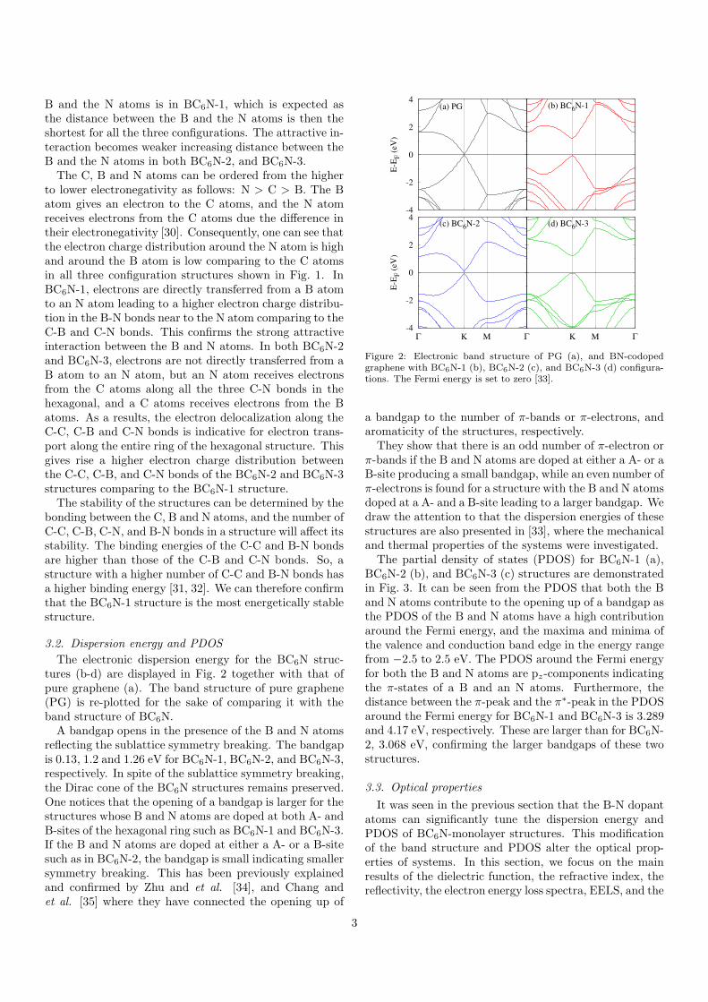
The electronic dispersion energy for the BC6N struc-tures (b-d) are displayed in Fig. 2 together with that ofpure graphene (a). The band structure of pure graphene(PG) is re-plotted for the sake of comparing it with theband structure of BC6N.A bandgap opens in the presence of the B and N atoms
reflecting the sublattice symmetry breaking. The bandgapis 0.13, 1.2 and 1.26 eV for BC6N-1, BC6N-2, and BC6N-3,respectively. In spite of the sublattice symmetry breaking,the Dirac cone of the BC6N structures remains preserved.One notices that the opening of a bandgap is larger for thestructures whose B and N atoms are doped at both A- andB-sites of the hexagonal ring such as BC6N-1 and BC6N-3.If the B and N atoms are doped at either a A- or a B-sitesuch as in BC6N-2, the bandgap is small indicating smallersymmetry breaking. This has been previously explainedand confirmed by Zhu and et al. [34], and Chang andet al. [35] where they have connected the opening up of
Figure 2: Electronic band structure of PG (a), and BN-codopedgraphene with BC6N-1 (b), BC6N-2 (c), and BC6N-3 (d) configura-tions. The Fermi energy is set to zero [33].
a bandgap to the number of π-bands or π-electrons, andaromaticity of the structures, respectively.They show that there is an odd number of π-electron or
π-bands if the B and N atoms are doped at either a A- or aB-site producing a small bandgap, while an even number ofπ-electrons is found for a structure with the B and N atomsdoped at a A- and a B-site leading to a larger bandgap. Wedraw the attention to that the dispersion energies of thesestructures are also presented in [33], where the mechanicaland thermal properties of the systems were investigated.The partial density of states (PDOS) for BC6N-1 (a),
BC6N-2 (b), and BC6N-3 (c) structures are demonstratedin Fig. 3. It can be seen from the PDOS that both the Band N atoms contribute to the opening up of a bandgap asthe PDOS of the B and N atoms have a high contributionaround the Fermi energy, and the maxima and minima ofthe valence and conduction band edge in the energy rangefrom −2.5 to 2.5 eV. The PDOS around the Fermi energyfor both the B and N atoms are pz-components indicatingthe π-states of a B and an N atoms. Furthermore, thedistance between the π-peak and the π∗-peak in the PDOSaround the Fermi energy for BC6N-1 and BC6N-3 is 3.289and 4.17 eV, respectively. These are larger than for BC6N-2, 3.068 eV, confirming the larger bandgaps of these twostructures.
3.3. Optical properties
It was seen in the previous section that the B-N dopantatoms can significantly tune the dispersion energy andPDOS of BC6N-monolayer structures. This modificationof the band structure and PDOS alter the optical prop-erties of systems. In this section, we focus on the mainresults of the dielectric function, the refractive index, thereflectivity, the electron energy loss spectra, EELS, and the
3
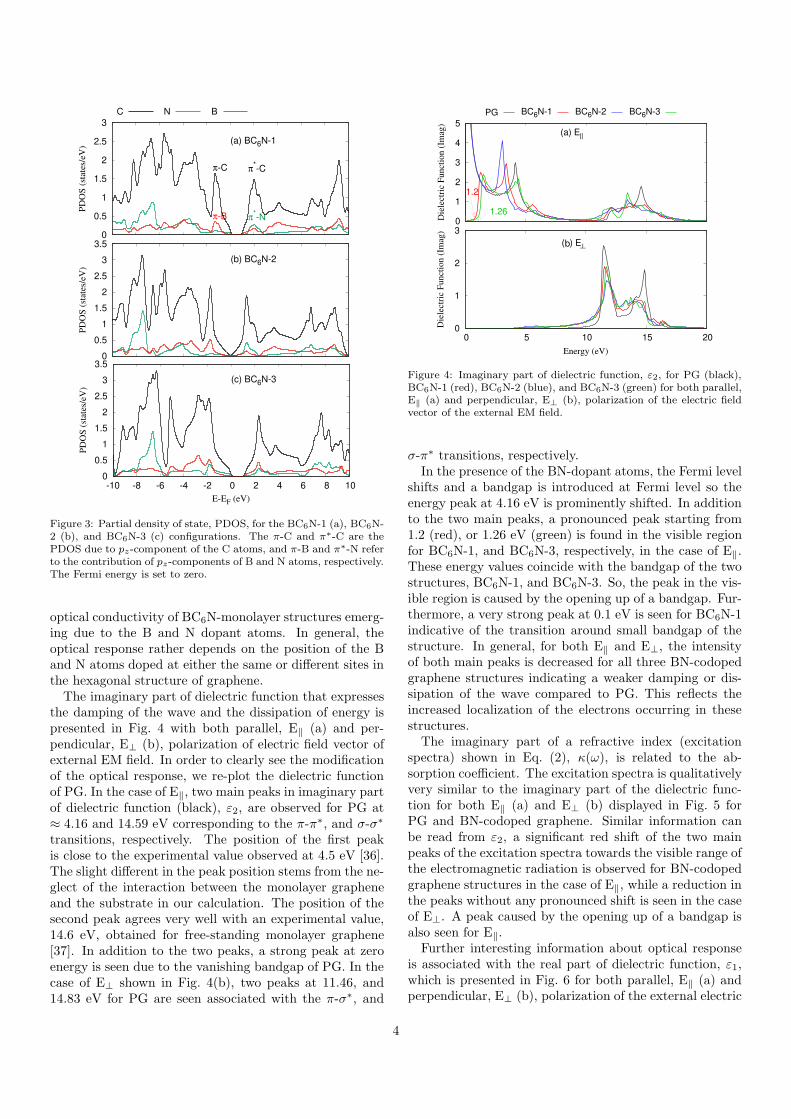
Figure 3: Partial density of state, PDOS, for the BC6N-1 (a), BC6N-2 (b), and BC6N-3 (c) configurations. The π-C and π∗-C are thePDOS due to pz-component of the C atoms, and π-B and π∗-N referto the contribution of pz-components of B and N atoms, respectively.The Fermi energy is set to zero.
optical conductivity of BC6N-monolayer structures emerg-ing due to the B and N dopant atoms. In general, theoptical response rather depends on the position of the Band N atoms doped at either the same or different sites inthe hexagonal structure of graphene.The imaginary part of dielectric function that expresses
the damping of the wave and the dissipation of energy ispresented in Fig. 4 with both parallel, E‖ (a) and per-pendicular, E⊥ (b), polarization of electric field vector ofexternal EM field. In order to clearly see the modificationof the optical response, we re-plot the dielectric functionof PG. In the case of E‖, two main peaks in imaginary partof dielectric function (black), ε2, are observed for PG at≈ 4.16 and 14.59 eV corresponding to the π-π∗, and σ-σ∗
transitions, respectively. The position of the first peakis close to the experimental value observed at 4.5 eV [36].The slight different in the peak position stems from the ne-glect of the interaction between the monolayer grapheneand the substrate in our calculation. The position of thesecond peak agrees very well with an experimental value,14.6 eV, obtained for free-standing monolayer graphene[37]. In addition to the two peaks, a strong peak at zeroenergy is seen due to the vanishing bandgap of PG. In thecase of E⊥ shown in Fig. 4(b), two peaks at 11.46, and14.83 eV for PG are seen associated with the π-σ∗, and
⊥b
Figure 4: Imaginary part of dielectric function, ε2, for PG (black),BC6N-1 (red), BC6N-2 (blue), and BC6N-3 (green) for both parallel,E‖ (a) and perpendicular, E⊥ (b), polarization of the electric fieldvector of the external EM field.
σ-π∗ transitions, respectively.In the presence of the BN-dopant atoms, the Fermi level
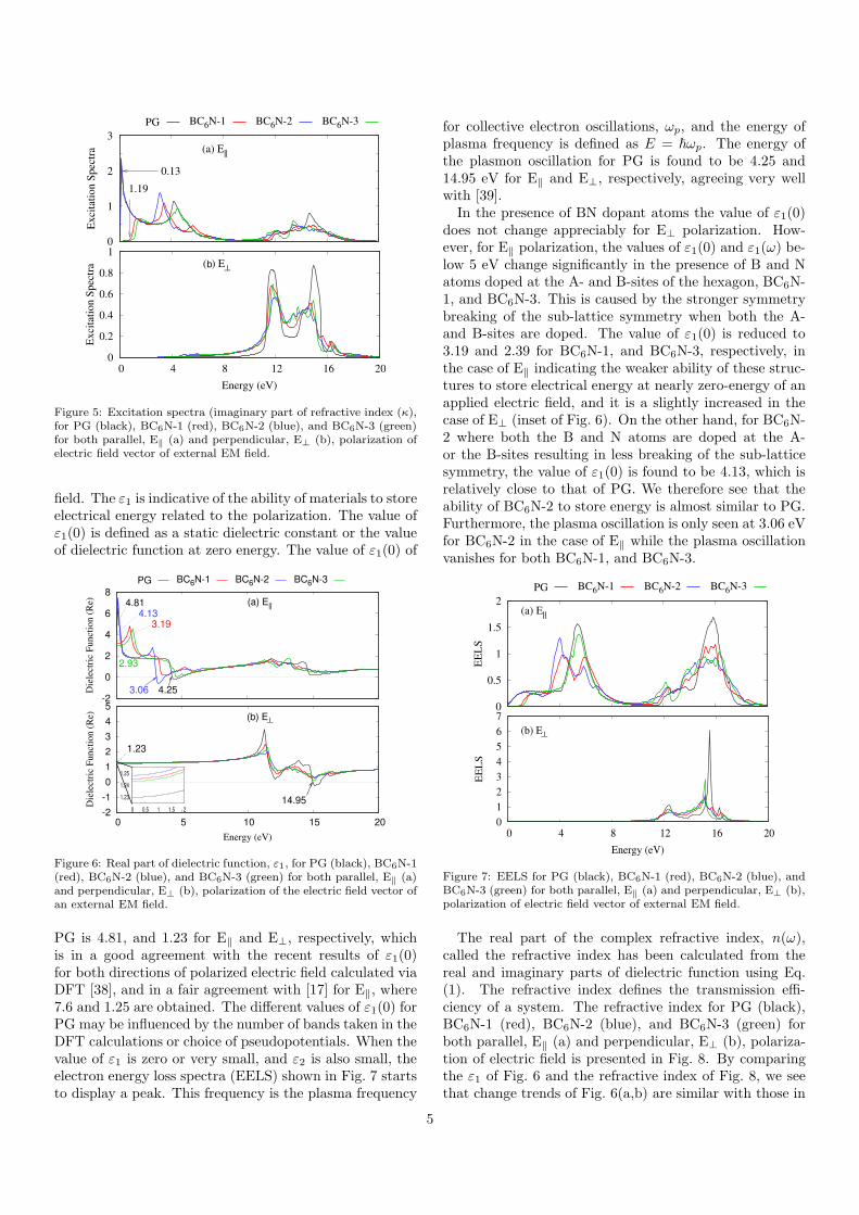
shifts and a bandgap is introduced at Fermi level so theenergy peak at 4.16 eV is prominently shifted. In additionto the two main peaks, a pronounced peak starting from1.2 (red), or 1.26 eV (green) is found in the visible regionfor BC6N-1, and BC6N-3, respectively, in the case of E‖.These energy values coincide with the bandgap of the twostructures, BC6N-1, and BC6N-3. So, the peak in the vis-ible region is caused by the opening up of a bandgap. Fur-thermore, a very strong peak at 0.1 eV is seen for BC6N-1indicative of the transition around small bandgap of thestructure. In general, for both E‖ and E⊥, the intensityof both main peaks is decreased for all three BN-codopedgraphene structures indicating a weaker damping or dis-sipation of the wave compared to PG. This reflects theincreased localization of the electrons occurring in thesestructures.The imaginary part of a refractive index (excitation
spectra) shown in Eq. (2), κ(ω), is related to the ab-sorption coefficient. The excitation spectra is qualitativelyvery similar to the imaginary part of the dielectric func-tion for both E‖ (a) and E⊥ (b) displayed in Fig. 5 forPG and BN-codoped graphene. Similar information canbe read from ε2, a significant red shift of the two mainpeaks of the excitation spectra towards the visible range ofthe electromagnetic radiation is observed for BN-codopedgraphene structures in the case of E‖, while a reduction inthe peaks without any pronounced shift is seen in the caseof E⊥. A peak caused by the opening up of a bandgap isalso seen for E‖.Further interesting information about optical response
is associated with the real part of dielectric function, ε1,which is presented in Fig. 6 for both parallel, E‖ (a) andperpendicular, E⊥ (b), polarization of the external electric
4
b ⊥
Figure 5: Excitation spectra (imaginary part of refractive index (κ),for PG (black), BC6N-1 (red), BC6N-2 (blue), and BC6N-3 (green)for both parallel, E‖ (a) and perpendicular, E⊥ (b), polarization ofelectric field vector of external EM field.
field. The ε1 is indicative of the ability of materials to storeelectrical energy related to the polarization. The value ofε1(0) is defined as a static dielectric constant or the valueof dielectric function at zero energy. The value of ε1(0) of
⊥
Figure 6: Real part of dielectric function, ε1, for PG (black), BC6N-1(red), BC6N-2 (blue), and BC6N-3 (green) for both parallel, E‖ (a)and perpendicular, E⊥ (b), polarization of the electric field vector ofan external EM field.
PG is 4.81, and 1.23 for E‖ and E⊥, respectively, whichis in a good agreement with the recent results of ε1(0)for both directions of polarized electric field calculated viaDFT [38], and in a fair agreement with [17] for E‖, where7.6 and 1.25 are obtained. The different values of ε1(0) forPG may be influenced by the number of bands taken in theDFT calculations or choice of pseudopotentials. When thevalue of ε1 is zero or very small, and ε2 is also small, theelectron energy loss spectra (EELS) shown in Fig. 7 startsto display a peak. This frequency is the plasma frequency
for collective electron oscillations, ωp, and the energy ofplasma frequency is defined as E = ~ωp. The energy ofthe plasmon oscillation for PG is found to be 4.25 and14.95 eV for E‖ and E⊥, respectively, agreeing very wellwith [39].In the presence of BN dopant atoms the value of ε1(0)
does not change appreciably for E⊥ polarization. How-ever, for E‖ polarization, the values of ε1(0) and ε1(ω) be-low 5 eV change significantly in the presence of B and Natoms doped at the A- and B-sites of the hexagon, BC6N-1, and BC6N-3. This is caused by the stronger symmetrybreaking of the sub-lattice symmetry when both the A-and B-sites are doped. The value of ε1(0) is reduced to3.19 and 2.39 for BC6N-1, and BC6N-3, respectively, inthe case of E‖ indicating the weaker ability of these struc-tures to store electrical energy at nearly zero-energy of anapplied electric field, and it is a slightly increased in thecase of E⊥ (inset of Fig. 6). On the other hand, for BC6N-2 where both the B and N atoms are doped at the A-or the B-sites resulting in less breaking of the sub-latticesymmetry, the value of ε1(0) is found to be 4.13, which isrelatively close to that of PG. We therefore see that theability of BC6N-2 to store energy is almost similar to PG.Furthermore, the plasma oscillation is only seen at 3.06 eVfor BC6N-2 in the case of E‖ while the plasma oscillationvanishes for both BC6N-1, and BC6N-3.
⊥
Figure 7: EELS for PG (black), BC6N-1 (red), BC6N-2 (blue), andBC6N-3 (green) for both parallel, E‖ (a) and perpendicular, E⊥ (b),polarization of electric field vector of external EM field.
The real part of the complex refractive index, n(ω),called the refractive index has been calculated from thereal and imaginary parts of dielectric function using Eq.(1). The refractive index defines the transmission effi-ciency of a system. The refractive index for PG (black),BC6N-1 (red), BC6N-2 (blue), and BC6N-3 (green) forboth parallel, E‖ (a) and perpendicular, E⊥ (b), polariza-tion of electric field is presented in Fig. 8. By comparingthe ε1 of Fig. 6 and the refractive index of Fig. 8, we seethat change trends of Fig. 6(a,b) are similar with those in
5
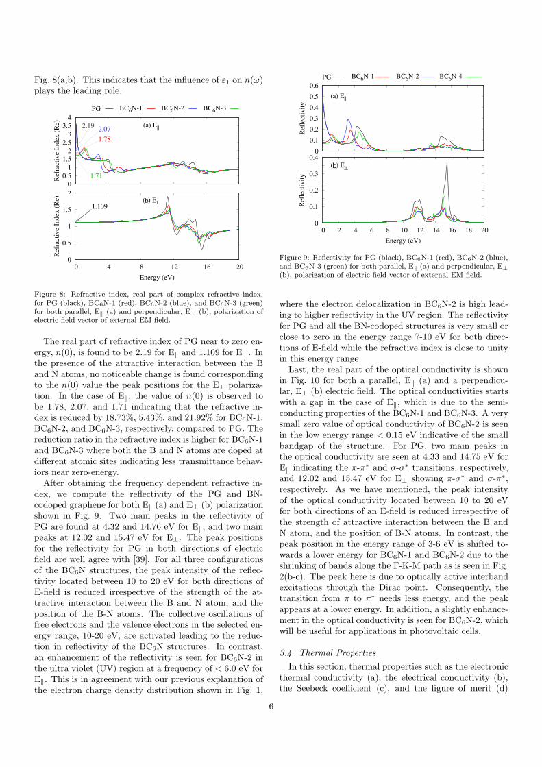
Fig. 8(a,b). This indicates that the influence of ε1 on n(ω)plays the leading role.
⊥b
Figure 8: Refractive index, real part of complex refractive index,for PG (black), BC6N-1 (red), BC6N-2 (blue), and BC6N-3 (green)for both parallel, E‖ (a) and perpendicular, E⊥ (b), polarization ofelectric field vector of external EM field.
The real part of refractive index of PG near to zero en-ergy, n(0), is found to be 2.19 for E‖ and 1.109 for E⊥. Inthe presence of the attractive interaction between the Band N atoms, no noticeable change is found correspondingto the n(0) value the peak positions for the E⊥ polariza-tion. In the case of E‖, the value of n(0) is observed tobe 1.78, 2.07, and 1.71 indicating that the refractive in-dex is reduced by 18.73%, 5.43%, and 21.92% for BC6N-1,BC6N-2, and BC6N-3, respectively, compared to PG. Thereduction ratio in the refractive index is higher for BC6N-1and BC6N-3 where both the B and N atoms are doped atdifferent atomic sites indicating less transmittance behav-iors near zero-energy.After obtaining the frequency dependent refractive in-
dex, we compute the reflectivity of the PG and BN-codoped graphene for both E‖ (a) and E⊥ (b) polarizationshown in Fig. 9. Two main peaks in the reflectivity ofPG are found at 4.32 and 14.76 eV for E‖, and two mainpeaks at 12.02 and 15.47 eV for E⊥. The peak positionsfor the reflectivity for PG in both directions of electricfield are well agree with [39]. For all three configurationsof the BC6N structures, the peak intensity of the reflec-tivity located between 10 to 20 eV for both directions ofE-field is reduced irrespective of the strength of the at-tractive interaction between the B and N atom, and theposition of the B-N atoms. The collective oscillations offree electrons and the valence electrons in the selected en-ergy range, 10-20 eV, are activated leading to the reduc-tion in reflectivity of the BC6N structures. In contrast,an enhancement of the reflectivity is seen for BC6N-2 inthe ultra violet (UV) region at a frequency of < 6.0 eV forE‖. This is in agreement with our previous explanation ofthe electron charge density distribution shown in Fig. 1,
b ⊥
Figure 9: Reflectivity for PG (black), BC6N-1 (red), BC6N-2 (blue),and BC6N-3 (green) for both parallel, E‖ (a) and perpendicular, E⊥
(b), polarization of electric field vector of external EM field.
where the electron delocalization in BC6N-2 is high lead-ing to higher reflectivity in the UV region. The reflectivityfor PG and all the BN-codoped structures is very small orclose to zero in the energy range 7-10 eV for both direc-tions of E-field while the refractive index is close to unityin this energy range.Last, the real part of the optical conductivity is shown
in Fig. 10 for both a parallel, E‖ (a) and a perpendicu-lar, E⊥ (b) electric field. The optical conductivities startswith a gap in the case of E‖, which is due to the semi-conducting properties of the BC6N-1 and BC6N-3. A verysmall zero value of optical conductivity of BC6N-2 is seenin the low energy range < 0.15 eV indicative of the smallbandgap of the structure. For PG, two main peaks inthe optical conductivity are seen at 4.33 and 14.75 eV forE‖ indicating the π-π∗ and σ-σ∗ transitions, respectively,and 12.02 and 15.47 eV for E⊥ showing π-σ∗ and σ-π∗,respectively. As we have mentioned, the peak intensityof the optical conductivity located between 10 to 20 eVfor both directions of an E-field is reduced irrespective ofthe strength of attractive interaction between the B andN atom, and the position of B-N atoms. In contrast, thepeak position in the energy range of 3-6 eV is shifted to-wards a lower energy for BC6N-1 and BC6N-2 due to theshrinking of bands along the Γ-K-M path as is seen in Fig.2(b-c). The peak here is due to optically active interbandexcitations through the Dirac point. Consequently, thetransition from π to π∗ needs less energy, and the peakappears at a lower energy. In addition, a slightly enhance-ment in the optical conductivity is seen for BC6N-2, whichwill be useful for applications in photovoltaic cells.
3.4. Thermal Properties
In this section, thermal properties such as the electronicthermal conductivity (a), the electrical conductivity (b),the Seebeck coefficient (c), and the figure of merit (d)
6

b ⊥
Figure 10: Optical conductivity, Re(σoptical) for PG (black), BC6N-1 (red), BC6N-2 (blue), and BC6N-3 (green) for both parallel, E‖
(a) and perpendicular, E⊥ (b), polarization of electric field vector ofexternal EM field.
are investigated and displayed in in Fig. 11. The ther-mal calculations are carried out in the temperature rangeof T = 20-150 K where the electron contribution to thetransport is dominant and the phonon participation canbe neglected because the electron and lattice temperatureare decoupled in this temperature range [40, 41]. Boltz-Trap software can be thus used to investigate the thermalproperties under the above condition [42]. The Boltztrapis based on the Boltzmann theory which is used to cal-culate the semiclassical transport coefficients. The codeuses a mesh of band energies and is interfaced to the QEpackage [43].
d
Figure 11: Electronic thermal conductivity, k (a), electrical conduc-tivity, σ (b), Seebeck coefficient, S (c), and figure of merit, ZT (d)versus energy are plotted PG (black), BC6N-1 (red), BC6N-2 (blue),and BC6N-3 (green).
The thermal efficiency of a material or a device is char-acterized by the figure of merit, ZT = (S2 σ/k)T , whereS is the Seebeck coefficient, σ is the electrical conductiv-ity, T is a temperature, and k is the electronic thermalconductivity. It has been shown that a material with highof ZT should have high S, and σ, and low k with a speci-ficity temperature [44]. Based on this, we can see that
the BC6N-1 and BC6N-3 have the highest ZT among allinvestigated structures in which the high symmetry break-ing plays an important role. The high value of ZT hererefers to the relatively larger bandgap and asymmetry inthe density of states of these two structures around theFermi energy which give rise to a lack of thermal electronsin the bandgap range. It thus leads to a decrease in thek (a) and an increase in the S (c) around the bandgap,which are the conditions to obtain the high value of ZT .The high value of ZT of a material is useful to improvethermoelectric devices such as solar cell.
4. Conclusions
To conclude, we have used density functional theory tostudy the structural, thermal, and optical properties ofmonolayer graphene doped with boron and nitrogen atomswhere the influences of an attractive interaction betweenthe dopant atoms are highlighted. We have assumed fewatomic configurations forming different BC6N structuresbased on the interaction between the B and N atoms. Wehave found that the static dielectric constant is decreased,and the plasmon oscillation is reduced or vanishes in thepresence of an attractive interaction between the B andN atoms compared to the pristine monolayer graphene.Furthermore, the refractive index indicating the transmit-tance behavior is enhanced in the case interactions be-tween the B and N atoms in the low energy ranges whilethe reflectivity is decreased. In addition, a high Seebeckcoefficient and a high figure of merit have been found forBC6N where the B and N atoms are doped at differentatomic sites of the hexagon structure. We can thus con-firm that the thermal and the optical properties of BC6Ncan be improved by controlling the interaction between thedopant atoms which may be useful for thermoelectric andoptoelectronic devises.
References
[1] Candela Mansilla Wettstein, Franco P. Bonafe, M. BelenOviedo, and Cristian G. Sanchez. Optical properties of graphenenanoflakes: Shape matters. The Journal of Chemical Physics,144(22):224305, 2016.
[2] Mehdi Shakourian-Fard and Ganesh Kamath. The effect of de-fect types on the electronic and optical properties of graphenenanoflakes physisorbed by ionic liquids. Phys. Chem. Chem.
Phys., 19:4383–4395, 2017.[3] Feng Wang, Yuanbo Zhang, Chuanshan Tian, Caglar Girit,
Alex Zettl, Michael Crommie, and Y. Ron Shen. Gate-variableoptical transitions in graphene. Science, 320(5873):206–209,2008.
[4] R. R. Nair, P. Blake, A. N. Grigorenko, K. S. Novoselov, T. J.Booth, T. Stauber, N. M. R. Peres, and A. K. Geim. Fine struc-ture constant defines visual transparency of graphene. Science,320(5881):1308–1308, 2008.
[5] Yansong Fan, Chucai Guo, Zhihong Zhu, Wei Xu, Fan Wu,Xiaodong Yuan, and Shiqiao Qin. Monolayer-graphene-basedbroadband and wide-angle perfect absorption structures in thenear infrared. Scientific Reports, 8(1):13709, 2018.
7
[6] Marco Romagnoli, Vito Sorianello, Michele Midrio, Frank H. L.Koppens, Cedric Huyghebaert, Daniel Neumaier, Paola Galli,Wolfgang Templ, Antonio D’Errico, and Andrea C. Ferrari.Graphene-based integrated photonics for next-generation dat-acom and telecom. Nature Reviews Materials, 3(10):392–414,Oct 2018.
[7] Chuancheng Jia, Jiaolong Jiang, Lin Gan, and Xuefeng Guo.Direct optical characterization of graphene growth and domainson growth substrates. Scientific Reports, 2(1):707, Oct 2012.
[8] Kun Ba, Wei Jiang, Jingxin Cheng, Jingxian Bao, NingningXuan, Yangye Sun, Bing Liu, Aozhen Xie, Shiwei Wu, andZhengzong Sun. Chemical and bandgap engineering in mono-layer hexagonal boron nitride. Scientific Reports, 7(1):45584,Apr 2017.
[9] Aurelien Lherbier, Andres Rafael Botello-Mendez, and Jean-Christophe Charlier. Electronic and transport properties ofunbalanced sublattice n-doping in graphene. Nano Letters,13(4):1446–1450, 2013. PMID: 23477418.
[10] Stefano Agnoli and Marco Favaro. Doping graphene with boron:a review of synthesis methods, physicochemical characteriza-tion, and emerging applications. J. Mater. Chem. A, 4:5002–5025, 2016.
[11] Jia Zhang, Chao Zhao, Na Liu, Huanxi Zhang, Jingjing Liu,Yong Qing Fu, Bin Guo, Zhenlong Wang, Shengbin Lei, andPingAn Hu. Tunable electronic properties of graphene throughcontrolling bonding configurations of doped nitrogen atoms.Scientific Reports, 6(1):28330, Jun 2016.
[12] M. Goudarzi, S.S. Parhizgar, and J. Beheshtian. Electronic andoptical properties of vacancy and b, n, o and f doped graphene:Dft study. Opto-Electronics Review, 27(2):130–136, 2019.
[13] Nzar Rauf Abdullah, Hunar Omar Rashid, Chi-Shung Tang,Andrei Manolescu, and Vidar Gudmundsson. Conversion ofthe stacking orientation of bilayer graphene due to\break theinteraction of bn-dopants. arXiv preprint arXiv:2101.00462,2021.
[14] Hongxia Bu, Haibin Zheng, Hongyu Zhang, Huimin Yuan, andJingfen Zhao. Optical properties of a hexagonal c/bn frame-work with sp2 and sp3 hybridized bonds. Scientific Reports,10(1):6808, Apr 2020.
[15] Nzar Rauf Abdullah, Hunar Omar Rashid, Chi-Shung Tang,Andrei Manolescu, and Vidar Gudmundsson. Role of inter-layer spacing on electronic, thermal and optical properties ofbn-codoped bilayer graphene: Influence of the interlayer andthe induced dipole-dipole interactions. Journal of Physics and
Chemistry of Solids, 155:110095, 2021.[16] Bohayra Mortazavi, Masoud Shahrokhi, Mostafa Raeisi, Xiaoy-
ing Zhuang, Luiz Felipe C. Pereira, and Timon Rabczuk. Out-standing strength, optical characteristics and thermal conduc-tivity of graphene-like bc3 and bc6n semiconductors. Carbon,149:733–742, 2019.
[17] Pooja Rani, Girija S. Dubey, and V.K. Jindal. Dft study ofoptical properties of pure and doped graphene. Physica E: Low-
dimensional Systems and Nanostructures, 62:28–35, 2014.[18] Paolo Giannozzi, Stefano Baroni, Nicola Bonini, Matteo Calan-
dra, Roberto Car, Carlo Cavazzoni, Davide Ceresoli, Guido LChiarotti, Matteo Cococcioni, Ismaila Dabo, Andrea DalCorso, Stefano de Gironcoli, Stefano Fabris, Guido Fratesi,Ralph Gebauer, Uwe Gerstmann, Christos Gougoussis, AntonKokalj, Michele Lazzeri, Layla Martin-Samos, Nicola Marzari,Francesco Mauri, Riccardo Mazzarello, Stefano Paolini, Al-fredo Pasquarello, Lorenzo Paulatto, Carlo Sbraccia, SandroScandolo, Gabriele Sclauzero, Ari P Seitsonen, Alexander Smo-gunov, Paolo Umari, and Renata M Wentzcovitch. QUANTUMESPRESSO: a modular and open-source software project forquantum simulations of materials. Journal of Physics: Con-
densed Matter, 21(39):395502, sep 2009.[19] Paolo Giannozzi, Oliviero Andreussi, Thomas Brumme, Oana
Bunau, M Buongiorno Nardelli, Matteo Calandra, RobertoCar, Carlo Cavazzoni, Davide Ceresoli, Matteo Cococcioni,et al. Advanced capabilities for materials modelling withquantum espresso. Journal of Physics: Condensed Matter,
29(46):465901, 2017.[20] W. Kohn and L. J. Sham. Self-consistent equations including
exchange and correlation effects. Phys. Rev., 140:A1133–A1138,Nov 1965.
[21] Max Petersen, Frank Wagner, Lars Hufnagel, Matthias Schef-fler, Peter Blaha, and Karlheinz Schwarz. Improving the effi-ciency of fp-lapw calculations. Computer Physics Communica-
tions, 126(3):294–309, 2000.[22] John P. Perdew, Kieron Burke, and Matthias Ernzerhof. Gen-
eralized gradient approximation made simple. Phys. Rev. Lett.,77:3865–3868, Oct 1996.
[23] John P. Perdew and Wang Yue. Accurate and simple densityfunctional for the electronic exchange energy: Generalized gra-dient approximation. Phys. Rev. B, 33:8800–8802, Jun 1986.
[24] J. P. Perdew and Alex Zunger. Self-interaction correction todensity-functional approximations for many-electron systems.Phys. Rev. B, 23:5048–5079, May 1981.
[25] Jan Mistrik, Safa Kasap, Harry E. Ruda, Cyril Koughia, and JaiSingh. Optical Properties of Electronic Materials: Fundamen-
tals and Characterization, pages 1–1. Springer InternationalPublishing, Cham, 2017.
[26] Nzar Rauf Abdullah, Danyal A. Abdalla, Taha Y. Ahmed, Sar-bast W. Abdulqadr, and Hunar Omar Rashid. Effect of bndimers on the stability, electronic, and thermal properties ofmonolayer graphene. Results in Physics, 18:103282, 2020.
[27] Nzar Rauf Abdullah, Hunar Omar Rashid, Chi-Shung Tang,Andrei Manolescu, and Vidar Gudmundsson. Properties ofbsi6n monolayers derived by first-principle computation. Phys-
ica E: Low-dimensional Systems and Nanostructures, page114556, 2020.
[28] Nabil Al-Aqtash, Khaldoun M. Al-Tarawneh, Tarek Tawalbeh,and Igor Vasiliev. Ab initio study of the interactions betweenboron and nitrogen dopants in graphene. Journal of Applied
Physics, 112(3):034304, 2012.[29] Nzar Rauf Abdullah, Hunar Omar Rashid, Andrei Manolescu,
and Vidar Gudmundsson. Interlayer interaction controlling theproperties of ab- and aa-stacked bilayer graphene-like bc14n andsi2c14. Surfaces and Interfaces, 21:100740, 2020.
[30] Nzar Rauf Abdullah, Hunar Omar Rashid, Mohammad T. Ka-reem, Chi-Shung Tang, Andrei Manolescu, and Vidar Gud-mundsson. Effects of bonded and non-bonded b/n codopingof graphene on its stability, interaction energy, electronic struc-ture, and power factor. Physics Letters A, 384(12):126350, 2020.
[31] Xiaofeng Fan, Zexiang Shen, A. Q. Liu, and Jer-Lai Kuo. Bandgap opening of graphene by doping small boron nitride domains.Nanoscale, 4:2157–2165, 2012.
[32] Nzar Rauf Abdullah, Mohammad T. Kareem, Hunar OmarRashid, Andrei Manolescu, and Vidar Gudmundsson. Spin-polarised dft modeling of electronic, magnetic, thermal and op-tical properties of silicene doped with transition metals. PhysicaE: Low-dimensional Systems and Nanostructures, 129:114644,2021.
[33] Nzar Rauf Abdullah, Hunar Omar Rashid, Chi-Shung Tang,Andrei Manolescu, and Vidar Gudmundsson. Modeling elec-tronic, mechanical, optical and thermal properties of graphene-like bc6n materials: Role of prominent bn-bonds. Physics Let-
ters A, 384(32):126807, 2020.[34] Jun Zhu, Sumanta Bhandary, Biplab Sanyal, and Henrik Ot-
tosson. Interpolation of atomically thin hexagonal boronnitride and graphene: Electronic structure and thermody-namic stability in terms of all-carbon conjugated paths andaromatic hexagons. The Journal of Physical Chemistry C,115(20):10264–10271, 2011.
[35] Chung-Huai Chang, Xiaofeng Fan, Lain-Jong Li, and Jer-Lai Kuo. Band gap tuning of graphene by adsorption ofaromatic molecules. The Journal of Physical Chemistry C,116(25):13788–13794, 2012.
[36] V. G. Kravets, A. N. Grigorenko, R. R. Nair, P. Blake, S. Anis-simova, K. S. Novoselov, and A. K. Geim. Spectroscopic ellip-sometry of graphene and an exciton-shifted van hove peak inabsorption. Phys. Rev. B, 81:155413, Apr 2010.
8

[37] T. Eberlein, U. Bangert, R. R. Nair, R. Jones, M. Gass, A. L.Bleloch, K. S. Novoselov, A. Geim, and P. R. Briddon. Plasmonspectroscopy of free-standing graphene films. Phys. Rev. B,77:233406, Jun 2008.
[38] Bin Qiu, Xiuwen Zhao, Guichao Hu, Weiwei Yue, JunfengRen, and Xiaobo Yuan. Optical properties of graphene/mos2heterostructure: First principles calculations. Nanomaterials,8(11), 2018.
[39] Palash Nath, Suman Chowdhury, D. Sanyal, and DebnarayanJana. Ab-initio calculation of electronic and optical proper-ties of nitrogen and boron doped graphene nanosheet. Carbon,73:275–282, 2014.
[40] S. Yigen, V. Tayari, J. O. Island, J. M. Porter, and A. R. Cham-pagne. Electronic thermal conductivity measurements in intrin-sic graphene. Phys. Rev. B, 87:241411, Jun 2013.
[41] Nzar Rauf Abdullah, Gullan Ahmed Mohammed, Hunar OmarRashid, and Vidar Gudmundsson. Electronic, thermal, andoptical properties of graphene like sicx structures: Signifi-cant effects of si atom configurations. Physics Letters A,384(24):126578, 2020.
[42] Georg K. H. Madsen and David J. Singh. Boltztrap. a codefor calculating band-structure dependent quantities. Computer
Physics Communications, 175(1):67–71, 2006.[43] Hunar Omar Rashid, Nzar Rauf Abdullah, and Vidar Gud-
mundsson. Silicon on a graphene nanosheet with triangle- anddot-shape: Electronic structure, specific heat, and thermal con-ductivity from first-principle calculations. Results in Physics,15:102625, 2019.
[44] G. Jeffrey Snyder and Alemayouh H. Snyder. Figure of meritzt of a thermoelectric device defined from materials properties.Energy Environ. Sci., 10:2280–2283, 2017.
9