Programmable Controller SYSMAC CPM1/CPM1A/CPM2A/CPM2C/SRM1(-V2) PROGRAMMING MANUAL
578
Cat.No. W353–E1–2 Programmable Controller SYSMAC CPM1/CPM1A/CPM2A/CPM2C/SRM1(-V2) PROGRAMMING MANUAL
-
Upload
independent -
Category
Documents
-
view
2 -
download
0
Transcript of Programmable Controller SYSMAC CPM1/CPM1A/CPM2A/CPM2C/SRM1(-V2) PROGRAMMING MANUAL

Cat.No. W353–E1–2
Programmable Controller
SYSMACCPM1/CPM1A/CPM2A/CPM2C/SRM1(-V2)
PROGRAMMING MANUAL

CPM1/CPM1A/CPM2A/CPM2C/SRM1(-V2)Programmable Controllers
Programming Manual
Revised January 2000

!
!
!
v
Notice:OMRON products are manufactured for use according to proper procedures by a qualified operatorand only for the purposes described in this manual.
The following conventions are used to indicate and classify precautions in this manual. Always heedthe information provided with them. Failure to heed precautions can result in injury to people or dam-age to property.
DANGER Indicates an imminently hazardous situation which, if not avoided, will result in death orserious injury.
WARNING Indicates a potentially hazardous situation which, if not avoided, could result in death orserious injury.
Caution Indicates a potentially hazardous situation which, if not avoided, may result in minor ormoderate injury, or property damage.
OMRON Product ReferencesAll OMRON products are capitalized in this manual. The word “Unit” is also capitalized when it refersto an OMRON product, regardless of whether or not it appears in the proper name of the product.
The abbreviation “Ch,” which appears in some displays and on some OMRON products, often means“word” and is abbreviated “Wd” in documentation in this sense.
The abbreviation “PC” means Programmable Controller and is not used as an abbreviation for any-thing else.
Visual AidsThe following headings appear in the left column of the manual to help you locate different types ofinformation.
Note Indicates information of particular interest for efficient and convenient operationof the product.
1, 2, 3... 1. Indicates lists of one sort or another, such as procedures, checklists, etc.
OMRON, 1999All rights reserved. No part of this publication may be reproduced, stored in a retrieval system, or transmitted, in anyform, or by any means, mechanical, electronic, photocopying, recording, or otherwise, without the prior written permis-sion of OMRON.
No patent liability is assumed with respect to the use of the information contained herein. Moreover, because OMRON isconstantly striving to improve its high-quality products, the information contained in this manual is subject to changewithout notice. Every precaution has been taken in the preparation of this manual. Nevertheless, OMRON assumes noresponsibility for errors or omissions. Neither is any liability assumed for damages resulting from the use of the informa-tion contained in this publication.

TABLE OF CONTENTS
vii
PRECAUTIONS xiii. . . . . . . . . . . . . . . . . . . . . . . . . . . . . . . . . 1 Intended Audience xiv. . . . . . . . . . . . . . . . . . . . . . . . . . . . . . . . . . . . . . . . . . . . . . . . . . . . . . . . . . . 2 General Precautions xiv. . . . . . . . . . . . . . . . . . . . . . . . . . . . . . . . . . . . . . . . . . . . . . . . . . . . . . . . . . 3 Safety Precautions xiv. . . . . . . . . . . . . . . . . . . . . . . . . . . . . . . . . . . . . . . . . . . . . . . . . . . . . . . . . . . 4 Operating Environment Precautions xv. . . . . . . . . . . . . . . . . . . . . . . . . . . . . . . . . . . . . . . . . . . . . 5 Application Precautions xvii. . . . . . . . . . . . . . . . . . . . . . . . . . . . . . . . . . . . . . . . . . . . . . . . . . . . . .
SECTION 1PC Setup 1. . . . . . . . . . . . . . . . . . . . . . . . . . . . . . . . . . . . . . .
1-1 PC Setup 2. . . . . . . . . . . . . . . . . . . . . . . . . . . . . . . . . . . . . . . . . . . . . . . . . . . . . . . . . . . . . . . 1-2 Basic PC Operation and I/O Processes 16. . . . . . . . . . . . . . . . . . . . . . . . . . . . . . . . . . . . . . .
SECTION 2Special Features 23. . . . . . . . . . . . . . . . . . . . . . . . . . . . . . . . .
2-1 CPM2A/CPM2C Interrupt Functions 24. . . . . . . . . . . . . . . . . . . . . . . . . . . . . . . . . . . . . . . . . 2-2 CPM2A/CPM2C High-speed Counters 37. . . . . . . . . . . . . . . . . . . . . . . . . . . . . . . . . . . . . . . 2-3 CPM1/CPM1A Interrupt Functions 68. . . . . . . . . . . . . . . . . . . . . . . . . . . . . . . . . . . . . . . . . . 2-4 SRM1(-V2) Interrupt Functions 86. . . . . . . . . . . . . . . . . . . . . . . . . . . . . . . . . . . . . . . . . . . . . 2-5 CPM2A/CPM2C Pulse Output Functions 89. . . . . . . . . . . . . . . . . . . . . . . . . . . . . . . . . . . . . 2-6 CPM1A Pulse Output Functions 121. . . . . . . . . . . . . . . . . . . . . . . . . . . . . . . . . . . . . . . . . . . . 2-7 Synchronized Pulse Control (CPM2A/CPM2C Only) 124. . . . . . . . . . . . . . . . . . . . . . . . . . . . 2-8 Data Computation Standards 134. . . . . . . . . . . . . . . . . . . . . . . . . . . . . . . . . . . . . . . . . . . . . . . 2-9 Analog I/O Functions (CPM1/CPM1A/CPM2A/CPM2C Only) 136. . . . . . . . . . . . . . . . . . . . 2-10 Temperature Sensor Input Functions (CPM1A/CPM2A/CPM2C Only) 136. . . . . . . . . . . . . . 2-11 CompoBus/S I/O Slave Functions (CPM1A/CPM2A/CPM2C Only) 136. . . . . . . . . . . . . . . . 2-12 CompoBus/S I/O Master Functions (SRM1(-V2) Only) 137. . . . . . . . . . . . . . . . . . . . . . . . . . 2-13 Analog Controls (CPM1/CPM1A/CPM2A Only) 138. . . . . . . . . . . . . . . . . . . . . . . . . . . . . . . 2-14 Quick-response Inputs 140. . . . . . . . . . . . . . . . . . . . . . . . . . . . . . . . . . . . . . . . . . . . . . . . . . . . 2-15 Macro Function 145. . . . . . . . . . . . . . . . . . . . . . . . . . . . . . . . . . . . . . . . . . . . . . . . . . . . . . . . . 2-16 Calculating with Signed Binary Data 146. . . . . . . . . . . . . . . . . . . . . . . . . . . . . . . . . . . . . . . . 2-17 Differential Monitor 147. . . . . . . . . . . . . . . . . . . . . . . . . . . . . . . . . . . . . . . . . . . . . . . . . . . . . . 2-18 Expansion Instructions (CPM2A/CPM2C/SRM1(-V2) Only) 148. . . . . . . . . . . . . . . . . . . . . . 2-19 Using the CPM2A/CPM2C Clock Function 151. . . . . . . . . . . . . . . . . . . . . . . . . . . . . . . . . . .
SECTION 3Using Expansion Units 153. . . . . . . . . . . . . . . . . . . . . . . . . . . .
3-1 Analog I/O Units 154. . . . . . . . . . . . . . . . . . . . . . . . . . . . . . . . . . . . . . . . . . . . . . . . . . . . . . . . 3-2 Temperature Sensor Units 176. . . . . . . . . . . . . . . . . . . . . . . . . . . . . . . . . . . . . . . . . . . . . . . . . 3-3 CompoBus/S I/O Link Units 197. . . . . . . . . . . . . . . . . . . . . . . . . . . . . . . . . . . . . . . . . . . . . . .
SECTION 4Communications Functions 203. . . . . . . . . . . . . . . . . . . . . . . .
4-1 Introduction 204. . . . . . . . . . . . . . . . . . . . . . . . . . . . . . . . . . . . . . . . . . . . . . . . . . . . . . . . . . . . 4-2 CPM1/CPM1A Communications Functions 205. . . . . . . . . . . . . . . . . . . . . . . . . . . . . . . . . . . 4-3 CPM2A/CPM2C Communications Functions 209. . . . . . . . . . . . . . . . . . . . . . . . . . . . . . . . . . 4-4 SRM1(-V2) Communications Functions 242. . . . . . . . . . . . . . . . . . . . . . . . . . . . . . . . . . . . . . 4-5 Host Link Commands 254. . . . . . . . . . . . . . . . . . . . . . . . . . . . . . . . . . . . . . . . . . . . . . . . . . . . .
SECTION 5Memory Areas 279. . . . . . . . . . . . . . . . . . . . . . . . . . . . . . . . . .
5-1 Memory Area Functions 280. . . . . . . . . . . . . . . . . . . . . . . . . . . . . . . . . . . . . . . . . . . . . . . . . . . 5-2 I/O Allocation for CPM1/CPM1A/CPM2A PCs 285. . . . . . . . . . . . . . . . . . . . . . . . . . . . . . . . 5-3 I/O Allocation for CPM2C PCs 295. . . . . . . . . . . . . . . . . . . . . . . . . . . . . . . . . . . . . . . . . . . . .

TABLE OF CONTENTS
viii
SECTION 6Ladder-diagram Programming 303. . . . . . . . . . . . . . . . . . . .
6-1 Basic Procedure 304. . . . . . . . . . . . . . . . . . . . . . . . . . . . . . . . . . . . . . . . . . . . . . . . . . . . . . . . . 6-2 Instruction Terminology 304. . . . . . . . . . . . . . . . . . . . . . . . . . . . . . . . . . . . . . . . . . . . . . . . . . . 6-3 Basic Ladder Diagrams 305. . . . . . . . . . . . . . . . . . . . . . . . . . . . . . . . . . . . . . . . . . . . . . . . . . . 6-4 Controlling Bit Status 324. . . . . . . . . . . . . . . . . . . . . . . . . . . . . . . . . . . . . . . . . . . . . . . . . . . . . 6-5 Work Bits (Internal Relays) 326. . . . . . . . . . . . . . . . . . . . . . . . . . . . . . . . . . . . . . . . . . . . . . . . 6-6 Programming Precautions 328. . . . . . . . . . . . . . . . . . . . . . . . . . . . . . . . . . . . . . . . . . . . . . . . . 6-7 Program Execution 330. . . . . . . . . . . . . . . . . . . . . . . . . . . . . . . . . . . . . . . . . . . . . . . . . . . . . . .
SECTION 7Instruction Set 331. . . . . . . . . . . . . . . . . . . . . . . . . . . . . . . . . .
7-1 Notation 334. . . . . . . . . . . . . . . . . . . . . . . . . . . . . . . . . . . . . . . . . . . . . . . . . . . . . . . . . . . . . . . 7-2 Instruction Format 334. . . . . . . . . . . . . . . . . . . . . . . . . . . . . . . . . . . . . . . . . . . . . . . . . . . . . . . 7-3 Data Areas, Definer Values, and Flags 334. . . . . . . . . . . . . . . . . . . . . . . . . . . . . . . . . . . . . . . 7-4 Differentiated Instructions 336. . . . . . . . . . . . . . . . . . . . . . . . . . . . . . . . . . . . . . . . . . . . . . . . . 7-5 Coding Right-hand Instructions 337. . . . . . . . . . . . . . . . . . . . . . . . . . . . . . . . . . . . . . . . . . . . . 7-6 Instruction Tables 340. . . . . . . . . . . . . . . . . . . . . . . . . . . . . . . . . . . . . . . . . . . . . . . . . . . . . . . . 7-7 Ladder Diagram Instructions 346. . . . . . . . . . . . . . . . . . . . . . . . . . . . . . . . . . . . . . . . . . . . . . . 7-8 Bit Control Instructions 347. . . . . . . . . . . . . . . . . . . . . . . . . . . . . . . . . . . . . . . . . . . . . . . . . . . 7-9 NO OPERATION – NOP(00) 351. . . . . . . . . . . . . . . . . . . . . . . . . . . . . . . . . . . . . . . . . . . . . . . 7-10 END – END(01) 351. . . . . . . . . . . . . . . . . . . . . . . . . . . . . . . . . . . . . . . . . . . . . . . . . . . . . . . . 7-11 INTERLOCK and INTERLOCK CLEAR – IL(02) and ILC(03) 351. . . . . . . . . . . . . . . . . . . 7-12 JUMP and JUMP END – JMP(04) and JME(05) 353. . . . . . . . . . . . . . . . . . . . . . . . . . . . . . . . 7-13 User Error Instructions: FAILURE ALARM AND RESET – FAL(06) and
SEVERE FAILURE ALARM – FALS(07) 355. . . . . . . . . . . . . . . . . . . . . . . . . . . . . . . . . . . . 7-14 Step Instructions: STEP DEFINE and STEP START–STEP(08)/SNXT(09) 356. . . . . . . . . . 7-15 Timer and Counter Instructions 358. . . . . . . . . . . . . . . . . . . . . . . . . . . . . . . . . . . . . . . . . . . . . 7-16 Shift Instructions 374. . . . . . . . . . . . . . . . . . . . . . . . . . . . . . . . . . . . . . . . . . . . . . . . . . . . . . . . 7-17 Data Movement Instructions 382. . . . . . . . . . . . . . . . . . . . . . . . . . . . . . . . . . . . . . . . . . . . . . . 7-18 Data Control Instructions 391. . . . . . . . . . . . . . . . . . . . . . . . . . . . . . . . . . . . . . . . . . . . . . . . . . 7-19 Comparison Instructions 402. . . . . . . . . . . . . . . . . . . . . . . . . . . . . . . . . . . . . . . . . . . . . . . . . . 7-20 Conversion Instructions 409. . . . . . . . . . . . . . . . . . . . . . . . . . . . . . . . . . . . . . . . . . . . . . . . . . . 7-21 BCD Calculation Instructions 427. . . . . . . . . . . . . . . . . . . . . . . . . . . . . . . . . . . . . . . . . . . . . . 7-22 Binary Calculation Instructions 437. . . . . . . . . . . . . . . . . . . . . . . . . . . . . . . . . . . . . . . . . . . . . 7-23 Special Math Instructions 441. . . . . . . . . . . . . . . . . . . . . . . . . . . . . . . . . . . . . . . . . . . . . . . . . . 7-24 Logic Instructions 450. . . . . . . . . . . . . . . . . . . . . . . . . . . . . . . . . . . . . . . . . . . . . . . . . . . . . . . . 7-25 Increment/Decrement Instructions 453. . . . . . . . . . . . . . . . . . . . . . . . . . . . . . . . . . . . . . . . . . . 7-26 Subroutine Instructions 455. . . . . . . . . . . . . . . . . . . . . . . . . . . . . . . . . . . . . . . . . . . . . . . . . . . 7-27 Pulse Output Instructions 458. . . . . . . . . . . . . . . . . . . . . . . . . . . . . . . . . . . . . . . . . . . . . . . . . . 7-28 Special Instructions 468. . . . . . . . . . . . . . . . . . . . . . . . . . . . . . . . . . . . . . . . . . . . . . . . . . . . . . 7-29 Interrupt Control Instructions 472. . . . . . . . . . . . . . . . . . . . . . . . . . . . . . . . . . . . . . . . . . . . . . . 7-30 Communications Instructions 477. . . . . . . . . . . . . . . . . . . . . . . . . . . . . . . . . . . . . . . . . . . . . . .
SECTION 8PC Operations and Processing Time 483. . . . . . . . . . . . . . . .
8-1 CPM1/CPM1A Cycle Time and I/O Response Time 484. . . . . . . . . . . . . . . . . . . . . . . . . . . . 8-2 CPM2A/CPM2C Cycle Time and I/O Response Time 495. . . . . . . . . . . . . . . . . . . . . . . . . . . 8-3 SRM1(-V2) Cycle Time and I/O Response Time 509. . . . . . . . . . . . . . . . . . . . . . . . . . . . . . .

TABLE OF CONTENTS
ix
SECTION 9Troubleshooting 521. . . . . . . . . . . . . . . . . . . . . . . . . . . . . . . . .
9-1 Introduction 522. . . . . . . . . . . . . . . . . . . . . . . . . . . . . . . . . . . . . . . . . . . . . . . . . . . . . . . . . . . . 9-2 Programming Console Operation Errors 522. . . . . . . . . . . . . . . . . . . . . . . . . . . . . . . . . . . . . . 9-3 Programming Errors 523. . . . . . . . . . . . . . . . . . . . . . . . . . . . . . . . . . . . . . . . . . . . . . . . . . . . . . 9-4 User-defined Errors 524. . . . . . . . . . . . . . . . . . . . . . . . . . . . . . . . . . . . . . . . . . . . . . . . . . . . . . 9-5 Operating Errors 525. . . . . . . . . . . . . . . . . . . . . . . . . . . . . . . . . . . . . . . . . . . . . . . . . . . . . . . . . 9-6 Error Log 527. . . . . . . . . . . . . . . . . . . . . . . . . . . . . . . . . . . . . . . . . . . . . . . . . . . . . . . . . . . . . . 9-7 Host Link Errors 529. . . . . . . . . . . . . . . . . . . . . . . . . . . . . . . . . . . . . . . . . . . . . . . . . . . . . . . . . 9-8 Troubleshooting Flowcharts 529. . . . . . . . . . . . . . . . . . . . . . . . . . . . . . . . . . . . . . . . . . . . . . . .
AppendicesA Programming Instructions 531. . . . . . . . . . . . . . . . . . . . . . . . . . . . . . . . . . . . . . . . . . . . . . . . . . . . B Error and Arithmetic Flag Operation 537. . . . . . . . . . . . . . . . . . . . . . . . . . . . . . . . . . . . . . . . . . . . C Memory Areas 541. . . . . . . . . . . . . . . . . . . . . . . . . . . . . . . . . . . . . . . . . . . . . . . . . . . . . . . . . . . . . D I/O Assignment Sheet 559. . . . . . . . . . . . . . . . . . . . . . . . . . . . . . . . . . . . . . . . . . . . . . . . . . . . . . . E Program Coding Sheet 561. . . . . . . . . . . . . . . . . . . . . . . . . . . . . . . . . . . . . . . . . . . . . . . . . . . . . . . F List of FAL Numbers 565. . . . . . . . . . . . . . . . . . . . . . . . . . . . . . . . . . . . . . . . . . . . . . . . . . . . . . . . G Extended ASCII 567. . . . . . . . . . . . . . . . . . . . . . . . . . . . . . . . . . . . . . . . . . . . . . . . . . . . . . . . . . . .
Index 569. . . . . . . . . . . . . . . . . . . . . . . . . . . . . . . . . . . . . . . . . .
Revision History 575. . . . . . . . . . . . . . . . . . . . . . . . . . . . . . . . .

xi
About this Manual:
This manual provides information on programming the CPM1, CPM1A, CPM2A, CPM2C, andSRM1 (-V2) PCs. The following manuals describe the system configurations and installation of the PCsand provide a basic explanation of operating procedures for the Programming Consoles. They also intro-duces the capabilities of the SYSMAC Support Software (SSS) and SYSMAC-CPT Support Software.Read the relevant manual first to acquaint yourself with the PC.
Manual Catalog No.
CPM1 Operation Manual W262
CPM1A Operation Manual W317
CPM2A Operation Manual W352
CPM2C Operation Manual W356
SRM1(-V2) Operation Manual W318
Note Version 2 (-V2) of the SRM1 is included beginning with following revision of the manual:W318-E1-3.
The SYSMAC Support Software Operation Manuals: Basics and C-series PCs (W247 and W248) providedescriptions of SSS operations for SYSMAC C-series PCs. The SYSMAC-CPT Support Software QuickStart Guide (W332) and User Manual (W333), as well as the CX-Programmer User Manual (W361) andCX-Server User Manual (362) provide descriptions of ladder diagram operations in the Windows environ-ment.
Please read this manual carefully and be sure you understand the information provide before attemptingto program or operate the PC.
Section 1 explains the PC Setup. The PC Setup can be used to control the operating parameters.
Section 2 explains special features of the PC.
Section 3 describes how to use the CPM1A-MAD01 and CPM2C-MAD11 Analog I/O Units, the CPM1A-TS and CPM2C-TS Temperature Sensor Units, and the CPM1A-SRT21 and CPM2C-SRT21CompoBus/S I/O Link Units.
Section 4 describes how to use the communications functions provided in the PCs.
Section 5 describes the structure of the PC memory areas and explains how to use them. Details of someareas are provided in Appendix C.
Section 6 explains the basic steps and concepts involved in writing a basic ladder diagram program. Itintroduces the instructions that are used to build the basic structure of the ladder diagram and control itsexecution.
Section 7 explains instructions individually and provides the ladder diagram symbol, data areas, andflags used with each.
Section 8 explains the internal PC processing, as well as the time required for processing and execution.
Section 9 describes how to diagnose and correct hardware and software errors that can occur duringoperation.
Various Appendices are also provided for easy reference. Refer to the table of contents for a list of ap-pendices.
WARNING Failure to read and understand the information provided in this manual may result inpersonal injury or death, damage to the product, or product failure. Please read eachsection in its entirety and be sure you understand the information provided in the sectionand related sections before attempting any of the procedures or operations given.
!

xiii
PRECAUTIONS
This section provides general precautions for using the Programmable Controller (PC) and related devices.
The information contained in this section is important for the safe and reliable application of the Programmable Con-troller. You must read this section and understand the information contained before attempting to set up or operate aPC system.
1 Intended Audience xiv. . . . . . . . . . . . . . . . . . . . . . . . . . . . . . . . . . . . . . . . . . . . . . . . . . . . . . . . . . . . 2 General Precautions xiv. . . . . . . . . . . . . . . . . . . . . . . . . . . . . . . . . . . . . . . . . . . . . . . . . . . . . . . . . . . 3 Safety Precautions xiv. . . . . . . . . . . . . . . . . . . . . . . . . . . . . . . . . . . . . . . . . . . . . . . . . . . . . . . . . . . . 4 Operating Environment Precautions xv. . . . . . . . . . . . . . . . . . . . . . . . . . . . . . . . . . . . . . . . . . . . . . 5 Application Precautions xvii. . . . . . . . . . . . . . . . . . . . . . . . . . . . . . . . . . . . . . . . . . . . . . . . . . . . . . . .

!
!
!
!
!
3Safety Precautions
xiv
1 Intended AudienceThis manual is intended for the following personnel, who must also have knowl-edge of electrical systems (an electrical engineer or the equivalent).
• Personnel in charge of installing FA systems.
• Personnel in charge of designing FA systems.
• Personnel in charge of managing FA systems and facilities.
2 General PrecautionsThe user must operate the product according to the performance specificationsdescribed in the operation manuals.
Before using the product under conditions which are not described in the manualor applying the product to nuclear control systems, railroad systems, aviationsystems, vehicles, combustion systems, medical equipment, amusement ma-chines, safety equipment, and other systems, machines, and equipment thatmay have a serious influence on lives and property if used improperly, consultyour OMRON representative.
Make sure that the ratings and performance characteristics of the product aresufficient for the systems, machines, and equipment, and be sure to provide thesystems, machines, and equipment with double safety mechanisms.
This manual provides information for programming and operating the Unit. Besure to read this manual before attempting to use the Unit and keep this manualclose at hand for reference during operation.
WARNING It is extremely important that a PC and all PC Units be used for the specifiedpurpose and under the specified conditions, especially in applications that candirectly or indirectly affect human life. You must consult with your OMRONrepresentative before applying a PC System to the above-mentionedapplications.
3 Safety Precautions
WARNING Do not attempt to take any Unit apart while the power is being supplied. Doing somay result in electric shock.
WARNING Do not attempt to disassemble, repair, or modify any Units. Any attempt to do somay result in malfunction, fire, or electric shock.
WARNING Always turn OFF the power supply to the PC before attempting any of thefollowing. Not turning OFF the power supply may result in malfunction or electricshock.
• Assembling the Units.
• Mounting or dismounting I/O Units, CPU Units, or any other Units.
• Connecting or wiring the cables.
• Connecting or disconnecting the connectors.
• Setting DIP switches.
• Replacing the battery
WARNING Do not touch any of the terminals or terminal blocks while the power is beingsupplied. Doing so may result in electric shock.

!
!
!
!
!
!
!
4Operating Environment Precautions
xv
WARNING Always ground the system to 100 Ω or less when installing the Units. Notconnecting to a ground of 100 Ω or less may result in electric shock.
WARNING Provide safety measures in external circuits (i.e., not in the ProgrammableController), including the following items, to ensure safety in the system if anabnormality occurs due to malfunction of the PC or another external factoraffecting the PC operation. Not doing so may result in serious accidents.
• Emergency stop circuits, interlock circuits, limit circuits, and similar safetymeasures must be provided in external control circuits.
• The PC will turn OFF all outputs when its self-diagnosis function detects anyerror or when a severe failure alarm (FALS) instruction is executed. As a coun-termeasure for such errors, external safety measures must be provided to en-sure safety in the system.
• The PC outputs may remain ON or OFF due to deposition or burning of theoutput relays or destruction of the output transistors. As a countermeasure forsuch problems, external safety measures must be provided to ensure safety inthe system.
• When the 24-VDC output (service power supply to the PC) is overloaded orshort-circuited, the voltage may drop and result in the outputs being turnedOFF. As a countermeasure for such problems, external safety measures mustbe provided to ensure safety in the system.
WARNING When handling the Memory Backup Battery, never drop, disassemble, distort,short-circuit, recharge, heat to a temperature exceeding 100°C, or throw intofire. The Battery may explode, catch fire, or leak fluid if mishandled in any ofthese ways.
Caution Execute online edit only after confirming that no adverse effects will be causedby extending the cycle time. Otherwise, input signals may not be readable.
Caution When transferring programs to other nodes, or when making changes to I/Omemory, confirm the safety of the destination node before transfer. Not doing somay result in injury.
Caution Tighten the screws on the terminal block of the AC Power Supply Unit to thetorque specified in the operation manual. The loose screws may result in fire ormalfunction.
4 Operating Environment Precautions
Caution Do not operate the control system in the following places:
• Locations subject to direct sunlight.
• Locations subject to temperatures or humidity outside the range specified inthe specifications.
• Locations subject to condensation as the result of severe changes in tempera-ture.
• Locations subject to corrosive or flammable gases.
• Locations subject to dust (especially iron dust) or salts.
• Locations subject to exposure to water, oil, or chemicals.

!
!
4Operating Environment Precautions
xvi
• Locations subject to shock or vibration.
Caution Take appropriate and sufficient countermeasures when installing systems in thefollowing locations:
• Locations subject to static electricity or other forms of noise.
• Locations subject to strong electromagnetic fields.
• Locations subject to possible exposure to radioactivity.
• Locations close to power supplies.
Caution The operating environment of the PC System can have a large effect on the lon-gevity and reliability of the system. Improper operating environments can lead tomalfunction, failure, and other unforeseeable problems with the PC System. Besure that the operating environment is within the specified conditions at installa-tion and remains within the specified conditions during the life of the system.

!
5Application Precautions
xvii
5 Application PrecautionsObserve the following precautions when using the PC System.
Caution Failure to abide by the following precautions could lead to faulty operation of thePC or the system, or could damage the PC or PC Units. Always heed these pre-cautions.
Designing Circuits or Creating Ladder Programs• Fail-safe measures must be taken by the customer to ensure safety in the
event of incorrect, missing, or abnormal signals caused by broken signal lines,momentary power interruptions, or other causes.
• Construct a control circuit so that power supply for the I/O circuits does notcome ON before power supply for the Unit. If power supply for the I/O circuitscomes ON before power supply for the Unit, normal operation may be tempo-rarily interrupted.
• If the operating mode is changed from RUN or MONITOR mode to PROGRAMmode, with the IOM Hold Bit ON, the output will hold the most recent status. Insuch a case, ensure that the external load does not exceed specifications. (Ifoperation is stopped because of an operating error, including errors generatedby FALS instructions, the values in the internal memory of the CPU Unit will besaved, but the outputs will all turn OFF.)
• For models with only the super-capacitor installed, the contents of the READ/WRITE enable area of the DM area, HR area, AR area, and CNT data areamay be damaged if the power is turned OFF for a long time. To prevent suchdamage, provide ladder program that will check AR 1314 to ensure proper op-eration of the system.
• The life of relays largely varies depending on switching conditions. Be sure totest operating conditions using actual Units and use the product within the spe-cified number of switchings so as not to cause any performance problems. Us-ing the product with performance problems may result in defective insulationbetween circuits or burning of the relays.
Installation• Install the Units properly as specified in the relevant operation manual(s). Im-
proper installation of the Units may result in malfunction.• Do not install the PC or PC Units in places where the Units may be affected by
excessive noise. Doing so may result in malfunction.• Install the Units properly so that they will not fall off.• Be sure that all the mounting screws, terminal screws, and cable connector
screws are tightened to the torque specified in the relevant manuals. Incorrecttightening torque may result in malfunction.
• Install the Expansion I/O Unit connector cover to the last Expansion I/O Unit toprevent dust or foreign matter from entering inside the Unit. Not doing so mayresult in malfunction.
• Be sure that the terminal blocks, expansion cables, and other items with lock-ing devices are properly locked into place. Improper locking may result in mal-function.
Wiring and Connection• Be sure to use cables as specified in the relevant manual(s).• Install external breakers and take other safety measures against short-circuit-
ing in external wiring. Insufficient safety measures against short-circuiting mayresult in burning.
• When wiring signal lines, do not place them in the same duct as high-voltagelines or power lines. Doing so may result in malfunction.

5Application Precautions
xviii
• Be sure that terminal blocks and connectors are connected in the specifieddirection with the correct polarity. Not doing so may result in malfunction.
• Leave the labels attached CPM1 or CPM2A Units when wiring to prevent wir-ing cuttings from entering the Units.
• Attach the labels supplied with CPM1A or CPM2C Units or provide other pro-tective covers when wiring to prevent dust or wiring cuttings from entering theUnits.
• Remove the labels after the completion of wiring to ensure proper heat dissipa-tion. Leaving the labels attached may result in malfunction.
• Use the connectors and wiring materials specified in the relevant manual(s).
• Be sure to wire according to the relevant manual(s). Incorrect wiring may resultin burning.
I/O Connection and System Startup• Disconnect the functional ground terminal when performing withstand voltage
tests.
• Always use the power supply voltages specified in the operation manual(s). Anincorrect voltage may result in malfunction or burning.
• Take appropriate measures to ensure that the specified power with the ratedvoltage and frequency is supplied. Be particularly careful in places where thepower supply is unstable.
• Do not apply voltages to the input terminals in excess of the rated input voltage.Excess voltages may result in burning.
• Do not apply voltages or connect loads to the output terminals in excess of themaximum switching capacity. Excess voltage or loads may result in burning.
• Double-check all wiring and switch settings before turning ON the power sup-ply. Incorrect wiring may result in burning.
• Check the user program for proper execution before actually running it on theUnit. Not checking the program may result in an unexpected operation.
Handling Precautions• When using, storing, or transporting the product, keep within the specifications
listed in the relevant manual(s).
• Confirm that no adverse effect will occur in the system before attempting any ofthe following. Not doing so may result in an unexpected operation.
• Changing the operating mode of the PC.
• Force-setting/force-resetting any bit in memory.
• Changing the present value of any word or any set value in memory.
• Before touching a Unit, be sure to first touch a grounded metallic object to dis-charge any static built-up. Not doing so may result in malfunction or damage.
• Do not touch the Expansion I/O Unit Connecting Cable while the power is be-ing supplied to prevent any malfunction due to static electricity.
• Do not pull on the cables or bend the cables beyond their natural limit. Doingeither of these may break the cables.
• Do not place objects on top of the cables. Doing so may break the cables.
• When disposing of Units or other products, be sure to do so according to locallaws and regulations.
• When using a Temperature Sensor Unit with a thermocouple input(CPM1A-TS001/002, CPM2C-TS001), observe the following precautions:
• With the CPM1A-TS001/002, do not remove the cold junction compensa-tor attached at the time of delivery. If the cold junction compensator isremoved the Unit will not be able to measure temperatures correctly.

5Application Precautions
xix
• With the CPM1A-TS001/002, each of the input circuits is calibrated withthe cold junction compensator attached to the Unit. If the Unit is used withthe cold junction compensator from other Units, the Unit will not be able tomeasure temperatures correctly.
• With the CPM1A-TS001/002 or the CPM2C-TS001, do not touch the coldjunction compensator. Doing so may result in incorrect temperature mea-surement.
Maintenance• When replacing a part, be sure to confirm that the rating of a new part is correct.
Not doing so may result in malfunction or burning.
• When the CPU Unit is replaced, resume operation only after transferring to thenew CPU Unit the contents of the DM and HR Areas required for operation. Notdoing so may result in an unexpected operation.
Transportation and Storage• When transporting the Units, use special packing boxes. Do not subject the
Units or other products to excessive vibration or shock during transportationand do not to drop them.
• Store the Units within the following temperature and humidity ranges:Storage temperature: -25 to 65°CStorage humidity: 25% to 85% (with no icing or condensation)

1
SECTION 1PC Setup
This section explains the PC Setup in the CPM1, CPM1A, CPM2A, CPM2C, and SRM1(-V2) PCs. The PC Setup can be usedto control the operating parameters. To change the PC Setup, refer to the Operation Manual of the PC for Programming Con-sole procedures.
Refer to the SSS Operation Manual: C-series PCs for SSS procedures. Refer to the SYSMAC-CPT Support Software QuickStart Guide (W332) and User Manual (W333) for SYSMAC-CPT Support Software procedures. Refer to the CX-Program-mer User Manual (W361) for CX-Programmer procedures.
If you are not familiar with OMRON PCs or ladder diagram program, you can read 1-1 PC Setup as an overview of the operat-ing parameters available for the CPM1/CPM1A, CPM2A/CPM2C, and SRM1(-V2). You may then want to read Section 5Memory Areas, Section 6 Ladder-diagram Programming, and related instructions in Section 7 Instruction Set before complet-ing this section.
1-1 PC Setup 2. . . . . . . . . . . . . . . . . . . . . . . . . . . . . . . . . . . . . . . . . . . . . . . . . . . . . . . . . . . . . . . . 1-1-1 Changing the PC Setup 2. . . . . . . . . . . . . . . . . . . . . . . . . . . . . . . . . . . . . . . . . . . . . 1-1-2 CPM1/CPM1A PC Setup Settings 3. . . . . . . . . . . . . . . . . . . . . . . . . . . . . . . . . . . . . 1-1-3 CPM2A/CPM2C PC Setup Settings 7. . . . . . . . . . . . . . . . . . . . . . . . . . . . . . . . . . . 1-1-4 SRM1(-V2) PC Setup Settings 13. . . . . . . . . . . . . . . . . . . . . . . . . . . . . . . . . . . . . . .
1-2 Basic PC Operation and I/O Processes 16. . . . . . . . . . . . . . . . . . . . . . . . . . . . . . . . . . . . . . . . 1-2-1 Startup Mode 16. . . . . . . . . . . . . . . . . . . . . . . . . . . . . . . . . . . . . . . . . . . . . . . . . . . . . 1-2-2 Hold Bit Status 17. . . . . . . . . . . . . . . . . . . . . . . . . . . . . . . . . . . . . . . . . . . . . . . . . . . . 1-2-3 Program Memory Write-protection 17. . . . . . . . . . . . . . . . . . . . . . . . . . . . . . . . . . . . 1-2-4 RS-232C Port Servicing Time (CPM2A/CPM2C/SRM1(-V2) Only) 18. . . . . . . . . 1-2-5 Peripheral Port Servicing Time 18. . . . . . . . . . . . . . . . . . . . . . . . . . . . . . . . . . . . . . . 1-2-6 Cycle Monitor Time 18. . . . . . . . . . . . . . . . . . . . . . . . . . . . . . . . . . . . . . . . . . . . . . . . 1-2-7 Minimum Cycle Time 19. . . . . . . . . . . . . . . . . . . . . . . . . . . . . . . . . . . . . . . . . . . . . . 1-2-8 Input Time Constants 19. . . . . . . . . . . . . . . . . . . . . . . . . . . . . . . . . . . . . . . . . . . . . . . 1-2-9 Error Log Settings 21. . . . . . . . . . . . . . . . . . . . . . . . . . . . . . . . . . . . . . . . . . . . . . . . .

!
1-1SectionPC Setup
2
1-1 PC SetupThe PC Setup comprises various operating parameters that control PC opera-tion. In order to make the maximum use of PC functionality when using interruptprocessing and communications functions, the PC Setup may be customizedaccording to operating conditions.
At the time of shipping, the defaults are set for general operating conditions, sothat the PC can be used without having to change the settings. You are, howev-er, advised to check the default values before operation.
Default Values The default values for the PC Setup are 0000 for all words (except for the lowbattery error enable in DM 6655 bits 12 to 15 for CPM2A CPU Units). The defaultvalues can be reset at any time by turning ON SR 25210 in PROGRAM mode.
Caution When data memory (DM) is cleared from a Programming Device, the PC Setupsettings will also be cleared to all zeros.
1-1-1 Changing the PC SetupPC Setup settings are accessed at various times depending on the setting, asdescribed below.
• DM 6600 to DM 6614: Accessed only when PC’s power supply is turnedON.
• DM 6615 to DM 6644: Accessed only when program execution begins.
• DM 6645 to DM 6655: Accessed regularly when the power is ON.
Since changes in the PC Setup become effective only at the times given above,the PC will have to be restarted to make changes in DM 6600 to DM 6614 effec-tive, and program execution will have to be restarted to make changes inDM 6615 to DM 6644 effective.
When DM 6602 bits 00 to 03 are set to protect the program memory, DM 6602cannot be changed using the PC Setup operation of the Support Software. Tochange DM 6602, use the I/O Monitor or DM Edit operation.
The PC Setup can be read, but not overwritten, from the user program. Writingcan be done only by using a Programming Device.
Although the PC Setup is stored in DM 6600 to DM 6655, settings can be madeand changed only from a Programming Device (e.g., SSS, or ProgrammingConsole). DM 6600 to DM 6644 can be set or changed only while in PROGRAMmode. DM 6645 to DM 6655 can be set or changed while in either PROGRAMmode or MONITOR mode. The cycle time will be rather long when the PC Setupis changed in MONITOR mode.
The following settings can be made in PROGRAM mode from the SSS usingmenu operations. All other settings must be made using the hexadecimal settingoperation.
• Startup Mode (DM 6600)
• I/O Hold Bit Status and Forced Status Hold Bit Status (DM 6601)
• Cycle Monitor Time (DM 6618)
• Cycle Time (DM 6619)
• RS-232C Port Settings (DM 6645 to DM 6649)
Note The RS-232C Port Settings (DM 6645 to DM 6649) are not used inCPM1/CPM1A PCs because these PCs aren’t equipped with an RS-232C port.
Errors in the PC Setup If an incorrect PC Setup setting is accessed, a non-fatal error (error code 9B) willbe generated, the corresponding error flag (AR 1300 to AR 1302) will be turnedON, and the default setting will be used instead of the incorrect setting.
Making Changes from aProgramming Device

1-1SectionPC Setup
3
1-1-2 CPM1/CPM1A PC Setup Settings
The PC Setup is broadly divided into four categories: 1) Settings related to basicPC operation and I/O processes, 2) Settings related to the cycle time, 3) Settingsrelated to interrupts, and 4) Settings related to communications. This section willexplain the settings according to these classifications.
The following table shows the settings for CPM1/CPM1A PCs in order. Refer tothe page number in the last column for more details on that setting.
Word(s) Bit(s) Function Page
Startup Processing (DM 6600 to DM 6614)
The following settings are effective after transfer to the PC only after the PC is restarted.
DM 6600 00 to 07 Startup mode (effective when bits 08 to 15 are set to 02).00: PROGRAM; 01: MONITOR 02: RUN
16
08 to 15 Startup mode designation00: Programming Console switch01: Continue operating mode last used before power was turned off. (See note 1.)02: Setting in 00 to 07
DM 6601 00 to 07 Not used. 17
08 to 11 IOM Hold Bit (SR 25212) Status at Startup0: Reset; 1: Maintain (See note 3.)
12 to 15 Forced Status Hold Bit (SR 25211) Status at Startup0: Reset; 1: Maintain (See note 3.)
DM 6602 00 to 03 Program memory write-protection0: Program memory unprotected1: Program memory write-protected (except DM 6602 itself)
17
04 to 07 Programming Console display language0: English; 1: Japanese
08 to 15 Not used.
DM 6603 00 to 15 Not used.
DM 6604 00 to 07 00: If data could not be saved with the built-in capacitor (AR 1314 ON), a memory error will notbe generated.
01: If data could not be saved with the built-in capacitor (AR 1314 ON), a memory error will begenerated.
08 to 15 Not used.
DM 6605 toDM 6614
00 to 15 Not used.
Cycle Time Settings (DM 6615 to DM 6619)
The following settings are effective after transfer to the PC the next time operation is started.
DM 6615,DM 6616
00 to 15 Not used.
DM 6617 00 to 07 Servicing time for peripheral port (effective when bits 08 to 15 are set to 01)00 to 99 (BCD): Percentage of cycle time used to service peripheral.
18
08 to 15 Peripheral port servicing setting enable00: 5% of the cycle time01: Use time in 00 to 07.
DM 6618 00 to 07 Cycle monitor time (effective when bits 08 to 15 are set to 01, 02, or 03)00 to 99 (BCD): Setting (see 08 to 15)
18
08 to 15 Cycle monitor enable (Setting in 00 to 07 x unit; 99 s max.)00: 120 ms (setting in bits 00 to 07 disabled)01: Setting unit: 10 ms02: Setting unit: 100 ms03: Setting unit: 1 s
DM 6619 00 to 15 Cycle time0000: Variable (no minimum)0001 to 9999 (BCD): Minimum time in ms
19

1-1SectionPC Setup
4
Word(s) PageFunctionBit(s)
Interrupt Processing (DM 6620 to DM 6639)
The following settings are effective after transfer to the PC the next time operation is started.DM 6620 00 to 03 Input constant for IR 00000 to IR 00002
0: 8 ms; 1: 1 ms; 2: 2 ms; 3: 4 ms; 4: 8 ms; 5: 16 ms; 6: 32 ms; 7: 64 ms; 8: 128 ms19
04 to 07 Input constant for IR 00003 and IR 00004 (Setting same as bits 00 to 03)
08 to 11 Input constant for IR 00005 and IR 00006 (Setting same as bits 00 to 03)
12 to 15 Input constant for IR 00007 to IR 00011 (Setting same as bits 00 to 03)
DM 6621 00 to 07 Input constant for IR 00100: 8 ms; 01: 1 ms; 02: 2 ms; 03: 4 ms; 04: 8 ms; 05: 16 ms; 06: 32 ms; 07: 64 ms; 08:128 ms
08 to 15 Input constant for IR 002 (Setting same as for IR 001.)
DM 6622 00 to 07 Input constant for IR 003 (Setting same as for IR 001.)
08 to 15 Input constant for IR 004 (Setting same as for IR 001.)
DM 6623 00 to 07 Input constant for IR 005 (Setting same as for IR 001.)
08 to 15 Input constant for IR 006 (Setting same as for IR 001.)
DM 6624 00 to 07 Input constant for IR 007 (Setting same as for IR 001.)
08 to 15 Input constant for IR 008 (Setting same as for IR 001.)
DM 6625 00 to 07 Input constant for IR 009 (Setting same as for IR 001.)
08 to 15 Not used.
DM 6626 toDM 6627
00 to 15 Not used.
DM 6628 00 to 03 Interrupt enable for IR 00003 (0: Normal input; 1: Interrupt input; 2: Quick-response) 70
04 to 07 Interrupt enable for IR 00004 (0: Normal input; 1: Interrupt input; 2: Quick-response)
08 to 11 Interrupt enable for IR 00005 (0: Normal input; 1: Interrupt input; 2: Quick-response)
12 to 15 Interrupt enable for IR 00006 (0: Normal input; 1: Interrupt input; 2: Quick-response)
DM 6629 toDM 6641
00 to 15 Not used.
High-speed Counter Settings (DM 6640 to DM 6644)
The following settings are effective after transfer to the PC the next time operation is started.
DM 6640 toDM 6641
00 to 15 Not used.
DM 6642 00 to 03 High-speed counter mode0: Up/down counter mode; 4: Incrementing counter mode
78
04 to 07 High-speed counter reset mode0: Z phase and software reset; 1: Software reset only
08 to 15 High-speed counter enable00: Don’t use high-speed counter; 01: Use high-speed counter with settings in 00 to 07
DM 6643,DM 6644
00 to 15 Not used.

1-1SectionPC Setup
5
Word(s) PageFunctionBit(s)
Peripheral Port Settings
The following settings are effective after transfer to the PC.
DM 6645 toDM 6649
00 to 15 Not used. 204
DM 6650 00 to 07 Port settings00: Standard (1 start bit, 7-bit data, even parity, 2 stop bits, 9,600 bps)01: Settings in DM 6651
(Other settings will cause a non-fatal error and AR 1302 will turn ON.)
08 to 11 Link area for 1:1 PC Link via peripheral port:0: LR 00 to LR 15
12 to 15 Communications mode0: Host Link; 2: 1:1 PC Link Slave; 3: 1:1 PC Link Master; 4: 1:1 NT Link
(Other settings will cause a non-fatal error and AR 1302 will turn ON.)
DM 6651 00 to 07 Baud rate00: 1.2K, 01: 2.4K, 02: 4.8K, 03: 9.6K, 04: 19.2K, 05 to 07: Cannot be used (see note2)(Other settings will cause a non-fatal error and AR 1302 will turn ON.)
08 to 15 Frame formatStart Length Stop Parity
00: 1 bit 7 bits 1 bit Even01: 1 bit 7 bits 1 bit Odd02: 1 bit 7 bits 1 bit None03: 1 bit 7 bits 2 bits Even04: 1 bit 7 bits 2 bits Odd05: 1 bit 7 bits 2 bits None06: 1 bit 8 bits 1 bit Even07: 1 bit 8 bits 1 bit Odd08: 1 bit 8 bits 1 bit None09: 1 bit 8 bits 2 bits Even10: 1 bit 8 bits 2 bits Odd11: 1 bit 8 bits 2 bits None
(Other settings will cause a non-fatal error and AR 1302 will turn ON.)
DM 6652 00 to 15 Transmission delay (Host Link) (See note 4.)0000 to 9999: In ms.
(Other settings will cause a non-fatal error and AR 1302 will turn ON.)
DM 6653 00 to 07 Node number (Host Link)00 to 31 (BCD)
(Other settings will cause a non-fatal error and AR 1302 will turn ON.)
08 to 15 Not used.
DM 6654 00 to 15 Not used.
Error Log Settings (DM 6655)
The following settings are effective after transfer to the PC.DM 6655 00 to 03 Style
0: Shift after 7 records have been stored1: Store only first 7 records (no shifting)2 to F: Do not store records
21
04 to 07 Not used.
08 to 11 Cycle time monitor enable0: Detect long cycles as non-fatal errors1: Do not detect long cycles
12 to 15 Not used.
Note 1. When the startup mode is set to continue the operating mode last used be-fore the power was turned off, that operating mode will be retained by thebuilt-in capacitor. If the power remains off for longer than the backup time ofthe capacitor, the data may be lost. (For details on the holding time, refer tothe CPM1A or CPM1 Operation Manual.)

1-1SectionPC Setup
6
2. Do not set to “05” to “07.” If set to this value, the CPM1/CPM1A will not oper-ate properly and the RUN PC Setup Error Flag (AR 1302 ON) will not turnON.
3. Retention of IOM Hold Bit (SR 25212) StatusIf the “IOM Hold Bit Status at Startup” (DM 6601, bits 08 to 11) is set to “Main-tain” with the IOM Hold Bit (SR 25212) turned ON, operation can be startedwith the I/O memory (I/O, IR, LR) status just as it was before the power wasturned OFF. (The input area is refreshed at startup, however, so it is over-written by the most recently updated input status.)
Retention of Forced Status Hold Bit (SR 25211) StatusIf the “Forced Status Hold Bit Status at Startup” (DM 6601, bits 12 to 15) isset to “Maintain” with the Forced Status Hold Bit (SR 25211) turned ON, op-eration can be started with the forced set/reset status just as it was beforethe power was turned OFF. (When starting up in RUN Mode, however, theforced set/reset status is cleared.)
Even if the “IOM Hold Bit Status at Startup” or “Forced Status Hold Bit Statusat Startup” is set to “Maintain,” the IOM Hold Bit (SR 25212) or Forced StatusHold Bit (SR 25211) status may be cleared if the power remains OFF forlonger than the backup time of the built-in capacitor. (For details on the hold-ing time, refer to the CPM1A or CPM1 Operation Manual.) At this time theI/O memory will also be cleared, so set up the system so that clearing the I/Omemory will not cause problems.
4. The transmission delay is the delay between the previous transmission andthe next transmission.
Host computer
Programmable Controller
Command
Response
Command
Response
Transmission delay time
5. If an out-of-range value is set, the following communications conditions willresult. In that case, reset the value so that it is within the permissible range.
Communications mode: Host Link
Communications format: Standard settings (1 start bit, 7-bit data; even parity, 2 stop bits, 9,600 bps)
Transmission delay: No
Node number: 00

1-1SectionPC Setup
7
1-1-3 CPM2A/CPM2C PC Setup SettingsThe PC Setup is broadly divided into four categories: 1) Settings related to basicPC operation and I/O processes, 2) Settings related to pulse output functions, 3)Settings related to interrupts, and 4) Settings related to communications. Thissection will explain the settings according to these classifications.
The following table shows the setting in order in the DM area. For details, refer tothe page numbers shown.
Word(s) Bit(s) Function Page
Startup Processing (DM 6600 to DM 6614)
The following settings are effective after transfer to the PC only after the PC is restarted.DM 6600 00 to 07 Startup mode (effective when bits 08 to 15 are set to 02).
00: PROGRAM; 01: MONITOR; 02: RUN16
08 to 15 Startup mode designation00: According to communications port setting switch and peripheral port connection
(See table at the bottom of this page.)01: Continue operating mode last used before power was turned OFF.02: Setting in 00 to 07
DM 6601 00 to 07 Not used. 17
08 to 11 IOM Hold Bit (SR 25212) Status at Startup0: Reset to 0; 1: Maintain previous status
12 to 15 Forced Status Hold Bit (SR 25211) Status at Startup0: Reset to 0; 1: Maintain previous status
DM 6602 00 to 03 Program memory write-protection0: Program memory unprotected1: Program memory write-protected (except DM 6602 itself)
17
04 to 07 Programming Console display language0: English; 1: Japanese
08 to 11 Expansion instruction function code assignments0: Default settings1: User assignments
149
12 to 15 Not used.
DM 6603 00 to 15 Not used.
DM 6604 00 to 07 00: A memory error will not be generated if data could not be retained by the battery.
01: A memory error will be generated if data could not be retained by the battery.
08 to 15 Not used.
DM 6605 toDM 6614
00 to 15 Not used.
Note The startup operating mode will be as shown in the following table is bits 08 to 15of DM 6600 are set to 00.
Peripheral port Communications port setting switchconnected to Pin 2 OFF Pin 2 ON
Nothing PROGRAM RUN
ProgrammingConsole
Mode set on ProgrammingConsole mode switch
PROGRAM (The CPM2C willnot be able to communicatewith Programming Console.)
Other ProgrammingDevice
PROGRAM (The CPM2C willnot be able to communicatewith Programming Device.)
PROGRAM
Word(s) Bit(s) Function Page
Cycle Time Settings (DM 6615 to DM 6619)
The following settings are effective after transfer to the PC the next time operation is started.
DM 6615 00 to 15 Not used.

1-1SectionPC Setup
8
Word(s) PageFunctionBit(s)DM 6616 00 to 07 Servicing time for RS-232C port (Effective when bits 08 to 15 are set to 01.)
00 to 99 (BCD): Percentage of cycle time used to service RS-232C port.18
08 to 15 RS-232C port servicing setting enable00: 5% of the cycle time01: Use time in bits 00 to 07.
DM 6617 00 to 07 Servicing time for peripheral port (Effective when bits 08 to 15 are set to 01.)00 to 99 (BCD): Percentage of cycle time used to service peripheral.
18
08 to 15 Peripheral port servicing setting enable00: 5% of the cycle time01: Use time in bits 00 to 07.
DM 6618 00 to 07 Cycle monitor time (Effective when bits 08 to 15 are set to 01, 02, or 03.)00 to 99 (BCD): Setting (See bits 08 to 15, below.)
A fatal error will be generated and PC operation will stop if the cycle time exceeds thecycle monitor time set here.
18
08 to 15 Cycle monitor enable (Setting in 00 to 07 × units; 99 s max.)00: 120 ms (setting in bits 00 to 07 disabled)01: Setting units: 10 ms02: Setting units: 100 ms03: Setting units: 1 s
DM 6619 00 to 15 Minimum cycle time0000: Variable (no minimum)0001 to 9999 (BCD): Minimum time in ms
19
Interrupt Processing (DM 6620 to DM 6639)
The following settings are effective after transfer to the PC the next time operation is started.
DM 6620 00 to 03 Input time constant for IR 00000 to IR 000020: 10 ms; 1: 1 ms; 2: 2 ms; 3: 3 ms; 4: 5 ms; 5: 10 ms; 6: 20 ms; 7: 40 ms; 8: 80 ms
19
04 to 07 Input time constant for IR 00003 and IR 00004 (Setting same as bits 00 to 03)
08 to 11 Input time constant for IR 00005 and IR 00006 (Setting same as bits 00 to 03)
12 to 15 Input time constant for IR 00007 to IR 00011 (Setting same as bits 00 to 03)
DM 6621 00 to 07 Input time constant for IR 00100: 10 ms 01: 1 ms 02: 2 ms 03: 3 ms 04: 5 ms05: 10 ms 06: 20 ms 07: 40 ms 08: 80 ms
08 to 15 Input constant for IR 002 (Setting same as for IR 001.)
DM 6622 00 to 07 Input constant for IR 003 (Setting same as for IR 001.)
08 to 15 Input constant for IR 004 (Setting same as for IR 001.)
DM 6623 00 to 07 Input constant for IR 005 (Setting same as for IR 001.)
08 to 15 Input constant for IR 006 (Setting same as for IR 001.)
DM 6624 00 to 07 Input constant for IR 007 (Setting same as for IR 001.)
08 to 15 Input constant for IR 008 (Setting same as for IR 001.)
DM 6625 00 to 07 Input constant for IR 009 (Setting same as for IR 001.)
08 to 15 Not used.
DM 6626 toDM 6627
00 to 15 Not used.
DM6628 00 to 03 Interrupt enable for IR 00003 (0: Normal input; 1: Interrupt input; 2: Quick-response) 25
04 to 07 Interrupt enable for IR 00004 (0: Normal input; 1: Interrupt input; 2: Quick-response)
08 to 11 Interrupt enable for IR 00005 (0: Normal input; 1: Interrupt input; 2: Quick-response)
(Set to 0 in CPM2C CPU Units with 10 I/O points.)
12 to 15 Interrupt enable for IR 00006 (0: Normal input; 1: Interrupt input; 2: Quick-response)
(This input does not exist in CPM2C CPU Units with 10 I/O points.)
DM 6629 00 to 03 PV coordinate system for pulse output 00: Relative coordinates; 1: Absolute coordinates
93
04 to 07 PV coordinate system for pulse output 10: Relative coordinates; 1: Absolute coordinates
08 to 15 Not used.

1-1SectionPC Setup
9
Word(s) PageFunctionBit(s)
DM 6630 toDM 6641
00 to 15 Not used.
High-speed Counter Settings (DM 6640 to DM 6644)
The following settings are effective after transfer to the PC the next time operation is started.
DM 6640 toDM 6641
00 to 15 Not used.
DM 6642 00 to 03 High-speed counter mode
0: Differential phase mode (5 kHz)1: Pulse + direction input mode (20 kHz)2: Up/down input mode (20 kHz)4: Increment mode (20 kHz)
40, 48
04 to 07 High-speed counter reset mode0: Z phase and software reset; 1: Software reset only
08 to 15 High-speed counter/Synchronized pulse control for IR 00000 to IR 00002
00: Don’t use either function.01: Use as high-speed counters.02: Use for synchronized pulse control (10 to 500 Hz).03: Use for synchronized pulse control (20 Hz to 1 kHz).04: Use for synchronized pulse control (300 Hz to 20 kHz).
DM 6643,DM 6644
00 to 15 Not used.
RS-232C Port Communications Settings
The following settings are effective after transfer to the PC.
If the CPM2A CPU Unit’s Communications Switch is ON, communications through the CPM2A’s RS-232C port are gov-erned by the default settings (all 0) regardless of the settings in DM 6645 through DM 6649.
If pin 2 of the CPM2C CPU Unit’s DIP switch is ON, communications through the CPM2C’s RS-232C port are governedby the default settings (all 0) regardless of the settings in DM 6645 through DM 6649.
DM 6645 00 to 03 Port settings
0: Standard (1 start bit, 7 data bits, even parity, 2 stop bits, 9,600 bps), Host Link unitnumber: 0
1: Settings in DM 6646
(Any other setting will cause a non-fatal error and AR 1302 will turn ON.)
204
04 to 07 CTS control setting0: Disable CTS control; 1: Enable CTS control
(Any other setting will cause a non-fatal error and AR 1302 will turn ON.)
08 to 11 Link words for 1:1 data link0: LR 00 to LR 15 (Any other settings are ineffective.)
12 to 15 Communications mode0: Host Link; 1: No-protocol; 2: 1:1 PC Link Slave; 3: 1:1 PC Link Master; 4: NT Link
(Any other setting causes a non-fatal error and turns ON AR 1302.)
DM 6646 00 to 07 Baud rate00: 1,200 bps; 01: 2,400 bps; 02: 4,800 bps; 03: 9,600 bps; 04: 19,200 bps
204
08 to 15 Frame formatStart bits Data bits Stop bits Parity
00: 1 bit 7 bits 1 bit Even01: 1 bit 7 bits 1 bit Odd02: 1 bit 7 bits 1 bit None03: 1 bit 7 bits 2 bits Even04: 1 bit 7 bits 2 bits Odd05: 1 bit 7 bits 2 bits None06: 1 bit 8 bits 1 bit Even07: 1 bit 8 bits 1 bit Odd08: 1 bit 8 bits 1 bit None09: 1 bit 8 bits 2 bits Even10: 1 bit 8 bits 2 bits Odd11: 1 bit 8 bits 2 bits None
(Any other setting specifies standard settings (1 start bit, 7 data bits; even parity, 2 stopbits, 9,600 bps), causes a non-fatal error, and turns ON AR 1302.)

1-1SectionPC Setup
10
Word(s) PageFunctionBit(s)
DM 6647 00 to 15 Transmission delay (0000 to 9999 BCD sets a delay of 0 to 99,990 ms.)
(Any other setting specifies a delay of 0 ms, causes a non-fatal error, and turns ONAR 1302.)
204
DM 6648 00 to 07 Node number (Host Link)00 to 31 (BCD)
(Any other setting specifies a node number of 00, causes a non-fatal error, and turnsON AR 1302.)
204
08 to 11 Start code selection for no-protocol communications0: Disables start code; 1: Enables start code in DM 6649
(Any other setting disables the start code, causes a non-fatal error, and turns ONAR 1302.)
12 to 15 End code selection for no-protocol communications0: Disables end code; 1: Enables end code in DM 6649; 2: Sets end code of CR, LF.
(Any other setting disables the end code, causes a non-fatal error, and turns ONAR 1302.)
DM 6649 00 to 07 Start code (00 to FF)
(This setting is valid only when bits 8 to 11 of DM 6648 are set to 1.)
204
08 to 15 When bits 12 to 15 of DM 6648 set to 0:Sets the number of bytes to receive. (00: 256 bytes; 01 to FF: 1 to 255 bytes)
When bits 12 to 15 of DM 6648 set to 1:Sets the end code. (00 to FF)

1-1SectionPC Setup
11
Word(s) PageFunctionBit(s)
Peripheral Port Communications Settings
The following settings are effective after transfer to the PC.
If the CPM2A CPU Unit’s Communications Switch is ON, communications through the peripheral port are governed bythe default settings (all 0) regardless of the settings in DM 6650 through DM 6654.The CPM2A’s Communications Switch setting has no effect on communications with a Programming Console connectedto the peripheral port or Support Software set for peripheral bus communications. The CPM2A CPU Unit will auto-detecteither Programming Device and automatically establish communications.
Pin 1 of the CPM2C CPU Unit’s DIP switch must be OFF and pin 2 must be ON in order for communications through theCPM2C’s peripheral port to be governed by the settings in DM 6650 through DM 6654.If pin 2 is OFF, communications through the CPM2C’s peripheral port are governed by the Programming Console proto-col. If pins 1 and 2 of the CPM2C CPU Unit’s DIP switch are ON, communications are governed by the standard HostLink settings (1 start bit, 7 data bits; even parity, 2 stop bits, 9,600 bps).
DM 6650 00 to 03 Port settings
00: Standard (1 start bit, 7 data bits, even parity, 2 stop bits, 9,600 bps), Host Link unitnumber: 0
01: Settings in DM 6651
(Any other setting specifies standard settings, causes a non-fatal error, and turns ONAR 1302.)
204
04 to 11 Not used.
12 to 15 Communications mode0: Host Link or peripheral bus; 1: No-protocol
(Any other setting specifies Host Link, causes a non-fatal error, and turns ONAR 1302.)
DM 6651 00 to 07 Baud rate00: 1,200 bps; 01: 2,400 bps; 02: 4,800 bps; 03: 9,600 bps; 04: 19,200 bps
08 to 15 Frame formatStart bits Data bits Stop bits Parity
00: 1 bit 7 bits 1 bit Even01: 1 bit 7 bits 1 bit Odd02: 1 bit 7 bits 1 bit None03: 1 bit 7 bits 2 bits Even04: 1 bit 7 bits 2 bits Odd05: 1 bit 7 bits 2 bits None06: 1 bit 8 bits 1 bit Even07: 1 bit 8 bits 1 bit Odd08: 1 bit 8 bits 1 bit None09: 1 bit 8 bits 2 bits Even10: 1 bit 8 bits 2 bits Odd11: 1 bit 8 bits 2 bits None
(Any other setting specifies standard settings (1 start bit, 7 data bits; even parity, 2 stopbits, 9,600 bps), causes a non-fatal error, and turns ON AR 1302.)
DM 6652 00 to 15 Transmission delay (0000 to 9999 BCD sets a delay of 0 to 99,990 ms.)
(Any other setting specifies a delay of 0 ms, causes a non-fatal error, and turns ONAR 1302.)
204
DM 6653 00 to 07 Node number (Host Link)00 to 31 (BCD)
(Any other setting specifies a node number of 00, causes a non-fatal error, and turnsON AR 1302.)
08 to 11 Start code selection for no-protocol communications0: Disables start code; 1: Enables start code in DM 6649
(Any other setting disables the start code, causes a non-fatal error, and turns ONAR 1302.)
12 to 15 End code selection for no-protocol communications0: Disables end code; 1: Enables end code in DM 6649; 2: Sets end code of CR, LF.
(Any other setting disables the end code, causes a non-fatal error, and turns ONAR 1302.)

1-1SectionPC Setup
12
Word(s) PageFunctionBit(s)DM 6654 00 to 07 Start code (00 to FF)
(This setting is valid only when bits 8 to 11 of DM 6648 are set to 1.)
204
08 to 15 When bits 12 to 15 of DM 6648 set to 0:Sets the number of bytes to receive. (00: 256 bytes; 01 to FF: 1 to 255 bytes)
When bits 12 to 15 of DM 6648 set to 1:Sets the end code. (00 to FF)
Error Log Settings (DM 6655)
The following settings are effective after transfer to the PC.
DM 6655 00 to 03 Style0: Shift after 7 records have been stored1: Store only first 7 records (no shifting)2 to F: Do not store records
21
04 to 07 Not used.
08 to 11 Cycle time monitor enable0: Generate a non-fatal error for a cycle time that is too long.1: Do not generate a non-fatal error.
12 to 15 Low battery error enable0: Generate a non-fatal error for low battery voltage.1: Do not generate a non-fatal error.
Low battery error detection is disabled (i.e., set to 1) by default in CPU Units that donot have a clock. If the PC Setup is cleared, the setting will changed to 0 and a lowbattery error will occur.
Bits 12 to 15 should always be set to 0 when the optional CPM2C-BAT01 is mounted.

1-1SectionPC Setup
13
1-1-4 SRM1(-V2) PC Setup Settings
The PC Setup is broadly divided into three categories: 1) Settings related to ba-sic PC operation and I/O processes, 2) Settings related to the cycle time, and 3)Settings related to communications. This section will explain the settings ac-cording to these classifications.
The following table shows the settings for SRM1(-V2) PCs in order. Refer to thepage number in the last column for more details on that setting.
Word(s) Bit(s) Function Page
Startup Processing (DM 6600 to DM 6614)
The following settings are effective after transfer to the PC only after the PC is restarted.DM 6600 00 to 07 Startup mode (effective when bits 08 to 15 are set to 02).
00: PROGRAM; 01: MONITOR 02: RUN16
08 to 15 Startup mode designation00: Programming Console switch01: Continue operating mode last used before power was turned off02: Setting in 00 to 07
DM 6601 00 to 07 Not used. 17
08 to 11 IOM Hold Bit (SR 25212) Status0: Reset; 1: Maintain (See caution on page 17.)
12 to 15 Forced Status Hold Bit (SR 25211) Status0: Reset; 1: Maintain
DM 6602 00 to 03 Program memory write-protection0: Program memory unprotected1: Program memory write-protected (except DM 6602 itself)
17
04 to 07 Programming Console display language0: English; 1: Japanese
08 to 11 Expansion Instructions0: Default settings; 1: User settings
12 to 15 Not used.
DM 6603 00 to 03 Maximum number of CompoBus/S devices0: Max. no. 321: Max. no. 16
04 to 07 CompoBus/S communications mode setting (V2 only)0: High-speed communications1: Long-distance communications
08 to 15 Not used.
DM 6604 00 to 07 00: If data could not be saved for a power interruption (AR 1314 ON), a memory error will not begenerated.01: If data could not be saved for a power interruption (AR 1314 ON), a memory error will begenerated.
08 to 15 Not used.
DM 6605 toDM 6614
00 to 15 Not used.
Cycle Time Settings (DM 6615 to DM 6619)
The following settings are effective after transfer to the PC the next time operation is started.
DM 6615 00 to 15 Not used.
DM 6616 00 to 07 Servicing time for RS-232C port (effective when bits 08 to 15 are set)00 to 99 (BCD): Percentage for cycle time used to service peripheral.
18
08 to 15 RS-232C port servicing enable00: 5% of the cycle time01: Use time in 00 to 07.
DM 6617 00 to 07 Servicing time for peripheral port (effective when bits 08 to 15 are set to 01)00 to 99 (BCD): Percentage of cycle time used to service peripheral.
18
08 to 15 Peripheral port servicing setting enable00: 5% of the cycle time01: Use time in 00 to 07.

1-1SectionPC Setup
14
Word(s) PageFunctionBit(s)DM 6618 00 to 07 Cycle monitor time (effective when bits 08 to 15 are set to 01, 02, or 03)
00 to 99 (BCD): Setting (see 08 to 15)18
08 to 15 Cycle monitor enable (Setting in 00 to 07 x unit; 99 s max.)00: 120 ms (setting in bits 00 to 07 disabled)01: Setting unit: 10 ms02: Setting unit: 100 ms03: Setting unit: 1 s
DM 6619 00 to 15 Cycle time0000: Variable (no minimum)0001 to 9999 (BCD): Minimum time in ms
19
DM 6620 toDM 6644
00 to 15 Not used.
RS-232C Port Settings
The following settings are effective after transfer to the PC.
DM 6645 00 to 03 Port settings0: Standard (1 start bit, 7-bit data, even parity, 2 stop bits, 9,600 bps)1: Settings in DM 6646
242
04 to 07 CTS control settings0: Disable; 1: Set
08 to 11 When using a 1:1 data link: Sets the link area for 1:1 PC Link.0: LR 00 to LR 15Not 0: Disable
When using a 1:N NT Link: Sets the maximum PT node number.1 to 7
12 to 15 Communications mode0: Host Link; 1: No-protocol; 2: 1:1 PC Link Slave; 3: 1:1 PC Link Master; 4: 1:1 NTLink; 5: 1:N NT Link
(Any other setting specifies Host Link mode, causes a non-fatal error, and turns ONAR 1302.)
The 1:N NT Link is supported by SRM1-C02-V2 only.
DM 6646 00 to 07 Baud rate00: 1.2K, 01: 2.4K, 02: 4.8K, 03: 9.6K, 04: 19.2K
08 to 15 Frame formatStart Length Stop Parity
00: 1 bit 7 bits 1 bit Even01: 1 bit 7 bits 1 bit Odd02: 1 bit 7 bits 1 bit None03: 1 bit 7 bits 2 bits Even04: 1 bit 7 bits 2 bits Odd05: 1 bit 7 bits 2 bits None06: 1 bit 8 bits 1 bit Even07: 1 bit 8 bits 1 bit Odd08: 1 bit 8 bits 1 bit None09: 1 bit 8 bits 2 bits Even10: 1 bit 8 bits 2 bits Odd11: 1 bit 8 bits 2 bits NoneOther: 1 bit 7 bits 2 bits Even
AR 1302 will turn ON to indicate a non-fatal system setting error if any value not be-tween 00 and 11 is set.
DM 6647 00 to 15 Transmission delay (Host Link)0000 to 9999 (BCD): Set in units of 10 ms, e.g., setting of 0001 equals 10 ms
DM 6648 00 to 07 Node number (Host Link, effective when bits 12 to 15 of DM 6645 are set to 0.)00 to 31 (BCD)
08 to 11 Start code enable (RS-232C, effective when bits 12 to 15 of DM 6645 are set to 1.)0: Disable; 1: Set
12 to 15 End code enable (RS-232C, effective when bits 12 to 15 of DM 6645 are set to 1.)0: Disable (number of bytes received)1: Set (specified end code)2: CR, LF

1-1SectionPC Setup
15
Word(s) PageFunctionBit(s)DM 6649 00 to 07 Start code (RS-232C)
00 to FF (binary)242
08 to 15 When bits 12 to 15 of DM 6648 are set to 0:Number of bytes received00: Default setting (256 bytes)01 to FF: 1 to 255 bytes
When bits 12 to 15 of DM 6648 are set to 1:End code (RS-232C)00 to FF (binary)
Peripheral Port Settings
The following settings are effective after transfer to the PC.DM 6650 00 to 03 Port settings
00: Standard (1 start bit, 7-bit data, even parity, 2 stop bits, 9,600 bps)01: Settings in DM 6651
(Other settings will cause a non-fatal error and AR 1302 will turn ON.)
242
04 to 07 Not used.
08 to 11 Not used.
12 to 15 Communications mode0: Host Link; 1: No-protocol
(Other settings will cause a non-fatal error and AR 1302 will turn ON.)
DM 6651 00 to 07 Baud rate00: 1.2K, 01: 2.4K, 02: 4.8K, 03: 9.6K, 04: 19.2K
08 to 15 Frame formatStart Length Stop Parity
00: 1 bit 7 bits 1 bit Even01: 1 bit 7 bits 1 bit Odd02: 1 bit 7 bits 1 bit None03: 1 bit 7 bits 2 bits Even04: 1 bit 7 bits 2 bits Odd05: 1 bit 7 bits 2 bits None06: 1 bit 8 bits 1 bit Even07: 1 bit 8 bits 1 bit Odd08: 1 bit 8 bits 1 bit None09: 1 bit 8 bits 2 bits Even10: 1 bit 8 bits 2 bits Odd11: 1 bit 8 bits 2 bits NoneOther: 1 bit 7 bits 2 bits Even
AR 1302 will turn ON to indicate a non-fatal system setting error if any value not be-tween 00 and 11 is set.
DM 6652 00 to 15 Transmission delay (Host Link)0000 to 9999 (BCD): Set in units of 10 ms.
(Other settings will cause a non-fatal error and AR 1302 will turn ON.)
242
DM 6653 00 to 07 Node number (Host Link)00 to 31 (BCD)
(Other settings will cause a non-fatal error and AR 1302 will turn ON.)
08 to 11 Start code enable (RS-232C, effective when bits 12 to 15 of DM6650 are set to 1.)0: Disable1: Set
12 to 15 End code enable (RS-232C, effective when bits 12 to 15 of DM6650 are set to 1.)0: Disable (number of bytes received)1: Set (specified end code)2: CR, LF

1-2SectionBasic PC Operation and I/O Processes
16
Word(s) PageFunctionBit(s)DM 6654 00 to 07 Start code (effective when bits 08 to 11 of DM6650 are set to 1.)
00: 256 bytes01 to FF: 1 to 255 bytes
242
08 to 15 End code
When bits 12 to 15 of DM6653 are set to 0:00: 256 bytes01 to FF: 1 to 255 bytes
When bits 12 to 15 of DM6653 are set to 1:Setting: 00 to FF (binary)
Error Log Settings (DM 6655)
The following settings are effective after transfer to the PC.
DM 6655 00 to 03 Style0: Shift after 7 records have been stored1: Store only first 7 records
Errors will not be stored if other values are set.
21
04 to 07 Not used.
08 to 11 Cycle time monitor enable0: Detect long cycles as non-fatal errors1: Do not detect long cycles
12 to 15 Low battery error enable0: Generate a non-fatal error for low battery voltage.1: Do not generate a non-fatal error.
Note If an out-of-range value is set, the following communications conditions will re-sult. In that case, reset the value so that it is within the permissible range.
Communications mode: Host LinkCommunications format: Standard settings
(1 start bit, 7-bit data; even parity, 2 stop bits, 9,600 bps)
Transmission delay: NoNode number: 00
1-2 Basic PC Operation and I/O ProcessesThis section explains the PC Setup settings related to basic operation and I/Oprocesses.
1-2-1 Startup ModeThe operation mode the PC will start in when power is turned on can be set asshown below.
15Bit
DM6600
0
Startup Mode Designation00: Programming Console Mode Selector (If not connected: RUN mode)01: Operating mode last used before power was turned off02: Mode set in bits 00 to 07
Startup Mode (Bits 08 to 15: Valid when bits 00 to 07 are set to 02)00: PROGRAM mode01: MONITOR mode02: RUN mode
Default: Programming Console Mode Selector or RUN mode when ProgrammingConsole is not connected.
Note When the “startup mode designation” is set to 00 and pin 2 of the CPM2C CPUUnit’s DIP switch is ON, the CPM2C will enter RUN mode automatically, regard-less of the Programming Console’s mode switch setting.

!
1-2SectionBasic PC Operation and I/O Processes
17
1-2-2 Hold Bit StatusMake the settings shown below to determine whether, when the power supply isturned on, the Forced Status Hold Bit (SR 25211) and/or IOM Hold Bit(SR 25212) will retain the status that was in effect when the power was lastturned off, or whether the previous status will be cleared.
15 0
0 0Bit
DM6601
SR 25211 setting0: Clear status1: Retain status
Always 00
SR 25212 setting0: Clear status1: Retain status
Default: Clear both.
The Forced Status Hold Bit (SR 25211) determines whether or not the forcedset/reset status is retained when changing from PROGRAM mode to MONITORmode.
The IOM Hold Bit (SR 25212) determines whether or not the status of IR bits andLR bits is retained when PC operation is started and stopped.
Caution In PCs with capacitor backup, do not use the I/O Hold Bit Status and Forced Sta-tus Hold Bit Status Bits (DM 6601) when the power to the PC is going to beturned off longer than the memory backup time of the internal capacitor. If thememory backup time is exceeded, memory status will be unstable even if the I/OHold Bit Status and Forced Status Hold Bit Status Bits are used. Unpredictableresults may occur if operation is attempted with unstable memory status.
Note 1. The memory backup time of the internal capacitor varies with the ambienttemperature, but is 20 days at 25C. Refer to hardware specifications formore details.
2. The memory backup time assumes that the internal capacitor is fullycharged before power is turned off. Fulling charging the capacitor requiresthat power is supplied to the CPU Unit for at least 15 minutes.
1-2-3 Program Memory Write-protectionIn CPM1, CPM1A, CPM2A, and CPM2C PCs, the program memory can be pro-tected by setting bits 00 to 03 of DM 6602 to 1. Bits 04 to 07 determine whetherProgramming Console messages are displayed in English or Japanese.
15 0
0 0Bit
DM6602
Programming Console messages0: English1: Japanese
Program memory0: Not write-protected1: Write-protected
Default: English displays, not write-protected
Always 00
Note DM 6602 itself can still be changed after the program memory has been write-protected by setting bits 04 to 07 of DM 6602 to 1.

1-2SectionBasic PC Operation and I/O Processes
18
1-2-4 RS-232C Port Servicing Time (CPM2A/CPM2C/SRM1(-V2) Only)The following settings are used to determine the percentage of the cycle timedevoted to servicing the RS-232C port.
15 0Bit
Servicing time setting enable00: Disabled (5% used)01: Enabled (setting in bits 00 to 07 used)
Servicing time (%, valid with bits 08 to 15 are 01)00 to 99 (BCD, two digits)
Default: 5% of cycle time
DM6616
Example: If DM 6616 is set to 0110, the RS-232C port will be serviced for 10% ofthe cycle time.
The servicing time will be 0.34 ms minimum.
The entire servicing time will not be used unless processing requests exist.
1-2-5 Peripheral Port Servicing TimeThe following settings are used to determine the percentage of the cycle timedevoted to servicing the peripheral port.
15 0Bit
Servicing time setting enable00: Disabled (5% used)01: Enabled (setting in bits 00 to 07 used)
Servicing time (%, valid with bits 08 to 15 are 01)00 to 99 (BCD, two digits)
Default: 5% of cycle time
DM6617
Example: If DM 6617 is set to 0115, the peripheral port will be serviced for 15%of the cycle time.
The servicing time will be 0.34 ms minimum.
The entire servicing time will not be used unless processing requests exist.
1-2-6 Cycle Monitor Time
15 0
DM6618
Bit
Cycle Monitor Time Enable and Units00: Setting disabled (time fixed at 120 ms)01: Setting in 00 to 07 enabled; units:10 ms02: Setting in 00 to 07 enabled; units:100 ms03: Setting in 00 to 07 enabled; units:1 s
Cycle monitor time setting (When bits 08 to 15 are not 00)00 to 99 (2 digits BCD; units set in bits 08 to 15.)
Default: 120 ms.
The cycle monitor time is used for checking for extremely long cycle times, ascan happen when the program goes into an infinite loop. If the cycle time ex-ceeds the cycle monitor setting, a fatal error (FALS 9F) will be generated.

1-2SectionBasic PC Operation and I/O Processes
19
Note 1. The units used for the maximum and current cycle times recorded in the ARarea (AR 14 and AR 15) are determined by the setting for the cycle monitortime in DM 6618, as shown below.
Bits 08 to 15 set to 01: 0.1 msBits 08 to 15 set to 02: 1 msBits 08 to 15 set to 03: 10 ms
2. If the cycle time is 1 s or longer, the cycle time read from Programming De-vices will be 999.9 ms. The correct maximum and current cycle times will berecorded in the AR area.
ExampleIf 0230 is set in DM 6618, an FALS 9F error will not occur until the cycle timeexceeds 3 s. If the actual cycle time is 2.59 s, the current cycle time stored in theAR area will be 2590 (ms), but the cycle time read from a Programming Devicewill be 999.9 ms.
A “cycle time over” error (non-fatal) will be generated when the cycle time ex-ceeds 100 ms unless detection of long cycle times is disable using the setting inDM 6655.
1-2-7 Minimum Cycle TimeMake the settings shown below to standardize the cycle time and to eliminatevariations in I/O response time by setting a minimum cycle time.
15 0Bit
DM6619
Cycle time (4 digits BCD)0000:Cycle time variable0001 to 9999: Minimum cycle time (Unit: 1 ms)
Default: Cycle time variable
If the actual cycle time is shorter than the minimum cycle time, execution will waituntil the minimum time has expired. If the actual cycle time is longer than theminimum cycle time, then operation will proceed according to the actual cycletime. AR 2405 will turn ON if the minimum cycle time is exceeded.
1-2-8 Input Time ConstantsMake the settings shown below to set the time from when the actual inputs fromthe DC Input Unit are turned ON or OFF until the corresponding input bits areupdated (i.e., until their ON/OFF status is changed). Make these settings whenyou want to adjust the time until inputs stabilize.
Increasing the input time constant can reduce the effects from chattering andexternal noise.
Input from an input devicesuch as a limit switch
Input bit status
Input time constantt t
The SRM1(-V2) does not have this setting.

1-2SectionBasic PC Operation and I/O Processes
20
CPM1/CPM1A PCs Set the input time constants for CPM1/CPM1A inputs from a Programming De-vice.
Input Time Constants for IR 000
15 0Bit
Time constant for IR 00007 to IR 00011 (1 digit BCD; see below.)
Time constant for IR 00005 to IR 00006 (1 digit BCD; see below.)
Time constant for IR 00003 to IR 00004 (1 digit BCD; see below.)
Time constant for IR 00000 to IR 00002 (1 digit BCD; see below.)
Default: 0000 (8 ms for each)
DM 6620
Input Time Constants for IR 001 to IR 009
15 0BitDM 6621: IR 001 and IR 002
DM 6622: IR 003 and IR 004
DM 6623: IR 005 and IR 006
DM 6624: IR 007 and IR 008
DM 6625: IR 009
Time constant for IR 002, IR 004, IR 006, and IR 008Time constant for IR 001, IR 003, IR 005, IR 007, and IR 009
Default: 0000 (8 ms for each)
DM 6621 to DM 6625
The nine possible settings for the input time constant are shown below. (Set onlythe rightmost digit for each setting for IR 000.)
00: 8 ms 01: 1 ms 02: 2 ms 03: 4 ms 04: 8 ms05: 16 ms 06: 32 ms 07: 64 ms 08: 128 ms
The CPM1/CPM1A’s I/O response time is the input time constant (1 ms to128 ms; default is 8 ms) + the cycle time.
Refer to 8-1 CPM1/CPM1A Cycle Time and I/O Response Time for more details.
CPM2A/CPM2C PCs Set the input time constants for CPM2A/CPM2C inputs from a Programming De-vice.
Input Time Constants for IR 000
15 0Bit
Time constant for IR 00007 to IR 00011 (1 digit BCD; see below.)
Time constant for IR 00005 to IR 00006 (1 digit BCD; see below.)
Time constant for IR 00003 to IR 00004 (1 digit BCD; see below.)
Time constant for IR 00000 to IR 00002 (1 digit BCD; see below.)
Default: 0000 (10 ms for each)
DM 6620
Input Time Constants for IR 001 to IR 009
15 0BitDM 6621: IR 001 and IR 002
DM 6622: IR 003 and IR 004
DM 6623: IR 005 and IR 006
DM 6624: IR 007 and IR 008
DM 6625: IR 009
Time constant for IR 002, IR 004, IR 006, and IR 008Time constant for IR 001, IR 003, IR 005, IR 007, and IR 009
Default: 0000 (10 ms for each)
DM 6621 to DM 6625

1-2SectionBasic PC Operation and I/O Processes
21
The nine possible settings for the input time constant are shown below. (Set onlythe rightmost digit for IR 000.)
00: 10 ms 01: 1 ms 02: 2 ms 03: 3 ms 04: 5 ms05: 10 ms 06: 20 ms 07: 40 ms 08: 80 ms
1-2-9 Error Log SettingsError Detection and Error Log Operation (DM 6655)
Make the settings shown below to determine whether or not a non-fatal error is tobe generated when the cycle time exceeds 100 ms or when the voltage of thebuilt-in battery drops (CPM2A/CPM2C only), and to set the method for storingrecords in the error log when errors occur.
Low battery voltage detection0: Detect1: Don’t detect
15 0
DM6655 0Bit
Always 0
Cycle time over detection0: Detect1: Don’t detect
Error log storage method0: Error records for the 7 most recent errors always stored (older errors deleted).1: Only the first 7 error records stored (no errors stored beyond that point).2 to F: Error records not stored.
Default: Low battery voltage and cycle time over errors detected, and error recordsstored for the 7 most recent errors.
Battery errors and cycle time overrun errors are non-fatal errors.
For details on the error log, refer to Section 9 Troubleshooting.
Note The low battery error is applicable to CPM2A/CPM2C only. This digit isn’t used inCPM1/CPM1A/SRM1(-V2) PCs and CPM2C PCs that aren’t equipped with abattery.

23
SECTION 2Special Features
This section explains special features of the CPM1, CPM1A, CPM2A, CPM2C, and SRM1(-V2).
2-1 CPM2A/CPM2C Interrupt Functions 24. . . . . . . . . . . . . . . . . . . . . . . . . . . . . . . . . . . . . . . . . 2-1-1 Interrupt Inputs 25. . . . . . . . . . . . . . . . . . . . . . . . . . . . . . . . . . . . . . . . . . . . . . . . . . . 2-1-2 Interval Timer Interrupts 32. . . . . . . . . . . . . . . . . . . . . . . . . . . . . . . . . . . . . . . . . . . .
2-2 CPM2A/CPM2C High-speed Counters 37. . . . . . . . . . . . . . . . . . . . . . . . . . . . . . . . . . . . . . . . 2-2-1 Using High-speed Counters 40. . . . . . . . . . . . . . . . . . . . . . . . . . . . . . . . . . . . . . . . . . 2-2-2 Input Interrupts In Counter Mode 60. . . . . . . . . . . . . . . . . . . . . . . . . . . . . . . . . . . . .
2-3 CPM1/CPM1A Interrupt Functions 68. . . . . . . . . . . . . . . . . . . . . . . . . . . . . . . . . . . . . . . . . . . 2-3-1 Types of Interrupts 68. . . . . . . . . . . . . . . . . . . . . . . . . . . . . . . . . . . . . . . . . . . . . . . . . 2-3-2 Input Interrupts 70. . . . . . . . . . . . . . . . . . . . . . . . . . . . . . . . . . . . . . . . . . . . . . . . . . . 2-3-3 Masking All Interrupts 75. . . . . . . . . . . . . . . . . . . . . . . . . . . . . . . . . . . . . . . . . . . . . . 2-3-4 Interval Timer Interrupts 76. . . . . . . . . . . . . . . . . . . . . . . . . . . . . . . . . . . . . . . . . . . . 2-3-5 High-speed Counter Interrupts 78. . . . . . . . . . . . . . . . . . . . . . . . . . . . . . . . . . . . . . .
2-4 SRM1(-V2) Interrupt Functions 86. . . . . . . . . . . . . . . . . . . . . . . . . . . . . . . . . . . . . . . . . . . . . . 2-4-1 Types of Interrupts 86. . . . . . . . . . . . . . . . . . . . . . . . . . . . . . . . . . . . . . . . . . . . . . . . . 2-4-2 Interval Timer Interrupts 86. . . . . . . . . . . . . . . . . . . . . . . . . . . . . . . . . . . . . . . . . . . .
2-5 CPM2A/CPM2C Pulse Output Functions 89. . . . . . . . . . . . . . . . . . . . . . . . . . . . . . . . . . . . . . 2-5-1 Using Single-phase Pulse Outputs Without Acceleration and Deceleration
(Fixed Duty Ratio) 93. . . . . . . . . . . . . . . . . . . . . . . . . . . . . . . . . . . . . . . . . . . . . . . . . 2-5-2 Using Pulse Outputs With Variable Duty Ratio 103. . . . . . . . . . . . . . . . . . . . . . . . . . . 2-5-3 Using Pulse Outputs With Trapezoidal Acceleration and Deceleration 108. . . . . . . .
2-6 CPM1A Pulse Output Functions 121. . . . . . . . . . . . . . . . . . . . . . . . . . . . . . . . . . . . . . . . . . . . . 2-6-1 Programming Example in Continuous Mode 122. . . . . . . . . . . . . . . . . . . . . . . . . . . . 2-6-2 Programming Example in Independent Mode 122. . . . . . . . . . . . . . . . . . . . . . . . . . . . 2-6-3 Using Pulse Output Instructions 122. . . . . . . . . . . . . . . . . . . . . . . . . . . . . . . . . . . . . . 2-6-4 Changing the Frequency 123. . . . . . . . . . . . . . . . . . . . . . . . . . . . . . . . . . . . . . . . . . . . 2-6-5 Stopping Pulse Output 123. . . . . . . . . . . . . . . . . . . . . . . . . . . . . . . . . . . . . . . . . . . . . .
2-7 Synchronized Pulse Control (CPM2A/CPM2C Only) 124. . . . . . . . . . . . . . . . . . . . . . . . . . . . . 2-8 Data Computation Standards 134. . . . . . . . . . . . . . . . . . . . . . . . . . . . . . . . . . . . . . . . . . . . . . . .
2-8-1 Pulse Outputs 135. . . . . . . . . . . . . . . . . . . . . . . . . . . . . . . . . . . . . . . . . . . . . . . . . . . . . 2-8-2 Synchronized Pulse Control 135. . . . . . . . . . . . . . . . . . . . . . . . . . . . . . . . . . . . . . . . .
2-9 Analog I/O Functions (CPM1/CPM1A/CPM2A/CPM2C Only) 136. . . . . . . . . . . . . . . . . . . . . 2-10 Temperature Sensor Input Functions (CPM1A/CPM2A/CPM2C Only) 136. . . . . . . . . . . . . . . 2-11 CompoBus/S I/O Slave Functions (CPM1A/CPM2A/CPM2C Only) 136. . . . . . . . . . . . . . . . . 2-12 CompoBus/S I/O Master Functions (SRM1(-V2) Only) 137. . . . . . . . . . . . . . . . . . . . . . . . . . . 2-13 Analog Controls (CPM1/CPM1A/CPM2A Only) 138. . . . . . . . . . . . . . . . . . . . . . . . . . . . . . . . 2-14 Quick-response Inputs 140. . . . . . . . . . . . . . . . . . . . . . . . . . . . . . . . . . . . . . . . . . . . . . . . . . . . .
2-14-1 CPM1/CPM1A Quick-response Inputs 140. . . . . . . . . . . . . . . . . . . . . . . . . . . . . . . . . 2-14-2 CPM2A/CPM2C Quick-response Inputs 142. . . . . . . . . . . . . . . . . . . . . . . . . . . . . . . .
2-15 Macro Function 145. . . . . . . . . . . . . . . . . . . . . . . . . . . . . . . . . . . . . . . . . . . . . . . . . . . . . . . . . . 2-16 Calculating with Signed Binary Data 146. . . . . . . . . . . . . . . . . . . . . . . . . . . . . . . . . . . . . . . . . .
2-16-1 Definition of Signed Binary Data 147. . . . . . . . . . . . . . . . . . . . . . . . . . . . . . . . . . . . . 2-16-2 Arithmetic Flags 147. . . . . . . . . . . . . . . . . . . . . . . . . . . . . . . . . . . . . . . . . . . . . . . . . . 2-16-3 Inputting Signed Binary Data Using Decimal Values 147. . . . . . . . . . . . . . . . . . . . . .
2-17 Differential Monitor 147. . . . . . . . . . . . . . . . . . . . . . . . . . . . . . . . . . . . . . . . . . . . . . . . . . . . . . . 2-18 Expansion Instructions (CPM2A/CPM2C/SRM1(-V2) Only) 148. . . . . . . . . . . . . . . . . . . . . .
2-18-1 CPM2A/CPM2C Expansion Instructions 149. . . . . . . . . . . . . . . . . . . . . . . . . . . . . . . 2-18-2 SRM1(-V2) Expansion Instructions 150. . . . . . . . . . . . . . . . . . . . . . . . . . . . . . . . . . .
2-19 Using the CPM2A/CPM2C Clock Function 151. . . . . . . . . . . . . . . . . . . . . . . . . . . . . . . . . . . . 2-19-1 Data Area Words 151. . . . . . . . . . . . . . . . . . . . . . . . . . . . . . . . . . . . . . . . . . . . . . . . . . 2-19-2 Setting the Time 151. . . . . . . . . . . . . . . . . . . . . . . . . . . . . . . . . . . . . . . . . . . . . . . . . . .

2-1SectionCPM2A/CPM2C Interrupt Functions
24
2-1 CPM2A/CPM2C Interrupt FunctionsThe CPM2A and CPM2C provide the following kinds of interrupt processing. In-terrupts may be disabled temporarily when online editing is performed duringoperation or STUP(––) is executed to change settings.
Note *Input points 00005 and 00006 do not exist in CPM2C CPU Units with only 10 I/Opoints. In these CPU Units, interrupt subroutine numbers 000 and 001 are allo-cated to input points 00003 and 00004.
Interrupt InputsInterrupt programs are executed when inputs to the CPU Unit’s built-in inputpoints (00003 to 00006*) are turned from OFF to ON. Interrupt subroutine num-bers 000 to 003* are allocated to input points 00003 to 00006*.
Interval Timer InterruptsInterval timer interrupt programs are executed with a precision of 0.1 ms. Inter-rupt subroutine numbers 000 to 049 are allocated by instructions.
Count-up Interrupts Using Interrupt Inputs (Counter Mode)Input signals to the CPU Unit’s built-in input points (00003 to 00006*) arecounted at high speed (2 kHz), and the normal program is stopped and an inter-rupt program is executed. Interrupt subroutine numbers 000 to 003* are allo-cated to input points 00003 to 00006*.
Count-check Interrupts Using the High-speed CounterPulse inputs to the CPU Unit’s input points (00000 to 00002) are counted at highspeed (20 kHz/5 kHz), and an interrupt program is executed when the presentvalue matches the target value or falls within a given range. Interrupt subroutinenumbers 000 to 049 are allocated by instructions.
Interrupt programs are defined as interrupt subroutines within the user program.Just like ordinary subroutines, an interrupt subroutine is defined by SBN(92) andRET(93). It is written at the end of the normal program.
Normalprogram
Interruptprogram
Subroutine
1, 2, 3... 1. A new interrupt can be defined in an interrupt subroutine, and an existingone can be cleared.
2. Within any given interrupt subroutine, it is not possible to write another sub-routine for processing another interrupt. Do not nest another interrupt sub-routine between the SBN(92) and RET(93) instructions.
3. It is not possible to write a subroutine program within an interrupt subroutine.Do not nest an ordinary subroutine program between the SBN(92) andRET(93) instructions.
Types of Interrupts
Writing InterruptPrograms

!
2-1SectionCPM2A/CPM2C Interrupt Functions
25
4. It is not possible to write an interrupt subroutine within an ordinary subrou-tine program. Do not nest an interrupt subroutine between the SBN(92) andRET(93) instructions.
When an interrupt subroutine is defined, an SBS UNDEFD error will be gener-ated during the program check but execution will be normal.
Caution Although IORF(97) can be used in interrupt subroutines, you must be careful ofthe interval between IORF(97) executions. If IORF(97) is executed too frequent-ly, a fatal system error may occur (FALS 9F), stopping operation. The intervalbetween executions of IORF(97) should be at least 1.3 ms + total execution timeof the interrupt subroutine.
The order of priority for interrupts is as follows:
Interrupt inputs Count-up interrupts Interval timerinterrupts
High-speed countercount check interrupts= > =
If an interrupt with a higher priority is generated. during interrupt program execu-tion, the interrupt that is currently being processed will be stopped and the newinterrupt will be processed first. Then the original interrupt will be resumed afterthe higher-priority interrupt processing has been completed.
If interrupts of the same priority are generated simultaneously, they will be pro-cessed in the following order:
Interrupt input 0 → Interrupt input 1 → Interrupt input 2 → Interrupt input 3 (in-cluding count-up mode)
Interval timer interrupt → High-speed counter interrupt
2-1-1 Interrupt InputsBy turning the CPU Unit’s built-in input points from OFF to ON, the normal pro-gram can be stopped and the interrupt program executed. The interrupt inputsare allocated to four points (00003 to 00006*).
Note *Input points 00005 and 00006 do not exist in CPM2C CPU Units with only 10 I/Opoints.
Normalprogram
Interrupt input
Interruptprogram Subroutine
Order of Priority forInterrupts

2-1SectionCPM2A/CPM2C Interrupt Functions
26
Input number(Note 1)
Interruptnumber
Subroutinenumber(Note 2)
Minimuminput signal
width
Interruptresponse time
00003 0 000 50 µs 0.3 ms (from
00004 1 001
µwhen input turns
00005 2 002ON until programexecution)
00006 3 003execution)
Note 1. Input numbers 00003 to 00006 can be used for any of the following func-tions: interrupt inputs, interrupt inputs (counter mode), or quick-response in-puts. When not being used for any of these, they can be used as ordinaryinputs.
2. Subroutine numbers 000 to 003 are the subroutine numbers for interruptprograms started up when interrupt inputs or count-up interrupts for inter-rupt inputs (counter mode) are generated. When not being used for this pur-pose, they can be used as ordinary inputs.
The following table shows the relationships between interrupt inputs and theCPM2A/CPM2C PC’s other functions.
Function Interrupt inputs (counter mode)
Synchronized pulse control Can be used simultaneously.
Interrupt inputs See note 1.
Interval timer interrupts Can be used simultaneously.
High-speed counters Can be used simultaneously.
Interrupt inputs (counter mode) See note 1.
Pulse outputs Can be used simultaneously.
Quick-response inputs See note 1.
Input time constant See note 2.
Clock Can be used simultaneously.
Note 1. The same input number (from 00003 to 00006) cannot be used for morethan one of the following functions: interrupt inputs, interrupt inputs (countermode), or quick-response inputs.
2. When inputs 00003 to 00006 are set for use as interrupt inputs (countermode), the input time constants for the relevant inputs are disabled. The in-put time constants remain in effect, however, for the values for refreshingthe relevant input relay area.

2-1SectionCPM2A/CPM2C Interrupt Functions
27
Procedure for Using Interrupt Inputs
Set the interrupt input number.
Wire the inputs.
PC Setup (DM 6628)
Create a ladder diagram program.
Input numbers: 00003 to 00006
Use as interrupt inputs (interrupt input mode or counter mode)
INT(89): For masking and unmasking interrupt inputs.
SBN(92) and RET(93): For creating interrupt subroutines.
Interrupt input Interrupt input 0 Interrupt isgenerated.
Ladder diagram programmingSpecified subroutine executed.
INT(89) instruction
Permission to useinterrupt input
Interrupt input 1
Interrupt input 2
Interrupt input 3
PC Setup
DM 6628
(92)
(93)
With interrupt inputs (interrupt input mode), the subroutine numbers executedfor the input numbers are fixed.
Input number Interrupt number Subroutine number
00003 0 000
00004 1 001
00005 2 002
00006 3 003
The same input number (from 00003 to 00006) cannot be used for more thanone of the following functions: interrupt inputs, interrupt inputs (counter mode),or quick-response inputs.
Setting the InterruptInput Number

2-1SectionCPM2A/CPM2C Interrupt Functions
28
With a CPM2A, wire to the input terminals as shown in the following illustration.
Input number 00003: Interrupt input 0Input number 00004: Interrupt input 1Input number 00005: Interrupt input 2Input number 00006: Interrupt input 3
With a CPM2C, wire to the input terminals as shown in the following illustration.
00004
00003
Input terminals Input connector
00004
00005
00003
00006
Note Refer to the operation manual for your CPU Unit for information on wiring.
The following table shows the settings in the PC Setup area related to interruptinput usage.
Word Bits Function Setting
DM 6628 00 to 03 Interrupt setting forinput 00003
0: Normal input 1
04 to 07 Interrupt setting forinput 00004
1: Interrupt input(interrupt input mode orcounter mode)
08 to 11 Interrupt setting forinput 00005*
counter mode)
2: Quick-response input
12 to 15 Interrupt setting forinput 00006*
Note *Input points 00005 and 00006 do not exist in CPM2C CPU Units with only 10 I/Opoints.
The settings will go into effect when the mode is changed (from PROGRAM toMONITOR/RUN) or when the power supply is turned ON to the CPM2A/CPM2C.
The following table shows the instruction operations related to interrupt inputcontrol.
Wiring the Inputs
PC Setup
Ladder DiagramProgramming

2-1SectionCPM2A/CPM2C Interrupt Functions
29
Instruction Control Operation
(@)INT(89) Mask/unmask interruptinputs
Prohibits or permits specified interrupts.
Clear interrupt inputs Clears the cause of a prohibited interruptinput.
Read current maskstatus
Reads the permitted/prohibited status ofan interrupt input.
Mask all interrupts Prohibits all interrupts, including interruptinputs, interval timer interrupts, high-speedcounters, etc.
Unmask all interrupts Permits all interrupts, including interruptinputs, interval timer interrupts, high-speedcounters, etc.
Masking or Unmasking Interrupt Inputs
This function is used to mask or unmask input numbers 00003 to 00006 (inter-rupt inputs 0 to 3).
Interrupt control designation (000: Mask/unmask interrupt inputs)
Fixed at 000.
Control data word
Specifies/stores 0.
Specifies input 00006 (interrupt input 3).
Specifies input 00005 (interrupt input 2).
Specifies input 00004 (interrupt input 1).
Specifies input 00003 (interrupt input 0).
0: Clear mask (interrupt input permitted).
1: Set mask (interrupt input prohibited).
(@)INT(89)
000
000
C2
All interrupt inputs are prohibited at the beginning of operation (in either PRO-GRAM mode or in RUN/MONITOR mode). To use interrupt inputs, use INT(89)to permit them.
Clearing Interrupt InputsThis function is used to clear input numbers 00003 to 00006 (interrupt inputs 0 to3). Since interrupt inputs are recorded, masked interrupts will be serviced afterthe mask is removed unless they are cleared first. Use INT(89) to clear the causeof the interrupt inputs so that they will not be executed when interrupt inputs arepermitted (i.e., when the mask is removed).

2-1SectionCPM2A/CPM2C Interrupt Functions
30
Interrupt control designation (001: Clear interrupt inputs)Fixed at 000.
Control data word
Specifies/stores 0.
Specifies input 00006 (interrupt input 3).
Specifies input 00005 (interrupt input 2).
Specifies input 00004 (interrupt input 1).
Specifies input 00003 (interrupt input 0).
0: Retain cause of interrupt input.
1: Clear cause of interrupt input.
(@)INT(89)
001
000
C2
While interrupt inputs are masked, one cause is recorded for each interrupt in-put.
Reading Current Mask StatusThis function is used to read the current mask status for input numbers 00003 to00006 (interrupt inputs 0 to 3).
Interrupt control designation (002: Read current mask status)
Fixed at 000.Control data word
Specifies/stores 0.
Specifies input 00006 (interrupt input 3).
Specifies input 00005 (interrupt input 2).
Specifies input 00004 (interrupt input 1).
Specifies input 00003 (interrupt input 0).
0: Mask is cleared (interrupt inputs permitted).
1: Mask is set (interrupt inputs prohibited).
(@)INT(89)
002
000
C2
Masking or Unmasking All InterruptsThis function is used to mask or unmask all interrupt processing, including inter-rupt inputs (interrupt input mode and counter mode), interval timer interrupts,and high-speed counters. Masked inputs are recorded, but ignored.
Masking All Interrupts
Interrupt control designation (100: Mask all interrupts)Fixed at 000.
Fixed at 000.
(@)INT(89)
100
000
000

2-1SectionCPM2A/CPM2C Interrupt Functions
31
Unmasking All Interrupts
Interrupt control designation (200: Unmask all interrupts)Fixed at 000.
Fixed at 000.
(@)INT(89)
200
000
000
The masking or unmasking all interrupts cannot be executed within an interruptsubroutine.
If causes for interrupts occur while all interrupts are masked, the causes will berecorded for each interrupt but the interrupt processing will not be executed.When “unmask all interrupts” is executed, the processing will then be carried outaccording to the interrupt mask status at that point in time.
Interrupt masks cannot be cleared simply by executing “unmask all interrupts.”Executing “unmask all interrupts” merely restores the status that was in effectprior to the execution of “mask all interrupts.”
Note INT(89) must be executed in order, with “mask all interrupts” followed by “un-mask all interrupts.”
Operation ExampleIn this example, an interrupt subroutine is executed by turning input 00003 fromOFF to ON. The interrupt subroutine adds 1 to DM 0000.
The following diagram shows input wiring in the CPM2A.
Input device
The following diagram shows input wiring in the CPM2C.
Inputdevice
Inputdevice
Input terminals Input connector
Explanation
Wiring

2-1SectionCPM2A/CPM2C Interrupt Functions
32
PC Setup
DM 6628
Input 00003 is used as an interrupt input. (Inputs 00004 to 00006 are used as ordinary inputs.)
0 0 0 1
15 0
Programming
ON for 1 cycle at beginningof operation
Clears Increment Area (DM 0000).
Permits interrupt for interrupt input 0 (input 00003).
Always ON
Executed when input 00003 turns from OFF to ON.
(89)
2-1-2 Interval Timer InterruptsOne interval timer (precision: 0.1 ms) is supported and it can be set from 0.5 msto 319,968 ms. There are two interrupt modes: the one-shot mode, in which asingle interrupt is executed when the time is up, and the scheduled-interruptmode, in which interrupts are executed at regular intervals.
Interval timer interrupt
Normalprogram
Interruptprogram
Subroutine
One-shot mode Scheduled-interrupt mode
Operation Interrupt is executed oncewhen time has elapsed.
Interrupts are executed atregular intervals.
Set time 0.5 to 316,968 ms (Unit: 0.1 ms)
Interruptresponse time
0.3 ms (from when time has elapsed until execution of interruptprogram)

2-1SectionCPM2A/CPM2C Interrupt Functions
33
The following table shows the relationships between interval timer interruptsand the CPM2A/CPM2C’s other functions.
Interval timer interrupts
Synchronized pulse control Can be used simultaneously.
Interrupt inputs Can be used simultaneously.
Interval timer interrupts ---
High-speed counters Can be used simultaneously.
Interrupt inputs (counter mode) Can be used simultaneously.
Pulse outputs Can be used simultaneously.
Quick-response inputs Can be used simultaneously.
Input time constant Can be used simultaneously.
Clock Can be used simultaneously.
Procedure for Using Interval Timer Interrupts
Select the mode. Either one-shot mode or schedule-interrupt mode
Ladder diagram programming STIM(69)
Interval timer Interrupt isexecuted.
Ladder diagram programming Specified subroutine is executed.
STIM(69) INTERVAL TIMERinstruction
Start timerOne-shot modeScheduled-interrupt mode
Read elapsed time
SBN(92)
RET(93)
Select either the one-shot mode or the scheduled-interrupt mode.
One-shot Mode
Normal program Normal program
Interrupt program
Interval timer interrupt
Interval timer operation
Start timer
Selecting the Mode

2-1SectionCPM2A/CPM2C Interrupt Functions
34
Scheduled-interrupt Mode
Normal program
Interrupt program
Interval timer interrupt
Interval timer operation
Start timer
In the scheduled-interrupt mode, the timer is reset each time the interrupt pro-gram is called when the set time elapses, and then the interval timer operatesagain.
Be careful with regard to the interrupt program’s execution time and the intervaltimer’s set time. If the interrupt program’s execution time exceeds the intervaltimer’s set time, scheduled interrupts cannot be executed properly.
The following table shows the instruction operations related to interrupt inputcontrol.
Instruction Control Operation(@)STIM(69) Start one-shot timer Starts interval timer in one-shot mode.
Start scheduled-interrupttimer
Starts interval timer inscheduled-interrupt mode.
Read timer PV Reads the timer PV.
Stop timer Stops timer operations.
(@)INT(89) Mask all interrupts Prohibits all interrupts, including interruptinputs, interval timer interrupts,high-speed counters, etc.
Unmask all interrupts Permits all interrupts, including interruptinputs, interval timer interrupts,high-speed counters, etc.
Starting TimersThis function sets the mode (one-shot or scheduled-interrupt) and the timer’sSV, and starts the interval timer.
One-shot Mode
Control designation (000: Start one-shot timer)
First word of timer SV
Subroutine number (4 digits BCD: 0000 to 0049)
(@)STIM(69)
000
C2
C3
Scheduled-interrupt Mode
Control designation (003: Start scheduled-interrupt timer)
First word of timer SVSubroutine number (4 digits BCD): 0000 to 0049
Decrementing counter initial value (4 digits Hex): 0000 to 9999
Decrementing time interval (4 digits BCD; unit: 0.1 ms):0005 to 0320 (0.5 to 32 ms)
(@)STIM(69)
003
C2
C3
C2
C2+1
Ladder DiagramProgramming

2-1SectionCPM2A/CPM2C Interrupt Functions
35
The interval from when STIM(69) is executed until the set time elapses is calcu-lated as follows:
(Content of word C2) x (Content of words C2 + 1) x 0.1 ms(0.5 to 319,968 ms)
When a constant is set for C2, that value will be taken as the decrementingcounter initial value, and the decrementing time interval will become 10 (1 ms).(The SV is specified just as it is, in units of ms.)
Reading Timer PVsThis function reads interval timer PVs.
Control designation (006: Read timer PV)
Number of times decrementing timeris decremented (4 digits Hex)Decrementing time interval(4 digits BCD; unit: 0.1 ms)
Time elapsed since last decrement(4 digits BCD; unit: 0.1 ms)
(@)STIM(69)
006
C2
C3
C2
C2+1
C3
Stopping TimersThis function stops the interval timer.
Control designation (010: Stop timer)
Fixed: 000
Fixed: 000
(@)STIM(69)
010
000
000
Masking or Unmasking All InterruptsFor details on masking/unmasking all interrupts, refer to 2-1-1 Interrupt Inputsand 7-29 Interrupt Control Instructions.

2-1SectionCPM2A/CPM2C Interrupt Functions
36
Operation ExampleOne-shot Mode
ExplanationIn this example, the timer is started when the execution condition (00005) turnsfrom OFF to ON. When the time (approx. 1 s) has elapsed, the interrupt subrou-tine is executed one time. When the interrupt subroutine is executed, 1 is addedto DM 0000.
Elapsed time: 100 x 100 x 0.1 = 1,000 ms
Programming
ON for 1 cycle at beginningof operation
Clears Increment Area (DM 0000).
Always ON
(Execution condition)
Decrement counter setting
Count: 100 (0000 to 9999 BCD)
Count interval setting
Count interval setting: 10 ms(0005 to 0320 BCD)
Starts interval timer in one-shot mode.
Executes interrupt one timeonly when time elapses.
(69)

2-2SectionCPM2A/CPM2C High-speed Counters
37
Scheduled-interrupt ModeExplanationIn this example, the timer is started when the execution condition (00005) turnsfrom OFF to ON. Then the interrupt subroutine is executed each time that the settime (approx. 1 s) elapses. Each time the interrupt subroutine is executed, 1 isadded to DM 0000.Elapsed time: 100 x 100 x 0.1 = 1,000 msProgramming
ON for 1 cycle at beginningof operation
Clears Increment Area (DM 0000).
Always ON
(Execution condition)
Decrement counter setting
Count: 100 (0000 to 9999 BCD)
Count interval setting
Count interval setting: 10 ms (0005 to 0320 BCD)
Starts interval timer in scheduled-interrupt mode.
Executes interrupt each time the set time elapses.
(69)
2-2 CPM2A/CPM2C High-speed CountersCPM2A CPU Units and most CPM2C CPU Units have five points for high-speedcounters: One point for a high-speed counter with a maximum response fre-quency of 20 kHz, and four points for interrupt inputs (counter mode).CPM2C CPU Units with 10 I/O points have four points for high-speed counters:One point for a high-speed counter with a maximum response frequency of 20kHz, and three points for interrupt inputs (counter mode).
High-speedcounters High-speed counter
1 point
No interrupts
Count checkinterrupts
Target value com-parison interrupts
Range comparisoninterrupts
No interrupts
Count-upinterrupts
Interrupt inputs(counter mode)
4 points
(2 points in CPM2C CPUUnits with 10 I/O points)
The CPM2A/CPM2C provides both a built-in high-speed counter and built-in in-terrupt inputs.
Types of High-speedCounters

2-2SectionCPM2A/CPM2C High-speed Counters
38
High-speed CounterThe built-in high-speed counter is a counter based on inputs to the CPU Unit’sbuilt-in points 00000 to 00002. The high-speed counter itself has one point, andit can provide either an incrementing/decrementing or just an incrementingcount depending on the mode setting.
Input No.(See note.)
Responsefrequency
Input mode (count value) Control method
0000000001
5 kHz Differential phase input mode(-8388608 to 8388607)
Target valuecomparison interrupts
00002 20 kHz Pulse + direction inputmode(-8388608 to 8388607)
Up/down pulse input mode(-8388608 to 8388607)
Increment mode(0 to 16777215)
Range comparisoninterrupts
Note Input points not used for counter inputs can be used as ordinary inputs.
Interrupt Inputs (Counter Mode)Interrupt inputs (counter mode) are counters based on inputs to the CPU Unit’sbuilt-in points 00003 to 00006 (00003 to 00005 in CPM2C CPU Units with 10 I/Opoints). These counters have four points, and they can provide either an incre-menting or decrementing count depending on the mode setting. Since this func-tion utilizes interrupt inputs for counting, it is not possible to use the same inputsfor other interrupt inputs.
Input No.(See note.)
Responsefrequency
Input mode (count value) Control method
00003 2 kHz Incrementing counter Count-up interrupts
00004 (0000 to FFFF)
00005 Decrementing counter
00006(0000 to FFFF)
Note 1. Input points not used for counter inputs can be used as ordinary inputs.
2. Input points 00005 and 00006 do not exist in CPM2C CPU Units with 10 I/Opoints.
High-speed Counter InterruptsInterrupts by High-speed Counter (Count-check Interrupts)
Target Value Comparison InterruptsThe current count is compared to each target value in the order that they are reg-istered in the table. When the count is the same as the current target value, aninterrupt subroutine is executed. Up to 16 target values and interrupt subrou-

2-2SectionCPM2A/CPM2C High-speed Counters
39
tines can be registered in the table in either the incrementing or decrementingdirection.
Current count
Target values in incrementingdirection
Target values in decrementingdirection
Match with target valueduring incrementing count
Match with target valueduring decrementing count
Time
Interrupt processing can be executed when the current count matches a target value ineither the incrementing or decrementing direction.
Range Comparison InterruptsA range comparison table contains up to eight ranges which are each defined bya lower limit and an upper limit, as well as their corresponding subroutine num-bers. The corresponding subroutine is called and executed when the currentcount (the counter PV) falls within a given range.
Counter PV
Upper limit 1
Upper limit 2
Lower limit 1
Lower limit 2
Range com-parison condi-tion 2 satisfied.
Range com-parison condi-tion 1 satisfied.
Range com-parison condi-tion 1 satisfied.
Range com-parison condi-tion 2 satisfied.
Interrupt processing can be executed when a range comparison condition is satisfied.Furthermore, when the counter PV is within a range between an upper limit and a lowerlimit, the corresponding bits (from 0 to 7) in AR 11 will turn ON.
Count-up Interrupts by Interrupt Inputs (Counter Mode)An interrupt subroutine is executed each time the condition is satisfied that thecounter PV equals the counter SV (in incrementing mode) or 0 (in decrementingmode).

2-2SectionCPM2A/CPM2C High-speed Counters
40
2-2-1 Using High-speed Counters
The CPM2A/CPM2C’s CPU Unit has one built-in channel for a high-speedcounter that can count inputs at a maximum of 20 kHz. Using this in conjunctionwith the interrupt function enables target value comparison control or rangecomparison control to be executed without deviating from the cycle time.
Counter inputs
Reset input
Sensor Rotary encoder
Item Input mode
Differential phase Pulse + direction Up/down input IncrementInput 00000 Phase-A inputs Pulse inputs CW inputs Pulse inputsnumber 00001 Phase-B inputs Direction inputs CCW inputs See note 1.
00002 Phase-Z inputs (Reset inputs) (See note 1.)
Input method Differential phaseinputs (4X)
Phase inputs Phase inputs Phase inputs
Response frequency 5 kHz 20 kHz 20 kHz 20 kHz
Count value –8388608 to 8388607 0 to 16777215
Counter PV storage destination(See note 2.)
Words SR 248 (rightmost digit) and SR 249 (leftmost digit)
Interrupts Target valuecomparison
Up to 16 target values and interrupt subroutine numbers can be registered in eitherthe incrementing or decrementing direction.
Range comparison Up to eight ranges (with upper and lower limits) and subroutine numbers can beregistered.
Counter reset method Phase-Z signal + software reset: Counter is reset when IR 00002 turns ON whileSR 25200 is ON.
Software reset: Counter is reset when SR 25200 turns ON.
Note 1. Input points not used for counter inputs can be used as ordinary inputs.
2. When not used for the counter PV storage destination, these words can beused as ordinary IR words.
3. SR 25200 is read once each cycle. Up to one cycle may be required for areset to occur on the leading edge of phase Z.
The following table shows the relationships between the high-speed counterand the CPM2A/CPM2C’s other functions.

2-2SectionCPM2A/CPM2C High-speed Counters
41
Function Interval timer interrupts
Synchronized pulse control Cannot be used simultaneously.
Interrupt inputs Can be used simultaneously.
Interval timer interrupts Can be used simultaneously.
High-speed counters ---
Interrupt inputs (counter mode) Can be used simultaneously.
Pulse outputs Can be used simultaneously.
Quick-response inputs Can be used simultaneously.
Input time constant See note.
Clock Can be used simultaneously.
Note When inputs 00000 to 00002 are set for use as a high-speed counter, the inputtime constants for the relevant inputs are disabled. The input time constants re-main in effect, however, for the values for refreshing the relevant input relayarea.
Operation Example
Select the input mode and resetmethod.
Select the interrupts to be used.
Wire the inputs.
PC Setup (DM 6642)
Create a ladder diagram program.
Input mode: Differential phase input, pulse + direction input, up/down input,or increment
Reset method: Phase-Z + software reset, or software reset
No interrupts (Read high-speed counter PV, or read range comparison results)
Target value comparison interrupts
Range comparison interrupts
Input numbers: 00000, 00001, 00002
High-speed counter setting
Input mode: Differential phase input, pulse + direction input, up/down input,or increment
Reset method: Phase-Z + software reset, or software reset
CTBL(63): Register comparison table, start comparison
INI(61): Change PV, start comparison
PRV(62): Read high-speed counter PV, read high-speed counter comparisonstatus, read range comparison results
SBN(92) and RET(93): Create interrupt subroutine program(when count-check interrupts are used)

2-2SectionCPM2A/CPM2C High-speed Counters
42
High-speedcounter function
PC Setup
DM 6642, bits 08 to 15
Encoderinputs
Input mode Count Count-check interruptgenerated.
Differential phase input
Pulse + direction input
Up/down input
Increment input
Ladder diagram program
CTBL(63) REGISTER COMPARI-SON TABLE instruction
Register comparisontable
Start comparison
INI(61)MODE CONTROLinstruction
Specified subroutine executed(when count-check interrupts areused).
Change PVStart/stopcomparison
SBN(92)
RET(93)
Every scan
Counter PV
SR 249 SR 248
PRV(62)
Each time
HIGH-SPEED COUNTERPV READ instruction
Read PVRead comparison statusRead range comparison results
Range comparisonresults
AR 1100 to AR 1107
PC Setup
DM 6642, bits00 to 03
Selecting the Input Mode and Reset MethodInput ModeSelect the input mode for the high-speed counter according to the signal type.
Differential Phase Input ModeIn the differential phase input mode, the count is incremented or decrementedaccording to two differential phase signals with a multiplication of 4 (phase A andphase B).
Maximum frequency: 5 kHz
Phase A
Phase B
Count
Nms → Frequency =1,000
N x 4
ON
OFF
ON
OFF

2-2SectionCPM2A/CPM2C High-speed Counters
43
Pulse + Direction Input ModeIn the pulse + direction input mode, pulse signals and direction signals are input,and the count is incremented or decremented according to the direction signalstatus.
Maximum frequency: 20 kHz
Count
Nms → Frequency =1,000
N
Pulse inputs
Directioninputs
ON
OFF
ON
OFF
Up/Down Pulse Input ModeIn the up/down pulse input mode, CW signals (up pulses) and CCW signals(down pulses) are input, and the count is incremented or decremented accord-ingly.
Maximum frequency: 20 kHz
Count
Nms → Frequency =1,000
N
CW inputs
CCW inputs
Incremented Decremented
ON
OFF
ON
OFF
Increment ModeIn the increment mode, pulse signals are input and the count is incremented witheach pulse. IR 00001 can be used as an ordinary input.
Maximum frequency: 20 kHz
Count
Nms → Frequency =1,000
N
Pulse inputsON
OFF
When the differential phase input mode is used, the inputs must be 4X differen-tial phase inputs. When an encoder is connected in this mode, the number ofcounts per revolution will be four times the encoder resolution. When selectingan encoder take into account the relationship with the number of counts that arepossible.
Count ValuesThe range of numbers counted by the high-speed counter are in linear mode

2-2SectionCPM2A/CPM2C High-speed Counters
44
only. If the count is outside of the permissible range, an overflow or underflow willresult. The PV will become 0FFFFFFF if an overflow occurs, or FFFFFFFF if anunderflow occurs, and the comparison will be stopped.
Differential phase inputmode
Pulse + direction inputmode
Up/down pulse inputmode
Underflow (FFFFFFFF) Overflow (0FFFFFFF)
Increment mode
Overflow (0FFFFFFF)
To restart the count following an overflow or underflow, reset the PV. (The PV isautomatically reset whenever operation is started or stopped.)
Reset MethodEither of the following two methods can be selected for resetting the counter PVto 0.
Phase-Z Signal (Reset Input) + Software ResetThe PV is reset when a phase-Z signal (i.e., a reset input) turns ON while theHigh-speed Counter Reset Flag (25200) is ON.
1 scan
Phase Z
Reset Reset ResetNot reset Not reset
Software ResetThe PV is reset when the High-speed Counter Reset Flag (25200) turns ON.
1 scan
Reset Not reset Not resetNot reset
The High-speed Counter Reset Flag (25200) is refreshed with every scan, so itmust remain ON for at least one cycle time to be certain it is read.
Even when the PV is reset, the comparison table registration status, the compar-ison execution status, and the range comparison results are all retained just asthey were before the PV reset. (If a comparison was underway prior to the PVreset, that comparison will be continued with no change following the reset.)
Following the reset, the High-speed Counter Reset Flag (25200) must be turnedOFF in order to be able to execute the next reset. To be certain that it is turnedOFF, it must be remain OFF for at least one cycle time.
Selecting the Interrupts to be UsedHigh-speed counter interrupts use a comparison table and perform a countcheck by either of the methods described below (i.e., target value comparison orrange comparison). If the conditions are satisfied, then an interrupt is generated.
For details regarding interrupt priorities, refer to Order of Priority for Interruptsunder 2-1 Interrupts.
High-speed CounterInterrupts

2-2SectionCPM2A/CPM2C High-speed Counters
45
If an interrupt is generated during execution of one of the high-speed countercontrol instructions, i.e., CTBL(63), INI(61), or PRV(62), these instructions willnot be executed within the interrupt program.
Target Value Comparison InterruptsUp to 16 combinations of comparison conditions (target value and count direc-tion) and interrupt subroutine numbers can be registered in the comparisontable. The specified subroutine is executed when the counter PV matches a tar-get value in the comparison table.
Comparison table PV
Target value: 5,000Count direction: Incre-mentSubroutine number: 10
Target value: 1,000Count direction: Incre-mentSubroutine number: 8
Target value: 3,000Count direction: Decre-mentSubroutine number: 9
Incrementdirection
Incrementdirection
Decrementdirection
TimeInterrupt Interrupt Interrupt
Subroutine 8executed
Subroutine 10executed
Subroutine 9executed
The relationship between the target value comparison count check and the com-parison table is different for the CPM1/CPM1A. Refer to the individual manualsfor details.
It is not possible to specify more than one comparison direction condition for thesame target value in the comparison table.
Either target value comparison or range comparison can be used for high-speedcounter interrupts.
Range Comparison InterruptsUp to eight combinations of comparison conditions (upper limit and lower limit)and interrupt subroutine numbers can be registered in the comparison table.The specified subroutine is executed once when the counter PV is greater thanor equal to the lower limit and less than or equal to the upper limit in the compari-son table.
Comparison table
Lower limit: 1,000Upper limit: 4,000Subroutine number: 10
Lower limit: 3,000Upper limit: 5,000Subroutine number: 9
PV
TimeInterrupt Interrupt Interrupt
Subroutine 10executed
Subroutine 9executed
Subroutine 9executed
Subroutine 10executed
Interrupt
If two or more comparison conditions are satisfied simultaneously (in the samecycle), the interrupt for the condition closest to the beginning of the comparisontable will be executed.

2-2SectionCPM2A/CPM2C High-speed Counters
46
Either target value comparison or range comparison can be used for high-speedcounter interrupts.
If an interrupt is generated during execution of one of the high-speed countercontrol instructions, i.e., CTBL(63), INI(61), or PRV(62), these instructions willnot be executed within the interrupt program.
If an interrupt is generated while an instruction controlling the high-speed count-er is being executed in the normal program area, the CTBL(63), INI(61), andPRV(62), instructions will not be executed within the interrupt program. This situ-ation can be avoided by means of the following programming.
Method 1
Prohibit interrupts in thenormal program area whileexecuting the instruction.
Method 2
In the normal program area,re-execute the instructionthat could not be executed.
Normal program area Interrupt program area
Interrupt processing subroutines are defined by SBN(92) and RET(93), just likeordinary subroutines.
An SBS UNDEFD error will be generated during the program check while an in-terrupt processing subroutine is being defined, but execution will be normal.
Wire the inputs as shown in the following illustrations, according to the inputmode and the reset method.
CPM2A Inputs
Differential Phase Input Mode
00000: Phase-A input00001: Phase-B input00002: Phase-Z input
Up/Down Pulse Input Mode
00000: CW input00001: CCW input00002: Reset input
00000: Pulse input00001: Direction input00002: Reset input
Pulse + Direction Input Mode Increment Mode00000: Pulse input
00002: Reset input
Wiring Inputs

2-2SectionCPM2A/CPM2C High-speed Counters
47
CPM2C Inputs
Differential Phase Input Mode
00000: Phase-A input
00001: Phase-B input
00002: Phase-Z input
00000: Phase-A input
00001: Phase-B input
00002: Phase-Z input
Input terminals Input connector
Up/Down Pulse Input Mode
00000: CW input
00001: CCW input
00002: Reset input
00000: CW input
00001: CCW input
00002: Reset input
Input terminals Input connector
Pulse + Direction Input Mode
00000: Pulse input
00001: Direction input
00002: Reset input
00000: Pulse input
00001: Direction input
00002: Reset input
Input terminals Input connector

2-2SectionCPM2A/CPM2C High-speed Counters
48
Increment Mode
00000: Pulse input
00002: Reset input
00000: Pulse input
00002: Reset input
Input terminals Input connector
When phase-Z and reset inputs are not used, 00002 can be used as an ordinaryinput.
Set the PC Setup areas related to the high-speed counter as follows:
High-speed counter usage DM 6642, bits 08 to 15
Input mode DM 6642, bits 00 to 03
Reset method DM 6642, bits 04 to 07(Use/not use 00002 as ordinary input)
Word Bits Function SettingDM 6642 00 to 03 High-speed counter input mode setting
0: Differential phase input 5 kHz1: Pulse + direction input 20 kHz2: Up/down input 20 kHz4: Increment 20 kHz
0, 1, 2, or 4
04 to 07 High-speed counter reset method setting
0: Phase-Z signal + software reset1: Software reset
0 or 1
08 to 15 High-speed counter usage setting
00: Do not use.01: Use as high-speed counter02: Use as pulse synchronization control
(10 Hz to 500 Hz)03: Use as pulse synchronization control
(20 Hz to 1 kHz)04: Use as pulse synchronization control
(300 Hz to 20 kHz)
01
The new settings for the System Setup go into effect when operation begins(when PROGRAM mode is changed to MONITOR or RUN mode), or when theCPM2A/CPM2C’s power is turned ON.
PC Setup

2-2SectionCPM2A/CPM2C High-speed Counters
49
The following table shows the instructions related to high-speed counter control.
Instruction Control Operation
(@)CTBL(63) Register target valuecomparison table
Registers target value comparison table.
Register rangecomparison table
Registers range comparison table.
Register target valuecomparison table andstart comparison
Registers target value comparison tableand starts comparison.
Register rangecomparison table andstart comparison
Registers range comparison table andstarts comparison.
(@)INI(61) Start comparison Starts comparison with registeredcomparison table.
Stop comparison Stops comparison.
Change PV Changes the high-speed counter PV.
(@)PRV(62) Read PV Reads the high-speed counter PV.
Read status Reads the high-speed counter status.
Read range comparisonresult
Reads range comparison result.
(@)INT(89) Mask all interrupts Prohibits all interrupts, including interruptinputs, interval timer interrupts,high-speed counters, etc.
Unmask all interrupts Permits all interrupts, including interruptinputs, interval timer interrupts,high-speed counters, etc.
The following table shows the data areas related to high-speed counter control.
Word Bits Name Contents
248 00 to 15 High-speed counter PV Reads high-speed counter249 00 to 15 PV.
252 00 High-speed counter reset When this bit turns ON, asoftware reset is triggeredfor the high-speed counter.
AR11 00 to 07 High-speed counter rangecomparison results
ON: Condition satisfiedOFF: Condition not satisfied
08 High-speed countercomparison
ON: Comparison in progressOFF: Comparison stopped
09 High-speed counter PVoverflow/underflow
ON: Overflow/underflowOFF: Normal
Register Target Value Comparison TableRegister Target Value Comparison Table and Start ComparisonThese functions register a comparison table to the CPM2A/CPM2C for the pur-pose of count checking in target value comparison. It is also possible to start thecomparison along with the registration.
Register Target Value Comparison Table
Port specifier (000: High-speed counter)Mode designation (002: Register target value comparison table only)
Beginning word of comparison table
(@)CTBL(63)
000
002
S
Ladder DiagramProgramming

2-2SectionCPM2A/CPM2C High-speed Counters
50
Register Target Value Comparison Table and Start Comparison
Port specifier (000: High-speed counter)Mode designation (000: Register target value comparison tableand start comparison)
Beginning word of comparison table
(@)CTBL(63)
000
000
S
Target Value Comparison Table
Number of comparisons
Target value 1 (rightmost)
Target value 1 (leftmost)
Subroutine number
Target value 2 (rightmost)
Target value 2 (leftmost)
Subroutine number
Comparison 1 setting
Comparison 2 setting
Number of comparisons0001 to 0016 BCD
Target value (rightmost, leftmost)
Register the counter value to be compared.
The leftmost digit shows the sign (+/–).
Differential phase input modePulse + direction input mode
Up/down pulse input modeF8388608 to 08388607
Increment mode00000000 to 16777215
Subroutine numberRegister the direction of comparison and the subroutinenumber to be executed when there is a match.The leftmost digit shows the direction (increment/decrement).
Increment direction: 0000 to 0049
Decrement direction: F000 to F049
It is not possible to specify more than one comparison direction condition for thesame target value in the comparison table.
Once a comparison table has been registered, it will be saved in the CPM2A/CPM2C as long as no other comparison table is registered and the mode is notchanged to PROGRAM mode (and as long as the power is not turned OFF).
Register Range Comparison TableRegister Range Comparison Table and Start ComparisonThese functions register a comparison table to the CPM2A/CPM2C for the pur-pose of count checking in range comparison. It is also possible to start the com-parison along with the registration.
Register Range Comparison Table
Port specifier (000: High-speed counter)Mode designation (003: Register range comparison table only)Beginning word of comparison table
(@)CTBL(63)
000
003
S
Register Range Comparison Table and Start Comparison
Port specifier (000: High-speed counter)Mode designation (001: Register range comparison tableand start comparison)Beginning word of comparison table
(@)CTBL(63)
000
001
S

2-2SectionCPM2A/CPM2C High-speed Counters
51
Range Comparison Table
Lower limit 1 (rightmost)
Lower limit 1 (leftmost)
Subroutine number
Range comparisoncondition 1
Upper and lower limits (rightmost, leftmost)
Register the upper and lower limits.The leftmost digit shows the sign (+/–).
Differential phase input modePulse + direction input mode
Up/down pulse input modeF8388608 to 08388607
Increment mode00000000 to 16777215
Subroutine numberRegister the subroutine number to be executed whenthe range comparison condition is satisfied.
0000 to 0049
Upper limit 1 (rightmost)
Upper limit 1 (leftmost)
Lower limit 8 (rightmost)
Lower limit 8 (leftmost)
Subroutine number
Range comparisoncondition 8Upper limit 8 (rightmost)
Upper limit 8 (leftmost)
Eight range comparison conditions consisting of upperand lower limits and subroutine numbers must be set.
If the set values do not reach 8, set FFFF.
If two or more comparison conditions are satisfied simultaneously (in the samecycle), the interrupt for the condition closest to the beginning of the comparisontable will be executed.
Once a comparison table has been registered, it will be saved in the CPM2A/CPM2C as long as no other comparison table is registered and the mode is notchanged to PROGRAM mode (and as long as the power is not turned OFF).
Start/Stop ComparisonThe comparison can be started or stopped according to the table that has al-ready been registered to the CPM2A/CPM2C by CTBL(63).
Start Comparison
Port specifier (000: High-speed counter)
Control designation (000: Start comparison)Fixed: 000
(@)INI(61)
000
000
000
Stop Comparison
Port specifier (000: High-speed counter)Control designation (001: Stop comparison)
Fixed: 000
(@)INI(61)
000
001
000

2-2SectionCPM2A/CPM2C High-speed Counters
52
Change PVThis function changes the high-speed counter PV.
Port specifier (000: High-speed counter)
Control designation (002: Change PV)
Beginning word of PV data to change
Rightmost 4 digits
Leftmost 4 digits
PV data to change (Rightmost and leftmost)
Register the PV data to be changed.
The leftmost digit shows the sign (+/–).
Differential phase input modePulse + direction input mode
Up/down pulse input modeF8388608 to 08388607
Increment mode00000000 to 16777215
(@)INI(61)
000
002
C2
C2
C2+1
No interrupt will occur during a target value comparison even if the target valueregistered in the comparison table is changed by INI(61).
Read PVThis function reads the high-speed counter PV.
Using an Instruction
Port specifier (000: High-speed counter)
Control designation (000: Read PV)
Beginning word for storing PV
Rightmost 4 digits
Leftmost 4 digits
PV (Rightmost and leftmost)
The read PV will be stored here.
Differential phase input modePulse + direction input mode
Up/down pulse input modeF8388608 to 08388607
Increment mode00000000 to 16777215
The leftmost digit shows the sign (+/–).
(@)PRV(62)
000
002
C2
D
D+1
Using Data AreasThe high-speed counter PV is stored in words 248 and 249 as shown below.
SR 248
SR 249
PV (Rightmost word)
PV (Leftmost word)
Words 248 and 249 are refreshed with every scan, so there may be a discrepan-cy from the exact PV at any given time.
When the high-speed counter is not used, words 248 and 249 can be used aswork words.
When the PV is read by executing PRV(62), words 248 and 249 are refreshedwith the same timing.

2-2SectionCPM2A/CPM2C High-speed Counters
53
Read StatusThis function reads the high-speed counter status, such as whether a compari-son operation is in progress or whether an overflow or underflow has occurred.Using an Instruction
Port specifier (000: High-speed counter)
Control designation (001: Read status)
Overflow/underflow0: Normal1: Overflow/underflow
Comparison0: Stopped1: In progress
(@)PRV(62)
000
001
D Word for storing status
Using Data AreasThe status is stored in AR 1108 and AR 1109 as shown below.
Overflow/underflow0: Normal1: Overflow/underflow
Comparison0: Stopped1: In progress
AR 1108 and AR 1109 are refreshed with every scan, so there may be a discrep-ancy from the exact status at any given time.When the status is read by executing PRV(62), AR 1108 and AR 1109 are re-freshed with the same timing.Read Range Comparison ResultThis function reads the result of a range comparison showing whether or not thePV is within a range.Using an Instruction
Port specifier (000: High-speed counter)
Control designation (002: Read range comparison result)
Beginning word for storing range comparison result
Match with 1st condition (0: No match; 1: Match)Match with 2nd condition (0: No match; 1: Match)Match with 3rd condition (0: No match; 1: Match)Match with 4th condition (0: No match; 1: Match)Match with 5th condition (0: No match; 1: Match)Match with 6th condition (0: No match; 1: Match)Match with 7th condition (0: No match; 1: Match)Match with 8th condition (0: No match; 1: Match)
(@)PRV(62)
000
002
D
Using Data AreasThe range comparison result is stored in AR 1100 through AR 1107, as shownbelow.
Match with 1st condition (0: No match; 1: Match)Match with 2nd condition (0: No match; 1: Match)Match with 3rd condition (0: No match; 1: Match)Match with 4th condition (0: No match; 1: Match)Match with 5th condition (0: No match; 1: Match)Match with 6th condition (0: No match; 1: Match)Match with 7th condition (0: No match; 1: Match)Match with 8th condition (0: No match; 1: Match)

2-2SectionCPM2A/CPM2C High-speed Counters
54
AR 1100 through AR 1107 are refreshed with every scan, so there may be a dis-crepancy from the exact PV range comparison result at any given time.
When the range comparison result is read by executing PRV(62), AR 1100through AR 1107 are refreshed with the same timing.
Mask/Unmask All InterruptsFor details regarding masking and unmasking all interrupts, refer to 2-1-1 Inter-rupt Inputs.
Application ExamplesTarget Value Comparison
ExplanationIn this example, specified interrupt subroutines are executed by matching thehigh-speed counter’s PV with five values set as a target value comparison table.With each interrupt, the data in DM 0000 to DM 0004 is incremented by one.
Wiring (CPM2A)
E6B2-CWZ6CRotary Encoder
Brown
Blue
Black
White
Orange

2-2SectionCPM2A/CPM2C High-speed Counters
55
Wiring (CPM2C)
Brown
Orange
White
Black
Rotary encoder
Blue
Input terminals
Input connector
Brown
Orange
White
Black
Rotary encoder
Blue
PC Setup
0: Differential phase input
0: Reset by phase-Z signal + software reset
01: Use as high-speed counter
DM 6642 0 1 0 0
15 0

2-2SectionCPM2A/CPM2C High-speed Counters
56
Programming
ON for 1 cycle at beginningof operation
Register target value comparison table and begin comparisonHigh-speed counterRegister target value comparison table and begin comparisonBeginning word of comparison table
Always ON
Always ON
Comparison 2
Comparison 4
Number of comparisons: 5
Target value:00010000 Comparison 1
Comparison 2
Comparison 3
Comparison 4
Comparison 5
Increment, subroutine 049
Target value:00003000
Increment, subroutine 040
Target value:00000000
Decrement, subroutine 010
Target value:00003000
Decrement, subroutine 041
Target value:00010000
Decrement, subroutine 048
Always ON
Comparison 5
Always ON
Comparison 1
Always ON
Comparison 3
(71)
(63)
(38)
(93)
(92)
(38)
(93)
(92)
(38)
(93)
(38)
(93)
(92)
(38)
(93)
(01)
(92)
(92)

2-2SectionCPM2A/CPM2C High-speed Counters
57
Range ComparisonExplanationIn this example, specified interrupt subroutines are executed by matching thehigh-speed counter’s PV with five range set as a range comparison table. Witheach interrupt, the data in DM 0000 to DM 0004 is incremented by one.
Wiring (CPM2A)
E6B2-CWZ6CRotary Encoder
Brown
Blue
Black
White
Orange
Wiring (CPM2C)
Brown
Orange
White
Black
Rotary encoder
Blue
Input terminals
Input connector
Brown
Orange
White
Black
Rotary encoder
Blue

2-2SectionCPM2A/CPM2C High-speed Counters
58
PC Setup
0: Differential phase input
0: Reset by phase-Z signal + software reset
01: Use as high-speed counter
DM 6642 0 1 0 0
15 0

2-2SectionCPM2A/CPM2C High-speed Counters
59
Programming
ON for 1 cycle at beginningof operation
Register range comparison table and begin comparison
High-speed counterRegister range comparison table and begin comparisonBeginning word of comparison table
Always ON
Comparison 1
Always ON
Comparison 2
Always ON
Comparison 3
Always ON
Comparison 4
Always ON
Comparison 5
Lower limit:9,000 Comparison 1
Upper limit:10,000
Subroutine 043
Comparison 6 Not used.
Comparison 7 Not used.
Comparison 8 Not used.
Subroutine 040
Lower limit:7,000
Upper limit:8,000
Subroutine 041
Lower limit:3,000
Upper limit:–3,000
Subroutine 010
Lower limit:–8,000
Upper limit:7,000
Subroutine 042
Lower limit:–10,000
Upper limit:9,000
Comparison 2
Comparison 3
Comparison 4
Comparison 5
(71)
(63)
(38)
(93)
(92)
(38)
(93)
(92)
(38)
(93)
(38)
(93)
(92)
(38)
(93)
(01)
(92)
(92)

2-2SectionCPM2A/CPM2C High-speed Counters
60
2-2-2 Input Interrupts In Counter ModeThe four built-in interrupt inputs in the CPM2A/CPM2C’s CPU Unit can be usedin counter mode as inputs of up to 2 kHz. These inputs can be used as eitherincrementing counters or decrementing counters, triggering an interrupt (i.e.,executing an interrupt subroutine) when the count matches the set value.
Counterinput
Normalprogram
Interruptprogram
Subroutine
Counter input
Input number(Note 2)
Count Interruptnumber
Subroutinenumber (Note 3)
Responsefrequency
00003 0 to 65535 0 000 2 kHz
00004 (0000 to FFFF) 1 001
00005 2 002
00006 3 003
Note 1. Input number 00005 and 00006 cannot be used in CPM2C CPU Units with10 I/O points.
2. Input numbers 00003 to 00006 can be used for any of the following func-tions: interrupt inputs, interrupt inputs (counter mode), or quick-response in-puts. When not being used for any of these, they can be used as ordinaryinputs.
3. Subroutine numbers 000 to 003 are the subroutine numbers for interruptprograms started up when interrupt inputs or count-up interrupts for inter-rupt inputs (counter mode) are generated. When not being used for this pur-pose, they can be used as ordinary inputs.

!
2-2SectionCPM2A/CPM2C High-speed Counters
61
Caution Although IORF(97) can be used in interrupt subroutines, you must be careful ofthe interval between IORF(97) executions. If IORF(97) is executed to frequently,a fatal system error may occur (FALS 9F), stopping operation. The interval be-tween executions of IORF(97) should be at least 1.3 ms + total execution time ofthe interrupt subroutine.
The following table shows the relationships between interrupt inputs (countermode) and the CPM2A/CPM2C’s other functions.
Function Interrupt inputs (counter mode)
Synchronized pulse control Can be used simultaneously.
Interrupt inputs See note 1.
Interval timer interrupts Can be used simultaneously.
High-speed counters Can be used simultaneously.
Interrupt inputs (counter mode) See note 1.
Pulse outputs Can be used simultaneously.
Quick-response inputs See note 1.
Input time constant See note 2.
Clock Can be used simultaneously.
Note 1. The same input number (from 00003 to 00006) cannot be used for morethan one of the following functions: interrupt inputs, interrupt inputs (countermode), or quick-response inputs.
2. When inputs 00003 to 00006 are set for use as interrupt inputs (countermode), the input time constants for the relevant inputs are disabled. The in-put time constants remain in effect, however, for the values for refreshingthe relevant input relay area.
Procedure for Using Interrupt Inputs in Counter Mode
Set the interrupt input number.
Wire the inputs.
PC Setup (DM 6628)
Create a ladder diagram program.
Input numbers: 00003 to 00006 (00003 or 00004 for CPM2C CPUUnits with 10 I/O points)
INI(61): Change counter PV
INT(89): Refresh counter SV*
PRV(62): Read counter PV
SBN(92) and RET(93): For creating interrupt subroutines.*
Select either incrementing ordecrementing count.
1: Use as interrupt input (interrupt input mode or counter mode)
*Used only for count-up interrupts.

2-2SectionCPM2A/CPM2C High-speed Counters
62
Interruptinput
Counter (2 kHz) 0
Counter (2 kHz) 1
Counter (2 kHz) 2
Counter (2 kHz) 3
PC Setup
DM 6628
Interrupt input (counter mode) Interrupt generated
Ladder diagram program
INT(89) INTERRUPTCONTROLinstruction
Specified subroutine executed.(Used only for count-up interrupts.)
SBN(92)
RET(93)Change SV (increment/decrement)
Counter SV
Counter 0Counter 1Counter 2Counter 3
SR 240SR 241SR 242SR 243
INI(61)MODE CONTROLinstruction
Change PV
Every scan Immediately
Counter SV
Counter 0Counter 1Counter 2Counter 3
SR 244SR 245SR 246SR 247
PRV(62) HIGH-SPEED COUNTERPV READ instruction
Read counter PV
With interrupt inputs in counter mode, the subroutine to be executed is deter-mined by the interrupt corresponding to the input number.
Input number Interrupt number Subroutine number
00003 0 000
00004 1 001
00005* 2 002
00006* 3 003
Note *Input numbers 00005 and 00006 cannot be used for CPM2C CPU Units with 10I/O points.
The same input number (from 00003 to 00006) cannot be used for more thanone of the following functions: interrupt inputs, interrupt inputs (counter mode),or quick-response inputs.
Setting the InterruptInput Number

2-2SectionCPM2A/CPM2C High-speed Counters
63
Either an incrementing or decrementing count can be used with interrupt inputsin counter mode.
Incrementing Counter ModeAs the set value (SV) is refreshed, the count is incremented from 0, and the inter-rupt subroutine is executed when the present value (PV) matches the SV.
The subroutine is executed when the count is up,and the PV is reset to 0.
PV
SV
Incrementing Incrementing
Interrupt
Subroutine executed.Return
Interrupt
Subroutine executed.
Time
Decrementing Counter ModeAs the set value (SV) is refreshed, the count is is decremented toward 0, and theinterrupt subroutine is executed when the present value (PV) reaches 0.
The subroutine is executed when the count is up,and the PV is reset to the SV.
PV
SV
Decrementing Decrementing
Interrupt
Subroutine executed.Return
Interrupt
Subroutine executed.
Time
With the CPM2A, wire the input terminals as shown in the following illustration.
Input 00003: Input interrupt (counter mode) 0Input 00004: Input interrupt (counter mode) 1Input 00005: Input interrupt (counter mode) 2Input 00006: Input interrupt (counter mode) 3
Selecting Incrementingor Decrementing Count
Wiring the Inputs

2-2SectionCPM2A/CPM2C High-speed Counters
64
With the CPM2C, wire the input terminals as shown in the following illustration.
00006: Input interrupt (counter mode) 3
00004: Input interrupt (counter mode) 1
00003: Input interrupt (counter mode) 0
00005: Input interrupt (counter mode) 2
00004: Input interrupt (counter mode) 1
00003: Input interrupt (counter mode) 0
Input terminals
Input connector
Note Inputs 00006 and 00005 cannotbe used with CPU Units thathave only 10 I/O points.
The following table shows the settings in the PC Setup area related to interruptinput usage.
Word Bits Function SettingDM 6628 00 to 03 Interrupt setting for
input 000030: Normal input 1
04 to 07 Interrupt setting forinput 00004
1: Interrupt input(interrupt input mode orcounter mode)
08 to 11 Interrupt setting forinput 00005*
counter mode)
2: Quick-response input
12 to 15 Interrupt setting forinput 00006*
Note *Input number 00005 and 00006 cannot be used in CPM2C CPU Units with 10I/O points.
The setting will go into effect when the mode is changed (from PROGRAM toMONITOR/RUN) or when the power supply is turned ON to the CPM2A/CPM2C.
PC Setup

2-2SectionCPM2A/CPM2C High-speed Counters
65
The following table shows the instruction operations related to interrupt input(counter mode) control.
Instruction Control Operation
(@)INT(89) Refresh incrementingcounter SV
Refreshes the counter’s SV and starts theincrementing count.
Refresh decrementingcounter SV
Refreshes the counter’s SV and starts thedecrementing count.
Mask all interrupts Prohibits all interrupts, including interruptinputs, interval timer interrupts, high-speedcounters, etc.
Unmask all interrupts Permits all interrupts, including interruptinputs, interval timer interrupts, high-speedcounters, etc.
(@)INI(61) Change PV Changes the counter’s PV.
(@)PRV(62) Read PV Reads the counter’s PV.
The functions related to input interrupts (counter mode) are executed accordingto the data areas shown in the following table.
Word Bits Name Contents
240 00 to 15 SV area for input interrupt (counter mode) 0 Stores the
241 00 to 15 SV area for input interrupt (counter mode) 1 counter’s set
242 00 to 15 SV area for input interrupt (counter mode) 2value (SV).
243 00 to 15 SV area for input interrupt (counter mode) 3
244 00 to 15 PV area for input interrupt (counter mode) 0 Stores the
245 00 to 15 PV area for input interrupt (counter mode) 1 counter’s
246 00 to 15 PV area for input interrupt (counter mode) 2present value(PV).
247 00 to 15 PV area for input interrupt (counter mode) 3(PV).
Refresh Incrementing Counter SV / Refresh Decrementing Counter SVThese functions store the counter’s set values in data areas and refresh them bymeans of INT(89). In this way, they start the count operation for interrupt inputs(counter mode) and they permit interrupts.
Storing Set Values in Data AreasThe counter’s set values are stored in words 240, 241, 242, and 243.
SR 240
SR 241
SR 242
SR 243
SV for interrupt input (count mode) 0: 0000 to FFFF
SV for interrupt input (count mode) 1: 0000 to FFFF
SV for interrupt input (count mode) 2: 0000 to FFFF
SV for interrupt input (count mode) 3: 0000 to FFFF
Ladder DiagramProgramming

2-2SectionCPM2A/CPM2C High-speed Counters
66
Starting the Count Operation and Permitting Interrupts
Incrementing Counter
Decrementing Counter
Interrupt control designation (004: Refresh incrementing counter SV)
Fixed: 000
Control data word
Interrupt control designation (003: Refresh decrementing counter SV)
Fixed: 000
Control data word
Specify and store 0
Specify interrupt input (counter mode) 3
Specify interrupt input (counter mode) 2Specify interrupt input (counter mode) 1
Specify interrupt input (counter mode) 0
0: Refresh SV
1: Do not refresh SV
(@)INT(89)
004
000
C2
(@)INT(89)
003
000
C2
Note When INT(89) is executed to mask interrupts during counter operation (interruptcontrol designation 000), counter operation will be stopped and the counter PVwill be reset. To use the counter again, start the counter operation again as de-scribed above.
Change PVThis function refreshes the counter’s present value (PV).
Port specifier (100. 102, 102, 103: Interrupt inputs (counter mode) 0 to 3)
Control designation (002: Change PV)Change PV data word
Change PV data
Registers the PV data to be changed.0000 to FFFF
(@)INT(89)
P
002
C2
C2
Read PVThis function reads the counter’s present value (PV).
Using an Instruction
Port specifier (100. 102, 102, 103: Interrupt inputs (counter mode) 0 to 3)Control designation (000: Read PV)
Word for storing PV
Read PV data
The PV that is read is stored here.0000 to FFFF
(@)PRV(62)
P
000
D
D

2-2SectionCPM2A/CPM2C High-speed Counters
67
Using Data AreasThe high-speed counter’s present value (PV) is stored in words SR 244 toSR 247 as shown below.
SR 244
SR 245
SR 246
SR 247
PV
PV
PV
PV
Interrupt input (counter mode) 0
Interrupt input (counter mode) 1
Interrupt input (counter mode) 2
Interrupt input (counter mode) 3
Words SR 244 to SR 247 are refreshed with every scan, so there may be a dis-crepancy from the exact PV at any given time.
Words SR 244 to SR 247 cannot be used as work word even when the interruptinputs (counter mode) are not used.
When the PV is read by executing PRV(62), words 244 to 247 are refreshed withthe same timing.
Mask/Unmask All InterruptsFor details regarding masking and unmasking all interrupts, refer to 2-1-1 Inter-rupt Inputs.
Application ExampleIn this example, the PV is decremented every time input 00003 is turned ON, andDM 0000 is incremented by 1 by an interrupt subroutine every 100 times (64Hex) that input 00003 is turned ON.
The following diagram shows input wiring in the CPM2A.
Input device
The following diagram shows input wiring in the CPM2C.
Input device
Input device
Input terminals Input connector
Explanation
Wiring

2-3SectionCPM1/CPM1A Interrupt Functions
68
PC Setup
Specifies bit 00003 as an interrupt input (counter mode). Inputs00004 to 00006 are used as ordinary inputs.
DM 6628 0 0 0 1
15 0
ProgrammingON for 1 cycle at beginningof operation
Clears Increment Area (DM 0000).
Decrement counter settingCounter SV: 64 Hex (100 times)Stores SV in word 240.
Starts counter with bit 00003 as interrupt input(counter mode).
Refreshes counter SV (decrement counter).
Specifies bit 00003. (Others are masked.)
Executed one time when count is up.
Always 000.
(89)
2-3 CPM1/CPM1A Interrupt FunctionsThis section explains the settings and methods for using the CPM1/CPM1A in-terrupt functions.
2-3-1 Types of InterruptsThe CPM1/CPM1A has three types of interrupt processing, as outlined below.Input InterruptsCPM1/CPM1A PCs have two or four interrupt inputs. Interrupt processing isexecuted when one of these inputs is turned ON from an external source.Interval Timer InterruptsInterrupt processing is executed by an interval timer with a precision of 0.1 ms.High-speed Counter InterruptsThe high-speed counter counts pulse inputs to one of CPU bits 00000 to 00002.Interrupt processing is executed when the count reaches the set value of a built-in high-speed counter.
Interrupt Priority When an interrupt is generated, the specified interrupt processing routine isexecuted. Interrupts have the following priority ranking.
Input interrupts > Interval interrupts = High-speed counter interruptsWhen an interrupt with a higher priority is received during interrupt processing,the current processes will be stopped and the newly received interrupt will beprocessed instead. After that routine has been completely executed, then pro-cessing of the previous interrupt will be resumed.When an interrupt with a lower or equal priority is received during interrupt pro-cessing, then the newly received interrupt will be processed as soon as the rou-tine currently being processed has been completely executed.

2-3SectionCPM1/CPM1A Interrupt Functions
69
When two interrupts with equal priority are received at the same time, they areexecuted in the following order:
Input interrupt 0 > Input interrupt 1 > Input interrupt 2 > Input interrupt 3Interval interrupts > High-speed counter interrupts
Observe the following precautions when using interrupt programs:
1, 2, 3... 1. A new interrupt can be defined within an interrupt program. Furthermore, aninterrupt can be cleared from within an interrupt program.
2. Another interrupt program cannot be written within an interrupt program.3. A subroutine program cannot be written within an interrupt program. Do not
write a SUBROUTINE DEFINE instruction, SBN(92), within an interrupt pro-gram.
4. An interrupt program cannot be written within a subroutine program. Do notwrite an interrupt program between a SUBROUTINE DEFINE instruction(SBN(92)) and a RETURN instruction (RET(93)).
Inputs used as interrupts cannot be used as regular inputs.
The following instructions cannot be executed in an interrupt subroutine whenan instruction that controls high-speed counters is being executed in the mainprogram:
INI(61), PRV(62), or CTBL(63)The following methods can be used to circumvent this limitation:Method 1All interrupt processing can be masked while the instruction is being executed.
@INT(89)
000
100
000
INI(61)
000
000
000
@INT(89)
000
200
000
Method 2Execute the instruction again in the main program.
1, 2, 3... 1. This is the program section from the main program:
@PRV(62)
002
000
DM 0000
CTBL(63)
000
000
DM 0000
RSET LR 0000
LR 0000
Interrupt ProgramPrecautions
High-speed CounterInstructions and Interrupts

2-3SectionCPM1/CPM1A Interrupt Functions
70
2. This is the program section from the interrupt subroutine:
SBN(92) 000
@CTBL(63)
000
000
DM 0000
25313
25503LR
0000
Note 1. Define interrupt routines at the end of the main program with SBN(92) andRET(93) instructions, just like regular subroutines.
2. When defining an interrupt routine, a “SBS UNDEFD” error will occur duringthe program check operation, but the program will be executed normally.
2-3-2 Input InterruptsThe 10-pt CPU Units (CPM1-10CDR- and CPM1A-10CDR-) have two inter-rupt inputs (00003 and 00004).
The 20-, 30-, and 40-pt CPU Units (CPM1-20CDR-, CPM1A-20CDR-,CPM1-30CDR-(-V1), CPM1A-30CDR- and CPM1A-40CDR-) havefour interrupt inputs (00003 to 00006).
There are two modes for input interrupts: input interrupt mode and countermode.
CPM1 PCs
10-pt CPU Units (CPM1-10CDR-)
20- and 30-pt CPU Units(CPM1-20CDR- and CPM1-30CDR-(-V1))
0000
300
004
0000
500
006
0000
3
0000
4
24VDCNC

2-3SectionCPM1/CPM1A Interrupt Functions
71
CPM1A PCs
10-pt CPU Units(CPM1A-10CDR-)
20-, 30-, and 40-pt CPU Units(CPM1A-20CDR-, CPM1A-30CDR-, andCPM1A-40CDR-)
CPU Unit Input Interrupt Response timenumber Interrupt mode Counter mode
CPM1-10CDR-
00003 00 0.3 ms max. 1 kHz
CPM1A-10CD- 00004 01 (Time until theCPM1-20CDR-
00003 00
(Time until theinterrupt
CPM1A-20CD-
00004 01
program isexecuted.)
CPM1-30CDR-(-V1)CPM1A-30CD- 00003 02CPM1A-30CD-
CPM1A-40CD- 00004 03
Note If input interrupts are not used, use inputs 00003 to 00006 as regular inputs.
Input Interrupt Settings Inputs 00003 to 00006 must be set as interrupt inputs in DM 6628 if they are tobe used for input interrupts in the CPM1/CPM1A. Set the corresponding digit to 1if the input is to be used as an interrupt input (input interrupt or counter mode);set it to 0 if it is to be used as a regular input.
Word Setting
DM 6628 0: Regular input (default setting)1: Interrupt input2: Quick-response input
15 0
DM 6628
Bit
Setting for input 00006: Set to 1
Setting for input 00005: Set to 1
Setting for input 00004: Set to 1
Setting for input 00003: Set to 1
Interrupt Subroutines Interrupts from inputs 00003 to 00006 are allocated interrupt numbers 00 to 03and call subroutines 000 to 003. If the input interrupts aren’t being used, subrou-tines 000 to 003 can be used in regular subroutines.
Input number Interrupt number Subroutine number
00003 0 000
00004 1 001
00005 2 002
00006 3 003
Input Refreshing If input refreshing is not used, input signal status within the interrupt routine willnot be reliable. Depending on the input time constant, the input signals might notgo ON even if input refreshing is used. This includes the status of the interruptinput bit that activated the interrupt.

2-3SectionCPM1/CPM1A Interrupt Functions
72
For example, IR 00000 would not be ON in interrupt routine for input interrupt 0unless it was refreshed. In this case, use the Always ON Flag, SR 25313 in theinterrupt routine instead of IR 00000.
Input Interrupt Mode When an input interrupt signal is received, the main program is interrupted andthe interrupt program is executed immediately, regardless of the point in thecycle in which the interrupt is received. The signal must be ON for 200 µs or moreto be detected.
Main program
Interrupt program
Input interrupt
Main program
Use the following instructions to program input interrupts using the Input Inter-rupt Mode.
Masking/Unmasking of InterruptsWith the INT(89) instruction, set or clear input interrupt masks as required.
(@)INT(89)
000
000
D
Make the settings with word D bits 0 to 3, which correspondto input interrupts 0 to 3.
0: Mask cleared. (Input interrupt enabled.)1: Mask set. (Input interrupt disabled.)
All of the input interrupts are masked when PC operation is started. If input inter-rupt mode is being used, be sure to enable the inputs by executing INT(89) asshown above.
Clearing Masked InterruptsIf the bit corresponding to an input interrupt turns ON while masked, that inputinterrupt will be saved in memory and will be executed as soon as the mask iscleared. In order for that input interrupt not to be executed when the mask iscleared, the interrupt must be cleared from memory.
Only one interrupt signal will be saved in memory for each interrupt number.
With the INT(89) instruction, clear the input interrupt from memory.
(@)INT(89)
001
000
D
If D bits 0 to 3, which correspond to input interrupts 0 to 3, areset to “1,” then the input interrupts will be cleared from memory.
0: Input interrupt retained.1: Input interrupt cleared.
Reading Mask Status With the INT(89) instruction, read the input interrupt mask status.
(@)INT(89)
002
000
D
The status of the rightmost digit of the data stored in word D (bits0 to 3) show the mask status.
0: Mask cleared. (Input interrupt enabled.)1: Mask set. (Input interrupt disabled.)

2-3SectionCPM1/CPM1A Interrupt Functions
73
Program ExampleWhen input 00003 (interrupt no. 0) goes ON, operation moves immediately tothe interrupt program with subroutine number 000. Inputs for DM 6628 havebeen set to 0001.
SBN(92) 000
RET(93)
25315 First Cycle FlagON for 1 cycle
Interrupt program
@INT(89)
000
000
#000E
Mask/unmask input interrupts.
Unmasks 00003 (interrupt input 0), masks others.
Counter Mode External signal inputs are counted at high speed and an interrupt is generatedwhen the count reaches the set value. When an interrupt is generated, the mainprogram is interrupted and the interrupt program is executed. Signals up to1 kHz can be counted.
Set value
Main program
Interrupt program
Main program
Input interrupt
Use the following steps to program input interrupts using the Counter Mode.
1, 2, 3... 1. Write the set values for counter operation to the SR words shown in the fol-lowing table. The set values are written between 0000 and FFFF (0 to65,535). A value of 0000 will disable the count operation until a new value isset and step 2, below, is repeated.
Interrupt Word
Input interrupt 0 SR 240
Input interrupt 1 SR 241
Input interrupt 2 SR 242
Input interrupt 3 SR 243
The SR words used in the Counter Mode (SR 240 to SR 243) contain hexa-decimal data, not BCD. If the Counter Mode is not used, these words can beused as work bits.
Note These SR words are cleared at the beginning of operation, and mustbe written from the program.

2-3SectionCPM1/CPM1A Interrupt Functions
74
2. With the INT(89) instruction, refresh the Counter Mode set value and enableinterrupts.
(@)INT(89)
003
000
D
If D bits 0 to 3, which correspond to input interrupts 0 to 3,are set to “0,” then the set value will be refreshed and inter-rupts will be permitted.
0: Counter mode set value refreshed and mask cleared.1: Not refreshed.
Be sure to set the corresponding bit to 1 if an input interrupt isn’t being con-trolled.
The input interrupt for which the set value is refreshed will be enabled in CounterMode. When the counter reaches the set value, an interrupt will occur, the count-er will be reset, and counting/interrupts will continue until the counter is stopped.
Note 1. If the INT(89) instruction is used during counting, the present value (PV) willreturn to the set value (SV). You must, therefore, use the differentiated formof the instruction or an interrupt may never occur.
2. The set value will be set when the INT(89) instruction is executed. If inter-rupts are already in operation, then the set value will not be changed just bychanging the content of SR 240 to SR 243, i.e., if the contents are changed,the set value must be refreshed by executing the INT(89) instruction again.
Interrupts can be masked using the same process used with the Input InterruptMode, but if the masked interrupts are cleared using the same process, the inter-rupts will operate in Input Interrupt Mode, not Counter Mode.
Interrupt signals received for masked interrupts can also be cleared using thesame process as for the Input Interrupt Mode.
Counter PV in Counter ModeWhen input interrupts are used in Counter Mode, the counter PV will be stored inthe SR word corresponding to input interrupts 0 to 3. Values are 0000 to FFFE (0to 65,534) and will equal the counter PV minus one.
Interrupt Word
Input interrupt 0 SR 244
Input interrupt 1 SR 245
Input interrupt 2 SR 246
Input interrupt 3 SR 247
Example: The present value for an interrupt whose set value is 000A will be re-corded as 0009 immediately after INT(89) is executed.
Note Even if input interrupts are not used in Counter Mode, these SR bits cannot beused as work bits.

2-3SectionCPM1/CPM1A Interrupt Functions
75
Program ExampleWhen input 00003 (interrupt no. 0) goes ON 10 times, operation moves immedi-ately to the interrupt program with subroutine number 000. The following tableshows where the counters‘ set values and present values –1 are stored. Inputsfor DM 6628 have been set to 0001.
Interrupt Word containingSV
Word containingPV–1
Input 00003 (input interrupt 0) SR 240 SR 244
Input 00004 (input interrupt 1) SR 241 SR 245
Input 00005 (input interrupt 2) SR 242 SR 246
Input 00006 (input interrupt 3) SR 243 SR 247
MOV(21)
#000A
240
SBN(92) 000
RET(93)
25315 First Cycle FlagON for 1 cycle
Interrupt program
Sets the SV to 10. (0000 to FFFF)
Word containing the SV (SR 240)
@INT(89)
003
000
#000E
Refresh counter SVs.
Refreshes the SV of 00003 (interrupt input 0) only.
2-3-3 Masking All InterruptsAll interrupts, including input interrupts, interval timer interrupts, and high-speedcounter interrupts, can be masked and unmasked as a group by means of theINT(89) instruction. The mask is in addition to any masks on the individual typesof interrupts. Furthermore, clearing the masks for all interrupts does not clear themasks on the individual types of interrupts, but restores them to the maskedconditions that existed before INT(89) was executed to mask them as a group.
Do not use INT(89) to mask interrupts unless it is necessary to temporarily maskall interrupts and always use INT(89) instructions in pairs to do so, using the firstINT(89) instruction to mask and the second one to unmask interrupts.
INT(89) cannot be used to mask and unmask all interrupts from within interruptroutines.
Masking Interrupts Use the INT(89) instruction to disable all interrupts.
(@)INT(89)
100
000
000
If an interrupt is generated while interrupts are masked, interrupt processing willnot be executed but the interrupt will be recorded for the input, interval timer, andhigh-speed counter interrupts. The interrupts will then be serviced as soon asinterrupts are unmasked.

2-3SectionCPM1/CPM1A Interrupt Functions
76
Unmasking Interrupts Use the INT(89) instruction to unmask interrupts as follows:
(@)INT(89)
200
000
000
2-3-4 Interval Timer InterruptsThe CPM1/CPM1A is equipped with one interval timer. When the interval timertimes out, the main program is interrupted and the interrupt program is executedimmediately, regardless of the point in the cycle.There are two modes for interval timer operation, the One-shot Mode, in whichonly one interrupt will be executed when time expires, and the Scheduled Inter-rupt Mode in which the interrupt is repeated at a fixed interval.The interval timer’s set value can be set anywhere from 0.5 to 319968 ms, inunits of 0.1 ms.
Operation Use the following instruction to activate and control the interval timer.Starting Up in One-Shot ModeUse the STIM(69) instruction to start the interval timer in the one-shot mode.
(@)STIM(69)
C1
C2
C3
C1: Interval timer, one-shot mode (000)
C2: Timer set value (first word address)
C3: Subroutine no. (4 digits BCD): 0000 to 0049
1, 2, 3... 1. When C2 is entered as a word address:C2: Decrementing counter set value (4 digits BCD): 0000 to 9999C2 + 1: Decrementing time interval (4 digits BCD; unit: 0.1 ms): 0005 to 0320(0.5 ms to 32 ms)Each time that the interval specified in word C2 + 1 elapses, the decrement-ing counter will decrement the present value by one. When the PV reaches0, the designated subroutine will be called just once and the timer will stop.The time from when the STIM(69) instruction is executed until time elapsesis calculated as follows:(Content of C2) × (Content of C2 + 1) × 0.1 ms = (0.5 to 319,968 ms)
2. When C2 is entered as a constant:The set value of the decrementing counter will equal the specified constant(in ms) and the decrementing time interval will be 10 (1 ms).
Starting Up in Scheduled Interrupt ModeUse the STIM(69) instruction to start the interval timer in the scheduled interruptmode.
(@)STIM(69)
C1
C2
C3
C1: Interval timer, scheduled interrupt mode (003)
C2: Timer set value (leading word no.)
C3: Subroutine no. (4 digits BCD): 0000 to 0049
1, 2, 3... 1. When C2 is entered as a word address:C2: Decrementing counter set value (4 digits BCD): 0000 to 9999C2 + 1: Decrementing time interval (4 digits BCD; unit: 0.1 ms): 0005 to 0320(0.5 ms to 32 ms)The meanings of the settings are the same as for the one-shot mode, but inthe scheduled interrupt mode the timer PV will be reset to the set value anddecrementing will begin again after the subroutine has been called. In thescheduled interrupt mode, interrupts will continue to be repeated at fixed in-tervals until the operation is stopped.

2-3SectionCPM1/CPM1A Interrupt Functions
77
2. When C2 is entered as a constant:
The settings are the same as for the one-shot mode, but interrupts will con-tinue to be repeated at fixed intervals until the operation is stopped.
Reading the Timer’s Elapsed TimeUse the STIM(69) instruction to read the timer’s elapsed time.
(@)STIM(69)
C1
C2
C3
C1: Read elapsed time (006)
C2: Leading word of parameter 1
C3: Parameter 2
C2: Number of times the decrementing counter has ben decremented (4 digitsBCD)C2 + 1: Decrementing counter time interval (4 digits BCD; unit: 0.1 ms)C3: Elapsed time from previous decrement (4 digits BCD; unit: 0.1 ms)
The time from when the interval timer is started until the execution of this instruc-tion is calculated as follows:
(Content of C2) × (Content of C2+1) + (Content of C3) × 0.1 ms
If the specified interval timer is stopped, then “0000” will be stored.
Stopping the TimerUse the STIM(69) instruction to stop the interval timer. The interval timer will bestopped.
(@)STIM(69)
C1
000
000
C1: Stop interval timer (010)
In this example, an interrupt is generated 2.4 ms (0.6 ms × 4) after input 00005goes ON; the interrupt executes interrupt subroutine number 23.
MOV(21)
#0004
DM 0010
MOV(21)
#0006
DM 0011
SBN(92) 023
RET(93)
@STIM(69)
000
DM 0010
#0023
00005
Interrupt program
Sets the decrementing counter‘s set value to 4.(BCD: 0000 to 9999)
Sets the decrementing time interval to 0.6 ms.(BCD: 0005 to 0320)
Starts the interval timer in one-shot mode.
Specifies the first word containing the set value.
Specifies the subroutine number (23).
25315 First Cycle FlagON for 1 cycle
Application Example(One-shot Mode)

2-3SectionCPM1/CPM1A Interrupt Functions
78
In this example, an interrupt is generated every 4.0 ms (1.0 ms × 4) after input00005 goes ON; the interrupts execute interrupt subroutine number 23.
MOV(21)
#0004
DM 0010
MOV(21)
#0010
DM 0011
SBN(92) 023
RET(93)
@STIM(69)
003
DM 0010
#0023
00005
25315 First Cycle FlagON for 1 cycle
Interrupt program
Sets the decrementing counter‘s set value to 4.(BCD: 0000 to 9999)
Sets the decrementing time interval to 1.0 ms.(BCD: 0005 to 0320)
Starts the interval timer in scheduled interrupt mode.
Specifies the first word containing the set value.
Specifies the subroutine number (23).
2-3-5 High-speed Counter InterruptsCPM1/CPM1A PCs have a high-speed counter function that can be used in in-crementing mode or up/down mode. The high-speed counter can be combinedwith input interrupts to perform target value control or zone comparison controlthat isn’t affected by the PC’s cycle time.
High-speed counter signals can be input to CPU bits 00000 through 00002.
CPM1 PCs
0000
0
0000
1
24VDCNC
0000
2
Application Example(Scheduled Interrupt Mode)

2-3SectionCPM1/CPM1A Interrupt Functions
79
CPM1A PCs
Mode Input functions Input method Countfrequency
Countrange
Control methods
Up/Down 00000: Phase-A input00001: Phase-B input00002: Phase-Z input
Phase-difference,4× inputs
2.5 kHz max. –32767to32767
Target value control:Up to 16 target values andinterrupt subroutine numbers canbe registered.
Incrementing 00000: Count input00001: See note.00002: Reset input
Individual inputs 5.0 kHz max. 0to65535
Zone comparison control:Up to 8 sets of upper limit values,lower limit values, and interruptsubroutine numbers can beregistered.
Note In incrementing mode, input 00001 can be used as a regular input. When thereset method is used for the software reset, input 00002 can be used as a regularinput. Also, even when used for the phase-Z signal and software reset, the inputstatus is reflected inn 00002 of the I/O memory.
High-speed Counter Settings The following settings must be made in DM 6642 when using theCPM1/CPM1A’s high-speed counter function.
DM 6642 Function SettingsBits Incrementing Up/Down Not used
00 to 03 Sets the counter mode:
0: Up/down4: Incrementing
4 0 0 or 4
04 to 07 Sets the reset method:
0: Phase-Z + software reset1: Software reset
0 or 1 0 or 1 0 or 1
08 to 15 Sets the counter:
00: Counter not being used.01: Counter being used.
01 01 00
Count Range The CPM1/CPM1A’s high-speed counter uses linear operation and the count(present value) is stored in SR 248 and SR 249. (The upper four digits are storedin SR 249 and the lower four digits are stored in SR 248.)
Mode Count range
Up/Down F003 2767 to 0003 2767 (–32,767 to 32,767)The leftmost digit in SR 248 indicates the sign. F is negative, 0 ispositive.
Incrementing 0000 0000 to 0006 5535 (0 to 65,535)

2-3SectionCPM1/CPM1A Interrupt Functions
80
An overflow will occur if the count exceeds the upper limit in the count range andan underflow will occur if the count goes below the lower limit in the count range.
Error Incrementing Up/Down Presentvalue
Overflow Occurs when the count isincremented from 65,535.
Occurs when the count isincremented from 32,767.
0FFF FFFF
Underflow --- Occurs when the count isdecremented from –32,767.
FFFF FFFF
Processing Two types of signals can be input from a pulse encoder. The count mode used forthe high-speed counter will depend on the signal type. The count mode and re-set mode are set in DM 6642; these settings become effective when the power isturned on or PC operation is started.
Up/Down Mode:
Phase-A difference 4× two-phase signal (phase-A and phase-B) and aphase-Z signal are used for inputs. The count is incremented or decrem-ented according to differences in the 2-phase signals.
Incrementing Mode:
One single-phase pulse signal and a count reset signal are used for inputs.The count is incremented according to the single-phase signal.
1 2 3 4 5 6 7 8 7 6 5 4 3 2 1 0 –1 –2 1 2 3 4
Phase A
Phase B
Up/Down Mode
Count
Incremented Decremented
Count
Pulseinput
Incrementing Mode
Incremented only
ON
OFF
ON
OFF
ON
OFF
Note One of the reset methods described below should always be used to reset thecounter when restarting it. The counter will be automatically reset when programexecution is started or stopped.
The following signal transitions are handled as forward (incrementing) pulses:Phase-A leading edge to phase-B leading edge to phase-A trailing edge tophase-B trailing edge. The following signal transitions are handled as reverse(decrementing) pulses: Phase-B leading edge to phase-A leading edge tophase-B trailing edge to phase-A trailing edge.
The Up/Down Mode always uses a 4× phase-difference input. The number ofcounts for each encoder revolution would be 4 times the resolution of the count-er. Select the encoder based on the countable ranges.
Reset MethodsEither of the two methods described below may be selected for resetting the PVof the count (i.e., setting it to 0).
Phase-Z signal + software reset:
The PV is reset when the phase-Z signal (reset input) is turned ON while theHigh-speed Counter Reset Bit (SR 25200) is ON.
Software reset:
The PV is reset when the High-speed Counter Reset Bit (SR 25200) isturned ON.

2-3SectionCPM1/CPM1A Interrupt Functions
81
(1) (2) (3) (4) (5)Phase-Z
25200
CPU processing
1 cycle
Not reset Not reset Not resetReset Reset
I/O refresh
Program execution
Program execution
Program execution
Program execution
Program execution
Program execution
Common processing,communications servicing, etc.
Phase-Z Signal + Software Reset
No. Operation timing Reset
(1) Phase-Z signal turns ON whenSR 25200 turns OFF.
Not reset.
(2) Phase-Z signal turns ON within onecycle after SR 25200 turns ON.
Not reset.
(3) Phase-Z signal turns ON after at leastone cycle elapses after SR 25200turns ON.
Reset with phase-Z leading edge.
(4) Phase-Z signal turns ON within onecycle after SR 25200 turns OFF.
Reset with phase-Z leading edge.
(5) SR 25200 turns ON when phase-Zsignal is ON.
Not reset.
Note The High-speed Counter Reset Bit (SR 25200) is refreshed once every cycle, soin order for it to be read reliably it must be ON for at least one cycle.
The “Z” in “phase-Z” is an abbreviation for “Zero.” It is a signal that shows that theencoder has completed one cycle.
High-speed Counter Interrupt CountFor high-speed counter 0 interrupts, a comparison table is used instead of a“count up.” The count check can be carried out by either of the two methods de-scribed below. In the comparison table, comparison conditions (for comparing tothe PV) and interrupt routine combinations are saved.
Target value:
A maximum of 16 comparison conditions (target values and count direc-tions) and interrupt routine combinations are saved in the comparison table.When the counter PV and the count direction match the comparison condi-tions, then the specified interrupt routine is executed.
Range (zone) comparison:
Eight comparison conditions (upper and lower limits) and interrupt routinecombinations are saved in the comparison table. When the PV is greaterthan or equal to the lower limit and less than or equal to the upper limit, thenthe specified interrupt routine is executed.

2-3SectionCPM1/CPM1A Interrupt Functions
82
The current count is compared to the target values in the order that target valuesare set in the comparison table and interrupts are generated as the count equalseach target value. Once the count has equaled all of the target values in thetable, the target value is set to the first target value in the table, which is againcompared to the current counted until the two values are equal.
Target value 1
Target value 2
Target value 3
Target value 4
Target value 5
Comparison TableCount
Initial value
Target value
Interrupts
1 2 3 4 5
The current count is compared in cyclic fashion to all of the ranges at the sametime and interrupts are generated based on the results of the comparisons.
Rage setting 1
Rage setting 2
Rage setting 3
Rage setting 4
Comparison Table
Count
1 3
0
2 4
Note When performing target value comparisons, do not repeatedly use the INI in-struction to change the current value of the count and start the comparison op-eration. The interrupt operation may not work correctly if the comparison opera-tion is started immediately after changing the current value from the program.(The comparison operation will automatically return to the first target value oncean interrupt has been generated for the last target value. Repetitious operationis thus possible merely by changing the current value.)
Programming Use the following steps to program the high-speed counter.
The high-speed counter begins the counting operation when the proper PC Set-up settings are made, but comparisons will not be made with the comparisontable and interrupts will not be generated unless the CTBL(63) instruction isexecuted.
The high-speed counter is reset to “0” when power is turned ON and when op-eration begins.
The present value of high-speed counter is maintained in SR 248 and SR 249.
Controlling High-speed Counter Interrupts
1, 2, 3... 1. Use the CTBL(63) instruction to save the comparison table in theCPM1/CPM1A and begin comparisons.
(@)CTBL(63)
P
C
TB
C: (3 digits BCD)000: Target table set and comparison begun001: Range table set and comparison begun002: Target table set only003: Range table set only
TB: Beginning word of comparison table
Target ValueComparisons
Range Comparisons

2-3SectionCPM1/CPM1A Interrupt Functions
83
If C is set to 000, then comparisons will be made by the target matchingmethod; if 001, then they will be made by the range comparison method.The comparison table will be saved, and, when the save operation is com-plete, then comparisons will begin. While comparisons are being executed,high-speed interrupts will be executed according to the comparison table.For details on the contents of the comparison tables that are saved, refer tothe explanation of the CTBL(63) instruction in Section 7 Instruction Set.
Note The comparison results are normally stored in AR 1100 throughAR 1107 while the range comparison is being executed.
If C is set to 002, then comparisons will be made by the target matchingmethod; if 003, then they will be made by the range comparison method. Foreither of these settings, the comparison table will be saved, but compari-sons will not begin, and the INI(61) instruction must be used to begin com-parisons.
2. To stop comparisons, execute the INI(61) instruction as shown below.
(@)INI(61)
000
001
000
To start comparisons again, set the second operand to “000” (execute com-parison), and execute the INI(61) instruction.
Once a table has been saved, it will be retained in the CPM1/CPM1A duringoperation (i.e., during program execution) as long as no other table is saved.
Reading the PVThere are two ways to read the PV. The first is to read it from SR 248 andSR 249, and the second to use the PRV(62) instruction.
Reading SR 248 and SR 249The PV of high-speed counter is stored in SR 248 and SR 249 as shown below.The leftmost bit will be F for negative values.
Leftmost 4 digits Rightmost 4 digits Up/Down Mode Incrementing Mode
SR 249 SR 248 F0032767 to 00032767(–32767)
00000000 to 00065535
Note 1. These words are refreshed only once every cycle, so there may be a differ-ence from the actual PV.
2. When high-speed counter is not being used, the bits in these words can beused as work bits.
Using the PRV(62) InstructionRead the PV of the high-speed counter by using the PRV(62) instruction.
(@)PRV(62)
000
000
P1
P1: Leading word of PV
The PV of the high-speed counter is stored as shown below. The leftmost bit willbe F for negative values.
Leftmost 4 digits Rightmost 4 digits Up/Down Mode Incrementing Mode
P1+1 P1 F0032767 to 00032767(–32767)
00000000 to 00065535

2-3SectionCPM1/CPM1A Interrupt Functions
84
The PV is read when the PRV(62) instruction is actually executed.
Changing the PVThere are two ways to change the PV of high-speed counter. The first way is toreset it by using the reset methods. (In this case the PV is reset to 0.) The secondway is to use the INI(61) instruction.
The method using the INI(61) instruction is explained here. For an explanation ofthe reset method, refer to the beginning of this description of high-speed count-er.
Change the timer PV by using the INI(61) instruction as shown below.
Leftmost 4 digits Rightmost 4 digits Up/Down Mode Incrementing Mode
D+1 D F0032767 to 00032767 00000000 to 00065535
(@)INI(61)
000
002
D
D: Leading word for storing PV change data
To specify a negative number in up/down mode, set F in the leftmost digit.
This example shows a program that uses the high-speed counter with single-phase inputs in the Incrementing Mode, making comparisons by means of thetarget matching method.
The comparison conditions (target values and count directions) are stored in thecomparison table with the subroutine numbers. Up to 16 target values can bestored. The corresponding subroutine is executed when the counter’s PVmatches the target value.
The following data is stored for the comparison table:
DM 0000 0002 Number of comparison conditions: 2DM 0001 1000 Target value 1: 1000DM 0002 0000DM 0003 0030 Comparison 1 interrupt subroutine no.: 30DM 0004 2000 Target value 2: 2000DM 0005 0000DM 0006 0031 Comparison 2 interrupt subroutine no.: 31
The following diagram shows the example ladder program. DM 6642 must beset to 014, where is the reset method which can be set to 0 or 1.
25315 (ON for first cycle)
SBN(92) 030
RET(93)
CTBL(63)
000
000
DM 0000
Registers comparison table, target value mode
First word of the comparison table
Interrupt program 30
SBN(92) 031
RET(93)
Interrupt program 31
Application Example(Incrementing Mode)

2-3SectionCPM1/CPM1A Interrupt Functions
85
This example shows a program that uses the high-speed counter with phase-dif-ference inputs in the Up/Down Mode, making comparisons by means of therange comparison method.
The comparison conditions (upper/lower limits of the ranges) are stored in thecomparison table with the subroutine numbers. Up to 8 separate ranges can bedefined. The corresponding subroutine is executed when the counter’s PV iswithin the range.
Note Always set 8 ranges. If fewer than 8 ranges are needed, set the remaining sub-routine numbers to FFFF. A value of FFFF indicates that no subroutine is to beexecuted.
The following data is stored for the comparison table:
DM 0000 1500DM 0001 0000 Lower limit 1: 1,500 countsDM 0002 3000DM 0003 0000 Upper limit 1: 3,000 countsDM 0004 0040 Range 1 interrupt subroutine no.: 40DM 0005 7500DM 0006 0000 Lower limit 2: 7,500 countsDM 0007 0000DM 0008 0001 Upper limit 2: 10,000 countsDM 0009 0041 Range 2 interrupt subroutine no.: 41DM 0010 0000DM 0011 0000DM 0012 0000DM 0013 0000DM 0014 FFFF Range 3 interrupt subroutine not executed. . .. . .. . .. . .. . .DM 0035 0000DM 0036 0000DM 0037 0000DM 0038 0000DM 0039 FFFF Range 8 interrupt subroutine not executed
Application Example(Up/Down Mode)

2-4SectionSRM1(-V2) Interrupt Functions
86
The following diagram shows the example ladder program. DM 6642 must beset to 010, where is the reset method which can be set to 0 or 1.
25315 (ON for first cycle)
SBN(92) 040
RET(93)
CTBL(63)
000
001
DM 0000
Registers comparison table,range comparison mode
First word of the comparison table
Interrupt program 40
SBN(92) 041
RET(93)
Interrupt program 41
2-4 SRM1(-V2) Interrupt FunctionsThis section explains the settings and methods for using the SRM1(-V2) inter-rupt functions.
2-4-1 Types of InterruptsThe SRM1(-V2) has only one type of interrupt processing, as outlined below.Interval Timer InterruptsInterrupt processing is executed by an interval timer with a precision of 0.1 ms.
2-4-2 Interval Timer InterruptsThe SRM1(-V2) is equipped with one interval timer. When the interval timertimes out, the main program is interrupted and the interrupt program is executedimmediately, regardless of the point in the cycle.There are two modes for interval timer operation, the One-shot Mode, in whichonly one interrupt will be executed when time expires, and the Scheduled Inter-rupt Mode in which the interrupt is repeated at a fixed interval.The interval timer’s set value can be set anywhere from 0.5 to 319,968 ms, inunits of 0.1 ms.
Operation Use the following instruction to activate and control the interval timer.Starting Up in One-Shot ModeUse the STIM(69) instruction to start the interval timer in the one-shot mode.
(@)STIM(69)
C1
C2
C3
C1: Interval timer, one-shot mode (000)
C2: Timer set value (first word address)
C3: Subroutine no. (4 digits BCD): 0000 to 0049
1, 2, 3... 1. When C2 is entered as a word address:C2: Decrementing counter set value (4 digits BCD): 0000 to 9999C2 + 1: Decrementing time interval (4 digits BCD; unit: 0.1 ms): 0005 to 0320(0.5 ms to 32 ms)Each time that the interval specified in word C2 + 1 elapses, the decrement-ing counter will decrement the present value by one. When the PV reaches0, the designated subroutine will be called just once and the timer will stop.

2-4SectionSRM1(-V2) Interrupt Functions
87
The time from when the STIM(69) instruction is executed until time elapsesis calculated as follows:(Content of C2) × (Content of C2 + 1) × 0.1 ms = (0.5 to 319,968 ms)
2. When C2 is entered as a constant:
The set value of the decrementing counter will equal the specified constant(in ms) and the decrementing time interval will be 10 (1 ms).
Starting Up in Scheduled Interrupt ModeUse the STIM(69) instruction to start the interval timer in the scheduled interruptmode.
(@)STIM(69)
C1
C2
C3
C1: Interval timer, scheduled interrupt mode (003)
C2: Timer set value (leading word no.)
C3: Subroutine no. (4 digits BCD): 0000 to 0049
1, 2, 3... 1. When C2 is entered as a word address:
C2: Decrementing counter set value (4 digits BCD): 0000 to 9999C2 + 1: Decrementing time interval (4 digits BCD; unit: 0.1 ms): 0005 to 0320(0.5 ms to 32 ms)
The meanings of the settings are the same as for the one-shot mode, but inthe scheduled interrupt mode the timer PV will be reset to the set value anddecrementing will begin again after the subroutine has been called. In thescheduled interrupt mode, interrupts will continue to be repeated at fixed in-tervals until the operation is stopped.
2. When C2 is entered as a constant:
The settings are the same as for the one-shot mode, but interrupts will con-tinue to be repeated at fixed intervals until the operation is stopped.
Reading the Timer’s Elapsed TimeUse the STIM(69) instruction to read the timer’s elapsed time.
(@)STIM(69)
C1
C2
C3
C1: Read elapsed time (006)
C2: Leading word of parameter 1
C3: Parameter 2
C2: Number of times the decrementing counter has been decremented (4 digitsBCD)C2 + 1: Decrementing counter time interval (4 digits BCD; unit: 0.1 ms)C3: Elapsed time from previous decrement (4 digits BCD; unit: 0.1 ms)
The time from when the interval timer is started until the execution of this instruc-tion is calculated as follows:
(Content of C2) × (Content of C2+1) + (Content of C3) × 0.1 ms
If the specified interval timer is stopped, then “0000” will be stored.
Stopping the TimerUse the STIM(69) instruction to stop the interval timer. The interval timer will bestopped.
(@)STIM(69)
C1
000
000
C1: Stop interval timer (010)

2-4SectionSRM1(-V2) Interrupt Functions
88
In this example, an interrupt is generated 2.4 ms (0.6 ms × 4) after input 00005goes ON; the interrupt executes interrupt subroutine number 23.
MOV(21)
#0004
DM 0010
MOV(21)
#0006
DM 0011
SBN(92) 023
RET(93)
@STIM(69)
000
DM 0010
#0023
00005
Interrupt program
Sets the decrementing counter‘s set value to 4.(BCD: 0000 to 9999)
Sets the decrementing time interval to 0.6 ms.(BCD: 0005 to 0320)
Starts the interval timer in one-shot mode.
Specifies the first word containing the set value.
Specifies the subroutine number (only lower by-tes are effective).
25315 First Cycle FlagON for 1 cycle
In this example, an interrupt is generated every 4.0 ms (1.0 ms × 4) after input00005 goes ON; the interrupts execute interrupt subroutine number 23.
MOV(21)
#0004
DM 0010
MOV(21)
#0010
DM 0011
SBN(92) 023
RET(93)
@STIM(69)
003
DM 0010
#0023
00005
25315 First Cycle FlagON for 1 cycle
Interrupt program
Sets the decrementing counter‘s set value to 4.(BCD: 0000 to 9999)
Sets the decrementing time interval to 1.0 ms.(BCD: 0005 to 0320)
Starts the interval timer in scheduled interrupt mode.
Specifies the first word containing the set value.
Specifies the subroutine number (only the lower by-tes are effective).
Application Example(One-shot Mode)
Application Example(Scheduled Interrupt Mode)

2-5SectionCPM2A/CPM2C Pulse Output Functions
89
2-5 CPM2A/CPM2C Pulse Output FunctionsThe CPM2A/CPM2C has two pulse outputs. By means of a selection in the PCSetup, these outputs can be used as two single-phase outputs without accelera-tion and deceleration, two variable duty ratio pulse outputs, or pulse outputs withtrapezoidal acceleration/deceleration (one pulse + direction output and one up/down pulse output). The pulse output PV coordinate system can also be speci-fied in the PC Setup as either relative or absolute.
There are two pulse output modes: Independent mode, in which outputs arestopped at a preset amount of pulses, and continuous mode, in which outputsare stopped by an instruction.
Note To use pulse outputs, it is necessary to use a CPU Unit with transistor outputs,i.e., either a CPM2A-CDT-D or CPM2A-CDT1-D.
The following diagram shows the configuration for a CPM2A, but the configura-tion for a CPM2C is identical.
Stepping motor
Pulse outputs
Motorcontroller
Item Single-phasepulse outputs
Variable dutyratio pulse
Single-phase pulse outputs with trapezoidalacceleration/deceleration
withoutaccel/decel
outputs Pulse + directionoutputs
Up/down pulseoutputs
Execution instructions PULS(65) andSPED(64)
PWM(––) PULS(65) and ACC(––)
Outputnumber
01000 Pulse output 0(See note 1.)
Pulse output 0(See note 1.)
Pulseoutput 0
Pulse output Pulseoutput 0
CW pulseoutput
01001 Pulse output 1(See note 1.)
Pulse output 1(See note 1.)
Directionoutput
CCW pulseoutput
Output frequency range 10 Hz to 10 kHz 0.1 to 999.9 Hz 10 Hz to 10 kHz 10 Hz to 10 kHz
Pitch 10 Hz 0.1 Hz 10 Hz 10 Hz
Up/down frequency pitch --- --- 10 Hz (See note 2.) 10 Hz (See note 2.)
Start speed pitch --- --- 10 Hz 10 Hz
Output mode Continuous,Independent
Continuous Continuous,Independent
Continuous,Independent
Number ofpulses
1 to 16777215 --- ±1 to 16777215 ±1 to 16777215
Duty ratio (See note 3.) 50% 0 to 100% 50% 50%
Controlmethod
Movementspecification
Yes No Yes Yes
Accel/decelspecification
No No Yes Yes
Start speedspecification
No No Yes Yes
Dutyspecification
No Yes No No

2-5SectionCPM2A/CPM2C Pulse Output Functions
90
Note 1. With single-phase pulse outputs, pulse outputs 0 and 1 can each be outputindependently.
2. Pulse outputs can be accelerated or decelerated in units of 10 Hz every 10ms.
3. Actual pulses are affected by the transistor output’s ON response time (20µs max.) and OFF response time (40 µs max.).
The following table shows the relationships between the high-speed counterand the CPM2A/CPM2C’s other functions.
Interval timer interrupts
Synchronized pulse control Cannot be used simultaneously.
Interrupt inputs Can be used simultaneously.
Interval timer interrupts Can be used simultaneously.
High-speed counters Can be used simultaneously.
Interrupt inputs (counter mode) Can be used simultaneously.
Pulse outputs See note.
Quick-response inputs Can be used simultaneously.
Input time constant Can be used simultaneously.
Clock Can be used simultaneously.
Note The number of simultaneous outputs varies according to the type of pulse out-put, as shown in the following table.
Combination Single-phase pulse output Pulse + direction Up/down pulse
Fixed duty ratio Variable duty ratio output output
Single-phasepulse output
Fixed dutyratio
Can use two pointssimultaneously(independently).
Can use one point at atime (independently).
Cannot be used. Cannot be used.
Variableduty ratio
Can use one point at atime (independently).
Can use two pointssimultaneously(independently).
Cannot be used. Cannot be used.
Pulse + direction output Cannot be used. Cannot be used. Cannot be used. Cannot be used.
Up/down pulse output Cannot be used. Cannot be used. Cannot be used. Cannot be used.
Up to two points can be output simultaneously with only single-phase pulse out-puts, so two-point output is possible when fixed duty ratio and variable duty ratioare used in combination.
Outputs are possible for only one point at a time with pulse + direction outputsand up/down pulse outputs, so no other pulses can be output.
There are three types of pulse outputs: Single-phase pulse outputs without ac-celeration and deceleration, variable duty ratio pulse outputs, and single-phasepulse outputs with trapezoidal acceleration and deceleration.
Single-phase Pulse Outputs Without Acceleration and Deceleration
• Frequency: 10 Hz to 10 kHz (Set in units of 10 Hz.)
• Output destination: Output number 01000 (Word 010, bit 00)Output number 01001 (Word 010, bit 01)(Pulses can be output simultaneously and indepen-dently from two points.
• Output mode: Continuous or Independent
• Number of pulses: 1 to 16,777,215
Types of Pulse Outputs
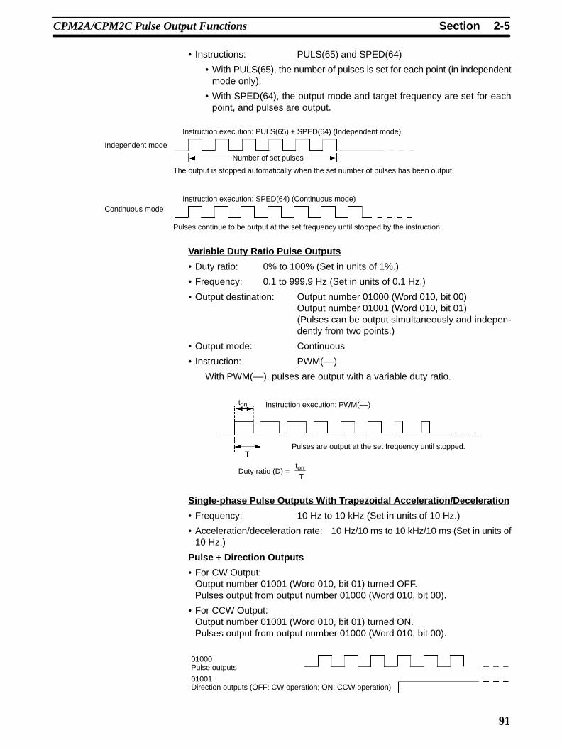
2-5SectionCPM2A/CPM2C Pulse Output Functions
91
• Instructions: PULS(65) and SPED(64)
• With PULS(65), the number of pulses is set for each point (in independentmode only).
• With SPED(64), the output mode and target frequency are set for eachpoint, and pulses are output.
Instruction execution: PULS(65) + SPED(64) (Independent mode)
Number of set pulses
The output is stopped automatically when the set number of pulses has been output.
Instruction execution: SPED(64) (Continuous mode)
Independent mode
Continuous mode
Pulses continue to be output at the set frequency until stopped by the instruction.
Variable Duty Ratio Pulse Outputs
• Duty ratio: 0% to 100% (Set in units of 1%.)
• Frequency: 0.1 to 999.9 Hz (Set in units of 0.1 Hz.)
• Output destination: Output number 01000 (Word 010, bit 00)Output number 01001 (Word 010, bit 01)(Pulses can be output simultaneously and indepen-dently from two points.)
• Output mode: Continuous
• Instruction: PWM(––)
With PWM(––), pulses are output with a variable duty ratio.
Instruction execution: PWM(––)
Pulses are output at the set frequency until stopped.
Duty ratio (D) =ton
T
ton
Single-phase Pulse Outputs With Trapezoidal Acceleration/Deceleration
• Frequency: 10 Hz to 10 kHz (Set in units of 10 Hz.)
• Acceleration/deceleration rate: 10 Hz/10 ms to 10 kHz/10 ms (Set in units of10 Hz.)
Pulse + Direction Outputs
• For CW Output:Output number 01001 (Word 010, bit 01) turned OFF.Pulses output from output number 01000 (Word 010, bit 00).
• For CCW Output:Output number 01001 (Word 010, bit 01) turned ON.Pulses output from output number 01000 (Word 010, bit 00).
01000Pulse outputs
01001Direction outputs (OFF: CW operation; ON: CCW operation)

2-5SectionCPM2A/CPM2C Pulse Output Functions
92
Up/Down Pulse Outputs
• For CW output:Pulses output from output number 01000 (Word 010, bit 00).
• For CCW output:Pulses output from output number 01001 (Word 010, bit 01).
01000CW operation
01001CCW operation
• Output mode: Continuous and Independent
• Number of pulses: 1 to 16,777,215
• Instructions: PULS(65) and ACC(––)
• With PULS(65), the number of pulses is set (in independent mode only).
• With ACC(––), the output mode, starting frequency, target frequency, andacceleration/deceleration rate are set, and the pulse outputs are started.From when the pulse outputs are started until they are stopped, they arecontrolled at a constant-ratio frequency change.
Independent Mode
Instruction execution: PULS(65) + ACC(––) (Independent mode)Pulse output frequency
Targetfrequency
Startingfrequency
0 Hz
AccelerationStart
ACC(––)
Deceleration
Time
In independent mode, deceleration iscarried out at the acceleration/deceleration rate in effect at the start.
Continuous Mode
Instruction execution: ACC(––) (Continuous mode)Pulse output frequency
Targetfrequency 2
0 Hz
Acceleration/decelerationStart
ACC(––)
Time
Targetfrequency 3
Targetfrequency 1
Acceleration/deceleration Acceleration/decelerationAcceleration ordeceleration
ACC(––)
Acceleration ordeceleration
ACC(––)

2-5SectionCPM2A/CPM2C Pulse Output Functions
93
2-5-1 Using Single-phase Pulse Outputs Without Acceleration andDeceleration (Fixed Duty Ratio)
Select the pulse output number. Pulse output number 0 or 1
Wire the outputs. Output numbers: 01000 and 01001
PC Setup (DM 6629) PV coordinate system for pulse output numbers 0 and 1
Create a ladder diagram program. PULS(65): For setting the number of output pulses.
SPED(64): For pulse output control without acceleration and deceleration.
INI(61): For stopping pulse outputs and changing the pulse output PV.
PRV(62): For reading the pulse output PV and status.
Single-phase Pulse Outputs
PULS(65) SETPULSESinstruction
SPED(64) SPEEDOUTPUTinstruction
Pulse output 0Pulse output 1
Specify relative orabsolute pulses.
Pulse output SV(8 digits BCD)
INI(61) MODECONTROLinstruction
Stop pulse outputs.Change pulse output PV.
PC Setup
DM 6629,bits 04 to 07
Output mode: Continuous or Independent
Target frequency: 10 Hz to 10 kHz
Start pulse outputs.
Every scan Every scan Immediately
Pulse output status
AR 11 AR 12
Pulse output PV
SR 228 SR 229
SR 230 SR 231
PRV(62) HIGH-SPEED COUNTERPV READ instruction
Read pulse output PV.
Read pulse outputstatus.
Select either pulse number 0 or 1.
Output number Pulse output number
01000 0
01001 1
Selecting the PulseOutput Number

2-5SectionCPM2A/CPM2C Pulse Output Functions
94
Wire the CPM2A outputs as shown in the following illustration. (Pulses can beoutput independently from pulse outputs 0 and 1.)
Output 01000: Pulse output 0 (single-phase output)
Output 01001: Pulse output 1 (single-phase output)
Wire the CPM2C outputs as shown in the following illustration. (Pulses can beoutput independently from pulse outputs 0 and 1.)
01000: Pulse output 0 (single-phase output)
01001: Pulse output 1 (single-phase output)
Output connector
Make the following settings in the PC Setup.
Word Bits Function SettingDM 6629 00 to 03 Pulse 0 PV coordinate
system0: Relative coordinatesystem
Either 0 or1
04 to 07 Pulse 1 PV coordinatesystem
1: Absolute coordinatesystem
DM 6642 08 to 15 High-speed countersetting
00: Do not use.
01: Use as high-speedcounter
02: Use assynchronized pulsecontrol (10 to 500 Hz).
03: Use assynchronized pulsecontrol (20 Hz to 1kHz).
04: Use assynchronized pulsecontrol (300 Hz to 20kHz).
Either 00 or01
If absolute pulses are specified with PULS(65), be sure to set the absolute coor-dinate system (1).
Synchronized pulse control cannot be used simultaneously.
Wiring the Outputs
PC Setup

2-5SectionCPM2A/CPM2C Pulse Output Functions
95
The settings will go into effect when the mode is changed (from PROGRAM toMONITOR/RUN) or when the power supply is turned ON to the PC.
The following table shows the instruction operations related to pulse outputswithout acceleration and deceleration (fixed duty ratio).
Instruction Control Operation
(@)PULS(65) Set number of pulses Sets the number of pulses to be outputin independent mode.
(@)SPED(64) Set frequency and startpulse outputs
Sets the frequency for outputs in theindependent mode or continuous mode,and starts the pulse outputs.
Change frequency Changes the frequency for outputs inthe independent mode or continuousmode.
Stop pulse outputs Stops the pulse outputs (by changingthe speed to a frequency of 0 Hz).
(@)INI(61) Stop pulse outputs Stops the pulse outputs.
Change pulse output PV Changes the pulse output PV.
(@)PRV(62) Read pulse output PV Reads the pulse output PV.
Read pulse output status Reads the pulse output status.
The following table shows which instructions can be executed during pulse out-puts without acceleration and deceleration.
PULS(65) SPED(64) INI(61) PRV(62) ACC(––) PWM(––)
Continuous mode No Yes (See note 2.) Yes (See note 1.) Yes No No
Independent mode No Yes (See note 2.) Yes (See note 1.) Yes No No
Note 1. This instruction can be executed only while pulse outputs are stopped. ThePV cannot be changed while pulses are being output. If the PV needs to bechanged, be sure to stop the pulse output first.
2. This instruction can be used only for changing the frequency and stoppingthe pulse output. It cannot be used for switching between independentmode and continuous mode.
The following table shows the words and bits related to pulse outputs withoutacceleration and deceleration (fixed duty ratio).
Word Bits Name Contents
228 00 to 15 Pulse output PV 0, rightmost 4 digits Cannot be used as
229 00 to 15 Pulse output PV 0, leftmost 4 digits work bits even when
230 00 to 15 Pulse output PV 1, rightmost 4 digitsnot used as pulseoutputs.
231 00 to 15 Pulse output PV 1, leftmost 4 digitsoutputs.
252 04 Pulse output 0 PV reset Clears PV 0 when ON.
05 Pulse output 1 PV reset Clears PV 1 when ON.
AR 11 12 Pulse output 0 PV overflow/underflow ON: OccurredOFF: Normal
13 Number of pulses set for pulse output 0 ON: Set (by PULS(65))OFF: Not set
14 Pulse output completed for pulseoutput 0
ON: Completed (bySPED(64))OFF: Not completed
15 Pulse output in progress for pulseoutput 0
ON: In progress (bySPED(64))OFF: Stopped
Ladder DiagramProgramming

2-5SectionCPM2A/CPM2C Pulse Output Functions
96
Word ContentsNameBitsAR 12 12 Pulse output 1 PV overflow/underflow ON: Occurred
OFF: Normal
13 Number of pulses set for pulse output 1 ON: Set (by PULS(65))OFF: Not set
14 Pulse output completed for pulseoutput 1
ON: Completed (bySPED(64))OFF: Not completed
15 Pulse output in progress for pulseoutput 0
ON: In progress (bySPED(64))OFF: Stopped
Set Number of PulsesSpecify the number of pulses to be output in independent mode.
Port specifier (000: Pulse output 0; 010: Pulse output 1)
Type of Pulse Output (000: Relative pulses; 001: Absolute pulses) (See note.)Beginning word of setting for number of pulses
Rightmost 4 digits
Leftmost 4 digits
Number of pulses (Rightmost, leftmost digits)
Register the number of pulses to be set.
96,777,215 to 16,777,215Negative numbers are expressed by turning ONthe leftmost bit.
Type of Pulse Output
000: Relative pulses (SV for number of pulses = Number of pulses moved)
001: Absolute pulses (SV for number of pulses = The next PV on the absolute coordinate system,i.e., the pulse output PV + number of pulses moved)*
*Absolute pulses can only be specified by PULS(65) when the PV coordinate systemin the PC Setup is set for an absolute coordinate system.
(@)PULS(65)
P
D
N
N
N+1
Set Frequency and Start Pulse OutputsChange FrequencyThese functions set the pulse output number, the output mode, and the frequen-cy, and begin pulse outputs. They can also be used to change the frequency ifpulse outputs are already in progress.
Port specifier (000: Pulse output 0; 010: Pulse output 1)Mode designation (000: Independent; 001: Continuous)
Target frequency data word
Target frequency
Register the target frequency data to be set.
#0001 to #1000 (4 digits BCD): 10 Hz to 10 kHz
#0000: Pulse output stopped
(@)SPED(64)
P
M
F
F

2-5SectionCPM2A/CPM2C Pulse Output Functions
97
Change Pulse Output PV
Resetting Pulse Output PVThis function changes the pulse output present value (PV). The PV can also becleared by using SR 25204 and SR 25205.
Port specifier (000: Pulse output 0; 010: Pulse output 1)Control designation (004: Change pulse output PV)
Beginning word for PV change data
Rightmost 4 digits
Leftmost 4 digits
Change PV data (Rightmost, leftmost digits)
Register the PV data to be changed.
96,777,215 to 16,777,215
Negative numbers are expressed by turningON the leftmost bit.
(@)INI(61)
P
004
C2
C2
C2+1
The pulse output PV can only be changed or reset while pulse outputs arestopped. Check to be sure that the Pulse Output In Progress Flags (AR 1115 andAR 1215) have been turned OFF.
Stop Pulse OutputsThis function stops the pulse outputs.
Using SPED(64)
Port specifier (000: Pulse output 0; 010: Pulse output 1)Mode designation (000: Independent; 001: Continuous)Target frequency data word
#0000 Specifies a frequency of 0 Hz.
(@)SPED(64)
P
M
F
F
Using INI(61)
Port specifier (000: Pulse output 0; 010: Pulse output 1)
Control designation (003: Stop pulse outputs)Fixed: 000
(@)INI(61)
P
003
000
Besides executing the instructions shown above, it is also possible to stop pulseoutputs by stopping operation (PROGRAM mode).
Read Pulse Output PVThis function reads the pulse output PV.
Using an Instruction
Port specifier (000: Pulse output 0; 010: Pulse output 1)Control designation (003: Read pulse output PV)
Beginning word for storing pulse output PV
Pulse output PV (rightmost, leftmost digits)
The PV data that is read is stored here.
96,777,215 to 16,777,215
Negative numbers are expressed by turningON the leftmost bit.
Rightmost 4 digits
Leftmost 4 digits
(@)PRV(62)
P
003
D
D
D+1

2-5SectionCPM2A/CPM2C Pulse Output Functions
98
Using Data AreasAs shown in the following illustration, the pulse output PV for pulse output 0 isstored in words 228 and 229, and the pulse output PV for pulse output 1 is storedin words 230 and 231.
Pulse Output 0 Pulse Output 1
Word 228
Word 229
Word 230
Word 231
PV (Rightmost) PV (Rightmost)
PV (Leftmost) PV (Leftmost)
Words 228 to 231 are refreshed with every scan, so there may be a discrepancyfrom the exact PV at any given time.
Words 228 to 231 cannot be used as work words even when pulse outputs arenot being used.
When the PV is read by executing PRV(62), words 228 to 231 are refreshed withthe same timing.
Read Pulse Output StatusThis function reads the pulse output status.
Using an Instruction
Port specifier (000: Pulse output 0; 010: Pulse output 1)
Control designation (001: Read pulse output status)Word for storing pulse output status
Pulse output in progress0: Stopped1: Output in progress
Pulse output PV overflow/underflow0: Normal; 1: Overflow or underflow occurred
Number of pulses0: Not set1: Set
Pulse output completion0: Not completed1: Completed
(@)PRV(62)
P
001
D
Pulse output status0: Constant speed; 1: Accelerating/decelerating
Using Data AreasAs shown in the following illustration, the pulse output status for pulse output 0 isstored in AR 11, and the pulse output status for pulse output 1 is stored in AR 12.
AR 11: Pulse output 0AR 12: Pulse output 1
Pulse output completion0: Not completed1: Completed
Pulse output in progress0: Stopped1: Output in progress Pulse output PV overflow/underflow
0: Normal1: Overflow or underflow occurred
Number of pulses0: Not set1: Set
Pulse output status: 0: Constant speed; 1: Accelerating/decelerating
Note The flags in AR 11 and AR 12 are refreshed once each cycle, so the values inthese words may not reflect the actual status during each cycle, but the flags inAR 11 and AR 12 are refreshed when the status is read with PRV(62).

2-5SectionCPM2A/CPM2C Pulse Output Functions
99
Relationship Between Status and Operation
Independent Mode (Without Acceleration and Deceleration)
Frequency
PULS(65) execution
SPED(64) execution
Output in progress
Output completed
Number of pulses set
Time
Continuous Mode
Frequency
SPED(64) execution
Output in progress
Output completed
Number of pulses set
Time
INI(61) execution
Stopping Output in Independent Mode (Without Acceleration and Deceleration)
Frequency
PULS(65) execution
SPED(64) execution
Output in progress
Output completed
Number of pulses set
Time
INI(61) execution

2-5SectionCPM2A/CPM2C Pulse Output Functions
100
Application ExamplesPositioning
ExplanationIn this example, when the execution condition (00005) turns ON, 100 pulses areoutput from output 01000 (pulse output 0) at a frequency of 60 Hz.
Frequency
60 Hz
Execution condition(00005)
Number of pulses
WiringWire the CPM2A to the motor driver as shown in the following illustration.
Motor Driver
Wire the CPM2C to the motor driver as shown in the following illustration. In thiscase, a CPU Unit with sinking transistor outputs is used.
Motor Driver
24 VDC
Output connector
PC Setup
Sets the coordinate system for pulse output 0 as relative.
Set for other than synchronized pulse control.
(Set to 01 when using the high-speed counter.)
DM 6629 0
15 0
DM 6642 0 0

2-5SectionCPM2A/CPM2C Pulse Output Functions
101
Programming
00005 (Execution condition)
Detects turning ON of execution condition.
Sets number of pulses.Pulse output 0Relative pulsesBeginning word for pulseSV data
DM 0000DM 0001
Number of pulses:100
Sets frequency and starts pulse output.Pulse output 0Independent modeFrequency: 60 Hz
PLUS(65)
SPED(64)
(13)
JOG OperationExplanationIn this example, when the execution condition (00005) turns ON, JOG pulses areoutput at a frequency of 100 Hz from either output 01000 (pulse output 0) or out-put 01001 (pulse output 1). When the execution condition (00005) turns OFF,the output is stopped. Switching between output 01000 (pulse output 0) and out-put 01001 (pulse output 1) is performed by means of the direction designator(00006).
Frequency(direction)
Execution condition(00005)Direction designator(00006)
Time
WiringWire the CPM2A to the motor driver as shown in the following illustration.
Motor Driver

2-5SectionCPM2A/CPM2C Pulse Output Functions
102
Wire the CPM2C to the motor driver as shown in the following illustration. In thiscase, a CPU Unit with sinking transistor outputs is used.
MotorDriver
24 VDC
Output connector
Note Refer to page operation manual for details on wiring outputs.
PC Setup
Sets the coordinate system for pulse outputs 0 and 1 as relative.
Set for other than synchronized pulse control.
(Set to 01 when using the high-speed counter.)
DM 6629 0
15 0
DM 6642 0 0
0
Programming
00005 (Execution condition)Detects turning ON of execution condition.
Detects turning OFF of execution condition.(Direction designator)
Output in CW directionPulse output 0Continuous modeOutput frequency: 100 Hz
Output in CCW direction
Pulse output 1Continuous modeOutput frequency: 100 Hz
Stops pulse outputs 0 and 1.
SPED(64)
INI(61)
INI(61)
SPED(64)
(13)
(14)
010

2-5SectionCPM2A/CPM2C Pulse Output Functions
103
2-5-2 Using Pulse Outputs With Variable Duty Ratio
Select the pulse output number. Pulse output number 0 or 1
Wire the outputs. Output numbers: 01000 and 01001
Create a ladder diagram program.PWM(––): For setting the frequency and duty ratio.
INI(61): For stopping pulse outputs.
PRV(62): For reading the pulse output status.
Pulse Outputs With Variable Duty Ratio
PWM(––)
Target frequency: 0.1 to 999.9 Hz
Duty ratio: 0 to 100%Start pulse outputs
INI(61)
Stop pulse outputs
Pulse output 0Pulse output 1
MODE CONTROLinstruction
Every scan Every scan Immediately
Pulse output status
AR 11 AR 12
PRV(62)
HIGH-SPEEDCOUNTER PVREAD instruction
Read pulseoutput status.
PULSE WITHVARIABLE DUTYRATIO instruction
(Note: The duty ratio is the ratioof ON time to pulse frequency.)
(Either 01000 or 01001can be used.)
Select either pulse output 0 or 1.
Output number Pulse output number
01000 0
01001 1
Wire the CPM2A outputs as shown in the following illustration. (Pulses can beoutput independently from pulse outputs 0 and 1.)
Output 01000: Pulse output 0 (single-phase output)
Output 01001: Pulse output 1 (single-phase output)
Selecting the PulseOutput Number
Wiring the Outputs

2-5SectionCPM2A/CPM2C Pulse Output Functions
104
Wire the CPM2C outputs as shown in the following illustration. (Pulses can beoutput independently from pulse outputs 0 and 1.)
01000: Pulse output 0 (single-phase output)
01001: Pulse output 1 (single-phase output)
Output connector
Make the following settings in the PC Setup.
Word Bits Function Setting
DM 6642 08 to 15 High-speedcountersetting
00: Do not use.
01: Use as high-speed counter
02: Use as synchronized pulsecontrol (10 to 500 Hz).
03: Use as synchronized pulsecontrol (20 Hz to 1 kHz).
04: Use as synchronized pulsecontrol (300 Hz to 20 kHz).
Either 00 or01
Synchronized pulse control cannot be used simultaneously.
The settings will go into effect when the mode is changed (from PROGRAM toMONITOR/RUN) or when the power supply is turned ON to the PC.
The following table shows the instruction operations related to pulse outputswith variable duty ratio.
Instruction Control Operation(@)PWM(––) Pulse output with
variable duty ratioSets the frequency and duty ratio andstarts the pulse outputs.
Change duty ratio Changes the duty ratio during pulsewhile pulse outputs with variable dutyratio are already in progress.
(@)INI(61) Stop pulse outputs Stops the pulse outputs.
(@)PRV(62) Read pulse output status Reads the pulse output status (duringpulse outputs).
The following table shows which instructions can be executed during pulse out-puts without acceleration and deceleration.
PULS(65) SPED(64) INI(61) PRV(62) ACC(––) PWM(––)
No No Yes (See note 1.) Yes No Yes (See note 2.)
Note 1. This instruction can be used only for stopping pulse outputs.
2. This instruction can be used only for changing the duty ratio. The frequencycannot be changed while pulses are being output. If the frequency needs tobe changed, be sure to stop the pulse output first.
PC Setup
Ladder DiagramProgramming

2-5SectionCPM2A/CPM2C Pulse Output Functions
105
The following table shows the words and bits related to pulse outputs with vari-able duty ratio.
Word Bit Name Contents
AR 11 15 Pulse output in progressfor pulse output 0
ON: In progress (by SPED(64),ACC(––), or PWM(––))OFF: Stopped
AR 12 15 Pulse output in progressfor pulse output 1
ON: In progress (by SPED(64),ACC(––), or PWM(––))OFF: Stopped
Pulse Output With Variable Duty RatioChange Duty RatioThese functions set the position for outputting pulses (01000, 01001), the fre-quency, and the duty ratio, and start the pulse outputs. By changing the duty ratiosetting and executing PWM(––) again, it is also possible to change the duty ratiowhile pulse outputs with variable duty ratio are already in progress.
Port specifier (000: Pulse output 0; 010: Pulse output 1)Target frequency data word
Target frequencyRegister the target frequency to be set.
#0001 to #9999 (4 digits BCD): 0.1 Hz to 999.9 Hz
Duty ratio data word
Duty ratio
Register the duty ratio to be set.
#0000 to #0100 (4 digits BCD): 0% to 100%
(@PWM(––)
P
F
D
F
D
The pulse frequency cannot be changed while pulses are being output.
Stop Pulse OutputsThis function stops pulse outputs.
Port specifier (000: Pulse output 0; 010: Pulse output 1)
Control designation (003: Stop pulse outputs)Fixed: 000
(@)INI(61)
P
003
000
Note The pulse outputs can also be stopped by switching the PC to PROGRAMmode.
Read Pulse Output StatusThis function reads the pulse output status.
Using an Instruction
Port specifier (000: Pulse output 0; 010: Pulse output 1)Control designation (001: Read pulse output status)
Beginning word for storing pulse output status
Pulse output in progress
0: Stopped
1: Output in progress
(@)PRV(62)
P
001
D

2-5SectionCPM2A/CPM2C Pulse Output Functions
106
Using Data AreasAs shown in the following illustration, the pulse output status for pulse output 0 isstored in AR 1115, and the pulse output status for pulse output 1 is stored in AR1215.
AR 11: Pulse output 0
AR 12: Pulse output 1
Pulse output in progress
0: Stopped1: Output in progress
Note AR 1115 and AR 1215 are refreshed once each cycle, so the values in thesewords may not reflect the actual status during each cycle, but AR 1115 andAR 1215 are refreshed when the status is read with PRV(62).
Relationship Between Status and OperationContinuous Mode (Pulse Output With Variable Duty Ratio)
Frequency
PWM(––) execution
INI(61) execution
Output in progress
Output completion
Set number of pulses
Time
Application ExampleExplanationIn this example, when the execution condition (00005) turns ON, variable dutypulses are output from output 01000 (pulse output 0) at a frequency of 100 Hz.The duty ratio at this time can be changed with the thumbwheel switch 0.
WiringWire the CPM2A to the motor driver and thumbwheel switch as shown in the fol-lowing illustration.
Motor Driver

2-5SectionCPM2A/CPM2C Pulse Output Functions
107
Wire the CPM2C to the motor driver and thumbwheel switch as shown in the fol-lowing illustration. In this case, a CPU Unit with sinking transistor outputs isused.
Motor Driver
24 VDCThumbwheel switch
Input connectorOutput connector
Note Refer to the operation manual for details on wiring.
PC Setup
High-speed counter not used. (Set for other than synchronized pulse control.)
DM 6642 0 0
15 0
Programming (CPM2A Example)
00005 (Execution condition)Detects turning OFF of execution condition.
Stops pulse output 0.
Changes analog control 0 value to a value from 0 to 100.Value in SR 250 (Analog control 0 in CPM2A PCs) (see note)Divide value by 2.Duty ratio setting
Pulse outputs with variable duty
Pulse output 0Output frequency: 100 HzDuty ratio setting
DIV(33)
PWM(––)
INI(61)
(14)
Note The CPM2C is not provided withan analog control. For externalsettings, specify the input wordconnected to the thumbwheelswitch.

2-5SectionCPM2A/CPM2C Pulse Output Functions
108
2-5-3 Using Pulse Outputs With Trapezoidal Acceleration andDeceleration
Select the pulse output number. Pulse output number 0
Wire the outputs. Output numbers: 01000 and 01001
PC Setup (DM 6629) PV coordinate system for pulse output number 0
Create a ladder diagram program.PULS(65): For setting the number of output pulses.
ACC(––): For controlling pulse outputs with trapezoidal acceleration anddeceleration
INI(61): For stopping pulse outputs and changing the pulse output PV.
PRV(62): For reading the pulse output PV and status.
Select the direction control method. Pulse + direction output or up/down pulse output
Pulse Outputs With Trapezoidal Acceleration and Deceleration
PULS(65) SETPULSESinstruction
ACC(––)ACCELERATIONCONTROLinstruction
Pulse, CWDirection, CCW
Specify relative or ab-solute pulses.
set value (8 digits BCD)
INI(61) MODECONTROLinstruction
Stop pulse outputs.Change pulse output PV.
PC Setup
DM 6629, bits00 to 03
Mode designation
Target frequency: 10 Hz to 10 kHz
Start pulse outputs.
Every scan Every scan Immediately
Pulse output status
AR 11
Pulse output PV
SR 228 SR 229
PRV(62)
HIGH-SPEEDCOUNTER PVREAD instruction
Read pulse output PV.Read pulse outputstatus.
Number of output pulses Starting frequency: 0 Hz to 10 kHz
Acceleration/deceleration rate:10 ms increase/decrease10 Hz to 10 kHz

2-5SectionCPM2A/CPM2C Pulse Output Functions
109
Select the pulse output direction control method according to the type of signalused.
Pulse + Direction Outputs Up/down Pulse Outputs
Select pulse output 0.
Output number Pulse output number
01000 0
01001
Wire the CPM2A outputs as shown in the following illustration.
Output 01000: Pulse output
Output 01001: Direction output
Output 01000: CW output
Output 01001: CCW output
Pulse + Direction Outputs Up/down Pulse Outputs
Wire the CPM2C outputs as shown in the following illustration.
01000: Pulse output
01001: Direction output
01000: CW output
01001: CCW output
Pulse + Direction Outputs Up/down Pulse Outputs
Output connector Output connector
Selecting the DirectionControl Method
Selecting the PulseOutput Number
Wiring the Outputs

2-5SectionCPM2A/CPM2C Pulse Output Functions
110
Make the following settings in the PC Setup.
Word Bits Function Setting
DM 6629 00 to 03 Pulse 0 PVcoordinatesystem
0: Relative coordinate system
1: Absolute coordinate system
Either 0 or 1
DM 6642 08 to 15 High-speedcountersetting
00: Do not use.
01: Use as high-speed counter
02: Use as synchronized pulsecontrol (10 to 500 Hz).
03: Use as synchronized pulsecontrol (20 Hz to 1 kHz).
04: Use as synchronized pulsecontrol (300 Hz to 20 kHz).
Either 00 or01
If absolute pulses are specified with PULS(65), be sure to set the absolute coor-dinate system (1).
Synchronized pulse control cannot be used simultaneously.
The settings will go into effect when the mode is changed (from PROGRAM toMONITOR/RUN) or when the power supply is turned ON to the PC.
The following table shows the instruction operations related to pulse outputswith trapezoidal acceleration and deceleration (fixed duty ratio).
Instruction Control Operation
(@)PULS(65) Set number of pulses Sets the number of pulses to be outputin independent mode.
(@)ACC(––) Set frequency and startpulse outputs
Sets the target frequency, startingfrequency, and acceleration/decelerationrate for outputs in independent mode orcontinuous mode, and starts the pulseoutputs.
Change frequency Changes the frequency during pulseoutput in continuous mode byaccelerating or decelerating accordingto the specifiedacceleration/deceleration rate.
Stop pulse outputs Decelerates pulse outputs to a stopaccording to the specifiedacceleration/deceleration rate.
(@)INI(61) Stop (decelerate stop)pulse outputs
Stops the pulse outputs.
Change pulse output PV Changes the pulse output PV.
(@)PRV(62) Read pulse output PV Reads the pulse output PV.
Read pulse output status Reads the pulse output status.
The following table shows which instructions can be executed during pulse out-puts with trapezoidal acceleration and deceleration.
PULS(65) SPED(64) INI(61) PRV(62) ACC(––) PWM(––)
Continuous mode No No Yes (See note 1.) Yes No No
Independent mode No No Yes (See note 1.) Yes Yes (See note 2.) No
Note 1. This instruction can be executed only while pulse outputs are stopped. ThePV cannot be changed while pulses are being output. If the PV needs to bechanged, be sure to stop the pulse output first.
2. This instruction can be used only for changing the frequency and stoppingthe pulse output. It cannot be used for switching between independentmode and continuous mode. Moreover, ACC(––) cannot be received duringacceleration or deceleration.
PC Setup
Ladder DiagramProgramming

2-5SectionCPM2A/CPM2C Pulse Output Functions
111
The following table shows the words and bits related to pulse outputs with trape-zoidal acceleration and deceleration (fixed duty ratio).
Word Bits Name Contents
228 00 to 15 Pulse output PV 0, rightmost 4 digits Cannot be used aswork bits even when
229 00 to 15 Pulse output PV 0, leftmost 4 digitswork bits even whennot used as pulseoutputs.
252 04 Pulse output 0 PV reset Clears PV 0 when ON.
AR 11 11 Pulse output status for pulse output 0 ON: Accelerating ordeceleratingOFF: Constant speed
12 Pulse output 0 PV overflow/underflow ON: OccurredOFF: Normal
13 Number of pulses set for pulse output 0 ON: SetOFF: Not set
14 Pulse output completed for pulseoutput 0
ON: CompletedOFF: Not completed
15 Pulse output in progress for pulseoutput 0
ON: In progress (bySPED(64), ACC(––),or PWM(––))OFF: Stopped
Set Number of PulsesSpecify the number of pulses to be output in independent mode.
Fixed at 000: Pulse output 0
Type of Pulse Output (000: Relative pulses; 001: Absolute pulses) (See note.)Beginning word of setting for number of pulses
Rightmost 4 digits
Leftmost 4 digits
Number of pulses (Rightmost, leftmost digits)
Register the number of pulses to be set.
96,777,215 to 16,777,215
Negative numbers are expressed by turningON the leftmost bit.
Type of Pulse Output
*Absolute pulses can only be specified by PULS(65) when the PV coordinate systemin the PC Setup is set for an absolute coordinate system.
(@)PULS(65)
000
D
N
N
N+1
000: Relative pulses (SV for number of pulses = Number of pulses moved)
001: Absolute pulses (SV for number of pulses = The next PV on the absolute coordinate system,i.e., the pulse output PV + number of pulses moved)*

2-5SectionCPM2A/CPM2C Pulse Output Functions
112
Set Frequency and Start Pulse OutputsChange FrequencyThese functions set the output mode, the target frequency, the starting frequen-cy, and the acceleration/deceleration rate, and they begin pulse outputs. Theycan also be used to change the frequency, by accelerating or decelerating at thespecified acceleration/deceleration rate, if pulse outputs are already in progressin continuous mode.
Setting the Frequencies, Acceleration/Deceleration, and Starting PulseOutputs in Independent Mode
Fixed at 000: Pulse output 0Output mode designationBeginning word of settings table
Output mode
Specify the output mode.
000: Up/down pulse outputs, independent mode
002: Pulse + direction outputs, independent mode
Acceleration/deceleration rate (#0001 to #1000 BCD: 10 Hz to 10 kHz)
Target frequency (#0001 to #1000 BCD: 10 Hz to 10 kHz)
Starting frequency (#0000 to #1000 BCD: 0 to 10 kHz)
Register the data for each frequency.The acceleration/deceleration rate is the increase or decrease in the fre-quency every 10 ms.
Pulse output frequency
Targetfrequency
Startingfrequency
0 Hz
Number ofpulses
In independent mode, the acceleration and decelerationpoints are determined from the number of pulses, theacceleration/deceleration rate, the target frequency, andthe the starting frequency.
(@)ACC(––)
000
M
T
M
T
T+1
T+2
Time

2-5SectionCPM2A/CPM2C Pulse Output Functions
113
Setting the Frequency and Acceleration/Deceleration, Starting Pulse Out-puts, and Changing the Frequency in Continuous Mode
Fixed at 000: Pulse output 0Output mode designation
Beginning word of settings table
Output mode
Specify the output mode.
Pulse output frequency
Targetfrequency
Startingfrequency
0 Hz
In continuous mode, pulses are output at the target frequency untilstopped. The next ACC(––) instruction cannot be received except duringacceleration or deceleration.
010: Up/down pulse output, CW, continuous mode
011: Up/down pulse output, CCW, continuous mode012: Pulse + direction output, CW, continuous mode
013: Pulse + direction output, CCW, continuous mode
(@)ACC(––)
000
M
T
M
T
T+1
T+2
Time
Acceleration/deceleration rate (#0001 to #1000 BCD: 10 Hz to 10 kHz)
Target frequency (#0001 to #1000 BCD: 10 Hz to 10 kHz)
Starting frequency (#0000 to #1000 BCD: 0 to 10 kHz)
Register the data for each frequency.The acceleration/deceleration rate is the increase or decrease in the fre-quency every 10 ms.
Change Pulse Output PVThis function changes the pulse output PV.
Control designation (004: Change pulse output PV)
Beginning word for PV change data
Rightmost 4 digits
Leftmost 4 digits
Change PV data (Rightmost, leftmost digits)
Register the PV data to be changed.
96,777,215 to 16,777,215
Negative numbers are expressed by turningON the leftmost bit.
Fixed at 000: Pulse output 0
(@)INI(61)
000
004
C2
C2
C2+1
Note The pulse output PV can be changed only while the pulse output is stopped.

2-5SectionCPM2A/CPM2C Pulse Output Functions
114
Stop Pulse Outputs,Decelerate and Stop Pulse OutputsThese functions stop the pulse outputs.
Stop Pulse Outputs
Control designation (003: Stop pulse outputs)
Fixed at 000: Pulse output 0
Fixed at 000
(@)INI(61)
000
003
000
Decelerate Stop Pulse Outputs
Fixed at 000: Port specifierMode designation
Beginning word of settings table
(@)ACC(––)
000
000
T
T
T+1
T+2
Acceleration/deceleration rate (#0001 to #1000 BCD: 10 Hz to 10 kHz)
Target frequency (#0000 to #1000 BCD: 0 Hz to 10 kHz)
Starting frequency (#0000 to #1000 BCD: 0 to 10 kHz)
Register the data for each frequency.The acceleration/deceleration rate is the increase or decrease in the fre-quency every 10 ms.
Note The pulse outputs can also be stopped by switching the PC to PROGRAMmode.
Read Pulse Output PVThis function reads the pulse output PV.
Using an Instruction
Fixed at 000: Pulse output 0Control designation (003: Read pulse output PV)
Beginning word for storing pulse output PV
Pulse output PV (rightmost, leftmost digits)
The PV data that is read is stored here.
96,777,215 to 16,777,215
Negative numbers are expressed by turningON the leftmost bit.
Rightmost 4 digits
Leftmost 4 digits
(@)PRV(62)
000
003
D
D
D+1
Using Data AreasAs shown in the following illustration, the pulse output PV for pulse output 0 isstored in words 228 and 229.
Pulse Output 0
Word 228
Word 229
PV (Rightmost)
PV (Leftmost)
Note SR 228 and SR 229 are refreshed once each cycle, so the values in these wordsmay not reflect the actual status during each cycle, but SR 228 and SR 229 arerefreshed immediately when their status is read with PRV(62).

2-5SectionCPM2A/CPM2C Pulse Output Functions
115
Read Pulse Output StatusThis function reads the pulse output status.
Using an Instruction
Fixed at 000: Pulse output 0
Control designation (001: Read pulse output status)
Word for storing pulse output status
Pulse output in progress0: Stopped1: Output in progress
Pulse output PV overflow/underflow0: Normal; 1: Overflow or underflow occurred
Number of pulses0: Not set1: Set
Pulse output completion0: Not completed1: Completed
Pulse output status0: Constant rate1: Accelerating or decelerating
(@)PRV(62)
000
001
D
Using Data AreasAs shown in the following illustration, the pulse output status for pulse output 0 isstored in AR 1111 to AR 1115.
AR 11: Pulse output 0
Pulse output completion0: Not completed1: Completed
Pulse output in progress0: Stopped1: Output in progress Pulse output PV overflow/underflow
0: Normal1: Overflow or underflow occurred
Number of pulses0: Not set1: Set
Pulse output status0: Constant rate1: Accelerating or decelerating
Note AR 1111 through AR 1115 are refreshed once each cycle, so the values of theseflags may not reflect the actual status, but these flags are refreshed immediatelywhen their status is read with PRV(62).
Relationship Between Status and OperationIndependent Mode with Acceleration and Deceleration
PULS(65) execution
ACC(––) execution
Output 0 in progress
Output 1 in progress
Output completion
Output status
Set number of pulses
Time
Frequency

2-5SectionCPM2A/CPM2C Pulse Output Functions
116
Continuous Mode with Acceleration and Deceleration 1
ACC(––) execution (2)
Output 0 in progress
Output 1 in progress
Output completion
Output status
Set number of pulses
Time
ACC(––) execution (1)
INI(61) execution
Frequency
Continuous Mode with Acceleration and Deceleration 2
ACC(––) execution (Stop)
Output 0 in progress
Output 1 in progress
Output completion
Output status
Set number of pulses
Time
Frequency
Stopping Outputs in Continuous Mode with Acceleration and Deceleration 1
ACC(––) execution
Output 0 in progress
Output 1 in progress
Output completion
Output status
Set number of pulses
Time
INI(61) execution
Frequency
PULS(65) execution

2-5SectionCPM2A/CPM2C Pulse Output Functions
117
Stopping Outputs in Continuous Mode with Acceleration and Deceleration 2
ACC(––) execution
Output 0 in progress
Output 1 in progress
Output completion
Output status
Set number of pulses
Time
Frequency
PULS(65) execution
ACC(––) execution
Application ExamplePositioning
ExplanationIn this example, when the execution condition (00005) turns ON, 1000 pulsesare output from output 01000 (pulse output 0) in a trapezoidal acceleration/de-celeration pattern as shown in the following diagram.
Frequency (Hz)
Execution condition(00005)
Number of pulses
200
10 Hz10 ms
Acceleration/deceleration rate500
WiringWire the CPM2A to the motor driver as shown in the following illustration.
Motor Driver

2-5SectionCPM2A/CPM2C Pulse Output Functions
118
Wire the CPM2C to the motor driver as shown in the following illustration. In thiscase, a CPU Unit with sinking transistor outputs is used.
Motor Driver
24 VDC
Output connector
Note Refer to the operation manual for details on wiring.
PC Setup
Sets the coordinate system for pulse output 0 as relative.
High-speed counter not used. (Set for other than synchronized pulse control.)
DM 6629 0
15 0
DM 6642 0 0
Programming
00005 (Execution condition)Detects turning ON of execution condition.
Sets number of pulses.Pulse output 0Relative pulsesBeginning word for pulse SVdata Number of pulses: 1,000
Sets frequency and starts pulse output.Pulse output 0Independent mode, up/down pulse outputBeginning word ofsettings table
PULS(65)
Acceleration/deceleration rate: 10 Hz/10 msTarget frequency: 500 HzStarting frequency: 200 Hz
ACC(––)
(13)

2-5SectionCPM2A/CPM2C Pulse Output Functions
119
JoggingExplanationIn this example, when the execution condition (00005) turns ON, JOG pulses areoutput at a frequency of 100 Hz from either output 01000 (CW direction) or out-put 01001 (CCW direction). When the execution condition (00005) turns OFF,the output is stopped. As shown in the following diagram, the JOG pulses areaccelerated and decelerated at the start and stop of the operation. Switching be-tween output 01000 (CW direction) and output 01001 (CCW direction) is per-formed by means of the direction designator (00006).
Frequency (Hz)
Execution condition(00005)Direction designator(00006)
Time 10 Hz10 ms
Acceleration/deceleration rate
WiringWire the CPM2A to the motor driver as shown in the following illustration.
Motor Driver
Wire the CPM2C to the motor driver as shown in the following illustration. In thiscase, a CPU Unit with sinking transistor outputs is used.
Motor Driver
24 VDC
Output connector

2-5SectionCPM2A/CPM2C Pulse Output Functions
120
Note Refer to the operation manual for details on wiring.
PC Setup
Sets the coordinate system for pulse output 0 as relative.
High-speed counter not used. (Set for other than synchronized pulse control.)
DM 6629 0
15 0
DM 6642 0 0
Programming
00005 (Execution condition)Detects turning ON of execution condition.
Detects turning OFF of execution condition.(Direction designator)
Output in CW directionPulse output 0Continuous mode, up/down pulses, CW directionBeginning word of settings table
Output in CCW directionPulse output 0
ACC(––)
Continuous mode, up/down pulses, CCW directionBeginning word of settings table
Acceleration/deceleration rate: 10 Hz/10 msTarget frequency: 500 Hz
Starting frequency: 200 Hz
Deceleration stopPulse output 0
Beginning word of settings table
Acceleration/deceleration rate: 10 Hz/10 msTarget frequency: 0 Hz
(Direction designator)
ACC(––)
ACC(––)
(13)
(14)
(14)
AR1115

2-6SectionCPM1A Pulse Output Functions
121
2-6 CPM1A Pulse Output Functions
The CPM1A PCs with transistor outputs have a pulse output function capable ofoutputting a pulse of 20 Hz to 2 kHz (single-phase). Either IR 01000 or IR 01001can be selected for pulse output, and the pulse output can be set to either thecontinuous mode, under which the output can be stopped by an instruction, orthe independent mode, under which the output is stopped after a preset numberof pulses (1 to 16,777,215).
Refer to the CPM1A Operation Manual for details on hardware connections tooutput points and ports.
Continuous mode
Independent mode
Pulses are output at the specified frequency until stopped.
Pulse output is stopped automatically when the specifiednumber of pulses has been output.
Specified number of pulses
Stepping motor
Control input
Motorcontroller
CW/CCW control outputPulse output(single-phase output)IR 01000 or IR 01001
Stepping motor
Note 1. The CPM1A uses a single-phase pulse output. The control signal for thedirection of rotation (CW/CCW) for the motor driver must be written in theprogram.
2. Be sure to use a CPU Unit with transistor outputs.

2-6SectionCPM1A Pulse Output Functions
122
2-6-1 Programming Example in Continuous Mode
In this example program, pulse output begins from IR 01000 when inputIR 00004 turns ON, and is stopped when input IR 00005 turns ON.
SPED(64) can be used to stop pulse output. When using SPED(64) for that pur-pose, specify #0000 (constant or word contents) as the pulse frequency.
@SPED(64)
001
000
#0100
00005 (pulse output stop condition)
@INI(61)
003
000
000
Begins pulse output.
Stops pulse output.
00004 (pulse output condition)
Output from 01000
Continuous mode
Pulse frequency: 1 kHz
2-6-2 Programming Example in Independent Mode
In this example program, pulse output begins from IR 01000 when inputIR 00004 turns ON, and is stopped after the specified number of pulses havebeen output. The pulse amount is set in DM 0100 and DM 0101.
@PULS(65)
000
000
DM 0100
@SPED(64)
000
000
#0100
Sets the number of pulses.
Begins pulse output.
Pulse number setting
00004 (pulse output condition)
00004 (pulse output condition)
Independent mode
Pulse frequency: 1 kHz
2-6-3 Using Pulse Output Instructions
Before beginning pulse output using the independent mode use PULS(65) asshown below to set the number of pulses to be output. This setting is not requiredfor the continuous mode.
@PULS(65)
000
000
N
In N, set the beginning word address of the words where the number of pulses isset. Store the number of pulses in words N and N+1, in eight digits BCD, with theleftmost four digits in N+1 and the rightmost four digits in N.
Make the setting within a range of 00000001 to 16777215 (BCD).
Setting the Number ofPulses

2-6SectionCPM1A Pulse Output Functions
123
With SPED(64), set the bit location for pulse outputs (IR 01000 or IR 01001), theoutput mode (independent, continuous), and the pulse frequency to begin thepulse output.
@SPED(64)
M
P
F
P (3 digits BCD) 000: Outputs to IR 01000010: Outputs to IR 01001
M (3 digits BCD) 000: Independent mode001 Continuous mode
F (4 digits BCD) For the beginning pulse output frequency, specify aconstant or word contents. The specified value and setfrequency are as follows:
Specified value: 0002 to 0200Set frequency: 20 to 2,000 Hz
Note 1. Pulses can be output from only one bit at a time.2. When pulse output is begun in independent mode, the number of pulses is
read when SPED(64) is executed. PULS(65) cannot be used to change thenumber of pulses while pulses are being output.
2-6-4 Changing the FrequencyTo change the frequency during pulse output, change the frequency setting withSPED(64). At that time, set the operands other than the frequency to the samesettings as at the beginning of pulse output.
@SPED(64)
M
P
F
P (3 digits BCD) Same as at beginning of pulse output.M (3 digits BCD) Same as at beginning of pulse output.F (4 digits BCD) For the changed pulse output frequency, specify a
constant or word contents. The specified value and setfrequency are as follows:
Specified value: 0002 to 0200Set frequency: 20 to 2,000 Hz
2-6-5 Stopping Pulse OutputWhen pulses are output in the independent mode, the pulse output will automati-cally stop after the number of pulses specified with PULS(65) has been output.When pulses are output in the continuous mode, either of the following twomethods can be used to stop the pulse output.1. Use SPED(64) to set the frequency to 0.2. Use INI(61) to stop the pulse output.
The first method is to use SPED(64) to stop the pulse output by setting the fre-quency to 0. For details, refer to 2-6-4 Changing the Frequency.
The second method is to use INI(61) to stop the pulse output, as follows:
@INI(61)
003
000
000
Beginning Pulse Output
Using SPED(64)
Using INI(61)

2-7SectionSynchronized Pulse Control (CPM2A/CPM2C Only)
124
2-7 Synchronized Pulse Control (CPM2A/CPM2C Only)By combining the CPM2A/CPM2C’s high-speed counter function with the pulseoutput function, the output pulse frequency can be controlled as a specified mul-tiple of the input pulse frequency.
Note A CPU Unit with transistor outputs is required in order to use synchronized pulsecontrol, i.e., either a CPM2A-CDT-D or CPM2A-CDT1-D.
The following diagram shows the configuration for a CPM2A, but the configura-tion for a CPM2C is identical.
Counter input
Pulse input 00000or 00001 Main motor Rotary encoder
Motordriver
Pulse output 01000 or 01001(single-phase output)
Item Input mode
Differential phaseinput mode
Pulse + directioninput mode
Up/down pulseinput mode
Increment mode
Input 00000 Phase-A input Count input CW input Count inputnumber 00001 Phase-B input Direction input CCW input (See note 1.)
Input method Differential phaseinput (4X)
Single-phase input Single-phase input Single-phase input
Input frequency range 10 to 500 Hz (accuracy ±1 Hz)20 Hz to 1 kHz (accuracy ±1 Hz)300 Hz to 20 kHz (accuracy ±25 Hz) (See note 2.)
Output 01000 Pulse output 0number (Seenote 3.) 01001 Pulse output 1
Output method Single-phase output
Output frequency range 10 Hz to 10 kHz (accuracy 10 Hz)
Frequency ratio 1% to 1,000% (Can be specified in units of 1%.)
Synchronized control cycle 10 ms
Note 1. Can be used as an ordinary input.
2. When 10 kHz or less, then the accuracy is ±10 Hz.
3. Either can be selected as the output number, using SYNC(––).

2-7SectionSynchronized Pulse Control (CPM2A/CPM2C Only)
125
The directions of pulse inputs are all ignored. The frequency of a pulse that hasbeen input is read, without regard to the direction.
The following table shows the relationships between synchronized pulse controland the CPM2A’s other functions.
Function Synchronized pulse control
Synchronized pulse control ---
Interrupt inputs Can be used simultaneously.
Interval timer interrupts Can be used simultaneously.
High-speed counters Cannot be used simultaneously.
Interrupt inputs (counter mode) Can be used simultaneously.
Pulse outputs Cannot be used simultaneously.
Quick-response inputs Can be used simultaneously.
Input time constant See note.
Clock Can be used simultaneously.
Note When inputs 00000 and 00001 are set for use as synchronized pulse control in-puts, the input time constant settings for the affected inputs are disabled. Theinput time constants remain in effect, however, for the values for refreshing therelevant input data area.
The relationship between the pulse input frequency and the pulse output fre-quency is shown below.
Pulse input frequency X Frequency ratio = Rough pulse output frequency
10 to 500 Hz
20 Hz to 1 kHz
300 Hz to 20 kHz
Values are rounded off in units of 10 Hz.
A value less than 10 Hz is regarded as 0 Hz.
A value greater than 10 kHz is regarded as 10 kHz.
Pulse output frequency
(10 Hz to 10 kHz)
The scaling factor control cycle is 10 ms, and the pulse output frequency ischanged at intervals of 10 ms with respect to the pulse input frequency.
Frequency
Time

2-7SectionSynchronized Pulse Control (CPM2A/CPM2C Only)
126
Using Synchronized Pulse Control
Select the input mode. Differential phase pulse input mode, pulse + direction inputmode, up/down pulse input mode, increment mode
Select the pulse synchronizationinput frequency. Input frequency: 10 Hz to 500 Hz; 20 Hz to 1 kHz; 300 Hz to 20 kHz
Wire the inputs and outputs.
PC Setup (DM 6642)
Output numbers: 01000 and 01001
Create a ladder diagram program.SYNC(––): For beginning synchronized pulse control and changing the scaling factor.
INI(61): For stopping synchronized pulse control.
PRV(62): For reading the high-speed counter frequency and the synchronized pulsecontrol status.
Input numbers: 00000, 00001, and 0002
Settings for synchronized pulse control: Input mode, input frequency
PC Setup
DM 6642, bits 08 to 15
Encoderinputs
Input mode Count
Differential phase input
Pulse + direction input
Up/down input
Increment input
Ladder diagram program
INI(61) MODE CONTROLinstructionStop synchronizedpulse control
Every scan
Counter frequency PV
SR 249 SR 248
PRV(62)
ImmediatelyHIGH-SPEEDCOUNTER PVREAD instruction
Read high-speed counterfrequency
Read synchronized pulsecontrol status
Synchronized pulsecontrol status
AR 1100 to AR 1107
PC Setup
DM 6642, bits00 to 03
EitherPulse output 0Pulse output 1
Synchronizedpulse control
10 Hz to 500 Hz20 Hz to 1 kHz300 Hz to 20 kHz
SYNC(––)SYNCHRONIZEDPULSE CONTROLinstructionStart synchronizedpulse controlChange scalingfactor
Every scan
The pulse output frequency cannot be read.

2-7SectionSynchronized Pulse Control (CPM2A/CPM2C Only)
127
Select the differential phase input mode, the pulse + direction input mode, theup/down pulse input mode, or the increment mode. These modes are explainedbelow.
Select one of the following as the input frequency range: 10 Hz to 500 Hz, 20 Hzto 1 kHz, or 300 Hz to 20 kHz. For more information on input frequencies, refer tothe following diagrams.
Differential Phase Input ModeIn the differential phase input mode, the count is incremented or decrementedaccording to two differential phase signals (phase A and phase B) with a multi-plication factor of 4.
Phase A
Phase B
Nms → Frequency =1,000
N
ON
OFF
ON
OFF
Pulse + Direction Input ModeIn the pulse + direction input mode, pulse signals and direction signals are input,and the count is incremented or decremented according to the direction signalstatus.
Nms → Frequency =1,000
N
Pulse inputs
Directioninputs
ON
OFF
ON
OFF
Up/Down Pulse Input ModeIn the up/down pulse input mode, CW signals (up pulses) and CCW signals(down pulses) are input, and the count is incremented or decremented accord-ingly.
Nms → Frequency =1,000
N
CW inputs
CWW inputs
Incremented Decremented
ON
OFF
ON
OFF
Selecting the Input Mode
Selecting the PulseSynchronization InputFrequency

2-7SectionSynchronized Pulse Control (CPM2A/CPM2C Only)
128
Increment ModeIn the increment mode, pulse signals are input and the count is incremented witheach pulse. Phase-B inputs can be used as ordinary inputs.
Nms → Frequency =1,000
N
Pulse inputsON
OFF
Wiring the InputsInput WiringWire the CPM2A inputs as shown in the following diagram.
Differential Phase Input Mode Up/Down Pulse Input Mode
Pulse + Direction Input Mode Increment Mode
00000: Phase-A input00001: Phase-B input00002: Phase-Z input
00000: CW input00001: CCW input
00000: Pulse input00001: Direction input
00000: Pulse input

2-7SectionSynchronized Pulse Control (CPM2A/CPM2C Only)
129
Wire the CPM2C inputs as shown in the following diagram.
Differential Phase Input Mode Up/Down Pulse Input Mode
Pulse + Direction Input Mode Increment Mode
00000: Phase-A input
00001: Phase-B input
00002: Phase-Z input
00000: CW input
00001: CCW input
00000: Pulse input
00001: Direction input
00000: Pulse input
Input connector Input connector
Input connector Input connector
Output WiringWire the CPM2A outputs as shown in the following diagram.
Output Wiring
01000: Pulse output 0
01001: Pulse output 1

2-7SectionSynchronized Pulse Control (CPM2A/CPM2C Only)
130
Wire the CPM2C outputs as shown in the following diagram.
01000: Pulse output 0
01001: Pulse output 1
Output connector
The settings in the PC Setup related to synchronized pulse control are listed inthe following table.
Word Bits Function SettingDM 6642 00 to 03 High-speed counter input mode setting
0: Differential phase input 5 kHz1: Pulse + direction input 20 kHz2: Up/down input 20 kHz4: Increment 20 kHz
0, 1, 2, or4
04 to 07 High-speed counter reset method setting
0: Phase-Z signal + software reset1: Software reset
0 or 1
08 to 15 High-speed counter setting
00: Do not use.01: Use as high-speed counter02: Use as synchronized pulse control
(10 Hz to 500 Hz)03: Use as synchronized pulse control
(20 Hz to 1 kHz)04: Use as synchronized pulse control
(300 Hz to 20 kHz)
02, 03, 04
The settings will go into effect when the mode is changed (from PROGRAM toMONITOR/RUN) or when the power supply is turned ON to the PC.
The following table shows the instruction operations related to synchronizedpulse control.
Instruction Control Operation(@)SYNC(––) Start synchronized
controlSpecifies the frequency scaling factorand the output port, and outputs pulses.
Change frequencyscaling factor
Changes the frequency scaling factorduring pulse output.
(@)INI(61) Stop synchronizedcontrol
Stops the pulse outputs.
(@)PRV(62) Read input frequency Reads the input frequency.
Read synchronizedcontrol status
Reads the synchronized control status.
PC Setup
Ladder DiagramProgramming

2-7SectionSynchronized Pulse Control (CPM2A/CPM2C Only)
131
The following table shows the words and bits related to synchronized pulse con-trol.
Word Bits Name Contents
248 00 to 15 Input frequency PV, rightmost digits Reads the input
249 00 to 15 Input frequency PV, leftmost digits frequency PV.
AR 11 15 Pulse output in progress for pulseoutput 0
ON: Output in progressOFF: Stopped
AR 12 15 Pulse output in progress for pulseoutput 1
Start Frequency ControlThis function specifies the bits for pulse outputs (01000, 01001) and the fre-quency scaling factor (1% to 1,000%), and starts the pulse output.
Pulse input port designation (000: High-speed counter)Pulse output port designation (000: Pulse output 0; 010: Pulse output 1)
Frequency scaling factor setting
Frequency scaling factor
Register the frequency scaling factor to be set.
#0001 to #1000 (4 digits BCD): 1 to 1,000%
(@)SYNC(––)
000
P2
C
C
Note When using SYNC(––) to specify a frequency scaling factor, be careful to keepthe pulse output frequency below 10 kHz.
Change Frequency Scaling FactorThis function changes the frequency scaling factor during synchronized control(during pulse output) by specifying the bits for pulse outputs (01000, 01001) andthe frequency scaling factor (1% to 1,000%) and executing SYNC(––).Stop Synchronized ControlThis function stops the pulse outputs.
Port specifier (000: High-speed counter)Control designation (005: Stop synchronized control)
Fixed: 000
(@)INI(61)
000
005
000
Note The pulse output can also be stopped by switching the PC to PROGRAM mode.
Read Input FrequencyThis function reads the input frequency PV.Using an Instruction
Fixed: 000Control designation (000: Read high-speed counter input frequency)
Beginning word for storing input frequency PV
Rightmost 4 digits
Leftmost 4 digits00000000 to 00020000 (8 digits BCD)
(@)PRV(62)
000
000
D
D
D+1
Using Data AreasAs shown in the following illustration, the input frequency is stored in words 248and 249.
Word 248
Word 249
Input frequency PV (Rightmost)
Input frequency PV (Leftmost)

2-7SectionSynchronized Pulse Control (CPM2A/CPM2C Only)
132
Words 248 and 249 are refreshed with every scan, so there may be a discrepan-cy from the exact PV at any given time.
When the PV is read by executing PRV(62), words 248 and 249 are refreshedwith the same timing.
Read Synchronized Control StatusThis function reads the synchronized control status.
Using an Instruction
Port specifier (000: Pulse output 0; 010: Pulse output 1)
Control designation (001: Read synchronized control status)Beginning word for storing synchronized control status
(@)PRV(62)
000
001
D
• Port specifier: 000
Status of pulse output 00: Stopped1: Pulse output in progress
• Port specifier: 010
Status of pulse output 10: Stopped
1: Pulse output in progress
Using Data AreasAs shown in the following illustration, the status of pulse output 0 is stored inAR 1115, and the status of pulse output 1 is stored in AR 1215.
AR 11
Status of pulse output 00: Stopped1: Output in progress
AR 12
Status of pulse output 10: Stopped1: Output in progress
AR 1115 and AR 1215 are refreshed once each cycle, so there may be a discrep-ancy from the exact PV at any given time.
When the PV is read by executing PRV(62), AR 1112 and AR 1212 are refreshedimmediately.

2-7SectionSynchronized Pulse Control (CPM2A/CPM2C Only)
133
Relationship Between Status and Operation
Frequency
Input pulses
Time
Frequency
Output pulses
Time
SYNC(––) execution
INI(61) execution
Output 0 in progress
Output 1 in progress
Application ExampleExplanationIn this example, when the execution condition (00005) turns ON, synchronizedpulse control is started and pulses are output from output 01000 (pulse output 0)according to the pulses input by the high-speed counter. At this time, the fre-quency scaling factor can be changed by means of analog control 0. When theexecution condition (00005) turns OFF, synchronized pulse control is stopped.
WiringWire the CPM2A as shown in the following illustration.
Rotary encoder
Motor driver
Brown
Blue
Black
White
Orange

2-8SectionData Computation Standards
134
Wire the CPM2C as shown in the following illustration. In this case, a CPU Unitwith sinking transistor outputs is used.
Motor Driver
COM
Input connector
Blue
Orange
White
Black
Rotary encoder
Output connector
Brown
24 VDC
Note For details regarding motor driver wiring to outputs and rotary encoder wiring toinputs, refer to the CPM2A/CPM2C Operation Manual.
PC Setup
0: Differential phase input
02: Use as pulse synchronization output.
DM 6642 0 2 0 0
15 0
Programming
Detects the turning OFF of the execution condition.
Sets DM 0000 to “1” when analog control 0 is setto “0.”
(The analog controls are built into the CPM2APCs, but not CPM2C PCs.)
CMP(20)
MOV(21)
SYNC(––)
INI(61)
SYNCHRONIZED PULSE CONTROL executionHIgh-speed counterPulse output port 0Beginning word of frequency scaling factor
Stops synchronized pulse control.
Moves the value of analog control 0 into DM 0000.MOV(21)
250DM0000
00005 (Execution condition)DIFD(14) 20000
2-8 Data Computation StandardsThe degree of error and performance in pulse outputs and synchronized pulsecontrol are described in this section.

2-8SectionData Computation Standards
135
2-8-1 Pulse OutputsThere will be a delay before a change in the frequency during pulse output isactually applied to the output, as shown below.
Pulse output
Frequencychanged
Delay
Maximum delay (ms) = One period of the current pulse output 2 + 10 + instruction execution time
There will be an error between the frequency of the output pulse and the set fre-quency of less than ± 1% due to internal processing error.
2-8-2 Synchronized Pulse ControlThe following diagram shows the delay that will occur between starting synchro-nized pulse control and the start of actual pulse output.
Pulse output
Delay
Maximum delay (ms) = One period of the pulse input x 2 + 16.25
Pulse input
There will be a delay before a change in the frequency during pulse output isactually applied to the output when performing synchronized pulse control, asshown below.
Delay
Maximum delay (ms) = One period of the current pulse output 2 + 10
Pulse output
Pulse input
The following diagram shows the delay that will occur between stopping syn-chronized pulse control (0 Hz) and the end of actual pulse output during synchro-nized pulse control.
Pulse output
Maximum delay (ms) = Setting in DM 6642 (see below) + One period of the current pulse output 2 + 10
Pulse input
Delay
Setting of DM 6642 bits 08 to 15
Frequency range Delay
02 10 to 500 Hz 262 ms
03 20 Hz to 1 kHz 66 ms
04 300 Hz to 20 kHz 4 ms
There will be an error between the frequencies of the input pulse and outputpulse, as described below. The error consists of error in the input pulse frequen-cy measurement and error in the output pulse frequency.
Delays in FrequencyChanges
Frequency Error
Delay in Start of PulseOutput
Delays in FrequencyChanges
Delay in Stop of PulseOutput
Frequency Error

2-11SectionCompoBus/S I/O Slave Functions (CPM1A/CPM2A/CPM2C Only)
136
Input Pulse Frequency Measurement ErrorThe error in measuring the frequency of the input pulse depends on the setting inDM 6642, as shown below. If a multiplication factor is specified for synchronizedpulse control, the error given in the table must also be multiplied by the samefactor.
Setting of DM 6642 bits 08 to 15
Frequency range Error
02 10 to 500 Hz ±1 Hz
03 20 Hz to 1 kHz ±1 Hz
04 300 Hz to 20 kHz ±10 Hz
Output Pulse Frequency ErrorThere will be an error between the frequency of the output pulse and the set fre-quency of less than ± 1% due to internal processing error.
ExampleDM 6642 bits 08 to 15: 4 (frequency range: 300 Hz to 20 kHz)Multiplication factor: 300%Input frequency: 1 kHz (error: 0%)
If synchronized pulse control is performed under the above conditions, there willbe an error of ±10 Hz in measuring the frequency range of the input pulse. Theinput frequency will thus be 990 to 1010 Hz. The multiplication factor of 300%,however, would make this 2970 to 3030 Hz. There would also be an error of ±1%in the frequency of the output pulse, so the output would be in the range 2940 to3060 Hz.
2-9 Analog I/O Functions (CPM1/CPM1A/CPM2A/CPM2C Only)One or more Analog I/O Units can be connected to the PC to provide analog I/O.One Analog I/O Unit allows 2 analog inputs and 1 analog output. See 3-1 AnalogI/O Units for details.
2-10 Temperature Sensor Input Functions(CPM1A/CPM2A/CPM2C Only)
Temperature Sensor Units can be added to directly input temperature sensorinputs into the PC. Temperature Sensor Units are available for either thermo-couple or platinum resistance thermometer inputs.
For the CPM1A or CPM2A, up to three CPM1A-TS001/101 Temperature SensorUnits or one CPM1A-TS002/102 Temperature Sensor Unit can be connected.Up to 6 temperature inputs are possible for one PC.
For the CPM2C, up to four CPM2C-TS001/101 Temperature Sensor Units canbe connected, enabling up to 8 temperature inputs for one PC.
2-11 CompoBus/S I/O Slave Functions(CPM1A/CPM2A/CPM2C Only)
The PC can function as a Slave to a CompoBus/S Master Unit (or SRM1 Compo-Bus/S Master Control Unit) when a CompoBus/S I/O Link Unit is connected. See3-3 CompoBus/S I/O Link Unit for details.

2-12SectionCompoBus/S I/O Master Functions (SRM1(-V2) Only)
137
2-12 CompoBus/S I/O Master Functions (SRM1(-V2) Only)Maximum Number of Nodes A maximum of either 16 or 32 CompoBus/S nodes may be connected.
Communications mode No. of nodes set Communications response timeHigh-speed mode 16 0.5 ms
32 0.8 ms
Long-distance mode 16 4.0 ms
32 6.0 ms
The communications mode and maximum number of nodes are set in the PCSetup, as shown in the following table.
Word Bit(s) Function SettingDM 6603 00 to 03 Maximum number of CompoBus/S nodes
0: 32 nodes1: 16 nodes
0 or 1
04 to 07 CompoBus/S communications mode
0: High-speed communications1: Long-distance communications
0 or 1
08 to 15 Not used. 00
Note When changes are made to these settings, always turn the power off and onagain to make the new setting effective.
Slave Interrupts Input bits in IR 000 to IR 007 and output bits in IR 010 to IR 017 are used as inter-rupts for CompoBus/S I/O Terminals. The CompoBus/S I/O Terminal interrupts(IN 0 to 15 and OUT 0 to 15) are allocated as indicated in the following table.
IN0 to IN15 are the node addresses for the Input Terminals and OUT0 to OUT15are the node addresses for the Output Terminals.
Word Bit
15 14 13 12 11 10 9 8 7 6 5 4 3 2 1 0Input IR 000 IN1 IN0
IR 001 IN3 IN2
IR 002 IN5 IN4
IR 003 IN7 IN6
IR 004 IN9 IN8
IR 005 IN11 IN10
IR 006 IN13 IN12
IR 007 IN15 IN14
Output IR 010 OUT1 OUT0
IR 011 OUT3 OUT2
IR 012 OUT5 OUT4
IR 013 OUT7 OUT6
IR 014 OUT9 OUT8
IR 015 OUT11 OUT10
IR 016 OUT13 OUT12
IR 017 OUT15 OUT14
Note 1. When the maximum number of CompoBus/S nodes is set to 16, IN8 to IN15can be used as work bits.
2. CompoBus/S Terminals with less than 8 points are allocated bit addressesfrom either 0 or 8.
3. CompoBus/S Terminals with 16 points can be set for only even number ad-dresses.

2-13SectionAnalog Controls (CPM1/CPM1A/CPM2A Only)
138
4. Analog Terminals can be set for only even number addresses.
Status Flags The communications status between CompoBus/S terminals is output throughAR04 to AR07 Slave Add Flags and Slave Communications Error Flags.
Word Uppermost bits: Slave Communications Error Flags Lower Bits: Slave Add Flags
15 14 13 12 11 10 9 8 7 6 5 4 3 2 1 0
AR04 OUT7
OUT6
OUT5
OUT4
OUT3
OUT2
OUT1
OUT0
OUT7
OUT6
OUT5
OUT4
OUT3
OUT2
OUT1
OUT0
AR05 IN7 IN6 IN5 IN4 IN3 IN2 IN1 IN0 IN7 IN6 IN5 IN4 IN3 IN2 IN1 IN0
AR06 OUT15
OUT14
OUT13
OUT12
OUT11
OUT10
OUT9
OUT8
OUT15
OUT14
OUT13
OUT12
OUT11
OUT10
OUT9
OUT8
AR07 IN15 IN14 IN13 IN12 IN11 IN10 IN9 IN8 IN15 IN14 IN13 IN12 IN11 IN10 IN9 IN8
Note 1. IN0 to IN15 are the input terminals and OUT0 to OUT15 are the output termi-nals.
2. When the maximum number of CompoBus/S units is set to 16, IN8 to IN15and OUT8 to OUT15 cannot be used.
3. The Slave Add Flag turns ON when a slave joins the communications. Whenthe power to the CPU Unit is turned OFF and ON again all bits will turn OFF.
4. The Slave Communications Error Flag turns ON when a slave participatingin the network is separated from the network. The bit will turn OFF when theslave re-enters the network.
2-13 Analog Controls (CPM1/CPM1A/CPM2A Only)The PCs are equipped with analog controls that automatically transfer the set-tings on the CPU Unit’s adjustment switches to words in the CPU Unit’s I/O me-mory. This function is very useful when there are set values that need to be pre-cisely adjusted during operation. These set values can be changed just by turn-ing the adjustment switches on the CPU Unit.
Settings The PCs have two analog adjustment controls that can be used for a wide rangeof timer and counter analog settings. The following diagrams show the adjust-ment controls. As these controls are turned, values from 0000 to 0200 (BCD) arestored in the SR Area. Use a Phillips screwdriver to adjust the settings.

!
2-13SectionAnalog Controls (CPM1/CPM1A/CPM2A Only)
139
The storage words are refreshed once with every CPU Unit cycle.
The analog setting for control 0 is in SR 250.
The analog setting for control 1 is in SR 251.
CPM1
The analog setting for control 0 is in SR 250.
The analog setting for control 1 is in SR 251.
CPM1A/CPM2A
Note The above diagram shows the CPM2A, but the settings are the same for theCPM1A.
Caution The analog setting may change with changing temperatures. Do not use theanalog adjustment controls for applications that require a precise, fixed setting.

2-14SectionQuick-response Inputs
140
Using Analog Controls
Make the analog settings. Use a Phillips screwdriver to adjust the controls.
Connect a Programming Device such as a Programming Console, andcheck the values stored in SR 250 and SR 251.
Create a ladder diagram program. Read the values in SR 250 and SR 251 with the ladder diagram program.
Analog control 0 Analog control 1
SR 251
SR 250
Analog control 1 set value (SV)
Analog control 0 set value (SV)
Use a Phillips screwdriver to adjust the analog controls. The set values can bechecked by connecting a Programming Device such as a Programming Consoleand reading the values stored in SR 250 and SR 251.
Analog control 0 Analog control 1
The following table shows the words and bits where the analog settings arestored.
Word Bit Name Value
SR 250 00 to 15 Analog control 0 SV storage area 0000 to 0200
SR 251 00 to 15 Analog control 1 SV storage area (BCD)
In the following example program, the analog control SV (0000 to 0200 BCD)stored in SR 250 is set as a timer SV. The timer’s set range is 0.0 s to 20.0 s.
Start bit
Specifies SR 250 for the timer SV.
2-14 Quick-response Inputs
2-14-1 CPM1/CPM1A Quick-response InputsThe CPM1/CPM1A have quick response inputs that can be used to enable in-putting shorter signals.
All 10-point CPU Units have 2 quick-response input terminals and the 20-, 30-,and 40-point CPU Units have 4 quick-response input terminals. The same termi-nals are used for quick-response inputs and interrupt inputs.
Making the AnalogSettings
Ladder DiagramProgramming

2-14SectionQuick-response Inputs
141
Quick-response Operation Quick-response inputs have an internal buffer, so input signals shorter than onecycle can be detected. Signals with a pulse width as short as 0.2 ms can be de-tected, regardless of their timing during the PC cycle.
Overseeingprocesses
Programexecution
I/Orefreshing
Overseeingprocesses
Programexecution
I/Orefreshing
Input signal(00003)
IR 00003
One cycle
CPU Unit Input bits Min. input pulse width
10-point CPU Units IR 00003 to IR 00004 0.2 ms
20-, 30-, 40-point CPU Units IR 00003 to IR 00006
The input bits in the above table can be set as quick-response inputs inDM 6628, as shown in the following table.
Word SettingsDM 6628 0: Normal inputDM 6628 0: Normal input
1: Interrupt input2: Quick-response input
(Default setting: 0)
15 0
DM 6628
Bit
Setting for input 00006: Set to 2
Setting for input 00005: Set to 2
Setting for input 00004: Set to 2
Setting for input 00003: Set to 2
Program ExampleIn this example, DM 6628 has been set to 0002.
25315 First Cycle FlagON for 1 cycle
@INT(89)
000
000
#000E
Mask/unmask input interrupts.
Unmasks 00003 (interrupt input 0), masks others.
Setting Quick-responseInputs

2-14SectionQuick-response Inputs
142
2-14-2 CPM2A/CPM2C Quick-response Inputs
The CPM2A and CPM2C have four inputs used for quick-response inputs(shared with interrupt inputs and 2-kHz high-speed counter inputs). With quick-response inputs, signals that are changed within a cycle can be received bymaintaining an internal buffer.
Input terminal(00003)
Sharedprocessing
Calculationprocessing
Sharedprocessing
Calculationprocessing
I/O refresh
1 cycle
00003
I/O refresh
Input number (See note.) Minimum input signal width
00003 50 µs
00004
µ
00005
00006 (See note 2.)
Note 1. Input numbers 00003 to 00006 can be used as interrupt inputs, 2-kHz high-speed counter inputs, or quick-response inputs. If they are not used for anyof these purposes, then they can be used as ordinary inputs.
2. Input number 00006 does not exist in CPM2C CPU Units with 10 I/O points.
The following table shows the relationships between quick-response inputs andthe CPM2A/CPM2C’s other functions.
Function Interval timer interrupts
Synchronized pulse control Can be used simultaneously.
Interrupt inputs See note 1.
Interval timer interrupts Can be used simultaneously.
High-speed counters Can be used simultaneously.
Interrupt inputs (counter mode) See note 2.
Pulse outputs Can be used simultaneously.
Quick-response inputs See note 3.
Input time constant See note 4.
Clock Can be used simultaneously.
Note 1. Quick-response inputs utilize the interrupt input function, so the same inputnumber from 00003 to 00006 cannot be assigned for both a quick-responseinput and an interrupt input in the PC Setup.
2. A quick-response input and an interrupt in counter mode cannot be as-signed the same input number in the PC Setup.
3. The input numbers allocated for quick-response inputs are 00003 to 00006.These inputs can be set and operated as quick-response inputs.
4. Input time constants are disabled for all inputs that are set as quick-re-sponse inputs.

2-14SectionQuick-response Inputs
143
Using Quick-response Inputs
Wire the inputs. Input numbers 00003, 00004, 00005, and 00006
PC Setup (DM 6628) 2: Use as quick-response inputs.
Quick-response inputs Quick-response input 0
Quick-response input 1
Quick-response input 2
Quick-response input 3
Quick response
PC Setup
DM 6628
Wire the CPM2A’s inputs as shown in the following diagram.
Input 00003: Quick-response input 0Input 00004: Quick-response input 1Input 00005: Quick-response input 2Input 00006: Quick-response input 3
Wiring the Inputs

2-14SectionQuick-response Inputs
144
Wire the CPM2C’s inputs as shown in the following diagram.CPU Units with 10 I/O Points
Input connector
00003: Quick-response input 0
00004: Quick-response input 1
Input terminal
Input 00003: Quick-response input 0
Input 00004: Quick-response input 1
CPU Units with 20 I/O Points
00006: Quick-response input 3*
00005: Quick-response input 2*
00003: Quick-response input 0
00004: Quick-response input 1
Input connector
To use quick-response inputs with the CPM2A or CPM2C, make the followingsettings in the System Setup Area (DM 6628) from a Programming Device.
Word Bits Function SettingDM 6628 00 to 03 Interrupt setting for
input number 30: Ordinary input 2
04 to 07 Interrupt setting forinput number 4
1: Interrupt input(interrupt input mode orcounter mode)
08 to 11 Interrupt setting forinput number 5*
counter mode)
2: Quick-response input
12 to 15 Interrupt setting forinput number 6*
Note *Input numbers 00005 and 00006 does not exist in CPM2C CPU Units with 10I/O points.
The settings will go into effect when the mode is changed (from PROGRAM toMONITOR/RUN) or when the power supply is turned ON to the PC.
PC Setup

2-15SectionMacro Function
145
2-15 Macro FunctionThe macro function allows a single subroutine (programming pattern) to be usedby simply changing the I/O word. A number of similar program sections can bemanaged with just one subroutine, thereby greatly reducing the number of stepsin the program and making the program easier to understand.
Using Macros To use a macro, call a subroutine by means of the MACRO instruction,MCRO(99), as shown below, in stead of SBS(91) (SUBROUTINE ENTRY).
MCRO(99)
Subroutine No
Fist input word
First output word
When MCRO(99) is executed, operation will proceed as follows:
1, 2, 3... 1. The contents of the four consecutive words beginning with the first inputword will be transferred to SR 232 through SR 235.
2. The specified subroutine will be executed until RET(93) (Subroutine Return)is executed.
3. The contents of SR 236 through SR 239 (results of the subroutine execu-tion) will be transferred to the four consecutive words beginning with the firstoutput word.
4. MCRO(99) will then be finished.
When MCRO(99) is executed, the same instruction pattern can be used asneeded simply by changing the first input word or the first output word.
The following restrictions apply when the macro function is used.
• The only words that can be used for each execution of the macro are the fourconsecutive words beginning with the first input word number (for input) andthe four consecutive words beginning with the first output word (for output).
• The specified inputs and outputs must correctly correspond to the words usedin the subroutine.
• Even when the direct output method is used for outputs,subroutine results willbe actually reflected in the specified output words only when the subroutinehas been completed (step 3 above).
Note SR 232 through SR 239 can be used as work bits when MCRO(99) is not used.
The first input word and the first output word can be specified not with I/O bits, butalso with other bits (such as HR bits, work bits, etc.) or with DM words.
Subroutines called by MCRO(99) are defined by SBN(92) and RET(93), just asare ordinary subroutines.

2-16SectionCalculating with Signed Binary Data
146
Application Example When a macro is used, the program can be simplified as shown below.
20000
00000 20001
20000
20001
00001
20500
00200 20501
20500
20501
00201 00202
21000
00500 21001
21000
21001
00501 00502
22000
01000 22001
22000
22001
00101 00102
23600
23200 23601
23600
23201
23201
RET(93)
MCRO(99)
030
000
200
MCRO(99)
030
002
205
MCRO(99)
030
005
210
MCRO(99)
030
010
220
25313 (Always ON)
00002
23202
SBN(92) 030
Macro not used Macro used
Subroutine usedto define macro
2-16 Calculating with Signed Binary DataThe CPM1/CPM1A/CPM2A/SRM1(-V2) allow calculations on signed binarydata. The following instructions manipulate signed binary data. Signed data ishandled using 2’s complements.
The following signed-binary instructions are available in CPM2A, CPM2C, andSRM1(-V2) PCs:
• BINARY ADD – ADB(50)
• BINARY SUBTRACT – SBB(51)
• 2’S COMPLEMENT – NEG(––)
The following signed-binary instructions are available in CPM1/CPM1A PCs:
• BINARY ADD – ADB(50)
• BINARY SUBTRACT – SBB(51)
Signed Data Calculations
Addition
7 + 3 = 10
(–7) + 3 = –4
7 + (–3) = 4
(–7) + (–3) = –10
Subtraction
7 – 3 = 4
(–7) – 3 = –10
7 – (–3) = 10
(–7) – (–3) = –4
CPM2A/CPM2C andSRM1(-V2) Instructions
CPM1/CPM1A Instructions

2-17SectionDifferential Monitor
147
2-16-1 Definition of Signed Binary DataSigned binary data is manipulated using 2’s complements and bit 15 is used asthe sign bit. The range of data that can be expressed using one word is as fol-lows:–32,768 to 32,767 (8000 to 7FFF hexadecimal).The following table shows equivalents between decimal and hexadecimal data.
Decimal 4-digit Hexadecimal
32,76732,766
.
.
.210
–1–2
.
.
.–32,767–32,768
7FFF7FFE
.
.
.000200010000FFFFFFFE
.
.
.80018000
2-16-2 Arithmetic FlagsThe results of executing signed binary instructions is reflected in the arithmeticflags. The flags and the conditions under which it will turn ON are given in thefollowing table. The flags will be OFF when these conditions are not met.
Flag ON conditions
Carry Flag (SR 25504) Carry in an addition.
Negative results for subtraction.
Equals Flag (SR 25506) The results of addition, subtraction,multiplication, or division is 0.
Results of converting 2’s complement is 0.
2-16-3 Inputting Signed Binary Data Using Decimal ValuesAlthough calculations for signed binary data use hexadecimal expressions, in-puts from the Programming Console or SSS can be done using decimal inputsand mnemonics for the instructions. The procedure to using the ProgrammingConsole to input using decimal values is shown in the CPM1 Operation Manual,CPM1A Operation Manual, CPM2A Operation Manual, CPM2C OperationManual, and SRM1 Master Control Unit Operation Manual. Refer to the SSS Op-eration Manual: C-series PCs for details on using the SSS.
Inputting Instructions Refer to the CPM1 Operation Manual, CPM1A Operation Manual, CPM2C Op-eration Manual, CPM2A Operation Manual, and SRM1 Master Control Unit Op-eration Manual details on inputting instructions from the Programming Console.
2-17 Differential MonitorThe CPM1/CPM1A, CPM2A//CPM2C, and SRM1(-V2) support differentialmonitoring from either the Programming Console or the SSS. The operator candetect on OFF-to-ON or ON-to-OFF transition in a specified bit. When the speci-fied transition takes place, the transition is indicated on the display and a buzzersounds to enable easy recognition of the transition.Refer to the CPM1 Operation Manual, CPM1A Operation Manual, CPM2A Op-eration Manual, CPM2C Operation Manual, or SRM1 Master Control Units Op-eration Manual for details on the Programming Console Differential Monitor pro-cedure and to the SSS Operation Manual: C-series PCs for the SYSMAC Sup-port Software procedure.

2-18SectionExpansion Instructions (CPM2A/CPM2C/SRM1(-V2) Only)
148
2-18 Expansion Instructions (CPM2A/CPM2C/SRM1(-V2) Only)A set of expansion instructions is available for the CPM2A, CPM2C, andSRM1(-V2) to aid in special programming needs. Function codes can be as-signed to up to 18 of the expansion instructions to enable using them in pro-grams. This allows the user to pick the instructions needed by each CPM2A,CPM2C, or SRM1(-V2) program to more effectively use the function codes re-quired to input instructions.
The mnemonics of expansion instructions are followed by “(––)” as the functioncode to indicate that they must be assigned function codes by the user in theinstructions table before they can be used in programming (unless they are usedunder their default settings).
Any of the instructions not assigned function codes will need to be assignedfunction codes in the instructions table used by the Programming Device and theCPM2A/CPM2C or SRM1(-V2) before they can be used in programming. Theassignments of expansion instructions in the instructions table will change themeaning of instructions and operands, so be sure to set the instructions tablebefore programming and transfer the proper instructions table to the CPM2A/CPM2C or SRM1(-V2) before program execution.
Example: CPM2A/CPM2C PCsThe specific instructions used in the following example are for the CPM2A/CPM2C. The concepts are the same for the SRM1(-V2).
Function code 61
Function code 64
Function code 65
Function code 61
Function code 64
Function code 65
INI
SPED
PULS
MAX
MIN
SUM
INI
SPED
PULS
MAX
MIN
SUM
At the time of shipping, the function codes areassigned as shown above. (In this example,the instructions all relate to pulse outputs.)
If pulse outputs are not being used, and ifmaximum values, minimum values, andsums are required, then the Set Instructionsoperation can be used as shown above toreassign instructions in the instruction table.
Note 1. Set the PC model to “CQM1” when setting the expansion instructions for theSRM1(-V2) or CPM2A/CPM2C from the SSS.
2. The PC Setup must be set for user-defined expansion instruction functioncodes in order for function codes to be assigned. Set bits 08 to 11 ofDM 6602 to 1.

2-18SectionExpansion Instructions (CPM2A/CPM2C/SRM1(-V2) Only)
149
2-18-1 CPM2A/CPM2C Expansion InstructionsThe following 18 function codes can be used for expansion instructions: 17, 18,19, 47, 48, 60, 61, 62, 63, 64, 65, 66, 67, 68, 69, 87, 88, and 89. The functioncode assignments can be changed with a Programming Console or the SupportSoftware.
Refer to 4-4-5 Assigning Expansion Instruction Function Codes in the CPM2A orCPM2C Operation Manual for the Programming Console procedure.Refer to the SSS Operation Manual: C-series PCs for the SSS procedure.Refer to the SYSMAC-CPT Support Software Quick Start Guide (W332) andUser Manual (W333) for the SYSMAC-CPT Support Software procedure.
The expansion instructions that can be used are listed below, along with the de-fault function codes that are assigned when the PC is shipped.
Mnemonic Function codeASFT 17--- 18--- 19RXD 47TXD 48CMPL 60INI 61PRV 62CTBL 63SPED 64PULS 65SCL 66BCNT 67BCMP 68STIM 69--- 87--- 88INT 89ACC ---AVG ---FCS ---HEX ---HMS ---MAX ---MIN ---NEG ---PID ---PWM ---SCL2 ---SCL3 ---SEC ---SRCH ---STUP ---SUM ---SYNC ---TIML ---TMHH ---ZCP ---ZCPL ---

2-18SectionExpansion Instructions (CPM2A/CPM2C/SRM1(-V2) Only)
150
2-18-2 SRM1(-V2) Expansion InstructionsThe following 18 function codes can be used for expansion instructions: 17, 18,19, 47, 48, 60, 61, 62, 63, 64, 65, 66, 67, 68, 69, 87, 88, and 89. The functioncode assignments can be changed with a Programming Console or the SupportSoftware.
Refer to 4-2-6 Setting Expansion Instructions in the SRM1 Master Control UnitOperation Manual for the Programming Console procedure. Refer to the SSSOperation Manual: C-series PCs for the SSS procedure. Refer to the SYSMAC-CPT Support Software Quick Start Guide (W332) and User Manual (W333) forthe SYSMAC-CPT Support Software procedure.
The expansion instructions that can be used are listed below, along with the de-fault function codes that are assigned when the SRM1(-V2) is shipped.
Mnemonic Function code
ASFT 17--- 18--- 19
RXD 47
TXD 48
CMPL 60--- 61--- 62--- 63--- 64--- 65
SCL* 66
BCNT 67
BCMP 68
STIM 69--- 87--- 88--- 89
FCS ---
HEX ---
NEG* ---
PID* ---
STUP ---
ZCP* ---
Note *SCL(66), NEG(––), PID(––), and ZCP (––) are supported by theSRM1-C0-V2 CPUs only.

2-19SectionUsing the CPM2A/CPM2C Clock Function
151
2-19 Using the CPM2A/CPM2C Clock FunctionThe CPM2A PCs and some CPM2C PCs have a built-in clock function. This sec-tion explains how to use the clock.
2-19-1 Data Area Words
This following illustration shows the configuration of the words (AR 17 throughAR 21) that are used with the clock. These words can be read and used as re-quired. (AR 17 is provided so that the hour and minute can be accessed quickly.)
15 8 7 0
AR 18
AR 19AR 20
AR 21
Minute
Date
Second
HourYear Month
Day of week
2 digits BCD each. (Only the last 2 digits of theyear are given.)
00 to 06: Sunday to Saturday
AR 2115 Clock Set Bit
AR 2114 Clock Stop Bit
AR 2113 30-Second Adjustment Bit
Hour MinuteAR 17
2-19-2 Setting the Time
To set the time, use a programming device as follows:
Setting Everything
1, 2, 3... 1. Turn ON AR 2114 (Clock Stop Bit) to stop the clock and allow AR 18 throughAR 21 to be overwritten.
2. Using a Programming Device, set AR 18 through AR 20 (minute/second,date/hour, and year/month) and AR 2100 through AR 2107 (day of week).
3. Turn ON AR 2115 (Clock Set Bit) when the time set in step 2 is reached. Theclock will start operating from the time that is set, and the Clock Stop Bit andClock Set BIt will be turned OFF automatically.
Setting Only the SecondsIt is also possible, by using AR 2113, to simply set the seconds to “00” withoutgoing through a complicated procedure. When AR 2113 is turned ON, the clocktime will change as follows:
If the seconds setting is from 00 to 29, the seconds will be reset to “00” and theminute setting will remain the same.
If the seconds setting is from 30 to 59, the seconds will be reset to “00” and theminute setting will advance by one.
When the time setting is complete, AR 2113 will turn OFF automatically.
Note The time can be set easily using menu operations from a Programming Consoleor SSS. Refer to the CPM2A Operation Manual or the CPM2C Operation Manu-al for the Programming Console procedure or to the SSS Operation Manual: C-series PCs for the SSS procedure.

153
SECTION 3Using Expansion Units
This section describes how to use the CPM1A-MAD01 and CPM2C-MAD11 Analog I/O Units, theCPM1A-TS001/002/101/102 and CPM2C-TS001/101 Temperature Sensor Units, and the CPM1A-SRT21 and CPM2C-SRT21 CompoBus/S I/O Link Units.
3-1 Analog I/O Units 154. . . . . . . . . . . . . . . . . . . . . . . . . . . . . . . . . . . . . . . . . . . . . . . . . . . . . . . . . 3-1-1 CPM1/CPM1A/CPM2A Analog I/O Units 154. . . . . . . . . . . . . . . . . . . . . . . . . . . . . . 3-1-2 CPM2C Analog I/O Units 163. . . . . . . . . . . . . . . . . . . . . . . . . . . . . . . . . . . . . . . . . . .
3-2 Temperature Sensor Units 176. . . . . . . . . . . . . . . . . . . . . . . . . . . . . . . . . . . . . . . . . . . . . . . . . . 3-2-1 CPM1A/CPM2A Temperature Sensor Units 176. . . . . . . . . . . . . . . . . . . . . . . . . . . . . 3-2-2 CPM2C Temperature Sensor Units 177. . . . . . . . . . . . . . . . . . . . . . . . . . . . . . . . . . . . 3-2-3 Using Temperature Sensor Units 178. . . . . . . . . . . . . . . . . . . . . . . . . . . . . . . . . . . . . . 3-2-4 Connecting Temperature Sensor Units 178. . . . . . . . . . . . . . . . . . . . . . . . . . . . . . . . . 3-2-5 Setting Temperature Ranges 180. . . . . . . . . . . . . . . . . . . . . . . . . . . . . . . . . . . . . . . . . 3-2-6 Connecting Temperature Sensors 183. . . . . . . . . . . . . . . . . . . . . . . . . . . . . . . . . . . . . 3-2-7 Ladder Programming 185. . . . . . . . . . . . . . . . . . . . . . . . . . . . . . . . . . . . . . . . . . . . . . . 3-2-8 Two-decimal-place Mode 191. . . . . . . . . . . . . . . . . . . . . . . . . . . . . . . . . . . . . . . . . . .
3-3 CompoBus/S I/O Link Units 197. . . . . . . . . . . . . . . . . . . . . . . . . . . . . . . . . . . . . . . . . . . . . . . .

3-1SectionAnalog I/O Units
154
3-1 Analog I/O Units
3-1-1 CPM1/CPM1A/CPM2A Analog I/O UnitsA maximum of 3 Expansion Units or Expansion I/O Units, including CPM1A-MAD01 Analog I/O Units, can be connected to a CPM1, CPM1A (see note) orCPM2A PC. One Analog I/O Unit allows 2 analog inputs and 1 analog output.With the maximum of 3 Analog I/O Units connected, 6 analog inputs and 3 ana-log outputs are possible.
• The analog input range can be set to 0 to 10 VDC, 1 to 5 VDC, or 4 to 20 mAwith a resolution of 1/256.
• An open-circuit detection function can be used with the 1 to 5 VDC and 4 to20 mA settings.
• The analog output range can be set to 0 to 10 VDC, 4 to 20 mA, or –10 to10 VDC. The output has a resolution of 1/256 when the range is set to 0 to10 VDC or 4 to 20 mA, or a resolution of 1/512 when set to –10 to 10 VDC.
A maximum of 3 Expansion Units or Expansion I/O Units can be connected.
CPM1(-V1)/CPM1A/CPM2ACPU Unit
CPM1A-20EDR1 Expansion I/O Unit
CPM1A-8EDExpansion I/O Unit
CPM1A-MAD01 Analog I/O Unit
2 an
alog
inpu
ts
1 an
alog
out
put
Note The CPM1-30CDR--V1 is the only CPM1 CPU Unit to which 3 ExpansionUnits or Expansion I/O Units can be connected. Only one Expansion Unit orExpansion I/O Unit can be connected to models without the “V1” suffix. AnalogUnits cannot be connected to 10-point or 20-point CPM1A CPU Units. You mustuse a 30-point or 40-point CPU Unit to connect to the CPM1A.

3-1SectionAnalog I/O Units
155
Item Voltage I/O Current I/OAnalog Number of inputs 2Input Input signal range 0 to 10 V/1 to 5 V 4 to 20 mASection
Max. rated input ±15 V ±30 mA
External input impedance 1 MΩ min. 250 Ω rated current
Resolution 1/256
Accuracy 1.0% full scale
A/D conversion data 8-bit binary
Analog Number of outputs 1OutputSection
Output signal range 0 to 10 V or–10 to 10 V
4 to 20 mA
(Seenote 1.) Max. external output current 5 mA ---note 1.)
Allowable external output load resistance --- 350 ΩResolution 1/256 (1/512 when the output signal range is –10 to 10 V)
Accuracy 1.0% of full scale
Set data 8-bit signed binary
Conversion time 10 ms max. per Unit (See note 2.)
Isolation method Photocoupler isolation between I/O terminals and PC signals.No isolation between analog I/O signals.
Note 1. With analog outputs it is possible to use both voltage outputs and currentoutputs at the same time. In this case however, the total output current mustnot exceed 21 mA.
2. The conversion time is the total time for 2 analog inputs and 1 analog output.
Analog I/O Signal RangesAnalog Input Signal Ranges
0 to 10 V inputs 1 to 5 V inputs 4 to 20 mA inputsConversion value Conversion value Conversion value
Input signal Input signal Input signal3 V1 V

3-1SectionAnalog I/O Units
156
Analog Output Signal Ranges
0 to 10 V outputs and–10 to +10 V outputs
Set value
Set value
4 to 20 mA outputs
Set value
Using Analog I/O
Set the I/O range
Connect the Unit
Wire the analog I/O
Create a ladder program
Analog inputs: 0 to 10 V, 1 to 5 V, or 4 to 20 mA
Analog outputs: 0 to 10 V, –10 to +10 V, or 4 to 20 mA
Connect the Analog I/O Unit.
Connect an analog input device.
Write the range code.
Analog input: Read converted data.
Analog output: Write set value.

3-1SectionAnalog I/O Units
157
Analog Inputs
CPU Unit Analog I/O Unit
Ladder programWord (n + 1)
MOVE instruction
Writes the range code.Reads the conversionvalue.
Where “m” is the last input word and “n” is thelast output word allocated to the CPU Unit, orprevious Expansion Unit or Expansion I/O Unit.
Analog devicesTemperature sensor
Pressure sensorSpeed sensorFlow sensorVoltage/current meter
Word (m + 1)
Word (m + 2)
Range code
Analog input 1conversion valueAnalog input 2conversion value
(21)
Analog Outputs
CPU Unit Analog I/O Unit
Ladder program
MOVE instruction
Writes the range code
Writes the set value
Word (n + 1)
(See note.)
Analog devicesAdjustment equipment
Servo Controller
Variable speed device
RecorderOther
Note Word (n + 1) can be used for either the range code or the analog output set value.
Range codeAnalog output set value
Where “n” is the last output word allocated tothe CPU Unit, or previous Expansion Unit orExpansion I/O Unit.
(21)

3-1SectionAnalog I/O Units
158
The I/O signal range is set by wiring the I/O terminal and by writing the rangecode to the Analog I/O Unit’s output word.
I/O Terminal Arrangement
Note When using current inputs, short terminal V IN1 with I IN1and terminal V IN2 with I IN2.
V OUT Voltage output
I OUT Current output
COM Output common
V IN1 Voltage input 1
I IN1 Current input 1
COM1 Input common 1
V IN2 Voltage input 2
I IN2 Current input 2
COM2 Input common 2
Range CodeThe range code must be set for the Analog I/O Unit to convert data.
The 8 range code settings provide 8 combinations of signal ranges for the ana-log inputs and analog output, as shown in the following table.
Rangecode
Analog input 1signal range
Analog input 2signal range
Analog outputsignal range
FF00 0 to 10 V 0 to 10 V 0 to 10 V or 4 to 20 mA
FF01 0 to 10 V 0 to 10 V –10 to 10 V or 4 to 20 mA
FF02 1 to 5 V or 4 to 20 mA 0 to 10 V 0 to 10 V or 4 to 20 mA
FF03 1 to 5 V or 4 to 20 mA 0 to 10 V –10 to 10 V or 4 to 20 mA
FF04 0 to 10 V 1 to 5 V or 4 to 20 mA 0 to 10 V or 4 to 20 mA
FF05 0 to 10 V 1 to 5 V or 4 to 20 mA –10 to 10 V or 4 to 20 mA
FF06 1 to 5 V or 4 to 20 mA 1 to 5 V or 4 to 20 mA 0 to 10 V or 4 to 20 mA
FF07 1 to 5 V or 4 to 20 mA 1 to 5 V or 4 to 20 mA –10 to 10 V or 4 to 20 mA
Write the range code to the Analog I/O Unit’s output word (n + 1) in the first cycleof program execution.
SR 25315 First Cycle FlagON for 1 cycle
Analog input 1: 1 to 5 V/4 to 20 mA
Analog input 2: 0 to 10 V
Analog output: 0 to 10 V/4 to 20 mA
(n + 1)
Range code (4-digit hexadecimal)
(21)
The Analog I/O Unit will not start converting analog I/O values until the rangecode has been written.
Setting I/O Signal Range

3-1SectionAnalog I/O Units
159
Once the range code has been set, it is not possible to change the setting whilepower is being supplied to the CPU Unit. To change the I/O range, turn the CPUUnit OFF then ON again.
Note If a range code other than those specified in the above table is written to n+1, therange code will not be received by the Analog I/O Unit and analog I/O conversionwill not start.
This section describes how to connect an Analog I/O Unit to the CPU Unit.
A maximum of 3 Expansion Units or Expansion I/O Units, including Analog I/OUnits, can be connected to one PC. When the Analog I/O Unit is used in com-bination with other Expansion Units or Expansion I/O Units, there are no restric-tions on the connection order.
CPM1/CPM1A/CPM2ACPU Unit
Analog I/O Unit
I/O AllocationI/O is allocated for the Analog I/O Unit in the same way as other Expansion Unitsor Expansion I/O Units starting from the next word following the last allocatedword on the CPU Unit, or previous Expansion Unit or Expansion I/O Unit. When“m” is the last allocated input word and “n” the last allocated output word on theCPU Unit, or previous Expansion Unit or Expansion I/O Unit, the allocation willbe as follows:
Analog I/O Unit
(m + 1)
(m + 2)
2 analog inputs
1 analog output
(n + 1)
For example, in the following diagram an Analog I/O Unit is connected to a CPUUnit with 30 I/O points.
Input address
Output address
30-point CPUUnit
Analog I/OUnit
IR 000IR 001
IR 010IR 011
IR 002IR 003
IR 012
Analog I/O UnitConnection

3-1SectionAnalog I/O Units
160
Wiring Analog I/O DevicesAnalog Input Wiring
2-core shieldedtwisted-pair cable
Analogoutputdevicevoltageoutput
Analogoutputdevicecurrentoutput
Analog I/O Unit
250 Ω
250 Ω
10 kΩ
10 kΩ
Analog Output WiringVoltage Outputs
2-core shieldedtwisted-pair cable
Analog I/O Unit
Analoginputdevicevoltageinput
Current Outputs
2-core shieldedtwisted-pair cable
Analog I/O Unit
Analogoutputdevicecurrentinput
For analog outputs it is possible to use both voltage outputs and current outputsat the same time, but the total current output must not exceed 21 mA.
Note 1. Use 2-core shielded twisted-pair cables.
2. Wire away from power lines (AC power supply wires, power lines, etc.)
3. When an input is not being used, short V IN and I IN to the COM terminal.
4. Use crimp terminals. (Tighten terminals to a torque of 0.5 N⋅m.)
5. When using current inputs, short V IN to I IN.
6. When there is noise in the power supply line, install a noise filter on the inputsection and the Power Supply Unit.
Ladder ProgramSpecifying the Range CodeSpecify the I/O signal range by writing the range code to the Analog I/O Unit’soutput word from the ladder program in the first cycle of program execution. TheAnalog I/O Unit will start to convert analog I/O values once the range code hasbeen specified. (Refer to page 158.)
Write the range code to the Analog I/O Unit’s output word in the first cycle of op-eration; the Analog I/O Unit’s output word is “n+1” when “n” is the last word allo-

3-1SectionAnalog I/O Units
161
cated to the CPU Unit, or previous Expansion Unit or Expansion I/O Unit in theconfiguration.Reading Converted Analog Input ValuesA ladder program can be used to read the memory area where the convertedvalues are stored. Values are output to the next two words (m + 1, m + 2) follow-ing the last input word (m) allocated to the CPU Unit, or previous Expansion Unitor Expansion I/O Unit.
(m + 1)
(m + 2)
Analog input 1Open-circuitDetection Flag
0: Normal1: Open-circuit
Analog input 1 conversion value (Hex: 00 to FF)
Analog input 2Open-circuitDetection Flag
0: Normal1: Open-circuit
Analog input 2 conversion value (Hex: 00 to FF)
0 0 0 0 000
0 0 0 0 000
Note The Open-circuit Detection Flag is turned ON when the input signal range is setto 1 to 5 V or 4 to 20 mA and the input signal falls below 1 V or 4 mA. (Open cir-cuits are not detected when the input signal range is set to 0 to 10 V.)
Writing Analog Output Set ValuesA ladder program can be used to write data to the output word where the set val-ue is stored. The output word will be “n+1” when “n” is the last output word allo-cated to the CPU Unit, or previous Expansion Unit or Expansion I/O Unit.
(n + 1)
Sign bit(Used when the output sig-nal range is –10 to 10 V.)
Set value (Hex: 00 to FF)
0 0 0 0 000
1, 2, 3... 1. The set value range is 0000 to 00FF when the output signal range is 0 to10 V/4 to 20 mA.
2. The set value range is divided into two parts: 80FF to 8000 (–10 to 0 V) and0000 to 00FF (0 to 10 V) when the output signal range is –10 to 10 V.
ExampleAnalog Input Program Example
Analog I/O Unit ConnectionIn this example, an Analog I/O Unit is connected to a CPU Unit with 30 I/O points.I/O words are allocated to the Analog I/O Unit beginning with the next word ad-dress following the last words allocated to the CPU Unit.
Input words
Output words
CPU Unit with30 I/O points
Analog I/OUnit
IR 000IR 001
IR 010IR 011
IR 002IR 003
IR 012

3-1SectionAnalog I/O Units
162
Analog I/O Wiring
Using analog input 1 as a voltage input Using analog input 2 as a current input
Voltage input 1 (+)
Common (–) Current input 2 (+)
Common (–)
Voltage output (+)
Common (–)
Using analog output as a voltage output
Analog I/O SettingsInput 1 signal range: 0 to 10 V
Input 2 signal range: 4 to 20 mA
Output signal range: 0 to 10 V
Range Code Setting: FF04
IR 012
Range code: FF04
Program
SR 25315(First Cycle ON Flag)
Writes the range code (FF04) to the Unit.
Execution condition
Execution condition
Execution condition
Reads analog input 1’s converted value.
Reads analog input 2’s converted value.
The content of DM0010 is written to the outputword as the analog output set value.
4(21)
(21)
(21)
(21)

3-1SectionAnalog I/O Units
163
3-1-2 CPM2C Analog I/O UnitsA maximum of 5 Expansion Units or Expansion I/O Units, including up to 4CPM2C-MAD11 Analog I/O Units, can be connected to a CPM2C PC. One Ana-log I/O Unit allows 2 analog inputs and 1 analog output. With the maximum of 4Analog I/O Units connected, 8 analog inputs and 4 analog outputs are possible.
• The analog input range can be set to 0 to 5 VDC, 1 to 5 VDC, 0 to 10 VDC, –10to 10 VDC, 0 to 20 mA, or 4 to 20 mA. The inputs have a resolution of 1/6000.
• An open-circuit detection function can be used with the 1 to 5 VDC and 4 to20 mA settings.
• The analog output range can be set to 1 to 5 VDC, 0 to 10 VDC, –10 to 10 VDC,0 to 20 mA, or 4 to 20 mA. The outputs have a resolution of 1/6000.
CPU Unit CPM2C Analog I/O Units Expansion I/O Unit
Two analog inputs and oneanalog output for each Unit
Item Voltage I/O Current I/OAnalog Number of inputs 2 inputs (2 words allocated)InputSection
Input signal range 0 to 5 VDC, 1 to 5 VDC,0 to 10 VDC, or –10 to 10 VDC
0 to 20 mA or 4 to 20 mA
Max. rated input ±15 V ±30 mA
External input impedance 1 MΩ min. 250 ΩResolution 1/6000 (full scale)
Overall accuracy 25°C 0.3% full scale 0.4% full scale
0 to 55°C 0.6% full scale 0.8% full scale
A/D conversion data 16-bit binary (4-digit hexadecimal)
Full scale for –10 to 10 V: F448 to 0BB8 HexFull scale for other ranges: 0000 to 1770 Hex
Averaging function Supported (Settable for individual inputs via DIP switch)
Open-circuit detection function Supported
Analog Number of outputs 1 output (1 word allocated)OutputSection
Output signal range 1 to 5 VDC, 0 to 10 VDC, or –10 to 10 VDC,
0 to 20 mA or 4 to 20 mA
Allowable external output loadresistance
1 kΩ min. 600 Ω max.
External output impedance 0.5 Ω max. ---
Resolution 1/6000 (full scale)
Overall accuracy 25°C 0.4% full scale
0 to 55°C 0.8% full scale
Set data (D/A conversion) 16-bit binary (4-digit hexadecimal)
Full scale for –10 to 10 V: F448 to 0BB8 HexFull scale for other ranges: 0000 to 1770 Hex
Conversion time 2 ms/point (6 ms/all points)
Isolation method Photocoupler isolation between analog I/O terminals and internal circuits.No isolation between analog I/O signals.

3-1SectionAnalog I/O Units
164
Analog I/O Signal RangesAnalog I/O signal ranges are digitally converted as described in this section.
The Analog I/O Unit converts analog input data to digital values. The digital val-ues depend on the input signal ranges, as shown in the following diagrams.When the input exceeds the specified range, the AD converted data will be fixedat either the lower limit or upper limit.
–10 to 10 VThe –10- to 10-V range corresponds to the hexadecimal values F448 to 0BB8(–3000 to 3000). The entire data range is F31C to 0CE4 (–3300 to 3300). A neg-ative voltage is expressed as a two’s complement.
Converted DataHexadecimal (Decimal)
0CE4 (3300)0BB8 (3000)
–11 V –10 V
0 V10 V 11 V
F448 (–3000)F31C (–3300)
0000 (0)
0 to 10 V The 0- to 10-V range corresponds to the hexadecimal values 0000 to 1770 (0 to6000). The entire data range is FED4 to 189C (–300 to 6300). A negative voltageis expressed as a two’s complement.
Converted DataHexadecimal (Decimal)
189C (6300)1770 (6000)
–0.5 V
0 VFED4 (–300) 10 V 10.5 V
0000 (0)
Analog Input SignalRanges

3-1SectionAnalog I/O Units
165
0 to 5 V The 0- to 5-V range corresponds to the hexadecimal values 0000 to 1770 (0 to6000). The entire data range is FED4 to 189C (–300 to 6300). A negative voltageis expressed as a two’s complement.
Converted DataHexadecimal (Decimal)
189C (6300)1770 (6000)
–0.25 V
0 V5 V 5.25 VFED4 (–300)
0000 (0)
1 to 5 VThe 1- to 5-V range corresponds to the hexadecimal values 0000 to 1770 (0 to6000). The entire data range is FED4 to 189C (–300 to 6300). Inputs between0.8 and 1 V are expressed as two’s complements. If the input falls below 0.8 V,open-circuit detection will activate and converted data will be 8000.
Converted DataHexadecimal (Decimal)
189C (6300)1770 (6000)
0000 (0)
FED4 (–300)
0.8 V
1 V 5 V 5.2 V
0 to 20 mAThe 0- to 20-mA range corresponds to the hexadecimal values 0000 to 1770 (0to 6000). The entire data range is FED4 to 189C (–300 to 6300). A negative volt-age is expressed as a two’s complement.
Converted DataHexadecimal (Decimal)
189C (6300)1770 (6000)
–1 mA
0 mA 20 mA 21 mAFED4 (–300)
0000 (0)

3-1SectionAnalog I/O Units
166
4 to 20 mA The 4- to 20-mA range corresponds to the hexadecimal values 0000 to 1770 (0to 6000). The entire data range is FED4 to 189C (–300 to 6300). Inputs between3.2 and 4 mA are expressed as two’s complements. If the input falls below3.2 mA, open-circuit detection will activate and converted data will be 8000.
Converted DataHexadecimal (Decimal)
189C (6300)1770 (6000)
0000 (0)
FED4 (–300)
3.2 mA
4 mA 20 mA 20.8 mA
0 mA
The Analog I/O Unit converts the digital output data to analog values. The analogvalues depend on the output signal ranges, as shown in the following diagrams.
–10 to 10 V The hexadecimal values F448 to 0BB8 (–3000 to 3000) correspond to an analogvoltage range of –10 to 10 V. The entire output range is –11 to 11 V. Specify anegative voltage as a two’s complement.
ConversionDataHexadecimal(Decimal)
11 V10 V
F31C(–3300)
F448(–3000) 0000 (0)
0 V
–10 V–11 V
8000
7FFF0BB8(3000)
0CE4(3300)
0 to 10 V The hexadecimal values 0000 to 1770 (0 to 6000) correspond to an analog volt-age range of 0 to 10 V. The entire output range is –0.5 to 10.5 V. Specify a nega-tive voltage as a two’s complement.
ConversionDataHexadecimal(Decimal)
10.5 V10 V
0 V
8000 FED4 (–300)
–0.5 V1770(6000)
189C(6300)0000 (0) 7FFF
Analog Output SignalRanges

3-1SectionAnalog I/O Units
167
1 to 5 VThe hexadecimal values 0000 to 1770 (0 to 6000) correspond to an analog volt-age range of 1 to 5 V. The entire output range is 0.8 to 5.2 V.
ConversionDataHexadecimal(Decimal)
5.2 V5 V
1 V
0.8 V0 V
FED4(–300)
1770(6000)
189C(6300)
8000 0000 (0) 7FFF
0 to 20 mA The hexadecimal values 0000 to 1770 (0 to 6000) correspond to an analog cur-rent range of 0 to 20 mA. The entire output range is 0 to 21 mA.
ConversionDataHexadecimal(Decimal)
21 mA20 mA
0 mA 1770(6000)
189C(6300)
8000
0000(0)
7FFF
4 to 20 mA The hexadecimal values 0000 to 1770 (0 to 6000) correspond to an analog cur-rent range of 4 to 20 mA. The entire output range is 3.2 to 20.8 mA.
ConversionDataHexadecimal(Decimal)
20.8 mA20 mA
4 mA
3.2 mA
0 mAFED4(–300)
1770(6000)
189C(6300)
8000 0000 (0) 7FFF
The averaging function can be enabled for inputs using the DIP switch. Theaveraging function stores the average (a moving average) of the last eight inputvalues as the converted value. Use this function to smooth inputs that vary at ashort interval.
The open-circuit detection function is activated when the input range is set to 1 to5 V and the voltage drops below 0.8 V, or when the input range is set to 4 to20 mA and the current drops below 3.2 mA. When the open-circuit detectionfunction is activated, the converted data will be set to 8000.
Averaging Function forAnalog Inputs
Open-circuit DetectionFunction for AnalogInputs

3-1SectionAnalog I/O Units
168
The open-circuit detection function is enabled or cleared when data is con-verted. If the input returns to the convertible range, the open-circuit detection iscleared automatically and the output returns to the normal range.
Using Analog I/O
Set the I/O ranges.
Connect the Unit.
Wire the analog I/O.
Program operation in theladder program.
Analog inputs: 0 to 5 VDC, 1 to 5 VDC, 0 to 10 VDC, –10 to 10 VDC, 0 to 20 mA, or 4 to 20 mA
Analog output: 1 to 5 VDC, 0 to 10 VDC, –10 to 10 VDC, 0 to 20 mA, or 4 to 20 mA
Set inputs as voltage or analog and set the averaging function.
Connect the Analog I/O Unit.
Connect analog I/O devices.
Write the range code.
Analog inputs: Read converted data.
Analog output: Write set values.
Analog Inputs
CPU Unit Analog I/O Unit
Ladder programWord (n + 1)
MOVE instruction
Writes the range code.Reads the convertedvalues.
Where “m” is the last input word and “n” is thelast output word allocated to the CPU Unit, orprevious Expansion Unit or Expansion I/O Unit.
Analog devicesTemperature sensorPressure sensorSpeed sensorFlow sensorVoltage/current meterOther
Word (m + 1)
Word (m + 2)
Range code
Analog input 0converted valueAnalog input 1converted value
(21)

3-1SectionAnalog I/O Units
169
Analog Outputs
CPU Unit Analog I/O Unit
Ladder program
MOVE instruction
Writes the range code.
Writes the set value.
Word (n + 1)
(See note.)
Analog devicesAdjustment equipment
Servo Controller
Variable speed device
RecorderOther
Note Word (n + 1) can be used for either the range code or the analog output set value.
Range codeAnalog output set value
Where “n” is the last output word allocated tothe CPU Unit, or previous Expansion Unit orExpansion I/O Unit.
(21)
This section describes how to connect an Analog I/O Unit to the CPU Unit.
A maximum of 5 Expansion Units or Expansion I/O Units, including up to 4 Ana-log I/O Units, can be connected to one CPM2C PC. When the Analog I/O Unit isused in combination with other Expansion Units or Expansion I/O Units, thereare no restrictions on the connection order.
CPU Unit CPM2C-MAD11 Analog I/O Units Expansion I/O Unit
I/O AllocationI/O is allocated for the Analog I/O Unit in the same way as other Expansion Unitsor Expansion I/O Units starting from the next word following the last allocatedword on the CPU Unit or previous Expansion Unit or Expansion I/O Unit. When“m” is the last allocated input word and “n” the last allocated output word on theCPU Unit, or previous Expansion Unit or Expansion I/O Unit, the allocation willbe as follows:
CPM2C-MAD11 Analog I/O Unit
Analog input 0: Word m+1Analog input 1: Word m+2
Analog output: Word n+1
Connecting the AnalogI/O Unit

!
3-1SectionAnalog I/O Units
170
For example, in the following diagram an Analog I/O Unit is connected to a CPUUnit with 20 I/O points.
CPU Unit CPM2C-MAD11 Analog I/O Unit
CPU Unit inputs: IR 000Analog input 0: IR 001Analog input 1: IR 002
CPU Unit outputs: IR 010Analog output: IR 011
I/O signal ranges are set for analog voltages by using the DIP switch and by writ-ing a range code to the output word of the Analog I/O Unit. I/O signal ranges areset for analog currents by using the DIP switch.
Expansion I/O connector (input) DIP switchEnables averaging inputs andswitching between voltage andcurrent inputs
Analog input terminals
Expansion I/O connector (output)
Analog output terminals
DIP Switch SettingsSet the DIP switch as shown below. All pins are factory-set to OFF.
Average processing for analog input 0(OFF: Average processing not performed; ON: Average processing performed)
Average processing for analog input 1(OFF: Average processing not performed; ON: Average processing performed)
Input type for analog input 0(OFF: Voltage input; ON: Current input)
Input type for analog input 1(OFF: Voltage input; ON: Current input)
ON
12
34
Caution Be sure to set the DIP switch pins for selecting the type of input to OFF when theinput is voltage input. These pins can only be set to ON when the input is currentinput.
Note Do not touch the DIP switch during operation. Static electricity may cause oper-ating errors.
Range CodeThe range code must be set for the Analog I/O Unit to convert data.
The range code settings provide the combinations of signal ranges for the ana-log inputs and analog output shown in the following table.
Rangecode
Analog input 1 signal range
Analog input 2 signal range
Analog outputsignal range
000 –10 to 10 V –10 to 10 V
001 0 to 10 V 0 to 10 V
010 1 to 5 V or 4 to 20 mA (selected on DIP switch) 1 to 5 V
011 1 to 5 V or 0 to 20 mA (selected on DIP switch) 0 to 20 mA
100 --- 4 to 20 mA
Setting I/O Signal Range

3-1SectionAnalog I/O Units
171
Write the range codes to the Analog I/O Unit’s output word (n + 1) in the first cycleof program execution.
n+1
Analogoutput
Analoginput 0
Analoginput 1
1 0 0 0 0 0 015 8 7 6 5 4 3 2 1 0
ExampleThe following instructions set analog input 0 to 4 to 20 mA, analog input 1 to 0 to10 V, and the analog output to –10 to 10 V.
SR 25315 (First Cycle Flag)
Analog input 0: 4 to 20 mA
Analog input 1: 0 to 10 V
Analog output: –10 to 10 V
MOV (21)
#800A
011
The Analog I/O Unit will not start converting analog I/O values until the rangecode has been written. Until conversion starts, inputs will be 0000, and 0 V or0 mA will be output.
After the range code has been set, 0 V or 0 mA will be output for the 0 to 10-V,–10 to 10-V, or 0 to 20-mA ranges, and 1 V or 4 mA will be output for the 1 to 5-Vand 4 to 20-mA ranges until a convertible value has been written to the outputword.
Once the range code has been set, it is not possible to change the setting whilepower is being supplied to the CPU Unit. To change the I/O range, turn the CPUUnit OFF then ON again.
Wiring Analog I/O DevicesInternal Circuits
Analog Inputs Analog Outputs
Analog ground
Input 0
Input 1
Analog ground
Output
Inte
rnal
circ
uits
510 kΩ
510 kΩ
510 kΩ
510 kΩ
250 Ω
250 Ω
0–
0+
1+
1+ Inte
rnal
circ
uits –
V+
I+
AGNC
NC
Terminal Arrangements
Analog Input Terminals
Analog input 0 +Analog input 0 –Analog input 1 +Analog input 1 –Analog ground
Analog Output Terminals
Analog voltage outputOutput commonAnalog current outputNot usedNot used
IN0 +0 –1 +1 –AG
INV+–I+NCNC

3-1SectionAnalog I/O Units
172
Analog Input Wiring
Analogoutputdevice
AnalogI/O Unit
+ +
– –
Analog Output Wiring
Analog input devicewith voltageinput
AnalogI/O Unit
AnalogI/O Unit
V+ +
– –
I+ +
– –
Analog input devicewith currentinput
Note 1. Use shielded twisted-pair cables, but do not connect the shield.
2. Wire away from power lines (AC power supply wires, power lines, etc.)
3. When an input is not being used, short the + and – terminals.
4. Separate wiring from power lines (AC power supply lines, high-voltagelines, etc.)
5. When there is noise in the power supply line, install a noise filter on the inputsection and the Power Supply Unit.

3-1SectionAnalog I/O Units
173
Reference InformationConsider the following information on open input circuits when using voltage in-puts.
If the same power supply is used as shown in the following diagram and an opencircuit occurs at point A or B, an unwanted current flow will occur as shown by thedotted lines in the diagram, creating a voltage at the other input of about 1/3 to1/2. If the 1 to 5-V range is being used, the open-circuit detection function will notoperate. Also, if there is an open circuit at C, the open-circuit detection functionwill not operate because the negative sides are the same.
Analoginputdevice 1
Analoginputdevice 2
24 VDC
A
B C
For example, if analog input device 2 is outputting 5 V and the same power sup-ply is being used as shown above, about 1/3, or 1.6 V, will be applied at the inputfor input device 1.
To eliminate the above problem, either use separate power supplies, or install anisolator at each input. This problem will not occur for current inputs even if thesame power supply is used.
Note When power is supplied (when setting the range code), or when there is a powerinterruption, pulse-form analog output of up to 1 ms may be generated.If this causes problems with operation, take countermeasure such as those sug-gested below.
• Turn ON the power supply for the CPM2C CPU Unit first, and then turn ON thepower supply for the load after confirming correct operation.
• Turn OFF the power supply for the load before turning OFF the power supplyfor the CPM2C CPU Unit.

3-1SectionAnalog I/O Units
174
Ladder ProgramSpecifying the Range CodeSpecify the I/O signal range by writing the range code to the Analog I/O Unit’soutput word from the ladder program in the first cycle of program execution. TheAnalog I/O Unit will start to convert analog I/O values once the range code hasbeen specified and convertible values are provided. (Refer to page 170.)
Write the range code to the Analog I/O Unit’s output word in the first cycle of op-eration; the Analog I/O Unit’s output word is “n+1” when “n” is the last word allo-cated to the CPU Unit, or previous Expansion Unit or Expansion I/O Unit in theconfiguration.
Reading Converted Analog Input ValuesThe ladder program can be used to read the memory area where the convertedvalues are stored. Values are output to the next two words (m + 1, m + 2) follow-ing the last input word (m) allocated to the CPU Unit or previous Expansion Unitor Expansion I/O Unit.
Writing Analog Output Set ValuesThe ladder program can be used to write data to the output word where the setvalue is stored. The output word will be “n+1” when “n” is the last output wordallocated to the CPU Unit, or previous Expansion Unit or Expansion I/O Unit.
Startup OperationAfter power is turned ON, it will require two cycle times plus approx. 50 ms beforethe first data is converted. The following instructions can be placed at the begin-ning of the program to delay reading converted data from analog inputs until con-version is actually possible.
Note Analog input data will be 0000 until initial processing has been completed. Ana-log output data will be 0 V or 0 mA until the range code has been written. After therange code has been written, the analog output data will be 0 V or 0 mA if therange is 0 to 10 V, –10 to 10 V, or 0 to 20 mA, or it will be 1 V or 4 mA if the range is1 to 5 V or 4 to 20 mA.
SR 25315 (Always ON Flag)
TIM 005 will start as soon as power turns ON.After 0.1 to 0.2 s (100 to 200 ms), the Comple-tion Flag for TIM 005 will turn ON, and the con-verted data from analog input will be read fromIR 001 and stored in DM 0000.
T005
MOV (21)
001
DM0000
TIM 005
#0002
Handling Unit ErrorsIf an error occurs in an Analog I/O Unit, the Error Flags in AR 0200 to AR 0204 willbe turned ON. The addresses of the Error Flags are in the order that the Expan-sion Units and Expansion I/O Units are connected in the PC, with AR 0200 usedfor the Expansion Unit or Expansion I/O Unit closest to the CPU Unit. Use theseflags in the program when it is necessary to detect errors.
When an error occurs in the Analog I/O Unit, analog input data will be 0000 and0 V or 0 mA will be output as the analog output.
If a CPU error or an I/O bus error (fatal errors) occurs at the CPU Unit and theanalog output is set to 1 to 5 V or 4 to 20 mA, 0 V or 0 mA will be output. For anyother fatal errors at the CPU Unit, 1 V or 4 mA will be output.

3-1SectionAnalog I/O Units
175
Programming ExampleThis programming example uses these ranges: Analog input 0: 0 to 10 VAnalog input 1: 4 to 20 mAAnalog output: 0 to 10 V
25135(First Cycle ON Flag)
Writes the range code (8051) to the Unit.
Reads analog input 0’s converted value.
Reads analog input 1’s converted value.
The content of DM 0010 is written to the outputword as the analog output set value.
25313 (Always ON Flag)
Open-circuit alarm
MOV (21)
8051
011
TIM 005
#0002
MOV (21)
001
DM0000
ExecutionconditionTIM005
CMP (20)
002
#8000
ExecutionconditionTIM005
0100025506(=)
MOV (21)
002
DM0001
ExecutionconditionTIM005
MOV (21)
DM0010
011
ExecutionconditionTIM005

3-2SectionTemperature Sensor Units
176
3-2 Temperature Sensor Units
3-2-1 CPM1A/CPM2A Temperature Sensor UnitsWith the CPM1A or CPM2A, up to three Expansion Units or Expansion I/O Unitscan be connected to the CPU Unit. One, two, or three of these Units can beCPM1A-TS001 or CPM1A-TS101 Temperature Sensor Units. If a CPM1A-TS002 or CPM1A-TS102 Temperature Sensor Unit is connected to the CPUUnit, then only one other Expansion Unit or Expansion I/O Unit can be con-nected. The other Unit can be a CPM1A-TS001/TS101 Temperature SensorUnit.
The CPM1A-TS001/TS101 Temperature Sensor Units each provide 2 inputpoints and the CPM1A-TS002/TS102 Temperature Sensor Units each provide 4input points, meaning up to 6 temperature input points can be used on oneCPM1A or CPM2A PC. The inputs can be from thermocouples or platinum resis-tance thermometers.
Up to 3 Units, including Expansion I/O Units and other ExpansionUnits. (Only 2 Units if CPM1A-TS002/TS102 is used.)
CPM1A-TS Temperature Sensor Unit
Temperature inputs
Thermocouples orplatinum resistancethermometers
CPM1A-20EDR1 Expansion I/O Unit
CPM1A-8EDExpansion I/O Unit
CPM1A or CPM2A CPU Unit
SpecificationsItem CPM1A-TS001 CPM1A-TS002 CPM1A-TS101 CPM1A-TS102
Temperature sensors Thermocouples
Switchable between K and J, but sametype must be used for all inputs.
Platinum resistance thermometer
Switchable between Pt100 and JPt100, butsame type must be used for all inputs.
Number of inputs 2 4 2 4
Allocated input words 2 4 2 4
Max. number of Units(See note 1.)
3 1 3 1
Accuracy (The larger of ±0.5% of converted value or±2C) ±1 digit max. (See note 2.)
(The larger of ±0.5% of converted value or±1C) ±1 digit max.
Conversion time 250 ms for 2 or 4 input points
Converted temperature data 16-bit binary data (4-digit hexadecimal)
Isolation Photocouplers between all temperature input signals
Note 1. If only the CPM1A-TS001 and CPM1A-TS101 are connected, then up to 3Units including Expansion I/O Units and other Expansion Units can be con-nected. If the CPM1A-TS002 or CPM1A-TS102 is connected, then only oneother Expansion I/O Unit or Expansion Unit can be connected. The CPM1A-TS001 or CPM1A-TS101 may be the other Unit, but another CPM1A-TS002or CPM1A-TS102 cannot be connected.

3-2SectionTemperature Sensor Units
177
2. Accuracy for a K-type sensor at –100°C or less is ±4C ±1 digit max.
3-2-2 CPM2C Temperature Sensor Units
With the CPM2C, up to four CPM2C-TS001/TS101 Temperature Sensor Unitscan be connected. Each Temperature Sensor Unit provides 2 input points mean-ing that a total of 8 input points can be used. The inputs can be from thermocou-ples or platinum resistance thermometers.
CPM2C CPU Unit Expansion I/O UnitCPM2C-TS001/101 Temperature Sensor Units
Temperature inputs8 points max.
Thermocouples orplatinum resistancethermometers
Specifications
Item CPM2C-TS001 CPM2C-TS101
Temperature sensors Thermocouples
Switchable between Kand J, but same typemust be used for allinputs.
Platinum resistancethermometer
Switchable betweenPt100 and JPt100, butsame type must be usedfor all inputs.
Number of inputs 2
Allocated input words 2
Max. number of Units(See note 1.)
4 4
Accuracy (The larger of ±0.5% ofconverted value or±2C) ±1 digit max. (Seenote.)
(The larger of ±0.5% ofconverted value or±1C) ±1 digit max.
Conversion time 250 ms for 2 input points
Converted temperature data 16-bit binary data (4-digit hexadecimal)
Isolation Photocouplers between all temperature inputsignals
Note 1. Accuracy for a K-type sensor at –100°C or less is ±4C ±1 digit max.
2. The error deviation for temperatures in °F is double that for °C.

3-2SectionTemperature Sensor Units
178
3-2-3 Using Temperature Sensor Units
Set the temperature ranges.
Connect the Unit.
Connect the temperature sensors.
Program operation in theladder program.
Set the temperature unit, 2-decimal-place Mode ifrequired, and set the temperature input range.Refer to 3-2-5 Setting Temperature Ranges.
Connect the Temperature Sensor Unit.Refer to 3-2-4 Connecting Temperature Sensor Units.
Connect temperature sensors.Refer to 3-2-6 Connecting Temperature Sensors.
Read temperature data stored in the input word.Refer to 3-2-7 Ladder Programming.
3-2-4 Connecting Temperature Sensor UnitsThis section shows example configurations containing Temperature SensorUnits.
CPM1A/CPM2A Temperature Sensor Unit AllocationsWords are allocated to Temperature Sensor Units just like other Expansion I/OUnits and Expansion Units: In the order in which the Units are connected. A Tem-perature Sensor Unit will thus be allocated the next input words after the Unit towhich it is connected (CPU Unit or other Unit).
Note Only one 4-input Temperature Sensor Unit (CPM1A-TS002 or CPM1A-TS102,4 words allocated) can be mounted to the CPU Unit. There are, however, norestrictions on the mounting order.
Temperature Sensor Units with 2 Inputs: CPM1A-TS001 and CPM1A-TS101 (2 Words Allocated)
TemperatureSensor Units
2 inputs CPM1A-TS001CPM1A-TS101
Up to 3 Units can beconnected. There are no
Expansion I/O Units With 8 or 20 I/O points restrictions on the order in
Analog I/O Units CPM1A-MAD01which Units areconnected.
CompoBus/S I/O Link Unit CPM1A-SRT21connected.
CPM1A or CPM2A CPU Unit(with 20, 30, 40, or 60 I/O points)
CPM1A-20EDR1 Expansion I/O Unit
CPM1A-8ED Expansion I/O Unit
CPM1A-TS001/TS101 Temperature Sensor Unit

3-2SectionTemperature Sensor Units
179
Word AllocationsThe CPM1A-TS001 and CPM1A-TS101 are allocated two words each (one foreach input point). No output words are allocated.
Input wordaddresses
Output wordaddresses
40-point CPU Unit 20-point ExpansionI/O Unit
IR 000IR 001
IR 010IR 011
IR 002
IR 012
8-point ExpansionInput Unit
IR 003
None
CPM1A-TS001/101 Temperature Sensor Unit
IR 004IR 005
None
Temperature Sensor Units with 4 Inputs (4 Words Allocated): CPM1A-TS002 and CPM1A-TS102
TemperatureSensor Units
4 inputs CPM1A-TS002 orCPM1A-TS102
1 Unit only Up to 2 Units can beconnected. There are
2 inputs CPM1A-TS001 orCPM1A-TS101
1 Unit only no restrictions on theorder in which Units
Expansion I/O Units With 8 or 20 I/Opoints
are connected.
Analog I/O Units CPM1A-MAD01
CompoBus/S I/O Link Unit CPM1A-SRT21
Word AllocationsThe CPM1A-TS002 and CPM1A-TS102 are allocated four words each (one foreach input point). No output words are allocated.
Input word addresses
Output word addresses
60-point CPU Unit 20-point ExpansionI/O Unit
IR 000IR 001IR 002
IR 010IR 011IR 012
IR 003
IR 013
CPM1A-TS002/102 Temperature Sensor Unit
IR 004IR 005IR 006IR 007
None
CPM2C Temperature Sensor Unit AllocationsUp to four CPM2C-TS001/101 Temperature Sensor Units can be connected. Upto a total of five Expansion I/O Units and Expansion Units can be connected (in-
CPM1A or CPM2A CPU Unit(with 20, 30, 40, or 60 I/O points)
CPM1A-20EDR1 Expansion I/O Unit
CPM1A-TS002/TS102 Temperature Sensor Unit

3-2SectionTemperature Sensor Units
180
cluding the Temperature Sensor Units.) No matter how many Units are con-nected, however, no more than 0 input words and 10 output words can be allo-cated in one PC. There are no restrictions on the order in which Units can beconnected.
CPM2C CPU Unit Expansion I/O UnitCPM2C-TS001/101 Temperature Sensor Units
Four TemperatureSensor Units max.
Example
Word AllocationWords are allocated to Temperature Sensor Units just like other Expansion I/OUnits and Expansion Units: In the order in which the Units are connected. ACPM2C-TS001 or CPM2C-TS101 Temperature Sensor Unit will thus be allo-cated the next two input words after the Unit to which it is connected (CPU Unit orother Unit). No output words are allocated.
20-point CPU Unit
InputsIR 000
OutputsIR 010
CPM2C-TS001 TemperatureSensor Unit
CPM2C-TS001 TemperatureSensor Unit
CPM2C-TS101 TemperatureSensor Unit
CPM2C-TS101 TemperatureSensor Unit
CPM2C-24EDTCExpansion I/O Unit
InputsIR 009
OutputsIR 011
InputsIR 001IR 002
OutputsNone
InputsIR 005IR 006
OutputsNone
InputsIR 007IR 008
OutputsNone
InputsIR 003IR 004
OutputsNone
3-2-5 Setting Temperature RangesThe temperature unit, the number of decimal places used, and the temperatureinput range are set on the DIP switch and rotary switch on the Temperature Sen-sor Unit.
Note 1. Always turn OFF the power supply before setting the temperature range.
2. Never touch the DIP switch or rotary switch during Temperature Sensor Unitoperation. Static electricity may cause operating errors.

3-2SectionTemperature Sensor Units
181
CPM1A/CPM2A Temperature Sensor UnitsCPM1A-TS001/002/101/102
DIP SwitchUsed to set the temperatureunit and the number of decimalplaces used.
Rotary SwitchUsed to set the temperatureinput range.
Temperature input terminals
CPM2C Temperature Sensor UnitsCPM2C-TS001/101
DIP SwitchUsed to set the temperatureunit and the number of decimalplaces used.
Rotary SwitchUsed to set the temperatureinput range.
Temperature input terminals
Cold junction compensator (TS001 only)
Expansion I/O connector (input)
Expansion I/O connector (output)
The DIP switch is used to set the temperature unit (°C or °F) and the number ofdecimal places used.
ON
1 2
CPM1A-TS CPM2C-TS
SW1ON
ON
12
F C
0.01 1 or 0.1
SW1 Setting1 Temperature unit OFF °C
ON °F2 Number of decimal
places usedOFF Normal (0 or 1 digit after the decimal
point, depending on the input range)
ON 2-decimal-place Mode (e.g., 0.01)
Note For details on 2-decimal-place Mode, refer to 3-2-8 Two-decimal-place Mode.
DIP Switch Settings

!
!
3-2SectionTemperature Sensor Units
182
The rotary switch is used to set the temperature range.
Caution Set the temperature range according to the type of temperature sensor con-nected to the Unit. Temperature data will not be converted correctly if the tem-perature range does not match the sensor.
Caution Do not set the temperature range to any values other than those for which tem-perature ranges are given in the following table. An incorrect setting may causeoperating errors.
Setting CPM1A-TS001/002CPM2C-TS001
CPM1A-TS101/102CPM2C-TS101
Inputtype
Range(°C)
Range(°F)
Inputtype
Range(°C)
Range(°F)
0 K –200 to1,300
–300 to2,300
Pt100 –200.0 to650.0
–300.0 to1,200.0
1 0.0 to500.0
0.0 to900.0
JPt100 –200.0 to650.0
–300.0 to1,200.0
2 J –100 to850
–100 to1,500
--- Setting not possible
3 0.0 to400.0
0.0 to750.0
---
4 to F --- Setting not possible ---
Rotary Switch Setting

3-2SectionTemperature Sensor Units
183
3-2-6 Connecting Temperature Sensors
CPM1A/CPM2A Temperature Sensor Units
CPM1A-TS001Either K or J thermocouples can be connected, but both of the thermocouplesmust be of the same type and the same input range must be used for each.
Input 0+
Temperature input 0
Temperature input 1 Cold junction compensator
Input 1+
NC NC NC
Input 0–
Input 1–
NC NC NCNC NC
CPM1A-TS002Either K or J thermocouples can be connected, but all four of the thermocouplesmust be of the same type and the same input range must be used for each.
Input 2+
Input 3+
Input 2–
Input 3–
Temperature input 2
Temperature input 3
Input 0+
Temperature input 0
Temperatureinput 1
Cold junction compensator
Input 1+
Input 0–
Input 1–
NCNC NC
NC
Note When using a Temperature Sensor Unit with a thermocouple input, observe thefollowing precautions:
• Do not remove the cold junction compensator attached at the time of deliv-ery. If the cold junction compensator is removed, the Unit will not be able tomeasure temperatures correctly.
• Each of the input circuits is calibrated with the cold junction compensatorattached to the Unit. If the Unit is used with the cold junction compensatorfrom other Units, the Unit will not be able to measure temperatures cor-rectly.
• Do not touch the cold junction compensator. Doing so may result in incor-rect temperature measurement.
Thermocouples

3-2SectionTemperature Sensor Units
184
CPM1A-TS101Either Pt100 or JPt100 platinum resistance thermometers can be connected,but both of the thermometers must be of the same type and the same input rangemust be used for each.
Input 0A
Input 1A
Input 0B
Input 1B
Temperature input 0 Temperature input 1
Input 1B
Input 0B
NCNC
NCNC
NC NC
NC NC
Pt Pt
CPM1A-TS102Either Pt100 or JPt100 platinum resistance thermometers can be connected,but all four of the thermometers must be of the same type and the same inputrange must be used for each.
Input 2A
Input 3A
Input 2B
Input 3B
Temperature input 2
Temperature input 3
Input 3B
Input 2B
Input 0A
Input 1A
Input 0B
Input 1B
Temperature input 0
Temperature input 1
Input 1B
Input 0B
NC
NC
Pt Pt Pt Pt
Note Do not connect anything to terminals not used for inputs.
Platinum ResistanceThermometers

3-2SectionTemperature Sensor Units
185
CPM2C Temperature Sensor UnitsCPM2C-TS001 (Thermocouples)Either K or J thermocouples can be connected, but both of the thermocouplesmust be of the same type and the same input range must be used for each.
Temperature input 0
Temperature input 1
Cold junction compensator
0+
0–
NC
1+
1–
NC
Note When using a Temperature Sensor Unit with a thermocouple input, observe thefollowing precautions:
• Do not touch the cold junction compensator. Doing so may result in incor-rect temperature measurement.
CPM2C-TS101 (Platinum Resistance Thermometers)Either Pt100 or JPt100 platinum resistance thermometers can be connected,but both of the thermometers must be of the same type and the same input rangemust be used for each.
Temperature input 0
Temperature input 1
0A
0B
0B
1A
1B
NC
Pt
Pt
3-2-7 Ladder ProgrammingThe temperature data will be stored in the input words allocated to the Tempera-ture Sensor Unit in 4-digit hexadecimal.CPM1A-TS001/TS101 and CPM2C-TS001/TS101“m” is the last word allocated to the CPU Unit, Expansion I/O Unit, or ExpansionUnit connected immediately before the Temperature Sensor Unit.
Word Contents
m + 1 Converted temperature data from input 0
m + 2 Converted temperature data from input 1
CPM1A-TS002/TS102“m” is the last word allocated to the CPU Unit, Expansion I/O Unit, or ExpansionUnit connected immediately before the Temperature Sensor Unit.
Word Contents
m + 1 Converted temperature data from input 0
m + 2 Converted temperature data from input 1
m + 3 Converted temperature data from input 2
m + 4 Converted temperature data from input 3
All Temperature Sensor UnitsNegative values are stored as 2’s complements. Data for range codes that in-
Converted TemperatureData

3-2SectionTemperature Sensor Units
186
clude one digit after the decimal point are stored without the decimal point, i.e.,10 times the actual value is stored. Some examples are provided in the followingtable.
Input Data conversion examples
Unit: 1° K or J 850° → 0352 Hex–200° → FF38 Hex
Unit: 0.1° K, J, Pt or JPt ×10 500.0° → 5000 → 1388 Hex–20.0° → –200 → FF38 Hex–200.0° → –2000 → F830 Hex
If the input temperature exceeds the range that can be converted, the convertedtemperature data will be held at the maximum or minimum value in the range. Ifthe input temperature exceeds the range by more than a specified amount, theopen-circuit detection function will detect an open-circuit and the converted tem-perature data will be set to 7FFF. The open-circuit detection function will alsooperate if the cold junction compensator is faulty. The open-circuit detectionfunction will be automatically cleared and normal input temperature conversionwill begin automatically when the input temperature returns to the convertiblerange.
After power is turned ON, it will require approximately 1 s before the first data isconverted. The following instructions can be placed at the beginning of the pro-gram and then IR 02000 can be used to delay reading converted data until con-version is actually begun.
(Always ON Flag)
User flag indicating that temperature dataconversion has begun.
02000
CMP (20)
001
#7FFE
25313
User-defined flag indicating that initializa-tion has been completed
25506 (=)
Note Input data will be 7FFF until actual conversion starts.
If an error occurs in an Expansion Unit, the Error Flags in AR 0200 to AR 0204will be turned ON ( AR 0200 to AR 0202 for the CPM1A/CPM2A). Refer to page544 for details. The addresses of the Error Flags are in order that the ExpansionUnits are connected in the PC, with AR 0200 used for the Expansion Unit closestto the CPU Unit. Use these flags in the program when it is necessary to detecterrors.
When an error occurs in a Temperature Sensor Unit, converted temperaturedata will be 7FFF.
Note The status of AR 0200 to AR 0204 will not change for the open-circuit detectionfunction.
The following programming example shows how to convert the input data from 2temperature sensor inputs to BCD and store the result in DM 0000 andDM 0001. The following system configuration is used.
Startup Operation
Handling Unit Errors
Programming Example 1

3-2SectionTemperature Sensor Units
187
20-point CPU Unit Temperature Sensor Unit
InputsIR 000
OutputsIR 010
InputsIR 001IR 002
OutputsNone
Temperature unit setting: OFF (°C)Two-decimal-place Mode: OFF (normal)Input range setting: 1 (K2, 0.0 to 500.0°C)Temperature input 0 storage word: IR 001Temperature input 1 storage word: IR 002

3-2SectionTemperature Sensor Units
188
Detects completion of input 0 initialization.
ON when input 0 has been initialized
Converts the contents of IR 001 (temperature datafor input 0) to BCD and stores the result inDM 0000.
Detects an open-circuit alarm or Unit error by check-ing converted temperature data for the error code7FFF.
Detects completion of input 1 initialization.
ON when input 1 has been initialized
ON when an open-circuit alarm or Unit error has beendetected for input 0.
Checks to see if the temperature data in IR 001 hasexceeded 500.0°C (1388 Hex without decimal point).
ON for an input 0 temperature error
02000
CMP (20)
001
#7FFE
25313
02001
CMP (20)
002
#7FFE
(Always ON Flag)
01000
CMP (20)
001
#7FFF
02000 Execution condition
CMP (20)
001
#1388
01001
BCD (24)
001
DM0000
25313
(Always ON Flag)
01002
CMP (20)
002
#7FFF
02001 Execution condition
25506(=)
CMP (20)
002
#1388
01003
25505(>)
BCD (24)
002
DM0001
25507(<)Converts the contents of IR 002 (temperature datafor input 1) to BCD and stores the result inDM 0001.
Detects an open-circuit alarm or Unit error by check-ing converted temperature data for the error code7FFF.
ON when an open-circuit alarm or Unit error has beendetected for input 1.
Checks to see if the temperature data in IR 002 hasexceeded 500.0°C (1388 Hex without decimal point).
ON for an input 1 temperature error
25506(=)
25506
25506(=)
25505(>)
25507(<)

3-2SectionTemperature Sensor Units
189
The following programming example shows how to convert the data for temper-ature input 0 to BCD and store the result in DM 0000 and DM 0001. “0001” isstored in DM 0001 when the input data is a negative value. The following systemconfiguration is used.
20-point CPU Unit Temperature Sensor Unit
Temperature unit setting: OFF (°C)Two-decimal-place Mode: OFF (normal)Input range setting: 1 (Pt100, –200.0 to 650.0°C)Temperature input 0 storage word: IR 001
InputsIR 000
OutputsIR 010
InputsIR 001IR 002
OutputsNone
Detects completion of input 0 initialization.
ON when input 0 has been initialized
When the input temperature data is non-negative,converts the contents of IR 001 (temperature datafor input 0) to BCD and stores the result inDM 0000.
Execution condition
Detects an open-circuit alarm or Unit error by check-ing converted temperature data for the error code7FFF.
25313(Always ON Flag)
ON when an open-circuit alarm or Unit error has beendetected for input 0.
Stores #0000 in DM 0001.
When the input temperature data is negative, con-verts the contents of IR 001 to the absolute value ofthe actual temperature and stores the result inDM 0010.
Converts the contents of DM 0010 (absolute valueof negative temperature data for input 0) to BCDand stores the result in DM 0000.
Stores #0001 in DM 0001 to indicate a negativenumber.
02000
CMP (20)
001
#7FFE
01000
CMP (20)
002
#7FFF
02000
25506(=)
MOV (21)
#0000
DM0001
BDC (24)
001
DM0000
00115
25506(=)
BCD (24)
DM0010
DM0010
SBB (51)
#0000
001
DM0010
CLC (41)
MOV (21)
#0001
DM0001
00115
Programming with BCD(24) Instruction
Programming Example 2

3-2SectionTemperature Sensor Units
190
02000
CMP (20)
001
#7FFE
Detects completion of initialization.
ON when initialization complete.
01000
CMP (20)
001
#7FFF
02000
25506(=)
Detects an open-circuit alarm.
ON when an open-circuit alarm has been detected.
Programming with SCL2(––) Instruction (CPM2A/CPM2C Only)
Execution condition
MOV (21)
#0000
DM0001
25506(=)
SCL2 (–)
001
DM0010
DM0000
25506(=)
MOV (21)
#0001
DM0001
25504(CY)
25504(CY)
Parameter settings for data conversion:
DM0010
DM0011
DM0012
#0000
#0001
#0001
25313(Always ON Flag)
When the converted value is non-negative,stores #0000 in DM 0001.
When the converted value is negative, stores#0001 in DM 0001.
Offset
∆X (Hex)
∆Y (BCD)
Operation
163 162 161 160IR 001
103 102 101 100
Binary to BCD conversion
DM 0000
1/0
1: Negative, 0: Non-negative0: If data non-negative, “0000” stored in DM 00011: If data negative, “0001” stored in DM 0001
0 0 0 1/0
DM 0001 CY (when using SCL2 instruction)

3-2SectionTemperature Sensor Units
191
3-2-8 Two-decimal-place ModeIf pin 2 on the DIP switch is turned ON, values are stored to two decimal places.In this case, temperature data is stored as 6-digit signed hexadecimal (binary)data with 4 digits in the integer portion and 2 digits after the decimal point. Theactual data stored in memory is 100 times the actual value, i.e., the decimal pointis not indicated. Methods for handling this data are described in this section.
Note When set to store values to two decimal places, temperature data as far as twodigits after the decimal point is converted to 6-digit binary data, but the actualresolution is not 0.01°C (°F). For this reason, there may be skipping and inaccu-racies in the first digit after the decimal point (0.1). Treat any resolution abovethat specified for the normal data format as reference data.
The structure of the data stored in memory is shown below. The value will be 100times the actual temperature.
Leftmost 3 Digits and Flags
Leftmost/Rightmost Flag
0: Leftmost1: Rightmost
TemperatureUnit Flag
0: °C1: °F
Open-circuitFlag
0: Normal1: Error
Not used.
Always 0
Temperature data
Rightmost 3 Digits and Flags
Leftmost/Rightmost Flag: Indicates whether the leftmost or rightmost 3 digits are provided.
Temperature Unit Flag: Indicates whether the temperature is in °C or °F.
Open-circuit Flag: Turns ON (1) when an open-circuit is detected. The temperaturedata will be 7FF FFF if this flag is ON.
15 14 13 12
x165 x164 x163
Leftmost/Rightmost Flag
0: Leftmost1: Rightmost
TemperatureUnit Flag
0: °C1: °F
Open-circuitFlag
0: Normal1: Error
Not used.
Always 0
Temperature data
15 14 13 12
x162 x161 x160
Data Structure

3-2SectionTemperature Sensor Units
192
Some examples of the data stored for various temperature inputs are providedbelow.
Example 1Temperature: 1,130.25°C×100: 113025Temperature Data: 01B981 (hexadecimal for 113025)
Leftmost 3 Digits and Flags
Rightmost 3 Digits and Flags
Flags
Bits 08 to 11 04 to 07 00 to 03
Flags
Data
Temperaturedata
Normal°C
Leftmost
FlagsTemperaturedata
0 0 1 B
8 9 8 1
15 14 13 12
0 0 0 0
x165 x164 x163
0 1 B
Flags
Bits 08 to 11 04 to 07 00 to 03
Data
Normal°C
Rightmost
15 14 13 12
1 0 0 0
x162 x161 x160
9 8 1
Example 2Temperature: –100.12°C×100: –10012Temperature Data: FFD8E4 (hexadecimal for –10012)
Leftmost 3 Digits and Flags
Rightmost 3 Digits and Flags
Flags Temperaturedata
Flags Temperaturedata
0 F F D
8 8 E 4
Flags
Bits 08 to 11 04 to 07 00 to 03
Data
Normal°C
Leftmost
15 14 13 12
0 0 0 0
x165 x164 x163
F F D
Flags
Bits 08 to 11 04 to 07 00 to 03
Data
Normal°C
Rightmost
15 14 13 12
1 0 0 0
x162 x161 x160
8 E 4
Data ConversionExamples

3-2SectionTemperature Sensor Units
193
Example 3Temperature: –200.12°F×100: –20012Temperature Data: FFB1D4 (hexadecimal for –20012)
Leftmost 3 Digits and Flags
Rightmost 3 Digits and Flags
Flags Temperaturedata
Flags Temperaturedata
4 F F B
C 1 D 4
Flags
Bits 08 to 11 04 to 07 00 to 03
Data
Normal°F
Leftmost
15 14 13 12
0 0 0 0
x165 x164 x163
F F B
Flags
Bits 08 to 11 04 to 07 00 to 03
Data
Normal°F
Rightmost
15 14 13 12
1 0 0 0
x162 x161 x160
1 D 4
Example 4Temperature: Open circuit (°F)Temperature Data: 7FFFFFFF
Leftmost 3 Digits and Flags
Rightmost 3 Digits and Flags
Flags Temperaturedata
Flags Temperaturedata
6 7 F F
E F F F
Flags
Bits 08 to 11 04 to 07 00 to 03
Data
Error°F
Leftmost
15 14 13 12
0 1 1 0
x165 x164 x163
7 F F
Flags
Bits 08 to 11 04 to 07 00 to 03
Data
Error°F
Rightmost
15 14 13 12
1 1 1 0
x162 x161 x160
F F F
Note 1. Leftmost digits are stored in the lower memory addresses. Treat the data inthe lower memory address as the leftmost digits when programming.
2. Be sure that the data is read at least once every 125 ms to allow for the CPUUnit’s cycle time and communications time. Correct data may not be ob-tained if the read cycle is greater than 125 ms.

3-2SectionTemperature Sensor Units
194
The following programming example shows how to use 2-decimal-place Modefor the following PC configuration.
20-point CPU Unit 20-point ExpansionI/O Unit
InputsIR 000
OutputsIR 010
InputsIR 001
OutputsIR 011
Temperature unit setting:OFF (°C)
Two-decimal-place Mode:ON (2 digits after decimal point stored)
Temperature Sensor Unit
InputsIR 002IR 003
OutputsNone
In this example, 100 times the temperature data for temperature input 0 is storedin binary form in DM 0100 to DM 0102.
Temperature input 0 IR 002Leftmost data
Rightmost data
IR 200
Bit
DM 0100
DM 0102
DM 0101
Always 0 Always 0Always 0
Temperature Unit Flag (0: °C, 1: °F)
Open-circuit Flag (0: Normal, 1: Error)
15 14 13 12 11 10 9 8 7 6 5 4 3 2 1 0
00
x163
x167
x162
x166
x161
x165
x160
x164
The following program would be used.
Programming Example

3-2SectionTemperature Sensor Units
195
25315(First Scan Flag)
25313(Always ON Flag)
25506(=)
02000 00213 (open-circuit detected)
00215 (leftmost digits)
02001 00215 (leftmost digits)
00215 (rightmost digits)
(1)Sets DM 0103 and DM 0102 to#0100 and #0000, respectively.
Detects completion of input 0 initialization.
ON when input 0 has been initialized.
Open-circuit alarm output
Ready for data conversion.
(2)Leftmost digits moved to IR 200
(3)
(4)
(5)
Leftmost and rightmost digitsrearranged and moved toIR 202 and IR 201.
Data rearrangement completed.
MOV (21)
#0000
DM0102
MOV (21)
#0100
DM0103
CMP (20)
002
#7FFE
02000
MOV (21)
002
200
01000
SET 02001
MOVD (83)
002
#0020
201
MOVD (83)
200
#0300
201
MOVD (83)
200
#0011
202
RSET 02001
RSET 02002

3-2SectionTemperature Sensor Units
196
02002 00207 (non-negative data)
00207 (negative data)
(6)If the temperature data is non-negative, thebinary data in IR 202 and IR 201 is convertedto BCD and placed in DM 0101 and DM 0100.
(7)If the temperature data is negative, the 2’scomplement data in IR 202 and IR 201 isconverted to binary data representing theabsolute value of the temperature inputand placed in HR 01 and HR 00.
(8)The binary data in HR 01 and HR 00 is con-verted to BCD and placed in DM 0101 andDM 0100.
(9)“1” is written to the bit in DM 0101indicating negative data.
BCDL (59)
201
DM0100
CLC (41)
SBB (51)
DM0102
201
HR00
SBB (51)
DM0103
202
HR01
BCDL (59)
HR00
DM0100
MOVD (83)
#0008
#0300
DM0101
RSET 02002
Note The BCDL(59) instruction is only available with the CPM2A and CPM2C.
The data movements corresponding to the numbers in the above ladder pro-gramming example are illustrated in the following diagram.
IR 002: Leftmost 3 digits of temperature data IR 002: Rightmost 3 digits of temperature data
(6)If the temperature data is non-negative, thebinary data in IR 202 and IR 201 is convertedto BCD and placed in DM 0101 and DM 0100.
(8)If the temperature data is negative, the binarydata in HR 01 and HR 00 is converted to BCDand placed in DM 0101 and DM 0100.
(9)If temperature data is negative, “8” is written here(i.e., “1” is written to the bit indicating negative data).
(7)The 2’s complement data in IR 202 and IR 201 is subtracted, as binary data,from the data in DM 0103 and DM 0102 and placed in HR 01 and HR 00.
0 165 164 163
0 165 164 163
(2)
1 162 161 160
164 163 161 1600 0 165 164
103 102 101 1000/8 106 105 104
(4)(5)
(3)
0 1 0 0
2’s complement data
0 0 0 0
2’s complement data
163 162 161 1600 0 165 164
–
#0100 #0000(1) (1)
IR 200
IR 202
DM0101
IR 202
DM0103
IR 201
DM0102
HR 01 HR 00
IR 201
DM0100

3-3SectionCompoBus/S I/O Link Units
197
3-3 CompoBus/S I/O Link UnitsThe CPM1A, CPM2A, or CPM2C PCs can function as Slaves to a CompoBus/SMaster Unit (or SRM1 CompoBus/S Master Control Unit) when a CompoBus/SI/O Link Unit is connected. The CompoBus/S I/O Link Unit establishes an I/O linkof 8 inputs and 8 outputs between the Master Unit and the PC.
Note For the CPM1A, a CPM1A CPU Unit with 30 or 40 I/O points must be used toconnected the CompoBus/S I/O Link Unit. It cannot be connected to a CPM1ACPU Unit with 10 or 20 I/O points.
CompoBus/S Master Unit(or SRM1 CompoBus/SMaster Control Unit)
Special flat cable or VCTF cable
CPM2C CPU Unit
CPM2C-SRT21CompoBus/SI/O Link Unit
CPM1A/CPM2A CPU Unit
CPM1A-SRT21CompoBus/SI/O Link Unit
From the standpoint of the CPU Unit, the 8 input bits and 8 output bits allocatedto the CompoBus/S I/O Link Unit are identical to input and output bits allocated toExpansion I/O Units even though the CompoBus/S I/O Link Unit does not controlactual inputs and outputs. The input and output bits allocated to the Compo-Bus/S I/O Link Unit are one side of an I/O link between the slave CPU Unit andthe CPU Unit to which the Master Unit is connected.
Master PC (CS1 Series)
CPU Unit
I/O memory
Output2000
Input2004
8 bits
8 bits
CompoBus/SMaster Unit
Unit No. 0
CPM1A, CPM2A, or CPM2C
CPU Unit with 30 I/O points
I/O memory
8 bits
8 bits
InputIR 002
OutputIR 012
CompoBus/SI/O Link Unit
Nodenumber: 0
Item Specification
Model number CPM1A or CPM2A: CPM1A-SRT21
CPM2C: CPM2C-SRT21
Master/slave CompoBus/S Slave
Number of I/O points 8 input points, 8 output points
Number of words allocatedin CPU Unit I/O memory
1 input word, 1 output word
(Allocated in the same way as Expansion I/O Unitsand other Expansion Units)
Node number setting Set using the DIP switch
(Set before turning on the CPU Unit’s power supply.)
Specifications

3-3SectionCompoBus/S I/O Link Units
198
Indicator Status MeaningCOMM ON Communications in progress.(yellow) OFF Communications stopped or error has occurred.
ERR ON A communications error has occurred.(red) OFF Indicates normal communications or stand-by.
Usage Procedure
Connect the Unit.
Determine the node address ofthe CompoBus/S I/O Link Unit andset the DIP switch.
Wire the CompoBus/S transmissionpath.
Connect the CompoBus/S I/O Link Unit.
The node number should be a unique number between 0 and 15.
Use the DIP switch to set the CompoBus/S I/O Link Unit’s nodenumber, communications mode, and the status of output datawhen a communications error occurs.
Connect the CompoBus/S I/O Link Unit to a CompoBus/Stransmission path.
Connect the CompoBus/S I/O Link Unit to the CPU Unit. Only one CompoBus/SI/O Link can be connected. When Expansion I/O Units or other Expansion Unitsare also connected, they can be connected in any order from the CPU Unit.
CPM2C CPU Unit CompoBus/S I/OLink UnitCPM1A/CPM2A CPU Unit
CPM1A-SRT21CompoBus/SI/O Link Unit
I/O AllocationI/O words are allocated to the CompoBus/S I/O Link Unit in the same way asExpansion I/O Units or other Expansion Units, the next available input and out-put words are allocated. When “m” is the last allocated input word and “n” is thelast allocated output word, the CompoBus/S I/O Link Unit is allocated “m+1” asits input word and “n+1” as its output word.
CompoBus/S I/O Link Unit
8 inputs
8 outputs
Word m+1 bits 00 to 07
Word n+1 bits 00 to 07
LED Indicators
Connecting theCompoBus/S I/O LinkUnit

3-3SectionCompoBus/S I/O Link Units
199
In the following example, a CompoBus/S I/O Link Unit is connected to a CPUUnit with 30 I/O points.
Input words
Output words
CPU Unit with30 I/O points
CompoBus/SI/O LInk Unit
IR 000IR 001
IR 010IR 011
IR 002
IR 012
The input word (m+1) contains the 8 bits of data from the Master Unit and twoCompoBus/S communications flags.
Word m+1
CompoBus/S Communications Error Flag
0: Normal; 1: Error
CompoBus/S Communication Status Flag
0: Stopped; 1: Communicating
Data from the Master Unit
15 09 08 0007
0 0 0 0 0 0
Write the data to be transmitted to the Master Unit in the output word (n+1).
Word n+1
Data to be transferred to the Master Unit
15 07 00
0 0 0 0 0 0 0 0
The 8 bits of I/O data are not always transmitted simultaneously. In other words,8 bits of data transmitted from the Master CPU Unit at the same time will not al-ways reach the Slave CPU Unit simultaneously, and 8 bits of data transmittedfrom the Slave CPU Unit at the same time will not always reach the Master CPUUnit simultaneously.
When the 8 bits of input data must be read together, modify the ladder program inthe CPU Unit receiving the data. For example, read the input data twice in suc-cession and accept the data only when the two values match.
Unused bits in the CompoBus/S I/O Link Unit’s output word can be used as workbits, but unused bits in the output slaves cannot be used as work bits.
Unused bits in input word cannot be used as work bits.
Determining the Node Number and Making DIP Switch SettingsNode NumberThe CompoBus/S I/O Link Unit is a Slave Unit with 8 input bits and 8 output bits.The node number setting is made using the DIP switch; the inputs and outputsshare the same node number.
The range of possible node number settings is determined by the type of PC theMaster Unit is mounted to and the settings on the Master Unit. For details refer tothe CompoBus/S Operation Manual.

3-3SectionCompoBus/S I/O Link Units
200
DIP Switch SettingsUse the DIP switch to set the CompoBus/S I/O Link Unit’s node number, commu-nications mode, and the status of output data when a communications error oc-curs.
DIP switch
CPM1A-SRT21
CPM2C-SRT21
Pinlabels
Contents
1, 2, 4,and 8
Node Address Setting
Pins PinsAddress 8421 Address 8421
0 0000 8 10001 0001 9 10012 0010 10 10103 0011 11 10114 0100 12 11005 0101 13 11016 0110 14 11107 0111 15 1111
1 = ON, 0 = OFF
DR ON Long-distance communications mode (See note 2.)
OFF High-speed communications mode
HOLD ON Retain inputs after a communications error.
OFF Clear inputs after a communications error.
Note 1. Always turn OFF the power supply before changing the DIP switch settings.
2. Never touch the DIP switch when the Unit is operating. Static electricity maycause operating errors.

3-3SectionCompoBus/S I/O Link Units
201
3. The long-distance communications mode can be used only when one of thefollowing Master Units is connected: C200HW-SRM21-V1,CQM1-SRM21-V1, or SRM1-C0-V2.
Wire the CompoBus/S communications path as shown in the following dia-grams.
These terminals are not used. They canhowever be used as communicationspower supply relay terminals.
Connect the CompoBus/S Communications Cable.
(BS +)
(BS –)
NC (BS+)
NC (BS–)
CPM1A-SRT21
CPM2C-SRT21
From the CompoBus/Scommunications path
To the CompoBus/Scommunications path
BD H
BD H
BD L
BD L
NC
BD L BD H
Wiring the CompoBus/SCommunications Path

203
SECTION 4Communications Functions
This section describes how to use the communications functions provided in the CPM1, CPM1A, CPM2A, CPM2C, andSRM1(-V2) PCs.
4-1 Introduction 204. . . . . . . . . . . . . . . . . . . . . . . . . . . . . . . . . . . . . . . . . . . . . . . . . . . . . . . . . . . . . 4-1-1 Overview 204. . . . . . . . . . . . . . . . . . . . . . . . . . . . . . . . . . . . . . . . . . . . . . . . . . . . . . . . 4-1-2 Wiring Ports 204. . . . . . . . . . . . . . . . . . . . . . . . . . . . . . . . . . . . . . . . . . . . . . . . . . . . . .
4-2 CPM1/CPM1A Communications Functions 205. . . . . . . . . . . . . . . . . . . . . . . . . . . . . . . . . . . . 4-2-1 Host Link Communications 205. . . . . . . . . . . . . . . . . . . . . . . . . . . . . . . . . . . . . . . . . . 4-2-2 One-to-one NT Link Communications 206. . . . . . . . . . . . . . . . . . . . . . . . . . . . . . . . . 4-2-3 One-to-one PC Link Communications 207. . . . . . . . . . . . . . . . . . . . . . . . . . . . . . . . .
4-3 CPM2A/CPM2C Communications Functions 209. . . . . . . . . . . . . . . . . . . . . . . . . . . . . . . . . . . 4-3-1 Host Link Communications 209. . . . . . . . . . . . . . . . . . . . . . . . . . . . . . . . . . . . . . . . . . 4-3-2 No-protocol Communications 226. . . . . . . . . . . . . . . . . . . . . . . . . . . . . . . . . . . . . . . . 4-3-3 One-to-one NT Link Communications 235. . . . . . . . . . . . . . . . . . . . . . . . . . . . . . . . . 4-3-4 One-to-one PC Link Communications 238. . . . . . . . . . . . . . . . . . . . . . . . . . . . . . . . .
4-4 SRM1(-V2) Communications Functions 242. . . . . . . . . . . . . . . . . . . . . . . . . . . . . . . . . . . . . . . 4-4-1 Host Link Communications 242. . . . . . . . . . . . . . . . . . . . . . . . . . . . . . . . . . . . . . . . . . 4-4-2 No-protocol Communications 245. . . . . . . . . . . . . . . . . . . . . . . . . . . . . . . . . . . . . . . . 4-4-3 One-to-one NT Link Communications 251. . . . . . . . . . . . . . . . . . . . . . . . . . . . . . . . . 4-4-4 One-to-N NT Link Communications 252. . . . . . . . . . . . . . . . . . . . . . . . . . . . . . . . . . . 4-4-5 One-to-one PC Link Communications 253. . . . . . . . . . . . . . . . . . . . . . . . . . . . . . . . .
4-5 Host Link Commands 254. . . . . . . . . . . . . . . . . . . . . . . . . . . . . . . . . . . . . . . . . . . . . . . . . . . . . . 4-5-1 IR/SR AREA READ – RR 254. . . . . . . . . . . . . . . . . . . . . . . . . . . . . . . . . . . . . . . . . . 4-5-2 LR AREA READ – RL 255. . . . . . . . . . . . . . . . . . . . . . . . . . . . . . . . . . . . . . . . . . . . . 4-5-3 HR AREA READ – RH 255. . . . . . . . . . . . . . . . . . . . . . . . . . . . . . . . . . . . . . . . . . . . . 4-5-4 PV READ – RC 256. . . . . . . . . . . . . . . . . . . . . . . . . . . . . . . . . . . . . . . . . . . . . . . . . . . 4-5-5 TC STATUS READ – RG 256. . . . . . . . . . . . . . . . . . . . . . . . . . . . . . . . . . . . . . . . . . . 4-5-6 DM AREA READ – RD 257. . . . . . . . . . . . . . . . . . . . . . . . . . . . . . . . . . . . . . . . . . . . 4-5-7 AR AREA READ – RJ 257. . . . . . . . . . . . . . . . . . . . . . . . . . . . . . . . . . . . . . . . . . . . . 4-5-8 IR/SR AREA WRITE – WR 258. . . . . . . . . . . . . . . . . . . . . . . . . . . . . . . . . . . . . . . . . 4-5-9 LR AREA WRITE – WL 259. . . . . . . . . . . . . . . . . . . . . . . . . . . . . . . . . . . . . . . . . . . 4-5-10 HR AREA WRITE – WH 259. . . . . . . . . . . . . . . . . . . . . . . . . . . . . . . . . . . . . . . . . . . 4-5-11 PV WRITE – WC 260. . . . . . . . . . . . . . . . . . . . . . . . . . . . . . . . . . . . . . . . . . . . . . . . . 4-5-12 TC STATUS WRITE – WG 260. . . . . . . . . . . . . . . . . . . . . . . . . . . . . . . . . . . . . . . . . . 4-5-13 DM AREA WRITE – WD 261. . . . . . . . . . . . . . . . . . . . . . . . . . . . . . . . . . . . . . . . . . . 4-5-14 AR AREA WRITE – WJ 262. . . . . . . . . . . . . . . . . . . . . . . . . . . . . . . . . . . . . . . . . . . . 4-5-15 SV READ 1 – R# 262. . . . . . . . . . . . . . . . . . . . . . . . . . . . . . . . . . . . . . . . . . . . . . . . . . 4-5-16 SV READ 2 – R$ 263. . . . . . . . . . . . . . . . . . . . . . . . . . . . . . . . . . . . . . . . . . . . . . . . . . 4-5-17 SV CHANGE 1 – W# 264. . . . . . . . . . . . . . . . . . . . . . . . . . . . . . . . . . . . . . . . . . . . . . 4-5-18 SV CHANGE 2 – W$ 265. . . . . . . . . . . . . . . . . . . . . . . . . . . . . . . . . . . . . . . . . . . . . . 4-5-19 STATUS READ – MS 266. . . . . . . . . . . . . . . . . . . . . . . . . . . . . . . . . . . . . . . . . . . . . . 4-5-20 STATUS WRITE – SC 267. . . . . . . . . . . . . . . . . . . . . . . . . . . . . . . . . . . . . . . . . . . . . 4-5-21 ERROR READ – MF 268. . . . . . . . . . . . . . . . . . . . . . . . . . . . . . . . . . . . . . . . . . . . . . 4-5-22 FORCED SET – KS 269. . . . . . . . . . . . . . . . . . . . . . . . . . . . . . . . . . . . . . . . . . . . . . . 4-5-23 FORCED RESET – KR 270. . . . . . . . . . . . . . . . . . . . . . . . . . . . . . . . . . . . . . . . . . . . . 4-5-24 MULTIPLE FORCED SET/RESET – FK 271. . . . . . . . . . . . . . . . . . . . . . . . . . . . . . . 4-5-25 FORCED SET/RESET CANCEL – KC 272. . . . . . . . . . . . . . . . . . . . . . . . . . . . . . . . 4-5-26 PC MODEL READ – MM 273. . . . . . . . . . . . . . . . . . . . . . . . . . . . . . . . . . . . . . . . . . 4-5-27 TEST – TS 273. . . . . . . . . . . . . . . . . . . . . . . . . . . . . . . . . . . . . . . . . . . . . . . . . . . . . . . 4-5-28 PROGRAM READ – RP 274. . . . . . . . . . . . . . . . . . . . . . . . . . . . . . . . . . . . . . . . . . . . 4-5-29 PROGRAM WRITE – WP 274. . . . . . . . . . . . . . . . . . . . . . . . . . . . . . . . . . . . . . . . . . 4-5-30 COMPOUND COMMAND – QQ 275. . . . . . . . . . . . . . . . . . . . . . . . . . . . . . . . . . . . 4-5-31 ABORT – XZ 277. . . . . . . . . . . . . . . . . . . . . . . . . . . . . . . . . . . . . . . . . . . . . . . . . . . . . 4-5-32 INITIALIZE – :: 277. . . . . . . . . . . . . . . . . . . . . . . . . . . . . . . . . . . . . . . . . . . . . . . . . . 4-5-33 TXD RESPONSE – EX 277. . . . . . . . . . . . . . . . . . . . . . . . . . . . . . . . . . . . . . . . . . . . . 4-5-34 Undefined Command – IC 278. . . . . . . . . . . . . . . . . . . . . . . . . . . . . . . . . . . . . . . . . . .

4-1SectionIntroduction
204
4-1 Introduction
4-1-1 OverviewThe CPM1/CPM1A can execute a variety of communications through its periph-eral port via an RS-232C Adapter or an RS-422 Adapter.
Host Link CommunicationsThe CPM1/CPM1A PCs are compatible with the Host Link System, which allowsup to 32 PCs to be controlled from a host computer. An RS-232C Adapter is usedfor 1:1 communications and an RS-422 Adapter and B500-AL004 Link Adapterare used for 1:N communications.
A CPM1/CPM1A equipped with an RS-232C Adapter can also communicatewith a OMRON Programmable Terminal using host link commands.
Refer to 4-2-1 CPM1/CPM1A Host Link Communications in this manual and1-2-2 Host Link Communications in the CPM1 Operation Manual or 1-2-2 HostLink Communications in the CPM1A Operation Manual for more details.
One-to-one PC LinkA data link can be created with a data area in another CPM1, CPM1A, CPM2A,CPM2C, CQM1, C200HX/HG/HE, or C200HS PC. An RS-232C Adapter is usedto make the 1:1 connection.
Refer to 4-2-3 CPM1/CPM1A 1:1 PC Link Communications in this manual and1-2-3 One-to-one PC Communications Links in the CPM1 Operation Manual or1-2-3 One-to-one PC Communications Links in the CPM1A Operation Manualfor more details.
One-to-one NT LinkUsing the 1:1 NT Link, the CPM1/CPM1A PC can connected to the OMRONProgrammable Terminal (NT Link Interface) through an RS-232C Adapter.
Refer to 4-2-2 CPM1/CPM1A 1:1 NT Link Communications in this manual and1-2-4 One-to-one NT Link Communications in the CPM1 Operation Manual orNT Link Communications in the CPM1A Operation Manual for more details.
The following types of communications can be executed through the ports of theCPM2A/CPM2C.
• Host Link communications with a host computer
• RS-232C communications with a computer or other device
• One-to-one PC Link communications with another PC
• One-to-one NT Link communications with OMRON Programmable Terminals
This section explains the required PC Setup and methods for using these typesof communications.
SRM1(-V2) Communications The following types of communications can be executed through the ports of theSRM1(-V2).
• Host Link communications with a host computer
• RS-232C communications with a computer or other device
• One-to-one PC Link communications with another PC
• One-to-one NT Link communications with OMRON Programmable Terminals
Note One-to-one NT Link communications are not possible with the SRM1-C01,which is equipped with only a peripheral port. The SRM1-C01 may be connectedto a PT through an RS-232C Adapter in Host Link mode.
4-1-2 Wiring PortsRefer to the CPM1 Operation Manual, CPM1A Operation Manual, CPM2A Op-eration Manual, CPM2C Operation Manual, or SRM1 Master Control Units Op-eration Manual for information on wiring the communications ports.
CPM1/CPM1ACommunications
CPM2A/CPM2CCommunications

4-2SectionCPM1/CPM1A Communications Functions
205
4-2 CPM1/CPM1A Communications Functions
4-2-1 Host Link Communications
Host Link communications were developed by OMRON for the purpose of con-necting PCs and one or more host computers by RS-232C cable, and controllingPC communications from the host computer. Normally the host computer issuesa command to a PC, and the PC automatically sends back a response. Thus thecommunications are carried out without the PCs being actively involved. ThePCs also have the ability to initiate data transmissions when direct involvementis necessary.
In general, there are two means for implementing Host Link communications.One is based on C-mode commands, and the other on FINS (CV-mode) com-mands. The CPM1/CPM1A supports C-mode commands only. For details onHost Link communications, refer to 4-5 Host Link Commands.
PC Setup Settings The CPM1/CPM1A’s peripheral port settings must be set properly in order to usethe Host Link communications, as shown in the following table.
Word Bit Function SettingDM 6650 00 to 07 Port settings1
00: Standard (1 start bit, 7-bit data, 2 stop bits, even parity, 9,600 bps)01: Settings in DM 6651
00
08 to 11 Link area for 1:1 PC Link via peripheral port0: LR 00 to LR 15
0(Any val-ue is OK)
12 to 15 Communications mode1
0: Host Link; 2: 1:1 PC Link Slave; 3: 1:1 PC Link Master; 4: 1:1 NT Link0
DM 6651 00 to 07 Baud rate1
00: 1.2K, 01: 2.4K, 02: 4.8K, 03: 9.6K, 04: 19.2K00(Any val-ue is OK)
08 to 15 Frame format1Start Length Stop Parity
00: 1 bit 7 bits 1 bit Even01: 1 bit 7 bits 1 bit Odd02: 1 bit 7 bits 1 bit None03: 1 bit 7 bits 2 bit Even04: 1 bit 7 bits 2 bit Odd05: 1 bit 7 bits 2 bit None06: 1 bit 8 bits 1 bit Even07: 1 bit 8 bits 1 bit Odd08: 1 bit 8 bits 1 bit None09: 1 bit 8 bits 2 bit Even10: 1 bit 8 bits 2 bit Odd11: 1 bit 8 bits 2 bit None
00(Any val-ue is OK)
DM 6652 00 to 15 Transmission delay (Host Link)10000 to 9999: In ms.
0000
DM 6653 00 to 07 Node number (Host Link)100 to 31 (BCD)
00 to 31
08 to 15 Not used. 00(Any val-ue is OK)
Note 1. If an improper setting is used, a non-fatal error will occur, AR 1302 will beturned ON, and the default setting (0, 00, or 0000) will be used.
2. For information on the Host Link settings for another OMRON PC, refer tothat PC’s Operation Manual.

4-2SectionCPM1/CPM1A Communications Functions
206
3. If an out-of-range value is set, the following communications conditions willresult. In that case, reset the value so that it is within the permissible range.
Communications mode: Host Link
Communications format: Standard settings (1 start bit, 7-bit data; 2 stop bits, even parity, 9,600 bps)
Transmission delay: No
Node number: 00
Example Program This example shows a BASIC program that reads the status of the CPM1’s in-puts in IR 000. For more details, refer to 4-5 Host Link Commands.
An FCS (frame check sequence) check isn’t performed on the received re-sponse data in this program. Be sure that the host computer’s RS-232C port isconfigured correctly before executing the program.
1010 ’CPM1 SAMPLE PROGRAM1020 ’SET THE COMMAND DATA1030 S$=”@00RR00000001”1040 FCS=01050 FOR I=1 TO LEN(S$)1060 FCS=FCS XOR ASC(MID$(S$,I,1))1070 NEXT I1080 FCS$=(FCS):IF LEN(FCS$)=1 THEN FCS$=”0”+FCS$1090 CLOSE 11100 CLS1110 PRINT ”SENDING COMMAND”1120 OPEN ”COM:E73” AS #11130 PRINT #1,S$ + FCS + CHR$(13);1140 CLS1150 PRINT ”RECEIVING RESPONSE DATA”1160 LINE INPUT #1,A$1170 PRINT A$1180 END
4-2-2 One-to-one NT Link Communications
Using the 1:1 NT Link, the CPM1/CPM1A PC can connected to the Program-mable Terminal (NT Link Interface) through an RS-232C Adapter.
CPM1 PCs
OMRON Programmable Terminal
RS-232C Cable
CPM1 CPU
CPM1 CPU UnitRS-232C Adapter

4-2SectionCPM1/CPM1A Communications Functions
207
CPM1A PCs
OMRON Programmable Terminal
RS-232C Cable
CPM1A CPU UnitRS-232CAdapter
PC Setup Settings The settings relating to 1:1 NT Link PC communications must be set as shown inthe following table.
Word Bit Function SettingDM 6650 00 to 07 Port settings1
00: Standard (1 start bit, 7-bit data, 2 stop bits, even parity, 9,600 bps)01: Settings in DM 6651
00(Any val-ue is OK)
08 to 11 Link area for 1:1 PC Link via peripheral port0: LR 00 to LR 15
0(Any val-ue is OK)
12 to 15 Communications mode1
0: Host Link; 2: 1:1 PC Link Slave; 3: 1:1 PC Link Master; 4: 1:1 NT Link4
Note 1. If an improper setting is used, a non-fatal error will occur, AR 1302 will beturned ON, and the default setting (0 or 00) will be used.
2. For information on the NT Link settings for another OMRON PC, refer to thatPC’s Operation Manual.
3. If an out-of-range value is set, the following communications conditions willresult. In that case, reset the value so that it is within the permissible range.
Communications mode: Host Link
Communications format: Standard settings (1 start bit, 7-bit data; 2 stop bits, even parity, 9,600 bps)
Transmission delay: No
Node number: 00
4-2-3 One-to-one PC Link CommunicationsIn a 1:1 PC Link, a CPM1/CPM1A is linked to another CPM1/CPM1A, CPM2A/CPM2C, CQM1, C200HX/HG/HE, or C200HS PC through an RS-232C Adapterand standard RS-232C cable. One of the PCs will serve as the Master and theother as the Slave. The 1:1 PC Link can connect up to 256 bits (LR 0000 to LR1515) in the two PCs.

4-2SectionCPM1/CPM1A Communications Functions
208
The following diagram shows a 1:1 PC Link between two CPM1s PCs. Refer tothe CPM1A Operation Manual for the corresponding information on the CPM1A.
CPM1 CPU UnitRS-232C Adapter
CPM1 CPU Unit
RS-232C Cable
RS-232C Adapter
The words used for the 1:1 PC Link are as shown below.
LR00
LR07LR08
LR00
LR07LR08
LR15
Master
Area for writing
Area for reading
Slave
Area for writing
Area for readingWrite data
Read data
Read data
Write dataLR15
Only the 16 LR words from LR 00 to LR 15 can be linked in the CPM1/CPM1A, souse only those 16 words in the CQM1 or C200HS when making a 1:1 PC Linkwith one of those PCs. A 1:1 PC Link cannot be made to a CPM1/CPM1A PCusing LR 16 through LR 63 in the CQM1, C200HX/HG/HE, or C200HS.
PC Setup Settings The settings relating to 1:1 PC Link communications must be set as shown in thefollowing table.
Word Bit Function Setting(Master)
Setting(Slave)
DM 6650 00 to 07 Port settings1
00: Standard (1 start bit, 7-bit data, 2 stop bits, even parity, 9,600 bps)01: Settings in DM 6651
00(Any val-ue is OK)
00(Any val-ue is OK)
08 to 11 Link area for 1:1 PC Link via peripheral port0: LR 00 to LR 15
0 0(Any val-ue is OK)
12 to 15 Communications mode1
0: Host Link; 2: 1:1 PC Link Slave; 3: 1:1 PC Link Master; 4: 1:1 NT Link3 2
Note 1. If an improper setting is used, a non-fatal error will occur, AR 1302 will beturned ON, and the default setting (0 or 00) will be used.
2. For information on the 1:1 PC Link settings for another OMRON PC, refer tothat PC’s Operation Manual.
3. For information on CPM1/CPM1A 1:1 PC Link connections and wiring dia-grams refer to 3-4-7 Host Link Connections in the CPM1 Operation Manualor CPM1A Operation Manual. For the SRM1(-V2) refer to 3-4-4 RS-232CPort Wiring in the SRM1 Master Control Unit Operation Manual.
4. If an out-of-range value is set, the following communications conditions willresult. In that case, reset the value so that it is within the permissible range.
Communications mode: Host Link
Communications format: Standard settings (1 start bit, 7-bit data; 2 stop bits, even parity, 9,600 bps)
Transmission delay: No
Node number: 00
CPM1/CPM1A One-to-onePC Links
Limitations of 1:1 PC Linkswith a CPM1/CPM1A

4-3SectionCPM2A/CPM2C Communications Functions
209
Example Program This example shows ladder programs that copy the status of IR 000 in eachCPM1/CPM1A to SR 200 in the other CPM1/CPM1A.
25313 (Always ON)
MOV(21)
000
LR00
MOV(21)
LR08
200
Program in the Master
MOV(21)
000
LR08
MOV(21)
LR00
200
25313 (Always ON)
Program in the Slave
LR00
LR07LR08
LR00
LR07LR08
LR15
Writing area
Reading area
Write
Read
Reading area
Writing area
LR15Write
ReadIR 000
SR 200 IR 000
SR 200
4-3 CPM2A/CPM2C Communications FunctionsThis section describes how to use CPM2A/CPM2C communications functions.Read this section if you are using Host Link, no-protocol, 1:1 NT Link, or 1:1 PCLink communications.
4-3-1 Host Link CommunicationsHost Link communications are a conversational-type communications protocol,in which the PC sends responses to commands issued from a host computerand can be used to read or write data in the PC’s data areas and control some PCoperations. There is no need for a communications program in the PC. Host Linkcommunications can be used through the peripheral port or the CPM2A/CPM2C’s RS-232C port.
Host computer
Commands
Responses
CPM2A

4-3SectionCPM2A/CPM2C Communications Functions
210
CPM2A One-to-one Communications
CPM2A RS-232C port connection(See note.)
OMRON ProgrammableTerminal
Note When connecting to the peripheral port, an RS-232C Adapter or computerconnection cable (CQM1-CIF01 or CQM1-CIF02) is necessary.
CPM2A RS-232C port connection(See note.)
Com
man
ds
Res
pons
es
Com
man
ds
Res
pons
es
CPM2C One-to-one Communications
RS-232C port (D-sub 9-pin) CPM2C CPU Unit
CPM2C-CN111 (0.15 m)
Connecting Cable
XW2Z-200S-V (2 m)XW2Z-500S-V (5 m)
CS1W-CN118 (0.1 m)IBM PC/ATor compatible
CPM2C-CIF01
CPM2C-CIF11
CPM2CCPU Unit
CPM2CCPU Unit

4-3SectionCPM2A/CPM2C Communications Functions
211
CPM2A 1:N Communications
B500-AL004Link Adapter
CPM2A RS-232Cport connection
CPM2A peripheralport connection
CPM1-CIF01 RS-422 AdapterNT-AL001 RS-232C/RS-422Conversion Adapter
Com
man
ds
Res
pons
es
IBM PC/ATor compatible

4-3SectionCPM2A/CPM2C Communications Functions
212
CPM2C 1:N Communications
Connecting Cable
XW2Z-200S-V (2 m)XW2Z-500S-V (5 m)
IBM PC/AT orcompatiblecomputer
B500-AL004 or NT-AL001 (requires +5 V)(See notes 1 and 2.)
RS-422 (Total length: 500 m max.)
When using the portas a peripheral port
CPM2CCPU Unit
CPM2CCPU Unit
CPM2CCPU Unit
CPM2-CIF11
When using the portas an RS-232C port
NT-AL001(See note 1.) NT-AL001
(See note 1.)NT-AL001(See note 1.)
RS-232C port
XW2Z-070T-1 (0.7 m)XW2Z-200T-1 (2 m)
CPM2-CIF01
XW2Z-070T-1 (0.7 m)XW2Z-200T-1 (2 m)
RS-232C port
CPM2C-CN111Connecting Cable(0.15 m)
Up to 32 PCs
XW2Z-070T-1 (0.7 m)XW2Z-200T-1 (2 m)
RS-232C port
CSW1-CN118 Con-necting Cable (0.1 m)
CPM2CCPU Unit
CPM2-CIF11
CPM2CCPU Unit
CPM2-CIF11
CPM2CCPU Unit

4-3SectionCPM2A/CPM2C Communications Functions
213
Frame Transmission and ReceptionIn Host Link communications, the host computer ordinarily has the transmissionright first and initiates the communications. The CPM2A/CPM2C then automati-cally sends a response.
Commands and responses are exchanged in the order shown in the illustrationbelow. The block of data transferred in a single transmission is called a “frame.”A single frame is configured of a maximum of 131 characters of data. The right tosend a frame is called the “transmission right.” The Unit that has the transmis-sion right is the one that can send a frame at any given time. The transmissionright is traded back and forth between the host computer and the CPM2A/CPM2C each time a frame is transmitted. The transmission right is passed fromthe transmitting Unit to the receiving Unit when either a terminator (the code thatmarks the end of a command or response) or a delimiter (the code that setsframes apart) is received.
TerminatorFCS
Text
Text
End codeHeader code
Unit no.
Unit no.Header code
FCSTerminator
Frame (response)
Frame (command)
Next frame transmissionenabled (i.e., transmissionright transferred)
Text
Unit no.Header code
FCSTerminator
Frame (command)
TerminatorFCS
Text
End codeHeader code
Unit no.
Frame (response)
Hostcomputer
CPM2A/CPM2C
Data transmissions from the PC to the host computer can be initiated by the CPUUnit using TXD(48).
Text
Unit no.Header code
FCSTerminator
Frame (response)
Hostcomputer
CPM2A/CPM2C
There is no responsefrom the host computer
Slave-initiatedCommunications

4-3SectionCPM2A/CPM2C Communications Functions
214
Command and Response FormatsThis section explains the formats for the commands and responses that are ex-changed in Host Link communications.
When transmitting a command from the host computer, prepare the commanddata in the format shown below.
x 101@
FCS
x 100 ↵
Node No. Headercode
Text Terminator
@An “@” symbol must be placed at the beginning.
Node No.Identifies the CPM2A/CPM2C PC communicating with the host computer.Specify the CPM2A/CPM2C’s node number in the PC Setup (DM 6648,DM 6653).
Header CodeSet the 2-character command code.
TextSet the command parameters.
FCSSet a 2-character Frame Check Sequence code. See page 216.
TerminatorSet two characters, “” and the carriage return (CHR$(13)) to indicate the end ofthe command.
The response from the CPM2A/CPM2C is returned in the format shown below.Prepare a program so that the response data can be interpreted and processed.
@ x 101 x 100 x 161 x 160
FCS
↵
Node No. Headercode
End code Text Terminator
@, Node No., Header CodeContents identical to those of the command are returned.
End CodeThe completion status of the command (e.g., whether or not an error has oc-curred) is returned.
TextText is returned only when there is data such as read data.
FCSThe set 2-character Frame Check Sequence is returned.
TerminatorSet two characters, “” and the carriage return (CHR$(13)) to indicate the end ofthe response.
Long TransmissionsThe largest block of data that can be transmitted as a single frame is 131 charac-ters. A command or response of 132 characters or more must therefore be di-vided into more than one frame before transmission. When a transmission issplit, the ends of the first and intermediate frames are marked by a delimiterinstead of a terminator.
Command Format
Response Format

4-3SectionCPM2A/CPM2C Communications Functions
215
As each frame is transmitted by the host computer, the computer waits for thedelimiter to be transmitted from the CPM2A/CPM2C. After the delimiter hasbeen transmitted, the next frame will then be sent. This procedure is repeateduntil the entire command has been transmitted.
Delimiter
Text
Unit no.Header code
FCSDelimiter
Frame 1 (command)
Text
FCSDelimiter
TerminatorFCS
Text
End codeHeader code
Unit no.
Frame 2 (command)
Frame (response)
Delimiter
Text
FCSTerminator
Frame 3 (command)
Hostcomputer
CPM2A/CPM2C
As each frame is received by the host computer, a delimiter is transmitted to theCPM2A/CPM2C. After the delimiter has been transmitted, the CPM2A/CPM2Cwill transmit the next frame. This procedure is repeated until the entire responsehas been transmitted.
Delimiter
Text
Unit no.Header code
FCSTerminator
Frame (command)
Hostcomputer
CPM2A/CPM2C
DelimiterFCS
Text
End codeHeader code
Unit no.
Frame1 (response)
Text
FCSDelimiter
Frame2 (response)
Delimiter
Text
FCSTerminator
Frame3 (response)
Dividing Commands
Dividing Responses

4-3SectionCPM2A/CPM2C Communications Functions
216
When dividing commands such as WR, WL, WC, or WD that execute write op-erations, be careful not to divide into separate frames data that is to be writteninto a single word. As shown in the illustration below, be sure to divide frames sothat they coincide with the divisions between words.
@
FCS
↵0 0 W D
FCS
↵
Frame 1
NodeNo.
Headercode
Data
One word of data
Data from the same word is not divided.Frame 2 (128 characters maximum)
Terminator
Data
Delimiter
One word of data
Data from the same word is not divided.
(131 characters maximum)
x101 x100
FCS (Frame Check Sequence)When a frame is transmitted, an FCS is placed just before the delimiter or termi-nator in order to check whether any data error has been generated. The FCS is8-bit data converted into two ASCII characters. The 8-bit data is the result of anEXCLUSIVE OR performed on the data from the beginning of the frame until theend of the text in that frame (i.e., just before the FCS). Calculating the FCS eachtime a frame is received and checking the result against the FCS that is includedin the frame makes it possible to check for data errors in the frame.
@ → 40 → 0100 0000XOR
1 → 31 → 0011 0001XOR
0 → 30 → 0011 0000XOR
R → 52 → 0101 0010XOR
0 → 30 → 0011 0000XOR
0 → 30 → 0011 0000XOR
to0 → 30 → 0011 0000
XOR1 → 31 → 0011 0001
0100 0010↓ ↓4 2
FCS
01 R R 0@ 0 0 1 4 2
TextNode No. Header code
FCS calculation range
Terminator
↵
Converted to hexadecimal.Handled as ASCII characters.
Calculation results
ASCII code Leftmost Rightmost
Precautions for LongTransmissions

4-3SectionCPM2A/CPM2C Communications Functions
217
This example shows a BASIC subroutine program for executing an FCS checkon a frame received by the host computer.
Normal reception data includes the FCS, delimiter or terminator, and so on.When an error occurs in transmission, however the FCS or some other data maynot be included. Be sure to program the system to cover this possibility.
––––––––––––––––––––––––––––––––––––––––––––––––––––––––––––––––––––––––––––400 *FCSCHECK410 L = LEN ( RESPONSE$ ) ’ Data transmitted and received. . . . . . . . . . . . . . . . . . . . . . . . . 420 Q = 0 : FCSCK$ = ” ”430 A$ = RIGHT$ ( RESPONSE$ , 1) 440 PRINT RESPONSE$ , A$ , L450 IF A$ = ”*” THEN LENGS = LEN ( RESPONSE$ ) – 3
ELSE LENGS = LEN ( RESPONSE$ ) – 2460 FCSP$ = MID$ ( RESPONSE$ , LENGS + 1 , 2 ) ’ FCS data received. . . . . . . . . . 470 FOR I = 1 TO LENGS ’ Number of characters in FCS. . . . . . . . . . . . . . . . . . . . . . . . . 480 Q = ASC ( MID$ ( RESPONSE$ , I , 1 ) ) XOR Q490 NEXT I500 FCSD$ = HEX$ ( Q )510 IF LEN ( FCS0$ ) = 1 THEN FCSD$ = ” 0 ” + FCSD$ ’ FCS result. . . . . . . . . 520 IF FCSD$ < > FCSP$ THEN FCSCK$ = ” ERR ”530 PRINT ” FCSD$ = ” ; FCSD$ , ” FCSP$ = ” ; FCSP$ , ” FCSCK$ = ” ; FCSCK$540 RETURN––––––––––––––––––––––––––––––––––––––––––––––––––––––––––––––––––––––––––––
Example Program forFCS

4-3SectionCPM2A/CPM2C Communications Functions
218
CommandsHeader CPM2A/CPM2C Operating Mode Name Pagecode RUN MONITOR PROGRAM
RR Valid Valid Valid IR/WR/SR AREA READ 254
RL Valid Valid Valid LR AREA READ 255
RH Valid Valid Valid HR AREA READ 255
RC Valid Valid Valid TC PV READ 256
RG Valid Valid Valid TC STATUS READ 256
RD Valid Valid Valid DM AREA READ 257
RJ Valid Valid Valid AR AREA READ 257
WR Not Valid Valid Valid IR/WR/SR AREA WRITE 258
WL Not Valid Valid Valid LR AREA WRITE 259
WH Not Valid Valid Valid HR AREA WRITE 259
WC Not Valid Valid Valid TC PV WRITE 260
WG Not Valid Valid Valid TC STATUS WRITE 260
WD Not Valid Valid Valid DM AREA WRITE 261
WJ Not Valid Valid Valid AR AREA WRITE 262
R# Valid Valid Valid SV READ 1 262
R$ Valid Valid Valid SV READ 2 263
W# Not Valid Valid Valid SV CHANGE 1 264
W$ Not Valid Valid Valid SV CHANGE 2 265
MS Valid Valid Valid STATUS READ 266
SC Valid Valid Valid STATUS WRITE 267
MF Valid Valid Valid ERROR READ 268
KS Not Valid Valid Valid FORCED SET 269
KR Not Valid Valid Valid FORCED RESET 270
FK Not Valid Valid Valid MULTIPLE FORCED SET/RESET 271
KC Valid Valid Valid FORCED SET/RESET CANCEL 272
MM Valid Valid Valid PC MODEL READ 273
TS Valid Valid Valid TEST 273
RP Valid Valid Valid PROGRAM READ 274
WP Not Valid Not Valid Valid PROGRAM WRITE 274
QQ Valid Valid Valid COMPOUND COMMAND 275
XZ Valid Valid Valid ABORT (command only) 277
** Valid Valid Valid INITIALIZE (command only) 277
EX Valid Valid Not Valid TXD RESPONSE (response only) 277
IC --- --- --- Undefined command (response only) 278
Note ---: Not affected by the mode.

4-3SectionCPM2A/CPM2C Communications Functions
219
Response CodesEndcode
Contents Probable cause Corrective measures
00 Normal completion --- ---
01 Not executable in RUN mode The command that was sent can-not be executed when the PC is inRUN mode.
Check the relation between thecommand and the PC mode.
02 Not executable in MONITOR mode The command that was sent can-not be executed when the PC is inMONITOR mode.
04 Address over The user program area’s highestaddress was exceeded.
Check the program.
0B Not executable in PROGRAMmode
The command that was sent can-not be executed when the PC is inPROGRAM mode.
This code is not presently beingused.
13 FCS error The FCS is wrong. Either the FCScalculation is mistaken or there isadverse influence from noise.
Check the FCS calculation method.If there was influence from noise,transfer the command again.
14 Format error The command format is wrong. Check the format and transfer thecommand again.
15 Entry number data error The read/write area specification iswrong.
Correct the areas and transfer thecommand again.
16 Command not supported The specified command does notexist in the specified address.(Reading the SV, etc.)
Check the address and instruction.
18 Frame length error The maximum frame length wasexceeded.
Divide the command into multipleframes.
19 Not executable Items to read not registered forcomposite command (QQ).
Execute QQ to register items toread before attempting batch read.
23 User memory write-protected The memory is write-protected inthe PC Setup.
Change the setting in the PC Setup(DM 6602).
A3 Aborted due to FCS error in trans-mit data
The error was generated while acommand extending over more
Check for corrupted frames, correctif necessary, and try the transfer
A4 Aborted due to format error intransmit data
than one frame was beingexecuted.
again.
A5 Aborted due to entry number dataerror in transmit data
Note: The data up to that point hasalready been written to the ap-
A8 Aborted due to frame length errorin transmit data
propriate area of the CPU Unit.
Other --- Influence from noise was received. Transfer the command again.
Application Procedure
Setting the CPU Unit’scommunications switch
Set the CPM2A CPU Unit’s communications switchor the CPM2C CPU Unit’s DIP switch.
Connecting the cables Make the 1:1 or 1:N connection.
Commands issued from the hostcomputer.
Ladder program (Communications initiated byCPM2A/CPM2C)

4-3SectionCPM2A/CPM2C Communications Functions
220
The CPM2A’s communications are controlled by the communications switch onthe front of the CPU Unit and the CPM2C’s communications are controlled bythe DIP switch on the front of the CPU Unit.
CPM2A Communications Switch SettingWhen the communications switch is set to OFF, communications through the pe-ripheral port and RS-232C port are governed by the settings in the PC Setup.
When the communications switch is set to ON, communications through the pe-ripheral port and RS-232C port are governed by the standard Host Link settings(1 start bit, 7 data bits, 2 stop bits, even parity, and 9,600 bps baud rate).
Note When a Programming Console is connected to the peripheral port, communica-tions with the Programming Console are unaffected by either the communica-tions switch or PC Setup.
Communications switch
Peripheral port RS-232C port
An RS-232C Adapter is needed to perform Host Link communications from aperipheral port.
CPM2C DIP Switch SettingsWhen pin 2 of the DIP switch is set to OFF, communications through the periph-eral port are set to Programming Console protocol, regardless of the setting ofpin 1 or the settings in the PC Setup.
DIP Switch
Communications SwitchSetting

4-3SectionCPM2A/CPM2C Communications Functions
221
When pin 2 is set to ON, the status of pin 1 determines whether communicationsthrough the peripheral port and RS-232C port are governed by the settings in thePC Setup or the standard settings (1 start bit, 7 data bits, 2 stop bits, even parity,and 9,600 bps baud rate).
Pin settings Peripheral port RS-232C port
Pin 1 Pin 2 communications communications
OFF OFF Programming Console protocol Governed by the PC Setup
OFF ON Governed by the PC Setup(DM 6650 to DM 6654)
(DM 6645 to DM 6649)
ON OFF Programming Console protocol Governed by standard settings
ON ON Governed by standard settings
An RS-232C Adapter is needed to perform Host Link communications from aperipheral port.
This section describes RS-232C connections.
One-to-one ConnectionsThe RS-232C port on the Host Link computer and the RS-232C port on theCPM2A/CPM2C or CPM1-CIF01 RS-232C Adapter are connected as shown inthe following diagram when there is no CTS control on the RS-232C port. Withthe CPM2C, the CPM2C-CN111 and CS1W-CN118 connecting cables can beused in place of the RS-232C Adapter.
IBM PC/AT or compatible RS-232C port
Signal Pin No. Signal Pin No.
Hood
One-to-N ConnectionsSet the DIP switch on the NT-AL001 RS-232C/RS-422 Conversion Adapter.
Normally ON
ON when the Unit is at the end of the transmission path. OFF in all other cases.
Used as a 4-conductor method. (Both switches set to OFF)
According to RS-232C CTS control (5: OFF, 6: ON)
The RS-232C port with the NT-AL001 RS-232C/RS-422 Conversion Adapterand the RS-232C port of the CPM2A/CPM2C or CPM1-CIF01 RS-232C Adapterare connected as shown in the following diagram when there is no CTS controlon the RS-232C port. A power supply of 5 VDC is supplied to theRS-232C/RS-422 Conversion Adapter. With the CPM2C, the CPM2C-CN111
Connecting the Cables

4-3SectionCPM2A/CPM2C Communications Functions
222
and CS1W-CN118 connecting cables can be used in place of the RS-232CAdapter.
NT-AL001 RS-232C/RS-422Conversion Adapter
Signal Pin No.
RS-232C port
Signal Pin No.
Hood
Note Do not connect external devices other than the NT-AL001 Conversion Adapterto the 5 VDC power supply of pin number 6 on the CPM2A/CPM2C’s RS-232Cport. Doing so may result in damage to the CPM2A/CPM2C or to the externaldevice.
The PC Setup settings that are required depend on whether a peripheral port oran RS-232C port is used.
Settings for RS-232C Port
Word Bit Function Setting
DM 6645 00 to 03 Port settings0: Standard (1 start bit, 7-bit data, 2 stop bits, even parity, 9,600 bps; Host
Link unit number: 0)
1: Settings in DM 6646
(Other settings will cause a non-fatal error, the default setting will be used,and AR 1302 will turn ON.)
Match hostparameters
04 to 07 CTS control settings0: Disable; 1: Set
0 or 1
08 to 11 Link words for 1:1 PC Link0: LR 00 to LR 15; Other: Not effective
Any
12 to 15 Communications mode0: Host Link (default setting); 1: RS-232C (no-protocol); 2: 1:1 PC Link Slave;3: 1:1 PC Link Master; 4: 1:1 NT Link
(Other settings will cause a non-fatal error, the Host Link setting will be used,and AR 1302 will turn ON.)
0
DM 6646 00 to 07 Baud rate:
00: 1,200 bps 01: 2,400 bps 02: 4,800 bps 03: 9,600 bps 04: 19,200 bps
Match hostparameters
08 to 15 Frame formatStart Length Stop Parity
00: 1 7 1 Even01: 1 7 1 Odd02: 1 7 1 None03: 1 7 2 Even04: 1 7 2 Odd05: 1 7 2 None06: 1 8 1 Even07: 1 8 1 Odd08: 1 8 1 None09: 1 8 2 Even10: 1 8 2 Odd11: 1 8 2 None(Other settings will cause a non-fatal error, the default settings (03) will beused, and AR 1302 will turn ON.)
DM 6647 00 to 15 Transmission delay (Host Link)0000 to 9999 (BCD): Set in units of 10 ms, e.g., setting of 0001 equals 10 ms
(Other settings will cause a non-fatal error, the default setting (0000) will beused, and AR 1302 will turn ON.)
0000 to 9999
PC Setup

4-3SectionCPM2A/CPM2C Communications Functions
223
Word SettingFunctionBitDM 6648 00 to 07 00 to 31 (BCD): Node number (Host Link)
(Other settings will cause a non-fatal error, the default setting (00) will beused, and AR 1302 will turn ON.)
00 to 31
08 to 11 Start code enable (RS-232C)0: Disable; 1: Use start code in DM 6649.
Any
12 to 15 End code enable (RS-232C)0: Disable (number of bytes received)1: Use end code in DM 6649.2: CR, LF
(Other settings will cause a non-fatal error, the disable setting will be used,and AR 1302 will turn ON.)
Any
DM 6649 00 to 07 Start code (01 to FF)(No-protocol, effective when bits 8 to 11 of DM 6648 are set to 1.)
Any
00 to 15 No. of bytes of data received(No-protocol, effective when bits 12 to 15 of DM 6648 are set to 0.)00: 256 bytes01 to FF: 1 to 255 bytes
Any
End code (00 to FF)(No-protocol, effective when bits 12 to 15 of DM 6648 are set to 1.)
Settings for Peripheral Port
Word Bit Function Setting
DM 6650 00 to 03 Port settings0: Standard (1 start bit, 7-bit data, 2 stop bits, even parity, 9,600 bps; Host
Link unit number: 0)
1: Settings in DM 6651
(Other settings will cause a non-fatal error, the default setting (0) will beused, and AR 1302 will turn ON.)
Match hostparameters
04 to 11 Not used 0
12 to 15 Communications mode0: Host Link or peripheral bus; 1: No-protocol
(Other settings will cause a non-fatal error, the Host Link setting (0) will beused, and AR 1302 will turn ON.)
0
DM 6651 00 to 07 Baud rate
00: 1,200 bps, 01: 2,400 bps, 02: 4,800 bps, 03: 9,600 bps, 04: 19,200 bps
Match hostparameters
08 to 15 Frame format
Start Length Stop Parity00: 1 7 1 Even01: 1 7 1 Odd02: 1 7 1 None03: 1 7 2 Even04: 1 7 2 Odd05: 1 7 2 None06: 1 8 1 Even07: 1 8 1 Odd08: 1 8 1 None09: 1 8 2 Even10: 1 8 2 Odd11: 1 8 2 None
(Other settings will cause a non-fatal error, the default settings (03) will beused, and AR 1302 will turn ON.)
DM 6652 00 to 15 Transmission delay (Host Link)0000 to 9999 (BCD): Set in units of 10 ms.
(Other settings will cause a non-fatal error, the default setting (0000) will beused, and AR 1302 will turn ON.)
0000 to 9999

4-3SectionCPM2A/CPM2C Communications Functions
224
Word SettingFunctionBitDM 6653 00 to 07 Node number (Host Link)
00 to 31 (BCD)
(Other settings will cause a non-fatal error, the default setting (03) will beused, and AR 1302 will turn ON.)
00 to 31
08 to 11 Start code enable (Peripheral port)0: Disable1: Use start code in DM 6654.
Any
12 to 15 End code enable (Peripheral port)0: Disable (number of bytes received)1: Use end code in DM 6654.2: CR, LF
(Other settings will cause a non-fatal error, the disable setting (0) will beused, and AR 1302 will turn ON.)
Any
DM 6654 00 to 07 Start code(Peripheral port, effective when bits 08 to 11 of DM 6653 are set to 1.)01 to FF (Hex)
Any
08 to 15 No. of bytes of data received(Peripheral port, effective when bits 12 to 15 of DM 6653 are set to 0.)00: 256 bytes01 to FF: 1 to 255 bytes
Any
End code (00 to FF)(Peripheral port, effective when bits 12 to 15 of DM 6653 are set to 1.)
This example shows a BASIC program that reads the status of the CPM2A/CPM2C’s inputs in IR 000. For more details see 4-5 Host Link Commands.An FCS (frame check sequence) check isn’t performed on the received re-sponse data in this program.Be sure that the host computer’s RS-232C port is configured correctly beforeexecuting the program.
1000 ’ ––––––––––––––––––––––––––––––––––––––––––––––––––––––––––––––––––––––1010 ’ CPM2A/CPM2C Sample Program for BASIC1020 ’1050 ’ ––––––––––––––––––––––––––––––––––––––––––––––––––––––––––––––––––––––1060 ’ –––Set value RS–232C SPEED:9600BPS,PARITY:EVEN,DATA:7,STOP:2–––1070 OPEN ”COM:E73” AS #11080 *REPEAT1090 –––Transmission data input–––––––––––––––––––––––––––––––––––––––––––––––1100 INPUT ” send data : ”,send$1110 ’ –––FCS Calculation–––––––––––––––––––––––––––––––––––––––––––––––1120 FCS=01130 FOR IFCS = 1 TO LEN ( send$ )1140 FCS = FCS XOR ASC( MID$ ( SEND$ , IFCS , 1 ) )1150 NEXT1160 FCS$ = RIGHT$ ( ”0” + HEX$ ( FCS ) , 2 )1170 ’ –––Communications execute–––––––––––––––––––––––––––––––––––––––––––––––1180 ZZZ$ = SEND$ + SCS$ + ”*” + CHR$(13)1190 PRINT #1 , ZZZ$ ;1200 ’ –––Response check–––––––––––––––––––––––––––––––––––––––––––––––1210 RECCNT = 0 : TMP$ – ””1220 *DRECLOOP1230 IF LOC ( 1 ) < > 0 THEN *DREC11240 RECCNT = RECCNT + 11250 IF RECCNT = 5000 THEN *DRECERR ELSE *DRECLOOP1260 *DREC11270 TMP$ = TMP$ + INPUT$ ( LOC (1 ) , #1 )1280 IF RIGHT$ ( TMP$ , 1 ) = CHR$ (13) THEN *DRECEND ELSE RECCNT = 0 : GOTO *DRECLOOP
Issuing Commands froma Host Computer

4-3SectionCPM2A/CPM2C Communications Functions
225
1290 *DRECERR1300 TMP$ = ” No response !! ” + CHR$ ( 13 )1310 *DRECEND1320 PRINT ” receive data : ” ; RECV$1340 ’ –––Go to transmission data input––––––––––––––––––––––––––––––––––––––––1350 GOTO *REPEAT1360 ’ –––Processing complete–––––––––––––––––––––––––––––––––––––––––––––––1370 CLOSE #11380 END
The unsolicited Host Link communications are executed using TXD(48).
Mnemonic Control Contents
(@)TXD(48) Communications portoutput
Reads data from I/O memory and transmitsit in the specified frame format.
Host Link communications are controlled with the following AR area flags.
Word Bit(s) ContentsAR 08 00 to 03 RS-232C Port Error Code
0: Normal completion 1: Parity error2: Frame error 3: Overrun error
04 RS-232C Communications Error FlagON: RS-232C port communications error occurredOFF: Normal
05 RS-232C Transmit Ready FlagON: The PC is ready to transmit data.
08 to 11 Peripheral Port Error Code0: Normal completion 1: Parity error2: Frame error 3: Overrun error
12 Peripheral Port Communications Error FlagON: Peripheral port communications error occurred.
13 Peripheral Port Transmit Ready FlagON: The PC is ready to transmit data.
Unsolicited CommunicationsA data transmission to the host computer is initiated by the PC.
S: Leading address of data to be transmitted
C: Control data
N: Number of bytes to be transmitted (BCD: 0001 to 0061)
Communications port0: RS-232 port; 1: Peripheral port
(@)TXD(48)
S
C
N
When Host Link communications are being used, TXD(48) converts the N-bytesof data starting at S to ASCII, adds the Host Link header, FCS, and terminator,and transmits this data as a Host Link frame.
Ladder Program(Mnemonics)

4-3SectionCPM2A/CPM2C Communications Functions
226
The transmitted Host Link frame will be as shown in the following diagram.
Converted to ASCII.
N bytes
Node No. Data (ASCII) ↵
In the following program example TXD(48) is used to transmit data from anRS-232C port to a host computer. If AR 0805 (the RS-232C Transmit ReadyFlag) is ON when IR 00100 turns ON, the ten bytes of data (DM 0100 toDM 0104) will be transmitted to the host computer, leftmost bytes first.
Leading address of data to be transmitted
RS-232C port specification
10 bytes
(48)
4-3-2 No-protocol Communications
OverviewWhen no-protocol communications are used, data can be exchanged with serialdevices such as bar code readers and serial printers using TXD(48) andRXD(47). No-protocol communications can be used with either an RS-232Cport or peripheral port.

4-3SectionCPM2A/CPM2C Communications Functions
227
CPM2A Connections
RS-232C devices
Bar code reader
Serial printer
Other
CPM2A CPU Unit
RS-232C port
CPM2A CPU Unit
CPM2A CPU Unit
Peripheral port
Peripheral port
CPM1-CIF01 RS-232C Adapter(CTS control cannot be used.)
CQM1-CIF01/02 RS-232C Adapter(CTS control cannot be used.)
RS-232C devices
Bar code reader
Serial printer
Other
RS-232C devices
Bar code reader
Serial printer
Other
CPM2C Connections
RS-232C devices
Bar code reader
Serial printer
Other
CPM2C CPU Unit
Note A CPM1-CIF01 RS-232C Adapter can also be used for no-protocol communica-tions through the peripheral port, or for a CPM2C, a CPM2C-CIF01 Peripheral/RS-232C Adapter Unit can be used to connect to external devices. Refer to theCPM2C Operation Manual for details.
Transmission Data ConfigurationWhen no-protocol communications are used, TXD(48) is used to send data andRXD(47) to receive data. The maximum amount of data that can be either sent orreceived is 259 bytes, including the start and end codes.

4-3SectionCPM2A/CPM2C Communications Functions
228
No Start or End Code:
Data (Specified No. of bytes)
Only a Start Code:
ST Data (Specified No. of bytes)
Only an End Code:
EDData (256 bytes max.)
Both a Start and End Code:
ST Data (256 bytes max.) ED
End Code of CR, LF:
LFData (256 bytes max.) CR
Start Code 00-FF/End Code CR,LF:
LFData (256 bytes max.) CRST
Note 1. The start and end codes are set in DM 6648 to DM 6649 (RS-232C) orDM 6653 to DM 6654 (peripheral port) in the PC Setup.
2. When there are several start or end codes in the transmission, the first ofeach will be effective.
3. When the end code is accidentally duplicated in the transmission data andthe transmission is stopped part way through, use CR and LF as the endcode.
4. The start and end codes themselves are not transmitted and received.
Transmission FlagsWhen sending data from the CPM2A/CPM2C, check that the Transmission En-able Flag is ON for executing TXD(48). The Transmission Enable Flag will turnOFF while the data is being transmitted and will turn ON again when transmis-sion is complete.
After the CPM2A/CPM2C has received data, the Receive Enable Flag turns ON.When RXD(47) is executed, the data received will be written to the specifiedwords and the Reception Complete Flag will turn OFF.
Flag Peripheral port RS-232C port
Transmit Ready Flag AR 0813 AR 0805
Reception Completed Flag AR 0814 AR 0806
Note The CPM2A/CPM2C starts and completes data reception at the followingpoints:
Reception Start:Start code disabled: Continually available for receptionStart code enabled: After start code is received
Reception Complete:When either the end code, the specified no. of bytes, or 256 bytes are received.

4-3SectionCPM2A/CPM2C Communications Functions
229
Application Procedure
Setting the Communications switch Set the CPM2A CPU Unit’s communications switch orthe CPM2C CPU Unit’s DIP switch.
Connecting the cables Make the RS-232C connection with the serial device.
Ladder program
The CPM2A’s communications are controlled by the communications switch onthe front of the CPU Unit and the CPM2C’s communications are controlled bythe DIP switch on the front of the CPU Unit.
CPM2A Communications Switch SettingTurn OFF the Communications switch when using no-protocol communications.No-protocol communications will not be possible if the communications switch isON.
Communications switch
Peripheral port RS-232C port
Note An RS-232C adapter is required for no-protocol communications on the periph-eral port.
CPM2C DIP Switch SettingsTurn OFF pin 1 of the DIP switch when using no-protocol communications sothat communications through the RS-232C port are governed by the settings in
Communications SwitchSetting

4-3SectionCPM2A/CPM2C Communications Functions
230
the PC Setup (DM 6645 to DM 6649). When performing no-protocol commu-nications through the peripheral port, turn ON pin 2 as well.
Communications port setting switch
Pin settings Peripheral port RS-232C port
Pin 1 Pin 2 communications communications
OFF OFF Programming Console protocol Governed by the PC Setup
OFF ON Governed by the PC Setup(DM 6650 to DM 6654)
(DM 6645 to DM 6649)
ON OFF Programming Console protocol Governed by standard settings
ON ON Governed by standard settings
Note An RS-232C Adapter is needed to perform no-protocol communications throughthe peripheral port.
This section describes RS-232C connections.
The RS-232C port on the serial device and the RS-232C port of the CPM2A/CPM2C or CPM1-CIF01 RS-232C Adapter are connected as shown in the fol-lowing diagram. With the CPM2C, the CPM2C-CN111 and CS1W-CN118 con-necting cables can be used in place of the RS-232C Adapter.
RS-232C port
Signal Pin No.
Hood
Serial device RD (receive data)
Serial device SD (send data)
Serial device SG (signal ground)
The PC Setup settings that are required depend on whether a peripheral port oran RS-232C port is used.
Connecting the Cables
PC Setup

4-3SectionCPM2A/CPM2C Communications Functions
231
Settings for RS-232C Port
Word Bit Function Setting
DM 6645 00 to 03 Port settings0: Standard (1 start bit, 7-bit data, 2 stop bits, even parity, 9,600 bps; Host Link
unit number: 0)
1: Settings in DM 6646
(Other settings will cause a non-fatal error, the default setting will be used, and AR1302 will turn ON.)
As required
04 to07 CTS control settings0: Disable; 1: Set
08 to 11 Link words for 1:1 PC Link0: LR 00 to LR 15; Other: Not effective
Any
12 to 15 Communications mode0: Host Link; 1: No-protocol; 2: 1:1 PC Link Slave; 3: 1:1 PC Link Master; 4: 1:1 NTLink
(Other settings will cause a non-fatal error, the Host Link setting will be used, andAR 1302 will turn ON.)
1
DM 6646 00 to 07 Baud rate
00: 1,200 bps; 01: 2,400 bps; 02: 4,800 bps; 3: 9,600 bps; 04: 19,200 bps
As required
08 to 15 Frame formatStart Length Stop Parity
00: 1 7 1 Even01: 1 7 1 Odd02: 1 7 1 None03: 1 7 2 Even04: 1 7 2 Odd05: 1 7 2 None06: 1 8 1 Even07: 1 8 1 Odd08: 1 8 1 None09: 1 8 2 Even10: 1 8 2 Odd11: 1 8 2 None
(Other settings will cause a non-fatal error, the default settings (03) will be used,and AR 1302 will turn ON.)
DM 6647 00 to 15 Transmission delay (Host Link)0000 to 9999 (BCD): Set in units of 10 ms, e.g., setting of 0001 equals 10 ms
(Other settings will cause a non-fatal error, the default setting (0000) will be used,and AR 1302 will turn ON.)
0000 to9999
DM 6648 00 to 07 00 to 31 (BCD): Node number (Host Link)(Other settings will cause a non-fatal error, the default setting (00) will be used, andAR 1302 will turn ON.)
As required
08 to 11 Start code enable (RS-232C)0: Disable; 1: Use start code in DM 6649.
0 or 1
12 to 15 End code enable (RS-232C)0: Disable (number of bytes received)1: Use end code in DM 6649.2: CR, LF
(Other settings will cause a non-fatal error, the default setting (0) will be used, andAR 1302 will turn ON.)
0 to 2
DM 6649 00 to 07 Start code (00 to FF)(No-protocol, effective when bits 8 to 11 of DM 6648 are set to 1.)
00 to FF
08 to 15 No. of bytes of data received(No-protocol, effective when bits 12 to 15 of DM 6648 are set to 0.)00: 256 bytes01 to FF: 1 to 255 bytes
00 to FF
End code (00 to FF)(No-protocol, effective when bits 12 to 15 of DM 6648 are set to 1.)
00 to FF

4-3SectionCPM2A/CPM2C Communications Functions
232
Settings for Peripheral Port
Word Bit Function SettingDM 6650 00 to 03 Port settings
0: Standard (1 start bit, 7-bit data, 2 stop bits, even parity, 9,600 bps; Host Linkunit number: 0)
1: Settings in DM 6651
(Other settings will cause a non-fatal error, the default setting (0) will be used, andAR 1302 will turn ON.)
As required
04 to 11 Not used 0
12 to 15 Communications mode0: Host Link or peripheral bus; 1: No-protocol
(Other settings will cause a non-fatal error, the Host Link setting will be used, andAR 1302 will turn ON.)
1
DM 6651 00 to 07 Baud rate00: 1,200 bps; 01: 2,400 bps; 02: 4,800 bps; 03: 9,600 bps; 04: 19,200 bps
As required
08 to 15 Frame formatStart Length Stop Parity
00: 1 7 1 Even01: 1 7 1 Odd02: 1 7 1 None03: 1 7 2 Even04: 1 7 2 Odd05: 1 7 2 None06: 1 8 1 Even07: 1 8 1 Odd08: 1 8 1 None09: 1 8 2 Even10: 1 8 2 Odd11: 1 8 2 None(Other settings will cause a non-fatal error, the default settings (03) will be used,and AR 1302 will turn ON.)
DM 6652 00 to 15 Transmission delay (Host Link)0000 to 9999 (BCD): Set in units of 10 ms.
(Other settings will cause a non-fatal error, the default setting (0000) will be used,and AR 1302 will turn ON.)
0000 to9999
DM 6653 00 to 07 00 to 31 (BCD): Node number (Host Link)
(Other settings will cause a non-fatal error, the default setting (00) will be used, andAR 1302 will turn ON.)
As required
08 to 11 Start code enable (Peripheral port)0: Disable1: Use start code in DM 6654.
0 or 1
12 to 15 End code enable (Peripheral port)0: Disable (number of bytes received)1: Use end code in DM 6654.2: CR. LF
(Other settings will cause a non-fatal error, the default setting (0) will be used, andAR 1302 will turn ON.)
0 to 2
DM 6654 00 to 07 Start code (00 to FF)(Peripheral port, effective when bits 8 to 11 of DM 6653 are set to 1.)
00 to FF
08 to 15 No. of bytes of data received(Peripheral port, effective when bits 12 to 15 of DM 6653 are set to 0.)00: 256 bytes01 to FF: 1 to 255 bytes
00 to FF
End code (00 to FF)(Peripheral port, effective when bits 12 to 15 of DM 6653 are set to 1)
00 to FF

4-3SectionCPM2A/CPM2C Communications Functions
233
The following instructions are used in no-protocol communications.
Mnemonic Control Contents
(@)TXD(48) Communicationsport output
Reads data from I/O memory and transmits it inthe specified frame format (the start and endcodes can be enabled/disabled).
(@)RXD(47) Communicationsport input
Receives data in the specified frame format (thestart and end codes can be enabled/disabled)and stores only the data in I/O memory.
No-protocol communications are controlled with the following AR area flags.
Word Bit(s) ContentsAR 08 00 to 03 RS-232C Port Error Code
0: Normal completion; 1: Parity error;2: Frame error; 3: Overrun error
04 RS-232C Communications Error FlagON: RS-232C port communications error occurred.OFF: Normal
05 RS-232C Transmit Ready FlagON: The PC is ready to transmit data.
06 RS-232C Reception Completed FlagON: The PC has completed reading data.
07 RS-232C Reception Overflow FlagON: A reception overflow has occurred.
08 to 11 Peripheral Port Error Code0: Normal completion; 1: Parity error;2: Frame error; 3: Overrun error
12 Peripheral Port Communications Error FlagON: A peripheral port communications error occurred.OFF: Normal
13 Peripheral Port Transmit Ready FlagON: The PC is ready to transmit data.
14 Peripheral Port Reception Completed FlagON: The PC has completed reading data.
15 Peripheral Port Reception Overflow FlagON: A reception overflow has occurred.
AR 09 00 to 15 RS-232C Port Reception Counter (4 digits BCD)
AR 10 00 to 15 Peripheral Port Reception Counter (4 digits BCD)
No-protocol Data TransmissionTXD(48) is used to transmit data to RS-232C devices.
S: Leading address of data to be transmitted
C: Control data
N: Number of bytes to be transmitted (BCD: 0001 to 0256)
Storage order0: Leftmost bytes first 1: Rightmost bytes firstCommunications port0: RS-232C port 1: Peripheral port
(@)TXD(48)
S
C
N
When no-protocol communications are being used, TXD(48) transmits N bytesof data beginning at S.
Program

4-3SectionCPM2A/CPM2C Communications Functions
234
No-protocol Data ReceptionRXD(47) is used to receive data from RS-232C devices.
D: Leading address for storing reception data
C: Control dataN: Number of bytes to receive (BCD: 0001 to 0256)
Storage order
0: Leftmost bytes first 1: Rightmost bytes first
Communications port
0: RS-232C port 1: Peripheral port
(@)RXD(47)
S
C
N
The following program example is for no-protocol communications conductedthrough a RS-232C port using TXD(48) and RXD(47) instructions.
If AR 0805 (the RS-232C Transmit Ready Flag) is ON when 00100 turns ON,then data from DM 0100 to DM 0104 is transmitted from leftmost bytes to right-most bytes. When AR 0806 (the Reception Completed Flag) turns ON, 256 by-tes of received data are read and written to DM 0200 from leftmost bytes to right-most bytes.
First word holding send data.
Transmit 10 bytes.
Use the RS-232C port; transmitdata from leftmost bytes to right-most bytes.
No-protocol communications start
00100
AR 0806
AR 0805
DIFU(13)
00101
@TXD(48)
DM 0100
00101
#0000
#0010
RXD(47)
DM 0200
#0000
#0256
First word to store received data.
Receive 256 bytes.
Use the RS-232C port; store trans-mitted data from leftmost bytes torightmost bytes.

4-3SectionCPM2A/CPM2C Communications Functions
235
4-3-3 One-to-one NT Link CommunicationsThe NT Link allows a CPM2A/CPM2C PC to be connected directly to an OM-RON Programmable Terminal. There is no need for a communications programon the PC. The NT Link can be used with an RS-232C port.
CPM2A Connection
OMRON ProgrammableTerminal
RS-232C cable
CPM2A CPU Unit
RS-232C port
CPM2C 1:1 NT Link Connection
Connecting Cable
XW2Z-200T (2 m)XW2Z-500T (5 m)
NT-AL001RS-232C Adapter
CPM2C-CN111 (0.15 m)
XW2Z-070T-1 (0.7 m)XW2Z-200T-1 (2 m)
CS1W-CN118 (0.1 m)
CPM2C CPU Unit
OMRON ProgrammableTerminal
RS-232C port(D-sub 9-pin)
RS-232Cport
RS-232C ← peripheral port
RS-232C port
CPM2C-CIF01
RS-422 ← peripheral port
RS-232C port
CPM2C-CIF11
RS-232C connection
RS-422 connection
Note The Programmable Terminal cannot be connected using a peripheral port con-nection when communicating via a 1:1 NT Link.

4-3SectionCPM2A/CPM2C Communications Functions
236
Application Procedure
Setting communications.
Connecting the cables
Use the settings in the PC Setup (DM6645 to DM 6649) forRS-232C communications.(Turn OFF the Communications switch on the CPM2A’s CPUUnit or pin 1 of the DIP Switch on the CPM2C’s CPU Unit.)
Connect to a Programmable Terminal.
The CPM2A’s communications are controlled by the communications switch onthe front of the CPU Unit and the CPM2C’s communications are controlled bythe DIP switch on the front of the CPU Unit.
CPM2A Communications Switch SettingTurn OFF the communications switch when using 1:1 NT Link communications.One-to-one NT Link communications will not be possible if the communicationsswitch is ON.
Communications switch
RS-232C port
ON
OFF
Communications SwitchSetting

4-3SectionCPM2A/CPM2C Communications Functions
237
CPM2C DIP Switch SettingsTurn OFF pin 1 of the DIP switch when using 1:1 NT Link communications so thatcommunications through the RS-232C port are governed by the settings in thePC Setup (DM 6645 to DM 6649).
DIP Switch
Pin settings Peripheral port RS-232C port
Pin 1 Pin 2 communications communications
OFF OFF Programming Console protocol Governed by the PC Setup
OFF ON Governed by the PC Setup(DM 6650 to DM 6654)
(DM 6645 to DM 6649)
ON OFF Programming Console protocol Governed by standard settings
ON ON Governed by standard settings
When using an NT Link with a CPM2A/CPM2C PC, the following settings mustbe made to the PC Setup (DM 6645) using a Programming Device.
Word Bit Function SettingDM 6645 00 to 03 Port settings
0: Standard (1 start bit, 7-bit data, 2 stop bits, even parity, 9,600 bps; Host Linkunit number: 0)
1: Settings in DM 6646
(Other settings will cause a non-fatal error, the default setting (00) will be used, andAR 1302 will turn ON.)
Any
04 to 07 CTS control settings0: Disable1: Set
Any
08 to 11 Link area for 1:1 PC Link0: LR 00 to LR 15
(Other settings: Disabled)
Any
12 to 15 Communications mode0: Host Link; 1: No-protocol; 2: 1:1 PC Link Slave; 3: 1:1 PC Link Master;4: 1:1 NT Link
(Other settings will cause a non-fatal error, the Host Link setting will be used, andAR 1302 will turn ON.)
4
For information on the 1:1 NT Link settings of an OMRON Programmable Termi-nal, refer to that PT’s Operation Manual.
This section describes RS-232C connections.
The RS-232C port on the Programmable Terminal and the RS-232C port on theCPM2A/CPM2C or CPM1-CIF01 RS-232C Adapter are connected as shown inthe following diagram when there is no CTS control on the RS-232C port. With
PC Setup
Connecting the Cables

4-3SectionCPM2A/CPM2C Communications Functions
238
the CPM2C, the CPM2C-CN111 and CS1W-CN118 connecting cables areused.
OMRON PT
Signal Pin No.
RS-232C port
Signal Pin No.
Hood
Recommended cables:XW2Z-200T: 2mXW2Z-500T: 5m
Hood
4-3-4 One-to-one PC Link CommunicationsA 1:1 PC Link of up to 256 bits (LR0000 to LR1515) can be created with the dataarea of another CPM2A/CPM2C, CQM1, CPM1, CPM1A, SRM1(-V2), or aC200HX/HG/HE PC, where one serves as the Master, the other as a Slave.There is no need for a communications program on the PC.
The 1:1 PC Link can be used with an RS-232C port.One-to-one PC Link
CPM2A CPU Unit CPM2A CPU Unit
RS-232C portRS-232C port
OMRON PC (CQM1, CPM1, CPM1A, CPM2C,SRM1(-V2), C200HS, or C200HX/HG/HE)
OMRON PC (CQM1, CPM1, CPM1A, CPM2C,SRM1(-V2), C200HS, or C200HX/HG/HE)

4-3SectionCPM2A/CPM2C Communications Functions
239
CPM2C-CN111(0.1 m)
CS1W-CN118(0.1 m)
CS1W-CN118 (0.1 m)
1:1 Link MasterCPM2C CPU Unit
Connecting Cable
XW2Z-200T (2 m)XW2Z-500T (5 m)
RS-232C port (D-sub 9-pin)
CPM2C-CN111 (0.1 m)
RS-232C port (D-sub 9-pin) 1:1 Link SlaveCPM2C CPU Unit
OMRON PC (CQM1, CPM1, CPM1A, CPM2A,SRM1(-V2), C200HS, or C200HX/HG/HE)
OMRON PC (CQM1, CPM1, CPM1A, CPM2A,SRM1(-V2), C200HS, or C200HX/HG/HE)
CPM2C-CIF01
CPM2C-CIF11
CPM2C-CIF01
CPM2C-CIF11
Master Slave
Link bits Link bitsLR00
LR07LR08
LR15
Write
Read
Writearea
Readarea
Readarea
Writearea Write
Read
LR00
LR07LR08
LR15Note Even though the peripheral port on the CPM2C-CIF01 can output RS-232C, this port cannot be used for
one-to-one link communications.

4-3SectionCPM2A/CPM2C Communications Functions
240
The link relay area on CPM2A/CPM2C PCs is only 16 words, LR00 to LR15.When performing a 1:1 PC Link with a CPM2A/CPM2C PC and a CQM1,C200HS, or C200HX/HE/HG use the corresponding 16 words, LR00 to LR15 onthe CQM1, C200HS, or C200HX/HE/HG PC. A 1:1 PC Link with a CPM2A/CPM2C PC cannot be formed using LR16 to LR 63.
Application Procedure
Setting communications.
Connecting the cables
Use the settings in the PC Setup (DM6645 to DM 6649) forRS-232C communications.(Turn OFF the Communications switch on the CPM2A’s CPUUnit or pin 1 of the DIP Switch on the CPM2C’s CPU Unit.)
Connect a 1:1 PC Link with another PC.
The CPM2A’s communications are controlled by the communications switch onthe front of the CPU Unit and the CPM2C’s communications are controlled bythe DIP switch on the front of the CPU Unit.
CPM2A Communications Switch SettingTurn OFF the Communications switch when using 1:1 PC Link communications.One-to-one PC Link communications will not be possible if the communicationsswitch is ON.
Communications switch
RS-232C port
ON
OFF
PC Links with Other PCs
Communications SwitchSetting

4-3SectionCPM2A/CPM2C Communications Functions
241
CPM2C DIP Switch SettingsTurn OFF pin 1 of the DIP switch when using 1:1 PC Link communications sothat communications through the RS-232C port are governed by the settings inthe PC Setup (DM 6645 to DM 6649).
DIP Switch
Pin settings Peripheral port RS-232C port
Pin 1 Pin 2 communications communications
OFF OFF Programming Console protocol Governed by the PC Setup
OFF ON Governed by the PC Setup(DM 6650 to DM 6654)
(DM 6645 to DM 6649)
ON OFF Programming Console protocol Governed by standard settings
ON ON Governed by standard settings
When creating a 1:1 PC Link with a CPM2A/CPM2C PC, use a ProgrammingDevice to make the following settings to the PC Setup (DM 6645) in the Masterand Slave.
Word Bit Function MasterSetting
SlaveSetting
DM 6645 00 to 03 Port settings00: Standard (1 start bit, 7-bit data, 2 stop bits, even parity, 9,600 bps)01: Settings in DM 6646
(Other settings will cause a non-fatal error, the default setting (00) will beused, and AR 1302 will turn ON.)
Any Any
04 to07 CTS control settings0: Disable1: Set
0 0
08 to 11 Link area for 1:1 PC Link0: LR 00 to LR 15
(Other settings: Disabled)
0 0
12 to 15 Communications mode0: Host Link; 1: No-protocol; 2: 1:1 PC Link Slave;3: 1:1 PC Link Master; 4: 1:1 NT Link
(Other settings will cause a non-fatal error, the Host Link setting will beused, and AR 1302 will turn ON.)
3 2
For information on the 1:1 PC Link settings of another OMRON PC, refer to thatPC’s Operation Manual.
This section describes the RS-232C connection.
The RS-232C cable used for 1:1 PC Links is a cross connection cable. Whenthere is no CTS control on the RS-232C port, the connection is made as shown
PC Setup
Connecting the Cables

4-4SectionSRM1(-V2) Communications Functions
242
in the following diagram. With the CPM2C, the CPM2C-CN111 and CS1W-CN118 connecting cables are used.
RS-232C port
Signal Pin No.
RS-232C port
Signal Pin No.
Hood
Recommended cablesXW2Z-200T: 2mXW2Z-500T: 5m
4-4 SRM1(-V2) Communications Functions
4-4-1 Host Link Communications
Host Link communications were developed by OMRON for the purpose of con-necting PCs and one or more host computers by RS-232C cable, and controllingPC communications from a host computer. Normally the host computer issues acommand to a PC, and the PC automatically sends back a response. Thus thecommunications are carried out without the PCs being actively involved. ThePCs also have the ability to initiate data transmissions when direct involvementis necessary.
In general, there are two means for implementing Host Link communications.One is based on C-mode commands, and the other on FINS (CV-mode) com-mands. The SRM1(-V2) supports C-mode commands only. For details on HostLink communications, refer to 4-5 Host Link Commands.
PC Setup Settings The SRM1(-V2)’s peripheral port and RS-232C port settings must be set proper-ly in order to use the Host Link communications, as shown in the following table.
Word Bit Function Setting
Peripheral Port Settings
The following settings are effective after transfer to the PC.DM 6650 00 to 03 Port settings
0: Standard (1 start bit, 7-bit data, 2 stop bits, even parity, 9,600 bps)1: Settings in DM 6651
(Other settings will cause a non-fatal error, the default setting (0) will be used, andAR 1302 will turn ON.)
To matchhost pa-rameters
04 to 07 Not used. 0
08 to 11 Not used. 0
12 to 15 Communications mode0: Host Link; 1: No-protocol
(Other settings will cause a non-fatal error, the default setting (0) will be used, andAR 1302 will turn ON.)
0: HostLink

4-4SectionSRM1(-V2) Communications Functions
243
Word SettingFunctionBitDM 6651 00 to 07 Baud rate
00: 1.2K, 01: 2.4K, 02: 4.8K, 03: 9.6K, 04: 19.2KTo matchhost pa-rameters
08 to 15 Frame formatStart Length Stop Parity
00: 1 bit 7 bits 1 bit Even01: 1 bit 7 bits 1 bit Odd02: 1 bit 7 bits 1 bit None03: 1 bit 7 bits 2 bit Even04: 1 bit 7 bits 2 bit Odd05: 1 bit 7 bits 2 bit None06: 1 bit 8 bits 1 bit Even07: 1 bit 8 bits 1 bit Odd08: 1 bit 8 bits 1 bit None09: 1 bit 8 bits 2 bit Even10: 1 bit 8 bits 2 bit Odd11: 1 bit 8 bits 2 bit None
(Other settings will cause a non-fatal error, the default setting (00) will be used, andAR 1302 will turn ON.)
To matchhost pa-rameters
DM 6652 00 to 15 Transmission delay (Host Link)0000 to 9999 (BCD): Set in units of 10 ms.
(Other settings will cause a non-fatal error, the default setting (0000) will be used,and AR 1302 will turn ON.)
To matchhost pa-rameters
DM 6653 00 to 07 Node number (Host Link)00 to 31 (BCD)
(Other settings will cause a non-fatal error, the default setting (0000) will be used,and AR 1302 will turn ON.)
00 to 31
08 to 11 Start code enable (RS-232C, effective when bits 12 to 15 of DM 6650 are set to 1.)0: Disable1: Set
Any
12 to 15 End code enable (RS-232C, effective when bits 12 to 15 of DM 6650 are set to 1.)0: Disable (number of bytes received)1: Set (specified end code)2: CR, LF
Any
DM 6654 00 to 07 Start code (effective when bits 08 to 11 of DM6650 are set to 1.)00: 256 bytes01 to FF: 1 to 255 bytes
Any
08 to 15 End code (no-protocol)
When bits 12 to 15 of DM6653 are set to 0:00: 256 bytes01 to FF: 1 to 255 bytes
When bits 12 to 15 of DM6653 are set to 1:Setting: 00 to FF (Hex)
Any
Note If an out-of-range value is set, the following communications conditions will re-sult. In that case, reset the value so that it is within the permissible range.
Communications mode: Host Link
Communications format: Standard settings (1 start bit, 7-bit data; 2 stop bits, even parity,9,600 bps)
Transmission delay: No
Node number: 00

4-4SectionSRM1(-V2) Communications Functions
244
Word Bit Function Setting
RS-232C Port Settings
The following settings are effective after transfer to the PC.
DM 6645 00 to 03 Port settings0: Standard (1 start bit, 7-bit data, 2 stop bits, even parity, 9,600 bps)1: Settings in DM 6646
To matchhost pa-rameters
04 to 07 CTS control settings0: Disable; 1: Set
0
08 to 11 When using a 1:1 PC Link: Sets the link words for 1:1 PC Link.0: LR 00 to LR 15Not 0: Disable
When using a 1:N NT Link: Sets the maximum PT node number.1 to 7
12 to 15 Communications mode0: Host Link; 1: No-protocol; 2: 1:1 PC Link Slave; 3: 1:1 PC Link Master; 4: 1:1 NTLink; 5: 1:N NT Link
(Any other setting specifies Host Link mode, causes a non-fatal error, and turns ONAR 1302.)
The 1:N NT Link is supported by SRM1-C02-V2 only.
0
DM 6646 00 to 07 Baud rate00: 1.2K, 01: 2.4K, 02: 4.8K, 03: 9.6K, 04: 19.2K
To matchhost pa-rameters
08 to 15 Frame formatStart Length Stop Parity
00: 1 bit 7 bits 1 bit Even01: 1 bit 7 bits 1 bit Odd02: 1 bit 7 bits 1 bit None03: 1 bit 7 bits 2 bit Even04: 1 bit 7 bits 2 bit Odd05: 1 bit 7 bits 2 bit None06: 1 bit 8 bits 1 bit Even07: 1 bit 8 bits 1 bit Odd08: 1 bit 8 bits 1 bit None09: 1 bit 8 bits 2 bit Even10: 1 bit 8 bits 2 bit Odd11: 1 bit 8 bits 2 bit None
To matchhost pa-rameters
DM 6647 00 to 15 Transmission delay (Host Link)0000 to 9999 (BCD): Set in units of 10 ms, e.g., setting of 0001 equals 10 ms
To matchhost pa-rameters
DM 6648 00 to 07 Node number (Host Link, effective when bits 12 to 15 of DM 6645 are set to 0.)00 to 31 (BCD)
00 to 31
08 to 11 Start code enable (RS-232C, effective when bits 12 to 15 of DM 6645 are set to 1.)0: Disable; 1: Set
Any
12 to 15 End code enable (RS-232C, effective when bits 12 to 15 of DM 6645 are set to 1.)0: Disable (number of bytes received)1: Set (specified end code)2: CR, LF
Any
DM 6649 00 to 07 Start code (RS-232C)00: 256 bytes01 to FF: 1 to 255 bytes
Any
08 to 15 End code enable (RS-232C)
00 to FF (BIN)
Any
Note If an out-of-range value is set, the following communications conditions will re-sult. In that case, reset the value so that it is within the permissible range.
Communications mode: Host Link
Communications format: Standard settings (1 start bit, 7-bit data; 2 stop bits, even parity,9,600 bps)

4-4SectionSRM1(-V2) Communications Functions
245
Transmission delay: NoNode number: 00
Example Program This example shows a BASIC program that reads the status of the SRM1(-V2)’sinputs in IR 000. For more details, refer to 4-5 Host Link Commands.An FCS (frame check sequence) check isn’t performed on the received re-sponse data in this program. Be sure that the host computer’s RS-232C port isconfigured correctly before executing the program.
1000 ’1010 ’SRM1 Sample Program for BASIC1020 ’1050 ’1060 ’ Set value RS-232C SPEED:9600BPS,PARITY:EVEN,DATA:7,STOP:21070 OPEN ”COM:E73” AS #11080 *REPEAT1090 ’ Transmission data input1100 INPUT ”send data:”,SEND$1110 ’ FCS Calculation1120 FCS=01130 FOR IFCS=1 TO LEN(SEND$)1140 FCS=FCS XOR ASC(MID$(SEND$;IFCS,1)1150 NEXT1160 FCS$=RIGHT$(”0”+HEX$(FCS),2)1170 ’ Communications execute1180 ZZZ$=SEND$+FCS$+”*”+CHR$(13)1190 PRINT #1,ZZZ$;1200 ’ Response check1210 RECCNT=0:TMP$=””1220 *DRECLOOP1230 IF LOC(1)<>0 THEN *DREC11240 RECCNT=RECCNT+11250 IF RECCNT=5000 THEN *DRECERR ELSE *DRECLOOP1260 *DREC11270 TMP$=TMP$+INPUT$(LOC(1),#1)1280 IF RIGHT$(TMP$,1)=CHR$(13) THEN *DRECEND ELSE RECCNT=0:GOTO *DRECLOOP1290 *DRECERR1300 TMP$=”No response!!”+CHR$(13)1310 *DRECEND1320 RECV$=TMP$1330 PRINT ”receive data:”;RECV$1340 ’ Go to transmission data input1350 GOTO *REPEAT1360 ’ Processing complete1370 CLOSE #11380 END
4-4-2 No-protocol CommunicationsThis section explains no-protocol (RS-232C) communications. No-protocolcommunications allow data to be exchanged with standard RS-232C devicessuch as printers and bar code readers. Data can be printed out by a printer orread by a bar code reader. Handshaking is not supported for no-protocol com-munications.
Communications ProcedureTransmissions
1, 2, 3... 1. Check to see that AR 0805 (the RS-232C Port Transmit Ready Flag) hasturned ON.

4-4SectionSRM1(-V2) Communications Functions
246
2. Use the TXD(48) instruction to transmit the data.
(@)TXD(48)
S
C
N
S: Leading word no. of data to be transmitted
C: Control data
N: Number of bytes to be transmitted (4 digits BCD), 0000 to 0256
From the time this instruction is executed until the data transmission is complete,AR 0805 ( or AR0813 for the peripheral port) will remain OFF. (It will turn ONagain upon completion of the data transmission.)
Start and end codes are not included when the number of bytes to be transmittedis specified. The largest transmission that can be sent with or without start andend codes in 256 bytes, N will be between 254 and 256 depending on the desig-nations for start and end codes. If the number of bytes to be sent is set to 0000,only the start and end codes will be sent.
Start code Data End code
256 bytes max.
To reset the RS-232C port (i.e., to restore the initial status), turn on SR 25209. Toreset the peripheral port, turn on SR 25208. These bits will turn OFF automati-cally after the reset.
Receptions
1, 2, 3... 1. Confirm that AR 0806 (RS-232C Reception Complete Flag) or AR 0814 (Pe-ripheral Reception Complete Flag) is ON.
2. Use the RXD(47) instruction to receive the data.
(@)RXD(47)
D
C
N
D: Leading word no. for storing reception data
C: Control dataBits 00 to 03
0: Leftmost bytes first1: Rightmost bytes first
Bits 12 to 150: RS-232C port1: Peripheral port
N: Number of bytes stored (4 digits BCD), 0000 to 0256
3. The results of reading the data received will be stored in the AR area. Checkto see that the operation was successfully completed. The contents of thesebits will be reset each time RXD(47) is executed.
RS-232Cport
Peripheralport
Error
AR 0800 toAR 0803
AR 0808 toAR 0811
RS-232C port error code (1 digit BCD) 0: Normalcompletion 1: Parity error 2: Framing error 3: Over-run error
AR 0804 AR0812 Communications error
AR 0807 AR0815 Reception Overrun Flag (After reception was com-pleted, the subsequent data was received before thedata was read by means of the RXD(47) instruction.)
AR 09 AR10 Number of bytes received
To reset the RS-232C port (i.e., to restore the initial status), turn ON SR 25209.To reset the peripheral port, turn ON SR 25208. These bits will turn OFF auto-matically after the reset.

4-4SectionSRM1(-V2) Communications Functions
247
The start code and end code are not included in AR 09 or AR 10 (number of bytes
received).
The data will be as follows: “31323132313231323132CR LF”
When the peripheral port is used to conduct no-protocol communications, the
following settings must be made from the Programming Device to DM 6650 to
DM 6653 in the SRM1(-V2).
Word Bit Function Setting
Peripheral Port Settings
The following settings are effective after transfer to the PC.
DM 6650 00 to 03 Port settings0: Standard (1 start bit, 7-bit data, 2 stop bits, even parity, 9,600 bps)1: Settings in DM 6651
(Other settings will cause a non-fatal error, the default setting (0) will be used, andAR 1302 will turn ON.)
As re-quired
04 to 07 Not used. 0
08 to 11 Not used. 0
12 to 15 Communications mode0: Host Link; 1: No-protocol
(Other settings will cause a non-fatal error, the default setting (0) will be used, andAR 1302 will turn ON.)
1: No-pro-tocol
DM 6651 00 to 07 Baud rate00: 1.2K, 01: 2.4K, 02: 4.8K, 03: 9.6K, 04: 19.2K
As re-quired
08 to 15 Frame formatStart Length Stop Parity
00: 1 bit 7 bits 1 bit Even01: 1 bit 7 bits 1 bit Odd02: 1 bit 7 bits 1 bit None03: 1 bit 7 bits 2 bit Even04: 1 bit 7 bits 2 bit Odd05: 1 bit 7 bits 2 bit None06: 1 bit 8 bits 1 bit Even07: 1 bit 8 bits 1 bit Odd08: 1 bit 8 bits 1 bit None09: 1 bit 8 bits 2 bit Even10: 1 bit 8 bits 2 bit Odd11: 1 bit 8 bits 2 bit None
(Other settings will cause a non-fatal error, the default setting (00) will be used, andAR 1302 will turn ON.)
As re-quired
DM 6652 00 to 15 Transmission delay (Host Link)0000 to 9999 (BCD): Set in units of 10 ms.
(Other settings will cause a non-fatal error, the default setting (0000) will be used,and AR 1302 will turn ON.)
To matchhost pa-rameters
DM 6653 00 to 07 Node number (Host Link)00 to 31 (BCD)
(Other settings will cause a non-fatal error, the default setting (0000) will be used,and AR 1302 will turn ON.)
00 to 31
08 to 11 Start code enable (RS-232C, effective when bits 12 to 15 of DM 6650 are set to 1.)0: Disable1: Set
As re-quired
12 to 15 End code enable (RS-232C, effective when bits 12 to 15 of DM 6650 are set to 1.)0: Disable (number of bytes received)1: Set (specified end code)2: CR, LF
As re-quired
Peripheral Port Settings

4-4SectionSRM1(-V2) Communications Functions
248
Word SettingFunctionBitDM 6654 00 to 07 Start code (effective when bits 08 to 11 of DM6650 are set to 1.)
00: 256 bytes01 to FF: 1 to 255 bytes
As re-quired
08 to 15 End code (no-protocol)
When bits 12 to 15 of DM6653 are set to 0:00: 256 bytes01 to FF: 1 to 255 bytes
When bits 12 to 15 of DM6653 are set to 1:Setting: 00 to FF (Hex)
As re-quired
Note If an out-of-range value is set, the following communications conditions will re-sult. In that case, reset the value so that it is within the permissible range.
Communications mode: Host LinkCommunications format: Standard settings
(1 start bit, 7-bit data; 2 stop bits, even parity, 9,600 bps)
Transmission delay: NoNode number: 00
When the RS-232C port is used to conduct no-protocol communications, the fol-lowing settings must be made from the Programming Device to DM 6645 toDM 6649 in the SRM1(-V2).
Word Bit Function Setting
RS-232C Port Settings
The following settings are effective after transfer to the PC.
DM 6645 00 to 03 Port settings0: Standard (1 start bit, 7-bit data, 2 stop bits, even parity, 9,600 bps)1: Settings in DM 6646
As re-quired
04 to 07 CTS control settings0: Disable; 1: Set
08 to 11 When using a 1:1 PC link: Sets the link words for 1:1 PC Link.0: LR 00 to LR 15Not 0: Disable
When using a 1:N NT Link: Sets the maximum PT node number.1 to 7
The 1:N NT Link is supported by SRM1-C02-V2 only.
0
12 to 15 Communications mode0: Host Link; 1: No-protocol; 2: 1:1 PC Link Slave; 3: 1:1 PC Link Master; 4: 1:1 NTLink; 5: 1:N NT Link
(Any other setting specifies Host Link mode, causes a non-fatal error, and turns ONAR 1302.)
The 1:N NT Link is supported by SRM1-C02-V2 only.
1
DM 6646 00 to 07 Baud rate00: 1.2K, 01: 2.4K, 02: 4.8K, 03: 9.6K, 04: 19.2K
As re-quired
08 to 15 Frame formatStart Length Stop Parity
00: 1 bit 7 bits 1 bit Even01: 1 bit 7 bits 1 bit Odd02: 1 bit 7 bits 1 bit None03: 1 bit 7 bits 2 bit Even04: 1 bit 7 bits 2 bit Odd05: 1 bit 7 bits 2 bit None06: 1 bit 8 bits 1 bit Even07: 1 bit 8 bits 1 bit Odd08: 1 bit 8 bits 1 bit None09: 1 bit 8 bits 2 bit Even10: 1 bit 8 bits 2 bit Odd11: 1 bit 8 bits 2 bit None
As re-quired
RS-232C Port Settings

4-4SectionSRM1(-V2) Communications Functions
249
Word SettingFunctionBit
DM 6647 00 to 15 Transmission delay (Host Link)0000 to 9999 (BCD): Set in units of 10 ms, e.g., setting of 0001 equals 10 ms
As re-quired
DM 6648 00 to 07 Node number (Host Link, effective when bits 12 to 15 of DM 6645 are set to 0.)00 to 31 (BCD)
As re-quired
08 to 11 Start code enable (RS-232C, effective when bits 12 to 15 of DM 6645 are set to 1.)0: Disable; 1: Set
As re-quired
12 to 15 End code enable (RS-232C, effective when bits 12 to 15 of DM 6645 are set to 1.)0: Disable (number of bytes received)1: Set (specified end code)2: CR, LF
DM 6649 00 to 07 Start code (RS-232C)00: 256 bytes01 to FF: 1 to 255 bytes
08 to 15 End code enable (RS-232C)
00 to FF (BIN)
Note If an out-of-range value is set, the following communications conditions will re-sult. In that case, reset the value so that it is within the permissible range.
Communications mode: Host Link
Communications format: Standard settings (1 start bit, 7-bit data; 2 stop bits, even parity, 9,600 bps)
Transmission delay: No
Node number: 00
When no-protocol communications are used, TXD(48) is used to send data andRXD(47) to receive data. The maximum amount of data that can be either sent orreceived is 259 bytes, including the start/end code.
• No Start or End Code:
Data (256 bytes max.)
• Only a Start Code:
ST Data (256 bytes max.)
• Only an End Code:
EDData (256 bytes max.)
• Both an Start and End Code:
ST Data (256 bytes max.) ED
• End Code of CR, LF:
LFData (256 bytes max.) CR
• Start Code 00-FF/End Code CR,LF:
LFData (256 bytes max.) CRST
Note 1. The start and end codes are set in DM 6648 to DM 6649 and DM 6653 toDM 6654 of the PC Setup.
Transmission DataConfiguration

4-4SectionSRM1(-V2) Communications Functions
250
2. When there are several start and end codes, the first part of each will be ef-fective.
3. When the end code duplicates the transmission data and the transmission isstopped part way through, use CR or LF as the end code.
4. The start and end codes are not stored.
When sending data from the SRM1(-V2), check that the Transmission EnableFlag is ON for executing the TXD(48) instruction. The Transmission Enable Flagwill turn OFF while the data is being transmitted and will turn ON again whentransmission is complete.
After the SRM1(-V2) has received data, the Receive Enable Flag turns ON.When the RXD instruction is executed, the data received will be written to thespecified words and the Reception Complete Flag will turn OFF.
Flag Peripheral port RS-232C port
Transmission Enable Flag AR 0813 AR 0805
Reception Complete Flag AR 0814 AR 0806
Note The timing from data reception starting to completion for the SRM1(-V2) is asindicated below.
Reception Start:Without start code: Normal reception statusWith start code: After start code is received.
Reception Complete:When either the end code, the specified no. of bytes, or 256 bytes are received.
The following program example is for no-protocol communication conductedthrough a RS-232C port using TXD(48) and RXD(47) instructions.
If AR 0805 (Transmission Enable Flag) is ON when 00100 is ON, then data fromDM0100 to DM0104 is transmitted from higher to lower values. When AR 0806(Reception Enable Flag) turns ON, 256 bytes of received data are read and writ-ten to DM 0200 from higher to lower values.
First word holding send data.
10 bytes transmitted
Using the RS-232C port data isstored from higher to lower values
No-protocol communications start
00100
AR0806
AR0805
DIFU(13)
00101
@TXD
DM0100
00100
#0000
#0010
@RXD
DM0200
#0000
256
First word to store receive data.
256 bytes transmitted
Using the RS-232C port data isstored from higher to lower values
Transmission Flags
Program Example

4-4SectionSRM1(-V2) Communications Functions
251
4-4-3 One-to-one NT Link CommunicationsUsing the 1:1 NT Link, the SRM1(-V2) PC can be connected to the Program-mable Terminal (NT Link Interface.) The RS-232C port can be used for the 1:1NT Link.
OMRON Programmable Terminal
SRM1
The 1:1 NT Link is possible only with the SRM1-C02-V1/-V2 PCs, which have anRS-232C port.
PC Setup Settings The settings relating to 1:1 NT Link PC communications must be set as shown inthe following table.
Word Bit Function Setting
DM 6645 00 to 03 Port settings1
00: Standard (1 start bit, 7-bit data, 2 stop bits, even parity, 9,600 bps)01: Settings in DM 6646
00 or 01
04 to 07 CTS control settings0: Disable1: Set
0 or 1
08 to 11 When using a 1:1 PC Link: Sets the link words for 1:1 PC Link.0: LR 00 to LR 15Not 0: Disable
When using a 1:N NT Link: Sets the maximum PT node number.1 to 7
The 1:N NT Link is supported by SRM1-C02-V2 only.
Any
12 to 15 Communications mode1
0: Host Link; 1: No-protocol; 2: 1:1 PC Link Slave; 3: 1:1 PC Link Master; 4: 1:1 NTLink; 5: 1:N NT Link
The 1:N NT Link is supported by SRM1-C02-V2 only.
4
Note 1. If an improper setting is used, a non-fatal error will occur, AR 1302 will beturned ON, and the default setting (0 or 00) will be used.
2. For information on the NT Link settings for another OMRON PC, refer to thatPC’s Operation Manual.
3. If an out-of-range value is set, the following communications conditions willresult. In that case, reset the value so that it is within the permissible range.
Communications mode: Host Link
Communications format: Standard settings (1 start bit, 7-bit data; 2 stop bits, even parity,9,600 bps)
Transmission delay: No
Node number: 00

4-4SectionSRM1(-V2) Communications Functions
252
4-4-4 One-to-N NT Link CommunicationsThe 1:N NT Link allows an SRM1(-V2) PC to be connected to as many as 8 OM-RON Programmable Terminals (PTs) and direct access provides high-speedcommunications. The 1:N NT Link can be used with the RS-232C port.
OMRON Programmable Terminal
SRM1
The 1:N NT Link is possible only with the SRM1-C02-V2 PCs, which have anRS-232C port.
Cable Connections Refer to the SRM1 Master Control Units Operation Manual for information oncable connections in a 1:N NT Link.
PC Setup Settings When the RS-232C port is used for a 1:N NT Link, make the following PC Setupsettings from a Programming Device.
Word Bit Function SettingDM 6645 00 to 03 Port settings1
00: Standard (1 start bit, 7-bit data, 2 stop bits, even parity, 9,600 bps)01: Settings in DM 6646
00 or 01
04 to 07 CTS control settings0: Disable1: Set
0 or 1
08 to 11 When using a 1:1 PC link: Sets the link words for 1:1 PC Link.0: LR 00 to LR 15Not 0: Disable
When using a 1:N NT Link: Sets the maximum PT node number.1 to 7
The 1:N NT Link is supported by SRM1-C02-V2 only.
1 to 7
12 to 15 Communications mode1
0: Host Link; 1: No-protocol; 2: 1:1 PC Link Slave; 3: 1:1 PC Link Master; 4: 1:1 NTLink; 5: 1:N NT Link
The 1:N NT Link is supported by SRM1-C02-V2 only.
5
Note 1. If an improper setting is used, a non-fatal error will occur, AR 1302 will beturned ON, and the default setting (0 or 00) will be used.
2. For information on 1:N NT Link settings for OMRON PTs, refer to the PT’sOperation Manual.
3. If an out-of-range value is set, the following communications conditions willresult. In that case, reset the value so that it is within the permissible range.
Communications mode: Host Link
Communications format: Standard settings (1 start bit, 7-bit data; 2 stop bits, even parity,9,600 bps)
Transmission delay: No
Node number: 00

4-4SectionSRM1(-V2) Communications Functions
253
4-4-5 One-to-one PC Link CommunicationsIn a 1:1 PC Link, an SRM1 is linked to another SRM1, CPM1, CPM1A, CPM2A,CPM2C, CQM1, C200HS, or C200HX/HG/HE PC through a standard RS-232Ccable. One of the PCs will serve as the master and the other as the slave. The 1:1PC Link can connect up to 256 bits (LR 0000 to LR 1515) in the two PCs.
The following diagram shows a 1:1 PC Link between two SRM1(-V2)s.
SRM1SRM1
RS-232C Port RS-232C Port
The words used for the 1:1 PC Link are as shown below.
LR00
LR07LR08
LR00
LR07LR08
LR15
Master
Area for writing
Area for reading
Slave
Area for writing
Area for readingWrite data
Read data
Read data
Write dataLR15
A 1:1 PC Link is possible only with the SRM1-C02-V1/V2 PCs, which areequipped with an RS-232C port.Only the 16 LR words from LR 00 to LR 15 can be linked in the SRM1, so use onlythose 16 words in the CQM1 or C200HS when making a 1:1 PC Link with one ofthose PCs. A 1:1 PC Link cannot be made to an SRM1 PC using LR 16 throughLR 63 in the CQM1 or C200HS.
Cable Connections Refer to the SRM1 Master Control Units Operation Manual for information oncable connections in a 1:1 PC Link.
PC Setup Settings When an SRM1(-V2) is used in a 1:1 PC Link, make the following PC Setup set-tings from a Programming Device.
Word Bit Function Setting(Master)
Setting(Slave)
DM 6645 00 to 03 Port settings1
00: Standard (1 start bit, 7-bit data, 2 stop bits, even parity, 9,600 bps)01: Settings in DM 6651
00 or 01 00 or 01
04 to 07 CTS Control settings0: Disable1: Set
0 0
08 to 11 When using a 1:1 PC Link: Sets the link words for 1:1 PC Link.0: LR 00 to LR 15Not 0: Disable
When using a 1:N NT Link: Sets the maximum PT node number.1 to 7
0 0
12 to 15 Communications mode1
0: Host Link; 1: No-protocol; 2: 1:1 PC Link Slave; 3: 1:1 PC Link Master; 4:1:1 NT Link; 5: 1:N NT Link
3 2
Note 1. If an improper setting is used, a non-fatal error will occur, AR 1302 will beturned ON, and the default setting (0 or 00) will be used.
One-to-one SRM1(-V2)PC Links
Limitations of 1:1 PC Linkswith a SRM1(-V2)

4-5SectionHost Link Commands
254
2. For information on the 1:1 PC Link settings for another OMRON PC, refer tothat PC’s Operation Manual.
3. If an out-of-range value is set, the following communications conditions willresult. In that case, reset the value so that it is within the permissible range.Communications mode: Host LinkCommunications format: Standard settings
(1 start bit, 7-bit data; 2 stop bits, even parity, 9,600 bps)
Transmission delay: NoNode number: 00
Example Program This example shows ladder programs that copy the status of IR 000 in eachSRM1 to IR 200 in the other SRM1.
25313 (Always ON)
MOV(21)
000
LR00
MOV(21)
LR08
200
Program in the Master
MOV(21)
000
LR08
MOV(21)
LR00
200
25313 (Always ON)
Program in the Slave
LR00
LR07LR08
LR00
LR07LR08
LR15
Writing area
Reading area
Write
Read
Reading area
Writing area
LR15Write
ReadIR 000
IR 200 IR 000
IR 200
4-5 Host Link CommandsThis section explains the commands that can be issued from the host computerto the PC.
4-5-1 IR/SR AREA READ – RRReads the contents of the specified number of IR and SR words, starting fromthe specified word.
Command Format
@
FCS
x 101 x 100 x 103 x 102 ↵R R x 101 x 100 x 103 x 102 x 101 x 100
Node no. Headercode
Beginning word* No. of words(0000 to 0256)
Terminator
Note *Beginning word: 0000 to 0049 and 0200 to 0255 in CPM2A/CPM2C PCs, 0000to 0019 and 0200 to 0255 in CPM1/CPM1A/SRM1(-V2) PCs.(A response of “0000” will be returned for non-existent IR and SR words.)
Response Format An end code of 00 indicates normal completion.
@ R R
FCS
x 101 x 100 x 161 x 160 ↵x 163 x 162 x 161 x 160
End code Read data (1 word)
Read data (for number of words read)
TerminatorNode no. Headercode

4-5SectionHost Link Commands
255
Note 1. Words 0050 to 0199 cannot be specified in CPM2A/CPM2C PCs and words0020 to 0199 cannot be specified in CPM1/CPM1A/SRM1(-V2) PCs. If anattempt to read any of these words is made, a response of 0000 will be re-turned.
2. The response will be divided when reading more than 30 words of data.
Parameters Read Data (Response)The contents of the number of words specified by the command are returned inhexadecimal as a response. The words are returned in order, starting with thespecified beginning word.
4-5-2 LR AREA READ – RLReads the contents of the specified number of LR words, starting from the speci-fied word.
Command Format
@ R L
FCS
x 101 x 100 x 103 x 102 ↵x 101 x 100 x 103 x 102 x 101 x 100
Node no. Headercode
Beginning word1 No. of words2 Terminator
Note 1. Beginning word: 0000 to 0015
2. No. of words: 0001 to 0016
Response Format An end code of 00 indicates normal completion.
@ R Lx 101 x 100 x 161 x 160 ↵x 163 x 162 x 161 x 160
FCSNode no. Headercode
End code Read data (1 word)
Read data (for number of words read)
Terminator
Parameters Read Data (Response)The contents of the number of words specified by the command are returned inhexadecimal as a response. The words are returned in order, starting with thespecified beginning word.
4-5-3 HR AREA READ – RHReads the contents of the specified number of HR words, starting from the speci-fied word.
Command Format
@ R H
FCS
x 101 x 100 x 103 x 102 ↵x 101 x 100 x 103 x 102 x 101 x 100
Node no. Headercode
Beginning word1 No. of words2 Terminator
Note 1. Beginning word: 0000 to 0019
2. No. of words: 0001 to 0020
Response Format An end code of 00 indicates normal completion.
@ R Hx 101 x 100 x 161 x 160 ↵x 163 x 162 x 161 x 160
FCSRead data (1 word)Headercode
Node no. End code Terminator
Read data (for number of words read)

4-5SectionHost Link Commands
256
Parameters Read Data (Response)The contents of the number of words specified by the command are returned inhexadecimal as a response. The words are returned in order, starting with thespecified beginning word.
4-5-4 PV READ – RCReads the contents of the specified number of timer/counter PVs (present val-ues), starting from the specified timer/counter.
Command Format
@ R C
FCS
x 101 x 100 x 103 x 102 ↵x 101 x 100 x 103 x 102 x 101 x 100
No. of timers/counters2Beginning timer/counter1Headercode
Node no. Terminator
Note 1. Beginning T/C: 0000 to 0255 in CPM2A/CPM2C PCs, 0000 to 0127 inCPM1/CPM1A/SRM1(-V2) PCs
2. No. of T/Cs: 0001 to 0256 in CPM2A/CPM2C PCs, 0001 to 0128 inCPM1/CPM1A/SRM1(-V2) PCs
Response Format An end code of 00 indicates normal completion.
@ R Cx 101 x 100 x 161 x 160 ↵x 103 x 102 x 101 x 100
FCS TerminatorRead data (1 word)
Read data (for number of words read)
End codeHeadercode
Node no.
The response will be divided when reading more than 30 words of data.
Parameters Read Data (Response)The number of present values specified by the command is returned in hexade-cimal as a response. The PVs are returned in order, starting with the specifiedbeginning timer/counter.
4-5-5 TC STATUS READ – RGReads the status of the Completion Flags of the specified number of timers/counters, starting from the specified timer/counter.
Command Format
@ R G
FCS
x 101 x 100 x 103 x 102 ↵x 101 x 100 x 103 x 102 x 101 x 100
Headercode
Node no. Beginning timer/counter1 No. of timers/counters2 Terminator
Note 1. Beginning T/C: 0000 to 0255 in CPM2A/CPM2C PCs, 0000 to 0127 inCPM1/CPM1A/SRM1(-V2) PCs
2. No. of T/Cs: 0001 to 0256 in CPM2A/CPM2C PCs, 0001 to 0128 inCPM1/CPM1A/SRM1(-V2) PCs
Response Format An end code of 00 indicates normal completion.
@ R Gx 101 x 100 x 161 x 160 ↵
FCSEnd codeHeadercode
Node no. TerminatorRead data(1 timer/counter)
Read data (for number of TC read)
ON/OFF

4-5SectionHost Link Commands
257
The response will be divided when reading the status of more than 123 timer/counters.
Parameters Read Data (Response)The status of the number of Completion Flags specified by the command is re-turned as a response. “1” indicates that the Completion Flag is ON.
4-5-6 DM AREA READ – RDReads the contents of the specified number of DM words, starting from the spe-cified word.
Command Format
@ R D
FCS
x 101 x 100 x 103 x 102 ↵x 101 x 100 x 103 x 102 x 101 x 100
Node no. Headercode
TerminatorBeginning word* No. of words(0001 to 6656)
Note Beginning word:DM 0000 to DM 1023 and DM 6144 to DM 6655 in CPM1/CPM1A PCsDM 0000 to DM 2047 and DM 6144 to DM 6655 in CPM2A/CPM2C/SRM1(-V2)PCs. (A response of “0000” will be returned for non-existent DM words.)
Response Format An end code of 00 indicates normal completion.
@ R Dx 101 x 100 x 161 x 160 ↵x 163 x 162 x 161 x 160
FCSNode no. End codeHeadercode
Read data (1 word)
Read data (for number of words read)
Terminator
Note 1. Words DM 1024 to DM 6143 in CPM1/CPM1A PCs and words DM 2048 toDM 6143 in CPM2A/CPM2C/SRM1(-V2) PCs cannot be specified. If an at-tempt to read any of these words is made, a response of 0000 will be re-turned.
2. The response will be divided when reading more than 30 words of data.
Parameters Read Data (Response)The contents of the number of words specified by the command are returned inhexadecimal as a response. The words are returned in order, starting with thespecified beginning word.
Note Be careful about the configuration of the DM area, as it varies depending on theCPU Unit model.
4-5-7 AR AREA READ – RJReads the contents of the specified number of AR words, starting from the speci-fied word.
Command Format
@ R J
FCS
x 101 x 100 x 103 x 102 ↵x 101 x 100 x 103 x 102 x 101 x 100
TerminatorBeginning word1Node no. Headercode
No. of words2
Note 1. Beginning word: 0000 to 0023 in CPM2A/CPM2C PCs, 0000 to 0015 inCPM1/CPM1A/SRM1(-V2) PCs
2. No. of words: 0001 to 0024 in CPM2A/CPM2C PCs, 0001 to 0016 inCPM1/CPM1A/SRM1(-V2) PCs

4-5SectionHost Link Commands
258
Response Format An end code of 00 indicates normal completion.
@ R J
FCS
x 101 x 100 x 161 x 160 ↵x 163 x 162 x 161 x 160
Node no. End codeHeadercode
Read data (1 word )
Read data (for number of words read)
Terminator
Parameters Read Data (Response)The contents of the number of words specified by the command are returned inhexadecimal as a response. The words are returned in order, starting with thespecified beginning word.
4-5-8 IR/SR AREA WRITE – WRWrites data to the IR and SR areas, starting from the specified word. Writing isdone word by word.
Command Format
@ W R
FCS
x 101 x 100 x 103 x 102 ↵x 101 x 100 x 163 x 162 x 161 x 160
Node no. Headercode
Beginning word* Write data (1 word)
Write data (for number of words to write)
Terminator
Note 1. Beginning word: 0000 to 0049 and 0200 to 0252 in CPM2A/CPM2C PCs,0000 to 0019 and 0200 to 0252 in CPM1/CPM1A/SRM1(-V2) PCs.
2. Divide the command when writing more than 30 words of data.
Response Format An end code of 00 indicates normal completion.
@ W Rx 101 x 100 x 161 x 160 ↵
FCSNode no. End codeHeadercode
Terminator
Note Words 0050 to 0199 cannot be specified in CPM2A/CPM2C PCs and words0020 to 0199 cannot be specified in CPM1/CPM1A/SRM1(-V2) PCs. If an at-tempt is made to write to any of these words, the writing operation will not beexecuted and normal completion occurs.
Parameters Write Data (Command)Specify in order the contents of the number of words to be written to the IR or SRarea in hexadecimal, starting with the specified beginning word.
Note If data is specified for writing which exceeds the allowable range, an error will begenerated and the writing operation will not be executed. If, for example, 252 isspecified as the beginning word for writing,and two words of data are specified,then 253 will become the last word for writing data, and the command will not beexecuted because SR 253 is beyond the writable range.

4-5SectionHost Link Commands
259
4-5-9 LR AREA WRITE – WLWrites data to the LR area, starting from the specified word. Writing is done wordby word.
Command Format
@ W L
FCS
x 101 x 100 x 103 x 102 ↵x 101 x 100 x 163 x 162 x 161 x 160
Node no. Headercode
TerminatorWrite data (1 word)
Write data (for number of words to write )
Beginning word*
Note Beginning word: 0000 to 0015
Response Format An end code of 00 indicates normal completion.
@ W Lx 101 x 100 x 161 x 160 ↵
FCSNode no. End codeHeadercode
Terminator
Parameters Write Data (Command)Specify in order the contents of the number of words to be written to the LR areain hexadecimal, starting with the specified beginning word.
Note If data is specified for writing which exceeds the allowable range, an error will begenerated and the writing operation will not be executed. If, for example, 12 isspecified as the beginning word for writing and five words of data are specified,then 16 will become the last word for writing data, and the command will not beexecuted because LR 16 is beyond area boundary.
4-5-10 HR AREA WRITE – WHWrites data to the HR area, starting from the specified word. Writing is done wordby word.
Command Format
@ W H
FCS
x 101 x 100 x 103 x 102 ↵x 101 x 100 x 163 x 162 x 161 x 160
Node no. Headercode
Beginning word*
Write data (for no. of words to write)
Write data (1 word) Terminator
Note Beginning word:0000 to 0019
Response Format An end code of 00 indicates normal completion.
@ W Hx 101 x 100 x 161 x 160 ↵
FCSNode no. End codeHeadercode
Terminator
Parameters Write Data (Command)Specify in order the contents of the number of words to be written to the HR areain hexadecimal, starting with the specified beginning word.
Note If data is specified for writing which exceeds the allowable range, an error will begenerated and the writing operation will not be executed. If, for example, 18 isspecified as the beginning word for writing, and three words of data are speci-fied, then 20 will become the last word for writing data, and the command will notbe executed because HR 20 is beyond area boundary.

4-5SectionHost Link Commands
260
4-5-11 PV WRITE – WCWrites the PVs (present values) of timers/counters starting from the specifiedtimer/counter.
Command Format
@ W C
FCS
x 101 x 100 x 103 x 102 ↵x 101 x 100 x 103 x 102 x 101 x 100
Node no. Headercode
TerminatorBeginning timer/counter* Write data (1 timer/counter)
Write data (for no. of PV to write)
Note 1. Beginning T/C: 0000 to 0255 in CPM2A/CPM2C PCs, 0000 to 0127 inCPM1/ CPM1A/SRM1(-V2) PCs
2. Divide the command when writing more than 29 words of data.
Response Format An end code of 00 indicates normal completion.
@ W Cx 101 x 100 x 161 x 160 ↵
FCSNode no. End codeHeadercode
Terminator
Parameters Write Data (Command)Specify in decimal numbers (BCD) the present values for the number of timers/counters that are to be written, starting from the beginning timer/counter.
Note 1. When this command is used to write data to the PV area, the CompletionFlags for the timers/counters that are written will be turned OFF.
2. If data is specified for writing which exceeds the allowable range, an errorwill be generated and the writing operation will not be executed. If, for exam-ple, 126 is specified as the beginning word for writing in a CPM1 PC, andthree words of data are specified, then 128 will become the last word for writ-ing data, and the command will not be executed because TC 128 is beyondarea boundary.
4-5-12 TC STATUS WRITE – WGWrites the status of the Completion Flags for timers and counters in the TC area,starting from the specified timer/counter (number). Writing is done number bynumber.
Command Format
@ W G
FCS
x 101 x 100 x 103 x 102 ↵x 101 x 100
Node no. Headercode
Write data (1 timer/counter)
Write data (for number of TC to write)
Beginning timer/counter* Terminator
ON/OFF
Note 1. Beginning T/C: 0000 to 0255 in CPM2A/CPM2C PCs, 0000 to 0127 inCPM1/ CPM1A/SRM1(-V2) PCs
2. Divide the command when writing the status of more than 118 timer/count-ers.

4-5SectionHost Link Commands
261
Response Format An end code of 00 indicates normal completion.
@ W Gx 101 x 100 x 161 x 160 ↵
FCSNode no. End codeHeadercode
Terminator
Parameters Write Data (Command)Specify the status of the Completion Flags, for the number of timers/counters tobe written, in order (from the beginning word) as ON (i.e., “1”) or OFF (i.e., “0”).When a Completion Flag is ON, it indicates that the time or count is up.
Note If data is specified for writing which exceeds the allowable range, an error will begenerated and the writing operation will not be executed. If, for example, 126 isspecified as the beginning word for writing in a CPM1 PC, and three words ofdata are specified, then 128 will become the last word for writing data, and thecommand will not be executed because TC 128 is beyond area boundary.
4-5-13 DM AREA WRITE – WDWrites data to the DM area, starting from the specified word. Writing is doneword by word.
Command Format
@ W D
FCS
x 101 x 100 x 103 x 102 ↵x 101 x 100 x 163 x 162 x 161 x 160
Node no. Headercode
Beginning word* Write data (1 word)
Write data (for number of words to write)
Terminator
Note 1. Beginning word:DM 0000 to DM 1023 and DM 6144 to DM 6655 in CPM1/CPM1A PCsDM 0000 to DM 2047 and DM 6144 to DM 6655 in CPM2A/CPM2C/SRM1(-V2) PCs
2. Divide the command when writing more than 29 words of data.
Response Format An end code of 00 indicates normal completion.
@ W Dx 101 x 100 x 161 x 160 ↵
FCSNode no. Headercode
TerminatorEnd code
Note Words DM 1024 to DM 6143 in CPM1/CPM1A PCs and words DM 2048 toDM 6143 in CPM2A/CPM2C/SRM1(-V2) PCs cannot be specified. If an attemptis made to write to any of these words, the writing operation will not be executedfor these words and the command will end normally.
Parameters Write Data (Command)Specify in order the contents of the number of words to be written to the DM areain hexadecimal, starting with the specified beginning word.
Note 1. If data is specified for writing which exceeds the allowable range, an errorwill be generated and the writing operation will not be executed. If, for exam-ple, 1022 is specified as the beginning word for writing in a CPM1 PC, andthree words of data are specified, then 1024 will become the last word forwriting data, and the command will not be executed because DM 1024 isbeyond the writable range.
2. Be careful about the configuration of the DM area, as it varies depending onthe CPU Unit model.

4-5SectionHost Link Commands
262
4-5-14 AR AREA WRITE – WJWrites data to the AR area, starting from the specified word. Writing is done wordby word.
Command Format
@ W J
FCS
x 101 x 100 x 103 x 102 ↵x 101 x 100 x 163 x 162 x 161 x 160
Write data (for the number of words to write)
Write data (1 word)Beginning word*Node no. Headercode
Terminator
Note Beginning word: 0000 to 0023 in CPM2A/CPM2C PCs, 0000 to 0015 inCPM1/CPM1A and SRM1(-V2) PCs
Response Format An end code of 00 indicates normal completion.
@ W Jx 101 x 100 x 161 x 160 : ↵
FCSNode no. End codeHeadercode
Terminator
Parameters Write Data (Command)Specify in order the contents of the number of words to be written to the AR areain hexadecimal, starting with the specified beginning word.
Note If data is specified for writing which exceeds the allowable range, an error will begenerated and the writing operation will not be executed. If, for example, 12 isspecified as the beginning word for writing in a CPM1 PC, and five words of dataare specified, then 16 will become the last word for writing data, and the com-mand will not be executed because AR 16 is beyond the writable range.
4-5-15 SV READ 1 – R#Searches for the first instance of a timer or counter instruction (TIM, TIMH(15),TIML(––), TMHH(––), CNT, or CNTR(12)) with the specified TC number in theuser’s program and reads the PV, which is assumed to be set as a constant. TheSV that is read is a 4-digit decimal number (BCD). The program is searched fromthe beginning, which may take as much as 10 seconds to produce a response.
Command Format
@ R #
FCS
x 101 x 100 OP1 OP2 ↵OP3 OP4 x 103 x 102 x 101 x 100
Node no. Headercode
TerminatorName TC number*
Note TC number: 0000 to 0255 in CPM2A/CPM2C PCs and 0000 to 0127 inCPM1/CPM1A/SRM1(-V2) PCs
Response Format
@ R #x 101 x 100 x 161 x 160 ↵
FCS
x 103 x 102 x 101 x 100
SV TerminatorNode no. Headercode
End code

4-5SectionHost Link Commands
263
Parameters Name, TC Number (Command)Specify the instruction for reading the SV in “Name.” Make this setting in 4 char-acters. In “TC number,” specify the timer/counter number used for the instruc-tion.
Name Instruction name
OP1 OP2 OP3 OP4
T I M (Space) TIMER
T I M H HIGH-SPEED TIMER
T I M L LONG TIMER
T M H H VERY HIGH-SPEED TIMER
C N T (Space) COUNTER
C N T R REVERSIBLE COUNTER
SV (Response)The constant SV is returned.
Note 1. The instruction specified under “Name” must be in four characters.
2. If the same instruction is used more than once in a program, only the first onewill be read.
3. Use this command only when it is definite that a constant SV has been set.
4. The response end code will indicate an error (16) if the SV wasn’t entered asa constant.
4-5-16 SV READ 2 – R$
Reads the constant SV or the word address where the SV is stored. The SV thatis read is a 4-digit decimal number (BCD) written as the second operand for theTIM, TIMH(15), TIML(––), TMHH(––), CNT, or CNTR(12) instruction at the spe-cified program address in the user’s program. This can only be done with a pro-gram of less than 10K.
Command Format
x 100 x 100@ R $x 100x 101 x 103 x 102 x 101 OP1 OP2 OP3 OP4 x 103 x 102 x 101 ↵
Node no. Programaddress
Name TC number* TerminatorFCSHeadercode
Note TC number: 0000 to 0255 in CPM2A/CPM2C PCs and 0000 to 0127 inCPM1/CPM1A/SRM1(-V2) PCs
Response Format An end code of 00 indicates normal completion.
x 160@ R $ OP1 OP2 OP3 OP4 x 100x 100x 101 x 161 x 103 x 102 x 101 ↵
Node no. Headercode
End code Operand SV TerminatorFCS

4-5SectionHost Link Commands
264
Parameters Name, TC Number (Command)Specify the name of the instruction for reading the SV in “Name.” Make this set-ting in 4 characters. In “TC number,” specify the timer/counter number used bythe instruction.
Name Instruction name
OP1 OP2 OP3 OP4
T I M (Space) TIMER
T I M H HIGH-SPEED TIMER
T I M L LONG TIMER
T M H H VERY HIGH-SPEED TIMER
C N T (Space) COUNTER
C N T R REVERSIBLE COUNTER
Operand, SV (Response)The name that indicates the SV classification is returned to “Operand,” and ei-ther the word address where the SV is stored or the constant SV is returned to“SV.”
Operand Classification Constant or word address
OP1 OP2 OP3 OP4 CPM2A/CPM2C PCs
CPM1 PCs
C I O (Space) IR or SR 0000 to 00490200 to 0255
0000 to 00190200 to 0255
L R (Space) (Space) LR 0000 to 0015 0000 to 0015
H R (Space) (Space) HR 0000 to 0019 0000 to 0019
A R (Space) (Space) AR 0000 to 0023 0000 to 0015
D M (Space) (Space) DM 0000 to 6655 0000 to 6655
D M (Space) DM (indirect) 0000 to 6655 0000 to 6655
C O N (Space) Constant 0000 to 9999 0000 to 9999
Note The instruction name specified under “Name” must be in four characters. Fill anygaps with spaces to make a total of four characters.
4-5-17 SV CHANGE 1 – W#Searches for the first instance of the specified TIM, TIMH(15), TIML(––),TMHH(––), CNT, or CNTR(12) instruction in the user’s program and changesthe SV to new constant SV specified in the second word of the instruction. Theprogram is searched from the beginning, and it may therefore take approximate-ly 10 seconds to produce a response.
Command Format
@ W # OP1 OP2 OP3 OP4x 100x 101 x 103 x 102 x 100x 101 ↵x 103 x 102 x 100x 101
Node no. Headercode
Name TC number* SV (0000 to 9999) TerminatorFCS
Note TC number: 0000 to 0255 in CPM2A/CPM2C PCs and 0000 to 0127 inCPM1/CPM1A/SRM1(-V2) PCs
Response Format An end code of 00 indicates normal completion.
@ W # x 160x 100x 101 x 161 ↵
Node no. Headercode
End code TerminatorFCS

4-5SectionHost Link Commands
265
Parameters Name, TC Number (Command)In “Name,” specify the name of the instruction, in four characters, for changingthe SV. In “TC number,” specify the timer/counter number used for the instruc-tion.
Instruction name Classification
OP1 OP2 OP3 OP4
T I M (Space) TIMER
T I M H HIGH-SPEED TIMER
T I M L LONG TIMER
T M H H VERY HIGH-SPEED TIMER
C N T (Space) COUNTER
C N T R REVERSIBLE COUNTER
4-5-18 SV CHANGE 2 – W$Changes the contents of the second word of the TIM, TIMH(15), TIML(––),TMHH(––), CNT, or CNTR(12) at the specified program address in the user’sprogram. This can only be done with a program of less than 10K.
Command Format
OP4OP3OP2OP1@ W $ x 100x 100x 101 x 103 x 102 x 101 x 100x 103 x 102 x 101
OP4OP3OP2OP1 x 100x 103 x 102 x 101 ↵
Node no. Programaddress
Name TC numberHeadercode
Operand SV TerminatorFCS
Note TC number: 0000 to 0255 in CPM2A/CPM2C PCs and 0000 to 0127 inCPM1/CPM1A/SRM1(-V2) PCs
Response Format An end code of 00 indicates normal completion.
@ W $ x 160x 100x 101 x 161 ↵
Node no. Headercode
TerminatorFCSEnd code
Parameters Name, TC Number (Command)In “Name,” specify the name of the instruction, in four characters, for changingthe SV. In “TC number,” specify the timer/counter number used for the instruc-tion.
Instruction name Classification
OP1 OP2 OP3 OP4
T I M (Space) TIMER
T I M H HIGH-SPEED TIMER
T I M L LONG TIMER
T M H H VERY HIGH-SPEED TIMER
C N T (Space) COUNTER
C N T R REVERSIBLE COUNTER

4-5SectionHost Link Commands
266
Operand, SV (Response)In “Operand,” specify the name that indicates the SV classification. Specify thename in four characters. In “SV,” specify either the word address where the SV isstored or the constant SV.
Operand Classification Constant or word address
OP1 OP2 OP3 OP4 CPM2A/CPM2C PCs
CPM1/CPM1A/SRM1(-V2) PCs
C I O (Space) IR or SR 0000 to 00490200 to 0252
0000 to 00190200 to 0252
L R (Space) (Space) LR 0000 to 0015 0000 to 0015
H R (Space) (Space) HR 0000 to 0019 0000 to 0019
A R (Space) (Space) AR 0000 to 0023 0000 to 0015
D M (Space) (Space) DM 0000 to 20476144 to 6655
0000 to 1023*6144 to 6655
D M (Space) DM (indirect) 0000 to 20476144 to 6655
0000 to 1023*6144 to 6655
C O N (Space) Constant 0000 to 9999 0000 to 9999
Note *For SRM1(-V2) PCs, the DM range is from 0000 to 2047.
4-5-19 STATUS READ – MSReads the PC operating conditions.
Command Format
@ M Sx 100x 101 ↵
Node no. Headercode
TerminatorFCS
Response Format An end code of 00 indicates normal completion.
@ M S x 162x 100x 101 x 161 x 160 x 163 x 160x 161 ↵
Node no. Headercode
Status dataEnd code TerminatorFCSMessage
16 characters

4-5SectionHost Link Commands
267
Parameters Status Data, Message (Response)“Status data” consists of four digits (two bytes) hexadecimal. The leftmost byteindicates CPU Unit operation mode, and the rightmost byte indicates the size ofthe program area.
15 14 13 12 11 10 9 8
0 0 0 0
9 8
0 0
1 0
1 1
x 163 x 162
This area is differentfrom that of STATUSWRITE.
Bit
Bit
1: FALS generated
1: Fatal error generatedOperation mode
PROGRAM mode
RUN mode
MONITOR mode
7 6 5 4 3 2 1 0
1 0 0 0
x 161 x 160
6 5
0 0
0 0
4
0
1
Bit
Bit
None
Program area write-protection0: Write-protected1: Not write-protectedProgram area
4 Kbytes
0 1 0 8 Kbytes
The “Message” parameter is a 16-character message that exists when MSG(47)has been executed. When there is no message, this parameter is omitted.
4-5-20 STATUS WRITE – SC
Changes the PC operating mode.
Command Format
@ S Cx 100x 101 x 161 x 160 ↵
Node no. Headercode
TerminatorFCSMode data
Response Format An end code of 00 indicates normal completion.
@ S Cx 100x 101 x 161 x 160 ↵
TerminatorFCSNode no. Headercode
End code

4-5SectionHost Link Commands
268
Parameters Mode Data (Command)“Mode data” consists of two digits (one byte) hexadecimal. With the leftmost twobits, specify the PC operating mode. Set all of the remaining bits to “0.”
RUN mode
7 6 5 4 3 2 1 0
0 0 0 0 0 0
1 0
0 0
1 0
1 1
x 161
PROGRAM mode
MONITOR mode
Bit
Bit Operation mode
This area is differentfrom that of STATUSREAD.
x 160
4-5-21 ERROR READ – MFReads and clears errors in the PC. Also checks whether previous errors havebeen cleared.
Command Format
@ M Fx 100x 101 x 101 x 100 ↵
Node no. Headercode
TerminatorFCSError clear
Response Format An end code of 00 indicates normal completion.
@ M Fx 100x 101 x 161 x 160 x 163 x 162 x 161 x 160 x 163 x 162 x 161 x 160 ↵
Node no. Headercode
End code Error information(1st word)
TerminatorFCSError information(2nd word)
Parameters Error Clear (Command)Specify 01 to clear errors and 00 to not clear errors (BCD). Fatal errors can becleared only when the PC is in PROGRAM mode.
Error Information (Response)The error information comes in two words.

4-5SectionHost Link Commands
269
CPM1/CPM1A/CPM2A/CPM2C PCs
15 14 13 12 11 10 9 8
0 0 0 0 0 0
x 163 x 162
7 6 5 4
x 161
3 2 1 0
x 160
FAL, FALS No. (00 to FF)
ON: Cycle time overrun (Error code F8)
ON: I/O Unit overflow (Error code E1)
15 14 13 12 11 10 9 8
0 0 0 0 0 0 0 0 0 0
x 163 x 162
7 6 5 4
x 161
3 2 1 0
x 160
ON: Battery alarm (F7)
ON: System error (FAL)
ON: Memory error (Error code F1)
ON: I/O bus error (Error code C0)
ON: No end instruction error (FALS)
ON: System error (FAL)
Bit
Bit
1st word
2nd word
SRM1(-V2) PCs
15 14 13 12 11 10 9 8
0 0 0 0 0 0 0
x 163 x 162
7 6 5 4
x 161
3 2 1 0
x 160
FAL, FALS No. (00 to 99)
ON: Cycle time overrun (Error code F8)
15 14 13 12 11 10 9 8
0 0 0 0 0 0 0 0 0 0 0 0
x 163 x 162
7 6 5 4
x 161
3 2 1 0
x 160
ON: System error (FAL)
ON: Memory error (Error code F1)
ON: No end instruction error (FALS)
ON: System error (FAL)
Bit
Bit
1st word
2nd word
4-5-22 FORCED SET – KSForce sets a bit in the IR, SR, LR, HR, AR, or TC area. Just one bit can be forceset at a time.
Once a bit has been forced set or reset, that status will be retained until aFORCED SET/RESET CANCEL (KC) command or the next FORCED SET/RE-SET command is transmitted.

4-5SectionHost Link Commands
270
Command Format
@ K Sx 100x 101 x 103 x 102 x 101 x 100 x 101 x 100 ↵OP1 OP2 OP3 OP4
Node no. Headercode
TerminatorFCSName Word address
Bit
Response Format An end code of 00 indicates normal completion.
@ K Sx 100x 101 x 161 x 160 ↵
Node no. Headercode
TerminatorFCSEnd code
Parameters Name, Word address, Bit (Command)In “Name,” specify the area (i.e., IR, SR, LR, HR, AR, or TC) that is to be forcedset. Specify the name in four characters. In “Word address,” specify the addressof the word, and in “Bit” the number of the bit that is to be forced set.
Name Classification Word address setting range Bit
OP1 OP2 OP3 OP4 CPM2A/CPM2C PCs
CPM1/ CPM1A/SRM1(-V2) PCs
C I O (Space) IR or SR 0000 to 00490200 to 0252
0000 to 00190200 to 0252
00 to 15(decimal)
L R (Space) (Space) LR 0000 to 0015 0000 to 0015
H R (Space) (Space) HR 0000 to 0019 0000 to 0019
A R (Space) (Space) AR 0000 to 0023 0000 to 0015
T I M (Space) Completion Flag (timer) 0000 to 0255 0000 to 0127 Always
T I M H Completion Flag (high-speed timer) 00
T I M L Completion Flag (long timer)
T M H H Completion Flag (very high-speed timer)
C N T (Space) Completion Flag (counter)
C N T R Completion Flag (reversible counter)
Note The area specified under “Name” must be in four characters. Add spaces afterthe data area name if it is shorter than four characters.
4-5-23 FORCED RESET – KRForce resets a bit in the IR, SR, LR, HR, AR, or TC area. Just one bit can be forcereset at a time.
Once a bit has been forced set or reset, that status will be retained until aFORCED SET/RESET CANCEL (KC) command or the next FORCED SET/RE-SET command is transmitted.
Command Format
@ K Rx 100x 101 x 103 x 102 x 101 x 100 x 101 x 100 ↵OP1 OP2 OP3 OP4
Node no. Headercode
TerminatorFCSName Word address
Bit
Response Format An end code of 00 indicates normal completion.
@ K Rx 100x 101 x 161 x 160 ↵
Node no. Headercode
TerminatorFCSEnd code

4-5SectionHost Link Commands
271
Parameters Name, Word address, Bit (Command)In “Name,” specify the area (i.e., IR, SR, LR, HR, AR, or TC) that is to be forcedreset. Specify the name in four characters. In “Word address,” specify the ad-dress of the word, and in “Bit” the number of the bit that is to be forced reset.
Name Classification Word address setting range Bit
OP1 OP2 OP3 OP4 CPM2A/CPM2C PCs
CPM1/CPM1A/SRM1(-V2)
PCs
C I O (Space) IR or SR 0000 to 00490200 to 0252
0000 to 00190200 to 0252
00 to 15(decimal)
L R (Space) (Space) LR 0000 to 0015 0000 to 0015
H R (Space) (Space) HR 0000 to 0019 0000 to 0019
A R (Space) (Space) AR 0000 to 0023 0000 to 0015
T I M (Space) Completion Flag (timer) 0000 to 0255 0000 to 0127 Always 00
T I M H Completion Flag (high-speed timer)
T I M L Completion Flag (long timer)
T M H H Completion Flag (very high-speed timer)
C N T (Space) Completion Flag (counter)
C N T R Completion Flag (reversible counter)
Note The area specified under “Name” must be in four characters. Add spaces afterthe data area name if it is shorter than four characters.
4-5-24 MULTIPLE FORCED SET/RESET – FK
Force sets, force resets, or cancels the status of the bits in one word in the IR,SR, LR, HR, AR, or TC area.
Command Format
@ F Kx 100x 101 x 103 x 102 x 101 x 100OP1 OP2 OP3 OP4
↵
15 14 13 12 11 10 1 0
Node no. Headercode
Name Wordaddress
Forced set/reset/cancel data
Bit
x 160 x 160 x 160x 160 x 160 x 160 x 160x 160
TerminatorFCS
Response Format An end code of 00 indicates normal completion.
@ F Kx 100x 101 x 161 x 160 ↵
Node no. Headercode
TerminatorFCSEnd code

4-5SectionHost Link Commands
272
Parameters Name, Word address (Command)In “Name,” specify the area (i.e., IR, SR, LR, HR, AR, or TC) that is to be forcedset or reset. Specify the name in four characters. In “Word address,” specify theaddress of the word that is to be forced set or reset.
Name Classification Word address setting range
OP1 OP2 OP3 OP4 CPM2A/CPM2CPCs
CPM1/CPM1A/SRM1(-V2) PCs
C I O (Space) IR or SR 0000 to 00490200 to 0252
0000 to 00190200 to 0252
L R (Space) (Space) LR 0000 to 0015 0000 to 0015
H R (Space) (Space) HR 0000 to 0019 0000 to 0019
A R (Space) (Space) AR 0000 to 0023 0000 to 0015
T I M (Space) Completion Flag (timer) 0000 to 0255 0000 to 0127
T I M H Completion Flag (high-speed timer) 0000 to 0255 0000 to 0127
T I M L Completion Flag (long timer) 0000 to 0255 0000 to 0127
T M H H Completion Flag (very high-speed timer) 0000 to 0255 0000 to 0127
C N T (Space) Completion Flag (counter)
C N T R Completion Flag (reversible counter)
Forced set/Reset/Cancel data (Command)If a timer or counter completion flag is specified, only bit 15 is effective and allother bits will be ignored. Only force-setting and force-resetting are possible fortimers/counters.If a word address is specified, the content of the word specifies the desired pro-cess for each bit in the specified word, as shown in the following table.
Hexadecimal setting Process
0000 No action (bit status not changed)
0002 Reset
0003 Set
0004 Forced-reset
0005 Forced-set
0008 Forced set/reset status cancel
The bits that are merely set or reset may change status the next time the pro-gram is executed, but bits that are force-set or force-reset will maintain theforced status until it is cleared.
Response Format An end code of 00 indicates normal completion.
@ F Kx 100x 101 x 161 x 160 ↵
Node no. Headercode
TerminatorFCSEnd code
4-5-25 FORCED SET/RESET CANCEL – KCCancels all forced set and forced reset bits (including those set by FORCEDSET, FORCED RESET, and MULTIPLE FORCED SET/RESET). If multiple bitsare set, the forced status will be cancelled for all of them. It is not possible to can-cel bits one by one using KC.
Command Format
@ K Cx 100x 101 ↵
Node no. Headercode
TerminatorFCS

4-5SectionHost Link Commands
273
Response Format An end code of 00 indicates normal completion.
@ K Cx 100x 101 x 161 x 160 ↵
Node no. Headercode
TerminatorFCSEnd code
4-5-26 PC MODEL READ – MMReads the model type of the PC.
Command Format
@ M Mx 100x 101 ↵
Node no. Headercode
TerminatorFCS
Response Format An end code of 00 indicates normal completion.
@ M Mx 100x 101 x 161 x 160 ↵x 161 x 160
Node no. Headercode
TerminatorFCSEnd code Modelcode
Parameters Model Code“Model code” indicates the PC model in two digits hexadecimal.
Model code Model
01 C250
02 C500
03 C120
0E C2000
10 C1000H
11 C2000H/CQM1/CPM2A/CPM2C/CPM1/CPM1A/SRM1(-V2)
12 C20H/C28H/C40H/C200H/C200HS
20 CV500
21 CV1000
22 CV2000
40 CVM1-CPU01-E
41 CVM1-CPU11-E
42 CVM1-CPU21-E
4-5-27 TEST – TSReturns, unaltered, one block of data transmitted from the host computer.
Command Format
@ T Sx 100x 101 ↵
Node no. Headercode
Characters
122 characters max.
TerminatorFCS

4-5SectionHost Link Commands
274
Response Format An end code of 00 indicates normal completion.
@ T Sx 100x 101 ↵
Node no. Headercode
Characters
122 characters max.
TerminatorFCS
Parameters Characters (Command, Response)For the command, this setting specifies any characters other than the carriagereturn (CHR$(13)). For the response, the same characters as specified by thecommand will be returned unaltered if the test is successful.
4-5-28 PROGRAM READ – RPReads the contents of the PC user’s program area in machine language (objectcode). The contents are read as a block, from the beginning to the end.
Command Format
@ R Px 100x 101 ↵
Node no. Headercode
TerminatorFCS
Response Format An end code of 00 indicates normal completion.
@ R Px 100x 101 x 161 x 160 ↵x 161 x 160
Node no. Headercode
End code 1 byte
Program (for entire UM area)
TerminatorFCS
Parameters Program (Response)The program is read from the entire program area.
Note To stop this operation in progress, execute the ABORT (XZ) command.
4-5-29 PROGRAM WRITE – WPWrites to the PC user’s program area the machine language (object code) pro-gram transmitted from the host computer. The contents are written as a block,from the beginning.
Command Format
@ W Px 100x 101 x 161 x 160 ↵
Node no. Headercode
1 byte
Program (Up to maximum memory size)
TerminatorFCS
Response Format An end code of 00 indicates normal completion.
@ W Px 100x 101 x 161 x 160 ↵
Node no. Headercode
End code TerminatorFCS
Parameters Program (Command)Program data up to the maximum memory size.

4-5SectionHost Link Commands
275
4-5-30 COMPOUND COMMAND – QQRegisters at the PC all of the bits, words, and timers/counters that are to be read,and reads the status of all of them as a batch.
Registering Read InformationRegister the information on all of the bits, words, and timers/counters that are tobe read.
Command Format
@ Q Qx 100x 101 x 103 x 102 x 101 x 100OP1 OP2 OP3 OP4M OP1 OP2
x 103 x 102 x 101 x 100OP1 OP2 OP3 OP4 OP1 OP2 ↵
Node no. Headercode
TerminatorFCS
Sub-headercode
Read area Read word address Dataformat
Data break
Single read information
Total read information (128 max.)
Single read information
Total read information (128 max.)
Read area Read word address Dataformat
Data break
R ,
,
Response Format An end code of 00 indicates normal completion.
@ Q Qx 100x 101 x 161 x 160M R ↵
Node no. Headercode
Sub-headercode
End code TerminatorFCS
Parameters Read Area (Command)Specify in four-character code the area that is to be read. The codes that can bespecified are listed in the following table.

4-5SectionHost Link Commands
276
Read Word address, Data Format (Command)Depending on the area and type of data that are to be read, the information to beread is as shown in the following table. The “read data” is specified in four digitsBCD, and the data format is specified in two digits BCD.
Area Read data Read area Read word Data formatclassification CPM2A/
CPM2C PCsCPM1/
CPM1A/SRM1(-V2)
PCsIR or SR Bit C I O (S) 0000 to 0049 0000 to 0019 00 to 15 (decimal)
Word 0200 to 0255 0200 to 0255 “CH”
LR Bit L R (S) (S) 0000 to 0015 0000 to 0015 00 to 15 (decimal)
Word “CH”
HR Bit H R (S) (S) 0000 to 0019 0000 to 0019 00 to 15 (decimal)
Word “CH”
AR Bit A R (S) (S) 0000 to 0023 0000 to 0015 00 to 15 (decimal)
Bit “CH”
Timer Completion Flag T I M (S) 0000 to 0255 0000 to 0127 2 characters other than “CH”
PV “CH”
High-speed timer Completion Flag T I M H 0000 to 0255 0000 to 0127 2 characters other than “CH”
PV “CH”
Long timer Completion Flag T I M L 0000 to 0255 Not used. 2 characters other than “CH”
PV “CH”
Very high-speed timer Completion Flag T M H H 0000 to 0255 Not used. 2 characters other than “CH”
PV “CH”
Counter Completion Flag C N T (S) 0000 to 0255 0000 to 0127 2 characters other than “CH”
PV “CH”
Reversible counter Completion Flag C N T R 0000 to 0255 0000 to 0127 2 characters other than “CH”
PV “CH”
DM Word D M (S) (S) 0000 to 20476144 to 6655
0000 to 1023*6144 to 6655
Any 2 characters
Note *For SRM1(-V2) PCs, the DM range is from 0000 to 2047.
(S): Space
Data Break (Command)The read information is specified one item at a time separated by a break code(,). The maximum number of items that can be specified is 128. (When the PV ofa timer/counter is specified, however, the status of the Completion Flag is alsoreturned, and must therefore be counted as two items.)
Batch ReadingThe bit, word, and timer/counter status is read as a batch according to the readinformation that was registered with QQ.
Command Format
@ Q Qx 100x 101 I R ↵
Node no. Headercode
Sub-headercode
TerminatorFCS

4-5SectionHost Link Commands
277
Response Format An end code of 00 indicates normal completion.
,
@ Q Qx 100x 101 x 161 x 160I R
x 163 x 162 x 161 x 160 ↵
ON/OFF
x 103 x 102 x 101 x 100
ON/OFF
Node no. Headercode
Sub-headercode
End code Timer/counterIf PV is specified the statusof the Completion Flag isalso returned.
Data break
Bit dataON/OFF
Word dataIR, SR, LR, HR,AR, DM
TerminatorFCS
, ,
,
Parameters Read Data (Response)Read data is returned according to the data format and the order in which readinformation was registered using QQ. If “Completion Flag” has been specified,then bit data (ON or OFF) is returned. If “Word” has been specified, then worddata is returned. If “PV” has been specified for timers/counters, however, thenthe PV is returned following the Completion Flag.
Data Break (Response)The break code (, ) is returned between sections that are read.
4-5-31 ABORT – XZAborts the Host Link operation that is currently being processed, and then en-ables reception of the next command. The ABORT command does not receive aresponse.
Command Format
@ X Zx 100x 101 ↵
Node no. Headercode
TerminatorFCS
4-5-32 INITIALIZE –
Initializes the transmission control procedure of all the PCs connected to thehost computer. The INITIALIZE command does not use node numbers or FCS,and does not receive a response.
Command Format
↵@
4-5-33 TXD RESPONSE – EXThis command is supported by CPM2A/CPM2C PCs only.
This is the response format used when the PC’s TXD(48) instruction is executedin Host Link communications mode. There is no command associated with EX.
TXD(48) converts the specified data into ASCII and transmits it to the host com-puter with this format. The response can contain up to 122 characters of ASCIIdata. (TXD(48) does not support multiple frames.)

4-5SectionHost Link Commands
278
Response Format An end code of 00 indicates normal completion.
@ T Sx 100x 101 ↵
Node no. Headercode
Characters(122 max.)
Data specified in TXD(48)
TerminatorFCS
Parameters Characters (Response)This is the data specified in TXD(48) that has been converted to ASCII.
4-5-34 Undefined Command – ICThis response is returned if the header code of a command cannot be decoded.Check the header code.
Response Format
@ I Cx 100x 101 ↵
Node no. Headercode
TerminatorFCS

279
SECTION 5Memory Areas
This section describes the structure of the PC memory areas and explains how to use them.
5-1 Memory Area Functions 280. . . . . . . . . . . . . . . . . . . . . . . . . . . . . . . . . . . . . . . . . . . . . . . . . . . . 5-1-1 Memory Area Structure 280. . . . . . . . . . . . . . . . . . . . . . . . . . . . . . . . . . . . . . . . . . . . . 5-1-2 Functions 283. . . . . . . . . . . . . . . . . . . . . . . . . . . . . . . . . . . . . . . . . . . . . . . . . . . . . . . . 5-1-3 CPM1/CPM1A/SRM1(-V2) Flash Memory 285. . . . . . . . . . . . . . . . . . . . . . . . . . . . .
5-2 I/O Allocation for CPM1/CPM1A/CPM2A PCs 285. . . . . . . . . . . . . . . . . . . . . . . . . . . . . . . . . 5-2-1 CPU Units 285. . . . . . . . . . . . . . . . . . . . . . . . . . . . . . . . . . . . . . . . . . . . . . . . . . . . . . . 5-2-2 Expansion I/O Units 289. . . . . . . . . . . . . . . . . . . . . . . . . . . . . . . . . . . . . . . . . . . . . . . . 5-2-3 Expansion Units 290. . . . . . . . . . . . . . . . . . . . . . . . . . . . . . . . . . . . . . . . . . . . . . . . . . . 5-2-4 Examples of Expansion Unit and Expansion I/O Unit Allocation 291. . . . . . . . . . . .
5-3 I/O Allocation for CPM2C PCs 295. . . . . . . . . . . . . . . . . . . . . . . . . . . . . . . . . . . . . . . . . . . . . . 5-3-1 CPU Units 295. . . . . . . . . . . . . . . . . . . . . . . . . . . . . . . . . . . . . . . . . . . . . . . . . . . . . . . 5-3-2 Expansion I/O Units 296. . . . . . . . . . . . . . . . . . . . . . . . . . . . . . . . . . . . . . . . . . . . . . . . 5-3-3 Expansion Units 298. . . . . . . . . . . . . . . . . . . . . . . . . . . . . . . . . . . . . . . . . . . . . . . . . . . 5-3-4 Examples of Expansion Unit and Expansion I/O Unit Allocation 299. . . . . . . . . . . .

5-1SectionMemory Area Functions
280
5-1 Memory Area Functions
5-1-1 Memory Area Structure
CPM1/CPM1A The following memory areas can be used with the CPM1/CPM1A.
Data area Words Bits FunctionIR area1 Input area IR 000 to IR 009
(10 words)IR 00000 to IR 00915(160 bits)
These bits are allocated to the external I/Oterminals.
Output area IR 010 to IR 019(10 words)
IR 01000 to IR 01915(160 bits)
Work area IR 200 to IR 231(32 words)
IR 20000 to IR 23115(512 bits)
Work bits can be freely used within the pro-gram.
SR area SR 232 to SR 255(24 words)
SR 23200 to SR 25515(384 bits)
These bits serve specific functions such asflags and control bits.
TR area --- TR 0 to TR 7(8 bits)
These bits are used to temporarily storeON/OFF status at program branches.
HR area2 HR 00 to HR 19(20 words)
HR 0000 to HR 1915(320 bits)
These bits store data and retain their ON/OFF status when power is turned off, or op-eration starts or stops. They are used in thesame way as work bits.
AR area2 AR 00 to AR 15(16 words)
AR 0000 to AR 1515(256 bits)
These bits serve specific functions such asflags and control bits.
LR area1 LR 00 to LR 15(16 words)
LR 0000 to LR 1515(256 bits)
Used for a 1:1 PC Link with another PC.
Timer/Counter area2 TC 000 to TC 127 (timer/counter numbers)3 Timers and counters use the TIM,TIMH(15), CNT and CNTR(12) instructions.The same numbers are used for both timersand counters.
DM area Read/write2 DM 0000 to DM 0999DM 1022 to DM 1023(1,002 words)
--- DM area data can be accessed in wordunits only. Word values are retained whenthe power is turned off, or operation startedor stopped.
Read/write areas can be read and writtenfreely within the program.
Error log DM 1000 to DM 1021(22 words)
--- Used to store the time of occurrence anderror code of errors that occur. These wordscan be used as ordinary read/write DMwhen the error log function is not beingused.
Read-only4 DM 6144 to DM 6599(456 words)
--- Cannot be overwritten from program.
PC Setup4 DM 6600 to DM 6655(56 words)
--- Used to store various parameters that con-trol PC operation.
Note 1. IR and LR bits that are not used for their allocated functions can be used aswork bits.
2. The contents of the HR area, AR area, Counter area, and read/write DMarea are backed up by a capacitor. The backup time varies with the ambienttemperature, but at 25C, the capacitor will back up memory for 20 days. Ifthe power supply is off longer than the backup time, memory contents will becleared and AR1314 will turn ON. (This flag turns ON when data can nolonger be retained by the built-in capacitor.) Refer to 2-1-2 Characteristics inthe CPM1 and CPM1A Operation Manual for a graph showing the backuptime vs. temperature.
3. When accessing a PV, TC numbers are used as word data; when accessingCompletion Flags, they are used as bit data.
4. Data in DM 6144 to DM 6655 cannot be overwritten from the program, butthey can be changed from a Programming Device.

5-1SectionMemory Area Functions
281
CPM2A/CPM2C The following memory areas can be used with the CPM2A/CPM2C.
Data area Words Bits Function
IR area1 Input area IR 000 to IR 009(10 words)
IR 00000 to IR 00915(160 bits)
These bits are allocated to the external I/Oterminals.
Output area IR 010 to IR 019(10 words)
IR 01000 to IR 01915(160 bits)
Work area IR 020 to IR 049,IR 200 to IR 227(58 words)
IR 02000 to IR 04915,IR 20000 to IR 22715(928 bits)
Work bits can be freely used within the pro-gram.
SR area SR 228 to SR 255(28 words)
SR 22800 to SR 25515(448 bits)
These bits serve specific functions such asflags and control bits.
TR area --- TR 0 to TR 7(8 bits)
These bits are used to temporarily storeON/OFF status at program branches.
HR area2 HR 00 to HR 19(20 words)
HR 0000 to HR 1915(320 bits)
These bits store data and retain their ON/OFF status when power is turned OFF, oroperation starts or stops. They are used inthe same way as work bits.
AR area2 AR 00 to AR 23(24 words)
AR 0000 to AR 2315(384 bits)
These bits serve specific functions such asflags and control bits.
LR area1 LR 00 to LR 15(16 words)
LR 0000 to LR 1515(256 bits)
Used for a 1:1 PC Link with another PC.
Timer/Counter area2 TC 000 to TC 255 (timer/counter numbers)3 Timers and counters use the TIM,TIMH(15), CNT, CNTR(12), TMHH(––), andTIML(––) instructions. The same numbersare used for both timers and counters.
DM area Read/write2 DM 0000 to DM 1999DM 2022 to DM 2047(2,026 words)
--- DM area data can be accessed in wordunits only. Word values are retained whenthe power is turned off, or operation startedor stopped.
Read/write areas can be read and writtenfreely within the program.
Error log DM 2000 to DM 2021(22 words)
--- Used to store the time of occurrence anderror code of errors that occur. These wordscan be used as ordinary read/write DMwhen the error log function isn’t being used.
Read-only4,5 DM 6144 to DM 6599(456 words)
--- Cannot be overwritten from program.
PC Setup4,5 DM 6600 to DM 6655(56 words)
--- Used to store various parameters that con-trol PC operation.
Note 1. IR and LR bits that are not used for their allocated functions can be used aswork bits.
2. The contents of the HR area, AR area, Counter area, and read/write DMarea are backed up by the CPU Unit’s battery. If the battery is removed orfails, the contents of these areas will be lost and returned to default values.(In CPM2C CPU Units without a battery, these areas are backed up by a ca-pacitor.)
3. When a TC numbers is used as a word operand, the timer or counter PV isaccessed; when used as a bit operand, its Completion Flag is accessed.
4. Data in DM 6144 to DM 6655 cannot be overwritten from the program, butthey can be changed from a Programming Device.
5. The program and data in DM 6144 to DM 6655 are stored in flash memory.

5-1SectionMemory Area Functions
282
SRM1(-V2) The following memory areas can be used with the SRM1(-V2).
Data area Words Bits Function
IR area1 Input area IR 000 to IR 007(8 words)
IR 00000 to IR 00715(128 bits)
These bits are allocated to the external I/Oterminals. The ON/OFF status of the I/Obits will be the same as the ON/OFF status
Output area IR 010 to IR 017(8 words)
IR 01000 to IR 01715(128 bits)
of the I/O terminals
(When the CompoBus/S is used in 128-bitmode, IR 004 to IR 007 and IR 014 toIR 017 can also be used as work bits.)
Work area IR 008 to IR 009IR 018 to IR 019IR 200 to IR 239(44 words)
IR 00800 to IR 00915IR 01800 to IR 01915IR 20000 to IR 23915(704 bits)
Work bits can be freely used within the pro-gram. IR 232 to IR 239 however, are usedas the MACRO input area when MCRO(99)is being used.
SR area SR 240 to SR 255(16 words)
SR 24000 to SR 25507(248 bits)
These bits serve specific functions such asflags and control bits.
TR area --- TR 0 to TR 7(8 bits)
These bits are used to temporarily storeON/OFF status at program branches.
HR area2 HR 00 to HR 19(20 words)
HR 0000 to HR 1915(320 bits)
These bits store data and retain their ON/OFF status when power is turned off, or op-eration starts or stops. They are used in thesame way as work bits.
AR area2 AR 00 to AR 15(16 words)
AR 0000 to AR 1515(256 bits)
These bits serve specific functions such asflags and control bits. AR 04 to 07 are usedas slaves. Refer to AR Area.
LR area1 LR 00 to LR 15(16 words)
LR 0000 to LR 1515(256 bits)
Used for a 1:1 PC Link with another PC.
Timer/Counter area2 TC 000 to TC 127 (timer/counter numbers)3 Timers and counters use the TIM,TIMH(15), CNT and CNTR(12) instructions.The same numbers are used for both timersand counters.
DM area Read/write2 DM 0000 to DM 1999(2,000 words)
--- DM area data can be accessed in wordunits only. Word values are retained whenthe power is turned off, or operation startedor stopped.
Read/write areas can be read and writtenfreely within the program.
Error log DM 2000 to DM 2021(22 words)
--- Used to store the time of occurrence anderror code of errors that occur. These wordscan be used as ordinary read/write DMwhen the error log function is not beingused.
Read-only4 DM 6144 to DM 6599(456 words)
--- Cannot be overwritten from program.
PC Setup4 DM 6600 to DM 6655(56 words)
--- Used to store various parameters that con-trol PC operation.
Note 1. IR and LR bits that are not used for their allocated functions can be used aswork bits.
2. The contents of the HR area, AR area, Counter area, and read/write DMarea are backed up by a capacitor or a battery. Refer to 2-1-2 Characteristicsin the SRM1 Master Control Unit Operation Manual for a graph showing thebackup time vs. temperature.
3. When accessing a PV, TC numbers are used as word data; when accessingCompletion Flags, they are used as bit data.
4. Data in DM 6144 to DM 6655 cannot be overwritten from the program, butthey can be changed from a Programming Device.

5-1SectionMemory Area Functions
283
5-1-2 FunctionsIR Area The functions of the IR area are explained below.
With CPM1, CPM1A, CPM2A, and CPM2C PCs, IR area bits from IR 00000 toIR 01915 are allocated to terminals on the CPU Unit and Expansion I/O Units.With the SRM1(-V2), IR area bits from IR 00000 to IR 00715 and IR 01000 to IR01715 are allocated to CompoBus/S Slaves. They reflect the ON/OFF status ofinput and output signals. Input bits begin at IR 00000, and output bits begin atIR 01000.
IR words that are not allocated to inputs or outputs can be used as work words. Inaddition, unused bits in IR words allocated to outputs can be used as work bits.
Work Bits The work bits can be used freely within the program. They can only be used with-in the program, however, and not for direct external I/O.
Note 1. The input bits shown in the following tables can operate as normal inputs orthey can be assigned special functions in the PC Setup.
Special functions for input bits IR 00000 through IR 00002 are set in DM 6642:
Bit PC Setup setting (DM 6642 bits 08 to15)address 00 01 02, 03, or 04
IR 00000 Used as normal Used as high-speed Used as inputs for
IR 00001inputs. counter inputs. synchronized pulse
control.
IR 00002 Used as a normal input.
Special functions for input bits IR 00003 through IR 00006 are set inDM 6628:
Bit Bits in PC Setup setting (in DM 6628)address DM 6628 0 1 2
IR 00003 00 to 03 Used as normal Used as Used as
IR 00004 04 to 07 inputs. interrupt inputs quick-response
IR 00005* 08 to 11(includingcounter mode).
inputs.
IR 00006* 12 to 15counter mode).
Note *Input 00006 does not exist and input 00005 must be used as a nor-mal input in CPM2C CPU Units with 10 I/O points.
2. Output bits IR 01000 and IR 01001 can operate as normal inputs or they canbe used for pulse outputs with PULS(65), SYNC(––), or PWM(––). (Use aCPU Unit with transistor outputs for the pulse output functions.)
Instruction Function
PULS(65) With SPED(64):Single-phase pulse output without acceleration or decelerationWith ACC(––):Single-phase pulse output with trapezoidal acceleration anddeceleration
SYNC(––) Synchronized pulse control output
PWM(––) Variable duty-ratio pulse output
SR Area These bits mainly serve as flags to PC operation or contain present and set val-ues for various functions. For details on the various bit functions, refer to relevantsections in this manual or to Appendix C Memory Areas.
Some SR area words can be used as work words when they are not used fortheir assigned purpose.
TR Area When a complex ladder diagram cannot be programmed in mnemonic code justas it is, these bits are used to temporarily store ON/OFF execution conditions at

5-1SectionMemory Area Functions
284
program branches. They are used only for mnemonic code. When programmingdirectly with ladder diagrams using the SYSMAC Support Software (SSS) or theSYSMAC-CPT Support Software, TR bits are automatically processed for you.The same TR bits cannot be used more than once within the same instructionblock, but can be used again in different instruction blocks. The ON/OFF statusof TR bits cannot be monitored from a Programming Device.Examples showing the use of TR bits in programming are provided on page 320.
HR Area These bits retain their ON/OFF status even after the PC power supply has beenturned off or when operation begins or stops. They are used in the same way aswork bits.
AR Area These bits mainly serve as flags related to PC operation. These bits retain theirstatus even after the PC power supply has been turned off or when operationbegins or stops. For details on the various bit functions, refer to relevant sectionsin this manual or to Appendix C Memory Areas.
LR Area When the CPM1/CPM1A/CPM2A/CPM2C/SRM1(-V2) is linked 1:1 with anoth-er CPM1/CPM1A/CPM2A/CPM2C/SRM1(-V2), a CQM1, an C200HS orC200HX/HG/HE PC, these bits are used to share data. For details, refer to page207.LR bits can be used as work bits when not used for 1:1 PC Links.
Timer/Counter Area This area is used to manage timers and counters created with TIM, TIMH(15),TMHH(––)*, TIML(––)*, CNT, and CNTR(12). The same numbers are used forboth timers and counters and each number can be used only once in the userprogram. Do not use the same TC number twice even for different instructions.Use TC numbers 000 through 003 for TIMH(15) and TC numbers 004 to 007 forTMHH(––)*. When these timer numbers are used, timing is performed as an in-terrupt process and the cycle timer does not affect timer operation.TC numbers are used to create timers and counters, as well as to accessCompletion Flags and present values (PVs). If a TC number is designated forword data, it will access the present value (PV); if it is used for bit data, it will ac-cess the Completion Flag for the timer/counter.Refer to instructions beginning on page 358 for details on timers and counters.
DM Area DM area data is accessed in word units only. The contents of the DM area areretained even after the PC power supply has been turned off or when operationbegins or stops.CPM1/CPM1ADM words DM 0000 through DM 0999, DM 1022, and DM 1023 can be usedfreely in the program; other DM words are allocated specific functions, de-scribed below.DM 1000 through DM 1021 contain the error log information. Refer to Section 9Troubleshooting for details on the error log.CPM2A/CPM2CDM words DM 0000 through DM 1999 and DM 2022 through DM 2047 can beused freely in the program; other DM words are allocated specific functions, de-scribed below.DM 2000 through DM 2021 contain the error log information. Refer to Section 9Troubleshooting for details on the error log.SRM1(-V2)DM words DM 0000 through DM 1999 can be used freely in the program; otherDM words are allocated specific functions, described below.DM 2000 through DM 2021 contain the error log information. Refer to Section 9Troubleshooting for details on the error log.
Note DM 6600 through DM 6655 contain the PC Setup. Refer to 1-1 PC Setup for de-tails.

5-2SectionI/O Allocation for CPM1/CPM1A/CPM2A PCs
285
5-1-3 CPM1/CPM1A/SRM1(-V2) Flash MemoryThe following settings must be made to use the flash memory area forCPM1/CPM1A/SRM1(-V2) PCs.
Writing Data In order to write the contents of the UM area, the DM read-only area (DM 6144 toDM 6599, and the PC Setup area (DM 6600 to DM 6655) to the flash memory,either one of the following operations must be performed.• Switch the PC to either the MONITOR or PROGRAM mode.• Turn the power to the PC OFF and ON again.
Note SRM1-CO01/02 Capacitor BackupIf changes are made to the above memory areas, they are not written to the flashmemory, and the power is switched off for 20 days or more (at 25°C), thechanges (in RAM) will be lost. If this occurs, the unchanged contents will be readfrom the flash memory when the PC is started again.
Changing Memory Areas When operating the SRM1 for the first time after changes have been made to theUM area, the DM read only area (DM 6144 to DM 6599, and the PC Setup area(DM 6600 to DM 6655), beware of the effect resulting from the SRM1’s delay inthe operation on other devices.The first operation for the SRM1 after the above memory areas have beenchanged will be a maximum of 850 ms later than the normal first operation with-out changes.
SRM1 Cycle Times A cycle time overflow warning will not be issued when any of the following opera-tions are performed in either MONITOR or OPERATION modes. Be careful ofthe effect of using online editing on SRM1 I/O response time.• Changes to the program using online editing.• Changes to the read-only DM area (DM 6144 to DM 6599.)• Changes to the PC Setup area (DM 6600 to DM 6655.)When any of the above operations are performed, the SRM1 cycle time will beincreased by a maximum of 850 ms. During this tiny interrupts will be disabledwhile the program or memory contents is written.
5-2 I/O Allocation for CPM1/CPM1A/CPM2A PCs
5-2-1 CPU UnitsCPM1
No. of I/O (on CPU Unit)
Model number I/O Allocated bits Max. No. ofExpansion I/O
Units
Max. No. of I/O(see note 1)
10 CPM1-10CDR- Input 6 inputs: 00000 to 00005 1 (see note 1) 30
Output 4 outputs: 01000 to 01003
20 CPM1-20CDR- Input 12 inputs: 00000 to 00011 1 (see note 1) 40
Output 8 outputs: 01000 to 01007
30 CPM1-30CDR- Input 18 inputs:00000 to 0001100100 to 00105
1 (see note 1) 50
Output 12 outputs:01000 to 0100701100 to 01103
30 CPM1-30CDR--V1 Input 18 inputs:00000 to 0001100100 to 00105
3 (see note 2) 90
Output 12 outputs:01000 to 0100701100 to 01103

5-2SectionI/O Allocation for CPM1/CPM1A/CPM2A PCs
286
Note 1. The values for the maximum number of I/O in the above table include I/O onExpansion I/O Units.
2. When using a CPM1 CPU Unit other than the CPM1-30CDR--V1, one ofthe following 20-point Expansion I/O Units can be connected to the PC:
• CPM1-20EDR (relay outputs)
• CPM1A-20EDRT (sinking transistor outputs)
• CPM1A-20EDT1 (sourcing transistor outputs)
3. When using the CPM1-30CDR--V1, up to 3 CPM1/CPM1A Expansion I/OUnits or CPM1A-MAD01 Analog I/O Units can be connected to the PC.
CPM1ANo. of I/O
(on CPU Unit)Model number I/O Allocated bits Max. No. of
Expansion I/OUnits
Max. No. of I/O(see note 1)
10 CPM1A-10CDR- Input 6 inputs: 00000 to 00005 None 10CPM1A-10CDT-DCPM1A-10CDT1-D Output 4 outputs: 01000 to 01003
20 CPM1A-20CDR- Input 12 inputs: 0000 to 00011 None 20CPM1A-20CDT-DCPM1A-20CDT1-D Output 8 outputs: 01000 to 01007
30 CPM1A-30CDR-CPM1A-30CDT-DCPM1A-30CDT1-D
Inputs 18 inputs:00000 to 0001100100 to 00105
3 (see note) 90
Output 12 outputs:01000 to 0100701100 to 01103
40 CPM1A-40CDR-CPM1A-40CDT-DCPM1A-40CDT1-D
Inputs 24 inputs:00000 to 0001100100 to 00111
3 (see note) 100
Output 16 outputs:01000 to 0100701100 to 01107
Note 1. The values for the maximum number of I/O in the above table include I/O onExpansion I/O Units.
2. When using a CPM1A CPU Unit with 30 or 40 I/O points, up to 3 ExpansionUnits or Expansion I/O Units can be connected to the PC.

5-2SectionI/O Allocation for CPM1/CPM1A/CPM2A PCs
287
CPM2A
No. of I/O(on CPU Unit)
Model number I/O Allocated bits Max. No. ofExpansion I/O
Units
Max. No. of I/O(see note 1)
20 CPM2A-20CDR- Input 12 inputs: 0000 to 00011 3 80CPM2A-20CDT-DCPM2A-20CDT1-D Output 8 outputs: 01000 to 01007
30 CPM2A-30CDR-CPM2A-30CDT-DCPM2A-30CDT1-D
Input 18 inputs:00000 to 0001100100 to 00105
3 90
Output 12 outputs:01000 to 0100701100 to 01103
40 CPM2A-40CDR-CPM2A-40CDT-DCPM2A-40CDT1-D
Input 24 inputs:00000 to 0001100100 to 00111
3 100
Output 16 outputs:01000 to 0100701100 to 01107
60 CPM2A-60CDR-CPM2A-60CDT-DCPM2A-60CDT1-D
Input 36 inputs:00000 to 0001100100 to 0011100200 to 00211
3 120
Output 24 outputs:01000 to 0100701100 to 0110701200 to 01207
Note 1. The values for the maximum number of I/O in the above table include the I/Oon Expansion I/O Units.
2. When using a CPM2A CPU Unit, up to 3 Expansion Units or Expansion I/OUnits can be connected to the PC.
CPU Unit Allocation• In the following diagrams, shaded areas indicate bits actually used for inputs or
outputs.
• Input bits are allocated starting from IR 00000.
• Output bits are allocated starting from IR 01000.
• Bits in the output words that are not used as output bits can be used as workbits.
• Bits in the input words that are not used as input bits cannot be used as workbits.
CPU Units with 10 I/O Points
6 inputsIR 00000 to IR 00005
4 outputsIR 01000 to IR 01003
CPM1-10CDR-CPM1A-10CD-
Inputs
Outputs
IR 000
IR 010
15 14 13 12 11 10 09 08 07 06 05 04 03 02 01 00
Do not use
Bits

5-2SectionI/O Allocation for CPM1/CPM1A/CPM2A PCs
288
CPU Units with 20 I/O Points
12 inputsIR 00000 to IR 00011
8 outputsIR 01000 to IR 01007
CPM1-20CDR-CPM1A-20CD-CPM2A-20CD-
Inputs
Outputs
IR 000
IR 010
15 14 13 12 11 10 09 08 07 06 05 04 03 02 01 00
Do not use
Bits
CPU Units with 30 I/O Points
18 inputsIR 00000 to IR 00011IR 00100 to IR 00105
12 outputsIR 01000 to IR 01007IR 01100 to IR 01103
CPM1-30CDR-/CPM1-30CDR--V1CPM1A-30CD-CPM2A-30CD-
InputsIR 000
IR 001
15 14 13 12 11 10 09 08 07 06 05 04 03 02 01 00
OutputsIR 010
IR 011
Do not use
Bits
CPU Units with 40 I/O Points
24 inputsIR 00000 to IR 00011IR 00100 to IR 00111
16 outputsIR 01000 to IR 01007IR 01100 to IR 01107
CPM1A-40CD-CPM2A-40CD-
InputsIR 000
IR 001
15 14 13 12 11 10 09 08 07 06 05 04 03 02 01 00
OutputsIR 010
IR 011
Do not use
Bits

5-2SectionI/O Allocation for CPM1/CPM1A/CPM2A PCs
289
CPU Units with 60 I/O Points
36 inputsIR 00000 to IR 00011IR 00100 to IR 00111IR 00200 to IR 00211
24 outputsIR 01000 to IR 01007IR 01100 to IR 01107IR 01200 to IR 01207
CPM1A-60CD-
Inputs
IR 000
IR 001
15 14 13 12 11 10 09 08 07 06 05 04 03 02 01 00
Outputs
IR 010
IR 011
Do not use
IR 002
IR 012
Bits
5-2-2 Expansion I/O Units
No. of I/O Model number I/O Allocated bits Compatible CPU Units
8 CPM1A-8ED Input 8 inputs: Word (m+1), bits 00 to 07 CPM1-30CDR--V1
Output ---CPM1ACPM2A
8 CPM1A-8ER Input --- CPM1-30CDR--V1CPM1A-8ETCPM1A-8ET1 Output 8 outputs: Word (n+1), bits 00 to 07
CPM1ACPM2A
20 CPM1A-20EDRCPM1A-20EDR1
Input 12 inputs: Word (m+1), bits 00 to 11 CPM1-30CDR--V1CPM1ACPM1A-20EDR1
CPM1A-20EDTCPM1A-20EDT1
Output 8 outputs: Word (n+1), bits 00 to 07CPM1ACPM2A
20 CPM1A-20EDR Input 12 inputs: Word (m+1), bits 00 to 11 CPM1-10CDR-
Output 8 outputs: Word (n+1), bits 00 to 07CPM1-20CDR-CPM1-30CDR-(-V1)
Note m: “m” denotes the last input word allocated to the CPU Unit, or to the previousExpansion Unit or Expansion I/O Unit if one is already connected.
n: “n” denotes the last output word allocated to the CPU Unit, or to the previousExpansion Unit or Expansion I/O Unit if one is already connected.
Expansion I/O Unit Allocation• In the following diagrams, shaded areas indicate bits actually used for inputs or
outputs.
• Input bits are allocated to Expansion I/O Units from word (m+1), where “m” isthe last input word allocated to the CPU Unit, or to the previous Expansion Unitor Expansion I/O Unit if one is already connected.
• Output bits are allocated to Expansion I/O Units from word (n+1), where “n” isthe last output word allocated to the CPU Unit, or to the previous ExpansionUnit or Expansion I/O Unit if one is already connected.
• Bits in the output words that are not used as output bits can be used as workbits.
• Bits in the input words that are not used as input bits cannot be used as workbits.

5-2SectionI/O Allocation for CPM1/CPM1A/CPM2A PCs
290
Expansion I/O Units with 8 Inputs
8 inputsWord (m+1), bits 00 to 07
No outputs
CPM1A-8ED
Inputs m+1
15 14 13 12 11 10 09 08 07 06 05 04 03 02 01 00
Do not use
Bits
Expansion I/O Units with 8 Outputs
No inputs
8 outputsWord (n+1), bits 00 to 07
CPM1A-8ERCPM1A-8ETCPM1A-8ET1
Outputs n+1
15 14 13 12 11 10 09 08 07 06 05 04 03 02 01 00Bits
Expansion I/O Units with 20 I/O Points
12 inputsWord (m+1), bits 00 to 11
8 outputsWords (n+1), bits 00 to 07
CPM1-20EDRCPM1A-20EDRCPM1A-20EDR1CPM1A-20EDTCPM1A-20EDT1
Inputs
Outputs
m+1
n+1
15 14 13 12 11 10 09 08 07 06 05 04 03 02 01 00
Do not use
Bits
5-2-3 Expansion UnitsUnit Model number I/O Allocated words Max. No. of
UnitsCompatibleCPU Units
Analog I/O Unit CPM1A-MAD01 Input 2 inputs: m+1, m+2 3 (see note 2) CPM1
Output 1 output: n+1CPM1ACPM2A
Temperature CPM1A-TS001 Input 2 inputs: m+1, m+2 3 CPM1ASensor Units CPM1A-TS101 Output --- CPM2A
CPM1A-TS002 Input 4 inputs: m+1 to m+4 1 CPM1ACPM1A-TS102 Output --- CPM2A
CompoBus/S I/O CPM1A-SRT21 Input 1 input: m+1 3 CPM1ALink Unit Output 1 output: n+1 CPM2A
Note 1. m: “m” denotes the last input word allocated to the CPU Unit, or to the pre-vious Expansion Unit or Expansion I/O Unit if one is already connected.
n: “n” denotes the last output word allocated to the CPU Unit, or to the pre-vious Expansion Unit or Expansion I/O Unit if one is already connected.

5-2SectionI/O Allocation for CPM1/CPM1A/CPM2A PCs
291
2. Only CPM1 CPU Units with the “-V1” suffix can have 3 Analog I/O Units con-nected. CPU Units without the “-V1” suffix can only have one Analog I/O Unitconnected.
3. Only one CPM1A-TS002/102 Temperature Sensor Unit can be connectedto the PC. If a CPM1A-TS002/102 Temperature Sensor Unit is connected tothe PC, one more Expansion Unit (other than another CPM1A-TS002/102Temperature Sensor Unit) or Expansion I/O Unit can be connected.
Analog I/O Unit
2 analog inputsInput 0: word (m+1)Input 1: word (m+2)
1 analog outputOutput 0: word (n+1)
CPM1A-MAD01
Temperature Sensor Units
2 temperature inputsInput 0: word (m+1)Input 1: word (m+2)
No outputs
CPM1A-TS001/TS101
4 temperature inputsInput 0: word (m+1)Input 1: word (m+2)Input 2: word (m+3)Input 3: word (m+4)
No outputs
CPM1A-TS002/TS102
CompoBus/S I/O Link Unit
8 inputsInput: word (m+1)
8 outputsOutput: word (n+1)
CPM1A-SRT21
Note Input bits 00 to 07 in word (m+1) are for outputs from the Master. Output bits 00 to07 in word (n+1), are for inputs to the Master.
5-2-4 Examples of Expansion Unit and Expansion I/O Unit Allocation• When using a CPM1 CPU Unit without “-V1” at the end of the model number,
only one Expansion I/O Unit can be connected.
• When using a CPM1 CPU Unit with “-V1” at the end of the model number, up to3 CPM1A-series Expansion I/O Units can be connected.
• When using a CPM1A CPU Unit with 30 or 40 I/O points, or when using aCPM2A CPU Unit, up to 3 Expansion Units or Expansion I/O Units, excluding4-input Temperature Sensor Units, can be connected. Only one 4-input Tem-perature Sensor Unit can be connected. If a 4-input Temperature Sensor Unitis connected to the PC, only one more Expansion Unit (except for another4-input Temperature Sensor Unit) or Expansion I/O Unit can be connected.

5-2SectionI/O Allocation for CPM1/CPM1A/CPM2A PCs
292
Example: CPU Unit with 20 I/O Points + Expansion I/O Unit with 20 I/O Points
12 inputsIR 00000 to IR 00011
8 outputsIR 01000 to IR 01007
InputsIR 000
IR 001
15 14 13 12 11 10 09 08 07 06 05 04 03 02 01 00
OutputsIR 010
IR 011
Do not use
12 inputsIR 00100 to IR 00111
8 outputsIR 01100 to IR 01107
CPU Unit(20 I/O points)
Expansion I/O Unit(20 I/O points)
Do not use
Bits
• IR 00000 to IR 00011 and IR 00100 to IR 00111 are allocated as input bits.IR 00012 to 00015 cannot be used.
• IR 01000 to IR 01007 and IR 01100 to IR 01107 are allocated as output bits.IR 01108 to IR 01115 can be used as work bits.
• IR 002 to IR 009 of the input words and IR 012 to IR 019 of the output words canall be used as work words.
Example: CPU Unit with 30 I/O Points + 3 Expansion I/O Units with 20 I/O Points
18 inputsIR 00000 to IR 00011IR 00100 to IR 00105
12 outputsIR 01000 to IR 01007IR 01100 to IR 01103
Inputs
IR 000
IR 001
15 14 13 12 11 10 09 08 07 06 05 04 03 02 01 00
Outputs
IR 010
IR 011
Do not use
12 inputsIR 00200 to IR 00211
8 outputsIR 01200 to IR 01207
CPU Unit(30 I/O points)
Expansion I/O Unit(20 I/O points)
Do not use
12 inputsIR 00300 to IR 00311
8 outputsIR 01300 to IR 01307
12 inputsIR 00400 to IR 00411
8 outputsIR 01400 to IR 01407
Expansion I/O Unit(20 I/O points)
Expansion I/O Unit(20 I/O points)
IR 012
IR 013
IR 014
Do not use
Do not use
Do not use
IR 002
IR 003
IR 004
Bits

5-2SectionI/O Allocation for CPM1/CPM1A/CPM2A PCs
293
Example: CPU Unit with 60 I/O Points + 3 Expansion I/O Units
36 inputsIR 00000 to IR 00011IR 00100 to IR 00111IR 00200 to IR 00211
Inputs
IR 000
IR 001
15 14 13 12 11 10 09 08 07 06 05 04 03 02 01 00
Outputs
IR 010
IR 011
Do not use
12 inputsIR 00300 to IR 00311
CPU Unit(60 I/O points)
Expansion I/O Unit(20 I/O points)
Do not use
No inputs12 inputsIR 00400 to IR 00411
Expansion I/O Unit(16 outputs)
Expansion I/O Unit(20 I/O points)
IR 012
IR 013
IR 014
Do not use
Do not use
Do not use
IR 002
IR 003
IR 004
24 outputsIR 01000 to IR 01007IR 01100 to IR 01107IR 01200 to IR 01207
8 outputsIR 01300 to IR 01307
16 outputsIR 01400 to IR 01415
8 outputsIR 01500 to IR 01507
IR 015
Bits

5-2SectionI/O Allocation for CPM1/CPM1A/CPM2A PCs
294
Example: Configuration Including Analog I/O Unit, Temperature Sensor Unit, and Expansion I/O Unit
36 inputsIR 00000 to IR 00011IR 00100 to IR 00111IR 00200 to IR 00211
Inputs
IR 000
IR 001
15 14 13 12 11 10 09 08 07 06 05 04 03 02 01 00
Outputs
IR 010
IR 011
Do not use
2 analog inputsInput 0: IR 003Input 1: IR 004
CPU Unit(60 I/O points)
Analog I/O UnitCPM1A-MAD01
Do not use
2 temperature inputsInput 0: IR 005Input 1: IR 006
16 inputsIR 00700 to IR 00711
Temperature Sensor UnitCPM1A-TS001/101
Expansion I/O Unit(20 I/O points)
IR 012
IR 013
IR 014
Do not use
Used for input 0 of the Analog I/O Unit
Used for input 1 of the Analog I/O Unit
IR 002
IR 003
IR 004
24 outputsIR 01000 to IR 01007IR 01100 to IR 01107IR 01200 to IR 01207
1 analog outputOutput 1: IR 013
No outputs 8 outputsIR 01400 to IR 01407
Used for input 0 of the Temperature Sensor Unit
Used for input 1 of the Temperature Sensor Unit
IR 005
IR 006
IR 007
Used for the output of the Analog I/O Unit
Do not use
Bits
With the exception of CPM1A-TS002/102 Temperature Sensor Units, up to 3Expansion Units (Analog I/O Units, Temperature Sensor Units, or CompoBus/SUnits) can be connected to a CPM1A or CPM2A PC. Only oneCPM1A-TS002/102 Temperature Sensor Unit can be connected. (See page295 for an example of CPM1A-TS002/102 allocations.)

5-3SectionI/O Allocation for CPM2C PCs
295
Example: Configuration Including Temperature Sensor Unit with 4 Inputs and CompoBus/S Link Unit
36 inputsIR 00000 to IR 00011IR 00100 to IR 00111IR 00200 to IR 00211
Inputs
IR 000
IR 001
15 14 13 12 11 10 09 08 07 06 05 04 03 02 01 00
Outputs
IR 010
IR 011
Do not use
2 temperature inputsInput 0: IR 003Input 1: IR 004Input 2: IR 005Input 3: IR 006
CPU Unit(60 I/O points)
Temperature Sensor UnitCPM1A-TS002/102
Do not use
8 inputsIR 00700 to IR 00707
CompoBus/S I/O Link UnitCPM1A-SRT21
IR 012
IR 013
Do not use
Used for input 0 of the Temperature Sensor Unit
Used for input 1 of the Temperature Sensor Unit
IR 002
IR 003
IR 004
24 outputsIR 01000 to IR 01007IR 01100 to IR 01107IR 01200 to IR 01207 No outputs 8 outputs
IR 01300 to IR 01307
Used for input 1 of the Temperature Sensor Unit
Used for input 1 of the Temperature Sensor Unit
IR 005
IR 006
IR 007 Do not use
Bits
Only one 4-input Temperature Sensor Unit (CPM1A-TS002/102) can be con-nected to the PC. The CPM1A-TS002/102 can, however, be connected togetherwith an Expansion I/O Unit or a different Expansion Unit.
5-3 I/O Allocation for CPM2C PCs
5-3-1 CPU UnitsNo. of I/O
(on CPU Unit)Model number I/O Allocated bits Max. No. of
Expansion I/OUnits
Max. No. of I/O(see note 1)
10 CPM2C-10CDR-DCPM2C-10C1DR-DCPM2C-10CDTC-D
Input 6 inputs: 00000 to 00005 5 130
CPM2C-10CDTC-DCPM2C-10C1DTC-DCPM2C-10C1DTC-DCPM2C-10C1DT1C-D
Output 4 outputs: 01000 to 01003
20 CPM2C-20CDTC-DCPM2C-20C1DTC-D
Input 12 inputs: 00000 to 00011 5 140CPM2C-20C1DTC-DCPM2C-20C1DTC-DCPM2C-20C1DT1C-D
Output 8 outputs: 01000 to 01007
Note 1. The values for the maximum number of I/O in the above table include the I/Oon Expansion I/O Units.
2. Although only up to 5 Expansion Units or Expansion I/O Units can be con-nected to a CPM2C PC, no more than 10 input words and 10 output wordscan be allocated.

5-3SectionI/O Allocation for CPM2C PCs
296
CPU Unit Allocation• In the following diagrams, shaded areas indicate bits actually used for inputs or
outputs.
• Input bits are allocated starting from IR 00000.
• Output bits are allocated starting from IR 01000.
• Bits in the output words that are not used as output bits can be used as workbits.
• Bits in the input words that are not used as input bits cannot be used as workbits.
CPU Units with 10 I/O Points
CPM2C-10CD-
Inputs
Outputs
IR 000
IR 010
15 14 13 12 11 10 09 08 07 06 05 04 03 02 01 00
Do not use
6 inputsIR 00000toIR 00005
4 outputsIR 01000toIR 01003
Bits
CPU Units with 20 I/O Points
CPM2C-20CD-
Inputs
Outputs
IR 000
IR 010
15 14 13 12 11 10 09 08 07 06 05 04 03 02 01 00
Do not use
12 inputsIR 00000toIR 00011
8 outputsIR 01000toIR 01007
Bits
5-3-2 Expansion I/O UnitsNo. of I/O Model number I/O Allocated bits Max. No. of Units
8 CPM2C-8EDC Input 8 inputs: Word (m+1), bits 00 to 07 5
Output ---
16 CPM2C-16EDC Input 16 inputs: Word (m+1), bits 00 to 15 5
Output ---
8 CPM2C-8ER Input --- 5CPM2C-8ETCCPM2C-8ET1C Output 8 outputs: Word (n+1), bits 00 to 07
16 CPM2C-16ETC Input --- 5CPM2C-16ET1C Output 16 outputs: Word (n+1), bits 00 to 15
10 CPM2C-10EDR Input 6 inputs: Word (m+1), bits 00 to 05 5
Output 4 outputs: Word (n+1), bits 00 to 03
24 CPM2C-24ETC Input 16 inputs: Word (m+1), bits 00 to 15 5CPM2C-24ET1C Output 8 outputs: Word (n+1), bits 00 to 07

5-3SectionI/O Allocation for CPM2C PCs
297
Note m: “m” denotes the last input word allocated to the CPU Unit, or to the previousExpansion Unit or Expansion I/O Unit if one is already connected.
n: “n” denotes the last output word allocated to the CPU Unit, or to the previousExpansion Unit or Expansion I/O Unit if one is already connected.
Expansion I/O Unit Allocation• In the following diagrams, shaded areas indicate bits actually used for inputs or
outputs.• Input bits are allocated to Expansion I/O Units starting from word (m+1), where
“m” is the last input word allocated to the CPU Unit, or to the previous Expan-sion Unit or Expansion I/O Unit if one is already connected.
• Output bits are allocated to Expansion I/O Units starting from word (n+1),where “n” is the last output word allocated to the CPU Unit, or to the previousExpansion Unit or Expansion I/O Unit if one is already connected.
• Bits in the output words that are not used as output bits can be used as workbits.
• Bits in the input words that are not used as input bits can be used as work bits.
Expansion I/O Unit with 8 Inputs
CPM2C-8EDC
Inputs m+1
15 14 13 12 11 10 09 08 07 06 05 04 03 02 01 00
Do not use
8 inputsWord (m+1), bit 00toWord (m+1), bit 07
No outputs
Bits
Expansion I/O Unit with 16 Inputs
CPM2C-16EDC
Inputs m+1
15 14 13 12 11 10 09 08 07 06 05 04 03 02 01 00
16 inputsWord (m+1), bit 00toWord (m+1), bit 15
No outputs
Bits
Expansion I/O Units with 8 Outputs
CPM2C-8ERCPM2C-8TCCPM2C-8ET1C
Outputs n+1
15 14 13 12 11 10 09 08 07 06 05 04 03 02 01 00
No inputs
8 outputsWord (n+1), bit 00toWord (n+1), bit 07
Bits

5-3SectionI/O Allocation for CPM2C PCs
298
Expansion I/O Units with 16 Outputs
CPM2C-16TCCPM2C-16ET1C
Outputs n+1
15 14 13 12 11 10 09 08 07 06 05 04 03 02 01 00
No inputs
16 outputsWord (n+1), bit 00toWord (n+1), bit 15
Bits
Expansion I/O Unit with 10 I/O Points
CPM2C-10EDR
Inputs m+1
15 14 13 12 11 10 09 08 07 06 05 04 03 02 01 00
6 inputsWord (m+1), bit 00to Word (m+1), bit 05
4 outputsWord (n+1), bit 00toWord (n+1), bit 03
Outputs n+1
Do not use
Bits
Expansion I/O Units with 24 I/O Points
CPM2C-24ETCCPM2C-24ET1C
Inputs m+1
15 14 13 12 11 10 09 08 07 06 05 04 03 02 01 00
16 inputsWord (m+1), bit 00toWord (m+1), bit 15
8 outputsWord (n+1), bit 00toWord (n+1), 07
Outputs n+1
Bits
5-3-3 Expansion UnitsUnit Model number I/O Allocated words Max. No. of Units
Analog I/O Unit CPM2C-MAD11 Input 2 inputs: m+1, m+2 4
Output 1 output: n+1
Temperature Sensor Unit CPM2C-TS001 Input 2 inputs: m+1, m+2 4CPM2C-TS101 Output ---
CompoBus/S I/O Link Unit CPM2C-SRT21 Input 1 input: m+1 5
Output 1 output: n+1
Note 1. m: “m” denotes the last input word allocated to the CPU Unit, or to the pre-vious Expansion Unit or Expansion I/O Unit if one is already connected.n: “n” denotes the last output word allocated to the CPU Unit, or to the pre-vious Expansion Unit or Expansion I/O Unit if one is already connected.

5-3SectionI/O Allocation for CPM2C PCs
299
2. Because the CPM2C-MAD11 Analog I/O Unit and the CPM2C-TS001/101Temperature Sensor Units require 2 I/O words each, only 4 of these Unitscan be connected to the PC. (The CPU Unit itself requires one input wordand one output word.) A different Unit, such as an Expansion I/O Unit or theCPM2C-SRT21 CompoBus/S I/O Link Unit, can, however, be connected inaddition to 4 Analog I/O Units or Temperature Sensor Units.
Analog I/O Unit
CPM2C-MAD11
2 analog inputsInput 0: word (m+1)Input 1: word (m+2)
1 analog outputOutput 0: word (n+1)
Temperature Sensor Units
CPM2C-TS001/TS101
2 temperature inputsInput 0: word (m+1)Input 1: word (m+2)
No outputs
CompoBus/S I/O Link Unit
CPM2C-SRT21
8 inputsInput: word (m+1)
8 outputsOutput: word (n+1)
Note Input bits 00 to 07 in word (m+1) are for outputs from the Master. Output bits 00 to07 in word (n+1), are for inputs to the Master.
5-3-4 Examples of Expansion Unit and Expansion I/O Unit AllocationUp to 5 Expansion Units or Expansion I/O Units can be connected to a CPM2CPC. Input bits and output bits are automatically allocated starting from the CPUUnit and continuing through Expansion Units and Expansion I/O Units in theorder in which they are connected. The input area consists of the 10 words fromIR 000 to 009, and the output area consists of the 10 words from IR 010 to 019.Although I/O bits are allocated automatically, it is necessary to ensure that boththe number of input words and the number of output words do not exceed 10. Forexample, the Analog I/O Unit and Temperature Sensor Unit require 2 inputwords and so it is not possible to connect 5 of these Units.

5-3SectionI/O Allocation for CPM2C PCs
300
Example: CPU Unit with 20 I/O Points + Expansion I/O Unit with 24 I/O Points
InputsIR 000
IR 001
15 14 13 12 11 10 09 08 07 06 05 04 03 02 01 00
OutputsIR 010
IR 011
Do not use
Expansion I/O Unit(24 I/O points)
16 inputsIR 00100toIR 00115
8 outputsIR 01100toIR 01107
CPU Unit(20 I/O points)
12 inputsIR 00000toIR 00011
8 outputsIR 01000toIR 01007
Bits
Example: CPU Unit with 20 I/O Points + 5 Expansion I/O Units with 24 I/O Points
Inputs
IR 000
IR 001
15 14 13 12 11 10 09 08 07 06 05 04 03 02 01 00
Outputs
IR 010
IR 011
Do not use
IR 012
IR 013
IR 014
IR 002
IR 003
IR 004
IR 005
Expansion I/O Unit(24 I/O points)
16 inputsIR 00100toIR 00115
8 outputsIR 01100toIR 01107
CPU Unit(20 I/O points)
12 inputsIR 00000toIR 00011
8 outputsIR 01000toIR 01007
Expansion I/O Unit(24 I/O points)
16 inputsIR 00200toIR 00215
8 outputsIR 01200toIR 01207
Expansion I/O Unit(24 I/O points)
16 inputsIR 00400toIR 00415
8 outputsIR 01400toIR 01407
Expansion I/O Unit(24 I/O points)
16 inputsIR 00300toIR 00315
8 outputsIR 01300toIR 01307
Expansion I/O Unit(24 I/O points)
16 inputsIR 00500toIR 00515
8 outputsIR 01500toIR 01507
IR 015
Bits

5-3SectionI/O Allocation for CPM2C PCs
301
Example: Configuration Including Expansion I/O Units and a CompoBus/S I/O Link Unit
Inputs
IR 000
IR 001
15 14 13 12 11 10 09 08 07 06 05 04 03 02 01 00
Outputs
IR 010
IR 011
Do not use
IR 012
IR 013
IR 002
IR 003
Expansion I/O Unit(16 input points)
16 inputsIR 00100toIR 00115
No outputs
CPU Unit(20 I/O points)
12 inputsIR 00000toIR 00011
8 outputsIR 01000toIR 01007
Expansion I/O Unit(16 input points)
16 inputsIR 00200toIR 00215
No outputs
Expansion I/O Unit(16 output points)
No inputs
16 outputsIR 01200toIR 01215
Expansion I/O Unit(16 output points)
No inputs
16 outputsIR 01100toIR 01115
CompoBus/S I/OLink Unit
8 inputsIR 00300toIR 00307
8 outputsIR 01300toIR 01307
Do not use
Bits

5-3SectionI/O Allocation for CPM2C PCs
302
Example: Configuration Including Analog I/O Units, Temperature Sensor Units, and Expansion I/O Unit
Inputs
IR 000
IR 001
15 14 13 12 11 10 09 08 07 06 05 04 03 02 01 00
Outputs
IR 010
IR 011
Do not use
IR 012
IR 013
IR 002
IR 003
IR 004
IR 005
Analog I/O Unit 1CPM2C-MAD11
2 analog inputsInput 0: IR 001Input 1: IR 002
1 analog outputOutput: IR 011
CPU Unit(20 I/O points)
12 inputsIR 00000toIR 00011
8 outputsIR 01000toIR 01007
Temperature SensorUnit 1
CPM2C-TS001
2 temperature inputsInput 0: IR 003Input 1: IR 004
No outputs
Temperature SensorUnit 2
CPM2C-TS101
2 temperature inputsInput 0: IR 007Input 1: IR 008
No outputs
Analog I/O Unit 2CPM2C-MAD11
2 analog inputsInput 0: IR 005Input 1: IR 006
1 analog outputOutput: word 012
Expansion I/O Unit(24 I/O points)
16 inputsIR 00900toIR 00915
8 outputsIR 01300toIR 01307
IR 006
IR 007
IR 008
IR 009
Used for input 0 of Analog I/O Unit 1
Used for input 1 of Analog I/O Unit 1
Used for input 0 of Temperature Sensor Unit 1
Used for input 1 of Temperature Sensor Unit 1
Used for input 0 of Analog I/O Unit 2
Used for input 1 of Analog I/O Unit 2
Used for input 0 of Temperature Sensor Unit 2
Used for input 1 of Temperature Sensor Unit 2
Used for the output of Analog I/O Unit 1
Used for the output of Analog I/O Unit 2
Bits

303
SECTION 6Ladder-diagram Programming
This section explains the basic steps and concepts involved in writing a basic ladder diagram program. It introduces theinstructions that are used to build the basic structure of the ladder diagram and control its execution. The entire set of instruc-tions used in programming is described in Section 7 Instruction Set.
6-1 Basic Procedure 304. . . . . . . . . . . . . . . . . . . . . . . . . . . . . . . . . . . . . . . . . . . . . . . . . . . . . . . . . . 6-2 Instruction Terminology 304. . . . . . . . . . . . . . . . . . . . . . . . . . . . . . . . . . . . . . . . . . . . . . . . . . . . 6-3 Basic Ladder Diagrams 305. . . . . . . . . . . . . . . . . . . . . . . . . . . . . . . . . . . . . . . . . . . . . . . . . . . .
6-3-1 Basic Terms 305. . . . . . . . . . . . . . . . . . . . . . . . . . . . . . . . . . . . . . . . . . . . . . . . . . . . . . 6-3-2 Mnemonic Code 306. . . . . . . . . . . . . . . . . . . . . . . . . . . . . . . . . . . . . . . . . . . . . . . . . . . 6-3-3 Ladder Instructions 307. . . . . . . . . . . . . . . . . . . . . . . . . . . . . . . . . . . . . . . . . . . . . . . . 6-3-4 OUTPUT and OUTPUT NOT 310. . . . . . . . . . . . . . . . . . . . . . . . . . . . . . . . . . . . . . . . 6-3-5 The END Instruction 311. . . . . . . . . . . . . . . . . . . . . . . . . . . . . . . . . . . . . . . . . . . . . . . 6-3-6 Logic Block Instructions 311. . . . . . . . . . . . . . . . . . . . . . . . . . . . . . . . . . . . . . . . . . . . 6-3-7 Coding Multiple Right-hand Instructions 319. . . . . . . . . . . . . . . . . . . . . . . . . . . . . . . 6-3-8 Branching Instruction Lines 319. . . . . . . . . . . . . . . . . . . . . . . . . . . . . . . . . . . . . . . . . 6-3-9 Jumps 323. . . . . . . . . . . . . . . . . . . . . . . . . . . . . . . . . . . . . . . . . . . . . . . . . . . . . . . . . . .
6-4 Controlling Bit Status 324. . . . . . . . . . . . . . . . . . . . . . . . . . . . . . . . . . . . . . . . . . . . . . . . . . . . . . 6-4-1 SET and RESET 324. . . . . . . . . . . . . . . . . . . . . . . . . . . . . . . . . . . . . . . . . . . . . . . . . . 6-4-2 DIFFERENTIATE UP and DIFFERENTIATE DOWN 325. . . . . . . . . . . . . . . . . . . . 6-4-3 KEEP 325. . . . . . . . . . . . . . . . . . . . . . . . . . . . . . . . . . . . . . . . . . . . . . . . . . . . . . . . . . . 6-4-4 Self-maintaining Bits (Seal) 326. . . . . . . . . . . . . . . . . . . . . . . . . . . . . . . . . . . . . . . . .
6-5 Work Bits (Internal Relays) 326. . . . . . . . . . . . . . . . . . . . . . . . . . . . . . . . . . . . . . . . . . . . . . . . . 6-6 Programming Precautions 328. . . . . . . . . . . . . . . . . . . . . . . . . . . . . . . . . . . . . . . . . . . . . . . . . . 6-7 Program Execution 330. . . . . . . . . . . . . . . . . . . . . . . . . . . . . . . . . . . . . . . . . . . . . . . . . . . . . . . .

6-2SectionInstruction Terminology
304
6-1 Basic ProcedureThere are several basic steps involved in writing a program. Sheets that can becopied to aid in programming are provided in Appendix D I/O Assignment Sheetand Appendix E Program Coding Sheet.
1, 2, 3... 1. Obtain a list of all I/O devices and the I/O points that have been assigned tothem and prepare a table that shows the I/O bit allocated to each I/O device.
2. If you are using LR bits to link two PCs, prepare sheet showing the used ofthese bits.
3. Determine what words are available for work bits and prepare a table inwhich you can allocate these as you use them.
4. Also prepare tables of TC numbers and jump numbers so that you can allo-cate these as you use them. Remember, the function of a TC number canbe defined only once within the program; jump numbers 01 through 99 canbe used only once each. (TC number are described in 7-15 Timer andCounter Instructions; jump numbers are described later in this section.)
5. Draw the ladder diagram.6. Input the program into the CPU Unit. When using the Programming Con-
sole, this will involve converting the program to mnemonic form.7. Check the program for syntax errors and correct these.8. Execute the program to check for execution errors and correct these.9. After the entire Control System has been installed and is ready for use,
execute the program and fine tune it if required.
The basics of ladder-diagram programming and conversion to mnemonic codeare described in 6-3 Basic Ladder Diagrams. Preparing for and inputting the pro-gram via the Programming Console are described in the CPM1 OperationManual, the CPM1A Operation Manual, the CPM2A Operation Manual, theCPM2C Operation Manual, and the SRM1 Master Control Units Manual and viathe SSS in the SSS Operation Manual: C-series PCs.
The rest of Section 6 covers more advanced programming, programming pre-cautions, and program execution. All special application instructions are cov-ered in Section 7 Instruction Set. Debugging is described in the CPM1 OperationManual, the CPM1A Operation Manual, the CPM2A Operation Manual, theCPM2C Operation Manual, the SRM1 Master Control Units Manual, and SSSOperation Manual: C-series PCs. Section 9 Troubleshooting also provides in-formation required for debugging.
6-2 Instruction TerminologyThere are basically two types of instructions used in ladder-diagram program-ming: instructions that correspond to the conditions on the ladder diagram andare used in instruction form only when converting a program to mnemonic codeand instructions that are used on the right side of the ladder diagram and areexecuted according to the conditions on the instruction lines leading to them.
Most instructions have at least one or more operands associated with them. Op-erands indicate or provide the data on which an instruction is to be performed.These are sometimes input as the actual numeric values, but are usually the ad-dresses of data area words or bits that contain the data to be used. For instance,a MOVE instruction that has IR 000 designated as the source operand will movethe contents of IR 000 to some other location. The other location is also desig-nated as an operand. A bit whose address is designated as an operand is calledan operand bit; a word whose address is designated as an operand is called anoperand word. If the actual value is entered as a constant, it is preceded by # toindicate that it is not an address.

6-3SectionBasic Ladder Diagrams
305
Other terms used in describing instructions are introduced in Section 7 Instruc-tion Set.
6-3 Basic Ladder Diagrams
A ladder diagram consists of one line running down the left side with linesbranching off to the right. The line on the left is called the bus bar; the branchinglines, instruction lines or rungs. Along the instruction lines are placed conditionsthat lead to other instructions on the right side. The logical combinations of theseconditions determine when and how the instructions at the right are executed. Aladder diagram is shown below.
00000 20000
Instruction
Instruction
00403
00001
HR 0109 LR 000325208 20001
00501 00502 00503 00504
20002
00100 00002
00010
00011
00003 HR 0050 00007 TIM 001 LR 0515
21001 21002
00405
21005 21007
As shown in the diagram above, instruction lines can branch apart and they canjoin back together. The vertical pairs of lines are called conditions. Conditionswithout diagonal lines through them are called normally open conditions andcorrespond to a LOAD, AND, or OR instruction. The conditions with diagonallines through them are called normally closed conditions and correspond to aLOAD NOT, AND NOT, or OR NOT instruction. The number above each condi-tion indicates the operand bit for the instruction. It is the status of the bitassociated with each condition that determines the execution condition for fol-lowing instructions. The way the operation of each of the instructions corre-sponds to a condition is described below. Before we consider these, however,there are some basic terms that must be explained.
Note When displaying ladder diagrams with the SSS, a second bus bar will be shownon the right side of the ladder diagram and will be connected to all instructions onthe right side. This does not change the ladder-diagram program in any function-al sense. No conditions can be placed between the instructions on the right sideand the right bus bar, i.e., all instructions on the right must be connected directlyto the right bus bar. Refer to the SSS Operation Manual: C-series PCs for details.
6-3-1 Basic Terms
Each condition in a ladder diagram is either ON or OFF depending on the statusof the operand bit that has been assigned to it. A normally open condition is ON ifthe operand bit is ON; OFF if the operand bit is OFF. A normally closed conditionis ON if the operand bit is OFF; OFF if the operand bit is ON. Generally speaking,you use a normally open condition when you want something to happen when a
Normally Open andNormally ClosedConditions

6-3SectionBasic Ladder Diagrams
306
bit is ON, and a normally closed condition when you want something to happenwhen a bit is OFF.
Instruction
Instruction
00000
00000Instruction is executedwhen IR bit 00000 is ON.
Instruction is executedwhen IR bit 00000 is OFF.
Normally opencondition
Normally closedcondition
In ladder diagram programming, the logical combination of ON and OFF condi-tions before an instruction determines the compound condition under which theinstruction is executed. This condition, which is either ON or OFF, is called theexecution condition for the instruction. All instructions other than LOAD instruc-tions have execution conditions.
The operands designated for any of the ladder instructions can be any bit in theIR, SR, HR, AR, LR, or TC areas. This means that the conditions in a ladder dia-gram can be determined by I/O bits, flags, work bits, timers/counters, etc. LOADand OUTPUT instructions can also use TR area bits, but they do so only in spe-cial applications. Refer to 6-3-8 Branching Instruction Lines for details.
The way that conditions correspond to what instructions is determined by therelationship between the conditions within the instruction lines that connectthem. Any group of conditions that go together to create a logic result is called alogic block. Although ladder diagrams can be written without actually analyzingindividual logic blocks, understanding logic blocks is necessary for efficient pro-gramming and is essential when programs are to be input in mnemonic code.
An instruction block consists of all the instructions that are interconnectedacross the ladder diagram. One instruction block thus consists of all the instruc-tions between where you can draw a horizontal line across the ladder diagramwithout intersecting any vertical lines and the next place where you can draw thesame type of horizontal line.
6-3-2 Mnemonic CodeThe ladder diagram cannot be directly input into the PC via a Programming Con-sole; the SSS is required. To input from a Programming Console, it is necessaryto convert the ladder diagram to mnemonic code. The mnemonic code providesexactly the same information as the ladder diagram, but in a form that can betyped directly into the PC. Actually you can program directly in mnemonic code,although it in not recommended for beginners or for complex programs. Also,regardless of the Programming Device used, the program is stored in memory inmnemonic form, making it important to understand mnemonic code.
Because of the importance of the Programming Console as a Programming De-vice and because of the importance of mnemonic code in complete understand-ing of a program, we will introduce and describe the mnemonic code along withthe ladder diagram. Remember, you will not need to use the mnemonic code ifyou are inputting via the SSS (although you can use it with the SSS if you prefer).
The program is input into addresses in Program Memory. Addresses in ProgramMemory are slightly different to those in other memory areas because each ad-dress does not necessarily hold the same amount of data. Rather, each addressholds one instruction and all of the definers and operands (described in more
Execution Conditions
Operand Bits
Logic Blocks
Instruction Block
Program Memory Structure

6-3SectionBasic Ladder Diagrams
307
detail later) required for that instruction. Because some instructions require nooperands, while others require up to three operands, Program Memory address-es can be from one to four words long.
Program Memory addresses start at 00000 and run until the capacity of ProgramMemory has been exhausted. The first word at each address defines the instruc-tion. Any definers used by the instruction are also contained in the first word.Also, if an instruction requires only a single bit operand (with no definer), the bitoperand is also programmed on the same line as the instruction. The rest of thewords required by an instruction contain the operands that specify what data isto be used. When converting to mnemonic code, all but ladder diagram instruc-tions are written in the same form, one word to a line, just as they appear in theladder diagram symbols. An example of mnemonic code is shown below. Theinstructions used in it are described later in the manual.
Address Instruction Operands
00000 LD HR 0001
00001 AND 00001
00002 OR 00002
00003 LD NOT 00100
00004 OR 00101
00005 AND LD
00006 MOV(21)
000
DM 0000
00007 CMP(20)
DM 0000
HR 00
00008 AND 25505
00009 OUT 20000
00010 MOV(21)
DM 0000
DM 0500
00011 LD 00502
00012 AND 00005
00013 OUT 20001
The address and instruction columns of the mnemonic code table are filled in forthe instruction word only. For all other lines, the left two columns are left blank. Ifthe instruction requires no definer or bit operand, the operand column is leftblank for first line. It is a good idea to cross through any blank data columnspaces (for all instruction words that do not require data) so that the data columncan be quickly scanned to see if any addresses have been left out.
When programming, addresses are automatically displayed and do not have tobe input unless for some reason a different location is desired for the instruction.When converting to mnemonic code, it is best to start at Program Memory ad-dress 00000 unless there is a specific reason for starting elsewhere.
6-3-3 Ladder Instructions
The ladder instructions are those instructions that correspond to the conditionson the ladder diagram. Ladder instructions, either independently or in combina-tion with the logic block instructions described next, form the execution condi-tions upon which the execution of all other instructions are based.

6-3SectionBasic Ladder Diagrams
308
The first condition that starts any logic block within a ladder diagram corre-sponds to a LOAD or LOAD NOT instruction. Each of these instruction requiresone line of mnemonic code. “Instruction” is used as a dummy instruction in thefollowing examples and could be any of the right-hand instructions described lat-er in this manual.
00000
00000
A LOAD instruction.
A LOAD NOT instruction.
Address Instruction Operands
00000 LD 00000
00001 Instruction
00002 LD NOT 00000
00003 Instruction
When this is the only condition on the instruction line, the execution condition forthe instruction at the right is ON when the condition is ON. For the LOAD instruc-tion (i.e., a normally open condition), the execution condition would be ON whenIR 00000 was ON; for the LOAD NOT instruction (i.e., a normally closed condi-tion), it would be ON when 00000 was OFF.
When two or more conditions lie in series on the same instruction line, the firstone corresponds to a LOAD or LOAD NOT instruction; and the rest of the condi-tions, to AND or AND NOT instructions. The following example shows threeconditions which correspond in order from the left to a LOAD, an AND NOT, andan AND instruction. Again, each of these instructions requires one line of mne-monic code.
00000 00100 LR 0000Instruction
Address Instruction Operands
00000 LD 00000
00001 AND NOT 00100
00002 AND LR 0000
00003 Instruction
The instruction would have an ON execution condition only when all three condi-tions are ON, i.e., when IR 00000 was ON, IR 00100 was OFF, and LR 0000 wasON.
AND instructions in series can be considered individually, with each taking thelogical AND of the execution condition (i.e., the total of all conditions up to thatpoint) and the status of the AND instruction’s operand bit. If both of these are ON,an ON execution condition will be produced for the next instruction. If either isOFF, the result will also be OFF. The execution condition for the first ANDinstruction in a series is the first condition on the instruction line.
Each AND NOT instruction in a series would take the logical AND between itsexecution condition and the inverse of its operand bit.
LOAD and LOAD NOT
AND and AND NOT

6-3SectionBasic Ladder Diagrams
309
When two or more conditions lie on separate instruction lines running in paralleland then joining together, the first condition corresponds to a LOAD or LOADNOT instruction; the rest of the conditions correspond to OR or OR NOT instruc-tions. The following example shows three conditions which correspond in orderfrom the top to a LOAD NOT, an OR NOT, and an OR instruction. Again, each ofthese instructions requires one line of mnemonic code.
Instruction
00100
LR 0000
00000
Address Instruction Operands
00000 LD NOT 00000
00001 OR NOT 00100
00002 OR LR 0000
00003 Instruction
The instruction would have an ON execution condition when any one of the threeconditions was ON, i.e., when IR 00000 was OFF, when IR 00100 was OFF, orwhen LR 0000 was ON.
OR and OR NOT instructions can be considered individually, each taking thelogical OR between its execution condition and the status of the OR instruction’soperand bit. If either one of these were ON, an ON execution condition would beproduced for the next instruction.
When AND and OR instructions are combined in more complicated diagrams,they can sometimes be considered individually, with each instruction performinga logic operation on the execution condition and the status of the operand bit.The following is one example. Study this example until you are convinced thatthe mnemonic code follows the same logic flow as the ladder diagram.
Instruction00002 0000300000 00001
00200
Address Instruction Operands
00000 LD 00000
00001 AND 00001
00002 OR 00200
00003 AND 00002
00004 AND NOT 00003
00005 Instruction
Here, an AND is taken between the status of IR 00000 and that of IR 00001 todetermine the execution condition for an OR with the status of IR 00200. Theresult of this operation determines the execution condition for an AND with thestatus of IR 00002, which in turn determines the execution condition for an ANDwith the inverse (i.e., and AND NOT) of the status of IR 00003.
OR and OR NOT
Combining AND and ORInstructions

6-3SectionBasic Ladder Diagrams
310
In more complicated diagrams, however, it is necessary to consider logic blocksbefore an execution condition can be determined for the final instruction, andthat’s where AND LOAD and OR LOAD instructions are used. Before we consid-er more complicated diagrams, however, we’ll look at the instructions required tocomplete a simple “input-output” program.
6-3-4 OUTPUT and OUTPUT NOTThe simplest way to output the results of combining execution conditions is tooutput it directly with the OUTPUT and OUTPUT NOT. These instructions areused to control the status of the designated operand bit according to the execu-tion condition. With the OUTPUT instruction, the operand bit will be turned ONas long as the execution condition is ON and will be turned OFF as long as theexecution condition is OFF. With the OUTPUT NOT instruction, the operand bitwill be turned ON as long as the execution condition is OFF and turned OFF aslong as the execution condition is ON. These appear as shown below. In mne-monic code, each of these instructions requires one line.
00000
01001
01000
00001
Address Instruction Operands
00000 LD 00000
00001 OUT 01000
Address Instruction Operands
00000 LD 00001
00001 OUT NOT 01001
In the above examples, IR 01000 will be ON as long as IR 00000 is ON andIR 01001 will be OFF as long as IR 00001 is ON. Here, IR 00000 and IR 00001would be input bits and IR 01000 and IR 01001 output bits assigned to the Unitscontrolled by the PC, i.e., the signals coming in through the input points assignedIR 00000 and IR 00001 are controlling the output points assigned IR 01000 andIR 01001, respectively.
The length of time that a bit is ON or OFF can be controlled by combining theOUTPUT or OUTPUT NOT instruction with Timer instructions. Refer to Exam-ples under 7-15-1 Timer – TIM for details.

6-3SectionBasic Ladder Diagrams
311
6-3-5 The END InstructionThe last instruction required to complete a simple program is the END instruc-tion. When the CPU Unit scans the program, it executes all instructions up to thefirst END instruction before returning to the beginning of the program and begin-ning execution again. Although an END instruction can be placed at any point ina program, which is sometimes done when debugging, no instructions past thefirst END instruction will be executed until it is removed. The number followingthe END instruction in the mnemonic code is its function code, which is usedwhen inputted most instruction into the PC. These are described later. The ENDinstruction requires no operands and no conditions can be placed on the sameinstruction line with it.
Instruction00000 00001
END(01)Program executionends here.
Address Instruction Operands
00500 LD 00000
00501 AND NOT 00001
00502 Instruction
00503 END(01) ---
If there is no END instruction anywhere in the program, the program will not beexecuted at all.
Now you have all of the instructions required to write simple input-output pro-grams. Before we finish with ladder diagram basic and go onto inputting the pro-gram into the PC, let’s look at logic block instruction (AND LOAD and OR LOAD),which are sometimes necessary even with simple diagrams.
6-3-6 Logic Block InstructionsLogic block instructions do not correspond to specific conditions on the ladderdiagram; rather, they describe relationships between logic blocks. The ANDLOAD instruction logically ANDs the execution conditions produced by two logicblocks. The OR LOAD instruction logically ORs the execution conditions pro-duced by two logic blocks.
Although simple in appearance, the diagram below requires an AND LOADinstruction.
Instruction00002
00003
00000
00001
Address Instruction Operands
00000 LD 00000
00001 OR 00001
00002 LD 00002
00003 OR NOT 00003
00004 AND LD ---
AND LOAD

6-3SectionBasic Ladder Diagrams
312
The two logic blocks are indicated by dotted lines. Studying this example showsthat an ON execution condition will be produced when: either of the conditions inthe left logic block is ON (i.e., when either IR 00000 or IR 00001 is ON), andwhen either of the conditions in the right logic block is ON (i.e., when either IR00002 is ON or IR 00003 is OFF).
The above ladder diagram cannot, however, be converted to mnemonic codeusing AND and OR instructions alone. If an AND between IR 00002 and the re-sults of an OR between IR 00000 and IR 00001 is attempted, the OR NOT be-tween IR 00002 and IR 00003 is lost and the OR NOT ends up being an OR NOTbetween just IR 00003 and the result of an AND between IR 00002 and the firstOR. What we need is a way to do the OR (NOT)’s independently and then com-bine the results.
To do this, we can use the LOAD or LOAD NOT instruction in the middle of aninstruction line. When LOAD or LOAD NOT is executed in this way, the currentexecution condition is saved in special buffers and the logic process is begunover. To combine the results of the current execution condition with that of a pre-vious “unused” execution condition, an AND LOAD or an OR LOAD instruction isused. Here “LOAD” refers to loading the last unused execution condition. An un-used execution condition is produced by using the LOAD or LOAD NOT instruc-tion for any but the first condition on an instruction line.
Analyzing the above ladder diagram in terms of mnemonic instructions, thecondition for IR 00000 is a LOAD instruction and the condition below it is an ORinstruction between the status of IR 00000 and that of IR 00001. The condition atIR 00002 is another LOAD instruction and the condition below is an OR NOTinstruction, i.e., an OR between the status of IR 00002 and the inverse of thestatus of IR 00003. To arrive at the execution condition for the instruction at theright, the logical AND of the execution conditions resulting from these two blockswould have to be taken. AND LOAD does this. The mnemonic code for the lad-der diagram is shown below. The AND LOAD instruction requires no operands ofits own, because it operates on previously determined execution conditions.Here too, dashes are used to indicate that no operands needs designated or in-put.
The following diagram requires an OR LOAD instruction between the top logicblock and the bottom logic block. An ON execution condition would be producedfor the instruction at the right either when IR 00000 is ON and IR 00001 is OFF orwhen IR 00002 and IR 00003 are both ON. The operation of and mnemonic codefor the OR LOAD instruction is exactly the same as those for a AND LOADinstruction except that the current execution condition is ORed with the last un-used execution condition.
Instruction00000 00001
00002 00003
Address Instruction Operands
00000 LD 00000
00001 AND NOT 00001
00002 LD 00002
00003 AND 00003
00004 OR LD ---
Naturally, some diagrams will require both AND LOAD and OR LOAD instruc-tions.
OR LOAD

6-3SectionBasic Ladder Diagrams
313
To code diagrams with logic block instructions in series, the diagram must bedivided into logic blocks. Each block is coded using a LOAD instruction to codethe first condition, and then AND LOAD or OR LOAD is used to logically combinethe blocks. With both AND LOAD and OR LOAD there are two ways to achievethis. One is to code the logic block instruction after the first two blocks and thenafter each additional block. The other is to code all of the blocks to be combined,starting each block with LOAD or LOAD NOT, and then to code the logic blockinstructions which combine them. In this case, the instructions for the last pair ofblocks should be combined first, and then each preceding block should be com-bined, working progressively back to the first block. Although either of thesemethods will produce exactly the same result, the second method, that of codingall logic block instructions together, can be used only if eight or fewer blocks arebeing combined, i.e., if seven or fewer logic block instructions are required.
The following diagram requires AND LOAD to be converted to mnemonic codebecause three pairs of parallel conditions lie in series. The two means of codingthe programs are also shown.
00000 00002 00004
00001 00003 00005
20000
Address Instruction Operands Address Instruction Operands
00000 LD 00000
00001 OR NOT 00001
00002 LD NOT 00002
00003 OR 00003
00004 AND LD —
00005 LD 00004
00006 OR 00005
00007 AND LD —
00008 OUT 20000
00000 LD 00000
00001 OR NOT 00001
00002 LD NOT 00002
00003 OR 00003
00004 LD 00004
00005 OR 00005
00006 AND LD —
00007 AND LD —
00008 OUT 20000
Again, with the method on the right, a maximum of eight blocks can be com-bined. There is no limit to the number of blocks that can be combined with thefirst method.
The following diagram requires OR LOAD instructions to be converted to mne-monic code because three pairs of conditions in series lie in parallel to each oth-er.
00000 00001
00002 00003
00004 00005
20001
Logic Block Instructions inSeries

6-3SectionBasic Ladder Diagrams
314
The first of each pair of conditions is converted to LOAD with the assigned bitoperand and then ANDed with the other condition. The first two blocks can becoded first, followed by OR LOAD, the last block, and another OR LOAD, or thethree blocks can be coded first followed by two OR LOADs. The mnemonic codefor both methods is shown below.
00000 LD 00000
00001 AND NOT 00001
00002 LD NOT 00002
00003 AND NOT 00003
00004 OR LD —
00005 LD 00004
00006 AND 00005
00007 OR LD —
00008 OUT 20001
00000 LD 00000
00001 AND NOT 00001
00002 LD NOT 00002
00003 AND NOT 00003
00004 LD 00004
00005 AND 00005
00006 OR LD —
00007 OR LD —
00008 OUT 20001
Address Instruction Operands Address Instruction Operands
Again, with the method on the right, a maximum of eight blocks can be com-bined. There is no limit to the number of blocks that can be combined with thefirst method.
Both of the coding methods described above can also be used when using ANDLOAD and OR LOAD, as long as the number of blocks being combined does notexceed eight.
The following diagram contains only two logic blocks as shown. It is not neces-sary to further separate block b components, because it can coded directly usingonly AND and OR.
00000 00001 00002 00003
00201
20001
00004
Blocka
Blockb
Address Instruction Operands
00000 LD 00000
00001 AND NOT 00001
00002 LD 00002
00003 AND 00003
00004 OR 00201
00005 OR 00004
00006 AND LD —
00007 OUT 20001
Although the following diagram is similar to the one above, block b in the diagrambelow cannot be coded without separating it into two blocks combined with ORLOAD. In this example, the three blocks have been coded first and then ORLOAD has been used to combine the last two blocks followed by AND LOAD tocombine the execution condition produced by the OR LOAD with the executioncondition of block a.
Combining AND LOAD andOR LOAD

6-3SectionBasic Ladder Diagrams
315
When coding the logic block instructions together at the end of the logic blocksthey are combining, they must, as shown below, be coded in reverse order, i.e.,the logic block instruction for the last two blocks is coded first, followed by theone to combine the execution condition resulting from the first logic blockinstruction and the execution condition of the logic block third from the end, andon back to the first logic block that is being combined.
00000 00001 00002 0000320002
00004 00202
Blocka
Blockb
Blockb2
Blockb1
Address Instruction Operands
00000 LD NOT 00000
00001 AND 00001
00002 LD 00002
00003 AND NOT 00003
00004 LD NOT 00004
00005 AND 00202
00006 OR LD —
00007 AND LD —
00008 OUT 20002
When determining what logic block instructions will be required to code a dia-gram, it is sometimes necessary to break the diagram into large blocks and thencontinue breaking the large blocks down until logic blocks that can be codedwithout logic block instructions have been formed. These blocks are then coded,combining the small blocks first, and then combining the larger blocks. EitherAND LOAD or OR LOAD is used to combine the blocks, i.e., AND LOAD or ORLOAD always combines the last two execution conditions that existed, regard-less of whether the execution conditions resulted from a single condition, fromlogic blocks, or from previous logic block instructions.
When working with complicated diagrams, blocks will ultimately be coded start-ing at the top left and moving down before moving across. This will generallymean that, when there might be a choice, OR LOAD will be coded before ANDLOAD.
Complicated Diagrams

6-3SectionBasic Ladder Diagrams
316
The following diagram must be broken down into two blocks and each of thesethen broken into two blocks before it can be coded. As shown below, blocks aand b require an AND LOAD. Before AND LOAD can be used, however, ORLOAD must be used to combine the top and bottom blocks on both sides, i.e., tocombine a1 and a2; b1 and b2.
00000 00001 00004 0000520003
Blocka
Blockb
00006 00007
Blockb2
Blockb1
00002 00003
Blocka2
Blocka1
Blocks a1 and a2
Blocks b1 and b2
Blocks a and b
Address Instruction Operands
00000 LD 00000
00001 AND NOT 00001
00002 LD NOT 00002
00003 AND 00003
00004 OR LD —
00005 LD 00004
00006 AND 00005
00007 LD 00006
00008 AND 00007
00009 OR LD —
00010 AND LD —
00011 OUT 20003
The following type of diagram can be coded easily if each block is coded in order:first top to bottom and then left to right. In the following diagram, blocks a and bwould be combined using AND LOAD as shown above, and then block c wouldbe coded and a second AND LOAD would be used to combined it with the execu-tion condition from the first AND LOAD. Then block d would be coded, a thirdAND LOAD would be used to combine the execution condition from block d withthe execution condition from the second AND LOAD, and so on through to blockn.
Blocka
Blockb
20000
Blockn
Blockc

6-3SectionBasic Ladder Diagrams
317
The following diagram requires an OR LOAD followed by an AND LOAD to codethe top of the three blocks, and then two more OR LOADs to complete the mne-monic code.
00002 00003
LR 0000
00000 00001
00004 00005
00006 00007
Address Instruction Operands
00000 LD 00000
00001 LD 00001
00002 LD 00002
00003 AND NOT 00003
00004 OR LD --
00005 AND LD --
00006 LD NOT 00004
00007 AND 00005
00008 OR LD --
00009 LD NOT 00006
00010 AND 00007
00011 OR LD --
00012 OUT LR 0000
Although the program will execute as written, this diagram could be drawn asshown below to eliminate the need for the first OR LOAD and the AND LOAD,simplifying the program and saving memory space.
00002 00003LR 0000
00001
00000
00004 00005
00006 00007
Address Instruction Operands
00000 LD 00002
00001 AND NOT 00003
00002 OR 00001
00003 AND 00000
00004 LD NOT 00004
00005 AND 00005
00006 OR LD --
00007 LD NOT 00006
00008 AND 00007
00009 OR LD --
00010 OUT LR 0000
The following diagram requires five blocks, which here are coded in order beforeusing OR LOAD and AND LOAD to combine them starting from the last twoblocks and working backward. The OR LOAD at program address 00008 com-bines blocks d and e, the following AND LOAD combines the resulting executioncondition with that of block c, etc.
LR 0000
00000
00003 00004
00006 00007
00001 00002
00005
Block e
Block dBlock c
Block b
Block a
Address Instruction Operands
Blocks d and e
Block c with result of above
Block b with result of above
Block a with result of above
00000 LD 00000
00001 LD 00001
00002 AND 00002
00003 LD 00003
00004 AND 00004
00005 LD 00005
00006 LD 00006
00007 AND 00007
00008 OR LD --
00009 AND LD --
00010 OR LD --
00011 AND LD --
00012 OUT LR 0000

6-3SectionBasic Ladder Diagrams
318
Again, this diagram can be redrawn as follows to simplify program structure andcoding and to save memory space.
00006 00007LR 0000
00005
00001 00002
00003 00004 00000Address Instruction Operands
00000 LD 00006
00001 AND 00007
00002 OR 00005
00003 AND 00003
00004 AND 00004
00005 LD 00001
00006 AND 00002
00007 OR LD --
00008 AND 00000
00009 OUT LR 0000
The next and final example may at first appear very complicated but can becoded using only two logic block instructions. The diagram appears as follows:
00000 00001
20000
00002 00003
01000 01001
00004 00005
20000
00006
Block cBlock b
Block a
The first logic block instruction is used to combine the execution conditions re-sulting from blocks a and b, and the second one is to combine the executioncondition of block c with the execution condition resulting from the normallyclosed condition assigned IR 00003. The rest of the diagram can be coded withOR, AND, and AND NOT instructions. The logical flow for this and the resultingcode are shown below.
00000 00001
20000
00002 00003
01000 01001
00004 0000520000
00006
Block c
Block bBlock a
OR LD
LD 00000AND 00001
OR 20000
AND 00002AND NOT 00003
LD 01000AND 01001
OR 00006
LD 00004AND 00005
AND LD
Address Instruction Operands
00000 LD 00000
00001 AND 00001
00002 LD 01000
00003 AND 01001
00004 OR LD --
00005 OR 20000
00006 AND 00002
00007 AND NOT 00003
00008 LD 00004
00009 AND 00005
00010 OR 00006
00011 AND LD --
00012 OUT 20000

6-3SectionBasic Ladder Diagrams
319
6-3-7 Coding Multiple Right-hand InstructionsIf there is more than one right-hand instruction executed with the same execu-tion condition, they are coded consecutively following the last condition on theinstruction line. In the following example, the last instruction line contains onemore condition that corresponds to an AND with IR 00004.
00000 00003
00001
0000400002
HR 0000
HR 0001
20000
20001
Address Instruction Operands
00000 LD 00000
00001 OR 00001
00002 OR 00002
00003 OR HR 0000
00004 AND 00003
00005 OUT HR 0001
00006 OUT 20000
00007 AND 00004
00008 OUT 20001
6-3-8 Branching Instruction LinesWhen an instruction line branches into two or more lines, it is sometimes neces-sary to use either interlocks or TR bits to maintain the execution condition thatexisted at a branching point. This is because instruction lines are executedacross to a right-hand instruction before returning to the branching point toexecute instructions one a branch line. If a condition exists on any of the instruc-tion lines after the branching point, the execution condition could change duringthis time making proper execution impossible. The following diagrams illustratethis. In both diagrams, instruction 1 is executed before returning to the branchingpoint and moving on to the branch line leading to instruction 2.
Instruction 1
00002
00000
Instruction 2
Branching point
Instruction 1
00002
00000
Instruction 2
Branching point
Diagram B: Incorrect Operation
Diagram A: Correct Operation
00001
Address Instruction Operands
00000 LD 00000
00001 Instruction 1
00002 AND 00002
00003 Instruction 2
Address Instruction Operands
00000 LD 00000
00001 AND 00001
00002 Instruction 1
00003 AND 00002
00004 Instruction 2
If, as shown in diagram A, the execution condition that existed at the branchingpoint cannot be changed before returning to the branch line (instructions at thefar right do not change the execution condition), then the branch line will beexecuted correctly and no special programming measure is required.
If, as shown in diagram B, a condition exists between the branching point and thelast instruction on the top instruction line, the execution condition at the branch-ing point and the execution condition after completing the top instruction line willsometimes be different, making it impossible to ensure correct execution of thebranch line.
There are two means of programming branching programs to preserve theexecution condition. One is to use TR bits; the other, to use interlocks(IL(02)/IL(03)).

6-3SectionBasic Ladder Diagrams
320
The TR area provides eight bits, TR 0 through TR 7, that can be used to tempo-rarily preserve execution conditions. If a TR bit is placed at a branching point, thecurrent execution condition will be stored at the designated TR bit. When return-ing to the branching point, the TR bit restores the execution status that wassaved when the branching point was first reached in program execution.
The previous diagram B can be written as shown below to ensure correct execu-tion. In mnemonic code, the execution condition is stored at the branching pointusing the TR bit as the operand of the OUTPUT instruction. This executioncondition is then restored after executing the right-hand instruction by using thesame TR bit as the operand of a LOAD instruction
Instruction 1
00002
00000
Instruction 2
Diagram B: Corrected Using a TR bit
00001TR 0 Address Instruction Operands
00000 LD 00000
00001 OUT TR 0
00002 AND 00001
00003 Instruction 1
00004 LD TR 0
00005 AND 00002
00006 Instruction 2
In terms of actual instructions the above diagram would be as follows: The statusof IR 00000 is loaded (a LOAD instruction) to establish the initial executioncondition. This execution condition is then output using an OUTPUT instructionto TR 0 to store the execution condition at the branching point. The executioncondition is then ANDed with the status of IR 00001 and instruction 1 is executedaccordingly. The execution condition that was stored at the branching point isthen re-loaded (a LOAD instruction with TR 0 as the operand), this is ANDed withthe status of IR 00002, and instruction 2 is executed accordingly.
The following example shows an application using two TR bits.
Instruction 1
00003
00000 00002TR 1
00005
TR 000001
00004
Instruction 2
Instruction 3
Instruction 4
Address Instruction Operands
00000 LD 00000
00001 OUT TR 0
00002 AND 00001
00003 OUT TR 1
00004 AND 00002
00005 Instruction 1
00006 LD TR 1
00007 AND 00003
00008 Instruction 2
00009 LD TR 0
00010 AND 00004
00011 Instruction 3
00012 LD TR 0
00013 AND NOT 00005
00014 Instruction 4
In this example, TR 0 and TR 1 are used to store the execution conditions at thebranching points. After executing instruction 1, the execution condition stored inTR 1 is loaded for an AND with the status IR 00003. The execution conditionstored in TR 0 is loaded twice, the first time for an AND with the status of IR00004 and the second time for an AND with the inverse of the status of IR 00005.
TR Bits

6-3SectionBasic Ladder Diagrams
321
TR bits can be used as many times as required as long as the same TR bit is notused more than once in the same instruction block. Here, a new instruction blockis begun each time execution returns to the bus bar. If, in a single instructionblock, it is necessary to have more than eight branching points that require theexecution condition be saved, interlocks (which are described next) must beused.
When drawing a ladder diagram, be careful not to use TR bits unless necessary.Often the number of instructions required for a program can be reduced andease of understanding a program increased by redrawing a diagram that wouldotherwise required TR bits. In both of the following pairs of diagrams, the bottomversions require fewer instructions and do not require TR bits. In the first exam-ple, this is achieved by reorganizing the parts of the instruction block: the bottomone, by separating the second OUTPUT instruction and using another LOADinstruction to create the proper execution condition for it.
Note Although simplifying programs is always a concern, the order of execution ofinstructions is sometimes important. For example, a MOVE instruction may berequired before the execution of a BINARY ADD instruction to place the properdata in the required operand word. Be sure that you have considered executionorder before reorganizing a program to simplify it.
Instruction 100000
Instruction 2
00001TR 0
Instruction 2
00000
Instruction 100001
Instruction 1
00000
Instruction 2
00003
TR 000001
00004
00002
00001 00003
00000
00004
00002
00001
Instruction 1
Instruction 2
Note TR bits are must be input by the user only when programming using mnemoniccode. They are not necessary when inputting ladder diagrams directly becausethey are processed for you automatically. The above limitations on the numberof branching points requiring TR bits, and considerations on methods to reducethe number of programming instructions, still hold.
The problem of storing execution conditions at branching points can also behandled by using the INTERLOCK (IL(02)) and INTERLOCK CLEAR (ILC(03))instructions to eliminate the branching point completely while allowing a specificexecution condition to control a group of instructions. The INTERLOCK and IN-TERLOCK CLEAR instructions are always used together.
Interlocks

6-3SectionBasic Ladder Diagrams
322
When an INTERLOCK instruction is placed before a section of a ladder pro-gram, the execution condition for the INTERLOCK instruction will control theexecution of all instruction up to the next INTERLOCK CLEAR instruction. If theexecution condition for the INTERLOCK instruction is OFF, all right-handinstructions through the next INTERLOCK CLEAR instruction will be executedwith OFF execution conditions to reset the entire section of the ladder diagram.The effect that this has on particular instructions is described in 7-11 INTER-LOCK and INTERLOCK CLEAR – IL(02) and ILC(03).
Diagram B can also be corrected with an interlock. Here, the conditions leadingup to the branching point are placed on an instruction line for the INTERLOCKinstruction, all of lines leading from the branching point are written as separateinstruction lines, and another instruction line is added for the INTERLOCKCLEAR instruction. No conditions are allowed on the instruction line for INTER-LOCK CLEAR. Note that neither INTERLOCK nor INTERLOCK CLEAR re-quires an operand.
Instruction 1
00002
00000
Instruction 2
00001
ILC(03)
IL(02) Address Instruction Operands
00000 LD 00000
00001 IL(02) ---
00002 LD 00001
00003 Instruction 1
00004 LD 00002
00005 Instruction 2
00006 ILC(03) ---
If IR 00000 is ON in the revised version of diagram B, above, the status of IR00001 and that of IR 00002 would determine the execution conditions forinstructions 1 and 2, respectively. Because IR 00000 is ON, this would producethe same results as ANDing the status of each of these bits. If IR 00000 is OFF,the INTERLOCK instruction would produce an OFF execution condition forinstructions 1 and 2 and then execution would continue with the instruction linefollowing the INTERLOCK CLEAR instruction.
As shown in the following diagram, more than one INTERLOCK instruction canbe used within one instruction block; each is effective through the next INTER-LOCK CLEAR instruction.
Instruction 1
00000
Instruction 2
00001
ILC(03)
IL(02)
00004
Instruction 3
Instruction 400006
00005
00003
00002
IL(02)
Address Instruction Operands
00000 LD 00000
00001 IL(02) ---
00002 LD 00001
00003 Instruction 1
00004 LD 00002
00005 IL(02) ---
00006 LD 00003
00007 AND NOT 00004
00008 Instruction 2
00009 LD 00005
00010 Instruction 3
00011 LD 00006
00012 Instruction 4
00013 ILC(03) ---

6-3SectionBasic Ladder Diagrams
323
If IR 00000 in the above diagram is OFF (i.e., if the execution condition for thefirst INTERLOCK instruction is OFF), instructions 1 through 4 would beexecuted with OFF execution conditions and execution would move to theinstruction following the INTERLOCK CLEAR instruction. If IR 00000 is ON, thestatus of IR 00001 would be loaded as the execution condition for instruction 1and then the status of IR 00002 would be loaded to form the execution conditionfor the second INTERLOCK instruction. If IR 00002 is OFF, instructions 2through 4 will be executed with OFF execution conditions. If IR 00002 is ON, IR00003, IR 00005, and IR 00006 will determine the first execution condition innew instruction lines.
6-3-9 Jumps
A specific section of a program can be skipped according to a designated execu-tion condition. Although this is similar to what happens when the executioncondition for an INTERLOCK instruction is OFF, with jumps, the operands for allinstructions maintain status. Jumps can therefore be used to control devicesthat require a sustained output, e.g., pneumatics and hydraulics, whereas inter-locks can be used to control devices that do not required a sustained output,e.g., electronic instruments.
Jumps are created using the JUMP (JMP(04)) and JUMP END (JME(05))instructions. If the execution condition for a JUMP instruction is ON, the programis executed normally as if the jump did not exist. If the execution condition for theJUMP instruction is OFF, program execution moves immediately to a JUMPEND instruction without changing the status of anything between the JUMP andJUMP END instruction.
All JUMP and JUMP END instructions are assigned jump numbers ranging be-tween 00 and 99. There are two types of jumps. The jump number used deter-mines the type of jump.
A jump can be defined using jump numbers 01 through 99 only once, i.e., each ofthese numbers can be used once in a JUMP instruction and once in a JUMPEND instruction. When a JUMP instruction assigned one of these numbers isexecuted, execution moves immediately to the JUMP END instruction that hasthe same number as if all of the instruction between them did not exist. DiagramB from the TR bit and interlock example could be redrawn as shown below usinga jump. Although 01 has been used as the jump number, any number between01 and 99 could be used as long as it has not already been used in a different partof the program. JUMP and JUMP END require no other operand and JUMP ENDnever has conditions on the instruction line leading to it.
Instruction 1
00002
00000
Instruction 2
Diagram B: Corrected with a Jump
00001
JME(05) 01
JMP(04) 01 Address Instruction Operands
00000 LD 00000
00001 JMP(04) 01
00002 LD 00001
00003 Instruction 1
00004 LD 00002
00005 Instruction 2
00006 JME(05) 01
This version of diagram B would have a shorter execution time when IR 00000was OFF than any of the other versions.

6-4SectionControlling Bit Status
324
The other type of jump is created with a jump number of 00. As many jumps asdesired can be created using jump number 00 and JUMP instructions using 00can be used consecutively without a JUMP END using 00 between them. It iseven possible for all JUMP 00 instructions to move program execution to thesame JUMP END 00, i.e., only one JUMP END 00 instruction is required for allJUMP 00 instruction in the program. When 00 is used as the jump number for aJUMP instruction, program execution moves to the instruction following the nextJUMP END instruction with a jump number of 00. Although, as in all jumps, nostatus is changed and no instructions are executed between the JUMP 00 andJUMP END 00 instructions, the program must search for the next JUMP END 00instruction, producing a slightly longer execution time.
Execution of programs containing multiple JUMP 00 instructions for one JUMPEND 00 instruction is similar to that of interlocked sections. The following dia-gram is the same as that used for the interlock example above, except redrawnwith jumps. The execution of this diagram would differ from that of the diagramdescribed above (e.g., in the previous diagram interlocks would reset certainparts of the interlocked section, however, jumps do not affect the status of any bitbetween the JUMP and JUMP END instructions).
Instruction 1
00000
Instruction 2
00001
JME(05) 00
JMP(04) 00
00004
Instruction 3
Instruction 400006
00005
00003
00002
JMP(04) 00
Address Instruction Operands
00000 LD 00000
00001 JMP(04) 00
00002 LD 00001
00003 Instruction 1
00004 LD 00002
00005 JMP(04) 00
00006 LD 00003
00007 AND NOT 00004
00008 Instruction 2
00009 LD 00005
00010 Instruction 3
00011 LD 00006
00012 Instruction 4
00013 JME(05) 00
6-4 Controlling Bit StatusThere are seven basic instructions that can be used generally to control individu-al bit status. These are the OUTPUT, OUTPUT NOT, SET, RESET, DIFFER-ENTIATE UP, DIFFERENTIATE DOWN, and KEEP instructions. All of theseinstructions appear as the last instruction in an instruction line and take a bit ad-dress for an operand. Although details are provided in 7-8 Bit Control Instruc-tions, these instructions (except for OUTPUT and OUTPUT NOT, which havealready been introduced) are described here because of their importance inmost programs. Although these instructions are used to turn ON and OFF outputbits in the IR area (i.e., to send or stop output signals to external devices), theyare also used to control the status of other bits in the IR area or in other dataareas.
6-4-1 SET and RESETThe SET and RESET instructions are very similar to the OUTPUT and OUTPUTNOT instructions except that they only change the status of their operand bits forON execution conditions. Neither instructions will affect the status of its operandbit when the execution condition is OFF.

6-4SectionControlling Bit Status
325
SET will turn ON the operand bit when the execution condition goes ON, but un-like the OUTPUT instruction, SET will not turn OFF the operand bit when theexecution condition goes OFF. RESET will turn OFF the operand bit when theexecution condition goes OFF, but unlike OUTPUT NOT, RESET will not turn ONthe operand bit when the execution condition goes OFF.
In the following example, IR 20000 will be turned ON when IR 00100 goes ONand will remain ON until IR 00101 goes ON, regardless of the status of IR 00100.When IR 00101 goes ON, RESET will turn IR 20000 OFF.
00100
00101
SET 20000
RSET 20000
Address Instruction Operands
00000 LD 00100
00001 SET 20000
00002 LD 00101
00003 RSET 20000
Note SET and RSET do not have function codes. To input them from the Program-ming Console, press the FUN and SET Keys or FUN and RSET Keys followedby the bit address.
6-4-2 DIFFERENTIATE UP and DIFFERENTIATE DOWNDIFFERENTIATE UP and DIFFERENTIATE DOWN instructions are used toturn the operand bit ON for one cycle at a time. The DIFFERENTIATE UPinstruction turns ON the operand bit for one cycle after the execution conditionfor it goes from OFF to ON; the DIFFERENTIATE DOWN instruction turns ONthe operand bit for one cycle after the execution condition for it goes from ON toOFF. Both of these instructions require only one line of mnemonic code.
00000
00001
DIFU(13) 20001
DIFD(14) 20002
Address Instruction Operands
00000 LD 00000
00001 DIFU(13) 20001
Address Instruction Operands
00000 LD 00001
00001 DIFD(14) 20002
Here, IR 20001 will be turned ON for one cycle after IR 00000 goes ON. The nexttime DIFU(13) 20001 is executed, IR 20001 will be turned OFF, regardless of thestatus of IR 00000. With the DIFFERENTIATE DOWN instruction, IR 20002 willbe turned ON for one cycle after IR 00001 goes OFF (IR 20002 will be kept OFFuntil then), and will be turned OFF the next time DIFD(14) 20002 is executed.
6-4-3 KEEPThe KEEP instruction is used to maintain the status of the operand bit based ontwo execution conditions. To do this, the KEEP instruction is connected to twoinstruction lines. When the execution condition at the end of the first instructionline is ON, the operand bit of the KEEP instruction is turned ON. When theexecution condition at the end of the second instruction line is ON, the operandbit of the KEEP instruction is turned OFF. The operand bit for the KEEP instruc-tion will maintain its ON or OFF status even if it is located in an interlocked sec-tion of the diagram.

6-5SectionWork Bits (Internal Relays)
326
In the following example, HR 0000 will be turned ON when IR 00002 is ON and IR00003 is OFF. HR 0000 will then remain ON until either IR 00004 or IR 00005turns ON. With KEEP, as with all instructions requiring more than one instructionline, the instruction lines are coded first before the instruction that they control.
00002
00004
00003
00005R: reset input
S: set input KEEP(11)
HR 0000
Address Instruction Operands
00000 LD 00002
00001 AND NOT 00003
00002 LD 00004
00003 OR 00005
00004 KEEP(11) HR 0000
6-4-4 Self-maintaining Bits (Seal)Although the KEEP instruction can be used to create self-maintaining bits, it issometimes necessary to create self-maintaining bits in another way so that theycan be turned OFF when in an interlocked section of a program.
To create a self-maintaining bit, the operand bit of an OUTPUT instruction isused as a condition for the same OUTPUT instruction in an OR setup so that theoperand bit of the OUTPUT instruction will remain ON or OFF until changes oc-cur in other bits. At least one other condition is used just before the OUTPUTinstruction to function as a reset. Without this reset, there would be no way tocontrol the operand bit of the OUTPUT instruction.
The above diagram for the KEEP instruction can be rewritten as shown below.The only difference in these diagrams would be their operation in an interlockedprogram section when the execution condition for the INTERLOCK instructionwas ON. Here, just as in the same diagram using the KEEP instruction, two resetbits are used, i.e., HR 0000 can be turned OFF by turning ON either IR 00004 orIR 00005.
00002 00003
HR 0000
HR 0000
00004
00005
Address Instruction Operands
00000 LD 00002
00001 AND NOT 00003
00002 OR HR 0000
00003 AND NOT 00004
00004 OR NOT 00005
00005 AND LD ---
00006 OUT HR 0000
6-5 Work Bits (Internal Relays)In programming, combining conditions to directly produce execution conditionsis often extremely difficult. These difficulties are easily overcome, however, byusing certain bits to trigger other instructions indirectly. Such programming isachieved by using work bits. Sometimes entire words are required for these pur-poses. These words are referred to as work words.
Work bits are not transferred to or from the PC. They are bits selected by theprogrammer to facilitate programming as described above. I/O bits and otherdedicated bits cannot be used as works bits. All bits in the IR area that are notallocated as I/O bits, and certain unused bits in the AR area, are available for useas work bits. Be careful to keep an accurate record of how and where you usework bits. This helps in program planning and writing, and also aids in debuggingoperations.

6-5SectionWork Bits (Internal Relays)
327
Work Bit Applications Examples given later in this subsection show two of the most common ways toemploy work bits. These should act as a guide to the almost limitless number ofways in which the work bits can be used. Whenever difficulties arise in program-ming a control action, consideration should be given to work bits and how theymight be used to simplify programming.
Work bits are often used with the OUTPUT, OUTPUT NOT, DIFFERENTIATEUP, DIFFERENTIATE DOWN, and KEEP instructions. The work bit is used firstas the operand for one of these instructions so that later it can be used as acondition that will determine how other instructions will be executed. Work bitscan also be used with other instructions, e.g., with the SHIFT REGISTERinstruction (SFT(10)). An example of the use of work words and bits with theSHIFT REGISTER instruction is provided in 7-16-1 SHIFT REGISTER –SFT(10).
Although they are not always specifically referred to as work bits, many of thebits used in the examples in Section 7 Instruction Set use work bits. Understand-ing the use of these bits is essential to effective programming.
Work bits can be used to simplify programming when a certain combination ofconditions is repeatedly used in combination with other conditions. In the follow-ing example, IR 00000, IR 00001, IR 00002, and IR 00003 are combined in alogic block that stores the resulting execution condition as the status ofIR 21600. IR 21600 is then combined with various other conditions to determineoutput conditions for IR 20000, IR 20001, and IR 20002, i.e., to turn the outputsallocated to these bits ON or OFF.
00000
00003
00001
00004
00002
00005
00004
00007
00006
0000521600
21600
21600
21600
20000
20001
20002
Address Instruction Operands
00000 LD 00000
00001 AND NOT 00001
00002 OR 00002
00003 OR NOT 00003
00004 OUT 21600
00005 LD 21600
00006 AND 00004
00007 AND NOT 00005
00008 OUT 20000
00009 LD 21600
00010 OR NOT 00004
00011 AND 00005
00012 OUT 20001
00013 LD NOT 21600
00014 OR 00006
00015 OR 00007
00016 OUT 20002
Reducing ComplexConditions

6-6SectionProgramming Precautions
328
Differentiated Conditions Work bits can also be used if differential treatment is necessary for some, but notall, of the conditions required for execution of an instruction. In this example,IR 20000 must be left ON continuously as long as IR 001001 is ON and bothIR 00002 and IR 00003 are OFF, or as long as IR 00004 is ON and IR 00005 isOFF. It must be turned ON for only one cycle each time IR 00000 turns ON (un-less one of the preceding conditions is keeping it ON continuously).
This action is easily programmed by using IR 22500 as a work bit as the operandof the DIFFERENTIATE UP instruction (DIFU(13)). When IR 00000 turns ON, IR22500 will be turned ON for one cycle and then be turned OFF the next cycle byDIFU(13). Assuming the other conditions controlling IR 20000 are not keeping itON, the work bit IR 22500 will turn IR 20000 ON for one cycle only.
22500
DIFU(13) 22500
00000
00001 00002 00003
00004 00005
20000
Address Instruction Operands
00000 LD 00000
00001 DIFU(13) 22500
00002 LD 22500
00003 LD 00001
00004 AND NOT 00002
00005 AND NOT 00003
00006 OR LD ---
00007 LD 00004
00008 AND NOT 00005
00009 OR LD ---
00010 OUT 20000
6-6 Programming PrecautionsThe number of conditions that can be used in series or parallel is unlimited aslong as the memory capacity of the PC is not exceeded. Therefore, use as manyconditions as required to draw a clear diagram. Although very complicated dia-grams can be drawn with instruction lines, there must not be any conditions onlines running vertically between two other instruction lines. Diagram A shownbelow, for example, is not possible, and should be drawn as diagram B. Mne-monic code is provided for diagram B only; coding diagram A would be impossi-ble.
Instruction 2
Instruction 1
00002
00003
00000
00001
00004
Diagram A: Not Programmable
Instruction 1
00004
00003
00000
00001
Diagram B: Correct Version
00002
Instruction 2
0000400000
00001
Address Instruction Operands
00000 LD 00001
00001 AND 00004
00002 OR 00000
00003 AND 00002
00004 Instruction 1
00005 LD 00000
00006 AND 00004
00007 OR 00001
00008 AND NOT 00003
00009 Instruction 2

6-6SectionProgramming Precautions
329
The number of times any particular bit can be assigned to conditions is not lim-ited, so use them as many times as required to simplify your program. Often,complicated programs are the result of attempts to reduce the number of times abit is used.
Except for instructions for which conditions are not allowed (e.g., INTERLOCKCLEAR and JUMP END, see below), every instruction line must also have atleast one condition on it to determine the execution condition for the instructionat the right. Again, diagram A , below, must be drawn as diagram B. If an instruc-tion must be continuously executed (e.g., if an output must always be kept ONwhile the program is being executed), the Always ON Flag (SR 25313) in the SRarea can be used.
Instruction25313
Instruction
Diagram A: Not Programmable for Most Instructions
Diagram B: Correct Version
Address Instruction Operands
00000 LD 25313
00001 Instruction
There are a few exceptions to this rule, including the INTERLOCK CLEAR,JUMP END, and step instructions. Each of these instructions is used as the se-cond of a pair of instructions and is controlled by the execution condition of thefirst of the pair. Conditions should not be placed on the instruction lines leading tothese instructions. Refer to Section 7 Instruction Set for details.
When drawing ladder diagrams, it is important to keep in mind the number ofinstructions that will be required to input it. In diagram A, below, an OR LOADinstruction will be required to combine the top and bottom instruction lines. Thiscan be avoided by redrawing as shown in diagram B so that no AND LOAD or ORLOAD instructions are required. Refer to 7-7-2 AND LOAD and OR LOAD formore details.
00000
00001 20007
20007
00001
00000
2000720007
Diagram A
Diagram B
Address Instruction Operands
00000 LD 00000
00001 LD 00001
00002 AND 20007
00003 OR LD ---
00004 OUT 20007
Address Instruction Operands
00000 LD 00001
00001 AND 20007
00002 OR 00000
00003 OUT 20007

6-7SectionProgram Execution
330
6-7 Program ExecutionWhen program execution is started, the CPU Unit scans the program from top tobottom, checking all conditions and executing all instructions accordingly as itmoves down the bus bar. It is important that instructions be placed in the properorder so that, for example, the desired data is moved to a word before that wordis used as the operand for an instruction. Remember that an instruction line iscompleted to the terminal instruction at the right before executing an instructionlines branching from the first instruction line to other terminal instructions at theright.
Program execution is only one of the tasks carried out by the CPU Unit as part ofthe cycle time. Refer to Section 8 PC Operations and Processing Time for de-tails.

331
SECTION 7Instruction Set
The CPM1, CPM1A, CPM2A, CPM2C, and SRM1(-V2) PCs have large programming instruction sets that allow for easyprogramming of complicated control processes. This section explains instructions individually and provides the ladder dia-gram symbol, data areas, and flags used with each.
The many instructions provided by these PCs are organized in the following subsections by instruction group. These groupsinclude Ladder Diagram Instructions, instructions with fixed function codes, and set instructions.Some instructions, such as Timer and Counter instructions, are used to control execution of other instructions, e.g., a TIMCompletion Flag might be used to turn ON a bit when the time period set for the timer has expired. Although these otherinstructions are often used to control output bits through the Output instruction, they can be used to control execution of otherinstructions as well. The Output instructions used in examples in this manual can therefore generally be replaced by otherinstructions to modify the program for specific applications other than controlling output bits directly.
7-1 Notation 334. . . . . . . . . . . . . . . . . . . . . . . . . . . . . . . . . . . . . . . . . . . . . . . . . . . . . . . . . . . . . . . .
7-2 Instruction Format 334. . . . . . . . . . . . . . . . . . . . . . . . . . . . . . . . . . . . . . . . . . . . . . . . . . . . . . . .
7-3 Data Areas, Definer Values, and Flags 334. . . . . . . . . . . . . . . . . . . . . . . . . . . . . . . . . . . . . . . . .
7-4 Differentiated Instructions 336. . . . . . . . . . . . . . . . . . . . . . . . . . . . . . . . . . . . . . . . . . . . . . . . . .
7-5 Coding Right-hand Instructions 337. . . . . . . . . . . . . . . . . . . . . . . . . . . . . . . . . . . . . . . . . . . . . .
7-6 Instruction Tables 340. . . . . . . . . . . . . . . . . . . . . . . . . . . . . . . . . . . . . . . . . . . . . . . . . . . . . . . . .
7-6-1 CPM1/CPM1A Function Codes 340. . . . . . . . . . . . . . . . . . . . . . . . . . . . . . . . . . . . . .
7-6-2 CPM2A/CPM2C Function Codes 341. . . . . . . . . . . . . . . . . . . . . . . . . . . . . . . . . . . . .
7-6-3 SRM1(-V2) Function Codes 342. . . . . . . . . . . . . . . . . . . . . . . . . . . . . . . . . . . . . . . . .
7-6-4 Alphabetic List by Mnemonic 343. . . . . . . . . . . . . . . . . . . . . . . . . . . . . . . . . . . . . . . .
7-7 Ladder Diagram Instructions 346. . . . . . . . . . . . . . . . . . . . . . . . . . . . . . . . . . . . . . . . . . . . . . . .
7-7-1 LOAD, LOAD NOT, AND, AND NOT, OR, and OR NOT 346. . . . . . . . . . . . . . . . .
7-7-2 AND LOAD and OR LOAD 347. . . . . . . . . . . . . . . . . . . . . . . . . . . . . . . . . . . . . . . . .
7-8 Bit Control Instructions 347. . . . . . . . . . . . . . . . . . . . . . . . . . . . . . . . . . . . . . . . . . . . . . . . . . . .
7-8-1 OUTPUT and OUTPUT NOT – OUT and OUT NOT 347. . . . . . . . . . . . . . . . . . . . .
7-8-2 SET and RESET – SET and RSET 348. . . . . . . . . . . . . . . . . . . . . . . . . . . . . . . . . . . .
7-8-3 KEEP – KEEP(11) 349. . . . . . . . . . . . . . . . . . . . . . . . . . . . . . . . . . . . . . . . . . . . . . . . .
7-8-4 DIFFERENTIATE UP and DOWN – DIFU(13) and DIFD(14) 350. . . . . . . . . . . . . .
7-9 NO OPERATION – NOP(00) 351. . . . . . . . . . . . . . . . . . . . . . . . . . . . . . . . . . . . . . . . . . . . . . .
7-10 END – END(01) 351. . . . . . . . . . . . . . . . . . . . . . . . . . . . . . . . . . . . . . . . . . . . . . . . . . . . . . . . .
7-11 INTERLOCK and INTERLOCK CLEAR – IL(02) and ILC(03) 351. . . . . . . . . . . . . . . . . . . .
7-12 JUMP and JUMP END – JMP(04) and JME(05) 353. . . . . . . . . . . . . . . . . . . . . . . . . . . . . . . .
7-13 User Error Instructions: FAILURE ALARM AND RESET – FAL(06) and SEVERE FAILURE ALARM – FALS(07) 355. . . . . . . . . . . . . . . . . . . . . . . . . . . . . . . . . . . . .
7-14 Step Instructions: STEP DEFINE and STEP START–STEP(08)/SNXT(09) 356. . . . . . . . . . .
7-15 Timer and Counter Instructions 358. . . . . . . . . . . . . . . . . . . . . . . . . . . . . . . . . . . . . . . . . . . . . .
7-15-1 TIMER – TIM 359. . . . . . . . . . . . . . . . . . . . . . . . . . . . . . . . . . . . . . . . . . . . . . . . . . . .
7-15-2 HIGH-SPEED TIMER – TIMH(15) 360. . . . . . . . . . . . . . . . . . . . . . . . . . . . . . . . . . .
7-15-3 VERY HIGH-SPEED TIMER: TMHH(––) 361. . . . . . . . . . . . . . . . . . . . . . . . . . . . .
7-15-4 LONG TIMER: TIML(––) 362. . . . . . . . . . . . . . . . . . . . . . . . . . . . . . . . . . . . . . . . . .
7-15-5 COUNTER – CNT 364. . . . . . . . . . . . . . . . . . . . . . . . . . . . . . . . . . . . . . . . . . . . . . . . .
7-15-6 REVERSIBLE COUNTER – CNTR(12) 365. . . . . . . . . . . . . . . . . . . . . . . . . . . . . . .
7-15-7 REGISTER COMPARISON TABLE – CTBL(63) 366. . . . . . . . . . . . . . . . . . . . . . . .
7-15-8 MODE CONTROL – INI(61) 369. . . . . . . . . . . . . . . . . . . . . . . . . . . . . . . . . . . . . . . .
7-15-9 HIGH-SPEED COUNTER PV READ – PRV(62) 371. . . . . . . . . . . . . . . . . . . . . . . .

332
7-16 Shift Instructions 374. . . . . . . . . . . . . . . . . . . . . . . . . . . . . . . . . . . . . . . . . . . . . . . . . . . . . . . . . 7-16-1 SHIFT REGISTER – SFT(10) 374. . . . . . . . . . . . . . . . . . . . . . . . . . . . . . . . . . . . . . . . 7-16-2 WORD SHIFT – WSFT(16) 375. . . . . . . . . . . . . . . . . . . . . . . . . . . . . . . . . . . . . . . . . 7-16-3 ARITHMETIC SHIFT LEFT – ASL(25) 375. . . . . . . . . . . . . . . . . . . . . . . . . . . . . . . 7-16-4 ARITHMETIC SHIFT RIGHT – ASR(26) 376. . . . . . . . . . . . . . . . . . . . . . . . . . . . . . 7-16-5 ROTATE LEFT – ROL(27) 376. . . . . . . . . . . . . . . . . . . . . . . . . . . . . . . . . . . . . . . . . . 7-16-6 ROTATE RIGHT – ROR(28) 377. . . . . . . . . . . . . . . . . . . . . . . . . . . . . . . . . . . . . . . . 7-16-7 ONE DIGIT SHIFT LEFT – SLD(74) 378. . . . . . . . . . . . . . . . . . . . . . . . . . . . . . . . . 7-16-8 ONE DIGIT SHIFT RIGHT – SRD(75) 378. . . . . . . . . . . . . . . . . . . . . . . . . . . . . . . . 7-16-9 REVERSIBLE SHIFT REGISTER – SFTR(84) 379. . . . . . . . . . . . . . . . . . . . . . . . . . 7-16-10 ASYNCHRONOUS SHIFT REGISTER – ASFT(17) 380. . . . . . . . . . . . . . . . . . . . .
7-17 Data Movement Instructions 382. . . . . . . . . . . . . . . . . . . . . . . . . . . . . . . . . . . . . . . . . . . . . . . . 7-17-1 MOVE – MOV(21) 382. . . . . . . . . . . . . . . . . . . . . . . . . . . . . . . . . . . . . . . . . . . . . . . . 7-17-2 MOVE NOT – MVN(22) 382. . . . . . . . . . . . . . . . . . . . . . . . . . . . . . . . . . . . . . . . . . . 7-17-3 BLOCK TRANSFER – XFER(70) 383. . . . . . . . . . . . . . . . . . . . . . . . . . . . . . . . . . . . 7-17-4 BLOCK SET – BSET(71) 384. . . . . . . . . . . . . . . . . . . . . . . . . . . . . . . . . . . . . . . . . . . 7-17-5 DATA EXCHANGE – XCHG(73) 385. . . . . . . . . . . . . . . . . . . . . . . . . . . . . . . . . . . . 7-17-6 SINGLE WORD DISTRIBUTE – DIST(80) 385. . . . . . . . . . . . . . . . . . . . . . . . . . . . 7-17-7 DATA COLLECT – COLL(81) 387. . . . . . . . . . . . . . . . . . . . . . . . . . . . . . . . . . . . . . . 7-17-8 MOVE BIT – MOVB(82) 389. . . . . . . . . . . . . . . . . . . . . . . . . . . . . . . . . . . . . . . . . . . 7-17-9 MOVE DIGIT – MOVD(83) 390. . . . . . . . . . . . . . . . . . . . . . . . . . . . . . . . . . . . . . . . .
7-18 Data Control Instructions 391. . . . . . . . . . . . . . . . . . . . . . . . . . . . . . . . . . . . . . . . . . . . . . . . . . . 7-18-1 SCALING – SCL(66) 391. . . . . . . . . . . . . . . . . . . . . . . . . . . . . . . . . . . . . . . . . . . . . . 7-18-2 SIGNED BINARY TO BCD SCALING – SCL2(––) 393. . . . . . . . . . . . . . . . . . . . . . 7-18-3 BCD TO SIGNED BINARY SCALING – SCL3(––) 394. . . . . . . . . . . . . . . . . . . . . . 7-18-4 PID CONTROL – PID(––) 396. . . . . . . . . . . . . . . . . . . . . . . . . . . . . . . . . . . . . . . . . .
7-19 Comparison Instructions 402. . . . . . . . . . . . . . . . . . . . . . . . . . . . . . . . . . . . . . . . . . . . . . . . . . . 7-19-1 COMPARE – CMP(20) 402. . . . . . . . . . . . . . . . . . . . . . . . . . . . . . . . . . . . . . . . . . . . . 7-19-2 TABLE COMPARE – TCMP(85) 403. . . . . . . . . . . . . . . . . . . . . . . . . . . . . . . . . . . . . 7-19-3 BLOCK COMPARE – BCMP(68) 404. . . . . . . . . . . . . . . . . . . . . . . . . . . . . . . . . . . . 7-19-4 DOUBLE COMPARE – CMPL(60) 406. . . . . . . . . . . . . . . . . . . . . . . . . . . . . . . . . . . 7-19-5 AREA RANGE COMPARE – ZCP(––) 407. . . . . . . . . . . . . . . . . . . . . . . . . . . . . . . . 7-19-6 DOUBLE AREA RANGE COMPARE – ZCPL(––) 408. . . . . . . . . . . . . . . . . . . . . .
7-20 Conversion Instructions 409. . . . . . . . . . . . . . . . . . . . . . . . . . . . . . . . . . . . . . . . . . . . . . . . . . . . 7-20-1 BCD-TO-BINARY – BIN(23) 409. . . . . . . . . . . . . . . . . . . . . . . . . . . . . . . . . . . . . . . . 7-20-2 BINARY-TO-BCD – BCD(24) 410. . . . . . . . . . . . . . . . . . . . . . . . . . . . . . . . . . . . . . . 7-20-3 DOUBLE BCD-TO-DOUBLE BINARY – BINL(58) 410. . . . . . . . . . . . . . . . . . . . . 7-20-4 DOUBLE BINARY-TO-DOUBLE BCD – BCDL(59) 411. . . . . . . . . . . . . . . . . . . . . 7-20-5 4-TO-16 DECODER – MLPX(76) 412. . . . . . . . . . . . . . . . . . . . . . . . . . . . . . . . . . . . 7-20-6 16-TO-4 ENCODER – DMPX(77) 414. . . . . . . . . . . . . . . . . . . . . . . . . . . . . . . . . . . . 7-20-7 7-SEGMENT DECODER – SDEC(78) 416. . . . . . . . . . . . . . . . . . . . . . . . . . . . . . . . 7-20-8 ASCII CONVERT – ASC(86) 419. . . . . . . . . . . . . . . . . . . . . . . . . . . . . . . . . . . . . . . . 7-20-9 ASCII-TO-HEXADECIMAL – HEX(––) 421. . . . . . . . . . . . . . . . . . . . . . . . . . . . . . . 7-20-10 HOURS-TO-SECONDS – SEC(––) 423. . . . . . . . . . . . . . . . . . . . . . . . . . . . . . . . . . . 7-20-11 SECONDS-TO-HOURS – HMS(––) 424. . . . . . . . . . . . . . . . . . . . . . . . . . . . . . . . . . 7-20-12 2’S COMPLEMENT – NEG(––) 425. . . . . . . . . . . . . . . . . . . . . . . . . . . . . . . . . . . . .
7-21 BCD Calculation Instructions 427. . . . . . . . . . . . . . . . . . . . . . . . . . . . . . . . . . . . . . . . . . . . . . . 7-21-1 SET CARRY – STC(40) 427. . . . . . . . . . . . . . . . . . . . . . . . . . . . . . . . . . . . . . . . . . . . 7-21-2 CLEAR CARRY – CLC(41) 427. . . . . . . . . . . . . . . . . . . . . . . . . . . . . . . . . . . . . . . . . 7-21-3 BCD ADD – ADD(30) 427. . . . . . . . . . . . . . . . . . . . . . . . . . . . . . . . . . . . . . . . . . . . . 7-21-4 BCD SUBTRACT – SUB(31) 428. . . . . . . . . . . . . . . . . . . . . . . . . . . . . . . . . . . . . . . . 7-21-5 BCD MULTIPLY – MUL(32) 430. . . . . . . . . . . . . . . . . . . . . . . . . . . . . . . . . . . . . . . . 7-21-6 BCD DIVIDE – DIV(33) 431. . . . . . . . . . . . . . . . . . . . . . . . . . . . . . . . . . . . . . . . . . . . 7-21-7 DOUBLE BCD ADD – ADDL(54) 432. . . . . . . . . . . . . . . . . . . . . . . . . . . . . . . . . . .

333
7-21-8 DOUBLE BCD SUBTRACT – SUBL(55) 434. . . . . . . . . . . . . . . . . . . . . . . . . . . . . . 7-21-9 DOUBLE BCD MULTIPLY – MULL(56) 436. . . . . . . . . . . . . . . . . . . . . . . . . . . . . . 7-21-10 DOUBLE BCD DIVIDE – DIVL(57) 436. . . . . . . . . . . . . . . . . . . . . . . . . . . . . . . . . .
7-22 Binary Calculation Instructions 437. . . . . . . . . . . . . . . . . . . . . . . . . . . . . . . . . . . . . . . . . . . . . . 7-22-1 BINARY ADD – ADB(50) 437. . . . . . . . . . . . . . . . . . . . . . . . . . . . . . . . . . . . . . . . . . 7-22-2 BINARY SUBTRACT – SBB(51) 438. . . . . . . . . . . . . . . . . . . . . . . . . . . . . . . . . . . . 7-22-3 BINARY MULTIPLY – MLB(52) 440. . . . . . . . . . . . . . . . . . . . . . . . . . . . . . . . . . . . 7-22-4 BINARY DIVIDE – DVB(53) 440. . . . . . . . . . . . . . . . . . . . . . . . . . . . . . . . . . . . . . .
7-23 Special Math Instructions 441. . . . . . . . . . . . . . . . . . . . . . . . . . . . . . . . . . . . . . . . . . . . . . . . . . . 7-23-1 DATA SEARCH – SRCH(––) 441. . . . . . . . . . . . . . . . . . . . . . . . . . . . . . . . . . . . . . . . 7-23-2 FIND MAXIMUM – MAX(––) 442. . . . . . . . . . . . . . . . . . . . . . . . . . . . . . . . . . . . . . 7-23-3 FIND MINIMUM – MIN(––) 444. . . . . . . . . . . . . . . . . . . . . . . . . . . . . . . . . . . . . . . . 7-23-4 AVERAGE VALUE – AVG(––) 446. . . . . . . . . . . . . . . . . . . . . . . . . . . . . . . . . . . . . . 7-23-5 SUM – SUM(––) 448. . . . . . . . . . . . . . . . . . . . . . . . . . . . . . . . . . . . . . . . . . . . . . . . . .
7-24 Logic Instructions 450. . . . . . . . . . . . . . . . . . . . . . . . . . . . . . . . . . . . . . . . . . . . . . . . . . . . . . . . . 7-24-1 COMPLEMENT – COM(29) 450. . . . . . . . . . . . . . . . . . . . . . . . . . . . . . . . . . . . . . . . 7-24-2 LOGICAL AND – ANDW(34) 451. . . . . . . . . . . . . . . . . . . . . . . . . . . . . . . . . . . . . . . 7-24-3 LOGICAL OR – ORW(35) 451. . . . . . . . . . . . . . . . . . . . . . . . . . . . . . . . . . . . . . . . . . 7-24-4 EXCLUSIVE OR – XORW(36) 452. . . . . . . . . . . . . . . . . . . . . . . . . . . . . . . . . . . . . . 7-24-5 EXCLUSIVE NOR – XNRW(37) 453. . . . . . . . . . . . . . . . . . . . . . . . . . . . . . . . . . . . .
7-25 Increment/Decrement Instructions 453. . . . . . . . . . . . . . . . . . . . . . . . . . . . . . . . . . . . . . . . . . . . 7-25-1 BCD INCREMENT – INC(38) 453. . . . . . . . . . . . . . . . . . . . . . . . . . . . . . . . . . . . . . . 7-25-2 BCD DECREMENT – DEC(39) 454. . . . . . . . . . . . . . . . . . . . . . . . . . . . . . . . . . . . . .
7-26 Subroutine Instructions 455. . . . . . . . . . . . . . . . . . . . . . . . . . . . . . . . . . . . . . . . . . . . . . . . . . . . 7-26-1 SUBROUTINE ENTER – SBS(91) 455. . . . . . . . . . . . . . . . . . . . . . . . . . . . . . . . . . . 7-26-2 SUBROUTINE DEFINE and RETURN – SBN(92)/RET(93) 457. . . . . . . . . . . . . . . 7-26-3 MACRO – MCRO(99) 457. . . . . . . . . . . . . . . . . . . . . . . . . . . . . . . . . . . . . . . . . . . . .
7-27 Pulse Output Instructions 458. . . . . . . . . . . . . . . . . . . . . . . . . . . . . . . . . . . . . . . . . . . . . . . . . . . 7-27-1 SET PULSES – PULS(65) 458. . . . . . . . . . . . . . . . . . . . . . . . . . . . . . . . . . . . . . . . . . 7-27-2 SPEED OUTPUT– SPED(64) 460. . . . . . . . . . . . . . . . . . . . . . . . . . . . . . . . . . . . . . . . 7-27-3 ACCELERATION CONTROL – ACC(––) 462. . . . . . . . . . . . . . . . . . . . . . . . . . . . . 7-27-4 PULSE WITH VARIABLE DUTY RATIO – PWM(––) 465. . . . . . . . . . . . . . . . . . . 7-27-5 SYNCHRONIZED PULSE CONTROL – SYNC(––) 467. . . . . . . . . . . . . . . . . . . . .
7-28 Special Instructions 468. . . . . . . . . . . . . . . . . . . . . . . . . . . . . . . . . . . . . . . . . . . . . . . . . . . . . . . 7-28-1 MESSAGE DISPLAY – MSG(46) 468. . . . . . . . . . . . . . . . . . . . . . . . . . . . . . . . . . . . 7-28-2 I/O REFRESH – IORF(97) 469. . . . . . . . . . . . . . . . . . . . . . . . . . . . . . . . . . . . . . . . . . 7-28-3 BIT COUNTER – BCNT(67) 470. . . . . . . . . . . . . . . . . . . . . . . . . . . . . . . . . . . . . . . . 7-28-4 FRAME CHECKSUM – FCS(––) 471. . . . . . . . . . . . . . . . . . . . . . . . . . . . . . . . . . . . .
7-29 Interrupt Control Instructions 472. . . . . . . . . . . . . . . . . . . . . . . . . . . . . . . . . . . . . . . . . . . . . . . . 7-29-1 INTERRUPT CONTROL – INT(89) 473. . . . . . . . . . . . . . . . . . . . . . . . . . . . . . . . . . 7-29-2 INTERVAL TIMER – STIM(69) 475. . . . . . . . . . . . . . . . . . . . . . . . . . . . . . . . . . . . .
7-30 Communications Instructions 477. . . . . . . . . . . . . . . . . . . . . . . . . . . . . . . . . . . . . . . . . . . . . . . . 7-30-1 RECEIVE – RXD(47) 477. . . . . . . . . . . . . . . . . . . . . . . . . . . . . . . . . . . . . . . . . . . . . . 7-30-2 TRANSMIT – TXD(48) 478. . . . . . . . . . . . . . . . . . . . . . . . . . . . . . . . . . . . . . . . . . . . 7-30-3 CHANGE RS-232C SETUP – STUP(––) 480. . . . . . . . . . . . . . . . . . . . . . . . . . . . . . .

!
7-3SectionData Areas, Definer Values, and Flags
334
7-1 NotationIn the remainder of this manual, all instructions will be referred to by their mne-monics. For example, the OUTPUT instruction will be called OUT; the ANDLOAD instruction, AND LD. If you’re not sure of the instruction a mnemonic isused for, refer to Appendix A Programming Instructions.
If an instruction is assigned a function code, it will be given in parentheses afterthe mnemonic. These function codes, which are 2-digit decimal numbers, areused to input most instructions into the CPU Unit. A table of instructions listed inorder of function codes is also provided in Appendix A Programming Instruc-tions. Lists of instructions are also provided in 7-6 Instruction Tables.
An @ before a mnemonic indicates the differentiated version of that instruction.Differentiated instructions are explained in Section 7-4.
7-2 Instruction FormatMost instructions have at least one or more operands associated with them. Op-erands indicate or provide the data on which an instruction is to be performed.These are sometimes input as the actual numeric values (i.e., as constants), butare usually the addresses of data area words or bits that contain the data to beused. A bit whose address is designated as an operand is called an operand bit;a word whose address is designated as an operand is called an operand word. Insome instructions, the word address designated in an instruction indicates thefirst of multiple words containing the desired data.
Each instruction requires one or more words in Program Memory. The first wordis the instruction word, which specifies the instruction and contains any definers(described below) or operand bits required by the instruction. Other operandsrequired by the instruction are contained in following words, one operand perword. Some instructions require up to four words.
A definer is an operand associated with an instruction and contained in the sameword as the instruction itself. These operands define the instruction rather thantelling what data it is to use. Examples of definers are TC numbers, which areused in timer and counter instructions to create timers and counters, as well asjump numbers (which define which Jump instruction is paired with which JumpEnd instruction). Bit operands are also contained in the same word as theinstruction itself, although these are not considered definers.
7-3 Data Areas, Definer Values, and FlagsIn this section, each instruction description includes its ladder diagram symbol,the data areas that can be used by its operands, and the values that can be usedas definers. Details for the data areas are also specified by the operand namesand the type of data required for each operand (i.e., word or bit and, for words,hexadecimal or BCD).
Not all addresses in the specified data areas are necessarily allowed for an oper-and, e.g., if an operand requires two words, the last word in a data area cannotbe designated as the first word of the operand because all words for a single op-erand must be within the same data area. Other specific limitations are given in aLimitations subsection. Refer to Section 5 Memory Areas for addressing con-ventions and the addresses of flags and control bits.
Caution The IR and SR areas are considered as separate data areas. If an operand hasaccess to one area, it doesn’t necessarily mean that the same operand will haveaccess to the other area. The border between the IR and SR areas can, howev-er, be crossed for a single operand, i.e., the last bit in the IR area may be speci-fied for an operand that requires more than one word as long as the SR area isalso allowed for that operand.

7-3SectionData Areas, Definer Values, and Flags
335
The Flags subsection lists flags that are affected by execution of an instruction.These flags include the following SR area flags.
Abbreviation Name Bit
ER Instruction Execution Error Flag 25503
CY Carry Flag 25504
GR Greater Than Flag 25505
EQ Equals Flag 25506
LE Less Than Flag 25507
ER is the flag most commonly used for monitoring an instruction’s execution.When ER goes ON, it indicates that an error has occurred in attempting toexecute the current instruction. The Flags subsection of each instruction listspossible reasons for ER being ON. ER will turn ON if operands are not enteredcorrectly. Instructions are not executed when ER is ON. A table of instructionsand the flags they affect is provided in Appendix B Error and Arithmetic Flag Op-eration.
When the DM area is specified for an operand, an indirect address can be used.Indirect DM addressing is specified by placing an asterisk before the DM: DM.
When an indirect DM address is specified, the designated DM word will containthe address of the DM word that contains the data that will be used as the oper-and of the instruction. If, for example, DM 0001 was designated as the first op-erand and LR 00 as the second operand of MOV(21), the contents of DM 0001was 1111, and DM 1111 contained 5555, the value 5555 would be moved toLR 00.
MOV(21)
DM 0001
LR 00
Word ContentDM 0000 4C59DM 0001 1111DM 0002 F35A
DM 1111 5555DM 1113 2506DM 1114 D541
5555 moved to LR 00.
Indicates DM 1111.
Indirect address
When using indirect addressing, the address of the desired word must be in BCDand it must specify a word within the DM area. In the above example, the contentof DM 0001 has to be in BCD and has to specify an address in the DM area of thePC being used. (Refer to Section 5 Memory Areas for DM area details.)
Although data area addresses are most often given as operands, many oper-ands and all definers are input as constants. The available value range for a giv-en definer or operand depends on the particular instruction that uses it.Constants must also be entered in the form required by the instruction, i.e., inBCD or in hexadecimal.
Indirect Addressing
Designating Constants

7-4SectionDifferentiated Instructions
336
7-4 Differentiated Instructions
Most instructions are provided in both differentiated and non-differentiatedforms. Differentiated instructions are distinguished by an @ in front of theinstruction mnemonic.
A non-differentiated instruction is executed each time it is scanned as long as itsexecution condition is ON. A differentiated instruction is executed only once af-ter its execution condition goes from OFF to ON. If the execution condition hasnot changed or has changed from ON to OFF since the last time the instructionwas scanned, the instruction will not be executed. The following two examplesshow how this works with MOV(21) and @MOV(21), which are used to move thedata in the address designated by the first operand to the address designated bythe second operand.
00000
MOV(21)
HR 10
DM 0000Diagram A
00000
@MOV(21)
HR 10
DM 0000Diagram B
Address Instruction Operands
Address Instruction Operands
00000 LD 00000
00001 MOV(21)
HR 10
DM 0000
00000 LD 00000
00001 @MOV(21)
HR 10
DM 0000
In diagram A, the non-differentiated MOV(21) will move the content of HR 10 toDM 0000 whenever it is scanned with 00000. If the cycle time is 80 ms and 00000remains ON for 2.0 seconds, this move operation will be performed 25 times andonly the last value moved to DM 0000 will be preserved there.
In diagram B, the differentiated @MOV(21) will move the content of HR 10 to DM0000 only once after 00000 goes ON. Even if 00000 remains ON for 2.0 secondswith the same 80 ms cycle time, the move operation will be executed only onceduring the first cycle in which 00000 has changed from OFF to ON. Because thecontent of HR 10 could very well change during the 2 seconds while 00000 isON, the final content of DM 0000 after the 2 seconds could be different depend-ing on whether MOV(21) or @MOV(21) was used.
All operands, ladder diagram symbols, and other specifications for instructionsare the same regardless of whether the differentiated or non-differentiated formof an instruction is used. When inputting, the same function codes are also used,but NOT is input after the function code to designate the differentiated form of aninstruction. Most, but not all, instructions have differentiated forms.
Refer to 7-11 INTERLOCK and INTERLOCK CLEAR – IL(02) and IL(03) for theeffects of interlocks on differentiated instructions.
The CPM2A/CPM2C also provides differentiation instructions: DIFU(13) andDIFD(14). DIFU(13) operates the same as a differentiated instruction, but isused to turn ON a bit for one cycle. DIFD(14) also turns ON a bit for one cycle, butdoes it when the execution condition has changed from ON to OFF. Refer to7-8-4 DIFFERENTIATE UP and DOWN - DIFU(13) and DIFD(14) for details.

7-5SectionCoding Right-hand Instructions
337
7-5 Coding Right-hand InstructionsWriting mnemonic code for ladder instructions is described in Section 6 Ladder-diagram Programming. Converting the information in the ladder diagram symbolfor all other instructions follows the same pattern, as described below, and is notspecified for each instruction individually.
The first word of any instruction defines the instruction and provides any defin-ers. If the instruction requires only a signal bit operand with no definer, the bitoperand is also placed on the same line as the mnemonic. All other operands areplaced on lines after the instruction line, one operand per line and in the sameorder as they appear in the ladder symbol for the instruction.
The address and instruction columns of the mnemonic code table are filled in forthe instruction word only. For all other lines, the left two columns are left blank. Ifthe instruction requires no definer or bit operand, the data column is left blank forfirst line. It is a good idea to cross through any blank data column spaces (for allinstruction words that do not require data) so that the data column can be quicklyscanned to see if any addresses have been left out.
If an IR or SR address is used in the data column, the left side of the column is leftblank. If any other data area is used, the data area abbreviation is placed on theleft side and the address is placed on the right side. If a constant to be input, thenumber symbol (#) is placed on the left side of the data column and the numberto be input is placed on the right side. Any numbers input as definers in theinstruction word do not require the number symbol on the right side. TC bits,once defined as a timer or counter, take a TIM (timer) or CNT (counter) prefix.
When coding an instruction that has a function code, be sure to write in the func-tion code, which will be necessary when inputting the instruction via the Pro-gramming Console. Also be sure to designate the differentiated instruction withthe @ symbol.
Note The mnemonics of expansion instructions are followed by “(––)” as the functioncode to indicate that they must be assigned function codes by the user in theinstructions table before they can be used in programming. Refer to page 148 fordetails.

7-5SectionCoding Right-hand Instructions
338
The following diagram and corresponding mnemonic code illustrates the pointsdescribed previously.
Address Instruction Data
00000 LD 00000
00001 AND 00001
00002 OR 00002
00003 DIFU(13) 21600
00004 LD 00100
00005 AND NOT 00200
00006 LD 01001
00007 AND NOT 01002
00008 AND NOT LR 0000
00009 OR LD ––
00010 AND 21600
00011 BCNT(67) ––
# 0001
004
HR 00
00012 LD 00005
00013 TIM 000
# 0150
00014 LD TIM 000
00015 MOV(21) ––
HR 00
LR 00
00016 LD HR 0015
00017 OUT NOT 01000
00100 00200
DIFU(13) 21600
01000
BCNT(67)
#0001
004
HR 00
MOV(21)
HR 00
LR 00
01001 01002 LR 0000
TIM 000
21600
00002
00005
HR 0015
00000 00001
TIM 000
#0150

7-5SectionCoding Right-hand Instructions
339
If a right-hand instruction requires multiple instruction lines (such as KEEP(11)),all of the lines for the instruction are entered before the right-hand instruction.Each of the lines for the instruction is coded, starting with LD or LD NOT, to form‘logic blocks’ that are combined by the right-hand instruction. An example of thisfor SFT(10) is shown below.
I
P
R
SFT(10)
HR 00
HR 00
Address Instruction Data
00000 LD 00000
00001 AND 00001
00002 LD 00002
00003 LD 00100
00004 AND NOT 00200
00005 LD 01001
00006 AND NOT 01002
00007 AND NOT LR 0000
00008 OR LD ––
00009 AND 21600
00010 SFT(10) HR 00
HR 00
00011 LD HR 0015
00012 OUT NOT 01001
00100 00200
01001
01001 01002 LR 0000
21600
00002
HR 0015
00000 00001
Multiple Instruction Lines

7-6SectionInstruction Tables
340
7-6 Instruction TablesThis section provides tables of the instructions supported by the CPM1/CPM1A,CPM2A/CPM2C, and SRM1(-V2) PCs. The first few tables can be used to findinstructions by function code. The last table can be used to find instructions bymnemonic. In both tables, the @ symbol indicates instructions with differen-tiated forms.
7-6-1 CPM1/CPM1A Function CodesThe following table lists the CPM1/CPM1A instructions that have fixed functioncodes. Each instruction is listed by mnemonic and by instruction name. Use thenumbers in the leftmost column as the left digit and the number in the columnheading as the right digit of the function code.
Left Right digitdigit 0 1 2 3 4 5 6 7 8 9
0 NOPNO OPERATION
ENDEND
ILINTERLOCK
ILCINTERLOCKCLEAR
JMPJUMP
JMEJUMP END
(@) FALFAILUREALARM AND RESET
FALSSEVEREFAILUREALARM
STEPSTEP DEFINE
SNXTSTEP START
1 SFTSHIFT REGISTER
KEEPKEEP
CNTRREVERS-IBLECOUNTER
DIFUDIFFER-ENTIATE UP
DIFDDIFFER-ENTIATEDOWN
TIMHHIGH-SPEED TIMER
(@) WSFTWORDSHIFT
(@) ASFTASYNCHRO-NOUS SHIFTREGISTER
--- ---
2 CMPCOMPARE
(@) MOVMOVE
(@) MVNMOVE NOT
(@) BINBCD TOBINARY
(@) BCDBINARY TOBCD
(@) ASLSHIFT LEFT
(@) ASRSHIFTRIGHT
(@) ROLROTATELEFT
(@) RORROTATERIGHT
(@) COMCOMPLE-MENT
3 (@) ADDBCD ADD
(@) SUBBCD SUBTRACT
(@) MULBCD MULTIPLY
(@) DIVBCD DIVIDE
(@) ANDWLOGICALAND
(@) ORWLOGICAL OR
(@) XORWEXCLUSIVEOR
(@) XNRWEXCLUSIVENOR
(@) INCINCREMENT
(@) DECDECRE-MENT
4 (@) STCSET CARRY
(@) CLCCLEARCARRY
--- --- --- --- (@) MSGMESSAGEDISPLAY
--- --- ---
5 (@) ADBBINARY ADD
(@) SBBBINARYSUBTRACT
(@) MLBBINARYMULTIPLY
(@) DVBBINARY DIVIDE
(@) ADDLDOUBLEBCD ADD
(@) SUBLDOUBLEBCD SUBTRACT
(@) MULLDOUBLEBCD MULTIPLY
(@) DIVLDOUBLEBCD DIVIDE
--- ---
6 CMPLDOUBLECOMPARE
(@) INIMODE CON-TROL
(@) PRVHIGH-SPEEDCOUNTERPV READ
(@) CTBLCOMPARI-SON TABLELOAD
(@) SPEDSPEED OUT-PUT (seenote)
(@) PULSSET PULSES(see note)
--- (@) BCNTBIT COUNT-ER
(@) BCMPBLOCKCOMPARE
(@) STIMINTERVALTIMER
7 (@) XFERBLOCKTRANSFER
(@) BSETBLOCK SET
--- (@) XCHGDATA EXCHANGE
(@) SLDONE DIGITSHIFT LEFT
(@) SRDONE DIGITSHIFTRIGHT
(@) MLPX4-TO-16 DECODER
(@) DMPX16-TO-4 ENCODER
(@) SDEC7-SEGMENTDECODER
---
8 (@) DISTSINGLEWORD DISTRIBUTE
(@) COLLDATA COLLECT
(@) MOVBMOVE BIT
(@) MOVDMOVE DIGIT
(@) SFTRREVERS-IBLE SHIFTREGISTER
(@) TCMPTABLE COMPARE
(@) ASCASCII CONVERT
--- --- (@) INTINTERRUPTCONTROL
9 --- (@) SBSSUBROU-TINE ENTRY
SBNSUBROU-TINE DEFINE
RETSUBROU-TINE RETURN
--- --- --- (@) IORFI/O REFRESH
--- (@) MCROMACRO
Note Only for the CPM1A transistor output models.

7-6SectionInstruction Tables
341
7-6-2 CPM2A/CPM2C Function Codes
The following table lists the CPM2A/CPM2C instructions that have fixed functioncodes. Each instruction is listed by mnemonic and by instruction name. Use thenumbers in the leftmost column as the left digit and the number in the columnheading as the right digit of the function code.
Left Right digitdigit 0 1 2 3 4 5 6 7 8 9
0 NOPNO OPERATION
ENDEND
ILINTERLOCK
ILCINTERLOCKCLEAR
JMPJUMP
JMEJUMP END
(@) FALFAILUREALARM AND RESET
FALSSEVEREFAILUREALARM
STEPSTEP DEFINE
SNXTSTEP START
1 SFTSHIFT REGISTER
KEEPKEEP
CNTRREVERS-IBLECOUNTER
DIFUDIFFER-ENTIATE UP
DIFDDIFFER-ENTIATEDOWN
TIMHHIGH-SPEED TIMER
(@) WSFTWORDSHIFT
(@) ASFTASYNCHRO-NOUS SHIFTREGISTER
--- ---
2 CMPCOMPARE
(@) MOVMOVE
(@) MVNMOVE NOT
(@) BINBCD TOBINARY
(@) BCDBINARY TOBCD
(@) ASLSHIFT LEFT
(@) ASRSHIFTRIGHT
(@) ROLROTATELEFT
(@) RORROTATERIGHT
(@) COMCOMPLE-MENT
3 (@) ADDBCD ADD
(@) SUBBCD SUBTRACT
(@) MULBCD MULTIPLY
(@) DIVBCD DIVIDE
(@) ANDWLOGICALAND
(@) ORWLOGICAL OR
(@) XORWEXCLUSIVEOR
(@) XNRWEXCLUSIVENOR
(@) INCINCREMENT
(@) DECDECRE-MENT
4 (@) STCSET CARRY
(@) CLCCLEARCARRY
--- --- --- --- (@) MSGMESSAGEDISPLAY
(@) RXDRECEIVE
(@) TXDTRANSMIT
---
5 (@) ADBBINARY ADD
(@) SBBBINARYSUBTRACT
(@) MLBBINARYMULTIPLY
(@) DVBBINARY DIVIDE
(@) ADDLDOUBLEBCD ADD
(@) SUBLDOUBLEBCD SUBTRACT
(@) MULLDOUBLEBCD MULTIPLY
(@) DIVLDOUBLEBCD DIVIDE
(@) BINLDOUBLEBCD-TO-DOUBLEBINARY
(@) BCDLDOUBLEBINARY-TO-DOUBLEBCD
6 CMPLDOUBLECOMPARE
(@) INIMODE CON-TROL
(@) PRVHIGH-SPEEDCOUNTERPV READ
(@) CTBLCOMPARI-SON TABLELOAD
(@) SPEDSPEED OUT-PUT
(@) PULSSET PULSES
(@) SCLSCALING
(@) BCNTBIT COUNT-ER
(@) BCMPBLOCKCOMPARE
(@) STIMINTERVALTIMER
7 (@) XFERBLOCKTRANSFER
(@) BSETBLOCK SET
--- (@) XCHGDATA EXCHANGE
(@) SLDONE DIGITSHIFT LEFT
(@) SRDONE DIGITSHIFTRIGHT
(@) MLPX4-TO-16 DECODER
(@) DMPX16-TO-4 ENCODER
(@) SDEC7-SEGMENTDECODER
---
8 (@) DISTSINGLEWORD DISTRIBUTE
(@) COLLDATA COLLECT
(@) MOVBMOVE BIT
(@) MOVDMOVE DIGIT
(@) SFTRREVERS-IBLE SHIFTREGISTER
(@) TCMPTABLE COMPARE
(@) ASCASCII CONVERT
--- --- (@) INTINTERRUPTCONTROL
9 --- (@) SBSSUBROU-TINE ENTRY
SBNSUBROU-TINE DEFINE
RETSUBROU-TINE RETURN
--- --- --- (@) IORFI/O REFRESH
--- (@) MCROMACRO
Note The shaded areas are function codes to which expansion instructions are allo-cated by default or to which the user can allocate expansion instructions. Thefollowing expansion instructions are available in addition to the ones listedabove with default function codes.
Mnemonic Name Mnemonic Name
(@)ACC ACCELERATION CONTROL (@)SCL3 BCD TO SIGNED BINARYSCALING
AVG AVERAGE VALUE (@)SEC HOURS TO SECONDS
(@)FCS FCS CALCULATE (@)SRCH DATA SEARCH
(@)HEX ASCII-TO-HEXADECIMAL (@)STUP CHANGE RS-232C SETUP
(@)HMS SECONDS TO HOURS (@)SUM SUM CALCULATE
(@)MAX FIND MAXIMUM SYNC SYNCHRONIZED PULSECONTROL
(@)MIN FIND MINIMUM TIML LONG TIMER
(@)NEG 2’S COMPLEMENT TMHH VERY HIGH-SPEED TIMER
PID PID CONTROL ZCP AREA RANGE COMPARE
(@)PWM PULSE WITH VARIABLE DUTYRATIO
ZCPL DOUBLE AREA RANGECOMPARE
(@)SCL2 SIGNED BINARY TO BCDSCALING

7-6SectionInstruction Tables
342
7-6-3 SRM1(-V2) Function CodesThe following table lists the SRM1(-V2) instructions that have fixed functioncodes. Each instruction is listed by mnemonic and by instruction name. Use thenumbers in the leftmost column as the left digit and the number in the columnheading as the right digit of the function code.
Left Right digitdigit 0 1 2 3 4 5 6 7 8 9
0 NOPNO OPERATION
ENDEND
ILINTERLOCK
ILCINTERLOCKCLEAR
JMPJUMP
JMEJUMP END
(@) FALFAILUREALARM AND RESET
FALSSEVEREFAILUREALARM
STEPSTEP DEFINE
SNXTSTEP START
1 SFTSHIFT REGISTER
KEEPKEEP
CNTRREVERS-IBLECOUNTER
DIFUDIFFER-ENTIATE UP
DIFDDIFFER-ENTIATEDOWN
TIMHHIGH-SPEED TIMER
(@) WSFTWORDSHIFT
(@) ASFTASYNCHRO-NOUS SHIFTREGISTER
--- ---
2 CMPCOMPARE
(@) MOVMOVE
(@) MVNMOVE NOT
(@) BINBCD TOBINARY
(@) BCDBINARY TOBCD
(@) ASLSHIFT LEFT
(@) ASRSHIFTRIGHT
(@) ROLROTATELEFT
(@) RORROTATERIGHT
(@) COMCOMPLE-MENT
3 (@) ADDBCD ADD
(@) SUBBCD SUBTRACT
(@) MULBCD MULTIPLY
(@) DIVBCD DIVIDE
(@) ANDWLOGICALAND
(@) ORWLOGICAL OR
(@) XORWEXCLUSIVEOR
(@) XNRWEXCLUSIVENOR
(@) INCINCREMENT
(@) DECDECRE-MENT
4 (@) STCSET CARRY
(@) CLCCLEARCARRY
--- --- --- --- (@) MSGMESSAGEDISPLAY
(@) RXDRECEIVE
(@) TXDTRANSMIT
---
5 (@) ADBBINARY ADD
(@) SBBBINARYSUBTRACT
(@) MLBBINARYMULTIPLY
(@) DVBBINARY DIVIDE
(@) ADDLDOUBLEBCD ADD
(@) SUBLDOUBLEBCD SUBTRACT
(@) MULLDOUBLEBCD MULTIPLY
(@) DIVLDOUBLEBCD DIVIDE
--- ---
6 CMPLDOUBLECOMPARE
--- --- --- --- --- (@) SCLSCALING
(@) BCNTBIT COUNT-ER
(@) BCMPBLOCKCOMPARE
(@) STIMINTERVALTIMER
7 (@) XFERBLOCKTRANSFER
(@) BSETBLOCK SET
--- (@) XCHGDATA EXCHANGE
(@) SLDONE DIGITSHIFT LEFT
(@) SRDONE DIGITSHIFTRIGHT
(@) MLPX4-TO-16 DECODER
(@) DMPX16-TO-4 ENCODER
(@) SDEC7-SEGMENTDECODER
---
8 (@) DISTSINGLEWORD DISTRIBUTE
(@) COLLDATA COLLECT
(@) MOVBMOVE BIT
(@) MOVDMOVE DIGIT
(@) SFTRREVERS-IBLE SHIFTREGISTER
(@) TCMPTABLE COMPARE
(@) ASCASCII CONVERT
--- --- ---
9 --- (@) SBSSUBROU-TINE ENTRY
SBNSUBROU-TINE DEFINE
RETSUBROU-TINE RETURN
--- --- --- --- --- (@) MCROMACRO
Note The shaded areas are function codes to which expansion instructions are allo-cated by default or to which the user can allocate expansion instructions. Thefollowing expansion instructions are available in addition to the ones listedabove with default function codes.
Mnemonic Name
(@)FCS FCS CALCULATE
(@)HEX ASCII-TO-HEXADECIMAL
(@)NEG* 2’S COMPLEMENT
PID* PID CONTROL
(@)STUP CHANGE RS-232C SETUP
ZCP* AREA RANGE COMPARE
Note *SCL(66), NEG(––), PID(––), and ZCP (––) are supported by theSRM1-C0-V2 CPUs only.

7-6SectionInstruction Tables
343
7-6-4 Alphabetic List by MnemonicDashes (“––”) in the Code column indicate expansion instructions, which do nothave fixed function codes. “None” indicates instructions for which functioncodes are not used.In the CPU Units column, “SRM1” indicates all versions of the SRM1 CPU Unitsand “SRM1(-V2)” indicates only version 2 of the SRM1 CPU Units.
Mnemonic Code Words Name CPU Units Page
ACC (@) –– 4 ACCELERATION CONTROL CPM2A/CPM2C 462
ADB (@) 50 4 BINARY ADD All 437
ADD (@) 30 4 BCD ADD All 427
ADDL (@) 54 4 DOUBLE BCD ADD All 433
AND None 1 AND All 346
AND LD None 1 AND LOAD All 347
AND NOT None 1 AND NOT All 346
ANDW (@) 34 4 LOGICAL AND All 451
ASC (@) 86 4 ASCII CONVERT All 419
ASFT(@) 17 4 ASYNCHRONOUS SHIFT REGISTER All 380
ASL (@) 25 2 ARITHMETIC SHIFT LEFT All 375
ASR (@) 26 2 ARITHMETIC SHIFT RIGHT All 376
AVG –– 4 AVERAGE VALUE CPM2A/CPM2C 446
BCD (@) 24 3 BINARY TO BCD All 410
BCDL (@) 59 3 DOUBLE BINARY-TO-DOUBLE BCD CPM2A/CPM2C 411
BCMP (@) 68 4 BLOCK COMPARE All 404
BCNT (@) 67 4 BIT COUNTER All 470
BIN (@) 23 3 BCD-TO-BINARY All 409
BINL (@) 58 3 DOUBLE BCD-TO-DOUBLE BINARY CPM2A/CPM2C 410
BSET (@) 71 4 BLOCK SET All 384
CLC (@) 41 1 CLEAR CARRY All 427
CMP 20 3 COMPARE All 402
CMPL 60 4 DOUBLE COMPARE All 406
CNT None 2 COUNTER All 364
CNTR 12 3 REVERSIBLE COUNTER All 365
COLL (@) 81 4 DATA COLLECT All 387
COM (@) 29 2 COMPLEMENT All 450
CTBL(@) 63 4 COMPARISON TABLE LOAD All 366
DEC (@) 39 2 BCD DECREMENT All 454
DIFD 14 2 DIFFERENTIATE DOWN All 350
DIFU 13 2 DIFFERENTIATE UP All 350
DIST (@) 80 4 SINGLE WORD DISTRIBUTE All 385
DIV (@) 33 4 BCD DIVIDE All 431
DIVL (@) 57 4 DOUBLE BCD DIVIDE All 436
DMPX (@) 77 4 16-TO-4 ENCODER All 414
DVB (@) 53 4 BINARY DIVIDE All 440
END 01 1 END All 351
FAL (@) 06 2 FAILURE ALARM AND RESET All 355
FALS 07 2 SEVERE FAILURE ALARM All 355
FCS (@) –– 4 FCS CALCULATE CPM2A/CPM2C/SRM1(-V2) 471
HEX (@) –– 4 ASCII-TO-HEXADECIMAL CPM2A/CPM2C/SRM1(-V2) 421
HMS –– 4 SECONDS TO HOURS CPM2A/CPM2C 424
IL 02 1 INTERLOCK All 351

7-6SectionInstruction Tables
344
Mnemonic PageCPU UnitsNameWordsCode
ILC 03 1 INTERLOCK CLEAR All 351
INC (@) 38 2 INCREMENT All 453
INI (@) 61 4 MODE CONTROL All 369
INT (@) 89 4 INTERRUPT CONTROL All 473
IORF (@) 97 3 I/O REFRESH All except SRM1 469
JME 05 2 JUMP END All 353
JMP 04 2 JUMP All 353
KEEP 11 2 KEEP All 349
LD None 1 LOAD All 346
LD NOT None 1 LOAD NOT All 346
MAX (@) –– 4 FIND MAXIMUM CPM2A/CPM2C 442
MCRO (@) 99 4 MACRO All 457
MIN (@) –– 4 FIND MINIMUM CPM2A/CPM2C 444
MLB (@) 52 4 BINARY MULTIPLY All 440
MLPX (@) 76 4 4-TO-16 DECODER All 412
MOV (@) 21 3 MOVE All 382
MOVB (@) 82 4 MOVE BIT All 389
MOVD (@) 83 4 MOVE DIGIT All 390
MSG (@) 46 2 MESSAGE All 468
MUL (@) 32 4 BCD MULTIPLY All 430
MULL (@) 56 4 DOUBLE BCD MULTIPLY All 436
MVN (@) 22 3 MOVE NOT All 382
NEG (@) –– 4 2’S COMPLEMENT CPM2A/CPM2C/SRM1(-V2) 425
NOP 00 1 NO OPERATION All 351
OR None 1 OR All 346
OR LD None 1 OR LOAD All 347
OR NOT None 1 OR NOT All 346
ORW (@) 35 4 LOGICAL OR All 451
OUT None 2 OUTPUT All 347
OUT NOT None 2 OUTPUT NOT All 347
PID –– 4 PID CONTROL CPM2A/CPM2C/SRM1(-V2) 396
PRV (@) 62 4 HIGH-SPEED COUNTER PV READ All except SRM1 371
PULS (@) 65 4 SET PULSES CPM1A/CPM2A/CPM2C(Transistor outputs only)
458
PWM (@) –– 4 PULSE WITH VARIABLE DUTY RATIO CPM2A/CPM2C 465
RET 93 1 SUBROUTINE RETURN All 457
ROL (@) 27 2 ROTATE LEFT All 376
ROR (@) 28 2 ROTATE RIGHT All 377
RSET None 2 RESET All 348
RXD (@) 47 4 RECEIVE CPM2A/CPM2C/SRM1 477
SBB (@) 51 4 BINARY SUBTRACT All 438
SBN 92 2 SUBROUTINE DEFINE All 457
SBS (@) 91 2 SUBROUTINE ENTRY All 455
SCL (@) 66 4 SCALING CPM2A/CPM2C/SRM1(-V2) 391
SCL2 (@) –– 4 SIGNED BINARY TO BCD SCALING CPM2A/CPM2C 393
SCL3 (@) –– 4 BCD TO SIGNED BINARY SCALING CPM2A/CPM2C 394
SDEC (@) 78 4 7-SEGMENT DECODER CPM2A/CPM2C 416
SEC –– 4 HOURS TO SECONDS CPM2A/CPM2C 423
SET None 2 SET All 348

7-6SectionInstruction Tables
345
Mnemonic PageCPU UnitsNameWordsCode
SFT 10 3 SHIFT REGISTER All 374
SFTR (@) 84 4 REVERSIBLE SHIFT REGISTER All 379
SLD (@) 74 3 ONE DIGIT SHIFT LEFT All 378
SNXT 09 2 STEP START All 356
SPED (@) 64 4 SPEED OUTPUT CPM1A/CPM2A/CPM2C(Transistor outputs only)
460
SRCH (@) –– 4 DATA SEARCH CPM2A/CPM2C 441
SRD (@) 75 3 ONE DIGIT SHIFT RIGHT All 378
STC (@) 40 1 SET CARRY All 427
STEP 08 2 STEP DEFINE All 356
STIM (@) 69 4 INTERVAL TIMER All 475
STUP –– 3 CHANGE RS-232C SETUP CPM2A/CPM2C/SRM1 480
SUB (@) 31 4 BCD SUBTRACT All 428
SUBL (@) 55 4 DOUBLE BCD SUBTRACT All 434
SUM (@) –– 4 SUM CPM2A/CPM2C 448
SYNC (@) –– 4 SYNCHRONIZED PULSE CONTROL CPM2A/CPM2C 467
TCMP (@) 85 4 TABLE COMPARE All 403
TIM None 2 TIMER All 359
TIMH 15 3 HIGH-SPEED TIMER All 360
TIML –– 4 LONG TIMER CPM2A/CPM2C 362
TMHH –– 4 VERY HIGH-SPEED TIMER CPM2A/CPM2C 361
TXD (@) 48 4 TRANSMIT CPM2A/CPM2C/SRM1 478
WSFT (@) 16 3 WORD SHIFT All 375
XCHG (@) 73 3 DATA EXCHANGE All 385
XFER (@) 70 4 BLOCK TRANSFER All 383
XNRW (@) 37 4 EXCLUSIVE NOR All 453
XORW (@) 36 4 EXCLUSIVE OR All 452
ZCP –– 4 AREA RANGE COMPARE CPM2A/CPM2C/SRM1(-V2) 407
ZCPL –– 4 DOUBLE AREA RANGE COMPARE CPM2A/CPM2C 408

7-7SectionLadder Diagram Instructions
346
7-7 Ladder Diagram InstructionsLadder diagram instructions include ladder instructions and logic block instruc-tions and correspond to the conditions on the ladder diagram. Logic blockinstructions are used to relate more complex parts.
7-7-1 LOAD, LOAD NOT, AND, AND NOT, OR, and OR NOT
B: Bit
IR, SR, AR, HR, TC, LR, TR
Ladder Symbols Operand Data Areas
LOAD – LDB
B: Bit
IR, SR, AR, HR, TC, LRLOAD NOT – LD NOT B
B: Bit
IR, SR, AR, HR, TC, LRAND – AND
B
B: Bit
IR, SR, AR, HR, TC, LRAND NOT – AND NOT
B
B: Bit
IR, SR, AR, HR, TC, LROR – OR B
B: Bit
IR, SR, AR, HR, TC, LROR NOT – OR NOT B
There is no limit to the number of any of these instructions, or restrictions in theorder in which they must be used, as long as the memory capacity of the PC isnot exceeded.
These six basic instructions correspond to the conditions on a ladder diagram.As described in Section 6 Ladder-diagram Programming, the status of the bitsassigned to each instruction determines the execution conditions for all otherinstructions. Each of these instructions and each bit address can be used asmany times as required. Each can be used in as many of these instructions asrequired.
The status of the bit operand (B) assigned to LD or LD NOT determines the firstexecution condition. AND takes the logical AND between the execution condi-tion and the status of its bit operand; AND NOT, the logical AND between theexecution condition and the inverse of the status of its bit operand. OR takes thelogical OR between the execution condition and the status of its bit operand; ORNOT, the logical OR between the execution condition and the inverse of the sta-tus of its bit operand.
Flags There are no flags affected by these instructions.
Limitations
Description

7-8SectionBit Control Instructions
347
7-7-2 AND LOAD and OR LOAD
Ladder Symbol
AND LOAD – AND LD00002
00003
00000
00001
Ladder Symbol
OR LOAD – OR LD00000 00001
00002 00003
When instructions are combined into blocks that cannot be logically combinedusing only OR and AND operations, AND LD and OR LD are used. WhereasAND and OR operations logically combine a bit status and an execution condi-tion, AND LD and OR LD logically combine two execution conditions, the currentone and the last unused one.
In order to draw ladder diagrams, it is not necessary to use AND LD and OR LDinstructions, nor are they necessary when inputting ladder diagrams directly, asis possible from the SSS. They are required, however, to convert the program toand input it in mnemonic form.
In order to reduce the number of programming instructions required, a basic un-derstanding of logic block instructions is required. For an introduction to logicblocks, refer to 6-3-6 Logic Block Instructions.
Flags There are no flags affected by these instructions.
7-8 Bit Control InstructionsThere are seven instructions that can be used generally to control individual bitstatus. These are OUT, OUT NOT, DIFU(13), DIFD(14), SET, RSET, andKEEP(11). These instructions are used to turn bits ON and OFF in differentways.
7-8-1 OUTPUT and OUTPUT NOT – OUT and OUT NOT
B: Bit
IR, SR, AR, HR, LR, TR
Ladder Symbol Operand Data AreasOUTPUT – OUT
B
B: Bit
IR, SR, AR, HR, LR
Ladder Symbol Operand Data AreasOUTPUT NOT – OUT NOT
B
Any output bit can generally be used in only one instruction that controls its sta-tus.
OUT and OUT NOT are used to control the status of the designated bit accordingto the execution condition.
Description
Limitations
Description

7-8SectionBit Control Instructions
348
OUT turns ON the designated bit for an ON execution condition, and turns OFFthe designated bit for an OFF execution condition. With a TR bit, OUT appears ata branching point rather than at the end of an instruction line. Refer to 6-3-8Branching Instruction Lines for details.
OUT NOT turns ON the designated bit for a OFF execution condition, and turnsOFF the designated bit for an ON execution condition.
OUT and OUT NOT can be used to control execution by turning ON and OFF bitsthat are assigned to conditions on the ladder diagram, thus determining execu-tion conditions for other instructions. This is particularly helpful and allows acomplex set of conditions to be used to control the status of a single work bit, andthen that work bit can be used to control other instructions.
The length of time that a bit is ON or OFF can be controlled by combining theOUT or OUT NOT with TIM. Refer to Examples under 7-15-1 TIMER – TIM fordetails.
Flags There are no flags affected by these instructions.
7-8-2 SET and RESET – SET and RSET
B: Bit
IR, SR, AR, HR, LR
Ladder Symbols Operand Data Areas
SET B
B: Bit
IR, SR, AR, HR, LRRSET B
SET turns the operand bit ON when the execution condition is ON, and does notaffect the status of the operand bit when the execution condition is OFF. RSETturns the operand bit OFF when the execution condition is ON, and does not af-fect the status of the operand bit when the execution condition is OFF.
The operation of SET differs from that of OUT because the OUT instruction turnsthe operand bit OFF when its execution condition is OFF. Likewise, RSET differsfrom OUT NOT because OUT NOT turns the operand bit ON when its executioncondition is OFF.
Note On the Programming Console, input SET by pressing the FUN and SET Keysand input RSET by pressing the FUN and RESET Keys.
Precautions The status of operand bits for SET and RSET programmed between IL(02) andILC(03) or JMP(04) and JME(05) will not change when the interlock or jumpcondition is met (i.e., when IL(02) or JMP(04) is executed with an OFF executioncondition).
Flags There are no flags affected by these instructions.
Examples The following examples demonstrate the difference between OUT and SET/RSET. In the first example (Diagram A), IR 20000 will be turned ON or OFFwhenever IR 00000 goes ON or OFF.
Description

7-8SectionBit Control Instructions
349
In the second example (Diagram B), IR 10000 will be turned ON when IR 00001goes ON and will remain ON (even if IR 00001 goes OFF) until IR 00002 goesON.
00000
Diagram A
00002
RSET 20000
Diagram B
SET 20000
00001
Address Instruction Operands
00000 LD 00000
00001 OUT 20000
Address Instruction Operands
00000 LD 00001
00001 SET 20000
00002 LD 00002
00003 RSET 20000
20000
7-8-3 KEEP – KEEP(11)
B: Bit
IR, SR, AR, HR, LR
Ladder Symbol Operand Data AreasS
R
KEEP(11)
B
Any output bit can generally be used in only one instruction that controls its sta-tus.
KEEP(11) is used to maintain the status of the designated bit based on twoexecution conditions. These execution conditions are labeled S and R. S is theset input; R, the reset input. KEEP(11) operates like a latching relay that is set byS and reset by R.
When S turns ON, the designated bit will go ON and stay ON until reset, regard-less of whether S stays ON or goes OFF. When R turns ON, the designated bitwill go OFF and stay OFF until reset, regardless of whether R stays ON or goesOFF. The relationship between execution conditions and KEEP(11) bit status isshown below.
S execution condition
R execution condition
Status of B
Flags There are no flags affected by this instruction.
Limitations
Description

7-8SectionBit Control Instructions
350
Exercise caution when using a KEEP reset line that is controlled by an externalnormally closed device. Never use an input bit in an inverse condition on the re-set (R) for KEEP(11) when the input device uses an AC power supply. The delayin shutting down the PC’s DC power supply (relative to the AC power supply tothe input device) can cause the designated bit of KEEP(11) to be reset. This situ-ation is shown below.
A
Input Unit
A
NEVER
S
R
KEEP(11)
B
Bits used in KEEP are not reset in interlocks. Refer to the 7-11 INTERLOCK –and INTERLOCK CLEAR IL(02) and ILC(03) for details.
7-8-4 DIFFERENTIATE UP and DOWN – DIFU(13) and DIFD(14)
B: Bit
IR, SR, AR, HR, LR
Ladder Symbols Operand Data Areas
DIFU(13) B
B: Bit
IR, SR, AR, HR, LRDIFD(14) B
Any output bit can generally be used in only one instruction that controls its sta-tus.
DIFU(13) and DIFD(14) are used to turn the designated bit ON for one cycleonly.
Whenever executed, DIFU(13) compares its current execution with the previousexecution condition. If the previous execution condition was OFF and the cur-rent one is ON, DIFU(13) will turn ON the designated bit. If the previous execu-tion condition was ON and the current execution condition is either ON or OFF,DIFU(13) will either turn the designated bit OFF or leave it OFF (i.e., if the desig-nated bit is already OFF). The designated bit will thus never be ON for longerthan one cycle, assuming it is executed each cycle (see Precautions, below).
Whenever executed, DIFD(14) compares its current execution with the previousexecution condition. If the previous execution condition was ON and the currentone is OFF, DIFD(14) will turn ON the designated bit. If the previous executioncondition was OFF and the current execution condition is either ON or OFF,DIFD(14) will either turn the designated bit OFF or leave it OFF. The designatedbit will thus never be ON for longer than one cycle, assuming it is executed eachcycle (see Precautions, below).
These instructions are used when differentiated instructions (i.e., those prefixedwith an @) are not available and single-cycle execution of a particular instructionis desired. They can also be used with non-differentiated forms of instructionsthat have differentiated forms when their use will simplify programming. Exam-ples of these are shown below.
Flags There are no flags affected by these instructions.
Precautions
Limitations
Description

7-11SectionINTERLOCK and INTERLOCK CLEAR – IL(02) and ILC(03)
351
DIFU(13) and DIFD(14) operation can be uncertain when the instructions areprogrammed between IL and ILC, between JMP and JME, or in subroutines. Re-fer to 7-11 INTERLOCK and INTERLOCK CLEAR – IL(02) and ILC(03), 7-12JUMP and JUMP END – JMP(04) and JME(05), 7-26 Subroutine Instructions,and 7-29-1 INTERRUPT CONTROL – INT(89).
In this example, IR 20014 will be turned ON for one cycle when IR 00000 goesfrom OFF to ON. IR 20015 will be turned ON for one cycle when IR 00000 goesfrom ON to OFF.
DIFU(13) 20014
00000Address Instruction Operands
00000 LD 00000
00001 DIFU(13) 20014
00002 DIFD(14) 20015DIFD(14) 20015
7-9 NO OPERATION – NOP(00)NOP(00) is not generally required in programming and there is no ladder symbolfor it. When NOP(00) is found in a program, nothing is executed and the programexecution moves to the next instruction. When memory is cleared prior to pro-gramming, NOP(00) is written at all addresses. NOP(00) can be input throughthe 00 function code.
Flags There are no flags affected by NOP(00).
7-10 END – END(01)
Ladder Symbol END(01)
END(01) is required as the last instruction in any program. If there are subrou-tines, END(01) is placed after the last subroutine. No instruction written afterEND(01) will be executed. END(01) can be placed anywhere in the program toexecute all instructions up to that point, as is sometimes done to debug a pro-gram, but it must be removed to execute the remainder of the program.
If there is no END(01) in the program, no instructions will be executed and theerror message “NO END INST” will appear.
Flags END(01) turns OFF the ER, CY, GR, EQ, and LE flags.
7-11 INTERLOCK and INTERLOCK CLEAR – IL(02) and ILC(03)
Ladder Symbol IL(02)
Ladder Symbol ILC(03)
IL(02) is always used in conjunction with ILC(03) to create interlocks. Interlocksare used to enable branching in the same way as can be achieved with TR bits,but treatment of instructions between IL(02) and ILC(03) differs from that withTR bits when the execution condition for IL(02) is OFF. If the execution conditionof IL(02) is ON, the program will be executed as written, with an ON executioncondition used to start each instruction line from the point where IL(02) is locatedthrough the next ILC(03). Refer to 6-3-8 Branching Instruction Lines for basicdescriptions of both methods.
Precautions
Example
Description
Description
Description

7-11SectionINTERLOCK and INTERLOCK CLEAR – IL(02) and ILC(03)
352
If the execution condition for IL(02) is OFF, the interlocked section betweenIL(02) and ILC(03) will be treated as shown in the following table:
Instruction Treatment
OUT and OUT NOT Designated bit turned OFF.
TIM and TIMH(15) Reset.
CNT, CNTR(12) PV maintained.
KEEP(11) Bit status maintained.
DIFU(13) and DIFD(14) Not executed (see below).
All other instructions The instructions are not executed, and all IR, AR, LR,HR, and SR bits and words written to as operands in theinstructions are turned OFF.
IL(02) and ILC(03) do not necessarily have to be used in pairs. IL(02) can beused several times in a row, with each IL(02) creating an interlocked sectionthrough the next ILC(03). ILC(03) cannot be used unless there is at least oneIL(02) between it and any previous ILC(03).
Changes in the execution condition for a DIFU(13) or DIFD(14) are not recordedif the DIFU(13) or DIFD(14) is in an interlocked section and the execution condi-tion for the IL(02) is OFF. When DIFU(13) or DIFD(14) is execution in an inter-locked section immediately after the execution condition for the IL(02) has goneON, the execution condition for the DIFU(13) or DIFD(14) will be compared tothe execution condition that existed before the interlock became effective (i.e.,before the interlock condition for IL(02) went OFF). The ladder diagram and bitstatus changes for this are shown below. The interlock is in effect while 00000 isOFF. Notice that 20000 is not turned ON at the point labeled A even though00001 has turned OFF and then back ON.
00000
IL(02)
DIFU(13) 20000
ILC(03)
00001
00000
00001
ON
OFF
ON
OFF
20000ON
OFF
A
Address Instruction Operands
00000 LD 00000
00001 IL(02)
00002 LD 00001
00003 DIFU(13) 20000
00004 ILC(03)
There must be an ILC(03) following any one or more IL(02).
Although as many IL(02) instructions as are necessary can be used with oneILC(03), ILC(03) instructions cannot be used consecutively without at least oneIL(02) in between, i.e., nesting is not possible. Whenever a ILC(03) is executed,all interlocks between the active ILC(03) and the preceding ILC(03) are cleared.
When more than one IL(02) is used with a single ILC(03), an error message willappear when the program check is performed, but execution will proceed nor-mally.
Flags There are no flags affected by these instructions.
DIFU(13) and DIFD(14) inInterlocks
Precautions

7-12SectionJUMP and JUMP END – JMP(04) and JME(05)
353
Example The following diagram shows IL(02) being used twice with one ILC(03).
Address Instruction Operands
00000 LD 00000
00001 IL(02)
00002 LD 00001
00003 TIM 000
# 0015
00004 LD 00002
00005 IL(02)
00006 LD 00003
00007 AND NOT 00004
00008 LD 00100
00009 LD 00100
00010 CNT 001
010
00011 LD 00005
00012 OUT 01002
00013 ILC(03)
00000
00001
ILC(03)
IL(02)
00004
00005
00003
00002
IL(02)
01002
CP
R
CNT001
IR 01000100
1.5 s
TIM 000
#0015
When the execution condition for the first IL(02) is OFF, TIM 000 will be reset to1.5 s, CNT 001 will not be changed, and 01002 will be turned OFF. When theexecution condition for the first IL(02) is ON and the execution condition for thesecond IL(02) is OFF, TIM 000 will be executed according to the status of 00001,CNT 001 will not be changed, and 01002 will be turned OFF. When the executionconditions for both the IL(02) are ON, the program will execute as written.
7-12 JUMP and JUMP END – JMP(04) and JME(05)
N: Jump number
#
Ladder Symbols Definer Values
JMP(04) N
N: Jump number
#JME(05) N
Jump numbers 01 through 49 may be used only once in JMP(04) and once inJME(05), i.e., each can be used to define one jump only. Jump number 00 can beused as many times as desired.
JMP(04) is always used in conjunction with JME(05) to create jumps, i.e., to skipfrom one point in a ladder diagram to another point. JMP(04) defines the pointfrom which the jump will be made; JME(05) defines the destination of the jump.When the execution condition for JMP(04) in ON, no jump is made and the pro-gram is executed consecutively as written. When the execution condition forJMP(04) is OFF, a jump is made to the JME(05) with the same jump number andthe instruction following JME(05) is executed next.If the jump number for JMP(04) is between 01 and 49, jumps, when made, will goimmediately to JME(05) with the same jump number without executing anyinstructions in between. The status of timers, counters, bits used in OUT, bitsused in OUT NOT, and all other status bits controlled by the instructions betweenJMP(04) and JMP(05) will not be changed. Each of these jump numbers can beused to define only one jump. Because all of instructions between JMP(04) andJME(05) are skipped, jump numbers 01 through 49 can be used to reduce cycletime.
Limitations
Description

7-12SectionJUMP and JUMP END – JMP(04) and JME(05)
354
Jump Number 00If the jump number for JMP(04) is 00, the CPU Unit will look for the next JME(05)with a jump number of 00. To do so, it must search through the program, causinga longer cycle time (when the execution condition is OFF) than for other jumps.
The status of timers, counters, bits used in OUT, bits used in OUT NOT, and allother status controlled by the instructions between JMP(04) 00 and JME(05) 00will not be changed. jump number 00 can be used as many times as desired. Ajump from JMP(04) 00 will always go to the next JME(05) 00 in the program. It isthus possible to use JMP(04) 00 consecutively and match them all with the sameJME(05) 00. It makes no sense, however, to use JME(05) 00 consecutively, be-cause all jumps made to them will end at the first JME(05) 00.
Although DIFU(13) and DIFD(14) are designed to turn ON the designated bit forone cycle, they will not necessarily do so when written between JMP(04) andJME(05). Once either DIFU(13) or DIFD(14) has turned ON a bit, it will remainON until the next time DIFU(13) or DIFD(14) is executed again. In normal pro-gramming, this means the next cycle. In a jump, this means the next time thejump from JMP(04) to JME(05) is not made, i.e., if a bit is turned ON by DIFU(13)or DIFD(14) and then a jump is made in the next cycle so that DIFU(13) orDIFD(14) are skipped, the designated bit will remain ON until the next time theexecution condition for the JMP(04) controlling the jump is ON.
When TIMH(15) or TMHH(––) is programmed between JMP(04) and JME(05),timing will be performed by interrupt if jump numbers 01 through 49 are used buttiming won’t be performed if jump number 00 is used.
When JMP(04) and JME(05) are not used in pairs, an error message will appearwhen the program check is performed. This message also appears if JMP(04)00 and JME(05) 00 are not used in pairs, but the program will execute properlyas written.
Flags There are no flags affected by these instructions.
Examples Examples of jump programs are provided in 6-3-9 Jumps.
DIFU(13) and DIFD(14) inJumps
TIMH(15) and TMHH(––) inJumps
Precautions
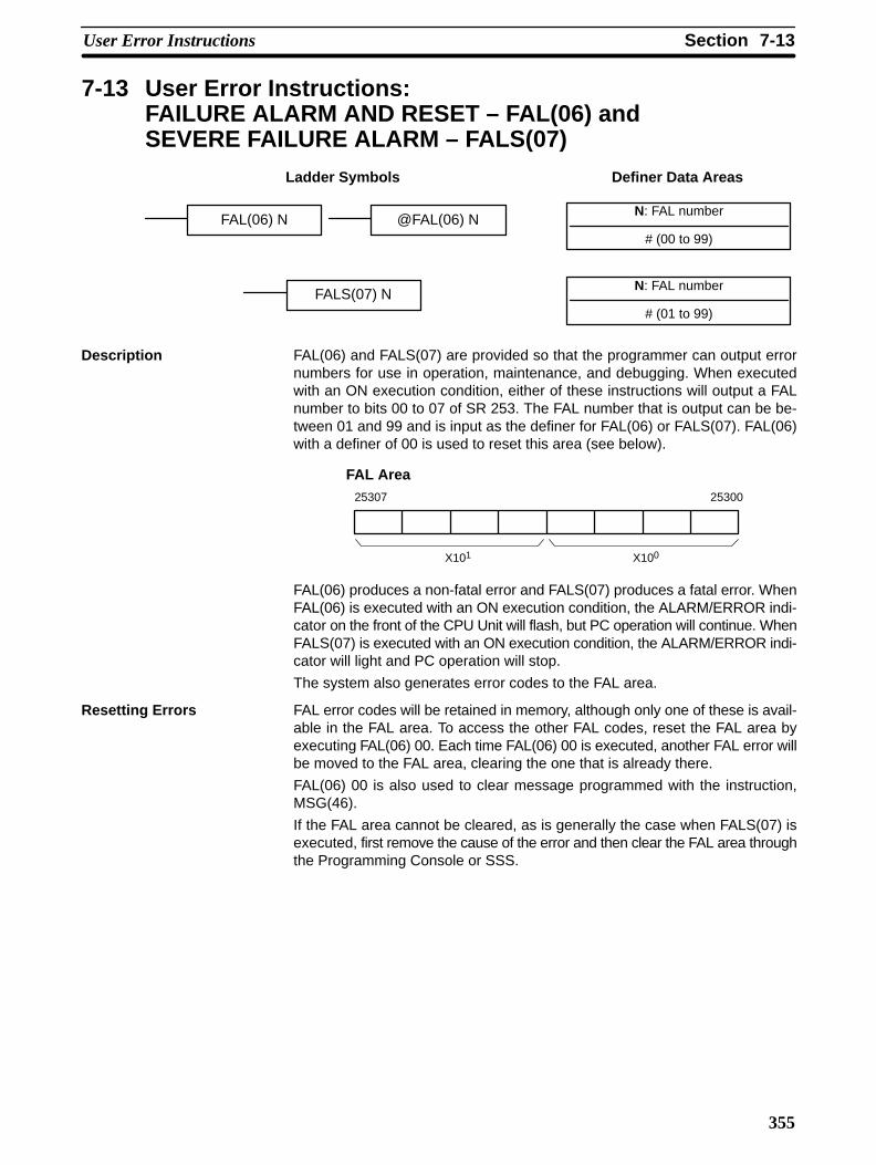
7-13SectionUser Error Instructions
355
7-13 User Error Instructions: FAILURE ALARM AND RESET – FAL(06) and SEVERE FAILURE ALARM – FALS(07)
N: FAL number
# (00 to 99)
Ladder Symbols Definer Data Areas
@FAL(06) NFAL(06) N
N: FAL number
# (01 to 99)FALS(07) N
FAL(06) and FALS(07) are provided so that the programmer can output errornumbers for use in operation, maintenance, and debugging. When executedwith an ON execution condition, either of these instructions will output a FALnumber to bits 00 to 07 of SR 253. The FAL number that is output can be be-tween 01 and 99 and is input as the definer for FAL(06) or FALS(07). FAL(06)with a definer of 00 is used to reset this area (see below).
25307 25300
X101 X100
FAL Area
FAL(06) produces a non-fatal error and FALS(07) produces a fatal error. WhenFAL(06) is executed with an ON execution condition, the ALARM/ERROR indi-cator on the front of the CPU Unit will flash, but PC operation will continue. WhenFALS(07) is executed with an ON execution condition, the ALARM/ERROR indi-cator will light and PC operation will stop.
The system also generates error codes to the FAL area.
FAL error codes will be retained in memory, although only one of these is avail-able in the FAL area. To access the other FAL codes, reset the FAL area byexecuting FAL(06) 00. Each time FAL(06) 00 is executed, another FAL error willbe moved to the FAL area, clearing the one that is already there.
FAL(06) 00 is also used to clear message programmed with the instruction,MSG(46).
If the FAL area cannot be cleared, as is generally the case when FALS(07) isexecuted, first remove the cause of the error and then clear the FAL area throughthe Programming Console or SSS.
Description
Resetting Errors

7-14SectionStep Instructions
356
7-14 Step Instructions: STEP DEFINE and STEP START–STEP(08)/SNXT(09)
B: Control bit
IR, AR, HR, LR
Ladder Symbols Definer Data Areas
STEP(08) B STEP(08)
B: Control bit
IR, AR, HR, LR
SNXT(09) B
Limitations All control bits must be in the same word and must be consecutive.
The step instructions STEP(08) and SNXT(09) are used together to set upbreakpoints between sections in a large program so that the sections can beexecuted as units and reset upon completion. A section of program will usuallybe defined to correspond to an actual process in the application. (Refer to theapplication examples later in this section.) A step is like a normal programmingcode, except that certain instructions (i.e., END(01), IL(02)/ILC(03),JMP(04)/JME(05), and SBN(92)) may not be included.
STEP(08) uses a control bit in the IR or HR areas to define the beginning of asection of the program called a step. STEP(08) does not require an executioncondition, i.e., its execution is controlled through the control bit. To start execu-tion of the step, SNXT(09) is used with the same control bit as used forSTEP(08). If SNXT(09) is executed with an ON execution condition, the stepwith the same control bit is executed. If the execution condition is OFF, the step isnot executed. The SNXT(09) instruction must be written into the program so thatit is executed before the program reaches the step it starts. It can be used at dif-ferent locations before the step to control the step according to two differentexecution conditions (see example 2, below). Any step in the program that hasnot been started with SNXT(09) will not be executed.
Once SNXT(09) is used in the program, step execution will continue untilSTEP(08) is executed without a control bit. STEP(08) without a control bit mustbe preceded by SNXT(09) with a dummy control bit. The dummy control bit maybe any unused IR or HR bit. It cannot be a control bit used in a STEP(08).
Description

7-14SectionStep Instructions
357
Execution of a step is completed either by execution of the next SNXT(09) or byturning OFF the control bit for the step (see example 3 below). When the step iscompleted, all of the IR and HR bits in the step are turned OFF and all timers inthe step are reset to their SVs. Counters, shift registers, and bits used inKEEP(11) maintain status. Two simple steps are shown below.
SNXT(09) LR 1005
STEP(08) LR 1005
00000
Step controlled by LR 1005
SNXT(09) 20200
STEP(08) 20200
00001
Step controlled by IR 20200
SNXT(09) 23000
STEP(08)
00002
Starts step execution
Ends step execution
1st step
2nd step
Address Instruction Operands Address Instruction Operands
00000 LD 00000
00001 SNXT(09) LR 1005
00002 STEP(08) LR 1005
Step controlled by LR 1005.
00100 LD 00001
00101 SNXT(09) 20200
00102 STEP(08) 20200
Step controlled by IR 20200.
00200 LD 00002
00201 SNXT(09) 23000
00202 STEP(08) ---
Steps can be programmed in consecutively. Each step must start with STEP(08)and generally ends with SNXT(09) (see example 3, below, for an exception).When steps are programmed in series, three types of execution are possible:sequential, branching, or parallel. The execution conditions for, and the position-ing of, SNXT(09) determine how the steps are executed. The three examplesgiven below demonstrate these three types of step execution.
Interlocks, jumps, SBN(92), and END(01) cannot be used within step programs.
Bits used as control bits must not be used anywhere else in the program unlessthey are being used to control the operation of the step (see example 3, below).All control bits must be in the same word and must be consecutive.
If IR or LR bits are used for control bits, their status will be lost during any powerinterruption. If it is necessary to maintain status to resume execution at the samestep, HR bits must be used.
Precautions

7-15SectionTimer and Counter Instructions
358
Flags 25407: Step Start Flag; turns ON for one cycle when STEP(08) is executed andcan be used to reset counters in steps as shown below if necessary.
SNXT(09) 20000
CP
R
CNT 001
#0003
00000
00100
25407
STEP(08) 20000
1 cycle
25407
20000
Start
Address Instruction Operands Address Instruction Operands
00000 LD 00000
00001 SNXT(09) 20000
00002 STEP(08) 20000
00003 LD 00100
00004 LD 25407
00005 CNT 01
# 0003
7-15 Timer and Counter InstructionsTIM and TIMH(15) are decrementing ON-delay timer instructions which requirea TC number and a set value (SV). STIM(69) is used to control the interval tim-ers, which are used to activate interrupt routines.
CNT is a decrementing counter instruction and CNTR(12) is a reversible counterinstruction. Both require a TC number and a SV. Both are also connected to mul-tiple instruction lines which serve as an input signal(s) and a reset. CTBL(63),INT(89), and PRV(62) are used to manage the high-speed counter. INT(89) isalso used to stop pulse output.
Any one TC number cannot be defined twice, i.e., once it has been used as thedefiner in any of the timer or counter instructions, it cannot be used again. Oncedefined, TC numbers can be used as many times as required as operands ininstructions other than timer and counter instructions.
TC numbers run from 000 through 255 in the CPM2A/CPM2C PCs and from 000through 127 in the CPM1/CPM1A/SRM1(-V2) PCs. No prefix is required whenusing a TC number as a definer in a timer or counter instruction. Once defined asa timer, a TC number can be prefixed with TIM for use as an operand in certaininstructions. The TIM prefix is used regardless of the timer instruction that wasused to define the timer. Once defined as a counter, a TC number can be pre-fixed with CNT for use as an operand in certain instructions. The CNT is alsoused regardless of the counter instruction that was used to define the counter.
TC numbers can be designated as operands that require either bit or word data.When designated as an operand that requires bit data, the TC number accessesa bit that functions as a ‘Completion Flag’ that indicates when the time/count hasexpired, i.e., the bit, which is normally OFF, will turn ON when the designated SVhas expired. When designated as an operand that requires word data, the TCnumber accesses a memory location that holds the present value (PV) of thetimer or counter. The PV of a timer or counter can thus be used as an operand inCMP(20), or any other instruction for which the TC area is allowed. This is doneby designating the TC number used to define that timer or counter to access thememory location that holds the PV.

7-15SectionTimer and Counter Instructions
359
Note that “TIM 000” is used to designate the TIMER instruction defined with TCnumber 000, to designate the Completion Flag for this timer, and to designatethe PV of this timer. The meaning of the term in context should be clear, i.e., thefirst is always an instruction, the second is always a bit operand, and the third isalways a word operand. The same is true of all other TC numbers prefixed withTIM or CNT.An SV can be input as a constant or as a word address in a data area. If an IRarea word assigned to an Input Unit is designated as the word address, the InputUnit can be wired so that the SV can be set externally through thumbwheelswitches or similar devices. Timers and counters wired in this way can only beset externally during RUN or MONITOR mode. All SVs, including those set ex-ternally, must be in BCD.
7-15-1 TIMER – TIM
N: TC number
#
Ladder Symbol
Definer Values
SV: Set value (word, BCD)
IR, SR, AR, DM, HR, LR, #
Operand Data Areas
TIM N
SV
SV is between 000.0 and 999.9. The decimal point is not entered.Each TC number can be used as the definer in only one TIMER or COUNTERinstruction. TC numbers run from 000 through 255 in the CPM2A/CPM2C PCsand from 000 through 127 in the CPM1/CPM1A/SRM1(-V2) PCs.TC 000 through TC 003 (TC 000 through TC 015 in the CPM2A/CPM2C) shouldnot be used in TIM if they are required for TIMH(15). Refer to 7-15-2 HIGH-SPEED TIMER – TIMH(15) for details.In the CPM2A/CPM2C PCs, TC 004 through TC 007 should not be used in TIM ifthey are required for TMHH(––). Refer to 7-15-3 VERY HIGH-SPEED TIMER –TMHH(––) for details.
A timer is activated when its execution condition goes ON and is reset (to SV)when the execution condition goes OFF. Once activated, TIM measures in unitsof 0.1 second from the SV.If the execution condition remains ON long enough for TIM to time down to zero,the Completion Flag for the TC number used will turn ON and will remain ONuntil TIM is reset (i.e., until its execution condition is goes OFF).The following figure illustrates the relationship between the execution conditionfor TIM and the Completion Flag assigned to it.
Execution condition
Completion Flag
ON
OFF
ON
OFF
SV SV
Timers in interlocked program sections are reset when the execution conditionfor IL(02) is OFF. Power interruptions also reset timers. If a timer that is not resetunder these conditions is desired, SR area clock pulse bits can be counted toproduce timers using CNT. Refer to 7-15-5 COUNTER – CNT for details.
Limitations
Description
Precautions

7-15SectionTimer and Counter Instructions
360
The Completion Flag may be turned ON one cycle late when reading its statusfrom the user program.
Always reset the timer after changing between TIM and TIMH(015) in onlineediting. The timer will not work properly if it is not reset.
If the timer’s set value is set to 0000, the Completion Flag will turn ON as soon asthe timer’s execution condition turns ON. If the timer’s set value is set to 0001,the Completion Flag will turn ON somewhere between 0 and 0.1 s after the tim-er’s execution condition turns ON (i.e., the timer accuracy will actually determinethe time), and may turn ON as soon as the timer’s execution condition turns ON.
Always consider the accuracy of the timer (0 to –0.1 s) in application programs.
Flags ER: Indirectly addressed DM word is non-existent. (Content of DM word isnot BCD, or the DM area boundary has been exceeded.)
7-15-2 HIGH-SPEED TIMER – TIMH(15)
N: TC number
#
Ladder Symbol
Definer Values
SV: Set value (word, BCD)
IR, SR, AR, DM, HR, LR, #
Operand Data Areas
TIMH(15) N
SV
SV is between 00.00 and 99.99. (Although 00.00 and 00.01 may be set, 00.00will disable the timer, i.e., turn ON the Completion Flag immediately, and 00.01 isnot reliably scanned.) The decimal point is not entered.
Each TC number can be used as the definer in only one TIMER or COUNTERinstruction. TC numbers run from 000 through 255 in the CPM2A/CPM2C PCsand from 000 through 127 in the CPM1/CPM1A/SRM1(-V2) PCs.
TIMH(15) operates in the same way as TIM except that TIMH measures in unitsof 0.01 second. Refer to 7-15-1 TIMER – TIM for operational details.
Timers in interlocked program sections are reset when the execution conditionfor IL(02) is OFF. Power interruptions also reset timers. If a timer that is not resetunder these conditions is desired, SR area clock pulse bits can be counted toproduce timers using CNT. Refer to 7-15-5 COUNTER – CNT for details.
Timers in jumped program sections will not be reset when the execution condi-tion for JMP(04) is OFF. The timer will stop timing if jump number 00 is used, butwill continue timing if other jump numbers are used.
Always reset the timer when changing between TIM and TIMH(15) in online edit-ing. Also, when changing a TIMH(15) instruction with interrupt refreshing, do soonly in PROGRAM mode.
Use timer numbers 000 to 003 for TIMH(15). High-speed timers with timer num-bers TC 004 through TC 127 (TC 016 through TC 255 in the CPM2A/CPM2C)may not be accurate when the cycle time exceeds 10 ms.
PC Interrupt refreshing every10 ms
Refreshed when TIMH(015)is executed
CPM2A/CPM2C TC 000 through TC 003 TC 004 through TC 255
CPM1, CPM1A, andSRM1(-V2)
TC 000 through TC 003 TC 004 through TC 127
Limitations
Description
Precautions

7-15SectionTimer and Counter Instructions
361
In the CPM2A/CPM2C PCs, TC 004 through TC 007 should not be used inTIMH(15) if they are required for TMHH(––). Refer to 7-15-3 VERY HIGH-SPEED TIMER – TMHH(––) for details.
If the timer’s set value is set to 0000, the Completion Flag will turn ON as soon asthe timer’s execution condition turns ON. If TIM000 to TIM003 are used, howev-er, there may be a delay before the flag turns ON.
If the timer’s set value is set to 0001, the Completion Flag will turn ON some-where between 0 and 0.01 s after the timer’s execution condition turns ON (i.e.,the timer accuracy will actually determine the time), and may turn ON as soon asthe timer’s execution condition turns ON.
Always consider the accuracy of the timer (0 to –0.01 s) in application programs.
Flags ER: Indirectly addressed DM word is non-existent. (Content of DM word isnot BCD, or the DM area boundary has been exceeded.)
Example The following example shows a timer set with a constant. CIO 01600 will beturned ON after CIO 00000 goes ON and stays ON for at least 1.5 seconds.When 00000 goes OFF, the timer will be reset and CIO 01600 will be turned OFF.
00000
TIM 000
01600
1.5 s
TIMH(15) Address Instruction Operands
00000 LD 00000
00001 TIMH(15) 000
# 0150
00002 LD TIM 000
00003 OUT 01600
000
#0150
7-15-3 VERY HIGH-SPEED TIMER: TMHH(––)
N: #
TIM000 to TIM255
Ladder Symbol Operand Data Areas
000
Set to 000.
SV: Set value
IR, SR, AR, DM, HR, LR, #
TMHH(––)
N
SV
000
This instruction is supported by the CPM2A/CPM2C only.
Each TC number can be used as the definer in only one TIMER or COUNTERinstruction. TC numbers run from TIM000 through TIM255. (You must enter“TIM” along with the actual timer number when using TIML(––). The instructionwill not work if only the number is entered.)
SV is BCD between 0000 and 9999 (0 to 9.999 s).
Set the third operand to 000. (This operand is ignored.)
TMHH(––) is a decrementing ON-delay timer that times in 1-ms units. The timerset value can be 0 to 9.999 s and the timer has a accuracy of 1 ms.
A very high-speed timer is activated when its execution condition goes ON and isreset (to the SV) when the execution condition goes OFF. Once activated,TMHH(––) times down from the SV in units of 1 ms.
The timer will time out when the PV reaches #0000 (0 ms). Once the timer hastimed out, the PV and Completion Flag status will be maintained. The timer canbe restarted by temporarily turning its execution condition from ON to OFF or
Limitations
Description

7-15SectionTimer and Counter Instructions
362
changing its PV to a value other than #0000 with an instruction such asMOV(21).The operation of very high-speed timers in jumped program sections dependsupon the TC number used to define the timer, as shown in the following table.
TC number Operation
000 to 003,008 to 255
The timer will stop when the execution condition for JMP(04) is OFF.This can greatly reduce the accuracy of timers in jumped programsections.
004 to 007 If jump number 00 is used, the timer will stop timing when theexecution condition for JMP(04) is OFF. This can greatly reduce theaccuracy of timers in jumped program sections.
If any other jump number is used, the timer will continue timingnormally when the execution condition for JMP(04) is OFF.
Precautions Very high-speed timers with timer numbers other than TC 004 through TC 007may not be accurate when the cycle time exceeds 1 ms. (The cycle time will notaffect very high-speed timers defined with TC 004 through TC 007.)Very high-speed timers in interlocked program sections are reset (to the SV)when the execution condition for IL(02) is OFF.If the timer’s set value is set to 0000, the Completion Flag will turn ON as soon asthe timer’s execution condition turns ON. If TIM004 to TIM007 are used, howev-er, there may be a delay before the flag turns ON.If the timer’s set value is set to 0001, the Completion Flag will turn ON some-where between 0 and 1 ms after the timer’s execution condition turns ON (i.e.,the timer accuracy will actually determine the time), and may turn ON as soon asthe timer’s execution condition turns ON.Always consider the accuracy of the timer (0 to –1 ms) in application programs.
Flags ER: N is not a valid TC number.
In the following example, CIO 20000 will be turned ON after CIO 00000 goes ONand stays ON for at least 1.5 seconds. When 00000 goes OFF, the timer will bereset and CIO 20000 will be turned OFF.
00000 LD 00000
00001 TMHH(––)
TIM 004
# 1500
000
00002 LD TIM 004
00003 OUT 2000020000
TIM004
00000
TMHH(––)
TIM004
#1500
000
Address Instruction Operands
1.5 s
7-15-4 LONG TIMER: TIML(––)
N: Timer number (see Limitations)
TIM000 to TIM255
Ladder Symbol Operand Data Areas
C: Control data
000 or 001
SV: Set value
IR, SR, AR, DM, HR, LR, #
TIML(––)
N
SV
C
This instruction is supported by the CPM2A/CPM2C only.
Example

7-15SectionTimer and Counter Instructions
363
Each timer number can be used as the definer in only one TIMER or COUNTERinstruction. Timer numbers run from TIM000 through TIM255. (You must enter“TIM” along with the actual timer number when using TIML(––). The instructionwill not work if only the number is entered.)
SV is BCD between 0000 and 9999 (0 to 9,999 s when C=000 and 0 to 99,990 swhen C=001).
C must be 000 (1-s timing units) or 001 (10-s timing units).
TIML(––) is a decrementing ON-delay timer that can time in 1-s units or 10-sunits. The timer set value can be 0 to 9,999 s (accuracy 0 to 1 s) when 1-s unitsare used (C=000) or 0.10 to 99,990 s (accuracy 0 to 10 s) when 10-s units areused (C=001).
A long timer is activated when its execution condition goes ON and is reset (tothe SV) when the execution condition goes OFF. Once activated, TIML(––)times down from the SV in units of 1 s or 10 s (depending upon the value of C).TIML(––) accuracy is 0 to 1 s with 1-s units or 0 to 10 s with 10-s units.
The timer will time out when the PV reaches #0000 (0 s). Once the timer hastimed out, the PV and Completion Flag status will be maintained. The timer canbe restarted by temporarily turning its execution condition from ON to OFF orchanging its PV to a value other than #0000 with an instruction such asMOV(21).
Long timers in jumped program sections will not be reset when the executioncondition for JMP(04) is OFF, but the timer will stop timing and the PV will bemaintained. Timing will resume when the execution condition for JMP(04) goesON again. This can greatly reduce the accuracy of long timers in jumped pro-gram sections.
Precautions TIML(––) may not be accurate when the cycle time exceeds 1 s (C=000) or 10 s(C=001).
Long timers in interlocked program sections are reset (to the SV) when theexecution condition for IL(02) is OFF.
The timing units in C can be changed while the long timer is timing. Changing thetiming units during operation reduces the timer’s accuracy by up to 10 s.
You must enter “TIM” along with the actual timer number when using TIML(––).The instruction will not work if only the number is entered.
If the timer’s set value is set to 0000, the Completion Flag will turn ON as soon asthe timer’s execution condition turns ON. If the timer’s set value is set to 0001,the Completion Flag will turn ON somewhere between 0 and 1 s or between 0and 10 s after the timer’s execution condition turns ON (i.e., the timer accuracywill actually determine the time), and may turn ON as soon as the timer’s execu-tion condition turns ON.
Always consider the accuracy of the timer (0 to –1 s or 0 to –10 s) in applicationprograms.
Flags ER: N is not a valid timer number.
C is not 000 or 001.
Limitations
Description

7-15SectionTimer and Counter Instructions
364
In the following example, CIO 20000 will be turned ON after CIO 00000 goes ONand stays ON for at least 1,500 seconds. When 00000 goes OFF, the timer willbe reset and CIO 20000 will be turned OFF.
00000 LD 00000
00001 TIML(––)
TIM 002
# 0150
001
00002 LD TIM 002
00003 OUT 2000020000
TIM002
00000
TIML(––)
TIM002
#0150
001
Address Instruction Operands
1500 s
7-15-5 COUNTER – CNT
N: TC number
#
Ladder Symbol
Definer Values
SV: Set value (word, BCD)
IR, SR, AR, DM, HR, LR, #
Operand Data Areas
CP
R
CNT N
SV
Each TC number can be used as the definer in only one TIMER or COUNTERinstruction. TC numbers run from 000 through 255 in the CPM2A/CPM2C PCsand from 000 through 127 in the CPM1/CPM1A/SRM1(-V2) PCs.
CNT is used to count down from SV when the execution condition on the countpulse, CP, goes from OFF to ON, i.e., the present value (PV) will be decrem-ented by one whenever CNT is executed with an ON execution condition for CPand the execution condition was OFF for the last execution. If the executioncondition has not changed or has changed from ON to OFF, the PV of CNT willnot be changed. The Completion Flag for a counter is turned ON when the PVreaches zero and will remain ON until the counter is reset.
CNT is reset with a reset input, R. When R goes from OFF to ON, the PV is resetto SV. The PV will not be decremented while R is ON. Counting down from SV willbegin again when R goes OFF. The PV for CNT will not be reset in interlockedprogram sections or by power interruptions.
Changes in execution conditions, the Completion Flag, and the PV are illus-trated below. PV line height is meant only to indicate changes in the PV.
Execution condition on count pulse (CP)
Execution condition on reset (R)
ON
OFF
ON
OFF
Completion FlagON
OFF
PVSV
SV – 1
SV – 2
0002
0001
0000
SV
Example
Limitations
Description

!
7-15SectionTimer and Counter Instructions
365
Program execution will continue even if a non-BCD SV is used, but the SV willnot be correct.
Flags ER: Indirectly addressed DM word is non-existent. (Content of DM word isnot BCD, or the DM area boundary has been exceeded.)
Example In the following example, CNT is used to create extended timers by counting SRarea clock pulse bits.
CNT 001 counts the number of times the 1-second clock pulse bit (SR 25502)goes from OFF to ON. Here again, IR 00000 is used to control the times whenCNT is operating.
Because in this example the SV for CNT 001 is 700, the Completion Flag forCNT 002 turns ON when 1 second x 700 times, or 11 minutes and 40 secondshave expired. This would result in IR 20002 being turned ON.
CP
R
CNT001
#0700
00000 25502
00001
CNT 00120002
Address Instruction Operands
00000 LD 00000
00001 AND 25502
00002 LD NOT 00001
00003 CNT 001
# 0700
00004 LD CNT 001
00005 OUT 20002
Caution The shorter clock pulses will not necessarily produce accurate timers becausetheir short ON times might not be read accurately during longer cycles. In partic-ular, the 0.02-second and 0.1-second clock pulses should not be used to createtimers with CNT instructions.
7-15-6 REVERSIBLE COUNTER – CNTR(12)
N: TC number
#
Ladder Symbol
Definer Values
SV: Set value (word, BCD)
IR, SR, AR, DM, HR, LR, #
Operand Data Areas
II
DICNTR(12)
N
SVR
Each TC number can be used as the definer in only one TIMER or COUNTERinstruction. TC numbers run from 000 through 255 in the CPM2A/CPM2C PCsand from 000 through 127 in the CPM1/CPM1A/SRM1(-V2) PCs.
The CNTR(12) is a reversible, up/down circular counter, i.e., it is used to countbetween zero and SV according to changes in two execution conditions, those inthe increment input (II) and those in the decrement input (DI).
The present value (PV) will be incremented by one whenever CNTR(12) isexecuted with an ON execution condition for II and the last execution conditionfor II was OFF. The present value (PV) will be decremented by one wheneverCNTR(12) is executed with an ON execution condition for DI and the last execu-tion condition for DI was OFF. If OFF to ON changes have occurred in both II andDI since the last execution, the PV will not be changed.
Precautions
Limitations
Description

7-15SectionTimer and Counter Instructions
366
If the execution conditions have not changed or have changed from ON to OFFfor both II and DI, the PV of CNT will not be changed.
When decremented from 0000, the present value is set to SV and the Comple-tion Flag is turned ON until the PV is decremented again. When incrementedpast the SV, the PV is set to 0000 and the Completion Flag is turned ON until thePV is incremented again.
CNTR(12) is reset with a reset input, R. When R goes from OFF to ON, the PV isreset to zero. The PV will not be incremented or decremented while R is ON.Counting will begin again when R goes OFF. The PV for CNTR(12) will not bereset in interlocked program sections or by the effects of power interruptions.
Changes in II and DI execution conditions, the Completion Flag, and the PV areillustrated below starting from part way through CNTR(12) operation (i.e., whenreset, counting begins from zero). PV line height is meant to indicate changes inthe PV only.
Execution condition on increment (II)
Execution condition on decrement (DI)
ON
OFF
ON
OFF
Completion FlagON
OFF
PVSV
SV – 1
SV – 20001
0000 0000
SV
SV – 1
SV – 2
Program execution will continue even if a non-BCD SV is used, but the SV willnot be correct.
Flags ER: Indirectly addressed DM word is non-existent. (Content of DM word isnot BCD, or the DM area boundary has been exceeded.)
7-15-7 REGISTER COMPARISON TABLE – CTBL(63)
P: Port specifier
000
Ladder Symbols Operand Data Areas
@CTBL(63)
P
C
TBTB: First comparison table word
IR, SR, AR, DM, HR, LR
C: Control data
000 to 003
CTBL(63)
P
C
TB
This instruction is not supported by SRM1(-V2) PCs.
Limitations The first and last comparison table words must be in the same data area. (Thelength of the comparison table varies according to the settings.)
P must be 000 and C must be between 000 and 003.
Description When the execution condition is OFF, CTBL(63) is not executed. When theexecution condition is ON, CTBL(63) registers a comparison table for use withthe high-speed counter PV. Depending on the value of C, comparison with thehigh-speed counter PV can begin immediately or it can be started separatelywith INI(61).
Precautions

7-15SectionTimer and Counter Instructions
367
The port specifier (P) specifies the high-speed counter that will be used in thecomparison. Always set P to 000.
The function of CTBL(63) is determined by the control data, C, as shown in thefollowing table. These functions are described after the table.
C CTBL(63) function
000 Registers a target value comparison table and starts comparison.
001 Registers a range comparison table and starts comparison.
002 Registers a target value comparison table. Start comparison with INI(61).
003 Registers a range comparison table. Start comparison with INI(61).
When the PV agrees with a target value or falls within a specified range, the spe-cified subroutine is called and executed. Refer to 2-3-5 High-speed Counter In-terrupts for more details on table comparison.
If the high-speed counter is enabled in the PC Setup (DM 6642), it will begincounting from zero when the CPM2A/CPM2C begins operation. The PV will notbe compared to the comparison table until the table is registered and compari-son is initiated with INI(61) or CTBL(63). Comparison can be stopped andstarted, or the PV can be reset with INI(61).
The operation of a target value comparison is different from a range comparison,but the two functions share some common characteristics.
1, 2, 3... 1. Subroutine numbers 000 to 049 can be used and the same subroutine num-ber can be used more than once in the table.
2. An undefined subroutine number or FFFF can be set for the subroutinenumber if interrupt processing is not required.
3. Comparison can be stopped with INI(61). A registered table is valid until PCoperation stops or a new comparison table is registered.
4. CTBL(62) cannot be executed if the high-speed counter is disabled in thePC Setup (DM 6642). (An error will occur if CTBL(63) is executed when thehigh-speed counter is disabled.)
Target Value Comparison A target value comparison table contains up to sixteen target values. A subrou-tine number is also registered for each target value. The corresponding subrou-tine is called and executed when the PV matches a target value. (When interruptprocessing is not required, an undefined subroutine number may be entered.)
• In the CPM1/CPM1A, target value comparisons are performed one item at atime in order of the comparison table. When the PV reaches the first target val-ue in the table, the interrupt subroutine is executed and comparison continuesto the next value in the table. When processing has been completed for the lasttarget value in the table, comparison returns to the first value in the table andthe process is repeated.
• In the CPM2A/CPM2C, the PV is compared to all of the target values in thetable each time CTBL(63) is executed. When the PV matches a target valuethe corresponding subroutine is called and executed.
The following diagram shows the structure of a target value comparison table.Target values must be unique; an error will occur if a target value appears in thetable more than once.
TB Number of target values (0001 to 0016, BCD)
TB+1 Target value #1, lower 4 digits (BCD)
TB+2 Target value #1, upper 4 digits (BCD)
TB+3 Subroutine number for #1 (See note.)
One targetvalue setting
Common Characteristicsof Target Value andRange Comparisons

7-15SectionTimer and Counter Instructions
368
Note The subroutine number can be F000 to F049 to activate the subroutine whendecrementing and can be 0000 to 0049 to activate the subroutine when incre-menting. An error will occur if the high-speed counter is set to increment modebut a decrementing subroutine number (F000 to F049) is specified.
Range Comparison A range comparison table contains 8 ranges which are defined by an 8-digit low-er limit and an 8-digit upper limit, as well as their corresponding subroutine num-bers. The comparison is performed once each cycle at the end of program exe-cution and can be performed during program execution with INI(61).
When the PV falls within a given range the corresponding subroutine is calledand executed. (When interrupt processing is not required, an undefined subrou-tine number may be entered.) Ranges can overlap, so the PV can fall withinmore than one range; in the PV is within two or more ranges, the subroutine forthe first of the ranges will be executed.
The following diagram shows the structure of a range comparison table. Alwaysset 8 ranges. If fewer than 8 ranges are needed, set the remaining subroutinenumbers to FFFF.
TB Lower limit #1, lower 4 digits (BCD)
TB+1 Lower limit #1, upper 4 digits (BCD)
TB+2 Upper limit #1, lower 4 digits (BCD)
TB+3 Upper limit #1, upper 4 digits (BCD)
TB+4 Subroutine number (See note 2.)
TB+35 Lower limit #8, lower 4 digits (BCD)
TB+36 Lower limit #8, upper 4 digits (BCD)
TB+37 Upper limit #8, lower 4 digits (BCD)
TB+38 Upper limit #8, upper 4 digits (BCD)
TB+39 Subroutine number (See note 2.)
First range setting
Eighth range setting
Note 1. Each range’s lower limit must be less than its upper limit. An error will occur ifthe lower limit is greater than the upper limit.
2. The subroutine number can be 0000 to 0049 and the subroutine will be exe-cuted as long as the counter’s PV is within the specified range. A value ofFFFF indicates that no subroutine is to be executed.
3. Since the comparison is usually performed just once each cycle, be sure totake the cycle time into account when the upper and lower limits representtime values.
4. A subroutine number can be used more than once in the table.
Flags ER: The comparison table exceeds the data area boundary, or there is anerror in the comparison table settings.
Indirectly addressed DM word is non-existent. (Content of *DM word isnot BCD, or the DM area boundary has been exceeded.)
P is not 000 or C is not between 000 and 003.
There is a CTBL(63) instruction using a different comparison format inthe subroutine called by another CTBL(63) instruction.
A CTBL(63) instruction using a different comparison format is executedduring comparison.
CTBL(63) is executed in an interrupt subroutine while a pulse I/O orhigh-speed counter instruction (INI(61), PRV(62), CTBL(63),SPED(64), PULS(65), ACC(––), PWM(––), or SYNC(––)) is beingexecuted in the main program.

7-15SectionTimer and Counter Instructions
369
Target Value Comparison Errors:
The number of target values (in TB) is not between 0001 and 0016.
A target value is not between F838 8608 and 0838 8607 (differentialphase mode, pulse + direction input mode, and up/down input mode).
A target value is not between 0000 0000 and 1677 7215 or a subroutinenumber is not between 0000 and 0049 (increment mode).
Range Comparison Errors:
A range’s upper limit value is less than its lower limit value.
A target value is not between F838 8608 and 0838 8607 (differentialphase mode, pulse + direction input mode, and up/down input mode).
A target value is not between 0000 0000 and 1677 7215 or a subroutinenumber is not between 0000 and 0049 (increment mode).
7-15-8 MODE CONTROL – INI(61)
P: Port specifier
000, 010, 100, 101, 102, 103
Ladder Symbols Operand Data Areas
@INI(61)
P
C
P1P1: First PV word
IR, SR, AR, DM, HR, LR (or 000)
C: Control data
000 to 005
INI(61)
P
C
P1
This instruction is not supported by SRM1(-V2) PCs.
Limitations In the CPM1/CPM1A PCs, P must be 000 and C must be 000 to 003.
In CPM2A/CPM2C PCs, P must be 000, 010, 100, 101, 102, or 103 and C mustbe 000 to 005.
P1 must be 000 unless C is 002 or 004.
P1 and P1+1 must be in the same data area.If a DM address is used for P1, it must be read/write DM.
Description When the execution condition is OFF, INI(61) is not executed. When the execu-tion condition is ON, INI(61) is used to control high-speed counter operation andstop pulse output.
The port specifier (P) specifies the high-speed counter or pulse output that willbe controlled.
P Function
000 Specifies high-speed counter input (inputs 00000, 00001, and 00002),single-phase pulse output 0 with no acceleration/deceleration (output01000 or 01001), single-phase pulse output 0 with trapezoidal accelera-tion/deceleration (output 01000).
010* Specifies single-phase pulse output 1 with no acceleration/deceleration(output 01001).
100* Specifies interrupt input 0 in counter mode (input 00003).
101* Specifies interrupt input 1 in counter mode (input 00004).
102* Specifies interrupt input 2 in counter mode (input 00005).
103* Specifies interrupt input 3 in counter mode (input 00006).
Note *These settings can be used in CPM2A/CPM2C PCs only.

7-15SectionTimer and Counter Instructions
370
The function of INI(61) is determined by the control data, C.
C P1 INI(61) function
000 000 Starts CTBL(63) table comparison.
001 000 Stops CTBL(63) table comparison.
002 New PV Changes PV of the high-speed counter or an interrupt input incounter mode.
003 000 Stops pulse output.
004* New PV Changes PV of the pulse output.
005* 000 Stops synchronized pulse control output.
Note *These settings can be used in CPM2A/CPM2C PCs only.
If C is 000 or 001, INI(61) starts or stops comparison of the high-speed counter’sPV to the comparison table registered with CTBL(63). An error will occur if thisfunction is executed without first registering a comparison table with CTBL(63).In general, @INI(61) should be used when C=000 because the instructionneeds to be executed only one time to start table comparison.
If C is 002, INI(61) changes the PV of the specified high-speed counter or inter-rupt input (counter mode).High-speed Counter PV (P=000)INI(61) changes the PV of the specified high-speed counter to the 8-digit BCDvalue in P1 and P1+1.The new PV can be F838 8608 to 0838 8607 in differential phase mode, pulse +direction input mode, or up/down input mode. (The hexadecimal “F” in the firstdigit acts as a minus sign.)The new PV can be 0000 0000 to 1677 7215 in increment mode.Interrupt Input PV (P=100 to 103)INI(61) changes the PV of the specified interrupt input (counter mode) to the4-digit hexadecimal value (0000 to FFFF) in P1.
If C is 003, INI(61) stops the pulse output.
INI(61) changes the PV of the pulse output to the 8-digit BCD value in P1 andP1+1. The PV cannot be changed while the pulse output is in progress.The new PV can be –16,777,215 to 16,777,215. Bit 15 of P1+1 acts as a sign bit;the number is negative if bit 15 is ON, positive if it is OFF.
If C is 003, INI(61) stops the synchronized pulse control output.
Flags ER: The port specifier and control data are incompatible.(For example: P=010 and C=000)There is an error in the operand settings or the specified PV is not withinthe acceptable range.
The address specified for P1 or P1+1 exceeds the data area boundary.
Indirectly addressed DM word is non-existent. (Content of *DM word isnot BCD, or the DM area boundary has been exceeded.)
The specified function is incompatible with actual PC operation. For ex-ample, do not set C=005 if synchronized pulse control is not being used.
INI(61) is executed to change the PV of a pulse output (C=004) while thepulse output is operating.
INI(61) is executed in an interrupt subroutine while a pulse I/O or high-speed counter instruction (INI(61), PRV(62), CTBL(63), SPED(64),PULS(65), ACC(––), PWM(––), or SYNC(––)) is being executed in themain program.
Start or Stop Comparison(C=000 or C=001)
Change PV(C=002)
Stop Pulse Output(C=003)
Change PV(C=004)
Stop Synchronized PulseControl Output (C=003)

7-15SectionTimer and Counter Instructions
371
INI(61) is executed in an interrupt subroutine while a pulse I/O or high-speed counter instruction is being executed in the main program.
7-15-9 HIGH-SPEED COUNTER PV READ – PRV(62)
P: Port specifier
000, 010, 100, 101, 102, 103
Ladder Symbols Operand Data Areas
@PRV(62)
P
C
DD: First destination word
IR, SR, AR, DM, HR, LR
C: Control data
000, 001, 002, or 003
PRV(62)
P
C
D
This instruction is not supported by SRM1(-V2) PCs.
Limitations In the CPM1/CPM1A PCs, P must be 000 and C must be 000 to 002.In CPM2A/CPM2C PCs, P must be 000, 010, 100, 101, 102, or 103 and C mustbe 000 to 003.D and D+1 must be in the same data area.If a DM address is used for D, it must be read/write DM.
Description When the execution condition is OFF, PRV(62) is not executed. When theexecution condition is ON, PRV(62) controls the high-speed counter PV, pulseoutput PV, interrupt input (counter mode) PV, or input frequency for synchro-nized control as specified by P and C.The port specifier (P) specifies the high-speed counter or pulse output that willbe controlled.
P Function
000 Specifies high-speed counter input (inputs 00000, 00001, and 00002), in-put frequency for synchronized pulse control (inputs 00000, 00001, and00002), single-phase pulse output 0 with no acceleration/deceleration (out-puts 01000 and 01001), single-phase pulse output 0 with trapezoidal ac-celeration/deceleration (output 01000), or synchronized pulse control out-put 0 (output 01000/01001).
010* Specifies single-phase pulse output 1 with no acceleration/deceleration(output 01001) or synchronized pulse control output 1 (output 01001).
100* Specifies interrupt input 0 in counter mode (input 00003).
101* Specifies interrupt input 1 in counter mode (input 00004).
102* Specifies interrupt input 2 in counter mode (input 00005).
103* Specifies interrupt input 3 in counter mode (input 00006).
Note *These settings can be used in CPM2A/CPM2C PCs only.
The control data, C, determines which type of data will be accessed.
C Function Destination word(s)
000 Reads the PV of the high-speed counter or interruptinput (counter mode) or the input frequency of thesynchronized pulse control.
D and D+1
001 Reads the status of the high-speed counter or pulseoutput.
D
002 Reads the results of range comparison. D
003* Reads the PV of the pulse output. D and D+1
Note *This setting can be used in CPM2A/CPM2C PCs only.

7-15SectionTimer and Counter Instructions
372
If C is 000, PRV(62) reads the PV of the specified high-speed counter or interruptinput (counter mode).
High-speed Counter PV or Input Frequency (P=000)When the output is used for a high-speed counter, PRV(62) reads the PV of thespecified high-speed counter and writes the 8-digit BCD value in D and D+1.(The leftmost 4 digits are written to D+1.)
The PV can be F838 8608 to 0838 8607 in differential phase mode, pulse + di-rection input mode, or up/down input mode. (The hexadecimal “F” in the first digitacts as a minus sign.)
The PV can be 0000 0000 to 1677 7215 in increment mode.
When the output is used for synchronized pulse control, PRV(62) reads the inputfrequency and writes the 8-digit BCD value in D and D+1. The input frequencycan be 0000 0000 to 0002 0000.
Interrupt Input PV (P=100 to 103)PRV(62) reads the PV of the specified interrupt input (counter mode) and writesthe 4-digit hexadecimal value (0000 to FFFF) in D.
If C is 001, PRV(62) reads the operating status of the specified high-speedcounter or pulse output and writes the data to D.
High-speed Counter or Pulse Output 0 Status (P=000)The following table shows the function of the bits in D when P=000. Bits not listedin the table are not used and will always be 0.
Usage Bit Function
High-speedcounter
00 High-speed counter comparison status.(0: Stopped; 1: Comparing)
01 High-speed counter underflow/overflow.(0: Normal; 1: Underflow/Overflow occurred.)
Pulse output 05 Total number of pulses specified for pulse output 0.(0: Not specified; 1: Specified.)
06 Pulse output 0 completed. (0: Not completed; 1: Completed)
07 Pulse output 0 status (0: Stopped; 1: Outputting)
08 Pulse output 0 PV underflow/overflow.(0: Normal; 1: Underflow/Overflow occurred.)
09 Pulse output 0 acceleration0: Constant; 1: Accelerating or decelerating
Pulse Output 1 Status (P=010)The following table shows the function of the bits in D when P=010. Bits not listedin the table are not used and will always be 0.
Bit Function
05 Total number of pulses specified for pulse output 1.(0: Not specified; 1: Specified.)
06 Pulse output 1 completed. (0: Not completed; 1: Completed)
07 Pulse output 1 status (0: Stopped; 1: Outputting)
08 Pulse output 1 PV underflow/overflow.(0: Normal; 1: Underflow/Overflow occurred.)
09 Pulse output 1 acceleration (0: Constant; 1: Accelerating or decelerating)
If C is 002, PRV(62) reads the results of the comparison of the PV to the 8 rangesdefined by CTBL(63) and writes this data to D. Bits 00 through 07 of D containthe Comparison Result Flags for ranges 1 to 8. (0: Not in range; 1: In range)
If C is 003, PRV(62) reads the pulse output PV and writes the 8-digit BCD valuein D and D+1. (The leftmost 4 digits are written to D+1.)
The PV can be –16,777,215 to 16,777,215. Bit 15 of D+1 acts as a sign bit; thenumber is negative if bit 15 is ON, positive if it is OFF.
Read PV (C=000)
Read Status (C=001)
Read Range ComparisonResults (C=002)
Read Pulse Output PV(C=003)

7-15SectionTimer and Counter Instructions
373
Flags ER: The port specifier and control data are incompatible.(For example: P=010 and C=000)
The address specified for D or D+1 exceeds the data area boundary.
There is an error in the operand settings.
Indirectly addressed DM word is non-existent. (Content of *DM word isnot BCD, or the DM area boundary has been exceeded.)
PRV(62) is executed in an interrupt subroutine while a pulse I/O or high-speed counter instruction (INI(61), PRV(62), CTBL(63), SPED(64),PULS(65), ACC(––), PWM(––), or SYNC(––)) is being executed in themain program.

7-16SectionShift Instructions
374
7-16 Shift Instructions
7-16-1 SHIFT REGISTER – SFT(10)
St: Starting word
IR, SR, AR, HR, LR
E: End word
IR, SR, AR, HR, LR
Operand Data AreasLadder Symbol
I
P
SFT(10)
St
ER
E must be greater than or equal to St, and St and E must be in the same dataarea.
If a bit address in one of the words used in a shift register is also used in aninstruction that controls individual bit status (e.g., OUT, KEEP(11)), an error(“COIL/OUT DUPL”) will be generated when program syntax is checked on theProgramming Console or another Programming Device. The program, howev-er, will be executed as written. See Example 2: Controlling Bits in Shift Registersfor a programming example that does this.
SFT(10) is controlled by three execution conditions, I, P, and R. If SFT(10) isexecuted and 1) execution condition P is ON and was OFF the last execution,and 2) R is OFF, then execution condition I is shifted into the rightmost bit of ashift register defined between St and E, i.e., if I is ON, a 1 is shifted into the regis-ter; if I is OFF, a 0 is shifted in. When I is shifted into the register, all bits previouslyin the register are shifted to the left and the leftmost bit of the register is lost.
Execution condition ILost data
E St+1, St+2, ... St
The execution condition on P functions like a differentiated instruction, i.e., I willbe shifted into the register only when P is ON and was OFF the last time SFT(10)was executed. If execution condition P has not changed or has gone from ON toOFF, the shift register will remain unaffected.
St designates the rightmost word of the shift register; E designates the leftmost.The shift register includes both of these words and all words between them. Thesame word may be designated for St and E to create a 16-bit (i.e., 1-word) shiftregister.
When execution condition R goes ON, all bits in the shift register will be turnedOFF (i.e., set to 0) and the shift register will not operate until R goes OFF again.
Flags ER: St and E are not in the same area or St is greater than E.
Limitations
Description

7-16SectionShift Instructions
375
The following example uses the 1-second clock pulse bit (25502) so that theexecution condition produced by 00000 is shifted into HR 00 every second. Out-put 20000 is turned ON whenever a “1” is shifted into HR 0007.
I
P
SFT(10)
HR 00
HR 00R
00000
25502
00001
Address Instruction Operands
00000 LD 00000
00001 LD 25502
00002 LD 00001
00003 SFT(10) HR 00
HR 00
00004 LD HR 0007
00005 OUT 2000020000
0007
7-16-2 WORD SHIFT – WSFT(16)
Ladder Symbols Operand Data Areas
WSFT(16)
St
E
@WSFT(16)
St
E
St: Starting word
IR, SR, AR, DM, HR, LR
E: End word
IR, SR, AR, DM, HR, LR
St and E must be in the same data area, and E must be greater than or equal toSt.DM 6144 to DM 6655 cannot be used for St or E.
When the execution condition is OFF, WSFT(16) is not executed. When theexecution condition is ON, WSFT(16) shifts data between St and E in word units.Zeros are written into St and the content of E is lost.
F 0 C 2 3 4 5 2 1 0 2 9
E St + 1 St
3 4 5 2 1 0 2 9 0 0 0 0
E St + 1 St
Lost
0000
Flags ER: The St and E words are in different areas, or St is greater than E.Indirectly addressed DM word is non-existent. (Content of DM word isnot BCD, or the DM area boundary has been exceeded.)
7-16-3 ARITHMETIC SHIFT LEFT – ASL(25)
Wd: Shift word
IR, SR, AR, DM, HR, LR
Ladder Symbols Operand Data Areas
ASL(25)
Wd
@ASL(25)
Wd
Limitations DM 6144 to DM 6655 cannot be used for Wd.
Example
Limitations
Description

7-16SectionShift Instructions
376
When the execution condition is OFF, ASL(25) is not executed. When the execu-tion condition is ON, ASL(25) shifts a 0 into bit 00 of Wd, shifts the bits of Wd onebit to the left, and shifts the status of bit 15 into CY.
1 0 0 1 1 1 0 0 0 1 0 1 0 0 1 1
CYBit 00
Bit 15
0
A 0 will be shifted into bit 00 every cycle if the undifferentiated form of ASL(25) isused. Use the differentiated form (@ASL(25)) or combine ASL(25) withDIFU(13) or DIFD(14) to shift just one time.
Flags ER: Indirectly addressed DM word is non-existent. (Content of DM word isnot BCD, or the DM area boundary has been exceeded.)
CY: Receives the status of bit 15.
EQ: ON when the content of Wd is zero; otherwise OFF.
7-16-4 ARITHMETIC SHIFT RIGHT – ASR(26)
Wd: Shift word
IR, SR, AR, DM, HR, LR
Ladder Symbols Operand Data Areas
ASR(26)
Wd
@ASR(26)
Wd
Limitations DM 6144 to DM 6655 cannot be used for Wd.
When the execution condition is OFF, ASR(25) is not executed. When theexecution condition is ON, ASR(25) shifts a 0 into bit 15 of Wd, shifts the bits ofWd one bit to the right, and shifts the status of bit 00 into CY.
1 0 0 1 0 1 1 0 0 1 1 0 0 1 01
Bit 00
Bit 15 CY
0
A 0 will be shifted into bit 15 every cycle if the undifferentiated form of ASR(26) isused. Use the differentiated form (@ASR(26)) or combine ASR(26) withDIFU(13) or DIFD(14) to shift just one time.
Flags ER: Indirectly addressed DM word is non-existent. (Content of DM word isnot BCD, or the DM area boundary has been exceeded.)
CY: Receives the data of bit 00.
EQ: ON when the content of Wd is zero; otherwise OFF.
7-16-5 ROTATE LEFT – ROL(27)
Wd: Rotate word
IR, SR, AR, DM, HR, LR
Ladder Symbols Operand Data Areas
ROL(27)
Wd
@ROL(27)
Wd
Limitations DM 6144 to DM 6655 cannot be used for Wd.
Description
Precautions
Description
Precautions

7-16SectionShift Instructions
377
When the execution condition is OFF, ROL(27) is not executed. When theexecution condition is ON, ROL(27) shifts all Wd bits one bit to the left, shiftingCY into bit 00 of Wd and shifting bit 15 of Wd into CY.
1 0 1 1 0 0 1 1 1 0 0 0 1 1 0 10
CYBit 00
Bit 15
Use STC(41) to set the status of CY or CLC(41) to clear the status of CY beforedoing a rotate operation to ensure that CY contains the proper status beforeexecuting ROL(27).
CY will be shifted into bit 00 every cycle if the undifferentiated form of ROL(27) isused. Use the differentiated form (@ROL(27)) or combine ROL(27) withDIFU(13) or DIFD(14) to shift just one time.
Flags ER: Indirectly addressed DM word is non-existent. (Content of DM word isnot BCD, or the DM area boundary has been exceeded.)
CY: Receives the data of bit 15.
EQ: ON when the content of Wd is zero; otherwise OFF.
7-16-6 ROTATE RIGHT – ROR(28)
Wd: Rotate word
IR, SR, AR, DM, HR, LR
Ladder Symbols Operand Data Areas
ROR(28)
Wd
@ROR(28)
Wd
Limitations DM 6144 to DM 6655 cannot be used for Wd.
When the execution condition is OFF, ROR(28) is not executed. When theexecution condition is ON, ROR(28) shifts all Wd bits one bit to the right, shiftingCY into bit 15 of Wd and shifting bit 00 of Wd into CY.
0 1 0 1 0 1 0 0 0 1 1 1 0 0 0 10
Bit 15CY
Bit 00
Use STC(41) to set the status of CY or CLC(41) to clear the status of CY beforedoing a rotate operation to ensure that CY contains the proper status beforeexecution ROR(28).
CY will be shifted into bit 15 every cycle if the undifferentiated form of ROR(28) isused. Use the differentiated form (@ROR(28)) or combine ROR(28) withDIFU(13) or DIFD(14) to shift just one time.
Flags ER: Indirectly addressed DM word is non-existent. (Content of DM word isnot BCD, or the DM area boundary has been exceeded.)
CY: Receives the data of bit 00.
EQ: ON when the content of Wd is zero; otherwise OFF.
Description
Precautions
Description
Precautions

7-16SectionShift Instructions
378
7-16-7 ONE DIGIT SHIFT LEFT – SLD(74)
Ladder Symbols Operand Data Areas
SLD(74)
St
E
@SLD(74)
St
E
St: Starting word
IR, SR, AR, DM, HR, LR
E: End word
IR, SR, AR, DM, HR, LR
St and E must be in the same data area, and E must be greater than or equal toSt.
DM 6144 to DM 6655 cannot be used for St or E.
When the execution condition is OFF, SLD(74) is not executed. When the execu-tion condition is ON, SLD(74) shifts data between St and E (inclusive) by onedigit (four bits) to the left. 0 is written into the rightmost digit of the St, and thecontent of the leftmost digit of E is lost.
5
E
8 1
St
F C 97D
Lost data 0
...
If a power failure occurs during a shift operation across more than 50 words, theshift operation might not be completed.
A 0 will be shifted into the least significant digit of St every cycle if the undifferen-tiated form of SLD(74) is used. Use the differentiated form (@SLD(74)) or com-bine SLD(74) with DIFU(13) or DIFD(14) to shift just one time.
Flags ER: The St and E words are in different areas, or St is greater than E.
Indirectly addressed DM word is non-existent. (Content of DM word isnot BCD, or the DM area boundary has been exceeded.)
7-16-8 ONE DIGIT SHIFT RIGHT – SRD(75)
Ladder Symbols Operand Data Areas
SRD(75)
E
St
@SRD(75)
E
St
E: End word
IR, SR, AR, DM, HR, LR
St: Starting word
IR, SR, AR, DM, HR, LR
St and E must be in the same data area, and E must be less than or equal to St.
DM 6144 to DM 6655 cannot be used for St or E.
Limitations
Description
Precautions
Limitations

7-16SectionShift Instructions
379
When the execution condition is OFF, SRD(75) is not executed. When theexecution condition is ON, SRD(75) shifts data between St and E (inclusive) byone digit (four bits) to the right. 0 is written into the leftmost digit of St and therightmost digit of E is lost.
2
St
3 1
E
4 5 C8F
Lost data0
...
If a power failure occurs during a shift operation across more than 50 words, theshift operation might not be completed.
A 0 will be shifted into the most significant digit of St every cycle if the undifferen-tiated form of SRD(75) is used. Use the differentiated form (@SRD(75)) or com-bine SRD(75) with DIFU(13) or DIFD(14) to shift just one time.
Flags ER: The St and E words are in different areas, or St is less than E.
Indirectly addressed DM word is non-existent. (Content of DM word isnot BCD, or the DM area boundary has been exceeded.)
7-16-9 REVERSIBLE SHIFT REGISTER – SFTR(84)
C: Control word
IR, SR, AR, DM, HR, LR
St: Starting word
IR, SR, AR, DM, HR, LR
Ladder Symbols
Operand Data Areas
E: End word
IR, SR, AR, DM, HR, LR
SFTR(84)
C
St
E
@SFTR(84)
C
St
E
St and E must be in the same data area and St must be less than or equal to E.
DM 6144 to DM 6655 cannot be used for C, St, or E.
SFTR(84) is used to create a single- or multiple-word shift register that can shiftdata to either the right or the left. To create a single-word register, designate thesame word for St and E. The control word provides the shift direction, the statusto be put into the register, the shift pulse, and the reset input. The control word isallocated as follows:
Not used.
Shift direction1 (ON): Left (LSB to MSB)0 (OFF): Right (MSB to LSB)
Status to input into register
Shift pulse bit
Reset
15 14 13 12
Description
Precautions
Limitations
Description

7-16SectionShift Instructions
380
The data in the shift register will be shifted one bit in the direction indicated by bit12, shifting one bit out to CY and the status of bit 13 into the other end wheneverSFTR(84) is executed with an ON execution condition as long as the reset bit isOFF and as long as bit 14 is ON. If SFTR(84) is executed with an OFF executioncondition or if SFTR(84) is executed with bit 14 OFF, the shift register will remainunchanged. If SFTR(84) is executed with an ON execution condition and the re-set bit (bit 15) is OFF, the entire shift register and CY will be set to zero.
Flags ER: St and E are not in the same data area or ST is greater than E.
Indirectly addressed DM word is non-existent. (Content of DM word isnot BCD, or the DM area boundary has been exceeded.)
CY: Receives the status of bit 00 of St or bit 15 of E, depending on the shiftdirection.
In the following example, IR 00000, IR 00001, IR 00002, and IR 00003 are usedto control the bits of C used in @SFTR(84). The shift register is in DM 0010, andit is controlled through IR 00004.
00000 LD 00000
00001 OUT 20012
00002 LD 00001
00003 OUT 20013
00004 LD 00002
00005 OUT 20014
00006 LD 00003
00007 OUT 20015
00008 LD 00004
00009 @SFTR(84)
200
DM 0010
DM 0011
20012
00000
20013
20014
20015
00001
00002
00003
00004
Direction
Status to input
Shift pulse
Reset
@SFTR(84)
200
DM 0010
DM 0011
Address Instruction Operands
7-16-10 ASYNCHRONOUS SHIFT REGISTER – ASFT(17)
ASFT(17)
C
St
E
Ladder Symbols
@ASFT(17)
C
St
E
C: Control word
IR, SR, AR, DM, HR, LR, #
St: Starting word
IR, SR, AR, DM, HR, LR
E: End word
IR, SR, AR, DM, HR, LR
Operand Data Areas
Note ASFT(17) is an expansion instruction for the SRM1(-V2). The function code 17 isthe factory setting and can be changed for the SRM1(-V2) if desired.
Limitations St and E must be in the same data area, and E must be greater than or equal toSt.DM 6144 to DM 6655 cannot be used for St or E.
Example

7-16SectionShift Instructions
381
Description When the execution condition is OFF, ASFT(17) does nothing and the programmoves to the next instruction. When the execution condition is ON, ASFT(17) isused to create and control a reversible asynchronous word shift register be-tween St and E. This register only shifts words when the next word in the registeris zero, e.g., if no words in the register contain zero, nothing is shifted. Also, onlyone word is shifted for each word in the register that contains zero. When thecontents of a word are shifted to the next word, the original word’s contents areset to zero. In essence, when the register is shifted, each zero word in the regis-ter trades places with the next word. (See Example below.)
The shift direction (i.e. whether the “next word” is the next higher or the next low-er word) is designated in C. C is also used to reset the register. All of any portionof the register can be reset by designating the desired portion with St and E.
Control Word Bits 00 through 12 of C are not used. Bit 13 is the shift direction: turn bit 13 ON toshift down (toward lower addressed words) and OFF to shift up (toward higheraddressed words). Bit 14 is the Shift Enable Bit: turn bit 14 ON to enable shiftregister operation according to bit 13 and OFF to disable the register. Bit 15 is theReset bit: the register will be reset (set to zero) between St and E whenASFT(17) is executed with bit 15 ON. Turn bit 15 OFF for normal operation.
Note If the non-differentiated form of ASFT(17) is used, data will be shifted every cyclewhile the execution condition is ON. Use the differentiated form to prevent this.
Flags ER: The St and E words are in different areas, or St is greater than E.
Indirectly addressed DM word is non-existent. (Content of DM word isnot BCD, or the DM area boundary has been exceeded.)
Example The following example shows instruction ASFT(17) used to shift words in an11-word shift register created between DM 0100 and DM 0110 with C=#6000.Non-zero data is shifted towards St (DM 0110).
ASFT(17)
#6000
DM 0100
DM 0110
00000Address Instruction Operands
00000 LD 00000
00001 ASFT(17)
# 6000
DM 0100
DM 0110
DM 0100 1234 1234 1234
DM 0101 0000 0000 2345
DM 0102 0000 2345 3456
DM 0103 2345 0000 4567
DM 0104 3456 3456 5678
DM 0105 0000 4567 6789
DM 0106 4567 0000 789A
DM 0107 5678 5678 0000
DM 0108 6789 6789 0000
DM 0109 0000 789A 0000
DM 0110 789A 0000 0000
Beforeexecution
After oneexecution
After sevenexecutions
Note The zeroes are shifted “upward” if C=4000, and the entire shift register is set tozero if C=8000.

7-17SectionData Movement Instructions
382
7-17 Data Movement Instructions
7-17-1 MOVE – MOV(21)
S: Source word
IR, SR, AR, DM, HR, TC, LR, #
D: Destination word
IR, SR, AR, DM, HR, LR
Ladder Symbols Operand Data Areas
MOV(21)
S
D
@MOV(21)
S
D
Limitations DM 6144 to DM 6655 cannot be used for D.
When the execution condition is OFF, MOV(21) is not executed. When theexecution condition is ON, MOV(21) copies the content of S to D.
Source word Destination word
Bit status not changed.
TC numbers cannot be designated as D to change the PV of the timer or counter.You can, however, easily change the PV of a timer or a counter by usingBSET(71).
Flags ER: Indirectly addressed DM word is non-existent. (Content of DM word isnot BCD, or the DM area boundary has been exceeded.)
EQ: ON when all zeros are transferred to D.
Example The following example shows @MOV(21) being used to copy the content ofIR 001 to HR 05 when IR 00000 goes from OFF to ON.
@MOV(21)
001
HR 05
00000Address Instruction Operands
00000 LD 00000
00001 @MOV(21)
001
HR 05
0 1 1 1 0 0 1 1 1 0 0 0 1 0 1HR 05
0 1 1 1 0 0 1 1 1 0 0 0 1 0 1IR 000 0
0
7-17-2 MOVE NOT – MVN(22)
S: Source word
IR, SR, AR, DM, HR, TC, LR, #
D: Destination word
IR, SR, AR, DM, HR, LR
Ladder Symbols Operand Data Areas
MVN(22)
S
D
@MVN(22)
S
D
Limitations DM 6144 to DM 6655 cannot be used for D.
Description
Precautions

7-17SectionData Movement Instructions
383
When the execution condition is OFF, MVN(22) is not executed. When theexecution condition is ON, MVN(22) transfers the inverted content of S (speci-fied word or four-digit hexadecimal constant) to D, i.e., for each ON bit in S, thecorresponding bit in D is turned OFF, and for each OFF bit in S, the correspond-ing bit in D is turned ON.
Source word Destination word
Bit status inverted.
TC numbers cannot be designated as D to change the PV of the timer or counter.However, these can be easily changed using BSET(71).
Flags ER: Indirectly addressed DM word is non-existent. (Content of DM word isnot BCD, or the DM area boundary has been exceeded.)
EQ: ON when all zeros are transferred to D.
Example The following example shows @MVN(22) being used to copy the complement of#F8C5 to DM 0010 when IR 00001 goes from OFF to ON.
@MVN(22)
#F8C5
DM 0010
00001Address Instruction Operands
00000 LD 00001
00001 @MOV(21)
# F8C5
DM 0010
0 0 0 0 0 1 1 1 0 0 1 1 0 1 0DM 0010
1 1 1 1 1 0 0 0 1 1 0 0 1 0 1#F8C5 0
1
7-17-3 BLOCK TRANSFER – XFER(70)
N: Number of words (BCD)
IR, SR, AR, DM, HR, TC, LR, #
S: Starting source word
IR, SR, AR, DM, HR, TC, LR
Ladder Symbols
Operand Data Areas
D: Starting destination word
IR, SR, AR, DM, HR, TC, LR
XFER(70)
N
S
D
@XFER(70)
N
S
D
S and S+N must be in the same data area, as must D and D+N.
DM 6144 to DM 6655 cannot be used for D.
Description
Precautions
Limitations

7-17SectionData Movement Instructions
384
When the execution condition is OFF, XFER(70) is not executed. When theexecution condition is ON, XFER(70) copies the contents of S, S+1, ..., S+N toD, D+1, ..., D+N.
2
D
3 4 5
1
D+1
3 4 5
2
D+2
3 4 2
2
D+N
6 4 5
2
S
3 4 5
1
S+1
3 4 5
2
S+2
3 4 2
2
S+N
6 4 5
Flags ER: N is not BCDS and S+N or D and D+N are not in the same data area.
Indirectly addressed DM word is non-existent. (Content of DM word isnot BCD, or the DM area boundary has been exceeded.)
7-17-4 BLOCK SET – BSET(71)
S: Source data
IR, SR, AR, DM, HR, TC, LR, #
St: Starting word
IR, SR AR, DM, HR, TC, LR
Ladder Symbols
Operand Data Areas
E: End Word
IR, SR, AR, DM, HR, TC, LR
BSET(71)
S
St
E
@BSET(71)
S
St
E
St must be less than or equal to E, and St and E must be in the same data area.DM 6144 to DM 6655 cannot be used for St or E.
When the execution condition is OFF, BSET(71) is not executed. When theexecution condition is ON, BSET(71) copies the content of S to all words from Stthrough E.
2
S
3 4 5 2
St
3 4 5
2
St+1
3 4 5
2
St+2
3 4 5
2
E
3 4 5
BSET(71) can be used to change timer/counter PV. (This cannot be done withMOV(21) or MVN(22).) BSET(71) can also be used to clear sections of a dataarea, i.e., the DM area, to prepare for executing other instructions. It can also beused to clear words by transferring all zeros.
Description
Limitations
Description

7-17SectionData Movement Instructions
385
Flags ER: St and E are not in the same data area or St is greater than E.
Indirectly addressed DM word is non-existent. (Content of DM word isnot BCD, or the DM area boundary has been exceeded.)
The following example shows how to use BSET(71) to copy a constant (#0000)to a block of the DM area (DM 0000 to DM 0500) when IR 00000 is ON.
@BSET(71)
#0000
DM 0000
DM 0500
00000 Address Instruction Operands
00000 LD 00000
00001 @BSET(71)
# 0000
DM 0000
DM 0500
7-17-5 DATA EXCHANGE – XCHG(73)
E1: Exchange word 1
IR, SR, AR, DM, HR, TC, LR
E2: Exchange word 2
IR, SR, AR, DM, HR, TC, LR
Ladder Symbols Operand Data Areas
XCHG(73)
E1
E2
@XCHG(73)
E1
E2
DM 6144 to DM 6655 cannot be used for E1 or E2.
When the execution condition is OFF, XCHG(73) is not executed. When theexecution condition is ON, XCHG(73) exchanges the content of E1 and E2.
E2E1
If you want to exchange content of blocks whose size is greater than 1 word, usework words as an intermediate buffer to hold one of the blocks using XFER(70)three times.
Flags ER: Indirectly addressed DM word is non-existent. (Content of DM word isnot BCD, or the DM area boundary has been exceeded.)
7-17-6 SINGLE WORD DISTRIBUTE – DIST(80)
S: Source data
IR, SR, AR, DM, HR, TC, LR, #
DBs: Destination base word
IR, SR, AR, DM, HR, TC, LR
Ladder Symbols
Operand Data Areas
C: Control word (BCD)
IR, SR, AR, DM, HR, TC, LR, #
DIST(80)
S
DBs
C
@DIST(80)
S
DBs
C
C must be BCD.
DM 6144 to DM 6655 cannot be used for DBs or C.
Example
Limitations
Description
Limitations

7-17SectionData Movement Instructions
386
DIST(80) can be used for single-word distribution or for a stack operation de-pending on the content of the control word, C.
When bits 12 to 15 of C=0 to 8, DIST(80) can be used for a single word distributeoperation. The entire contents of C specifies an offset, Of (0000 to 2047 in BCD).
When the execution condition is OFF, DIST(80) is not executed. When theexecution condition is ON, DIST(80) copies the content of S to DBs+Of, i.e., Of isadded to DBs to determine the destination word.
Note DBs and DBs+Of must be in the same data area and cannot be betweenDM 6144 and DM 6655.
ExampleThe following example shows how to use DIST(80) to copy #00FF to HR 10 + Of.The content of LR 10 is #3005, so #00FF is copied to HR 15 (HR 10 + 5) whenIR 00000 is ON.
@DIST(80)
#00FF
HR 10
LR 10
00000 Address Instruction Operands
00000 LD 00000
00001 @DIST(80)
# 00FF
HR 10
LR 10
F
#00FF
0 0 F 0
HR 10
0 0 0
F
HR 15
0 0 F
5
LR 10
3 0 0
Stack Operation When bits 12 to 15 of C=9, DIST(80) can be used for a stack operation. The other3 digits of C specify the number of words in the stack (000 to 999 in BCD). Thecontent of DBs is the stack pointer.
When the execution condition is OFF, DIST(80) is not executed. When theexecution condition is ON, DIST(80) copies the content of S to DBs+1+the con-tent of DBs. In other words, 1 and the content of DBs are added to DBs to deter-mine the destination word. The content of DBs is then incremented by 1.
Note 1. DIST(80) will be executed every cycle unless the differentiated form(@DIST(80)) is used or DIST(80) is used with DIFU(13) or DIFD(14).
2. Be sure to initialize the stack pointer before using DIST(80) as a stack op-eration.
Description
Single-word Distribution

7-17SectionData Movement Instructions
387
ExampleThe following example shows how to use DIST(80) to create a stack betweenDM 0001 and DM 0005. DM 0000 acts as the stack pointer.
@DIST(80)
200
DM 0000
216
00000 Address Instruction Operands
00000 LD 00000
00001 @DIST(80)
200
DM 0000
216
DM 0000 0000
DM 0001 0000
DM 0002 0000
DM 0003 0000
DM 0004 0000
DM 0005 0000
Stack pointerincremented
First executionDM 0000 0001
DM 0001 FFFF
DM 0002 0000
DM 0003 0000
DM 0004 0000
DM 0005 0000
Stack pointerincremented
Secondexecution
IR 200 FFFF
IR 216 9005
DM 0000 0002
DM 0001 FFFF
DM 0002 FFFF
DM 0003 0000
DM 0004 0000
DM 0005 0000
Flags ER: The offset or stack length in the control word is not BCD.
Indirectly addressed DM word is non-existent. (Content of DM word isnot BCD, or the DM area boundary has been exceeded.)
During stack operation, the value of the stack pointer+1 exceeds thelength of the stack.
EQ: ON when the content of S is zero; otherwise OFF.
7-17-7 DATA COLLECT – COLL(81)
SBs: Source base word
IR, SR, AR, DM, HR, TC, LR
C: Control word (BCD)
IR, SR, AR, DM, HR, TC, LR, #
Ladder Symbols
Operand Data Areas
D: Destination word
IR, SR, AR, DM, HR, TC, LR
COLL(81)
SBs
C
D
@COLL(81)
SBs
C
D
C must be BCD.
DM 6144 to DM 6655 cannot be used for D.
COLL(81) can be used for data collection, an FIFO stack operation, or an LIFOstack operation depending on the content of the control word, C.
When bits 12 to 15 of C=0 to 7, COLL(81) is used for data collection. The entirecontents of C specifies an offset, Of (0000 to 2047 in BCD).
When the execution condition is OFF, COLL(81) is not executed. When theexecution condition is ON, COLL(81) copies the content of SBs + Of to D, i.e., Ofis added to SBs to determine the source word.
Note SBs and SBs+Of must be in the same data area.
Limitations
Description
Data Collection

7-17SectionData Movement Instructions
388
ExampleThe following example shows how to use COLL(81) to copy the content ofDM 0000+Of to LR 00. The content of 200 is #0005, so the content of DM 0005(DM 0000 + 5) is copied to LR 00 when IR 00001 is ON.
@COLL(81)
DM 0000
200
LR 00
00001 Address Instruction Operands
00000 LD 00001
00001 @DIST(80)
DM 0000
200
LR 00
F
LR 00
0 0 F0
DM 0000
0 0 0
F
DM 0005
0 0 F
5
200
0 0 0
FIFO Stack Operation When bits 12 to 15 of C=9, COLL(81) can be used for an FIFO stack operation.The other 3 digits of C specify the number of words in the stack (000 to 999, inBCD). The content of SBs is the stack pointer.
When the execution condition is ON, COLL(81) shifts the contents of each wordwithin the stack down by one address, finally shifting the data from SBs+1 (thefirst value written to the stack) to the destination word (D). The content of thestack pointer (SBs) is then decremented by one.
Note COLL(81) will be executed every cycle unless the differentiated form(@COLL(81)) is used or COLL(81) is used with DIFU(13) or DIFD(14).
ExampleThe following example shows how to use COLL(81) to create a stack betweenDM 0001 and DM 0005. DM 0000 acts as the stack pointer.
When IR 00000 goes from OFF to ON, COLL(81) shifts the contents of DM 0002to DM 0005 down by one address, and shifts the data from DM 0001 to IR 001.The content of the stack pointer (DM 0000) is then decremented by one.
@COLL(81)
DM 0000
216
001
00000 Address Instruction Operands
00000 LD 00000
00001 @COLL(81)
DM 0000
216
001
DM 0000 0005
DM 0001 AAAA
DM 0002 BBBB
DM 0003 CCCC
DM 0004 DDDD
DM 0005 EEEE
Stack pointerdecremented
IR 216 9005
DM 0000 0004
DM 0001 BBBB
DM 0002 CCCC
DM 0003 DDDD
DM 0004 EEEE
DM 0005 EEEE
IR 001 AAAA
LIFO Stack Operation When bits 12 to 15 of C=8, COLL(81) can be used for an LIFO stack operation.The other 3 digits of C specify the number of words in the stack (000 to 999). Thecontent of SBs is the stack pointer.

7-17SectionData Movement Instructions
389
When the execution condition is ON, COLL(81) copies the data from the wordindicated by the stack pointer (SBs+the content of SBs) to the destination word(D). The content of the stack pointer (SBs) is then decremented by one.
The stack pointer is the only word changed in the stack.
Note COLL(81) will be executed every cycle unless the differentiated form(@DIST(80)) is used or DIST(80) is used with DIFU(13) or DIFD(14).
ExampleThe following example shows how to use COLL(81) to create a stack betweenDM 0001 and DM 0005. DM 0000 acts as the stack pointer.
When IR 00000 goes from OFF to ON, COLL(81) copies the content of DM 0005(DM 0000 + 5) to IR 001. The content of the stack pointer (DM 0000) is then de-cremented by one.
@COLL(81)
DM 0000
216
001
00000 Address Instruction Operands
00000 LD 00000
00001 @COLL(81)
DM 0000
216
001
DM 0000 0005
DM 0001 AAAA
DM 0002 BBBB
DM 0003 CCCC
DM 0004 DDDD
DM 0005 EEEE
Stack pointerdecremented
IR 216 8005
DM 0000 0004
DM 0001 AAAA
DM 0002 BBBB
DM 0003 CCCC
DM 0004 DDDD
DM 0005 EEEE
IR 001 EEEE
Flags ER: The offset or stack length in the control word is not BCD.
Indirectly addressed DM word is non-existent. (Content of DM word isnot BCD, or the DM area boundary has been exceeded.)
During stack operation, the value of the stack pointer exceeds thelength of the stack; an attempt was made to write to a word beyond theend of the stack.
EQ: ON when the content of S is zero; otherwise OFF.
7-17-8 MOVE BIT – MOVB(82)
S: Source word
IR, SR, AR, DM, HR, LR, #
Bi: Bit designator (BCD)
IR, SR, AR, DM, HR, TC, LR, #
Ladder Symbols
Operand Data Areas
D: Destination word
IR, SR, AR, DM, HR, LR
MOVB(82)
S
Bi
D
@MOVB(82)
S
Bi
D
Limitations The rightmost two digits and the leftmost two digits of Bi must each be between00 and 15.
DM 6144 to DM 6655 cannot be used for Bi or D.

7-17SectionData Movement Instructions
390
When the execution condition is OFF, MOVB(82) is not executed. When theexecution condition is ON, MOVB(82) copies the specified bit of S to the speci-fied bit in D. The bits in S and D are specified by Bi. The rightmost two digits of Bidesignate the source bit; the leftmost two bits designate the destination bit.
1
Bi
1 2 0
Source bit (00 to 15)
Destination bit (00 to 15)
0 0 0 1 0 0 1 0 0 0 0 0 0 0 0 1
Bit 15
Bit 00
0 1 0 1 0 1 0 0 0 1 1 1 0 0 0 1
0 1 0 0 0 1 0 0 0 1 1 1 0 0 0 1
S
D
Bi
1 2 0 1Bit 15
Bit 15
Bit 00
Bit 00
LSBMSB
Flags ER: Bi is not BCD, or it is specifying a non-existent bit (i.e., bit specificationmust be between 00 and 15).
Indirectly addressed DM word is non-existent. (Content of DM word isnot BCD, or the DM area boundary has been exceeded.)
7-17-9 MOVE DIGIT – MOVD(83)
S: Source word
IR, SR, AR, DM, HR, TC, LR, #
Di: Digit designator (BCD)
IR, SR, AR, DM, HR, TC, LR, #
Ladder Symbols
Operand Data Areas
D: Destination word
IR, SR, AR, DM, HR, TC, LR
MOVD(83)
S
Di
D
@MOVD(83)
S
Di
D
Limitations The rightmost three digits of Di must each be between 0 and 3.DM 6144 to DM 6655 cannot be used for Di or D.
When the execution condition is OFF, MOVD(83) is not executed. When theexecution condition is ON, MOVD(83) copies the content of the specified digit(s)in S to the specified digit(s) in D. Up to four digits can be transferred at one time.The first digit to be copied, the number of digits to be copied, and the first digit toreceive the copy are designated in Di as shown below. Digits from S will be co-pied to consecutive digits in D starting from the designated first digit and contin-ued for the designated number of digits. If the last digit is reached in either S or D,further digits are used starting back at digit 0.
First digit in S (0 to 3)
Number of digits (0 to 3)0: 1 digit1: 2 digits2: 3 digits3: 4 digits
First digit in D (0 to 3)
Not used. (Set to 0.)
Digit number: 3 2 1 0
Description
Description

7-18SectionData Control Instructions
391
The following show examples of the data movements for various values of Di.
0
1
2
3
0
1
2
3
0
1
2
3
0
1
2
3
S
Di: 0031 Di: 0023
Di: 0030Di: 0010
S
SS
0
1
2
3
D
0
1
2
3
D
0
1
2
3
D
0
1
2
3
D
Flags ER: At least one of the rightmost three digits of Di is not between 0 and 3.
Indirectly addressed DM word is non-existent. (Content of DM word isnot BCD, or the DM area boundary has been exceeded.)
7-18 Data Control Instructions
7-18-1 SCALING – SCL(66)
S: Source word
IR, SR, AR, DM, HR, TC, LR, #
Ladder Symbols Operand Data Areas
@SCL(66)
S
P1
RR: Result word
IR, SR, AR, DM, HR, LR
P1: First parameter word
IR, SR, AR, DM, HR, TC, LR
SCL(66)
S
P1
R
Limitations This instruction is available in the CPM2A/CPM2C/SRM1(-V2) only.
S must be BCD.
P1 through P1+3 must be in the same data area.
DM 6144 to DM 6655 cannot be used for P1 through P1+3 or R.
Description SCL(66) is used to linearly convert a 4-digit hexadecimal value to a 4-digit BCDvalue. Unlike BCD(24), which converts a 4-digit hexadecimal value to its 4-digitBCD equivalent (Shex → SBCD), SCL(66) can convert the hexadecimal value ac-cording to a specified linear relationship. The conversion line is defined by twopoints specified in the parameter words P1 to P1+3.
When the execution condition is OFF, SCL(66) is not executed. When the execu-tion condition is ON, SCL(66) converts the 4-digit hexadecimal value in S to the4-digit BCD value on the line defined by points (P1, P1+1) and (P1+2, P1+3) andplaces the results in R. The results is rounded off to the nearest integer. If theresults is less than 0000, then 0000 is written to R, and if the result is greater than9999, then 9999 is written to R.
Digit Designator

7-18SectionData Control Instructions
392
The following table shows the functions and ranges of the parameter words:
Parameter Function Range Comments
P1 BCD point #1 (AY) 0000 to 9999 ---
P1+1 Hex. point #1 (AX) 0000 to FFFF Do not set P1+1=P1+3.
P1+2 BCD point #2 (BY) 0000 to 9999 ---
P1+3 Hex. point #2 (BX) 0000 to FFFF Do not set P1+3=P1+1.
The following diagram shows the source word, S, converted to D according tothe line defined by points (AY, AX) and (BY, BX).
AX S BX
Value after conversion(BCD)
BY
R
Value before conversion(Hexadecimal)
AY
The results can be calculated by first converting all values to BCD and then usingthe following formula.
Results = BY – [(BY – AY)/(BX – AX) × (BX – S)]
Flags ER: The value in P1+1 equals that in P1+3.
Indirectly addressed DM word is non-existent. (Content of *DM word isnot BCD, or the DM area boundary has been exceeded.)
P1 and P1+3 are not in the same data area, or other setting error.
EQ: ON when the result, R, is 0000.
Example When 00000 is turned ON in the following example, the BCD source data inDM 0100 (#0100) is converted to hexadecimal according to the parameters inDM 0150 to DM 0153. The result (#0512) is then written to DM 0200.
@SCL(66)
DM 0150
DM 0100
00000
DM 0200
Address Instruction Operands
00000 LD 00000
00001 @SCL(66)
DM 0100
DM 0150
DM 0200
DM 0150 0010
DM 0151 0005
DM 0152 0050
DM 0153 0019
DM 0100 0100
DM 0200 0512

7-18SectionData Control Instructions
393
7-18-2 SIGNED BINARY TO BCD SCALING – SCL2(––)
S: Source word
IR, SR, AR, DM, HR, LR
Ladder Symbols Operand Data Areas
@SCL2(––)
S
P1
RR: Result word
IR, SR, AR, DM, HR, LR
P1: First parameter word
IR, SR, AR, DM, HR, LR
SCL2(––)
S
P1
R
Limitations This instruction is available in the CPM2A/CPM2C only.
S must be BCD.
P1 through P1+2 must be in the same data area.
DM 6144 to DM 6655 cannot be used for R.
Description SCL2(––) is used to linearly convert a 4-digit signed hexadecimal value to a4-digit BCD value. Unlike BCD(24), which converts a 4-digit hexadecimal valueto its 4-digit BCD equivalent (Shex → SBCD), SCL2(––) can convert the signedhexadecimal value according to a specified linear relationship. The conversionline is defined by the x-intercept and the slope of the line specified in the parame-ter words P1 to P1+2.
When the execution condition is OFF, SCL2(––) is not executed. When theexecution condition is ON, SCL2(––) converts the 4-digit signed hexadecimalvalue in S to the 4-digit BCD value on the line defined by the x-intercept (P1, 0)and the slope (P1+2 ÷ P1+1) and places the results in R. The result is rounded offto the nearest integer.
If the result is negative, then CY is set to 1. If the result is less than –9999, then–9999 is written to R. If the result is greater than 9999, then 9999 is written to R.
The following table shows the functions and ranges of the parameter words:
Parameter Function Range
P1 x-intercept (signed hex.) 8000 to 7FFF (–32,768 to 32,767)
P1+1 ∆X (signed hex.) 8000 to 7FFF (–32,768 to 32,767)
P1+2 ∆Y (BCD) 0000 to 9999
The following diagram shows the source word, S, converted to R according tothe line defined by the point (P1, 0) and slope ∆Y/∆X.
S
Value after conversion(BCD)
R
Value before conversion(Signed hexadecimal)
X-intercept
∆X
∆Y

7-18SectionData Control Instructions
394
The result can be calculated by first converting all signed hexadecimal values toBCD and then using the following formula.
R YX
(S–P1)
Flags ER: Indirectly addressed DM word is non-existent. (Content of *DM word isnot BCD, or the DM area boundary has been exceeded.)
P1 and P1+2 are not in the same data area, or other setting error.
CY: ON when the result, R, is negative.
EQ: ON when the result, R, is 0000.
Example When 05000 is turned ON in the following example, the signed binary sourcedata in 200 (#FFE2) is converted to BCD according to the parameters inDM 0000 to DM 0002. The result (#0018) is then written to LR 00 and CY isturned ON because the result is negative.
@SCL2(––)
DM 0000
200
05000
LR 00
Address Instruction Operands
00000 LD 05000
00001 @SCL2(––)
200
DM 0000
LR 00
DM 0000 FFFD
DM 0001 0003
DM 0002 0002
IR 200 FFE2
LR 00 0018
FFFD3
2
CY=1
FFE2
–0018
CY flag is turned ON becausethe conversion result is negative.R
00020003
(FFE2–FFFD)
23
(–1B) –18
7-18-3 BCD TO SIGNED BINARY SCALING – SCL3(––)
S: Source word
IR, SR, AR, DM, HR, LR
Ladder Symbols Operand Data Areas
@SCL3(––)
S
P1
RR: Result word
IR, SR, AR, DM, HR, LR
P1: First parameter word
IR, SR, AR, DM, HR, LR
SCL3(––)
S
P1
R
Limitations This instruction is available in the CPM2A/CPM2C only.
P1+1 must be BCD.
P1 through P1+4 must be in the same data area.
DM 6144 to DM 6655 cannot be used for R.

7-18SectionData Control Instructions
395
Description SCL3(––) is used to linearly convert a 4-digit 4-digit BCD value to 4-digit signedhexadecimal. SCL3(––) converts the BCD value according to a specified linearrelationship. The conversion line is defined by the y-intercept and the slope ofthe line specified in the parameter words P1 to P1+2.When the execution condition is OFF, SCL3(––) is not executed. When theexecution condition is ON, SCL3(––) converts the 4-digit BCD value in S to the4-digit signed hexadecimal value on the line defined by the y-intercept (0, P1)and the slope (P1+2 ÷ P1+1) and places the result in R. The result is rounded offto the nearest integer.The content of S can be 0000 to 9999, but S will be treated as a negative value ifCY=1, so the effective range of S is actually –9999 to 9999. Be sure to set thedesired sign in CY using STC(40) or CLC(41).Parameter words P1+3 and P1+4 define upper and lower limits for the result. Ifthe result is greater than the upper limit in P1+3, then the upper limit is written toR. If the result is less than the lower limit in P1+4, then the lower limit is written toR.
Note The upper and lower limits for a 12-bit Analog Input Unit would be 07FF andF800.
The following table shows the functions and ranges of the parameter words:
Parameter Function Range
P1 x-intercept (signed hex.) 8000 to 7FFF (–32,768 to 32,767)
P1+1 ∆X (BCD) 0001 to 9999
P1+2 ∆Y (signed hex.) 8000 to 7FFF (–32,768 to 32,767)
P1+3 Upper limit (signed hex.) 8000 to 7FFF (–32,768 to 32,767)
P1+4 Lower limit (signed hex.) 8000 to 7FFF (–32,768 to 32,767)
The following diagram shows the source word, S, converted to R according tothe line defined by the point (0, P1) and slope ∆Y/∆X.
S
Value after conversion(Signed hexadecimal)
R
Value before conversion(BCD)
Y-intercept
∆X
∆Y
Lower limit
Upper limit
The result can be calculated by first converting all BCD values to signed binaryand then using the following formula.
R YX
S P1
Flags ER: Indirectly addressed DM word is non-existent. (Content of *DM word isnot BCD, or the DM area boundary has been exceeded.)The content of S is not BCD.
CY: CY is not changed by SCL3(––). (CY shows the sign of S before execu-tion.)
EQ: ON when the result, R, is 0000.

!
7-18SectionData Control Instructions
396
Example The status of 00101 determines the sign of the BCD source word in the followingexample. If 00101 is ON, then the source word is negative. When 00100 isturned ON, the BCD source data in LR 02 is converted to signed binary accord-ing to the parameters in DM 0000 to DM 0004. The result is then written toDM 0100. (In the second conversion, the signed binary equivalent of –1035 isless than the lower limit specified in DM 0004, so the lower limit is written toDM 0100.)
CLC(41)
STC(40)
00100
Address Instruction Operands
00000 LD 25313
00001 CLC(41)
00002 LD 00101
00101 STC(40)
00004 LD 00100
00005 SCL3(––)
LR 02
DM 0000
DM 0100
25313(Always ON)
00101
@SCL3(––)
DM 0000
LR 02
DM 0100
DM 0000 0005
DM 0001 0003
DM 0002 0006
DM 0003 07FF
DM 0004 F800
LR 02 0100
DM 0100 00CD
00053
6CY=0
BCD
Signed hex.
LR 02 1035
DM 0100 F800
CY=1
7-18-4 PID CONTROL – PID(––)
IW: Input data word
IR, SR, AR, DM, HR, LR
Ladder Symbol Operand Data Areas
OW: Output data word
IR, SR, AR, DM, HR, LR
P1: First parameter word
IR, SR, DM, HR, LR
PID(––)
IW
P1
OW
Limitations This instruction is available in the CPM2A/CPM2C and SRM1(-V2) only.
DM 6144 to DM 6655 cannot be used for P1 or OW.
P1 to P1+32 must be in the same data area.
Caution A total of 33 continuous words starting with P1 must be provided for PID(––) tooperate correctly. Also, PID(––) may not operate dependably in any of the fol-lowing situations: In interrupt programs, in subroutines, between IL(02) andILC(03), between JMP(04) and JME(05), and in step programming(STEP(08)/SNXT(09)). Do not program PID(––) in these situations.

!
7-18SectionData Control Instructions
397
Description PID(––) performs PID control based on the parameters specified in P1 throughP1+6.
When the execution condition OFF, PID(––) is not executed. When the execu-tion condition is ON, PID(––) carries out PID control according to the designatedparameters. It takes the specified input range of binary data from the contents ofIW and carries out the PID action according to the parameters that are set. Theresult is then stored as the manipulated variable in OW.
The following table shows the function of the parameter words.
Word Bits Parameter name Function/Setting range
P1 00 to 15 Set value (SV). This is the target value for PID control. It can be set to any binary numberwith the number of bits set by the input range parameter.
P1+1 00 to 15 Proportional bandwidth.
This parameter specifies the proportional band width/input range ratio from0.1% to 999.9%. It must be BCD from 0001 to 9999.
P1+2 00 to 15 Integral time (Tik)/sampling period (τ)
Sets the strength of integral action. Increasing this value strengthens theintegral action. It must be BCD from 0001 to 8191, or 9999. A setting of9999 disables integral control.
Set the integral time divided by the sampling time.
P1+3 00 to 15 Derivative time(Tdk)/sampling peri-od (τ)
Sets the strength of derivative action. Increasing this value strengthens thederivative action. It must be BCD from 0001 to 8191, or 0000.(A setting of 0000 disables derivative control.)
Set the derivative time divided by the sampling time.
P1+4 00 to 15 Sampling period (τ) Sets the interval between samplings of the input data. It must be BCD from0001 to 1023. The period will be from 0.1 to 102.3 s
P1+5 00 to 03 Operation specifier Sets reverse or normal operation. Set to 0 to specify reverse operation or1 to specify normal operation.
04 to 15 Input filter coefficient(α)
Determines the strength of the input filter. The lower the coefficient, theweaker the filter.
This setting must be BCD from 100 to 199, or 000. A setting of 000 setsthe default value (0.65) and a setting of 100 to 199 sets the coefficientfrom 0.00 to 0.99.
P1+6 00 to 03 Output range Determines the number of bits of output data. This setting must be be-tween 0 and 8, which sets the output range between 8 and 16 bits.
08 to 15 Input range Determines the number of bits of input data. This setting must be between00 and 08, which sets the input range between 8 and 16 bits.
P1+7 toP1+32
00 to 15 Work area Do not use.(Used by the system.)
Caution Changes made to the parameters will not be effective until the execution condi-tion for PID(––) goes from OFF to ON.
Note Do not use PID(––) in the following situations; it may not be executed properly.In interrupt programsIn subroutine programsIn interlocked program sections (between IL and ILC)In jump program sections (between JMP and JME)In step ladder program section (created with STEP)
When the execution condition is ON, PID(––) performs the PID calculation onthe input data when the sampling period has elapsed. The sampling period is thetime that must pass before input data is read for processing.

7-18SectionData Control Instructions
398
The following diagram shows the relationship between the sampling period andPID processing. PID processing is performed only when the sampling period(100 ms in this case) has elapsed.
70 ms
1 cycle
60 ms 70 ms 70 ms
PID processingwith initial values(0 ms)
No processing(70 ms)
PID processing(70+30=100 ms,no carryover)
No processing(60 ms)
PID processing(130 ms, 30 ms carryover)
PID CONTROL Action Execution Condition OFFAll data that has been set is retained. When the execution condition is OFF, themanipulated variable can be written to the output word (OW) to achieve manualcontrol.
Rising Edge of the Execution ConditionThe work area is initialized based on the PID parameters that have been set andthe PID control action is begin. Sudden and radical changes in the manipulatedvariable output are not made when starting action to avoid adverse affect on thecontrolled system (bumpless operation).
When PID parameters are changed, they first become valid when the executioncondition changes from OFF to ON.
Execution Condition ONThe PID action is executed at the intervals based on the sampling period, ac-cording to the PID parameters that have been set.
Sampling Period and PID Execution TimingThe sampling period is the time interval to retrieve the measurement data forcarrying out a PID action. PID(––), however, is executed according to CPUcycle, so there may be cases where the sampling period is exceeded. In suchcases, the time interval until the next sampling is reduced.
PID Control Method PID control actions are executed by means of PID control with feed-forward con-trol (two degrees of freedom).
When overshooting is prevented with simple PID control, stabilization of distur-bances is slowed (1). If stabilization of disturbances is speeded up, on the otherhand, overshooting occurs and response toward the target value is slowed (2).With feed-forward PID control, there is no overshooting, and response towardthe target value and stabilization of disturbances can both be speeded up (3).
Simple PID Control Feed-forward PID control
As the target response is slowed,the disturbance response worsens.
As the disturbance response is speededup, the target response worsens.Overshoot
Target response Disturbance response
(1)
(2)

7-18SectionData Control Instructions
399
Control Actions Proportional Action (P)Proportional action is an operation in which a proportional band is establishedwith respect to the set value (SV), and within that band the manipulated variable(MV) is made proportional to the deviation. An example for reverse operation isshown in the following illustration
If the proportional action is used and the present value (PV) becomes smallerthan the proportional band, the manipulated variable (MV) is 100% (i.e., themaximum value). Within the proportional band, the MV is made proportional tothe deviation (the difference between from SV and PV) and gradually decreaseduntil the SV and PV match (i.e., until the deviation is 0), at which time the MV willbe 0% (i.e., the minimum value). The MV will also be 0% when the PV is largerthan the SV.
The proportional band is expressed as a percentage of the total input range. Thesmaller the proportional band, the larger the proportional constant and the stron-ger the corrective action will be. With proportional action an offset (residual devi-ation) generally occurs, but the offset can be reduced by making the proportionalband smaller. If it is made too small, however, hunting will occur.
Proportional Action (Reverse Action) Adjusting the Proportional Band
SV
Proportional band too narrow (hunting occurring)
Proportional band just right
Proportional band too wide (large offset)
OffsetManipulatedvariable
Proportionalband
100%
0%
SV
Integral Action (I)Combining integral action with proportional action reduces the offset accordingto the time that has passed. The strength of the integral action is indicated by theintegral time, which is the time required for the manipulated variable of the inte-gral action to reach the same level as the manipulated variable of the proportion-al action with respect to the step deviation, as shown in the following illustration.The shorter the integral time, the stronger the correction by the integral actionwill be. If the integral time is too short, the correction will be too strong and willcause hunting to occur.
Integral Action
Pi Action and Integral Time
Deviation
Manipulatedvariable
Step response
PI action
P action
Ti: Integral time
Deviation
Manipulatedvariable
Step response
I action

7-18SectionData Control Instructions
400
Derivative Action (D)Proportional action and integral action both make corrections with respect to thecontrol results, so there is inevitably a response delay. Derivative action com-pensates for that drawback. In response to a sudden disturbance it delivers alarge manipulated variable and rapidly restores the original status. A correctionis executed with the manipulated variable made proportional to the incline (de-rivative coefficient) caused by the deviation.
The strength of the derivative action is indicated by the derivative time, which isthe time required for the manipulated variable of the derivative action to reachthe same level as the manipulated variable of the proportional action with re-spect to the step deviation, as shown in the following illustration. The longer thederivative time, the stronger the correction by the derivative action will be.
Derivative Action
PD Action and Derivative Time
Step response
PD actionP action
Td: Derivative time
D action
Ramp response
Deviation
Manipulatedvariable
Deviation
Manipulatedvariable
PID ActionPID action combines proportional action (P), integral action (I), and derivativeaction (D). It produces superior control results even for control objects with deadtime. It employs proportional action to provide smooth control without hunting,integral action to automatically correct any offset, and derivative action to speedup the response to disturbances.
Step Response of PID Control Action Output
Ramp Response of PID Control Action Output
PID actionI actionP action
D action
Step responseDeviation
Manipulatedvariable
PID actionI actionP action
D action
Ramp responseDeviation
Manipulatedvariable

7-18SectionData Control Instructions
401
Direction of Action When using PID action, select either of the following two control directions. Ineither direction, the MV increases as the difference between the SV and the PVincreases.
• Forward action: MV is increased when the PV is larger than the SV.
• Reverse action: MV is increased when the PV is smaller than the SV.
Manipulatedvariable
Reverse Action
Low temperature SV
High temperature
Forward Action
100%
0%
SV
100%
0%
Proportionalband
Manipulatedvariable
Proportionalband
Low temperature High
temperature
Adjusting PID Parameters The general relationship between PID parameters and control status is shownbelow.
• When it is not a problem if a certain amount of time is required for stabilization(settlement time), but it is important not to cause overshooting, then enlargethe proportional band.
SV
Control by measured PID
When P is enlarged
• When overshooting is not a problem but it is desirable to quickly stabilize con-trol, then narrow the proportional band. If the proportional band is narrowed toomuch, however, then hunting may occur.
When P is narrowed
Control by measured PIDSV
• When there is broad hunting, or when operation is tied up by overshooting andundershooting, it is probably because integral action is too strong. The huntingwill be reduced if the integral time is increased or the proportional band is en-larged.
Control by measured PID (when loose hunting occurs)
Enlarge I or P.
SV

7-19SectionComparison Instructions
402
• If the period is short and hunting occurs, it may be that the control system re-sponse is quick and the derivative action is too strong. In that case, set the de-rivative action lower.
Control by measured PID (when hunting occurs in a short period)
Lower D.
SV
Flags ER: There is an error in the parameter settings.
The cycle time is more than twice as long as the sampling period, soPID(––) cannot be executed accurately. PID(––) will be executed in thiscase.
P1 and P1+32 are not in the same area or a parameter setting is notwithin the specified range.
Indirectly addressed DM word is non-existent. (Content of *DM word isnot BCD, or the DM area boundary has been exceeded.)
CY: ON when PID processing is being performed. (OFF when the samplingperiod has not elapsed.)
7-19 Comparison Instructions
7-19-1 COMPARE – CMP(20)
Cp1: First compare word
IR, SR, AR, DM, HR, TC, LR, #
Cp2: Second compare word
IR, SR, AR, DM, HR, TC, LR, #
Ladder Symbols Operand Data Areas
CMP(20)
Cp1
Cp2
When comparing a value to the PV of a timer or counter, the value must be inBCD.
When the execution condition is OFF, CMP(20) is not executed. When theexecution condition is ON, CMP(20) compares Cp1 and Cp2 and outputs theresult to the GR, EQ, and LE flags in the SR area.
Placing other instructions between CMP(20) and the operation which accessesthe EQ, LE, and GR flags may change the status of these flags. Be sure to ac-cess them before the desired status is changed.
Flags ER: Indirectly addressed DM word is non-existent. (Content of DM word isnot BCD, or the DM area boundary has been exceeded.)
EQ: ON if Cp1 equals Cp2.
LE: ON if Cp1 is less than Cp2.
GR: ON if Cp1 is greater than Cp2.
Flag Address C1 < C2 C1 = C2 C1 > C2
GR 25505 OFF OFF ON
EQ 25506 OFF ON OFF
LE 25507 ON OFF OFF
Limitations
Description
Precautions

7-19SectionComparison Instructions
403
The following example shows how to save the comparison result immediately. Ifthe content of HR 09 is greater than that of DM 0000, 20000 is turned ON; if thetwo contents are equal, 20001 is turned ON; if content of HR 09 is less than thatof DM 0000, 20002 is turned ON. In some applications, only one of the threeOUTs would be necessary, making the use of TR 0 unnecessary. With this typeof programming, 20000, 20001, and 20002 are changed only when CMP(20) isexecuted.
00000 LD 00000
00001 OUT TR 0
00002 CMP(20)
HR 09
DM 0000
00003 AND 25505
00004 OUT 20000
00005 LD TR 0
00006 AND 25506
00007 OUT 20001
00008 LD TR 0
00009 AND 25507
00010 OUT 20002
Address Instruction Operands Address Instruction Operands
CMP(20)
DM 0000
HR 09
00000
2550520000
2550720002
TR0
25506
20001
Greater Than
Equal
Less Than
7-19-2 TABLE COMPARE – TCMP(85)
CD: Compare data
IR, SR, DM, HR, TC, LR, #
TB: First comparison table word
IR, SR, DM, HR, TC, LR
Ladder Symbols
Operand Data Areas
R: Result word
IR, SR, DM, HR, TC, LR
TCMP(85)
CD
TB
R
@TCMP(85)
CD
TB
R
DM 6144 to DM 6655 cannot be used for R.
When the execution condition is OFF, TCMP(85) is not executed. When theexecution condition is ON, TCMP(85) compares CD to the content of TB, TB+1,TB+2, ..., and TB+15. If CD is equal to the content of any of these words, thecorresponding bit in R is set, e.g., if the CD equals the content of TB, bit 00 isturned ON, if it equals that of TB+1, bit 01 is turned ON, etc. The rest of the bits inR will be turned OFF.
Flags ER: The comparison table (i.e., TB through TB+15) exceeds the data area.
Indirectly addressed DM word is non-existent. (Content of DM word isnot BCD, or the DM area boundary has been exceeded.)
Example: Saving CMP(20) Results
Limitations
Description

7-19SectionComparison Instructions
404
The following example shows the comparisons made and the results providedfor TCMP(85). Here, the comparison is made during each cycle when IR 00000is ON.
CD: HR 00 Upper limits R: 216
HR 00 0210 DM 0000 0100 IR 21000 0
DM 0001 0200 IR 21001 0
DM 0002 0210 IR 21002 1
DM 0003 0400 IR 21003 0
DM 0004 0500 IR 21004 0
DM 0005 0600 IR 21005 0
DM 0006 0210 IR 21006 1
DM 0007 0800 IR 21007 0
DM 0008 0900 IR 21008 0
DM 0009 1000 IR 21009 0
DM 0010 0210 IR 21010 1
DM 0011 1200 IR 21011 0
DM 0012 1300 IR 21012 0
DM 0013 1400 IR 21013 0
DM 0014 0210 IR 21014 1
DM 0015 1600 IR 21015 0
TCMP(85)
HR 00
DM 0000
216
00000
Compare the data in IR 001with the given ranges.
Address Instruction Operands
00000 LD 00000
00001 TCMP(85)
HR 00
DM 0000
216
7-19-3 BLOCK COMPARE – BCMP(68)
CD: Compare data
IR, SR, AR, DM, HR, TC, LR, #
CB: First comparison block word
IR, SR, DM, HR, TC, LR
Ladder Symbols
Operand Data Areas
R: Result word
IR, SR, AR, DM, HR, TC, LR
BCMP(68)
CD
CB
R
@BCMP(68)
CD
CB
R
Note BCMP(68) is an expansion instruction for the SRM1(-V2). The function code 68is the factory setting and can be changed for the SRM1(-V2) if desired.
Limitations Each lower limit word in the comparison block must be less than or equal to theupper limit.
DM 6144 to DM 6655 cannot be used for R.
Example

7-19SectionComparison Instructions
405
Description When the execution condition is OFF, BCMP(68) is not executed. When theexecution condition is ON, BCMP(68) compares CD to the ranges defined by ablock consisting of CB, CB+1, CB+2, ..., CB+31. Each range is defined by twowords, the first one providing the lower limit and the second word providing theupper limit. If CD is found to be within any of these ranges (inclusive of the upperand lower limits), the corresponding bit in R is set. The comparisons that aremade and the corresponding bit in R that is set for each true comparison areshown below. The rest of the bits in R will be turned OFF.
CB ≤ CD ≤ CB+1 Bit 00CB+2 ≤ CD ≤ CB+3 Bit 01CB+4 ≤ CD ≤ CB+5 Bit 02CB+6 ≤ CD ≤ CB+7 Bit 03CB+8 ≤ CD ≤ CB+9 Bit 04CB+10 ≤ CD ≤ CB+11 Bit 05CB+12 ≤ CD ≤ CB+13 Bit 06CB+14 ≤ CD ≤ CB+15 Bit 07CB+16 ≤ CD ≤ CB+17 Bit 08CB+18 ≤ CD ≤ CB+19 Bit 09CB+20 ≤ CD ≤ CB+21 Bit 10CB+22 ≤ CD ≤ CB+23 Bit 11CB+24 ≤ CD ≤ CB+25 Bit 12CB+26 ≤ CD ≤ CB+27 Bit 13CB+28 ≤ CD ≤ CB+29 Bit 14CB+30 ≤ CD ≤ CB+31 Bit 15
Flags ER: The comparison block (i.e., CB through CB+31) exceeds the data area.
Indirectly addressed DM word is non-existent. (Content of DM word isnot BCD, or the DM area boundary has been exceeded.)

7-19SectionComparison Instructions
406
Example The following example shows the comparisons made and the results providedfor BCMP(68). Here, the comparison is made during each cycle when IR 00000is ON.
HR 00 Lower limits Upper limits R:LR 05
HR 00 0210 DM 0010 0000 DM 0011 0100 LR 0500 0
DM 0012 0101 DM 0013 0200 LR 0501 0
DM 0014 0201 DM 0015 0300 LR 0502 1
DM 0016 0301 DM 0017 0400 LR 0503 0
DM 0018 0401 DM 0019 0500 LR 0504 0
DM 0020 0501 DM 0021 0600 LR 0505 0
DM 0022 0601 DM 0023 0700 LR 0506 0
DM 0024 0701 DM 0025 0800 LR 0507 0
DM 0026 0801 DM 0027 0900 LR 0508 0
DM 0028 0901 DM 0029 1000 LR 0509 0
DM 0030 1001 DM 0031 1100 LR 0510 0
DM 0032 1101 DM 0033 1200 LR 0511 0
DM 0034 1201 DM 0035 1300 LR 0512 0
DM 0036 1301 DM 0037 1400 LR 0513 0
DM 0038 1401 DM 0039 1500 LR 0514 0
DM 0040 1501 DM 0041 1600 LR 0515 0
BCMP(68)
HR 00
DM 0010
LR 05
00000
Compare data in IR 001 (which contains 0210) withthe given ranges.
Address Instruction Operands
00000 LD 00000
00001 BCMP(68)
HR 00
DM 0010
LR 05
7-19-4 DOUBLE COMPARE – CMPL(60)
Cp2: First word of second compare word pair
IR, SR, AR, DM, HR, TC, LR
Cp1: First word of first compare word pair
IR, SR, AR, DM, HR, TC, LR
Ladder Symbols Operand Data Areas
CMPL(60)
Cp1
Cp2
––
Note CMPL(60) is an expansion instruction for the SRM1(-V2). The function code 60is the factory setting and can be changed for the SRM1(-V2) if desired.
Limitations Cp1 and Cp1+1 must be in the same data area.Cp2 and Cp2+1 must be in the same data area.Set the third operand to 000.
Description When the execution condition is OFF, CMPL(60) is not executed. When theexecution condition is ON, CMPL(60) joins the 4-digit hexadecimal content ofCp1+1 with that of Cp1, and that of Cp2+1 with that of Cp2 to create two 8-digithexadecimal numbers, Cp+1,Cp1 and Cp2+1,Cp2. The two 8-digit numbers arethen compared and the result is output to the GR, EQ, and LE flags in the SRarea.
Precautions Placing other instructions between CMPL(60) and the operation which ac-cesses the EQ, LE, and GR flags may change the status of these flags. Be sureto access them before the desired status is changed.

7-19SectionComparison Instructions
407
Flags ER: Indirectly addressed DM word is non-existent. (Content of DM word isnot BCD, or the DM area boundary has been exceeded.)
GR: ON if Cp1+1,Cp1 is greater than Cp2+1,Cp2.
EQ: ON if Cp1+1,Cp1 equals Cp2+1,Cp2.
LE: ON if Cp1+1,Cp1 is less than Cp2+1,Cp2.
The following example shows how to save the comparison result immediately. Ifthe content of HR 10, HR 09 is greater than that of DM 0001, DM 0000, then20000 is turned ON; if the two contents are equal, 20001 is turned ON; if contentof HR 10, HR 09 is less than that of DM 0001, DM 0000, then 20002 is turned ON.In some applications, only one of the three OUTs would be necessary, makingthe use of TR 0 unnecessary. With this type of programming, 20000, 20001, and20002 are changed only when CMPL(60) is executed.
CMPL(60)
DM 0000
HR 09
00000
2550520000
2550720002
TR0
25506
20001
Greater Than
Equal
Less Than
---
Address Instruction Operands
00000 LD 00000
00001 OUT TR 0
00002 CMPL(60)
HR 09
DM 0000
00003 AND 25505
00004 OUT 20000
00005 LD TR 0
00006 AND 25506
00007 OUT 20001
00008 LD TR 0
00009 AND 25507
00010 OUT 20002
7-19-5 AREA RANGE COMPARE – ZCP(––)
CD: Compare data
IR, SR, AR, DM, HR, TC, LR, #
LL: Lower limit of range
IR, SR, AR, DM, HR, TC, LR, #
Ladder Symbol
Operand Data Areas
UL: Upper limit of range
IR, SR, AR, DM, HR, TC, LR, #
ZCP(––)
CD
LL
UL
Limitations This instruction is available in the CPM2A/CPM2C/SRM1(-V2) only.
LL must be less than or equal to UL.
When the execution condition is OFF, ZCP(––) is not executed. When theexecution condition is ON, ZCP(––) compares CD to the range defined by lowerlimit LL and upper limit UL and outputs the result to the GR, EQ, and LE flags inthe SR area. The resulting flag status is shown in the following table.
Comparison result Flag status
GR (SR 25505) EQ (SR 25506) LE (SR 25507)
CD < LL 0 0 1
LL ≤ CD ≤ UL 0 1 0
UL < CD 1 0 0
Example:Saving CMPL(60) Results
Description

7-19SectionComparison Instructions
408
Placing other instructions between ZCP(––) and the operation which accessesthe EQ, LE, and GR flags may change the status of these flags. Be sure to ac-cess them before the desired status is changed.
Flags ER: Indirectly addressed DM word is non-existent. (Content of DM word isnot BCD, or the DM area boundary has been exceeded.)
LL is greater than UL.
EQ: ON if LL ≤ CD ≤ UL
LE: ON if CD < LL.
GR: ON if CD > UL.
Example In the following example, the content of IR 200 (#6FA4) is compared to the range#0010 to #AB1F. Since #0010 ≤ #6FA4 ≤ #AB1F, the EQ flag and IR 10101 areturned ON.
00000 LD 00000
00001 OUT TR 0
00002 ZCP(––)
200
# 0010
# AB1F
00003 AND 25505
00004 OUT 01000
00005 LD TR 0
00006 AND 25506
00007 OUT 01001
00008 LD TR 0
00009 AND 25507
00010 OUT 01002
ZCP(––)
#0010
200
00000
2550501000
2550701002
TR0
25506
01001
Greater Than(above range)
Equal(within range)
Less Than(below range)
Address Instruction Operands Address Instruction Operands
#AB1F
UL: #AB1FA B 1 F<CD: 200
6 F A 4<LL: #00100 0 1 0
20000: OFF20001: ON20002: OFF
7-19-6 DOUBLE AREA RANGE COMPARE – ZCPL(––)
CD: Compare data
IR, SR, AR, DM, HR, LR
LL: Lower limit of range
IR, SR, AR, DM, HR, LR
Ladder Symbol
Operand Data Areas
UL: Upper limit of range
IR, SR, AR, DM, HR, LR
ZCPL(––)
CD
LL
UL
Precautions

7-20SectionConversion Instructions
409
Limitations This instruction is available in the CPM2A/CPM2C only.The 8-digit value in LL+1,LL must be less than or equal to UL+1,UL.
When the execution condition is OFF, ZCPL(––) is not executed. When theexecution condition is ON, ZCPL(––) compares the 8-digit value in CD, CD+1 tothe range defined by lower limit LL+1,LL and upper limit UL+1,UL and outputsthe result to the GR, EQ, and LE flags in the SR area. The resulting flag status isshown in the following table.
Comparison result Flag status
GR(SR 25505)
EQ(SR 25506)
LE(SR 25507)
CD , CD+1< LL+1,LL 0 0 1
LL+1,LL ≤ CD, CD+1 ≤ UL+1,UL 0 1 0
UL+1,UL < CD, CD+1 1 0 0
Placing other instructions between ZCPL(––) and the operation which accessesthe EQ, LE, and GR flags may change the status of these flags. Be sure to ac-cess them before the desired status is changed.
Flags ER: Indirectly addressed DM word is non-existent. (Content of DM word isnot BCD, or the DM area boundary has been exceeded.)
LL+1,LL is greater than UL+1,UL.
EQ: ON if LL+1,LL ≤ CD, CD+1 ≤ UL+1,UL
LE: ON if CD, CD+1 < LL+1,LL.
GR: ON if CD, CD+1 > UL+1,UL.
7-20 Conversion Instructions7-20-1 BCD-TO-BINARY – BIN(23)
S: Source word (BCD)
IR, SR, AR, DM, HR, TC, LR
R: Result word
IR, SR, AR, DM, HR, LR
Ladder Symbols Operand Data Areas
BIN(23)
S
R
@BIN(23)
S
R
Limitations DM 6144 to DM 6655 cannot be used for R.
When the execution condition is OFF, BIN(23) is not executed. When the execu-tion condition is ON, BIN(23) converts the BCD content of S into the numericallyequivalent binary bits, and outputs the binary value to R. Only the content of R ischanged; the content of S is left unchanged.
S
R
BCD
Binary
BIN(23) can be used to convert BCD to binary so that displays on the Program-ming Console or any other programming device will appear in hexadecimal rath-er than decimal. It can also be used to convert to binary to perform binary arith-metic operations rather than BCD arithmetic operations, e.g., when BCD andbinary values must be added.
Description
Precautions
Description

7-20SectionConversion Instructions
410
Flags ER: The content of S is not BCD.
Indirectly addressed DM word is non-existent. (Content of DM word isnot BCD, or the DM area boundary has been exceeded.)
EQ: ON when the result is zero.
7-20-2 BINARY-TO-BCD – BCD(24)
S: Source word (binary)
IR, SR, AR, DM, HR, LR
R: Result word
IR, SR, AR, DM, HR, LR
Ladder Symbols Operand Data Areas
BCD(24)
S
R
@BCD(24)
S
R
If the content of S exceeds 270F, the converted result would exceed 9999 andBCD(24) will not be executed. When the instruction is not executed, the contentof R remains unchanged.
DM 6144 to DM 6655 cannot be used for R.
BCD(24) converts the binary (hexadecimal) content of S into the numericallyequivalent BCD bits, and outputs the BCD bits to R. Only the content of R ischanged; the content of S is left unchanged.
S
RBCD
Binary
BCD(24) can be used to convert binary to BCD so that displays on the Program-ming Console or any other programming device will appear in decimal ratherthan hexadecimal. It can also be used to convert to BCD to perform BCD arith-metic operations rather than binary arithmetic operations, e.g., when BCD andbinary values must be added.
Flags ER: Indirectly addressed DM word is non-existent. (Content of DM word isnot BCD, or the DM area boundary has been exceeded.)
EQ: ON when the result is zero.
7-20-3 DOUBLE BCD-TO-DOUBLE BINARY – BINL(58)
S: First source word (BCD)
IR, SR, AR, DM, HR, TC, LR
R: First result word
IR, SR, AR, DM, HR, LR
Ladder Symbols Operand Data Areas
BINL(58)
S
R
@BINL(58)
S
R
Limitations This instruction is available in the CPM2A/CPM2C only.
Limitations
Description

7-20SectionConversion Instructions
411
DM 6144 to DM 6655 cannot be used for R.
When the execution condition is OFF, BINL(58) is not executed. When theexecution condition is ON, BINL(58) converts an eight-digit number in S and S+1into 32-bit binary data, and outputs the converted data to R and R+1.
S + 1 S
R + 1 R
BCD
Binary
Flags ER: The contents of S and/or S+1 words are not BCD.
Indirectly addressed DM word is non-existent. (Content of DM word isnot BCD, or the DM area boundary has been exceeded.)
EQ: ON when the result is zero.
7-20-4 DOUBLE BINARY-TO-DOUBLE BCD – BCDL(59)
S: First source word (binary)
IR, SR, AR, DM, HR, LR
R: First result word
IR, SR, AR, DM, HR, LR
Ladder Symbols Operand Data Areas
BCDL(59)
S
R
@BCDL(59)
S
R
Limitations This instruction is available in the CPM2A/CPM2C only.
If the content of S exceeds 05F5E0FF, the converted result would exceed99999999 and BCDL(59) will not be executed. When the instruction is notexecuted, the content of R and R+1 remain unchanged.
DM 6144 to DM 6655 cannot be used for R.
BCDL(59) converts the 32-bit binary content of S and S+1 into eight digits ofBCD data, and outputs the converted data to R and R+1.
S + 1 S
R + 1 RBCD
Binary
Flags ER: Content of R and R+1 exceeds 99999999.
Indirectly addressed DM word is non-existent. (Content of DM word isnot BCD, or the DM area boundary has been exceeded.)
EQ: ON when the result is zero.
Description
Description

7-20SectionConversion Instructions
412
7-20-5 4-TO-16 DECODER – MLPX(76)
S: Source word
IR, SR, AR, DM, HR, TC, LR
Di: Digit designator
IR, SR, AR, DM, HR, TC, LR, #
Ladder Symbols
Operand Data Areas
R: First result word
IR, SR, AR, DM, HR, LR
MLPX(76)
S
Di
R
@MLPX(76)
S
Di
R
The rightmost two digits of Di must each be between 0 and 3.
All result words must be in the same data area.
DM 6144 to DM 6655 cannot be used for R.
When the execution condition is OFF, MLPX(76) is not executed. When theexecution condition is ON, MLPX(76) converts up to four, four-bit hexadecimaldigits from S into decimal values from 0 to 15, each of which is used to indicate abit position. The bit whose number corresponds to each converted value is thenturned ON in a result word. If more than one digit is specified, then one bit will beturned ON in each of consecutive words beginning with R. (See examples, be-low.)
The following is an example of a one-digit decode operation from digit number 1of S, i.e., here Di would be 0001.
Source word
First result word
C
0 0 0 1 0 0 0 0 0 0 0 0 0 0 0 0
Bit C (i.e., bit number 12) turned ON.
The first digit and the number of digits to be converted are designated in Di. Ifmore digits are designated than remain in S (counting from the designated firstdigit), the remaining digits will be taken starting back at the beginning of S. Thefinal word required to store the converted result (R plus the number of digits to beconverted) must be in the same data area as R, e.g., if two digits are converted,the last word address in a data area cannot be designated; if three digits are con-verted, the last two words in a data area cannot be designated.
The digits of Di are set as shown below.
Specifies the first digit to be converted (0 to 3)
Number of digits to be converted (0 to 3) 0: 1 digit1: 2 digits2: 3 digits3: 4 digits
Not used (Set to zero)
Digit number: 3 2 1 0
Limitations
Description
Digit Designator

7-20SectionConversion Instructions
413
Some example Di values and the digit-to-word conversions that they produceare shown below.
0
1
2
3
R
R + 1
R
R + 1
R + 2
0
1
2
3
0
1
2
3
0
1
2
3
R
R + 1
R + 2
R + 3
R
R + 1
R + 2
R + 3
S
Di: 0031 Di: 0023
Di: 0030Di: 0010
S
SS
Flags ER: Undefined digit designator, or R plus number of digits exceeds a dataarea.
Indirectly addressed DM word is non-existent. (Content of DM word isnot BCD or the DM area boundary has been exceeded.)
The following program converts digits 1 to 3 of data from DM 0020 to bit positionsand turns ON the corresponding bits in three consecutive words starting with HR10. Digit 0 is not converted.
00000MLPX(76)
DM 0020
#0021
HR 10
Address Instruction Operands
00000 LD 00000
00001 MLPX(76)
DM 0020
# 0021
HR 10
S: DM 0020 R: HR 10 R+1: HR 11 R+2: HR 12
DM 0020 00 HR 1000 0 HR 1100 0 HR 1200 1
DM 0020 01 HR 1001 0 HR 1101 0 HR 1201 0
DM 0020 02 HR 1002 0 HR 1102 0 HR 1202 0
DM 0020 03 HR 1003 0 HR 1103 0 HR 1203 0
DM 0020 04 1 HR 1004 0 HR 1104 0 HR 1204 0
DM 0020 05 1 HR 1005 0 HR 1105 0 HR 1205 0
DM 0020 06 1 HR 1006 0 HR 1106 1 HR 1206 0
DM 0020 07 1 HR 1007 0 HR 1107 0 HR 1207 0
DM 0020 08 0 HR 1008 0 HR 1108 0 HR 1208 0
DM 0020 09 1 HR 1009 0 HR 1109 0 HR 1209 0
DM 0020 10 1 HR 1010 0 HR 1110 0 HR 1210 0
DM 0020 11 0 HR 1011 0 HR 1111 0 HR 1211 0
DM 0020 12 0 HR 1012 0 HR 1112 0 HR 1212 0
DM 0020 13 0 HR 1013 0 HR 1113 0 HR 1213 0
DM 0020 14 0 HR 1014 0 HR 1114 0 HR 1214 0
DM 0020 15 0 HR 1015 1 HR 1115 0 HR 1215 0
15
6
0
NotConverted
Example

7-20SectionConversion Instructions
414
7-20-6 16-TO-4 ENCODER – DMPX(77)
SB: First source word
IR, SR, AR, DM, HR, TC, LR
R: Result word
IR, SR, AR, DM, HR, LR
Ladder Symbols
Operand Data Areas
Di: Digit designator
IR, SR, AR, DM, HR, TC, LR, #
DMPX(77)
SB
R
Di
@DMPX(77)
SB
R
Di
The rightmost two digits of Di must each be between 0 and 3.
All source words must be in the same data area.
DM 6144 to DM 6655 cannot be used for SB, R, or Di.
When the execution condition is OFF, DMPX(77) is not executed. When theexecution condition is ON, DMPX(77) determines the position of the highest ONbit in S, encodes it into single-digit hexadecimal value corresponding to the bitnumber of the highest ON bit number, then transfers the hexadecimal value tothe specified digit in R. The digits to receive the results are specified in Di, whichalso specifies the number of digits to be encoded.
The following is an example of a one-digit encode operation to digit number 1 ofR, i.e., here Di would be 0001.
Result word
First source word
C
0 0 0 1 0 0 0 1 0 0 0 1 0 1 1 0
C transferred to indicate bit number 12 asthe highest ON bit.
Up to four digits from four consecutive source words starting with S may be en-coded and the digits written to R in order from the designated first digit. If moredigits are designated than remain in R (counting from the designated first digit),the remaining digits will be placed at digits starting back at the beginning of R.
The final word to be converted (S plus the number of digits to be converted) mustbe in the same data area as SB.
The digits of Di are set as shown below.
Specifies the first digit to receive converted data (0 to 3).
Number of words to be converted (0 to 3) 0: 1 word1: 2 words2: 3 words3: 4 words
Not used.
Digit numbers: 3 2 1 0
Limitations
Description
Digit Designator

7-20SectionConversion Instructions
415
Some example Di values and the word-to-digit conversions that they produceare shown below.
0
1
2
3
R
Di: 0011
S
S + 1
0
1
2
3
S
S + 1
S + 2
S + 3
Di: 0030
R
S
S + 1
S + 2
S + 3
0
1
2
3
Di: 0032R
Di: 0013
0
1
2
3
S
S + 1
R
Flags ER: Undefined digit designator, or S plus number of digits exceeds a dataarea.
Content of a source word is zero.
Indirectly addressed DM word is non-existent. (Content of DM word isnot BCD, or the DM area boundary has been exceeded.)
When 00000 is ON, the following diagram encodes IR words 200 and 201 to thefirst two digits of HR 10 and then encodes LR 10 and 11 to the last two digits ofHR 10. Although the status of each source word bit is not shown, it is assumedthat the bit with status 1 (ON) shown is the highest bit that is ON in the word.
00000DMPX(77)
200
HR 10
#0010
LR 10
HR 10
#0012
IR 200
01000
:
01011 1
01012 0
: : :
01015 0
LR 10
LR 1000
LR 1001 1
LR 1002 0
: : :
: : :
LR 1015 0
Digit 0
IR 201
01100
:
01109 1
01110 0
: : :
01115 0
Digit 1
Digit 2
Digit 3
B
9
1
8 LR 11
LR 1100
:
LR 1108 1
LR 1109 0
: : :
LR 1115 0
HR 10
DMPX(77)
Address Instruction Operands
00000 LD 00000
00001 DMPX(77)
200
HR 10
# 0010
00002 DMPX(77)
LR 10
HR 10
# 0012
Example

7-20SectionConversion Instructions
416
7-20-7 7-SEGMENT DECODER – SDEC(78)
S: Source word (binary)
IR, SR, AR, DM, HR, TC, LR
Di: Digit designator
IR, SR, AR, DM, HR, TC, LR, #
Ladder Symbols
Operand Data Areas
D: First destination word
IR, SR, AR, DM, HR, LR
SDEC(78)
S
Di
D
@SDEC(78)
S
Di
D
Di must be within the values given below.
All destination words must be in the same data area.
DM 6144 to DM 6655 cannot be used for D.
When the execution condition is OFF, SDEC(78) is not executed. When theexecution condition is ON, SDEC(78) converts the designated digit(s) of S intothe equivalent 8-bit, 7-segment display code and places it into the destinationword(s) beginning with D.
Any or all of the digits in S may be converted in sequence from the designatedfirst digit. The first digit, the number of digits to be converted, and the half of D toreceive the first 7-segment display code (rightmost or leftmost 8 bits) are desig-nated in Di. If multiple digits are designated, they will be placed in order startingfrom the designated half of D, each requiring two digits. If more digits are desig-nated than remain in S (counting from the designated first digit), further digits willbe used starting back at the beginning of S.
The digits of Di are set as shown below.
Specifies the first digit of S to be converted (0 to 3).
Number of digits to be converted (0 to 3)0: 1 digit1: 2 digits2: 3 digits3: 4 digits
First half of D to be used.0: Rightmost 8 bits (1st half)1: Leftmost 8 bits (2nd half)
Not used; set to 0.
Digit number: 3 2 1 0
Limitations
Description
Digit Designator

7-20SectionConversion Instructions
417
Some example Di values and the 4-bit binary to 7-segment display conversionsthat they produce are shown below.
0
1
2
3
S digits
Di: 0011
D
0
1
2
3
Di: 0030
S digits
0
1
2
3
Di: 0130S digits
Di: 0112
0
1
2
3
S digits
1st half
2nd half
D
1st half
2nd half
D+1
1st half
2nd half
D
1st half
2nd half
D+1
1st half
2nd half
D
1st half
2nd half
D+1
1st half
2nd half
D+2
1st half
2nd half

7-20SectionConversion Instructions
418
The following example shows the data to produce an 8. The lower case lettersshow which bits correspond to which segments of the 7-segment display. Thetable underneath shows the original data and converted code for all hexadeci-mal digits.
20
21
22
23
20
21
22
23
20
21
22
23
20
21
22
23
0
1
0
0
0
0
0
1
0
1
1
1
1
0
1
1
0
1
2
3
1
1
1
1
1
1
1
0
DM 0010
gf b
c
d
e
aIR 200
0
1
0
0
0
0
0
0
0
0
0
0
0
0
0
0
x100
x101
x102
x103
0: One digit
0 or 1: 0 Bits 00 through 071 Bits 08 through 15.
Not used.
a
b
c
d
e
f
g
Bit 07
8
1: Second digit
LR 07
Bit 00
00000@ SDEC(78)
DM 0010
LR 07
200
Original data Converted code (segments) DisplayDigit Bits – g f e d c b a
0 0 0 0 0 0 0 1 1 0 0 0 0
1 0 0 0 1 0 0 1 1 0 0 0 0
2 0 0 1 0 0 0 1 1 0 0 1 1
3 0 0 1 1 0 0 1 1 0 0 1 1
4 0 1 0 0 0 0 1 1 0 1 0 0
5 0 1 0 1 0 0 1 1 0 1 0 1
6 0 1 1 0 0 0 1 1 0 1 0 1
7 0 1 1 1 0 0 1 1 0 1 1 1
8 1 0 0 0 0 0 1 1 1 0 0 0
9 1 0 0 1 0 0 1 1 1 0 0 1
A 1 0 1 0 0 1 0 0 0 0 0 1
B 1 0 1 1 0 1 0 0 0 0 1 0
C 1 1 0 0 0 1 0 0 0 0 1 1
D 1 1 0 1 0 1 0 0 0 1 0 0
E 1 1 1 0 0 1 0 0 0 1 0 1
F 1 1 1 1 0 1 0 0 0 1 1 0
Example

7-20SectionConversion Instructions
419
Flags ER: Incorrect digit designator, or data area for destination exceeded.
Indirectly addressed DM word is non-existent. (Content of DM word isnot BCD, or the DM area boundary has been exceeded.)
7-20-8 ASCII CONVERT – ASC(86)
S: Source word
IR, SR, AR, DM, HR, TC, LR
Di: Digit designator
IR, SR, AR, DM, HR, TC, LR, #
Ladder Symbols
Operand Data Areas
D: First destination word
IR, SR, AR, DM, HR, LR
ASC(86)
S
Di
D
@ASC(86)
S
Di
D
Di must be within the values given below.
All destination words must be in the same data area.
DM 6144 to DM 6655 cannot be used for D.
When the execution condition is OFF, ASC(86) is not executed. When theexecution condition is ON, ASC(86) converts the designated digit(s) of S into theequivalent 8-bit ASCII code and places it into the destination word(s) beginningwith D.
Any or all of the digits in S may be converted in order from the designated firstdigit. The first digit, the number of digits to be converted, and the half of D to re-ceive the first ASCII code (rightmost or leftmost 8 bits) are designated in Di. Ifmultiple digits are designated, they will be placed in order starting from the des-ignated half of D, each requiring two digits. If more digits are designated thanremain in S (counting from the designated first digit), further digits will be usedstarting back at the beginning of S.
Note Refer to Appendix G for a table of ASCII characters.
The digits of Di are set as shown below.
Specifies the first digit to be converted (0 to 3).
Number of digits to be converted (0 to 3) 0: 1 digit1: 2 digits2: 3 digits3: 4 digits
First half of D to be used.0: Rightmost 8 bits (1st half)1: Leftmost 8 bits (2nd half)
Parity 0: none1: even2: odd
Digit number: 3 2 1 0
Limitations
Description
Digit Designator

7-20SectionConversion Instructions
420
Some examples of Di values and the 4-bit binary to 8-bit ASCII conversions thatthey produce are shown below.
0
1
2
3
S
Di: 0011
D
0
1
2
3
Di: 0030
S
0
1
2
3
Di: 0130S
Di: 0112
0
1
2
3
S
1st half
2nd half
D
1st half
2nd half
D+1
1st half
2nd half
D
1st half
2nd half
D+1
1st half
2nd half
D
1st half
2nd half
D+1
1st half
2nd half
D+2
1st half
2nd half
The leftmost bit of each ASCII character (2 digits) can be automatically adjustedfor either even or odd parity. If no parity is designated, the leftmost bit will alwaysbe zero.
When even parity is designated, the leftmost bit will be adjusted so that the totalnumber of ON bits is even, e.g., when adjusted for even parity, ASCII “31”(00110001) will be “B1” (10110001: parity bit turned ON to create an even num-ber of ON bits); ASCII “36” (00110110) will be “36” (00110110: parity bit turnedOFF because the number of ON bits is already even). The status of the parity bitdoes not affect the meaning of the ASCII code.
When odd parity is designated, the leftmost bit of each ASCII character will beadjusted so that there is an odd number of ON bits.
Flags ER: Incorrect digit designator, or data area for destination exceeded.
Indirectly addressed DM word is non-existent. (Content of DM word isnot BCD, or the DM area boundary has been exceeded.)
Parity

7-20SectionConversion Instructions
421
7-20-9 ASCII-TO-HEXADECIMAL – HEX(––)
S: First source word
IR, SR, AR, DM, HR, TC, LR, #
Di: Digit designator
IR, SR, AR, DM, HR, TC, LR, #
Ladder Symbols
Operand Data Areas
D: Destination word
IR, SR, AR, DM, HR, LR
HEX(––)
S
Di
D
@HEX(––)
S
Di
D
Limitations This instruction is available in the CPM2A/CPM2C/SRM1(-V2) only.
Di must be within the values given below.
All source words must be in the same data area.
Bytes in the source words must contain the ASCII code equivalent of hexadeci-mal values, i.e., 30 to 39 (0 to 9) or 41 to 46 (A to F).
DM 6144 to DM 6655 cannot be used for D.
When the execution condition is OFF, HEX(––) is not executed. When theexecution condition is ON, HEX(––) converts the designated byte(s) of ASCIIcode from the source word(s) into the hexadecimal equivalent and places it intoD.
Up to 4 ASCII codes may be converted beginning with the designated first byteof S. The converted hexadecimal values are then placed in D in order from thedesignated digit. The first byte (rightmost or leftmost 8 bits), the number of bytesto be converted, and the digit of D to receive the first hexadecimal value aredesignated in Di. If multiple bytes are designated, they will be converted in orderstarting from the designated half of S and continuing to S+1 and S+2, ifnecessary.
If more digits are designated than remain in D (counting from the designated firstdigit), further digits will be used starting back at the beginning of D. Digits in Dthat do not receive converted data will not be changed.
The digits of Di are set as shown below.
Specifies the first digit of D to be used (0 to 3).
Number of bytes to be converted (0 to 3)0: 1 byte (2-digit ASCII code)1: 2 bytes2: 3 bytes3: 4 bytes
First byte of S to be used.0: Rightmost 8 bits (1st byte)1: Leftmost 8 bits (2nd byte)
Parity 0: none1: even2: odd
Digit number: 3 2 1 0
Description
Digit Designator

7-20SectionConversion Instructions
422
Some examples of Di values and the 8-bit ASCII to 4-bit hexadecimal conver-sions that they produce are shown below.
0
1
2
3
D
Di: 0011
S
Di: 0030
Di: 0133Di: 0023
1st byte
2nd byte
S
1st byte
2nd byte
S+1
1st byte
2nd byte
0
1
2
3
D
S
1st byte
2nd byte
S+1
1st byte
2nd byte
0
1
2
3
D S
1st byte
2nd byte
S+1
1st byte
2nd byte
0
1
2
3
D
S+2
1st byte
2nd byte
ASCII Code Table The following table shows the ASCII codes before conversion and the hexadeci-mal values after conversion. Refer to Appendix G for a table of ASCII characters.
Original data Converted data
ASCII Code Bit status (See note.) Digit Bits
30 * 0 1 1 0 0 0 0 0 0 0 0 0
31 * 0 1 1 0 0 0 1 1 0 0 0 1
32 * 0 1 1 0 0 1 0 2 0 0 1 0
33 * 0 1 1 0 0 1 1 3 0 0 1 1
34 * 0 1 1 0 1 0 0 4 0 1 0 0
35 * 0 1 1 0 1 0 1 5 0 1 0 1
36 * 0 1 1 0 1 1 0 6 0 1 1 0
37 * 0 1 1 0 1 1 1 7 0 1 1 1
38 * 0 1 1 1 0 0 0 8 1 0 0 0
39 * 0 1 1 1 0 0 1 9 1 0 0 1
41 * 1 0 1 0 0 0 1 A 1 0 1 0
42 * 1 0 1 0 0 1 0 B 1 0 1 1
43 * 1 0 1 0 0 1 1 C 1 1 0 0
44 * 1 0 1 0 1 0 0 D 1 1 0 1
45 * 1 0 1 0 1 0 1 E 1 1 1 0
46 * 1 0 1 0 1 1 0 F 1 1 1 1
Note The leftmost bit of each ASCII code is adjusted for parity.
The leftmost bit of each ASCII character (2 digits) is automatically adjusted foreither even or odd parity.
With no parity, the leftmost bit should always be zero. With odd or even parity, theleftmost bit of each ASCII character should be adjusted so that there is an odd oreven number of ON bits.
If the parity of the ASCII code in S does not agree with the parity specified in Di,the ER Flag (SR 25503) will be turned ON and the instruction will not beexecuted.
Parity

7-20SectionConversion Instructions
423
Flags ER: Incorrect digit designator, or data area for destination exceeded.
The source words do not contain ASCII data that can be converted tohexadecimal, i.e., values ranging from 0 to 9 or A to F.
Indirectly addressed DM word is non-existent. (Content of DM word isnot BCD, or the DM area boundary has been exceeded.)
Example In the following example, the 2nd byte of LR 10 and the 1st byte of LR 11 are con-verted to hexadecimal values and those values are written to the first and se-cond bytes of IR 200.
@HEX(––)
HR 10
LR 10
00000
200
Address Instruction Operands
00000 LD 00000
00001 @HEX(––)
LR 10
HR 10
200
3 1 3 0LR 104 2 3 2
Conversion tohexadecimal
LR 11
0 0 2 1200
3 5 3 4LR 12
0 1 1 0HR 10
7-20-10 HOURS-TO-SECONDS – SEC(––)
S: Beginning source word (BCD)
IR, SR, AR, DM, HR, TC, LR
R: Beginning result word (BCD)
IR, SR, AR, DM, HR, TC, LR
Ladder Symbols Operand Data Areas
000: No function
000
SEC(––)
S
R
000
@SEC(––)
S
R
000
Limitations This instruction is available in the CPM2A/CPM2C only.
S and S+1 must be within the same data area. R and R+1 must be within thesame data area. S and S+1 must be BCD and must be in the proper hours/min-utes/seconds format.
DM 6144 to DM 6655 cannot be used for R.
Description SEC(––) is used to convert time notation in hours/minutes/seconds to an equiv-alent in just seconds.
For the source data, the seconds are designated in bits 00 through 07 and theminutes are designated in bits 08 through 15 of S. The hours are designated inS+1. The maximum is thus 9,999 hours, 59 minutes, and 59 seconds.
The result is output to R and R+1. The maximum obtainable value is 35,999,999seconds.
Flags ER: S and S+1 or R and R+1 are not in the same data area.

7-20SectionConversion Instructions
424
S and/or S+1 do not contain BCD.
Number of seconds and/or minutes exceeds 59.
Indirectly addressed DM word is non-existent. (Content of DM word isnot BCD, or the DM area boundary has been exceeded.)
EQ: ON when the result is zero.
Example When 00000 is OFF (i.e., when the execution condition is ON), the followinginstruction would convert the hours, minutes, and seconds given in HR 12 andHR 13 to seconds and store the results in DM 0100 and DM 0101 as shown.
SEC(––)
HR 12
DM 0100
000
00000
HR 12 3 2 0 7HR 13 2 8 1 5
DM 0100 5 9 2 7DM 0101 1 0 1 3
2,815 hrs, 32 min,07 s
10,135,927 s
Address Instruction Operands
00000 LD NOT 00000
00001 SEC(––)
HR 12
DM 0100
000
7-20-11 SECONDS-TO-HOURS – HMS(––)
S: Beginning source word (BCD)
IR, SR, AR, DM, HR, TC, LR
R: Beginning result word (BCD)
IR, SR, AR, DM, HR, TC, LR
Ladder Symbols Operand Data Areas
000: No function
000
HMS(––)
S
R
000
@HMS(––)
S
R
000
Limitations This instruction is available in the CPM2A/CPM2C only.
S and S+1 must be within the same data area. R and R+1 must be within thesame data area. S and S+1 must be BCD and must be between 0 and35,999,999 seconds.
DM 6144 to DM 6655 cannot be used for R.
Description HMS(––) is used to convert time notation in seconds to an equivalent in hours/minutes/seconds.
The number of seconds designated in S and S+1 is converted to hours/minutes/seconds and placed in R and R+1.
For the results, the seconds are placed in bits 00 through 07 and the minutes areplaced in bits 08 through 15 of R. The hours are placed in R+1. The maximum is9,999 hours, 59 minutes, and 59 seconds.
Flags ER: S and S+1 or R and R+1 are not in the same data area.
S and/or S+1 do not contain BCD or exceed 36,000,000 seconds.
Indirectly addressed DM word is non-existent. (Content of DM word isnot BCD, or the DM area boundary has been exceeded.)
EQ: ON when the result is zero.

7-20SectionConversion Instructions
425
Example When 00000 is OFF (i.e., when the execution condition is ON), the followinginstruction would convert the seconds given in HR 12 and HR 13 to hours, min-utes, and seconds and store the results in DM 0100 and DM 0101 as shown.
HMS(––)
HR 12
DM 0100
000
00000
HR 12 5 9 2 7HR 13 1 0 1 3
DM 0100 3 2 0 7DM 0101 2 8 1 5
10,135,927 s
2,815 hrs, 32 min, 07 s
Address Instruction Operands
00000 LD NOT 00000
00001 HMS(––)
HR 12
DM 0100
000
7-20-12 2’S COMPLEMENT – NEG(––)
S: Source word
IR, SR, AR, DM, HR, TC, LR, #
Ladder Symbols Operand Data Areas
R: Result word
IR, SR, AR, DM, HR, LR
NEG(––)
S
R
000
@NEG(––)
S
R
000000
Not used. Set to 000.
Limitations This instruction is available in the CPM2A/CPM2C/SRM1(-V2) only.
DM 6144 to DM 6655 cannot be used for R.
Converts the four-digit hexadecimal content of the source word (S) to its 2’scomplement and outputs the result to the result word (R). This operation is effec-tively the same as subtracting S from 0000 and outputting the result to R; it willcalculate the absolute value of negative signed binary data.
If the content of S is 0000, the content of R will also be 0000 after execution andEQ (SR 25506) will be turned on.
If the content of S is 8000, the content of R will also be 8000 after execution andUF (SR 25405) will be turned on.
Note Refer to 2-16 Calculating with Signed Binary Data for more details.
Flags ER: Indirectly addressed DM word is non-existent. (Content of DM word isnot BCD, or the DM area boundary has been exceeded.)
EQ: ON when the content of R is zero after execution; otherwise OFF.
UF: ON when the content of S is 8000; otherwise OFF.
N: ON when bit 15 of R is ON; otherwise OFF.
Description

7-20SectionConversion Instructions
426
The following example shows how to use NEG(––) to find the 2’s complement ofthe content of DM 0005 and output the result to IR 105.
00000 LD 00100
00001 NEG(––)
DM 0005
105
000
NEG(––)
DM 0005
105
000
00100Address Instruction Operands
#0000
#001F
#FFE1
–Output to IR 105.
Content of DM 0005.
Example

7-21SectionBCD Calculation Instructions
427
7-21 BCD Calculation Instructions
7-21-1 SET CARRY – STC(40)
Ladder Symbols
STC(40) @STC(40)
When the execution condition is OFF, STC(40) is not executed. When theexecution condition is ON, STC(40) turns ON CY (SR 25504).
Note Refer to Appendix B Error and Arithmetic Flag Operation for a table listing theinstructions that affect CY.
7-21-2 CLEAR CARRY – CLC(41)
Ladder Symbols
CLC(41) @CLC(41)
When the execution condition is OFF, CLC(41) is not executed. When theexecution condition is ON, CLC(41) turns OFF CY (SR 25504).
CLEAR CARRY is used to reset (turn OFF) CY (SR 25504) to “0.”
Note Refer to Appendix B Error and Arithmetic Flag Operation for a table listing theinstructions that affect CY.
7-21-3 BCD ADD – ADD(30)
Au: Augend word (BCD)
IR, SR, AR, DM, HR, TC, LR, #
Ad: Addend word (BCD)
IR, SR, AR, DM, HR, TC, LR, #
Ladder Symbols
Operand Data Areas
R: Result word
IR, SR, AR, DM, HR, LR
ADD(30)
Au
Ad
R
@ADD(30)
Au
Ad
R
Limitations DM 6144 to DM 6655 cannot be used for R.
When the execution condition is OFF, ADD(30) is not executed. When theexecution condition is ON, ADD(30) adds the contents of Au, Ad, and CY, andplaces the result in R. CY will be set if the result is greater than 9999.
Au + Ad + CY CY R
Flags ER: Au and/or Ad is not BCD.
Indirectly addressed DM word is non-existent. (Content of DM word isnot BCD, or the DM area boundary has been exceeded.)
CY: ON when there is a carry in the result.
EQ: ON when the result is 0.
Description

7-21SectionBCD Calculation Instructions
428
If 00002 is ON, the program represented by the following diagram clears CY withCLC(41), adds the content of IR 200 to a constant (6103), places the result in DM0100, and then moves either all zeros or 0001 into DM 0101 depending on thestatus of CY (25504). This ensures that any carry from the last digit is preservedin R+1 so that the entire result can be later handled as eight-digit data.
TR 0
MOV(21)
#0001
DM 0101
00002CLC(41)
ADD(30)
200
#6103
DM 0100
MOV(21)
#0000
DM 0101
25504
25504
Address Instruction Operands
00000 LD 00002
00001 OUT TR 0
00002 CLC(41)
00003 ADD(30)
200
# 6103
DM 0100
00004 AND 25504
00005 MOV(21)
# 0001
DM 0101
00006 LD TR 0
00007 AND NOT 25504
00008 MOV(21)
# 0000
DM 0101
Although two ADD(30) can be used together to perform eight-digit BCD addition,ADDL(54) is designed specifically for this purpose.
7-21-4 BCD SUBTRACT – SUB(31)
Mi: Minuend word (BCD)
IR, SR, AR, DM, HR, TC, LR, #
Su: Subtrahend word (BCD)
IR, SR, AR, DM, HR, TC, LR, #
Ladder Symbols
Operand Data Areas
R: Result word
IR, SR, AR, DM, HR, LR
SUB(31)
Mi
Su
R
@SUB(31)
Mi
Su
R
Limitations DM 6144 to DM 6655 cannot be used for R.
When the execution condition is OFF, SUB(31) is not executed. When theexecution condition is ON, SUB(31) subtracts the contents of Su and CY fromMi, and places the result in R. If the result is negative, CY is set and the 10’s com-plement of the actual result is placed in R. To convert the 10’s complement to thetrue result, subtract the content of R from zero (see example below).
Mi – Su – CY CY R
Flags ER: Mi and/or Su is not BCD.
Indirectly addressed DM word is non-existent. (Content of DM word isnot BCD, or the DM area boundary has been exceeded.)
CY: ON when the result is negative, i.e., when Mi is less than Su plus CY.
EQ: ON when the result is 0.
Example
Description

!
7-21SectionBCD Calculation Instructions
429
Caution Be sure to clear the carry flag with CLC(41) before executing SUB(31) if its pre-vious status is not required, and check the status of CY after doing a subtractionwith SUB(31). If CY is ON as a result of executing SUB(31) (i.e., if the result isnegative), the result is output as the 10’s complement of the true answer. To con-vert the output result to the true value, subtract the value in R from 0.
When 00002 is ON, the following ladder program clears CY, subtracts the con-tents of DM 0100 and CY from the content of 201 and places the result in HR 10.
If CY is set by executing SUB(31), the result in HR 10 is subtracted from zero(note that CLC(41) is again required to obtain an accurate result), the result isplaced back in HR 10, and HR 1100 is turned ON to indicate a negative result.
If CY is not set by executing SUB(31), the result is positive, the second subtrac-tion is not performed, and HR 1100 is not turned ON. HR 1100 is programmed asa self-maintaining bit so that a change in the status of CY will not turn it OFFwhen the program is rescanned.
In this example, differentiated forms of SUB(31) are used so that the subtractionoperation is performed only once each time 00002 is turned ON. When anothersubtraction operation is to be performed, 00002 will need to be turned OFF for atleast one cycle (resetting HR 1100) and then turned back ON.
CLC(41)
@SUB(31)
201
DM 0100
HR 10
CLC(41)
@SUB(31)
#0000
HR 10
HR 10
TR 0
25504HR 1100
00002
25504
HR 1100
First subtraction
Second subtraction
Turned ON to indicatenegative result.
Example

7-21SectionBCD Calculation Instructions
430
00000 LD 00002
00001 OUT TR 0
00002 CLC(41)
00003 @SUB(31)
201
DM 0100
HR 10
00004 AND 25504
00005 CLC(41)
00006 @SUB(31)
# 0000
HR 10
HR 10
00007 LD TR 0
00008 LD 25504
00009 OR HR 1100
00010 AND LD ---
00011 OUT HR 1100
Address Instruction Operands
The first and second subtractions for this diagram are shown below using exam-ple data for 201 and DM 0100.
Note The actual SUB(31) operation involves subtracting Su and CY from 10,000 plusMi. For positive results the leftmost digit is truncated. For negative results the10s complement is obtained. The procedure for establishing the correct answeris given below.
First SubtractionIR 201 1029DM 0100 – 3452CY – 0
HR 10 7577 (1029 + (10000 – 3452))CY 1 (negative result)
Second Subtraction0000
HR 10 –7577CY –0
HR 10 2423 (0000 + (10000 – 7577))CY 1 (negative result)
In the above case, the program would turn ON HR 1100 to indicate that the valueheld in HR 10 is negative.
7-21-5 BCD MULTIPLY – MUL(32)
Md: Multiplicand (BCD)
IR, SR, AR, DM, HR, TC, LR, #
Mr: Multiplier (BCD)
IR, SR, AR, DM, HR, TC, LR, #
Ladder Symbols
Operand Data Areas
R: First result word
IR, SR, AR, DM, HR LR
MUL(32)
Md
Mr
R
@MUL(32)
Md
Mr
R
Limitations DM 6144 to DM 6655 cannot be used for R.

7-21SectionBCD Calculation Instructions
431
When the execution condition is OFF, MUL(32) is not executed. When theexecution condition is ON, MUL(32) multiplies Md by the content of Mr, andplaces the result In R and R+1.
Md
Mr
R +1 R
X
When IR 00000 is ON with the following program, the contents of IR 013 andDM 0005 are multiplied and the result is placed in HR 07 and HR 08. Exampledata and calculations are shown below the program.
MUL(32)
013
DM 0005
HR 07
00000
R+1: HR 08 R: HR 070 0 0 8 3 9 0 0
Md: IR 0133 3 5 6
Mr: DM 00050 0 2 5
X
Address Instruction Operands
00000 LD 00000
00001 MUL(32)
013
DM 0005
HR 07
Flags ER: Md and/or Mr is not BCD.
Indirectly addressed DM word is non-existent. (Content of DM word isnot BCD, or the DM area boundary has been exceeded.)
CY: ON when there is a carry in the result.
EQ: ON when the result is 0.
7-21-6 BCD DIVIDE – DIV(33)
Dd: Dividend word (BCD)
IR, SR, AR, DM, HR, TC, LR, #
Ladder Symbol
Dr: Divisor word (BCD)
IR, SR, AR, DM, HR, TC, LR, #
Operand Data Areas
DIV(33)
Dd
Dr
R
R: First result word (BCD)
IR, SR, AR, DM, HR, LR
R and R+1 must be in the same data area. DM 6144 to DM 6655 cannot be usedfor R.
Description
Example
Limitations

7-21SectionBCD Calculation Instructions
432
When the execution condition is OFF, DIV(33) is not executed and the programmoves to the next instruction. When the execution condition is ON, Dd is dividedby Dr and the result is placed in R and R + 1: the quotient in R and the remainderin R + 1.
R+1 R
DdDr
QuotientRemainder
Flags ER: Dd or Dr is not in BCD.
Indirectly addressed DM word is non-existent. (Content of DM word isnot BCD, or the DM area boundary has been exceeded.)
EQ: ON when the result is 0.
When IR 00000 is ON with the following program, the content of IR 216 is dividedby the content of HR 09 and the result is placed in DM 0017 and DM 0018. Exam-ple data and calculations are shown below the program.
DIV(33)
216
HR 09
DM 0017
00000
R: DM 0017 R + 1: DM 00181 1 5 0 0 0 0 2
Dd: IR 2163 4 5 2
Quotient Remainder
Dd: HR 090 0 0 3
Address Instruction Operands
00000 LD 00000
00001 DIV(33)
216
HR 09
DM 0017
7-21-7 DOUBLE BCD ADD – ADDL(54)
Au: First augend word (BCD)
IR, SR, AR, DM, HR, TC, LR
Ad: First addend word (BCD)
IR, SR, AR, DM, HR, TC, LR
Ladder Symbols
Operand Data Areas
R: First result word
IR, SR, AR, DM, HR, LR
ADDL(54)
Au
Ad
R
@ADDL(54)
Au
Ad
R
DM 6144 to DM 6655 cannot be used for R.
Description
Example
Limitations

7-21SectionBCD Calculation Instructions
433
When the execution condition is OFF, ADDL(54) is not executed. When theexecution condition is ON, ADDL(54) adds the contents of CY to the 8-digit val-ue in Au and Au+1 to the 8-digit value in Ad and Ad+1, and places the result in Rand R+1. CY will be set if the result is greater than 99999999.
Au + 1 Au
Ad + 1 Ad
R + 1 R
+ CY
CY
Flags ER: Au and/or Ad is not BCD.
Indirectly addressed DM word is non-existent. (Content of DM word isnot BCD, or the DM area boundary has been exceeded.)
CY: ON when there is a carry in the result.
EQ: ON when the result is 0.
When 00000 is ON, the following program section adds two 12-digit numbers,the first contained in LR 00 through LR 02 and the second in DM 0010 throughDM 0012. The result is placed in HR 10 through HR 13.
The rightmost 8 digits of the two numbers are added using ADDL(54), i.e., thecontents of LR 00 and LR 01 are added to DM 0010 and DM 0011 and the resultsis placed in HR 10 and HR 11. The second addition adds the leftmost 4 digits ofeach number using ADD(30), and includes any carry from the first addition. Thelast instruction, ADB(50) (see 7-22-1 BINARY ADD – ADB(50)) adds two all-zero constants to place any carry from the second addition into HR 13.
@ADDL(54)
LR 00
DM 0010
HR 10
CLC(41)
00000
@ADD(30)
LR 02
DM 0012
HR 12
@ADB(50)
#0000
#0000
HR 13
Address Instruction Operands
00000 LD 00000
00001 CLC(41)
00002 @ADDL(54)
LR 00
DM 0010
HR 10
00003 @ADD(30)
LR 02
DM 0012
HR 12
00004 @ADB(50)
# 0000
# 0000
HR 13
Description
Example

7-21SectionBCD Calculation Instructions
434
7-21-8 DOUBLE BCD SUBTRACT – SUBL(55)
Mi: First minuend word (BCD)
IR, SR, AR, DM, HR, TC, LR, #
Su: First subtrahend word (BCD)
IR, SR, AR, DM, HR, TC, LR, #
Ladder Symbols
Operand Data Areas
R: First result word
IR, SR, AR, DM, HR, LR
SUBL(55)
Mi
Su
R
@SUBL(55)
Mi
Su
R
DM 6144 to DM 6655 cannot be used for R.
When the execution condition is OFF, SUBL(55) is not executed. When theexecution condition is ON, SUBL(55) subtracts CY and the 8-digit contents of Suand Su+1 from the 8-digit value in Mi and Mi+1, and places the result in R andR+1. If the result is negative, CY is set and the 10’s complement of the actualresult is placed in R. To convert the 10’s complement to the true result, subtractthe content of R from zero. Since an 8-digit constant cannot be directly entered,use the BSET(71) instruction (see 7-17-4 BLOCK SET – BSET(71)) to create an8-digit constant.
Mi + 1 Mi
Su + 1 Su
R + 1 R
– CY
CY
Flags ER: Mi, M+1,Su, or Su+1 are not BCD.
Indirectly addressed DM word is non-existent. (Content of DM word isnot BCD, or the DM area boundary has been exceeded.)
CY: ON when the result is negative, i.e., when Mi is less than Su.
EQ: ON when the result is 0.
Limitations
Description

7-21SectionBCD Calculation Instructions
435
Example The following example works much like that for single-word subtraction. In thisexample, however, BSET(71) is required to clear the content of DM 0000 andDM 0001 so that a negative result can be subtracted from 0 (inputting an 8-digitconstant is not possible).
CLC(41)
@SUBL(55)
HR 00
220
DM 0100
CLC(41)
@SUBL(55)
DM 0000
DM 0100
DM 0100
TR 0
25504HR 0100
00003
25504
HR 0100
First subtraction
Secondsubtraction
Turned ON to indicatenegative result.
@BSET(71)
#0000
DM 0000
DM 0001
00000 LD 00003
00001 OUT TR 0
00002 CLC(41)
00003 @SUBL(55)
HR 00
220
DM 0100
00004 AND 25504
00005 @BSET(71)
# 0000
DM 0000
DM 0001
00006 CLC(41)
00007 @SUBL(55)
DM 0000
DM 0100
DM 0100
00008 LD TR 0
00009 LD 25504
00010 OR HR 0100
00011 AND LD
00012 OUT HR 0100
Address Instruction Operands Address Instruction Operands

7-21SectionBCD Calculation Instructions
436
7-21-9 DOUBLE BCD MULTIPLY – MULL(56)
Md: First multiplicand word (BCD)
IR, SR, AR, DM, HR, TC, LR
Mr: First multiplier word (BCD)
IR, SR, AR, DM, HR, TC, LR
Ladder Symbols
Operand Data Areas
R: First result word
IR, SR, AR, DM, HR LR
MULL(56)
Md
Mr
R
@MULL(56)
Md
Mr
R
DM 6144 to DM 6655 cannot be used for R.
When the execution condition is OFF, MULL(56) is not executed. When theexecution condition is ON, MULL(56) multiplies the eight-digit content of Md andMd+1 by the content of Mr and Mr+1, and places the result in R to R+3.
Md + 1 Md
Mr + 1 Mr
R + 1 RR + 3 R + 2
x
Flags ER: Md, Md+1,Mr, or Mr+1 is not BCD.
Indirectly addressed DM word is non-existent. (Content of DM word isnot BCD, or the DM area boundary has been exceeded.)
CY: ON when there is a carry in the result.
EQ: ON when the result is 0.
7-21-10 DOUBLE BCD DIVIDE – DIVL(57)
Dd: First dividend word (BCD)
IR, SR, AR, DM, HR, TC, LR
Dr: First divisor word (BCD)
IR, SR, AR, DM, HR, TC, LR
Ladder Symbols
Operand Data Areas
R: First result word
IR, SR, AR, DM, HR LR
DIVL(57)
Dd
Dr
R
@DIVL(57)
Dd
Dr
R
DM 6144 to DM 6655 cannot be used for R.
When the execution condition is OFF, DIVL(57) is not executed. When theexecution condition is ON, DIVL(57) the eight-digit content of Dd and D+1 is di-vided by the content of Dr and Dr+1 and the result is placed in R to R+3: the quo-tient in R and R+1, the remainder in R+2 and R+3.
R+1 R
QuotientRemainder
Dd+1 DdDr+1 Dr
R+3 R+2
Limitations
Description
Limitations
Description
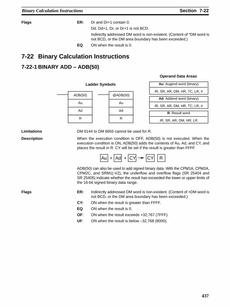
7-22SectionBinary Calculation Instructions
437
Flags ER: Dr and Dr+1 contain 0.
Dd, Dd+1, Dr, or Dr+1 is not BCD.
Indirectly addressed DM word is non-existent. (Content of *DM word isnot BCD, or the DM area boundary has been exceeded.)
EQ: ON when the result is 0.
7-22 Binary Calculation Instructions
7-22-1 BINARY ADD – ADB(50)
Au: Augend word (binary)
IR, SR, AR, DM, HR, TC, LR, #
Ad: Addend word (binary)
IR, SR, AR, DM, HR, TC, LR, #
Ladder Symbols
Operand Data Areas
R: Result word
IR, SR, AR, DM, HR, LR
ADB(50)
Au
Ad
R
@ADB(50)
Au
Ad
R
DM 6144 to DM 6655 cannot be used for R.
When the execution condition is OFF, ADB(50) is not executed. When theexecution condition is ON, ADB(50) adds the contents of Au, Ad, and CY, andplaces the result in R. CY will be set if the result is greater than FFFF.
Au + Ad + CY CY R
ADB(50) can also be used to add signed binary data. With the CPM1A, CPM2A,CPM2C, and SRM1(-V2), the underflow and overflow flags (SR 25404 andSR 25405) indicate whether the result has exceeded the lower or upper limits ofthe 16-bit signed binary data range.
Flags ER: Indirectly addressed DM word is non-existent. (Content of DM word isnot BCD, or the DM area boundary has been exceeded.)
CY: ON when the result is greater than FFFF.
EQ: ON when the result is 0.
OF: ON when the result exceeds +32,767 (7FFF).
UF: ON when the result is below –32,768 (8000).
Limitations
Description

7-22SectionBinary Calculation Instructions
438
Example The following example shows a four-digit addition with CY used to place either#0000 or #0001 into R+1 to ensure that any carry is preserved.
CLC(41)
00000
ADB(50)
200
DM 0100
HR 10
MOV(21)
#0000
HR 11
MOV(21)
#0001
HR 11
TR 0
25504
25504
= R
= R+1
= R+1
Address Instruction Operands
00000 LD 00000
00001 OUT TR 0
00002 CLC(41)
00003 ADB(50)
200
DM 0100
HR 10
00004 AND NOT 25504
00005 MOV(21)
# 0000
HR 11
00006 LD TR 0
00007 AND 25504
00008 MOV(21)
# 00001
HR 11
In the case below, A6E2 + 80C5 = 127A7. The result is a 5-digit number, so CY(SR 25504) = 1, and the content of R + 1 becomes #0001.
R+1: HR 11 R: HR 100 0 0 1 2 7 A 7
Au: IR 200A 6 E 2
Ad: DM 01008 0 C 5
+
Note For signed binary calculations, the status of the UF and OF flags indicate wheth-er the result has exceeded the signed binary data range (–32,768 (8000) to+32,767 (7FFF)).
7-22-2 BINARY SUBTRACT – SBB(51)
Mi: Minuend word (binary)
IR, SR, AR, DM, HR, TC, LR, #
Su: Subtrahend word (binary)
IR, SR, AR, DM, HR, TC, LR, #
Ladder Symbols
Operand Data Areas
R: Result word
IR, SR, AR, DM, HR, LR
SBB(51)
Mi
Su
R
@SBB(51)
Mi
Su
R
DM 6144 to DM 6655 cannot be used for R.Limitations

7-22SectionBinary Calculation Instructions
439
When the execution condition is OFF, SBB(51) is not executed. When theexecution condition is ON, SBB(51) subtracts the contents of Su and CY from Miand places the result in R. If the result is negative, CY is set and the 2’s comple-ment of the actual result is placed in R.
Mi – Su – CY CY R
SBB(51) can also be used to subtract signed binary data. With the CPM1A,CPM2A, CPM2C, and SRM1(-V2), the underflow and overflow flags (SR 25404and SR 25405) indicate whether the result has exceeded the lower or upper lim-its of the 16-bit signed binary data range.
Flags ER: Indirectly addressed DM word is non-existent. (Content of DM word isnot BCD, or the DM area boundary has been exceeded.)
CY: ON when the result is negative, i.e., when Mi is less than Su plus CY.
EQ: ON when the result is 0.
OF: ON when the result exceeds +32,767 (7FFF).
UF: ON when the result is below –32,768 (8000).
Example The following example shows a four-digit subtraction. When IR 00001 is ON, thecontent of LR 00 and CY are subtracted from the content of IR 002 and the resultis written to HR 01.
CY is turned ON if the result is negative. If normal data is being used, a negativeresult (signed binary) must be converted to normal data using NEG(––). Refer to7-20-12 2’s COMPLEMENT – NEG(––) for details.
CLC(41)
00001
SBB(51)
200
LR00
HR 01
Address Instruction Operands
00000 LD 00001
00001 OUT TR 1
00002 CLC(41)
00003 SBB(51)
200
LR 00
HR 01
In the case below, the content of LR 00 (#7A03) and CY are subtracted fromIR 002 (#F8C5). Since the result is positive, CY is 0.
If the result had been negative, CY would have been set to 1. For normal (un-signed) data, the result would have to be converted to its 2’s complement.
Mi: IR 002F 8 C 5
Su: LR 007 A 0 3
–
0 0 0 0–
CY = 0(from CLC(41))
R: HR 017 E C 2
Note For signed binary calculations, the status of the UF and OF flags indicate wheth-er the result has exceeded the signed binary data range (–32,768 (8000) to+32,767 (7FFF)).
Description

7-22SectionBinary Calculation Instructions
440
7-22-3 BINARY MULTIPLY – MLB(52)
Md: Multiplicand word (binary)
IR, SR, AR, DM, HR, TC, LR, #
Mr: Multiplier word (binary)
IR, SR, AR, DM, HR, TC, LR, #
Ladder Symbols
Operand Data Areas
R: First result word
IR, SR, AR, DM, HR LR
MLB(52)
Md
Mr
R
@MLB(52)
Md
Mr
R
DM 6144 to DM 6655 cannot be used for R.MLB(52) cannot be used to multiply signed binary data.
When the execution condition is OFF, MLB(52) is not executed. When theexecution condition is ON, MLB(52) multiplies the content of Md by the contentsof Mr, places the rightmost four digits of the result in R, and places the leftmostfour digits in R+1.
Md
Mr
R +1 R
X
Flags ER: Indirectly addressed DM word is non-existent. (Content of DM word isnot BCD, or the DM area boundary has been exceeded.)
EQ: ON when the result is 0.
7-22-4 BINARY DIVIDE – DVB(53)
Dd: Dividend word (binary)
IR, SR, AR, DM, HR, TC, LR, #
Dr: Divisor word (binary)
IR, SR, AR, DM, HR, TC, LR, #
Ladder Symbols
Operand Data Areas
R: First result word
IR, SR, AR, DM, HR LR
DVB(53)
Dd
Dr
R
@DVB(53)
Dd
Dr
R
DM 6144 to DM 6655 cannot be used for R.DVB(53) cannot be used to divide signed binary data.
When the execution condition is OFF, DVB(53) is not executed. When theexecution condition is ON, DVB(53) divides the content of Dd by the content ofDr and the result is placed in R and R+1: the quotient in R, the remainder in R+1.
DdDr
R R + 1
Quotient Remainder
Limitations
Description
Limitations
Description

7-23SectionSpecial Math Instructions
441
Flags ER: Dr contains 0.
Indirectly addressed DM word is non-existent. (Content of DM word isnot BCD, or the DM area boundary has been exceeded.)
EQ: ON when the result is 0.
7-23 Special Math Instructions
7-23-1 DATA SEARCH – SRCH(––)
R1: First word in range
IR, SR, AR, DM, HR, TC, LR
N: Number of words
IR, SR, AR, DM, HR, TC, LR, #
Ladder Symbols Operand Data Areas
@SRCH(––)
N
R1
CC: Comparison data, result word
IR, SR, AR, DM, HR, LR
SRCH(––)
N
R1
C
Limitations This instruction is available in the CPM2A/CPM2C only.
N must be BCD between 0001 to 9999.
R1 and R1+N–1 must be in the same data area.
DM 6144 to DM 6655 cannot be used for C.
Description When the execution condition is OFF, SRCH(––) is not executed. When theexecution condition is ON, SRCH(––) searches the range of memory from R1 toR1+N–1 for addresses that contain the comparison data in C. If one or more ad-dresses contain the comparison data, the EQ Flag (SR 25506) is turned ON andthe lowest address containing the comparison data is identified in C+1. The ad-dress is identified differently for the DM area:
1, 2, 3... 1. For an address in the DM area, the word address is written to C+1. For ex-ample, if the lowest address containing the comparison data is DM 0114,then #0114 is written in C+1.
2. For an address in another data area, the number of addresses from the be-ginning of the search is written to C+1. For example, if the lowest addresscontaining the comparison data is IR 114 and the first word in the searchrange is IR 014, then #0100 is written in C+1.
If none of addresses in the range contain the comparison data, the EQ Flag(SR 25506) is turned OFF and C+1 is left unchanged.
Flags ER: Indirectly addressed DM word is non-existent. (Content of DM word isnot BCD, or the DM area boundary has been exceeded.)
N is not BCD between 0001 and 9999.
R1 and R1+N–1 are not in the same data area.
EQ: ON when the comparison data has been matched in the search range.
Example In the following example, the 10 word range from IR 200 to IR 209 is searchedfor addresses that contain the same data as DM 0100 (89AB). Since IR 204 con-

7-23SectionSpecial Math Instructions
442
tains the same data, the EQ Flag (SR 25506) is turned ON and #0004 is writtento DM 0101.
@SRCH(––)
200
#0010
00000
DM 0100
Address Instruction Operands
00000 LD 00000
00001 @SRCH(––)
# 0010
0200
DM 0100
IR 200 1234
IR 201 5678
IR 202 ABCD
IR 203 EF13
IR 204 89AB
IR 205 8860
IR 206 90CD
IR 207 00FF
IR 208 89AB
IR 209 810C
DM 0101 0004
DM 0100 89AB
← Search data found
← Search data found
Offset of first word con-taining the search data
Offset: 0004
Note The matching search data in IR 208 is ignored because the search data wasfound in an earlier word in the range.
7-23-2 FIND MAXIMUM – MAX(––)
R1: First word in range
IR, SR, AR, DM, HR, TC, LR
C: Control data
IR, SR, AR, DM, HR, TC, LR, #
Ladder Symbols Operand Data Areas
@MAX(––)
C
R1
DD: Destination word
IR, SR, AR, DM, HR, LR
MAX(––)
C
R1
D
Limitations This instruction is available in the CPM2A/CPM2C only.N must be BCD between 0001 to 9999.R1 and R1+N–1 must be in the same data area.DM 6144 to DM 6655 cannot be used for D.
Description When the execution condition is OFF, MAX(––) is not executed. When theexecution condition is ON, MAX(––) searches the range of memory from R1 toR1+N–1 for the address that contains the maximum value and outputs the maxi-mum value to the destination word (D).The address is identified differently for the DM area:
1, 2, 3... 1. For an address in the DM area, the word address is written to C+1. For ex-ample, if the address containing the maximum value is DM 0114, then #0114is written in D+1.
2. For an address in another data area, the number of addresses from the be-ginning of the search is written to D+1. For example, if the address contain-ing the maximum value is IR 114 and the first word in the search range isIR 014, then #0100 is written in D+1.

!
7-23SectionSpecial Math Instructions
443
If bit 14 of C is ON and more than one address contains the same maximum val-ue, the position of the lowest of the addresses will be output to D+1. The positionwill be output as the DM address for the DM area, but as an absolute positionrelative to the first word in the range for all other areas.
The number of words within the range (N) is contained in the 3 rightmost digits ofC, which must be BCD between 001 and 999.
When bit 15 of C is OFF, data within the range is treated as unsigned binary andwhen it is ON the data is treated as signed binary.
15 14 13 12 11 00
Not used – set to zero.
Number of wordsin range (N: 001 to 999 BCD)
Not used – set to zero.
Output address to D+1?1 (ON): Yes.0 (OFF): No.
C:
Caution If bit 14 of C is ON, values above #8000 are treated as negative numbers, so theresults will differ depending on the specified data type. Be sure that the correctdata type is specified.
Flags ER: Indirectly addressed DM word is non-existent. (Content of DM word isnot BCD, or the DM area boundary has been exceeded.)
R1 and R1+N–1 are not in the same data area.
EQ: ON when the maximum value is #0000.
When IR 00000 is ON, the control data in DM 0000 (4010) will cause a search forthe maximum value in the 10 words starting at IR 200. The largest unsigned val-
Example

7-23SectionSpecial Math Instructions
444
ue will be stored in DM 0500. The offset from the beginning of the search of theword containing the maximum value will be stored in DM 0501.
00000MAX(––)
DM 0000
200
DM 0500
Address Instruction Operands
00000 LD 00000
00001 MAX(––)
DM 0000
200
DM 0500
DM 0000
10 words
IR 200
IR 201
IR 202
IR 203
IR 204
IR 205
IR 206
IR 207
IR 208
IR 209
DM 0500
DM 0501
Maximum value
Offset of word containing maximum value: 2 words
Maximum value
If there are two words containingthe maximum value, the one foundfirst will be stored in DM 0501.
3F2A
51C3
E02A
7C9F
2A20
A827
2A20
E02A
C755
94DC
4010
E02A
0002
7-23-3 FIND MINIMUM – MIN(––)
R1: First word in range
IR, SR, AR, DM, HR, TC, LR
C: Control data
IR, SR, AR, DM, HR, TC, LR, #
Ladder Symbols Operand Data Areas
@MIN(––)
C
R1
DD: Destination word
IR, SR, AR, DM, HR, LR
MIN(––)
C
R1
D
Limitations This instruction is available in the CPM2A/CPM2C only.N must be BCD between 0001 to 9999.
R1 and R1+N–1 must be in the same data area.DM 6144 to DM 6655 cannot be used for D.
Description When the execution condition is OFF, MIN(––) is not executed. When the execu-tion condition is ON, MIN(––) searches the range of memory from R1 to R1+N–1for the address that contains the minimum value and outputs the minimum valueto the destination word (D).The address is identified differently for the DM area:
1, 2, 3... 1. For an address in the DM area, the word address is written to C+1. For ex-ample, if the address containing the minimum value is DM 0114, then #0114is written in D+1.

!
7-23SectionSpecial Math Instructions
445
2. For an address in another data area, the number of addresses from the be-ginning of the search is written to D+1. For example, if the address contain-ing the minimum value is IR 114 and the first word in the search range isIR 014, then #0100 is written in D+1.
If bit 14 of C is ON and more than one address contains the same minimum val-ue, the position of the lowest of the addresses will be output to D+1. The positionwill be output as the DM address for the DM area, but as an absolute positionrelative to the first word in the range for all other areas.
The number of words within the range (N) is contained in the 3 rightmost digits ofC, which must be BCD between 001 and 999.
When bit 15 of C is OFF, data within the range is treated as unsigned binary andwhen it is ON the data is treated as signed binary.
Number of wordsin range (N: 001 to 999 BCD)
Not used – set to zero.
Output address to D+1?1 (ON): Yes.0 (OFF): No.
C:15 14 13 12 11 00
Not used – set to zero.
Caution If bit 14 of C is ON, values above #8000 are treated as negative numbers, so theresults will differ depending on the specified data type. Be sure that the correctdata type is specified.
Flags ER: Indirectly addressed DM word is non-existent. (Content of DM word isnot BCD, or the DM area boundary has been exceeded.)
R1 and R1+N–1 are not in the same data area.
EQ: ON when the minimum value is #0000.
When IR 00000 is ON, the control data in DM 0300 (4010) will cause a search forthe maximum value in the 10 words starting at DM 0000. The smallest unsigned
Example

7-23SectionSpecial Math Instructions
446
value will be stored in DM 0500. The address of the word containing the mini-mum value (0014) will be stored in DM 0501.
00000MIN(––)
DM 0300
DM 0000
DM 0500
Address Instruction Operands
00000 LD 00000
00001 MIN(––)
DM 0300
DM 0000
DM 0500
Minimum value
Address of word containing maximum value: 0014
Minimum value
If there are two words containingthe minimum value, the one foundfirst will be stored in DM 0501.
DM 0300
10 words
DM0010
DM0011
DM0012
DM0013
DM0014
DM0015
DM0016
DM0017
DM0018
DM0019
DM 0500
DM 0501
3F2A
51C3
E02A
7C9F
2A20
A827
33BF
E02A
2A20
94DC
4010
2A20
0014
7-23-4 AVERAGE VALUE – AVG(––)
S: Source word
IR, SR, AR, DM, HR, TC, LR
N: Number of cycles
IR, SR, AR, DM, HR, TC, LR, #
Ladder Symbols Operand Data Areas
D: First destination word
IR, SR, AR, DM, HR, LR
AVG(––)
S
N
D
Limitations This instruction is available in the CPM2A/CPM2C only.
S must be hexadecimal.
N must be BCD from #0001 to #0064.
D and D+N+1 must be in the same data area.
DM 6144 to DM 6655 cannot be used for S, N, or D to D+N+1.
Description AVG(––) is used to calculate the average value of S over N cycles.
When the execution condition is OFF, AVG(––) is not executed.
Each time that AVG(––) is executed, the content of S is stored in words D+2 toD+N+1. On the first execution, AVG(––) writes the content of S to D+2; on thesecond execution it writes the content of S to D+3, etc. On the Nth execution,

7-23SectionSpecial Math Instructions
447
AVG(––) writes the content of S is stored in D+N+1, AVG(––) calculates the av-erage value of the values stored in D+2 to D+N+1, and writes the average to D.
The following diagram shows the function of words D to D+N+1.
D Average value (after N or more executions)
D+1 Used by the system.
D+2 Content of S from the 1st execution of AVG(––)
D+3 Content of S from the 2nd execution of AVG(––)
D+N+1 Content of S from the Nth execution of AVG(––)
Precautions The average value is calculated in binary. Be sure that the content of S is inbinary.
N must be BCD from #0001 to #0064. If the content of N ≥ #0065, AVG(––) willoperate with N=64.
The average value will be rounded off to the nearest integer value. (0.5 isrounded up to 1.)
Set the contents of D+1 to #0000 to execute AVG(––) from the first scan.
Flags ER: Indirectly addressed DM word is non-existent. (Content of DM word isnot BCD, or the DM area boundary has been exceeded.)
One or more operands have been set incorrectly.
D and D+N+1 are not in the same data area.
Example In the following example, the content of IR 200 is set to #0000 and then increm-ented by 1 each cycle. For the first two cycles, AVG(––) moves the content ofIR 200 to DM 1002 and DM 1003. On the third and later cycles AVG(––) calcu-

7-23SectionSpecial Math Instructions
448
lates the average value of the contents of DM 1002 to DM 1004 and writes thataverage value to DM 1000.
@MOV(21)
200
#0000
00001
Address Instruction Operands
00000 LD 00001
00001 @MOV(21)
# 0000
200
00002 AVG(––)
200
# 0003
DM 1000
00003 CLC(41)
00004 ADB(50)
200
# 0001
200
AVG(––)
#0003
200
DM 1000
CLC(41)
ADB(50)
#0001
200
200
1st cycle 2nd cycle 3rd cycle 4th cycle
DM 1000 0000 0001 0001 0002 Average
DM 1001 Used by the system.
DM 1002 0000 0000 0000 0003 Previous
DM 1003 --- 0001 0001 0001 values of
DM 1004 --- --- 0002 0002 IR 200
1st cycle 2nd cycle 3rd cycle 4th cycle
IR 200 0000 0001 0002 0003
7-23-5 SUM – SUM(––)
C: Control data
IR, SR, AR, DM, HR, LR, #
R1: First word in range
IR, SR, AR, DM, HR, TC, LR
Ladder Symbols Operand Data Areas
D: First destination word
IR, SR, AR, DM, HR, LR
SUM(––)
C
R1
D
@SUM(––)
C
R1
D
Limitations This instruction is available in the CPM2A/CPM2C only.
The 3 rightmost digits of C must be BCD between 001 and 999.
DM 6144 to DM 6655 cannot be used for D.
If bit 14 of C is OFF (setting for BCD data), all data within the range R1 to R1+N–1must be BCD.
Description When the execution condition is OFF, SUM(––) is not executed. When theexecution condition is ON, SUM(––) adds either the contents of words R1 toR1+N–1 or the bytes in words R1 to R1+N/2–1 and outputs that value to the des-tination words (D and D+1). The data can be summed as binary or BCD and willbe output in the same form. Binary data can be either signed or unsigned.

7-23SectionSpecial Math Instructions
449
The function of bits in C are shown in the following diagram and explained inmore detail below.
Number of items in range (N, BCD)Number of words or number of bytes001 to 999
First byte (when bit 13 is ON)1 (ON): Rightmost0 (OFF): Leftmost
Addition units1 (ON): Bytes0 (OFF): Words
C:
Data type1 (ON): Binary0 (OFF): BCD
Not used – set to zero.
15 14 13 12 11 00
Number of Items in Range The number of items within the range (N) is contained in the 3 rightmost digits ofC, which must be BCD between 001 and 999. This number will indicate the num-ber of words or the number of bytes depending the items being summed.
Addition Units Words will be added if bit 13 is OFF and bytes will be added if bit 13 is ON.
If bytes are specified, the range can begin with the leftmost or rightmost byte ofR1. The leftmost byte of R1 will not be added if bit 12 is ON.
MSB LSB
R1 1 2
R1+1 3 4
R1+2 5 6
R1+3 7 8
The bytes will be added in this order when bit 12 is OFF: 1+2+3+4....
The bytes will be added in this order when bit 12 is ON: 2+3+4....
Data Type Data within the range is treated as unsigned binary when bit 14 of C is ON and bit15 is OFF, and it is treated as signed binary when both bits 14 and 15 are ON.
Data within the range is treated as BCD when bit 14 of C is OFF, regardless of thestatus of bit 15.
Flags ER: Indirectly addressed DM word is non-existent. (Content of DM word isnot BCD, or the DM area boundary has been exceeded.)
R1 and R1+N–1 are not in the same data area.
The number of items in C is not BCD between 001 and 999.
The data being summed in not BCD when BCD was designated.
EQ: ON when the result is zero.

7-24SectionLogic Instructions
450
Example In the following example, the BCD contents of the 8 words from DM 0000 toDM 0007 are added when IR 00001 is ON and the result is written to DM 0010and DM 0011.
@SUM(––)
DM 0000
#0008
00001
DM 0010
Address Instruction Operands
00000 LD 00001
00001 @SUM(––)
# 0008
DM 0000
DM 0010
DM 0000 0001
DM 0001 0002
DM 0002 0003
DM 0003 0004
DM 0004 0005
DM 0005 0006
DM 0006 0007
DM 0007 0008
DM 0010 0036
DM 0011 0000
7-24 Logic Instructions
7-24-1 COMPLEMENT – COM(29)
Wd: Complement word
IR, SR, AR, DM, HR, LR
Ladder Symbols Operand Data Areas
COM(29)
Wd
@COM(29)
Wd
Limitations DM 6144 to DM 6655 cannot be used for Wd.
When the execution condition is OFF, COM(29) is not executed. When theexecution condition is ON, COM(29) clears all ON bits and sets all OFF bits inWd.
The complement of Wd will be calculated every cycle if the undifferentiated formof COM(29) is used. Use the differentiated form (@COM(29)) or combineCOM(29) with DIFU(13) or DIFD(14) to calculate the complement just once.
1 0 0 1 1 0 0 1 1 0 0 1 1 0 0 1
0 1 1 0 0 1 1 0 0 1 1 0 0 1 1 0
15 00
15 00
Original
Complement
Flags ER: Indirectly addressed DM word is non-existent. (Content of DM word isnot BCD, or the DM area boundary has been exceeded.)
EQ: ON when the result is 0.
Description
Precautions
Example

7-24SectionLogic Instructions
451
7-24-2 LOGICAL AND – ANDW(34)
I1: Input 1
IR, SR, AR, DM, HR, TC, LR, #
I2: Input 2
IR, SR, AR, DM, HR, TC, LR, #
Ladder Symbols
Operand Data Areas
R: Result word
IR, SR, AR, DM, HR, LR
ANDW(34)
I1
I2
R
@ANDW(34)
I1
I2
R
DM 6144 to DM 6655 cannot be used for R.
When the execution condition is OFF, ANDW(34) is not executed. When theexecution condition is ON, ANDW(34) logically AND’s the contents of I1 and I2bit-by-bit and places the result in R.
1 0 0 1 1 0 0 1 1 0 0 1 1 0 0 1
15 00
0 1 0 1 0 1 0 1 0 1 0 1 0 1 0 1
0 0 0 1 0 0 0 1 0 0 0 1 0 0 0 1
15 00
15 00
I1
I2
R
Flags ER: Indirectly addressed DM word is non-existent. (Content of DM word isnot BCD, or the DM area boundary has been exceeded.)
EQ: ON when the result is 0.
7-24-3 LOGICAL OR – ORW(35)
I1: Input 1
IR, SR, AR, DM, HR, TC, LR, #
I2: Input 2
IR, SR, AR, DM, HR, TC, LR, #
Ladder Symbols
Operand Data Areas
R: Result word
IR, SR, AR, DM, HR, LR
ORW(35)
I1
I2
R
@ORW(35)
I1
I2
R
DM 6144 to DM 6655 cannot be used for R.
Limitations
Description
Example
Limitations

7-24SectionLogic Instructions
452
When the execution condition is OFF, ORW(35) is not executed. When theexecution condition is ON, ORW(35) logically OR’s the contents of I1 and I2 bit-by-bit and places the result in R.
1 0 0 1 1 0 0 1 1 0 0 1 1 0 0 1
15 00
0 1 0 1 0 1 0 1 0 1 0 1 0 1 0 1
1 1 0 1 1 1 0 1 1 1 0 1 1 1 0 1
15 00
15 00
I1
I2
R
Flags ER: Indirectly addressed DM word is non-existent. (Content of DM word isnot BCD, or the DM area boundary has been exceeded.)
EQ: ON when the result is 0.
7-24-4 EXCLUSIVE OR – XORW(36)
I1: Input 1
IR, SR, AR, DM, HR, TC, LR, #
I2: Input 2
IR, SR, AR, DM, HR, TC, LR, #
Ladder Symbols
Operand Data Areas
R: Result word
IR, SR, AR, DM, HR, LR
XORW(36)
I1
I2
R
@XORW(36)
I1
I2
R
DM 6144 to DM 6655 cannot be used for R.
When the execution condition is OFF, XORW(36) is not executed. When theexecution condition is ON, XORW(36) exclusively OR’s the contents of I1 and I2bit-by-bit and places the result in R.
1 0 0 1 1 0 0 1 1 0 0 1 1 0 0 1
15 00
0 1 0 1 0 1 0 1 0 1 0 1 0 1 0 1
1 1 0 0 1 1 0 0 1 1 0 0 1 1 0 0
15 00
15 00
I1
I2
R
Flags ER: Indirectly addressed DM word is non-existent. (Content of DM word isnot BCD, or the DM area boundary has been exceeded.)
EQ: ON when the result is 0.
Description
Example
Limitations
Description
Example

7-25SectionIncrement/Decrement Instructions
453
7-24-5 EXCLUSIVE NOR – XNRW(37)
I1: Input 1
IR, SR, AR, DM, HR, TC, LR, #
I2: Input 2
IR, SR, AR, DM, HR, TC, LR, #
Ladder Symbols
Operand Data Areas
R: Result word
IR, SR, AR, DM, HR, LR
XNRW(37)
I1
I2
R
@XNRW(37)
I1
I2
R
DM 6144 to DM 6655 cannot be used for R.
When the execution condition is OFF, XNRW(37) is not executed. When theexecution condition is ON, XNRW(37) exclusively NOR’s the contents of I1 andI2 bit-by-bit and places the result in R.
1 0 0 1 1 0 0 1 1 0 0 1 1 0 0 1
15 00
0 1 0 1 0 1 0 1 0 1 0 1 0 1 0 1
0 0 1 1 0 0 1 1 0 0 1 1 0 0 1 1
15 00
15 00
I1
I2
R
Flags ER: Indirectly addressed DM word is non-existent. (Content of DM word isnot BCD, or the DM area boundary has been exceeded.)
EQ: ON when the result is 0.
7-25 Increment/Decrement Instructions7-25-1 BCD INCREMENT – INC(38)
Wd: Increment word (BCD)
IR, SR, AR, DM, HR, LR
Ladder Symbols Operand Data Areas
INC(38)
Wd
@INC(38)
Wd
DM 6144 to DM 6655 cannot be used for Wd.
When the execution condition is OFF, INC(38) is not executed. When the execu-tion condition is ON, INC(38) increments Wd, without affecting Carry (CY).
The content of Wd will be incremented every cycle if the undifferentiated form ofINC(38) is used. Use the differentiated form (@INC(38)) or combine INC(38)with DIFU(13) or DIFD(14) to increment Wd just once.
Flags ER: Wd is not BCD
Indirectly addressed DM word is non-existent. (Content of DM word isnot BCD, or the DM area boundary has been exceeded.)
EQ: ON when the incremented result is 0.
Limitations
Description
Limitations
Description
Precautions

7-25SectionIncrement/Decrement Instructions
454
7-25-2 BCD DECREMENT – DEC(39)
Wd: Decrement word (BCD)
IR, SR, AR, DM, HR, LR
Ladder Symbols Operand Data Areas
DEC(39)
Wd
@DEC(39)
Wd
DM 6144 to DM 6655 cannot be used for Wd.
When the execution condition is OFF, DEC(39) is not executed. When theexecution condition is ON, DEC(39) decrements Wd, without affecting CY.DEC(39) works the same way as INC(38) except that it decrements the valueinstead of incrementing it.
The content of Wd will be decremented every cycle if the undifferentiated form ofDEC(39) is used. Use the differentiated form (@DEC(39)) or combine DEC(39)with DIFU(13) or DIFD(14) to decrement Wd just once.
Flags ER: Wd is not BCD.
Indirectly addressed DM word is non-existent. (Content of DM word isnot BCD, or the DM area boundary has been exceeded.)
EQ: ON when the decremented result is 0.
Limitations
Description
Precautions

7-26SectionSubroutine Instructions
455
7-26 Subroutine Instructions
Subroutines break large control tasks into smaller ones and enable you to reusea given set of instructions. When the main program calls a subroutine, control istransferred to the subroutine and the subroutine instructions are executed. Theinstructions within a subroutine are written in the same way as main programcode. When all the subroutine instructions have been executed, control returnsto the main program to the point just after the point from which the subroutinewas entered (unless otherwise specified in the subroutine).
7-26-1 SUBROUTINE ENTER – SBS(91)
N: Subroutine number
000 to 049
Ladder Symbol Definer Data Areas
SBS(91) N
Limitations The subroutine number must be between 000 and 049.
Description A subroutine can be executed by placing SBS(91) in the main program at thepoint where the subroutine is desired. The subroutine number used in SBS(91)indicates the desired subroutine. When SBS(91) is executed (i.e., when theexecution condition for it is ON), the instructions between the SBN(92) with thesame subroutine number and the first RET(93) after it are executed beforeexecution returns to the instruction following the SBS(91) that made the call.
SBS(91) 000
SBN(92) 000
RET(93)
END(01)
Main program
Subroutine
Main program
SBS(91) may be used as many times as desired in the program, i.e., the samesubroutine may be called from different places in the program).

!
7-26SectionSubroutine Instructions
456
SBS(91) may also be placed into a subroutine to shift program execution fromone subroutine to another, i.e., subroutines may be nested. When the secondsubroutine has been completed (i.e., RET(93) has been reached), programexecution returns to the original subroutine which is then completed before re-turning to the main program. Nesting is possible to up to sixteen levels. A sub-routine cannot call itself (e.g., SBS(91) 000 cannot be programmed within thesubroutine defined with SBN(92) 000). The following diagram illustrates two lev-els of nesting.
SBN(92) 010 SBN(92) 011 SBN(92) 012
SBS(91) 011
RET(93)
SBS(91) 010 SBS(91) 012
RET(93) RET(93)
The following diagram illustrates program execution flow for various executionconditions for two SBS(91).
SBS(91) 000
SBS(91) 001
SBN(92) 000
RET(93)
SBN(92) 001
RET(93)
END(01)
Main program
Subroutines
A
B
C
D
E
A
A
A
A
B
B
B
B
C
C
C
C
D
D
E
E
OFF execution conditions for subroutines 000 and 001
ON execution condition for subroutine 000 only
ON execution condition for subroutine 001 only
ON execution conditions for subroutines 000 and 001
Flags ER: A subroutine does not exist for the specified subroutine number.
A subroutine has called itself.
An active subroutine has been called.
Caution SBS(91) will not be executed and the subroutine will not be called when ER isON.

7-26SectionSubroutine Instructions
457
7-26-2 SUBROUTINE DEFINE and RETURN – SBN(92)/RET(93)
N: Subroutine number
000 to 049
Ladder Symbols Definer Data Areas
SBN(92) N
RET(93)
Limitations The subroutine number must be between 000 and 049.Each subroutine number can be used in SBN(92) once only.
SBN(92) is used to mark the beginning of a subroutine program; RET(93) isused to mark the end. Each subroutine is identified with a subroutine number, N,that is programmed as a definer for SBN(92). This same subroutine number isused in any SBS(91) that calls the subroutine (see 7-26-1 SUBROUTINE EN-TER – SBS(91)). No subroutine number is required with RET(93).
All subroutines must be programmed at the end of the main program. When oneor more subroutines have been programmed, the main program will beexecuted up to the first SBN(92) before returning to address 00000 for the nextcycle. Subroutines will not be executed unless called by SBS(91).
END(01) must be placed at the end of the last subroutine program, i.e., after thelast RET(93). It is not required at any other point in the program.
Precautions If SBN(92) is mistakenly placed in the main program, it will inhibit programexecution past that point, i.e., program execution will return to the beginningwhen SBN(92) is encountered.
If either DIFU(13) or DIFU(14) is placed within a subroutine, the operand bit willnot be turned OFF until the next time the subroutine is executed, i.e., the oper-and bit may stay ON longer than one cycle.
Flags There are no flags directly affected by these instructions.
7-26-3 MACRO – MCRO(99)
I1: First input word
IR, SR, AR, DM, HR, TC, LR
Ladder Symbols
Operand Data Areas
O1: First output word
IR, SR, AR, DM, HR, LR
MCRO(99)
N
I1
O1
@MCRO(99)
N
I1
O1
N: Subroutine number
000 to 127
The subroutine number must be between 000 and 049.
If a DM address is used for O1, O1 through O1+3 must be read/write DM.
The MACRO instruction allows a single subroutine to replace several subrou-tines that have identical structure but different operands. There are 4 inputwords (SR 232 to SR 235) and 4 output words (SR 236 to SR 239), allocated toMCRO(99). These 8 words are used in the subroutine and take their contentsfrom I1 to I1+3 and O1 to O1+3 when the subroutine is executed.
Description
Limitations
Description

7-27SectionPulse Output Instructions
458
When the execution condition is OFF, MCRO(99) is not executed. When theexecution condition is ON, MCRO(99) copies the contents of I1 to I1+3 to SR 232to SR 235, and then calls and executes the subroutine specified in N. When thesubroutine is completed, the contents of SR 236 through SR 239 are then trans-ferred back to O1 to O1+3 before MCRO(99) is completed.
Note Refer to page 145 for more details on MCRO(99).
Example In this example, the contents of DM 0010 through DM 0013 are copied to SR 232through SR 235, and then subroutine 10 is called and executed. When the sub-routine is completed, the contents of SR 236 through SR 239 are copied to out-put words DM 0020 to DM 0023.
MCRO(99) 010
DM 0010
DM 0020
SBN(92) 010
RET(93)
END(01)
Main program
Subroutine
Main program
Flags ER: A subroutine does not exist for the specified subroutine number.
An operand has exceeded a data area boundary.
Indirectly addressed DM word is non-existent. (Content of DM word isnot BCD, or the DM area boundary has been exceeded.)
A subroutine has called itself.
An active subroutine has been called.
7-27 Pulse Output Instructions
7-27-1 SET PULSES – PULS(65)
P: Port specifier
000 or 010
Ladder Symbols Operand Data Areas
@PULS(65)
P
C
NN: Number of pulses
IR, SR, AR, DM, HR, LR
C: Control data
000 or 001
PULS(65)
P
C
N

7-27SectionPulse Output Instructions
459
Limitations This instruction is supported by the CPM1A and CPM2A/CPM2C PCs withtransistor outputs only.
N and N+1 must be in the same data area.
DM 6144 to DM 6655 cannot be used for N.
Description PULS(65) is used to set the number of pulses for pulse outputs that are startedlater in the program using SPED(64) or ACC(––). The number of pulses set withPULS(65) are output in independent mode.
The number of pulses cannot be changed while pulses are being output. In gen-eral, PULS(65) should be executed just once each time that the number ofpulses needs to be set; use the differentiated variation (@PULS(65)) or an inputcondition that is ON for just one cycle.
Note Refer to 2-5 Pulse Output Functions for more details.
Port Specifier (P)The port specifier indicates the pulse output location. The parameters set by thein C and N will apply to the next SPED(64) or ACC(––) instruction in which thesame port output location is specified.
P Pulse output location(s)
000 Single-phase pulse output 0 without acceleration or deceleration (output01000) or single-phase pulse output 0 with trapezoidal acceleration and decel-eration (outputs 01000 and 01001)
010 Single-phase pulse output 1 without acceleration or deceleration (output01001)
This setting is supported by CPM2A/CPM2C PCs only.
Control Data (C)The control data determines the type of pulses (relative or absolute).
C Pulse type
000 Relative pulse specification
001 Absolute pulse specification (Valid only when the absolute coordinate systemis being used.)
This setting is supported by CPM2A/CPM2C PCs only.
Number of Output Pulses (N+1 and N)N+1 and N contain the 8-digit BCD number of output pulses setting for indepen-dent mode pulse outputs. The number of output pulses can be –16,777,215 to16,777,215. Bit 15 of N+1 acts as a sign bit; the number is negative if bit 15 is ON,positive if it is OFF.
Positive: 0 to +16,777,215 (0000 0000 to 1677 7215)Negative: –16,777,215 to 0 (9677 7215 to 8000 0000)
N+1 contains the leftmost 4 digits and N contains the rightmost 4 digits.
The number of movement pulses depends upon the number of output pulses(N+1 and N) and the pulse type (C).
Coordinatesystem
Movement pulses
Relative Number of movement pulses = Number of output pulses
Absolute Pulse type: Relative (C=000)Number of movement pulses = Number of output pulses
Pulse type: Absolute (C=001, CPM2A/CPM2C only)Number of movement pulses = Number of output pulses – PV
After PULS(65) has been executed, the calculated number of movement pulseswill not be changed even if INI(61) is executed to change the pulse output PV.
A specification that causes movement outside of the allowed PV range(–16,777,215 to 16,777,215) can be specified without problems.
Number of MovementPulses

7-27SectionPulse Output Instructions
460
PULS(65) will not be executed and an error will occur (SR 25503 ON) if the cal-culated number of movement pulses is 0.
When the pulse output is operating in independent mode without acceleration ordeceleration and the number of movement pulses is negative, the absolute val-ue of the number of movement pulses will be used. (For example, if the numberof movement pulses is –500, a value of 500 will be used.)
Flags ER: A data area boundary is exceeded.
Indirectly addressed DM word is non-existent. (Content of *DM word isnot BCD, or the DM area boundary has been exceeded.)
P is not 000 or 010.
C is not 000 or 001. (C cannot be set to 001 when relative coordinatesare being used.)
The number of output pulses is not between –16,777,215 and16,777,215.
PULS(65) is executed in an interrupt subroutine while a pulse I/O orhigh-speed counter instruction (INI(61), PRV(62), CTBL(63),SPED(64), PULS(65), ACC(––), PWM(––), or SYNC(––)) is beingexecuted in the main program.
After PULS(65) is executed, the absolute value of the number of move-ment pulses is not between 1 and 16,777,215.
7-27-2 SPEED OUTPUT– SPED(64)
P: Port specifier
001 or 010
Ladder Symbols Operand Data Areas
@SPED(64)
P
M
FF: Target frequency
IR, SR, AR, DM, HR, LR, #
M: Output mode
000 or 001
SPED(64)
P
M
F
Limitations This instruction is supported by the CPM1A and CPM2A/CPM2C PCs withtransistor outputs only.
In the CPM1A: F must be BCD, #0000 or #0002 to #0200.In the CPM2A/CPM2C: F must be BCD, #0000 or #0001 to #1000.
DM 6144 to DM 6655 cannot be used for F.
Description SPED(64) is used to set the output pulse frequency and start the pulse outputfrom the specified output bit. When the execution condition is OFF, SPED(64) isnot executed. When the execution condition is ON, SPED(64) sets the pulse fre-quency F for the output bit specified by P. M determines the output mode.
In general, SPED(64) should be executed just once each time that the frequencyneeds to be set; use the differentiated variation (@SPED(64)) or an input condi-tion that is ON for just one cycle.
Note Refer to 2-5 Pulse Output Functions for more details.

7-27SectionPulse Output Instructions
461
Port Specifier (P)The port specifier indicates the output bit where the pulses will be output.
P Pulse output location(s)
000 Single-phase pulse output 0 without acceleration or deceleration (output01000)
010 Single-phase pulse output 1 without acceleration or deceleration (output01001)
This setting is supported by CPM2A/CPM2C PCs only.
Output Mode (M)The value of M determines the output mode.
M Pulse type
000 Independent mode
001 Continuous mode
Operation in independent mode and continuous mode is described below.
Target Frequency (F)The 4-digit BCD value of F sets the pulse frequency in units of 10 Hz, as shownbelow. Setting F to 0000 will stop the pulse output from the specified output bit.
PC Possible values of F
CPM1A 0000 (stops pulse output) or 0002 to 0200 (20 Hz to 2 kHz)
CPM2A/CPM2C 0000 (stops pulse output) or 0001 to 1000 (10 Hz to 10 kHz)
The pulse output started by SPED(64) will continue until one of the following oc-curs:
1, 2, 3... 1. The INI(61) instruction is executed with C=003.
2. In independent mode, the number of output pulses specified by PULS(65) isreached. (Execute PULS(65) before SPED(64).)
3. SPED(64) is executed again with the target frequency, F, set to #0000.
4. The PC is switched to PROGRAM mode.
Pulses can be output simultaneously and independently from two output bits.
When outputting pulses in independent mode, specify the number of pulses be-forehand by executing PULS(65). The number of output pulses must be speci-fied again with PULS(65) each time that the pulse output has been stopped.
The frequency cannot be changed with SPED(64) when pulses are already be-ing output from the specified output bit by ACC(––) or PWM(––). An error willoccur and SR 25503 will be turned ON if SPED(64) is executed under these cir-cumstances.
In independent mode, just the number of output pulses set by PULS(65) will beoutput. The number of output pulses must be specified by executing PULS(65)before executing SPED(64). (Pulses won’t be output if the number of outputpulses has not been specified in advance.)
When the calculated number of movement pulses is negative, the absolute val-ue of the number of movement pulses will be used. (For example, if the numberof movement pulses is –500, a value of 500 will be used.)
Pulse frequency
Time
General Operation
Operation in IndependentMode

7-27SectionPulse Output Instructions
462
In continuous mode, pulses will be output indefinitely until stopped by executingINI(61) with C=003, executing SPED(64) again with F=0000, or switching thePC to PROGRAM mode.
Pulse frequency
Time
Flags ER: A data area boundary is exceeded.
Indirectly addressed DM word is non-existent. (Content of *DM word isnot BCD, or the DM area boundary has been exceeded.)
P is not 000 or 010, M is not 000 or 001, or F is not 0000 to 1000.
SPED(64) is executed in an interrupt subroutine while a pulse I/O orhigh-speed counter instruction (INI(61), PRV(62), CTBL(63),SPED(64), PULS(65), ACC(––), PWM(––), or SYNC(––)) is beingexecuted in the main program.
7-27-3 ACCELERATION CONTROL – ACC(––)
P: Port specifier
000
Ladder Symbols Operand Data Areas
@ACC(––)
P
M
CC: First control word
IR, SR, AR, DM, HR, LR
M: Mode specifier
000, 002, or 010 to 013
ACC(––)
P
M
C
Limitations This instruction is available in the CPM2A/CPM2C only.
P must be 001 or 002 and M must be 000 to 003.
C to C+3 must be in the same data area.
Description ACC(––) is used to specify the acceleration/deceleration rate and start the pulseoutput for a pulse output with trapezoidal acceleration and deceleration.
In general, ACC(––) should be executed just once each time that the accelera-tion/deceleration rate needs to be set; use the differentiated variation(@ACC(––)) or an input condition that is ON for just one cycle.
Note Refer to 2-5 Pulse Output Functions for more details.
Port Specifier (P)Always set the port specifier to 000. The 000 setting specifies single-phasepulse output 0 with trapezoidal acceleration and deceleration.
Operation in ContinuousMode

7-27SectionPulse Output Instructions
463
Mode Specifier (M)The value of M determines the output mode.
M Mode Note
000 Independent mode and up/down pulse output mode ---
002 Independent mode and pulse + direction output mode ---
010 CW (continuous mode and up/down pulse output mode) CW: Clockwise
011 CCW (continuous mode and up/down pulse output mode) CCW: Counter-012 CW (continuous mode and pulse + direction output mode)
CCW: Counter-clockwise
013 CCW (continuous mode and pulse + direction output mode)
In independent mode, the output direction is set when PULS(65) is executed.
Control Words (C, C+1, and C+2)The 3 control words indicate the acceleration rate, target frequency, and decel-eration rate. (Each frequency is set in multiples of 10 Hz.)
Word Function
C The content of C determines the acceleration rate.During acceleration, the output frequency is increased by the amount set inC every 10 ms. C must be BCD from 0001 to 1000 (10 Hz to 10 kHz).
C+1 The content of C+1 specifies the target frequency.C+1 must be BCD from 0001 to 1000 (10 Hz to 10 kHz).
C+2 The content of C+2 determines the deceleration rate.During deceleration, the output frequency is decreased by the amount setin C+2 every 10 ms. C must be BCD from 0001 to 1000 (10 Hz to 10 kHz).
Two output bits are required for pulse outputs controlled by ACC(––).
Up/down pulse output mode
IR 01000 (CW operation)
IR 01001 (CCW operation)
Pulse + direction output mode
IR 01000 (Pulse output)
IR 01001 (Direction specifier)
The pulse output will start when ACC(––) is executed and the output frequencywill be increased every 10 ms by amount specified in control word C. When thetarget frequency (specified in C+1) is reached, acceleration is stopped and thepulse output continues at a constant frequency.
When the pulse output is operating with trapezoidal acceleration and decelera-tion, the pulse output can be stopped by one of the following methods.
1, 2, 3... 1. Execute the INI(61) instruction with C=003. (Immediate stop)
2. In independent mode, the number of output pulses specified by PULS(65) isreached. (Decelerates to a stop.)
3. ACC(––) is executed with the target frequency (in C+1) set to 0000.
a) When pulses are being output in independent mode, the output will de-celerate to a stop at the deceleration rate set when the pulse output wasstarted.
b) When pulses are being output in continuous mode, the output will decel-erate to a stop at the specified deceleration rate.
4. Switch the PC to PROGRAM mode. (Immediate stop)
General Operation

7-27SectionPulse Output Instructions
464
In independent mode, just the number of output pulses set by PULS(65) will beoutput. The number of output pulses must be specified by executing PULS(65)before executing ACC(––). (Pulses won’t be output if the number of outputpulses has not been specified in advance.)
Pulse frequency
Time
The number of output pulses must be specified again with PULS(65) each timethat the pulse output has been stopped.
In independent mode, the pulse output will begin decelerating at the point deter-mined by the preset number of output pulses and the acceleration/decelerationrates. The pulse output will stop when the preset number of output pulses hasbeen output.
Pulse frequency
Time
(The number of output pulses is always accurately output.)
If the number of output pulses required for acceleration and deceleration (thetime to reach the target frequency × the target frequency) exceeds the presetnumber of pulses, the acceleration and deceleration will be cut short and thepulse output will be triangular rather than trapezoidal.
Pulse frequency
Time
(The number of output pulses is always accurately output.)
If a high acceleration/deceleration rate and a low number of output pulses areset, there will be effectively no acceleration and deceleration. (The pulse outputwill operate at a constant speed.)
If the (target frequency ÷ acceleration/deceleration rate) is not an integer value,the specified acceleration/deceleration rates will be increased or decreased. Inthe following example, the acceleration and deceleration are 10-ms long, (1) isthe acceleration/deceleration rate, and (2) is the target frequency.
Pulse frequency
Time10 ms 10 ms
Operation in IndependentMode

7-27SectionPulse Output Instructions
465
In continuous mode, pulses will be output indefinitely until stopped by executingINI(61) with C=003, executing ACC(––) again with the target frequency (in C+1)set to 0000, or switching the PC to PROGRAM mode.
Pulse frequency
Time
The following conditions apply when ACC(––) is executed while pulses are al-ready being output with trapezoidal acceleration/deceleration.• ACC(––) will have no effect if it is executed when the pulse output is accelerat-
ing or decelerating.• When ACC(––) is executed while pulses are being output in continuous mode,
the frequency can be changed to a new target frequency (0001 to 1000: 10 Hzto 10 kHz) with the set acceleration/deceleration rates.
• If pulses are being output in independent mode, the pulse output can be decel-erated to a stop while by executing ACC(––) with the target frequency (in C+1)set to 0000. The acceleration/deceleration rates and number of output pulseswon’t be checked or changed.
• ACC(––) will have no effect if it is executed when pulses are being output byone of the following instructions. (The pulse output will continue unchanged.)
Pulses being output from output 01000 by SPED(64).Pulses being output from output 01001 by SPED(64).Pulses being output from output 01000 by PWM(––).Pulses being output from output 01001 by PWM(––).
Note Be sure to check the status of the pulse output before executing ACC(––).
Flags ER: A data area boundary is exceeded.
Indirectly addressed DM word is non-existent. (Content of *DM word isnot BCD, or the DM area boundary has been exceeded.)
P is not 000.
M is not 000, 002, or 010 to 013. (The mode specifier is read only whenstarting the pulse output.)
ACC(––) is executed for a bit from which pulses are already being out-put by PWM(––) or SPED(64).
ACC(––) is executed in an interrupt subroutine while a pulse I/O or high-speed counter instruction (INI(61), PRV(62), CTBL(63), SPED(64),PULS(65), ACC(––), PWM(––), or SYNC(––)) is being executed in themain program.
7-27-4 PULSE WITH VARIABLE DUTY RATIO – PWM(––)
P: Port specifier
000 or 010
Ladder Symbols Operand Data Areas
@PWM(––)
P
F
DD: Duty ratio
IR, SR, AR, DM, HR, LR, #
F: Frequency
IR, SR, AR, DM, HR, LR, #
PWM(––)
P
F
D
Operation in ContinuousMode

7-27SectionPulse Output Instructions
466
Limitations This instruction is available in the CPM2A/CPM2C only.
P must be 000 or 010, F must be BCD between 0001 and 9999, and D must beBCD between 0001 and 0100.
Description PWM(––) is used to output pulses with the specified duty ratio from the specifiedoutput bit. The pulse output continues until PWM(––) is executed again with adifferent duty ratio, INI(61) is executed with C=003, or the PC is switched toPROGRAM mode.
In general, PWM(––) should be executed just once to start the pulse output; usethe differentiated variation (@PWM(––)) or an input condition that is ON for justone cycle.
Variable duty-ratio pulses can be output simultaneously and independently fromtwo output bits.
When variable duty-ratio pulses are being output from an output bit andPWM(––) is executed for that bit again with a different duty ratio, pulses will con-tinue being output with the new duty ratio. The frequency cannot be changed.
PWM(––) cannot be executed for an output bit if pulses are already being outputfrom that bit by SPED(64) or ACC(––). An error will occur and SR 25503 will beturned ON if PWM(––) is executed under these circumstances.
Note Refer to 2-5 Pulse Output Functions for more details.
Port Specifier (P)The port specifier indicates the output bit where the pulses will be output.
P Pulse output location(s)
000 Variable duty-ratio pulse output 0 (output 01000)
010 Variable duty-ratio pulse output 1 (output 01001)
Frequency (F)The 4-digit BCD value of F sets the pulse frequency in units of 0.1 Hz. The fre-quency can be set between 0001 and 9999 (0.1 to 999.9 Hz).
Duty Ratio (D)The 4-digit BCD value of D specifies the duty ratio of the pulse output, i.e., thepercentage of time that the output is ON. The duty ratio can be set between 0001and 0100 (1% to 100%). The duty ratio is 75% in the following diagram.
T
ton
ton
T D (1% to 100%)
Flags ER: A data area boundary is exceeded.
Indirectly addressed DM word is non-existent. (Content of *DM word isnot BCD, or the DM area boundary has been exceeded.)
P is not 000 or 010, F is not BCD between 0001 and 9999, or D is notBCD between 0001 and 0100. (The frequency setting in F is read onlywhen starting the pulse output.)
ACC(––) is executed for a bit from which pulses are already being out-put by ACC(––) or SPED(64).
PWM(––) is executed in an interrupt subroutine while a pulse I/O orhigh-speed counter instruction (INI(61), PRV(62), CTBL(63),SPED(64), PULS(65), ACC(––), PWM(––), or SYNC(––)) is beingexecuted in the main program.

7-27SectionPulse Output Instructions
467
7-27-5 SYNCHRONIZED PULSE CONTROL – SYNC(––)
P1: Input port specifier
000
Ladder Symbols Operand Data Areas
@SYNC(––)
P1
P2
CC: Scaling factor
IR, SR, AR, DM, HR, LR, #
P2: Output port specifier
000 or 010
SYNC(––)
P1
P2
C
Limitations This instruction is available in the CPM2A/CPM2C only.P1 must be 000 and P2 must be 000 or 010.
Description SYNC(––) takes the frequency of the input pulse received through the high-speed counter inputs, multiplies it by a fixed scaling factor, and outputs pulsesfrom the specified output bit at the resulting frequency.
Output frequency = Input frequency × Scaling factor/100In general, SYNC(––) should be executed just once each time that synchronizedpulse output control needs to be set; use the differentiated variation(@SYNC(––)) or an input condition that is ON for just one cycle.
Note Refer to 2-5 Pulse Output Functions for more details.
Input Port Specifier (P1)Always set P1 to 000.Output Port Specifier (P2)The value of P2 determines where the scaled pulse frequency is output.
P2 Pulse output location(s)
000 Synchronized pulse output 0 (output 01000)
010 Synchronized pulse output 1 (output 01001)
Scaling Factor (C)The 4-digit BCD value of C sets the scaling factor by which the input frequency ismultiplied. The scaling factor can be set between 0001 and 1000 (1 to 1,000%).
The counter input mode for inputs 00000 and 00001 is set in bits 00 to 03 ofDM 6642.
DM 6642 bits 00 to 03 High-speed counter setting
0 Differential phase mode (5 kHz)
1 Pulse + direction input mode (20 kHz)
2 Up/down input mode (20 kHz)
4 Increment mode (20 kHz)
Input Frequency RangeThe input frequency range for the synchronized pulse control is set in bits 08 to15 of DM 6642, as shown in the following table.
DM 6642 bits 08 to 15 Function of inputs 00000 and 00001
02 Use for synchronized pulse control (10 to 500 Hz)
03 Use for synchronized pulse control (20 Hz to 1 kHz).
04 Use for synchronized pulse control (300 Hz to 20 kHz).
Synchronized pulse control cannot be executed unless inputs 00000 to 00003are set for synchronized pulse control in bits 08 to 15 (settings 02, 03, and 04).An error will occur and SR 25503 will be turned ON if SYNC(––) is executed butDM 6642 is not set for synchronized pulse control.
PC Setup Settings andGeneral Operation

7-28SectionSpecial Instructions
468
The high-speed counter function and pulse output functions cannot be used whi-le synchronized pulse control is in operation. An error will occur and SR 25503will be turned ON if a related pulse output instruction is executed to use one ofthese functions while synchronized pulse control is being performed.
If the input frequency exceeds the maximum in the table above, the maximuminput frequency for that range will be used. If the input frequency falls below theminimum, an input frequency of 0 Hz will be used.
Output Frequency RangeThe output frequency range is 10 Hz to 10 kHz. If the calculated output frequen-cy (input frequency × scaling factor/100) exceeds 10 kHz, pulses will be output at10 kHz. If the calculated output frequency falls below 10 Hz, pulses will not beoutput (0 Hz).
Changing the Scaling Factor or Output PortThe scaling factor can be changed while synchronized pulse control is in opera-tion by executing SYNC(––) again with a different scaling factor, but the outputport specifier cannot be changed during operation.
Stopping the Synchronized Pulse Control OutputThe synchronized pulse output can be stopped by executing INI(61) with C=005or switching the PC to PROGRAM mode.
Flags ER: A data area boundary is exceeded.
Indirectly addressed DM word is non-existent. (Content of *DM word isnot BCD, or the DM area boundary has been exceeded.)
P1 is not 000, P2 is not 000 or 010, or C is not BCD between 0001 and1000.
SYNC(––) is executed when bits 08 to 15 of DM 6642 are not set forsynchronized pulse control.
SYNC(––) is executed in an interrupt subroutine while a pulse I/O orhigh-speed counter instruction (INI(61), PRV(62), CTBL(63),SPED(64), PULS(65), ACC(––), PWM(––), or SYNC(––)) is beingexecuted in the main program.
7-28 Special Instructions
7-28-1 MESSAGE DISPLAY – MSG(46)
FM: First message word
IR, SR, AR, DM, HR, LR
Ladder Symbols Operand Data Areas
MSG(46)
FM
@MSG(46)
FM
DM 6649 to DM 6655 cannot be used for FM.
When executed with an ON execution condition, MSG(46) reads eight words ofextended ASCII code from FM to FM+7 and displays the message on the Pro-gramming Console. The displayed message can be up to 16 characters long,i.e., each ASCII character code requires eight bits (two digits). Refer to Appen-dix G for the ASCII codes. Japanese katakana characters are included in thiscode.
If not all eight words are required for the message, it can be stopped at any pointby inputting “OD.” When OD is encountered in a message, no more words will be
Limitations
Description

7-28SectionSpecial Instructions
469
read and the words that normally would be used for the message can be used forother purposes.
Up to three messages can be buffered in memory. Once stored in the buffer, theyare displayed on a first in, first out basis. Since it is possible that more than threeMSG(46)s may be executed within a single cycle, there is a priority scheme,based on the area where the messages are stored, for the selection of thosemessages to be buffered.
The priority of the data areas is as follows for message display:
LR > IR > HR > AR > TC > DMIn handling messages from the same area, those with the lowest ad-dress values have higher priority.
In handling indirectly addressed messages (i.e. DM), those with thelowest final DM addresses have higher priority.
To clear a message, execute FAL(06) 00 or clear it via a Programming Consoleor the Support Software.
If the message data changes while the message is being displayed, the displaywill also change.
Flags ER: Indirectly addressed DM word is non-existent. (Content of DM word isnot BCD, or the DM area boundary has been exceeded.)
The following example shows the display that would be produced for the instruc-tion and data given when 00000 was ON. If 00001 goes ON, a message will becleared.
MSG(46)
DM 0010
FAL(06) 00
00000
00001
Address Instruction Operands
00000 LD 00000
00001 MSG(46)
DM 0010
00002 LD 00001
00003 FAL(06) 00
DM contents ASCIIequivalent
DM 0010 4 1 4 2 A B
DM 0011 4 3 4 4 C D
DM 0012 4 5 4 6 E F
DM 0013 4 7 4 8 G H
DM 0014 4 9 4 A I J
DM 0015 4 B 4 C K L
DM 0016 4 D 4 E M N
DM 0017 4 F 5 0 O P
7-28-2 I/O REFRESH – IORF(97)
St: Starting word
IR 000 to IR 019
Ladder Symbol
E: End word
IR 000 to IR 019
Operand Data Areas
IORF(97)
St
E
Message Buffering andPriority
Clearing Messages
Example

!
7-28SectionSpecial Instructions
470
Note This instruction is not supported by SRM1(-V2) PCs.
Limitations St must be less than or equal to E.
To refresh I/O words, specify the first (St) and last (E) I/O words to be refreshed.When the execution condition for IORF(97) is ON, all words between St and Ewill be refreshed. This will be in addition to the normal I/O refresh performed dur-ing the CPU Unit’s cycle.
(If St>E, IORF(97) will be treated as NOP(00).)
Normally, I/O refreshing is performed just once each cycle at the end of programexecution, but IORF(97) can be used to refresh I/O words immediately duringprogram execution.
Caution Although IORF(97) can be used in interrupt subroutines, you must be careful ofthe interval between IORF(97) executions. If IORF(97) is executed to frequently,a fatal system error may occur (FALS 9F), stopping operation. The interval be-tween executions of IORF(97) should be at least 1.3 ms + total execution time ofthe interrupt subroutine.
Flags ER: St or E is not within the allowed range (IR 000 to IR 019).
St is greater than E. (If St>E, IORF(97) will be treated as NOP(00).)
Flags There are no flags affected by this instruction.
7-28-3 BIT COUNTER – BCNT(67)
N: Number of words (BCD)
IR, SR, AR, DM, HR, TC, LR, #
SB: Source beginning word
IR, SR, AR, DM, HR, TC, LR
Operand Data Areas
R: Destination word
IR, SR, AR, DM, HR, TC, LR
Ladder Symbols
BCNT(67)
N
SB
R
@BCNT(67)
N
SB
R
Note BCNT(67) is an expansion instruction in the CPM2A/CPM2C and SRM1(-V2).The function code 67 is the factory setting and can be changed for if desired.
Limitations N cannot be 0.
DM 6144 to DM 6655 cannot be used for R.
Description When the execution condition is OFF, BCNT(67) is not executed. When theexecution condition is ON, BCNT(67) counts the total number of bits that are ONin all words between SB and SB+(N–1) and places the result in R.
Flags ER: N is not BCD, or N is 0; SB and SB+(N–1) are not in the same area.
A DM address is used for SB, but SB through SB+(N–1) are not all inread/write DM.
Indirectly addressed DM word is non-existent. (Content of DM word isnot BCD, or the DM area boundary has been exceeded.)
EQ: ON when the result is 0.
Description

7-28SectionSpecial Instructions
471
7-28-4 FRAME CHECKSUM – FCS(––)
C: Control data
IR, SR, AR, DM, HR, LR, #
R1: First word in range
IR, SR, AR, DM, HR, TC, LR
Ladder Symbols Operand Data Areas
D: First destination word
IR, SR, AR, DM, HR, LR
FCS(––)
C
R1
D
@FCS(––)
C
R1
D
Limitations This instruction is available in the CPM2A/CPM2C/SRM1(-V2) only.
The 3 rightmost digits of C must be BCD between 001 and 999.
DM 6144 to DM 6655 cannot be used for D.
Description FCS(––) can be used to check for errors when transferring data through commu-nications ports.
When the execution condition is OFF, FCS(––) is not executed. When theexecution condition is ON, FCS(––) calculates the frame checksum of the speci-fied range by exclusively ORing either the contents of words R1 to R1+N–1 or thebytes in words R1 to R1+N–1. The frame checksum value (hexadecimal) is thenconverted to ASCII and output to the destination words (D and D+1).
The function of bits in C are shown in the following diagram and explained inmore detail below.
15 14 13 12 11 00
Number of items in range (N, BCD)001 to 999 words or bytes
First byte (when bit 13 is ON)1 (ON): Rightmost0 (OFF): Leftmost
Calculation units1 (ON): Bytes0 (OFF): Words
C:
Not used. Set to zero.
Number of Items in Range The number of items within the range (N) is contained in the 3 rightmost digits ofC, which must be BCD between 001 and 999.
Calculation Units The frame checksum of words will be calculated if bit 13 is OFF and the framechecksum of bytes will be calculated if bit 13 is ON.
If bytes are specified, the range can begin with the leftmost or rightmost byte ofR1. The leftmost byte of R1 will not be included if bit 12 is ON.
MSB LSB
R1 1 2
R1+1 3 4
R1+2 5 6
R1+3 7 8
When bit 12 is OFF the bytes will be ORed in this order: 1, 2, 3, 4, ....
When bit 12 is ON the bytes will be ORed in this order: 2, 3, 4, 5, ....

7-29SectionInterrupt Control Instructions
472
Conversion to ASCII The byte frame checksum calculation yields a 2-digit hexadecimal value which isconverted to its 4-digit ASCII equivalent. The word frame checksum calculationyields a 4-digit hexadecimal value which is converted to its 8-digit ASCII equiva-lent, as shown below.
3 4 4 1
Byte frame checksum value
D
4A
4 6 3 1
Word frame checksum value
D
F10B
3 0 4 2D+1
Flags ER: Indirectly addressed DM word is non-existent. (Content of DM word isnot BCD, or the DM area boundary has been exceeded.)
The number of items is not 001 to 999 BCD.
Example When IR 00000 is ON in the following example, the frame checksum (0008) iscalculated for the 8 words from DM 0000 to DM 0007 and the ASCII equivalent(30 30 30 38) is written to DM 0010 and DM 0011.
@FCS(––)
DM 0000
#0008
00000
DM 0010
Address Instruction Operands
00000 LD 00000
00001 @FCS(––)
# 0008
DM 0000
DM 0010
DM 0000 0001
DM 0001 0002
DM 0002 0003
DM 0003 0004
DM 0004 0005
DM 0005 0006
DM 0006 0007
DM 0007 0008
0 0 0 0 0 0 0 0 0 0 0 0 1 0 0 0
0 800
FCScalculation
3 0 3 8DM 00113 0 3 0DM 0010
ASCII codeconversion
7-29 Interrupt Control InstructionsThis section describes the operation of INT(89) and STIM(69). For general infor-mation on interrupt processing in CPM1/CPM1A, CPM2A/CPM2C, orSRM1(-V2) PCs refer to the section shown in the following table.
PC Reference
CPM1/CPM1A See 2-3 CPM1/CPM1A Interrupt Functions.
CPM2A/CPM2C See 2-1 CPM2A/CPM2C Interrupt Functions.
SRM1(-V2) See 2-4 SRM1 Interrupt Functions.

7-29SectionInterrupt Control Instructions
473
7-29-1 INTERRUPT CONTROL – INT(89)
C1: Control code
# (000 to 004, 100, or 200)
000: No function
000
Ladder Symbols
Operand Data Areas
C2: Control data
IR, SR, AR, DM, HR, TC, LR, #
INT(89)
C1
000
C2
@INT(89)
C1
000
C2
Note This instruction is not supported by SRM1(-V2) PCs.
Limitations DM 6144 to DM 6655 cannot be used for C2 when C1=002.
When the execution condition is OFF, INT(89) is not executed. When the execu-tion condition is ON, INT(89) is used to control interrupts and performs one of theseven functions shown in the following table depending on the value of C1.
C1 INT(89) function
000 Mask/unmask interrupt inputs
001 Clear interrupt inputs
002 Read current mask status of interrupt inputs
003 Restart decrementing counter and unmask interrupt
004* Restart incrementing counter and unmask interrupt
100 Mask all interrupts
200 Unmask all interrupts
Note *This setting can be used in CPM2A/CPM2C PCs only.
This function is used to mask and unmask interrupt inputs 00003 to 00006.Masked inputs are recorded, but ignored. When an input is masked, the interruptprogram for it will be run as soon as the bit is unmasked (unless it is cleared be-forehand by executing INT(89) with C1=001).
Set the corresponding bit in C2 to 0 or 1 to unmask or mask an interrupt input.Bits 00 to 03 correspond to 00003 to 00006. Bits 04 to 15 should be set to 0.
Interrupt input 00003 (0: unmask, 1: mask)Interrupt input 00004 (0: unmask, 1: mask)Interrupt input 00005 (0: unmask, 1: mask)Interrupt input 00006 (0: unmask, 1: mask)
Word C2 bits: 3 2 1 0
All of the interrupt inputs are masked at the start of PC operation, so the inputsmust be unmasked in order to be used.
This function is used to clear interrupt inputs 00003 to 00006. Since interrupt in-puts are recorded, masked interrupts will be serviced as soon as the mask is re-moved unless they are cleared first.
Set the corresponding bit in C2 to 1 to clear an I/O interrupt input. Bits 00 to 03correspond to 00003 to 00006. Bits 04 to 15 should be set to 0.
Word C2 bits: 3 2 1 0
Interrupt input 00003 (0: Do not clear, 1: clear)Interrupt input 00004 (0: Do not clear, 1: clear)Interrupt input 00005 (0: Do not clear, 1: clear)Interrupt input 00006 (0: Do not clear, 1: clear)
Description
Mask/Unmask InterruptInputs (C1=000)
Clear Interrupt Inputs(C1=001)

7-29SectionInterrupt Control Instructions
474
This function reads the current mask status for interrupt inputs 00003 to 00006and writes that information to word C2. The corresponding bit will be ON if theinput is masked. (Bits 00 to 03 correspond to 00003 to 00006.)
Word C2 bits: 3 2 1 0
Interrupt input 00003 (0: not masked, 1: masked)Interrupt input 00004 (0: not masked, 1: masked)Interrupt input 00005 (0: not masked, 1: masked)Interrupt input 00006 (0: not masked, 1: masked)
These functions are used to restart interrupt inputs (counter mode) by refreshingthe counter SV (in SR 240 to SR 243) and unmasking the interrupt input (00003to 00006).
Set C1=3 to restart decrementing counters or C1=4 (CPM2A/CPM2C PCs only)to restart incrementing counters.
Set the corresponding bit in C2 to 0 to refresh the input’s counter SV and unmaskthe interrupt. (Bits 00 to 03 correspond to 00003 to 00006.)
Interrupt input 00003 counterInterrupt input 00004 counterInterrupt input 00005 counterInterrupt input 00006 counter
Word C2 bits: 3 2 1 0
Use the differentiated variation (@INT(89)) or an input condition that is ON forjust one cycle when executing INT(89) with C1=003 or C1=004. The counter PVwill be reset to the SV if INT(89) is executed while the counter is operating, so theinterrupt will never be generated if INT(89) is executed every cycle.
When INT(89) is executed with C1=003 or C1=004 and the SV word contains anon-zero SV (0001 to FFFF), the corresponding counter will begin operating(decrementing or incrementing) and the corresponding interrupt will be enabledin counter mode. When the count reaches the SV, an interrupt will be generatedand the PV will be returned to the SV, so interrupts will be generated repeatedlyuntil the counter is stopped.
Writing 0000 to a counter’s SV word (SR 240 to SR 243) and executing INT(89)to refresh the SV will stop the counter and disable the corresponding interrupt.To restart the counter, write the non-zero SV to its SV word and execute INT(89).(The SV words are reset to 0000 at the start of operation, so the counter’s SVmust be written to its SV word from the ladder program.)
When an interrupt has already been enabled (unmasked), the SV cannot be re-freshed just by writing a new value to the SV word. Refresh the SV by executingINT(89) with C1=003 (C1=004 for an incrementing counter).
A counter mode interrupt can be masked by executing INT(89) with C1=000 andthe corresponding bit in C2 set to 1, but an input will operate in interrupt inputmode, not counter mode, when its corresponding bit in C2 is set to 0.
All interrupts, including input interrupts, interval timer interrupts, and high-speedcounter interrupts, can be masked or unmasked as a group by executingINT(89) with C1=100 or C1=200. The masked inputs are recorded, but ignored.
The global mask is in addition to any masks on the individual types of interrupts.Furthermore, clearing the masks for all interrupts does not clear the masks onthe individual types of interrupts, but restores them to the masked conditions thatexisted before INT(89) was executed to mask them as a group.
Do not use INT(89) to mask interrupts unless it is necessary to temporarily maskall interrupts. Always use INT(89) instructions in pairs to do so, using the firstINT(89) instruction to mask all interrupts and the second one to unmask all inter-rupts.
Read Current Mask Status(C1=002)
Restart Counter andUnmask Interrupt(C1=003 or C1=004)
Masking or Unmasking AllInterrupts(C1=100 or C1=200)

7-29SectionInterrupt Control Instructions
475
INT(89) cannot be used to mask and unmask all interrupts from within interruptroutines.
Masking Interrupts (C1=100)Use the INT(89) instruction with C1=100 to mask all interrupts.
(@)INT(89)
100
000
000
If an interrupt is generated while interrupts are masked, interrupt processing willnot be executed but the interrupt will be recorded for the input, interval timer, andhigh-speed counter interrupts. The interrupts will then be serviced as soon asinterrupts are unmasked.
Unmasking Interrupts (C1=200)Use the INT(89) instruction with C1=200 to unmask interrupts as follows:
(@)INT(89)
200
000
000
Flags ER: A data area boundary is exceeded.
Indirectly addressed DM word is non-existent. (Content of DM word isnot BCD, or the DM area boundary has been exceeded.)
C1 is not 000 to 004,100, or 200.
C2 is not 0000 to 000F.
INT(89) is executed with C1=100 or C1=200 while an interrupt programwas being executed.
INT(89) is executed with C1=100 when all inputs were already masked.
C1=200 when inputs were not all unmasked.
7-29-2 INTERVAL TIMER – STIM(69)
C1: Control data #1
000 to 008, 010 to 012
Ladder Symbols Operand Data Areas
@STIM(69)
C1
C2
C3C3: Control data #3
IR, SR, AR, DM, HR, TC, LR, #
C2: Control data #2
IR, SR, AR, DM, HR, TC, LR, #
STIM(69)
C1
C2
C3
Note STIM(69) is an expansion instruction in the CPM2A/CPM2C and SRM1(-V2).The function code 69 is the default setting and can be changed if desired.
C1 must be 000, 003, 006. or 010.
If C1 is 000 or 003, C3 represents a BCD subroutine number up to 0049.If C1 is 006, constants cannot be used for C2 or C3.If C1 is 010, both C2 and C3 must be set to 000.
Limitations

7-29SectionInterrupt Control Instructions
476
Description STIM(69) is used to control the interval timers by performing four basic func-tions: starting the timer for a one-shot interrupt, starting the timer for scheduledinterrupts, reading the timer’s PV, and stopping the timer. Set the value of C1 tospecify which of these functions will be performed, as shown in the followingtable. Refer to Section 2 Special Features for more detailed descriptions of usinginterval timer interrupts. STIM(69) is also described in more detail after the table.
C1 value Function
000 Starts the one-shot interrupt timer.
003 Starts the scheduled interrupt timer.
006 Reads the timer PV.
010 Stops the timer.
Set C1=000 to activate the one-shot interrupt timer. Set C1=003 to start thescheduled interrupt timer.
C2, which specifies the timer’s SV, can be a constant or the first of two wordscontaining the SV. The settings are slightly different depending on the methodused.
C2 = ConstantIf C2 is a constant, it specifies the SV of the decrementing counter in BCD. Thesetting range is 0000 to 9999 (0 to 9.999 ms). (The timing units are fixed at 1 ms.)
C3 specifies subroutine number: 0000 to 0049.
C2 = Word AddressIf C2 is a word address, the content of C2 contains the SV of the decrementingcounter (BCD, 0000 to 9999).The content of C2+1 specifies the timing units (BCD, 0005 to 0320) in units of0.1 ms. The decrementing time interval can thus be 0.5 to 32 ms.
The timer SV is: (the content of C2) × (the content of C2+1) × 0.1 ms.
C3 specifies subroutine number: 0000 to 0049.
Set C1=006 to read the timer PV.
C2 specifies the first of two destination words that will receive the timer’s PV. C2receives the number of times the decrementing counter has been decremented(hexadecimal, 0000 to 9999) and C2+1 receives the timing units (BCD in 0.1 msunits).
C3 specifies the destination word that receives the time which has elapsed sincethe last time the timer was decremented (BCD in 0.1 ms units).
Note The time that has elapsed since the timer was started is computed as follows:((Content of C2) × (Content of C2+1)) + ((Content of C3)) × 0.1 ms
Set C1=010 to stop the timer. C2 and C3 have no function and should both be setto 000.
Flags ER: C1 is not 000, 003, 006, or 010.
A specified subroutine number is not between 0000 and 0049.
Indirectly addressed DM word is non-existent. (Content of *DM word isnot BCD, or the DM area boundary has been exceeded.)
A data area boundary has been exceeded.
Starting Interrupt Timers(C1= 000 or 003)
Reading the Timer PV(C1=006)
Stopping the Timer(C=010)

!
7-30SectionCommunications Instructions
477
7-30 Communications Instructions
7-30-1 RECEIVE – RXD(47)
D: First destination word
IR, SR, AR, DM, HR, TC, LR
C: Control word
#
Ladder Symbols Operand Data Areas
N: Number of bytes
IR, SR, AR, DM, HR, TC, LR, #
RXD(47)
D
C
N
@RXD(47)
D
C
N
Limitations This instruction is available in the CPM2A/CPM2C and SRM1(-V2) only.
D and D+(N÷2)–1 must be in the same data area.
DM 6144 to DM 6655 cannot be used for D or N.
N must be BCD from #0000 to #0256. (#0000 to #0061 in Host Link mode)
Description When the execution condition is OFF, RXD(47) is not executed. When theexecution condition is ON, RXD(47) reads N bytes of data received at the portspecified in the control word, and then writes that data in words D to D+(N÷2)–1.Up to 256 bytes of data can be read at one time.
If fewer than N bytes are received, the amount received will be read.
Note Refer to 4-1Communications Functions for details on using the RXD(47) instruc-tion, setting communications protocol in the PC Setup, etc.
Caution The PC will be incapable of receiving more data once 256 bytes have been re-ceived if received data is not read using RXD(47). Read data as soon as pos-sible after the Reception Completed Flag is turned ON (AR 0806 for theRS-232C port, AR 0814 for the peripheral port.)
Control Word The value of the control word determines the port from which data will be readand the order in which data will be written to memory.
Byte order0: Most significant bytes first, same word1: Least significant bytes first, same word
Not used. (Set to 00.)
Port0: RS-232C port.1: Peripheral port.
Digit number: 3 2 1 0

7-30SectionCommunications Instructions
478
The order in which data is written to memory depends on the value of digit 0 of C.Eight bytes of data 12345678... will be written in the following manner:
MSB LSB
D 1 2
D+1 3 4
D+2 5 6
D+3 7 8
Digit 0 = 0MSB LSB
D 2 1
D+1 4 3
D+2 6 5
D+3 8 7
Digit 0 = 1
MSB LSB
D 1
D+1 2 3
D+2 4 5
D+3 6 7
Digit 0 = 2MSB LSB
D 1
D+1 2 3
D+2 4 5
D+3 6 7
Digit 0 = 3
Flags ER: The settings in C are not correct.
N is greater than 256.
The PC Setup is not set for no-protocol mode.
RXD(47) is already being executed.
AR 08: AR 0806 will be turned ON when data has been received normally at theRS-232C port. Reset when RXD(47) is executed.AR 0814 will be turned ON when data has been received normally at theperipheral port. Reset when RXD(47) is executed.
AR 09: Contains the number of bytes received at the RS-232C port. Reset to0000 when RXD(47) is executed.
AR 10: Contains the number of bytes received at the peripheral port. Reset to0000 when RXD(47) is executed.
Note Communications flags and counters can be cleared either by specifying 0000 forN or using the Port Reset Bits (SR 25208 for peripheral port and SR 25209 forRS-232C port.)
7-30-2 TRANSMIT – TXD(48)
S: First source word
IR, SR, AR, DM, HR, TC, LR
C: Control word
#
Ladder Symbols Operand Data Areas
N: Number of bytes
IR, SR, AR, DM, HR, TC, LR, #
TXD(48)
S
C
N
@TXD(48)
S
C
N
Limitations This instruction is available in the CPM2A/CPM2C and SRM1(-V2) only.
S and S+(N÷2)–1 must be in the same data area.
DM 6144 to DM 6655 cannot be used for S or N.

7-30SectionCommunications Instructions
479
N must be BCD from #0000 to #0256. (#0000 to #0061 in Host Link mode)
Description When the execution condition is OFF, TXD(48) is not executed. When theexecution condition is ON, TXD(48) reads N bytes of data from words S toS+(N÷2)–1, converts it to ASCII, and outputs the data from the specified port.TXD(48) operates differently in Host Link mode and RS-232C mode, so thesemodes are described separately.
Note 1. Flag AR 0805 will be ON when the PC is capable of transmitting datathrough the RS-232C port and AR 0813 will be ON when the PC is capableof transmitting data through the peripheral port.
2. Refer to 4-1 Communications Functions for details on using the TXD(48)instruction, setting communications protocol in the PC Setup, etc.
Host Link Mode N must be BCD from #0000 to #0061 (i.e., up to 122 bytes of ASCII). The value ofthe control word determines the port from which data will be output, as shownbelow.
Not used. (Set to 000.)
Port 0: Specifies RS-232C port.1: Specifies peripheral port.
Digit number: 3 2 1 0
The specified number of bytes will be read from S through S+(N/2)–1, convertedto ASCII, and transmitted through the specified port. The bytes of source datashown below will be transmitted in this order: 12345678...
MSB LSB
S 1 2
S+1 3 4
S+2 5 6
S+3 7 8
The following diagram shows the format for Host Link command (TXD) sent fromthe CPM2A/CPM2C. The CPM2A/CPM2C automatically attaches the prefixesand suffixes, such as the node number, header, and FCS.
@ E X ......... ∗ CR
Header code
Data (122 ASCII characters max.) FCSNode number
Terminator
RS-232C Mode N must be BCD from #0000 to #00256. The value of the control word determinesthe port from which data will be output and the order in which data will be writtento memory.
Control Word The value of the control word determines the port from which data will be readand the order in which data will be written to memory.
Byte order 0: Most significant bytes first1: Least significant bytes first
Not used. (Set to 00.)
Port 0: Specifies RS-232C port.1: Specifies peripheral port.
Digit number: 3 2 1 0

7-30SectionCommunications Instructions
480
The specified number of bytes will be read from S through S+(N÷2)–1 and trans-mitted through the specified port.
MSB LSB
S 1 2
S+1 3 4
S+2 5 6
S+3 7 8
When digit 0 of C is 0, the bytes of source data shown above will be transmitted inthis order: 12345678...
When digit 0 of C is 1, the bytes of source data shown above will be transmitted inthis order: 21436587...
Note When start and end codes are specified the total data length should be 256 bytesmax., including the start and end codes.
Flags ER: The settings in C are not correct.
N is greater than 256 for no-protocol mode or greater than 61 for HostLink mode.
The PC Setup is not set for the correct communications mode.
Indirectly addressed DM word is non-existent. (Content of *DM word isnot BCD, or the DM area boundary has been exceeded.)
TXD(48) is already being executed.
AR 08: AR 0805 will be turned ON when it is possible to transmit through theRS-232C port. AR 0813 will be turned ON when it is possible to transmitthrough the peripheral port.
7-30-3 CHANGE RS-232C SETUP – STUP(––)
N: RS-232C port specifier
000
S: First source word
IR, SR, AR, DM, HR, LR, #
Ladder Symbols Operand Data Areas
STUP(––)
N
S
@STUP(––)
N
S
The third operand is ignored.– –
Limitations This instruction is available in the CPM2A/CPM2C and SRM1(-V2) only.
N must be 000.
S and S+4 must be in the same data area.(S can be set to #0000 to change the RS-232C settings to their defaults.)
STUP(––) can’t be executed within an interrupt subroutine.
Description When the execution condition is OFF, STUP(––) is not executed. When theexecution condition is ON, STUP(––) changes the PC Setup settings for thebuilt-in RS-232C port. The settings are changed in the PC Setup, but they arenot written to flash memory until the PC is switched to PROGRAM mode (fromRUN or MONITOR mode) or the PC is turned OFF and then ON again.

7-30SectionCommunications Instructions
481
In CPM2A/CPM2C and SRM1(-V2) PCs, N must be 000 because STUP(––) canchange the RS-232C Setup for the built-in RS-232C port (DM 6645 to DM 6649)only.
If S is a word address, the contents of S through S+4 are copied to DM 6645 toDM 6649.
If S is input as the constant #0000, the settings for the built-in RS-232C port arereturned to their default values.
S Function
Word address The contents of S through S+4 are copied to DM 6645 throughDM 6649.
Constant (#0000) The settings in DM 6645 through DM 6649 are returned to theirdefault values.
Note 1. The Changing RS-232C Setup Flag (SR 25312) will be ON while STUP(––)is being executed; it is turned OFF when STUP(––) is completed.
2. In the CPM2A/CPM2C, an error will occur and STUP(––) will not be execut-ed if the Communications Switch on the front of the CPU Unit is ON. Whenthis switch is ON, RS-232C communications are governed by the defaultsettings.
Application Example This example shows a program that transfers the contents of DM 0100 throughDM 0104 to the PC Setup area for the built-in RS-232C port (DM 6645 throughDM 6649).
00000 LD 00000
00001 @STUP(––)
000
DM 0100
---
@STUP(––)
000
DM 0100
000
00000 Address Instruction Operands
The settings are transferred as shown below. The Changing RS-232C SetupFlag (SR 25312) will be turned OFF when the transfer has been completed.
The following table shows the function of the transferred setup data.
Sourceword
Destinationword
Content Function
DM 0100 DM 6645 1001 Enables the communications settings in DM0101 and sets the communications mode tono-protocol.
DM 0101 DM 6646 0803 Sets the following communications settings:9,600 bps, 1 start bit, 8-bit data, 1 stop bit,no parity
DM 0102 DM 6647 0000 No transmission delay (0 ms)
DM 0103 DM 6648 2000 Enables the end code CR, LF.
DM 0104 DM 6649 0000 (No function when DM 6648 is set to 2000.)
Flags ER: Indirectly addressed DM word is non-existent. (Content of DM word isnot BCD, or the DM area boundary has been exceeded.)
The port specifier (N) isn’t 000.
In the CPM2A/CPM2C, the Communications Switch on the front of theCPU Unit is ON.
Another STUP(––) instruction is already being executed or event proc-essing is being performed.
The specified source words exceed the data area.
The instruction was executed from an interrupt program.
The PC Setup is write-protected.

483
SECTION 8PC Operations and Processing Time
This section explains the internal processing of the CPM1, CPM1A, CPM2A, CPM2C, and SRM1(-V2), as well as the timerequired for processing and execution. Refer to this section to gain an understanding of the precise timing of PC operation.
8-1 CPM1/CPM1A Cycle Time and I/O Response Time 484. . . . . . . . . . . . . . . . . . . . . . . . . . . . . . 8-1-1 The CPM1/CPM1A Cycle 484. . . . . . . . . . . . . . . . . . . . . . . . . . . . . . . . . . . . . . . . . . . 8-1-2 CPM1/CPM1A Cycle Time 485. . . . . . . . . . . . . . . . . . . . . . . . . . . . . . . . . . . . . . . . . . 8-1-3 I/O Response Time 486. . . . . . . . . . . . . . . . . . . . . . . . . . . . . . . . . . . . . . . . . . . . . . . . 8-1-4 One-to-one PC Link I/O Response Time 487. . . . . . . . . . . . . . . . . . . . . . . . . . . . . . . . 8-1-5 Interrupt Processing Time 489. . . . . . . . . . . . . . . . . . . . . . . . . . . . . . . . . . . . . . . . . . . 8-1-6 CPM1/CPM1A Instruction Execution Times 490. . . . . . . . . . . . . . . . . . . . . . . . . . . .
8-2 CPM2A/CPM2C Cycle Time and I/O Response Time 495. . . . . . . . . . . . . . . . . . . . . . . . . . . . 8-2-1 CPM2A/CPM2C Cycle Time 495. . . . . . . . . . . . . . . . . . . . . . . . . . . . . . . . . . . . . . . . 8-2-2 I/O Response Time 496. . . . . . . . . . . . . . . . . . . . . . . . . . . . . . . . . . . . . . . . . . . . . . . . 8-2-3 One-to-one PC Link I/O Response Time 497. . . . . . . . . . . . . . . . . . . . . . . . . . . . . . . . 8-2-4 Interrupt Processing Time 499. . . . . . . . . . . . . . . . . . . . . . . . . . . . . . . . . . . . . . . . . . . 8-2-5 CPM2A/CPM2C Instruction Execution Times 500. . . . . . . . . . . . . . . . . . . . . . . . . . .
8-3 SRM1(-V2) Cycle Time and I/O Response Time 509. . . . . . . . . . . . . . . . . . . . . . . . . . . . . . . . 8-3-1 The SRM1(-V2) Cycle 509. . . . . . . . . . . . . . . . . . . . . . . . . . . . . . . . . . . . . . . . . . . . . . 8-3-2 SRM1(-V2) Cycle Time 510. . . . . . . . . . . . . . . . . . . . . . . . . . . . . . . . . . . . . . . . . . . . 8-3-3 I/O Response Time 512. . . . . . . . . . . . . . . . . . . . . . . . . . . . . . . . . . . . . . . . . . . . . . . . 8-3-4 One-to-one PC Link I/O Response Time 513. . . . . . . . . . . . . . . . . . . . . . . . . . . . . . . . 8-3-5 Interrupt Processing Time 514. . . . . . . . . . . . . . . . . . . . . . . . . . . . . . . . . . . . . . . . . . . 8-3-6 SRM1(-V2) Instruction Execution Times 515. . . . . . . . . . . . . . . . . . . . . . . . . . . . . . .

8-1SectionCPM1/CPM1A Cycle Time and I/O Response Time
484
8-1 CPM1/CPM1A Cycle Time and I/O Response Time
8-1-1 The CPM1/CPM1A Cycle
The overall flow of CPM1/CPM1A operation is as shown in the following flow-chart.
Power application
Check hardware andProgram Memory.
Check OK?
Preset cycle timemonitoring time.
Execute user program.
End of program?
Check cycle time setting.
Minimum cycle time set?
Wait until minimum cycletime expires.
Compute cycle time.
Refresh input bits andoutput terminals.
Service peripheral port.
Set error flags andactivate indicators.
ERROR or ALARM?
No
ERROR(lit)
ALARM(flashing)
Initialization
Overseeingprocesses
Programexecution
Cycle timeprocessing
I/O refreshing
Serviceperipheralport.
CycletimeNo
Yes
No
Yes
Yes
Initialization processes
Note Initialization processes include clearing the IR, SR, and AR areas, presettingsystem timers, and checking I/O Units.

8-1SectionCPM1/CPM1A Cycle Time and I/O Response Time
485
8-1-2 CPM1/CPM1A Cycle Time
The processes involved in a single CPM1/CPM1A cycle are shown in the follow-ing table, and their respective processing times are explained.
Process Content Time requirements
Overseeing Setting cycle watchdog timer, I/O bus check, UMcheck, clock refreshing, refreshing bits allocated tonew functions, etc.
0.6 ms
Program execution User program is executed. Total time for executing instructions.(Varies according to content of user’sprogram.)
Cycle time calculation Standby until set time, when minimum cycle time isset in DM 6619 of PC Setup.
Calculation of cycle time.
Almost instantaneous, except forstandby processing.
I/O refresh Input information is read to input bits.Output information (results of executing program) iswritten to output bits.
10-point CPU : 0.06 ms20-point CPU: 0.06 ms30-point CPU: 0.3 msExpansion I/O Unit: 0.3 ms
Peripheral port servicing Devices connected to peripheral port serviced. 0.26 ms min., 5% or less of cycletime up to 66 ms (see note)
Note The percentage of the cycle allocated to peripheral port servicing can bechanged in the PC Setup (DM 6617).
Cycle Time and Operations The effects of the cycle time on CPM1/CPM1A operations are as shown below.When a long cycle time is affecting operation, either reduce the cycle time or im-prove responsiveness with interrupt programs.
Cycle time Operation conditions
10 ms or longer TIMH(15) may be inaccurate when TC 004 through TC 127 are used (operation will be normal forTC 000 through TC 003).
20 ms or longer Programming using the 0.02-second Clock Bit (SR 25401) may be inaccurate.
100 ms or longer TIM may be inaccurate. Programming using the 0.1-second Clock Bit (SR 25500) may be inaccu-rate. A CYCLE TIME OVER error is generated (SR 25309 will turn ON). See note 1.
120 ms or longer The FALS 9F monitoring time SV is exceeded. A system error (FALS 9F) is generated, and opera-tion stops. See note 2.
200 ms or longer Programming using the 0.2-second Clock Bit (SR 25501) may be inaccurate.
Note 1. The PC Setup (DM 6655) can be used to disable detection of CYCLE TIMEOVER error.
2. The cycle monitoring time can be changed in the PC Setup (DM 6618).
Cycle Time Example In this example, the cycle time is calculated for a CPM1/CPM1A CPU Unit with20 I/O points (12 input points and 8 output points). The I/O is configured as fol-lows:
Inputs: 1 word (00000 to 00011)Outputs: 1 word (01000 to 01007)
The rest of the operating conditions are assumed to be as follows:
User’s program:500 instructions (consists of only LD and OUT)Cycle time: Variable (no minimum set)

8-1SectionCPM1/CPM1A Cycle Time and I/O Response Time
486
The average processing time for a single instruction in the user’s program is as-sumed to be 2.86 µs. The cycle times are as shown in the following table.
Process Calculation method Time with Programming De-vice
Time without ProgrammingDevice
1. Overseeing Fixed 0.6 ms 0.6 ms
2. Program execution 2.86 × 500 (µs) 1.43 ms 1.43 ms
3. Cycle time calculation Negligible 0 ms 0 ms
4. I/O refresh 0.01 × 1 + 0.005 × 1 (µs) 0.06 ms 0.06 ms
5. Peripheral port servicing Minimum time 0.26 ms 0 ms
Cycle time (1) + (2) + (3) + (4) + (5) 2.35 ms 2.09 ms
Note 1. The cycle time can be read from the PC via a Programming Device.
2. The maximum and current cycle time are stored in AR 14 and AR 15.
3. The cycle time can vary with actual operating conditions and will not neces-sarily agree precisely with the calculated value.
8-1-3 I/O Response TimeThe I/O response time is the time it takes after an input signal has been received(i.e., after an input bit has turned ON) for the PC to check and process the in-formation and to output a control signal (i.e., to output the result of the proces-sing to an output bit). The I/O response time varies according to the timing andprocessing conditions.
The minimum and maximum I/O response times are shown here, using the fol-lowing program as an example.
InputOutput
The following conditions are taken as examples for calculating the I/O responsetimes.
Input ON delay: 8 ms (input time constant: default setting)Overseeing time: 1 ms (includes I/O refresh for CPM1A)Instruction execution time: 14 msOutput ON delay: 10 msPeripheral port: Not used.
Minimum I/O Response Time The CPM1/CPM1A responds most quickly when it receives an input signal justprior to I/O refreshing, as shown in the illustration below.
Input ON delay (8 ms)
I/O refreshing
Inputpoint
Inputbit
Outputpoint
I/O refreshingProgram execution and other processes(15 ms)
Min. I/O response time = 8+15+10 = 33 ms
Output ON delay (10 ms)

8-1SectionCPM1/CPM1A Cycle Time and I/O Response Time
487
Maximum I/O Response Time The CPM1/CPM1A takes longest to respond when it receives the input signaljust after the input refresh phase of the cycle, as shown in the illustration below.In that case, a delay of approximately one cycle will occur.
Input ON delay (8 ms)
I/O refreshing
Inputpoint
Inputbit
Outputpoint
Program executionand other processes
(15 ms)
Max. I/O response time = 8+15 × 2+10 = 48 ms
Output ON delay (10 ms)
I/O refreshingProgram execution
and other processes(15 ms)
I/O refreshing
8-1-4 One-to-one PC Link I/O Response TimeWhen two CPM1/CPM1As are linked 1:1, the I/O response time is the time re-quired for an input executed at one of the CPM1/CPM1As to be output to theother CPM1/CPM1A by means of 1:1 PC Link communications.
The minimum and maximum I/O response times are shown here, using as anexample the following instructions executed at the master and the slave. In thisexample, communications proceed from the master to the slave.
InputOutput (LR) Input
(LR)Output
Master Slave
The following conditions are taken as examples for calculating the I/O responsetimes. In CPM1/CPM1A PCs, LR area words LR 00 to LR 15 are used in 1:1 datalinks and the transmission time is fixed at 12 ms.
Input ON delay: 8 ms (input time constant: default setting)Master cycle time: 10 msSlave cycle time: 15 msOutput ON delay: 10 msPeripheral port: Not used.
Minimum I/O Response Time The CPM1/CPM1A responds most quickly under the following circumstances:
1, 2, 3... 1. The CPM1/CPM1A receives an input signal just prior to the input refreshphase of the cycle.
2. The Master’s communications servicing occurs just as the Master-to-Slavetransmission begins.

8-1SectionCPM1/CPM1A Cycle Time and I/O Response Time
488
3. The Slave’s communications servicing occurs just after the transmission iscompleted.
Outputpoint
Master’s cycle time (10 ms)
Programexecution
Transmission time (12 ms)
Slave’s cycle time (15 ms)
Min. I/O response time = 8+10+12+15+10 = 55 ms
Inputpoint
Inputbit
I/O refreshOverseeing, communica-tions, etc.
Input ON delay (8 ms)
Master toSlave
Output ONdelay (10 ms)
Programexecution
CPUprocessing
CPUprocessing
Master
Slave
Calculation formula = Input ON response time + Master’s cycle time + Slave’scycle time + Output ON response time
Maximum I/O Response Time The CPM1/CPM1A takes the longest to respond under the following circum-stances:
1, 2, 3... 1. The CPM1/CPM1A receives an input signal just after the input refreshphase of the cycle.
2. The Master’s communications servicing just misses the Master-to-Slavetransmission.
3. The transmission is completed just after the Slave’s communications servic-ing ends.
I/O Maximum Response Time Input ON response time + Master’s cycle time x 2 + Transmission time x 3 + Out-put ON response time
Outputpoint
I/O refresh
Peripheral port servicing
Inputpoint
Inputbit
Programexecution
CPUprocessing
Master
Slave
Input ON response time
Master #1
Trans-missiontime
(Data transmission according to input point)
Programexecution
Programexecution
Programexecution
CPUprocessing
Programexecution
Programexecution
Slave #1
Programexecution
Programexecution
Slave #2Slave #3
Master to SlaveTrans-missiontime
Slave to Master Transmission timeMaster to Slave
Maximum I/O response time = 8 + 10 x 2 + 12 x 3 + 15 x 3 + 10 = 119 (ms)
Output OFFresponse time

8-1SectionCPM1/CPM1A Cycle Time and I/O Response Time
489
8-1-5 Interrupt Processing TimeThis section explains the processing times involved from the time an interrupt isexecuted until the interrupt processing routine is called, and from the time an in-terrupt processing routine is completed until returning to the initial location. Thisexplanation applies to input interrupts, interval timer interrupts, and high-speedcounter interrupts.
1, 2, 3... 1. Source of interrupt
2. Interrupt ON delay
3. Wait for completion of interrupt-mask processing
4. Change to interrupt processing
5. Interrupt routing (CPM1A only)
6. Return to initial location
The table below shows the times involved from the generation of an interrupt sig-nal until the interrupt processing routine is called, and from when the interruptprocessing routine is completed until returning to the original position.
Item Contents Time
Interrupt ON delay This is the delay time from the time the interrupt input bit turns ON until thetime that the interrupt is executed. This is unrelated to other interrupts.
100 µs
Wait for completion ofinterrupt-mask processing
This is the time during which interrupts are waiting until processing hasbeen completed. This situation occurs when a mask processes isexecuted. It is explained below in more detail.
See below.
Change to interruptprocessing
This is the time it takes to change processing to an interrupt. 30 µs
Return This is the time it takes, from execution of RET(93), to return to the proces-sing that was interrupted.
30 µs
Mask ProcessingInterrupts are masked during processing of the operations described below. Un-til the processing is completed, any interrupts will remain masked for the indi-cated times.
Generation and clearing of non-fatal errors:
When a non-fatal error is generated and the error contents are registered atthe CPM1, or when an error is being cleared, interrupts will be masked for amaximum of 100 µs until the processing has been completed.
Online editing:
Interrupts will be masked for a maximum of 600 ms (i.e.: editing DM 6144 toDM 6655) when online editing is executed during operation. In addition, thesystem processing may have to wait for a maximum of 170 µs during thisprocessing.
Example Calculation This example shows the interrupt response time (i.e., the time from when theinterrupt input turns ON until the start of the interrupt processing routine) wheninput interrupts are used under the conditions shown below.
Minimum Response TimeInterrupt ON delay: 100 µsInterrupt mask standby time: 0 µs
+ Change-to-interrupt processing: 30 µsMinimum response time: 130 µs
Maximum Response Time (Except for the Online Editing of DM 6144 to DM6655)
Interrupt ON delay: 100 µsInterrupt mask standby time: 170 µs
+ Change-to-interrupt processing: 30 µsMaximum response time: 300 µs

8-1SectionCPM1/CPM1A Cycle Time and I/O Response Time
490
In addition to the response time shown above, the time required for executingthe interrupt processing routine itself and a return time of 30 µs must also be ac-counted for when returning to the process that was interrupted.
8-1-6 CPM1/CPM1A Instruction Execution TimesThe following table lists the execution times for CPM1/CPM1A instructions.
Basic Instructions
Code Mnemonic ON execution Conditions (Top: min.; bottom: max.) OFF execution time (µs)time (µs) RSET IL JMP
------
LDLD NOT
1.72 Any ---
------------
ANDAND NOTOROR NOT
1.32
------
AND LDOR LD
0.72
------
OUTOUT NOT
4.0
--- SET 5.8
--- RSET 5.9
--- TIM 10.0 Constant for SV 16.2 16.0 6.4
DM for SV 31.4 31 6.4
--- CNT 12.5 Constant for SV 14.1 6.2 6.6
DM for SV 29.1 6.2 6.6
Special Instructions
Code Mnemonic ON executiontime (µs)
Conditions (Top: min.; bottom: max.) OFF execution time (µs)
00 NOP 0.36 Any
01 END 10.8
02 IL 4.6 2.6
03 ILC 3.6 3.6
04 JMP 4.3 2.4
05 JME 4.7 4.7
06 FAL 38.5 5.5
07 FALS 5.0 5.4
08 STEP 14.9 11.1
09 SNXT 14.2 7.6
10 SFT Reset IL JMP
21.9 With 1-word shift register 19.7 2.6 2.6
34.1 With 10-word shift register 26.5 2.6 2.6
93.6 With 100-word shift register 60.1 2.6 2.6
11 KEEP 6.2 Any Reset IL JMP
6.1 3.1 3.1
12 CNTR Reset IL JMP
25.8 Constant for SV 16.8 12.2 12.2
41.2 DM for SV
13 DIFU 11.8 Any Shift IL JMP
10.1 12.2 12.2
14 DIFD 11.0 Any Shift IL JMP
10.0 9.9 2.3

8-1SectionCPM1/CPM1A Cycle Time and I/O Response Time
491
Code OFF execution time (µs)Conditions (Top: min.; bottom: max.)ON executiontime (µs)
Mnemonic
15 TIMH Reset IL JMP
19.0 Regular execution, constant for SV 25.7 28.4 15.8
20.2 Interrupt execution, constant for SV
19.0 Regular execution, DM for SV 41.2 43.6 15.8
20.2 Interrupt execution, DM for SV
16 WSFT 29.2 With 1-word shift register 5.6
40.7 With 10-word shift register
1.42 ms With 1,024-word shift register using DM
17 ASFT 29.6 Shifting a word 5.6
50.2 Shifting 10 words
1.76 ms Shifting 1,023 words via DM
20 CMP 15.8 When comparing a constant to a word 5.6
17.2 When comparing two words
46.3 When comparing two DM
21 MOV 16.3 When transferring a constant to a word 5.6
17.7 When transferring from one word to another
45.5 When transferring DM to DM
22 MVN 16.4 When transferring a constant to a word 5.6
17.5 When transferring from one word to another
45.7 When transferring DM to DM
23 BIN 31.6 When converting a word to a word 5.6
45.7 When converting DM to DM
24 BCD 29.5 When converting a word to a word 5.6
57.3 When converting DM to DM
25 ASL 17.3 When shifting a word 5.5
31.3 When shifting DM
26 ASR 16.9 When shifting a word 5.5
31.1 When shifting DM
27 ROL 14.5 When rotating a word 5.5
28.5 When rotating DM
28 ROR 14.5 When rotating a word 5.5
28.5 When rotating DM
29 COM 18.1 When inverting a word 5.5
32.1 When inverting DM
30 ADD 29.5 Constant + word → word 5.6
30.9 Word + word → word
72.7 DM + DM → DM
31 SUB 29.3 Constant – word → word 5.6
30.5 Word – word → word
72.5 DM – DM → DM
32 MUL 49.1 Constant word → word 5.6
50.5 Word word → word
95.1 DM DM → DM
33 DIV 47.7 Word ÷ constant → word 5.6
50.9 word ÷ word → word
94.3 DM ÷ DM → DM
34 ANDW 27.1 Constant word → word 5.6
28.7 Word word → word
70.7 DM DM → DM

8-1SectionCPM1/CPM1A Cycle Time and I/O Response Time
492
Code OFF execution time (µs)Conditions (Top: min.; bottom: max.)ON executiontime (µs)
Mnemonic
35 ORW 27.1 Constant V word → word 5.6
28.7 Word V word → word
70.7 DM V DM → DM
36 XORW 27.1 Constant V word → word 5.6
28.7 Word V word → word
70.5 DM V DM → DM
37 XNRW 27.0 Constant V word → word 5.6
28.6 Word V word → word
70.5 DM V DM → DM
38 INC 17.9 When incrementing a word 5.5
31.9 When incrementing DM
39 DEC 18.3 When decrementing a word 5.5
32.3 When decrementing DM
40 STC 6.3 Any 5.5
41 CLC 6.3 5.5
46 MSG 21.5 With message in words 5.5
35.7 With message in DM
50 ADB 30.5 Constant + word → word 5.6
32.1 Word + word → word
73.9 DM + DM → DM
51 SBB 30.9 Constant – word → word 5.6
32.7 Word – word → word
74.5 DM – DM → DM
52 MLB 34.7 Constant word → word 5.6
36.3 Word word → word
80.7 DM DM → DM
53 DVB 35.1 Word ÷ constant → word 5.6
36.7 Word ÷ word → word
81.1 DM ÷ DM → DM
54 ADDL 48.9 Word + word → word 5.6
94.7 DM + DM → DM
55 SUBL 48.9 Word – word → word 5.6
94.7 DM – DM → DM
56 MULL 138.7 Word word → word 5.6
184.3 DM DM → DM
57 DIVL 136.7 Word ÷ word → word 5.6
181.3 DM ÷ DM → DM
60 CMPL 30.4 Comparing words 5.6
60.8 Comparing DM
61 INI 112.0 Starting comparison via word 5.6
126.0 Starting comparison via DM
48.0 Stopping comparison via word
48.0 Stopping comparison via DM
120.0 Changing PV via word
128.0 Changing PV via DM
46.0 Stopping pulse output via word
60.0 Stopping pulse output via DM
62 PRV 62.2 Designating output via word 5.6
78.0 Designating output via DM

8-1SectionCPM1/CPM1A Cycle Time and I/O Response Time
493
Code OFF execution time (µs)Conditions (Top: min.; bottom: max.)ON executiontime (µs)
Mnemonic
63 CTBL 106.3 Target table with 1 target in words and start 5.6
120.3 Target table with 1 target in DM and start
775.5 Target table with 16 targets in words and start
799.5 Target table with 16 targets in DM and start
711.5 Range table in words and start
722.5 Range table in DM and start
91.9 Target table with 1 target in words
106.3 Target table with 1 target in DM
693.5 Target table with 16 targets in words
709.5 Target table with 16 targets in DM
607.5 Range table in words
621.5 Range table in DM
64 SPED 73.6 Specifying a constant 5.6
75.0 Specifying a word
88.8 Specifying DM 5.6
65 PULS 62.0 Specifying a word 5.6
78.0 Specifying DM
67 BCNT 52.6 Counting a word 5.6
4.08 ms Counting 6,656 words via DM
68 BCMP 79.6 Comparing constant, results to word 5.6
80.8 Comparing word, results to word
123.2 Comparing DM, results to DM
69 STIM 47.5 Word-set one-shot interrupt start 5.6
58.7 DM-set one-shot interrupt start
47.9 Word-set scheduled interrupt start
59.1 DM-set scheduled interrupt start
33.5 Word-set timer read
63.5 DM-set timer read
25.7 Word-set timer stop
54.1 DM-set timer stop
70 XFER 45.5 When transferring a constant to a word 5.6
47.1 When transferring a word to a word
1.78 ms When transferring 1,024 words using DM
71 BSET 28.1 When setting a constant to 1 word 5.6
38.3 When setting word constant to 10 words
1.12 ms When setting DM to 1,024 words
73 XCHG 30.5 Word → word 5.6
59.1 DM → DM
74 SLD 25.9 Shifting 1 word 5.6
51.7 Shifting 10 word
3.02 ms Shifting 1024 words using DM
75 SRD 25.9 Shifting 1 word 5.6
51.7 Shifting 10 word
3.02 ms Shifting 1,024 words using DM
76 MLPX 47.7 When decoding word to word 5.6
92.7 When decoding DM to DM
77 DMPX 59.5 When encoding word to word 5.6
95.5 When encoding DM to DM

8-1SectionCPM1/CPM1A Cycle Time and I/O Response Time
494
Code OFF execution time (µs)Conditions (Top: min.; bottom: max.)ON executiontime (µs)
Mnemonic
78 SDEC 51.1 When decoding word to word 5.6
96.3 When decoding DM to DM
80 DIST 39.1 When setting a constant to a word + a word 5.6
40.9 When setting a word to a word + a word
84.7 When setting DM to DM +DM
63.4 When setting a constant to a stack
65.0 When setting a word to a stack
109.6 When setting DM to a stack via DM
81 COLL 42.6 When setting a constant + a word to a word 5.6
43.6 When setting a word + a word to a word
83.4 When setting DM + DM to DM
78.0 When setting a word + constant to FIFO stack
79.2 When setting a word + word to FIFO stack
1.76 ms When setting a DM + DM to FIFO stack via DM
66.8 When setting a word + constant to LIFO stack
68.0 When setting a word + word to LIFO stack
112.0 When setting a DM + DM to LIFO stack via DM
82 MOVB 32.5 When transferring a constant to a word 5.6
37.5 When transferring from one word to another
79.1 When transferring DM to DM
83 MOVD 28.3 When transferring a constant to a word 5.6
33.3 When transferring from one word to another
75.5 When transferring DM to DM
84 SFTR 39.3 Shifting 1 word 5.6
52.9 Shifting 10 word
1.42 ms Shifting 1,024 words using DM
85 TCMP 57.7 Comparing constant to word-set table 5.6
58.9 Comparing word to word-set table
101.9 Comparing DM to DM-set table
86 ASC 56.7 Word → word 5.6
103.9 DM → DM
89 INT 32.3 Set masks via word 5.6
46.3 Set masks via DM
29.1 Clear interrupts via word
43.1 Clear interrupts via DM
27.3 Read mask status via word
41.5 Read mask status via DM
29.7 Change counter SV via word
43.7 Change counter SV via DM
15.3 Mask all interrupts via word
15.3 Mask all interrupts via DM
15.9 Clear all interrupts via word
15.9 Clear all interrupts via DM
91 SBS 36.6 Any 5.5
92 SBN 1.7 1.7
93 RET 15.0 2.5

8-2SectionCPM2A/CPM2C Cycle Time and I/O Response Time
495
Code OFF execution time (µs)Conditions (Top: min.; bottom: max.)ON executiontime (µs)
Mnemonic
97 IORF 40.0 Refreshing IR 000 6.0
142.6 Refreshing one input word
135.4 Refreshing one output word
99 MCRO 74.0 With word-set I/O operands 5.6
116.4 With DM-set I/O operands
8-2 CPM2A/CPM2C Cycle Time and I/O Response Time8-2-1 CPM2A/CPM2C Cycle Time
The processes involved in a single CPM2A/CPM2C cycle are shown in the fol-lowing table, and their respective processing times are explained.
Process Content Time requirements
Overseeing Setting cycle watchdog timer, I/O bus check, UMcheck, clock refreshing, refreshing bits allocated tonew functions.
0.3 ms
Programexecution
User program is executed. Total time for executing instructions. (Variesaccording to content of user’s program.)
Cycle timecalculation
Automatic delay until minimum cycle time when aminimum cycle time is set in DM 6619 of PC Setup.
Calculation of cycle time.
Negligible except for the delay itself when re-quired.
I/O refreshing Output information (results of executing program) iswritten to output bits.
Input information is read to input bits.
CPM2C CPU Unit: 0.06 ms20-point CPM2A CPU Unit: 0.06 ms30-point CPM2A CPU Unit: 0.3 ms40-point CPM2A CPU Unit: 0.3 ms60-point CPM2A CPU Unit: 0.54 msExpansion I/O Unit: 0.3 ms
RS-232C portservicing
Communications processing when a ProgrammingDevice or Communications Adapter is connected tothe RS-232C port.
0.55 ms min., 5% or less of cycle time up to131 ms
(The percentage of cycle time allocated toRS-232C servicing can be set in DM 6616.)
Peripheral portservicing
Devices connected to peripheral port serviced. 0.55 ms min., 5% or less of cycle time up to131 ms
(The percentage of cycle time allocated to pe-ripheral port servicing can be set in DM 6617.)
Cycle Time and Operations The effects of the cycle time on CPM2A/CPM2C operations are as shown below.When a long cycle time is affecting operation, either reduce the cycle time or im-prove responsiveness with interrupt programs.
Cycle time Operation conditions
1 ms or longer TMHH(––) may be inaccurate when TC 000 through TC 003 or TC 008 through TC 255 are used(operation will be normal for TC 004 through TC 007).
10 ms or longer TIMH(15) may be inaccurate when TC 004 through TC 255 are used (operation will be normal forTC 000 through TC 003).
20 ms or longer Programming using the 0.02-second Clock Bit (SR 25401) may be inaccurate.
100 ms or longer TIM may be inaccurate. Programming using the 0.1-second Clock Bit (SR 25500) may be inaccu-rate. A CYCLE TIME OVER error is generated (SR 25309 will turn ON).
120 ms or longer The FALS 9F monitoring time SV is exceeded. A system error (FALS 9F) is generated, and opera-tion stops.
200 ms or longer Programming using the 0.2-second Clock Bit (SR 25501) may be inaccurate.
Cycle Time Example In this example, the cycle time is calculated for a CPM2A/CPM2C CPU Unit with30 I/O points (18 input points and 12 output points). The I/O is configured as fol-lows:
18 inputs: 2 words (00000 to 00011, 00100 to 00105)12 outputs: 2 words (01000 to 01007, 01100 to 01103)

8-2SectionCPM2A/CPM2C Cycle Time and I/O Response Time
496
The rest of the operating conditions are assumed to be as follows:
User’s program:500 instructions (consists of only LD and OUT)Cycle time: Variable (no minimum set)
The average processing time for a single instruction in the user’s program is as-sumed to be 1.26 µs. The cycle times are as shown in the following table.
Process Calculation method Time withProgramming Device
Time withoutProgramming Device
1. Overseeing Fixed 0.3 ms 0.3 ms
2. Program execution 1.26 × 500 (µs) 0.6 ms 0.6 ms
3. Cycle time calculation Negligible 0 ms 0 ms
4. I/O refreshing Fixed 0.3 ms (CPM2C: 0.06 ms) 0.3 ms (CPM2C: 0.06 ms)
5. Peripheral port servicing Minimum time 0.55 ms 0 ms
Cycle time (1) + (2) + (3) + (4) + (5) 1.75 ms (CPM2C: 1.51 ms) 1.2 ms (CPM2C: 0.96 ms)
Note 1. The cycle time can be read from the PC via a Programming Device.
2. The maximum and current cycle time are stored in AR 14 and AR 15.
3. The cycle time can vary with actual operating conditions and will not neces-sarily agree precisely with the calculated value.
8-2-2 I/O Response TimeThe I/O response time is the time it takes after an input signal has been received(i.e., after an input bit has turned ON) for the PC to check and process the in-formation and to output a control signal (i.e., to output the result of the proces-sing to an output bit). The I/O response time varies according to the timing andprocessing conditions.
The minimum and maximum I/O response times are shown here, using the fol-lowing program as an example.
InputOutput
The following conditions are taken as examples for calculating the I/O responsetimes.
Input ON delay: 10 ms (input time constant: default setting)Overseeing time: 1 ms (includes I/O refreshing)Instruction execution time: 14 msOutput ON delay: 15 msCommunications ports: Not used.
Minimum I/O Response Time The CPM2A/CPM2C responds most quickly when it receives an input signal justprior to I/O refreshing, as shown in the illustration below.
Input ON delay (10 ms)
I/O refreshing
Inputpoint
Inputbit
Outputpoint
I/O refreshingProgram execution and other processes(15 ms)
Min. I/O response time = 10+15+15 = 40 ms
Output ON delay (10 ms)

8-2SectionCPM2A/CPM2C Cycle Time and I/O Response Time
497
Maximum I/O Response Time The CPM2A/CPM2C takes longest to respond when it receives the input signaljust after the input refresh phase of the cycle, as shown in the illustration below.In that case, a delay of approximately one cycle will occur.
Input ON delay (10 ms)
I/O refreshing
Inputpoint
Inputbit
Outputpoint
Program executionand other processes
(15 ms)
Max. I/O response time = 10+15 × 2+15 = 55 ms
Output ON delay (10 ms)
I/O refreshingProgram execution
and other processes(15 ms)
I/O refreshing
8-2-3 One-to-one PC Link I/O Response TimeWhen two CPM2A/CPM2Cs are linked 1:1, the I/O response time is the time re-quired for an input executed at one of the CPM2A/CPM2Cs to be output to theother CPM2A/CPM2C by means of 1:1 PC Link communications.
The minimum and maximum I/O response times are shown here, using as anexample the following instructions executed at the master and the slave. In thisexample, communications proceed from the master to the slave.
InputOutput (LR) Input
(LR)Output
Master Slave
The following conditions are taken as examples for calculating the I/O responsetimes. In CPM2A/CPM2C PCs, LR area words LR 00 to LR 15 are used in 1:1data links and the transmission time is fixed at 21 ms.
Input ON delay: 10 ms (input time constant: default setting)Master cycle time: 10 msSlave cycle time: 15 msOutput ON delay: 15 ms
Minimum I/O Response Time The CPM2A/CPM2C responds most quickly under the following circumstances:
1, 2, 3... 1. The CPM2A/CPM2C receives an input signal just prior to the input refreshphase of the cycle.
2. The Master’s communications servicing occurs just as the Master-to-Slavetransmission begins.

8-2SectionCPM2A/CPM2C Cycle Time and I/O Response Time
498
3. The Slave’s communications servicing occurs just after the transmission iscompleted.
Outputpoint
Master’s cycle time (10 ms)
Programexecution
Transmission time (21 ms)
Slave’s cycle time (15 ms)
Min. I/O response time = 10+10+12+15+15 = 62 ms
Inputpoint
Inputbit
I/O refresh
Overseeing, communicationsservicing, etc.
Input ON delay (10 ms)
Master toSlave
Output ONdelay (10 ms)
Programexecution
CPUprocessing
CPUprocessing
Master
Slave
Maximum I/O Response Time The CPM2A/CPM2C takes the longest to respond under the following circum-stances:
1, 2, 3... 1. The CPM2A/CPM2C receives an input signal just after the input refreshphase of the cycle.
2. The Master’s communications servicing just misses the Master-to-Slavetransmission.
3. The transmission is completed just after the Slave’s communications servic-ing ends.
I/O Maximum Response Time Input ON response time + Master’s cycle time × 2 + Transmission time × 3 +Slave’s cycle time × 2 + Output ON response time
Outputpoint
I/O refresh
Peripheral port servicing
Inputpoint
Inputbit
Programexecution
CPUprocessing
Master
Slave
Input ON response time
Master #1
Trans-missiontime
(Data transmission according to input point)
Programexecution
Programexecution
Programexecution
CPUprocessing
Programexecution
Programexecution
Slave #1
Programexecution
Programexecution
Slave #2Slave #3
Master to SlaveTrans-missiontime
Slave to Master Transmission timeMaster to Slave
Maximum I/O response time = 10 + 10 × 2 + 12 × 3 + 15 × 2 + 15 = 111 (ms)
Output OFFresponse time

8-2SectionCPM2A/CPM2C Cycle Time and I/O Response Time
499
8-2-4 Interrupt Processing TimeThis section explains the processing times involved from the time an interrupt isexecuted until the interrupt processing routine is called, and from the time an in-terrupt processing routine is completed until returning to the initial location. Thisexplanation applies to input interrupts, interval timer interrupts, and high-speedcounter interrupts.
1, 2, 3... 1. Source of interrupt2. Interrupt ON delay3. Wait for completion of interrupt-mask processing4. Change to interrupt processing5. Interrupt routing (CPM1A/CPM2A/CPM2C only)6. Return to initial location
The table below shows the times involved from the generation of an interrupt sig-nal until the interrupt processing routine is called, and from when the interruptprocessing routine is completed until returning to the original position.
Item Contents Time
Interrupt ON delay This is the delay time from the time the interrupt input bit turns ON until thetime that the interrupt is executed. This delay does not affect other interrupts.
100 µs
Wait for completion ofinterrupt-mask processing
When a process that disables (masks) the interrupt is being executed, this isthe time required for that process to be completed.
See below.
Change to interruptprocessing
This is the time it takes to change processing to the interrupt process. 30 µs
Return This is the time it takes, from execution of RET(93), to return to the processingthat was interrupted.
30 µs
Mask ProcessingInterrupts are masked during processing of the operations described below. Un-til the processing is completed, any interrupts will remain masked for the indi-cated times.Generation and clearing of non-fatal errors:
Interrupts will be masked for up to 100 µs when a non-fatal error has beengenerated and the error contents are being registered in the PC, or when anerror is being cleared.
Online editing:Operation will stop and interrupts will be masked for up to 600 ms (forDM 6144 to DM 6655) when online editing is executed or the settings arechanged with STUP(––) during operation. The program or PC Setup can beoverwritten during that delay.In addition to the online editing delay, interrupts may be masked for up to170 µs for system processing.
Example Calculation This example shows the interrupt response time (i.e., the time from when theinterrupt input turns ON until the start of the interrupt processing routine) wheninput interrupts are used under the conditions shown below.Minimum Response Time
Interrupt ON delay: 100 µsInterrupt mask standby time: 0 µs
+ Change-to-interrupt processing: 30 µsMinimum response time: 130 µs
Maximum Response Time (Except for the Online Editing of DM 6144 to DM 6655)
Interrupt ON delay: 100 µsInterrupt mask standby time: 170 µs
+ Change-to-interrupt processing: 30 µsMaximum response time: 300 µs

8-2SectionCPM2A/CPM2C Cycle Time and I/O Response Time
500
In addition to the response time shown above, the time required for executingthe interrupt processing routine itself and a return time of 30 µs must also be ac-counted for when returning to the process that was interrupted.
8-2-5 CPM2A/CPM2C Instruction Execution TimesThe following table lists the execution times for CPM2A/CPM2C instructions.
Basic Instructions
Code Mnemonic ON execution Conditions (Top: min.; bottom: max.) OFF execution time (µs)time (µs) RSET IL JMP
------
LDLD NOT
0.64 Any ---
------------
ANDAND NOTOROR NOT
0.52
------
AND LDOR LD
0.26
------
OUTOUT NOT
1.88
--- SET 2.58
--- RSET
--- TIM 4.76 Constant for SV 7.8 7.6 2.9
DM for SV 15.6 15.4 2.9
--- CNT 4.50 Constant for SV 6.8 2.9 3.1
DM for SV 14.5 2.9 3.1
Special Instructions
Code Mnemonic ON executiontime (µs)
Conditions (Top: min.; bottom: max.) OFF execution time (µs)
00 NOP 0.15 Any
01 END 6.2
02 IL 1.1 2.1
03 ILC 1.6 1.6
04 JMP 0.95 1.8
05 JME 2.1 2.1
06 FAL 20.5 2.5
07 FALS 2.9 2.5
08 STEP 7.3 6.0
09 SNXT 5.1 3.6
10 SFT Reset IL JMP
10.4 With 1-word shift register 9.2 0.98 0.98
15.3 With 10-word shift register 11.9 1.0 1.0
39.6 With 53-word shift register 26.2 1.0 1.0
11 KEEP 3.2 Any Reset IL JMP
3.1 1.2 1.3
12 CNTR Reset IL JMP
10.9 Constant for SV 7.9 5.5 5.6
18.8 DM for SV
13 DIFU 5.5 Any Shift IL JMP
5.1 4.8 0.96
14 DIFD 5.3 Any Shift IL JMP
5.4 4.7 0.97

8-2SectionCPM2A/CPM2C Cycle Time and I/O Response Time
501
Code OFF execution time (µs)Conditions (Top: min.; bottom: max.)ON executiontime (µs)
Mnemonic
15 TIMH Reset IL JMP
9.0 Regular execution, constant for SV 13.0 12.6 6.1
9.6 Interrupt execution, constant for SV 14.4 14.0 7.5
9.8 Regular execution, DM for SV 20.8 20.5 6.1
10.7 Interrupt execution, DM for SV 22.2 22.0 7.5
16 WSFT 14.0 With 1-word shift register 2.6
18.6 With 10-word shift register
1.15 ms With 2,048-word shift register using DM
17 ASFT 13.0 Shifting 1 word 2.6
22.9 Shifting 10 words
1.51 ms Shifting 2,048 words via DM
20 CMP 7.0 When comparing a constant to a constant 2.6
8.3 When comparing two words
12.1 When comparing two DM
21 MOV 7.8 When transferring a constant to a word 2.6
8.4 When transferring from one word to another
22.8 When transferring DM to DM
22 MVN 7.9 When transferring a constant to a word 2.6
8.4 When transferring from one word to another
22.8 When transferring DM to DM
23 BIN 15.8 When converting a word to a word 2.6
30.3 When converting DM to DM
24 BCD 14.6 When converting a word to a word 2.6
29.0 When converting DM to DM
25 ASL 8.6 When shifting a word 2.5
15.8 When shifting DM
26 ASR 8.4 When shifting a word 2.5
15.6 When shifting DM
27 ROL 7.3 When rotating a word 2.5
14.5 When rotating DM
28 ROR 7.3 When rotating a word 2.5
14.5 When rotating DM
29 COM 8.9 When inverting a word 2.5
16.1 When inverting DM
30 ADD 14.7 Constant + constant → word 2.6
16.0 Word + word → word
37.6 DM + DM → DM
31 SUB 14.6 Constant – constant → word 2.6
15.8 Word – word → word
37.5 DM – DM → DM
32 MUL 26.8 Constant constant → word 2.6
28.3 Word word → word
51.0 DM DM → DM
33 DIV 25.9 Constant ÷ constant → word 2.6
27.5 word ÷ word → word
50.1 DM ÷ DM → DM
34 ANDW 12.3 Constant constant → word 2.6
13.8 Word word → word
35.4 DM DM → DM

8-2SectionCPM2A/CPM2C Cycle Time and I/O Response Time
502
Code OFF execution time (µs)Conditions (Top: min.; bottom: max.)ON executiontime (µs)
Mnemonic
35 ORW 12.3 Constant V constant → word 2.6
13.8 Word V word → word
35.4 DM V DM → DM
36 XORW 12.3 Constant V constant → word 2.6
13.8 Word V word → word
35.4 DM V DM → DM
37 XNRW 12.3 Constant V constant → word 2.6
13.8 Word V word → word
35.5 DM V DM → DM
38 INC 8.8 When incrementing a word 2.5
15.9 When incrementing DM
39 DEC 8.9 When decrementing a word 2.5
16.1 When decrementing DM
40 STC 3.0 Any 2.5
41 CLC 3.0 2.5
46 MSG 9.9 With message in words 2.5
17.8 With message in DM
47 RXD 71.9 Word specification, 1 byte input 2.6
314.5 DM specification, 256 bytes input
48 TXD 32.4 Word specification, 1 byte input, RS-232C 2.6
264.5 DM specification, 256 bytes input, RS-232C
27.7 Word specification, 1 byte input, Host Link
42.2 DM specification, 256 bytes input, Host Link
50 ADB 14.1 Constant + constant → word 2.6
15.6 Word + word → word
37.4 DM + DM → DM
51 SBB 14.4 Constant – constant → word 2.6
15.9 Word – word → word
37.7 DM – DM → DM
52 MLB 16.8 Constant constant → word 2.6
18.5 Word word → word
41.2 DM DM → DM
53 DVB 16.9 Constant ÷ constant → word 2.6
18.6 Word ÷ word → word
41.3 DM ÷ DM → DM
54 ADDL 25.3 Word + word → word 2.6
48.6 DM + DM → DM
55 SUBL 25.3 Word – word → word 2.6
48.6 DM – DM → DM
56 MULL 79.1 Word word → word 2.6
102.1 DM DM → DM
57 DIVL 73.9 Word ÷ word → word 2.6
98.6 DM ÷ DM → DM
58 BINL 23.9 When converting word data to a word 2.6
38.5 When converting DM to DM
59 BCDL 19.1 When converting word data to a word 2.6
33.7 When converting DM to DM
60 CMPL 14.8 Comparing words 2.6
30.6 Comparing DM
8-2SectionCPM2A/CPM2C Cycle Time and I/O Response Time
503
Code OFF execution time (µs)Conditions (Top: min.; bottom: max.)ON executiontime (µs)
Mnemonic
61 INI 68.8 Starting high-speed counter comparison 2.6
12.0 Stopping high-speed counter comparison
43.3 Specifying a constant when changing high-speed counter PV
51.8 Specifying DM when changing high-speedcounter PV
42.8 Specifying increment mode via constant
50.8 Specifying increment mode via DM
60.1 Stopping pulse output
42.7 Specifying a constant when changing pulse out-put PV
50.7 Specifying DM when changing pulse outputPV
17.8 Stopping synchronized control of high-speedcounter
20.0 Specifying a constant when changing interruptcounter PV
27.6 Specifying DM when changing interruptcounter PV
62 PRV 36.9 Reading high-speed counter PV via word 2.6
44.7 Reading high-speed counter PV DM
36.6 Specifying increment mode via word
44.3 Specifying increment mode via D
38.5 Specifying a word when using synchronizedcontrol
46.2 Specifying DM when using synchronized con-trol
20.2 Reading high-speed counter pulse output statusvia word
27.4 Reading high-speed counter pulse output statusvia DM
24.4 Reading high-speed counter read range com-parison results via word
32.4 Reading high-speed counter read range com-parison results via DM
39.9 Reading pulse output PV via word
47.8 Reading pulse output PV via DM
20.1 Reading interrupt counter PV via word
27.1 Reading interrupt counter PV via DM

8-2SectionCPM2A/CPM2C Cycle Time and I/O Response Time
504
Code OFF execution time (µs)Conditions (Top: min.; bottom: max.)ON executiontime (µs)
Mnemonic
63 CTBL 186.0 Registering a target value comparison table andstarting comparison in incrementing/decrement-ing pulse input mode via word
2.6
807.5 Registering a target value comparison table andstarting comparison in incrementing/decrement-ing pulse input mode via DM
185.8 Registering a target value comparison table andstarting comparison in incrementing mode viaword
781.9 Registering a target value comparison table andstarting comparison in incrementing mode viaDM
410.0 Registering a range comparison table and start-ing comparison in incrementing/decrementingpule input mode via word
418.9 Registering a range comparison table and start-ing comparison in incrementing/decrementingpule input mode via DM
380.6 Registering a range comparison table and start-ing comparison in incrementing mode via word
399.7 Registering a range comparison table and start-ing comparison in incrementing mode via DM
183.4 Only registering a target value comparison tablein incrementing/decrementing pulse input modevia word
810.3 Only registering a target value comparison tablein incrementing/decrementing pulse input modevia DM
182.4 Only registering a target value comparison tablein incrementing mode via word
776.3 Only registering a target value comparison tablein incrementing mode via DM
351.0 Only registering a range comparison table inincrementing/decrementing pule input mode viaword
359.1 Only registering a range comparison table inincrementing/decrementing pule input mode viaDM
331.2 Only registering a range comparison table inincrementing mode via word
335.9 Only registering a range comparison table inincrementing mode via DM
64 SPED 44.6 Specifying a constant in independent mode 2.6
53.8 Specifying DM in independent mode
42.9 Specifying a constant in continuous pulse out-put mode
52.0 Specifying DM in continuous pulse outputmode
34.1 Specifying a word when changing output fre-quency
39.8 Specifying DM when changing output fre-quency

8-2SectionCPM2A/CPM2C Cycle Time and I/O Response Time
505
Code OFF execution time (µs)Conditions (Top: min.; bottom: max.)ON executiontime (µs)
Mnemonic
65 PULS 38.4 Specifying a relative pulse for the set pulse out-put via a word
2.6
46.6 Specifying a relative pulse for the set pulse out-put via DM
40.0 Specifying an absolute pulse for the set pulseoutput via a word
48.1 Specifying an absolute pulse for the set pulseoutput via DM
66 SCL 37.9 Specifying a parameter word; constant to word 2.6
39.2 Specifying a parameter word; word to word
59.9 Specifying a parameter DM ; DM to DM
67 BCNT 24.9 When counting 1 word 2.6
4.32 ms When counting 2,048 words via DM
68 BCMP 35.3 Comparing constant, results to word 2.6
38.3 Comparing word, results to word
58.1 Comparing DM, results to DM
69 STIM 25.7 Constant-set one-shot interrupt start 2.6
47.8 DM-set one-shot interrupt start
25.9 Constant-set scheduled interrupt start
47.8 DM-set scheduled interrupt start
34.0 Constant-set timer read
46.4 DM-set timer read
10.6 Stopping timer
70 XFER 21.3 When transferring a constant to a word 2.6
23.8 When transferring a word to a word
1.52 ms When transferring 2,048 words using DM
71 BSET 13.8 When setting a constant to a word 2.6
14.3 When setting a word to a word
971.1 When setting DM to 2,048 words
73 XCHG 14.5 Word → word 2.6
29.3 DM → DM
74 SLD 12.3 Shifting 1 word 2.6
23.9 Shifting 10 words
2.83 ms Shifting 2,048 words using DM
75 SRD 12.3 Shifting 1 word 2.6
23.9 Shifting 10 words
2.83 ms Shifting 2,048 words using DM
76 MLPX 16.8 When decoding word to word 2.6
46.1 When decoding DM to DM
77 DMPX 19.7 When encoding word to word 2.6
52.1 When encoding DM to DM
78 SDEC 19.8 When decoding word to word 2.6
48.3 When decoding DM to DM
80 DIST 18.7 When setting a constant to a word + a word 2.6
20.2 When setting a word to a word + a word
43.1 When setting DM to DM +DM
31.0 When setting a constant to a stack
32.7 When setting a word to a stack
55.9 When setting DM to a stack via DM

8-2SectionCPM2A/CPM2C Cycle Time and I/O Response Time
506
Code OFF execution time (µs)Conditions (Top: min.; bottom: max.)ON executiontime (µs)
Mnemonic
81 COLL 21.5 When setting a constant + a word to a word 2.6
21.9 When setting a word + a word to a word
42.5 When setting DM + DM to DM
31.5 When setting a word + constant to FIFO stack
32.0 When setting a word + word to FIFO stack
784.7 When setting a DM + DM to FIFO stack viaDM
33.6 When setting a word + constant to LIFO stack
34.0 When setting a word + word to LIFO stack
57.1 When setting a DM + DM to LIFO stack viaDM
82 MOVB 17.3 When transferring a constant to a word 2.6
18.0 When transferring from one word to another
41.7 When transferring DM to DM
83 MOVD 13.8 When transferring a constant to a word 2.6
16.2 When transferring from one word to another
38.1 When transferring DM to DM
84 SFTR 22.8 Shifting 1 word 2.6
24.3 Shifting 10 words
1.15 ms Shifting 2,048 words using DM
85 TCMP 27.5 Comparing constant to word-set table 2.6
28.0 Comparing word to word-set table
48.3 Comparing DM to DM-set table
86 ASC 19.1 Word → word 2.6
52.2 DM → DM
89 INT 22.1 Set masks via word 2.6
30.1 Set masks via DM
18.4 Clear interrupts via word
26.4 Clear interrupts via DM
17.2 Read mask status via word
24.1 Read mask status via DM
23.1 Change counter SV via word
31.1 Change counter SV via DM
10.7 Mask all interrupts via word
10.7 Mask all interrupts via DM
11.0 Clear all interrupts via word
11.0 Clear all interrupts via DM
91 SBS 10.8 Any 2.6
92 SBN --- 0.76
93 RET 6.2 1.0
97 IORF 16.8 Refreshing IR 000 2.8
130.7 Refreshing one input word
110.7 Refreshing one output word
99 MCRO 26.1 With word-set I/O operands 2.6
42.3 With DM-set I/O operands

8-2SectionCPM2A/CPM2C Cycle Time and I/O Response Time
507
Expansion Instructions without Default Function Codes
Code Mnemonic ON executiontime (µs)
Conditions (Top: min.; bottom: max.) OFF execution time (µs)
--- ACC 66.5 When specifying a word in independent modeand CW/CCW mode
2.6
92.1 When specifying DM in independent modeand CW/CCW mode
66.2 When specifying a word in independent modeand Feed/Dir mode
92.2 When specifying DM in independent modeand Feed/Dir mode
65.5 When executing the word designation in CWcontinuous mode and CW/CCW mode
75.0 When executing the DM designation in CWcontinuous mode and CW/CCW mode
45.4 When changing the word designation in CWcontinuous mode and CW/CCW mode
53.8 When changing the DM designation in CWcontinuous mode and CW/CCW mode
65.5 When executing the word designation in CCWcontinuous mode and CW/CCW mode
75.0 When executing the DM designation in CCWcontinuous mode and CW/CCW mode
45.5 When changing the word designation in CCWcontinuous mode and CW/CCW mode
53.6 When changing the DM designation in CCWcontinuous mode and CW/CCW mode
65.0 When executing the word designation in CWcontinuous mode and Feed/Dir mode
74.5 When executing the DM designation in CWcontinuous mode and Feed/Dir mode
45.4 When changing the word designation in CWcontinuous mode and Feed/Dir mode
53.5 When changing the DM designation in CWcontinuous mode and Feed/Dir mode
65.4 When executing the word designation in CCWcontinuous mode and Feed/Dir mode
74.8 When executing the DM designation in CCWcontinuous mode and Feed/Dir mode
45.5 When changing the word designation in CCWcontinuous mode and Feed/Dir mode
53.6 When changing the DM designation in CCWcontinuous mode and Feed/Dir mode
--- AVG 23.2 Average for 1 cycle (constant designation) 3.2
23.9 Average for 1 cycle (word designation)
84.2 Average for 64 cycles (DM designation)
--- FCS 27.6 Adding one word and outputting to word 2.6
592.3 Adding 999 words and outputting to DM
--- HEX 25.8 Word → Word 2.6
72.2 DM → DM
--- HMS 30.7 When converting word to word 2.6
45.0 When converting DM to DM
--- MAX 21.9 Searching one word and outputting to word 2.6
713.9 Searching 999 words and outputting to DM
--- MIN 21.9 Searching one word and outputting to word 2.6
713.9 Searching 999 words and outputting to DM

8-2SectionCPM2A/CPM2C Cycle Time and I/O Response Time
508
Code OFF execution time (µs)Conditions (Top: min.; bottom: max.)ON executiontime (µs)
Mnemonic
--- NEG 12.0 Converting constant to word 3.0
12.8 Converting word to word
28.3 Converting DM to DM
--- PID 392.5 Initializing word to word 3.3
418.8 Initializing DM to DM
29.3 Sampling word to word
58.7 Sampling DM to DM
--- PWM 30.3 Constant for pulse width ratio 2.6
43.4 Word for pulse width ratio
46.0 DM for pulse width ratio
--- SCL2 35.1 Parameter word designation, word to word 2.6
59.3 Parameter DM designation, DM to DM
--- SCL3 37.1 Parameter word designation, word to word 2.6
62.3 Parameter DM designation, DM to DM
--- SEC 29.8 Converting from word to word 2.6
44.0 Converting from DM to DM
--- SRCH 28.9 Searching one word and outputting to a word 2.6
1.40 ms DM specification, searching 2,048 words andoutputting to DM
--- STUP 3.42 ms Constant specification, executed first scan 2.6
34.1 Constant specification, executed second scanor later
3.44 ms DM specification, executed first scan
39.8 DM specification, executed second scan orlater
--- SUM 22.8 Word added and output to word 2.6
1.44 ms DM specification, 999 bytes added and outputto DM
--- SYNC 34.6 Constant ratio specification, when executed 2.6
35.3 Word ratio specification, when executed
42.5 DM ratio specification, when executed
25.3 Word ratio specification, when changed
32.6 DM ratio specification, when changed
--- TIML Reset IL JMP
12.8 Normal execution, constant specification 17.9 17.5 8.1
13.5 Interrupt execution, constant specification 25.7 25.5 8.1
--- TMHH Reset IL JMP
12.3 Normal execution, constant specification 15.6 15.1 7.4
12.7 Interrupt execution, constant specification 17.2 16.9 9.1
12.7 Normal execution, DM specification 23.6 23.3 7.7
13.6 Interrupt execution, DM specification 25.1 24.7 9.1
--- ZCP 9.4 Comparing a constant to a constant range andoutput to word
2.6
11.8 Comparing a word to a word range and outputto word
33.4 Comparing DM to DM and output to DM
--- ZCPL 19.5 Comparing a word to a word range 2.6
45.2 Comparing DM to DM

8-3SectionSRM1(-V2) Cycle Time and I/O Response Time
509
8-3 SRM1(-V2) Cycle Time and I/O Response Time
8-3-1 The SRM1(-V2) Cycle
The overall flow of SRM1(-V2) operation is as shown in the following flowchart.
Initialization
Overseeingprocesses
Programexecution
Cycle timeprocessing
RS-232Cservicing
Peripheralport ser-vicing
Cycletime
Output re-freshing
CompoBus/Send wait
Inputrefreshing
Note 1. The cycle time can be read using Programming Devices.
2. Cycle time maximum and current cycle time are stored in AR 14 and AR 15.
3. Change to processing will cause cycle times to change therefore the calcu-lated values and actual values (for cycle time) will no always match.

8-3SectionSRM1(-V2) Cycle Time and I/O Response Time
510
8-3-2 SRM1(-V2) Cycle TimeThe processes involved in a single SRM1(-V2) cycle are shown in the followingtable, and their respective processing times are explained.
Process Content Time requirements
Overseeing Setting cycle watchdog timer, UM check, etc. 0.18 ms
CompoBus/S end wait Waiting for CompoBus/S processing to finish CompoBus/S communications re-sponse time – Overseeing time –RS-232C port servicing time – periph-eral port servicing time
Input refreshing Input information is read to input bits. 0.02 ms
Program execution User program is executed.
Refer to 8-3-6 SRM1(-V2) Instruction ExecutionTimes.
Total time for executing instructions.(Varies according to content of user’sprogram.)
Cycle time calculation Standby until set time, when minimum cycle time isset in DM 6619 of PC Setup.
Calculation of cycle time.
Almost instantaneous, except forstandby processing.
Output refreshing Output information (results of executing program) iswritten to output bits.
CompoBus/S communications are started.
0.05 ms
RS-232C port servicing Devices connected to RS-232C port serviced. 5% or less of cycle time, but alwaysbetween 0.55 and 131 ms(Set in DM 6616.)
Peripheral port servicing Devices connected to peripheral port serviced. 5% or less of cycle time, but alwaysbetween 0.55 and 131 ms(Set in DM 6617.)
Minimum Cycle Time In SRM1(-V2) PCs, CompoBus/S communications are started after the outputrefresh is completed. As a result, when the overseeing time plus the RS-232Cport servicing time plus the peripheral port servicing time is shorter than theCompoBus/S communications response time, processing is placed on stand-byuntil CompoBus/S communications are completed.
The minimum cycle time therefore is the the CompoBus/S communications re-sponse time plus the program execution time plus the input refresh time plus theoutput refresh time. The CompoBus/S communications response time dependson the “maximum number of nodes” and “communications mode” settings, asfollows:
Max. number of nodes Communications mode CompoBus/S response time32 High-speed mode 0.8 ms
Long-distance mode 6.0 ms
16 High-speed mode 0.5 ms
Long-distance mode 4.0 ms
Note The maximum number of nodes and communications mode are set in the PCSetup (DM 6603).

8-3SectionSRM1(-V2) Cycle Time and I/O Response Time
511
Cycle Time and Operations The effects of the cycle time on SRM1(-V2) operations are as shown below.When a long cycle time is affecting operation, either reduce the cycle time or im-prove responsiveness with interrupt programs.
Cycle time Operation conditions
10 ms or longer TIMH(15) may be inaccurate when TC 004 through TC 127 are used (operation will be normal forTC 000 through TC 003).
20 ms or longer Programming using the 0.02-second Clock Bit (SR 25401) may be inaccurate.
100 ms or longer TIM may be inaccurate. Programming using the 0.1-second Clock Bit (SR 25500) may be inaccu-rate. A CYCLE TIME OVER error is generated (SR 25309 will turn ON). See note 1.
120 ms or longer The FALS 9F monitoring time SV is exceeded. A system error (FALS 9F) is generated, and opera-tion stops. See note 2.
200 ms or longer Programming using the 0.2-second Clock Bit (SR 25501) may be inaccurate.
Note 1. The PC Setup (DM 6655) can be used to disable detection of CYCLE TIMEOVER error.
2. The cycle monitoring time can be changed in the PC Setup (DM 6618).
Cycle Time Example The following is an example of a cycle time calculation.
The operating conditions are assumed to be as follows:
User’s program:500 instructions (consists of only LD and OUT)
Cycle time: Variable (no minimum set)
RS-232C port: Not used.
Max. nodes: 32 nodes and high-speed communications mode(CompoBus/S communication response time = 0.8 ms)
Peripheral: 0.7 ms
The average processing time for a single instruction in the user’s program is as-sumed to be 1.16 µs. The cycle times are as shown in the following table.
Process Calculation method Peripheral port used Peripheral port not used
1. Overseeing Fixed 0.18 ms 0.18 ms
2. CompoBus/S end wait See previous page. 0.00 ms 0.62 ms
3. Input refresh Fixed 0.02 ms 0.02 ms
4. Program execution 1.16 × 500 (µs) 0.8 ms 0.8 ms
5. Cycle time calculation Negligible 0.00 ms 0.00 ms
6. Output refresh 0.01 × 1 + 0.005 × 1 (µs) 0.05 ms 0.05 ms
7. RS-232C port servicing Not required 0.00 ms 0.00 ms
8. Peripheral port servicing 5% of cycle time 0.7 ms 0.00 ms
Cycle time (1) + (2) + (3) + ...+ (8) 1.75 ms 1.67 ms
Note 1. The cycle time can be read from the PC via a Programming Device.
2. The maximum and current cycle time are stored in AR 14 and AR 15.
3. The cycle time can vary with actual operating conditions and will not neces-sarily agree precisely with the calculated value.
4. When the peripheral port is used, there is no CompoBus/S end wait time as itis always 0 or less.
5. CompoBus/S end wait time = 0.8 – 0.18 – 0 – 0 = 0.62 (CompoBus/S com-munication response time – Overseeing – RS-232C port servicing time –peripheral port servicing time.

8-3SectionSRM1(-V2) Cycle Time and I/O Response Time
512
8-3-3 I/O Response Time
The I/O response time is the time it takes after an input signal has been received(i.e., after an input bit has turned ON) for the PC to check and process the in-formation and to output a control signal (i.e., to output the result of the proces-sing to an output bit).
CompoBus/S communications are started when the SRM1(-V2) input refresh fi-nishes. The ON/OFF status is read from the Input Terminals during the input re-fresh and the ON/OFF status is output to the Output Terminal during the outputrefresh. Accordingly, the SRM1(-V2) I/O response time varies according to thecycle time and CompoBus/S communications cycle status or I/O timing.
Example calculations of the I/O response time are provided next.
Minimum I/O Response TimeMinimum I/O response time = Input ON delay + Output ON delay + CompoBus/S communications cycle time +SRM1(-V2) cycle time
SRM1(-V2) cycle
Communicationsresponse time
Input on Slave
Output on Slave
Inputdelay
Cycle time
CompoBus/Scycle time
Outputdelay
Maximum I/O Response TimeMaximum I/O response time = Input ON delay + Output ON delay + CompoBus/S communications cycle time +SRM1(-V2) cycle time x 2
SRM1(-V2) cycle
Communicationsresponse time
Input on Slave
Output on Slave
Inputdelay
Cycle time
CompoBus/Scycle time
Outputdelay

8-3SectionSRM1(-V2) Cycle Time and I/O Response Time
513
8-3-4 One-to-one PC Link I/O Response TimeWhen two SRM1s are linked in a 1:1 PC Link, the I/O response time is the timerequired for an input executed at one of the SRM1s to be output to the otherSRM1 by means of 1:1 PC Link communications.
Minimum I/O Response Time The SRM1(-V2) responds most quickly under the following circumstances:
1, 2, 3... 1. The SRM1(-V2) receives an input signal just prior to the I/O refresh phase ofthe cycle.
2. The Master’s communications servicing occurs just as the Master-to-Slavetransmission begins.
3. The Slave’s communications servicing occurs just after the transmission iscompleted.
Outputpoint
Master’s cycle time (10 ms)
Programexecution
Transmission time (39 ms)
Slave’s cycle time (15 ms)
Min. I/O response time = 8+10+39+15+10 = 82 ms
Inputpoint
Inputbit
I/O refreshOverseeing, communica-tions, etc.
Input ON delay (8 ms)
Master toSlave
Output ONdelay (10 ms)
Programexecution
Maximum I/O Response Time The SRM1(-V2) takes the longest to respond under the following circum-stances:
1, 2, 3... 1. The SRM1(-V2) receives an input signal just after the I/O refresh phase ofthe cycle.
2. The Master’s communications servicing just misses the Master-to-Slavetransmission.

8-3SectionSRM1(-V2) Cycle Time and I/O Response Time
514
3. The transmission is completed just after the Slave’s communications servic-ing ends.
Outputpoint
Master’s cycle time (10 ms)
Transmission time (39 ms × 3)
Slave’s cycle time (15 ms)
Max. I/O response time = 8 + 10 × 2 + 39 × 3 + 15× 2 + 10 = 185 ms
I/O refresh
Overseeing, communica-tions, etc.
Input ON delay (8 ms)
Inputpoint
Inputbit
Master toSlave
Slave toMaster
Master toSlave
Output ONdelay (10 ms)
Programexecution
Programexecution
Programexecution
Programexecution
8-3-5 Interrupt Processing TimeThis section explains the processing times involved from the time an interrupt isexecuted until the interrupt processing routine is called, and from the time an in-terrupt processing routine is completed until returning to the initial location. Thisexplanation applies to input, interval timer interrupts.
1, 2, 3... 1. Source of interrupt
2. Wait for completion of interrupt-mask processing
3. Change to interrupt processing
4. Interrupt routing (CPM1A only)
5. Return to initial locationThe table below shows the times involved from the generation of an interrupt sig-nal until the interrupt processing routine is called, and from when the interruptprocessing routine is completed until returning to the original position.
Item Contents Time
Wait for completion ofinterrupt-mask processing
This is the time during which interrupts are waiting until processing hasbeen completed. This situation occurs when a mask processes isexecuted. It is explained below in more detail.
See below.
Change to interruptprocessing
This is the time it takes to change processing to an interrupt. 15 µs
Return This is the time it takes, from execution of RET(93), to return to the proces-sing that was interrupted.
15 µs
Mask ProcessingInterrupts are masked during processing of the operations described below. Un-til the processing is completed, any interrupts will remain masked for the indi-cated times.
Generation and clearing of non-fatal errors:
When a non-fatal error is generated and the error contents are registered atthe SRM1(-V2), or when an error is being cleared, interrupts will be maskedfor a maximum of 100 µs until the processing has been completed.

8-3SectionSRM1(-V2) Cycle Time and I/O Response Time
515
Online editing:
Interrupts will be masked for a maximum of 600 ms (i.e.: editing DM 6144 toDM 6655) when online editing is executed during operation. In addition, thesystem processing may have to wait for a maximum of 170 µs during thisprocessing.
8-3-6 SRM1(-V2) Instruction Execution TimesThe following table lists the execution times for SRM1(-V2) instructions.
Basic Instructions
Code Mnemonic ON execution Conditions (Top: min.; bottom: max.) OFF execution time (µs)time (µs) RSET IL JMP
--- LD 0.97 Any ---
--- LD NOT 0.97
------
ANDAND NOT
0.77
------
OROR NOT
0.78 Any ---
------
AND LDOR LD
0.39 Any ---
------
OUTOUT NOT
2.2
--- SET 2.7
--- RSET 2.8
--- TIM 5.7 Constant for SV 9.3 9.1 3.5
DM for SV 17.4 17.2 3.5
--- CNT 6.6 Constant for SV 8.0 3.6 3.8
DM for SV 16.3 3.6 3.8
Special Instructions and Expansion InstructionsCode Mnemonic ON execution
time (µs)Conditions (Top: min.; bottom: max.) OFF execution time (µs)
00 NOP 0.20 Any
01 END 4.8
02 IL 2.5 1.4
03 ILC 1.9 1.9
04 JMP 2.2 1.3
05 JME 2.5 2.5
06 FAL 18.4 2.9
07 FALS 3.6 2.9
08 STEP 10.7 9.0
09 SNXT 5.9 4.1
10 SFT 14.5 Reset IL JMP
With 1-word shift register 11.0 1.4 1.4
21.0 With 10-word shift register 14.9 1.4 1.4
49.1 With 100-word shift register 30.8 1.4 1.4
11 KEEP 3.0 Any Reset IL JMP
3.4 1.6 1.7
12 CNTR 14.8 Reset IL JMP
Constant for SV 9.1 6.6 6.5
23.2 DM for SV
13 DIFU 6.7 Any Shift IL JMP
5.8 5.2 1.3

8-3SectionSRM1(-V2) Cycle Time and I/O Response Time
516
Code OFF execution time (µs)Conditions (Top: min.; bottom: max.)ON executiontime (µs)
Mnemonic
14 DIFD 6.4 Any Shift IL JMP
5.8 5.7 1.3
15 TIMH 10.3 Reset IL JMP
Regular execution, constant for SV 14.1 13.9 7.0
10.9 Interrupt execution, constant for SV 15.6 15.4 8.5
10.3 Regular execution, DM for SV 22.8 22.1 7.0
10.9 Interrupt execution, DM for SV 23.9 23.6 8.5
16 WSFT 16.2 With 1-word shift register 2.9
23.0 With 10-word shift register
712.3 With 1,024-word shift register using DM
17 ASFT* 18.6 Shifting a word 3.0
25.9 Shifting 10 words
865.7 Shifting 1,023 words via DM
20 CMP 9.1 When comparing a constant to a word 3.0
9.9 When comparing two words
25.6 When comparing two DM
21 MOV 9.1 When transferring a constant to a word 3.0
9.5 When transferring from one word to another
24.9 When transferring DM to DM
22 MVN 9.3 When transferring a constant to a word 3.0
9.8 When transferring from one word to another
25.1 When transferring DM to DM
23 BIN 17.2 When converting a word to a word 3.0
32.0 When converting DM to DM
24 BCD 15.8 When converting a word to a word 3.0
30.6 When converting DM to DM
25 ASL 9.9 When shifting a word 2.9
17.3 When shifting DM
26 ASR 9.7 When shifting a word 3.0
17.2 When shifting DM
27 ROL 8.5 When rotating a word 2.9
16.1 When rotating DM
28 ROR 8.5 When rotating a word 2.9
16.1 When rotating DM
29 COM 10.5 When inverting a word 3.0
17.7 When inverting DM
30 ADD 15.9 Constant + word → word 3.1
16.4 Word + word → word
39.5 DM + DM → DM
31 SUB 15.6 Constant – word → word 3.0
16.3 Word – word → word
38.6 DM – DM → DM
32 MUL 29.7 Constant word → word 3.0
28.5 Word word → word
51.6 DM DM → DM
33 DIV 27.2 Word ÷ constant → word 2.9
28.5 word ÷ word → word
53.1 DM ÷ DM → DM

8-3SectionSRM1(-V2) Cycle Time and I/O Response Time
517
Code OFF execution time (µs)Conditions (Top: min.; bottom: max.)ON executiontime (µs)
Mnemonic
34 ANDW 14.3 Constant word → word 2.9
15.2 Word word → word
37.3 DM DM → DM
35 ORW 14.3 Constant V word → word 2.9
15.2 Word V word → word
37.3 DM V DM → DM
36 XORW 14.3 Constant V word → word 2.9
15.2 Word V word → word
37.3 DM V DM → DM
37 XNRW 14.3 Constant V word → word 2.9
15.2 Word V word → word
37.3 DM V DM → DM
38 INC 9.9 When incrementing a word 2.9
17.3 When incrementing DM
39 DEC 10.2 When decrementing a word 2.9
17.4 When decrementing DM
40 STC 3.5 Any 2.9
41 CLC 3.0 2.9
46 MSG 11.3 With message in words 2.9
19.4 With message in DM
47 RXD* 39.1 Word specification, 1 byte input 2.9
116.8 DM specification, 256 bytes input
48 TXD* 31.3 Word specification, 1 byte input (RS-232C) 2.9
266.5 DM specification, 256 bytes input (RS-232C)
26.7 Word specification, 1 byte input (Host Link)
34.0 DM specification, 256 bytes input (Host Link)
50 ADB 16.8 Constant + word → word 3.0
17.6 Word + word → word
39.9 DM + DM → DM
51 SBB 17.0 Constant – word → word 3.0
17.8 Word – word → word
40.2 DM – DM → DM
52 MLB 19.1 Constant word → word 3.0
20.1 Word word → word
43.5 DM DM → DM
53 DVB 19.5 Word ÷ constant → word 3.0
20.4 Word ÷ word → word
43.7 DM ÷ DM → DM
54 ADDL 26.7 Word + word → word 3.0
49.9 DM + DM → DM
55 SUBL 26.8 Word – word → word 3.0
49.9 DM – DM → DM
56 MULL 81.4 Word word → word 3.0
106.2 DM DM → DM
57 DIVL 76.9 Word ÷ word → word 3.0
101.8 DM ÷ DM → DM
60 CMPL 16.9 Comparing words 2.9
32.9 Comparing DM

8-3SectionSRM1(-V2) Cycle Time and I/O Response Time
518
Code OFF execution time (µs)Conditions (Top: min.; bottom: max.)ON executiontime (µs)
Mnemonic
66 SCL* 69.5 Word specification 3.0
91.5 DM specification
67 BCNT* 26.9 Counting a word 3.0
2.29 ms Counting 6,656 words via DM
68 BCMP* 41.4 Comparing constant, results to word 3.0
41.9 Comparing word, results to word
64.5 Comparing DM, results to DM
69 STIM* 34.7 Word specification, one-shot timer start 3.0
49.5 DM specification, one-shot timer start
35.3 Word specification, scheduled interrupt start
50.0 DM specification, scheduled interrupt start
33.9 Words specification, timer read
49.5 DM specification timer read
11.4 Word specification, timer stop
70 XFER 22.9 When transferring a constant to a word 3.0
24.0 When transferring a word to a word
902.0 When transferring 1,024 words using DM
71 BSET 15.2 When setting a constant to 1 word 3.0
15.7 When setting word constant to 10 words
565.2 When setting DM to 1,024 words
73 XCHG 16.2 Word → word 3.1
31.5 DM → DM
74 SLD 13.6 Shifting 1 word 3.0
26.7 Shifting 10 word
1.54 ms Shifting 1024 words using DM
75 SRD 13.6 Shifting 1 word 3.0
26.6 Shifting 10 word
1.54 ms Shifting 1,024 words using DM
76 MLPX 25.5 When decoding word to word 3.0
48.9 When decoding DM to DM
77 DMPX 35.1 When encoding word to word 3.0
58.1 When encoding DM to DM
78 SDEC 26.8 When decoding word to word 2.9
49.9 When decoding DM to DM
80 DIST 21.3 When setting a constant to a word + a word 3.0
21.9 When setting a word to a word + a word
45.7 When setting DM to DM +DM
34.3 When setting a constant to a stack
35.3 When setting a word to a stack
59.3 When setting DM to a stack via DM
8-3SectionSRM1(-V2) Cycle Time and I/O Response Time
519
Code OFF execution time (µs)Conditions (Top: min.; bottom: max.)ON executiontime (µs)
Mnemonic
81 COLL 21.4 When setting a constant + a word to a word 3.0
21.8 When setting a word + a word to a word
44.9 When setting DM + DM to DM
34.0 When setting a word + constant to FIFO stack
33.9 When setting a word + word to FIFO stack
892.0 When setting a DM + DM to FIFO stack via DM
35.4 When setting a word + constant to LIFO stack
36.1 When setting a word + word to LIFO stack
60.5 When setting a DM + DM to LIFO stack via DM
82 MOVB 18.2 When transferring a constant to a word 3.0
19.0 When transferring one word to another
42.1 When transferring DM to DM
83 MOVD 16.3 When transferring a constant to a word 2.9
17.6 When transferring one word to another
39.9 When transferring DM to DM
84 SFTR 21.0 Shifting 1 word 3.0
26.9 Shifting 10 word
718.5 Shifting 1,024 words using DM
85 TCMP 30.0 Comparing constant to word-set table 3.0
30.7 Comparing word to word-set table
53.1 Comparing DM to DM-set table
86 ASC 30.0 Word → word 3.0
53.7 DM → DM
91 SBS 13.2 Any 3.0
92 SBN --- 1.3
93 RET 7.8 1.3
99 MCRO 26.8 With word-set I/O operands 3.0
43.5 With DM-set I/O operands
Note Those instructions marked with an asterisk are expansion instructions.
Expansion Instructions without Default Function Codes
Code Mnemonic ON executiontime (µs)
Conditions (Top: min.; bottom: max.) OFF execution time (µs)
--- FCS 23.4 Adding one word and outputting to word 3.0
643.7 Adding 999 words and outputting to DM
--- HEX 43.6 DM → DM 3.0
73.5 DM → DM
--- NEG 46.0 Converting constant to word 3.0
48.0 Converting word to word
65.5 Converting DM to DM
--- PID 420.0 Initializing word to word 3.0
452.0 Initializing DM to DM
63.0 Sampling word to word
84.5 Sampling DM to DM
--- STUP 51.2 Transferring constant to word 3.0
58.2 Transferring word to word

8-3SectionSRM1(-V2) Cycle Time and I/O Response Time
520
Code OFF execution time (µs)Conditions (Top: min.; bottom: max.)ON executiontime (µs)
Mnemonic
--- ZCP 45.0 Comparing a word to a constant range 3.0
46.5 Comparing a word to a word range
69.0 Comparing DM to DM

521
SECTION 9Troubleshooting
This section describes how to diagnose and correct the hardware and software errors that can occur during PC operation.
9-1 Introduction 522. . . . . . . . . . . . . . . . . . . . . . . . . . . . . . . . . . . . . . . . . . . . . . . . . . . . . . . . . . . . . 9-2 Programming Console Operation Errors 522. . . . . . . . . . . . . . . . . . . . . . . . . . . . . . . . . . . . . . . 9-3 Programming Errors 523. . . . . . . . . . . . . . . . . . . . . . . . . . . . . . . . . . . . . . . . . . . . . . . . . . . . . . . 9-4 User-defined Errors 524. . . . . . . . . . . . . . . . . . . . . . . . . . . . . . . . . . . . . . . . . . . . . . . . . . . . . . . 9-5 Operating Errors 525. . . . . . . . . . . . . . . . . . . . . . . . . . . . . . . . . . . . . . . . . . . . . . . . . . . . . . . . . .
9-5-1 Non-fatal Errors 525. . . . . . . . . . . . . . . . . . . . . . . . . . . . . . . . . . . . . . . . . . . . . . . . . . . 9-5-2 Fatal Errors 526. . . . . . . . . . . . . . . . . . . . . . . . . . . . . . . . . . . . . . . . . . . . . . . . . . . . . . 9-5-3 Other Errors 526. . . . . . . . . . . . . . . . . . . . . . . . . . . . . . . . . . . . . . . . . . . . . . . . . . . . . .
9-6 Error Log 527. . . . . . . . . . . . . . . . . . . . . . . . . . . . . . . . . . . . . . . . . . . . . . . . . . . . . . . . . . . . . . . 9-7 Host Link Errors 529. . . . . . . . . . . . . . . . . . . . . . . . . . . . . . . . . . . . . . . . . . . . . . . . . . . . . . . . . . 9-8 Troubleshooting Flowcharts 529. . . . . . . . . . . . . . . . . . . . . . . . . . . . . . . . . . . . . . . . . . . . . . . . .

9-2SectionProgramming Console Operation Errors
522
9-1 IntroductionPC errors can be divided broadly into the following four categories:
1, 2, 3... 1. Program Input Errors
These errors occur when inputting a program or attempting an operationused to prepare the PC for operation.
2. Programming Errors
These errors will occur when the program is checked using the ProgramCheck operation.
3. User-defined Errors
There are three instructions that the user can use to define his own errors ormessages. The instructions will be executed when a particular condition(defined by the user) has occurred during operation.
4. Operating Errors
These errors occur after program execution has been started.
a) Non-fatal Operating ErrorsPC operation and program execution will continue after one or more ofthese errors have occurred.
b) Fatal Operating ErrorsPC operation and program execution will stop and all outputs from thePC will be turned OFF when any of these errors have occurred.
The PC’s indicators will indicate when a PC error has occurred and an error mes-sage or code will be displayed on the Programming Console or host computer ifone is connected. The error code is also contained in SR 25300 to SR 25307.
For the most recent errors, both the type of error and time of occurrence will berecorded in the PC’s error log area. Details are provided starting on page 527.
There are flags and other information provided in the SR and AR areas that canbe used in troubleshooting. Refer to Section 3 Memory Areas for lists of these.
Note In addition to the errors described above, communications errors can occurwhen the PC is part of a Host Link System. Refer to page 529 for details.
9-2 Programming Console Operation ErrorsThe following error messages may appear when performing operations on theProgramming Console. Correct the error as indicated and continue with the op-eration. The asterisks in the displays shown below will be replaced with numericdata, normally an address, in the actual display. Refer to the Ladder SupportSoftware Operation Manual, SYSMAC Support Software Operation Manual: C-series PCs, or Data Access Console Operation Manual for errors that may ap-pear when operating the SSS or a Data Access Console.
Message Meaning and appropriate response
REPL ROM An attempt was made to write to write-protected memory. Set bits00 to 03 of DM 6602 to “0.”
PROG OVER The instruction at the last address in memory is not NOP(00). Eraseall unnecessary instructions at the end of the program.
ADDR OVER An address was set that is larger than the highest memory addressin Program Memory. Input a smaller address.
SET DATAERR
FALS 00 has been input, and “00” cannot be input. Re-input thedata.
I/O NO. ERR A data area address has been designated that exceeds the limit ofthe data area, e.g., an address is too large. Confirm therequirements for the instruction and re-enter the address.

9-3SectionProgramming Errors
523
9-3 Programming ErrorsThese errors in program syntax will be detected when the program is checkedusing the Program Check operation.
Three levels of program checking are available. The desired level must bedesignated to indicate the type of errors that are to be detected. The follow-ing table provides the error types, displays, and explanations of all syntaxerrors. Check level 0 checks for type A, B, and C errors; check level 1, fortype A and B errors; and check level 2, for type A errors only.
Message Meaning and appropriate response
????? The program has been damaged, creating a non-existent functioncode. Re-enter the program.
CIRCUITERR
The number of logic blocks and logic block instructions does notagree, i.e., either LD or LD NOT has been used to start a logicblock whose execution condition has not been used by anotherinstruction, or a logic block instruction has been used that does nothave the required number of logic blocks. Check your program.
OPERANDERR
A constant entered for the instruction is not within defined values.Change the constant so that it lies within the proper range.
NO ENDINSTR
There is no END(01) in the program. Write END(01) at the finaladdress in the program.
LOCN ERR An instruction is in the wrong place in the program. Checkinstruction requirements and correct the program.
JMEUNDEFD
A JME(05) instruction is missing for a JMP(04) instruction. Correctthe jump number or insert the proper JME(05) instruction.
DUPL The same jump number or subroutine number has been used twice.Correct the program so that the same number is only used once foreach.
SBNUNDEFD
The SBS(91) instruction has been programmed for a subroutinenumber that does not exist. Correct the subroutine number orprogram the required subroutine.
STEP ERR STEP(08) with a section number and STEP(08) without a sectionnumber have been used incorrectly. Check STEP(08) programmingrequirements and correct the program.
Message Meaning and appropriate response
IL-ILC ERR IL(02) and ILC(03) are not used in pairs. Correct the program sothat each IL(02) has a unique ILC(03). Although this error messagewill appear if more than one IL(02) is used with the same ILC(03),the program will be executed as written. Make sure your program iswritten as desired before proceeding.
JMP-JMEERR
JMP(04) and JME(05) are not used in pairs. Make sure yourprogram is written as desired before proceeding.
SBN-RETERR
If the displayed address is that of SBN(92), two differentsubroutines have been defined with the same subroutine number.Change one of the subroutine numbers or delete one of thesubroutines. If the displayed address is that of RET(93), RET(93)has not been used properly. Check requirements for RET(93) andcorrect the program.
Level A Errors
Level B Errors

!
9-4SectionUser-defined Errors
524
Message Meaning and appropriate response
COIL DUPL The same bit is being controlled (i.e., turned ON and/or OFF) bymore than one instruction (e.g., OUT, OUT NOT, DIFU(13),DIFD(14), KEEP(11), SFT(10)). Although this is allowed for certaininstructions, check instruction requirements to confirm that theprogram is correct or rewrite the program so that each bit iscontrolled by only one instruction.
JMPUNDEFD
JME(05) has been used with no JMP(04) with the same jumpnumber. Add a JMP(04) with the same number or delete theJME(05) that is not being used.
SBSUNDEFD
A subroutine exists that is not called by SBS(91). Program asubroutine call in the proper place, or delete the subroutine if it isnot required.
Caution Expansion instructions (those assigned to function codes 17, 18, 19, 47, 48, 60to 69, 87, 88, and 89) are not subject to program checks. Program checks alsodo not cover DM 1024 to DM 6143 for PCs that do not support this part of the DMarea. Data will not be written even if these areas are specified and data read fromthese areas will always be “0000.”
9-4 User-defined ErrorsThere are four instructions that the user can use to define his own errors or mes-sages. These instructions are used to send messages to the Programming Con-sole connected to the PC, cause a non-fatal or a fatal error.
MESSAGE – MSG(46) MSG(46) is used to display a message on the Programming Console. The mes-sage, which can be up to 16 characters long, is displayed when the instruction’sexecution condition is ON. Refer to page 468 for details.
FAL(06) is an instruction that causes a non-fatal error. Refer to page 355 for de-tails. The following will occur when an FAL(06) instruction is executed:
1, 2, 3... 1. The ERR/ALM indicator on the CPU Unit will flash. PC operation will contin-ue.
2. The instruction’s 2-digit BCD FAL number (01 to 99) will be written toSR 25300 to SR 25307.
3. The FAL number will be recorded in the PC’s error log area. The time of oc-currence will also be recorded in CPM2A PCs and CPM2C PCs that areequipped with an internal clock.
The FAL numbers can be set arbitrarily to indicate particular conditions. Thesame number cannot be used as both an FAL number and an FALS number.To clear an FAL error, correct the cause of the error, execute FAL 00, and thenclear the error using the Programming Console.
FALS(07) is an instruction that causes a fatal error. Refer to page 355 for details.The following will occur when an FALS(07) instruction is executed:
1, 2, 3... 1. Program execution will be stopped and outputs will be turned OFF.2. The ERR/ALM indicator on the CPU Unit will be lit.3. The instruction’s 2-digit BCD FALS number (01 to 99) will be written to
SR 25300 to SR 25307.4. The FALS number will be recorded in the PC’s error log area. The time of
occurrence will also be recorded in CPM2A PCs and CPM2C PCs that areequipped with an internal clock.
The FALS numbers can be set arbitrarily to indicate particular conditions. Thesame number cannot be used as both an FAL number and an FALS number.To clear an FALS error, switch the PC to PROGRAM Mode, correct the cause ofthe error, and then clear the error using the Programming Console.
Level C Errors
FAILURE ALARM – FAL(06)
SEVERE FAILURE ALARM –FALS(07)

!
9-5SectionOperating Errors
525
9-5 Operating ErrorsThere are two kinds of operating errors, non-fatal and fatal. PC operation willcontinue after a non-fatal error occurs, but operation will be stopped if a fatalerror occurs.
Caution Investigate all errors, whether fatal or not. Remove the cause of the error assoon as possible and restart the PC. Refer to the CPM1 Operation Manual,CPM2A Operation Manual, or CPM2C Operation Manual for hardware informa-tion and Programming Console operations related to errors. Refer to the SSSOperation Manual for SSS operations related to errors.
9-5-1 Non-fatal ErrorsPC operation and program execution will continue after one or more of these er-rors have occurred. Although PC operation will continue, the cause of the errorshould be corrected and the error cleared as soon as possible.
When one of these errors occurs, the POWER and RUN indicators will remain litand the ERR/ALM indicator will flash.
Message FAL No. Meaning and appropriate responseSYS FAIL FAL**(See note.)
01 to 99 An FAL(06) instruction has been executed in the program. Check the FAL number todetermine conditions that would cause execution, correct the cause, and clear theerror.
9B An error has been detected in the PC Setup. Check flags AR 1300 to AR 1302, andcorrect as directed.
AR 1300 ON: An incorrect setting was detected in the PC Setup (DM 6600 to DM6614) when power was turned on. Correct the settings in PROGRAM Mode and turnon the power again.
AR 1301 ON: An incorrect setting was detected in the PC Setup (DM 6615 to DM6644) when switching to RUN Mode. Correct the settings in PROGRAM Mode andswitch to RUN Mode again.
AR 1302 ON: An incorrect setting was detected in the PC Setup (DM 6645 to DM6655) during operation. Correct the settings and clear the error.
BATT LOW(CPM2A/CPM2CPCs only)
F7 If the voltage of the CPM2A-BAT01 or CPM2C-BAT01 backup battery is below theminimum level, the ERR/ALM indicator will flash and SR 25308 will be turned ON.Replace the battery.
SCAN TIME OVER F8 Watchdog timer has exceeded 100 ms. (SR 25309 will be ON.)
This indicates that the program cycle time is longer than recommended. Reduce cycletime if possible. (The PC Setup can be set so that this error won’t be detected.)
Note ** is 01 to 99 or 9B.

9-5SectionOperating Errors
526
9-5-2 Fatal Errors
PC operation and program execution will stop and all outputs from the PC will beturned OFF when any of these errors have occurred.
All CPU Unit indicators will be OFF for the power interruption error. For all otherfatal operating errors, the POWER and ERR/ALM indicators will be lit. The RUNindicator will be OFF.
Message FALSNo.
Meaning and appropriate response
Power interruption(no message)
00 Power has been interrupted for at least 10 ms. Check power supply voltage and powerlines. Try to power-up again.
MEMORY ERR F1 AR 1308 ON: An unspecified bit area exists in the user program. Check the programand correct errors.
AR 1309 ON: An error has occurred in the flash memory. Since the number of writingsto the flash memory has exceeded the specified level, replace the CPU Unit.
AR 1310 ON: A checksum error has occurred in read-only DM (DM 6144 to DM 6599).Check and correct the settings in the read-only DM area.
AR 1311 ON: A checksum error has occurred in the PC Setup. Initialize all of the PCSetup and re-input.
AR 1312 ON: A checksum error has occurred in the program. Check the program andcorrect any errors detected.
AR 1313 ON: A checksum error has occurred in the expansion instruction’s functioncode assignment area. Expansion instruction function codes will be returned to defaultsettings. Assign function codes again.
AR 1314 ON: Power interruption hold area was not held. Clear the error and reset thesettings of the power interruption hold area.
AR 1315 ON: An error has occurred in CompoBus/S communications. If the errorcannot be corrected, replace the CPU Unit (SRM1(-V2) only).
NO END INST F0 END(01) is not written in the program. Write END(01) at the end of the program.
I/O BUS ERR(See note 1.)
C0 An error has occurred during data transfer between the CPU Unit and an ExpansionUnit or Expansion I/O Unit. Check the Unit’s connecting cable.
I/O UNIT OVER(See note 1.)
E1 Too many Expansion Units or Expansion I/O Units have been connected. Check thePC configuration.
SYS FAIL FALS**(See note 2.)
01 to 99 A FALS(07) instruction has been executed in the program. Check the FALS number todetermine the conditions that caused execution, correct the cause, and clear the error.
9F The cycle time has exceeded the FALS 9F Cycle Time Monitoring Time (DM 6618).Check the cycle time and adjust the Cycle Time Monitoring Time if necessary.
Note 1. CPM1/CPM1A/CPM2A/CPM2C only.
2. ** is 01 to 99 or 9F.
9-5-3 Other Errors
The PWR indicator will be ON for the following fatal errors. Ignore the status ofother indicators unless a specific status is given in the following table.
Error status FALSNo.
Meaning and appropriate response
CompoBus/Scommunications error
None The ERC indicator will light to indicate an error in CompoBus/S communications.Check the slaves and the transmission path and restart the system.
RS-232C portcommunications error
None If an error occurs in communications through the RS-232C port, the COMMindicator will be OFF and the error flag (AR 0804) will be ON. Check theconnecting cables and restart.
Peripheral portcommunications error
None If an error occurs in communications through the peripheral port, the COMMindicator will be OFF and the error flag (AR 0812) will be ON. Check theconnecting cables and restart.

9-6SectionError Log
527
9-6 Error LogThe error log function registers the error code of any fatal or non-fatal error thatoccurs in the PC. The date and time at which the error occurred are registeredalong with the error code. Refer to page 525 for error codes.
In CPM1/CPM1A PCs, the error log is stored in DM 1000 through DM 1021.
DM1000 Error log pointer
DM1001 Error log record 0DM1002DM1003
DM1019 Error log record 9DM1020DM1021
to
Error classification Error code00 0000 00
Leading wordLeading word + 1Leading word + 2
The location for storing the next error record is shown. (0 to 6)
Error classification: 00: Nonfatal80: Fatal
Bit 15 8 7 0
Each error log record is configured as follows:
Error Log Storage MethodsThe error log storage method is set in the PC Setup (DM 6655). Set any of thefollowing methods.
1, 2, 3... 1. You can store the most recent 10 error log records and discard older re-cords. This is achieved by shifting the records as shown below so that theoldest record (record 0) is lost whenever a new record is generated.
Error log record 6
Error log record 7
Error log record 1
Error log record 2
Lost
New record added
All records shifted
2. You can store only the first 10 error log records, and ignore any subsequenterrors beyond those 10.
3. You can disable the log so that no records are stored.
The default setting is the first method. Refer to Error Log Settings on page 21 fordetails on the PC Setup for the error log.
Clearing the Error LogTo clear the entire error log, turn ON SR 25214 from a Programming Device. (Af-ter the error log has been cleared, SR 25214 will turn OFF again automatically.)
In CPM2A/CPM2C PCs, the error log is stored in DM 2000 through DM 2021. Upto 7 error records can be stored.
DM 2000 Error log pointer
DM 2021 Error log record 1 (3 words used.)DM 2022
DM 2023
DM 2019 Error log record 7(3 words used.)DM 2020
DM 2021
toError classification Error codeMin SecDay Hour
Leading wordLeading word + 1Leading word + 2
Error classification: 00: Non-fatal80: Fatal
Each stored in2 digits BCD.
15 8 7 0
Each error log record is configured as follows:
Indicates the number of records stored in the log (0 to 7). A 0 indi-cates no records.
CPM1/CPM1A Error LogArea
CPM2A/CPM2C Error LogArea

9-6SectionError Log
528
Note An error record with an error code of 00 will be stored in the error log for powerinterruptions.
Error Log Storage MethodsThe error log storage method is set in the PC Setup (DM 6655). Set any of thefollowing methods.
1, 2, 3... 1. You can store the most recent 7 error log records and discard older records.This is achieved by shifting the records as shown below so that the oldestrecord (record 0) is lost whenever a new record is generated.
Error log record 6
Error log record 7
Error log record 1
Error log record 2
Lost
New record added
All records shifted
2. You can store only the first 7 error log records, and ignore any subsequenterrors beyond those 7.
3. You can disable the log so that no records are stored.The default setting is the first method. Refer to Error Log Settings on page 21 fordetails on the PC Setup for the error log.Clearing the Error LogTo clear the entire error log, turn ON SR 25214 from a Programming Device. (Af-ter the error log has been cleared, SR 25214 will turn OFF again automatically.)
In SRM1(-V2) PCs, the error log is stored in DM 2000 through DM 2021.
DM2000 Error log pointer
DM2001 Error log record 1DM2002DM2003
DM2019 Error log record 7DM2020DM2021
to
Error classification Error code00 0000 00
Leading wordLeading word + 1Leading word + 2
Indicates the number of records stored in the log (0 to 7). A 0 indi-cates no records.
Error classification: 00: Nonfatal80: Fatal
Bit 15 8 7 0
Each error log record is configured as follows:
Error Log Storage MethodsThe error log storage method is set in the PC Setup (DM 6655). Set any of thefollowing methods.
1, 2, 3... 1. You can store the most recent 7 error log records and discard older records.This is achieved by shifting the records as shown below so that the oldestrecord (record 0) is lost whenever a new record is generated.
Error log record 6
Error log record 7
Error log record 1
Error log record 2
Lost
New record added
All records shifted
2. You can store only the first 7 error log records, and ignore any subsequenterrors beyond those 7.
SRM1 Error Log Area

9-8SectionTroubleshooting Flowcharts
529
3. You can disable the log so that no records are stored.
The default setting is the first method. Refer to Error Log Settings on page 21 fordetails on the PC Setup for the error log.
Clearing the Error LogTo clear the entire error log, turn ON SR 25214 from a Programming Device. (Af-ter the error log has been cleared, SR 25214 will turn OFF again automatically.)
9-7 Host Link ErrorsSee 4-3 Host Link Communications for a description of the response format andthe response codes that are returned when a command from a host computercannot be processed.
9-8 Troubleshooting FlowchartsThe troubleshooting flowcharts are available in the Operation Manuals.
Refer to 5-6 Troubleshooting Flowcharts in the CPM1 Operation Manual.
Refer to 5-6 Troubleshooting Flowcharts in the CPM1A Operation Manual.
Refer to 5-5 Troubleshooting Flowcharts in the CPM2A Operation Manual.
Refer to 5-5 Troubleshooting Flowcharts in the CPM2C Operation Manual.
Refer to 5-6 Troubleshooting Flowcharts in the SRM1 Operation Manual.
CPM1 Flowcharts
CPM1A Flowcharts
CPM2A Flowcharts
CPM2C Flowcharts
SRM1 Flowcharts

531
Appendix AProgramming Instructions
A PC instruction is input either by pressing the corresponding Programming Console key(s) (e.g., LD, AND, OR,NOT) or by using function codes. To input an instruction with its function code, press FUN, the function code, andthen WRITE. Refer to the pages listed programming and instruction details.
Code Mnemonic Name Function Page
— AND AND Logically ANDs status of designated bit with execution condi-tion.
346
— AND LD AND LOAD Logically ANDs results of preceding blocks. 347
— AND NOT AND NOT Logically ANDs inverse of designated bit with executioncondition.
346
— CNT COUNTER A decrementing counter. 364
— LD LOAD Used to start instruction line with the status of the designatedbit or to define a logic block for use with AND LD and OR LD.
346
— LD NOT LOAD NOT Used to start instruction line with inverse of designated bit. 346
— OR OR Logically ORs status of designated bit with execution condi-tion.
346
— OR LD OR LOAD Logically ORs results of preceding blocks. 347
— OR NOT OR NOT Logically ORs inverse of designated bit with execution condi-tion.
346
— OUT OUTPUT Turns ON operand bit for ON execution condition; turns OFFoperand bit for OFF execution condition.
347
— OUT NOT OUTPUT NOT Turns operand bit OFF for ON execution condition; turns op-erand bit ON for OFF execution condition (i.e., inverts opera-tion).
347
— RSET RESET Turns the operand bit OFF when the execution condition isON, and does not affect the status of the operand bit whenthe execution condition is OFF.
348
— SET SET Turns the operand bit ON when the execution condition isON, and does not affect the status of the operand bit whenthe execution condition is OFF.
348
— TIM TIMER ON-delay (decrementing) timer operation. 359
00 NOP NO OPERATION Nothing is executed and program moves to next instruction. 351
01 END END Required at the end of the program. 351
02 IL INTERLOCK If interlock condition is OFF, all outputs are turned OFF andall timer PVs reset between this IL(02) and the next ILC(03).
351
03 ILC INTERLOCK CLEARall timer PVs reset between this IL(02) and the next ILC(03).Other instructions are treated as NOP; counter PVs aremaintained.
351
04 JMP JUMP If jump condition is OFF, all instructions between JMP(04) 353
05 JME JUMP END and the corresponding JME(05) are ignored. 353
06 (@)FAL FAILURE ALARM ANDRESET
Generates a non-fatal error and outputs the designated FALnumber to the Programming Console.
355
07 FALS SEVERE FAILUREALARM
Generates a fatal error and outputs the designated FALSnumber to the Programming Console.
355
08 STEP STEP DEFINE When used with a control bit, defines the start of a new stepand resets the previous step. When used without N, definesthe end of step execution.
356
09 SNXT STEP START Used with a control bit to indicate the end of the step, resetthe step, and start the next step.
356
10 SFT SHIFT REGISTER Creates a bit shift register. 374
11 KEEP KEEP Defines a bit as a latch controlled by set and reset inputs. 349
12 CNTR REVERSIBLECOUNTER
Increases or decreases PV by one whenever the incrementinput or decrement input signals, respectively, go from OFFto ON.
365
13 DIFU DIFFERENTIATE UP Turns ON the designated bit for one cycle on the rising edgeof the input signal.
350

Appendix AProgramming Instructions
532
Code PageFunctionNameMnemonic
14 DIFD DIFFERENTIATEDOWN
Turns ON the bit for one cycle on the trailing edge. 350
15 TIMH HIGH-SPEED TIMER A high-speed, ON-delay (decrementing) timer. 360
16 (@)WSFT WORD SHIFT Shifts data between starting and ending words in word units,writing zeros into starting word.
375
17 to 19 For expansion instructions. 148
20 CMP COMPARE Compares the contents of two words and outputs result toGR, EQ, and LE Flags.
402
21 (@)MOV MOVE Copies source data (word or constant) to destination word. 382
22 (@)MVN MOVE NOT Inverts source data (word or constant) and then copies it todestination word.
382
23 (@)BIN BCD TO BINARY Converts four-digit, BCD data in source word into 16-bitbinary data, and outputs converted data to result word.
409
24 (@)BCD BINARY TO BCD Converts binary data in source word into BCD, and outputsconverted data to result word.
410
25 (@)ASL ARITHMETIC SHIFTLEFT
Shifts each bit in single word of data one bit to left, with CY. 375
26 (@)ASR ARITHMETIC SHIFTRIGHT
Shifts each bit in single word of data one bit to right, with CY. 376
27 (@)ROL ROTATE LEFT Rotates bits in single word of data one bit to left, with CY. 376
28 (@)ROR ROTATE RIGHT Rotates bits in single word of data one bit to right, with CY. 377
29 (@)COM COMPLEMENT Inverts bit status of one word of data. 450
30 (@)ADD BCD ADD Adds two four-digit BCD values and content of CY, and out-puts result to specified result word.
427
31 (@)SUB BCD SUBTRACT Subtracts a four-digit BCD value and CY from another four-digit BCD value and outputs result to the result word.
428
32 (@)MUL BCD MULTIPLY Multiplies two four-digit BCD values and outputs result tospecified result words.
430
33 (@)DIV BCD DIVIDE Divides four-digit BCD dividend by four-digit BCD divisor andoutputs result to specified result words.
431
34 (@)ANDW LOGICAL AND Logically ANDs two 16-bit input words and sets correspond-ing bit in result word if corresponding bits in input words areboth ON.
451
35 (@)ORW LOGICAL OR Logically ORs two 16-bit input words and sets correspondingbit in result word if one or both of corresponding bits in inputdata are ON.
451
36 (@)XORW EXCLUSIVE OR Exclusively ORs two 16-bit input words and sets bit in resultword when corresponding bits in input words differ in status.
452
37 (@)XNRW EXCLUSIVE NOR Exclusively NORs two 16-bit input words and sets bit in resultword when corresponding bits in input words are same instatus.
453
38 (@)INC BCD INCREMENT Increments four-digit BCD word by one. 453
39 (@)DEC BCD DECREMENT Decrements four-digit BCD word by one. 454
40 (@)STC SET CARRY Sets carry flag (i.e., turns CY ON). 427
41 (@)CLC CLEAR CARRY Clears carry flag (i.e., turns CY OFF). 427
46 (@)MSG MESSAGE Displays a 16-character message on the Programming Con-sole display.
468
47 & 48 For expansion instructions. 148
50 (@)ADB BINARY ADD Adds two four-digit hexadecimal values and content of CY,and outputs result to specified result word.
437
51 (@)SBB BINARY SUBTRACT Subtracts a four-digit hexadecimal value and CY from anoth-er four-digit hexadecimal value and outputs result to the re-sult word.
438
52 (@)MLB BINARY MULTIPLY Multiplies two four-digit hexadecimal values and outputs re-sult to specified result words.
440
53 (@)DVB BINARY DIVIDE Divides four-digit hexadecimal dividend by four-digit hexade-cimal divisor and outputs result to specified result words.
440

Appendix AProgramming Instructions
533
Code PageFunctionNameMnemonic
54 (@)ADDL DOUBLE BCD ADD Adds two eight-digit values (2 words each) and content of CY,and outputs result to specified result words.
433
55 (@)SUBL DOUBLE BCDSUBTRACT
Subtracts an eight-digit BCD value and CY from anothereight-digit BCD value and outputs result to the result words.
434
56 (@)MULL DOUBLE BCDMULTIPLY
Multiplies two eight-digit BCD values and outputs result tospecified result words.
436
57 (@)DIVL DOUBLE BCD DIVIDE Divides eight-digit BCD dividend by eight-digit BCD divisorand outputs result to specified result words.
436
58 (@)BINL DOUBLE BCD TODOUBLE BINARY
Converts BCD value in two consecutive source words intobinary and outputs converted data to two consecutive resultwords. (CPM2A only)
410
59 (@)BCDL DOUBLE BINARY TODOUBLE BCD
Converts binary value in two consecutive source words intoBCD and outputs converted data to two consecutive resultwords. (CPM2A only)
411
60 to 69 For expansion instructions. 148
70 (@)XFER BLOCK TRANSFER Moves content of several consecutive source words to con-secutive destination words.
383
71 (@)BSET BLOCK SET Copies content of one word or constant to several consecu-tive words.
384
73 (@)XCHG DATA EXCHANGE Exchanges contents of two different words. 385
74 (@)SLD ONE DIGIT SHIFTLEFT
Left shifts data between starting and ending words by onedigit (four bits).
378
75 (@)SRD ONE DIGIT SHIFTRIGHT
Right shifts data between starting and ending words by onedigit (four bits).
378
76 (@)MLPX 4-TO-16 DECODER Converts up to four hexadecimal digits in source word intodecimal values from 0 to 15 and turns ON, in result word(s),bit(s) whose position corresponds to converted value.
412
77 (@)DMPX 16-TO-4 ENCODER Determines position of highest ON bit in source word(s) andturns ON corresponding bit(s) in result word.
414
78 (@)SDEC 7-SEGMENTDECODER
Converts hexadecimal values from source word to data forseven-segment display.
416
80 (@)DIST SINGLE WORDDISTRIBUTE
Moves one word of source data to destination word whoseaddress is given by destination base word plus offset.
385
81 (@)COLL DATA COLLECT Extracts data from source word and writes it to destinationword.
387
82 (@)MOVB MOVE BIT Transfers designated bit of source word or constant to desig-nated bit of destination word.
389
83 (@)MOVD MOVE DIGIT Moves hexadecimal content of specified four-bit source dig-it(s) to specified destination digit(s) for up to four digits.
390
84 (@)SFTR REVERSIBLE SHIFTREGISTER
Shifts data in specified word or series of words to either leftor right.
379
85 (@)TCMP TABLE COMPARE Compares four-digit hexadecimal value with values in tableconsisting of 16 words.
403
86 (@)ASC ASCII CONVERT Converts hexadecimal values from the source word to eight-bit ASCII code starting at leftmost or rightmost half of startingdestination word.
419
87 to 89 For expansion instructions. 148
91 (@)SBS SUBROUTINE ENTRY Calls and executes subroutine N. 455
92 SBN SUBROUTINEDEFINE
Marks start of subroutine N. 457
93 RET RETURN Marks the end of a subroutine and returns control to mainprogram.
457
97 (@)IORF I/O REFRESH Refreshes all I/O words between the start and end words.Cannot be used with the SRM1(-V2).
469
99 (@)MCRO MACRO Calls and executes a subroutine replacing I/O words. 457

Appendix AProgramming Instructions
534
Expansion InstructionsThe following table shows the instructions that can be treated as expansion instructions in the CPM2A, CPM2C,and SRM1(-V2) PCs. The default function codes are given for instructions that have codes assigned by default.
Code Mnemonic Name Function CPU Units Page
17 (@)ASFT ASYNCHRONOUS SHIFTREGISTER
Creates a shift register that exchanges the con-tents of adjacent words when one of the wordsis zero and the other is not.
All 380
47 (@)RXD RECEIVE Receives data via a communications port. All 477
48 (@)TXD TRANSMIT Sends data via a communications port. All 478
60 CMPL DOUBLE COMPARE Compares two eight-digit hexadecimal values. All 406
61 (@)INI MODE CONTROL Starts and stops counter operation, comparesand changes counter PVs, and stops pulse out-put.
All 369
62 (@)PRV HIGH-SPEED COUNTERPV READ
Reads counter PVs and status data for the high-speed counter.
CPM2A/CPM2C
371
63 (@)CTBL COMPARISON TABLELOAD
Compares counter PVs and generates a directtable or starts operation.
CPM2A/CPM2C
366
64 (@)SPED SPEED OUTPUT Outputs pulses at the specified frequency (10Hz to 50 KHz in 10 Hz units). The output fre-quency can be changed while pulses are beingoutput.
CPM2A/CPM2C
460
65 (@)PULS SET PULSES Outputs the specified number of pulses at thespecified frequency. The pulse output cannot bestopped until the specified number of pulseshave been output.
CPM2A/CPM2C
458
66 (@)SCL SCALING Performs a scaling conversion on the calculatedvalue.
Use the Programming Console or SSS to ac-cess this instruction for the SRM1(-V2).
All
(But, Ver-sion 2 onlyfor SRM1)
391
67 (@)BCNT BIT COUNTER Counts the total number of bits that are ON inthe specified block of words.
All 470
68 (@)BCMP BLOCK COMPARE Judges whether the value of a word is within 16ranges (defined by lower and upper limits).
All 404
69 (@)STIM INTERVAL TIMER Controls interval timers used to perform sched-uled interrupts.
All 475
89 (@)INT INTERRUPT CONTROL Performs interrupt control, such as masking andunmasking the interrupt bits for I/O interrupts.
CPM2A/CPM2C
473
--- (@)ACC ACCELERATIONCONTROL
Together with PULS(––), ACC(––) controls theacceleration and/or deceleration of pulses outputfrom port 1 or 2.
CPM2A/CPM2C
462
--- AVG AVERAGE VALUE Adds the specified number of hexadecimalwords and computes the mean value. Roundsoff to 4 digits past the decimal point.
CPM2A/CPM2C
446
--- (@)FCS FCS CALCULATE Checks for errors in data transmitted by a HostLink command.
All 471
--- (@)HEX ASCII-TO-HEXADECIMAL Converts ASCII data to hexadecimal data. All 421
--- (@)HMS SECONDS TO HOURS Converts second data to hour and minute data. CPM2A/CPM2C
424
--- (@)MAX FIND MAXIMUM Finds the maximum value in specified data areaand outputs that value to another word.
CPM2A/CPM2C
442
--- (@)MIN FIND MINIMUM Finds the minimum value in specified data areaand outputs that value to another word.
CPM2A/CPM2C
444
--- (@)NEG 2’S COMPLEMENT Converts the four-digit hexadecimal content ofthe source word to its 2’s complement and out-puts the result to R.
Use the Programming Console or SSS to ac-cess this instruction for the SRM1(-V2).
All
(But, Ver-sion 2 onlyfor SRM1)
425

Appendix AProgramming Instructions
535
Code PageCPU UnitsFunctionNameMnemonic
--- PID PID CONTROL Performs PID control based on the specifiedparameters.
Use the Programming Console or SSS to ac-cess this instruction for the SRM1(-V2).
All
(But, Ver-sion 2 onlyfor SRM1)
396
--- (@)PWM PULSE WITH VARIABLEDUTY RATIO
Outputs pulses with the specified duty ratio (0%to 99%) from port 1 or 2.
CPM2A/CPM2C
465
--- (@)SCL2 SIGNED BINARY TO BCDSCALING
Linearly converts a 4-digit signed hexadecimalvalue to a 4-digit BCD value.
CPM2A/CPM2C
393
--- (@)SCL3 BCD TO SIGNED BINARYSCALING
Linearly converts a 4-digit BCD value to a 4-digitsigned hexadecimal value.
CPM2A/CPM2C
394
--- (@)SEC HOURS TO SECONDS Converts hour and minute data to second data. CPM2A/CPM2C
423
--- (@)SRCH DATA SEARCH Searches the specified range of memory for thespecified data. Outputs the word address(es) ofwords in the range that contain the data.
CPM2A/CPM2C
441
--- (@)STUP CHANGE RS-232CSETUP
Changes the communications parameters in thePC Setup for a specified port.
All 480
--- (@)SUM SUM CALCULATE Computes the sum of the contents of the wordsin the specified range of memory.
CPM2A/CPM2C
448
--- SYNC SYNCHRONIZED PULSECONTROL
Multiplies an input pulse frequency by a fixedscaling factor and outputs pulses from the speci-fied output bit at the resulting frequency.
CPM2A/CPM2C
467
--- TIML LONG TIMER A decrementing ON-delay timer with SV of up to99,990 s
CPM2A/CPM2C
362
--- TMHH VERY HIGH-SPEEDTIMER
A high-speed, decrementing ON-delay timer thattimes in 1-ms units
CPM2A/CPM2C
361
--- ZCP AREA RANGE COMPARE Compares a word to a range defined by lowerand upper limits and outputs the result to theGR, EQ, and LE flags.
Use the Programming Console or SSS to ac-cess this instruction for the SRM1(-V2).
All
(But, Ver-sion 2 onlyfor SRM1)
407
--- ZCPL DOUBLE AREA RANGECOMPARE
Compares an 8-digit value to a range defined bylower and upper limits and outputs the result tothe GR, EQ, and LE flags.
CPM2A/CPM2C
408

537
Appendix BError and Arithmetic Flag Operation
The following table shows the instructions that affect the ER, CY, GT, LT and EQ flags. In general, ER indicates thatoperand data is not within requirements. CY indicates arithmetic or data shift results. GT indicates that a comparedvalue is larger than some standard, LT that it is smaller, and EQ, that it is the same. EQ also indicates a result ofzero for arithmetic operations. Refer to Section 7 Instruction Set for details.
Vertical arrows in the table indicate the flags that are turned ON and OFF according to the result of the instruction.
Although ladder diagram instructions,TIM, and CNT are executed when ER is ON, other instructions with a verticalarrow under the ER column are not executed if ER is ON. All of the other flags in the following table will also notoperate when ER is ON.
Instructions not shown do not affect any of the flags in the table. Although only the non-differentiated form of eachinstruction is shown, differentiated instructions affect flags in exactly the same way.
The ER, CY, GT, LT and EQ Flags are turned OFF when END(01) is executed, so their status cannot be monitoredwith a Programming Device.
The status of the ER, CY, GT, LT and EQ Flags is affected by instruction execution and will change each time aninstruction that affects them is executed. Differentiated instructions are executed only once when their executioncondition changes (ON to OFF or OFF to ON) and are not executed again until the next specified change in theirexecution condition. The status of the ER, CY, GT, LT and EQ Flags is thus affected by a differentiated instructiononly when the execution condition changes and is not affected during scans when the instruction is not executed,i.e., when the specified change does not occur in the execution condition. When a differentiated instruction is notexecuted, the status of the ER, CY, GT, LT and EQ Flags will not change and will maintain the status produced bythe last instruction that was executed.
Instructions 25503 (ER) 25504 (CY) 25505 (GR) 25506 (EQ) 25507 (LE) 25402 (N) Page
TIM Unaffected Unaffected Unaffected Unaffected Unaffected 359
CNT 364
END(01) OFF OFF OFF OFF OFF OFF 351
STEP(08) Unaffected Unaffected Unaffected Unaffected Unaffected Unaffected 356
SNXT(09) 356
CNTR(12) 365
TIMH(15) 360
WSFT(16) 375
CMP(20) Unaffected Unaffected 402
MOV(21) Unaffected Unaffected Unaffected 382
MVN(22) 382
BIN(23) OFF 409
BCD(24) Unaffected 410
ASL(25) Unaffected Unaffected 375
ASR(26) OFF 376
ROL(27) 376
ROR(28) 377
COM(29) Unaffected Unaffected Unaffected 450
ADD(30) Unaffected 427
SUB(31) 428

Appendix BError and Arithmetic Flag Operation
538
Instructions Page25402 (N)25507 (LE)25506 (EQ)25505 (GR)25504 (CY)25503 (ER)
MUL(32) Unaffected Unaffected Unaffected Unaffected 430
DIV(33) 431
ANDW(34) 451
ORW(35) 451
XORW(36) 452
XNRW(37) 453
INC(38) Unaffected 453
DEC(39) 454
STC(40) Unaffected ON Unaffected Unaffected Unaffected Unaffected 427
CLC(41) OFF 427
MSG(46) Unaffected 468
ADB(50) Unaffected Unaffected 437
SBB(51) 438
MLB(52) Unaffected Unaffected Unaffected 440
DVB(53) Unaffected Unaffected Unaffected 440
ADDL(54) Unaffected 433
SUBL(55) 434
MULL(56) Unaffected Unaffected Unaffected Unaffected 436
DIVL(57) 436
BINL(58) OFF 410
BCDL(59) Unaffected 411
XFER(70) Unaffected Unaffected Unaffected Unaffected Unaffected 383
BSET(71) 384
XCHG(73) Unaffected Unaffected Unaffected Unaffected Unaffected 385
SLD(74) 378
SRD(75) 378
MLPX(76) 412
DMPX(77) 414
SDEC(78) 416
DIST(80) Unaffected Unaffected Unaffected 385
COLL(81) 387
MOVB(82) Unaffected Unaffected 389
MOVD(83) 390
SFTR(84) Unaffected Unaffected Unaffected Unaffected 379
TCMP(85) Unaffected 403
ASC(86) Unaffected 419
SBS(91) 455
MCRO(99) 457

Appendix BError and Arithmetic Flag Operation
539
Expansion Instructions (CPM2A/CPM2C and SRM1(-V2))Instructions 25503 (ER) 25504 (CY) 25505 (GR) 25506 (EQ) 25507 (LE) 25402 (N) Page
ASFT(17) Unaffected Unaffected Tnaffected Unaffected Unaffected 380
RXD(47) 477TXD(48) 478
CMPL(60) 406
INI(61) Unaffected Unaffected Unaffected Unaffected 369
PRV(62) 371
CTBL(63) 366
SPED(64) 460
PULS(65) 458
SCL(66) Unaffected 391
BCNT(67) 470
BCMP(68) Unaffected 404
STIM(69) 475
INT(89) 473
SRCH(––) 441
MAX(––) 442
MIN(––) 444
HMS(––) Unaffected 424
NEG(––)* 425
SEC(––) 423
SUM(––) 448
FCS(––) Unaffected Unaffected 471
HEX(––) Unaffected 421
AVG(––) 446
PID(––) 396
ZCP(––) Unaffected 407
Note *Depending on the results, NEG(––) may also affect the status of the underflow flag (SR 25405).
Expansion Instructions (CPM2A/CPM2C Only)Instructions 25503 (ER) 25504 (CY) 25505 (GR) 25506 (EQ) 25507 (LE) Page
PWM(––) Unaffected Unaffected Unaffected Unaffected 465
ZCPL(––) 408ACC(––) 462
SCL2(––) Unaffected Unaffected 393
SCL3(––) Unaffected 394
SYNC(––) 394

541
Appendix CMemory Areas
CPM1/CPM1A Memory AreasMemory Area StructureThe following memory areas can be used with the CPM1/CPM1A.
Data area Words Bits FunctionIR area1 Input area IR 000 to IR 009
(10 words)IR 00000 to IR 00915(160 bits)
These bits can be allocated to the externalI/O terminals.
Output area IR 010 to IR 019(10 words)
IR 01000 to IR 01915(160 bits)
Work area IR 200 to IR 231(32 words)
IR 20000 to IR 23115(512 bits)
Work bits can be freely used within the pro-gram.
SR area SR 232 to SR 255(24 words)
SR 23200 to SR 25515(384 bits)
These bits serve specific functions such asflags and control bits.
TR area --- TR 0 to TR 7(8 bits)
These bits are used to temporarily storeON/OFF status at program branches.
HR area2 HR 00 to HR 19(20 words)
HR 0000 to HR 1915(320 bits)
These bits store data and retain their ON/OFF status when power is turned off.
AR area2 AR 00 to AR 15(16 words)
AR 0000 to AR 1515(256 bits)
These bits serve specific functions such asflags and control bits.
LR area1 LR 00 to LR 15(16 words)
LR 0000 to LR 1515(256 bits)
Used for a 1:1 data link with another PC.
Timer/Counter area2 TC 000 to TC 127 (timer/counter numbers)3 The same numbers are used for both timersand counters.
DM area Read/write2 DM 0000 to DM 0999DM 1022 to DM 1023(1,002 words)
--- DM area data can be accessed in wordunits only. Word values are retained whenthe power is turned off.
Error log2 DM 1000 to DM 1021(22 words)
--- Used to store the error code of errors thatoccur. These words can be used as ordi-nary read/write DM when the error log func-tion isn’t being used.
Read-only4 DM 6144 to DM 6599(456 words)
--- Cannot be overwritten from program.
PC Setup4 DM 6600 to DM 6655(56 words)
--- Used to store various parameters that con-trol PC operation.
Note 1. IR and LR bits that are not used for their allocated functions can be used as work bits.2. The contents of the HR area, AR area, Counter area, and read/write DM area are backed up by a capaci-
tor. The backup time varies with the ambient temperature, but at 25C, the capacitor will back upmemory for 20 days. If the power supply is off longer than the backup time, memory contents will becleared and AR1314 will turn ON. (This flag turns ON when data can no longer be retained by the built-incapacitor.) Refer to 2-1-2 Characteristics in the CPM1 Operation Manual for a graph showing the back-up time vs. temperature.
3. When accessing a PV, TC numbers are used as word data; when accessing Completion Flags, they areused as bit data.
4. Data in DM 6144 to DM 6655 cannot be overwritten from the program, but they can be changed from aProgramming Device.
SR AreaThese bits mainly serve as flags related to CPM1/CPM1A operation or contain present and set values for variousfunctions. The functions of the SR area are explained in the following table.
Note “Read-only” words and bits can be read as status in controller PC operation, but they cannot be written fromthe ladder program. Bits and words that are “Not used” are also read-only.

Appendix CMemory Areas
542
Word(s) Bit(s) Function Read/write
Page
SR 232toSR 235
00 to 15 Macro Function Input AreaContains the input operands for MCRO(99).(Can be used as work bits when MCRO(99) is not used.)
Read/write
145
SR 236toSR 239
00 to 15 Macro Function Output AreaContains the output operands for MCRO(99).(Can be used as work bits when MCRO(99) is not used.)
SR 240 00 to 15 Input Interrupt 0 Counter Mode SVSV when input interrupt 0 is used in counter mode (4 digits hexadecimal).(Can be used as work bits when input interrupt 0 is not used in countermode.)
73
SR 241 00 to 15 Input Interrupt 1 Counter Mode SVSV when input interrupt 1 is used in counter mode (4 digits hexadecimal).(Can be used as work bits when input interrupt 1 is not used in countermode.)
SR 242 00 to 15 Input Interrupt 2 Counter Mode SVSV when input interrupt 2 is used in counter mode (4 digits hexadecimal).(Can be used as work bits when input interrupt 2 is not used in countermode.)
SR 243 00 to 15 Input Interrupt 3 Counter Mode SVSV when input interrupt 3 is used in counter mode (4 digits hexadecimal).(Can be used as work bits when input interrupt 3 is not used in countermode.)
SR 244 00 to 15 Input Interrupt 0 Counter Mode PV Minus OneCounter PV–1 when input interrupt 0 is used in counter mode (4 digits hexa-decimal).
Read-only
74
SR 245 00 to 15 Input Interrupt 1 Counter Mode PV Minus OneCounter PV–1 when input interrupt 1 is used in counter mode (4 digits hexa-decimal).
SR 246 00 to 15 Input Interrupt 2 Counter Mode PV Minus OneCounter PV–1 when input interrupt 2 is used in counter mode (4 digits hexa-decimal).
SR 247 00 to 15 Input Interrupt 3 Counter Mode PV Minus OneCounter PV–1 when input interrupt 3 is used in counter mode (4 digits hexa-decimal).
SR 248,SR 249
00 to 15 High-speed Counter PV Area(Can be used as work bits when the high-speed counter is not used.)
79
SR 250 00 to 15 Analog Setting 0Used to store the 4-digit BCD set value (0000 to 0200) from analog control 0.
138
SR 251 00 to 15 Analog Setting 1Used to store the 4-digit BCD set value (0000 to 0200) from analog control 1.

Appendix CMemory Areas
543
Word(s) PageRead/write
FunctionBit(s)
SR 252 00 High-speed Counter Reset Bit Read/write
80
01 to 07 Not used.
08 Peripheral Port Reset BitTurn ON to reset peripheral port. (Not valid when Programming Device isconnected.) Automatically turns OFF when reset is complete.
Read/write
245
09 Not used.
10 PC Setup Reset BitTurn ON to initialize PC Setup (DM 6600 through DM 6655). Automaticallyturns OFF again when reset is complete. Only effective if the PC is in PRO-GRAM mode.
Read/write
2
11 Forced Status Hold Bit (See note.)OFF:The forced status of bits that are forced set/reset is cleared when
switching between PROGRAM mode and MONITOR mode.ON: The status of bits that are forced set/reset are maintained when switch-
ing between PROGRAM mode and MONITOR mode.The status of this bit can be maintained when PC power turns off by using the
PC Setup.
17
12 I/O Hold Bit (See note.)OFF: IR and LR bits are reset when starting or stopping operation.ON: IR and LR bit status is maintained when starting or stopping operation.The status of this bit can be maintained when PC power turns off by using the
PC Setup.
17
13 Not used.
14 Error Log Reset BitTurn ON to clear error log. Automatically turns OFF again when operation iscomplete.
Read/write
527
15 Not used.
SR 253 00 to 07 FAL Error CodeThe error code (a 2-digit number) is stored here when an error occurs. TheFAL number is stored here when FAL(06) or FALS(07) is executed. This wordis reset (to 00) by executing a FAL 00 instruction or by clearing the error froma Programming Device.
Read-only
355
08 Not used.
09 Cycle Time Overrun FlagTurns ON when a cycle time overrun occurs (i.e., when the cycle time ex-ceeds 100 ms).
Read-only
---
10 to 12 Not used.
13 Always ON Flag Read- ---
14 Always OFF Flag only ---
15 First Cycle FlagTurns ON for 1 cycle at the start of operation.
---
SR 254 00 1-minute clock pulse (30 seconds ON; 30 seconds OFF) ---
01 0.02-second clock pulse (0.01 second ON; 0.01 second OFF) ---
02 Negative (N) Flag ---
03 to 05 Not used.
06 Differential Monitor Complete FlagTurns ON when differential monitoring is complete.
Read-only
147
07 STEP(08) Execution FlagTurns ON for 1 cycle only at the start of process based on STEP(08).
356
08 to 15 Not used.

Appendix CMemory Areas
544
Word(s) PageRead/write
FunctionBit(s)
SR 255 00 0.1-second clock pulse (0.05 second ON; 0.05 second OFF) Read- ---
01 0.2-second clock pulse (0.1 second ON; 0.1 second OFF) only ---
02 1.0-second clock pulse (0.5 second ON; 0.5 second OFF) ---
03 Instruction Execution Error (ER) FlagTurns ON when an error occurs during execution of an instruction.
---
04 Carry (CY) FlagTurns ON when there is a carry in the results of an instruction execution.
---
05 Greater Than (GR) FlagTurns ON when the result of a comparison operation is “greater.”
---
06 Equals (EQ) FlagTurns ON when the result of a comparison operation is “equal,” or when theresult of an instruction execution is 0.
---
07 Less Than (LE) FlagTurns ON when the result of a comparison operation is “less.”
---
08 to 15 Not used.
Note DM 6601 in the PC Setup can be set to maintain the previous status of the I/O Hold Bit (SR 25212) and theI/O Hold Bit (SR 25212) when power is turned OFF. If power is left OFF for longer than the backup time,however, status may be cleared. For details regarding the backup time, refer to the CPM1A or CPM1Operation Manual. Refer to 1-1-2 CPM1/CPM1A PC Setup Settings for details on the PC Setup.
AR Area
These bits mainly serve as flags related to CPM1/CPM1A operation. These bits retain their status even after theCPM1/CPM1A power supply has been turned off or when operation begins or stops.
Word(s) Bit(s) Function Page
AR 00,AR 01
00 to 15 Not used.
AR 02 00 Expansion Unit Error Flag for 1st Unit These flags turn ON ---
01 Expansion Unit Error Flag for 2nd Unit(Not used by CPM1 CPU Units without “-V1” suffix.)
when there is an error inthe corresponding Unit.
02 Expansion Unit Error Flag for 3rd Unit(Not used by CPM1 CPU Units without “-V1” suffix.)
03 to 07 Not used.
08 to 11 Number of I/O Units Connected ---
12 to 15 Not used.
AR 03 toAR 07
00 to 15 Not used.
AR 08 00 to 07 Not used.
08 to 11 Programming Device Error Code0: Normal completion1: Parity error2: Frame error3: Overrun error
246
12 Programming Device Error Flag
13 to 15 Not used.
AR 09 00 to 15 Not used.
AR 10 00 to 15 Power-off Counter (4 digits BCD)This is the count of the number of times that the power has been turned off.To clear the count, write “0000” from a Programming Device.
---

Appendix CMemory Areas
545
Word(s) PageFunctionBit(s)AR 11 00 to 07 High-speed Counter Range Comparison Flags
00 ON: Counter PV is within comparison range 101 ON: Counter PV is within comparison range 202 ON: Counter PV is within comparison range 303 ON: Counter PV is within comparison range 404 ON: Counter PV is within comparison range 505 ON: Counter PV is within comparison range 606 ON: Counter PV is within comparison range 707 ON: Counter PV is within comparison range 8
82
08 to 14 Not used.
15 Pulse Output StatusON: Stopped.OFF: Pulses being output.
---
AR 12 00 to 15 Not used.
AR 13 00 Power-up PC Setup Error FlagTurns ON when there is an error in DM 6600 to DM 6614 (the part of the PC Setup areathat is read at power-up).
525
01 Start-up PC Setup Error FlagTurns ON when there is an error in DM 6615 to DM 6644 (the part of the PC Setup areathat is read at the beginning of operation).
02 RUN PC Setup Error FlagTurns ON when there is an error in DM 6645 to DM 6655 (the part of the PC Setup areathat is always read).
03, 04 Not used.
05 Long Cycle Time FlagTurns ON if the actual cycle time is longer than the cycle time set in DM 6619.
---
06, 07 Not used.
08 Memory Area Specification Error FlagTurns ON when a non-existent data area address is specified in the program.
---
09 Flash Memory Error FlagTurns ON when there is an error in flash memory.
---
10 Read-only DM Error Flag (See note 3.)Turns ON when a checksum error occurs in the read-only DM (DM 6144 to DM 6599)and that area is initialized.
526
11 PC Setup Error FlagTurns ON when a checksum error occurs in the PC Setup area.
12 Program Error FlagTurns ON when a checksum error occurs in the program memory (UM) area, or whenan improper instruction is executed.
---
13 Not used.
14 Data Save Error FlagTurns ON when power is turned on if data could not be saved with the built-in capacitor.Data is saved in the following areas with the built-in capacitor:DM area (Read/write-capable: DM 0000 to 0999 and DM 1022 to 1023)HR area (HR 00 to 19)Counter area (CNT 000 to 127)SR area, word 252, bits 11, 12 (when PC Setup in DM 6601 is set to maintain status)AR area, word 10 (power-off counter)Operation mode (when PC Setup in DM 6600 is set to continue mode last used beforepower failure)
If data could not be saved in the above areas:The DM, error log, HR, counter, SR (word 252, bits 11 and 12), and AR (word 10) areaswill be cleared.The operation mode will go into PROGRAM Mode.
(For details regarding the holding time, refer to the CPM1A Operation Manual.)
---
15 Not used.

Appendix CMemory Areas
546
Word(s) PageFunctionBit(s)
AR 14 00 to 15 Maximum Cycle Time (4 digits BCD) (See note 1.)The longest cycle time since the beginning of operation is stored. It is cleared at thebeginning, and not at the end, of operation.
The units can be any of the following, depending on the setting of in DM 6618.Default: 0.1 ms; “10 ms” setting: 0.1 ms; “100 ms” setting: 1 ms; “1 s” setting: 10 ms
509
AR 15 00 to 15 Current Cycle Time (4 digits BCD) (See note 1.)The most recent cycle time during operation is stored. The Current Cycle Time is notcleared when operation stops.
The units can be any of the following, depending on the setting of in DM 6618.Default: 0.1 ms; “10 ms” setting: 0.1 ms; “100 ms” setting: 1 ms; “1 s” setting: 10 ms
Note 1. The units will be as follows, depending on the unit setting for the cycle monitor time (DM 6618):Initial status: 0.1-ms unitWhen 10-ms unit is set: 0.1-ms unitWhen 100-ms unit is set: 1-ms unitWhen 1-s unit is set: 10-ms unit
2. Areas that cannot be used are cleared when the power is turned on.
3. The contents of AR 10 is backed up by the built-in capacitor. If power is left OFF for longer than the back-up time, however, the contents may be cleared. For details regarding the backup time, refer to theCPM1A or CPM1 Operation Manual.
CPM2A/CPM2C Memory Areas
Memory Area StructureThe following memory areas can be used with the CPM2A/CPM2C.
Data area Words Bits FunctionIR area1 Input area IR 000 to IR 009
(10 words)IR 00000 to IR 00915(160 bits)
These bits can be allocated to the externalI/O terminals.
Output area IR 010 to IR 019(10 words)
IR 01000 to IR 01915(160 bits)
Work area IR 020 to IR 049IR 200 to IR 227(58 words)
IR 02000 to IR 04915IR 20000 to IR 22715(928 bits)
Work bits can be freely used within the pro-gram.
SR area SR 228 to SR 255(28 words)
SR 22800 to SR 25515(448 bits)
These bits serve specific functions such asflags and control bits.
TR area --- TR 0 to TR 7(8 bits)
These bits are used to temporarily storeON/OFF status at program branches.
HR area2 HR 00 to HR 19(20 words)
HR 0000 to HR 1915(320 bits)
These bits store data and retain their ON/OFF status when power is turned off.
AR area2 AR 00 to AR 23(24 words)
AR 0000 to AR 2315(384 bits)
These bits serve specific functions such asflags and control bits.
LR area1 LR 00 to LR 15(16 words)
LR 0000 to LR 1515(256 bits)
Used for a 1:1 data link with another PC.
Timer/Counter area2 TC 000 to TC 255 (timer/counter numbers)3 The same numbers are used for both timersand counters.
DM area Read/write2 DM 0000 to DM 1999DM 2022 to DM 2047(2,026 words)
--- DM area data can be accessed in wordunits only. Word values are retained whenthe power is turned off.
Error log2 DM 2000 to DM 2021(22 words)
--- Used to store the error code of errors thatoccur. These words can be used as ordi-nary read/write DM when the error log func-tion isn’t being used.
Read-only4 DM 6144 to DM 6599(456 words)
--- Cannot be overwritten from program.
PC Setup4 DM 6600 to DM 6655(56 words)
--- Used to store various parameters that con-trol PC operation.

Appendix CMemory Areas
547
Note 1. IR and LR words that are not used for their allocated functions can be used as work words.
2. The contents of the HR area, AR area, Counter area, and read/write DM area are backed up by the CPUUnit’s battery. If the battery is removed or fails, the data in these areas will be lost and reset to defaultvalues. (In CPM2C CPU Units without a battery, these areas are backed up by a capacitor. At 25C, thecapacitor will back up memory for 10 days.)
3. When a TC number is used as a word operand, it accesses the timer or counter’s PV; when used as a bitoperand, it accesses the Completion Flag.
4. Data in DM 6144 to DM 6655 cannot be overwritten from the program, but they can be changed from aProgramming Device. The program and data in DM 6144 to DM 6655 are backed up in flash memory.
SR Area
These bits mainly serve as flags related to CPM2A/CPM2C operation or contain present and set values for variousfunctions. The functions of the SR area are explained in the following table.
Note “Read-only” words and bits can be read as status in controller PC operation, but they cannot be written fromthe ladder program. Bits and words that are “Not used” are also read-only.
Word(s) Bit(s) Function Read/write
Page
SR 228,SR 229
00 to 15 Pulse Output PV 0Contains the pulse output PV (–16,777,215 to 16,777,215). SR 22915 acts asthe sign bit; a negative number is indicated when SR 22915 is ON.(The same PV data can be read immediately with PRV(62).)
Only Pulse Output PV 0 is used for ACC(––).
Read-only
98
SR 230,SR 231
00 to 15 Pulse Output PV 1Contains the pulse output PV (–16,777,215 to 16,777,215). SR 23115 acts asthe sign bit; a negative number is indicated when SR 23115 is ON.(The same PV data can be read immediately with PRV(62).)
SR 232toSR 235
00 to 15 Macro Function Input AreaContains the input operands for MCRO(99).(Can be used as work bits when MCRO(99) is not used.)
Read/write
145
SR 236toSR 239
00 to 15 Macro Function Output AreaContains the output operands for MCRO(99).(Can be used as work bits when MCRO(99) is not used.)
SR 240 00 to 15 Interrupt Input 00003 Counter Mode SVSV when interrupt input 00003 is used in counter mode (4 digits hexadeci-mal).(Can be used as work bits when interrupt input 00003 is not used in countermode.)
65
SR 241 00 to 15 Interrupt Input 00004 Counter Mode SVSV when interrupt input 00004 is used in counter mode (4 digits hexadeci-mal).(Can be used as work bits when interrupt input 00004 is not used in countermode.)
SR 242 00 to 15 Interrupt Input 00005 Counter Mode SVSV when interrupt input 00005 is used in counter mode (4 digits hexadeci-mal).(Can be used as work bits when interrupt input 00005 is not used in countermode.)
SR 243 00 to 15 Interrupt Input 00006 Counter Mode SVSV when interrupt input 00006 is used in counter mode (4 digits hexadeci-mal).(Can be used as work bits when interrupt input 00006 is not used in countermode.)
(Input 00006 does not exist in CPM2C CPU Units with 10 I/O points.)

Appendix CMemory Areas
548
Word(s) PageRead/write
FunctionBit(s)
SR 244 00 to 15 Interrupt Input 00003 Counter Mode PVCounter PV when interrupt input 00003 is used in counter mode (4 digits hex-adecimal).
Read-only
67
SR 245 00 to 15 Interrupt Input 00004 Counter Mode PVCounter PV when interrupt input 00004 is used in counter mode (4 digits hex-adecimal).
SR 246 00 to 15 Interrupt Input 00005 Counter Mode PVCounter PV when interrupt input 00005 is used in counter mode (4 digits hex-adecimal).
SR 247 00 to 15 Interrupt Input 00006 Counter Mode PVCounter PV when interrupt input 00006 is used in counter mode (4 digits hex-adecimal).
(Input 00006 does not exist in CPM2C CPU Units with 10 I/O points.)
SR 248,SR 249
00 to 15 High-speed Counter PV Area(Can be used as work bits when the high-speed counter is not used.)
52
SR 250 00 to 15 Analog Setting 0 (CPM2A PCs only)Used to store the 4-digit BCD set value (0000 to 0200) from analog control 0.
138
SR 251 00 to 15 Analog Setting 1 (CPM2A PCs only)Used to store the 4-digit BCD set value (0000 to 0200) from analog control 1.
SR 252 00 High-speed Counter Reset Bit Read/write
44
01 to 03 Not used.
04 Pulse Output 0 PV Reset BitTurn ON to clear the PV of pulse output 0.
Read/write
89
05 Pulse Output 1 PV Reset BitTurn ON to clear the PV of pulse output 1.
06, 07 Not used.
08 Peripheral Port Reset BitTurn ON to reset the peripheral port. Automatically turns OFF when reset iscomplete.
Read/write
---
09 RS-232C Port Reset BitTurn ON to reset the RS-232C port. Automatically turns OFF when reset iscomplete.
---
10 PC Setup Reset BitTurn ON to initialize PC Setup (DM 6600 through DM 6655). Automaticallyturns OFF again when reset is complete. Only effective if the PC is in PRO-GRAM mode.
2
11 Forced Status Hold Bit (See note.)OFF:The forced status of bits that are forced set/reset is cleared when
switching between PROGRAM mode and MONITOR mode.ON: The status of bits that are forced set/reset are maintained when switch-
ing between PROGRAM mode and MONITOR mode.The PC Setup can be set to maintain the status of this bit when the PC is
turned off.
17
12 I/O Hold Bit (See note.)OFF: IR and LR bits are reset when starting or stopping operation.ON: IR and LR bit status is maintained when starting or stopping operation.The PC Setup can be set to maintain the status of this bit when the PC is
turned off.
17
13 Not used.
14 Error Log Reset BitTurn ON to clear error log. Automatically turns OFF again when operation iscomplete.
Read/write
527
15 Not used.

Appendix CMemory Areas
549
Word(s) PageRead/write
FunctionBit(s)
SR 253 00 to 07 FAL Error CodeThe error code (a 2-digit number) is stored here when an error occurs. TheFAL number is stored here when FAL(06) or FALS(07) is executed. This wordis reset (to 00) by executing a FAL 00 instruction or by clearing the error froma Programming Device.
Read-only
355
08 Battery Error FlagTurns ON when the CPU Unit backup battery’s voltage is too low.
---
09 Cycle Time Overrun FlagTurns ON when a cycle time overrun occurs (i.e., when the cycle time ex-ceeds 100 ms).
---
10,11 Not used.
12 Changing RS-232C Setup FlagTurns ON when the RS-232C port’s settings are being changed.
Read/write
---
13 Always ON Flag Read- ---
14 Always OFF Flag only ---
15 First Cycle FlagTurns ON for 1 cycle at the start of operation.
---
SR 254 00 1-minute clock pulse (30 seconds ON; 30 seconds OFF) ---
01 0.02-second clock pulse (0.01 second ON; 0.01 second OFF) ---
02 Negative (N) Flag ---
03 Not used.
04 Overflow (OF) FlagTurns ON when an overflow occurs in a signed binary calculation.
Read-only
---
05 Underflow (UF) FlagTurns ON when an underflow occurs in a signed binary calculation.
---
06 Differential Monitor Complete FlagTurns ON when differential monitoring is completed.
147
07 STEP(08) Execution FlagTurns ON for 1 cycle only at the start of process based on STEP(08).
356
08 to 15 Not used.
SR 255 00 0.1-second clock pulse (0.05 second ON; 0.05 second OFF) Read- ---
01 0.2-second clock pulse (0.1 second ON; 0.1 second OFF) only ---
02 1.0-second clock pulse (0.5 second ON; 0.5 second OFF) ---
03 Instruction Execution Error (ER) FlagTurns ON when an error occurs during execution of an instruction.
---
04 Carry (CY) FlagTurns ON when there is a carry in the results of an instruction execution.
---
05 Greater Than (GR) FlagTurns ON when the result of a comparison operation is “greater.”
---
06 Equals (EQ) FlagTurns ON when the result of a comparison operation is “equal,” or when theresult of an instruction execution is 0.
---
07 Less Than (LE) FlagTurns ON when the result of a comparison operation is “less.”
---
08 to 15 Not used.
Note DM 6601 in the PC Setup can be set to maintain the previous status of the Forced Status Hold Bit(SR 25211) and the I/O Hold Bit (SR 25212) when power is turned OFF. Refer to 1-1-3 CPM2A/CPM2C PCSetup Settings for details on the PC Setup.
AR Area
These bits mainly serve as flags related to CPM2A/CPM2C operation. These bits retain their status even after theCPM2A/CPM2C power supply has been turned off or when operation begins or stops.

Appendix CMemory Areas
550
Word(s) Bit(s) Function Page
AR 00,AR 01
00 to 15 Not used.
AR 02 00 Expansion Unit Error Flag for 1st Unit These flags turn ON ---
01 Expansion Unit Error Flag for 2nd Unit when there is an error in
02 Expansion Unit Error Flag for 3rd Unitthe corresponding Unit.
03 Expansion Unit Error Flag for 4th Unit(Not used by CPM2A.)
04 Expansion Unit Error Flag for 5th Unit(Not used by CPM2A.)
05 to 07 Not used.
08 to 11 Number of Expansion Units and Expansion I/O Units Connected ---
12 to 15 Not used.
AR 03 toAR 07
00 to 15 Not used.
AR 08 00 to 03 RS-232C Port Error Code0: Normal completion1: Parity error2: Frame error3: Overrun error
225,233
04 RS-232C Communications Error FlagTurns ON when an RS-232C port communications error occurs.
05 RS-232C Transmit Ready FlagTurns ON when the PC is ready to transmit data. (No-protocol and Host Link only)
06 RS-232C Reception Completed FlagTurns ON when the PC has completed reading data. (No-protocol only)
07 RS-232C Reception Overflow FlagTurns ON when an overflow has occurred. (No-protocol only)
08 to 11 Peripheral Port Error Code0: Normal completion1: Parity error2: Frame error3: Overrun error
12 Peripheral Port Communications Error FlagTurns ON when a peripheral port communications error occurs.
13 Peripheral Port Transmit Ready FlagTurns ON when the PC is ready to transmit data. (No-protocol and Host Link only)
14 Peripheral Port Reception Completed FlagTurns ON when the PC has completed reading data. (No-protocol only)
15 Peripheral Port Reception Overflow FlagTurns ON when an overflow has occurred. (No-protocol only)
AR 09 00 to 15 RS-232C Port Reception Counter (4 digits BCD)Valid only when no-protocol communications are used.
233
AR 10 00 to 15 Peripheral Port Reception Counter (4 digits BCD)Valid only when no-protocol communications are used.
233

Appendix CMemory Areas
551
Word(s) PageFunctionBit(s)AR 11
(Note 1)
00 to 07 High-speed Counter Range Comparison Flags00 ON: Counter PV is within comparison range 101 ON: Counter PV is within comparison range 202 ON: Counter PV is within comparison range 303 ON: Counter PV is within comparison range 404 ON: Counter PV is within comparison range 505 ON: Counter PV is within comparison range 606 ON: Counter PV is within comparison range 707 ON: Counter PV is within comparison range 8
53
08 High-speed Counter Comparison OperationON: OperatingOFF: Stopped
09 High-speed Counter PV Overflow/Underflow FlagON: An overflow or underflow occurred.OFF: Normal operation
10 Not used.
11 Pulse Output 0 Output StatusON: Pulse output 0 is accelerating or decelerating.OFF: Pulse output 0 is operating at a constant rate.
95
12 Pulse Output 0 Overflow/Underflow FlagON: An overflow or underflow occurred.OFF: Normal operation
13 Pulse Output 0 Pulse Quantity Set FlagON: Pulse quantity has been set.OFF: Pulse quantity has not been set.
14 Pulse Output 0 Pulse Output Completed FlagON: CompletedOFF: Not completed
15 Pulse Output 0 Output StatusON: Pulses being output.OFF: Stopped.
AR 12 00 to 11 Not used.
(Note 1) 12 Pulse Output 1 Overflow/Underflow FlagON: An overflow or underflow occurred.OFF: Normal operation
95
13 Pulse Output 1 Pulse Quantity Set FlagON: Pulse quantity has been set.OFF: Pulse quantity has not been set.
14 Pulse Output 1 Pulse Output Completed FlagON: CompletedOFF: Not completed
15 Pulse Output 1 Output StatusON: Pulses being output.OFF: Stopped.

Appendix CMemory Areas
552
Word(s) PageFunctionBit(s)AR 13 00 Power-up PC Setup Error Flag
Turns ON when there is an error in DM 6600 to DM 6614 (the part of the PC Setup areathat is read at power-up).
525
01 Start-up PC Setup Error FlagTurns ON when there is an error in DM 6615 to DM 6644 (the part of the PC Setup areathat is read at the beginning of operation).
02 RUN PC Setup Error FlagTurns ON when there is an error in DM 6645 to DM 6655 (the part of the PC Setup areathat is always read).
03, 04 Not used.
05 Cycle Time Too Long FlagTurns ON if the actual cycle time is longer than the cycle time set in DM 6619.
---
06, 07 Not used.
08 Memory Area Specification Error FlagTurns ON when a non-existent data area address is specified in the program.
---
09 Flash Memory Error FlagTurns ON when there is an error in flash memory.
---
10 Read-only DM Error FlagTurns ON when a checksum error occurs in the read-only DM (DM 6144 to DM 6599)and that area is initialized.
526
11 PC Setup Error FlagTurns ON when a checksum error occurs in the PC Setup area.
12 Program Error FlagTurns ON when a checksum error occurs in the program memory (UM) area, or whenan improper instruction is executed.
---
13 Expansion Instruction Area Error FlagTurns ON when a checksum error occurs in the expansion instruction assignments area. Theexpansion instruction assignments will be cleared to their default settings.
14 Data Save Error FlagTurns ON if data could not be retained with the backup battery.
The following words are normally backed up by the battery:DM read/write words (DM 0000 to DM 1999 and DM 2022 to DM 2047), Error Log(DM 2000 to DM 2021), HR area, counter area, SR 25511, SR 25512 (if DM 6601 is setto hold I/O memory at startup), AR 23, operating mode (if DM 6600 is set to use theprevious operating mode), and clock words (AR 17 to AR 21, for CPU Units withclocks).
If the above words cannot be retained, all data will be cleared except that AR 2114 willbe turned ON. The CPU Unit will start in PROGRAM mode if DM 6600 is set to use theprevious operating mode. (If DM 6604 is set to generate an error, the PC will start inPROGRAM mode regardless.)
---
15 Not used.
AR 14 00 to 15 Maximum Cycle Time (4 digits BCD, see note 3)The longest cycle time since the beginning of operation is stored. It is not cleared whenoperation stops, but it is cleared when operation starts again.
495
AR 15 00 to 15 Current Cycle Time (4 digits BCD, see note 3)The most recent cycle time during operation is stored. The Current Cycle Time is notcleared when operation stops.
AR 16 00 to 15 Not used.
AR 17 00 to 07 Minute (00 to 59, BCD) 151
(Note 2) 08 to 15 Hour (00 to 59, BCD)
AR 18 00 to 07 Second (00 to 59, BCD)
(Note 2) 08 to 15 Minute (00 to 59, BCD)
AR 19 00 to 07 Hour (00 to 23, BCD)
(Note 2) 08 to 15 Day of the Month (01 to 31, BCD)
AR 20 00 to 07 Month (01 to 12, BCD)
(Note 2) 08 to 15 Year (00 to 99, BCD)

Appendix CMemory Areas
553
Word(s) PageFunctionBit(s)AR 21
(Note 2)
00 to 07 Day of the Week3 (00 to 06, BCD)00: Sunday 01: Monday 02: Tuesday 03: Wednesday04: Thursday 05: Friday 06: Saturday
151
08 to 12 Not used.
13 30-second Compensation BitTurn this bit ON to round off to the nearest minute. When the seconds are 00 to 29, theseconds are cleared to 00 and the rest of the time setting is left unchanged. When theseconds are 30 to 59, the seconds are cleared to 00 and the time is incremented byone minute.
151
14 Clock Stop BitTurn this bit ON to stop the clock. The time/date can be overwritten while this bit is ON.
15 Clock Set BitTo change the time/date, turn ON AR 2114, write the new time/date (being sure to leaveAR 2114 ON), and then turn this bit ON to enable a new time/date setting. The clockwill restart and both AR 2114 and AR 2115 will be turned OFF automatically.
AR 22 00 to 15 Not used.
AR 23 00 to 15 Power-off Counter (4 digits BCD)This is the count of the number of times that the power has been turned off.To clear the count, write “0000” from a Programming Device.
---
Note 1. The same data can be read immediately with PRV(62).2. The time and date can be set while AR 2114 is ON. The new setting becomes effective when AR 2115 is
turned ON. (AR 2114 and AR 2115 are turned OFF automatically when the new setting goes into effect.)These words will contain 0000 in CPM2C CPU Units that are not equipped with the clock function.
3. The units for the maximum and current cycle times are determined by the setting in bits 08 to 15 ofDM 6618. A setting of 00 specifies 0.1-ms units, 01 specifies 0.1-ms units, 02 specifies 1-ms units, and03 specifies 10-ms units.
SRM1 Memory AreasMemory Area StructureThe following memory areas can be used with the SRM1.
Data area Words Bits Function
IR area1 Input area IR 000 to IR 007(8 words)
IR 00000 to IR 00715(128 bits)
These bits can be allocated to the externalI/O terminals. The ON/OFF status of the I/Obits will be the same as the ON/OFF status
Output area IR 010 to IR 017(8 words)
IR 01000 to IR 01715(128 bits)
of the I/O terminals
(When the CompoBus/S is used in 128-bitmode, IR 004 to IR 007 and IR 014 toIR 017 can also be used as work bits.)
Work area IR 008 to IR 009IR 018 to IR 019IR 200 to IR 239(44 words)
IR 00800 to IR 00915IR 01800 to IR 01915IR 20000 to IR 23915(704 bits)
Work bits can be freely used within the pro-gram. IR 232 to IR 239 however, are usedas the MACRO input area when MCRO(99)is being used.
SR area SR 240 to SR 255(16 words)
SR 24000 to SR 25507(248 bits)
These bits serve as storage space for flagsand function set values/present values forSRM1 operation. Refer to SR Area.
TR area --- TR 0 to TR 7(8 bits)
When a complicated ladder diagram cannotbe recorded as a mnemonic these bits areused to temporarily store ON/OFF status atprogram branches. These temporary bitscannot be used within the same block but ifthe blocks are different several may beused. The ON/OFF status of these bits can-not be monitored using the monitoring func-tion of a Programming Device.
HR area2 HR 00 to HR 19(20 words)
HR 0000 to HR 1915(320 bits)
These bits store data and retain their ON/OFF status when power is turned off, or op-eration starts or stops. They are used in thesame way as work bits.

Appendix CMemory Areas
554
Data area FunctionBitsWords
AR area2 AR 00 to AR 15(16 words)
AR 0000 to AR 1515(256 bits)
These bits serve specific functions such asflags and control bits. AR 04 to 07 are usedas slaves. Refer to AR Area.
LR area1 LR 00 to LR 15(16 words)
LR 0000 to LR 1515(256 bits)
Used for a 1:1 data link with another SRM1,CQM1 or C200HS PC.
Timer/Counter area2 TC 000 to TC 127 (timer/counter numbers)3 Timers and counter use the TIM, TIMH(15),CNT and CNTR(12) instructions. The samenumbers are used for both timers andcounters.
Timer/counter numbers should be specifiedas bits when dealing with timer/counterpresent values. The counter data will bestored even when the SRM1 power isturned off or operation is stopped or started.
When timer/counter are treated as up-flagsthe number should be specified as relaydata.
DM area Read/write2 DM 0000 to DM 1999(2,000 words)
--- DM area data can be accessed in wordunits only. Word values are retained whenthe power is turned off, or operation startedor stopped.
Read/write areas can be read and writtenfreely within the program.
Error log4 DM 2000 to DM 2021(22 words)
--- Used to store the time of occurrence anderror code of errors that occur. Refer to 7-5Coding Right-hand Instructions.
Read-only4 DM 6144 to DM 6599(456 words)
--- Cannot be overwritten from program.
PC Setup4 DM 6600 to DM 6655(56 words)
--- Used to store various parameters that con-trol PC operation.
Note 1. IR and LR bits that are not used for their allocated functions can be used as work bits.
2. The contents of the HR area, LR area, Counter area, and read/write DM area are backed up by a capaci-tor. At 25C, the capacitor will back up memory for 20 days. Refer to 2-1-2 Characteristics in the SRM1Master Control Unit Operation Manual for a graph showing the backup time vs. temperature.
3. When accessing a PV, TC numbers are used as word data; when accessing Completion Flags, they areused as bit data.
4. Data in DM 6144 to DM 6655 cannot be overwritten from the program, but they can be changed from aProgramming Device.
SR Area
These bits mainly serve as flags related to SRM1 operation or contain present and set values for various functions.The functions of the SR area are explained in the following table.
Note “Read-only” words and bits can be read as status in controller PC operation, but they cannot be written fromthe ladder program. Bits and words that are “Not used” are also read-only.
Word(s) Bit(s) Function Read/write
Page
SR 240toSR 247
00 to 15 Not used.
SR 248,SR 249
00 to 15 Reserved.
SR 250,SR 251
00 to 15 Not used.

Appendix CMemory Areas
555
Word(s) PageRead/write
FunctionBit(s)
SR 252 00 Not used. (system use)
01 to 07 Not used.
08 Peripheral Port Reset BitTurn ON to reset peripheral port. (Not valid when Programming Device isconnected.) Automatically turns OFF when reset is complete.
Read/write
245
09 RS-232C Port Reset BitAutomatically turns OFF when reset is complete.
10 PC Setup Reset BitTurn ON to initialize PC Setup (DM 6600 through DM 6655). Automaticallyturns OFF again when reset is complete. Only effective if the PC is in PRO-GRAM mode.
2
11 Forced Status Hold BitOFF:The forced status of bits that are forced set/reset is cleared when
switching between PROGRAM mode and MONITOR mode.ON: The status of bits that are forced set/reset are maintained when switch-
ing between PROGRAM mode and MONITOR mode.
17
12 I/O Hold BitOFF: IR and LR bits are reset when starting or stopping operation.ON: IR and LR bit status is maintained when starting or stopping operation.
17
13 Not used.
14 Error Log Reset BitTurn ON to clear error log. Automatically turns OFF again when operation iscomplete.
Read/write
527
15 Not used.
SR 253 00 to 07 FAL Error CodeThe error code (a 2-digit number) is stored here when an error occurs. TheFAL number is stored here when FAL(06) or FALS(07) is executed. This wordis reset (to 00) by executing a FAL 00 instruction or by clearing the error froma Programming Device.
Read-only
355
08 Not used.
09 Cycle Time Overrun FlagTurns ON when a cycle time overrun occurs.
Read-only
---
10 to 11 Not used.
12 RS-232C Port Set BitTurn ON to set RS-232C port.Turn OFF when reset is complete.
Read/write
13 Always ON Flag Read- ---
14 Always OFF Flag only ---
15 First Cycle FlagTurns ON for 1 cycle at the start of operation.
---
SR 254 00 1-minute clock pulse (30 seconds ON; 30 seconds OFF) ---
01 0.02-second clock pulse (0.01 second ON; 0.01 second OFF) ---
02 Negative (N) Flag ---
03 Not used.
04 Overflow Flag Read- ---
05 Underflow Flag only ---
06 Differential Monitor Complete FlagTurns ON when differential monitoring is complete.
147
07 STEP(08) Execution FlagTurns ON for 1 cycle only at the start of process based on STEP(08).
356
08 to 15 Not used.

Appendix CMemory Areas
556
Word(s) PageRead/write
FunctionBit(s)
SR 255 00 0.1-second clock pulse (0.05 second ON; 0.05 second OFF) Read- ---
01 0.2-second clock pulse (0.1 second ON; 0.1 second OFF) only ---
02 1.0-second clock pulse (0.5 second ON; 0.5 second OFF) ---
03 Instruction Execution Error (ER) FlagTurns ON when an error occurs during execution of an instruction.
---
04 Carry (CY) FlagTurns ON when there is a carry in the results of an instruction execution.
---
05 Greater Than (GR) FlagTurns ON when the result of a comparison operation is “greater.”
---
06 Equals (EQ) FlagTurns ON when the result of a comparison operation is “equal,” or when theresult of an instruction execution is 0.
---
07 Less Than (LE) FlagTurns ON when the result of a comparison operation is “less.”
---
08 to 15 Not used.
AR Area
These bits mainly serve as flags related to SRM1 operation. These bits retain their status even after the SRM1power supply has been turned off or when operation begins or stops.
Word(s) Bit(s) Function Page
AR 00,AR 01
00 to 15 Not used.
AR 02 00 to 07 Not used.
08 to 11 Not used. (system use)
12 to 15 Not used.
AR 03 00 to 15 Not used.
AR 04 toAR 07
00 to 15 Slave Status Flag ---
AR 08 00 to 03 RS-232C Error Code (1-digit number)0: Normal completion1: Parity error2: Framing error3: Overrun error
---
04 RS-232C Communications Error ---
05 RS-232C Transmission Enabled FlagValid only when Host Link, no-protocol communications are used.
---
06 RS-232C Reception Completed FlagValid only when no-protocol communications are used.
---
07 RS-232C Reception Overflow FlagValid only when no-protocol communications are used.
---
08 to 11 Programming Device Error Code0: Normal completion1: Parity error2: Frame error3: Overrun error
246
12 Programming Device Error Flag
13 Programming Device Transmission Enabled FlagValid only when Host Link, no-protocol communications are used.
---
14 Programming Device Reception Completed FlagValid only when no-protocol communications are used.
---
15 Programming Device Reception Overflow FlagValid only when no-protocol communications are used.
---

Appendix CMemory Areas
557
Word(s) PageFunctionBit(s)AR 09 00 to 15 When the no-protocol communications mode is being used:
RS-232C Reception Counter (4 digits BCD)---
When the 1:N NT Link communications mode is being used (V2 only):Communicating with PT Flags (Bits 00 to 07 are flags for PTs 0 to 7.)Registering Priority with PT Flags (Bits 08 to 15 are flags for PTs 0 to 7.)
---
AR 10 00 to 15 Programming Device Reception Counter (4 digits BCD)Valid only when no-protocol communications are used.
---
AR 11 00 to 15 4 digits BCDPower supply cut frequency.
---
AR 12 00 to 15 Not used.
AR 13 00 Power-up PC Setup Error FlagTurns ON when there is an error in DM 6600 to DM 6614 (the part of the PC Setup areathat is read at power-up).
525
01 Start-up PC Setup Error FlagTurns ON when there is an error in DM 6615 to DM 6644 (the part of the PC Setup areathat is read at the beginning of operation).
02 RUN PC Setup Error FlagTurns ON when there is an error in DM 6645 to DM 6655 (the part of the PC Setup areathat is always read).
03, 04 Not used.
05 Long Cycle Time FlagTurns ON if the actual cycle time is longer than the cycle time set in DM 6619.
---
06 Turns ON when the program memory (UM) area is full. ---
07 Turns ON when instructions other than those in the support software area used. ---
08 Memory Area Specification Error FlagTurns ON when a non-existent data area address is specified in the program.
---
09 Flash Memory Error FlagTurns ON when there is an error in flash memory.
---
10 Read-only DM Error FlagTurns ON when a checksum error occurs in the read-only DM (DM 6144 to DM 6599)and that area is initialized.
526
11 PC Setup Error FlagTurns ON when a checksum error occurs in the PC Setup area.
12 Program Error FlagTurns ON when a checksum error occurs in the program memory (UM) area, or whenan improper instruction is executed.
---
13 Not used. (Cleared when power is turned on.)
AR 13 14 Data Save Error FlagTurns ON when power is turned on if data could not be saved in the following areas:DM area (read/write-capable), HR area, CNT area, SR 252, bits 11, 12 (when PC Setup in DM6601 is set to maintain status), error log, operation mode (when PC Setup in DM 6600 is set tocontinue mode last used before power failure).
(For details regarding the holding time, refer to the SRM1 Operation Manual.)
If data could not be saved in the above areas:The DM (read/write-capable), error log, HR, and CNT areas, and SR 252, bits 11 and 12 will becleared. The operation mode will go into PROGRAM mode.
15 SRM1 CompoBus/S Communications Error Flag ---
AR 14 00 to 15 Maximum Cycle Time (4 digits BCD) The longest cycle time since the beginning of operation is stored. It is cleared at thebeginning, and not at the end, of operation.
The units can be any of the following, depending on the setting of in DM 6618.Default: 0.1 ms; “10 ms” setting: 0.1 ms; “100 ms” setting: 1 ms; “1 s” setting: 10 ms
495
AR 15 00 to 15 Current Cycle Time (4 digits BCD) The most recent cycle time during operation is stored. The Current Cycle Time is notcleared when operation stops.
The units can be any of the following, depending on the setting of in DM 6618.Default: 0.1 ms; “10 ms” setting: 0.1 ms; “100 ms” setting: 1 ms; “1 s” setting: 10 ms

559
Appendix DI/O Assignment Sheet
Name of system Produced by Verified by Authorized by
PC model Sheet No.
IR_____ Unit No.: Model: IR_____ Unit No.: Model:
00 00
01 01
02 02
03 03
04 04
05 05
06 06
07 07
08 08
09 09
10 10
11 11
12 12
13 13
14 14
15 15
IR_____ Unit No.: Model: IR_____ Unit No.: Model:
00 00
01 01
02 02
03 03
04 04
05 05
06 06
07 07
08 08
09 09
10 10
11 11
12 12
13 13
14 14
15 15

561
Appendix EProgram Coding Sheet
Name of system Produced by Verified by Authorized by
PC Chart No.
Address Instruction Functioncode
Operands
0 0
0 1
0 2
0 3
0 4
0 5
0 6
0 7
0 8
0 9
1 0
1 1
1 2
1 3
1 4
1 5
1 6
1 7
1 8
1 9
2 0
2 1
2 2
2 3
2 4
2 5
2 6
2 7
2 8
2 9
3 0
3 1
3 2
3 3

Appendix EProgram Coding Sheet
562
Address OperandsFunctioncode
Instruction
3 4
3 5
3 6
3 7
3 8
3 9
4 0
4 1
4 2
4 3
4 4
4 5
4 6
4 7
4 8
4 9
5 0
5 1
5 2
5 3
5 4
5 5
5 6
5 7
5 8
5 9
6 0
6 1
6 2
6 3
6 4
6 5
6 6
6 7
6 8
6 9
7 0
7 1
7 2

Appendix EProgram Coding Sheet
563
Address OperandsFunctioncode
Instruction
7 3
7 4
7 5
7 6
7 7
7 8
7 9
8 0
8 1
8 2
8 3
8 4
8 5
8 6
8 7
8 8
8 9
9 0
9 1
9 2
9 3
9 4
9 5
9 6
9 7
9 8
9 9

565
Appendix FList of FAL Numbers
Name of system Produced by Verified by Authorized by
PC model Chart No.
FALNo.
FAL contents Corrective measure FALNo.
FAL contents Corrective measure
00 35
01 36
02 37
03 38
04 39
05 40
06 41
07 42
08 43
09 44
10 45
11 46
12 47
13 48
14 49
15 50
16 51
17 52
18 53
19 54
20 55
21 56
22 57
23 58
24 59
25 60
26 61
27 62
28 63
29 64
30 65
31 66
32 67
33 68
34 69

Appendix FList of FAL Numbers
566
FALNo.
Corrective measureFAL contentsFALNo.
Corrective measureFAL contents
70 85
71 86
72 87
73 88
74 89
75 90
76 91
77 92
78 93
79 94
80 95
81 96
82 96
83 97
84 99

567
Appendix GExtended ASCII
The following codes are used to output characters to the Programming Console or Data Access Console usingMSG(46). Refer to pages 468 for details.
Right Left digitdigit 0, 1,
8, 92 3 4 5 6 7 A B C D E F
0
1
2
3 ! " # $ ! " # $
4 % & ' ( ) % & ' ( )
5 * + , - . * + , - .
6 / 0 1 2 3 / 0 1 2 3
7 4 5 6 7 8 4 5 6 7 8
8 9 : ; < = 9 : ; < =
9 > ? @ A B > ? @ A B
A C D E F G C D E F G
B H I J K L H I J K L
C M N O P Q M N O P Q
D R S T U R S T U
E V W X Y Z V W X Y
F [ \ ] ^ _ [ \ ] ^ Z

569
Index
Numbers1:1 PC Link
CPM1/CPM1A, 207CPM2A/CPM2C, 238SRM1, 253
1:1 PC Link communications, I/O response timingCPM1/CPM1A, 487CPM2A/CPM2C, 497SRM1, 513
A–Banalog controls, 138
analog I/O functions, 136, 154, 163
Analog I/O Units, 136for CPM1A/CPM2A, 154for CPM2C, 163
Analog Input Unitsaveraging function, 167input range, 164open-circuit detection function, 167
analog inputs, 157, 168
Analog Output Units, output range, 166
analog outputs, 157, 169
analog settings, 138
arithmetic flags, 147, 335
ASCIIconverting data, 419, 421table of codes, 567
averaging function, 167
binary data, signed binary, 147
bits, controlling, 347
Ccheck levels, program checks, 523
checksum, calculating frame checksum, 471
clock, 151
communications1:1 NT Link
CPM2A/CPM2C, 235SRM1, 251
1:1 PC LinkCPM1/CPM1A, 207CPM2A/CPM2C, 238SRM1, 253
1:N NT Link, SRM1, 252errors, 526host link
CPM1/CPM1A, 205CPM2A/CPM2C, 209SRM1, 242
NT Link, CPM1/CPM1A, 206types, 204wiring, 204
communications functions, 203
Communications Switch, settingCPM2A, 229, 236, 240CPM2C, 229, 237, 241
CompoBus/S I/O Link Unit, 136, 197using, 197
CompoBus/S I/O Master functions, 137
CompoBus/S I/O Slave functions, 136, 197
constants, operands, 335
counter mode interrupts, CPM2A/CPM2C, 60
countersconditions when reset, 364, 366creating extended timers, 365reversible counters, 365
cycle monitor time, PC Setup settings, 18
cycle timeCPM1/CPM1A
calculating, 485effects on operations, 485processes, 485
CPM2A/CPM2Ccalculating, 495effects on operations, 495processes, 495
SRM1calculating, 510effects on operations, 511processes, 510
cycle time (minimum), PC Setup settings, 19
Ddata
computation standards, 134decrementing, 454incrementing, 453
decrementing. See data
definers, definition, 334
Differential Monitor, function, 147
differential monitoring, 147
differentiated instructions, 336function codes, 334
display, for Temperature Sensor Units, 191
duty ratiofixed duty ratio pulse outputs, 93variable duty ratio pulse outputs, 103

Index
570
Eerror codes, programming, 355
error log, PC Setup settings, 21
error log area, 524
error messages, programming, 468
errorscommunications, 526degree of error in pulse outputs, 134fatal, 526general, 522non-fatal, 525other, 526PC Setup, 2programming, 523Programming Console operations, 522programming messages, 468resetting, 355types, 522user-defined errors, 524
execution condition, definition, 306
expansion instructions, 341, 342, 534function codes, 148
Expansion Units, using, 153
FFAL area, 355
FAL numbers, table, 565
FAL(06), 524
FALS(07), 524
flagarithmetic, programming example, 403, 407CY
clearing, 427setting, 427
flags, error and arithmetic, 537
Frame Check Sequence. See frames, FCS
frame checksum, calculating with FCS(––), 471
frames, FCS, 216
function codes, 334expansion instructions, 148, 149, 150, 341, 342
Hhigh-speed counter interrupts
CPM1/CPM1A, 78CPM2A/CPM2C, 38
high-speed counters, CPM2A/CPM2C, 37
hold bit status, PC Setup settings, 17
host linkCPM1/CPM1A, 205CPM2A/CPM2C, 209SRM1, 242
host link commands**, 277EX, 277FK, 271IC, 278KC, 272KR, 270KS, 269MF, 268MM, 273MS, 266QQ, 275R#, 262R$, 263RC, 256RD, 257RG, 256RH, 255RJ, 257RL, 255RP, 274RR, 254SC, 267TS, 273W#, 264W$, 265WC, 260WD, 261WG, 260WH, 259WJ, 262WL, 259WP, 274WR, 258XZ, 277
II/O points, refreshing, 469
I/O response time1:1 PC Link communications
CPM1/CPM1A, 487CPM2A/CPM2C, 497SRM1, 513
CPM1/CPM1A. See timingCPM2A/CPM2C. See timingSRM1. See timing
incrementing, 453
indicators, CompoBus/S LED indicators, 198
indirect addressing, 335
INI(61), 123
initialization processes, CPM1/CPM1A, 484
input interruptsCPM1/CPM1A, 70CPM2A/CPM2C, 25
input interrupts (counter mode), CPM2A/CPM2C, 60

Index
571
input modeCPM2A/CPM2C, 42selecting, 127
input time constants, PC Setup settings, 19
inputs, quick-response inputs, 140
instruction set, 531ACC(––), 462ADB(50), 437ADD(30), 427ADDL(54), 432AND, 308, 346
combining with OR, 309AND LD, 311, 347
combining with OR LD, 314use in logic blocks, 313
AND NOT, 308, 346ANDW(34), 451ASC(86), 419ASFT(17), 380ASL(25), 375ASR(26), 376AVG(––), 446BCD(24), 410BCDL(59), 411BCMP(68), 404BCNT(67), 470BIN(23), 409BINL(58), 410BSET(71), 384CLC(41), 427CMP(20), 402CMPL(60), 406CNT, 364CNTR(12), 365COLL(81), 387COM(29), 450CTBL(63), 366DEC(39), 454DIFD(14), 325, 350–359
using in interlocks, 352using in jumps, 354
DIFU(13), 325, 350–359using in interlocks, 352using in jumps, 354
DIST(80), 385DIV(33), 431DIVL(57), 436DMPX(77), 414DVB(53), 440END(01), 311, 351FAL(06), 355FALS(07), 355FCS(––), 471HEX(––), 421HTS(65), 423IL(02), 321, 351–353ILC(03), 321, 351–353INC(38), 453INI(61), 123, 369INT(89), 75, 473IORF(97), 469JME(05), 353JMP(04), 353
JMP(04) and JME(05), 323KEEP(11), 349
in controlling bit status, 325ladder instructions, 307LD, 308, 346LD NOT, 308, 346MAX(––), 442MCRO(99), 145, 457MIN(––), 444MLB(52), 440MLPX(76), 412MOV(21), 382MOVB(82), 389MOVD(83), 390MSG(46), 468MUL(32), 430MULL(56), 436MVN(22), 382NEG(––), 425NOP(00), 351NOT, 305operands, 304OR, 309, 346
combining with AND, 309OR LD, 312, 347
combining with AND LD, 314use in logic blocks, 313
OR NOT, 309, 346ORW(35), 451OUT, 310, 347OUT NOT, 310, 347PID(––), 396PRV(62), 371PULS(65), 122, 458PWM(––), 465RESET, 324RET(93), 457ROL(27), 376ROR(28), 377RSET, 348–349RXD(47), 227, 249, 477SBB(51), 438SBN(92), 24, 68, 457SBS(91), 455SCL(66), 391SCL2(––), 393SCL3(––), 394SDEC(78), 416SET, 324, 348–349SFT(10), 374SFTR(84), 379SLD(74), 378SNXT(09), 356SPED(64), 122, 460SRCH(––), 441SRD(75), 378STC(40), 427STEP(08), 356STH(––), 424STIM(69), 475STUP(––), 480SUB(31), 428SUBL(55), 434SUM(––), 448SYNC(––), 467

Index
572
TCMP(85), 403terminology, 304TIM, 359TIMH(15), 360
using in jumps, 354TIML(––), 362TMHH(––), 361
using in jumps, 354TXD(48), 227, 249, 478WSFT(16), 375XCHG(73), 385XFER(70), 383XNRW(37), 453XORW(36), 452ZCP(––), 407ZCPL(––), 408
instructionsexecution times
CPM1/CPM1A, 490CPM2A/CPM2C, 500SRM1, 515
expansion, 148instruction set lists, 340mnemonics list, ladder, 343right-hand instructions, coding multiple, 319subroutines, 455
INT(89), 75
interlocks, 351–353using self-maintaining bits, 326
interrupt functionsCPM1/CPM1A, 68CPM2A/CPM2C, 24SRM1(-V2), 86
interrupt processingcalculating response time
CPM1/CPM1A, 489CPM2A/CPM2C, 499
maskingCPM1/CPM1A, 489CPM2A/CPM2C, 499SRM1, 514
timingCPM1/CPM1A, 489CPM2A/CPM2C, 499SRM1, 514
interruptscontrol, 473CPM1/CPM1A
counter mode, 73high-speed counter, 78
overflows and underflows, 80input interrupt mode, 72input interrupts, 70interval timers, 76
scheduled interrupt mode, 76masking, 75setting modes, 72types, 68unmasking, 76
CPM2A/CPM2Chigh-speed counter, 38input interrupts, 25
interval timers, 32scheduled interrupt mode, 34
masking, 29order of priority, 25selecting interrupts to be used, 44setting modes, 28types, 24unmasking, 29, 30
high-speed counter, programming, 49, 82masking, masking, 30SRM1
interval timers, 86scheduled interrupt mode, 87
types, 86unmasking, 475
interval timer interruptsCPM1/CPM1A, 76CPM2A/CPM2C, 32SRM1, 86
J–L
JOG operation, CPM2A/CPM2C, 101
jogging, 119
jump numbers, 353
jumps, 353–354
ladder diagrambranching, 319
IL(02) and ILC(03), 321using TR bits, 320
combining logic blocks, 315controlling bit status
using DIFU(13) and DIFD(14), 325, 350–359using KEEP(11), 349–350using OUT and OUT NOT, 310using SET and RESET, 324using SET and RSET, 348–349
converting to mnemonic code, 306–324display via GPC, FIT, LSS, or SSS, 305instructions
combining, AND LD and OR LD, 314controlling bit status
using KEEP(11), 325using OUT and OUT NOT, 347
format, 334notation, 334structure, 305using logic blocks, 311
ladder diagram instructions, 346–347
logic block instructions, converting to mnemonic code,311–318
logic blocks. See ladder diagram

Index
573
Mmacro function, subroutines. See programming
maskingCPM1/CPM1A interrupt processes, 489CPM2A/CPM2C interrupt processes, 499SRM1 interrupt processes, 514
MCRO(99), 145
memory areasAR area bits
CPM2A/CPM2C, 549SRM1, 556
flags and control bitsCPM1/CPM1A, 541CPM2A/CPM2C, 547SRM1, 554
structureCPM1/CPM1A, 280, 541CPM2A/CPM2C, 281, 546SRM1, 282, 553
messages, programming, 468
mnemonic code, converting, 306–324
MSG(46), 524
Nnesting, subroutines, 456
no-protocol communicationsCPM2A/CPM2C, 226program example, 233, 250SRM1, 245transmission data configuration, 227, 249transmission flags, 228, 250
normally open/closed condition, definition, 305
NOT, definition, 305
NT LinkCPM1/CPM1A, 206CPM2A/CPM2C, 235SRM1, 251, 252
Oopen-circuit detection function, 167
operand bit, 306
operands, 334allowable designations, 334requirements, 334
operationsCPM1/CPM1A internal processing, flowchart, 484effects on CPM1/CPM1A cycle time, 485effects on CPM2A/CPM2C cycle time, 495effects on SRM1 cycle time, 511SRM1 internal processing, flowchart, 509
output bitcontrolling ON/OFF time, 348controlling status, 324, 326
PPC Link, CPM2A/CPM2C, 238
PC Setup. See settings
PC Setup settingsCPM1/CPM1A, 3CPM2A/CPM2C, 7SRM1(-V2), 13
peripheral port, servicing time, 18
peripheral port servicing time, PC Setup settings, 18
positioning, 117
precautions, general, xiii
program coding sheet, 561
Program Memory, structure, 306
program write protection, PC Setup settings, 17
programmingerrors, 523for temperature monitoring, 185high-speed counter
CPM1/CPM1A, 82CPM2A/CPM2C, 49
instructions, 531interrupts, 49, 82jumps, 323macro function, subroutines, 145precautions, 328preparing data in data areas, 384program coding sheet, 561special features, 148writing, 304
programschecking, check levels, 523executing, 330
PULS(65), 122
pulse outputerrors/delays, 135fixed duty ratio, 93synchronized to input frequency, 124, 467variable duty ratio, 103
pulse output functionsCPM1A, 121CPM2A/CPM2C, 89
PVCNTR(12), 365timers and counters, 359

Index
574
Rrange code, 160, 174
range comparison interrupts, CPM2A/CPM2C, 45
right-hand instructions, coding. See instructions
RS-232Ccommunications
receivingCPM2A/CPM2C, 234SRM1, 246
transmittingCPM2A/CPM2C, 233SRM1, 245
control bits, SRM1, 246
RS-232C port, servicing time (CPM2A/CPM2C/SRM1), 18
RS-232C port servicing time, PC Setup settings, 18
RXD(47), 227, 249
SSBN(92), 24, 68
serial communications, CPM2A/CPM2C, 226
settingsbasic operations
hold bit status, 17startup mode, 16
changing, 2communications, 204
host linkCPM1/CPM1A, 205CPM2A/CPM2C, 209SRM1, 242
defaults, 2I/O operations, 16
port servicing scan time, 18, 19
seven-segment displays, converting data, 416
signed binary data, 146, 147
SPED(64), 122
startup mode, PC Setup settings, 16
subroutine number, 457
subroutines, interrupt subroutines, 24
SVCNTR(12), 365
timers and counters, 359
synchronized pulse control, 124errors/delays, 135
synchronized pulse output, 467
T–Wtarget value comparison table, CPM2A/CPM2C, 49
TC numbers, 358
temperature sensor input functions, 136
Temperature Sensor Units, 136, 176
timereading the time, 151setting the time, 151
timers, conditions when reset, 359, 360TIML(––), 363TMHH(––), 362
timingbasic instructions
CPM1/CPM1A, 490CPM2A/CPM2C, 500SRM1, 515
CPM1/CPM1A cycle time, 485CPM2A/CPM2C cycle time, 495I/O response time
CPM1/CPM1A, 486CPM2A/CPM2C, 496SRM1, 512
instruction executionCPM1/CPM1A. See instructionCPM2A/CPM2C. See instructionSRM1. See instruction
interrupt processingCPM1/CPM1A, 489CPM2A/CPM2C, 499SRM1, 514
special instructionsCPM1/CPM1A, 490CPM2A/CPM2C, 500, 507SRM1, 515, 519
SRM1 cycle time, 510
TR bits, use in branching, 320
two-decimal place display, 191
TXD(48), 227, 249
write protecting the program, PC Setup settings, 17

575
Revision History
A manual revision code appears as a suffix to the catalog number on the front cover of the manual.
Cat. No. W353-E1-2
Revision code
The following table outlines the changes made to the manual during each revision. Page numbers refer to theprevious version.
Revision code Date Revised content1 May 1999 Original production
2 January 2000 Information on new Expansion Units and the relevant PCs was added throughout the manual. Additionalchanges were made on the following pages:
Page xi: Updated to new contents of manual.
Page xv: Change made to first caution.
Page xvi: Change made to first installation precaution.
Page xvii: Ground precaution changed to warning and moved to safety precaution section. Otherprecautions expanded or reworded.
Page xv: Caution on online editing reworded.
Page xvi: First installation precaution expanded.
Pages 9, 11, 185, 186, 194, 195, 200: Host Link unit number added to port settings.
Pages 11, 186, 195: Communications mode description changed.
Page 17: Setting to protect memory changed.
Page 24: Position of notes changed.
Pages 54, 55, 56, 57, 58, 71, 79, 92, 99, 106, 107, 112, 113, 115, 116, 117, 119, 133, 153, 154, 160,174, 175, 198, 201, 213, 348, 414, 425, 428, 429: Changes to graphics.
Pages 96, 111: Change to “Pulse Output Flag” description.
Page 120: Pulse output number changed in program.
Page 134: Section added on data calculations.
Pages 137 to 139: Analog control sections combined.
Pages 148, 149: Corrections made for function codes.
Page 159: Table removed.
Pages 187, 207: Change to first line of program.
Pages 190, 300, 475: Note added.
Pages 238, 367, 444: Changes made to tables.
Pages 283-285: Updated to new contents and order of section.
Pages 293, 294: Changes made to existing table. Table added.
Pages 311-314: Information added to “Precautions.”
Page 313: Changes made to graphics and “Limitations.” Section moved to the end of section on“TMHH.”
Page 314: Changes made to graphics and “Limitations.”
Pages 387, 388: Example added.
Page 413: Section on“SRCH” moved before section on “MAX.”
Page 443: Information on “I/O refreshing” added.
Page 490: “Volume” removed from information on SR 250 and SR 251.
Pages 490, 491, 495-497, 501-503: “Read/write” column added to table.
Page 497: Changes made to information on AR 02.
Page 498: Changes made to information on AR 1111.
Page 499: Changes made to information on AR 1314.