Programmable Logic Arrays - arXiv
18
This is the peer reviewed version of the following article: [I. Damaj, Programmable Logic Arrays, in Wiley Encyclopedia of Computer Science and Engineering, Benjamin Wah (Editor), Hoboken: John Wiley & Sons, Inc, New Jersey, January 15, 2008. V 4 P 2272 – 2280.], which has been published in final form at [https://doi.org/10.1002/9780470050118.ecse316]. This article may be used for non-commercial purposes in accordance with Wiley Terms and Conditions for Use of Self- Archived Versions. Programmable Logic Arrays Issam W. Damaj, Dhofar University Introduction Programmable Logic Arrays (PLAs) are widely used traditional digital electronic devices. The term “digital” is derived from the way digital systems process information; that is by representing information in digits and operating on them. Over the years, digital electronic systems have progressed from vacuum-tube circuits to complex integrated circuits, some of which contain millions of transistors. Nowadays, digital systems are included in a wide range of areas, such as, communication systems, military systems, medical systems, industrial control systems, and consumer electronics. Electronic circuits can be separated into two groups, digital and analog circuits. Analog circuits operate on analog quantities that are continuous in value, while digital circuits operate on digital quantities that are discrete in value and limited in precision. Analog signals are continuous in time besides being continuous in value. Most measurable quantities in nature are in analog form, for example, temperature. Measuring round the hour temperature changes is continuous in value and time, where the temperature can take any value at any instance of time with no limit on precision but the capability of the measurement tool. Fixing the measurement of temperature to one reading per an interval of time and rounding the value recorded to the nearest integer will graph discrete values at discrete intervals of time that easily could be coded into digital quantities. From the given example, an analog-by-nature quantity could be converted to digital by taking discrete- valued samples at discrete intervals of time and then coding each sample. The process of conversion is usually known as analog-to-digital conversion (A/D). The opposite scenario of conversion is also valid and known as digital-to-analog conversion (D/A). The representation of information in a digital form has many advantages over analog representation in electronic systems. Digital data that is discrete in value, discrete in time, and limited in precision could be efficiently stored, processed and transmitted. Digital systems are said practically to be more noise immune as compared to analog electronic systems due to the physical nature of analog signals. Accordingly, digital systems are more reliable than their analog counter part. Examples of analog and digital systems are shown in Figure 1.
-
Upload
khangminh22 -
Category
Documents
-
view
1 -
download
0
Transcript of Programmable Logic Arrays - arXiv

This is the peer reviewed version of the following article: [I. Damaj, Programmable Logic Arrays,
in Wiley Encyclopedia of Computer Science and Engineering, Benjamin Wah (Editor), Hoboken:
John Wiley & Sons, Inc, New Jersey, January 15, 2008. V 4 P 2272 – 2280.], which has been
published in final form at [https://doi.org/10.1002/9780470050118.ecse316]. This article may be
used for non-commercial purposes in accordance with Wiley Terms and Conditions for Use of Self-
Archived Versions.
Programmable Logic Arrays
Issam W. Damaj, Dhofar University
Introduction
Programmable Logic Arrays (PLAs) are widely used traditional digital electronic devices.
The term “digital” is derived from the way digital systems process information; that is by
representing information in digits and operating on them. Over the years, digital electronic
systems have progressed from vacuum-tube circuits to complex integrated circuits, some
of which contain millions of transistors. Nowadays, digital systems are included in a wide
range of areas, such as, communication systems, military systems, medical systems,
industrial control systems, and consumer electronics.
Electronic circuits can be separated into two groups, digital and analog circuits. Analog
circuits operate on analog quantities that are continuous in value, while digital circuits
operate on digital quantities that are discrete in value and limited in precision. Analog
signals are continuous in time besides being continuous in value. Most measurable
quantities in nature are in analog form, for example, temperature. Measuring round the
hour temperature changes is continuous in value and time, where the temperature can take
any value at any instance of time with no limit on precision but the capability of the
measurement tool. Fixing the measurement of temperature to one reading per an interval
of time and rounding the value recorded to the nearest integer will graph discrete values at
discrete intervals of time that easily could be coded into digital quantities. From the given
example, an analog-by-nature quantity could be converted to digital by taking discrete-
valued samples at discrete intervals of time and then coding each sample. The process of
conversion is usually known as analog-to-digital conversion (A/D). The opposite scenario
of conversion is also valid and known as digital-to-analog conversion (D/A). The
representation of information in a digital form has many advantages over analog
representation in electronic systems. Digital data that is discrete in value, discrete in time,
and limited in precision could be efficiently stored, processed and transmitted. Digital
systems are said practically to be more noise immune as compared to analog electronic
systems due to the physical nature of analog signals. Accordingly, digital systems are more
reliable than their analog counter part. Examples of analog and digital systems are shown
in Figure 1.

A Bridge between Logic and Circuits
Digital electronic systems represent information in digits. The digits used in digital systems
are the 0 and 1 that belong to the binary mathematical number system. In logic, the 0 and
1 values correspond to True and False. In circuits, the True and False could be thought of
as High voltage and Low voltage. These correspondences set the relations among logic
(True and False), binary mathematics (0 and 1), and circuits (High and Low).
Logic, in its basic shape, deals with reasoning that checks the validity of a certain
proposition - a proposition could be either True or False. The relation among logic, binary
mathematics, and circuits enables a smooth transition of processes expressed in
propositional logic to binary mathematical functions and equations (Boolean algebra), and
to digital circuits. A great scientific wealth exist that supports strongly the relations among
the three different branches of science that lead to the foundation of modern digital
hardware and logic design.
Boolean algebra uses three basic logic operations AND, OR, and NOT. The NOT operation
if joined with a proposition P works by negating it; for instance, if P is True then NOT P
is False and vice versa. The operations AND and OR should be used with two propositions,
for example, P and Q. The logic operation AND, if applied on P and Q would mean that P
AND Q is True only when both P and Q are True. Similarly, the logic operation OR, if
applied on P and Q would mean that P OR Q is True when either P or Q is True. Truth
tables of the logic operators AND, OR, and NOT are shown in Figure 2.a. Figure 2.b shows
an alternative representation of the truth tables of AND, OR, and NOT in terms of 0s and
1s.
Analog Amplifier Speaker
Microphone
A Simple Analog System
Personal Digital Assistant and a Mobile Phone
Speaker
Microphone
A Digital System
Figure 1. A simple analog system and a digital system; the analog signal amplifies the input signal
using analog electronic components. The digital system can still include analog components like a
speaker and a microphone, the internal processing is digital.
Input X Input Y Output:
X AND Y Input X Input Y
Output:
X OR Y Input X
Output:
NOT X
False False False False False False False True
False True False False True True True False
True False False True False True
True True True True True True
(a)

Input X Input Y Output:
X AND Y Input X Input Y
Output:
X OR Y Input X
Output:
NOT X
0 0 0 0 0 0 0 1
0 1 0 0 1 1 1 0
1 0 0 1 0 1
1 1 1 1 1 1
(b)
AND Gate OR Gate Inverter
0
1
0
0
0
0
0
1
0
1
1
1
0
1
1
1
0
0
0 1 0
01 1
0
1 1
1
(c)
Figure 2. (a) Truthtables for AND, OR, and Inverter. (b) Truthtables for AND, OR, and Inverter in
binary numbers, (c) Symbols for AND, OR, and Inverter with their operation.
X Y
X AND Y
X
Y
X OR Y
X
Y
X
Y
X AND Y X OR Y
Figure 3. A suggested analogy between AND and OR gates and electric circuits.
Input Output
+VDD
130 W1.6 kW4 kW
1 kW
+VCC
Output
Input
CMOS Inverter TTL Inverter
Figure 4. Complementary Metal-oxide Semiconductor (CMOS) and Transistor-Transistor Logic
(TTL) Inverters.
GND
Vcc
GND
Vcc
GND
Vcc
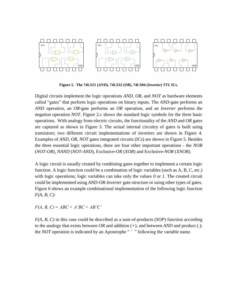
Figure 5. The 74LS21 (AND), 74LS32 (OR), 74LS04 (Inverter) TTL ICs.
Digital circuits implement the logic operations AND, OR, and NOT as hardware elements
called “gates” that perform logic operations on binary inputs. The AND-gate performs an
AND operation, an OR-gate performs an OR operation, and an Inverter performs the
negation operation NOT. Figure 2.c shows the standard logic symbols for the three basic
operations. With analogy from electric circuits, the functionality of the AND and OR gates
are captured as shown in Figure 3. The actual internal circuitry of gates is built using
transistors; two different circuit implementations of inverters are shown in Figure 4.
Examples of AND, OR, NOT gates integrated circuits (ICs) are shown in Figure 5. Besides
the three essential logic operations, there are four other important operations - the NOR
(NOT-OR), NAND (NOT-AND), Exclusive-OR (XOR) and Exclusive-NOR (XNOR).
A logic circuit is usually created by combining gates together to implement a certain logic
function. A logic function could be a combination of logic variables (such as A, B, C, etc.)
with logic operations; logic variables can take only the values 0 or 1. The created circuit
could be implemented using AND-OR-Inverter gate-structure or using other types of gates.
Figure 6 shows an example combinational implementation of the following logic function
F(A, B, C):
F(A, B, C) = ABC + A’BC + AB’C’
F(A, B, C) in this case could be described as a sum-of-products (SOP) function according
to the analogy that exists between OR and addition (+), and between AND and product (.);
the NOT operation is indicated by an Apostrophe “ ’ ” following the variable name.

A
BC
F(A, B, C)A
BCA
BC
Figure 6. AND-OR-Inverter implementation of the function F(A, B, C) = ABC + A’BC + AB’C’.
Programmable Logic
Basically, there are three types of IC technologies that can be used to implement logic
functions on (1), these are, full-custom, semi-custom, and programmable logic devices
(PLDs). In full-custom implementations, the designer cares about the realization of the
desired logic function to the deepest details including the transistor-level optimizations to
produce a high-performance implementation. In semi-custom implementations, the
designer uses some ready logic-circuit blocks and completes the wiring to achieve an
acceptable performance implementation in a shorter time than full-custom procedures. In
PLDs, the logic blocks and the wiring are ready. In implementing a function on a PLD, the
designer will only decide of which wires and blocks to use; this step is usually referred to
as programming the device.
Obviously, the development time using a PLD is shorter than the other full-custom and
semi-custom implementation options. The performance of a PLD varies according to its
type and complexity; however, a full-custom circuit is optimized for achieving higher
performance. The key advantage of modern programmable devices is their reconfiguration
without rewiring or replacing components (re-programmability). Programming a modern
PLD is as easy as writing a software program in a high-level programming language.
The first programmable device which achieved a widespread use was the Programmable
Read-Only Memory (PROM) and its derivatives Mask-PROM, and Field-PROM (the
Erasable or Electrically Erasable versions). Another step forward took place in this field
which led to the development of PLDs. Programmable Array Logic (PAL), Programmable
Logic Array (PLA), and Generic Array Logic (GALs) are commonly used PLDs designed
for small logic circuits and referred to as Simple-PLDs (SPLDs). Other types, the Mask-
Programmable Gate Arrays (MPGAs), were developed to handle larger logic circuits.
Complex-PLDs (CPLDs) and Field Programmable Gate Arrays (FPGAs) are more
complicated devices that are fully programmable and instantaneously customizable.
Moreover, FPGAs and CPLDs have the ability to implement very complex computations

with millions of gates devices currently in production. A classification of PLDs is shown
in Figure 7.
Figure 7. Typical PLD devices classification.
Programmable Logic Arrays
A Programmable Logic Array (PLA) is a simple programmable device (SPLD) used to
implement combinational logic circuits. A PLA has a set of programmable AND gates,
which link to a set of programmable OR gates to produce an output (see Figure 8).
Implementing a certain function using a PLA requires the determination of which
connections among wires to keep. The unwanted routes could be eliminated by burning the
switching device (possibly a fuse or an antifuse) connecting different routs. The AND-OR
layout of a PLA allows for implementing logic functions that are in an SOP form.
Technologies usually used to implement programmability in PLAs include fuses or
antifuses. A fuse is a low resistive element that could be blown (programmed) to result in
an open circuit or high impedance. An antifuse is a high resistive element (initially high
impedance) and is programmed to be low impedance.
Boolean expressions can be represented in either of two standard forms, the sum-of-
products (SOPs) and the product-of-sums (POSs). For example, the equations for F (an
SOP) and G (a POS) are as follows:
F(A, B, C) = ABC + A’BC + AB’C’
G(A, B, C) = (A + B + C) . ( A’ +B + C) . (A + B’ + C’)
A product term is a term consisting of the AND (Boolean multiplication) of literals (A, B,
C, etc.). When two or more product terms are summed using an OR (Boolean addition),
the resulting expression is an SOP. A standard SOP expression F(A, B, C, …) is one where
all the variables appear in each product term. Standardizing expressions makes evaluation,
simplification, and implementation much easier and systematic.
PLDs
SPLDs
PLA PAL GAL
High-density PLDs
CPLDs FPGAs

The implementation of any SOP expression using AND-gates, OR-gates, and inverters,
could be easily replaced using the structure offered by a PLA. The algebraic rules of
hardware development using standard SOP forms are the theoretical basis for designs
targeting PLAs. The design procedure simply starts by writing the desired function in an
SOP form, and then the implementation works by choosing which fuses to burn in a fused-
PLA.
Standard Multiple
AND Gate SymbolAND Array
Symbol
Standard Multiple
OR Gate Symbol
OR Array
Symbol
A B C
Figure 8. A 3-input 2-output PLA with its AND Arrays and OR Arrays. An AND array is equivalent
to a standard multiple-input AND gate, and an OR array is equivalent to a standard multiple-input
OR gate.
In the following two examples, we demonstrate the design and implementation of logic
functions using PLA structures. In the first example, we consider the design and
implementation of a three variables majority function. The function F(A, B, C) will return
a 1 (High or True) whenever the number of 1s in the inputs is greater than or equal to the
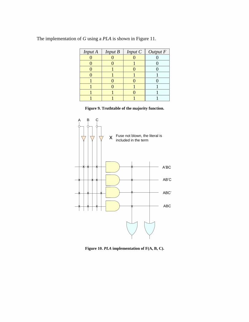
number of 0s. The truthtable of F is shown in Figure 9. The terms that make the function
F return a 1 are the terms F(0, 1, 1), F(1, 0, 1), F(1, 1, 0), or F(1, 1, 1). This could be
alternatively formulated as in the following equation:
F = A’BC + AB’C + ABC’ + ABC
In Figure 10, the implementations using a standard AND-OR-Inverter gate-structure and a
PLA are shown.
Another function G(A, B, C, D) could have the following equation:
G = A’B + AB’CD + BC’ + ABD + B’C’D’
The implementation of G using a PLA is shown in Figure 11.
Input A Input B Input C Output F
0 0 0 0
0 0 1 0
0 1 0 0
0 1 1 1
1 0 0 0
1 0 1 1
1 1 0 1
1 1 1 1
Figure 9. Truthtable of the majority function.
A B C
x x x
x x x
x x x
x x x
x
x
x
x
x Fuse not blown, the literal is
included in the term
A’BC
AB’C
ABC’
ABC
Figure 10. PLA implementation of F(A, B, C).

B C D
G
x x
x x x
x x
x x x
x
x
x
x
x Fuse not blown, the literal is
included in the term
A’B
AB’CD
BC’
B’C’D’
A
x
Figure 11. PLA implementation of G(A, B, C, D).
Early PLAs
Near the beginning of 1970s, companies like Philips, Texas Instruments, National
Semiconductor, Intersil, IBM (2) and Signetics introduced early PLA and PLA-based
devices. Early PLAs had limited numbers of input/output ports (around twenty), array cells
count (from hundreds to few thousands), and speeds (with around 1 to 35 nanoseconds
delay). Later PLAs performed with greater speeds (with around 2 to 5 nanoseconds delay),
with array sizes of thousands of cells, and input/output ports number of around 100 (3).
Currently, some PLA-structures are parts of high-density, high-performance, and complex
programmable logic devices (CPLDs).
Currently, PLAs are available in the market in different types. PLAs could be standalone
chips, or parts of bigger processing systems. Standalone PLAs are available as Mask
Programmable (MPLAs) and Field Programmable (FPLAs) devices. Mask Programmable
PLAs are programmed at the time of manufacture, while Field Programmable PLAs can be
programmed by the user with a computer-aided design (CAD) tool.

PLAs in Modern Complex Systems and Areas of Application
PLAs have largely motivated the development of many modern programmable systems.
PLAs are usually used as parts of more complicated processing systems. PLAs have also
inspired the creation of complex PLA-based systems with PLA-like structure. The available
variety of PLAs and PLA-based systems paved the way for their employment in many areas
of application.
The CoolRunner II CPLD from Xilinx uses a PLA type structure. This device has multiple
function blocks (FBs). Each function block contains sixteen macrocells, the function blocks
are interconnected by an advanced interconnect matrix (AIM). A basic architectural block
diagram for the CoolRunner II with a greatly simplified diagram of a function block (FB)
is shown in Figure 12.
.
.
.
I/O
Macrocell 1
.
.
.
Macrocell 2
Macrocell 3
Macrocell 16
...
1
. . . 1256
14
0...
16
AIM
FB
FB - I/O
FB - I/O
.
.
.
FB - I/O
.
.
.
FB - I/O
FB - I/O
Figure 12. Architectural block diagram for the CoolRunner II.
The CoolRunner II series of CPLDs contains from 32 macrocells to 512 macrocells. The
number of function blocks range from 2 to 32. The PLA structure contains a programmable
AND array with 56 AND-gates, and a programmable OR array with 16 OR-gates. With the
PLA structure, any product term can be connected to any OR gate to create an SOP output.
Each FB can produce up to 16 SOP outputs each with 56 product terms.
The main additions to the traditional PLA structure in a device like CoolRunner II are the
complex macrocells. A macrocell can be configured for combinational logic or sequential
logic (with availability of flip-flops). The macrocell in a CoolRunner II also contain an

XOR-gate to enable complementing the SOP output (coming from the PLA OR-gate) to
produce a POS form. A 1 on the input of the XOR-gate complements the OR output (a POS
form is produced) and a 0 keeps the output uncomplemented (in an SOP form). Choices
between SOP forms and POS forms, various clock inputs, flip-flop include or bypass, are
done using different multiplexers.
Another famous device with a PLA-like structure is the ICT Programmable Electrically
Erasable Logic (PEEL) Array (4). PEEL Arrays are large PLAs that include macrocells
with flip-flops. The PEEL Array structure is shown in Figure 13 with its PLA-like planes;
the outputs of the OR-plane are divided into groups of four, and each group can be input to
any of the logic cells. The logic cells, depicted in Figure 14, provide registers for the sum
terms and can feed-back the sum terms to the AND-plane. The logic cells can also connect
the sum terms to the Input/Output pins. The multiplexers each produce an output of the
logic cell and can provide either a registered or combinational output. Because of their
PLA-like planes, the PEEL Arrays are well-suited to applications that require SOP terms.
Logic Cells
I/O
Pins
Input
Pins
Figure 13. Main components in the architecture of ICT PEEL Arrays.

J
Q
Q
K
SET
CLR
D, T, J
Global Preset
Global Reset
To AND
Array
To I/O
Pins
System
Clock
From 4
Sum
Terms
Figure 14. Structure of PEEL Array Logic Cell.
The Multiple ALU Architecture with Reconfigurable Interconnect Experiment System
(MATRIX) is another modern architecture that benefits from the PLA architecture (5). The
MATRIX architecture is unique in that it aims to unify resources for instruction storage and
computation. The basic unit (BFU) can serve either as a memory or a computation unit.
The 8 BFUs are organized in an array, and each BFU has a 256-word memory, ALU-
multiply unit and reduction control logic. The interconnection network has a hierarchy of
three levels; it can deliver up to 10 GOPS with 100 BFUs when operating at 100 MHz. The
MATRIX controller is composed of a pattern matcher for generating local control from the
ALU output, a reduction network for generating local control, and a 20-input, 8-output NOR
block which serve as half of a PLA.
One famous application of PLAs is to implement the control over a datapath in a processor.
A datapath controller usually follows predefined sequences of states. In each control state,
the PLA part of the controller will determine what are the datapath control signals to
produce and what is the next state of the controller. The design of the controller usually
starts by formulating different states and transitions using a state diagram. The state
diagram is then formulated in a truthtable form (state transition table), where SOP
equations could be produced. The derived SOP equations are then mapped onto the PLA.
A design example of a datapath controller is shown in Figures 15, 6, 17 and 18. Figure 16
shows a typical controller state diagram. Figure 17 depicts the block diagram of the
datapath controller. Figure 18 suggests a PLA implementation of the controller.
Many areas of application have benefited from PLAs and PLA-based devices, such as,
cryptography (6), signal processing (7), computer graphics (8), image processing (9), data
mining (9), networking (10), etc.

System Description
Synthesis
Place, Route, and Timing Analysis
Downloading the generated bitstream
to the programmable device
HDL
Representation
Netlist
Bitstream file and the
expected propagation
delay
Figure 15. The process of hardware describe-and-synthesize development for programmable logic
devices.
State 0
Instruction
Fetch
State 1
Instruction
Decode
State 2
Calculate
Memory
Address
Load/Store
State 3
Memory
Read
Load
State 4
Memory
Write
Store
State 5
Execute
ALU Operation
State 6
Writeback
State 7
Branch
Figure 16. A design example of a datapath controller; the State Diagram.

CPU Control Element
Implemented on a PLA
Current
State
Next
State
Input
Instruction
Opcode
Output
Control
Signals
Figure 17. A design example of a datapath controller; Control Element block diagram
Figure 18. A design example of a datapath controller; PLA internal implementation.
Wired-AND
Wired-OR
Sum-of-Products Expressions
Next State
Opcode Bits
Current State
Control Signals

Programming PLAs
Traditional PLAs are usually programmed using a PLA device programmer (like traditional
PROMs and EPROM-based logic devices). Some more complex PLA-based devices, such
as CPLDs, can be also programmed using device programmers; nevertheless modern
CPLDs are in-circuit programmable. In other words, the circuit required to perform device
programming is provided within the CPLD chip. In-circuit programmability makes it
possible to erase and reprogram the device without an external device programmer.
Modern CPLDs, including the internal PLA-like structures, benefit from the latest advances
in the area of hardware/software co-design. Descriptions of the desired hardware structure
and behavior are written in a high-level context using hardware description languages
(HDLs), such as VHDL or Verilog. The description code is then compiled and downloaded
in the programmable device prior to execution. Schematic captures are also an option for
design entry. Schematic captures has become less popular especially with complex designs.
The process of hardware describe-and-synthesize development for programmable logic
devices is shown in Figure 15.
Hardware compilation consists of several steps. Hardware synthesis is the first major step
of compilation, where an intermediate representation of the hardware design (called a
netlist) is produced. A netlist is usually stored in a standard format called the Electronic
Design Interchange Format (EDIF) and it is independent of the targeted device details. The
second step of compilation is called place and route, where the logical structures described
in the netlist are mapped onto the actual macrocells, interconnections, and input and output
pins of the targeted device. The result of the place and route process is a usually called a
bitstream. The bitstream is the binary data that must be loaded into the PLD to program it
to implement a hardware design.
The renewable usefulness of PLAs
PLAs and their design basis have witnessed a renewable importance and have been the
choice of designers for many systems as well as the target of different design
methodologies. The renewable usefulness of PLAs is clear from the number of
investigations carried out relying based on PLAs.
A sub-threshold circuit design approach based on asynchronous micro-pipelining of a
levelized network of PLAs is investigated in (11). The main purpose of the presented
approach is to reduce the speed gap between sub-threshold and traditional designs. Energy

saving is noted when using the proposed approach in a factor of four as compared to a
traditional designed network of PLAs.
In (12) the authors propose a maximum crosstalk minimization algorithm taking logic
synthesis into consideration for PLA structures. To minimize the crosstalk, technique of
permuting wires is used. The PLA product terms lines are partitioned into long set and short
set, and then product lines in long set and short set are interleaved. The interleaved wires
are then checked for the maximum coupling capacitance for the aim of reducing the
maximum crosstalk effect of the PLA.
A logic synthesis method for an AND-XOR-OR type sense-amplifying PLA is proposed in
(13). Latch sense-amplifiers and a charge sharing scheme are used to achieve low-power
dissipation in the suggested PLA.
Testable design for detecting stuck-at and bridging faults in PLAs is suggested in (14). The
testable design is based on Double Fixed-Polarity Reed-Muller Expressions (DFPRMs).
An XOR part is proposed in the design implemented in a tree structure to reduce circuit
delay.
A VLSI approach addressing cross-talk problem in Deep Sub-Micron (DSM) IC design is
investigated in (15). Logic netlists are implemented in the form of a network of medium
sized PLAs. Two regular layout "fabrics" are used in this methodology, one for areas where
PLA logic is implemented, and another for routing regions between logic blocks.
In (16), a PLA-based performance optimization design procedure for standard-cells is
proposed. The optimization is done by implementing circuits’ critical paths using PLAs.
PLAs are proven to be good for such a replacement approach as they exhibit a gradual
increase in delay as additional items are added. The final optimized hybrid design is to
contain standard cells and a PLA.
A performance-driven mapping algorithm for CPLDs with many PLA-style logic cells is
proposed in (17). The primary goal of the mapping algorithm is to minimize the depth of
the mapped circuit. The algorithm included applying several heuristic techniques for area
reduction, threshold control of PLA fan-outs and product terms, slack-time relaxation, and
PLA-packing.
The attractions of PLAs that brought them to mainstream engineers include their simplicity,
relatively small circuit area, predictable propagation delay, and ease of development. The
powerful-but-simple property brought PLAs to rapid prototyping, synthesis, design
optimization techniques, embedded systems, traditional computer systems, hybrid high-

performance computing systems, etc. Indeed, there has been renewable interests in working
with the simple AND-to-OR PLAs.
Bibliography.
[1] F. Vahid et al., Embedded System Design: A Unified Hardware/Software Introduction,
New York: John Wiley & Sons, 2002.
[2] R. A. Wood, High-speed dynamic programmable logic array chip, IBMJ. Res. Develop,
379–383, 1975.
[3] Symmetrical Programmable Logic Array, US Pat. 4431928, Z. E. Skokan
[4] S. Brown and J. Rose, Architecture of FPGAs and CPLDs: A Tutorial, IEEE Design
and Test of Computers, 2: 42–57, 1996.
[5] E. Mirsky and A. DeHon, MATRIX: A reconfigurable computing architecture with
configurable instruction distribution and deployable resources, Proc. IEEE Workshop on
FPGAs for Custom Computing Machines, 157 – 166, 1996.
[6] R.W. Ward and T.C.A. Molteno, A CPLD coprocessor for embedded cryptography,
Proc. Electronics New Zealand Conf. 2003.
[7] S. Pirog, M. Baszynski, J. Czekonski, S. Gasiorek, A. Mondzik, A. Penczek, R. Stala,
Multicell DC/DC converter with DSP/CPLD control, Power Electronics and Motion
Control Conf. 677-682 2006.
[8] J. Hamblen, Using Large CPLDs and FPGAs for Prototyping and VGA Video Display
Generation in Computer Architecture Design Laboratories, IEEE Computer Society
Technical Committee on Computer Architecture Newsletter, 12-15, 1999.
[9] A. Esteves, A. Proença, A hardware/software partition methodology targeted to an
FPGA/CPLD architecture, Proc. Jornadas sobre Sistemas Reconfiguráveis, 2005.
[10] Z. Diao, D. Shen, V.O.K. Li, CPLD-PGPS scheduling algorithm in wireless OFDM
systems, Proc. IEEE Global Telecom. Conf. 6: 3732-3736, 2004.
[11] N. Jayakumar, R. Garg, B. Gamache, and S. P. Khatri, A PLA based asynchronous
micropipelining approach for subthreshold circuit design, Proc. Annu. Conf. on Design
Automation, 419–424, 2006.

[12] Y. Liu, K. Wang, and T. Hwang, Crosstalk minimization in logic synthesis for PLA,
Proc. Conf. on Design, Automation and Test in Europe, 2:16–20, 2004.
[13] H. Yoshida, H. Yamaoka, M. Ikeda, and K. Asada, Logic synthesis for AND-XOR-
OR type sense-amplifying PLA, Proc. Conf. on Asia South Pacific Design
automation/VLSI Design, 166, 2002.
[14] H. Rahaman, and D. K. Das, Bridging fault detection in Double Fixed-Polarity Reed-
Muller (DFPRM) PLA, Proc. Conf. on Asia South Pacific Design Automation, 172–177,
2005.
[15] S. P. Khatri, R. K.Brayton, and A. Sangiovanni-Vincentelli, Cross-talk immune VLSI
design using a network of PLAs embedded in a regular layout fabric. Proc. IEEE/ACM
Conf. on Computer-Aided Design, 412–419, 2000.
[16] R. Garg, M. Sanchez, K. Gulati, N. Jayakumar, A. Gupta, and S. P. Khatri, A design
flow to optimize circuit delay by using standard cells and PLAs. Proc. ACM Great Lakes
Symposium on VLSI, 217–222, 2006.
[17] D. Chen, J. Cong, M. D. Ercegovac, and Z. Huang, Performance-driven mapping for
CPLD architectures. Proc. ACM/SIGDA Symposium on Field Programmable Gate Arrays,
39–47, 2001.
Reading List
T. Floyd , Digital Fundamentals with PLD Programming, New Jersey: Prentice Hall,
2006.
M. Mano et al., Logic and Computer Design Fundamentals, New Jersey: Prentice Hall,
2004.
Cross-references
Programmable Logic Devices, See PLDs.
Synthesis, See High-level Synthesis
Design, See Logic Design