FLUKE 4270A BCD PROGRAMMABLE POWER SOURCE
186
GB PIN 338418 AUG. 1975 JOHN FLUKE MFG . CO. , INC. Scans by ARTEK MEDIA => PO. Box 43210 M ount l 3ke Terrace, W as h ing ton 98043 MODEL BCD PROGR AMMABLE POWER SOURCE
-
Upload
khangminh22 -
Category
Documents
-
view
0 -
download
0
Transcript of FLUKE 4270A BCD PROGRAMMABLE POWER SOURCE

GB
PIN 338418
AUG. 1975
JOHN FLUKE MFG. CO. , INC.
Scans by ARTEK MEDIA =>
PO. Box 43210 Mount l3ke Terrace, Washington 98043
MODEL
BCD PROGRAMMABLE POWER SOURCE


WARRANTY The JOHN FLUKE MFG. CO., INC.' warrants each instrument manufactured by them to be free from defects in material and workmanship. Their obligation under this Warranty is limited to servicing or adjusting an instrument returned to the factory for that purpose, and to making good at the factory any part or parts thereof; except tubes, fuses, choppers and batteries, which shall, within one year after making delivery to the original purchaser, be returned by the original purchaser with transportation charges prepaid, and which upon their examination shall disclose to their satisfaction to have been thus defective. If the fault has been caused by misuse or abnormal conditions of operations, repairs will be billed at a nominal cost. In this case, an estimate will be submitted before work is started, if requested.
If any fault develops, the following steps should be taken:
1. Notify the John Fluke Mfg. Co., Inc.: giving full details of the difficulty, and include the Model number, type number, and serial number. On receipt of this information, service data or shipping instructions will be forwarded to you.
2. On receipt of the shipping instructions, forward the instrument prepaid, and repairs will be made at the factory. If requested, an estimate will be made before the work begins, provided the instrument is not covered by the Warranty.
"The foregoing warranty is in lieu of all other warranties, express or implied, including but not limited to, any implied warranty of merchantability, fitness Or adequacy for any particular purpose or use. Fluke shall not be liable for any special, incident or consequential damages."
SHIPPING
All shipments of John Fluke Mfg. Co., Inc.' instruments should be made via United Parcel Service or "Best Way"" prepaid. The instrument should be shipped in the original packing carton; or if it is not available, use any suitable container that is rigid. If a substitute container is used, the instrument should be wrapped in paper and surrounded with at least four inches of excelsior or similar shock-absorbing material.
CLAIM FOR DAMAGE IN SHIPMENT
The instrument should be thoroughly inspected immediately upon receipt. All material in the container should be checked against the enclosed packing list. The manufacturer will not be responsible for shortages against the packing sheet unless notified immediately. If the instrument fails to operate properly, or is damaged in any way, a claim should be filed with the carrier. A full report of the damage should be obtained by the claim agent, and this report should be forwarded to John Fluke Mfg. Co., Inc.' Upon receipt of this report, you will be advised of the disposition of the equipment for repair or replacement. Include the model number, type number, and serial number when referring to this
instrument for any reason.
The John Fluke Mfg. Co., Inc.' will be happy to answer all application questions which will enhance your use of this instrument. Please address your requests to: JOHN FLUKE MFG. CO., INC., P. O. Box 7428, SEATTLE, WASHINGTON 98133'.
, For European customers: FLUKE (Nederland) B.V. Ledeboerstraat 27 Tilburg, Netherlands
"For European customers, Air Freight prepaid.
Fluke Western Technical Center Mike Nagy, Service Manager 2020 North Lincoln St. Burbank, CA 91504 Tel. 213-849-4641 TWX: 910-497-2086
Fluke Western Technical Center Tom Marshall, Service Manager 4805 Mercury St. San Diego, CA 92111 Tel. 714-565-4455 TWX: 910-337-1273
Fluke Western Technical Center Attn: Tom Marshall 2359 De La Cruz Blvd Santa Clara, CA 95050 Tel. 408-244-1 505 TWX: 910-338-0121
Fluke S.W. Technical Center Mel Suelzle, Service Manager Unit4 1980 South Quebec Street Denver, CO 80231 Tel. 303-750-1228
Rev. 5175
FLUKE TECHNICAL SERVICE CENTERS Fluke S.E. Technical Center Jesse Morse, Service Manager P.O. Box 6578 940 North Fern Creek Avenue Orlando, FL 32803 Tel. 305-896-2296 TWX: 810-850-0185
Fluke Midwestern Tech Center Bruce Hunt, Service Manager 1287 North Rand Road Des Plaines, I L 60016 Tel. 312-298-7470 TWX: 910-233-4978
Fluke Mideastern Tech Center John Hines, Service Manager 11501 Huff Court Kensington, MD 20795 Tel. 301-881-5300 TWX: 710-825-9645
Fluke N.E. Technical Center Dick Zemba, Service Manager 109 Massachussetts Ave. Lexington, MA 02173 Tel. 617-861-8620 TWX: 710-826-1715
Fluke Midwestern Tech Center Robert Wayne, Service Mgr. 10800 Lyndale Avenue South Minneapolis, MN 55420 Tel. 612-884-4541 TWX: 910-576-3141
Fluke Eastern Technical Center Bernard Ciongoli, Service Mgr. 101 Berkshire Ave. Paterson, NJ 07502 Tel. 201-742-3215 TWX: 710-988-5945
Fluke Eastern Technical Center Fran k Forte, Service Manager 4515 Culver Road Rochester, NY 14622 Tel. 716-342-6940 TWX: 510-253-6145
Fluke S.E. Technical Center Dwain Cox, Service Manager P.O. Box 9619 1310 Beaman Place Greensboro, NC 27408 Tel. 919-273-1918 TWX: 510-925-1173
Scans by ARTEK MEDIA =>
John Fluke Mfg. Co., Inc. Bill Fetrow, Tech. Services Spvr. 7001 - 220th S.w. Mountlake Terrace, WA 98043 Tel. 206-774-2238 TWX: 910-449-2850
Fluke Canadian Technical Center Tony Unser, Service Manager 640 11th Ave. S.w. Calgary, Alberta Tel. 403-261-0780 TWX: 610-821-2233
Fluke Canadian Technical Center Herb Duval, Service Manager 6427 Northam Drive Mississauga, Ontario Tel. 416-678-1500 TWX: 610-492-2119

SECTION
1
2
3
4270A
Tabl e of Contents
TITLE
INTRODUCTION AND SPECIFICATIONS
1-1.
1-6. INTRODUCTION SPECIFICATIONS
OPERATING INSTRUCTIONS
2-1.
2-3.
2-6.
2-8.
2-10.
2-12.
2-14.
2-16.
2-18.
2-20.
2-22.
2-24.
2-27.
2-29.
2-33.
2-35.
2-38.
2-41.
245. 2-47.
INTRODUCTION
SHIPPING INFORMATION
INPUT POWER . . . .
RACK INST ALLA TION .
OPERATING FEATURES
OPERATING NOTES .
AC Line Connection.
Load Connections
Remote Sensing . .
Ground Connections
Guard Connections .
PROGRAMMING INFORMATION.
Standby. . . . . . . . .
Range/Output Magnitude/Polarity
Data Strobe . . . . . . .
Flag Outputs . . . . . . .
Programmable Current Limiting.
External Reference . .
Front Panel Indicators .
Dynamic Characteristics
THEORY OF OPERATION . . . .
3-1.
3-3.
3-5.
3-14.
3-16.
3-18.
INTRODUCTION
FUNDAMENTAL CIRCUIT DESCRIPTION
BLOCK DIAGRAM ANALYSIS. . . . . CIRCUIT DESCRIPTIONS
Al Mother Board and A7 BCD Display (4270A-1011)
A2 Power Supply and AlO Connector Board (4270A-1061
and 4270A-1012) . . . . . . . . . . . . .
Scans by ARTEK MEDIA =>
PAGE
1-1
1-1 1-3
2-1
2-1
2-1
2-1
2-2
2-2 24 24 2-4
24 2-4
2-4
2-5
2-5
2-5
2-6
2-7
2-7
2-7
2-8
2-8
3-1
3-1
3-1
3-1
3-3 3-3
3-3
(continued on page ii)

4270A
TABLE OF CONTENTS, continued
SECTION TITLE
3-40. A3 Preamplifier (4275A-1051) 3-58. A4 External Reference (4250A-I041) .
3-66. . A5 BCD Ladder (42lOA-I031) . . . 3-74. A6 Isolated Control Logic (4275A-I02l) . 3-91. A8 Programmable Current Limiter (4270A-I081) 3-109. A9 Power Amplifier (4270A-I071) .
4 MAINTENANCE. . . . . . . .
5
6
7
8
4-1. 4-3. 4-6.
4-7. 4-9. 4-11. 4-13. 4-15.
4-17.
4-19.
4-20. 4-21.
INTRODUCTION . . . SERVICE INFORMATION GENERAL MAINTENANCE.
Cleaning. . . . Air Filter Cleaning Fuse Replacement
MAINTENANCE. . INVERTED CONTROL LOGIC .
CALIBRATION ..... . Initial Procedure. . . . .
Power Amplifier Bias Adjustment. Bit Adjustment (0.4) . . . .
4-22. Zero, Reference, and Bit Adjustment 4-23. External Reference Adjustment (-03 Option) 4-25. Current Limiter Adjustment (-06 Option) 4-27. Final Zero Adjustment . 4-29. Output Checks
LISTS OF REPLACEABLE PARTS
5-1. INTRODUCTION . . 5-4. HOW TO OBTAIN PARTS
OPTIONS AND ACCESSORIES. . .
6-1. 6-3. 6-5.
INTRODUCTION . . . OPTION INFORMATION. ACCESSORY INFORMATION
Option -07 lOOuV Resolution Schematic Diagram 4210A-1032
Option -09, Multi-Strobe Isolated Logic Schematic Diagram
Model A4200 Manual Control Unit Schematic Diagram A4200-1000
Rack Mounting Fixtures
Programming Connector
Extender PCB Assembly and Cable Extender Assembly
GENERAL INFORMATION.
SCHEMATIC DIAGRAMS
ii
PAGE
3-4 3-5 3-6 3-7 3-11 3-12
4-1
4-1 4-1 4-1 4-1 4-1 4-1 4-2 4-3
4-3
4-3
4-5 4-5
4-6 4-6 4-6 4-7 4-7
5-1
5-2 5-2
6-1
6-1 6-1 6-1
7-1
8-1
FIGURE
1-1.
1-2.
2-1.
2-2.
2-3.
2-4.
2-5.
2-6.
2-7.
2-8.
2-9.
2-10.
2-1l.
2-12.
3-1.
3-2.
3-3.
3-4.
3-5.
4-1.
5-1.
5-2.
5-3.
5-4.
5-5.
5-6.
5-7.
4270A
List of Illustrations
TITLE
Outline Drawing . . . . . .
Programming Connector Pin Assignments.
Input Power Switching. . .
Power Supply Switch Location
Accessory Rack Mounting Kits
Front Panel Operating Features
Rear Panel Operating Features
Remote Sensing Connections .
Guarded Load Connection. .
Isolated Control Logic Timing (-01 Option).
Accuracy Versus External Reference Frequency
AC External Reference Feedthrough Versus Frequency (OV Output) .
AC External Reference Phase Shift Versus Frequency. . . .
AC External Reference Harmonic Distortion Versus Frequency
Power Source Equivalent Circuit.
Model 4270A Block Diagram .
Ladder Decade (Simplified) .
Ladder Driver (Simplified) . .
Isolated Control Logic (Simplified) .
Assembly, Adjustment, and Test Point Locations
Binary Programmable Power Source
Mother PCB Assembly . . .
Power Supply PCB Assembly .
Pre-Amplifier PCB Assembly .
External Reference PCB Assembly (-03 Option)
Binary Ladder PCB Assembly.
Isolated Control Logic . . .
iii
PAGE
1-4
1-5
2-1
2-2
2-2
2-3
2-3
2-4
2-5
2-7
2-8
2-9
2-9
2-9
3-1
3-2
3-6
3-7
3-9
4-4
5-5
5-6
5-11
5-16
5-19
5-23
5-27
(continued on page iv)

4270A
LIST OF ILLUSTRA nONS, continued
FIGURE
5-8.
5-9.
5-10.
5-11.
6-1.
6-2.
6-1.
6-2.
6-3.
64.
6-5.
6-6.
6-7.
6-8.
6-9.
6-10.
6-11.
6-1.
6-2.
6-3.
64.
6-5.
6-6.
6-7.
6-8.
6-9.
6-10.
6-11.
TITLE
PCB Display PCB Assembly . .
Programmable Current Limit (-06 Option)
Power Amplifier . . . . . . . . .
H.V. Power Supply and Connector Board.
OPTION -07 100uV RESOLUTION
Ladder Decade (Simplified)
BCD Ladder PCB Assembly
OPTION -09 MULTI-STROBE ISOLATED LOGIC
4200-09 Connectors . .
Multiple 4200 Connections
BCD Program Data, Typical 16-Bit Data Word 8-Bit Control Word
BCD Program Data Typical 18-Bit Data Word, 6-Bit Control Word
Binary Program Data, Typical 16-Bit and 18-Bit Data Words
Multiple Mainframe Addressing . .
Status Busses Layout . . . . .
4200-09 Simplified Block Diagram
4200-09 Block Diagram . . . .
Input Sequence - Timing Diagram .
4200 Multi-Strobe Isolated Logic Card.
MODELA4200
Model A4200 Manual Control Unit Connected to Typical Power Source
Connectors, Controls, and Indicators . . . . . . . .
External Trigger Generator Requirements. . . . . . .
Programming in the Auto Mode (421OA,4250A, and 4270A)
A4200 Manual Control Unit Block Diagram .
Model A4200 MCU Timing Diagram
Mother Board Al Connector Assembly PCB .
Manual Control Unit
Connector Assembly PCB (A4200-4001)
Program Assembly
Function Assembly
iv
PAGE
5-28
5-33
5-39
541
6-3
6-5
6-2
6-2
6-8
6-9
6-10
6-13
6-14
6-16
6-19
6-21
6-37
6-1
6-3
64
6-8
6-9
6-15
6-17
6-19
6-20
6-21
(continued on page v)

LIST OF ILLUSTRATIONS, continued
FIGURE
6-l.
6-2.
6-3.
64.
6-l.
6-l.
6-2.
6-3.
RACK MOUNTING FIXTURES
Accessory Rack Mounting Kits .
Rack Mounting Bracket Installation
Dual Rack Mounting
Chassis Slide Installation
PROGRAMMING CONNECTOR
Male Programming Connector
TITLE
EXTENDER PCB ASSEMBLY AND CABLE EXTENDER ASSEMBLY
PCB Assembly Extender . . . . . . . . . . . . .
Extender PCB Assembly Installed in 421OA/4216A Instrument
Cable Extender Assembly. . . . . . . . . . . . .
PAGE
6-1
6-2
6-2
6-3
6-1
6-1
6-2
6-2
64. Extender PCB and Cable Extender Assemblies Installed in 4250A/4265A Instruments 6-3
6-5. Extender PCB and Cable Extender Assemblies Installed in 4270A/4275A Instruments 6-3
v
4270A

4270A
List of Tables
TABLE
1-1.
1-2.
2-1.
3-1.
4-1.
4-2.
4-3.
6-1.
6-2.
6-1.
6-2.
6-3.
64.
6-5.
6-6.
6-7.
6-8.
6-9.
6-10.
6-1.
6-2.
6-3.
64.
Options. . . . . . . .
Programming Input/Outputs .
Programming Connector Data
Operating Voltages . . . .
Recommended Test Equipment
Binary by Decade Coding
Linearity Checks. . .
OPTION -07 100uV RESOLUTION
Programming Input/Outputs
Resolution Check
MULTI-STROBE ISOLATED LOGIC
TITLE
Input/Output Signals, BCD Program Source
Input/Output Signals, Binary Program Source
4200-09 Jumper Requirements. . . . .
Mainframe Addresses - Pin Assignment. . .
Troubleshooting Chart, Inactive PCB Assembly.
Troubleshooting Chart, Data Errors at Parallel Outputs
Troubleshooting Chart, No Complimenting of Binary Data
Troubleshooting Chart, No Asynchronous Standby
Troubleshooting Chart, No Current Limit Flag. .
Troubleshooting Chart, No Power Fail and/or Abnormal Status Flags
MODEL A4200 MANUAL CONTROL UNIT
Programming Switches Controlled by the Binary Counter
4200A Series Instrument Ranges . . . .
Current Limit Programming With -06 Option
Current Limit Programming With -06 Option
vi
PAGE
1-2
1-5
2-6
3-3
4-3
4-5
4-7
6-2
6-3
6-3
6-5
6-7
6-13
6-22
6-24
6-25
6-26
6-27
6-28
6-5
6-7
6-7
6-7
4270A
Section 1
Introduction & Specifications
1-1. INTRODUCTION
1-2. The Model 4270A is a programmable, bipolar dc voltage source and ac power amplifier. Output voltage is from 0 to ±llOVdc in two ranges, 10 and XlOVdc. Programming resolution using the internal reference voltage is ImV on the 10 volt range and lOmV on the XlO volt range. Output accuracy is given in paragraph 1-6. After a lOOMS settling time, a READY flag indicates that the output has settled to ±0.01 % of the programmed level for a resistive load. The output current is rated at ±0.5 ampere maximum and is limited to approximately ±0.6 ampere in the event of an overload or short circuit. The sink current (milliamps) is rated at 500-4.5E OUT maximum. A Programmable Current Limiter (Option -06) is available to allow programming the maximum output current to a lower level. A current limit flag indicates when a sink or source current overload exists with or without the -06 Option.
1-3. Programming requirements are compatible with DTL or TTL logic levels. Contact or relay closures can also be used. The voltage source is programmable using BCD or binary-per-decade coding, using 84-2-1 format. All programming inputs and flag outputs are made through a 50-pin Amphenol, Blue Ribbon connector located on the rear
panel. A +5Vdc output is also available at this connector and is used to provide power for external programming circuitry. Negative logic is employed for programming. The logic levels are as follows:
Logic "0" = +2.0Vdc to +5.0Vdc or open circuit. Logic "1" = 0 to +0.4Vdc or short circuit to
LOGIC GND.
14. Four options are available and provide tailoring of the power supply to fit application requirements. These options are identified by numeric designations -03, -06, -07, and -09. Each option is described in Table 1-1. The options can be installed at the factory when the instrument is ordered or in the field at a later time.
1-5. This power source is completely solid state. Plug-in printed circuit boards, with accessible test points and adjustments, are provided for ease in servicing. The unit is forced-air cooled. This results in lower component temperatures and higher reliability than would normally be obtained in a source of this power capability. The chassis is designed for bench top use, or it can be installed in a standard equipment rack by using the Accessory Rack Mount· ing Fixtures.
1-1

4270A
OPTIONS TITLE
--03 EXTERNAL REFERENCE (Field Installable)
--06 PROGRAMMABLE CURRENT LIMIT (Field Installable)
-07 100tlV RESOLUTION (Field Installable)
-09 MULTI-STROBE ISOLATED LOGIC (Field Installable)
1-6. SPECIFICATIONS
OUTPUT VOLTAGE
OUTPUT VOLTAGE RESOLUTION
OUTPUT CURRENT
CURRENT SINK CAPABILITY.
ACCURACY (1SoC to 35°C, 90 days) .
STEADY STATE RIPPLE AND NOISE (10 Hz to 10 MHz bandwidth)
SPEED .......... .
DIGITAL NOISE REJECTION
OUTPUT IMPEDANCE
EXTERNAL REFERENCE (Option -03)
Voltage Range. .
1-2
Input Impedance . Output Voltage
Output Current Frequency Range.
Table 1-1. OPTIONS
DESCRIPTION
Allows the use of an external signal source in place of the internal refer-ence voltage. Any dc or ac signal can be used that has an amplitude from 0 to ± 14.5 volts dc or peak ac and a frequency from dc to 30 kHz. Input impedance is 100k, in parallel with 70pF.
Programmable current limit is provided in two ranges, 50mA and 0.5 ampere. Each range may be programmed in 10% increments from 10% to 110% of range.
The -07 Option provides 100tlV resolution on the 10V range and 1mV on the X10V range.
Permits any of the Fluke 4200 series Programmable Voltage Sources to be remotely controlled by a large variety of program sources such as a computer, a system coupler, as well as a Fluke Automatic Test Equip-ment System. Refer to Section 6 for details.
o to ±9.999Vdc (BCD inputs) o to ± 16 .66SV dc (4-bit binary, by decade) ±99.99Vdc (BCD inputs) ±1100Vdc (4-bit binary, by decade) (Maximum output terminal voltage = ±1100V)
lOV range: l.Om V (100tlV option -07) XlOV range: lOmV (1mV option -07)
o to ±0.5 (Short circuit protected at 0.6 ampere)
Isink (rnA) = 500 - 4.5Eout (Overload protected) Maximum voltage = ±llOV
lOV range: ±(0.01 % of program +lOOtlV) XlOV range: ±(0.01 % of program +700tlV)
lOV range: 2.lmV POp S00tlV rms X10V range: 3.6mV Pop l.2mV rms
Settles to 0.1 % of the programmed change in 80tlS Settles to 0.01 % of the programmed change in 11Otls. A range change does not increase settling time.
Noise between digital programming ground and the analog output is rejected 1000: 1 (6Odb) at IMHz
0.04 milliohms @dc; 1 phm @ 30 kHz
o to ±14.5Vdc or peak ac lOOk ohms in parallel with 70 pF 10V range: 0 to 12V rms, ± 17V peak XIOV range: 0 to 78V rms, ±llOV peak 3SOmA rms, 0.5 amp peak dc to 30 kHz

Accuracy . . . . . . . . . . (15°C to 35°C, 90 days with respect to the External Reference, EXR)
Programming Resolution . .
PROGRAMMABLE CURRENT LIMIT (Option -06)
OUTPUT STABILITY
TEMPERATURE COEFFICIENT . . . (Temperatures between 15° and 35°C)
LOAD REGULATION .
LOAD RECOVERY.
LINE REGULATION
BARRIER STRIP TERMINALS.
PROGRAMMING CONNECTOR (See Table 1-3)
INPUT POWER .
ENVIRONMENTAL Temperature Relative Humidity Shock Vibration Altitude.
SIZE (See Figure 1-1) .
ACCESSORIES
Manual Control Unit
Rack Mounting Brackets
Programming Mating Connector .
Extender PCB Assembly
Cable Extender Assembly. . .
lOVrange: ±(0.01%ofprogram+.0001% 75 + 100~V) at dc EXR
X10V range: ±.0001% 75 +700"N at dc.
EXR
lOV range: EXR x 10-4 volts X10V range: EXR x 10-3 volts
50mA range: ±5mA to ±55mA in 5mA increments 0.5 amp range: ±50mA to ±0.55 amp in 50mA increments Minimum program possible: ±5mA
lOV range: ±(lOppm of program +40J..lV) for 24 hours ±(30ppm of program + 70J..lV) for 90 days X10V range: ±(10 ppm of program +280J..lV) for 24 hours ±(30ppm of program +490J..lV) for 90 days
lOV range: ±(10ppm of program +5J..lV per °C) XlOV range: ±lOppm of program +35J..lV per °C)
An output current change of 0.5 ampere causes the output voltage to change less than 0.001 % of range
The output voltage will settle to within 0.01 % of final value in 11OJ..lS after an output current change of 0.5 ampere
The output voltage will change less than 0.001 % of range for a ±10% change in line voltage
4270A
EXT REF LO, EXT REF HI, OUTPUT HI, SENSE HI, SENSE ' LO, OUTPUT LO, GUARD and CHASSIS. Terminals are located on the rear panel. The GUARD terminal can be floated up to 1000 volts above chassis ground.
A 50-pin connector is located on the rear panel. Mating connector is Amphenol, Blue Ribbon, Part No. 57-30500, and is included with each power source.
loo/115/125/200/230/250Vac ±1O% 50 to 60 Hz, 200 watts fully loaded
O°C to 50°C operating; -40°C to 75°C storage o to 80% 20G, 11 millisecond half-sine wave 4.5G, 10 to 55 Hz o to 10,000 feet operating 50,000 feet and above-non-operating
5 W' high x 17" wide x 197/16" (Max.) deep
Allows manual checkout, calibration, and control FLUKE Model A4200 • M05-205-600 • MOO-260-610 (18") • MOO-280-610 (24") Amphenol, Blue Ribbon 57-30500 FLUKE PART NO. 266056
FLUKE PART NO. 292623
FLUKE PART NO. 337584
1-3

4270A
1-4
~~ ____ 17" ____ ~~ 2 1/4" ~
111"'-----11 ~i T 51/4"
1 9/16"
..L T~I~ _____ 19 7/16"------~~
FRONT VIEW SIDE VIEW
Figure 1-1. OUTLINE DRAWING
Table 1-2. PROGRAMMING INPUT/OUTPUTS
PROGRAM CONTROL: All program control and response lines are compatible with DTL and TTL logic Programming lines are brought out on the rear panel on Amphenol connector J1. See Figure 1-2.
LOGIC LEVELS: Logic "1" = 0 +.4Vdc or contact Logic "0" = +2.0 to +5.0Vdc or open closure circuit
SIGN: Connector Pin 35 Logic "1" = Negative output voltage
MAGNITUDE: Bit Conn. Bit Conn. Bit Conn. Wt. Pin Wt. Pin Wt. Pin
AS 1 CII 9 ES 43 A4 2 ~ 10 E4 44 A2 3 C2 11 E2 45 Al 4 C1 12 El 46 BII 5 DII 13 -B4 6 D4 14 (-07 Option) B2 7 D2 15 Bl 8 Dl 16
NOTE: Decade numbers greater than 9 (10 thru 15) will be accepted and converted to an equivalent analog value. The maximum full scale output is ± 11 OVdc.
DATA STROBE: Connector pin 33. When using the Isolated Control Logic Option -01, a strobe pulse is required to start the digital-to-analog conversion process after a valid command is present. Minimum pulse width is 500 nanoseconds. A negative leading slope (+5V to OV transition) is required.
RANGE: Connector Pin 29; Logic "0" = Low Voltage Range, Logic "1" = High Voltage Range.
EXTERNAL Connector Pin 36; Logic "0" = Internal DC Reference, Logic "1" = External REFERENCE: Reference.
STANDBY: Connector Pin 34; Logic "0" = Operate Mode, Logic "1" = Standby; Output is ~ 1% of programmed value.
CURRENT LIMIT:
RESPONSE SIGNALS:
CURRENT LIMIT FLAG:
READY/NOT READY FLAG:
READY/NOT READY FLAG:
POWER CONNECTIONS:
LOGIC GROUND:
MOST SIGNI
FICANT DIGIT
LEAST SIGNIFICANT DIGIT
LOGIC GROUND
+5VDC
{ :!=~ A 2 __ 3
Al 4
B8=5
B4 __ 6 -B2 __ 7 -BI __ 8 -
c8 __ 9 -
c4 __ 10-
c2 __ 11-
{ ~= ~! ~ D2 15
DI =16=
17 18
__ 19_
__ 20 __ 21 __ 22 __ 23 __ 24 _
__ 25_
4270A
Table 1-2. PROGRAMMING INPUT/OUTPUTS
Connector Pin Function Logic "1" Logic "0"
42 Range 0.5 amp 50mA
43 Magnitude 80% of Range o All "O"s = 44 Magnitude 40% of Range o 10% of range 45 Magnitude 20% of Range 0 46 Magnitude 10% of Range 0
Connector Pin 49; Logic "1" represents a current limit condition.
Connector Pin 37; Logic "0" = "Ready" condition following a 110l1s delay 'to allow the output to settle to within 0.01 % of the programmed increment for a resistive load.
Logic "1" = "Not Ready" condition, the power source is in the process of settling to the programmed value.
Connector Pin 25; An internal, isolated power supply furnishes +5Vdc current limited by 2.7 ohms for use by the external system interface logic.
Connector Pins 17 It is recommended that a large logic ground strap be used be-thru 24; tween the interface logic and the power source to reduce the
Jl
digital programming noise on the system ground.
~~ } NOT USED 28
~~ -} :::~:'E:OLTS 32 33 _STROBE 34 _STANDBY 35 _SIGN 36 _ EXT REF 37 _ RDY/RDY
_ 38 } _ 39 _ 40 NOT USED
_ 41
42 _ RANGE, CURRENT 43 _80% RANGE [!>
_ 44 _40% RANGE ~ 45 _20% RANGE 46 _ 10% RANGE
47 }NOT USED 48 49 _I LIMIT 50 _NOT USED
-06 OPTION
[l:::> -07 OPTION NOT USED
[t::> USE OF -07 OPTION SUBSTITUTES FOR -06 OPTION AND PROVIDES LEAST SIGNIFICANT DIGITS ON J1 PINS AS FOLLOWS:
43 - E8 44 - E4 45 _ E2
46 - El
Figure 1-2. PROGRAMMING CONNECTOR PIN ASSIGNMENTS
1-5/1-6

4270A
Section 2
Operating Instructions
2-1. INTRODUCTION
2-2. This section contains information regarding install-ation and operation of the Model 4270A. It is recommended that the contents of this section be read and understood before any attempt is made to operate this power source. Should any difficulties be encountered during operation, please contact your nearest John Fluke Sales Representative, or the John Fluke Mfg. Co., Inc., P.O. Box 43210, Mountlake Terrace, Washington 98043, telephone (206) 774-2211. A list of Sales Representatives is located in Section 7 of this manual.
2-3. SHIPPING INFORMATION
24. The Model 4270A was packaged and shipped in a foam-packed cardboard carton. Upon receipt, a thorough inspection should be performed to reveal any instrument damage incurred in transit. Special instructions for inspection and claims are included in the carton.
2-5. If reshipment of this power source is necessary, the original container should be used. If the original container is not available, a new one can be obtained from the John Fluke Mfg. Co., Inc. Please reference the Model number when requesting a new shipping container.
2-6. INPUT POWER
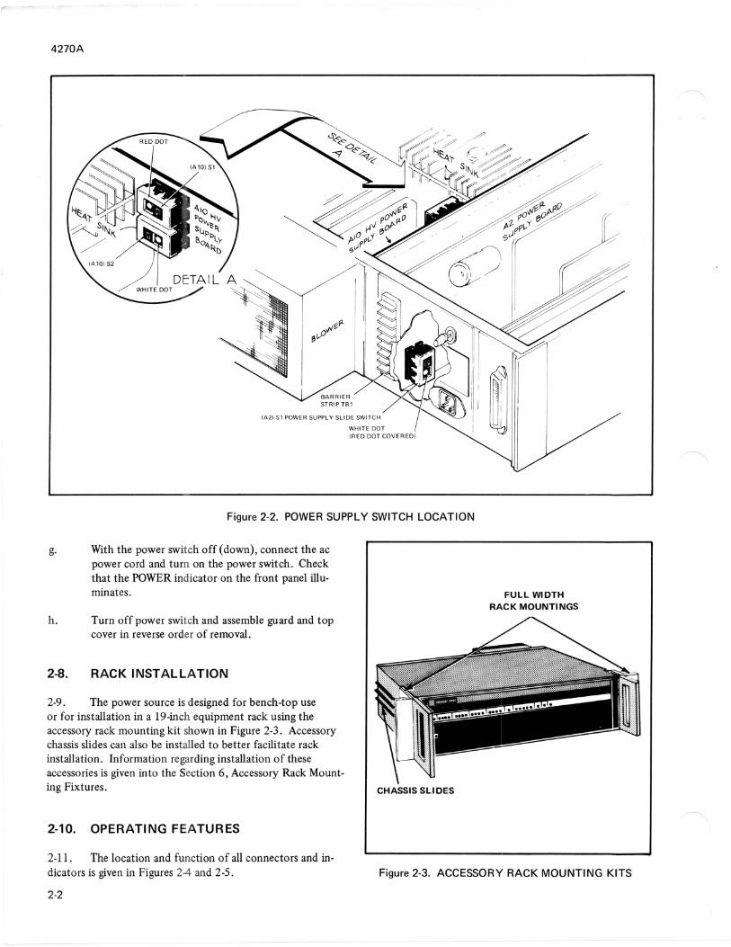
2-7. This power source can be operated from a 50 to 60 Hz power line ranging from 100 to 250 volts ac. A decal on the rear panel indicates the power input limits. Specific power line voltages require that slide switches internal of the instrument be set as indicated in Figure 2-1 or on the lower left corner of the guard cover. To accommodate the instrument to the specific power line voltage, proceed as follows:
LINE SWITCH POSITIONS VOLTAGE PWR SPLY H - V PWR SUPPLY
100 115 125 200 230 250
a.
b.
c.
d.
e.
f.
(A21 S1 (A101 S1 (A101 S2
WHT WHT RED WHT RED WHT WHT RED RED RED WHT RED RED RED WHT RED RED RED
Figure 2-1. INPUT POWER SWITCHING
Determine the ac line voltage and relate its value to the closest value shown in Figure 2-1. Remove the power cord.
Remove the top cover of the instrument.
Remove the top inner guard cover.
Refer to Figure 2 -2 and locate the three slide switches in the instrument.
Refer to Figure 2-1 and set the three power switches such that the color dot showing corresponds to the color given for the specific line voltage that was selected in step a.
Refer to the decal on the rear panel of the instrument, determine the appropriately rated fuse for the line power selected in step a., and install the fuse in the fuse holder.
2-1
4270A
STRIPTB1
IA 2) Sl POWER SUPPLY SLI DE SW ITCH
WHIT E DOT IRE D DOT COVE RED )
Figure 2-2. POWER SUPPLY SWITCH LOCATION
g. With the power switch off (down), connect the ac power cord and turn on the power switch. Check that the POWER indicator on the front panel illuminates.
h. Turn off power switch and assemble guard and top cover in reverse order of removal.
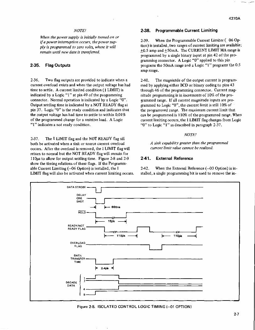
2-8. RACK INSTALLATION
2-9. The power source is designed for bench-top use or for installation in a 19-inch equipment rack using the accessory rack mounting kit shown in Figure 2-3. Accessory chassis slides can also be installed to better facilitate rack installation. Information regarding installation of these accessories is given into the Section 6, Accessory Rack Mounting Fixtures.
2-10. OPERATING FEATURES
2-11. The location and function of all connectors and in-
CHASSIS SLI DES
FULL WIDTH RACK MOUNTINGS
dicators is given in Figures 24 and 2-5 . Figure 2-3. ACCESSORY RACK MOUNTING KITS
2-2

4270A
STATUS INDICATORS (-02 OPTION ONL V) Illuminate to indicate the programmed level and status of the power sou rce
...
Illuminates when the power source is energized
Figure 2.4 FRONT PANEL OPERATING FEATURES
BARRIER STRIP Contains the analog input!
output terminals.
EXT REF (-03 Option) Receives a 0 to ± 14. 5 Vdc or
peak ac signal having a fre
quency from dc to 30 kHz.
Provide connection to the
load . See para 2-16.
See
GUARD TERMINAL Provides for load connections
that reduce errors caused by
common mode signals. See
para 2 -22.
CHASSIS TERMINAL Provides con nection to chassis
and earth ground. See para 2-20.
FUSE
± SENSE TERMINALS Provide four terminal load
connection. See para 2 -1 8.
POWER SWITCH Toggle switch used to energize the power source. A POWER Indicator on the front panel illuminates when the power source Is energized.
throu gh the power cord·
to line power.
PROGRAMMING CONNECTOR, FEMALE, AMPHENOL Contai ns the digital input/output connections required for programming. An accessory mating connector (not shown) is provided.
Protects the ac Input circuitry.
100, 115, l25VAC 200,230, 250VAC
2A , AGC lA. AGC
Figure 2-5. REAR PANEL OPERATING FEATURES
2-3

4270A
2-12. OPERATING NOTES
2-13. The following paragraphs describe various condi-tions which should be considered before operating the Model 4270A.
2-14. AC Line Connection
2-15. The input power cord plug is a three prong, polar-ized connector. This plug allows connection to a 100 to 250 volts ac, 50 to 60 Hz, power line (see Input Power, paragraph 2-6), and connects the power source chassis to earth ground. Always ensure thiJt the ground pin is connected to a high quality earth ground. The power source is energized through a toggle switch on the rear panel.
2-16. Load Connections
2-17. An eight terminal barrier strip, located on the rear panel, serves as an analog input/output connector for the power source. The ± power output terminals (OUTPUT HI and LO) provide connection to the load. The ±sense terminals (SENSE HI and LO) are provided to allow remote sensing at the load. The sense terminals are bussed through jumpers installed at the factory to the output terminals. If remote sensing is not required,the load is connected to the respective ± output terminals and the sensing busses are not removed. If remote sensing is required, the busses must be removed and separate sense lines provided between the sense terminals and the load. In either case, NEVER operate the power source with the sense terminals disconnected. The CHASSIS terminal is connected directly to the chassis and allows grounding of the load through the input power cord, if desired. The GUARD terminal allows load connections that can greatly reduce errors caused by common mode signals. This guard connection should always be used if optimum noise free performance is to be achieved.
2-18. Remote Sensing
2-19. When a load is connected to the OUTPUT terminals, the I-R drop across the output power leads may be excessive in some applications. If the rated accuracy of the power supply is required at the load, remote sensing must be used. For this reason, SENSE HI and SENSE LO terminals are provided to allow the power supply output to be sensed directly at the load, thus compensating for any I-R drop in the output power leads. Figure 2-6 shows an example of remote sensing load connections.
24
NOTE!
The two jumpers on the barrier strip which bus ± output must be removed for remote sensing. When remote sensing, always use a twisted pair P of insulated wire from the output and sense terminals to the load. A maximum of 0.35
volts (at 25°C, decreasing 0.002 volts per degree C at higher temperatures) is allowable between either output terminal and its corresponding sense terminal. The leads between the output and sense terminals and the load must be large enough to carry the load current of up to 0.5 ampere and the sense current of about 1 rnA without exceeding this voltage.
POWER SOURCE • P ~
JUMPER REMOVE;) FOR REMOTE SENSING
JUMPER REMOVED FOR REMOTE SENSING
TWISTED PAIR WIRES
Figure 2-6. REMOTE SENSING CONNECTIONS
2-20. Ground Connections
2-21. A CHASSIS terminal is provided at the rear panel. This terminal is directly connected to the chassis of the power source and earth ground through the ground pin on the input power plug. If grounding of the load is desired, this terminal provides a convenient connection to earth ground. When a guarded output (explain in paragraph 2-22) is not desired, this terminal should be connected to the GUARD terminal.
2-22. Guard Connections
2-23. The power source is equipped with a guard shield that isolates its internal circuitry from the chassis and ground. A GUARD terminal at the rear panel is connected to this shield and allows load connections that greatly reduce errors caused by common mode Signals. The guard may be driven ___ to a maximum of 1000 volts above chassis ground. Figure 2-7 shows a simplified diagram of a guarded load connection.

2-24. PROGRAMMING INFORMATION
2-25. All instrument functions, with the exception of ac power switching and control, are controlled via a mating pair of 50-pin Amphenol connectors located on the instrument rear panel. The female Amphenol connector is rigidly attached to the rear panel and a mating male connector, less cabling, is supplied with each instrument as a separate accessory. These Amphenol connectors establish the interface between the instrument and the programming equipment. Cabling is to be provided by the instrument user who determines pin utilization and cable length to satisfy his individual requirements. The instrument is powered via a rear panel toggle switch and not through the programming connector. Table 2-1 is a tabular listing that functionally describes each connector pin. Cable/connector assembly data is given in Section 6, Accessory Programming Connector.
2-26. Programming input requirements are compatible with either DTL or TTL logic levels. Logic "0" is +2.0 to 5.0Vdc or open circuit to logic ground. Logic "1" is 0 to +0.4Vdc or short circuit to logic ground. Logic ground is available at pins 17 through 24 of the programming connector. Shorting these lines to the appropriate pins of the programming connector using contact closures also allows control of the power source. The internal +5Vdc output, current limited by 2.7 ohms, is available at pin 25 for use by the external programming lOgic.
DIGITAL INPUTS
L.---r--' I I
TC1 I
CASE L_r_J (CHASSIS) C2
4270A
2-27. Standby
2-28. The STANDBY mode can be programmed by apply-ing a Logic" 1 " to pin 34 of the programming connector. When this condition exists, the output of the power source will be driven to less than 1 % of the programmed value. Application of a logic "0" at this pin returns the output voltage to the programmed level.
2-29. Range/Output Magnitude/Polarity
2-30. Two voltage ranges are available; ±.10 volts and ±.X1O volts. The RANGE is programmed by a single binary input at pin 29 of the programming connector. A Logic "0" applied to this pin will program the ±.1O volt range, and a Logic "1" will program the ±.XI0 volt range. The power supply is capable of an output of ±.l1OVdc minimum at ±.0.55 ampere.
2-31. The magnitude of the output voltage is programmed by applying either BCD or four bit binary-per-decade coding, using 8-4-2-1 format, to pins 1 through 16 of the program connector. Four decades of programmable voltage are available; each receives a four-bit 84-2-1 coded input. The maximum program of any decade is (8+4+2+1) 15, which provides a total output program of ±.16.665 volts on the 10 volt range with a programmable resolution of ImV. If BCD coding is used, the maximum programmable output on the 10 volt range is ±.9.999 volts. When using the X10
E em
C1 = CIRCUITRY TO GUARD CAPACITANCE C2 = GUARD TO CASE CAPACITANCE E = COMMON MODE VOLTAGE
em
Figure 2-7. GUARDED LOAD CONNECTION
2-5

4270A
Table 2-1. PROGRAMMING CONNECTOR DATA
LOGIC "0"= +2.0 to +5.0Vdc or open circuit LOGIC "1"= 0 to +O.4Vdc or short circuit to LOGIC GRD
PIN NO. FUNCTION
2-6
1 2 3 4 5 6 7 8 9
10 11 12 13 14 15
CODE 8 4 2 1 8 4 2 1 8 4 2 1 8 4 2
A DECADE: 1V-10V range 10V-100V range
B DECADE: 1V-10V range 1V-100V range
C DECADE: 0.01V-10V range 0.1 V-1 OOV range
o DECADE: 0.001D-10V range IT> 0.01V-100Vrange
16 1 17 18 20 21 LOGIC GRD 22 23 24 25 LOGIC PWR (+5Vdc, current limited by
2.7 ohms internally) 26 27 NOT USED 28 29 RANGE:
30 31 32 33
34
36
37
38 39 40
LOGIC "0" = 10 VOLT Range (± 16.665V max) LOGIC "1" =100 VOLT Range (±110V max)
NOT USED
DATA STROBE (-01 Option) (See Figure 2-8) INITIATES DIGITAL TO ANALOG CONVERSION
STANDBY/OPERATE: LOGIC "0" = OPERATE LOGIC "1" = STANDBY
EXTERNAL REFERENCE (-03 Option): LOGIC "0" = INTERNAL REFERENCE LOGIC "1" = EXTERNAL REFERENCE
READY/NOT READY FLAG: LOGIC "0" = READY LOGIC "1" = NOT READY
NOT USED
41 CURRENT LIMIT: (-06 Option) [r:>
42 Function Logic "0" Logic "1" 43 Range 100mA 1amp
44 Magnitude o (All "O"s = 80% of range
45 Magnitude o 10% of range) 40% of range
45 Magnitude 0 20% of range
46 Magnitude 0 10% of range
47 48 NOT USED
49 CURRENT OVERLOAD FLAG: LOGIC "0" = NORMAL LOGIC "1" = OVERLOAD (Over-Current)
50 NOT USED
[I:::> Least significant digit when -07 Option (100~V Resolution) is not used.
§::::>Use of -07 Option substitutes for -06 Option and provides least significant digits in an E Decade; i.e., E8 , E4 , E2, E I •
volt range, which has a program resolution of lOmV, it should be noted that the maximum input program can ex· ceed the output voltage capability of the power source. The maximum program using four bit binary-per-decade coding in 8-4-2-1 format is ±166.65 volts, while BCD coding provides a maximum program of ±99 .99 volts. The maximum output voltage, however, is ±110 volts.
2-32. Polarity of the output is controlled by a single in-put (SIGN) at pin 35 of the program connector. A Logic "0" will produce a positive output. A Logic "1" will produce a negative output.
2·33. Data Strobe
2-34. The DATA STROBE shown in Figure 2-8 is required to initiate the transfer of the data present at the programming inputs to the internal memory of the Isolated Control Logic (-01 Option). The DATA STROBE is applied to pin 33 of the programming connector. Upon its negative transition, program data transfer begins. At the same time, two pulses are generated; 15~s and 110~s. The 15~ pulse holds the power supply output at its previously programmed level while new data is transferred into memory and allowed to settle. At the end of the 15~ pulse the power source is allowed to respond to the new program data. The 11 O~s pulse provides a NOT READY flag output that indicates the power source has not had time to respond to new program data and for the output to be within ±O.O 1 % of the programmed change for a resistive load. Program data must be present and settled for a minimum of 2.4~s after the negative transition of the DATA STROBE.
NOTE!
When the power supply is initially turned on or if a power interruption occurs, the power supply is programmed to zero volts, where it will remain until new data is transferred.
2-35. Flag Outputs
2-36. Two flag outputs are provided to indicate when a current overload exists and when the output voltage has had time to settle. A current limited condition (I LIMIT) is indicated by a Logic" 1 " at pin 49 of the programming connector. Normal operation is indicated by a Logic "0". Output settling time is indicated by a NOT READY flag at pin 37. Logic "0" is the ready condition and indicates that the output voltage has had time to settle to within 0.01% of the programmed change for a resistive load. A Logic "1" indicates a not ready condition.
2-37. The I LIMIT flag and the NOT READY flag sill both be activated when a sink or source current overload occurs. After the overload is removed, the I LIMIT flag will return to normal but the NOT READY flag will remain for 11OJ.lS to allow for output settling time. Figure 2-8 and 2-9 show the timing relations of these flags. If the Programmable Current Limiting (-06 Option) is installed, the I LIMIT flag will also be activated when current limiting occurs.
DATA STROBE -u DELAY ONE --, I SHOT L-...J
~ ~ 800ns
HciLi5---, ~I I I-- 15JJs --...j
READY/NOT
READY FLAG ~.f I I-- 110JJs ---I
4270A
2-38. Programmable Current Limiting
2-39. When the Programmable Current Limiter (-06 Option) is installed, two ranges of current limiting are available; ±0.5 amp and ±SOmA. The CURRENT LIMIT MA range is programmed by a single binary input at pin 42 of the programming connector. A Logic "0" applied to this pin programs the SOmA range and a Logic "1" programs the 0.5 amp range.
240. The magniutde of the output current is programmed by applying either BCD or binary coding to pins 43 through 46 of the programming connector. Current magnitude programming is in increments of 10% of the programmed range. If all current magnitude inputs are programmed to Logic "0", the current limit is still 1 0% of the programmed range. The maximum current limit that can be programmed is 110% of the programmed range. When current limiting occurs, the I LIMIT flag changes from Logic "0" to Logic" 1 " as described in paragraph 2-37.
NOTE!
A sink capability greater than the programmed current limit value cannot be realized.
2-41. External Reference
242. When the External Reference (-03 Option) is installed, a single programming bit is used to remove the in-
OVERLOAD __________________________ ~
FLAG
DECADE DATA
1=~==~------~------------------------------
4--~======~ __ -----------------------B~
Figure 2-8. ISOLATED CONTROL LOGIC TIMING (-01 OPTION)
2-7
4270A
ternal 10Vdc reference from the D-to-A ladder network and switch in an external signal source to replace it. The output accuracy and stability of the power source, however, is then relative to the accuracy and stability of the external signal source.
243. The external reference may be any dc or ac signal with an amplitude between 0 and ±14.5Vdc or peak ac (volts rms x 1.414) and have a frequency between dc and 30kHz. It is applied to the external reference terminals located on the rear panel barrier strip. The input impedance at these terminals is lOOk ohms in parallel with 70pF. The external reference is programmed by applying a Logic "1" to pin 36 of the programming connector. It should be noted that the polarity of the output will be the same as the external reference regardless of the SIGN (polarity) programmed.
244. Programming the magnitude of the output voltage with a ±1 0 volt external reference is accomplished by the same method used for programming with the internal reference voltage. (See paragraph 2-31). However, if the external reference is not exactly ±1O volts, the magnitude of the programming word required to obtain a specified output voltage must be calculated as follows:
MPW = Magnitude of the programming word
Eout = Output voltage (Vdc)
EXT REF = External reference voltage.
10 volt range: Eout MPW=
EXT REF
Programming resolution = EXT REF 7 10
100 volt range: MPW= Eout
EXT REF
Programming resolution = EXT REF 7103 Note: Eout .;;;; 1l0V
It should be noted that the rated output of the power supply is ±I1OV maximum at 0.55 ampere. It therefore becomes obvious that when using the X10 volt range, the programming word can easily exceed the output capability of the power supply. The following example, using the previously shown formula for the XI0 volt range, illustrates this.
Example:
Find: Eout
Given: EXT REF = 14.5Vdc MPW (BCD) = 9999. Range = 110 volts
2·8
EXT REF @ 14.5Vac MPW (BCD) = 9999 Range = 110 volts
MPW = Eout 103
EXT REF x
:.Eout = MPW x EXT REF 7103
Eout = 9999 x +14.5Vdc 7103
Eout = +144.9855Vdc
Eout in this example greatly exceeds the rated 110 volt output capability of the power supply. To avoid this situation always calculate MPW with Eout < I10Vdc or peak ac.
2-45. Front Panel Indicators
246. When the Front Panel Display (-02 Option) is in-stalled, status indicators (light emitting diodes) are provided on the front panel. They indicate the programmed output voltage level, output polarity, current overload, current limit levels, external reference, and standby status of the internal register. None of these indicators are provided when the Blank Front Panel (-05 Option) is installed. A POWER indicator is included with either option to indicate that the power is on.
2-47. Dynamic Characteristics
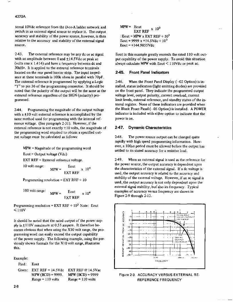
248. The power source output can be changed quite rapidly with high speed programming information. However, a 100J1s period must be allowed before the output has settled to its stated accuracy for a resistive load.
249. When an external signal is used as the reference for the power source, the output accuracy is dependent upon the characteristics of the external signal. If a dc voltage is used, the output accuracy is related to the accuracy and stability of the external voltage. However, if an ac signal is used, the output accuracy is not only dependent upon the external signal stability, buf also its frequency. Typical examples of accuracy versus frequency are shown in Figure 2-9 through 2-12.
>u
'" 0: :0
t! 0
'" u o :;; -10
~ -1
u... -20 z
4 6 B 1
5~-+ --~-++ 5- - + --, -,--
5 I I I I
----l j
I
I
4 6 B IV rms AND
T - IOV rms OUTPUT IOV RANGE
-- ;" ~. d I ~ -_.,-t-----~ ... IV.
Q -2 >'" -30
5 ---l---+--L..-. • r I I
r-----------r---i 50V rms '" 1 ,II •. ~ OUTPUT "
~ o -3
>- -40 ~ u -4 0:
5
5
~ -50
j I I I I
i I I
~ I 65V RANGE "'.
I -----tIl ! X. i ! \
'- I
lkHl IOkHI 40kHl
FREQUENCY
Figure 2·9. ACCURACY VERSUS EXTERNAL RE
REFERENCE FREQUENCY
100
90 .... ~ 80 .... ::J o
0
~ 60 a: .... 0
<5 40 >
0
0
6 8 2 4
! III II III I
1111 I II _,EXTERNAL REFERENCE = IOV rms
PROG RAMMED OUTPUT a VOLTS
1kHz
FREQUENCY
6 8 4
I lOOV I _ lI-RA,G
I/ f-
V-/1
1/ lOV
RI~N't,!.
.A" I
10kHz 40kHz
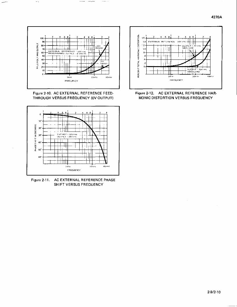
Figure 2-10_ AC EXTERNAL REFERENCE FEEDTHROUGH VERSUS FREQUENCY (OV OUTPUT)
2 6 8 2 4 6 8 2 4
I 100
:fl w 200
a: ~ " ;;:: 300
t;: I 400
'"
, ..... ~! 1 - "-I "' ! ,
EXT REF = lOVrms I'\. OUTPUT - 30V rms , \. ,
w
'" '" ~ 500 1\ , 600 I
\ i \
1kHz 10kHz 40kHZ
FREQUENCY
Figure 2-11. AC EXTERNAL REFERENCE PHASE SHIFT VERSUS FREQUENCY
1 1.6 2 4 6 8 2
4270A
4 6 8 I 2 4
1.
1.2
1.
4 EXTERNAL REFERENCE lOV,m, II III OUT~U~ 0
1 ~~ ,m' ~; Or-- r I IOn LOAD
I I I I ~
6f---- -1 t ~t ----- .. ~ ~IV 'f ~ J .4
I -+ ~ I
2 ----- --r- -"" I ~
i i I OUTPUT = 30V rms
I I lOOn LOAD
o
1kHz IDkH7 40kHz
FREQUENCY
Figure 2-12. AC EXTERNAL REFERENCE HARMONIC DISTORTION VERSUS FREQUENCY
2-9/2-10

3-1. INTRODUCTION
3-2. This section contains the theory of operation for the Model 4270A. The information is arranged under headings of "FUNDAMENTAL CIRCUIT DESCRIPTIONS, BLOCK DIAGRAM ANALYSIS, and CIRCUIT DESCRIPTIONS." An equivalent circuit of the power source is shown in Figure 3-1. Figure 3-2 is a simplified block diagram.
3-3. FUNDAMENTAL CIRCUIT DESCRIPTION
34. The Model 4270A converts a digital program word into a representative dc output voltage. Basically, the circuitry consists of a high gain operational amplifier shown in Figure 3-1. Digital to analog conversion is done using a ladder network driven by a bi-polar reference voltage. The differential amplifier then produces an output voltage (Vo) that is maintained by the current through Rf as determined
by the ratio ofVREF over Ro~V::F1
3-5. BLOCK DIAGRAM ANAL YSIS
3-6. The following paragraphs describe the major cir-cuit functions of the Model 4270A. A block diagram of the power source, including all options, is shown in Figure 3-2.
3-7. The Isolated Control Logic provides isolation and storage of the digital inputs. A STROBE input is required for any data transfer. The assembly also provides READY / NOT READY and CURRENT LIMIT FLAG outputs. Internal commands from the A6 LOGIC control polarity, range, magnitude, sample and hold, and current limiting of the output. These commands (except sample and hold) are also applied to the A 7 Display where visual status is provided on the front panel.
4270A
Section 3
Theory of Operation
3-8. All operating voltages as well as the internal reference voltage (VREF) are produced in the A2 Power Supply and the AlO Connector Board. Commands from the A6 Logic determine the polarity ofVREF applied to VREF bus line. A +POL command produces a -VREF and a -POL command a +VREF' Presence of either or both EXT REF and STDBY commands disable the internal VREF'
3-9. The A4 External Reference (-03 Option) pro-cesses the external reference input voltage. The magnitude of this voltage can be from 0 to ±14.SV dc or peak ac and have a frequency from dc to 30 kHz. Presence of an EXT REF command disables the previously described internal VREF and applies the output of the A4 External Reference to the VREF bus line. If a STDBY command exists, the external VREF is disabled.
3-10. BCD ladder networks in the A3 Preamplifier and AS BCD Ladder scale the selected internal or external VREF
RO",
y LADDER
~~ ~---.. Vo
Figure 3-1. POWER SOURCE EQUIVALENT CIRCUIT
3-1

4270A
INPUT
REF
A2PDWER
SUPPLY
Al0CONN
BOARD
(A4) -03 OPTION
EXT. REf
EXT (HIGH
INPUT LOW >+-~IY
tlEF STD8Y
'V A COMMO~ t---+-+---+-_----1 V L COMMON t---+-+----+--I
V REF COMMON I--t-t----t-----'
(AS) BINARY
LADDER
l00V RANGE
(FEEDBACK I
HIGH SENSE
H'GHI OUTPUT
LOW
LOW SENSE
DIGITAL INPUTS CURRENT LIMIT READY FLAG LIMIT COMMANDS ~ l A[;
Figure 3-2. MODEL 4270A BLOCK DIAGRAM
to a level determined by the A, B, and C commands. This scaled voltage is then inverted and amplified by voltage and power amplifier in the A3 Preamplifier and A9 Power Amplifier. Current through Rf in the A3 Preamplifier maintains a proportional output voltage dependent upon the value of Re, ladder, and polarity ofVREF. In the 10V range the total parallel value of Rf in combination with an internal VREF establishes an output in millivolts directly proportional to the digital input word. The value of Rf is increased by four times in the 100V range by disconnecting one of the Rf resistors. Subsequently, outputs in the lOOV range are four times the digital input word. When the external VREF is selected, the output is proportional to the combined effects of the external reference magnitude and the digital input word. Actual output is determined as follows:
10V Range: Eout = (MPW X 10-4) (EXT REF)
100V Range: Eout = (4MPW x 10-4) (EXT REF)
Where: MPW = Magnitude of digital input word EXT REF = External reference voltage
(V dc or peak ac):
3-11. Programming changes are prevented from appear-ing at the output until the entire digital input word is stored. This is provided through the sample and hold circuit in the A3 Preamplifier. Presence of a STROBE input to the A6 Logic produces a HOLD command which activates the sample and hold circuit. The sample and hold disconnects and
3-2
stores the last input to the voltage amplifier, thus providing a memory condition for the duration of tile HOLD command. The HOLD command has a duration of 15).Lsec.
3-12. Overload protection circuitry in the A9 Power Amp-lifier automatically limits the maximum uutput current to 0.6A_ Whenever a current limit occurs, ar, I LIMIT command is applied to the A6 Logic which then produces a CURRENT LIMIT FLAG output. Current limitmg at less than 0.6A is also possible using the A8 Programmable Current Limiter (-06 Option) described later. Clamp circuits in the A9 Power Amplifier limit voltage transients at the output during a current limit condition when the load is disconnected.
3-13. Current limiting at less than O.6A is provided upon installation of the A8 Programmable Current Limiter (-06 Option). Maximum bipolar output current can be limited to a level between 10 ma and 0.55 ampere in 10 percent steps on two separate reanges. In the event the output current is clamped at that level by action of the A8 Programmable Current Limiter. During periods of current limiting, an I LIMIT command is generated in the A9 Power Amplifier and is applied to the A6 Control Logic and to the A7 Front Panel. The I LIMIT command applied to the A6 Control Logic produces a CURRENT LIMIT FLAG at pin 4Y of the Programming Connector. The I LIMIT command applied to the A 7 Front Panel illuminates the I LIMIT indicator on the front panel.

3-14. CIRCUIT DESCRIPTIONS
3-15. The following paragraphs describe the circuitry in the power source. Each description is keyed to a schematic diagram located at the rear of the manual.
3-16. Al Mother Board and A7 BCD Display (4270A-l0ll )
3-17. The Al Mother Board serves to interconnect the A2 through A9 assemblies. No component circuitry other than connectors and amp pins are contained on this assembly. The A7 BCD Display provides light emitting diode (LED) indicators which display the internal command data and power on state. Internal commands of OV (true) are inverted by Ul through US and turn on the associated LED of Ql through Q27. Power on is indicated through direct application of -VL to Q1.
3-18. A2 Power Supply and Al0 Connector Board (4270A-l061 and 4270A-l012)
3-19. All operating voltages, as well as the internal refer-ence voltage upon which the power source accuracy and stability relies, are produced in the A2 and AlO assemblies. Designations and nominal magnitudes of each voltage is given in Table 3-1.
Table 3-1. OPERATING VOLTAGES
DESIGNATION VOL TAGE (VDC)
+VL +5V
-VL -5V
±VH ±136V * ±VA +23.4V, -25.1V
VREF ±10V
* Approximate (at 115V line voltage, no load)
3-20. INPUT POWER
3-21. Ac line power at 11 is applied to the primary of T1 through POWER switch S2 and the 115/230 switch SI. The primary of T1 consists of two windings which allow operation from either a 115 or 230V ac line. SI provides a parallel primary winding connection for 115V ac line operation. A series connection is provided for 230Y ac line operation. AC power for the blower (Ml) is provided from the primary windings of T 1. The four secondary windings of T 1 supply ac voltages to associated power supplies.
3-22. +VL SUPPLY
3-23. The +VL Supply, composed ofCRl9 and Q21 through Q24, produces a regulated +5V dc for use by the
4270A
A6 Logic and external programming equipment. Diode bridge CR19 rectifies the secondary voltage ofTI and supplies the series regulator of 021 through Q24 with a dc voltage. C16 mters the voltage applied to the regulator. 022 functions as a constant current source, supplying base drive to Q23. The resulting +5V output of the regulator is developed across CR23 and R54 which supplies a sample of the output voltage to the base of Q24. The conduction of Q24 will limit the base drive to Q21 and Q23 producing a regulated +5V output. This supply is completely isolated from all other supplies in the instrument and is electrically external of the guard. All other supplies are electrically inside the guard.
3-25. The -VL Supply composed ofCR14 and Q16 through Q18 produces the regulated -5V dc required to operate the internal logic circuits. Diode bridge CR14 rectifies the secondary voltage of T1 and supplies the series regulator of Q16 through Q18 with a dc voltage. Cl3 filters the rectified voltage. The base drive for Q18 and Q17 is derived from the +V A Supply through R44. Reference voltage for the base of Q 18 is derived from the -V A Supply through the divider consisting of R46 and R47. Any variation in the -5V output is then sensed by Q18, which controls the base drive to A17 and thus Q16, producing a regulated -5V dc output.
3-27. The ±V A Supply produces the regulated +23.4 and -25.1 V dc operating voltages that are used to provide power for most analog circuitry. Diode bridge CR4 rectifies the tapped secondary voltage of T 1 and supplies positive and negative voltages for the respective ± VA regulators. C7 and C8 fIlter these rectified voltages.
3-28. The +V A regulator consists of Q12, Q13 and U4. Reference voltage for this regulator is derived from A2 in the VREF supply and is applied to the non-inverting input of U4. The inverting input of U4 receives a sample of the output voltage from the divider, R36 and R37. Any variations in the +V A output are thus sensed by A4, which controls the base drive to Q12, producing a regulated +23.4V dc output. Q13 together with R33 function to limit the maximum output current of this supply to 125 rna. Should the current through R33 exceed 125ma, the voltage across R33 will turn on Q13 which limits the base current to Q12.
3-29. The -VA regulator consists of Q14, Q15, and US. R40 and the +V A supply establish the reference current for the feedback resistor R41. US supplies the base drive reqUired by Q15 to maintain the regulated output of -25.lV dc. 014 and R39 limit the output current in a similar manner to 013 and R33 described previously.
3-3

4270A
3-30. ± VH SUPPLY
3-31. The ± VH Supply (on A10) produces unregulated ±136 volts dc operating voltages for the A9 Power Amplifier. Diodes CR1 and through CR4 are connected as two full-wave rectifiers with C2 and C3 acting as filters. Resistors R2 and R3 function as discharge resistor for C2 and C3, respectively. Positive voltage regulation is accomplished by series pass element Q1 which is controlled by driver Q2. Reference voltage for the positive supply is established by Zener diodes CR5 and CR6. Regulation of the negative supply is accomplished by Q3, Q4, CR7, and CRS which function in a similar manner as the positive supply.
3-32. VREF SVPPLY
3-33. The VREF Supply produces an extremely stable ±lOV dc reference upon which the accuracy and stability of the power source is based. Circuitry of this supply consists of a stable reference amplifier V2, a differential amplifier VI, a series-pass element Q1, an inverter amplifier V3, and an emitter follower Q4.
3-34. The reference amplifier V2 contains matched zener and transistor elements which produce a time and temperature stabilized reference voltage. The zener element receives a portion ofits bias current from the +23.4V supply through R4 and CR1. The amplifier element receives collector current from the same source through R5. Base current for this amplifier is provided through a divider composed of R9, R14, R16, R56 and R59. This divider is connected to the +VREF sense line. The FET switches, Q2 and Q3, provide separate output and sense connections when a positive VREF is called. Should any variations occur on the +VREF sense line, V2 will amplify them with respect to the zener element reference. The change is then applied to one input of V I which also receives a sample of the + V REF line from the divider composed of R2 and R3. VI in tum amplifies the change and alters the conduction of Ql to maintain a constant +lOV output for +VREF sense. Variable resistor R9 allows adjustment of the sense line input to V2 and subsequently the +VREF sense level.
3-35. The inverter amplifier composed of V3 and Q4 pro-duces a -VREF. V3 is connected as an inverting, unity gain, amplifier. Emitter follower Q4 functions as an output buffer. Feedback through R19 and RlS controls the overall gain of both amplifiers. Variable resistor R19 adjust this feedback level and subsequently the resultant -V REF sense output level. Resistors R6 and R21 compensate for TC factors associated with FET gates in the ladder section driven by VREF.
3-36. GATE DRIVERS
3-37. The Gate Drivers of Q7 through QIl control the conduction of the FET switches associated with the V REF
3-4
Supply. When the power source has a positive output programmed, the command at pin IS is low (-5V), thus turning on QS, Q11 and switching off FET gates Q2, Q3. With Q8 on, the emitter-base junction of Q9 is reverse biased causing Q9 and QlO to turn off, thus turning on FET gates Q5, Q6, and Q25. The VREF output applied to pin D is therefore -10V when a positive output is programmed. Should a negative output be programmed, the command at pin IS is high (OV), which turns off QS and Qll and switches the FET gates Q2 and Q3 on. With QS cut-off, Q9 conducts and turns on QI0, thus switching the FET gates Q5, Q6, and Q25 off. As a result, the voltage at pin Dis +lOV when a negative output is called. Should the STANDBY or EXT REF mode be programmed, low (-5V) commands exist at pins S or V. These low inputs will turn on Q7 and QS, thus turning on both QlO and Qll and switch all FET gates off. As a result the VREF supply is completely disconnected from the VREF output terminals, B and D.
3-3S. RELA Y DRIVER
3-39. The Relay Driver composed of Ql9 and Q20 is used to energize Kl when the power source is turned on. The contacts of K1 then complete the connections to the OVTPUT connector. Whould the power source be shut off for any reason, the connections are broken and the load is not subjected to any unprogrammed voltage.
3-40. A3 Preampl ifier (4275A-1 051 )
3-41. The A3 Preamplifier produces a drive signal pro-portional to the input programming commands. This drive signal is applied to the A9 Power Amplifier which, in turn, produces the power source output. The circuitry consists of the four most significant bits of the binary ladder and associated switches and drivers, ladder clamps, voltage range switches, high impedance input stage, sample and hold, and output stage. '
342. BINARY LADDER
343. The four most significant bits of the Binary Ladder consist essentially of R26, R27 , R29 and R31. Their individual resistance values weigh the division factor necessary to scale VREF in respective AS, A4, A2, and Al bit weights. Selection of individual ladder resistors in done through associated ladder switches. Variable resistors R2S, R30, and R32 allow precise calibration of the A4, A2, and Al ladder bits to the AS bit. The resulting scaled VREF from these ladder bits is combined with the AS Binary Ladder input through R25 and applied to the input of QlSA. Feedback from the HIGH SENSE terminal at the output of the power source through resistances selected by the Voltage Range Switches drives the input to QlS to virtual analog common, in the manner of a high-gain operation amplifier.

344. LADDER SWITCHES AND DRIVERS
345. The Ladder Switches and Drivers Q1 through Q16, apply VREF or analog common V A common, to the ladder resistors under control of the A8, A4, A2, and Al bit commands. Each Ladder Switch-Driver combination functions in the same manner; thus only operation of the A8 bit is described.
346. The A8 ladder resistor is connected to V REF or analog common through Ql and Q2 or Q3, respectively. When an A8 command (OV) exists at terminal 18 of PI, bot Q4 and Q5 will be siwtched off. Q3 is switched off by its resulting -V A gate voltage and Q 1, Q2 are switched on by the resulting VR, gate voltage. With Q1 and Q2 conducting, VREF is applied to R26. Absence of an A8 command applies -5V to terminal 18 of PI and switches Q4 and Q5 on. The resulting OV gate voltage at Q3 switches it on and applies analog common to R26. Ql and Q2 are switched off by conduction of Q5, which applies -V A by their gates.
347. LADDER CLAMPS
348. The Ladder Clamps consisting ofCR5, CR6, R47 and R48 limit the summing junction voltage at the input of Q18. Clamp signals at terminals 7, 19, and W of PI turn on CRS or CR6 during a current limit condition. This minimizes any output voltage transients at the output of A9 Power Amplifier if the load causing the current-limit condition is suddenly removed.
349. VOLTAGE RANGE SWITCHES
3-50. The Voltage Range Switches and Drivers consisting of Q30 through Q34 select the appropriate feedback resistance and frequency compensation for the lOY and 100V range. In the lOY range, a -5V command is present at terminal 14 of Pl. This voltage turns off Q34 and Q33, which, in turn, switch on FET gates Q30 through Q32. Conduction of Q31 and Q32 connects R39, R40, R42, and R43 across R36 and R35. The end of this network that connects to pin 4 of PI ultimately becomes the HIGH SENSE terminal at the output of the power source. The frequency response of the Preamplifier in both voltage ranges is controlled by Q31. In the 32V range, conduction of Q30 by-passes R34 and C2, thus connecting only R33 and Cl to the Preamp-lifier output. In the 100V range, a OV command at terminal 14 of PI turns on Q34 and Q33 which turns off Q30 through Q32. With Q31 and Q32 off, only R35 and R36 are connected to the power source output (HIGH SENSE), thus increasing the total feedback resistance by four. The result-ing output voltage is subsequently four times the binary input commands. By connecting the MSB jumpers across R36 and R39 alters the feedback such that only output voltages corresponding to the most significant bit appear at the output. With Q30 offin the lOOV range, R33, Cl and R34, C2 are connected in series to establish the desired frequency response.
4270A
3-51. HIGH IMPEDANCE INPUT STAGE
3-52. Differential amplifier Q18 amplifies the Binary Ladder output with respect to analog common, V A common, such that feedback through resistance selected by the Voltage Range Switches produces a virtual analog common at the input of Q18A. Transistor Q19 functions as a constant current source, and Q20 provides temperature compensation. Variable resistor R61 provides adjustment to compensate for the input offset of Q18. Jumper selection of RS7 through RS9 and R62 provides coarse offset adjutment. Selection of Rp and RN in the drain circuit of Q 18 is done to provide a low temperature coefficient of input offset voltage. Diodes CR7 through CR12 limit the maximum voltage swing applied to the follOWing stage.
3-53. SAMPLE AND HOLD
3-54. The Sample and Hold circuitry consists of MOSFET gates Q21 , Q22, driver Q23, and capacitors C 10 and C 11. These capacitors provide memory during programming changes. Normally, a HOLD command (OV) is present at terminal P of PI and Q23 is conducting. This condition turns on Q21 and Q22 and the output of Q 18 is am plified by Q24, Q25. During programming changes, however, presence of a HOLD command (-5V) at terminal P of PI turns off Q23 and Q21, Q22. Capacitors C 10 and C 11 , which are connected to the inputs of Q24, then hold a sample of the last input from Q18 and hold the output voltage relatively constant for the duration of the HOLD command. The HOLD period is short enough and the circuit constants are chosen so that negligible output voltage change occurs. A secondary HOLD circuit composed of VI and Q35 through Q37 provides a clamp to analog ground at the input of Q18 during the HOLD command. Presence of a HOLD corrunand (-5V) presets J-K flip-flop Ul to provide a low Q output, which turns on Q37. Q36 is switched on by the resulting -VL common base signal and turns on Q35, which applies analog common to the base of Q 18.
3-55. Transistor Q26 functions as high impedance constant current source for Q25B. Q27 and Q28 amplify the output of Q25B and furnish a drive signal to Q29.
3-56. OUTPUT STAGE
3-57. Emitter follower Q29 provides a low impedance output signal at terminal 5 of Pl. This signal is applied to the A9 Power Amplifier which then produces the power source output.
3-58. A4 External Reference (4210A-1041)
3-59. The A4 External Reference is installed as the -03 Option. It receives and processes an external reference input having a frequency of dc to 30 kHz and a level from 0 to ±14.5V dc or peak ac. The circuitry consists of three dif-
3-5

4270A
ferential amplifiers and an emitter follower which form an operational amplifier. FET gates Q9 and QIO controlled by drivers QII and Ql2 apply the amplifier output and sense line to the V REF line in the A3 Preamplifier.
3-60. DIFFERENTIAL AMPLIFIER
3-61. The differential Amplifier consists of three in-dividual amplifiers: QI through Q8 and the emitter follower of Q13. The external reference input is applied through Rl and C9 to tone input of the differential FET, Q1.. This stage amplifies the input in respect to VREF common and provides a differential input to Q5. Feedback through Rl6 and R17 maintains the input of Ql at virtual VREF common. Adjustment of R17 controls the overall gain and subsequently the output VREF high at terminal 4. Variable resistor R6 allows zero offset adjustment of the output, VREF high. Jumper selection of R5 and R8 through RIO provides coarse adjustment of offset. Selection of RN and Rp in the drain circuit of Ql is done to provide a low temperature coefficient for the offset voltage. A constant current source for QI is provided by Q2, while TC compensation of the current source is provided by Q3. The differential Darlington composed of Q4 and Q5 amplifies the output of Ql and furnishes a singleended drive signal to Q7. This drive signal is developed across Q6 which functions as a high impedance, constant current source for Q4B. The final quasi-differential amplifier Q7 and Q8 supplies a drive signal to the emitter-follower output stage of Q13. This stage provides a low impedance output to drive the VREF high line. Q14 functions as a high impedance current source for Q13. Diodes CRI and CR2 provide connection to the feedback line when Q9 and Q10 are turned off.
3-62. FET GATES
3-63. The application of the external reference to the in-ternal stet lines is controlled by Q9 and QIO. Q9 connects the feedback line to VREF sense, and QIO connects the external reference to the internal VREF high line. Drivers QIl and Q12 control the on/off condition of Q9 and QIO in conjunction with the EXT REF and STANDBY commands at terminals 13 and M.
3-64. When an EXT REF command (OV) exists at termin-alB, Qll is turned off, and -VA is applied to both the emitter and base of Q 12. This condition turns off Q12 and switches FET gates Q9 and Q 10 on, thus applying the extemal reference to the internal VREF line. The same condition occurs when a STANDBY command (Oy) exists at terminal M. Diodes CR3 and CR4 provide isolation between the input command lines.
3-65. Should a STANDBY or EXT REF command (-5Y) exists, QII will be switched on and turn on Q12. Conduc-
, tion of Q12 applies -VA to the gates of Q9 and QIO which turns them off. This condition then disconnects the external reference from the internal VREFlines.
3-6
3-66. A5 BCD Ladder (421 OA-1 031 )
3-67. The A5 BCD Ladder contains a buffer amplifier for VREF and the three lower decade segments of a ladder network. The buffer amplifier produces a VR signal from VREF to prevent loading ofVREF by ladder switching currents. The ladder decades are voltage dividers weighted in fifteenths for control by digital words from I to 15 (8 + 4 + 2 + 1). The relative position of each decade with respect to the ladder output determines the significance of each decade's contribution to the total ladder network output.
3-68. BUFFER AMPLIFIER
3-69. The Buffer Amplifier composed of Ql through Q3 is a unity gain amplifier connected through CRI to function as a voltage follower. This circuit produces a VR Signal that is applied to the ladder driver circuits. Output impedance is sufficiently low from dc to 100 kHz to prevent loading by ladder switching currents.
3-70. LADDERS
3-71. The three lower decade ladders consists of Rl through R18. Each decade of the ladder is formed essentially by four resistors which in combination weigh the division factor of each decade in fifteenths. A simplified diagram of a typical decade ladder is shown in Figure 3-3.
VREF
"S" 25K
"4" 50K
OUTPUT (Vo)
"2" 100K
"1" 200K
v Vo IS AVAILABLE IN --1!f£. VOLT STEPS
15
Figure 3-3. LADDER DECADE (SIMPLIFIED)

3-72. DRNERS
3-73. Each ladder resistor is connected to VREF common using a driver such as the one shown in Figure 3-4. When the bit command is high (Oy), QA and QC are both turned off, which applies -V A to the gate of QB and VR, to the gate of QD. This condition switches QD on and QB off,
, thus applying V REF through QD to the ladder resistor RN. Absense of a bit command will apply a low (-5V) to the base of QA which causes it to conduct. The resulting OV collector signal switches on gate QB and the driver. QC. Conduction of QC applies -V A to the gate of QD, turning it off. As a result, VREF common is applied through QB to the ladder resistor RN'
TO LADD£R
BIT IrIIPUT 0\1 T~UE
:,\ F ALS~
Figure 3-4. LADDER DRIVER (SIMPLIFIED)
3-74. A61solated Control Logic (4275A-l021)
3-75. The A6 Isolated Control Logic assembly receives and processes all input and output data at the Programming Connector, J 1. A logic diagram in simplified form is shown in Figure 3-5.
3-76. PRESET GENERATORS
3-77. Two Preset Generators are used in the Isolated Control Logic. Their purpose is to preset all counters, flipflops, and registers to their proper state when the supply is first turned on. This is to insure that the output of the power source is programmed to its minimum value, and that all logic is in the proper state to accept input data and process it properly upon command. One Preset Generator is used to preset the input programming circuitry and is composed of Q8 and Q5. When input power is applied the +VL supply rises to its regulated level of +5 volts. At this point C5 has not been charged, and Q8 and Q5 are turned off, leaving the preset line high. C5, driven by the current from the +5V supply begins to charge C5 at a linear rate. The voltage divider composed of R9 and RIO provides a +4V reference to the gate of a Programmable Unijunction Transistor, Q8. When the charge on C5 reaches approximately +4.5V, the gate of anode Q8 is forward biased causing it to turn on
4270A
and latch. C5 now begins to rapidly discharge through Q8 and Rll. The voltage developed across R11 is sufficient to turn on Q5, which causes the preset line to go low, thereby presetting all input programming circuitry. When the discharge of C5 is almost complete, the voltage drop across R11 can no longer supply base drive to Q5; it therefore turns off, allowing the preset line to return to its high state.
3-78. The second Preset Generator is used to preset the shift registers in the isolated portion of the logic circuitry. It is com posed of Q 16 and Q 15 and is less complex than the preset generator previously described. When input power is applied, the -VL supply rises to its regulated level of-5V. At this time Q16 is not conducting, C33 is not charged, and the output ofU15 is -IV. C33 now begins to charge at an exponential rate through R57. R54 and R55 form a voltage divider which provides a -1 V reference to the gate of a Programmable Unijunction Transistor, Q16. When the charge on C33 reaches approximately -O.5V, the gate to anode of Q16 is forward biased causing it to turn on and latch. C33 now begins to rapidly discharge through Q16 and R58. The voltage developed across R58 drives the input of Q15 toward OV, causing its output to drive close to -5V and clear shift registers U20, U21 and U22. As the discharge of C33 is almost complete, the voltage drop across R58 approaches zero volts allowing the input of Ql5 to return to a -5V level. The output of Q15 then returns to OV, completing the preset pulse. Q 16, however, remains latched because of the small holding current supplied through R57.
3-79. DATA TRANSFER SEQUENCE
3-80. The parallel program data (output voltage magni-tude, sign, output voltage range, current limit magnitude and external reference function) is applied to the inputs of a series of multiplexing circuits as shown in Figure 3-5. When the data is settled at the multiplexer inputs, the program source generates a strobe signal having a duration of nanoseconds or longer. The strobe pulse is fed via an integrator to the trigger input of a delay one-shot. The integrator provides noise immunity, and triggers the delay oneshot when it receives a pulse having a width of 800 nanoseconds or greater. The delay one-shot produces an 800 nanosecond pulse, the leading edge of which triggers the hold one-shot (via T5) to produce an eight or 16 microsecond pulse to the hold input of the power source. The width of the hold one-shot output pulse depends upon the particular power source model. That is, the 4210A and 4216A require an eight microsecond hold pulse, while the remaining models require a 16 microsecond hold pulse. In either case, the hold pulse is used within the A3 assembly to hold the output voltage magnitude constant while programming is underway.
3-81. The trailing edge of the delay one-shot output triggers the not ready one-shot and sets the start/flip-flop. The not ready one-shot generates a 100 microsecond pulse which
3-7

4270A
becomes the not ready flag output to the program source. The not ready flag indicates that the 4200-09 is busy and not available to accept program data or strobe signals from the program source. When the start/stop flip-flop becomes set, the Q output provides a start signal (voltage level) to the start/stop input of a 10 MHz clock. The Q output of the start/stop flip-flop is also fed to an input of gate V12-8 to gate the clock output pulses to various portions of the controllogic to transfer the program data across the guard. Concurrently, the Q output of the start/stop flip-flop inhibits gate V14-3 to prevent clock pulses from reaching the primary winding of T4. (This function is described in later paragraphs.)
3-82. The 10 MHz clock pulses gated by V12-8 are fed to the input of a';- 16 (four-bit binary) counter. At the time of the sixteenth clock pulse, the counter reaches full count and generates a carry pulse to the reset input of the start/stop flip-flop (and also to the reset input of the ocmplement flip-flop described later). As the counter advances through its 16 states, the four binary weighted (1, 2,4 and 8) outputs address the multiplexer channels and move the bits of data applied to the parallel inputs over to the multiplexer output. For example, the first clock pulse to the counter advances it from the zero state to the first state in which the "1" output is true and the "2", "4" and "8" outputs are false. As a result, the second channel of VI and V4 is addressed, and the second bit of data appears at the multiplexer outputs. As the counter advances the subsequent inputs of VI and V4 appear at the multiplexer outputs, until the count of eight is reached. At this point, the "8" output becomes true to inhibit VI and enable V2. The eight inputs of V2 are sequentially addressed in the same manner as VI and the program data appears in serial format at the V2 output, and is commonly connected with the VI output. During the 16-state cycle of the counter, VI and V2 are each cycled once, while V4 is cycled through its eight addresses twice. This is of no consequence since input data has not changed during the generation of the 16 clock pulses.
3-83. The 16 clock pulses are fed to inputs of gates V13-3 and V13-5 to gate the serial program data appearing at the multiplexer outputs to the primaries of T1 and T3. The clock pulses are also fed directly to the primary of T2. The transformers couple the signals across the guard. On the inside of the guard, the clock pulses are applied to three eightbit shift registers causing the registers to load the serial program data. Shift registers V20 load the 16 bits of output magnitude data while V22 loads (twice) up to eight bits of control data. The parallel outputs of V20 and V21 are applied directly to the ladder network assembly (AS), while the parallel outputs of V22 are applied to a series oflatch circuits. To load the control data into the latch Circuits, the first of the 16 clock pulses triggers a latch-timing one-shot which has a period of two microseconds. This one-shot is not re-triggerable by the subsequent clock pulses, and the trailing edge of the output pulse occurs after the clock pulses
3-8
and serial transfer of data into the shift registers is complete. The trailing edge triggers the latch load one-shot to parallel load the eight bits of control data from the shift register into the latch circuits for application to the control circuits within the power source.
NOTE!
Complementing magnitude data occurs only in binary-type power sources.
3-84. COMPLEMENTING BINARY DATA
3-85. Binary-type power sources require that negative value of magnitude data be two's complemented since binary program sources usually indicate polarity by means of a single bit and supply two's complemented magnitude data for negative outputs. The binary-type power sources require non-complemented binary data plus a polarity bit. As a result, negative binary magnitude data, consisting of complemented data, must be re-complemented to satisfy the requirements of the power source. When the binary program source indicates negative sign, gate V9-8 is enabled to pass the output of the complementing logic. The complementing logic receives the serial output of VI and V2, complements it, and passes it across the guard via TI.
3-86. Operation of the two's complementing logic (V9 and VIO) is such that the first bit of serial data (multiplex address zero) is present at the output of multi plexer, V I, before the';- 16 counter and complement flip-flop (VlO) receives the first of 16 clock pulses. At this time, the .;- 16 counter is in its zero state to address channel zero of VI, and the complementing flip-flop is still reset (as a result of the carry pulse generated by the .;- 16 counter at the end of the previous data transfer sequence). With the complement flip-flop reset, the complement logic is not enabled and no inversion of serial data takes plact. This condition permits the first binary magnitude data to be transferred without being complemented. However, after the first clock pulse, the complement flip-flop may be allowed to go set (to enable the complement logic) depending upon the state of the J input, which is derived from the serial data. As a result, the complement flip-flop goes set at the time of the first true bit of serial data is enable the inverting logic and complement the remaining bits of serial data. After the 16th bit of data, the complementing flip-flop is reset by the carry output of the .;- 16 counter.
3-87. STANDBY OPERATION
3-88. The power source can be commanded to standby or operate mode at any time by the program source. As shown in Figure 3-5, the standby command (dc) is gated to the start input of the 10 MHz clock. The clock is turned on and generates pulses as long as the standby signal is present. The start/stop flip-flop remains reset from the last transfer sequence to enable gate V14-3 and pass the clock pulses
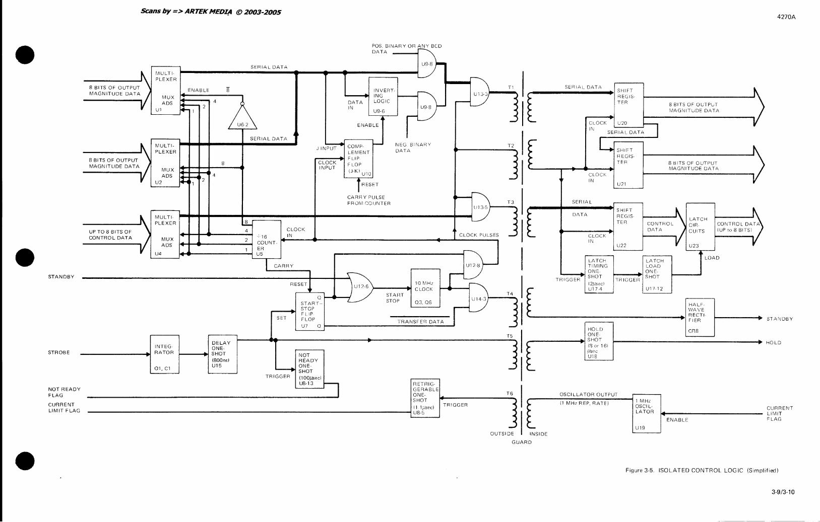
STANDBY
STROBE
NOT READY FLAG
CURRENT LIMIT FLAG
Scans by => ARTEK MED~ @ 2003-2005
pas BINARYORANYBCD DATA [1-SER IA L DA T.A
8 BITS OF OUTPUT\
MULTI-PLEXER
ENABLE "8 INVERT-
~E>-MAGNITUDE DATV ING MUX
A LOGIC ADS ~ 4 DATA
I+- 2 IN U9-6 U1 1
ENABLE
SERIAL DATA
8 BITS OF OUTPUT -\
JIN~ CaMP- I"- NEG BINARY MULTI-DATA PLEXER LEMENT
--. F LI p-8 CLOCK FLOP
MAGNITUDE DATAi INPUT (J-Kl U10 MUX
ADS 4
U2 ~1 2 lRESET
CARRY PULSE FROM COUNTER
J MULTI-PLEXER ..!L
4 CLOCK UP TO 8 BITS OF ~ 16 IN CONTROL DATA MUX 2 COUNT-ADS ER 1
U4 U5
l CARRY
RESET 10 MHz ~
U12-6 CLOCK
START 0
STOP START-- 03,06 STOP
r FLIP SET FLOP TRANSFER DATA
U7 0
DELAY INTEG- ONE-RATOR SHOT NOT
(800ns) READY U15 ONE-01, C1
SHOT TRIGGER (100~ec)
U8-13
~ RETRIG-GERABLE ONE-SHOT
[\ T1
~U .. .. .. .. -T2
.. i '") ~ -
~D T3
D .. ., ., CLOCK PULSES ...:)
8-1[\
T4
D .. .. . . -T5
.. .. .. .. -T6
SERIAL DATA SHIFT
[ : REGIS-TER 8 BITS OF OUTPUT
MAGNITUDE DATA
CI_OCK U20 IN
SERIAL DATA
SHIFT I REGIS-TER 8 BITS OF OUTPUT
MAG~~ITUDE DATA CLOCK IN
U21
SER IA L
;-----t-------~ SHi FT DATA
CLOCK IN
LATCH TIMING ONE-
----I~ SHOT TRIGGER
12/lsecl
REGIS-TER
U22
CONTROL DATA
LATCH LOAD ONE-
~---I~I SHOT TR IGGER
U1712
LATCH CIRCUITS
U23
HALFWAVE
LOAD
f I U174
l ____________________ ..... RECTI-.... FIER
ONE-CR8
4270A
STANDBY
,-____________ ~SHOT ~-------------------------------------_.. HOLD
HOLD J 18 or 16) /lsec U18
OSCILLATOR OUTPUT
-------------~---.., 1 MHz .. 11 1,usecl TRIGGER ~
~ ~ ~
(1 MHz REP. RATt) OSCIL-CURRENT LIMIT FLAG
-----------------------------------------------------------------------------Ll_)8_-5 __ ~
OUTSIDE -INSIDE
GUARD
LATOR .... ENABLE
U19
Figure 3-5. ISOLATED CONTROL LOG IC (Simplified)
3-9/3-10

via T4 to a half-wave rectifier on the inside of the guard. The dc output of the rectifier becomes the standby signal for control of the power source. During standby operation, data transfer does not take place due to the start/stop flipflop being reset and gate U12-8 being inhibited.
3-89. CURRENT LIMIT FLAG
3-90. The current limit flag produced by the A9 Power Amplifier whenever the power source is in the current limit mode, is used to enable a 1MHz oscillator (U19) which produces pulses at a 1MHz rate. The pulses are fed via T6 to the trigger input of a re-triggerable one-shot having a period of 1.1 microseconds. As long as the 1MHz pulses occur, the output of the re-triggerable one-shot is held at dc level which becomes the current limit flag to the program source.
3-91. A8 Programmable Current Limiter (4270A-1081 )
3-92. The A8 Programmable Current Limiter is installed as the -06 Option. It compares the voltage from a ladder network to an input voltage proportional to the output current. When the output current exceeds the ladder network reference, a clamp signal is produced that is used to limit the output current of the A9 Power Amplifier. The A8 Programmable Current Limiter contains the following circuitry: an 84-2-1 to 44-2-1 binary code converter, FET drivers, a ladder voltage reference, ladder switches and a ladder, a programmable reference and programmer reference inverter, and two current limit comparators - one positive and the other negative. Auxiliary circuits are a ground isolator and two power supplies, one 15 volts and the other -16 volts. A two-ohm current sampling resistor is tied to the input of the two current limit comparators.
3-93. 84-2-1 to 44-2-1 CONVERTER
3-94. This logic converter consists of two, digital inte-grated circuit, hex-inverters U1A through Ul F and U2A through U2F. They convert the input 84-2-1 code to 44-2-1 code, and in the absence of any programmed inputs, program the ladder to the lowest current limit, 10 milliamps. This is the quiescent state of the limiter in which ladder swtich Q4 and the current range switch Q26 are turned on, placing operational amplifier U4 in low range. This ensures that the Model 4275A current limits at the lowest current, limits at the lowest current, 10 milliamps, as a safety feature. In the event a programmed input for 80 milliamps is applied to the converter, the logic input is applied to two circuits, one directly to the base of FET Driver Q13 and the other indirectly through two inverters U2F and U1A to the base of FET Driver Q10. These two drivers turn on ladder switches Q9 and Q12 and two code 4 ladder resistors, thereby applying an equivalent 8 to the Programmable Reference amplifier and establishing a current limit of 80 milliamps.
4270A
3-95. FET DRIVERS
3-96. The ladder FET DRIVERS consist of PNP-NPN Transistor pairs Q3-Q5, Q7-Q8, Q13-Q14, and Q10-Ql1. The emitters of these pairs as well as the current range FET drivers Q15-Q16, are returned to VL common through a ground isolator network is described later. The purpose of the drivers is to increase the voltage output of the converters to a level required by the FET switches.
3-97. LADDER VOLTAGE REFERENCE
3-98. The Ladder Voltage Reference consists of a temp-erature compensated, 6.3 volt zener diode CR7 and produces a stable reference voltage that is reduced to 0.1 volt at TP3 by resistors R4, R6, and R59. This voltage reference is supplied by the regulated +15 volts power supply (TP2) consisting of 16 volt zener CR1, transistor Q28, and associated components.
3-99. LADDER SWITCHES AND LADDER
3-100. The Ladder Switches and Ladder, respectively, consist of FET switches Q4, Q6, Q12, and Q9 and resistors R52, R55, R54,and R15. The ladder resistors are weighted in a ratio of 1,2,4, and 4. The ladder operation is best explained in conjunction with the Programmable Reference. (See paragraph 3-121.)
3-101. PROGRAMMABLE REFERENCE AMPLIFIER
3-102. Programmable Reference Amplifier U4 is monolithic IC operational amplifier. Assuming current range switch Q26 is on, then U4 output voltage varies between -0.01 volt and -0.11 volt as the ladder resistors are switched into the circuit by the FET switches. That is, with only Q4 on, the output voltage is -0.01 volt. With Q4, Q6, Q12, and Q9 on, the output voltage is -0.11 v61t. The range is set by R31 in parallel with R30 and is the lOrna to 110 ma current range. With Q26 turned off, the range is determined by R30 alone. This is the 100 rna to 1.1 ampere range (Current Limit x 10 command) in which the ladder resistors produce an output from U4 of -0.1 volt to 1.0 volt. Amplifier U3, also a monolithic integrated circuit, together with resistors R24 and R25, forms a unity gain, inverting amplifier. The output of U3 is the same magnitude as that of U4, but of opposite polarity.
3-103. POSITIVE AND NEGATIVE I LIMIT COMPARATORS
3-104. Since the comparators function in the same manner, except for polarities, only the positive comparator is described. The output current from the Model 4275A flows through a one-ohm resistor, R51. A positive output current through this resistor produces a positive voltage that is compared to the output of U3 by action of transistor Q 17.
3-11

4270A
When the positive output of U3 is greater than the positive voltage developed across R51, Q17B is on and Q17 A is off, as are Q18, Q19, and Q17. This corresponds to the Model 4275A output current being less than the programmed 1-limit. When the positive output of U3 is less than the positive voltage developed across R51 , Q 17 A, Q 18, Q 19, and Q27 are all on and conducting. The greater the difference between the R51 and U3 Voltages, the greater these transistors conduct. The collector of Q27 connects, by way of pin 2 of PI, to the base of Q31 on the A9 Power Amplifier. When the Q27 collector conducts, it shunts base current drive away from Q31, limiting the 4275A output current to the programmed level. Transistors Q18 and Q27 are common-base stages used as voltage translators: Q18 from the -10 volts level of Q17 A to Q19 which is referred to VH (about -100 volts), and Q27 from Q19 are essentially the OUTPUT HIGH terminal voltage. Transistor Q19 provides current gain and Q20 is used as a temperature compensating diode for Q19. Capacitor C4 and resistor R40 are the primary frequency response determining components. Transistor Q25A and Q25B compares a negative reference voltage to negative voltages produced across resistor R51 by the output current in a manner similar to Q 17 A and Q 17B. Transistors Q24, Q2l, Q23, and Q22 correspond in function to Q 18 through Q20 and Q27 , respectively.
3-105. GROUND ISOLATOR
3-106. The Ground Isolator circuit, composed of transistors Ql and Q2 isolate the ground currents flOWing in VH COMMON from those in VL COMMON. The input logic lines driving the first transistor of each pair of FET Drivers (the emitters of the drivers) are referenced to VL COMMON indirectly through transistors Q1 and Q2. Thus, the only current through the point of commonality of VL - VA - VH is base current of Q1 and this has but a negligible effect in the OUTPUT LOW sense line.
3-107. MINUS 16 VOLTS POWER SUPPLY
3-108. Diode CR2, a 16 volt zener, produces -16 volts at test point 4. This voltage is used in the Ground Isolator, the FET Drivers, and U3 and U4.
3-109. A9 Power Amplifier (4270A-1071)
3-110. The A9 Power Amplifier produces the final output voltage and current of the power source. It also provides both source and sink current limit protection of the bipolar output. The circuitry consists of an input amplifier, driver, clamp circuitry, current sources, output stage, and current limit detector.
3-111. INPUT AMPLIFIER
3-112. The Input Amplifier composed of Q9 through Qll and Q20 through Q25 amplifies the input appearing at ter-
3-12
minal D ofP1. The resulting voltage at the emitter of Ql1 corresponds closely to the programmed output voltage. A closed-loop dc gain of five is established by feedback through R62 and R21. Overall frequency response is controlled to 6 db per octave by C6. Amplifiers Q22 and Q23 link VH common to the A3 Preamplifier common (VREF common) such that current flow between these two points is minimized. Q20 and Q21 provide current with respect to the common established by Q23, Q22 emitters. Emitter follower Q9 and amplifier QlO provide voltage gain and a drive signal to the output emitter follower Qll. Overall frequency response to this point is controlled with feedback through C6. The resulting emitter voltage of Q11 is close to the final output voltage of the power source. Transistors Q24 and Q25 function as current sources of Q 1 0 and Q 11, respectively.
3-113. DRIVER
3-114. The Driver consisting of Q12 and Q26, form complementary current amplifiers. These amplifiers receive a bipolar drive voltage from Q11 and together with the CURRENT SOURCES produce respective drive currents for the output stage. The voltage drops across Q13, CR33, Q17 and CR27 together with variable resistor R51 set the bias current required for the output transistors Q32, Q33, 041 and 042. Q13 collector current is turned off when a (+) current limit condition exists and Q 17 is affected similarly for a (-) current limit. These collectors drive the CURRENT LIMIT DETECTOR.
3-115. CLAMP CIRCUITRY
3-116. Voltage transients that would occur during a current limit and abrupt load removal are limited by the Clamp Circuitry. Two circuits titled + Clamp and - Clamp limit the bipolar transients. The + Clamp consists of Q I through 04. Transistors Q5 through Q8 form the - Clamp. Since operation of each circuit is the same, except for polarity, only the + Clamp is described.
3-117. The + Clamp monitors the voltage between the emitter of Q II and that on the anode of CR33. Normally, QI and Q2 are cut-off and Q3 is conducting; however, when a current limit occurs, the anode voltage of CR33 decreases through action of either the built-in current limiter (overload protection) or the A8 Programmable Current Limiter (optional) and subsequently turns off Q3. The voltage at the emitter of Q II, will increase toward +V H during current limiting and this turns on Q2. Conduction of Q2 turns on QI and produces a clamp signal at terminal 6 of PI. This clamp signal then limits the summing junction voltage in the A3 Preamplifier and causes the emitter voltage of Qll to be clamped to a voltage slightly above that of the base drive to the Output Stage. Transistor Q4 [unctions as a current source for Q2 and Q3. Frequency and phase characteristics of the + Clamp circuitry is determined by C 1, C2, C26 and R65.

3-118. CURRENT SOURCES
3-119. Constant current for the Output Stage is provided by the Positive and Negative Constant Current Sources. Transistor Q30 forms the Positive Constant Current Source. The Negative Constant Current Source consists of Q38. The positive and negative constant current sources produce a constant reference current for the bases of Q31 and Q37, respectively.
3-120. OUTPUT STAGE
3-121. The Output Stage consisting of Q31 through Q35 and Q37 through 042 produces the power source output. It also provides both sourcing and sinking current limit protection.
3-122. Transistors Q31 through Q33 and Q37, 041, 042, form a complementary, emitter follower stage. Q31 through Q33 produce the positive output and Q37, 041,042 the negative. Total output current flows through R43, R44 (positive) and R47, R48 (negative).
3-123. Both sourcing and sinking current limit protection is provided for each section of the output amplifier. Q34 protects the positive output section and Q35 the negative. Maximum output current (sourcing) is limited to l.2A. Sinking current is limited at a lesser value depending on the programmed output voltage. Since operation of each current limiter is the same, only the positive output section protected by Q34 is described.
3-124. Output current passes through R43. This current produces a bias voltage for A34. When the output current (sourcing) exceeds 0.6A, the resulting potential turns on Q34. Conduction of Q34 via CR34 shunts any further base drive current to Q31, thus limiting the maximum sourcing
4270A
output current at 0.6A. In the sinking mode, output current will pass through R43 to the output as above, but the output voltage polarity is zero or negative by definition. Under this condition, negative voltage more than -O.6V at the output will turn on CR25 which supplies base current for Q34 through R41 from common and adds to that supplied from the voltage drop across R43. Therefore, the base current is dependent on both sinking voltage magnitude and output current. Current limiting in milliamperes is equal to 500 - 4.5Eout.
3-125. When the A8 Programmable Curremt Limiter -06 Option is installed, ±I LIMIT inputs are applied to terminals 2 and U of PI. These inputs clamp the maximum base drive to both sections of the Output Stage in a similar manner to Q34, thus limiting the maximum output current at a level determined by the input limit commands.
3-126. CURRENT LIMIT DETECTOR
3-127. The Current Limit Detector produces an I LIMIT (OV) command at terminal 14 of PI whenever a source of sink limit condition exists. Circuitry consists of Q14 through Q16, Q18 and Q19. Positive output section limiting is detected by Q14. Limiting in the negative output section is detected by Q18. Transistors Q15, Q16 and Q19 are drivers.
3-128. Under normal operating conditions Q14 and Q18 are turned on by conduction of Q 13 and Q 17 in the Driver. Transistors Q15 and Q19 are switched off by conduction of Q14 and Q18, thus turning Q16 on and producing an I LIMIT (-5V) command at terminal 14 of PI. Should a current limit occur in the positive or negative section of the Output Stage, the associated Q13 or Q17 in the Driver will be turned off. This turns offQ14, Q15 or Q18, Q19, thus turning Q16 off and producing an I LIMIT (OV) command at terminal 14 of PI.
3·13/3·14
4-1. INTRODUCTION
4-2. This section contains servicing information for the instrument. Table 4-1 lists the recommended test equipment. If the recommended equipment is unavailable, use test equipment of equivalent or superior specifications.
4-3. SERVICING INFORMATION
44. All products manufactured by the John Fluke Mfg. Co., Inc. are warranted for a period of one year. Complete warranty information is located in the WARRANTY at the front of the manual
4-5. Factory authorized calibration and services is avail-able at various world-wide locations. A list of authorized service centers is located at the front of the manual. If requested, an estimate will be provided before repair work is done on an instrument that is beyond the warranty period.
4-6. GENERAL MAINTENANCE
4-7. Cleaning
4-8. This instrument should be cleaned periodically to remove dust, grease, or other contaminates. The exterior of the instrument can be cleaned with a clean cloth moistened with anhydrous ethyl alcohol or Freon T.F. Degreaser (MS 180) available from the Miller Stephensen Chemical Co., Inc. If neither cleaning agent is readily available, soap and water applied sparingly to a clean cloth is usable. Interior sections of the instrument are cleaned using clean, dry air at low pressure.
4270A
Section 4
Maintenance
4-9. Air Filter Cleaning
4-10. A remove able air filter is attached to the rear panel and against the blower by a covering bracket that is held in place by four screws. This air filter should be removed and cleaned frequently to remove accumulations of dust and grease. The air fIlter is removed by unscrewing the four covering bracket screws, removing the bracket, and separating the bracket and filter. Cleaning is done by rinsing the fIlter in hot detergent solution frequntly for best results. After the fIlter is dry, install it as indicated by the air flow arrow scribed on the frame of the fIlter. Secure the filter bracket to the rear panel with four screws.
4-11. Fuse Replacement
NOTE
Turn off power switch and disconnect instrume nt from power supply (line power) before replacing fuse.
4-12. The power fuse is located on the rear panel of the instrument. If replacement is necessary, use the following rated fuses:
AC LINE AC LINE VOLTAGE VOLTAGE
100 2A,AGC 200 1A,AGe
115 Slo Blo 230 Slo Blo
125 250
4·'
4270A
4-13. MAINTENANCE ACCESS
4-14. Access to the interior of the instrument shown in Figure 4-1 is as follows:
a.
b.
c.
d.
e.
f.
4-2
Turn off the power switch and disconnect the power cord from line power.
Remove the top dust cover and the underlying guard cover to gain access to all of the calibration adjustments, test points, and most of the PCB assemblies. Note that most of the calibration adjustments are labeled on the guard cover.
Removal of the AlO PCB requires prior removal of the A2 PCB, the bottom dust cover, and the A9 Power Amplifier PCB and heat sink. However, if AlO PCB removal is not desired, proceed to step k.; otherwise continue as follows. The A9 heat sink is secured to the bottom guard tray by two screws accessible from the upper surface of the guard tray. The A9 PCB assembly and attached heat sink are removed from the Al PCB as a unit following disconnection of the A9Sl thermostatic switch cable A9WI from the AlO PCB at AlOP2. Refer to Interconnect Diagram 4270A/4275A-1000.
Following removal of the A9 PCB, the machine screws securing the two longitudinal cross braces to the guard tray must be removed. Next, four large machine screws securing the lateral cross bracket to the front panel at the rear of the Al PCB (two high and two low) must be removed.
The lateral and longitudinal cross braces with attaching Al 0 PCB, A 10 heat sink, and 1 A I T1 power transformer, may be displaced obliquely internal of the instrument following removal of two machine screws through the rear panel of the instrument and disconnection of the AlOAI connector PCB from the A2 PCB receptacle J 1. In addition, the blower power cable AlOW3 must be either unsoldered from the AlO PCB or disconnected from the blower motor at the blower itself. The latter requires removal of the blower filter bracket, filter, and fan as outlined in paragraph 4-10. The blower cable is then removed, within a protective grommet, from a rear panel slot to free it from the instrument chassis.
This step is readily accomplished providing that the A2 PCB assembly is previously removed from the instrument, since greater freedom of movement is allowed. Remove the overall assemblage described in previous step by lifting vertically out of the instrument while simultaneously rotating the
assemblage obliquely to clear the rear panel overhang. Exercise care in withdrawing the flatwire cable AlOWl and connector PCB AlOAl with the assemblage to prevent damage.
g. With the assemblage removed from the instrument and placed on a level, clean surface and the power transformer being farthest away, remove the two machine screws securing the shorter longitudinal bras:e to the lateral cross brace.
/
h. Remove the six machine screws from the longer longitudinal brace. These screws secure the AlO PCB to the brace. Hold the power transformer steady and withdraw the AlO PCB with attaching parts from the transformer cable receptacle lAU1.
i. Separation of the short longitudinal brace from the AlO heat sink and filter capacitors is accorut>lished by releasing the heat sink alignment clip screw and the two screws in the capacitor support brackets, these latter two being hidden beneath the heat sink. The brace may then be separated from the AlO components by a firm, even pulling force.
NOTE
PCB's can be mounted on an accessory extender PCB assembly for servicing. See Section 6 for use of the extender and associated extender cable.
j. Removal of the A2 through A6, A8 and A9 PCB's is done by pulling rearward with a firm rocking motion on each PCB. However, those PCB's with rear panel brackets (A2 and A6) must be freed of attaching rear panel screws.
k. The A9 PCB is secured to the bottom guard tray through the A9 heat sink. Hence, A9 PCB removal requires prior removal of heat sink attaching screws accessible from the upper surface of the bottom guard. The A9 PCB and heat sink are withdrawn from the instrument as a unit follOWing disconnection of the A9S1 thermostatic switch cable from the AlO PCB at AlOP2. Refer to Interconnect Diagram 4270A/4275A-1000.
1. In the event the A2 PCB is removed from the Al PCB and reconnected via the extender PCB assembly, as in servicing or troubleshooting, an accessory cable extender assembly must be used to tie the A2 and AlO PCB's together electrically. The recommended installation is depicted in Section 6 of the manual.

m.
n.
o.
p.
q.
Access to the Al and A7 PCB pair is possible after removal of the front panel. To remove the front panel, remove the bottom dust cover and then remove the rack mountings, if installed, from the front corners. If no rack mountings are installed, peel the decals from the sides of the front handles. Place the instrument face down on its handles and remove the four mounting screws (two upper and two lower) which secure the lateral cross bracket to the front panel at the rear of the Al PCB.
Disconnect the Al PCB guard wire from the lower guard by removing the lug screw.
Place the instrument normal side down and remove all the screws from the sides of both front handles, or from the front corner panels in the event the instrument was rack mounted.
Pull the entire front panel assemblies free of the instrument, and at the same time, dislodge those PCB's which may be still inserted into the Al motherboard.
To separate the Al and A7 PCB pair from the front panel, remove the large screws that secure the PCB pair to the front panel by means of the teflon standoffs.
r. To separate the Al and A7 PCB pair from each other after they are removed from the front panel, remove all the small screws from the Al PCB. Separate the Al and A7 PCB by pulling the two boards perpendicularly apart.
s. Assembly of the instrument is accomplished by reversal of the order of disassembly, with attention to connection of the A2 PCB guard wire that was removed in step o.
t. The air filter and blower are removed from the rear panel by removing the filter cover screws, the filter cover, the filter, the blower screws, and the blower line power plug.
u. Instructions for cleaning and installation of the air filter are given on the frame of the filter itself. See paragraph 4-10.
4-15. INVERTED CONTROL LOGIC
4-16. The Isolated Control Logic PCB can be altered to provide inverted logic levels. This is accomplished by jumpering to appropriate PCB pads. Refer to the table on the A6 Isolated Control Logic Schematic Diagram (4275A-1021, sheet 1 of 2). The table indicates the proper jumper configuration for normal and inverted logic levels for each
4270A
model of the 4200 series instruments. Jumper locations are identified by alphabetical designations which appear on the schematic diagram and the PCB.
NOTE
The same Isolated Control Logic PCB Assembly is used in all models of the 4200 series instruments. However, the PCB's are not interchangeable until the jumper configuration is changed in accordance with the table on the 4275A -1 021 schematic diagram. Therefore, insure that any control logic assemblies used as replacements conform to the jumper configuration shown in the table before installing the assembly in the instrument.
4-17. CALIBRATION PROCEDURES
4-18. The recommended period between successive cal-ibrations for this instrument is 90 days or annually. The instrument must be calibrated following repairs. Use the test equipment defined in paragraph 4-2. Table 4-1. Assembly, adjustment, and test point locations are shown in Fgirue 4-1. Table 4-2 shows binary by decade coding for output magnitude control.
Table 4·1. RECOMMENDED TEST EQUIPMENT
NOMENCLATURE EQUIPMENT
AC/DC Voltmeter FLUKE Model 887A
Manual Control Unit (MCU) FLUKE Model A4200
*AC Source,±0.02% of FLUKE Model 510A, output, 400 Hz Option -04
** Resistive Load 10 ohm ± 1%. 20w
*Required only if -03 Option is installed.
* * Required only if -06 Option is installed.
4-19. Initial Procedure
a. Turn off the instrument and remove the top dust cover screws. Leave the dust cover in place.
b. Connect the Model A4200 Manual Control Unit (MCU) to the programming connector on the rear of the instrument.
CAUTION!
The Model A4200 Manual Control Unit (MCU) is not compatible with 4200 series instruments equipped with the -09 Option. DO NOT connect the MCU to these instruments.
4-3

4270A
TP TP 4 6
(+) (-)
PROGRAM
I LIMIT
4-4
HI
+1
AS A9
A9S1
TP TP
3
XFMR 1 A 1T 1 A lOA 1 A2 A3 A4 A5 A6 A 7
Al0Wl A2Jl XA2F1 A2S2
Al0A1Pl A2TBl A2J1
~--+A2
~,;;--- +B 15 ",,"---EXT REF GAIN
~+';---+A1
::=;;.;;,;:;:;::;--+B4 ~~~-----EXTREFZERO
A6Jl
~';:---+A4
+==--+AS
~=--ZERO
Figure 4-1. ASSEMBLY, ADJUSTMENT, AND TEST POINT LOCATIONS

Table 4·2. BINARY BY DECADE CODING
DECADE CODING OUTPUT VOLTAGE (V DC)
10V RANGE x10V RANGE
1 .001 .01
o DECADE 2 .002 .02
4 .004 .04
8 .008 .08
1 .01 .1 C DECADE 2 .02 .2
4 .04 .4 8 .08 .8
1 . 1 1
B DECADE 2 .2 2 4 .4 4 8 .8 8
1 1 10 A DECADE 2 2 20
4 4 40 8 8 80
4270A
Check that the 11 0 VOLT RANGE indicator illuminates.
NOTE!
If the A8 Current Limiter PCB is installed (-06 Option), depress the following buttons for a current limit condition of 0.55 amperes: Xl 0, 80, 20,10, and STROBE. Check that these indicators illuminate: CURRENT LIMIT MA XlO, 40, and 5.
b. Remove the guard cover and connect a dc voltmeter to A9TP4 (+) and A9TP6 (-). See Figure 4·1 for location of test points.
c. Adjust P.A. BIAS, as necessary, to obtain a meter reading in the range of70mV to 278mVdc.
d. Disconnect the voltmeter from A9TP4 and A9TP6 .
4·21. Bit Adjustment (0.4)
a. Connect a dc voltmeter to the OUTPUT HI (+) and LO (-) terminals on the rear panel barrier strip.
b. Connect an insulated shorting jumper between A3TP3 and ASTPl.
c. Release the RANGE button and depress the STROBE button to select OV output on the 10 volt range. Check that the 110 VOLT RANGE indicator goes
CAUTION! out.
c.
On the rear panel barrier strip the foUowing terminals must be jumpered: OUTPUT HI to SENSE HI and SENSE LO to OUTPUT LOtoGUARD.
Turn on the instrument in accordance with Operating Instructions, paragraphs 2-6 and 2-7. Depress the MANUAL button on the MCU and release all other buttons that may be depressed.
NOTE!
In an instrument containing an A6 Inverted Isolated Control Logic PCB (-08 Option) all instructions reading depress shall mean release and all instructions reading release shall mean depress. This note, however, is not applicable to EXT REF, STANDBY, STROBE, MANUAL A UTO or EXT functions.
d. Depress the STROBE button on the MCU (0 volt, positive, low range) and allow the instrument to warm up for one-half hour.
4·20. Power Amplifier Bias Adjustment
a. Remove the top dust cover. Depress RANGE and STROBE buttons to call a OV output, high range.
d.
e.
f.
g.
h.
i.
Adjust A3, ZERO for a OVdc ±10~N output.
Depress the B decade 8 and STROBE buttons. Check that the output voltage is about +8Vdc and that the B decade 8 indicator is on.
Record the exact dc voltage read in step e. and then divide the recorded value by 2 for a final value; e.g. 8.00383Vdc -;- 2 = 4.00192Vdc.
Recorded value ___________ _
-;- 2 = ___________ Final Value
Release the B8 button and depress the B4 and STROBE buttons. Check that the output voltage is about 4Vdc and that only the B decade 4 indicator is on.
Adjust AS, +B4 for an output that is within ±lOOpV of the final value com puted in step f.; e.g., 4.00192Vdc ±lOOpV.
Release the B4 button, depress STROBE, and remove the jumper between A3TPI and ASTPI. Install the guard cover and insert all guard cover screws. Check that the B decade 4 indicator is out.
4-5

4270A
4-22. Zero, Reference, and Bit Adjustments
a.
b.
c.
d.
e.
f.
g.
h.
i.
j.
k.
1.
Release all MCU buttons except MANUAL, and depress RANGE and STROBE to obtain OVoutput in the high range. Check that the 110 VOLT RANGE indicator is on and that the dc voltmeter is connected as defined in step 4-19. a.
Adjust A3, ZERO for OVdc ±701lV output, using an insulated screwdriver or tuning tool.
Release RANGE and depress STROBE. Check that 110 VOLT RANGE is out and that the output is OVdc ±1OIlV. Repeat steps a., b., and c. to achieve this tolerance, if necessary.
Depress RANGE, POL, A decade B and STROBE for a -BOV, high range output. Check that 110 VOLT RANGE and SIGN indicators are on.
Adjust A2, -ABO for an output of -BOVdc±lmV.
Release POL and depress STROBE for a +BOV high range output. Check that SIGN goes out and the A decade B stays on.
Adjust A2, +ABO for an output of+BOVdc ±lmV.
Release RANGE, depress STROBE, and check that 110 VOLT RANGE goes out and the A decade B stays on.
Adjust A3, +AB for an output of +BVdc ±100IlV.
Release A decade B, depress A decade 4 and STROBE. Check that only A decade 4 indicator light is on.
Adjust A3, +A4 for an output of +4Vdc ±100IlV.
Release 4, depress 2 and STROBE. Check that only A decade 2 indicator light is on.
m. Adjust A3, +A2 for an output of +2Vdc ±100IlV.
n. Release 2, depress 1 and STROBE. Check that only A decade 1 indicator light is on.
o. Adjust A3 +Al for output of+lVdc±1OIlV.
p.
q.
r.
4-6
Release 1, depress B decade B, 2, and 1, and STROBE. Check that B decade indicators B, 2, and 1 come on.
Adjust A3, +B15 for an output of+1.1 Vdc ±1OIlV.
Release all MCU buttons except MANUAL and depress STROBE. Check that output reads zero volts and that only the POWER indicator is on.
4-23. External Reference Adjustments (-03 Option)
4-24. If the A4 External Reference PCB Assembly is installed, perform the following adjustments:
a. Connect a shorting jumper between the EXT REF HI and EXT REF LO input terminals on the rear panel barrier strip.
b. Depress EXT REF, A decade B,4, 2,1 and STROBE buttons. Check that EXT REF and A decade B, 4, 2 and 1 indicators are on.
c. Adjust A4, EXT REF ZERO for an output of OV ±IOIlVdc.
d.
e.
f.
g.
h.
i.
j.
Remove the shorting jumper from the rear panel barrier strip.
Apply a 10Vac ±0.02%, 400 Hz signal to the EXT REF HI and LO terminals. Mea~ure and record the actual ac voltage applied to these terminals with an ac voltmeter.
Recorded value.
Disconnect the ac voltmeter and connect it to the OUTPUT HI and LO terminals on the same barrier strip.
Release A decade 4 and I buttons and check that the A decade Band 2 indicators :ue on.
Adjust A4, EXT REF GAIN for an ac output that is within ±5001lV of the value recorded in step e.
Release A decade 8 and 2 buttons and depress STROBE. Check that the output is OV and that all decade indicators are out.
Disconnect the ac signal source and set the ac voltmeter to measure dc volts.
4-25. Current Limiter Adjustment (-06 Option)
4-26. Adjustment of the A8 current limiter, when installed, is performed as follows:
a.
b.
c.
Turn off the instrument and install a I OSG ±I %, 20W resistor between the OUTPUT HI and LO terminals. Leave the dc voltmeter connected.
Set the top dust cover in place, turn on the instrument, and release all MCU buttons that were depressed, except MANUAL.
Allow the instrument to operate for about one-half hour and then remove the top dust cover.

d.
e.
f.
Depress POL, A decade 8,2, I, CURRENT LIMIT MA or % XIO, 80, 20, and then STROBE. An -llVdc output with a 100% current limit is called. Check that the following indicators are on: A decade 8, 2,1, CURRENT LIMIT MA XIO, 40,10, and I LIMIT.
Adjust A8, REF for an output of -SVdc ±ISmV. Check that the I LIMIT indicator is on.
Release CURRENT LIMIT MA or % buttons XIO, 80, and 20; depress 10 and STROBE. Check that CURRENT LIMIT MA or %5 indicator and I LIMIT indicator are on. This action calls the SmA current limit (10 percent current limit).
g. Adjust A8, -I for output of -SOmVdc ±O.5mV.
h. Release POL button, depress STROBE, and check that SIGN indicator goes out. This action calls a +11 Vdc output.
i. Adjust A8, +I for an output of SOmVdc ±O.5mV.
j. Release CURRENT LIMIT MA or % 10 button and depress X1O, 80, 20, and STROBE buttons. This action calls the O.5A current limit (100 percent current limit). Check that the output is +SVdc ±100mV, and that the following indicators are on: XIO, 40,10 and I LIMIT. Repeat the procedure starting at step d. if output is not within tolerance.
k. Release all MCU buttons and depress STROBE to call a OV output. Also remove the 10 ohm resistor.
4-27. Final Zero Adjustmeilt
4-28. The following adjustments must be performed only after the instrument has been operating for a minimum period of one-half hour with all covers in place.
a. Connect a dc voltmeter to OUTPUT HI and LO terminals on the rear panel barrier strip. Release all MCU buttons, except MANUAL, and depress STROBE. This action calls for a OV output, positive in the low range. Check that only the POWER indicator is on.
b. Adjust AMPLIFIER ZERO (A3, ZERO) for an output ofOVdc ±1O~V.
d.
e.
f.
g.
4270A
If the A4 External Reference is installed (-03 Option), depress EXT REF, A decade 8, 4, 2, and 1 buttons and release RANGE. Depress STROBE and check that A decade indicators 8,4,2, 1 and EXT REF indicator illuminate.
Connect a shorting jumper between EXT REF HI and EXT REF LO terminals on the rear panel barrier strip.
Adjust EXT REF ZERO (A4, EXT REF ZERO) for an output ofOV ±1O~V.
Remove the shorting jumper, release all MCU buttons, except MANUAL, depress STROBE, and check that the only indicator remaining on is POWER.
4-29. Output Checks
a.
SIGN
Perform the linearity checks given in Table 4-3, and check that the specified outputs are obtained. Connect an ac/dc voltmeter as described in step 4-26. a.
Table 4-3. LINEARITY CHECKS
CALLED OUTPUT POWER SOURCE
DECADE OUTPUT VOLTAGE
(POLARITYI A B C D (VOCI
+ 0 0 0 0 OV ±100 uv
+ 0 1 1 1 +lllmV ±120~V
+ 0 2 2 2 +222mV ±120~V + 0 3 3 3 +333mV ±130~V + 0 4 4 4 +444m V ± 140~V + 0 5 5 5 +555mV ±150~V + 0 6 6 6 ~6mV±160~V
+ 0 7 7 7 +777mV ±180~V + 0 8 8 8 +888m V ± 190~V + 0 9 9 9 +999mV ±200~V + 0 10 10 10 +1.111V±200~V
+ 1 0 0 0 +lV ±0.2mV + 2 0 0 0 +2V ±0.3mV + 3 0 0 0 +3V ±O.4mV + 4 0 0 0 +4V±0.5mV + 5 0 0 0 +5V±0.6mV + 6 0 0 0 +6V ±0.7mV + 7 0 0 0 +7V±0.7mV + 8 0 0 0 +8V±0.8mV + 9 0 0 0 +9V±0.9mV + 10 0 0 0 +10±lmV
+ 1-5 15 15 15 +16.665V ±lmV - 15 15 15 15 -16.665V ±lmV
c. Depress the RANGE and STROBE buttons. Check b. If the A4 External Reference PCB Assembly (-03 Option) is installed disconnect the ac/dc voltmeter, release all MCU buttons except MANUAL, and depress EXT REF and STROBE. Check that the EXT REF indicator comes on.
that the 100 VOLT RANGE indicator is on. This action calls the high or XIO range and OV ±70~Vdc output. If the output reading is not within tolerance, repeat steps a. through c.
4-7

4270A
c.
d.
e.
4-8
Apply a 1 OVac, ±O .02%,400 Hz signal and connect an ac/dc voltmeter to the EXT REF HI and LO input terminals on the rear panel barrier strip. Record the ac voltage indicated on the ac voltmeter.
Recorded value: ____________ _
Remove the ac voltmeter from the EXT REF HI and LO input terminals and connect it to the OUTPUT HI and LO terminals.
Depress A decade I button and STROBE; check that the A decade 1 indicator comes on and that the
f.
g.
h.
ac voltmeter reads within ±5001lV of the level recorded in step G.
Depress RANGE, A decade 4, 2, 1; B decade 4, 2, 1; and STROBE buttons. The output should be 77Vac ±0.1 V. Check that the 110 VOLT RANGE indicator is on, and that the 4, 2, and 1 indicators in both A and B decades are on.
Turn off the instrument and disconnect all test equipment.
Install the top dust cover. Calibration is complete and the instrument is ready for use.
4270A
Section 5
Lists of Replaceable Parts
REFERENCE ASSEMBLY NAME/NUMBER PART NO. PAGE DESIGNATOR
Al Mother PCB Assembly (4270A4011) 332908 5-6
A2 Power Supply PCB Assembly (4270A4061) . 332940 5-7
A3 Pre-Amplifier PCB Assembly (4270A4051) . 332924 5-12
A4 External Reference PCB Assembly (-03 Option) (421OA4041) 292581 5-17
AS BCD Ladder Assembly (4210A4031) . 292565 5-20
A6 Isolated Control Logic (4250A/4270A-01) . 365692 5-24
A7 BCD Display PCB Assembly (4250A4013) . 302257 5-28
A8 Current Limit PCB Assembly (4270A4081) . 332965 5-29
A9 Power Amp PCB Assembly (4270A4071) 332957 5-34
A10 High Voltage Power Supply Assembly (4270A4201) . 333005 540
5-1

4270A
5-1. INTRODUCTION
5-2. This section contains an illustrated parts break-down of the instrument. Components are listed alphnumerically by assembly. Electrical components are listed by item number. Each listed part is shown in an accompanying illustration.
5-3.
a.
b.
c.
d.
e.
f.
g.
5-2
Parts lists include the following information:
Reference Designation or Item Number
Description of each part
Fluke Stock Number
Federal Supply Code for Manufacturers. (See Section 7 for Code-to-Name list.)
Manufacturer's Part Number or Type.
Total Quantity per assembly of component.
Recommended Quantity: This entry indicates the recommending number of spare parts necessary to support one to five instruments for a period of two years. This list presumes an availability of common electronic parts at the maintenance site. For maintenance for one year or more at an isolated site, it is recommended that at least one in
5-4.
each assembly in the instrument be stocked. In the case of optional subassemblies, plug-ins, etc. that are not always part of the instrument, or are deviations from the basic instrument model, the REC QTY column lists the recommended quantity of the item in that particular assembly.
HOW TO OBTAIN PARTS
5-5. Components may be ordered directly from the manufacturer by using the manufacturer's part number, of from the John Fluke Mfg. Co., Inc. factory or authorized representative by using the FLUKE STOCK NUMBER. In the event the part you order has been replaced by a new or improved part, the replacement will be accompanied by an explanatory note and installation instructions, if necessary.
5-6. To ensure prompt and efficient handling of your order, include the following information:
a. Quantity
b. FLUKE Stock Number
c. Description
d. Reference Designation or Item Number
e. Printed Circuit Board Part Number
f. Instrument Model and Serial Number

4270A
REF MFG MFG DESIG FLUKE OR DESCRIPTION STOCK
FED PART NO. TOT REC USE
ITEM NO. SPLY OR QTY QTY COE
NO. COE TYPE
BCD PROGRAMMABLE POWER SOURCE 4270A 89536 4270A
Figure 5-1
Al Mother PCB Assembly (Figure 5-2) 332908 89536 332908 1
A2 Power Supply PCB Assembly (Figure 5-3) 332940 89536 332940 1
A3 Pre-Amplifier PCB Assembly (Figure 5-4) 332924 89536 332924 1
A4 External Reference PCB Assembly 292581 89536 292581 1
(-03 Option) (Figure 5-5)
A5 BCD Ladder Assembly (Figure 5-6) 292565 89536 292565 1
A6 Isolated Control Logic (Figure 5-7) 365692 89536 365692
A7 BCD Display PCB Assembly (Figure 5-8) 302257 89536 302257 1
A8 Current Limit PCB Assembly (-06 Option) 332965 89536 332965 1
(Figure 5-9)
A9 Power Amp PCB Assembly (Figure 5-10) 332957 89536 332957 1
A10 High Voltage Power Supply Assembly 333005 89536 333005 1
Figure 5-11)
Card Guide 229047 89536 229047 6
Card Guide 256461 89536 256461 1
Chassis, Side 296962 89536 296962 2
Connector, programming, male, 50 contact 307017 89536 307017 1
Cover, bottom 308122 89536 308122
Cover, guard 331884 89536 331884 1
Decal, corner 296269 89536 296269 1
Decal, Handle trim 295493 89536 295493 1
Decal, front panel 302034 89536 302034 1
Decal, rear panel 334516 89536 334516 1
Decal, side trim 295386 89536 295386 1
Fan, muffin, venturi 103374 89536 103374 1
Filter 313056 89536 313056 1
Handle, corner front 295667 89536 295667 2
Housing, fIlter 314047 89536 314047 1
5-3
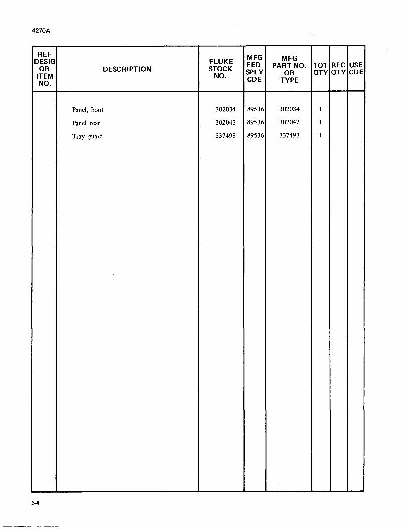
4270A
REF DESIG FLUKE MFG MFG
OR DESCRIPTION STOCK FED PART NO. TOT REC USE ITEM NO. SPLY OR OTY OTY CDE NO. CDE TYPE
Panel, front 302034 89536 302034 1
Panel, rear 302042 89536 302042 I
Tray, guard 337493 89536 337493 1
5-4

4270A
Figure 5-1. BINARY PROGRAMMABLE POWER SOURCE
5·5

4270A
REF MFG MFG DESIG FLUKE OR DESCRIPTION STOCK
FED PART NO. TOT REC USE
ITEM NO. SPLY OR OTY OTY CDE
NO. CDE TYPE
Al MOTHER PCB ASSEMBLY 332908 89536 332908 REF
Figure 5-2
11 thru 17 Connector, femal, 50 contact 284604 02660 222-22501-110 7
0
I I J1 II
II J2 II 0
, I I J3 II 0 I I J4 II
I I J5 II 0 0
0
0 0
I I J6 II 0 0
~ J II J7 I L \. ® f
Figure 5-2. MOTHER PCB ASSEMBLY
5-6

4270A
REF MFG MFG DESIG FLUKE OR DESCRIPTION STOCK
FED PART NO. TOT REC USE
ITEM NO. SPLY OR OTY OTY CDE
NO. CDE TYPE
A2 POWER SUPPLY PCB ASSEMBL Y 332940 89536 332940 REF
Figure 5-3
C1,C14, Cap, cer, 0.05 uf +8-/-20%, 25V 148924 72982 5855-Y50-503Z 3
C17
C2,C5, Cap, mica, 33 pf± 5%, 500V 160317 71236 DM15E330J 5
C10,C19
C3 Cap, mica, 100 pf± 5%, 500V 148494 71236 DM15FlOlJ 1
C4 Not used
C6 Cap,cer, 500 pf±1O%, 1 kV 105692 71580 2DDH60N501K 1
C7,C8 Cap, elect, 250 uf +50/-10%, 64V 185850 73445 C437ARH250 2
C11 ,C12 Not Used
C13,C16 Cap, elect, 8000 uf +100/-10%, 15V 309245 99392 61C15AS83 2
C15 Not Used
C18 Cap, Ta, 1.0 uf ±20%, 35V 161919 56289 196D105X0035 1
C20 Cap, cer, 2000 pf, gmv, 1 kV 105569 71590 DA140-139CB 1
C21 Cap, cer, 0.1 uf+80/-20%, 500V 105684 56289 41C92 1
e22 Cap, plstc, 0.1 uf ±1O%, 400V 289744 73445 C28OCF/ A1001< 1
C23,C24 Cap,cer, 1 uf±gmv,3V 106567 71590 UKI05 2
CR1, CR25, Diode, silicon, 1 amp, 600 piv 112383 05277 1N4822 3 CR26
CR2, CR3, CR27 , CR28, Diode, silicon, 150 rna 203323 03508 DHD1105 7 2 CR33, CR34, CR35
CR4, CR14, Diode bridge, 2 amp 296509 09423 FB100 3 1
CR19
rR5 thru '-'RB, ~R1O, Not Used thru CR13 CR15
5·7

4270A
REF MFG MFG DESIG FLUKE OR DESCRIPTION STOCK FED PART NO. TOT REC USE
ITEM NO. SPLY OR OTY OTY CDE
NO. CDE TYPE
CR16 thru CR18 CR20 Not used thru CR22, CR24
CR9, Diode, zener, 4.3V 180455 07910 1N749A 2
CR23
CR29 thru Diode, Rectifier 329672 03508 1N5059 4
CR32
F1 Fuse, slow blow, 2 amp, 250V (For 115V 109181 71400 MDX 1 operation)
11 Connector, male, 3 contact, power 284166 82839 EAC301 1
12 Connector, female, 36 contact 236885 13511 225-21821-105 1
Kl Relay, 4PDT, 5V Coil 272716 24796 R40-E030-1 1 1
Ql,Q10, Qll,Q13
Xstr, silicon, NPN 218396 04713 2N3904 7 Q18,Q19 Q24
Q2,Q3, Xstr, I-FET, N-channel 261578 15818 U2366E 4 2 Q5,Q6
Q4,Q7, Q8,Q9, Xstr, silicon, PNP 195974 04713 2N3906 5
Q14
Q12,Q17 Xstr, silicon, NPN 150359 95303 2N3053 3 Q23
Q15,Q20 Xstr, silicon, PNP 269076 95303 2N4037 2
Q16,Q21 Xstr, silicon, NPN 288381 95303 40372 2 1
Q22 Xstr, I-FET, N-channel 271924 07910 CFE13041 1
Q25 Xstr, I-FET, N-channel 288324 12040 SF50070 1 1
R1,R55 Res, comp, 1 k ±5%, Y4W 148023 01121 C81025 2
R2 Res, met flm, 2.87k ±1%, 1/8W 185629 91637 MFFl-82R87F 1
R3,R46 Res, met flm, 17.4k±1%, 1/8W 236802 91637 MFFl-817R4F ,., '"
R4 Res, met flm,5.76k±1%, 1/8W 260349 91637 MFFl-85R76F 1
5-8

4270A
REF MFG MFG DESIG FLUKE OR DESCRIPTION STOCK FED PART NO. TOT REC USE
ITEM NO. SPLY OR OTY OTY CDE NO. CDE TYPE
R6 Res,met flm, 13.7k±I%, 1/8W 236752 91637 MFFI-813R7F 1
R7,R8, R22, R24, Res, comp, 22k ±5%, ~W 148130 01121 CB2235 6
R28, R30
R9 Res, var, cermet, 20n ±20%, YzW 285114 71450 360S-200B 1
Rl0thru R13 Not used
R14 Res, met flm, 40.2n ±1 %, 1/8W 245373 91637 MFFI-840-250 1
R15 Not used
R17 Res, WW, 20.02k ±0.1% Matched Set 291674 89536 291674 1 1
R18 Res, WW, 20k ±0.1%
R19 Res, var, cermet, son ±1O%, YzW 285122 71450 360S-500A 1
R20 Res, met flm, 10k ±1 %, 1/8W 168260 91637 MFFI-8102F 1
R21 Res, met flm, 30.1k ±1%, 1/8W 168286 91637 MFFI-830RIF 1
R23,R44 Res, comp, 10k ±5%, ~W 148106 01121 CB1035 2
R25,R26, Res, comp, 3 .9k ±5%, I4W 148064 01121 CB3925 R48 3
R27,R29 Res, comp, 2k ±5%, ~W 202879 01121 CB2025 2
R31,R32 Res, comp, 2.7k ±5%, I4W 170720 01121 CB2725 3
R38
R33,R39 Res, comp, 4.7 5%, ~W 193359 01121 CB47G5 2
R34,R35 Not Used
R36 Res, WW, 10k ±0.1 %, ~W 240945 89536 240945 1
R37,R41 Res, WW, 4.02k ±0.1%, ~W 240937 89536 240937 2
R40 Res, WW, 3.74k ±0.1%, ~W 246173 89536 246173 1
R45,R49, RSO,RS3 Res, comp, 470 ±5%, ~W 147983 01121 CB4715 6
RS8,Rro
R47 Res, met flm, 3.74k ±1%, 1/8W 272096 91637 MFFI-83R74F 1
R51,RS2 Not Used
R54 Res, comp, 22 ±5%, YzW 169847 01121 EB2205 1
5-9

4270A
REF MFG MFG DESIG FLUKE OR DESCRIPTION STOCK FED PART NO. TOT REC USE
ITEM NO. SPLY OR OTY OTY CDE NO. CDE TYPE
R57,R61 Res, comp, 10 ±5%, ~W 147868 01121 CB1oo5 2
RS9 Res, factory selected value, may not be installec
R62 Res,met flm, 7.15k±1%, 1/8W 260356 91637 MFF1·87R15 1
Sl Switch, slide, dpdt, line voltage 234278 82389 XW1649 1
S2 Switch, toggle, dpdt, power 115113 95146 MST215N 1
T1 Trnnsfonner, power (See Figure 5-1) 308239 89536 308239 1
U1 Ie, operational amplifier 271502 12040 LM301A 1
U2 Ie, reference amplifier
RS Res, met flm, selected value Matched Set 301846 89536 301846 1
R16 Res, ww, 12k ±0.05%, ~W
RS6 Res, ww, ~W, selected value
U3 Ie, operational amplifier, selected 225961 89536 225961 1
U4,U5 Ie, operational amplifier 321224 34333 SG8178T 2
TB1 Terminal barrier strip 295212 71785 TYPE 140Y 1
XF1 Fuse holder 160846 75915 342004 1
Guard 297044 89536 297044 1
Socket, Ie, 14 contact 276527 23880 TSA-29OO-14W 1
Heat sink, Q12 & Q15 104646 05820 NF207 2
Jumper, terminal barrier strip 283713 71785 ~22-13-11-013 3
U2,RS, Ref Amp Set 301846 89536 301846 1 R16,R56
5-10

4270A
Figure 5-3. POWER SUPPLY PCB ASSEMBLY
5-11

4270A
REF MFG MFG DESIG FLUKE OR DESCRIPTION STOCK FED PART NO. TOT REC USE
ITEM NO. SPLY OR OTY OTY CDE
NO. CDE TYPE
A3 PRE-AMPLIFIER PCB ASSEMBL Y 332924 89536 332924 REF
Figure 5-4 "
Cl Cap, mica 1300 pF ±.5%, 500 182881 DM195132J 1
C2 Cap, mica 130 pF ±.5%, 500V 266205 71236 DMI5F13lJ 1
~3 Cap, mica,43 pF ±.1%, 500V 277202 71236 DM15E430F 1 !
~4 Not used
~5 Cap, mica, 1000 pF ±.5%, 500V 148387 71236 DM19F1OlJ 1
~6, C12 Cap, mica, 330 pF ±.5%, 500V 148445 71236 DM15F331F 2
C7,C8 Cap, elect, 20 uF +25/-10%, 50V 106229 56289 30D206G05CC4 2
C9 Cap, elect, 50 uF +50/-10%, 25V 168823 56289 IET470X25A7 1
pO Cap, mica, 3600 pF ±.2%, 500V 176644 71236 DM19F360G 1
C11 Cap, mica, 3300 pF ±.2%, 500V 192518 71236 DM19F330G 1
CI3 Cap, mica, 150 pF ±.5%, 500V 148478 71236 DM15F15lJ 1
C14,C16 Cap, cer, 0.05 ±.20%, 100V 149161 56289 55C23A1 2
C15 Cap, mica, 22 pF ±.5%, 500V 148551 71236 DM15E220J 1
CRI, CR2,
Diode, silicon, 75 ma, 90 piv 260554 07910 CD55105 4 CR5, CR6
CR3, CR4, CR7 Diode, silicon, 150 ma 203323 03508 DHD1105 8 thru CR12
CR13, CR14 Diode, zener 342527 07910 TD333719 2
Ql,Q2, Q3,Q6, Q7,QI0,
Xstr, FET-SET, N-channel 256487 89536 256487 11 Qll,Q14 Q15,Q31, Q32
Q4,Q8, Q12,Q16, Xstr, silicon, PNP 195974 04713 2N3906 6 Q34,Q37
5-12

4270A
REF MFG MFG DESIG FLUKE FED PART NO. TOT REC USE OR DESCRIPTION STOCK SPLY OR OTY OTY CDE ITEM NO. CDE TYPE NO.
Q5,Q9, Q13,Q17, Q19,Q20, Xstr, silicon, NPN 218396 04713 2N3904 9 026,033, Q36
Q18 Xstr, FEr, dual, N-channel, selected 225987 89536 225987 1
Q21, Q22, Xstr, FEr, P-channel 306142 05397 3N173 3 Q35
Q23 Xstr, silicon, NPN 159855 07910 CS23030 1
Q24,Q25 Xstr, silicon, PNP, dual 242016 07263 SE4901 2
027,028 Xstr, silicon, NPN 269084 07910 CS2484 2
Q29 Xstr, silicon, NPN 150359 95303 2N3053 1
Q30 Xstr, J-FEr, N-channel 288324 12040 SF50070 1
R1,R3, R7,R9, Rl3,R15, Res, comp, 51k ±.5%, Y4W 193334 01121 CB5135 10 Rl9,R21, R38,R41
R2,R8, Rl4,R20, R47thru Res, comp, lOOk ±5%, Y4W 148189 01121 CB1045 10 RSO,R.70, R91
R4,R6, RlO,R12, Rl6,R18, Res, comp, 2.7k ±5%, Y4W 170720 01121 CB2725 10 R22,R.24, R44,R46
RS, Rll Res, comp, 560 ±5%, Y4W 147991 01121 VN5615 4 Rl7,R23
R25 Res, ww, 108k ±0.1%, ~W
R26 Res, ww, 25.013k ±0.1%, ~W
R27 Res, ww, 50k±0.1%, ~W Matched
R29 Res,ww, 100.025k±0.1%,~W Set 333575 89536 333575 1
R31 Res, ww, 200.075k ±O.l%, ~W
R35 Res, ww, 200.20k ±0.1 %, ~W
R42,R43 Res, ww, 11.l04k ±0.1%, ~W
5-13

4270A
REF MFG MFG DESIG FLUKE OR DESCRIPTION STOCK FED PART NO. TOT REC USE
ITEM NO. SPLY OR OTY OTY CDE
NO. CDE TYPE
R28,R40 Res, var, cermet, 50 ±5%, 1 W 285122 71450 360S-500A 2
R30 Res, var, cermet, 100 ±1O%, 1W 285130 71450 360S-101A 1
R31 Not used
R32 Res, var, cermet, 200 ±1O%, 1W 285148 71450 360S-201A 1
R33 Res, met flm, 3.32k ±1%, 1/8W 312652 91637 MFFl-83R32F 1
R34 Res, met flm, 30.9k ±1%, 1/8W 235275 91637 MFFl-830R9F 1
R36 Not used
R37 Res, comp, 100m ±10%, YzW 190520 01121 EB1071 1
R39 Not used
R45 Res, comp, 1k ±5%, Y4W 148023 01121 CB1025 1
R51 Res, comp, l.5k ±5%, Y4W 148031 01121 CB1525 1
R52,R53, R83,R86, Res, comp, 5.lk ±5%, Y4W 193342 01121 CB5125 5 R88
R54 Res, met flm, 40.2k ±1%, 1/8W 235333 91637 MFFl-840R2F 1
R55, R56,
Res, comp, 10 ±5%, Y4W 147868 01121 CBI005 4 R63, R87
R57 Res, met flm, 187k ±1%, 1/8W 296376 91637 MFFI-81873F 1
R58 Res, met flm, 374k ± 1%, YzW 262105 91637 MFFI-23743F 1
R59 Res, met flm, 750k ±1%, YZW 155192 91637 MFFl-2753F 1
R60 Res, met flm, 1.27M ±1 %, YZW 229252 91637 MFF 1-21 R27 Al 1 F
R61 Res, var, cermet, lOOk ±1O%, 1 W 288308 71450 360S-104A 1
R62 Res, met flm, 107k 1 %, YzW 296384 91637 MFFI-21073F 1
R64,R65 Res, WW, 6.8k ±0.03%, YZW 254359 89536 244359 2
R67,R.(f) Res,met flm,2k±I%, 1/8W 277137 91637 MFFl-8202F 2
R68 Res,met flm, lOk±I%, 1/8W 291633 91637 MFFI-8103F 1
R71 Res, comp, 22k ±5%, Y4W 148130 01121 CB2235 1
R72 Res, comp, 10k ±5%, Y4W 148106 01121 CB1035 1
R73,R75 Res, met flm, 49.9k ±1%, YzW 182890 91637 MFFl-249R9F 2
5-14

4270A
REF MFG MFG OESIG FLUKE OR OESCR IPTION STOCK FED PART NO. TOT REC USE
ITEM NO. SPLY OR QTY QTY COE NO. COE TYPE
R74 Res, met flm, 2.1k ±1%, %W 193276 91637 MFFl-22R1F 1
R76,RBO Res, comp, 100 ±5%, Y4W 147926 01121 CB1015 2
R77,RB4 Res, met flm, 10k ±1 %, %W 151274 91637 MFFl-2103F 2
R78,RB5 Res, met flm,4.87k±1%,%W 247775 91637 MFFl-24R87Ii 2
R79 Res, met flm, 2.49k±1%, %W 193995 91637 MFF 1-22R49F 1
R81 Res, comp, 910 ±5%, Y4W 203851 01121 CB9115 1
R82 Res, comp, 680 ±5%, Y4W 148007 01121 CB6815 1
R89 Res, ww, 45 ±1 %, 1/8W 111815 01686 TYPE R1250 1
R90 Res, comp, 20k ±5%, Y4W 22164 01121 CB2035 1
U1 IC, TTL, Monostable Multivibrator 293050 01295 SN74121N 1
Socket, IC, 14 contact 276527 23880 TSA-2900-14W 2
,
5-15

4270A
Figure 5-4. PRE-AMPLIFIER PCB ASSEMBLY
5-16

4270A
REF MFG MFG OESIG FLUKE OR OESCR IPTION STOCK FED PART NO. TOT REC USE
ITEM NO. SPLY OR OTY OTY COE
NO. CDE TYPE
A4 EXTERNAL REFERENCE PCB ASSY. 292581 89536 292581 REF
EXTERNAL REFERENCE
Figure 5-5 (-03 Option)
Cl,C3 Cap, elect, 20 uf +75/-1O%,50V 106229 56289 30D206G05CC4 2
C2 Cap, mica, 390 pf±5%, 500V 148437 71236 DM15F391J 1
C4,C6 Cap, mica, 82 pf ±5%, 500V 148502 71236 DM15F8201 2
C5 Cap, mica, 270 pf ±5%, 500V 148452 71236 DM15F271J 1
C7,C11 Cap, cer, 0.05 uf ±20%, 100V 149161 56289 55C23Al 2
C8,C9 Cap, mica,S pf ±1O%, 500V 148577 71236 DM15C050K 2
CI0 Cap, mica, 22 pf ±5%, 500V 148551 71236 DM15E2201 1
CRI thru Diode, silicon, 150 rna 203323 03508 DHD1105 4
CR4
Ql Tstr, I-FET, dual, N-channel, selected 225987 89536 225987 1
Q2,Q3, Tstr, silicon, NPN 218396 04713 2N3904 4 Q6,Q12
Q4,Q5 Tstr, silicon, PNP, dual 242016 07263 SE4901 2
Q7,Q8 Tstr, silicon, NPN 168716 07263 S19254 2
09, Q10 Tstr, I-FET, N-channel 261578 U1897E 2
Q11 Tstr, silicon, PNP 195974 04713 2N3906 1
Q13,QI4 Tstr, silicon, NPN 150359 95303 2N3053 2
Rl Res, WW, 100.025k Matched Set 291682 89536 291682 1
R16 Res, WW, 99.955k
R2,Rll Res, comp, 10 ±5%, I4W 147868 01121 CBI005 2
R3,R4 Res, WW, 6.8k ±0.03%, Ih,W 254359 89536 254359 2
R5 Res, met flm, 107k ±1 %, Ih,W 296384 91637 MFFI-21073F 1
R6 Res, var, cermet, lOOk ± 10%, Ih, W 288308 71450 360S-104A 1
R7 Res, met flm, 1.27M ±1 %, Ih,W 229252 91637 MFFI-21275 1
R8 Res, met flm, 750k ±1 %, Ih,W 155192 91637 MFFI-2754F 1
R9 Res, met flm, 374k ±1 %, Ih,W 262105 91637 MFFI-23743F 1
RIO Res, met flm, 187k ±1 %, Ih,W 296376 91637 MFFI-21873F 1
5-17

4270A
REF MFG MFG DESIG FLUKE OR DESCRIPTION STOCK FED PART NO. TOT REC USE
ITEM NO. SPLY OR QTY QTY CDE NO. CDE TYPE
R12 Res WW, 45 ±0.1%, 1/8W 111815 01686 TYPE 1250 1
R13,R15 Res, met flm, 2k ±1%,1/8W 277137 91637 MFF1·8202F 2
R14 Res,met flm, 10k±1%, 1/8W 291633 91637 MFF1·8103F 1
R17 Res, var, cermet, 100 ±1Q%, IhW 285130 71450 360S·101A 1
R18,R20 Res, met flm, 49 .9k ±1 %, IhW 182980 91637 MFF1·249R9F 2
1R19 Res, met flm, 2.1k ±1 %, IhW 193276 91637 MFF1·2212F 1
~1,R35, Res, comp, 100 ±5%, %W 147926 01121 CB1015 3
~
R22 Res, comp, 5.1 k ±5%, %W 193342 01121 CB5125 1
R23,R28 Res, met flm, 10k ±1%, IhW 151274 91637 MFF1·2103F 2
R24,R29 Res, met flm, 4.87k ±1%, IhW 247775 91637 MFF1·24R87F 2
R25 Res, met flm, 2.49k ±1 %, IhW 193995 91637 MFF1·22R49F 1
R26 Res, comp, 1k ±5%, %W 148023 01121 CB1025 1
R27,R36 Res, comp, 820 ±5%, %W 148015 01121 CB8215 2
R30 Res, comp, 18k ±5%, %W 148122 01121 CB1835 1
R31 Res, comp, 47k ±5%, %W 148163 01121 CB4735 1
R32,R33 Res, comp, 3 .9k ±5%, %W 148064 01121 CB3925 2
R34 Res, comp, 2.7k ±5%, %W 170720 01121 CB2725 1
R37 Res, comp, 4.7k ±5%, %W 148072 01121 CB4725 1
R38 Res, comp, 270 ±5%, %W 160804 01121 CB2715 1
Socket, IC, 14 contact 276527 23880 TSA·29oo·14W 2
5·18

4270A
Figu re 5-5. EXTERNAL REFERENCE PCB ASSEMBLY (- 03 OPTION)
5·19

4270A
REF MFG MFG DESIG FLUKE OR DESCRIPTION STOCK
FED PART NO. TOT REC USE
ITEM NO. SPLY OR OTY OTY CDE
NO. CDE TYPE
AS BCD LADDER PCB ASSEMBL Y 292565 89536 292565 REF
Figure 5-6
Cl,C2 Cap, cer, 0.05 uf±20%, 100V 149161 56289 55C23Al 2
CRI Diode, silicon, 150 rna 203323 03508 DHDll05 1
Ql Diode, Field Effect, current regulator 285106 07910 CRE3021 1
Q2 Xstr, silicon, NPN 168716 07263 S19254 1
Q3 Xstr, silicon, PNP 269076 95303 2N4037 1
Q4 Not used
Q5,Q9, Q13,QI7 021,025,
Xstr, silicon, PNP 195974 04713 2N3906 12 Q29,Q33, 037,041 045,049
Q6,Q8 Xstr, J-FEr, N-channel, U2366E, Matched Pair 306399 89536 306399 1
Q7,Qll QI5,QI9, 023,027,
Xstr, silicon, NPN 218396 04713 2N3904 12 O31Q35, 039,043, 047,051
QlO,Q12 Xstr, J -FEr, N-channel, U2366E, Matched Pair 306381 89536 306381 2
Q14,Q16 Xstr, J-FEr N-channel, U2366E Matched Pairs 306373 89536 306373 2 QI8,Q20 (Q14 matched to Q16; Q18 matched to Q20)
022,024, 026,028, Q30,Q32,
Xstr, J-FEr, N-channel, U2366E, Matched Set 298299 89536 298299 1 034,036, 046,048, O50,Q52
Q38,Q40, Xstr, J-FEr, N-channel 261578 15818 U2366E 4 042,044
Rl Res, var, cermet, 200 ±10%, 1/2W 285148 71450 360S-201A 1
R2 Res, WW, 24.987k R3 Res, WW, 49.975k • R5 Res, ww, 100.025k Matched Resistor Set 289827 89536 289827 1
R6 Res, ww, 200.075k R7 Res, ww, 108k
5-20

4270A
REF MFG MFG DESIG FLUKE OR DESCRIPTION STOCK FED PART NO. TOT REC USE
ITEM NO. SPLY OR OTY OTY CDE
NO. CDE TYPE
R4 Res, var, cermet, 50 ±1O%, YzW 285122 71450 360S-500A 1
R8 Res, met flm, 60.4 ±1%, 1/8W 235366 91637 MFFl-860.4F 1
R9 Res, WW, 24.987k ±0.03%, J4W 289769 89536 289769 1
RIO Res, WW, 50k ±0.03%, J4W 289777 89536 289777 1
R11 Res, met flm, 100.03k ±0.1 %, 1/8W 291088 91637 MFFl-810032B· 1
R12 Res, met flm, 200.08k ±0.1 %, 1/8W 290122 91637 MFF 1-8200R08 1 B
R13 Res, met flm, 108.06k±0.1%, 1/8W 290114 91637 MFF 1-8108R06 1 B
R14 Res, met flm, 49.9k ±0.1%, 1/8W 291070 91637 MFFl-849R9B 1
R15 Res, met flm, 24.9k ±0.1 %, 1/8W 290106 91637 MFFl-824R9B 1
R16 Res, met flm, lOOk ±0.5%, 1/8W 291054 91637 MFFl-8104 1
R17 Res, met flm, 200k ±1 %, 1/8W 261701 91637 MFFl-8204F 1
R18 Res,met flm, 120k±1%, 1/8W 291062 91637 MFFl-8124F 1
R19 Res, comp, 1.8k ±5%, J4W 175042 01121 CB1825 1 B
R20 Res, comp, 20k ±5%, J4W 221614 01121 CB2035 1 B
R23,R26, R29,R32, R35,R38, R41,R44, R47,R50, R53~6, Res, comp, 2.7k ±5%, J4W 170720 01121 CB2725 24 R59,R62, R65,R68, R71,R74, R77,R80, R83,R86, R89,R92
R24,R30, R36,R42, R48,R54,
Res, comp, 560 ±5%, Y4W 147991 01121 CB5615 12 B Rro,R66, R72,R78, R84,R90
5-21
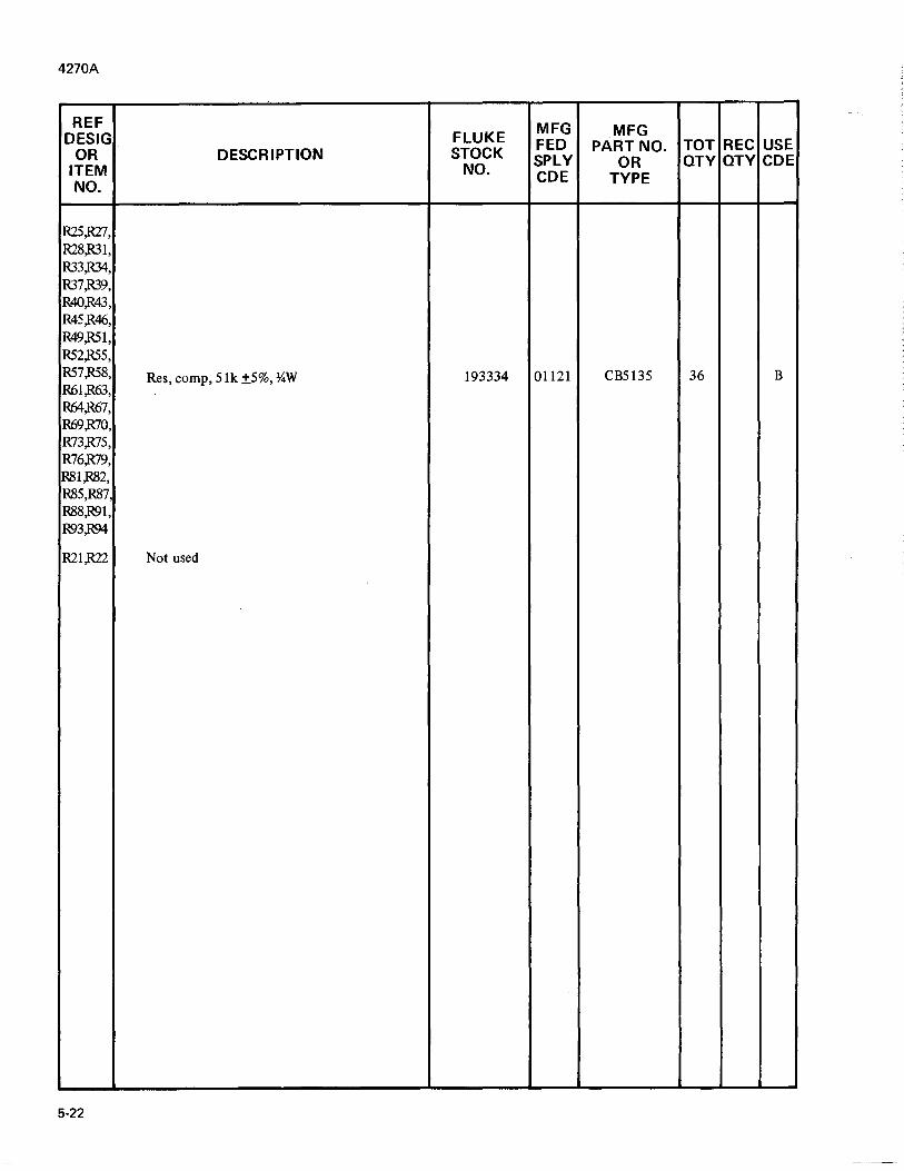
4270A
REF OESIG FLUKE MFG MFG
OR OESCR IPTION STOCK FEO PART NO. TOT REC USE
ITEM NO. SPLY OR OTY OTY COE
NO. COE TYPE
R25,R27, R28,R31, R33,R34, R37,R39, R40,R43, R45,R46, R49,R51, R52,R55, R57,R58, Res, comp, 51k ±5%, Y-.W 193334 01121 CB5135 36 R61,R63,
B
R64,R67, R69,R70, R73,R75, R76,R79, R81,R82, R85,R87, R88,R91, R93,R94
R21,R22 Not used
5·22

4270A
Figure 5-6. BINARY LADDER PCB ASSEMBLY
5-23

4270A
REF MFG MFG DESIG FLUKE OR DESCRIPTION STOCK
FED PART NO. TOT REC USE
ITEM NO. SPLY OR OTY OTY CDE
NO. CDE TYPE
A6 LOGIC ASSEMBL Y 365692 89536 365692 REF
Figure 5·7
Cl Cap, mylar, 0.001 uF ±IO%, 200V 159582 56289 10292 1
C2,C3 Cap, mica, 12 pF ±5%, 500V 175224 71232 DMI5C120J 2
C4,C47 Cap, mica, 100 pF ±1 %, 500V 226126 71236 DM15FI0lF 2
C5 -Cap, Ta, 0.68 uF ±1O%, 35V 182790 56289 150D684X935A 1
C6 Cap, polyst, .0033 uF ±2%, 100V 168344 02799 PE·332·G 1
C7,C8, C9,C29, Cap, mica, 56 pF ±5%, 500V 148528 71236 DM15F560J 5
C50
CI0 Cap, mica, 270 pF ±5%, 500V 148452 71236 DMI5F271J 1
Cll thru C15,C16 thruC25 C28,C34 Cap, cer, 0.025 uF ±20%, 50V 168435 56289 C023BI0IH253 27 thruC40 M C43 thru C46
C26,C42 Cap, elect, 220 uF -10/+50%, lOV 236935 25403 ET221XOlOA5 2 -
C27 Cap, cer, .0027 uF ±GMV, 600V 106211 56289 5GA·D33 1
C30 Cap, mica, 620 pF ±5%, 500V 215244 71236 DM19F621J 1
C31,C49 Cap, mica, 360 pF ±1 %, 500V 170407 71236 DM15F361F 2
C32 Cap, mica, 220 pF ±5%, 500V 170423 71236 DM15F221J 1
C33 Cap, plstc, 0.10 uF ±1O%, 500V 271866 06001 75F2R5AI04 I
C41 Not Used
C48 Cap, polyst, 0.0075 uF ±2%, 100V 168369 02799 PE·752·G I
CR3,CR4 Diode, Hi·speed sWitching 256339 28480 5082-2900 2
CRSthn.l CR9 Diode, Si, 150 rnA 203323 03508 DHDl105 5
Ql, Q3 Xstr, Si, NPN 159855 07910 CS23030 14 thru QI5
Q2,QI6 Xstr, Si, uni·junction 268110 03508 2N6027 2
Rl Res, met fUm, 523 ±l %, 1/8W 294835 91637 MFF1·85230F I
5·24

4270A
REF MFG MFG DESIG FLUKE OR DESCRIPTION STOCK FED PART NO. TOT REC USE
ITEM NO. SPLY OR OTY OTY CDE NO. CDE TYPE
/
R2, Rl3, R23,R24, R27,R29, Res, comp, 1.0k ±5%, Y4W 148023 01121 CB1025 12 R31,R33, R41,R44, R46,R50
R3 Res, comp, 2.7 ±5%, Y4W 246744 01121 CB2705 1
R4 Res, comp, l.5k ±5%, Y4W 148031 01121 CB1525 1
RS,R6, Not used 'R7
R8 Res, met fIlm, 11.5k ±1%, 1/8W 267138 91637 MFFI-81152F 1
R9,R54 Re, comp, lOOk ±5%, Y4W 148189 01121 CBI045 2
RlO,R55 Res, comp, 390k ±5%, Y4W 193383 01121 CB3945 2
Rll,R58 Res, comp, 390 ±5%, Y4W 147975 01121 CB3915 2
R12 Res, comp, 13k ±5%, Y4W 234252 01121 CB1325 1
R14 Res,met fIlm, 32.4k ±1%, 1/8W 182956 91637 MFFI-83242F 1
R15 Res, comp, 12k ±5%, Y4W 159731 01121 CB1235 1
Rl6,R37 thru R4(J Res, comp, 200 ±5%, Y4W 193482 01121 CB2015 7 R42,Rro
Rl7,R21, Res, comp, 510 ±5%, Y4W 218032 01121 CB5115 4 R25,R51
Rl8,R36, R45,R47, Res, comp, 33k ±5%, Y4W 148056 01121 CB3325 7 R48,R49, RS9
Rl9,R20 Res, met fIlm, 6.98k ±I %, 1/8W 261685 91637 MFFI-8698IF 2
R22,R26, R28,R30, Res, comp, 51 ±5%, Y4W 221879 01121 CB5105 6
R32,R43
R34 Res,met fIlm, 13k±I%, 1/8W 335539 91637 MFFI-8133F I
R35 Not used
R52,R56 Res, met fIlm, 10k ±I%, 1/8W 168260 91637 MFFI-8103F 2
R53 Res, met fIlm, 28k ±I%, 1/8W 291385 91637 MFFI-8283F I
RS7 Res, comp, 27k ±5%, Y4W 148148 01121 CB2735 1
5-25

4270A
REF MFG DESIG FLUKE MFG OR DESCRIPTION STOCK FED PART NO. TOT REC USE
ITEM NO. SPLY OR OTY OTY CDE NO. CDE TYPE
R61 Res, comp, 5 .lk ±5%, %W 193342 01121 C85125 1
T1 thru T6 Xfmr 299594 89536 299594 6
Ul,U2 IC, TTL, MSI, 8-Input Multiplexer 326165 07263 9313 2
U3, Ul6 IC, TTL, Hex Inverter 293076 01295 SN74H04N 2
U4 IC, TTL, MSI, Digital Multiplexer 288852 04713 MC8312 1
U5 IC, TTL, MSI, Synchronous 4-bit up-down 293183 01295 SN74193N 1
counter
U6, U26 IC, TTL, Hex Inverter 292979 01295 SN7404N 2
U7 IC, TTL, JK Master-Slave Flip-Flop 296491 01295 SN7472N 1
U8, Ul7 IC, TTL, Dual Retriggerable Monostable 310235 01295 SN74123N 2
Mul tivibrator
U9 IC, TTL, Dual 2 Wide, 2-Input and-or-inverter 293084 01295 SN74H51N 1
gate
UlO IC, TTL, JK Negative Edge Triggered Flip- 293092 01295 SN74HI02N 1
Flop with AND Inputs
Ull IC, TTL, Quadruple, 2-Input Positive AND gate 292987 01295 SN7408N 1
Ul2 IC, TTL, Quad, 2-Input NAND Gate 292953 01295 SN7400N 1
U13,U14 IC, TTL, Dual Peripheral Pos NAND Driver 329706 01295 SN75452P 2
UI5,U18 IC, TTL, Monostable, Multivibrator 293050 01295 SN74121N 2
Ul9 IC, TTL, Retriggerable Monostable 293134 07263 U6A960159X 1
Multivibrator
U20,U21 IC, TTL, 8-bit Parallel outshift register 272138 01295 SN74164N 3 U22
Connector, female 267252 13511 5740360 1
Guard, logic 331785 89536 331785 1
5-26
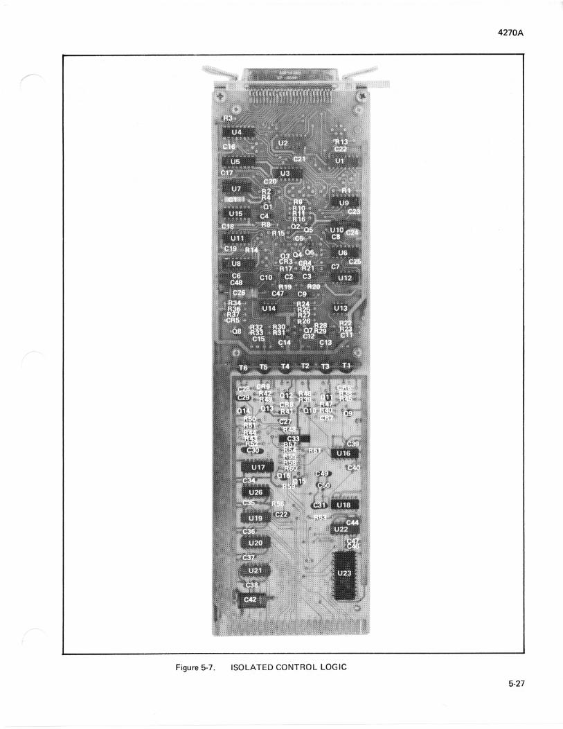
4270A
Figure 5-7. ISOLATED CONTROL LOGIC
5-27

4270A
REF MFG MFG DESIG FLUKE
OR DESCRIPTION STOCK FED PART NO. TOT REC USE
ITEM NO. SPLY OR OTY OTY CDE
NO. CDE TYPE
A7 BCD DISPLAY PCB ASSEMBLY 302257 89536 302257 REF
PANEL DISPLAY OPTION
Figure 5-8
CRlthru CR27 Diode, light emitting 309617 27
Rlthru R27 Res, comp, 270 ±5%, Y4W 160804 01121 CB2715 27
U1 thru US IC, TTL, Hex Inverter 292979 01295 SN7404N 5
@1 -[ID @z -mJ-{}!D- @3 -rm- @4 ~@6 -ill}- @II -ill]- @7 -em--ill]-
@8 {M]- @a --I!ID- @1O EJ@ll -oon- @12 -[[ID- @13 -ill!}--{KID- @14 R14 -{fiill- @15 ~ @16 ~~ @17 ~ @18 {ill}-
-{ill]- @19 EJ ~ ~20 ~ CRZ1 illY- @ZZ ~ @Z3 ~ @Z4
~ -rnru- @25
ill!J- @Z6
@m 302257
ill!}-
-
Figure 5·8. BCD D ISPLA Y PCB ASSEMB L Y
5·28

4270A
CURRENT LIMIT PCB ASSEMBLY (-06 Option)
REF MFG MFG DESIG FLUKE FED PART NO. TOT REC USE OR DESCRIPTION STOCK SPLY OR OTY OTY CDE
ITEM NO. NO. CDE TYPE
A8 CURRENT LIMIT PCB ASSEMBLY 332973 89536 332973 REF (-06 Option)
Figure 5-9
Cl, C2, Cap, plstc, 0.1 J.1f ±10%, 250V 161992 73445 C280AE/ 3 C12 AlOOK
C3 Cap, mica, 10 pf ±10%, 500V 175216 71236 DM15C100K 1
C4, Cap, plstc, 0.033 J.1f± 10%, 200V 106062 56289 192P33392 2 C5
C6 Cap, mica, 4 pf ±5%, 500V 190397 73236 DMI5C040J 1
C7 Cap, mica, 27 pf ±5%, 500V 177998 71236 DM15E27OJ 1
C8, C9, C13, Cap,cer, 0.0012J.1f±10%, 500V 106732 71590 CP122 6 thru C16
C10, Cap, mica, 33 pf ±5%, 500V 160317 71236 DM15E330J 2 C11
C17 Cap, plstc, 0.022 J.1f ±10%, 250V 234484 73445 C280AE/ A22K 1
CR1, Diode, zener, 16V 113332 07910 1N966A 2 CR2
CR3, CR5, Diode, zener, 20 rnA, 3.9V 113316 07910 1N748 4 CR10, CR11
CR4, Diode, zener, 12.5 rnA 246611 07910 1N961B 2 CR8,
CR6, Diode, zener, 36V 186163 07910 1N974B 2 CR9
CR7 Diode, zener, 6.3V, 7.5 rnA 172148 03877 1N3496 1
5·29

4270A CURRENT LIMIT PCB ASSEMBLY (-06 Option) Cont.
REF MFG MFG DESIG FLUKE OR DESCRIPTION STOCK FED PART NO. TOT REC USE
ITEM NO. SPLY OR OTY OTY CDE
NO. CDE TYPE
Q1,Q2, Xstr, Si, NPN 218396 04713 2N3904 9 Q5,Q8, Qll,Q14, Q16, Q19, Q20
Q3,Q7, Xstr, Si, PNP 195974 04713 2N3906 7
QlO,Q13, Q15, Q21, Q23
04,06, Xstr, J-FET, N-channel 261578 07910 U2366E 5
09, Q12, Q26
Q17 Xstr, semicon, Si, PNP, dual 242016 07263 SE 4901 1 - -,
Q18 Xstr, Si, PNP 276899 95303 2N5415 1
Q22 Xstr, Si, PNP 284448 95303 2N5416 1
Q24, Q28 Xstr, Si, NPN 218511 95303 60994 2
Q25 Xstr, Si, NPN 220087 24355 00/17 1
Q27 Xstr, Si, NPN 335067 04713 2N3439 1
R1 Res, comp, 39k±5%, 1W 236729 01121 GB3935 1
R2, Res, comp, 8.2k ±5%, 2W 330555 01121 HB8225 2 R58
R3 Res, met fim, 649 ±1%, 1/8W 309955 91637 MFFl-8649F 1
R4 Res, met fim, 750±1%, 1/8W 312801 91637 MFFl-8751F 1
R5 Res, var, cermet, 500 ±1Q%, 1 W 291120 71450 3608-501A 1
R6 Res, met fim, p ±1%, 1/8W 296434 91637 MFFl-8151F 1
R7, R56, Res, comp, 2.7k :!:5%, 2W 330548 01121 HB2725 3 R57
5-30

4270A
CURRENT LIMIT PCB ASSEMBLY (-06 Option) Cont.
REF MFG MFG DESIG FLUKE FED PART NO. TOT REC USE
OR DESCRIPTION STOCK SPLY OR OTY OTY CDE ITEM NO. NO.
CDE TYPE
R8 Res, comp, 47k±5%, %W 148163 01121 CB4735 1
R9 Res, comp, 10k ±5%, %W 148106 01121 CB1035 1
RIO, Res, comp, 24k ±5% , %W 193425 01121 CB2435 5
R12, R16, R19, R22
R11, Res, comp, 12k ±5%, %W 159731 01121 CB1235 6
R13, R17, R21, R23, R33
R14, Res, comp, 27k ±5%, %W 148148 01121 CB2725 5 R18, R20, R32, RSO
R15, Res, met tIm, 6.19k±1%, 1/8W 283911 91637 MFFl-86R19F 2 RS4
R24, Res,met tIm, 10k±1%, 1/8W 168260 91637 MFF1=8103F 2 R25
R26, Res, comp, 5.1M±5%, %W 294467 01121 CB5155 2 R35
R27 Res, compo 5.1k±5%, %W 193342 01121 CB5125 1
R28, R34 Res, comp, 10M ±5%, %W 194944 01121 CB1065 2
R29, Res, var, cermet, 20k ±10%, YZW 291609 71450 360S-203A 2 RS3
R30, Res, met tIm, 24.9k±1%, 1/8W 291369 91637 MFFl-824R9F 2 R52
R31 Res, met tIm, 2.74k±1%' 1/8W 293761 91637 MFFl-82R74F 1
R36, Res, comp, 22k :!:.5%, 1 W 330530 01121 GB 2235 2 R49
5-31

4270A CURRENT LIMIT PCB ASSEMBLY (-06 Option)Cont.
REF MFG MFG DESIG FLUKE
OR DESCRIPTION STOCK FED PART NO. TOT REC USE
ITEM NO. SPLY OR OTY OTY CDE
NO. CDE TYPE
R37, Res, comp 36k.±5%, 7flW 221929 01121 CB3635 2
R48
R38, Res, comp, 39k ±5%, 7flW 188466 01121 CB3935 2
R46
R39, Res, comp, 36k ±5%, 1 W 109736 01121 CB3635 2
R47
R40, Res, compo 120 ±5%, 7flW 170712 01121 CB1215 2
R45
R41, R44, Res, compo 1.2k ±5%, 7flW 190371 01121 CBl225 3
RS9
R42, Res, comp, 100 ±5%, 7flW 147926 01121 CBlO15 2
R43
RS1 Res, WW, 2 ±1%, 2W 229542 56289 223E 1
R55 Res, met flm, 12.4k ± 1%, 1 j8W 261644 91637 MFFl-812$4F 1
R60, R61, Res, comp 50 ±5%, 7flW 147900 01121 CB5605 3
R62
U1, IC, Hex Inverter 268367 04713 MC 836P 2
U2
U3, IC, Operational Amplifier 271502 12090 LM301A 2 U4
5-32
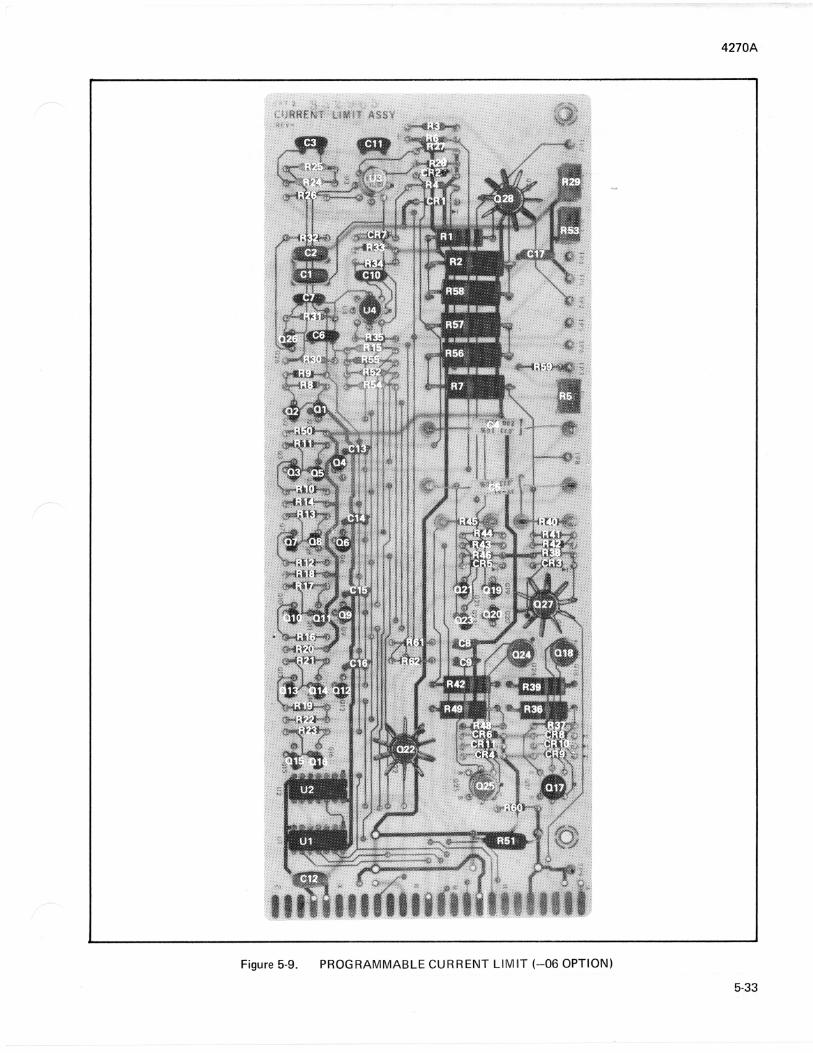
4270A
Figure 5-9. PROGRAMMABLE CURRENT LIM IT (- 06 OPTION)
5-33
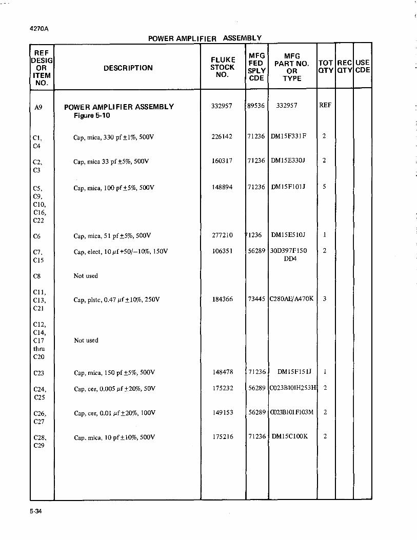
4270A
POWER AMPLIFIER ASSEMBLY
REF MFG MFG DESIG FLUKE
OR DESCRIPTION STOCK FED PART NO. TOT REC USE
ITEM NO. SPLY OR OTY OTY CDE
NO. CDE TYPE
A9 POWER AMPLIFIER ASSEMBLY 332957 89536 332957 REF
Figure 5-10
C1, Cap, mica, 330 pf ±1 %, 500V 226142 71236 DM15F331F 2
C4
C2, Cap, mica 33 pf ±5%, 500V 160317 71236 DM15E330J 2
C3
C5, Cap, mica, 100 pf ±5%, 500V 148894 71236 DM15F10lJ 5
C9, C10, C16, C22
C6 Cap, mica, 51 pf ±5%, 500V 277210 1236 DM15E51OJ 1
C7, Cap, elect, 10J.Lf+50/-1Q%, 150V 106351 56289 30D397F150 2
CIS DD4
C8 Not used
C11, C13, Cap, plstc, 0.47 J.Lf ±1Q%, 250V 184366 73445 C280AE! A470K 3
C21
C12, C14, C17 Not used thru C20
C23 Cap, mica, 150 pf ±5%, 500V 148478 71236 DM15F151J 1
C24, Cap, cer, 0.005 J.Lf ±2Q%, 50V 175232 56289 C023BlOIH253H 2
C25
C26, Cap, cer, 0.01 J.Lf ±20%, 100V 149153 56289 C023B101 F103M 2
C27
C28, Cap, mica, 10 pf±lO%, 500V 175216 71236 DM15C100K 2
C29
5-34

4270A
POWER AMPLI FIER ASSEMBLY (Cont)
REF MFG MFG DESIG FLUKE FED PART NO. TOT REC USE
OR DESCRIPTION STOCK SPLY OR OTY OTY CDE ITEM NO. CDE TYPE NO.
CRI Diode, Si, 150 rnA 203323 03508 DHDII05 15
thm CRIO, CRI9, (
CR20, CR35, CR36, CR37
CR11 Not used
CR12 Diode, zener, 6.8V 260695 07910 IN754A 1
CR13 Not Used
CRI4, Diode, Si, 1 amp, 600 piv 112383 05277 IN4822 12
CRI6, CR24, CR25, CR27 thm CR30, CR33, CR34, CR38, CR39
CRI5, Not Used CRI7, CRI8, CR21, CR22, CR23, CR26, CR31, CR32
CR40, Diode, FET 334714 07910 TCR 5315 2 CR41
Ql Xstr, Si, PNP 276899 95303 2N5415 1
Q2, Xstr, Si, NPN 335067 04713 2N3439 8 Q3, Q8, Q11, Q13, Q18, Q26, Q38
5-35

4270A
POWER AMPLIFIER ASSEMBLY (Cont)
REF MFG MFG DESIG FLUKE FED PART NO. TOT REC USE
OR DESCRIPTION STOCK SPLY OR OTY OTY CDE ITEM NO. NO.
CDE TYPE
Q4, Xstr, Si, NPN 218511 9530 60994 6 Q20, thru Q25
Q5, Xstr, Si, PNP 284448 05303 2N5416 9 Q6, Q7, Q9, Q10, Q12, Q14, Q17, Q30
Q15, Xstr, Si, PNP 195974 04713 2N3906 2 Q35
Q16, Xstr, Si, NPN 218396 04713 2N3904 3 Q19, Q34
Q27, Not used Q28, Q29
Q31 Xstr, Si, NPN 190710 04713 2N3739 1
Q32, Xstr, Si, NPN, power (on He at sink) 313213 95303 2N5240 4 Q33, 041, 042
Q36 Not used
Q37 Xstr, Si, PNP, power 309302 04713 2N5345 1
Q39, Not used 040
R1, Res, comp, 2k ±5%, %W 202879 01121 CB2025 5 R2, R9, RIO, R23
R3, Res, comp, 20k ± 5%, %W 221614 01121 CB2035 4 R8, R69, R73
R4, Res, comp,62k ±5%, %W 220053 01121 CB6235 2 R6
RS, Res, comp, 270 ±5%, %W 160804 01121 CB2715 2
R7
5-36

4270A
REF MFG MFG DESIG FLUKE OR DESCRIPTION STOCK FED PART NO. TOT REC USE
ITEM NO. SPLY OR OTY OTY CDE
NO. CDE TYPE
Rll Res,met flm,4.12k±1%, 1/8W 235341 91637 MFFl-84R12F 1
R12, R65, Res, comp, 1k ±5%, !f4W 148023 01121 CB1025 3
R67
R13, R31, Res, comp, 100 ±5%, !f4W 147926 01121 CB1015 3
R40
R14,R18 Res, comp, 250k ±5%,!f4W .. 218016 01121 CB2445 2
R15, R19, Res, comp, 330k ±5%, !f4W 192948 01121 CB3345 3
R63
R16,R17 Res, comp, 6.2k ±5%,!f4W 221911 01121 CB6225 2
R20,R22 Res, comp, 10k ±5%, !f4W 148106 01121 CB1035 2
R21 Res, met flm, 10k ±1 %, 1/8W 168260 91637 MFFl-8103F 1
R24 Res,met flm,6.04k±1%, 1/8W 285189 91637 MFFl-86R04F 1
R25 Res,met flm, 15.8k±1%, 1/8W . 293688 91637 MFFl-815R8F 1
R26,R33 Res, comp, 7 .5k ±5%, 14W 193326 01121 CB7525 2
R27,R32 Res, comp, 130k ±5%, YzW 108852 01121 EB1345 2
R28,R29 Res, comp, 180 ±5%,!f4W 147942 01121 CB1815 2
R30 Res, comp, 33k ±5%, 1W 109538 01121 GB3335 1
R34,R35 Not Used
R36,R50, Rro,R61, Res, comp, lOOk ±5%,!f4W 148189 01121 CBI045 8 R68,R70, R71,R72
R37,R53 Res, comp, 68 ±5%, !f4W 147918 01121 CB6805 2
R38,R39, Res, comp, 1 ±5%, !f4W 218693 01121 EBlOG5 4
R56,R57
R41 Res,met flm,23.7k±I%, 1W 330506 91637 MFFI-23R7F 1
R42,R45 Res, met flm, 127 ±1 %, 1/8t 330944 91637 MFFl-8127F 2
R43,R47 Res, comp, 1.1 ±5%, YzW 163717 01121 EBllG5 2
R44,R46, Not used R48
R49 Res, comp, 51 ±5%, YzW 144717 01121 EB5105 1
5-37

4270A
REF MFG MFG DESIG FLUKE FED PART NO. TOT REC USE OR DESCRIPTION STOCK SPLY OR OTY OTY CDE ITEM NO. CDE TYPE NO.
RS1 Res, var, cermet, 100 ±1Q%, 1W 285130 71450 360S·101A 1
R52,R54, Not used RS5
R58 Res, comp, 20k ±5%, 1W 330951 01121 GB2035 1
RS9 Not used
R62 Res,met flm,54.8k±1%, 1/8W 271353 91637 MFF1·854R9F 1
R64,R66 Res, comp, 1M ±5%, ~W 182204 01121 CB1055 2
Heat Sink 302141 89536 302141 1
Conn, assy. 310771 89536 310771 5
5·38

4270A
Figure 5-10. POWER AMPLIFIER
5-39

4270A
-.- -"- - - -= ~
REF MFG MFG DESIG FLUKE OR DESCRIPTION STOCK FED PART NO. TOT REC USE
ITEM NO. SPLY OR QTY QTY CDE
NO. CDE TYPE
A10 HIGH VOLTAGE POWER SUPPLY ASSY 333005 89536 333005 REF
AlOAl High Voltage Power Supply PCB 332916 89536 332916 1
(Figure 5-11)
T1 Xfmr, power 333799 89536 333799 1
Cord Set 248708 82877 16415 1
A10A1 High Voltage Power Supply PCB 332916 REF
C1,C4, Cap, cer, 0,01 uF ±20%, 500V 105668 56289 ic023B50IJ103 3
C6 M
C2,C3 Cap, elect, 1200 uF +75/-10%, 250V 329953 56289 36D 122G250OC 2 2B
C5 Not used
C7,C8 Cap, p1stc, 0.47 uF ±1O%, 250V 184366 56289 C280AE/A470K 2
CR1 thru Diode, Si, 1 amp, 600 piv 112383 05277 1N4822 4
CR4
CR5 thru Diode, zener 328820 04713 1N3040B 4
CR8
Q1,Q4 Xstr, Si, NPN (located on Heatsink) 223602 05277 2N3773 2
Q2 Xstr, Si, NPN 218511 95303 65120 1
Q3 Xstr, Si, PNP 276899 95303 2N5415 1
R1 Res, comp, 4.7k ±5%, Y2W 108886 01121 EB4725 1 .
R2,R3 Res, comp, 33k ±1O%, 2W 158964 01121 HB3331 2
R4,R6 Res, comp, 8.2k ±5%, 1 S 330936 01121 GB8225 2
R5 Not used
R7,R8 Res, comp, 6.8k ±5%, Y2W 187906 01121 EB6825 2
R9 Res, comp, 51 ±5%, Y2W 144717 01121 EB5105 1
Sl,S2 Switch, slide, dpdt 234278 82389 XW1649 2
Conn, recpt, amp 267534 00779 85884·3 6
Conn, Post 267500 00779 86144·2 8
Heatsink (use with Q2, Q3) 104646 05820 207-AB 2
Heatsink 334524 89536 334524 1
Socket, Xstr 342816 91506 X8080-1GlO 2
5-40
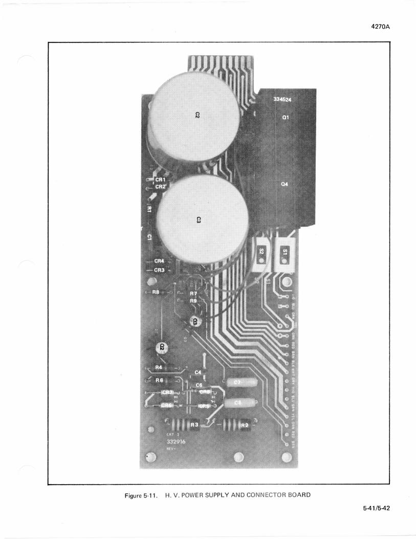
4270A
Figure 5-11 . H. V . POWER SUPPLY AND CONNECTOR BOARD
541/542

6-1. INTRODUCTION
6-2. The -07 Option provides 100~.tV resolution (E Decade) throughout the voltage range of 0 to 16.6665V dc ip. the Model 4210A. Status of the E decade is not provided on the front panel display.
6-3. SPECIFICATIONS
64. Specifications for the -07 Option are located in Section I of the manual.
6-5. INSTALLATION
6-6. Use the following procedure to install the -07 Option into the Model 4210A.
a. Disconnect the power cord from line power.
b. Remove the top dust cover and the inner guard cover.
c.
1/20ns
Remove the AS BCD LADDER ASSY by using a gentle rocking motion and an even, rearward pulling force.
d.
e.
f.
g.
h.
6-7.
4200 SERIES OPTION -07
Option-07
100 ~V Resolution
Remove four mounting screws on rear panel adjacent to Programming Connector, J 1.
Insert the -07 Option, AS BCD Ladder into LADDER receptacle (12) on MOTHER ASSY.
Attach Programming Connector J I panel to rear panel of instrument using the four screws removed in step d.
Replace inner guard and top dust cover.
Reconnect power cord to line power.
OPERATING INSTRUCTIONS
6-8. Programming Information
6-9. Operation of the 4210A with the -07 Option is done in a manner similar to operation with the -01 Option, Isolated Control Logic, described in Section 2. Programming input/output lines for the Programming Connector are given in Table 6-l.
6-1

4200 SERIES OPTION -07
Table 6-1. PROGRAMMING INPUT/OUTPUTS
LOGIC "0" = 2.8 to +5.5Vdc or open circuit LOGIC "1" = 0 ±O.4Vdc or short circuit to LOGIC GRD.
PIN NO. FUNCTION CODE
1 8 2 4 A DECADE (1V) 3 2 4 1 5 8 6 4 B DECADE (0.1V) 7 2 8 1 9 8
10 4 C DECADE (0.01 V) 11 2 12 1 13 8 14 4 D DECADE (0.001V) 15 2 16 1 43 8 44 4 E DECADE (0.0001V) 45 2 46 1 17 18 20 21 LOGIC GRD 22 23 24 25 LOGIC PWR (+5 vdc at 0 to 125mA) 26 27 28 29 NOT USED 30 31 32 33 DATA STROBE (-01 Option) (See Figure 2-6)
INITIATES DIGITAL TO ANALOG CON-VERSION
34 STAN DBY /OPERA TE: LOGIC "0" = OPERATE LOGIC "1" = STANDBY
35 SIGN: LOGIC "0" = POSITIVE OUTPUT LOGIC "1" = NEGATIVE OUTPUT
36 EXTERNAL REFERENCE (-03 Option): LOGIC "0" = INTERNAL REFERENCE LOGIC "1" = EXTERNAL REFERENCE
37 READY/NOT READY FLAG: LOGIC "0" = READY LOGIC "1" = NOT READY
38 39 40 NOT USED 41 42 47 48 49 CURRENT OVERLOAD FLAG:
LOGIC "0" = NORMAL LOGIC "1" = OVERLOAD
50 NOT USED
6-2
6-10. Manual Operation
6-11. Operation of the 421OA-07 with the Accessory A4200 is done as follows:
a. Ensure that all push buttons on the A4200 are in the non-depressed condition.
b. Attach mating connector on A4200 cable to Programming Connector (11) on rear of Model 4210A -07.
c. To obtain E decade output voltage ranging from 100 to 1500~V, depress CURRENT LIMIT MA press-buttons 10,20,40, and 80 sequentially. The STROBE push-button must be depressed following each of the above. Depression of a current limit button followed by a STROBE calls an output voltage in microvolts that is ten times the button legend (s). A second depression followed by a STROBE removes the call.
6-12. THEORY OF OPERATION
6-13. General
6-14. A5 BCD Ladder (4210A-1032)
6-15. The AS BCD Ladder contains a buffer amplifier for V REF and the four lower decade segments of a ladder network. The buffer amplifier produces a V R' signal from V REF to prevent loading of V REF by ladder switching currents. The ladder decades are voltage dividers weighted in fIfteenths for control by digital words from 0 to 15 (8 + 4 + 2 + 1). The relative position of each decade with respect to the ladder output determines the significance of each decade's contribution to the total ladder network output.
6-16. BUFFER AMPLIFIER. The Buffer Amplifier composed of Ql through Q3 is a unity gain amplifier connected through CRI to function as a voltage follower. This circuit produces a V R' signal that is applied to the ladder driver circuits. Output impedance is sufficiently low from dc to 100 kHz to prevent loading by ladder switching currents.
6-17. LADDERS. The four lower decade ladders consist of Rl through R18 and R119 through R12. Each decade of the ladder is formed essentially by four resistors which, in combination, weight the division factor of each decade in fifteenths. A simplified diagram of a typical decade ladder is shown in Figure 6-1.
1/20n5

"S" 25K
"4" 50K
OUTPUT (Vol
"2" 100K
"1" 200K
V Vo IS AVAILABLE IN --BfE VOLT STEPS
15
Figure 6-1. LADDER DECADE (SIMPLIFIED)
6-18. MAINTENANCE PROCEDURES
6-1 (). Maintenance procedures for the Model 421OA-07 are the same as those given in Section 4 of the manual. A resolution check of the -07 Option is given in the following paragraphs.
6-20. This procedure provides a resolution check on the E decade. Required equipment is a FLUKE Model 8400A -01 AC/DC Voltmeter, or equivalent, and a FLUKE Model A4200 Manual Control Unit (MCU).
a. Connect Model A4200 MCU as described in steps 6-11., a. and b.
b. Connect Model 8400A-01 Voltmeter to ±OUTPUT TERMINALS of barrier strip on rear of Model 421OA-07.
c. With all decades set to zero, perform steps 1 through 5 in Table 6-3. Each push-button on the A4200 MCU must be released for each succeeding step following step 2. Each step also must be followed by a STROBE.
STEPS
1 2 3 4 50
4200 SERIES OPTION -07
Table 6-3. RESOLUTION CHECK
DECADE OUTPUT VOLTAGE (IlV)
E
0 o ±100 (Record voltage) 1 100llV > Step 1 Voltage 2 200llV > Step 1 Voltage 4 400llV > Step 1 Voltage 8 800llV > Step 1 Voltage
6-21. LIST OF REPLACEABLE PARTS
6-22. For column entry explanations, part ordering information and basic instrument configuration Use Codes and Serial Number Effectivity List, see Section 5, paragraphs 5-1 through 5-10. See paragraph 6-40, this option subsection, for additional Use Codes and Serial Number Effectivity List assigned to this printed circuit assembly option.
6-23. SERIAL NUMBER EFFECTIVITY
6-24. A Use Code column is provided to identify certain parts that have been added, deleted, or modified during production of the Model 421OA. Each part in this option for which a use code has been assigned may be identified with a particular serial number by consulting the Use Code Effectivity List below. All parts with no code are used on all serial numbers 123 and on. NOTE: These Use Codes and Serial Number Effectivity apply to this option only. For the standard instrument configuration, see Section 5, paragraph 5-9, and for additional options, see the appropriate option subsection.
USE
CODE SERIAL NUMBER EFFECTIVITY
1/20n5 6-3

4200 SERIES OPTION -07
REF DES
AS
Cl,C2
CRI
Ql
Q2
Q7,Qll, Q15, Q19, Q23, Q27, Q31, Q35, Q39, Q43, Q47, Q51, Q55, Q59, Q63, Q67
Q3
Q4
Q5,Q9, Q13 QI7,Q21, Q25, Q29, Q33, Q37, Q41, Q45, Q49, Q53, Q57, Q61, 065
Q6,Q8
~lO, Q12
914, Q16, ~18, Q20
922, Q24, g26, Q28, g30, Q32, g34, Q36, ~?,Q48, P50,Q52
g38, Q40, ~2,Q44, g54, Q56, g58, Q60, g62, Q64, ~66, Q68
R.l
R2
R3
R5
64
DESCRIPTION
BCD LADDER PCB ASSEMBLY -07 Option FIGURE 6-2.
Cap, cer, 0.05 uF ±20%, lOOY
Dio, silicon, 150 rnA
Dio, FET, current regulator
Xstr, silicon, NPN
Xstr, silicon, NPN
Xstr, silicon, PNP
Not used
Xstr, silicon, PNP
Xstr, J-FET, N-channel, U2366E, Matched Pair
Xstr, J-FET, N-channel, U2366E, Matched Pair
Xstr, J-FET N-channel, U2366e, Matched Pairs (Q14 matched to Q16; Q18 matched to Q20)
Xstr, J-FET, N-channel, U2366E, Matched Set
Xstr, J-FEr, N-channel
Res, var, cermet, 200il±10%, 1/2w
Res, WW, 24.987k
} Res, WW, 49.975k Matched Resistor Set
Res, WW, lOO.025k
SNO TOT RECM USE
QTY QTY CODE
322602 REF
149161 2
203323 1
285106 1
269084 1
218396 16
269076 1
195974 16
306399 1
306381 1
306373 2
298299 1
288324 12
285148 1
289827 1
1/20/75
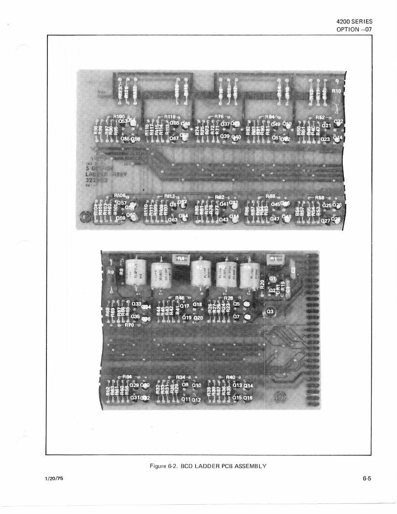
Figure 6-2. BCD LA DD ER PCB ASSEMB LY
1/20/15
4200 SERIES OPTION -07
6-5

4200 SERIES OPTION -07
REF DES
R6
R7
R4
R8
R9
RIO
R11
R12
R13, R18
R14, R120
R15, R119
R16, R121
R17, R122
R19
R24, R30, R36, R42, R48, R54, R60, R66, R72, R78, R84, R90, R96, R102, R108, R114
R20
R25, R27, R28, R31, 1R33, R34, 1R37, R39, ~40, R43, ~45, R46, R49, R51, ~52, R55, ~7,R58, ~61, R63, ~64, R67, ~69, R70, ~73, R75, ~76, R79, ~81, R82, ~85, R87, ~88, R91, R93, R94, R97, R99,
6-6
DESCRIPTION
Res, WW, 200.075k } Matched Resistor Set
Res, WW, 108k
Res, var, cermet, 50n ±10%, 1/2w
Res, met flm, 60.4n±1%, 1/8w
Res, WW, 24.987k ±0.03%, 1/4w
Res, WW, 50k±0.03%, 1/4w
Res, met flm, l00.03k±0.1%, 1/8w
Res, met flm, 200.08k ±0.1 %, 1/8w
Res, met flm, 108.06k±0.1%, 1/8w
Res, met flm, 49.9k±0.1%, 1/8w
Res, met flm, 24.9k±0.1%, 1/8w
Res, met flm, l00k±0.5%, 1/8w
Res, met flm, 200k±I%, 1/8w
Res, cmpsn, 1.8k ±5%, 1/4w
Res, cmpsn, 560n ±5%, 1/4w
Res, cmpsn, 20k±5%, 1/4w
Res, cmpsn, 51k±5%, 1/4w
SNO TOTRECM USE
QTY pTY CODE
289827 1
285122 1
235366 1
289769 1
289777 1
291088 1
290122 1
290114 2
291070 2
290106 2
291054 2
261701 2
175042 1
147991 16
221614 1
193334 48
1/20115

REF DES DESCRIPTION
RI00, RI03, RI0S, RI06, RI09, RIll, Res, cmpsn, Slk±S%, 1/4w R1l2, RllS, R1l7, R1l8
R21, R22 Not used
R23, R26, R29, R32, R3S, R38, R41, R44, R47, RSO, RS3, RS6, RS9, R62, R6S,R68, Res, cmpsn, 2.7k±S%, 1/4w R71, R74, R77, R80, R83, R86, R89, R92, R9S, R98, RIOl, RI04, RI07, RllO, RI13, R1l6
R123 Res, met flm, 120k±1%, 1/8w
1/20/15
SNO TOT pTY
193334 48
170720 32
291062 1
4200 SERIES OPTION -07
~ECM USE
pTY CODE
6-7/6-8

+VA
VREF
VA COMMON
-VA
-VLCOMMON
TO 1st DECADE
REF COMMON
Scans by => ARTEK HEDI/f @ 2003-2005
DRIVER CKT. REFERENCE DESIGNATIONS
DESIG. CKT 021 022 024 028 031 032 034 038 041 042 044 048 E·l E·2 E·4 E·8
RA 2.7K R23 R29 R35 R41 R47 R53 R59 R65 R71 R77 R83 R89 Rt5 Rl0l Rl07 Rl13
RB 560 R24 R30 R36 R42 R48 R54 R60 R66 R72 R78 R84 R90 Rt6 Rl02 Rl01 Rl14
RC 51K R25 R31 R37 R43 R49 R55 R61 R67 R73 R7t RI5 R91 Rt7 Rl03 Rl09 Rl15
RD 2.7K R2I R22 R31 R44 R50 R56 R62 RII R74 RIO RI6 R92 Rtl 'U ... Rll0 RIll
RE 51K/100K- R27 R33 R3. R45 R51 R57 RI3 Rlt R71 RI1 RI7 RI3 R99 Rl05 RIll Rl17
RF R21 R34 R40 R46 R52 R51 R64 R70 'R76 !RII RII Rt4 Rl00 Rl06 Rl12 RIll
C QA 2N3906 Q5 Q9 Q13 Q17 Q21 Q25 Q2. Q33 Q37 Q41 Q45 Q4' Q53 QI7 Q61 Q65
3 VR'
B
Qb U231IE/U1994E- Q6 Ql0 Q14 Q18 Q22 Q26 Q30 Q34 1IQ31 1Q42 Q46 Q50 *Q54 OQ5I OQ62 OQ66
QC 2N3904 Q7 Qll Q15 Q18 Q23 Q27 Q31 Q35 Q3t Q43 tH7 Q51 cas 5 Q5. Q63 Q67
2 QD U2311E/U 1994E- QI Q12 Ql1 Q20 Q24 Q21 Q32 Q31 1IQ40 1IQ44 Q41 Q52 OQII OQ60 OQ64 OQII
20 -VA
2~~ r------------------------------------------------------------LADDER-----------------------------------------------------------------------------------------,
A Rl
D~ 200
S B8
R P B4 BZ
\~-------------.. V B DECADE
R7- R8 108K 60.4
N Bl
1 \
W C8
V C4
C V
U
Rll 100.03K
C2
DECADE DRIVER
(16 PLACES)
RA
LOGIC BIT INPUT IOV = TRUE)
T Cl
R13 108.06K
( \
VR'
RE
R15
19 08
VREF
R14 49.9K
11 04
17 DZ
R18 120K
R17
16 01
Rl19 Z4.9K
5 EI
R1Z0 49.9K
I F E4 EZ
7 El
R123 120K
V \ 1 ~--------~Vr---------~
,...-_____ --1
D DECADE E DECADE
TO LADDER RESISTOR
NOTES:
1. ALL CAPACITANCE IN uF UNLESS OTHERWISE NOTED
2.
3.
4.
W LOGIC GROUND
\] COMMON
~ PCB CONNECTOR
5. * FACTORY INSTALLED
6. W REF COMMON
FUNCTIONAL SCHEMATIC DIAGRAM
A5 OPTION-07
BCD LADDER
DRAWING NO. 4210A·1032 r IFLUKEI .JOHN FLUKE MFG. CO .• INC .
• P.O 80. 7428 Seattl •. Wo,hlnQton 98133

4200 SERIES OPTION -09
Option-09
Multi-Strobe Isolated Logic
6-1. INTRODUCTION
6-2. The 4200-09 Multi-Strobe Isolated Logic pennits any of the Fluke 4200 Series Programmable Voltage Sources (hereafter referred to as the 4200) to be remotely controlled by a large variety of program sources such as a computer, a system coupler, as well as a Fluke Automatic Test Equipment System. The 4200-09 consists of a pair of printed circuit boards mounted as one assembly and connected together by means of a ribbon-type cable. The entire assembly mounts within the 4200 and is accessed through an opening in the rear panel and a 50-pin connector. Up to eight 4200 series power sources equipped with the -09 option (4200-09) may be connected to and addressed by a single program source.
6-3. Programming the 4200 series voltage sources requires that the program source provide certain information to the 4200-09. Such program information required to generate specific output voltages, includes:
a. Output voltage magnitude.
b. Output voltage range.
c. Output voltage polarity.
d. Current limit magnitude.
e. Strobe pulse (s).
f.
g.
1I20ns
Voltage source mainframe address.
Operate/Standby signal.
CAUTION!
The Model A4200 MeV is NOT compatible with the -09 option.
6-4. In addition to providing signals to the voltage source, the program source should also have the capability to receive status information from the voltage source. By means of unique voltage source mainframe addresses, the program source can determine the status of any particular voltage source in the system. (Refer to Status Checking for details.)
6-5. CONNECTION TO PROGRAM SOURCE
6-6. Connection of the program source to the 4200 is made by means of an interconnecting cable and a 50-pin connector on the rear panel of the 4200. (Refer to Figure 6-1.) The mating connector used on the interconnecting cable is an Amphenol Blue Ribbon 57-30500, Fluke stock number 266056. Up to eight 4200's may be connected to a single program source as shown in Figure 6-2. The first 4200 connects to the program source interface, the second 4200 connects to the first, the third to the second, etc. The cable assemblies used to connect the 4200's are Fluke Stock Number
6-7. INPUT/OUTPUT SIGNALS
6-8. Details of the interface siganls between the 4200-09 and the program source are listed in the following Tables 6-1 and 6-2. Table 6-2 describes those interface signals between th(~ 4200-09 and a program source interface which communicates in binary format. (Positive-true logic employs +5 volts for a logic 1 and zero volts for a logic 0.)
6-'

4200 SERIES OPTION -09
NOTE!
Not all the signals listed in Tables 6-/ and 6-2 apply to all 4200 series voltage sources. For specific programming requirements, refer to the Programming Information given in Section 2 of the technical manual for the particular model voltage source.
NOTE!
The following paragraphs provide jumpering instructions for the 4200-09. Table 6-3 provides abbreviated jumpering instructions with reference to the appropriate text.
56-PIN CARD EDGE CONNECTOR
(TO SUCCEEDING 4200)
I
(CONNECTS TO PROGRAM SOURCE
OR PRECEDING 4200)
Figure 6-1. 4200-09 CONNECTORS
6-2
CABLE ASSEMBLY
(CUSTOM-BUI L T TO SUITE PROGRAM SOURCE)
PROGRAM SOURCE INTERFACE
TO SUCCEEDING 4200 - UP TO A TOTAL OF EIGHT UNITS
Figure 6-2. MULTIPLE 4200 CONNECTIONS
6-9. DATA WORD/CONTROL WORD LENGTHS
6-10. BCD - Type Voltage Sources
6-11. Program data for BCD-type 4200 voltage sources consists of a 16-bit or a 18-bit data word, and if necessary a control word (up to eight bits in length). Figure 6-3 shows a typical 16-bit data word and an eight-bit control word used to program a BCD-type voltage source. By keeping the four BCD digits of output magnitude data separate from the range, polarity and current limit functions, output voltage can be changed without affecting functions established by a previous control word. To obtain a 16-bit data word and an eight-bit control word, jumper pad T to pad U.
NOTE!
The first bit of the control word may be either the polarity bit or the standby/operate bit. Refer to paragraph 6-22.

4200 SERIES OPTION -09
Table 6-1. INPUT/OUTPUT SIGNALS, BCD PROGRAM SOURCE (Sheet 1 of 2)
PIN NUMBER
50 - PIN
CONN.
56 - PIN
CONN.
43, 44, 19, 44,43,
& 42 42 & 41
38, 8,
25 & 24
39,40,
11 & 10
13, 15,
12 & 14
26
31
2
37, 35,
5 & 3
17
23,22,
34,7,6
&4
40, 39,
38 & 37
36,35
34 & 33
32,31,
30 & 29
53
27
55
28
4, 3,
2 & 1
45
46 thru 52
SIGNAL NAME
Voltage output
magnitude - MSD
Voltage output
magnitude - 2SD
Voltage output
magnitude - 3SD
Voltage output
magnitude - LSD
Polarity (Sign)
Output Magnitude
Range
External Reference
Current Limit
range
Current Limit
Magnitude
Standby/operate
(address zero)
Standby/operate
(addresses one
through seven)
DESCRIPTION
Four BCD lines to program the most-significant digit of
the output voltage. (Refer also to the schematic diagram
for pin number assignments.)
Four BCD lines to program the second most-significant
digit of the output voltage.
Four BCD I ines to program the third most-significant digit
of the output voltage.
Four BCD lines to program the least significant digit of the
output voltage.
Single line to program output polarity. Either polarity
can be programmed by either logic level as selected by
jumpers at PCB pads, W, X, and Y.
Single line to program output magnitude range on those
voltage sources requiring range selection. (Logic 1 = high
range, Logic 0 = low range)
Single line to program external reference mode on those
voltage sources equipped with the external reference option.
(Logic 1 = ext. reference, Logic 0 = into reference.)
Single line to program range of current output limiting
on those voltage sources equipped current limit selection.
(Logic 1 = 1 amp ran!le, logic 0 = 100 mA range)
Four lines to select the current limit value, expressed as a
percentage of the programmed range. Up to 120% can be
programmed. Any attempt to program 0% results in 10%.
(Refer also to the schematic diagram for pin number
assignments.)
Single line used to select the standby or operate mode of
the voltage source. Either mode can be programmed by
either logic level as selected by jumpers at PCB pads 18 and
19.
Seven lines (through connections) used to select the standby
or operate mode of up to seven succeeding voltage sources.
(Refer to schematic diagram for pin number assignments.)
6-3

------4200 SERIES OPTION -09
Table 6-1. INPUT/OUTPUT SIGNALS, BCD PROGRAM SOURCE (Sheet 2 of 2)
PIN NUMBER
50 - PIN
CONN.
20
56 - PIN
CONN.
12
21 & 5 thru 11
45 thru 50
18 13
36 14
9 12
29 22
28 21
23
30 27
16 25
6-4
SIGNAL NAME
Instrument main
frame (address
zero)
I nstrument mainframe
addresses one through
seven.
Control word
strobe
Data word strobe
Poll status
Polled current
limit flag
Polled power-off
flag
Abnormal status
Vcc
Ready Flag
DESCRIPTION
Single line used to address the voltage source in order to per
form any programming function. The addressing signal
must be present in order for any strobe signal to be
recognized by the 4200-09 logic. Addressing may be by
either logic level as selected by jumpers at PCB pads 8, 9, and 10. Refer also to Addressing Multiple Mainframes.
Seven lines (through connections) used to address up to
seven succeeding voltage sources.
Single line which accepts a 500 ns, or longer, pulse to
load the control word portion of the program data into
the 4200-09 assembly. (Refer also to Dual-Strobe Opera
tion) Either logic level may be used as selected by
jumpers on PCB pads, 5, 6 and 7.
Single line which accepts a 500 ns, or longer, oulse to load
the data word portion of the program data into the 4200-09 assembly. (Refer also to Dual-Strobe Operation)
Either logic level may be used as selected by jumpers on
PCB pads 22, 23 and 24.
Single line used to poll status (Vcc failure and current limit
mode). A logic 0 causes the generation of Vcc and cur
rent limit status of their respective outputs.
Single line which generates a logic 0 when the polled
4200 is in the current limit mode.
Single line which generates a logic 0 when the Vcc supply
of the polled 4200 fails (power off).
Single line which generates a logic 0 whenever the 4200 goes to the current limit mode or the Vcc supply fails
(power off). This status lines does not need to be polled.
Single line which provides Vcc to the status logic on the
4200-09. (This is necessary iin order to obtain polled power-off status when power is off.) Current requirement
is two milliamperes per power source.
Single line which provides a logic 0 when any 4200-09 is not ready to receive a strobe signal. This signal is present while the 4200 is changing output voltage as result of a
previous strobe signal.
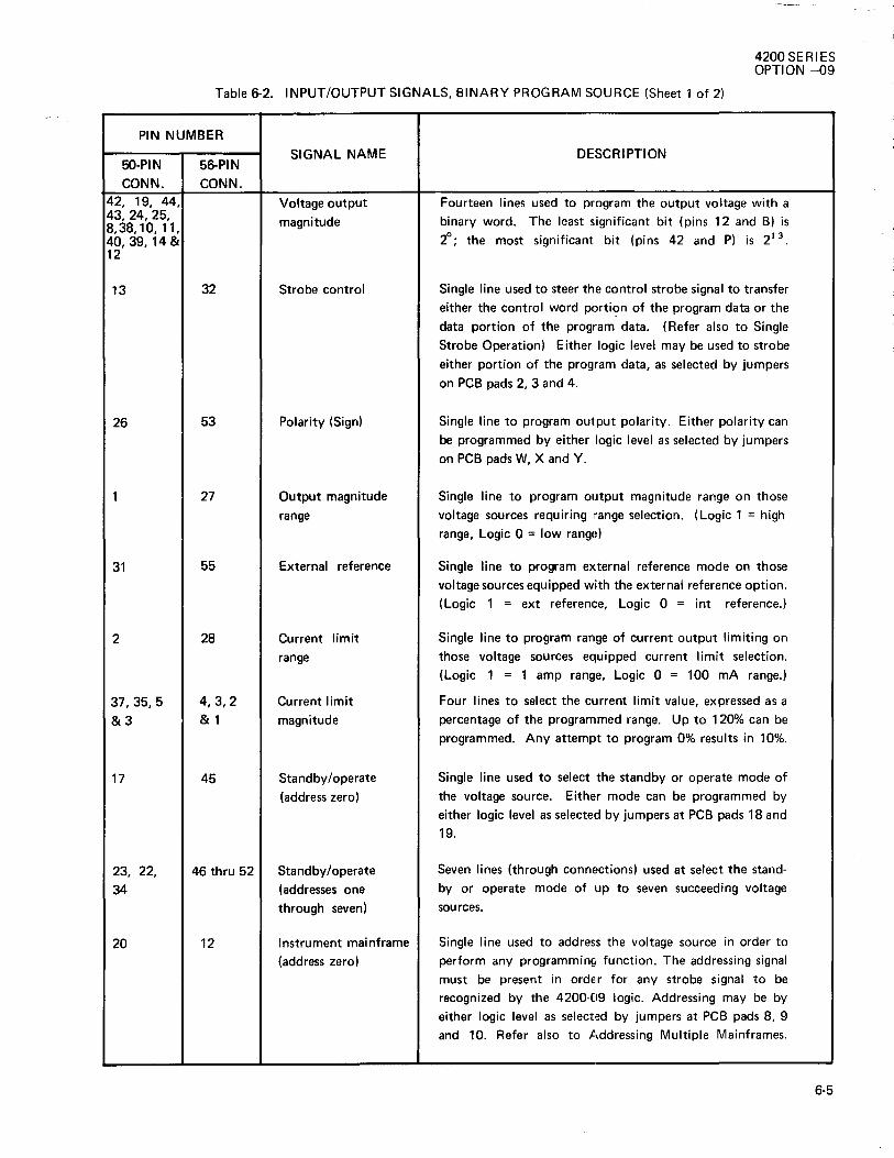
4200 SERIES OPTION -09
Table 6-2. INPUT/OUTPUT SIGNALS, BINARY PROGRAM SOURCE (Sheet 1 of 2)
PIN NUMBER
50-PIN
CONN. 42, 19, 44, 43,24,25, 8,38,10,11, 40,39,14 & 12
13
26
31
2
37,35,5
&3
17
23, 22,
34
20
56-PIN
CONN.
32
53
27
55
28
4,3,2
&1
45
46 thru 52
12
SIGNAL NAME
Voltage output
magnitude
Strobe control
Polarity (Sign)
Output magnitude
range
External reference
Current limit
range
Current limit
magnitude
Standby/operate
(address zero)
Standby/operate
(addresses one
through seven)
Instrument mainframe
(address zero)
DESCRIPTION
Fourteen lines used to program the output voltage with a
binary word. The least significant bit (pins 12 and B) is
2°; the most significant bit (pins 42 and P) is 213.
Single line used to steer the control strobe signal to transfer
either the control word portion of the program data or the
data portion of the program data. (Refer also to Single
Strobe Operation) Either logic level may be used to strobe
either portion of the program data, as selected by jumpers
on PCB pads 2, 3 and 4.
Single line to program output polarity. Either polarity can
be programmed by either logic level as selected by jumpers
on PCB pads W, X and Y.
Single line to program output magnitude range on those
voltage sources requiring range selection. (Logic 1 = high
range, Logic 0 = low range)
Single line to program external reference mode on those
voltage sources equipped with the external reference option.
(Logic 1 = ext reference, Logic 0 = int reference.)
Single line to program range of current output limiting on
those voltage sources equipped current I imit selection.
(Logic 1 = 1 amp range, Logic 0 = 100 mA range.)
Four lines to select the current limit value, expressed as a
percentage of the programmed range. Up to 120% can be
programmed. Any attempt to program 0% results in 10%.
Single line used to select the standby or operate mode of
the voltage source. Either mode can be programmed by
either logic level as selected by jumpers at PCB pads 18 and
19.
Seven lines (through connections) used at select the stand
by or operate mode of up to seven succeeding voltage
sources.
Single line used to address the voltage source in order to
perform any programming function. The addressing signal
must be present in order for any strobe signal to be
recognized by the 4200-09 logic. Addressing may be by
either logic level as selected by jumpers at PCB pads 8, 9
and 10. Refer also to Addressing Multiple Mainframes.
6-5

4200 SERIES OPTION -09
Table 6-2_ INPUT/OUTPUT SIGNALS, BINARY PROGRAM SOURCE (Sheet 2 of 2)
PIN NUMBER
50 - PIN CONN_
21 & 45 thru 50
18
36
9
29
28
27
30
16
6-6
56-PIN
CONN.
5 thru 11
13
14
12
22
21
23
24
25
SIGNAL NAME
Instrument mainframe
addresses one thru seven
Control Word Strobe
Data word strobe
Poll status
Polled current
limit flag
Polled power
off flag
Abnormal status
Vcc
Ready flag
DESCRIPTION
Seven lines (through connections) used to address up to
seven succeeding voltage sources.
Single line which accepts a 500 ns, or longer, pulse to
load the control word portion of the program data into
the 4200-09 assembly. In a single-strobe system, also loads
the data word portion of the program data when the Strobe
Control level is in the opposite state. (Refer also to Single
Strobe and Dual-Strobe operation) Either logic level may
be used, as selected by jumpers at PCB pads 5, 6 and 7.
Single line which accepts a 500ns, or longer, pulse to initiate
the transfer of the data word portion of the program data.
(Refer also to Multi-Strobe Operation) Either logic level
may be used as selected by jumpers on PCB pads 22, 23 and
24.
Single line used to poll status (Vcc failure and current limit
mode). A logic 0 causes the generation of Vcc and current
limit status at their respective outputs.
Single line which generates a logic 0 when the polled 4200
is in the current limit mode.
Single line which generates a logic 0 when the Vcc supply
of the polled 4200 fails (power off).
Single line which generates a logic 0 whenever the 4200
goes to the current limit mode or the Vcc supply fails (power off). This status line does not need to be polled.
Single line which provides Vcc to the status logic on the 4200-09. (This is necessary in order to obtain polled
power-off status when power is off.)
Single line which provides a logic 0 when the 4200-09 is not
ready to receive any strobe signals. This signal is present
while the 4200 is changing output voltage as a result of a
previous strobe signal.
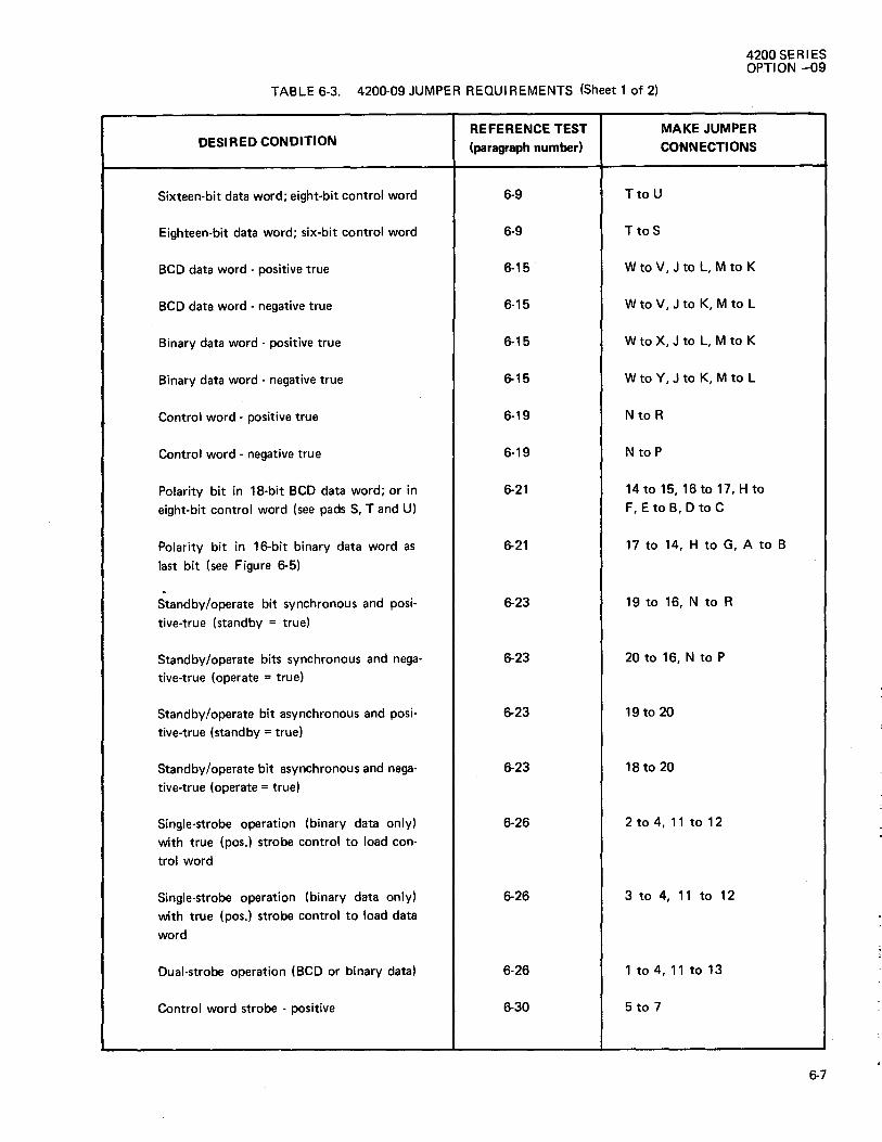
4200 SERIES OPTION -09
TABLE 6-3. 4200-09 JUMPER REQUI REMENTS (Sheet 1 of 2)
DESIRED CONDITION
Sixteen-bit data word; eight-bit control word
Eighteen-bit data word; six-bit control word
BCD data word - positive true
BCD data word - negative true
Binary data word - positive true
Binary data word - negative true
Control word - positive true
Control word - negative true
Polarity bit in 18-bit BCD data word; or in eight-bit control word (see pads S, T and U)
Polarity bit in 16-bit binary data word as last bit (see Figure 6-5)
Standby/operate bit synchronous and positive-true (standby = true)
Standby/operate bits synchronous and negative-true (operate = true)
Standby/operate bit asynchronous and positive-true (standby = true)
Standby/operate bit asynchronous and negative-true (operate = true)
Single-strobe operation (binary data only) with true (pos.) strobe control to load control word
Single-strobe operation (binary data only) with true (pos.) strobe control to load data
word
Dual-strobe operation (BCD or binary data)
Control word strobe - positive
REFERENCE TEST (paragraph number)
6-9
6-9
6-15
6-15
6-15
6-15
6-19
6-19
6-21
6-21
6-23
6-23
6-23
6-23
6-26
6-26
6-26
6-30
MAKE JUMPER CONNECTIONS
Tto U
TtoS
W to V, J to L, M to K
W to V, J to K, M to L
W to X, J to L, M to K
W to Y, J to K, M to L
N to R
N to P
14 to 15, 16 to 17, H to F, E to B, D to C
17 to 14, H to G, A to B
19 to 16, N to R
20 to 16, N to P
19 to 20
18 to 20
2 to 4, 11 to 12
3 to 4, 11 to 12
1 to 4, 11 to 13
5 to 7
6-7

4200SERIES OPTION -09
Table 6-3. 4200-09 JUMPER REQUI REMENTS (Sheet 2 of 2)
6-8
DESIRED CONDITION
Control word strobe - negative
Data word strobe - positive
Data word strobe - negative
Mainframe address line enable-positive
Mainframe address line enable-negative
Data transferred by control word strobe
Data transferred by data word strobe
Data transferred by data word strobe or
control word strobe
Complement last bit of data word
Not-complement last bit of data word
MSD
16-BIT
DATA WORD
"
2SD 3SD
REFERENCE TEST (paragraph number)
6-30
6-30
6-30
6-37
6-37
6-39
6-39
6-39
6-48
6-48
LSD
POLARITY BIT
(OR STANDBY/OPERATE BIT)
EXTERNAL REFERENCE
MODE BIT
CURRENT LIMIT RANGE BIT
MAKE JUMPER CONNECTIONS
22 to 23
23 to 24
8 to 10
8to 10
9 to 10
G to H. 5 to E
E to F, H to T
E to F, G to H
A to B
A to B
8-BIT CONTROL WORD
" ....
~ .... --v,--",'
CURRENT LIMIT
MAGNITUDE (FOUR BITS)
Figure 6-3. BCD PROGRAM DATA, TYPICAL 16-BIT DATA WORD, 8-BIT CONTROL WORD

6-12. When the power source to be programmed requires only output magnitude, polarity and range data, an 18-bit data word, as illustrated in Figure 6-4, can be used without the control word. The control word is necessary when it is required to program the external reference function and current limiting. To obtain an 18-bit data word, jumper pad T to pad S.
6-13. Binary-Type Voltage Sources
6-14. As shown in Figure 6-5, both 16-bit and 18-bit data words may be used with binary-type voltage sources. As described for the BCD-type voltage sources, either the 16-bit or 18-bit data word may be selected, depending
upon the system and voltage source requirements. That is,
if the voltage source is not equipped with external reference and current limit magnitude selection, the six-bit control word is of no value and an 18-bit data word provides sufficient program data.
6-15. DATA WORD POLARITY
6-16. BCD -Type Voltage Sources
6-17. The 16 or 18 bits which make up the data word portion of the program data may be either positive-true or negative-true as determined by jumpering pads J, K, L,
l8-BIT
DATA WORD
4200SERIES OPTION -09
M, V and W. For either logic polarity of BCD data, pad V is jumpered to pad W. For positive-true logic,jumper pad J to pad L and pad M to pad K. For negative-true logic, jumper pad J to pad K and pad L to pad M. (Refer also to Table 6-3.)
NOTE!
Positive-true logic employs +5 volts for a logic 1 and zero volts for a logic O.
6-18. Binary-Type Voltage Sources
6-19. The logic polarity (Le. positive-true or negativetrue) of the binalY data word is determined in much the same manner as that described for the BCD data word. However, pad W is jumpered to pads X or Y (Refer to Table 6-3) instead of pad V.
6-20. CONTROL WORD POLAR ITY
6-2l. The logic: polarity for the control word, in either BCD or binary voltage sources, is determined by jumpers at pads N, P and R. If the control word uses positive-true logic, jumper pad N to pad R. If the control word uses negative-true logic, jumper pad N to pad P.
6-BIT CONTROL
WORD
~--------------------~------------------~,~~----~~----~,
MSD 2SD JSD LSD
POLARITYBIT -!/; (OR STANDBY/OPERATE BIT)
OUTPUT
RANGE BIT
EXTERNAL
REFERENCE
MODE BIT
CURRENT LIMIT
RANGE BIT
v
4-BIT CURRENT LIMIT
MAGNITUDE
Figure 6-4. BCD PROGRAM DATA, TYPICAL l8-BIT DATA WORD, 6-BIT CONTROL WORD
1/20/75 6-9
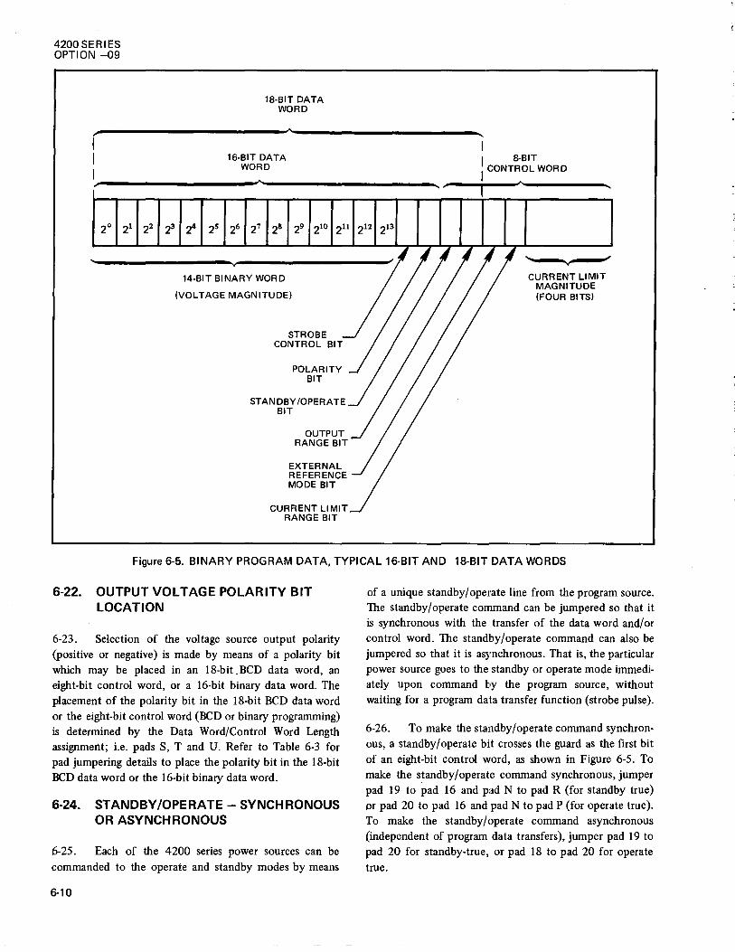
4200 SERIES OPTION -09
18-BIT DATA WORD
f I I 16-BIT DATA I 8-BIT I WORD I CONTROL WORD '~--------________ ~~~ ___________________ '_~ __ ~I __ -r'~ ______ __
... 14-BIT BINARY WORD
(VOLTAGE MAGNITUDE)
STROBE CONTROL BIT
POLARITY BIT
STANDBY/OPERATE BIT
OUTPUT RANGE BIT
EXTERNAL REFERENCE MODE BIT
CURRENT LIMIT RANGE BIT
v
CURRENT LIMIT MAGNITUDE (FOUR BITS)
Figure 6-5_ BINARY PROGRAM DATA, TYPICAL 16-BIT AND 18-BIT DATA WORDS
6-22. OUTPUT VOLTAGE POLARITY BIT LOCATION
6-23. Selection of the voltage source output polarity (positive or negative) is made by means of a polarity bit which may be placed in an IS-bit _ BCD data word, an eight-bit control word, or a 16-bit binary data word. The placement of the polarity bit in the IS-bit BCD data word or the eight-bit control word (BCD or binary programming) is determined by the Data Word/Control Word Length assignment; i.e. pads S, T and U. Refer to Table 6-3 for pad jumpering details to place the polarity bit in the IS-bit BCD data word or the 16-bit binary data word.
6-24. STANDBY/OPERATE - SYNCHRONOUS OR ASYNCHRONOUS
6-25. Each of the 4200 series power sources can be commanded to the operate and standby modes by means
6-10
of a unique standby/operate line from the program source. The standby/operate command can be jumpered so that it is synchronous with the transfer of the data word and/or control word. The standby/operate command can also be jumpered so that it is asynchronous. That is, the particular power source goes to the standby or operate mode immediately upon command by the program source, without waiting for a program data transfer function (strobe pulse).
6-26. To make the standby/operate command synchronous, a standby/operate bit crosses the guard as the first bit of an eight-bit control word, as shown in Figure 6-5. To make the standby/operate command synchronous, jumper pad 19 to pad 16 and pad N to pad R (for standby true) or pad 20 to pad 16 and pad N to pad P (for operate true). To make the standby/operate command asynchronous (independent of program data transfers), jumper pad 19 to pad 20 for standby-true, or pad IS to pad 20 for operate true.

6-27. SINGLE/DUAL - STROBE OPERATION
6-28. The 4200-09 can program output voltages in both single-strobe and dual-strobe modes. BCD-type voltage sources are usually operated in the dual·strobe mode, while binary-type voltage sources may be operated in either mode. The single-strobe mode refers to the use of a single strobe line (but two strobe pulses) to load both the data word and the control word from the program source into the 4200-09 assembly. Which of the two words (data or control) loaded depends upon the logic level applied to the strobe control line. In single-strobe operation, the binary data word is into the 4200-09 storage resistors (in preparation for transfer to the voltage source) by placing the proper logic level on the strobe control line (Refer to Table 6-3 for strobe control line logic levels) and placing a strobe pulse on the control word strobe line (pin 18). The control word is loaded into storage registers by placing the opposite logic level on the strobe control line and placing a second strobe pulse on the control word strobe line. In this manner, a single strobe line is used to load both the data and control words into storage registers by changing the logic level on the strobe control line. This system is usually used with binary program and voltage sources.
6-29. The dual-strobe mode refers to the use of two separate strobe pulses on two separate lines to load the data word and control word from the program source into storage registers in preparation for transfer to the voltage source. This mode is usually used when the data word is BCD. The data word strobe line (pin 36) is used to load the 16-bit or 18-bit data word, while the control word strobe line is used to load the control word.
6-30. To operate the 4200-09 in the single-strobe mode, jumper pad 2 to pad 4 and pad 11 to pad 12, if a positive strobe control signal level is used to load the control word; or jumper pad 3 to pad 4, and pad 11 to pad 12, if a positive strobe control signal level is used to load the data word. To operate in the dual-strobe mode, jumper pad 1 to pad 4, and pad II to pad 13.
6-31. CONTROL/DATA WORD STROBE SIGNALS
6-32. Control Word Strobe, Single-Strobe Mode
6-33. The control word strobe signal is a 500 nanosecond, or longer, pulse which is issued by the program source after the control word and/or data word has been applied to the parallel data inputs of the 4200-09 assembly. In the single· strobe mode, the control word strobe is used to load the
4200 SERIES OPTION -09
control word from the program source into the 4200-09 storage registers when the strobe control line is at the appropriate logic level (determined by pads 2, 3 and 4). When the strobe control line is at the other logic level, the control word strobe loads the data word into the registers. If the control word strobe is a positive-going (zero to +5V dc) pulse, jumper pad 5 to pad 7. If the control word strobe is a negative-going (+5Vdc to zero) pulse, jumper pad 6 to pad 7.
6-34. Control Word Strobe, Dual-Strobe Mode
6-35. As in the single-strobe mode, the control word strobe is a 500 nanosecond, or longer, pulse which is issued by the program source, the program data is applied to the parallel inputs of the 4200-09 assembly. In the singlestrobe mode, the control word strobe load the control word only, into the storage registers. (The data word is transferred by a data word strobe signal.) If the control word strobe is a positive-going pulse, jumper pad 5 to pad 7. If the control word strobe is a negative-going pulse, jumper pad 6 to pad 7.
6-36. Data Word Strobe
6-37. The data word strobe signal is used in the dualstrobe mode to load the data word, applied to the parallel data word inputs of the 4200-09 assembly, into the storage registers. The data word strobe is a 500 nanosecond, or longer, pulse which is issued by the program source after the data word has been applied to the parallel inputs of the 4200-09 assembly .. If the data word strobe is a positivegoing (zero to +5Vdc) pulse, jumper pad 8 to pad 10. If the data word strobe is a negative-going (+5V dc to zero) pulse, jumper pad 9 to pad 10.
6-38. MAINFRAME ADDRESS SIGNAL LEVEL
6-39. In order for the 4200-09 to receive and program data, it must be addressed at the time of the strobe signal (s). The mainframe address signal is a +5 volt or ground level signal applied to the address line number zero of the 4200-09 to be addressed (Refer also to paragraph 6-53). If a +5 volt signal is to be used for mainframe addressing, jumper pad 8 to pad 10. If a ground level is to be used, jumper pad 9 to pad 10.
6-40. PROGRAM DATA TRANSFER
6-41. General
642. The generation of the control word strobe and data word strobe signals by the program source loads the
6-11

4200 SERIES OPTION -09
program data into storage registers within the 4200-09 assembly. From the storage registers, the program data (control word and data word) is transferred in serial fashion (bit-by-bit) across the guard shield to the digital-toanalog converter within the voltage source. The serial transfer of program data is initiated after a short delay by the trailing edge of the control word strobe, or the data word strobe, or both, as determined by pads D, E, F, G, H and J.
NOTE!
The power source output voltage does not change to the newly programmed value until data transfer is completed.
6-43. Data Transfer By Control Word Strobe
6-44. To initiate the transfer of the program data (the control word and the data word) from the storage registers to the digital-to-analog converter within the power source by means of the control word strobe, jumper pad G to pad H. To prevent data transfer at the occurance of a data word strobe, jumper pad D to E.
6-45. Data Transfer By Data Word
621-6. To initiate transfer of the program data by means of the data word strobe, jumper pad E to pad F. To prevent data transfer at the occurance of a control word strobe, jumper pad H to pad J.
6-47. Data Transfer By Control Word Or Data Word Strobe
6-48. To initiate transfer of the program data by means of either the control word strobe or the control word strobe, jumper pad E to pad F, and pad G to pad H.
6-49. COMPLEMENTING BINARY PROGRAM DATA
6-50. Binary data words supplied by the program source which represent negative voltage outputs are two's complemented, and must be re-complemented in order to obtain the required output polarity at the power source. When jumpering is performed to receive binary data from the program source (pads J, K, L, M, W, X, Y), complementing to accomodate data word polarity is automatically performed. However, additional jumpering is required in order to
6-12
properly handle the polarity indication for the binary data word (power source output magnitude). The polarity (positive or negative) of the power source output may be indicated by means of:
a. the last (l6th) bit of the binary data word.
b. a polarity bit as part of the control word.
6-51. If the polarity is indicated in the last bit of the binary data word, following the 14-bit magnitude data and strobe control bit (as shown in Figure 6-5), it must not be complemented along with the data word. To prevent this last bit of the data word from being complemented, jumper pad A to pad B. If the polarity is indicated by a bit within the control word, the entire data word should be complemented (when necessary) by jumpering pad A to pad C. (This is only necessary when transferring all 16 bits of binary data to a 4275A.)
6-52. ADDRESSING MULTIPLE MAINFRAMES
6-53. Up to eight separately addressable 4200 series power sources may be connected to a single program source when each are equipped with the 4200-09. Figure 6-2 shows the method of multiple power source connections using factory-manufactured cable assemblies. The power source electrically closest to the program source is numbered zero, and the succeeding power sources are numbered in ascending order, up to seven. The mainframe address signals, which are +5 volts or ground levels, are supplied to the power sources for the duration of the programming sequence. All mainframe address signals must be applied to the mainframe address inputs of the first power source (number zero). That is, the program source is only connected directly to the first power source, and connection to subsequent power sources is handled by means of through connections on the 4200-09 assembly.
6-54. The mainframe address signals may be either +5 volts or ground as determined by jumpers 8, 9 and 10. All signals are applied to the mainframe address lines of the first 4200-09 mainframe, address line number zero enables the first 4200-09 mainframe, to accept program data and strobe signals. As shown in Figure 6-6, mainframe address line number one is fed through the first 4200-09 to exit at its zero address output for application to the next power source. The mainframe address lines are shifted by one position each time they pass through a 4200-09. In this manner, each power source is directly addressed at its zero address input although the program source selects the
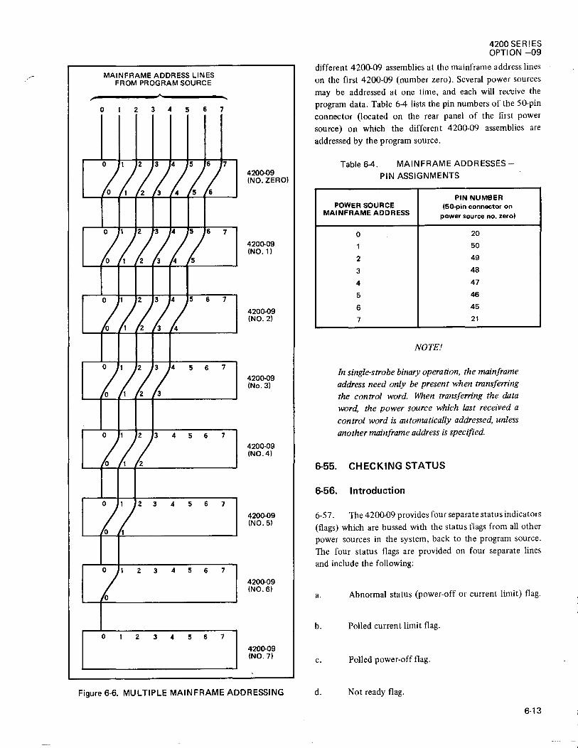
MAINFRAME ADDRESS LINES FROM PROGRAM SOURCE
o 234 5 6 7
0 1 2 3 4 5 6 7
0 1 2 3 4 5 6
0 1 2 3 4 5 6 7
0 1 2 3 4 5
0 1 2 3 4 5 6 7
1/21./ 0 1 2 3 4 5 6 7
0 1 2 3
0 1 2 3 4 5 6 7
0 '/2
0 1 2 3 4 5 6 7
0 t
0 1 2 3 4 5 6 7
0
0 1 2 3 4 5 6 7
4200-09 (NO. ZERO)
4200-09 (NO.1)
4200-09 (NO.2)
4200-09 (No.3)
4200-09 (NO.4)
4200-09 (NO.5)
4200-09 (NO.6)
4200-09 (NO.7)
Figure 6-6. MULTIPLE MAINFRAME ADDRESSING
4200 SER!ES OPTION -09
different 4200-09 assemblies at the mainframe address lines
on the first 4200-09 (number zero). Several power sources may be addressed at one time, and each will receive the program data. Table 64 lists the pin numbers of the 50-pin connector (located on the rear panel of the first power source) on which the different 4200-09 assemblies are
addressed by the program source.
Table 64. MAINFRAME ADDRESSES-PIN ASSIGNMENTS
PIN NUMBER POWER SOURCE (50-pin connector on
MAINFRAME ADDRESS power source no. zero)
0 20
1 50
2 49
3 48
4 47
5 46
6 45
7 21
NOTE.!
In single-strobe binary operation, the mainframe address need only be present when transferring the control word. When transferring the data word, the power source which last received a control word is automatically addressed, unless another mainframe address is specified.
6-55. CHECKING STATUS
6-56. Introduction
6-57. The 420()'09 provides four separate status indicators
(flags) which are bussed with the status flags from all other power sources in the system, back to the program source. The four status nags are provided on four separate lines
and include the following:
a. Abnormal status (power-off or current limit) flag.
b. Polled current limit nag.
c. Polled power-off nag.
d. Not ready flag.
6·13

4200 SERIES OPTION -09
NOTE!
All flag lines are wire-ored to an open collector
bus. Pull-up resistors are required in the program
source interface to enable the flags to reach +5
volts.
6-58. Status checking the 4200-09 is typically handled by the program source in such a manner that the abnormal status flag is allowed to interrupt. As a result of the interrupt, the program source may poll each 4200-09 in the system while monitoring the polled current limit flag bus and polled power-off flag bus for a flag indication. The not ready flag is not polled, and when present, indicates that one or more power sources is still acting on program commands, and is not yet ready to receive further commands.
6-59. Polled Current limit Flag
6-60. As shown in Figure 6-7, the polled current limit flag bus appears on pin 29 (on the 50-pin connector) of any 4200-09 in the system. The flag is polled by placing a ground level on the poll status input (pin 9) of the particular 4200-09 being polled. If the current limit flag bus responds with +5 volts, the current limit condition for the polled power source does not exist. However, if the current limit flag bus responds with a ground level, the current limit condition does exist, and an overloaded power source is indicated.
6-61. As illustrated in Figure 6-7, the poll status inputs to several 4200-09 in a system are not normally bussed together, but may be individually polled by the program source. A typical method of polling the status is to jumper the mainframe address line (number zero) from pin number 20 to the poll status input at pin number 9. In this manner, status is available at the current limit flag bus (and the power-off flag bus) whenever the particular 4200-09 is addressed.
6-62. Polled Power-Off Flag
6-63. Polling the power-off flag is identical to that described for the current limit flag except some external source of +5 volts must be applied to pin number 30. The +5 volt source is required in order to obtain the power-off status indication when the power to the polled unit has actually failed. The power-off status indication is a ground level on the power-off flag bus.
6-64. INPUT LOADING
6-65. Each input to each 4200-09 used in the system represents a single TTL input load. With a full complement
6-14
CURRENT LIMIT FLAG BUS
ABNORMAL STATUS
BUS~
STATUS 1 POLL
POLL STATUS
~
POLL STATUS
POLL STATUS
1.
POLL STATUS
~,
POLL STATUS
~,
STATUS 1 POLL
POLL STATUS
t I I I I I I
I I I I I
I I I I I I
I I I I I I
I I I I I I
I I I I I I
I I I I I I
I I I I I I
POWER-OFF / FLAG BUS
I I I
I I I
I I I
I I I
I I I
I I I
I I
I I I
4200-09 (No. ZERO)
4200-09 (No.1)
4200-09 (No.2)
4200-09 (No.3)
4200-09 (No.4)
4200-09 (No.5)
4200-09 (No.6)
4200-09 (No.7)
Figure 6-7. STATUS BUSSES LAYOUT

of eight power sources in the system, the power requirements for each input of the first power source are increased by a
t. factor of eight, except for the Mainframe Address and the Standby/Operate which are always single loads.
6-66. THEORY OF OPERATION
6-67. General Description
6-68. The 4200-09 can be configured (by means of jumpers) to accomodate a large number of program environments. Consequently, theory discussions are somewhat generalized, since all configurations cannot be described. In any application, the main function of the 4200-09 is to receive output magnitude and control data from a program source in parallel form, transfer the data across the power source guard shield, and present the data to the power source digital-to-analog converter. Figure 6-8 shows a simplified block diagram of the 4200-09 and how the data and control words, generated by the program source in parallel form, are applied to shift registers which perform a parallel-toserial conversion.
6-69. Upon the receipt of a data word strobe or control word strobe, the control logic generates a load command to one or both shift registers. The data word and control word supplied by the program source, and present at the shift register inputs, is loaded into the shift registers. When the shift registers are loaded with the program data, the control logic starts a 10 MHz clock and issues a hold command to the power source.
6-70. The output pulses from the clock are fed to the shift registers to move the program data out of the registers, bit-by-bit, to the coupling transformers at the guard shield. The data word is shifted out of its respective storage register via two's complementing logic which is enabled when the program source indicates that the data word is a negative binary number. This action is necessary since the 4200 binary power source requires positive binary numbers (in conjunction with a positive or negative polarity indicator). The control word undergoes no complementing at any time.
6-71. While the program data is being shifted across the guard shield by the clock pulses, the clock pulses are also being fed across the guard shield, and the hold one-shot is triggered as a result of the hold command issued by the
., control logic. On the inside of the guard shield, the clock pulses are used to shift the serial program data into shift
registers which provide the necessary serial -to-parallel
4200 SERIES OPTION -09
conversion. (The 4200 power sources require parallel program data.) The output of the hold one-shot is present for the duration of the serial data transfer across the guard shield. This action is necessary to inhibit any change in power source output magnitude while the data word is being serially loaded into the shift register.
6-72. The control word portion of the program data is also loaded into a shift register, and is double-buffered to prevent any change in power source output while loading is taking place. The double-buffering is provided by a series of latch circuits which receive a load pulse from a latch timing circuit. The latch timing circuit issues the load pulse to the latch circuits sometime after the last clock pulse when all data has been shifted into the registers. As the load pulse occurs, the latch circuits are loaded with the control word and present it in parallel form to the 4200 power source. (Double-buffering for the data word is not required since the hold signal "freezes" the power source output magnitude until the data word is completely loaded into the shift register.)
6-73. The shifting and loading of the program data is performed by the clock pulses. The start of the clock pulses is a function of the control logic. The stopping of the clock is also performed by the control logic, but after the generation of 16 pulses. When the clock is stopped, all shifting action ceases; and after the fold signal disappears and the load pulse to the latch occurs, all program data is presented to the digital-to-analog converter within the 4200 power source. At this time, the power source assumes its newly programmed output.
6-74. BLOCK DIAGRAM ANALYSIS
6-75. Input Sequence
6-76. Figure 6-9 shows that the parallel program data, supplied by the program source, is applied to a pair of shift registers as well as to the succeeding 4200 power source (s) in the system. The data is loaded into the register (s) when the appropriate strobe signal is received from the program source.
6-77. In a device configured for single-strobe operation, the control word strobe signal (in conjunction with the strobe control line) is used to load both the data word and control word info their respective registers. The strobe signal gating accepts the control word strobe from the program source, and depending upon the state (+5 volts or ground) of the strobe control line, directs the strobe signal
to either the control word one-shot or the data word one-
6-15
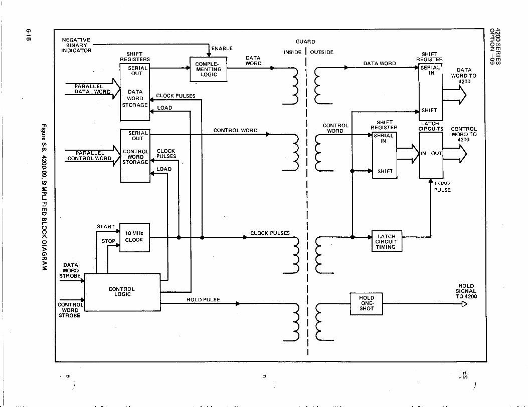
"T1 tE' I: .., (1)
~ !Xl ~ I\.)
~ .~ ~ s: "tI C "T1
m o ttl ro (')
A o » C> :::c » s:
NEGATIVE BINARY -----------------.
GUARD
INDICATOR I ENABLE SHIFT • INSIDE OUTSIDE
PARALLEL .1\ DATA WORD .1
y
REGISTERS SERIALI-----.~ COMPLE-
OUT -.. MENTING LOGIC
DATA WORD ~ CLOCK PULSES
STORAGE LOAD
DATA WORD
SERIALr-____ ~-t_~C~O~N~T~R~O~L~W~O~R~D~~~~----OUT )
PARAL[EL -'\ CONTROL CLOCK .) CONTROL WORD ,I WORD ... PULSES J
DATA WORD
STROBE_
CONTROL WORD
STROBE
, <1>
r STORAGE ~)
14 LOAD
START
ST~
10 MHz CLOCK
CONTROL LOGIC
HOLD PULSE
CLOCK PULSES
) ) )
.-J
j
CONTROL WORD
DATA WORD
SHIFT REGISTER
SERIAL IN DATA
WORD TO 4200
r--------~ SHI FT
SHIFT REGISTER
SERIAL IN
HOLD ONE
SHOT
SHIFT
LATCH CIRCUIT TIMING
LATCH CIRCUITS CONTROL
LOAD PULSE
WORD TO 4200
HOLD SIGNAL TO 4200
" ri, JC/)
)
O~ "til\.) -1 0 _0 Oen zm I~ om wen

shot. If the strobe control line directs the control strobe pulse to the control word one-shot, a pulse is generated and fed to the parallel-load input of the control word shift register. The pulse causes the shift register to load the parallel control word supplied by the program source. If the strobe control line directs the control strobe pulse to the data word one-shot, a pulse is fed to the parallel-load input of the data word shift register.
NOTE!
In order for the control word strobe (or the data word strobe) to trigger either of the oneshots, the mainframe address line must be enabled.
6-78. In a device configured for dual-strobe operation, both the control word strobe and data word strobe signals are used to load the program data from the program source. In this configuration, the control word strobe triggers the control word one-shot to load the control word into its shift register, and the data word strobe triggers the data word one-shot to load the data word. (Refer also to Figure 6-10.)
6-79. Data Transfer
6-80. Whenever the control word one-shot or data word one-shot is triggered, the resulting output triggers a first hold one-shot. (Refer also to Figure 6-10.) One output of the hold one-shot produces a hold pulse which is fed across the guard shield (via T2) to trigger a second hold one-shot. The second hold one-shot generates a hold pulse required by the power source to hold the output magnitude at the current value while magnitude data is being reprogrammed.
NOTE!
The duration of the hold pulse depends upon the particular power source being used.
6-81. The trailing edge of the other first hold one-shot output (triggered by the strobe signal), sets a data transfer flip-flop. The Q output of the data transfer flip-flop starts a 10 MHz clock, if not already operating (refer to Standby Sequence), and gates the clock pulses to the serial shift inputs of the control word and data word shift registers. (The clock pulses are also gated to the input of a .;. 16 counter and to the primary winding of T4.) As each clock pulse is received by the shift registers, the previously loaded program data is shifted, serial-by-bit out of the
4200 SERIES OPTION -09
shift registers to the coupling transformers (T3 and T5) at the guard shield. On the inside of the guard shield, the serial data and control words are loaded into a second set of shift registers which are clocked by the pulses at the secondary of T4.
6-82. The clock pulses gated by the data transfer flip-flop are also fed to a 4-bit binary counter which produces a carry pulse at the time of the sixteenth clock pUlse. The carry pulse resets the data transfer flip-flop to inhibit the gating of the clock pulses and stop the clock, if the standby mode is not present. (Refer to Standby Sequence.) After the generation and gating of 16 clock pulses the data word has shifted completely around the data word shift register while being transformer-coupled across the guard and into the second shift register for application to the 4200 power source. The control word, since it contains eight bits or less, is actually shifted around the control word register, across the guard and into the second control word register two complete times.
6-83. The control word is double-buffered for application to the 4200 power source. This is necessary since the hold signal, provided during data transfer by the second hold oneshot, does not "freeze" the output range of the 4200 power source, just the output magnitude. To parallel shift the control word from the shift register to a set of latch circuits, the first of the 16 clock pulses triggers a latch timing one-shot which has a pulse width slightly greater the serial data transfer time (16 clock pulses). The trailing edge of the latch timing one-shot output is fed to a pulse generator which provides a load pulse to the latch circuits. At the time of the load pulse, the latch circuits are parallel loaded with the control word for application to the 4200 power source.
6-84. Complementing Binary Data
NOTE!
Complementing magnitude data occurs only in binary-type power sources.
6-85. Binary-type power sources require that negative values of magnitude data be two's complemented since binary program sources usually indicate polarity by means of a single bit and supply two's complemented magnitude data for negative outputs. The binary-type power sources require non-complemented binary data plus a polarity bit. As a result, negative binary magnitude data, consisting of complemented data, must be re-complemented to satisfy the
requirements of the power source. When the binary program
6-17

4200 SERIES OPTION -09
source indicates negative sign, U14 is enabled to pass the output of the complementing logic. The complementing logic receives the serial output of the shift registers, complements it, and passes it across the guard via T1.
6-86. Operation of the two's complementing logic is such that the first bit of serial data is present at the output of the shift registers before the 7 16 counter and a complement flip-flop receives the first of 16 clock pulses. At this time, the 7 16 counter is in its zero state and the complementing flip-flop is still reset (as a result of the carry pulse generated by the 7 16 counter at the end of the previous data transfer sequence). With the complement flip-flop reset, the complement logic is not enabled and no inversion of serial data takes place. This condition permits the first bit of binary magnitude data to be transferred without being complemented. However, after the first clock pulse, the complement flip-flop may be allowed to go set (to enable the complement logic), depending upon the state of the J input, which is derived from the serial data. As a result, the complement flip-flop goes set at the time of the first true bit of serial data to ,enable the inverting logic and complement the remaining bits of serial data. After the 16th bit of data, the complementing flip-flop is reset by the carry output of the 7 16 counter.
6-87. Programming the 4200 power source to standby (zero output, but no change in programmed magJ1,itude and range) may be performed in a synchronous or asynchrorious manner, depending on jumper configuration. With synchronous standby operation, (not shown in Figure 6-9) the standby bit supplied by the program source becomes part of the control word and is serially shifted across the guard for application to the standby input of the 4200 power source. This mode is referred to as synchronous standby because commanding the 4200 power source to standby or operate is always synchronous with a strobe signal from the program source.
6-88. Asynchronous Standby Operation
6-89. With asynchronous standby operation, the 4200 power source can be commanded to standby or operate at any time by the program source. As shown in Figure 6-9, the standby signal (dc) is gated to the start input of the 10 MHz clock to initiate the generation of clock pulses (if not already being generated during a data transfer sequence of 16 clock pulses). As long as a data transfer sequence is not in progress, the data transfer flip-flop is in
6-18
its reset state. When the data transfer flip-flop resets the clock pulses are gated through to the primary winding of T6 and are inhibited (by the Q output) from the shift registers and 7 16 counter. The secondary winding, located inside the guard, feeds the clock pulses to a halfwave rectifier. The dc output of the rectifiers is fed to the 4200 power source standby/operate input.
6-90. Status Logic
6-91. Two separate status conditions are indicated by 1he power source equipped with the 4200-09, i.e. current limit mode status and power failure. The current limit status flag is furnished by the 4200 power source whenever an overload condition exists and the current limit function is being used. The power failure indication is provided by the 4200-09.
6-92. The current limit flag is fed from the 4200 power source to enable a current limit oscillator on the 4200-09 (Refer to Figure 6-9). The oscillator output signal is coupled to the outside of the guard via T 1, and to the input of a half-wave rectifier. The dc output of the rectifier indicates the current limit condition and appears at the abnormal status output. The current limit flag is also available at the current limit flag output when the pro
gram source addresses the unit with a status enable signal.
6-93. The power fail flag results from the failure of the +5 volt supply to the 4200-09, which is indicative of a general power failure within the power source. As in the current limit flag, the power fail flag appears on the abnormal status line, and on the power fail flag output when the unit is addressed with a status enable signal.
6-94. Not Ready Signal
6-95. The 4200-09 generates a not-ready signal to the program source whenever it is not ready to accept program data or strobe signal (s) from the program source. As shown in Figure 6-9 and 6-10, the not ready flag one-shot is triggered by the trailing edge of the first hole one-shot output to generate the not ready flag. The duration of the
not ready flag is through the data input sequence to notify the program source that the data is being transferred to the power source and no strobe signal should be generated at this time. The duration of the not ready flag depends upon the type of power source being programmed. The table included on the schematic diagram lists the different component values used and the one-shot periods provided

14 BITS BINARY OR
16 BITS BCD OF DATA WORD
'I
... ;..
DATA WORD TO SUCCEEDING 4200
CONTROL WORD (UP TO B BITSi
CONTROL WOR 0 TO SUCCEEDING 4200
ST ANDBV
ROBE ST CO NTROl
NTROL CO WO RD STROBE
TAWORD DA STR OBE
INFRAME MA AD DRESS
NO TREADY
ABNORMAL STATUS
r.
\ / •
II.
\ / •
Scans by => ARTEK NEOI/f @ 2003-2005
SIGN BIT INDICATING D POS. BINARY DR ANY -BCD DATA U14
~ SHIFT SERIAL DATA WORD OUT REGISTER
I -,'J -< INVERTING "ON,,, r:>- -(
LOGIC -(
DATA INDICATING _ IN NEG. BINARY --- ~
PARALLEL U14 DATA DATA IN
CLOCK ENABLE
SERIAL SHIFT PULSES CLOCK PULSES T4
.) COMPLEMENT .)
U5, U8 PARALLEL J INPUT FLIP-FLOP ) LOAD IJ-Ki CLOCK CLOCK -Y PULSES INPUT
U15 SERiAL CONTROL ~~ SHIFT WORD OUT RESET T3
REGISTER U13 )
L- ") "') -<
PARALLEL DATA IN
CLOCK SERIAL CARRY PULSES SHIFT ~
';'16
~TRANSFER COUNTER
CLOCK U6 IN
U2,U3,U4 PARALLEL LOAD
10MHz
)~9 CLOCK
!---< TRIGGER CONTROL RESET DATA 0 START
WORD TRANSFER STOP 01,02 '-1:\ ONE-SHOT FLIP-FLOP T2
,,"~fil STROBE
~ '--i Q DATA TRANSFER LJ STANDBY U19 U9 PULSES SIGNAL
GATING NOT
READY [U1J [U3J ONE-5HOT ~
DATA WORD
V [U4J [U5J ONE-5HOT HOLD r-9-ONE-SHOT U18 TRIGGER 800 nsec Q HOLD PULSE T6
UI9 Ul0
NOT READY PULSE .. VcC -(
~
\-________ ~----__ ----------------------------------~~C~U~R~R~EN~T~L~IM=I~T~S~I~G~N~A~L~(~D~C~i __________ ~~~~~i~~~E OSCILLATOR SIGNAL Tl
4----------------; CR3 CURRENT LIMIT
FLAG
POWER FAIL FLAG
STATUS ENABLE
NOTE:
COMPONENTS WITH REFERENCE DESIGNATORS IN BRACKETS (E.G. [U5J ARE LOCATED ON THE SMALL PCB ASSEMBLY.
Figure 6-R 4200-09 BLOCK DIAGRAM
>->->-'---
>-->->-
>->->-
SERIAL DATA WORD
SERIAL CONTROL WORD
CLOCK IN
LATCH TIMING
C~ ONE-5HOT
PULSES U30
GATED CLOCK PULSES
SECOND HOLD
ONE-5HOT
U28
CURRENT LIMIT
,..-____ -i0SCILLATOR
ENABLE 012,023,
025
CONTROL WORD SHIFT
REGISTER
U26
TIMING PULSE
HALF-WAVE RECTIFIER
CR16
DATA WORD SHIFT
REGISTER
CLOCK IN
U24 U25
LATCH CIRCUITS
.. CONTROL \
WORD
/ r
U27
LOAD PULSE PULSE
GENERATOR
U29
DC OUTI'UT
t.
4200 SERIES OPTION -09
14 BITS DATA WORD TO 4200
OR 16 BITS
Y
t.
UP TO 8 BITS
CONTROL WORD TO 4200
v
STANDBY
HOLD· SIGNAL
•
CURRENT LIMIT FLAG
6-19/20

STROBE PULSE (EITHER STROBE) --u
I I
CONTROL WORD I OR DATA WORD ---,
ONE-SHOT I ~----'
I I
FIRST HOLD 1
ONE-SHOT ~O;:j
1 I
DATA TRANSFER ______ -;' FLIP-FLOP I
CLOCK OUTPUT ------.... (10MHz)
I I
4200 SERIES OPTION -09
NOT READY FLAG ______ .... '
ONE-SHOT I "-._----- DURATION DEPENDS ON 'I .. POWER SOURCE USED _
~----------~SrS------------~
Figure 6-10. INPUT SEQUENCE - TIMING DIAGRAM
for the different 4200 series power sources being programmed.
6-96. MAINTENANCE
6-97. Performance Checks
6-98. Proper operation of the 4200-09 is best verified while in its normal operating environment, i.e. while installed in the power source and connected to the program source. In the system environment, operation of the 4200-09 is typically verified by means of diagnositc routines, or by manually-entered statements at the operator interface, i.e. crt console, teletypewriter, control console, etc. The actual procedure employed to check the 4200-09 depends upon the particular system configuration and is beyond the scope of this manual.
6-99. Calibration
6-100. The 4200-09 requires no periodic or repair calibration.
6-101. Troubleshooting
6-102. The troubleshooting information in the following tables is provided to assist in isolating 4200-09 malfunctions, and is presented in flow chart form. Following the chart from beginning to end will usually identify and localize any malfunction. It is suggested that the preceeding theory of operation be read and the block and schematic diagrams be referenced prior to troubleshooting.
NOTE!
Prior to troubleshooting, place the 4200-09 PCB assembly on an extender card (Fluke part no. 292263).
6-21

4200 SERIES OPTION -09
6-22
Table 6-5. TROUBLESHOOTING CHART, INACTIVE PCB ASSEMBLY (Sheet 1 of 2)
START
NO
YES
NO
NO
NO
YES
CHECK ALL LOGIC ELEMENTS PRE
CEDING U19
CHECK ALL LOGIC ELEMENTS BETWEEN
U10 AND U9, PIN 6
CHECK 10 MHZ CLOCK
NO CHECK STROBE PULSE SOURCE
REPLACE U10, R71 OR C48
NOTE:
LOGIC 1 = ZERO TO +O.4V
LOGI C 0 = +2V to +5V
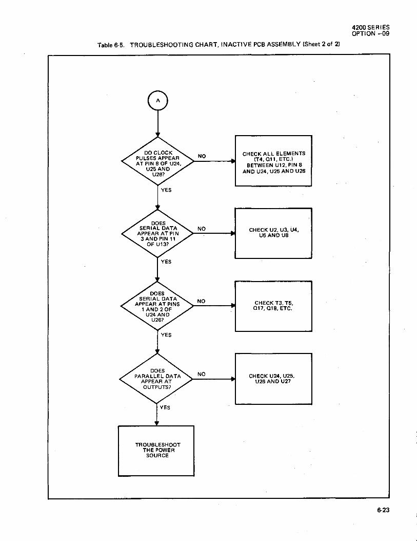
Table 6-5. TROUBLESHOOTING CHART. INACTIVE PCB ASSEMBLY (Sheet 2 of 2)
TROUBLESHOOT THE POWER
SOURCE
NO
NO
NO
NO
CHECK ALL ELEMENTS (T4. 011. ETC.)
BETWEEN U12. PIN 8 AND U24. U2S AND U26
CHECK U2. U3. U4. US AND U8
CHECK T3. TS. 017. 018, ETC.
CHECK U24, U2S, U26 AND U27
4200 SERIES OPTION -09
6-23

4200 SERIES OPTION -09
Table 6-6. TROUBLESHOOTING CHART, DATA ERRORS AT PARALLEL OUTPUTS
6-24
START
CHECK SERIAL DATA INPUT AND PARALLEL
OUTPUTS OF U24. U25, U26 AND U27
NO
NO
CHECK THE PROGRAM DATA
SOURCE
CHECK THE + 16 COUNTER (U6)
NO CHECK U2. U3, U4. U50R US AS
APPROPRIATE

4200SERIES OPTION -09
Table 6-7. TROUBLESHOOTING CHART, NO COMPLEMENTING OF BINARY DATA
START
YES
CHECK ALL GATES OF U14
NO
NO
NO
NO
REPLACE [US]
REPLACE U1S
NOTE:
CHECK THE POLARITY (SIGN) INPUT LINE AND INVERTERS (UG)
CHECK ALL STROBE INPUT
LOGIC ELEMENTS (U19, U3, U4, ETC.)
REFERENCE DESIGNATORS PLACED IN BRACKETS (E.G. [US]) INDICATE THAT COMPONENT LOCATED ON SMALL PCB ASSEMBLY (NO. 4200-402S)
6-25

4200 SERIES OPTION -09
Table 6-8. TROUBLESHOOTING CHART, NO ASYNCHRONOUS STANDBY
6-26
START
YES
YES
CHECK JUNCTION OF CR16 AND
C55 FOR EXCESSIVE RIPPLE
NO
NO
NO
YES
CHECK OPERATION OF 10 MHz CLOCK
CHECK FLIP-FLOP U9 AND ASSOCIATED
CIRCUITRY. ALSO CARRY OUTPUT OF COUNTER U6
NOTE:
CHECK PRIMARY AND SECONDARY CIRCUITS OF T2. ALSO CR16. C55
AND R42.
LOGIC 1 = ZERO TO +0.4V LOGIC 0 E +2V TO +6V
NO CHECK STANDBY IOPERATE
INPUT LINE

START
CHECK [Q3) AND [U3]
PLACE ZERO VOLTS ON POLL
STATUS LINE
REPLACE U7 ALSO ENSURE
RIPPLE FROM CR3 IS NOT EXCESSIVE
CHECK T1, CR3, C15, ETC.
NOTE:
REFERENCE DESIGNATORS PLACED IN BRACKETS (E.G. [U5)) INDICATE THAT COMPONENT LOCATED ON SMALL PCB ASSEMBLY (NO. 4200-4025)
NO TROUBLESHOOT
CURRENT LIMIT OSC. Q12, Q23, 025, ETC.
ANDIOR FLAG INPUT FROM
POWER SOURCE
-I :JJ o C OJ r m en :r: o
.. ~ z G)
n :r: :t> :JJ ,-I Z o n c :JJ :JJ m Z -I r ~
-I "T1 r :t> G)

4200 SERIES OPTION -09
Table 6-10. TROUBLESHOOTING CHART, NO POWER FAIL AND/OR ABNORMAL STATUS FLAGS
6-28
START
CH ECK Vee (+5V) SUPPLY FROM
PROGRAM SOURCE
NO
CHECK U4AND U1
NO
NO
CHECK Q2, 04, Q5 AND ASSOC
IATEDCOMPONENTS
TROUBLESHOOT CURRENT LIMIT FLAG (REFER TO
TABLE 6-9)
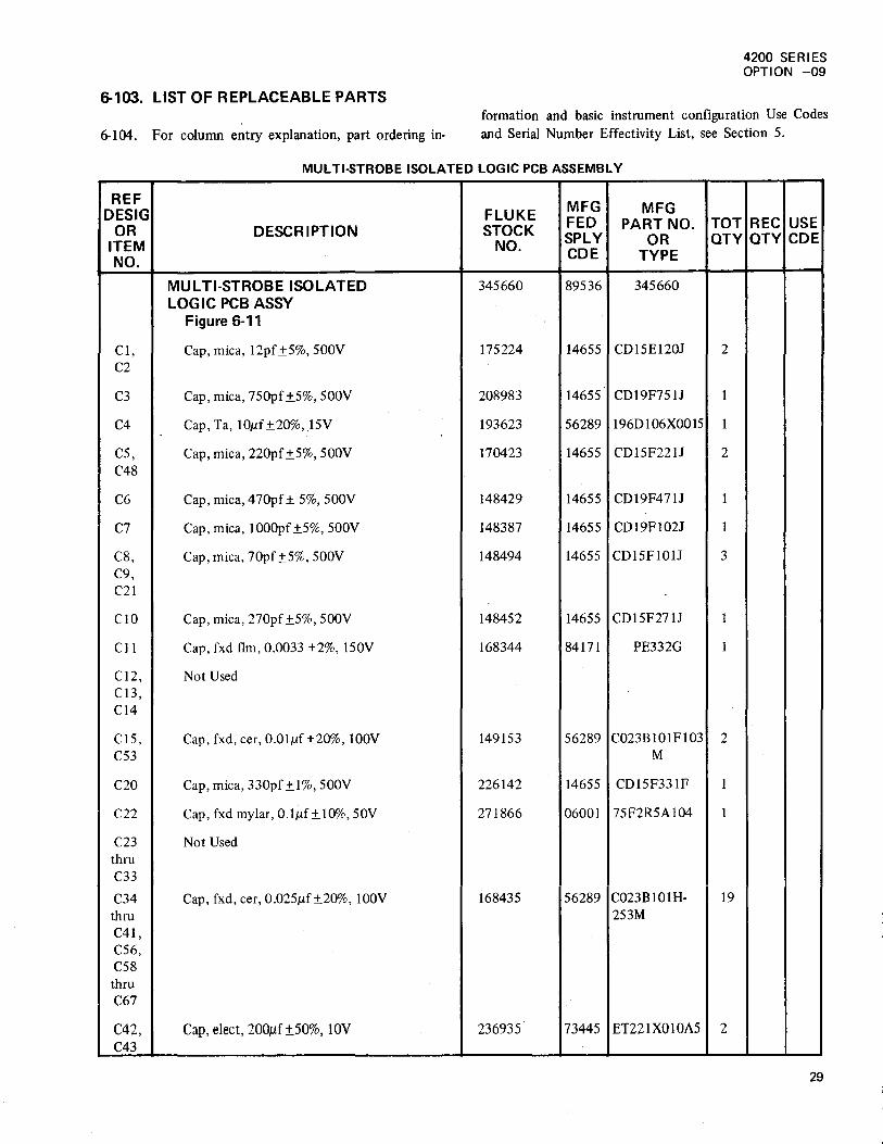
6-103. LIST OF REPLACEABLE PARTS
6-104. For column entry explanation, part ordering in-
4200 SERIES OPTION -09
formation and basic instrument configuration Use Codes and Serial Number Effectivity List, see Section 5.
MUL TI-STROBE ISOLATED LOGIC PCB ASSEMBLY
REF MFG DESIG FLUKE MFG
OR DESCRIPTION STOCK FED PART NO. TOT REC USE
ITEM NO. SPLY OR QTY QTY CDE
NO. CDE TYPE
MUL TI-STROBE ISOLATED 345660 89536 345660 LOGIC PCB ASSY
Figure 6-11
C1, Cap, mica, 12pf ±5%, 500V 175224 14655 CD15E120J 2 C2
C3 Cap, mica, 750pf±5%, 500V 208983 14655 CD19F75lJ 1
C4 Cap, Ta, 10J.Lf±20%,15V 193623 56289 196D 1 06XOO 15 1
C5, Cap, mica, 220pf ±5%, 500V 170423 14655 CD15F22lJ 2 C48
C6 Cap, mica, 470pf ± 5%, 500V 148429 14655 CD19F47lJ 1
C7 Cap, mica, 1 OOOpf ±5%, 500V 148387 14655 CD19F102J 1
C8, Cap, mica, 70pf ±5%, 500V 148494 14655 CD15FlOlJ 3 C9, C21
C10 Cap, mica, 270pf ±5%, 500V 148452 14655 CD15F271J 1
C11 Cap, fxd £lm, 0.0033 ±2%, 150V 168344 84171 PE332G 1
C12, Not Used C13, C14
C15, Cap, fxd, cer, O.OlJ.Lf ±20%, 100V 149153 56289 C023B101F103 2 C53 M
C20 Cap, mica, 330pf±1%, 500V 226142 14655 CD15F331F 1
C22 Cap, fxd mylar, O.lJ.Lf ±10%, 50V 271866 06001 75F2R5A104 1
C23 Not Used thru C33
C34 Cap, fxd, cer, 0.025J.Lf±20%, 100V 168435 56289 C023B10lH- 19 thru 253M C41, C56, C58 thru C67
C42, Cap, elect, 200J1f ±5Q%, lOY 236935 73445 ET221XOIOA5 2 C43
29

4200 SERIES OPTION -09
REF DESIG
OR ITEM NO.
C44 thru C47, C49
C50, C51, C52, C54
C55
C57
CRl, CR7 thru CRIO, CRI5, CR16
CR2, CR4, CR5, CR6, CR13, CR14
CR3, CR11, CR12
Ql,Q2, Q3,Q6, Q7,Q8, QlO, Q11, Q12, Q14, Q16, Q17, Q18, Q19, Q20, Q26, Q27
30
,
DESCRIPTION
Cap, mica, 56pf ±5%, 500V
Not Used.
Cap, fxd, eer, .OO27pf ±GMV, 600V
Cap, fxd eer, .0033J.Lf±GMV, 600V
Diode, Si, 150mA
Not Used
Diode, hot carrier
Xstr, Si, NPN
MFG MFG FLUKE STOCK FED PART NO. TOT REC USE
NO. SPLY OR QTY QTY CDE CDE TYPE
148528 14655 CD15F56OJ 5
106211 72982 851.000ZSUO- 1 272P
106674 C0238102F· 1 332M
203323 03508 DHDII05 7
313247 28480 2811 3
159855 07910 CS23030 17

REF DESIG FLUKE
OR DESCRIPTION STOCK ITEM NO. NO.
Q4,Q5 Not Used Q9, Q15, Q21, Q22, Q24
Q13 Xstr, Si, Unijunction 268110
Q23 Xstr, Si, NPN 168716
Q25 Xstr, Si, PNP 195974
Rl, Res, Comp, lKn ± 5%, %w 148023 R20, R22, R24, R28, R36, R45, R59, R60, R61, R70, R73, R75
R2,R4 Res, Comp, IOKn ± 5%, %w 148106
R3, Res, comp, 510 ± 5%, %w 218032 R9, RIO, R13, R21, R23, R69, R72
R5 Res, comp, 470 ± 5%, %w 147983
R6 Res, comp, 1.3Kn ± 5%, %w 234252
R7,R8 Res, comp, 390 ± 5%, %w 147975 R14 R42 R50
Rl1 Res, met flm, 6.98Kn ± 1%, 1/8w 261685 R12
MFG MFG FED PART NO. SPLY OR CDE TYPE
03508 2N6027
12040 SM07154
04713 2N3906
01121 CB1025
01121 CB1035
01121 CB5115
01121 CB4715
01121 CB1325
01121 CB3915
91637 MFFI-86-98K-PORM 1 PCT
4200 SERIES OPTION -09
TOT REC USE QTY OTY CDE
1
1
13
2
8
1
1
5
31
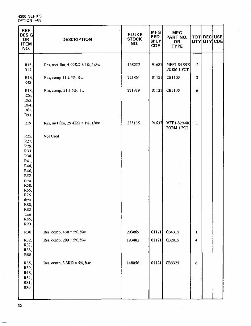
4200 SERIES OPTION -09
REF DESIG
OR ITEM NO.
R15, R17
R16, R43
R18, R26, R63, R64, R65, R91
R19
R25, R27, R29, R33, R34, R41, R44, R46, R52 thru R58, R66, R76 thru R80, R82 thru R85, R90
R30
R32, R37, R38, R88
R35, R39, R48, R54, R81, R89
32
FLUKE DESCRIPTION STOCK
NO.
Res, met fun, 4.99K.Q ± 1%, 1/8w 168252
Res, comp 11 ± 5%, J4w 221861
Res, comp, 51 ± 5%, J4w 221879
Res, met fun, 29.4K.Q ± 1%, 1/8w 235135
Not Used
Res, comp, 430 ± 5%, J4w 203869
Res, comp, 200 ± 5%, J4w 193482
Res, comp, 3.3K.Q ± 5%, J4w 148056
MFG MFG FED PART NO. TOT REC USE SPLY OR OTY OTY CDE CDE TYPE
91637 MFFI-84-99K 2 PORM 1 PeT
01121 CB1105 2
01121 CB5105 6
91637 MFFI-8294K 1 PORM 1 PeT
01121 CB4315 1
01121 CB2015 4
01121 CB3325 6

v
REF DESIG FLUKE
OR DESCRIPTION STOCK ITEM NO. NO.
R40 Res, met flm, 30.9Kn ± 1%, 1/8w 235275
R47 Res, comp 27Kn ± 5%, %w 148148
R49 Res, comp, 39Kn ± 5%, %w 188466
R51 Res, comp 100 ± 5%, %w 147926
R62, Res, comp, 680 ± 5%, %w 148007 R67, R68
R71 Res, met flm, lOKn ± 1%, 1/8w 168260
R86 Res, comp, 1.6Kn ± 5%, %w 234252
R87 Res, comp, 2Kn ± 5%, %w 202879
Tl Xfmr 299594 thru T6
Ul, IC, TTL Hex inverter 292979 U7, U16
U2, IC, TTL, 4 bit Right-shift, left-shift register 342691 U3, U4
US, IC, TTL, MSI 8-bit shift register 293118 U8
U6 IC, TTL, MSI, Syn 4-bit up down counters 293183
U9, IC, TTL, 3 input positive NAND Gates 292995 Ul7
UlO, IC, TTL, MSI, retriggerable monostable 293134 U18 multivibrator
UIl, IC, TTL, quad 2-input NAND gate 292953 Ul2, U13, U20
Ul4 IC, TTL, dual, 2-wide 2-input AND-OR 293084 Invert high speed
UIS IC, TTL, J-K edge triggered Flip-Flops with 293092
MFG MFG FED PART NO. SPLY OR CDE TYPE
91637 MFF 1-83(}9K PORM I PCT
01121 CB2735
01121 CB3935
01121 CBlO15
01121 CB6815
91637 MFFl-810K PORM 1 PCT
01121 CBI025
01121 CB2025
89536 299594
01295 SN7404N
01295 SN7495N
01295 SN74165N
01295 SN74193N
01295 SN74 ION
07263 MC8601P
01295 SN7400N
01295 SN74H51N
01295 SN74Hl02N
4200 SERIES OPTION -09
TOT REC USE OTY OTY CDE
1
1
1
1
3
1
1
1
3
3
2
1
2
2
4
1
1
33

4200 SERIES OPTION -09
REF DESIG
OR ITEM NO.
U15
U19
U21
U22, U23
U24, U25, U26
U27
U28, U30
U29
34
FLUKE DESCRIPTION STOCK
NO.
IC, TIL, J-K edge triggered Flip-Flops with 293092 AND inputs
IC, TIL, Dual retriggerable monostable 310235 multivibrator
IC, TIL, Hex inverter 293076
Not Used
IC, TIL, 8-bit serial-in-parallel-out shift register 272138
IC, TTL, Dual four-bit latch 293191
IC, TIL, monostable multivibrator 293050
IC, TIL, J-K master slave Flip-Flop 296491
MFG MFG FED PART NO. TOT REC USE SPLY OR OTY OTY CDE CDE TYPE
01295 SN74HI02N 1
01295 SN74123 1
01295 SN74HQ4N 1
01295 DM857~ 3
07263 MC830 P 1
01295 SN7412 IN 2
01295 SN7472 N 1

REF DESIG
OR ITEM NO.
Cl,C3
C2,C4
CRl, CR2, CR3
Ql th..ru Q5
Rl, R7
R2
R3 thru R6
R8
R9
Ul
U2, U6
U3
U4
US
ISOLATED LOGIC PIGGY BACK PCB ASSEMBLY
MFG MFG FLUKE DESCRIPTION STOCK FED PART NO.
NO. SPLY OR CDE TYPE
ISOLATED LOGIC PIGGY BACK PCB 341222 89536 341222
ASSEMBLY
Cap, mica, 330pf ± 5% 148445 14655 CDl5F331J
Cap, ceramic, 0.22J,Lf ± 5% 309849 32897 8131·050·651· 224M
Diode, Si, 150 rnA 203323 03508 DHD1105
Xstr, NPN, Si 159855 07910 CS23030
Res, comp, 470 ± 5%, ~w 147983 01121 CB4715
Res, comp, 2Krl ± 5%, ~w 202879 01121 CB2025
Res, comp 10Krl ± 5%, ~w 148106 01121 CB1035
Res, comp, 20Krl ± 5%, ~w 221614 01121 CB2035
Res, comp, 4.7Krl ± 5%, ~w 148072 01121 CB4725
IC, DTL, hex inverter 268367 01295 SN15836N
IC, TTL, hex inverter 292979 01295 SN7404N
IC, TTL, quad 2·input NOR gate 288845 01295 SN7402N
IC, TTL, quad 2·input NAND gate 292953 01295 SN7400N
IC, TTL, dual J·K Flip·Flops 293043 01295 SN74107N
4200 SERIES OPTION -09
TOT REC USE OTY OTY CDE
2
2
3
5
2
1
4
1
1
1
2
1
1
1
35/36
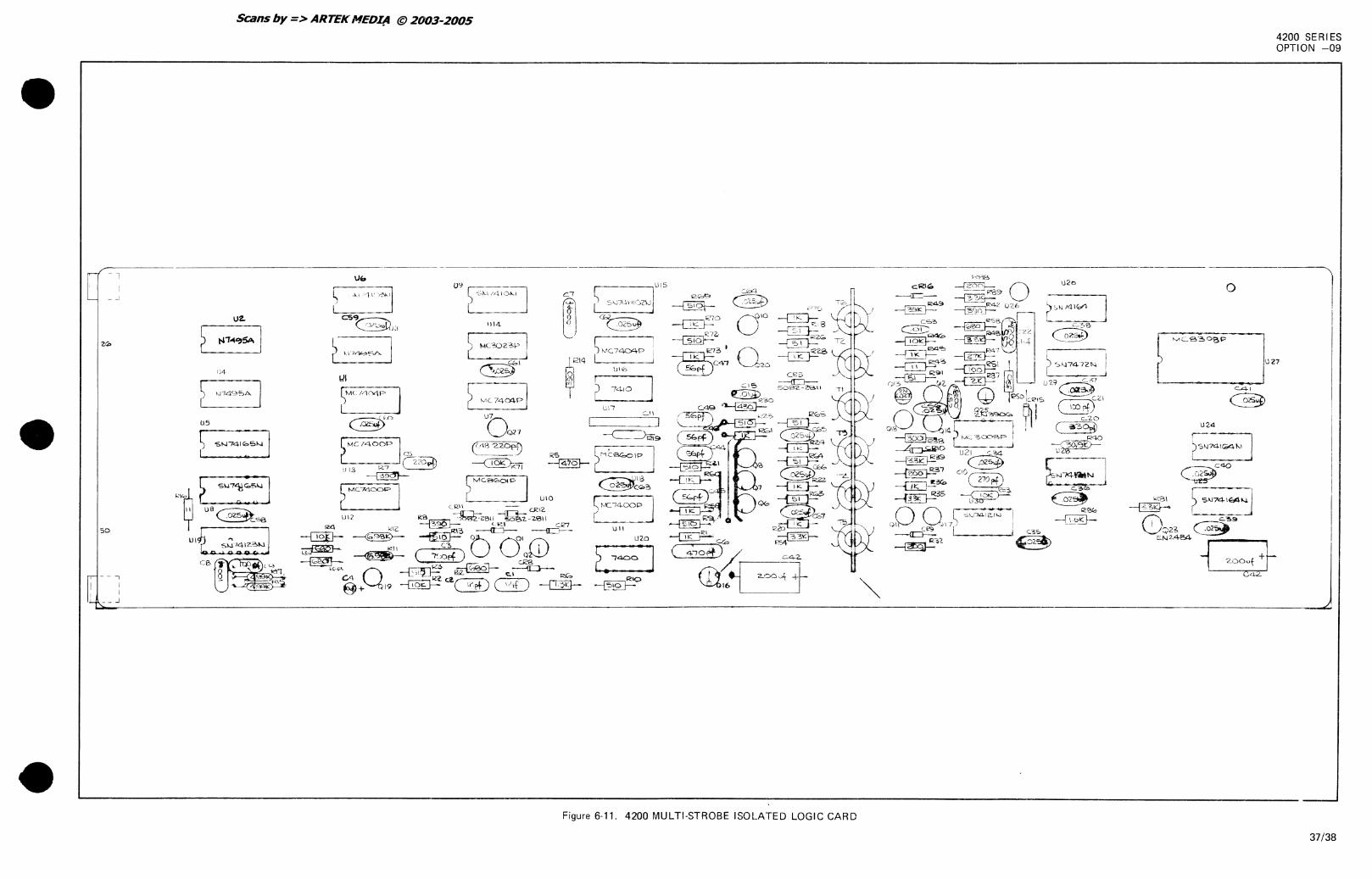
l
50
t - - --,
I I
__ J
1)4
lJ5
Scans by => ARTEK NEDI!'. @ 2003-2005
~ ,)..L 1/)1' ):'>1-11
cs., ~j:!
? \.n~5A bJl
Uli
U20
[=:J C.42.
2.00q +~
Figure 6-11. 4200 . MULTI-STROBE ISOLATED LOGIC CARD
o
4200 SERIES OPTION -09
I I
f Mce~oep ::: I"" C-41
C3
37/38

BINARY
,<.
'2.5G.
51'Z..
IDZ4-
Z04e,
4O<!c;.
SI'f'<:.
STANDBY
BCD
4
S
Scans by => ARTEK NEDIIf @ 2003-2005
SHIFT r RE-GISTER. -,
I; ,...----, 1'2. (----.-------=;-1 f.1 Q. 1
14 <----+-.------~G q ~ 4- F q,
~ 4Dt-.--4_t-t--.-----I-c-I+ E
1\ 0
u?
I..
• M
+SV
~ ______ ~I~I..)I 21-~~3~UI + v r~, 5 •• _ '0"" US~S ,~ V 1 ~.. "I, - -l
~~ I" CA+
COMPLeMENTE:.D r DATA GAilNG --,
10 -E~'-----t-f++_r_.-----I1'3 C. i..O~D r'---3S~ 1'Z.p, ceK~
. I II A 5:I~
• . ,~'., '," , Jl, ~~ p
COMPLE;ME~T L+- FLl P - FLOP ...,
~~_u~ ~'f ~ rit, t.r::: LOG Ie ---,----'-----+----------.-1 UI; p------j U I :>o------<t-----+--"""~.--___H
I 1Z.S'f 1)(.
INVERTING - - 1. -; q ~IQ 1 ... 1 ~?
r- C:r J~ --- - - +~v ~J, _~ c.4<.> ~ Jz. a.t-----tll:::l-o;---I So IZ.'Z.~ • ~~?F
C. '\ s L2- J3 UIS I 510 '> 1 " 1 '2.15 L~---"------:-l K .::u-- ~, L-_---"I'2.~cU<. I ~ I ~UI~ 0")--.11 ___ 54 Lli ~:>-c,,_~--<I""""I\'N'A __ ~ ;'t-__ +~ _____ S~6 UI3 'I rd=l I ~~ ~ 'Y
204 , 4- us q 10 ~ ~~ t-_8 __ -----' \'1 -=-_____ U_I_4_ 13- Rkl 4; (----++t-----;::-i F .--ll Ie, ~ L-- I K
44- ~ E CLR +SV 1'1 ; 14 D -r:;:- CA-S
~ 13 eo~~ ~ r------------------~---------------, • D~I ~?F
see ow~ 102J3
a.'1 4'2.(----·----Ic-+++-t-1~rr-I'2.-:-I1\ ~ c~:p~:-4-+-----t-;:===========v===t========:j====]l----:---I.-~l c Si~rlh ~5 ~ (-4Al JLIS ~--I-----+---4--------------~--~~ ~ ~ ~O
A eel< eN, I, ,2. lUI'" "'<)-'2. __ ,1-1 Ulc" ",o1_O-----t~3__t UI" 4- 9 Ult.>~&+-+---.. l'"""'" AV" A'V'-A+-l __ ~-Ir , (-4 ZJ l. K T S R P ., ..;- V • UII it> 51:1: r>N~ 1025 t-----.-----------------------------, I K
4 u(-4y '---P1N5---'~~ 5CEU~610'2.S ~ '2. UII .JUMPE.R.'2.0 II r--IOMI-h.C.LOCK.-. "3 3+ (------i ~ ~ U3 Qat--"I?.~+---------J r' - 4- UI -t-;iV
1.. 22 (------t ... ~ MODc!-"-"'+-r----, _ ~Io UI~? 10
2~ (-4 V 'Si'E DNG 101.'5 eLI< 1 rq++--t.--------' -';- 1<0 1! 1<7 q +'5V -t-SI/ 1>..10 1>..11 ~ IZ.I'Z.. 1>..13 ~
III 17 (------i U .JUMP,.!'.. Ie. a B eLK? ~ T e ~ (OUNTE:R ---t-, • .- " .'10 S UI7 II~ 8 I r.~ ;IQ~;'1SK ~ leRilK ~1~_r?IGl ~ __ ~'-' B I +SV S -,....,~--q uw q :1 7-----.-----,'2. I>. 5.I.'--'- U J:- C. A u7.O S J' c.~ .. _tt-..... ~IO.,C1UI'2. Iv'\A<:ONITUDc R"'NGoE" _..l..' 'Z.<.DpF 10 ~ C.I ~
Pl"1.7;SE."~I0'2.? 4 '5 .,[ul7ll-12?---------------.... --~ l'Z..pF l'2.pF
{US-IO >---. -------+++--++--------+--t---_-------.II ""o~~ ~ DATA. TRNSFR' ;.to .~-~,,,-I-' ~Li ~'2.
POWeR.. onlo'" I'RE5ET U,,-I, ,- A r FUP- FLOP.., ; CRI ~~o ~ C~ +5~ Q,I I~ t' C12.11 CRl'2.
Ll2 D.1!> ~ ~ B Ulo , ~-, r l50rF r +sV ~ Q & '" > 'r' ~7
~ C i lJq P-..... ---, ~K a:; ~I'I ~ c"so MDDEt-+-r---.
eLI< I r-'I --t-t-i<!'
EXTcl!..lJAl.- REFe.~ '>1
1..IIv'\IT tU.t-IG,E. 1.. ;,
S"TRO&£ CWTI.. ,*,4 { ~ POLAR.I"TV ('~>I<I\N)
.. B CLl< \'l
_.1 s.:r,~
~7.0 ; PI"S J
, ~----'IO SEt OW61OV>S Q,pr
.. (--------.-----------~4 D ~~rc~+~--------------r__t-----'5 L-E.~----~_.-----------tc q
~ D ClZ.l?, II CCI!. ,.. • I?.
t-t--"12.!ov..8 ...... ....-~ UI?. I, -t-sv ~ c~ .A~ J U q ~ ... ~~ I~ V II S V r.80 17. U11
L-____ -. ______ ~~~_-_-_-_~~lo~rU_q~J~~--4-----------------+---------------------~----------------------j--~ ___ L_~
Coso
+5V
CA-7
RVI 7,pf
II '5\~ 1 . l~? 10 UII P-...., ..... MtI'---t-t
1>..'10 II<.
51
t'5V GUA.ll.C TS
12.'2.0 ~ II<. L3
IZ.(,,5
SI
-+Sv T4
+SV T2
~ II<. t __ 3
. • CLl<.1 1-'-+-1--' 35 • B !-'-s--+-t-______________ -. 31t-... ---f-f-+ 1.l ..... ---1.=-t '" c.U<~ I r::L
~ LJ4 S,I. -'- l V
rPOWER-ON PRESET CIRC.UIT --, +,,-y ~:z.. r
.;&1<. . 11 ~4
101<.
NOT R.E:ADY aNI: SHOT HALF- WAVe.
r- RECTIFieR. --,
~
5
4-
o 2
45 ~" :1 7. .. v4 : Pl~S ) R'? ~ 4!l'lK .... C&
4<. (---l 7 trblOOPf 41 (---l 8 . c.'> 12.1
46 (----l. ~ +5V IS 14- '> 1 K
4'l (----l. 10 k 8 a. ~ lJ7 FIRST l-lOLD ?o (----l. II DATA WORD ~ Ulq s. r ONE - SHOT-, zo ~ 12 r ONE -SHOT -, Ci.R. _ 4 C7 -I-S'"
U4.I\~ A '< t----r-.---t-lli-::'13::-t--12 ,:',oopf r'
Il I - I 2.U~ I' •
<;C.E OWE.! \025
(----l. 1.1
FI:>I.l.CD CURJW.li LJMI'T ~U>t:t 2.~ (----l. 'Z.1. l V "- --I R'I. C4a
Vc.c. ;0 (----i?4
'2.7 (------1 7.3
~ (----{ IS ~~:OPF U'1 l?o II 13
12
SEE DWG> 10'2.0; RE:.A.O~: rLAC::;
see OW410ZS U3-8, U4 -4-,'5
10
RTZ SID
r-----------~------------------------------S_iUIr., ~ I'IBNoRMfo.L <;'l"'''U~
roLL S, ... .,. us
GROUND
-+SVOLTS
2.\1 • CONTROL WaR!) : ~ 10K. '2.7.°rF fl 4ilQI<.> c... ONE:SHQT ~~ +sv '~
+'5'1 ~ V-tw 3 &
~: : ;' ~' +st-v---~+--'-L:-I, ~:, ~::l~~~~~~~~~~~~~~~~~~-LI.lt-_-_-_-... F-:-liL":.=-_E-_-_-_-_-_-_-_-_-_-_-_-_-G_e_I_3.e_-H_-_-:-1~'"-I·1 U~: I:, ~r.,~~~~~~I-. -,-. :1 ===~-----------'I SCcDW~~1.S: N01~r~l~ ~<~--------------------------------------------------------------------------------------------------~--~
CHANGE DESCRIPTION DR CHK r.;;'01
4-'2.00 MULTI - 5TROI;EISOl.ATeD LOGIC. CARD
PART NO. SIZE DRAWING NO.
D 4200 - 102.4-SCALE NON.E:.... SHT OF , REV

GU
Scans by => ARTEK NEDI/4 @ 2003-2005
'-v SHIFT ~~'S .~ 1.?K. r R.EGISTeRS -,
&0 OA.iA / BlI-tARY DATA. S ("
U2.1
tV 0.1'
\t! Cl!.q ~ ...
~'s~
~ ~~ ~
~ 4 UZ,I
IY CUI
-sv
~~ ~ ~
'?'?.I(.
I '2. U'Z.I
I ~
~ Sa.. o..
4-QI.
Sb ~ s r..
~ U'Z.4 10
~
~" II
q CWl Q.
1'2.
~ cu. CIt I~
J 3 , a.
p-- Sa. a... 4-
CIO
l ~
S RS 't
'Z.70pF '01(. ~ SI. '" a. ~·AAA.V 10
U'Z.5 a.s II 10 11
?> 10 LA.TCH l'~MI~G Q,t. 4 A. Q- ~ I'Z.
ONE:- -S\-lOT CL.R.. Q.7
5 /Io,z. , I~
J >--- CI-k.. o..
~ 1!>.
"'7
H F ) ~ } >11'4-• u
c;, , T
~ 5 n*, ~I'I'Z.
~ II. 4Oq(,
~ P 'ZD4fJ ~ to! 10'2.04 ~ 1'5 :}~Z ?I'Z. ~ 14- 'Z.'7c.. ,.
"R.O 1I.·~"2.
T? wo
I~ 'Y
I}-It"
-sv
~ 1'3 ~} *2 1'Z.~
~ 1'2. r..+ ~ 1'1
n~· '?'2.
~ IS 1(" ~ n 6 ;.
1(0 4-~ w
:} Jf4 'Z.
-~ V I ,. LA.TCH
~& r CIRCUITS --, UZ.I ~ J cXTERN~ REFERENCE ,. II. A 17 ,
0.. Qo
~ t> '} 1& 114
D. 0.1 ~
4- '2, 'Ul '2.1
C. : LIMIT M,t.,GNITUDf:' ~ (4
~ 'l.'Z. 'Z.?> ~ Qa
~ 4- -- - -- 5 LIMIT RA.NGE:' 0.. B Qo
~ ~
(., D. Q. 7
6 E'4TE:RNAL.. Rf:F~NCe: & ~ Qz.
q ~ F Mot-GNITUOE- R.At-IGe 10 ~ ~& ) II POLAR.ITV D. ~ I 0 .e > ~
1o,o\R. U'Z.1 c.. ~T"'IoI06't'
MR.
14
-sv
I 3
~ s... ~
Q. 4-
S 51. ~
(. a,
U'U.I 10 QQ
q II Cll!. 0.,
I'Z. C«.
S 11 ~ c.lK as
I!.~II
n "Z.OO IY
I~, ....
~ ell~O
'" -5'1
r R40 ·lit.lOTe"2..) SEL... saL.
~ECOND HOL.D ~h c:w ONE: -t.;HOT \I UIO
PULSE: r GcNERATOR..-,
12. ~J, el.RQ~ ~ J'Z, ~~ C.Z.I ~ J. T IOOpF
'--_+--,1'2.-=1 el.I(. -!;v
~ K.. I ) I )
~ K... q 10 ~ ~ Q.,J------II---IU2.I~~-----
PR.ESE<T thlf' Ht..LF-WA'IE ~E:CTIFIER "~-----' 13
-5'1
-h c.ll.U" --, I'?> 1'2. V ~--~·*-·~--~~----iU'2.I~~------------------+---------------------------t-----------------------------------~ _ ____
r r. • L----------------------------r-------------------------------------------------------------~: = HD~D SI~~A~ ::~~~p,,' ~~
•
12."11 •
> Rose > ~"I0 100
l POWER.-ON. PRESeT CIRCUIT
J
r- BY-PASS CAPACITORS ---, G f I C~4 i~~U C41 I I C4-'Z. e. PLAcCS
J------::~ I r" t! -sv
Y} ~oc.le COMMON '2.1
:l.} Y '2.'2. I.
~ 5 CURRENt LIMIT -~ 4 ~~} GUAI!.D
SI CHANGE DESCRIPTION DR CHK APPR
-sv
NOTeS: I. Al~ RESISi .... HCI!!: I~ li'l OH~ "-i'll) AL.1. CAP",c.lT.t..NC.e
I~ IN MIC~F.t.aA.tlISo,\.lN~ QT\oIE:IlWI~ t.lQ'il!r.O. ,
'2.. '!teL - J'.A.CTOIl.'l' 'SC\,..eC.TaC i'A.1Z.:iS I IN .AC.dl1U>"*'IGE: WIT~ Tlole. ~AIZ.",\,IGU\.A.~ 1"'s.'TIZ.I,)Ma~T MODal.. USIIo.l($o. 'TI-II: - Cl"\ OPTION.
MULTl- STROBE: lSOLATI::D LOc;,IG BRD: IN.SIDE:' e:,UARD
PART NO. SIZE DRAWING NO.
014200 -1024 SCALE NONe SHT 'Z. OF 2- REV
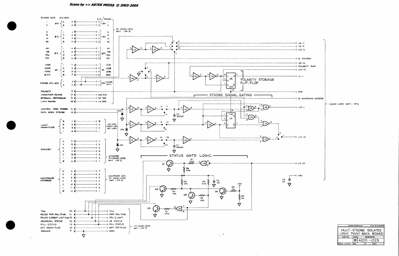
Scans by => ARTEK NEDIIf @ 2003-2005
BINA.R'{ PA~ Bc.D DI>.TA
'Z. ~4{:
4-
~'H @.
1(,
~
* {; I~
1f'Z. '2.%
SI'Z.
IOV!-
~{ ~
4G'I ....
&1<l'2..
'!>,we.c ~\\...<lI'4 { ~
POLAIUT\(
MA6NITI>C>e. AAN.61!:
EXTIlWA\.. RE:FE~
LIMn 1IAt-I&&
COIolTWL. WOR.tI <;'1'IUlI',e
DA,A Wotl.D STROP.!::
{; UMIT M""'NI,UOI!:
'" 0;,
-:.TAI<IOe.Y 4-
-.;
z
~
'" S
M,6..INFAAMe: 4-ADDIl.~~ 3
2.
i:I?
a A
lKO/I>INAI2..Y
~-----~l 4}':lr4- I ~------------~l S ~
(
< J <
~------------~j~ ~ TO 4-ZCO -10'24 ~; 100;=-'2..
H < F (
c (
N (
M (
L. < k < ~------------~: ~} : ~-----~l 't- ,*,2. 1.r;,/p
~------------~l s 512.
,. < ~ ( J2. (
I' (
I 11 IO~4-~------~I 'Z. ~
~-----~l 4- 41'1 M't" ~-----------l! s J ~1'tZ.
t>
c I }lf4- STi1.OP..£:
~--*------------i '2. eNT\...
c: 'Z.. < ~------------~I Wb R.>lC.
~------------~l EOX<' IU::r
~------------_l! LIM \I.K(,.
~ ( 'Z1'>(
I~
1<1-
I (
~(
':! < 4-(
~----------ll S
~--------------il 4-
~------------~1 Z.
~-------------l! I
}
LIMMAc:. ~-1O'2S
9<1 101'2
i.. < ~< Y(
)( <
~----------ll •
~--------------il ....
~------~l 5
~-------------il ~
w( <;TAND3'(
CII-I
V (
u<
3
2-
~---------ll I TO <I'ZQO-loz.'5 "S>!-\, 10F,-
10 (
7 < s < ~ < 10 < II < I'l. <
2.4
MAIN FI<AMl:: -"00. TO 4= -10'2'5 ?HT IOF,-
Vee.
II
ftlUE.O PWR FAI L. FL.A.& 2. I
l'OL-LED CURIU:i'IT LlMIl FlXo 'Z2
PWR. FAIL PLi..6
POL I. LIMIT
"SNOIl-M.Io.L STATL6 ~'l>
POLL STATUS IS
NOT RE"'DY FL-AG 'l.5
GWUNO F
AS 51' ... TUS
~--------------~--~ POLL- STp.,TU5
( (
~ NO, RD'I FLA6
~----~------------~l ~ND
'----------'
a:~
TO 4ZDO-IOzn SI-IT I 0" 'Z.
OJ
a:z.
7
10
IS 14-•• ------------------------------------------------------------------------------~l US-II
I'" • U~-'l> ~o
• U12-2
11
10
POLARITY STORAGE:' FLIP-FLOP
J STROBE: SIG NAL GATING
II
s '" 4-I,
lsi sr ... NDIW
UI'>-12
POI..AlI.\TY SIc;,N
UI'\ -t;
UI-\
POP
-----------------------*----1 U2 . .>:>-~-__I K. a '2.
'I
z'Z.
Rl 470
Cl .¢ 330pF
STATUS
~ 101(.
10 U?>
1'2. II
'Z. 10 •• ---------11 Wq -10
~~--------------------------------------------~U'l>~------3
Gp.,T~ LOGIC Itl
4.0 l.
Rl!. 2Q,,-
R5 R!\ 101<. 4:JK.
q<> R7 10K.
c:z. ~ .2.7.. +sv
q4
'2.
C4-:,2
U7-IO
+sv
8
4200-I07..S .,,' .. Ii I OF'Z.
CHANGE DESCRIPTION OR CHI( APPR
MULTI-STROBE:- ISOLATED LOGIC PIGGY - BAC.K BOARD
PART NO. SIZE DRAWING NO.
1014-200 -1025 SCALE NONE:- SHT OF REV
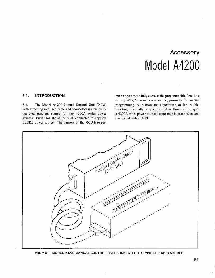
6-1. INTRODUCTION
6-2. The Model A4200 Manual Control Unit (MCU) with attaching interface cable and connectors is a manually operated program source for the 4200A series power sources. Figure 6-1 shows the MCU connected to a typical FLUKE power source. The purpose of the MCU is to per-
Accessory
Model A4200
mit an operator to fully exercise the programmable functions of any 4200A series power source, primarily for manual programming, calibration and adjustment, or for troubleshooting. Secondly, a synchronized oscilloscope display of a 4200A series power source output may be established and controlled with an MCU.
Figure 6-1. MODEL A4200 MANUAL CONTROL UNIT CONNECTED TO TYPICAL POWER SOURCE.
6-1

A4200
MCU
6-3. SPECIFICATIONS
64. There are no specifications for the Model A4200 MCU.
6-5. INSTALLATION
6-6. The MCU is supplied with an interface cable and connectors designed to fit any of the 4200A series power sources. The operating voltages for the MCU are supplied from the associated power source through the interface cable. The interface cable also supplies the power source with all programming inputs initiated by the MCU. Connection of the MCU to the power source via the interface cable is done as follows:
a.
b.
c.
CAUTION!
The Model A4200 MCU is NOT compatible with the -09 option.
Turn off the power source and disconnect the programming connector from the rear panel of the power source.
Connect the interface cable connectors to both the programming connector on the power source and on the MCU.
Select the desired operating configuration on the top panel of the MCU and then turn on the power source. The power source is now ready for operation with the MCU.
6-7. OPERATING INSTRUCTIONS
6-8. The location and function of the MCU controls, indicators and connectors are described in Figure 6-2. The active or high level logic state of the pushbutton switches on the MCU is the depressed or in state. However, in the event the associated power source is equipped with the inverted logic option (08 Option), the logic level states of all pushbuttons defined below is high when the pushbuttons are extended or out. When depressed or in, the logic level state is low. This condition applies to all pushbuttons except STROBE,MANUAL,AUTO,andEXT. Figure 6-2 functionally describes the MCU controls, indicators, and connectors related to an associated power source that is not equipped with an -08 Option.
6-9. OPERATING FEATURES
6-10. The following paragraphs describe operating features relating the MCU to power sources and should be read prior to operating the MCU.
6-11.
6-2
Isolated Control Logic (-01 Option)
6-12. The MCU provides the digital input programming, including the STROBE pulse, necessary to test and control an associated 4200A power source equipped with an isolated control logic option (-01 Option) or with an inverted isolated control logic option (-08 Option). When using either option, a STROBE pulse is required to start the digital-to-analog conversion process after a valid digital input program is entered. In MANUAL mode, the STROBE pulse is generated by manual depression of the STROBE
pushbutton. In AUTO/EXTERNAL REFERENCE mode, the STROBE pulse is generated automatically following a l.SJ1S delay that terminates the last programmed bit. The STROBE pulse is O.SJ1 sec wide with a minimum width of 500 ns. A negative slope (+SV to 0 transition) is reqUired.
6-13. Direct Coupled Control Logic (-04 Option)
6-14. Power sources using the direct coupled control logic option do not require use of the STROBE pulse. When used in the AUTO mode the performance is limited by the timing format of the STROBE pulse. Ideally, the STROBE pulse should precede the input data change and last until the input data is settled. The STROBE pulse, however, occurs about l.SJ1S after the change of input data and lasts about O.SJ1s. Consequently, voltage spikes may occur (going to 0 volts) when voltage levels are stepped. These spikes may be observed on an oscilloscope when monitoring the power source output and do not indicate a fault in the power source.
6-15. Coax Jack Cluster
6-16 Three BNC coaxial cable connectors located on the top panel of the MCU provide connections for test instruments. The common of these connectors is tied to logic ground_
6-17. Trigger Input
6-18. TRIGGER INPUT jack provides an input connection for an external trigger generator to produce a remote, manually controlled STROBE pulse when the MCU is in the AUTO EXT mode. The external trigger generator replaces a fOkHzmultivibrator when the EXT pushbutton is depressed. An external sin termination resistor is provided in the MCU for the external trigger generator. For optimum performance the trigger generator should have an output pulse impedance of son and be capable of producing the waveform shown in Figure 6-3_
1/20n5

A4200
MCU
BCD CODE (BLK FOR 4210A, 4250A, & 4270A) --.......
BINARY CODE (BLK FOR 4216A & 4265A) ---..,
BINARY CODE (BCD FOR 4275A) _____ -,
.5J 16384 8192 4096 2098 1024 512 256 128 64 32 16 8 SIGN/POL 81924096 2048 1024 512 256 128 64 32 16 8 4
4 2
2
rl~ ~, ,I . L 1 I, J, I I I I I ,1 I POLARITY "-'" A DECADE B DECADE C DECADE D DECADE /
SWITCH " / Select polarity of" " MAGNITUDE AND POLARITY PROGRAM SWITCHES /
output voltage " '" " / +OUT " -IN ~ .. , IU .. IUIUCIUItIU1T /
{]~"'L"'I""!""'''''I'''\'''I'''I'''I''\''I""1','1'1 I I
• . :~'.:I"~.:;':: __ . , , , I . I ',::;::.' ':.~'~Ir" ~~~,: I 1
RANGE ~:'::~~~R· /1-L::.."I",,,,:j"'7--"CC~ -' .'\J READY
SWITCH R".;v", ;n,,"'''' / ,. J , " FLAG Selects Cable AssemblY/,1 \\ "Provides 5V ready low (OUT) /' / . I dOV
LIMIT FLAG / I \\ '" signa an not or high / INDICATOR CONTROL '" ready signal (IN) range / & MODE COAX "
~~r ~\ /
FUNCTION PROGRAM SWITCHES JACK '-sJour/ce SWITCHES / mOIl MI~UAt lUTe !II CLUSTER '-
IIMI! • fllC \ U,CGH ftllGiI '- IUO'
/
'"'UI OUT'UT fllC i>----- CUUUT liMIT MI .• ,.~-~, ... ,! I 110 .. H 18 " (!taH SIU081 ~ , ,.,
, I ,__ J - SWITCH e ~, ~ X10 40 Enters \ \
MCU Selects TRIGGER TRIGGER data auto INPUT CURRENT
LIMIT SWITCHES
[ BLK FOR 4250A & 4265. USED WITH -06 OPTION.
RED FOR 4270A & 4275A] USED WITH -06 OPTION Switches select I limit range and level of I limit.
LIMIT FLAG INDICATOR Displays I limit condition of power source out by switches.
when pressed 01 &08 Options
STANDBY SWITCH Selects standby mode (IN) where output is <l%of programmed level
program control (IN)
MANUAL SWITCH Selects Manual program control (IN)
EXTERNAL REFERENCE SWITCH Selects the external reference mode (I N) -03 Option
Figure 6-2 CONNECTORS, CONTROLS, AND INDICATORS
Receives external program control trigger.
EXTERNAL SWITCH Selects external program control (IN)
OUTPUT Provides scope sync & allows STROBE pulse viewing
6-3

A4200
MCU
CAUTION
Application of trigger voltages higher than the recommended value will damage the MCU.
~~ 1 G)
CD DC OFFSET - ±OA Vdc (?) AMPLITUDE +2.8 +5.5 Vdc
~ WIDTH 0.5 - /JS @) PRF DC 10K Hz
MIN MAX UNITS
LIMITS
Figure 6-3. External Trigger Generator Requirements
6-19. Trigger Output
6-20. TRIGGER OUTPUT jack provides an output connection for monitoring the inverse of the MeU generated
STROBE pulse. The output trigger is a positive-going pulse that occurs each time a STROBE pulse is generated. It is useful in synching a scope to the MANUAL-STROBE mode. However, when using the AUTO or EXT modes, which generate an automatic internal or external STROBE, the output trigger provides a valid scope sync for the ready or not ready flag output only. It cannot be used to monitor the power source output voltage in the AUTO or EXT modes.
6-21. Ready Flag
6-22. READY FLAG jack provides an output connection for monitoring the ready or not ready flag voltage. In the three control modes (MANUAL, AUTO, or EXT) the output trigger provides a valid scope sync for displaying the flag voltage.
6-23. PROGRAMMING SWITCHES
6-24. Of the twenty-nine program switches located on the MeU top panel, all but three are used to enter programming inputs into the 4200A series power sources. These three are AUTO, MANUAL, and EXT. Figure 6-2 divides these switches into three groups of control mode switches, magnitude and polarity program switches, and function program switches.
6-25. Control Mode Switches
6-4
6-26. The four control mode switches provide manual or automatic control of the manually selected input data program. MANUAL, AUTO, or EXT are the three control modes selectable on the MeU.
6-27. Manual Mode
6-28. The MANUAL mode allows manual manipulation of the input programming data as well as manual generation of the STROBE pulse. This mode is selected by depressing the Manual pushbutton. Each push of the STROBE pushbutton generates a O.5p.s STROBE pulse which transfers the previously selected manual program to the internal registers of the isolated control logic option (-01 Option). In the event the power source is equipped with a direct coupled control logic option (-04 Option) rather than the isolated control logic option, the power source output voltage changes as the program pushbuttons are pressed. No STROBE is necessary.
6-29. Auto Mode
6-30. The AUTO mode of operation provides automatic and sequential scanning of a previously selected magnitude program. The power source output is thusly stair-stepped or pulsed in a manually selected pattern, the sequence of which is governed by an internal 10kHz multivibrator. The multivibrator also initiates the STROBE pulse for the isolated control logic option. If a direct coupled control logic option is used in lieu of the isolated control logic option in the associated power source, then the timing of the STROBE is incorrect.
6-31. External Mode
6-32. EXT mode operation is similar to the auto mode of operation. The difference is that the internal 10kHz multivibrator is switched out and an external pulse generator is substituted at the TRIGGER INPUT jack. The sequence frequency is thereby remotely controlled by the trigger generator.
6-33. Magnitude Program Switches
6-34. Sixteen magnitude program switches provided on the MeU are used to program the BeD or binary magnitude inputs into an associated power source. Each pushbutton is labeled with one or more bit values depending upon unit serialization. Units bearing serial No. 224 and below are labeled entirely in black. Units bearing higher serial numbers are labeled in black and red. The red coding applies to (1) the binary magnitude used to program the 4275A power

source, and (2) to the current magnitude used to program the current limit option (when installed) in the 4270A and 4275A power sources. The black coding applies to both binary and BCD magnitude power sources with the location and format of the magnitude bits identifying related power source effectivity as follows: The black binary magnitude bits above the pushbuttons apply to the 4216A and 4265A power sources. The black BCD magnitude bits below the pushbuttons apply to the 421OA, 4250A, and 4270A power sources. In MANUAL mode the magnitude inputs are programmed directly by depressing a single or combination of magnitude pushbuttons. In AUTO mode an internal binary counter controls the manually selected magnitude inputs in a four-bit binary pattern. Each output of the binary counter is parallel connected to the four corresponding BCD or binary magnitude programming switches shown in Table 6-1. The power source input program is sequenced in a pattern that is determined by the selected magnitude program switches and the binary counter outputs. Figure 64 shows the power source output voltage patterns available by programming a single decade in the 421OA, the 4250A, or the 4270A power source.
6-35. Polarity or Sign/Polarity
6-36. The polarity program for the power sources is controlled by the program switch marked POL or SIGN/POL. Depressing this switch commands the negative programmed output voltage. The non-depressed or out position commands the positive programmed output voltage.
6-37. External Reference
6-38. The EXT REF switch, when depressed, programs the External Reference Option (-03 Option) of the 4200A series power sources.
6-39. Standby
TABLE 6-1
A4200
MCU
640. The STANDBY switch, when depressed, programs the 4200A series power sources to the standby condition. This condition permits a single bit on a given control line to clear the output to about 1 percent of the programmed level without disturbing the previous command word. Upon returning to the operational condition by releasing the STANDBY pushbutton, the output reverts to the preprogrammed level.
6-41. Range
642. When the RANGE switch is depressed, the high range of the associated power source is programmed. When not depressed and in the out position, the RANGE switch programs the low range of the power source. The low and high ranges of the 4200A series power sources are given in
Table 6-2.
6-43. Current Limit
644. The five CURRENT LIMIT MA switches labeled in black or in black and red numbers, depending upon serial No. effectivity, program the Programmable Current Limit Option (-06 Option) in the 4250A, 4265A, 4270A, and 4275A power sources. The black numbered pushbuttons are used with the 4250A and 4265A power sources and the red numbered pushbuttons are used with the 4270A and 4275A power sources. Pushbutton switches labeled in black enable selection of the desired current limit point in increments of lOrnA low range or 100mA high range (Xl 0) for the 4250A and 4265A power sources (Table 6-3). The red labeled pushbutton switches enable selection of the desired current limit point in increments of 5 rnA low range or 50 rnA high range (XIO) for the 4270A and 4275A (Table 6-4). When none of the pushbuttons are depressed, the current limit is 10 percent of selected range; i.e., lOrnA and 100 rnA for the 4250A and 4265A; 5 rnA and 50 rnA for the 4270A and 4275A. The 4210A and 4216A power sources do not utilize the programmable current limit
PROGRAMMING SWITCHES CONTROLLED BY THE BINARY COUNTER.
PROGRAMMING SWITCHES
Binary Counter 4210A-4250A
outputs 4216A-4265A 4270A-4275A
1 1,1,1,1 4, 64,1024 .5, 8, 128, 2048 2 2,2,2,2 8,128,2048 1,16,256,4096 4 4.4.4.4 1,16,256,4096 2,32,512,8192 8 8,8,8,8 2,32,512,8192 4,64,1024,16384
6-5

A4200 MCU
CD 8-1
® 8-2-1
® 8-4-1
® 8-4-2-1
6-6
® 8-2
@ 8-4---....
@ 8-4-2
Figure 6-4. VOLTAGE PATTERNS OBTAINABLE BY DECADE PROGRAMMING IN THE AUTO MODE (4210A, 4250A, AND 4270A)
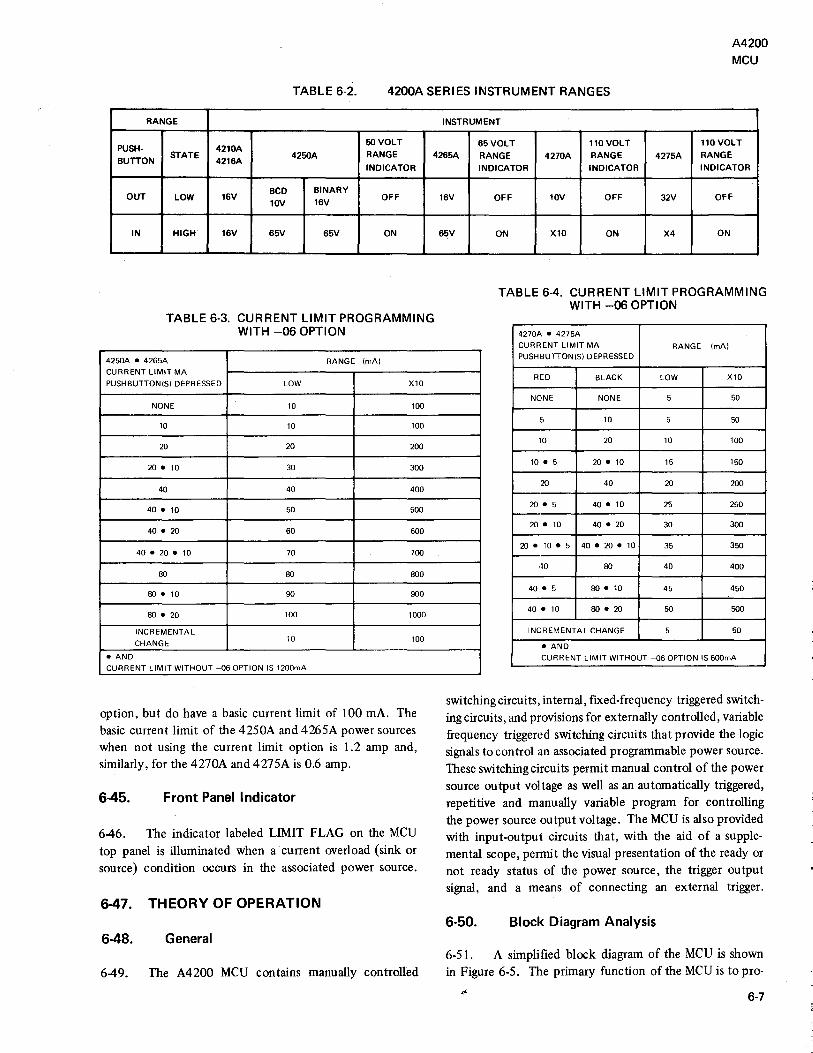
A4200 MCU
TABLE 6-2. 4200A SERIES INSTRUMENT RANGES
RANGE INSTRUMENT
50 VOLT 65 VOLT 110VOLT 110VOLT PUSH·
STATE 42l0A
4250A RANGE BUTTON 42l6A
4265A RANGE 4270A RANGE 4275A RANGE
INDICATOR
BCD BINARY OUT LOW l6V OFF
10V l6V
IN HIGH l6V 65V 65V ON
TABLE 6-3. CURRENT LIMIT PROGRAMMING WITH -06 OPTION
4250A - 4265A RANGE (rnA)
CURRENT LIMIT MA
PUSHBUTTON(S) DEPRESSED LOW Xl0
NONE 10 100
10 10 100
20 20 200
20-10 30 300
40 40 400
40 _ 10 50 500
40 _ 20 60 600
40 - 20 - 10 70 700
80 80 800
80-10 90 900
80 _ 20 100 1000
INCREMENTAL
CHANGE 10 100
- AND CURRENT LIMIT WITHOUT -06 OPTION IS 1200mA
option, but do have a basic current limit of 100 mAo The basic current limit of the 42S0A and 426SA power sources when not using the current limit option is 1.2 amp and, similarly, for the 4270A and 427SA is 0.6 amp.
6-45. Front Panel Indicator
646. The indicator labeled LIMIT FLAG on the MeV top panel is illuminated when a current overload (sink or source) condition occurs in the associated power source.
6-47. THEORY OF OPERATION
6-48. General
649. The A4200 MeV contains manually controlled
l6V
65V
INDICATOR INDICATOR INDICATOR
OFF 10V OFF 32V OFF
ON Xl0 ON X4 ON
TABLE 6-4. CURRENT LIMIT PROGRAMMING WITH -06 OPTION
4270A - 4275A CURRENT LIMIT MA RANGE (rnA) PUSHBUTTON(S) DEPRESSED
RED BLACK LOW Xl0
NONE NONE 5 50
i5 10 5 50
10 20 10 100
10 - 5 20 - 10 15 150
20 40 20 200
20 - 5 40 - 10 25 250
20 - 10 40 - 20 30 300
20 - 10 - 5 40 - 20 - 10 35 350
40 80 40 400
40 - 5 80-10 45 450
40 - 10 80-20 50 500
INCREMENTAL CHANGE 5 50
- AND CURRENT LIMIT WITHOUT -06 OPTION IS 600mA
switching circuits, internal, fIxed-frequency triggered switching circuits, and provisions for externally controlled, variable frequency triggered switching circuits that provide the logic signals to control an associated programmable power source. These switching circuits permit manual control of the power source output voltage as well as an automatically triggered, repetitive and manually variable program for controlling the power source output voltage. The MeV is also provided with input-output circuits that, with the aid of a supplemental scope, permit the visual presentation of the ready or not ready status of the power source, the trigger output signal, and a means of connecting an external trigger.
6-50. Block Diagram Analysis
6-51. A simplifIed block diagram of the MeV is shown in Figure 6-5. The primary function of the MeV is to pro-
6-7

"'T1
G) C :0 m C(l ?1
~ ~ o s: » z c » r (')
o Z -i :0 o r C Z =i OJ r o (') A o » G) :0 » s:
A3 Al MANUAL STROBE STROBE
SWITCH
59
1--------' GENE RA TO R r----..
TRIGGER
INPUT
06-03 'i. <J5 TRIGGER OUTPUT
TO AUXILLARY EOUIPMENT
~ < ~J6READYFLAG
Al Al Al . 1----"" AUTO STROBE INVERTER INVERTER I I CONTROL
MODE
SWITCHES
AUTO Sll
1----aI GENERATOR I---'"-~ U1B ~ U1A ~~:""<'if..+--~I 05 - 04 ~ __ --l I 1
A2
EXT S10 A DECADE
MANUAL S121 Al
i r------1---r-~~---A FOUR Al
Al A I-- D
1
21- C A'
BIT INVERTER
41-- U2 B A
I I I I I I I I
~ i ... J INTERFACE ,----------, 10kHz MULTI
VIBRATOR
02-01
BINARY COUNTER
U3 81--
>---+-C,~~--,I CABLE rr;;'-j-l, 4200A I 1 I Wl I I
: I I PROGRAMMED L ___ ---.!.~t-t~~:::::::t_--" I I I : PROGRAMMABLE I-~, OUTPUT
I I I I POWER : VOLTAGES
A A
A3
FUNCTION
PROGRAM
SWITCHES
SIGN/POL
S17
Sl RANGE ~ S2 STANDBY----....
~ EXT REF r---.. 54 55 56 S7
58
Xl0
80/40
40/20 20/10
10/5
r---" ~
i-------' ~
A3 llMii FLAG
INDICATOR
CRl
B t::=:'l I ii, SOURCE
DECADE t::::::::1r--""1---~II-<""""~I--"I ! ~~L(~Y~~~~ ___ J C F===t 1 __ I i
DECADE t ':=J I .... ' I
D t:::=l : I v--- !~:~~NOL DECADE t=:::::J T .... , I ~ CONNECTORS
I MAGNITuDE I I I (TYPICAL) I-- PROGRAM---I
SWITCH ESI i I __ i
I I I I I <i" I
Jl
PROGRAMMING
CONNECTOR (TYPICAL)
NOTES: ... +5Vdc l!. at LOGIC GROUND
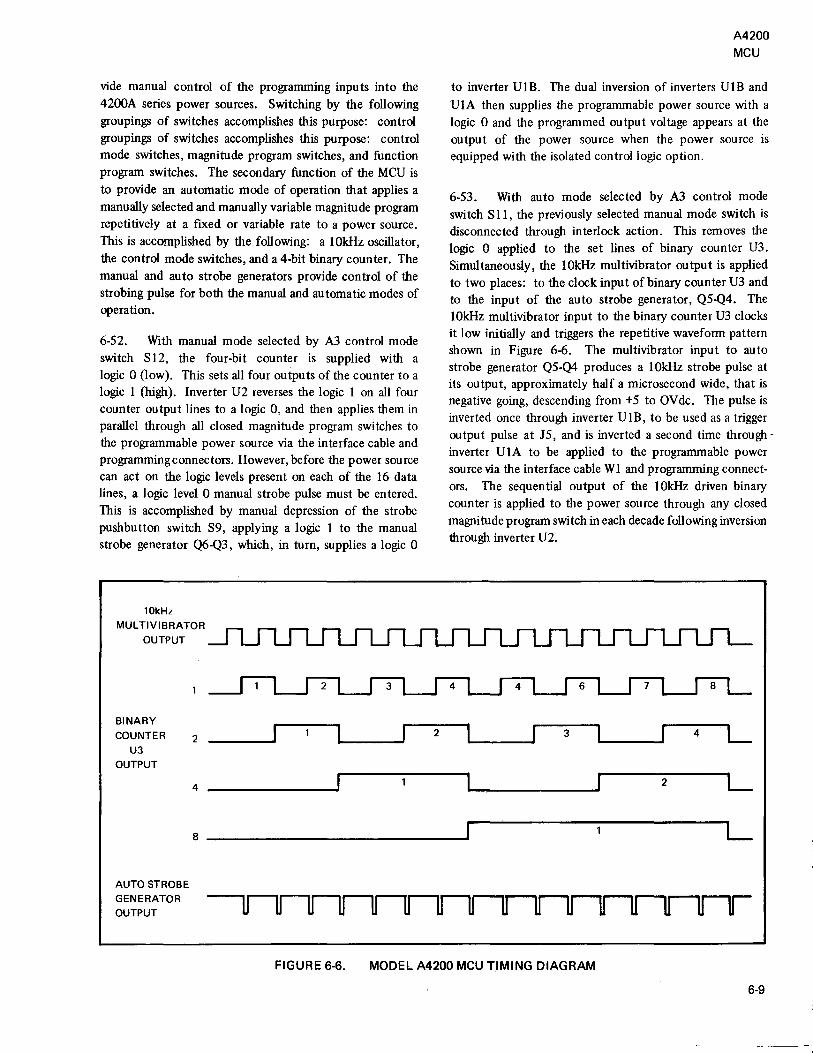
vide manual control of the programming inputs into the 4200A series power sources. Switching by the following groupings of switches accomplishes this purpose: control groupings of switches accomplishes this purpose: control mode switches, magnitude program switches, and function program switches. The secondary function of the MeV is to provide an automatic mode of operation that applies a manually selected and manually variable magnitude program repetitively at a fIxed or variable rate to a power source. This is accomplished by the following: a 10kHz oscillator, the control mode switches, and a 4-bit binary counter. The manual and auto strobe generators provide control of the strobing pulse for both the manual and automatic modes of operation.
6-52. With manual mode selected by A3 control mode switch S12, the four-bit counter is supplied with a logic 0 {low). This sets all four outputs of the counter to a logic 1 (high). Inverter V2 reverses the logic 1 on all four counter output lines to a logic 0, and then applies them in parallel through all closed magnitude program switches to the programmable power source via the interface cable and programming connectors. However, before the power source can act on the logic levels present on each of the 16 data lines, a logic level 0 manual strobe pulse must be entered. This is accomplished by manual depression of the strobe pushbutton switch S9, applying a logic 1 to the manual strobe generator Q6-Q3, which, in turn, supplies a logic 0
10kHz
MUL TIVIBRATOR OUTPUT
BINARY COUNTER
U3
OUTPUT
2
4
2
A4200
MCU
to inverter VIB. The dual inversion of inverters VIB and VIA then supplies the programmable power source with a logic 0 and the programmed output voltage appears at the output of the power source when the power source is equipped with the isolated control logic option.
6-53. With auto mode selected by A3 control mode switch S 11, the previously selected manual mode switch is disconnected through interlock action. This removes the logic 0 applied to the set lines of binary counter V3. Simultaneously, the 10kHz multivibrator output is applied to two places: to the clock input of binary counter V3 and to the input of the auto strobe generator, Q5-Q4. The 10kHz multivibrator input to the binary counter V3 clocks it low initially and triggers the repetitive waveform pattern shown in Figure 6-6. The multivibrator input to auto strobe generator Q5-Q4 produces a 10kHz strobe pulse at its output, approximately half a microsecond wide, that is negative going, descending from +5 to OVdc. The pulse is inverted once through inverter U IB, to be used as a trigger output pulse at J5, and is inverted a second time through' inverter VIA to be applied to the programmable power source via the interface cable WI and programming connectors. The sequential output of the 10kHz driven binary counter is applied to the power source through any closed magnitude program switch in each decade following inversion through inverter U2.
3 4 L
2 L 8 ______________ -" L
AUTO STROBE GENERATOR OUTPUT
FIGURE 6-6. MODEL A4200 MCU TIMING DIAGRAM
6·9
A4200
MCU
6-54. With external mode selected by the A3 control mode switch, SlO, the previously selected auto mode switch is disconnected through interlock action. This removes the 10kHz multivibrator output from the input to the binary counter and from the input to the auto strobe generator. Switched into these two input circuits is trigger input jack 14. Hence, use of an externally controllable trigger generator is possible, providing the parameters are generally as follows: output pulse frequency of 10kHz, O.5J1.s pulse width, and having an output pulse impedance of about 50 ohms. The external trigger generator substitutes for the internal 10kHz multivibrator in the external mode, and circuit activity is essentially the same as discussed in auto mode.
6-55. The A3 function program switches provide a logic level low signal on the appropriate line to the connected power source when a given function switch is depressed. The SIGN/POL switch, S17, is shown as an example typical of these switches.
6-56. The indicator light LIMIT FLAG on the MCU top panel is essentially a duplication of the I LIMIT indicator on the front panel of a 4200A series power source. Hence, these two indicators can be expected to illuminate together when a specified current limit point is reached.
6-57. Circuit Description
6·58. The following paragraphs briefly describe the cir· cuitry in the MCU. Each description, unless otherwise noted, is referenced to the schematic diagram A4200-1000 located at the end of this section.
6-59. CONTROL MODE SWITCHES. The control mode switches consist of three single pole, double-throw switches on the A3 Function Assembly, SlO through S12. These switches are the ganged, interlock, pushbutton type and only one switch at a time can be closed and latched. Switch S 12, the MANUAL mode switch, when depressed and latched, applies a logic low (0 volts) to the four set input lines of the four-bit binary counter U3, pins 3,5,10, and 12. This forces the counter outputs on pins 4,6,9, and 11 to a logic high (5 volts). When the AUTO mode switch SII is depressed and latched, the MANUAL mode switch is interlock released to its non-depressed state. This applies 5 volts to the binary counter previously held low by the latched, but now released MANUAL mode switch, and permits the counter to be advanced by the 10kHz multivibrator input at pin 1 of U3. The 10kHz MV output, supplied to the counter through the closed contacts of switch S11, is also applied to the input of the auto strobe generator at pin 90fUID. When the EXT mode switch SlO is depressed and latched, the AUTO mode switch is released. This removes the
6-10
10kHz MV output from the input of the auto strobe generator and from the clock input of the binary counter. The closed EXT mode switch connects the TRIGGER INPUT jack 14 to the counter and strobe generator inputs. An external 50 ohm pulse generator can be used to replace the 10kHz MV pulse. A 51 ohm resistor Rl, provides the input termination for the external generator.
6-60. MAGNITUDE PROGRAM SWITCHES
6-61. The magnitude program switches consist of sixteen single pole, double-throw, push-push switches on the A2 Program Assembly, SI through S16. The arms of these switches are wired directly to pins 1 through 16 of the 11 programming connector. The normally closed contacts of these switches are bussed to the 5Vdc power input, pin 25 of the programming connector. Hence, in their normally closed condition, which is the non-depressed state, these switches apply 5Vdc to pins 1 through 16 of the programming connector.
6-62,. The normally open contacts of the switches are bussed in fours to one switch each in each of four groups, as SI to S5 to S9 to S13, as S2 to S6, to S10, to S14, etc. In one case, these switches can be considered to be bussed in four BCD groups as determined by the weighting assigned each switch; i.e., 8,4, 2, and 1. Thus, in the four decades,
all similar weighted switches are paralleled on their normally open contacts.
6-63. Binary counter U3 supplies 1-24-8 logic levels through inverting gates U2D through A to the 1-24-8 switch busses, respectively. The logic levels are dependent on the state of the binary counter. In manual mode, the outputs of U3 are forced high (5 volts). Therefore, the outputs of the inventory gates supply a low (0 volts) to the switch busses. However, in auto or external mode, the switch buss· es are switched between high and low in a binary sequence and at a frequency determined by the 10kHz multivibrator, or by an external frequency applied at the trigger inpu t jack 14.
6·64. FOUR· BIT BINARY COUNTER
6·65. The four-bit binary counter U3 is an asynchronous negative-edge triggered counter. The outputs (1-24-8) of the counter are connected to the correspondingly weighted busses of the sixteen magnitude program switches through the inverting gates of U2. The outputs of the counter are low at zero and go high in binary sequence. The clock required to advance the counter is supplied through the control mode switches by the 10kHz multivibrator, or by an

external pulse generator connected to trigger inpu t jack J4.
6-66. TEN KILOHERTZ MULTIVIBRATOR
6-67. The IOkHzmultivibratoris a simple, dual transistor (Q l-Q2) mul tivibrator designed to free run at approximately 10kHz. The square wave output is used in the auto control mode to clock the binary counter and to trigger the auto strobe generator.
6-68. AUTO STROBE GENERATOR
6-69. The Al auto strobe generator is composed of transistors Q4-Q5 and inverter amplifiers UIA through UIE, plus related circuit components. It is an active pulse shaping network that is used to supply a strobe pulse in the auto and external modes of MCU operation. The negative descent of each 10kHz pulse from the 10kHz MV triggers the auto strobe generator. Following an approximate delay of 1.5 microseconds, a strobe pulse of half a microsecond, approaching 0 volts from a 5 Vdc reference, is produced at the input of inverter amp UIB. The output of UIB produces a positive-going pulse that is applied as a trigger at trigger output jack J5. Inverter amp UIA returns the strobe pulse to its original excursion and presents it at pin 33 of the programming connector.
6-70. MANUAL STROBE GENERATOR
6-71. The Al manual strobe generator is composed of transistors Q6 - Q3, A3 control mode switch S9 (STROBE), and related circuit components. The manual strobe pulse generator is built around a programmable unijunction tran" sistor (PUT) Q6 which is effectively anode gated by the application of a positive voltage through the momentary closed contacts of the STROBE pushbutton switch S9. The firing of Q6 turns on gating transistor Q3, which effectively applies a logic 0 pulse at the input of inverter amp UIB. Pulse processing through the two inverters, UlB and UIA, is the same as described in the previous paragraph.
6-72. FUNCTION PROGRAM SWITCHES
6-73. The function program switches consist of nine spot push-push switches (with one exception - the momentary contact STROBE switch S9) on the A3 Function Assembly, S 1 through S9. The arms of these switches are wired directly to their corresponding pins on the J 1 programming connector. These switches are independent and are not controlled by any other switches or any other circui try , with the exception of the 5 volt Ins line which is paralleled to the normally closed contacts of switches SI
A4200 MCU
through S8. Switch S9 is the opposite configuration with the 5 volt bus line tied to the normally open momentary contact. Switches SI through S8, when depressed, latch to logic O.
6-74. READY FLAG
6-75. Ready flag connector J6, mounted on the MCU top panel, produces an output of 5Vdc to indicate that the related power source is ready to accept programming inpu ts, or produces a 0 volt output to indicate that the power source is not ready to accept programming inputs. This output jack is tied directly to the power source through the interface cable and programming connectors on Pin 37.
6-76. LIMIT FLAG
6-77. Limit flag indicator CRl, mounted on the MCU top panel, is a red-light emitting diode. It illuminates when forward biased by a logic 1 (logic ground) on its cathode. A logic 1 is applied to the cathode from the programmable power source via the interface cable and programming connectors on Pin 49 when an overload (overcurrent) condition exists in the power source.
6-78. MAINTENANCE
6-79. Introduction
6-80. The maintenance procedures given in the follOWing paragraphs describe maintenance access, pushbutton replacement, LIMIT FLAG indicator replacement, and troubleshooting.
6-81. Maintenance Access
6-82. Remove six Phillips Head screws from sides of channel bottom. Remove four Phillips Head screws securing rubber feet to bottom of unit.
6-83. Withdraw V-shaped channel bottom from MCU. Test points 1 through 5 are now accessible at bottom of unit on the component side of the motherboard, connect0r PCB Assembly.
6-84. Remove two Phillips Head screws from rear, left side of unit.
6-85. Remove motherboard, Connector PCB Assembly from the unit with a gentle rocking and pulling motion to separate motherboard from the two other PCB's in the unit.
6-11

A4200
MCU
6-86. Disconnect coaxial jack cluster connectors at the underside of the Function Assembly PCB. These four connectors may be colored BLK, RED, BRN and ORN.
6-87. Disconnect leads to LIMIT FLAG light emitting diode - also on the same PCB. These two leads may be colored ORN and YEL.
6-88. Remove two Phillips Head screws from the right side of the unit and two remaining screws from the left side of the unit.
6-89. Remove the switch panel from the MCU top panel. Each of the individual pushbutton switches are accessible for individual continuity checks. The upper switch bank is mounted on the Program PCB Assembly and the lower switch bank is mounted on the Function PCB Assembly. Prior to further disassembly, note the relationship of the program PCB and function PCB to the end flanges of the MCU top panel. Viewed from the rear, with program PCB uppermost, the cluster of four P-nuts must be on the right flange.
6-90. Removal of two Phillips Head screws from each of the ends of the program and function PCB's permit removal of these two boards with attached pushbutton switch banks.
6-91. Assembly of the MCU is done in reverse order of disassembly with attention to the proper locating of the program and function PCB's on the switch panel as noted in step 6-89. Reversal of these two PCB's is possible, but will not permit final assembly of the top panel.
6-92. Switch Maintenance
6-93. The following eleven paragraphs describe the procedure to be followed when a defective switch is to be replaced in the MCU.
6-94. Remove the PCB assembly that contains ~e defective switch using the maintenance access procedures given in the previous paragraphs.
6-95. Since individual pushbutton switches are not replaceable, an entire switch set that contains the defective switch must be replaced as a unit.
6-96. Refer to the List of Replaceable Parts to determine the FLUKE part number for the switch set to be replaced and order the switch set in conformance with part ordering instructions.
6-97. Following receipt of the correct replacement
6-12
switch set, determine that it is operating correctly and then remove the switch set containing the defective switch as follows:
a. Using a small soldering iron and a solder removing tool, unsolder all of the switch set mounting tabs from the circuit board pads and remove as much liquified solder as possible with the solder removing tool.
b. Prevent adherence of the cooling tabs to the pads by vibrating each tab in its pad with a pair of needlenose pliers or a similar tool.
c. After all tabs are unsoldered from the PCB pads, remove the entire switch set from the PCB and exercise care to remove the PCB
spacers that are attached to the switch tabs. Make a layout sketch of the positions of the spacers on the switch set.
d. Remove the spacers from the defective switch set and install them, each one on the
new switch set in accordance with the layout sketch made in the previous step. Press the spacers tightly against the switches, cleaning out any flowed solder that prevents full surface contact between the spacers, switches, and PCB.
e. Insert the new switch set into the PCB in the same orientation as the adjacent switch set, top side up.
f.
g.
Solder all tabs into the PCB pads and be careful to press each switch tightly against the PCB. The installed switch set must be aligned with the adjacent switch set and with the PCB evenly, or else the switch assembly will not fit through the slots on the top panel at final assembly.
Check that the newly installed switch set is operating correctly and install the PCB into the MCU as defined under maintenance access.
6-98. Limit Flag Indicator Replacement
6-99. The following eleven paragraphs describe the procedure to be followed when a defective indicator is to be replaced in the MCU.
6-100. Refer to the List of Replaceable Parts to detennine the FLUKE part number for the indicator to be replaced
and order it in confonnance with the part ordering instructions.
6-101. Install replacement indicator in the MCU as follows:
a. Perform maintenance access procedures to the step that removes the motherboard connector PCB Assembly from the MCU.
b. Locate insulating sleeving that covers one of the wires leading into the rear of the defective indicator and slide it back along the wire until the amp connector it covers is fully
exposed. Observe color coding of wires for later hook-up.
c. With a long pointed soldering tool, unsolder the amp connector uncovered in the previous step from an indicator lead. Repeat with the other indicator lead and clean both amp connectors internally of any residual solder.
d. Using a blunt instrument or rod of sufficient diameter to clear the inside of the indicator retaining cup, push the indicator out the retaining cup from the rear. Observe orientation upon removal for later installation of replacement.
e.
f.
g.
h.
Using the removed indicator as a guide for the new indicator, clip the correct lead at the base and the other two leads to the proper length.
Insert the indicator into the cup in the same exact orientation as observed during removal of the defective indicator.
Connect both amp connectors identically to the earlier observed hook-up and solder connectors to the indicator leads using minimal heat and solder.
Slide the insulating sleeving over the amp connector to insulate the bare indicator leads from each other.
i. Assemble the MCU in accordance with procedures given under maintenance access.
6-102_ TROUBLESHOOTING
A4200
MCU
6-103. The troubleshooting of an improperly responding and defective power source, when under control of an MCU, is not covered in this section. Troubleshooting the power source is covered, however, in the basic instrument maintenance section of the manual, and may not include use of the MCU as a troubleshooting aid. On the other hand, the first indication that troubleshooting is necessary will be an improperly responding power source that is under control of an MCU. Consequently, the first step in using these
troubleshooting procedures is to detennine that the MCU is faulty and not the associated power source.
6-104. The MCU and power source are tied together for one of three purposes: (1) for manual control of the programming inputs to a valid power source, (2) for calibration and adjustment of an out-of-tolerance or repaired power source, and (3) for troubleshooting an improperly operating power source. In the first two cases when malfunctions are observed in the response of the power source to MCU programming inputs, other than obvious mechanical faults on the MCU, such as a stuck switch, a bent or misaligned programming connector, or a servered cable wire - all of which are readily identified and repaired - isolation of the fault to the MCU is accomplished by disconnecting the MCU at the power source programming connector and connecting another programming source, known to be good, to the power source. In the third case where an MCU is used to
troubleshoot an improperly operating power source and the MCU becomes suspect, the MCU must be considered de
fective and checked separately. A troubleshooting procedural outline is given on the reverse side of the foldout page which faces the schematic diagram of the MCU.
6-105. Equipment required for troubleshooting the MCU is a multimeter, an oscilloscope, and a 7 -inch insulated shorting jumper tenninated with midget alligator clips. Additionally, a 5 volt dc power supply is required for troubleshooting the MCU when it is disconnected from the power source.
6-106. With the interface cable attached and locked to the J 1 programming connector on the MCU, gain access to the motherboard Al Connector Assembly and locate test points 1 through 5. See maintenance access procedures, paragraph 6-81. ,Proceed with troubleshooting procedures given on drawing No. A4200-I800.
6-13

A4200 MCU
MODEL A4200
TROUBLESHOOTING PROCEDURES
Power Off Checks
1.
2.
Inspect MCU for improperly seated plug-in assemblies, loose or broken wires, damaged or burned components, or other obvious problems.
Check that switches are aligned and that no broken switch return springs are evident.
3. Check that connectors are properly attached to motherboard Al Connector Assembly from coaxial jacks and from LIMIT FLAG indicator.
Power on Checks
1. Apply S Vdc to MCU in either of two ways to determine that power input and distribution circuits are continuous. Either apply power by connecting interface cable connector to power source and turning on power switch, or by locating test points 4 (+) and:3 (-) and applying +SVdc to these test points from the and applying +SVdc to these test points from the SV dc power supply.
2.
3.
6-14
If MCU is connected to a power source as defined above, check for +SVdc between test points 4 (+) and 3 (-). IfMCU is connected to the SVdc power supply at test points 4 (+) and 3 (-), check for +SV dc between pin 2S (+) and any pin of the group number 17 through 24 (-) on the unconnected interface cable connector.
Failure to measure the required voltage at the places specified above indicates a defective interface cable/ connectors or a defective Al motherboard Al Connector PCB Assembly. Refer to the schematic diagram and localize the fault to either the interface cable/ connectors or to the Al PCB, as appropriate.
10kHz MUL TIVIBRA TOR CHECK. Check the output of the 10kHz multivibrator by measuring between test points 1 (+) and 3 (-) either with a multimeter set to 2.SVdc for full scale deflection, or, if a waveform inspection is desired, connect the input of the scope to these test points and observe the square wave output as shown in Figure 6-6. If neither voltage nor waveform is present, the multivibrator may be locked up. In this case, remove power from the MCU and reapply as a step function to initiate flip-flop action of the multivibrator. Check output again, and, if
none is observed, the multivibrator circuit is defective.
MANUALSWITCH,FOUR-BITBINARY COUNTER, AND GATED INVERTER U2. Locate pins 9 through 12 on the rear of the interface cable connector attached to the Al motherboard. Select one of the four pins for +SVdc full scale deflection measurement on the meter. Use test point 3 (-) for ground reference. Depress and latch the C docade pushbuttons. Depress and latch the MANUAL pushbutton and check that the multimeter reads about OVdc. Check for OVdc on the other three pins. Release MANUAL and check that the multimeter reads +SVdc on each pin. Failure to read anyone voltage indicates that inverter U2 is probably defective. Failure to read all voltages indicates that the four-bit binary counter or MANUAL switch is probably defective. To isolate the MANUAL switch from the counter, proceed as follows: Confirm that SVdc exists on pin 9 at the rear of the interface cable connector attached to the Al motherboard. Attach the shorting jumper between test points I and 2 and check that the multimeter reads less than the previous dc voltage. If less, then the MANUAL switch is probably defective. If dc voltage does not decrease after the shorting jumper is attached then the four-bit counter is defective. This condition can be confirmed by viewing absence of waveform on scope at pin 9 after the shorting jumper is attached.
STROBE SWITCH, MANUAL STROBE GENERATOR, AND INVERTERS UIA-UIB. Connect oscilloscope input between pin 33 and test point 3.
Set up scope for display of O.SJ.lS pulse (s) descending to 0 from +SVdc. Depress STROBE pushbutton switch repeatedly and observe more than one decending pulse of the extent and magnitude given above.
If no pulse is obtained, repeatedly attach shorting jumper between test points 4 and S and check scope for pulses. If pulses are obtained, STROBE switch is defective. If no pulses, take scope input from TRIGGER OUTPUT jack IS, and look for ascending pulses. If pulses are obtained, integrated circuit inverter UIA is defective. If no pulses are obtained either the manual strobe generator or the auto strobe generator is defective. To check the auto strobe generator, remove the previously attached shorting jumper and attach it between test points I and 2. Check for previously defined output pulse(s) from TRIGGER OUTPUT jack IS. If pulses are present, manual strobe generator is defective. If pulses abseni, integrated circuit inverter UIB, which is part of the auto strobe generator, is defective.

AUTO STROBE GENERATOR AND AUTO SWITCH: The previous paragraph defined the procedures for checking part of the autostrobe generator that is common to the manual strobe generator. This paragraph gives the procedure for checking that portion of the auto strobe generator upstream of inverter UIB as well. Set up the scope as defined in first two sentences of the previous paragraph. Remove shorting jumper from test points land 2 if previously attached. Depress and latch AUTO pushbutton on top panel of MCU. Check for repeated pulses as defined above. If pulses are present, the circuitry from the 10kHz multivibrator to AUTO switch to auto strobe generator to output at pin 33 is valid. Ifpulses are not present, determine from a previous paragraph that 10kHz multivibrator is valid and then apply the shorting jumper between test points 1 and 2. If pulses are present, the AUTO switch is defective. If pulses are absent, the auto strobe generator is defective. To determine which pulse forming stage in the pulse generator is defective, refer to the schematic and, using the scope, check each stage regressively from the base circuit of transistor Q4 until a waveform synched to 10kHz is found. This point defines the input to the defective stage.
SWITCHES AND INDICATOR: Troubleshooting of the pushbutton switches and indicator is done using a multimeter for either continuity or volrage checks.
J2
A
J2 18 Y
_TP3
Figure 6-7. MOTHER BOARD A1
CONNECTOR ASSEMBLY PCB
J3 L
TP5
TROUBLESHOOTING PROCEDURES
DRAWING NO. A4200-1800
A4200
MCU
6-15

A4200 MCU
6-107. LIST OF REPLACEABLE PARTS
6-108. For column entry explanations, part ordering information and basic instrument configuration Use Codes and Serial Number Effectivity List, see Section 5. See paragraph 6-109, this option subsection, for additional Use Codes and Serial Number Effectivity List assigned to this printed circuit assembly option.
6-16
6-100. SERIAL NUMBER EFFECTIVITY
6-110. A Use Code column is provided to identify certain parts that have been added, deleted, or modified during production of the Model A4200. Each part in this option for which a use code has been assigned may be identified with a particular serial number by consulting the Use Code Effectivity List below. All parts with no code are used on all serial numbers 123 and on. NOTE: These Use Codes and Serial Number Effectivity apply to this option only.
USE CODE SERIAL NUMBER EFFECTIVITY

RE F DESIG
Al
A2
A3
CRl
WI
XCRI
DESCRIPTION
MANUAL CONTROL UNIT (Figure 6-8)
CONNECTOR ASSEMBLY , PCB Figure 6-9.
PROGRAM SWITCH ASSEMBLY, PCB Figure 6-10.
FUNCTION ASSEMBLY, SWITCH PCB Figure 6-11.
PANEL, TOP, SCREENED Figure 6-8.
Connector, BNC, level cont. input.
Diode, Light Emitting
Cable Assembly, Interface
Clip, Snap-in , (diode) black Panel Switch ( Panel Switch (interior)
Foot, Rubber Button, black
Channel, bottom
Switch Assemblies (see A2/Figu re 6-9 . and A3/Figure 6-10.)
Figure 6-8 MANUAL CONTROL UNIT
A4200 MCU
STOCK NO TOT REC USE TV TVCODE
A4200
303701
303727
303 719
303743
152033
309617
303354
309625
30376 8
130138
303750
3
4
6- 17

A4200 MCU
REF DESIG
Al
Cl,C2
C3
C4
C5
C6
C7
C8
CRl,CR2
11
12
J3
Ql thru Q5
Q6
Rl,R4,R28, R29
R2,R3
R5
R6
R7
R8
R9
R1O,R11 ,R17
RI2,RI4,RI9 thru R22
R13
RI5,R23,R26
RI6,R18,R25
R24
R27
6-18
DESCRIPTION
CONNECTOR ASSEMBLY, PCB Figure 6-9.
Cap, fxd flm, .004 7 uf ±2% 150v
Cap, plstc .047 uf ± 1 0%, 200v
Cap, mica, 330 pf ±5%, 500v
Cap, mica, 100 pf ±5%,50Ov
Cap, fxd, elect, 640 uf + 50/-10%, 6.4v
Cap, plstc, .47 uf ±1O%, 250v
Cap, mica, 640 pf ± 5%, 500v
Diode, sil, 150 rna
Connector, female, 50 contact
Connector, female, 36 contact
Connector, female, 20 contact
Xstr, Si, NPN
Xstr, Si, unijunction
Res, comp, 2.4K ±5%, 1/4w
Res,met flm 15.4K±I%, 1/8w
Not used
Res, comp, 22K ±5%, 1/4w
Res, comp, 10K ±5%, 1/4w
Res, comp, 39K ±5%, 1/4w
Res, comp, 15n ±5%, 1/4w
Res, comp, lK
Res, comp, 3K ±5%, 1/4w
Res, met flm, 13.7K±I%, 1/8w
Res, comp, 510n ±5%, 1/4w
Res, comp, 390n ±5%, 1/4w
Res, comp, 2.7n ±5%, 1/4w
Res, comp, 270n ±5%, 1/4w
STOCK NO TOT REC USE
bTY pTY CODE
REF
182972 2
207555 1
148445 1
148494 1
178608 1
184366 1
215251 1
203323 2
267252 1
285247 1
292912 I
159855 5
268110 1
193433 4
261651 2
148130 1
148106 1
188466 1
147876 1
148023 3
193508 6
236752 1
218032 1
147975 3
246744 1
160804 1

REF OESIG
Ul
U2
U3
A4200 MCU
OESCR IPTION STOCK NO TOT REC USE
TV TVCOOE
I.C., TTL, Hex inverter, Buffe r/Driver
I.C., DTL, Quad 2- 1npu t NAND Gate
I.e., DTL, Binary Counter
288605
268375
267153
Figure 6-9_ CONNECTOR ASSEMBLY PC B (A4200-4001)
t\ \
6-19

A4200 MCU
REF DESIG
A2
Sl thru S8
S9 thru S17
6-20
DESCRIPTION
PROGRAM ASSEMBLY Figure 6-10.
Switch Assembly (8 pushbutton)
Switch Assembly (9 pushbutton)
Figure 6-10. PROGRAM ASSEMBLY
STOCK NO TOT REC USE TY TYCODE
REF
306589
306571

REF DESIG
A3
Rl
SI thru S8
S9 thru S12
DESCRIPTION
FUNCTION ASSEMBL V PCB Figure 6-11.
Res, comp, 5In ±5%, 1/4w
Switch Assembly (8 pushbutton)
Switch Assembly (4 pushbutton)
Connector pin
Figure 6· 11. FUNCTION ASSEMBLY
A4200 MCU
STOCK NO TOT REC USE TV TVCODE
REF
221879
306589
306597
267500 6
6·21

A4200 Meu
FLUKE STOCK NO. r
130138
147876
147975
148023
148106
148130
148445
148494
152033
159855
160804
178608
182972
184366
188466
193433
193508
203323
207555
215251
218032
221879
236752
246744
261651
267153
267252
267500
268110
6-22
MANUFACTURERS' CROSS REFERENCE LIST
MFR. r MFR. PART NO. FLUKE STOCK NO. r
70485 366 268375
01121 CB1505 285247
01121 CB3915 288605
01121 CBI025 292912
01121 CB1035 303354
01121 CB2235 303701
14655 CD15F330J 303743
14655 CD15FI0lJ 303750
02660 UG1094A/U 303719
07910 CS23030 303727
01121 CB2715 303768
73445 C437ARC640 306571
02799 PE--472~G 306597
73445 C280AE/ A4 70K 306589
01121 CB3935 309617
01121 CB2425 309625
01121 CB3025
03508 DHDI105
14655 DMF2S47
14655 CDl9F64lJ
01121 CB5115
01121 CB5105
91637 Type MFF 1/8
01121 CB27G5
91637 Type MFF 1/8
04713 MC839P~6921
02660 57-40500
00779 86144~2
03508 D13T1
MFR. I MFR. PART NO.
04713 MC846P
02660 225-21821-110
01295 SN7416N
02660 225~21021~I1O
89536 303354
89536 303701
89536 303743
89536 303750
89536 303719
89536 303727
89536 303768
89536 306571
89536 306597
89536 306589
71318 FLV102
07263 FVC 001T

fRI(,(,f. INPUT
Scans by => ARTEK MEDI/4 @ 2003-2005
.----- ~OKH'Z. MULTIVIBRA.TOR.----,
r-----~------".------.------.--____, ,..---------------- AUTO STROBE GENERATOR ---------------, TP I
UI."2.
.----.J--------
PI FUNc..;~ONl f!.,,%'( I
...)4- RE:O I .-r----j-<~~--+__0 EXT PI J3
c."2. .004-7
TP 2
~o-.. ~ 6 >,----.
I
\1.'2% 'lA·1<..
CI C.R.I . 0047
RI 2.4·'"
-tSV
I'
~ n3 T 510
I C4-
RIS
-~310PF
+sv 3~O
V
"'SV
r .,.sv
T ~ 1'.13 "I ,3lK
-t5Y
IRI4-~Y ..
i
qs I
L L~13 I .~_----.J
GATED r INVE:RTER-,
3K.. 3K.. ,1'.. t';<.'ZJ·\1."2.1 rCNTRL MODE SW1.---___ MANUAL S1R08c GENER"'TOR---+--, I
+SY I I
I II +sv
10---+--- -- --...... I. - - -- - - --l ! I ' A.3 FUNCTION ;:'55'(. I
5 U3 ' I ~ R<O R"2.S 504 QI g 'I +5V l:------D PI I J3 ~o
10 !' s~-) rl >---------____ IV'..I<--<,.....,N\I'--..... --+--+--:M-t-~~_.JVV\.---_t_{ SD, Ql 0 I
11. So<- Q3 ~ U'l..BP-----'r------___. i : STROBE :
~-- J - .. - ..
I L--~ I
"L..-..SD: ---1
04 "l~ I i I L,,-/~~ I MAGNITUDE- AND POLARITY PROGRAM SW i-+------i+-------ll-----·-""""1"l-J1.-----------.....,
L-- CNTRL MODE SW~
r ------- -------- --------- -- -- -- - ··---13----1'2-----\1---10------- - - -----
A2 PIWC,RAM ASSY
,---tl----r---t--.--+!---T-.... ·--+-
I
--------- ----l I
! I PI I J'2. j ~i>:-
SIS I I Silo I Sil ----4 ~ >-.L~ ----.-----I
R.'\ i0
1'-11 IK
Q3
+SV
4-
RIO I",
,J5
TRIC.GEI1.. OUTPUT
SW---J3-+-----+------~
234 S & 7 1"2. 13 14- ''''1", 3'> 5IGN/ POL
" 15 :q 20 '-I 2'2 '23 24 \....-- - ------y--------'
LOGIC. GND
'25 ,.\ 2'1 .>,4 3& 4-70 43 44· 4'7 4-«> ~ ____ _y___----.-J L ___ ~y-- .J '---______ -------y-__ ---...J
I>- DEC"DE: B DECI>-DE C D[,;CP--DE- iJ DECADE:
l~ _____________________ __ y
TO WI ,NTE:~FACc CA.SI.E-
+5'1 [l"TA INPUT ">'R.OBE
,,",,",N(,E: "'-[0(1'< EXT REF CUiUEt-IT'-------___ -y _________ )
~Z.f: (,UR.ltEr.n LIMIT "/0 I2./lNGe,
NOTES: I. "'LL RE-SIST"IolC.I::S IN OI-l""S "'NI) .... 1..1.- C. .... Pi'.CI"Ti'.NCI!
llol N\ICW ...... ll..I'IO" ,uJ,JU!:~<;, OTI-IEn.WI\,e tJOieC .
'4, i'.C.L SWITCHeS SHOINN IN 'OUT" POSITION,
3. UI ,l.n,L.!o PIIol 14 c.oNNec..Teo TO .,.!!>y"
4-,ul,Ln.,U3 PIN 1 C.o ........ ec.,.e.O TO _O~I<:.IloND '7 5. '..II ,UL,..I"!. PIN ,-OCA..TIONS
+511
11<.'27 210
J"
J3
JI ~l 4-9
RoU-DY CURll.J:NT NOT UMIT
RE~OY FLI>-(o I FLAG ----..-J
I 'J 14-
1. I~
> 1"2. 4- II 5 10 10 9 7 8
0 QI i QI
'2. i:{1
3 QI 4- ~ 5 QI
" ~ 1 QI 8 1:fi ~ ~: 10 1/
~ \'2 13 0..1 1+ ~\ 1'5 QI
PR.OGR.~MMI~e:. CONNcc,iQI2...
"-EDR!w'iN
~ Q3 C(2. ~ C(2. 0..3
~ ~ q'!o
~ c:r~
q'2. q3
~ ~ q'l ~ 0..'2. 3J> C(2. Q3 ID q~ q1. q~ q'2. q~
0..1. 0..3
1--------+---,---------------
MA.I\JUAL CONTROL UNIT ---- --- ---'" --- -------------
/\4-'2C.)0 ,- :QOO
~ ~ ~ ~ C/ct ~4-q.I-Q4-q4-Q4-Q4-Q4-~

.. ~--
6-1. INTRODUCTION
6-2. The Accessory Rack Mounting Kits are of two general types: half-rack width and full-rack width. The half-rack width mountings are further divided into dual mountings, center mountings, and offset mountings. Chassis Slide Kits, which enable withdrawl of the rack mounted instrument for inspection and servicing, can be installed on full-width rack instruments and on half-rack width instruments when in the dual mounting configuration. Figure 6-1 shows the variations possible in rack mountings and the configurations which can use chassis slides, all variations related to the standard 19-inch equipment rack.
6-3. INSTALLATION PROCEDURES
(HANDLES NOT SHOWN'
MC»280-61 0124'" DUAL MOUNTING
M05-200-603
HALf RACK
OfFSET MOUNTING
M05-203-601
c
~~ Rack Mounting
Accessory
Rack Mounting Fixtures
6-4. Half-Rack Width Mountings
6-5. The half-rack width mountings are shown in Figure 6-1 as A, B, and C. The full-rack mounting is shown as D. To install the mountings shown In Figure 6-1 B through D, proceed as follows:
a. Disconnect the line power cord.
b.
c.
Peel the decal shown in Figure 6-2 from each front side panel.
Install the mounting brackets on each front side panel using the #8-32 x 1/2" PHP screws provided in the kit. The mounting brackets for offset installation can be installed on either side, as desired.
B
HALF RACK
CENTER MOUNTING
M05-203-6C2
Figure 6-1. ACCESSORY RACK MOUNTING KITS
6-1
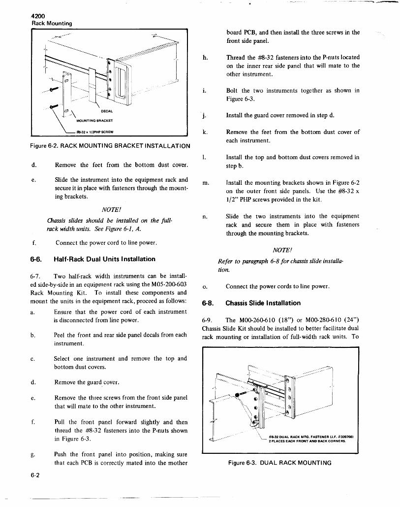
4200 Rack Mounting
--.,,~"-" g DECAL
- ." MOUNTING BRACKET
#8-32 x 1/2PHP SCREW
Figure 6-2. RACK MOUNTING BRACKET INSTALLATION
d.
e.
Remove the feet from the bottom dust cover.
Slide the instrument into the equipment rack and secure it in place with fasteners through the mounting brackets.
NOTE!
Otassis slides should be installed on the fullrack width units. See Figure 6-1, A.
f. Connect the power cord to line power.
6-6. Half-Rack Dual Units Installation
6-7. Two half-rack width instruments can be installed side-by-side in an equipment rack using the MOS-200-603 Rack Mounting Kit. To install these components and mount the units in the equipment rack, proceed as follows:
a.
b.
c.
d.
e.
f.
g.
6-2
Ensure that the power cord of each instrument is disconnected from line power.
Peel the front and rear side panel decals from each
instrument.
Select one instrument and remove the top and bottom dust covers.
Remove the guard cover.
Remove the three screws from the front side panel
that will mate to the other instrument.
Pull the front panel forward slightly and then thread the #8-32 fasteners into the P-nu ts shown in Figure 6-3.
Push the front panel into position, making sure
that each PCB is correctly mated into the mother
h.
i.
j.
k.
1.
m.
n.
o.
"-.----"-~.--
board PCB, and then install the three screws in the
front side panel.
Thread the #8-32 fasteners into the P-nuts located on the inner rear side panel that will mate to the other instrument.
Bolt the two instruments together as shown in Figure 6-3.
Install the guard cover removed in step d.
Remove the feet from the bottom dust cover of each instrument.
Install the top and bottom dust covers removed in
step b.
Install the mounting brackets shown in Figure 6-2 on the outer front side panels. Use the #8-32 x
1/2" PHP screws provided in the kit.
Slide the two instruments into the equipment
rack and secure them in place with fasteners
through the mounting brackets.
NOTE!
Refer to paragraph 6-8 for chassis slide installa
tion.
Connect the power cords to line power.
6-8. Chassis SI ide Installation
6-9. The MOO-260-610 (18") or MOO-280-610 (24") Chassis Slide Kit should be installed to better facilitate dual rack mounting or installation of full-width rack units. To
~~ ~ ..... ----J ~~<~~~ - ~~...--....
f-~\~ f _---- _ . ~ #8.32 DUAL RACK MYG. FAST ••• R 'J.F. #300'08' ~ 2 PLACES EACH FRONT AND BACK CORNERS.
Figure 6-3. DUAL RACK MOUNTI NG

install these components and mount the units or unit in the equipment rack, proceed as follows:
a. Peel the center side panel decals from the instru-ment.
b. Peel the rear side panel decals from the instrument.
c. Remove the six screws from the rear panel corner brackets and then remove the brackets.
d. Slide the spacer (A) into the center section of the side panel until the tapped holes are aligned with the holes in the side panels.
e. Scribe a line on spacer where it protrudes from the rear of the side panel and then remove it from the instrument.
f. Cut off the spacer at the scribe mark and then in-stall it in the side panel.
g.
h.
i.
j.
k.
1.
Install the rear panel corners.
4200 . Rack Mounting
Attach the chassis section (B) to the side panels with the screws (C) provided in the kit.
Install the cabinet sections (E) and center sections (D) in equipment rack. The extension angle brackets, which are part of section (E), are mounted at the rear of the cabinet.
Slide the center sections (D) toward the front of the cabinet until they lock in place.
Depress the spring locks on the chassis sections (B) and insert the instrument between the extended center sections (D) on the cabinet.
Slide the instrument completely into the equipment rack and secure in place with fasteners through the mounting brackets.
Figure 6-4. CHASSIS SLIDE INSTALLATION
6-3

4200 Connector
Accessory
Programming Connector
6-1. INTRODUCTION
6-2. The Amphenol, male, programming connector shown in Figure 6-1 is used to interface the instrument to a programming source. This male programming connector mates with the female programming connector that is mounted on the rear panel of the instrumen 1. A male connector is normally supplied with each instrument, less cabling, but may also be ordered directly from Amphenol 'under PART NO. 57-30500, or from the John Fluke Mfg. Co., Inc., by referencing FLUKE PART NO. 266056.
6-3. ASSEMBL V INSTRUCTIONS
6-4. Cabling connections to the male programming connector are done as follows:
a. Remove the screws from the terminal cover of the male connector and remove the cover and num
bered terminal/pin insert.
b.
c.
d.
Remove the screws from the restraining clamps on the cover and spread the clamps.
Thread the cable wiring through the terminal cover. Maximum size is #22.
Solder the wiring to the appropriate terminals of the numbered insert. Refer to Figure 6-1 for terminal locations. Use pin cover to support insert during soldering.
e. Slide the covers together and install the attaching screws.
f.
g.
CABLE
Close the restraining clamp around the cable and install the screws. If necessary, wrap the wiring bundle to provide a proper diameter for the restraining clamp.
Connect the male programming connector to the
female connector on the rear panel of the instrument. Fasten them securely with the end clips.
~TERMIN~® ~,
TERMINAL COVER
\ f..... ""COYER ~ RnAl ....
SCREW 121
Figure 6-1. MALE PROGRAMMING CONNECTOR
6-1

4200 Extender PCB Assembly and
Cable Extender Assembly
Accessories
Extender PCB Assembly and Cable Extender Assembly
6-1. INTRODUCTION
6-2. The Extender PCB Assembly shown in Figure 6-1 is available as an accessory for the FLUKE series of 4200 power sources. This accessory permits the printed circuit boards in the power source to be extended for servicing. The Extender PCB Assembly can be obtained by ordering FLUKE PART NO. 292623.
6-3. INSTALLATION
6-4. Extender PCB Assembly
6-5. To install a printed circuit board on the extender as shown in Figure 6-2, proceed as follows:
a. Turn off the power source, remove the line power cord, and then remove the top dust cover and guard cover.
b. Locate the printed circuit board to be serviced and remove it using the information given in Section 4, MAINTENANCE ACCESS.
c. Install the extender into the mother board connector as shown in Figure 6-2.
d. Support the extender and install the printed circuit board into the extender connector as shown in Figure 6-2.
CAUTION!
THE COMPONENT SIDE OF THE PRINTED CIRCUIT BOARD THAT IS INSERTED INTO THE EXTENDER CONNECTOR MUST FACE THE FRONT OF THE INSTRUMENT.
o
Figure 6-1. PCB ASSEMBLY EXTENDER
6-1

4200 Extender PCB Assembly and Cable Extender Assembly
6-6. Cable Extender Assembly
a.
b.
The removal of certain interconnected printed circuit boards requires the use of a cable extender assembly to reconnect the board to its original electrical configuration after the board is inserted into the extender PCB. The cable extender assembly is shown in Figure 6-3, and is obtained by ordering FLUKE PART NO. 337584.
Usage of the cable extender assembly is shown in Figures 64 and 6-5 for the instruments requiring
4210A/4216A CONFIGURATION
CAUTION' INSTALL PCB COMPONENTS SIDE FRONT!
its use. Normally the cable extender assembly is not used with the 4210A/4216A instruments unless troubleshooting of the power supply PCB would require separating and remotely locating the ac input power controls and input transformer. The cable extender assembly would join the ac input power controls and input transformer to the power supply PCB.
c. After the extender PCB assembly and test PCB and, where requiTed, the cable extender assembly are connected, the power can be applied.
" CIRCUIT BOARD
Figure 6-2. EXTENDER PCB ASSEMBLY INSTALLED IN 4210A/4216A INSTRUMENT
Figure 6-3. CABLE EXTENDER ASSEMBLY
6-2

4250A/4265A
CONFIGURATIOf\~
CAUTION!
INSTALL PCB COMPONENTS SIDE FRONT!
4200 Extender PCB Assembly and
Cable Extender Assembly
CIRCUIT
BOARD ASSEMBLY
Figure 6-4. EXTENDER PCB AND CABLE EXTENDER ASSEMBLIES INSTALLED IN 4250A/4265A INSTRUMENTS
4270A/4275A CONFIGURATION
CAUTION! INSTALL PCB COMPONENTS
SIDE FRONT!
EXTENDER
CIRCUIT BOARD ASSEMBLY
Figure 6-5. EXTENDER PCB AND CABLE EXTENDER ASSEMBLIES INSTALLED IN 4270A/4275A INSTRUMENTS
6-3

-Section 7
General Information
7 -1. This section of the manual contains generalized Lists of Replaceable parts contained in Section 5. The following information is presented in this section: user information as well as supplemental information to the
TABLE
7-1.
7-2.
7-3.
74. 7-5.
TITLE
List of Abbreviations
Federal Supply Codes for Manufacturers
Fluke Technical Service Centers. .
Sales Representatives - Domestic. .
Sales Representatives - International
PAGE
7-1
7-3
7-10
7-11
7-13
Table 7-1. LIST OF ABBREVIATIONS AND SYMBOLS
Aor amp ampere cont continue
ac alternating current crt cathode-ray tube
at audio frequency cw clockwise
aid analog-to-digital dla digital-to-analog
assy assembly dac digital-to-analog converter
AWG american wire guage dB decibel
B bel dc direct current
bcd binary coded decimal dmm digital multi meter
°c Celsius dvm digital voltmeter
cap capacitor elect electrolytic
ccw counter clockwise ext external cer ceramic F farad cermet ceramic to metal (seal) of Fahrenheit ckt circuit FET field-effect transistor cm centimeter ff flip-flop cmrr common mode rejection ratio freq frequency comp composition FSN federal stock number
3/75 7-1

Table 7-1. LIST OF ABBREVIATIONS AND SYMBOLS (Continued)
g gram opnl ampl· operational amplifier
G giga (109) p pico (10- 12 )
gd guard para paragraph
Ge germanium pcb printed circuit board
GHz gigahertz pF picofarad
gmv guaranteed minimum value pn part number
(+) or pos positive gnd ground pot potentiometer H henry p-p peak-to-peak hd heavy duty ppm parts per million hf high frequency PROM programmable read-only memory Hz hertz psi pound-force per square inch IC integrated circuit RAM random-access memory if intermediate frequency rf radio frequency in inch(es) rms root mean square inti internal ROM read-only memory I/O input/output s or sec second (time) k kilo (103
) scope oscilloscope kHz kilohertz SH shield kn kilohm(s) Si silicon kV kilovolt(s) serno serial number If low frequency sr shift register LED light-emitting diode Ta tantalum LSB least significant bit tb terminal board LSD least significant digit tc temperature coefficient or M mega (106
) temperature compensating
m milli (10-3 ) tcxo temperature compensated
mA mill iampere(s) crystal oscillator
max maximum tp test point
mf metal film u orJ.,( micro (10-6 )
MHz megahertz uhf ultra high frequency
min minimum us or /1S microsecond (s) (10-6)
mm millimeter uut unit under test
ms millisecond V volt MSB most significant bit v voltage MSD most significant digit var variable MTBF mean time between failures vco voltage controlled oscillator
MTTR mean time to repair vhf very high frequency mV millivolt(s) vlf very low frequency
mv multivibrator W watt(s)
Mn megohm(s) ww wire wound n nano (10-9 ) xfmr transformer
na not applicable xstr transistor
NC normally closed xtal crystal
(-) or neg negative xtlo crystal oscillator
NO normally open n ohm(s)
ns nanosecond /1 micro (10-6 )
7-2 3/75
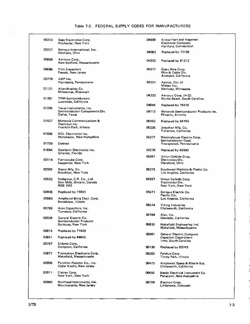
Table 7-2. FEDERAL SUPPLY CODES FOR MANUFACTURERS
00213 Sage Electronics Corp. 04009 Arrow Hart and Hegeman Rochester, New York Elec:tronic Company
Hartford, Connecticut 00327 Welwyn International, Inc.
04062 Replaced by 72136 Westlake, Ohio
00656 Aerovox Corp. 04202 Replaced by 81312 New Bedford, Massachusetts
00686 Film Capacitors 04217 Essex Wire Corp. Passaic, New Jersey Wire & Cable Div.
Anaheim, California 00779 AMP Inc.
Harrisberg, Pennsylvania 04221 Aemco, Div. of Midtex Inc.
01121 Allen-Bradley Co. Mankato, Minnesota Milwaukee, Wisconsin
04222 Aerovox Corp. (H-Q) 01281 TRW Semiconductors Myrtle Beach, South Carolina
Lawndale, California 04645 Replaced by 75376
01295 Texas I nstruments, Inc. Semiconductor Components Div. 04713 Motorola Semiconductor Products Inc. Dallas, Texas Phoenix, Arizona
01537 Motorola Communications & Electrical Inc.
05082 Replaced by 94154
Franklin Park, Illinois 05236 Jonathan Mfg. Co. Fullerton, California
01686 RCL Electronics Inc. Manchester, New Hampshire 05277 Westinghouse Electric Corp.
01730 Deleted Semiconductor Dept. Youngwood, Pennsylvania
01884 Dearborn Electronics Inc. 05278 Replaced by 43543 Orlando, Florida
05397 Union Carbide Crop. 02114 Ferroxcube Corp. Ele<:tronics Div.
Saugerties, New York Cleveland, Ohio
02395 Rason Mfg. Co. 05279 Southwest Machine & Plastic Co. Brooklyn, New York Los Angeles, California
02533 Snelgrove, C.R. Co., Ltd. 05397 Union Carbide Corp. Don Mills, Ontario, Canada Elel:tronics Div. M3B 1M2 New York, New York
02606 Replaced by 15801 05571 Sprague Electric Co. Pacific Div.
02660 Amphenol-Borg Elect. Corp. Los Angeles, California Broadview, Illinois
05574 Viking Industries 02799 Areo Capacitors, Inc. Chaisworth, California
Torrence, California 05704 Alac, Inc.
03508 General Electric Co. Glendale, Cal ifornia Semiconductor Products Syracuse, New York 05820 Wakefield Engineering Ind.
Wakefield, Massachusetts 03614 Replaced by 71400
06001 General Electric Company 03651 Replaced by 44655 Capacitor Department
Irmo, South Carolina 03797 Eldema Corp.
Compton, California 06136 Replaced by 63743
03877 Transistron Electronic Corp. 06383 Panduit Corp Wakefield, Massachusetts Tinley Park, Illinois
03888 Pyrofilm Resistor Co., Inc. 06473 Amphenol Space & Missile Sys. Cedar Knolls, New Jersey Chatsworth, California
03911 Clairex Corp. 06555 Beede Electrical I nstrument Co. New York, New York Penacook, New Hampshire
03980 Muirhead Instruments, Inc. 06739 Electron Crop. Mountainside, New Jersey Littletown, Colorado
3/75 7-3

Table 7-2. FEDERAL SUPPLY CODES FOR MANUFACTURERS (Continued)
06743 Clevite Corp. 09969 Dale Electronics Inc. Cleveland, Ohio Yankton, S Dakota
06751 Semcor Div., Components, Inc. 11236 CTS of Berne Phoenix, Arizona Berne, Indiana
06860 Gould National Batteries Inc. 11237 Chicago Telephone of City of Industry, California Calif. Inc., (CTC)
Paso Robles, California
06980 Varian-Eimac 11358 Discontinued San Carlos, California
11403 Best Products Co. 07047 Ross Milton, Co., The Chicago, Illinois
South Hampton, Pennsylvania 11503 Keystone Mfg.
07115 Replaced by 14674 Div. of Avis Industrial Crop. Warren, Michigan
07138 Westinghouse Electric Corp., Electronic 11711 General I nstrument Corp Tube Division Rectifier Division Elmira, New York Hickville, New York
07233 TRW Electronic Components Cinch Graphic 11726 Qualidyne Corp. CitY of Industry, California Santa Clara, Cal ifornia
07256 Silicon Transistor Corp. 12014 Chicago Rivet & Machine Co. Garden City, New York Bellwood, Illinois
07263 Fairchild Semiconductor 12040 National Semiconductor Corp. Div. of Fairchild Camera Danburry, Connecticut & I nstrument Corp. Mountain View, California 12060 Diodes, Inc.
Chatsworth, California 07344 Bircher Co., Inc.
Rochester, New York 12136 Philadelphia Handle Co. Camden, New Jersey
07792 Lerma Engineering Corp. Northampton, Massachusetts 12300 Potter-Brumfield Division
AMF Canada LTD. 07910 Teledyne Corp. Guelph, Ontario, Canada
(Continental Device) Hawthorne, California 12323 Pres in Co., Inc.
Shelton, Connecticut 08225 I ndustro Transistor Corp.
Long Island City, New York 12327 Freeway Washer & Stamping Co. Cleveland, Ohio
08261 Spectra Strip Corp Garden Grove, California 12400 Replaced by 75042
08530 Reliance Mica Corp. 12615 U.S. Terminals Inc. Brooklyn, New York Cincinnati, Ohio
08792 Discontinued 12617 Hamlin Inc. Lake Mills, Wisconsin
08806 General Electric Co. Miniature Lamp Dept. 12697 Clarostat Mfg. Co. Cleveland, Ohio Dover, New Hampshire
08863 Nylomatic Corp. 12749 James Electronics Norrisville, Pennsylvania Chicago, Illinois
08988 Skottie Electronics Inc. 12856 Micrometals Archbald, Pennsylvania Sierra Madre, California
09214 G.E. Semi-Conductor Products Dept. 12954 Dickson Electronics Corp. Auburn, New York Scottsdale, Arizona
09353 C and K Components 12969 Unitrode Corp. Watertown, Massachusetts Watertown, Massachusetts
09423 Scientific Components, Inc. 13103 Themalloy Co. Santa Barbara, California Dallas, Texas
09922 Burndy Corp. 13327 Solitron Devices Inc. Norwalk, Connecticut Tappan, New York
7-4 3/75

Table 7-2. FEDERAL SUPPLY CODES FOR MANUFACTURERS (Continued)
13511 Amphenol Corp. 18083 Deleted Los Gatos, California
18178 Vactec Inc. 13606 Sprague Electric Co. Maryland Heights, Missouri
Transistor Div. Concord, New Hampshire 18324 Signetics Corp.
Sunnyvale, California 13839 Replaced by 23732
18612 Vishay Intertechnology Inc. 14099 Semtech Corp. Malvern, Pennsylvania
Newbury Park, California 18736 Voltronics Corp.
14193 California Resistor Corp. Hanover, New Jersey Santa Monica, California
18927 GTE Sylvania Inc. 14298 American Components, Inc. Precision Material Group
Conshohocken, Pennsylvania Parts Division Titusville, Pennsylvania
14655 Cornell-Dubilier Electronics Newark, New Jersey 19429 Discontinued, use 89536
14674 Discontinued, see 16299 19451 Perine Machinery & Supply Co. Seattle, Washington
14752 Electro Cube Inc. 19701 Electra Mfg. Co. San Gabriel, California
I ndependence, Kansas
14869 Replaced by 96853 25084 Enochs Mfg. Co.
15636 Elec-Trol Inc. Indianapolis, Indiana Northridge, California
20891 Self-Organizing Systems, Inc. 15801 Fenwal Electronics Inc. Dallas, Texas
Framingham, Massachusetts 21604 Buckeye Stamping Co.
15818 Amelco Semiconductor Colurnbus, Ohio Div. of Teledyne Inc. Mountain View, California 21845 Sol itron Devices Inc.
Transistor Division 15849 USECO, Inc. Riveria Beach, Florida
Mt. Vernon, New York 22767 ITT Semiconductors
15898 I nternational Business Div. of ITT Machines (IBM) Palo Alto, California Essex Junction, Vermont
23050 Product Compo Corp. 15909 Replaced by 17870 Mount Vernon, New York
16299 Corning Glass 23732 Tracor Raleigh, N-orth Carolina Rockville, Maryland
16332 Replaced by 28478 23880 Stanford Applied Engrng. Santa Clara, California
16473 Cambridge Scientific Ind. Inc. Cambridge, Maryland 23936 Pamotor Div., Wm. J. Purdy Co.
Burlingame, California 16742 Paramount Plastics
Downey, California 24248 Southco Div. of South Chester Corp.
16758 Delco Radio Lester, Pennsylvania Div. of General Motors Kokomo, Indiana 24355 Analog Devices Inc.
Norwood, Massachusetts 17001 ITT Cannon
Santa Ana, California 24655 General Radio Co. West Concord, Massachusetts
17069 Circuit Structures Lab. Upland, California 24759 Lenox-Fugle Electronics
Plainfield, New Jersey 17338 High Pressure Eng. Co., Inc.
Oklahoma City, Oklahoma 25088 Siemen Corp. Isilen, New Jersey
17856 Siliconix, Inc. Sunnyvale, California
25403 Amperex Electronic Corp. 17870 Daven Div. of Thomas A. Edison Semiconductor & Receiving
Ind. - McGraw - Edison Co. Tube Division Manchester, New Hampshire Slatersville, Rhode Island
3/75 7-5
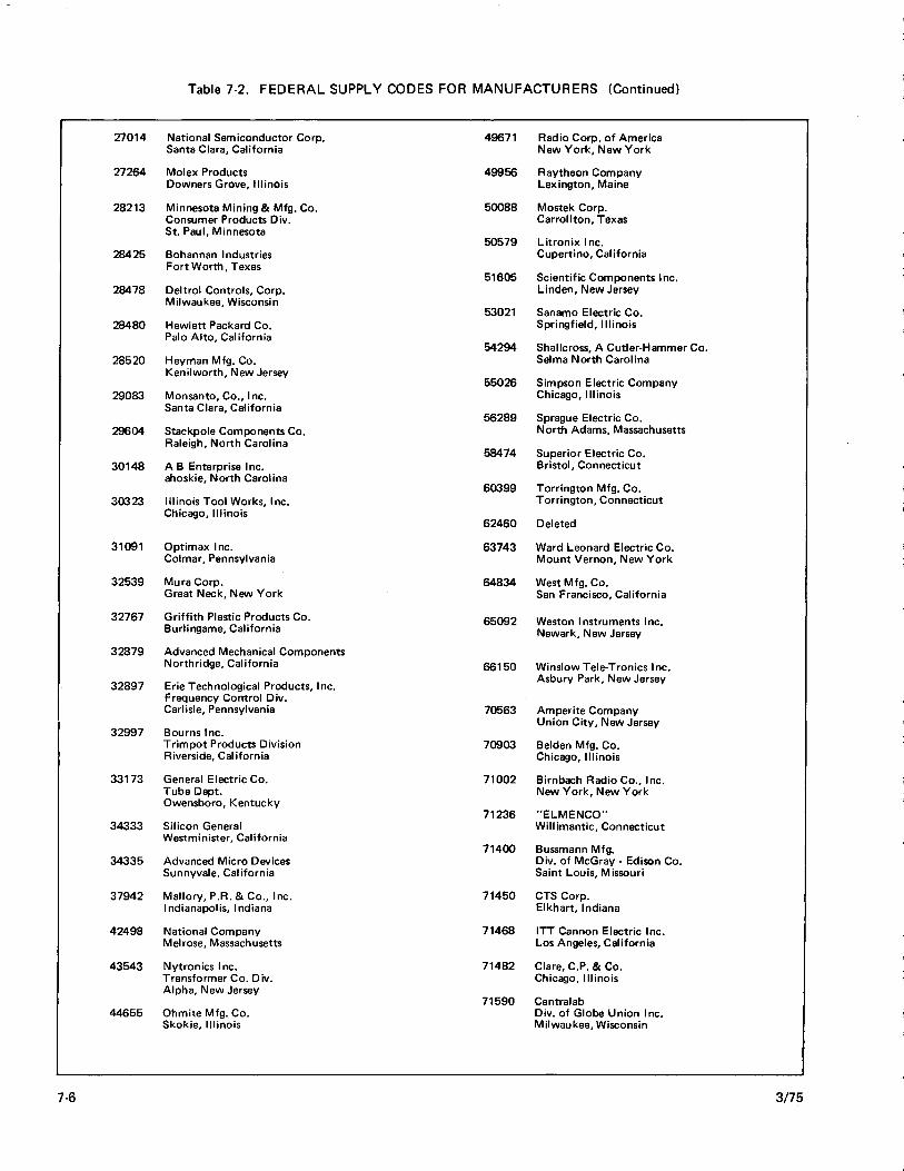
Table 7-2. FEDERAL SUPPLY CODES FOR MANUFACTURERS (Continued)
27014 National Semiconductor Corp. 49671 Radio Corp. of America Santa Clara, California New York, New York
27264 Molex Products 49956 Raytheon Company Downers Grove, Illinois Lexington, Maine
28213 Minnesota Mining & Mfg. Co. 50088 Mostek Corp. Consumer Products Div. Carrollton, Texas St. Paul, Minnesota
50579 Litronix Inc. 28425 Bohannan Industries Cupertino, California
Fort Worth, Texas 51605 Scientific Components Inc.
28478 Deltrol Controls, Corp. Linden, New Jersey Milwaukee, Wisconsin
53021 Sanamo Electric Co. 28480 Hewlett Packard Co. Springfield,llIinois
Palo Alto, California 54294 Shallcross, A Cutler-Hammer Co.
28520 Heyman Mfg. Co. Selma North Carolina Kenilworth, New Jersey
55026 Simpson Electric Company 29083 Monsanto, Co., Inc. Chicago, Illinois
Santa Clara, California 56289 Sprague Electric Co.
29604 Stackpole Components Co. North Adams, Massachusetts Raleigh, North Carolina
58474 Superior Electric Co. 30148 A B Enterprise Inc. Bristol, Connecticut
ahoskie, North Carolina 60399 Torrington Mfg. Co.
30323 Illinois Tool Works, Inc. Torrington, Connecticut Chicago, Illinois
62460 Deleted
31091 Optimax Inc. 63743 Ward Leonard Electric Co. Colmar, Pennsylvania Mount Vernon, New York
32539 Mura Corp. 64834 West Mfg. Co. Great Neck, New York San Francisco, California
32767 Griffith Plastic Products Co. 65092 Weston Instruments Inc. Burlingame, California Newark, New Jersey
32879 Advanced Mechanical Components Northridge, California 66150 Winslow Tele-Tronics Inc.
32897 Erie Technological Products, Inc. Asbury Park, New Jersey
Frequency Control Div. Carlisle, Pennsylvania 70563 Amperite Company
32997 Bourns Inc. Union City, New Jersey
Trimpot Products Division 70903 Belden Mfg. Co. Riverside, Cal ifornia Chicago, Illinois
33173 General Electric Co. 71002 Birnbach Radio Co., Inc. Tube Dept. New York, New York Owensboro, Kentucky
71236 "ELMENCO" 34333 Silicon General Will imantic, Connecticut
Westminister, California 71400 Bussmann Mfg.
34335 Advanced Micro Devices Div. of McGray - Edison Co. Sunnyvale, California Saint Louis, Missouri
37942 Mallory, P.R. & Co., Inc. 71450 CTS Corp. Indianapolis, Indiana Elkhart, Indiana
42498 National Company 71468 ITT Cannon Electric Inc. Melrose, Massachusetts Los Angeles, California
43543 Nytronics Inc. 71482 Clare, C.P. & Co. Transformer Co. Div. Chicago, Illinois Alpha, New Jersey
71590 Centralab 44655 Ohmite Mfg. Co. Div. of Globe Union Inc.
Skokie, Illinois Milwaukee, Wisconsin
7-6 3/75

Table 7-2. FEDERAL SUPPLY CODES FOR MANUFACTURERS (Continued)
71707 Coto Coil Co., Inc. 74306 Piezo Crystal Co. Providence, Rhode Island Carl isle, Pennsylvania
71744 Chicago Miniature Lamp Works 74542 Hoyt Elect. I nstr. Works Chicago, Illinois Penacook, New Hampsh ire
71785 Cinch Mfg. Co. & 74970 Johnson. E. F., Co. Howard B. Jones Div. Waseca, Minnesota Chicago, Illinois
75042 IRC Inc. (Div. of TRW) 72005 Driver, Wilber B., Co. Phil'3delphia, Pennsylvania
Newark, New Jersey 75376 Kurz-Kasch. Inc.
72092 Replaced by 06980 Dayton, Ohio
72136 Electro Motive Mfg. Co. 75378 CTS Knights Inc. Williamantic, Connecticut Sandwich, Illinois
72259 Nytronics Inc. 75382 Kulka Electric Corp. Berkeley H eights, New Jersey Mount Vernon, New York
72354 Deleted 75915 Littl efu se I nc. Des Plaines, Illinois
72619 Dialight Corp. Brooklyn, New York 76854 Oak Mfg. Co.
Cry~1al Lake, Illinois 72653 G. C. Electronics
Rockford, III inois 77342 Potter & Brumfield Div. of Amer. Machine & Foundry
72665 Replaced by 90303 Princeton, Indiana
72794 Dzus Fastener Co., Inc. 77638 General I nstrument Corp. West I sliPl, New York Rectifier Division
Brooklyn, New York 72928 Gudeman Co. (Gulton I nd.)
Chicago, Illinois 77969 Rubbercraft Corp. of Calif. LTD. Torrance, California
72982 Erie Tech. Products Inc. Erie, Pennsylvania 78189 Shakeproof
Div. of Illinois Tool Works 73138 Beckman Instruments Inc. Elgin, Illinois
Helipot Division Fullerton, California 78277 Sigma I nstruments, Inc.
South Braintree, Massachusetts 73293 Hughes Aircraft Co.
Electron Dynamics Div. 78488 Stackpole Carbon Co. Torrence, California Saint Marys, Pennsylvania
73445 Amperex Electronic Corp. 78553 Tinnerman Products Hicksville, New York Cleveland, Ohio
73559 Carling Electric Inc. 78136 Waldes Kohinoor Inc.
Hartford, Connecticut Long Island City, New York
73586 Circle F Industries 79497 Western Rubber Company
Trenton, New Jersey Goshen, Indiana
73734 Federal Screw Products, Inc. 79963 Zierick Mfg. Corp.
Chicago, Illinois New Rochelle, New York 80031 Mepco
73743 Fischer Special Mfg. Co. Div. of Sessions Clock Co. Cincinnati, Ohio Morristown, New Jersey
73899 JFD Electronics Co. 80145 API Instruments Co. Brooklyn, New York Chesterland, Ohio
73949 Guardian Electric Mfg. Co. 80183 Spraque Products Chicago, Illinois North Adams, Massachusetts
74199 Quam Nichols Co. 80294 Bourns Inc. Chicago, Illinois Riverside, California
74217 Radio Switch Corp. 80583 Hammarlund Co., Inc. Marlboro, New Jersey Mars Hill, North Carolina
74276 Signalite Inc. 80640 Stevens, Arnold Inc. Neptune, New Jersey Boston, Massachusetts
7-7

Table 7-2. FEDERAL SUPPLY CODES FOR MANUFACTURERS (Continued)
81073 Grayhill, Inc. 88245 litton Products Inc. La Grange, Illinois Van Nuys, California
81590 Korry Mfg. Co. 88419 Use 14655 Seattle, Washington
88690 Replaced by 04217 81312 Winchester Electronics
Div. of Litton Industries 89536 Fluke, John Mfg. Co., Inc. Oakville, Connecticut Seattle, Washington
81439 Therm-O-Disc Inc. 89730 Replaced by 08806 Mansfield, Ohio
90201 Mallory Capacitor Co. 81483 International Rectifier Corp. Indianapolis, Indiana
Los Angeles, California 90215 Best Stamp & Mfg. Co.
81741 Chicago Lock Corp. Kansas City, Missouri Chicago, Illinois
90211 Square D Co. 82305 Palmer Electronics Chicago, Illinois
South Gate, California 90303 Mallory Battery Co.
82389 Switch craft Inc. Tarrytown, New York Chicago, Illinois
91293 Johanson Mfg. Co. 82415 Price Electric Corp. Boonton, New Jersey
Frederick, Maryland 91407 Replaced by 58474
82872 Roanwell Corp. New York, New York 91502 Associated Machine
\ Santa Clara, Cal ifornia
82877 Rotron Mfg. Co., Inc. Woodstock, New York 91506 Augat
Attleboro, Massachusetts 82879 ITT Wire & Cable Div.
Pawtucket, Rhode Island 91637 Dale Electronics Inc. Columbus, Nebraska
83003 Varo Inc. Garland, Texas 91662 Elco Corp.
Willow Grove, Pennsylvania 83298 Bendix Corp.
Electric Power Division 91737 Gremar Mfg. Co., Inc. (ITT) Eatontown, New Jersey Woburn, Massachusetts
83330 Smith, Herman H., Inc. 91802 I ndustrial Devices, Inc. Brooklyn, New York Edgewater, New Jersey
83478 Rubbercraft Corp. of America 91833 Keystone Electronics Corp. New Haven, Connecticut New York, New York
83594 Burroughs Corp. 91836 King's Electronics Electronic Components Div. Tuckahoe, New York Plainfield, New Jersey
91929 Honeywell Inc. 83740 Union Carbide Corp. Micro Switch Div.
Consumer Products Div. Freeport, III inois New York, New York
91934 Miller Electric Co., Inc. 84171 Arco Electronics, Inc. Pawtucket, Rhode Island
Great Neck, New York 93332 Sylvania Electric Products
84411 TRW Semiconductor Products Div. Ogallala, Nebraska Woburn, Massachusetts
84613 Fuse I ndicator Corp. 94145 Replaced by 49956 Rockvillw, Maryland
94154 Tung-Sol 86577 Precision Metal Products Div. of Wagner Electric Corp.
Stoneham, Massachusetts Newark, New Jersey
86684 Radio Corp. of America 95146 Alco Electronics Products Inc. Electronic Components & Devices Lawrence, Massachusetts Harrison, New Jersey
86689 Deleted 95263 Leecraft Mfg. Co. Long I sland City, New York
87034 Marco -Oak Inc. Anaheim, California 95264 Replaced by 98278
7-8 3/75

Table 7-2. FEDERAL SUPPLY CODES FOR MANUFACTURERS (Continued)
95275 Vitramon Inc. 98278 Microdot Inc. Bridgeport, Connecticut Pasadena, California
95303 Radio Corp. of America 98291 Sealectro Corp. Solid State & Receiving Tube Div. Con hex Div. Cincinnati, Ohio Mamaroneck, New York
95354 Methode Mfg. Corp. 98388 Accurate Rubber & Plastics Rolling Meadows, Illinois Culver City, California
95712 Dage Electric Co., Inc. 98743 Replaced by 12749 Franklin, Indiana
95987 Weckesser Co. Inc. 98925 Deleted Chicago, Illinois
96733 San Fernando Electric Mfg. Co. 99120 Plastic Capacitors, Inc.
San Fernando, California Chicago, Illinois
96853 Rustrak Instrument Co. 99217 Southern Electronics Corp.
Manchester, New Hampshire Burbank, California
96881 Thomson Industries, Inc. 99392 STM
Manhasset, New York Oakland, California
97540 Master Mobile Mounts 99515 Marshall Industries
Div. of Whitehall Electronics Corp. Capacitor Div.
Los Angeles, California Monrovia, California
97913 Industrial Electronic Hdware Corp. 99779 Barnes Corp.
New York, New York Lansdowne, Pennsylvania
97945 White, S.S. Co. 99800 American Precision Industries Inc.
Plastics Div. Delevan Division
New York, New York East Aurora, New York
97966 Replaced by 11358 Toyo Electronics (R-Ohm Corp.)
98094 Replaced by 49956 Irvine, Cal ifornia
98159 Rubber-Teck, Inc. National Connector Gardena, California Minneapolis, Minnesota

7-10
Fluke Western Technical Center
2020 North Lincoln St.
Burbank, CA 91504
Tel. 213-849-4641
TWX: 910-497-2086
Fluke Western Technical Center 2359 De La Cruz Blvd.
Santa Clara, CA 95050 Tel. 408-244-1505
TWX: 910-338-0121
Fluke S.W. Technical Center
Unit4 1980 South Quebec Street
Denver, CO 80231
Tel. 303-750-1228
Fluke S.E. Technical Center
P.O. Box 6578
940 North Fern Creek Avenue
Orlando, FL 32803
Tel. 305-896-2296
TWX: 810-850-0185
Table 7-3. FLUKE TECHNICAL CENTERS
Fluke Midwestern Technical Center
1287 North Rand Road
Des Plaines, IL 60016
Tel. 312-298-7470
TWX: 910-233-4978
Fluke Mideastern Technical Center
11501 Huff Court Kensington, MD 20795
Tel. 301-881-5300
TWX: 710-825-9645
Fluke N.E. Technical Center
109 Massachusetts Ave. Lexington, MA 02173
Tel. 617 -861-8620
TWX: 710-826-1715
Fluke Midwestern Technical Center
10800 Lyndale Avenue South
Minneapolis, MN 55420
Tel. 612-884-4541
TWX: 910-576-3141
Fluke Eastern Technical Center
101 Berkshire Ave.
Paterson, NJ 07502
Tel. 201-742-3215
TWX: 710-988-5945
Fluke Eastern Technical Center
4515 Culver Road
Rochester, NY 14622
Tel. 716-342-6940
TWX:, 510"253-6145
Fluke S.E. Technical Center
P.O. Box 9619
1310 Beaman Place Greensboro, NC 27408
Tel. 919-273-1918 TWX: 510-925-1173
John Fluke Mfg. Co., Inc.
7001 - 220th S.W. Mountlake Terrace, WA 98043
Tel. 206-774-2238
TWX: 910-449-2850
Fluke Canadian Technical Center
640 11th Ave. S.W.
Calgary Alberta
Tel. 403-261-0780
TWX: 61-0-821-2233
Fluke Canadian Technical Center
6427 Northam Drive
Mississauga, Ontario
Tel. 416-678-1500
TWX: 610-492-2119
3/75

3/75
Table 7-4. SALES REPRESENTATIVES - DOMESTIC
ALABAMA HUNTSVILLE BCS Associates, Inc. 3322 S. Memorial Parkway P.O. Box 1273 Tel. (205) 881-6220 Zip 35801
ALASKA ANCHORAGE Harry Lang & Associates 1406 W. 47th Ave. Tel. (907) 279-5741 Zip 99503
ARIZONA PHOENIX Barnhill Associates 7319 E. Stetson Dr. Tel. (602) 947-7841 Scottsdale, AZ 85251
CALIFORNIA LOS ANGELES Instrument Specialists,lnc. 2020 N. Lincoln Street Burbank, CA 91504 Tel. (213) 849-7181
NEWPORT BEACH I nstrument Special ists, Inc. 4120 Birch Street Suite 119 Tel. (714) 752-6200 Zip 92660
SANTA CLARA Instruments Specialists, Inc. 2359 De La Cruz Blvd. Tel. (408) 244-1505 Zip 95050
SAN DIEGO I nstrument Special ists, Inc. 4805 Mercury St., Ste. 1 Tel. (714) 565-2555 Zip 92111
COLORADO DENVER Barnh ill Associates, Inc. 1980 South Quebec St. Tel. (303) 750-1228 Zip 80231
CONNECTICUT HARTFORD Instrument Representatives, Inc. P.O. Box 165 Glastonbury, CT 06033 Tel. (203) 633-0777
FLORIDA ORLANDO BCS Associates, Inc. 940 N. Fern Creek Ave. Tel. (305) 8964881
(305) 843-1510 Zip 32803
GEORGIA DECATUR BCS Associates, Inc. 2522 Tanglewood Road Tel. (404) 321-0980 Zip 30033
HAWAII HONOLULU I ndustrial Electronics, Inc. 646 Queen Street P.O. Box 135 Tel. (808) 533-6095 Zip 96817
ILLINOIS CHICAGO Cozzens & Cudahy, Inc. 1301 N. Rand Road Des Plaines, IL 60016 Tel. (312) 298-3600
INDIANA INDIANAPOLIS Cozzens & Cudahy, Inc. Port O'Cail Executive Ctr. 21 Beachway Drive Tel. (317) 244-2456 Zip 46244
KENTUCKY VALLEY STATION BCS Associates, Inc. 4506 Freda Way Tel. (502) 935-9634 Zip 40272
MARYLAND BALTIMORE Electronic Marketing Assoc.lnc. 11501 Huff Court Kensington, MD 20795 Tel. (301) 881-5300,744-7700
MASSACHUS ETTS BOSTON I nstrument Representatives, Inc. 109 Massachusetts Ave. Lexington, MA 02173 Tel. (617) 861-8620
MICHIGAN DETROIT WKM Associates, Inc. 1474 East Outer Dr. Tel. (313) 892-2500 Zip 48234
MINNESOTA MINNEAPOLIS Cozzens & CudahY,lnc. 10800 Lyndale Ave. S. Tel. (612) 8844336 Zip 55420
MISSOURI KANSAS CITY Cozzens & CudahY,lnc 4404 Chouteau Traffic Way Tel. (816) 454-5836 Zip 64117
ST. LOUIS Cozzens & Cudahy Inc. P.O. Box 10013 Lambert Field - Zip 63145 Tel. (314) 423-1234
NEW JERSEY
NEWARK SBM Representatives 1519 Stuyvesant Avenue Union, NJ 07083 Tel. (201) 687-8737
NEW MEXICO ALBUQUERQUE Barnhill Associates 1410- 0 Wyoming N.E. Tel. (505) 299-7658 Zip 87112
NEW YORK
NEW YORK SBM Representatives 28 Hobby Street Pleasantville, NY 10570 Tel. (914) 769-1811
ROCHESTER SBM Representatives 4515 Culver Road Tel. (716) 226-1400 Zip 14622
NORTH CAROLINA GREENSBORO BCS Associates, Inc. P.O. Box 9619 1310 Beaman Place Tel. (919) 273-1918 Zip 27408
OHIO CLEVELAND WKM Associates, Inc. 16141 Puritas Ave. Tel. (216) 267-0445 Zip 44135
DAYTON WKM Associates, Inc. 6073 Far H ills Ave. Tel. (513) 434-7500 Zip 45459
OREGON BEAVERTON Showalter Instruments,lnc. 13485 S.W. Hargis Road Tel. (503) 646-3004 Zip 97005
PENNSYLVANIA PHILADELPHIA Electronic Marketing Assoc. 210 Goddard Blvd., Ste. 100 King of Prussia, PA Tel. (215) 248-5050 Zip 19406
PITTSBURGH WKM Associates, Inc. 90 Clairton Blvd. Tel. (412) 892-2953 Zip 15236
7-11
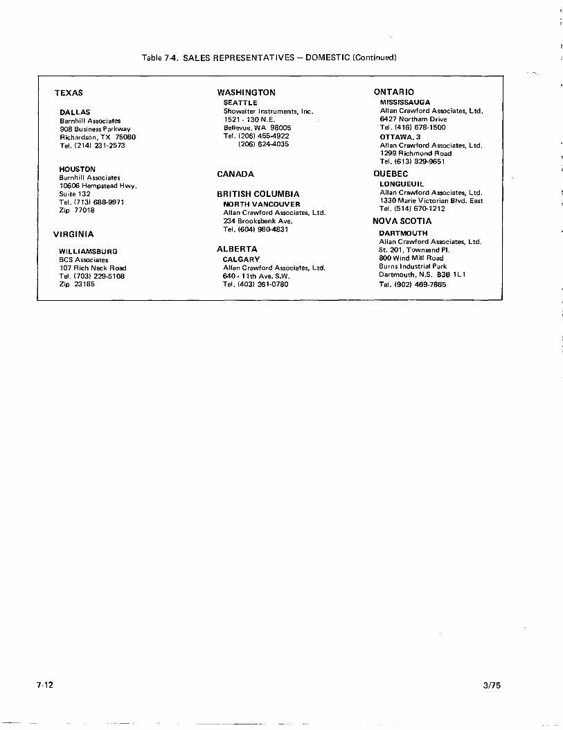
Table 7-4. SALES REPRESENTATIVES - DOMESTIC (Continued)
TEXAS WASHINGTON ONTARIO SEATTLE MISSISSAUGA
DALLAS Showalter Instruments, Inc. Allan Crawford Associates, Ltd.
Barnhill Associates 1521 - 130 N.E. 6427 Northam Drive
908 Business Parkway Bellevue, WA 98005 Tel. (416) 678-1500
Richardson, TX 75080 Tel. (206) 455-4922 OTTAWA,3 Tel. (214) 231-2573 (206) 624-4035 Allan Crawford Associates, Ltd.
1299 Richmond Road Tel. (613) 829-9651
HOUSTON CANADA QUEBEC Barnhill Associates
10606 Hempstead Hwy. LONGUEUIL
Suite 132 BRITISH COLUMBIA Allan Crawford Associates, Ltd. Tel. (713) 688-9971 NORTH VANCOUVER 1330 Marie Victorian Blvd. East Zip 77018 Allan Crawford Associates, Ltd.
Tel. (514) 670-1212
234 Brooksbank Ave. NOVA SCOTIA
VIRGINIA Tel. (604) 980-4831
DARTMOUTH Allan Crawford Associates, Ltd.
WILLIAMSBURG ALBERTA St. 201, Townsend PI.
BCS Associates CALGARY 800 Wind Mill Road
107 Rich Neck Road Allan Crawford Associates, Ltd. Burns I ndustrial Park
Tel. (703) 229-5108 640 - 11th Ave. S.W. Dartmouth, N.S. B3B 1 L 1 Zip 23185 Tel. (403) 261-0780 Tel. (902) 469-7865
7-12 3/75
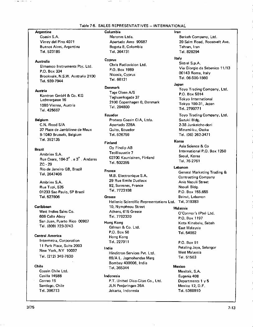
Table 7-5. SALES REPRESENTATIVES - INTERNATIONAL
Argentina Coasin S.A. Virrey del Pino 4071 Buenos Aires, Argentina Tel. 523185
Australia Elmaesco Instruments Pty. Ltd. P.O. Box 334 Brookvale, N.S.W. Australia 2100 Tel. 939-7944
Austria Kontron GmbH & Co. KG Lederergasse 16
1080 Vienna, Austria Tel. 425667
Belgium C.N. Rood S/A 37 Place de Jamblinne de Meux B-1040 Brussels, Belgium Tel. 352135
Brazil Ambriex S.A. Rue Ceara, 104-2° . e 3° . Andares ZC -29 Rio de Janeiro GB, Brazil Tel. 2647406
Ambriex S.A. Rua Tupi, 535 01233 Sao Paulo, SP Brazil Tel. 527806
Caribbean West Indies Sales Co. 606 Calle Aboy San Juan, Puerto Rico 00907 Tel. (809) 723-3743
Central America Intermetra, Corporation 11 Park Place, Suite 2003 New York, NY 10007
Tel. (212) 349-7630
Chile Coasin Chile Ltd. Casilla 14588 Correo 15 Santiago, Chile Tel. 396713
Columbia Marones Ltda. Apartado Aero 90687 Bogota 8, Colombia Tel. 364731
Cyprus Chris Radiovision Ltd. P.O. Box 1989 Nicosia, Cyprus Tel. 66121
Denmark Tage Olsen A/S Teglvaerksgade 37 2100 Copenhagen 0, Denmark Tel. 294800
Ecuador Proteco Coasin CIA, Ltda. Apartado 228A Quito, Ecuador Tel. 526759
Finland Oy Findip AB Teollisuustie 7 02700 Kauniainen, Finland Tel. 502255
France M.B. Electronique S.A. 29 Rue Emile Duclaux 92, Suresnes, France Tel. 7723108
Greece
Iran Berkeh Company, Ltd. 20 Salm Road, Roosevelt Ave. Tehran, Iran Tel. 828294
Italy Sistrel S.p.A. Via Giorgio da Sebenico 11/13 00143 Roma, Italy Tel. 06-500-1860
Japan Toyo Trading Company, Ltd. P.O. Box 5014 Tokyo International Tokyo 100-31, Japan Tel. 2790771
Toyo Trading Company, Ltd. Suzuki Bldg. 2-38 Junkeicho-dori Minami-ku, Osaka Tel. (06) 262-3471
Korea Asia Science & Co International P.O. Box 1250 Seoul, Korea Tel. 76-2761
Lebanon General Marketing Trading & Contracting Company Anis Nsouli Street Nsouli Bldg. P.O. Box 155.655 Beirut, Lebanon
Hellenic Scientific Representations Ltd. Tel. 319383 10, Nympheou Street Athens, 615 Greece Tel. 7792320
Hong Kong Gilman & Co. Ltd. P.O. Box 56 Hong Kong Tel. 227011
India Hinditron Services Pvt. Ltd. 69/ A L. Jagmohandas Marg Bombay 400006, India Tel. 365344
Indonesia P.T. United Dico-Citas Co., Ltd. JLN Penjaringan 39A Jakarta, Indonesia
Malaysia O'Connor's (Pte) Ltd. P.O. Box 1197 Kota Kinabalu, Sabah East Malaysia Tel. 54082
P.O. Box 91 Petaling Jaya, Selangor West Malaysia Tel. 51563
Mexico Mexitek, S.A. Eugenia 408 Departments 1 y 5 Mexico 12, D.F. Tel. 536091 0
7-13

7·14
Table 7·5. SALES REPRESENTATIVES - INTERNATIONAL (Continued)
The Netherlands C.N. Rood, B.V. P.O. Box 42 13 . Cort van der Lindenstraat Rijswijk (Z.H.) 2100 Netherlands Tel. 996360
Fluke (Nederland) B.V. P.O. Box 5053 Ledeboerstraat 27 Tilburg, Netherlands Tel. (13) 673973
New Zealand Elmeasco Instruments Pty. Ltd. P.O. Box 30515 Lower Hutt, New Zealand Tel. 63976
Nigeria Deemtee Electrotechnics Ltd. P.O. Box 3073 Lagos, Nigeria
Norway Morgenstierne & Co. A/S P.B. 6688 Rodelokka Oslo 5, Norway Tel. 372940
Pakistan Pak International Operations P.O. Box 5323 505 Muhammadi House McLeod Rd. Karachi, Pakistan
Peru Importaciones y Representaciones Electronicos S.A. Avda, Franklin D. Roosevelt 105 Lima 1, Peru Tel. 272078
Portugal Equipamentos De Laboratorio Lda. P.O. Box 1100 Lisbon 1, Portugal Tel. 976551
Singapore O'Connor's (Pte) Ltd. 98 Pasir Panjang Road Sinllapore 5, Singapore Tel. 637944
South Africa Elairco (Pty.) Ltd. P.O. Box 13091 Northmead 1511 Benoni, Transvaal Republic of South Africa Tel. 545513
Spain Ataio Ingenieros S.A. Enrique Larreta 12 Madrid 16, Spain Tel. 7330562
Sweden Teleinstrument AB P.O. Box 490 Maltesholmvagen 490 S·162 04 Vallingby· 4 Sweden Tel. 380370
Switzerland Kontron Electronic A.G. Bernerstrasse (Sud) 169 8048 Zurich, Switzerland Tel. 628282
Taiwan· Republic of China Heighten Trading Co., Ltd. P.O. 1408· Taipei, Taiwan 104 Republic of China Tel. 518324
Thailand G. Simon Radio Ltd. 30 Pat pong Ave. Suriwong Bangkok, Thailand Tel. 30991·3
Turkey M. Suheyl Erkman Necatibey Cad. 92/2 Karakoy/Istanbul Turkey Tel. 441546
The United Kingdom Fluke International Corp. Garnett Close Watford, WD24TT, England Tel. 33066
Uruguay Coasin Uruguaya S.R.L. Cerrito 617 4
0 Piso
Montevideo, Uruguay
Venezuela Coasin C.A APDO Postal 50939 Sabana Grande No.1 Caracas 105, Venezuela Tel. 722311
West Germany Fluke (Deutschland) GmbH 4·DUSSELDORF Mei neckestrasse 53 Tel. (0211)450831 Telex: 8585576 Flk D
Fluke (Deutschland) GmbH 8 MUNCH EN 40 Imhofstrasse 3 Tel. (089) 369086 Telex: 052·16087
In Europe, contact FLUKE NEDERLAND, B. V., P.O. Box 5053, Industrieterrein Noord, Tilburg, The Netherlands
FLUKE REGIONAL SERVICE CENTER:THE NETHERLANDS FLUKE (NEDERLAND) B.V.
FLUKE REGIONAL SERVICE CENTER, UNITED KINGDOM FLUKE INTERNATIONAL CORP.
P.O. BOX 5053 TILBURG, THE NETHERLANDS
GARNETT CLOSE WATFORD, WD24TT ENGLAND
AUTHORIZED SERVICE LABORATORIES INTERNATIONAL
EACH INTERNATIONAL REPRESENTATIVE IS EQUIPPED WITH AN AUTHORIZED SERVICE LABORATORY. PLEASE REFER TO THE INTERNATIONAL REPRESENTATIVE LISTING FOR YOUR SERVICE NEEDS.
3/75

TITLE
Interconnect Diagram . . . . . . .
Al Motherboard and BCD/Binary Display
A2 Power Supply.
A3 Preamplifier .
A4 Option -03 External Reference.
AS BCD Ladder . . . . . . .
A6 Isolated Control Logic (2 sheets)
A8 Option -06 Programmable Current Limiter .
A9 Power Amplifier. . . . . . . . .
AlO H.V. Power Supply and Connector Board
4270A
Section 8
Schematic Diagrams
FIGURE NO.
4270A-1000
4270A-lOII
4270A-106I
4270A-105I
42I0A-I04I
421OA-I03I
4275A-1021
4270A-1081
4270A-I07I
4270A-1012
8-1/8-2
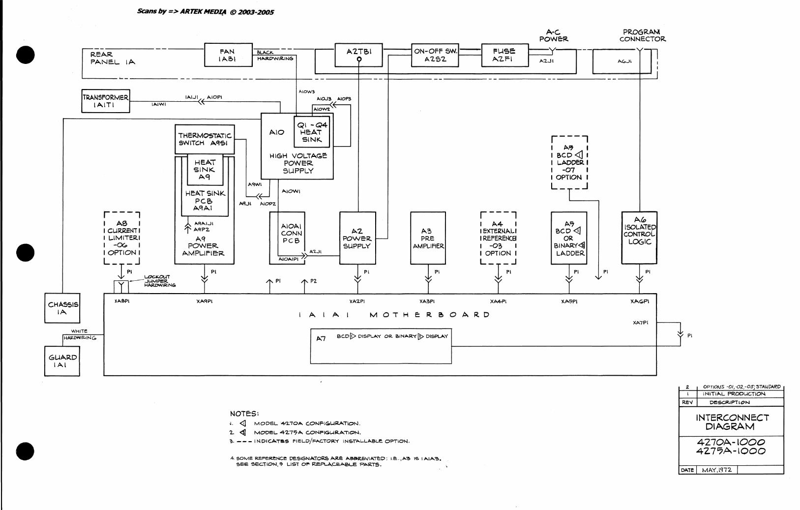
Scans by => ARTEK NEO~ @2oo3-2oo5
A-C POWeR
ON-OFf SW. FUse: T -A2S'2. A.'2.FI A."Z..JI
-- -- --
I RE/..R ----- - ----I FA.N 1----Bl,.-/>..CJ4.-- - - ------1 A '2.TBI
PANE.l... .... ~A ________ ~_ .... _______ I-A. ___ e,=l~-_~ __ H_A.fIl.I7\N __ IR_I_I4G1-+ __ L._-_-_-_-_-_-_-_-_~«f_:>f-_-------.... 1-------------------------------------' "'lOW?
TRANSFORMeR~-~~~--I-A-IJ~I/C~·/~A-I-O-PI------~ IAITI IAIINI" I A.1OJ'a././ A.lO~
r---, I A.S I I CURRENT I I LIM ITER. I I -QG, I I OPTION I
L-J-J PI
LOGK.OUT fYI-JUMPeR I I I HAA.DWIR.INGI
THERMOSTATIC. I-SWITC.H A,qSI
HEA.T SINK.
.A.q
HEA.T SINK. PC.B AqAI
..6 AqA.IJI 1'MP2.
Aq POWER.
AMPLIFIE'I<.
AIO
A.IOW'1 "
QI -Q4 HcAT SINK
'-------HIGH VOLTA.GE:
POWeR. SUPPLY
AIOWI
A.IDAI C.ONI\l PCS
" A"2.JI
AlOAI?1 '.
~2 POWeR.. r-SUPPL.Y
A.3 PRE
AMPLIFIER.
llABPI XA."Z.PI )(A.~PI
r---l I A.4 I II:)(TE~~A.L I IREFER.E~ I -03 I I OPTION I L_r.J
PI
r XAA-PI
CHA~15 IA. I AlA.I MOTHE:~~OARD
WHITE
GUA.R.D I A.I
p...--, sco!!> DISPl..A'( OR. e.INA.R'(B> DISPLAV
NOTE:S: J. <0 MooeL""."z.:70A. C.ONF-IGoUI2.ATION.
'2.. 4J MooeL. 4'2.77"" c.oNFIGI."II~ .. AIION.
~. --- I 14 DIc.A.Tas FIEL.D/~TOR,( IN$orl'o.l..l..ABI..e. OPTION.
4, SOME R.Cf"e~~NCe reS1GNA'TORS AFte. A.&aR.S""Aie:D: 1.1:., A.~ IS I I'o.IA.'!>. see SEC..iION,"1 LIST 01'"- RC~ce.A.E!>LE PARTS.
r----, I p..." I I &CD «] I I L.ADDfRI I -07 I I OPTION I
L_T-.J
A.7 BCD <!1
OR BINAR.Y4J LADDER
f"' )('A'7PI
--
PI ",v
PR.06R.A.~ COI\lNECTOR..
/-l AG.JI
A.~ ISOl..A.iEP CONTROL
LOGIC
PI
~~
AA'7PI
I I
I
z OP ONS 01 02 os :STA~DAA'D T/ - , - I -I INITIAL PRODUC.TIO~
REv oeSCR..IPTION
INTERCONNECT DIAGRAM
4270A-lOOO 42. 7'?A-~OOO
DAlE MAY,I~l2. I
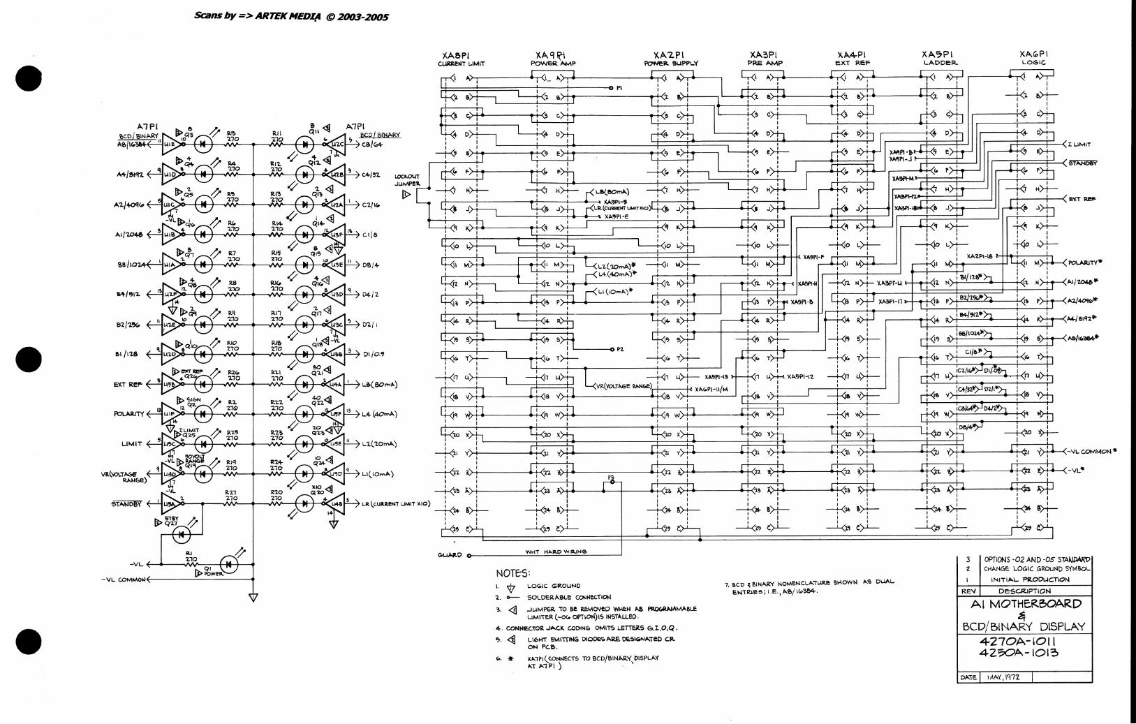
M/SIIIJ"Z.
A'1./J,oqCl>
"./1.Q4.6
"/~I'2..
&1.1'1"'-
&1/11.&
e1(T Re~
~ITY
LIMIT
VR(\IOI.:r A6E RANGe)
ST.a.WDBI( 1.
I» STIY Q'2.1
-VL
-\IL COMMOIol
Scans by => ARTEK NEDIIf @ 2003-2005
It.'!o '1.10
RA '1.10
11.., '1'70
R.G. '1.'70
11.7 '1.'"70
1t8 7..'70
1I.q 'li0
RIO 1.10
Itl'o 7..'"70
1l7.. 21(l1
11...., '210
II.IQ 'Zi0
11.'2.1
RU 'liO
RI'! '2.10
RI5 '2.10
Ill(, 7..10
11.1& 210
11.'2.0
A.'PI BCD / BIHAR'!'
C&/a.+
C1./Ir.
Gila
D8/+
04/2
07./1
01/0."
L&(80I'\'\")
1..4 (4OYn")
L'2.('2.0'"")
LI(IO",,")
XA'2.PI PoWeIt. SUPPL...Y
XA~PI PRE "MP
XAA .. PI EXT ~F
XA.1,;oPI L"OOER.
XA(DPI LOGIC.
h---------~.~~~I ~~~~~----------~~ ~I ~~~,l~------.~~,~ ~-.~II.~------~ : - i I I I I' ~====~====~--~--~~-----oo~
rirlr-__ ;1~ _______ ~~~I~'L a>+:~------------~:~----4---~:-_-_-_-~=~i<-:--:-;~i~'---------.~----~ I I I I
I , I
---f<' :~L-----,~i_(_Ij_D_E:r:~:JL----------~~==~~====~~--1:-~-.,-O-E~~;~------~----~
I I I I I I
cdr
. ~ I R)-b I I I 1
~Ij 5) ill. • 1
~: <)'7 ~ I s>t-I -+<" I I . 1 I I I
I I on 1 I I I I 1
T>-t-
I I It. T>+- ~r. ~r. T>-t-
I I I .
I I f , -+-41
f 1 ~ 11 ~. )(A,}PI-I'2. --+(11
VR('lOI..T.l>.GE AANr.c) I 1 I , 1
, I I ,
~ v>-r-I I
Lkq v9 i 1 I I
~~ w)+--I I I 1
G:<'I.OlC I I I t;<w tRw ,
I l( l(
I I I I I
-j--<'2.1 '( I Y '2.1 '( I
, I I I I I 1
1) : ~ I (12 1): 1 ~1. I , I
• 1 I
-k'l.~ ~ 1 '2.3
I , , I 1 , , I I ,
I 1
r.>t-I I
,----;:=*=====:¢-<. I: UMIT
.-+<i,' t. v) i,c+tnt>! D2/ll11h I ' ~ I !(l&?-h
-\IL COMMON ..
I I '210 '2.70 LR(C.UIlR.ENT UMIT )1.10) :
I I I I 1
i>-t- , ,>+- -+<1f. I -+<'2.+ -+<'2+ '>t-1 I , I
-kli- I
-k~ '>-t-,>t-1 I
--K~ ,>+-, 1
---k-1
a>i-~
I I I I
11.1 1.10
GLI~O
91 I» PoWEll.;
I I , , I I I I
~)l-I ,
~1."
WHT H __ saD WIIUN&
NOTE:"5: I. W LOGIC GROUND
2. 0,-- SOLOeRA6Le cowlol&.TION
..JLlM PCR. 'TO r.e R.E:MOV1!D WIolE:W 1>.& !'II.06\UIMMA8l..E LIMITeR (-0<. oPT 10 '"') I!> IN!>T"LLeo.
4. COW"'EC.~ .»o.c.1<. CODlNc:. OMITS LEl'l'S.S <=>,:t ,o,Q. "I. 41 LlEWfT eMITt'ING PIOces. Pt.RE oe.SlGoNAoTEO c.1t.
ON Pc.e.. Iio, * X/t..1PI<"CONNECTS TO SCD/8INAoRVDISPL ..... V
~'T A.7PI ) , '
, I I I , , I I I
----L('l'7 e)-!- ----L(t' e)-!-
7, '"CO ~ &INAA'I' NOMet-lCL .... 'TUl!.l!: $I-\OWIoi .... S oLlAL...
ENiRleSj l.e'l"f;/\"'~·
, ' I I
I I I :
----L¢i cr-
3 OPTIONS .. 02 AND .. 05 STMl~ 2. CHI>.I'IGc LOGIC: GmUIoID S'1'MSOL
IN I'T I jIo..\..,. ·Plt.ODI.IC.TION
RE\( DeSCRIPTiON
AI MOTHE.ReoARD ~
BCD/BINARY DiSPLAY 4270A-IOII 4Z~A-IOI3

+I~"'VDC.
-lac.. .... DC.
7.PNAC
2f!,N I'>C.. C.OMMOW
NOT USeD
Scans by => ARTEK NEDI/I. @ 2003-2005
JI +VH VH ':"t.AMQN~_VH 10
J ~---------------------------------VREr 5UPP~Y--------------------------------..., 1't'23.4-V t1.'3A-V
Itl II(. C.I
PI
~} -VA COMMON H~>---+---____ Pl _t_l ----lJ __ -------- +YA SUPPLY ---..., L: '2.'l}
-\lL
~oor;
{: R<.. 1~:7"
4, Cl '2",0
{: R40 3:141(.
c.s +
r~"c 1.<;0
R'!>II 4-,0
~~"c AAI
ql<; 4.0'2.1<..
-'2.7.IV
I -VA SUPPLY CR1.C.>
1 CR'L'5
H
.J
+'1V 1
21} '( -\lL COMMON
-'2'5.1 V ClUl
H---.-1-...... -~ 5 STI'o.N08Y
(-"~F ~-t-----_+---------~~-t--t----_7B V~E~ S~MSe
R'2.~ Rn 101<.. 1.0.0'21<.
(-V~) ~---'------------------;----7 0 ~F HIGH
- GATE DRIVERS -----....I ~--.---------------1>----.---~--------~7 ~vv 5eN~
R'2.0 101<..
4-'0
r- RELAY DRIYER. .. q
_~.rr-.-~- - - - - -
C'z,?> I
~-----------_*--~>----~--------~? OU,PU, L.O~
~--------'---1>----'----------7 "2. HIEtH se~e
C"2.4 I -'Z.~.I" ~I --7) '2.0 -",.."
~-----..... ---e----4~---------7 3 PWR AMI' OUTPUT
t:~}GU~D r-----------------7 e eY-T IleF
GUARD {IO >---, L~GUAAO
C.I~ + 1!>ooo
+ CIS
T 1.0 -5V t--------------7: },,~ COM~ON '--------+-------+-----5 -'7'J -'2501V -"!IV
-VL 5UPP~Y I TBI '1 C'. 4 3 1 II '2. rl~------~) '2" +'IL. COMMa ....
13
p
SVAC.
14-
A~S\ 1'6
AIO-SIA v
± n,lI
AIO-SIB I(",T
± IS,?
COMMON (C.IU6SIS)
1'1.,'"
r-- - - - - - - - - - - - - - - - - - - - - - - - -......-i GoU,",RD I.J:JW OIIl'PUT tllG:oH PI'ofR AMP ~D QI..s. EXT REF eXT R£F I ! >--1>------~I'!-----, L ________________________ ~~E....:L£~_ ~~~ O~T..!..u!' __ ~~ __ ~~ ~ ____ J ':" I
t-------------------------------------------------------~~C +"L. I ,---------------------------------------------------------------~ I I I I I I I I
>--4---------r'-;----~ I I I I R'74 I I '2"2. I I I
IL-----------+-VL5UppLy-----------~~1
WHITE J~" 115 VAc.- ?3O ~A.C
51
ON
NOTeS: I. ALL CA.P"c:,ITAI>JCe. IN MIC.ROFI"o~ "WO AL.L ~TANCE IN
OHMS UNL.eSoS 0\~el2.1N\se: NOi'eo.
'2.. THE FOU.OY-/IN(.. 1"1 PIN ... f>..e NO'\' Cc:>I-INe.c.iEO: 4-, II THRU n,l'!, C.E.H • .J.MTHRUF-,T,U,W. PI '2.4/e. 1$ OMITTED FQOM pc-e..
~ W L.O&IG GI'OUi'JO
4. '\7 COMt.AQtooI
7.) ) pce. CONNEC.:iORS
1.#. W RE:F COMMaI-!.
1. ..L EXTERNAL. LOGIC. GROUND. -=-~ "* S1::l.E.CTe-D
"l. ~ PowEll SUPPLY VOL.,.AGe: ~ U ~ .
10. ~ VH COMMON AND OUTPUT LOW AI Lcx'I'DUT ...JUMPeR..
TIED THRU INIACT
VOLTAGE:
100
11"5
n.? 200
'2~O
'2.'50
SWITCH POSITlO"""
PWR. SPLY H.Y. PWR SPi..'1
tla.~1 AlO':>I AIOS'2.
WI-IT
!/IIHT
WHT
~D
RED
REO
IZEO
WHT
WHT
RE.O
\ INITIAL. ISSUE:
"~'1 OE.SC1ZJPTIOi'l
A7.. POWER 5UPPL,(
4270A-IO(D1
DA,e . MAY,I"l''2. I

Scans by => ARTEK NEOI/j @ 2003-2005
.-------HIGH 1. INPUT 5TAGE----..., Ittn 10
SAMPLe: AND HOl..D ~ rOUT PlAT ?TAGE---,
+VA r-_.--------~~~~._----~~~--------_.--~----~~----------------~~----~------._----------~
+Jlc~ RP • ~ *0;0 Rt.4 ~ ~
it;4-'1.1 v..
+VA
itS! p ~ r~f & I.o.SI<. CR., c!& c.:;.q ~ ~'" ~'7"" qL~ \IREi' C "" 1 L~.J RG."2.
VR.E;F- SEN'SE 3 L~"'---+-J----"""---{ VII.EI" 1011<. ".. /~'2.1 I~ ...,.,"" ........ "' ... 1\+--_-,
~\.OO R81 CIa. 10
VREF HIGH 0 +----' +-------+------I----+---hu~) .k \L ql2AA .... -"T .. J J +VA X ~ TVI>.. rn t C~O Cf:I'1 C!L1.. '.::::::7 T '-""' ....... r----+----+----1/''''-'J -VA 'l.o( l-'III>.. ~ '1 CCW I~ #,~ <11 '" '" cia ~ CII
O'I~
* 6C~ :=:~ ~ (fl_~_~~ __ ~j~~~~~~~~_~~~_ERS ~l-h',--L------:~ ~E_~ ________ --U-----t.~/-ql-IS-A-----a-I@,J.f:~S:::::----I-qz;-f1~~ --. '"""~ ;:t- ". ~7~ P
v.' " ------1:.--~R----------v::~----1~'----1 "----:--:----- --~~~~- ---------'\.">-l~ ____ ...... -------'J I L- ~R ";~~ ~ ~:' v~ ~-t . .-_~--~>'7 OUTPUi iOPWRI>oMP
Q'1'\
"' I 'C ~'<'2.. r---;;-J 10.10 ~;!~ ~ 'l ~ ~ 100 ~o.oo; -VA. 1 R4 l\"'.D Go ,1 I I 0--< QI"I ~ [Sb. (l,S1 1 CI~ ((&'2& ' ;:'~
-VI... COMMON 1..1 ( "2.:J1<;. '-17'<7 "2.o;.O,I}'" -vp... cl T+ _~~T R'71 <1l \1.111,JJ Q"2.3 Q2t. "IIOTI.,O,-F ff
..,L .,( tVL ..:;'.. '" ~ L_m~ T' L....._18_1_1<. ___ ·-_-_~ ____ ~ ____ ~ ____________ ~~~~-~1----------____ ..... _________ -_"_L ____ -+-_~_~ ____ ..... ~1-&~-I(, ___ ~ 'l._R~ __ j(, ...... -::-;-----------~-$-~rc.~ -VA
A!. IS < '2..11<.~Q"" :iir. ! I~PF ~~j(, 1;~pF 5 ~~ I"
YR' ~r ' ~qe.. It'll -~ ~W ! * I:M '~30~ ~. c;o +M @ Il;<; : ~11r.....
A+
6 -VA I ltiO {'L ""~l I<. 200,'1\1. I ~",,-
2,11(. '= '" ""~ R'2.& I R'II I > 4- HIGH SENse 70 I 100'" CRI4- ., ~~~
~~:,~ I Vc-----...,..,..,...t--+---it-----........ --------+-----+--------------t-------------::-----+--------------------------------------------------~/" ~ VH COMMON 41 I I ~ cil; .... ---- -----, I
RI'2.:~ I ~ I C; T AA'1' Iw.. VOL.ii\GE v ~(------------.JJJ <;18 : CRI l' CR'Z..] : ~pF- 11.1041<.1 11.10#.. RANGE
~ V REf r®l L - -- ~:I-~ ... nt-t--1>-+--...".,~~1 ~'___1~,,~,,~r__I---L-------------------..J------------------5W--IT..:.., C_H_E_S __ +-______________________________________________ ---?.~ 14 VR(VOI-TAGE: R/>.NGoE) /_
RI~ qlo 1-CW .1:.......l ~ V ~ ~44 J it~ :~~~ ~, ~~:J~ 0;11<. ' 5 ~"V
~i~ ~~ ~1OO'02."'" ;, .!;:A- r~ ______ ::~_::JI4t---...... +-c.c-::--; .. ""f----<,~c2i--, ~ -VL
100 . r-------------------------~~-------------------------------------------------~)p HOLD ). R+I I q'!3 -1001<. I R4(.
~~oYI<.~ql'l~V~ 'Ii r ~~~f~ I -J", .H~ " -AP ~.ir---~C~R~~~-------------------------....---------------~r------------------------------------------------------------------------------~~I'\ NeGAilY~Cl...AMP
RI'\ I _cw tt-----*----------------------------~------------..... --~r_----------------------------------------------------------------------------~/ 7 POSITI\I5 Cl...Io.MP 'ilK' QI4 R;l : £) ~ +V"" R41 R48 1 ~; I ~t7~ 1001<. IOO~
!---.---:R-22.-~l.<..\.. ql7. ~~~01'71(. : ".1010. ~ Y V 2,,1<. "-, QI"J I 11.;'2. R,8 CGo 1l,4-
I '100 ::: co; R"2.1 > \<.20 1------, ~;"',d! I.S\<.. .. 1000pf' ;~l'1' 40.2.\<.. '111<. ~ lOOK: I+----+-----...J., 'd7
JJt LP (~ '1;0; ~?q;1 '0 II V
+-------.R"'l.";I'-e-I~1N '1 Ie.. D'" r--~\"""p;-tH----------"
........ I~OO'~ ~ lI.72 R'''' 7"0 :- lOOK " '" 7'-
'-- S.II(. '7.11<.
"17 ~
I Q 3
1..11 2....-- q ±-. R!18
7.1"-
W ~ -YL
",7
NOTE.S; I. AI-I.. C.APACITANCE: IN MICllOFI>..tzAD~ AND ALI... ItESISTANce-:,
11'-1 OHMS UNLeSS OTHEIlWIse NOTE:D.
7. .• HE FOLLOWING PI PI>lS ARE NOT CONNE.<.TEO: C..8,9,IOTI-lR.U 1';,1'7 Ie., '2.;' THRU '2.'7, A,c.J, LTHI!..I..\ N I II.. THiZ.U T I w,V:1., ;e.. THR.Uc..
3. W 1..0GIC GROUND
4. <V COMMOI'-I
"I. f-- Pce. CONNecTOR
q.
R.l!:F, COMMON
INSTAl..l... PR.OPEII.. ..JUMPeR. TO "1.EI<.O I N51""1WMENi.
2 Io.ND e, ON OPPC>SIT~ SIDC:S OF- PCB.
'IIH COMMON AND OUTP\..li L.O'N TieD THIt.I.I INTA.CT AI LOCKOUT ..Jl...!MPE:R.
I I 1i'41T1A.1- ISSl...!e-1-----+----
REV oe:sc..rz.IPTION t--..L...-_-A3
PRE:'AMPLlflE-R.
4270A -10171


Scans by => ARTEK NEDIif @ 2003-2005
PI r- VR' SL.lPPL.Y ----,
VR' 4 f-(---Oo/'Z VR'
+VA. 'X.
C.RI
-VA. COMMON { ~ ...... --.... --...... -~ VR'
-VA. 20 ~-----~~-~--------~-VA
-VCCO"MON {i, 9 Be 0 LADOCR { I OUiPUi '"
./
'/ , 1
I ~ +81"
.~ \2.1 ~ 1..00
~1 * 12~1<. ...
~+lYr-> "70. "?> R,?'* >~. 14"2.. .. R.~. ~ lOO0'2.'?IC. '> '1.OO.01'1K..
"20¥.1&'''' 4'1."1'"'''' L'I ''I u., 1>1
DRIVER DRNa. DRIVER. D1Z . .lVE~ DLB D"ZA- D'Z.'2... 0'2..1
LfI '!'I 'i' L
BS S B4- ~
e.'Z. p e.l N cs W 01- V cz. U CI T De. 1'1 D4 IS D'Z. n 01 I~
REF COMMON D
./
'/ L" '/
/' '/
/" '/
/'
'/
./' 'L /' ,
ORNER. CIRCUIT REFeReNCe. D~SIGoN,c...iIONS
OESIG. VA.LL.lC 021 D"2'l D1.4- OLe D31 D3"2 034- D~ D4-1 D4-"2. D44 D4-6
RA. "1../ K. 2."23 ~I.q R3'? 144-1 2.47 RC;~ 2.5'1 l<Co'7 R11 Rl1 1CS~ ReA
ll.B %0 R'2..4 R~ 2.3(" AA1.. Rita 2.'14- 1Z!..O R.<oCl> RT/" 1418 1CM RqO
~ ?IK. R"25 ~~I R31 ~ AA'I R'77 Rc,,1 flJp7 R13 Rll:! ~? R'II
RD "2...1\c" R"2..(p R31.. R~8 RA4 1l.'70 R% Re,it RlDS R14 RSO Rae.. 2.(\'l
RE '71"- 2."2..1 \2.33 R3'i I2AJ? 12.''71 2.'71 ReP.. R"''\ 12.17 ~ ~1 Rq~
RF- 51K. R....e. i<.~ R4D AAG, R'77.. R'7e. Rc.A- 12.10 Rlc" 2.$'2. RS& Rq4
QA. "Z..N~qO(p Q'7 Q<\ QI~ Qn Q'2.1 Q'2.'7 Q"q Q?I~ Q31 Qlrl Q4'7 Q4I'I QB Ll23(o("& Q'" QIO QI4 QIB 0.7,7. Q"Z.{p Q30 Q~ Q?J2, Q4-'7. Q<I(, Q70
qc.. '2N3'104- ql q" QI7 Qlq C(7..~ Q7..1 0.31 Q37 Q3~ ~ Q41 Q'"
QD l.I2. '~,t·Lc QS QI7.. 0.1'" Q7.0 Q7.4 Q"Z.I!o Q~'2. QYo Q40 Q44 Q4% Q"
~5 ~o.4 .,
,..------DRiVeR. (1'2- PLAc.es) ------, VRI
LOGIC eon INPL .. n(ov.n .. IJE) -""
L,c...OOE:R
..: R'I '2+.'1811(.
~'1
DRillER O!S '!'I
~I~ 10&.0<.01C.
> RIO ..
RII ?> 2.1'2. "> 2.1'7 oj RI4-'701C. lOO.O~1(. ~ 200.08K >"2.'1-.'1;:' : 44.'1K..
,~ LJ'I V'I "'" U1
DRIVER DRIVER DRIVER ORNER DRIVER 034 D~'Z.. D~I D46 D44-
!'I L'" Lr" 1'1 '11
NOTE-5: I. J>..LL iZ.E:SI$TA."-ICe: IS IN OHM$ AND ,o..LL CA.PACITANCE.
is IN MIC~!=A.~A.DS. L.I"-IL..eSS OTHI!:R.wISe 'NDIC .... ,eD.
'2.. W LQe.Ic.. GfZ0\...4l-lD
~. ~ COMMCi'J
4. ~ PCB CONNECT"OlZ.
9. *" FA.CTOR.Y Se..L...cCTED
Co. W RE:F- COMMOi'l
7. @ INDICA"TES IN,EItNt>-L A.P.JU-"'MENT.
8. THE fOL..LOWING PI Plk!5 }>.RE NOT CONNECTED: '7THRUI'7, '2."2. "THI'!.I..l '27, e,F,H, -.J THRUM ,':l.1 A.,~,ANDC.
VIU'F
..... -+-~ "TO L..A.OOER. ~SISTOR.
RIS 1'2.0K.
> RI(' > RII, ~IOO\(' > "2.00K.. ~,
IJ"I ~
DRIVER DRIVER D4"2. D4-I
1 I'
I l"'IT'A.L ISSUe:-
RE'I' DESCRIPTION
A5 BCD LADDeR
4ZIOA-I031
DATE MAY,IQ'2. I

Scans by => ARTEK NEDIIf (§) 2003-2005
"TWO'S \NPUT P1WGR~MMI~
r CDNlola:.rOR.. , It-JPUT
rMULiIPLc~E:I<.., r TWO'S toMPLEMeNT Qec.oDe:R..., 't ~_Ul-!IJ.!-~~~ ;a BIT DRI\lER-")
-. I ''0 I aaAAlt,y \ J ... I ,r-----~
I , d / Ie.*, I 1., '&
,--------~, _u, ..... '\. 0 r- - - - - - - - - - -, I 14-A4 I.... t"'~ ...... ----------'.!.fl.
A'I. / 404Cr , .. I, UI ~'----~~_~~~~I~~---~ : ~ L ______ _
AI ./ ~ ... '" S 14 '... . ' ..
~,-- UIU. I I' / 10M> & ~ I,
L __________ J
I ... / ~ ,.... 11,
'.. ~ 10
It / 7.. , 1., "I.
&1 / IU • ~ I r..... ~, s, U .. '"
1
CLOCK ORIVE-R---,
c.. c.. C1.
C.I
o. D+ 01.
DI
/ ... , ft,
/ 110
I • I +
/ " / I
/ Q.~
1-1 'MI_) I Ii'. 1-_ (U~ / E2.¥
I-4Wt ..... ) / &4. '"8(sD...t.) I .8 *
I-a. [t>/ -En ~
,,~~/ -
:I LIMIT
I" Itt I" I
... ~ r, .. : 10 >-__________ l'il,. II ... .. 4 Ul.
1'1 .. S X-\I ... 4 1,
.. S I, ""2 It. "L~
a CI"2. 1 .cn."!> -tSli
.0 ,.)oj ... .. >i ~+ I I.or... s, n
~ 1 ~-Q) IL"-'= I""'~ 11l==~'1 z 0 ~ 51
-~--'=r!U\-IC. ..... ~ ~ .. +,;....-__ ..
~ RIO ~o
" r-- BIT DRIVE:R. --,
UJe,~IO'"___4 .... "__1USO • lqPI-,----- I~ 4 J * * .. r ~ uriS- ~ - ~ Uq ~ ... ~~-----------'-I7 I. U4- : t-:..:14:""--+-+-+-+- ...:-1-+----~~------------------t----------:i.,L-t..I_ _ _ _ _ _ _ J ,~ ~ '"
\I
; ;)-----------:~ .. ~. ® +5Vl--1Z.I-,-....... --JZ;-l'1-..... .-JZ;-:2Q-~-It."Z.---,1 .~. ....J:._--i.~ :f-I~--4_..I .... SV ~ ..... !iNa ~-: "'.... 510 l~ ) _____________ l~I. ~~ r I-
C.. - II •• 10 ~ 1:11
... .... ~----------'1~t, h "e"Z. C?"
M ' !oo. 0;" '" I '*' I'lop" l"Z.p!' r- STAND8'i DRIVER -, ;
t1CR~ CR. ... : ~ IZ.?O 0 I" II~ I'~ START -~TOP .- SI i. FLIP FLOP Q~ ~ fr' Q(. ~ ~;. .• ) ~ r r -, 'P ~ I~~LII4.-- z
ADDRESS r"---+3-+~-+"-+'---++--+--~----':z. .------&-I"Z.--<Q-+----------t-----+----:"Z.:;i~-l._1 _ _ _ _ _ _ J ;:1. .! CONTR.OL ~ CA':~~· 0., q" S 1.~ ~ 4~":........, ... 4-.:c~1("" to HK. -:- Q.... 4' ..... ~ .. ,(-_+-~ L --'.'.-. ._ft us uPf-'--- ..., U7 ~s U '* T c.'1~ 1
r--'" - K cur. * .0000S +5V r 1,·~, \, I~ ~~I.!·~~-------=-------------.JrHOLD ~Nt:Rsr-."v:\II;tl'----o-... --__.-~..,TI5 • 1 i - - - u~ ~ - ~
~------+-----------~~-----------------fl , R~~ .:-1 _______________ -:-=:--+-__ ----:=_=_~ +6V IK. •
-t5V r REI\DY ONE. -SHOT -=' to L. - - - - - - 4 J f----o~ ... r DELA'< ONE -SHOT~ -, 1.'1.4K. R_ .. 'N -:- .~~'" -t~1/
II.!*.
11 ~-+-...,
11).- ~ :,~ '" ~, S'l ,.---.
;~ 1.0
" T' L-__ --'
'" '3K .~ '1. )~-.... .:_"'~"'~,... --i.L .... .v ~r ~-~~ li .OO1sL C "2.ic.:,~F • RS<.
fi() .!.- 'S " 7 U ...
':::.I IS ~ ~ II'r~_,.b---oO ...... ---.. ....-- ~&o\, lI.i_·~z-----.J Qut.s ~ q& ~"1' ~
, 1.~ ~ ~ Q. ..,. ® -. _ ::I .~ '---- 4~ CR~
I ~I'r JH 1 : )~-------------------------.:..~ " I~ ~ )~------------------------------------------------IJ"·
. I~
-t5V
~-a. B~® It1. _ .. uIA r
l ~ •• I_-...""I""IC.,....._fi"t-t-t( ql CI
l _ ~ '. ~ ': ,.001
.l-
UIS S'
-
•
LOGIC CONTROL JUMPER R:>5ITION CONAGURATION A. B C D E F G H J K. L
4l1QA,-01 1-2 \-2 1-3 1-2 1-2 \-2 1-2 1-2 - - -
4210A-0\ .. 1-3 1-3 1-3 1-3 1-3 1-3 1-3 1-:3 - - -
4216.<\-0\ 1-2 1-2 1-2. 1-2 \-z. 1-2. \-2 ·\-2 1-2. -- --2.-4
4Z.1~-OI'fl 1-3 1-3 1-4 1-3 1-3 1-3 1-3 1-3 2-4 - --3-4
4lSacy'4Z70A-OI 1-2. 1-2. '-3 I-Z. 1-2. 1-2. 1-2 1-2 - 1-2 1-2
42501'(42.70\.01· 1-3 1-3 '-3 1-3 1-3 1-"3 \-'3 I~ - 1-2. I-Z
42bSA-OI 1-2.. 1-2- 1-2. 1-2. \-2. 1-2. 1-2. 1-2 1-2
1-2. 1-<-20-4
42105A-OI* 1-3 1-"3 1-4 I~ 1-3 1-3 1-3 1-3 2.-4 3-4 1-2 1-i2
4e75A-ol I-Z. 1-2. I-z. I-Z. \-z. \-2. 1-2 - 1-2 1-2.
4275A-OI* 1-3 1-3 1-4 1-" 1-3 1-3 1-3 1-3 - 1-"1. 1-2.
* INVERTED LOGIC LEVELS
NOTES: I. "'LL .. f:S'STo\,Nce I~'~ OHM'> ..... 0 'L..L.. GA.P~IT~ .e;, IN
..... C-R.O ..... ruo..os ......... _ OfWt:IZIM ... N~Q.
"Z.. -= EXTEIl.NAL. L.C:IeoIC. CiROUIIIO ~. 9 u::;oc".IC. GoIlOUNO
M 1-2. 13-4 1-20 "3-4
--
'-2. ~ 1-2. ~-+ -
-,-z. !>-+ I-Z 3-4-
4. * '~. ~ , ... PUT W_ ....... BCD LA.~1t. UOQI"V USOLUTIQN) - 0' OPTION I" uost:n .
.,.. ** SHIFT lI:eGI'ST~ OUTP\Ji WHe.t.I "''!> 8(:.0 u..Do.III. C.IOO~V R.eSoQL.IJrlON) - 0' OPTIO,,", .~ use:o.
". [» LR. (C.U\l.IZENT Wi,A'" )(. 10)
7. [9 'III.. ('IOL"TM.e: IlAN<".e.)
a. ""Eo "OLJ..OWINca l" I PI"'S AR.e. "'OT CONNI!C.~O: z..,,., .. O."Z.O,""ZI>'- ...... ,, .... ,IC.,L.,M.lC "''''D \. ',.~e. PO ...... OWINt:;. .)1 ..J"-C"-S ... 1le r-IOT Go\oo\I'.-c.Tec.: "z'''.'2."7 .'2.. ,30,"!>1 ,,!>'2. ,"!oIl,"'!f'I ,40, 41,4' .... , AI.#) so·
(ECO'S 7435 & 7955) R34 WAS 1~10K_ADDEDJUMPER
A POSITION CHART, REVISED ZONESC7 & A4
~- JUUf'fR F'C-S!"!1Ol.J cOI?gcC"!'IOU 1 l~m~L f'~ooJ.(mON
~.
I\EV , tlESCRlPTlOt.
1\6 ISOLt\TEO CONTROL lOGIC
42.75A· 102l
DATE FEe.·I't13 I SHT IOF'2..
--.
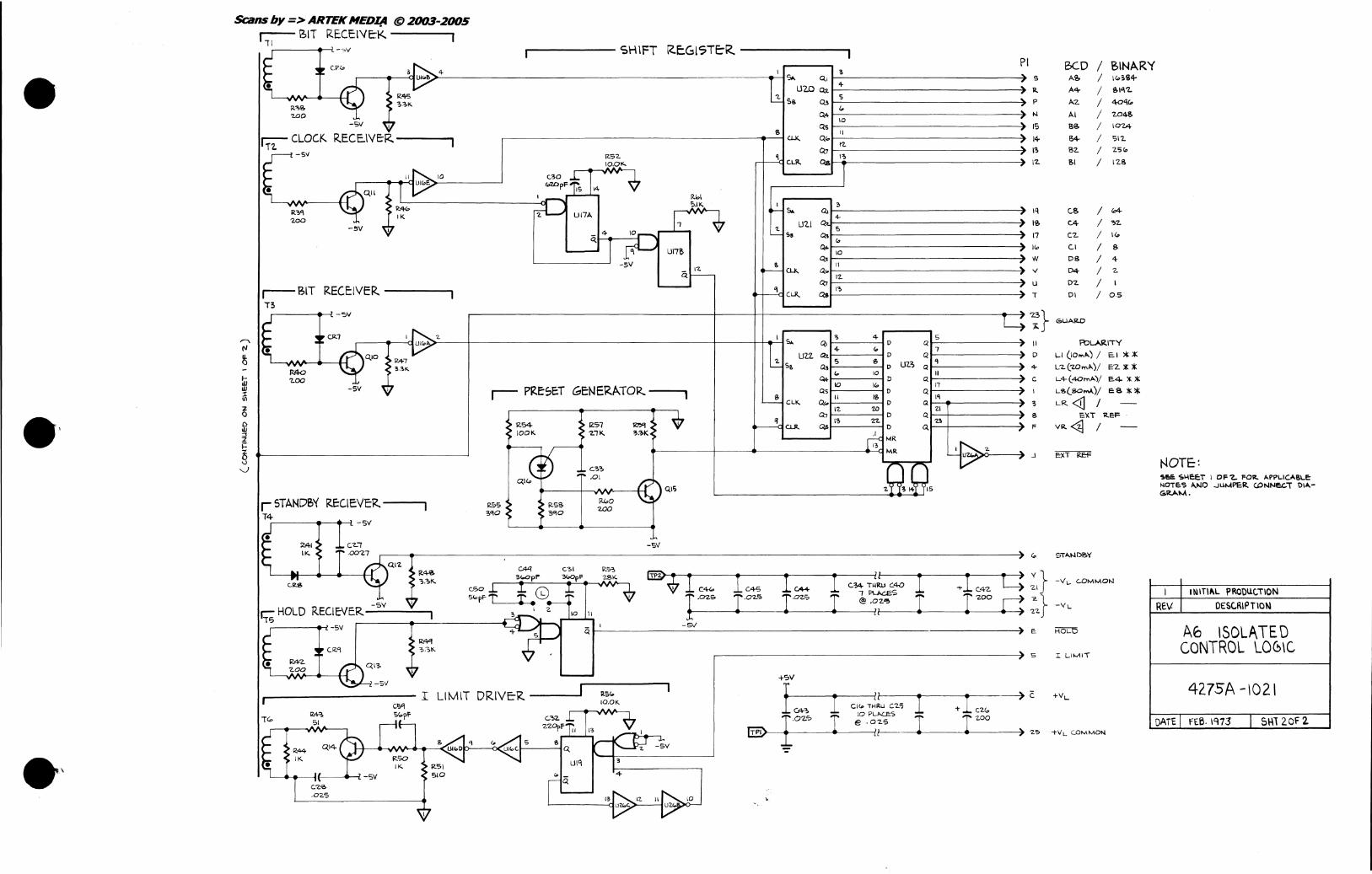
"'-1 ----- SHIFT RE:GISTE:R. --------,1 PI
, lJl£.I!>I>-4'----------------------------l...--t1 """ 0.1 I__:--------------~~ s ~ lJW 0.1. , R.
1<45 ~ S • 3.'1>1'. Ss 0.3 ~--------------4" P
-sv
r:;:;- CLOCK RECE.IVE:R-----,I
t-" . R3'1 200
-'5V
r-- BIT RECEIVER.. ------,1 T3
~ .~ N Q4r---------------~ qSr-IO ______________ ~~ IS
B II .---------------------~~~ ~
_ 17. Gte--
~ 5.t. ~I__~--------------~ ... 1'1
U'2.1 f">< 4- ~ I~ S ~
Q.. 10 :: 1(0
q.I__--------------~ W S II ~ ~ eLK a."/---------------~,,
~ 1'2.
Q;7 I~ ~ U as/---------------~" T
L;~} UI(qfi.>2--+-------------------+----+-t-.--'--I1 s... q'I-~ ____ 4--tD a.1__5-------~ ... II 1 ... 10 "1 ~
-sv 1
r STANDB'{ RE=CIEVf:R. ---'1 T4 .---~~~-t.-5V
~ s~ lJ'Z.'Z. :I--s---s-l: lJL.~ ~ I--q-------~" : ~ ~ ~
Cl4-1--1O---I,,-I 0 a 1--1-7 ------~" C
QSI__I-1 ---1&-1 D Q 1--1-,\ ------~,
Q"'r-----\ D Q I__--.------~ 3 r- PRE-SE:T GE:NERATOR.. ----"
2 eLK.
t2.S4-IDOl'.
> 12.51 "Z.'K.
RIoo 200
12 'Z-O 21 ~ V O:7r-----\D Qr---t------~S ~ '>- I ~ r, 0 IS 27. 'B .~
... I' ~ ......... asl------\ D a.r---t------~" F ~~K ~ 1
~ ______ +_--~~--~-~~~~~----~~~;3~MR ~2 ~. MR U~~--~ ... ~ ,
7.Qlgs 0,1<;
-sv
BCD A~
A4-A:Z.
AI
BS
54 B'2.
i!>1
e.s c.4-
cz. Col
DS D4
D"Z.
DI
GUAIZ.D
I BINARY I 1"'~i4-
I 81'1'2.
I 40'1('
I 'Z.04l!o
I IO'Z4
I SI'Z.
I 2510
I 17.8
/ W<\
I ~"Z.
I 1(,
I s I 4-
I '2.
I I 0.5
FOLARI"TY
1-1 (10"" .... ) I ~I ~;t::
L"Z.(W", .... )/ e:;"Z.;t:: JI;
L4-(40rn .... V ~4- :t:)I(
LS(SClMA)j e: 8 '" *' LR. <0 /
e:;,)(T R.EF
VR~ I
.---.--------------------------------------.-----------~> '" ST~DBY
.. , C~
CA<l C31 1<~3
3c..op,. 3(qQpF 2SK. Iffi>-r- I I I I II I I ~ Y} .---.--'----...,. ...... ~v"Av_·~ W L-..) 21 -\It- C.OMMON
-SV W ~:~* f .C0JH t 1 T·~ I'~ I'~ I C.1~IRul?!3~4{) I +I~~; ~~} r,s HOLD RECIE-VER 1 ~" 2. liD II I t .. ------4->-------..... -----4-->-----1.·~· -----_----il->---_~~ '2'2 -YL
5 .---------------~ ;; -5\1 ~ .- v + ~I__----------------------------------------------------.--------------~) c HOLD
I~ ~~C~'1 ~~ r, I ~L.--,,,I1.4''':z.I'_"*___tH/"''" ql~ " L -;00 (r-.. '.
~-----------------------------------------------~) S I 1-IMI,
+5V -sv
,r---------- I LI M IT DRIVE-R __ ---'I f I If-I ---I-----ilI>----~ C +vL. C4~ Cic.. TH~U C2'7 ;- C2("
10'2.<:' I ~o.~~s I 1200
§-~I~--------I'I:--- ----~----~> 7.5 "VL ('oMMON
NOTE:: ~!:a SHeeT I 0 F -z. FOIZ. .... PPLIC"81-E: !-lOTe'S A.NO .JUMPER CONNe.c., 01"GIlAM.
I ItIIlTlt\L pROOU.CTION
REV DESC.RIPTION
A6 ISOLATED CONTROL lOC'>\C
42.75A -\021
DArE fEB. 1973 I 51·11 2. Or 2

-VL
+VH
PI
Scans by => ARTEK NEDII' @ 2003-2005
r- GRD ISOLA-'"TOR.---, I +l'jV I
Q'2..
L t------<t---...... ~~---~ tlJH rFET DRIVER.S-, t--t-~~ RI
3'1K.
- ... ------<~ -t1C;;V -I("V ~-+--~-I
r B-4-2-1 TO 4-4-'2-1 CONVER1ER,
L..7..("2.0.,...,A)/f:2. ~ 1'2.~---e------f--_--.J
1c.4--* N ~--_--'-i
p---- -leo VOL\, SUPPLY -----,
-VH
C~1.
ICs>V
IO~----------------------~~~ '" I
-1(0'11
TP ., It'?
?oo
~ REf-
r -SWI1CHc~ t ~ADDER.--, CI3
.0011.
R'l? 10K
Ro'll ?I"-
R1.4-10K.
IPOS. I LlMI! COMPARATOR-,
+VH
-VI-\
r-NEG. I LIMIT COMPARATOR, +'1H
r'r=-<~~"" PROGRAMtJABLE r -REF ER'ENCE - -, R~'2.
:2.1K.
NOTes: I, I>-LL RESIST,o..I-ICE 1'1> N OHM~ 1*10 p.o.l.\.. CAI'ACIT~C.e. IS IN MIC.~-FM~.AOS L.lI-ILE5>S O"THERWI5>E I'-\O'EO.
2. THE FOLLOWIN(;' 1'1 PINS,I.J2..c N.O' CONNecr~D: :, THRU. 7,11,14-, : It'" =::.::~~ """ 0,", ",M< "'''''' "TIl"" , ,'S,C.
.,. (--- Pc.1!> COKNti:CTOR
c... @ Pc. e, TIORMIN.t>.L
1, ;It- '* SIiIFT REGISTER. IfJPU\' W.,E:N f>...'? BCD U~DDER (100 , ... V,) \<.E.SOLUTION') -07 OPTIOI-.l is Uc,E:['l
8. (t> PROVISIONS FOR FACTOI<.'I INSTA.LLA.BLE: OPTION EN"'BLINEo l:'X"TER.N..t>.I... CU~NT MONI10~NG,
PI '2. +LlMIT
r--
r I PRDV''..ION FOR. EXT
CURREln MONITOR..
[1:>: L __
:} VH COMMON<n
PIZ.DIIISIOI-I 1'012.. E)I, i c.~\ MO~\'iO
.----------4 U - LIMIT
1 INITI,o.,L ISSUe:
RE\( DESC.RIPTION
AB OPTION-OCo PROGRAMMABLe
CURRENi LIMITER 4Z70A-\OBI
DA.TE. I 1.\ ',1'11'2. I

Scans by => ARTEK NED~ @ 2003-2005
CONSTfa.NT -----..... 1 r-CURRcN1 SOURCE ---. r-, ---- POSITiVe: CL.AMP
+VHr--~--~----C~2-~~~-~--------'-------~~--------------~-----------------------1--1
PI C~~&
CI
330pF
poSITNe CI....6,MP ,,~---------------------MI-----..----..--~~
+LIMIi' 'l.
+"H L
'11-1 C.OMMOt-.l 41 )(...
PRE,60.MP INPUT D
-VA. '10
100
CI'7 10
L CRI'Z. c;..sv
R,<"40 1M
0.01 CR~S
tVH R51 100
RI? 100
R"51 100
-'II>.. COMMON A ~-~----~~-~
-VH
- LIt"'I'
'OI~----------------+---~-------------4---~--------4~4-~-~H
uf------------------------------4-----+--------------------------------+-----------------~----~--~----_r----~ r------ NEG. CLA.MP ---..., C'l.'2.
R21 C1 "2.0"-
10 ~
-+VH NEG.CONST
rCUR. roURCE·-, J 100 pi'"
{Iq
loJE6A.ilVE ·CLJo.MP W
R(,I"
1M
11.12 1001<.
PI
__ :.....----4--=-=::...!.!::4~ ..... ------...... ----~ 4 powt!.R.I>MP OUTPIJ.T
C.I! 0.4-7
PoWeR.. T'R1\1115\ti.GIl.. I-I~"T It}o.DI,60.ia... PC e. />..'Ss'(.
3 1 Y} -VL COMMO~
...----_--....... --4 '2.1
.------~ 14- ~ LIMn
-VH~----~~--*-----*---~----*-------------....... --~------------+-------~--~ l} -\fL
~--+--------~--~~~~--~2'2.
NOTE.s; . I. i HE FOL.LOWI NG PI PINS A.R.e NOT CONNE:.CTE:O; B. c..c. il-\RU
...l. M iHRU'" ,'1,'10., A iHRIJ.C, I ,~,s " .HRU q ,II TI-IRLI 13, 1'7 iHRU I!!I. p... THR.U C:.
2. ,6o.LL P.E:SIS,.,60.NC.= IS It-.I OHMS AND ALL CA.?Iloo.Cli'ANCE IS IN MICROF"RA.OS UNLE:SS OTHeRWISe. NOi'CD.
?.~ pee. CONNE-CTOR
4. E> VH c..oMMON ~ OUi'PUi L.OIN ,lcD THIlU INTACi' AI LOCI'.OUi .JUMPEli..
'.
I INlil"'-L I&sue
R!:" Dc.'1>C.RIPTIO~
A'I POWER A.MPUFIE:R
4270A-IOll
DATE 1'11"'<.1'112 I

Scans by => ARTEK NEDI14 @ 2003-2005
r--=- IAITI r-
Vlolw, -, r':---=-;l ORN 01l.N I
h-il swlwl- : I I : ~ , , I?';VAC. I
VEI..Jw - : 1 ~ I' , I' ,I ~ED :~ : ,
ORN/W -, , I ,~ , 1?'7VAG 1 I :>- I ORH
I ,
IAUI
l __ 1 1 , 1
VIO 1 1 -BLU 1 1
VEL, -1 I
cm.Il - REO'
1 1 1 1 ,
''''IW' SR.N , , REO:-=3
, 1 ,
I r--, ,YEI.. I !f- I I L .• 1 , , 1 ~LJ(.
C:.RN 1 ,.
i~ l' , I IBl.-U L __ J' , , ORH " 1
1 l ' VIO! '(eLI
~I 1)1..1'.""
BLu ' via' "" L_rvJ , E>IlY' "
WHT WHil~ C:.RNI/ lZSI) I '/
.~.'/'
ALOPI I A /
"'-
/ ,
. RI 4-.1K
,= ('1 '1"'0.01
.. .... CIl'2..
I"
AIO HIGH VOLIAGE POWER SUPPL.Y
C4 ;::0.01
R4 > 8.'2.1/..
r!Jq2 ";~ C'2. 1'2.00 2?OV ~----..
+~ C'! l' 1'200
l'70V C(g
;;'0.01
0A-1 ~rC7
RC. • e:2.I<..:
CIlr.; ~,
CR..G. ~,
OR.NI'/
VeL. ! /"
" /"f!!NA..C F '/ ± 7 /' lOOVA.C.
i!ol-U i'. I
VIO 1/
O~IWI'/ VE.I..}W I ." BL.U/WI '/
I " VIO/W'
NOTE:S: I. SWITCH LOGIC VS. L..INE VOL.TA.GE:
LINE' SWITCH Ft::lc;.ITIONS
VOLT~Ge P'NII.'l>PLY H.\I. rowa SUPPLY ~~/_i;,1 ~ ,60..10501 AlO502---------
100 WHilE: WHITE RED
II~ I WI'iI1'E "E:.D WHITE I
1'2.~ I WHITE: RED Reo I
7,.00 I ~E:-D WHITE. RED I I
'2:~O I R.eD RED WHITE': I
?J';O I I ~EO RED Rao
::t 1'.251 Iv\OUi<lTEo ON A'L PUWE R SI..lPPI-Y
WHT Sle. WHT
~I I
! I
, , I
RED , 51 ... I I
IlEO I '!>'2.A
~Sl
52 r " H.V. POWeR SUPPLY SW.
,--REARl r PANEL
, I~ 1Ae-1
sue.. -HD W~
'2.. [!> GIl AND Q4 MOUN'TE:D ON AIO HEAT SIN\(.. AND CCNNECTe.C TO A;C; PC"'>!iA CABLE: AIOW·Z..
~. A.I..L.. RESISTANCe 1"-1 OHM50 A.ND .a..LL C.a..PA.CITA.NCe IS IN MICWfAIC.ADS,UNLE5S OTHE:RWISE: NOiED.
4-. m "CHA.SSI!; GROUND
RS ".SK
(l!LI<.)
RED
COM '"
e.uA ./ VIO. I':;R.v ./ WHT ./ 'OLI<. ./ 5~ ./ RED ./ ORIoi ./
VEL. ./
VIO
AIOAI CONNEC10R
I' BOARD ---,
,-o-=---+--~ B ~}
~o-~_--44-
D _o=:.;..;;,.;..~--~ '7
E _o=:=-~--~ "
F ....-O-="--........ -~ 7
v
+ 1?I(o,\fDC.
COM.
-l~\fDC
2&VAC
2'OVA.C
8VAC
NOT useD
Tl OUTPUT S,HIEL.D (~~)
NOT USED
TI INPUT SHlE.LD lCI1ASSI<5)
BVA.C
H.Y. POWER SUI'I'L.Y SWliC.H !Ole.
±. ± TH1<M5TC SWITCH AIISI H.Y. POWER SUPPLY SWITOi SIA.
I INITIPo.L ISSI.,.jE-
I'!.V DE:SCRIP,.ION
AIO H.V. POWER SUPPLY ~ CONNE:CTOR BOARD
4270A-I012
DATE- 1'.1A Y ,IGT2. I