BCD to 7 segment latch/decoder/LCD driver
10
1/10 July 2001 ■ HIGH SPEED: t PD = 14ns (TYP.) at V CC = 6V ■ LOW POWER DISSIPATION: I CC = 4μA(MAX.) at T A =25°C ■ HIGH NOISE IMMUNITY: V NIH = V NIL = 28 % V CC (MIN.) ■ SYMMETRICAL OUTPUT IMPEDANCE: |I OH | = I OL = 4mA (MIN) ■ BALANCED PROPAGATION DELAYS: t PLH 2245 t PHL ■ WIDE OPERATING VOLTAGE RANGE: V CC (OPR) = 2V to 6V ■ PIN AND FUNCTION COMPATIBLE WITH 74 SERIES 4543 DESCRIPTION The M74HC4543 is an high speed CMOS BCD-TO-7 SEGMENT DECODER WITH LCD DRIVER fabricated with silicon gate C 2 MOS technology. This device consists of BCD-TO-7 segment decoder with a BCD input latch and a 7-segment driver for a liquid crystal display (LCD). When any illegal BCD input signal is applied or input BI is held high, the display is blanked. When driving LCDs, a common square wave signal should be applied not only to the PH input of this device but also to the electrically common backplane of the display. For other types of readouts, such as light-emitting diode (LED), some additional drivers, such as a transistor array is required. All inputs are equipped with protection circuits against static discharge and transient excess voltage. M74HC4543 BCD TO 7 SEGMENT LATCH/DECODER/LCD DRIVER PIN CONNECTION AND IEC LOGIC SYMBOLS ORDER CODES PACKAGE TUBE T & R DIP M74HC4543B1R SOP M74HC4543M1R M74HC4543RM13TR TSSOP M74HC4543TTR TSSOP DIP SOP Obsolete Product(s) - Obsolete Product(s)
-
Upload
khangminh22 -
Category
Documents
-
view
1 -
download
0
Transcript of BCD to 7 segment latch/decoder/LCD driver

1/10July 2001
HIGH SPEED:tPD = 14ns (TYP.) at VCC = 6V
LOW POWER DISSIPATION:ICC = 4µA(MAX.) at TA=25°C
HIGH NOISE IMMUNITY:VNIH = VNIL = 28 % VCC (MIN.)
SYMMETRICAL OUTPUT IMPEDANCE:|IOH| = IOL = 4mA (MIN)
BALANCED PROPAGATION DELAYS:tPLH ≅ tPHL
WIDE OPERATING VOLTAGE RANGE:VCC (OPR) = 2V to 6V
PIN AND FUNCTION COMPATIBLE WITH 74 SERIES 4543
DESCRIPTIONThe M74HC4543 is an high speed CMOSBCD-TO-7 SEGMENT DECODER WITH LCDDRIVER fabricated with silicon gate C2MOStechnology.This device consists of BCD-TO-7 segmentdecoder with a BCD input latch and a 7-segmentdriver for a liquid crystal display (LCD). When anyillegal BCD input signal is applied or input BI isheld high, the display is blanked. When driving
LCDs, a common square wave signal should beapplied not only to the PH input of this device butalso to the electrically common backplane of thedisplay. For other types of readouts, such aslight-emitting diode (LED), some additionaldrivers, such as a transistor array is required. Allinputs are equipped with protection circuitsagainst static discharge and transient excessvoltage.
M74HC4543
BCD TO 7 SEGMENT LATCH/DECODER/LCD DRIVER
PIN CONNECTION AND IEC LOGIC SYMBOLS
ORDER CODES
PACKAGE TUBE T & R
DIP M74HC4543B1R
SOP M74HC4543M1R M74HC4543RM13TR
TSSOP M74HC4543TTR
TSSOPDIP SOP
O
bsolete Product(
s) - O
bsolete Product(
s)

M74HC4543
2/10
INPUT AND OUTPUT EQUIVALENT CIRCUIT PIN DESCRIPTION
TRUTH TABLE
X : Don’t Care↑ : Same as above combinations### : Depends upon the BCD code previously applied when LD =’H’
PIN No SYMBOL NAME AND FUNCTION
1 LD Latch Disable Input (Active HIGH)
5, 3, 2, 4 A to D Address (Data) Inputs
6 PH Phase Input (Active HIGH)
7 BI Blanking Input (Active HIGH)
9, 10, 11, 12, 13, 15, 14
a to g Segment Outputs
8 GND Ground (0V)
16 VCC Positive Supply Voltage
INPUT OUTPUTDISPLAY MODE
LD BI PH D C B A a b c d e f g
X H L X X X X L L L L L L L BLANK
H L L L L L L H H H H H H L 0
H L L L L L H L H H L L L L 1
H L L L L H L H H L H H L H 2
H L L L L H H H H H H L L H 3
H L L L H L L L H H L L H H 4
H L L L H L H H L H H L H H 5
H L L L H H L H L H H H H H 6
H L L L H H H H H H L L L L 7
H L L H L L L H H H H H H H 8
H L L H L L H H H H H L H H 9
H L L H L H X L L L L L L L BLANK
H L L H H X X L L L L L L L BLANK
L L L X X X X ##### #####
↑ ↑ H ↑ INVERSE OF ABOVE OUTPUT LEVELDISPLAY AS
ABOVE
O
bsolete Product(
s) - O
bsolete Product(
s)
M74HC4543
3/10
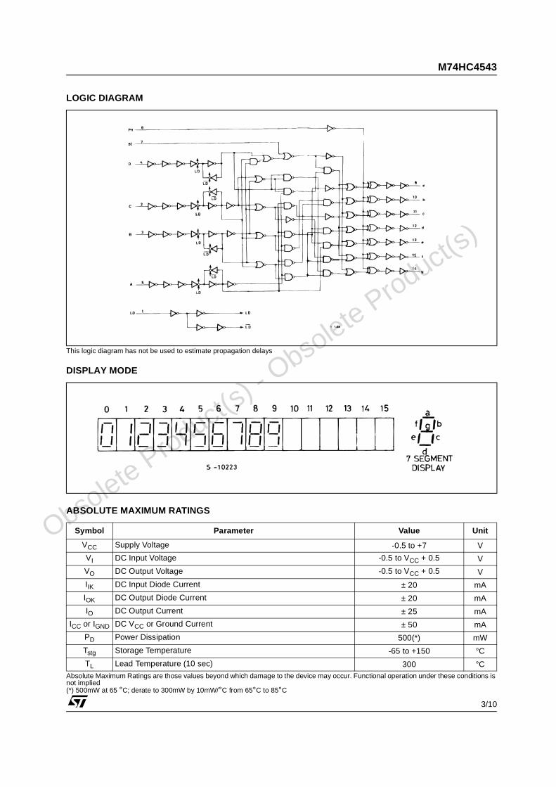
LOGIC DIAGRAM
This logic diagram has not be used to estimate propagation delays
DISPLAY MODE
ABSOLUTE MAXIMUM RATINGS
Absolute Maximum Ratings are those values beyond which damage to the device may occur. Functional operation under these conditions is not implied(*) 500mW at 65 °C; derate to 300mW by 10mW/°C from 65°C to 85°C
Symbol Parameter Value Unit
VCC Supply Voltage -0.5 to +7 V
VI DC Input Voltage -0.5 to VCC + 0.5 V
VO DC Output Voltage -0.5 to VCC + 0.5 V
IIK DC Input Diode Current ± 20 mA
IOK DC Output Diode Current ± 20 mA
IO DC Output Current ± 25 mA
ICC or IGND DC VCC or Ground Current ± 50 mA
PD Power Dissipation 500(*) mW
Tstg Storage Temperature -65 to +150 °C
TL Lead Temperature (10 sec) 300 °C
O
bsolete Product(
s) - O
bsolete Product(
s)
M74HC4543
4/10
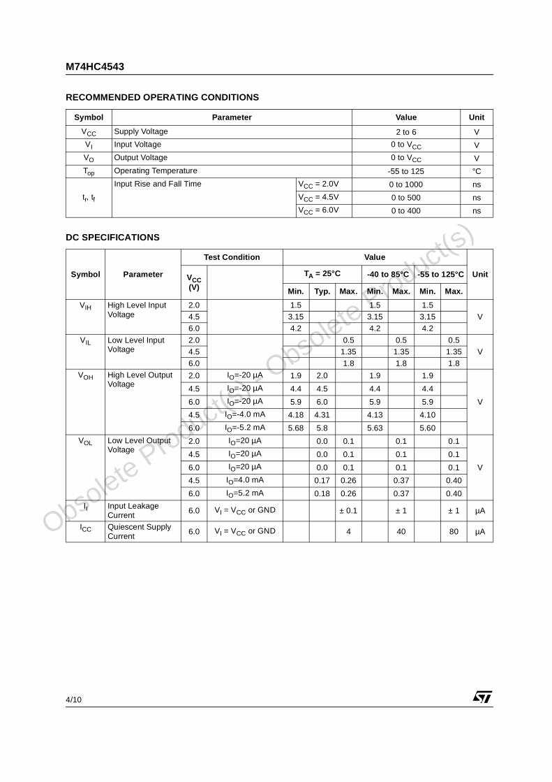
RECOMMENDED OPERATING CONDITIONS
DC SPECIFICATIONS
Symbol Parameter Value Unit
VCC Supply Voltage 2 to 6 V
VI Input Voltage 0 to VCC V
VO Output Voltage 0 to VCC V
Top Operating Temperature -55 to 125 °C
tr, tf
Input Rise and Fall Time VCC = 2.0V 0 to 1000 ns
VCC = 4.5V 0 to 500 ns
VCC = 6.0V 0 to 400 ns
Symbol Parameter
Test Condition Value
UnitVCC(V)
TA = 25°C -40 to 85°C -55 to 125°C
Min. Typ. Max. Min. Max. Min. Max.
VIH High Level Input Voltage
2.0 1.5 1.5 1.5
V4.5 3.15 3.15 3.15
6.0 4.2 4.2 4.2
VIL Low Level Input Voltage
2.0 0.5 0.5 0.5
V4.5 1.35 1.35 1.35
6.0 1.8 1.8 1.8
VOH High Level Output Voltage
2.0 IO=-20 µA 1.9 2.0 1.9 1.9
V
4.5 IO=-20 µA 4.4 4.5 4.4 4.4
6.0 IO=-20 µA 5.9 6.0 5.9 5.9
4.5 IO=-4.0 mA 4.18 4.31 4.13 4.10
6.0 IO=-5.2 mA 5.68 5.8 5.63 5.60
VOL Low Level Output Voltage
2.0 IO=20 µA 0.0 0.1 0.1 0.1
V
4.5 IO=20 µA 0.0 0.1 0.1 0.1
6.0 IO=20 µA 0.0 0.1 0.1 0.1
4.5 IO=4.0 mA 0.17 0.26 0.37 0.40
6.0 IO=5.2 mA 0.18 0.26 0.37 0.40
II Input Leakage Current
6.0 VI = VCC or GND ± 0.1 ± 1 ± 1 µA
ICC Quiescent Supply Current
6.0 VI = VCC or GND 4 40 80 µA
O
bsolete Product(
s) - O
bsolete Product(
s)
M74HC4543
5/10
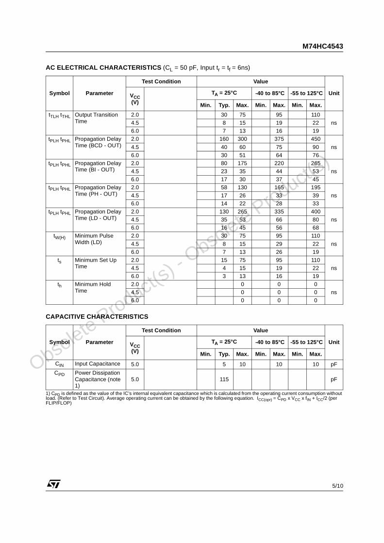
AC ELECTRICAL CHARACTERISTICS (CL = 50 pF, Input tr = tf = 6ns)
CAPACITIVE CHARACTERISTICS
1) CPD is defined as the value of the IC’s internal equivalent capacitance which is calculated from the operating current consumption without load. (Refer to Test Circuit). Average operating current can be obtained by the following equation. ICC(opr) = CPD x VCC x fIN + ICC/2 (per FLIP/FLOP)
Symbol Parameter
Test Condition Value
UnitVCC(V)
TA = 25°C -40 to 85°C -55 to 125°C
Min. Typ. Max. Min. Max. Min. Max.
tTLH tTHL Output Transition Time
2.0 30 75 95 110
ns4.5 8 15 19 22
6.0 7 13 16 19
tPLH tPHL Propagation Delay Time (BCD - OUT)
2.0 160 300 375 450
ns4.5 40 60 75 90
6.0 30 51 64 76
tPLH tPHL Propagation Delay Time (BI - OUT)
2.0 80 175 220 265
ns4.5 23 35 44 53
6.0 17 30 37 45
tPLH tPHL Propagation Delay Time (PH - OUT)
2.0 58 130 165 195
ns4.5 17 26 33 39
6.0 14 22 28 33
tPLH tPHL Propagation Delay Time (LD - OUT)
2.0 130 265 335 400
ns4.5 35 53 66 80
6.0 16 45 56 68
tW(H) Minimum Pulse Width (LD)
2.0 30 75 95 110
ns4.5 8 15 29 22
6.0 7 13 26 19
ts Minimum Set Up Time
2.0 15 75 95 110
ns4.5 4 15 19 22
6.0 3 13 16 19
th Minimum Hold Time
2.0 0 0 0
ns4.5 0 0 0
6.0 0 0 0
Symbol Parameter
Test Condition Value
UnitVCC(V)
TA = 25°C -40 to 85°C -55 to 125°C
Min. Typ. Max. Min. Max. Min. Max.
CIN Input Capacitance 5.0 5 10 10 10 pF
CPD Power Dissipation Capacitance (note 1)
5.0 115 pF O
bsolete Product(
s) - O
bsolete Product(
s)
M74HC4543
6/10
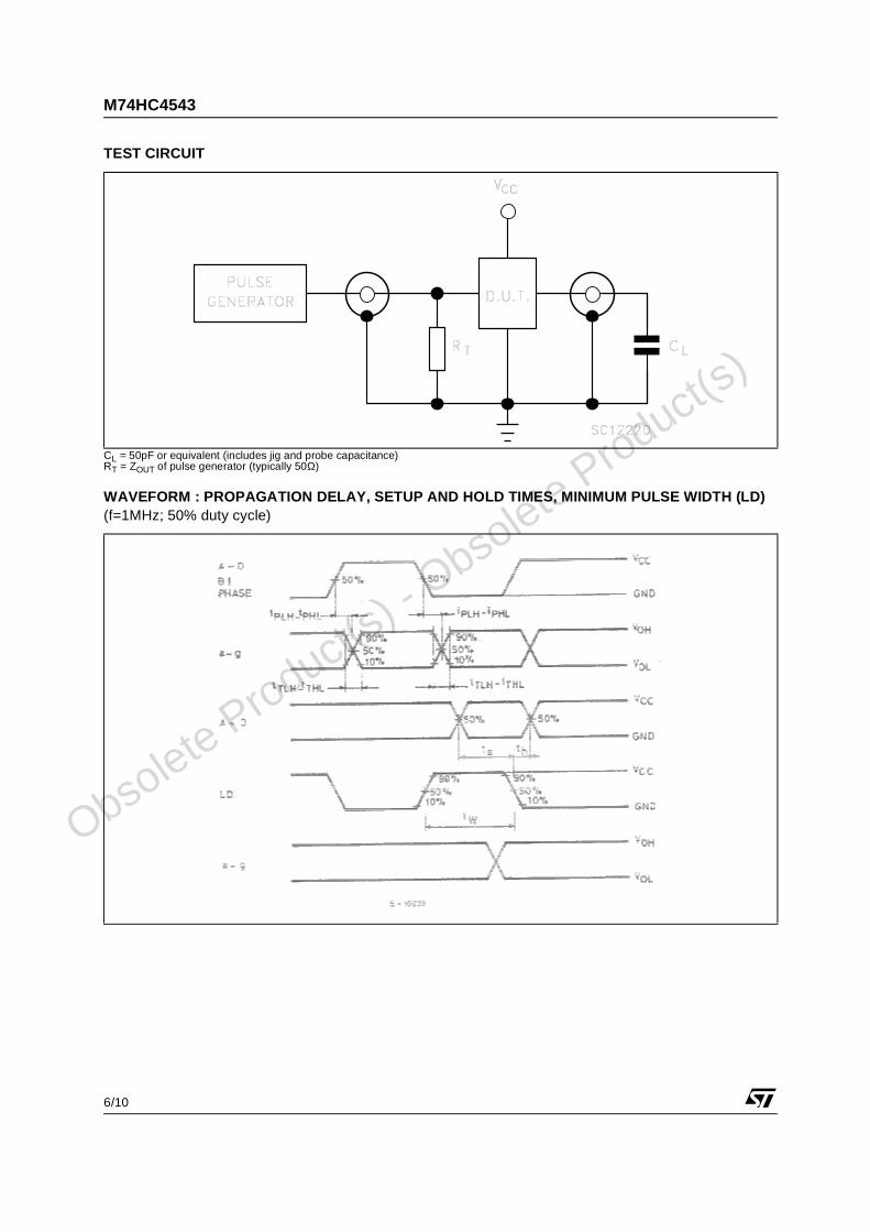
TEST CIRCUIT
CL = 50pF or equivalent (includes jig and probe capacitance)RT = ZOUT of pulse generator (typically 50Ω)
WAVEFORM : PROPAGATION DELAY, SETUP AND HOLD TIMES, MINIMUM PULSE WIDTH (LD) (f=1MHz; 50% duty cycle)
O
bsolete Product(
s) - O
bsolete Product(
s)
M74HC4543
7/10
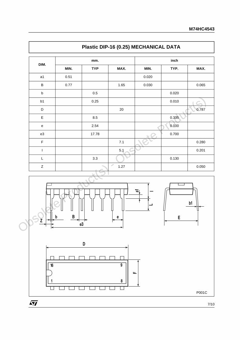
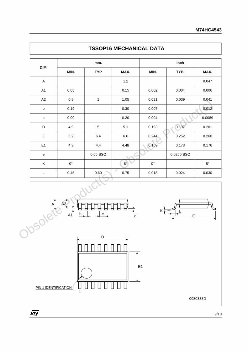
DIM.mm. inch
MIN. TYP MAX. MIN. TYP. MAX.
a1 0.51 0.020
B 0.77 1.65 0.030 0.065
b 0.5 0.020
b1 0.25 0.010
D 20 0.787
E 8.5 0.335
e 2.54 0.100
e3 17.78 0.700
F 7.1 0.280
I 5.1 0.201
L 3.3 0.130
Z 1.27 0.050
Plastic DIP-16 (0.25) MECHANICAL DATA
P001C
O
bsolete Product(
s) - O
bsolete Product(
s)

M74HC4543
8/10
DIM.mm. inch
MIN. TYP MAX. MIN. TYP. MAX.
A 1.75 0.068
a1 0.1 0.2 0.003 0.007
a2 1.65 0.064
b 0.35 0.46 0.013 0.018
b1 0.19 0.25 0.007 0.010
C 0.5 0.019
c1 45° (typ.)
D 9.8 10 0.385 0.393
E 5.8 6.2 0.228 0.244
e 1.27 0.050
e3 8.89 0.350
F 3.8 4.0 0.149 0.157
G 4.6 5.3 0.181 0.208
L 0.5 1.27 0.019 0.050
M 0.62 0.024
S 8° (max.)
SO-16 MECHANICAL DATA
PO13H
O
bsolete Product(
s) - O
bsolete Product(
s)
M74HC4543
9/10
DIM.mm. inch
MIN. TYP MAX. MIN. TYP. MAX.
A 1.2 0.047
A1 0.05 0.15 0.002 0.004 0.006
A2 0.8 1 1.05 0.031 0.039 0.041
b 0.19 0.30 0.007 0.012
c 0.09 0.20 0.004 0.0089
D 4.9 5 5.1 0.193 0.197 0.201
E 6.2 6.4 6.6 0.244 0.252 0.260
E1 4.3 4.4 4.48 0.169 0.173 0.176
e 0.65 BSC 0.0256 BSC
K 0° 8° 0° 8°
L 0.45 0.60 0.75 0.018 0.024 0.030
TSSOP16 MECHANICAL DATA
c Eb
A2A
E1
D
1PIN 1 IDENTIFICATION
A1LK
e
0080338D
O
bsolete Product(
s) - O
bsolete Product(
s)

M74HC4543
10/10
Information furnished is believed to be accurate and reliable. However, STMicroelectronics assumes no responsibility for theconsequences of use of such information nor for any infringement of patents or other rights of third parties which may result fromits use. No license is granted by implication or otherwise under any patent or patent rights of STMicroelectronics. Specificationsmentioned in this publication are subject to change without notice. This publication supersedes and replaces all informationpreviously supplied. STMicroelectronics products are not authorized for use as critical components in life support devices orsystems without express written approval of STMicroelectronics.
© The ST logo is a registered trademark of STMicroelectronics
© 2001 STMicroelectronics - Printed in Italy - All Rights ReservedSTMicroelectronics GROUP OF COMPANIES
Australia - Brazil - China - Finland - France - Germany - Hong Kong - India - Italy - Japan - Malaysia - Malta - Morocco Singapore - Spain - Sweden - Switzerland - United Kingdom
© http://www.st.com
O
bsolete Product(
s) - O
bsolete Product(
s)