Latch circuits Questions: 1 through 10 Lab Exercise: SR latc
Upload
khangminh22Category
view
0download
0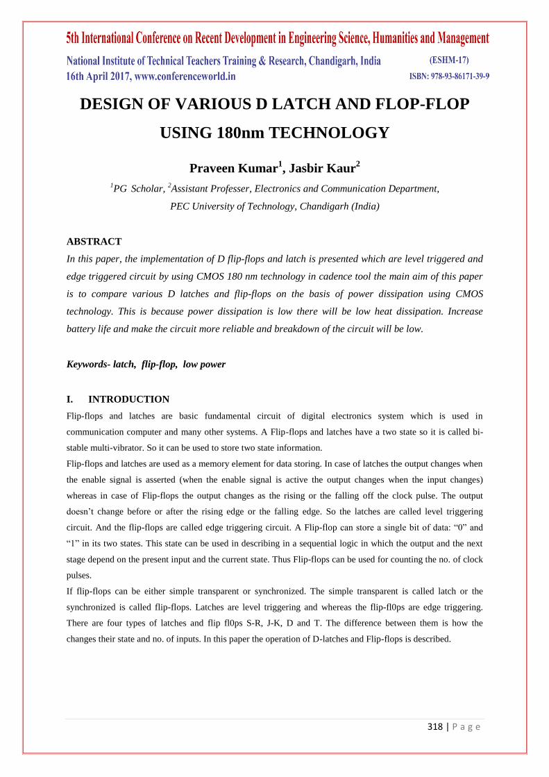
318 | P a g e
DESIGN OF VARIOUS D LATCH AND FLOP-FLOP
USING 180nm TECHNOLOGY
Praveen Kumar1, Jasbir Kaur
2
1PG
Scholar,
2Assistant Professer, Electronics and Communication Department,
PEC University of Technology, Chandigarh (India)
ABSTRACT
In this paper, the implementation of D flip-flops and latch is presented which are level triggered and
edge triggered circuit by using CMOS 180 nm technology in cadence tool the main aim of this paper
is to compare various D latches and flip-flops on the basis of power dissipation using CMOS
technology. This is because power dissipation is low there will be low heat dissipation. Increase
battery life and make the circuit more reliable and breakdown of the circuit will be low.
Keywords- latch, flip-flop, low power
I. INTRODUCTION
Flip-flops and latches are basic fundamental circuit of digital electronics system which is used in
communication computer and many other systems. A Flip-flops and latches have a two state so it is called bi-
stable multi-vibrator. So it can be used to store two state information.
Flip-flops and latches are used as a memory element for data storing. In case of latches the output changes when
the enable signal is asserted (when the enable signal is active the output changes when the input changes)
whereas in case of Flip-flops the output changes as the rising or the falling off the clock pulse. The output
doesn’t change before or after the rising edge or the falling edge. So the latches are called level triggering
circuit. And the flip-flops are called edge triggering circuit. A Flip-flop can store a single bit of data: “0” and
“1” in its two states. This state can be used in describing in a sequential logic in which the output and the next
stage depend on the present input and the current state. Thus Flip-flops can be used for counting the no. of clock
pulses.
If flip-flops can be either simple transparent or synchronized. The simple transparent is called latch or the
synchronized is called flip-flops. Latches are level triggering and whereas the flip-fl0ps are edge triggering.
There are four types of latches and flip fl0ps S-R, J-K, D and T. The difference between them is how the
changes their state and no. of inputs. In this paper the operation of D-latches and Flip-flops is described.
319 | P a g e
II. IMPLEMENTATION OF LATCH AND FLIP-FLOP USING CMOS TECHNOLOGY.
Latch and flip-flop are the most important part of many electronic circuit like counter, Analog to Digital
converter etc. The D flip-flop is by far the most important of the clocked flip-flops as it ensures that ensures that
inputs S and R are never equal to one at the same time. The D-type flip flop are constructed from a gated SR
flip-flop with an inverter added between the S and the R inputs to allow for a single D (data) input.
A. D- Latches
This is the most basic circuit of D latches in S-R latch we have two input, whereas in D latches only one input is
used. At the input of S-R a not gate is connected between S and R. In D-latch Two and gates are required. The
NAND gate which ha step input of the not gate corresponded to the output Q. And other to the Q’. The fig 1(a),
fig 1(b), fig 1(c), shows the circuit diagram, truth table, output waveform respectively.
(a) (b)
(c)
FIG 1. D LATCH (A): LATCH CIRCUIT DIAGRAM (B): TRUTH TABLE (C): TIMING
DIAGRAM
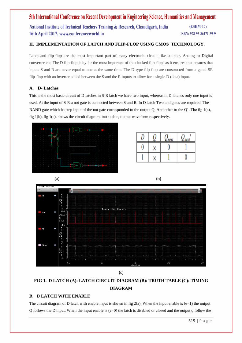
B. D LATCH WITH ENABLE
The circuit diagram of D latch with enable input is shown in fig 2(a). When the input enable is (e=1) the output
Q follows the D input. When the input enable is (e=0) the latch is disabled or closed and the output q follow the
320 | P a g e
last value which is independent of the D input, The truth table is shown in fig 2(b) and the timing diagram is
shown in Fig 2(c).
(a) (b)
(c)
FIG 2. D LATCH WITH ENABLE (A): D LATCH CIRCUIT DIAGRAM (B): TRUTH
TABLE (C): TIMING DIAGRAM
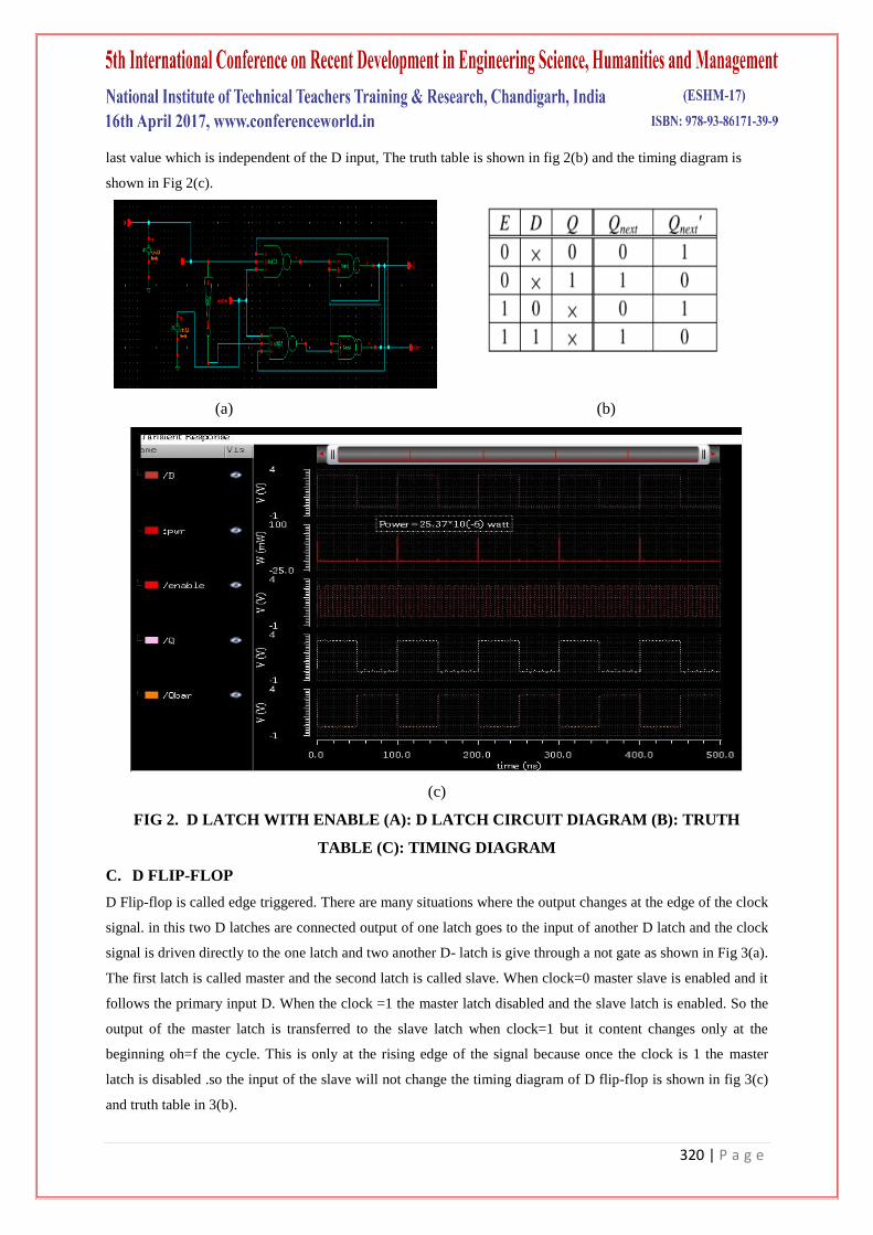
C. D FLIP-FLOP
D Flip-flop is called edge triggered. There are many situations where the output changes at the edge of the clock
signal. in this two D latches are connected output of one latch goes to the input of another D latch and the clock
signal is driven directly to the one latch and two another D- latch is give through a not gate as shown in Fig 3(a).
The first latch is called master and the second latch is called slave. When clock=0 master slave is enabled and it
follows the primary input D. When the clock =1 the master latch disabled and the slave latch is enabled. So the
output of the master latch is transferred to the slave latch when clock=1 but it content changes only at the
beginning oh=f the cycle. This is only at the rising edge of the signal because once the clock is 1 the master
latch is disabled .so the input of the slave will not change the timing diagram of D flip-flop is shown in fig 3(c)
and truth table in 3(b).
321 | P a g e
(a) (b)
(c)
FIG 3. D FLIP-FLOP (A): D FLIP-FLOP CIRCUIT DIAGRAM (B): TRUTH TABLE (C):
TIMING DIAGRAM
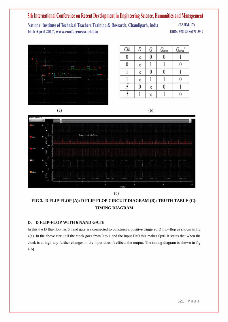
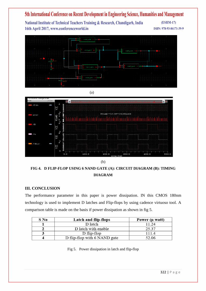
D. D FLIP-FLOP WITH 6 NAND GATE
In this the D flip-flop has 6 nand gate are connected to construct a positive triggered D flip=flop as shown in fig
4(a). In the above circuit if the clock goes from 0 to 1 and the input D=0 this makes Q=0. it states that when the
clock is at high any further changes in the input doesn’t effects the output. The timing diagram is shown in fig
4(b).
322 | P a g e
(a)
(b)
FIG 4. D FLIP-FLOP USING 6 NAND GATE (A): CIRCUIT DIAGRAM (B): TIMING
DIAGRAM
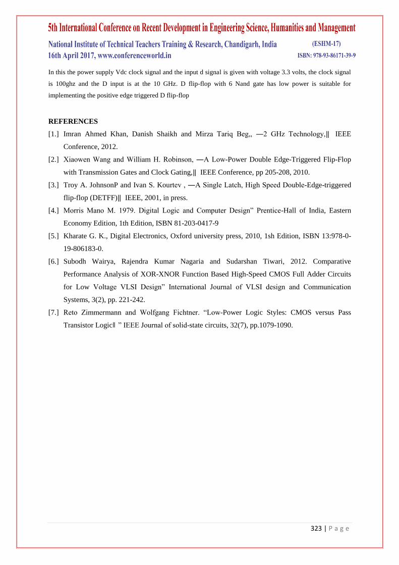
III. CONCLUSION
The performance parameter in this paper is power dissipation. IN this CMOS 180nm
technology is used to implement D latches and Flip-flops by using cadence virtuoso tool. A
comparison table is made on the basis if power dissipation as shown in fig 5.
Fig 5. Power dissipation in latch and flip-flop
323 | P a g e
In this the power supply Vdc clock signal and the input d signal is given with voltage 3.3 volts, the clock signal
is 100ghz and the D input is at the 10 GHz. D flip-flop with 6 Nand gate has low power is suitable for
implementing the positive edge triggered D flip-flop
REFERENCES
[1.] Imran Ahmed Khan, Danish Shaikh and Mirza Tariq Beg,, ―2 GHz Technology,‖ IEEE
Conference, 2012.
[2.] Xiaowen Wang and William H. Robinson, ―A Low-Power Double Edge-Triggered Flip-Flop
with Transmission Gates and Clock Gating,‖ IEEE Conference, pp 205-208, 2010.
[3.] Troy A. JohnsonP and Ivan S. Kourtev , ―A Single Latch, High Speed Double-Edge-triggered
flip-flop (DETFF)‖ IEEE, 2001, in press.
[4.] Morris Mano M. 1979. Digital Logic and Computer Design” Prentice-Hall of India, Eastern
Economy Edition, 1th Edition, ISBN 81-203-0417-9
[5.] Kharate G. K., Digital Electronics, Oxford university press, 2010, 1sh Edition, ISBN 13:978-0-
19-806183-0.
[6.] Subodh Wairya, Rajendra Kumar Nagaria and Sudarshan Tiwari, 2012. Comparative
Performance Analysis of XOR-XNOR Function Based High-Speed CMOS Full Adder Circuits
for Low Voltage VLSI Design” International Journal of VLSI design and Communication
Systems, 3(2), pp. 221-242.
[7.] Reto Zimmermann and Wolfgang Fichtner. “Low-Power Logic Styles: CMOS versus Pass
Transistor Logicǁ ” IEEE Journal of solid-state circuits, 32(7), pp.1079-1090.
Copyright © 2022 FDOKUMEN