1. Explain Various Memory Technologies in detail
36
CS 6303 - Computer Architecture Unit 5 – Q & A 1. Explain Various Memory Technologies in detail The term memory hierarchy is used in computer architecture when discussing performance issues in computer architectural design, algorithm predictions, and the lower level programming constructs such as involving locality of reference. A "memory hierarchy" in computer storage distinguishes each level in the "hierarchy" by response time. Since response time, complexity, and capacity are related, the levels may also be distinguished by the controlling technology. Memory is categorized into volatile and non-volatile memories, with the former requiring constant power ON of the system to maintain data storage. Furthermore, a typical computer system provides a hierarchy of different times of memories for data storage. There are four major storage levels Internal – Processor registers and cache. Main – the system RAM and controller cards. On-line mass storage – Secondary storage. Off-line bulk storage – Tertiary and Off-line storage. SVCET
-
Upload
khangminh22 -
Category
Documents
-
view
0 -
download
0
Transcript of 1. Explain Various Memory Technologies in detail

CS 6303 - Computer Architecture Unit 5 – Q & A
1. Explain Various Memory Technologies in detail
The term memory hierarchy is used in computer architecture when discussing
performance issues in computer architectural design, algorithm predictions, and the
lower level programming constructs such as involving locality of reference.
A "memory hierarchy" in computer storage distinguishes each level in the "hierarchy"
by response time. Since response time, complexity, and capacity are related, the levels
may also be distinguished by the controlling technology.
Memory is categorized into volatile and non-volatile memories, with the former
requiring constant power ON of the system to maintain data storage.
Furthermore, a typical computer system provides a hierarchy of different times of
memories for data storage.
There are four major storage levels
Internal – Processor registers and cache.
Main – the system RAM and controller cards.
On-line mass storage – Secondary storage.
Off-line bulk storage – Tertiary and Off-line storage.
SVCET

CS 6303 - Computer Architecture Unit 5 – Q & A
Internal or cache:
Cache is the fastest accessible memory of a computer system.
Its access speed is in the order of a few nanoseconds.
It is volatile and expensive, so the typical cache size is in the order of megabytes.
Main memory (gb):
Main memory is arguably the most used memory.
The main memory is reasonably fast, with access speed around 100 nanoseconds.
It also offers larger capacity at a lower cost. Typical main memory is in the order of 10
GB. However, the main memory is volatile.
RAM: Random Access Memories are volatile in nature. As soon as the computer is
switched off, the contents of memory are also lost.
ROM: Read only memories are non volatile in nature. The storage is permanent, but
it is read only memory. We cannot store new information in ROM.
Several types of ROM
o PROM: Programmable Read Only Memory; it can be programmed once as per
user requirements.
o EPROM: Erasable Programmable Read Only Memory; the contents of the
memory can be erased and store new data into the memory. In this case,
we have to erase whole information.
o EEPROM: Electrically Erasable Programmable Read Only Memory; in this
type of memory the contents of a particular location can be changed without
effecting the contents of other location.
Online mass storage (or) secondary storage (tb):
Secondary storage refers to non-volatile data storage units that are external to the
computer system. Hard drives and solid state drives are examples of secondary storage.
They offer very large storage capacity in the order of terabytes at very low cost.
Therefore, database servers typically have an array of secondary storage devices with
data stored distributedly and redundantly across these devices.
Modern hard drives have access speed in the order of a few milliseconds.
Off-line bulk storage or tertiary storage (pb):
Tertiary storage refers storage designed for the purpose data backup.
Examples of tertiary storage devices are tape drives are robotic driven disk arrays.
They are capable of petabyte range storage, but have very slow access speed with data
access latency in seconds or minutes.
SVCET

CS 6303 - Computer Architecture Unit 5 – Q & A
MEMORY technologies
There are four primary technologies used today in memory hierarchies. Main memory
is implemented from DRAM (dynamic random access memory), while levels closer to
the processor (caches) use SRAM (static random access memory).
DRAM is less costly per bit than SRAM, although it is substantially slower.
The price difference arises because DRAM uses significantly less area per bit of
memory, and DRAMs thus have larger capacity for the same amount of silicon;
The third technology is flash memory. This non-volatile memory is the secondary
memory in Personal Mobile Devices.
The fourth technology, used to implement the largest and slowest level in the hierarchy
in servers, is magnetic disk.
SRAM Technology
SRAMs are simply integrated circuits that are memory arrays with (usually) a single
access port that can provide either a read or a write.
SRAMs have a fixed access time to any datum, though the read and write access times
may differ.
SRAMs don’t need to refresh and so the access time is very close to the cycle time.
SRAMs typically use six to eight transistors per bit to prevent the information from
being disturbed when read. SRAM needs only minimal power to retain the charge in
standby mode.
In the past, most PCs and server systems used separate SRAM chips for either their
primary, secondary, or even tertiary caches.
DRAM Technology
In a SRAM, as long as power is applied, the value can be kept indefinitely. In a dynamic
RAM (DRAM), the value kept in a cell is stored as a charge in a capacitor.
A single transistor is then used to access this stored charge, either to read the value or
to overwrite the charge stored there.
DRAMs use only a single transistor per bit of storage, they are much denser and cheaper
per bit than SRAM.
As DRAMs store the charge on a capacitor, it cannot be kept indefinitely and must
periodically be refreshed. That is why this memory structure is called dynamic, as
opposed to the static storage in an SRAM cell.
To refresh the cell, we merely read its contents and write it back. The charge can be
kept for several milliseconds.
If every bit had to be read out of the DRAM and then written back individually, we
would constantly be refreshing the DRAM, leaving no time for accessing it.
DRAMs use a two-level decoding structure, and this allows us to refresh an entire row
(which shares a word line) with a read cycle followed immediately by a write cycle.
SVCET

CS 6303 - Computer Architecture Unit 5 – Q & A
Internal organization of a DRAM
Performance of DRAM & SRAM
The row organization that helps with refresh also helps with performance.
To improve performance, DRAMs buffer rows for repeated access. The buffer acts like
an SRAM; by changing the address, random bits can be accessed in the buffer until the
next row access.
This capability improves the access time significantly, since the access time to bits in
the row is much lower.
To further improve the interface to processors, DRAMs added clocks and are properly
called Synchronous DRAMs or SDRAMs.
The advantage of SDRAMs is that the use of clock eliminates the time for the memory
and processor to synchronize.
The speed advantage of synchronous DRAMs comes from the ability to transfer the bits
in the burst without having to specify additional address bits. Instead, the clock transfers
the successive bits in a burst.
Flash Memory
Flash memory is a type of electrically erasable programmable read-only memory
(EEPROM).
Flash memory stores information in an array of memory cells made from floating-gate
transistors.
The floating gate may be conductive (typically polysilicon in most kinds of flash
memory) or non-conductive (as in SONOS flash memory).
In traditional single-level cell (SLC) devices, each cell stores only one bit of
information. Some newer flash memory, known as multi-level cell (MLC) devices,
including triple-level cell (TLC) devices, can store more than one bit per cell by
choosing between multiple levels of electrical charge to apply to the floating gates of
its cells.
Embedded devices also need non-volatile storage, but premiums placed on space and
power normally lead to the use of Flash memory instead of magnetic recording. Flash
memory is also used as a rewritable ROM in embedded systems, typically to allow
software to be upgraded without having to replace chips.
Applications are typically prohibited from writing to Flash memory in such
circumstances.
SVCET

CS 6303 - Computer Architecture Unit 5 – Q & A
Like electrically erasable and programmable read-only memories (EEPROM), Flash
memory is written by inducing the tunneling of charge from transistor gain to a floating
gate.
The floating gate acts as a potential well which stores the charge, and the charge cannot
move from there without applying an external force. The primary difference between
EEPROM and Flash memory is that Flash restricts write to multi-kilobyte blocks,
increasing memory capacity per chip by reducing area dedicated to control. Compared
to disks, Flash memories offer low power consumption (less than 50 milliwatts), can be
sold in small sizes, and offer read access times comparable to DRAMs. In 2001, a 16
Mbit Flash memory has a 65 ns access time, and a 128 Mbit Flash memory has a 150
ns access time.
Disk Memory or Magnetic Memory
Magnetic hard disk consists of a collection of platters, which rotate on a spindle at 5400
to 15,000 revolutions per minute. The metal platters are covered with magnetic
recording material on both sides, similar to the material found on a cassette or
videotape.
To read and write information on a hard disk, a movable arm containing a small
electromagnetic coil called a read-write head is located just above each surface. The
entire drive is permanently sealed to control the environment inside the drive, which,
in turn, allows the disk heads to be much closer to the drive surface.
Each disk surface is divided into concentric circles, called tracks. There are typically
tens of thousands of tracks per surface. Each track is in turn divided into sectors that
contain the information; each track may have thousands of sectors. Sectors are typically
512 to 4096 bytes in size. The sequence recorded on the magnetic media is a sector
number, a gap, the information for that sector including error correction code a gap, the
sector number of the next sector, and so on.
SVCET
CS 6303 - Computer Architecture Unit 5 – Q & A
2. Write short Notes on Memory Hierarchy Levels?
The goal is to present the user with as much memory as is available in the cheapest
technology, while providing access at the speed offered by the fastest memory.
When we move away from the processor, the levels take progressively longer to access.
Data is copied between only two adjacent levels at a time.
The upper level—the one closer to the processor— is smaller and faster Fig. shows that the
minimum unit of information that can be either present or not present in the two-level
hierarchy is called a block or a line.
Block (line): unit of copying, May be multiple words / word / byte. If accessed data is present
in upper level is called as HIT. The hit rate, or hit ratio, is the fraction of memory accesses
found in the upper level.
Hit ratio: hits/accesses
If accessed data is absent in upper level is called as MISS. The lower level in the hierarchy
is then accessed to retrieve the block containing the requested data.
The miss rate (1−hit rate) is the fraction of memory accesses not found in the upper level.
Miss ratio: misses/accesses
Then accessed data supplied from upper level. Hit time is the time to access the upper
level of the memory hierarchy, which includes the time needed to determine whether the
access is a hit or a miss.
The miss penalty is the time to replace a block in the upper level with the corresponding
block from the lower level, plus the time to deliver this block to the processor.
The hit time will be much smaller than the time to access the next level in the
hierarchy(miss penalty), which is the major component of the miss penalty.
SVCET

CS 6303 - Computer Architecture Unit 5 – Q & A
3. Brief about principle of locality? ( 6 marks, or add in any memory related
answer)
Principle of locality states that programs access a relatively small portion of their
address space at any instant of time.
Temporal locality (locality in time): If an item is referenced, it will tend to be
referenced again soon.
Example: If you recently brought a book to your desk to look at, you will probably
need to look at it again soon.
Spatial locality (locality in space): If an item is referenced, items whose addresses
are close by will tend to be referenced soon.
Example: Libraries put books on the same topic together on the same shelves to
increase spatial locality.
Most programs contain loops, so instructions and data are likely to be accessed
repeatedly, showing high amounts of temporal locality.
Sequential accesses to elements of an array or a record will naturally have high degrees
of spatial locality.
SVCET

CS 6303 - Computer Architecture Unit 5 – Q & A
4. Explain cache memory?
Processor is much faster than the main memory. As a result, the processor has to spend
much of its time waiting while instructions and data are being fetched from the main memory.
Major obstacle towards achieving good performance.
Speed of the main memory cannot be increased beyond a certain point. Cache memory
is an architectural arrangement which makes the main memory appear faster to the processor
than it really is.
Cache memory is based on the property of computer programs known as “locality of
reference”. Prefetch the data into cache before the processor needs it. Needs to predict
processor future access requirement. [Locality of Reference]
Locality of Reference
Analysis of programs indicates that many instructions in localized areas of a program
are executed repeatedly during some period of time, while the others are accessed relatively
less frequently. These instructions may be the ones in a loop, nested loop or few procedures
calling each other repeatedly. This is called “locality of reference”.
Temporal locality of reference
Recently executed instruction is likely to be executed again very soon.
Spatial locality of reference:
Instructions with addresses close to a recently instruction are likely to be executed soon.
Use of a cache memory //Basic Cache Operations//
Processor issues a Read request, a block of words is transferred from the main
memory to the cache, one word at a time.
Subsequent references to the data in this block of words are found in the cache.
At any given time, only some blocks in the main memory are held in the cache,
which blocks in the main memory are in the cache is determined by a “mapping
function”.
When the cache is full, and a block of words needs to be transferred from the
main memory, some block of words in the cache must be replaced. This is
determined by a “replacement algorithm”.
Cache Hit
Existence of a cache is transparent to the processor. The processor issues Read
and Write requests in the same manner.
If the data is in the cache it is called a Read or Write hit.
Read Hit
The data is obtained from the cache.
SVCET

CS 6303 - Computer Architecture Unit 5 – Q & A
Write Hit
Cache has a replica of the contents of the main memory.
Contents of the cache and the main memory may be updated simultaneously- The
write- through protocol.
Update the contents of the cache, and mark it as updated by setting a bit known as
the dirty bit or modified bit. The contents of the main memory are updated when the
block is replaced - This is write-back or copy-back protocol.
Cache miss
If the data is not present in the cache, then a Read miss or Write miss occurs.
Read miss
Block of words containing this requested word is transferred from the memory.
After the block is transferred, the desired word is forwarded to the processor.
The desired word may also be forwarded to the processor as soon as it is transferred
without waiting for the entire block to be transferred. This is called load-through or
early- restart.
Write-miss
Write-through protocol is used, then the contents of the main memory are directly.
If write-back protocol is used, the block containing the addressed word is first
brought into the cache. The desired word is overwritten with new information.
Mapping Functions
The process of moving the data from main memory to cache memory is known as
mapping. Mapping functions determine how memory blocks are placed in the cache. A simple
processor example:
Cache consisting of 128 blocks of 16 words each. Total size of cache is 2048 (2K)
words.
Main memory is addressable by a 16-bit address. Main memory has 64K words.
Main memory has 4K blocks of 16 words each.
Three mapping functions:
Direct mapping.
Associative mapping.
Set-associative mapping.
SVCET

CS 6303 - Computer Architecture Unit 5 – Q & A
Direct Mapping
Block j of the main memory maps to j modulo 128 of the cache. 0 maps to 0, 129 maps
to Block 1, 129, 257 are stored in cache block 1 & so on.
More than one memory block is mapped onto the same position in the cache.
May lead to contention for cache blocks even if the cache is not full.
Resolve the contention by allowing new block to replace the old block, leading to a
trivial replacement algorithm.
Memory address is divided into three fields:
• Low order 4 bits determine one of the 16 words in a block.
• When a new block is brought into the cache, the next 7 bits determine
which cache block this new block is placed in.
• High order 5 bits determine which of the possible 32 blocks is currently
present in the cache. These are tag bits.
Simple to implement but not very flexible.
Associative mapping
Main memory block can be placed into any cache position.
Memory address is divided into two fields:
o Low order 4 bits identify the word within a block.
o High order 12 bits or tag bits identify a memory block when it is resident in the
cache.
Flexible, and uses cache space efficiently.
Replacement algorithms can be used to replace an existing block in the cache when the
cache is full.
Cost is higher than direct-mapped cache because of the need to search all 128 patterns
to determine whether a given block is in the cache.
SVCET

CS 6303 - Computer Architecture Unit 5 – Q & A
Set-Associative mapping
Blocks of cache are grouped into sets. Mapping function allows a block of the main
memory to reside in any block of a specific set. Divide the cache into 64 sets, with two
blocks per set. Memory block 0, 64, 128 etc. map to block 0, and they can occupy either
of the two positions.
Memory address is divided into three fields:
o 6 bit field determines the set number.
o High order 6 bit fields are compared to the tag fields of the two blocks in a set.
Set-associative mapping combination of direct and associative mapping. Number of
blocks per set is a design parameter.
• One extreme is to have all the blocks in one set, requiring no set bits
(fully associative mapping).
• Other extreme is to have one block per set, is the same as direct mapping.
The number of blocks per set is decided according to the requirement of the application
used.
Cache that has k blocks per set is referred to as a k-way set associative cache.
A control bit called valid bit must be provided for each block.
Advantage: less expensive.
Replacement Algorithms
Difficult to determine which blocks to kick out.
Least Recently Used (LRU) block.
The cache controller tracks references to all blocks as computation proceeds.
Increase / clear track counters when a hit/miss occurs.
For Associative & Set-Associative Cache.
Which location should be emptied when the cache is full and a miss occurs?
First In First Out (FIFO)
Least Recently Used (LRU)
Distinguish an Empty location from a Full one
Valid Bit
SVCET

CS 6303 - Computer Architecture Unit 5 – Q & A
5. Explain about Improving Cache Performance / Performance
Considerations.
A key design objective of a computer system is to achieve the best possible performance
at the lowest possible cost. Price/performance ratio is a common measure of success.
Performance of a processor depends on:
How fast machine instructions can be brought into the processor for execution.
How fast the instructions can be executed?
Ways to improve the performance:
Memory interleaving.
Improving hit ratio and reducing miss penalty.
Having caches on the processor chip.
Write buffer.
Prefetching.
Look-up free cache.
Memory Interleaving
Divides the memory system into a number of memory modules. Each module has its
own address buffer register (ABR) and data buffer register (DBR).
Arranges addressing so that successive words in the address space are placed in
different modules.
When requests for memory access involve consecutive addresses, the access will be to
different modules.
Since parallel access to these modules is possible, the average rate of fetching words
from the Main Memory can be increased.
Methods of address layouts// Methods to achieve interleaving
Successful access to data in a cache is called hit.
The number of hits stated as a fraction of all attempted accesses is called the hit rate.
Miss rate is the number of misses stated as a fraction of attempted accesses.
The extra time needed to bring the desired information into the cache is called the miss
penalty.
Hit rate can be improved by increasing block size, while keeping cache size constant
Block sizes that are neither very small nor very large give best results.
Miss penalty can be reduced if load-through approach is used when loading new blocks
into cache.
Caches on the processor chip
In high performance processors 2 levels of caches [one for data and another for
instruction] are normally used.
SVCET

CS 6303 - Computer Architecture Unit 5 – Q & A
Average access time in a system with 2 levels of caches is T ave = h1c1+(1-h1)h2c2+(1-
h1)(1-h2)M
Combined cache: increases hit ratio.
Separate cache: increases parallelism.
Write buffer
Write-through:
Each write operation involves writing to the main memory.
If the processor has to wait for the write operation to be complete, it slows down the
processor.
Processor does not depend on the results of the write operation.
Write buffer can be included for temporary storage of write requests.
Processor places each write request into the buffer and continues execution.
If a subsequent Read request references data which is still in the write buffer, then this
data is referenced in the write buffer.
Write-back:
Block is written back to the main memory when it is replaced.
If the processor waits for this write to complete, before reading the new block, it is
slowed down.
Fast write buffer can hold the block to be written, and the new block can be read first.
Prefetching
New data are brought into the processor when they are first needed.
Processor has to wait before the data transfer is complete.
Prefetch the data into the cache before they are actually needed, or a before a Read miss
occurs.
Prefetching can be accomplished through software by including a special instruction in
the machine language of the processor.
Inclusion of prefetch instructions increases the length of the programs.
Prefetching can also be accomplished using hardware:
Circuitry that attempts to discover patterns in memory references and then prefetches
according to this pattern.
Lockup-Free Cache
Prefetching scheme does not work if it stops other accesses to the cache until the
prefetch is completed.
A cache of this type is said to be “locked” while it services a miss.
Cache structure which supports multiple outstanding misses is called a lockup free
cache.
SVCET

CS 6303 - Computer Architecture Unit 5 – Q & A
Since only one miss can be serviced at a time, a lockup free cache must include Recall
that an important challenge in the design of a computer system is to provide a large,
fast memory system at an affordable cost.
Architectural solutions to increase the effective speed and size of the memory system.
Cache memories were developed to increase the effective speed of the memory system.
Virtual memory is an architectural solution to increase the effective size of the memory
system.
Circuits that keep track of all the outstanding misses.
Special registers may hold the necessary information about these misses.
The steps to be taken on an instruction cache miss
1. Send the original PC value (current PC – 4) to the memory.
2. Instruct main memory to perform a read and wait for the memory to complete its access.
3. Write the cache entry, putting the data from memory in the data portion of the entry,
writing the upper bits of the address (from the ALU) into the tag field, and turning the
valid bit on.
4. Restart the instruction execution at the first step, which will refetch the instruction, this
time finding it in the cache.
The control of the cache on a data access is essentially identical: on a miss, we simply stall
the processor until the memory responds with the data.
Scheme -- write-through.
Suppose a store instruction wrote the data into only the data cache (without changing
main memory); then, after the write into the cache, memory would have a different
value from that in the cache.
Now the cache and memory are said to be inconsistent.
To keep main memory and the cache consistent, always data write is performed in both
the memory and the cache.
This will not provide good performance as these memory writes can take 100 CPI
(cycles per Instruction).
One solution to this problem is to use a write buffer. The memory write is done, by
writing the content in the write Buffer. When the buffer data are written in memory,
then that part of the buffer is freed.
Alternative scheme -- write-back.
The new value is written only to the block in the cache. The modified block is written
to the lower level of the hierarchy when it is replaced. Write-back schemes can improve
performance, more complex to implement than write-through.
SVCET

CS 6303 - Computer Architecture Unit 5 – Q & A
6. Write short notes on handling the cache Misses and data inconsistency?
The steps to be taken on an instruction cache miss:
1. Send the original PC value (current PC – 4) to the memory.
2. Instruct main memory to perform a read and wait for the memory to complete its access.
3. Write the cache entry, putting the data from memory in the data portion of the entry,
writing the upper bits of the address (from the ALU) into the tag field, and turning the
valid bit on.
4. Restart the instruction execution at the first step, which will refetch the instruction, this
time finding it in the cache.
The control of the cache on a data access is essentially identical: on a miss, we simply stall
the processor until the memory responds with the data.
Scheme -- write-through.
Suppose a store instruction wrote the data into only the data cache (without changing
main memory); then, after the write into the cache, memory would have a different value from
that in the cache. Now the cache and memory are said to be inconsistent.
To keep main memory and the cache consistent, always data write is performed in both
the memory and the cache. This will not provide good performance as these memory writes
can take 100 CPI (cycles per Instruction).
One solution to this problem is to use a write buffer. The memory write is done, by
writing the content in the write Buffer. When the buffer data are written in memory, then that
part of the buffer is freed.
Alternative scheme -- write-back.
The new value is written only to the block in the cache. The modified block is written
to the lower level of the hierarchy when it is replaced. Write-back schemes can improve
performance, more complex to implement than write-through.
Note
Previous questions include this question
SVCET

CS 6303 - Computer Architecture Unit 5 – Q & A
7. Explain Virtual Memory? (If it is asked for 16 mark include 7th answer)
The main memory can act as a “cache” for the secondary storage, this technique is called
virtual memory.
Need for Virtual Memory
To allow efficient and safe sharing of memory among multiple programs.
Virtual memory role is to protect and ensuring that a program can only read and write
the portions of main memory that have been assigned to it
Virtual memory implements the translation of a program’s address space to physical
addresses. This translation process enforces protection of a program’s address space
Protection
A set of mechanisms for ensuring that multiple processes sharing the processor,
memory, or I/O devices cannot interfere, intentionally or unintentionally, with one
another by reading or writing each other’s data.
It is also used to isolate OS process and user process.
User program
Virtual memory allow a single user program to exceed the size of primary memory.
Programmers divided programs into pieces and then identified the pieces that were
mutually exclusive.
User program control ensures that program never access overlays that are not loaded
and these overlays never exceeds the allocated size of the memory.
Page, Page Fault, Address Translation
A virtual memory block is called a page, and a virtual memory miss is called a page
fault.
The processor produces a virtual address, which is translated by a combination of
hardware and soft ware to a physical address, which inturn can be used to access main
memory. This process is called address mapping or address translation.
Mapping from a virtual to a physical address
SVCET

CS 6303 - Computer Architecture Unit 5 – Q & A
Address Translation
Virtual memory also simplifies loading the program for execution by providing
relocation.
This relocation allows us to load the program anywhere in main memory.
All virtual memory systems uses relocation, the program is divided as a set of fixed-
size blocks (pages), it eliminates the need to find a contiguous block of memory for a
program
instead, the operating system need only find a sufficient number of pages in main
memory.
In virtual memory, the address is broken into a virtual page number and a page
off set. (refer previous diagram)
The physical page number constitutes the upper portion of the physical address,
while the page off set, which is not changed, constitutes the lower portion.
The number of bits in the page off set field determines the page size.
A larger number of virtual pages than physical pages is essentially the concept to show
unbounded amount of virtual memory.
Page fault leads to enormous miss penalty. (millions of clock cycles)
To Design a virtual memory system
1. 1. Pages should be large enough to reduce high access time. Sizes from 4 KiB to 16
KiB are typical today (depends on computer types).
2. The primary technique used here is to allow fully associative placement of pages in
memory.
3. Page faults can be handled in software because the overhead will be small compared to
the disk access time. (it reduces miss penalty)
4. Write-through will not work for virtual memory, since writes take too long. Instead,
virtual memory systems use write-back.
SVCET
CS 6303 - Computer Architecture Unit 5 – Q & A
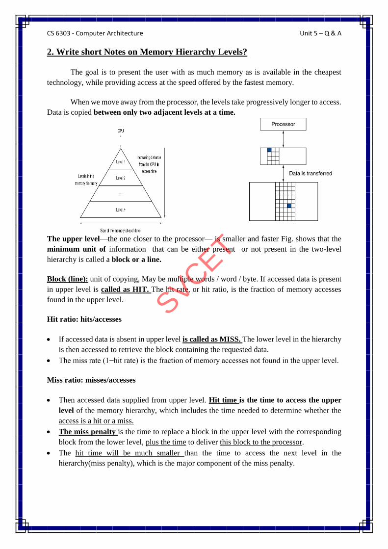
8. Explain Page management in virtual memory and translation
Placing a Page and Finding It Again
Location of pages by using a table that indexes the memory; this structure is called a
page table.(It presents in memory).
A page table is indexed with the page number from the virtual address to discover the
corresponding physical page number.
Each program has its own page table, which maps the virtual address space of that
program to main memory.
To indicate the location of the page table in memory, the hardware includes a register
that points to the start of the page table; we call this the page table register.
(Refer figure)The page table register, the virtual address, and the indicated page Table
shows how the hardware can form a physical address. A valid bit is used in each page
table entry,(as in cache).
If the bit is off , the page is not present in main memory and a page fault occurs.
If the bit is on, the page is in memory and the entry contains the physical page number.
The page table contains a mapping for every possible virtual page, no tags are
required.
Translation Using a Page Table
Handling Page Faults
If the valid bit for a virtual page is off, a page fault occurs.
The OS finds the page in the next level of the hierarchy (usually Secondary device) and
decide where to place the requested page in main memory.
SVCET

CS 6303 - Computer Architecture Unit 5 – Q & A
Swap space & Auxiliary page table
The operating system usually creates the space on secondary devices for all the pages
of a process when it creates the process. This space is called the swap space.
(requirement of page in memory cannot be predicted)To keep track a page table is
created, which may part of the page table or an auxiliary page table is created.
Page Replacement
When a page fault occurs, If all the pages in main memory are in use, the operating
system must choose a page to replace. operating systems follow the least recently
used (LRU) replacement scheme.
The replaced pages are written to swap space on the disk.
To help the operating system estimate the LRU pages, some computers provide a
reference bit or use bit.
Replacements & Writes
In a virtual memory, writes operation in lower level(disk) can take millions of processor
clock cycles; therefore, building a write buffer to allow the system to write-through to
disk would be completely impractical .
So, write-back scheme is used, performing the writes into the page in memory, and
copying the page back to disk.
Dirty bit & Dirty Page
To track whether a page has been written since it was read into the memory, a dirty bit
is added to the page table.
The dirty bit is set when any word in a page is written.
The dirty bit indicates whether the page needs to be written out. (in disk) .
So modified page is often called a dirty page.
SVCET

CS 6303 - Computer Architecture Unit 5 – Q & A
9. Explain about Translation-Lookaside Buffer (TLB)
Page tables are stored in main memory, Memory access by a program can take at least
twice as long.
1. One memory access to obtain the physical Address
2. Second access to get the data.
To improve performance, rely on locality of reference i.e., when a virtual page is
translated, it will be referenced again(due to temporal and spatial locality).
So, special address translation cache is used and is traditionally referred to as a
translation-lookaside buffer (TLB) or translation cache
TLB is accessed instead of the page table on every reference, the TLB will need to
include other status bits, such as the dirty and the reference bits
When a miss in the TLB occurs, we must determine whether it is a page fault or merely
a TLB miss.
If the page exists in memory, then the TLB miss indicates only that the translation is
missing, so the processor can handle the TLB miss by loading the translation from the
page table into the TLB.
If the page is not present in memory, then the TLB miss indicates a true page fault.
Details about TLB
1. TLB size: 16–512 entries
2. Block size: 1–2 page table entries (typically 4–8 bytes each)
3. Hit time: 0.5–1 clock cycle
4. Miss penalty: 10–100 clock
5. cycles Miss rate: 0.01%–1%
SVCET

CS 6303 - Computer Architecture Unit 5 – Q & A
To obtain lower miss rate
• TLB uses small, fully associative mapping (lower miss rate).
• Handling a TLB miss or a page fault requires using the exception mechanism to
interrupt the active process, transferring control to the operating system, and later
resuming execution of the interrupted process.
SVCET

CS 6303 - Computer Architecture Unit 5 – Q & A
10. Write short notes on I/O modules or I/O Organizations?
The computer system's input/output (I/O) architecture is its interface to the outside
world. we have discussed the two important modules of the computer system - The
processor and The memory module.
The third key component of a computer system is a set of I/O modules. Each I/O
module interfaces to the system bus and controls one or more peripheral devices.
There are several reasons why an I/O device or peripheral device is not directly
connected to the system bus. Some of them are as follows -
There are a wide variety of peripherals with various methods of operation. It would be
impractical to include the necessary logic within the processor to control several
devices.
The data transfer rate of peripherals is often much slower than that of the memory or
processor. Thus, it is impractical to use the high-speed system bus to communicate
directly with a peripheral.
Peripherals often use different data formats and word lengths than the computer to
which they are attached.
Thus, an I/O module is required.
Input / Output Modules
The major functions of an I/O module are categorized as follows –
Control and timing
Processor Communication
Device Communication
Data Buffering
Error Detection
Control & timings: The I/O function includes a control and timing requirement to co-
ordinate the flow of traffic between internal resources and external devices. For example, the
control of the transfer of data from an external device to the processor might involve the
following sequence of steps –
1. The processor interacts with the I/O module to check the status of the attached device.
2. The I/O module returns the device status.
3. If the device is operational and ready to transmit, the processor requests the transfer of
data, by means of a command to the I/O module.
4. The I/O module obtains a unit of data from external device.
5. The data are transferred from the I/O module to the processor.
If the system employs a bus, then each of the interactions between the processor and the
I/O module involves one or more bus arbitrations.
SVCET

CS 6303 - Computer Architecture Unit 5 – Q & A
Processor & Device Communication
During the I/O operation, the I/O module must communicate with the processor and
with the external device. Processor communication involves the following -
Command decoding : The I/O module accepts command from the processor, typically sent as
signals on control bus.
Data : Data are exchanged betweeen the processor and the I/O module over the data bus.
Status Reporting : Because peripherals are so slow, it is important to know the status of the
I/O module. For example, if an I/O module is asked to send data to the processor(read), it may
not be ready to do so because it is still working on the previous I/O command. This fact can be
reported with a status signal. Common status signals are BUSY and READY.
Address Recognition : Just as each word of memory has an address, so thus each of the I/O
devices. Thus an I/O module must recognize one unique address for each peripheral it controls.
On the other hand, the I/O must be able to perform device communication. This communication
involves command, status information and data.
Data Buffering
An essential task of an I/O module is data buffering. The data buffering is required
due to the mismatch of the speed of CPU, memory and other peripheral devices. In
general, the speed of CPU is higher than the speed of the other peripheral devices. So, the I/O
modules store the data in a data buffer and regulate the transfer of data as per the speed of the
devices.
In the opposite direction, data are buffered so as not to tie up the memory in a slow
transfer operation. Thus the I/O module must be able to operate at both device and memory
speed.
Error Detection
Another task of I/O module is error detection and for subsequently reporting error to
the processor. One class or error includes mechanical and electrical malfunctions reported by
the device (e.g. paper jam). Another class consists of unintentional changes to the bit pattern
as it is transmitted from devices to the I/O module. Block diagram of I/O Module is shown in
the Figure 6.1.
Figure 6.1: Block diagram of I/O Module.
SVCET
CS 6303 - Computer Architecture Unit 5 – Q & A
11. Write short notes on how I/O are mapped to memory?
There will be many I/O devices connected through I/O modules to the system. Each
device will be identified by a unique address.
When the processor issues an I/O command, the command contains the address of
the device that is used by the command. The I/O module must interpret the address lines to
check if the command is for itself.
Generally in most of the processors, the processor, main memory and I/O share a
common bus(data address and control bus).
Two types of addressing are possible -
1. Memory-mapped I/O
2. Isolated or I/O mapped I/O
Memory-mapped I/O:
There is a single address space for memory locations and I/O devices. The processor
treats the status and address register of the I/O modules as memory location.
For example, if the size of address bus of a processor is 16, then there are
216 combinations and all together 216 address locations can be addressed with these 16 address
lines. Out of these 216 address locations, some address locations can be used to address I/O
devices and other locations are used to address memory locations.
Since I/O devices are included in the same memory address space, so the status and
address registers of I/O modules are treated as memory location by the processor.
Therefore, the same machine instructions are used to access both memory and I/O devices.
Isolated or I/O -mapped I/O:
In this scheme, the full range of addresses may be available for both. The address refers to a
memory location or an I/O device is specified with the help of a command line.
In general command line is used to identify a memory location or an I/O device.
if =1, it indicates that the address present in address bus is the address of an I/O
device.(i.e., IO=1 and M=0)
if =0, it indicates that the address present in address bus is the address of a
memory location.(i.e., IO=0 and M=1)
Since full range of address is available for both memory and I/O devices, so, with 16 address
lines, the system may now support both 216 memory locations and 216 I/O addresses.
(Note: If I/O module is asked for 16 marks try to combine both 10th and 11th question
content)
SVCET
CS 6303 - Computer Architecture Unit 5 – Q & A
12. Brief about I/O subsystems or different I/O system?
There are three basic forms of input and output systems
Programmed I/O
Interrupt driven I/O
Direct Memory Access(DMA)
With programmed I/O, the processor executes a program that gives its direct control of
the I/O operation, including sensing device status, sending a read or write command, and
transferring the data.
With interrupt driven I/O, the processor issues an I/O command, continues to execute other
instructions, and is interrupted by the I/O module when the I/O module completes its work.
In Direct Memory Access (DMA), the I/O module and main memory exchange data directly
without processor involvement.
With both programmed I/O and Interrupt driven I/O, the processor is responsible for
extracting data from main memory for output operation and storing data in main memory for
input operation. To send data to an output device, the CPU simply moves that data to a special
memory location in the I/O address space if I/O mapped input/output is used or to an
address in the memory address space if memory mapped I/O is used.
Memory
I/O device Special
address
space
space
processor is responsible for extracting data
from main memory
SVCET

CS 6303 - Computer Architecture Unit 5 – Q & A
To read data from an input device, the CPU simply moves data from the address (I/O
or memory) of that device into the CPU.
Input/Output Operation: The input and output operation looks very similar to a
memory read or write operation except it usually takes more time since peripheral devices are
slow in speed than main memory modules. The working principle of the three method for input
of a Block of Data is shown in the Figure Working of three techniques for input of block of
data.
SVCET

CS 6303 - Computer Architecture Unit 5 – Q & A
13. Write short notes on DMA?
Programmed I/O and Interrupt-driven I/O methods require the active intervention of the
processor to transfer data between memory and the I/O module, and any data transfer must
transverse a path through the processor. Thus both these forms of I/O suffer from two
inherent drawbacks.
The I/O transfer rate is limited by the speed with which the processor can test and
service a device.
The processor is tied up in managing an I/O transfer; a number of instructions must be
executed for each I/O transfer.
To transfer large block of data at high speed, a special control unit may be provided to
allow transfer of a block of data directly between an external device and the main memory,
without continuous intervention by the processor. This approach is called direct memory
access or DMA.
DMA transfers are performed by a control circuit associated with the I/O device and
this circuit is referred as DMA controller. The DMA controller allows direct data transfer
between the device and the main memory without involving the processor.
To transfer data between memory and I/O devices, DMA controller takes over the
control of the system from the processor and transfer of data take place over the system bus.
For this purpose, the DMA controller must use the bus only when the processor does not need
it, or it must force the processor to suspend operation temporarily.
The later technique is more common and is referred to as cycle stealing, because
the DMA module in effect steals a bus cycle.
The typical block diagram of a DMA controller is shown in the Figure. When the
processor wishes to read or write a block of data, it issues a command to the DMA module,
by sending to the DMA module the following information.
SVCET

CS 6303 - Computer Architecture Unit 5 – Q & A
Whether a read or write is requested, using the read or write control line between the
processor and the DMA module.
The address of the I/O devise involved, communicated on the data lines.
The starting location in the memory to read from or write to, communicated on data
lines and stored by the DMA module in its address register.
The number of words to be read or written again communicated via the data lines and
stored in the data count register.
The processor then continues with other works. It has delegated this I/O operation to
the DMA module. The DMA module checks the status of the I/O devise whose address is
communicated to DMA controller by the processor. If the specified I/O devise is ready for data
transfer, then DMA module generates the DMA request to the processor. Then the processor
indicates the release of the system bus through DMA acknowledge.
The DMA module transfers the entire block of data, one word at a time, directly to or
from memory, without going through the processor. When the transfer is completed, the DMA
module sends an interrupt signal to the processor. After receiving the interrupt signal, processor
takes over the system bus. Thus the processor is involved only at the beginning and end of the
transfer. During that time the processor is suspended.
It is not required to complete the current instruction to suspend the processor. The
processor may be suspended just after the completion of the current bus cycle. On the other
hand, the processor can be suspended just before the need of the system bus by the processor,
because DMA controller is going to use the system bus, it will not use the processor. The point
where in the instruction cycle the processor may be suspended shown in the Figure 6.10.
DMA break point
When the processor is suspended, then the DMA module transfer one word and return
control to the processor. Note that, this is not an interrupt, the processor does not save a context
and do something else. Rather, the processor pauses for one bus cycle. During that time
processor may perform some other task which does not involve the system bus. In the worst
situation processor will wait for some time, till the DMA releases the bus.
The net effect is that the processor will go slow. But the net effect is the enhancement
of performance, because for a multiple word I/O transfer, DMA is far more efficient than
interrupt driven or programmed I/O.
SVCET
CS 6303 - Computer Architecture Unit 5 – Q & A
The DMA mechanism can be configured in different ways. The most common amongst them
are:
Single bus, detached DMA - I/O configuration.
Single bus, Integrated DMA - I/O configuration.
Using separate I/O bus.
Single bus, detached DMA - I/O configuration:
In this organization all modules share the same system bus. The DMA module here acts
as a surrogate processor. This method uses programmed I/O to exchange data between memory
and an I/O module through the DMA module.
For each transfer it uses the bus twice. The first one is when transferring the data
between I/O and DMA and the second one is when transferring the data between DMA and
memory. Since the bus is used twice while transferring data, so the bus will be suspended twice.
The transfer consumes two bus cycle.
Single bus arrangement for DMA transfer
Single bus, Integrated DMA - I/O configuration:
By integrating the DMA and I/O function the number of required bus cycle can be
reduced. In this configuration, the DMA module and one or more I/O modules are integrated
together in such a way that the system bus is not involved. In this case DMA logic may actually
be a part of an I/O module, or it may be a separate module that controls one or
more I/O modules.
The DMA module, processor and the memory module are connected through the system
bus. In this configuration each transfer will use the system bus only once and so the processor
is suspended only once. The system bus is not involved when transferring data between DMA
and I/O device, so processor is not suspended. Processor is suspended when data is transferred
between DMA and memory.
Figure
Single bus integrated DMA transfer
SVCET

CS 6303 - Computer Architecture Unit 5 – Q & A
Using separate I/O bus
In this configuration the I/O modules are connected to the DMA through
another I/O bus. In this case the DMA module is reduced to one. Transfer of data
between I/O module and DMA module is carried out through this I/O bus.
In this transfer, system bus is not in use and so it is not needed to suspend the processor. There
is another transfer phase between DMA module and memory. In this time system bus is needed
for transfer and processor will be suspended for one bus cycle.
Separate I/O bus for DMA transfer
SVCET

CS 6303 - Computer Architecture Unit 5 – Q & A
14. write short notes on I/O Processors (IOP)
A specialized processor, Not only loads and stores into memory but also can execute
instructions, which are among a set of I/O instructions.
The IOP interfaces to the system and device.
The sequence of events involved in I/O transfers to move or operate the results of an
I/O operation into the main memory (using a program for IOP, which is also in main
memory)
Used to address the problem of direct transfer after executing the necessary format
conversion or other instructions.
In an IOP-based system, I/O devices can directly access the memory without
intervention by the processor
IOP Instructions
Instructions help in format conversions ─ byte from memory as packed decimals to the
output device for line-printer.
The I/O device data in different format can be transferred to main memory using an
IOP.
Sequence of events involved in I/O transfers using IOP
Figure below shows the sequence of events involved in I/O transfers
Figure The sequence of events involved in I/O transfers
SVCET

CS 6303 - Computer Architecture Unit 5 – Q & A
Sequence of events involved in I/O transfers using IOP
Sequence 1: A DRQ (for IOP request) signal from an IOP device starts the IOP
sequence, the IOP signals an interrupt on INTR line this requests attention from the
processor.
Sequence 2: The processor responds by checking the device’s status via the memory-
mapped control registers and issues a command telling the IOP to execute IOP
instructions for the transfer to move the formatted data into the memory.
Sequence 3: During each successive formatted byte(s) transfer, the device DMAC
(DMA controller) logic inside the IOP uses a processor bushold request line, HOLD,
distinct from INTR device interrupt request line.
o The main processor sends to the device a signal from the processor called
DACK (distinct from INTA device-interrupt request-acknowledge line).
o The I/O device bus has access to the address and data buses of the memory bus
when DACK is activated.
o It has no access when DACK is not activated when a HOLD request is not
accepted by the processor when the processor is using the memory bus.
o Once the DMA logic start command has been issued to IOP, the main processor
begins working on something else while the I/O device transfers the data into
the memory.
Sequence 4: When the IOP’s DMA transfer as per instructions is complete, the I/O
device signals another interrupt (using DRQ).
o Lets the main processor know that the DMA is done and it may access the data.
SVCET

CS 6303 - Computer Architecture Unit 5 – Q & A
15. Discuss the design Issues for implementing Interrupt I/O and methods
to solve issues.
Two design issues arise in implementing interrupt I/O.
1. When multiple I/O modules, the processor needs to know / identify which device
issued the interrupt.
2. If multiple interrupts have occurred the processor needs to map interrupt and the
process.
Device Identification (for issue 1, multiple I/O modules)
Four general categories of techniques are in common use:
Multiple interrupt lines.
Software poll.
Daisy chain. (hardware poll, vectored)
Bus arbitration. (vectored)
Multiple Interrupts Lines:
The straightest forward approach is to provide multiple interrupt lines between the
processor and the I/O modules.
It is impractical to dedicate more than a few bus lines or processor pins to interrupt
lines.
Thus, though multiple interrupt lines are used, it is most likely that each line will have
multiple I/O modules attached to it. Thus one of the other three techniques must be
used on each line.
Software Poll
When the processor detects an interrupt, it branches to an interrupt service routine
whose job is to poll each I/O module to determine which module caused the interrupt.
The poll could be implemented with the help of a separate command line (e.g. TEST
I/O). In this case, the processor raises TEST I/O and place the address of a particular
I/O module on the address lines. The I/O module responds positively if it set the
interrupt.
Alternatively, each I/O module could contain an addressable status register. The
processor then reads the status register of each I/O module to identify the interrupting
module.
Once the correct module is identified, the processor branches to a device service routine
specific to that device.
The main disadvantage of software poll is that it is time consuming. Processor has
to check the status of each I/O module and in the worst case it is equal to the number
of I/O modules.
SVCET

CS 6303 - Computer Architecture Unit 5 – Q & A
Daisy Chain :
In this method for interrupts all I/O modules share a common interrupt request lines.
However the interrupt acknowledge line is connected in a daisy chain fashion. When
the processor senses an interrupt, it sends out an interrupt acknowledgement.
The interrupt acknowledge signal propagates through a series of I/O module until it
gets to a requesting module.
The requesting module typically responds by placing a word on the data lines. This
word is referred to as a vector and is either the address of the I/O module or some
other unique identification.
In either case, the processor uses the vector as a pointer to the appropriate device
service routine. This avoids the need to execute a general interrupt service routine first.
This technique is referred to as a vectored interrupt. The daisy chain arrangement
is shown in the Figure.
Daisy chain arrangement
where INTR - Interrupt request, INTA - Interrupt acknowledge.
Bus Arbitration
In bus arbitration method, an I/O module must first gain control of the bus before it
can raise the interrupt request line. Thus, only one module can raise the interrupt line at a
time. When the processor detects the interrupt, it responds on the interrupt acknowledge line.
The requesting module then places it vector on the data line.
Handling multiple interrupts (for issue 2, multiple interrupts)
There are several techniques to identify the requesting I/O module. These techniques
also provide a way of assigning priorities when more than one device is requesting interrupt
service.
With multiple lines, the processor just picks the interrupt line with highest priority.
During the processor design phase itself priorities may be assigned to each interrupt lines.
With software polling, the order in which modules are polled determines their priority.
In case of daisy chain configuration, the priority of a module is determined by the position
of the module in the daisy chain. The module nearer to the processor in the chain has got
higher priority, because this is the first module to receive the acknowledge signal that is
generated by the processor.
SVCET

CS 6303 - Computer Architecture Unit 5 – Q & A
In case of bus arbitration method, more than one module may need control of the bus.
Since only one module at a time can successfully transmit over the bus, some method of
arbitration is needed. The various methods can be classified into two group – centralized
and distributed.
In a centralized scheme, a single hardware device, referred to as a bus controller or
arbiter is responsible for allocating time on the bus. The device may be a separate module or
part of the processor.
In distributed scheme, there is no central controller. Rather, each module contains
access control logic and the modules act together to share the bus.
It is also possible to combine different device identification techniques to identify the
devices and to set the priorities of the devices. As for example multiple interrupt lines and daisy
chain technologies can be combined together to give access for more devices.
In one interrupt line, more than one device can be connected in daisy chain fashion. The
High priorities devices should be connected to the interrupt lines that has got higher priority.
Possible arrangement to handle multiple interrupt.
Interrupt Nesting
The arrival of an interrupt request from an external device causes the processor to
suspend the execution of one program and starts the execution of another. The execution of
this another program is nothing but the interrupt service routine for that specified device.
Interrupt may arrive at any time. So during the execution of an interrupt service routine,
another interrupt may arrive. This kind of interrupts are known as nesting of interrupt.
Generally nesting of interrupt is allowed, but with some restrictions. The common
problem is that a high priority device may interrupt a low priority device, but not the vice-
versa. The processor provides some instructions to enable the interrupt and disable the
interrupt.
If interrupt is disabled, the CPU will not respond to any interrupt signal. When
multiple lines are used for interrupt and priorities are assigned to these lines, then the interrupt
received in a low priority line will not be served if an interrupt routine is in execution for
a high priority device (Low priority has to wait).
SVCET

CS 6303 - Computer Architecture Unit 5 – Q & A
SVCET