Prediction of microelectronic substrate warpage using homogenized finite element models
13
Prediction of microelectronic substrate warpage using homogenized finite element models Parsaoran Hutapea a, * , Joachim L. Grenestedt b , Mitul Modi c , Michael Mello c , Kristopher Frutschy c a Department of Mechanical Engineering, Temple University, 1947 N 12th Street, Philadelphia, PA 19122, United States b Department of Mechanical Engineering and Mechanics, Lehigh University, Bethlehem, PA 18015, United States c Assembly Technology Development, Intel Corporation, Chandler, AZ 85226, United States Received 26 August 2005; received in revised form 20 November 2005; accepted 16 December 2005 Available online 10 January 2006 Abstract The focus of this study was to numerically predict effective thermo-mechanical properties and substrate warpage of high-density microelectronic substrates used in organic CPU packages. Microelectronic substrates are typically composed of several polymer, fiber-weave, and copper layers and are filled with a variety of complex features, such as electric traces, plated-through-holes, micro-vias, and adhesion holes. When subjected to temperature changes, these substrates may warp, driven by the mismatch in coefficients of ther- mal expansion (CTE) of the constituent materials. This study focused on predicting substrate warpage in an isothermal condition. The numerical approach consisted of three major tasks: estimating homogenized (effective) thermo-mechanical properties of the features; cal- culating effective properties of discretized layers using the effective properties of the features; and assembling the layers to create two- dimensional (2D) finite element (FE) plate models and to calculate warpage of the substrates. The effective properties of the features were extracted from three-dimensional (3D) unit cell FE models, and closed-form approximate expressions were developed using the numerical results, curve fitting, and some simple bounds. The numerical approach was applied to predict warpage of production sub- strates, analyzed, and validated against experimentally measured stiffness and CTEs. In this paper, the homogenization approach, numerical predictions, and experimental validation are discussed. Ó 2005 Elsevier B.V. All rights reserved. Keywords: Microelectronic substrates; Reliability; Thermo-mechanical; Finite element 1. Introduction The objective of the present work was to predict effective thermo-mechanical properties and isothermal warpage of high-density microelectronic substrates used in organic CPU packages (Fig. 1(a) and (b)). In principle, the numer- ical method used in this work is similar to the method that was previously developed by Grenestedt and Hutapea [1–4] for predicting isothermal warpage of a production printed circuit board (PCB) fabricated using X-Y routing method [5]. The objectives of the previous work were to estimate the effective properties of the copper layers and, using the effective properties, to develop simplified 2D. Finite ele- ment (FE) plate models of the PCB to be used simulta- neously with an optimization procedure to reduce the PCB warpage. The classical lamination theory [6] was used to model the PCB. However, in the previous work, only electric trace was considered as the main substrate feature by neglecting other PCB features, such as vias, copper pads, adhesion holes, etc. The optimization of the PCB electric artworks was done by changing only electric trace widths and/or spacing to find a PCB with the least warpage. It should be mentioned that 3D FE analyses may be used for such modeling and tuning, but the 0167-9317/$ - see front matter Ó 2005 Elsevier B.V. All rights reserved. doi:10.1016/j.mee.2005.12.009 * Corresponding author. Tel.: +1 2152047805; fax: +1 2152044956. E-mail address: [email protected] (P. Hutapea). www.elsevier.com/locate/mee Microelectronic Engineering 83 (2006) 557–569
-
Upload
independent -
Category
Documents
-
view
0 -
download
0
Transcript of Prediction of microelectronic substrate warpage using homogenized finite element models

www.elsevier.com/locate/mee
Microelectronic Engineering 83 (2006) 557–569
Prediction of microelectronic substrate warpage usinghomogenized finite element models
Parsaoran Hutapea a,*, Joachim L. Grenestedt b, Mitul Modi c,Michael Mello c, Kristopher Frutschy c
a Department of Mechanical Engineering, Temple University, 1947 N 12th Street, Philadelphia, PA 19122, United Statesb Department of Mechanical Engineering and Mechanics, Lehigh University, Bethlehem, PA 18015, United States
c Assembly Technology Development, Intel Corporation, Chandler, AZ 85226, United States
Received 26 August 2005; received in revised form 20 November 2005; accepted 16 December 2005Available online 10 January 2006
Abstract
The focus of this study was to numerically predict effective thermo-mechanical properties and substrate warpage of high-densitymicroelectronic substrates used in organic CPU packages. Microelectronic substrates are typically composed of several polymer,fiber-weave, and copper layers and are filled with a variety of complex features, such as electric traces, plated-through-holes, micro-vias,and adhesion holes. When subjected to temperature changes, these substrates may warp, driven by the mismatch in coefficients of ther-mal expansion (CTE) of the constituent materials. This study focused on predicting substrate warpage in an isothermal condition. Thenumerical approach consisted of three major tasks: estimating homogenized (effective) thermo-mechanical properties of the features; cal-culating effective properties of discretized layers using the effective properties of the features; and assembling the layers to create two-dimensional (2D) finite element (FE) plate models and to calculate warpage of the substrates. The effective properties of the featureswere extracted from three-dimensional (3D) unit cell FE models, and closed-form approximate expressions were developed using thenumerical results, curve fitting, and some simple bounds. The numerical approach was applied to predict warpage of production sub-strates, analyzed, and validated against experimentally measured stiffness and CTEs. In this paper, the homogenization approach,numerical predictions, and experimental validation are discussed.� 2005 Elsevier B.V. All rights reserved.
Keywords: Microelectronic substrates; Reliability; Thermo-mechanical; Finite element
1. Introduction
The objective of the present work was to predict effectivethermo-mechanical properties and isothermal warpage ofhigh-density microelectronic substrates used in organicCPU packages (Fig. 1(a) and (b)). In principle, the numer-ical method used in this work is similar to the method thatwas previously developed by Grenestedt and Hutapea [1–4]for predicting isothermal warpage of a production printedcircuit board (PCB) fabricated using X-Y routing method
0167-9317/$ - see front matter � 2005 Elsevier B.V. All rights reserved.
doi:10.1016/j.mee.2005.12.009
* Corresponding author. Tel.: +1 2152047805; fax: +1 2152044956.E-mail address: [email protected] (P. Hutapea).
[5]. The objectives of the previous work were to estimatethe effective properties of the copper layers and, using theeffective properties, to develop simplified 2D. Finite ele-ment (FE) plate models of the PCB to be used simulta-neously with an optimization procedure to reduce thePCB warpage. The classical lamination theory [6] was usedto model the PCB. However, in the previous work, onlyelectric trace was considered as the main substrate featureby neglecting other PCB features, such as vias, copperpads, adhesion holes, etc. The optimization of the PCBelectric artworks was done by changing only electric tracewidths and/or spacing to find a PCB with the leastwarpage. It should be mentioned that 3D FE analysesmay be used for such modeling and tuning, but the

Fig. 1. (a) A microelectronic substrate, (b) a cross-sectional area, and (c)–(f) cross-sectional photos of substrate features.
558 P. Hutapea et al. / Microelectronic Engineering 83 (2006) 557–569
computational effort would be too overwhelming for suchan optimization procedure. The numerical predictions wereconfirmed with some experimental work and showed rea-sonable agreements [3,4].
Microelectronic substrates, in this case, were more com-plex and much smaller than the PCBs. In addition to elec-tric traces, other substrate features, such as micro-vias,plated-through-holes (PTH), and adhesion holes(Fig. 1(c)–(f)) must be considered in the numerical homog-enization procedure. From some experiments, these addi-tional features were found to significantly influence thewarpage of the substrates as much as the electric trace[7,8]. Thus, the major task of this work was to calculateeffective thermo-mechanical properties of substrate fea-
Fig. 2. Steps for the substrate
tures using three-dimensional (3D) FE unit cell analyses[1–4]. In this paper, analytical models of effective thermo-mechanical properties of microelectronic substrate featuresare presented. In summary, the numerical approach wasperformed in three steps: estimating effective thermo-mechanical properties of the features; calculating effectiveproperties of a discretized layer using the effective proper-ties of the features; and assembling the layers to create2D FE plate models and to calculate warpage of the wholesubstrates. These steps were illustrated in Fig. 2.
The details of the determination of the effective thermo-mechanical properties are presented in Section 2. Using theeffective properties, simplified 2D FE analyses to predictsubstrate warpage are discussed in Section 3. Finally,
homogenization method.

P. Hutapea et al. / Microelectronic Engineering 83 (2006) 557–569 559
experimental verifications of the numerical prediction wereperformed to confirm the predictive results and these arepresented in Section 4.
2. Analytical models of effective thermo-mechanical
properties of substrate features
The basic concept was to derive analytical models ofeffective properties of a lamina in a substrate and use theeffective properties in conjunction with classical laminationtheory to estimate thermo-mechanical properties of thesubstrate. The effective properties were extracted from full3D unit cell models of substrate features, for example, asshown in Figs. 3–6. The microelectronic substrates usedwere composed of eight copper layers, seven dielectric lay-ers as the intermediate layers, and a core layer consisting ofPTHs as shown in Fig. 1(b). The substrate consisted ofmaterials, such as woven glass/epoxy (FR4) typically usedfor the core, copper for the electric traces, micro-via andPTH plating, a built-up-film (BUF) polymer material forthe copper and dielectric layers, and a plug material forthe PTH. The properties of these materials were given inTable 1 and assumed to be independent of temperaturechanges. Note that this assumption should be sufficientfor the current work, since the working temperature wasthe glass transition temperature of the materials [9].
2.1. Effective properties obtained from FE unit cell analysis
Electric trace FE models, as shown in Fig. 3, had eightlayers with copper traces in alternating direction. The
Fig. 3. 3D FE unit cell model of electric trace. Black indicates copper trace, whThere are no PTHs, micro-vias, or adhesion holes in this model.
copper layers were separated by dielectric layers modeledusing BUF materials, and a core layer consisting of PTHs.The stack, as illustrated in Fig. 1(b), consisted of eight0.015-mm thick copper layers, separated by 0.03-mm thickdielectric layers and PTH layer, resulting in a total sub-strate thickness of 1.12 mm. The in-plane size of the modelwas w · w, where w was varied from 0.0254 to 2.54 mm forthe case, where the trace width, h, was 0.0254 mm and from0.0834 to 83.4 mm for the case, where h was 0.0834 mm.The effective properties of the lamina with copper traceswere extracted as a function of h/w, which was variedbetween h/w = 0% and h/w = 100%.
The PTH filled in the core layer which occupies 80% ofthe volume. The height of the PTH was 0.8 mm andenclosed with a circular caps of 0.45 mm in diameter onthe top and the bottom of the PTH. The PTH was filledwith a plug material. The detail of the PTH geometry isshown in Fig. 4. The effective properties were extractedas a function of d/w, where d was the cap diameter,0.45 mm.
Two types of micro-via were assumed: ‘‘filled’’ and‘‘unfilled’’ micro-vias. The 3D FE unit cell models can beseen in Fig. 5. The effective properties were extracted as afunction of d/w, where d was the diameter of the top partof the micro-via, that was 0.138 mm. Finally, the 3D FEunit cell model of adhesion hole with a diameter of0.2 mm is shown in Fig. 6. Similarly, the effective propertieswere extracted as a function of d/w, where d was the holediameter.
The periodic unit cell FE models were subjected to theboundary conditions:
ite indicates a BUF material, and dark gray represents FR4 core material.

Fig. 4. 3D FE unit cell model of PTH. Black indicates copper trace, white indicates a BUF material, light gray represents plug material, and dark grayrepresents FR4 core material. There are no traces, micro-vias, or adhesion holes in this model.
560 P. Hutapea et al. / Microelectronic Engineering 83 (2006) 557–569
uAa � uBa ¼ ð�e�ab þ x3�jabÞðxAb � xBb Þ;uCa � uDa ¼ ð�e�ab þ x3�jabÞðxCb � xDb Þ;
ð1Þ
where the tensorial summation convention was used withGreek letters ranging from 1 to 2; x1, x2, x3 are coordinatesand uAa ,u
Ba ,u
Ca ,u
Da are in-plane displacements on surfaces A,
B, C, and D, respectively, as illustrated in Fig. 7. Coordi-nate pairs ðxAb ; xBb Þ and ðxCb ; xDb Þ correspond to equivalentpoints with respect to periodicity on the vertical boundarysurfaces A, B and C, D. �e�ab and �jab are homogenized (vol-ume average) in-plane strains and out-of-plane curvatures,respectively.
In ordinary FE programs, these kinematic boundaryconditions are sufficient to guarantee periodicity also inthe dynamic boundary conditions. The boundary condi-tions were enforced by multi-point constraints in theANSYS 8.0 finite element package, using six degrees offreedom of nodes not physically connected to the finite
element model for the six components of �e�ab and �jab. Lam-inate stiffnesses (Aabcd, Babcd, Dabcd) introduced below werecomputed from an evaluation of the total strain energyresulting from the applied generalized strains, whereas lam-inate thermal strains (�e�ab) and curvatures (�jab) were calcu-lated from an evaluation of the average generalized strainsresulting from application of a unit change in temperature.For each copper volume fraction for each model, eighteenFE analyses were performed to compute the laminate stiff-nesses and one FE analysis was conducted to calculate thelaminate thermal strains and curvatures.
From classical lamination theory, the plate forces Nab
and moments Mab are defined as
N ab ¼ Aabcd�e�cd þ Babcd�jcd � NT
ab;
Mab ¼ Babcd�e�cd þDabcd�jcd �MT
ab;ð2Þ
where the laminate stiffnesses are
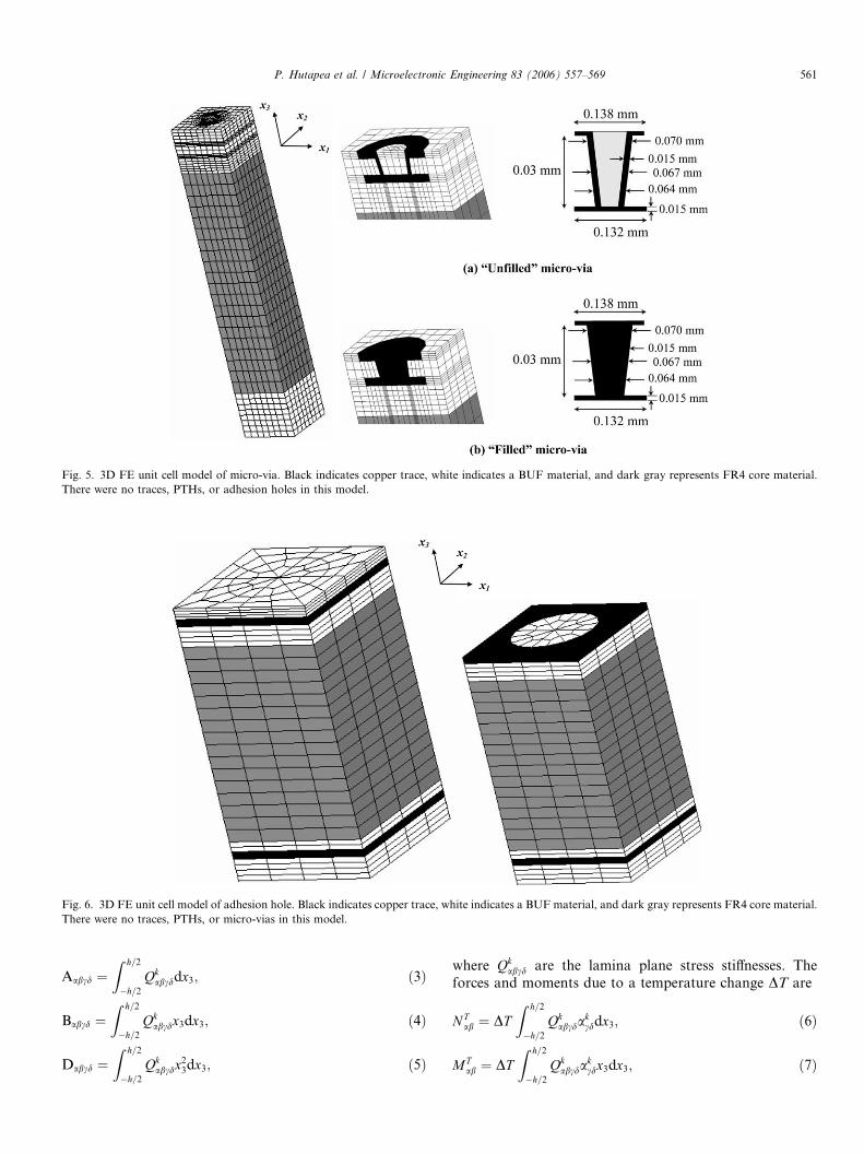
Fig. 5. 3D FE unit cell model of micro-via. Black indicates copper trace, white indicates a BUF material, and dark gray represents FR4 core material.There were no traces, PTHs, or adhesion holes in this model.
Fig. 6. 3D FE unit cell model of adhesion hole. Black indicates copper trace, white indicates a BUF material, and dark gray represents FR4 core material.There were no traces, PTHs, or micro-vias in this model.
P. Hutapea et al. / Microelectronic Engineering 83 (2006) 557–569 561
Aabcd ¼Z h=2
�h=2Qk
abcddx3; ð3Þ
Babcd ¼Z h=2
�h=2Qk
abcdx3dx3; ð4Þ
Dabcd ¼Z h=2
�h=2Qk
abcdx23dx3; ð5Þ
where Qkabcd are the lamina plane stress stiffnesses. The
forces and moments due to a temperature change DT are
NTab ¼ DT
Z h=2
�h=2Qk
abcdakcddx3; ð6Þ
MTab ¼ DT
Z h=2
�h=2Qk
abcdakcdx3dx3; ð7Þ
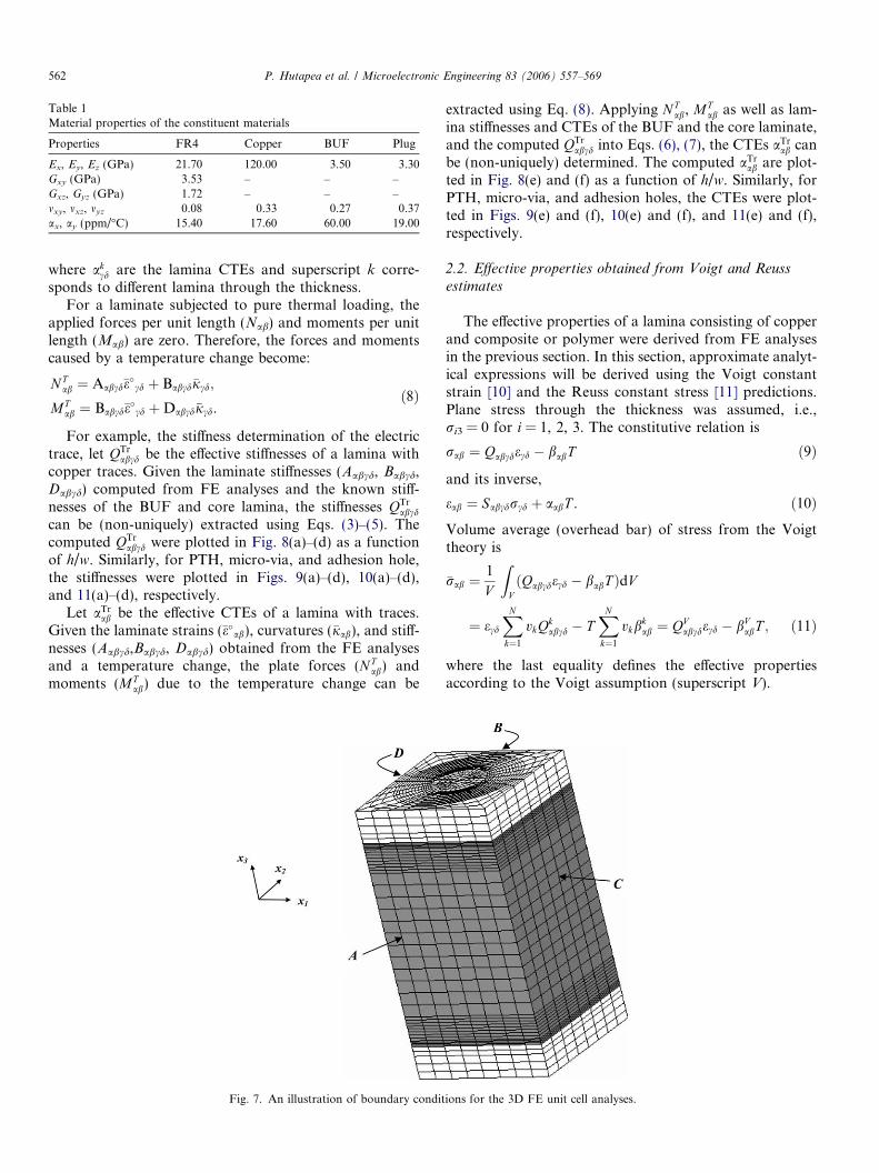
Table 1Material properties of the constituent materials
Properties FR4 Copper BUF Plug
Ex, Ey, Ez (GPa) 21.70 120.00 3.50 3.30Gxy (GPa) 3.53 – – –Gxz, Gyz (GPa) 1.72 – – –mxy, mxz, myz 0.08 0.33 0.27 0.37ax, ay (ppm/�C) 15.40 17.60 60.00 19.00
562 P. Hutapea et al. / Microelectronic Engineering 83 (2006) 557–569
where akcd are the lamina CTEs and superscript k corre-sponds to different lamina through the thickness.
For a laminate subjected to pure thermal loading, theapplied forces per unit length (Nab) and moments per unitlength (Mab) are zero. Therefore, the forces and momentscaused by a temperature change become:
NTab ¼ Aabcd�e
�cd þ Babcd�jcd;
MTab ¼ Babcd�e
�cd þDabcd�jcd.
ð8Þ
For example, the stiffness determination of the electrictrace, let QTr
abcd be the effective stiffnesses of a lamina withcopper traces. Given the laminate stiffnesses (Aabcd, Babcd,Dabcd) computed from FE analyses and the known stiff-nesses of the BUF and core lamina, the stiffnesses QTr
abcd
can be (non-uniquely) extracted using Eqs. (3)–(5). Thecomputed QTr
abcd were plotted in Fig. 8(a)–(d) as a functionof h/w. Similarly, for PTH, micro-via, and adhesion hole,the stiffnesses were plotted in Figs. 9(a)–(d), 10(a)–(d),and 11(a)–(d), respectively.
Let aTrab be the effective CTEs of a lamina with traces.Given the laminate strains (�e�ab), curvatures (�jab), and stiff-nesses (Aabcd,Babcd, Dabcd) obtained from the FE analysesand a temperature change, the plate forces (NT
ab) andmoments (MT
ab) due to the temperature change can be
Fig. 7. An illustration of boundary condit
extracted using Eq. (8). Applying NTab, M
Tab as well as lam-
ina stiffnesses and CTEs of the BUF and the core laminate,and the computed QTr
abcd into Eqs. (6), (7), the CTEs aTrab canbe (non-uniquely) determined. The computed aTrab are plot-ted in Fig. 8(e) and (f) as a function of h/w. Similarly, forPTH, micro-via, and adhesion holes, the CTEs were plot-ted in Figs. 9(e) and (f), 10(e) and (f), and 11(e) and (f),respectively.
2.2. Effective properties obtained from Voigt and Reuss
estimates
The effective properties of a lamina consisting of copperand composite or polymer were derived from FE analysesin the previous section. In this section, approximate analyt-ical expressions will be derived using the Voigt constantstrain [10] and the Reuss constant stress [11] predictions.Plane stress through the thickness was assumed, i.e.,ri3 = 0 for i = 1, 2, 3. The constitutive relation is
rab ¼ Qabcdecd � babT ð9Þ
and its inverse,
eab ¼ Sabcdrcd þ aabT . ð10ÞVolume average (overhead bar) of stress from the Voigttheory is
�rab ¼1
V
ZVðQabcdecd � babT ÞdV
¼ ecdXNk¼1
vkQkabcd � T
XNk¼1
vkbkab ¼ QV
abcdecd � bVabT ; ð11Þ
where the last equality defines the effective propertiesaccording to the Voigt assumption (superscript V).
ions for the 3D FE unit cell analyses.

Electric Trace
0
20
40
60
80
100
120
140
160
0 0.2 0.4 0.6 0.8 1
h/w
QT
r 1111 (
GP
a)Voigt
ReussFE (h = 0.0254 mm)
FE (h = 0.0834 mm)
Electric Trace
0
20
40
60
80
100
120
140
160
0 0.2 0.4 0.6 0.8 1
h/w
QT
r 2222 (
GP
a)
Voigt
Reuss
FE (h = 0.0254 mm)
FE (h = 0.0834 mm)
Electric Trace
0
10
20
30
40
50
0 0.2 0.4 0.6 0.8 1
h/w
QT
r 1122 (
GP
a)
Voigt
ReussFE (h = 0.0254 mm)
FE (h = 0.0834 mm)
Electric Trace
0
10
20
30
40
50
0 0.2 0.4 0.6 0.8 1
h/w
QT
r 1212 (
GP
a)
Voigt
Reuss
FE (h = 0.0254 mm)
FE (h = 0.0834 mm)
Electric Trace
0
20
40
60
80
0.0 0.2 0.4 0.6 0.8 1.0h/w
αT
r 11, L
amin
a C
TE
(pp
m/ o C
)
Voigt
Reuss
FE (h = 0.0254 mm)
FE (h = 0.0834 mm)
Electric Trace
0
20
40
60
80
0.0 0.2 0.4 0.6 0.8 1.0h/w
αT
r 22, L
amin
a C
TE
(p
pm
/o C)
Voigt
Reuss
FE (h = 0.0254 mm)
FE (h = 0.0834 mm)
a b
d
fe
c
Fig. 8. Stiffness (QTrabcd) and CTEs (aTrab) of electric traces.
P. Hutapea et al. / Microelectronic Engineering 83 (2006) 557–569 563
The volume average of strain from the Reuss theory is
�eab ¼1
V
ZVðSabcdrcd þ aabT ÞdV
¼ rcd
XNk¼1
vkSabcd þ TXNk¼1
vkakab ¼ SRabcdrcd þ aRabT ; ð12Þ
where the last equality defines the effective propertiesaccording to the Reuss assumption (superscript R).
2.3. Analytical models for effective thermo-mechanical
properties
The analytical models of the effective stiffnesses andCTEs of substrate features was based on the effective prop-erties calculated from the FE analyses of Section 2.1 and
the Voigt and Reuss estimates of Section 2.2, plus a fewconstants. As shown in Fig. 8, stiffnesses QTr
1111 followedthe Voigt estimate while stiffnesses QTr
2222, QTr1122, Q
Tr1222 fol-
lowed the Reuss estimate. CTEs aTr11 and aTr22 followed theVoigt and Reuss estimates, respectively. The analyticalmodels for electric traces are listed in Table 2.
For PTH, all lamina stiffnesses were between the Voigtand Reuss estimates as shown in Fig. 9(a)–(d). However,both lamina CTEs followed the Reuss estimate, Fig. 9(e)and (f). The analytical models for PTHs are listed in Table 3.
Formicro-via,Qlvia1111 andQ
lvia2222 were between theVoigt and
Reuss estimates as shown in Fig. 10(a) and (b). However,Qlvia
1122 and Qlvia1212 were close to the Reuss estimate as shown
in Fig. 10(c) and (d). Both lamina CTEs were between theVoigt and Reuss estimates, Fig. 10(e) and (f). The analyticalmodels for the micro-vias are listed in Table 4.

PTH
0
5
10
15
20
25
30
35
0.0 0.2 0.4 0.6 0.8 1.0
d/w
QPT
H11
11 (G
Pa)
VoigtReuss
FE
PTH
0
5
10
15
20
25
30
35
0.0 0.2 0.4 0.6 0.8 1.0
d/w
QPT
H22
22 (G
Pa)
VoigtReussFE
PTH
0
2
4
6
8
10
0.0 0.2 0.4 0.6 0.8 1.0
0.0 0.2 0.4 0.6 0.8 1.0
d/w
QPT
H11
22 (G
Pa)
VoigtReussFE
PTH
0
2
4
6
8
10
0.0 0.2 0.4 0.6 0.8 1.0
d/w
QPT
H12
12 (G
Pa)
VoigtReuss
FE
PTH
15
16
17
d/w
αPT
H11
(ppm
/ o C)
VoigtReuss
FE
PTH
15
16
17
0.0 0.2 0.4 0.6 0.8 1.0
d/w
αPT
H22
(ppm
/ o C)
VoigtReuss
FE
a b
c d
e f
Fig. 9. Stiffness (QPTHabcd ) and CTEs (aPTHab ) of PTHs.
Table 2Analytical models for electric traces
Lamina stiffness
QTr1111 ¼ QV
1111
QTr2222 ¼ QR
2222
QTr1122 ¼ QR
1122
QTr1212 ¼ QR
1212
Lamina CTEs
aTr11 ¼ aV11aTr22 ¼ aR22
Table 3Analytical models for PTHs
Lamina stiffness
QPTH1111 ¼ QV
1111ð1� uAÞ þ QR1111u
AÞ, where uA ¼ 0:274þ 0:101 dw
QPTH2222 ¼ QV
2222ð1� uBÞ þ QR2222u
BÞ, where uB ¼ 0:274þ 0:101 dw
QPTH1122 ¼ QV
1122ð1� uCÞ þ QR2222u
CÞ, where uC ¼ 0:693� 0:351 dw
QPTH1212 ¼ QV
1212ð1� uDÞ þ QR1212u
DÞ, where uD ¼ 0:739� 0:140 dw
Lamina CTEs
aPTH11 ¼ aR11aPTH22 ¼ aR22
564 P. Hutapea et al. / Microelectronic Engineering 83 (2006) 557–569
For adhesion hole, all lamina stiffnesses were betweenthe Voigt and Reuss estimates as shown in Fig. 11(a)–(d).Both lamina CTEs followed the Reuss estimate,Fig. 11(e) and (f). The analytical models for the adhesionholes are listed in Table 5.
3. Simplified 2D FE analyses of substrates to predict
warpage
The 2D FE models of the substrate were generated bydiscretizing the substrate into 10 · 10 cells. The size of

Micro-via
0
10
20
30
40
50
60
70
0.0 0 .2 0.4 0 .6 0.8 1.0
d/w
Qµv
ia11
11 (G
Pa)
VoigtReussFE (Filled)FE (Unfilled)
Micro-via
0
10
20
30
40
50
60
70
0.0 0.2 0.4 0.6 0.8 1.0
d/w
Qµv
ia22
22 (G
Pa)
VoigtReussFE (Filled)FE (Unfilled)
Micro-via
0
5
10
15
20
25
0.0 0.2 0.4 0.6 0.8 1.0
d/w
Qµv
ia11
22 (G
Pa)
VoigtReussFE (Filled)FE (Unfilled)
Micro-via
0
5
10
15
20
25
0.0 0.2 0.4 0.6 0.8 1.0
d/w
Qµv
ia12
12 (
GP
a)
VoigtReussFE (Filled)FE (Unfilled)
Micro-via
0
10
20
30
40
50
60
70
0.0 0.2 0.4 0.6 0.8 1.0
d/w
αµv
ia11
(ppm
/oC
)
VoigtReussFE (Filled)FE (Unfilled)
Micro-via
0
10
20
30
40
50
60
70
0.0 0.2 0.4 0.6 0.8 1.0
d/w
αµv
ia22 (
ppm
/oC
)
VoigtReussFE (Filled)FE (Unfilled)
a b
c d
e f
Fig. 10. Stiffness (Qlviaabcd) and CTEs (alviaab ) of micro-vias.
P. Hutapea et al. / Microelectronic Engineering 83 (2006) 557–569 565
each cell was 3.8 · 3.8 mm2. In each discretized cell (100cells · 15 layers), the characteristics of the features wereidentified. For example, in the copper layers, the coppervolume fraction (h/w) of traces and their orientations
Table 4Analytical models for micro-vias
Lamina stiffness
Qlvia1111 ¼ QV
1111ð1� uAÞ þ QR1111u
AÞ, where uA ¼ 0:854� 0:083 dw
Qlvia2222 ¼ QV
2222ð1� uBÞ þ QR2222u
BÞ, where uB ¼ 0:854� 0:083 dw
Qlvia1122 ¼ QV
1122ð1� uCÞ þ QR2222u
CÞ, where uC ¼ 0:654þ 0:293 dw
Qlvia1212 ¼ QV
1212ð1� uDÞ þ QR1212u
DÞ, where uD ¼ 1:217� 0:323 dw
Lamina CTEs
aPTH11 ¼ aR11aPTH22 ¼ aR22
were determined. In the dielectric and core layers, quan-tities and locations of PTHs and micro-vias wereassessed. A program was used to interface with the sub-strate database to estimate the copper volume fractionsin the copper layers and locations of the PTHs, micro-vias, and adhesion holes. For example, in the case ofelectric traces, using the estimated copper volume frac-tions and the trace orientations of each layer in each cell,the effective properties (Qijkl and aij) were estimated usingthe empirical analytical models in Tables 2–5. Usingthese analytical models, the laminate properties (Aijkl,Bijkl, Dijkl, N
Tij, M
Tij) of the 100 cells of the substrate were
calculated.Two-dimensional FE models constructed with the
cells using the respective laminate properties were devel-oped. Each cell was meshed using four elements. Com-mercial FE software ANSYS 8.0 was used. The

Adhesion Hole Adhesion Hole
Adhesion Hole Adhesion Hole
Adhesion Hole Adhesion Hole
0
20
40
60
80
100
120
140
0.0 0.2 0.4 0.6 0.8 1.0
d/w
QH
ole 11
11 (G
Pa) Voigt
Reuss
FE
0
20
40
60
80
100
120
140
0.0 0.2 0.4 0.6 0.8 1.0
d/w
QH
ole 22
22 (G
Pa) Voigt
Reuss
FE
0
10
20
30
40
50
0.0 0.2 0.4 0.6 0.8 1.0
d/w
QH
ole 11
22 (
GP
a)
Voigt
Reuss
FE
0
10
20
30
40
50
0.0 0.2 0.4 0.6 0.8 1.0
d/w
QH
ole 12
12 (G
Pa) Voigt
Reuss
FE
10
20
30
40
50
60
0.0 0.2 0.4 0.6 0.8 1.0
d/w
αH
ole 11
(ppm
/o C)
Voigt
Reuss
FE
10
20
30
40
50
60
0.0 0.2 0.4 0.6 0.8 1.0
d/w
ααHo
le22
(ppm
/o C)
Voigt
Reuss
FE
a b
c d
e f
Fig. 11. Stiffness (QHoleabcd ) and CTEs (aHole
ab ) of adhesion holes.
566 P. Hutapea et al. / Microelectronic Engineering 83 (2006) 557–569
substrate was modeled using a linear layer material(Shell99 element). Displacement boundary conditionswere appl- ied to prevent the rigid body rotation. A unit
Table 5Analytical models for adhesion holes
Lamina stiffness
Qhole1111 ¼ QV
1111ð1� uAÞ þ QR1111u
AÞ, where uA ¼ �0:069þ 0:577 dw
Qhole2222 ¼ QV
2222ð1� uBÞ þ QR2222u
BÞ, where uB ¼ �0:069þ 0:577 dw
Qhole1122 ¼ QV
1122ð1� uCÞ þ QR2222u
CÞ, where uC ¼ 0:697þ 0:139 dw
Qhole1212 ¼ QV
1212ð1� uDÞ þ QR1212u
DÞ, where uD ¼ �0:174þ 0:981 dw
Lamina CTEs
ahole11 ¼ aV11ahole22 ¼ aV22
temperature increase (DT = 1 �C) was applied to the FEmodel as the thermal loading. A summary of the stepsused in this homogenization method is illustrated inFig. 2. Warpage of two similar microelectronic sub-strates were predicted.
4. Experimental verifications
Effective CTE, stiffness, and warpage measurementswere used to validate the substrate homogenizationmethod. Effective CTE and warpage measurements wereperformed through the use of digital image correlation(DIC). The DIC measurement technique is a digital imageprocessing tool capable of measuring in-plane surfacedeformations. Surface preparation is generally not

Fig. 12. CTE contour maps of substrate 2 measured using digital image correlation.
Table 6Numerical and experimental correlations (CTEs, ppm/�C)
Areas ax ay
Experiment Prediction Experiment Prediction
A 18.72 18.53 16.99 17.64B 18.33 18.00 17.14 17.56C 20.57 20.15 19.46 19.71D 18.16 18.03 17.57 17.66
Table 7Numerical and experimental correlations (warpage, lm/�C)
Substrate 1ðUmax
z � Uminz Þ=DT
Substrate 2ðUmax
z � Uminz Þ=DT
Prediction 0.126 0.106Experiment 0.139 0.108
P. Hutapea et al. / Microelectronic Engineering 83 (2006) 557–569 567
required so long as the surface of interest contains asufficient amount of spatial detail or gray level variation.In the case of organic substrates, the high-density solderbump array was leveraged along with the appropriatechoice of magnification. Contrast enhancement of the sub-strate regions lying outside of the central bump array wasachieved through the implementation of a thin graphitelayer. A telecentric imaging lens imaging lens and 8 bitCCD camera were used to obtain images at two differenttemperatures. Thermal loading was achieved through theuse of Peltier thermal head within a partial vacuum envi-ronment. The 40 Torr partial vacuum environment servedto mitigate any optical distortion effects induced by ther-mal convection. Images were digitally stored as an arrayof grey scale values which may be treated as intensity dis-tribution functions. At the heart of the DIC technique liesa robust algorithm which serves to correlate correspond-
ing surface features between deformed and undeformedsubset regions. Once a correlation is established, resultingin-plane displacements are deduced from the pixel coordi-nate transformation between correlated images. Dimen-sionally scaled horizontal (U) and vertical (V)displacement fields are obtained by incorporating theimaging system magnification. Strain field maps areobtained through numerical differentiation of calculateddisplacement fields. Last, and perhaps most useful here,strain field plots may be divided by the imposed tempera-ture change in order to obtain whole field CTE plots.Fig. 12, Tables 6 and 7 show the DIC effective CTE con-tour maps, the average CTEs for each of the four regions,and the substrate warpage, respectively. In Fig. 12, regionsA, B, and D are outside the die area and region C is thedie area. The results show a substantial difference in theeffective CTEs between the die and outside die region. Pre-dictions of the effective CTEs were made from the homog-enized substrate by subjecting the FE model to a smalltemperature change. Strain extracted from the FE modelwas divided by the temperature change to yield the effec-tive CTEs – this method is essentially the same as whatwas performed in DIC. It should also be mentioned thatthe values in Table 7 are the slopes of the warpage changeas a function of temperature changes. Tables 6 and 7shows the comparisons of the experimental and predictedresults – predictions matched experimental trends andmagnitudes well.
Effective extensional stiffness measurements were madeusing uniaxial tensile tests performed on strips cut fromthe substrate, as shown in Fig. 13. An MTS load framewas used to apply the uniaxial load and axial strain wasmeasured using extensometers (locations indicated by hor-izontal lines in Fig. 13). The stress–strain response wasgenerally linear up to approximately 0.2% strain, thereaf-ter a non-linear response occurred, Fig. 14. Effective

Fig. 13. Location of strips cut from substrates for effective stiffness measurements. Blue lines indicate the location of the extensometer clips. Specimen 3was used to capture the die shadow regions. (For interpretation of the references to color in this figure legend, the reader is referred to the Web version ofthis article.)
0
40
80
120
160
200
0.000 0.002 0.004 0.006 0.008 0.010 0.012 0.014
Strain
Str
ess
(MP
a)
1A 1B
2B 2A
3A 3B
4A 4B
5A 5B
Specimens 1, 2, 4, 5
Die shadow regions, Specimens 3
Fig. 14. Measurements of stiffness using tensile test method. The loweststiffness was observed in specimen 3. The stiffness is listed in Table 8.
568 P. Hutapea et al. / Microelectronic Engineering 83 (2006) 557–569
secant modulus was calculated at 0.2% strain and theresults are shown in Table 8. As in the case of the effectiveCTEs, the results show a substantial difference in the dieversus outside die region. Table 8 shows the comparisonof the experimental and predicted results. The stiffnessesof regions A, B, C and D was the average of the stiffness ofthe discretized areas calculated using the plate constitutiveequation from the classical lamination theory and the pre-dicted laminate stiffnesses (Aijkl, Bijkl, Dijkl) obtained from
Table 8Numerical and experimental correlations (stiffness, GPa)
Specimen 1 Specimen 2
Prediction 26.20 24.87Experiment 26.61 25.45
the previous section. Predictions match the experimentaltrends very well (lower stiffness in the die region), howeverthere was some error in the magnitude in the die region,which could be due to some of the complexity in the dieregion that was not captured by the four featuresexamined.
5. Results and discussion
A numerical procedure to predict effective thermo-mechanical properties and substrate warpage under iso-thermal condition has been developed. Substrate features- electric trace, PTH, micro-via, and adhesion hole – havestrong influence on the warpage. The effective thermo-mechanical properties of these features were predictedthrough 3D FE unit cell analyses. Empirical analyticalmodels for the effective properties were developed usingthe FE data and Voigt and Reuss estimations. Using theempirical models, the simplified 2D FE plate models weredeveloped.
Additionally, the effective CTE and stiffness predictionsmatched very well with the experimental results as given inTables 6–8. The results show a substantial difference in theeffective CTEs and stiffness between the die and outside thedie region.
Specimen 3 Specimen 4 Specimen 5
21.05 24.40 25.7918.42 25.17 24.06

P. Hutapea et al. / Microelectronic Engineering 83 (2006) 557–569 569
6. Conclusions
The present numerical method has the potential to beused as a numerical tool to predict the warpage andmechanical properties of electronic substrates. Such acapability is critical in assessing substrates before fabrica-tion to ensure that the complexity of the substrate designproduces stiffnesses, CTEs, and warpage consistent withexpectations. Future work will include the developmentof tuning method to reduce the microelectronic substratewarpage.
Acknowledgments
This research was supported by Intel Corporation ATD,Chandler, Arizona. In particular, we would like to thankIbrahim Bekar and Josh Tor for their help in measuringthe substrate stiffness and effective CTEs, respectively.
References
[1] J.L. Grenestedt, P. Hutapea, Appl. Phys. Lett. 81 (21) (2002) 4079–4081.
[2] J.L. Grenestedt, P. Hutapea, J. Appl. Phys. 94 (1) (2003) 686–696.[3] P. Hutapea, J.L. Grenestedt, 9th International Symposium and
Exhibition on Advanced Packaging Materials, IEEE CPMT, Atlanta,GA, March 24–26, 2004.
[4] P. Hutapea, J.L. Grenestedt, ASME J. Electron. Packag. 126 (3)(2004) 282–287.
[5] L.W. Ritchey, Printed Circuit Design 17 (2) (2000) 26–29.[6] Y. Stavsky, N.J. Hoff, in: A.G.H. Dietz (Ed.), Composite Engineering
Laminates, MIT Press, Cambridge, MA, 1969.[7] J.L. Grenestedt, P. Hutapea, K. Frutschy, Mechanics and Materials
Conference, Scottsdale, AZ, June 17–20, 2003.[8] P. Hutapea, J.L. Grenestedt, M. Modi, M. Mello, K. Frutschy,
ASME Interpack 05, San Francisco, California, July 17–22,2005.
[9] P. Hutapea, J.L. Grenestedt, J. Electron. Mater. 32 (4) (2003) 221–227.
[10] W. Voigt, Wied. Ann. 38 (1889) 573–587.[11] A. Reuss, Z. Angew. Math. Mech. 9 (1929) 49–58.