Performance enhancement of diindenoperylene-based organic photovoltaic cells by nanocolumn-arrays
8
Performance enhancement of diindenoperylene-based organic photovoltaic cells by nanocolumn-arrays Shuwen Yu a , Andreas Opitz a,⇑ , Stefan Grob b , Roland Resel c , Martin Oehzelt a,d , Wolfgang Brütting b , Ingo Salzmann a , Norbert Koch a,d,⇑ a Humboldt-Universität zu Berlin, Institut für Physik & IRIS Adlershof, Brook-Taylor Straße 6, 12489 Berlin, Germany b Augsburg University, Institut für Physik, Universitätsstraße 1, 86135 Augsburg, Germany c Graz University of Technology, Institute of Solid State Physics, Petersgasse 16, 8010 Graz, Austria d Helmholtz-Zentrum für Materialien und Energie GmbH, Bereich Solarenergieforschung, Albert-Einstein-Straße 15, 12489 Berlin, Germany article info Article history: Received 9 April 2014 Received in revised form 1 June 2014 Accepted 20 June 2014 Available online 3 July 2014 Keywords: Organic photovoltaic cells Nanocolumns Morphology Structure abstract Crystalline and uniform nanocolumns of the organic semiconductor diindenoperylene (DIP) were fabricated by glancing-angle deposition and employed in organic photovoltaic cells (OPVCs) forming an interdigitated donor/acceptor heterojunction, with fullerene as electron acceptor. In comparison to reference bilayer devices the nanocolumn-based solar cells exhibit increased power conversion efficiency. Based on a comprehensive structural and morphological analysis, we identify three advantages of the interdigitated nanocolumn structures: (i) The active donor/acceptor interface area, crucial for exciton dissociation, is increased and the column diameter is in the range of the exciton diffusion length. (ii) The molecular orientation of DIP is such in the nanocolumns that light absorption is enhanced. (iii) The ubiquitous presence of vertical interfaces throughout nanocolumn- based devices is further beneficial to light absorption, as it fully compensates wave- length-dependent interference effects within the device structure. This work shows how the benefits of nanocolumns can go beyond simple interface area enlargement to improve the efficiency of OPVCs. Ó 2014 Elsevier B.V. All rights reserved. 1. Introduction Since the initial application of ‘‘sandwich’’ structure in organic photovoltaic cells (OPVCs) in the 1970s [1,2], the power conversion efficiency of OPVCs significantly increased only after introducing the donor/acceptor het- erojunction concept [3], where layers of preferentially hole/electron conducting materials with an interface pro- moting exciton dissociation are employed. Today, high open circuit voltage (V oc ) and optimized light harvesting can be realized with a wide variety of organic semiconduc- tors suitable for application in OPVCs [4–13]. However, the short diffusion length of photo-generated excitons in such materials (typically in the range of tens of nanometers [14,15]) significantly limits the fraction of excitons dissoci- ated at the donor/acceptor interface, thus restricting the generation of mobile charges. To reconcile the exciton dif- fusion length with the average dimensions of organic het- erojunctions, the concept of bulk heterojunction was introduced, which allows increasing the effective area of the donor/acceptor interface and, simultaneously, reducing the separation between individual donor and acceptor volumes [16–18]. While this approach turned out to be highly successful for polymer-based OPVCs processed from http://dx.doi.org/10.1016/j.orgel.2014.06.023 1566-1199/Ó 2014 Elsevier B.V. All rights reserved. ⇑ Corresponding authors. Address: Humboldt-Universität zu Berlin, Institut für Physik & IRIS Adlershof, Brook-Taylor Straße 6, 12489 Berlin, Germany (N. Koch). E-mail addresses: [email protected] (A. Opitz), Norbert. [email protected] (N. Koch). Organic Electronics 15 (2014) 2210–2217 Contents lists available at ScienceDirect Organic Electronics journal homepage: www.elsevier.com/locate/orgel
Transcript of Performance enhancement of diindenoperylene-based organic photovoltaic cells by nanocolumn-arrays
Organic Electronics 15 (2014) 2210–2217
Contents lists available at ScienceDirect
Organic Electronics
journal homepage: www.elsevier .com/locate /orgel
Performance enhancement of diindenoperylene-based organicphotovoltaic cells by nanocolumn-arrays
http://dx.doi.org/10.1016/j.orgel.2014.06.0231566-1199/� 2014 Elsevier B.V. All rights reserved.
⇑ Corresponding authors. Address: Humboldt-Universität zu Berlin,Institut für Physik & IRIS Adlershof, Brook-Taylor Straße 6, 12489 Berlin,Germany (N. Koch).
E-mail addresses: [email protected] (A. Opitz), [email protected] (N. Koch).
Shuwen Yu a, Andreas Opitz a,⇑, Stefan Grob b, Roland Resel c, Martin Oehzelt a,d,Wolfgang Brütting b, Ingo Salzmann a, Norbert Koch a,d,⇑a Humboldt-Universität zu Berlin, Institut für Physik & IRIS Adlershof, Brook-Taylor Straße 6, 12489 Berlin, Germanyb Augsburg University, Institut für Physik, Universitätsstraße 1, 86135 Augsburg, Germanyc Graz University of Technology, Institute of Solid State Physics, Petersgasse 16, 8010 Graz, Austriad Helmholtz-Zentrum für Materialien und Energie GmbH, Bereich Solarenergieforschung, Albert-Einstein-Straße 15, 12489 Berlin, Germany
a r t i c l e i n f o
Article history:Received 9 April 2014Received in revised form 1 June 2014Accepted 20 June 2014Available online 3 July 2014
Keywords:Organic photovoltaic cellsNanocolumnsMorphologyStructure
a b s t r a c t
Crystalline and uniform nanocolumns of the organic semiconductor diindenoperylene(DIP) were fabricated by glancing-angle deposition and employed in organic photovoltaiccells (OPVCs) forming an interdigitated donor/acceptor heterojunction, with fullerene aselectron acceptor. In comparison to reference bilayer devices the nanocolumn-based solarcells exhibit increased power conversion efficiency. Based on a comprehensive structuraland morphological analysis, we identify three advantages of the interdigitated nanocolumnstructures: (i) The active donor/acceptor interface area, crucial for exciton dissociation, isincreased and the column diameter is in the range of the exciton diffusion length. (ii)The molecular orientation of DIP is such in the nanocolumns that light absorption isenhanced. (iii) The ubiquitous presence of vertical interfaces throughout nanocolumn-based devices is further beneficial to light absorption, as it fully compensates wave-length-dependent interference effects within the device structure. This work shows howthe benefits of nanocolumns can go beyond simple interface area enlargement to improvethe efficiency of OPVCs.
� 2014 Elsevier B.V. All rights reserved.
1. Introduction
Since the initial application of ‘‘sandwich’’ structure inorganic photovoltaic cells (OPVCs) in the 1970s [1,2], thepower conversion efficiency of OPVCs significantlyincreased only after introducing the donor/acceptor het-erojunction concept [3], where layers of preferentiallyhole/electron conducting materials with an interface pro-moting exciton dissociation are employed. Today, high
open circuit voltage (Voc) and optimized light harvestingcan be realized with a wide variety of organic semiconduc-tors suitable for application in OPVCs [4–13]. However, theshort diffusion length of photo-generated excitons in suchmaterials (typically in the range of tens of nanometers[14,15]) significantly limits the fraction of excitons dissoci-ated at the donor/acceptor interface, thus restricting thegeneration of mobile charges. To reconcile the exciton dif-fusion length with the average dimensions of organic het-erojunctions, the concept of bulk heterojunction wasintroduced, which allows increasing the effective area ofthe donor/acceptor interface and, simultaneously, reducingthe separation between individual donor and acceptorvolumes [16–18]. While this approach turned out to behighly successful for polymer-based OPVCs processed from
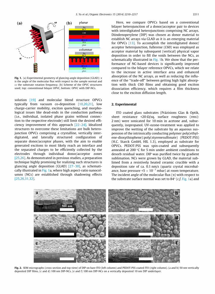
Fig. 1. (a) Experimental geometry of glancing-angle deposition (GLAD); ais the angle of the molecular flux with respect to the sample normal andx the substrate rotation frequency. (b) Scheme of the OPVC structuresused; top: conventional bilayer OPVC, bottom: OPVC with DIP-NCs.
S. Yu et al. / Organic Electronics 15 (2014) 2210–2217 2211
solution [19] and molecular blend structure OPVCstypically from vacuum co-deposition [10,20,21], lowcharge-carrier mobility, exciton quenching, and morpho-logical issues like dead-ends in the conduction pathway(i.e., individual, isolated phase grains without connec-tion to the respective electrode) still limit the desired effi-ciency improvement of this approach [22–24]. Idealizedstructures to overcome these limitations are bulk hetero-junction OPVCs comprising a crystalline, vertically inter-digitated, and laterally structured configuration ofseparate donor/acceptor phases, with the aim to enablegenerated excitons to most likely reach an interface andthe separated charges to be efficiently collected by theelectrodes through individual donor/acceptor zones[25,26]. As demonstrated in previous studies, a preparationtechnique highly promising for realizing such structures isglancing angle deposition (GLAD) [27–30], as schemati-cally illustrated in Fig. 1a, where high aspect-ratio nanocol-umns (NCs) are established through shadowing effects[25,26,31,32].
Fig. 2. SEM micrographs (cross section and top view) of DIP on bare ITO (left coludeposited DIP films, (c and d) 100 nm DIP-NCs, (e and f) 100 nm DIP-NCs on a v
Here, we compare OPVCs based on a conventionalbilayer heterojunction of a donor/acceptor pair to deviceswith interdigitated heterojunctions comprising NC arrays.Diindenoperylene (DIP) was chosen as donor material toestablish NC arrays via GLAD as it is an emerging materialfor OPVCs [13]. To accomplish the interdigitated donor/acceptor heterojunction, fullerene (C60) was employed asacceptor material by subsequent (vertical) physical vapordeposition in order to fill the voids between the NCs, asschematically illustrated in Fig. 1b. We show that the per-formance of NC-based devices is significantly improvedcompared to the bilayer reference OPVCs, which we relateto the increase in active interface area and enhancedabsorption of the NC arrays, as well as reducing the influ-ence of the ‘‘trade-off’’ between getting high light absorp-tion with thick C60 films and obtaining good excitondissociation efficiency, which requires a film thicknessclose to the exciton diffusion length.
2. Experimental
ITO coated glass substrates (Präzisions Glas & Optik,sheet resistance <20 X/sq, surface roughness (rms):2 nm) were sonicated for 10 min in acetone and, subse-quently, isopropanol. UV-ozone-treatment was applied toimprove the wetting of the substrate by an aqueous sus-pension of the intrinsically conducting polymer poly(ethyl-ene-dioxythiophene):poly(styrenesulfonate) (PEDOT:PSS)(H.C. Starck GmbH, HIL 1.3), employed as substrate forOPVCs. PEDOT:PSS was spin-coated and subsequentlyannealed at 200 �C for 5 min under ambient conditions todesorb residual water. DIP was purified twice by gradientsublimation. NCs were grown by GLAD, the material sub-limed from a resistively heated ceramic crucible with adeposition rate of ca. 0.1 nm/s (quartz crystal microbal-ance, base pressure <5 � 10�7 mbar) at room temperature.The incident angle of the molecular flux (a) with respect tothe substrate surface normal was set to 84� (c.f. Fig. 1a) and
mn) and PEDOT:PSS coated ITO (right column). (a and b) 50 nm verticallyertically deposited 10 nm DIP underlayer.
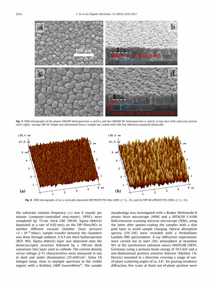
Fig. 3. SEM micrographs of the planar C60/DIP heterojunction (a and b), and the C60/DIP-NC heterojunction (c and d), in top view (left) and cross sectionview (right); average DIP NC height was determined from a sample not coated with C60, but otherwise prepared identically.
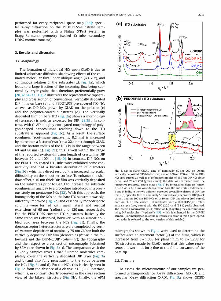
Fig. 4. AFM micrographs of (a) a vertically deposited DIP/PEDOT:PSS film (SEM c.f. Fig. 2b), and (b) DIP-NCs/PEDOT:PSS (SEM c.f. Fig. 2d).
2212 S. Yu et al. / Organic Electronics 15 (2014) 2210–2217
the substrate rotation frequency (x) was 6 rounds perminute (computer-controlled step-motor). OPVCs werecompleted by 75 nm thick C60 (99.9%, Sigma–Aldrich)deposited at a rate of 0.02 nm/s on the DIP films/NCs inanother different vacuum chamber (base pressure<2 � 10�8 mbar); sample transfer between the chamberswas done through ambient. A 6.5 nm thick bathocuproine(BCP, 96%, Sigma–Aldrich) layer was deposited onto thedonor/acceptor structure followed by a 100 nm thicksamarium (Sm) layer used as cathode. The current densityversus voltage (J–V) characteristics were measured in-situin dark and under illumination (25 mW/cm2, Solux C6halogen lamp, close to daylight spectrum in the visibleregion) with a Keithley 2400 SourceMeter�. The sample
morphology was investigated with a Bruker Multimode-8atomic force microscope (AFM) and a HITACHI S-4100field-emission scanning electron microscope (SEM), usingthe latter after sputter-coating the samples with a thingold layer to avoid sample charging. Optical absorptionspectra (UV–VIS) were recorded with a PerkinElmerLambda 900 spectrometer. X-ray diffraction experimentswere carried out in inert (He) atmosphere at beamlineW1 at the synchrotron radiation source HASYLAB (DESY,Germany) using a primary beam energy of 10.5 keV and aone-dimensional position sensitive detector (Mythen 1 K,Dectris) mounted in z-direction covering a range of out-of-plane scattering angles of ca. 3.8�; for grazing-incidencediffraction, five scans at fixed out-of-plane position were
S. Yu et al. / Organic Electronics 15 (2014) 2210–2217 2213
performed for every reciprocal space map [33]; specu-lar X-ray diffraction on the PEDOT:PSS-substrate sam-ples was performed with a Philips X’Pert system inBragg–Berntano geometry (sealed Cr-tube, secondaryHOPG monochromator).
Fig. 5. (a) In-plane GIXRD data of nominally 60 nm C60 on 90 nmvertically deposited DIP (black curve) and on 100 nm C60 on 160 nm DIP-NCs (red curve), as well as of reference samples of 160 nm DIP NCs (bluecurve) and 20 nm C60 (green curve); the data was extracted from therespective reciprocal space maps (Fig. 6) by integrating along qz (range:0.0–0.1 Å�1). All films were deposited on bare ITO substrates. Index labelsB and B0 indicate the two different observed crystalline phases of DIP (seetext). (b) Specular XRD of nominally 50 nm vertically deposited DIP (blackcurve), and on 100 nm DIP-NCs on a 10 nm DIP underlayer (red curve),both on PEDOT:PSS coated ITO substrates with a PEDOT:PSS/ITO refer-ence sample (grey curve) with the ITO (222) and (211) peaks observed.The inset is a zoom of the (004) reflection highlighting the contribution oflying DIP molecules (‘‘k-phase’’) [45], which is enhanced in the DIP-NCsample. (For interpretation of the references to color in this figure legend,the reader is referred to the web version of this article.)
3. Results and discussion
3.1. Morphology
The formation of individual NCs upon GLAD is due tolimited adsorbate diffusion, shadowing effects of the colli-mated molecular flux under oblique angle (a > 70�), andcontinuous rotation of the substrate (c.f. Fig. 1a), whichleads to a large fraction of the incoming flux being cap-tured by larger grains that, therefore, preferentially grow[28,32,34–37]. Fig. 2 illustrates the representative topogra-phy and cross section of conventional vertically depositedDIP films on bare (a) and PEDOT:PSS pre-covered ITO (b),as well as DIP-NCs grown by GLAD on the pristine (c)and the polymer-coated substrates (d). The verticallydeposited film on bare ITO (Fig. 2a) shows a morphologyof (terraced) islands as expected for DIP [38,39]. In con-trast, with GLAD a highly corrugated morphology of poly-gon-shaped nanocolumns reaching down to the ITOsubstrate is apparent (Fig. 2c). As a result, the surfaceroughness (root-mean-square-rms: 9.2 nm) is increasedby more than a factor of two (rms: 22.4 nm) through GLAD,and the bottom radius of the NCs is in the range between60 and 80 nm (c.f. Fig. 2c); this is well within the rangeof the reported exciton diffusion length of crystalline DIPbetween 20 and 100 nm [15,40]. In contrast, DIP-NCs onthe PEDOT:PSS coated ITO substrates exhibited some con-nectivity and had a broader distribution of diameters(Fig. 2d), which is a direct result of the increased moleculardiffusibility on the smoother surface. To enhance the sha-dow effect, a 10 nm thick DIP film was vertically depositedon the substrates prior to GLAD to increase the substrateroughness, in analogy to a procedure introduced in a previ-ous study on pentacene NCs [32]. With this approach, thehomogeneity of the NCs on the bare ITO substrate was sig-nificantly improved (Fig. 2e) and essentially monodispersecolumns were formed with mean lateral and verticalextensions of 65 nm (radius) and 120 nm, respectively.For the PEDOT:PSS covered ITO substrates, basically thesame trend was observed, however, with an almost dou-bled void area between the NCs (Fig. 2f). Finally, thedonor/acceptor heterostructures were completed by verti-cal vacuum deposition of nominally 75 nm C60 on both thevertically deposited DIP film (denoted as planar in the fol-lowing) and the DIP-NC/DIP (columnar); the topographyand the respective cross section micrographs (obtainedby SEM) are shown in Fig. 3a–d. The comparison with theDIP-only samples reveals that fullerene molecules com-pletely cover the vertically deposited DIP layer (Fig. 3aand b) and also fully penetrate into the voids betweenthe NCs (Fig. 3c and d). For the NCs, this is clearly seen inFig. 3d from the absence of a clear-cut DIP/C60 interface,which is, in contrast, clearly observed in the cross sectionview of the bilayer structure (Fig. 3b). Finally, the AFM
micrographs shown in Fig. 4 were used to determine thesurface-area enlargement factor (n) of the films, which isincreased from n = 1.068 for planar film to n = 1.288 forNC structures made by GLAD; note that this value repre-sents a lower limit for n due to the finite curvature of theAFM tip.
3.2. Structure
To assess the microstructure of our samples we per-formed grazing-incidence X-ray diffraction (GIXRD) andspecular X-ray diffraction (XRD). Fig. 5a shows GIXRD
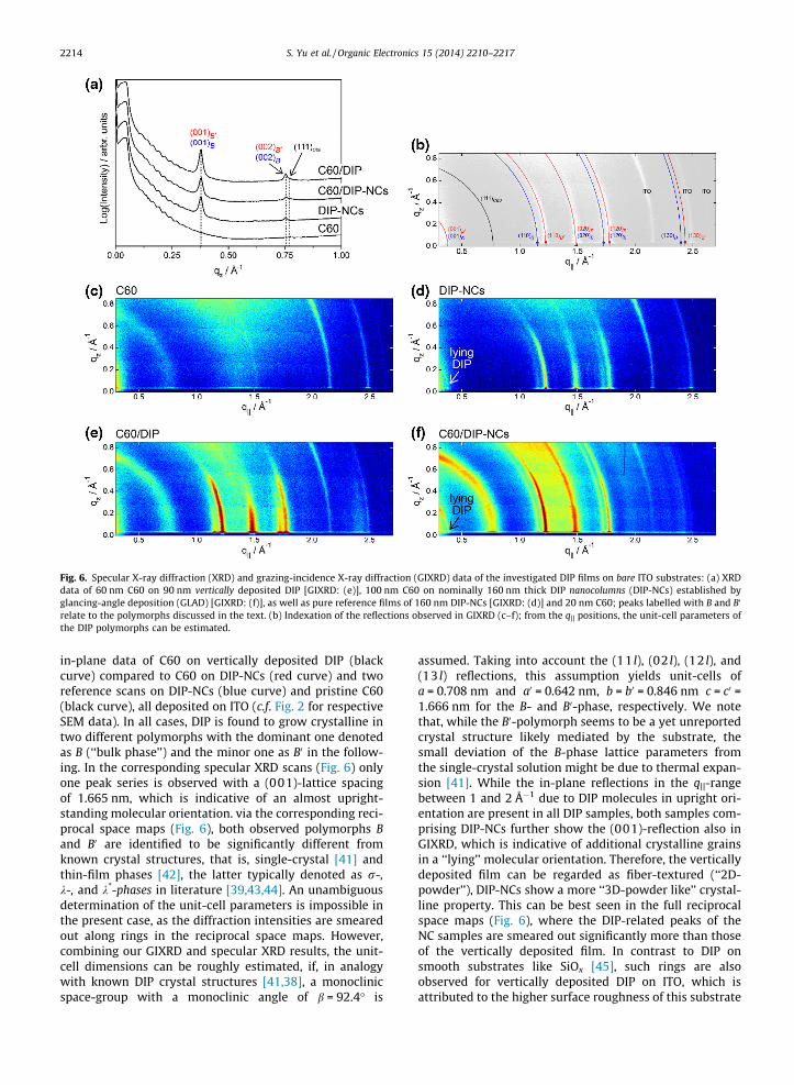
Fig. 6. Specular X-ray diffraction (XRD) and grazing-incidence X-ray diffraction (GIXRD) data of the investigated DIP films on bare ITO substrates: (a) XRDdata of 60 nm C60 on 90 nm vertically deposited DIP [GIXRD: (e)], 100 nm C60 on nominally 160 nm thick DIP nanocolumns (DIP-NCs) established byglancing-angle deposition (GLAD) [GIXRD: (f)], as well as pure reference films of 160 nm DIP-NCs [GIXRD: (d)] and 20 nm C60; peaks labelled with B and B0
relate to the polymorphs discussed in the text. (b) Indexation of the reflections observed in GIXRD (c–f); from the q|| positions, the unit-cell parameters ofthe DIP polymorphs can be estimated.
2214 S. Yu et al. / Organic Electronics 15 (2014) 2210–2217
in-plane data of C60 on vertically deposited DIP (blackcurve) compared to C60 on DIP-NCs (red curve) and tworeference scans on DIP-NCs (blue curve) and pristine C60(black curve), all deposited on ITO (c.f. Fig. 2 for respectiveSEM data). In all cases, DIP is found to grow crystalline intwo different polymorphs with the dominant one denotedas B (‘‘bulk phase’’) and the minor one as B0 in the follow-ing. In the corresponding specular XRD scans (Fig. 6) onlyone peak series is observed with a (001)-lattice spacingof 1.665 nm, which is indicative of an almost upright-standing molecular orientation. via the corresponding reci-procal space maps (Fig. 6), both observed polymorphs Band B0 are identified to be significantly different fromknown crystal structures, that is, single-crystal [41] andthin-film phases [42], the latter typically denoted as r-,k-, and k*-phases in literature [39,43,44]. An unambiguousdetermination of the unit-cell parameters is impossible inthe present case, as the diffraction intensities are smearedout along rings in the reciprocal space maps. However,combining our GIXRD and specular XRD results, the unit-cell dimensions can be roughly estimated, if, in analogywith known DIP crystal structures [41,38], a monoclinicspace-group with a monoclinic angle of b = 92.4� is
assumed. Taking into account the (11 l), (02 l), (12 l), and(13 l) reflections, this assumption yields unit-cells ofa = 0.708 nm and a0 = 0.642 nm, b = b0 = 0.846 nm c = c0 =1.666 nm for the B- and B0-phase, respectively. We notethat, while the B0-polymorph seems to be a yet unreportedcrystal structure likely mediated by the substrate, thesmall deviation of the B-phase lattice parameters fromthe single-crystal solution might be due to thermal expan-sion [41]. While the in-plane reflections in the q||-rangebetween 1 and 2 Å�1 due to DIP molecules in upright ori-entation are present in all DIP samples, both samples com-prising DIP-NCs further show the (001)-reflection also inGIXRD, which is indicative of additional crystalline grainsin a ‘‘lying’’ molecular orientation. Therefore, the verticallydeposited film can be regarded as fiber-textured (‘‘2D-powder’’), DIP-NCs show a more ‘‘3D-powder like’’ crystal-line property. This can be best seen in the full reciprocalspace maps (Fig. 6), where the DIP-related peaks of theNC samples are smeared out significantly more than thoseof the vertically deposited film. In contrast to DIP onsmooth substrates like SiOx [45], such rings are alsoobserved for vertically deposited DIP on ITO, which isattributed to the higher surface roughness of this substrate
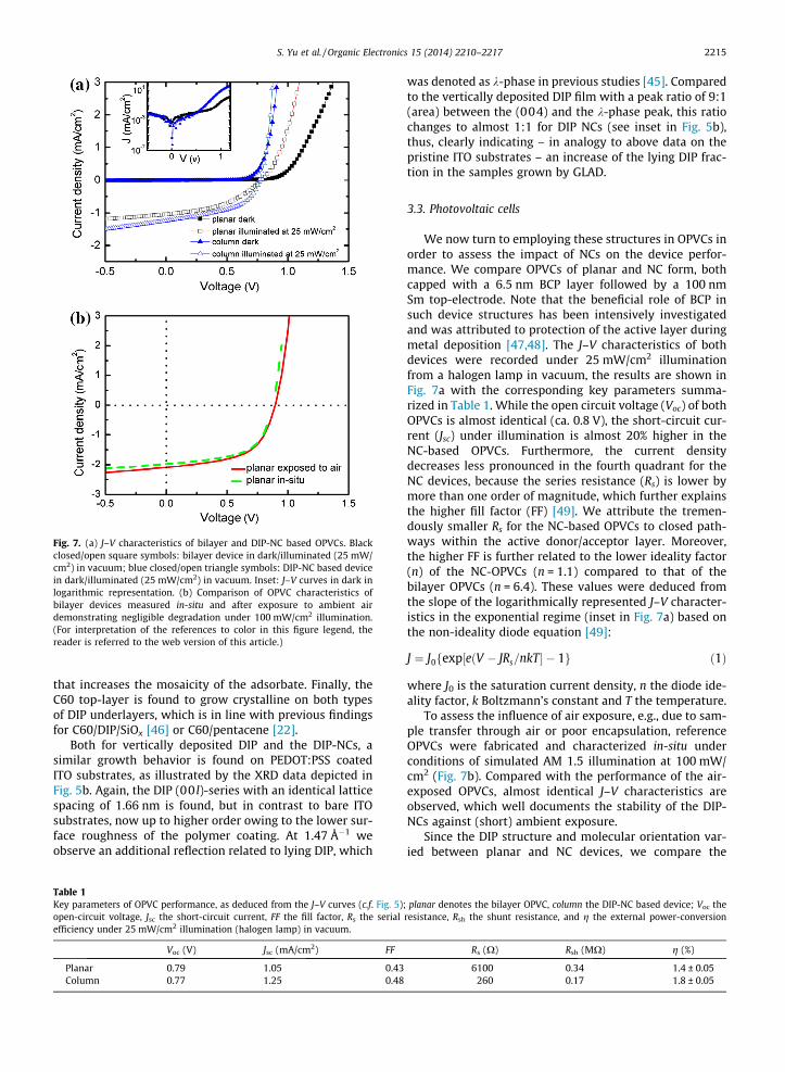
Fig. 7. (a) J–V characteristics of bilayer and DIP-NC based OPVCs. Blackclosed/open square symbols: bilayer device in dark/illuminated (25 mW/cm2) in vacuum; blue closed/open triangle symbols: DIP-NC based devicein dark/illuminated (25 mW/cm2) in vacuum. Inset: J–V curves in dark inlogarithmic representation. (b) Comparison of OPVC characteristics ofbilayer devices measured in-situ and after exposure to ambient airdemonstrating negligible degradation under 100 mW/cm2 illumination.(For interpretation of the references to color in this figure legend, thereader is referred to the web version of this article.)
S. Yu et al. / Organic Electronics 15 (2014) 2210–2217 2215
that increases the mosaicity of the adsorbate. Finally, theC60 top-layer is found to grow crystalline on both typesof DIP underlayers, which is in line with previous findingsfor C60/DIP/SiOx [46] or C60/pentacene [22].
Both for vertically deposited DIP and the DIP-NCs, asimilar growth behavior is found on PEDOT:PSS coatedITO substrates, as illustrated by the XRD data depicted inFig. 5b. Again, the DIP (00 l)-series with an identical latticespacing of 1.66 nm is found, but in contrast to bare ITOsubstrates, now up to higher order owing to the lower sur-face roughness of the polymer coating. At 1.47 �1 weobserve an additional reflection related to lying DIP, which
Table 1Key parameters of OPVC performance, as deduced from the J–V curves (c.f. Fig. 5);open-circuit voltage, Jsc the short-circuit current, FF the fill factor, Rs the serialefficiency under 25 mW/cm2 illumination (halogen lamp) in vacuum.
Voc (V) Jsc (mA/cm2) FF
Planar 0.79 1.05 0.43Column 0.77 1.25 0.48
was denoted as k-phase in previous studies [45]. Comparedto the vertically deposited DIP film with a peak ratio of 9:1(area) between the (004) and the k-phase peak, this ratiochanges to almost 1:1 for DIP NCs (see inset in Fig. 5b),thus, clearly indicating – in analogy to above data on thepristine ITO substrates – an increase of the lying DIP frac-tion in the samples grown by GLAD.
3.3. Photovoltaic cells
We now turn to employing these structures in OPVCs inorder to assess the impact of NCs on the device perfor-mance. We compare OPVCs of planar and NC form, bothcapped with a 6.5 nm BCP layer followed by a 100 nmSm top-electrode. Note that the beneficial role of BCP insuch device structures has been intensively investigatedand was attributed to protection of the active layer duringmetal deposition [47,48]. The J–V characteristics of bothdevices were recorded under 25 mW/cm2 illuminationfrom a halogen lamp in vacuum, the results are shown inFig. 7a with the corresponding key parameters summa-rized in Table 1. While the open circuit voltage (Voc) of bothOPVCs is almost identical (ca. 0.8 V), the short-circuit cur-rent (Jsc) under illumination is almost 20% higher in theNC-based OPVCs. Furthermore, the current densitydecreases less pronounced in the fourth quadrant for theNC devices, because the series resistance (Rs) is lower bymore than one order of magnitude, which further explainsthe higher fill factor (FF) [49]. We attribute the tremen-dously smaller Rs for the NC-based OPVCs to closed path-ways within the active donor/acceptor layer. Moreover,the higher FF is further related to the lower ideality factor(n) of the NC-OPVCs (n = 1.1) compared to that of thebilayer OPVCs (n = 6.4). These values were deduced fromthe slope of the logarithmically represented J–V character-istics in the exponential regime (inset in Fig. 7a) based onthe non-ideality diode equation [49]:
J ¼ J0fexp½eðV � JRs=nkT� � 1g ð1Þ
where J0 is the saturation current density, n the diode ide-ality factor, k Boltzmann’s constant and T the temperature.
To assess the influence of air exposure, e.g., due to sam-ple transfer through air or poor encapsulation, referenceOPVCs were fabricated and characterized in-situ underconditions of simulated AM 1.5 illumination at 100 mW/cm2 (Fig. 7b). Compared with the performance of the air-exposed OPVCs, almost identical J–V characteristics areobserved, which well documents the stability of the DIP-NCs against (short) ambient exposure.
Since the DIP structure and molecular orientation var-ied between planar and NC devices, we compare the
planar denotes the bilayer OPVC, column the DIP-NC based device; Voc theresistance, Rsh the shunt resistance, and g the external power-conversion
Rs (X) Rsh (MX) g (%)
6100 0.34 1.4 ± 0.05260 0.17 1.8 ± 0.05
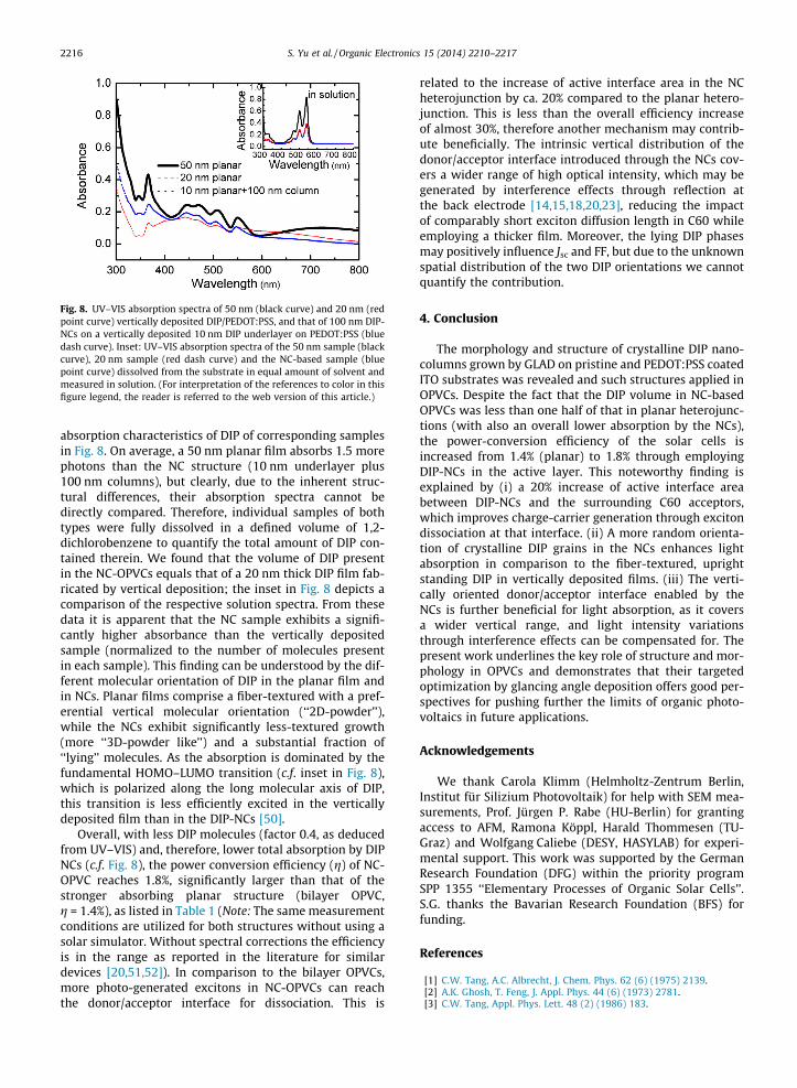
Fig. 8. UV–VIS absorption spectra of 50 nm (black curve) and 20 nm (redpoint curve) vertically deposited DIP/PEDOT:PSS, and that of 100 nm DIP-NCs on a vertically deposited 10 nm DIP underlayer on PEDOT:PSS (bluedash curve). Inset: UV–VIS absorption spectra of the 50 nm sample (blackcurve), 20 nm sample (red dash curve) and the NC-based sample (bluepoint curve) dissolved from the substrate in equal amount of solvent andmeasured in solution. (For interpretation of the references to color in thisfigure legend, the reader is referred to the web version of this article.)
2216 S. Yu et al. / Organic Electronics 15 (2014) 2210–2217
absorption characteristics of DIP of corresponding samplesin Fig. 8. On average, a 50 nm planar film absorbs 1.5 morephotons than the NC structure (10 nm underlayer plus100 nm columns), but clearly, due to the inherent struc-tural differences, their absorption spectra cannot bedirectly compared. Therefore, individual samples of bothtypes were fully dissolved in a defined volume of 1,2-dichlorobenzene to quantify the total amount of DIP con-tained therein. We found that the volume of DIP presentin the NC-OPVCs equals that of a 20 nm thick DIP film fab-ricated by vertical deposition; the inset in Fig. 8 depicts acomparison of the respective solution spectra. From thesedata it is apparent that the NC sample exhibits a signifi-cantly higher absorbance than the vertically depositedsample (normalized to the number of molecules presentin each sample). This finding can be understood by the dif-ferent molecular orientation of DIP in the planar film andin NCs. Planar films comprise a fiber-textured with a pref-erential vertical molecular orientation (‘‘2D-powder’’),while the NCs exhibit significantly less-textured growth(more ‘‘3D-powder like’’) and a substantial fraction of‘‘lying’’ molecules. As the absorption is dominated by thefundamental HOMO–LUMO transition (c.f. inset in Fig. 8),which is polarized along the long molecular axis of DIP,this transition is less efficiently excited in the verticallydeposited film than in the DIP-NCs [50].
Overall, with less DIP molecules (factor 0.4, as deducedfrom UV–VIS) and, therefore, lower total absorption by DIPNCs (c.f. Fig. 8), the power conversion efficiency (g) of NC-OPVC reaches 1.8%, significantly larger than that of thestronger absorbing planar structure (bilayer OPVC,g = 1.4%), as listed in Table 1 (Note: The same measurementconditions are utilized for both structures without using asolar simulator. Without spectral corrections the efficiencyis in the range as reported in the literature for similardevices [20,51,52]). In comparison to the bilayer OPVCs,more photo-generated excitons in NC-OPVCs can reachthe donor/acceptor interface for dissociation. This is
related to the increase of active interface area in the NCheterojunction by ca. 20% compared to the planar hetero-junction. This is less than the overall efficiency increaseof almost 30%, therefore another mechanism may contrib-ute beneficially. The intrinsic vertical distribution of thedonor/acceptor interface introduced through the NCs cov-ers a wider range of high optical intensity, which may begenerated by interference effects through reflection atthe back electrode [14,15,18,20,23], reducing the impactof comparably short exciton diffusion length in C60 whileemploying a thicker film. Moreover, the lying DIP phasesmay positively influence Jsc and FF, but due to the unknownspatial distribution of the two DIP orientations we cannotquantify the contribution.
4. Conclusion
The morphology and structure of crystalline DIP nano-columns grown by GLAD on pristine and PEDOT:PSS coatedITO substrates was revealed and such structures applied inOPVCs. Despite the fact that the DIP volume in NC-basedOPVCs was less than one half of that in planar heterojunc-tions (with also an overall lower absorption by the NCs),the power-conversion efficiency of the solar cells isincreased from 1.4% (planar) to 1.8% through employingDIP-NCs in the active layer. This noteworthy finding isexplained by (i) a 20% increase of active interface areabetween DIP-NCs and the surrounding C60 acceptors,which improves charge-carrier generation through excitondissociation at that interface. (ii) A more random orienta-tion of crystalline DIP grains in the NCs enhances lightabsorption in comparison to the fiber-textured, uprightstanding DIP in vertically deposited films. (iii) The verti-cally oriented donor/acceptor interface enabled by theNCs is further beneficial for light absorption, as it coversa wider vertical range, and light intensity variationsthrough interference effects can be compensated for. Thepresent work underlines the key role of structure and mor-phology in OPVCs and demonstrates that their targetedoptimization by glancing angle deposition offers good per-spectives for pushing further the limits of organic photo-voltaics in future applications.
Acknowledgements
We thank Carola Klimm (Helmholtz-Zentrum Berlin,Institut für Silizium Photovoltaik) for help with SEM mea-surements, Prof. Jürgen P. Rabe (HU-Berlin) for grantingaccess to AFM, Ramona Köppl, Harald Thommesen (TU-Graz) and Wolfgang Caliebe (DESY, HASYLAB) for experi-mental support. This work was supported by the GermanResearch Foundation (DFG) within the priority programSPP 1355 ‘‘Elementary Processes of Organic Solar Cells’’.S.G. thanks the Bavarian Research Foundation (BFS) forfunding.
References
[1] C.W. Tang, A.C. Albrecht, J. Chem. Phys. 62 (6) (1975) 2139.[2] A.K. Ghosh, T. Feng, J. Appl. Phys. 44 (6) (1973) 2781.[3] C.W. Tang, Appl. Phys. Lett. 48 (2) (1986) 183.
S. Yu et al. / Organic Electronics 15 (2014) 2210–2217 2217
[4] M. Svensson, F. Zhang, S. Veenstra, W. Verhees, J. Hummelen, J.Kroon, O. Inganä, M. Andersson, Adv. Mater. 15 (2003) 988.
[5] T. Kietzke, D.A.M. Egbe, H.-H. Horhöld, D. Neher, Macromolecules 39(2006) 4018.
[6] F. Zhang, W. Mammo, L.M. Andersson, S. Admassie, M.R. Andersson,O. Inganäs, Adv. Mater. 18 (16) (2006) 2169.
[7] R.F. Bailey-Salzman, B.P. Rand, S.R. Forrest, Appl. Phys. Lett. 91 (1)(2007) 013508.
[8] M. Riede, T. Mueller, W. Tress, R. Schueppel, K. Leo, Nanotechnology19 (42) (2008) 424001.
[9] J.C. Bijleveld, R.A.M. Verstrijden, M.M. Wienk, R.A.J. Janssen, Appl.Phys. Lett. 97 (7) (2010) 073304.
[10] J. Wagner, M. Gruber, A. Wilke, Y. Tanaka, K. Topczak, A. Steindamm,U. Hörmann, A. Opitz, Y. Nakayama, H. Ishii, J. Pflaum, N. Koch, W.Brütting, J. Appl. Phys. 111 (5) (2012) 054509.
[11] L. Dou, J. You, Z. Hong, Z. Xu, G. Li, R.A. Street, Y. Yang, Adv. Mater. 25(46) (2013) 6642.
[12] U. Hörmann, J. Wagner, M. Gruber, A. Opitz, W. Brütting, Phys. StateSolid – R 5 (7) (2011) 241.
[13] J. Wagner, M. Gruber, A. Hinderhofer, A. Wilke, B. Bröker, J. Frisch, P.Amsalem, A. Vollmer, A. Opitz, N. Koch, F. Schreiber, W. Brütting,Adv. Funct. Mater. 20 (24) (2010) 4295.
[14] T. Stübinger, W. Brütting, J. Appl. Phys. 90 (7) (2001) 3632.[15] D. Kurrle, J. Pflaum, Appl. Phys. Lett. 92 (13) (2008) 133306.[16] G. Yu, J. Gao, J.C. Hummelen, F. Wudl, A.J. Heeger, Science 270 (5243)
(1995) 1789.[17] J.J.M. Halls, C.A. Walsh, N.C. Greenham, E.A. Marseglia, R.H. Friend,
S.C. Moratti, A.B. Holmes, Nature 376 (2002) 498.[18] P. Peumans, S. Uchida, S.R. Forrest, Nature 425 (2003) 158.[19] W. Ma, C. Yang, X. Gong, K. Lee, A.J. Heeger, Adv. Funct. Mater. 15
(10) (2005) 1617.[20] M. Gruber, M. Rawolle, J. Wagner, D. Magerl, U. Hörmann, J. Perlich,
S.V. Roth, A. Opitz, F. Schreiber, P. Müller-Buschbaum, W. Brütting,Adv. Energy Mater. 3 (8) (2013) 1075.
[21] X. Xiao, J.D. Zimmerman, B.E. Lassiter, K.J. Bergemann, S.R. Forrest,Appl. Phys. Lett. 102 (7) (2013).
[22] I. Salzmann, S. Duhm, R. Opitz, R.L. Johnson, J.P. Rabe, N. Koch, J.Appl. Phys. 104 (11) (2008).
[23] A. Opitz, J. Wagner, W. Brütting, I. Salzmann, N. Koch, J. Manara, J.Pflaum, A. Hinderhofer, F. Schreiber, J. Sel. Top. Quantum Electron.16 (2010) 1707.
[24] M. Gruber, J. Wagner, K. Klein, U. Hörmann, A. Opitz, M. Stutzmann,W. Brütting, Adv. Energy Mater. 2 (9) (2012) 1100.
[25] F. Yang, M. Shtein, S.R. Forrest, Nat. Mater. 4 (1) (2004) 37.[26] N. Koch, Chemphyschem: A Eur. J. Chem. Phys. Phys. Chem. 8 (10)
(2007) 1438.[27] K. Robbie, M.J. Brett, A. Lakhtakia, Nat. Mater. 384 (6610) (1996).[28] K. Robbie, M.J. Brett, J. Vac. Sci. Technol. A 15 (3) (1997) 1460.[29] J.G. Van Dijken, M.D. Fleischauer, M.J. Brett, Org. Electron. 12 (12)
(2011) 2111.
[30] Y. Zhou, T. Taima, T. Miyadera, T. Yamanari, M. Kitamura, K. Nakatsu,Y. Yoshida, Nano Lett. 12 (8) (2012) 4146.
[31] Y. Zheng, R. Bekele, J.M. Ouyang, J.G. Xue, Org. Electron. 10 (8) (2009)1621.
[32] S.W. Yu, C. Klimm, P. Schäfer, J.P. Rabe, B. Rech, N. Koch, Org.Electron. 12 (12) (2011) 2180.
[33] I. Salzmann, A. Moser, M. Oehzelt, T. Breuer, X. Feng, Z.-Y. Juang, D.Nabok, R.G. Della Valle, S. Duhm, G. Heimel, A. Brillante, E. Venuti, I.Bilotti, C. Christodoulou, J. Frisch, P. Puschnig, C. Draxl, G. Witte, K.Müllen, N. Koch, ACS Nano 6 (12) (2012) 10874.
[34] J. Zhang, I. Salzmann, S. Rogaschewski, J.P. Rabe, N. Koch, F. Zhang, Z.Xu, Appl. Phys. Lett. 90 (19) (2007) 193117.
[35] L. Abelmann, C. Lodder, Thin Solid Films 305 (1997) 1.[36] Y.P. Zhao, D.X. Ye, G.C. Wang, T.M. Lu, Nano Lett. 2 (2002) 351.[37] J.G. Van Dijken, M.D. Fleischauer, M.J. Brett, J. Mater. Chem. 21 (4)
(2011) 1013.[38] A. Turak, M. Nguyen, F. Maye, J. Heidkamp, P. Lienerth, J. Wrachtrup,
H. Dosch, J. Nano Res. 14 (2011).[39] A.C. Dürr, F. Schreiber, M. Münch, N. Karl, B. Krause, V. Kruppa, H.
Dosch, Appl. Phys. Lett. 81 (12) (2002) 2276.[40] R.R. Lunt, N.C. Giebink, A.A. Belak, J.B. Benziger, S.R. Forrest, J. Appl.
Phys. 105 (5) (2009) 45.[41] M.A. Heinrich, J. Pflaum, A.K. Tripathi, W. Frey, M.L. Steigerwald, T.
Siegrist, J. Phys. Chem. C 111 (51) (2007) 18878.[42] A.C. Dürr, F. Schreiber, M. Kelsch, H.D. Carstanjen, H. Dosch, O.H.
Seeck, J. Appl. Phys. 93 (9) (2003) 5201.[43] S. Kowarik, A. Gerlach, S. Sellner, L. Cavalcanti, O. Konovalov, F.
Schreiber, Appl. Phys. A 95 (1) (2009) 233.[44] A.C. Dürr, N. Koch, M. Kelsch, A. Rühm, J. Ghijsen, R.L. Johnson, J.J.
Pireaux, J. Schwartz, F. Schreiber, H. Dosch, A. Kahn, Phys. Rev. B 68(11) (2003) 115428.
[45] S. Kowarik, A. Gerlach, S. Sellner, F. Schreiber, L. Cavalcanti, O.Konovalov, Phys. Rev. Lett. 96 (12) (2006) 125504.
[46] A. Hinderhofer, A. Gerlach, K. Broch, T. Hosokai, K. Yonezawa, K.Kato, S. Kera, N. Ueno, F. Schreiber, J. Phys. Chem. C 117 (2) (2012)1053.
[47] H. Gommans, B. Verreet, B.P. Rand, R. Muller, J. Poortmans, P.Heremans, J. Genoe, Adv. Funct. Mater. 18 (22) (2008) 3686.
[48] M. Vogel, S. Doka, C. Breyer, M.C. Lux-Steiner, K. Fostiropoulos, Appl.Phys. Lett. 89 (16) (2006) 163501.
[49] S.M. Sze, Physics of Semiconductor Devices, second ed., Wiley, NewYork, 1981.
[50] U. Heinemeyer, R. Scholz, L. Gisslén, M. Alonso, J. Ossó, M. Garriga, A.Hinderhofer, M. Kytka, S. Kowarik, A. Gerlach, F. Schreiber, Phys. Rev.B 78 (8) (2008) 56.
[51] A. Steindamm, M. Brendel, A.K. Topczak, J. Pflaum, Appl. Phys. Lett.101 (14) (2012) 56.
[52] C. Schuenemann, A. Petrich, R. Schulze, D. Wynands, J. Meiss, M.P.Hein, J. Jankowski, C. Elschner, J. Alex, M. Hummert, K.-J. Eichhorn, K.Leo, M. Riede, Org. Electron. 14 (7) (2013) 1704.