
OneNAND512(KFG1216x2A-xxB5) FLASH MEMORY
114
OneNAND512(KFG1216x2A-xxB5) FLASH MEMORY 1 OneNAND TM Specification Density Part No. VCC(core & IO) Temperature PKG 512Mb KFG1216Q2A 1.8V(1.7V~1.95V) Extended 63FBGA(LF)/63FBGA KFG1216D2A 2.65V(2.4V~2.9V) Extended 63FBGA(LF)/63FBGA KFG1216U2A 3.3V(2.7V~3.6V) Industrial 63FBGA(LF)/63FBGA Version: Ver. 1.0 Date: May 17th, 2005 查询KFG1216D2A供应商 捷多邦,专业PCB打样工厂,24小时加急出货
-
Upload
khangminh22 -
Category
Documents
-
view
0 -
download
0
Transcript of OneNAND512(KFG1216x2A-xxB5) FLASH MEMORY

OneNAND512(KFG1216x2A-xxB5) FLASH MEMORY
1
OneNANDTM Specification
Density Part No. VCC(core & IO) Temperature PKG
512Mb KFG1216Q2A 1.8V(1.7V~1.95V) Extended 63FBGA(LF)/63FBGA
KFG1216D2A 2.65V(2.4V~2.9V) Extended 63FBGA(LF)/63FBGA
KFG1216U2A 3.3V(2.7V~3.6V) Industrial 63FBGA(LF)/63FBGA
Version: Ver. 1.0Date: May 17th, 2005
查询KFG1216D2A供应商 捷多邦,专业PCB打样工厂,24小时加急出货

OneNAND512(KFG1216x2A-xxB5) FLASH MEMORY
2
1.0 INTRODUCTIONThis specification contains information about the Samsung Electronics Company OneNAND™‚ Flash memory product family. Section 1.0 includes a general overview, revision history, and product ordering information. Section 2.0 describes the OneNAND device. Section 3.0 provides information about device operation. Electrical specifications and timing waveforms are in Sections 4.0 though 6.0. Section 7.0 provides additional application and technical notes pertaining to use of the OneNAND. Package dimensions are found in Section 8.0
INFORMATION IN THIS DOCUMENT IS PROVIDED IN RELATION TO SAMSUNG PRODUCTS,AND IS SUBJECT TO CHANGE WITHOUT NOTICE.NOTHING IN THIS DOCUMENT SHALL BE CONSTRUED AS GRANTING ANY LICENSE,EXPRESS OR IMPLIED, BY ESTOPPEL OR OTHERWISE,TO ANY INTELLECTUAL PROPERTY RIGHTS IN SAMSUNG PRODUCTS OR TECHNOLOGY. ALLINFORMATION IN THIS DOCUMENT IS PROVIDEDON AS "AS IS" BASIS WITHOUT GUARANTEE OR WARRANTY OF ANY KIND.
1. For updates or additional information about Samsung products, contact your nearest Samsung office.
2. Samsung products are not intended for use in life support, critical care, medical, safety equipment, or similar applications where Product failure could result in loss of life or personal or physical harm, or any military or defense application, or any governmental procurement to which special terms or provisions may apply.
OneNAND™‚ is a trademark of Samsung Electronics Company, Ltd. Other names and brands may be claimed as the property of their rightful owners.
Copyright © 2005, Samsung Electronics Company, Ltd

OneNAND512(KFG1216x2A-xxB5) FLASH MEMORY
3
Document TitleOneNAND
Revision History
Revision No.
0.0
0.1
0.2
0.3
0.4
Remark
Preliminary
Preliminary
Preliminary
Preliminary
Preliminary
Draft Date
Nov. 4, 2004
Dec. 7, 2004
Dec. 24, 2004
Jan. 13, 2005
Feb. 25, 2005
History
Initial issue.
1. Corrected Errata2. Revised cache read flow chart3. Revised standby current4. Revised spare area description5. Added CE don’t care state for Asynch Write, Load, Program, and Block Erase timing diagram
1. Added Copy Back Operation with Random Data Input2. Changed tBA from 11ns to 11.5ns3. Pended Active Erase Current
1. Corrected the errata2. Revised typical value of ISB from 50uA to 10uA3. Revised maximum value of ISB from 100uA to 50uA4. Revised maximum value of tCE, tAA and tACC from 70ns to 76ns 5. Revised Vcc-IO description6. Revised Spare Area description7. Added extra information on Controller Status Register8. Added commands related to Interrupt Status Register bits9. Revised Write Protection Status on Chapter 3.4.310. Revised Copy-Back Program Operation description11. Added extra information on Multi-Block Erase Operation12. Disabled FBA restriction in OTP operation13. Revised Cache Read Flow Chart14. Revised Reset Parameter descriptions15. Added RDY information on Warm Reset Timing diagram16. Added information on Data Protection Timing During Power Down17. Revised Interrupt pin rise and falling slope graph18. Added restriction on address register setting on Dual Operations19. Added restriction on address register setting on Cache Read Operation
1. Corrected the errata2. Updated DC parameters to RMS values3. Added Speed Information on Product Number4. Revised tOEZ description5. Revised OTP register setting restriction6. Added Boot Sequence Infrormation on Technical Notes7. Added Cint Information
1.1 Revision History

OneNAND512(KFG1216x2A-xxB5) FLASH MEMORY
4
Revision History
Revision No.
1.0
Remark
Final
Draft Date
May. 17, 2005
History
1. Corrected the errata2. Added Data Protection flow chart.3. Removed Cache Read Operation.4. Added additional information on command register.5. Revised Interrupt status register information.6. Added INT pin schematic.7. Changed tPGM1 to 205 from 320us, tPGM2 to 220 from 350us.8. Revised AC/DC parameters9. Revised ECC Bypass Description.10. Revised Reset Parameters and Timing Diagrams.

OneNAND512(KFG1216x2A-xxB5) FLASH MEMORY
5
Samsung offers a variety of Flash solutions including NAND Flash, OneNAND™ and NOR Flash. Samsung offers Flash products both component and a variety of card formats including RS-MMC, MMC, CompactFlash, and SmartMedia.
To determine which Samsung Flash product solution is best for your application, refer the product selector chart.
Application RequiresSamsung Flash Products
NAND OneNAND NOR
Fast Random Read •
Fast Sequential Read • •
Fast Write/Program • •
Multi Block Erase • (Max 64 Blocks) •
Erase Suspend/Resume • •
Copyback • (EDC) • (ECC)
Lock/Unlock/Lock-Tight • •
ECC External (Hardware/Software) Internal X
Scalability • •
1.3 Ordering Information
1.2 Flash Product Type Selector
K F G 12 1 6 Q 2 A - x x B 5
Samsung OneNAND Memory
Device TypeG : Single Chip
Density12: 512Mb
Operating Temperature Range E = Extended Temp. (-30 °C to 85 °C) I = Industrial Temp. (-40 °C to 85 °C)
Page Architecture 2 : 2KB Page
Version 2nd Generation
Product Line desinator B : Include Bad Block D : Daisy Sample
Operating Voltage RangeQ : 1.8V(1.7 V to 1.95V)D : 2.65V(2.4V to 2.9V)U : 3.3V(2.7 V to 3.6V)
PackageD : FBGA(Lead Free)F : FBGA(Leaded)
Organization x16 Organization
Speed 5 : 54MHz 6 : 66MHz

OneNAND512(KFG1216x2A-xxB5) FLASH MEMORY
6
The attached datasheets are prepared and approved by SAMSUNG Electronics. SAMSUNG Electronics CO., LTD. reserve the rightto change the specifications. SAMSUNG Electronics will evaluate and reply to your requests and questions about device. If you haveany questions, please contact the SAMSUNG branch office near you.
OneNAND is a highly integrated non-volatile memory solution based around a NAND Flash memory array.
The chip integrates system features including: • A BootRAM and bootloader • Two independent bi-directional 2KB DataRAM buffers • A High-Speed x16 Host Interface • On-chip Error Correction • On-chip NOR interface controller
This on-chip integration enables system designers to reduce external system logic and use high-density NAND Flash in applications that would otherwise have to use more NOR components.
OneNAND takes advantage of the higher performance NAND program time, low power, and high density and combines it with the synchronous read performance of NOR. The NOR Flash host interface makes OneNAND an ideal solution for applications like G3 Smart Phones, Camera Phones, and mobile applications that have large, advanced multimedia applications and operating systems, but lack a NAND controller.
When integrated into a Samsung Multi-Chip-Package with Samsung Mobile DDR SDRAM, designers can complete a high-perfor-mance, small footprint solution.
1.4 Architectural Benefits

OneNAND512(KFG1216x2A-xxB5) FLASH MEMORY
7
Device Architecture • Design Technology: • Supply Voltage: • Host Interface: • 5KB Internal BufferRAM: • SLC NAND Array:
Device Performance • Host Interface Type: - Up to 54MHz clock frequency - Linear Burst 4-, 8-, 16, 32-words with wrap around - Continuous 1K word Sequential Burst
• Programmable Burst Read Latency • Multiple Sector Read: • Multiple Reset Modes: • Multi Block Erase: • Low Power Dissipation: - Standby current : [email protected], [email protected]/3.3V device - Synchronous Burst Read current : [email protected] [email protected]/3.3V device - Load current : 30mA@all device - Program current : [email protected] device [email protected]/3.3V device - Erase current : [email protected] device [email protected]/3.3V device - Multi Block Erase current : [email protected] device [email protected]/3.3V device
System Hardware • Voltage detector generating internal reset signal from Vcc • Hardware reset input (/RP) • Data Protection Modes
• User-controlled One Time Programmable(OTP) area • Internal 2bit EDC / 1bit ECC • Internal Bootloader supports Booting Solution in system
• Handshaking Feature
• Detailed chip information
Packaging
90nm1.8V (1.7V ~ 1.95V), 2.65V (2.4 ~ 2.9V), 3.3V (2.7 ~3.6V)16 bit 1KB BootRAM, 4KB DataRAM(2K+64)B Page Size, (128K+4K)B Block Size
Synchronous Burst Read
Asynchronous Random Read - 76ns access time Asynchronous Random WriteLatency 3(up to 40MHz), 4, 5, 6, and 7Up to 4 sectors using Sector Count RegisterCold/Warm/Hot/NAND Flash Resetsup to 64 blocksTypical Power,
- Write Protection for BootRAM - Write Protection for NAND Flash Array- Write Protection during power-up- Write Protection during power-down
- INT pin indicates Ready / Busy- Polling the interrupt register status bit - by ID register
63ball, 9.5mm x 12mm x max 1.0mmt , 0.8mm ball pitch FBGA
1.5 Product Features

OneNAND512(KFG1216x2A-xxB5) FLASH MEMORY
8
OneNAND™‚ is a monolithic integrated circuit with a NAND Flash array using a NOR Flash interface. This device includes control logic, a NAND Flash array, and 5KB of internal BufferRAM. The BufferRAM reserves 1KB for boot code buffering (BootRAM) and 4KB for data buffering (DataRAM), split between 2 independent buffers. It has a x16 Host Interface and a random access time speed of ~76ns. The device operates up to a maximum host-driven clock frequency of 54MHz for synchronous reads at Vcc(or Vccq. Refer to chapter 4.2) with minimum 4-clock latency. Below 40MHz it is accessible with minimum 3-clock latency. Appropriate wait cycles are deter-mined by programmable read latency.
OneNAND provides for multiple sector read operations by assigning the number of sectors to be read in the sector counter register. The device includes one block-sized OTP (One Time Programmable) area that can be used to increase system security or to provide identification capabilities.
1.6 General Overview
OneNAND512(KFG1216x2A-xxB5) FLASH MEMORY
9
The OneNAND is an advanced generation, high-performance NAND-based Flash memory.
It integrates on-chip a single-level-cell (SLC) NAND Flash Array memory with two independent data buffers, boot RAM buffer, a page buffer for the Flash array, and a one-time-programmable block.
The combination of these memory areas enable high-speed pipelining of reads from host, BufferRAM, Page Buffer, and NAND Flash Array memory.
Clock speeds up to 54MHz with a x16 wide I/O yields a 68MByte/second bandwidth.
The OneNAND also includes a Boot RAM and boot loader. This enables the device to efficiently load boot code at device startup from the NAND Array without the need for off-chip boot device.
One block of the NAND Array is set aside as an OTP memory area. This area, available to the user, can be configured and locked with secured user information.
On-chip controller interfaces enable the device to operate in systems without NAND Host controllers.
2.0 DEVICE DESCRIPTION2.1 Detailed Product Description

OneNAND512(KFG1216x2A-xxB5) FLASH MEMORY
10
B (capital letter) Byte, 8bits
W (capital letter) Word, 16bits
b (lower-case letter) Bit
ECC Error Correction Code
Calculated ECC ECC that has been calculated during a load or program access
Written ECC ECC that has been stored as data in the NAND Flash array or in the BufferRAM
BufferRAM On-chip internal buffer consisting of BootRAM and DataRAM
BootRAM A 1KB portion of the BufferRAM reserved for Boot Code buffering
DataRAM A 4KB portion of the BufferRAM reserved for Data buffering
SectorPart of a Page ; 512B for the main data area and 16B for the spare area.
It is also the minimum Load/Program/Copy-Back Program unit during a 1~4 sector operation is available.
Data unit
Possible data unit to be read from memory to BufferRAM or to be programmed to memory. - 528B of which 512B is in main area and 16B in spare area - 1056B of which 1024B is in main area and 32B in spare area - 1584B of which 1536B is in main area and 48B in spare area - 2112B of which 2048B is in main area and 64B in spare area
2.2 Definitions

OneNAND512(KFG1216x2A-xxB5) FLASH MEMORY
11
NC NC NC NC
INT A0 A1 NC A10 A6
NC NC NC
WE RP DQ14 VSS VSS DQ13
DQ12 DQ8 DQ1 OE DQ9 VCC
DQ7 DQ4 DQ11 DQ10 DQ3 VCC
DQ15 A12 DQ0 DQ5 DQ6
CE DQ2 NC NC A9
AVD A7 A11 A8
A4 A5 A2 A3 NC
NC NC NC NC
NC NC NC NC
Core
IO
CLK
A15
A13A14
RDY
(TOP VIEW, Balls Facing Down)63ball FBGA OneNAND Chip
63ball, 9.5mm x 12mm x max 1.0mmt , 0.8mm ball pitch FBGA
2.3 Pin Configuration
OneNAND512(KFG1216x2A-xxB5) FLASH MEMORY
12
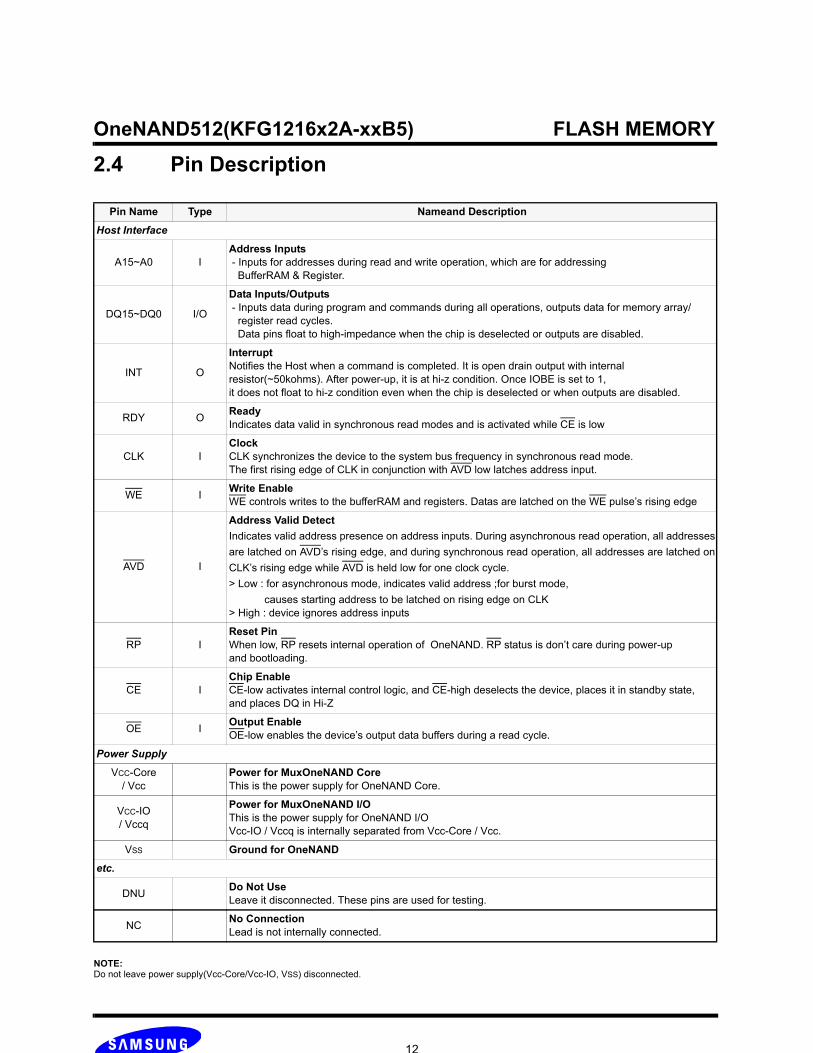
NOTE:Do not leave power supply(Vcc-Core/Vcc-IO, VSS) disconnected.
Pin Name Type Nameand Description
Host Interface
A15~A0 IAddress Inputs - Inputs for addresses during read and write operation, which are for addressing BufferRAM & Register.
DQ15~DQ0 I/O
Data Inputs/Outputs - Inputs data during program and commands during all operations, outputs data for memory array/ register read cycles. Data pins float to high-impedance when the chip is deselected or outputs are disabled.
INT O
InterruptNotifies the Host when a command is completed. It is open drain output with internal resistor(~50kohms). After power-up, it is at hi-z condition. Once IOBE is set to 1, it does not float to hi-z condition even when the chip is deselected or when outputs are disabled.
RDY O ReadyIndicates data valid in synchronous read modes and is activated while CE is low
CLK IClockCLK synchronizes the device to the system bus frequency in synchronous read mode.The first rising edge of CLK in conjunction with AVD low latches address input.
WE I Write EnableWE controls writes to the bufferRAM and registers. Datas are latched on the WE pulse’s rising edge
AVD I
Address Valid DetectIndicates valid address presence on address inputs. During asynchronous read operation, all addressesare latched on AVD’s rising edge, and during synchronous read operation, all addresses are latched onCLK’s rising edge while AVD is held low for one clock cycle.> Low : for asynchronous mode, indicates valid address ;for burst mode,
causes starting address to be latched on rising edge on CLK> High : device ignores address inputs
RP IReset PinWhen low, RP resets internal operation of OneNAND. RP status is don’t care during power-up and bootloading.
CE IChip EnableCE-low activates internal control logic, and CE-high deselects the device, places it in standby state,and places DQ in Hi-Z
OE I Output EnableOE-low enables the device’s output data buffers during a read cycle.
Power Supply
VCC-Core/ Vcc
Power for MuxOneNAND CoreThis is the power supply for OneNAND Core.
VCC-IO/ Vccq
Power for MuxOneNAND I/OThis is the power supply for OneNAND I/OVcc-IO / Vccq is internally separated from Vcc-Core / Vcc.
VSS Ground for OneNAND
etc.
DNU Do Not UseLeave it disconnected. These pins are used for testing.
NC No ConnectionLead is not internally connected.
2.4 Pin Description

OneNAND512(KFG1216x2A-xxB5) FLASH MEMORY
13
BootRAM
Host Interface
CLK
CE
OE
WE
RP
AVD
StateMachine
Bootloader
Internal Registers
(Address/Command/Configuration/Status Registers)
ErrorCorrection
Logic
INT
DataRAM0
BufferRAM
NAND FlashArray
OTP(One Block)RDY
A15~A0
DQ15~DQ0
2.6 Memory Array Organization The OneNAND architecture integrates several memory areas on a single chip.
2.6.1 Internal (NAND Array) Memory Organization
The on-chip internal memory is a single-level-cell (SLC) NAND array used for data storage and code. The internal memory is divided into a main area and a spare area.
Main AreaThe main area is the primary memory array. This main area is divided into Blocks of 64 Pages. Within a Block, each Page is 2KB and is comprised of 4 Sectors. Within a Page, each Sector is 512B and is comprised of 256 Words.
Spare AreaThe spare area is used for invalid block information and ECC storage. Spare area of internal memory is associated with correspond-ing main area of internal memory. Within a Block, each Page has four 16B Sectors of spare area. Each spare area Sector is 8 words.
DataRAM1
2.5 Block Diagram

OneNAND512(KFG1216x2A-xxB5) FLASH MEMORY
14
Internal Memory Array Information
Internal Memory Array Organization
Area Block Page Sector
Main 128KB 2KB 512B
Spare 4KB 64B 16B
2KB Page0
512B 16B
64B Page0
2KB Page63 64B Page63
SectorMain Area Spare Area
Block
PageMain Area Spare Area
2KB 64B
Main Area Spare Area
128KB 4KB
Page 0
Page 63
512B Sector0 512B Sector1 512B Sector2 512B Sector3 16B Sector0 16B Sector1 16B Sector2 16B Sector3

OneNAND512(KFG1216x2A-xxB5) FLASH MEMORY
15
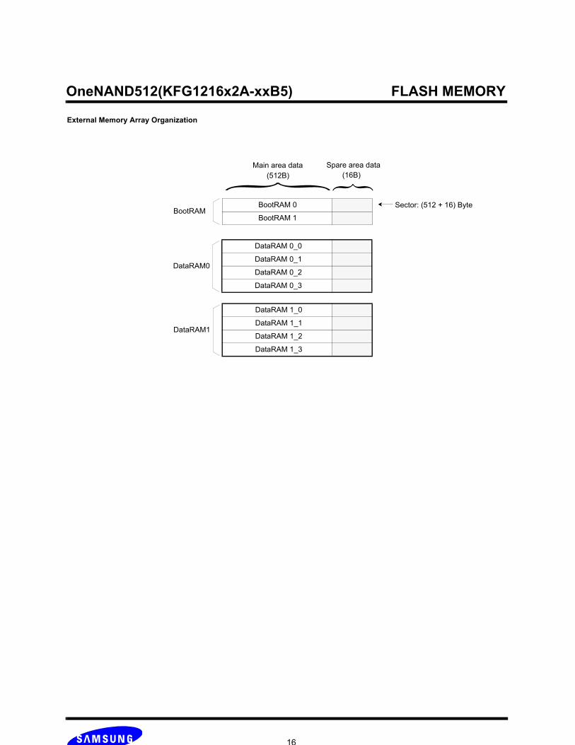
The on-chip external memory is comprised of 3 buffers used for Boot Code storage and data buffering.
The BootRAM is a 1KB buffer that receives Boot Code from the internal memory and makes it available to the host at start up.
There are two independent 2KB bi-directional data buffers, DataRAM0 and DataRAM1. These dual buffers enable the host to execute simultaneous Read-While load, and Write-While-program operations after Boot Up. During Boot Up, the BootRam is used by the host to initialize the main memory, and deliver boot code from NAND Flash core to host.
The external memory is divided into a main area and a spare area. Each buffer is the equivalent size of a Sector. The main area data is 512B. The spare area data is 16B.
External Memory Array Information
Area BootRAM DataRAM0 DataRAM1
Total Size 1KB+32B 2KB+64B 2KB+64B
Number of Sectors 2 4 4
SectorMain 512B 512B 512B
Spare 16B 16B 16B
Host
OTP Block
Nand Array
Boot code (1KB)BootRAM (1KB)
DataRAM0 (2KB)
DataRAM1 (2KB)
External (BufferRAM) Memory
Internal (Nand Array) Memory
2.6.2 External (BufferRAM) Memory Organization
OneNAND512(KFG1216x2A-xxB5) FLASH MEMORY
16
External Memory Array Organization
BootRAM 0
BootRAM 1BootRAM
DataRAM 1_0
DataRAM 1_1
DataRAM 1_2
DataRAM 1_3
DataRAM1{ Main area data Spare area data
DataRAM 0_0
DataRAM 0_1
DataRAM 0_2
DataRAM 0_3
DataRAM0
Sector: (512 + 16) Byte
{(512B) (16B)

OneNAND512(KFG1216x2A-xxB5) FLASH MEMORY
17
The following tables are the memory maps for the OneNAND.
2.7.1 Internal (NAND Array) Memory Organization The following tables show the Internal Memory address map in word order.
Block Block Address Page and Sector Address Size Block Block Address Page and Sector
Address Size
Block0 0000h 0000h~00FFh 128KB Block32 0020h 0000h~00FFh 128KB
Block1 0001h 0000h~00FFh 128KB Block33 0021h 0000h~00FFh 128KB
Block2 0002h 0000h~00FFh 128KB Block34 0022h 0000h~00FFh 128KB
Block3 0003h 0000h~00FFh 128KB Block35 0023h 0000h~00FFh 128KB
Block4 0004h 0000h~00FFh 128KB Block36 0024h 0000h~00FFh 128KB
Block5 0005h 0000h~00FFh 128KB Block37 0025h 0000h~00FFh 128KB
Block6 0006h 0000h~00FFh 128KB Block38 0026h 0000h~00FFh 128KB
Block7 0007h 0000h~00FFh 128KB Block39 0027h 0000h~00FFh 128KB
Block8 0008h 0000h~00FFh 128KB Block40 0028h 0000h~00FFh 128KB
Block9 0009h 0000h~00FFh 128KB Block41 0029h 0000h~00FFh 128KB
Block10 000Ah 0000h~00FFh 128KB Block42 002Ah 0000h~00FFh 128KB
Block11 000Bh 0000h~00FFh 128KB Block43 002Bh 0000h~00FFh 128KB
Block12 000Ch 0000h~00FFh 128KB Block44 002Ch 0000h~00FFh 128KB
Block13 000Dh 0000h~00FFh 128KB Block45 002Dh 0000h~00FFh 128KB
Block14 000Eh 0000h~00FFh 128KB Block46 002Eh 0000h~00FFh 128KB
Block15 000Fh 0000h~00FFh 128KB Block47 002Fh 0000h~00FFh 128KB
Block16 0010h 0000h~00FFh 128KB Block48 0030h 0000h~00FFh 128KB
Block17 0011h 0000h~00FFh 128KB Block49 0031h 0000h~00FFh 128KB
Block18 0012h 0000h~00FFh 128KB Block50 0032h 0000h~00FFh 128KB
Block19 0013h 0000h~00FFh 128KB Block51 0033h 0000h~00FFh 128KB
Block20 0014h 0000h~00FFh 128KB Block52 0034h 0000h~00FFh 128KB
Block21 0015h 0000h~00FFh 128KB Block53 0035h 0000h~00FFh 128KB
Block22 0016h 0000h~00FFh 128KB Block54 0036h 0000h~00FFh 128KB
Block23 0017h 0000h~00FFh 128KB Block55 0037h 0000h~00FFh 128KB
Block24 0018h 0000h~00FFh 128KB Block56 0038h 0000h~00FFh 128KB
Block25 0019h 0000h~00FFh 128KB Block57 0039h 0000h~00FFh 128KB
Block26 001Ah 0000h~00FFh 128KB Block58 003Ah 0000h~00FFh 128KB
Block27 001Bh 0000h~00FFh 128KB Block59 003Bh 0000h~00FFh 128KB
Block28 001Ch 0000h~00FFh 128KB Block60 003Ch 0000h~00FFh 128KB
Block29 001Dh 0000h~00FFh 128KB Block61 003Dh 0000h~00FFh 128KB
Block30 001Eh 0000h~00FFh 128KB Block62 003Eh 0000h~00FFh 128KB
Block31 001Fh 0000h~00FFh 128KB Block63 003Fh 0000h~00FFh 128KB
2.7 Memory Map

OneNAND512(KFG1216x2A-xxB5) FLASH MEMORY
18
Block Block Address Page and Sector Address Size Block Block Address Page and Sector
Address Size
Block64 0040h 0000h~00FFh 128KB Block96 0060h 0000h~00FFh 128KB
Block65 0041h 0000h~00FFh 128KB Block97 0061h 0000h~00FFh 128KB
Block66 0042h 0000h~00FFh 128KB Block98 0062h 0000h~00FFh 128KB
Block67 0043h 0000h~00FFh 128KB Block99 0063h 0000h~00FFh 128KB
Block68 0044h 0000h~00FFh 128KB Block100 0064h 0000h~00FFh 128KB
Block69 0045h 0000h~00FFh 128KB Block101 0065h 0000h~00FFh 128KB
Block70 0046h 0000h~00FFh 128KB Block102 0066h 0000h~00FFh 128KB
Block71 0047h 0000h~00FFh 128KB Block103 0067h 0000h~00FFh 128KB
Block72 0048h 0000h~00FFh 128KB Block104 0068h 0000h~00FFh 128KB
Block73 0049h 0000h~00FFh 128KB Block105 0069h 0000h~00FFh 128KB
Block74 004Ah 0000h~00FFh 128KB Block106 006Ah 0000h~00FFh 128KB
Block75 004Bh 0000h~00FFh 128KB Block107 006Bh 0000h~00FFh 128KB
Block76 004Ch 0000h~00FFh 128KB Block108 006Ch 0000h~00FFh 128KB
Block77 004Dh 0000h~00FFh 128KB Block109 006Dh 0000h~00FFh 128KB
Block78 004Eh 0000h~00FFh 128KB Block110 006Eh 0000h~00FFh 128KB
Block79 004Fh 0000h~00FFh 128KB Block111 006Fh 0000h~00FFh 128KB
Block80 0050h 0000h~00FFh 128KB Block112 0070h 0000h~00FFh 128KB
Block81 0051h 0000h~00FFh 128KB Block113 0071h 0000h~00FFh 128KB
Block82 0052h 0000h~00FFh 128KB Block114 0072h 0000h~00FFh 128KB
Block83 0053h 0000h~00FFh 128KB Block115 0073h 0000h~00FFh 128KB
Block84 0054h 0000h~00FFh 128KB Block116 0074h 0000h~00FFh 128KB
Block85 0055h 0000h~00FFh 128KB Block117 0075h 0000h~00FFh 128KB
Block86 0056h 0000h~00FFh 128KB Block118 0076h 0000h~00FFh 128KB
Block87 0057h 0000h~00FFh 128KB Block119 0077h 0000h~00FFh 128KB
Block88 0058h 0000h~00FFh 128KB Block120 0078h 0000h~00FFh 128KB
Block89 0059h 0000h~00FFh 128KB Block121 0079h 0000h~00FFh 128KB
Block90 005Ah 0000h~00FFh 128KB Block122 007Ah 0000h~00FFh 128KB
Block91 005Bh 0000h~00FFh 128KB Block123 007Bh 0000h~00FFh 128KB
Block92 005Ch 0000h~00FFh 128KB Block124 007Ch 0000h~00FFh 128KB
Block93 005Dh 0000h~00FFh 128KB Block125 007Dh 0000h~00FFh 128KB
Block94 005Eh 0000h~00FFh 128KB Block126 007Eh 0000h~00FFh 128KB
Block95 005Fh 0000h~00FFh 128KB Block127 007Fh 0000h~00FFh 128KB

OneNAND512(KFG1216x2A-xxB5) FLASH MEMORY
19
Block Block Address Page and Sector Address Size Block Block Address Page and Sector
Address Size
Block128 0080h 0000h~00FFh 128KB Block160 00A0h 0000h~00FFh 128KB
Block129 0081h 0000h~00FFh 128KB Block161 00A1h 0000h~00FFh 128KB
Block130 0082h 0000h~00FFh 128KB Block162 00A2h 0000h~00FFh 128KB
Block131 0083h 0000h~00FFh 128KB Block163 00A3h 0000h~00FFh 128KB
Block132 0084h 0000h~00FFh 128KB Block164 00A4h 0000h~00FFh 128KB
Block133 0085h 0000h~00FFh 128KB Block165 00A5h 0000h~00FFh 128KB
Block134 0086h 0000h~00FFh 128KB Block166 00A6h 0000h~00FFh 128KB
Block135 0087h 0000h~00FFh 128KB Block167 00A7h 0000h~00FFh 128KB
Block136 0088h 0000h~00FFh 128KB Block168 00A8h 0000h~00FFh 128KB
Block137 0089h 0000h~00FFh 128KB Block169 00A9h 0000h~00FFh 128KB
Block138 008Ah 0000h~00FFh 128KB Block170 00AAh 0000h~00FFh 128KB
Block139 008Bh 0000h~00FFh 128KB Block171 00ABh 0000h~00FFh 128KB
Block140 008Ch 0000h~00FFh 128KB Block172 00ACh 0000h~00FFh 128KB
Block141 008Dh 0000h~00FFh 128KB Block173 00ADh 0000h~00FFh 128KB
Block142 008Eh 0000h~00FFh 128KB Block174 00AEh 0000h~00FFh 128KB
Block143 008Fh 0000h~00FFh 128KB Block175 00AFh 0000h~00FFh 128KB
Block144 0090h 0000h~00FFh 128KB Block176 00B0h 0000h~00FFh 128KB
Block145 0091h 0000h~00FFh 128KB Block177 00B1h 0000h~00FFh 128KB
Block146 0092h 0000h~00FFh 128KB Block178 00B2h 0000h~00FFh 128KB
Block147 0093h 0000h~00FFh 128KB Block179 00B3h 0000h~00FFh 128KB
Block148 0094h 0000h~00FFh 128KB Block180 00B4h 0000h~00FFh 128KB
Block149 0095h 0000h~00FFh 128KB Block181 00B5h 0000h~00FFh 128KB
Block150 0096h 0000h~00FFh 128KB Block182 00B6h 0000h~00FFh 128KB
Block151 0097h 0000h~00FFh 128KB Block183 00B7h 0000h~00FFh 128KB
Block152 0098h 0000h~00FFh 128KB Block184 00B8h 0000h~00FFh 128KB
Block153 0099h 0000h~00FFh 128KB Block185 00B9h 0000h~00FFh 128KB
Block154 009Ah 0000h~00FFh 128KB Block186 00BAh 0000h~00FFh 128KB
Block155 009Bh 0000h~00FFh 128KB Block187 00BBh 0000h~00FFh 128KB
Block156 009Ch 0000h~00FFh 128KB Block188 00BCh 0000h~00FFh 128KB
Block157 009Dh 0000h~00FFh 128KB Block189 00BDh 0000h~00FFh 128KB
Block158 009Eh 0000h~00FFh 128KB Block190 00BEh 0000h~00FFh 128KB
Block159 009Fh 0000h~00FFh 128KB Block191 00BFh 0000h~00FFh 128KB

OneNAND512(KFG1216x2A-xxB5) FLASH MEMORY
20
Block Block Address Page and Sector Address Size Block Block Address Page and Sector
Address Size
Block192 00C0h 0000h~00FFh 128KB Block224 00E0h 0000h~00FFh 128KB
Block193 00C1h 0000h~00FFh 128KB Block225 00E1h 0000h~00FFh 128KB
Block194 00C2h 0000h~00FFh 128KB Block226 00E2h 0000h~00FFh 128KB
Block195 00C3h 0000h~00FFh 128KB Block227 00E3h 0000h~00FFh 128KB
Block196 00C4h 0000h~00FFh 128KB Block228 00E4h 0000h~00FFh 128KB
Block197 00C5h 0000h~00FFh 128KB Block229 00E5h 0000h~00FFh 128KB
Block198 00C6h 0000h~00FFh 128KB Block230 00E6h 0000h~00FFh 128KB
Block199 00C7h 0000h~00FFh 128KB Block231 00E7h 0000h~00FFh 128KB
Block200 00C8h 0000h~00FFh 128KB Block232 00E8h 0000h~00FFh 128KB
Block201 00C9h 0000h~00FFh 128KB Block233 00E9h 0000h~00FFh 128KB
Block202 00CAh 0000h~00FFh 128KB Block234 00EAh 0000h~00FFh 128KB
Block203 00CBh 0000h~00FFh 128KB Block235 00EBh 0000h~00FFh 128KB
Block204 00CCh 0000h~00FFh 128KB Block236 00ECh 0000h~00FFh 128KB
Block205 00CDh 0000h~00FFh 128KB Block237 00EDh 0000h~00FFh 128KB
Block206 00CEh 0000h~00FFh 128KB Block238 00EEh 0000h~00FFh 128KB
Block207 00CFh 0000h~00FFh 128KB Block239 00EFh 0000h~00FFh 128KB
Block208 00D0h 0000h~00FFh 128KB Block240 00F0h 0000h~00FFh 128KB
Block209 00D1h 0000h~00FFh 128KB Block241 00F1h 0000h~00FFh 128KB
Block210 00D2h 0000h~00FFh 128KB Block242 00F2h 0000h~00FFh 128KB
Block211 00D3h 0000h~00FFh 128KB Block243 00F3h 0000h~00FFh 128KB
Block212 00D4h 0000h~00FFh 128KB Block244 00F4h 0000h~00FFh 128KB
Block213 00D5h 0000h~00FFh 128KB Block245 00F5h 0000h~00FFh 128KB
Block214 00D6h 0000h~00FFh 128KB Block246 00F6h 0000h~00FFh 128KB
Block215 00D7h 0000h~00FFh 128KB Block247 00F7h 0000h~00FFh 128KB
Block216 00D8h 0000h~00FFh 128KB Block248 00F8h 0000h~00FFh 128KB
Block217 00D9h 0000h~00FFh 128KB Block249 00F9h 0000h~00FFh 128KB
Block218 00DAh 0000h~00FFh 128KB Block250 00FAh 0000h~00FFh 128KB
Block219 00DBh 0000h~00FFh 128KB Block251 00FBh 0000h~00FFh 128KB
Block220 00DCh 0000h~00FFh 128KB Block252 00FCh 0000h~00FFh 128KB
Block221 00DDh 0000h~00FFh 128KB Block253 00FDh 0000h~00FFh 128KB
Block222 00DEh 0000h~00FFh 128KB Block254 00FEh 0000h~00FFh 128KB
Block223 00DFh 0000h~00FFh 128KB Block255 00FFh 0000h~00FFh 128KB

OneNAND512(KFG1216x2A-xxB5) FLASH MEMORY
21
Block Block Address Page and Sector Address Size Block Block Address Page and Sector
Address Size
Block256 0100h 0000h~00FFh 128KB Block288 0120h 0000h~00FFh 128KB
Block257 0101h 0000h~00FFh 128KB Block289 0121h 0000h~00FFh 128KB
Block258 0102h 0000h~00FFh 128KB Block290 0122h 0000h~00FFh 128KB
Block259 0103h 0000h~00FFh 128KB Block291 0123h 0000h~00FFh 128KB
Block260 0104h 0000h~00FFh 128KB Block292 0124h 0000h~00FFh 128KB
Block261 0105h 0000h~00FFh 128KB Block293 0125h 0000h~00FFh 128KB
Block262 0106h 0000h~00FFh 128KB Block294 0126h 0000h~00FFh 128KB
Block263 0107h 0000h~00FFh 128KB Block295 0127h 0000h~00FFh 128KB
Block264 0108h 0000h~00FFh 128KB Block296 0128h 0000h~00FFh 128KB
Block265 0109h 0000h~00FFh 128KB Block297 0129h 0000h~00FFh 128KB
Block266 010Ah 0000h~00FFh 128KB Block298 012Ah 0000h~00FFh 128KB
Block267 010Bh 0000h~00FFh 128KB Block299 012Bh 0000h~00FFh 128KB
Block268 010Ch 0000h~00FFh 128KB Block300 012Ch 0000h~00FFh 128KB
Block269 010Dh 0000h~00FFh 128KB Block301 012Dh 0000h~00FFh 128KB
Block270 010Eh 0000h~00FFh 128KB Block302 012Eh 0000h~00FFh 128KB
Block271 010Fh 0000h~00FFh 128KB Block303 012Fh 0000h~00FFh 128KB
Block272 0110h 0000h~00FFh 128KB Block304 0130h 0000h~00FFh 128KB
Block273 0111h 0000h~00FFh 128KB Block305 0131h 0000h~00FFh 128KB
Block274 0112h 0000h~00FFh 128KB Block306 0132h 0000h~00FFh 128KB
Block275 0113h 0000h~00FFh 128KB Block307 0133h 0000h~00FFh 128KB
Block276 0114h 0000h~00FFh 128KB Block308 0134h 0000h~00FFh 128KB
Block277 0115h 0000h~00FFh 128KB Block309 0135h 0000h~00FFh 128KB
Block278 0116h 0000h~00FFh 128KB Block310 0136h 0000h~00FFh 128KB
Block279 0117h 0000h~00FFh 128KB Block311 0137h 0000h~00FFh 128KB
Block280 0118h 0000h~00FFh 128KB Block312 0138h 0000h~00FFh 128KB
Block281 0119h 0000h~00FFh 128KB Block313 0139h 0000h~00FFh 128KB
Block282 011Ah 0000h~00FFh 128KB Block314 013Ah 0000h~00FFh 128KB
Block283 011Bh 0000h~00FFh 128KB Block315 013Bh 0000h~00FFh 128KB
Block284 011Ch 0000h~00FFh 128KB Block316 013Ch 0000h~00FFh 128KB
Block285 011Dh 0000h~00FFh 128KB Block317 013Dh 0000h~00FFh 128KB
Block286 011Eh 0000h~00FFh 128KB Block318 013Eh 0000h~00FFh 128KB
Block287 011Fh 0000h~00FFh 128KB Block319 013Fh 0000h~00FFh 128KB

OneNAND512(KFG1216x2A-xxB5) FLASH MEMORY
22
Block Block Address Page and Sector Address Size Block Block Address Page and Sector
Address Size
Block320 0140h 0000h~00FFh 128KB Block352 0160h 0000h~00FFh 128KB
Block321 0141h 0000h~00FFh 128KB Block353 0161h 0000h~00FFh 128KB
Block322 0142h 0000h~00FFh 128KB Block354 0162h 0000h~00FFh 128KB
Block323 0143h 0000h~00FFh 128KB Block355 0163h 0000h~00FFh 128KB
Block324 0144h 0000h~00FFh 128KB Block356 0164h 0000h~00FFh 128KB
Block325 0145h 0000h~00FFh 128KB Block357 0165h 0000h~00FFh 128KB
Block326 0146h 0000h~00FFh 128KB Block358 0166h 0000h~00FFh 128KB
Block327 0147h 0000h~00FFh 128KB Block359 0167h 0000h~00FFh 128KB
Block328 0148h 0000h~00FFh 128KB Block360 0168h 0000h~00FFh 128KB
Block329 0149h 0000h~00FFh 128KB Block361 0169h 0000h~00FFh 128KB
Block330 014Ah 0000h~00FFh 128KB Block362 016Ah 0000h~00FFh 128KB
Block331 014Bh 0000h~00FFh 128KB Block363 016Bh 0000h~00FFh 128KB
Block332 014Ch 0000h~00FFh 128KB Block364 016Ch 0000h~00FFh 128KB
Block333 014Dh 0000h~00FFh 128KB Block365 016Dh 0000h~00FFh 128KB
Block334 014Eh 0000h~00FFh 128KB Block366 016Eh 0000h~00FFh 128KB
Block335 014Fh 0000h~00FFh 128KB Block367 016Fh 0000h~00FFh 128KB
Block336 0150h 0000h~00FFh 128KB Block368 0170h 0000h~00FFh 128KB
Block337 0151h 0000h~00FFh 128KB Block369 0171h 0000h~00FFh 128KB
Block338 0152h 0000h~00FFh 128KB Block370 0172h 0000h~00FFh 128KB
Block339 0153h 0000h~00FFh 128KB Block371 0173h 0000h~00FFh 128KB
Block340 0154h 0000h~00FFh 128KB Block372 0174h 0000h~00FFh 128KB
Block341 0155h 0000h~00FFh 128KB Block373 0175h 0000h~00FFh 128KB
Block342 0156h 0000h~00FFh 128KB Block374 0176h 0000h~00FFh 128KB
Block343 0157h 0000h~00FFh 128KB Block375 0177h 0000h~00FFh 128KB
Block344 0158h 0000h~00FFh 128KB Block376 0178h 0000h~00FFh 128KB
Block345 0159h 0000h~00FFh 128KB Block377 0179h 0000h~00FFh 128KB
Block346 015Ah 0000h~00FFh 128KB Block378 017Ah 0000h~00FFh 128KB
Block347 015Bh 0000h~00FFh 128KB Block379 017Bh 0000h~00FFh 128KB
Block348 015Ch 0000h~00FFh 128KB Block380 017Ch 0000h~00FFh 128KB
Block349 015Dh 0000h~00FFh 128KB Block381 017Dh 0000h~00FFh 128KB
Block350 015Eh 0000h~00FFh 128KB Block382 017Eh 0000h~00FFh 128KB
Block351 015Fh 0000h~00FFh 128KB Block383 017Fh 0000h~00FFh 128KB

OneNAND512(KFG1216x2A-xxB5) FLASH MEMORY
23
Block Block Address Page and Sector Address Size Block Block Address Page and Sector
Address Size
Block384 0180h 0000h~00FFh 128KB Block416 01A0h 0000h~00FFh 128KB
Block385 0181h 0000h~00FFh 128KB Block417 01A1h 0000h~00FFh 128KB
Block386 0182h 0000h~00FFh 128KB Block418 01A2h 0000h~00FFh 128KB
Block387 0183h 0000h~00FFh 128KB Block419 01A3h 0000h~00FFh 128KB
Block388 0184h 0000h~00FFh 128KB Block420 01A4h 0000h~00FFh 128KB
Block389 0185h 0000h~00FFh 128KB Block421 01A5h 0000h~00FFh 128KB
Block390 0186h 0000h~00FFh 128KB Block422 01A6h 0000h~00FFh 128KB
Block391 0187h 0000h~00FFh 128KB Block423 01A7h 0000h~00FFh 128KB
Block392 0188h 0000h~00FFh 128KB Block424 01A8h 0000h~00FFh 128KB
Block393 0189h 0000h~00FFh 128KB Block425 01A9h 0000h~00FFh 128KB
Block394 018Ah 0000h~00FFh 128KB Block426 01AAh 0000h~00FFh 128KB
Block395 018Bh 0000h~00FFh 128KB Block427 01ABh 0000h~00FFh 128KB
Block396 018Ch 0000h~00FFh 128KB Block428 01ACh 0000h~00FFh 128KB
Block397 018Dh 0000h~00FFh 128KB Block429 01ADh 0000h~00FFh 128KB
Block398 018Eh 0000h~00FFh 128KB Block430 01AEh 0000h~00FFh 128KB
Block399 018Fh 0000h~00FFh 128KB Block431 01AFh 0000h~00FFh 128KB
Block400 0190h 0000h~00FFh 128KB Block432 01B0h 0000h~00FFh 128KB
Block401 0191h 0000h~00FFh 128KB Block433 01B1h 0000h~00FFh 128KB
Block402 0192h 0000h~00FFh 128KB Block434 01B2h 0000h~00FFh 128KB
Block403 0193h 0000h~00FFh 128KB Block435 01B3h 0000h~00FFh 128KB
Block404 0194h 0000h~00FFh 128KB Block436 01B4h 0000h~00FFh 128KB
Block405 0195h 0000h~00FFh 128KB Block437 01B5h 0000h~00FFh 128KB
Block406 0196h 0000h~00FFh 128KB Block438 01B6h 0000h~00FFh 128KB
Block407 0197h 0000h~00FFh 128KB Block439 01B7h 0000h~00FFh 128KB
Block408 0198h 0000h~00FFh 128KB Block440 01B8h 0000h~00FFh 128KB
Block409 0199h 0000h~00FFh 128KB Block441 01B9h 0000h~00FFh 128KB
Block410 019Ah 0000h~00FFh 128KB Block442 01BAh 0000h~00FFh 128KB
Block411 019Bh 0000h~00FFh 128KB Block443 01BBh 0000h~00FFh 128KB
Block412 019Ch 0000h~00FFh 128KB Block444 01BCh 0000h~00FFh 128KB
Block413 019Dh 0000h~00FFh 128KB Block445 01BDh 0000h~00FFh 128KB
Block414 019Eh 0000h~00FFh 128KB Block446 01BEh 0000h~00FFh 128KB
Block415 019Fh 0000h~00FFh 128KB Block447 01BFh 0000h~00FFh 128KB

OneNAND512(KFG1216x2A-xxB5) FLASH MEMORY
24
Block Block Address Page and Sector Address Size Block Block Address Page and Sector
Address Size
Block448 01C0h 0000h~00FFh 128KB Block480 01E0h 0000h~00FFh 128KB
Block449 01C1h 0000h~00FFh 128KB Block481 01E1h 0000h~00FFh 128KB
Block450 01C2h 0000h~00FFh 128KB Block482 01E2h 0000h~00FFh 128KB
Block451 01C3h 0000h~00FFh 128KB Block483 01E3h 0000h~00FFh 128KB
Block452 01C4h 0000h~00FFh 128KB Block484 01E4h 0000h~00FFh 128KB
Block453 01C5h 0000h~00FFh 128KB Block485 01E5h 0000h~00FFh 128KB
Block454 01C6h 0000h~00FFh 128KB Block486 01E6h 0000h~00FFh 128KB
Block455 01C7h 0000h~00FFh 128KB Block487 01E7h 0000h~00FFh 128KB
Block456 01C8h 0000h~00FFh 128KB Block488 01E8h 0000h~00FFh 128KB
Block457 01C9h 0000h~00FFh 128KB Block489 01E9h 0000h~00FFh 128KB
Block458 01CAh 0000h~00FFh 128KB Block490 01EAh 0000h~00FFh 128KB
Block459 01CBh 0000h~00FFh 128KB Block491 01EBh 0000h~00FFh 128KB
Block460 01CCh 0000h~00FFh 128KB Block492 01ECh 0000h~00FFh 128KB
Block461 01CDh 0000h~00FFh 128KB Block493 01EDh 0000h~00FFh 128KB
Block462 01CEh 0000h~00FFh 128KB Block494 01EEh 0000h~00FFh 128KB
Block463 01CFh 0000h~00FFh 128KB Block495 01EFh 0000h~00FFh 128KB
Block464 01D0h 0000h~00FFh 128KB Block496 01F0h 0000h~00FFh 128KB
Block465 01D1h 0000h~00FFh 128KB Block497 01F1h 0000h~00FFh 128KB
Block466 01D2h 0000h~00FFh 128KB Block498 01F2h 0000h~00FFh 128KB
Block467 01D3h 0000h~00FFh 128KB Block499 01F3h 0000h~00FFh 128KB
Block468 01D4h 0000h~00FFh 128KB Block500 01F4h 0000h~00FFh 128KB
Block469 01D5h 0000h~00FFh 128KB Block501 01F5h 0000h~00FFh 128KB
Block470 01D6h 0000h~00FFh 128KB Block502 01F6h 0000h~00FFh 128KB
Block471 01D7h 0000h~00FFh 128KB Block503 01F7h 0000h~00FFh 128KB
Block472 01D8h 0000h~00FFh 128KB Block504 01F8h 0000h~00FFh 128KB
Block473 01D9h 0000h~00FFh 128KB Block505 01F9h 0000h~00FFh 128KB
Block474 01DAh 0000h~00FFh 128KB Block506 01FAh 0000h~00FFh 128KB
Block475 01DBh 0000h~00FFh 128KB Block507 01FBh 0000h~00FFh 128KB
Block476 01DCh 0000h~00FFh 128KB Block508 01FCh 0000h~00FFh 128KB
Block477 01DDh 0000h~00FFh 128KB Block509 01FDh 0000h~00FFh 128KB
Block478 01DEh 0000h~00FFh 128KB Block510 01FEh 0000h~00FFh 128KB
Block479 01DFh 0000h~00FFh 128KB Block511 01FFh 0000h~00FFh 128KB
OneNAND512(KFG1216x2A-xxB5) FLASH MEMORY
25
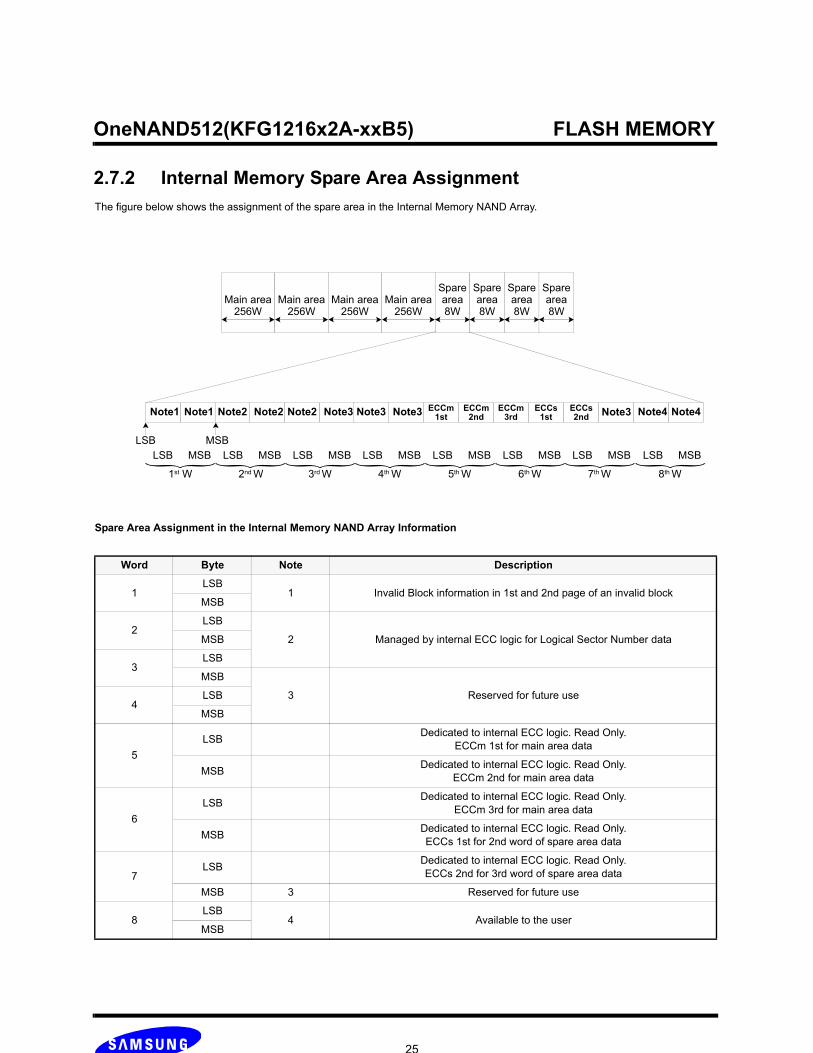
The figure below shows the assignment of the spare area in the Internal Memory NAND Array.
Spare Area Assignment in the Internal Memory NAND Array Information
Word Byte Note Description
1LSB
1 Invalid Block information in 1st and 2nd page of an invalid blockMSB
2LSB
2 Managed by internal ECC logic for Logical Sector Number dataMSB
3LSB
MSB
3 Reserved for future use4
LSB
MSB
5LSB Dedicated to internal ECC logic. Read Only.
ECCm 1st for main area data
MSB Dedicated to internal ECC logic. Read Only. ECCm 2nd for main area data
6LSB Dedicated to internal ECC logic. Read Only.
ECCm 3rd for main area data
MSB Dedicated to internal ECC logic. Read Only. ECCs 1st for 2nd word of spare area data
7LSB Dedicated to internal ECC logic. Read Only.
ECCs 2nd for 3rd word of spare area data
MSB 3 Reserved for future use
8LSB
4 Available to the userMSB
Main area256W
Main area256W
Main area256W
Main area256W
Sparearea8W
Sparearea8W
Sparearea8W
Sparearea8W
{
1st W
ECCm1st
ECCm2nd
ECCm3rd
ECCs1st
ECCs2nd
LSB MSBLSB MSB {
2nd W
LSB MSB {
3rd W
LSB MSB {4th W
LSB MSB {5th W
LSB MSB {6th W
LSB MSB {
7th W
LSB MSB {
8th W
LSB MSB
Note1 Note1 Note2 Note2 Note2 Note3 Note3 Note3 Note4 Note4 Note3
2.7.2 Internal Memory Spare Area Assignment

OneNAND512(KFG1216x2A-xxB5) FLASH MEMORY
26
Division Address(word order)
Address(byte order)
Size(total 128KB) Usage Description
Main area(64KB)
0000h~00FFh 00000h~001FEh 512B1KB R
BootM 0 BootRAM Main sector0
0100h~01FFh 00200h~003FEh 512B BootM 1 BootRAM Main sector1
0200h~02FFh 00400h~005FEh 512B
4KB R/W
DataM 0_0 DataRAM Main page0/sector0
0300h~03FFh 00600h~007FEh 512B DataM 0_1 DataRAM Main page0/sector1
0400h~04FFh 00800h~009FEh 512B DataM 0_2 DataRAM Main page0/sector2
0500h~05FFh 00A00h~00BFEh 512B DataM 0_3 DataRAM Main page0/sector3
0600h~06FFh 00C00h~00DFEh 512B DataM 1_0 DataRAM Main page1/sector0
0700h~07FFh 00E00h~00FFEh 512B DataM 1_1 DataRAM Main page1/sector1
0800h~08FFh 01000h~011FEh 512B DataM 1_2 DataRAM Main page1/sector2
0900h~09FFh 01200h~013FEh 512B DataM 1_3 DataRAM Main page1/sector3
0A00h~7FFFh 01400h~0FFFEh 59K 59K - Reserved Reserved
Spare area(8KB)
8000h~8007h 10000h~1000Eh 16B32B R
BootS 0 BootRAM Spare sector0
8008h~800Fh 10010h~1001Eh 16B BootS 1 BootRAM Spare sector1
8010h~8017h 10020h~1002Eh 16B
128B R/W
DataS 0_0 DataRAM Spare page0/sector0
8018h~801Fh 10030h~1003Eh 16B DataS 0_1 DataRAM Spare page0/sector1
8020h~8027h 10040h~1004Eh 16B DataS 0_2 DataRAM Spare page0/sector2
8028h~802Fh 10050h~1005Eh 16B DataS 0_3 DataRAM Spare page0/sector3
8030h~8037h 10060h~1006Eh 16B DataS 1_0 DataRAM Spare page1/sector0
8038h~803Fh 10070h~1007Eh 16B DataS 1_1 DataRAM Spare page1/sector1
8040h~8047h 10080h~1008Eh 16B DataS 1_2 DataRAM Spare page1/sector2
8048h~804Fh 10090h~1009Eh 16B DataS 1_3 DataRAM Spare page1/sector3
8050h~8FFFh 100A0h~11FFEh 8032B 8032B - Reserved Reserved
Reserved(24KB) 9000h~BFFFh 12000h~17FFEh 24KB 24KB - Reserved Reserved
Reserved(8KB) C000h~CFFFh 18000h~19FFEh 8KB 8KB - Reserved Reserved
Reserved(16KB) D000h~EFFFh 1A000h~1DFFEh 16KB 16KB - Reserved Reserved
Registers(8KB) F000h~FFFFh 1E000h~1FFFEh 8KB 8KB R or R/W Registers Registers
The following table shows the External Memory address map in Word and Byte Order.Note that the data output is unknown while host reads a register bit of reserved area.
2.7.3 External Memory (BufferRAM) Address Map

OneNAND512(KFG1216x2A-xxB5) FLASH MEMORY
27
The tables below show Word Order Address Map information for the BootRAM and DataRAM main and spare areas.
-0000h~01FFh: 2(sector) x 512byte(NAND main area) = 1KB
0000h~00FFh(512B)BootM 0
(sector 0 of page 0)
0100h~01FFh(512B)BootM 1
(sector 1 of page 0)
• BootRAM(Main area)
-0200h~09FFh: 8(sector) x 512byte(NAND main area) = 4KB
0200h~02FFh(512B)DataM 0_0
(sector 0 of page 0)
0300h~03FFh(512B)DataM 0_1
(sector 1 of page 0)
0400h~04FFh(512B)DataM 0_2
(sector 2 of page 0)
0500h~05FFh(512B)DataM 0_3
(sector 3 of page 0)
0600h~06FFh(512B)DataM 1_0
(sector 0 of page 1)
0700h~07FFh(512B)DataM 1_1
(sector 1 of page 1)
0800h~08FFh(512B)DataM 1_2
(sector 2 of page 1)
0900h~09FFh(512B)DataM 1_3
(sector 3 of page 1)
• DataRAM(Main area)
-8000h~800Fh: 2(sector) x 16byte(NAND spare area) = 32B
8000h~8007h(16B)BootS 0
(sector 0 of page 0)
8008h~800Fh(16B)BootS 1
(sector 1 of page 0)
• BootRAM(Spare area)
-8010h~804Fh: 8(sector) x 16byte(NAND spare area) = 128B
*NAND Flash array consists of 2KB page size and 128KB block size.
8010h~8017h(16B)DataS 0_0
(sector 0 of page 0)
8018h~801Fh(16B)DataS 0_1
(sector 1 of page 0)
8020h~8027h(16B)DataS 0_2
(sector 2 of page 0)
8028h~802Fh(16B)DataS 0_3
(sector 3 of page 0)
8030h~8037h(16B)DataS 1_0
(sector 0 of page 1)
8038h~803Fh(16B)DataS 1_1
(sector 1 of page 1)
8040h~8047h(16B)DataS 1_2
(sector 2 of page 1)
8048h~804Fh(16B)DataS 1_3
(sector 3 of page 1)
• DataRAM(Spare area)
2.7.4 External Memory Detail Map Information

OneNAND512(KFG1216x2A-xxB5) FLASH MEMORY
28
Buf. Word Address
Byte Address F E D C B A 9 8 7 6 5 4 3 2 1 0
BootS 0 8000h 10000h BI
8001h 10002h Managed by Internal ECC logic
8002h 10004h Reserved for the future use Managed by Internal ECC logic
8003h 10006h Reserved for the current and future use
8004h 10008h ECC Code for Main area data (2nd) ECC Code for Main area data (1st)
8005h 1000Ah ECC Code for Spare area data (1st) ECC Code for Main area data (3rd)
8006h 1000Ch FFh(Reserved for the future use) ECC Code for Spare area data (2nd)
8007h 1000Eh Free Usage
BootS 1 8008h 10010h BI
8009h 10012h Managed by Internal ECC logic
800Ah 10014h Reserved for the future use Managed by Internal ECC logic
800Bh 10016h Reserved for the current and future use
800Ch 10018h ECC Code for Main area data (2nd) ECC Code for Main area data (1st)
800Dh 1001Ah ECC Code for Spare area data (1st) ECC Code for Main area data (3rd)
800Eh 1001Ch FFh(Reserved for the future use) ECC Code for Spare area data (2nd)
800Fh 1001Eh Free Usage
DataS 0_0
8010h 10020h BI
8011h 10022h Managed by Internal ECC logic
8012h 10024h Reserved for the future use Managed by Internal ECC logic
8013h 10026h Reserved for the current and future use
8014h 10028h ECC Code for Main area data (2nd) ECC Code for Main area data (1st)
8015h 1002Ah ECC Code for Spare area data (1st) ECC Code for Main area data (3rd)
8016h 1002Ch FFh(Reserved for the future use) ECC Code for Spare area data (2nd)
8017h 1002Eh Free Usage
DataS 0_1
8018h 10030h BI
8019h 10032h Managed by Internal ECC logic
801Ah 10034h Reserved for the future use Managed by Internal ECC logic
801Bh 10036h Reserved for the current and future use
801Ch 10038h ECC Code for Main area data (2nd) ECC Code for Main area data (1st)
801Dh 1003Ah ECC Code for Spare area data (1st) ECC Code for Main area data (3rd)
801Eh 1003Ch FFh(Reserved for the future use) ECC Code for Spare area data (2nd)
801Fh 1003Eh Free Usage
Equivalent to 1word of NAND Flash
2.7.5 External Memory Spare Area Assignment

OneNAND512(KFG1216x2A-xxB5) FLASH MEMORY
29
Buf. WordAddress
ByteAddress F E D C B A 9 8 7 6 5 4 3 2 1 0
DataS 0_2 8020h 10040h BI
8021h 10042h Managed by Internal ECC logic
8022h 10044h Reserved for the future use Managed by Internal ECC logic
8023h 10046h Reserved for the current and future use
8024h 10048h ECC Code for Main area data (2nd) ECC Code for Main area data (1st)
8025h 1004Ah ECC Code for Spare area data (1st) ECC Code for Main area data (3rd)
8026h 1004Ch Reserved for the future use ECC Code for Spare area data (2nd)
8027h 1004Eh Free Usage
DataS 0_3 8028h 10050h BI
8029h 10052h Managed by Internal ECC logic
802Ah 10054h Reserved for the future use Managed by Internal ECC logic
802Bh 10056h Reserved for the current and future use
802Ch 10058h ECC Code for Main area data (2nd) ECC Code for Main area data (1st)
802Dh 1005Ah ECC Code for Spare area data (1st) ECC Code for Main area data (3rd)
802Eh 1005Ch Reserved for the future use ECC Code for Spare area data (2nd)
802Fh 1005Eh Free Usage
DataS 1_0 8030h 10060h BI
8031h 10062h Managed by Internal ECC logic
8032h 10064h Reserved for the future use Managed by Internal ECC logic
8033h 10066h Reserved for the current and future use
8034h 10068h ECC Code for Main area data (2nd) ECC Code for Main area data (1st)
8035h 1006Ah ECC Code for Spare area data (1st) ECC Code for Main area data (3rd)
8036h 1006Ch Reserved for the future use ECC Code for Spare area data (2nd)
8037h 1006Eh Free Usage
DataS 1_1 8038h 10070h BI
8039h 10072h Managed by Internal ECC logic
803Ah 10074h Reserved for the future use Managed by Internal ECC logic
803Bh 10076h Reserved for the current and future use
803Ch 10078h ECC Code for Main area data (2nd) ECC Code for Main area data (1st)
803Dh 1007Ah ECC Code for Spare area data (1st) ECC Code for Main area data (3rd)
803Eh 1007Ch Reserved for the future use ECC Code for Spare area data (2nd)
803Fh 1007Eh Free Usage
DataS 1_2 8040h 10080h BI
8041h 10082h Managed by Internal ECC logic
8042h 10084h Reserved for the future use Managed by Internal ECC logic
8043h 10086h Reserved for the current and future use
8044h 10088h ECC Code for Main area data (2nd) ECC Code for Main area data (1st)
8045h 1008Ah ECC Code for Spare area data (1st) ECC Code for Main area data (3rd)
8046h 1008Ch Reserved for the future use ECC Code for Spare area data (2nd)
8047h 1008Eh Free Usage

OneNAND512(KFG1216x2A-xxB5) FLASH MEMORY
30
Equivalent to 1word of NAND Flash
NOTE:- BI: Bad block Information
>Host can use complete spare area except BI and ECC code area. For example, Host can write data to Spare area buffer except for the area controlled by ECC logic at program operation.>In case of ’with ECC’ mode, OneNAND automatically generates ECC code for both main and spare data of memory during program operation, but does not update ECC code to spare bufferRAM during load operation.>When loading/programming spare area, spare area BufferRAM address(BSA) and BufferRAM sector count(BSC) is chosen via Start buffer register as it is.
Buf. WordAddress
ByteAddress F E D C B A 9 8 7 6 5 4 3 2 1 0
DataS 1_3 8048h 10090h BI
8049h 10092h Managed by Internal ECC logic
804Ah 10094h Reserved for the future use Managed by Internal ECC logic
804Bh 10096h Reserved for the current and future use
804Ch 10098h ECC Code for Main area data (2nd) ECC Code for Main area data (1st)
804Dh 1009Ah ECC Code for Spare area data (1st) ECC Code for Main area data (3rd)
804Eh 1009Ch Reserved for the future use ECC Code for Spare area data (2nd)
804Fh 1009Eh Free Usage
Equivalent to 1word of NAND Flash

OneNAND512(KFG1216x2A-xxB5) FLASH MEMORY
31
Section 2.8 of this specification provides information about the OneNAND512 registers.
2.8.1 Register Address Map
This map describes the register addresses, register name, register description, and host accessibility.
Address(word order)
Address(byte order) Name Host
Access Description
F000h 1E000h Manufacturer ID R Manufacturer identification
F001h 1E002h Device ID R Device identification
F002h 1E004h Version ID R N/A
F003h 1E006h Data Buffer size R Data buffer size
F004h 1E008h Boot Buffer size R Boot buffer size
F005h 1E00Ah Amount ofbuffers R Amount of data/boot buffers
F006h 1E00Ch Technology R Info about technology
F007h~F0FFh 1E00Eh~1E1FEh Reserved - Reserved for user
F100h 1E200h Start address 1 R/W NAND Flash Block Address
F101h 1E202h Start address 2 R/W Reserved
F102h 1E204h Start address 3 R/W Destination Block address for Copy back program
F103h 1E206h Start address 4 R/W Destination Page & Sector address for Copyback program
F104h 1E208h Start address 5 - N/A
F105h 1E20Ah Start address 6 - N/A
F106h 1E20Ch Start address 7 - N/A
F107h 1E20Eh Start address 8 R/W NAND Flash Page & Sector address
F108h~F1FFh 1E210h~1E3FEh Reserved - Reserved for user
F200h 1E400h Start Buffer R/W
Buffer Number for the page data transfer to/from the memory and the start Buffer AddressThe meaning is with which buffer to start and how manybuffers to use for the data transfer
F201h~F207h 1E402h~1E40Eh Reserved - Reserved for user
F208h~F21Fh 1E410h~1E43Eh Reserved - Reserved for vendor specific purposes
F220h 1E440h Command R/W Host control and memory operation commands
F221h 1E442h SystemConfiguration 1 R, R/W memory and Host Interface Configuration
F222h 1E444h SystemConfiguration 2 - N/A
F223h~F22Fh 1E446h~1E45Eh Reserved - Reserved for user
F230h~F23Fh 1E460h~1E47Eh Reserved - Reserved for vendor specific purposes
F240h 1E480h Controller Status R Controller Status and result of memory operation
F241h 1E482h Interrupt R/W Memory Command Completion Interrupt Status
F242h~F24Bh 1E484h~1E496h Reserved - Reserved for user
F24Ch 1E498h StartBlock Address R/W Start memory block address in Write Protection mode
2.8 Registers

OneNAND512(KFG1216x2A-xxB5) FLASH MEMORY
32
Address(word order)
Address(byte order) Name Host
Access Description
F24Dh 1E49Ah Reserved R/W Reserved for user
F24Eh 1E49Ch Write ProtectionStatus R Current memory Write Protection status
(unlocked/locked/tight-locked)
F24Fh~FEFFh 1E49Eh~1FDFEh Reserved - Reserved for user
FF00h 1FE00h ECC StatusRegister R ECC status of sector
FF01h 1FE02h ECC Result ofmain area data R ECC error position of Main area data error for first
selected Sector
FF02h 1FE04h ECC Result ofspare area data R ECC error position of Spare area data error for first
selected Sector
FF03h 1FE06h ECC Result ofmain area data R ECC error position of Main area data error for second
selected Sector
FF04h 1FE08h ECC Result ofspare area data R ECC error position of Spare area data error for second
selected Sector
FF05h 1FE0Ah ECC Result ofmain area data R ECC error position of Main area data error for third
selected Sector
FF06h 1FE0Ch ECC Result ofspare area data R ECC error position of Spare area data error for third
selected Sector
FF07h 1FE0Eh ECC Result ofmain area data R ECC error position of Main area data error for fourth
selected Sector
FF08h 1FE10h ECC Result ofspare area data R ECC error position of Spare area data error for fourth
selected Sector
FF09h~FFFFh 1FE12h~1FFFEh Reserved - Reserved for vendor specific purposes
This Read register describes the manufacturer's identification. Samsung Electronics Company manufacturer's ID is 00ECh.
F000h, default = 00ECh
15 14 13 12 11 10 9 8 7 6 5 4 3 2 1 0
ManufID
2.8.2 Manufacturer ID Register F000h (R)

OneNAND512(KFG1216x2A-xxB5) FLASH MEMORY
33
This Read register describes the device.
F001h, see table for default.
15 14 13 12 11 10 9 8 7 6 5 4 3 2 1 0
DeviceID
Device Identification
Device ID Default
Device Identification Description
DeviceID [1:0] Vcc 00 = 1.8V, 01 = 2.65V/3.3V, 10/11 = reserved
DeviceID [2] Muxed/Demuxed 0 = Muxed, 1 = Demuxed
DeviceID [3] Single/DPP 0 = Single, 1 = DDP
DeviceID [6:4] Density 000 = 128Mb, 001 = 256Mb, 010 = 512Mb, 011 = 1Gb, 100 = 2Gb
Device DeviceID[15:0]
KFG1216Q2A 0024h
KFG1216D2A 0025h
KFG1216U2A 0025h
2.8.3 Device ID Register F001h (R)

OneNAND512(KFG1216x2A-xxB5) FLASH MEMORY
34
This register is reserved for manufacturer
2.8.5 Data Buffer Size Register F003h (R)
This Read register describes the size of the Data Buffer.
F003h, default = 0800h
15 14 13 12 11 10 9 8 7 6 5 4 3 2 1 0
DataBufSize
Data Buffer Size Information
Version Identification Description
DataBufSizeTotal data buffer size in Words equal to 2 buffers of 1024 Words each
(2 x 1024 = 211) in the memory interface
2.8.6 Boot Buffer Size Register F004h (R) This Read register describes the size of the Boot Buffer.
F004h, default = 0200h
15 14 13 12 11 10 9 8 7 6 5 4 3 2 1 0
BootBufSize
Register Information Description
BootBufSizeTotal boot buffer size in Words equal to 1 buffer of 512 Words
(1 x 512 = 29) in the memory interface
2.8.4 Version ID Register F002h

OneNAND512(KFG1216x2A-xxB5) FLASH MEMORY
35
This Read register describes the number of each Buffer.
F005h, default = 0201h
15 14 13 12 11 10 9 8 7 6 5 4 3 2 1 0
DataBufAmount BootBufAmount
Number of Buffers Information
Register Information Description
DataBufAmount The number of data buffers = 2 (2N, N=1)
BootBufAmount The number of boot buffers = 1 (2N, N=0)
2.8.8 Technology Register F006h (R) This Read register describes the internal NAND array technology.
F006h, default = 0000h
15 14 13 12 11 10 9 8 7 6 5 4 3 2 1 0
Tech
Technology Information
Technology Register Setting
NAND SLC 0000h
NAND MLC 0001h
Reserved 0002h ~ FFFFh
2.8.7 Number of Buffers Register F005h (R)

OneNAND512(KFG1216x2A-xxB5) FLASH MEMORY
36
This Read/Write register describes the start address of the NAND Flash block address which will be loaded, programmed, or erased.
F100h, default = 0000h
15 14 13 12 11 10 9 8 7 6 5 4 3 2 1 0
Reserved(00000) FBA
Device Number of Block FBA
512Mb 512 FBA[8:0]
Start Address1 Information
Register Information Description
FBA NAND Flash Block Address
2.8.10 Start Address2 Register F101h (R/W)
This register is reserved for future use.
2.8.9 Start Address1 Register F100h (R/W)

OneNAND512(KFG1216x2A-xxB5) FLASH MEMORY
37
This Read/Write register describes the NAND Flash destination block address which will be copy back programmed.
F102h, default = 0000h
15 14 13 12 11 10 9 8 7 6 5 4 3 2 1 0
Reserved(000000) FCBA
Device Number of Block FBA
512Mb 512 FCBA[8:0]
Start Address3 Information
Register Information Description
FCBA NAND Flash Copy Back Block Address
2.8.12 Start Address4 Register F103h (R/W) This Read/Write register describes the NAND Flash destination page address in a block and the NAND Flash destination sector address in a page for copy back programming.
F103h, default = 0000h
15 14 13 12 11 10 9 8 7 6 5 4 3 2 1 0
Reserved(00000000) FCPA FCSA
Start Address4 Information
Item Description Default Value Range
FCPA NAND Flash Copy Back Page Address 000000 000000 ~ 111111,
6 bits for 64 pages
FCSA NAND Flash Copy Back Sector Address 00 00 ~ 11,
2 bits for 4 sectors
2.8.11 Start Address3 Register F102h (R/W)
OneNAND512(KFG1216x2A-xxB5) FLASH MEMORY
38
This register is reserved for future use.
2.8.14 Start Address6 Register F105h
This register is reserved for future use.
2.8.15 Start Address7 Register F106h
This register is reserved for future use.
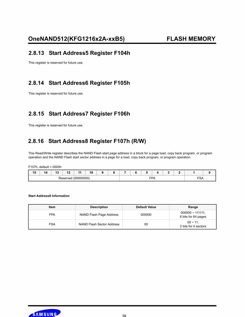
2.8.16 Start Address8 Register F107h (R/W)
This Read/Write register describes the NAND Flash start page address in a block for a page load, copy back program, or program operation and the NAND Flash start sector address in a page for a load, copy back program, or program operation.
F107h, default = 0000h
15 14 13 12 11 10 9 8 7 6 5 4 3 2 1 0
Reserved (00000000) FPA FSA
Start Address8 Information
Item Description Default Value Range
FPA NAND Flash Page Address 000000 000000 ~ 111111, 6 bits for 64 pages
FSA NAND Flash Sector Address 00 00 ~ 11,2 bits for 4 sectors
2.8.13 Start Address5 Register F104h

OneNAND512(KFG1216x2A-xxB5) FLASH MEMORY
39
This Read/Write register describes the BufferRAM Sector Count (BSC) and BufferRAM Sector Address (BSA).
The BufferRAM Sector Count (BSC) field specifies the number of sectors to be loaded, programmed, or copy back programmed. At 00 value (the default value), the number of sector is "4". If the internal RAM buffer reaches its maximum value of 11, it will count up to 0 value to meet the BSC value. For example, if BSA = 1101, BSC = 00, then the selected BufferRAM will count up from '1101 → 1110 → 1111 → 1100'.
The BufferRAM Sector Address (BSA) is the sector 0~3 address in the internal BootRAM and DataRAM where data is placed.
F200h, default = 0000h
15 14 13 12 11 10 9 8 7 6 5 4 3 2 1 0
Reserved(0000) BSA Reserved(000000) BSC
Start Address8 Information
Item Description
BSA[3] Selection bit between BootRAM and DataRAM
BSA[2] Selection bit between DataRAM0 and DataRAM1
BSA[1:0] Selection bit between Sector0 and Sector1 in the internal BootRAMSelection bit between Sector0 to Sector3 in the internal DataRAM
BootRAM 0
BootRAM 1BootRAM
Sector: (512 + 16) Byte
DataRAM 1_0
DataRAM 1_1
DataRAM 1_2
DataRAM 1_3
DataRAM1
00000001
1100
1101
1110
1111
BSC Number of Sectors
01 1 sector
10 2 sector
11 3 sector
00 4 sector
{Main area data {Spare area data
BSA
DataRAM 0_0
DataRAM 0_1
DataRAM 0_2
DataRAM 0_3
DataRAM0
1000
1001
1010
1011
512B 16B
2.8.17 Start Buffer Register F200h (R/W)

OneNAND512(KFG1216x2A-xxB5) FLASH MEMORY
40
This Read/Write register describes the operation of the OneNAND interface.Note that all commands should be issued right after INT is turned from ready state to busy state. (i.e. right after 0 is written to INT reg-ister.) After any command is issued and the corresponding operation is completed, INT goes back to ready state. (00F0h and 00F3h may be accepted during busy state of some operations. Refer to the rightmost column of the command register table below.)
F220h, default = 0000h
15 14 13 12 11 10 9 8 7 6 5 4 3 2 1 0
Command
NOTE:1) 0080h programs both main and spare area, while 001Ah programs only spare area. Refer to chapter 5.8 for NOP limits in issuing these commands.When using 0080h and 001Ah command, Read-only part in spare area must be masked by FF. (Refer to chapter 2.7.2)2) ’Reset OneNAND’(=Hot reset) command makes the registers and NAND Flash core into default state as the warm reset(=reset by RP pin).
CMD OperationAcceptablecommand
during busy
0000h Load single/multiple sector data unit into buffer 00F0h, 00F3h
0013h Load single/multiple spare sector into buffer 00F0h, 00F3h
0080h Program single/multiple sector data unit from buffer1) 00F0h, 00F3h
001Ah Program single/multiple spare data unit from buffer 00F0h, 00F3h
001Bh Copy back Program operation 00F0h, 00F3h
0023h Unlock NAND array a block -
002Ah Lock NAND array a block -
002Ch Lock-tight NAND array a block
0071h Erase Verify Read 00F0h, 00F3h
0094h Block Erase 00F0h, 00F3h
0095h Multi-Block Erase 00F0h, 00F3h
00B0h Erase Suspend -
0030h Erase Resume 00F0h, 00F3h
00F0h Reset NAND Flash Core -
00F3h Reset OneNAND 2) -
0065h OTP Access 00F0h, 00F3h
2.8.18 Command Register F220h (R/W)

OneNAND512(KFG1216x2A-xxB5) FLASH MEMORY
41
This Read/Write register describes the system configuration.
F221h, default = 40C0h
15 14 13 12 11 10 9 8 7 6 5 4 3 2 1 0
R/W R/W R/W R/W R/W R/W R/W R/W R R
RM BRL BL ECC RDYpol
INTpol IOBE RDY
Conf Reserved(000) BWPS
Read Mode (RM)
RM Read Mode
0 Asynchronous read(default)
1 Synchronous read
Read Mode Information[15]
Item Definition Description
RM Read Mode Selects between asynchronous read mode and synchronous read mode
Burst Read Latency (BRL)
BRL Latency Cycles
000 8(N/A)
001 9(N/A)
010 10(N/A)
011 3(up to 40MHz)
100 4(default, min.)
101 5
110 6
111 7
Burst Read Latency (BRL) Information[14:12]
Item Definition Description
BRL Burst Read Latency Specifies the access latency in the burst read transfer after the initial access
2.8.19 System Configuration 1 Register F221h (R, R/W)

OneNAND512(KFG1216x2A-xxB5) FLASH MEMORY
42
Burst Length (BL)
BL Burst Length(Main) Burst Length(Spare)
000 Continuous(default)
001 4 words
010 8 words
011 16 words
100 32 words N/A
101~111 Reserved
Burst Length (BL) Information[11:9]
Item Definition Description
BL Burst Length Specifies the size of the burst length during a synchronous read, wrap around and linear burst read
Error Correction Code (ECC) Information[8]
Item Definition Description
ECC Error Correction Code Operation 0 = with correction (default)1 = without correction (bypassed)
RDY Polarity (RDYpol) Information[7]
Item Definition Description
RDYpol RDY signal polarity 1 = high for ready (default)0 = low for ready
INT Polarity (INTpol) Information[6]
INTpol INT bit of Interrupt Status Register INT Pin output
00 (busy) High
1 (ready) Low
1 (default)0 (busy) Low
1 (ready) High
OneNAND512(KFG1216x2A-xxB5) FLASH MEMORY
43
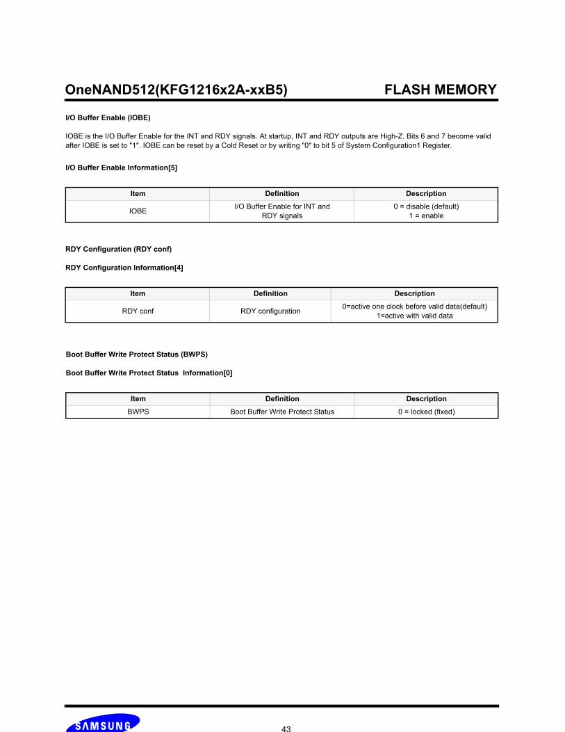
I/O Buffer Enable (IOBE)
IOBE is the I/O Buffer Enable for the INT and RDY signals. At startup, INT and RDY outputs are High-Z. Bits 6 and 7 become valid after IOBE is set to "1". IOBE can be reset by a Cold Reset or by writing "0" to bit 5 of System Configuration1 Register.
I/O Buffer Enable Information[5]
Item Definition Description
IOBE I/O Buffer Enable for INT and RDY signals
0 = disable (default)1 = enable
Boot Buffer Write Protect Status (BWPS)
Boot Buffer Write Protect Status Information[0]
Item Definition Description
BWPS Boot Buffer Write Protect Status 0 = locked (fixed)
RDY Configuration (RDY conf)
RDY Configuration Information[4]
Item Definition Description
RDY conf RDY configuration 0=active one clock before valid data(default)1=active with valid data

OneNAND512(KFG1216x2A-xxB5) FLASH MEMORY
44
This register is reserved for future use.
2.8.21 Controller Status Register F240h (R) This Read register shows the overall internal status of the OneNAND and the controller.
F240h, default = 0000h
15 14 13 12 11 10 9 8 7 6 5 4 3 2 1 0
OnGo Lock Load Prog Erase Error Sus Reserved(0) RSTB OTPL Reserved(000000) TO
(0)
OnGo
This bit shows the overall internal status of the OneNAND device.
OnGo Information[15]
Item Definition Description
OnGo Internal Device Status 0 = ready1 = busy
Lock
This bit shows whether the host is loading data from the NAND Flash array into the locked BootRAM or whether the host is perform-ing a program/erase of a locked block of the NAND Flash array.
Lock Information[14]
Lock Locked/Unlocked Check Result
0 Unlocked
1 Locked
Load
This bit shows the Load Operation status.
Load Information[13]
Item Definition Description
Load Load Operation status 0 = ready (default)1 = busy or error (see controller status output modes)
2.8.20 System Configuration 2 Register F222h

OneNAND512(KFG1216x2A-xxB5) FLASH MEMORY
45
Program
This bit shows the Program Operation status.
Program Information[12]
Item Definition Description
Prog Program Operation status 0 = ready (default)1 = busy or error (see controller status output modes)
Erase
This bit shows the Erase Operation status.
Erase Information[11]
Item Definition Description
Erase Erase Operation status 0 = ready (default)1 = busy or error (see controller status output modes)
Error
This bit shows the overall Error status, including Load Reset, Program Reset, and Erase Reset status.
Error Information[10]
Error Current Sector/Page Load/Program/CopyBack. Program/Erase Result and Invalid Command Input
0 Pass
1 Fail
Erase Suspend (Sus)
This bit shows the Erase Suspend status.
Sus Information[9]
Sus Erase Suspend Status
0 Erase Resume(Default)
1 Erase Suspend, Program Ongoing(Susp.), Load Ongoing(Susp.), Program Fail(Susp.), Load Fail(Susp.), Invalid Command(Susp.)
OneNAND512(KFG1216x2A-xxB5) FLASH MEMORY
46
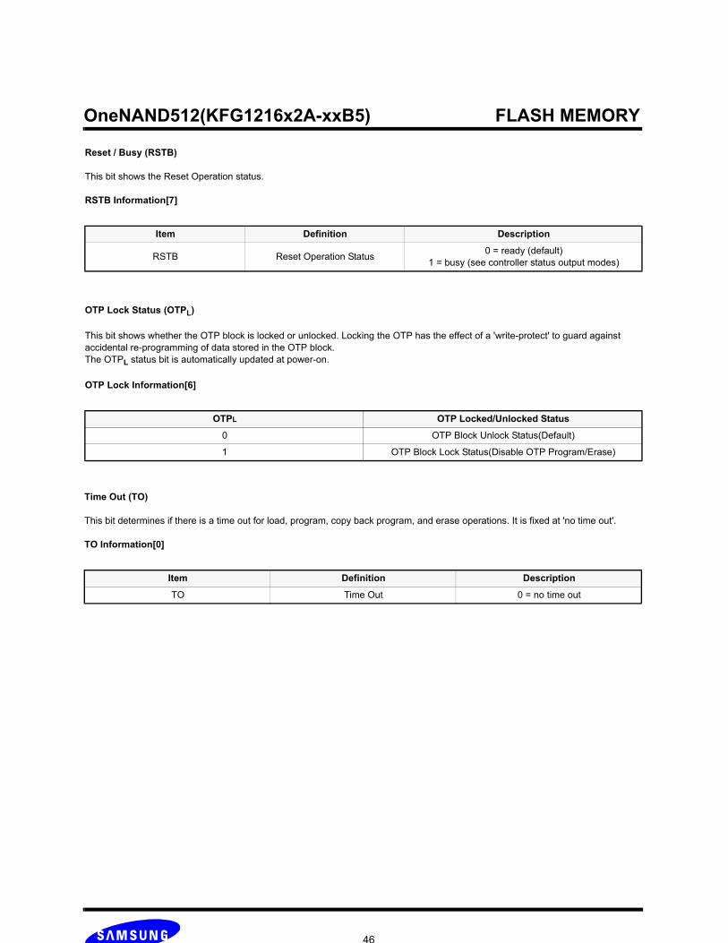
Reset / Busy (RSTB)
This bit shows the Reset Operation status.
RSTB Information[7]
Item Definition Description
RSTB Reset Operation Status 0 = ready (default)1 = busy (see controller status output modes)
OTP Lock Status (OTPL)
This bit shows whether the OTP block is locked or unlocked. Locking the OTP has the effect of a 'write-protect' to guard against accidental re-programming of data stored in the OTP block. The OTPL status bit is automatically updated at power-on.
OTP Lock Information[6]
OTPL OTP Locked/Unlocked Status
0 OTP Block Unlock Status(Default)
1 OTP Block Lock Status(Disable OTP Program/Erase)
Time Out (TO)
This bit determines if there is a time out for load, program, copy back program, and erase operations. It is fixed at 'no time out'.
TO Information[0]
Item Definition Description
TO Time Out 0 = no time out

OneNAND512(KFG1216x2A-xxB5) FLASH MEMORY
47
Controller Status Register Output Modes
NOTE:1. ERm and/or ERs bits in ECC status register at Load Fail case is 10. (2bits error - uncorrectable)2. ERm and ERs bits in ECC status register at Load Reset case are 00. (No error)3. Multi Block Erase status should be checked by Erase Verify Read operation.
ModeController Status Register [15:0]
OnGo Lock Load Prog Erase Error Sus Reserved(0) RSTB OTPL Reserved(0) TO
Load Ongoing 1 0 1 0 0 0 0 0 0 0/1 00000 0
Program Ongoing 1 0 0 1 0 0 0 0 0 0/1 00000 0
Erase Ongoing 1 0 0 0 1 0 0 0 0 0/1 00000 0
Reset Ongoing 1 0 0 0 0 0 0 0 1 0/1 00000 0
Multi-Block EraseOngoing 1 0 0 0 1 0 0 0 0 0/1 00000 0
Erase Verify ReadOngoing 1 0 0 0 0 0 0 0 0 0/1 00000 0
Load OK 0 0 0 0 0 0 0 0 0 0/1 00000 0
Program OK 0 0 0 0 0 0 0 0 0 0/1 00000 0
Erase OK 0 0 0 0 0 0 0 0 0 0/1 00000 0
Erase Verify ReadOK3) 0 0 0 0 0 0 0 0 0 0/1 00000 0
Load Fail1) 0 0 1 0 0 1 0 0 0 0/1 00000 0
Program Fail 0 0 0 1 0 1 0 0 0 0/1 00000 0
Erase Fail 0 0 0 0 1 1 0 0 0 0/1 00000 0
Erase Verify ReadFail3) 0 0 0 0 1 1 0 0 0 0/1 00000 0
Load Reset2) 0 0 1 0 0 1 0 0 1 0/1 00000 0
Program Reset 0 0 0 1 0 1 0 0 1 0/1 00000 0
Erase Reset 0 0 0 0 1 1 0 0 1 0/1 00000 0
Erase Suspend 0 0 0 0 1 0 1 0 0 0/1 00000 0
Program Lock 0 1 0 1 0 1 0 0 0 0/1 00000 0
Erase Lock 0 1 0 0 1 1 0 0 0 0/1 00000 0
Load Lock(Buffer Lock) 0 1 1 0 0 1 0 0 0 0/1 00000 0
OTP Program Fail(Lock) 0 1 0 1 0 1 0 0 0 1 00000 0
OTP Program Fail 0 0 0 1 0 1 0 0 0 0 00000 0
OTP Erase Fail 0 1 0 0 1 1 0 0 0 0/1 00000 0
Program Ongo-ing(Susp.) 1 0 0 1 1 0 1 0 0 0/1 00000 0
Load Ongoing(Susp.) 1 0 1 0 1 0 1 0 0 0/1 00000 0
Program Fail(Susp.) 0 0 0 1 1 1 1 0 0 0/1 00000 0
Load Fail(Susp.) 0 0 1 0 1 1 1 0 0 0/1 00000 0
Invalid Command 0 0 0 0 0 1 0 0 0 0/1 00000 0
Invalid Com-mand(Susp.) 0 0 0 0 1 1 1 0 0 0/1 00000 0
OneNAND512(KFG1216x2A-xxB5) FLASH MEMORY
48
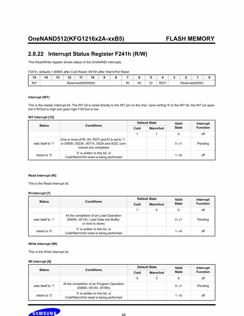
This Read/Write register shows status of the OneNAND interrupts.
F241h, defaults = 8080h after Cold Reset; 8010h after Warm/Hot Reset
15 14 13 12 11 10 9 8 7 6 5 4 3 2 1 0
INT Reserved(0000000) RI WI EI RSTI Reserved(0000)
2.8.22 Interrupt Status Register F241h (R/W)
Interrupt (INT)
This is the master interrupt bit. The INT bit is wired directly to the INT pin on the chip. Upon writing '0' to the INT bit, the INT pin goes low if INTpol is high and goes high if INTpol is low.
INT Interrupt [15]
Status ConditionsDefault State Valid
StateInterruptFunctionCold Warm/hot
1 1 0 off
sets itself to ’1’One or more of RI, WI, RSTI and EI is set to ’1’, or 0065h, 0023h, 0071h, 002A and 002C com-
mands are completed0→1 Pending
clears to ’0’ ’0’ is written to this bit, orCold/Warm/Hot reset is being performed 1→0 off
Read Interrupt (RI)
This is the Read interrupt bit.
RI Interrupt [7]
Status ConditionsDefault State Valid
StateInterruptFunctionCold Warm/hot
1 0 0 off
sets itself to ’1’At the completion of an Load Operation(0000h, 0013h, Load Data into Buffer,
or boot is done)0→1 Pending
clears to ’0’ ’0’ is written to this bit, orCold/Warm/Hot reset is being performed 1→0 off
Write Interrupt (WI)
This is the Write interrupt bit.
WI Interrupt [6]
Status ConditionsDefault State Valid
StateInterruptFunctionCold Warm/hot
0 0 0 off
sets itself to ’1’ At the completion of an Program Operation(0080h, 001Ah, 001Bh) 0→1 Pending
clears to ’0’ ’0’ is written to this bit, orCold/Warm/Hot reset is being performed 1→0 off

OneNAND512(KFG1216x2A-xxB5) FLASH MEMORY
49
This Read/Write register shows the NAND Flash block address in the Write Protection mode. Setting this register precedes a 'Lock Block' command, 'Unlock Block' command, or ’Lock-Tight' Command.
F24Ch, default = 0000h
15 14 13 12 11 10 9 8 7 6 5 4 3 2 1 0
Reserved(0000000) SBA
Device Number of Block SBA
512Mb 512 [8:0]
SBA Information[9:0]
Item Definition Description
SBA Start Block Address Precedes Lock Block, Unlock Block, or Lock-Tight commands
2.8.23 Start Block Address Register F24Ch (R/W)
Erase Interrupt (EI)
This is the Erase interrupt bit.
EI Interrupt [5]
Status ConditionsDefault State Valid
StateInterruptFunctionCold Warm/hot
0 0 0 off
sets itself to ’1’ At the completion of an Erase Operation(0094h, 0095h, 0030h) 0→1 Pending
clears to ’0’ ’0’ is written to this bit, orCold/Warm/Hot reset is being performed 1→0 off
Reset Interrupt (RSTI)
This is the Reset interrupt bit.
RSTI Interrupt [4]
Status ConditionsDefault State Valid
StateInterruptFunctionCold Warm/hot
0 1 0 off
sets itself to ’1’At the completion of an Reset Operation
(00B0h, 00F0h, 00F3h or warm reset is released)
0→1 Pending
clears to ’0’ ’0’ is written to this bit 1→0 off

OneNAND512(KFG1216x2A-xxB5) FLASH MEMORY
50
2.8.25 NAND Flash Write Protection Status Register F24Eh (R) This Read register shows the Write Protection Status of the NAND Flash memory array.To read the write protection status, FBA has to be set before reading the register.
F24Eh, default = 0002h
Write Protection Status Information[2:0]
15 14 13 12 11 10 9 8 7 6 5 4 3 2 1 0
Reserved(0000000000000) US LS LTS
Item Bit Definition Description
US 2 Unlocked Status 1 = current NAND Flash block is unlocked
LS 1 Locked Status 1 = current NAND Flash block is locked
LTS 0 Locked-Tight Status 1 = current NAND Flash block is locked-tight
This register is reserved for future use.
2.8.26 ECC Status Register FF00h (R) This Read register shows the Error Correction Status. The OneNAND can detect 1- or 2-bit errors and correct 1-bit errors. 3-bit or more error detection and correction is not supported.
ECC can be performed on the NAND Flash main and spare memory areas. The ECC status register can also show the number of errors in a sector as a result of an ECC check in during a load operation. ECC status bits are also updated during a boot loading oper-ation.
FF00h, default = 0000h
Error Status
15 14 13 12 11 10 9 8 7 6 5 4 3 2 1 0
ERm3 ERs3 ERm2 ERs2 ERm1 ERs1 ERm0 ERs0
ERm, ERs ECC Status
00 No Error
01 1-bit error(correctable)
10 2 bits error (uncorrectable)
11 Reserved
2.8.24 End Block Address Register F24Dh

OneNAND512(KFG1216x2A-xxB5) FLASH MEMORY
51
ECC Information[15:0]
Item Definition Description
ERm0 1st selected sector of the main BufferRAM
Status of errors in the 1st selected sector of the main BufferRAM as a result of an ECC check during a load operation.
Also updated during a Bootload operation.
ERm1 2nd selected sector of the main BufferRAM
Status of errors in the 2nd selected sector of the main BufferRAM as a result of an ECC check during a load operation.
Also updated during a Bootload operation.
ERm2 3rd selected sector of the main BufferRAM
Status of errors in the 3rd selected sector of the main BufferRAM as a result of an ECC check during a load operation.
Also updated during a Bootload operation.
ERm3 4th selected sector of the main BufferRAM
Status of errors in the 4th selected sector of the main BufferRAM as a result of an ECC check during a load operation.
Also updated during a Bootload operation.
ERs0 1st selected sector of the spare BufferRAM
Status of errors in the 1st selected sector of the spare BufferRAM as a result of an ECC check during a load operation.
Also updated during a Bootload operation.
ERs1 2nd selected sector of the spare BufferRAM
Status of errors in the 2nd selected sector of the spare BufferRAM as a result of an ECC check during a load operation.
Also updated during a Bootload operation.
ERs2 3rd selected sector of the spare BufferRAM
Status of errors in the 3rd selected sector of the spare BufferRAM as a result of an ECC check during a load operation.
Also updated during a Bootload operation.
ERs3 4th selected sector of the spare BufferRAM
Status of errors in the 4th selected sector of the spare BufferRAM as a result of an ECC check during a load operation.
Also updated during a Bootload operation.
This Read register shows the Error Correction result for the 1st selected sector of the spare area data. ECClogSector0 is the error position address for 1.5 words of 2nd and 3rd words in the spare area. ECCposIO0 is the error position address which selects 1 of 16 DQs. ECClogSector0 and ECCposIO0 are also updated at boot loading.
FF02h, default = 0000h
15 14 13 12 11 10 9 8 7 6 5 4 3 2 1 0
Reserved(0000000000) ECClogSector0 ECCposIO0
This Read register shows the Error Correction result for the 1st selected sector of the main area data. ECCposWord0 is the error position address in the Main Area data of 256 words. ECCposIO0 is the error position address which selects 1 of 16 DQs. ECCposWord0 and ECCposIO0 are also updated at boot loading.
FF01h, default = 0000h
15 14 13 12 11 10 9 8 7 6 5 4 3 2 1 0
Reserved(0000) ECCposWord0 ECCposIO0
2.8.27 ECC Result of 1st Selected Sector, Main Area Data Register FF01h (R)
2.8.28 ECC Result of 1st Selected Sector, Spare Area Data Register FF02h (R)

OneNAND512(KFG1216x2A-xxB5) FLASH MEMORY
52
2.8.29 ECC Result of 2nd Selected Sector, Main Area Data Register FF03h (R) This Read register shows the Error Correction result for the 2nd selected sector of the main area data. ECCposWord1 is the error position address in the Main Area data of 256 words. ECCposIO1 is the error position address which selects 1 of 16 DQs. ECCposWord1 and ECCposIO1 are also updated at boot loading.
FF03h, default = 0000h
15 14 13 12 11 10 9 8 7 6 5 4 3 2 1 0
Reserved(0000) ECCposWord1 ECCposIO1
2.8.30 ECC Result of 2nd Selected Sector, Spare Area Data Register FF04h (R) This Read register shows the Error Correction result for the 2nd selected sector of the spare area data. ECClogSector1 is the error position address for 1.5 words of 2nd and 3rd words in the spare area. ECCposIO1 is the error position address which selects 1 of 16 DQs. ECClogSector1 and ECCposIO1 are also updated at boot loading.
FF04h, default = 0000h
15 14 13 12 11 10 9 8 7 6 5 4 3 2 1 0
Reserved(0000000000) ECClogSector1 ECCposIO1
2.8.32 ECC Result of 3rd Selected Sector, Spare Area Data Register FF06h (R) This Read register shows the Error Correction result for the 3rd selected sector of the spare area data. ECClogSector2 is the error position address for 1.5 words of 2nd and 3rd words in the spare area. ECCposIO2 is the error position address which selects 1 of 16 DQs. ECClogSector2 and ECCposIO2 are also updated at boot loading.
FF06h, default = 0000h
15 14 13 12 11 10 9 8 7 6 5 4 3 2 1 0
Reserved(0000000000) ECClogSector2 ECCposIO2
2.8.31 ECC Result of 3rd Selected Sector, Main Area Data Register FF05h (R) This Read register shows the Error Correction result for the 3rd selected sector of the main area data. ECCposWord2 is the error position address in the Main Area data of 256 words. ECCposIO2 is the error position address which selects 1 of 16 DQs. ECCposWord2 and ECCposIO2 are also updated at boot loading.
FF05h, default = 0000h
15 14 13 12 11 10 9 8 7 6 5 4 3 2 1 0
Reserved(0000) ECCposWord2 ECCposIO2

OneNAND512(KFG1216x2A-xxB5) FLASH MEMORY
53
This Read register shows the Error Correction result for the 4th selected sector of the main area data. ECCposWord3 is the error position address in the Main Area data of 256 words. ECCposIO3 is the error position address which selects 1 of 16 DQs. ECCposWord3 and ECCposIO3 are also updated at boot loading.
FF07h, default = 0000h
15 14 13 12 11 10 9 8 7 6 5 4 3 2 1 0
Reserved(0000) ECCposWord3 ECCposIO3
2.8.34 ECC Result of 4th Selected Sector, Spare Area Data Register FF08h (R) This Read register shows the Error Correction result for the 4th selected sector of the spare area data. ECClogSector3 is the error position address for 1.5 words of 2nd and 3rd words in the spare area. ECCposIO3 is the error position address which selects 1 of 16 DQs. ECClogSector3 and ECCposIO3 are also updated at boot loading.
FF08h, default = 0000h
15 14 13 12 11 10 9 8 7 6 5 4 3 2 1 0
Reserved(0000000000) ECClogSector3 ECCposIO3
2.8.33 ECC Result of 4th Selected Sector, Main Area Data Register FF07h (R)
ECC Log Sector
ECClogSector0~ECClogSector3 indicates the error position in the 2nd word and LSB of 3rd word in the spare area. Refer to note 2 in chapter 2.7.2
ECClogSector Information [5:4]
ECClogSector Error Position
00 2nd word
01 3rd word
10, 11 Reserved

OneNAND512(KFG1216x2A-xxB5) FLASH MEMORY
54
This section of the datasheet discusses the operation of the OneNAND device. It is followed by AC/DC Characteristics and Timing Diagrams which may be consulted for further information.
The OneNAND supports either a command-based or a register-based interface for performing operations on the device including reading device ID, writing data to buffer etc.
The command-based interface is active in the boot partition. Commands can only be written with a boot area address. Boot area data is only returned if no command has been issued prior to the read.
When reading and programming the OneNAND, data handling is data unit-based. One data is read at the time from NAND Flash array.
3.1 Command Based OperationThe command-based interface is active in the boot partition. Commands can only be written with a boot area address. Boot area data is only returned if no command has been issued prior to the read.
The entire address range, except for the boot area, can be used for the data buffer. All commands are written to the boot partition. Writes outside the boot partition are treated as normal writes to the buffers or registers.
The command consists of one or more cycles depending on the command. After completion of the command the device starts its exe-cution. Writing incorrect information including address and data to the boot partition or writing an improper command will terminate the previous command sequence and make the device enter the ready status.
The defined valid command sequences are stated in Command Sequences Table.
Command Sequences
NOTE:1) DP(Data Partition) : DataRAM Area2) BP(Boot Partition) : BootRAM Area [0000h ~ 01FFh, 8000h ~ 800Fh]3) Load Data into Buffer operation is available within a block(128KB)4) Load 2KB unit into DataRAM0. Current Start address(FPA) is automatically incremented by 2KB unit after the load. 5) 0000h -> Data is Manufacturer ID 0001h -> Data is Device ID 0002h -> Current Block Write Protection Status6) WE toggling can terminate ’Read Identification Data’ operation.
Command Definition Cycles 1st cycle 2nd cycle
Read Data from BufferAdd
1DP1)
Data Data
Write Data to BufferAdd
1DP
Data Data
Reset OneNANDAdd
1BP2)
Data 00F0h
Load Data into Buffer3)Add
2BP BP
Data 00E0h 0000h4)
Read Identification Data 6)Add
2BP XXXXh5)
Data 0090h Data
3.0 DEVICE OPERATION
OneNAND512(KFG1216x2A-xxB5) FLASH MEMORY
55
The buffer memory can be read by addressing a Read to the desired buffer area.
3.1.2 Writing Data to BufferThe buffer memory can be written to by addressing a Write to a desired buffer area.
3.1.3 Reset OneNAND CommandThe Reset command is given by writing 00F0h to the boot partition address. Reset will return all default values into the device.
3.1.4 Load Data Into Buffer CommandLoad Data into Buffer command is a two-cycle command. Two sequential designated command activates this operation. Sequentially writing 00E0h and 0000h to the boot partition [0000h~01FFh, 8000h~800Fh] will load one page to DataRAM0. This operation refers to FBA and FPA. FSA, BSA, and BSC are not considered. At the end of this operation, FPA will be automatically increased by 1. So continuous issue of this command will sequentially load data in next page to DataRAM0. This page address increment is restricted within a block.The default value of FBA and FPA is 0. Therefore, initial issue of this command after power on will load the first page of memory, which is usually boot code.
3.1.5 Read Identification Data CommandThe Read Identification Data command consists of two cycles. It gives out the devices identification data according to the given address. The first cycle is 0090h to the boot partition address and second cycle is read from the addresses specified in Identification Data Description Table.
Identification Data Description
Note 1) To read the write protection status, FBA has to be set before issuing this command.
Address Data Out
0000h Manufacturer ID : 00ECh
0001h Device ID : refer to chapter 2.8.3
0002h Current Block Write Protection Status 1)
3.1.1 Reading Data From Buffer

OneNAND512(KFG1216x2A-xxB5) FLASH MEMORY
56
The device bus operations are shown in the table below.
Note : L=VIL (Low), H=VIH (High), X=Don’t Care.
Operation CE OE WE ADD0~15 DQ0~15 RP CLK AVD
Standby H X X X High-Z H X X
Warm Reset X X X X High-Z L X X
Asynchronous Write L H L Add. In Data In H L X
Asynchronous Read L L H Add. In Data Out H Lor L
Load Initial Burst Address L H H Add. In X H
Burst Read L L H X Burst Data Out H
Terminate Burst ReadCycle H X H X High-Z H X X
Terminate Burst ReadCycle via RP X X X X High-Z L X X
Terminate Current BurstRead Cycle and Start
New Burst Read CycleH H Add In High-Z H
X
3.2 Device Bus Operation

OneNAND512(KFG1216x2A-xxB5) FLASH MEMORY
57
The One NAND has 4 reset modes: Cold/Warm/Hot Reset, and NAND Flash Array Reset. Section 3.3 discusses the operation of these reset modes.
The Register Reset Table shows the which registers are affected by the various types or Reset operations.
Internal Register Reset Table
NOTE: 1) RDYpol, INTpol, IOBE is reset by Cold reset. The other bits are reset by Cold/Warm/Hot reset. 2) ECC Status Register & ECC Result Registers are reset when any command is issued. 3) Refer to Device ID Register F001h.
Internal Registers Default Cold Reset Warm Reset(RP)
HotReset
(00F3h)
HotReset
(BP-F0)
NAND FlashReset(00F0h)
F000h Manufacturer ID Register (R) 00ECh N/A N/A N/A N/A
F001h Device ID Register (R): OneNAND (Note 3) N/A N/A N/A N/A
F002h Version ID Register (R): N/A N/A N/A N/A N/A N/A
F003h Data Buffer size Register (R) 0800h N/A N/A N/A N/A
F004h Boot Buffer size Register (R) 0200h N/A N/A N/A N/A
F005h Amount of Buffers Register (R) 0201h N/A N/A N/A N/A
F006h Technology Register (R) 0000h N/A N/A N/A N/A
F100h Start Address1 Register (R/W): FBA 0000h 0000h 0000h 0000h N/A
F101h Start Address2 Register (R/W): Reserved 0000h 0000h 0000h 0000h N/A
F102h Start Address3 Register (R/W): FCBA 0000h 0000h 0000h 0000h N/A
F103h Start Address4 Register (R/W): FCPA, FCSA 0000h 0000h 0000h 0000h N/A
F107h Start Address8 Register (R/W): FPA, FSA 0000h 0000h 0000h 0000h N/A
F200h Start Buffer Register (R/W): BSA, BSC 0000h 0000h 0000h 0000h N/A
F220h Command Register (R/W) 0000h 0000h 0000h 0000h N/A
F221h System Configuration 1 Register (R/W) 40C0h 40C0h O (Note1) O (Note1) N/A
F240h Controller Status Register (R) 0000h 0000h 0000h 0000h N/A
F241h Interrupt Status Register (R/W) - 8080h 8010h 8010h N/A
F24Ch Start Block Address (R/W) 0000h 0000h 0000h N/A N/A
F24Dh End Block Address: N/A N/A N/A N/A N/A N/A
F24Eh NAND Flash Write Protection Status (R) 0002h 0002h 0002h N/A N/A
FF00h ECC Status Register (R) (Note2) 0000h 0000h 0000h 0000h N/A
FF01h ECC Result of Sector 0 Main area data Register(R) 0000h 0000h 0000h 0000h N/A
FF02h ECC Result of Sector 0 Spare area data Register (R) 0000h 0000h 0000h 0000h N/A
FF03h ECC Result of Sector 1 Main area data Register(R) 0000h 0000h 0000h 0000h N/A
FF04h ECC Result of Sector 1 Spare area data Register (R) 0000h 0000h 0000h 0000h N/A
FF05h ECC Result of Sector 2 Main area data Register(R) 0000h 0000h 0000h 0000h N/A
FF06h ECC Result of Sector 2 Spare area data Register (R) 0000h 0000h 0000h 0000h N/A
FF07h ECC Result of Sector 3 Main area data Register(R) 0000h 0000h 0000h 0000h N/A
FF08h ECC Result of Sector 3 Spare area data Register (R) 0000h 0000h 0000h 0000h N/A
3.3 Reset Mode Operation

OneNAND512(KFG1216x2A-xxB5) FLASH MEMORY
58
3.3.2 Warm Reset Mode Operation See Timing Diagrams 6.12
A Warm Reset means that the host resets the device by using the /RP pin. When the a /RP low is issued, the device logic stops all current operations and executes internal reset operation and resets current NAND Flash core operation synchronized with the falling edge of /RP.
During an Internal Reset Operation, the device initializes internal registers and makes output signals go to default status. The BufferRAM data is kept unchanged after Warm/Hot reset operations.
The device guarantees the logic reset operation in case /RP pulse is longer than tRP min. (200ns).The device may reset if tRP < tRP min(200ns), but this is not guaranteed.
Warm reset will abort the current NAND Flash core operation. During a warm reset, the content of memory cells being altered is no longer valid as the data will be partially programmed or erased.
Warm reset has no effect on contents of BootRAM and DataRAM.
3.3.3 Hot Reset Mode Operation See Timing Diagram 6.13
A Hot Reset means that the host resets the device by Reset command. The reset command can be either Command based or Register Based. Upon receiving the Reset command, the device logic stops all current operation and executes an internal reset operation and resets the current NAND Flash core operation.
During an Internal Reset Operation, the device initializes internal registers and makes output signals go to default status. The BufferRAM data is kept unchanged after Warm/Hot reset operations.
Hot reset will abort the current NAND Flash core operation. During a Hot reset, the content of memory cells being altered is no longer valid as the data will be partially programmed or erased.
Hot reset has no effect on contents of BootRAM and DataRAM.
3.3.4 NAND Flash Core Reset Mode Operation See Timing Diagram 6.14
The Host can reset the NAND Flash Core operation by issuing a NAND Flash Core reset command. NAND Flash core reset will abort the current NAND Flash core operation. During a NAND Flash core reset, the content of memory cells being altered is no longer valid as the data will be partially programmed or erased.
Hot reset has no effect on contents of BootRAM and DataRAM, as well as register values.
At system power-up, the voltage detector in the device detects the rising edge of Vcc and releases an internal power-up reset signal. This triggers bootcode loading. Bootcode loading means that the boot loader in the device copies designated sized data (1KB) from the beginning of memory into the BootRAM. This sequence is the Cold Reset of OneNAND.The POR(Power On Reset) triggering level is typically 1.5V. Boot code copy operation activates 400us after POR. Therefore, the system power should reach 1.7V within 400us from the POR triggering level for bootcode data to be valid. For 2.65V and 3.3V device, POR level is typically 1.8V and system power should reach 2.2V within 400us.
It takes approximately 70us to copy 1KB of bootcode. Upon completion of loading into the BootRAM, it is available to be read by the host. The INT pin is not available until after IOBE = 1 and IOBE bit can be changed by host.
3.3.1 Cold Reset Mode Operation See Timing Diagram 6.11

OneNAND512(KFG1216x2A-xxB5) FLASH MEMORY
59
The OneNAND can be write-protected to prevent re-programming or erasure of data. The areas of write-protection are the BootRAM, and the NAND Flash Array.
3.4.1 BootRAM Write Protection Operation
At system power-up, voltage detector in the device detects the rising edge of Vcc and releases the internal power-up reset signalwhich triggers bootcode loading. And the designated size data(1KB) is copied from the first page of the first block in the NAND flash array to the BootRAM.After the bootcode loading is completed, the BootRAM is always locked to protect the boot code from the accidental write.
3.4.2 NAND Flash Array Write Protection Operation
The device has both hardware and software write protection of the NAND Flash array.
Hardware Write Protection OperationThe hardware write protection operation is implemented by executing a Cold or Warm Reset. On power up, the NAND Flash Array is in its default, locked state. The entire NAND Flash array goes to a locked state after a Cold or Warm Reset.
Software Write Protection Operation The software write protection operation is implemented by writing a Lock command (002Ah) or a Lock-tight command (002Ch) to command register (F220h).
Lock (002Ah) and Lock-tight (002Ch) commands write protects the block defined in the Start Block Address Register F24Ch.
3.4.3 NAND Array Write Protection States
There are three lock states in the NAND Array: unlocked, locked, and locked-tight.OneNAND512 supports lock/unlock/lock-tight by one block, so each block should be locked/unlocked/locked-tight individually.
Write Protection StatusThe current block Write Protection status can be read in NAND Flash Write Protection Status Register(F24Eh). There are three bits -US, LS, LTS -, which are not cleared by hot reset. These Write Protection status registers are updated when FBA is set, and whenWrite Protection command is entered.
The followings summarize locking status. example) In default, [2:0] values are 010. -> If host executes unlock block operation, then [2:0] values turn to 100. -> If host executes lock-tight block operation, then [2:0] values turn to 001.
3.4 Write Protection Operation

OneNAND512(KFG1216x2A-xxB5) FLASH MEMORY
60
An Unlocked block can be programmed or erased. The status of an unlocked block can be changed to locked or locked-tight using the appropriate software command. (locked-tight state can be achieved via lock-tight command which follows lock command)
Only one block can be released from lock state to unlock state with Unlock command and addresses. The unlocked block can be changed with new lock command. Therefore, each block has its own lock/unlock/lock-tight state.
Unlock Command Sequence:Start block address+Unlock block command (0023h)
Unlocked
3.4.3.2 Locked NAND Array Write Protection State
A Locked block cannot be programmed or erased. All blocks default to a locked state following a Cold or Warm Reset. Unlocked blocks can be changed to locked using the Lock block command. The status of a locked block can be changed to unlocked orlocked-tight using the appropriate software command.
Lock Command Sequence:Start block address+Lock block command (002Ah)
Locked
3.4.3.1 Unlocked NAND Array Write Protection State

OneNAND512(KFG1216x2A-xxB5) FLASH MEMORY
61
A block that is in a locked-tight state can only be changed to lock state after a Cold or Warm Reset. Unlock and Lock command sequences will not affect its state. This is an added level of write protection security.
A block must first be set to a locked state before it can be changed to locked-tight using the Lock-tight command. locked-tight blocks will revert to a locked state following a Cold or Warm Reset.
Lock-Tight Command Sequence:Start block address+Lock-tight block command (002Ch)
Locked-tight
3.4.4 NAND Flash Array Write Protection State Diagram
Power On
Start block address+Unlock block Command
RP pin: High&
Lock block Command
RP pin: High&
+Lock-tight block Command
RP pin: High&
Cold reset or
unlock
Lock
Lock-tight
Lock
Lock
Warm resetStart block address
Lock
Lock
Start block address
Cold reset or Warm reset
or
3.4.3.3 Locked-tight NAND Array Write Protection State

OneNAND512(KFG1216x2A-xxB5) FLASH MEMORY
62
Data Protection Operation Flow Diagram
Start
Write ’SBA’ of FlashAdd: F24Ch DQ=SBA
Lock/Unlock/Lock-Tight
Write ’lock/unlock/lock-tight’
Add: F220hDQ=002Ah/0023h/002Ch
Wait for INT registerlow to high transition
Add: F241h DQ[15]=INT
Write 0 to interrupt registerAdd: F241h DQ=0000h
Command
completed
Note) Samsung strongly recommend to follow the above flow chart

OneNAND512(KFG1216x2A-xxB5) FLASH MEMORY
63
The device is designed to offer protection from any involuntary program/erase during power-transitions.
An internal voltage detector disables all functions whenever Vcc is below POR level, about 1.3V. It is recommended that the /RP pin, which provides hardware protection, should be kept at VIL before power-down.
3.6 Load Operation See Timing Diagram 6.8
The Load operation is initiated by setting up the start address from which the data is to be loaded. The Load command is issued in order to initiate the load.
During a Load operation, the device: -Transfers the data from NAND Flash array into the BufferRAM -ECC is checked and any detected and corrected error is reported in the status response as well as any unrecoverable error.
Once the BufferRAM has been filled, an interrupt is issued to the host so that the contents of the BufferRAM can be read. The read from the BufferRAM can be an asynchronous read mode or synchronous read mode. The status information related to load operation can be checked by the host if required.
The device has a dual data buffer memory architecture (DataRAM0, DataRAM1), each 2KB in size. Each DataRAM buffer has 4 Sectors. The device is capable of independent and simultaneous data-read operation from one data buffer and data-load operation to the other data buffer. Refer to the information for more details in section 3.12.1, "Read-While-Load Operation".
Load Operation Flow Chart Diagram
Start
Write ’FBA’ of FlashAdd: F100h DQ=FBA
Write ’FPA, FSA’ of FlashAdd: F107h DQ=FPA, FSA
Write ’BSA, BSC’ of DataRAMAdd: F200h DQ=BSA, BSC
Write ’Load’ Command
Add: F220hDQ=0000h or 0013h
Wait for INT registerlow to high transition
Add: F241h DQ[15]=INT
Read Controller
Add: F240h DQ[10]=Error
DQ[10]=0?NO
YES
Status Register
Host reads data fromDataRAM
Read completed
Map Out
Write 0 to interrupt registerAdd: F241h DQ=0000h
3.5 Data Protection During Power Down Operation See Timing Diagram 6.15

OneNAND512(KFG1216x2A-xxB5) FLASH MEMORY
64
The device has two read modes; Asynchronous Read and Synchronous Burst Read.
The initial state machine automatically sets the device into the Asynchronous Read Mode (RM=0) to prevent the spurious altering of memory content upon device power up or after a Hardware reset. No commands are required to retrieve data in Asynchronous Read Mode.
The Synchronous Read Mode is enabled by setting RM bit of System Configuration1 Register (F221h) to Synchronous Read Mode (RM=1). See Section 2.8.19 for more information about System Configuration1 Register.
3.7.1 Asynchronous Read Mode Operation (RM=0) See Timing Diagrams 6.3, 6.4, 6.5 and 6.6
In an Asynchronous Read Mode, data is output with respect to a logic input, /AVD. Output data will appear on DQ15-DQ0 in when a valid address is asserted on A15-A0 while driving /AVD and /CE to VIL. / WE is held at VIH. The function of the /AVD signal is to latch the valid address.
Address access time from /AVD low (tAA) is equal to the delay from valid addresses to valid output data.
The Chip Enable access time (tCE) is equal to the delay from the falling edge of /CE to valid data at the outputs.
The Output Enable access time (tOE) is the delay from the falling edge of /OE to valid data at the output.
3.7.2 Synchronous Read Mode Operation (RM=1) See Timing Diagrams 6.1 and 6.2
In a Synchronous Read Mode, data is output with respect to a clock input.
The device is capable of a continuous linear burst operation and a fixed-length linear burst operation of a preset length. Burst address sequences for continuous and fixed-length burst operations are shown in the table below.
Burst Address Sequences
In the burst mode, the initial word will be output asynchronously, regardless of BRL. While the following words will be determined byBRL value.
The latency is determined by the host based on the BRL bit setting in the System Configuration 1 Register. The default BRL is 4latency cycles. At clock frequencies of 40MHz or lower, latency cycles can be reduced to 3. BRL can be set up to 7 latency cycles.
The BRL registers can be read during a burst read mode by using the /AVD signal with an address.
StartAddr.
Burst Address Sequence(Decimal)
Continuous Burst 4-word Burst 8-word Burst 16-word Burst 32-word Burst
Wraparound
0 0-1-2-3-4-5-6... 0-1-2-3-0... 0-1-2-3-4-5-6-7-0... 0-1-2-3-4-....-13-14-15-0... 0-1-2-3-4-....-29-30-31-0...
1 1-2-3-4-5-6-7... 1-2-3-0-1... 1-2-3-4-5-6-7-0-1... 1-2-3-4-5-....-14-15-0-1... 1-2-3-4-5-....-30-31-0-1...
2 2-3-4-5-6-7-8... 2-3-0-1-2... 2-3-4-5-6-7-0-1-2... 2-3-4-5-6-....-15-0-1-2... 2-3-4-5-6-....-31-0-1-2...
.
...
.
...
.
...
3.7 Read Operation See Timing Diagrams 6.1, 6.2, 6.3, 6.4, 6.5 and 6.6

OneNAND512(KFG1216x2A-xxB5) FLASH MEMORY
65
First Clock CycleThe initial word is output at tIAA after the rising edge of the first CLK cycle. The RDY output indicates the initial word is ready to the system by pulsing high. If the device is accessed synchronously while it is set to Asynchronous Read Mode, the first data can still be read out.
Subsequent Clock CyclesSubsequent words are output (Burst Access Time from Valid Clock to Output) tBA after the rising edge of each successive clock cycle, which automatically increments the internal address counter.
Terminating Burst ReadThe device will continue to output sequential burst data until the system asserts /CE high, or /RP low, wrapping around until it reaches the designated address (see Section 2.7.3 for address map information). Alternately, a Cold/Warm/Hot Reset, asserting /CE high, or a /WE low pulse will terminate the burst read operation.
Synchronous Read Boundary
Division Add.map(word order)
BootRAM Main(0.5Kw) 0000h~01FFh
BrfferRAM0 Main(1Kw) 0200h~05FFh
BufferRAM1 Main(1Kw) 0600h~09FFh
Reserved Main 0A00h~7FFFh
BootRAM Spare(16w) 8000H~800Fh
BufferRAM0 Spare(32w) 8010h~802Fh
BufferRAM1 Spare(32w) 8030h~804Fh
Reserved Spare 8050h~8FFFh
Reserved Register 9000h~EFFFh
Register(4Kw) F000h~FFFFh
Not Support
Not Support
* Reserved area is not available on Synchronous read
3.7.2.2 4-, 8-, 16-, 32-Word Linear Burst Read Operation See Timing Diagram 6.1
An alternate Burst Read Mode enables a fixed number of words to be read from consecutive address.
The device supports a burst read from consecutive addresses of 4-, 8-, 16-, and 32-words with a linear-wrap around. When the last word in the burst has been reached, /CE and /OE are asserted high.
In this mode, the start address for the burst read can be any address of the address map with one exception. The device does not support a 32-word linear burst read on the spare area of the BufferRAM.
Not Support
Not Support
Not Support
3.7.2.1 Continuous Linear Burst Read Operation See Timing Diagram 6.2

OneNAND512(KFG1216x2A-xxB5) FLASH MEMORY
66
Upon power up, the number of initial clock cycles from Valid Address (/AVD) to initial data defaults to four clocks.
The number of clock cycles (n) which are inserted after the clock which is latching the address. The host can read the first data with the (n+1)th rising edge.
The number of total initial access cycles is programmable from three to seven cycles. After the number of programmed burst clockcycles is reached, the rising edge of the next clock cycle triggers the next burst data.
Four Clock Burst Read Latency (default condition)
3.7.3 Handshaking Operation
The handshaking feature allows the host system to simply monitor the RDY signal from the device to determine when the initial word of burst data is ready to be read.
To set the number of initial cycles for optimal burst mode, the host should use the programmable burst read latency configuration (see Section 2.8.19, "System Configuration1 Register").
The rising edge of RDY which is derived from one cycles ahead of data fetch clock indicates the initial word of valid burst data.
3.7.2.3 Programmable Burst Read Latency Operation See Timing Diagrams 6.1 and 6.2
tIAA
Hi-Z
CE
CLK
AVD
OE
RDY
≈≈
tRDYS
tRDYA
DQ0:DQ15 D6 D7 D0 D1 D2 D3 D7 D0
Hi-Z
≈≈
≈≈
0 1 2 3-1
tBA
Rising edge of the clock cycle following last read latencytriggers next burst data
A0:A15
ValidAddress
4

OneNAND512(KFG1216x2A-xxB5) FLASH MEMORY
67
When the CE or OE input is at VIH, output from the device is disabled. The outputs are placed in the high impedance state.
The Program operation is used to program data from the on-chip BufferRAMs into the NAND FLASH memory array.
The device has two 2KB data buffers, each 1 Page (2KB + 64B) in size. Each page has 4 sectors of 512B each main area and 16Bspare area. The device can be programmed in units of 1~4 sectors.
The architecture of the DataRAMs permits a simultaneous data-write operation from the Host to one of data buffers and a programoperation from the other data buffer to the NAND Flash Array memory. Refer to Section 3.12.2, "Write While Program Operation", formore information.
3.8 Program Operation See Timing Diagram 6.9
Within a block, the pages must be programmed consecutively from the LSB (least significant bit) page of the block to MSB (most sig-nificant bit) pages of the block. Random page address programming is prohibited.
From the LSB page to MSB page
DATA IN: Data (1) Data (64)
(1)(2)(3)
(32)
(64)
Data register
Page 0Page 1Page 2
Page 31
Page 63
Ex.) Random page program (Prohibition)
DATA IN: Data (1) Data (64)
(2)(32)(3)
(1)
(64)
Data register
Page 0Page 1Page 2
Page 31
Page 63
Addressing for program operation
:
:
:
:
3.7.4 Output Disable Mode Operation

OneNAND512(KFG1216x2A-xxB5) FLASH MEMORY
68
Program Operation Flow Diagram
During the execution of the Internal Program Routine, the host is not required to provide any further controls or timings. Furthermore, all commands, except a Reset command, will be ignored. A reset during a program operation will cause data corruption at the corresponding location.
If a program error is detected at the completion of the Internal Program Routine, map out the block, including the page in error, and copy the target data to another block. An error is signaled if DQ10 = "1" of Controller Status Register(F240h) .
Data input from the Host to the DataRAM can be done at any time during the Internal Program Routine after "Start" but before the "Write Program Command" is written.
Start
Data Input
Write ’FBA’ of FlashAdd: F100h DQ=FBA
Write ’FPA, FSA’ of FlashAdd: F107h DQ=FPA, FSA
Write Data into DataRAM2)
ADD: DP DQ=Data-in
Program completed
Write ’Program’ Command
Add: F220hDQ=0080h or 001Ah
Completed? Wait for INT registerlow to high transition
Add: F241h DQ[15]=INT
Read ControllerStatus Register
Add: F240h DQ[10]=Error
DQ[10]=0?
Program Error
YES NO
NO
YES
: If program operation results in an error, map out the block including the page in error and copy the target data to another block.
*
Note 1) This must happen before data input 2) Data input could be done anywhere between "Start" and "Write Program Command".
Write 0 to interrupt registerAdd: F241h DQ=0000h
Write ’BSA, BSC’ of DataRAMAdd: F200h DQ=BSA, BSC
OneNAND512(KFG1216x2A-xxB5) FLASH MEMORY
69
The Copy-Back program is configured to quickly rewrite data stored in one page without utilizing memory other than OneNAND.Since the time-consuming cycles of serial access and re-loading cycles are removed, the system performance is improved. The ben-efit is especially obvious when a portion of block is updated and the rest of the block also need to be copied to the newly assignedfree block.
Data from the source page is saved in one of the on-chip DataRAM buffers and then programmed directly into the destination page.The DataRAM overwrites the previous data using the Buffer Sector Address (BSA) and Buffer Sector Count (BSC).
The Copy-Back Program Operation does this by performing sequential page-reads without a serial access and executing a copy-program using the address of the destination page.
Copy-Back Program Operation Flow Chart
Start
Write ’FBA’ of FlashAdd: F100h DQ=FBA
Write ’FPA, FSA’ of FlashAdd: F107h DQ=FPA, FSA
Write ’FCBA’ of FlashAdd: F102h DQ=FCBA
Write ’FCPA, FCSA’ of FlashAdd: F103h DQ=FCPA, FCSA
Copy back completed
Write ’Copy-back Program’command
Add: F220h DQ=001Bh
Wait for INT registerlow to high transition
Add: F241h DQ[15]=INT
Read ControllerStatus Register
Add: F240h DQ[10]=Error
DQ[10]=0?
Copy back Error
YES NO
Note 1) Selected DataRAM by BSA & BSC is used for Copy back operation, so previous data is overwritten.
: If program operation results in an error, map out the block including the page in error and copy the target data to another block.
*
2) FBA, FPA and FSA should be input prior to FCBA, FCPA and FCSA.
Write 0 to interrupt registerAdd: F241h DQ=0000h
Write ’BSA, BSC’ of DataRAMAdd: F200h DQ=BSA, BSC 1)
3.9 Copy-Back Program Operation

OneNAND512(KFG1216x2A-xxB5) FLASH MEMORY
70
The Copy-Back steps shown in the flow chart are:
• Data is read from the NAND Array using Flash Block Address (FBA), Flash Page Address (FPA) and Flash Sector Address (FSA). FBA, FPA, and FSA identify the source address to read data from NAND Flash array.
• The BufferRAM Sector Count (BSC) and BufferRAM Sector Address (BSA) identifies how many sectors and the location of the sectors in DataRAM that are used.
• The destination address in the NAND Array is written using the Flash Copy-Back Block Address (FCBA), Flash Copy-Back Page Address (FCPA), and Flash Copy-Back Sector Address (FCSA).
• The Copy-Back Program command is issued to start programming.
• Upon completion of copy-back programming to the destination page address, the Host checks the status to see if the operation was successfully completed. If there was an error, map out the block including the page in error and copy the target data to another block.
OneNAND512(KFG1216x2A-xxB5) FLASH MEMORY
71
The Copy-Back Program Operation with Random Data Input in OneNAND consists of 2 phase, Load data into DataRAM, Modify dataand program into designated page. Data from the source page is saved in one of the on-chip DataRAM buffers and modified by thehost, then programmed into the destination page.
As shown in the flow chart, data modification is possible upon completion of load operation. ECC is also available at the end of loadoperation. Therefore, using hardware ECC of OneNAND, accumulation of 1 bit error can be avoided.
Copy-Back Program Operation with Random Data Input will be effectively utilized at modifying certain bit, byte, word, or sector ofsource page to destination page while it is being copied.
Copy-Back Program Operation with Random Data Input Flow Chart
Start
Write ’FBA’ of FlashAdd: F100h DQ=FBA
Write ’FPA, FSA’ of FlashAdd: F107h DQ=FPA, FSA
Write ’BSA, BSC’ of DataRAMAdd: F200h DQ=BSA, BSC
Write ’Load’ Command
Add: F220hDQ=0000h or 0013h
Wait for INT registerlow to high transition
Add: F241h DQ[15]=INT
Read Controller
Add: F240h DQ[10]=Error
DQ[10]=0?NO
YES
Status Register
Map Out
Write 0 to interrupt registerAdd: F241h DQ=0000h
Copy back completed
Wait for INT registerlow to high transition
Add: F241h DQ[15]=INT
Read ControllerStatus Register
Add: F240h DQ[10]=Error
DQ[10]=0?
Copy back Error
YES NO
Random Data Input
Write ’FBA’ of FlashAdd: F100h DQ=FBA
Write ’FPA, FSA’ of FlashAdd: F107h DQ=FPA, FSA
Write ’Program’ Command
Add: F220hDQ=0080h or 001Ah
Write 0 to interrupt registerAdd: F241h DQ=0000h
Add: Random Address inSelected DataRAM
DQ=Data
3.9.1 Copy-Back Program Operation with Random Data Input

OneNAND512(KFG1216x2A-xxB5) FLASH MEMORY
72
There are multiple methods for erasing data in the device including Block Erase and Multi-Block Erase.
3.10.1 Block Erase Operation See Timing Diagram 6.10
The device can be erased one block at a time. To erase a block is to write all 1's into the desired memory block by executing the Inter-nal Erase Routine. All previous data is lost.
Block Erase Operation Flow Chart
Start
Write ’FBA’ of FlashAdd: F100h DQ=FBA
Write ’Erase’ CommandAdd: F220h DQ=0094h
Wait for INT register
Add: F241h DQ=[15]=INT
Add: F240h DQ[10]=Error
Erase completed
DQ[10]=0?
YES
Erase Error
NO
low to high transition
Read ControllerStatus Register
: If erase operation results in an error, map out
the failing block and replace it with another block. *
Write 0 to interrupt register
Add: F241h DQ=0000h
3.10 Erase Operation
OneNAND512(KFG1216x2A-xxB5) FLASH MEMORY
73
In order to perform the Internal Erase Routine, the following command sequence is necessary.
• The Host sets the block address of the memory location.
• The Erase Command initiates the Internal Erase Routine. During the execution of the Routine, the host is not required to provide further controls or timings. During the Internal erase routine, all commands, except the Reset command and Erase Suspend Command, written to the device will be ignored.
A reset during an erase operation will cause data corruption at the corresponding location.
Using Multi-Block Erase, the device can erase up to 64 multiple blocks simultaneously.
Multiple blocks can be erased by issuing a Multi-Block Erase command and writing the block address of the memory location to beerased. The final Flash Block Address (FBA) and Block Erase command initiate the internal multi block erase routine. During a Multi-Block Erase, the OnGo bit of the Controller Status Register is set to '1'(busy) from the time first block address to be latched iswritten until the actual erase has finished.
During block address latch sequence, issuing of other commands except Block Erase, Multi Block Erase, and Erase suspend atINT=High will abort the current operation. So to speak, It will cancel the previously latched addresses of Multi Block Erase Operation. On the other hand, Other command issue at INT=low will be ignored.
A reset during an erase operation will cause data corruption at the address location being operated on during the reset.
Despite a failed block during Multi-Block Erase operation, the device will continue the erase operation until all other specified blocksare erased.
Erase Suspend Command issue during Multi Block Erase Address latch sequence is prohibited.
Locked BlocksIf there are locked blocks in the specified range, the Multi-Block Erase operation works as the follows.
Case 1: All specified blocks except BA(2) will be erased.
[BA(1)+0095h] + [BA((2), locked))+0095h] + ... + [BA(N-1)+0095h] + [BA(N)+0094h]
Case 2: Multi-Block Erase Operation is suspended and fails to start if the last Block Erase command is put together with the lockedblock address until right command and address input are issued.
[BA(1)+0095h] + [BA(2)+0095h] + ... + [BA(N-1)+0095h] + [BA((N), locked))+0094h]
Case 3: All specified blocks except BA(N) are erased. [BA(1)+0095h] + [BA(2)+0095h] + ... + [BA(N-1)+0095h] + [BA((N, locked))+0094h] + [BA(N+1)+0094h]
3.10.2 Multi-Block Erase Operation See Timing Diagram 6.10
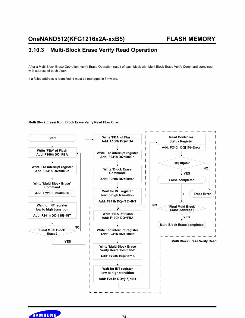
OneNAND512(KFG1216x2A-xxB5) FLASH MEMORY
74
After a Multi-Block Erase Operation, verify Erase Operation result of each block with Multi-Block Erase Verify Command combined with address of each block.
If a failed address is identified, it must be managed in firmware.
Multi Block Erase/ Multi Block Erase Verify Read Flow Chart
Start
Write ’FBA’ of FlashAdd: F100h DQ=FBA
Write ’Multi Block Erase’
Add: F220h DQ=0095h
Wait for INT register
Add: F241h DQ=[15]=INT
Final Multi Block
YES
NO
low to high transition
Write 0 to interrupt registerAdd: F241h DQ=0000h
Command
Erase?
Write ’FBA’ of FlashAdd: F100h DQ=FBA
Write ’Block Erase
Add: F220h DQ=0094h
Wait for INT register
Add: F241h DQ=[15]=INT
low to high transition
Write 0 to interrupt registerAdd: F241h DQ=0000h
Command’
Multi Block Erase Verify Read
Write ’FBA’ of FlashAdd: F100h DQ=FBA
Write ’Multi Block Erase
Add: F220h DQ=0071h
Wait for INT register
Add: F241h DQ=[15]=INT
low to high transition
Write 0 to interrupt registerAdd: F241h DQ=0000h
Verify Read Command’
Read Controller
Add: F240h DQ[10]=Error
Status Register
DQ[10]=0?
Multi Block Erase completed
Final Multi Block
YES
NOErase Address?
Erase completed
YES
Erase Error
NO
3.10.3 Multi-Block Erase Verify Read Operation
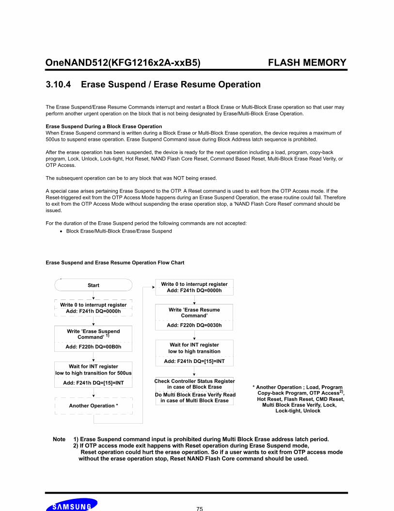
OneNAND512(KFG1216x2A-xxB5) FLASH MEMORY
75
The Erase Suspend/Erase Resume Commands interrupt and restart a Block Erase or Multi-Block Erase operation so that user may perform another urgent operation on the block that is not being designated by Erase/Multi-Block Erase Operation.
Erase Suspend During a Block Erase OperationWhen Erase Suspend command is written during a Block Erase or Multi-Block Erase operation, the device requires a maximum of 500us to suspend erase operation. Erase Suspend Command issue during Block Address latch sequence is prohibited.
After the erase operation has been suspended, the device is ready for the next operation including a load, program, copy-back program, Lock, Unlock, Lock-tight, Hot Reset, NAND Flash Core Reset, Command Based Reset, Multi-Block Erase Read Verity, or OTP Access.
The subsequent operation can be to any block that was NOT being erased.
A special case arises pertaining Erase Suspend to the OTP. A Reset command is used to exit from the OTP Access mode. If the Reset-triggered exit from the OTP Access Mode happens during an Erase Suspend Operation, the erase routine could fail. Therefore to exit from the OTP Access Mode without suspending the erase operation stop, a 'NAND Flash Core Reset' command should be issued.
For the duration of the Erase Suspend period the following commands are not accepted: • Block Erase/Multi-Block Erase/Erase Suspend
Erase Suspend and Erase Resume Operation Flow Chart
Start
Write ’Erase Suspend
Add: F220h DQ=00B0h
Wait for INT register
Add: F241h DQ=[15]=INT
low to high transition for 500us
Command’ 1)
Write 0 to interrupt registerAdd: F241h DQ=0000h
Write ’Erase Resume
Add: F220h DQ=0030h
Wait for INT register
Add: F241h DQ=[15]=INT
low to high transition
Write 0 to interrupt registerAdd: F241h DQ=0000h
Command’
Another Operation *
* Another Operation ; Load, Program Copy-back Program, OTP Access2), Hot Reset, Flash Reset, CMD Reset,
Multi Block Erase Verify, Lock,Lock-tight, Unlock
Check Controller Status Register
Do Multi Block Erase Verify Readin case of Block Erase
in case of Multi Block Erase
2) If OTP access mode exit happens with Reset operation during Erase Suspend mode, Reset operation could hurt the erase operation. So if a user wants to exit from OTP access mode
without the erase operation stop, Reset NAND Flash Core command should be used.
Note 1) Erase Suspend command input is prohibited during Multi Block Erase address latch period.
3.10.4 Erase Suspend / Erase Resume Operation

OneNAND512(KFG1216x2A-xxB5) FLASH MEMORY
76
Erase ResumeWhen the Erase Resume command is executed, the Block Erase will restart. The Erase Resume operation does not actually resume the erase, but starts it again from the beginning.
When an Erase Suspend or Erase Resume command is executed, the addresses are in Don't Care state.
On Block of the NAND Flash Array memory is reserved as a One-Time Programmable Block memory area.
The OTP block can be read, programmed and locked using the same operations as any other NAND Flash Array memory block. OTP block cannot be erased.
OTP block is fully-guaranteed to be a valid block.
Entering the OTP BlockThe OTP block is separately accessible from the rest of the NAND Flash Array by using the OTP Access command instead of the Flash Block Address (FBA).
Exiting the OTP BlockTo exit the OTP Access Mode, a Cold-, Warm-, Hot-, or NAND Flash Core Reset operation is performed.
Exiting the OTP Block during an Erase OperationIf the Reset-triggered exit from the OTP Access Mode happens during an Erase Suspend Operation, the erase routine could fail. Therefore to exit from the OTP Access Mode without suspending the erase operation stop, a'NAND Flash Core Reset' command should be issued.
The OTP Block Page AssignmentsOTP area is one block size (128KB+4KB, 64 Pages) and is divided into two areas. The 10-page User Area is available as an OTP storage area. The 54-page Manufacturer Area is programmed by the manufacturer prior to shipping the device to the user.
OTP Block Page Allocation Information
Area Page Use
User 0 ~ 9 (10 pages) Designated as user area
Manufacturer 10 ~ 63 (54 pages) Used by the device manufacturer
3.11 OTP Operation

OneNAND512(KFG1216x2A-xxB5) FLASH MEMORY
77
OTP Area Structure
Page:2KB+64B
Sector(main area):512B
Sector(spare area):16BOne Block:
128KB+4KB64pages
Manufacturer Area :
page10 to page6354pages
User Area :
page0 to page910pages

OneNAND512(KFG1216x2A-xxB5) FLASH MEMORY
78
An OTP Load Operation accesses the OTP area and transfers identified content from the OTP to the DataRAM on-chip buffer, thus making the OTP contents available to the Host.
The OTP area is a separate part of the NAND Flash Array memory. It is accessed by issuing OTP Access command(65h) instead of a Flash Block Address (FBA) command.
After being accessed with the OTP Access Command, the contents of OTP memory area are loaded using the same operationsas a normal load operation to the NAND Flash Array memory (see section 3.6 for more information).
To exit the OTP access mode following an OTP Load Operation, a Cold-, Warm-, Hot-, or NAND Flash Core Reset operation is performed.
OTP Read Operation Flow Chart
Start
Wait for INT register
Add: F241h DQ[15]=INT
Write 0 to interrupt registerAdd: F241h DQ=0000h
Write ’FPA, FSA’ of Flash1)
Add: F107h DQ=FPA, FSAOTP Reading completed
Write ’Load’ Command
Add: F220hDQ=0000h or 0013h
Wait for INT registerlow to high transition
Add: F241h DQ[15]=INT
Write ’OTP Access’ CommandAdd: F220h DQ=0065h
Write ’BSA, BSC’ of DataRAMAdd: F200h DQ=BSA, BSC
low to high transition
OTP Exit
Host reads data fromDataRAM
Note 1) FBA(NAND Flash Block Address) could be any address.
Do Cold/Warm/Hot/NAND Flash Core Reset
Write ’FBA’ of Flash1)
Add: F100h DQ=FBA
Write 0 to interrupt registerAdd: F241h DQ=0000h
3.11.1 OTP Load Operation

OneNAND512(KFG1216x2A-xxB5) FLASH MEMORY
79
An OTP Program Operation accesses the OTP area and programs content from the DataRAM on-chip buffer to the designated page(s) of the OTP.
A memory location in the OTP area can be programmed only one time (no erase operation permitted).
The OTP area is programmed using the same sequence as normal program operation after being accessed by the command (see section 3.8 for more information).
Programming the OTP Area • Issue the OTP Access Command • Write data into the DataRAM (data can be input at anytime between the "Start" and "Write Program" commands • Issue a Flash Block Address (FBA) which is unlocked area address of NAND Flash Array address map. • Issue a Write Program command to program the data from the DataRAM into the OTP • When the OTP programming is complete, do a Cold-, Warm-, Hot-, NAND Flash Core Reset to exit the OTP Access mode.
3.11.2 OTP Program Operation

OneNAND512(KFG1216x2A-xxB5) FLASH MEMORY
80
OTP Program Operation Flow Chart
Write ’FBA’ of Flash1)
Add: F100h DQ=FBA
Start
Data Input
Write ’OTP Access’ CommandAdd: F220h DQ=0065h
Write ’FPA, FSA’ of FlashAdd: F107h DQ=FPA, FSA
Write ’BSA, BSC’ of DataRAMAdd: F200h DQ=BSA, BSC
Write Data into DataRAM2)
Add: DP DQ=Data-in
OTP Programming completed
Write Program command
DQ=0080h or 001Ah
Completed?Wait for INT register
low to high transition
Add: F241h DQ[15]=INT
NO
Add: F220h
Wait for INT register
Add: F241h DQ[15]=INT
Write 0 to interrupt registerAdd: F241h DQ=0000h
low to high transition
Do Cold/Warm/Hot
OTP Exit
Automaticallychecked
Update Controller
Add: F240h Status Register
Wait for INT registerlow to high transition
Add: F241h DQ[15]=INT
OTP Exit
Automatically
OTPL=0?
YES
NO updated
Read ControllerStatus Register
Add: F240h DQ[10]=1(Error)
DQ[14]=1(Lock), DQ[10]=1(Error)
Add: F200h DQ=BSA, BSC
2) Data input could be done anywhere between "Start" and "Write Program Command".
Write ’FBA’ of FlashAdd: F100h DQ=FBA3)
Note 1) FBA(NAND Flash Block Address) could be any address.
Read ControllerStatus Register
Add: F240h DQ[10]=0(Pass)
/NAND Flash Core resetDo Cold/Warm/Hot
/NAND Flash Core reset
Write 0 to interrupt registerAdd: F241h DQ=0000h

OneNAND512(KFG1216x2A-xxB5) FLASH MEMORY
81
Even though the OTP area can only be programmed once without erase capability, it can be locked when the device starts up to prevent any changes from being made.
Unlike the main area of the NAND Flash Array memory, once the OTP block is locked, it cannot be unlocked.
Locking the OTPProgramming to the OTP area can be prevented by locking the OTP area. Locking the OTP area is accomplished by programming XXXCh to 8th word of sector0 of page0 of the spare0 memory area.
At device power-up, this word location is checked and if XXXCh is found, the OTPL bit of the Controller Status Register is set to "1", indicating the OTP is locked. When the Program Operation finds that the status of the OTP is locked, the device updates the Error Bit of the Controller Status Register as "1" (fail).
OTP Lock Operation Steps
• Issue the OTP Access Command • Fill data to be programmed into DataRAM (data can be input at anytime between the "Start" and "Write Program" commands) • Write 'XXXCH' data into the 8th word of sector0 of page0 of the spare0 memory area of the DataRAM. • Issue a Flash Block Address (FBA) to any address in the NAND Flash Array address map. • Issue a Program command to program the data from the DataRAM into the OTP • When the OTP lock is complete, do a Cold Reset to exit the OTP Access mode and update OTP lock bit[6]. • OTP lock bit[6] of the Controller Status Register will be set to "1" and the OTP will be locked.
3.11.3 OTP Lock Operation

OneNAND512(KFG1216x2A-xxB5) FLASH MEMORY
82
OTP Lock Operation Flow Chart
Start
Write ’FPA, FSA’ of FlashAdd: F107h DQ=0000h
Write ’BSA, BSC’ of DataRAMAdd: F200h DQ=0001h
Write Data into DataRAM2)
Add: 8th Word
Write Program command
DQ=0080h or 001Ah
Wait for INT registerlow to high transition
Add: F241h DQ[15]=INT
Add: F220h
Write 0 to interrupt registerAdd: F241h DQ=0000h
Automaticallyupdated
DQ=XXXChin spare0/sector0/page0
Update Controller
Add: F240h Status Register
OTP lock completed
DQ[6]=1(OTPL)
Write ’FBA’ of FlashAdd: F100h DQ=FBA3)
Write ’OTP Access’ CommandAdd: F220h DQ=0065h
Wait for INT register
Add: F241h DQ[15]=INT
low to high transition
Write 0 to interrupt registerAdd: F241h DQ=0000h
Do Cold reset
Write ’FBA’ of Flash1)
Add: F100h DQ=FBA
Note 1) FBA(NAND Flash Block Address) could be any address. 2) Data input could be done anywhere between "Start" and "Write Program Command".
3) FBA should point the unlocked area address among NAND Flash Array address map.
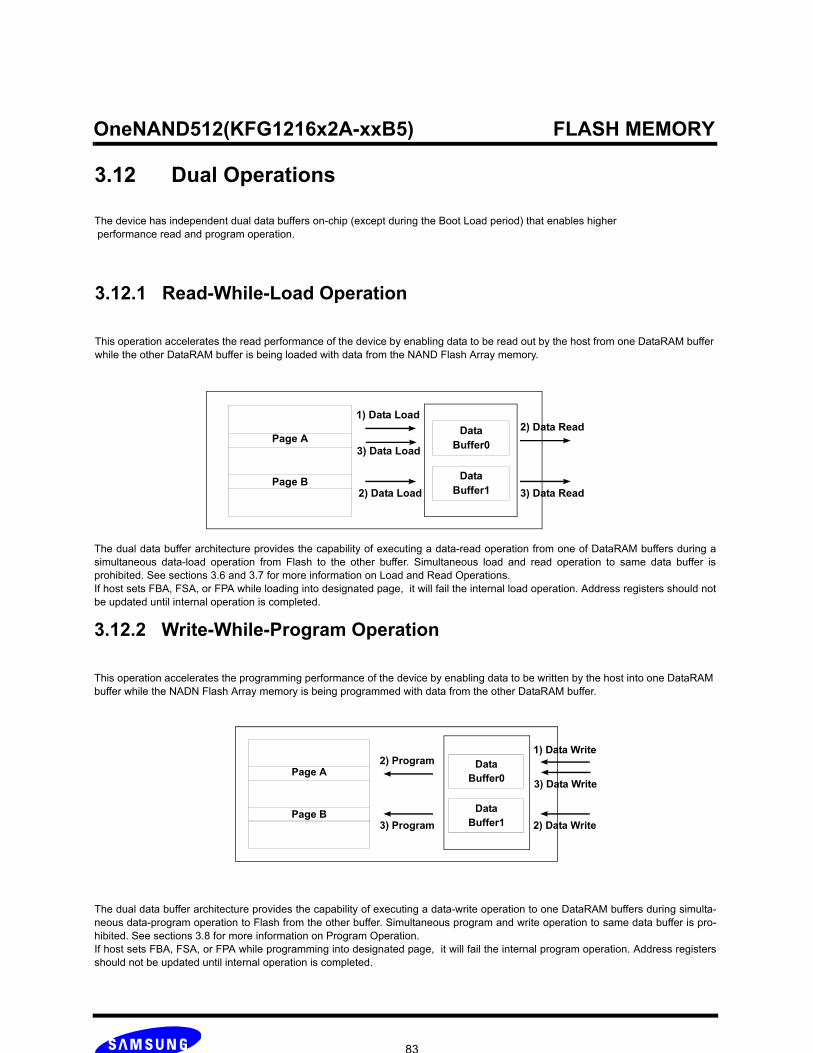
OneNAND512(KFG1216x2A-xxB5) FLASH MEMORY
83
The device has independent dual data buffers on-chip (except during the Boot Load period) that enables higher performance read and program operation.
3.12.1 Read-While-Load Operation
This operation accelerates the read performance of the device by enabling data to be read out by the host from one DataRAM buffer while the other DataRAM buffer is being loaded with data from the NAND Flash Array memory.
Page A
Page B
1) Data Load
2) Data LoadData
Buffer1
DataBuffer0
2) Data Read
3) Data Read
3) Data Load
The dual data buffer architecture provides the capability of executing a data-read operation from one of DataRAM buffers during asimultaneous data-load operation from Flash to the other buffer. Simultaneous load and read operation to same data buffer isprohibited. See sections 3.6 and 3.7 for more information on Load and Read Operations. If host sets FBA, FSA, or FPA while loading into designated page, it will fail the internal load operation. Address registers should notbe updated until internal operation is completed.
3.12.2 Write-While-Program Operation
This operation accelerates the programming performance of the device by enabling data to be written by the host into one DataRAM buffer while the NADN Flash Array memory is being programmed with data from the other DataRAM buffer.
Page A
Page B
2) Program
3) ProgramData
Buffer1
DataBuffer0
1) Data Write
2) Data Write
3) Data Write
The dual data buffer architecture provides the capability of executing a data-write operation to one DataRAM buffers during simulta-neous data-program operation to Flash from the other buffer. Simultaneous program and write operation to same data buffer is pro-hibited. See sections 3.8 for more information on Program Operation. If host sets FBA, FSA, or FPA while programming into designated page, it will fail the internal program operation. Address registersshould not be updated until internal operation is completed.
3.12 Dual Operations

OneNAND512(KFG1216x2A-xxB5) FLASH MEMORY
84
Rea
d W
hile
Loa
d D
iagr
am
Page
BA
DD
WE
OE
INT
0~15
2) 2)
Page
A1)
Add
_re
gIn
t_re
gC
MD
_re
gC
S_ reg
Dat
a Lo
ad_D
B0
Dat
a Lo
ad_D
B1
Dat
a R
ead
_DB
0 *
Add
_re
gIn
t_re
gC
MD
_re
gA
dd_
reg
Add
_re
g
DB
1_a
ddLD
_C
MD
Rea
dSt
atus
DB
0_a
dd00
00h
LD_
CM
DFl
ash
DQ
0~15
Int_
reg
: Int
erru
pt R
egis
ter A
ddre
ssA
dd_r
eg :
Add
ress
Reg
iste
r Add
ress
Flas
h_ad
d : F
lash
Add
ress
to b
e lo
aded
DB
n_ad
d : D
ataR
AM
Add
ress
to b
e lo
aded
CM
D_r
eg :
Com
man
d R
egis
ter A
ddre
ssLD
_CM
D :
Load
Com
man
dD
ata
Load
_DB
n : L
oad
Dat
a fro
m N
AN
D F
lash
Arr
ay to
Dat
aRA
Mn
CS
_reg
: C
ontro
ller S
tatu
s R
egis
ter A
ddre
ssD
ata
Rea
d_D
Bn
: Rea
d D
ata
from
DB
nD
Bn_
radd
: D
ataR
AM
Add
ress
to b
e re
ad
1)D
ata
Load
_DB
0
DB
0_ra
dd*
Dat
a Lo
ad_D
B1
_add
0000
hFl
ash
_add

OneNAND512(KFG1216x2A-xxB5) FLASH MEMORY
85
Writ
e W
hile
Pro
gram
Dia
gram
Page
B
AD
D
OE
INT
0~15
Page
A1)
WE
DB
0_w
add*
Add
_re
gA
dd_
reg
Int_
reg
CM
D_
reg
CS_ reg
Int_
reg
CM
D_
reg
Dat
a PG
M_P
ageB
DQ
0~15
DB
0_a
ddFl
ash
_add
0000
hPD
_C
MD
Dat
a W
rite
_DB
1 *
DB
1_a
ddR
ead
Stat
us00
00h
PD_
CM
D
Dat
a PG
M_P
ageA
Add
_reg
: A
ddre
ss R
egis
ter A
ddre
ssD
Bn_
add
: Dat
aRA
M A
ddre
ss to
be
prog
ram
med
DB
n_w
add
: Dat
aRA
M A
ddre
ss to
be
writ
ten
Dat
a W
rite_
DB
n : W
rite
Dat
a to
Dat
aRA
Mn
Flas
h_ad
d : F
lash
Add
ress
to b
e pr
ogra
mm
edIn
t_re
g : I
nter
rupt
Reg
iste
r Add
ress
CM
D_r
eg :
Com
man
d R
egis
ter A
ddre
ssP
D_C
MD
: P
rogr
am C
omm
and
Dat
a P
GM
_Pag
eA :
Pro
gram
Dat
a fro
m D
ataR
AM
to P
ageA
CS
_reg
: C
ontro
ller S
tatu
s R
egis
ter A
ddre
ss
Dat
a W
rite
_DB
0 *
DB
1_w
add*
Dat
a PG
M_P
ageA
2)
Add
_re
gA
dd_
reg
Flas
h_a
ddD
ata
Writ
e_D
B0
*
DB
0_w
add*
Dat
a PG
M_P
ageB

OneNAND512(KFG1216x2A-xxB5) FLASH MEMORY
86
The OneNAND device has on-chip ECC with the capability of detecting 2 bit errors and correcting 1-bit errors in the NAND Flash Array memory main and spare areas.
As the device transfers data from a BufferRAM to the NAND Flash Array memory Page Buffer for Program Operation, the device ini-tiates a background operation which generates an Error Correction Code (ECC) of 24bits for each sector main area data and 10bits for 2nd and 3rd word data of each sector spare area.
During a Load operation from the NAND Flash Array memory Page, the on-chip ECC engine generates a new ECC. The 'Load ECC result' is compared to the originally 'Program ECC' thus detecting the number and position of errors. Single-bit error is corrected.
ECC is updated by the device automatically. After a Load Operation, the Host can determine whether there was error by reading the 'ECC Status Register' (refer to section 2.8.26).
Error types are divided into 'no error', '1bit correctable error', and '2bit error uncorrectable error'.
OneNAND supports 2bit EDC even though 2bit error seldom or never occurs. Hence, it is not recommeded for Host to read 'ECC Sta-tus Register' for checking ECC error because the built-in Error Correction Logic of OneNAND automatically corrects ECC error.
When the device reads the NAND Flash Array memory main and spare area data with an ECC operation, the device doesn't place the newly generated ECC for main and spare area into the buffer. Instead it places the ECC which was generated and written during the program operation into the buffer.
An ECC operation is also done during the Boot Loading operation.
3.13.1 ECC Bypass Operation
3.13 ECC Operation
In an ECC bypass operation, the device does not generate ECC as a background operation. The result does not indicate error posi-tion (refer to the ECC Result Table).
In a Program Operation the ECC code to NAND Flash Array memory spare area is not updated. During a Load operation, the on-chip ECC engine does not generate a new ECC internally. Also the ECC Status & Result to Regis-ters are invalid. The error is not corrected and detected by itself, so that ECC bypass operation is not recommended for host.
ECC bypass operation is set by the 9bit of System Configuration 1 Register (see section 2.8.19)
ECC Code and ECC Result by ECC Operation
NOTE:1. Pre-written ECC code : ECC code which is previously written to NAND Flash Spare Area in program operation.
OperationProgram operation Load operation
ECC Code Update to NAND Flash Array Spare Area
ECC Code at BufferRAM Spare Area
ECC Status & Result Updateto Registers 1bit Error
ECC operation Update Pre-written ECC code(1) loaded Update Correct
ECC bypass Not update Pre-written code loaded Invalid Not correct

OneNAND512(KFG1216x2A-xxB5) FLASH MEMORY
87
Invalid blocks are defined as blocks in the device's NAND Flash Array memory that contain one or more invalid bits whose reliability is not guaranteed by Samsung.
The information regarding the invalid block(s) is called the Invalid Block Information. Devices with invalid block(s) have the same quality level as devices with all valid blocks and have the same AC and DC characteristics.
An invalid block(s) does not affect the performance of valid block(s) because it is isolated from the bit line and the common source line by a select transistor.
The system design must be able to mask out the invalid block(s) via address mapping. The 1st block, which is placed on 00h block address, is always fully guaranteed to be a valid block.
Due to invalid marking, during load operation for indentifying invalid block, a load error may occur.
3.14.1 Invalid Block Identification Table Operation
A system must be able to recognize invalid block(s) based on the original invalid block information and create an invalid block table.
Invalid blocks are identified by erasing all address locations in the NAND Flash Array memory except locations where the invalid block(s) information is written prior to shipping.
An invalid block(s) status is defined by the 1st word in the spare area. Samsung makes sure that either the 1st or 2nd page of every invalid block has non-FFFFh data at the 1st word of sector0.
Since the invalid block information is also erasable in most cases, it is impossible to recover the information once it has been erased. Any intentional erase of the original invalid block information is prohibited.
The following suggested flow chart can be used to create an Invalid Block Table.
3.14 Invalid Block Operation

OneNAND512(KFG1216x2A-xxB5) FLASH MEMORY
88
Invalid Block Table Creation Flow Chart
Within its life time, additional invalid blocks may develop with NAND Flash Array memory. Refer to the device's qualification report for the actual data.
The following possible failure modes should be considered to implement a highly reliable system.
In the case of a status read failure after erase or program, a block replacement should be done. Because program status failure during a page program does not affect the data of the other pages in the same block, a block replacement can be executed with a page-sized buffer by finding an erased empty block and reprogramming the current target data and copying the rest of the replaced block.
Block Failure Modes and Countermeasures
Failure Mode Detection and Countermeasure sequence
Erase Failure Status Read after Erase --> Block Replacement
Program Failure Status Read after Program --> Block Replacement
Single Bit Failure in Load Operation Error Correction by ECC mode of the device
3.14.2 Invalid Block Replacement Operation
*Check "FFFFh" at the 1st word of sector 0
Start
Set Block Address = 0
Check
Increment Block Address
Last Block ?
End
No
Yes
Yes
Create (or update) NoInvalid Block(s) Table
in 1st and 2nd page of every block
"FFFFh" ?

OneNAND512(KFG1216x2A-xxB5) FLASH MEMORY
89
Referring to the diagram for further illustration, when an error happens in the nth page of block 'A' during program operation, copy the data in the 1st ~ (n-1)th page to the same location of block 'B' via data buffer0.
Then copy the nth page data of block 'A' in the data buffer1 to the nth page of block 'B' or any free block. Do not further erase or program block 'A' but instead complete the operation by creating an 'Invalid Block Table' or other appropriate scheme.
Block Replacement Operation Sequence
Data Buffer1 of the device
1stBlock A
Block B
(n-1)thnth
(page)
{∼
1st
(n-1)thnth
(page)
{∼
an error occurs.
1
2
Data Buffer0 of the device
1(assuming the nth page data is maintained)

OneNAND512(KFG1216x2A-xxB5) FLASH MEMORY
90
4.1 Absolute Maximum Ratings
NOTES: 1. Minimum DC voltage is -0.5V on Input/ Output pins. During transitions, this level should not fall to POR level(typ. [email protected] device, [email protected]/3.3V device). Maximum DC voltage is Vcc+0.6V on input / output pins which, during transitions, may overshoot to Vcc+2.0V for periods <20ns.2. Permanent device damage may occur if ABSOLUTE MAXIMUM RATINGS are exceeded. Functional operation should be restricted to the conditions detailed in the operational sections of this data sheet. Exposure to absolute maximum rating conditions for extended periods may affect reliability.
Parameter Symbol Rating Unit
Voltage on any pin relative to VSS
VccVcc (for 1.8V) -0.5 to + 2.45
VVcc (for 2.65V/3.3V) -0.5 to + 4.6
All PinsVIN (for 1.8V) -0.5 to + 2.45
VIN (for 2.65V/3.3V) -0.5 to + 4.6
Temperature Under BiasExtended
Tbias-30 to +125
°CIndustrial -40 to +125
Storage Temperature Tstg -65 to +150 °C
Short Circuit Output Current IOS 5 mA
Recommended Operating TemperatureTA (Extended Temp.) -30 to +85
°CTA (Industrial Temp.) -40 to +85
4.2 Operating Conditions
4.0 DC CHARACTERISTICS
Voltage reference to GND
NOTES: 1. The system power should reach 1.7V after POR triggering level(typ. 1.5V) within 400us. For 2.65V and 3.3V device, the system power should reach 2.2V after POR triggering level(typ. 1.8V) within 400us.2. Vcc-Core (or Vcc) should reach the operating voltage level prior to or at the same time as Vcc-IO (or Vccq).
Parameter Symbol1.8V Device 2.65V Device 3.3V Device
UnitMin Typ. Max Min Typ. Max Min Typ. Max
Supply Voltage
VCC-core / Vcc1.7 1.8 1.95 2.4 2.65 2.9 2.7 3.3 3.6 V
VCC- IO / Vccq
VSS 0 0 0 0 0 0 0 0 0 V

OneNAND512(KFG1216x2A-xxB5) FLASH MEMORY
91
Note 1. CE should be VIH for RDY. IOBE should be ’0’ for INT.Note 2. Icc active for Host access Note 3. ICC active for Internal operation. (without host access)
Parameter Symbol Test Conditions 1.8V device 2.65V device 3.3V device
UnitMin Typ Max Min Typ Max Min Typ Max
Input Leakage Current ILI VIN=VSS to VCC, VCC=VCCmax - 1.0 - + 1.0 - 1.0 - + 1.0 - 1.0 - + 1.0 µA
Output Leakage Cur-rent ILO
VOUT=VSS to VCC, VCC=VCCmax, CE or OE=VIH(Note 1) - 1.0 - + 1.0 - 1.0 - + 1.0 - 1.0 - + 1.0 µA
Active Asynchronous Read Current (Note 2) ICC1 CE=VIL, OE=VIH - 8 15 - 18 22 - 18 22 mA
Active Burst Read Cur-rent (Note 2) ICC2 CE=VIL, OE=VIH
54Mhz - 12 20 - 22 30 - 22 30 mA
1MHz - 3 4 - 7 9 - 7 9 mA
Active Write Current (Note 2) ICC3 CE=VIL, OE=VIH - 8 15 - 17 22 - 17 22 mA
Active Load Current (Note 3) ICC4 CE=VIL, OE=VIH, WE=VIH - 30 40 - 30 40 - 30 40 mA
Active Program Cur-rent (Note 3) ICC5 CE=VIL, OE=VIH, WE=VIH - 25 30 - 28 35 - 28 35 mA
Active Erase Current (Note 3) ICC6 CE=VIL, OE=VIH, WE=VIH - 20 25 - 23 30 - 23 30 mA
Multi Block Erase Cur-rent (Note 3) ICC7
CE=VIL, OE=VIH, WE=VIH, 64blocks - 20 25 - 23 30 - 23 30 mA
Standby Current ISB CE= RP=VCC ± 0.2V - 10 50 - 35 80 - 35 80 µA
Input Low Voltage VIL - -0.5 - 0.4 -0.5 - 0.4 0 - 0.8 V
Input High Voltage VIH - VCCq-0.4 - VCCq
+0.4VCCq-
0.4 - VCCq
+0.40.7*V
CCq- VCCq V
Output Low Voltage VOLIOL = 100 µA , VCC=VCCmin , VCCq=VCCqmin - - 0.2 - - 0.2 - - 0.22*
Vccq V
Output High Voltage VOHIOH = -100 µA , VCC=VCCmin , VCCq=VCCqmin
VCCq-0.1 - - VCCq-
0.4 - - 0.8*VCCq
- - V
4.3 DC Characteristics

OneNAND512(KFG1216x2A-xxB5) FLASH MEMORY
92
5.1 AC Test Conditions Parameter Value
Input Pulse Levels 0V to VCC
Input Rise and Fall TimesCLK 3ns
other inputs 5ns
Input and Output Timing Levels VCC/2
Output Load CL = 30pF
0V
VCC
VCC/2 VCC/2
Input Pulse and Test Point
Input & OutputTest Point
Output Load
DeviceUnderTest
* CL = 30pF including scope and Jig capacitance
5.2 Device Capacitance
NOTES:1. The device may include invalid blocks when first shipped. Additional invalid blocks may develop while being used. The number of valid blocks is pre-
sented with both cases of invalid blocks considered. Invalid blocks are defined as blocks that contain one or more bad bits. Do not erase or programfactory-marked bad blocks.
2. The 1st block, which is placed on 00h block address, is fully guaranteed to be a valid block.
Parameter Symbol Min Typ. Max Unit
Valid Block Number NVB 502 - 512 Blocks
CAPACITANCE(TA = 25 °C, VCC = 1.8V/2.65V/3.3V, f = 1.0MHz)
NOTE : Capacitance is periodically sampled and not 100% tested.
Item Symbol Test ConditionKFG1216x2A
UnitMin Max
Input Capacitance CIN1 VIN=0V - 10 pF
Control Pin Capacitance CIN2 VIN=0V - 10 pF
Output Capacitance COUT VOUT=0V - 10 pF
INT Capacitance CINT VOUT=0V - 15 pF
5.3 Valid Block Characteristics
5.0 AC CHARACTERISTICS

OneNAND512(KFG1216x2A-xxB5) FLASH MEMORY
93
Note 1. If OE is disabled at the same time or before CE is disabled, the output will go to high-z by tOEZ. If CE is disabled at the same time or before OE is disabled, the output will go to high-z by tCEZ. If CE and OE are disabled at the same time, the output will go to high-z by tOEZ. 2. It is the following clock of address fetch clock.
Parameter SymbolKFG1216x2A
UnitMin Max
Clock CLK 1 54 MHz
Clock Cycle tCLK 18.5 - ns
Initial Access Time tIAA - 76 ns
Burst Access Time Valid Clock to Output Delay tBA - 14.5 ns
AVD Setup Time to CLK tAVDS 7 - ns
AVD Hold Time from CLK tAVDH 7 - ns
Address Setup Time to CLK tACS 7 - ns
Address Hold Time from CLK tACH 7 - ns
Data Hold Time from Next Clock Cycle tBDH 4 - ns
Output Enable to Data tOE - 20 ns
CE Disable to Output High Z tCEZ1) - 20 ns
OE Disable to Output High Z tOEZ1) - 17 ns
CE Setup Time to CLK tCES 7 - ns
CLK High or Low Time tCLKH/L tCLK/3 - ns
CLK 2) to RDY valid tRDYO - 14.5 ns
CLK to RDY Setup Time tRDYA - 14.5 ns
RDY Setup Time to CLK tRDYS 4 - ns
CE low to RDY valid tCER - 15 ns
5.4 AC Characteristics for Synchronous Burst Read See Timing Diagrams 6.1 and 6.2

OneNAND512(KFG1216x2A-xxB5) FLASH MEMORY
94
NOTE: 1. If OE is disabled at the same time or before CE is disabled, the output will go to high-z by tOEZ. If CE is disabled at the same time or before OE is disabled, the output will go to high-z by tCEZ. If CE and OE are disabled at the same time, the output will go to high-z by tOEZ.
These parameters are not 100% tested.
Parameter SymbolKFG1216x2A Unit
Min Max Unit
Access Time from CE Low tCE - 76 ns
Asynchronous Access Time from AVD Low tAA - 76 ns
Asynchronous Access Time from address valid tACC - 76 ns
Read Cycle Time tRC 76 - ns
AVD Low Time tAVDP 12 - ns
Address Setup to rising edge of AVD tAAVDS 7 - ns
Address Hold from rising edge of AVD tAAVDH 7 - ns
Output Enable to Output Valid tOE - 20 ns
WE disable to OE enable tOEH 0 - ns
CE Setup to AVD falling edge tCA 0 - ns
CE Disable to Output & RDY High Z1) tCEZ - 20 ns
OE Disable to Output High Z1) tOEZ - 17 ns
WE Disable to AVD Enable tWEA 15 - ns
5.6 AC Characteristics for Warm Reset (RP), Hot Reset and NAND Flash Core Reset See Timing Diagrams 6.12, 6.13 and 6.14
5.5 AC Characteristics for Asynchronous Read See Timing Diagrams 6.3, 6.4, 6.5 and 6.6
Note1. These parameters are tested based on INT bit of interrupt register. Because the time on INT pin is related to the pull-up and pull-down resistor value. 2. The device may reset if tRP < tRP min(200ns), but this is not guaranteed.
Parameter Symbol Min Max Unit
RP & Reset Command Latch to BootRAM Access tReady1(BufferRAM) - 5 µs
RP & Reset Command Latch(During Load Routines) to INT High (Note1) tReady2(NAND Flash Array) - 10 µs
RP & Reset Command Latch(During Program Routines) to INT High (Note1) tReady2(NAND Flash Array) - 20 µs
RP & Reset Command Latch(During Erase Routines) to INT High (Note1) tReady2(NAND Flash Array) - 500 µs
RP & Reset Command Latch(NOT During Internal Routines) to INT High (Note1) tReady2(NAND Flash Array) - 10 µs
RP Pulse Width (Note2) tRP 200 - ns

OneNAND512(KFG1216x2A-xxB5) FLASH MEMORY
95
Note 1)These parameters are tested based on INT bit of interrupt register. Because the time on INT pin is related to the pull-up and pull-down resistor value.
Parameter Symbol Min Typ Max Unit
Sector Read time(Note 1) tRD1 - 23 35 µs
Page Read time(Note 1) tRD2 - 30 45 µs
Sector Program time(Note 1) tPGM1 - 205 720 µs
Page Program time(Note 1) tPGM2 - 220 750 µs
OTP Access Time(Note 1) tOTP - 500 700 ns
Lock/Unlock/Lock-tight Time(Note 1) tLOCK - 500 700 ns
Erase Suspend Time(Note 1) tESP - 400 500 µs
Erase Resume Time(Note 1)1 Block tERS1 - 2 3 ms
2~64 Blocks tERS2 4 6 ms
Number of Partial Program Cycles in the sector (Including main and spare area) NOP - - 2 cycles
Block Erase time (Note 1)1 Block tBERS1 - 2 3 ms
2~64 Blocks tBERS2 - 4 6 ms
Multi BlocK Erase Verify Read time(Note 1) tRD3 - 70 100 µs
Parameter Symbol Min Typ Max Unit
WE Cycle Time tWC 70 - - ns
AVD low pulse width tAVDP 12 - - ns
Address Setup Time tAWES 0 - - ns
Address Hold Time tAH 30 - - ns
Data Setup Time tDS 25 - - ns
Data Hold Time tDH 0 - - ns
CE Setup Time tCS 0 - - ns
CE Hold Time tCH 10 - - ns
WE Pulse Width tWPL 40 - - ns
WE Pulse Width High tWPH 30 - - ns
AVD Disable to WE Disable tVLWH 15 - - ns
WE Disable to AVD Enable tWEA 15 - - ns
5.8 AC Characteristics for Load/Program/Erase Performance See Timing Diagrams 6.8, 6.9, and 6.10
5.7 AC Characteristics for Asynchronous Write/Load/ Program/Erase Operation See Timing Diagrams 6.7, 6.8 and 6.9
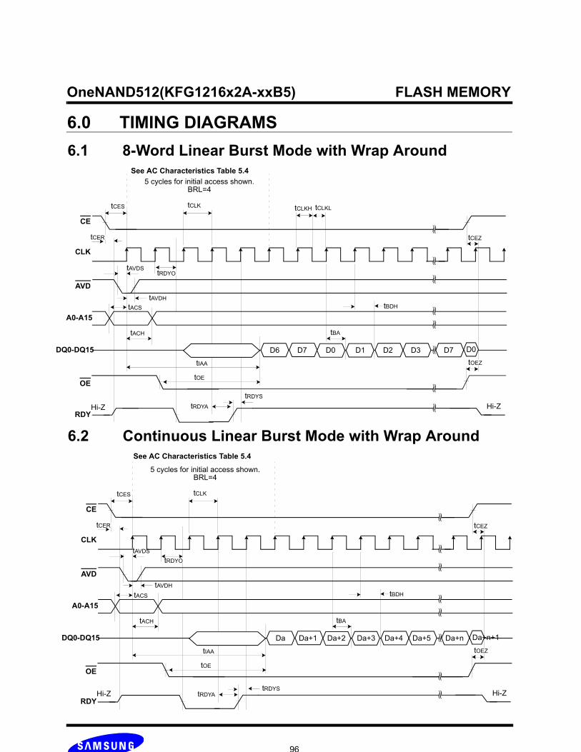
OneNAND512(KFG1216x2A-xxB5) FLASH MEMORY
96
6.1 8-Word Linear Burst Mode with Wrap Around See AC Characteristics Table 5.4
6.2 Continuous Linear Burst Mode with Wrap Around See AC Characteristics Table 5.4
5 cycles for initial access shown.
tCES
tAVDS
tAVDHtACS
tACH
tIAA
tBA
tBDH
tCLK
CE
CLK
AVD
OE
DQ0-DQ15
A0-A15
≈≈
≈≈
≈≈
≈
D6 D7 D0 D1 D2 D3 D7
tRDYA
tOE
BRL=4
tCEZ
tOEZ
D0
tCLKH tCLKL
tRDYO
tCER
Hi-ZRDY
≈
tRDYS
Hi-Z
5 cycles for initial access shown.
tCES
tAVDS
tAVDH
tACS
tACH
tIAA
tBA
tBDH
tCLK
Hi-Z
CE
CLK
AVD
OE
DQ0-DQ15
RDY
A0-A15
≈≈
≈≈
≈≈
≈≈tRDYS
Da Da+1 Da+2 Da+3 Da+4 Da+5 Da+n
tRDYA
tOE
BRL=4
tCEZ
tOEZ
Da+n+1
Hi-Z
tRDYO
tCER
6.0 TIMING DIAGRAMS

OneNAND512(KFG1216x2A-xxB5) FLASH MEMORY
97
6.4 Asynchronous Read (VA and AVD Transition After CE Low) See AC Characteristics Table 5.5
NOTE: VA=Valid Read Address, RD=Read Data.
tOE
VA
Valid RD
tCE tOEZ
CE
OE
WE
A0-A15
CLK VIL
AVD
Hi-ZHi-ZRDY
tAVDP
tAAVDH
DQ0-DQ15
tCEZ
NOTE: VA=Valid Read Address, RD=Read Data.
tOE
VA
Valid RD
tOEZ
CE
OE
WE
A0-A15
CLK VIL
AVD
tAA
Hi-ZHi-ZRDY
tAVDP
tAAVDH
DQ0-DQ15
tWEA
tCEZ
6.3 Asynchronous Read (VA and AVD Transition Before CE Low)
See AC Characteristics Table 5.5

OneNAND512(KFG1216x2A-xxB5) FLASH MEMORY
98
6.6 Asynchronous Read (AVD is tied to CE) See AC Characteristics Table 5.5
NOTE: VA=Valid Read Address, RD=Read Data.
tOE
VA
Valid RD
tOEZ
CE
OE
WE
A0-A15
tACC
CLK VIL
AVDtAAVDS
Hi-ZHi-ZRDY
tAVDP
tAAVDH
DQ0-DQ15
tWEA
tCEZ
NOTE: VA=Valid Read Address, RD=Read Data.
tOE
VA
Valid RD
tCE tOEZ
CE
OE
WE
A0-A15
tACC
CLK VIL
Hi-ZHi-ZRDY
tRC
DQ0-DQ15
tCEZ
6.5 Asynchronous Read (VA and AVD Transition After CE Low) See AC Characteristics Table 5.5

OneNAND512(KFG1216x2A-xxB5) FLASH MEMORY
99
NOTE: VA=Valid Read Address, WD=Write Data.
CE
WE
OE
RP
A0-A15
tCS
DQ0-DQ15 Valid WD
tDS
RDY
VA
Valid WD
tWPL tWPH
tWC
tDHtAWES
VA
tAH
Hi-Z Hi-Z
CLK VIL
tCH tCS
6.7 Asynchronous Write See AC Characteristics Table 5.7

OneNAND512(KFG1216x2A-xxB5) FLASH MEMORY
100
NOTES: 1. AA = Address of address register CA = Address of command register LCD = Load Command LMA = Address of memory to be loaded BA = Address of BufferRAM to load the data BD = Program Data SA = Address of status register 2. “In progress” and “complete” refer to status register3. Status reads in this figure is asynchronous read, but status read in synchronous mode is also supported.
Load Command Sequence
A0:A15
WE
CE
CLK
tDS
tDH
tCH
tWPL
tCStWPH
tWC
CA BA BA
LCDLMA
AA
DQ0-DQ15
OE
Read Data
VIL
≈≈
≈≈
≈≈
Da Da+1
tAHtAWES
INT
tRD
tCH tCS
6.8 Load Operation Timing See AC Characteristics Tables 5.7 and 5.8

OneNAND512(KFG1216x2A-xxB5) FLASH MEMORY
101
NOTES: 1. AA = Address of address register CA = Address of command register PCD = Program Command PMA = Address of memory to be programmed BA = Address of BufferRAM to load the data BD = Program Data SA = Address of status register 2. “In progress” and “complete” refer to status register3. Status reads in this figure is asynchronous read, but status read in synchronous mode is also supported.
Program Command Sequence (last two cycles)
A0:A15
WE
CE
CLK
tDS tDH
tCH
tWPL
tCS
tWPH
tWC
SA SA
InProgress Complete
AA
DQ0-DQ15
OE
Read Status Data
VIL
≈≈
≈≈
≈≈
BA CA
PCDPMA BD
tAHtAWES
tPGM
INT
tCHtCH tCS tCS
6.9 Program Operation Timing See AC Characteristics Tables 5.7 and 5.8

OneNAND512(KFG1216x2A-xxB5) FLASH MEMORY
102
NOTES: 1. AA = Address of address register CA = Address of command register ECD = Erase Command EMA = Address of memory to be erased SA = Address of status register 2. “In progress” and “complete” refer to status register3. Status reads in this figure is asynchronous read, but status read in synchronous mode is also supported.
Erase Command Sequence (last two cycles)
A0:A15
WE
CE
tDStDH
tCH
CA SA SA
InProgress CompleteECDEMA
AA
DQ0-DQ15
OE
Read Status Data
tWPL
tCStWPH
tWC
CLK VIL
≈≈
≈≈
≈≈
tAHtAWES
tBERS
INT
tCH tCS
6.10 Block Erase Operation Timing See AC Characteristics Tables 5.7 and 5.8

OneNAND512(KFG1216x2A-xxB5) FLASH MEMORY
103
6.11 Cold Reset Timing
Note: 1) Bootcode copy operation starts 400us later than POR activation. The system power should reach Vcc after POR triggering level(typ. 1.5V) within 400us for valid boot code data. 2) 1K bytes Bootcode copy takes 70us(estimated) from sector0 and sector1/page0/block0 of NAND Flash array to BootRAM. Host can read Bootcode in BootRAM(1K bytes) after Bootcode copy completion. 3) INT register goes ‘Low’ to ‘High’ on the condition of ‘Bootcode-copy done’ and RP rising edge. If RP goes ‘Low’ to ‘High’ before ‘Bootcode-copy done’, INT register goes to ‘Low’ to ‘High’ as soon as ‘Bootcode-copy done’
System Power
Sleep Bootcode copy Idle
Bootcode - copy done
POR triggering level
3)
2)
RP
INT
OneNANDOperation
0 (default) 1IOBE bit
1 (default)INTpol bit
High-Z
1)
INT bit 0 (default) 1

OneNAND512(KFG1216x2A-xxB5) FLASH MEMORY
104
6.12 Warm Reset Timing See AC Characteristics Tables 5.6
CE, OE
RPtRP
tReady1
RDY
INT
High-ZHigh-Z
tReady2
Idle1)Operation Status Reset Ongoing2) BootRAM Access3) Idle1)INT Bit Polling4)
NOTES: 1. The status which can accept any register based operation(Load, Program, Erase command, etc).2. The status where reset is ongoing. 3. The status allows only BootRAM(BL1) read operation for Boot Sequence.(refer to 7.2.2 Boot Sequence)4. To read BL2 of Boot Sequence, Host should wait INT until becomes ready. and then, Host can issue load command. (refer to 7.2.2 Boot Sequence, 7.1 Methods of Determing Interrupt status)
bit

OneNAND512(KFG1216x2A-xxB5) FLASH MEMORY
105
6.13 Hot Reset Timing
NOTE:1. Internal reset operation means that the device initializes internal registers and makes output signals go to default status and bufferRAM data are keptunchanged after Warm/Hot reset operations.2. Reset command : Command based reset or Register based reset3. BP(Boot Partition): BootRAM area [0000h~01FFh, 8000h~800Fh]4. 00F0h for BP, and 00F3h for F220h
AVD
BP(Note 3)
INT
A0~A15
WE
CE
or F220h
RDY
Operation or Idle OneNAND reset IdleOneNANDOperation
High-Z
DQ0~DQ15 00F0h or 00F3h4)
OE
tReady2
bit

OneNAND512(KFG1216x2A-xxB5) FLASH MEMORY
106
6.15 Data Protection Timing During Power Down
VCC
RP
NAND WriteProtectedIdle One NAND Reset
INT
OneNANDOperation
typ. 1.3V
0V
The device is designed to offer protection from any involuntary program/erase during power-transitions. An internal voltage detectordisables all functions whenever Vcc is below about 1.3V. RP pin provides hardware protection and is recommended to be kept at VIL
before power-down.
6.14 NAND Flash Core Reset Timing
AVD
CE
F220h
RDY
Operation or Idle NAND Flash Core reset IdleOneNANDOperation
High-Z
00F0h
A0~A15
DQ0~DQ15
INT
WE
OE
tReady2
bit

OneNAND512(KFG1216x2A-xxB5) FLASH MEMORY
107
From time-to-time supplemental technical information and application notes pertaining to the design and operation of the device in asystem are included in this section. Contact your Samsung Representative to determine if additional notes are available.
7.1 Methods of Determining Interrupt Status
There are two methods of determining Interrupt Status on the OneNAND. Using the INT pin or monitoring the Interrupt Status Regis-ter Bit.
The OneNAND INT pin is an output pin function used to notify the Host when a command has been completed. This provides a hard-ware method of signaling the completion of a program, erase, or load operation.
In its normal state, the INT pin is high if the INT polarity bit is default. Before a command is written to the command register, the INTbit must be written to '0' so the INT pin transitions to a low state indicating start of the operation. Upon completion of the commandoperation by the OneNAND’s internal controller, INT returns to a high state.
INT is an open drain output allowing multiple INT outputs to be Or-tied together. INT does not float to a hi-Z condition when the chip isdeselected or when outputs are disabled. Refer to section 2.8 for additional information about INT.
INT can be implemented by tying INT to a host GPIO or by continuous polling of the Interrupt status register.
7.1.1 The INT Pin to a Host General Purpose I/O
INT can be tied to a Host GPIO to detect the rising edge of INT, signaling the end of a command operation.
This can be configured to operate either synchronously or asynchronously as shown in the diagrams below.
INT
COMMAND
7.0 TECHNICAL AND APPLICATION NOTES

OneNAND512(KFG1216x2A-xxB5) FLASH MEMORY
108
Synchronous Mode Using the INT PinWhen operating synchronously, INT is tied directly to a Host GPIO.
An alternate method of determining the end of an operation is to continuously monitor the Interrupt Status Register Bit instead of using the INT pin.
Host OneNAND
Asynchronous Mode Using the INT PinWhen configured to operate in an asynchronous mode, /CE and /AVD of the OneNAND are tied to /CE of the Host. CLK is tied to theHost Vss (Ground). /RDY is tied to a no-connect. /OE of the OneNAND and Host are tied together and INT is tied to a GPIO.
RDY
OE
CLK
CE
RDY
OE
CLK
CE
AVD AVD
GPIO INT
Host OneNAND
N.C
OE
Vss
CE
RDY
OE
CLK
CE
AVD
GPIO INT
INT
Command
This can be configured in either a synchronous mode or an asynchronous mode.
7.1.2 Polling the Interrupt Register Status Bit
OneNAND512(KFG1216x2A-xxB5) FLASH MEMORY
109
Synchronous Mode Using Interrupt Status Register Bit PollingWhen operating synchronously, /CE, /AVD, CLK, /RDY, /OE, and DQ pins on the host and OneNAND are tied together.
Host OneNAND
RDY
OE
CLK
CE
RDY
OE
CLK
CE
AVD AVD
DQ DQ
Asynchronous Mode Using Interrupt Status Register Bit PollingWhen configured to operate in an asynchronous mode, /CE and /AVD of the OneNAND are tied to /CE of the Host. CLK is tied to the Host Vss (Ground). /RDY is tied to a no-connect. /OE and DQ of the OneNAND and Host are tied together.
Host OneNAND
N.C
OE
CE
RDY
OE
CLK
CE
AVD
DQ DQ
Vss

OneNAND512(KFG1216x2A-xxB5) FLASH MEMORY
110
Because the pull-up resistor value is related to tr(INT) an appropriate value can obtained with the following reference charts.
7.1.3 Determining Rp Value tr,
tf
Ibus
y [m
A]
Rp(ohm)
Ibusy
tr[us]
@ Vcc = 1.8V, Ta = 25°C , CL = 30pF
1K 10K 20K 30K
0.089
tf[ns]
0.7727 1.345
1.788
3.77 3.77 3.77 3.77
1.750.18
0.09
40K 50K
2.1422.431
3.77 3.77
0.0450.06
0.036
Open(100K)
5.420
0.000
≈≈
≈
≈≈
≈
Busy State
Ready Vcc
VOH
tf tr
VOL Vss
~50k ohm
INT
Internal Vcc
Rp
INT pol = ’High’

OneNAND512(KFG1216x2A-xxB5) FLASH MEMORY
111
~50k ohm
INT
Internal Vcc
Rp
INT pol = ’Low’tr,
tf
Ibus
y [m
A]
Rp(ohm)
Ibusy
tf[us]
@ Vcc = 1.8V, Ta = 25°C , CL = 30pF
1K 10K 20K 30K
0.067
tr[ns]
0.586 1.02
1.356
6.49 6.49 6.49 6.49
1.750.18
0.09
40K 50K
1.6231.84
6.49 6.49
0.0450.06
0.036
Open(100K)
4.05
0.000
≈≈
≈
≈≈
≈
Busy State
Ready
VOH
tftr
VOLVss
Vcc
OneNAND512(KFG1216x2A-xxB5) FLASH MEMORY
112
One of the best features OneNAND has is that it can be a booting device itself since it contains an internally built-in boot loader despite the fact that its core architecture is based on NAND Flash. Thus, OneNAND does not make any additional booting device necessary for a system, which imposes extra cost or area overhead on the overall system.
As the system power is turned on, the boot code originally stored in NAND Flash Arrary is moved to BootRAM automatically and then fetched by CPU through the same interface as SRAM’s or NOR Flash’s if the size of the boot code is less than 1KB. If its size is larger than 1KB and less than or equal to 3KB, only 1KB of it can be moved to BootRAM automatically and fetched by CPU, and the rest of it can be loaded into one of the DataRAMs whose size is 2KB by Load Command and CPU can take it from the DataRAM after finish-ing the code-fetching job for BootRAM. If its size is larger than 3KB, the 1KB portion of it can be moved to BootRAM automatically and fetched by CPU, and its remaining part can be moved to DRAM through two DataRAMs using dual buffering and taken by CPU to reduce CPU fetch time.
A typical boot scheme usually used to boot the system with OneNAND is explained at Patition of NAND Flash Array and OneNAND Boot Sequence. In this boot scheme, boot code is comprised of BL1, where BL stands for Boot Loader, BL2, and BL3. Moreover, the size of the boot code is larger than 3KB (the 3rd case above). BL1 is called primary boot loader in other words. Here is the table of detailed explanations about the function of each boot loader in this specific boot scheme.
Boot Loaders in OneNAND
NAND Flash Array of OneNAND is divided into the partitions as described at Partition of NAND Flash array to show where each com-ponent of code is located and how much portion of the overall NAND Flash Array each one occupies. In addition, the boot sequence is listed below and depicted at Boot Sequence.
Boot Loader Description
BL1 Moves BL2 from NAND Flash Array to DRAM through two DataRAMs using dual buffering
BL2 Moves OS image (or BL3 optionally) from NAND Flash Array to DRAM through two DataRams using dual buffering
BL3 (Optional) Moves or writes the image through USB interface
7.2.1 Boot Loaders in OneNAND
Boot Sequence : 1. Power is on BL1 is loaded into BootRAM
2. BL1 is executed in BootRAM BL2 is loaded into DRAM through two DataRams using dual buffering by BL1
3. BL2 is executed in DRAM OS image is loaded into DRAM through two DataRams using dual buffering by BL2
4. OS is running
7.2.2 Boot Sequence
7.2 Boot Sequence

OneNAND512(KFG1216x2A-xxB5) FLASH MEMORY
113
Reservoir
File System
Os Image
NBL3
NBL2NBL1
Partition 6
Block 162
Block 2
Block 1
Block 0
Partition 5Sector 0 Sector 1 Sector 2 Sector 3
Page 63
Page 62
Page 2
Page 1
Page 0
BL2Partition 4
Partition 3
Partition of NAND Flash array
Reservoir
File System
Os Image
BL3
BL2BL1
Partition 6
Block 162
Block 2
Block 1
Block 0
Partition 5Sector 0 Sector 1 Sector 2 Sector 3
Page 63
Page 62
Page 2
Page 1
Page 0
Partition 4
Partition 3
::
Reservoir
File System
Os Image
BL2BL1Os Image
BL 2
NAND Flash Array
OneNAND DRAM
OneNAND Boot Sequence
BL1
Internal BufferRAM
Data Ram 1
Data Ram 0
Boot Ram(BL 1)
NOTE:Step 2 and Step 3 can be copied into DRAM through two DataRAMs using dual buffering
Block 512
step 1 step 2
step 3

OneNAND512(KFG1216x2A-xxB5) FLASH MEMORY
114
0.10 MAX
0.45±0
.05
0.32±0.05
0.9±0.10
63-FBGA-9.50x12.00 Units:millimeters
BOTTOM VIEWTOP VIEW
A
C
E
B
D
F
0.80x9=7.20A
0.80
x11=
8.80
63-∅ 0.45±0.05
G
4.40
0 .8 0
B
0.20 M A B ∅
(Datum A)
(Datum B)
25 4 3 16
3.60
#A1 INDEX
H
9.50±0.10
12.0
0±0.
10
#A1
12.0
0±0.
10
0.80
9.50±0.10
12.0
0±0.
10
8.0 PACKAGE DIMENSIONS