9 Reprogramming 3D TLC Flash Memory based Solid State ...
33
9 Reprogramming 3D TLC Flash Memory based Solid State Drives CONGMING GAO, Tsinghua University, China MIN YE and CHUN JASON XUE, City University of Hong Kong, China YOUTAO ZHANG, University of Pittsburgh, USA LIANG SHI, East China Normal University, China JIWU SHU, Tsinghua University, China JUN YANG, University of Pittsburgh, USA NAND flash memory-based SSDs have been widely adopted. The scaling of SSD has evolved from plannar (2D) to 3D stacking. For reliability and other reasons, the technology node in 3D NAND SSD is larger than in 2D, but data density can be increased via increasing bit-per-cell. In this work, we develop a novel reprogram- ming scheme for TLCs in 3D NAND SSD, such that a cell can be programmed and reprogrammed several times before it is erased. Such reprogramming can improve the endurance of a cell and the speed of program- ming, and increase the amount of bits written in a cell per program/erase cycle, i.e., effective capacity. Our work is the first to perform a real 3D NAND SSD test to validate the feasibility of the reprogram operation. From the collected data, we derive the restrictions of performing reprogramming due to reliability challenges. Furthermore, a reprogrammable SSD (ReSSD) is designed to structure reprogram operations. ReSSD is eval- uated in a case study in RAID 5 system (RSS-RAID). Experimental results show that RSS-RAID can improve the endurance by 35.7%, boost write performance by 15.9%, and increase effective capacity by 7.71%, with negligible overhead compared with conventional 3D SSD-based RAID 5 system. CCS Concepts: • Information systems → Flash memory;• Hardware → 3D integrated circuits;• Computer systems organization → Architectures; Additional Key Words and Phrases: 3D TLC SSD, reprogramming, reliability, RAID 5 An earlier version of this article was presented at the 52nd IEEE/ACM International Symposium on Microarchitecture, MICRO’19, October 2019 [22]. This work is supported in part by National Key Research & Development Program of China (Grant No. 2018YFB1003301), the National Natural Science Foundation of China (Grant No. 61832011), Zhejiang Lab (Grant No. 2020KC0AB03), NSF Grant No. 2011146, 1738783, 1910413, 1718080, the Research Grants Council of the Hong Kong Spe- cial Administrative Region, China (Project No. CityU 11219319), China Postdoctoral Science Foundation No. 2020M680568, 2021T140376. Authors’ addresses: C. Gao and J. Shu (corresponding author), Department of Computer Science and Technology, Ts- inghua University, 30 Shuangqing Rd., Haidian District, Beijing, 100084, P. R. China; emails: [email protected], [email protected]; M. Ye and C. J. Xue, Department of Computer Science, City University of Hong Kong, 83 Tat Chee Avenue, Kowloon, Hong Kong; emails: [email protected], [email protected]; Y. Zhang and J. Yang, Computer Science Department, University of Pittsburgh, 210 S. Bouquet Street, Pittsburgh, PA 15260; emails: [email protected], [email protected]; L. Shi, Department of Computer Science and Technology, East China Normal University, Putuo District, 500 Dongchuan Rd., Shanghai, 200241, P.R, China; email: [email protected]. Permission to make digital or hard copies of all or part of this work for personal or classroom use is granted without fee provided that copies are not made or distributed for profit or commercial advantage and that copies bear this notice and the full citation on the first page. Copyrights for components of this work owned by others than ACM must be honored. Abstracting with credit is permitted. To copy otherwise, or republish, to post on servers or to redistribute to lists, requires prior specific permission and/or a fee. Request permissions from [email protected]. © 2022 Association for Computing Machinery. 1553-3077/2022/01-ART9 $15.00 https://doi.org/10.1145/3487064 ACM Transactions on Storage, Vol. 18, No. 1, Article 9. Publication date: January 2022.
-
Upload
khangminh22 -
Category
Documents
-
view
3 -
download
0
Transcript of 9 Reprogramming 3D TLC Flash Memory based Solid State ...

9
Reprogramming 3D TLC Flash Memory based Solid
State Drives
CONGMING GAO, Tsinghua University, China
MIN YE and CHUN JASON XUE, City University of Hong Kong, China
YOUTAO ZHANG, University of Pittsburgh, USA
LIANG SHI, East China Normal University, China
JIWU SHU, Tsinghua University, China
JUN YANG, University of Pittsburgh, USA
NAND flash memory-based SSDs have been widely adopted. The scaling of SSD has evolved from plannar(2D) to 3D stacking. For reliability and other reasons, the technology node in 3D NAND SSD is larger than in2D, but data density can be increased via increasing bit-per-cell. In this work, we develop a novel reprogram-ming scheme for TLCs in 3D NAND SSD, such that a cell can be programmed and reprogrammed severaltimes before it is erased. Such reprogramming can improve the endurance of a cell and the speed of program-ming, and increase the amount of bits written in a cell per program/erase cycle, i.e., effective capacity. Ourwork is the first to perform a real 3D NAND SSD test to validate the feasibility of the reprogram operation.From the collected data, we derive the restrictions of performing reprogramming due to reliability challenges.Furthermore, a reprogrammable SSD (ReSSD) is designed to structure reprogram operations. ReSSD is eval-uated in a case study in RAID 5 system (RSS-RAID). Experimental results show that RSS-RAID can improvethe endurance by 35.7%, boost write performance by 15.9%, and increase effective capacity by 7.71%, withnegligible overhead compared with conventional 3D SSD-based RAID 5 system.
CCS Concepts: • Information systems→ Flash memory; • Hardware→ 3D integrated circuits; • Computer
systems organization→ Architectures;
Additional Key Words and Phrases: 3D TLC SSD, reprogramming, reliability, RAID 5
An earlier version of this article was presented at the 52nd IEEE/ACM International Symposium on Microarchitecture,
MICRO’19, October 2019 [22]. This work is supported in part by National Key Research & Development Program of China
(Grant No. 2018YFB1003301), the National Natural Science Foundation of China (Grant No. 61832011), Zhejiang Lab (Grant
No. 2020KC0AB03), NSF Grant No. 2011146, 1738783, 1910413, 1718080, the Research Grants Council of the Hong Kong Spe-
cial Administrative Region, China (Project No. CityU 11219319), China Postdoctoral Science Foundation No. 2020M680568,
2021T140376.
Authors’ addresses: C. Gao and J. Shu (corresponding author), Department of Computer Science and Technology, Ts-
inghua University, 30 Shuangqing Rd., Haidian District, Beijing, 100084, P. R. China; emails: [email protected],
[email protected]; M. Ye and C. J. Xue, Department of Computer Science, City University of Hong Kong, 83 Tat
Chee Avenue, Kowloon, Hong Kong; emails: [email protected], [email protected]; Y. Zhang and J. Yang, Computer
Science Department, University of Pittsburgh, 210 S. Bouquet Street, Pittsburgh, PA 15260; emails: [email protected],
[email protected]; L. Shi, Department of Computer Science and Technology, East China Normal University, Putuo District,
500 Dongchuan Rd., Shanghai, 200241, P.R, China; email: [email protected] to make digital or hard copies of all or part of this work for personal or classroom use is granted without fee
provided that copies are not made or distributed for profit or commercial advantage and that copies bear this notice and
the full citation on the first page. Copyrights for components of this work owned by others than ACM must be honored.
Abstracting with credit is permitted. To copy otherwise, or republish, to post on servers or to redistribute to lists, requires
prior specific permission and/or a fee. Request permissions from [email protected].
© 2022 Association for Computing Machinery.
1553-3077/2022/01-ART9 $15.00
https://doi.org/10.1145/3487064
ACM Transactions on Storage, Vol. 18, No. 1, Article 9. Publication date: January 2022.

9:2 C. Gao et al.
ACM Reference format:
Congming Gao, Min Ye, Chun Jason Xue, Youtao Zhang, Liang Shi, Jiwu Shu, and Jun Yang. 2022. Reprogram-ming 3D TLC Flash Memory based Solid State Drives. ACM Trans. Storage 18, 1, Article 9 (January 2022),33 pages.https://doi.org/10.1145/3487064
1 INTRODUCTION
NAND flash memory-based Solid State Drive (SSD) is widely applied in storage systems due toits dramatic performance improvement, low power consumption, and lightweight form factors,compared to Hard Disk Drive (HDD) [37, 50]. To reduce cost per bit, SSD products take twoapproaches: (1) adopting higher bit density flash cells (MLC, TLC, QLC, and PLC); and (2) con-structing vertical architecture (3D SSDs [32, 33, 60]). These two approaches can be combined toachieve even higher capacity. Currently, a 96-layer 3D TLC SSD with terabits of capacity per chiphas been launched [18]. However, storing more bits per cell reduces endurance and operation speedsharply [5, 7, 15]. Although having more than 100 layers per block is on the industry agenda, stack-ing more layers is also getting harder [25] due to limited space for control circuits that span acrossall layers [39]. While storing more bits per cell effectively multiplies the capacity of an SSD, thechallenges in its endurance and performance remain. Recently, a reprogram scheme was proposedfor 2D NAND SLC SSDs [10, 12, 14], which reprograms an SLC by dividing the large voltage rangeof an SLC into smaller ranges to represent new data in the cell. This directly increases the SSD ca-pacity, which, in turn, decreases the occurrences of garbage collections (GCs) and benefits bothendurance and performance (since GC is both time-consuming and wear-sensitive) of an SSD. How-ever, the same mechanism cannot be applied to 2D TLC [15] as the voltage range between neigh-boring states is too narrow to be further divided. However, the concept of reprogramming therewas used to mainly increase the read performance. Neither capacity nor endurance was changed.
In this work, we propose a Reprogrammable 3D TLC SSD (ReSSD) design. Our goal is toachieve capacity increase, endurance improvement, and performance improvement. We design anovel encoding scheme for to-be-stored bits during each reprogram such that a TLC cell can bereprogrammed twice before an erase is necessary. The number of flash pages consumed by thesame amount of program operations is decreased, increasing effective SSD capacity. The benefitsof fewer GCs, better endurance and performance naturally follow. As we adopt it in a 3D SSD,there are new challenges in reliability so that reprogramming should be applied with constraints.To the best of our knowledge, our work is the first to test reprogramming on a product 3D NANDSSD to verify its feasibility, and derive its constraints.
We performed a case study on implementing ReSSD design in Redundant Array of Inde-
pendent Disks (RAID) 5 system (called RSS-RAID). RAID 5 system has been widely adopteddue to its good trade-off among performance, fault-tolerance, and redundant capacity consump-tion [11, 30, 49]. There are two important technologies adopted in the RAID 5 system: Stripe andParity Protection. Stripe is designed to evenly distribute data to multiple disks for performance op-timization. Parity Protection is designed to protect user data loss within one stripe by generatingadditional parity data. However, with the adoption of SSD in the RAID 5 system, extra capacityconsumption resulted from Parity Protection will quickly increase, which triggers more GCs inthe entire storage system, hurting endurance and performance of the RAID 5 system. As ReSSD ismost suitable for frequently updated data streams, we applied it on a 3D TLC SSD-based RAID 5system in simulation and measured its effectiveness.
The results reveal that RSS-RAID can reduce capacity consumption and bring fewer GC ac-tivities, improving the lifetime and endurance, and increasing the effective capacity of 3D TLCSSD- based RAID 5 system. On average, the endurance is increased by 30.3%, write performance is
ACM Transactions on Storage, Vol. 18, No. 1, Article 9. Publication date: January 2022.

Reprogramming 3D TLC Flash Memory based Solid State Drives 9:3
Fig. 1. The architecture of 3D SSD.
improved by 16.7% and effective capacity is increased by 7.71%. We summarized our contributionsas follows:
— We verified the feasibility of reprogram operation on real 3D TLC NAND flash memory, fromwhich we derive several important constraints on applying reprogramming;
— We relaxed constraints of reprogramming on 3D TLC NAND flash memory for achievingbetter endurance and available capacity of 3D TLC SSD;
— We proposed a ReSSD design to construct a large, durable, and fast SSD system;— We evaluated proposed ReSSD in 3D TLC SSD-based RAID 5 system using a modified 3D TLC
SSD-based RAID 5 simulator [26]. The experimental results show that RSS-RAID effectivelyimproves capacity, endurance, and performance of 3D TLC SSD-based RAID 5 system.
The rest of the work is organized as follows: In Section 2, the background of this work is pre-sented. Section 3 describes the feasibility of reprogram operation on 3D TLC SSDs. In Section 4,the design of ReSSD is presented. In Section 5, a case study employing ReSSD is presented. InSection 6, the potential of reprogramming is exploited by the proposed virtual super layer (V-
SL) design. In Section 7, the experiments are presented. In Section 8, related works are discussed.Finally, the work is concluded in Section 9.
2 BACKGROUND
2.1 3D Flash Memory-based SSD
Currently, several vertical architectures have been proposed for 3D SSDs, including BiCS, P-BiCS,V-NAND, and Terabit Cell Array Transistor (TCAT) [43]. In this work, TCAT-based 3D SSDdesigned by Samsung is discussed due to its better performance and reliability [28, 43].
Figure 1 shows the organization of a typical TCAT-based 3D SSD [28, 39]. Inside SSD, there is ahost interface, which is responsible for the connection between SSD and the host system. The flashcontroller contains several important components, which are in charge of GC, Data Allocation
(DA), mapping between logical address and physical address Flash Translation Layer (FTL),and some other functions, such as Wear Leveling (WL) [1] and cache [20]. Apart from thesecomponents, a flash chip controller is equipped to connect flash chips and flash controllers. Toboost the performance of SSDs, internal architecture is organized in four levels of parallelism, fromchannel to chip, to die, and to plane [20, 21]. Inside each plane, multiple blocks are maintained. Themain difference between 3D SSD and 2D SSD comes from the architecture of flash block.
The bottom of Figure 1 shows the vertical block architecture of 3D SSD, where flash cells arelayered. Based on the vertical architecture, a new concept, named layer, is proposed in 3D SSD,which contains several word lines lying on a horizontal level. Each layer consists of multiple wordlines and each word line is made up of multiple flash cells. In addition, since the current 3D SSD
ACM Transactions on Storage, Vol. 18, No. 1, Article 9. Publication date: January 2022.

9:4 C. Gao et al.
Fig. 2. The voltage distribution of TLC [15, 45].
uses larger process technology node (i.e., 30–50 nm), one-shot programming (detailed below) isadopted to boost the write performance without making programmed pages error-prone [5]. Withthe assistance of three write-back registers, one-shot programming writes three pages (TLC-based3D SSD) to a word line at a time [24].
2.2 Voltage Distributions of Triple-Level-Cell
TLC has been widely adopted in 3D SSDs due to its reasonable trade-off among bit density, per-formance, and reliability. Figure 2 shows a voltage distribution of TLC [15], of which the codingscheme can reduce the number of data sensing iterations for read operation [44]. In this figure, thex-axis represents the possible voltage threshold (Vth) in the flash cell, and the y-axis shows theprobability in each state. Through charging different number of electrons into a flash cell, the en-tire voltage range can be divided into eight states (ER, P1∼P7). Each state represents information ofthree bits, Least-Significant-Bit (LSB), Central-Significant-Bit (CSB), and Most-Significant-
Bit (MSB). With a fixed coding scheme, three-bit values can be represented in a TLC by movingthe state from “ER” to the right along the x-axis. This voltage state movement can be realizedby a program operation, termed “one-shot programming” in 3D SSD [24]. Since there is only onecharging process for one-shot programming, three write-back registers per plane are equipped tohold three pages that will be written into the same word line at a time. For a read operation, readsensing circuits use seven reference voltages (Vref) to distinguish these eight states, while otherunread cells are applied with a pass-through voltage (Vpass) [6].
2.3 Garbage Collection and Endurance of SSD
SSD adopts out-of-place updates for program operations, meaning updates are written to freepages and original pages are invalidated because a cell can be only written from an erased state(“ER” state in Figure 2). Once the free space of SSD drops to a pre-defined threshold, GC is triggeredto reclaim invalid pages for serving future program operations. A GC migrates valid pages in avictim block to free space and erases the victim block. The efficiency of GC is highly related to thenumber of valid page migration [8, 19]. A typical optimization scheme selects the block with thelargest number of invalid pages to reclaim, so as to minimize the cost of valid page migration [1,26, 53].
GC not only introduces performance overhead but also consumes the lifetime of flash cells. Theendurance of SSD is quantified by the Program/Erase (P/E) cycle, which indicates the manu-facturer guaranteed maximum number of program and erase operations executed on flash cellswithout introducing unrecoverable errors. As cells can only be written once between erases,one effective approach to improve the endurance of SSDs is to reduce the number of erases, orGCs [14, 34, 35]. However, endurance can also be improved if more writing can be performed
ACM Transactions on Storage, Vol. 18, No. 1, Article 9. Publication date: January 2022.

Reprogramming 3D TLC Flash Memory based Solid State Drives 9:5
between erases. As the duration of voltage stress in the program operation is less than the eraseoperation, previous studies have shown that cells are not significantly further worn in a programoperation [14, 29, 48]. Therefore, if cells can be written multiple times before an erase operation,the number of erases or GCs can be reduced and endurance of SSD can be improved.
3 REPROGRAMMING ON 3D TLC SSDS
3.1 Feasibility of Reprogramming Strategy
Reprogramming 2D flash memory has been developed in previous works [10, 14, 34, 35]. The largevoltage range between two voltage states in an SLC is leveraged to reprogram a cell by increasingVth multiple times to represent new values inplace before a true erase becomes necessary. In [15],a similar approach is adopted on TLC, where the lower voltage state is reprogrammed to a highervoltage state to realize in-place update. However, previous reprogramming schemes cannot bedirectly applied to 3D TLC SSDs due to two additional restrictions. First, the voltage range betweentwo voltage states in TLC is too narrow to be further divided; Second, reprogramming flash cellswill result in poor reliability on 3D TLCs, as will be demonstrated in this article.
3.2 Reprogram Operation on 3D TLC
In this work, we develop a novel reprogramming technique to avoid further narrowing the rangebetween voltage states in TLC flash cells. The basic idea is to first program a TLC as an MLC by onlyusing the first four voltage states to represent 2-bit value, as shown at the top of Figure 3(a). Then,as the threshold voltage can keep increasing but not decreasing, low voltage states can be repro-grammed to higher voltage states to represent new values. In this case, a cell can be reprogrammedseveral times before a true erase is necessary. This is in contrast to the conventional model wherea cell is programmed only once and the second program must be preceded by an erase.
In our design, the program operation is realized by one-shot programming, which writes twopages at a time from the write-back registers to a word line. In these two pages, the paired bits withthe same in-page offset are used to determine the desired state of a cell. One-shot programminginjects electrons into each flash cell until its current threshold voltage reaches the desired voltagestate, which is coded to represent the values of two bits (MSB and LSB) [5]. Once one of thetwo bits in a cell becomes invalid, a reprogram operation can be carried out to transform the old2-bit value into a new 2-bit value represented by a higher voltage state in the cell. If the old 2-bitvalue remains valid, reprogramming on this cell is then prohibited. If both of the two bits becomeinvalid, reprogramming on this cell is performed by assuming one of the two bits still is valid.The reason comes from two aspects: First, if only one page is going to be reprogrammed, theproposed reprogramming method can be performed immediately without waiting for another onepage; Second, thanks to the reliability impact from cell-to-cell interference, reprogram operationselects the target word line in an interleaving manner [5], which requires to read and check firstreprogrammed data before performing the second reprogram operation. If there are no additionalreprogrammable word lines in the super layer, reprogramming invalid bits one by one also benefitsfrom the interleaving manner. We create such a design on TLC cells and discovered that to coverall possible bit update sequences with altogether eight valid voltage states, two reprograms can becarried out after the initial program. Hence a cell can be programmed three times. The transitionsfrom old 2-bit states to new 2-bit states are enumerated in Figure 3. At the top of Figure 3, theleftmost four voltage states (ER∼P3) are used to represent a 2-bit value after the initial programoperation. Then, according to which bit is invalidated, a new voltage distribution is constructed byusing a current or higher voltage state to represent the new 2-bit value. More details are presentedas follows.
ACM Transactions on Storage, Vol. 18, No. 1, Article 9. Publication date: January 2022.

9:6 C. Gao et al.
Fig. 3. State movements and voltage distribution arrangements. Reprogram(LSB/MSB) means the LSB of a
MLC mode cell is reprogrammed first, followed by reprogramming the MSB.
As a 2-bit value can only be updated twice on a cell, depending on which bit is invalidated first,there are four possible reprogramming sequences that can be represented by four voltage distri-butions, as depicted in the four subfigures of Figure 3. Then, since each bit can be reprogrammedinto two possible values, there exist eight transitions as listed in Table 1. Take Figure 3(b) as anexample. The two transitions from top to bottom correspond to the invalidation of the LSB andthen the MSB, as shown in the left two columns and right two columns in Table 1, respectively.For the first transition that updates LSB, there are eight possible state changes, as listed in theleft two columns of Table 1. The voltage distribution needs to be reprogrammed to higher statesand re-encoded because otherwise, there would be two backward state transitions, which are im-possible without an erase. These two backward transitions are “00”→“01” and “10”→“11”. Hence,“11” and “01” are mapped to P4 and P5 states, respectively, shifting the four states to the middleof the entire voltage range, as depicted in the middle of Figure 3(b). Hence, all LSB updates arerepresented by increasing voltages, which are viable in one-shot programming. Similarly, as the
ACM Transactions on Storage, Vol. 18, No. 1, Article 9. Publication date: January 2022.
Reprogramming 3D TLC Flash Memory based Solid State Drives 9:7
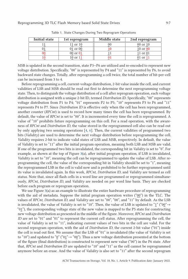
Table 1. State Changes During Two Reprogram Operations
Initial state 1st reprogram Middle state 2nd reprogram
11 11 or 10 00 00 or 1001 01 or 00 10 10 or 0000 00 or 01 11 11 or 0110 10 or 11 01 01 or 11
MSB is updated in the second transition, state P3∼P6 are utilized and re-encoded to represent newvoltage distribution. Specifically, “00” is represented by P4 and “11” is represented by P6, to avoidbackward state changes. Totally, after reprogramming a cell twice, the total number of bit-per-cellcan be increased from 3 to 4.
Before reprogramming a cell, current-voltage distribution, 2-bit value inside the cell, and currentvalidities of LSB and MSB should be read out first to determine the next reprogramming voltagestate. Then, to distinguish the voltage distribution of a cell after reprogram operation, each voltagedistribution is assigned with a unique 2-bit ID, termed Distribution ID. Specifically, “00” representsvoltage distribution from P1 to P4; “01” represents P2 to P5; “10” represents P3 to P6 and “11”represents P4 to P7. Since Distribution ID is effective only when the cell has been reprogrammed,another counter (RPCnt) is used to record how many times the cell has been reprogrammed. Bydefault, the value of RPCnt is set to “00”. It is incremented every time the cell is reprogrammed. Avalue of “10” prohibits future reprogramming on this cell. For a read operation, with the aware-ness of RPCnt and Distribution ID, the value stored in the reprogrammed cell also can be read outby only applying two sensing operations [4, 6]. Then, the current validities of programmed twobits (Validity) are used to determine the next voltage distribution before reprogramming the cell.Validity requires 2-bit to indicate valid states of LSB and MSB, respectively. In default, the valueof Validity is set to “11” after the initial program operation, meaning both LSB and MSB are valid.If one of the programmed two bits is invalidated, the corresponding bit in Validity is set to “0”. Forexample, as shown at the top of Figure 3(a), after initial program operation, if LSB is invalidated,Validity is set to “10”, meaning the cell can be reprogrammed to update the value of LSB. After re-programming the cell, the value of the corresponding bit in Validity should be set to “1”, meaningthe reprogrammed LSB in the cell is valid now and is prohibited to be further reprogrammed untilits value is invalidated again. In this work, RPCnt, Distribution ID, and Validity are termed as cellstatus. Note that, since all flash cells in a word line are programmed or reprogrammed simultane-ously, RPCnt, Distribution ID, and Validity are needed on per word line basis. They are checkedbefore each program or reprogram operation.
We use Figure 3(a) as an example to illustrate the entire hardware procedure of reprogrammingwith the aid of metadata. Suppose the initial program operation writes (“00”) in the TLC. Thevalues of RPCnt, Distribution ID, and Validity are set to “00”, “00”, and “11” by default. As the LSBis invalidated, the value of Validity is set to “10”. Then, the value of LSB is updated to “1” (“00”→“01”), the corresponding voltage state of the new value is mapped to the P5 state for constructingnew voltage distribution as presented in the middle of the figure. Moreover, RPCnt and Distribution
ID are set to “01” and “01” to represent the current cell status. After reprogramming the cell, thevalue of Validity is set to “11”, indicating current values of two bits in the cell are valid. For thesecond reprogram operation, with the aid of Distribution ID, the current 2-bit value (“01”) insidethe cell is read out first. We assume that the LSB of “01” is invalidated (the value of Validity is setto “10”) and updated to “0” (“01”→ “00”). Thus a new voltage distribution presented at the bottomof the figure (final distribution) is constructed to represent new value (“00”) in the P6 state. Afterthat, RPCnt and Distribution ID are updated to “10” and “11” as the cell cannot be reprogrammedanymore before an erase. And the value of Validity is also set to “11” after the second reprogram
ACM Transactions on Storage, Vol. 18, No. 1, Article 9. Publication date: January 2022.

9:8 C. Gao et al.
operation on the cell. In summary, at any point in time, there can be at most two bits inside acell. However, when a cell is reprogrammed twice, four bits of information are programmed orreprogrammed into a TLC (“00” in first initial program, “1” in first reprogram, and “0” in secondreprogram). As a result, from the overall SSD perspective, the effective capacity can be increasedby reprogramming a cell twice. Note that, effective capacity is defined as the number of free flashpages in SSDs. If more reprogram operations are executed, fewer free flash pages are consumedwhile more data is reprogrammed in a single word line. Thus, fewer GCs are triggered so that theperformance and endurance can be improved.
For a read operation, when the accessed page resides in the reprogrammable block, the wordline’s status is read from controller buffer firstly. According to the value of Distribution ID, thevoltage distribution can be determined; thus, sensing operations are performed to read LSB orMSB data from reprogrammed cells. If the accessed page belongs to normal block, regular readoperation is performed to get data from TLC cells.
3.3 Reprogram Operation Verification
To verify the feasibility of reprogram operations on 3D TLC SSDs, we evaluate them on YEESTOR9083 flash memory testing platform [22, 59] with Micron B17A Series NAND flash chips [46].YEESTOR 9083 flash memory testing platform, is a high-reliability and high-performance flashmemory controller that enables users to implement specified flash memory solutions.
As discussed earlier, reprogram operation is enabled as one of the old two bits has been invali-dated in a cell. Since there are many word lines in a block in 3D TLC SSDs, flash cells in a wordline may be invalidated and rewritten whenever necessary, and not follow conventional sequen-tial program order. With the capability of reprogramming, in our verification design, we relaxthe restriction of sequential order among word lines through two steps. In the first step, the re-striction of sequential order among word lines in a layer is relaxed. All word lines in a layer arereprogrammed in a random order while layers are reprogrammed sequentially. Such a reprogram-ming scheme is termed as “One-Layer Reprogram” (OLR) in this work. In the second step, therestriction of sequential order among layers is relaxed by reprogramming word lines in multiplelayers in a somewhat random order. We term such scheme as “Multi-Layer Reprogram” (MLR).More details about OLR and MLR will be presented in the following subsections. In the verificationdesign, to show the maximal capability of a cell to be reprogrammed, each cell in the followingexperiments is reprogrammed four times to completely shift the initial voltage distribution to therightmost side.
3.3.1 One-Layer Reprogram. Evaluation Methodology: For the OLR scheme, initially, allword lines within each layer are sequentially programmed such that all flash cells in each wordline are programmed in an MLC mode. Then, word lines in the layer are randomly selected toreprogram flash cells by moving the first four states to the rightmost four states step by step. Toevaluate the reliability of OLR, the worst voltage distribution (ER∼P7) of a cell is evaluated andpresented in Figure 4, where the x-axis represents the voltage threshold and the y-axis representsthe number of flash cells falling into different voltage states. For OLR, one program operation iscarried to initialize the voltage distribution and four reprogram operations are performed to movefirst four voltage states (including the ER state) to the following states. As shown in the figure,these voltage states are distributed to different threshold voltage ranges separately.
Reliability Impact of OLR: To analyze the impact of reprogramming on reliability, the max-imum and average numbers of bit errors per page are evaluated. There are two types of readmethods for reading and checking the raw data on each page. The first read method uses default
voltage offsets (DVO), and the second read method adopts voltage calibration that can minimize
ACM Transactions on Storage, Vol. 18, No. 1, Article 9. Publication date: January 2022.

Reprogramming 3D TLC Flash Memory based Solid State Drives 9:9
Fig. 4. Voltage distribution after implementing OLR.
the number of page bit errors by applying optimized voltage offset (OVO) between every twoneighboring states [4, 6, 23, 46], which has been used in SSD products. The results of maximumand average numbers of page bit errors collected by these two read methods are presented in thesecond row of Table 2. In contrast, the results of the conventional program scheme are evaluatedas well and presented in the first row of this table. As we can see, with the voltage calibration readmethod, the numbers of maximum and average page bit errors are increased by 4 and 1, respec-tively, from the conventional program scheme. Given the strong ECC capability (e.g., 80bits/1KB)in modern SSD products [23, 46]), the increased number of page bit errors resulted from OLR isnegligible. Therefore, we conclude that reprogramming flash cells layer by layer in 3D TLC SSDsis effective and reliable.
3.3.2 Multi-Layer Reprogram. To relax the restriction of sequential order among layers, in ourdesign, we group multiple physical layers as a reprogrammable super layer (R-SL). Inside eachR-SL, physical layers are reprogrammed in a random order, while R-SLs are programmed in se-quence.
ACM Transactions on Storage, Vol. 18, No. 1, Article 9. Publication date: January 2022.
9:10 C. Gao et al.
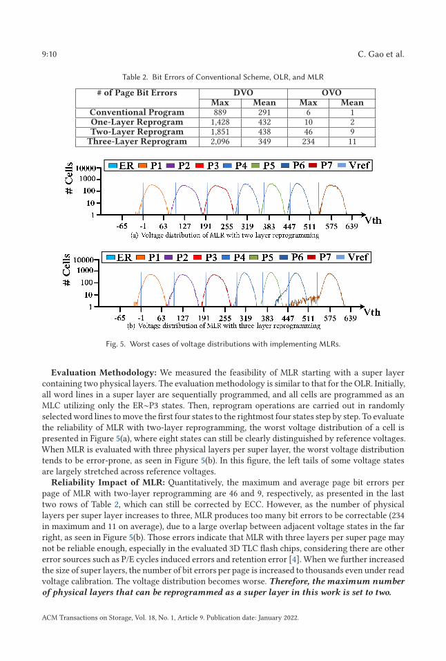
Table 2. Bit Errors of Conventional Scheme, OLR, and MLR
# of Page Bit Errors DVO OVOMax Mean Max Mean
Conventional Program 889 291 6 1One-Layer Reprogram 1,428 432 10 2Two-Layer Reprogram 1,851 438 46 9
Three-Layer Reprogram 2,096 349 234 11
Fig. 5. Worst cases of voltage distributions with implementing MLRs.
Evaluation Methodology: We measured the feasibility of MLR starting with a super layercontaining two physical layers. The evaluation methodology is similar to that for the OLR. Initially,all word lines in a super layer are sequentially programmed, and all cells are programmed as anMLC utilizing only the ER∼P3 states. Then, reprogram operations are carried out in randomlyselected word lines to move the first four states to the rightmost four states step by step. To evaluatethe reliability of MLR with two-layer reprogramming, the worst voltage distribution of a cell ispresented in Figure 5(a), where eight states can still be clearly distinguished by reference voltages.When MLR is evaluated with three physical layers per super layer, the worst voltage distributiontends to be error-prone, as seen in Figure 5(b). In this figure, the left tails of some voltage statesare largely stretched across reference voltages.
Reliability Impact of MLR: Quantitatively, the maximum and average page bit errors perpage of MLR with two-layer reprogramming are 46 and 9, respectively, as presented in the lasttwo rows of Table 2, which can still be corrected by ECC. However, as the number of physicallayers per super layer increases to three, MLR produces too many bit errors to be correctable (234in maximum and 11 on average), due to a large overlap between adjacent voltage states in the farright, as seen in Figure 5(b). Those errors indicate that MLR with three layers per super page maynot be reliable enough, especially in the evaluated 3D TLC flash chips, considering there are othererror sources such as P/E cycles induced errors and retention error [4]. When we further increasedthe size of super layers, the number of bit errors per page is increased to thousands even under readvoltage calibration. The voltage distribution becomes worse. Therefore, the maximum number
of physical layers that can be reprogrammed as a super layer in this work is set to two.
ACM Transactions on Storage, Vol. 18, No. 1, Article 9. Publication date: January 2022.

Reprogramming 3D TLC Flash Memory based Solid State Drives 9:11
3.3.3 Reliability Discussion. We first discuss why reprogram operations introduce challengesin maintaining reliability. Then, we give further evaluations on reliability when aggregating allerror sources from reprogramming, P/E cycle, and retention.
Reliability Challenges: There are two main reasons for reprogram operation to challengereliability: cell-to-cell interference [4, 7] and background pattern dependency (BPD) [13, 31, 36].The former is slightly weaker and the latter is dominant in harming reliability.
First, reprogram operation will aggravate its harm to the reliability due to the impact of cell-to-cell interference, which is highly related to how many times neighboring cells are programmedor reprogrammed [7]. In the OLR and MLR evaluated above, each cell is programmed once andreprogrammed four more times to fully moving voltage state to the rightmost side, causing fourmore times cell-to-cell interference to neighboring cells. Put it in another way, each cell receivesfour more times cell-to-cell interference from reprogramming on top of the cell from programoperations in the conventional scheme. However, in real SSD products, with applying voltagedistribution arrangement, a cell can only be reprogrammed twice at most so that the impact of thecell-to-cell interference can be further mitigated.
Second, BPD means the current-voltage characteristic of a cell can be affected by whether othercells in the same cell string (a cell string means flash cells sharing the same bit line) have been pro-grammed or reprogrammed. The resistance of a cell string increases as more cells are programmedin the same string [31]. Therefore, BPD makes the electrons hard to be injected into a cell if thereare cells atop already programmed [44]. To suppress the reliability impact from BPD, a sequentialprogram order is placed to program word lines from the bottom (closest to the source line+) to thetop (closest to the bit line contact), as shown in Figure 1. However, the proposed OLR and MLRbreak conventional sequential program orders, aggravating the reliability impact from BPD. As aresult, some cells cannot be reprogrammed to the desired state within the manufacturer guaran-teed maximum times of program and verify iterations, creating the left tail of voltage distribution,as depicted in Figure 5. In addition, such a left shift in voltage distribution also shows that BPDis the chief influence on reliability, as cell-to-cell interference tends to shift voltage distribution tothe right side [7].
Reliability Impact from Other Error Sources: Here we quantitatively analyze how repro-gram operations worsen reliability when there are already error sources such as P/E cycles andretention time.
First, we test the reliability of cells when they are stressed under both P/E cycles and reprogram-ming. An experiment is constructed by reprogramming two blocks with two types of P/Es, thenormal P/E and reprogram P/E. The former means a block is repeatedly programmed and erasedwithout reprogram operations, and the latter means a block is worn by repeated MLR with two-layer reprogramming and normal erase operations. After 1 K normal and reprogram P/E cycles ontwo blocks, the maximum and average numbers of bit errors per page are collected and presented inthe left two columns of Table 3 (under w/o Retention). Compared to normal P/Es, reprogram P/Esincrease the maximum and the average number of bit errors by 7 and 4, respectively. Such a slightincrease in page bit errors can be easily corrected by ECC. Moreover, the experiment also provesthat reprogramming a cell multiple times before an erase operation induces little wear stress on acell. The reason is that the stress duration of erase operation is much longer than that of programand reprogram operations [29]. That is, the main wear stress on a cell comes from erase operationeven when a cell is reprogrammed multiple times.
Second, we test the reliability with further error sources from retention when the cells are al-ready stressed under P/E cycles and reprogramming. The above evaluated chip is heated to 120◦Cfor three hours, of which the effective retention time is 1 year under 40◦C [2, 3]. The maximumand average numbers of page bit errors per page collected by reading voltage calibration are
ACM Transactions on Storage, Vol. 18, No. 1, Article 9. Publication date: January 2022.

9:12 C. Gao et al.
Table 3. Page Bit Errors Under Different Retention Time and
Two Types of P/E Cycles
# of Page Bit Errors w/o Retention w/RetentionMax Mean Max Mean
Normal P/E 20 5 100 34Reprogram P/E 27 9 121 49
presented in the right two columns of Table 3. Compared to normal P/E, reprogram P/E increasesthe maximum and average numbers of page bit errors by 21 and 15, respectively. In the worst case,after 1 K reprogram P/E and 1-year retention under 40◦C, there are 121-bit errors per page, whichstill can be corrected by ECC. Notice that, according to the results presented in Tables 2 and 3, themaximum number of bit errors after 1 K reprogram P/E cycles (27) is even smaller than that ofMLR with two-layer reprogramming without P/E impact (49). The reason is that the chips evalu-ated in these two experiments are different but with the same specification. We remark here thatthe impact of process variation (PV) [51, 54] dominates error rates over reprogramming.
Based on the above results, we conclude that the reprogram operation still is reliable enougheven when P/E cycles and retention time are considered.
Risk of Capacity Loss: By degenerating TLC to MLC, the number of bit-per-cell is reducedfrom three to two, causing capacity loss of SSD. On the other hand, if data is frequently updated, re-programming can write more bits into a cell before an erase, increasing effective capacity. Hence,reprogramming hot data is more beneficial than cold data in terms of capacity. However, if thehotness of programmed data cools down and remains valid, the reprogram operation on this cellwill be prohibited, thereby resulting in capacity loss. Moreover, given the sequential order amongR-SLs, previous R-SLs are not allowed to be reprogrammed again once the next R-SL is activated.Thus, the capacity may become lost while flash cells in the previous R-SL have not been repro-grammed. An extreme case is that each reprogrammable layer is programmed into MLC mode butnever reprogrammed. Then one-third of capacity is lost.
However, such capacity loss does not have lasting effects on SSD, due to the GC process thatis used inside SSD to reclaim invalid or lost space. In this work, if there exists lost space, GC isactivated to move valid data from reprogrammable blocks to normal blocks as cold data [57], andthen, the reprogrammable block is erased and reset to a normal block. Additionally, if only hot datacan be reprogrammed, most data in reprogrammable blocks tend to be invalid as each page can onlybe programmed twice. Hence, reprogrammable blocks are more likely to be GC-friendly, meaningthat they require less copies for valid data. Since hot data is frequently invalidated and updated,reprogram operation induced page bit errors will not be propagated by reading and rewritingupdated data.
Selective Reprogram: Based on the above analysis, we draw the conclusion that reprogram-
ming flash cells in 3D TLC SSDs is feasible but should be applied selectively. First, a flash cellcan be reprogrammed only when some of the programmed bits are invalidated. Second, the maxi-mum number of physical layers per R-SL should not exceed two for reliability reasons (accordingto the chips we tested). Third, to avoid capacity loss, only hot data that can be updated soon issuggested to be reprogrammed.
4 THE DESIGN OF RESSD SYSTEM
Following the restrictions above, an ReSSD design is proposed, as outlined in Figure 6. InsideReSSD, the hotness of each write request is detected by the Hotness Filter module. Hot write re-quests are reprogrammed and cold write requests are regularly programmed. TimeStamp Recording
and Reprogram Reference modules are used to assist reprogram operation. Then, another function,
ACM Transactions on Storage, Vol. 18, No. 1, Article 9. Publication date: January 2022.

Reprogramming 3D TLC Flash Memory based Solid State Drives 9:13
Fig. 6. The overview of ReSSD system design.
termed Fully Invalidated, is added to passively invalidate cooling data in reprogrammable blockand make sure all data in reprogrammable block can be invalidated soon.
4.1 Selecting Hot Writes for Reprogramming
To detect hot write requests, Hotness Filter defines the hotness of each write request and determinewhere hot requests should be written to. The filter follows these two rules:
Rule 1: Only updated requests are selected as hot write requests, as most updated data has highpotential to be updated again;
Rule 2: Writes with similar hotness are placed in the same block.In this work, we categorize the hotness of write requests into four levels based on the update
time interval between two continuous writes accessing the same data. In detail, data to be up-dated either within 30 minutes, between 30 minutes and 60 minutes, or between 60 minutes and120 minutes is defined as hot data. For data that never be updated or to be updated over 120 min-utes, it is defined as cold data. Within 120 minutes, most data in server workloads are updatedaccording to [14]. Such update time interval calculation requires to record the arrival time of eachwrite. However, maintaining timestamps of all write requests is space-consuming; thus, per-pagetime stamp is replaced by block-level granularity timestamp, which is set as the arrival time offirst write request programmed to this block.
Based on the hotness determined by the update time interval, write requests are distributedto the blocks containing data with the same hotness. In our design, flash blocks are divided intoNormal Blocks for regular TLC programming, and Repro. Blocks for reprogramming. We use asimple example illustrated in Figure 7 to show how data are distributed among those two types ofblocks. When the first arriving write ❶ is programmed to Normal Block 0, the timestamp of Normal
Block 0 is set to TS 1. Later when the same data is updated, it is considered hot by calculating theinter arrival time between TS 1 and its arrival time, and the update is placed in Repro. Block 1 andblock timestamp of Repro. Block 1 is set to TS 2. Here, the first super layer is created and the twoupdates ❷ and ❸ are allocated to this super layer. Suppose, there are some other updates land inthis super layer, and it becomes no longer reprogrammable (all data are valid), a second super layeris activated to host future updates. Suppose, the same data is updated at the third time (❹), it isnow allocated to one word line in the second super layer. Recall that each Repro. Block maintainsonly one active super layer, the timestamp of Repro. Block 1 is updated to TS 4.
4.2 Writing a Super Layer in Reprogrammable Block
We use an example to explain how writes are programmed and reprogrammed in the R-SL, asillustrated in Figure 8. We assume that there is one physical layer per R-SL and each physical layer
ACM Transactions on Storage, Vol. 18, No. 1, Article 9. Publication date: January 2022.

9:14 C. Gao et al.
Fig. 7. Hotness based data reprogramming.
Fig. 8. An example of implementing reprogram operation on R-SL.
contains four-word lines. Each word line is first programmed utilizing states ER∼P3, termed MLCProgram, and then reprogrammed twice utilizing remaining states. Figure 8 shows these steps infour columns where the first two represent the status of the two bits written in the MLC. At time❶, there are eight updates arriving, which have the same hotness and they access the same R-SL.Each paired writes (e.g.,<P0,P1>) are first written via MLC programming. After writing the firsttwo pairs, <p3> in the third pair invalidates its previous version in WL1 and writes new data toWL2. Similarly, <p0> in the fourth pair also invalidates the previous version in WL0 and writesnew data to WL3. When all word lines in the super layer have been programmed in the MLC mode,reprogramming begins. At time ❷, three more writes arrive, in which <P6> is a new write requestand <p4>, <p1> invalidate and update their previous data. Since a previous version of <P0> hasbeen invalidated in WL0, <P6> can be reprogrammed in WL0. For the remaining two updates, theirprevious versions in WL2 and WL0 are invalidated first. Then, new data is reprogrammed to WL1
and WL2 that still can be reprogrammed. At time ❸, since previous data of <P1> in WL0 has beeninvalidated and WL0 has not been reprogrammed, <P8> can be reprogrammed, paring with <P6>.Totally, two reprogram operations are executed on WL0. Notice that, if <p1> is first written to thesuper layer at time ❷, the previous version of <p1> in WL0 is invalidated, making both of oldtwo pages in WL0 invalid. To reprogram new data of <p1> to WL0, we assume there still existsone valid page so as to match one of the four 2-bit value transitions presented in the middle ofFigure 3.
After time ❸, each word line in this super layer maintains two valid pages, prohibiting futurereprogramming. Moreover, WL1, WL2, and WL3 still that have not been fully reprogrammed arefacing the risk of capacity loss. Thus, we suspend the current reprogrammable block as a can-didate block, and select another available reprogrammable block. For candidate blocks, they can
ACM Transactions on Storage, Vol. 18, No. 1, Article 9. Publication date: January 2022.

Reprogramming 3D TLC Flash Memory based Solid State Drives 9:15
be switched back to reprogrammable blocks proactively or passively. If valid pages in candidateblocks are proactively invalidated by host updates, the corresponding word lines in this block areset to be reprogrammable again. However, if there are no available reprogrammable blocks butstill some candidate blocks, the latter should be reused with higher priority to avoid the greedyallocation of reprogrammable blocks. In this casevalid pages in the candidate block should be Fully
Invalidated and migrated to normal TLC block passively.
4.3 Greedy Reclamation
If there exists a word line that has not been fully reprogrammed, valid pages as cooling data, arepassively invalidated and migrated to normal TLC blocks, termed Greedy Reclamation, makingcandidate blocks reprogrammable again. Greedy reclamation not only avoids capacity loss butalso can reduce GC cost by moving valid pages in advance. Such invalidation also helps to correcterrors created by reprograms as they are moved to normal TLC blocks. In addition, since only hotdata is selected and reprogrammed, the cooling data that needs to be invalidated and migratedpassively only account for a small part of overall reprogrammed data. On one hand, if there is idletime, greedy reclamation is performed without delaying host requests. On the other hand, if thereexist incoming requests as greedy reclamation is being executed, candidate block is reclaimed atthe penalty of blocking host requests.
To minimize such a conflict, the write-back registers equipped for one-shot programming in3D TLC SSDs are leveraged. In our design, the candidate block with the fewest valid pages isselected and its valid pages are moved to the write-back registers. During this process, valid pagesare read into the SSD controller firstly, and then, ECC is carried to perform error correction foravoiding error propagation, especially for reprogrammed data, which is error-prone. After that,valid pages are moved to write-back registers. To hide the latency of valid page migration, theyare programmed to a normal TLC block accompanied with incoming host write requests. At eachtime, the number of valid pages being read out from a candidate block is decided by the numberof current hosts write requests accessing the write-back registers. One or two valid pages shouldbe read out to form a three-page word line written to a normal TLC block. As shown in Figure 9,valid pages in a R-SL are migrated to the normal TLC block word line by word line. If the currentword line (WL0 in Figure 9) contains two valid pages, only one host write request is allowed to betransferred to the write-back register for constructing a new one-shot programming. Otherwise,such as WL1 in Figure 9, the write-back registers are occupied by one valid page from the candidateblock and two hosts write requests. According to the settings of 3D TLC SSDs in Section 7, withineach R-SL, there are four-word lines in a R-SL, meaning at most each word line maintains fourvalid pages and a total of eight valid pages in a R-SL should be sequentially migrated. Thus theoverhead of reclaiming a candidate block is at most two valid page reads per host write request.
4.4 Discussion
4.4.1 Overhead Analysis. Space for storing metadata: In this work, we assume a 576 GB 3DTLC SSD containing 64 planes, 1,536 blocks per plane, and 384 pages per block. The detailed pa-rameters and configurations can be found in Section 7. The overhead of implementing ReSSDcomes from four aspects. First, each block maintains a 4-byte timestamp [42, 55], which sum up to384 KB for the entire SSD. Second, in this work, we divide data hotness into four levels and datawith the top three levels is reprogrammed. Therefore, for each block, a 2-bit tag is added to repre-sent four types of hotness levels. In addition, another 1-bit tag is added to distinguish candidateand reprogrammable block. Totally, 36 KB is required for those information. Third, in traditionalSSD, each plane is equipped with a pointer to record active blocks. While proposed ReSSD is em-ployed, additional three-pointers per plane are required to record in-plane addresses of three active
ACM Transactions on Storage, Vol. 18, No. 1, Article 9. Publication date: January 2022.

9:16 C. Gao et al.
Fig. 9. Migrating valid pages to a normal TLC block accompanied with host write requests.
reprogrammable blocks with different hotness. Based on the total block number of each plane, eachpointer needs 11 bits. In addition, to record the address of the current reprogrammable word line,three 7-bit pointers are required per plane. Totally, additional 432 bytes are needed for the entire3D TLC SSD. Fourth, the status of each word line should be maintained, which requires 2-bit torecord RPCnt, 2-bit to record Distribution ID, and 2-bit to record Validity. Therefore, the space over-head of word line status is 9 MB. In total, less than 10 MB additional space for each 3D TLC SSDis required. On the other hand, for reprogrammable blocks, since each word line only containstwo pages at any time, the space cost of address mappings can be reduced to 2/3 of a normal TLCblock. Since the space cost for each mapping entry (recording the paired addresses from logicaladdress to physical address) is 7 bytes, the saved space of mappings per block reaches to 128 ×8 bytes = 896 bytes as a total of 128 mapping entries are saved. That is, if there are 12 blocks beingreprogrammed, the additional space cost can be covered by the saved space of mappings (12 ×896 bytes = 10.5 MB).
4.4.2 Power Failure Recovery. ReSSD requires additional metadata to make it work. Totally,there are four types of metadata, including timestamp recorder, hotness tag, and block type tag,active block pointer, and word line status, which are stored in the buffer of SSD. If there exists acapacitor inside SSD for avoiding data loss caused by sudden power failure, metadata can be writ-ten back to flash memory with the aid of the capacitor. Otherwise, flash pages in ReSSD shouldbe scanned to recover the required metadata. Firstly, for word line status, which is critical for cor-rectly reading data from reprogrammed flash pages, it also should be maintained in the OOB space.In each flash page’s OOB, only 3-bit space is required to record current word line status while eachword line contains two flash pages in this work. Therefore, if a sudden power failure occurs, wordline status still can be reconstructed. But for the other three types of metadata, we propose toreconstruct it by setting all current blocks as normal blocks after restarting the system.
In addition, if there is a non-completed reprogram operation while sudden power failure occurs,original data in the reprogrammed word line is able to be lost. To solve this problem, on the onehand, the capacitor can be engineered to continue supply power for reprogram operation. On theother hand, a backup-based programming scheme, which has been adopted in traditional SSDs,can be used in ReSSD to store the copies of programmed data to a preserved space (such as LSBpages) for avoiding data loss caused by power failure [52].
4.4.3 Latency of a Reprogram Operation. Finally, reprogramming a word line is carried in twosteps. First, the word line status information including RPCnt and Distribution ID are checked
ACM Transactions on Storage, Vol. 18, No. 1, Article 9. Publication date: January 2022.

Reprogramming 3D TLC Flash Memory based Solid State Drives 9:17
Fig. 10. Normalized number of parity writes and average parity update time.
(“Reprogram Reference” in Figure 6), and the data is read out from the word line. Those infor-mation are used to determine how many times the word line has been reprogrammed and thelocation of the current state, which is used to determine how to shift state in the reprogramming.Therefore, compared with conventional program operation, the reprogram operation experiencesan additional read time. However, benefiting from the fewer voltage states covered by arrangedvoltage distribution, a cell is reprogrammed with fewer charging cycles, resulting actual smaller la-tency than a full program operation [15]. As a result, the total latency including the read overheadis still smaller than that of the conventional program operation (detailed parameters are shown inTable 4).
5 CASE STUDY: RESSD IN RAID 5
The ideal application of ReSSD design should be update-intensive, which quickly invalidates pre-vious data in the reprogrammable blocks. In this work, 3D TLC SSD-based RAID 5 systems, whichrequires significant capacity consumption and frequent updates to parity data, is selected as atypical application to verify the effectiveness of ReSSD design in RAID 5 systems [11, 30, 49].
In RAID 5 systems, the adopted Stripe and Parity Protection can introduce significant writeamplification, which will accelerate capacity consumption and trigger frequent GCs. To verify theseverity of this problem, first, the number of parity accompanied by user data writes should beevaluated. The RAID 5 setting is configured based on /drivers/md/ module of Linux Kernel 5.0.2
Version, where a maximum stripe count is set as the maximum cached stripe number to realize thecache function for reducing the update frequency of parity data [16, 27, 38]. As shown in Figure 10,on average, the number of parity writes, which is normalized to total user writes, reaches 88.1%.Such a large parity writes will occupy a lot of physical pages, causing frequent GC activities and anegative impact on performance and endurance. Second, the average parity update time intervalis also evaluated and normalized to user data update time interval. On average, the parity updatetime interval presented in Figure 10 is reduced by 32.3%. The update time interval decrease comesfrom the design principle of parity protection, which requires parity to be updated while any userdata in the same stripe is written or updated.
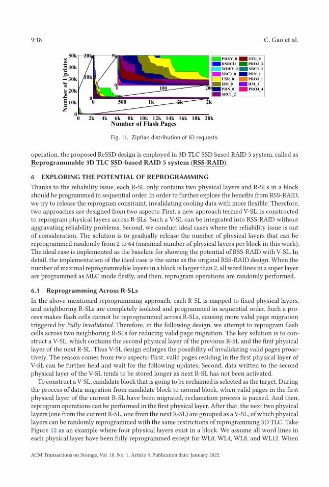
In addition, the update frequency of all write operations (including user writes and parity writes)is evaluated and presented in the form of Zipfian distribution as shown in Figure 11 [56]. Thex-axis shows the count of logical addresses accessed by write operations at flash page granularity,and the y-axis represents the number of update operations on each logical address. This figureshows that only a small part of logical addresses tend to be frequently accessed by update re-quests, while the rest are barely updated. On average, 73.9% of update operations occur in 20%of logical addresses (80/20 rule [17]). Therefore, to mitigate the impact of frequent parity update
ACM Transactions on Storage, Vol. 18, No. 1, Article 9. Publication date: January 2022.
9:18 C. Gao et al.
Fig. 11. Zipfian distribution of IO requests.
operation, the proposed ReSSD design is employed in 3D TLC SSD based RAID 5 system, called asReprogrammable 3D TLC SSD-based RAID 5 system (RSS-RAID).
6 EXPLORING THE POTENTIAL OF REPROGRAMMING
Thanks to the reliability issue, each R-SL only contains two physical layers and R-SLs in a blockshould be programmed in sequential order. In order to further explore the benefits from RSS-RAID,we try to release the reprogram constraint, invalidating cooling data with more flexible. Therefore,two approaches are designed from two aspects: First, a new approach termed V-SL, is constructedto reprogram physical layers across R-SLs. Such a V-SL can be integrated into RSS-RAID withoutaggravating reliability problems. Second, we conduct ideal cases where the reliability issue is outof consideration. The solution is to gradually release the number of physical layers that can bereprogrammed randomly from 2 to 64 (maximal number of physical layers per block in this work).The ideal case is implemented as the baseline for showing the potential of RSS-RAID with V-SL. Indetail, the implementation of the ideal case is the same as the original RSS-RAID design. When thenumber of maximal reprogrammable layers in a block is larger than 2, all word lines in a super layerare programmed as MLC mode firstly, and then, reprogram operations are randomly performed.
6.1 Reprogramming Across R-SLs
In the above-mentioned reprogramming approach, each R-SL is mapped to fixed physical layers,and neighboring R-SLs are completely isolated and programmed in sequential order. Such a pro-cess makes flash cells cannot be reprogrammed across R-SLs, causing more valid page migrationtriggered by Fully Invalidated. Therefore, in the following design, we attempt to reprogram flashcells across two neighboring R-SLs for reducing valid page migration. The key solution is to con-struct a V-SL, which contains the second physical layer of the previous R-SL and the first physicallayer of the next R-SL. Thus V-SL design enlarges the possibility of invalidating valid pages proac-tively. The reason comes from two aspects: First, valid pages residing in the first physical layer ofV-SL can be further held and wait for the following updates; Second, data written to the secondphysical layer of the V-SL tends to be stored longer as next R-SL has not been activated.
To construct a V-SL, candidate block that is going to be reclaimed is selected as the target. Duringthe process of data migration from candidate block to normal block, when valid pages in the firstphysical layer of the current R-SL have been migrated, reclamation process is paused. And then,reprogram operations can be performed in the first physical layer. After that, the next two physicallayers (one from the current R-SL, one from the next R-SL) are grouped as a V-SL, of which physicallayers can be randomly reprogrammed with the same restrictions of reprogramming 3D TLC. TakeFigure 12 as an example where four physical layers exist in a block. We assume all word lines ineach physical layer have been fully reprogrammed except for WL0, WL4, WL8, and WL12. When
ACM Transactions on Storage, Vol. 18, No. 1, Article 9. Publication date: January 2022.

Reprogramming 3D TLC Flash Memory based Solid State Drives 9:19
Fig. 12. Reprogramming flash cells across R-SLs.
pages in the first physical layer are moved, the candidate block is switched to reprogrammableblock again and reprogram operations are performed in WL0. After that, the second physical layerof R-SL0 and the first physical layer of R-SL1 are grouped as V-SL0. For the first physical layerof V-SL0, its valid pages still are stored and able to be invalidated by following updates. In themeanwhile, WL8 resided in the second physical layer of V-SL0 can be programmed by host writesin MLC mode at Step ❶. In this figure, at Step ❷, valid page in WL4 resided in the first physicallayer of V-SL0 is invalidated by update request. Benefiting from this, WL4 can be reprogrammedagain at Step ❸ without passively migrating valid page to normal TLC block. Additionally, beforereleasing V-SL0 and setting the current R-SL to R-SL1, any update on valid page in WL8 is allowedas well. Thus, such a V-SL design enlarges the opportunity of invalidating valid pages proactively.In the end, if WL4 has been fully reprogrammed, V-SL0 is released and the current R-SL is set toR-SL1. Otherwise, the block is switched to candidate block until valid pages in WL4 of V-SL0 areproactively or passively invalidated.
6.1.1 Reliability Issue. The V-SL design does not violate the restrictions of reprogram operation.First, each word line still is reprogrammed twice at most; thus, the program and reprogram inter-ference from neighboring word lines is the same as the original ReSSD design; Second, physicallayers in the V-SL are programmed or reprogrammed only when the last physical layer in the pre-vious super layer has been fully reprogrammed. Take Figure 12 as an example. WL4 and WL8 areprogrammed and reprogrammed after WL0 has been reprogrammed twice. That is, super layersin a block still are reprogrammed in a sequential order, which follows the restriction of reprogramoperation verified in Section 3.3.
7 EXPERIMENT
7.1 Experimental Setup
Simulated SSD-based RAID 5 System: A workload-driven flash memory simulator, SSDSim[26], is used in this work. To match the characteristics of 3D TLC SSD-based RAID 5 system, threemodifications are made in SSDSim. First, the parameters of simulated single SSD are configuredbased on a state-of-the-art 3D TLC SSD, as shown in Table 4. Second, one-shot programming isadded in SSDSim. Third, multiple modified 3D TLC SSDs employing ReSSD design are organizedas a RAID 5, where the RAID 5 controller and its configurations are implemented based on /dri-
vers/md/ module of Linux Kernel 5.0.2 Version. The bottom of Table 4 shows the configurations ofRAID 5. In addition, other default management mechanisms are also implemented in each SSD con-troller, including page mapping-based flash translation layer [1], static WL [9], static DA [26], andgreedy-based GC [19]. The evaluated latencies of reprogram and read operations are presentedin the middle two rows of Table 4. The results show that program and reprogram latencies onthe reprogrammable blocks are slightly smaller than the natural program latency of 3D TLC SSD.
ACM Transactions on Storage, Vol. 18, No. 1, Article 9. Publication date: January 2022.

9:20 C. Gao et al.
Table 4. Parameters of Simulated 3D TLC SSD-based RAID 5 System [14, 46]
Parameters Value Parameters Value
Number of Channels 4 Layers per Block 64Chips per Channel 4 Tr (in Page) 66 us
Dies per Chip 2 Tp (in Page) 3,000 usPlanes per Die 2 Te (in Block) 10 ms
Blocks per Plane 1,536 Data Transfer Rate 400 MB/sPages per Block 384 GC Threshold 8%
Page Size 16 KB Initial Data 92%
Reprogram Scheme Value Reprogram Scheme ValueTr eдular p (in Page) 2,675 us Tr ep (in Page) 2,705 us
Tr (in Page) 53 us
RAID 5 Configuration Value RAID 5 Configuration ValueNumber of SSDs 4 Chunk per Stripe 4Pages per Chunk 64 Max Stripe Count 256
This is because the voltage distance of each program or reprogram operation is reduced. Similarly,the read latency is reduced as well thanks to the reduced number of sensing operations in eachreprogrammed cell.
For the hotness determination, three update time points that divide hotness into four zones areset to 30, 60, and 120 minutes, respectively. The percentages of the four zones are listed in Table 5.Note that, only updated write requests are counted. And we can see that, within 120 minutes, mostdata in selected server workloads are updated. Averagely, more than 70% of updated writes belongto Zone1–3, where the data can benefit from reprogram operation. For the baseline, host writerequests are distributed to blocks based on their hotness as well.
In the experiments, TLC SSD is selected as the comparison target instead of MLC SSD. Thereasons come from two aspects: First, basic ReSSD design is an optimized architecture of TLCSSD, which aims at achieving better performance, endurance and stores more data only whenfrequently updated data is reprogrammed. As a reasonable comparison, TLC SSD is selected as thetarget comparison because ReSSD should achieve the same results as TLC SSD, while all incomingdata is cold. Second, proposed reprogram operation is conducted based on TLC cells, where eightvoltage states can be used to perform one program operation and two reprogram operations. Butif an MLC cell is used, proposed reprogram operation does not work because there are not enoughstates that can be used to store additional data without narrowing the voltage state margin.
Workloads: A set of MSR Cambridge workloads [50] are used as user data workloads in RAID 5system. For parity requests, they are generated based on /drivers/md/ module of Linux Kernel 5.0.2
Version. The characteristics of workloads are presented in Table 6. Note that, Write Pct, UpdatePct, WS, RS, WV, and RV indicate the percentages of write requests, the percentages of updaterequests, average write/read request size, and write/read data volume.
7.2 Experimental Results
Proposed RSS-RAID is evaluated without and with V-SL, respectively. In first part, several metricsare defined to show the improvements of endurance, saved capacity, and performance of RSS-RAID without V-SL (termed RSS-RAID). Then, RSS-RAID is implemented with V-SL to indicatethe efficiency of proposed V-SL design (termed RSS-RAID w/V-SL).
7.2.1 Flash Page Consumption Analysis. Physical Page Consumption (PPC) is evaluated toshow the number of flash pages being written during run time. Although reprogram operationsupports writing four-page data into a single word line, from the perspective of users, the number
ACM Transactions on Storage, Vol. 18, No. 1, Article 9. Publication date: January 2022.

Reprogramming 3D TLC Flash Memory based Solid State Drives 9:21
Table 5. The Percentages of Four Zones
Workloads Zone1 Pct Zone2 Pct Zone3 Pct Zone4 Pct
HM_0 29.0% 18.4% 12.4% 40.2%HM_1 21.7% 35.0% 13.7% 29.6%PRN_0 51.7% 26.0% 7.1% 15.2%PRN_1 39.6% 21.7% 13.6% 25.1%PROJ_1 16.9% 67.9% 7.6% 7.6%PROJ_3 32.0% 31.1% 13.9% 23.0%PROJ_4 28.4% 23.7% 13.5% 34.4%RSRCH 22.5% 16.5% 13.3% 47.6%SRC1_2 39.0% 24.2% 12.8% 24.0%SRC2_0 28.0% 22.4% 15.2% 34.4%SRC2_2 22.3% 21.7% 20.6% 35.4%STG_0 21.6% 15.2% 25.2% 38.0%
WDEV_0 29.7% 24.8% 13.0% 32.5%PRXY_0 57.5% 13.6% 12.9% 16.0%USR_0 26.6% 21.4% 14.7% 37.3%
Table 6. The Characteristics of Evaluated Workloads
Workloads Write Pct Update Pct WS(KB) RS(KB) WV(GB) RV(GB)
HM_0 75.1% 91.7% 11.2 11.7 7.95 2.74HM_1 3.1% 74.3% 22.9 18.1 0.35 8.54PRN_0 89.3% 81.0% 14.0 26.6 11.77 2.69PRN_1 31.1% 61.1% 13.8 17.7 4.05 11.54PROJ_1 9.4% 25.3% 22.2 43.2 1.97 36.93PROJ_3 9.8% 36.6% 30.1 15.1 2.78 12.87PROJ_4 3.7% 61.7% 14.8 10.3 0.51 9.37RSRCH 90.9% 97.7% 12.7 15.7 10.90 1.35SRC1_2 84.5% 98.3% 44.9 16.9 35.81 2.48SRC2_0 86.4% 95.2% 11.0 12.6 8.99 1.63SRC2_2 71.8% 51.6% 57.8 88.5 39.18 23.56STG_0 76.7% 97.3% 12.7 33.6 9.19 7.39
WDEV_0 80.4% 96.6% 12.1 16.5 9.21 3.05PRXY_0 97.0% 97.9% 6.3 9.7 5.75 0.27USR_0 63.1% 95.0% 13.6 47.1 8.07 16.42
of consumed flash pages still is three and the number of the consumed word line is one. Resultsare presented in Figure 13, where the number of PPC of RSS-RAID 5 system is evaluated and nor-malized to the baseline. On average, compared with the baseline, PPC of RSS-RAID is reduced to70.1%, which can be broken into three parts, including write requests induced PPC (flash page con-sumption caused by normal write requests and reprogram-based write requests), GC writes (flashpage consumption caused by GC induced valid page writes) induced PPC, and Fully Invalidatedwrites induced PPC ( Fully Invalidated Writes refer to the process of moving cooling pages fromcandidate blocks to normal TLC blocks). On average, these three pages account for 34.5%, 51.1%,and 14.4% of the total PCC of RSS-RAID, respectively.
Compared with the baseline, write requests induced PPC of RSS-RAID is reduced to 68.4%. AsFully Invalidated writes can reduce GC cost by moving valid pages in advance, the total PPC re-sulting from Fully Invalidated writes and GC writes in RSS-RAID is reduced to 72.1%, comparedwith the baseline. Based on the results, one can see that RSS-RAID can achieve significant PPCdecreases. The reasons come from two aspects: First, reprogram operation is able to increase the
ACM Transactions on Storage, Vol. 18, No. 1, Article 9. Publication date: January 2022.

9:22 C. Gao et al.
Fig. 13. Normalized physical flash page decrease.
Fig. 14. Normalized total GC time cost.
number of pages written in a word line. Second, reprogram operation can also reduce GC countand cost by storing more data into each block and erasing a block with less valid page migrations(details can be found in Section 7.2.2.)
7.2.2 GC Evaluation and Analysis. In this subsection, first, total GC numbers of the baselineand RSS-RAID are evaluated. There are two types of GCs in flash memory, including GC withvalid page migration and direct GC (erasing a block without a valid page inside). If there are moreblocks that can be reclaimed by direct GCs, the performance can be improved due to less validpage migration costs. On average, the total GC number of RSS-RAID is reduced by 30.6%, of whichthe number of GC with valid page migration is reduced by 49.4% and the number of direct GC isincreased by 10.9 times. The reasons are as follows: First, reprogram operation can reduce physicalpage consumption, triggering fewer GC activities; Second, reprogrammable blocks can be erasedby direct GCs when cooling valid pages in blocks that have been moved out in advance by FullyInvalidation. In the evaluation, the number of blocks erased by Fully Invalidation is counted onlywhen valid page migration caused by Fully Invalidation has been performed in the erased block.
As the total number of GC decreases significantly, the total GC time cost can also be reducedsignificantly. As shown in Figure 14, on average, the total GC time cost is reduced by 48.3%. This isbecause the total GC count is reduced and more GCs are processed without valid page migration.As a result, the effectiveness of GC can be improved by adopting RSS-RAID.
7.2.3 Endurance Improvement Analysis. Endurance of SSD is quantified by P/E cycles. In thiswork, two metrics are determined to measure the endurance of 3D TLC-based RSS-RAID. First,the number of GC count is evaluated and presented in Figure 15, where the numbers of GC withvalid page migration and direct GC (without valid page migration) are collected respectively. InFigure 15, within the range of each workload, there exist two bars, of which the left one indicates
ACM Transactions on Storage, Vol. 18, No. 1, Article 9. Publication date: January 2022.

Reprogramming 3D TLC Flash Memory based Solid State Drives 9:23
Fig. 15. The number of GCs of baseline and RSS-RAID.
Fig. 16. The number of PWE of RSS-RAID.
the evaluated result of baseline and the right one means GC number of RSS-RAID. On average,RSS-RAID can desirably reduce total GC number by 30.6% as fewer flash pages are consumed andeach page can be written with more data. Additionally, the percentage of direct GC also showsa significant increase due to timely data invalidation. Since reprogram operation induced voltagestress is quite small, the total GC (erase) count can be used to identify the lifetime of flash memoryfrom the perspective of SSD.
On the other hand, from the perspective of users, a metric, termed Page Writes per Erase
(PWE), is used to identify the endurance of flash memory [14]. When the total number of hostwrite requests is fixed, reprogram operation triggers fewer GCs so that the erase operation’s impacton endurance is less. In this work, to combine the impact from program (reprogram) operation anderase operation, PWE is defined to show the number of page writes between erases. The larger thevalue of PWE is, the lesser the impact on endurance is caused. If PWE is increased, then the totalnumber of erase operations of the RSS-RAID system can be reduced, improving the endurance.The evaluated results are presented in Figure 16, where the PWE of RSS-RAID is increased by30.3% on average. The reason is that RSS-RAID not only increases the number of bits stored in acell but also significantly reduces the total erase count of GC activities. With the increase of PWE,the endurance of RSS-RAID is improved.
7.2.4 Performance Impact Analysis. In order to reveal reprogram operation induced impact onread and write performance of 3D TLC SSD-based RAID 5 system, the average read and writelatencies are evaluated and presented in Figure 17. In this figure, evaluated latency is normalizedto the baseline and one can observe that the read performance of RSS-RAID is slightly reduced
ACM Transactions on Storage, Vol. 18, No. 1, Article 9. Publication date: January 2022.

9:24 C. Gao et al.
Fig. 17. Normalized read/write latency of RSS-RAID.
Fig. 18. Normalized effective capacity increase.
compared with the baseline. This is because only two read sensing operations are required forreading a reprogrammed page.
For write performance, on average, the write latency of RSS-RAID is reduced by 16.7% comparedwith the baseline. Although the program and reprogram operations executed in reprogrammableblocks can slightly reduce the latency, the benefit from one-shot programming is reduceddue to less data being programmed simultaneously, hindering the write performance. However,the benefit from GC optimization can recover this negative impact, bringing better write perfor-mance of RSS-RAID.
7.2.5 Increased Effective Capacity. In this subsection, after running each workload, the effectivecapacity represented by the number of free flash pages in the RAID 5 system is evaluated. Noticethat, in RSS-RAID scheme, if a block is reprogrammable, all word lines in this block are regardedas MLC word line that only contains two pages. In Figure 18, the number of free flash pages ofRSS-RAID is normalized to that of the baseline. The number of free flash pages of RSS-RAID isincreased by 7.71% on average, compared with the baseline. Furthermore, RSS-RAID can achieveat least 8% free page number increases for more than half of workloads (8 out of 15). This is becauseeach flash cell is able to store more bits before an erase operation.
However, for other workloads, such as PROJ_4, the number of free flash pages of RSS-RAID isonly increased by 1.25%, on average. The reason is that, since the numbers of total write requestsand update requests in PROJ_4 are small, only a few reprogrammable blocks can be frequentlyaccessed and reprogrammed to achieve effective capacity increases while other blocks are barelyaccessed.
ACM Transactions on Storage, Vol. 18, No. 1, Article 9. Publication date: January 2022.

Reprogramming 3D TLC Flash Memory based Solid State Drives 9:25
Fig. 19. Normalized physical flash page decreases of RSS-RAID and ReSSD.
Fig. 20. Normalized number of PWEs of RSS-RAID and ReSSD.
Fig. 21. Normalized read/write latencis of RSS-RAID and ReSSD.
7.2.6 Comparison between RSS-RAID and ReSSD. In this section, PPC, PWE, and latency ofReSSD are evaluated and the results are presented in the following figures. For PPC, as shownin Figure 19, on average, ReSSD can achieve a 20.5% flash page consumption decrease, whileRSS-RAID reduces flash page consumption by 29.9%. The reason is that, RSS-RAID benefits fromthe frequently updated data in RAID system. The same reason makes ReSSD achieve a smallerPWE increase as well. In Figure 20, ReSSD increases PWE by 1.133 as RSS-RAID achieves a 30.3%increase. For read and write latency, thanks to fewer flash pages are consumed by RSS-RAID, thenumber of GC in RSS-RAID is smaller than ReSSD, making fewer read and write requests to bedelayed. As a result, as shown in Figure 21, read and write latencies of RSS-RAID are smaller thanthat of ReSSD.
ACM Transactions on Storage, Vol. 18, No. 1, Article 9. Publication date: January 2022.

9:26 C. Gao et al.
Fig. 22. Comparison among baseline, MLC mode RAID and RSS-RAID.
7.2.7 Evaluation of MLC Mode RAID. In this subsection, conventional 3D TLC SSD is used as3D MLC mode SSD by degenerating TLC to MLC. The most direct impact is that the capacity of3D MLC mode SSD is reduced by 33.3% as only two bits are used per cell. The performance andendurance of MLC mode SSD can be improved because of its advantages in faster program speedand larger P/E cycles [45, 46].
First, the latency of programming MLC page via one-shot programming is set to 2,200 us. Resultsare presented at the top of Figure 22, where the read and write latencies of RSS-RAID and MLCmode RAID are normalized to the baseline. On average, the write latency of MLC mode RAID isreduced by 27.8% while the write latency of RSS-RAID is reduced by 16.7%, compared with thebaseline. The main reason is that the latency of program operation on MLC is smaller than thatof conventional 3D TLC SSD and RSS-RAID 5 systems. However, since each block in MLC modeSSD contains fewer flash pages, GC may be triggered more frequently, delaying more requestsand increasing request latency. Therefore, in some workloads (e.g., PROJ_1), the write latency ofMLC mode SSD is even larger than that of RSS-RAID. For read performance, MLC mode RAID andRSS-RAID achieve 8.5% and 6.3% read latency reduction on average compared with the baseline.
Second, the results of PWE are evaluated and presented in the bottom of Figure 22. Themaximal number of P/E cycles of SSDs depends on the type of flash cells. Compared to TLCcell, MLC cell has better endurance and its maximal number of P/E cycles is also largerthan TLC cell. In the experiment, the maximal numbers of P/E cycles of RSS-RAID and MLCmode SSD are set to 1,500 and 30,000, respectively [45, 47]. Therefore, we have normalized
endurance=paдewrites/(erases/max_P/E). As a result, compared with baseline and RSS-RAID, theaverage normalized endurance of MLC mode SSD is increased by 13.4 times and 10.3 times, respec-tively. Although MLC mode SSD has better endurance, RSS-RAID can achieve better endurancethan baseline by slowing down the wearing process of TLC based SSD by reducing the number oferase operations.
7.2.8 Benefit from Virtual Super Layer. In this section, the proposed RSS-RAID is implementedwith a V-SL. The most straightforward insight is that the V-SL enables reprogramming cells acrossneighboring R-SLs, makes fewer valid page migrations caused by fully invalidation.
In Figure 23, the number of reduced migrated valid pages caused by fully invalidation is nor-malized to total numbers of migrated valid pages and total writes of RSS-RAID, respectively. First,compared with the number of total migrated valid pages, the percentage of reduced migrated validpages of RSS-RAID w/V-SL can reach to 12.0%. Second, compared with the number of total writes
ACM Transactions on Storage, Vol. 18, No. 1, Article 9. Publication date: January 2022.

Reprogramming 3D TLC Flash Memory based Solid State Drives 9:27
Fig. 23. Percentages of reduced numbers of migrated valid pages caused by fully invalidation.
Fig. 24. Normalized PPC decreases of RSS-RAID and RSS-RAID w/V-SL.
of RSS-RAID, RSS-RAID w/V-SL contributes less to valid page migration decrease, of which re-duced number accounts for only 1.5%. That is, only fewer flash pages are earned by the proposedV-SL, making PPC hard to be significantly decreased.
As shown in Figure 24, RSS-RAID w/V-SL can slightly reduce PPC compared with the originalRSS-RAID. Such a slight decrease comes from two aspects: First, the number of migrated validpages caused by fully invalidation accounts for a small portion of total writes; second, the V-SLcannot eliminate valid page migration when pages keep valid as cooling data. Similar results alsoexist in the evaluations of total GC time cost decrease and effective capacity increase. As a result,RSS-RAID w/V-SL can only slightly decrease total GC time cost by 2.5% (presented in Figure 14),and increase effective capacity by 0.21%.
For endurance of flash memory, the total numbers of GCs are evaluated and presented inFigure 25. Compared with the original RSS-RAID, RSS-RAID w/V-SL can only slightly reduce thenumber of GCs by 2.1% as there is less contribution from PPC decrease. In addition, the ratios ofGC w/valid page migration and direct GC change almost nothing, meaning the original RSS-RAIDis effective enough for reprogramming hot data. Also for PWE, RSS-RAID w/V-SL achieves 6.5%PWE improvement compared with RSS-RAID. Since the V-SL can further reduce flash page con-sumption as total GC count synchronised declines as well, the values of these two approaches arealmost at the same level.
For write latency of RSS-RAID w/V-SL, averagely, it is further reduced by 0.8% compared withRSS-RAID. Write latency is used to evaluate the performance while a read request is processedwith highest priority. Although total GC time cost can be slightly reduced, more data are able tobe reprogrammed into flash memory with higher reprogram latency.
ACM Transactions on Storage, Vol. 18, No. 1, Article 9. Publication date: January 2022.

9:28 C. Gao et al.
Fig. 25. The number of GCs of baseline, RSS-RAID and RSS-RAID w/V-SL.
Fig. 26. The percentages of switched pages among four zones.
To illustrate the reason why the V-SL only achieves slight improvement compared with theoriginal RSS-RAID, we distribute write requests of each workload into four zones based on theirupdate interval. And then, during run time, the percentages of data in page size switched to otherzones are evaluated and presented in the top of Figure 26. Also, the breakdowns of switched dataare collected and presented in the bottom of Figure 26. Data belonging to each zone can only beswitched to the other three type zones.
First, according to the top of Figure 26, we can find that average percentages of switched data inzone1 (Z1), zone2 (Z2), and zone3 (Z3) only account for 13.5%, 11.6%, and 2.5%, respectively. Thismeans most data can keep their hotness within a fixed period of time. Second, in the bottom ofFigure 26, the portions of data that switched to other zones are evaluated as well. For hot data inZ1, Z2, and Z3, they tend to be switched to other hot zones instead of zone4 (Z4). Totally, only 6.4%of hot data in hot zones are switched to Z4 as cooling data. Therefore, it is hard to significantlyincrease the efficiency of RSS-RAID as there only exits a small subset of cooling data in Z1, Z2 andZ3.
In the following, the ideal case is implemented and its related metrics are evaluated. The resultsof RSS-RAID w/V-SL are normalized to the ideal case for quantifying its efficiency.
7.2.9 Ideal Case. In ideal case, all physical layers within a flash block can be fully programmedor reprogrammed in random order. Therefore, we manually relax the reprogram restrictions, con-structing the R-SL of which the number of physical layers varies from 2 to 64. The results ofaverage PPC, PWE, and write latency of RSS-RAID with various numbers of physical layers in aR-SL are evaluated and presented in Figure 27. While the number of physical layers per super layerreaches 32, all evaluated results tend to be saturated. For PPC of RSS-RAID with 32 layers, it is
ACM Transactions on Storage, Vol. 18, No. 1, Article 9. Publication date: January 2022.

Reprogramming 3D TLC Flash Memory based Solid State Drives 9:29
Fig. 27. Results of PPC, PWE, and Write Latency of RSS-RAID in ideal case and RSS-RAID w/V-SL.
Fig. 28. Normalized PPC, PWE, and Write Latency on RSS-RAID w/V-SL system with different number of
SSD devices.
further reduced by 7% compared with original RSS-RAID (presented as 2 Layers in Figure 27). ForPWE, RSS-RAID can increase the value by 16.6% compared with the original RSS-RAID. For writelatency, only a 0.8% latency decrease is achieved by RSS-RAID with 32 layers. Such a slight writelatency decline comes from that more data are reprogrammed, losing the benefit from one-shotprogramming. Differing from PPC and PWE, the ideal write latency of RSS-RIAD is the value ofRSS-RAID with 2 layers, while PPC and PWE of RSS-RAID with 32 layers are the ideal results ofRSS-RAID.
In addition, the results of RSS-RAID w/V-SL are also evaluated and presented in Figure 27. Inaverage, compared with ideal results, RSS-RAID with 32 layers can reduce PPC by 5.5%, increasePWE by 12.2% and reduce write latency by 0.3%. That is, RSS-RAID w/V-SL can reduce PPC to78.6%, increase PWE to 73.5%, and reduce write latency to 63.5% of ideal case.
7.2.10 Various Number of SSDs Per RSS-RAID. In this section, the number of 3D TLC SSDs inRSS-RAID w/V-SL system is changed from 4 to 10 for evaluating the achieved benefits of RSS-RAID. In Figure 28, average PPC, PWE, and write latency of RSS-RAID are normalized to Baseline,indicating the achieved capacity consumption decrease, endurance improvement, and performanceimprovement.
In this figure, there is a trend that PPC, PWE, and write latency tend to be worse as moredevices are employed in the RAID 5 system. In the worst case, RSS-RAID w/V-SL containing10 devices increases PPC by 2.7%, decreases PWE by 1.8% and increases write latency by 3.2%.But all evaluated values still are better than baseline. That is, proposed RSS-RAID w/V-SL can bewell employed in RAID 5 systems with different number of SSD devices.
ACM Transactions on Storage, Vol. 18, No. 1, Article 9. Publication date: January 2022.

9:30 C. Gao et al.
8 RELATED WORKS
Several previous works have been proposed to write more data in a word line. They can be dividedinto three types: First, Kim et al. [35] and Kim et al. [34] proposed a subpage program method,which can program a large flash page multiple times with a small write operation so that data canbe stored in flash page at a finer granularity. Second, multiple previous works adopt write-once
memory (WOM) code [40, 41, 58] to enlarge the capacity of SSDs. However, WOM code requiresthe assistance of ECC space for holding additional information, which will weaken the capabilityof ECC. Third, [14] and [10] are proposed to reprogram SLC by narrowing the voltage margin be-tween two states. In this case, each cell can be reprogrammed multiple times by invalidating previ-ous values in the same cell. These works are proposed oriented 2D SLC SSDs, where a large voltagemargin exists for serving to reprogram operation. For 2D TLC SSDs, [15] shows that TLC can be re-programmed as well. The main drawback of reprogramming 2D TLC SSDs is the reliability, whichcomes from the cell-to-cell interference among flash cells. To solve this problem, refresh operationsin SSDs are applied. The characteristics of reprogramming 3D TLC SSDs have not been discussedin all previous works, which has completely different characteristics compared to 2D SSDs.
9 CONCLUSION
In this work, the feasibility of reprogram operation in 3D TLC SSDs is verified. Then, a repro-grammable SSD design is proposed in 3D TLC SSDs, which aims at reducing capacity consumption,improve the endurance and performance of 3D TLC SSDs. By applying the proposed approach, acase study for 3D TLC SSD-based RAID 5 system is evaluated. As a result, the proposed approachcan improve the endurance by 35.7%, boost write performance by 15.9% and increase effectivecapacity by 7.71%, respectively, which is realized with negligible overhead compared with conven-tional SSD-based RAID 5 system.
REFERENCES
[1] Nitin Agrawal, Vijayan Prabhakaran, Ted Wobber, John D. Davis, Mark S. Manasse, and Rina Panigrahy. 2008. Design
tradeoffs for SSD performance. In Proceedings of the Annual Technical Conference. USENIX.
[2] Svante Arrhenius. 1889. Über die reaktionsgeschwindigkeit bei der inversion von rohrzucker durch Säuren. In Pro-
ceedings of the Zeitschrift für physikalische Chemie. De Gruyter Oldenbourg.
[3] JEDEC SOLID STATE TECHNOLOGY ASSOCIATION. 2011. JEDEC STANDARD:Stress-Test-Driven Qualification of
Integrated Circuits JESD47H.01. JEDEC.
[4] Yu Cai, Saugata Ghose, Erich F. Haratsch, Yixin Luo, and Onur Mutlu. 2017. Error characterization, mitigation, and
recovery in flash-memory-based solid-state drives. In Proceedings of the IEEE. IEEE.
[5] Yu Cai, Saugata Ghose, Yixin Luo, Ken Mai, Onur Mutlu, and Erich F. Haratsch. 2017. Vulnerabilities in MLC NAND
flash memory programming: Experimental analysis, exploits, and mitigation techniques. In Proceedings of the Inter-
national Symposium on High Performance Computer Architecture. IEEE.
[6] Yu Cai, Yixin Luo, Saugata Ghose, and Onur Mutlu. 2015. Read disturb errors in MLC NAND flash memory: Charac-
terization, mitigation, and recovery. In Proceedings of the Dependable Systems and Networks. IEEE.
[7] Yu Cai, Onur Mutlu, Erich F. Haratsch, and Ken Mai. 2013. Program interference in MLC NAND flash memory:
Characterization, modeling, and mitigation. In Proceedings of the 31st International Conference on Computer Design.
IEEE.
[8] Li-Pin Chang, Tei-Wei Kuo, and Shi-Wu Lo. 2004. Real-time garbage collection for flash-memory storage systems of
real-time embedded systems. In Proceedings of the Transactions on Embedded Computing Systems. ACM.
[9] Yuan-Hao Chang, Jen-Wei Hsieh, and Tei-Wei Kuo. 2007. Endurance enhancement of flash-memory storage systems:
An efficient static wear leveling design. In Proceedings of the Design Automation Conference.
[10] Yu-Ming Chang, Yung-Chun Li, Ping-Hsien Lin, Hsiang-Pang Li, and Yuan-Hao Chang. 2016. Realizing erase-free
SLC flash memory with rewritable programming design. In Proceedings of the Hardware/Software Codesign and System
Synthesis. IEEE.
[11] SZ Chen and Don Towsley. 1993. The design and evaluation of RAID 5 and parity striping disk array architectures. In
Proceedings of the booktitle of Parallel and Distributed Computing. Elsevier.
ACM Transactions on Storage, Vol. 18, No. 1, Article 9. Publication date: January 2022.

Reprogramming 3D TLC Flash Memory based Solid State Drives 9:31
[12] Tseng-Yi Chen, Yuan-Hao Chang, Yuan-Hung Kuan, and Yu-Ming Chang. 2017. VirtualGC: Enabling erase-free
garbage collection to upgrade the performance of rewritable SLC NAND flash memory. In Proceedings of the Annual
Design Automation Conference. ACM.
[13] Wei-Chen Chen, Hang-Ting Lue, Kuo-Pin Chang, Yi-Hsuan Hsiao, Chih-Chang Hsieh, Yen-Hao Shih, and Chih-Yuan
Lu. 2014. Study of the programming sequence induced back-pattern effect in split-page 3D vertical-gate (VG) NAND
flash. In Proceedings of the Technical Program-2014 International Symposium on VLSI Technology, Systems and Applica-
tion. IEEE.
[14] Wonil Choi, Mohammad Arjomand, Myoungsoo Jung, and Mahmut Kandemir. 2017. Exploiting data longevity for en-
hancing the lifetime of flash-based storage class memory. In Proceedings of the Measurement and Analysis of Computing
Systems. ACM.
[15] Wonil Choi, Myoungsoo Jung, and Mahmut Kandemir. 2018. Invalid data-aware coding to enhance the read perfor-
mance of high-density flash memories. In Proceedings of the Annual IEEE/ACM International Symposium on Microar-
chitecture. IEEE.
[16] Ching-Che Chung and Hao-Hsiang Hsu. 2014. Partial parity cache and data cache management method to improve
the performance of an SSD-based RAID. In Proceedings of the IEEE Transactions on Very Large Scale Integration Systems.
IEEE.
[17] Wikipedia contributors. 2019. Pareto principle. Retrieved January 8, 2022 from https://en.wikipedia.org/w/index.php?
title=Pareto_principle&oldid=904233270.
[18] Western Digital. 2017. Western Digital Announces Industry’s First 96-Layer 3D NAND Technology. Retrieved January
8, 2022 from https://www.westerndigital.com/company/newsroom/press-releases/2017/2017-06-27-western-digital-
announces-industrys-first-96-layer-3d-nand-technology.
[19] Congming Gao, Liang Shi, Yejia Di, Qiao Li, Chun Jason Xue, Kaijie Wu, and Edwin Sha. 2018. Exploiting chip idleness
for minimizing garbage collection induced chip access conflict on SSDs. In Proceedings of the Transactions on Design
Automation of Electronic Systems. ACM.
[20] Congming Gao, Liang Shi, Jason Chun Xue, Cheng Ji, Jun Yang, and Youtao Zhang. 2019. Parallel all the time: Plane
level parallelism exploration for high performance SSDs. In Proceedings of the Mass Storage Systems and Technologies.
IEEE.
[21] Congming Gao, Liang Shi, Mengying Zhao, Chun Jason Xue, Kaijie Wu, and Edwin H-M Sha. 2014. Exploiting paral-
lelism in I/O scheduling for access conflict minimization in flash-based solid state drives. In Proceedings of the Mass
Storage Systems and Technologies. IEEE.
[22] Congming Gao, Min Ye, Qiao Li, Chun Jason Xue, Youtao Zhang, Liang Shi, and Jun Yang. 2019. Constructing large,
durable and fast ssd system via reprogramming 3D TLC flash memory. In Proceedings of the 52nd Annual IEEE/ACM
International Symposium on Microarchitecture.
[23] Erich F. Haratsch. 2017. Controller technologies for managing 3D NAND flash memories. In Proceedings of the Seagate.
Flash Memory Summit.
[24] Chien-Chung Ho, Yung-Chun Li, Yuan-Hao Chang, and Yu-Ming Chang. 2018. Achieving defect-free multilevel 3D
flash memories with one-shot program design. In Proceedings of the Design Automation Conference. IEEE.
[25] Joel Hruska. 2018. Samsung Now Mass Producing 96-Layer 3D NAND. Retrieved January 8, 2022 from https://www.
extremetech.com/computing/273167-samsung-now-mass-producing-96-layer/-3d-nand.
[26] Yang Hu, Hong Jiang, Dan Feng, Lei Tian, Hao Luo, and Shuping Zhang. 2011. Performance impact and interplay of
SSD parallelism through advanced commands, allocation strategy and data granularity. In Proceedings of the Interna-
tional Conference on Supercomputing. ACM.
[27] Soojun Im and Dongkun Shin. 2011. Flash-aware RAID techniques for dependable and high-performance flash mem-
ory SSD. In Proceedings of the Transactions on Computers. IEEE.
[28] Jaehoon Jang, Han-Soo Kim, Wonseok Cho, Hoosung Cho, Jinho Kim, Sun Il Shim, Younggoan Jang, Jae-Hun Jeong,
Byoung-Keun Son, Dong Woo Kim, Kihyun, Jae-Joo Shim, Jin Soo Lim, Kyoung-Hoon Kim, Su Youn Yi, Ju-Young Lim,
Dewill Chung, Hui-Chang Moon, Sungmin Hwang, Jong-Wook Lee, Yong-Hoon Son, U-In Chung, and Won-Seong
Lee. 2009. Vertical cell array using TCAT (terabit cell array transistor) technology for ultra high density NAND flash
memory. In Proceedings of the Symposium on VLSI Technology. IEEE.
[29] Jaeyong Jeong, Sangwook Shane Hahn, Sungjin Lee, and Jihong Kim. 2014. Lifetime improvement of NAND flash-
based storage systems using dynamic program and erase scaling. In Proceedings of the Conference on File and Storage
Technologies. USENIX.
[30] Timothy J. Johnson. 1998. Raid-5 parity generation and data reconstruction. U.S. Patent 5,805,788[P]. 1998-9-8.
[31] Tae-Sung Jung, Young-Joan Choi, Kang-Deog Suh, Byung-Hoon Suh, Jin-Ki Kim, Young-Ho Lim, Yong-Nam Koh, Jong-
Wook Park, Ki-Jong Lee, Jung-Hoon Park, Kee-Tae Park, Jhang-Rae Kim, Jeong-Hyong Yi, and Hyung-Kyu Lim. 1996.
A 117-mm/sup 2/3.3-V only 128-Mb multilevel NAND flash memory for mass storage applications. In Proceedings of
the IEEE Booktitle of Solid-State Circuits. IEEE.
ACM Transactions on Storage, Vol. 18, No. 1, Article 9. Publication date: January 2022.

9:32 C. Gao et al.
[32] C. Kim, J. Cho, W. Jeong, I. Park, H. Park, D. Kim, D. Kang, S. Lee, J. Lee, W. Kim, J. Park, Y. Ahn, J. Lee, J. Lee, S. Kim,
H. Yoon, J. Yu, N. Choi, Y. Kwon, N. Kim, H. Jang, J. Park, S. Song, Y. Park, J. Bang, S. Hong, B. Jeong, H. Kim, C. Lee,
Y. Min, I. Lee, I. Kim, S. Kim, D. Yoon, K. Kim, Y. Choi, M. Kim, H. Kim, P. Kwak, J. Ihm, D. Byeon, J. Lee, K. Park, and
K. Kyung. [n.d.]. 11.4 A 512Gb 3b/cell 64-stacked WL 3D V-NAND flash memory. In Proceedings of the International
Solid-State Circuits Conference. IEEE.
[33] Hyunsuk Kim, Su-Jin Ahn, Yu Gyun Shin, Kyupil Lee, and Eunseung Jung. 2017. Evolution of NAND flash memory:
from 2D to 3D as a storage market leader. In Proceedings of the Memory Workshop. IEEE.
[34] Jung-Hoon Kim, Sang-Hoon Kim, and Jin-Soo Kim. 2015. Subpage programming for extending the lifetime of nand
flash memory. In Proceedings of the Design, Automation and Test in Europe Conference and Exhibition. IEEE.
[35] Myungsuk Kim, Jaehoon Lee, Sungjin Lee, Jisung Park, and Jihong Kim. 2017. Improving performance and lifetime of
large-page NAND storages using erase-free subpage programming. In Proceedings of the Design Automation Conference.
IEEE.
[36] Seungjae Lee, Jin-Yub Lee, I. Park, Jong-Yeol Park, Sung-Won Yun, Min-su Kim, Jong-Hoon Lee, Min-Seok Kim, Kang-
bin Lee, Taeeun Kim, Byungkyu Cho, Dooho Cho, S. Yun, Jung-No Im, H. Yim, Kyung-hwa Kang, Suchang Jeon, S. Jo,
Yang-Lo Ahn, S. Joe, Suyong Kim, Deok-kyun Woo, Jiyoon Park, H. Park, Youngmin Kim, Jonghoon Park, Yongsuk
Choi, M. Hirano, Jeong-Don Ihm, B. Jeong, Seon-Kyoo Lee, Moosung Kim, Hokil Lee, S. Seo, H. Jeon, Chan-ho Kim,
Hyunggon Kim, Jintae Kim, Y. Yim, Hoosung Kim, D. Byeon, Hyang-Ja Yang, Ki-Tae Park, K. Kyung, and Jeong-Hyuk
Choi. 2016. 7.5 A 128Gb 2b/cell NAND flash memory in 14nm technology with tPROG= 640μs and 800MB/s I/O rate.
In Proceedings of the International Solid-State Circuits Conference. IEEE.
[37] Sang-Won Lee, Bongki Moon, Chanik Park, Jae-Myung Kim, and Sang-Woo Kim. 2008. A case for flash memory ssd
in enterprise database applications. In Proceedings of the SIGMOD International Conference on Management of Data.
ACM.
[38] Chu Li, Dan Feng, Yu Hua, and Fang Wang. 2016. Improving raid performance using an endurable SSD cache. In
Proceedings of the International Conference on Parallel Processing. IEEE.
[39] Chun-yi Liu, Jagadish Kotra, Myoungsoo Jung, and Mahmut Kandemir. 2018. PEN: Design and evaluation of partial-
erase for 3D NAND-based high density SSDs. In Proceedings of the Conference on File and Storage Technologies. USENIX.
[40] Fabio Margaglia and André Brinkmann. 2015. Improving MLC flash performance and endurance with extended P/E
cycles. In Proceedings of the Symposium on Mass Storage Systems and Technologies. IEEE.
[41] Fabio Margaglia, Gala Yadgar, Eitan Yaakobi, Yue Li, Assaf Schuster, and André Brinkmann. 2016. The devil is in
the details: Implementing flash page reuse with WOM codes. In Proceedings of the Conference on File and Storage
Technologies.
[42] Fei Meng, Li Zhou, Xiaosong Ma, Sandeep Uttamchandani, and Deng Liu. 2014. vCacheShare: Automated server flash
cache space management in a virtualization environment. In Proceedings of the Annual Technical Conference. USENIX.
[43] Rino Micheloni. 2016. 3D Flash Memories. Springer.
[44] Rino Micheloni, Luca Crippa, and Alessia Marelli. 2010. Inside NAND Flash Memories. Springer Science and Business
Media.
[45] Rino Micheloni, Alessia Marelli, and Kam Eshghi. 2013. Inside Solid State Drives (SSDs). Springer.
[46] Micron. 2018. MT29F1T08EEHAFJ4-3R 3D TLC NAND Flash. Retrieved January 8, 2022 from https://www.micron.
com/products/nand-flash/3d-nand/part-catalog/mt29f1t08eehafj4-3r.
[47] Inc. Micron Technology. 2016. Micron 3D NAND Flash Memory. Technical Report. Retrieved January 8, 2022 from
https://www.micron.com/-/media/client/global/documents/products/product-flyer/3d_nand_flyer.pdf?la=en.
[48] Neal Mielke, Hanmant Belgal, Ivan Kalastirsky, Pranav Kalavade, Andrew Kurtz, Qingru Meng, Nick Righos, and Jie
Wu. 2004. Flash EEPROM threshold instabilities due to charge trapping during program/erase cycling. In Proceedings
of the Transactions on Device and Materials Reliability. IEEE.
[49] Sangwhan Moon and A. L. Narasimha Reddy. 2013. Don’t Let RAID raid the lifetime of your SSD array. In Proceedings
of the Workshop on Hot Topics in Storage and File Systems. USENIX.
[50] Dushyanth Narayanan, Eno Thereska, Austin Donnelly, Sameh Elnikety, and Antony Rowstron. 2009. Migrating
server storage to SSDs: Analysis of tradeoffs. In Proceedings of the European Conference on Computer Systems. ACM.
[51] Pravin Prabhu, Ameen Akel, Laura M. Grupp, S. Yu Wing-Kei, G. Edward Suh, Edwin Kan, and Steven Swanson. 2011.
Extracting device fingerprints from flash memory by exploiting physical variations. In Proceedings of the International
Conference on Trust and Trustworthy Computing. Springer.
[52] SanDisk. 2013. Unexpected Power Loss Protection. Technical Report. Retrieved January 8, 2022 from http://www.
sandisk.com/Assets/docs/Unexpected.
[53] Narges Shahidi, Mohammad Arjomand, Myoungsoo Jung, Mahmut T. Kandemir, Chita R. Das, and Anand
Sivasubramaniam. 2016. Exploring the potentials of parallel garbage collection in ssds for enterprise storage systems.
In Proceedings of the International Conference for High Performance Computing, Networking, Storage and Analysis. IEEE
Press.
ACM Transactions on Storage, Vol. 18, No. 1, Article 9. Publication date: January 2022.

Reprogramming 3D TLC Flash Memory based Solid State Drives 9:33
[54] Liang Shi, Yejia Di, Mengying Zhao, Chun Jason Xue, Kaijie Wu, and Edwin H.-M. Sha. 2015. Exploiting process varia-
tion for write performance improvement on NAND flash memory storage systems. In Proceedings of the Transactions
on Very Large Scale Integration Systems. IEEE.
[55] Jonathan Tjioe, Andrés Blanco, Tao Xie, and Yiming Ouyang. 2012. Making garbage collection wear conscious for
flash SSD. In Proceedings of the Networking, Architecture and Storage. IEEE.
[56] Catriona Tullo and James Hurford. 2003. Modelling zipfian distributions in language. In Proceedings of the Language
Evolution and Computation Workshop/Course at ESSLLI.
[57] Benny Van Houdt. 2013. Performance of garbage collection algorithms for flash-based solid state drives with hot/cold
data. Performance Evaluation 70, 10 (2013), 692–703.
[58] Gala Yadgar, Eitan Yaakobi, and Assaf Schuster. 2015. Write once, get 50% free: Saving SSD erase costs using WOM
codes. In Proceedings of the Conference on File and Storage Technologies.
[59] YEESTOR. 2018. YS9083XT/YS9081XT SSD Platform. Retrieved January 8, 2022 from http://www.yeestor.com/index-
product-info-id-946-cid-33-pid-3-infopid-33.html.
[60] Jung H. Yoon, Ranjana Godse, Gary Tressler, and Hillery Hunter. 2017. 3D-NAND scaling and 3D-SCM–implications
to enterprise storage. In Proceedings of the Flash Memory Summit.
Received October 2020; revised June 2021; accepted August 2021
ACM Transactions on Storage, Vol. 18, No. 1, Article 9. Publication date: January 2022.