
Nnano 2011 1-3
6
Flexible high-performance carbon nanotube integrated circuits Dong-ming Sun 1 , Marina Y. Timmermans 2,† , Ying Tian 2 , Albert G. Nasibulin 2 , Esko I. Kauppinen 2 , Shigeru Kishimoto 1 , Takashi Mizutani 1 and Yutaka Ohno 1 * Carbon nanotube thin-film transistors 1 are expected to enable the fabrication of high-performance 2 , flexible 3 and transparent 4 devices using relatively simple techniques. However, as-grown nanotube networks usually contain both metallic and semi- conducting nanotubes, which leads to a trade-off between charge-carrier mobility (which increases with greater metallic tube content) and on/off ratio (which decreases) 5 . Many approaches to separating metallic nanotubes from semicon- ducting nanotubes have been investigated 6–11 , but most lead to contamination and shortening of the nanotubes, thus reducing performance. Here, we report the fabrication of high-performance thin-film transistors and integrated circuits on flexible and transparent substrates using floating-catalyst chemical vapour deposition followed by a simple gas-phase filtration and transfer process. The resulting nanotube network has a well-controlled density and a unique morphology, consisting of long (∼10 mm) nanotubes connected by low- resistance Y-shaped junctions. The transistors simultaneously demonstrate a mobility of 35 cm 2 V –1 s –1 and an on/off ratio of 6 3 10 6 . We also demonstrate flexible integrated circuits, including a 21-stage ring oscillator and master–slave delay flip-flops that are capable of sequential logic. Our fabrication procedure should prove to be scalable, for example, by using high-throughput printing techniques. The basic active devices of almost all the flat-panel displays cur- rently available are amorphous- or poly-silicon-based thin-film tran- sistors (TFTs). Such TFTs are also expected to be used in the development of the drivers and logic circuits of future devices, includ- ing low-cost, printable and flexible e-papers and radio-frequency identification tags. For such applications, it is advantageous that the semiconductor material for the active layer be deposited on a plastic substrate using a fast, low-temperature and non-vacuum process. Here, we present such a technique, realizing high-performance TFTs and integrated circuits based on random carbon nanotube networks. Figure 1a shows the basic concept of the device fabrication process. Carbon nanotubes are continuously grown using an atmos- pheric-pressure floating-catalyst (aerosol) chemical vapour depo- sition (FC-CVD) technique by feeding a carbon source gas with a catalyst precursor 12 . The nanotubes are then collected on a mem- brane filter, at room temperature, for a short time, usually between 1 and 5 s. By dissolving the filter in acetone, the as-grown nanotubes are transferred from the filter to the substrate on which the TFT electrodes have been prepared. The fabrication procedure is completed by removing the nanotubes located outside the channel areas using oxygen plasma treatment, so that each device is electrically separated (see Methods for details). The transferred carbon nanotube film has a network morphology consisting of rather straight and long nanotubes, 10 mm in length, as shown in the scanning electron microscopy (SEM) images in Fig. 1b, and the carbon nanotube network consists mainly of indi- vidual nanotubes (Supplementary Section 1). The morphology of this film is quite unique when compared to those comprising nano- tubes prepared by solution-based techniques 4,10,13,14 and by direct deposition onto a substrate through FC-CVD (Supplementary Section 2). A number of the junctions occurring between nanotubes are Y-type rather than X-type. Because there is strong coupling of carrier wavefunctions at nanotube–nanotube contacts that have a large area, the Y-junctions (which have a large junction area) can have lower junction resistances than the X-junctions (which have a small junction area and therefore a high contact resistance) (Fig. 1c). Indeed, others have recently shown experimentally that the inter-nanotube resistance of Y-junctions is lower than that of X-junctions 15 . Given that the Y-junctions in our study were also observed in the carbon nanotube network on the membrane filter (Supplementary Section 3), they could have been formed by van der Waals interactions among nanotubes downflow of an aerosol containing nanotubes in the reactor. Figure 1d,e presents the transfer and output characteristics of a carbon nanotube TFT device with an optimized density of nano- tubes (collection time of 2 s). This device was fabricated on a heavily doped p-Si substrate with a 100-nm-thick SiO 2 layer. The substrate was used as the back gate, and the channel length (L ch ) and channel width (W ch ) were both 100 mm. The device showed p-type characteristics with a high on/off ratio of 6 × 10 6 and an effective device mobility of 35 cm 2 V 21 s 21 , which was evaluated by the standard formula m ¼ (L ch /W ch )(1/C )(1/V DS )(dI D /dV GS ), where C is the gate capacitance. We calculated C using a parallel plate model as 1/t ox , where t ox and 1 are the thickness and dielectric constant, respectively, of the gate insulator. This model is commonly used to evaluate mobility as a performance index of common TFTs such as silicon, organic and other semiconductors TFTs with a sheet channel. In the case of carbon nanotube TFTs, however, the parallel plate model overestimates the gate capacitance when the density of nanotubes is low, as in the present case. A more rigorous model that takes into account the realistic electrostatic coupling between sparse nanotubes and the gate electrode is therefore often used to estimate the gate capacitance of carbon nanotube TFTs 2,16 . The mobility of our fabricated TFT as evaluated by the rigorous model was 634 cm 2 V 21 s 21 (Supplementary Section 4). Previous studies 3,17,18 have reported that the on/off ratio of TFTs degrades considerably with increasing V DS . However, the present device maintained an on/off ratio as high as 1 × 10 6 at a V DS of 25 V. Details on the degradation of the on/off ratio are provided in Supplementary Section 5. Generally, the mobility of carbon nanotube TFTs as evaluated by the parallel plate model increases with increasing density (r CNT ) and 1 Department of Quantum Engineering, Nagoya University, Furo-cho, Chikusa-ku, Nagoya 464-8603, Japan, 2 NanoMaterials Group, Department of Applied Physics and Center for New Materials, Aalto University, Finland; † Previously published as Marina Y. Zavodchikova. *e-mail: [email protected] LETTERS PUBLISHED ONLINE: 6 FEBRUARY 2011 | DOI: 10.1038/NNANO.2011.1 NATURE NANOTECHNOLOGY | VOL 6 | MARCH 2011 | www.nature.com/naturenanotechnology 156 © 2011 Macmillan Publishers Limited. All rights reserved.
Transcript of Nnano 2011 1-3
Flexible high-performance carbon nanotubeintegrated circuitsDong-ming Sun1, Marina Y. Timmermans2,†, Ying Tian2, Albert G. Nasibulin2, Esko I. Kauppinen2,
Shigeru Kishimoto1, Takashi Mizutani1 and Yutaka Ohno1*
Carbon nanotube thin-film transistors1 are expected to enablethe fabrication of high-performance2, flexible3 and transparent4
devices using relatively simple techniques. However, as-grownnanotube networks usually contain both metallic and semi-conducting nanotubes, which leads to a trade-off betweencharge-carrier mobility (which increases with greater metallictube content) and on/off ratio (which decreases)5. Manyapproaches to separating metallic nanotubes from semicon-ducting nanotubes have been investigated6–11, but most leadto contamination and shortening of the nanotubes, thusreducing performance. Here, we report the fabrication ofhigh-performance thin-film transistors and integrated circuitson flexible and transparent substrates using floating-catalystchemical vapour deposition followed by a simple gas-phasefiltration and transfer process. The resulting nanotubenetwork has a well-controlled density and a unique morphology,consisting of long (∼10 mm) nanotubes connected by low-resistance Y-shaped junctions. The transistors simultaneouslydemonstrate a mobility of 35 cm2 V–1 s–1 and an on/off ratioof 6 3 106. We also demonstrate flexible integrated circuits,including a 21-stage ring oscillator and master–slave delayflip-flops that are capable of sequential logic. Our fabricationprocedure should prove to be scalable, for example, by usinghigh-throughput printing techniques.
The basic active devices of almost all the flat-panel displays cur-rently available are amorphous- or poly-silicon-based thin-film tran-sistors (TFTs). Such TFTs are also expected to be used in thedevelopment of the drivers and logic circuits of future devices, includ-ing low-cost, printable and flexible e-papers and radio-frequencyidentification tags. For such applications, it is advantageous that thesemiconductor material for the active layer be deposited on a plasticsubstrate using a fast, low-temperature and non-vacuum process.Here, we present such a technique, realizing high-performance TFTsand integrated circuits based on random carbon nanotube networks.
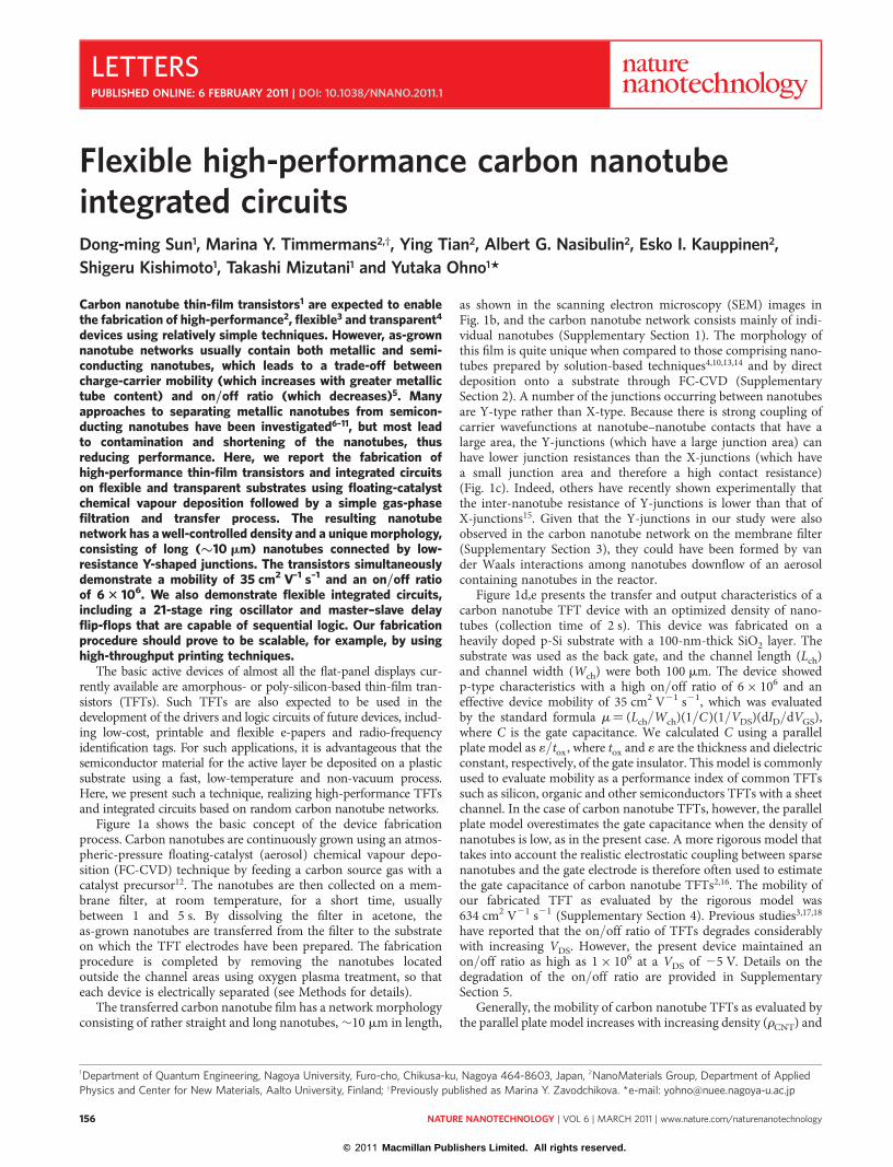
Figure 1a shows the basic concept of the device fabricationprocess. Carbon nanotubes are continuously grown using an atmos-pheric-pressure floating-catalyst (aerosol) chemical vapour depo-sition (FC-CVD) technique by feeding a carbon source gas with acatalyst precursor12. The nanotubes are then collected on a mem-brane filter, at room temperature, for a short time, usuallybetween 1 and 5 s. By dissolving the filter in acetone, theas-grown nanotubes are transferred from the filter to the substrateon which the TFT electrodes have been prepared. The fabricationprocedure is completed by removing the nanotubes locatedoutside the channel areas using oxygen plasma treatment, so thateach device is electrically separated (see Methods for details).
The transferred carbon nanotube film has a network morphologyconsisting of rather straight and long nanotubes, �10 mm in length,
as shown in the scanning electron microscopy (SEM) images inFig. 1b, and the carbon nanotube network consists mainly of indi-vidual nanotubes (Supplementary Section 1). The morphology ofthis film is quite unique when compared to those comprising nano-tubes prepared by solution-based techniques4,10,13,14 and by directdeposition onto a substrate through FC-CVD (SupplementarySection 2). A number of the junctions occurring between nanotubesare Y-type rather than X-type. Because there is strong coupling ofcarrier wavefunctions at nanotube–nanotube contacts that have alarge area, the Y-junctions (which have a large junction area) canhave lower junction resistances than the X-junctions (which havea small junction area and therefore a high contact resistance)(Fig. 1c). Indeed, others have recently shown experimentally thatthe inter-nanotube resistance of Y-junctions is lower than that ofX-junctions15. Given that the Y-junctions in our study were alsoobserved in the carbon nanotube network on the membrane filter(Supplementary Section 3), they could have been formed by vander Waals interactions among nanotubes downflow of an aerosolcontaining nanotubes in the reactor.
Figure 1d,e presents the transfer and output characteristics of acarbon nanotube TFT device with an optimized density of nano-tubes (collection time of 2 s). This device was fabricated on aheavily doped p-Si substrate with a 100-nm-thick SiO2 layer. Thesubstrate was used as the back gate, and the channel length (Lch)and channel width (Wch) were both 100 mm. The device showedp-type characteristics with a high on/off ratio of 6 × 10⁶ and aneffective device mobility of 35 cm2 V21 s21, which was evaluatedby the standard formula m¼ (Lch/Wch)(1/C)(1/VDS)(dID/dVGS),where C is the gate capacitance. We calculated C using a parallelplate model as 1/tox, where tox and 1 are the thickness and dielectricconstant, respectively, of the gate insulator. This model is commonlyused to evaluate mobility as a performance index of common TFTssuch as silicon, organic and other semiconductors TFTs with a sheetchannel. In the case of carbon nanotube TFTs, however, the parallelplate model overestimates the gate capacitance when the density ofnanotubes is low, as in the present case. A more rigorous model thattakes into account the realistic electrostatic coupling between sparsenanotubes and the gate electrode is therefore often used to estimatethe gate capacitance of carbon nanotube TFTs2,16. The mobility ofour fabricated TFT as evaluated by the rigorous model was634 cm2 V21 s21 (Supplementary Section 4). Previous studies3,17,18
have reported that the on/off ratio of TFTs degrades considerablywith increasing VDS. However, the present device maintained anon/off ratio as high as 1 × 10⁶ at a VDS of 25 V. Details on thedegradation of the on/off ratio are provided in SupplementarySection 5.
Generally, the mobility of carbon nanotube TFTs as evaluated bythe parallel plate model increases with increasing density (rCNT) and
1Department of Quantum Engineering, Nagoya University, Furo-cho, Chikusa-ku, Nagoya 464-8603, Japan, 2NanoMaterials Group, Department of AppliedPhysics and Center for New Materials, Aalto University, Finland; †Previously published as Marina Y. Zavodchikova. *e-mail: [email protected]
LETTERSPUBLISHED ONLINE: 6 FEBRUARY 2011 | DOI: 10.1038/NNANO.2011.1
NATURE NANOTECHNOLOGY | VOL 6 | MARCH 2011 | www.nature.com/naturenanotechnology156
© 2011 Macmillan Publishers Limited. All rights reserved.
length (LCNT) of the nanotubes. However, when LCNT is comparableto Lch, or when rCNT of the metallic nanotubes exceeds the percola-tion threshold19 rth¼ 4.242/pL CNT
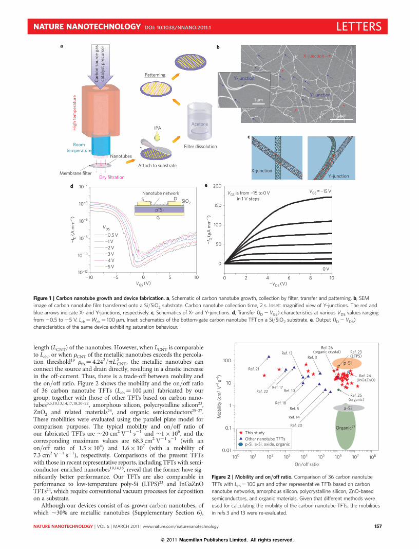
2 , the metallic nanotubes canconnect the source and drain directly, resulting in a drastic increasein the off-current. Thus, there is a trade-off between mobility andthe on/off ratio. Figure 2 shows the mobility and the on/off ratioof 36 carbon nanotube TFTs (Lch¼ 100 mm) fabricated by ourgroup, together with those of other TFTs based on carbon nano-tubes3,5,10,13,14,17,18,20–22, amorphous silicon, polycrystalline silicon23,ZnO2 and related materials24, and organic semiconductors25–27.These mobilities were evaluated using the parallel plate model forcomparison purposes. The typical mobility and on/off ratio ofour fabricated TFTs are �20 cm2 V21 s21 and �1 × 10⁶, and thecorresponding maximum values are 68.3 cm2 V21 s21 (with anon/off ratio of 1.5 × 10⁴) and 1.6 × 10⁷ (with a mobility of7.3 cm2 V21 s21), respectively. Comparisons of the present TFTswith those in recent representative reports, including TFTs with semi-conductor-enriched nanotubes10,14,18, reveal that the former have sig-nificantly better performance. Our TFTs are also comparable inperformance to low-temperature poly-Si (LTPS)23 and InGaZnOTFTs24, which require conventional vacuum processes for depositionon a substrate.
Although our devices consist of as-grown carbon nanotubes, ofwhich �30% are metallic nanotubes (Supplementary Section 6),
a b
c
d e
Hig
h te
mpe
ratu
re
AcetoneIPA
Roomtemperature
Membrane filter
Nanotubes
Dry filtration
Attach to substrate
Filter dissolution
Patterning
X-junctionY-junction
−10 −5 0 5 10
10−2
10−4
10−6
10−8
10−10
10−12
VDS
−ID
(A m
m−1
)
−ID
(μA
mm
−1)
VGS (V)
−0.5 V−1 V−2 V−3 V−4 V−5 V
0 2 4 6 8 10
0
50
100
150
200
0 V
−VDS (V)
VGS = −15 VVGS is from −15 to 0 Vin 1 V steps S D
Nanotube network
G
SiO2
p+ Si
Car
bon
sour
ce g
asca
taly
st p
recu
rsor
p+Si
5 μm
Y-junction
Y-junction
X-junction
1 μm
Figure 1 | Carbon nanotube growth and device fabrication. a, Schematic of carbon nanotube growth, collection by filter, transfer and patterning. b, SEM
image of carbon nanotube film transferred onto a Si/SiO2 substrate. Carbon nanotube collection time, 2 s. Inset: magnified view of Y-junctions. The red and
blue arrows indicate X- and Y-junctions, respectively. c, Schematics of X- and Y-junctions. d, Transfer (ID 2 VGS) characteristics at various VDS values ranging
from 20.5 to 25 V. Lch¼Wch¼ 100 mm. Inset: schematics of the bottom-gate carbon nanotube TFT on a Si/SiO2 substrate. e, Output (ID 2 VDS)
characteristics of the same device exhibiting saturation behaviour.
100 101 102 103 104 105 106 107 1080.01
0.1
1
10
100
(organic crystal)
(organic)
(InGaZnO)
This studyOther nanotube TFTsp-Si, a-Si, oxide, organic
On/off ratio
Ref. 21
Ref. 22 Ref. 10
Ref. 18Ref. 5
Ref. 25
Ref. 24
Ref. 23Ref. 26
Ref. 3
Ref. 14
Ref. 20
Ref. 17
Ref. 13
a-Si
p-Si(LTPS)
Organic27
Mob
ility
(cm
2 V
−1 s−1
)
Figure 2 | Mobility and on/off ratio. Comparison of 36 carbon nanotube
TFTs with Lch¼ 100 mm and other representative TFTs based on carbon
nanotube networks, amorphous silicon, polycrystalline silicon, ZnO-based
semiconductors, and organic materials. Given that different methods were
used for calculating the mobility of the carbon nanotube TFTs, the mobilities
in refs 3 and 13 were re-evaluated.
NATURE NANOTECHNOLOGY DOI: 10.1038/NNANO.2011.1 LETTERS
NATURE NANOTECHNOLOGY | VOL 6 | MARCH 2011 | www.nature.com/naturenanotechnology 157
© 2011 Macmillan Publishers Limited. All rights reserved.
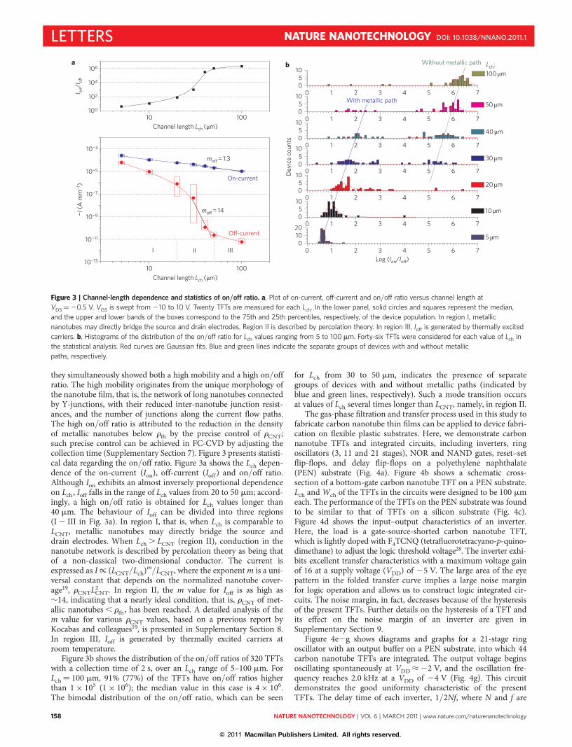
they simultaneously showed both a high mobility and a high on/offratio. The high mobility originates from the unique morphology ofthe nanotube film, that is, the network of long nanotubes connectedby Y-junctions, with their reduced inter-nanotube junction resist-ances, and the number of junctions along the current flow paths.The high on/off ratio is attributed to the reduction in the densityof metallic nanotubes below rth by the precise control of rCNT;such precise control can be achieved in FC-CVD by adjusting thecollection time (Supplementary Section 7). Figure 3 presents statisti-cal data regarding the on/off ratio. Figure 3a shows the Lch depen-dence of the on-current (Ion), off-current (Ioff ) and on/off ratio.Although Ion exhibits an almost inversely proportional dependenceon Lch, Ioff falls in the range of Lch values from 20 to 50 mm; accord-ingly, a high on/off ratio is obtained for Lch values longer than40 mm. The behaviour of Ioff can be divided into three regions(I 2 III in Fig. 3a). In region I, that is, when Lch is comparable toLCNT, metallic nanotubes may directly bridge the source anddrain electrodes. When Lch . LCNT (region II), conduction in thenanotube network is described by percolation theory as being thatof a non-classical two-dimensional conductor. The current isexpressed as I/ (LCNT/Lch)m/LCNT, where the exponent m is a uni-versal constant that depends on the normalized nanotube cover-age19, rCNTLCNT
2 . In region II, the m value for Ioff is as high as�14, indicating that a nearly ideal condition, that is, rCNT of met-allic nanotubes , rth, has been reached. A detailed analysis of them value for various rCNT values, based on a previous report byKocabas and colleagues19, is presented in Supplementary Section 8.In region III, Ioff is generated by thermally excited carriers atroom temperature.
Figure 3b shows the distribution of the on/off ratios of 320 TFTswith a collection time of 2 s, over an Lch range of 5–100 mm. ForLch¼ 100 mm, 91% (77%) of the TFTs have on/off ratios higherthan 1 × 10⁵ (1 × 10⁶); the median value in this case is 4 × 10⁶.The bimodal distribution of the on/off ratio, which can be seen
for Lch from 30 to 50 mm, indicates the presence of separategroups of devices with and without metallic paths (indicated byblue and green lines, respectively). Such a mode transition occursat values of Lch several times longer than LCNT, namely, in region II.
The gas-phase filtration and transfer process used in this study tofabricate carbon nanotube thin films can be applied to device fabri-cation on flexible plastic substrates. Here, we demonstrate carbonnanotube TFTs and integrated circuits, including inverters, ringoscillators (3, 11 and 21 stages), NOR and NAND gates, reset–setflip-flops, and delay flip-flops on a polyethylene naphthalate(PEN) substrate (Fig. 4a). Figure 4b shows a schematic cross-section of a bottom-gate carbon nanotube TFT on a PEN substrate.Lch and Wch of the TFTs in the circuits were designed to be 100 mmeach. The performance of the TFTs on the PEN substrate was foundto be similar to that of TFTs on a silicon substrate (Fig. 4c).Figure 4d shows the input–output characteristics of an inverter.Here, the load is a gate-source-shorted carbon nanotube TFT,which is lightly doped with F4TCNQ (tetrafluorotetracyano-p-quino-dimethane) to adjust the logic threshold voltage28. The inverter exhi-bits excellent transfer characteristics with a maximum voltage gainof 16 at a supply voltage (VDD) of 25 V. The large area of the eyepattern in the folded transfer curve implies a large noise marginfor logic operation and allows us to construct logic integrated cir-cuits. The noise margin, in fact, decreases because of the hysteresisof the present TFTs. Further details on the hysteresis of a TFT andits effect on the noise margin of an inverter are given inSupplementary Section 9.
Figure 4e2g shows diagrams and graphs for a 21-stage ringoscillator with an output buffer on a PEN substrate, into which 44carbon nanotube TFTs are integrated. The output voltage beginsoscillating spontaneously at VDD ≈ 22 V, and the oscillation fre-quency reaches 2.0 kHz at a VDD of 24 V (Fig. 4g). This circuitdemonstrates the good uniformity characteristic of the presentTFTs. The delay time of each inverter, 1/2Nf, where N and f are
a b
10 100
moff = 1.3
moff = 14
Off-current
IIIII
Channel length Lch (μm)
10 100Channel length Lch (μm)
−I (A
mm
−1)
I
On-current
100
106
10−3
10−5
10−7
10−9
10−11
10−13
104
102
Log (Ion/Ioff)
5 μm
10 μm
0 1 2 3 4 5 6 7
0 1 2 3 4 5 6 7
0 1 2 3 4 5 6 7
20 μm
Dev
ice
coun
ts
30 μm
Without metallic path
40 μm
With metallic path 50 μm
0 1 2 3 4 5 6 7
0 1 2 3 4 5 6 7
0 1 2 3 4 5 6 7
0 1 2 3 4 5 6 7
01020
05
10
05
10
05
10
05
10
05
10
05
10Lch:100 μm
I on/I
off
Figure 3 | Channel-length dependence and statistics of on/off ratio. a, Plot of on-current, off-current and on/off ratio versus channel length at
VDS¼20.5 V. VGS is swept from 210 to 10 V. Twenty TFTs are measured for each Lch. In the lower panel, solid circles and squares represent the median,
and the upper and lower bands of the boxes correspond to the 75th and 25th percentiles, respectively, of the device population. In region I, metallic
nanotubes may directly bridge the source and drain electrodes. Region II is described by percolation theory. In region III, Ioff is generated by thermally excited
carriers. b, Histograms of the distribution of the on/off ratio for Lch values ranging from 5 to 100 mm. Forty-six TFTs were considered for each value of Lch in
the statistical analysis. Red curves are Gaussian fits. Blue and green lines indicate the separate groups of devices with and without metallic
paths, respectively.
LETTERS NATURE NANOTECHNOLOGY DOI: 10.1038/NNANO.2011.1
NATURE NANOTECHNOLOGY | VOL 6 | MARCH 2011 | www.nature.com/naturenanotechnology158
© 2011 Macmillan Publishers Limited. All rights reserved.
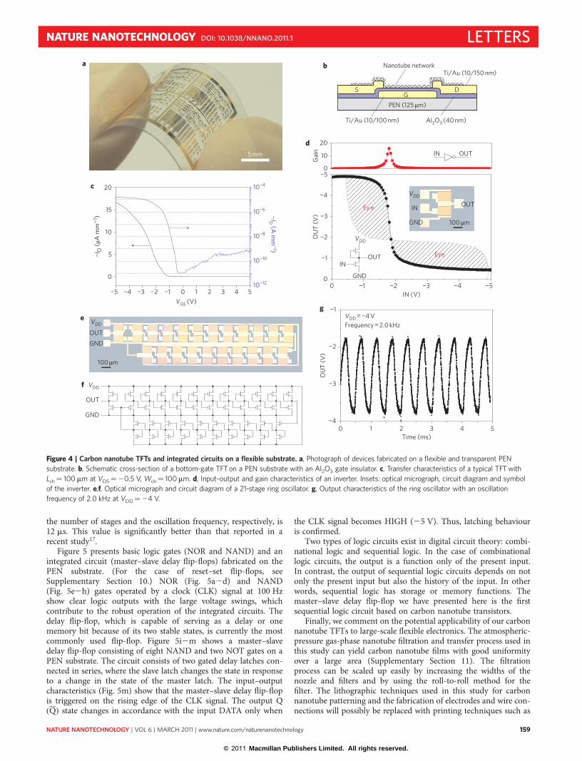
the number of stages and the oscillation frequency, respectively, is12 ms. This value is significantly better than that reported in arecent study17.
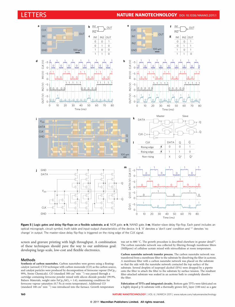
Figure 5 presents basic logic gates (NOR and NAND) and anintegrated circuit (master–slave delay flip-flops) fabricated on thePEN substrate. (For the case of reset–set flip-flops, seeSupplementary Section 10.) NOR (Fig. 5a2d) and NAND(Fig. 5e2h) gates operated by a clock (CLK) signal at 100 Hzshow clear logic outputs with the large voltage swings, whichcontribute to the robust operation of the integrated circuits. Thedelay flip-flop, which is capable of serving as a delay or onememory bit because of its two stable states, is currently the mostcommonly used flip-flop. Figure 5i2m shows a master–slavedelay flip-flop consisting of eight NAND and two NOT gates on aPEN substrate. The circuit consists of two gated delay latches con-nected in series, where the slave latch changes the state in responseto a change in the state of the master latch. The input–outputcharacteristics (Fig. 5m) show that the master–slave delay flip-flopis triggered on the rising edge of the CLK signal. The output Q(Q) state changes in accordance with the input DATA only when
the CLK signal becomes HIGH (25 V). Thus, latching behaviouris confirmed.
Two types of logic circuits exist in digital circuit theory: combi-national logic and sequential logic. In the case of combinationallogic circuits, the output is a function only of the present input.In contrast, the output of sequential logic circuits depends on notonly the present input but also the history of the input. In otherwords, sequential logic has storage or memory functions. Themaster–slave delay flip-flop we have presented here is the firstsequential logic circuit based on carbon nanotube transistors.
Finally, we comment on the potential applicability of our carbonnanotube TFTs to large-scale flexible electronics. The atmospheric-pressure gas-phase nanotube filtration and transfer process used inthis study can yield carbon nanotube films with good uniformityover a large area (Supplementary Section 11). The filtrationprocess can be scaled up easily by increasing the widths of thenozzle and filters and by using the roll-to-roll method for thefilter. The lithographic techniques used in this study for carbonnanotube patterning and the fabrication of electrodes and wire con-nections will possibly be replaced with printing techniques such as
a b
c
d
e
5 mm
S
Ti/Au (10/150 nm)
Ti/Au (10/100 nm) Al2O3 (40 nm)
PEN (125 Üm)
Nanotube network
DG
10−4
10−12
10−10
10−8
10−6
−5 −4 −3 −2 −1 0 1 2 3 4 5
0
5
10
15
20
VDD
VGS (V)
OUT
GND
f
OUTGND
0 −1 −2 −3 −4 −50
−1
−2
−3
−4
−50
10
20
Eye
IN (V)
Ey e
OU
T (V
)G
ain IN OUT
VDD
VDD
OUTIN
GND
IN
GND 100 μm
100 μm
OUT
0 1 2 3 4 5−4
−3
−2
−1
Frequency = 2.0 kHzO
UT
(V)
Time (ms)
VDD = −4 Vg
−ID (A m
m−1)
−ID
(μA
mm
−1)
VDD
S DG
PEN (125 μm)
Figure 4 | Carbon nanotube TFTs and integrated circuits on a flexible substrate. a, Photograph of devices fabricated on a flexible and transparent PEN
substrate. b, Schematic cross-section of a bottom-gate TFT on a PEN substrate with an Al2O3 gate insulator. c, Transfer characteristics of a typical TFT with
Lch¼ 100 mm at VDS¼20.5 V, Wch¼ 100mm. d, Input–output and gain characteristics of an inverter. Insets: optical micrograph, circuit diagram and symbol
of the inverter. e,f, Optical micrograph and circuit diagram of a 21-stage ring oscillator. g, Output characteristics of the ring oscillator with an oscillation
frequency of 2.0 kHz at VDD¼24 V.
NATURE NANOTECHNOLOGY DOI: 10.1038/NNANO.2011.1 LETTERS
NATURE NANOTECHNOLOGY | VOL 6 | MARCH 2011 | www.nature.com/naturenanotechnology 159
© 2011 Macmillan Publishers Limited. All rights reserved.
screen and gravure printing with high throughput. A combinationof these techniques should pave the way to our ambitious goal:developing large-scale, low-cost and flexible electronics.
MethodsSynthesis of carbon nanotubes. Carbon nanotubes were grown using a floating-catalyst (aerosol) CVD technique with carbon monoxide (CO) as the carbon source,and catalyst particles were produced by decomposition of ferrocene vapour (FeCp2,99%, Strem Chemicals). CO (standard 300 cm3 min21) was passed through acartridge containing ferrocene powder mixed with silicon dioxide powder (99.9%,Balzers Materials, weight ratio FeCp2:SiO2¼ 1:4), maintaining conditions forferrocene vapour saturation (0.7 Pa at room temperature). Additional CO(standard 100 cm3 min21) was introduced into the furnace. Growth temperature
was set to 880 8C. The growth procedure is described elsewhere in greater detail12.The carbon nanotube network was collected by filtering through membrane filters(Millipore) of cellulose acetate mixed with nitrocellulose at room temperature.
Carbon nanotube network transfer process. The carbon nanotube network wastransferred from a membrane filter to the substrate by dissolving the filter in acetone.A membrane filter with a carbon nanotube network was placed on the substrateso that the side with the nanotube network contacted the top surface of thesubstrate. Several droplets of isopropyl alcohol (IPA) were dropped by a pipetteonto the filter to attach the filter to the substrate by surface tension. The resultantfilter-attached substrate was soaked in an acetone bath to completely dissolvethe filter.
Fabrication of TFTs and integrated circuits. Bottom-gate TFTs were fabricated ona highly doped p-Si substrate with a thermally grown SiO2 layer (100 nm) as a gate
e
hd
i
IN1 OUTIN2
a b
c
1
000
1
1 1
0 0
−5
0
−5
0
−5
0
−5
0
0 0
0 0 0 0 0 0 0 0 0 0 0 0 01
0 01
0 0
0
OU
T (V
)IN
2 (V
)IN
1 (V
)C
LK (V
)
−5
0
−5
0
−5
0
−5
0Q (V
)Q
(V)
DA
TA (V
)C
LK (V
)
−5
0
−5
0
−5
0
−5
00 0
1 1 1
0 0 0 0
1
0
1
0 0 0 0
1
OU
T (V
)IN
2 (V
)IN
1 (V
)C
LK (V
)
10 20 30 40 50 60 70 80Time (ms)
0 10 20 30 40 50 60 70 80Time (ms)
0 10
10
10
00
0 0 0
1
0
0
1 1
0 0 0
111
0
011
1
1
20 30 40 50 60 70 80Time (ms)
0 0 0 0 0 0 0 0 0 0 0 0
111111
111
0 0 0 0 0 0 0 01
1 1 1 1 1 1
1111
00
0
0 0 0 0 0 0 0 0
0 0 0 0 0 0 0
1 1 1 1
1 1 1 1 1 1 1 1 1 1
1 1 1
1 1 1 1 1 1 1 1 1
0 0 0 0 0 0 0 0
1111
0
1 1 1
0 00 11 01 1
IN1 IN2 OUT
f
1
110
0 00 11 01 1
IN1 IN2 OUT
IN1 OUTIN2
g
CLK
GND
IN2
IN1OUT
CLK
GND
IN2
IN1OUT
100 μm100 μm
VDD
GND
CLK
DATA
Q
Q
k DATAQ
Q
Q
CLK
Master Slave
CLK DATA Q
Rising edge
Rising edge
Non-rising
01 1
10 0
Q* Q*X
l
VDD
CLK
GND
GNDDATA
Q
Q
mj
100 μm
Figure 5 | Logic gates and delay flip-flops on a flexible substrate. a–d, NOR gate. e–h, NAND gate. i–m, Master–slave delay flip-flop. Each panel includes an
optical micrograph, circuit symbol, truth table and input–output characteristics of the device. In l, ‘X’ denotes a ‘don’t care’ condition and ‘*’ denotes ‘no
change’ in output. The master–slave delay flip-flop is triggered on the rising edge of the CLK signal.
LETTERS NATURE NANOTECHNOLOGY DOI: 10.1038/NNANO.2011.1
NATURE NANOTECHNOLOGY | VOL 6 | MARCH 2011 | www.nature.com/naturenanotechnology160
© 2011 Macmillan Publishers Limited. All rights reserved.

dielectric. The bottom-gate electrode (Ti/Au: 10/100 nm) was deposited byelectron-beam evaporation after the SiO2 layer on the back-side of the wafer wasetched by reactive ion etching (RIE). Source and drain electrodes (Ti/Au:10/100 nm) were fabricated by standard photolithography, electron-beamevaporation and lift-off processes. Subsequently, the carbon nanotube network wastransferred from the membrane filter to the substrate with patterned electrodes.Carbon nanotubes outside the channel area were removed by oxygen plasma.
In the case of PEN substrates (Teijin DuPont Films; thickness, 125 mm), theprocess temperature was controlled to below 145 8C throughout device fabrication.After formation of gate electrodes, a 40 nm Al2O3 insulator layer was deposited onthe substrate by an atomic layer deposition technique using trimethylaluminium(TMA) and H2O at 145 8C. Contact windows for the gate electrodes were thenopened by photolithography and RIE. Similar processes to those described above forthe silicon substrate were adopted for the fabrication of source and drain electrodesas well as transfer and patterning of the carbon nanotube network on thePEN substrate.
Received 10 December 2010; accepted 5 January 2011;published online 6 February 2011
References1. Jorio, A., Dresselhaus, M. S. & Dresselhaus, G. (ed.) Carbon Nanotubes:
Advanced Topics in the Synthesis, Structure, Properties and Applications(Springer, 2008).
2. Kang, S. J. et al. High-performance electronics using dense, perfectly alignedarrays of single-walled carbon nanotubes. Nature Nanotech. 2, 230–236 (2007).
3. Cao, Q. et al. Medium-scale carbon nanotube thin-film integrated circuits onflexible plastic substrates. Nature 454, 495–500 (2008).
4. Wu, Z. et al. Transparent, conductive carbon nanotube films. Science 305,1273–1276 (2004).
5. Snow, E. S., Novak, J. P., Campbell, P. M. & Park, D. Random networks of carbonnanotubes as an electronic material. Appl. Phys. Lett. 82, 2145–2147 (2003).
6. Li, Y. et al. Preferential growth of semiconducting single-walled carbonnanotubes by a plasma enhanced CVD method. Nano Lett. 4, 317–321 (2004).
7. Collins, P. G., Arnold, M. S. & Avouris, Ph. Engineering carbon nanotubes andnanotube circuits using electrical breakdown. Science 292, 706–709 (2001).
8. Zhang, Y., Zhang, Y., Xian, X., Zhang, J. & Liu, Z. Sorting out semiconductingsingle-walled carbon nanotube arrays by preferential destruction of metallictubes using xenon-lamp irradiation. J. Phys. Chem. C 112, 3849–3856 (2008).
9. An, L., Fu, Q., Lu, C. & Liu, J. A simple chemical route to selectively eliminatemetallic carbon nanotubes in nanotube network devices. J. Am. Chem. Soc. 126,10520–10521 (2004).
10. Arnold, M. S., Green, A. A., Hulvat, J. F., Stupp, S. I. & Hersam, M. C. Sortingcarbon nanotubes by electronic structure using density differentiation. NatureNanotech. 1, 60–65 (2006).
11. Tanaka, T., Jin, H., Miyata, Y. & Kataura, H. High-yield separation of metallicand semiconducting single-wall carbon nanotubes by agarose gelelectrophoresis. Appl. Phys. Express 1, 114001 (2008).
12. Moisala, A. et al. Single-walled carbon nanotube synthesis using ferrocene andiron pentacarbonyl in a laminar flow reactor. Chem. Eng. Sci. 61,4393–4402 (2006).
13. Wang, C. et al. Wafer-scale fabrication of separated carbon nanotube thin-filmtransistors for display applications. Nano Lett. 9, 4285–4291 (2009).
14. LeMieux, M. C. et al. Self-sorted, aligned nanotube networks for thin-filmtransistors. Science 321, 101–104 (2008).
15. Nirmalraj, P. N., Lyons, P. E., De, S., Coleman, J. N. & Boland, J. J. Electricalconnectivity in single-walled carbon nanotube networks. Nano Lett. 9,3890–3895 (2009).
16. Cao, Q. et al. Gate capacitance coupling of singled-walled carbon nanotube thin-film transistors. Appl. Phys. Lett. 90, 023516 (2007).
17. Ha, M. et al. Printed, sub-3 V digital circuits on plastic from aqueous carbonnanotube inks. ACS Nano 4, 4388–4395 (2010).
18. Engel, M. et al. Thin film nanotube transistors based on self-assembled, aligned,semiconducting carbon nanotube arrays. ACS Nano 2, 2445–2452 (2008).
19. Kocabas, C. et al. Experimental and theoretical studies of transport through largescale, partially aligned arrays of single-walled carbon nanotubes in thin film typetransistors. Nano Lett. 5, 1195–1202 (2007).
20. Zavodchikova, M. Y. et al. Carbon nanotube thin film transistors based onaerosol methods. Nanotechnology 20, 085201 (2009).
21. Snow, E. S., Campbell, P. M., Ancona, M. G. & Novak, J. P. High-mobilitycarbon-nanotube thin-film transistors on a polymeric substrate. Appl. Phys. Lett.86, 033105 (2005).
22. Cao, Q., Xia, M., Shim, M. & Rogers, J. A. Bilayer organic–inorganic gatedielectrics for high-performance, low-voltage, single-walled carbon nanotubethin-film transistors, complementary logic gates, and p-n diodes on plasticsubstrates. Adv. Funct. Mater. 16, 2355–2362 (2006).
23. Pecora, A. Low-temperature polysilicon thin film transistors on polyimidesubstrates for electronics on plastic. Solid-State Electron. 52, 348–352 (2008).
24. Kim, M. et al. High mobility bottom gate InGaZnO thin film transistors withSiOx etch stopper. Appl. Phys. Lett. 90, 212114 (2007).
25. Uemura, T., Hirose, Y., Uno, M., Takimiya, K. & Takeya, J. Very high mobilityin solution-processed organic thin-film transistors of highly ordered[1]benzothieno[3,2-b]benzothiophene derivatives. Appl. Phys. Express 2,111501 (2009).
26. Sundar, V. C. et al. Elastomeric transistor stamps: reversible probing of chargetransport in organic crystals. Science 303, 1644–1646 (2004).
27. Forrest, S. R. The path to ubiquitous and low-cost organic electronic applianceson plastic. Nature 428, 911–918 (2004).
28. Takenobu, T. et al. Control of carrier density by a solution method in carbon-nanotube devices. Adv. Mater. 17, 2430–2434 (2005).
AcknowledgementsThis work was supported by the Industrial Technology Research Grant Program in2008 from the New Energy and Industrial Technology Development Organization (NEDO)of Japan and the Aalto University MIDE program via the CNB-E project, and was partiallysupported by the Academy of Finland (pr. no. 128445).
Author contributionsY.O. and E.K. conceived and designed the experiments. D.S. performed device fabricationand characterization. M.T. and Y.O. performed the growth of nanotubes. Y.T. and M.T.performed absorption measurements. A.N. and E.K. developed the floating-catalyst growthtechnique. D.S. and Y.O. co-wrote the paper. All authors discussed the results andcommented on the manuscript.
Additional informationThe authors declare no competing financial interests. Supplementary informationaccompanies this paper at www.nature.com/naturenanotechnology. Reprints andpermission information is available online at http://npg.nature.com/reprintsandpermissions/.Correspondence and requests for materials should be addressed to Y.O.
NATURE NANOTECHNOLOGY DOI: 10.1038/NNANO.2011.1 LETTERS
NATURE NANOTECHNOLOGY | VOL 6 | MARCH 2011 | www.nature.com/naturenanotechnology 161
© 2011 Macmillan Publishers Limited. All rights reserved.