
One-Dimensional Nanostructures: Synthesis, Characterization, and Applications

Nm
NMa
b
a
ARRAA
KINNM
1
taareIthbbmtohtIw
(
h0
Applied Surface Science 317 (2014) 765–770
Contents lists available at ScienceDirect
Applied Surface Science
jou rn al h om ep age: www.elsev ier .com/ locate /apsusc
i2O3 decoration of In2O3 nanostructures for catalytically enhancedethane sensing
guyen Minh Vuonga,∗, Nguyen Minh Hieua, Dojin Kima,∗, Byunh Il Choib,yungbae Kimb
Department of Materials Science and Engineering, Chungnam National University, Daejeon 305-764, Republic of KoreaEnvironmental & Energy Systems Div., Korea Inst. Machinery & Materials, Daejeon 305-343, Republic of Korea
r t i c l e i n f o
rticle history:eceived 8 May 2014eceived in revised form 8 August 2014ccepted 21 August 2014vailable online 9 September 2014
a b s t r a c t
The explosive limit of methane (CH4) gas concentration is 5%. However, detection of CH4 gas at lowerconcentrations is essential for prevention and warning purposes in leaking gas systems. In this study,a simple method for fabricating thin films of granular indium oxide (In2O3) particles decorated withnickel oxide (Ni2O3) nanoparticles was developed for high response CH4 gas sensor. The In2O3 granularfilm was fabricated by sputter deposition of indium, followed by oxidation. Ni2O3 nanoparticles were
eywords:ndium oxideickel oxideanowire gas sensorethane
deposited onto the In2O3 film by arc-discharge deposition of single-wall carbon nanotubes (SWCNTs)with Ni catalyst nanowires, followed by burning the carbon nanotubes. The Ni nanoparticle catalystsdeposited on the SWCNTs were then oxidized to Ni2O3.The Ni2O3 nanoparticles on the surface exhibiteda catalytic role in methane gas reactions, resulting in reduction of operation temperature. The sensorsshowed relatively high response percentage per 100 ppm methane gas concentration.
© 2014 Elsevier B.V. All rights reserved.
. Introduction
Methane (CH4) is an important gas used for domestic and indus-rial applications. However, CH4 can react with pollutants in airnd produce dangerous explosives. The explosive limit of CH4 ispproximately 5% [1]; however, for preventive alarms, sensors mayequire reliable detection of trace concentrations of CH4 in thenvironment. Metal oxide semiconductors, such as SnO2, ZnO, andn2O3 have shown remarkable advantages in gas sensing because ofheir unique combination of interesting properties: high response,igh chemical stability, good electrical, optical, and piezoelectricehavior, non-toxicity, and low price [1]. Sensor performance haseen improved by decorating sensing-layer surfaces with nobleetals and metal oxides catalysts [1–5]. However, sensor proper-
ies can be improved further with the application of nanostructuresn sensing probes. Thus, a SnO2 thin film decorated with Ni2O3as been developed for a high-response methane sensor [6]. In
his work, similar fabrication method was applied to In2O3 film.n2O3 has good hemisphere-shape agglomeration on the substrateshen heat-treated for oxidation. The method of coating Ni2O3
∗ Corresponding authors. Tel.: +82 42 821 6639/+82 42 823 7638.E-mail addresses: [email protected] (N.M. Vuong), [email protected]
D. Kim).
ttp://dx.doi.org/10.1016/j.apsusc.2014.08.125169-4332/© 2014 Elsevier B.V. All rights reserved.
nanoparticles on In2O3 films is unique. Ni was used for the arc dis-charge synthesis of single-wall carbon nanotubes (SWCNTs) anddispersed among the SWCNTs. As the In2O3 film SWCNTs coatingburns up, Ni is oxidized to Ni2O3, which is then deposited onto thefilm. In this manner, the amount of Ni2O3 nanoparticles in In2O3surface is closely controlled.
2. Experimental
SiO2 (300 nm)/Si substrates (5 mm × 5 mm × 0.6 mm) wereultrasonicated in acetone, methanol, and deionized water for 15min each and subsequently blow-dried with nitrogen gas. Thesensor fabrication flowchart is shown in Fig. 1; the experimentalprocedure is similar to that in [6]. Bar-type Pt (120 nm)/Ti (30 nm)electrodes were patterned by sequential DC sputtering of Ti andPt through a shadow mask. Indium (In, 99.99% purity) was thendeposited by sputtering onto the patterned substrates through ashadow mask. Indium metal was deposited at room temperatureunder 0.45 Pa argon pressure and 16 W power input. The In2O3films agglomerated into various sizes of hemispheric clusters dur-ing oxidation (700 ◦C for 2 h in air), as illustrated in Fig. 2.
Under a shadow mask, the In2O3 film substrate was mounted onthe inner wall of the arc-discharge chamber for Ni2O3coating. SWC-NTs were conventionally synthesized for 4 min with 40 A cm−2 arcdischarge current density under 5.3 × 10⁴ Pa hydrogen atmosphere

766 N.M. Vuong et al. / Applied Surface Science 317 (2014) 765–770
[immtNI
w(BtUpuCia
3
I
Fig. 1. Flowchart for the fabrication of Ni2O3-decorated In2O3 sensor.
7,8]. As the source of Ni, four Ni wires with 0.2 mm diameter werenserted into a hollow graphite rod. SWCNTs with dispersed Ni
etal catalyst particles were then coated onto the In2O3 film. Theethanol-treated samples were oxidized with air at 500 ◦C for 2 h
o remove the carbon nanotubes and convert the Ni particles toi2O3. The Ni2O3 nanoparticles deposited onto the surface of the
n2O3 film while the SWCNTs burn up.Surface morphology and structural properties of the sensing film
ere investigated by field-emission scanning electron microscopyFE-SEM; JSM 700F; JEOL), X-ray diffraction (XRD; D8 DISCOVER;ruker AXS, Germany, with a CuK� radiation), and X-ray photoelec-ron spectroscopy (XPS; VG Multilab 2000; Thermo VG Scientific,K). The schematic of the apparatus used for measuring the sensingroperty is shown in Ref. [9]. Gas sensing properties were measuredsing a pico-ammeter/voltage source (Keithley 6487). A 1000 ppmH4 gas in nitrogen was used for analysis, which was further diluted
n dry air by varying the CH4 gas concentrations at a constant dryir flow rate of 300 sccm.
. Results and discussion
The FE-SEM morphologies of the In2O3 and Ni2O3-decoratedn2O3 films are shown in Fig. 2a and b, respectively, wherein higher
Fig. 2. FE-SEM morphology of pure In2O3 (a) and Ni2O3-decorated In2O3 (b) st
Fig. 3. XRD patterns of In2O3, Ni2O3, and Ni2O3-decorated In2O3 material structures.
magnifications are presented in the insets. Results showed thatIn2O3 film was formed through the distribution of hemisphericIn2O3 particles in various sizes under about 1 �m. In2O3 size distri-bution was larger than SnO2 [6]. Ni2O3 nanoparticles accumulatedon the In2O3 film as residues when the SWCNTs burn up. Ni2O3nanoparticles at the scale of 10 nm barely changed the roughnessof the In2O3 film surface, as shown in Fig. 2a.
The XRD patterns of the In2O3 film (oxidized at 700 ◦C), Ni2O3clusters (oxidized at 500 ◦C), and Ni2O3-decorated In2O3 film (oxi-dized each at 700 and 500 ◦C) are presented in Fig. 3, which providesfurther insights on the crystallinity of the products. As shown inFig. 3, a cubic In2O3 structure (JCPDS file no. 06-0416) hastypicalpeaks at (2 1 1), (2 2 2), (4 0 0), (4 3 1), (4 4 0), and (6 2 2) and a hexag-onal Ni2O3 structure has main peaks at (0 0 2) and (2 0 2) (JCPDS fileno. 14-0481).
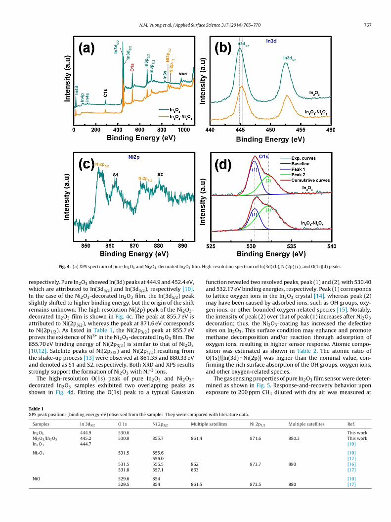
To further investigate the surface composition, binding energy,and chemical states of the elements in the samples, XPS mea-surements on pure In2O3 and Ni2O3-decorated In2O3 film wereconducted. The spectrum at Fig. 4 revealed the presence of In,O, and C in both samples; however, Ni observed clearly only inNi2O3-In2O3. The observed binding energy data are listed in Table 1.Literature values were compared with the observed values to sup-port indexing [10]. The peak at 285.35 eV is attributed to CO2adsorbed on the surface of the film [11]. As shown in Fig. 4, whenthe In2O3 film surface was decorated with Ni2O3, the characteris-tic peaks for In2O3 slightly decreased in intensity. Although Ni2O3peaks are not distinct in XRD measurements, the XPS spectrumclearly confirms the presence of Ni2O3. Therefore, decoration of
the In2O3 surface with Ni2O3 nanoparticles was achieved.The high-resolution XPS spectra of In(3d) for both samples(Fig. 4b) shows two typical peaks, which exhibited characteristicspin–orbit split for In(3d5/2) and In(3d3/2) of a trivalent indium ion,
ructures, respectively. Insets show the images at higher magnifications.
N.M. Vuong et al. / Applied Surface Science 317 (2014) 765–770 767
lm. Hi
rwIsrdatp8[tas
ds
TX
Fig. 4. (a) XPS spectrum of pure In2O3 and Ni2O3-decorated In2O3 fi
espectively. Pure In2O3 showed In(3d) peaks at 444.9 and 452.4 eV,hich are attributed to In(3d5/2) and In(3d3/2), respectively [10].
n the case of the Ni2O3-decorated In2O3 film, the In(3d5/2) peaklightly shifted to higher binding energy, but the origin of the shiftemains unknown. The high resolution Ni(2p) peak of the Ni2O3-ecorated In2O3 film is shown in Fig. 4c. The peak at 855.7 eV isttributed to Ni(2p3/2), whereas the peak at 871.6 eV correspondso Ni(2p1/2). As listed in Table 1, the Ni(2p3/2) peak at 855.7 eVroves the existence of Ni3+ in the Ni2O3-decorated In2O3 film. The55.70 eV binding energy of Ni(2p3/2) is similar to that of Ni2O310,12]. Satellite peaks of Ni(2p3/2) and Ni(2p1/2) resulting fromhe shake-up process [13] were observed at 861.35 and 880.33 eVnd denoted as S1 and S2, respectively. Both XRD and XPS results
trongly support the formation of Ni2O3 with Ni+3 ions.The high-resolution O(1s) peak of pure In2O3 and Ni2O3-ecorated In2O3 samples exhibited two overlapping peaks ashown in Fig. 4d. Fitting the O(1s) peak to a typical Gaussian
able 1PS peak positions (binding energy-eV) observed from the samples. They were compared
Samples In 3d5/2 O 1s Ni 2p3/2 Multipl
In2O3 444.9 530.6
Ni2O3/In2O3 445.2 530.9 855.7 861.4
In2O3 444.7
Ni2O3 531.5 555.6
556.0
531.5 556.5 862
531.8 557.1 863
NiO 529.6 854
529.5 854 861.5
gh-resolution spectrum of In(3d) (b), Ni(2p) (c), and O(1s)(d) peaks.
function revealed two resolved peaks, peak (1) and (2), with 530.40and 532.17 eV binding energies, respectively. Peak (1) correspondsto lattice oxygen ions in the In2O3 crystal [14], whereas peak (2)may have been caused by adsorbed ions, such as OH groups, oxy-gen ions, or other bounded oxygen-related species [15]. Notably,the intensity of peak (2) over that of peak (1) increases after Ni2O3decoration; thus, the Ni2O3-coating has increased the defectivesites on In2O3. This surface condition may enhance and promotemethane decomposition and/or reaction through adsorption ofoxygen ions, resulting in higher sensor response. Atomic compo-sition was estimated as shown in Table 2. The atomic ratio ofO(1s)/[In(3d) + Ni(2p)] was higher than the nominal value, con-firming the rich surface absorption of the OH groups, oxygen ions,
and other oxygen-related species.The gas sensing properties of pure In2O3 film sensor were deter-mined as shown in Fig. 5. Response-and-recovery behavior uponexposure to 200 ppm CH4 diluted with dry air was measured at
with literature data.
e satellites Ni 2p1/2 Multiple satellites Ref.
This work871.6 880.3 This work
[10]
[10][12]
873.7 880 [16][17]
[10]873.5 880 [17]
768 N.M. Vuong et al. / Applied Surface Science 317 (2014) 765–770
Table 2The atomic percentages of In, O, and Ni estimated from the XPS measurement.
Samples [In] [O] [Ni] [O/(In + Ni)]
dTrrrasIFfietar[dr
Iom3so
FCtt
In2O3 29.2 70.8 2.4Ni2O3/In2O3 15.6 68.8 15.6 2.2
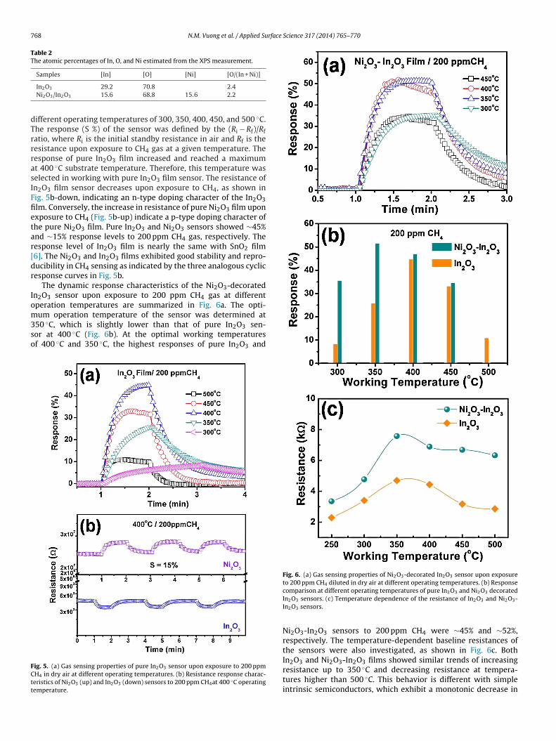
ifferent operating temperatures of 300, 350, 400, 450, and 500 ◦C.he response (S %) of the sensor was defined by the (Ri − Rf)/Rfatio, where Ri is the initial standby resistance in air and Rf is theesistance upon exposure to CH4 gas at a given temperature. Theesponse of pure In2O3 film increased and reached a maximumt 400 ◦C substrate temperature. Therefore, this temperature waselected in working with pure In2O3 film sensor. The resistance ofn2O3 film sensor decreases upon exposure to CH4, as shown inig. 5b-down, indicating an n-type doping character of the In2O3lm. Conversely, the increase in resistance of pure Ni2O3 film uponxposure to CH4 (Fig. 5b-up) indicate a p-type doping character ofhe pure Ni2O3 film. Pure In2O3 and Ni2O3 sensors showed ∼45%nd ∼15% response levels to 200 ppm CH4 gas, respectively. Theesponse level of In2O3 film is nearly the same with SnO2 film6]. The Ni2O3 and In2O3 films exhibited good stability and repro-ucibility in CH4 sensing as indicated by the three analogous cyclicesponse curves in Fig. 5b.
The dynamic response characteristics of the Ni2O3-decoratedn2O3 sensor upon exposure to 200 ppm CH4 gas at differentperation temperatures are summarized in Fig. 6a. The opti-
um operation temperature of the sensor was determined at50 ◦C, which is slightly lower than that of pure In2O3 sen-or at 400 ◦C (Fig. 6b). At the optimal working temperaturesf 400 ◦C and 350 ◦C, the highest responses of pure In2O3 and
ig. 5. (a) Gas sensing properties of pure In2O3 sensor upon exposure to 200 ppmH4 in dry air at different operating temperatures. (b) Resistance response charac-eristics of Ni2O3 (up) and In2O3 (down) sensors to 200 ppm CH4at 400 ◦C operatingemperature.
Fig. 6. (a) Gas sensing properties of Ni2O3-decorated In2O3 sensor upon exposureto 200 ppm CH4 diluted in dry air at different operating temperatures. (b) Response
comparison at different operating temperatures of pure In2O3 and Ni2O3 decoratedIn2O3 sensors. (c) Temperature dependence of the resistance of In2O3 and Ni2O3-In2O3 sensors.Ni2O3-In2O3 sensors to 200 ppm CH4 were ∼45% and ∼52%,respectively. The temperature-dependent baseline resistances ofthe sensors were also investigated, as shown in Fig. 6c. Both
In2O3 and Ni2O3-In2O3 films showed similar trends of increasingresistance up to 350 ◦C and decreasing resistance at tempera-tures higher than 500 ◦C. This behavior is different with simpleintrinsic semiconductors, which exhibit a monotonic decrease in
N.M. Vuong et al. / Applied Surface Science 317 (2014) 765–770 769
F ture or ties (c
rwcsv-ataTitttrdaraNiooscabt
ig. 7. (a) Sensing properties to 200 ppm CH4 gas and at 350 ◦C operating temperaesponse of Ni2O3 (4 min)-In2O3 sensor to 100 ppm CH4 at 350 ◦C. Response proper
esistance with temperature. The observed resistance variationith temperature is associated with the change in the physico-
hemical nature of the oxygen species adsorbed on the oxideurfaces. A similar complex trend was also observed in a pre-ious study of In2O3 film [18]. When pure In2O3 and Ni2O3decorated In2O3 sensors are exposed to dry air, oxygen moleculesre adsorb on the surface. These adsorbed oxygen molecules cap-ure quasi-free electrons in the conduction band of the sensing bodynd become stabilized in ionic forms, such as O2
−, O−, and O2−.his ionosorption of oxygen narrows the conduction channel andncreases the resistance of the sensor. When the sensor is exposedo CH4 gas, CH4 molecules react with the absorbed oxygen ions onhe surface of the sensing body (i.e., CH4 + 4O− → 2H2O + CO2 + 4e−),hereby decreasing the resistance of the sensor because of theeduction of oxygen ions. The higher response of the Ni2O3-ecorated In2O3 sensor compared with pure In2O3 sensor can bettributed to two possible reasons as discussed in our previousesults [6]. First, with the addition ofNi2O3, p–n junction is formedt the interface between Ni2O3 and In2O3. The resistance of thei2O3–In2O3 structure was higher than that of pure In2O3. The
ncreased resistance after Ni2O3 decoration validates the formationf the p–n junction at the Ni2O3–In2O3 interfaces. The formationf the p–n junction did not directly enhance the response of theensor; however, sensor response can be enhanced if the In2O3
hannel was driven near the total depletion condition broughtbout by the formation of p–n junction. Nanostructural sensor haseen shown to exhibit maximum response when the sensor condi-ion (doping and size) is close to the total depletion condition [8].f Ni2O3-In2O3sensors generated from varied Ni arc-discharge times. (b) Resistance) and linearity (d) of the Ni2O3 (4 min)-In2O3 sensor at varying CH4 concentrations.
Therefore, if the p–n junction formation drove the In2O3 layer nearthe total depletion condition, the sensor response can be enhancedby the Ni2O3-decoration. However, this condition needs to be con-firmed. Second, the decoration of Ni2O3 nanoparticles on In2O3films produced higher surface roughness and area, which leadsto increase in gas absorption sites. Third, Ni2O3 can play a cat-alytic role for decomposition of CH4, possibly through the so-calledspillover effect [19]. XPS results showed the formation of oxygen-related defective bindings at the In2O3 surface and/or In2O3-Ni2O3interface. The slight decrease in the working temperature withNi2O3-decoration strongly suggests its catalytic role. As a conse-quence, enhanced reaction with adsorbed oxygen will lead to anenhanced response.
The effect of Ni2O3 coating thickness on the sensing propertywas systematically examined. The amount of Ni2O3 was varied bycontrolling the Ni arc-discharge time from 1 min to 5 min. Fromthe XPS spectra of the Ni(2p)/In(3d), the estimated amounts ofthe Ni2O3 coated on the surface of In2O3 were 0.41, 0.57, 0.84,1, and 2.24 atomic percent at Ni arc-discharge times of 1, 2, 3, 4,and 5 min, respectively. In addition, the sensors showed a base-line resistance of 4.9, 6.2, 6.5, 6.9, and 14.5 k� at Ni arc-dischargetimes of 1, 2, 3, 4, and 5 min, respectively. Sensor responses at350 ◦C operation temperature as a function of the amount of Ni2O3catalyst clusters are plotted in Fig. 7a. The optimum thickness of
Ni2O3 at the maximum response of the sensor was obtained atthe arc-discharge time of 4 min. This optimization procedure canbe associated with the optimization of all the possible parame-ters, such as surface area for gas molecular adsorption, depletion
7 rface
lcNwd(dCfi
(taraetIswcmepTesc
4
prrttitgipfi
A
o
[
[
[
[
[
[
[
[
[
response to reducing (CO, H2) gases, Sens. Actuators B: Chem. 98 (2004)
70 N.M. Vuong et al. / Applied Su
ayer thickness at the p–n junction, gas penetration thickness, andatalytic effect. Degradation of the sensor response with 5 mini2O3 coating may be attributed to hindered molecular gas contactith In2O3 through the thick coating. In any case, the overall con-uction type of the Ni2O3-In2O3 sensors remained n-type dopedFig. 7b) because of the much thicker In2O3 layer. The good repro-ucibility of the response of Ni2O3 (4 min)/In2O3 sensor to 100 ppmH4 at the optimal operating temperature 350 ◦C was also con-rmed in Fig. 7b.
The optimal operating temperature of Ni2O3-In2O3 sensor350 ◦C) is lower than that of pure In2O3 sensor (400 ◦C). This reduc-ion of optimal operating temperature with Ni2O3 decoration waslso observed with the SnO2 sensor [6]. In addition to the enhancedesponse, reduction in the working temperature of the sensor isnother important synergetic effect observed. Although responsenhancement with Ni2O3 decoration is not profound with In2O3han with SnO2, the optimal working temperature is lower withn2O3 (350 ◦C) than with SnO2 (400 ◦C) [6]. This improvement ofensor response and reduction in sensor operating temperatureas also observed by doping noble metals on metal oxide semi-
onductor surfaces [1]. The rather high operation temperature forethane sensing could originate from the nature of the gas to
xhibit covalent bonding, and the reduction of the sensing tem-erature could be attributed to a catalytic role of nickel oxide.he response properties of the Ni2O3 (4 min)–In2O3 sensor uponxposure to varying methane concentrations were investigated ashown in Fig. 7c. The linearity of the sensor response in ppm con-entration ranges are summarized in Fig. 7d.
. Conclusions
Ni2O3-decorated In2O3 film CH4 sensors were fabricated. Theroposed method of coating In2O3 with Ni2O3 nanoparticles accu-ately controls the amount of Ni2O3 to obtain high surface area andoughness. The Ni2O3–In2O3 sensor showed higher performancehan pure In2O3 sensor in terms of response level and workingemperature. The synergetic effects of Ni2O3 in CH4 sensing arets catalytic role and increased surface area for molecular adsorp-ion. The XPS results showed the oxygen-related defective bindingsenerated by the Ni2O3 coating on the Ni2O3–In2O3 surface and/ornterface. These defective binding sites could promote the decom-osition of methane and/or surface reactions as observed with theormation of p-Ni2O3/n-SnO2 junction. However, this phenomenons not directly related to the enhanced response.
cknowledgements
This work was supported by the principal research programf the Korea Institute of Machinery and Materials (KIMM) and
[
Science 317 (2014) 765–770
the National Research Foundation of Korea (NRF) grant (No. NRF-2013R1A4A1069528).
References
[1] S. Basu, P.K. Basu, Nanocrystalline metal oxides for methane sensors: role ofnoble metals, J. Sens. 2009 (2009).
[2] P. Bhattacharyya, P.K. Basu, H. Saha, S. Basu, Fast response methane sensorusing nanocrystalline zinc oxide thin films derived by sol–gel method, Sens.Actuators B: Chem. 124 (2007) 62–67.
[3] S. Chakraborty, I. Mandal, I. Ray, S. Majumdar, A. Sen, H.S. Maiti, Improve-ment of recovery time of nanostructured tin dioxide-based thick film gassensors through surface modification, Sens. Actuators B-Chem. 127 (2007)554–558.
[4] P. Bhattacharyya, P.K. Basu, C. Lang, H. Saha, S. Basu, Noble metal catalytic con-tacts to sol–gel nanocrystalline zinc oxide thin films for sensing methane, Sens.Actuators B: Chem. 129 (2008) 551–557.
[5] D. Haridas, V. Gupta, Enhanced response characteristics of SnO2 thin film basedsensors loaded with Pd clusters for methane detection, Sens. Actuators B: Chem.166–167 (2012) 156–164.
[6] N.M. Vuong, N.M. Hieu, H.N. Hieu, H. Yi, D. Kim, Y.-S. Han, M. Kim, Ni2O3-decorated SnO2 particulate films for methane gas sensors, Sens. Actuators B:Chem. 192 (2014) 327–333.
[7] N.D. Hoa, N. Van Quy, H. Song, Y. Kang, Y. Cho, D. Kim, Tin oxide nanotube struc-tures synthesized on a template of single-walled carbon nanotubes, J. CrystalGrowth 311 (2009) 657–661.
[8] N.M. Vuong, H. Jung, D. Kim, H. Kim, S.-K. Hong, Realization of an open spaceensemble for nanowires: a strategy for the maximum response in resistivesensors, J. Mater. Chem. 22 (2012) 6716–6725.
[9] N.D. Hoa, N. Van Quy, D. Kim, Nanowire structured SnOx–SWNT composites:high performance sensor for NOx detection, Sens. Actuators B: Chem. 142(2009) 253–259.
10] J.F. Moulder, W.F. Stickle, P.E. Sobol, K.D. Bomben, Handbook of X-ray Photo-electron Spectroscopy, Perkin Elmer, Eden Prairie, 1992.
11] Y.-W. Zhang, R. Si, C.-S. Liao, C.-H. Yan, C.-X. Xiao, Y. Kou, Facile alco-hothermal synthesis, size-dependent ultraviolet absorption, and enhanced coconversion activity of ceria nanocrystals, J. Phys. Chem. B 107 (2003) 10159–10167.
12] S.Z. Hu, F.Y. Li, Z.P. Fan, The synergistic effect of nitrogen and Ni2O3 over TiO2
photocatalyst in the degradation of 2,4,6-trichlorophenol under visible light,Bull. Korean Chem. Soc. 33 (2012) 4052–4058.
13] K.S. Kim, N. Winograd, X-ray photoelectron spectroscopic studies of nickel-oxygen surfaces using oxygen and argon ion-bombardment, Surf. Sci. 43 (1974)625–643.
14] C. Chen, D. Chen, X. Jiao, S. Chen, In2O3 nanocrystals with a tunable size in therange of 4–10 nm: one-step synthesis, characterization, and optical properties,J. Phys. Chem. C 111 (2007) 18039–18043.
15] B. Erdem, R.A. Hunsicker, G.W. Simmons, E.D. Sudol, V.L. Dimonie, M.S. El-Aasser, XPS and FTIR surface characterization of TiO2 particles used in polymerencapsulation, Langmuir 17 (2001) 2664–2669.
16] B. Sasi, K.G. Gopchandran, Nanostructured mesoporous nickel oxide thin films,Nanotechnology 18 (2007) 115613.
17] M. Ristova, J. Velevska, M. Ristov, Chemical bath deposition and elec-trochromic properties of NiOx films, Solar Energy Mater. Solar Cells 71 (2002)219–230.
18] G. Korotcenkov, V. Brinzari, A. Cerneavschi, M. Ivanov, A. Cornet, J.Morante, A. Cabot, J. Arbiol, In2O3 films deposited by spray pyrolysis: gas
122–129.19] D. Haridas, A. Chowdhuri, K. Sreenivas, V. Gupta, Effect of thickness of platinum
catalyst clusters on response of SnO2 thin film sensor for LPG, Sens. ActuatorsB: Chem. 153 (2011) 89–95.
Copyright © 2022 FDOKUMEN