NASRI BIN SULAIMAN, Ph.D - Cade UPM
275
-
Upload
khangminh22 -
Category
Documents
-
view
3 -
download
0
Transcript of NASRI BIN SULAIMAN, Ph.D - Cade UPM


i
NASRI BIN SULAIMAN, Ph.D
Profile
Nasri bin Sulaiman is a senior lecturer at the Department of Electrical and Electronic
Engineering, Faculty of Engineering, Universiti Putra Malaysia. He received a bachelor
degree in electronics and computer engineering from the Universiti Putra Malaysia
(UPM), Malaysia in 1994 and a master degree in microelectronics system design from
the University of Southampton, United Kingdom in 1999. He also obtained a Ph.D
degree in adaptive hardware from the University of Edinburgh, United Kingdom in 2007.
His areas of interest include evolutionary algorithms, digital signal processing, digital
communications and low power VLSI designs.
He is currently working on a variety of research projects such as “High Performance
Hardware Implementation of a Multi-Objective Genetic Algorithm” which is funded
through the Research University Grant Scheme (RUGS) of Universiti Putra Malaysia
(UPM), as well as, “Crest Factor Reduction and Digital Pre-distortion Implementation in
Orthogonal Frequency Division Multiplexing (OFDM) Systems“, funded by the Ministry
of Science, Technology and Innovation (MOSTI).

TABLE OF CONTENTS
SECTION 1. TEACHING AND LEARNING PHILOSOPHY THAT REFLECTS CANDIDATE’S
EXPERTISE ........................................................................................................................................... 1
1.1 TEACHING PHILOSOPHY.................................................................................................................... 1
1.2 THEORY/MODEL STATEMENT OF TEACHING AND LEARNING PHILOSOPHY ............................................ 2
SECTION 2. PLANNING & IMPLEMENTATION OF TEACHING/SUPERVISING AND
EVALUATING STRATEGY ................................................................................................................. 6
2.1 TEACHING/SUPERVISION .................................................................................................................. 6
2.1.1 Before Lecture .......................................................................................................................... 6
2.1.2 After Lecture ............................................................................................................................ 9
2.1.3 Supervision............................................................................................................................. 19
2.2 EVALUATIONS ............................................................................................................................... 22
2.2.1 First level questions ................................................................................................................ 22 2.2.2 Intermediate level questions .................................................................................................... 22
2.2.3 Highest level questions ........................................................................................................... 24
SECTION 3. INNOVATION AND CREATIVITY IN TEACHING AND LEARNING .................... 42
3.1 STATEMENT OF INNOVATION IN TEACHING ..................................................................................... 42
3.1.1 Interactive Power Point .......................................................................................................... 42
3.1.2 Using PSPICE Simulator to teach: BJT Amplifiers .................................................................. 53
3.1.3 JFET Biasing Analysis using Turbo Pascal Programming Language ....................................... 56
3.1.4 E-learning .............................................................................................................................. 59
3.2 CREATIVITY IN TEACHING .............................................................................................................. 64
3.3 KBAT (HIGH ORDER THINKING SKILLS) ........................................................................................ 68
3.3.1 Problem Based Learning ........................................................................................................ 68 3.3.2 Outputs from students Examinations Results ........................................................................... 74
3.4 IMPACT OF LEARNING AND TEACHING INNOVATION AND/OR CREATIVITY TOWARDS STUDENTS,
COLLEAGUE AND COMMUNITY ............................................................................................................ 84
SECTION 4. EVALUATION AND TESTIMONY OF TEACHING/SUPERVISION ....................... 90
4.1 PROOF OF EVALUATION OF TEACHING AND SUPERVISION BY STUDENTS ........................................... 90
4.1.1 Course Evaluation Score ........................................................................................................ 97
4.2 TESTIMONY ON TEACHING AND SUPERVISION ............................................................................... 103
4.2.1 Teaching Assessment Report comments ................................................................................. 103
4.2.2 Appreciation from Students ................................................................................................... 111
4.2.3 List of Teaching Awards ....................................................................................................... 121
SECTION 5. IMPROVEMENT ON TEACHING, SUPERVISION AND PROFESSIONAL
DEVELOPMENT ............................................................................................................................... 135
5.1 MEETING RECORDS ...................................................................................................................... 135
5.2 GRADING ..................................................................................................................................... 138
5.2.1 Lab Report Grading ............................................................................................................. 138
5.2.2 Assignment Grading ............................................................................................................. 140
SECTION 6. SCHOLARLY ACCOMPLISHMENTS IN TEACHING, SUPERVISION AND
EVALUATION ................................................................................................................................... 145
6. 1 SEMINARS ATTENDED AND ORGANIZED ........................................................................................ 143
6.2 RESEARCH GRANTS ...................................................................................................................... 149

REFERENCES ................................................................................................................................... 183
LAB MANUALS ................................................................................................................................ 184
MINI PROJECT REPORT ................................................................................................................ 237
CV ....................................................................................................................................................... 255

Nasri Sulaiman, Ph.D
1
1. Teaching and learning philosophy that reflects candidate’s expertise
The teaching and learning philosophy I believe in and hold on to are as follow:
1.1 Teaching philosophy
Essentially, teaching is the process of changing or transforming students’ taxonomy levels in
terms of cognitive, psychomotor, affective, and spiritual domains from the lowest level to the
highest level possible as shown in Figure 1.1. There are several factors that contribute to the
wholesomeness of this process, the main contributor being the effectiveness of teaching,
reflecting the change that a student undergoes throughout their learning process. I believe that a
being a good educator comes hand in hand with mastering his or her field of expertise alongside
with applying effective teaching methodologies that in time, through the right implementation
can ensure maximum transformation in the students. The process of teaching and learning have
been the sole drive of civilization evolving the world that we live into something greater every
day. Therefore, it is a great honour to contribute to the revolutionary of the world even if the
impact is miniscule, the drive that motivates me to continue pursuing my role as an educator.
Teaching is a changing process from;
Not knowing to knowing
knowing to understanding,
understanding to mastering

Nasri Sulaiman, Ph.D
2
Figure 1.1: teaching philosophy model
1.2 Theory/model statement of teaching and learning philosophy
My teaching and learning philosophy is based on Bloom’s taxonomy of learning domains.
Bloom’s taxonomy is a classification system used to define and distinguish different levels of
human cognition—i.e., thinking, learning, and understanding. Educators have typically used
Bloom’s taxonomy to inform or guide the development of assessments (tests and other
evaluations of student learning), curriculum (units, lessons, projects, and other learning
activities), and instructional methods such as questioning strategies.
The original taxonomy was organized into three domains: Cognitive, Affective, and
Psychomotor. Educators have primarily focused on the Cognitive model, which includes six
different classification levels: Knowledge, Comprehension, Application, Analysis, Synthesis,
and Evaluation (Figure 1.2). The group sought to design a logical framework for teaching and
learning goals that would help researchers and educators understand the fundamental ways in
which people acquire and develop new knowledge, skills, and understandings [1].
Some users of the taxonomy place more emphasis on the hierarchical nature of the framework,
asserting that the first three elements: Knowledge, Comprehension, and Application represent
T E A
C H
I N
G
C O GNITIVE
P SYCH MOTOR
AFFECTIVE
SPIRITUAL

Nasri Sulaiman, Ph.D
3
lower levels of cognition and learning, while Analysis, Synthesis, and Evaluation are
considered higher-order skills. For this reason, the taxonomy is often graphically represented as a
pyramid with higher-order cognition at the top.
The Psychomotor domain (Simpson, 1972) includes physical movement, coordination, and use
of the motor-skill areas. Development of these skills requires practice and is measured in terms
of speed, precision, distance, procedures, or techniques in execution (Figure 1.3). Thus,
psychomotor skills range from manual tasks, such as digging a ditch or washing a car, to more
complex tasks, such as operating a complex piece of machinery or dancing [2].
Figure 1.2: Bloom’s cognitive model

Nasri Sulaiman, Ph.D
4
Figure 1.3: Psychomotor domain
Like cognitive objectives, affective objectives can also be divided into a hierarchy (according to
Krathwohl). This domain was first described in 1964 and is attributed to David Krathwohl as the
primary author. The affective domain (Krathwohl, Bloom, Masia, 1973) includes the manner in
which we deal with things emotionally, such as feelings, values, appreciation, enthusiasms,
motivations, and attitudes (Figure 1.4). Again, the taxonomy is arranged from simpler feelings to
those that are more complex [3].

Nasri Sulaiman, Ph.D
5
Figure 1.4: Krathwohl affective objectives hierarchy
The Western challenge to education or human development process is scientific or technological
in nature but the Muslim challenge to education includes spiritual, moral and social
development. Therefore the planned of genuine reform in education should reflect the spirit and
aspiration of Islam [4]. By instilling spiritual education such as love, compassion, patience,
forgiveness, etc., students will have a balance between internal and external morals. Also,
emphasizing on spiritual education, students will know that, apart from gaining education to
improve one’s material attainment and success, it is also important to have selfless love and
respect for the society.

Nasri Sulaiman, Ph.D
6
2. Planning & implementation of teaching/supervising and evaluating strategy
Teaching/supervision strategy is planned and implemented according to the teaching philosophy
to change the taxonomy levels in the three domains.
2.1 Teaching/supervision
The teaching strategy is divided into 3 sessions which are before lecture, during lecture and after
lecture. This teaching strategy is applicable to all the undergraduate and post graduate courses.
2.1.1 Before Lecture
Before I begin my lectures, I will ask a few simple questions to my students such as the
following:
1. Why are you interested in taking this subject?
2. How is this subject useful in your life?
3. What do you wish to obtain from this subject?
4. Did you use your hand phone or computers this morning?
5. Why is this subject necessary in your curriculum?
Image 2.1: shot of me asking questions before beginning lectures

Nasri Sulaiman, Ph.D
7
The answers vary amongst students however the common answers from students are as follow:
1. This subject is compulsory to completing my major and I have no choice but to take it.
2. I do not know why I am taking this subject but I wish to get an A.
3. I wish to work with electrical and electronic systems but I am not sure or do not
understand how to use them.
4. Yes, I used my hand phone and laptop this morning.
The answers to these questions may seem simple and mundane, however they are very important
and relevant for me in evaluating their thoughts and perceptions before taking my subject. Upon
knowing these thoughts and perceptions, I am able to formulate my strategy to ensure that
stimulation in class can be carried out at the highest possible rate.
I begin my lectures as most educators of any field would, by explaining to students why this
subject is important in their studies and life through examples of applications in their future work
which require extensive knowledge in this field. It is at the utmost importance for me to welcome
the students to the subject as it can evoke their will, interest and excitement to study and explore
the subject. This question serves to create eagerness amongst students motivating them to reach
their potential in this subject and outside of this subject. This is followed by several technical
questions such as:
1. What is the main component in amplifier systems?
2. What is a function of amplifier systems?
3. Where are the filters used in electrical and electronic systems?
As these questions have the lowest level of thinking, students can mainly answer using their
memory or from memorization, which is why most students are able to answer the questions. I
will then continue to explain the answers giving the students more information and a short
introduction to what they have in store for them during their time of being a student of mine.

Nasri Sulaiman, Ph.D
8
Image 2.2: shot of me explaining conceptual ideas to students
My next question to the students require a higher level of thinking which require students to
relate their knowledge in amplifiers and filters to solve a given problem. These questions are
such as the following:
1. What are the similarities, differences and relationship between filters and amplifiers?
2. How to analyze amplifier circuits?
3. How to design amplifier circuits?
4. What are the similarities, differences and relationship between analysing and designing
amplifiers?
As these questions have a higher level of difficulty, students usually find it more challenging to
answer and thus many of them if not almost all, are unable to of give the correct answers to these
questions. I will then give them my answers encapsulating my knowledge, experiences and
research findings as much as I can to motivate students in becoming knowledgeable engineers. It
is vital for me that my students understand that it takes more than just facts and book smart in
becoming an all rounded engineer.

Nasri Sulaiman, Ph.D
9
My final question to students before getting into the subject matters of a lecture are:
1. If you are given a big system which contains many blocks, could you identify which one
is amplifier, filters, oscillator, etc.?
2. Could you identify the relationship between these blocks?
3. Could solve the problems for individual block and finally reassemble them back to the
original situation?
These questions require the highest level thinking as they are a synthesis type of question
requiring students to operate with the problems, breaking the problems into smaller parts and
reassembling the parts to form the original condition.
2.1.2 After Lecture
During laboratory sessions, I will use the same techniques as in the lectures to develop and
stimulate my students’ thinking. In these sessions, I focus on developing and stimulating the
level of psychomotor of my students. This is the main difference between lectures and
experiments. I begin the process by evaluating what they already know, their psychomotor and
values in the subject. Upon analyzing their feedback and response, I will give my take on the
matter based on my knowledge, skills and values from my experiences and research work, in
relation to the three components (knowledge, psychomotor and values) for this subject. I apply
these practices to both under graduates and post graduates under my supervision.

Nasri Sulaiman, Ph.D
10
Image 2.3: shot of student taking part in lecture activity

Nasri Sulaiman, Ph.D
11
Below are a list of all my undergraduate and post graduate courses listed in Tables 2.1 and 2.2:
Bil Course Code Course Name Semester Credit
No. of
Students
1 KEE 3100 Electrical and Electronic Technology May
1999/2000 4(3+1) 50
2 KEE 3100 Electrical and Electronic Technology Nov
1999/2000 4(3+1) 58
3 KEE 3201 Optoelectronic Devices Nov
1999/2000 3(3+0) 50
4 KEE 3100 Electrical and Electronic Technology May
2000/2001 4(3+1) 60
5 KEE 3111 Electrical and Electronic Principle May
2000/2001 3(3+0) 56
6 KEE 3104 Analog Circuits Nov
2000/2001 4(3+1) 64
7 KEE 3110 Instrumentation and Measurements Nov
2000/2001 3(3+0) 53
8 KEE 3106 Analog Systems May
2001/2002 4(3+1) 14
9 KEE 3106 Analog Systems May
2001/2002 4(3+1) 52
10 KEE 3115 Analog Circuits Nov
2001/2002 4(3+1)T 50
11 KEE 4204 VLSI Design II Nov
2002/2003 3(3+0) 14
12 EEE 3100 Electrical and Electronic Technology II 2007/2008 3(2+1) 43
13 KEE 4403 Industrial Control Electronics II 2007/2008 3(3+0) 17
14 EEE 3100 Electrical and Electronic Technology I 2008/2009 3(2+1) 23
15 EEE 3402 Industrial Control Electronics I 2008/2009 3(3+0) 66
16 KEE 4403 Industrial Control Electronics I 2008/2009 3(3+0) 10
17 EEE 3100 Electrical and Electronic Technology II 2008/2009 3(2+1) 71
18 KEE 3601 Communication Engineering II 2008/2009 3(3+0) 30
19 EEE 3502 Communication Engineering I 2009/2010 4(3+1) 70
20 EEE 3107 Analog Systems II 2009/2010 4(3+1) 48
21 EEE 3502 Communication Engineering I 2010/2011 4(3+1) 50
22 EEE 3107 Analog Systems II 2010/2011 4(3+1) 12
23 EEE 3502 Communication Engineering I 2011/2012 4(3+1) 57
24 EEE 3107 Analog Systems II 2011/2012 4(3+1) 28
25 EEE 3100 Electrical and Electronic Technology I 2012/2013 3(2+1) 54
26 EEE 3502 Communication Engineering I 2012/2013 4(3+1) 40
27 EEE 3501 Signal Processing II 2012/2013 3(3+0) 30

Nasri Sulaiman, Ph.D
12
28 EEE 3100 Electrical and Electronic Technology I 2013/2014 3(2+1) 14
29 EEE 3100 Electrical and Electronic Technology I 2013/2014 3(2+1) 47
30 EEE 3501 Signal Processing II 2013/2014 3(3+0) 69
31 EEE 3202 Microelectronic Principle II 2013/2014 3(3+0) 51
32 EEE 3100 Electrical and Electronic Technology I 2014/2015 3(2+1) 53
33 EEE 3107 Analog Systems I 2014/2015 4(3+1) 40
34 EEE 3202 Microelectronic Principle II 2014/2015 3(3+0) 55
35 EEE 3100 Electrical and Electronic Technology I 2015/2016 3(2+1) 71
36 EEE 3502 Communication Engineering II 2015/2016 4(3+1) 48
37 EEE 3902 Electrical and Electronics Laboratory 1
(K1) II 2016/2017 1(0+1) 29
38 EEE 3902 Electrical and Electronics Laboratory 1
(K2) II 2016/2017 1(0+1) 18
39 ECC 3004 Engineering Statistics I 2017/2018 3(3+0) 43
40 EEE 3902 Electrical and Electronics Laboratory 1
(K1) II 2017/2018 1(0+1) 29
41 EEE 3902 Electrical and Electronics Laboratory 1
(K2) II 2017/2018 1(0+1) 25
42 EEE 3127 Analog Systems I 2018/2019 4(3+1) 29
43 ECC 3014 Engineering Statistics II 2018/2019 3(3+0) 44
44 EEE 3922 Electrical and Electronics Laboratory 1 II 2018/2019 1(0+1) 28
Table 2.1: Undergraduate Courses
Bil Course Code Course Name Semester Credit No. of Students
1 EEE 5202 Mixed-Signal Circuit Design I 2010/2011 3(3+0) 10
2 EEE 5202 Mixed-Signal Circuit Design I 2015/2016 3(3+0) 12
3 EEE 5201 Advanced Digital Design II 2015/2016 3(3+0) 22
4 EEE 5202 Mixed-Signal Circuit Design II 2016/2017 3(3+0) 6
Table 2.2: Postgraduate Courses

Nasri Sulaiman, Ph.D
13
Below is an example of a course outline for an undergraduate subject:
COURSE NAME : ANALOG SYSTEM
(Sistem Analog)
COURSE CODE : EEE3127
CREDIT : 4(3+1)
TOTAL STUDENT
LEARNING
HOURS : 160 hours
PREREQUISITE : EEE3121
LEARNING
OUTCOMES
:
Students are able to:
1. analyze operational amplifier-based analog circuits using computer
aided tools (C4)
2. build and test the operational amplifier-based analog circuits (P4,
CTPS, TS)
3. formulate operational amplifier-based analog systems (P4)
SYNOPSIS : This course covers analysis and design of analog circuits and systems.
Amplifier characteristics, transistor biasing techniques, small signal
analysis and the concept of feedback are introduced and applied for
various types of amplifiers and oscillator. This course also covers
operational amplifier and applications such as adder and filter.
(Kursus ini meliputi analisis dan reka bentuk litar dan sistem analog.
Ciri penguat, teknik pincangan transistor, analisis isyarat kecil dan
konsep suapbalik diperkenalkan dan diaplikasikan untuk berbagai jenis
penguat dan pengayun. Kursus ini juga merangkumi penguat operasian
dan penggunaannya seperti penambah dan penuras.)
COURSE
CONTENTS
Learning
Contact Hours
LECTURE :
1. Operational amplifier
- Property of ideal operational amplifier
- Non-ideal operational amplifier
3

Nasri Sulaiman, Ph.D
14
2. Basic operational amplifier circuit 6
- Inverting amplifier, non-inverting amplifier and voltage
follower
- Adder, substracter, integrator and differentiator circuit
- Instrumentation amplifier
- Comparator
3. Frequency response 3
- Frequency domain analysis
- Bode plot
- Amplifier transfer function
4. Analog filter 6
- Passive filter
- Active filter
- Low pass, high pass, band pass and band stop filters
5. Feedback 6
- Feedback concepts
- Feedback circuit classifications (voltage series, voltage
shunt, current series, current shunt)
6. Oscillator 3
- Wien-bridge oscillator
- Colpitts oscillator
- Hartley oscillator
- Crystal oscillator
- Voltage controlled oscillator
7. Vibrators 3
- Astable, bistable and monostable vibrators
- Phase-locked loop
8. Power amplifier 3
- Classification of power amplifiers (Class A, Class B,
Class AB)
- Power input and output
- Amplifier efficiency
9. Digital/Analog converter 6
- Signal quantisation
- Principle of digital to analog converter
- Principle of analog to digital converter
- Type of digital to analog converter
- Type of analog to digital converter

Nasri Sulaiman, Ph.D
15
10
.
.
Voltage regulator
- Principle of voltage regulator
- Type of voltage regulator
- Integrated circuit voltage regulator
3
Total
42
EXPERIMENTS
: Learning
Contact Hours
1. Analysis of Inverting amplifier, non-inverting amplifier and
voltage follower
3
2. Analysis of Adder, substracter, integrator and differentiator
circuit
3
3. Analysis of operational amplifier characteristics 3
4. Analysis of filter circuit characteristics 3
5.
6.
7.
Analysis of oscillator and vibrator characteristics
Analysis of phase-locked loop
Analysis of power amplifier circuit
6
3
3
8. Analysis of digital to analog converter 3
9. Analysis of analog to digital converter 3
10. Analysis of voltage regulator 3
11. Correlation between software and hardware (mini project) 6
12. Mini project presentation 3
Total 42

Nasri Sulaiman, Ph.D
16
Example of a course outline for a postgraduate subject.
BAHAGIAN A UNTUK DILENGKAPKAN OLEH PENSYARAH
Nama Program Master/PhD
Nama Kursus MIXED-SIGNAL CIRCUIT DESIGN
Kod Kursus EEE5202
Jam Kredit 3+0
Semester 1 sesi 2015/2016
Jabatan Kejuruteraan Elektrik dan Elektronik
Masa Kuliah 9.00 – 12.00pm
Tempat BK18
Nama Pensyarah Nasri bin Sulaiman
Bilik 04.45
Telefon Pejabat 03-89464361
E-mel [email protected]
Laman Web
Kursus Upm putra blast
PERKHIDMATAN UTAMA
SISWAZAH
PEJABAT TIMBALAN NAIB CANSELOR
(AKADEMIK & ANTARABANGSA)
Kod Dokumen: PU/S/BR07/GS-PRG01
RANGKA KURSUS DAN RANCANGAN PENGAJARAN

Nasri Sulaiman, Ph.D
17
1. SINOPSIS KURSUS (Bahasa Melayu & Bahasa Inggeris): Pastikan sinopsis terkini dan yang
diluluskan
Senat digunakan.
This course focuses on mixed-signal circuit design. It covers analogue and digital basic
circuits, signal processing circuits, analogue to digital converter (ADC) circuits and digital
to analogue converter (DAC) circuits, analogue VLSI interconnects, and mixed analogue-
digital circuits layout.
2. OBJEKTIF
Relate mixed-mode circuits and systems (C5).
Compare signal processing techniques (A4,LL).
Design mixed-signal integrated circuits (CTPS,P4).
3. RANGKA KURSUS
BI
L KANDUNGAN
JAM
SYARAH
AN
MINGGU/
PERJUMPA
AN
1 Integrated Circuits and BiCMOS Technology
- Comparison of performance for bipolar technology
- CMOS and BiCMOS
- Alternate current properties and matching properties
(4 hours) 2
2 Analog and Digital Circuits
- Current mirrors
- Current sources
- Differential current generators
- Amplifier stages
- nOutput stages
- Comparators
- Gating circuits
- Flip flop
- Counters
(6 hours) 2
3 Current Mode Signal Processing
- Voltage to current converter
- Current squaring
- Current square rooting
(6 hours) 2

Nasri Sulaiman, Ph.D
18
- Multipliers
- Absolute value circuits
- Translinear current mode circuits
4
Continuous Time Signal Processing
- Continuous time signal processor
- Current mode filters
- Delay circuits
- Low voltage design
(6 hours) 2
5
Sample Data Signal Processing
- Switched capacitor circuits (SC)
- First and second order SC filters
- Design of current-switched filters
(4 hours) 2
6
Analog to Digital Converter (ADC) and Digital to Analog
Converter (DAC)
- Nyquist rate ADC and their limitations
- Oversampled converter
- Modulator for oversampled for ADC
- Modulator for sigma delta
- Interpolative architecture
- Cascade architecture and decimation filter
(6 hours) 2
7
Interconnect Analog VLSI
- Resistance
- Capacitance
- Scaling of interconnects
- Model for wiring density estimate
- Prototype analog circuits architecture
(4 hours)
2
8
Mixed Analog Digital Circuits Layout
- CMOS transistor layout
- Resistor layout
- Capacitor layout
- Analog cell layout
- Floor planning layout
- Mixed analog digital layout
(6 hours) 2

Nasri Sulaiman, Ph.D
19
4. PENILAIAN KURSUS/AMALI
Assignment 1 : 20%
Assignment 2 : 20%
Assignment 3 : 20%
Final exam : 40%
5. SENARAI RUJUKAN
- Allen, P.E. & Holberg, D.R. (2002). CMOS Analog Circuit Design (2nd Edition). New
York: Oxford University Press.
- Baker, R.J. (2009). CMOS Mixed-Signal Circuit Design (2nd Edition). Piscataway:
Wiley-IEEE Press.
- Baker, R.J. (2010). CMOS Circuit Design, Layout, and Simulation (3rd Edition).
Hoboken: John Wiley & Sons.
- Jaeger, R.C. & Blalock, T. (2010). Microelectronic Circuit Design (4th Edition). New
York: McGraw-Hill.
- Razavi, B. (2001). Design of Analog CMOS Integrated Circuits. New York: McGraw-
Hill
2.1.3 Supervision
My Guidance and Supervision Philosophy:
Before my students start their learning process, I always ask these three particular questions: why
do you want to do this?, how are you going to do this?, and what will you get from this? When
they give me their answers to these questions, I will then ask them how they will justify that their
answers are correct? Upon analyzing the answers given by the students I will share my take on
the questions with the knowledge, skills and values in this matter or subject that I have acquired
over the years. I will also give my constructive and critical views on the issues. Tables 2.3, 2.4,
2.5 and 2.6 list of all the bachelor, master, PhD and post-doctoral students under my supervision.
To guide and supervise the students so that they will improve or enhance in terms of cognitive,
psychomotor, affective and spiritual.

Nasri Sulaiman, Ph.D
20
Bil Name of Student Session
1 Julian Anak Timbong 1999/2000
2 Noorshahidin Mohd Saad 1999/2000
3 Rohana Sahak 1999/2000
4 Rona Ratnawati Abdul Aziz 1999/2000
5 Roszaidi @ Zai b. Abdullah 1999/2000
6 Siti Rohmah Mohamed Kamaruddin 1999/2000
7 Suraya bt. Abu Seman 1999/2000
8 Maznah bt. Ahmad 2000/2001
9 Mohd Manzawawi Othman 2000/2001
10 Noraishah Masrom 2000/2001
11 Noor Afidah Mohamad 2000/2001
12 Nor Hayati Jaafar 2000/2001
13 Normi Othman 2000/2001
14 Riza Zakria 2000/2001
15 Zamri Iberahim 2000/2001
16 Aritha Liwas 2001/2002
17 Jaikumar A/L Kumarasamy 2001/2002
18 Muhd Azizu Abdullah 2001/2002
19 Siti Khatijah Yasim 2001/2002
20 Teh Peng Ting 2001/2002
21 Siti Mardhiah Anuar 2008/2009
22 Cong Kok Lim 2008/2009
23 Loh Sek Nee 2008/2009
24 Ang Chin Seang 2009/2010
25 Rosman Mansor 2009/2010
26 Izat Syazwan Mohd Nasir 2010/2011
27 Nicholas Ng Chun Ming 2011/2012
28 Ang Oon Thay 2011/2012
29 Foong Hong Meng 2011/2012
30 Lim Fei Kian 2012/2013
31 Poh Kai ling 2012/2013
32 Mohamad Farhan Mohamad Amin 2013/2014
33 Umi Rushaidah Abdul Hamid 2013/2014
34 Siti Zanariah bt. Ayub 2014/2015
35 Nur Syairatul Aleeya Mohd Sofean 2014/2015
36 Muhammad Fikri Mohamad Yunus 2015/2016
37 Amgad Malik Hag Elobied 2016/2017
38 Muhammad Hafiz Roslee 2017/2018
Table 2.3 List of Undergraduate students

Nasri Sulaiman, Ph.D
21
Bil. Name of Student Status
1 Mohamad Farhan b Mohamad Amin Continue
2 Firas Faisal Ghazi Thesis Submitted
3 Ike Chidiebere Somadina Completed
4 Hamzah Fadhil Abbas Completed
5 Zaid Ali Abbas Completed
6 Mohammed Ayad Saadoon Completed
7 Hussein Mohammed Barakat Completed
8 Zaid Hadi Khudhair Completed
9 Mokhalad Khaleel Hassoon Completed
10 Hossein Mazidi Completed
11 Mohammed Kassim Ahmed Completed
12 Arash Abbasi Completed
13 Muhammad Jabir Completed
14 Sara Razavi Completed
15 Seyedkaveh Mazloomi Completed
16 Muhammad Sabir Hussain Completed
17 Farzin Piltan Completed
18 Pang Jia Hong Completed
19 Basheer Noaman Hussein Completed
20 Zeyad Assi Obaid Completed
Table 2.4 List of Master by research students
Bil Name of Student Status
1 Zaid Ali Abbas Continue
2 Hasniliati binti Hassan Continue
3 Al Khaimi Muhammed Hussein Baqir Continue
4 Syed Haider Abbas Naqvi Continue
5 Siti Lailatul binti Mohd Hassan Continue
6 Muhammad Sabir Hussain Continue
7 Sinan Sabah Mahmood Completed
Table 2.5: List of PhD students
Bil Name of Students Project Title
1 Somayeh Mohammady/
Crest factor reduction and digital pre-distortion
implementation in orthogonal frequency division
multiplexing (OFDM) systems.
Table 2.6: List of Post-Doctoral students

Nasri Sulaiman, Ph.D
22
2.2 Evaluations
Evaluations are designed to check changes in the cognitive, psychomotor and affective domains.
Evaluations consists of three levels which include first level questions, intermediate level
questions and highest level questions. Cognitive domain is evaluated through tests and
examinations. The tests and examination questions are classified into three different levels
(lowest, intermediate and highest) to address 6 different taxonomy levels in cognitive domain.
2.2.1 First level questions
The lowest level will address the first two lowest level of cognitive domain (remembering and
understanding). The following are examples of first level questions:
1. What are the applications of BJT?
2. Sketch the electronic symbol for Bipolar Junction Transistor (BJT).
3. Define DC biasing.
4. List four advantages of using fibre optic communication.
2.2.2 Intermediate level questions
The intermediate level will address the third and fourth levels of cognitive domain (applying
and analysing). The following are examples of intermediate level questions:
1. Calculate the input impedance, voltage gain and output impedance of the amplifier shown
in Figure 2.1 using either re model or hybrid model.
1 µF
330 W
Vi
10 µF
10 kW330 W
3.3 kW33 kW
10 V
1 µF
β = 100
Vo
Figure 2.1: re model or hybrid model of amplifier 1

Nasri Sulaiman, Ph.D
23
2. Explain why FM receivers have better audio quality than AM receivers.
3. Explain why commercial FM broadcasts operate at higher frequencies than AM.
4. Discuss why a superheterodyne receiver has better selectivity than a tuned radio
frequency receiver.
4. For an active filter shown in Figure 2.2, evaluate the cut-off frequency, fc and explain
whether it is a Butterworth or Chebyshev type (give your comment).
−VEE
VCC
0.001 mF
10 kW10 kW10 kW10 kW
Vo
VCC
−VEE
0.01 mF
10 kW
Vi +
−+
−
0.001 mF 0.005 mF0.002 mF
Figure 2.2: Active filter
6. For the amplifier shown in Figure 2.3, determine the output voltage, Vo if the input
voltage Vi is 25 µV and a 50 kΩ load is connected to the output.

Nasri Sulaiman, Ph.D
24
3 kW100 kW2.7 kW
1.5 kW 1.5 kW
β = 150
C3
C2 Vo
2.1 MW
270 kW
ViIDSS = 8 mA
Vp = −4 V
16 V
C1
100 kW
Figure 2.3: Cascade amplifier
2.2.3 Highest level questions
Finally, the highest level will address the last two levels in the cognitive domain (evaluating and
creating). Examples of intermediate level questions are:
1. Design an amplifier using n-channel junction field effect transistor (JFET) with IDQ = 6
mA and VGSQ = 3 V. IDSS and Vp values for the transistor are 12 mA and -6 V
respectively.
2. Construct a circuit using an operational amplifier that has an output voltage, Vo = –7V1 –
3V2 + 2V3 + 4V4 where V1, V2, V3 and V4 are the input voltages.
3. Figure 2.4 displays a block diagram for a superheterodyne receiver. The antenna of the
receiver has an impedance of 50 Ω and receives a radio signal of 8 mV (rms). The radio
signal undergoes various processes beginning at the RF amplifier and ending at the audio
amplifier.

Nasri Sulaiman, Ph.D
25
(a) Propose a modification to the system such the input signal at the detector is 0
dBm.
(b) Suggest a modification to increase the sensitivity and selectivity of the receiver.
Figure 2.4: Superheterodyne receiver
4. Devise a second order low pass Sallen-key filter with a a cut-off frequency, fc= 10
kHz and voltage gain, Av = 2 dB at this frequency.
Psychomotor domain is evaluated from laboratory experiments. Lab manuals are designed to
address all the taxonomy level shown in Figure 1.3. Samples of lab manuals are:
RF AMP
GP = 14 dB
MIXER
GP = -3 dB
IF AMP
GP = 26 dB
DETECTOR
GP = -4 dB
AUDIO
AMP
GP = 34 dB
LOUD
SPEAKER
LOCAL
OSCILLATO

Nasri Sulaiman, Ph.D
26
Lab Manual #1
DEPARTMENT OF ELECTRICAL AND ELECTRONIC ENGINEERING
FACULTY OF ENGINEERING
UNIVERSITI PUTRA MALAYSIA
EEE 3922 ELECTRICAL AND ELECTRONIC LABORATORY 1
LAB 1
RESISTANCE MEASUREMENT
1.1 Objectives
1. To identify the resistance value of a resistor through its color band code.
2. To measure the resistance value of a resistor using digital multimeter.
3. To measure the equivalent resistance of resistor circuits using digital multimeter.
1.2 Equipment and Components
Resistors
Digital multimeter
Breadboard
Connecting wires and probes
1.3 Introduction
1.3.1 Resistor’s Colour Band Code
Figure 1.1 shows three common resistors which could be found in most home electrical
devices such as radio, television, compact disc player, etc., which used 4-, 5- or 6- band
colour codes. Further information could be found in Table 1 for calculating the resistance
value. Note that in Figure 1.1 the resistor with 4-band colour is with red, green, orange
and gold bands. And, the resistor with 5-band colour is with yellow, blue, black, orange
and brown bands. Also, the resistor with 6-band colour is with red, purple, blue, black,
gold and brown bands.

Nasri Sulaiman, Ph.D
27
Figure 1.1: Resistance Colour Coding System
1.3.2 Series and Parallel Resistance
Example of resistors in series, parallel and combination configurations are displayed in
Figures 1.2, 1.3, and 1.4, respectively. The current which flow through resistors in series
stays the same, but the voltage drop across each resistor can be different. The sum of the
voltage drop is normally equal to the source voltage. Hence, the total equivalence
resistance eqR is given by;
neq RRRR 21……………………………………………………………(1.1)
Black
Brown
Red
Orange
Colours
Yellow
Green
Blue
Purple
Grey
White

Nasri Sulaiman, Ph.D
28
Each resistor in a parallel configuration will have similar voltage drop, with possible
different current flow through it. The total equivalent resistance eqR is denoted as;
neq RRRR
1111
21
………………………………..…………………………(1.2)
The parallel property can also be represented in equations by two vertical lines || to
simplify the equations. For example, to calculate the eqR between two parallel resistors
1R and 2R we could write as;
Req = R1||R2…….……………………………………..……………………………(1.3)
or
Req = (R1R2) / (R1+R2)………………………………………………………………(1.4)
A resistor network that is a combination of series and parallel can sometimes be broken
up into smaller parts that are either one or the other. For instance, we have for the
combination showed in Figure 1.4 as;
Req = (R1||R2) + R3…………………………………………………………………..(1.5)
R1 R2 Rn
Figure 1.2: Resistors in Series

Nasri Sulaiman, Ph.D
29
R1 R2 Rn
Figure 1.3: Resistors in Parallel
R1 R2
R3
Req
Figure 1.4: Resistors in Combination of Series and Parallel
1.4 Procedures
1. Identify the resistance of resistors, R1, R2, R3 and R4 through their colour band code.
Record the resistance of the resistors in Table 1.2.
2. Measure the resistance of the resistors using a digital multimeter and record their
values in Table 1.2.
3. Discuss the results obtained in steps 1 and 2.

Nasri Sulaiman, Ph.D
30
Colour Band Read
Value, W
Measured
Value, W Band 1 Band 2 Band 3 Band 4
R1
R2
R3
R4
Table 1.2
4. Arrange the resistors according to the circuits shown in Figure 1.5. Calculate and
measure the equivalent resistance, Req and record the values in Table 1.3. Discuss the
results.
R1 R2 R3 R4
(a)
R1 R2 R3 R4
(b)
R1 R2
R3 R4
(c)
R1 R2
R3 R4
(d)
R1
R2
R3 R4
Figure 1.5

Nasri Sulaiman, Ph.D
31
Figure Equivalent resistance, Req
Calculated value, W Measured value, W
1.5(a)
1.5(b)
1.5(c)
1.5(d)
1.5(e)
Table 1.3

Nasri Sulaiman, Ph.D
32
Lab Manual #2
DEPARTMENT OF ELECTRICAL AND ELECTRONIC ENGINEERING
FACULTY OF ENGINEERING
UNIVERSITI PUTRA MALAYSIA
EEE 3127 ANALOG SYSTEMS
LAB 1:
BJT Biasing
1.1 OUTCOMES
To calculate and measure the operating condition of BJT
To analyze BJT biasing techniques
To use computer aided design (CAD) software for circuit analysis
1.2 THEORY
Bipolar transistors have 3 modes of operations: cut off, saturation and linear (active). For
amplification, the transistor is made to operate at the linear region where the base-emitter
junction is forward biased while reverse biasing the base-collector junction. Typically, the
operating (quiescent) point known as Q-point is set around the centre of the linear region so that
the output has minimum distortion. This experiment will investigate 3 biasing networks for
amplifiers: fixed-bias, emitter-feedback and voltage-divider configurations and their stability
factor.
1.3 LAB EQUIPMENTS
Transistors: 2N3904 AND 2N4401
Resistors: 680, 2.2k, 2.7k, 1.8k, 6.8k, 33k, 1MΩ
DC power supply and multimeter
PSPICE software
1.4 INSTRUCTIONS
1) Figure 1(a) shows a fixed-bias configuration. Describe and perform necessary
measurements to determine the base and collector currents, collector-emitter

Nasri Sulaiman, Ph.D
33
voltage and common-emitter forward gain, β of the 2N3904 and 2N4401 BJTs
which are biased as in Figure 1(a). Using the β value, calculate the collector
current, IC and collector-emitter voltage, VCE. Compare the calculated values with
the measured results.
2) Calculate the magnitude of the change of β, VCE, IC and IB due to a change in
transistors. As an example, the change of β in percentage can be calculated as in
Eq. 1.
∆𝛽 =𝛽(2𝑁4401)−𝛽(2𝑁3904)
𝛽(2𝑁3904))× 100% Eq.1
3) Calculate the stability factor of IC and VCE against the change in β according to
Eq. 2.
𝑆(𝛽) =%∆𝐼𝐶
%𝛽 and 𝑆(𝛽) =
%∆𝑉𝐶𝐸
%𝛽 Eq.2
4) Repeat items 1 to 3 above for emitter-feedback configurations in Figure 1(b).
5) Repeat items 1 to 3 above for voltage divider configuration in Figure 1(c).
6) Which biasing configuration is the most stable? Explain the reason.
7) Verify that each circuit element in Figure 1(a) is below the maximum rating.
8) Do the measured base currents agree with the calculated values? Justify your
answer.

Nasri Sulaiman, Ph.D
34
Figure 1: (a) Fixed-bias (b) Emitter-feedback (c) Voltage-divider biasing
1.5 REFERENCE
1. Boylestad, R.L., Nashelsky, L. and Monssen, F.J., (2002) Electronic Devices and
Circuit Theory, Prentice Hall.
Rb
Rc 2.7k
Q1
Q2N3904
1M
20V
Vcc+
-
(a)
Rb
Rc 2.2k
Q2
Q2N3904
1M
20V
+
-
Re
2.2k
(b)
R1
R9 1.8k
Q3
Q2N3904
33k
20V
+
-
R10
680
R2 6.8k
Vcc
(c)

Nasri Sulaiman, Ph.D
35
Lab Manual #3
DEPARTMENT OF ELECTRICAL AND ELECTRONIC ENGINEERING
FACULTY OF ENGINEERING
UNIVERSITI PUTRA MALAYSIA
EEE 3502 COMMUNICATION ENGINEERING
LAB 1: DESIGN OF LOW AND BAND PASS FILTERS
OBJECTIVES:
1. To design passive low and band pass filters.
2. To design active low and band pass filters.
INTRODUCTION
A filter is an electrical network that alters the amplitude and/or phase characteristics of a signal
with respect to frequency. Filters are often used in electronic systems to emphasize signals in
certain frequency ranges and reject signals in other frequency ranges
In the field of telecommunication, band-pass filters are used in the audio frequency range (0 kHz
to 20 kHz) for modems and speech processing. High-frequency band-pass filters (several
hundred MHz) are used for channel selection in telephone central offices.
Data acquisition systems usually require anti-aliasing low-pass filters as well as low-pass noise
filters in their preceding signal conditioning stages.
Low pass filter
By definition, a low-pass filter is a circuit offering easy passage to low-frequency signals and
difficult passage to high-frequency signals. Figure 1 displays frequency response for an ideal low
pass filter.

Nasri Sulaiman, Ph.D
36
Figure 1: Frequency response of an ideal low pass filter
Band pass filter
There are applications where a particular band, or spread, or frequencies need to be filtered from
a wider range of mixed signals. Filter circuits can be designed to accomplish this task by
combining the properties of low-pass and high-pass into a single filter. The result is called a
band-pass filter. Figure 2 shows frequency response of an ideal band pass filter.
Figure 2: Frequency response of an ideal band pass filter
Difference between Active and Passive filters
The most obvious different between passive and active filter is that passive filters do not require
a power supply to function, while active filters do require a power supply. An active filter is
constructed using an operational amplifier, a few resistors and capacitors while passive filter not
required any operational amplifier. Active and passive filters are both useful.

Nasri Sulaiman, Ph.D
37
Active filter is easier to be designed and promise equal or better performance compare to passive
filter. Design of passive filter for higher order can be time consuming. The other advantage of
active filter is that it can produce gain.
PROCEDURES
1. Design a first order passive low-pass filter with a cut-off frequency of 250 kHz.
2. Design a second order active low-pass filter with a DC gain of 10 and a cut-off frequency
of 500 kHz.
3. Design a low-pass filter with a transfer function as below.
𝑇(𝑠) =1000
𝑠2 + 10𝑠 + 1000
4. Design a band-pass filter that has the frequency response shown in Figure 1.
Figure 1
A complete set of lab manuals for EEE3502 subject is given in Appendix 1.
8000 4000 600 300 f (Hz)
G (dB)
0
12

Nasri Sulaiman, Ph.D
38
The students have to submit a lab report based on the following format for each lab.
Lab Report Format
1. Title (1 mark)
2. Objectives (1 mark)
3. Summary of Theory (2 marks)
4. Procedures (2 marks)
a. Methodology and design process
5. Results (4 marks)
a. Table
b. Sketch of graph (may use graph paper or use Excel)
c. All tables and graphs must be labeled clearly
6. Discussion (6 marks)
a. Expected result from the experiment
b. Discuss the results
c. Why and how the result come out
d. Show how it proves the theory
e. Do the theory calculation (depends on the experiment)
f. If necessary, do explain why the result is different from the theory
7. Conclusion (2 marks)
a. Conclude the experiment (did or did not met the objectives)
b. State personal understanding at the end of the experiment
c. Briefly state the result had from the experiment and what does the result prove
8. References (2 marks)
a. Please include related references.
9. The front cover of the report should contain the following:
a. Student's name and matric number
b. Partner’s name and matric number
c. Course name and code
d. Lecturer, technician and demonstrator's name

Nasri Sulaiman, Ph.D
39
Writing Skills Assessment
Scale 1 2 3 4 5
Criteria Poor Acceptable Excellent
A. Content Topic is poorly
developed with
supporting
details that are
absent or vague.
Trite ideas
and/or unclear
wording reflect
lack or
understanding of
topic and
audience.
Topic is evident
with some
supporting details;
generally meets
requirements or
assignment.
Topic is well
developed, effectively
supported and
appropriate for the
assignment. Effective
thinking is clearly and
creatively expressed.
B. Organization Writing is
rambling and
unfocused, with
main theme and
supporting
details presented
in a
disorganized,
unrelated way.
Writing
demonstrates some
grasp of
organization, with
a discernible
theme and
supporting details.
Writing is clearly
organized around a
central theme. Each
paragraph is clear and
relates to the others in
a well-planned
framework.
C. Language Writing lacks
sentence variety.
Significant
deficiencies in
wording,
spelling,
grammar,
punctuation or
presentation.
Sources, if
appropriate
poorly cited.
Some sentence
variety; adequate
usage of wording,
grammar and
punctuation. If
appropriate, some
cited sources used.
Wide variety of
sentence structures.
Excellent word usage,
spelling, grammar and
punctuation. If
appropriate multiple
sources correctly
cited. Effective
integration of
information.
D. Critical
Analysis
Unable to apply
rational and
logical thinking
in writing.
Writing lacks
definition of
problem
statement. There
is no support
statement.
Able to apply
rational and
logical thinking in
writing. The
problem statement
is defined with
analyses to
support the
argument.
Able to apply rational
and logical thinking
in writing, anticipate
the problems and
address the solutions.
Excellent argument to
support the cases.

Nasri Sulaiman, Ph.D
40
E. Summary Unable to draw
conclusion
Able to stress the
importance of the
report and give
sense of
completeness
Able to stress the
importance of the
report, give sense of
completeness and
leave a final
impression on the
reader.
Affective domain is evaluated from presentations on laboratory experiments or mini project. The
presentation is evaluated based on the following format.
Oral Skills Assessment
Scale 1 2 3 4 5
Criteria Poor Acceptable Excellent
A. Content Topic is poorly
developed with
supporting
details that are
absent or vague.
Trite ideas
and/or unclear
wording reflect
lack or
understanding of
topic and
audience.
Topic is evident
with some
supporting details,
generally meets
requirements or
assignment.
Topic is well
developed,
effectively
supported and
appropriate for the
assignment.
Effective thinking
is clearly and
creatively
expressed.
B. Organization Speech is
rambling and
unfocused, with
main theme and
supporting
details presented
in a
disorganized,
unrelated way.
Speech
demonstrates
some grasp of
organization, with
a discernible
theme and
supporting details.
Speech is clearly
organized around a
central theme.
Each paragraph is
clear and relates to
the others in a
well-planned
framework.
C. Delivery Speaker appears
unpracticed.
Unnecessary
pauses, filler
words. Problems
with voice
control, eye
contact or
posture.
Speaker appears
proficient with
language, vocal
and physical
expression. Notes
and visuals used
as needed.
Speakers use
grammatically
correct and
appropriate
language. Smooth,
effective delivery.
Good voice
control, eye
contact and

Nasri Sulaiman, Ph.D
41
Incorrect or
inappropriate
language.
Visuals/notes are
not used as
needed.
physical
demeanor. Notes
and visuals used to
enhance the
presentation.
D. Ability to
answer
questions
Speaker is
unable to answer
questions related
to the presented
topic and
appears not
knowledgeable
about the
presented
materials.
Speaker is able to
answer some
questions
regarding the
presented
materials.
Speaker is able to
provide excellent
answers, complete
with arguments to
support the
answers.
Demonstrate a
broad knowledge
of the presentation.
Image 2.4 shows an example of students’ presentation for their mini project.

Nasri Sulaiman, Ph.D
42
3. Innovation and creativity in teaching and learning
My innovation and creativity I practise and hold on to are as follow:
3.1 Statement of Innovation in Teaching
To use ICT such as an interactive power point, simulation software (Pspice), programming
language and e-learning to facilitate/enhance the teaching process.
3.1.1 Interactive Power Point

Nasri Sulaiman, Ph.D
43

Nasri Sulaiman, Ph.D
44

Nasri Sulaiman, Ph.D
45

Nasri Sulaiman, Ph.D
46

Nasri Sulaiman, Ph.D
47

Nasri Sulaiman, Ph.D
48

Nasri Sulaiman, Ph.D
49

Nasri Sulaiman, Ph.D
50

Nasri Sulaiman, Ph.D
51

Nasri Sulaiman, Ph.D
52

Nasri Sulaiman, Ph.D
53
3.1.2 Using PSPICE Simulator to teach: BJT Amplifiers
Fixed bias - Pspice
Method IB (mA) IC (mA) VCE (V)
Hand calculation 50 47.08 2.35 6.83
PSPICE 50 47.23 2.274 6.998
Using Pspice simulator to analyse fixed-biased bipolar junction transistor amplifier circuit. The
simulator performs the detail analysis in terms of current and voltage for this amplifier.

Nasri Sulaiman, Ph.D
54
Voltage divider - Pspice
Using Pspice simulator to analyse voltage divider bipolar junction transistor amplifier circuit.
The simulator provides all the currents flowing through all the components and the voltage
across all the components.

Nasri Sulaiman, Ph.D
55
Method ETH (V) IB (mA) IC (mA) VCE (V)
Exact 100 2 8.38 0.84 12.34
PSPICE 100 1.965 9.91 0.874 11.934
Voltage divider – Exact vs Pspice
Comparison between hand calculations and analysis from Psipce simulator for voltage divider
bipolar junction transistor amplifier circuit.

Nasri Sulaiman, Ph.D
56
3.1.3 JFET Biasing Analysis using Turbo Pascal Programming Language
A program to calculate the biasing point for this amplifier was written using Turbo Pascal
programming language.
Voltage-divider bias (example)

Nasri Sulaiman, Ph.D
57
Voltage-divider bias (example: mathematical solution)
Hand calculation analysis.

Nasri Sulaiman, Ph.D
58
This is an example of the output from the execution of the code.
######################################################################
#### This program calculates the Q-point for voltage-divider-bias NJFET amplifier ####
##This program is developed for EEE 3107 course at UNIVERSITI PUTRA MALYSIA##
###################### by N B SULAIMAN on 4th May 2012 ##################
---------------------------------------------------
Please enter the following parameters:
----------------------------------------------------
IDSS = 10.00 mAmperes
VP = -8.00 Volts
VDD = 16.00 Volts
R1 = 2100.000 kOhms

Nasri Sulaiman, Ph.D
59
3.1.4 E-learning
A step towards being more innovative and creative with my teaching is by using E-learning as a
teaching tool to give students more freedom and convenience in learning. Below are several
images from the e-learning website:

Nasri Sulaiman, Ph.D
60

Nasri Sulaiman, Ph.D
61

Nasri Sulaiman, Ph.D
62

Nasri Sulaiman, Ph.D
63

Nasri Sulaiman, Ph.D
64
3.2 Creativity in Teaching
In order to motivate students to explore and study the subjects, I like to share my personal
experience as a student and an engineer as an attempt to introduce creativity in my lectures. I
believe that sharing sessions as such can help students realize and utilize the potential that they
have within them to achieve their accomplishments.
I had a humble beginning, born on 10th July 1970 in the small town of Kota Bharu, Kelantan, I
received my early education at Sekolah Rendah Kebangsaan Kota, Kota Bharu, Kelantan and
continued my higher education at Sekolah Menengah Kota, Kota Bharu, Kelantan. This was
followed by attending Universiti Putra Malaysia where I received my Bachelor in (Electronic
and Computer Engineering) in 1994, also the very same university that I have been working at
for the past 20 years. I then continued my studies, obtaining my master of Science in 1999
(Microelectronic system design engineering) from University of Southampton, United Kingdom,
and several years later went on to receive my PhD in Microelectronic Engineering from
University of Edinburgh, United Kingdom in 2008.
Some of my industrial experience include working as a research and developer engineer (R&D
engineer) at Sapura Research Sdn. Bhd. upon receiving my degree from UPM in 1994. At Sapura
Research Sdn. Bhd., I was assigned to design wireless telecommunication devices such as
pagers, hand phones and radio transmitters. In 1995, I was transferred to Sapura Thomson
Radiocommunications Sdn. Bhd. (a cooperation company between Malaysia and France ) for
another project of designing a walkie-talkie for the Ministry of Defence.

Nasri Sulaiman, Ph.D
65
Image 3.1: examples of hand phones
My teaching career took off in UPM in October 1997 as a tutor at the Electric and Electronic
Engineering Department. It was there where I received my title as a lecturer in UPM upon
obtaining my masters in 1999 followed by the title of senior lecturer in 2008. I was also assigned
as a graduate coordinator in the same department.
My interest in electronic engineering was sparked at a young age, back in elementary school. I
was intrigued to know how radios and television worked as during that time, the technology for
fairly new and a rare sight especially for a boy who grew up in a small town like the one I am
from. The question “why?” was always there, lingering in the back of my mind. One question
that I remember asking my teacher in particular is “why and how is the value of π determined as
3.14159?”. Most of my friends accepted and did not question this value, however I always found
my mind wandering, questioning these facts. Although this is nothing of the extraordinary and
may even be mundane for some, I want my students to have the same attitude in their learning
journey. For me, students should always be allowed to speak up and ask their lecturers questions
or give their opinions without fear of being wrong, as by doing so, their understanding on the
subject can be enhanced. At the end of the day I am proud of my interest in learning something
new from the littlest to the utmost deepest detail as I apply it to my teaching methods making it
strength in my teaching.

Nasri Sulaiman, Ph.D
66
Image 3.2: example of radio
An example of an early inquisition of mine that sparked my interest in this field is how a radio
such as the one in the picture above operates.
Image 3.3: components inside a radio

Nasri Sulaiman, Ph.D
67
As a young, impressionable and inquisitive young boy, managing to open the cover of the radio
is something that I will never forget. It was an unforgettable moment for me as seeing the
components inside the radio further excited me to search for the answers to my questions such as
why those particular components are used for radios.
Figure 3.1: schematic diagram of components of a radio
Upon doing my bachelor degree in UPM, I learnt about the schematic and components of the
radio, a question that I had had from many years ago as a child finally answered. This journey of
obtaining an answer to a question that I had in my adolescent years is something I often share
with my students in order to motivate them to always continue pursuing and searching for the
answers to any questions that they may have. They may not be able to obtain the answers at the
very moment or in the near future, but with persistence and resilience they will surely obtain a
satisfaction from their pursuit.

Nasri Sulaiman, Ph.D
68
3.3 KBAT (High Order Thinking Skills)
I implement KBAT in my teaching using problem based learning through mini projects and
assignments in which I ask students to solve practical engineering problems.
3.3.1 Problem Based Learning
I usually implement one type of SCL in all my subjects where the students are required to
complete a mini project in 14 weeks. The briefing for this matter will be done during the first
lecture, in which the briefing consists of the scope, expectations, limitations and grading scheme
of the project. The students are free to choose any topic for the project as long as it is related to
the subject. They need to apply the knowledge gained in the lectures to design, implement and
test the system. In this project, they are also required to have skills in choosing the right
components for their system. During this project, students will have the opportunity to improve
their leadership skills as they work in a group to complete the project which they will present in
week 14 of the semester. The grading will depend on the relevant knowledge, necessary skills,
techniques and modern engineering tools applied to solve the problem.
Example of mini projects: Audio Amplifier
Design an audio system with volume control adjustment based on the following specification.
System amplification : 50 – 100
Maximum symmetrical output swing : 10 Vpp
Resistance of microphone : 50 kΩ
Impedance of speaker : 4 Ω
Response frequency : 300 Hz – 10 kHz
Example of assignment: FM transmitter
Referring either to FM circuit 1, FM circuit 2 or FM circuit 3 (please check your circuit from the
circuit selection list), explain the following.
(1) The functionality of the circuit.
[5 marks]

Nasri Sulaiman, Ph.D
69
(2) The range of the transmission frequency is 88 MHz to 108 MHz.
[5 marks]
(3) The testing procedure of the circuit.
[5 marks]
(4) One possible method to increase the power of the transmission.
[5 marks]
Please submit this assignment to the general office of the Department of Electrical and Electronic
Engineering the latest by at 5pm on Friday (21 December 2012). Failure to do so will result a
zero mark will be awarded for this assignment.
Marks will be awarded based on how detail, critical and innovative discussions.

Nasri Sulaiman, Ph.D
70
Figure 3.2: FM Circuit 1

Nasri Sulaiman, Ph.D
71
Figure 3.3: FM Circuit 2

Nasri Sulaiman, Ph.D
72
Figure 3.4: FM Circuit 3

Nasri Sulaiman, Ph.D
73
Figure 3.4: FM Circuit 3 (cont)

Nasri Sulaiman, Ph.D
74
3.3.2 Outputs from students Examinations Results

Nasri Sulaiman, Ph.D
75

Nasri Sulaiman, Ph.D
76

Nasri Sulaiman, Ph.D
77

Nasri Sulaiman, Ph.D
78
Mini project
Students’ Name : Mohamad Azwan Bin Abdul Aziz and Soo Yong Zheng
Project Title : Audio Amplifier System

Nasri Sulaiman, Ph.D
79
Students’ Name : Goh Qi Liang and Nik Hasniza Nik Aman
Project Title : Audio Intercom
An intercom is one of the amplifier applications. This mini projects involves with application of
knowledge, assembling and testing the circuits.

Nasri Sulaiman, Ph.D
80
In this project, our group is requiring to use Proteus software. Proteus software is important in
design a circuit. Also, our group member can have a chance to do by using PCB board. The
connection should be place correctly to make sure it functioning well.
The BJT voltage divider bias amplifier is a type of pre amplifier. This type of preamplifier is
consider the most suitable to being choose compare to others type such as fixed biases
configuration, emitter-biases configuration. The correct component should be choosing to get the
correct gain.
Then the preamplifier is connected to Class AB power amplifier. Class AB power amplifier is
choose because it is better in efficiency and crossover distortion compared to Class A and B
power amplifier respectively. This type of amplifier will produce a full cycle output.
The circuit design is converted to PCB layout to implement the circuit on the hardware PCB
board. Continue the circuit is tested by connecting the power supply and the signal generator to

Nasri Sulaiman, Ph.D
81
observe the waveforms and sound produced. The report for this mini project is given in
Appendix 2.

Nasri Sulaiman, Ph.D
82
Final year projects
Student’s Name : Ang Oon Thay
Project Title : Design of Pipelined Fast Fourier Transform Processor on
Field Programmable Gate Array
Output of R4SDF FFT
Output of Matlab FFT
Word length of FFT coefficients

Nasri Sulaiman, Ph.D
83
Student’s Name : Ang Chin Seang
Project Title : Design a Reconfigurable Fast Fourier Transform (FFT)
Processor

Nasri Sulaiman, Ph.D
84
3.4 Impact of Learning and Teaching Innovation and/or Creativity Towards Students,
Colleague and Community
Below is a sample of an award received by one of my students:
Majlis Kecemerlangan Graduan 2011/2012
Kriteria: ProjekTerbaik
Bacelor Kejuruteraan (Elektrik dan Elektronik)
Nama Pelajar : Ang Oon Thay
Nama Projek : Design of Pipelined Fast Fourier Transform Processor on Field Programmable
Gate Array
Nama Penyelia : Dr. Nasri bin Sulaiman
Penaja : Dataran Berlian Sdn. Bhd. RM500 dan Sijil
Fast Fourier transform (FFT) processors are critical blocks in multi-carrier telecommunication
systems. They perform intensive computational task in demodulating orthogonal frequency
division multiplexing (OFDM) signals in these systems. Hardware implementation of FFT
processors can be realized using different platforms: applications specific integrated circuits
(ASIC) and reconfigurable devices such as field programmable gate array (FPGA). FPGA offers
a faster design process and flexibility than ASIC. This project focuses on a design of 16 points
Radix-4 single delay feedback (R4SDF) pipelined FFT processor. The FFT processor is designed
on Altera Cyclone II EP2C70F896C6 FPGA chip. The performance of the FFT processor in
terms of signal to noise ratio (SNR) and switching activity (SA) are evaluated for different word
lengths.

Nasri Sulaiman, Ph.D
85
Samples of Certificate of Participation:

Nasri Sulaiman, Ph.D
86

Nasri Sulaiman, Ph.D
87

Nasri Sulaiman, Ph.D
88

Nasri Sulaiman, Ph.D
89

Nasri Sulaiman, Ph.D
90
4. Evaluation and Testimony of Teaching/Supervision
4.1 Proof of evaluation of Teaching and Supervision by students
Evaluation for teaching and supervision is carried out at the end of each semester whereby
students are able to asses my teaching methods and how they feel in regards to my overall
performance in lectures through teaching assessments and course evaluations. Feedback is also
collected through course evaluations.
Bil Course Code Course Name Semester Credit Evaluation
1 KEE 3100 Electrical and Electronic Technology May 1999/2000 4(3+1) 4.50
2 KEE 3100 Electrical and Electronic Technology Nov 1999/2000 4(3+1) 4.29
3 KEE 3201 Optoelectronic Devices Nov 1999/2000 3(3+0) 4.50
4 KEE 3100 Electrical and Electronic Technology May 2000/2001 4(3+1) 4.17
5 KEE 3111 Electrical and Electronic Principle May 2000/2001 3(3+0) 4.34
6 KEE 3104 Analog Circuits Nov 2000/2001 4(3+1) 4.2
7 KEE 3110 Instrumentation and Measurements Nov 2000/2001 3(3+0) 3.82
8 KEE 3106 Analog Systems May 2001/2002 4(3+1) 3.99
9 KEE 3106 Analog Systems May 2001/2002 4(3+1) 4.36
10 KEE 3115 Analog Circuits Nov 2001/2002 4(3+1)T 4.44
11 KEE 4204 VLSI Design II Nov 2002/2003 3(3+0) 4.42
12 EEE 3100 Electrical and Electronic Technology II 2007/2008 3(2+1) 4.18
13 KEE 4403 Industrial Control Electronics II 2007/2008 3(3+0) 4.36
14 EEE 3100 Electrical and Electronic Technology I 2008/2009 3(2+1) 4.62
15 EEE 3402 Industrial Control Electronics I 2008/2009 3(3+0) 3.66
16 KEE 4403 Industrial Control Electronics I 2008/2009 3(3+0) 3.98
17 EEE 3100 Electrical and Electronic Technology II 2008/2009 3(2+1) 4.76
18 KEE 3601 Communication Engineering II 2008/2009 3(3+0) 4.23
19 EEE 3502 Communication Engineering I 2009/2010 4(3+1) 4.02
20 EEE 3107 Analog Systems II 2009/2010 4(3+1) 4.69
21 EEE 3502 Communication Engineering I 2010/2011 4(3+1) 4.59
22 EEE 3107 Analog Systems II 2010/2011 4(3+1) 4.34
23 EEE 3502 Communication Engineering I 2011/2012 4(3+1) 4.75
24 EEE 3107 Analog Systems II 2011/2012 4(3+1) 4.71
25 EEE 3100 Electrical and Electronic Technology I 2012/2013 3(2+1) 4.67
26 EEE 3502 Communication Engineering I 2012/2013 4(3+1) 4.46
27 EEE 3501 Signal Processing II 2012/2013 3(3+0) 4.69
28 EEE 3100 Electrical and Electronic Technology I 2013/2014 3(2+1) 4.83
29 EEE 3100 Electrical and Electronic Technology I 2013/2014 3(2+1) 4.27

Nasri Sulaiman, Ph.D
91
30 EEE 3501 Signal Processing II 2013/2014 3(3+0) 4.39
31 EEE 3202 Microelectronic Principle II 2013/2014 3(3+0) 4.57
32 EEE 3100 Electrical and Electronic Technology I 2014/2015 3(2+1) 4.61
33 EEE 3107 Analog Systems I 2014/2015 4(3+1) 4.56
34 EEE 3202 Microelectronic Principle II 2014/2015 3(3+0) 4.53
35 EEE 3100 Electrical and Electronic Technology I 2015/2016 3(2+1) 4.57
36 EEE 3502 Communication Engineering II 2015/2016 4(3+1) 4.53
37 EEE 3902 Electrical and Electronics Laboratory 1
(K1) II 2016/2017 1(0+1)
4.72
38 EEE 3902 Electrical and Electronics Laboratory 1
(K2) II 2016/2017 1(0+1)
4.72
39 ECC 3004 Engineering Statistics I 2017/2018 3(3+0) 4.61
40 EEE 3902 Electrical and Electronics Laboratory 1
(K1) II 2017/2018 1(0+1)
4.44
41 EEE 3902 Electrical and Electronics Laboratory 1
(K2) II 2017/2018 1(0+1)
4.53
42 EEE 3127 Analog Systems I 2018/2019 4(3+1) 4.78
43 ECC 3014 Engineering Statistics II 2018/2019 3(3+0) 4.50
44 EEE 3922 Electrical and Electronics Laboratory 1 II 2018/2019 1(0+1) 4.50
Table 4.1: Teaching Assessment Scores of Undergraduate Courses
Figure 4.1: Histogram of mean scores given by students of Electrical and Electronic Technology
4.50
4.29
4.17 4.18
4.62
4.76
4.67
4.83
4.27
4.614.57
3.80
4.00
4.20
4.40
4.60
4.80
5.00
Evaluation
Electrical and ElectronicTechnology May 1999/2000 4(3+1)
Electrical and ElectronicTechnology Nov 1999/2000 4(3+1)
Electrical and ElectronicTechnology May 2000/2001 4(3+1)
Electrical and ElectronicTechnology II 2007/2008 3(2+1)
Electrical and ElectronicTechnology I 2008/2009 3(2+1)
Electrical and ElectronicTechnology II 2008/2009 3(2+1)
Electrical and ElectronicTechnology I 2012/2013 3(2+1)
Electrical and ElectronicTechnology I 2013/2014 3(2+1)

Nasri Sulaiman, Ph.D
92
Figure 4.2: Histogram of mean scores given by students of Analog Systems
Figure 4.3: Histogram of mean scores given by students of Communication Engineering
3.99
4.36
4.69
4.34
4.714.56
4.78
3.4
3.6
3.8
4
4.2
4.4
4.6
4.8
5
Evaluation
Analog Systems May 2001/2002
Analog Systems May 2001/2002
Analog Systems II 2009/2010
Analog Systems II 2010/2011
Analog Systems II 2011/2012
Analog Systems I 2014/2015
Analog Systems I 2018/2019
4.23
4.02
4.59
4.75
4.464.53
3.6
3.8
4
4.2
4.4
4.6
4.8
5
Evaluation
Communication Engineering II2008/2009 3(3+0)
Communication Engineering I2009/2010 4(3+1)
Communication Engineering I2010/2011 4(3+1)
Communication Engineering I2011/2012 4(3+1)
4.57
4.53
4.51
4.52
4.53
4.54
4.55
4.56
4.57
4.58
Evaluation
MicroelectronicPrinciple II2013/2014
MicroelectronicPrinciple II2014/2015

Nasri Sulaiman, Ph.D
93
Figure 4.4: Histogram of mean scores given by students of Microelectronic Principle II
Figure 4.5: Histogram of mean scores given by students of Engineering Statistics
Figure 4.6: Histogram of mean scores given by students of Signal Processing
4.61
4.50
4.44
4.46
4.48
4.50
4.52
4.54
4.56
4.58
4.60
4.62
Evaluation
Engineering Statistics I2017/2018
Engineering Statistics II2018/2019
4.69
4.39
4.20
4.25
4.30
4.35
4.40
4.45
4.50
4.55
4.60
4.65
4.70
4.75
Evaluation
Signal Processing II2012/2013
Signal Processing II2013/2014

Nasri Sulaiman, Ph.D
94
Figure 4.7: Histogram of mean scores given by students of Industrial control
Figure 4.8: Histogram of mean scores given by students of Analog Circuits
4.36
3.66
3.98
3.2
3.4
3.6
3.8
4
4.2
4.4
4.6
Evaluation
Industrial ControlElectronics II 2007/2008
Industrial ControlElectronics I 2008/2009
Industrial ControlElectronics I 2008/2009
4.2
4.44
4.05
4.1
4.15
4.2
4.25
4.3
4.35
4.4
4.45
4.5
Evaluation
Analog Circuits Nov2000/2001
Analog Circuits Nov2001/2002

Nasri Sulaiman, Ph.D
95
Figure 4.9: Histogram of mean scores given by students of Optoelectronic Devices, Electrical
and Electronic Principle, Instrumentation and Measurements & VLSL Design II
Bil Course Code Course Name Semester Credit Evaluation
1 EEE 5202 Mixed-Signal Circuit Design I 2010/2011 3(3+0) 4.23
2 EEE 5202 Mixed-Signal Circuit Design I 2015/2016 3(3+0) 4.48
3 EEE 5201 Advanced Digital Design
II
2015/2016 3(3+0) 4.80
4 EEE 5202 Mixed-Signal Circuit Design
II
2016/2017 3(3+0) 4.50
Table 4.2: Teaching Assessment Scores of Post Graduate Courses
4.50
4.34
3.82
4.42
3.40
3.60
3.80
4.00
4.20
4.40
4.60
Evaluation
Optoelectronic DevicesNov 1999/2000
Electrical and ElectronicPrinciple May 2000/2001
Instrumentation andMeasurements Nov2000/2001
VLSI Design II Nov2002/2003

Nasri Sulaiman, Ph.D
96
Figure 4.10: Histogram of mean scores given by students of Mixed Signal Circuit Design
Based on the tables and figures, it is shown that all the courses obtained a score more than 4.0
which is an indication of effectiveness of innovation and creativity in teaching. The students also
gave very positive comments and feedback on my teaching which indicating its effectiveness.
4.23
4.484.50
4.05
4.1
4.15
4.2
4.25
4.3
4.35
4.4
4.45
4.5
4.55
Evaluation
Mixed-Signal Circuit Design I2010/2011
Mixed-Signal Circuit Design I2015/2016
Mixed-Signal Circuit Design II2016/2017

Nasri Sulaiman, Ph.D
97
4.1.1 Course Evaluation Score
These are several samples of course evaluation forms filled out by previous students:

Nasri Sulaiman, Ph.D
98

Nasri Sulaiman, Ph.D
99

Nasri Sulaiman, Ph.D
100

Nasri Sulaiman, Ph.D
101

Nasri Sulaiman, Ph.D
102

Nasri Sulaiman, Ph.D
103
4.2 Testimony on Teaching and Supervision
4.2.1 Teaching Assessment Report comments
Below are Students’ Comments from Teaching Assessment Reports collected over the years:
(students alternate with using Malay and English)
Course : KEE 3001
Semester : November 1999/2000
1. Beliau seorang pensyarah yang baik, dedikasi, rajin dan selalu menunjukkan
senyuman yang menawan.
2. UPM memerlukan pensyarah sebegini bagi meningkatkan imej Universiti. Syabas.
Course : KEE 3001
Semester : May 1999/2000
1. You are a great and fantastic lecturer.
2. Cara pengajaran unik.
3. Pelajar akan lebih rajin jika pengajar bersikap seperti En. Nasri.
4. Bagus dan dedikasi.
5. Seorang pensyarah yang berdedikasi.
6. Seorang pensyarah yang berfikiran terbuka.
7. Seorang pensyarah yang baik.
8. Menyampaikan ilmu dengan dengan sangat jelas dan baik.
9. Secara keseluruhan, pensyarah ini baik.
Course : KEE 3111
Semester : May 1999/2000
1. Fantastic! Good lecturer.
2. Wonderful! Bagus sokmo.
3. He’s great.
4. Bagi saya En. Nasri merupakan seorang pensyarah yang tidak membosankan dan
saya berasa selesa dengan cara mengajarnya.

Nasri Sulaiman, Ph.D
104
Course : KEE 3110
Semester : November 2000/2001
1. Bagus, cemerlang dalam pengajaran kursus ini.
2. Sebenarnya, bagus!
3. Soalan dikemukakan mencabar.
4. Seorang pensyarah yang baik.
Course : KEE 3104
Semester : November 2000/2001
1. Syabas kerana berjaya menjadi seorang pensyarah yang begitu kreatif.
2. Pensyarah bersikap terbuka dan sentiasa membimbing pelajar.
3. Soalan peperiksaan yang dibuat amat kritis.
4. Kemahiran komunikasi yang marvelous.
5. Beliau bersungguh-sungguh dalam proses mengajar.
6. Cara mengajar yang bersungguh-sungguh. Mesra dengan pelajar.
7. Pensyarah ini patut diberi pujian kerana mengajar dengan baik.
Course : KEE 3106
Semester : May 2001/2002
1. REMARKABLE LECTURER – one of the best. Pihak pentadbiran perlu
mempebanyakkan pengambilan “young lecturer” seperti beliau daripada mengambil
“foreign lecturer” yang rata-rata penyampaiannya dalam kuliah tidak memuaskan.
2. Hebat.
3. Bagus.
4. Mamat ngajar memang best!. Lawak pun standard. Overall memang best.
Course : KEE 3115
Semester : November 2001/2002
1. Beliau menyampaikan tugasnya sebagai pensyarah dengan baik sekali.

Nasri Sulaiman, Ph.D
105
2. Penyampaian yang sangat baik, mengambil kira sebarang masalah pelajar dan
membantu menyelesaikannya. Pensyarah yang baik dan mematuhi segala etika.
Memahami keadaan pelajar. Pensyarah yang berkualiti.
3. Pensyarah yang begitu mengambil berat hal ehwal pelajaran pelajar.
4. Penyampain yang baik.
5. Penyediaan pengajaran yang baik.
6. Pensyarah yang beretika.
7. Good lecturer.
8. Seorang lecturer yang baik.
9. Corak dan cara pengajaran menarik. Very interesting.
10. Contoh pensyarah yang baik.
11. Cara penyampaian semakin meningkat dan memberangsangkan minda saya.
Course : EEE 3100
Semester : 2 2007/2008
1. A nice lecturer.
2. Seorang pensyarah yang baik.
3. He is a very competent lecturer. Very good in teaching. He is able to motivate
students to study his subjects. I wish all lecturers are like him.
4. Saya sangat suka pensyarah ini. Harap-harap fakulti mempunyai ramai pensyarah
seperti ini…sporting… pandai berinteraksi.
5. Penerangan yang baik.
6. His lecture very best, not sleepy and I can understand his lecture.
7. I am thankful that I got him as a lecturer…since I can understand more on the topic
that being taught than before…
8. Anda seorang yang memahami kehendak pelajar. Diharap lebih ramai lecturer
mengikuti anda.
9. The best lecturer I have ever encountered! He is able to motivate students to his
subject and convince students that the subject is easy.
10. Seorang pensyarah yang baik dan senang untuk berkongsi pendapat.
11. Seorang pengajar yang terbaik. Saya amat hormati pensyarah ini.

Nasri Sulaiman, Ph.D
106
Course : KEE 4403
Semester : 2 2007/2008
1. Way of teaching makes the class interesting.
2. Concern about the students’ understanding towards his lecture, be proactive to answer
their questions as well.
Course : EEE 3100
Semester : 1 2008/2009
1. A fantastic lecturer…really cares about us.
2. Good Lecturer.
3. Overall, a very good lecturer who really cares about our progress.
Course : EEE 3100
Semester : 2 2008/2009
1. A very good lecturer who understand very well. A very knowledgeable and kind
lecturer. Respects us as a student.
2. Very good lecturer for this semester … always help students in class. He is also open
minded and very kind.
3. Very good.
4. Merupakan pengajar yang bertanggungjawab dan cemerlang.
5. Good way of teaching.
6. I can see Dr. Nasri’s effort in approaching the students. His approach makes me has
more interest in this subject. Students are encouraged to see him whenever there is
any confusions or questions.
7. I very appreciate a good lecturer.
8. A very dedicative and hardworking lecturer.
9. A very responsible lecturer.
10. I do not have any suggestion as you are already the best as your way…keep it,
sir…thanks for teaching me this semester…I’ve got a lot of knowledge and
experiences…I will remember all of your funny stories and jokes…thanks again.

Nasri Sulaiman, Ph.D
107
Course : EEE 3502
Semester : 1 2009/2010
1. Baik bagus.
Course : EEE 3107
Semester : 2 2009/2010
1. Pengajaran berkesan.
Course : EEE 3502
Semester : 1 2011/2012
1. The lecturer prepared the material (the lecture notes) for us every lecture. This is very
good because we could more understand the lecture by having the lecture notes when
lecturer is teaching.
2. Dr. helps us increase our understand in this subject by preparing the material (slide)
for the students every lecture. This is very good.
Course : EEE 3107
Semester : 1 2011/2012
1. Very good.
Course : EEE 3100-2
Semester : 1 2012/2013
1. Overall Dr have explained the good information for student but some time Dr used the
time to make sure the student understand the topic
2. Doctor really gave his effort to teach us, relax when listening to his subject
3. Cara Dr mengajar kami memang bagus, ada tunjuk sikit cara untuk menjawab soalan
step by step
Course : EEE 3100-2
Semester : 1 2013/2014
1. Lectures are energetic and enjoy the delivery of his lecture.

Nasri Sulaiman, Ph.D
108
Course : EEE 3100-1
Semester : 1 2013/2014
1. Keep up the good work in teaching. Easy to understand Dr.’s explanation in the class.
Course : EEE 3107-1
Semester : 1 2014/2015
1. So far so good.
Course : EEE 3202-1
Semester : 2 2014/2015
1. Seorang pensyarah yang periang, pandai mengawal suasana kelas dengan baik.
2. Good lecturer
3. Keep up the good work
Course : EEE 3100-2
Semester : 1 2015/2016
1. You’re the best!
2. Saya suka cara Dr mengajar, meanrik dan tak bosan.
3. Thank you for teaching me.
4. You’re very kind and good.
5. Thanks for your teaching. I really enjoyed being one of your students even if it was
only for one semester.
6. I am satisfied with all your teaching methods given during classes.
7. Antara pensyarah yang paling tersusun dengan masa kerana dari kuliah pertama lagi
sudah diberikan tarikh, masa, dan tempat untuk test 1, test 2 dan final exam. Thumbs
up!
Course : EEE 3502-2
Semester : 2 2015/2016
1. The lecturer explains very well

Nasri Sulaiman, Ph.D
109
Course : EEE 3902-1
Semester : 2 2016/2017
1. Very nice and funny lecturer
2. Funniest Dr I have ever met
3. Good
Course : ECC 3004-2
Semester : 1 2017/2018
1. Bagus
2. Thanks Dr teach us this semester. The best lecturer ever.
Course : EEE 3902-1
Semester : 2 2017/2018
1. Sangat baik
2. Sangat bagus
3. Good
4. A best lecturer that can relate the knowledge with the application in the industry as
well as know how to apply it in real life.
Course : EEE 3902-2
Semester : 2 2017/2018
1. A good and dedicated lecturer
2. A very nice and dedicated lecturer. Very informative and helpful. He also has a good
sense of humour. Thank you dr.
3. Beliau pensyarah yang baik dan senang difahami
4. Good
5. Helpful and dedicated
6. Easy going lecturer
Course : EEE 3127-1
Semester : 1 2018/2019

Nasri Sulaiman, Ph.D
110
1. Kelakar
2. Very nice and good lecturer
Course : ECC 3014-6
Semester : 2 2018/2019
1. Thank you very much
2. Thank you Dr Nasri. Keep up the excellent work teaching us the future engineer.
Love your happy attitude in class.
3. Kind lecturer
4. Very good
5. Very funny person, may Allah bless you and thank you
6. Thank you for this amazing semester. Most chill lecturer ever.
7. Pengajaran yang sangat berkesan
8. Friendly and approachable lecturer. Provide easy and understandable way of teaching.
9. I love how he entertains his students in every class. Especially when he saw our
sleepy face in the morning.
10. Nice lecturer
11. Funny and caring lecturer always getting in touch with his students.
Course : EEE 3922-1
Semester : 2 2018/2019
1. Best
2. I enjoyed Dr Nasri’s lab and learned a lot of things from him. I know how to use all
the devices in the lab correctly by now. May Allah grant him Jannah
3. Dr Nasri is one of the best lecturers I’ve ever had.

Nasri Sulaiman, Ph.D
111
4.2.2 Appreciation from Students
Throughout the years I also receive letters (in email form) of appreciation from students who
either take one course with me or students who I have taught for several years. Both type of
students mainly express their gratitude for my guidance and appreciation towards my teaching
style that contributed to their success in the course. Below are several samples of emails I
received from students:
Date: Sat, 29 Dec 2012 04:03:32 -0800
From: aylis raja <[email protected]>
Subject: silya kpm
All headers
All attachments
This subject is about introduction to the basics of electrics and electronics, our lecturer
Dr.Nasri conducted this subject very interestingly. At first as process engineering
student,i was not clear about the purpose of learning this subject. At the end of the
semester,our Dr managed to realise us the importance of electronics and its application
in our field.I have never felt bored learning this subject as in each class, there is always
something new to learn. Our lecturer always guide us when ever we have doubts
regarding the lesson.Besides,we have been always motivated in each lecture class.
Date: Sat, 29 Dec 2012 01:58:50 -0800 (PST)
From: Burhan Abdullah <[email protected]>
Reply-to: Burhan Abdullah <[email protected]>
To: "[email protected]" <[email protected]>
Subject: teaching comment-burhan abdullah-
All headers
All attachments
Lecturer always brainstorming the students while teaching in class. Way of teaching
that impact student to think creatively to solve problems. Always seek the opinion of
the students in conducting a more effective teaching for students' convenience and
enjoyment. Always provide opportunities for students to express an opinion to
improve the quality of learning. Give practical examples of learning to be applied in
industry and share experiences. Concerned about student performance in tests and
examinations and emphasizes the important aspects to improve student excellence.
Little joke that makes class with a cheerful environment to avoid sleepiness.

Nasri Sulaiman, Ph.D
112
Date: Sat, 29 Dec 2012 17:49:27 +0800
From: cik iera <[email protected]>
Subject: comment
All headers
All attachments
Dr. Nasri,
You have an amazing personality that makes me want to attend class.
You definitely are the expert in the field so the content of the course was strong.
You obviously enjoyed what you was teaching.
Material was presented clearly and made interesting.
TQ
--
NORAMIRA BT ABAS
Electrical & Electronics Engineering Department,
Faculty of Engineering,
Universiti Putra Malaysia.
Contact Number: +60 0123803478
Date: Sat, 29 Dec 2012 17:29:12 +0800
From: siti norakmal <[email protected]>
Subject: TEACHING FEEDBACK
All headers
All attachments
Assalamulaikum, Dear Dr. Nasri,
I am Akmal from your communication class. regarding to your teaching, for me your
teaching style is good. sincerely is very good and obviously i can see your hard effort
to make us,your students to love your subject and how you relate every topics to the
application in the industry. I really like the way you communicate with us as if we are
really precious to you. I also like you mention our name in the class and asking some
questions randomly. I could say that I have tried to focus in your class but
sometimes,or most of the time I got lost too but I think that you should try to do some
activities in your class such as let the students discuss in their group and present to the
class what have they discussed. Overall, your teaching method is good as well as the
discussion on your students performances. As some great people in the past said that "
a GOOD teacher is one that makes you feel to appreciate her/him, but a GREAT
teacher makes you feel yourself is appreciated ".For me you are a good and great
teacher. Thank you very much.

Nasri Sulaiman, Ph.D
113
Date: Sat, 15 Dec 2012 19:23:40 +0800
From: "Kaveh Mazloomi" <[email protected]>
To: <[email protected]>
Subject: Expression of appreciation_Kaveh
All headers
All attachments
Dear Dr. Nasri,
I am writing this Email to express my deepest appreciation of your supervision and
invaluable helps regarding the review process of my thesis. I am sure not many
supervisors are willing to stay at the university as late as 10 PM and review every page
of a thesis with their students as you did for me. As a result of our extremely long
discussions and your most kind and precise comments, I have found ways to enhance
my report. Going over my thesis with you caused me to remember some of the
smallest details of my experimental work and made me to go over my notes which I
took during that stage of my research. Now, I am more than ever confident to submit
my thesis for oral examination.
Moreover, I think this is a place to thank you for all your support during my study at
UPM. Your kind understanding of my work, your acknowledgement of my right
decisions and guidance on the wrong ones, were the key to whatever I could achieve. I
am afraid that it is not in my power to do more than wishing you all the best for
whatever steps you are going to take from now on.
Yours sincerely,
Seyedkaveh Mazloomi.

Nasri Sulaiman, Ph.D
114
Date: Sat, 29 Dec 2012 21:49:44 +0800
From: Mohamad Hafis Fauzan Mohamad Hanif Loo
Subject: evaluation on teaching element
All headers
All attachments
assalamualaikum dr nasri
i'm hafis fauzan. i want to share my opinion regarding your teaching in BKEE, since
you have teach me for 2 times, one is analog system and another is communication
engineering.
for me, you are the best lecturer that i ever had for almost 3 years and a half of my
study here. your teaching is good, and i can understand or get what did you want to
deliver in class. i can see you have try your best to make us understand of what you
teach. besides, i know you have try your best to help us especially me during the test or
final exam. it is because, for me, your question is quite challenging, it makes me try to
understand what the question want in the paper. basically, you have success in
teaching, with me, two different subject, and like i said, you have already help us too
much, such as give much tips, sample question, what do you want in your question etc.
i think thats all of my opinion for your teaching in two different subject. last but not
least, i want to take this oppurtunity to apologize if i somehow make you feel uneasy, if
i had make you angry, because somehow i do not mean to do that. thank you for teach
me not only the academic purpose, but the most important thing, how to become a
good engineer when i successfully finish my study soon.
thank you very much
Regards
Mohamad Hafis Fauzan bin Mohamad Hanif Loo
154594
013-9609358

Nasri Sulaiman, Ph.D
115
Date: Sat, 29 Dec 2012 21:20:59 +0800
From: XiaoFen Xf <[email protected]>
Subject: Teaching performance during class
All headers
All attachments
I'm Lee Xiao Fen, second year student from Bachelor of Process and Food
Engineering, UPM. Dr.Nasri is my lecturer who teaches me in the subject EEE3100.
The first impression which Dr. gave me is he is friendly as he treats us like friend
instead of only student. He don't mind and he would never get angry when we ask for
lecturer notes, scope for examination and the other things from him. He would never
angry of us even though sometimes we text or make him a phone call after office
hours.
I like the way Dr. teaches us during lecture class. First, he will greet us by asking have
we take our breakfast or not. After that he will start the class with introduction of the
topic which he would be teaching on that day. By the introduction, it makes me get into
the topic easily. In explaining the topic, he will tell us the main content which we need
to learn. He will teach us how to use the formula by giving us example. This makes the
class interesting as it won't get bored because Dr would never read the content in slides
only.
In addition, Dr. will tell us the scope for examination and he would never leave us in
our own imagination part of scope for exam. This is good for students as we know
which to study and how to study. As people usually say, study smart is important.
In conclusion, I seriously like the way Dr. teaches us. Thank you.

Nasri Sulaiman, Ph.D
116

Nasri Sulaiman, Ph.D
117

Nasri Sulaiman, Ph.D
118

Nasri Sulaiman, Ph.D
119

Nasri Sulaiman, Ph.D
120

Nasri Sulaiman, Ph.D
121
4.2.3 List of Teaching Awards
I have also been lucky and honoured to receive several teaching awards. Below are samples of
teaching awards received:

Nasri Sulaiman, Ph.D
122

Nasri Sulaiman, Ph.D
123

Nasri Sulaiman, Ph.D
124

Nasri Sulaiman, Ph.D
125

Nasri Sulaiman, Ph.D
126

Nasri Sulaiman, Ph.D
127

Nasri Sulaiman, Ph.D
128

Nasri Sulaiman, Ph.D
129

Nasri Sulaiman, Ph.D
130

Nasri Sulaiman, Ph.D
131

Nasri Sulaiman, Ph.D
132

Nasri Sulaiman, Ph.D
133

Nasri Sulaiman, Ph.D
134

Nasri Sulaiman, Ph.D
135
5. Improvement on Teaching, Supervision and Professional Development
Improvement on teaching, supervision and professional development are conducted through
meetings with the students and grading their assignments, mini projects, etc.
5.1 Meeting Records
Below are samples of meeting records on discussions regarding student projects:

Nasri Sulaiman, Ph.D
136

Nasri Sulaiman, Ph.D
137

Nasri Sulaiman, Ph.D
138
5.2 Grading
5.2.1 Lab Report Grading
Below are samples of how I grade lab reports of students:

Nasri Sulaiman, Ph.D
139

Nasri Sulaiman, Ph.D
140
5.2.2 Assignment Grading
Below are samples of how I grade lab reports of students:

Nasri Sulaiman, Ph.D
141

Nasri Sulaiman, Ph.D
142

Nasri Sulaiman, Ph.D
143
6. Scholarly Accomplishments in Teaching, Supervision and Evaluation
6. 1 Seminars attended and organised
Below are several certificates obtained from seminars I have attended and organized:

Nasri Sulaiman, Ph.D
144

Nasri Sulaiman, Ph.D
145

Nasri Sulaiman, Ph.D
146

Nasri Sulaiman, Ph.D
147

Nasri Sulaiman, Ph.D
148

Nasri Sulaiman, Ph.D
149
6. 2 Research Grants
Research conducted to enhance
Project Title Amount (RM) Source of fund
1 Design of a reconfigurable fast Fourier transform (FFT)
processor using multi-objective genetic algorithms.
30,000.00
RUGS (UPM)
2 Power consumption investigation in reconfigurable fast
Fourier transform (FFT) processor.
44,000.00 FRGS (MOHE)
3 Crest factor reduction and digital pre-distortion
implementation in orthogonal frequency division
multiplexing (OFDM) systems.
161,600.00 ScienceFund
(MOSTI)
4 High Performance Hardware Implementation of a Multi-
Objective Genetic Algorithm.
42,000.00 RUGS (UPM)
5 Development of RF circuit for flexible circuit systems in
short range wireless applications
126,000.00 Geran Putra IPB
(Sub-
Projek)/IPM/IPS
Table 6.1: Research Work Related to Teaching Subjects

Nasri Sulaiman, Ph.D
150
Research background
Fast Fourier transform (FFT) is an efficient algorithm to compute the discrete Fourier transform
(DFT) and its inverse. FFT processors are widely used in various applications such as
telecommunications, radars, speech/image processing, medical electronics, and seismic
processing, etc. In particular, it is a critical block in most mobile telecommunication system such
as Multi-Carrier Code Division Multiple Access (MC-CDMA). The portability requirement of
these receiver systems imposes the need of low power architectures. These systems usually
operate in a changing communication channel with varying parameters such as data rate, bit error
rate, bandwidth, delay spread etc. Therefore, their requirement in terms of power consumption
will depend on the condition of the channel and where the receiver is operating such as
indoor/outdoor, stationary/moving, etc. Thus, it is important to design these systems which can
adapt their operations instead of being designed for the worst case scenario.
Power consumption in an FFT processor depends on the size of the word length for both data and
FFT coefficients. Larger word lengths imply higher power consumption due to larger switched
capacitance. On the other hands, larger word length means less error and higher signal-to-noise
ratio (SNR). One way to reduce the power consumption here is by dynamically reducing the
switching activity (SA) of the FFT coefficients in receiver architecture in real time as per the
changing channel requirements such as the delay spread, SNR, bandwidth and bit error rate.
Genetic algorithms (GAs) are a particular class of evolutionary algorithms (EAs) that use
techniques inspired by evolutionary biology such as inheritance, mutation, selection and
crossover. These algorithms have proven themselves as a general, robust and powerful search
mechanism capable of finding near-optimal solutions to real complex multi-modal problems.
They have been applied in many areas, for examples, optimization, automatic programming,
machine learning, economics, immune systems, ecology, population genetics, evolution and
learning and social systems.
Design of a reconfigurable fast Fourier transform
(FFT) processor using multi-objective
genetic algorithms

Nasri Sulaiman, Ph.D
151
Research objective
The objective of this research to design reconfigurable Fast Fourier Transform (FFT) processors
which have optimum performance in terms of signal-to-noise ratio (SNR) and switching activity
(SA) values using multi-objective genetic algorithms (GAs).
Novel theories/New findings/Knowledge
The contribution to the knowledge from this research is the development of reconfigurable FFT
processors using a novel multi-objective GA.
Specific or potential applications
Digital signal processing (DSP) chip, multi-carrier code-division multiple access (MC-CDMA)
receivers (communication systems).
Student development
1. Number of MSc. student graduated: 1
2. Number of bachelor student graduated: 2

Nasri Sulaiman, Ph.D
152
Research background
Fast Fourier Transform (FFT) and its inverse transform (IFFT) processors are critical blocks in
all multi-carrier telecommunication systems used primarily in mobile environment. The
processors perform intensive computational task in demodulating orthogonal frequency division
multiplexing (OFDM) signals in multi-carrier code division multiple access (MC-CDMA)
receiver systems. They are among of the most power consuming blocks in the systems. The
portability requirement of these systems imposes the need of low power FFT processors
hardware. Hardware implementation of FFT processors can be realized using different platforms
such as Digital Signal Processors (DSP), applications specific integrated circuits (ASIC) and
reconfigurable devices such as Field Programmable Gate Array (FPGA). Power consumption of
these processors varies depending on which platform they are implemented. A number of
researchers have investigated the area of implementation of low power FFT processors. The
author in has implemented a low power radix-4 FFT processor using a technique which reorders
the sequence of complex multiplier coefficients to reduce their switching activities. Another
method to reduce these switching activities is to implement the coefficients with smaller word
lengths. However, this will reduce the signal-to-noise ratio (SNR) at the output of FFT
processors. This leads to a multi-objective optimization problem with the goal to search for the
smallest word length for the coefficients with optimum performance in terms of power
consumption and SNR. Genetic Algorithms (GAs) can be used to find these solutions since they
have proven themselves as a general, robust and powerful search mechanism capable of finding
near-optimal solutions to real complex multi-modal problems in many applications such as Very
Large Scale Integration (VLSI) designs.
Research objective
The objective of this research to analyse power consumption in a reconfigurable FFT processor
using Standard Cell Library developed by Collaborative Electronic Design Excellence Centre
(CEDEC) based on 180 nm complementary metal oxide semiconductor (CMOS) technology.
Power consumption investigation in reconfigurable fast
Fourier transform (FFT) processor.

Nasri Sulaiman, Ph.D
153
Novel theories/New findings/Knowledge
The contribution to the knowledge from this research is the development of low
power hardware for reconfigurable FFT processors.
Specific or potential applications
Multi-carrier code-division multiple access (MC-CDMA) receivers (communication systems)
Student development
1. Number of MSc. student graduated: 1
2. Number of bachelor student graduated: 2

Nasri Sulaiman, Ph.D
154
Research background
There are several ways to reduce peak-to-average power ratio (PAPR), such as clipping method
and redundant coding method. Coding method is good for systems with small number of carriers.
Researchers had proposed a new technique to reduce the PAPR for orthogonal frequency
division multiplexing (OFDM) transmission based on signal precoding, where each data block is
multiplied by a pre-coding matrix prior to OFDM modulation and transmission. This method is
data-dependent and thus, avoids block based optimization. It also works with an arbitrary
number of subcarriers and any type of baseband modulation used. The PAPR distribution
function of the OFDM transmitted signal was investigated for two suggested pre-coding schemes
and obtained results showed that pre-coding can reduce the PAPR of the OFDM signals
considerably. Clipping method can compensate the performance because it reduces the
dynamical range of analog to digital which reduces the quantization noise.
Recently crest factor reduction (CFR) schemes have been implemented widely for code division
multiple access (CDMA) systems, however they exhibit poor performance when used in
conjunction with OFDM signals, given the stringent error vector magnitude (EVM) requirements
specified in a standard such as WiMAX.
In review of the researches using CFR schemes, the results show that there is an explicit trade-
off between EVM and ACPR for desired levels of PAR with an optimum clipping level and
weighting factors. Complete filtering of out-of-band is not good when both ACPR and EVM are
being optimized. Therefore, ACPR and EVM performance at higher power levels needs to be
improved using some techniques such as digital pre-distortion.
Crest factor reduction and digital predistortion
implementation in orthogonal frequency division
multiplexing (OFDM) systems

Nasri Sulaiman, Ph.D
155
A digital pre-distortion that can compensate memory effects of power amplifier has been
developed. The memory effort is the dependence of amplifier’s transfer characteristic’s on the
frequency content of the signal or defined as changes of the amplitude and phase in distortion
components due to past signal values. The memory effects compensation is an important issue of
the digital pre-distortion algorithm in addition to correction of power amplifier (PA) nonlinearity
especially when the signal bandwidth increases. Many studies are involved in this technique but
many of them suffer from limitations in bandwidth, precision or stability.
This method has shown significant result in ACPR reduction of single input single output (SISO)
systems. With the increasing demand of bandwidth, wireless systems are going to use multiple
access methods and technologies like OFDM. Therefore, the combination of the method used in
SISO and CFR method implemented using field programmable gate array (FPGA) is expected to
show reduction in PAR of the output signal in multiple input and multiple output (MIMO)
systems leading to improve PA efficiency and reduced cost. Although the focus of this research
is on WiMax systems, it also can be applied in any wireless communication systems.
Research objective
The objectives of this research are:
1. To implement a pre-distortion technique which considers the memory effects of power
amplifier in OFDM systems.
2. To combine the pre-distortion and CFR techniques to simultaneously increase the PA
linearity and reduce the PAPR.
Novel theories/New findings/Knowledge
The contribution to the knowledge from this research is the implementation of the new crest
factor reduction technique.
Specific or potential applications
Wireless communication systems.

Nasri Sulaiman, Ph.D
156
Student development
1. Number of PhD. student graduated: 1
2. Number of MSc. student graduated: 1
3. Number of bachelor student graduated: 2

Nasri Sulaiman, Ph.D
157
Research background
A genetic algorithm (GA) is a particular class of evaluation algorithms (EAs) which mimics
biological evolution such as inheritance, mutation, selection and crossover. GA has been proven
to be a powerful search mechanism in many engineering problems such as automated circuit
design, automatic programming, immune system etc. In many real-life problems, objectives
under consideration conflict with each other. Hence, optimizing a particular solution with respect
to a single objective often results in unacceptable results with respect to the other objectives. A
reasonable solution to a multi-objective problem is to investigate a set of solutions, each of
which satisfies the objectives at an acceptable level without being dominated by any other
solution.
Multi-objective genetic algorithm (MOGA) is a very attractive solution. Since MOGA searches a
wide variety of pareto optimal solutions in a large complex search space, it consumes a large
computational power. The MOGA is also required to find these solutions in a very short time in
many applications such as multi-carrier code division multiple access (CDMA) receivers.
Therefore, it is desirable to implement the MOGA on hardware with optimum performance in
terms of time spending and hardware consumption. Optimization in hardware means moving
forward in direction of green technology aspect which includes cost-effective solutions that are
very demanded in this century.
Hardware implementation of MOGA can be realized using different platforms such as
applications specific integrated circuits (ASIC) and reconfigurable devices such as Field
Programmable Gate Array (FPGA). Several techniques for hardware implementation of GAs
have been proposed. A number of researchers have investigated the area of hardware
implementation of MOGA. Tachibana et al., have implemented a MOGA for a knapsack
problem using a parallel execution architecture based on island GA. Jagadeeswari et al. have
implemented a MOGA for hardware software partitioning of embedded systems using elitist
High Performance Hardware Implementation of a Multi-
Objective Genetic Algorithm.

Nasri Sulaiman, Ph.D
158
non-dominated sorting genetic algorithm (ENGA) which performs better than weighted-sum
genetic algorithm (WSGA).
This research proposes an implementation of high performance hardware of MOGA based on
elitist non-dominated sorting genetic algorithm (NSGA-II) algorithm on a Field Programmable
Gate Array (FPGA). This algorithm has been proven to find a much better spread of solutions
and better convergence near the true Pareto-optimal for most problems. The expected output of
this research is a cost-effective MOGA program that can be implemented on FPGA board. It is
targeted to be applicable for any real-world applications.
Novel theories/New findings/Knowledge
The main objectives of this research are as follows:
1. To design, develop and enhance the MOGA in order to have high performance based on
non-dominated sorting genetic algorithm (NSGA-II).
2. To implement MOGA on FPGA with less hardware resource consumption, higher
efficiency, and cost effectively.
3. To test, evaluate, and compare the implemented MOGA with existing prototypes.
4. To capable the MOGA program for real word application.
Novel theories/New findings/Knowledge
The contribution to the knowledge from this research is the development of low power and high
speed hardware for multi-objective genetic algorithm. Optimum efficiency and enhanced
performance is expected from this implementation and also capability for real word applications.
Specific or potential applications
Reconfigurable fast Fourier transform (FFT) processors, finite impulse response (FIR) filters and
infinite impulse response filters (IIR) in wireless digital communication systems.

Nasri Sulaiman, Ph.D
159
Student development
1. Number of MSc. student to be graduated: 2
2. Number of bachelor student to be graduated: 2
3. Number of bachelor student graduated: 1

Nasri Sulaiman, Ph.D
160
Research background
A baseband filter is a vital component in the low power front-end Zigbee compliant receiver. The
role of baseband filter is to filter out the undesirable interference and eliminate the flicker noise
which is out from the desired frequency band. Besides that, it also help to adjust the level of the
wanted channel in order to demodulate the IF signal. ZigBee (IEEE 802.15.4) is a standard that
defines a set of communication protocols for low-data-rate short-range wireless networking
which is targeted mainly for battery-powered applications. The baseband filter also helps to
remove the noise outside the frequency band of interest and improves the desired signal SNR.
In order to design a baseband filter with a superior performance, there are various specifications
have to be considered which include filter order, bandwidth, cutoff frequency, noise figure and
linearity. As BW increases, more noise is added just reducing SNR value. However, as the filter
BW decreases, more signal power will be filtered out. It will remove useful information and
reducing SNR. The frequency bandwidth of each stage of the filter is typically depends on some
resistors and capacitors.
Filter is the most power consumption block in Zigbee compliant receiver. If the power
consumption of filter can be reduced, it would benefit the overall power consumption in this
receiver. In general, reducing supply voltage can help to reduce power consumption of active
circuit. The challenges in designing a low voltage filter are maintaining its performance and
reduce noise in output frequency band.
The aim of this project is to propose a low voltage and low power consumption of a baseband
filter for flexible circuit. The proposed filter is targeted to operate at 1.0 V supply voltage, cut-
off frequency < 2 MHz and power consumption < 30 µW
Research objective
Development of RF circuit for flexible circuit systems in
short range wireless applications

Nasri Sulaiman, Ph.D
161
The objectives of this research are:
1. To design the RF circuit.
2. To develop the layout for the RF circuit.
3. To evaluate the performance of the RF circuit
Novel theories/New findings/Knowledge
The contribution to the knowledge from this research is the development of RF circuit for
flexible circuit using newly developed materials and technology. One IP is estimated from this
project.
Specific or potential applications
This project can be applied to the signal processing section of existing wireless communication
systems such as 4G, LTE, and WiMAX systems in Malaysia and other countries.
Student development
1. Number of PhD student to be graduated: 1
2. Number of MSc student to be graduated: 2
3. Number of bachelor student graduated: 1

Nasri Sulaiman, Ph.D
162
6.1.2 Journal Papers Related to Teaching Subjects
1. Sinan Sabah, Nasri Sulaiman, Nurul Amziah Md Yunus, Mohd Nizar Hamidon and Nor
Hisham Bin Hamid, “Read Operation Performance of Self-Rectifying Memristive
Crossbar Arrays”, Pertanika JST, UPM 2017 (SCOPUS).
2. Mokhalad Khaleel Alghrairi, Nasri Bin Sulaiman, Roslina Bt Mohd Sidek and Saad
Mutashar, “OPTIMIZATION OF SPIRAL CIRCULAR COILS FOR BIO-
IMPLANTABLE MICRO-SYSTEM STIMULATOR AT 6.78 MHz ISM BAND,”
ARPN J. Eng. Appl. Sci., vol. 11, no. 11, pp. 7046–7054, 2016.
3. Siba Monther Yousif, Roslina M. Sidek, Anwer Sabah Mekki, Nasri Sulaiman, and
Pooria Varahram, “Efficient Low-Complexity Digital Predistortion for Power Amplifier
Linearization,” Int. J. Electr. Comput. Eng., vol. 6, no. 3, p. 1096, 2016.
4. S. Mohammady, R. M. Sidek, P. Varahram, M. N. Hamidon, N. Sulaiman, “A Low
Complexity Selected Mapping Scheme for Peak to Average Power Ratio Reduction with
Digital Predistortion in OFDM Systems, ” International Journal of Communication
Systems, Wiley, 2011.
5. Somayeh Mohammady, Pooria Varahram, Mohd Nizar Hamidon, Roslina Mohd Sidek,
Nasri Sulaiman, “FPGA Implementation of the Complex Division in Digital Predistortion
Linearizer”, Australian Journal of Basic and Applied Sciences, 4(10): 5028-5037, 2010,
ISSN 1991-8178.
6. S. Mohammady, P. Varahram, R.M. Sidek, M.N. Hamidon and N. Sulaiman, “Efficiency
improvement in microwave power amplifiers by using complex gain predistortion
technique,” IEICE Electronics Express, Vol. 7, No. 23, pp 1721-1727, 2010. IF = 0.571.

Nasri Sulaiman, Ph.D
163
7. Pang Jia Hong, Nasri Sulaiman “Genetic Algorithm optimisation for coefficient of FFT
processor” Australian Journal of Basic and Applied Sciences, Vol. 4, No.9, pp.4184-
4192, 2010.
8. Somayeh Mohammady, R. M. Sidek, P. Varahram, M. N. Hamidon, N. Sulaiman,
“FPGA implementation of Inverse Fast Fourier Transform in Orthogonal Frequency
Division Multiplexing systems”, Fourier Transforms, InTech Open Access publisher,
Croatia 2011.
9. Zeyad Assi Obaid, Nasri B Sulaiman and M.N.Hamidon, “ Developed method of fpga-based
fuzzy logic controller design with the aid of conventional pid algorithma,” Australian Journal
of Basic Applied Science, Vo. 3, No.3, pp. 2724-2740, 2009.
10. Zeyad Assi Obaid, Nasri B Sulaiman, M.H.Marhaban and M.N.Hamidon, “ FPGA-based
implementation of digital logic design using altera de2 board,” International Journal of
Computer Science and Network Security, Vol. 9, No. 8, pp. 186-194, 2009.
11. Nasri Sulaiman, Zeyad Assi Obaid, M.H.Marhaban and M.N.Hamidon, “FPGA-based fuzzy
logic: design and applications – a review” International Journal of Engineering and
Technology, Vol. 1, No. 5, p: 491-502, 2009.
12. Nasri B Sulaiman, Zeyad Assi Obaid, M.H. Marhaban and M.N. Hamidon “Design and
implementation of the fpga-based systems - A Review” Australian Journal of Basics and
Applied Science, Vol. 3, No.4, pp. 3575-3596, 2009.

Nasri Sulaiman, Ph.D
164
1. P. Varahram, S. Mohammady, B. M. Ali, and N. Sulaiman, Power efficiency in
broadband wireless communications. CRC Press, 2014.
2. Somayeh Mohammady, R. M. Sidek, P. Varahram, M. N. Hamidon, N. Sulaiman,
“FPGA implementation of Inverse Fast Fourier Transform in Orthogonal Frequency
Division Multiplexing systems”, Fourier Transforms, InTech Open Access publisher,
Croatia 2011..
Book Publication Related to Teaching Subjects
Chapter in Books Related to Teaching Subjects

Nasri Sulaiman, Ph.D
165

Nasri Sulaiman, Ph.D
166

Nasri Sulaiman, Ph.D
167

Nasri Sulaiman, Ph.D
168
Nasri Sulaiman, Ph.D
169

Nasri Sulaiman, Ph.D
170

Nasri Sulaiman, Ph.D
171

Nasri Sulaiman, Ph.D
172

Nasri Sulaiman, Ph.D
173

Nasri Sulaiman, Ph.D
174

Nasri Sulaiman, Ph.D
175
6.2 Acknowledgement in Teaching
Below are certificates obtained as acknowledgement for…

Nasri Sulaiman, Ph.D
176

Nasri Sulaiman, Ph.D
177

Nasri Sulaiman, Ph.D
178

Nasri Sulaiman, Ph.D
179

Nasri Sulaiman, Ph.D
180

Nasri Sulaiman, Ph.D
181

Nasri Sulaiman, Ph.D
182

Nasri Sulaiman, Ph.D
183
[1] https://www.edglossary.org/blooms-taxonomy/
[2] http://www.nwlink.com/~donclark/hrd/Bloom/psychomotor_domain.html
[3] https://thesecondprinciple.com/instructional-design/threedomainsoflearning/
[4] Rohana Hamzah, and Kamarudzaman Md Isa, and Roziah Mohd. Janor, (2010) Spiritual
education development model. JIAE: Journal of Islamic and Arabic Education, 2 (2). pp. 1-12.
ISSN 1985-6236

Nasri Sulaiman, Ph.D
184
DEPARTMENT OF ELECTRICAL AND ELECTRONIC ENGINEERING
FACULTY OF ENGINEERING
UNIVERSITI PUTRA MALAYSIA
EEE 3502 COMMUNICATION ENGINEERING
LAB 1: DESIGN OF LOW AND BAND PASS FILTERS
OBJECTIVES:
3. To design passive low and band pass filters.
4. To design active low and band pass filters.
INTRODUCTION
A filter is an electrical network that alters the amplitude and/or phase characteristics of a signal
with respect to frequency. Filters are often used in electronic systems to emphasize signals in
certain frequency ranges and reject signals in other frequency ranges
In the field of telecommunication, band-pass filters are used in the audio frequency range (0 kHz
to 20 kHz) for modems and speech processing. High-frequency band-pass filters (several
hundred MHz) are used for channel selection in telephone central offices.
Data acquisition systems usually require anti-aliasing low-pass filters as well as low-pass noise
filters in their preceding signal conditioning stages.
Low pass filter
By definition, a low-pass filter is a circuit offering easy passage to low-frequency signals and
difficult passage to high-frequency signals. Figure 1 displays frequency response for an ideal low
pass filter.

Nasri Sulaiman, Ph.D
185
Figure 1: Frequency response of an ideal low pass filter
Band pass filter
There are applications where a particular band, or spread, or frequencies need to be filtered from
a wider range of mixed signals. Filter circuits can be designed to accomplish this task by
combining the properties of low-pass and high-pass into a single filter. The result is called a
band-pass filter. Figure 2 shows frequency response of an ideal band pass filter.
Figure 2: Frequency response of an ideal band pass filter
Difference between Active and Passive filters
The most obvious different between passive and active filter is that passive filters do not require
a power supply to function, while active filters do require a power supply. An active filter is
constructed using an operational amplifier, a few resistors and capacitors while passive filter not
required any operational amplifier. Active and passive filters are both useful.

Nasri Sulaiman, Ph.D
186
Active filter is easier to be designed and promise equal or better performance compare to passive
filter. Design of passive filter for higher order can be time consuming. The other advantage of
active filter is that it can produce gain.
PROCEDURES
1. Design a first order passive low-pass filter with a cut-off frequency of 250 kHz.
2. Design a second order active low-pass filter with a DC gain of 10 and a cut-off frequency
of 500 kHz.
3. Design a low-pass filter with a transfer function as below.
𝑇(𝑠) =1000
𝑠2 + 10𝑠 + 1000
4. Design a band-pass filter that has the frequency response shown in Figure 1.
Figure 1
8000 4000 600 300 f (Hz)
G (dB)
0
12

Nasri Sulaiman, Ph.D
187
DEPARTMENT OF ELECTRICAL AND ELECTRONIC ENGINEERING
FACULTY OF ENGINEERING
UNIVERSITI PUTRA MALAYSIA
EEE 3502 COMMUNICATION ENGINEERING
LAB 2: DESIGN AND SIMULATION OF FINITE-DURATION IMPULSE RESPONSE
(FIR) FILTERS
OBJECTIVES:
1. To design low pass and band pass FIR filters.
2. To simulate FIR filters using MATLAB.
INTRODUCTION
A finite impulse response (FIR) filter is a type of a digital filter. The impulse response, the filter's
response to a Kronecker delta input, is finite because it settles to zero in a finite number of
sample intervals. This is in contrast to infinite impulse response (IIR) filters, which have internal
feedback and may continue to respond indefinitely. The impulse response of an Nth-order FIR
filter lasts for N+1 samples, and then dies to zero.
How to characterize digital FIR filters
There are a few terms used to describe the behavior and performance of FIR filter including the
following:
Filter Coefficients - The set of constants, also called tap weights, used to multiply against
delayed sample values. For an FIR filter, the filter coefficients are, by definition, the impulse
response of the filter.
Impulse Response – A filter’s time domain output sequence when the input is an impulse. An
impulse is a single unity-valued sample followed and preceded by zero-valued samples. For an
FIR filter the impulse response of a FIR filter is the set of filter coefficients.

Nasri Sulaiman, Ph.D
188
Tap – The number of FIR taps, typically N, tells us a couple things about the filter. Most
importantly it tells us the amount of memory needed, the number of calculations required, and
the amount of "filtering" that it can do. Basically, the more taps in a filter results in better
stopband attenuation (less of the part we want filtered out), less rippling (less variations in the
passband), and steeper rolloff (a shorter transition between the passband and the stopband).
Multiply-Accumulate (MAC) – In the context of FIR Filters, a "MAC" is the operation of
multiplying a coefficient by the corresponding delayed data sample and accumulating the result.
There is usually one MAC per tap.
EQUIPMENT
PC with Matlab software
PROCEDURES
1. Design a low pass FIR filter using Matlab with the specification shown in Figure 1.
Figure 1: Specifications for the low-pass FIR filter.
2. Design a band pass FIR filter using Matlab with the specification shown in Figure 2.

Nasri Sulaiman, Ph.D
189
Figure 2: Specification for the FIR band pass filter.

Nasri Sulaiman, Ph.D
190
DEPARTMENT OF ELECTRICAL AND ELECTRONIC ENGINEERING
FACULTY OF ENGINEERING
UNIVERSITI PUTRA MALAYSIA
EEE 3502 COMMUNICATION ENGINEERING
LAB 3: DESIGN AND SIMULATION OF INFINITE-DURATION IMPULSE
RESPONSE (IIR) FILTERS
OBJECTIVES
1. To design low pass and band pass IIR filters.
2. To simulate IIR filters using MATLAB.
INTRODUCTION
FIR filters offer great control over filter shaping and linear phase performance (waveform
retention over the pass band). At times, the required number of taps (coefficients) exceeds
available hardware compute power, or acceptable input to output time delay. Another type of
digital filter, a close cousin to analog filters, is the IIR. Analog filters utilize analog components
to filter continues signals and IIR's use numerical processing to filter sampled data signals, yet
they are both based on "pole and zero" theory, yielding Butterworth, Chebyshef, Bessel and the
other familiar filter response curves.
IIR filters offers a lot more "bang per tap" then FIR's. Computational efficiency and relatively
short time delay make them desirable, especially when linear phase is of lesser importance. FIR's
are "forward" structures. Signal samples are sent forward from tap to tap. Many taps translate to
long delays, and increase in the number of arithmetic operations, however IIR's use feedback.
The signal path is no longer a straight delay. Much of the filtering action depends on a feedback
path. Portions of the output are feedback to be recomputed "over and over" by the same few
coefficients. Each feedback tap contributes to shaping of many samples without the cost of
additional arithmetic.
EQUIPMENT
PC with Matlab software

Nasri Sulaiman, Ph.D
191
PROCEDURES
1. Design a low pass IIR filter using Matlab with the specification shown in Figure 1.
Figure 1: Specification for the low pass IIR filter.
2. Design a band pass IIR filter using Matlab with the specification shown in Figure 2.
Figure 2: Specification for the band pass IIR filter.

Nasri Sulaiman, Ph.D
192
DEPARTMENT OF ELECTRICAL AND ELECTRONIC ENGINEERING
FACULTY OF ENGINEERING
UNIVERSITI PUTRA MALAYSIA
EEE 3502 COMMUNICATION ENGINEERING
LAB 4: DIGITAL SIGNAL PROCESSING BY USING MATLAB SOFTWARE
OBJECTIVES:
1. To familiarize with the Matlab Simulink program.
2. To implement DSP modulation using Simulink Matlab.
INTRODUCTION
In electronic communications, one of the most important concepts that must be learned is that of
time and frequency representation of communication signals. Examples in most text books do
not convey some of the important characteristics of complex communication signals. One must
be able to analyze the time and frequency representation of a signal, modify parameters, and
immediately see the effect. An effective way of doing this is using a numerical computation and
graphics program such as MATLAB. MATLAB is a numerical computation and graphics
program that has been designed specifically to manipulate matrices of any dimension as easily as
scalar quantities. This makes processing of sequences of sampled time data as simple as working
with a single number. A communication signal can be sampled in time, plotted in time, then be
transformed into the frequency domain and plotted. One can enters the mathematical
representation of a communication signal and create graphs of the signal’s time and frequency
representation. Then one may easily vary parameters of the signal and analyze the results of the
time and frequency components of the signal.
EQUIPMENT
PC with Matlab software
PROCEDURES

Nasri Sulaiman, Ph.D
193
EXPERIMENT 1: AM MODULATION
1. Construct the circuit in Matlab simulink.
2. Input appropriate parameter for audio signal and carrier signal and the phase
offset to “pi/2”.
3. Set the sample time of both audio and carrier to 1 us,
4. Set the simulation End time to 0.0002s and solver option to “Fixed-step”.
5. Simulate the circuit.
6. Record and discuss your observations.
Figure 1: AM Modulation
EXPERIMENT 2: Modulation Design using Simulink
1. Implement an analog modulation (FM or PM) using Matlab simulink.
2. Implement a digital modulation (ASK or FSK or PSK) using Matlab simulink.
3. Record and discuss your observations for each case.
4.

Nasri Sulaiman, Ph.D
194
DEPARTMENT OF ELECTRICAL AND ELECTRONIC ENGINEERING
FACULTY OF ENGINEERING
UNIVERSITI PUTRA MALAYSIA
EEE 3502 COMMUNICATION ENGINEERING
LAB 5: AMPLITUDE MODULATION AND DEMODULATION
OBJECTIVES:
1. To implement the basic theory of amplitude modulation (AM) using balanced modulator.
2. To implement the basic theory of amplitude Demodulation using balanced modulator.
INTRODUCTION
All types of communication systems, telephone, radio, TV, etc., whether they are based on
transmission by cable (wire) or electromagnetic waves (“wireless”), use some sort of signal
modulation.
AM Modulation
Amplitude modulated signal can be represented by the following equation:
Where carrier signal is
The audio signal is
Thus,
The following figure shows the modulated signal in both time and frequency domains.

Nasri Sulaiman, Ph.D
195
Figure 1: Amplitude modulated signal in time and frequency domain.
The modulation index (m) of an amplitude modulated signal is defined by the following equation
Figure 2: Circuit diagram of amplitude modulation by utilizing MC1496.
AM Demodulation

Nasri Sulaiman, Ph.D
196
The process of detection provides a means of recovering the modulating Signal from modulating
signal. Demodulation is the reverse process of modulation. The detector circuit is employed to
separate the carrier wave and eliminate the side bands. Since the envelope of an AM wave has
the same shape as the message, independent of the carrier frequency and phase, demodulation
can be accomplished by extracting envelope. The detector circuit is typical asynchronous
demodulator.
Figure 3: Circuit diagram of diode detector.
The second type of AM demodulator utilizing balanced modulator is kind of synchronous
detector or called product detector. In this detector, the carrier signal with same frequency and
phase is needed to demodulate the AM signal.
Figure 4: Circuit diagram of product detector.

Nasri Sulaiman, Ph.D
197
EQUIPMENTS
ACT3 AM Modulator and ACT4 AM Demodulator Modules, signal generator, oscilloscope,
multi-meter, and power supply.
PROCEDURES
EXPERIMENT 1: Variation of amplitude and frequency of audio signal observation
1. On the module ACT3, let J1 short circuit, J2 open circuit.
2. Input 600mV amplitude, 1 kHz sine wave at (audio I/P) and 300mV amplitude, 500 kHz
sine wave at (carrier I/P).
3. Observe AM O/P1 and AM O/P2 using oscilloscope. Adjust VR2 until AM O/P1
maximum without distortion. Adjust VR1 until modulation index reach 50%.
4. Observe output at TP1, TP2, TP3, TP4, TP5, TP6, TP7.
5. Obtain modulation index using equation 1.
6. Repeat step 4 to 6 using different audio input signal (amplitudes).
7. Let J1 open circuit, J2 short circuit. Repeat step 2 to 7.
8. Repeat step 2 to 6 using different audio input signal (frequencies).
EXPERIMENT 2: Product detector and product detector
1. On the module ACT3, let J1 short circuit, J2 open circuit.
2. Input 600mV amplitude, 2 kHz sine wave at (audio I/P) and 300mV amplitude, 500 kHz
sine wave at (carrier I/P).
3. Adjust VR1 so that modulation index is 50%.
4. Connect AM O/P1 to ACT4-1 AM I/P of diode detector.
5. Observe also the AM I/P, Carrier I/P, Audio O/P, TP1, TP2, TP3, and TP4.
6. Connect AM O/P1 to ACT4-2 AM I/P of product detector.
7. Observe the waveform of ACT4-2 Audio O/P, adjust VR1, VR2 and VR3 to obtain
maximum signal without distortion.
8. Observe also the AM I/P, Carrier I/P, Audio O/P, TP1, TP2, TP3, TP4, TP5, TP6 and
TP7.

Nasri Sulaiman, Ph.D
198
QUESTIONS FOR DISCUSSION
1. Explain the objectives of VR1 and VR2 in FM modulator ACT3.
2. For FM modulator ACT3 what is the different when J1 open, J2 close and vice versa.
3. What is the different of output between diode detector and product detector through your
observation?
4. Discuss about the advantages and disadvantage between diode detector and product
detector.

Nasri Sulaiman, Ph.D
199
DEPARTMENT OF ELECTRICAL AND ELECTRONIC ENGINEERING
FACULTY OF ENGINEERING
UNIVERSITI PUTRA MALAYSIA
EEE 3502 COMMUNICATION ENGINEERING
LAB 6: FREQUENCY MODULATION AND DEMODULATION
OBJECTIVES:
1. To implement the basic theory of frequency modulation (FM) using voltage controlled
oscillator (VCO).
2. To implement the basic theory of amplitude Demodulation using the phase locked loop.
INTRODUCTION
Frequency Modulation
Frequency modulation (FM) is the standard technique for high-fidelity communications as is
evident in the received signals of the FM band (88-108 MHz) vs. the AM band (450-1650 KHz).
The main reason for the improved fidelity is that FM detectors, when properly designed, are not
sensitive to random amplitude variations which are the dominant part of electrical noise (heard as
static on the AM radio). Frequency modulation is not only used in commercial radio broadcasts,
but also in police and hospital communications, emergency channels, TV sound, wireless
(cellular) telephone systems, and radio amateur bands above 30 MHz.
The basic idea of an FM signal vs. an AM signal is shown in Figure 1. In an FM signal, the
frequency of the signal is changed by the modulation (baseband) signal while its amplitude
remains the same. In an AM signal, we now know that it is the amplitude (or the envelope) of the
signal that is changed by the modulation signal. The FM signal can be summarized as follows:

Nasri Sulaiman, Ph.D
200
Figure 1: FM and AM representation
Frequency modulation process is carried out by an FM modulator as illustrated below:
Thus

Nasri Sulaiman, Ph.D
201
FM modulation using VCO LM566 and MC1648
Figure 2: The circuit diagram of MC1648 FM modulator
Circuit in Figure 3 is an oscillator where the DC bias input controls the oscillation frequency.
The frequency tuning is operate base on the tank circuit consist of ISV55 and L1 which operate
as varactor diode. The FM modulation can be obtained when the audio signal is added to the DC
bias.
LM566
Figure 3: The circuit diagram of LM566 FM modulator.

Nasri Sulaiman, Ph.D
202
The VCO circuit using LM566 can also work as oscillator, when SW1 open circuit (Figure 3).
VR1, C3 and DC bias control the oscillation frequency. When SW 1 is close circuit the circuit
work as the FM modulator where the VCO output frequency depend on audio signal voltage.
FM Demodulation using Phase Locked Loop (PLL)
Figure 3: Block diagram of PLL components.
The PLL has the characteristic to adjust the VCO free running frequency so that it will be same
as the frequency of input signal. During this process the PLL output voltage will change.
When input frequency lower than free running frequency, PLL output voltage is small. If input
frequency higher than free running frequency, PLL output voltage is large.
This characteristic enable PLL operate as FM Demodulator
Figure 4: Block diagram of a LM565 PLL frequency modulator.
EQUIPMENTS

Nasri Sulaiman, Ph.D
203
ACT7 FM Modulator and ACT8-1 FM Demodulator Modules, signal generator, oscilloscope,
multi-meter, and power supply.
PROCEDURES
EXPERIMENT 1: MC1648 FM Modulator
1. At module ACT7-1, let J1 and J2 close circuit, J3 open circuit. Observe the output
frequency called center frequency fc.
2. Connect I/P1 with 2 Vpp, 3 kHz. Adjust VR1 to maximum.
3. Repeat step 2 and 3 with 2 Vpp, 8 kHz.
EXPERIMENT 2: LM566 VCO Characteristic Measurement
1. At module ACT7-2, let J2 short circuit, J1 and J3 open circuit.
2. Input DC 3.6 V at pin 5; adjust VR1 until output frequency is 2 kHz, this called cut off
frequency.
3. Observed the output signal frequency (for cut off frequency 2 kHz) at varied of input DC.
4. Let J2 open, J3 close circuit.
5. Input DC 3.6 V at pin 5; adjust VR1 until output frequency is 20 kHz, this called cut off
frequency.
6. Observed the output signal frequency (for cut off frequency 20 kHz) at varied of input
DC.
EXPERIMENT 3: LM566 VCO FM Modulator
1. At module ACT7-2, let J1 and J3 short circuit, J2 open circuit. Adjust VR1 until output
frequency is 20 kHz, this called cut off frequency.
2. Input 800mV amplitude, 1 kHz sine wave audio signal to I/P. Observe the output.
3. Repeat step 2 for 3 kHz and 5 kHz. Observe the output.
4. Input 1V amplitude, 1 kHz sine wave audio signal to I/P. Observe the output.
EXPERIMENT 4: Phase Locked Loop Frequency Demodulator

Nasri Sulaiman, Ph.D
204
1. At module ACT7-2, let J1 and J3 short circuit, J2 open circuit. Adjust VR1 until output
frequency is 20 kHz, this called cut off frequency.
2. At ACT8-1, let J3 short circuit, J1 and J2 open circuit, adjust free running frequency fo of
VCO to 20 kHz.
3. Let J1 short circuit. Connect output of VCO LM566 to the input of LM565 PLL circuit.
4. Using function generator, input 250 mV amplitude, 800 Hz to LM566 VCO. Observe the
output of LM565 PLL circuit using oscilloscope.
5. Change input to 4 kHz.
6. Repeat step 4 and 5 with 500 mV amplitude.
QUESTIONS FOR DISCUSSION
1. For MC1648 frequency modulator using 80nH inductor, what is the capacitance of
varactor diode Cd in order to oscillate at 50 MHz for the tank circuit? (Refer theory of
manual)
2. For LM566 VCO, when J1 short circuit, what is the function of R1 and R2?
3. What is the function of C3 and R3 in PLL demodulator, how changing the C3 will affect
the output?

Nasri Sulaiman, Ph.D
205
DEPARTMENT OF ELECTRICAL AND ELECTRONIC ENGINEERING
FACULTY OF ENGINEERING
UNIVERSITI PUTRA MALAYSIA
EEE 3502 COMMUNICATION ENGINEERING
LAB 7: DSB-SC AND SSB MODULATION AND DEMODULATION
OBJECTIVES
1. To implement the DSB-SC and SSB modulator.
2. To implement the DSB-SC and SSB demodulator.
INTRODUCTION
Recalling from AM modulation
The first is the double-side band signal: the second term is the carrier signal. The sequence of
power consumption of the three different types of modulation is:
AM > DSB-SC > SSB

Nasri Sulaiman, Ph.D
206
Figure 1: Different spectrum of AM modulation
DSB-SC Modulation
Since it is kind of AM modulation, thus the Balanced Modulator is utilized as in AM modulation.
Figure 2: Circuit diagram of DSB-SC modulation using MC1496
DSC-SC is created at certain percentage modulation of AM modulation, thus the VR1 is used to
control the amplitude of audio signal. VR2 is for adjusting output amplitude and gain.

Nasri Sulaiman, Ph.D
207
SSB Modulation
SSB modulation is created utilizing two DSB-SC modulators where they should have a 90
degree phase difference.
Figure 3: Block diagram of SSB modulator.
The phase shifter shift the signals for 45 degree and -45 degree then being fed to two different
balanced modulators, later that they are being added using linear adder.
DSB-SC and SSB demodulation
The demodulation method of DSB-SC and SSB is the same as AM demodulation which retrieve
back the audio signal through the demodulation. In this case, the product detector using MC1496
Balanced Modulator is implemented.

Nasri Sulaiman, Ph.D
208
Figure 4: Circuit diagram of Product Detector.
The product detector requires the carrier signal with same frequency and phase to demodulate the
DSB-SC and SSB signal.
EQUIPMENTS
ACT5 DSB-SC and SSB Modulator and ACT6 DSB-SC and SSB Demodulator Modules, signal
generator, oscilloscope, multi-meter, and power supply.
PROCEDURES
EXPERIMENT 1: DSB-SC Modulator
1. At module ACT5-1 apply audio signal 300 mV, 1 kHz sine wave to Audio I/P. Then
apply 300 mV, 100 kHz sine wave to Carrier I/P.
2. Observe TP1, TP2. Adjust “QPS” so that they are 90 degree phase difference. Then
observe TP3, TP4. Adjust “Phase Adjust” so that they are 90 degree phase difference.
3. Observe TP5; adjust VR1 for maximum output without distortion. Adjust VR3 for 100%
modulation index.
4. Observe TP6; adjust VR2 for maximum output without distortion. Adjust VR4 for 100%
modulation index.
5. Repeat step 1 to 4 with Audio and Carrier signal.
6.

Nasri Sulaiman, Ph.D
209
EXPERIMENT 2: DSB-SC Demodulator
1. At module ACT6-1 let J1 short, J2 open.
2. At module ACT5-1 apply audio signal 1 V, 1 kHz sine wave to Audio I/P. Then apply 1
V, 200 kHz sine wave to Carrier I/P.
3. Observe TP1, TP2. Adjust “QPS” so that they are 90 degree phase difference. Then
observe TP3, TP4. Adjust “Phase Adjust” so that they are 90 degree phase difference.
4. Observe TP5; adjust VR1 for maximum output without distortion. Adjust VR3 for 100%
modulation index.
5. Observe TP6; adjust VR2 for maximum output without distortion. Adjust VR4 for 100%
modulation index.
6. Connect ACT5-1 DSB-SC O/P to DSB-SC/SSB I/P of ACT6-1. Apply the same carrier
signal to Carrier I/P of ACT6-1.
7. Observe Audio O/P of ACT6-1. Adjust VR1 and VR2 to obtain maximum amplitude
without distortion.
8. At module ACT6-1 let J1 open, J2 short and repeat step 7.
QUESTIONS FOR DISCUSSION
1. Explain DSC-SC modulation and demodulation.
2. If the phase of carrier signal between modulator and demodulator is unsynchronized,
explain the results.
3. What is the important of low pass filter in the demodulator?

Nasri Sulaiman, Ph.D
210
DEPARTMENT OF ELECTRICAL AND ELECTRONIC ENGINEERING
FACULTY OF ENGINEERING
UNIVERSITI PUTRA MALAYSIA
EEE 3502 COMMUNICATION ENGINEERING
LAB 8: AMPLITUDE SHIFT KEYING MODULATION AND DEMODULATION
OBJECTIVES:
1. To implement the basic theory of Amplitude Shift Keying modulator using MC1496 and
XR2206.
2. To implement the basic theory of Amplitude Shift Keying Demodulation using
OPAMP741 (synchronous) and XR2206 (asynchronous).
INTRODUCTION
ASK Modulation
ASK Modulation is a kind of AM modulation which is utilized to transmit digital signal
effectively.
Figure 1: ASK modulation signal waveform.

Nasri Sulaiman, Ph.D
211
XR2206
XR2206 is a waveform generator which waveform frequency can be controlled by resistors.
There is a comparator inside the IC, a TTL (data) signal will determine the output frequency.
There are 2 frequency can be produced, f1 for voltage high and f2 for voltage low, both
frequency can be control led by resistors.
Figure 2: Circuit diagram of ASK modulator using XR2206.

Nasri Sulaiman, Ph.D
212
MC1496
Figure 3: Circuit diagram of ASK modulator using MC1496.
In figure 3 the OP-AMP 741 function as a band pass filter with gain. The MC1496 balanced
modulator create the AM by multiplying the Data signal (digital square wave) and carrier signal
(sine wave).

Nasri Sulaiman, Ph.D
213
ASK Demodulation
ASK asynchronous detector
Figure 4: Circuit diagram of ASK asynchronous detector.
In figure 4, the rectifier use to obtain the positive half wave. The first OP-AMP 741 is the
amplifier while the second is the comparator to recover the TTL (data) signal.
ASK synchronous detector
Figure 5: Circuit diagram of ASK synchronous detector using MC1496.

Nasri Sulaiman, Ph.D
214
In figure 4, the MC1496 balanced modulator is used to retrieve back the audio signal. The OP-
AMP 741 is the comparator to recover the TTL (data) signal.
EQUIPMENTS
DCT11 ASK Modulator and DCT12 ASK Demodulator Modules, signal generator, oscilloscope,
multi-meter, and power supply.
PROCEDURES
EXPERIMENT 1: XR2206 ASK Modulator
1. At DCT11-1, let J2 short and J3 open.
2. Let J1 open, I/P short circuit. Observe the ASK O/P.
3. Let J1 short, I/P open circuit. Observe the ASK O/P.
4. At Data I/P input TTL signal 5 V, 100 Hz. Observe the ASK O/P.
5. At Data I/P input TTL signal 5 V, 200 Hz. Observe the ASK O/P.
6. Let J2 open, J3 short circuit. Repeat step 2 to 5. Observe the ASK O/P.
EXPERIMENT 2: MC1496 ASK Modulator
1. At DCT11-2, input TTL signal 5 V, 500 Hz at Data I/P. Input sine signal 400 mV, 20
kHz at Carrier I/P.
2. Observe the ASK O/P. Adjust VR1 until no distortion, then adjust VR2 to get symmetry
signal.
3. According input value in table 2-1, 2-2, 2-3, repeat step 2.
EXPERIMENT 3: Asynchronous ASK Detector
1. At DCT11-2, input TTL signal 5 V, 100 Hz at Data I/P. Input sine signal 400 mV, 20
kHz at Carrier I/P.
2. Adjust VR1 until no distortion, then adjust VR2 to get symmetry signal.
3. Connect ASK O/P of DCT11-2 to ASK I/P of DCT12-1.
4. At DCT12-1, adjust VR1 to obtain optimum reference of comparator. Observe TP1, TP2,
TP3 and Data O/P.

Nasri Sulaiman, Ph.D
215
EXPERIMENT 4: Synchronous ASK Detector
1. At DCT11-2, input TTL signal 5 V, 1 kHz at Data I/P. Input sine signal 400 mV, 100
kHz at Carrier I/P.
2. Adjust VR1 until no distortion, then adjust VR2 to get symmetry signal.
3. Connect ASK O/P of DCT11-2 to ASK I/P of DCT12-2.
4. At DCT12-2, adjust VR2 to obtain optimum reference of comparator. Observe TP1, TP2,
TP3 and Data O/P.
QUESTIONS FOR DISCUSSION
1. For ASK demodulator using MC1946, what is the function of OP-AMP 741,
C3,R17,R18,R19,VR1,VR2,R13 and R14?
2. For Synchronous ASK Detector, what is the purpose of comparator, R13, C9, C11, D1
and Dz?

Nasri Sulaiman, Ph.D
216
DEPARTMENT OF ELECTRICAL AND ELECTRONIC ENGINEERING
FACULTY OF ENGINEERING
UNIVERSITI PUTRA MALAYSIA
EEE 3502 COMMUNICATION ENGINEERING
LAB 9: FREQUENCY SHIFT KEYING MODULATION AND DEMODULATION
OBJECTIVES:
1. To implement the basic theory of Frequency Shift Keying modulator using XR2206 and
LM566.
2. To implement the basic theory of Frequency Shift Keying Demodulation using PLL
circuit (LM565).
3. To make observation, measurement and adjustment of Frequency Shift Keying
Modulator and Demodulator.
INTRODUCTION
FREQUENCY SHIFT KEYING MODULATION
FSK is kind of FM modulation used to transmit digital signal. In this technique, two different
signal frequencies f1, f2 are used to represent data high and data low in digital signal.
Figure 1: Relation diagram between data signal and FSK.

Nasri Sulaiman, Ph.D
217
Figure 2: Circuit diagram of FSK modulator using 2206 IC.
X2206 is a waveform generator, which will generate two signal in different frequency and the
frequencies is controlled by R1 and R5 in figure 2
LM566
Figure 3: Circuit diagram of FSK modulator using LM566.

Nasri Sulaiman, Ph.D
218
LM566 used as VCO to create the FM modulation (figure 3). VR1 and VR2 used to adjust the
two frequency f1 and f2. The data input high or low will makes the toggling of these two
frequencies. The 3 OA741 is the 4th order low pass filter to remove unwanted signals.
FREQUENCY SHIFT KEYING DEMODULATION
Figure 4: Circuit diagram of FSK demodulator using LM565
The PLL has the characteristic to adjust the VCO free running frequency so that it will be same
as the frequency of input signal. During this process the PLL output voltage will change. When
input frequency lower than free running frequency, PLL output voltage is small. If input
frequency higher than free running frequency, PLL output voltage is large. This characteristic
enable PLL operate as FM Demodulator.
The comparator using OP-AMP LM741 is used to recover the digital signal.
EQUIPMENTS
DCS13 FSK Modulator and DCS14 FSK Demodulator Modules, signal generator, oscilloscope,
multi-meter, and power supply.

Nasri Sulaiman, Ph.D
219
PROCEDURES
EXPERIMENT 1: XR2206 FSK Modulator
1. At DCS13-1 module, J2, J4 short and J3, J5 open circuit.
2. Let JP1 open, I/P short circuit. Observe FSK O/P and record it in table 1-1.
3. Let I/P open, JP1 short circuit. Observe FSK O/P and record it in table 1-1.
4. At Data I/P, input 5 V, 100 Hz TTL signal. Observe FSK O/P and record it in table 1-1.
5. According signal value in table 1-1. Repeat step 4.
6. At DCS13-1 module, J2, J4 open and J3, J5 short circuit.
7. According signal value in table 1-1. Repeat step 2 to 4.
EXPERIMENT 2: LM566 FSK Modulator
1. At DCS13-2 module, let JP1 open, I/P short circuit. Observe TP2, adjust VR2 to obtain
TP2 frequency 1370 Hz. Observe TP1, TP3 and FSK O/P then record it in table 1-2.
2. Let I/P open, JP1 short circuit. Observe TP2, adjust VR2 to obtain TP2 frequency 870
Hz. Observe TP1, TP3 and FSK O/P then record it in table 1-2.
3. At Data I/P, input 5 V, 200 Hz TTL signal. Observe Data I/P, TP1, TP2, TP3 and FSK
O/P then record it in table 1-2.
4. According signal value in table 1-2. Repeat step 3.
EXPERIMENT 3: FSK Demodulator (XC2206 Modulation)
1. At DCS14-1 module, without any input to FSK I/P, observe TP1. Adjust VR1 so that the
free running frequency is 1170 Hz.
2. At DCS14-1 module, apply 4 V amplitude, 870 Hz sine wave to FSK I/P. Observe FSK
I/P, TP1, TP2, TP3, TP4, TP5, TP6, TP7, TP8 and Data O/P then record it to table 2.
3. At DCS14-1 module, apply 4 V amplitude, 870 Hz sine wave to FSK I/P. repeat the
observation in step 2.
4. At DCS13-1 module, J2, J4 open and J3, J5 short circuit.
5. At DCS14-1 module, without any input to FSK I/P, observe TP1. Adjust VR1 so that the
free running frequency is 1170 Hz.
6. At DCS13-1 module Data I/P, input 5 V, 150 Hz TTL signal.

Nasri Sulaiman, Ph.D
220
7. Connect DCS13-1 module FSK O/P to DCS14-1 module FSK I/P. Observe TP1, TP2,
TP3, TP4, TP5, TP6 and Data O/P then record it to table 2.
8. According to signal value in table 2, repeat step 6 to 7.
EXPERIMENT 4: FSK Demodulator (LM565 FSK Modulator)
1. At DCS13-2 module, let JP1 open, I/P short circuit. Observe TP1, adjust VR1 to obtain
TP1 frequency 1370 Hz. Then let I/P open, JP1 short circuit. Observe TP1, adjust VR1 to
obtain TP1 frequency 870 Hz.
2. At DCS14-1 module, without any input to FSK I/P, observe TP1. Adjust VR1 so that the
free running frequency is 1170 Hz.
3. At DCS13-2 module Data I/P, input 5 V, 150 Hz TTL signal. Connect DCS13-2 module
FSK O/P to DCS14-1 module FSK I/P. Observe TP1, TP2, TP3, TP4, TP5, TP6 and Data
O/P then record it to table 3.
4. According to signal value in table 3, repeat step 3.
QUESTIONS FOR DISCUSSION
1. For FSK LM566 modulator what is the function of VR1 and VR2?
2. For FSK LM566 modulator, what will happen if input signal frequency higher than FSK
frequency?
3. For FSK LM565 demodulator, what is the function of OP-AMP 741?
4. For FSK LM565 demodulator, why the output need to pass through multi-stages low pass
filter?

Nasri Sulaiman, Ph.D
221
DEPARTMENT OF ELECTRICAL AND ELECTRONIC ENGINEERING
FACULTY OF ENGINEERING
UNIVERSITI PUTRA MALAYSIA
EEE 3502 COMMUNICATION ENGINEERING
LAB 10: PHASE SHIFT KEYING MODULATION AND DEMODULATION
OBJECTIVES:
1. To implement the basic theory of Phase Shift Keying modulator using MC1946.
2. To implement the basic theory of Phase Shift Keying Demodulation using MC1946
INTRODUCTION
PSK Modulation
PSK is a kind of modulation which transmits digital data through the phase of signal. The phase
of 180 degree represent high signal bit while 0 degree represent low signal bit in digital.
Figure 1: Signal waveform of BPSK modulation.
In figure 2, the PSK modulation circuit apply the same method in ASK modulation using
MC1946, the only different is that the data signals (unipolar) are converted to bipolar signal

Nasri Sulaiman, Ph.D
222
before fed to the balanced modulator. The bipolar converter comprise of 74HCU04 (Hex
converter), 74HC126 (Quad bus buffer), diodes, PNP and NPN transistors. The OP-AMP LM741
is a band pass filter to remove unwanted signal.
Figure 2: Circuit diagram of PSK using MC1946.
PSK Demodulation

Nasri Sulaiman, Ph.D
223
In figure 3, the balance modulator is utilized to obtain the second harmonic carrier signal of PSK
modulated signal. This harmonic signal is converted to square wave using PLL circuit
(74HC4046). Then, the signal pass through frequency divider (74HC393), phase shifter
(74HC4538), analogue switch (74HC4053) and finally to comparator OA 741 to recover the
digital signal.
Figure 3: Circuit diagram of PSK demodulator using MC1946.
EQUIPMENTS
DCS15 PSK Modulator and DCS16 PSK Demodulator Modules, signal generator, oscilloscope,
multi-meter, and power supply.
PROCEDURES
EXPERIMENT 1: PSK Modulator

Nasri Sulaiman, Ph.D
224
1. At DCS15-1, apply signal amplitude 5V, 100Hz TTL to Data I/P.
2. According to table 1-1, repeat step 1.
3. At DCS15-1, apply signal amplitude 5V, 100Hz TTL with 50% duty cycle to Data I/P.
Observe TP1.
4. According to signal value in table 1-2, repeat step 3.
5. At DCS15-1, apply signal amplitude 5V, 100Hz TTL with 50% duty cycle to Data I/P. At
carrier I/P, input signal amplitude 400 mV, 20 kHz sine wave.
6. Observe PSK O/P, adjust VR1 until no distortion, adjust VR2 to get symmetry signal.
Observe TP1, TP2,TP3, TP4 and PSK O/P.
7. According to signal value in table 1-3, 1-4, 1-5, repeat step 6.
EXPERIMENT 2: PSK Demodulator
1. At DCS15-1, apply signal amplitude 5V, 100Hz TTL with 50% duty cycle to Data I/P. At
carrier I/P, input signal amplitude 600 mV, 20 kHz sine wave.
2. Observe PSK O/P, adjust VR1 until no distortion, and adjust VR2 to get symmetry and
optimum signal.
3. At DCS16-1, observe TP6, adjust VR1 to obtain free running frequency fo 40 kHz.
4. Connect PSK O/P of DCS15-1 to PSK I/P of DCS16-1. Observe TP4, adjust VR2 to
obtain the frequency double of carrier frequency (20k x2 = 40 kHz).
5. At DCS16-1, observe Data I/P, adjust VR3 to obtain demodulate PSK signal. Observe
TP1, TP2, TP3, TP4, TP5, TP6, TP7, TP8, TP9 and Data.
6. According signal value in table 2-1, 2-2, repeat steps 2 to 5.
QUESTIONS FOR DISCUSSION
1. What are the differences between PSK and ASK modulation.
2. Explain the PLL and frequency divider function in PSK demodulator circuit.
3. Sketch the block diagram of PSK demodulator.

Nasri Sulaiman, Ph.D
225
DEPARTMENT OF ELECTRICAL AND ELECTRONIC ENGINEERING
FACULTY OF ENGINEERING
UNIVERSITI PUTRA MALAYSIA
EEE 3502 COMMUNICATION ENGINEERING
LAB 11: PULSE CODE MODULATION AND DEMODULATION
OBJECTIVES:
1. To implement the basic theory of Pulse Code Modulation using IC CW6694.
2. To implement the basic theory of Pulse Code Demodulation using IC CW6694.
INTRODUCTION
PCM modulation is the process of converting analogue signal to digital signal and this makes the
operation of encoding and filtering easier and promise better signal quality.
Figure 1: Block diagram of PCM modulation.
Better resolution of A/D converter and quantizer will provide better quality signal and prevent
distortion.

Nasri Sulaiman, Ph.D
226
PCM modulator
Figure 2: Circuit diagram of PCM modulation.
In figure 2, the IC CW6694 is implemented, the OP-AMP741 provide amplifier and filtering
function to the circuit. The PIN FS0 and FS1 provide selection of data format as shown in below
table.
FS0 FS1 DATA FORMAT
0 0 8-bit u-Law
0 1 8-bit A-Law
1 0 16 bits Liner
1 1 8 bits CVSD
Table 1: Output data format of PCM modulation.
PCM Demodulation
PCM Demodulation is the process recover digital signal back to analogue signal.

Nasri Sulaiman, Ph.D
227
Figure 3: Block diagram of PCM demodulation.
Figure 4: Circuit diagram of PCM demodulation.
In figure 4, the IC CW6694 is implemented, the OP-AMP741 function as buffer circuit for
impedance matching input. For both modulator and demodulator the master clk use is 2048 kHz
and sample clk is 8 kHz. Since the audio normally in range 40-4kHz, the sampling clk is 8 kHz is
to fulfill the nyquist rate theory (double of the audio frequency). The FS0 and FS1 is the data
format selection for demodulation as in table 1.
EQUIPMENTS
DCT5 PCM Modulator and DCT6 PCM Demodulator Modules, signal generator, oscilloscope,
multi-meter, and power supply.

Nasri Sulaiman, Ph.D
228
PROCEDURES
EXPERIMENT 1: PCM Modulator
1. At DCT5-1 module, let J1 short circuit. Input 250 mV amplitude, 500 Hz sine wave to
I/P. Observe TP1, TP2 and TP3, then connect oscilloscope CH1 at TP4 and CH2 at TP6.
2. Follow the signal value in table 1, repeat step 2.
3. At DCT5-1 module, let J2 short circuit. Input 250 mV amplitude, 500 Hz sine wave to
I/P. Observe TP1, TP2 and TP3, then connect oscilloscope CH1 at TP4 and CH2 at TP6.
EXPERIMENT 2: PCM Demodulator
1. At DCT5-1 module, let J1 short circuit. Input 250 mV amplitude, 500 Hz sine wave to
I/P.
2. At DCT6-1 module, let J1 short circuit. Connect DCT5-1 PCM O/P to DCT6-1 PCM I/P.
Observe TP1, TP2, TP3, TP4 and Audio O/P.
3. Follow the signal value in table 2, repeat step 2 and record the result in table 2.
4. At DCT5-1 module, let J2 short circuit. Input 250 mV amplitude, 500 Hz sine wave to
I/P. Connect DCT5-1 PCM O/P to DCT6-1 PCM I/P. Observe TP1, TP2, TP3, TP4 and
Audio O/P. At DCT6-1 module, let J2 short circuit.
5. Follow the signal value in table 2, repeat step 5.
QUESTIONS FOR DISCUSSION
1. For PCM modulator, what is the function of 1st and 2nd OP-AMP 741?
2. For PCM modulator, what is the function of R5 and R6?
3. What is the function of FS0 and FS1?
4. Explain the process of PCM demodulation.

Nasri Sulaiman, Ph.D
229
DEPARTMENT OF ELECTRICAL AND ELECTRONIC ENGINEERING
FACULTY OF ENGINEERING
UNIVERSITI PUTRA MALAYSIA
EEE 3502 COMMUNICATION ENGINEERING
LAB 12: SAMPLING THEOREM
OBJECTIVE:
1. To understand the concept and observe the effects of periodically sampling a
continuous signal at different rate
INTRODUCTION
In order to store, display and modify audio signals on a digital computer, the physical analog
signals must be digitized. This is done through two processes known as sampling and
quantization, collectively referred to as analog to digital (A/D) conversion. One of the most
common ways in which discrete-time signals arise is in sampling continuous-time signals.
Consider an analog signal x(t) that can be viewed as a continuous function of time, as shown in
Figure 1(a). This signal can represented as a discrete-time signal by using values of x(t) at
intervals nT to form x[n], as shown in Figure 1(b). Essentially, instantaneous values of x(t) is
obtained at regular intervals.

Nasri Sulaiman, Ph.D
230
Figure 1: A signal (a) and its samples (b)
EQUIPMENT
PC with Mathlab software
PROCEDURES
1. Create a Mathlab M-file and type the following command.
2. Observe the plot then create another Mathlab M-file and type the following command.
t=[-5:0.001:5];
outp=((3/2)+((3/10)*sin(2*pi*t))+sin(((2*pi)/3)*t)-sin(((2*pi)/10)*t)).*sinc(t);
plot(t,outp,'k-')
title ('Original Signal')
xlabel('Time')
ylabel('Amplitude')
legend('x(t)')

Nasri Sulaiman, Ph.D
231
3. Observe the plot and try vary the sampling rate Ts with different value.
4. Discuss about your observation.
Ts=1/4;
n=[-5/Ts:1:5/Ts];
g=n*Ts;
outp2=((3/2)+((3/10)*sin(2*pi*g))+sin(((2*pi)/3)*g)-sin(((2*pi)/10)*g)).*sinc(g);
stem(n,outp2,'k-')
title('Sampled Signal')
xlabel('n')
ylabel('Amplitude')
legend('x(n*Ts)')

Nasri Sulaiman, Ph.D
232
DEPARTMENT OF ELECTRICAL AND ELECTRONIC ENGINEERING
FACULTY OF ENGINEERING
UNIVERSITI PUTRA MALAYSIA
EEE 3502 COMMUNICATION ENGINEERING
LAB 13: PSEUDO-RANDOM BINARY SEQUENCE AND EYE PATTERN
OBJECTIVES:
1. To understand the basic theory of pseudo-random binary sequence and eye pattern.
2. To investigate the effect of channel filtering on a PRBS and display the corresponding
eye pattern.
INTRODUCTION
In analog communication systems (AM, FM and SSB modulation) that we have studied so far,
we used a single tone message as a standard test signal. We also have performed more rigorous
tests by adding some noise to the modulated waveform. In this case, the Signal-to-Noise ratio
(SNR) at the output of the receiver was the key parameter to determine the performance of the
system and the ultimate goal was to increase it. Speech or music signals were also used as test
signals but they do not lend themselves easily to mathematical analysis or measurements.
In digital communication systems, only bits are involved. The common test signals are binary
sequences that have a known pattern of 1 and 0 ,when we want to measure the performance of a
digital communication system, we generate a binary sequence and make sure that it is known by
the transmitter and the receiver. The transmitter uses the sequence as a message. At the receiver,
the demodulated binary sequence is compared to the original error free sequence and each error
is counted, giving rise to the Bit Error Rate (BER). In the digital world, BER is a performance
criterion that is much more used than the SNR.
The Sequence Generator
The output of the SEQUENCE GENERATOR module is a Pseudo Random Binary Sequence
(PRBS). A PRBS is a bit stream of binary pulses, i.e., a sequence of 1 or 0 that has a known and

Nasri Sulaiman, Ph.D
233
reproducible pattern. The bit rate, or number of bits per second, is determined by the frequency
of an external clock, which is used to drive the generator. For each clock period, a single bit is
emitted from the SEQUENCE GENERATOR and the corresponding pulse has a width equal to
the clock period. This is why the external clock is referred to as a bit clock. One can visualize a
short section of a PRBS provided by the SEQUENCE GENERATOR along with the external
clock signal on Figure 1.
Figure 1: Section of a pseudo random binary sequence.
Inter-Symbol Interference (ISI)
The binary sequence sent by the transmitter is a base-band signal. It is not shifted to any carrier
frequency. A base-band channel is modeled as a linear low-pass filter. It is bandwidth limited.
The most encountered bandwidth limited channels are telephone channels, satellite channels and
underwater acoustic channels. Since it is band limited, the channel introduces some distortions in
the transmitted waveform. One of their consequences is Inter-Symbol Interference (ISI), a
phenomenon that can drastically increase the probability of error at the receiver detector due to
the side-slopes of the sinc functions will overlap each other. Figure 2 shows the superposition of
the different sinc functions that can be observed on the signal.

Nasri Sulaiman, Ph.D
234
Figure 2: Inter-Symbol Interference for the binary sequence 1 1 0 1 1 0 1
The Eye Pattern
The eye pattern method consists in visualizing the output sequence of the channel filter by
triggering the scope on the signal provided by the bit clock as shown in figure3. Therefore, each
sweep of the scope corresponds to a clock period Tc. In practice, the persistence of the screen of
a general-purpose scope allows the visualization of more than on trace on the display. It is
actually possible to visualize a synchronized superposition of all possible realizations of the
output sequence. This superposition is referred to as the eye pattern. This name comes from the
fact that it looks like a human eye for binary signaling. Figure 4 shows different aspects of an
eye pattern.

Nasri Sulaiman, Ph.D
235
Figure 3: Method to view snap-shot and eye pattern.
Figure 4: Eye pattern representations.
EQUIPMENTS
Audio Oscillator, Sequence Generator, Base-band Channels Filters and Tunable LPF.

Nasri Sulaiman, Ph.D
236
PROCEDURES
1. First, set up a pseudorandom sequence. Start using the shortest available sequence, so that
the output can be easily observed with an oscilloscope. Very long sequences are not easy
to observe because the time elapsed between trigger pulses is too long. The oscilloscope
will be triggered to the start of sequence signal. The display has been defined as “snap
shot”.
2. Next pass this sequence through a TUNEABLE LPF module. Observe the effect of the
filter on the shape of the sequence, at various pulse rates.
3. Then the above observations will be repeated, but this time the oscilloscope will be
triggered by the bit clock, giving what is defined as an eye pattern.
4. Finally you compare the performance of the various cases in terms of achievable
transmission rate and “eye opening”

Nasri Sulaiman, Ph.D
237
Electric and Electronics
Engineering Department
EEE3107
Analog System
Semester 4
Assignment-Design of an Audio Amplifier
Name : Foong Hong Meng (149009)
:Nadzaty Azma Azie Bt Sukaime (146795)
Lecturer’s Name: Dr Nasri Bin Sulaiman
Demos’ Name : En Hafiz Rashidi Bin Ramli
Due Date : April 16, 2017
Assignment- Combination of Lab 4 and 12: Design of an Audio Amplifier
Objectives
To design, construct and test BJT amplifier.
To design the amplifier system using Proteus.
To learn the PCB fabrication process.
To compare and verify calculated, simulated and measured results.

Nasri Sulaiman, Ph.D
238
To lead a group and/ or to function as a team member.
Lab Equipments
PSPICE software
Proteus Software
Signal generator
Multimeter
DC power supply 12V
Resistors: 10KΩ, 33KΩ, 3 KΩ, 1 KΩ,
Capacitors: 10µF, 100µF
Jumpers
Transistor: 2N3904 (NPN), 2N3906 (PNP)
Diode 1N4007
Procedures
1. A pre-amplifier as in Figure 1 is designed. The amplifier is to picks up an input signal of
VS=0.01 sin(2000πt) V from a sensor.
Figure 1: Block Diagram of Amplifier System.
2. The amplifier system is designed for amplifying the input signal by at least 100 times.
The sensor of 100Ω and output load of 10 KΩ are included with the first designed circuit.
3. The maximum output voltage swing for linear amplification is determined.
4. After the pre-amplifier is designed, a power amplifier is designed for the high power
output stage. Either a class A or class B amplifier can be used.
V+
Sensor
Load V-
Amplifier

Nasri Sulaiman, Ph.D
239
5. The pre-amplifier and power amplifier is combined together to generate large output
signal.
6. The pre-amplifier is tested and troubleshooting to get a voltage gain at least of 100 times
the input signal.
7. The output signal and input signal waveform is notified. The voltage gain of the audio
amplifier is then calculated.
8. Once a hundred times amplification is obtained, the PCB layout of the circuit is made.
9. The PCB fabrication is done based on the designed layout.
10. The electrical components are assembled and the final product is come out.
Results
Figure 1: Full schematic diagram for amplifier system.

Nasri Sulaiman, Ph.D
240
Figure 2: Schematic diagram for the pre-amplifier.
Figure 3: Input and output signal for the pre-amplifier with 10kΩ.
Figure 4: Input and output signal voltage after combination of pre-amplifier and power amplifier.
Output
signal Input
signal
Output signal Input signal

Nasri Sulaiman, Ph.D
241
Figure 5: Schematic diagram for the class AB power amplifier.
Figure 6: Input and output signal voltage for the power amplifier.
Figure 7: The bottom copper layout of the PCB board.
Input signal Output signal

Nasri Sulaiman, Ph.D
242
Figure 8: The top of view of the amplifier system.
Figure 9: The measured value of the output signal voltage for amplifier system.
Table 1: Comparing the simulation values with the measured values for pre-amplifier.
Parameters Simulation values Measured values
VC 3.997V 4.00V
VB 2.699V 2.70V
VE 2.015V 2.00V
VRC 6.003V 6.00V
VP-P(in) 20mV 20mV
VP-P(out) 3.00V 2.60V

Nasri Sulaiman, Ph.D
243
AVL -150 -130
Table 2: Comparing the simulation values with the measured values for power amplifier.
Parameters Simulation values Measured values
VP-P(in) 20mV 20mV
VP-P(out) 2.10V 1.92V
AVL -105 -96
Discussion
A simple BJT amplifier is designed for amplifying the input signal to get the large output signal.
In the real case, the input signal is associated with the sound and the sound will be amplified by
audio amplifier to obtained large amplitude of the sound. This is because the sound can be
clearly and loudly for hearing. For the audio system, it consists of pre-amplifier and power
amplifier in the amplifier system. The simple block diagram is drawn to shows the configuration
of the amplifier system.
Figure 10: Block diagram of the amplifier system.
Designing process
Pre-amplifier
A pre-amplifier is designed based on the specifications which is required in the amplifier system.
First, the transistor used in the pre-amplifier is NPN transistor which is 2N3904.
Next, the supply voltage is applied to the NPN transistor depending on the assigned
specification. Besides that, the electrical feature of the 2N3904 can be obtained from the data
sheet to ensure that it can not exceed the maximum current and voltage limitation. After that, the
circuit configuration is chosen to construct the pre-amplifier. The circuit designed is depending
on the stabilization and thermal sensitivity.
For the information given, the circuit is designed with the input signal of 10mV and the
frequency of 1kHz. Then, the voltage supply applied to the pre-amplifier is 10V. After that, the
Input signal
(sensor)
Pre-amplifier
Power amplifier
Output signal
(speaker)

Nasri Sulaiman, Ph.D
244
sensor has resistance 100Ω and the pre-amplifier may amplify the input signal at least 100 times
and drive a 10kΩ.
The circuit can be designed by following the information given. So, the circuit chosen for pre-
amplifier is common-emitter NPN BJT amplifier with voltage divider bias network. First, the VE
should be obtained at least 0.2VCC to ensure large output swing from the Q-point. After that, the
resistance value of RE should be obtained by using the formula of RE = VE/IE.
The value of VE is selected as 0.2VCC to ensure large output swing can be obtained at the output.
Thus, the VE of 2V is obtained and then the IE can be also determined. Besides that, the value of
RE is assumed that 1kΩ. Therefore, IE is given by
IE=VE/RE
=2.0mA
The next step is to determine the VB by using the value obtained from the calculation. The value
of VB can be calculated by using the formula of VBE=VB-VE. The emitter-base voltage, VBE is
obtained from the data sheet. So, the VBE is 0.7V for the 2N3904 npn transistor. The IC is about
2mA because it is approximately with IE and the VCE is about 2V in this case.
Therefore,
VE =IERE
VBE =VB-VE
VB =VBE+VE
=0.7+(2mA)(1kΩ)
=2.7v
Since the VB is 2.7V and the common-emitter amplifier with voltage divider bias network is
chosen, hence R1 and R2 can be determined by applying the voltage divider method. Before the
value of R2 is determined, an assumption should be made for the calculation which is R2≤0.1βRE.
For a reason, R2 based on that condition is to ensure that the emitter resistor, RE does not cause
loading effect. The R2 can be obtained by substituting the value of RE into R2≤0.1βRE.
Since RE=1kΩ, hence
R2≤ 0.1(1000)β
R2≤ 100β
To determine the value of R2, the transistor current gain, β is assumed that 150 for the
calculation. So, the value of R2 is less than or equal to 15kΩ. After that, the value R1 can be
determined by using the voltage divider method. However, the RE can not be exactly 15kΩ. So,
the value of R2 selected is 13kΩ.

Nasri Sulaiman, Ph.D
245
After that, the R1 can be calculated using the value of R2. So,
[R2/(R1+R2)](VCC)=Eth=VB
[13kΩ/(13 kΩ+R1)](10V)=2.7V
R1=35.15 kΩ
Since there is not valid with that value for the resistor in real case, hence the resistor, R1 chosen
is 33 kΩ for the circuit. Then, the RC can be calculated using the expression which is VRC=VCC-
VCE-VE. The calculated values from above are used to determine the value of VCC first before the
value of RC is calculated.
Therefore,
VRC =VCC-VCE-VE
VRC =10v-2v-2v
=6v
ICRC =6v
RC =6/IC
=6v/2mA
=3kΩ
For the ac analysis, the input impedance, Zi is calculated using the values calculated such as
R1=33 kΩ and R2=13 kΩ. Before the input impedance is determined, the re is obtained by using
the formula which is re=VT/IE. VT represents a thermal voltage (26mV) and the IE (2mA)
represents emitter current. So, the re= 13Ω.
The input impedance is calculated by using the formula given as below:
Zi=R1//R2//βre
This formula can be obtained from the ac analysis equivalent circuit as shown in Figure 11.
Figure 11: Equivalent circuit of BJT for ac analysis.
IB
βre βIb 3k

Nasri Sulaiman, Ph.D
246
Zi =33k//13k//[(150)(13)]
=1.612kΩ
The output impedance is calculated by using the formula shown in below:
Zo RC
=3kΩ
The no load voltage gain obtained is AV-RC/re
AV=-3000/13=-230.77
Figure 12: The bias voltage and bias current display for the pre-amplifier.
The values of R1=33kΩ, R2=13 kΩ, RE=1 kΩ, RC=3 kΩ obtained are to use for computer
analysis to check the functionality of the circuit. The configuration of the pre-amplifier is shown
in Figure 12. The input signal of 20mVp-p is applied to the pre-amplifier for amplification. So,
the output signal will be generated about 3Vp-p which can drive 10kΩ load. To obtain the voltage
gain with load, the ratio of the output voltage to the input voltage is calculated as shown below:
AVL =-Vout/Vin
=-VPP(out)/VPP(in)
=-3/20m
=-150
Power amplifier
After the pre-amplifier is designed, the power amplifier is necessary designed and constructed in
another amplifier stage. For some reasons, the power amplifier is used to handle the large-
voltage signal at moderate to high current levels. The pre-amplifier or small-signal amplifier is to

Nasri Sulaiman, Ph.D
247
increase the voltage of the input signal. Meanwhile, the power amplifier is to provide sufficient
power to an output load to drive a speaker or other power device. Besides that, the main features
of the power amplifier are to provide the power efficiency and handling the maximum power as
well as the impedance matching to the output device.
From the Figure 6, the output signal voltage of the load is almost the same as the input signal
voltage that applied to the power amplifier. Since the gain of the power amplifier is almost unity,
hence the power amplifier does not cause any increment of input signal voltage but to provide
sufficient power to drive the load. The class AB power amplifier is chosen because it has higher
power efficiency compared with class A power amplifier.
The class AB power amplifier is to provide the output stages each conduct for 1800 which add up
together will provide a full cycle of the output signal voltage. However, there has a problem with
the complementary circuit which is crossover distortion in output signal. The problem is the
circuit can not provide exact switching of one transistor off and the other on at the zero-voltage
condition. To overcome the problem, the diode is required to reduce the crossover distortion due
to the diode can provide some voltage to turn on the transistor.
For the class AB power amplifier, the input power (DC) is given by
𝑃𝑖(𝑑𝑐) = 𝑉𝐶𝐶𝐼𝐷𝐶 =2𝑉𝑐𝑐𝑉𝐶(𝑝𝑒𝑎𝑘)
𝜋𝑅𝐿
The power delivered to the load can be calculated using
𝑃𝑜(𝑎𝑐) =𝑉𝐿
2(𝑟𝑚𝑠)
𝑅𝐿=
𝑉𝐿2(𝑝)
2𝑅𝐿=
𝑉𝐿2(𝑝 − 𝑝)
8𝑅𝐿
The efficiency of the class AB amplifier is given by
%𝜂 =𝑃𝑜(𝑎𝑐)
𝑃𝑖(𝑑𝑐)× 100%
From the Figure 1, the resistance of the speaker and R5 are 8Ω and 100Ω respectively. There is
series configuration and it is considered as one load which the total resistance is 108Ω. The
resistor, R5, is connected with speaker by series configuration due to the impedance matching.
So, the output power, input power and circuit efficiency can be calculated for those values
obtained. From the simulation in Figure 4, the output signal voltage for the load with class AB
amplifier is about 2.10VP-P. Therefore, the calculation will be done to find the circuit efficiency.
The calculation is shown below:
𝑃𝑖(𝑑𝑐) =2𝑉𝑐𝑐𝑉𝐶(𝑝𝑒𝑎𝑘)
𝜋𝑅𝐿
=2(10𝑣)(2.12𝑣/2)
𝜋(108Ω)
= 0.06248𝑤

Nasri Sulaiman, Ph.D
248
𝑃𝑜(𝑎𝑐)
=𝑉𝐿
2(𝑝−𝑝)
8𝑅𝐿
=(2.12𝑣)(2.12𝑣)
8(108Ω)
= 5.202𝑚𝑊
%𝜂
=𝑃𝑜(𝑎𝑐)
𝑃𝑖(𝑑𝑐)× 100%
=5.202𝑚𝑊
0.06248𝑊× 100%
= 8.33%
The power efficiency obtained in this case is quite low because the peak voltage of the load is
small then the circuit efficiency will become low. If the VL(p) is increased to VCC, then the
maximum efficiency is 78.5% . Besides that, the circuit produces the low efficiency due to the
power amplifier is not used. However, the power amplifier is designed by replacing with
transistor 2N3904 and 2N3906 in our design. So, it can not really handling large voltage signal at
moderate to high current level.
Some power will be dissipated by the output power transistor. The power dissipated by the
output transistor is given by
P2Q=Pi(dc)-Po(ac)
P2Q represents the power dissipated by the two output power transistor. Each transistor will
handle the power dissipated which is P2Q/2.
From the calculation, the input power is 0.06248W and the output power is 5.202mW, then the
power dissipated handled by each transistor is then
PQ=(0.06248W-5.202mW)/2=28.64mW
The class AB amplifier will provide the maximum output power to the load when using a supply
of VCC=10V and driving a load of 108Ω. The maximum power consideration will be predicted
because the maximum power dissipated by the output transistor does not occur at the maximum
power input or output condition.
Therefore,
Maximum 𝑃𝑂(𝑎𝑐) =𝑉𝐶𝐶
2
2𝑅𝐿
=102
2(108)

Nasri Sulaiman, Ph.D
249
= 0.4630𝑊
Maximum 𝑃𝑖(𝑑𝑐) =2𝑉𝐶𝐶
2
𝜋𝑅𝐿
=2(10)2
𝜋(108)
= 0.5895𝑊
The circuit efficiency, %𝜂 =𝑃𝑜(𝑎𝑐)
𝑃𝑖(𝑑𝑐)× 100%
=0.4630
0.5895× 100%
= 78.54%
Maximum 𝑃𝑄 =𝑚𝑎𝑥𝑖𝑚𝑢𝑚 𝑃2𝑄
2
= 0.5 (2𝑉𝐶𝐶
2
𝜋2𝑅𝐿)
= 0.5 (2(10)2
𝜋2(108))
= 93.82mW
From the calculation above, the maximum power dissipated by each transistor is 93.82mW.
However, under maximum level a pair of transistor each handling 93.82mW at most can deliver
0.4630W to a load 108Ω while drawing 0.5895W from the supply. Neglecting the R5=100Ω, the
load is only considered with the speaker which is 8Ω. Therefore,
𝑃𝑖(𝑑𝑐) =2𝑉𝑐𝑐𝑉𝐶(𝑝𝑒𝑎𝑘)
𝜋𝑅𝐿
=2(10𝑣)(2.12𝑣/2)
𝜋(8Ω)
= 0.8435𝑤
𝑃𝑜(𝑎𝑐)
=𝑉𝐿
2(𝑝−𝑝)
8𝑅𝐿
=(2.12𝑣)(2.12𝑣)
8(8Ω)
= 70.23𝑚𝑊

Nasri Sulaiman, Ph.D
250
%𝜂
=𝑃𝑜(𝑎𝑐)
𝑃𝑖(𝑑𝑐)× 100%
=70.23𝑚𝑊
0.8435𝑊× 100%
= 8.33%
Maximum power consideration,
Maximum 𝑃𝑂(𝑎𝑐) =𝑉𝐶𝐶
2
2𝑅𝐿
=102
2(8)
= 6.250𝑊
Maximum 𝑃𝑖(𝑑𝑐) =2𝑉𝐶𝐶
2
𝜋𝑅𝐿
=2(10)2
𝜋(8)
= 7.958𝑊
The circuit efficiency, %𝜂 =𝑃𝑜(𝑎𝑐)
𝑃𝑖(𝑑𝑐)× 100%
=6.250
7.958× 100%
= 78.54%
Maximum 𝑃𝑄 =𝑚𝑎𝑥𝑖𝑚𝑢𝑚 𝑃2𝑄
2
= 0.5 (2𝑉𝐶𝐶
2
𝜋2𝑅𝐿)
= 0.5 (2(10)2
𝜋2(8))
= 1.267W
Table 3: Comparing the values obtained from the simulation for load of 8Ω and 108Ω
Parameter Load =108Ω Load =8Ω
𝑃𝑖(𝑑𝑐) 0.06248𝑤 0.8435𝑤
𝑃𝑜(𝑎𝑐) 5.202𝑚𝑊 70.23𝑚𝑊

Nasri Sulaiman, Ph.D
251
%𝜂 8.33% 8.33%
𝑃𝑄 28.64mW 77.33𝑚𝑊
Maximum 𝑃𝑂(𝑎𝑐) 0.4630𝑊 6.250𝑊
Maximum 𝑃𝑖(𝑑𝑐) 0.5895𝑊 7.958𝑊
Maximum %𝜂 78.54% 78.54%
Maximum 𝑃𝑄 93.82mW 1.267W
From the calculation above, the maximum power dissipated by each transistor is 1.267W.
However, under maximum level a pair of transistor each handling 1.267W at most can deliver
6.25W to a load 8Ω while drawing 7.958W from the supply.
PCB fabrication
The circuit has been designed then the schematic diagram will be converted into the PCB layout
using the software Proteus. The PCB layout is illustrated in Figure 13. After that, the 3-D
visualization can be displayed in Figure 14 which is used to check the configuration of the
components on the board. Then, the PCB board will be fabricated following the layout designed.
The final product is shown in Figure 7 and 8. The specification used is T25 (trace) and the C-70-
30 (drill hole) in the designed circuit.
Figure 13: PCB layout for the amplifier system.

Nasri Sulaiman, Ph.D
252
Figure 14: The 3D visualization for the top view.
Hardware implementation
The next step is to construct the circuit based on the designed schematic diagram. However, the
difference between the software designed circuit and the hardware designed circuit is two
resistors removed from the circuit and made it short circuit with wire in real case. This is because
that resistance should be considered to make it functional in real case. One of the resistors acts as
sensor and another acts as load to draw some voltage from signal generator and output signal
voltage respectively in software designed circuit.
For a reason, those resistors should be removed because resistance in instrument and signal
generator is included in real case.
After the circuit is constructed, then the circuit will be tested and the result is obtained. For the
hardware designed circuit, the input signal of 20mVP-P is applied to the amplifier system, and
then the output signal is measured using the oscillator. Next, the waveform of the output signal
voltage is recorded. This can be shown in Figure 11.
From the Figure 11, the output signal voltage is 1.92VP-P and input signal voltage of 20mVP-P.
So, the voltage gain can be calculated using the formula which is given by
AVL =-Vout/Vin
= -1.92/20m
=-96
However, the voltage gain is obtained is lower than the software designed circuit, but it is still
amplified by approximately 100 times. In real case, there has loading effect for the circuit due to
the speaker and the oscillator. The voltage gain with load of 10kΩ obtained in pre-amplifier is
about 130 in real designed circuit. Since the power amplifier is combined with the pre-amplifier,
hence there has loading effect and provide the overall voltage gain may lower than the no load
gain which is -230.77. Since, the power amplifier is unity gain, hence it does not cause effect to
the input signal applied to the power amplifier.

Nasri Sulaiman, Ph.D
253
To obtain the input power, output power and circuit efficiency, the calculation is shown below:
𝑃𝑖(𝑑𝑐) =2𝑉𝑐𝑐𝑉𝐶(𝑝𝑒𝑎𝑘)
𝜋𝑅𝐿
=2(10𝑣)(1.92/2)
𝜋(8Ω)
= 0.7639𝑤
𝑃𝑜(𝑎𝑐) =𝑉𝐿
2(𝑝−𝑝)
8𝑅𝐿
=(1.92𝑣)(1.92𝑣)
8(8Ω)
= 0.0576𝑊
%𝜂 =𝑃𝑜(𝑎𝑐)
𝑃𝑖(𝑑𝑐)× 100%
=0.0576𝑊
0.7639𝑊× 100%
= 7.54%
The measured values are obtained to calculate the input power, output power and the circuit
efficiency as above. These calculated values are almost the same as the simulation as shown in
Table 2. So, the hardware implementation provides almost the same input power, output power
and circuit efficiency. For some reasons, some factors are neglected in the ideal case such as
tolerance of the component, the internal resistance of the instrument and thermal sensitivity. In
the real case, all those factors should be considered because it does cause the effect on the results
obtained.
From the simulation results, the load of 108Ω is considered including the internal resistance of
the instrument and the resistance of the speaker. This can be shown in Table 2. While the load of
8Ω (speaker) is considered by ignored the internal resistance of the instrument, then the
measured values is quite similar to the simulation results. The circuit efficiency is the same no
matter the load it is because it is based on the output signal voltage across the load, VL as supply
voltage, VCC remains unchanged.
Comparing between the simulation results and the measurement results, there is different in term
of input power, output power and the circuit efficiency due to the effects just has been mention.
The change between the simulation reading and the measurement reading is quite small. This can
be illustrated as below:

Nasri Sulaiman, Ph.D
254
Table 3: Comparing the percentage of changes between the simulation results and the
measurement results.
Parameter Percentage for the changes
Input power [(0.8435-0.7639)/0.8435]×100%=9.44%
Output power [(70.23-57.6)/70.23]×100%=17.98%
Circuit efficiency [(8.33-7.54)/8.33]×100%=9.48%
Conclusion
In conclusion, the construction of amplifier system process is divided into two steps which are
using the software to design the circuit and then the hardware implementation based on the
schematic drawing. The software Proteus is used to design the amplifier system and then the
circuit is simulated to get the result. The circuit is constructed based on the schematic diagram
and the functionality of the circuit is tested in the breadboard. Then, the PCB is made based on
the designed and the assembly process is done. For the pre-amplifier, the NPN transistor is used
to amplify the small signal voltage to large signal voltage. The voltage gain with no load
obtained is 150. After the combination of the class AB amplifier and pre-amplifier, the overall
voltage gain is 96 due to the loading effect. Since the class AB amplifier is unity gain, hence it
does not cause the effect on the input signal. By comparing the simulation results with the
measurement results, there is almost similar in term of input power, output power and circuit
efficiency. Some facts should be considered to reduce the effect on the results such as tolerance
of electrical component, thermal sensitivity and internal resistance of the instrument.
Reference
Robert L. Boylestad and Louis Nashelsky, Electronic Devices and Circuit Theory, Tenth
Edition, Pearson Prentice Hall
www.answers.com/topic/voltage-divider-biasing
en.wikipedia.org/wiki/Impedance_matching
http://en.wikipedia.org/wiki/Class_B_amplifier#Class_B_and_AB
http://scholar.lib.vt.edu/theses/available/etd-07152001-172453/unrestricted/Chap2.PDF

Nasri Sulaiman, Ph.D
255
Education
1. Ph.D., Microelectronics Engineering, University of Edinburgh, UK, 2008
2. MSc., Microelectronics Engineering, University of Southampton, UK, 1999
3. B. Eng., (Electronic and Computer), Universiti Putra Malaysia, 1994
Areas of Interest
Evolvable Hardware, Evolutionary Algorithms, Digital Signal Processing, Communications
and Low Power VLSI Designs
ProfessionalQualification/Membership/Affiliation
1. Senior Lecturer, Department of Electrical and Electronic Engineering, Faculty of
Engineering, UPM, October 2008 to present.
2. Lecturer, Department of Electrical and Electronic Engineering, Faculty of Engineering,
UPM, May 1999 to September 2008.
3. Tutor, Department of Electrical and Electronic Engineering, Faculty of Engineering,
UPM, October 1997 to April 1999.
4. Tutor, Pusat Pengajian Diploma, UTM Jalan Semarak, May 1997 to September 1997.
5. Design Engineer, Sapura Thompson Radio Communication Sdn. Bhd., June 1995 to April
1997.
6. Design Engineer, Sapura Research Sdn. Bhd., June 1994 to May 1995.
DR. NASRI BIN SULAIMAN
Jabatan Kejuruteraan Elektrik dan Elektronik, Universiti Putra Malaysia,
43400 UPM Serdang, Selangor
T: +603-8946 4361
Hp: +6017 9774029
F: +603-8942 6327

Nasri Sulaiman, Ph.D
256
Publications
Journals
1
Yunus, N. A. M., Ismail, N. F., Halin, I. A., Sulaiman, N., & Mohtar, M. N. (2018).
Microdroplet electrowetting actuation on flexible paper-based lab on a chip. Results
in Physics, 11, 847-852.
2
Hassan, S. L. M., Sulaiman, N., Shariffudin, S. S., & Yaakub, T. N. T. (2018).
Signal-to-noise Ratio Study on Pipelined Fast Fourier Transform Processor. Bulletin
of Electrical Engineering and Informatics, 7(2), 230-235.
3
Alkhafaji, F. S., Hasan, W. W., Isa, M. M., & Sulaiman, N. (2018). A Novel Method
for Tuning PID Controller. Journal of Telecommunication, Electronic and Computer
Engineering (JTEC), 10(1-12), 33-38.
4
Alkhafaji, F. S., Hasan, W. Z., Isa, M. M., & Sulaiman, N. (2018). Robotic
Controller: ASIC versus FPGA—A Review. Journal of Computational and
Theoretical Nanoscience, 15(1), 1-25.
5
Khaldon Mohammed Almadhagi, Izhal Abdul Halin, Nasri Sulaiman and Nurul
Amziah Md Yunus, “The Effect of Latex Particles on the Edges of the
Microelectrode” ASM Science Journal, ASM Sci. J., 2017. (SCOPUS).
6
Sinan Sabah, Nasri Sulaiman, Nurul Amziah Md Yunus, Mohd Nizar Hamidon and
Nor Hisham Bin Hamid, “Read Operation Performance of Self-Rectifying
Memristive Crossbar Arrays”, Pertanika JST, UPM 2017 (SCOPUS).
7
Ali Ghahraei, Nurul Amziah Md Yunus, Nasri Sulaiman and Chandima Gomes
“Fuzzy-Controlled Humidity Variation by Silica-gel and Nitrogen gas in an
Atmospheric Chamber”, Pertanika JST, UPM 2017 (SCOPUS).
8
Nurul Amziah Md Yunus, Nasri Sulaiman, Izhal Abdul Halin and Lee Xin Yi,
“Integrated Monitoring and Control System for Lab on a Chip”, Pertanika JST, UPM
2017 (SCOPUS).
9
Zaid Hadi, Nasri Sulaiman, Izhal Abdul Halin, Nurul Amziah Md Yunus and Hadi
K. Mohammed, “Image Processing Techniques to Cope Color Vision Deficiency in
Detecting Pork Adulteration in Meatballs Visually,” Res. J. Appl. Sci. Eng. Technol.,
vol. 13, no. 5, pp. 365–374, 2016.
10
Siba Monther Yousif, Roslina M. Sidek, Anwer Sabah Mekki, Nasri Sulaiman, and
Pooria Varahram, “Efficient Low-Complexity Digital Predistortion for Power
Amplifier Linearization,” Int. J. Electr. Comput. Eng., vol. 6, no. 3, p. 1096, 2016.
11
Mokhalad Khaleel Alghrairi, Nasri Bin Sulaiman, Roslina Bt Mohd Sidek and Saad
Mutashar, “OPTIMIZATION OF SPIRAL CIRCULAR COILS FOR BIO-
IMPLANTABLE MICRO-SYSTEM STIMULATOR AT 6.78 MHz ISM BAND,”
ARPN J. Eng. Appl. Sci., vol. 11, no. 11, pp. 7046–7054, 2016.
12
Maryam Sarostad, Farzin Piltan, Fatemeh Dehghan Ashkezari, and Nasri B.
Sulaiman, “Nonlinear Model-free Control and ARX Modeling of Industrial Motor”,
International Journal of Smart Home, Vol.10, No.12 (2016), pp. 63-76.
13
Amirzubir Sahamijoo, Farzin Piltan, Shahnaz Tayebihaghighi, and Nasri b
Sulaiman ," Functional- Based Auto-Tuned IC Engine ", International Journal of U-
and e- Service, Science and Technology, 9(12): 53-68, 2016.

Nasri Sulaiman, Ph.D
257
14
Ehsan pouladi, Farzin Piltan, Narges Gholami Mozafari, Somayeh Jowkar, Ali
Roshanzamir, and Nasri Sulaiman “Design Neuro-Fuzzy On-line Tuning Controller
for Sensitive Dental Actuator”, International Journal of Hybrid Information
Technology Vol. 9, No.12 (2016), pp. 99-116. (SCOPUS).
15
Somayeh Jowkar, Farzin Piltan, Amirzubir Sahamijoo, Ali Taghizadegan, Rouhollah
Bahrami, Hossein Rashidi Bod, and Nasri Sulaiman, “Fuzzy Surface Slope Auto
Tuner for Medical Robot” International Journal of Bio-Science and Bio-Technology,
8(6): 185-202, 2016. (SCOPUS).
16
Farzin Piltan, Meysam Esmaeili, Mohammad Ali Tayebi, Mahsa Piltan, Mojtaba
Yaghoot and Nasri B. Sulaiman, “Research on Oscillation-Free Robust Control for
ActiveJoint Dental Automtion“, International Journal of Hybrid Information
Technology, vol.9, no.11, pp.285-302, 2016. (SCOPUS).
17
Hossein Rashidi Bod, Farzin Piltan, Somayeh Jowkar, Amirzubir Sahamijoo, Ali
Taghizadegan, Rouhollah Bahrami and Nasri Sulaiman, “Design Single Fuzzy
Adaptive Controllerfor 4 DOF Medical Robot”, International Journal of Control and
Automation, 9 (9): 391-406, 2016. (SCOPUS).
18
Amirzubir Sahamijoo, Farzin Piltan, Hootan Ghiasi, Mohammad Reza Avazpour,
Mohammad Hadi Mazloom, and Nasri B. Sulaiman,“Design SPARTAN FPGA-
Based PD Controller for FOD System”, International Journal of Smart Home,
Vol.10, No.11 (2016), pp. 177-196..
19
Ali Taghizadegan, Farzin Piltan, and Nasri Sulaiman, “Design High Frequency
Surgical Robot Controller: Design FPGA-Based Controller for Surgical Robot
Manipulator Simscape Modeling”, International Journal of Hybrid Information
Technology, vol. 9, no. 5, pp. 431-474, 2016.
20
Rouhollah Bahrami, Samira Soltani, Hossein Rashidi Bod, Somayeh Jowkar,
Amirzubir Sahamijoo, Ali Taghizadegan and Nasri. B Sulaiman, “Design Sensitive
Model Reference Controller with Application to Medical Technology”, International
Journal of Hybrid Information Technology Vol. 9, No.7 (2016), pp. 249-268.
21
M. H. Mazloom, F. Piltan, A. Sahamijoo, M. R. Avazpour, H. Ghiasi, and Nasri B.
Sulaiman, “Robust Auto-Intelligent Sliding Accuracy for High Sensitive Surgical
Joints,” Int. J. Bio Science Bio-Technology, vol. 8, no. 1, pp. 213–238, 2016.
22
A. Sahamijoo, F. Piltan, M. H. Mazloom, M. R. Avazpour, H. Ghiasi, and Nasri B.
Sulaiman, “Methodologies of Chattering Attenuation in Sliding Mode Controller,”
Int. J. Hybrid Inf. Technol., vol. 9, no. 2, pp. 11–36, 2016.
23
H. Ghiasi, F. Piltan, M. R. Avazpour, M. H. Mazloom, A. Sahamijoo, and Nasri B.
Sulaiman, “Design Sensor-less PID Filter Controller for First Order Delays System,”
Int. J. Hybrid Inf. Technol., vol. 9, no. 4, pp. 11–24, 2016.
24
A. Jahed, F. Piltan, S. Namvarrechi, I. Nazari, A. Roshanzamir, and Nasri B.
Sulaiman, “Design a Methodology to Model-Reference Control of First Order
Delays System,” Int. J. Hybrid Inf. Technol., vol. 9, no. 3, pp. 105–116, 2016.
25
Ali Roshanzamir, Farzin Piltan, Arman Jahed, Saman Namvarchi, Iman Nazari,
Nasri B. Sulaiman, “Research on Nonlinear Automation for First Order Delays
System”, International Journal of Hybrid Information Technology, Vol:8, No:9,
(2015), pp. 313-328. Indexing

Nasri Sulaiman, Ph.D
258
26
A. Barzegar, F. Piltan, A. M. Mirshekaran, A. Siahbazi, M. Vosoogh, and N.
Sulaiman, “Research on Hand Tremors-Free in Active Joint Dental Automation”,
International Journal of Hybrid Information Technology, Vol:8, No:12, (2015), pp.
71-96.
27
N.A. Kamsani, V. Thangasamy, M. N. Hamidon, N. Sulaiman, M. F. Bukhori “Q
and Frequency Tunable Second Order LC Bandpass Filter for Long Term Evolution
(LTE) Receiver”, Mitteilungen Klosterneuburg , Vol:64, No:3, (2014), pp. 234-245.
ISI index
28
Nasim Sobhani, Farzin Piltan, Maryam Rahmani, Farzin Matin, Hamid Cheraghi,
Nasri Sulaiman, “Precision Improvement Based on Intelligent Hype-Plane
Computed Torque Control”, International Journal of Artificial Intelligence and
Applications for Smart Devices, Vol:2, No:2 (2014), pp.9-22.
29
Pooria Varahram, Borhanuddin M Ali, Somayeh Mohammady, Nasri Sulaiman,
“Power amplifier linearisation scheme to mitigate superfluous radiations and
suppress adjacent channel interference”, Communications, IET, Vol:8, No:2, (2014),
pp. 258-265. ISI index
30
Mohammad Reza Avazpour, Farzin Piltan, Mohammad Hadi Mazloom, Amirzubir
Sahamijoo, Hootan Ghiasi, Nasri B Sulaiman, “Research on First Order Delays
System Automation”, International Journal of Grid Distribution Computing, Vol:8,
No:4, (2015), pp. 211-224. Indexing
31
Farzin Piltan, Sara Yekband, Rezvan Mirzaie, Samira Soltani, Nasri Sulaiman,
Amin Jalali, “Design Active Robot Controller for Dental Automation”, International
Journal of U-& E-Service, Science & Technology, Vol:8, No:4, (2015), pp.359-376.
Indexing
32
A. Abbasi, N. Sulaiman, and R. Teymourzadeh, “Highly linear low-pass Gm− C
filter with self-biasing transconductor for digital TV tuner,” Int. J. Electron. Lett., no.
just-accepted, 2015.
33
Nurul Amziah Md Yunus, Izhal Abdul Halin, Nasri Sulaiman, Noor Faezah Ismail,
Ong Kai Sheng, “Valuation on MEMS Pressure Sensors and Device Applications”,
World Academy of Science, Engineering and Technology, International Journal of
Electrical, Computer, Energetic, Electronic and Communication Engineering, Vol:9,
No:8, (2015), pp. 741-749. Indexing
34
Nurul Amziah Md Yunus, Izhal Abdul Halin, Nasri Sulaiman, Noor Faezah Ismail,
Nik Hasniza Nik Aman, “A Compilation of Nanotechnology in Thin Film Solar Cell
Devices”, World Academy of Science, Engineering and Technology, International
Journal of Electrical, Computer, Energetic, Electronic and Communication
Engineering, Vol:9, No:8, (2015), pp. 724-728. Indexing
35
Sareh Mohammadi Jaberi, Farzin Piltan, Amirzubir Sahamijoo and Nasri b
Sulaiman, “Intelligent Prevent the Risk of Carcinoma of the Lung Progression”,
International Journal of Bio-Science and Bio-Technology Vol. 7, No. 1 (2015),
pp.179-202. Scopus index
36
Mahdi Mirshekaran, Farzin Piltan, Nasri Sulaiman, Alireza Salehi, Meysam
Kazeminasab and Zahra Esmaeili, “Hand Tremors Reduction Based on Integral
Intelligent Filter Computed Torque Controller”, International Journal of Bio-Science
and Bio-Technology Vol.7, No.1 (2015), pp.105-120. Scopus index

Nasri Sulaiman, Ph.D
259
37
Mahmood Vosoogh, Farzin Piltan, Abdol Majid Mirshekaran, Ali Barzegar, Alireza
Siahbazi and Nasri Sulaiman, “Integral Criterion-Based Adaptation Control to
Vibration Reduction in Sensitive Actuators”, International Journal of Hybrid
Information Technology Vol.8, No.2 (2015), pp.11-30. Indexing
38
Amirzubir Sahamijoo, Farzin Piltan, Sareh Mohammadi Jaberi and Nasri b
Sulaiman, “Prevent the Risk of Lung Cancer Progression Based on Fuel Ratio
Optimization”, International Journal of u- and e- Service, Science and Technology
Vol.8, No.2 (2015), pp.45-60. Indexing
39
Mina Mirzaie, Farzin Piltan, Nasri Sulaiman and Shahnaz Tayebi Haghighi,
“Design New Rule-based Effect Fuzzy Controller”, International Journal of
Advanced Science and Technology Vol.72 (2014), pp.1-18. Indexing
40 P. Varahram, S. Mohammady, and N. Sulaiman, “Hardware implementation of a
peak-to-average power ratio reduction.,” 2014.
41
Kaveh Mazloomi, Nasri Sulaiman, “Retarding Forces Cancellation in Electrolyte
Solutions-An Electrical Approach”, International Journal of Applied Electronics in
Physics & Robotics, Vol.1, No.1 (2013), pp. 1-4.
42
Abdol Majid Mirshekaran, Farzin Piltan, Nasri Sulaiman, Alireza Siahbazi, Ali
Barzegar, Mahmood Vosoogh, “Design Intelligent Model-free Hybrid Guidance
Controller for Three Dimension Motor”, International Journal of Information
Engineering and Electronic Business (2014), 5, 29-35.
43
Mahmoud Reza Safaei Nasrabad, Ehsan Pouladi, Ghasem Sahamijoo, Alireza Salehi,
Farzin Piltan and Nasri b. Sulaiman, “Fuzzy Hype-Plane Variable Sliding Mode
Control to Reduce Joint Vibrations”, International Journal of u-and e-Service,
Science and Technology Vol.7, No.5 (2014), pp.105-116.
44
S. Mohammady, R.M. Sidek, P. Varahram, M.N. Hamidon and N. Sulaiman, "A low
complexity selected mapping scheme for peak to average power ratio reduction with
digital predistortion in OFDM systems", International Journal of Communication
Systems, vol. 26, no. 4, pp. 481-494 2013. IF: 0.22. ISI journal
45
Somayeh Mohammady, Nasri Sulaiman, Roslina M. Sidek, Pooria Varahram, and
M. Nizar Hamidon, “Optimum Phase Sequence With Dummy Sequence Insertion
(OPS-DSI) For Peak To Average Power Ratio Reduction (PAPR) In Orthogonal
Frequency Division Multiplexing (OFDM) Systems”, accepted for publication,
InTech, ISBN 980-953-307-842-2, DEIS-University of Bologna, Wilab, Italy, 2013.
46
Kaveh Mazloomi, Nasri Sulaiman, and Siti Anom Ahmad, “Analysis of the
Frequency Response of a Water Electrolysis cell", International Journal of
Electrochemical Science, Vol. 8, March 2013, pp. 3731-3739. Scopus index
47
Farzin Piltan and Nasri B Sulaiman “Review of sliding mode control of robotic
manipulator”, World Applied Sciences Journal, Vol.18, No.12, (2012), pp. 1855-
1869.

Nasri Sulaiman, Ph.D
260
48
Kaveh Mazloomi and Nasri sulaiman, “Influencing Factors of Water electrolysis
Electrical Efficiency", Renewable and Sustainable Energy Reviews, Vol. 16, Issue 6,
August 2012, pp. 4257-4263. IF: 6.018. ISI index
49
Kaveh Mazloomi, Nasri B Sulaiman, Hossein Moayedi, “Electrical efficiency of
electrolytic hydrogen production”, International Journal of Electrochemical Science,
Vol.7, No.4, (2012), pp. 3314-3326. ISI index
50
Nasser Lotfivand, Mohd Nizar Hamidon, Maryam Mohd Isa, Nasri Sulaiman, Vida
Abdolzadeh, “A review of the present state of art in FPGA-Based Adders”, Life
Science Journal, Vol.9, No.3, (2012), pp. 1234-1238. ISI index
51
Lojius Lombigit, Mohd Nizar Hamidon, Mohd Ashhar Khalid, Nasri Sulaiman,
“Low cost front-end readout electronic for instrumentation used in neutron
experiments” International Journal of Physical Sciences, Vol.7, No.20, (2012), pp.
2812-2817. Scopus index
52
Seyed Kaveh Mazloomi Nasri Sulaiman and Hossein Moayedi, “An investigation
into the electrical impedance of water analysis cell”, International Journal of
Electrochemical Science, Vol. 7, Issue 4, April 2012, pp. 3466-3481. IF: 3.729.
53
Seyed Kaveh Mazloomi, Nasri Sulaiman and Hossein Moayedi, “Electrical
Efficiency of Water Electrolysis Cells”, International Journal of Electrochemical
Science, Vol. 7, Issue 4, April 2012, pp. 3314-3326. IF: 3.729. ISI index
54
S. Mohammady, R. M. Sidek, P. Varahram, M. N. Hamidon, N. Sulaiman, “A Low
Complexity Selected Mapping Scheme for Peak to Average Power Ratio Reduction
with Digital Predistortion in OFDM Systems,” International Journal of
Communication Systems, John Wiley & Sons, pp 1099-1131, 2011. ISI index
55
S. Mohammady, R. M. Sidek, P. Varahram, M. N. Hamidon, N. Sulaiman, “FPGA
Implementation of Low Complexity PAPR reduction Scheme Based on Optimum
Phase Sequence in OFDM Systems”, IEICE Electronics Express, 2011.
56
S. Mohammady, R. M. Sidek, P. Varahram, M. N. Hamidon, N. Sulaiman, Low
Complexity OPS-DSI scheme with Digital Predistortion in OFDM Systems,
Radioengineering journal, May 2011. ISI index
57
Farzin Piltan, Nasri Sulaiman, Iraj Asadi Talooki and Payman Ferdosali, “Designing
on-line Tunable Gain Fuzzy Sliding Mode Controller using Sliding Mode Fuzzy
Algorithm: Applied to Internal Combustion Engine”, World Applied Sciences
Journal (WASJ), Vol 15, No.3, 2011, pp. 422-428.
58
Farzin Piltan, Alireza Salehi and Nasri B. Sulaiman, “Design artificial robust control
of second order system based on adaptive fuzzy gain scheduling”, World Applied
Sciences Journal (WASJ), Vol. 13, No.5, 2011, pp. 1085-1092.
59
Farzin Piltan, A.H. Aryanfar, Nasri Sulaiman, M.H. Marhaban and R. Ramli,
“Design Adaptive Fuzzy Robust Controllers for Robot Manipulator”, World Applied
Sciences Journal (WASJ), Vol. 12, No.12, 2011, pp. 2317-2329.
60
Farzin Piltan, A. Zare, N. Sulaiman, M.H. Marhaban and R. Ramli, “A Model-Free
Robust Sliding Surface Slope Adjustment in Sliding Mode Control for Robot
Manipulator”, World Applied Sciences Journal (WASJ), Vol. 12, No.12, 2011, pp.
2230-2336.

Nasri Sulaiman, Ph.D
261
61
Farzin Piltan, Nasri Sulaiman, Samira Soltani, M. H. Marhaban and R. Ramli, “An
Adaptive sliding surface slope adjustment in PD Sliding Mode Fuzzy Control for
Robot Manipulator”, International journal of Control and Automation (IJCA), Vol 4,
No.3, 2011, pp. 65-76. Indexing
62
Farzin Piltan, Nasri Sulaiman, Amin Jalali, Sobhan Siamak and Iman Nazari,
“Artificial Robust Control of Robot Arm: Design a Novel SISO Backstepping
Adaptive Lyapunov Based Variable Structure Control”, International journal of
Control and Automation (IJCA), Vol 4, No.4, 2011, pp. 1-19. Indexing
63
Farzin Piltan, N Sulaiman, Sobhan Siamak Amin Jalali, Iman Nazari, “Control of
Robot Manipulator: Design a Novel Tuning MIMO Fuzzy Backstepping Adaptive
Based Fuzzy Estimator Variable Structure Control”, International Journal of Control
and Automation, Vol. 4, No. 4, 2011, pp. 91-110.
64
Farzin Piltan, N. Sulaiman, A. Gavahian, S. Soltani and S. Roosta, “Design
Mathematical Tunable Gain PID-Like Sliding Mode Fuzzy Controller with Minimum
Rule base”, International journal of Robotics and Automation (IJRA), Vol. 2, No. 3,
2011, pp. 146-156. ISI index
65
Farzin Piltan, N. Sulaiman, M. H. Marhaban, Adel Nowzary and Mostafa Tohidian,
“Design of FPGA-based Sliding Mode Controller for Robot Manipulator”,
International journal of Robotics and Automation (IJRA), Vol. 2, No. 3, 2011, pp.
173-194.
66
Farzin Piltan, N. Sulaiman, Z.Tajpaykar, P.Ferdosali & M.Rashidi, “Design
Artificial Nonlinear Robust Controller Based on CTLC and FSMC With Tunable
Gain”, International journal of Robotics and Automation (IJRA), Vol. 2, No. 3, 2011,
pp. 195-210.
67
Farzin Piltan, N. Sulaiman, A. Jalali and F. Danesh Narouei, “Design of Model Free
Adaptive Fuzzy Computed Torque Controller: Applied to Nonlinear Second Order
System”, International journal of Robotics and Automation (IJRA), Vol. 2, No. 4,
2011, pp. 232-244. ISI index
68
Farzin Piltan, A. Jalali and N. Sulaiman, “Design of PC-based sliding mode
controller and normalized sliding surface slope using PSO method for robot
manipulator”, International journal of Robotics and Automation (IJRA), Vol. 2, No.
4, 2011, pp. 245-257. Scopus index
69
Farzin Piltan, N. Sulaiman, M. Rashidi, Z. Tajpaykar and P. Ferdosali, “Design and
Implementation of Sliding Mode Algorithm: Applied to Robot Manipulator-A
Review”, International journal of Robotics and Automation (IJRA), Vol. 2, No. 5,
2011, pp. 265-281. Indexing
70
Farzin Piltan, N. Sulaiman, A. Zare, s. Allahdadi and M. Dialame, “Design Adaptive
Fuzzy Inference Sliding Mode Algorithm: Applied to Robot Arm”, International
journal of Robotics and Automation (IJRA), Vol. 2, No. 5, 2011, pp. 283-296.
Indexing
71
B. N. Hussein, N. Sulaiman, R. K. Raja Ahmad, and M. H. Marhaban, “Design of
PSO‐based fuzzy logic controller for single axis magnetic levitation system” IEEJ
Trans. Electr. Electron. Eng., vol. 6, no. 6, pp. 577–584, 2011. ISI index

Nasri Sulaiman, Ph.D
262
72
Farzin Piltan, A. Jalali, N. Sulaiman, A. Gavahian and S. Siamak, “Novel Artificial
Control of Nonlinear Uncertain System: Design a Novel Modified PSO SISO
Lyapunov Based Fuzzy Sliding Mode Algorithm”, International journal of Robotics
and Automation (IJRA), Vol. 2, No. 5, 2011, pp. 297-314. Indexing
73
F. Piltan, N. Sulaiman, M. H. Marhaban, and R. Ramli, “Design On-Line Tunable
Gain Artificial Nonlinear Controller,” J. Adv. Comput. Res., vol. 2, no. 4, pp. 75–83,
2011.
74
Farzin Piltan, N. Sulaiman, A. Jalali, and K. Aslansefat, “Evolutionary Design of
Mathematical tunable FPGA Based MIMO Fuzzy Estimator Sliding Mode Based
Lyapunov Algorithm: Applied to Robot Manipulator”, International journal of
Robotics and Automation (IJRA), Vol. 2, No. 5, 2011, pp. 327-352. Indexing
75
Farzin Piltan, N. Sulaiman, I. Assadi Talooki and P. Ferdosali, “Control of IC
Engine: Design a Novel MIMO Fuzzy Backstepping Adaptive Based Fuzzy
Estimator Variable Structure Control”, International journal of Robotics and
Automation (IJRA), Vol. 2, No. 5, 2011, pp. 363-385. Indexing
76
Farzin Piltan, N. Sulaiman, A. Gavahian, S. Roosta and S. Soltani, “On line Tuning
Premise and Consequence FIS: Design Fuzzy Adaptive Fuzzy Sliding Mode
Controller based on Lyaponuv Theory”, International journal of Robotics and
Automation (IJRA), Vol. 2, No. 5, 2011, pp. 386-404. Indexing
77
Farzin Piltan, A. Salehi, N. Sulaiman, I. Nazari and S. Siamak, “Artificial Control of
PUMA Robot Manipulator: A-Review of Fuzzy Inference Engine And Application to
Classical Controller”, International journal of Robotics and Automation (IJRA), Vol.
2, No. 5, 2011, pp. 406-429. Indexing
78
Farzin Piltan, N. Sulaiman, Samaneh Roosta, M.H. Marhaban, R. Ramli, “Design a
New Sliding Mode Adaptive Hybrid Fuzzy Controller”, Journal of Advanced Science
& Engineering Research (JASER), 2011, pp. 115-123.
79
Farzin Piltan, Atefe Gavahian, N. Sulaiman and M. H. Marhaban, “Novel Sliding
Mode Controller for robot manipulator using FPGA”, Journal of Advanced Science
& Engineering Research (JASER), 2011, pp. 1-22.
80
Farzin Piltan, N. Sulaiman, P. Ferdosali and I. A. Talooki, “Design Model Free
Fuzzy Sliding Mode Control: Applied to Internal Combustion Engine”, International
Journal of Engineering, Vol. 5, No. 4, 2011, pp. 302-312. Scopus index
81
Farzin Piltan, N. Sulaiman, S. Soltani, S. Roosta and A. Gavahian, “Artificial
Chattering Free on-line Fuzzy Sliding Mode Algorithm for Uncertain System:
Applied in Robot Manipulator”, International Journal of Engineering, Vol. 5, No. 5,
2011, pp. 333-351. Scopus index
82
Farzin Piltan, N. Sulaiman, P. Ferdosali, M. Rashidi and Z. Tajpeikar, “Adaptive
MIMO Fuzzy Compensate Fuzzy Sliding Mode Algorithm: Applied to Second Order
Nonlinear System”, International Journal of Engineering, Vol. 5, No. 5, 2011, pp.
365-382. Scopus index
83
Farzin Piltan, N. Sulaiman, H. Nasiri, S. Allahdadi and M. A. Bairami, “Novel
Robot Manipulator Adaptive Artificial Control: Design a Novel SISO Adaptive
Fuzzy Sliding Algorithm Inverse Dynamic Like Method,” International Journal of
Engineering, Vol. 5, no. 5, 2011, pp. 384-403. Scopus Index

Nasri Sulaiman, Ph.D
263
84
Farzin Piltan, N. Sulaiman, S. Roosta, A. Gavahian and S. Soltani, “Evolutionary
Design of Backstepping Artificial Sliding Mode Based Position Algorithm: Applied
to Robot Manipulator,” International Journal of Engineering, Vol. 5, no. 5, 2011, pp.
433-447. Scopus index
85
Farzin Piltan, N. Sulaiman, A. Zargari, M. Keshavarz and A. Badri, “Design PID-
Like Fuzzy Controller With Minimum Rule Base and Mathematical Proposed On-
line Tunable Gain: Applied to Robot Manipulator,” International Journal of Artificial
intelligence and expert system, Vol. 2, No. 4, 2011, pp. 183-194.
86
Z. A. Obaid, S. A. A. Salman, H. I. Ali, N. Sulaiman, M. H. Marhaban, and M. N.
Hamidon, “Design of PSO-Based Optimal/Tunable PID Fuzzy Logic Controller
Using FPGA,” Ed. by Cl. M. Ionescu, p. 197, 2011.
87
Farzin Piltan, N. Sulaiman, S. Allahdadi, M. Dialame and A. Zare, “Position Control
of Robot Manipulator: Design a Novel SISO Adaptive Sliding Mode Fuzzy PD
Fuzzy Sliding Mode Control,” International Journal of Artificial intelligence and
Expert System, Vol. 2, No. 5, 2011, pp. 196-214.
88
Farzin Piltan, N. Sulaiman and I. A. Talooki, “Evolutionary Design on-line Sliding
Fuzzy Gain Scheduling Sliding Mode Algorithm: Applied to Internal Combustion
Engine,” International journal of Engineering Science and Technology, Vol. 3, No.
10, 2011, pp. 7301-7308.
89
Basheer Noaman Hussein, Nasri Sulaiman, R. K. Raja Ahmad, Mohammad
Hamiruce Marhaban and Hazem I. Ali, “H_infinity Controller Design to Control the
Single Axis Magnetic Levitation System with Parametric Uncertainty”, Journal of
Applied Sciences, Vol. 11, No. 1, 2011, pp. 66-75. Scopus index
90
Basheer Noaman Hussein, Nasri Sulaiman and Hazem I. Ali, “Robust Controller
Design for Single Axis Magnetic Levitation System”, Australian Journal of Basics
and Applied Sciences, Vol. 4, No. 9, 2010, pp. 4379-4389. Scopus index
91
Somayeh Mohammady, Pooria Varahram, Mohd Nizar Hamidon, Roslina Mohd
Sidek, Nasri Sulaiman, “FPGA Implementation of the Complex Division in Digital
Predistortion Linearizer”, Australian Journal of Basic and Applied Sciences, 4(10):
5028-5037, 2010, ISSN 1991-8178, INSInet Publication. Scopus index
92 P. J. Hong and N. Sulaiman, “Genetic algorithm optimization for coefficient of FFT
processor,” Aust. J. Basic Appl. Sci., vol. 4, no. 9, pp. 4184–4192, 2010.
93
S. Mohammady, P. Varahram, R.M. Sidek, M.N. Hamidon and N. Sulaiman,
“Efficiency improvement in microwave power amplifiers by using complex gain
predistortion technique,” IEICE Electronics Express, Vol. 7, No. 23, pp 1721-1727,
2010. IF = 0.571, ISI index
94
Zeyad Assi Obaid, Nasri Sulaiman, M.H. Marhaban and M.N. Hamidon, “Analysis
and performance evaluation of pd-like fuzzy logic controller design based on matlab
and fpga,” IAENG International Journal of Computer Science, Vol. 37, no. 2, 2010.
Scopus index
95
Pang Jia Hong, Nasri Sulaiman “Genetic Algorithm optimisation for coefficient of
FFT processor” Australian Journal of Basic and Applied Sciences, Vol. 4, No.9,
pp.4184-4192, 2010. Scopus index

Nasri Sulaiman, Ph.D
264
96
Zeyad Assi Obaid, Nasri B Sulaiman, M.H. Marhaban and M.N. Hamidon
“Implementation of multistructure pid-like fuzzy logic controller using fpga” IEICE
Electronics Express, Vol. 7, No. 3, pp.132-137, February 2010. IF: 0.48. ISI index
97
Nasri B Sulaiman, Zeyad Assi Obaid, M.H. Marhaban and M.N. Hamidon “Design
and implementation of the fpga-based systems - A Review” Australian Journal of
Basics and Applied Science, Vol. 3, No.4, pp. 3575-3596, 2009. Scopus index
98
Zeyad Assi Obaid, Nasri B Sulaiman and M.N.Hamidon, “Developed method of
fpga-based fuzzy logic controller design with the aid of conventional pid
algorithma,” Australian Journal of Basic Applied Science, Vo. 3, No.3, pp. 2724-
2740, 2009. Scopus index
99
Nasri Sulaiman, Zeyad Assi Obaid, M.H.Marhaban and M.N.Hamidon, “FPGA-
Based Fuzzy Logic: Design and Applications – A Review” International Journal of
Engineering and Technology, Vol. 1, No. 5, p: 491-502, 2009. Indexing
100
Zeyad Assi Obaid, Nasri B Sulaiman, M.H.Marhaban and M.N.Hamidon, “FPGA-
based implementation of digital logic design using altera de2 board,” International
Journal of Computer Science and Network Security, Vol. 9, No. 8, pp. 186-194,
2009. ISI index
Conference Proceedings
1 Khaldon Mohammed Almadhagi, Izhal Abdul Halin, Nasri Sulaiman and Nurul
Amziah Md Yunus, “The Effect of Latex Particles on the Edges of the
Microelectrode” NanoMITE Annual Symposium 2016 (NMAS 2016) 28th
September 2016. (SCOPUS).
2 Sinan Sabah, Nasri Sulaiman, Nurul Amziah Md Yunus, Mohd Nizar Hamidon and
Nor Hisham Bin Hamid, “Read Operation Performance of Self-Rectifying
Memristive Crossbar Arrays”, International Conference on Electrical & Electronic
Technology 2016, UPM 2016 (SCOPUS).
3 Ali Ghahraei, Nurul Amziah Md Yunus, Nasri Sulaiman and Chandima Gomes
“Fuzzy-Controlled Humidity Variation by Silica-gel and Nitrogen gas in an
Atmospheric Chamber”, International Conference on Electrical & Electronic
Technology 2016, UPM 2016 (SCOPUS).
4 Nurul Amziah Md Yunus, Nasri Sulaiman, Izhal Abdul Halin and Lee Xin Yi,
“Integrated Monitoring and Control System for Lab on a Chip”, Pertanika JST, UPM
2016 (SCOPUS).
5 Nurul Amziah Md Yunus, Nasri Sulaiman and Noor Faezah Ismail, “Drop Impact
Testing For Pb-Free Alloy On Ic Packaging”, 2nd International Symposium on
Applied Engineering and Sciences (SAES2015), Universiti Putra Malaysia. 23rd –
24th Dec. 2015.
6 Nurul Amziah Md Yunus, Izhal Abdul Halin, Nasri Sulaiman and Loke Chi Chung,
“Graphene 12. Sensor And Device Application”, The International Conference on
Electrical and Electronic Engineering, Telecommunication Engineering, and
Mechatronics (EEETEM2015), Kuala Lumpur, Malaysia. September 8-10, 2015.
(Accepted)
7 Noor Faezah Ismail, Seyed Amin Firouzeh, Nasri Sulaiman, Izhal Abdul Halin and

Nasri Sulaiman, Ph.D
265
Nurul Amziah Md Yunus, “A Survey on Design of Microelectrodes for Microdroplet
Motion Based on Electrowetting”, The International Conference on Electrical and
Electronic Engineering, Telecommunication Engineering, and Mechatronics
(EEETEM2015), Kuala Lumpur, Malaysia. September 8-10, 2015. (Accepted)
8 Nurul Amziah Md Yunus, Izhal Abdul Halin, Nasri Sulaiman, Noor Faezah Ismail
and Ong Kai Sheng, “Valuation on MEMS Pressure Sensors and Device
Applications”, 17th International Conference on MEMS, Nano and Smart Systems
(ICMNSS 2015), Kuala Lumpur, Malaysia. 24-25th August 2015.
9 Nurul Amziah Md Yunus, Izhal Abdul Halin, Nasri Sulaiman, Noor Faezah Ismail
and Nik Hasniza Nik Aman, “A Compilation of Nanotechnology in Thin Film Solar
Cell Devices” 17th International Conference on MEMS, Nano and Smart Systems
(ICMNSS 2015), Kuala Lumpur, Malaysia. 24-25th August 2015.
10 Sara Razavi, Nasri Sulaiman, Roslina Mohd Sidek, Somayeh Mohammady, Pooria
Varahram, "Analysis on the Parameters of Selected Mapping without Side
Information on PAPR Performances", accepted to be presented in 2014 IEEE
TENSYMP - IEEE Region 10 Symposium - Signal Processing, 14th – 16th April
2014, Kuala Lumpur, Malaysia.
11 A. Abbasi, N. Sulaiman and Rozita Teymourzadeh, “High linear low noise amplifier
based on self-biasing multiple gated transistors”, 2nd International Conference on
Electrical, Electronics and System Engineering”, 9-10 Dec. 2014, Kuala Lumpur,
Malaysia.
12 M. Kazemian, P. Varahram, S. J. B. Hashim, B. B. M. Ali, S. Mohammady, and N.
Sulaiman, “Peak-to-average power ratio reduction based on Cross-Correlation in
OFDM systems,” in Advanced Communication Technology (ICACT), 2014 16th
International Conference on, 2014, pp. 244–248.
13 A. S. Mohamad, N. Mariun, N. Sulaiman, and M. A. M. Radzi, “A new cascaded
multilevel inverter topology with minimum number of conducting switches,” in
Innovative Smart Grid Technologies-Asia (ISGT Asia), 2014 IEEE, 2014, pp. 164–
169.
14 Tan Seaw Wei, Nasri Sulaiman, Noor'Ain Kamsani, Nurul Amziah Md Yunus,
“Dual control Direct Digital Synthesizer (DCDDS) for electronic testing and
experimental work”, Engineering Technology and Technopreneuship (ICE2T), 2014
4th International Conference on, 27-29 Aug. 2014, Kuala Lumpur, Malaysia.
15 Nueraimaiti Aimaier, RM Sidek, Mohd Nizar Hamidon, Nasri Sulaiman “Transistor
sizing methodology for low noise charge sensitive amplifier with input transistor
working in moderate inversion”, Semiconductor Electronics (ICSE), 2014 IEEE
International Conference on 27-29 Aug. 2014, Kuala Lumpur, Malaysia.
16 P. Varahram, B. M. Ali, S. Mohammady, and N. B. Sulaiman, “A recursive
optimum frequency domain matrix to reduce crest factor in OFDM systems,” in
Consumer Electronics (ICCE), 2014 IEEE International Conference on, 2014, pp.
29–30.
17 Somayeh Mohammady, Nasri Sulaiman, Roslina M. Sidek, Pooria Varahram, and
M. Nizar Hamidon, "FPGA Implementation of Low Complexity Crest Factor
Reduction in OFDM systems", IEEE Malaysia International Conference on

Nasri Sulaiman, Ph.D
266
Communications (MICC 2013), 26-28 Nov 2013, Kuala Lumpur, Malaysia.
18 Y. Hoon, N. A. Kamsani, R. M. Sidek, N. Sulaiman, and F. Z. Rokhani, “Energy
efficient 8-bit microprocessor for wireless sensor network applications,” in Energy
Aware Computing Systems and Applications (ICEAC), 2013 4th Annual International
Conference on, 2013, pp. 147–151.
19 Somayeh Mohammady, Nasri Sulaiman, Pooria Varahram, Roslina Mohd Sidek,
Mohd Nizar Hamidon, “Performance Investigation between DSI-SLM and DSI-PTS
Schemes in OFDM Signals”, International Symposium on Telecommunication
Technologies (ISTT2012), Kuala Lumpur, Malaysia, 27-28 Nov 2012.
20 Lioe De Xing, Suhaidi Shafie, Harikrishnan Ramiah, Nasri Sulaiman, “Front end of
low power transmitter for wireless capsule endoscope”, Circuits and Systems
(ICCAS), 2012 IEEE International Conference on, pp. 116-119 3 Oct. 2012. Scopus
21 Somayeh Mohammady, Nasri Sulaiman, Pooria Varahram, Roslina Mohd Sidek,
Mohd Nizar Hamidon, “Computational Complexity Investigation of PAPR reduction
Schemes in OFDM Signals”, World Research and Innovation Convention on
Engineering and Technology (WRICET2012), Kuala Lumpur, Malaysia, 3-5 Dec
2012. ISI index
22 L. Lombigit, M. A. Khalid, M. N. Hamidon, and N. Sulaiman, “Noise measurement
in amplifying system for radiation detectors,” in Circuits and Systems (ICCAS), 2012
IEEE International Conference on, 2012, pp. 218–222.
23 Sara Razavi, Nasri Sulaiman, Somayeh Mohammady, Roslina Mohd Sidek,
”Efficiency Analysis of PAPR Reduction Schemes”, International Symposium on
Telecommunication Technologies (ISTT2012), Kuala Lumpur, Malaysia, 27-28 Nov
2012.
24 Sara Razavi, Nasri Sulaiman, Somayeh Mohammady, Roslina Mohd Sidek, “Recent
Techniques on Gm-C Filters”, World Research and Innovation Convention on
Engineering and Technology (WRICET2012), Kuala Lumpur, Malaysia, 3-5 Dec
2012.
25 Mohammady, S.; Sidek, R.M.; Varahram, P.; Hamidon, M.N.; Sulaiman, N., "A new
DSI-SLM method for PAPR reduction in OFDM systems," Consumer Electronics
(ICCE), 2011 IEEE International Conference on , presented, pp.369-370, 9-12 Jan.
USA. 2011.
26 Mohammady, S.; Sidek, R.M.; Varahram, P.; Hamidon, M.N.; Sulaiman, N., "Study
of PAPR reduction methods in OFDM systems," Advanced Communication
Technology (ICACT), 2011 13th International Conference on, Feb. Korea. 2011.
27 Mohammady, S.; Sidek, R.M.; Varahram, P.; Hamidon, M.N.; Sulaiman, N., "FPGA
Implementation of the Proposed DSI-SLM Scheme for PAPR Reduction in OFDM
Systems," 17th Asia Pacific Conference on Communication, Oct. Malaysia. 2011.
ISI index
28 S. K. Mazloomi and Nasri B. Sulaiman, “Design of a low cost energy efficient water
electrolysis cell”, Proceedings of the 2011 3rd International Conference on Energy
and Electrical Systems (ICEES 2011), Kuala Lumpur, Malaysia. August 2011, pp.
683-688.
29 S. K. Mazloomi and Nasri B. Sulaiman, “Efficiency Enhancement of PWM

Nasri Sulaiman, Ph.D
267
Controlled Water Electrolysis Cells”, World Academy of Science Engineering and
Technology (WASET), Penang, Malaysia, February 2011, pp 634-638.
30 Pang Jia Hong, Nasri Sulaiman, "Design of a Reconfigurable FFT Processor using
Multi-objective Genetic Algorithm", 3rd International Conference on Intelligent and
Advanced System, October 2010.
31 S. Mohammady, P. Varahram, R.M. Sidek, M.N. Hamidon and N. Sulaiman,
“Dynamic memory effects compensation of high power amplifiers in wideband
applications,” The 7th International Conference on Robotics, Vision, Signal
Processing, & Power Applications (RoViSP 2009), December 2009.
32 Zeyad Assi Obaid, Nasri Sulaiman and M.N. Hamidon, “Design of Fuzzy Logic
Controller for AC Motor Based on Field Programmable Gate Array”, IEEE Student
Conference on Research and Development (SCOReD2009), November 2009, pp.
487-490.
33 Zeyad Assi Obaid, Nasri B Sulaiman, M. N. Hamidon and Mohammed Obaid Ali
“Design Representation of the Multipurpose Fuzzy Logic Controller using Hardware
Description Language” Proceeding of the International Conference on MAN
MACHINE SYSTEMS, Batu Ferringhi, Penang, Malaysia, 11-13 October 2009, pp.
1-7.
34 Zeyad Assi Obaid and Nasri B Sulaiman “Design of Fuzzy Logic Controller for the
Physical Systems on the Reconfigurable FPGA System”, Proceeding of the 2nd
International Conference on Control, Instrumentation and Mechatronic Engineering
(CIM09), Malacca, Malaysia, 2-3 June 2009, pp. 30-35.
35 Farzin Piltan and Nasri b Sulaiman, “Design of Intelligent Control for Robot Arm
using AFIS”, Proceeding of the 2nd International Conference on Control,
Instrumentation and Mechatronic Engineering (CIM09), Malacca, Malaysia, 2-3 June
2009.
36 Farzin Piltan and Nasri b Sulaiman, “Design of Intelligent Control for 3DOF
nonlinear Robot Arm using AFIS”, International Advanced of Technology Congress
(ATCi), PWTC, Malaysia. November 3-5, 2009.
37 Farzin Piltan and Nasri b Sulaiman, “Artificial Control of 6 DOF Robot Arm Based
on AFGS”, International Advanced of Technology Congress (ATCi), PWTC,
Malaysia. November 3-5, 2009.
38 Zeyad Assi Obaid, Nasri B Sulaiman and Mazin T. Muhsen “Design of Fuzzy Logic
Controller using FPGA for the Nonlinear Systems”, Proceeding of the 3rd
International Conference on Postgraduate Education, page(s): 1-10, Penang,
Malaysia, 16-17 December.
39 Nasri Sulaiman and Tughrul Arslan, “Non-Uniform Search Domain Based Genetic
Algorithm for the Optimization of Real time FFT Processor Architectures”, IEEE
Congress on Evolutionary Computation, Intelligence (CEC 2006), Vancouver, BC,
Canada, July 16 – 21, 2006, pp 3161-3165.
40 Nasri Sulaiman and Ahmet T. Erdogan, “A Multi-objective Genetic Algorithm for
On-Chip Real-Time Adaptation of a Multi-Carrier Based Telecommunications
Receiver”, First NASA/ESA Conference on Adaptive Hardware and System (AHS
2006), Istanbul, Turkey, June 15 – 18 2006, pp. 424-427.
41 Nasri Sulaiman and Tughrul Arslan, “A Multi-objective Genetic Algorithm for On-
chip Real- time Optimisation of Word Length and Power Consumption in a

Nasri Sulaiman, Ph.D
268
Pipelined FFT Processor targeting on MC-CDMA Receiver”, 2005 NASA/DoD
Conference on Evolvable Hardware, Washington DC, USA June 29 – July 1, 2005,
pp. 154–159.
42 N. Sulaiman and T. Arslan, “A multi-objective genetic algorithm for on-chip real-
time optimisation of word length and power consumption in a pipelined FFT
processor targeting a MC-CDMA receiver,” in Evolvable Hardware, 2005.
Proceedings. 2005 NASA/DoD Conference on, 2005, pp. 154–159.
43 Nasri Sulaiman and Tughrul Arslan, “A Genetic Algorithm for the Optimisation of a
Reconfigurable Pipelined FFT Processor”, 2004 NASA/DoD Conference on
Evolvable Hardware, Seattle, USA, June 24– 26, 2004, pp. 104–108.
44 Muhammad Nazir, Mohammed Khalid, Wan Zuha Wan Hasan, Nasri Sulaiman and
Rahman Wagiran, “Development of High Speed Booth Multiplier with Optimized
Stuck-at-Fault Implementation”, 2nd World Engineering Congress (WEC), Kuching,
Malaysia, July 22–25, 2002, pp. 193 – 198.
45 Azura Che Soh, Samsul Bahari Mohd Noor, Roslina Mohd Sidek, Rahman Wagiran
and Nasri Sulaiman, “Failure Monitoring System of a Traffic Light”, 2nd World
Engineering Congress (WEC), Kuching, Malaysia, July 22–25, 2002, pp. 387 – 392.
46 Norulhuda Abd. Rasheid, Roslina Mohd Sidek, Rahman Wagiran and Nasri
Sulaiman, “Simulations of Si/SiGe Heterostructures for CMOS Transistors”, 2001
IEEE National Symposium on Microelectronics, Genting Highlands, Malaysia, pp.
276 – 279.
47 Nasri Sulaiman and Peter Ashburn, “Feasibility Study on Vertical CMOS Gates”,
2000 IEEE International Conference on Semiconductor Electronics, Port Dickson,
Malaysia, November 13 – 15, 2000, pp. 192 – 195.
48 Ibrahim Ahmad and Nasri Sulaiman, “Review on Policies, Research and
Development in Microelectronic Industry in Malaysia”, International Conference on
Semiconductor Electronics, Port Dickson, Malaysia, November 13 – 15, 2000, pp.
134 – 138.
49 Nasri Sulaiman and Peter Ashburn, “Design of Test Mask for Vertical MOS
Transistor”, 1999 IEEE National Symposium on Microelectronics, Pangkor,
Malaysia, September 6 – 7, 1999, pp. 9 – 13.
Books (Author/Editor)/ Technical Report/Guidelines/ Policy
1 Pooria Varahram, Somayeh Mohammady, Burhanuddin Mohd Ali, Nasri Sulaiman,
"Peak to Average Power Ration in Orthogonal Frequency Division Multiplexing
Systems", Book CRC Taylor and Francis, 2014.
2 P. Varahram, S. Mohammady, B. M. Ali, and N. Sulaiman, Power efficiency in
broadband wireless communications. CRC Press, 2014.
Chapter in Books
1 Somayeh Mohammady, R. M. Sidek, P. Varahram, M. N. Hamidon, N. Sulaiman,
“FPGA implementation of Inverse Fast Fourier Transform in Orthogonal Frequency

Nasri Sulaiman, Ph.D
269
Division Multiplexing systems”, Fourier Transforms, InTech Open Access publisher,
Croatia 2011.
Research Grants (Principal Investigator)
N
o Project Title
Amount
(RM)
Duratio
n
Source of
Fund
1 Development of RF circuit for flexible circuit
systems in short range wireless applications
126,000 01/2015
–
12/2016
PUTRA
Grant
2 High Performance Hardware Implementation
of a Multi-Objective Genetic Algorithm
42,000 09/2012
–
08/2014
RUGS
3 Crest factor reduction and digital predistortion
Implementation in Orthogonal frequency
Division multiplexing (OFDM) systems
161,600 09/2011
–
08/2013
Science
Fund
4 Power consumption investigation in
reconfigurable fast Fourier transform (FFT)
processor
44,000 08/2010
–
07/2012
FRGS
5 Design of a reconfigurable fast Fourier
transform (FFT) processor using multi-
objective genetic algorithms
30,000 06/2008-
07/2010
RUGS
Research Grants (Member)
No Project Title Amount
(RM) Duration
Source of
Fund
1 An algorithmn of real time self calibration
for pressure sensor on hand glove
rehabilitation system
99,000 08/2017
–
08/2019
FRGS
2 Feasibility study on optimized angle solar
generation on roof top for tropical climate
46,000 04/2018
–
04/2020
Geran Putra
3 Design and development of imaging device for
detection of tuberculosis infection via
fluorochrome acid-dast stained tubercle bacilli
samples
105,600 11/2013
–
11/2015
Geran Putra
(IPB)
4 Design and development of a low complexity
linearization scheme to conserve power
consumption in broadband mimo-ofdm
communication systems
43,000 11/2013
–
10/2015
Geran Putra
(inisiatif
putra muda)
Awards/Recognition
N Name of awards Award Award Year
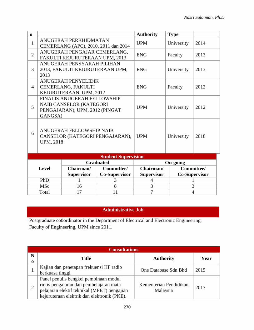
Nasri Sulaiman, Ph.D
270
o Authority Type
1 ANUGERAH PERKHIDMATAN
CEMERLANG (APC), 2010, 2011 dan 2014 UPM University 2014
2 ANUGERAH PENGAJAR CEMERLANG,
FAKULTI KEJURUTERAAN UPM, 2013 ENG Faculty 2013
3
ANUGERAH PENSYARAH PILIHAN
2013, FAKULTI KEJURUTERAAN UPM,
2013
ENG University 2013
4
ANUGERAH PENYELIDIK
CEMERLANG, FAKULTI
KEJURUTERAAN, UPM, 2012
ENG Faculty 2012
5
FINALIS ANUGERAH FELLOWSHIP
NAIB CANSELOR (KATEGORI
PENGAJARAN), UPM, 2012 (PINGAT
GANGSA)
UPM University 2012
6
ANUGERAH FELLOWSHIP NAIB
CANSELOR (KATEGORI PENGAJARAN),
UPM, 2018
UPM University 2018
Student Supervision
Level
Graduated On-going
Chairman/
Supervisor
Committee/
Co-Supervisor
Chairman/
Supervisor
Committee/
Co-Supervisor
PhD 1 3 4 1
MSc 16 8 3 3
Total 17 11 7 4
Administrative Job
Postgraduate co0ordinator in the Department of Electrical and Electronic Engineering,
Faculty of Engineering, UPM since 2011.
Consultations
N
o Title Authority Year
1 Kajian dan penetapan frekuensi HF radio
berkuasa tinggi One Database Sdn Bhd 2015
2
Panel penulis bengkel pembinaan modul
rintis pengajaran dan pembelajaran mata
pelajaran elektif teknikal (MPET) pengajian
kejuruteraan elektrik dan elektronik (PKE).
Kementerian Pendidikan
Malaysia 2017

Nasri Sulaiman, Ph.D
271
3
Panel penggubal dokumen standard
kurikulum dan pentaksiran (DSKP)
kurikulum standard sekolah menengah
(KSSM) mata pelajaran elektif teknikal
(MPET) pengajian kejuruteraan elektrik dan
elektronik (PKE).
Kementerian Pendidikan
Malaysia 2018