Nanofabrication of insulated scanning probes for electromechanical imaging in liquid solutions
19
Nanofabrication of insulated scanning probes for electromechanical imaging in liquid solutions Joo Hyon Noh 1 , Maxim Nikiforov 2 , Sergei V. Kalinin 2 , Alexey A. Vertegel 3 , and Philip D. Rack 1,2,* 1 Department of Materials Science and Engineering, University of Tennessee, Knoxville, TN 37996-2200 2 Center for Nanophase Materials Sciences, Oak Ridge National Laboratory, Oak Ridge, TN 37831 3 Department of Bioengineering, Clemson University, Clemson, SC 29634-0905 Abstract In this paper, the fabrication and electrical and electromechanical characterization of insulated scanning probes have been demonstrated in liquid solutions. The silicon cantilevers were sequentially coated with chromium and silicon dioxide, and the silicon dioxide was selectively etched at tip apex using focused electron beam induced etching (FEBIE) with XeF 2 The chromium layer acted not only as the conductive path from the tip, but also as an etch resistant layer. This insulated scanning probe fabrication process is compatible with any commercial AFM tip and can be used to easily tailor the scanning probe tip properties because FEBIE does not require lithography. The suitability of the fabricated probes is demonstrated by imaging of standard topographical calibration grid as well as piezoresponse force microscopy (PFM) and electrical measurements in ambient and liquid environments. 1. INTRODUCTION Combining force and electrical measurements using a conductive atomic force microscopy (AFM) probe has opened a new era to simultaneously measure the topography and electrical properties, and explore the interplay between electromechanical transport, and mechanical phenomena in inorganic and biological systems on the nanometer and ultimately molecular scales [1-2]. Recent examples include: 1) the application of high resolution scanning electrochemical microscopy [3]; 2) voltage induced conformational changes of ion channels embedded in cell membranes in a buffer solution [4-5]; 3) the analysis of membrane embedded redox proteins [6]; 4) local modification of the pH [7-8]; and 5) improving the image contrast by varying the electric field or local pH [9-10]. Accessing electrochemical and electromechanical properties of biological systems requires the measurement be done in a liquid to keep the system biologically viable and mimic the real environment of cells and bimolecules. Furthermore, liquid environment allows precise control of tip-surface forces and minimization of competing capillary interactions, hence minimizing surface damage. Additionally, the measurement of electromechanical interactions in living cells in many cases needs to be performed in a multicomponent cell culture medium. However, the conductivity of the medium typically causes stray current and electromechanical reactions, which makes precise control of dc and ac probe potentials * Corresponding author: PD Rack: [email protected]. NIH Public Access Author Manuscript Nanotechnology. Author manuscript; available in PMC 2011 January 11. Published in final edited form as: Nanotechnology. 2010 September 10; 21(36): 365302. doi:10.1088/0957-4484/21/36/365302. NIH-PA Author Manuscript NIH-PA Author Manuscript NIH-PA Author Manuscript
-
Upload
independent -
Category
Documents
-
view
2 -
download
0
Transcript of Nanofabrication of insulated scanning probes for electromechanical imaging in liquid solutions
Nanofabrication of insulated scanning probes forelectromechanical imaging in liquid solutions
Joo Hyon Noh1, Maxim Nikiforov2, Sergei V. Kalinin2, Alexey A. Vertegel3, and Philip D.Rack1,2,*1Department of Materials Science and Engineering, University of Tennessee, Knoxville, TN37996-22002Center for Nanophase Materials Sciences, Oak Ridge National Laboratory, Oak Ridge, TN378313Department of Bioengineering, Clemson University, Clemson, SC 29634-0905
AbstractIn this paper, the fabrication and electrical and electromechanical characterization of insulatedscanning probes have been demonstrated in liquid solutions. The silicon cantilevers weresequentially coated with chromium and silicon dioxide, and the silicon dioxide was selectivelyetched at tip apex using focused electron beam induced etching (FEBIE) with XeF2 The chromiumlayer acted not only as the conductive path from the tip, but also as an etch resistant layer. Thisinsulated scanning probe fabrication process is compatible with any commercial AFM tip and canbe used to easily tailor the scanning probe tip properties because FEBIE does not requirelithography. The suitability of the fabricated probes is demonstrated by imaging of standardtopographical calibration grid as well as piezoresponse force microscopy (PFM) and electricalmeasurements in ambient and liquid environments.
1. INTRODUCTIONCombining force and electrical measurements using a conductive atomic force microscopy(AFM) probe has opened a new era to simultaneously measure the topography and electricalproperties, and explore the interplay between electromechanical transport, and mechanicalphenomena in inorganic and biological systems on the nanometer and ultimately molecularscales [1-2]. Recent examples include: 1) the application of high resolution scanningelectrochemical microscopy [3]; 2) voltage induced conformational changes of ion channelsembedded in cell membranes in a buffer solution [4-5]; 3) the analysis of membraneembedded redox proteins [6]; 4) local modification of the pH [7-8]; and 5) improving theimage contrast by varying the electric field or local pH [9-10].
Accessing electrochemical and electromechanical properties of biological systems requiresthe measurement be done in a liquid to keep the system biologically viable and mimic thereal environment of cells and bimolecules. Furthermore, liquid environment allows precisecontrol of tip-surface forces and minimization of competing capillary interactions, henceminimizing surface damage. Additionally, the measurement of electromechanicalinteractions in living cells in many cases needs to be performed in a multicomponent cellculture medium. However, the conductivity of the medium typically causes stray current andelectromechanical reactions, which makes precise control of dc and ac probe potentials
*Corresponding author: PD Rack: [email protected].
NIH Public AccessAuthor ManuscriptNanotechnology. Author manuscript; available in PMC 2011 January 11.
Published in final edited form as:Nanotechnology. 2010 September 10; 21(36): 365302. doi:10.1088/0957-4484/21/36/365302.
NIH
-PA Author Manuscript
NIH
-PA Author Manuscript
NIH
-PA Author Manuscript
difficult [11-12]. Because bare conductive probes with metal coatings conduct significantcurrents in liquid electrolytes, probes that are insulated except at the tip apex are needed inorder to localize the potential and minimize the effective probe area.
The use of insulated probes for electromechanical and electrical probing in liquidenvironments requires (a) good dynamic properties and reflectivity of the lever, (b) goodinsulation except for the apex, (c) high apex conductivity, and (d) an apex geometryconsistent with high resolution [11]. For these insulated probes, several approaches havebeen reported for scanning tunneling microscopy (STM) and AFM tips (refs. in [2,13]).Various insulator materials have been explored such as cathodic or anodic-basedelectrophoretic paints [14-15], poly(phenylene oxide) by electropolymerization [5],photoresist by electrophoretic deposition[16], parylene C [17], fluorocarbons [13], andsilicon dioxide or silicon nitride by plasma enhanced chemical vapor deposition (PECVD)[18-19]. However, the key issue in insulated probe fabrication is how to open or expose avery small conductive area at the tip apex. In order to open the conductive area at the tipapex, focused ion beam (FIB) milling [13,17-19] or timed hydrofluoric (HF) acid wet etch[2,12,20] processes have mostly been used. In the case of FIB milling, however, it isdifficult to etch the insulator selectively because of physical etching nature of FIB milling.Therefore, the underlying metal layer with high conductivity is often damaged whichreduces the conductivity and the effective probe size, which is unfavorable for highresolution electrical measurements at the nanometer level. The timed HF wet etch process,while offering the advantage of batch processing, is very complex and it is difficult to etchsilicon dioxide only at the tip apex. As an alternative, the combined process with focused ionbeam etching (FIBE) and electron beam induced deposition (EBID) has been reportedrecently [11]. In that, the cantilever was coated with silicon dioxide and an opening wasfabricated through the oxide at the tip apex by FIBE, and then backfilled with tungsten byEBID to create an insulated probe with a conducting tip. Although the suitability of thisprobe was shown through piezoresponse force microscopy (PFM) measurements in liquid,there quality of the conductive probes was limited. Specifically, the contact resistance of Si– tungsten interface is very large due to very small area of contact and low purity (~55 at %)of EBID tungsten.
In this study, we discuss a new approach for insulated probe fabrication using focusedelectron beam induced etching (FEBIE) process, which can selectively etch silicon dioxideat the nanoscale apex. Because FEBIE does not require lithography, this process can beeasily implemented with any commercial AFM tip and can controllably sculpt the tip regionat the nanoscale. In addition to the FEBIE process, we discuss the other relevantnanofabrication issues relative to the metallization and the insulator deposition process.Finally, the suitability of the fabricated probes is demonstrated and discussed by imaging astandard grid as well as PFM and electrical measurements in ambient and conductive liquidenvironments.
2. Experimental details2.1. Tip fabrication
Commercial backside Al-coated Si atomic force microscope (AFM) cantilevers (ACD36/AlBS, MikroMasch) were used and Cr (Kurt J. Lesker, 99.9 wt.% purity, 2 in diameter, and0.25 in thickness) was deposited using RF-magnetron sputtering. The This Cr layer acts notonly as the conductive path, but also as an etch stop layer, since Cr has a high etch resistanceto fluorine based etching due to low volatility of Cr-F by-products. This allowed precisetuning of deposition conditions, and is instrumental to the probe development. Thedeposition conditions consisted of a 25 sccm Ar flow rate, 5 mTorr pressure, and 100 Wsputtering power. In order to control the density, surface roughness and thin film stress of
Noh et al. Page 2
Nanotechnology. Author manuscript; available in PMC 2011 January 11.
NIH
-PA Author Manuscript
NIH
-PA Author Manuscript
NIH
-PA Author Manuscript
the Cr films, substrate bias was varied with 0, 5, and 10 W using additional RF powersupply [21-22]. For Cr thickness and roughness measurements, an extra ~ 1 cm × 1cm pieceof silicon wafer accompanied each AFM tip deposition. Thickness and root-mean-square(rms) roughness were measured using AFM. The sheet resistance was measured using the 4-point probe method.
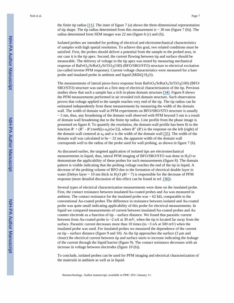
To insulate the scanning probes, silicon dioxide was deposited by plasma enhanced chemicalvapor deposition (PECVD) (Oxford 100). The deposition parameters consisted of a flow rateof 85 sccm Ar (95%)-SiH4 (5%) and 157 sccm N2O, at a total process pressure of 1 Torr,350 °C, and 20 W rf power. To make electrical contact, a portion of each the probe base wasshadowed using polyimide tape during the oxide deposition. Silicon dioxide films wereseparately deposited on Si wafers and thicknesses were measured using an ellipsometer (JAWoollam M-2000U). Individual AFM tips were then etched in an FEI Nova 600 dual beamscanning electron microscope (SEM). Silicon dioxide at the apex tip was etched using afocused-electron-beam-induced etching (FEBIE) process [23-24]. XeF2 vapor was locallyinjected using a gas injection system under electron beam irradiation. During etching, theAFM tips were tilted at 45° and periodically rotated for uniform etching. The electron beamparameters were 5 keV and 400 pA. Figure 1 schematically illustrates the insulated probefabrication sequence.
2.2. Tip characterization2.2.1. Tip sharpness evaluation using atomic force microscopy imaging of astandard grid—VEECO Dimension Atomic Force Microscope (AFM) equipped with aNanoscope III controller was used for imaging in ambient. Contact mode of microscopeoperation with deflection set-point 0.2 – 0.5 V was used. Standard grid of sharp spikes withapex sharpness ~ 1 nm radius of curvature located 2.12 μm apart (NT-MDT, TGT1) wasused.
2.2.1. Piezo-Force microscopy measurementsa. Liquid measurements: Asylum Research MFP-3D Atomic Force Microscope (AFM)with a static fluid cell was used for the imaging in MilliQ water. A piece of BiFeO3/SrRuO3/SrTiO3 (50 nm/ ~30 nm/ (100) single crystal) structure was used for PFM imaging in liquid.Single frequency lateral PFM measurements were performed by applying AC voltage usingfunction generator (Stanford Instruments DS340) with 10 V peak-to-peak at 24 kHz; surfaceoscillations were measured by lock-in (Signal Recovery 7280 DSP) with sensitivity at 5 μVand time constant 5 ms. The image was acquired at a scan rate 0.15 Hz.
b. Ambient measurements: VEECO Multimode Atomic Force Microscope (AFM)equipped with a Nanonis controller was used for imaging in ambient. Single frequencylateral PFM measurements were performed by driving tip with 4 V peak-to-peak at 30 kHz(Stanford Instruments DS340); surface oscillations were measured by lock-in (SignalRecovery 7280 DSP) with sensitivity at 1 mV and time constant 5 ms. The image wasacquired at a scan rate 0.25 Hz.
2.2.2. Current – distance measurements—Electrical characterization of the tip wasperformed using a two-terminal method. The AFM tip of interest served as one electrode,and a Au film on mica (SPI supplies 466PS-AB) served as second electrode. Au on micawas cleaned in O2 plasma before use. The current between AFM tip and Au on mica wasmeasured using 2 nA/V current amplifier (ORCA, Asylum Research).
Noh et al. Page 3
Nanotechnology. Author manuscript; available in PMC 2011 January 11.
NIH
-PA Author Manuscript
NIH
-PA Author Manuscript
NIH
-PA Author Manuscript
3. RESULTS AND DISCUSSIONS3.1. Tip fabrication
In order to localize the electrical potential in solution within the probed volume, theinsulating layer near apex edge needs to be etched in very small area to open conductivepath. Because of the ability to induce localized reactions by placement of a nanometer-sizedfocused electron beam [23-25], the FEBIE process was introduced to selectively etch theinsulator layer at the tip apex. However, the inner Si apex can be etched spontaneously byXeF2 vapor [26], thus an etch resistive layer with good electrical conductivity is neededbetween Si apex and the insulating layer. Here, Cr was chosen as an etch resistive layerbecause Cr has a high etch selectivity to a fluorine based etch process.
The sputtered metal thin films have intrinsic residual stress which can be varied with thedeposition conditions, such as working pressure and substrate bias [21-22]. Increasingsubstrate bias leads the residual stress transition from tensile to compressive. The residualstress in Cr films can cause the cantilever to bend upward (tensile) or downward(compressive) depending on the residual stress, which can cause laser alignment problemsduring scanning probe imaging. Therefore, the effects that substrate bias and thickness haveon the resultant thin film stress and cantilever bending were investigated. Figure 2 (a) – (f)show SEM images of the cantilevers as a function of substrate bias and Cr thin filmthickness. Firstly, Cr films were deposited with varying substrate bias. The deposition timewas 7 min and the resultant thicknesses were 18.4, 12.2 and 11.7 nm for 0, 5, and 10 Wsubstrate bias conditions, respectively (figure 2(a)-(c)). The thickness decrease is likely dueto densification and mild resputtering as the substrate bias increased. While the unbiasedcantilever had a concave curvature due to the intrinsic tensile stress, the Cr film depositedwith 5 W (-141 V dc self-bias) biased resulted in a cantilever with a slight convex curvaturewhich suggests it has a modest residual compressive stress. The dashed line in the figuresdenotes the straight line (zero stress) condition and is included to facilitate viewing thecantilever deflection. When the substrate bias was increased up to 10 W (-166 V dc self-bias) during Cr deposition, the cantilever showed higher convex curvature which isconsistent with previous reported results [21]. However, the residual stress is stronglydependent on not only substrate bias but also film thickness. In order to investigate thethickness effect on the residual stress, the deposition time was increased for the 5 Wsubstrate bias Cr deposition. When the deposition time was increased to 10 min (16.0 nmthick), the residual compressive stress was increased, therefore the cantilever bendingincreased as shown in figure 2(d). When the deposition time was decreased to 5 min (9.2nm, not shown here), no measurable cantilever bending was observed in the SEM imageswhich suggested very small residual stress.
The precise magnitudes of the cantilever tip deflection were measured using an opticalprofilometer [27], and the stresses were calculated using Stoney's equation [28-29].
where, Ys is Young's modulus for the substrate, ds is the thickness of the substrate, R is thesubstrate curvature radius, υs is Poisson's ratio of the substrate, and df is the film thickness.Figure 2 (g) shows a typical top-view optical micrograph and profilometer scan for the AFMcantilever with 5 W substrate biased Cr thin film. Due to the fact that the profilometer scanwas distorted at the end of cantilever due to the apex, the curvature radius was obtained atthe middle position of cantilever using the scanning probe image processor software [30].The thickness of back side coated Al was very thin, and hence the contribution of Al was
Noh et al. Page 4
Nanotechnology. Author manuscript; available in PMC 2011 January 11.
NIH
-PA Author Manuscript
NIH
-PA Author Manuscript
NIH
-PA Author Manuscript
neglected. Figure 2 (h) shows the calculated film stress (solid symbol) and the product ofstress and thickness (open symbol) as a function of thickness and substrate bias. As thethickness increased, the magnitude of the average tensile and compressive stresses bothdecreased. Meanwhile, the product of stress and thickness was increased, which is inverselyproportional to the radius of curvature and commonly used to interpret substrate curvaturemeasurements [31]. Figure 2 (e) and (f) shows the cantilever SEM images after silicondioxide deposition for the 0 and 5 W substrate bias, respectively. The PECVD silicondioxide was deposited for 2 min with a thickness of ~ 138 nm, which shows a mildcompressive residual stress. Therefore, the cantilever with the Cr film deposited with zerosubstrate bias and a tensile residual stress was compensated with the SiO2 film and is nolonger bent. In the case of 5 W bias the original compressive stress is enhanced and thus theoxide coated Cr cantilever has a higher convex curvature. For a PECVD process, theresidual stress, which consists of an intrinsic and thermal stress, is strongly related to thedeposition parameters and substrate temperature [32]. While the detailed mechanisms issubject for future studies, here we were able to minimize the effect of the compressive stressintroduced by the silicon dioxide by decreasing the silicon dioxide deposition time (andthickness) to 1 min (69 nm).
In addition to the thin film stress, the roughness of the deposited Cr thin film is also animportant factor for AFM tip fabrication. A smoother surface is more favorable for highresolution. The surface roughness was measured by AFM for the scan size of 500 × 500 nmas a function of substrate bias (not shown). While the unbiased Cr film has a root-mean-square (rms) roughness of 0.583 nm, the 5 W and 10 W biased Cr films have rmsroughnesses of 0.283 nm and 0.308, respectively. Compared to unbiased Cr film, smoothersurface and thinner thickness indicates the densification in biased Cr film due to energeticparticle bombardment. The densification using substrate bias has another merit. Because theCr film is used as the etch resistive layer, it has to block XeF2 penetration to preventspontaneous etching of the Si apex. If there are voids in the thin film, XeF2 can etch the Siapex through the voids. For instance, we tested the etch resistance of commercial Pt or Aucoated Si tips but all tips failed due to the spontaneous etching of the Si apex, as shown infigure 3. The etching is likely due to defects, such as voids, in the Pt and Au. Figure 3 (a)and (b) show the etched tip images taken from the top and 45° tilted view, respectively, forthe commercial Pt coated tip with 150 nm-thick SiO2 film deposited by PECVD. This tipwas tilted with 45° degree during etching. The void like defects in Pt film are clearly shownin figure 3 (b). Figure 3 (c) and (d) show another failed tip images taken from top and 45°tilted view, respectively, for the commercial Pt coated tip with 30 nm-thick SiO2 filmdeposited by sputtering. This tip was etched with top-down configuration. One plane of theapex was aggressively spontaneously etched by the XeF2.
Clearly a critical thickness is required in order to prevent XeF2 penetration, however, theradius of curvature of the tip is increased with increasing thickness. Because substrate biascan suppress void formation through densification, and thus require a thinner etch resistantfilm, very thin biased Cr film is favorable to maintain a sharp Si apex required for highresolution imaging. However, further increase of substrate bias caused an increase in theroughness. The roughness of the 10 W biased Cr film increased to 0.308 nm compared to0.283 nm of 5 W biased film, which is likely due to higher re-sputtering.
Additionally, the resistivity was investigated for the unbiased and biased films because theconductivity of Cr film is also important. The resistivity was calculated from the sheetresistance using 4 point probe method. Figure 4 shows the resistivity as a function ofsubstrate bias. While the unbiased Cr film had a resistivity of 3.5 × 10⁻⁴ Ω-cm, the 5 W and10 W biased Cr films have resistivity of 2.8 and 3.1 × 10⁻⁵ Ω-cm, respectively. Theresistivity of biased Cr films is comparable to the bulk Cr resistivity of 1.29 × 10⁻⁵ Ω-cm
Noh et al. Page 5
Nanotechnology. Author manuscript; available in PMC 2011 January 11.
NIH
-PA Author Manuscript
NIH
-PA Author Manuscript
NIH
-PA Author Manuscript
[33]. As mentioned above, the low resistivity of biased films is likely due to densificationthrough energetic particle bombardment and sputtering of adsorbed oxygen (or othercontaminants). As demonstrated for the metal layer, there are important trade-offs that haveto be evaluated such as stress, surface roughness, conductivity, and etch resistance.
In our experiments, Cr films with 5 W substrate bias were chosen for an optimized etchresistive layer with low resistivity and roughness. After the PECVD silicon dioxide wasdeposited on Cr films, the AFM tips were processed using the FEBIE process. Silicondioxide can be only etched by XeF2 with assistance by ion or electron irradiation [26]. Thesilicon dioxide focused electron beam etching mechanism with a XeF2 precursor issuggested to proceed via a two-step etch process [24]. This model involves the reductionprocess by the electron-stimulated desorption of oxygen at the silicon dioxide surface, andsubsequent silicon etching by XeF2. Therefore etching only can occur in the electron-beamirradiation region. The etch rate is strongly dependent on the electron beam energy, current,XeF2 pressure, and pixel dwell time. In our experiment, the etching was performed in thearea scan mode with 50 ns pixel dwell time. Figure 5 shows SEM images at each processstep. For figure 5, the Cr and SiO2 deposition times were 7 and 2 min, respectively, whichcorresponded to 12.2 nm and 138 nm, respectively. From the SEM images, as shown infigure 5 (a) – (c), the tip radii of curvature were measured to be approximately 18, 30, and285 nm for bare, Cr, and SiO2 deposited tip, respectively. Before etching, the tip positionwas adjusted to the XeF2 gas injector as close as possible (<500 μm) and the magnificationwas set as × 400,000. Figure 5 (d) – (f) show SEM images during different stages of theFEBIE process. In order to realize uniform etching, the tip was tilted 45° and periodicallyrotated. The final images of the etched tip are shown in figure 5 (g) – (i), taken from the top,45° tilt, and 90° rotation view, respectively. The revealed apex has dimensions of 284 nmheight and 164 nm width. There was not any evidence for inner Si attack by XeF2 from thehigh magnification SEM images. The estimated SiO2 thickness at apex was approximately255 nm from the figure 5 (h), although the SiO2 thickness was 138 nm measured at flatsample deposited separately. This enhanced thickness is likely due to field enhancement atthe apex during the PECVD process.
These observations indicate that there is a trade-off in performance and fabrication withincreased insulator thickness. For thicker films, lower leakage currents and higherbreakdown voltages are realized. However, longer processing times, more compressivestress, and possible interference of the insulator sidewalls with the scanning probemeasurement are detriments of thicker insulators. Figure 6 shows the SEM images at eachprocess step for a tip with a reduced silicon dioxide deposition thickness (1 min of SiO2deposition time) which corresponded to 69 nm thickness measured on the flat substrate andestimated to be 123 nm at the apex tip (figure 6 (f)). In order to reduce the tip radius, the Crdeposition time was also decreased to 5 min, which corresponded to 10.5 nm. The tip radiiof curvature were measured to be ~ 22 and 140 nm after Cr and SiO2 deposition,respectively. The final images of the uniformly etched tip are shown in figure 6 (c) and (g),taken from the top and 45° tilt view, respectively. The exposed apex has dimensions of 199nm height and 166 nm width.
3.2. Tip characterization: imaging, piezo-force microscopy (PFM) and electricalcharacterization of the isolated tip
In order to evaluate the quality of the tip prepared according to the procedure describedabove the tip was used for imaging of standard grid as well as for PFM and electricalmeasurements (see Experimental description for the detailed description of techniques).Figure 7 (a) shows the tapping mode AFM image of the standard grid consisting of sharpspikes with radius of curvature ~ 1 nm regularly spaced on the surface, which allowsestimation of the tip radius because the broadening of the spike on the image happens due to
Noh et al. Page 6
Nanotechnology. Author manuscript; available in PMC 2011 January 11.
NIH
-PA Author Manuscript
NIH
-PA Author Manuscript
NIH
-PA Author Manuscript
the finite tip radius [11]. The inset of figure 7 (a) shows the three-dimensional representationof tip shape. The tip radius determined from this measurement is ~ 30 nm (figure 7 (b)). Theradius determined form SEM images was 22 nm (figure 6 (c) and (f)).
Isolated probes are intended for probing of electrical and electromechanical characteristicsof samples with high spatial resolution. To achieve this goal, two related conditions must besatisfied. First, the probes should deliver a potential from the sample to the probed area, inour case it is the tip apex. Second, the current flowing between tip and surface should bemeasurable. The delivery of voltage to the tip apex was tested by measuring mechanicalresponse of BaFeO3/SrRuO3/SrTiO3(100) (BFO/SRO/STO) structure to electrical excitation(so-called inverse PFM response). Current voltage characteristics were measured for a bareprobe and insulated probe in ambient and liquid (MilliQ H2O).
The measurements of lateral piezo-force response from BaFeO3/SrRuO3/SrTiO3(100) (BFO/SRO/STO) structure was used as a first step of electrical characterization of the tip. Previousstudies show that such a sample has a rich in-plane domain structure [34]. Figure 8 showsthe PFM measurements performed in air revealed rich domain structure. Such observationproves that voltage applied to the sample reaches very end of the tip. The tip radius can beestimated independently from these measurements by measuring the width of the domainwall. The width of domain wall in PFM experiments on BFO/SRO/STO structure is usually~ 5 nm, thus, any broadening of the domain wall observed with PFM beyond 5 nm is a resultof domain wall broadening due to the finite tip radius. Line profile from the phase image ispresented on figure 8. To quantify the resolution, the domain-wall profile has been fit to thefunction R- + (R+ - R-)·tanh[(x-x0)/(w/2)], where R+ (R-) is the response on the left (right) ofthe domain wall centered at x0 and w is the width of the domain wall [35]. The width of thedomain wall was calculated to be ~ 32 nm, the apparent width of the domain wallcorresponds well to the radius of the probe used for wall probing, as shown in figure 7 (b).
As discussed earlier, the targeted application of isolated tips are electromechanicalmeasurements in liquid, thus, lateral PFM imaging of BFO/SRO/STO was done in H2O todemonstrate the applicability of these probes for such measurements (figure 8). The domainpattern is visible indicating that the probing voltage reaches the end of the tip in liquid. Adecrease of the probing volume of BFO due to the formation of electrical double layer inwater (Debye layer ~ 10 nm thick in H2O pH ~ 7) is responsible for the decrease of PFMresponse (more detailed discussion of this effect can be found in ref. [36]).
Several types of electrical characterization measurements were done on the insulated probe.First, the contact resistance between insulated/Au-coated probes and Au was measured inambient. The contact resistance for the insulated probe was ~ 62 kΩ, comparable to theconventional Au-coated probes The difference in resistance between isolated and Au-coatedprobe was quite small indicating applicability of this probe for electrical measurements. Inliquid we compared measurements of current between insulated/Au-coated probes and Aucounter electrode as a function of tip – surface distance. We found that parasitic currentbetween from Au-coated probe is ~2 nA at 30 mV, when the tip is located far away from thesurface. Parasitic current decreases more than 10 times (to ~3 nA at 500 mV) when theinsulated probe was used. For insulated probes we measured the dependence of the currenton tip – surface distance (figure 9 and 10). As the tip approaches the surface (3 μm andcloser) the electrical current between tip and surface starts to increase indicating the leakageof the current through the liquid barrier (figure 9). The contact resistance decreases with anincrease in voltage between electrodes (figure 10 (b)).
To conclude, isolated probes can be used for PFM imaging and electrical characterization ofthe materials in ambient as well as in liquid.
Noh et al. Page 7
Nanotechnology. Author manuscript; available in PMC 2011 January 11.
NIH
-PA Author Manuscript
NIH
-PA Author Manuscript
NIH
-PA Author Manuscript
4. CONCLUSIONIn summary, we have demonstrated the fabrication of insulated probes for electrical andelectromechanical imaging in liquids using FEBIE process which can selectively silicondioxide at the nanoscale apex. In addition to FEBIE, we discuss the other relevantnanofabrication issues relative to the metallization and the insulator deposition process.Finally, the suitability of the fabricated probes is demonstrated and discussed by imaging ofstandard grid as well as PFM and electrical measurements. This fabrication process ofinsulated probes can be easily implemented with any commercial AFM tip because FEBIEdoes not require lithography process.
AcknowledgmentsThis work was supported in part by NIH grant No. RR024449. A portion of this research was conducted at theCenter for Nanophase Materials Sciences, which is sponsored at Oak Ridge National Laboratory by the Division ofScientific User Facilities, U.S. Department of Energy.
Reference list1. Macpherson JV, Unwin PR. Combined Scanning Electrochemical−Atomic Force Microscopy. Anal
Chem 2000;72:276–85. [PubMed: 10658320]2. Frederix P, Gullo MR, Akiyama T, Tonin A, de Rooij NF, Staufer U, Engel A. Assessment of
insulated conductive cantilevers for biology and electrochemistry. Nanotechnology 2005;16:997–1005.
3. Zoski CG, Liu B, Bard AJ. Scanning electrochemical microscopy: Theory and characterization ofelectrodes of finite conical geometry. Anal Chem 2004;76:3646–54. [PubMed: 15228336]
4. Drake B, Prater CB, Weisenhorn AL, Gould SAC, Albrecht TR, Quate CF, Cannell DS, HansmaHG, Hansma PK. Imaging crystals, polymers, and processes in water with the atomic microscope.Science 1989;243:1586–9. [PubMed: 2928794]
5. Engel A, Muller DJ. Observing single biomolecules at work with the atomic force microscope. Nat.Struct. Biol 2000;7:715–8. [PubMed: 10966636]
6. Frederix PLTM, Bosshart PD, Akiyama T, Chami M, Gullo MR, Blackstock JJ, Dooleweerdt K, deRooij NF, Staufer U, Engel A. Conductive supports for combined AFM-SECM on biologicalmembranes. Nanotechnology 2008;19:384004.
7. Bullard JW, Kershner RJ, Cima MJ. Scanning probe characterization of localized pH changes on asapphire surface in the presence of an applied field. Mater. Res. Soc. Symp. Proc 2004;782:A3.1.1–6.
8. Jang JW, Sanedrin RG, Maspoch D, Hwang S, Fujigaya T, Jeon YM, Vega RA, Chen XD, MirkinCA. Electrically biased nanolithography with KOH-coated AFM tips. Nano Lett 2008;8:1451–5.[PubMed: 18376868]
9. Muller DJ, Engel A. The height of biomolecules measured with the atomic force microscopedepends on electrostatic interactions. Biophys. J 1997;73:1633–44. [PubMed: 9284330]
10. Muller DJ, Fotiadis D, Scheuring S, Muller SA, Engel A. Electrostatically balanced subnanometerimaging of biological specimens by atomic force microscope. Biophys. J 1999;76:1101–11.[PubMed: 9916042]
11. Rodriguez BJ, Jesse S, Seal K, Baddorf AP, Kalinin SV, Rack PD. Fabrication, dynamics, andelectrical properties of insulated scanning probe microscopy probes for electrical andelectromechanical imaging in liquids. Appl Phys Lett 2007;91:093130.
12. Akiyama T, Gullo MR, de Rooij NF, Tonin A, Hidber HR, Frederix P, Engel A, Staufer U.Development of insulated conductive probes with platinum silicide tips for atomic forcemicroscopy in cell biology. Japan. J. Appl. Phys 2004;43:3865–7.
13. Wiedemair J, Balu B, Moon JS, Hess DW, Mizaikoff B, Kranz C. Plasma-deposited fluorocarbonfilms: Insulation material for microelectrodes and combined atomic force microscopy-scanningelectrochemical microscopy probes. Anal Chem 2008;80:5260–5. [PubMed: 18510344]
Noh et al. Page 8
Nanotechnology. Author manuscript; available in PMC 2011 January 11.
NIH
-PA Author Manuscript
NIH
-PA Author Manuscript
NIH
-PA Author Manuscript
14. Durig U, Gimzewski JK, Pohl DW. Experimental-Observation of Forces Acting during ScanningTunneling Microscopy. Phys. Rev. Lett 1986;57:2403–6. [PubMed: 10033716]
15. Frederix PT, Hoogenboom BW, Fotiadis D, Muller DJ, Engel A. Atomic force microscopy ofbiological samples. Mrs Bull 2004;29:449–55.
16. Lantz MA, O'Shea SJ, Welland ME. Characterization of tips for conducting atomic forcemicroscopy in ultrahigh vacuum. Rev. Sci. Instrum 1998;69:1757–64.
17. Kueng A, Kranz C, Mizaikoff B, Lugstein A, Bertagnolli E. Combined scanning electrochemicalatomic force microscopy for tapping mode imaging. Appl Phys Lett 2003;82:1592–4.
18. Kranz C, Friedbacher G, Mizaikoff B, Lugstein A, Smoliner J, Bertagnolli E. Integrating anUltramicroelectrode in an AFM Cantilever:□ Combined Technology for Enhanced Information.Anal Chem 2001;73:2491–500. [PubMed: 11403290]
19. Lugstein A, Bertagnolli E, Kranz C, Kueng A, Mizaikoff B. Integrating micro- and nanoelectrodesinto atomic force microscopy cantilevers using focused ion beam techniques. Appl Phys Lett2002;81:349–51.
20. Gullo MR, Frederix PLTM, Akiyama T, Engel A, deRooij NF, Staufer U. Characterization ofmicrofabricated probes for combined atomic force and high-resolution scanning electrochemicalmicroscopy. Anal Chem 2006;78:5436–42. [PubMed: 16878880]
21. Misra A, Nastasi M. Limits of residual stress in Cr films sputter deposited on biased substrates.Appl Phys Lett 1999;75:3123–5.
22. Thornton JA, Hoffman DW. Stress-Related Effects in Thin-Films. Thin Solid Films 1989;171:5–31.
23. Randolph SJ, Fowlkes JD, Rack PD. Focused, nanoscale electron-beam-induced deposition andetching. Crit Rev Solid State 2006;31:55–89.
24. Randolph SJ, Fowlkes JD, Rack PD. Focused electron-beam-induced etching of silicon dioxide. JAppl Phys 2005;98:034902.
25. Lassiter MG, Rack PD. Nanoscale electron beam induced etching: a continuum model thatcorrelates the etch profile to the experimental parameters. Nanotechnology 2008;19:455306.
26. Winters HF, Coburn JW. Etching of silicon with XeF2 vapor. Appl Phys Lett 1979;34:70–3.27. Guo Q, Li M, Li Y, Shi L, Chong TC, Kalb JA, Thompson CV. Crystallization-induced stress in
thin phase change films of different thicknesses. Appl Phys Lett 2008;93:221907–3.28. Ohring, M. Materials science of thin films. Academic Press; Boston: 1992.29. Stoney GG. The Tension of Metallic Films Deposited by Electrolysis. Proc. R. Soc. London, Ser.
A 1909;82:172–5.30. Scanning Probe Image Processor (SPIP). Ver. 5.1.1. http://www.imagemet.com/31. Seel SC, Thompson CV, Hearne SJ, Floro JA. Tensile stress evolution during deposition of
Volmer--Weber thin films. J Appl Phys 2000;88:7079–88.32. Tarraf A, Daleiden J, Irmer S, Prasai D, Hillmer H. Stress investigation of PECVD dielectric layers
for advanced optical MEMS. J. Micromech. Microeng 2004;14:317–23.33. Kulkarni AK, Chang LC. Electrical and structural characteristics of chromium thin films deposited
on glass and alumina substrates. Thin Solid Films 1997;301:17–22.34. Balke N, Choudhury S, Jesse S, Huijben M, Chu YH, Baddorf AP, Chen LQ, Ramesh R, Kalinin
SV. Deterministic control of ferroelastic switching in multiferroic materials. Nat. Nanotechnol2009;4:868–75. [PubMed: 19893529]
35. Bode M. Spin-polarized scanning tunnelling microscopy. Rep. Prog. Phys 2003;66:523–82.36. Rodriguez BJ, Jesse S, Baddorf AP, Kalinin SV. High resolution electromechanical imaging of
ferroelectric materials in a liquid environment by piezoresponse force microscopy. Phys. Rev. Lett2006;96:4.
Noh et al. Page 9
Nanotechnology. Author manuscript; available in PMC 2011 January 11.
NIH
-PA Author Manuscript
NIH
-PA Author Manuscript
NIH
-PA Author Manuscript
Figure 1.Schematic illustration of the insulated probe fabrication sequence.
Noh et al. Page 10
Nanotechnology. Author manuscript; available in PMC 2011 January 11.
NIH
-PA Author Manuscript
NIH
-PA Author Manuscript
NIH
-PA Author Manuscript
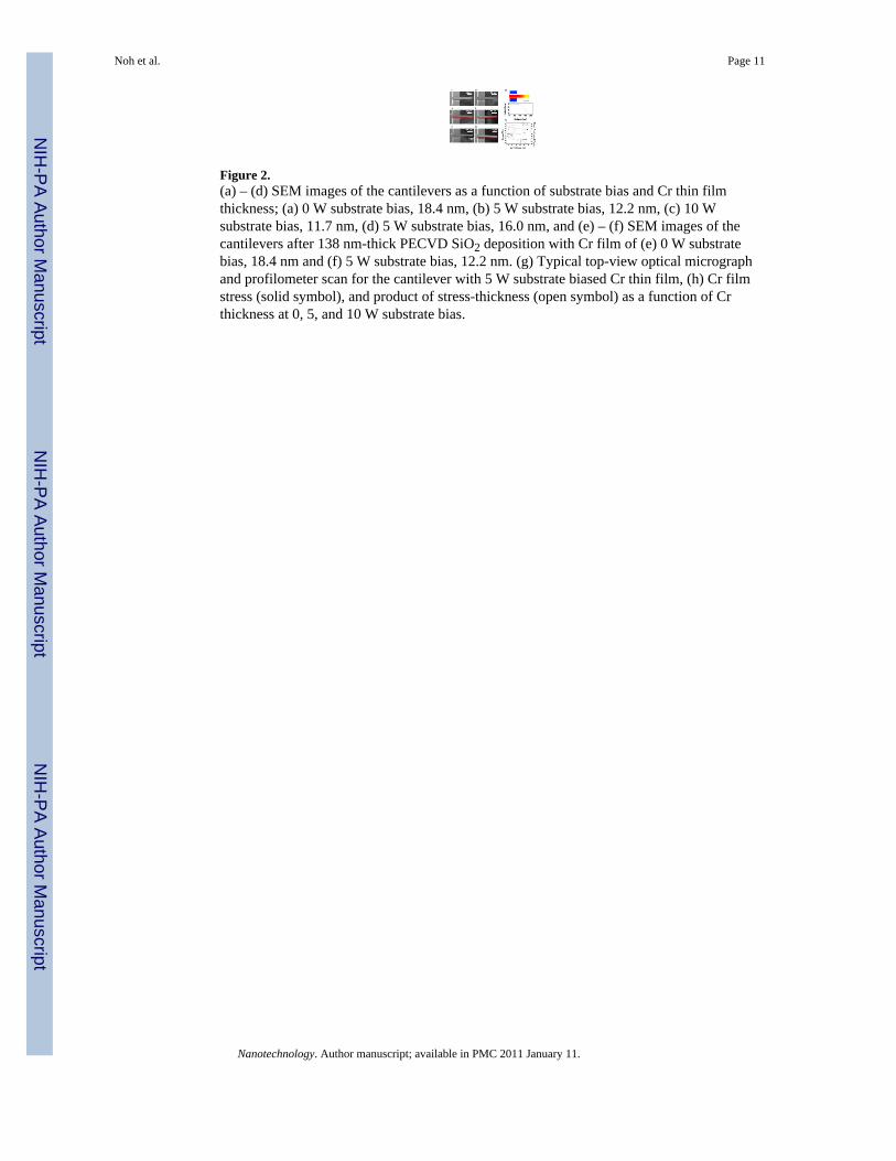
Figure 2.(a) – (d) SEM images of the cantilevers as a function of substrate bias and Cr thin filmthickness; (a) 0 W substrate bias, 18.4 nm, (b) 5 W substrate bias, 12.2 nm, (c) 10 Wsubstrate bias, 11.7 nm, (d) 5 W substrate bias, 16.0 nm, and (e) – (f) SEM images of thecantilevers after 138 nm-thick PECVD SiO2 deposition with Cr film of (e) 0 W substratebias, 18.4 nm and (f) 5 W substrate bias, 12.2 nm. (g) Typical top-view optical micrographand profilometer scan for the cantilever with 5 W substrate biased Cr thin film, (h) Cr filmstress (solid symbol), and product of stress-thickness (open symbol) as a function of Crthickness at 0, 5, and 10 W substrate bias.
Noh et al. Page 11
Nanotechnology. Author manuscript; available in PMC 2011 January 11.
NIH
-PA Author Manuscript
NIH
-PA Author Manuscript
NIH
-PA Author Manuscript
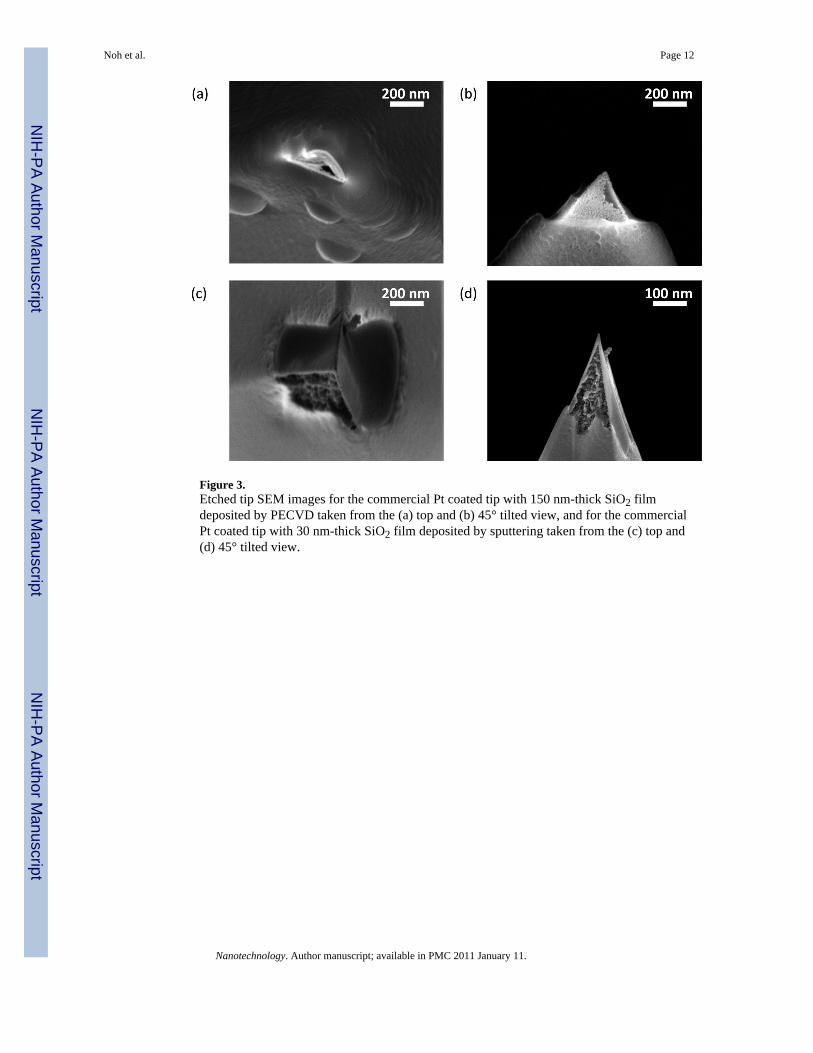
Figure 3.Etched tip SEM images for the commercial Pt coated tip with 150 nm-thick SiO2 filmdeposited by PECVD taken from the (a) top and (b) 45° tilted view, and for the commercialPt coated tip with 30 nm-thick SiO2 film deposited by sputtering taken from the (c) top and(d) 45° tilted view.
Noh et al. Page 12
Nanotechnology. Author manuscript; available in PMC 2011 January 11.
NIH
-PA Author Manuscript
NIH
-PA Author Manuscript
NIH
-PA Author Manuscript
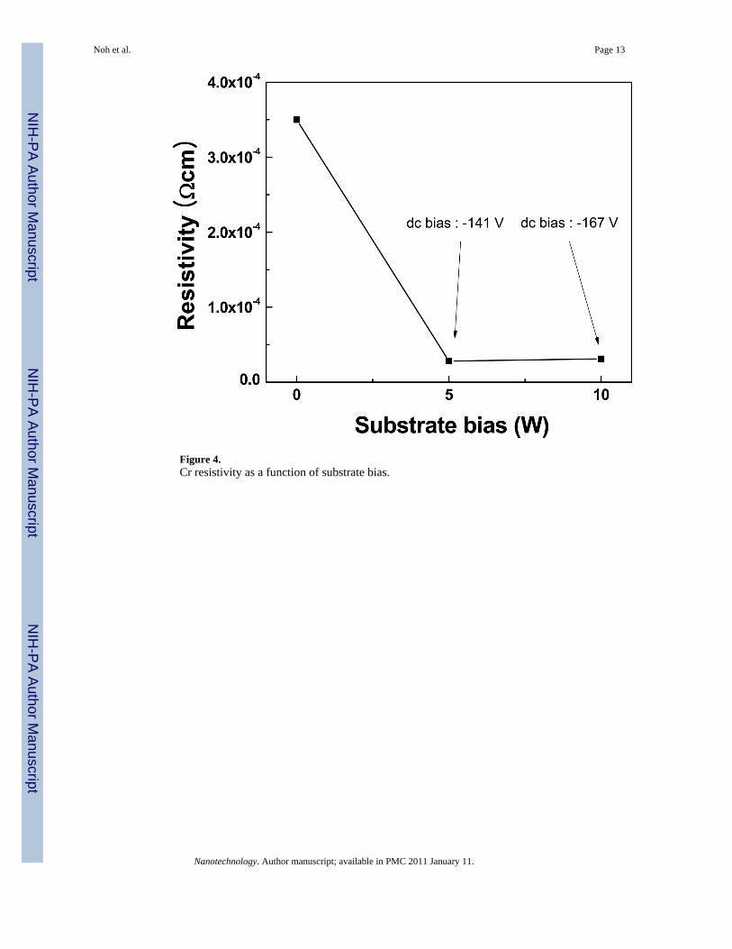
Figure 4.Cr resistivity as a function of substrate bias.
Noh et al. Page 13
Nanotechnology. Author manuscript; available in PMC 2011 January 11.
NIH
-PA Author Manuscript
NIH
-PA Author Manuscript
NIH
-PA Author Manuscript
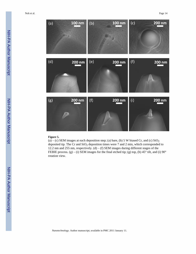
Figure 5.(a) – (c) SEM images at each deposition step; (a) bare, (b) 5 W biased Cr, and (c) SiO2deposited tip. The Cr and SiO2 deposition times were 7 and 2 min, which corresponded to12.2 nm and 255 nm, respectively. (d) – (f) SEM images during different stages of theFEBIE process. (g) – (i) SEM images for the final etched tip; (g) top, (h) 45° tilt, and (i) 90°rotation view.
Noh et al. Page 14
Nanotechnology. Author manuscript; available in PMC 2011 January 11.
NIH
-PA Author Manuscript
NIH
-PA Author Manuscript
NIH
-PA Author Manuscript
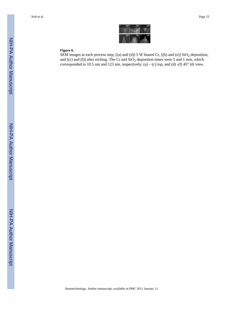
Figure 6.SEM images at each process step; [(a) and (d)] 5 W biased Cr, [(b) and (e)] SiO2 deposition,and [(c) and (f)] after etching. The Cr and SiO2 deposition times were 5 and 1 min, whichcorresponded to 10.5 nm and 123 nm, respectively; (a) – (c) top, and (d) -(f) 45° tilt view.
Noh et al. Page 15
Nanotechnology. Author manuscript; available in PMC 2011 January 11.
NIH
-PA Author Manuscript
NIH
-PA Author Manuscript
NIH
-PA Author Manuscript
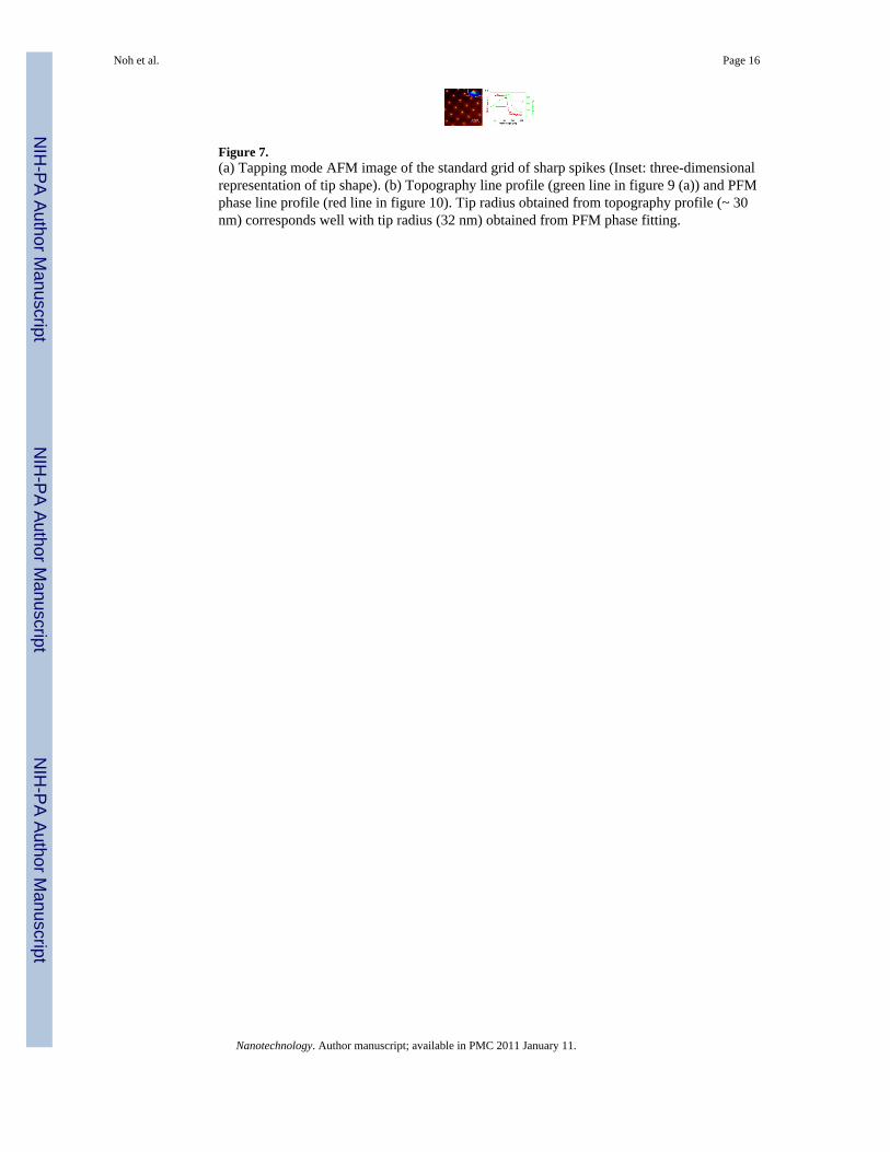
Figure 7.(a) Tapping mode AFM image of the standard grid of sharp spikes (Inset: three-dimensionalrepresentation of tip shape). (b) Topography line profile (green line in figure 9 (a)) and PFMphase line profile (red line in figure 10). Tip radius obtained from topography profile (~ 30nm) corresponds well with tip radius (32 nm) obtained from PFM phase fitting.
Noh et al. Page 16
Nanotechnology. Author manuscript; available in PMC 2011 January 11.
NIH
-PA Author Manuscript
NIH
-PA Author Manuscript
NIH
-PA Author Manuscript
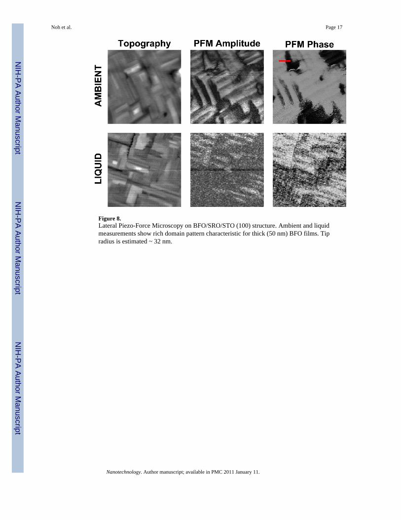
Figure 8.Lateral Piezo-Force Microscopy on BFO/SRO/STO (100) structure. Ambient and liquidmeasurements show rich domain pattern characteristic for thick (50 nm) BFO films. Tipradius is estimated ~ 32 nm.
Noh et al. Page 17
Nanotechnology. Author manuscript; available in PMC 2011 January 11.
NIH
-PA Author Manuscript
NIH
-PA Author Manuscript
NIH
-PA Author Manuscript
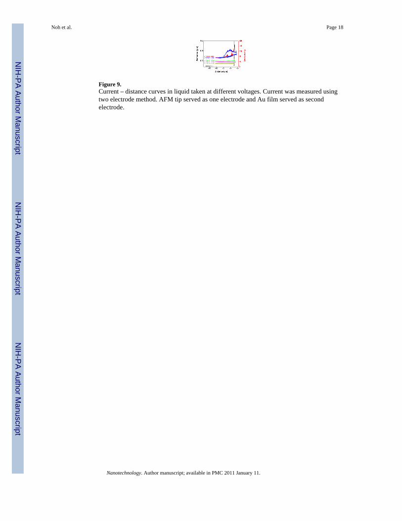
Figure 9.Current – distance curves in liquid taken at different voltages. Current was measured usingtwo electrode method. AFM tip served as one electrode and Au film served as secondelectrode.
Noh et al. Page 18
Nanotechnology. Author manuscript; available in PMC 2011 January 11.
NIH
-PA Author Manuscript
NIH
-PA Author Manuscript
NIH
-PA Author Manuscript
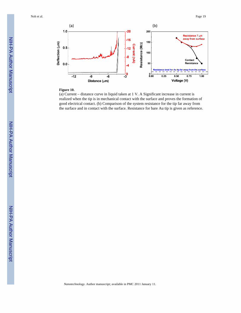
Figure 10.(a) Current – distance curve in liquid taken at 1 V. A Significant increase in current isrealized when the tip is in mechanical contact with the surface and proves the formation ofgood electrical contact. (b) Comparison of the system resistance for the tip far away fromthe surface and in contact with the surface. Resistance for bare Au tip is given as reference.
Noh et al. Page 19
Nanotechnology. Author manuscript; available in PMC 2011 January 11.
NIH
-PA Author Manuscript
NIH
-PA Author Manuscript
NIH
-PA Author Manuscript