
My title - Inspire HEP
246
HIGH VOLTAGE DEVELOPMENT AND LASER SPECTROSCOPY FOR THE SEARCH OF THE PERMANENT ATOMIC ELECTRIC DIPOLE MOMENT OF RADIUM-225 By Roy Anthony Ready A DISSERTATION Submitted to Michigan State University in partial fulfillment of the requirements for the degree of Physics – Doctor of Philosophy June 10, 2021
-
Upload
khangminh22 -
Category
Documents
-
view
1 -
download
0
Transcript of My title - Inspire HEP

HIGH VOLTAGE DEVELOPMENT AND LASER SPECTROSCOPY FOR THE SEARCHOF THE PERMANENT ATOMIC ELECTRIC DIPOLE MOMENT OF RADIUM-225
By
Roy Anthony Ready
A DISSERTATION
Submitted toMichigan State University
in partial fulfillment of the requirementsfor the degree of
Physics – Doctor of Philosophy
June 10, 2021

ABSTRACT
HIGH VOLTAGE DEVELOPMENT AND LASER SPECTROSCOPY FOR THE SEARCHOF THE PERMANENT ATOMIC ELECTRIC DIPOLE MOMENT OF RADIUM-225
By
Roy Anthony Ready
Permanent electric dipole moments (EDMs) violate parity (P ), time reversal (T ), and
combined charge-conjugation and parity transformation (CP ) assuming CP T symme-
try. Radium-225 is expected to have an enhanced atomic EDM because its nucleus is
octupole-deformed. In the Ra EDM experiment, 225Ra atoms are vaporized in an effusive
oven, slowed and collimated by cooling lasers, and trapped between two high voltage
electrodes. We measure the spin precession frequency of the trapped radium in uniform,
applied electric and magnetic fields and search for a frequency shift correlated with the
electric field, the signature of a nonzero EDM.
There are two first generation radium EDM measurements. The most recent measure-
ment reduced the upper limit to 1.4× 10⁻²³ e cm. In the upcoming second generation
measurements, we will implement key upgrades to improve our EDM sensitivity by up
to three orders of magnitude. This thesis focuses on my work improving the electric field
strength and laser cooling efficiency for the second generation measurements.
Additionally, The Facility of Rare Isotope Beams is expected to produce Radium-225
that can be harvested for EDM measurements. We are developing a laser induced flu-
orescence experiment that will measure the absolute flux of a directed beam of atoms
emitted from an effusive oven. The flux measurement will use stable surrogate isotopes
to characterize radium harvesting efficiency. I will report the results of our initial efforts
modeling and measuring the atomic beam fluorescence of multiple atom sources.

Copyright byROY ANTHONY READY
June 10, 2021

ACKNOWLEDGEMENTS
I have been exceedingly fortunate in having the support of wonderful friends, mentors,
and family. I am grateful to them for helping me on this journey.
Thanks my friends that I grew up with and am now growing old with: Joe, Jordan,
Carissa, Johnny, Nick, and Shea. Whenever see each other, which sometimes is not so
often, we pick things right up as if I’d never gone off to grad school. It’s great.
Thanks to my professors and mentors, from community college to graduate school:
Ron Armale (who encouraged me to apply for that JPL program that really kicked things
off), Matt Dietrich, Jiyeong Gu, Morten Hjorth-Jensen, Prashanth Jaikumar, Kay Kolos,
Glenn Orton, Galen Pickett, and Michael Syphers. These folks supported me, got to
know me, and helped shape me into the scientist I am today.
Thanks to my Michigan friends: Deanna Ambrose, Bakul Agarwal, Lisa Carpen-
ter, Boe Colabewala, Brandon Elman, Alec Hamaker, Monica Hamaker, Max Hughes,
Jake Huneau, Andrew Lajoie, Brenden Longfellow, Andrew Miller, Elizabeth Miller, Al-
ice Mills, Daniel Rhodes, Sean Sweany, Zak Tilocco, Corah Walker, Lindsay Weinheimer,
and Erin White. As important as the science was, so too was the joy I found in commiser-
ating, relaxing, laughing, and building relationships with you all.
Thanks to all my Spinlab labmates. They are a fantastic team and I’m glad they were
with me to share in the fun parts, the painful parts, the setbacks, and the successes that
come with our line of work. Ben Loseth was always ready to lend a hand with clean
room work, although he may have occasionally rued that standing offer from time to
time! Tenzin Rabga is a great hang on long drives to faraway workshops and an excellent
soccer teammate. When we worked together at Argonne we would try to make the radium
lasers behave in the morning and joke about modeling the Argonne geese population as
a “goose-ian” distribution on the walk to the cafeteria for lunch.
Thanks to my advisor Jaideep Singh. I joined Spinlab for the lasers, but I stayed for
iv

the. . . well, the lasers, but also the incredible amount of fun I had working with Jaideep
and in the supportive, exciting community of students and collaborators he has culti-
vated. Jaideep let me learn at my own pace, while guiding me with well-timed support,
advice, and humorous anecdotes. I can’t adequately quantify how much he taught me
about science and being a scientist—“a lot” will have to do.
Lastly, I’m grateful for the love and support of my family: my sisters, Kristen and
Brianna; my parents, Charisa and John; our dog, Summer; my grandparents, Joy and
John; and my great-grandmother, Barbara. You always believed in me and helped me
build the confidence to follow through with my education. Twenty year-old Roy did not
know he was going to study physics! It seemed to turn out okay though, and through it
all I took solace knowing that you were rooting for me from afar. Thank you!
v

TABLE OF CONTENTS
LIST OF TABLES . . . . . . . . . . . . . . . . . . . . . . . . . . . . . . . . . . . . . . x
LIST OF FIGURES . . . . . . . . . . . . . . . . . . . . . . . . . . . . . . . . . . . . . . xiv
LIST OF ABBREVIATIONS . . . . . . . . . . . . . . . . . . . . . . . . . . . . . . . . . xxiii
CHAPTER 1 SYMMETRY VIOLATION AND PERMANENT ELECTRIC DIPOLEMOMENTS . . . . . . . . . . . . . . . . . . . . . . . . . . . . . . . . . 1
1.1 The Standard Model . . . . . . . . . . . . . . . . . . . . . . . . . . . . . . . . 11.1.1 Predictive power . . . . . . . . . . . . . . . . . . . . . . . . . . . . . . 11.1.2 Unsolved puzzles . . . . . . . . . . . . . . . . . . . . . . . . . . . . . 2
1.2 Fundamental Symmetries . . . . . . . . . . . . . . . . . . . . . . . . . . . . . 21.2.1 Time reversal . . . . . . . . . . . . . . . . . . . . . . . . . . . . . . . . 21.2.2 Parity transformation . . . . . . . . . . . . . . . . . . . . . . . . . . . 31.2.3 Charge conjugation . . . . . . . . . . . . . . . . . . . . . . . . . . . . 41.2.4 CP transformation . . . . . . . . . . . . . . . . . . . . . . . . . . . . . 41.2.5 CP T transformation . . . . . . . . . . . . . . . . . . . . . . . . . . . . 6
1.3 Baryon asymmetry of the Universe . . . . . . . . . . . . . . . . . . . . . . . 61.4 CP Violation Beyond the Standard Model . . . . . . . . . . . . . . . . . . . 81.5 Electric dipole moment searches as a probe of CP violation . . . . . . . . . 11
1.5.1 Neutron electric dipole moment . . . . . . . . . . . . . . . . . . . . . 131.6 CP Violation in Atoms and Molecules . . . . . . . . . . . . . . . . . . . . . . 14
1.6.1 The shielding of the nucleus from external fields . . . . . . . . . . . 141.6.2 Sensitivity to the electron electric dipole moment . . . . . . . . . . . 141.6.3 The electron-nucleon interaction . . . . . . . . . . . . . . . . . . . . 14
1.7 CP Violation in Diamagnetic Systems . . . . . . . . . . . . . . . . . . . . . . 191.8 Thesis outline . . . . . . . . . . . . . . . . . . . . . . . . . . . . . . . . . . . 20
CHAPTER 2 INTRODUCTION TO THE RA EDM EXPERIMENT . . . . . . . . . 222.1 Motivation . . . . . . . . . . . . . . . . . . . . . . . . . . . . . . . . . . . . . 22
2.1.1 Laser-cooled electric dipole moment searches . . . . . . . . . . . . . 222.1.2 Sensitivity to experimental parameters . . . . . . . . . . . . . . . . . 25
2.2 Overview of experimental apparatus . . . . . . . . . . . . . . . . . . . . . . 262.2.1 Laser cooling and the Zeeman Slower . . . . . . . . . . . . . . . . . . 272.2.2 Laser trapping . . . . . . . . . . . . . . . . . . . . . . . . . . . . . . . 312.2.3 The 2015 Radium-225 measurement . . . . . . . . . . . . . . . . . . 33
2.3 Targeted upgrades for an improved electric dipole moment measurement . 332.3.1 Atom cooling with an improved Zeeman slower . . . . . . . . . . . . 332.3.2 Atom detection efficiency with Stimulated Raman Adiabatic Passage 342.3.3 Higher electric field strength . . . . . . . . . . . . . . . . . . . . . . . 352.3.4 Increasing Radium-225 availability . . . . . . . . . . . . . . . . . . . 36
vi

2.4 Experimental requirements . . . . . . . . . . . . . . . . . . . . . . . . . . . . 372.4.1 Measurement technique . . . . . . . . . . . . . . . . . . . . . . . . . 372.4.2 Magnetic Johnson noise calculations . . . . . . . . . . . . . . . . . . 392.4.3 Paramagnetic impurities . . . . . . . . . . . . . . . . . . . . . . . . . 422.4.4 Leakage current and field angle . . . . . . . . . . . . . . . . . . . . . 432.4.5 Polarity imbalance in the electric field . . . . . . . . . . . . . . . . . 44
2.5 Effect of Electrode Misalignments . . . . . . . . . . . . . . . . . . . . . . . . 452.5.1 Description of the electric field finite element analysis . . . . . . . . 462.5.2 Electric field response to electrode misalignment near the center
of the gap . . . . . . . . . . . . . . . . . . . . . . . . . . . . . . . . . . 482.5.3 Electric field behavior in the electrode edge region . . . . . . . . . . 512.5.4 Modeling the electric field behavior near the center of the elec-
trode gap . . . . . . . . . . . . . . . . . . . . . . . . . . . . . . . . . . 522.5.5 Estimating effects for realistic misalignments in the high voltage
apparatus . . . . . . . . . . . . . . . . . . . . . . . . . . . . . . . . . . 542.6 Electrode Upgrade Strategy and Results . . . . . . . . . . . . . . . . . . . . 55
2.6.1 High voltage discharge-conditioning . . . . . . . . . . . . . . . . . . 552.6.2 Typical size of discharges . . . . . . . . . . . . . . . . . . . . . . . . . 582.6.3 Results . . . . . . . . . . . . . . . . . . . . . . . . . . . . . . . . . . . 59
CHAPTER 3 HIGH VOLTAGE ELECTRODE DEVELOPMENT . . . . . . . . . . . 603.1 Electrode Properties and Preparation . . . . . . . . . . . . . . . . . . . . . . 60
3.1.1 Legacy electrode preparation . . . . . . . . . . . . . . . . . . . . . . . 603.1.2 Consideration of materials for new electrodes . . . . . . . . . . . . . 62
3.2 Electrode Residual Magnetization Measurements . . . . . . . . . . . . . . . 643.3 Review of High Voltage Surface Processing Applications . . . . . . . . . . . 67
3.3.1 Second generation electrode surface processing . . . . . . . . . . . . 693.3.2 Clean rooms and high pressure rinsing . . . . . . . . . . . . . . . . . 71
3.4 Electrode Discharge-Conditioning . . . . . . . . . . . . . . . . . . . . . . . . 723.4.1 High voltage test station . . . . . . . . . . . . . . . . . . . . . . . . . 723.4.2 Optical measurements of electrodes and gap sizes . . . . . . . . . . 753.4.3 Data acquisition and filtering settings . . . . . . . . . . . . . . . . . 773.4.4 Identifying electrode discharges . . . . . . . . . . . . . . . . . . . . . 783.4.5 Discharge-conditioning procedure . . . . . . . . . . . . . . . . . . . 803.4.6 Conditioning results for electrode pair Nb56 . . . . . . . . . . . . . 823.4.7 Conditioning results for electrode pair Nb78 . . . . . . . . . . . . . . 853.4.8 Conditioning results for electrode pair Ti13 . . . . . . . . . . . . . . 863.4.9 Conditioning results for electrode pair Nb23 . . . . . . . . . . . . . 873.4.10 Comparison of overall electrode performance . . . . . . . . . . . . . 883.4.11 Comparison of electrode performance with other systems . . . . . . 893.4.12 Steady-state leakage current analysis . . . . . . . . . . . . . . . . . . 903.4.13 Transportation and installation of electrodes in Ra EDM apparatus . 93
CHAPTER 4 RADIUM BRANCHING RATIOS . . . . . . . . . . . . . . . . . . . . 954.1 Radium laser cooling with the Zeeman slower . . . . . . . . . . . . . . . . . 95
vii

4.2 Lasers for the branching ratio measurement . . . . . . . . . . . . . . . . . . 1014.3 Radium fluoroscopy experimental setup . . . . . . . . . . . . . . . . . . . . 1034.4 Radium fluoroscopy data acquisition . . . . . . . . . . . . . . . . . . . . . . 1044.5 Measurement . . . . . . . . . . . . . . . . . . . . . . . . . . . . . . . . . . . . 1054.6 Results . . . . . . . . . . . . . . . . . . . . . . . . . . . . . . . . . . . . . . . 1074.7 Analysis . . . . . . . . . . . . . . . . . . . . . . . . . . . . . . . . . . . . . . . 112
CHAPTER 5 CALIBRATING THE ATOMIC BEAM FLUX FROM AN EFFUSIVEOVEN . . . . . . . . . . . . . . . . . . . . . . . . . . . . . . . . . . . 117
5.1 Motivation . . . . . . . . . . . . . . . . . . . . . . . . . . . . . . . . . . . . . 1185.1.1 Radium source for electric dipole moment experiment . . . . . . . . 1185.1.2 Rubidium flux measurements . . . . . . . . . . . . . . . . . . . . . . 121
5.2 Hyperfine spectrum . . . . . . . . . . . . . . . . . . . . . . . . . . . . . . . . 1225.2.1 Atomic state notation . . . . . . . . . . . . . . . . . . . . . . . . . . . 1225.2.2 Atomic transition intensity . . . . . . . . . . . . . . . . . . . . . . . . 1235.2.3 Frequency of transitions . . . . . . . . . . . . . . . . . . . . . . . . . 126
5.3 Modeling the spectral line profile of a directed atomic beam . . . . . . . . . 1285.3.1 The ABF apparatus and calculating the photodetector signal . . . . 1285.3.2 Calculating the fluorescence power on the photodetector . . . . . . . 130
5.3.2.1 Calculating the atomic flux, vapor pressure, and the atomrate . . . . . . . . . . . . . . . . . . . . . . . . . . . . . . . . 130
5.3.3 The single atom fluorescence rate . . . . . . . . . . . . . . . . . . . . 1325.3.4 The Doppler-free excitation rate . . . . . . . . . . . . . . . . . . . . . 1365.3.5 Doppler broadening for a directed atomic beam . . . . . . . . . . . 1385.3.6 The atomic angular distribution and photodetector solid angle . . . 1405.3.7 Atomic angular distribution . . . . . . . . . . . . . . . . . . . . . . . 1415.3.8 Solid angle calculation . . . . . . . . . . . . . . . . . . . . . . . . . . 1445.3.9 Tying everything together into an atomic beam fluorescence sim-
ulation . . . . . . . . . . . . . . . . . . . . . . . . . . . . . . . . . . . 1465.4 Comparing simulations to data . . . . . . . . . . . . . . . . . . . . . . . . . 147
5.4.1 Yb fluorescence and power broadening . . . . . . . . . . . . . . . . . 1475.4.2 Rubidium fluorescence . . . . . . . . . . . . . . . . . . . . . . . . . . 1535.4.3 Simulations of a calcium spectrum . . . . . . . . . . . . . . . . . . . 162
5.5 Suggested improvements to measurement technique . . . . . . . . . . . . . 1655.5.1 Tracking laser polarization and magnetic field . . . . . . . . . . . . . 1655.5.2 Increasing the signal size with light collection . . . . . . . . . . . . . 1675.5.3 Increasing the signal size with a calibrated pumping laser and
atomic oven . . . . . . . . . . . . . . . . . . . . . . . . . . . . . . . . 170
CHAPTER 6 PRECISION GAMMA-RAY INTENSITY MEASUREMENTS . . . . . 1726.1 Introduction . . . . . . . . . . . . . . . . . . . . . . . . . . . . . . . . . . . . 172
6.1.1 Gamma-ray spectroscopy and stockpile stewardship . . . . . . . . . 1726.1.2 Long-lived fission isotopes . . . . . . . . . . . . . . . . . . . . . . . . 1736.1.3 HPGe calibration . . . . . . . . . . . . . . . . . . . . . . . . . . . . . 1786.1.4 Monte Carlo simulation . . . . . . . . . . . . . . . . . . . . . . . . . . 181
viii

6.2 Results and analysis . . . . . . . . . . . . . . . . . . . . . . . . . . . . . . . . 1856.3 Conclusions and Outlook . . . . . . . . . . . . . . . . . . . . . . . . . . . . . 188
CHAPTER 7 CONCLUSIONS AND OUTLOOK . . . . . . . . . . . . . . . . . . . 190
APPENDICES . . . . . . . . . . . . . . . . . . . . . . . . . . . . . . . . . . . . . . . . 197A Constants, units, atomic and nuclear properties . . . . . . . . . . . . . . . . 198B Code and data availability . . . . . . . . . . . . . . . . . . . . . . . . . . . . 200C Avalanche Photodiode Settings . . . . . . . . . . . . . . . . . . . . . . . . . . 200D Fluxgate magnetometry . . . . . . . . . . . . . . . . . . . . . . . . . . . . . . 201E Doppler broadening modification to the atom excitation rate for the case
of a vapor cell . . . . . . . . . . . . . . . . . . . . . . . . . . . . . . . . . . . 203
BIBLIOGRAPHY . . . . . . . . . . . . . . . . . . . . . . . . . . . . . . . . . . . . . . . 205
ix

LIST OF TABLES
Table 1.1: Even/odd-ness of the electric field (~E), magnetic field (~B), intrinsicangular momentum (~J), and their dot products under time reversaland parity transformations. . . . . . . . . . . . . . . . . . . . . . . . . . . 4
Table 1.2: Standard Model estimates of electric dipole moments of different par-ticles. . . . . . . . . . . . . . . . . . . . . . . . . . . . . . . . . . . . . . . 5
Table 1.3: EDM measurements of different systems. UCN = ultracold neutron.CL = confidence level. PSI = Paul Scherrer Institute. JILA = Joint In-stitute for Laboratory Astrophysics. Boulder = University of Colorado,Boulder. PTB = Physikalisch Techische Bundesanstalt. ANL = ArgonneNational Lab. ILL = Institut Laue-Langevin. . . . . . . . . . . . . . . . . 12
Table 1.4: 95% confidence level upper limit calculations of low-energyCP -violatingparameters based on experimental measurements using a global ap-proach [59, 6]. CS and de calculated from measurements by para-
magnetic systems [60, 61, 62, 63]. g(0)π , g
(1)π , CT , and dsrn calculated
from measurements in diamagnetic systems and nuclear theory as of2019 [64, 65, 43, 66, 67, 68]. . . . . . . . . . . . . . . . . . . . . . . . . . 16
Table 1.5: A collection of calculations of nuclear Schiff moment coefficients forRadium-225 and Mercury-199. Ranges are listed in brackets. . . . . . . 18
Table 1.6: Experimental (even-even) and calculated (odd-even beta deformationparameters for a selection of isotopes. . . . . . . . . . . . . . . . . . . . . 20
Table 2.1: Radium Zeeman slower properties for the current red cycling transi-tion and the planned blue cycling transition. . . . . . . . . . . . . . . . . 28
Table 2.2: Ra EDM systematic requirements at the 10−26 e cm sensitivity level.Detailed systematic limit evaluations for these parameters can be foundin previous work [48, 95]. ∆B is determined by Equation 2.29. . . . . . . 38
x

Table 3.1: Electrode inventory. Large-grain (LG) niobium electrode residual re-sistance ratio (RRR) > 250. OF = oxygen free. G2 = grade-2. Simichromepolish by hand. Diamond paste polish (DPP) by hand. LPR = lowpressure rinse. HPR = high pressure rinse. HF = hydrofluoric chemi-cal polish. EP = electropolish. BCP= buffered chemical polish. SiC = siliconcarbide machine polish. CSS = colloidal silica suspension machinepolish. VB = 420–450 C vacuum outgas bake. WB = 150–160 C wa-ter bake. USR = ultrasonic rinse after detergent bath. . . . . . . . . . . . 62
Table 3.2: Bulk material properties of electrodes. We define “strong B-impurities”as χm/(10−6 cm3 mol−1) > +1000, where χm is the molar susceptibil-ity. χm(Nb) = +208. . . . . . . . . . . . . . . . . . . . . . . . . . . . . . . 63
Table 3.3: Surface decontamination comparison. P = rinse pressure, T = rinsetime, CR = clean room, RR = rinse resistivity. . . . . . . . . . . . . . . . . 72
Table 3.4: 5σ Data acquisition and filtering settings. Used filters indicated byfilled-in circles. SR = sample rate. . . . . . . . . . . . . . . . . . . . . . . 77
Table 3.5: Electrode conditioning summary. Ei = initial field strength. Emax = maxfield strength. Ef = final validated field strength. Ri (Rf ) = initial (fi-nal) discharge rate. I = steady-state current at Ef . . . . . . . . . . . . . . 88
Table 4.1: Transitions and wavelengths for branching ratio measurement. . . . . . . 101
Table 4.2: Measured PMT signals of decays from 3Fo2. . . . . . . . . . . . . . . . . . 108
Table 4.3: Calculated branching fractions (BF) and oscillator strengths from 3Fo2. . 116
Table 5.1: A selection of atomic transitions of the Yb ground state, S10. Val-
ues from NIST. I = intensity. λ,ν = resonant wavelength, frequency.τ = lifetime. A = Einstein A-coefficient. . . . . . . . . . . . . . . . . . . . 121
Table 5.2: Ytterbium total strength factors for S10 (F)→ P1 o
1 (F′). . . . . . . . . . . 123
Table 5.3: Rubidium relative strength factors for 2S1/2→2 P1/2. Wigner 6-j val-ues calculated with an online version of the Root-Rational-Fractionpackage [145]. . . . . . . . . . . . . . . . . . . . . . . . . . . . . . . . . . 124
Table 5.4: Rubidium total strength factors for 2S1/2→2 P1/2. . . . . . . . . . . . . . 125
Table 5.5: Literature values of the hyperfine constants of Yb, Rb, and Ca isotopeswith nonzero nuclear spin. . . . . . . . . . . . . . . . . . . . . . . . . . . 126
xi

Table 5.6: Calculated hyperfine shifts ∆EHF of ytterbium, rubidium, and cal-cium. Total angular momentum F = I + J . . . . . . . . . . . . . . . . . . 127
Table 5.7: Values used for Yb 1S0→ 1P o1 atom excitation rate R(νγ ,~r). . . . . . . . 135
Table 5.8: Calculated, measured, and literature values of the 1S0 →1Po1 transi-tion frequencies with respect to Yb174 (I = 0, F = 1). . . . . . . . . . . . . 150
Table 5.9: Saturation intensities and oscillator strengths for selected ytterbium,rubidium, and calcium transitions. ν = frequency, A = Einstein A-coefficient (NIST values). fa = oscillator strength. fa(Rb) from [146].fa(Ca) from [152]. I0 = saturation intensity. . . . . . . . . . . . . . . . . . 151
Table 5.10: A selection of atomic transitions of the Rb ground state, 5s S21/2. In-
tensity values and wavelengths from NIST, lifetime values from [153].I = intensity. λ,ν = resonant wavelength, frequency. τ = lifetime.A = Einstein A-coefficient. . . . . . . . . . . . . . . . . . . . . . . . . . . 153
Table 5.11: Calculated rubidium transition frequencies (hyperfine + isotope shifts)with respect to the transition of 85Rb, ν0
(85Rb
)= ν
(S2
1/2→ P2 o1/2
)=
377.107 THz. . . . . . . . . . . . . . . . . . . . . . . . . . . . . . . . . . . 155
Table 5.12: A selection of atomic transitions of the Ca ground state, 4s2 1S0. Inten-sity values and wavelengths from NIST. 3P o1 lifetime from Drozdowskiet. al [154]. I = intensity. λ,ν = resonant wavelength, frequency.τ = lifetime. A = Einstein A-coefficient. . . . . . . . . . . . . . . . . . . . 165
Table 5.13: Calculated and literature transition frequencies (hyperfine + isotopeshifts) with respect to the transition of 40Ca, ν0
(40Ca
)= ν
(S1
0→ P1 o1
)= 709.078 THz. Reference value for ν
(46Ca
)from [155], all others
from [156]. . . . . . . . . . . . . . . . . . . . . . . . . . . . . . . . . . . . 166
Table 6.1: Gamma-ray decays from a selection of long-lived fission isotopes. δ(BR)= branching ratio uncertainty. . . . . . . . . . . . . . . . . . . . . . . . . . 175
Table A1: Fundamental physical constants (from the NIST database) . . . . . . . . 198
Table A2: Unit definitions. . . . . . . . . . . . . . . . . . . . . . . . . . . . . . . . . 198
Table A3: Angular momentum, masses, and abundances of Yb. Values from NIST. 199
Table A4: Vapor pressure coefficients for ytterbium, rubidium, and calcium. . . . 199
xii

Table A5: Rubidium properties. Mass number A, nuclear spin I , isotope shift IS.Values from NIST. . . . . . . . . . . . . . . . . . . . . . . . . . . . . . . . 199
Table A6: Calcium properties. Mass number A, nuclear spin I , isotope shift (IS)for the transition 1S0→ 1P o1 . 47Ca atomic mass from Kramida [172].47Ca isotope shift by Andl et. al [149]. All other isotope shifts fromNörtershäuser et. al [155]. All other mases from NIST. . . . . . . . . . . 199
xiii

LIST OF FIGURES
Figure 1.1: A hierarchical diagram depicting the relationships betweenCP -violatingphenomena at the low-energy (atomic) scale up to the high-energy(theory) scale. Dotted lines connect parameters with the highest cou-pling strength. Dashed lines represent potential CP -violating pro-vided by BSM physics. . . . . . . . . . . . . . . . . . . . . . . . . . . . . 8
Figure 2.1: The Ra EDM experimental apparatus. . . . . . . . . . . . . . . . . . . . 25
Figure 2.2: A cartoon of the radium Zeeman slower. ~p = m~v is the momentumof a radium atom with mass m and velocity ~v and ~pγ = −h/λ z is themomentum of a slowing laser photon with wavelength λ. . . . . . . . . 29
Figure 2.3: Cloud of radium atoms trapped between high voltage electrodes inoptical dipole trap. . . . . . . . . . . . . . . . . . . . . . . . . . . . . . . 31
Figure 2.4: One possible electrode design whose volume is a factor of ten smallerthan the standard Ra EDM electrode. . . . . . . . . . . . . . . . . . . . 42
Figure 2.5: A plot of the maximum allowed field misalignment over a range ofleakage currents for a targeted 10−26 e cm sensitivity. . . . . . . . . . . 44
Figure 2.6: Left: assembly of the niobium pair Nb56 at 1 mm gap in Macorholder. Right: a slit centered on the gap shields the electrode sur-faces from heating by the atom trapping and polarizing lasers. . . . . . 45
Figure 2.7: A software meshed model of the electrode pair and coordinate sys-tem. The finer-meshed electrode gap region is shaded blue. . . . . . . . 46
Figure 2.8: A plot of the electric field angle as a function of the vertical positiony. In this plot, the electrodes are axially aligned and the angular mis-alignment is varied from 0–16 mrad. The center of the gap, 0.5 mmbelow the top electrode, corresponds to y = 0. . . . . . . . . . . . . . . . 48
Figure 2.9: A plot of the vertical electric field for angular alignments in the range0–16 mrad. The axial misalignment is 100 µm. The center of the gap,0.5 mm below the top electrode, corresponds to y = 0. . . . . . . . . . . 49
Figure 2.10: A contour of the horizontal electric field magnitude for misalignedelectrodes close to the 8 mm edge region. . . . . . . . . . . . . . . . . . . 50
xiv

Figure 2.11: A plot of the electric field angle as we scan horizontally across theelectrode surface (8 mm radius) from the center to the edge region. . . . 51
Figure 2.12: A plot of the vertical component of the electric field as we scan hor-izontally across the electrode surface in the edge region (radius of8 mm). . . . . . . . . . . . . . . . . . . . . . . . . . . . . . . . . . . . . . 52
Figure 2.13: A straight line fit to the simulated polar angle of the electric fieldfor an angular misalignment of 16 mrad and an axial misalignmentof 1 mm. The center of the gap, 0.5 mm below the top electrode,corresponds to y = 0. . . . . . . . . . . . . . . . . . . . . . . . . . . . . . 53
Figure 2.14: A residual plot of a model of the vertical electric field for a 16 mradangular misalignment and 1 mm axial misalignment. The model as-sumes that the field is a function of the angle of the electric field. . . . . 54
Figure 2.15: Contour plots of the vertical component of the electric field in the xz(left) and xy (right) plane and with a 2 mrad tilt. . . . . . . . . . . . . . 55
Figure 2.16: Forty-minute snapshots of the conditioning process in early, middle,and final stages. Positive and negative current is plotted with greencrosses and red circles on a logarithmic scale. Leakage current lessthan 10 pA is omitted for clarity. The right vertical axis is the appliedvoltage and is plotted as a blue line. . . . . . . . . . . . . . . . . . . . . 56
Figure 2.17: A schematic of the periodic EDM high voltage waveform. A positivecharging up ramp. B positive charging down ramp. C negativecharging up ramp. D negative charging down ramp. . . . . . . . . . . 57
Figure 3.1: (a) Cross-sectional electrode schematic. Surfaces have a flatness tol-erance of 25.4 µm and a parallelism of 50.8 µm. The top surface ispolished to an average roughness of 0.127 µm. The base is mountedby a 10-32 tapped hole. Copper rods are used to connect to the elec-trodes’ 3.2 mm diameter side bore to high voltage feedthroughs. (b)A pair of large-grain Niobium electrodes in a clean room stainlesssteel container. . . . . . . . . . . . . . . . . . . . . . . . . . . . . . . . . 60
Figure 3.2: From left to right: a copper, niobium, and titanium electrode. . . . . . . 61
Figure 3.3: The magnetization rail system sits inside a mu-metal shield. . . . . . . 64
Figure 3.4: A schematic of the gradiometer circuit. More details in Figure D1. . . . 65
xv

Figure 3.5: Simulated 3 kHz Butterworth lowpass curve and measured frequencyresponse with a waveform generator input. 1.86 kHz dashed verticalline = measured cutoff frequency. 16.4 kHz dashed vertical line =fluxgate frequency, attenuated by ≈ 53 dB. . . . . . . . . . . . . . . . . 66
Figure 3.6: Gradiometer results for a niobium electrode. Average gradiometersignal = −440.8± 1.6 pT. Average monitor signal = 88.2± 1.3 pT. Av-erage null signal = −8.5± 0.1 pT. . . . . . . . . . . . . . . . . . . . . . . 67
Figure 3.7: Residual magnetization measurements of grade-2 titanium electrodesusing commercial fluxgates (MSU) and a custom magnetometer (USTC). 68
Figure 3.8: (a) I built a portable clean room with a 2′ × 2′ HEPA filter (SAM22MS NCR). (b) The NSCL detector clean room. It has several HEPAunits and accommodates the test station and up to three personnel. . . 69
Figure 3.9: Electrode high pressure rinse equipment. (a) The electrodes are mountedon an acrylic cylindrical shell centered on a turntable. As the appa-ratus rotates, a concentric high pressure rinse ‘wand’ rinses the elec-trodes. (b) The electrodes are mounted so that the primary surfacesface the wand. (c) We switched to a rinse gun because the waterquality was better. . . . . . . . . . . . . . . . . . . . . . . . . . . . . . . 70
Figure 3.10: Electrode storage and transport.(a) Each electrode pair is mountedfrom the base in a stainless-steel bin. (b) The electrodes are labeledby etching the material and electrode number on the outside of thebin. (c) We recommend buckling up the electrodes for car trips. . . . . 71
Figure 3.11: MSU HV test apparatus. 1 9699334 Agilent Turbo-V vibration damper2 Pfeiffer HiPace 80 turbomolecular pump with foreline Edwards
nXDS10i A736-01-983 dry scroll rough pump and two valves 3 Matheson6190 Series 0.01 µm membrane filter and purge port 4 Ceramtec30 kV 16729-03-CF feedthrough 5 0.312 in.2 electrodes in PEEK holder(resistivity 1016 MΩ cm) 6 20 AWG Kapton-insulated, gold-platedcopper wire 7 MKS 392502-2-YG-T all-range conductron/ion gauge8 Shielded protection circuit: Littelfuse SA5.0A transient voltage
suppressor, EPCOS EX-75X gas discharge tube, Ohmite 90J100E 100 Ωresistor in series with Keithley 6482 2-channel picoammeter 9 OhmiteMOX94021006FVE 100 MΩ resistors in series with Applied KilovoltsHP030RIP020 HV. . . . . . . . . . . . . . . . . . . . . . . . . . . . . . . 73
xvi

Figure 3.12: The imaging components of the HV apparatus. This is a profile viewof the apparatus after rotating the schematic in Figure 3.11 by 90
and removing non-imaging components. 1 worm-drive rail mount2 Thorlabs MVTC23024 magnification (M) = 0.243, 4.06” working
distance (WD) telecentric lens 3 Edmund Optics EO-2323 monochromeCMOS camera, 4.8 µm square pixels 4 Adjustable Electrode GapAssembly: MDC 660002 linear motion 0.001” graduated, 1” traveladjustable drive and custom PEEK mount interface with angular ad-justment. . . . . . . . . . . . . . . . . . . . . . . . . . . . . . . . . . . . . 75
Figure 3.13: Left: The linear adjustable electrode gap assembly. Right: a weightedline is fit to a scatter plot of gap size vs. drive position and a conver-sion from pixels to inches is determined. . . . . . . . . . . . . . . . . . 76
Figure 3.14: A Gaussian fit (red line) to a set of approximately 220 standard de-viations collected over a 60 second time period at −22 kV for Nb23.
. . . . . . . . . . . . . . . . . . . . . . . . . . . . . . . . . . . . . . . . . 78
Figure 3.15: The offset-subtracted average leakage currents for each positive andnegative high voltage time period during conditioning at 20 kV withNb56 at a gap size of 1 mm. . . . . . . . . . . . . . . . . . . . . . . . . . 79
Figure 3.16: Histograms of the discharges for both polarities during the third hourof conditioning of the titanium electrodes on a log-log scale. . . . . . . 80
Figure 3.17: Discharge-conditioning timeline for Nb56 at a 1 mm gap size. . . . . . 81
Figure 3.18: Installation of niobium electrode pair Nb56 in Ra EDM apparatus.(a) ANL portable clean room with aluminum beams, plastic drapes,and a 4′ × 2′ HEPA filter. (b) The borosilicate glass tube was cleanedwith a clean-room grade wipe wrapped around the end of a fiberglasspole. (c) The clean room was positioned over the electrode entrypoint before installing the electrodes (seen in the bottom corner). . . . 82
Figure 3.19: A schematic of the water bake of the Ra EDM experimental apparatusfollowing the installation of the new electrode pair. . . . . . . . . . . . . 83
Figure 3.20: Discharge-conditioning timeline for Nb78 with a 1 mm gap size. . . . . 84
Figure 3.21: Discharge-conditioning timeline for Ti13 at a 0.9 mm gap size. . . . . . 85
Figure 3.22: Discharge-conditioning timeline for Nb23 at a 1 mm gap size. . . . . . 87
xvii

Figure 3.23: A plot of electric fields reached by electrode pairs. Blue data areelectrodes used in the Ra EDM apparatus. Green data are electrongun electrodes tested with a −100 kV power supply [114]. Red dataare electrodes tested at MSU. Brighter, more intense colors are morerecent results. . . . . . . . . . . . . . . . . . . . . . . . . . . . . . . . . . 90
Figure 3.24: Weighted averages of the steady-state leakage current on linear andlog scales. Errors are on the order of 0.1 pA. . . . . . . . . . . . . . . . . 91
Figure 4.1: Left: the current “red” Zeeman slowing scheme. R1 = 1429 nm. Right:the envisioned “blue” Zeeman slower upgrade. R1 = 698 nm, R2 =712 nm, R3 = 2752 nm. . . . . . . . . . . . . . . . . . . . . . . . . . . . 96
Figure 4.2: The Maxwell-Boltzmann speed distribution of radium atoms exitingthe oven. The estimated fraction of atoms that can be sufficientlyslowed for trapping are shaded according to the slowing scheme. . . . . 97
Figure 4.3: An energy level diagram of the fifteen lowest energy levels and E1-allowed transitions of 226Ra. Measured lifetimes: 7s7p P3 o
1 [137],6d7p F3 o
2 [90], 7s6d D31 [139], 7s6d D1
2 [140]. Calculated lifetimes:7s6d D3
2 [141], all other transitions [89]. Wavelengths are labeledalong transition lines in [nm] in vacuum/air. . . . . . . . . . . . . . . . 99
Figure 4.4: A schematic of the branching ratio fluoroscopy setup. Inset: energydiagram for measuring the 3D1 branching ratio. . . . . . . . . . . . . . 100
Figure 4.5: (a) NIR laser diode in a temperature-controlled mount. During flu-oroscopy measurements, the power meter is removed and laser lightis coupled to the fiber behind it. (b) Left: Custom NIR interfacebox circuit. Right: The current source, thermoelectric temperaturecontroller, and custom interface box used for the NIR laser diode. . . . 102
Figure 4.6: A fit of the near-infrared (NIR) diode laser wavelength to the temper-ature controller resistance setting. . . . . . . . . . . . . . . . . . . . . . 103
Figure 4.7: Left: the three fibers are combined with dichroics and sent to thefluorescence mirror with a telescope mirror setup. Right: a top-downview of the blue laser light passing through the viewport into thefluorescence region. . . . . . . . . . . . . . . . . . . . . . . . . . . . . . 104
Figure 4.8: A screenshot of the VI I wrote for recording PMT counts for thebranching ratio measurements. . . . . . . . . . . . . . . . . . . . . . . . 105
xviii

Figure 4.9: Fluorescence signal of the 3Fo2→3 D1 transition while depopulating
the 3D2 state with a 712 nm probe laser. . . . . . . . . . . . . . . . . . . 106
Figure 4.10: 8/8/2018 Averaged fluorescence signal of the 3Fo2 →3 D1 transition
while depopulating the 3D2 state with a 712 nm probe laser. . . . . . . 109
Figure 4.11: 8/8/2018 Averaged fluorescence signal of the 3Fo2→3 D1 transition
while depopulating the 1D2 state with a 912 nm probe laser. . . . . . . 110
Figure 4.12: 8/9/2018 Second measurement of 3Fo2 →3 D1 transition while de-
populating the 3D2 state with a 712 nm probe laser. . . . . . . . . . . . 110
Figure 4.13: 8/8/2018 Average fluorescence signal with pump beam and probebeams blocked. . . . . . . . . . . . . . . . . . . . . . . . . . . . . . . . . 111
Figure 4.14: 8/9/2018 Average fluorescence signal of the 3Fo2 →3 D3 transition
with the pump beam tuned on resonance. . . . . . . . . . . . . . . . . . 111
Figure 4.15: 8/9/2018 Average fluorescence signal of the 3Fo2 →3 D3 transition
with the pump beam tuned off resonance. . . . . . . . . . . . . . . . . . 112
Figure 4.16: Lineshape fits for the 3Fo2 decay channels at different probe laserpowers. . . . . . . . . . . . . . . . . . . . . . . . . . . . . . . . . . . . . 115
Figure 5.1: Decay scheme of 225Ra. Alpha and beta-decay are denoted by α andβ, respectively. Half-lives are from the National Nuclear Data Center.kyr = 1000 years. d = days. m = minutes. . . . . . . . . . . . . . . . . . 118
Figure 5.2: A schematic (not to scale) of the atomic beam fluorescence setup.This is generalized to be applicable to all three setups discussed inthis chapter. . . . . . . . . . . . . . . . . . . . . . . . . . . . . . . . . . . 128
Figure 5.3: Schematic of laser system. . . . . . . . . . . . . . . . . . . . . . . . . . . 129
Figure 5.4: Saturated vapor pressure curve for ytterbium, calcium, and rubidium. . 132
Figure 5.5: Calculated fluorescence signal as the oven temperature is varied us-ing a laser power of 10 mW. . . . . . . . . . . . . . . . . . . . . . . . . . 133
Figure 5.6: Excited state population of a two-level system for R = 2× 10⁸ s−1 andτ0 = 5 ns. . . . . . . . . . . . . . . . . . . . . . . . . . . . . . . . . . . . . 134
Figure 5.7: The weak pumping limit Yb single atom laser excitation rate usingthe parameters in Table 5.7. . . . . . . . . . . . . . . . . . . . . . . . . . 136
xix

Figure 5.8: From left to right, in order of increasing noodle diameter-to-length:bucatini, cannelloni, anellini noodles. Images obtained under the CC01.0 Universal (CC0 1.0) Public Domain Dedication License (link) . . . . 141
Figure 5.9: The atomic angular distribution of for a range of nozzle ratios. Top:80 degree range, all lines converge to an intensity of zero at 90 de-grees. Bottom: Zoomed in to within 5 degrees. The legend appearsin the order of descending intensity. Middle solid line = ytterbiumand calcium ratio γ = 0.25. Dashed line = radium γ = 0.024. Bottomsolid line = rubidium γ = 0.01. . . . . . . . . . . . . . . . . . . . . . . . 143
Figure 5.10: A grid of the points used to numerically integrate the solid angle ofa circular detector. We start with a 2 × 2 square mesh and cut out acircle (shown with red squares) to obtain the result. . . . . . . . . . . . 145
Figure 5.11: The photon-atom yield percent change as the number of subdivisionsof the fluorescence volume is varied. The megacube side length is32 mm, the laser width is 7 mm. . . . . . . . . . . . . . . . . . . . . . . . 146
Figure 5.12: The integral of η in the plane y = 0. In this plane, the photodetectorat y = 76.2 mm viewing angle is constrained by the inner diameterof the vacuum cross (30.226 mm). The scanning area available to thephotodetector is 15.52 mm square. . . . . . . . . . . . . . . . . . . . . . 148
Figure 5.13: Yb 5/15/2017 ABF measurement. Yb172 TP = triple peak consistingof Yb172 , Yb173 (F = 7/2), and Yb173 (F = 3/2). Top: seven-peak Voigtfit + constant offset to data. Bottom: fractional residual of fit (y axistruncated for clarity). . . . . . . . . . . . . . . . . . . . . . . . . . . . . 149
Figure 5.14: Simulated Yb fluorescence spectrum in the weak pumping limit. . . . . 152
Figure 5.15: A representative rubidium ABF measurement. Top: Voigt fit to ru-bidium fluorescence measurement. Bottom: fractional residual. . . . . 154
Figure 5.16: Simulated Rb fluorescence spectrum in the weak pumping limit. Laserpower = 50 µW, laser radius = 2.7 mm. Top: collimated beam withnozzle ratio γ = 0.01. Bottom: uncollimated beam with nozzle ratioγ →∞. . . . . . . . . . . . . . . . . . . . . . . . . . . . . . . . . . . . . . 156
Figure 5.17: Voigt fits to simulated fluorescence (red circles) with collimated anduncollimated angular distributions. Top: collimated distribution, cor-responding to one of the peaks in Figure 5.16a. Bottom: uncollimateddistribution, corresponding to one of the peaks in Figure 5.16b. . . . . 159
Figure 5.18: Residuals of fits to simulated Rb transitions in Figures 5.17b, 5.17a. . . 160
xx

Figure 5.19: Measured total strength factor ratios SFF′ / S32 of Rb85 . The horizon-tal lines are expected values for unpolarized light from calculationsin Table 5.4. Dashed line = S23 / S32 = 1; dot-dashed line = S33 / S32= 0.8; dotted line = S22 / S32 = 0.2857 . . . . . . . . . . . . . . . . . . . 161
Figure 5.20: Measured total strength factor ratios SFF′ / S22 of Rb87 . The hori-zontal lines are expected values for unpolarized light from calcula-tions in Table 5.4. Dashed line = S21 / S22 = S12 / S22 = 1; dotted line= S11 / S22 = 0.2 . . . . . . . . . . . . . . . . . . . . . . . . . . . . . . . 162
Figure 5.21: Measured abundance ratio of Rb87 to Rb85 . Dashed line = 0.3856 isthe calculated ratio using the NIST database values listed in Table A5. 163
Figure 5.22: Simulated calcium fluorescence spectrum in the weak pumping limit.Log scale calcium fluorescence spectrum simulation to show the weakertransitions. The small signal discontinuities at 600 MHz and 1400 MHzare numerical artifacts. . . . . . . . . . . . . . . . . . . . . . . . . . . . . 164
Figure 5.23: (a) the Atomic Flux apparatus. (b) Schematic of in-vacuum lightcollection setup (not to scale). . . . . . . . . . . . . . . . . . . . . . . . . 167
Figure 5.24: The atom-to-photon yield if we use a light-focusing lens, or, equiv-alently, increase the detector area. The laser width is 7 mm in thiscalculation. Assuming only rays perpendicular to the detector sur-face are focused onto the detector, we get maximum light collectionsfor a detector radius of half the laser width, or 3.5 mm. . . . . . . . . . 168
Figure 5.25: The atom-to-photon yield as we vary the laser beam power. µcubeside length is 0.5 mm, megacube side length is 3.2 cm. ηmax = 1.523for w = 7 mm. . . . . . . . . . . . . . . . . . . . . . . . . . . . . . . . . . 169
Figure 5.26: The atom photon yield as we vary the size of the laser beam width.µcube side length is 0.5 mm, megacube side length is 3.2 cm. ηmax =1.523 for w = 7 mm. . . . . . . . . . . . . . . . . . . . . . . . . . . . . . 170
Figure 6.1: A simplified example of one of the possible 236U decay chains. Datafrom [158]. . . . . . . . . . . . . . . . . . . . . . . . . . . . . . . . . . . 174
Figure 6.2: LLNL gamma-ray detector setup. . . . . . . . . . . . . . . . . . . . . . . 176
Figure 6.3: A schematic of the LLNL BEGe detector. Model by Canberra, MirionTechnologies. Used with permission. . . . . . . . . . . . . . . . . . . . . 177
Figure 6.4: (a) Geant4 model of the gamma-ray source. (b) Expanded schematicof the gamma ray source geometry (not to scale). . . . . . . . . . . . . . 179
xxi

Figure 6.5: Schematic of detector-sample configuration. . . . . . . . . . . . . . . . . 180
Figure 6.6: Fits for the 1173 keV and 1332 keV 60Co gamma-ray spectrum. . . . . . 181
Figure 6.7: (a) Efficiency plot of HPGe with calibrated gamma sources and asample-detector distance of 164 mm. (b) Efficiency plot of HPGe witha sample-detector distance of 95 mm . . . . . . . . . . . . . . . . . . . . 182
Figure 6.8: A simulation of 1 MeV gamma-rays emitting from a source (right sideof graphic) above the LLNL HPGe detector (left side of graphic). . . . . 183
Figure 6.9: Snapshot of Geant4 model of the HPGe detector and background shield. 184
Figure 6.10: Fourth-order empirical fit to the measured efficiencies of a suite ofcalibrated gamma sources at a distance of 95 mm. . . . . . . . . . . . . 185
Figure 6.11: Fractional residual efficiency scatterplot with sample-detector dis-tance of 95 mm. . . . . . . . . . . . . . . . . . . . . . . . . . . . . . . . . 186
Figure 6.12: Fractional residual efficiency scatterplot with sample-detector dis-tance of 164 mm. . . . . . . . . . . . . . . . . . . . . . . . . . . . . . . . 187
Figure 6.13: custom-designed gamma-source holder for the LLNL HPGe detector. . 188
Figure D1: C1 = 5.6 nF, C2 = 47 nF, C3 = 4.7 nF, C4 = 47 nF, C5 = 1.5 nF, C6 =5.6 nF, C7 = 100 nF, C8 = 2.2 nF, C9 = 15 nF, C10 = 0.82 nF, CN =1 µF, R1 = 10 kΩ, R2 = 100 kΩ, R3 +R4 = 10 kΩ, Rref = 10 kΩ, RF =10 kΩ, Roff = 10 kΩ . . . . . . . . . . . . . . . . . . . . . . . . . . . . . 201
Figure D2: Bartington Mag03IEL70 fluxgate schematic for magnetization mea-surements. . . . . . . . . . . . . . . . . . . . . . . . . . . . . . . . . . . . 202
Figure D3: Fluxgate: Bartington Mag03IEL70. 16 kHz excitation frequency, noisefloor is 6 pTrms/
√Hz. Power supply: Bartington PSU1. 5 pTrms/
√Hz
noise floor. Data acquisition: NI PCie-6320. 16-bit. 2 mV noise flooron 10 V scale. . . . . . . . . . . . . . . . . . . . . . . . . . . . . . . . . . 202
Figure E1: Comparison of a normalized Lorentzian profile with a normalizedVoigt profile. FWHM(L) = 31.0 MHz. FWHM(V) = 103 MHz. . . . . . . . . 203
xxii

LIST OF ABBREVIATIONS
ANL . . . . . . . . . . Argonne National Lab
AOM . . . . . . . . . . acousto-optical modulator
APD . . . . . . . . . . avalanche photodiode
AWG . . . . . . . . . . American wire gauge
BAU . . . . . . . . . . . baryon asymmetry of the Universe
BCP . . . . . . . . . . . buffered chemical polish
BEGe . . . . . . . . . broad energy germanium
BR . . . . . . . . . . . . branching ratio
BSM . . . . . . . . . . Beyond the Standard Model
C . . . . . . . . . . . . . charge conjugation symmetry
CARIBU . . . . . . Californium Rare Isotope Breeder Upgrade
CEDM . . . . . . . . quark chromo-electric dipole moment
CKM . . . . . . . . . . Cabibbo-Kobayashi-Maskawa
CL . . . . . . . . . . . . confidence level
CMB . . . . . . . . . . Cosmic Microwave Background
CP . . . . . . . . . . . . combined charge conjugation and parity symmetry
CP T . . . . . . . . . . combined charge conjugation, parity, and time reversal symmetry
CSS . . . . . . . . . . . colloidal silica suspension machine polish
DAQ . . . . . . . . . . data acquisition card
dph . . . . . . . . . . . discharges per hour
DPP . . . . . . . . . . . diamond paste polish
EDM . . . . . . . . . . permanent electric dipole moment
EP . . . . . . . . . . . . electropolish
FRIB . . . . . . . . . . Facility for Rare Isotope Beams
FWHM . . . . . . . . . . full width at half maximum
xxiii

G2 . . . . . . . . . . . . grade-2
HEPA . . . . . . . . . high-efficiency particulate air
HF . . . . . . . . . . . . hydrofluoric chemical polish
HPR . . . . . . . . . . high pressure rinse
HPGe . . . . . . . . . high purity germanium
HV . . . . . . . . . . . . high voltage
IS . . . . . . . . . . . . . isotope shift
ISO . . . . . . . . . . . the International Organization for Standardization
KEK . . . . . . . . . . High Energy Accelerator Research Organization
LG . . . . . . . . . . . . large-grain
LLNL . . . . . . . . . Lawrence Livermore National Laboratory
LPR . . . . . . . . . . . low pressure rinse
MJN . . . . . . . . . . magnetic Johnson noise
mil . . . . . . . . . . . . thousandth of an inch
MOT . . . . . . . . . . magneto-optical trap
MSU . . . . . . . . . . Michigan State University
NSCL . . . . . . . . . National Superconducting Cyclotron Laboratory
NSSC . . . . . . . . . Nuclear Science and Security Consortium
ODT . . . . . . . . . . optical dipole trap
OF . . . . . . . . . . . . oxygen free
ORNL . . . . . . . . . Oak Ridge National Laboratory
P . . . . . . . . . . . . . . parity symmetry
PEEK . . . . . . . . . polyether ether ketone
PMT . . . . . . . . . . photomultiplier tube
RF . . . . . . . . . . . . radiofrequency
RRR . . . . . . . . . . . residual resistance ratio
SAM . . . . . . . . . . Single Atom Microscope
xxiv

SiC . . . . . . . . . . . . silicon carbide machine polish
SM . . . . . . . . . . . . Standard Model
STIRAP . . . . . . . Stimulated Raman Adiabatic Passage
SUS . . . . . . . . . . . specially refined stainless steel (“Clean-Z”)
T . . . . . . . . . . . . . time reversal symmetry
TEC . . . . . . . . . . . thermoelectric temperature controller
Ti:Saph . . . . . . . titanium sapphire
TMP . . . . . . . . . . turbomolecular pump
TUM . . . . . . . . . . Technical University of Munich
UCN . . . . . . . . . . ultracold neutron
UHV . . . . . . . . . . ultrahigh vacuum
UPW . . . . . . . . . . ultrapure water
USR . . . . . . . . . . . ultrasonic rinse
USTC . . . . . . . . . University of Science and Technology of China
VB . . . . . . . . . . . . vacuum outgas bake
WB . . . . . . . . . . . water bake
WD . . . . . . . . . . . working distance
xxv

CHAPTER 1
SYMMETRY VIOLATION AND PERMANENT ELECTRIC DIPOLE MOMENTS
1.1 The Standard Model
The Standard Model (SM) explains the interactions between all quarks, which make
up baryons such as protons and neutrons, and leptons, such as electrons. The inter-
actions are characterized by the exchange of force-mediating particles: gluons for the
strong force, photons for the electromagnetic force, and W and Z bosons for the weak
force. Quarks, leptons, and their associated antiparticles undergo interactions in accor-
dance with fundamental symmetry rules established by the Standard Model.
There is more matter than antimatter in the universe due to a minute degree of vi-
olation of fundamental discrete symmetries that otherwise treat particles and antiparti-
cles equally. To date, the Standard Model is consistent with all experimentally observed
symmetry-breaking processes.
1.1.1 Predictive power
Particles with intrinsic angular momentum will precess about an external magnetic field
with a frequency that is characterized by its gyromagnetic ratio g. An electron is a point-
like particle with intrinsic spin J = 1/2. In an empty vacuum, the expectation value of the
electron’s gyromagnetic ratio is g = 2.
In reality, space is permeated by virtual particles that are spontaneously created and
annihilated. The deviations from the empty vacuum expectation value of g caused by
these particle pairs can be calculated with quantum electrodynamics. The electron’s
gyromagnetic ratio has been measured to a precision of less than one part in a trillion
(1012) [1, 2]. This is one of the most sensitive tests of the SM and turns out to be in
complete agreement with theory.
1

The Standard Model has also predicted the existence of particles, including the top
quark and the Higgs boson.
1.1.2 Unsolved puzzles
While unifying the electromagnetic, strong, and weak forces, the SM fails to describe
dynamics involving the gravitational force. It also cannot account for matter that does
not interact through the three unified forces. Observable, radiative matter makes up
only 5% of the total mass needed to explain the observed kinematics of galaxies and the
expansion of the universe. The missing mass is thought to be balanced by 75% dark
energy and 20% dark matter.
1.2 Fundamental Symmetries
1.2.1 Time reversal
There are three fundamental discrete symmetries: parity transformation (P ), charge con-
jugation (C), and time reversal (T ). Fields, particles, and particle properties behave dif-
ferently under application of any one or any composite of these transformations. Their
behavior is characterized by “even-ness” or “odd-ness” under a transformation. For ex-
ample, under time reversal the electric field is even and the magnetic field is odd:
T ~E (~r, t) = ~E(~r,−t) = ~E(~r, t) “even′′
T ~B(~r, t) = ~B(~r,−t) = −~B(~r, t) “odd′′
Here t is time, ~r is the position vector, T is the time reversal operator, ~E(t) is the electric
field, and ~B(t) is the magnetic field. The P and T transformations of ~E, ~B, intrinsic angular
momentum~J, and their dot products are given in Table 1.1.
This can be generalized to any quantum system. We can write the time reversal trans-
formation of any state characterized by the wave function ψi(~r, t)[m−3/2
]:
2

T ψ1 (~r, t) = ψ1 (~r, t) “even′′
T ψ2 (~r, t) = −ψ2 (~r, t) “odd′′
1.2.2 Parity transformation
Parity transformation, or space inversion, inverts the coordinates of the state. In a Carte-
sian coordinate system (~r = xx + yy + zz), a parity transformation can be written as:
πψ (~r, t) = ψ (−~r, t) =
+ψ (~r, t) , “even′′
−ψ (~r, t) , “odd′′
where π is the parity operator. Polar vectors such as the electric field ~E are odd, while
pseudovectors (cross product of two polar vectors) such as the magnetic field ~B are even.
Parity violation was first measured in 1957 by Wu et. al [3], following the proposal of
Lee and Yang [4], in the beta-decay of cobalt-60 (1925-day half-life) to nickel-60:
Co6027 → Ni60
28 + e− + νe ,
where e− is an electron (beta particle) and νe is an antineutrino. They polarized a sample
of 60Co in a magnetic field and measured the beta particle intensity at an angle θ and
θ − 180 with respect to the polarization axis. In the first field orientation, the nuclei
tended to emit beta particles opposite the direction of nuclear spin. Wu then inverted
the nuclear spin of the sample by switching the polarizing field direction, simulating the
parity transformation, and repeated the measurement. Again, the beta particles preferen-
tially emitted opposite the nuclear spin. This test demonstrated parity violation through
the observation of the correlation between the beta decay direction and the nuclear spin.
3

Table 1.1: Even/odd-ness of the electric field (~E), magnetic field (~B),intrinsic angular momentum (~J), and their dot products under time re-versal and parity transformations.
~J ~B ~E ~J · ~B ~J ·~E
P +1 +1 −1 +1 −1T −1 −1 +1 +1 −1
1.2.3 Charge conjugation
Charge conjugation changes a particle to its antiparticle and vice versa, for example an
electron to a positron. In ket notation:
C |e−〉 →∣∣∣e+⟩ ,
where C is the charge conjugation operator. Unlike P and T symmetry, the state is
changed unless the particle is its own antiparticle, e.g. the photon.
1.2.4 CP transformation
The CKM matrix characterizes the approximate preservation of quark generation num-
ber (up/down, charm/strange, top/bottom). Quark interactions involve a small amount
“mixing” where, for example, an up quark may undergo an interaction and convert to
a strange quark a very small percentage of the time. Violation of combined charge con-
jugation (C) and parity (P ) symmetry, or CP , is a necessary ingredient of the observed
dominance of matter over antimatter, or baryon asymmetry of the universe (BAU) [5]. CP
violation is encoded in the Standard Model (SM) by a complex phase δ in the Cabibbo-
Kobayashi-Maskawa (CKM) quark mixing matrix [6].
To date, CP violation has been measured in two systems. The first is from the indi-
rect observation of the CP -forbidden 2π decay of the long-lived K meson mixed state in
1964 [7]. The effect is small, a few parts in a thousand, but this decay process is quite
common. This was later directly observed (i.e. no state mixing) [8].
4

Table 1.2: Standard Model estimates of electric dipole moments ofdifferent particles.
label EDM system SM prediction(×10−32 e cm
)de electron 0.000000000001 [14]
dq quark 0.01 [15]dn neutron 1 [16]dp proton 1 [16]dA
(129Xe
)xenon atomic 0.005 [6]
dA(199Hg
)mercury atomic 0.04 [6]
The second measured CP -violating process is the decay of neutral B meson pairs B0
and B0 in 2001 [9, 10]. Two collaborations (the “B-factory” measurements) independently
measured asymmetric branching ratios in one of the baryon-antibaryon decay channels.
The measurements were initially indirect observations of CP violation. The experiment
was repeated by both groups and direct CP violation was observed in 2004 [11, 12].
Experimental input from the B-factory and other measurements yield SM-consistent
CP -violation calculations with the single CP -violating phase parameterization of the
CKM matrix [13].
CP violation has also been searched for in measurements of the permanent electric
dipole moments (EDMs) of leptons, nucleons, atoms, and molecules. The Standard Model
predictions for EDMs are far smaller than current best measurements, as shown in Ta-
ble 1.2. We will discuss CP violation in the context of EDMs in Section 1.5.
CP -violating interactions in quantum chromodynamics arise from the “theta term”
θ [dimensionless] (also called θQCD) described by quark flavor mixing [17]. As we will
see in Section 1.4, quark and lepton EDMs scale linearly with θ. SM estimates of EDMs
of electrons, neutrons, and atoms are listed in Table 1.2.
5
1.2.5 CP T transformation
The CP T theorem rose to notoriety after P violation was observed in the Wu experiment
and CP violation was observed in the Cronin & Fitch measurement.
The CP T theorem arises from quantum field theory and states that the combined dis-
crete symmetry transformation of charge, parity, and time reversal is conserved (CP T = +1)
in all interactions. From this it follows that each particle and its antiparticle, for exam-
ple an electron and a positron, must have exactly the same mass. CP T conservation also
means that any violation of CP is compensated by an equal violation of T .
To date, there is no known interaction that violates CP T . The most stringent experi-
mental test is that of the mass differencemK0 −mK0 [GeV] between the neutral kaon pair
K0 and K0
[18, 19, 20, 21, 22, 13]:
mK0 −mK0 < 4.0× 10⁻¹⁹ GeV 95% confidence level
The neutral kaon mass is 497.6 MeV, so the precision of this test is eight parts in 10−19.
1.3 Baryon asymmetry of the Universe
The baryon asymmetry of the Universe (BAU) is the extremely high abundance of
baryons, for example protons and neutrons, relative to antibaryons. Baryon dominance
allows matter to stick around. If fundamental processes weighted baryon generation
and antibaryon generation equally, then theses and the keyboards needed write them
wouldn’t exist because the baryons needed to make those things would annihilate with
an equal number of antibaryons.
Antimatter abundance can be directly searched for in cosmic rays (atoms traveling
near the speed of light) and in the Faraday rotation of light passing through the inter-
stellar medium, as well as indirectly in the decay products of annihilation pairs [23].
Recent measurements of antiproton/proton and positron/electron ratios in cosmic rays
place increasingly stringent constraints on antimatter abundance [24, 25, 26, 27].
6

One way the BAU could have been established is through baryogenesis. Baryogen-
esis proposes that at some time after the early, “particle soup” phase of the Universe,
the Universe reached a critical temperature that allowed some CP -violating mechanism
switched on, allowing a net generation of baryons [5]. As the Universe cooled further, the
net baryon-generating process ramped down, preserving the asymmetry [28].
In electroweak baryogenesis, CP -violating processes drive baryon generation at a crit-
ical electroweak phase transition temperature of approximately 100 GeV. However, Stan-
dard Model calculations of the phase transition cannot reproduce the observed BAU. This
is primarily due to the heaviness of the Higgs boson (125 GeV) and the small-ness of the
CKM matrix-induced CP -violation [29].
This CP -violating phase is related to the observed baryon-to-photon to ratio
η [dimensionless]:
η =nB −nBnγ
∝ sin(δ) ,
(1.1)
where
nB[m−3
]is the baryon density,
nB[m−3
]is the antibaryon density, and
nγ[m−3
]is the early universe photon density.
Nuclear physics models and astronomical observations are used to determine the mass
fractions of light elements such as Helium-4. These mass fractions are used to constrain
η. The net baryon density is also inferred from measurements of the cosmic microwave
background (CMB). Both the mass fractions and CMB measurements are in concordance,
resulting in η ≈ 10−9 [30].
The CP -violating phase in the Standard Model yields a baryon-to-photon ratio of
η ≈ 10−26 [31]. This discrepancy strongly motivates the search for new sources of CP
7

199Hg 225Ra 129Xe
180Hf19F+ ThO
S
-gπ(0) -gπ
(1) -gπ(2)
dn dp CT CS CP
dq dq de
θ-
atom
nucleon
fundamental theory
205TlF
quarks & electrons
nucleus
BSM
Figure 1.1: A hierarchical diagram depicting the relationships between CP -violating phenomena at the low-energy (atomic) scale up to the high-energy(theory) scale. Dotted lines connect parameters with the highest couplingstrength. Dashed lines represent potential CP -violating provided by BSMphysics.
violation.
1.4 CP Violation Beyond the Standard Model
Figure 1.1 shows a simplified hierarchy of the relation between subatomic EDMs and
CP -violating interactions to atomic and molecular EDMs. Strong couplings between
terms are highlighted with connecting lines. The path for nonzero EDMs in the Stan-
dard Model is through the CKM matrix and θ. BSM theories provide potential additional
CP -violating channels that significantly increase predicted EDM magnitudes.
Supersymmetry (SUSY) is one extension to the Standard Model that proposes that
every particle has its own “super” particle, doubling the number of particles in the Stan-
dard Model. The minimal supersymmetric Standard Model (MSSM) is one version of
SUSY where all supersymmetric masses are equivalent to MSUSY [TeV] [32].
In the search for a theory unifying the electromagnetic, weak, and strong forces (“grand
8

unification”), particles possessing both quark quantum numbers and lepton quantum
numbers have been proposed. These leptoquarks are thought to be very heavy bosons
that can interact with both quarks and leptons [32]. If observed, leptoquarks would be a
clean source of new physics and provide an additional contribution to the tensor electron-
nucleon interaction CT (discussed in Section 1.6.3).
SUSY provides a contribution to the neutron EDM through the quark EDMs dq and
quark chromo-EDMs dq [33, 34, 17]:
dn =43dd −
13du −
m2π e
mN m
(23dd +
13du
)(1.2)
m =mu +md
2, (1.3)
where
mu = 2.32± 0.10 MeV is the up quark mass,
md = 4.71± 0.09 MeV is the down quark mass,
mN [eV] is the nucleon mass, and
mπ [eV] is the pion mass.
The EDM of the neutron and proton dn, dp depends most strongly on θ and the isoscalar
pion-nucleon coupling parameter g(0)π . The nucleon EDMs have very similar expressions,
so for brevity I’ll show just the neutron EDM dependence [35]:
dn = dsrn −e gA g
(0)π
8π2 Fπ
logm2π
m2N
− π mπ2mN
, (1.4)
where
e > 0 is the elementary charge,
dsrn [e cm] is the short-range neutron EDM,
gA ≈ 1.27 [dimensionless] is the strong pion-nucleon coupling constant, and
Fπ ≈ 92.4 [MeV]1 is the pion decay constant.
1I have also seen reported values of Fπ ≈ 186 MeV [36] and ≈ 130.2 MeV [37], wherethese values differ from the main text value by factors of 2 and
√2, respectively.
9

Recently, the dependence of dn on θ and g(0)π has been calculated using Lattice QCD [35]:
dn = − (1.52± 0.71)× 10−16 θ e cm , (1.5)
g(0)π = − (12.8± 6.4)× 10−3 θ (1.6)
The isovector pion-nucleon coupling constant g(1)π is related to the up and down quark
chromo-EDMs (CEDMs) by the following expression [34]:
g(1)π = 3× 10⁻¹² du − dd
10−26 cm| < qq > |
(225 MeV)3
∣∣∣ m20
∣∣∣0.8 GeV2 , (1.7)
where | < qq > | = |⟨0 | qq|0
⟩|[MeV3
]is the quark gluon condensate andm2
0 ≈ −m2N
[MeV2
]is the strength coefficient of | < qq > |.
The pion-nucleon coupling constants are related to θ by the following expression [38,
39]:
| g | ≈ 0.027θ , (1.8)
g = g(0)π + g
(1)π − 2g
(2)π (1.9)
The pion-nucleon coupling constants are related to the CEDMs by [40, 39]:
g(0)π + g
(1)π − 2g
(2)π =
du − dd10−14 cm
(1.10)
The electron EDM is a lepton, does not participate in strong interactions, and therefore
is not expressed in terms of θ or the pion-nucleon coupling constants. As shown in Fig-
ure 1.1, de couples strongly to paramagnetic systems, which I’ll discuss in Section 1.6.2.
In the MSSM extension, the electron EDM de and the quark EDM dq are given by [34, 32]:
de ≈e mf
16π2 M2SUSY
5g22 + g2
124
sinθµ tanβ +g2
112
sinθA
, (1.11)
dq ≈Qqe mf
16π2 M2SUSY
2g2s
9
(sinθµ [tanβ]−2Qq+1/3 − sinθA
), (1.12)
tanβ = vd / vu , (1.13)
10

where
Qq [e] is the electric charge of the quark,
g1 [dimensionless] is the U (1)Y gauge theory coupling,
g1 [dimensionless] is the SU (2)L gauge theory coupling,
gs [dimensionless] is the QCD coupling,
θA [rad] is a CP -violating phase, and
vu / vd [dimensionless] is the ratio of the vacuum expectation values of the up and
down Higgs fields.
There is a similar expression for CEDMs. With reasonable assumptions, one can estimate
the electron EDM de ≈ 10−27 e cm, quark EDM dq ≈ 10−25 e cm, and quark chromo-EDM
dq ≈ 10−25 cm in the MSSM framework [32].
1.5 Electric dipole moment searches as a probe of CP violation
An electric dipole moment is the distribution of charge along the position vector
pointing from negative to positive charge. A permanent electric dipole moment ~d [e cm]
is aligned with the intrinsic angular momentum of the particle,~J [6]:
~d =∫~r ρQdV = d
~JJ
, (1.14)
where ~r [cm] is the position of the charge, ρ[e m−3
]is the electric charge distribution,
and V =∫dV
[m3
]is the volume of the particle.
A nonzero permanent electric dipole moment violates time-reversal (T ) and P sym-
metry. To see this, we consider the Hamiltonian H [J] of a system with intrinsic spin in
the presence of an electric and magnetic field:
H = −µ~J · ~BJ− d
~J ·~EJ
, (1.15)
where ~µ = µ(~J/J
)[J/T] is the magnetic moment.
The first term in Equation 1.15 is proportional to the magnetic moment. As we can
see from Table 1.1,~J ·~B is even under both P and T transformation. The second term,~J ·~E,
11

Table 1.3: EDM measurements of different systems. UCN = ultracold neutron.CL = confidence level. PSI = Paul Scherrer Institute. JILA = Joint Institute for Labo-ratory Astrophysics. Boulder = University of Colorado, Boulder. PTB = PhysikalischTechische Bundesanstalt. ANL = Argonne National Lab. ILL = Institut Laue-Langevin.
particle sensitivity 90% CL [e cm] 95% CL [e cm] Ref.
UCN dn 1.8× 10⁻²⁶ · PSI [41]UCN dn 3.0× 10⁻²⁶ 3.6× 10⁻²⁶ ILL[42, 43]180Hf19F+ CS , de 1.3× 10⁻²⁸ · JILA/Boulder [44]ThO CS , de 1.1× 10⁻²⁹ · ACME [45]199Hg CT , S · 7.4× 10⁻³⁰ Seattle [46]129Xe CT , S · 1.4× 10⁻²⁷ HeXeEDM PTB[47]225Ra CT , S · 1.4× 10⁻²³ RaEDM ANL [48]proton 205TlFb dp · 6.5× 10⁻²³c Yale [49, 50]
a EDM limit interpreted by setting CS = 0 (sole source).b 199EDM currently gives a stronger limit on dp than TlF. The reported limit for
TlF interprets the CP -violating frequency shift as an effective proton EDM (solesource).
c Calculated from symmetric Gaussian statistics.
is proportional to the EDM and is odd under P and T . A nonzero EDM therefore violates
both P and T symmetry.
Assuming CP T conservation, EDMs also violate CP . Neutron, electron, molecular,
and atomic EDM experiments have been carried out over the last seven decades in an
effort to measure a nonzero EDM magnitude. A nonzero EDM has not been measured
yet, but the precision of EDM experiments continues to improve. Observing a nonzero
EDM near sensitivities of today’s leading experiments would provide a clean signature of
Beyond the Standard Model physics [6].
A Table of EDM limits for neutron, proton, electron, and atomic EDMs is given in
Table 1.3. The world’s most sensitive atomic EDM measurement uses 199Hg.
12
1.5.1 Neutron electric dipole moment
Neutrons EDMs are primarily sensitive to the short-range neutron EDM dsrn and pion-
nucleon coupling constants g(0)π , g
(1)π .
The first EDM experiment was a beamline neutron measurement at Oak Ridge Na-
tional Lab (ORNL) [51]. They sent a collimated beam of neutrons traveling at a Maxwellian
velocity of approximately 2870 m/s through a uniform DC magnetic field and a tuneable
radiofrequency (RF) magnetic field. The spin precession frequency was determined by
measuring the neutron intensity with a counter as a function of the RF frequency.
To measure spin precession frequencies correlated with an electric field, the neutrons
also passed between two nickel-plated copper electrodes 135 cm long. The static elec-
tric field was 25 kV / 3.49 mm = 7.2 kV/mm and parallel to the DC magnetic field. By
measuring the spin precession frequency under parallel and antiparallel DC fields, they
measured the upper limit of the neutron EDM to be 5× 10⁻²⁰ e cm.
In 1980 the first ultracold neutron (UCN) EDM measurement was demonstrated [52]
at the Leningrad Nuclear Physics Institute. A beam of thermal neutrons was impinged
on a beryllium target cooled to 30 K with helium gas. The neutrons were guided to a
precession chamber with a reduced speed of approximately 7 m/s. The UCN approach
allowed for longer spin precession times and reduced the systematic source of uncertainty
due to motional magnetic fields, or the “~E × ~v ” effect [6].
The current most sensitive neutron EDM measurement was performed in 2020 at the
Paul Scherrer Institute [41]. They use a 199Hg vapor as a comagnetometer dispersed with
the UCNs to track systematic drifts in the uniform magnetic field. They report a neutron
EDM upper limit of 1.8× 10⁻²⁶ e cm (90% confidence).
13
1.6 CP Violation in Atoms and Molecules
1.6.1 The shielding of the nucleus from external fields
The nucleus of a neutral atom is shielded from external electric fields by the surrounding
electron cloud, which polarizes to cancel the field. The shielding is exact and the net field
is zero at the location of a classical point-like nucleus [53]. Finite-sized nuclei break this
perfect shielding. The spin of the nucleus interacts with a fraction of the external field.
Large, octupole-deformed nuclei are less shielded than smaller, more spherical nuclei,
enhancing the nuclear Schiff moment [54, 55] .
1.6.2 Sensitivity to the electron electric dipole moment
In the presence of a static electric field, the atomic EDM causes a linear Stark shift. The
measurement of the upper limit of the Stark shift is interpreted as an atomic EDM.
Paramagnetic atoms and molecules, which have an unpaired valence electron, have an
enhanced sensitivity to the electron electric dipole moment de. The enhancement comes
from imperfect Schiff shielding due to relativistic effects of the unpaired electron and
scales with the size of the nucleus [56, 57]:
dade≈ 10Z3α2 ,
where da is the atomic EDM, Z is the proton number of the atom, and
α = 7.29735257× 10⁻³ is the fine-structure constant.
1.6.3 The electron-nucleon interaction
An atomic EDM can arise from CP -violating interactions between the nucleons and elec-
trons. These couplings are characterized by the scalar, pseudoscalar, and tensor electron-
nucleon couplings CS , CP , and CT [dimensionless].
14

The atomic Hamiltonian can be written in terms of the electron-nucleon couplings [17]:
HTVPV =HS +HP +HT (1.16)
The Hamiltonians follow similar forms, although HP is suppressed by a factor of mN .
Focusing on CT ,HT shows how the P -violating and T -violating interaction between elec-
trons and nucleons generates an atomic EDM that diamagnetic systems are primarily
sensitive to [58]:
HT =1√
2CT i GF
∑n,e
(ψn γ5 σµν ψn
)(ψe σ
µν ψe)
, (1.17)
where
GF/(~c)3 = 1.16638× 10⁻⁵ GeV−2 is the Fermi coupling constant,
ψn, ψe are the nucleon and electron wavefunctions,
γ5 ≡ iγ0γ1γ2γ3 =
O I
I O
is the 4 × 4 Dirac gamma matrix, and
σµν are the Dirac matrices generated from the Pauli matrices σi in 3+1 dimensional
notation.
HT includes contributions from every nucleon, so diamagnetic atoms such as 129Xe,
171Yb, 199Hg, and 225Ra are its most sensitive probes. Sensitivity to CT depends both on
the nuclear and atomic structure of the atom.
The atomic permanent electric dipole moment dA [e cm] can be explicitly written as
a linear combination of CP -violating parameters [17]:
dA =∂dA∂de
de +∂dA
∂dsrn
dsrn +
∂dA
∂dsrp
dsrp +
∂dA∂CS
CS +∂dA∂CP
CP +∂dA∂CT
CT + . . .
+∂dA
∂g(0)π
g(0)π +
∂dA
∂g(1)π
g(1)π +
∂dA
∂g(2)π
g(2)π ,
(1.18)
where the coefficients ∂dA/∂Cj indicate the sensitivity of the atomic EDM to parameters
15

Table 1.4: 95% confidence level upper limit calculations of low-energy CP -violatingparameters based on experimental measurements using a global approach [59, 6].CS and de calculated from measurements by paramagnetic systems [60, 61, 62, 63].
g(0)π , g
(1)π , CT , and dsrn calculated from measurements in diamagnetic systems and
nuclear theory as of 2019 [64, 65, 43, 66, 67, 68].
label description primary sensitivity global upper limit
de electron EDM paramagnetic 8.4× 10⁻²⁸ e cm
CS scalar electron-nucleon interaction paramagnetic 7.5× 10⁻⁸
g(0)π isoscalar pion-nucleon coupling diamagnetic 1.5× 10⁻⁸
g(1)π isovector pion-nucleon coupling diamagnetic 2.4× 10⁻⁹
CT tensor electron-nucleon interaction diamagnetic 1.1× 10⁻⁶
dsrn short-range neutron EDM neutron 2.4× 10⁻²² e cm
Cj . Some of the coefficients are often written in a more compact notation:
∂d/∂de → ηe ∂d
/∂CT → αCT
b ∂d/∂g
(0)π → a0 ∂d
/∂g
(1)π → a1
∂d/∂g
(2)π → a2 ∂d
/∂CS → kS ∂d
/∂CP → kP
These parameters couple fundamental theory properties such as the CKM matrix, BSM
physics, or the strong interaction parameter θ to low-energy, potentially measurable
EDMs.
To set the stage for the key parameters that I’ll discuss in the following sections, I will
rewrite Equation 1.18 in terms of the Schiff moment, scalar and tensor electron-nucleon
interactions, and electron EDM [6]:
dA = ηe de + kS CS +αCT CT +κS S , (1.19)
where I’ve omitted terms with weaker coupling to paramagnetic and diamagnetic sys-
tems.
Paramagnetic systems are most sensitive to de and CS . For example, in 205Tl, the
tensor electron-nucleon interaction is a higher-order effect, and CS(205Tl
) CT
(205Tl
).
bkT is sometimes used as well.
16

In the past ten years, strides in measurement sensitivity have been made by forming
paramagnetic systems from diatomic molecules [69]. The most stringent limit on de and
CS comes from a global analysis from recent EDM measurements of ThO and 180Hf19F+,
as shown in Table 1.4.
I’ve listed global-source calculations of the low-energy CP -violating parameters from
measurements made in paramagnetic and diamagnetic systems in Table 1.4. Several
parameters are not included in the global analysis. The sole-source calculation of
the isotensor pion-nucleon coupling g(2)π < 1.1 × 10⁻¹² and short-range proton EDM
dsrp < 2.0× 10⁻²⁵ e cm are found from the 199Hg measurement [46, 6]. The pseudoscalar
electron-nucleon interaction CP is not listed because it is a higher-order effect that is sup-
pressed by an additional factor of 1/mN (the nucleon mass), giving αCT kP [17, 70].
The leading order term of the isoscalar pion-nucleon coupling g(0)π is given by [71]:
2Fπ g(0)π = δ(0)mN
m∗ θm ε
, (1.20)
δ(0)mN =md −mu , (1.21)
ε =md −mumd +mu
, (1.22)
m∗ =mumdms
ms(mu +md) +mumd=
m (1− ε2)
2 +m m−1s (1− ε2)
, (1.23)
where δ(0)mN [MeV] is the neutron-proton mass difference and ms = 92.9 ± 0.7 MeV is
the strange quark mass.
Using the values from the literature for m = 3.39± 0.04 MeV [30],
ms/m = 27.37± 0.10 MeV [30], δ(0)mN = 2.39± 0.13 MeV [71], and the quark masses
and Equation 1.22 and Equation 1.23 for ε = 0.352± 0.020, m∗ = 1.695± 0.066 MeV, I
calculate g(0)π ≈ (0.019± 0.003)θ.
Nuclear forces in diamagnetic atoms and molecules induce nuclear moments that can
be several orders of magnitude larger than the constituent neutron and proton EDMs [70].
Therefore, diamagnetic atomic and molecular EDMs are written in terms of the nuclear
17

Table 1.5: A collection of calculations of nuclear Schiff moment coefficients for Radium-225 and Mercury-199. Ranges are listed in brackets.
System κS(cm fm−3
)αCT (e cm) a0
(e fm3
)a1
(e fm3
)Ref.
225Ra +0.2± 0.6 −5± 3 [72]225Ra −8.5× 10⁻¹⁷ +5.3× 10⁻²⁰ [−6,−1] [+4,+24] [55, 73, 74, 17, 59]199Hg −2.8× 10⁻¹⁷ +3.0× 10⁻²⁰ [0.005,0.05] [−0.03,+0.09] [75, 76, 59]199Hga +0.087 +0.087 [75, 17]199Hgb +0.010 +0.074 [77]
a Schematic method.b Skyrme SkO’ QRPA.
Schiff moment S[e fm3
]:
dA = κS S − kCT CTc , (1.24)
S = sN dN +mN gAFπ
[a0 g
(0)π + a1 g
(1)π + a2 g
(2)π
], (1.25)
where κS[cm fm−3
]is the Schiff moment sensitivity and kCT [e cm] is the
electron-quark tensor interaction sensitivity. We’ve dropped the higher-order terms
ηe, ∂dA/∂d
srn , ∂dA
/∂d
srp , ∂dA
/∂CS , ∂dA
/∂CP . The isotensor pion-nucleon coupling g
(2)π
may also be neglected, as it is suppressed by a factor of [78, 6, 71, 17]:
g(2)π / g
(1)π = εm2
π /M2QCD ≈ 0.007 ,
where mπ = 139.57 MeV is the mass of the charged pion [13] and MQCD ≈ 1 GeV is the
hadronic energy scale [78].
I’ve listed estimates of the Schiff coupling parameters of radium and mercury in Ta-
ble 1.5. Note that in the top row, recent calculations of radium aided by correlated oc-
tupole moment measurements have significantly reduced uncertainties of ai [72].
ckCT has an isoscalar and isovector component which I’ve simplified for clarity.
18

1.7 CP Violation in Diamagnetic Systems
The atomic EDM is directly proportional to the Schiff moment, as shown in Equa-
tion 1.19. The Schiff moment S[e fm3
]is given by [73]:
S =⟨Ψ0
∣∣∣Sz∣∣∣Ψ0⟩
(1.26)
=∑i,0
⟨Ψ0
∣∣∣Sz∣∣∣Ψi⟩⟨Ψi ∣∣∣VPT∣∣∣Ψ0
⟩E0 −Ei
, (1.27)
Sz =e
10
∑p
(r2p −
53r2
ch
)zp , (1.28)
where
Ψ0[m−3/2
]is the ground state wavefunction,
Sz[e fm3
]is the component of the Schiff moment along the axis of the nuclear spin,
E0 [eV] is the energy of the ground state
VPT [eV] is the P and T -violating interaction,
r2ch
[m2
]is the mean square charge radius,
rp [m] is the proton distance, and
zp [m] is the z-component of the proton position.
Nuclear Schiff moment-induced atomic EDM searches are carried out in the diamagnetic
atoms Mercury-199, Xenon-129, and Radium-225.
The nuclear Schiff moment is enhanced by octupole deformation (pear shape) of
the nucleus. The deformation is characterized by the octupole deformation parameter
β3 [dimensionless]. The Schiff moment can be rewritten as [6]:
S = η eβ2 β
23 Z A
2/3 r30
∆E, (1.29)
where
η [eV] is the strength coefficient of the P and T -odd interaction,
19

Table 1.6: Experimental (even-even) and calculated (odd-even beta deformation parameters for a selection of isotopes.
isotope β2 β3 S(η × 108 e fm3
)∆E Ref.
129Xe · · +1.75 · [54]199Hg · · −1.4 · [54]223Ra 0.125 0.100 +500 50.2 [55, 54]224Ra 0.154 0.097 · · [79]225Ra 0.143 0.099 +1100 55.2 [55, 54]229Pa 0.176 0.082 +300000 0.22 [55, 54]
a Calculated using one-tailed Gaussian statistics.
e is the elementary charge,
β2 [dimensionless] is quadrupole moment deformation parameter,
Z [dimensionless] is the number of protons in the nucleus,
A [dimensionless] is the number of protons + neutrons in the nucleus,
r0 = 1.2 fm is the internucleon distance, and
∆E [eV] is energy difference between the parity doublet states of the nucleus.
The deformation parameters are found by Coulomb excitation experiments with iso-
topes with even numbers of neutrons and protons (“even-even”). The deformation pa-
rameters of even-odd isotopes such as 225Ra are inferred from these measurements or
calculated. A selection of deformation parameters for several isotopes is given in Ta-
ble 1.6.
1.8 Thesis outline
This thesis details my work on high voltage development and precision spectroscopy.
So far, I’ve discussed electric dipole moments and discrete symmetry violation in general.
In Chapter 2, I will describe the radium experiment and associated systematic effects.
Chapter 3 is about my work in developing a new pair high voltage electrodes to use in the
radium experiment. I discuss my efforts using laser induced fluorescence (LIF) to mea-
sure the branching ratios of a cycling transition for an improved laser-cooling scheme
20

for the radium experiment in Chapter 4. In Chapter 5, I will detail isotope harvesting
studies at the Facility for Rare Isotope Beams (FRIB) for harvesting radium for EDM mea-
surements in the future. I take a detour in Chapter 6 to describe my computational and
experimental work in precision gamma-ray intensity measurements for nuclear security
applications. Finally, I offer concluding thoughts and explicitly list my personal contri-
butions to the experiments described in this thesis in Chapter 7.
21

CHAPTER 2
INTRODUCTION TO THE RA EDM EXPERIMENT
2.1 Motivation
The atomic EDM of 225Ra (nuclear spin I = 1/2) is enhanced by the octupole defor-
mation (“pear shape”) of its nucleus. Radium-225 has a 55 keV parity doublet ground
state structure, compared to approximately 1 MeV in spherically symmetric nuclei [80].
The Schiff moment of 225Ra is predicted to be up to three orders of magnitude larger
than that of diamagnetic atoms with spherically symmetric nuclei [54, 73, 74, 76]. These
effects greatly enhance experimental sensitivity to the atomic EDM.
2.1.1 Laser-cooled electric dipole moment searches
In the 199Hg and 129Xe EDM experiments, the atoms are contained within vapor cells.
This technique allows the spin precession frequency of a large sample of atoms to be re-
peatably measured. The sample sizeN , spin precession time τ , and integration time T are
large. The leading systematic uncertainty for both the mercury and xenon experiments is
related to high voltage-correlated motion of the vapor cells [46, 47].
The vapor pressure of 225Ra is too low for a radium vapor cell. Instead, atoms are
heated up in an oven to generate an atomic beam, and a system of laser cooling and
trapping is needed to place the atoms in an optical dipole trap between two high voltage
electrodes in a background-shielded “science chamber”. The ODT is a linearly polarized
1550 nm laser detuned far below the atom resonant transition frequency. Detuning the
laser far below the transition frequency attracts the atoms to the ODT intensity maximum
and reduces atom heating from scattered laser photons [81].
The Ra EDM laser trap confines the atoms to a 100 µm diameter cloud [48]. The small
atom volume is advantageous for maintaining a highly uniform electric and magnetic
22

field throughout the cloud. Vapor cells, by contrast, can be tens of millimeters in diam-
eter, and atoms may experience significantly different fields at different locations in the
cell volume. A new EDM measurement of 171Yb at the University of Technology and
Science of China (USTC) will use a cooling and trapping setup similar to the Ra EDM
experiment.
The laser trapping approach faces the challenge of efficiently collecting atoms exit-
ing the oven. The efficiency of trapping 225Ra atoms is on the order of parts per mil-
lion [82], resulting in an ODT population of only several hundred atoms. The ODT trap
lifetime limits each spin precession frequency measurement to approximately twenty sec-
onds [48].
There are three ODT systematic effects that must be considered. First, circularly-
polarized light from the ODT laser causes Zeeman splitting of the atoms, causing a vector
light shift [81]. The vector light shift ∆νV [Hz] is given by:
∆νV = νV(P ) ×(mf Ph k · B
), (2.1)
where
νV(P ) [Hz] is the vector light shift scale factor at laser power P [W],
mF [dimensionless] is the projection of the intrinsic angular momentum along the
DC magnetic field axis,
Ph [dimensionless] ∈ [0,1] is the fraction of circular polarization,
k [dimensionless] is the ODT axis, and
B [dimensionless] is the DC magnetic field axis.
We try to minimize this effect by suppressing residual circular polarization in the ODT
beam and by aligning the ODT perpendicular to the magnetic field. The upper bound of
this effect on the Ra EDM experiment is calculated to be < 10−25 e cm [48].
Second, the DC electric field can cause significant mixing of opposite-parity atomic
23

states, or Stark mixing. The Stark light shift ∆νS [Hz] is given by:
∆νS = ν1(b · σ
)(ε · E
)+ ν2
(b · E
)(ε · σ ) , (2.2)
where
ν1,ν2 [Hz] are the Stark interference scale factors,
b = k × ε [dimensionless] is the AC magnetic field of the ODT,
σ = B [dimensionless] is the spin quantization axis, equivalent to the DC magnetic
field axis,
ε [dimensionless] is the laser polarization direction, and
E [dimensionless] is the DC electric field axis.
This effect is similar to the vector light shift in that it is suppressed by appropriately
oriented ODT and DC magnetic field axes and by using a linearly-polarized ODT laser.
As I will discuss in Section 2.4, we align ~E parallel or antiparallel to the DC magnetic
field. The Ra EDM Stark shift systematic uncertainty is calculated to be < 10−25 e cm [48].
The Stark mixing systematic is sensitive to the alignment of the DC electric field. In
Section 2.5 I will use finite element modeling to demonstrate the effect of the electric field
for a range of electrode misalignments.
Atoms with nuclear spin I ≥ 1 undergo a quadratic Stark shift proportional to the
square of the applied electric field [81, 83]. 225Ra is spin-1/2, so it does not experience a
quadratic Stark shift.
However, radium atoms may be repelled from the center of the ODT by E2-proportional
effects other than the quadratic Stark shift. The field gradient would cause different spin
precession frequencies. Under an asymmetric electric field reversal, this will introduce a
systematic mimicking an EDM signal. In the most recent 225Ra measurement, the field
reversal asymmetry was 0.7%, resulting in a systematic uncertainty of 10−25 e cm [48].
This systematic scales with the statistical sensitivity, for example improving the sensitiv-
ity of the measurement by a factorX also reduces the E2 effect by factorX. The systematic
24

RadiumOven
Atomic Beam Collimation(Transverse Cooling)
Atomic Beam Slowing(Zeeman Slower)
Atom Collection(Magneto-Optical Trap)
Atom Transport(Optical Dipole Trapwith Focusing Lens
mounted on Motion Stage)
Measurement Trap(RetroreflectedStanding Wave
Optical Dipole Trap)
MagneticShielding
+Magnet Coils
High VoltageElectrodes
Pump/Probe Beam(Optical Pumping &
Shadow Imaging)
Figure 2.1: The Ra EDM experimental apparatus.
will be suppressed even further as the ODT is improved to confine the atoms to a smaller
volume.
2.1.2 Sensitivity to experimental parameters
The Ra EDM experiment (Argonne National Lab, Michigan State University) measures
the spin precession frequency of 225Ra in a controlled, uniform magnetic and electric
field between two high voltage electrodes in an optical dipole trap. EDM spin precession
measurements are performed at Argonne National Lab (ANL). Offline upgrades such as
the high voltage development discussed in this thesis are carried out at Michigan State
University (MSU). In the proof of principle measurement, the EDM upper limit was mea-
sured to 5.0× 10⁻²² e cm at the 95% confidence level (CL) [65]. This was reduced to
1.4× 10⁻²³ e cm in the subsequent run [48]. Hereafter we will refer to these as the ‘first
generation’ measurements.
25

The quantum projection noise-limited EDM standard error σEDM [e cm] is given by:
σEDM =~
2E√εNT τ
, (2.3)
where
E [V/cm] is the external electric field,
~ [eV s] is the reduced Planck constant,
ε [unitless] is the atom detection efficiency,
N [unitless] is the number of atoms per sample,
T [s] is the total measurement time, and
τ [s] is the measurement time per cycle.
As seen in Equation 2.3, the statistical sensitivity of the EDM measurement scales linearly
with the electric field strength. The Ra EDM experiment will be significantly improved
with targeted upgrades to the experimental apparatus over the next several ‘second gener-
ation’ measurements. In particular, we will use a new atom detection method to increase
ε and new electrodes to increase E.
We will surpass the 10−25 e cm sensitivity level during this phase and the 225Ra EDM
limit will constrain hadronic CP -violating parameters alongside other EDM experiments.
For example, a radium EDM measurement of 10−25 e cm will improve the constraint on
the tensor electron-nucleon interaction CT by more than an order of magnitude within
the framework of a global EDM analysis [59, 6].
2.2 Overview of experimental apparatus
A schematic of the Ra EDM experimental apparatus is shown in Figure 2.1. Radium
is packaged as nitrate salt and loaded into the oven with metallic barium chips. The oven
is heated to 350–500 C to emit an atomic beam from the oven nozzle. The nozzle has a
length of 83 mm and a diameter of 2 mm, or a nozzle ratio of γ = 2/83 = 0.024 [82].
26
2.2.1 Laser cooling and the Zeeman Slower
The atomic beam is collimated in the chamber adjacent to the oven by laser light from
a titanium sapphire (Ti:Saph) laser, oriented transverse to the beam and tuned to the
S10 → P3 o
1 transition at 714 nm.
Then the atoms are longitudinally cooled, or slowed with counter-propagating laser
light in the Zeeman Slower section. In the current “red” slower configuration, atoms
are slowed over a length of one meter by lasers resonant with the 3Po1 transition
(λ = 714 nm, τ = 420 ns). As the cooling laser slows the atoms down, Doppler shifts in
the energy levels are compensated by Zeeman shifts from a calibrated, varying magnetic
field generated by a tapered solenoid.
For the following discussion we will work in the dipole approximation limit λ >> a0,
where a0 = 5.292× 10⁻¹¹ m is the Bohr radius. When a two-level atom with states |1〉 and
|2〉 interacts with light in an electric field ~E that is resonant with the transition frequency
between the two states, it will excite and deexcite between the levels. The excitation rate
occurs at the Rabi frequency Ω [rad/s] [84]:
Ω =〈1|e~r · ~E0 |2〉
~=eX12
∣∣∣∣ ~E0
∣∣∣∣~
, (2.4)
X12 = 〈1|x |2〉 , (2.5)
~E = ~E0 cos(ωt) , (2.6)
where
e [C] is the electron charge,
~r [m] is the position of the electron with respect to the nucleus,
ω [rad/s] is the angular frequency of the photon, and
~E0 [V/m] is the electric field amplitude.
The matrix element X12 can be expressed in terms of the likelihood of exciting an
27
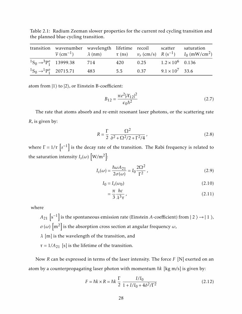
Table 2.1: Radium Zeeman slower properties for the current red cycling transition andthe planned blue cycling transition.
transition wavenumber wavelength lifetime recoil scatter saturationν (cm−1) λ (nm) τ (ns) vr (cm/s) R (s−1) I0 (mW/cm2)
1S0→3Po1 13999.38 714 420 0.25 1.2× 10⁶ 0.1361S0→1Po1 20715.71 483 5.5 0.37 9.1× 10⁷ 33.6
atom from |1〉 to |2〉, or Einstein B-coefficient:
B12 =πe2|X12|2
ε0~2 (2.7)
The rate that atoms absorb and re-emit resonant laser photons, or the scattering rate
R, is given by:
R =Γ
2Ω2
δ2 +Ω2/2 + Γ 2/4, (2.8)
where Γ = 1/τ[s−1
]is the decay rate of the transition. The Rabi frequency is related to
the saturation intensity Is(ω)[W/m2
]:
Is(ω) =~ωA212σ (ω)
= I02Ω2
Γ 2 , (2.9)
I0 = Is(ω0) (2.10)
=π3hc
λ3τ, (2.11)
where
A21[s−1
]is the spontaneous emission rate (Einstein A-coefficient) from | 2 〉 → | 1 〉,
σ (ω)[m2
]is the absorption cross section at angular frequency ω,
λ [m] is the wavelength of the transition, and
τ = 1/A21 [s] is the lifetime of the transition.
Now R can be expressed in terms of the laser intensity. The force F [N] exerted on an
atom by a counterpropagating laser photon with momentum ~k [kg m/s] is given by:
F = ~k ×R = ~kΓ
2I/I0
1 + I/I0 + 4δ2/Γ 2 (2.12)
28

1000 z
(cm)
mvatomic beam Slowing laser(s)
tapered solenoid
Zeeman profile B(z) z
h/λ
Figure 2.2: A cartoon of the radium Zeeman slower. ~p = m~v is the momentumof a radium atom with mass m and velocity ~v and ~pγ = −h/λ z is the momentumof a slowing laser photon with wavelength λ.
The recoil velocity vr of an atom emitting a photon is given by:
vr2τ
= amax =F0m
=~km
Γ
2, (2.13)
where amax[kg m s−2
]is the maximum acceleration and F0 [N] is the maximum force
exerted on the atom. From Newtonian kinematics we can estimate the length scale over
which an atom with initial speed v0 [m/s] can be stopped by a coherent field of resonant
photons:
L0 =v2
0amax
(2.14)
The atoms are exposed to a counter-propagating, circularly-polarized laser as they
move through the solenoid, as shown in Figure 2.2. The solenoid magnetic field is tuned
to compensate for both the atom Doppler shifts (velocity-related) and the Zeeman shifts
(quantum number related). The atoms absorb and emit the laser photons at a rate de-
29

termined by the lifetime of the optical cyling transition [85]. Each photon absorption-
emission cycle gives a small momentum kick to the atom, slowing it down.
The Ra EDM Zeeman slower uses the S10←→ P3 o
1 optical cycling transition to trap
atoms with initial speeds up to 55 m/s. A one meter-long, tapered solenoid generates a
magnetic field gradient along the atomic beam axis. The magnetic field causes a Zeeman
shift Ez [J] in the energy of the atom:
Ez = gF mF µB Bz , (2.15)
gF =F(F + 1) + J(J + 1)− I(I + 1)
2F(F + 1)gJ , (2.16)
gJ =32
+S(S + 1)−L(L+ 1)
2J(J + 1), (2.17)
where
gF , gJ [unitless] are the Landé g-factors,
µB [J/T] is the Bohr magneton,
F = I + J [unitless] is the total angular momentum,
J = L+ S [unitless] is the electron total angular momentum,
L,S [unitless] is the electron orbital angular momentum and spin, and
Bz [T] is the Zeeman slower magnetic field.
In general, the total Zeeman-shifted energy ∆Ez must account for the energy shift of the
excited state and the ground state. For our case of an optical cycling transition with S10
atoms, the Zeeman shift is dominated by the excited state contribution and I make the
approximation ∆Ez ≈ Ez.
The excitation angular frequency ω of the atom is modified by a Doppler and Zeeman
contribution, shifting it from the unperturbed angular frequency ω0:
ω+ kv =ω0 +∆Ez/~ (2.18)
To keep the atom resonant with the laser, the magnetic field profile is given by:
30

CCDV
A
B
Figure 2.3: Cloud of radium atoms trapped between high voltage electrodes in opticaldipole trap.
B(z) = B0
(1− z
L0
)1/2+Bbias , (2.19)
B0 =hv0λµB
(2.20)
For the 3Po1 transition, B0 = 5.5 mT = 55 G. This produces a Zeeman shift
ν = Ez/h ≈ 80 MHz.
2.2.2 Laser trapping
The Zeeman slower cools a small fraction of the atom beam to sufficiently low speeds.
These are trapped by a three-dimensional magneto-optical trap (3D MOT) downstream
of the Zeeman Slower (bottom-center of Figure 2.1). The MOT is formed by three lasers
slightly detuned from the 3P1 transition. The lasers are mutually perpendicular and
intersect. The laser paths are immersed within a magnetic field gradient of approximately
0.5 Gauss / cm [86]. The trapping efficiency is a few parts per million [82].
31

A 1550 nm laser is overlapped with the center of the MOT. The MOT lasers and field
are switched off and the atoms are now attracted to the focus of the 1550 nm laser. This
laser is an optical dipole trap with a 500 µK trapping depth. The location of the beam
focus is controlled by a lens on a translation stage.
The “Bus” ODT transports the atoms from the MOT into a nonmagnetic, borosilicate
glass tube chamber called the “science chamber.” The tube is surrounded by concentric
nickel-alloy “mu” metal, so-named for its high relative permeability µr ≈ 20000. There
are three layers of mu-metal surrounding the tube. The mu-metal is de-Gaussed by run-
ning a 10 Hz AC current through wires coiled around the mu-metal. The de-Gaussed
shield suppresses low-frequency external fields by a factor of ≈ 104. This reduces Earth’s
magnetic field from 500 mGauss to 50 µGauss inside the science chamber.
The atoms are transported to the center of the science chamber between two metal
high voltage electrodes. The electrodes are mounted in a Macor holder within the tube,
separated by a distance on the order of millimeters. The electrodes are discussed in detail
in Chapter 3. Inside the science chamber, we apply a uniform 10 mGauss field in the
vertical direction.
The Bus ODT is overlapped with a second, perpendicular “Holding” ODT in the elec-
trode gap. The Holding ODT is a 1550 nm laser with a 100 µm diameter at the focus. The
Bus ODT is shuttered at this point and the atom cloud is in position for spin precession
frequency measurements.
Figure 2.3 shows a schematic of the EDM measurement. The atoms are polarized
along the axis of the Holding ODT with a pulse from the collinear “Pump/Probe” beam
tuned to the S10→ P1 o
1 (483 nm) transition. They precess at a frequency of ≈ 20 Hz in
the Holding ODT. A uniform electric field is generated parallel to the applied magnetic
field by charging one of the electrodes with a bipolar high voltage power supply. The
field direction is reversed by reversing the polarity of the power supply. The Ra EDM
measurement aims to detect a frequency difference in the atom spin precession when the
32

electric field is aligned and anti-aligned with the magnetic field.
Systematic effects related to laser trapping and the EDM apparatus were studied by
previous Ra EDM graduate students Mukut Kalita, Richard Parker, and Ibrahim Sulai.
Their findings are discussed in great detail in their theses [86, 87, 88].
2.2.3 The 2015 Radium-225 measurement
The second and most recent 225Ra EDM measurement was performed in the summer of
2015. An average electric field of 15 kV/ 2.3 mm = 6.5 kV/mm was used for the spin
precession measurement [48]. A single oven load of 9 mCi was used, improving over the
3 + 6 mCi separate oven loads in the previous measurement [65].
The sensitivity of the measurement was improved by a factor of 36. Experience devel-
oped from the first measurement was instrumental in performing a more sensitive mea-
surement. Minute details, such as laser stability, data acquisition, and analysis contribute
to the result. The single most consequential improvement was an approximately factor
of 10 improvement to the spin precession lifetime of the atoms (τ in Equation 2.3). This
was achieved by improving the stability of the Holding ODT and significantly reducing
the science chamber vacuum pressure.
I’ll highlight targeted upgrades to the EDM experimental apparatus for the next mea-
surement in Section 2.3. Then I’ll describe the EDM measurement scheme in Section 2.4.
2.3 Targeted upgrades for an improved electric dipole moment mea-surement
2.3.1 Atom cooling with an improved Zeeman slower
We used the S10→ P3 o
1 transition to slow the atoms in the first generation measurements.
This cycling transition only requires a single repump laser tuned to the D31 → P1 o
1
transition. The drawback is that less than 1% of the atoms exiting the oven are sufficiently
slowed to be captured. The details of the operation of a Zeeman slower are discussed in
33

Section 2.2.1.
We will improve the Zeeman slower by using the faster-cycling S10→ P1 o
1 transition
to slow more than half of all the atoms exiting the oven. This will increase the number
of atoms that we can measure in the science chamber (N in Equation 2.3). The improved
“blue” slower will operate simultaneously with the current “red” slower. The blue slower
optical cycling scheme requires three repump lasers.
I built a fluoroscopy setup to measure the additional repump channels to verify the
feasibility of the blue slower scheme. The branching ratios to these additional D states
were predicted to be favorable [89]. Prior to my work, the D state branching ratios were
not yet experimentally verified [89]. I’m the third author of our publication describ-
ing the branching ratio measurement and results [90]. My contribution to the radium
branching ratio measurement is further discussed in Chapter 4.
2.3.2 Atom detection efficiency with Stimulated Raman Adiabatic Passage
For the first generation EDM experiments, we measured the atom spin preces-
sion by pulsing the atoms with circularly polarized (σ+) laser light tuned to the
S10 (F = 1/2)→ P1 o
1 (F′ = 1/2) transition, where F = I + J is the total angular momentum
summing nuclear spin I and total electronic angular momentum J . The atoms scatter an
average of three photons before decaying from the excited state to a ground state that we
cannot utilize for spin precession detection, i.e. a dark state.i
To increase the number of photon scatters per atom, and thus the detection efficiency
in Equation 2.3, we will use a hyperfine magnetic sublevel-selective measurement scheme
with the S10 (F = 1/2) → P1 o
1 (F′ = 3/2) transition. With this method, the atoms are
expected to scatter an average of one thousand photons.
Our strategy to measure the spin-selective F′ = 3/2 transition is to use the technique of
iAtoms may also decay to the equally unusable metastable 3D1 state ≈ 0.1% of thetime.
34

Stimulated Raman Adiabatic Passage (STIRAP). This technique uses two lasers: one tuned
to the transition | 1 〉 → | 2 〉, and one tuned to | 2 〉 → | 3 〉. By pulsing the atom cloud
with the two lasers separated by the time interval δ [µs], we can transfer the population
of state | 1 〉 directly to state | 3 〉.
The states for the proposed 225Ra detection scheme are:
| 1 〉 = S10 (F = 1/2; mF = −1/2)
| 2 〉 = P1 o1 (F = 1/2; mF = +1/2)
| 3 〉 = D31 (F = 1/2; mF = −1/2) ,
The spin-selective atom detection is then carried out by probing the
S10 (F = 1/2; mF = +1/2)→ P1 o
1 (F′ = 3/2; mF′ = +3/2) transition with σ+ circularly-
polarized light.
Tenzin Rabga led the recent effort resulting in significant progress towards achieving
spin-selective STIRAP with radium. This work is discussed in great detail in his the-
sis [91].
2.3.3 Higher electric field strength
The first generation experiments used an electric field of 6.7 kV/mm and 6.5 kV/mm. We
used a pair of oxygen-free, electropolished copper electrodes. The copper electrodes were
tested (conditioned) to fields as high as 10 kV/mm in a test apparatus at ANL. However,
they were unstable at those fields when they were installed in the EDM apparatus. The
installation procedure is invasive and requires a teardown of the vacuum equipment on
the opposite side of the MOT chamber in Figure 2.1.
After the most recent EDM measurement, four pairs of niobium electrodes and two
pairs of titanium electrodes were prepared at Jefferson Lab and sent to MSU. I built a
high voltage test station and conditioned new titanium and niobium electrode pairs at
MSU. I improved the conditioning procedure and developed analysis code that can be
35

run concurrently with conditioning to inform the testing. To store, transport, and install
the electrodes in high voltage setups, I designed clean rooms, storage containers, and
installation procedures.
I transported a pair of conditioned niobium electrodes to the EDM apparatus. The
electrodes were conditioned to 20 kV/mm at MSU. I built a clean room around the tear-
down section of the EDM apparatus and installed the electrodes in the EDM apparatus
and revalidated them to 20 kV/mm. This will more than triple the electric field strength
(E in Equation 2.3). Since the EDM sensitivity is linearly proportional to the electric field
strength, it should also triple the sensitivity of the next EDM measurement. The details
of this work is discussed in Chapter 3.
2.3.4 Increasing Radium-225 availability
For the first two measurements, 225Ra was procured from Oak Ridge National Lab (ORNL).
The new Facility for Rare Isotope Beams (FRIB) linear accelerator at MSU is nearing regu-
lar operation. Isotope production at the NSCL was recently benchmarked for the produc-
tion of 47Ca [92]. When fully operational, FRIB is expected to be capable of supplying
at least 4.9 mCi of 225Ra per week [93], and significantly more for a dedicated radium
harvesting campaign.
FRIB-harvested radium will allow us to perform an EDM measurement with larger
source loads more frequently. First we will develop the extraction and sample preparation
procedure, starting with stable calcium as a radium surrogate. Calcium, like radium, has
a strong P1 o1 cycling transition and can be used in atomic beam studies.
We’re developing an atomic beam fluorescence (ABF) study at MSU that will calibrate
the harvesting procedure. Our goal is to compare the initial harvested atom source size
to the atom rate it produces in an effusive oven that will be measured with laser induced
fluorescence (LIF). The details of my ABF measurements and analysis are in Chapter 5.
36
2.4 Experimental requirements
2.4.1 Measurement technique
The EDM couples to an external electric field analogously to the coupling of the magnetic
dipole moment to an external magnetic field. The Hamiltonian H [eV] of an atom in the
presence of a perfectly uniform electric and magnetic field is given by:
H = −µ ~I · ~BI
− d ~I ·~EI , (2.21)
where
µ = −2.3× 10⁻⁸ eV/T is the nuclear magnetic moment of 225Ra [94],
~I is the nuclear spin,
~B [T] is the applied magnetic field,
d [e cm] is the atomic EDM, and
~E [V/cm] is the applied electric field.
The 225Ra atoms will precess with frequency ω+ (ω−) when ~E is parallel (antiparallel) to
~B:
ω± =2~
(µB± dE) , (2.22)
In the most recent Ra EDM experiment we applied a 2.6 µT magnetic field and measured
a spin precession frequency of 181.1± 1.6 rad/s [48].
We use a pair of identical plane-parallel electrodes to produce a stable, uniform, and
symmetric electric field. The spin precession of the atoms is measured in three con-
figurations: with the electric field parallel to the magnetic field, with the electric field
antiparallel to the magnetic field, and with no applied electric field. The “field-off” set-
ting is used to control for a systematic effect generated by an imperfect reversal of the
electric field. We measure the accumulated spin precession phase for each field configu-
37

Table 2.2: Ra EDM systematic requirements at the 10−26 e cm sensitivity level.Detailed systematic limit evaluations for these parameters can be found in pre-vious work [48, 95]. ∆B is determined by Equation 2.29.
description systematic limit Section
~E, ~B alignment θE ≤ 2 mrad 2.4.4
polarity imbalance|∆E|E
≤ 0.7% 2.4.5
electrode magnetic impurity ∆B ≤ 100 fTa 2.4.3
steady-state leakage current I ≤ 100 pAa 2.4.4
magnetic Johnson noise
√dB2
ndν
≤ 15pTa√
Hz2.4.2
a per measurement cycle
ration. The extracted EDM is proportional to the accumulated phase difference between
the parallel and antiparallel configurations, ∆φ [rad]:
d =~∆φ4Eτ
(2.23)
With a perfectly uniform and static magnetic field under all configurations, the phase
difference between the parallel and antiparallel field configurations is purely due to the
EDM interaction with the electric field. A higher electric field will result in a larger
accumulated phase and will increase our EDM sensitivity.
During each measurement cycle, one electrode is charged to ≤ +30 kV (positive po-
larity) while the other is grounded. The atom spin precession lifetime is currently about
twenty seconds. We expect to increase the spin precession lifetime to one hundred sec-
onds [81] as improvements are made to the ODT. The charged electrode is then ramped
to zero voltage and remains grounded for a period of 60 s while a new sample of atoms
is prepared. The cycle restarts and the electrode is charged to the same voltage magni-
tude at negative polarity. We repeat this process until the atomic oven is depleted after
approximately two weeks.
38
Now we’ll discuss EDM measurement systematics related to the high voltage system.
Our requirements for each systematic are given in Table 2.2.
The electric field between the electrodes must be symmetric, uniform, and reversible
to minimize systematic effects. The alignment between ~E and ~B is fixed after mounting
the electrodes to the Macor holder, as shown in Figure 2.6. In the experimental apparatus,
the holder and electrodes rest within a borosilicate glass tube (see Figure 2.1). We will
use vector fluxgates with a system of autocollimators to optically determine the field
uniformity and alignment for the second generation EDM measurements [96]. The field
reversibility is measured with a calibrated high voltage divider (Ross Engineering V30-
8.3-A).
2.4.2 Magnetic Johnson noise calculations
Magnetic field fluctuations caused by random thermally-induced currents in the elec-
trodes, or magnetic Johnson noise (MJN), limits the choice of electrode materials and
geometries that are suitable for an EDM measurement [97, 98].
In the next two years, we are aiming for a statistical sensitivity of d ≈ 10−25 e cm
or better as improvements in the external electric field and atom detection efficiency
are implemented in the second generation measurements. The Ra EDM roadmap in-
cludes upgrades over the next five years that will enable an EDM sensitivity as high as
d ≈ 10−28 e cm.
In the presence of perfectly uniform magnetic and electric fields, the atom precesses
with a frequency given by Equation 2.22. With an applied electric field of 30 kV/mm, I
find the following frequency due to an EDM magnitude d ≈ 10−25 e cm:
f (upper limit) =4dEh
=4× 10⁻²⁵e cm× 30× 104 V/cm
4.135× 10⁻¹⁵ eV/Hz≈ 2.9× 10⁻⁵ Hz
The atoms precess in a 10 mGauss magnetic field corresponding to a Larmor preces-
sion frequency of ≈ 20 Hz. The fractional change in the spin precession frequency due to
39

the EDM is 2.9× 10⁻⁵/20 ≈ 1.5 ppm. Therefore systematics affecting the spin precession
signal should be suppressed to below 150 ppb.
The thermal or Johnson noise in a conductor at a location~r is given by:
dB2n,q
dν=µ2
0kBT
4π2ρVu , (2.24)
Vu =∫ ∣∣∣∣∣∣∣∣(~r−~u)× q∣∣∣~r−~u∣∣∣3
∣∣∣∣∣∣∣∣2
d3u , (2.25)
where
dB2n,q/dν
[T2 Hz−1
]is the magnetic field noise density in direction q,
µ0[N A−2
]is the vacuum magnetic permeability,
kB [J/K] is the Boltzmann constant,
T [K] is the temperature,
ρ [Ω m] is the resistivity of the conductor, and
~u [m] is the location of the infinitesimal conductor volume element.
The resistivities of copper, niobium, and titanium are shown in Table 3.2. For the Ra
EDM electrode geometry (Figure 3.1), Vx = Vy = 93.1 cm−1 and Vz = 57.2 cm−1 in the
vertical direction [99]. With improvements to the thermal stability of the transport beam,
we expect to achieve an atom spin precession lifetime of for τ = 100 s. Therefore the rms
magnetic field noise at room temperature (T = 298 K) is given by:
√B2n,q =
√dB2
n,q
dν× τ−1/2 =
√V × 1.647τ ρ′
× 10−12 T , (2.26)
where ρ′ = ρ/(10−8 Ω m). For a pair of niobium electrodes, the magnitude of the magnetic
field noise in the vertical direction is√dB2
n,z
dν= 2.48
pT√
Hz
With an expected spin precession lifetime of 100 s we calculate a field of√B2n,z = 2.49× 10⁻¹³ T = 2.48× 10⁻⁹ G
40

This corresponds to a per-shot frequency sensitivity of
2.48× 10⁻⁹ G10−2 G
≈ 250 ppb
The integrated sensitivity of the frequency shift is related to the per-shot sensitivity
by the number of measurements made:
σf =δf√N
, (2.27)
where
σf [Hz] is the integrated frequency sensitivity,
δf [Hz] is the per-shot frequency sensitivity, and
N [dimensionless] is the number of measurements.
For a 15-day EDM measurement, we expect
N = 15 days × 24 hoursday
× 60 minuteshour
× 1 measurement2 minutes
≈ 104 measurements.
Our integrated frequency sensitivity must be better than the fractional change in the
spin precession frequency due to the EDM, which we found to be ≈ 150 ppb. Therefore
the per-shot frequency sensitivity must be better than 150 ppb ×√
104 = 15 ppm. This
corresponds to a per-measurement noise of:
15 ppm×(10−2 G
)×√
100 s × 1012 pT104 G
= 150pT√
Hz(2.28)
We calculated earlier that the per-shot frequency sensitivity of niobium is 250 ppb = 2.48
pT/√
Hz. The magnetic field noise scales as ρ−1/2, from which we estimate the per-shot
frequency sensitivity of copper and titanium to be (250 ppb) ×√
15.2/1.543 ≈ 780 ppb
and (250 ppb)×√
15.2/39 ≈ 160 ppb, respectively.
I expect that MJN will remain a minor source of systematic uncertainty for EDM mea-
surements at the d ≈ 10−25 e cm level. As we approach our long-term goal of 10−28e cm,
we’ll need to modify the electrodes to reduce magnetic noise. For example, Figure 2.4
41

13.5 mm
3.3 mm
ϕ 3.3 mm
Figure 2.4: One possible electrode design whose volume is a factor of ten smallerthan the standard Ra EDM electrode.
shows a possible design where the volume of the electrode has been reduced by an order
of magnitude, reducing the field noise by approximately a factor of√
10. Any new elec-
trode geometry could be optimized by rigorous modeling of the field uniformity under a
variety of potential electrode misalignments. I discuss this type of analysis I performed
for the existing Ra EDM geometry in Section 2.5.
2.4.3 Paramagnetic impurities
We consider a potential systematic in which the magnetization of a fraction of the im-
purities in the electrodes depends on the polarity of the charging current. A suffi-
ciently high concentration of paramagnetic impurities near an electrode primary sur-
face could perturb the magnetic field in the radium cloud region. This would induce a
polarity-dependent spin precession frequency mimicking an EDM signal, or “false” EDM
d∆B [e cm]:
d∆B =µ∆B
E, (2.29)
where
µ is the nuclear magnetic moment,
E is the magnitude of the applied electric field, and
∆B is the change in local magnetic field under reversal of E.
42

Impurities in the electrode material are minimized by using high-grade materials, using
machine shop tooling that does not embed impurities on the surface, and using polishing
and cleaning techniques that remove surface-level contaminants. In the scenario of an
applied electric field of 30 kV/mm and a magnetic field change of 100 fT under reversal,
I find a false EDM magnitude of:
d∆B =2.3× 10⁻⁸ eV/T× 100× 10−15 T
30× 104 V/cm= 7.7× 10⁻²⁷e cm
Other EDM high voltage systematic requirements are given in Table 2.2. Table 3.1 and
Table 3.2 list the material properties and processing techniques that we use. I’ll discuss
electrode material selection and surface processing in detail in Section 3.1.
2.4.4 Leakage current and field angle
I define leakage current as any current flowing between the electrodes. This includes
current flowing through the insulating mount and “field emission” between the two pri-
mary surfaces across the electrode gap (see Figure 2.6). Leakage current induces magnetic
fields whose properties depend on the magnitude, path, and dynamic properties of the
current.
I define an electrode discharge as a transient surge in field emission between the elec-
trode surfaces. In the event of a discharge close to the location of the atom cloud, the
atoms will interact with the induced magnetic field. The interaction will manifest as a
change in the spin precession frequency of the atoms. If the discharge rate is correlated
with the polarity of the electrodes, it will introduce a systematic shift in the EDM signal.
To study the effect of leakage current on the spin precession we model the discharge as
a thin wire of current traveling a distance r [m] from the cloud. This consequent “false”
EDM signal dI [e cm] is given by [48]:
dI =µ~BE· B =
µ
E
µ0I
2πrsinθE , (2.30)
43
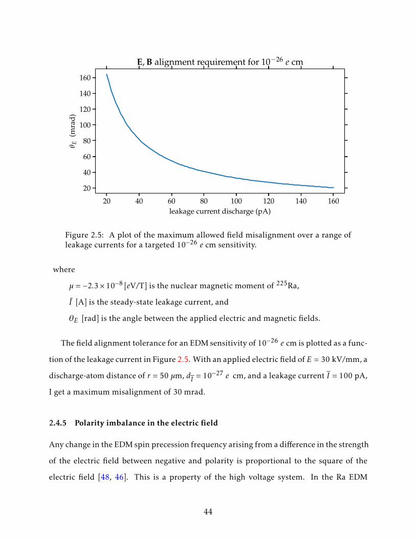
20 40 60 80 100 120 140 160leakage current discharge (pA)
20
40
60
80
100
120
140
160θ E
(mra
d)E, B alignment requirement for 10−26 e cm
Figure 2.5: A plot of the maximum allowed field misalignment over a range ofleakage currents for a targeted 10−26 e cm sensitivity.
where
µ = −2.3× 10⁻⁸ [eV/T] is the nuclear magnetic moment of 225Ra,
I [A] is the steady-state leakage current, and
θE [rad] is the angle between the applied electric and magnetic fields.
The field alignment tolerance for an EDM sensitivity of 10−26 e cm is plotted as a func-
tion of the leakage current in Figure 2.5. With an applied electric field of E = 30 kV/mm, a
discharge-atom distance of r = 50 µm, dI = 10−27 e cm, and a leakage current I = 100 pA,
I get a maximum misalignment of 30 mrad.
2.4.5 Polarity imbalance in the electric field
Any change in the EDM spin precession frequency arising from a difference in the strength
of the electric field between negative and polarity is proportional to the square of the
electric field [48, 46]. This is a property of the high voltage system. In the Ra EDM
44

Figure 2.6: Left: assembly of the niobium pair Nb56 at 1 mm gap in Macorholder. Right: a slit centered on the gap shields the electrode surfaces fromheating by the atom trapping and polarizing lasers.
measurement, the polarity imbalance is symmetric to within 0.7%.
2.5 Effect of Electrode Misalignments
Two identical electrodes make up the Ra EDM electrode pair. The primary surface,
seen as the top surface in Figure 3.1, is flat and 16 mm in diameter. The rounded edges
have 4 mm circular radial curvatures. We use plane-parallel electrodes (see Figure 2.6)
so that the reversible field is uniform and symmetric as the electrodes alternate roles as
cathode and anode every EDM measurement cycle.
The Ra EDM experiment requires an applied electric field that is symmetric, uniform,
and reversible in the center of the electrode gap where the spin precession frequency of
the 50 µm diameter radium cloud is measured. Our electrode geometry reliably meets
these requirements at field strengths of 12–30 kV/mm.
Systematic effects arising from asymmetric field reversal must continue to be reduced
as the experimental sensitivity improves. In the current measurement scheme, one elec-
trode is permanently grounded and the other electrode is charged by a bipolar power sup-
ply. We will design a more symmetric apparatus that allows us to alternate the charged
and grounded electrodes using high voltage switches and a unipolar 50 kV power supply
in the next phase of high voltage development.
45

Figure 2.7: A software meshed model of the electrode pair and coordinate sys-tem. The finer-meshed electrode gap region is shaded blue.
I demonstrated the effect of steady-state leakage current on the spin precession fre-
quency with a simple wire model in Section 2.4.4. In Section 2.5.1 I will show that the
electrode electric field matches that of the ideal infinite-plane capacitor in the atom cloud
region using finite element modeling. We will use the methods developed here to opti-
mize electrode geometries as the experiment sensitivity improves.
2.5.1 Description of the electric field finite element analysis
One systematic that creates a “false” EDM-like signal scales with the sine of the angle
between the electric field and the controlled uniform magnetic field we use for measur-
ing the spin precession of the radium atoms. We modeled the high voltage electrodes
in the finite element analysis software COMSOL Multiphysics (version 5.3) to study the
electrostatic behavior as the alignment is varied from perfectly parallel, axially-centered
electrodes. In the model, the electrodes are surrounded by a perfect vacuum. The elec-
trode gap size is set to 1 mm gap and the top electrode is charged to −30 kV for a nominal
electric field of E0 = 30 kV/mm.
My simulations use the Extremely Fine settings with Size Expression increased to
46

4×10⁻⁴ in the gap region and Resolution increased to 200 along the upper curved elec-
trode surface. One can see the higher mesh element density in Figure 2.7. The minimum
mesh element size is set to 20 µm, where I found that the electric field dependence on the
mesh size converges to negligibly small fluctuations.
The coordinate system of the electrostatic model of the electrodes is shown in Fig-
ure 2.7, with the origin defined as the midpoint between the two electrodes along their
vertical axis of the top electrode. I find that the vertical field strength Ey changes by less
than 6 ppb per 100 µm when the electrodes are perfectly aligned. The horizontal field
magnitude E⊥ =√E2x +E2
z changes by less than 5 ppb per 100 µm with respect to E0
within 0.5 mm of the origin. In practice, we align our electrodes to better than 4 mrad in
the high voltage test stand described in Section 3.4.1.
The mesh density was optimized in the volume between the electrode primary sur-
faces. We refined the maximum and minimum element size to minimize field calculation
dependence on mesh settings. This was done by convergence analysis, decreasing the
minimum element size from 120 µm to 18.5 µm and recording the change in the maxi-
mum electric field with a gap size of 1 mm and an applied voltage of −30 kV. The lower
bound of the mesh size is limited by the RAM of our workstation PC (32 GB). I fixed the
maximum element size to be a factor of 4 larger than the minimum element size.
I set the maximum and minimum element sizes in the gap between the electrodes to
be 80 µm and 20 µm, respectively, where the maximum vertical component of the electric
field changes by less than 0.03% (about 10 V/mm) when changing the mesh size by 10%.
However, these deviations are based on field points very close to the mesh border and
electrode surfaces. When we perform an identical convergence analysis while restricting
the maximum field value to the horizontal plane bisecting the electrode gap, the field
changes by less than 4 parts per billion.
47

Field angle response to different angular misalignments
gap coordinate shift along vertical axis y (µm)
angular misalignment (mrad)
Figure 2.8: A plot of the electric field angle as a function of the vertical positiony. In this plot, the electrodes are axially aligned and the angular misalignment isvaried from 0–16 mrad. The center of the gap, 0.5 mm below the top electrode,corresponds to y = 0.
2.5.2 Electric field response to electrode misalignment near the center of the gap
I investigated the effect of misalignments between the electrodes on the electric field an-
gle, defined as θE = arctan(E⊥ / Ey
). There are two types of misalignments we consider.
Angular misalignments, or tilts, are introduced by rotating the bottom electrode about
the z axis in the range 0–16 mrad. Axial misalignments, or shifts, translates the bottom
electrode along the x axis and offsets the electrode centers. Shifts of up to 1 mm displace-
ments are considered in this work. When the tilt and shift are zero, the electrodes are
perfectly aligned and θE = 0 near the center of the gap, corresponding to a uniform ver-
tical field. When the electrodes are perfectly aligned (θE = 0,∆ = 0) E⊥ fluctuates by ≈ 6
ppb and δ(Ey) ≈ 10 ppb from the nominal applied field of −30 kV/mm for x∩z ≤ 100 µm.
I’ve plotted the electric field angle θE for a range of electrode tilts in Figure 2.8. From
my definition of the coordinate system, θE is zero at~r = +0.5y mm, the surface of the top
electrode. For a tilt of 0 mrad, the electric field angle is perfectly aligned (θE = 0) across
48

−400 −200 0 200 400
y(x = −0 µm) (µm)
0.00
0.01
0.02
0.03
0.04
0.05
Ey
-30
.021
(kV
/mm
)E-field response: -30 kV / 1 mm (z = −0 µm) ∆ = 100 µm
surface misalignment (mrad)
0
2
4
8
16
Figure 2.9: A plot of the vertical electric field for angular alignments in therange 0–16 mrad. The axial misalignment is 100 µm. The center of the gap,0.5 mm below the top electrode, corresponds to y = 0.
the electrode gap. For nonzero tilts, θE scales linearly with distance y from the top elec-
trode surface to the value of the electrode tilt angle at the surface of the bottom electrode,
~r = −0.5y mm. Even for the largest angular misalignment of 16 mrad, the electric field
angle θE is linear and appears insensitive to the effects from the electrode edge.
I also studied the effect of shifting the bottom electrode along x with respect to the
top electrode’s vertical axis in the range 0–1000 µm. In Figure 2.9, I show the vertical
component of the electric field response for a 100 µm shift. The bottom electrode is offset
along −x to maximize the convolution of angular and spatial misalignment. Even for large
tilts, axial misalignments introduce a constant offset in Ey that appears to be independent
of the tilt. In this worst-case scenario, the magnitude of the constant depends on both the
tilt and the horizontal misalignment, which brings one side of the bottom electrode closer
49

0 1000 2000 3000 4000 5000 6000 7000 8000
z (µm)
0
1000
2000
3000
4000
5000
6000
7000
8000
x(µ
m)
E⊥(y = 0 µm) θ = 0 mrad, ∆ = 1000 µm
-3.0e-02
0.0e+00
3.0e-02
6.0e-02
9.0e-02
1.2e-01
1.5e-01
1.8e-01
2.1e-01
2.4e-01
rela
tive
dev
iati
onfr
om30
.02
kV
/mm
Figure 2.10: A contour of the horizontal electric field magnitude for misalignedelectrodes close to the 8 mm edge region.
to the surface of the top electrode.
The constant term in Ey can be found by considering the electrodes at a reduced gap
size of ∆× tanθ, where ∆ is the spatial displacement. For a tilt of 16 mrad and a spatial
misalignment of 1 mm (the largest misalignment simulated), this results in a shift of
+0.5 kV/mm along the vertical axis. The shift value will be negative if we move along −x
a distance greater than the offset because the electrode surfaces will be angled away from
each other. In all configurations shown in Figure 2.9, the contributions to changes in the
electric field due to angular and spatial misalignments are independent of each other for
horizontal displacements x∩ z ≤ 1 mm.
50
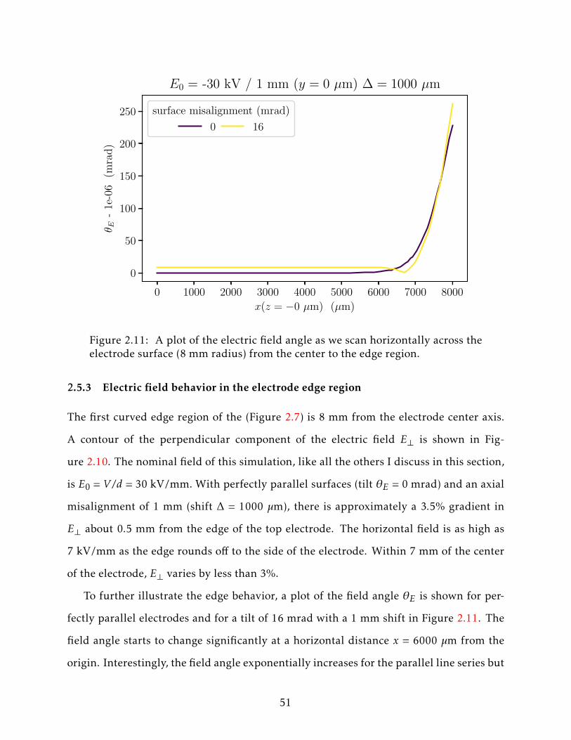
0 1000 2000 3000 4000 5000 6000 7000 8000
x(z = −0 µm) (µm)
0
50
100
150
200
250θ E
-1e
-06
(mra
d)
E0 = -30 kV / 1 mm (y = 0 µm) ∆ = 1000 µm
surface misalignment (mrad)
0 16
Figure 2.11: A plot of the electric field angle as we scan horizontally across theelectrode surface (8 mm radius) from the center to the edge region.
2.5.3 Electric field behavior in the electrode edge region
The first curved edge region of the (Figure 2.7) is 8 mm from the electrode center axis.
A contour of the perpendicular component of the electric field E⊥ is shown in Fig-
ure 2.10. The nominal field of this simulation, like all the others I discuss in this section,
is E0 = V /d = 30 kV/mm. With perfectly parallel surfaces (tilt θE = 0 mrad) and an axial
misalignment of 1 mm (shift ∆ = 1000 µm), there is approximately a 3.5% gradient in
E⊥ about 0.5 mm from the edge of the top electrode. The horizontal field is as high as
7 kV/mm as the edge rounds off to the side of the electrode. Within 7 mm of the center
of the electrode, E⊥ varies by less than 3%.
To further illustrate the edge behavior, a plot of the field angle θE is shown for per-
fectly parallel electrodes and for a tilt of 16 mrad with a 1 mm shift in Figure 2.11. The
field angle starts to change significantly at a horizontal distance x = 6000 µm from the
origin. Interestingly, the field angle exponentially increases for the parallel line series but
51

4000 6000 8000 10000 12000 14000 16000 18000horizontal position x(z = 4000 µm) (µm)
5
10
15
20
25
30el
ectr
icfie
ldE y
(kV
/mm
)
Field strength in midplane ∆ = 0 µm
surface misalignment (mrad)
0
Figure 2.12: A plot of the vertical component of the electric field as we scanhorizontally across the electrode surface in the edge region (radius of 8 mm).
there is a dip in the field angle in the 16 mrad series, leading to a crossing between the
two. At x > 7000 µm, the field angle of the 16 mrad line increases more rapidly than the
parallel line.
Finally we look at the vertical component of the field behavior near the edge region
in Figure 2.12. Since we’re interested specifically in the edge behavior, we start from
~r(µm) = 4000x+0y+4000z and scan horizontally along x. Ey decreases by approximately
0.9 kV/mm over both curved surfaces of the electrodes, from 8 mm to 12 mm and 12 mm
to 16 mm. In this region, the horizontal field strength is on the same order of magnitude
as the vertical field strength.
2.5.4 Modeling the electric field behavior near the center of the electrode gap
The electric field angle θE scales linearly with the angular misalignments, as shown in
Figure 2.8. I modeled the change in θE as a linear function of the position in both the xy
plane and the xz plane. The linear change in Ey along the horizontal xz plane is very weak.
52

−400 −200 0 200 400position along vertical axis y (µm)
0
20
40
60
80
100θ E
/θ m
ax(%
)
field angle model with 1000 µm axial misalignment
16 mrad surface misalignment
θ(mrad) = (−1.6e− 02)y + 8.1
data
Figure 2.13: A straight line fit to the simulated polar angle of the electric fieldfor an angular misalignment of 16 mrad and an axial misalignment of 1 mm.The center of the gap, 0.5 mm below the top electrode, corresponds to y = 0.
I show the fit to Ey for the more interesting case of the vertical xy plane in Figure 2.13.
The linear model reproduces the change in the electric field angle to an accuracy of better
than 1 µrad in both planes up to 1 mm from the center of the gap, even for large angular
and axial misalignments.
I also modeled the change in the horizontal component of the electric field E⊥ as the
fraction of the maximum angle. Like the fit to θE in Figure 2.13, E⊥ scales linearly with
the distance from the origin. For a 16 mrad tilt and E0 = 30 kV/mm, the fractional linear
change in the transverse field strength is:
E⊥/E0θ≈ 0.1% / mrad
I modeled the behavior of the vertical electric field Ey using the same misalignment
settings as the θE model in Figure 2.14. The misalignment causes a 1.6% reduction in the
field strength and the change in Ey along y is nonlinear. I compared the behavior with a
cos(θE) model, which assumes that the change in Ey is purely due to the changing field
53

−400 −200 0 200 400vertical distance y(x = −0 µm) (µm)
−1.25
−1.00
−0.75
−0.50
−0.25
0.00(E
y−|E|c
osθ)
/E 0
×10−4 field strength model ∆ = 1000 µm
16 mrad surface misalignment
Ey − |E| cos θ
Figure 2.14: A residual plot of a model of the vertical electric field for a 16 mradangular misalignment and 1 mm axial misalignment. The model assumes thatthe field is a function of the angle of the electric field.
direction.
The reduction in Ey is larger than the amount reproduced by the cosine model. For
a 16 mrad tilt, the cosine model accounts for a change of ∆Ey/E0 ≈ 100 ppm per 500 µm
from the origin while the total effect is 230 ppm / 500 µm.
2.5.5 Estimating effects for realistic misalignments in the high voltage apparatus
A contour of the vertical component of the electric field for a 2 mrad tilt is shown in
Figure 2.15. The total change in Ey across a 1000 µm range in x is 2.1%. Even for
large horizontal radial displacements (x∩ z > 100 µm), the electric field is uniform. This
can be seen in the left panel, where the change in the electric field depends on x and is
insensitive to displacement along the axis of rotation (z).
For a larger 4 mrad tilt, the electric field gradient becomes (∆Ey/Ey)/25 µm ≈ 100 ppm.
This gradient would cause an EDM systematic on the order of 10−29e cm across a 100 µm
54

0 200 400 600 800 1000horizontal scan from center x (µm)
−400
−200
0
200
400
vert
ical
sca
n fro
m c
ente
r y
(µm
)
vertical plane
-3.0e-04
0.0e+00
3.0e-04
6.0e-04
9.0e-04
1.2e-03
1.5e-03
1.8e-03
2.1e-03
rela
tive
devi
atio
nfrom
30.0
2kV
/mm
0 200 400 600 800 1000horizontal scan from center z (µm)
0
200
400
600
800
1000
hor
izon
tal sc
an fro
m c
ente
r x
(µm
)Change in vertical electric field Ey , tilt = 2 mrad, shift = 0 µm
horizontal plane
Figure 2.15: Contour plots of the vertical component of the electric field in thexz (left) and xy (right) plane and with a 2 mrad tilt.
radium cloud. The behavior of E⊥ is identical but the strength of the gradient is more
than two orders of magnitude weaker.
In the more realistic case of a 2 mrad tilt, we find that θE changes by 0.2 µrad per 100 µm
in the vertical plane and 0.02 µrad per 100 µm in the midplane. EDM systematic effects
arising from field angle changes of this magnitude are far below our current statistical
sensitivity.
2.6 Electrode Upgrade Strategy and Results
2.6.1 High voltage discharge-conditioning
We define discharge-conditioning as the process of applying iteratively higher voltages
to the electrodes to suppress steady-state leakage current and discharge rates between
them. Leakage current refers to any current flowing between the electrodes detected by a
picoammeter in series with one of the electrodes, as shown in Figure 3.11.
Figure 2.16 shows several forty-minute snapshots of a subset of shifts over the lifetime
of conditioning and validating a pair of niobium electrodes. I started with manually
controlled voltage steps before using a periodic, polarity-alternating voltage to simulate
EDM measurement conditions for the electrodes.
55

5 10 15 20 25 30 35 400-30
-10
10
30
-30
-10
10
30
-30
-10
10
30
-30
-10
10
30
app
lied
vo
ltag
e (k
V)
time (min)
2017-09-20
2017-10-12
2017-10-17
2017-10-23
leak
age
curr
ent
(pA
)p
osi
tiv
e /n
egat
ive
Nb56 conditioning 1 mm gap size
101
103
105
101
103
105
101
103
105
101
103
105
Figure 2.16: Forty-minute snapshots of the conditioning process in early, mid-dle, and final stages. Positive and negative current is plotted with green crossesand red circles on a logarithmic scale. Leakage current less than 10 pA is omit-ted for clarity. The right vertical axis is the applied voltage and is plotted as ablue line.
A schematic of one full period of the conditioning voltage waveform is shown in Fig-
ure 2.17. The period is 280 seconds (60 seconds positive polarity, 80 seconds no voltage,
60 seconds negative polarity, 80 seconds no voltage). This period is chosen to reflect the
measurement technique discussed in Section 2.4.1.
We differentiate our method from the standard “current-conditioning” method [100]
because we characterize electrode performance by counting discrete discharges over time
and we use a periodic voltage waveform. I will interchangeably use the shorthand term
“conditioning” when referring to discharge-conditioning.
In the absence of surface particulate contamination, electrode discharges are caused
by charge buildup on microprotrusions on the electrode surfaces [101], which we will
56

time (min)
vo
ltag
e (k
V)
20
0
-20
0.5 1.0 1.5
A
B
C
D
Figure 2.17: A schematic of the periodic EDM high voltage waveform. A posi-tive charging up ramp. B positive charging down ramp. C negative chargingup ramp. D negative charging down ramp.
refer to as charge emitters. We process and handle our electrodes in Class 100 or better
environments to minimize particulate contamination. The height of charge emitters have
been measured on the order of 1 µm in buffer chemical-polished large-grain niobium
electrodes prepared similarly to our electrodes [102]. If the charge emitter is near the
edge of the electrode, we expect the higher gradients will increase the likelihood of a
discharge.
Controlled discharges electrically polish away, or ablate charge emitters over time,
allowing the electrodes to perform reliably at higher voltages [100]. As shown in Sec-
tion 3.4, it may take tens to more than one hundred hours of discharge-conditioning to
suppress charge emitters. We expect the required conditioning duration may take longer
if the surface is insufficiently polished or contaminated. Bulk properties, such as the
work function, resistivity, or hardness of the electrode may also play a role in the condi-
tioning time. These bulk properties are listed for a selection of commonly used electrode
materials in Table 3.2.
57

2.6.2 Typical size of discharges
The electrode geometry is shown in Figure 3.1. We’ll consider the main high-gradient
surfaces of the electrodes as the only surfaces where discharges occur. For a pair of circu-
lar, parallel plate capacitors whose diameter 2R is much greater than the electrode gap
d, the capacitance of the electrodes can be written as
C =QV
= εoπR2
d, (2.31)
where C [F] is the electrode capacitance, Q [C] is the charge on each electrode, V [V] is
the electric potential between the two electrodes, and εo[F m−1
]is the vacuum electric
permittivity constant.
For an electrode gap of d = 1× 10⁻³ m, a plate radius R = 8× 10⁻³ m, and an applied
voltage of V = 30 kV, we get a capacitance of 1.78 pF. However, from the model of
the electrodes in COMSOL, I get a capacitance of 3.3728 pF. This gives a total charge of
Q = 3.3728 pF × 30 kV = 1.01 × 10⁻⁷ C.
I integrate the discharge current I(t) [A] to estimate the amount of charge ejected from
an electrode surface in a discharge, Qdc [C]:
Qdc =∫ +∞
−∞I(t)dt (2.32)
The discharge current waveform varies in duration and amplitude, but a reasonable
estimate is an amplitude of 100 nA over a 1 ms timescale. I’ll approximate the waveform
as Gaussian:
Qdc =∫ +∞
−∞(100 nA) exp
−(t2
2σ2
)dt , (2.33)
σ = 1 ms (2.34)
In such a discharge we would expect to see ≈ 2.51 × 10⁻¹⁰ C or 1.56 × 10⁹ electrons.
This is ≈ Qdc/Q × 100 % = 0.25 % of the total charge stored on each electrode.
58

2.6.3 Results
Four pairs of niobium electrodes and two pairs of titanium electrodes were surface pro-
cessed as described in Table 3.1. After high-pressure rinsing they are preserved in clean
room environments of Class 100 (ISO 5) or better. I conditioned pairs of electrodes in a
custom, Class 100-rated high voltage test station at MSU by applying DC voltages as high
as ±30 kV at gap sizes in the range 0.4–2.5 mm. Maximum fields of +52.5 kV/mm and
−51.5 kV/mm were tested and are discussed in Section 3.4.7.
One pair of large-grain niobium electrodes was validated to operate reliably at
20 kV/mm at MSU. I mounted the electrodes in a stainless steel container and sealed
the container with tubing. The container was backfilled with particle-filtered, dry nitro-
gen and transported to ANL. Then I constructed and validated a Class 100 clean room
that covered the electrode entry point to the Ra EDM experimental apparatus. The elec-
trodes were removed from their packaging and installed in the experimental apparatus
in May 2018, where I revalidated them to 20 kV/mm.
59

CHAPTER 3
HIGH VOLTAGE ELECTRODE DEVELOPMENT
In Section 3.1 I will describe past and present considerations in electrode material and
surface processing. We start with the preparation of the previous electrode pair used
for the first generation EDM measurements in Section 3.1.1. Material selection, surface
processing, and electrode decontamination for the new electrodes tested in this work
are detailed in Sections 3.1.2 and 3.3.1. I will present our method of benchmarking the
performance of the electrodes in Section 3.4. Finally, we’ll compare the performance of
all the tested pairs in Section 3.4.10.
3.1 Electrode Properties and Preparation
3.1.1 Legacy electrode preparation
The first generation EDM measurements used a pair of electropolished oxygen-free cop-
per electrodes [65, 48]. Their geometry is identical to the new electrodes discussed in
(a) (b)
Figure 3.1: (a) Cross-sectional electrode schematic. Surfaces have a flatness tol-erance of 25.4 µm and a parallelism of 50.8 µm. The top surface is polished toan average roughness of 0.127 µm. The base is mounted by a 10-32 tapped hole.Copper rods are used to connect to the electrodes’ 3.2 mm diameter side boreto high voltage feedthroughs. (b) A pair of large-grain Niobium electrodes in aclean room stainless steel container.
60

Figure 3.2: From left to right: a copper, niobium, and titanium electrode.
this work (Figure 3.1). Surface processing of these electrodes, labeled Cu12, is detailed in
Table 3.1.
The legacy electrodes were conditioned at ANL with a unipolar −30 kV power supply
(Glassman PS/WH-30N15-LR) in a Macor holder at a 2 mm gap size in 2008 [103]. The
electric field was reversed by turning the system off and manually switching the power
supply terminations at the high voltage feedthroughs. Voltage was increased from 1–
20 kV in 1 kV steps while monitoring the steady-state leakage current. Conditioning was
declared complete if the electrodes could hold 20 kV with a steady-state leakage current
of < 100 pA for ten hours.
Four pairs of electrodes total were tested in this manner, including two pairs of tita-
nium electrodes and one pair of copper electrodes without electropolishing. The legacy
titanium electrodes all exhibited leakage current higher than 100 pA at 20 kV. Flooding
the test chamber with argon gas and plasma discharge-conditioning the titanium elec-
trodes was attempted without an observable benefit. Both copper electrode pairs were
conditioned, with the electropolished (EP) electrodes taking significantly less time.
61

Table 3.1: Electrode inventory. Large-grain (LG) niobium electrode residual resis-tance ratio (RRR) > 250. OF = oxygen free. G2 = grade-2. Simichrome polish by hand.Diamond paste polish (DPP) by hand. LPR = low pressure rinse. HPR = high pressurerinse. HF = hydrofluoric chemical polish. EP = electropolish. BCP= buffered chemi-cal polish. SiC = silicon carbide machine polish. CSS = colloidal silica suspension ma-chine polish. VB = 420–450 C vacuum outgas bake. WB = 150–160 C water bake.USR = ultrasonic rinse after detergent bath.
batch material pair surface processing recipe
1 OF copper Cu12a Simichrome → EP → USR →WB
2 LG niobium Nb14 SiC → BCP → DPP → CSS → USR · · ·· · · VB → LPR → HPR
2 LG niobium Nb23 SiC → BCP → USR → VB → HPR · · ·· · · resurface → BCP → HPR
2 G2 titanium Ti24 SiC → HF → USR → VB → HPR2 G2 titanium Ti13 SiC → HF → EP → USR → VB · · ·
· · · HPR3 LG niobium Nb56
b SiC → BCP → USR → HPR →WB3 LG niobium Nb78 SiC → BCP → USR → HPR
a Legacy electrodes used for first two measurements [65, 48].b Second generation electrodes, currently installed in the Ra EDM apparatus.
The legacy electrode pair Cu12 was mounted in a Macor holder at a 2.3 mm gap size
and installed in the Ra EDM experimental apparatus [86]. The two published 225Ra EDM
results employed electric fields of ±6.7 kV/mm and ±6.5 kV/mm [65, 48]. The pair was
retested at 20 kV / 2.3 mm = 8.7 kV/mm but exceeded the 100 pA limit. This was reme-
died by reducing the electric field by 25% to 6.5 kV/mm for the EDM measurement.
We suspect that the primary surface of one or both of these legacy electrodes was con-
taminated during installation. This was a motivating factor in the development of the
decontamination techniques for the new electrodes discussed in subsequent sections.
3.1.2 Consideration of materials for new electrodes
We selected large-grain niobium and grade-2 titanium (middle and right electrodes in
Figure 3.2) for testing after reviewing accelerator physics literature. The bulk properties
of these metals and other commonly used high voltage metals are catalogued in Table 3.2.
62
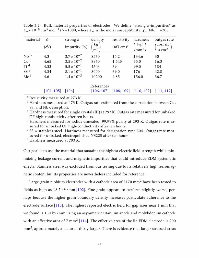
Table 3.2: Bulk material properties of electrodes. We define “strong B-impurities” asχm/(10−6 cm3 mol−1) > +1000, where χm is the molar susceptibility. χm(Nb) = +208.
material φ strong B density resistivity hardness outgas rate
(eV) impurity (%)(
kgm3
)(µΩ cm)a
(kgf
mm2
) (Torr nLs cm2
)Nb b 4.3 2.7× 10⁻² 8570 15.2 134.6 30Cu c 4.65 2.5× 10⁻⁷ 8960 1.543 35.0 16.3Ti d 4.33 5.5× 10⁻¹ 4506 39 99.0 184SS e 4.34 8.1× 10+1 8000 69.0 176 42.8Mo f 4.6 1.4× 10⁻² 10200 4.85 156.0 36.7
References[104, 105] [106] [106, 107] [108, 109] [110, 107] [111, 112]
a Resistivity measured at 273 K.b Hardness measured at 473 K. Outgas rate estimated from the correlation between Cu,
SS, and Nb desorption.c Hardness measured for single crystal (III) at 293 K. Outgas rate measured for unbaked
OF high-conductivity after ten hours.d Hardness measured for iodide-annealed, 99.99% purity at 293 K. Outgas rate mea-
sured for unbaked OF high-conductivity after ten hours.e SS = stainless steel. Hardness measured for designation type 304. Outgas rate mea-
sured for unbaked, electropolished NS22S after ten hours.f Hardness measured at 293 K.
Our goal is to use the material that sustains the highest electric field strength while min-
imizing leakage current and magnetic impurities that could introduce EDM systematic
effects. Stainless steel was excluded from our testing due to its relatively high ferromag-
netic content but its properties are nevertheless included for reference.
Large-grain niobium electrodes with a cathode area of 3170 mm2 have been tested to
fields as high as 18.7 kV/mm [102]. Fine-grain appears to perform slightly worse, per-
haps because the higher grain boundary density increases particulate adherence to the
electrode surface [113]. The highest reported electric field for gap sizes near 1 mm that
we found is 130 kV/mm using an asymmetric titanium anode and molybdenum cathode
with an effective area of 7 mm2 [114]. The effective area of the Ra EDM electrode is 200
mm2, approximately a factor of thirty larger. There is evidence that larger stressed areas
63

Figure 3.3: The magnetization rail system sits inside a mu-metal shield.
are prone to lower breakdown voltages, suggesting that a miniaturized Ra EDM electrode
geometry could improve the maximum stable electric field [115].
In the presence of high electric fields, an oxide layer on an electrode surface could
be a significant source of particle emission. Niobium oxidizes at a higher rate than
titanium and oxygen-free copper [116, 117, 118, 119, 120]. However, significant oxi-
dation rates for these materials have only been observed at temperatures in excess of
500 C [116, 120, 119, 121, 122]. The Ra EDM experimental apparatus is pumped to ul-
trahigh vacuum (< 10−11 Torr) at room temperature. We therefore expect that oxidation
rates are negligibly low for any selection of the considered electrode materials.
3.2 Electrode Residual Magnetization Measurements
We have considered a potential EDM systematic arising from magnetic impurities in
the electrodes that change polarization with each electric field reversal. A sufficiently
64

RG
RF
VA
VB
V2
Vout
+
−
+
−
+
− +
−
+
−+5 V
100× gain
+
−
+
−
V2
Low-pass filter
Offset subtraction
10× gain
RFRF RF
RF
RFRF
R3
R4
Rref
Rref
Roff Roff
Roff
Roff
R2
R1
C1
C2
C4C3
C5
C6
C7
C8 C10
C9
Figure 3.4: A schematic of the gradiometer circuit. More details in Figure D1.
high concentration of such impurities could perturb the magnetic field in the radium
cloud region. I describe potential effects from this systematic in Section 2.4.3.
I measured the residual magnetization of copper, niobium, and titanium electrodes
in a magnetically shielded mu-metal enclosure shown in Figure 3.3. The mu-metal box
is a prototype that we borrowed from our generous HeXeEDM colleagues at the Tech-
nical University of Munich (TUM). I used commercial low-noise fluxgates (Bartington
Mag03IEL70) with a maximum noise floor of 6 pT/√
Hz.
The residual magnetization measurement records data from each of the three flux-
gates. For each measurement, the electrode is alternated between the first and third
fluxgate. The fluxgate centered on the electrode is the “signal” fluxgate; the fluxgate
furthest from the electrode is the “background” fluxgate. These signals are inputs to a
gradiometer circuit, which inputs two signals VA and VB to a differential op amp (shown
in Figure 3.4). The signals are subtracted and amplified to isolate the residual magnetiza-
tion due to the electrode. The resulting amplified, background-subtracted signal is then
sent through a seventh-order low-pass filter.
65
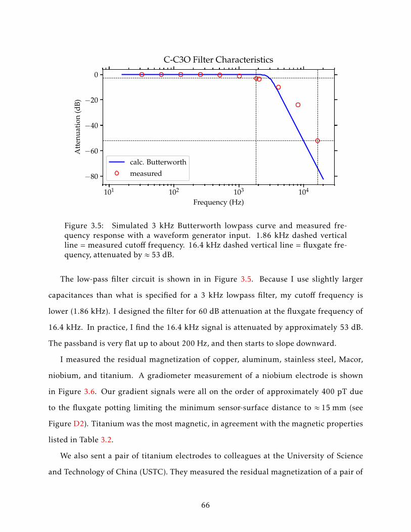
101 102 103 104
Frequency (Hz)
−80
−60
−40
−20
0A
tten
uati
on(d
B)
C-C3O Filter Characteristics
calc. Butterworth
measured
Figure 3.5: Simulated 3 kHz Butterworth lowpass curve and measured fre-quency response with a waveform generator input. 1.86 kHz dashed verticalline = measured cutoff frequency. 16.4 kHz dashed vertical line = fluxgate fre-quency, attenuated by ≈ 53 dB.
The low-pass filter circuit is shown in in Figure 3.5. Because I use slightly larger
capacitances than what is specified for a 3 kHz lowpass filter, my cutoff frequency is
lower (1.86 kHz). I designed the filter for 60 dB attenuation at the fluxgate frequency of
16.4 kHz. In practice, I find the 16.4 kHz signal is attenuated by approximately 53 dB.
The passband is very flat up to about 200 Hz, and then starts to slope downward.
I measured the residual magnetization of copper, aluminum, stainless steel, Macor,
niobium, and titanium. A gradiometer measurement of a niobium electrode is shown
in Figure 3.6. Our gradient signals were all on the order of approximately 400 pT due
to the fluxgate potting limiting the minimum sensor-surface distance to ≈ 15 mm (see
Figure D2). Titanium was the most magnetic, in agreement with the magnetic properties
listed in Table 3.2.
We also sent a pair of titanium electrodes to colleagues at the University of Science
and Technology of China (USTC). They measured the residual magnetization of a pair of
66

0 5 10 15 20 25time (min)
−500
−400
−300
−200
−100
0
100
field
(pT)
2016-12-13-135643-gradiometer-run-Nb-1.txt
monitor
gradient
null
Figure 3.6: Gradiometer results for a niobium electrode. Average gradiometersignal = −440.8± 1.6 pT. Average monitor signal = 88.2± 1.3 pT. Average nullsignal = −8.5± 0.1 pT.
titanium electrodes to ≤ 5 nT with a custom 5 mm atomic vapor cell magnetometer that
allowed them to place their sensor approximately 8 mm from the surface. The residual
magnetization measurements with the MSU fluxgate measurements and USTC magne-
tometer measurements are shown in Figure 3.7.
Because of the higher residual magnetization of the titanium electrodes, we decided
to use large-grain niobium for radium spin precession frequency measurements.
3.3 Review of High Voltage Surface Processing Applications
Electrode performance depends on the material, geometry, gap size, vacuum pressure,
applied voltage magnitude, voltage polarity, voltage frequency, and the electrode surface
condition. The analysis described in this thesis benchmarks the benefit of conventional
high gradient surface processing techniques for our unique electrode geometry and op-
67

5 10 15 20 25electrode surface to center of sensing element (mm)
102
103
104
mag
neti
zati
on(p
T)
Grade-2 Ti electrode magnetization
MSU
USTC
Figure 3.7: Residual magnetization measurements of grade-2 titanium elec-trodes using commercial fluxgates (MSU) and a custom magnetometer (USTC).
erational requirements. In this section I will briefly describe some of the use cases of
high-voltage accelerator applications that inspired us.
Radiofrequency (RF) cavities are designed to accelerate and, in some cases, bunch an
incoming beam of particles. The AC accelerating potential is typically applied across a
large gap (> 5 mm) [113]. They are usually made of large-grain or fine-grain niobium and
are often cooled to superconducting temperatures to reduce residual losses.
Electron guns provide electron sources for beam experiments. These applications typ-
ically use a conical (“point”) small-area cathode and a relatively large-area flat (“plane”)
anode to generate high-intensity current. Electron guns can be AC or DC and provide
a stable electron beam for hundreds of hours. For long-pulse (DC) gun types, applied
voltages reach hundreds of kilovolts and gap sizes of tens of millimeters [102].
Electrode geometry and operating voltage is optimized to steer charged particles and
simplify their motion in storage ring EDM experiments. The particles precess in multiple
planes through their electric and magnetic dipole interactions with the applied electric
68

(a) (b)
Figure 3.8: (a) I built a portable clean room with a 2′ × 2′ HEPA filter (SAM22MS NCR). (b) The NSCL detector clean room. It has several HEPA units andaccommodates the test station and up to three personnel.
and magnetic fields. The precession of the particles can be constrained to a single plane
relative to the momentum vector by appropriately choosing the strength of the applied
fields. Applied voltages can range from a few kV to ≈ 240 kV and electrode gaps range
from 30–120 mm [123, 124].
3.3.1 Second generation electrode surface processing
We fabricated four pairs of large-grain niobium electrodes and two pairs of grade-2 ti-
tanium electrodes in two separate batches. Surface treatment procedures for each elec-
trode pair are catalogued in Table 3.1 (batches 2 and 3). For this phase of the high voltage
development, our goal was to increase the electrode field strength from 6.5 kV/mm to
15 kV/mm or better .
With this in mind, we used processing procedures informed by discussions with Jef-
ferson Lab accelerator physicists and a review of the literature. The general recipe is to
first mechanically polish, chemical polish, then high-pressure rinse (HPR) the electrodes.
Chemical polishing and HPR with ultrapure water (UPW) significantly improves electric
field strength and stability [102, 114, 125, 126]. For an overview of chemical polishing,
69

(a) (b) (c)
Figure 3.9: Electrode high pressure rinse equipment. (a) The electrodes aremounted on an acrylic cylindrical shell centered on a turntable. As the appara-tus rotates, a concentric high pressure rinse ‘wand’ rinses the electrodes. (b) Theelectrodes are mounted so that the primary surfaces face the wand. (c) Weswitched to a rinse gun because the water quality was better.
including electropolishing and buffered chemical polishing (BCP), we refer the reader to
[127, 128, 129, 130, 131, 132, 133]. Comparing the machined dimensions to optical mea-
surements of the polished electrodes (discussed in Section 3.4.2), I find that mechanical
and chemical polishing reduces our electrode dimensions by approximately 100 µm.
Recently, centrifugal barrel polishing has been shown to reduce the required condi-
tioning time compared to chemical etching [134]. This is an encouraging prospect for
conditioning Ra EDM electrodes to significantly higher fields in a future phase of devel-
opment.
The four titanium electrodes (Ti1, Ti2, Ti3, and Ti4) were mechanically polished with
silicon carbide after fabrication. Their mean surface roughness averages were measured
in the range 16–23 nm using a profilometer (MicroXAM) in a clean room. We electropol-
ished pair Ti13 commercially and remeasured the electrode surfaces. We observed an
increase in the surface roughness of the electropolished titanium electrodes by ≈ 50%
and microprotrusions in the range 1–10 µm.
70

(a) (b) (c)
Figure 3.10: Electrode storage and transport.(a) Each electrode pair is mountedfrom the base in a stainless-steel bin. (b) The electrodes are labeled by etchingthe material and electrode number on the outside of the bin. (c) We recommendbuckling up the electrodes for car trips.
3.3.2 Clean rooms and high pressure rinsing
We developed our clean room technique by building a clean room in the lab and installing
a pair of electrodes. The Spinlab portable clean room is shown in Figure 3.8a. The HEPA
filter is safely secured overhead. I taped 2 mil polyethylene sheeting in a pleat fashion.
Then I used PVC pipes to frame a 5′×4′ area under the filter, over which the sheeting was
draped. I validated the clean room to Class 100 with a NIST-calibrated particle detector.
We decontaminate the electrodes in clean rooms at the Facility for Rare Isotope Beams
(FRIB) after polishing. The electrodes are cleaned with detergent and rinsed with pure
water in an ultrasonic bath in a staging area. They are rinsed in a second ultrasonic bath
with UPW inside a Class 100 clean room. The electrodes are then high pressure-rinsed
with UPW at 1200 psi for twenty minutes.
We used two HPR methods, shown in Figure 3.9. First, we rinsed the electrodes si-
multaneously with a turntable and high pressure rinse wand. When we later rinsed a
repolished niobium electrode pair (Nb23), the water quality of the turntable setup de-
graded. We instead used a high pressure rinse gun as shown in Figure 3.9c. After HPR,
the electrodes dry in the clean room for several days before being sealed in poly tubing
71

Table 3.3: Surface decontamination comparison. P = rinse pressure,T = rinse time, CR = clean room, RR = rinse resistivity.
Lab P T RR CR Ref.(psi) (min) (MΩ cm) (Class)
CERN 1500 30 18 100 [127]JLab 1200 20 > 18 - [102]KEK 1100 5 80 100 [114]MSU 1200 20 18.1 100 This work
backfilled with dry, filtered nitrogen. A summary of clean room and HPR parameters
from several high-gradient development groups is given in Table 3.3.
The cleaned electrodes rest in either in the high voltage test station or in a sealed
container, as shown in Figure 3.10. The electrodes have approximately 1” clearance from
the container walls on the side and bottom, and 2” below the upper edge. For storage
and transport, they are sealed in two layers of clean room tubing and are backfilled with
purified, dry nitrogen. The nitrogen is filtered at the point of use by a 0.2 µm membrane
filter.
3.4 Electrode Discharge-Conditioning
3.4.1 High voltage test station
A schematic of the MSU high voltage test station is shown in Figure 3.11. Electrode pairs
are mounted to a polyether ether ketone (PEEK) holder inside a six-way cross vacuum
chamber. To estimate the steady-state leakage current flowing through the holder itself,
we model the four “arms” as resistors in parallel with length ` = 2 × 1.6 + 0.1 = 3.3 cm
and cross-sectional area A = (1.27 cm)2. From Ohm’s law, the steady-state leakage current
I [A] is:
I =VR
= 4V Aρ `
, (3.1)
where V [V] is the applied voltage and ρ = 1016 Ω cm is the PEEK holder resistivity. The
factor of 4 comes from the equivalent resistance of the parallel leakage paths. With an
72

A
1 2456
9
8 3
7
Figure 3.11: MSU HV test apparatus. 1 9699334 Agilent Turbo-V vibra-tion damper 2 Pfeiffer HiPace 80 turbomolecular pump with foreline EdwardsnXDS10i A736-01-983 dry scroll rough pump and two valves 3 Matheson 6190Series 0.01 µm membrane filter and purge port 4 Ceramtec 30 kV 16729-03-CF feedthrough 5 0.312 in.2 electrodes in PEEK holder (resistivity 1016 MΩ cm)6 20 AWG Kapton-insulated, gold-plated copper wire 7 MKS 392502-2-YG-T all-range
conductron/ion gauge 8 Shielded protection circuit: Littelfuse SA5.0A transient voltagesuppressor, EPCOS EX-75X gas discharge tube, Ohmite 90J100E 100 Ω resistor in serieswith Keithley 6482 2-channel picoammeter 9 Ohmite MOX94021006FVE 100 MΩ re-sistors in series with Applied Kilovolts HP030RIP020 HV.
applied voltage of 30 kV, I estimate Imax ≈ 6 pA.
The vacuum chamber is maintained at 10−7 Torr with a turbomolecular pump (Pfeif-
fer Hipace 80). At this pressure the mean free path of residual gas molecules is over a
meter, significantly larger than the dimensions of the chamber. The Ra EDM apparatus
typically operates at ultrahigh vacuum (UHV) pressures (< 10−11 Torr) in the region of
the electrodes and trapped atoms [48]. The test station does not involve any trapping
of atoms and so we only require a pressure low enough such that the atmospheric con-
stituents do not collide on a length scale close to our gap size of a few millimeters. The
mean free path of an atom or molecule λ [m] is given by [135]:
λ =1σn
(3.2)
=kBTσ
1P
, (3.3)
73

where
σ[m2
]is the collisional cross section,
kB [J/K] is the Boltzmann constant,
T [K] is the temperature in the vacuum chamber,
P [Pa] is the pressure, and
n[m−3
]= P /(kBT ) is the number density for non-interacting particles, i.e. in the
limit of the ideal gas equation.
For an oxygen molecule with a cross section of ≈ 5 × 10⁻²⁰ m2 [136] and a vacuum
pressure of ≈ 5 ×10⁻⁵ Torr, the mean free path is over a meter. With a roughing pump
and turbomolecular pump (TMP) we typically operate at pressures ≈ 2× 10⁻⁷ Torr, well
below minimum requirements.
The test station is frequently brought to atmospheric pressure for upgrades and elec-
trode installations. We perform this work in clean rooms that are validated to Class 100 or
better with a NIST-calibrated particle counter (Lighthouse Handheld 3016). The chamber
is backfilled with dry, high-purity nitrogen through a 0.01 micron gas membrane particle
filter (Matheson 6190 Series) while venting the chamber and after clean room operations.
During initial evacuation the pump rate is controlled at 1 Torr/s with foreline valves to
reduce the risk of disturbing vacuum chamber surfaces.
We use polished corona ball connections inside and outside the test chamber to min-
imize discharge risk beyond the electrode gap region. The power supply (Applied Kilo-
volts HP030RIP020) and feedback resistors are mounted inside a grounded high voltage
cage. The feedthroughs are enclosed by grounded “soup can” style shields that can be
flooded with dry nitrogen to reduce humidity.
We use a 2-channel picoammeter (Keithley 6482) to measure the current flowing be-
tween the electrodes. One channel is not connected and is used to track correlated drifts
between the channels. A protection circuit between the electrode and picoammeter sup-
presses high-power transients that could damage the picoammeter. Typical discharges
74

80/20 mounting rail
Di use room light
Di use room light
Figure 3.12: The imaging components of the HV apparatus. This is a profile view ofthe apparatus after rotating the schematic in Figure 3.11 by 90 and removing non-imaging components. 1 worm-drive rail mount 2 Thorlabs MVTC23024 magnifica-tion (M) = 0.243, 4.06” working distance (WD) telecentric lens 3 Edmund Optics EO-2323 monochrome CMOS camera, 4.8 µm square pixels 4 Adjustable Electrode GapAssembly: MDC 660002 linear motion 0.001” graduated, 1” travel adjustable drive andcustom PEEK mount interface with angular adjustment.
between the electrodes do not trigger the protection circuit. We calibrated the picoam-
meter with the protection circuit to within 10 pA.
3.4.2 Optical measurements of electrodes and gap sizes
The Ra EDM experiment requires a gap-measuring precision of 0.1 mm or better. I devel-
oped an imaging system to measure electrode dimensions and gap sizes without making
contact with the electrode. The system uses a CMOS camera and bi-telecentric machine
lens (Thorlabs MVTC23024). A schematic of the optical imaging system is shown in Fig-
ure 3.12.
To test the electrodes at different gap sizes, we adjust the gap size in situ by translating
75
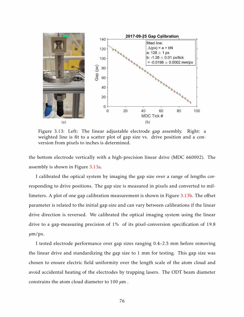
(a) (b)
Figure 3.13: Left: The linear adjustable electrode gap assembly. Right: aweighted line is fit to a scatter plot of gap size vs. drive position and a con-version from pixels to inches is determined.
the bottom electrode vertically with a high-precision linear drive (MDC 660002). The
assembly is shown in Figure 3.13a.
I calibrated the optical system by imaging the gap size over a range of lengths cor-
responding to drive positions. The gap size is measured in pixels and converted to mil-
limeters. A plot of one gap calibration measurement is shown in Figure 3.13b. The offset
parameter is related to the initial gap size and can vary between calibrations if the linear
drive direction is reversed. We calibrated the optical imaging system using the linear
drive to a gap-measuring precision of 1% of its pixel-conversion specification of 19.8
µm/px.
I tested electrode performance over gap sizes ranging 0.4–2.5 mm before removing
the linear drive and standardizing the gap size to 1 mm for testing. This gap size was
chosen to ensure electric field uniformity over the length scale of the atom cloud and
avoid accidental heating of the electrodes by trapping lasers. The ODT beam diameter
constrains the atom cloud diameter to 100 µm .
76

Table 3.4: 5σ Data acquisition and filtering settings. Used filters indicated by filled-in circles. SR = sample rate.
DAQ Digital filters
pair SR samples 25–35 Hz 55–65 Hz 109–113 Hz 115-125 Hz 7.5 kHz(kHz) point bandstop bandstop bandstop bandstop lowpass
Nb56 16 8192 • • • • •Nb78 16 8192 • • • • •Ti13 30 8192 •Nb23 30 8192 •
We used the optical imaging system electrode measurements to fabricate the EDM
electrode holder for the niobium electrode pair Nb56, shown in shown in Figure 2.6. The
EDM electrode holder is designed for a 1.0± 0.1 mm gap size.
3.4.3 Data acquisition and filtering settings
A complete description of acquisition and filtering settings used for each tested pair of
electrodes is given in Table 3.4. We record the power supply current, power supply volt-
age, vacuum pressure, leakage current, and rough pump foreline pressure with a 16-bit,
250 kS/s data acquisition device (NI DAQ USB-6218) connected to an office model desk-
top PC. Each input channel uses a ±10 V range. The analog signals are digitally filtered
to remove 60 Hz outlet noise and mechanical vibrations from the vacuum pumps. We
initially sampled data at 16 kHz but later increased the sample rate to 30 kHz after up-
grading the RAM and hard disk of the DAQ PC. The mean and standard deviation for
each recorded data point is calculated from 8192 samples.
We removed the outlet noise filters after conditioning several pairs of electrodes be-
cause they introduced artificial shapes in the signal waveform. Comparing the leakage
current data of electrode pairs with different filtering settings, we found that the dig-
ital filters did not significantly affect the distribution of the dataset discussed in Sec-
tion 3.4.4. As I will discuss in Section 3.4.10, we are sensitive to absolute currents as
77

Nb23 stdevs at -22 kV / 1 mm , time period 32 / 58
100 110 120 130 140leakage current (pA)
0
5
10
15
20
25
30
cou
nts
115.2 3.3 pA 5σ
Figure 3.14: A Gaussian fit (red line) to a set of approximately 220 standarddeviations collected over a 60 second time period at −22 kV for Nb23.
small as σ ≈ 25 pA with the acquisition settings described in Table 3.4.
3.4.4 Identifying electrode discharges
We average 8192 samples at sample rates of 16 kHz for electrode pairs Nb56, Nb78 and
30 kHz for Ti13, Nb23, corresponding to a recorded data point every 512 ms and 273 ms,
respectively. Since each high voltage magnitude and polarity setting lasts for a time pe-
riod of 60 seconds, this corresponds to about 120 samples collected per time period at
16 kHz and 220 samples collected per time period at 30 kHz.
The distribution of each time period in a conditioning shift is modeled as a Gaussian
distribution. As shown in Figure 3.14, the data is reasonably fit by a Gaussian. I define
a “discharge” as any standard deviation exceeding the Gaussian 5σ threshold above the
center value.
To estimate discharge magnitudes, I report the median value of the standard devia-
tions in each 60 s time period. We expect to see high rates of discharges during condi-
tioning. Small discharges occurring at a stable rate are beneficial and do not damage the
electrode surfaces.
78

0 20 40 60 80 100 120 140 160 180 200time (min)
-15
-10
-5
0
5
10
15
20
25
leak
age
curr
ent
(pA
)
steady-state leakage current
-19.9 kV19.7 kV
Figure 3.15: The offset-subtracted average leakage currents for each positiveand negative high voltage time period during conditioning at 20 kV with Nb56at a gap size of 1 mm.
Our discharge counting method does not exclude discharges that could occur at an-
other part of the test station, for example the high voltage feedthroughs. Therefore, we
expect our reported discharge rates are conservative overestimates of the true electrode
discharge rate.
Additionally, we calculate the steady-state leakage current I by fitting a Gaussian to
the sample means, rather than the standard deviations, of each 60 s time period. Elec-
tronic offsets and drifts are removed by subtracting the mean current measured by the
picoammeter during the zero voltage time periods neighboring each high voltage time
period. An example of I measurements measured over a four-hour conditioning shift for
Nb56 is shown in Figure 3.15.
Since the integration time for each data point at 30 kHz is 273 ms, I is insensitive
to discharges, which typically last ≈ 1 ms. To illustrate, we can compare the discharges
identified by the mean data and the standard deviation in the third hour of a 26.2 kV
79

(a) (b)
Figure 3.16: Histograms of the discharges for both polarities during the thirdhour of conditioning of the titanium electrodes on a log-log scale.
conditioning shift of Ti13. Histograms of the discharges identified by the standard de-
viations are shown in Figure 3.16. I count a polarity-combined 111 discharges with the
standard deviation data over one hour. Using a similar analysis with the sample means, I
count only 11 events outside of the 5σ threshold during the same time period.
My analysis code models the leakage current and calculates the discussed perfor-
mance metrics. The accuracy of the analysis was independently verified. Code and data
availability may be found in Appendix B.
3.4.5 Discharge-conditioning procedure
Our goal is maximize the electric field strength while minimizing the discharge rate and
discharge size. We condition the electrodes at DC voltage, alternating the voltage polarity
every 60 s. The voltage is applied to the top electrode. The periodic voltage waveform
is chosen to simulate the EDM measurement and is more challenging to stabilize than
holding off a static unipolar field. Each conditioning shift at one high voltage magnitude
80

0 5 10 15 20 25 30 35-100
-50
0
50
100
150
200
250
300
350Nb56 5 discharge rates (-HV)
12.0 kV
13.0 kV
13.9 kV
14.9 kV
15.9 kV
16.9 kV
17.9 kV
18.9 kV
19.9 kV
0 5 10 15 20 25 30 35-100
-50
0
50
100
150
200
250
300
350ra
te -
bas
elin
e (h
r-1)
Nb56 5 discharge rates (+HV)
0 5 10 15 20 25 30 35conditioning time (hr)
-20
0
20
40
60
size
- b
asel
ine
(pA
)
Nb56 5 discharge sizes (+HV)
0 5 10 15 20 25 30 35conditioning time (hr)
-20
0
20
40
60
Nb56 5 discharge sizes (-HV)
baseline = 118 hr-1 baseline = 59 hr-1
baseline = 42 pA baseline = 31 pA
Figure 3.17: Discharge-conditioning timeline for Nb56 at a 1 mm gap size.
with this periodic waveform typically lasts 3–5 hours1.
In the final conditioning phase we validate the electrodes at some fraction of the max-
imum voltage to reduce the discharge rate. The validation voltage is typically 80–95% of
the maximum tested voltage, consistent with the literature [100, 113].
I show the average discharge rates and discharge sizes for both polarities for all the
electrodes in Figures 3.17, 3.20, 3.21, and 3.22. I define a ‘baseline’ value as the average
discharge rate and discharge size during the first conditioning shift. Each of these figures
has a baseline value that is subtracted from the data.
In Sections 3.4.6, 3.4.7, 3.4.8, and 3.4.9, I will discuss the discharge-conditioning re-
sults of each electrode pair. In Section 3.4.10, I will compare the overall performance of
the electrodes.
1We found that the highest discharge rates tended to occur during the second andthird hours of a shift, so we scheduled five-hour shifts when possible.
81

(a) (b) (c)
Figure 3.18: Installation of niobium electrode pair Nb56 in Ra EDM apparatus.(a) ANL portable clean room with aluminum beams, plastic drapes, and a 4′ × 2′
HEPA filter. (b) The borosilicate glass tube was cleaned with a clean-room gradewipe wrapped around the end of a fiberglass pole. (c) The clean room waspositioned over the electrode entry point before installing the electrodes (seenin the bottom corner).
3.4.6 Conditioning results for electrode pair Nb56
The average discharge rate over the course of conditioning the niobium electrode pair
Nb56 is shown in the upper panels of Figure 3.17. At each voltage, the discharge rates,
expressed in discharges per hour (dph), tend to decrease as we condition. There is a
step-like increase in discharge rates when the voltage is increased. Nb56 was validated
at 20 kV / 1 mm with an average discharge rate of 98± 19 dph after approximately thirty
hours of conditioning.
At negative polarity, the discharge rate increases more slowly with each voltage step.
However, the overall curve does not flatten at a minimum count rate as it does at positive
polarity. This suggests that additional conditioning could further suppress discharges at
negative polarity. It’s also possible that the test station design facilitates a higher dis-
charge rate at negative polarity. We will explore this in the near future by conducting
conditioning tests while the electrodes are removed from the test station.
Nb56 discharge sizes are shown in the lower panels of Figure 3.17. As we will see
82

high voltage feedthroughs
MOT
bellows heater boom
bellows heater top
feedthru heater boom
feedthru heater topTiSubpump
geerpump
RGA
X: thermocouple position
heater tape
x xx x x x xx
x
x
x
x
Figure 3.19: A schematic of the water bake of the Ra EDM experimental appa-ratus following the installation of the new electrode pair.
with all the discharge plots, the discharge size behavior does not scale with the discharge
rate. The largest median discharge size over the course of conditioning is 60 pA, which
is relatively small compared to the typical discharge sizes of the other electrode pairs.
In the last hour of conditioning the discharge sizes are 20 pA smaller than the starting
discharge sizes.
As mentioned in Section 3.1.1, the legacy copper electrodes were conditioned to
10 kV/mm but could only be operated at 6.5 kV/mm after installing them in the Ra EDM
apparatus. For the second generation electrodes, I made two major improvements to the
technique to prevent a similar reduction in field strength. First, our electrodes are now
preserved in Class 100 (ISO 5) or better clean room environments during both condi-
tioning and transport as described in Sections 3.3.1 and 3.4.1. Second, we used the new,
rigorous discharge-conditioning analysis described Section 3.4.4 for Nb56 and the elec-
trodes discussed in the subsequent sections.
Nb56 was installed in the Ra EDM apparatus on May 15, 2018 in the conditions shown
83

0 5 10 15 20 25 30-500
0
500
1000
1500
2000
2500
3000Nb78 5 discharge rates (-HV)
12.0 kV
12.9 kV
13.9 kV
14.9 kV
15.9 kV
16.9 kV
17.0 kV
17.5 kV
17.9 kV
0 5 10 15 20 25 30-500
0
500
1000
1500
2000
2500
3000ra
te -
bas
elin
e (h
r-1)
Nb78 5 discharge rates (+HV)
0 5 10 15 20 25 30conditioning time (hr)
0
100
200
300
400
Nb78 5 discharge sizes (-HV)
0 5 10 15 20 25 30conditioning time (hr)
0
100
200
300
400
size
- b
asel
ine
(pA
)
Nb78 5 discharge sizes (+HV)
baseline = 58 hr-1baseline = 347 hr-1
baseline = 24 pA baseline = 39 pA
Figure 3.20: Discharge-conditioning timeline for Nb78 with a 1 mm gap size.
in Figure 3.18. Details will be discussed in Section 3.4.13.
Following installation, I “baked” the EDM apparatus by heating the borosilicate tube
and high voltage vacuum components at 120 C for three days and then increased the
temperature to 150 C for approximately five weeks. This temperature is high enough
to remove moisture that was introduced during the electrode installation. The vacuum
pressure dropped by more than three orders of magnitude over the course of the water
bake.
A schematic of the water bake is shown in Figure 3.19. To equalize the temperature
throughout the system, I used heater tape, foil, and several heat guns. I monitored the
temperature with thermocouples.
After the water bake, I revalidated electrodes Nb56 at 20 kV/mm. This electrode pair
will be used for upcoming second generation EDM measurements and is expected a factor
84

0 20 40 60 80 100-1000
0
1000
2000
3000
4000
5000
6000
7000
8000Ti13 5 discharge rates (-HV)
0.7 kV9.8 kV14.7 kV16.1 kV17.8 kV17.9 kV19.4 kV19.5 kV20.5 kV21.9 kV23.3 kV24.8 kV26.2 kV27.6 kV29.1 kV
baseline = 134 hr-1
0 20 40 60 80 100-1000
0
1000
2000
3000
4000
5000
6000
7000
8000ra
te -
bas
elin
e (h
r-1)
Ti13 5 discharge rates (+HV)
baseline = 143 hr-1
0 20 40 60 80 100conditioning time (hr)
-150
-100
-50
0
50
100
150
200
250
300Ti13 5 discharge sizes (-HV)
baseline = 101 pA
0 20 40 60 80 100conditioning time (hr)
-150
-100
-50
0
50
100
150
200
250
300
size
- b
asel
ine
(pA
)
Ti13 5 discharge sizes (+HV)
baseline = 116 pA
Figure 3.21: Discharge-conditioning timeline for Ti13 at a 0.9 mm gap size.
of 3.1 improvement to our EDM measurement sensitivity.
3.4.7 Conditioning results for electrode pair Nb78
Discharge rates and sizes for the second pair of niobium electrodes Nb78 are given in Fig-
ure 3.20. We started conditioning Nb78 at 12 kV/ 1 mm, the same electric field as Nb56.
The initial discharge rates are occasionally in excess of 1000 dph, or about once every
three seconds for several hours with discharge sizes of 50 pA. The high discharge rate
coupled with low discharge size is an indication that we are operating at an ideal voltage
for discharge-conditioning. During the last 10 hours of conditioning the discharge rates
decrease to less than the initial rates. The final conditioning shift was performed at 17.8
kV/mm.
These electrodes were packaged according to our procedure described in Section 3.3.2
85

and shipped to USTC, where they are being used in a new ytterbium EDM measurement.
3.4.8 Conditioning results for electrode pair Ti13
We changed our data acquisition and digital filter settings for Ti13 and the pair that
we will discuss in Section 3.4.9 (see Table 3.4). To reach electric fields higher than
20 kV/mm, we conditioned the titanium electrodes for 110 hours, four times longer than
the previous pairs.
Discharge rates and sizes for the titanium electrodes are shown in Figure 3.21. We
started conditioning the electrodes at 14.9 kV/ 0.9 mm = 16.5 kV/mm. The initial dis-
charge sizes are approximately 100 pA, significantly higher than Nb56 and Nb78. The
discharge rates did not consistently decrease over the course of several shifts at 19.4 kV.
At hour 12, we reduced the voltage to 0.7 kV for one shift to verify that the discharge
rates decrease before resuming testing at higher voltages.
The discharge rate increases from 290 dph to 5550 dph when stepping the voltage
from −26.2 kV to −27.6 kV. This step-like ‘switching on’ of leakage emission sites is con-
sistent with our expectations, given the physical picture of conditioning we describe in
Section 2.6. In principle, the emission sites, which may be thought of as microprotru-
sions, are ablated after spending sufficient time discharge-conditioning the electrodes.
The factors influencing the required amount of time include the smoothness of the high-
gradient surfaces, the gap size, and the applied voltage. We were unable to significantly
reduce the discharge rates at 27.6 kV / 0.9 mm = 30.7 kV/mm despite more than twenty
hours of conditioning at that field strength.
During the final shift, we reduced the voltage to 14.7 kV / 0.9 mm = 16.3 kV/mm and
again observed the discharge rates returning to the baseline. Ti13 can likely be condi-
tioned to perform stably at ≈ 24 kV, or 85% of the maximum applied voltage with addi-
tional conditioning. However, the concentration of magnetic impurities in our titanium
electrodes (shown in Table 3.2) is likely too high to be used for an EDM measurement.
86

0 20 40 60 80 100 120
0
500
1000
1500
2000
2500
3000
3500Nb23 5 discharge rates (-HV)
12.0 kV
13.0 kV
13.1 kV
15.1 kV
16.8 kV
16.9 kV
17.0 kV
18.9 kV
19.0 kV
20.0 kV
21.9 kV
22.0 kV
0 20 40 60 80 100 120
0
500
1000
1500
2000
2500
3000
3500ra
te -
bas
elin
e (h
r-1)
Nb23 5 discharge rates (+HV)
0 20 40 60 80 100 120conditioning time (hr)
0
500
1000
1500
2000Nb23 5 discharge sizes (-HV)
0 20 40 60 80 100 120conditioning time (hr)
0
500
1000
1500
2000
size
- b
asel
ine
(pA
)
Nb23 5 discharge sizes (+HV)
baseline = 190 hr-1baseline = 131 hr-1
baseline = 30 pAbaseline = 35 pA
Figure 3.22: Discharge-conditioning timeline for Nb23 at a 1 mm gap size.
3.4.9 Conditioning results for electrode pair Nb23
I initially tested Nb23 at a 0.4 mm gap with fields as high as +52.5 kV/mm and
−51.5 kV/mm using the traditional hold-off or “current-conditioning” method [100].
Then I discharge-conditioned the electrodes with the periodic waveform described in Sec-
tion 3.4.4 to 27.5 kV/mm. However, a large discharge of ≈ 100 nA during a 30 kV/mm
conditioning shift triggered a current avalanche that rapidly increased the leakage cur-
rent and damaged the electrodes.
I was unable to recover meaningful performance after several conditioning attempts.
The electrodes were removed from the test station and repolished the surface according
to Table 3.1. Then I reinstalled Nb23 and repeated the conditioning at a 1 mm gap.
Repolished Nb23 discharge rates and sizes are shown in Figure 3.22. The rates stay
near the baseline, about 200 dph for both polarities up to 20 kV. When we increased the
87

Table 3.5: Electrode conditioning summary. Ei = initialfield strength. Emax = max field strength. Ef = final vali-dated field strength. Ri (Rf ) = initial (final) discharge rate.I = steady-state current at Ef .
pairEi Emax Ef Ef
Ei
RfRi
I(kV/mm) (kV/mm) (kV/mm) (pA)
Nb56 11.9 19.8 19.8 1.7 1.6 < 10Nb78 12.0 17.9 17.9 1.5 0.9 < 10Ti13 19.8 32.3 29.1 1.5 2.2 < 30Nb23 12.0 22.0 21.9 1.8 1.3 < 25
voltage from 20 kV to 22 kV, the discharge rates at negative polarity become as high as
3000 dph (about once every second). The discharge sizes were low, less than 500 pA, so we
continued conditioning at this voltage. Despite conditioning the electrodes at 22 kV/mm
for more than twenty hours, the discharge rate remained high. I expect that reducing the
voltage by ≈ 1 kV will restore the baseline discharge rate.
For this pair of electrodes, repolishing and reconditioning allowed us to recover 80%
of the original electric field performance.
3.4.10 Comparison of overall electrode performance
Table 3.5 compares the electric fields tested and discharge rates observed for all of the
conditioned electrode pairs averaged over both polarities. Ei is the electric field strength
at the start of the conditioning, while Emax is the electric field strength at the end of the
conditioning. Ef is the final validated field strength, and may be reduced to ≈ 85% of
Emax for more stable performance.
The initial electric field is 12 kV/mm for the niobium electrodes and 16.5 kV/mm
for the titanium electrode pair. I chose these field strengths because the discharge rate
and discharge size was sufficiently low. The maximum and final electric fields depended
entirely on the performance of the electrodes.
All the electrodes were discharge-conditioned to higher than our original goal of
88

15 kV/mm. The steady-state currents I at Ef are under the EDM experimental threshold
of 100 pA.
One metric for characterizing discharge-conditioning is to compare the electric field
strength ratio Ef /Ei versus the discharge rate ratio Rf /Ri . My expectation for successful
conditioning is that the electric field scaling should be comparable, and ideally larger
than the discharge rate ratio. We were able to scale the electric field more quickly than
the discharge rates for all the niobium electrodes. For Nb78, the final polarity-averaged
discharge rates were lower than the initial discharge rates. As discussed in Section 3.4.8,
the Ti13 discharge rate outpaced the electric field strength increase at 30.7 kV/mm.
Of particular note is the polarity dependence of the electrode discharge rates. In all
cases except for Nb23, the negative polarity discharge rates are significantly higher than
the discharge rates at positive polarity. Polarity-correlated discharge rates could be a con-
sequence of the asymmetry of our setup, as illustrated by Figure 3.11. Our goal for the
next phase in high voltage development is to design a more symmetric setup that will al-
ternate the role of grounded and charged electrode. In addition to increasing the electric
field strength capability, we expect the new setup to aid the investigation of polarity-
correlated discharge rates.
3.4.11 Comparison of electrode performance with other systems
A comparison of the maximum stable electric field performance of electrode pairs pre-
pared at ANL [65, 48], the High Energy Accelerator Research Organization (KEK) [114],
and MSU is shown in Figure 3.23. We tested a maximum electric field of +52.5 kV/mm
and −51.5 kV/mm with one of our niobium pairs of electrodes (Nb23) at a gap size of
0.4 mm. The electrode conditioning results described by Furuta et. al are a useful, if
imperfect comparison. Their electrode size is and electrode gap size is similar, but they
use an asymmetric electrode geometry and a unipolar power supply. The KEK group
pairs a stainless steel spherical anode with “button-shaped” cathodes made from refined,
89

0 0.5 1 1.5 2 2.5 3electrode gap (mm)
0
20
40
60
80
100
120
elec
tric
eld
(k
V/m
m)
100 kV30 kV E- highest
E+ highest
E-
validated
E+ validated
KEKANLMSU
Figure 3.23: A plot of electric fields reached by electrode pairs. Blue data areelectrodes used in the Ra EDM apparatus. Green data are electron gun elec-trodes tested with a −100 kV power supply [114]. Red data are electrodes testedat MSU. Brighter, more intense colors are more recent results.
high-purity 316L stainless steel (“Clean-Z”), titanium, and molybdenum.
The data in Figure 3.23 suggests that fields in the realm of 100 kV/mm are attainable
in principle. Electrode geometry, high-gradient surface area, high voltage polarity, and
the nature of the voltage waveform are some of the parameters that may limit the ultimate
performance of our electrodes.
At present, the main limiting factor of the Ra EDM electric field strength is the 30 kV
maximum output of the high voltage power supply.
3.4.12 Steady-state leakage current analysis
We plot the weighted average steady-state leakage current for each applied voltage for all
the electrodes in Figure 3.24. Each data point represents the average of one polarity at
90

-30 -20 -10 0 10 20 30
-20
-15
-10
-5
0
5
10
leak
age
curr
ent
(pA
)
steady-state leakage current
Nb56Nb78Ti13Nb23
-30 -20 -10 0 10 20 30voltage (kV)
10-1
100
101
102
103
| le
akag
e cu
rren
t |
(pA
)
Figure 3.24: Weighted averages of the steady-state leakage current on linear andlog scales. Errors are on the order of 0.1 pA.
one voltage setting over an entire shift. For example, Figure 3.15 shows the “raw data”
that’s averaged into ±20 kV data points for Nb56 and plotted in Figure 3.24.
In Section 3.4.4, I stated that the steady-state leakage current is calculated by sub-
tracting the signal measured during the zero-voltage time periods that occur between
each high voltage time period. This zero-voltage background subtraction removes the
instrument offsets and linear drift, but does not account for high-voltage correlated sys-
tematics.
91

The power supply voltage monitor and current monitor signals scale with voltage
magnitude. Because we sample data on one DAQ card, a small amount of signal from
adjacent and non-adjacent input channels can affect each other. Each leakage current
value I from Figure 3.24 can be written as the true leakage current I(0)
plus correlated
systematics:
I(0)
+ δIVMON(V ) + δIIMON(V ) , (3.4)
where δIVMON(V ) and δIVMON(V ) are voltage magnitude-correlated systematics.
I estimate the voltage magnitude-correlated systematics assuming an applied high
voltage of 30 kV. At this voltage, the signal size of the voltage monitor VVMON ≈ 10 V
and VIMON ≈ 0.4 V. The current monitor channel is adjacent to the leakage current signal
and the voltage monitor signal is non-adjacent. From the DAQ datasheet (NI DAQ USB-
6218), I assume the adjacent channel crosstalk is −75 dB and the non-adjacent crosstalk
is −95 dB. This gives a total crosstalk signal of
VCT ≈ (+0.4 V)× 10−(75/20) + (10 V)× 10−(95/20) ≈ +0.3 mV
The picoammeter range is 200 nA and the analog voltage output is inverting on a 10 V
scale, so the crosstalk voltage shifts the leakage current signal at both high voltage polar-
ities by
+0.3 mV × (−200 nA) /10 V = −6 pA
The magnitude of voltage-correlated systematics is on the order of the sampling resolu-
tion of the 16-bit DAQ card. There is also a polarity-dependent crosstalk systematic, but
this effect is negligible at the ≈ 1 pA level.
Taking high-voltage correlated systematics into account, the steady-state leakage cur-
rents in Figure 3.24 are subject to systematic uncertainty at the ≈ 10 pA level.
The steady-state leakage current versus voltage trend is modestly linear with an ohmic
resistance of 40 kV/10 pA ≈ 1016 Ω. We observe large leakage currents > 100 pA, corre-
92

lated with high discharge rates, for Ti13 and Nb23 beyond 22 kV. In the most extreme
case, we measured I ≈ −670 pA during conditioning Ti13 at −27.6 kV.
The steady-state leakage current must be less than 100 pA to avoid systematics that
could mimic an EDM signal at our current statistical sensitivity. This criterion is similar
to metrics used in other electrode development groups [102, 114]. Our steady-state leak-
age current sensitivity is limited to ≈ 25 pA. At the Nb56 final validated field strength of
20 kV/mm, the measured steady-state leakage current is below this upper limit.
3.4.13 Transportation and installation of electrodes in Ra EDM apparatus
Moving the Nb56 electrodes from the MSU high voltage test station to the ANL EDM
apparatus posed the highest risk of surface contamination. Before transport, I packaged
them in a Class 100 clean room at the National Superconducting Cyclotron Laboratory
(NSCL). The electrodes were mounted in a cleaned stainless steel container by their base
to minimize their risk of contact with any surface, as seen in Figure 3.1. I double-bagged
and sealed the container and electrodes in clean room tubing and backfilled with particle-
filtered dry nitrogen.
I transported the electrodes from MSU to ANL in December 2017.
Starting in February 2018, I constructed a custom portable clean room at ANL. I used
a NIST-calibrated particle counter to verify that the clean room was within Class 100
limits. The portable clean room is shown in Figure 3.18a. On May 13, 2018, I unpacked
Nb56 in the portable clean room and assembled in a new Macor holder designed for an
electrode gap of 1 mm. I packaged the electrodes and Macor holder in backfilled poly
tubing, as before.
On May 15, 2018, the Ra EDM science chamber front end was disassembled (shown
in Figure 3.18b) and the legacy copper electrodes were removed.
The portable clean room was positioned over the science chamber opening. The clean
room and science chamber were cleaned and validated at Class 100 standard. A view
93

from inside the clean room is shown in Figure 3.18c. Finally, the electrodes were removed
from their packaging and installed in the science chamber on May 15, 2018.
The EDM apparatus was vacuum pumped and water baked as described in Section 3.4.6.
On July 22, 2018, I revalidated the Nb56 electrode performance to 20 kV/mm.
94

CHAPTER 4
RADIUM BRANCHING RATIOS
I worked at Argonne National Laboratory (ANL) from February 2018 through August
2018. During that time I worked on the upgrade for the longitudinal atom slower (“Blue
slower”) project. I’m the third author on the publication describing our fluorescence
measurements branching fraction measurements [90].
First, I’ll describe the Blue Slower project in the context of the Ra EDM experiment.
Then I’ll describe the experimental setup for the measurements, including the lasers
needed. Then we’ll discuss the fluoroscopy measurements of the atomic transitions of
interest. Finally, I’ll talk about the analysis that we use to find the intensity of the Blue
slower transitions.
4.1 Radium laser cooling with the Zeeman slower
To measure an EDM, we need to trap atoms between two high voltage electrodes to
perform spin precession frequency measurements (see Figure 2.1). From Equation 2.3,
the statistical sensitivity of the EDM measurements scales as√N , whereN is the number
of atoms precessing between the electrodes. Our goal is to interrogate as many atoms as
possible, i.e. maximize N .
Radium atoms exit an effusive oven with some angular distribution j(θ), where θ
is the angle from the longitudinal axis, and velocity distribution g(v), where v [m/s] is
the speed. After radium atoms exit the oven, they are collimated with a retro-reflected
transverse laser to reduce the angular spread.
Next, the atom beam propagates through a Zeeman slowing section. The details of the
Zeeman slower are given in Section 2.2.1. A tapered solenoid coil around the beamline
Zeeman-shifts the transition frequency to compensate for the Doppler effect. The result
is a fraction of atoms that are sufficiently slowed for trapping.
95

510 μs
5.5 ns
420 ns
1𝑃1𝑜
1𝐷2385 μs
3𝑃1𝑜
3𝐷23𝐷1
1𝑆0
red (weak)
714 nm
R1
3𝐹2𝑜
3𝐷3
15 ns
Red slower
blue (strong)
483 nm
Blue slower
510 μs
5.5 ns
420 ns
1𝑃1𝑜
1𝐷2385 μs
3𝑃1𝑜
3𝐷23𝐷1
1𝑆0
red (weak)
714 nm
R1
3𝐹2𝑜
3𝐷3
15 ns
R3
R2
Figure 4.1: Left: the current “red” Zeeman slowing scheme. R1 = 1429 nm.Right: the envisioned “blue” Zeeman slower upgrade. R1 = 698 nm, R2 =712 nm, R3 = 2752 nm.
We currently use the 1S0→ P3 o1, or “red” cycling transition to decelerate the radium
atoms. In this scheme, shown in side (a) Figure 4.1, radium atoms are excited to 3P o1 with
a Ti:Saph laser at 714 nm. They decay to 3D1 with a half-life of 422(20) ns [137, 138].
To circumvent the relatively long lifetime of this metastable state, an additional laser is
used to “repump” atoms to 1Po1, where they decay to the ground state after approximately
5 ns. This scheme is simple, requiring only a single repump laser. Using the red cycling
transition, we can slow atoms with an initial velocity of ≤ 60 m/s, or about 0.2% of all the
atoms exiting the oven. The momentum of any atoms exiting the oven at a speed greater
than 60 m/s is too large to sufficiently slow for trapping.
For the next phase of the radium Zeeman slower, we’ll use an additional, stronger
cycling transition to slow down a larger fraction of the atoms exiting the oven. The
1S0→ P1 o1, or “blue” cycling transition, delivers a stronger momentum kick to the atom
and can be cycled about 80 times quicker than the red cycling transition. The blue slower
upgrade will be assembled upstream of the red slower and calibrated to slow atoms to
96

0 100 200 300 400 500 600 700velocity (m/s)
0.0000
0.0002
0.0004
0.0006
0.0008
0.0010
0.0012
0.0014
0.0016
0.0018
nor
mal
ized
inte
nsi
ty
500 C
red slower
blue slower
Figure 4.2: The Maxwell-Boltzmann speed distribution of radium atoms exitingthe oven. The estimated fraction of atoms that can be sufficiently slowed fortrapping are shaded according to the slowing scheme.
60 m/s, so the red slower can be used with or without the blue cycling transition.
The Maxwell-Boltzmann speed distribution of radium atoms exiting a 500C oven
is shown in Figure 4.2. The shaded area of the curve represents the relative amount of
atoms that can be trapped for the red slower (shaded red) and the blue slower (shaded
blue). The blue slower upgrade is expected to trap more than 50% of atoms exiting the
oven and will yield approximately 100 times more trappable atoms than the red slower
alone.
The blue slower cycling scheme is more complex and requires consideration of addi-
tional decay channels than the red cycling scheme. Once 1Po1 is populated, there are four
non-cycling deexcitation paths that the atoms can take. Electric dipole, or E1 transitions
of the lowest atomic excited states of radium are shown in Figure 4.3. New repump lasers
97

are required for decay states with significant branching fractions. They need sufficiently
high intensity to saturate each of these transitions. The fractional rate of atoms deexcit-
ing from initial state | i 〉 to one possible decay state | k 〉 is known as the branching ratio
BR (| i 〉 → | k 〉) [unitless]: a
BR (| i 〉 → | k 〉) =gkfikλ2ik
/∑`
g`fi`λ2`k
, (4.1)
where
g ′k [unitless] is the degeneracy of | k 〉,
fik [unitless] is the oscillator strength of the transition | i 〉 → | k 〉, or the ratio of
power absorbed by the atom to that absorbed by a classical oscillator, and
λik [m] is the transition wavelength from | i 〉 → | k 〉.
The decay strengths are sometimes expressed in terms of the transition matrix element
|Dik | rather than fik in theory calculations. The two are related by fik ∝|Dik |2
giλ.
E1E1E1-allowed atomic transitions:
∆J = 0,±1 except for gs→ gs transitions
∆M = 0,±1 except for gs→ gs transitions when ∆J = 0
one electron jump with ∆` = ±1
LSLSLS coupling:
∆S = 0
∆L = 0,±1 except for gs→ gs transitions
The envisioned repumping scheme is shown in Figure 4.1. One of the possible non-
cycling states, 3D3, is predicted to have a surprisingly weak branching ratio. Another
state, 1D2, is normally a forbidden transition (E1, ∆S = 0), but is predicted to have a
aWe are technically calculating branching fractions, but this is the nomenclature usedin our paper. The true branching ratio is the ratio of one branching fraction to anotherbranching fraction.
98

7s2 1S0
freq
uen
cy (
TH
z)
7s7p 1P1o 5.5 ns
7s7p 3P0o
7s7p 3P2o 5.4 µs
7s6d 3D3
7s8s 3S1 18 ns
7s8s 1S0 80 ns
7s7p 3P1o 422(20) ns
7s6d 3D1 510(60) µs
7s6d 1D2 385(45) µs
6d7p 3F2o 15.3(40) ns
6d7p 3F3o 28 ns
6d7p 3F4o 23 ns
6d7p 1D2o 19 ns
482.
7254
/ 4
82.8
65
731.2288 /731.44
698.
2168
/ 6
98.4
19
726.29 / 726.50784.0266 / 784.254
712.
0438
/ 7
12.2
5062
0.20
08 /
620
.381
750.
1482
/ 7
50.3
66
648.
9112
/ 6
49.0
99
993.4916 / 993.780
722.
7162
/ 7
22.9
26
566.
2376
/ 5
66.4
02
7s6d 3D2 4 s
1020
940
820
700
580
460
340
0
380
420
500
540
620
660
740
780
860
900
980
Figure 4.3: An energy level diagram of the fifteen lowest energy levels and E1-allowed transitions of 226Ra. Measured lifetimes: 7s7p P3 o
1 [137], 6d7p F3 o2 [90],
7s6d D31 [139], 7s6d D1
2 [140]. Calculated lifetimes: 7s6d D32 [141], all other
transitions [89]. Wavelengths are labeled along transition lines in [nm] in vac-uum/air.
99

Oven
RaNO3 + Ba
Atomic Ra Beam
Lens
Pum
p48
3nm
712n
m
Prob
e
Filter
PMT
Fluorescence collection
region
x
y
z
698
nm
(sig
nal)
712
nm
(pro
be)1P1
1D2
3D23D1
1S0
3D3
3F2
Figure 4.4: A schematic of the branching ratio fluoroscopy setup. Inset: energydiagram for measuring the 3D1 branching ratio.
favorably strong branching ratio [89]. This is due to the total angular momentum J = L+S
coupling of the parent state 3Fo2. The high intensity of 1D2 will allow us to “flip” the spin
of the 3Fo2 state and repump along the transition 1D2→ P1 o1.
My goal was to measure the 1Po1 decay channels using laser-induced fluoroscopy to
experimentally verify the predicted branching ratios for the Blue slower upgrade. This
was necessary because implementing the blue slowing scheme requires lasers that can
provide sufficient power at each transition. The requisite power depends on the branch-
ing fraction intensity of 1D2 and the 3DJ states. In the case of 3D3, the branching ratio is
predicted to be low enough that we can neglect repumping that state without significant
atom loss.
To measure the fluorescence from a signal state, we populate all the D states with a
483 nm pump laser resonant with the 1S0→1P1 transition. Then we depopulate one of
the strong decay states, either 3D1 or 3D2, with a second probe laser. Finally, we detect
the fluorescence to the decay channel of interest with a PMT and an appropriately chosen
100

Table 4.1: Transitions and wavelengths for branchingratio measurement.
transition wavelength (nm) laser1S0→1 Po
1 482.7254 blue imaging laser1D2→3 Fo
2 912.6919 NIR diode laser3D1→3 Fo
2 698.2168 tunable Ti:Saph laser3D2→3 Fo
2 712.0438 tunable Ti:Saph laser
bandpass filter. A schematic is shown in Figure 4.4. A list of the transitions and the lasers
used to excite the state to 3Fo2 is given in Table 4.1. By measuring the fluorescence of the
transitions using all the possible configurations, we can construct a system of equations
that allows us to solve for individual branching ratios.
4.2 Lasers for the branching ratio measurement
The pumping transition and three of the four transitions of interest were accessible
with two existing Ra EDM lasers. I used the imaging & polarizing laser (Moglabs external
cavity diode) for the 1Po1 transition at 483 nm. I used the Zeeman slower laser (Spectra-
Physics Matisse ring-cavity Titanium:Sapphire) for the 3D1 (698 nm) 3D2 (712 nm) and
3D3 (750 nm) transitions.
I assembled a diode laser from to probe 1D2. It’s a TO-can 300 mW-rated laser diode
(Thorlabs M9-915-0300) actively cooled with a temperature mount, as shown in Fig-
ure 4.5a. The light passes through an optical free-space isolator and an anamorphic prism
pair.
The laser wavelength is tuned with a thermoelectric temperature controller (ILX LDT-
5412) and powered with a precision current source (ILX LDX-3525). I assembled a circuit
that interfaces the thermoelectric temperature controller (TEC) and current source to the
laser and connects the instruments to the laboratory safety interlock (Figure 4.5b).
A pickoff feeds laser light into a spectrometer (Ocean Optics FLAME-VIS-NIR-ES). I
used the spectrometer to calibrate the laser wavelength as a function of TEC set point. I
101

(a)
(b)
Figure 4.5: (a) NIR laser diode in a temperature-controlled mount. During flu-oroscopy measurements, the power meter is removed and laser light is coupledto the fiber behind it. (b) Left: Custom NIR interface box circuit. Right: Thecurrent source, thermoelectric temperature controller, and custom interface boxused for the NIR laser diode.
102

10 12 14 16Set R (kOhm)
911.5
912.0
912.5
913.0
913.5
914.0
914.5
peak
wav
elen
gth
(nm
)06-22-2018 TEC-wavelength calibration
Datay = (-3.4e-01)x + 9.174e+02
Figure 4.6: A fit of the near-infrared (NIR) diode laser wavelength to the tem-perature controller resistance setting.
plotted the wavelength vs. set point and fit the data in Figure 4.6. The data is reasonably
modeled with a linear fit.
4.3 Radium fluoroscopy experimental setup
The lasers interact with the radium atoms just outside the oven in a six-way vacuum
cross. First, the atoms first traverse the 483 nm pumping beam to populate all the singlet
and triplet D states. After the pumping beam, one of the states D2S+1J → F3 o
2 is driven
with a “probe” laser, which is the NIR or Ti:Saph depending on the transition.
To collimate the beams and orient them parallel to each other, they are all fiber-
coupled to a small stage shown in Figure 4.7. I set the beam diameters with lenses po-
sitioned at the fiber exits. A series of dichroic mirrors combine the beams so that they
are parallel and closely grouped. A periscope mirror directs the beam above the view-
port, while a final mirror steers them vertically down through the fluorescence region ap-
103

Figure 4.7: Left: the three fibers are combined with dichroics and sent to thefluorescence mirror with a telescope mirror setup. Right: a top-down view ofthe blue laser light passing through the viewport into the fluorescence region.
proximately 2 m away (Figure 4.7). An 8 mm× 6 mm photomultiplier tube (Hamamatsu
R2949) is positioned perpendicular to the atomic beam and laser axes. A collection lens
focuses the fluorescence onto the PMT sensor. We place a bandpass filter appropriate for
the transition wavelength of interest between the collection lens and PMT.
4.4 Radium fluoroscopy data acquisition
The PMT counts are recorded by a USB data acquisition card (DAQ) (National Instru-
ments USB-6341) with an onboard timer every second. To scan the wavelength over a
transition, we use a signal generator to send a waveform to an acousto-optical modulator
(AOM). The waveform generator frequency is also sent to the DAQ.
I created a LabView program that logs the PMT counts and AOM frequency as a func-
tion of time. A screenshot is shown in Figure 4.8. On the main graph, the raw PMT count
is plotted with a user-defined N -sample average. The bottom graph plots the acousto-
optical modulator frequency setting. The user can run a laser sweep with a frequency
104

Figure 4.8: A screenshot of the VI I wrote for recording PMT counts for thebranching ratio measurements.
step size of their choosing. The filters installed on the PMT and the lasers being used are
specified in the box on the left and the settings are mapped to integers which are saved
to a text file along with the PMT counts and AOM settings.
4.5 Measurement
To measure the fluorescence of one of the 3Fo2 decay channels, I first identified the
1Po1 resonant wavelength. I installed the 698 nm bandpass filter on the PMT sensor
and looked for peak counts which would indicate that 3D1 is populated. The literature
excitation wavenumber is 20715.71 cm−1 [142]. We usually measure the transition at
around 20715.6042 cm−1, about ∆λ = ∆k / k2 ≈ 0.0025 nm difference. This is within the
range that our wavemeter tends to drift.
105

340 345 350 355 360 365 370 375time (min)
1050
1100
1150
1200
1250
1300
1350co
unts
per
seco
nd2018-08-08 226Ra BR 3D1 (698 nm) transition
PMT counts
pump laser off
712 nm probe on
Figure 4.9: Fluorescence signal of the 3Fo2→3 D1 transition while depopulating
the 3D2 state with a 712 nm probe laser.
In addition, we shift the blue imaging laser wavelength with two AOMs, a double-pass
set to −447 MHz and a single-pass set to +80 MHz. This means that we look for resonance
at around:
20715.6042 cm−1 − (2× 447− 80) MHz3× 1010 cm/s
= 20715.5771 cm−1
To scan the pump laser frequency, I manually changed the current source driving the
blue imaging laser and read the wavemeter. I found peak fluorescence at 20715.5756 cm−1,
shown in Figure 4.8.
A schematic of the fluorescence measurement technique is shown in Figure 4.4. After
identifying the pump transition frequency, I installed the PMT bandpass filter that gates
on the “signal” transition 3Fo2 → D2S+1
J . Then I used a probe laser to depopulate a
different D state with total angular momentum J ′. I repeated the search for a fluorescence
signal correlated with the signal transition.
I took a series of ”triplet” measurements by integrating the fluorescence signal in al-
106

ternating cycles of blocking and unblocking the pump beam. This allows us to separate
the signal transition from background light. In Figure 4.9, I identify a signal peak using
this scanning method.
4.6 Results
For each transition, I integrated for 100 seconds for each cycle of blocked and un-
blocked pump beam. This gave us enough statistics to sufficiently reduce the uncertainty
of the sample mean. The PMT reports counts, so we model population with a Poissonian
distribution. The standard deviation scales with the root of the number of samples taken,
or σ =√N . Integrating for 100 seconds is a short enough timescale to manually stabilize
laser frequency and wash out short-term frequency drifts.
Each 100 s integration period is reduced to a single weighted average and shown in
Figures 4.10, 4.11, 4.12, 4.13, 4.14, 4.15. To get a count due only to the signal, I subtract a
weighted average of the background measurements before and after each (signal + back-
ground) measurement:
Si = Ai −Bi−1ti − ti−1ti+1 − ti−1
−Bi+1ti+1 − titi+1 − ti−1
, (4.2)
where
Si [unitless] is the ith signal-only term,
Ai [unitless] is the ith measurement and is a (signal + background) measurement,
Bi [unitless] is the ith measurement and is a background-only measurement, and
ti [s] is the median time of the ith measurement.
The background-subtracted average PMT counts for six configurations and an index
of their associated plots are summarized in Table 4.2. We were able to measure two of the
four transitions during my ANL fellowship.
Our PMT is significantly less sensitive to the 3Fo2 → D12 912 nm transition. Initial
efforts did not yield a convincing fluorescence measurement of 1D2. I attempted using
107

Table 4.2: Measured PMT signals of decays from 3Fo2.
probe signal note signal Fig. pump probe Tcount (mW) (mW) (C)
3D2 D31 80.8(24) 4.10 2.5 4.8 441
D12
3D1 2.3(18) 4.11 2.5 4.8 4413D2 D3
1 57.5(36) 4.12 2.6 6.0 4913D2 D3
3 beams blocked −1.9(45) 4.13 2.5 4.8 4413D2 D3
3 pump resonant 42.0(58) 4.14 2.6 6.0 4913D2 D3
3 pump detuned 45.6(70) 4.15 2.6 6.0 491
the NIR laser to depopulate 1D2 for a measurement of the 3D3 signal in Figure 4.11. The
signal was consistent with zero, suggesting that there was insufficient probe power. The
excitation power for 1D2 was later increased by reducing the linewidth the NIR laser.
I started the search for the 3Fo2 → D32 transition, but background PMT counts were
greater than 4 × 10⁵ counts s−1. The atomic oven could have contributed to the high
background. The expected signal strength was < 100 counts s−1, so I prioritized mea-
surements of the other transitions.
In one measurement, I carried out the measurement procedure with both beams blocked
using a second beam block downstream of the pump laser beam block (Figure 4.13). The
750 nm PMT bandpass filter was installed for 3D3 measurements. As expected, the
signal-only measurements are indistinguishable from the (signal+background) measure-
ments. The total weighted average for the signal measurement is consistent with zero
counts (1σ ). The no-beam measurement measures the ambient lighting inside the cham-
ber, e.g. from the atomic oven, and also provides a baseline measurement of the counts
for the installed bandpass filter. Finally, over the course of the measurement the PMT
counts drifted down by ≈ 100 counts. From this we can expect an approximately linear
drift of 1–2 counts hr−1.
To measure the 3D3 transition, I installed the 750 nm PMT bandpass filter and made
two measurements. In the first measurement, I tuned the pump (483 nm) and probe
108

345 350 355 360 365time (min)
1120
1140
1160
1180
1200
1220av
erag
eco
unts
per
seco
nd2018-08-08 226Ra BR 3D1 (698 nm) transition
1P1 off1P1 on
Figure 4.10: 8/8/2018 Averaged fluorescence signal of the 3Fo2→3 D1 transition
while depopulating the 3D2 state with a 712 nm probe laser.
(712 nm) beams to their resonant wavelengths (Figure 4.14). In the second measurement,
I detuned the pump beam so that the D states would not be populated (Figure 4.15). The
difference between the two measurements, which gives us the fluorescence signal of the
3D3 transition, is 42.0 ± 5.8 − (45.6 ± 7.0) = −3.6 ± 12.8 counts s−1. Our measured result
is consistent with zero. As expected, this transition is too weak to be measured by our
method.
To measure the 3D1 transition, I installed the 698 nm PMT bandpass filter. I took
measurements for two different configurations. In the first configuration, I depopulated
the 3D2 state with the 712 nm. I measured the fluorescence twice for this configuration
over two days (Figures 4.10, 4.12). In both cases, I measure nonzero count rates, but there
is a ≈ 30 counts hr−1 discrepancy between the two days. For the first (8/8) measurement,
we used a pump beam power of 2.5 mW and a probe beam power of 4.8 mW. For the
second (8/9) measurement, we used a pump beam power of 2.6 mW and a probe beam
power of 6.0 mW. Despite the higher power, the (signal + background) measurements are
109

260 265 270 275 280 285 290time (min)
775
780
785
790
795
800
805
aver
age
coun
tspe
rse
cond
2018-08-08 226Ra BR 3D1 (698 nm) transition
1P1 off1P1 on
Figure 4.11: 8/8/2018 Averaged fluorescence signal of the 3Fo2→3 D1 transition
while depopulating the 1D2 state with a 912 nm probe laser.
12 14 16 18 20 22 24time (min)
1080
1100
1120
1140
1160
aver
age
coun
tspe
rse
cond
2018-08-09 226Ra BR 3D1 (698 nm) transition
1P1 off1P1 on
Figure 4.12: 8/9/2018 Second measurement of 3Fo2 →3 D1 transition while de-
populating the 3D2 state with a 712 nm probe laser.
110

400 420 440 460 480 500 520time (min)
17680
17700
17720
17740
17760
17780
aver
age
coun
tspe
rse
cond
2018-08-08 226Ra BR PMT background
1P1 off1P1 on
Figure 4.13: 8/8/2018 Average fluorescence signal with pump beam and probebeams blocked.
90 100 110 120 130 140 150time (min)
19360
19380
19400
19420
19440
19460
19480
aver
age
coun
tspe
rse
cond
2018-08-09 226Ra BR 3D3 (750 nm) on-resonance
1P1 off1P1 on
Figure 4.14: 8/9/2018 Average fluorescence signal of the 3Fo2 →3 D3 transition
with the pump beam tuned on resonance.
111

122 124 126 128 130 132time (min)
19400
19420
19440
19460
19480av
erag
eco
unts
per
seco
nd2018-08-09 226Ra BR 3D3 (750 nm) off-resonance
1P1 off1P1 on
Figure 4.15: 8/9/2018 Average fluorescence signal of the 3Fo2 →3 D3 transition
with the pump beam tuned off resonance.
smaller by ≈ 50 counts s−1. This is likely due to depletion of the atom source.
4.7 Analysis
After constructing the fluoroscopy setup and calibrating the lasers, refined laser sweeps
were performed to capture atomic lineshapes of each of the transitions. In this section, I
will show how we extracted branching fractions from the lineshape data.
We measure a fluorescence signal by sweeping the laser frequency across the reso-
nance frequency. Then we fit the measured data to a function L characterizing the line-
shape, given by the following:
L =Dnmax∑n=1
pn−1(1− p)[1− CDF(Λ,n)] +C0 , (4.3)
n = 0, 1, 2, . . . (4.4)
where
112

n [dimensionless] is the number of photons scattered before an atom deexcites,
p [dimensionless] is the branching ratio to the probe state,
D [arbitrary] is the amplitude of the lineshape, and
C0 [arbitrary] is an offset.
The probability that n photons are scattered before decaying to the signal state is
given by a Poissonian cumulative distribution function CDF(Λ,n):
CDF(Λ,n) =Γ [n+ 1,Λ]
n!, (4.5)
Γ (`,Λ) =∫ ∞Λ
t`−1 exp(−t)dt ,
` = n+ 1 > 0 ,
(4.6)
where Γ (`,Λ) is the incomplete upper gamma function. The lineshape is characterized
the Poissonian weight Λ:
Λ =∑y
τ n(y) f σ0 V(ω =ω0;γ,σD ) , (4.7)
n(y) =P
~ω∆y2
∑x I(x,y)∑x,y I(x,y)
, (4.8)
V(ω =ω0;γ,σD ) =1σD
∫ ∞0
exp
−(ν′ − νaσD
)2 γ/(4π2)(ν − ν′)2 + (γ/4π)2
dν′ , (4.9)
γ = 2∑i
Aki =8π σ0gk
∑i
giλ2ik
fik , (4.10)
σ0 = e2/(4ε0 me c) = 2.65400886× 10⁻⁶ m2/s , (4.11)
where
Aki [Hz] is the Einstein spontaneous decay rate for | k 〉 → | i 〉,
γ [Hz] is the Lorentzian width,
ω0 [rad/s] is the resonant frequency of the atomic transition,
me [kg] is the electron mass,
e [C] is the elementary charge,
c [m/s] is the speed of light in vacuum,
113

ε0 [F/m] is the vacuum electric permittivity,
P [W] is the power of the excitation laser,
∆y [m] is the beam image pixel width,
I(x,y)[W m−2
]is the intensity of the laser at a pixel with coordinates (x,y),
gi = 2Ji + 1 is the degeneracy of | i 〉 with total angular momentum Ji ,
τ [s] is the laser-atom interaction time as the atom traverses one pixel length, and
n(y)[W m−2
]is the photon intensity on an atom at coordinate y.
The branching ratio of the atomic transition i→ k is:
pik =Akiγ/2
, (4.12)
where pik is the probability that an atom in state i decays to state k.
The parameters of the fit are fik , Di , ω0,i , γ , and Ci . k is the 3Fo2 state. i = 1,2,3
corresponds to states 1D2, 3D2, and 3D1, respectively. There are 3 + 3 + 3 + 1 + 3 = 13
total parameters to fit. We measured the Doppler-broadened linewidth on the 1S0→3P1
(714 nm) to be γ/2 = 2.32 MHz.
The branching ratio (or branching fraction) is given by:
Rki(λki) =Aki∑iAki
(4.13)
The branching ratio can be related to dipole-allowed transition amplitude matrix ele-
ments by:
Aki =1gk
16π2 ν3
3ε0hc3|Dik |2 , (4.14)
where ν [Hz] is the frequency of the transition and |Dik | [C m] is the dipole-allowed tran-
sition amplitude matrix element on the transition |i〉 → |k〉.
114

0
50
100
150
200
0
20
40
60
80
100
120
140
-100 -50 0 50 100
0
50
100
150
200
250
Co
un
ts (
arb
itra
ry)
Co
un
ts (
arb
itra
ry)
Co
un
ts (
arb
itra
ry)
-100 -50 0 50 100-50 0 50
712 nm Probe 698 nm Probe 912 nm Probe
ν - ν0 (MHz) ν - ν0 (MHz) ν - ν0 (MHz)
500 μW
750 μW
1000 μW
2100 μW
280 μW
100 μW
35 μW
20 μW20 μW
55 μW
100 μW
700 μW
1600 μW
30 μW
60 μW
100 μW
300 μW
700 μW
Figure 4.16: Lineshape fits for the 3Fo2 decay channels at different probe laserpowers.
The oscillator strength fik the ratio of the power absorbed by an atom on |i〉 → |k〉 to
the power absorbed by a classical oscillator with eigenfrequency ωik = (Ek −Ei)/~. The
oscillator strength is related to the Einstein A-coefficient by the following:
Aki =2πe2
me c ε0 λ2gigkfik , (4.15)
where me [kg] is the mass of the electron.
We measured the fluorescence signal from 3D1, 3D2, and 1D2 over a range of probe
laser powers as shown in Figure 4.16. The 3D3 fluorescence is too weak to accurately fit
a lineshape. For this transition we took a ratio of the fluorescence for 3D3 to 3D1 and
determined a branching ratio upper limit of 0.4% [90].
The theoretical branching ratios calculated from the dipole transition amplitude and
our measured branching ratios derived from the line profile in Equation 4.3 are given in
115

Table 4.3: Calculated branching fractions (BF) and oscillator strengths from 3Fo2.
transition wavelength (nm) fik (measured) BF (theory) % BF (measured) %3Fo2→
3 D1 698.21510 0.25± 0.08 54.0 31± 113Fo2→
3 D2 712.04341 0.32± 0.12 31.8 64± 243Fo2→
3 D3 750 − 0.0359 < 0.43Fo2→
1 D2 912.68277 0.041± 9 14.2 5.0± 1.1References
[90] [90] [89] [90]
Table 4.3. We measured the 3D1 and 3D2 branching ratios to be a factor of two smaller
and a factor of two larger than the predicted values, respectively. The 1D2 branching ratio
measurement is a factor of three smaller than the predicted value, but at 5% the branch-
ing fraction intensity is large enough for the blue slower scheme depicted in Figure 4.1.
The measurements are qualitatively consistent with the theoretical values, and we
conclude that 3D3 is weak enough to neglect repumping and 1D2 is strong enough to use
as a spin-flipping repumping channel.
116

CHAPTER 5
CALIBRATING THE ATOMIC BEAM FLUX FROM AN EFFUSIVE OVEN
The Ra EDM experiment uses an effusive oven to generate a directed beam of radium
atoms. A fraction of the atoms are laser-cooled and trapped for spin precession frequency
measurements. In the first phase of the Single Atom Microscope (SAM) experiment, an
atomic beam of neutral atoms is implanted in a solid noble gas film. Both projects require
precise knowledge of the atomic beam intensity and distribution to accurately count the
rate of atoms exiting the oven.
In the MSU atomic beam fluorescence (ABF) measurement, we illuminate the directed
atomic beam with a laser beam tuned to the atomic transition frequency. The laser is
scanned over an appropriate frequency range spanning the atomic transition(s) of inter-
est. The resulting laser induced fluorescence (LIF) of the atomic beam is captured by
a photodetector positioned perpendicular to the plane formed by the atomic beam axis
and laser beam axis. From this data we can plot the atomic absorption line profile and
determine the oven atom rate.
I will motivate the ABF experiment in Section 5.1. Then, I will describe the hyperfine
structure and hyperfine transition studies for relevant isotopes in Section 5.2 This will
be followed by a discussion of atomic absorption line profiles for the case of a directed
atomic beam intersecting a weak-pumping fluorescent laser in Section 5.3. I will describe
previous ABF measurements in Section 5.4. In Section 5.4, I will compare the measure-
ments to simulated spectra. I will conclude the chapter with suggestions for improved
ABF measurements in Section 5.5.
117

229Th7.34 kyr
221Fr4.77 m
225Ac9.92 d
225Ra14.9 d
233U159 kyr
α
βα α
α
Figure 5.1: Decay scheme of 225Ra. Alpha and beta-decay are denoted byα and β, respectively. Half-lives are from the National Nuclear Data Center.kyr = 1000 years. d = days. m = minutes.
5.1 Motivation
5.1.1 Radium source for electric dipole moment experiment
The Facility for Rare Isotope Beams (FRIB) is linear accelerator at MSU that is planned
to be fully operational in 2022. Exotic nuclei will be generated by impinging a uranium
beam on a water-cooled graphite target. This will create primary, desired isotopes, along
with many secondary isotopes. The primary isotopes will be directed to experimental
halls, while secondary isotopes will be extracted from the target water reservoir (for de-
tails, see Paige Abel’s thesis [92]). The process of extracting the isotope of interest from
the FRIB target coolant and preparing an oven-loadable atom sample is the “isotope har-
vesting” process.
The Ra EDM experiment (ANL, MSU) used 225Ra (I = 1/2) prepared at Oak Ridge
National Lab (ORNL) in the first two EDM measurements [65, 48]. A decay scheme of
radium is shown in Figure 5.1. Radium is produced at ORNL from a 229Th stockpile
and sent to ANL as radium nitrate salt. Then we dissolve the salt in nitric acid and add
118

metallic barium to the solution before wrapping the radium-barium solution in foil and
placing it in the oven crucible [48].
Radium-225 has become increasingly sought after for medical research in recent years.
The daughter isotope, Ac225 , has been identified as an effective isotope for targeted alpha
therapy [143]. The new demand for 225Ra oversubscribes the current available supply
and makes an EDM campaign with Ra225 from ORNL unlikely for the foreseeable future.
We’re addressing this challenge in two ways. As a stop-gap measure, we will acquire
commercially-available Ra223 (nuclear spin I = 3/2, half-life 11.43 days) and recalibrate
the EDM laser cooling and trapping setup at ANL for Ra223 EDM measurements.
Simultaneously, we are developing a Ra225 harvesting program at FRIB. The harvest-
ing efficiency of a 225Ra source for a new Ra EDM experiment will be evaluated with
ABF measurements. I discuss my work in effusive oven atom flux calibrations for isotope
harvesting and noble gas implantation in this chapter.
In the most recent 2015 Ra EDM experiment, we used an oven load of 10 mCi (dis-
cussed in detail in Section 2.2.3):
10 mCi = 10× 10−3 Ci× 3.7× 1010 Bq/Ci
= 3.7× 10⁸ Bq ,
where Bq are decays per second. 225Ra has a half-life t1/2 = 14.9 days = 1.29× 10⁶ s,
or equivalently a mean lifetime of τ = t1/2/ log(2) = 1.86× 10⁶ s. The decay con-
stant is γ = 1/τ = 5.38× 10⁻⁷ s−1. That corresponds to an initial oven load of
N0 = 10 mCi/γ ≈ 7× 10¹⁴ atoms.
FRIB is expected to produce secondary radium isotopes, including 225Ra. We will be
able to extract radium from the target coolant and chemically purify an oven-loadable
sample analogously to the ORNL method. The new source will deliver 225Ra more fre-
quently and in larger quantities than the two previous Ra EDM measurements.
Our goal is to develop an ABF measurement with the aid of computational tools to
measure the oven atom rate to within 20%. We can compare this rate to the initial source
119

size to quantify our isotope harvesting ability. The critical atom and geometry-dependent
property is the number of photons emitted by the atom during the fluorescence interac-
tion, or “photon-atom yield” η [dimensionless]:
η =dNγ /dt
dNa/dt, (5.1)
where dNa/dt[s−1
]is the atom oven exit rate and dNγ /dt
[s−1
]is the rate of photons
emitted from the atoms.
The photon-atom yield is dependent on the properties of the isotope, electronic tran-
sition, pumping (excitation) laser, atomic angular distribution, and photodetector.
In 2017, I worked on the ABF-commissioning study of stable ytterbium isotopes. We
were successful in measuring an ytterbium spectrum and establishing the proper opera-
tion of vacuum chambers, laser equipment, and data acquisition. We used a laser power
of approximately 800 mW for the P1 o1 (398.8 nm) transition. In 2019, the ABF sensitiv-
ity was improved with a measurement of the rubidium 2Po1/2 transition (795 nm) for the
SAM project (for details, see Ben Loseth’s thesis [144]). Using a lower laser power range
of 10 µW to 10 mW, the SAM team improved the sensitivity of the method and identified
all the hyperfine transitions in the spectrum.
The Yb apparatus was disassembled to build the rubidium SAM ABF setup. After
the rubidium ABF measurement, I assembled a new ABF setup. The new setup, which
I will refer to as the “Atomic Flux” apparatus, will be used for isotope harvesting ABF
measurements. I designed an in-vacuum light-collecting setup that will be installed in
the Atomic Flux apparatus to improve the light collection efficiency by an estimated two
orders of magnitude (details in Section 5.5.2).
Our timeline for the isotope harvesting efficiency measurement begins with a new
ABF measurement of stable ytterbium in the Atomic Flux apparatus. This will calibrate
the new setup and will be aided by computational modeling (discussed in Section 5.3)
to make an accurate atom rate count. Then we will repeat the ABF measurement with
120

Table 5.1: A selection of atomic transitions of the Yb ground state, S10.
Values from NIST. I = intensity. λ,ν = resonant wavelength, frequency.τ = lifetime. A = Einstein A-coefficient.
excited state I (arb.) λ (nm) ν (THz) τ (ns) A (MHz)
6s6p P1 o1 1000 398.799 751.53 5.21 1.92
6s6p P3 o1 130 555.6466 539.387 869.6 0.0115(
2Fo7/2)5d5/26s2 (7/2, 5/2)o 130 346.437 865.11 15.7 0.683
commercially-available calcium chips. This will allow us to calibrate the setup for cal-
cium and improve the sensitivity of the measurement. Next, we will dissolve commercial
calcium in water, simulating the initial conditions of an FRIB harvest. The dissolved cal-
cium will be harvested and prepared as a nitrate with barium in foil, identical to the
ORNL/ANL source preparation procedure. We’ll measure the fluorescence of the dis-
solved calcium and determine the harvesting efficiency by comparing the initial source
size and measured atom rate.
5.1.2 Rubidium flux measurements
The Single Atom Detection (SAM) project aims to measure rare nuclear reactions, on
the order of one event per day, relevant to nuclear astrophysics by capturing reaction
products in a transparent, frozen noble gas film and counting the products with LIF.
A prototype microscope was built to demonstrate the method by implanting rubidium
atoms in a krypton film and counting the rubidium atoms before and after implantation.
First, an effusive oven source was used as a rubidium source. Then the prototype was
placed on the ReA3 beamline and two accelerator experiments were carried out: krypton
ions implanted in a krypton film, followed by rubidium ions implanted in a new krypton
film [144].
In the offline rubidium ABF measurement, a rubidium source was placed in an oven
similar to the Yb and Ra ovens, but with a much narrower nozzle (discussed in Sec-
tion 5.3.7). The oven was heated to oven temperatures ranging from 25–220 C to gener-
121

ate a directed atomic beam. The beam passed a fluorescence chamber, like the Yb setup.
After the fluorescence chamber, the atoms were implanted in a noble gas frozen film tar-
get.
Like the isotope harvesting project, the effusive oven rubidium measurement requires
a careful measurement of the atomic angular distribution. I present analysis of the ru-
bidium ABF measurements in the context of modeling the lineshape of the fluorescence
spectrum to derive an absolute calculation of the atomic flux for isotope harvesting stud-
ies.
5.2 Hyperfine spectrum
5.2.1 Atomic state notation
The electronic configuration of the ground state of neutral ytterbium “Yb(I)” is explicitly
defined as:
1s22s22p63s23p63d104s24p64d105s25p64f 146s2 1S0
The filled electron shells can be abbreviated in the LS-coupling scheme with principal
quantum number n, the angular momentum, and spin with the following notation:
n 2S+1LJ ,
L = (S, P, D, F . . . ) 7→ L = (0, 1, 2, 3 . . . ) ,
where S is the spin, L defines the total electronic orbital angular momentum L, and
J = L+ S is the total electronic spin of the atom. In this notation the ground state be-
comes 6 1S0, often shortened to 1S0. For the fluorescence measurement, we’re probing
the strong transition 1S0 →1Po1. A list of selected ground state transitions is given in
Table 5.1.
122

Table 5.2: Ytterbium total strength factors for S10 (F)→ P1 o
1 (F′).
isotope S1/2 S3/2 S5/2 S7/2171Yb 2/6 4/6 · ·173Yb · 4/18 6/18 8/18
Nucleons configure within the nucleus analogously to electron orbitals. When there
are one or more unpaired nucleons, there is a net, nonzero nuclear spin I . The total
angular momentum F of the atom is then described by the sum of electronic and nuclear
angular momentum:
F = I + J, I + J − 1, . . . , |I − J |
To completely capture an atomic transition, we need to label the total angular momentum
as well. In the case of 171Yb (I = 1/2), one of the possible transitions can be written as:
1S0 (F = 1/2)→ P1 o1 (F′ = 3/2) ,
where F and F′ is the initial and final total angular momentum. The ground state of this
transition has J = L = S = 0, so F can only be 1/2. In general, both the initial and final
total angular momentum can both take on multiple values.
5.2.2 Atomic transition intensity
Hyperfine splitting is present in atoms with nonzero nuclear spin and shifts the tran-
sition frequency of the hyperfine transition | i F 〉 →∣∣∣ f F′ ⟩ relative to the transition
| i 〉 → | f⟩. To simulate the hyperfine spectrum of Yb, we need to distribute the popula-
tions of the nonzero nuclear spin isotopes among its degenerate states. We will assume
that the magnetic sublevels mF are equally populated and that the pumping laser is un-
polarized. The unpolarized assumption implies that the transitions mF −mF′ = +1,0,−1
are equally likely.
123

Table 5.3: Rubidium relative strength factors for 2S1/2 →2 P1/2.Wigner 6-j values calculated with an online version of the Root-Rational-Fraction package [145].
isotope S33 S32 S23 S22 S21 S12 S1185Rb 4/9 5/9 7/9 2/9 · · ·87Rb · · · 1/2 1/2 5/6 1/6
We’ll look at the case of Yb171 (I = 1/2), where there is no hyperfine structure in the
ground state. The transition of interest, S10 (F)→ P1 o
1 (F′), has a final electronic angular
momentum J ′ = 1. The total angular momentum of the excited state can take on possible
values of F′ = 3/2, 1/2.
The allowed magnetic sublevels are mF′ = F′,F′ − 1, ...,−F′, which gives a degeneracy
of gF′ = 2F′ + 1. For unpolarized laser light, we can characterize the intensity of the hy-
perfine transition by the degeneracy. The intensity, or “total strength factor” SF is given
by:
SF =gF∑i gFi
(5.2)
Total strength factors for the nonzero Yb isotopes are given in Table 5.2.
Next we consider the general case of hyperfine structure in both the ground state and
excited state. The strength of a transition |F mF〉 →∣∣∣F′ mF′⟩ driven by a resonant photon
(e.g., from a laser) is proportional to the dipole matrix element:
⟨FmF
∣∣∣e~r ∣∣∣F′mF′⟩ , (5.3)
where e is the electron charge and ~r is a spherical tensor of rank 1. I follow Steck’s
method [146] to calculate the relative strength of each branch in a transition with hy-
perfine splitting. The relative hyperfine transition strength factor SFF′ [unitless] is given
by:
124

Table 5.4: Rubidium total strength factors for 2S1/2→2 P1/2.
isotope S33 S32 S23 S22 S21 S12 S1185Rb 28/108 35/108 35/108 10/108 · · ·87Rb · · · 15/48 15/48 15/48 3/48
SFF′ =(2F′ + 1
)· (2J + 1) ·
J J ′ 1
F′ F I
2
, (5.4)
∑F′SFF′ = 1 , (5.5)
where we have used the Wigner 6-j symbol, which is derived from the Clebsch-Gordon
coefficient⟨F mF
∣∣∣F′ mF′⟩. For 85Rb F = 3→ F′ = 2, I get:
S32 = (5) · (2) ·1
3
√12
2
=59
Table 5.3 lists the relative hyperfine transition strength factors for the rubidium isotopes.
The relative strength factors provide fractional strengths for the different branches
F′, given an initial F. However, we need an additional factor to distinguish the relative
intensities for different initial F. For example, in 85Rb, we need to know the relative
intensity between the transitions for F = 3 versus F = 2.
For a transition driven by unpolarized laser light, the total strength factor for each
transition is by found multiplying each SFF′ by the degeneracy gF and normalizing to a
weighted sum:
SFF′ =gF · SFF′∑FF′ gF · SFF′
(5.6)
where SFF′ is the total strength factor with initial and final angular momentum F and
F′. For example, S32 = 35/108 for 85Rb. The total strength factors for the transition
2S1/2→ P2 o1/2 are given in Table 5.4.
125

Table 5.5: Literature values of the hyperfine constants of Yb, Rb, and Ca isotopeswith nonzero nuclear spin.
isotope level AHF (MHz) BHF (MHz) Ref.171Yb 1P1 −214.173(53) 0.0 [147]173Yb 1P1 −57.682(29) +609.065(98) [147]87Rb 2S1/2 +3417.341305452145(45) 0.0 [148]87Rb 2P1/2 +407.25(63) 0.0 [148]85Rb 2S1/2 +1011.9108130(20) 0.0 [148]85Rb 2P1/2 +120.527(56) 0.0 [148]43Ca 1Po1 −15.46(15) −9.7(7) [149]47Ca 1Po1 −16.20(23) +4.1(6) [149]
5.2.3 Frequency of transitions
The resonance frequency of an atom depends on the isotope number and hyperfine struc-
ture. In the case of ytterbium, there are seven stable naturally-occurring isotopes. Two
of these isotopes have hyperfine structure with 2 + 3 = 5 hyperfine transitions. In total,
there are ten resonance peaks. Abundance, mass, and nuclear spin values are listed in
Table A3.
To first order, there are two contributions to shift of an atom’s energy level due to a
nonzero nuclear spin: a magnetic dipole moment and electric quadrupole moment term.
The magnetic dipole hyperfine shift term ∆Em1 [MHz] is given by [150]:
∆Em1 =12AHF K , (5.7)
K = F(F + 1)− J(J + 1)− I(I + 1) , (5.8)
where AHF [MHz] is the magnetic dipole hyperfine constant.
The electric quadrupole interaction term is given by:
∆Ee2 =14BHF
32K(K + 1)− 2I(I + 1)J(J + 1)
I(2I − 1)J(2J − 1), (5.9)
where ∆Ee2 [MHz] is the electric quadrupole hyperfine shift term and BHF [MHz] is the
electric quadrupole hyperfine constant. AHF and BHF are experimentally measured pa-
126

Table 5.6: Calculated hyperfine shifts ∆EHF ofytterbium, rubidium, and calcium. Total angu-lar momentum F = I + J
isotope state I F ∆EHF (MHz)171Yb 6s6p P1 o
1 1/2 1/2 +214.2171Yb 6s6p P1 o
1 1/2 3/2 −107.1173Yb 6s6p P1 o
1 5/2 3/2 +224.5173Yb 6s6p P1 o
1 5/2 5/2 −544.9173Yb 6s6p P1 o
1 5/2 7/2 +296.585Rb 5s S2
1/2 5/2 2 −1770.885Rb 5s S2
1/2 5/2 3 +1264.985Rb 5s P2
1/2 5/2 2 −210.8885Rb 5s P2
1/2 5/2 3 +150.6287Rb 5s S2
1/2 3/2 1 −4271.787Rb 5s S2
1/2 3/2 2 +2563.087Rb 5s P2
1/2 3/2 1 −508.7587Rb 5s P2
1/2 3/2 2 +305.2543Ca 4s4p P1 o
1 7/2 9/2 −5743Ca 4s4p P1 o
1 7/2 7/2 +2243Ca 4s4p P1 o
1 7/2 5/2 +6447Ca 4s4p P1 o
1 7/2 9/2 −5647Ca 4s4p P1 o
1 7/2 7/2 +1347Ca 4s4p P1 o
1 7/2 5/2 +75
rameters for each isotope with nonzero I . Together, we have the total first-order hyperfine
structure shift, ∆EHF [MHz]:
∆EHF = ∆Em1 +∆Ee2 (5.10)
Equation 5.10 gives the hyperfine shift with respect to the state L2S+1J (I,F). Literature
values of hyperfine constants for Yb, Rb, and Ca isotopes are listed in Table 5.5. I calcu-
lated ∆EHF for each state with hyperfine structure in Yb, Rb, and Ca in Table 5.6.
There is also an “isotope shift” in the transition frequency due to the different atomic
masses. The calculation of the isotope shift is complex (see, for example, Woodgate [150]).
The isotope shift of ytterbium is approximately linear for the even isotopes. I estimated
the hyperfine isotope shifts by interpolating the even-nucleon shifts as inputs for the
127

θz
xy
z
x
L
laser viewport
photodetector viewport
high vacuum chamber
O2a
dV ʺmicrocubeʺoven nozzle
Σ dV = V ʺmegacubeʺ
photo-sensitive active area
2w
bandpass filter
tuneable Ti:Sapphire laser
Figure 5.2: A schematic (not to scale) of the atomic beam fluorescence setup.This is generalized to be applicable to all three setups discussed in this chapter.
computational modeling discussed in Section 5.3.
5.3 Modeling the spectral line profile of a directed atomic beam
The atomic angular distribution must be well-characterized to accurately count atoms
in a directed beam from an effusive oven. I developed a Python program that simulates
a laser sweep and generates a fluorescence spectrum for a given set of isotopes. The
program models the vacuum geometry, laser profile, photodetector, and atomic oven ge-
ometry. The simulation also accepts an angular distribution input, which we will vary to
match the simulation to LIF measurements.
5.3.1 The ABF apparatus and calculating the photodetector signal
A schematic of the beamline is shown in Figure 5.2. An atom source, such as a metal
ingot, is loaded into an effusive oven. The oven is heated and emits atoms from the oven
nozzle with a geometry-dependent angular distribution j(θ), where θ is the angle with
respect to the nozzle axis z.
128

Lithium triborate crystal doubling cavity 350-500 nm 2 W
Pump:532 nm 18 W diode laser (SPROUT-G)
700--1000 nm 7 W 5 kHz FWHM Ti:Saph
Fiber couple output
IR pickoff
Doubling cavity output
M Squared SolsTiS continuous wave Ti:Saph with ECD-X doubling cavity
Figure 5.3: Schematic of laser system.
The atoms enter a fluorescence chamber where a resonant laser propagates perpen-
dicular to the nozzle axis along x. The chamber is a six-way cross. Perpendicular to the zx
plane, a photodetector is mounted at the window of the cross arm. For the measurements
discussed in this chapter, we use an avalanche photodiode (Thorlabs 410APD2) with a
0.5 mm diameter circular active area. The laser is scanned over an appropriate frequency
range and a fraction of the light emitted by atoms absorbing the laser light is captured
by the avalanche photodetector (APD). A schematic of the ABF laser setup is shown in
Figure 5.3.
The voltage output of the APD V (ν) [V] is given by:
V (ν) = Pd(ν)×RM(λ)×G , (5.11)
where
Pd(ν) [W] is the incident fluorescent light power at frequency ν,
RM(λ) [A/W] is the detector responsivity at wavelength λ,
M (the “M-factor”) is the gain, and
G [V/A] is the transimpedance gain.
We will use a NIST-traceable power meter to calibrate the APD (Thorlabs 410-APD2)
wavelength response and gain for the flux measurements. For simulations, I estimate the
129

response using the manufacturer specifications (see Appendix C).
5.3.2 Calculating the fluorescence power on the photodetector
The APD voltage signal is proportional to the fluorescent power incident on the photode-
tector. Given an active sensor area Ad[m2
], the incident power P
qd (νγ ) [W] is given by
the following:
Pqd (νγ ) =
∫ ∫ hνγva
Φa(~r ) Fq(νγ ,~r ) dVadAd
4π∣∣∣∣~d−~r ∣∣∣∣2 , (5.12)
where
q = 1,0,−1 for σ+, π, and σ− polarized light, respectively,
F[s−1
]is the single atom fluorescence rate,
~d [m] is the position of the center of the photodetector surface,
va [m/s] is the component of the atom velocity along the z axis, and
Φa(~r )[m−2 s−1
]is the atom flux at position~r.
As we will see in the next section, the atom photon emission rate is related to the fluores-
cent power through the atomic flux of the oven.
5.3.2.1 Calculating the atomic flux, vapor pressure, and the atom rate
We consider a position~r, where the origin is defined as the oven nozzle exit in Figure 5.2.
At this location, the atomic flux Φa(~r )[m−2 s−1
]is given by:
Φa(~r ) =dNadt
j(θ)r2 , (5.13)
dNadt
=novaAo
4π, (5.14)
no =PkBT
, (5.15)
where
j(θ) [unitless] is the atomic angular distribution at polar angle θ,
130

no[m−3
]is the atom number density,
Ao[m2
]is the cross-sectional area of the oven nozzle,
P [Pa] is the saturated vapor pressure of the atoms, and
T [K] is the oven temperature.
The vapor pressure is the pressure at which the gaseous atoms are in thermodynamic
equilibrium with its solid phase. The vapor pressure is saturated when the vaporization
and condensation rates are equivalent. The atom saturated vapor pressure P is given by:
log10PP0
= ∆+A+BT
+C log10T +D
T 3 , (5.16)
∆ =
2.881, P0 = 1 Torr ,
5.006, P0 = 1 Pa
Equation 5.16 is empirically derived and the constants A,B,C, and D are properties of
the atom species. For an oven temperature of 300 C, P = 9.4× 10⁻⁴ Pa = 7.1× 10⁻⁶ Torr:
no = 1.2 × 10¹⁷ atoms m−3 ,dNadt
= 1.7 × 10¹³ atoms s−1
I plotted vapor pressure curves for Yb, Rb, and Ca in Figure 5.4. Vapor pressure coeffi-
cients are listed in Table A4.
I simulated the photodetector signal for a range of temperatures with an ytterbium
oven source and oven nozzle ratio γ = 0.25 in Figure 5.5. At ≈ 250 C the calculated
signal is 10 µV, which is the limit of the measurement sensitivity of the ABF measurement
without light-collecting optics. This corresponds to an atom oven rate of approximately
1012 atoms per second.
For an oven temperature of 300 C, nozzle ratio γ = 0.25, with an oven nozzle radius
of 1.5875 mm, and atoms traveling at va = 232.3 m/s along z 13.2 cm downstream from
the nozzle, I calculate an atomic flux of:
Φ ≈ 1015 atoms m−2 s−1
131
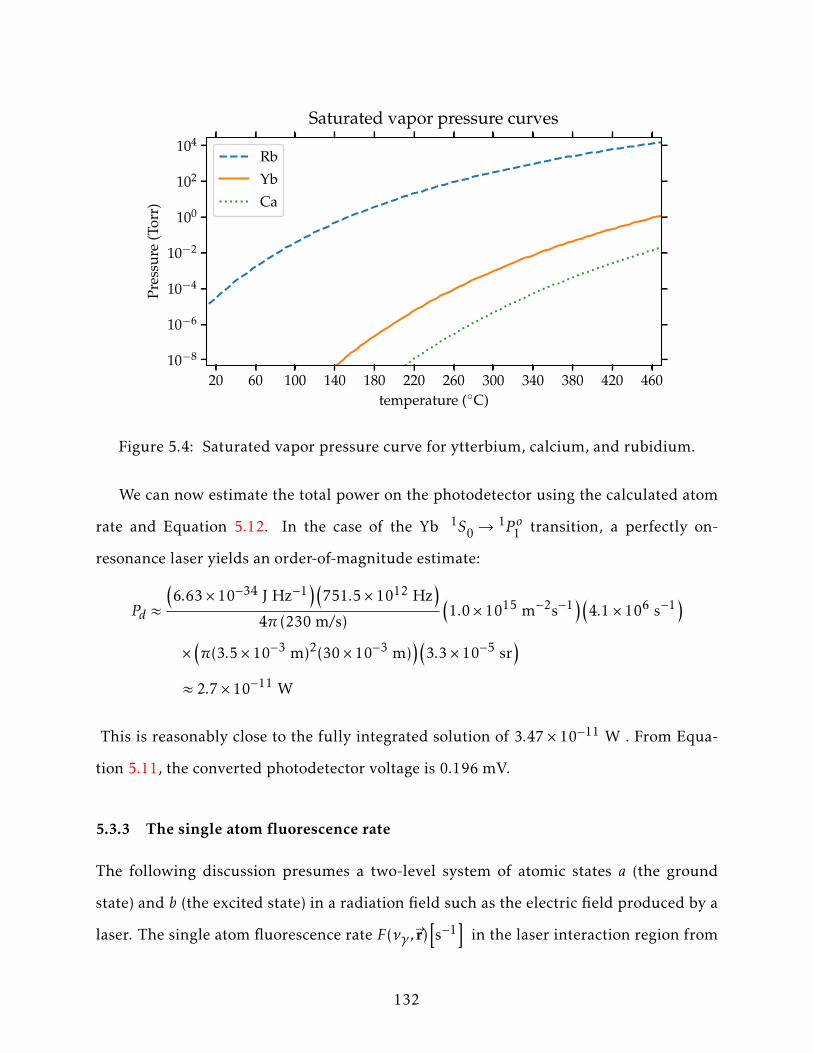
20 60 100 140 180 220 260 300 340 380 420 460temperature (C)
10−8
10−6
10−4
10−2
100
102
104Pr
essu
re(T
orr)
Saturated vapor pressure curves
Rb
Yb
Ca
Figure 5.4: Saturated vapor pressure curve for ytterbium, calcium, and rubidium.
We can now estimate the total power on the photodetector using the calculated atom
rate and Equation 5.12. In the case of the Yb S10→ P1 o
1 transition, a perfectly on-
resonance laser yields an order-of-magnitude estimate:
Pd ≈
(6.63× 10⁻³⁴ J Hz−1
)(751.5× 10¹² Hz
)4π (230 m/s)
(1.0× 10¹⁵ m−2s−1
)(4.1× 10⁶ s−1
)×(π(3.5× 10⁻³ m)2(30× 10−3 m)
)(3.3× 10⁻⁵ sr
)≈ 2.7× 10⁻¹¹ W
This is reasonably close to the fully integrated solution of 3.47 × 10⁻¹¹ W . From Equa-
tion 5.11, the converted photodetector voltage is 0.196 mV.
5.3.3 The single atom fluorescence rate
The following discussion presumes a two-level system of atomic states a (the ground
state) and b (the excited state) in a radiation field such as the electric field produced by a
laser. The single atom fluorescence rate F(νγ ,~r)[s−1
]in the laser interaction region from
132

250 300 350 400 450 500 550
oven temperature (C)
100
101
102
103
104
105
106
AP
Dvo
ltag
e(µ
V)
1011
1012
1013
1014
1015
1016
1017
atom
emis
sion
rate
(s−
1)
Mcube = 3.2 cm, µcube = 0.5 mm, w(z) = 7 mm
Figure 5.5: Calculated fluorescence signal as the oven temperature is variedusing a laser power of 10 mW.
Equation 5.12 is the rate at which an atom in state b emits a photon and decays to a :
F(νγ ,~r) = b(νγ ,~r) A =b(νγ ,~r)
τ0, (5.17)
where
νγ [Hz] is the frequency of the laser,
~r [m] is the position of the atom,
A [Hz] is the spontaneous emission rate Einstein A-coefficient, and
τ0 [s] is the lifetime of the atomic state when a photon of wavelength λ0 is absorbed
by the atom.
The fraction of atoms in the excited state b(νγ ,~r, t) [unitless] is derived from the pop-
ulation rate equations with equal stimulated excitation and emission rates R[s−1
]and the
133

0.0 0.5 1.0 1.5 2.0 2.5time t / τ0
0.33
0.67
1.00b(
t)/
b 0
excited state population fraction
Figure 5.6: Excited state population of a two-level system for R = 2× 10⁸ s−1
and τ0 = 5 ns.
spontaneous decay rate from b to a, given by the Einstein A-coefficient A = 1/τ0[s−1
]:
dadt
= −Ra+Rb+bτ0
, (5.18)
dadt
= +Ra−Rb − bτ0
, (5.19)
a+ b = 1 (5.20)
Solving these equations yields the fraction of atoms in b at time t:
b(t) = b0 exp(− tτ∗
)+(
Rτ01 + 2Rτ0
)×[1− exp
(− tτ∗
)], (5.21)
τ∗ =τ0
1 +Rτ0, (5.22)
where b0 [unitless] is the population fraction of b at t = 0.
As an example of the time to reach population equilibrium, I’ll use rounded P1 o1 num-
bers: R = 2× 10⁸ s−1 ,τ0 = 5 ns. In the limit t→∞, we get the steady-state expression for
the fraction of atoms in b:
b(νγ ,~r) = limt→∞
b(νγ ,~r, t) =R(νγ ,~r)τ0
1 + 2R(νγ ,~r)τ0
134

Table 5.7: Values used for Yb 1S0→ 1P o1 atom excitation rate R(νγ ,~r).
parameter definition value
T oven temperature 300Cνa resonant transition frequency of the atom 7.51526× 10¹⁴ HzFWHM full width-half max of the laser 5.0× 10⁶ HzPγ laser power 1.0× 10⁻² Ww(z) beam radius 1.0× 10⁻² mρ radial distance from laser axis 0.0 mfa atomic transition oscillator strength 1.37RM detector responsivity at 398.8 nm 11.3 A/WG transimpedance gain 5× 10⁵ V/Ar interaction-sensor distance 7.74× 10⁻² mvp,z most probable speed atom speed along z 232.3 m/sAdet sensor area 1.96× 10⁻⁸ m2
F atom fluorescence rate 4.1× 10⁶ s−1
ν0 emitted photon frequency 7.51526× 10¹⁴ HzV interaction volume 8× 10⁻⁹ m3
In our example, b(νγ ,~r) = 1/3. Figure 5.6 plots the excited state fraction vs. times for
factors of the mean lifetime τ0. After less than three lifetimes, the fraction has converged
to 1/3 to within 1%. During this time an atom passing through a laser-generated electric
field would travel a distance:
≈ 300 m/s × 15 ns = 4.5 µm
We typically use laser diameters of 5–10 mm, making the steady-state approximation
quite reasonable for our setup. Upcoming ABF measurements will be performed in the
‘weak pumping limit,’ or R(νγ ,~r)τ0 << 1. In this limit, b(νγ ,~r) ≈ R·τ0 and the single atom
fluorescence rate is equivalent to the excitation rate:
F(νγ ,~r) =1τ0R · τ0 = R(νγ ,~r) (weak pumping limit) (5.23)
I’ve plotted the single atom excitation rate in Figure 5.7 using ytterbium transition values
listed in Table 5.7.
135

−1000 −750 −500 −250 0 250 500 750 1000νγ − νa (MHz)
0.0
0.2
0.4
0.6
0.8
1.0
1.2
1.4
1.6R
(MH
z)Yb atom excitation rate calculation
Figure 5.7: The weak pumping limit Yb single atom laser excitation rate usingthe parameters in Table 5.7.
5.3.4 The Doppler-free excitation rate
The Doppler-free atom absorption cross section σ (ν,νa)[m2
]is defined by:
σ (ν,νa) =hνcBa ×L(ν,νa,A) , (5.24)
Ba =πrec
2
hνfa , (5.25)
L(ν,νa,A) =A/(4π2)
(ν − νa)2 + (A/4π)2=
δνn/(2π)(ν − νa)2 + (δνn/2)2
, (5.26)
where
Ba[s−1
]is the Einstein absorption B-coefficient,
L(ν,νa,A)[Hz−1
]is the probability of atomic transition per unit frequency,
fa [unitless] is the atomic transition oscillator strength, and
δνn = A/2π [Hz] is the natural linewidth.
136

The natural linewidth, also known as the halfwidth, is the width of the line profile of
an atomic transition at which the amplitude is one half the central frequency peak max-
imum. The Lorentzian natural linewidth is sometimes referred to as a full-width half-
maximum, but we will reserve that term for referring to the laser profile.
For the Yb 1P1 transition, A = 1.92× 10⁸ s−1 and δνn = 30.6 MHz.
The atom excitation rate R(νγ ,νa,~r) is the rate at which a single atom absorbs a resonant
photon for a given atomic transition in a radiation field. In the Doppler-free regime, this
is defined as:
R(νγ ,νa,~r) =∫ ∞
0φ(ν,νγ ,FWHM,~r) σ (ν,νa) dν , (5.27)
φ(ν,νγ ,FWHM,~r) =Pγhν
S(~r)×G(ν,νγ ,FWHM) , (5.28)
S(~r) =I(~r)Pγ
=2
πw2(z)exp
[−
2ρ2
w2(z)
], (5.29)
G(ν,νγ ,FWHM) =2√
log2/πFWHM
exp
−4log(2)(ν − νγ )2
FWHM2
, (5.30)
where
νa [Hz] is the resonant transition frequency of the atom,
FWHM [Hz] is the full width-half max of the laser,
φ(ν,νγ ,FWHM,~r)[m−2
]is the local photon flux,
S(~r)[m−2
]is the fraction of all photons per unit area,
Pγ [W] is the laser power,
I(~r)[W m2
]is the laser intensity,
w(z) [m] is the beam radius,
ρ [m] is the radial distance from the laser beam longitudinal axis, and
G(ν,νγ ,FWHM)[Hz−1
]is the fraction of all photons per unit frequency.
Now we’re in a position to plug everything into Equation 5.27 and separate R(νγ ,νa,~r)
137

into a prefactor and an integral over frequency:
R(νγ ,να ,~r) =Pγhνγ
2πrecfaπw2(z)
exp[−ρ2
w(z)
]× 2πAL(ν,νγ ,A,FWHM) , (5.31)
L(ν,νγ ,A,FWHM) =πA2
∫ ∞0
√4log(2)/πFWHM
exp
−4log(2)(ν − νγ )2
FWHM2
L(ν,νa,A) dν , (5.32)
where we have redefined the integral factor L(ν,νγ ,A,FWHM) [dimensionless] as the “line-
shape overlap” function.
L can be solved numerically, but I found that the narrow width of the peak was
not properly integrated by some the standard Python and MatLab solvers, such as
the Fortran-based QUADPACK . I instead used the simpler composite trapezoidal in-
tegration routine numpy.trapz() . I approximated the integration limits of ν to[νγ − 3(FWHM),νγ + 3(FWHM)
], beyond which the exponential term rapidly drives R to 0.
A plot of the single atom excitation rate for the Yb 1S0 → P1 o1 transition is shown in
Figure 5.7.
5.3.5 Doppler broadening for a directed atomic beam
The SAM and Flux ABF setups use an effusive oven to generate an atom vapor beam. As
seen in the experimental layout in Figure 5.2, we’ve chosen the origin to be the exit point
of the nozzle, so that~r and ~v have identical trajectories. The laser is oriented perpendicu-
lar to the atom beam axis, along x. Atom trajectories at some angle θ from the atom beam
axis z will also have a velocity component aligned with the laser.
I define the angle between the laser axis and the atom velocity at position~r as α [rad]:
cos(α) =~r · x∥∥∥~r ∥∥∥ (5.33)
When α = π/2, the Doppler shift between the atom and laser is cos(π/2) = 0.
We assume the atoms in our directed beam are non-interacting particles at thermody-
namic equilibrium. For this scenario we model the speed distribution of the atom beam
as a Maxwell-Boltzmann distribution g(v) [m/s]−1 at oven temperature T [K], given by:
138

g(v) =
√2π
(mkBT
)3/2v2 exp
−( vvp)2 , (5.34)
vp =
√2kBTm
,∫ ∞
0g(v) dv = 1 , (5.35)
where
v [m/s] is the atom speed,
vp [m/s] is the most probable atom speed,
kB [J/K] is the Boltzmann constant, and
m [kg] is the mass of the atom.
For 174Yb exiting a 300 C oven, the most probable speed is vp = 234 m/s. The most
probable speed of For 85Rb exiting a 100 C oven is vp = 270 m/s.
The Doppler broadening effect depends on both α and the velocity of the atom. To first
order, the Doppler term is:
1− vc
cos(α)
The first-order Doppler term is incorporated by modifying the atom absorption cross
section (Equation 5.24) σ (ν,νa)→ σD(ν,νa):
σD(ν,νa,~r) =hνcBa ×LD(ν,νa,A) , (5.36)
LD(ν,νa,A,~r) =A/(4π2)
[ν − νa(1− cos(α)v/c)]2 + (A/4π)2(5.37)
The modified excitation rate includes the additional speed integral from σD:
R(νγ ,νa,~r) =∫ ∞
0
∫ ∞0φ(ν,νγ ,FWHM,~r) σD(ν,νa,~r) g(v) dνdv (5.38)
Equation 5.38 has the practical effect of broadening the spectral profile width.
139

The linear Doppler full width at half maximum FWHMD [Hz] is given by:
FWHMD =
√8kBT log2 /m
cνa sin(θ) , (5.39)
= 2.92×√T /m νa sin(θ)× 10−20 , (5.40)
where c [m/s] is the speed of light in vacuum and θ [rad] is the polar angle of the
atom relative to the beam axis. With an oven temperature of 300C = 573.15 K and
a maximum angle of θ = 0.12435 rad, the Doppler broadening of the Yb 1Po1 transi-
tion δνD = 121 MHz. A comparison of the natural linewidth and a Doppler-broadened
linewidth with these parameters is given in Figure E1.
Our fluorescence measurement uses a directed atomic beam with a large angular com-
ponent and requires the general form of the excitation rate in Equation 5.38. A common
alternative fluoroscopy setup uses collimation downstream of the oven to suppress angu-
lar dependence on atom intensity. In this case the atoms move uniformly along z, so θ
is small and α = π/2. The general form of Doppler broadening then simplifies to a Voigt
profile g(v) LD→ V and the modified Lorentzian is reduced to νa(1− cos(α)v/c)→ νa.
5.3.6 The atomic angular distribution and photodetector solid angle
Now that we can calculate the atomic flux, excitation rate, and photodetector power, it’s
natural to reexamine the photon-atom yield first shown in Equation 5.1.
The photon emission rate dNγ /dt can be written as:
dNγdt
=4πd2Pd(νγ )
Adhνγ, (5.41)
where
~d [m] is the position of the center of the photodetector surface,
va [m/s] is the component of the atom velocity along z, and
Ad[m2
]is the photodetector active area.
140

Figure 5.8: From left to right, in order of increasing noodle diameter-to-length:bucatini, cannelloni, anellini noodles. Images obtained under the CC0 1.0 Uni-versal (CC0 1.0) Public Domain Dedication License (link)
Using Equation 5.41, we can rewrite the photon-atom yield η in terms of Pd(νγ ) :
η =∫ ∫
1va
d2y
Ad× j(θ)×F(νγ ,~r)× dVa
r2dAd∣∣∣∣ ~d−~r ∣∣∣∣2 , (5.42)
where dy [m] is the distance along y from the center of the fluorescence volume to the
photodetector surface.
In the next section, I will describe the model for the angular distribution j(θ). Then
I’ll detail the solid angle calculation in Section 5.3.8.
5.3.7 Atomic angular distribution
The oven nozzle geometry is shown schematically in Figure 5.2. The distribution of the
atoms flowing through the nozzle depends on the nozzle aspect ratio. Long nozzles colli-
mate the beam, while shorter nozzles permit a higher atom flux. We can characterize the
nozzle by the ratio of the radius to length, or the oven nozzle ratio γ :
γ =2aL
, (5.43)
where a [m] is the nozzle radius and L [m] is the nozzle length.
It’s natural (and delicious) to think of the oven nozzles as different kinds of noodles. A
diverse selection of noodles is shown in Figure 5.8. As γ →∞, one can imagine a shorter
and wider noodle, for example anellini. For γ → 0, the nozzle is very long compared to
141

its diameter, similar to bucatini. The Yb nozzle ratio is closest to the cannelloni geometry,
with γ = 0.1250′′/0.5000′′ = 0.2500. The calcium oven nozzle ratio will be identical to
the ytterbium nozzle ratio.
Collisions between the atoms exiting the channel affect the resulting angular distri-
bution. We use the tube length Knudsen number KnL to characterize the density of atoms
in the oven channel [151]:
KnL =λL
, (5.44)
where λ [m] is the mean free path of the atoms in the channel. Atom-oven states with
Knudsen numbers in the range KnL > 10 are classified as the “molecular flow” regime,
where the only significant atom interactions are collisions along the nozzle channel wall.
Atoms in intermediate regime, KnL ≤ 10 must take atomic collision effects into account.
For the ytterbium nozzle (γ = 0.25), Kn > 104 for oven temperatures less than 330 C. For
the rubidium nozzle (γ = 0.01), Kn > 10 for oven temperatures less than 100 C.
In the molecular flow limit, the angular distribution of atoms exiting the oven
jM(θ) [unitless] at some angle θ [rad] with respect to the beam axis z is given by [151]:
jM(θ) =
ζ0 cosθ +
2π
cosθ[(1− ζ0)R(p) +
23
(ζ1 − ζ0)1− (1− p2)3/2
p
], p ≤ 1
ζ0 cosθ +4γ3π
(ζ1 − ζ0)cos2θsinθ
, p ≥ 1
(5.45)
ζ0 =12− 1
3γ2
1− 2γ3 + (2γ2 − 1)√
1 +γ2√1 +γ2 −γ2 sinh−1(1/γ)
, (5.46)
ζ1 = 1− ζ0 , (5.47)
R(p) = cos−1(p)− p√
1− p2 , (5.48)
p =1γ
tanθ , (5.49)
where
ζ0 [dimensionless] is the channel exit collision parameter,
142

0 10 20 30 40 50 60 70 80θ (degrees)
0.0
0.2
0.4
0.6
0.8
1.0j M
(θ)/
j M(0
)molecular flow angular distribution
nozzle ratio
→ ∞
2.500
0.250
0.079
0.024
0.010
(a)
0 1 2 3 4 5θ (degrees)
0.0
0.2
0.4
0.6
0.8
1.0
j M(θ
)/j M
(0)
molecular flow angular distribution
(b)
Figure 5.9: The atomic angular distribution of for a range of nozzle ratios. Top: 80 de-gree range, all lines converge to an intensity of zero at 90 degrees. Bottom: Zoomed into within 5 degrees. The legend appears in the order of descending intensity. Middlesolid line = ytterbium and calcium ratio γ = 0.25. Dashed line = radium γ = 0.024. Bot-tom solid line = rubidium γ = 0.01.
143

ζ1 [dimensionless] is the channel entrance collision parameter,
R(p) [dimensionless] is the noodle parameter, and
p [dimensionless] is the noodle angle.
A plot of the normalized angular distribution is over a wide range of angles and mag-
nified to within several degrees in Figure 5.9a and Figure 5.9b. The rubidium nozzle
(γ = 0.01) is designed to collimate the distribution to within several degrees. By contrast,
the intensity of atoms exiting the ytterbium and calcium nozzle (γ = 0.25) is significant
even at 50 degrees. In the case of a nozzle width much longer than the nozzle length
(think anellini), jM approaches a cosine distribution:
limγ→∞
jM(θ) = cosθ
5.3.8 Solid angle calculation
Atomic beam fluorescence is measured with an avalanche photodiode with a 0.5 mm
diameter active surface (Thorlabs 410-APD2). I investigated solid angle coverage calcu-
lations using both approximation and a numerical method for different detector sizes and
distances from the fluorescence region.
The dAd/∣∣∣∣ ~d−~r ∣∣∣∣2 term in Equation 5.12 can be rewritten as the solid angle coverage
of the photodetector:
dΩdet =dAd∣∣∣∣ ~d−~r ∣∣∣∣2 (5.50)
The “1/r2” approximation Ω ≈ Adet/d2y = 3.3 × 10⁻⁵ sr is reasonably accurate for this
geometry, but this breaks down for larger detectors or shorter fluorescence-detector dis-
tances.
A map of the vertices of each detector surface area element is shown in Figure 5.10.
To make use of parallel processing, I initialize the detector infinitesimal elements as a
square grid.Then I apply a boundary condition to use elements within the radius of the
144

−200 −100 0 100 200
location of dz (µm)
−200
−100
0
100
200lo
cati
onofx
(µm
)
location of dΩi for circular detector
Figure 5.10: A grid of the points used to numerically integrate the solid angle ofa circular detector. We start with a 2×2 square mesh and cut out a circle (shownwith red squares) to obtain the result.
detector to calculate the solid angle. I calculate Ω = 3.27× 10⁻⁵ sr with the Atomic Flux
detector using 441 elements with side length Rdet/10 = 0.25 mm/10 = 25 µm.
When the detector is large (Rdet ≈ 12.7 mm) or close (dy ≈ 40 mm) to the fluorescence
region, the solid angle calculation is highly dependent on the detector shape. This is also
true for the light collection implementation that I discuss in Section 5.5.2. The solid angle
of a square detector, such as that used in the SAM solid noble gas measurement [144],
deviates from the solid angle of an equivalent-surface area circular detector by tens of
percent as the solid angle is compared at different positions in the fluorescence region.
145

1 2 3 4 5
µcube side length (mm)
0.0
0.2
0.4
0.6
0.8
1.0
1.2
1.4
1.6ch
ange
inη
(%)
atom-photon yield response, w(z) = 7 mm, megacube = 3.2 cc
Figure 5.11: The photon-atom yield percent change as the number of subdivi-sions of the fluorescence volume is varied. The megacube side length is 32 mm,the laser width is 7 mm.
5.3.9 Tying everything together into an atomic beam fluorescence simulation
The previous sections of this chapter describe the necessary calculations that are inputs
for a ABF simulation code I developed in the Python programming language. In Sec-
tion 5.3.7, I showed analytic expressions for the atomic angular distribution j(θ). In
practice, the functions as written do not capture all the features of a measured spectrum.
The ABF simulation provides a comparison to a measured spectrum and allows us to
numerically derive j(θ) and the effective oven nozzle geometry.
The simulation integrates over the interaction volume where the atomic beam passes
through the laser radiation field. I approximate the true volume as a simple right rectan-
gular prism, which I define as the “megacube” V[m3
]:∫
dV =∫ ∫ ∫
dx dy dz = V “megacube′′
146

Each infinitesimal volume element dxdydz is called a “microcube.” These terms are de-
picted in Figure 5.2.
I studied the effect of varying the megacube and microcube size. In Figure 5.11, I
fixed the mega cube to 32× 32× 32 mm cube for the Flux ABF oven nozzle (γ = 0.25) and
varied the micro cube size. I found that the change in the calculated photon-atom yield
changed by less than .1% when using a microcube size of 1 mm or less.
For the rubidium oven (γ = 0.01), the angular intensity changes significantly over even
one degree, as shown in Figure 5.9b. This requires an appropriately small microcube and
is computationally expensive.
The atomic beam fluorescence simulations discussed in the following sections are
computed with 68921 microcubes of side length of 0.3902 mm in a megacube with a
16 mm side length.
Figure 5.12 shows zx plane contour plots of the integrand of the solid angle, fluores-
cence rate, angular distribution, and photon-atom yield for an ytterbium ABF simulation.
These terms represent significant pieces of the ABF simulation and are combined in the
manner prescribed by Equation 5.42. Each zx “slice” of Ω, F(νγ ,~r), and j(θ) is integrated
over a vertical range corresponding to the megacube side length to determine η.
5.4 Comparing simulations to data
5.4.1 Yb fluorescence and power broadening
The commissioning ytterbium ABF measurement was performed in 2017. Laser power
data was recorded by a Thorlabs powermeter that measured laser intensity sampled from
a 8:92 pellicle beamsplitter. We used a laser scan step size of 9 MHz at the Ti:Sapphire
output which is frequency-doubled to 17.9 MHz at the external doubling cavity.
I used a sum of seven Voigt profiles plus a constant offset C +∑7i=1Vi to fit the spec-
trum in Figure 5.13a. The dashed lines are individual fitted peaks, and the solid line is
the overall fit.
147

-10.0 0.0 10.0z− 132 (mm)
-10.0
0.0
10.0
x(y
=0.
0)(m
m) jM
0.72
0.80
0.88
0.96
-10.0
0.0
10.0F (MHz)
0.0
20.0
40.0
60.0
80.0
-10.0 0.0 10.0z− 132 (mm)
-10.0
0.0
10.0dη/cm3
0.0
4.0
8.0
12.0
16.0
20.0
-10.0
0.0
10.0x
(y=
0.0)
(mm
) Ω (µsr)
29.0
30.0
31.0
32.0
33.0
Figure 5.12: The integral of η in the plane y = 0. In this plane, the photode-tector at y = 76.2 mm viewing angle is constrained by the inner diameter of thevacuum cross (30.226 mm). The scanning area available to the photodetector is15.52 mm square.
The triple peak consisting of Yb172 and Yb171 (F = 3/2,7/2) is difficult to decouple
given the relative coarseness of the scan size. The Voigt fitting function prefers to under-
weight the amplitude 173Yb(I = 3/2) and over-weight the two more populated states.
To find a convergent fit, I condensed the triple peak into one Voigt profile. The frac-
tional residual of the spectrum fit is shown in Figure 5.13b. The fit models the data to
within 10% except for the boundaries of the laser scan and in the region between Yb174
and the triple peak.
A table of the calculated, measured, and literature transition frequencies are given in
Table 5.8.
The Gaussian widths σ are allowed to vary independently and range from 40–80 MHz.
148

−1000 −500 0 500 1000 1500laser frequency νγ − ν0(174Yb) (17.9 MHz bin)
0
1
2
3
4
fluor
esce
nce
sign
al(V
)×10−3 `2017-05-15-170825´ Yb 346 C, Pγ = 880 mW ·
Yb-174
Yb-176
Yb-170
Yb-172TP
Yb-173 (5/2)
Yb-171 (3/2)
Yb-171 (1/2)
(a)
−1000 −500 0 500 1000 1500laser frequency νγ − ν0(174Yb) (17.9 MHz bin)
−0.4
−0.2
0.0
0.2
0.4
0.6
(fit−
data
)/da
ta
‘2017-05-15-170825´ Yb 346 C, Pγ = 880 mW ·
(b)
Figure 5.13: Yb 5/15/2017 ABF measurement. Yb172 TP = triple peak consisting ofYb172 , Yb173 (F = 7/2), and Yb173 (F = 3/2). Top: seven-peak Voigt fit + constant offset
to data. Bottom: fractional residual of fit (y axis truncated for clarity).
149

Table 5.8: Calculated, measured, and literature values of the 1S0→1Po1 transitionfrequencies with respect to Yb174 (I = 0, F = 1).
isotope Calc. ∆ν (MHz) Meas. ∆ν (MHz) Ref. [147] (MHz)168Yb (I = 0, F = 1) +1887.4170Yb (I = 0, F = 1) +1192.4 +1183(18) +1192.393(66)171Yb (I = 1/2, F = 1/2) +1077.0 +1106(67) +1153.696(61)171Yb (I = 1/2, F = 3/2) +755.76 +849.6(59) +832.436(50)172Yb (I = 0, F = 1) +533.3 +554.9(16) +533.309(53)173Yb (I = 5/2, F = 3/2) +491.11173Yb (I = 5/2, F = 5/2) −278.28 −261(10) −253.418(50)173Yb (I = 5/2, F = 7/2) +563.12176Yb (I = 0, F = 1) −509.3 −526.7(44) −509.310(50)
The saturation intensity Is(ν,νa)[W m−2
]of a single atom is given by:
Is(ν,νa) =hνA
2σ (ν,νa), (5.51)
where σ (ν,νa) is the cross section of the atom given by Equation 5.24. In the case of
the Yb P1 o1 transition, νa = 7.515× 10¹⁴ Hz and the resonant cross section and saturation
intensity are given by:
σ0 = σ (νa,νa) = 7.58× 10⁻¹⁴ m2 ,
I0 = Is(νa,νa) = 63 mW cm−2
Saturation intensities for the Yb, Rb, and Ca transitions of interest are listed in Ta-
ble 5.9.
I estimate a broadened linewidth of 260 MHz for Figure 5.13a. With a laser intensity of
approximately Iγ = 863 mW / π (0.35 cm)2 = 2240 mW/cm2, the saturation factor is:
Iγ /I0 = 36
The power-broadened transition linewidth As [Hz] can now be calculated:
As2π
=A
2π
(1 +
II0
)1/2≈ 6.1
A2π
(5.52)
150

Table 5.9: Saturation intensities and oscillator strengths for selected ytterbium, ru-bidium, and calcium transitions. ν = frequency, A = Einstein A-coefficient (NISTvalues). fa = oscillator strength. fa(Rb) from [146]. fa(Ca) from [152]. I0 = satura-tion intensity.
transition ν (THz) A (MHz) fa I0[mW/cm2
]Yb 6s2 S1
0→ 6s6p 1Po1 751.53 192 1.37 63Rb 5s S2
1/2→ 5p P2 o1/2 377.10743 36.0 0.34231(33) 1.5
Ca 4s2 S10→ 4s4p P1 o
1 709.078235 220 1.75 61
From this I estimate a linewidth of As/2π ≈ 190 MHz. The fitted linewidths range from
150–245 MHz in Figure 5.13a. The closest-matching transition is Yb176 with a linewidth
of 206± 16 MHz.
In Figure 5.14 I show a simulated ytterbium spectrum with a laser intensity of:
10 mW/(π 0.35 cm2
)= 26 mW/cm2
This is well below the saturation intensity and in the weak pumping limit (Equation 5.23.
The Doppler broadening is significantly reduced and the 170Yb and 171Yb (F = 1/2) peaks
are easily resolved. The peak voltage is on the order of hundreds of µV, which we’re easily
sensitive to.
In the next Yb ABF measurement, we will reduce the laser intensity to the simulated
intensity and use a smaller laser scan step size of 5 MHz to control Doppler broadening
and improve our sensitivity to individual transitions in the cluster peak.
All the numbers used for calculating the flux, excitation rate, and photon-atom yield
are given in Table 5.7. Now I will show explicit calculations for a selection of the values.
Origin-to-photodetector distance r:
The distance from the center of the atomic beam to the front surface of the APD detector
r [m] is the sum of the distances of (1) the center of the 2.75” 6-way cross to the top of the
flange (Kurt J. Lesker C6-0275) (2) the width of the cage plate (Thorlabs LCP01) (3) the
151

−1000 −500 0 500 1000 1500 2000laser frequency νγ − ν0(174Yb) (5.0 MHz bin)
0.0
0.2
0.4
0.6
0.8
1.0
1.2flu
ores
cenc
esi
gnal
(×10−
4V
)`2021-04-22-Yb-abf´ Yb sim 300 C, Pγ = 10.000 mW
Figure 5.14: Simulated Yb fluorescence spectrum in the weak pumping limit.
distance from the APD (Thorlabs APD410A2) flange to the active surface of the detector:
r = 62.484 mm + 12.7 mm + 2.2± 0.3 mm = 77.4± 0.3 mm
Most probable atom speed along nozzle axis vp,z:
To find the most probable speedvp,z [m/s], I used an oven temperature of T = 573.15 K
and the mass of 174Yb found in Table A3. This gives vp = 234.08 m/s. For a flux calcula-
tion, we are interested in the component of the velocity that is parallel to the axis of the
oven nozzle. Therefore we need to know the maximum divergence angle of the atomic
beam exiting the nozzle. The ytterbium oven nozzle has a length of 1/2” and a diameter
of 1/8”. If we bisect the cone forming the boundary of beam, the divergence angle is:
θ = arctan0.5× 0.1250′′
0.5000′′= 0.12435 rad
The longitudinal component of the most probable velocity is given by:
vp,z = cos(θ)vp = 232.3 m/s
152

Table 5.10: A selection of atomic transitions of the Rb ground state, 5s S21/2.
Intensity values and wavelengths from NIST, lifetime values from [153].I = intensity. λ,ν = resonant wavelength, frequency. τ = lifetime. A = Ein-stein A-coefficient.
excited state I (arb.) λ (nm) ν (THz) τ (ns) A (MHz)
5p P2 o3/2 1000 780.027 384.23035 26.25(8) 38.1
5p P2 o1/2 500 794.760 377.10743 27.75(8) 36.0
Laser-atom interaction volume V :
I’m assuming that the interaction volume V[m3
]is a 2 mm cube:
V = `3 = 8× 10⁻⁹ m3
The 2017 Yb measurement used a high laser power that does not satisfy the weak
pumping limit (Equation 5.23). The ABF simulation code is intended for weak pumping
limit analysis.
5.4.2 Rubidium fluorescence
A table of relevant properties of the 52S1/2→ P2 o1/2 transition are shown in Table 5.10.
Seventeen ABF measurements were performed with a 0.54 cm laser diameter at pow-
ers ranging from 10 µW to 9.8 mW and oven temperatures ranging from 25–220 C [144].
A Ti:Sapphire identical to that of the Atomic Flux laser (Figure 5.3) is used to generate
the 795 nm laser beam. The beam is picked off at the Ti:Saph output and before any
frequency mixing or doubling. The laser light is linearly polarized but is fiber-coupled to
the fluorescence chamber. The fiber does not conserve polarization and we assume that
the light is unpolarized, or equal parts σ+, π, and σ− components.
I performed fits of each rubidium isotope peak in the spectra with Voigt line pro-
file fits. I also included a constant offset to fit the background. Each Voigt peak Vi has
four adjustable parameters: the Gaussian standard deviation σi , the peak center νi , the
Lorentzian FWHM γi , and the amplitude Ci . For each dataset, I allowed the Lorentzian
153

−3200 −2400 −1600 −800 0 800 1600 2400 3200 4000 4800laser frequency νγ − ν0(85Rb) (4.4 MHz bin)
0.0
0.2
0.4
0.6
0.8
1.0
1.2
1.4
1.6
fluor
esce
nce
sign
al(×
10−
4V
)`2019-09-02-155544´ Rb 25–220 C, Pγ = 0.050 mW
Rb-85 (3→2)
Rb-85 (3→3)
Rb-85 (2→3)
Rb-85 (2→2)
Rb-87 (2→1)
Rb-87 (2→2)
Rb-87 (1→2)
Rb-87 (1→1)
(a)
−3200 −2400 −1600 −800 0 800 1600 2400 3200 4000 4800laser frequency νγ − ν0(85Rb) (4.4 MHz bin)
−1
0
1
2
3
(fit−
data
)/da
ta
‘2019-09-02-155544´ Rb 25–220 C, Pγ = 0.050 mW
(b)
Figure 5.15: A representative rubidium ABF measurement. Top: Voigt fit to rubidiumfluorescence measurement. Bottom: fractional residual.
154

Table 5.11: Calculated rubidium transition frequen-cies (hyperfine + isotope shifts) with respect to thetransition of 85Rb, ν0
(85Rb
)= ν
(S2
1/2→ P2 o1/2
)=
377.107 THz.
isotope5s S2
1/2→ 5s P2 o1/2 ν − ν0
(85Rb
)[MHz]
F → F′
85Rb 2 → 2 +1560.085Rb 2 → 3 +1921.585Rb 3 → 2 −1475.885Rb 3 → 3 −1114.387Rb 1 → 1 +3840.587Rb 1 → 2 +4654.587Rb 2 → 1 −2994.287Rb 2 → 2 −2180.2
FWHM of the Rb85 (F = 3→ F′ = 2) vary within bounds, then fixed that value for the re-
maining peaks. This leaves a total of 1 peak × 4 + 7 peaks × 3 + 1 background = 26 free
parameters for each dataset.
I calculated the total transition frequency given for each rubidium isotope in Ta-
ble 5.11. The laser frequency axis origin is fixed by setting the Rb85 (F = 3→ F′ = 2) peak
center −1475.8 MHz from the origin.
A representative rubidium ABF spectrum fit and associated residual is shown in Fig-
ure 5.15a and Figure 5.15b. Peak widths range from 350–500 MHz, significantly larger
than expected. The residual shows general agreement to within 20%, with discrepancies
as large as 300% in the peak-free regions. At lower laser powers (tens of µW), the dis-
crepancy in peak height is more pronounced as the peaks are sharper. As we increase
the laser power towards 9.8 mW, the broader peaks are more closely matched by a Voigt
curve.
I simulated a rubidium spectrum with a laser power 50 µW corresponding to a laser
intensity of 0.22 mW / cm2 in Figure 5.16a. At this laser intensity, I calculate an on-
resonance atom excitation rate of R(ν0) ≈ 1.3× 10⁶ s−1. The lifetime from Table 5.10 is
155

−3200 −2400 −1600 −800 0 800 1600 2400 3200 4000 4800laser frequency νγ − ν0(85Rb) (5.0 MHz bin)
0.0
1.5
3.0
4.5
6.0
7.5
9.0
fluor
esce
nce
sign
al(×
10−
7V
)`2021-04-25-004211´ Rb sim 100 C, Pγ = 0.050 mW
(a)
−3200 −2400 −1600 −800 0 800 1600 2400 3200 4000 4800laser frequency νγ − ν0(85Rb) (5.0 MHz bin)
0
1
2
3
4
5
fluor
esce
nce
sign
al(×
10−
6V
)
`2021-04-26-021911´ Rb sim 100 C, Pγ = 0.050 mW
(b)
Figure 5.16: Simulated Rb fluorescence spectrum in the weak pumping limit. Laserpower = 50 µW, laser radius = 2.7 mm. Top: collimated beam with nozzle ratio γ = 0.01.Bottom: uncollimated beam with nozzle ratio γ →∞.
156

27.8 ns, so this simulation satisfies the weak pumping requirement Rτ << 1.
I chose an oven temperature of 100 C to constrain the angular distribution to the
molecular flow regime. The peak widths are 20 MHz, a factor of twenty smaller Doppler
broadening than the measured data. Note that above 100C, the Knudsen number for
the rubidium oven is Kn < 10 and the Maxwellian and molecular flow treatment that we
use becomes an increasingly crude approximation.
Figure 5.16a assumes the machined dimensions of the rubidium nozzle ratio of γ = 0.01.
The range of oven temperatures in the measured data is reported in the range of 25–220 C.
Because the measured line profiles are wider than expected, it raises the nefarious possi-
bility that a data run at ≈ 220 C liquified some of the metallic rubidium. In this scenario,
some of the rubidium could have “leaked” out of the oven crucible and some fraction of
the way down the nozzle [144]. Indeed, I noted a colorless film on the surface of the oven
crucible when troubleshooting the SAM ABF setup.
We can interpret the potential leakage distance of the rubidium as a free parameter of
the nozzle ratio. For example, if the liquid traveled halfway down the nozzle, this would
double the effective nozzle ratio. If the liquid traveled 100% down the nozzle, this would
effectively be a completely uncollimated oven source (γ →∞).
To investigate the fluorescence for an uncollimated atomic beam, I repeated the simu-
lation with the same oven and laser settings while setting the nozzle ratio to γ →∞. The
full width of the transitions in Figure 5.16b is 130 MHz, about a third of the measured
peak widths. This is closer to what is measured, though the peaks are still a factor of ≈ 3
narrower than the measured data.
Moving beyond the ABF simulation, I further investigate the effect of rubidium leak-
age with an oven temperature of 220 C. I assume a modified rubidium nozzle ratio that
allows nonzero j(θ) at θ ≈ 20 degrees, for example γ ‘ ≈ 0.25. With these parameters, I es-
timate a maximum broadening of 225 MHz using Equation 5.40. This is still significantly
smaller than the measured spectrum peak widths, suggesting that additional factors are
157
contributing to the broadening.
Nozzle-laser alignment, oven temperature, laser intensity, background light, and laser
polarization differences between experiment and simulation are all possible contributing
factors to the discrepancy in linewidth. The nozzle and laser axis are nominally perpen-
dicular to each other. A misalignment would introduce larger angles between the atom
and laser photon trajectories (α) and increase Doppler broadening.
Assuming the excess broadening is purely due to a misalignment between the nozzle
axis and laser axis, I calculate a misalignment of δθ ≈ 20 degrees would account for the
observed peak widths.
We’ve seen that the measured rubidium transitions aren’t completely captured by the
Voigt lineshape. The true lineshape of a directed atomic beam is the generalized Doppler-
broadened expression discussed in Section 5.3.5.
With the general expression for Doppler broadening, I simulated a single rubid-
ium peak with a nozzle ratio γ = 0.01 (Figure 5.17a) and γ →∞ (Figure 5.17b). Then
I fit Voigt profiles to the peaks. The oven and laser settings are identical to Fig-
ure 5.16a. The collimated transition is sharply peaked and required a finer laser scan
step to capture the shape. From the fit, I find that the collimated linewidth is nar-
row with FWHM = 23.88 + / − 0.10 MHz and the uncollimated transition is broad with
FWHM = 120.69± 0.79 MHz.
The Voigt fit struggles to simultaneously reproduce the transition peak and tails of a
fluorescence spectrum of a directed atomic beam. For the cases of a highly collimated and
uncollimated oven nozzle, the transition peak and tails are underestimated in the former
and overestimated in the latter. The peak fit mismatch is clearly seen in the fractional
residuals for both angular distributions in Figure 5.18. The uncollimated fit is accurate to
within approximately 4% within 10 MHz of the peak, owing to the transition broadness.
Off scale, the fit is 10%-accurate within 75 MHz of the resonance but then diverges by
more than +1000% as one moves further out. The collimated fit is accurate to within
158

−10 −5 0 5 10laser frequency νγ − ν0(85Rb(3→ 2)) (0.1 MHz bin)
4
5
6
7
8
9flu
ores
cenc
esi
gnal
(×10−
7V
)‘2021-04-24-Rb-abf-simulation-maxboltz´ 2r/L = 0.010000
(a)
−200 −150 −100 −50 0 50 100 150 200laser frequency νγ − ν0(85Rb(3→ 2)) (5.0 MHz bin)
0
1
2
3
4
5
fluor
esce
nce
sign
al(×
10−
6V
)
‘2021-04-20-Rb-abf-simulation-maxboltz-costheta´ 2r/L = in f
(b)
Figure 5.17: Voigt fits to simulated fluorescence (red circles) with collimated and uncol-limated angular distributions. Top: collimated distribution, corresponding to one of thepeaks in Figure 5.16a. Bottom: uncollimated distribution, corresponding to one of thepeaks in Figure 5.16b.
159

−10 −5 0 5 10laser frequency νγ − ν0(85Rb(3→ 2)) (MHz)
−0.15
−0.10
−0.05
0.00
0.05
0.10
0.15(fi
t−da
ta)/
data
2021-04-24-Rb-abf-simulation-maxboltz
2r/L = 0.01
2r/L→ ∞
Figure 5.18: Residuals of fits to simulated Rb transitions in Figures 5.17b, 5.17a.
approximately 5% within 6 MHz of the resonance and then sharply converges to ≈ −100%
farther from resonance.
I integrated the fitted peak areas of the seventeen measured spectra to find the total
strength factors and plotted SFF′ / S32′ (Figure 5.19) and SFF′ / S22′ (Figure 5.20) as a
function of laser power. The standard deviations are calculated from the uncertainty
in the spectrum fits. These measured ratios are compared with the predicted strength
factors for perfectly unpolarized light from Table 5.4.
In 85Rb plot, the strength factors S23, S22, and S33 are divided by S32. Dashed hori-
zontal lines are the predicted ratios SFF′ /S32 which are calculated for the condition that
the laser light is perfectly unpolarized. The plotted ratios are all smaller than expected up
to laser powers of 1 mW, indicating that S32 is large. The intensities of the F = 2→ F′ = 3
and F = 3→ F′ = 3 transitions increase as the laser power is increased from 1–10 mW,
inverting the relationship between the transitions at around 5 mW.
For the Rb87 plot, I divide the strength factors S21, S12, and S11 by S22. The ratios
160
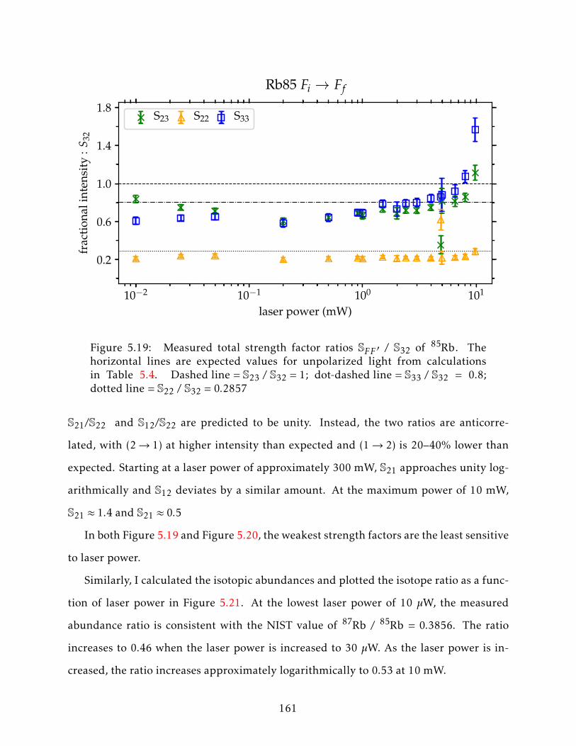
10−2 10−1 100 101
laser power (mW)
0.2
0.6
1.0
1.4
1.8
frac
tion
alin
tens
ity
:S32
Rb85 Fi → Ff
S23 S22 S33
Figure 5.19: Measured total strength factor ratios SFF′ / S32 of Rb85 . Thehorizontal lines are expected values for unpolarized light from calculationsin Table 5.4. Dashed line = S23 / S32 = 1; dot-dashed line = S33 / S32 = 0.8;dotted line = S22 / S32 = 0.2857
S21/S22 and S12/S22 are predicted to be unity. Instead, the two ratios are anticorre-
lated, with (2→ 1) at higher intensity than expected and (1→ 2) is 20–40% lower than
expected. Starting at a laser power of approximately 300 mW, S21 approaches unity log-
arithmically and S12 deviates by a similar amount. At the maximum power of 10 mW,
S21 ≈ 1.4 and S21 ≈ 0.5
In both Figure 5.19 and Figure 5.20, the weakest strength factors are the least sensitive
to laser power.
Similarly, I calculated the isotopic abundances and plotted the isotope ratio as a func-
tion of laser power in Figure 5.21. At the lowest laser power of 10 µW, the measured
abundance ratio is consistent with the NIST value of Rb87 / Rb85 = 0.3856. The ratio
increases to 0.46 when the laser power is increased to 30 µW. As the laser power is in-
creased, the ratio increases approximately logarithmically to 0.53 at 10 mW.
161

10−2 10−1 100 101
laser power (mW)
0.2
0.6
1.0
1.4
1.8
frac
tion
alin
tens
ity
:S22
Rb87 Fi → Ff
S21 S12 S11
Figure 5.20: Measured total strength factor ratios SFF′ / S22 of Rb87 . The hor-izontal lines are expected values for unpolarized light from calculations in Ta-ble 5.4. Dashed line = S21 / S22 = S12 / S22 = 1; dotted line = S11 / S22 = 0.2
These results suggest that there are laser power-correlated effects that influence both
the strength factors and the isotopic ratios. From Table 5.9, the saturation intensity of
rubidium is around 2 mW/cm2. Assuming the laser radius is 0.27 cm [144], I expect the
ratios to be insensitive to laser powers up to ≈ 200 µW. However, we see the surprising
result that the ratios are affected by the laser power well below this threshold.
5.4.3 Simulations of a calcium spectrum
I simulated a calcium fluorescence spectrum of the 4s4p P1 o1 transition (τ = 4.5 ns) in Fig-
ure 5.22. Atomic properties of this transition and several others are listed in Table 5.12.
I use the same oven nozzle dimensions (γ = 0.25) and laser settings (Pγ = 10 mW,
r = 3.5 mm, I = 26 mW/cm2) as the ytterbium simulation in Figure 5.14. The Ca simula-
tion also satisfies the weak pumping limit requirement R(νγ ,~r)τ0 << 1.
162

10−2 10−1 100 101
laser power (mW)
0.36
0.40
0.44
0.48
0.52
0.56
Rb8
7/
Rb8
5Rb fractional isotopic abundance
Figure 5.21: Measured abundance ratio of Rb87 to Rb85 . Dashed line = 0.3856is the calculated ratio using the NIST database values listed in Table A5.
Calculated and literature transition frequencies are listed in Table 5.13. The transition
intensity of the most abundant isotope, 40Ca, will be more than an order of magnitude
larger than the next most abundant isotope. The bottom panel is a log-scale plot that
shows the smaller peaks.
The simulated calcium signal of the dominant peak is approximately 50 nV, several or-
ders of magnitude lower than the ytterbium fluorescence. This is because of the relatively
low vapor pressure of calcium. The oven temperature can be increased to compensate for
the low vapor pressure, but this will also increase the Doppler broadening. Because of
the smaller atomic mass, the calcium peaks will be significantly wider than the ytterbium
peaks for equivalent oven temperatures.
We will use the Atomic Flux apparatus, pictured in Figure 5.23a, to measure the
atomic beam fluorescence of calcium. I expect to improve the ABF measurement sen-
sitivity by a factor of 100 or more with the addition of a light collection setup (discussed
163

−400 −200 0 200 400 600 800 1000 1200 1400 1600 1800laser frequency νγ − ν0(40Ca) (5.0 MHz bin)
0.0
0.5
1.0
1.5
2.0
2.5
3.0
3.5
4.0
4.5
5.0
fluor
esce
nce
sign
al(×
10−
8V
)`2021-04-22-Ca-abf´ Ca sim 250 C, Pγ = 10.000 mW
(a)
−400 −200 0 200 400 600 800 1000 1200 1400 1600 1800laser frequency νγ − ν0(40Ca) (5.0 MHz bin)
10−13
10−12
10−11
10−10
10−9
10−8
fluor
esce
nce
sign
al(V
)
`2021-04-22-Ca-abf´ Ca sim 250 C, Pγ = 10.000 mW
(b)
Figure 5.22: Simulated calcium fluorescence spectrum in the weak pumping limit. Logscale calcium fluorescence spectrum simulation to show the weaker transitions. The smallsignal discontinuities at 600 MHz and 1400 MHz are numerical artifacts.
164

Table 5.12: A selection of atomic transitions of the Ca ground state, 4s2 1S0. Inten-sity values and wavelengths from NIST. 3P o1 lifetime from Drozdowski et. al [154].I = intensity. λ,ν = resonant wavelength, frequency. τ = lifetime. A = EinsteinA-coefficient.
excited state I (arb.) λ (nm) ν (THz) τ (ns) A (MHz)
4s5p P11 o 140 272.1645 1101.1861 3.7 ×10³ 0.27
4s4p P11 o 1000 422.6727 709.078235 4.5 220
4s4p P13 o 500 657.2777 455.986217 5.7(3) ×105 0.0018
in Section 5.5.2). The light collection gain will amplify the calcium APD signal to ap-
proximately 10 µV, a readily measurable fluorescence signal. Detecting the next most
abundant isotope 44Ca peak, on the order of 1 nV without light collection, would be a
powerful demonstration of the ABF measurement sensitivity.
The oven temperature and laser power can also be cautiously increased to boost the
fluorescence signal. At an oven temperature of 250 C, the calcium linewidth is al-
ready significantly Doppler-broadened with FWHM = 200 MHz. However, 40Ca is approx-
imately 400 MHz from the neighboring 42Ca peak, so one can trade off the additional
broadening if a higher fluorescence signal is needed. The simulated laser intensity is
10 mW / π(0.35 cm)2 = 26 mW / cm2. This could be increased by up to a factor of 2 and
still remain below the saturation intensity.
5.5 Suggested improvements to measurement technique
5.5.1 Tracking laser polarization and magnetic field
Competing properties of the ABF measurement could be driving the hyperfine transition
strength factor dependence on pumping laser power, for example the Rb85 S32 transition
in Section 5.4.2.
The weak pumping threshold from Equation 5.23 is approximately 200 µW, assum-
ing a pumping laser radius of 0.27 cm. The four lowest-power ratios in of each of the
Figures 5.19, 5.20, and 5.21 range from 10–200 µW . With a perfectly unpolarized laser
165

Table 5.13: Calculated and literature transition frequencies(hyperfine + isotope shifts) with respect to the transition of40Ca, ν0
(40Ca
)= ν
(S1
0→ P1 o1
)= 709.078 THz. Reference
value for ν(46Ca
)from [155], all others from [156].
A4s S1
0→ 4p P11 ν − ν0 (40Ca) [MHz]
F → F′ Calculated Reference
42 0 → 1 +393.5 +393.1(4)43 9/2 → 9/2 +555.3
+611.8a +610.7(6)a43 7/2 → 7/2 +634.243 5/2 → 5/2 +676.244 0 → 1 +773.8 +773.8(2)46 0 → 1 +1159.8 +1159.8(7)48 0 → 1 +1513.0 +1513.1(4)a “center of gravity” values, which is the average of the
hyperfine peak frequencies weighted by their relativeisotopic abundances.
beam and negligible magnetic fields, I expect the rubidium transition ratios to be insen-
sitive to laser powers below the 200 µW threshold. Instead, we see laser power-correlated
trends in the data starting at the 10–50 µW range.
The 795 nm Ti:Sapphire laser output is linearly polarized. The output is fiber-coupled
to the ABF chamber with an optical fiber that is not polarization-maintaining, so we
assume the pumping laser light is perfectly unpolarized. It may be that some residual
polarization is present after fiber coupling. A significant degree of linear or circular
polarization would modify the magnetic sublevel transition amplitudes. My strength
factor calculations are only valid for an unpolarized laser beam.
It’s also possible that the ambient magnetic field, which we take to be on the scale
of Earth’s field (≈ 60 µT), is significantly affecting the transitions. However, the litera-
ture suggests that transition probability dependence on external magnetic fields are not
significant below ≈ 1 mT [157].
Several improvements can be made to future ABF measurements. To control mag-
netic field-correlated effects, we can screen external magnetic fields and measure the
166

(a)
O
atomic beam
chamber
0.25 mm
12.7 mm
77 mm
focusing optic
diameter
tuneable Ti:Sapphire laser
(b)
Figure 5.23: (a) the Atomic Flux apparatus. (b) Schematic of in-vacuum lightcollection setup (not to scale).
magnetic field uniformity in the fluorescence region, e.g. with fluxgates. We can mea-
sure the pumping laser polarization to verify our assumptions about the strength factor
calculations and filter out any residual linear or circular polarization if necesssary.
In the case of the rubidium experiment, the majority of the measured ratios do not
satisfy the weak pumping condition Rτ << 1. Our next ABF experiment should concen-
trate data collection at low laser intensities in the weak pumping regime. For the case
of a 0.27 cm laser diameter, most of the fluorescence measurements could be made be-
low 200 µW. We observed laser power-correlated effects as low 50 µW corresponding to
0.22 mW/cm2. It would be very interesting to see more measured ratios at below this
intensity.
5.5.2 Increasing the signal size with light collection
A limiting factor on the photon-atom yield η is the solid angle coverage of the photode-
tector. I calculate a solid angle of ≈ 33 µrad (Figure 5.12) in the center of the fluorescence
region of the Atomic Flux apparatus with our 0.5 mm diameter active surface APD posi-
tioned 77 mm (Table 5.7) away.
167

0.5 1.0 1.5 2.0 2.5 3.0 3.5
detector radius (mm)
100
101
102
atom
-to-
ph
oton
yie
ldη
Mcube = 3.2 cm, µcube = 0.5 mm, w(z) = 7 mm
Figure 5.24: The atom-to-photon yield if we use a light-focusing lens, or, equiv-alently, increase the detector area. The laser width is 7 mm in this calculation.Assuming only rays perpendicular to the detector surface are focused onto thedetector, we get maximum light collections for a detector radius of half the laserwidth, or 3.5 mm.
To improve the solid angle, I considered two scenarios. In the first scenario, the APD
can be moved closer to the fluorescence using a smaller vacuum chamber. If we replace
our 2.75” window vacuum cross with a commercial 1.33” setup, the distance from the
fluorescence center to the APD would be reduced by approximately half, or dy ≈ 30 mm.
I estimate a factor of approximately 5 increase in the solid angle by reducing the APD
distance in this manner.
The more promising scenario is to place a light collection lens in the vacuum chamber
between the fluorescence region and the APD. I designed an in-vacuum light collection
setup, shown in Figure 5.23b. The lens is a 1/2” biconvex lens with a 20 mm focal distance
that is mounted to a 16 mm cage plate. The cage plate is mounted to the bottom vacuum
168

100 101 102 103 104 105 106
laser power (µW)
100
101
102
103
104
105
106at
om-t
o-p
hot
onyie
ldη×
104
Mcube = 3.2 cm, µcube = 0.5 mm, w(z) = 1 mm
Figure 5.25: The atom-to-photon yield as we vary the laser beam power. µcubeside length is 0.5 mm, megacube side length is 3.2 cm. ηmax = 1.523 for w = 7mm.
flange using threaded rods. The distance of the light collection lens to the center of the
fluorescence volume is adjustable so the position can be optimized for maximum signal
on the photodetector active surface.
The photon-eta yield increases with increasing solid angle coverage of the photode-
tector (Equations 5.42 and 5.50). To estimate the gain in the solid angle, I make the
assumption that all fluorescence photons reaching the light collection lens surface is fo-
cused directly onto the photodetector. At the center of the fluorescence volume I calculate
an enhanced solid angle of 78 mrad, a factor of 2400 higher than a setup without light
collection.
Since η is a volume integral, the solid angle enhancement will vary by fluorescence
location. To simulate the enhancement in η I approximate the light collection gain by
increasing the photodetector area. A plot of the atom-to-photon yield as we increase the
169

2 4 6 8 10
laser beam diameter (mm)
1.0
1.1
1.2
1.3
1.4
1.5
η(p
hot
ons
per
atom
)atom-photon yield response
Figure 5.26: The atom photon yield as we vary the size of the laser beam width.µcube side length is 0.5 mm, megacube side length is 3.2 cm. ηmax = 1.523 forw = 7 mm.
detector area is shown in Figure 5.24. From the plot I estimate that the light-collecting
lens will increase fluorescence sensitivity by at least a factor of 100.
5.5.3 Increasing the signal size with a calibrated pumping laser and atomic oven
I studied η dependence on a range of laser power and beam widths for a simulated yt-
terbium ABF measurement with oven nozzle ratio γ = 0.25. In Figure 5.25 I plotted η
for laser powers ranging from 1 µW–1 W, keeping the laser width fixed at 1 mm. I also
plotted the photon-atom yield for laser widths ranging from 1 mm–10 mm, keeping the
power fixed in Figure 5.26. I expect that the trends in these figures are also relevant
for the calcium ABF measurement, which will use the same oven nozzle ratio and a 1Po1
atomic transition.
170

These plots show that the laser width can be calibrated to maximize η for a given laser
intensity. The simulated data depends on the atomic distribution j(θ). We’ve seen from
the rubidium analysis in Section 5.4.2 that our understanding of the atomic distribution
is limited, so the simulated optimized laser width should only be used as a starting point.
A careful calibration of the ABF measurement parameters is especially important for
calcium, which is expected to have a very small fluorescence signal. The photon-atom
yield depends on the overlap between the atomic angular distribution and the pumping
laser. The atomic angular distribution is controlled by the oven nozzle ratio. The laser
beam power and diameter should be chosen to maximize η while satisfying the weak
pumping requirement.
171

CHAPTER 6
PRECISION GAMMA-RAY INTENSITY MEASUREMENTS
As a fellow of the Nuclear Science and Security Consortium (NSSC), I had the opportu-
nity to research nuclear security applications in nuclear physics. I went to Lawrence Liv-
ermore National Laboratory (LLNL) to develop a new precision gamma-ray spectroscopy
experiment from January 1 2019 to March 29 2019.
6.1 Introduction
6.1.1 Gamma-ray spectroscopy and stockpile stewardship
The United States and other nuclear powers minimize nuclear weapon threats by nego-
tiating treaties that limit nuclear weapon stockpile inventory and ban intrusive weapons
testing, including above-ground and underground detonation. These treaties have mech-
anisms that provide members with rights to limited inspections each other’s stockpiles
and validate the number of stockpiled warheads.
Fissile material occasionally falls under the investigative purview of nuclear security,
for example in the case of stockpile verification, recent weapons testing, or weapons traf-
ficking. The size and nature of a sample can be determined by measuring the intensity
of the radiation of the daughter isotopes in the sample. A high precision radiation mea-
surement can provide insight on the composition and timescale of the original material
the sample is derived from.
Gamma-ray spectroscopy is used to characterize nuclear decay spectra to derive nu-
clear properties from isotopes of interest. One facet of gamma-ray spectroscopy is study-
ing the possible decay paths an excited nucleus can take in order to decay to a more stable
nucleus. This is particularly useful application for nuclear forensics and nuclear security,
as the number of fissions that occurred in a nuclear sample can be quantified by mea-
172

suring the intensity of the photons, or gamma-rays, emitted by the nuclei of the fission
daughter isotopes.
6.1.2 Long-lived fission isotopes
Nuclear induced fission can be initiated by impinging a neutron on a 235U nucleus. To
a lesser effect, fission can also be initiated by other uranium isotopes and some thorium
and plutonium isotopes. We’ll limit the scope of this discussion to a 235U nucleus.
After the incoming neutron is captured by the 235U, an excited state of 236U is
formed. The 236U nucleus will primarily fission into two unstable isotopes of mass num-
ber A1 ≈ 90 and A2 ≈ 145, roughly a 2:3 ratio. 236 − A1 − A2 free neutrons will
be ejected as well. The process is statistical so the number of nucleons in each isotope
daughter fluctuates.
Figure 6.1 is a simplified example of a simplified A = 147 decay chain of a nuclear
fission isotope. 147Ce is the first 236U descendent in this decay chain. 147Ce has a
half-life of 56 seconds and a relative proportion of decays from its parent nucleus, or
independent yield (IY), of 1.9%. The daughter is neutron-rich and will decay to a more
stable nucleus by converting one of its neutrons to a proton via the weak force:
AZX→
AZ+1X
′ + e− + νe , (6.1)
where
AZX is the original nucleus with A nucleons and Z protons,
AZ+1X
′ is the product nucleus with A nucleons and Z + 1 protons,
e− is an electron, and
νe is an electron antineutrino.
173

14758Ce89
14759Pr88
14760Nd87
14761Pm86
5/2-
5/2+
5/2-
7/2+
Q = 224.6 keVT1/2 = 2.62 yr
Q = 896.0 keVT1/2 = 10.98 d
Q = 2697 keVT1/2 = 13.4 min
Q = 3430 keVT1/2 = 56.4 s
β-
β-
β-
Iβ
5.6467.5 keV
37
5.65/2- 362 keV
5/2-
Iβ
2.5
23.4792.5 keV3/2+
127.9 keV0
5/2-
1310.8 keV10.2
3/2+
Iβ
15.4531 keV
80.291.1 keV
5/2+, 7/2+2.43
685.9 keV5/2+, 7/2+
≤ 0.15
5/2+
β-
0 keV
0 keV
0 keV
Figure 6.1: A simplified example of one of the possible 236U decay chains. Datafrom [158].
174

Table 6.1: Gamma-ray decays from a selection of long-lived fission isotopes.δ(BR) = branching ratio uncertainty.
isotope γ-ray (keV) Q-value (keV) δ(BR) (%) half-life (days) Ref.95Zr 724.192± 0.004 1123.6± 1.8 0.50 64.03 [159]95Zr 756.725± 0.012 1123.6± 1.8 0.40 64.03 [159]156Eu 811.77± 0.05 2449± 5 8.2 15.19 [160]147Nd 531.016± 0.022 896.0± 0.9 2.2 10.98 [161]147Nd 91.105± 0.002 896.0± 0.9 2.5 10.98 [161]144Ce 133.515± 0.002 318.7± 0.8 1.7 284.91 [162]161Tb 74.56669± 0.00006 593.0± 1.3 4.9 6.89 [163]127Sb 685.5± 0.5 1581± 5 5.6 3.85 [164]111Ag 342.13± 0.02 1036.8± 1.4 4.9 7.45 [165]
147Ce beta-decays to a new isotope with a longer half-life. After several beta-decays
down the chain in Figure 6.1, the half-life approaches an order of hours or days. This is
long enough that a sample of such material could be transported from a scene to a labo-
ratory for spectroscopy analysis. These isotopes are known as long-lived fission isotopes.
In order to usefully quantify the number of nuclear fissions that occurred in a sample
of decayed material, an uncertainty of 2% or better in the branching ratio of the isotope of
interest is desired. Table 6.1 shows a representative list of long-lived fission isotopes. The
primary beta-decay branching ratios of 95Zr are known to sub-percent precision. The
branching ratio uncertainties of the other isotopes are relatively large, ranging from 1.7%
to 8.2%. The reasons for the relatively imprecise measurements of these isotopes’ decay
properties vary. It may be due to using impure samples, having insufficient counting
statistics, or internal conversion competing with β− decay. Sometimes the sources are
difficult to fabricate, for example if the accelerator used to produce the source cannot
deliver a sufficiently pure and/or intense beam. The substrate the isotope is collected on
may attenuate the signal if the gamma-ray of interest is low-energy.
A precision β− branching ratio measurement for long-lived fission isotopes is being
developed at Lawrence Livermore National Laboratory. The new method uses thin sam-
ples produced at the Californium Rare Isotope Breeder Upgrade (CARIBU) and a nearly
175

Figure 6.2: LLNL gamma-ray detector setup.
100%-efficient 4π beta counter. A proof-of-principle measurement was performed using
a high purity germanium (HPGe) detector meticulously calibrated at Texas A&M Univer-
sity [166, 167].
In 2017 they measured the two primary branching ratios of 95Zr [168]. The two pri-
mary β− decays, γ1(keV) = 724.2 and γ2(keV) = 756.7, were measured with 0.6% preci-
sion, in agreement with the literature values shown in Table 6.1 [169].
The Zr measurement validated the new sample preparation, calibrated gamma-ray
detection, and β−-coincidence measurement. The goal of the LLNL gamma-ray spec-
troscopy group is to improve the branching ratio measurements of additional long-lived
fission isotopes such as those listed in Table 6.1 to better than 1 % precision.
For the next phase of the long-lived fission isotope gamma-ray spectroscopy experi-
ment, the isotope sample will be measured in a new detection system at LLNL, shown
in Figure 6.2. The newly-assembled detector is a broad energy germanium (BEGe) de-
176

Figure 6.3: A schematic of the LLNL BEGe detector. Model by Canberra, MirionTechnologies. Used with permission.
tector (schematic shown in Figure 6.3), so-named for its sensitivity to gamma-rays in the
range ≈ 0.01–3 MeV. This model has a particularly thin front layer of inactive, or “dead”
germanium of about 0.3 µm, more than an order of magnitude thinner than a standard
HPGe design. Unlike standard “coaxial” detectors, the BEGe does not have a significant
bullet-hole design on the bottom surface of the detector, which preserves the volume of
active germanium and simplifies modeling.
The LLNL BEGe detector is mounted on an ultra low-background preamplifier (Can-
berra iPA) inside a lead shield with an additional inner layer of high purity copper (Can-
berra 777 series), shown in Figure 6.2. The shield blocks both external effects like cosmic
radiation and emission from the lead lining itself. Data acquisition is handled by a CAEN
DT5780 dual digital multichannel analyzer.
177

6.1.3 HPGe calibration
In order to measure the intensity of a gamma-ray, the efficiency of the detector must be
known at that gamma-ray energy. Efficiencies at several energies are typically provided
by the manufacturer, and in many cases interpolation is sufficient to calculate reasonable
gamma-ray intensities of well-understood isotopes. However, high precision measure-
ments of hard-to-measure fission isotopes require correspondingly well-calibrated detec-
tors. A detector can be calibrated by using a gamma-ray source of a known intensity
and deriving the efficiency. We’re interested in the efficiency of the full gamma-ray de-
position, or the full-energy peak efficiency [170]. This ignores gamma-rays that partially
deposit, or scatter, in the detector. Standardized samples of reference sources, such as
152Eu, 241Am, and 60Co, are readily available off the shelf.
The full-energy peak efficiency of a detector at gamma-ray energy Eγ , or ε(Eγ ), is
given by:
εγ =R
S × Pγ, (6.2)
R =NT −1 , (6.3)
S = A0 exp(−λt) , (6.4)
where
R[s−1
]is the full-energy peak count rate,
T [s] is the detector live time,
N [dimensionless] is the detector count,
S [Bq] is the source strength,
A0 [Bq] is the source initial activity,
λ[s−1
]is the source decay constant, and
Pγ is the probability that the source emits a photon at Eγ , i.e. its branching ratio.
For this experiment it’s useful to use the half-life rather than the decay constant. The
178

(a)
3 mm diameter
0.6 µm Kapton
0.254 mm Mylar
Decal25.4 mm
Dir
ecti
on
of
det
ecto
r
gamma source
(b)
Figure 6.4: (a) Geant4 model of the gamma-ray source. (b) Expanded schematicof the gamma ray source geometry (not to scale).
two are related by:
t1/2 =ln2λ
, (6.5)
where t1/2 [s] is the half-life. We measured the absolute gamma-ray detection efficiency
of the detector using a set of ten standardized sources with gamma-ray emission spanning
14 keV–1.4 MeV. The sources are calibrated isotopes with well-understood gamma-ray
branching ratios are high-intensity and well-measured at useful energies. The geometry
is a Type M “scatterless” geometry (shown in Figure 6.4).
Each sample has a thin 3 mm diameter deposition of an isotope whose primary gamma-
ray branching ratio is measured to sub-percent level, except for 241Am, whose primary
gamma-ray branching ratio (γ = 59.54 keV) is measured to within 1.1%. The initial activ-
ities of the samples are measured to within 3% by the manufacturer (Eckert & Ziegler).
To measure the efficiency spectrum of the detector, the samples were mounted on a
plastic holder as shown in Figure 6.5. The holder is similar to a stackable CD holder. The
plastic holder has a tray design for loading samples at different heights. There is no base
so it can be centered over the detector.
We took a suite of gamma-ray source measurements for two different sample-source
179

sample bracket
retaining ring
Mylar substrate + sample deposit
inner shield layer
29.55 cm
13.50 cm
0.25 cm
0.028 cm
sample - counter distance: 16.33 cm
detectorshell
40.3 cm
sample holder
10.16 cm
Figure 6.5: Schematic of detector-sample configuration.
distances. Measuring efficiencies at two different distances offers a robust way to bench-
mark a numerical model of the detector system, since an on-axis displacement would
result in an efficiency change due solely to geometry. For each measurement, we placed
the sample at one of two distances and collected statistics until enough counts were in
the peaks corresponding to the primary β− decay branching ratio energies of the sample.
An example of a measured spectrum of a 60Co sources is shown in Figure 6.6.
The gamma-ray collection efficiency of the detector scales as d−2, where d is the dis-
tance from the source to the front surface of the detector. The sample should be close
enough to collect enough statistics in a reasonable amount of time (≈ hours to days) but
far enough away to avoid pileup effects on the detector. We try to get the total detector
peak counts N to within 0.1% uncertainty, which corresponds to:
σPoissonN
=
√NN≤ 10−3 → N ≥ 106 (6.6)
For the LLNL HPGe detector, this corresponds to a detector-sample distance of 10–15 mm.
180

1150 1175 1200 1225 1250 1275 1300 1325 1350
energy (keV)
100
101
102
103
104
cou
nts
/0.
4ke
V
g0 center = 1173.1 ± 8.1e-04 keVg0 FWHM = 2.0 ± 1.9e-03 keVg0 counts = 188330 ± 439
g1 center = 1332.4 ± 9.9e-04 keVg1 FWHM = 2.1 ± 2.3e-03 keVg1 counts = 165356 ± 408
60Co gamma-ray spectrum
least squares fit
background
Figure 6.6: Fits for the 1173 keV and 1332 keV 60Co gamma-ray spectrum.
The measured efficiencies and their uncertainties of the HPGe detector are shown
in Figure 6.7a and Figure 6.7b. The shape is characteristic of many efficiency spectra
of semiconductor detectors. There is a logarithmic increasing efficiency from low energy
(< 100keV), a peak at the “knee” at around 90 keV, and a logarithmic decreasing efficiency
from the knee onwards. The effective bandwidth of the detector is about 2 MeV.
6.1.4 Monte Carlo simulation
I started with a boilerplate model of a HPGe detector within a background shield in
Geant4. The original model generates a number of gamma-rays at an energy specified
by the user with random initial vectors from a point source. An example of a detector
measurement of a gamma source is shown in Figure 6.8. To clearly view the gamma-ray
trajectories, I only simulated three hundred gamma-rays. For a simulation that I use for
181

10−2 10−1 100
gamma-ray energy (MeV)
10−3
10−2
effic
ienc
yHPGe efficiency plot, 164 mm
Am-241
Co-57
Co-60
Cs-137
Mn-54
Na-22
Y-88
Eu-152
Ba-133
Cd-109
(a)
10−2 10−1 100
gamma-ray energy (MeV)
10−3
10−2
effic
ienc
y
HPGe efficiency plot, 95 mm
(b)
Figure 6.7: (a) Efficiency plot of HPGe with calibrated gamma sources and asample-detector distance of 164 mm. (b) Efficiency plot of HPGe with a sample-detector distance of 95 mm
182

Figure 6.8: A simulation of 1 MeV gamma-rays emitting from a source (rightside of graphic) above the LLNL HPGe detector (left side of graphic).
analysis, one million or more gamma-rays are simulated. The number of gamma-rays that
are deposited in the active germanium volume of the detector are recorded. A histogram
is generated with a call to the scientific coding toolkit ROOT. The histogram bin height is
scaled to the number of hits in the detector.
The boilerplate detector model includes the active germanium, the front deadlayer,
the shell, the detector window, and the shield. It models a more conventional detec-
tor with a bullet-hole design and a standard (≈ 600 µm) front deadlayer thickness. The
source is a point source with no source holder geometry.
To improve the accuracy of the simulation, I updated the detector-source model to
more closely match the new LLNL system. To start, I modified the detector model to
match the parameters provided by the manufacturer for our new detector as shown in
Figure 6.3. Over the course of the practicum, I updated the model to include additional
components modify existing designs. I note a selections of improvements I made to the
Monte Carlo model in the following list:
183

Figure 6.9: Snapshot of Geant4 model of the HPGe detector and background shield.
• reduce the bullet-hole depth
• add side deadlayers and back deadlayers which can be varied independently of the
front deadlayer
• add an infrared film between the detector window and germanium crystal
• add a plastic concentric sample holder
• create a Type-M source geometry with the layers shown in Figure 6.4
• modify the gamma-ray source to be a uniform planar circular distribution consis-
tent with the geometry shown in Figure 6.4
In Figure 6.9 I show a snapshot of the updated BEGe Geant4 Monte Carlo model. The
detector is surrounded by three layers of shielding (in gray) and a concentric sample
184

0.0 0.2 0.4 0.6 0.8 1.0 1.2 1.4gamma-ray energy (MeV)
0.002
0.006
0.010
0.014
0.018
0.022
0.026
0.030
0.034
0.038ef
ficie
ncy
Empirical fit of HPGe efficiency at 95 mm
4th order fit
Am-241
Co-57
Co-60
Cs-137
Mn-54
Na-22
Y-88
Eu-152
Ba-133
Cd-109
Figure 6.10: Fourth-order empirical fit to the measured efficiencies of a suite ofcalibrated gamma sources at a distance of 95 mm.
holder (in yellow). The germanium crystal is shaded in green and is surrounded by a
vacuum-sealed shell. The front of the shell, which faces the gamma source, is a carbon
composite cryostat window.
6.2 Results and analysis
I wrote a Bash script that wraps the single-energy efficiency calculation code and re-
peats the simulation for a range of energies. The efficiency calculated for each iteration is
stored in a separate array. I wrote a ROOT script that fills a histogram with the stored ef-
ficiencies after the energy range is swept. The bin heights are scaled by their efficiencies.
The simulated efficiencies for a given energy is the number of gamma-rays deposited in
the detector divided by the number of generated gamma-rays.
One way to model HPGe detector efficiency is to fit an empirical function to the mea-
185

0 0.2 0.4 0.6 0.8 1 1.2 1.4gamma ray energy (MeV)
30−
20−
10−
0
10
20
30weighted average fractional residual = 5.25 +/- 0.00 %
frac
tio
nal
res
idu
al (
%)
Am-241
Co-57
Cs-137
Mn-54
Na-22
Eu-152
Ba-133
Cd-109
Gamma source intensity measurements at 95 mm
Figure 6.11: Fractional residual efficiency scatterplot with sample-detector dis-tance of 95 mm.
sured efficiencies. The form of the empirical fit is:
logε(E) = a0 +∑n=1
an(log(E))n
A fourth-order fit usually fits the data well. For non-precision measurements, this is
enough to characterize the HPGe efficiency curve.
The empirical fit is also useful for comparing simulated efficiencies to measured effi-
ciencies. I wrote a ROOT script that fits a fourth-order curve to a 2D array of simulated
efficiency vs. energy. The function is minimized with the FMINUIT routine. In Fig-
ure 6.10 the empirical curve is drawn and the measured data is plotted over it.
Our calibration method follows the procedure of Helmer et. al for calibrating an HPGe
detector to the sub-percent level over an energy range of 3.5 MeV [166, 167].
186

0 0.5 1 1.5 2gamma ray energy (MeV)
20−
15−
10−
5−
0
5
10
15
20Am-241
Co-57
Co-60
Cs-137
Mn-54
Na-22
Y-88
Eu-152
Ba-133
Cd-109
Gamma source intensity measurements at 164 mm
weighted average fractional residual = 2.99 +/- 0.00 %
frac
tio
nal
res
idu
al (
%)
Figure 6.12: Fractional residual efficiency scatterplot with sample-detector dis-tance of 164 mm.
The HPGe detector Monte Carlo calibration is characterized by comparing the frac-
tional residual between the measured efficiency and the simulated efficiency of the detec-
tor at a given energy. The fractional residual of the detector efficiency at a gamma-ray of
energy Eγ , or R(Eγ ), is given by:
R(Eγ ) =εm(Eγ )− εs(Eγ )
εs(Eγ ), (6.7)
where εm(Eγ ) is the measured efficiency and εs(Eγ ) is the simulated efficiency of the
detector at gamma-ray energy Eγ .
Figure 6.11 and Figure 6.12 are plots of measured vs. simulated efficiencies over an
energy range of 2 MeV for a sample-source distance of 95 mm and 164 mm, respectively.
Weighted-average fractional residuals are quoted for each plot. We obtain a 5.25% av-
187

Figure 6.13: custom-designed gamma-source holder for the LLNL HPGe detector.
erage residual for the 95 mm plot and a 2.99% residual for the 164 mm plot. This took
approximately ten weeks of modeling work.
In general, the residuals appear randomly distributed about zero. However, when
looking at each source individually, in many cases the residuals appear consistently un-
derestimated or overestimated by the simulation. For example, in Figure 6.11, the 57Co
data points appear underestimated, but the 152Eu sample appears overestimated.
We suspect that the systematic shifts in the efficiency are due to small displacements
that are introduced by removing and installing the gamma sources. I will discuss our
design of a new, highly repeatable sample holder in the next section.
6.3 Conclusions and Outlook
The new high purity germanium detector system at LLNL will measure gamma-ray
intensities of long-lived fission isotopes to sub-percent precision. I started my practicum
shortly after the new HPGe was assembled. We measured the gamma-ray intensities of a
suite of standardized gamma sources to obtain the efficiency curve of the detector. Then
I developed a Monte Carlo simulation code to reproduce the measured intensities. The
188

code is written in Geant4 and models the HPGe detection system, simulates gamma-ray
efficiency of the HPGe as a function of energy, and compares the simulation deviation
from measured gamma-ray intensities. I measured gamma-ray intensity of a suite of
calibrated gamma-ray sources at different distances and compared the results to the sim-
ulation.
I calibrated the HPGe detector Monte Carlo model to within 3% of the measured
gamma-ray efficiencies over a 2 MeV range. We believe that the leading source of uncer-
tainty in the calibration is in the variance in gamma-ray source position when changing
samples.
I designed a sample holder that mounts directly to the HPGe shell to suppress shifts
in the source position between measurements. The finished gamma-ray sample holder is
shown in Figure 6.13. A sheath interfaces with the endcap edge of the HPGe. The sample
holder distance is fixed with stacking spacers calibrated to within a 0.2 mm tolerance that
will let us vary the sample-detector distance from 2–30 cm in increments as small 1 cm.
We have two sample holding adapters that will allow us to mount either a source disk
for calibration measurements (left of Figure 6.13) or the 4π beta counter for long-lived
fission isotope intensity measurements.
We expect that a new measurement of known gamma sources will calibrate the de-
tector to within 1% using the position-repeatable sample holder. After the detector is
sufficiently calibrated, precision measurements of long-lived fission isotopes will be pos-
sible. The goal is to measure the gamma-ray intensities of 147Nd and other long-lived
fission isotopes to determine the principal beta-decay branching ratios to within 1%.
189

CHAPTER 7
CONCLUSIONS AND OUTLOOK
The Ra EDM experiment measures the atomic electric dipole moment of 225Ra. Atoms
are vaporized in an oven and are collimated and cooled with resonant lasers. They are
trapped in a magneto-optical trap, then transported between two high-voltage electrodes
using optical tweezers. During the measurement, the atoms precess between a pair of
identical plane-parallel electrodes that generate a uniform and stable DC electric field
that reverses direction every measurement cycle. We used a pair of oxygen-free copper
electrodes that operated at ±6.7 kV/mm at a 2.3 mm gap size and measured an EDM
upper limit of 1.4× 10⁻²³ e cm in the first generation of measurements. For the second
generation measurements, we will use a new pair of large-grain niobium electrodes whose
systematic effects have been evaluated to the 10−26 e cm level.
I constructed a high voltage test station to condition high voltage electrodes at gap
sizes of 0.4–2.5 mm with a 30 kV bipolar power supply at MSU. The test station was
commissioned with a pair of copper electrodes, and the following high voltage tests were
performed with niobium and titanium electrodes. I varied the electrode gap size with
a high-precision linear drive and verified that the electrodes could perform reliably at
1 mm. Then, a fixed gap holder was fabricated and replaced the adjustable gap assembly.
Subsequent conditioning was performed with electrode pairs at a gap of 1.0± 0.1 mm.
To reach fields higher than 10 kV/mm, I developed hardware and procedures to clean
and preserve the surface purity of the electrodes. I built a portable clean room validated
to Class 100 (ISO 5) with a NIST-calibrated particle counter and developed a clean room
electrode swap procedure. Then I worked with engineers at FRIB to develop a procedure
of high-pressure rinsing the electrodes with ultrapure water. I designed a packaging
method for storage and transport of decontaminated electrodes. Subsequent test station
work and electrode swaps were performed in the NSCL detector clean room.
190

Two pairs of grade-2 titanium and four pairs of large-grain niobium electrodes were
fabricated and polished according to surface preparation techniques that were modi-
fied from accelerator physics literature. We discharge-conditioned three pairs of nio-
bium electrodes and one pair of titanium electrodes, alternating the polarity of the
applied DC field every 60 s to mimic the EDM measurement. Electric fields were
tested as high as +52.5 kV/mm and −51.5 kV/mm. All the electrodes exhibited less than
100 pA steady-state leakage current when operated under 22 kV. We validated a pair of
large-grain niobium electrodes (Nb56) at 20 kV/mm with an average discharge rate of
98± 19 discharges per hour and a steady-state leakage less than 25 pA (1σ ).
The large-grain niobium electrodes (Nb56) were transported to ANL, where I con-
structed a portable clean room and positioned it at the EDM apparatus. Nb56 was in-
stalled in the Ra EDM apparatus all while preserving the electrodes in Class 100 environ-
ments. I revalidated the performance of Nb56 to 20 kV/mm after the apparatus vacuum
pressure was restored.
Several targeted upgrades will be implemented in the second generation EDM mea-
surements to collectively improve sensitivity by up to three orders of magnitude. The
new niobium electrodes increase the electric field strength and will initially contribute
an enhancement factor of 3.1 in EDM statistical sensitivity.
We plan to further increase the electric field to a factor of 7.7 during a future phase
of high voltage development. This will be achieved by designing a more symmetric high
voltage test chamber using a unipolar power supply that alternates the field direction by
switching connections between the electrodes. Our goal is to discharge-condition elec-
trodes to operate reliably at ±50 kV/mm over a 1 mm gap.
The new Blue Slower will use the 1S0→ P1 o1 optical cycling transition to allow us
trap two orders of magnitude more atoms for spin precession frequency measurements.
I built a fluoroscopy setup to characterize the additional decay channels that we will
need to repump to use the blue cycling transition. The setup combines several fiber-
191
coupled lasers to populate and probe the deexcitation paths from the 3Fo2 atomic state to
several D states and measures the fluorescence intensity of each of the channels. From
the fluorescence intensity we then determine the branching ratio for each decay channel.
In this manner we verified the qualitative behavior of the D state branching ratios in the
context of the blue Zeeman slowing scheme.
The Zeeman slower upgrade is expected to improve EDM sensitivity by an order of
magnitude. In addition, a spin-selective STIRAP atom detection efficiency upgrade is
being developed. STIRAP is also expected to improve sensitivity by more than one order
of magnitude. Taken together with improvements to the electric field, we expect to reach
an EDM sensitivity at the 10−26 e cm level or better.
In the near future, we will be able to harvest 225Ra from the FRIB beamline. FRIB is
expected to produce larger quantities of 225Ra more frequently for the Ra EDM exper-
iment than past sources. Our goal is to develop the FRIB harvesting procedure with a
series of progressively sophisticated measurements with stable isotopes that have similar
spectroscopic properties to radium.
The measurement is a laser induced fluorescence measurement of a directed beam of
atoms from an effusive oven. We will initially use commercial, stable ytterbium as a ra-
dium surrogate to commission the flux measurement. As the measurement is refined, we
will prepare a sample of stable calcium extracted from water, simulating a radium har-
vesting process. The calcium sample will be measured with the atomic beam fluorescence
technique and allow us to benchmark the harvesting efficiency.
I assembled an atomic beam fluorescence setup that generates a directed beam of
atoms from an effusive oven, illuminates the atoms with a laser beam, and captures the
fluorescence with a photodetector. I wrote a program that simulates the photodetector
signal as a function of the laser frequency, laser power, and oven temperature for a given
atomic angular distribution and atom species. The simulation will allow us to optimize
and interpret future atomic beam fluorescence measurements of ytterbium, calcium, and
192

other isotopes relevant for precision nuclear physics experiments.
Personal scientific contributions
The following list summarizes the tasks I performed for my thesis work.
1 Electrode material magnetization measurement
• Designed and assembled an electrode magnetization measurement setup using an
external field-shielding mu-metal box and a custom mechanical translation stage.
• Configured fluxgate magnetometers above the translating stage and performed a
suite of gradiometer measurements with copper, stainless steel, Macor, titanium,
aluminum, and niobium electrodes and electrode-sized cylinder surrogates.
• Built a conditioning circuit with a differential op amp input and low-pass filter to
amplify the magnetization signal.
2 High voltage electrode preparation, testing, and operation
• Designed and assembled a high voltage test station to discharge-condition six pairs
of high voltage electrodes.
• Built data acquisition interface circuitry and housing units for a unipolar −30 kV
unipolar and a ±30 kV bipolar power supply for the high voltage test station.
• Lead more than 80 conditioning shifts ranging from 3–6 hours each.
• Wrote analysis software for characterizing electrode conditioning performance.
• Designed and assembled high voltage components, including HV feedthrough shield-
ing and in-vacuum electrode gap alignment components.
• Calibrated gap alignment with custom optical system.
• Designed, built, and assembled clean rooms for high voltage test station work at
MSU and ANL.
193

• Performed high voltage test station maintenance and electrode installation and pack-
aging in clean rooms at MSU, FRIB, and ANL.
• Transported a pair of conditioned niobium electrodes from MSU to ANL, assembled
electrodes in holder, and assisted in installation of the electrodes in the ANL setup.
• Revalidated the electrode performance at ANL.
• First author of the publication being prepared for this work (submitted October
2020).
3 Laser cooling Zeeman slower upgrade
• Built fluoroscopy setup that fiber-couples three lasers and combines the beams with
dichroic mirrors for radium laser induced fluorescence study at ANL.
• Built near-infrared diode laser and focusing components for radium fluorescence.
• Built near-infrared laser interface box which connects the thermoelectric tempera-
ture controller and current source to the diode laser and interlocks the setup to the
laboratory safety system.
• Wrote data acquisition laser scanning LabView software for the radium branching
ratio measurement.
• Manually searched for and found resonance frequencies for pump transition and
excited state.
4 Long-lived fission isotope gamma-ray branching ratios
• Created Geant4 model of new high purity germanium gamma-ray detector at LLNL
for the long-lived fission isotope gamma-ray spectroscopy experiment.
• Assisted with measurement of standardized gamma-emitting sources.
194
• Compared Geant4 Monte Carlo simulation of gamma source detector efficiency and
measured efficiency and matched simulation to within 3% of experiment.
• Designed position-repeatable precision gamma source and 4π beta counter detector
mounts to precisely fix source-detector distances.
5 Atomic beam fluorescence
• Assembled atomic beam fluorescence apparatus at for laser induced fluorescence
studies of FRIB-harvested isotopes at MSU.
• Assembled vacuum hardware and atomic oven.
• Tuned titanium sapphire laser with frequency-doubling cavity to ytterbium excita-
tion wavelength.
• Wrote analysis software that simulates an atomic beam fluorescence spectrum for
user-defined atomic species and transition, oven geometry, atomic angular distribu-
tion, photodetector, and laser.
• Simulated ytterbium, rubidium, and calcium fluorescence spectra.
• Developed calculation of total atom rate count for a given photodetector fluores-
cence signal.
• Designed in-vacuum light-collection setup to amplify photodetector fluorescence
signal.
Support
My heartfelt thanks to the Physics & Astronomy department, and to the many op-
erations folks in administration, electronics, IT, and safety who helped make this work
possible. Thanks to the NSCL and FRIB engineers for helping me build cool stuff to do
some cool science.
195

Thanks to Kay Kolos, Nick Scielzo, and Keenan Thomas for introducing me to applied
nuclear spectroscopy.
Thanks to my graduate committee: Morten Hjorth-Jensen, Kei Minamisono, Dave Mor-
rissey, Johannes Pollanen, and Jaideep Singh for the guidance and support.
Thanks to the Argonne Ra EDM team: Kevin Bailey, Michael Bishof, Matt Dietrich,
Peter Mueller, and Thomas O’Connor for a rewarding collaborative experience.
This work was supported by: Michigan State University; US DOE Office of Science, Of-
fice of Physics under DE-AC02-06CH11357; DOE Oak Ridge Institute for Science and Ed-
ucation DE-SC0014664; DOE National Nuclear Security Administration through NSSC
DE-NA0003180; and US DOE Office of Science, Office of Nuclear Physics under contract
DE-SC0019455.
196

APPENDICES
197

A Constants, units, atomic and nuclear properties
Table A1: Fundamental physical constants (from the NIST database)
constant definition value
h Planck constant 6.62607015 ×10⁻³⁴ J Hz−1
4.135667696 ×10⁻¹⁵ eV Hz−1
kB Boltzmann constant 1.380649 ×10⁻²³ J K−1
u unified atomic mass unit 1.66053906660(50) ×10−27 kgc speed of light in vacuum 2.99792458 ×10⁸ m s−1
re classical electron radius 2.8179403262 ×10⁻¹⁵ mεo vacuum electric permittivity 8.8541878128(13) ×10−12 F m−1
e elementary charge 1.602176634 ×10⁻¹⁹ CµN nuclear magneton 5.0507837461(15) ×10−27 J/TµB Bohr magneton 9.2740100783(28) ×10−24 J/T
5.7883818060(17) ×10−5 eV/TµB/h 1.39962449361(42) ×1010 Hz/Tµ0 vacuum magnetic permeability 1.25663706212(19) ×10−6 N A−2
me electron mass 9.1093837015(28) ×10−31 kg
a0 Bohr radius =~2
(e2/4πε0) me= 5.29177210903(80) ×10−11 m
GF/(~)3 Fermi coupling constant 1.1663787(6) ×10−5 GeV−2
Table A2: Unit definitions.
unit definition
Pascal (Pa) 1 Pa = 1 N m−2
atmosphere (atm) 1 atm = 101325 PaTorr 1 Torr = 101325/760 = 133.3 Pabar 1 bar = 105 PaTesla (T) 1 T = 104 gausselementary charge (e) 1 e = 1.602176634× 10⁻¹⁹ C
198

Table A3: Angular momentum, masses, and abundances of Yb. Val-ues from NIST.
mass number A Nuclear spin I mass (×10−25 kg) abundance (%)
168 0 2.7886078 0.123(3)170 0 2.8218331 2.982(39)171 1/2 2.8384645 14.09(14)172 0 2.8550709 21.68(13)173 5/2 2.8717066 16.103(63)174 0 2.8883228 32.026(80)176 0 2.9215952 12.996(83)
Table A4: Vapor pressure coefficients for ytterbium, rubidium,and calcium.
atom A [1] B [K] C [1] D[K3
]Ref.
Yb 9.111 −8111.0 −1.0849 0.0 [171]Rb 4.857 −4215 0.0 0.0 [108]Ca 10.127 −9517 −1.4030 0.0 [108]
Table A5: Rubidium properties. Mass number A, nuclear spin I , iso-tope shift IS. Values from NIST.
RbA I mass (×10−25 kg) abundance (%) IS −ν0(85Rb) [MHz]
87 3/2 1.4431610 27.83 77.583(12)85 5/2 1.4099935 72.17 0.0
Table A6: Calcium properties. Mass number A, nuclear spin I , iso-tope shift (IS) for the transition 1S0→ 1P o1 . 47Ca atomic mass fromKramida [172]. 47Ca isotope shift by Andl et. al [149]. All otherisotope shifts from Nörtershäuser et. al [155]. All other mases fromNIST.
A I mass (×10−25 kg) abundance (%) IS −ν0(40Ca) [MHz]
40 0 0.66359444 96.941 0.042 0 0.69673924 0.647 393.543 7/2 0.71334709 0.135 611.844 0 0.72989791 2.086 773.846 0 0.76307896 0.004 1159.847 7/2 7.7969848 synthetic 1348.748 0 0.79627088 0.187 1513.0
199

B Code and data availability
The code used to analyze the high voltage data and generate the current discharge
plots is available for use at https://zenodo.org/badge/latestdoi/294766922. The data
used for the high voltage analysis may be made available for reasonable requests sent to
C Avalanche Photodiode Settings
The voltage output of the avalanche photodiode V (ν) [V] is given by:
V (ν) = Pd(ν)×RM(λ)×G ,
where
Pd(ν) [W] is the incident fluorescent light power at frequency ν,
RM = 11.3 (24.0) A/W for λ = 398.8 (555.6) nm for M = 50 is the detector respon-
sivity at wavelength,
M ∈ [5,50] is the gain or “M-factor”, and
G = 500 kV/A is the transimpedance gain.
Vout ≤ 4.1 (2.0) V at high-Z (50 Ω) termination. The detector area is
Adet = π(0.25 mm)2 = 0.196 mm2. The distance between the surface of the active detec-
tive area and the flange = 2.2± 0.3 mm. The optical damage threshold = 1 mW.
200

D Fluxgate magnetometry
Figure D1: C1 = 5.6 nF, C2 = 47 nF, C3 = 4.7 nF, C4 = 47 nF, C5 = 1.5 nF, C6 =5.6 nF, C7 = 100 nF, C8 = 2.2 nF, C9 = 15 nF, C10 = 0.82 nF, CN = 1 µF, R1 = 10 kΩ, R2 =100 kΩ, R3 +R4 = 10 kΩ, Rref = 10 kΩ, RF = 10 kΩ, Roff = 10 kΩ
201

Figure D2: Bartington Mag03IEL70 fluxgate schematic for magnetization measurements.
Figure D3: Fluxgate: Bartington Mag03IEL70. 16 kHz excitation frequency, noise floor is6 pTrms/
√Hz. Power supply: Bartington PSU1. 5 pTrms/
√Hz noise floor. Data acquisi-
tion: NI PCie-6320. 16-bit. 2 mV noise floor on 10 V scale.
202

−200 −150 −100 −50 0 50 100 150 200ν − νa (MHz)
0.0
0.5
1.0
1.5
2.0
P(a
tom
ictr
ansi
tion
)(H
z−1)
×10−8 Yb DBaa
Voigt
Lorentzian
Figure E1: Comparison of a normalized Lorentzian profile with a normalizedVoigt profile. FWHM(L) = 31.0 MHz. FWHM(V) = 103 MHz.
E Doppler broadening modification to the atom excitation rate for thecase of a vapor cell
This section discusses Doppler broadening for the simplified case of a vapor cell ex-
posed to resonant laser light. The atoms move randomly in all directions and resonant
laser light saturates the cell. We can modify the lineshape overlap function from Equa-
tion 5.32 to include Doppler broadening. This is done by convolulting the Lorentzian
(Equation 5.26) with a normalized Gaussian:
L→ V =1√
2π
cvpyνa
∫ ∞0
exp
−12
(ν′ − νavpyνa/c
)2 A/(4π2)(ν − ν′)2 + (A/4π)2
dν′ , (1)
where vpy [m/s] is the most probable velocity of the atom along y and c [m/s] is the
speed of light in vacuum.
203

The convolution of a Lorentzian and a Gaussian is called a Voigt profile. The Doppler-
broadened form of Equation 5.32 becomes:
L(ν,νγ ,A,FWHM) =πA2
∫ ∞0
√4log(2)/πFWHM
exp
−4log(2)(ν − νγ )2
FWHM2
dν × . . .×∫ ∞
0
1√
2π
cvpyνa
exp
−12
(ν′ − νavpyνa/c
)2 A/(4π2)(ν − ν′)2 + (A/4π)2
dν′(2)
A comparison of a Lorentzian profile and Voigt profile is shown in Figure E1.
204

BIBLIOGRAPHY
205
BIBLIOGRAPHY
[1] B. Odom, D. Hanneke, B. D’Urso, and G. Gabrielse. New measurement of theelectron magnetic moment using a one-electron quantum cyclotron. Phys. Rev.Lett., 97:030801, Jul 2006.
[2] G. Gabrielse, D. Hanneke, T. Kinoshita, M. Nio, and B. Odom. Erratum: Newdetermination of the fine structure constant from the electron g value and qed[phys. rev. lett. 97, 030802 (2006)]. Phys. Rev. Lett., 99:039902, Jul 2007.
[3] C. S. Wu, E. Ambler, R. W. Hayward, D. D. Hoppes, and R. P. Hudson. Experimentaltest of parity conservation in beta decay. Phys. Rev., 105:1413–1415, Feb 1957.
[4] T. D. Lee and C. N. Yang. Question of parity conservation in weak interactions.Phys. Rev., 104:254–258, Oct 1956.
[5] A D Sakharov. Violation of CP in variance, C asymmetry, and baryon asymmetryof the universe. JETP Letters, 5(1):24–26, 1967.
[6] T. E. Chupp, P. Fierlinger, M. J. Ramsey-Musolf, and J. T. Singh. Electric dipolemoments of atoms, molecules, nuclei, and particles. Rev. Mod. Phys., 91:015001,Jan 2019.
[7] J. H. Christenson, J. W. Cronin, V. L. Fitch, and R. Turlay. Evidence for the 2π decayof the k0
2 meson. Phys. Rev. Lett., 13:138–140, Jul 1964.
[8] V. Fanti, A. Lai, D. Marras, L. Musa, A.J. Bevan, T.J. Gershon, B. Hay, R.W. Moore,K.N. Moore, D.J. Munday, M.D. Needham, M.A. Parker, S.F. Takach, T.O. White,S.A. Wotton, G. Barr, H. Blümer, et al. A new measurement of direct cp violationin two pion decays of the neutral kaon. Physics Letters B, 465(1):335–348, 1999.
[9] K. Abe, K. Abe, R. Abe, I. Adachi, Byoung Sup Ahn, H. Aihara, M. Akatsu, G. Al-imonti, K. Asai, M. Asai, Y. Asano, T. Aso, V. Aulchenko, T. Aushev, A. M. Bakich,E. Banas, et al. Observation of large CP violation in the neutral B meson system.Phys. Rev. Lett., 87:091802, Aug 2001.
[10] B. Aubert, D. Boutigny, J.-M. Gaillard, A. Hicheur, Y. Karyotakis, J. P. Lees, P. Robbe,V. Tisserand, A. Palano, G. P. Chen, J. C. Chen, N. D. Qi, G. Rong, P. Wang, Y. S.Zhu, et al. Observation of CP violation in the b0 meson system. Phys. Rev. Lett.,87:091801, Aug 2001.
[11] B. Aubert, R. Barate, D. Boutigny, F. Couderc, J.-M. Gaillard, A. Hicheur, Y. Kary-otakis, J. P. Lees, V. Tisserand, A. Zghiche, A. Palano, A. Pompili, J. C. Chen, N. D.Qi, et al. Direct cp violating asymmetry in B0 → K+π− decays. Phys. Rev. Lett.,93:131801, Sep 2004.
206

[12] Y. Chao, P. Chang, K. Abe, K. Abe, N. Abe, I. Adachi, H. Aihara, K. Akai, M. Akatsu,M. Akemoto, Y. Asano, T. Aso, V. Aulchenko, T. Aushev, T. Aziz, S. Bahinipati, et al.Evidence for direct cp violation in B0 → K+π−decays. Phys. Rev. Lett., 93:191802,Nov 2004.
[13] Particle Data Group, P A Zyla, R M Barnett, J Beringer, O Dahl, D A Dwyer, D EGroom, C J Lin, K S Lugovsky, E Pianori, D J Robinson, C G Wohl, W M Yao,K Agashe, G Aielli, B C Allanach, C Amsler, M Antonelli, E C Aschenauer, D MAsner, H Baer, Sw Banerjee, L Baudis, C W Bauer, J J Beatty, V I Belousov, S Bethke,A Bettini, O Biebel, K M Black, E Blucher, O Buchmuller, V Burkert, M A Bychkov,R N Cahn, M Carena, A Ceccucci, A Cerri, D Chakraborty, R Sekhar Chivukula,G Cowan, G D’Ambrosio, T Damour, D de Florian, A de Gouvêa, T DeGrand,P de Jong, G Dissertori, B A Dobrescu, M D’Onofrio, M Doser, M Drees, H KDreiner, P Eerola, U Egede, S Eidelman, J Ellis, J Erler, V V Ezhela, W Fetscher,B D Fields, B Foster, A Freitas, H Gallagher, L Garren, H J Gerber, G Gerbier, T Ger-shon, Y Gershtein, T Gherghetta, A A Godizov, M C Gonzalez-Garcia, M Goodman,C Grab, A V Gritsan, C Grojean, M Grünewald, A Gurtu, et al. Review of ParticlePhysics. Progress of Theoretical and Experimental Physics, 2020(8), 08 2020. 083C01.
[14] Maxim Pospelov and Adam Ritz. Ckm benchmarks for electron electric dipolemoment experiments. Phys. Rev. D, 89:056006, Mar 2014.
[15] Andrzej Czarnecki and Bernd Krause. Neutron electric dipole moment in the stan-dard model: Complete three-loop calculation of the valence quark contributions.Phys. Rev. Lett., 78:4339–4342, Jun 1997.
[16] Chien-Yeah Seng. Reexamination of the standard model nucleon electric dipolemoment. Phys. Rev. C, 91:025502, Feb 2015.
[17] Jonathan Engel, Michael J. Ramsey-Musolf, and U. van Kolck. Electric dipole mo-ments of nucleons, nuclei, and atoms: The standard model and beyond. Progress inParticle and Nuclear Physics, 71:21 – 74, 2013. Fundamental Symmetries in the Eraof the LHC.
[18] T. Alexopoulos, M. Arenton, R. F. Barbosa, A. R. Barker, L. Bellantoni, A. Bella-vance, E. Blucher, G. J. Bock, E. Cheu, S. Childress, R. Coleman, M. D. Corco-ran, B. Cox, A. R. Erwin, R. Ford, A. Glazov, A. Golossanov, J. Graham, J. Hamm,K. Hanagaki, Y. B. Hsiung, H. Huang, V. Jejer, D. A. Jensen, R. Kessler, H. G. E.Kobrak, K. Kotera, J. LaDue, A. Ledovskoy, P. L. McBride, E. Monnier, K. S. Nelson,H. Nguyen, R. Niclasen, V. Prasad, X. R. Qi, E. J. Ramberg, R. E. Ray, M. Ronquest,E. Santos, P. Shanahan, J. Shields, W. Slater, D. Smith, N. Solomey, E. C. Swallow,P. A. Toale, R. Tschirhart, Y. W. Wah, J. Wang, H. B. White, J. Whitmore, M. Wilk-ing, B. Winstein, R. Winston, E. T. Worcester, T. Yamanaka, and E. D. Zimmerman.Measurements ofKL branching fractions and the cp violation parameter |η+−|. Phys.Rev. D, 70:092006, Nov 2004.
207

[19] Giancarlo D’Ambrosio, Gino Isidori, KLOE collaboration, et al. Determinationof cp and cpt violation parameters in the neutral kaon system using the bell-steinberger relation and data from the kloe experiment. Journal of High EnergyPhysics, 2006(12):011, 2006.
[20] Adriano Lai, Davide Marras, A Bevan, RS Dosanjh, TJ Gershon, B Hay, GE Kalmus,C Lazzeroni, DJ Munday, E Olaiya, et al. Measurement of the ratio γ (kl → π+π-)/γ (kl → π ± e ∓ ν) and extraction of the cp violation parameter |η+−|. PhysicsLetters B, 645(1):26–35, 2007.
[21] E. Abouzaid, M. Arenton, A. R. Barker, M. Barrio, L. Bellantoni, E. Blucher, G. J.Bock, C. Bown, E. Cheu, R. Coleman, M. D. Corcoran, B. Cox, A. R. Erwin, C. O.Escobar, A. Glazov, A. Golossanov, R. A. Gomes, P. Gouffon, J. Graham, J. Hamm,Y. B. Hsiung, D. A. Jensen, R. Kessler, K. Kotera, J. LaDue, A. Ledovskoy, P. L.McBride, E. Monnier, H. Nguyen, R. Niclasen, D. G. Phillips, V. Prasad, X. R.Qi, E. J. Ramberg, R. E. Ray, M. Ronquest, A. Roodman, E. Santos, P. Shanahan,P. S. Shawhan, W. Slater, D. Smith, N. Solomey, E. C. Swallow, S. A. Taegar, P. A.Toale, R. Tschirhart, Y. W. Wah, J. Wang, H. B. White, J. Whitmore, M. J. Wilking,B. Winstein, R. Winston, E. T. Worcester, T. Yamanaka, E. D. Zimmerman, and R. F.Zukanovich. Precise measurements of direct cp violation, cpt symmetry, and otherparameters in the neutral kaon system. Phys. Rev. D, 83:092001, May 2011.
[22] D Babusci, D Badoni, I Balwierz-Pytko, G Bencivenni, C Bini, C Bloise, F Bossi,P Branchini, A Budano, L Caldeira Balkeståhl, et al. A new limit on the cp violatingdecay ks→ 3π0 with the kloe experiment. Physics Letters B, 723(1-3):54–60, 2013.
[23] Gary Steigman. Observational tests of antimatter cosmologies. Annual Review ofAstronomy and Astrophysics, 14(1):339–372, 1976.
[24] O. Adriani, G. C. Barbarino, G. A. Bazilevskaya, R. Bellotti, M. Boezio, E. A.Bogomolov, L. Bonechi, M. Bongi, V. Bonvicini, S. Borisov, S. Bottai, A. Bruno,F. Cafagna, D. Campana, R. Carbone, P. Carlson, M. Casolino, G. Castellini, L. Con-siglio, M. P. De Pascale, C. De Santis, N. De Simone, V. Di Felice, A. M. Galper,W. Gillard, L. Grishantseva, P. Hofverberg, G. Jerse, A. V. Karelin, S. V. Koldashov,S. Y. Krutkov, A. N. Kvashnin, A. Leonov, V. Malvezzi, L. Marcelli, A. G. May-orov, W. Menn, V. V. Mikhailov, E. Mocchiutti, A. Monaco, N. Mori, N. Nikonov,G. Osteria, P. Papini, M. Pearce, P. Picozza, C. Pizzolotto, M. Ricci, S. B. Ricciarini,L. Rossetto, M. Simon, R. Sparvoli, P. Spillantini, Y. I. Stozhkov, A. Vacchi, E. Van-nuccini, G. Vasilyev, S. A. Voronov, J. Wu, Y. T. Yurkin, G. Zampa, N. Zampa, andV. G. Zverev. Pamela results on the cosmic-ray antiproton flux from 60 mev to 180gev in kinetic energy. Phys. Rev. Lett., 105:121101, Sep 2010.
[25] M. Ackermann, M. Ajello, A. Allafort, W. B. Atwood, L. Baldini, G. Barbiellini,D. Bastieri, K. Bechtol, R. Bellazzini, B. Berenji, R. D. Blandford, E. D. Bloom,E. Bonamente, A. W. Borgland, A. Bouvier, J. Bregeon, M. Brigida, P. Bruel,R. Buehler, S. Buson, G. A. Caliandro, R. A. Cameron, P. A. Caraveo, J. M. Casand-jian, C. Cecchi, E. Charles, A. Chekhtman, C. C. Cheung, J. Chiang, S. Ciprini,
208

R. Claus, J. Cohen-Tanugi, J. Conrad, S. Cutini, A. de Angelis, F. de Palma, C. D.Dermer, S. W. Digel, E. do Couto e Silva, P. S. Drell, A. Drlica-Wagner, C. Favuzzi,S. J. Fegan, E. C. Ferrara, W. B. Focke, P. Fortin, Y. Fukazawa, S. Funk, P. Fusco,F. Gargano, D. Gasparrini, S. Germani, N. Giglietto, P. Giommi, F. Giordano,M. Giroletti, T. Glanzman, G. Godfrey, I. A. Grenier, J. E. Grove, S. Guiriec,M. Gustafsson, D. Hadasch, A. K. Harding, M. Hayashida, R. E. Hughes, G. Jóhan-nesson, A. S. Johnson, T. Kamae, H. Katagiri, J. Kataoka, J. Knödlseder, M. Kuss,J. Lande, L. Latronico, M. Lemoine-Goumard, M. Llena Garde, F. Longo, F. Loparco,M. N. Lovellette, P. Lubrano, G. M. Madejski, M. N. Mazziotta, J. E. McEnery,P. F. Michelson, W. Mitthumsiri, T. Mizuno, A. A. Moiseev, C. Monte, M. E. Mon-zani, A. Morselli, I. V. Moskalenko, S. Murgia, T. Nakamori, P. L. Nolan, J. P.Norris, E. Nuss, M. Ohno, T. Ohsugi, A. Okumura, N. Omodei, E. Orlando, J. F.Ormes, M. Ozaki, D. Paneque, D. Parent, M. Pesce-Rollins, M. Pierbattista, F. Piron,G. Pivato, T. A. Porter, S. Rainò, R. Rando, M. Razzano, S. Razzaque, A. Reimer,O. Reimer, T. Reposeur, S. Ritz, R. W. Romani, M. Roth, H. F.-W. Sadrozinski,C. Sbarra, T. L. Schalk, C. Sgrò, E. J. Siskind, G. Spandre, P. Spinelli, A. W. Strong,H. Takahashi, T. Takahashi, T. Tanaka, J. G. Thayer, J. B. Thayer, L. Tibaldo,M. Tinivella, D. F. Torres, G. Tosti, E. Troja, Y. Uchiyama, T. L. Usher, J. Van-denbroucke, V. Vasileiou, G. Vianello, V. Vitale, A. P. Waite, B. L. Winer, K. S.Wood, M. Wood, Z. Yang, and S. Zimmer. Measurement of separate cosmic-rayelectron and positron spectra with the fermi large area telescope. Phys. Rev. Lett.,108:011103, Jan 2012.
[26] Laurent Canetti, Marco Drewes, and Mikhail Shaposhnikov. Matter and antimatterin the universe. New Journal of Physics, 14(9):095012, sep 2012.
[27] Gaëlle Giesen, Mathieu Boudaud, Yoann Génolini, Vivian Poulin, Marco Cirelli,Pierre Salati, and Pasquale D. Serpico. AMS-02 antiprotons, at last! secondaryastrophysical component and immediate implications for dark matter. Journal ofCosmology and Astroparticle Physics, 2015(09):023–023, sep 2015.
[28] Helen R. Quinn. The asymmetry between matter and antimatter. Physics Today,56(2):30–35, 2003.
[29] David E Morrissey and Michael J Ramsey-Musolf. Electroweak baryogenesis. NewJournal of Physics, 14(12):125003, dec 2012.
[30] P.A. Zyla et al. Review of Particle Physics. PTEP, 2020(8):083C01, 2020.
[31] Patrick Huet and Eric Sather. Electroweak baryogenesis and standard model cpviolation. Phys. Rev. D, 51:379–394, Jan 1995.
[32] N Yamanaka, BK Sahoo, N Yoshinaga, T Sato, K Asahi, and BP Das. Probing exoticphenomena at the interface of nuclear and particle physics with the electric dipolemoments of diamagnetic atoms: A unique window to hadronic and semi-leptoniccp violation. The European Physical Journal A, 53(3):1–49, 2017.
209

[33] Maxim Pospelov and Adam Ritz. Neutron electric dipole moment from electric andchromoelectric dipole moments of quarks. Physical Review D, 63(7):073015, 2001.
[34] Maxim Pospelov and Adam Ritz. Electric dipole moments as probes of new physics.Annals of physics, 318(1):119–169, 2005.
[35] Jack Dragos, Thomas Luu, Andrea Shindler, Jordy de Vries, and Ahmed Yousif.Confirming the existence of the strong cp problem in lattice qcd with the gradientflow. Phys. Rev. C, 103:015202, Jan 2021.
[36] Chien-Yeah Seng and Michael Ramsey-Musolf. Parity-violating and time-reversal-violating pion-nucleon couplings: Higher order chiral matching relations. Phys.Rev. C, 96:065204, Dec 2017.
[37] S Aoki, Y Aoki, D Bečirević, T Blum, Gilberto Colangelo, S Collins, M Della Morte,P Dimopoulos, S Dürr, H Fukaya, et al. Flag review 2019. The European PhysicalJournal C, 80(2):1–268, 2020.
[38] R.J. Crewther, P. Di Vecchia, G. Veneziano, and E. Witten. Chiral estimate of theelectric dipole moment of the neutron in quantum chromodynamics. Physics LettersB, 88(1):123–127, 1979.
[39] Florian Kuchler. Electric dipole moment searches using the isotope 129-xenon. PhDthesis, Technische Universität München, 2014.
[40] Maxim Pospelov. Best values for the cp-odd meson–nucleon couplings from super-symmetry. Physics Letters B, 530(1):123–128, 2002.
[41] C. Abel, S. Afach, N. J. Ayres, C. A. Baker, G. Ban, G. Bison, K. Bodek, V. Bon-dar, M. Burghoff, E. Chanel, Z. Chowdhuri, P.-J. Chiu, B. Clement, C. B. Craw-ford, M. Daum, S. Emmenegger, L. Ferraris-Bouchez, M. Fertl, P. Flaux, B. Franke,A. Fratangelo, P. Geltenbort, K. Green, W. C. Griffith, M. van der Grinten, Z. D.Grujić, P. G. Harris, L. Hayen, W. Heil, R. Henneck, V. Hélaine, N. Hild, Z. Hodge,M. Horras, P. Iaydjiev, S. N. Ivanov, M. Kasprzak, Y. Kermaidic, K. Kirch, A. Knecht,P. Knowles, H.-C. Koch, P. A. Koss, S. Komposch, A. Kozela, A. Kraft, J. Krem-pel, M. Kuźniak, B. Lauss, T. Lefort, Y. Lemière, A. Leredde, P. Mohanmurthy,A. Mtchedlishvili, M. Musgrave, O. Naviliat-Cuncic, D. Pais, F. M. Piegsa, E. Pierre,G. Pignol, C. Plonka-Spehr, P. N. Prashanth, G. Quéméner, M. Rawlik, D. Re-breyend, I. Rienäcker, D. Ries, S. Roccia, G. Rogel, D. Rozpedzik, A. Schnabel,P. Schmidt-Wellenburg, N. Severijns, D. Shiers, R. Tavakoli Dinani, J. A. Thorne,R. Virot, J. Voigt, A. Weis, E. Wursten, G. Wyszynski, J. Zejma, J. Zenner, andG. Zsigmond. Measurement of the permanent electric dipole moment of the neu-tron. Phys. Rev. Lett., 124:081803, Feb 2020.
[42] C. A. Baker, D. D. Doyle, P. Geltenbort, K. Green, M. G. D. van der Grinten, P. G.Harris, P. Iaydjiev, S. N. Ivanov, D. J. R. May, J. M. Pendlebury, J. D. Richardson,D. Shiers, and K. F. Smith. Improved experimental limit on the electric dipolemoment of the neutron. Phys. Rev. Lett., 97:131801, Sep 2006.
210

[43] J. M. Pendlebury, S. Afach, N. J. Ayres, C. A. Baker, G. Ban, G. Bison, K. Bodek,M. Burghoff, P. Geltenbort, K. Green, W. C. Griffith, M. van der Grinten, Z. D. Gru-jić, P. G. Harris, V. Hélaine, P. Iaydjiev, S. N. Ivanov, M. Kasprzak, Y. Kermaidic,K. Kirch, H.-C. Koch, S. Komposch, A. Kozela, J. Krempel, B. Lauss, T. Lefort,Y. Lemière, D. J. R. May, M. Musgrave, O. Naviliat-Cuncic, F. M. Piegsa, G. Pig-nol, P. N. Prashanth, G. Quéméner, M. Rawlik, D. Rebreyend, J. D. Richardson,D. Ries, S. Roccia, D. Rozpedzik, A. Schnabel, P. Schmidt-Wellenburg, N. Severijns,D. Shiers, J. A. Thorne, A. Weis, O. J. Winston, E. Wursten, J. Zejma, and G. Zsig-mond. Revised experimental upper limit on the electric dipole moment of theneutron. Phys. Rev. D, 92:092003, Nov 2015.
[44] William B. Cairncross, Daniel N. Gresh, Matt Grau, Kevin C. Cossel, Tanya S.Roussy, Yiqi Ni, Yan Zhou, Jun Ye, and Eric A. Cornell. Precision measurementof the electron’s electric dipole moment using trapped molecular ions. Phys. Rev.Lett., 119:153001, Oct 2017.
[45] Vitaly Andreev and NR Hutzler. Improved limit on the electric dipole moment ofthe electron. Nature, 562(7727):355–360, 2018.
[46] B. Graner, Y. Chen, E. G. Lindahl, and B. R. Heckel. Reduced limit on the perma-nent electric dipole moment of 199Hg. Phys. Rev. Lett., 116:161601, Apr 2016.
[47] N. Sachdeva, I. Fan, E. Babcock, M. Burghoff, T. E. Chupp, S. Degenkolb, P. Fier-linger, S. Haude, E. Kraegeloh, W. Kilian, S. Knappe-Grüneberg, F. Kuchler, T. Liu,M. Marino, J. Meinel, K. Rolfs, Z. Salhi, A. Schnabel, J. T. Singh, S. Stuiber, W. A.Terrano, L. Trahms, and J. Voigt. New limit on the permanent electric dipole mo-ment of 129Xe using 3He comagnetometry and squid detection. Phys. Rev. Lett.,123:143003, Oct 2019.
[48] Michael Bishof, Richard H. Parker, Kevin G. Bailey, John P. Greene, Roy J. Holt,Mukut R. Kalita, Wolfgang Korsch, Nathan D. Lemke, Zheng-Tian Lu, PeterMueller, Thomas P. O’Connor, Jaideep T. Singh, and Matthew R. Dietrich. Im-proved limit on the 225Ra electric dipole moment. Phys. Rev. C, 94:025501, Aug2016.
[49] D. Cho, K. Sangster, and E. A. Hinds. Search for time-reversal-symmetry violationin thallium fluoride using a jet source. Phys. Rev. A, 44:2783–2799, Sep 1991.
[50] A. N. Petrov, N. S. Mosyagin, T. A. Isaev, A. V. Titov, V. F. Ezhov, E. Eliav, andU. Kaldor. Calculation of P,T-odd effects in 205tlF including electron correlation.Phys. Rev. Lett., 88:073001, Jan 2002.
[51] J. H. Smith, E. M. Purcell, and N. F. Ramsey. Experimental limit to the electricdipole moment of the neutron. Phys. Rev., 108:120–122, Oct 1957.
[52] I.S. Altarev, Yu.V. Borisov, A.B. Brandin, A.I. Egorov, V.F. Ezhov, S.N. Ivanov, V.M.Lobashov, V.A. Nazarenko, G.D. Porsev, V.L. Ryabov, A.P. Serebrov, and R.R. Tal-daev. A search for the electric dipole moment of the neutron using ultracold neu-trons. Nuclear Physics A, 341(2):269–283, 1980.
211

[53] L I Schiff. Measurability of Nuclear Electric Dipole Moments. Phys. Rev.,132(5):2194–2200, December 1963.
[54] N. Auerbach, V. V. Flambaum, and V. Spevak. Collective t- and p-odd electromag-netic moments in nuclei with octupole deformations. Phys. Rev. Lett., 76:4316–4319, Jun 1996.
[55] V Spevak, N Auerbach, and VV Flambaum. Enhanced t-odd, p-odd electromag-netic moments in reflection asymmetric nuclei. Physical Review C, 56(3):1357,1997.
[56] PGH Sandars. Enhancement factor for the electric dipole moment of the valenceelectron in an alkali atom. Physics Letters, 22(3):290–291, 1966.
[57] Eugene D. Commins, J. D. Jackson, and David P. DeMille. The electric dipole mo-ment of the electron: An intuitive explanation for the evasion of schiff’s theorem.American Journal of Physics, 75(6):532–536, 2007.
[58] T. G. Vold, F. J. Raab, B. Heckel, and E. N. Fortson. Search for a permanent electricdipole moment on the 129Xe atom. Phys. Rev. Lett., 52:2229–2232, Jun 1984.
[59] Timothy Chupp and Michael Ramsey-Musolf. Electric dipole moments: A globalanalysis. Phys. Rev. C, 91:035502, Mar 2015.
[60] S. A. Murthy, D. Krause, Z. L. Li, and L. R. Hunter. New limits on the electronelectric dipole moment from cesium. Phys. Rev. Lett., 63:965–968, Aug 1989.
[61] B. C. Regan, Eugene D. Commins, Christian J. Schmidt, and David DeMille. Newlimit on the electron electric dipole moment. Phys. Rev. Lett., 88:071805, Feb 2002.
[62] Jonathan J Hudson, Dhiren M Kara, IJ Smallman, Ben E Sauer, Michael R Tarbutt,and Ed A Hinds. Improved measurement of the shape of the electron. Nature,473(7348):493–496, 2011.
[63] J. Baron, W. C. Campbell, D. DeMille, J. M. Doyle, G. Gabrielse, Y. V. Gurevich,P. W. Hess, N. R. Hutzler, E. Kirilov, I. Kozyryev, B. R. O’Leary, C. D. Panda, M. F.Parsons, E. S. Petrik, B. Spaun, A. C. Vutha, and A. D. West. Order of magnitudesmaller limit on the electric dipole moment of the electron. Science, 343(6168):269–272, 2014.
[64] M. A. Rosenberry and T. E. Chupp. Atomic electric dipole moment measurementusing spin exchange pumped masers of 129Xe and 3He. Phys. Rev. Lett., 86:22–25,Jan 2001.
[65] R. H. Parker, M. R. Dietrich, M. R. Kalita, N. D. Lemke, K. G. Bailey, M. Bishof, J. P.Greene, R. J. Holt, W. Korsch, Z.-T. Lu, P. Mueller, T. P. O’Connor, and J. T. Singh.First measurement of the atomic electric dipole moment of 225Ra. Phys. Rev. Lett.,114:233002, Jun 2015.
212

[66] B. Graner, Y. Chen, E. G. Lindahl, and B. R. Heckel. Erratum: Reduced limit on thepermanent electric dipole moment of 199Hg [phys. rev. lett. 116, 161601 (2016)].Phys. Rev. Lett., 119:119901, Sep 2017.
[67] Tanmoy Bhattacharya, Vincenzo Cirigliano, Saul D. Cohen, Rajan Gupta, AnoshJoseph, Huey-Wen Lin, and Boram Yoon. Isovector and isoscalar tensor charges ofthe nucleon from lattice qcd. Phys. Rev. D, 92:094511, Nov 2015.
[68] Tanmoy Bhattacharya, Vincenzo Cirigliano, Saul D. Cohen, Rajan Gupta, Huey-Wen Lin, and Boram Yoon. Axial, scalar, and tensor charges of the nucleon from2 + 1 + 1-flavor lattice qcd. Phys. Rev. D, 94:054508, Sep 2016.
[69] William B Cairncross and Jun Ye. Atoms and molecules in the search for time-reversal symmetry violation. Nature Reviews Physics, 1(8):510–521, 2019.
[70] Iosif B Khriplovich and Steve K Lamoreaux. Cp violation without strangeness:electric dipole moments of particles, atoms, and molecules. 1997.
[71] J. de Vries, E. Mereghetti, and A. Walker-Loud. Baryon mass splittings and strongCP violation in su(3) chiral perturbation theory. Phys. Rev. C, 92:045201, Oct 2015.
[72] Jacek Dobaczewski, Jonathan Engel, Markus Kortelainen, and Pierre Becker. Corre-lating schiff moments in the light actinides with octupole moments. Physical reviewletters, 121(23):232501, 2018.
[73] J. Dobaczewski and J. Engel. Nuclear time-reversal violation and the schiff momentof 225Ra. Phys. Rev. Lett., 94:232502, Jun 2005.
[74] Shufang Ban, Jacek Dobaczewski, Jonathan Engel, and A. Shukla. Fully self-consistent calculations of nuclear schiff moments. Phys. Rev. C, 82:015501, Jul2010.
[75] V.V. Flambaum, I.B. Khriplovich, and O.P. Sushkov. On the p- and t-nonconservingnuclear moments. Nuclear Physics A, 449(4):750–760, 1986.
[76] V. A. Dzuba, V. V. Flambaum, J. S. M. Ginges, and M. G. Kozlov. Electric dipolemoments of hg, xe, rn, ra, pu, and tlf induced by the nuclear schiff moment andlimits on time-reversal violating interactions. Phys. Rev. A, 66:012111, Jul 2002.
[77] J. H. de Jesus and J. Engel. Time-reversal-violating schiff moment of 199Hg. Phys.Rev. C, 72:045503, Oct 2005.
[78] J. de Vries, E. Mereghetti, R.G.E. Timmermans, and U. van Kolck. The effectivechiral lagrangian from dimension-six parity and time-reversal violation. Annals ofPhysics, 338:50–96, 2013.
[79] Liam Paul Gaffney, Peter A Butler, Marcus Scheck, Adam B Hayes, Frederik Wenan-der, Michael Albers, Beyhan Bastin, Christopher Bauer, Andrey Blazhev, SabineBönig, et al. Studies of pear-shaped nuclei using accelerated radioactive beams.Nature, 497(7448):199–204, 2013.
213

[80] W. C. Haxton and E. M. Henley. Enhanced t-nonconserving nuclear moments. Phys.Rev. Lett., 51:1937–1940, Nov 1983.
[81] M. V. Romalis and E. N. Fortson. Zeeman frequency shifts in an optical dipoletrap used to search for an electric-dipole moment. Phys. Rev. A, 59:4547–4558, Jun1999.
[82] D. H. Potterveld, S. A. Fromm, K. G. Bailey, M. Bishof, D. W. Booth, M. R. Di-etrich, J. P. Greene, R. J. Holt, M. R. Kalita, W. Korsch, N. D. Lemke, P. Mueller,T. P. O’Connor, R. H. Parker, T. Rabga, and J. T. Singh. Characterizing the opticaltrapping of rare isotopes by monte carlo simulation, 2019.
[83] Cheng Chin, Véronique Leiber, Vladan Vuletić, Andrew J Kerman, and Steven Chu.Measurement of an electron’s electric dipole moment using cs atoms trapped inoptical lattices. Physical Review A, 63(3):033401, 2001.
[84] Christopher J Foot et al. Atomic physics, volume 7. Oxford University Press, 2005.
[85] William D. Phillips and Harold Metcalf. Laser deceleration of an atomic beam.Phys. Rev. Lett., 48:596–599, Mar 1982.
[86] Richard Parker. First EDM measurement of radium. PhD thesis, The University ofChicago, Jan 2015.
[87] Mukut Kalita. Search for a Permanent Electric Dipole Moment of Ra-225. PhD thesis,The University of Kentucky, 2015.
[88] Ibrahim Archibald Sulai. Precision Spectroscopy of Laser Trapped Helium and RadiumAtoms. PhD thesis, The University of Chicago, 2011.
[89] V A Dzuba and V V Flambaum. Calculation of energy levels and transition ampli-tudes for barium and radium. Journal of Physics B: Atomic, Molecular and OpticalPhysics, 40(1):227–236, dec 2006.
[90] D.W. Booth, T. Rabga, R. Ready, K.G. Bailey, M. Bishof, M.R. Dietrich, J.P. Greene,P. Mueller, T.P. O’Connor, and J.T. Singh. Spectroscopic study and lifetime mea-surement of the 6d7p 3f2o state of radium. Spectrochimica Acta Part B: AtomicSpectroscopy, 172:105967, 2020.
[91] Tenzin Rabga. Upgrades for an Improved Measurement of the Permanent ElectricDipole Moment of Radium. PhD thesis, 2020. Copyright - Database copyright Pro-Quest LLC; ProQuest does not claim copyright in the individual underlying works;Last updated - 2021-01-15.
[92] Emily Paige Abel. Isotope Harvesting of Aqueous Phase Ions from Heavy-Ion Fragmen-tation Facilities for the Production of a 47 Ca/47 Sc Generator. PhD thesis, MichiganState University, 2020.
214

[93] E Paige Abel, Mikael Avilov, Virginia Ayres, Eva Birnbaum, Georg Bollen, GregBonito, Todd Bredeweg, Hannah Clause, Aaron Couture, Joe DeVore, Matt Diet-rich, Paul Ellison, Jonathan Engle, Richard Ferrieri, Jonathan Fitzsimmons, MosheFriedman, Dali Georgobiani, Stephen Graves, John Greene, Suzanne Lapi, C ShaunLoveless, Tara Mastren, Cecilia Martinez-Gomez, Sean McGuinness, Wolfgang Mit-tig, David Morrissey, Graham Peaslee, Frederique Pellemoine, J David Robertson,Nicholas Scielzo, Matthew Scott, Gregory Severin, Dawn Shaughnessy, JenniferShusterman, Jaideep Singh, Mark Stoyer, Logan Sutherlin, Ate Visser, and JohnWilkinson. Isotope harvesting at FRIB: additional opportunities for scientific dis-covery. Journal of Physics G: Nuclear and Particle Physics, 46(10):100501, aug 2019.
[94] E. Arnold, W. Borchers, M. Carre, H. T. Duong, P. Juncar, J. Lerme, S. Liberman,W. Neu, R. Neugart, E. W. Otten, M. Pellarin, J. Pinard, G. Ulm, J. L. Vialle, andK. Wendt. Direct measurement of nuclear magnetic moments of radium isotopes.Phys. Rev. Lett., 59:771–774, Aug 1987.
[95] Roy A Ready, Gordon Arrowsmith-Kron, Kevin G Bailey, Dominic Battaglia,Michael Bishof, Daniel Coulter, Matthew R Dietrich, Ruoyu Fang, Brian Hanley,Jake Huneau, et al. Surface processing and discharge-conditioning of high voltageelectrodes for the ra edm experiment. arXiv preprint arXiv:2102.11029, 2021.
[96] M. R. Dietrich, K. G. Bailey, and T. P. O’Connor. Alignment of a vector magnetome-ter to an optical prism. Review of Scientific Instruments, 88(5):055105, 2017.
[97] S K Lamoreaux. Feeble magnetic fields generated by thermal charge fluctuationsin extended metallic conductors: Implications for electric-dipole moment experi-ments. Phys. Rev. A, 60(2):1717–1720, August 1999.
[98] T Varpula and T Poutanen. Magnetic field fluctuations arising from thermal motionof electric charge in conductors. Journal of Applied Physics, 55(11):4015–4021, June1984.
[99] J. Singh. Estimating the size of magnetic fluctuations due to johnson noise currents,2011.
[100] Rod V Latham. High voltage vacuum insulation: Basic concepts and technologicalpractice. Elsevier, 1995.
[101] B Bonin. Field emission and surface conditioning. Vacuum, 46(8):907 – 912, 1995.
[102] M. BastaniNejad, Md. Abdullah Mohamed, A. A. Elmustafa, P. Adderley, J. Clark,S. Covert, J. Hansknecht, C. Hernandez-Garcia, M. Poelker, R. Mammei, K. Surles-Law, and P. Williams. Evaluation of niobium as candidate electrode material for dchigh voltage photoelectron guns. Phys. Rev. ST Accel. Beams, 15:083502, Aug 2012.
[103] Brent Graner. Electric and magnetic field preparation for measurement of the225ra permanent electric dipole moment. Master’s thesis, University of Chicago,2009.
215

[104] Herbert B. Michaelson. The work function of the elements and its periodicity. Jour-nal of Applied Physics, 48(11):4729–4733, 1977.
[105] R. G. Wilson. Vacuum thermionic work functions of polycrystalline be, ti, cr, fe,ni, cu, pt, and type 304 stainless steel. Journal of Applied Physics, 37(6):2261–2267,1966.
[106] W.M. Haynes. Handbook of Chemistry and Physics. Taylor & Francis Group, LLC,Boca Raton, Florida, 2014.
[107] J.R. Davis. Metals Handbook . ASM International, Materials Park, OH, 1998.
[108] John R. Rumble. CRC Handbook of Chemistry and Physics, 101st Edition (InternetVersion 2020). Taylor & Francis Group, LLC, Boca Raton, Florida, 2020.
[109] D.U. Furrer and S.L. Semiatin. ASM International, 2010.
[110] G. V. Samsonov. Handbook of the Physicochemical Properties of the Elements. PlenumPublishing Corporation., New York, New York, 1968.
[111] John F. O’Hanlon. A User’s Guide to Vacuum Technology. John Wiley & Sons, Inc.,Hoboken, New jersey, 2003.
[112] William T. Diamond. New perspectives in vacuum high voltage insulation. ii. gasdesorption. Journal of Vacuum Science & Technology A: Vacuum, Surfaces, and Films,16(2):720–735, 1998.
[113] Rod Latham. High Voltage Vacuum Insulation: A New Perspective. Authorhouse,Bloomington, Indiana, USA, 2006.
[114] F. Furuta, T. Nakanishi, S. Okumi, T. Gotou, M. Yamamoto, M. Miyamoto, M. Kuwa-hara, N. Yamamoto, K. Naniwa, K. Yasui, H. Matsumoto, M. Yoshioka, and K. To-gawa. Reduction of field emission dark current for high-field gradient electrongun by using a molybdenum cathode and titanium anode. Nuclear Instruments andMethods in Physics Research Section A: Accelerators, Spectrometers, Detectors and As-sociated Equipment, 538(1):33 – 44, 2005.
[115] N. S. Phan, W. Wei, B. Beaumont, N. Bouman, S. M. Clayton, S. A. Currie, T. M. Ito,J. C. Ramsey, and G. M. Seidel. A study of dc electrical breakdown in liquid heliumthrough analysis of the empirical breakdown field distributions, 2020.
[116] J.S. Sheasby. The Oxidation of Niobium in the Temperature Range 450-720 C.Journal of the Electrochemical Society, 115:695, 1968.
[117] B.B. Argent and B. Phelps. The oxidation of niobium-titanium and niobium-molybdenum alloys. Journal of the Less Common Metals, 2(2):181 – 190, 1960. Con-ference on Niobium, Tantalum, Molybdenum and Tungsten.
[118] P. Kofstad, P.B. Anderson, and O.J. Krudtaa. Oxidation of titanium in the tempera-ture range 800–1200 c. Journal of the Less Common Metals, 3(2):89 – 97, 1961.
216

[119] E. Gemelli and N.H.A. Camargo. Oxidation kinetics of commercially pure tita-nium. Materia (Rio de Janeiro), 12:525 – 531, 00 2007.
[120] L. Ogbuji and D.L. Humphrey. Comparison of the oxidation rates of some newcopper alloys. Oxidation of Metals, 60(3):271–291, Oct 2003.
[121] Mingcheng Sun, Xinqiang Wu, Zhaoen Zhang, and En-Hou Han. Oxidation of 316stainless steel in supercritical water. Corrosion Science, 51(5):1069 – 1072, 2009.
[122] E.A. Gulbransen, K.F. Andrew, and F.A. Brassart. Oxidation of Molybdenum 550to 1700 C. Journal of the Electrochemical Society, 110:952 – 959, 1963.
[123] J. Bailey, K. Borer, F. Combley, H. Drumm, C. Eck, F.J.M. Farley, J.H. Field, W. Flegel,P.M. Hattersley, F. Krienen, F. Lange, G. Lebée, E. McMillan, G. Petrucci, E. Picasso,O. Rúnolfsson, W. von Rüden, R.W. Williams, and S. Wojcicki. Final report on thecern muon storage ring including the anomalous magnetic moment and the electricdipole moment of the muon, and a direct test of relativistic time dilation. NuclearPhysics B, 150(Supplement C):1 – 75, 1979.
[124] V. Anastassopoulos, S. Andrianov, R. Baartman, S. Baessler, M. Bai, J. Benante,M. Berz, M. Blaskiewicz, T. Bowcock, K. Brown, B. Casey, M. Conte, J. D. Crnkovic,N. D’Imperio, G. Fanourakis, A. Fedotov, P. Fierlinger, W. Fischer, M. O. Gaisser,Y. Giomataris, M. Grosse-Perdekamp, G. Guidoboni, S. Hacıömeroğlu, G. Hoffs-taetter, H. Huang, M. Incagli, A. Ivanov, D. Kawall, Y. I. Kim, B. King, I. A. Koop,D. M. Lazarus, V. Lebedev, M. J. Lee, S. Lee, Y. H. Lee, A. Lehrach, P. Lenisa, P. LeviSandri, A. U. Luccio, A. Lyapin, W. MacKay, R. Maier, K. Makino, N. Malitsky, W. J.Marciano, W. Meng, F. Meot, E. M. Metodiev, L. Miceli, D. Moricciani, W. M. Morse,S. Nagaitsev, S. K. Nayak, Y. F. Orlov, C. S. Ozben, S. T. Park, A. Pesce, E. Petrakou,P. Pile, B. Podobedov, V. Polychronakos, J. Pretz, V. Ptitsyn, E. Ramberg, D. Raparia,F. Rathmann, S. Rescia, T. Roser, H. Kamal Sayed, Y. K. Semertzidis, Y. Senichev,A. Sidorin, A. Silenko, N. Simos, A. Stahl, E. J. Stephenson, H. Ströher, M. J.Syphers, J. Talman, R. M. Talman, V. Tishchenko, C. Touramanis, N. Tsoupas, G. Ve-nanzoni, K. Vetter, S. Vlassis, E. Won, G. Zavattini, A. Zelenski, and K. Zioutas. Astorage ring experiment to detect a proton electric dipole moment. Review of Sci-entific Instruments, 87(11):115116, 2016.
[125] P Adderley, J Clark, J Grames, J Hansknecht, M Poelker, M Stutzman, R Suleiman,K Surles-Law, J McCarter, and M BastaniNejad. Cebaf 200kv inverted electron gun.In Proceedings of the 2011 Particle Accelerator Conference, pages 1501–1503, 2011.
[126] Mahzad BastaniNejad, Abdelmageed A. Elmustafa, Eric Forman, Steven Covert,John Hansknecht, Carlos Hernandez-Garcia, Matthew Poelker, Lopa Das, MichaelKelley, and Phillip Williams. Evaluation of electropolished stainless steel elec-trodes for use in dc high voltage photoelectron guns. Journal of Vacuum Science &Technology A, 33(4):041401, 2015.
217

[127] P. Bernard, D. Bloess, W. Hartung, C. Hauviller, W. Weingarten, P. Bosland, andJ. Martignac. Superconducting niobium sputter coated copper cavities at 1500-MHz. Part. Accel., 40:487–496, 1992.
[128] P. Bernard, D. Bloess, T. Flynn, C. Hauviller, W. Weingarten, P. Bosland, and J. Mar-tignac. Superconducting niobium sputter coated copper cavities at 1500-MHz.1992.
[129] H. Diepers, O. Schmidt, H. Martens, and F.S. Sun. A new method of electropolish-ing niobium. Physics Letters A, 37(2):139 – 140, 1971.
[130] P. Kneisel, K. Nakajima, J. Kirchgessner, J. Mioduszewski, M. Pickup, R. Sundelin,and M. Tigner. Development of Superconducting Cavities of Cylindrical Symmetryat Cornell. IEEE Transactions on Nuclear Science, 30(4):3348–3350, 1983.
[131] K. Saito, S. Inoue, E. Kako, T. Fujino, S. Noguchi, M. Ono, and T. Shishido. Su-periority of electropolishing over chemical polishing on high gradients. ParticleAccelerators, 60:193–217, 1998.
[132] L. Lilje, C. Antoine, C. Benvenuti, D. Bloess, J.-P. Charrier, E. Chiaveri, L. Fer-reira, R. Losito, A. Matheisen, H. Preis, D. Proch, D. Reschke, H. Safa, P. Schmüser,D. Trines, B. Visentin, and H. Wenninger. Improved surface treatment of the super-conducting tesla cavities. Nuclear Instruments and Methods in Physics Research Sec-tion A: Accelerators, Spectrometers, Detectors and Associated Equipment, 516(2):213 –227, 2004.
[133] Hasan Padamsee. RF Superconductivity: Science, Technology, and Applications.WILEY-VCH Verlag GmbH & Co. KGaA, Weinheim, Germany, 2009.
[134] C. Hernandez-Garcia, D. Bullard, F. Hannon, Y. Wang, and M. Poelker. Highvoltage performance of a dc photoemission electron gun with centrifugal barrel-polished electrodes. Review of Scientific Instruments, 88(9):093303, 2017.
[135] Dmitry Budker, Derek F. Kimball, and David P. DeMille. Atomic Physics: An Explo-ration through Problems and Solutions. Oxford University Press., Great ClarendonStreet, Oxford OX2 6DP, United Kingdom, 2008.
[136] Yukikazu Itikawa. Cross sections for electron collisions with oxygen molecules.Journal of Physical and Chemical Reference Data, 38(1):1–20, 2009.
[137] N. D. Scielzo, J. R. Guest, E. C. Schulte, I. Ahmad, K. Bailey, D. L. Bowers, R. J. Holt,Z.-T. Lu, T. P. O’Connor, and D. H. Potterveld. Measurement of the lifetimes of thelowest 3p1 state of neutral ba and ra. Phys. Rev. A, 73:010501, Jan 2006.
[138] V. A. Dzuba and J. S. M. Ginges. Calculations of energy levels and lifetimes oflow-lying states of barium and radium. Phys. Rev. A, 73:032503, Mar 2006.
218

[139] J. R. Guest, N. D. Scielzo, I. Ahmad, K. Bailey, J. P. Greene, R. J. Holt, Z.-T. Lu,T. P. O’Connor, and D. H. Potterveld. Laser trapping of 225Ra and 226Ra withrepumping by room-temperature blackbody radiation. Phys. Rev. Lett., 98:093001,Feb 2007.
[140] W. L. Trimble, I. A. Sulai, I. Ahmad, K. Bailey, B. Graner, J. P. Greene, R. J. Holt,W. Korsch, Z.-T. Lu, P. Mueller, and T. P. O’Connor. Lifetime of the 7s6d 1D2 atomicstate of radium. Phys. Rev. A, 80:054501, Nov 2009.
[141] Jacek Biero, Charlotte Froese Fischer, Stephan Fritzsche, and Krzysztof Pachucki.Lifetime and hyperfine structure of the3d2state of radium. Journal of Physics B:Atomic, Molecular and Optical Physics, 37(17):L305–L311, aug 2004.
[142] C_E_ Moore. Atomic energy levels, natl. Bur. Stand. Circ, 467, 1971.
[143] Alfred Morgenstern, Christos Apostolidis, Clemens Kratochwil, Mike Sathekge,Leszek Krolicki, and Frank Bruchertseifer. An overview of targeted alpha therapywith 225actinium and 213bismuth. Current radiopharmaceuticals, 11(3):200–208,2018.
[144] Benjamin T. Loseth. Development of a Single-Atom Microscope for Optical Detectionof Atomic Nuclear Reaction Products. PhD thesis, Michigan State University, 2020.
[145] A.J. Stone and C.P. Wood. Root-rational-fraction package for exact calculationof vector-coupling coefficients. Computer Physics Communications, 21(2):195–205,1980.
[146] Daniel A Steck. Rubidium 85 d line data, 2.2.1, 21 november 2019, 2008.
[147] Dipankar Das, Sachin Barthwal, Ayan Banerjee, and Vasant Natarajan. Absolutefrequency measurements in yb with 0.08 ppb uncertainty: Isotope shifts and hy-perfine structure in the 399−nm 1s0→1 p1 line. Phys. Rev. A, 72:032506, Sep 2005.
[148] Daniel A Steck. Rubidium 87 d line data, revision 2.2.1, 21 november 2019, 2001.
[149] A. Andl, K. Bekk, S. Göring, A. Hanser, G. Nowicki, H. Rebel, G. Schatz, and R. C.Thompson. Isotope shifts and hyperfine structure of the 4s2 1s0−4s4p1p1 transitionin calcium isotopes. Phys. Rev. C, 26:2194–2202, Nov 1982.
[150] GK Woodgate. Elementary atomic structure, clarendon, 1980.
[151] Donald R. Olander and Valerie Kruger. Molecular beam sources fabricated frommultichannel arrays. iii. the exit density problem. Journal of Applied Physics,41(7):2769–2776, 1970.
[152] Wolfgang L Wiese, Melvin William Smith, and BM Miles. Atomic transition prob-abilities. volume 2. sodium through calcium. Technical report, NATIONAL STAN-DARD REFERENCE DATA SYSTEM, 1969.
219

[153] R. F. Gutterres, C. Amiot, A. Fioretti, C. Gabbanini, M. Mazzoni, and O. Dulieu.Determination of the 87Rb 5p state dipole matrix element and radiative lifetimefrom the photoassociation spectroscopy of the rb2 0−g (P 3/2) long-range state. Phys.Rev. A, 66:024502, Aug 2002.
[154] R Drozdowski, J Kwela, and M Walkiewicz. Lifetimes of the 4s4p 3 p 1 and 4s3d 1 d2 states of ca i. Zeitschrift für Physik D Atoms, Molecules and Clusters, 27(4):321–324,1993.
[155] W. Nörtershäuser, N. Trautmann, K. Wendt, and B.A. Bushaw. Isotope shifts andhyperfine structure in the 4s2 1s0 → 4s4p1p1 → 4s4d 1d2 transitions of stablecalcium isotopes and calcium-41. Spectrochimica Acta Part B: Atomic Spectroscopy,53(5):709–721, 1998.
[156] E. J. Salumbides, V. Maslinskas, I. M. Dildar, A. L. Wolf, E.-J. van Duijn, K. S. E.Eikema, and W. Ubachs. High-precision frequency measurement of the 423-nm cai line. Phys. Rev. A, 83:012502, Jan 2011.
[157] P. Tremblay, A. Michaud, M. Levesque, S. Thériault, M. Breton, J. Beaubien, andN. Cyr. Absorption profiles of alkali-metal d lines in the presence of a static mag-netic field. Phys. Rev. A, 42:2766–2773, Sep 1990.
[158] J. Laurec, A. Adam, T. de Bruyne, E. Bauge, T. Granier, J. Aupiais, O. Bersillon,G. Le Petit, N. Authier, and P. Casoli. Fission product yields of 233u, 235u, 238uand 239pu in fields of thermal neutrons, fission neutrons and 14.7-mev neutrons.Nuclear Data Sheets, 111(12):2965 – 2980, 2010. Nuclear Reaction Data.
[159] S.K. Basu, G. Mukherjee, and A.A. Sonzogni. Nuclear data sheets for a = 95. NuclearData Sheets, 111(10):2555 – 2737, 2010.
[160] C.W. Reich. Nuclear data sheets for a = 156. Nuclear Data Sheets, 113(11):2537 –2840, 2012.
[161] N. Nica. Nuclear data sheets for a = 147. Nuclear Data Sheets, 110(4):749 – 997,2009.
[162] AA Sonzogni. Experimental data on ground- and excited-state properties for allnuclei with mass number a=144 have been compiled and evaluated. states pop-ulated in radioactive decay as well as in nuclear reactions have been considered.for these nuclei, level and decay schemes have been built, as well as tables of nu-clear properties. this work supersedes the 1989 evaluation by j.k. tuli (1989tu02).manuscripts published before december 2000 have been included in this work. Nu-clear Data Sheets, 93(3):599 – 762, 2001.
[163] C.W. Reich. Nuclear data sheets for a = 161. Nuclear Data Sheets, 112(10):2497 –2713, 2011.
[164] A. Hashizume. Nuclear data sheets for a = 127. Nuclear Data Sheets, 112(7):1647 –1831, 2011.
220

[165] Jean Blachot. Nuclear data sheets for a = 111. Nuclear Data Sheets, 77(2):299 – 432,1996.
[166] R.G Helmer, J.C Hardy, V.E Iacob, M Sanchez-Vega, R.G Neilson, and J Nelson.The use of monte carlo calculations in the determination of a ge detector efficiencycurve. Nuclear Instruments and Methods in Physics Research Section A: Accelerators,Spectrometers, Detectors and Associated Equipment, 511(3):360 – 381, 2003.
[167] R.G. Helmer, N. Nica, J.C. Hardy, and V.E. Iacob. Precise efficiency calibration ofan hpge detector up to 3.5mev, with measurements and monte carlo calculations.Applied Radiation and Isotopes, 60(2):173 – 177, 2004. Proceedings of the 14th Inter-national Conference on Radionuclide Metrology and its Applications, ICRM 2003.
[168] K Kolos and ND Scielzo. Determination of gamma-ray branching ratios for 95zrand 147nd. Technical report, Lawrence Livermore National Lab.(LLNL), Liver-more, CA (United States), 2020.
[169] K. Kolos, A.M. Hennessy, N.D. Scielzo, V.E. Iacob, J.C. Hardy, M.A. Stoyer, A.P.Tonchev, W.-J. Ong, M.T. Burkey, B. Champine, J.A. Clark, P. Copp, A. Gallant,E.B. Norman, R. Orford, H.I. Park, J. Rohrer, D. Santiago-Gonzalez, G. Savard, A.J.Shaka, B.S. Wang, and S. Zhu. New approach to precisely measure gamma-rayintensities for long-lived fission products, with results for the decay of 95zr. NuclearInstruments and Methods in Physics Research Section A: Accelerators, Spectrometers,Detectors and Associated Equipment, 1000:165240, 2021.
[170] W.R. Leo. Techniques for Nuclear and Particle Physics Experiments. Springer-Verlag,Berlin, Germany, 1994.
[171] C. B. Alcock, V. P. Itkin, and M. K. Horrigan. Vapour pressure equations for themetallic elements: 298–2500k. Canadian Metallurgical Quarterly, 23(3):309–313,1984.
[172] A. Kramida. Isotope shifts in neutral and singly-ionized calcium. Atomic Data andNuclear Data Tables, 133-134:101322, 2020.
221