Muhammad Kamran_Final Thesis.pdf - SBASSE
144
Applications of Coupled-Wave Approach for 1D Gratings Illuminated from Planar Interface Muhammad Kamran Department of Electrical Engineering Syed Babar Ali School of Science and Engineering Lahore University of Management Science (LUMS) Lahore, Pakistan This dissertation is submitted in partial fulfillment of the requirement for the degree of Doctor of Philosophy June 2020
-
Upload
khangminh22 -
Category
Documents
-
view
1 -
download
0
Transcript of Muhammad Kamran_Final Thesis.pdf - SBASSE

Applications of Coupled-WaveApproach for 1D Gratings Illuminated
from Planar Interface
Muhammad Kamran
Department of Electrical EngineeringSyed Babar Ali School of Science and EngineeringLahore University of Management Science (LUMS)
Lahore, Pakistan
This dissertation is submitted in partial fulfillmentof the requirement for the degree of
Doctor of Philosophy
June 2020


I dedicate this thesis to my loving family.


Declaration
Lahore University of Management Sciences (LUMS)Lahore, Pakistan.
Department of Electrical Engineering
I hereby declare that except where specific reference is made to the work of others, thecontents of this dissertation are original and have not been submitted in whole or in partfor consideration for any other degree or qualification in this or any other university. Thisdissertation is my own work and contains nothing which is the outcome of work done incollaboration with others, except as specified in the text and Acknowledgements.
Muhammad KamranJune 2020


Acknowledgements
All praise and glories be to Allah, the Creator, Who created everything from spinningelectrons to spiraling galaxies with astonishing beauty and symmetry. Also, peace be uponHis last Prophet, Hazrat Muhammad, who taught us to unveil the truth behind the naturalphenomena which gives us motivation for research.
I would like to take this opportunity to appreciate the role of my thesis advisor, Dr.Muhammad Faryad, in completion of this work. His constant guidance, support and encour-agement enabled me to do this work.
I can never forget my teachers for what they have taught me, especially the thought-provoking lectures and inspiring personality of Dr. Muhammad Sabieh Anwar, Dr. Muham-mad Imran Cheema, Dr. Ata Ulhaq, Dr. Nauman Zafar Butt, and Dr. Syed Azer Reza.
I want to thank the Lahore University of Management Sciences (LUMS) for providingme such a generous funding for my PhD. Without their constant financial support, it wouldhave been very difficult for me to complete my degree. I also want to thank Higher EducationCommission (HEC), Pakistan, for providing me funds for my PhD, as well as for supportingmy six-month visit under the International Research Support Initiative Program (IRSIP). Iam thankful to Michigan State University (MSU), and Prof. Shanker Balasubramaniam fortheir hosting under IRSIP. It really helped me to get the research exposure in the USA.
I think these acknowledgements remain incomplete without mentioning my family andfriends. My special gratitude is for my father and mother, whose love has been with methroughout my education career. I want to acknowledge the constant support and patience ofmy wife Maria, because she was always waiting for me to come back home from LUMS, andspend time with her. She is a wonderful wife, I really want to thank her for her love. I alsowant to acknowledge the smiles of my daughter Aiza Kamran, who remained a source of joyduring my PhD. I also thank my brothers Imran and Rizwan, sister Nadia, Bhabis Bushraand Saima for their moral and financial support in my odd times.
I would like to acknowledge constant support of my group mates and friends AamirHayat, Kiran Mujeeb, and Mehran Rasheed. I want to admire the the constant support fromMuhammad Arshad Maral. He was very helpful during my time at LUMS. I want to mentionthe joyful company of my friends Muhammad Zareef, Muzamil Shah, Ali Akbar, Ali Raza

viii
Mirza, Hasan Imran, Usama Bin Qasim, and Muhammad Umer Farooq. The time spent withthese friends is unforgettable.
Muhammad Kamran

Abstract
Rigorous coupled-wave approach (RCWA) is formulated and applied to the computationalmodeling of problems involving 1D gratings and periodic structures. The RCWA is basedon the expansion of the permittivity and permeability of the periodically varying material interms of a Fourier series. A similar expansion of the electromagnetic field phasors is alsoused. This numerical method can be used to find the scattered and transmitted fields fromsurface-relief gratings and volume gratings.
In this thesis, the RCWA is used to study three important applications that requireillumination from the planar side of periodic interface or periodic material. These applicationsinvolve surface plasmon-polariton (SPP) waves and anti-reflection coatings for solar cells.SPP waves are the electromagnetic surface waves that propagate at an interface of a metaland a dielectric material and find applications in sensitive (bio)chemical sensors, increasingthe efficiency of light harvesting in the solar cells, imaging, microscopy, fiber optics, andwaveguides. The SPP wave is excited only when the phase speed of the component of theincident light parallel to the interface is nearly equal to the phase speed of the possible SPPwave that can exist at that interface. Therefore, phase matching has to be achieved either byusing a prism, or a surface-relief grating.
As a first application, SPP waves guided by an interface of a metal and a dielectricmaterial using grating and prism couplings are numerically investigated for optical sensing.A new scheme is introduced by combining a prism on the planar side of the grating to excitethe SPP waves. This new combination is only possible because of the excitation from theplanar side. Both the prism-coupled configuration and the grating-coupled configurationshave different advantages in an optical sensor. As a second application, the excitation of SPPwaves at an interface of a metal and a one-dimensional photonic crystal (1DPC) along thedirection of periodicity of the photonic crystal is theoretically studied. This interface wasaccessible only for illumination from the planar side. As a third application, we have proposedanti-reflection coatings of zero index metamaterials (ZIMs) for maximum absorption of lightin solar cells. A thin layer of a ZIM is shown to help trap light inside a solar cell. The outersurface of the ZIM layer is planar, and the inner surface has periodic corrugations in order

x
for the incident light to pass through but block the re-transmission of the light back into freespace.

Publications
• M. Kamran and M. Faryad, “Plasmonic sensor using a combination of grating andprism couplings”, Plasmonics 14, 791–798 (2019)
• M. Kamran and M. Faryad, “Excitation of surface plasmon polariton waves along thedirection of periodicity of a one-dimensional photonic crystal”, Physical Review A 99,053811 (2019)
• M. Kamran and M. Faryad, “Anti-reflection coatings of zero-index metamaterial forsolar cells”, AIP Advances 10, 025010 (2020)
• H. Imran, I. Durrani, M. Kamran, T. M. Abdolkader, M. Faryad, and N. Z. Butt, “High-performance bifacial Perovskite/Silicon double-tandem solar cell”, IEEE Journal ofPhotovoltaics 8, 1222–1229 (2018)
• U. B. Qasim, H. Imran, M. Kamran, M. Faryad, and N. Z. Butt, “Computational studyof stack/terminal topologies for perovskite based bifacial tandem solar cells”, SolarEnergy, 203, 1–9 (2020)


Table of contents
List of figures xv
1 Introduction 11.1 Surface Plasmon-Polariton (SPP) Waves . . . . . . . . . . . . . . . . . . . 3
1.1.1 S-polarized Surface Waves . . . . . . . . . . . . . . . . . . . . . . 51.1.2 P-polarized Surface Waves . . . . . . . . . . . . . . . . . . . . . . 6
1.2 Excitation of SPP Waves . . . . . . . . . . . . . . . . . . . . . . . . . . . 61.2.1 Prism-Coupled Configurations . . . . . . . . . . . . . . . . . . . . 71.2.2 Grating-Coupled Configuration . . . . . . . . . . . . . . . . . . . 81.2.3 Waveguide-Coupled Configurations . . . . . . . . . . . . . . . . . 91.2.4 Applications of SPP Waves . . . . . . . . . . . . . . . . . . . . . . 10
1.3 Anti-Reflection Coatings for Solar Cells . . . . . . . . . . . . . . . . . . . 101.3.1 Index-Matching Layer . . . . . . . . . . . . . . . . . . . . . . . . 111.3.2 Quarter-Wave Layer . . . . . . . . . . . . . . . . . . . . . . . . . 111.3.3 Double Layer Coatings . . . . . . . . . . . . . . . . . . . . . . . . 121.3.4 Multi-Layer Coatings . . . . . . . . . . . . . . . . . . . . . . . . . 13
1.4 Zero-Index Metamaterials (ZIM) . . . . . . . . . . . . . . . . . . . . . . . 141.5 Thesis Overview . . . . . . . . . . . . . . . . . . . . . . . . . . . . . . . 14
2 Rigorous Coupled-Wave Approach for Dielectric-Magnetic Materials 172.1 Boundary-Value Problem . . . . . . . . . . . . . . . . . . . . . . . . . . . 182.2 Expansions of Fields and Material Properties . . . . . . . . . . . . . . . . 202.3 Coupled Equations . . . . . . . . . . . . . . . . . . . . . . . . . . . . . . 212.4 Fields at Boundaries . . . . . . . . . . . . . . . . . . . . . . . . . . . . . 232.5 Solution Algorithm . . . . . . . . . . . . . . . . . . . . . . . . . . . . . . 252.6 Stable RCWA Algorithm . . . . . . . . . . . . . . . . . . . . . . . . . . . 262.7 Absorptances . . . . . . . . . . . . . . . . . . . . . . . . . . . . . . . . . 272.8 Time-Averaged Poynting Vector . . . . . . . . . . . . . . . . . . . . . . . 28

xiv Table of contents
2.9 Numerical Results And Discussion . . . . . . . . . . . . . . . . . . . . . . 28
3 Combination of Grating and Prism for Optical Sensing 313.1 Introduction . . . . . . . . . . . . . . . . . . . . . . . . . . . . . . . . . . 313.2 Problem Description . . . . . . . . . . . . . . . . . . . . . . . . . . . . . 333.3 Numerical Results and Discussion . . . . . . . . . . . . . . . . . . . . . . 35
3.3.1 Angular Interrogation . . . . . . . . . . . . . . . . . . . . . . . . . 363.3.2 Wavelength Interrogation . . . . . . . . . . . . . . . . . . . . . . . 44
3.4 Conclusions . . . . . . . . . . . . . . . . . . . . . . . . . . . . . . . . . . 45
4 SPP Waves along the Direction of Periodicity of Photonic Crystal 474.1 Introduction . . . . . . . . . . . . . . . . . . . . . . . . . . . . . . . . . . 474.2 Problem Description . . . . . . . . . . . . . . . . . . . . . . . . . . . . . 484.3 Numerical Results and Discussion . . . . . . . . . . . . . . . . . . . . . . 524.4 Conclusions . . . . . . . . . . . . . . . . . . . . . . . . . . . . . . . . . . 57
5 Anti-Reflection Coatings of Zero-Index Metamaterial 595.1 Introduction . . . . . . . . . . . . . . . . . . . . . . . . . . . . . . . . . . 595.2 Problem Description . . . . . . . . . . . . . . . . . . . . . . . . . . . . . 60
5.2.1 Solar-Spectrum-Integrated (SSI) Absorption . . . . . . . . . . . . . 655.3 Numerical Results . . . . . . . . . . . . . . . . . . . . . . . . . . . . . . . 655.4 Conclusions . . . . . . . . . . . . . . . . . . . . . . . . . . . . . . . . . . 71
6 Concluding Remarks and Future Directions 73
References 75
7 Appendix 1 877.1 Code for Fig. 3.2 . . . . . . . . . . . . . . . . . . . . . . . . . . . . . . . 877.2 Code for Fig. 3.3 . . . . . . . . . . . . . . . . . . . . . . . . . . . . . . . 917.3 Code for Fig. 3.4 . . . . . . . . . . . . . . . . . . . . . . . . . . . . . . . 967.4 Code for Fig. 3.5 . . . . . . . . . . . . . . . . . . . . . . . . . . . . . . . 987.5 Code for Fig. 3.7 . . . . . . . . . . . . . . . . . . . . . . . . . . . . . . . 1017.6 Code for Fig. 4.2 . . . . . . . . . . . . . . . . . . . . . . . . . . . . . . . 1027.7 Code for Fig. 5.2 . . . . . . . . . . . . . . . . . . . . . . . . . . . . . . . 1067.8 Code for Fig. 5.3 . . . . . . . . . . . . . . . . . . . . . . . . . . . . . . . 1137.9 Code for Fig. 5.4 . . . . . . . . . . . . . . . . . . . . . . . . . . . . . . . 119
List of figures
1.1 Schematic figure showing the surface plasmon-polariton (SPP) waves guidedby an interface of a metal and a dielectric material. . . . . . . . . . . . . . 3
1.2 Schematic of the geometry of the canonical boundary-value problem. Thehorizontal arrow at the interface of two dissimilar mediums at z = 0 showsthe propagation of surface wave. . . . . . . . . . . . . . . . . . . . . . . . 4
1.3 Schematic figure of (a) Turbadar–Kretschmann–Raether configuration (TKR)and (b) Turbadar–Otto configuration. . . . . . . . . . . . . . . . . . . . . . 7
1.4 Schematic of grating-coupled configuration for excitation of SPP wave. . . 81.5 Schematic of waveguide-coupled configuration for excitation of SPP wave. 91.6 Schematic of single-layer anti-reflection coatings of quarter-wave layer. . . 111.7 Schematic of double-layer anti-reflection coatings. . . . . . . . . . . . . . 121.8 Schematic of multi-layer anti-reflection coatings. . . . . . . . . . . . . . . 13
2.1 Schematic of the geometry of the boundary-value problem. It consists of asurface-relief grating in the region Ld < z < Ld +Lg. Here Lt = Ld +Lg +Lm. 18
2.2 Apsorptance for an s-polarized incident wave as a function of the incidenceangle θ for Nt = 19, 20, and 21, when Ld = 900 nm, Lg = 50 nm, L = 550nm, Nd = 1, Ng = 50, Nm = 1, εd = 2, µd = 1.5, εm = −20+ 1.5i, andµm = 1.5+0.2i. . . . . . . . . . . . . . . . . . . . . . . . . . . . . . . . . 30
2.3 Absorptance Ap as a function of the incidence angle θ for Nt = 19, 20, and21, all other parameters are same as in Fig 2.2. . . . . . . . . . . . . . . . . 30
3.1 Schematic of the geometry of the boundary-value problem. It is a combina-tion of the prism-coupled configuration and the grating-coupled configuration. 32
3.2 Absorptance Ap as a function of incidence angle θ , Lm = 20 nm, Lg = 40 nm,Ld = 1000 nm, nt = nd , (a) L = 700 nm, np = 1.7, (b) L = 800 nm, np = 1.7,and (c) L = 700 nm, np = 2.6. The horizontal arrows show the shift of peaksrepresenting the excitation of SPP wave. . . . . . . . . . . . . . . . . . . . 37

xvi List of figures
3.3 Variation of the x-component of the time averaged Poynting vector P(x,z)as a function of x and z, when nd = nt = 1.2, L = 700 nm, Ld = 1000 nm,Lg = 40 nm, np = 1.7, (a) (ℓ = 0 peak) θ = 52.2 deg and (b) (ℓ = 1 peak)θ = 11.4 deg. . . . . . . . . . . . . . . . . . . . . . . . . . . . . . . . . . 38
3.4 Sensitivity (Eq. 3.12) in degrees per refractive index units (RIU) as a functionof the refractive index (nd) of the dielectric material corresponding to thecases presented in Fig. 3.2 for the angular interrogation scheme. . . . . . . 39
3.5 Figure of merit (FOM) as a function of refractive index of the dielectricmaterial (nd) corresponding to the cases presented in Fig. 3.2. . . . . . . . 40
3.6 Absorptance Ap as a function of wavelength λ0, when θ = 0 deg, np = 1.7,and (a) L = 700 nm, and (b) L = 800 nm. . . . . . . . . . . . . . . . . . . 41
3.7 Graphical solution of Eq. (3.14): The right-hand side of the equation asa function of λ0 is shown by a solid black straight line when ℓ = 1. Thereal parts of the solutions of the canonical problem q/k0 as a function ofwavelength for different values of nd are also plotted. The spectral values ofthe intersections represent the solutions of the equation. The values of thegrating periods are (a) L = 700 nm and (b) L = 800 nm. . . . . . . . . . . . 42
3.8 Sensitivity (Eq. 3.15) in nm per refractive index units (RIU) as a functionof the refractive index (nd) of the dielectric material for the wavelengthinterrogation scheme. . . . . . . . . . . . . . . . . . . . . . . . . . . . . . 43
4.1 Schematic representation of the geometry of the boundary-value problem. Ap-polarized plane wave is incident upon metal/1DPC bilayer from inside aprism of relative permittiity εp. . . . . . . . . . . . . . . . . . . . . . . . . 49
4.2 Absorptance Ap as a function of incidence angle θ and the period Λ of the1DPC, when Lm = 10 nm, Lpc = 250 nm, nt = np, and (a) np = 2.6 and(b) np = 3.0. The black dashed line represents the angle of incidence forthe excitation of surface waves in the underlying canonical boundary-valueproblem predicted using Eq. (4.28). . . . . . . . . . . . . . . . . . . . . . 53
4.3 Absorptance Ap as a function of incidence angle θ and the thickness Lpc ofthe 1DPC when Lm = 10 nm, Λ = 1.0λ0 nm, nt = np, and (a) np = 2.6 and(b) np = 3.0. The black dashed line represents the angle of incidence forthe excitation of surface waves in the underlying canonical boundary-valueproblem predicted using Eq. (4.28). . . . . . . . . . . . . . . . . . . . . . 54
4.4 Variation of the x component of the time-averaged Poynting vector Px as afunction of x and z, when Lm = 10 nm, Lpc = 250 nm, np = 3.0, nt = np,θ = 44 deg and (a) Λ = 1.0λ0 and (b) Λ = 1.5λ0. . . . . . . . . . . . . . . 55
List of figures xvii
5.1 Schematic representation of the geometry of the boundary-value problem.The periodically corrugated ZIM is a one-dimensional surface-relief gratingbetween a planar AR coating and the active material of the solar cell (silicon). 61
5.2 Absorptance Ap for p-polarized incident light as a function of wavelength λ0
for four different configurations. Other parameters are LAR = 80 nm, Lz = 80nm, Lg = 80 nm, Ls = 2000 nm, Lm = 80 nm, and L = 600 nm. . . . . . . . 65
5.3 Same as Fig. 5.2 except for s-polarized incident light. . . . . . . . . . . . . 665.4 Solar spectrum integrated (SSI) Absorption for p-polarized incident light as
a function of period L for four different configurations as described in Fig.5.2 (all other parameters are same). . . . . . . . . . . . . . . . . . . . . . . 66
5.5 Same as Fig. 5.4 except for s-polarized incident light. . . . . . . . . . . . . 675.6 SSI Absorption for p-polarized incident light as a function of thickness of
silicon layer Ls for four different configurations as described in Fig. 5.2 (allother parameters are the same as in Fig. 5.2). . . . . . . . . . . . . . . . . 67
5.7 Same as Fig. 5.6 except for s-polarized incident light. . . . . . . . . . . . . 685.8 SSI Absorption for p-polarized incident light as a function of depth Lg of the
periodic corrugations for three different configurations (all other parametersare the same as in Fig. 5.2). . . . . . . . . . . . . . . . . . . . . . . . . . . 68
5.9 Same as Fig. 5.8 except for s-polarized incident light. . . . . . . . . . . . . 69

Chapter 1
Introduction
Periodic surfaces and periodic variations in the optical properties of materials are ubiquitousin optical devices. A periodic surface separating two dissimilar materials is called a surface-relief grating, and periodic variation in the permittivity and/or permeability is called volumegrating. Usually, surface-relief gratings and volume gratings are illuminated from periodicsurface to study scattering and other phenomena. The surface-relief gratings have manyapplications in the fields of acoustics, optics, holography and spectroscopy [1–4]. Gratingscan also be used for the excitation of surface waves at an interface of two different materials[5]. Periodically corrugated metallic back reflectors are used for increasing the efficiency ofenergy harvesting in solar cells [6–8]. Because of periodic interfaces developed in contactlithography, it can also be used to understand near-field interaction [9, 10]. Gratings haveapplication in the field of integrated optical devices. Integrated optical devices have thecapability of doing the same tasks as the bulk optical devices are performing, but due to theircompact size they are getting attention for on-chip applications. Some examples of integratedoptical devices are beam expanders [11, 12], polarization-dependent devices [13–15], andholographic intensity profile reshaping [16, 17]. Other integrated optical device applicationsinclude the read/write heads of computer devices [18, 19], optical sensors [20, 21], andprinter heads [22]. In all of the above examples, the grating is illuminated from the periodicside.
This thesis deals with the illumination from the planar side of the periodic materials toengender new applications. The illumination from the planar side opens up new avenuesfor applications, especially for surface plasmon-polariton (SPP) waves. SPP waves are theelectromagnetic surface waves that are excited at an interface of a metal and a dielectricmaterial. These waves find applications in the fields of chemical (bio) sensors, imaging,microscopy, fiber optics, and waveguide. The SPP wave cannot simply be excited byimpinging light on a dielectric film that is lying on top of a metal film or a metal film lying on
2 Introduction
top of a dielectric film because the phase speed of the SPP wave is usually smaller than thatof a plane wave in the bulk partnering dielectric material. The SPP wave is excited only whenthe phase speed of the component of the incident light parallel to the interface is nearly equalto the phase speed of the possible SPP wave that can exist at that interface. Therefore, phasematching has to be achieved either by using a prism, or a surface-relief grating. There aretwo common configurations available to excite the surface waves, one is the prism-coupledconfiguration and the other is a grating-coupled configuration. By illuminating from planarside, we can couple the prism and grating configurations. Furthermore, the SPP wave isusually excited at an interface of a metal and a one-dimensional photonic crystal at aninterface perpendicular to the direction of periodicity. This is excited in grating coupling byilluminating from periodic-interface side [5]. However, excitation of SPP waves parallel tothe periodicity direction requires illumination from the planar side of the partnering metal.A problem where illumination from planar side is used already are periodic top surfaces insolar cells for light scattering into solar cells. Using the same setting, we propose a novelanti-reflection coating that is enabled only by illuminating from the planar side.
For all research presented in this thesis, we used rigorous coupled-wave approach (RCWA)for numerical computations. The RCWA is a numerical method that is used to compute thereflection and transmission coefficients from volume gratings and surface-relief gratingsbounded by two dissimilar media. The RCWA was introduced by Moharam and Gaylord in1981 [23]. The method is based on the Fourier series expansion of the material propertiesand the fields. They applied this method to a lossless sinusoidal grating to consider thediffraction of an obliquely incident plane wave. In 1982, they extended the RCWA fordiffraction analysis of arbitrary surface-relief gratings [24], and later extended it to thethree-dimensional diffraction for an arbitrarily oriented planar grating [25]. The extension ofthe RCWA for a metallic grating followed in 1986 by them [26], where they used a complexpermittivity of the material. In 1987, the RCWA was formulated for three-dimensionalanisotropic gratings [27]. An improved solution algorithm for the RCWA was developedfor the diffraction gratings using a characteristic-matrix formulation later [28]. A stableand efficient algorithm for the binary gratings was soon developed for both the s- and p-polarization states as well as for the conical diffraction [29]. An application for multi-layerstructures also quickly followed [30].
The rest of this chapter introduces SPP waves, anti-reflection coatings and zero-indexmetamaterial. A canonical boundary-value problem is presented for the SPP wave propa-gating at an interface of two dielectric-magnetic mediums in Section 1.1. Some commonlyavailable configurations for the excitation of SPP waves and applications of SPP wavesare presented in Section 1.2. Different types of anti-reflection coatings for solar cells are

1.1 Surface Plasmon-Polariton (SPP) Waves 3
presented in Section 1.3. A brief introduction to zero-index metamaterial is discussed inSection 1.4. At the end of this chapter, an overview of this thesis is presented in Section 1.5.
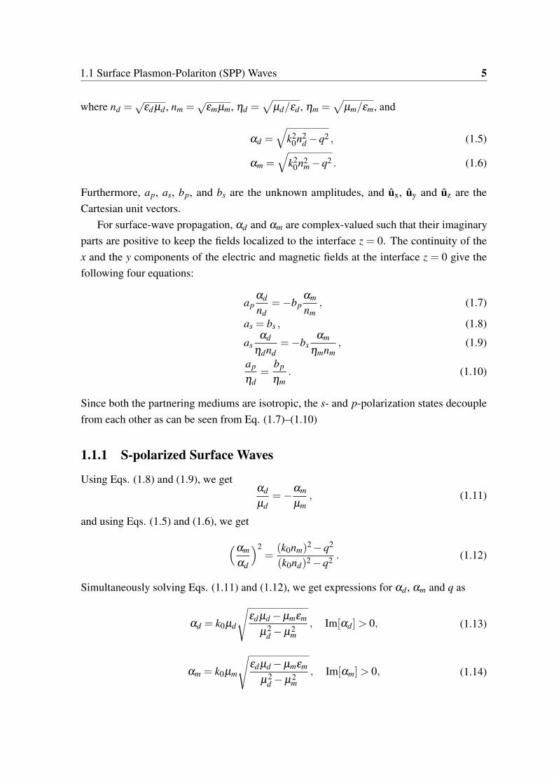
1.1 Surface Plasmon-Polariton (SPP) Waves
Fig. 1.1 Schematic figure showing the surface plasmon-polariton (SPP) waves guided by aninterface of a metal and a dielectric material.
Surface waves are electromagnetic waves that are guided by an interface of two dissimilarmaterials. The surface waves guided by an interface of a metal and a dielectric material arecalled surface plasmon-polariton (SPP) waves [31], schematically shown in Fig. 1.1. TheSPP waves are localized to the interface and decay away from that interface. This localizationmakes the SPP waves practically significant for sensitive (bio)chemical sensors becausethese waves are very sensitive to the small changes in the electromagnetic properties of thepartnering metal and dielectric material near the interface [32]. The SPP-wave-based sensorscan be used to sense very small molecules in analytes, pollutants in the environment, and smallconcentration of proteins or assays in a solution [33]. All these detections rely on sensingthe small change in the refractive index of the dielectric material near the metal/dielectricinterface.
The basic characteristics of an SPP wave can be understood from its dispersion equationthat shows the relation of the wave number of the wave and the properties of the partneringmaterials. Dispersion equation can be best derived by eliminating all the interfaces but one

4 Introduction
to exclude all the possibilities other than surface waves. This problem is called canonicalboundary-value problem.
z
x
Surface wave
𝜖𝑑 , 𝜇𝑑
𝜖𝑚, 𝜇𝑚
𝑧 = 0
Fig. 1.2 Schematic of the geometry of the canonical boundary-value problem. The horizontalarrow at the interface of two dissimilar mediums at z = 0 shows the propagation of surfacewave.
Let us consider SPP wave propagation by planar interface of two general isotropicmaterials. For this purpose, let us consider the geometry of the canonical boundary-valueproblem shown in Fig. 1.2. The half-space z< 0 is occupied by a dielectric-magnetic mediumof relative permittivity εd and relative permeability µd . The half-space z > 0 is occupied byanother dielectric-magnetic medium with relative permittivity εm and relative permeabilityµm. Without loss of generality, let us assume that the surface wave is propagating in theplanar interface of two dielectric-magnetic mediums along the x-axis. The electric andmagnetic field phasors in the two contiguous half-spaces can be written as [34]
Ed(r) =[asuy +ap
(αdux +quz
k0nd
)]exp[i(qx−αdz)
], z < 0 , (1.1)
Hd(r) =1
ηdη0
[as
(αdux +quz
k0nd
)−apuy
]exp[i(qx−αdz)
], z < 0 , (1.2)
Em(r) =[bsuy +bp
(−αmux +quz
k0nm
)]exp[i(qx+αmz)
], z > 0 , (1.3)
Hm(r) =1
ηmη0
[bs
(−αmux +quz
k0nm
)−bpuy
]exp[i(qx+αmz)
], z > 0 , (1.4)
1.1 Surface Plasmon-Polariton (SPP) Waves 5
where nd =√
εdµd , nm =√
εmµm, ηd =√
µd/εd , ηm =√
µm/εm, and
αd =√
k20n2
d −q2 , (1.5)
αm =√
k20n2
m −q2 . (1.6)
Furthermore, ap, as, bp, and bs are the unknown amplitudes, and ux, uy and uz are theCartesian unit vectors.
For surface-wave propagation, αd and αm are complex-valued such that their imaginaryparts are positive to keep the fields localized to the interface z = 0. The continuity of thex and the y components of the electric and magnetic fields at the interface z = 0 give thefollowing four equations:
apαd
nd=−bp
αm
nm, (1.7)
as = bs , (1.8)
asαd
ηdnd=−bs
αm
ηmnm, (1.9)
ap
ηd=
bp
ηm. (1.10)
Since both the partnering mediums are isotropic, the s- and p-polarization states decouplefrom each other as can be seen from Eq. (1.7)–(1.10)
1.1.1 S-polarized Surface Waves
Using Eqs. (1.8) and (1.9), we getαd
µd=−αm
µm, (1.11)
and using Eqs. (1.5) and (1.6), we get
(αm
αd
)2=
(k0nm)2 −q2
(k0nd)2 −q2 . (1.12)
Simultaneously solving Eqs. (1.11) and (1.12), we get expressions for αd , αm and q as
αd = k0µd
√εdµd −µmεm
µ2d −µ2
m, Im[αd]> 0, (1.13)
αm = k0µm
√εdµd −µmεm
µ2d −µ2
m, Im[αm]> 0, (1.14)
6 Introduction
q = k0
√µdµm(εmµd − εdµm)
µ2d −µ2
m. (1.15)
The last equation gives wave number q of s-polarized SPP waves. When µm = µd = 1, weget from Eq. (1.11) αd =−αm, which means Im[αm] and Im[αm] can not be both positive atthe same time. So s-polarized SPP can not exist.
1.1.2 P-polarized Surface Waves
Using Eqs. (1.7) and (1.10), we get
αd
εd=−αm
εm. (1.16)
Next, solving Eqs. (1.12) and (1.16), we get αd , αm and q as
αd = k0εd
√εdµd −µmεm
ε2d − ε2
m, (1.17)
αm = k0εm
√εdµd −µmεm
ε2d − ε2
m, (1.18)
q = k0
√ε2
d µmεm − ε2mµdεd
ε2d − ε2
m. (1.19)
The dispersion Eq. (1.19) gives the wavenumber of possible p-polarized SPP wave. Whenµm = µd = 1, we get the usual case of q = k0
√εdεm
εd+εm.
1.2 Excitation of SPP Waves
Excitation of SPP waves is not simple and straightforward. SPP waves cannot be excitedby simply illuminating the light on the dielectric material that is lying on a metal film or ametal film lying on top of a dielectric material. This is because the phase speed of the SPPwave is smaller than the plane wave in the dielectric material. The SPP wave is excited onlywhen the phase speed of the component of the incident light parallel to the interface is nearlyequal to the phase speed of the possible SPP wave that can exist at that interface. The phasespeed of possible SPP waves is determined by canonical boundary-value problem. Therefore,wavenumber matching has to be attained because phase speed is related to wavenumberby the relation vp = ω/k. The wavenumber matching can be achieved either by using a

1.2 Excitation of SPP Waves 7
prism, or a surface-relief grating. For exciting SPP waves in practical configurations, onlythe materials with finite thicknesses are used. Many practical configurations are available forSPP wave excitation. The most common are described below.
1.2.1 Prism-Coupled Configurations
The prism-coupled configuration can be either Turbadar–Kretschmann–Raether (TKR) [35,36] (commonly called Kretschmann configuration) or Turbadar–Otto [35, 37] (commonlycalled Otto configuration). They both employ evanescent waves to excite SPP waves. The
Fig. 1.3 Schematic figure of (a) Turbadar–Kretschmann–Raether configuration (TKR) and(b) Turbadar–Otto configuration.
TKR configuration is more famous and practical of the two prism-coupled configurations.It consists of a prism whose refractive index exceeds the refractive index of the dielectricmaterial. An interface is formed by depositing dielectric material over metallic film. Otherside of the metal is attached with the base of prism as shown in Fig. 1.3(a). When the rayof light impinges on the prism/metal interface at an angle θ , the component of wave vectorparallel to metal/dielectric interface is given by
kx = npk0 sinθ , (1.20)

8 Introduction
where np is the refractive index of the prism. The SPP wave is only excited when the realpart of the wavenumber q of possible SPP wave is nearly equal to kx, i.e.,
npk0 sinθ ≈ Re(q) . (1.21)
The Turbadar–Otto configuration is similar to the TKR, but the position of metal anddielectric is interchanged, as shown in Fig. 1.3(b). Turbadar–Otto configuration is lesspopular as compared to the TKR configuration. It is because Turbadar–Otto configurationrequires thin layer of dielectric material. In sensing applications, where dielectric materialis involved, thick layer of dielectric material is desirable. On the other hand, in TKRconfiguration we require thin layer of metal, which is not a problem in sensing applications.
1.2.2 Grating-Coupled Configuration
Fig. 1.4 Schematic of grating-coupled configuration for excitation of SPP wave.
In the grating-coupled configuration [31], a periodically corrugated interface of a dielec-tric material and a metal is used to create non-specular electromagnetic modes with variouswavenumbers, schematically shown in Fig. 1.4. An SPP wave is excited if the wavenumberof one of the non-specular mode is the same as that of the possible SPP wave and a dipin reflectance spectrum (or a peak in absorptance spectrum) appears because of the energytransfer from the incident light to the SPP wave. In this configuration metal and dielectricmaterial are of finite thickness with a surface-relief grating z = g(x) = g(x± L) at their
1.2 Excitation of SPP Waves 9
interface, where L is the period along x-axis. A surface wave is excited when
Re(q)≈ k0 sinθ + ℓ2π
L, ℓ ∈ {0,±1,±2, ...} . (1.22)
To investigate grating-coupled configuration theoretically, we require the help of numericaltechniques like the extinction boundary condition method [38, 39], the method of covariantspatial transformation [40], and the rigorous coupled-wave approach (RCWA) [27, 28]. Allthese numerical method work very well for grating-coupled configuration when the partner-ing materials are homogeneous and isotropic. But for periodically nonhomogeneous andanisotropic materials, the RCWA is well suited [27].
1.2.3 Waveguide-Coupled Configurations
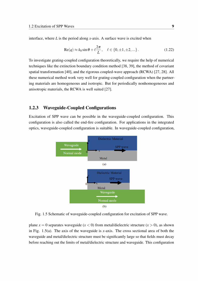
Excitation of SPP wave can be possible in the waveguide-coupled configuration. Thisconfiguration is also called the end-fire configuration. For applications in the integratedoptics, waveguide-coupled configuration is suitable. In waveguide-coupled configuration,
Fig. 1.5 Schematic of waveguide-coupled configuration for excitation of SPP wave.
plane x = 0 separates waveguide (x < 0) from metal/dielectric structure (x > 0), as shownin Fig. 1.5(a). The axis of the waveguide is x-axis. The cross sectional area of both thewaveguide and metal/dielectric structure must be significantly large so that fields must decaybefore reaching out the limits of metal/dielectric structure and waveguide. This configuration

10 Introduction
was introduced by Stegeman et al. [41] in 1983. For sensing applications, a differentwaveguide-coupled configuration is used. In this configuration a thin layer of metal is placedon a dielectric waveguide, and partnering dielectric layer is placed on the top of metal layeras shown in Fig. 1.5(b). This type of configuration is useful in building sensors due to theirsmall size and ruggedness [33].
1.2.4 Applications of SPP Waves
The SPP waves are sensitive to the change in permittivity/permeability of the partneringmaterials. Therefore most common applications of SPP waves are in optical sensing. Sensingapplications started back in 1980s. Practical configurations employ evanescent waves toexcite SPP waves. The SPP wave absorbs energy from the evanescent wave that results in areduction in the reflected light and increase in absorptance showing as a reflectance dip or anabsorptance peak in the spectrum. This is often referred to as surface plasmon resonance(SPR). These SPR based sensors can detect the change in refractive index as low as 3×10⁻⁷
[32]. SPP waves are present in a very narrow region of interface and these waves are verysensitive to the change in refractive index. Using SPR we can sense a wide range of chemicaland biochemical species. SPR based sensors are deployed to sense very small molecules,which found its application in observing pollutants in the environment, pathological analysesin medical laboratories, purity and compositional analyses in different industries [42–44].
Prism-coupled configuration is very good for sensing analytes. The TKR configuration ismore convenient than the Turbadar–Otto, because latter configuration requires thin layer ofdielectric, which is not good for sensing application. Wide range of samples can be sensedusing prism-coupled configuration.
Grating-coupled configuration is also applied in sensing application [45]. Grating-coupledconfiguration is more useful in sensors where electronic circuitry is involved. It is becausemodern technology is based planar chips and integration with electronic circuitry is easywithout the need of bulky prisms.
Advances in the research had opened new doors in the energy sector. Efficiency of lightharvesting by solar cells is improved many times using periodic texturing. Use of plasmonicstructures to increase the absorption capability is being investigated [46, 47].
1.3 Anti-Reflection Coatings for Solar Cells
Solar cells are at the leading position for the alternative energy sources. In a solar cell, theoptical properties are responsible for how much light is absorbed by it, and thus the quantity

1.3 Anti-Reflection Coatings for Solar Cells 11
of light that generates the electron-hole pairs [48]. Two conventional methods to enhance theabsorption of light of solar cells are light trapping and anti-reflection coatings.
For light trapping, surface-relief gratings and rough surfaces are used for light scatteringand excitation of surface waves inside the solar cell. Anti-reflection coatings are designedusing the principle of interference of light between incident and reflected waves. The idea inanti-reflection coatings is to cancel the reflecting light by destructive interference of lightreflected from multiple interfaces. Basic anti-reflection coatings are discussed here.
1.3.1 Index-Matching Layer
The simplest anti-reflection coatings were discovered by Lord Rayleigh in 1886. At thattime, the optical glass tended to develop a tarnish on its surface due to the environmentaleffects. Rayleigh took a tarnished glass and tested the light reflection and transmission fromthat tarnished glass. He found that the glass with the tarnish transmitted more light than theclean glass. It was because the tarnish created an extra interface at the glass surface. Now theglass surface has two interfaces, one is the glass-tarnish and the other is tarnish-air interface.The refractive index of tarnish is between the refractive indices of air and glass, so it offersless reflection than the air-glass interface did [49]. Hence by matching the indices we canalso make anti-reflection coatings.
1.3.2 Quarter-Wave Layer
Fig. 1.6 Schematic of single-layer anti-reflection coatings of quarter-wave layer.

12 Introduction
The most commonly known anti-reflection coating is a quarter-wave layer. A quarter-wave layer of anti-reflection coating can reduce the reflections at the desired wavelength.The idea of quarter-wave layer is based on the creation of a thin layer which provides twointerfaces, to give two reflected waves as shown in Fig. 1.6. When the thickness of theanti-reflection coating is λ/4, the reflected waves R1 and R2 will be 180 deg out of phaseas shown in Fig. 1.6, resulting in a destructive interference. Hence they give rise to zeroreflection. For the suppression of reflected wave, the refractive index of the anti-reflectioncoating has to be the geometric mean of the refractive indices of the air and the substrate.The drawback of this type of anti-reflection coatings is that it reduces the reflection only at asingle wavelength and for a single incidence angle.
1.3.3 Double Layer Coatings
Fig. 1.7 Schematic of double-layer anti-reflection coatings.
Double layer [50–52] anti-reflection coatings are very useful for reducing the reflectionfor a specific wavelength. In double-layer anti-reflection coatings, the upper layer facing theair has low refractive index than the other layer, schematically shown in Fig. 1.7. In thisscheme, the interference condition should be fulfilled for the destructive interference in thesetwo layers. Therefore the thicknesses of each layer is set to be the multiple of quarter or halfwavelength (λ/4 and λ/2). The optical thicknesses of each layer and the refractive indexcan be set using the relation
n1 ×d1 = n2 ×d2 , (1.23)

1.3 Anti-Reflection Coatings for Solar Cells 13
and condition for the reduction of reflection down to zero is given by [49]
n1 ×n2 = nair ×ns , (1.24)
where n1 and n2 are the refractive indices of first (upper) layer and the second layer, respec-tively, and d1 and d2 are the thickness of these layers. This coating is somewhat broad bandthan single layer, but it requires more complicated structure and material.
1.3.4 Multi-Layer Coatings
Fig. 1.8 Schematic of multi-layer anti-reflection coatings.
A single-layer anti-reflection coatings can minimize the reflection only at a single wave-length. For a broad spectrum, multi-layer anti-reflection coatings can be used to get zerorefelction at multiple wavelengths [53, 54]. These multi-layer coatings can be combinedwith different thicknesses to minimize the reflections for a broad range of spectrum, asschematically shown in Fig. 1.8. The interference condition is achieved in these layers bylight circulation inside the optical cavities formed by thin films [55]. Forward and backwardmoving fields add in each other to fulfill the condition of destructive interference. However,increasing the number of layers keeps on adding complexity to design.
14 Introduction
1.4 Zero-Index Metamaterials (ZIM)
Metamaterials are the artificially designed materials that get their bulk properties fromnot only their constituent materials but also from their structural arrangements. Commonmetamaterials include double positive materials with both the permittivity and permeabilityhaving positive values [56], double negative [57, 58], zero-index metamaterial (ZIM) withnear-zero refractive index [59, 60], bi-isotropic and bianisotropic materials [61, 62]. TheZIM is a metamaterial in which the permittivity and/or the permeability of the mediumare nearly zero, thus its refractive index is close to zero. The ZIM finds applications inelectromagnetic cloaking [63], directional emission [64], tunneling effects [65], transitionfrom total reflection to total transmission [66], and the reshaping of the phase front [67, 68].The ZIM can be designed as a mixture of metallic and dielectric materials or as a photoniccrystal of all-dielectric materials working at a frequency close to the Dirac-like point in thephotonic band structure [69, 70]. The ZIM using metallic inclusion suffer from the ohmiclosses and the fact that the impedance is infinite. However, the photonic-crystal-based designdo not suffer from both of these issues. However, all designs of the ZIM currently are notbroadband.
When the refractive index n of a material is near zero, the phase velocity νD = ω/nk0
is very large inside it, and wavelength λ = λ0/n is also large. As a result, phase is uniformthroughout the material regardless of the size and shape of the material. The fields insidethe material whose refractive index is zero oscillate in unison as field dependence is onlyon exp(iωt). Now there will bo no spatial dependence, and a quasi-electrostatic behaviorcan be achieved. This uniform phase inside ZIM gives rise to numerous applications likephase-front shaping [71] and unidirectional transmission [72, 73].
1.5 Thesis Overview
The goal of the thesis is twofold: First is to generalize the RCWA to formulate the boundary-value problem of scattering from the dielectric-magnetic gratings. A stable algorithm of theRCWA is implemented on the computer. The second goal is to apply the RCWA for thecomputational modeling of the problems involving periodic structure with inverted geometry.Therefore, a detailed mathematical formulation of the RCWA is given in Chapter 2. TheRCWA is formulated for the surface-relief grating at an interface of two different dielectric-magnetic materials. Complete algorithm and the method of computation of fields is given indetail.
1.5 Thesis Overview 15
In Chapter 3, a plasmonic sensor using a combination of grating and prism couplingsis presented. A new scheme is described that uses the prism and grating couplings for theoptical sensing after exploiting illumination from the planar side. The plasmonic sensor isanalyzed using both angular and wavelength interrogations.
In Chapter 4, the excitation of surface plasmon-polariton waves along the direction ofperiodicity of one-dimensional photonic crystal is described. Previously, the SPP wavesguided by one-dimensional photonic crystals are usually excited at the interface perpendicularto the direction of periodicity. In this work, we will present the numerical results describingthe excitation of the SPP waves on the interface along the direction of periodicity. This newinterface is accessed by illuminating from planar metallic side.
In Chapter 5, anti-reflection coatings of zero-index metamaterial for solar cells areproposed and analyzed. A new scheme of designing anti-reflection coatings using zero indexmaterials is presented. This approach can be used to design light-trapping layers for otherdevices as well.
In Chapter 6, the concluding remarks are presented. Some future directions of this workare also given in Chapter 6. All the computer codes are compiled in Matlab. Important codesare given in the Appendix. The given codes are for some figures as specified and the codesfor remaining figures are similar with small changes.
An exp(−iωt) time-dependency is implicit throughout the thesis, where ω is the angularfrequency and t being the time. The free-space wavenumber and the free-space wavelengthare indicated by k0 = ω
√ε0µ0 and λ0 = 2π/k0, respectively, where ε0 and µ0 are the
permittivity and permeability of free space. Vectors are in bold face, and unit vectors are inbold face and have a hat on them. The Cartesian unit vectors are denoted by ux, uy and uz.Matrices are enclosed in square brackets.

Chapter 2
Rigorous Coupled-Wave Approach forDielectric-Magnetic Materials
Rigorous coupled-wave approach (RCWA) is a numerical technique in the computationalelectromagnetics that is used to solve the scattering problems involving periodic structuresand gratings [23]. This method demands that all the field quantities and the material propertiesbe expressed as Fourier series. The RCWA is used to find the reflection and transmissioncoefficients from the surface-relief gratings or volume gratings. These gratings have manyapplications in the field of optics, acoustics, and spectroscopy [1–4]. These gratings are alsohelpful in designing optical sensors and improving diffractive structures for high efficiencyphotovoltaics solar cells [6–8]. The RCWA is used for numerical results in all of this thesis.
In this chapter, the RCWA is generalized to formulate the boundary-value problem ofscattering from the dielectric-magnetic gratings. The formulation is developed for a surface-relief grating with both sides of the grating occupied by the dielectric-magnetic mediums.The general formulation of the RCWA for bianisotropic materials is provided in [34]. Here,we present its specialization to isotropic dielctric and magnetic materials.
The plan of this chapter is as follows: boundary-value problem is given in Section 2.1.Fourier expansions of field and material properties are presented in Section 2.2. Coupledequations derived from Maxwell equations are given in Section 2.3. Fields at the boundariesare computed in Section 2.4, and solution algorithm is discussed in Section 2.5. A detailedformulation is discussed for stable algorithm for the implementation of the RCWA in Section2.6. The relations for the absorptances are given in Section 2.7, and time-averaged Poyntingvectors are given in Section 2.8. The numerical results showing the convergence of theRCWA are presented and discussed in Section 2.9.
18 Rigorous Coupled-Wave Approach for Dielectric-Magnetic Materials
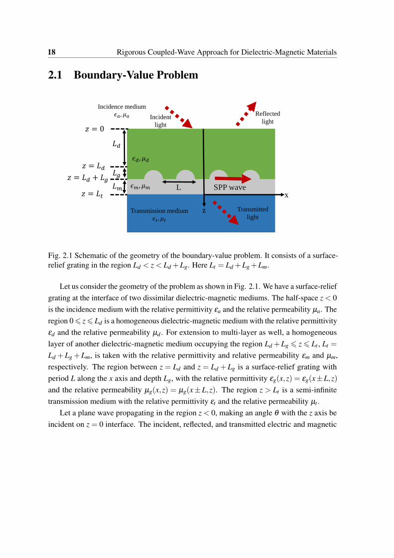
2.1 Boundary-Value Problem
SPP waveL
𝐿𝑑
𝐿𝑔
𝐿𝑚
Incident
light
Reflected
light
x
z Transmitted
light
𝜖𝑑 , 𝜇𝑑
Transmission medium
𝜖𝑡, 𝜇𝑡
𝜖𝑚, 𝜇𝑚
Incidence medium
𝜖𝑎, 𝜇𝑎
𝑧 = 𝐿𝑑𝑧 = 𝐿𝑑 + 𝐿𝑔
𝑧 = 𝐿𝑡
𝑧 = 0
Fig. 2.1 Schematic of the geometry of the boundary-value problem. It consists of a surface-relief grating in the region Ld < z < Ld +Lg. Here Lt = Ld +Lg +Lm.
Let us consider the geometry of the problem as shown in Fig. 2.1. We have a surface-reliefgrating at the interface of two dissimilar dielectric-magnetic mediums. The half-space z < 0is the incidence medium with the relative permittivity εa and the relative permeability µa. Theregion 0⩽ z⩽ Ld is a homogeneous dielectric-magnetic medium with the relative permittivityεd and the relative permeability µd . For extension to multi-layer as well, a homogeneouslayer of another dielectric-magnetic medium occupying the region Ld +Lg ⩽ z ⩽ Lt , Lt =
Ld +Lg +Lm, is taken with the relative permittivity and relative permeability εm and µm,respectively. The region between z = Ld and z = Ld +Lg is a surface-relief grating withperiod L along the x axis and depth Lg, with the relative permittivity εg(x,z) = εg(x±L,z)and the relative permeability µg(x,z) = µg(x±L,z). The region z > Lt is a semi-infinitetransmission medium with the relative permittivity εt and the relative permeability µt .
Let a plane wave propagating in the region z < 0, making an angle θ with the z axis beincident on z = 0 interface. The incident, reflected, and transmitted electric and magnetic

2.1 Boundary-Value Problem 19
field phasors in terms of Floquet harmonics can be written as [34].
Einc(r) = ∑ℓ∈Z
[sℓa
(ℓ)s + p+
ℓ a(ℓ)p
]exp{
i[k(ℓ)x x+ k(ℓ)za z]}, z ⩽ 0 , (2.1)
η0Hinc(r) = na ∑ℓ∈Z
[p+ℓ a(ℓ)s − sℓa
(ℓ)p
]exp{
i[k(ℓ)x x+ k(ℓ)za z]}, z ⩽ 0 , (2.2)
Eref(r) = ∑ℓ∈Z
[sℓr
(ℓ)s + p−
ℓ r(ℓ)p
]exp{
i[k(ℓ)x x− k(ℓ)za z]}, z ⩽ 0 , (2.3)
η0Href(r) = na ∑ℓ∈Z
[p−ℓ r(ℓ)s − sℓr
(ℓ)p
]exp{
i[k(ℓ)x x− k(ℓ)za z]}, z ⩽ 0 , (2.4)
Etr(r) = ∑ℓ∈Z
[sℓt
(ℓ)s + pt
ℓt(ℓ)p
]exp{
i[k(ℓ)x x+ k(ℓ)zt (z−Lt)]}, z ⩾ Lt , (2.5)
η0Htr(r) = nt ∑ℓ∈Z
[ptℓt(ℓ)s − sℓt
(ℓ)p
]exp{
i[k(ℓ)x x+ k(ℓ)zt (z−Lt)]}, z ⩾ Lt , (2.6)
wherek(ℓ)x = k0na sinθ + ℓκx , κx = 2π/L, (2.7)
k(ℓ)za =
√[k0na
]2−[k(ℓ)x
]2, (2.8)
k(ℓ)zt =
√[k0nt
]2−[k(ℓ)x
]2. (2.9)
In Eqs. (2.1)–(2.6), a(0)s and a(0)p are the amplitudes of the s- and p-polarized incident planewaves, respectively, and a(ℓ)s = a(ℓ)p = 0∀ℓ = 0. Furthermore, r(ℓ)s and t(ℓ)s are unknownamplitudes of the Floquet harmonics of order ℓ in the s-polarized reflected and transmittedfields, respectively. Similarly, r(ℓ)p and t(ℓ)p are the amplitudes of the Floquet harmonics oforder ℓ in the p-polarized reflected and transmitted fields, respectively, where ℓ is the order ofFloquet harmonics with ℓ ∈ {0,±1,±2,±3...}. Let us note that ℓ= 0 represents the specularcomponent of the reflected and transmitted field, and ℓ = 0 are the non-specular components.Specular reflection from a surface is known as a regular reflection in which incident ray isreflected at the same angle with the surface normal as the incident ray. On the other hand,whenever we have some irregular surface we get non-specular reflection. In non-specularreflection, the reflected rays reflect at different angles than the incidence angle.
The s-polarization state is represented by the unit vector
sℓ = uy , (2.10)

20 Rigorous Coupled-Wave Approach for Dielectric-Magnetic Materials
the p-polarization state of the incident and reflected waves is represented by
p±ℓ =
∓k(ℓ)za ux + k(ℓ)x uz
k0na, (2.11)
and the p-polarization state of the transmitted wave is represented by
ptℓ =
k(ℓ)zt ux + k(ℓ)x uz
k0nt. (2.12)
2.2 Expansions of Fields and Material Properties
The constitutive relations can be written as
D(r) = ε0ε(x,z)E(r)B(r) = µ0µ(x,z)H(r)
}, z ∈ [0,Lt ] . (2.13)
The RCWA demands that all the field phasors, permittivity and permeability are expressedas Fourier series with respect to x [29, 30, 34]. Fourier series for the permittivity and thepermeability can be written as
ε(x,z) =∞
∑ℓ=−∞
ε(ℓ)(z)exp(iℓκxx) , z ∈ [0,Lt ] , (2.14)
and
µ(x,z) =∞
∑ℓ=−∞
µ(ℓ)(z)exp(iℓκxx) , z ∈ [0,Lt ] , (2.15)
respectively, where
ε(0)(z) =
εd , z ∈ [0,Ld] ,
1L
L∫0
εg(x,z)dx , z ∈ (Ld,Ld +Lg) ,
εm , z ∈ [Ld +Lg,Lt ] ,
(2.16)
µ(0)(z) =
µd , z ∈ [0,Ld] ,
1L
L∫0
µg(x,z)dx , z ∈ (Ld,Ld +Lg) ,
µm , z ∈ [Ld +Lg,Lt ] ,
(2.17)

2.3 Coupled Equations 21
and
ε(ℓ)(z) =
1L
L∫0
εg(x,z)exp(−iℓκxx)dx , ℓ = 0 , z ∈ (Ld,Ld +Lg) ,
0 , otherwise ,(2.18)
µ(ℓ)(z) =
1L
L∫0
µg(x,z)exp(−iℓκxx)dx , ℓ = 0 , z ∈ (Ld,Ld +Lg) ,
0 , otherwise .(2.19)
Similarly, the field phasors in terms of Floquet harmonics in region 0 ⩽ z ⩽ Lt can be writtenas
E(r) =∞
∑ℓ=−∞
[E(ℓ)
x (z)ux +E(ℓ)y (z)uy +E(ℓ)
z (z)uz
]exp{
i[k(ℓ)x x]}
H(r) =∞
∑ℓ=−∞
[H(ℓ)
x (z)ux +H(ℓ)y (z)uy +H(ℓ)
z (z)uz
]exp{
i[k(ℓ)x x]} , z ∈ [0,Lt ] . (2.20)
2.3 Coupled Equations
The source-free Maxwell equations in the frequency-domain are given by
▽×E(r,ω) = iωµ(z)H(r,ω) , (2.21)
▽×H(r,ω) =−iωε(z)E(r,ω) , (2.22)
▽·E(r,ω) = 0 , (2.23)
▽·H(r,ω) = 0 . (2.24)
Substituting Eqs. (2.14), (2.15), and (2.20) in Maxwell curl postulates given in Eqs.(2.21) and (2.22), along with the constitute relations given in Eq. (2.13), we get four ordinarydifferential equations and two algebraic equations, given by
ddz
E(ℓ)x (z)− ik(ℓ)x E(ℓ)
z (z) = ik0η0
∞
∑m=−∞
µ(ℓ−m)(z)H(m)
y (z) , (2.25)

22 Rigorous Coupled-Wave Approach for Dielectric-Magnetic Materials
ddz
E(ℓ)y (z) =−ik0η0
∞
∑m=−∞
µ(ℓ−m)(z)H(m)
x (z) , (2.26)
k(ℓ)x E(ℓ)y (z) = k0η0
∞
∑m=−∞
µ(ℓ−m)(z)H(m)
z (z) , (2.27)
ddz
H(ℓ)x (z)− ik(ℓ)x H(ℓ)
z (z) =− ik0
η0
∞
∑m=−∞
ε(ℓ−m)(z)E(m)
y (z) , (2.28)
ddz
H(ℓ)y (z) =
ik0
η0
∞
∑m=−∞
ε(ℓ−m)(z)E(m)
x (z) , (2.29)
k(ℓ)x H(ℓ)y (z) =− k0
η0
∞
∑m=−∞
ε(ℓ−m)(z)E(m)
z (z) . (2.30)
The sums in Eqs. (2.25)–(2.30) contain infinite terms. Implementation of these sums on acomputer requires the truncation of the series to a finite number of terms. An approximationis obtained by restricting the series between ℓ ∈ [−Nt ,Nt ]. Defining column (2Nt +1)-vectors
[X(n)σ (z)] = [X (−Nt)
σ (z),X (−Nt+1)σ (z), ...,X (0)
σ (z), ...,X (Nt−1)σ (z),X (Nt)
σ (z)]T , (2.31)
where X ∈ {E,H} and σ ∈ {x,y,z}, (2Nt +1)× (2Nt +1)-diagonal matrix[Kx
]= diag
[k(ℓ)x
], (2.32)
and (2Nt +1)× (2Nt +1)-square matrices[ε(z)
]=[ε(ℓ−m)(z)
],[µ(z)
]=[µ(ℓ−m)(z)
], (2.33)
Eqs. (2.27) and (2.30) give
[Hz(z)
]=
1η0k0
[µ(z)
]−1·
([Kx
]·[Ey(z)
])(2.34)
and [Ez(z)
]=−η0
k0
[ε(z)
]−1·
([Kx
]·[Hy(z)
]). (2.35)
Substituting Eqs. (2.34) and (2.35) back in Eqs. (2.25), (2.26), (2.28), and (2.29) andeliminating E(ℓ)
z (z) and H(ℓ)z (z), we obtained matrix ordinary differential equation
ddz
[f(z)] = i[P(z)
]·[f(z)] , z ∈ (0,Lt) , (2.36)

2.4 Fields at Boundaries 23
where [f(z)] is a column vector with 4(2Nt +1) components given as
[f(z)] =[[Ex(z)]T , [Ey(z)]T ,η0[Hx(z)]T ,η0[Hy(z)]T
]T, (2.37)
and 4(2Nt +1)×4(2Nt +1)-matrix [P(z)] is
[P(z)
]=
[0] [
0] [
0] [
P14(z)]
[0] [
0] [
P23(z)] [
0][
0] [
P32(z)] [
0] [
0][
P41(z)] [
0] [
0] [
0]
, (2.38)
with[P14(z)] = k0[µ(z)]−
1k0[Kx]·[ε(z)]
−1·[Kx] , (2.39)
[P23(z)] =−k0[µ(z)] , (2.40)
[P32(z)] =1k0[Kx]·[µ(z)]
−1·[Kx]− k0[ε(z)] , (2.41)
[P41(z)] = k0[ε(z)] , (2.42)
where [0] is a (2Nt +1)× (2Nt +1)-null matrix.
2.4 Fields at Boundaries
To implement the boundary conditions at the z = 0 and z = Lt interfaces, the column fieldvectors are required at these boundaries. The column vectors [f(0)] and [f(Lt)] can be obtainedusing Eqs. (2.1)–(2.6) as
[f(0)
]=
[[Y inc
e ] [Y refe ]
[Y inch ] [Y ref
h ]
]·
[[A]
[R]
], (2.43)
and [f(Lt)
]=
[[Y tr
e ]
[Y trh ]
]·[T], (2.44)
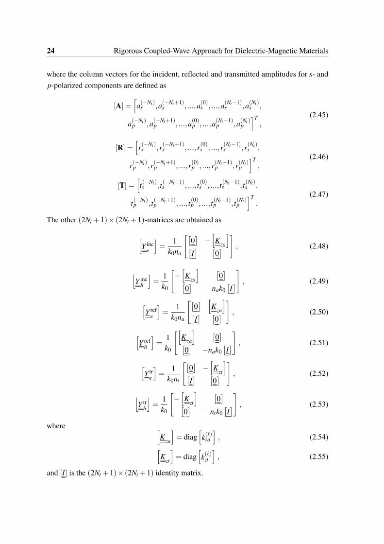
24 Rigorous Coupled-Wave Approach for Dielectric-Magnetic Materials
where the column vectors for the incident, reflected and transmitted amplitudes for s- andp-polarized components are defined as
[A] =[a(−Nt)
s ,a(−Nt+1)s , ...,a(0)s , ...,a(Nt−1)
s ,a(Nt)s ,
a(−Nt)p ,a(−Nt+1)
p , ...,a(0)p , ...,a(Nt−1)p ,a(Nt)
p
]T,
(2.45)
[R] =[r(−Nt)
s ,r(−Nt+1)s , ...,r(0)s , ...,r(Nt−1)
s ,r(Nt)s ,
r(−Nt)p ,r(−Nt+1)
p , ...,r(0)p , ...,r(Nt−1)p ,r(Nt)
p
]T,
(2.46)
[T] =[t(−Nt)s , t(−Nt+1)
s , ..., t(0)s , ..., t(Nt−1)s , t(Nt)
s ,
t(−Nt)p , t(−Nt+1)
p , ..., t(0)p , ..., t(Nt−1)p , t(Nt)
p
]T.
(2.47)
The other (2Nt +1)× (2Nt +1)-matrices are obtained as
[Y inc
e
]=
1k0na
[[0]
−[Kza
][I] [
0] ]
, (2.48)
[Y inc
h
]=
1k0
[−[Kza
] [0][
0]
−nak0[I]] , (2.49)
[Y ref
e
]=
1k0na
[[0] [
Kza
][I] [
0] ] , (2.50)
[Y ref
h
]=
1k0
[[Kza
] [0][
0]
−nak0[I]] , (2.51)
[Y tr
e
]=
1k0nt
[[0]
−[Kzt
][I] [
0] ]
, (2.52)
[Y tr
h
]=
1k0
[−[Kzt
] [0][
0]
−ntk0[I]] , (2.53)
where [Kza
]= diag
[k(ℓ)za
], (2.54)[
Kzt
]= diag
[k(ℓ)zt
], (2.55)
and [I] is the (2Nt +1)× (2Nt +1) identity matrix.

2.5 Solution Algorithm 25
2.5 Solution Algorithm
The matrix [P(z)] in Eq. (2.38) is z dependent. In order to solve this differential equation,the region between 0 ⩽ z ⩽ Lt is divided into small slices parallel to xy plane, so that in eachslice the matrix [P(z)] remains constant. The region 0 ≤ z ≤ Ld is divided into Nd slices, theregion Ld ≤ z ≤ Ld +Lg is divided into Ng slices, and the region Ld +Lg ≤ z ≤ Lt is dividedinto Nm slices. Thus the total number of slices is Ns = Nd +Ng +Nm. Let us consider the jthslice, where j ∈ [1,Ns], bounded by the planes z = z j−1 and z = z j, and approximate
[P(z)
]=[P]
j=
[P
(z j+z j−1
2
)]. (2.56)
Now, the solution of differential Eq. (2.36) is given by[f(z j)
]=[X]
j·[f(z j−1)
], j ∈ [1,Ns] , (2.57)
where [X]
j= exp
{i△ j
[P]
j
}, j ∈ [1,Ns] , (2.58)
and △ j = z j − z j−1. Repeated use of Eq. (2.57) at the boundaries give
[f(Lt)
]=[X](Ns)
·[X](Ns−1)
...[X](2)
·[X](1)
·[f(0)
]. (2.59)
Using Eqs. (2.43), (2.44), and (2.59), we get[[Y tr
e ]
[Y trh ]
]·[T]=[X](Ns)
·[X](Ns−1)
...[X](2)
·[X](1)
·
[[Y inc
e ] [Y refe ]
[Y inch ] [Y ref
h ]
]·
[[A]
[R]
]. (2.60)
Solving Eq. (2.60) for [R] and [T], we can write[[Y tr
e ]
[Y trh ]
]·[T]=[Q]·
[[Y inc
e ] [Y refe ]
[Y inch ] [Y ref
h ]
]·
[[A]
[R]
], (2.61)
where[Q]=[X](Ns)
·[X](Ns−1)
...[X](2)
·[X](1)
. Hence
[[T][R]
]=
[[Y tr
e ]
[Y trh ]
−[Q]
[[Y ref
e ]
[Y refh ]
]]−1 [Q]·
[[Y inc
e ]
[Y inch ]
]·[A]. (2.62)

26 Rigorous Coupled-Wave Approach for Dielectric-Magnetic Materials
In Eq. (2.62), finding the inverse of matrix is difficult. It is because the matrix is ill-conditioned. A stable algorithm is adopted to overcome the problem of ill-conditioning inthe matrix.
2.6 Stable RCWA Algorithm
To solve the problem of ill-conditioning in matrix in Eq. (2.62), we will implement a stablealgorithm [5, 29, 30, 34]. We need to diagonalize the matrix
[P]
j. Now the solution of Eq.
(2.36) takes the form in one slice[f(z j−1)
]=[G]
j· exp
{− i△ j
[D]
j
}·[G]−1
j·[f(z j)
], (2.63)
with [P]
j=[G]
j·[D]
j·[G]−1
j, (2.64)
where[G]
jhas eigenvectors of
[P]
jon its columns, and diagonal matrix
[D]
jcomprises
of the eigenvalues of[P]
j. The eigenvalues in
[D]
jare arranged in the decreasing order of
imaginary part, and each eigenvector in[G]
jis also at the same position as corresponding
eigenvalue in[D]
j. Defining auxiliary matrices
[Z]
jand
[T]
j, we can write
[f(z j)
]=[Z]
j·[T]
j, j ∈ [0,Ns] , (2.65)
and [T]
Ns=[T], (2.66)
and [Z]
Ns=
[[Y tr
e ]
[Y trh ]
]. (2.67)
Substituting Eq. (2.65) in Eq. (2.63), we get
[Z]
j−1·[T]
j−1=[G]
j·
[e−i△ j[D]uj 0
0 e−i△ j[D]lj
]·[G]−1
j·[Z]
j·[T]
j, (2.68)
where[D]u
jand
[D]l
jare upper and lower diagonal submatrices of matrix
[D]
j, when
eigenvalues are arranged in the decreasing order of the imaginary part. From Eq. (2.68), we

2.7 Absorptances 27
can define that [T]
j−1= exp
{− i△ j
[D]u
j
}·[W]u
j·[T]
j, (2.69)
where matrices[W]u
jand
[W]l
jare defined as
[[W ]uj[W ]lj
]=[G]−1
j·[Z]
j. (2.70)
Substituting Eq. (2.69) in Eq. (2.68) gives
[Z]
j−1=[G]
j·
[[I]
exp{−i△ j [D]lj} · [W ]lj · {[W ]uj}−1 · exp{i△ j [D]uj}
]. (2.71)
Finally, we can write[R]
and[T]
0by using Eqs. (2.43), (2.44) and (2.65) as
[[T]0[R]
]=
[[Z]u0 −[Y ref
e ]
[Z]l0 −[Y refh ]
]−1
·
[[Y inc
e ]
[Y inch ]
]·[A], (2.72)
where [Z]
0=
[[Z]u0[Z]l0
]. (2.73)
From Eq. (2.72), we can find[T]
0, and
[T]=[T]
Nscan be found by reversing the iteration
in Eq. (2.69).
2.7 Absorptances
After the amplitudes are computed, the total absorptances for the s- and p-polarized incidentplane waves can be computed as [74] as
As = 1−Nt
∑ℓ=−Nt
|r(ℓ)s |2 + |r(ℓ)p |2
|a(0)s |2Re
(k(ℓ)za
k(0)za
)−
Nt
∑ℓ=−Nt
|t(ℓ)s |2 + |t(ℓ)p |2
|a(0)s |2Re
(k(ℓ)zt
k(0)za
)∣∣∣∣∣a(ℓ)p =0
(2.74)
and
Ap = 1−Nt
∑ℓ=−Nt
|r(ℓ)s |2 + |r(ℓ)p |2
|a(0)p |2Re
(k(ℓ)za
k(0)za
)−
Nt
∑ℓ=−Nt
|t(ℓ)s |2 + |t(ℓ)p |2
|a(0)p |2Re
(k(ℓ)zt
k(0)za
)∣∣∣∣∣a(ℓ)s =0
,
(2.75)
28 Rigorous Coupled-Wave Approach for Dielectric-Magnetic Materials
respectively.
2.8 Time-Averaged Poynting Vector
When[T]
j, j ∈ [1,Ns], is known in each layer, we can find fields
[f(z j)
]in each layer using
Eq. (2.65). As a result,[f(z j)
]j
will give [Ex(z)]T , [Ey(z)]T , [Hx(z)]T , and [Hy(z)]T in each
layer using the Eq. (2.37). We can then use Eqs. (2.34) and (2.35) to find [Hz(z)]T and[Ez(z)]T , respectively.
The instantaneous Poynting vector is defined as E(r, t)×H(r, t). The time-averagedPoynting vector is defined as
P(r) =12
Re [E(r)×H∗(r)] , (2.76)
where (∗) asterisk denotes complex conjugate. For s-polarization, three components ofPoynting vector Px,s are Py,s, and Pz,s are given by
Px,s =12
Re(EyH∗
z), (2.77)
Py,s = 0 , (2.78)
Pz,s =−12
Re(EyH∗
x), (2.79)
and for the p-polarization state, three component of Poynting vector Px,p are Py,p, and Pz,p
are given by
Px,p =−12
Re(EzH∗
y), (2.80)
Py,p = 0 , (2.81)
Pz,p =12
Re(ExH∗
y). (2.82)
2.9 Numerical Results And Discussion
We have implemented the RCWA to find the convergence of absorptances for both the s- andp-polarized incident plane waves. For this purpose, a surface-relief grating was chosen in the

2.9 Numerical Results And Discussion 29
region Ld ≤ z ≤ Ld +Lg with the relative permittivity and the relative permeability as
εg(x,z) =
εm − [εm − εd]U[Ld +Lg − z−g(x)
], x ∈ (0,0.5L) ,
εd , x ∈ (0.5L,L) ,(2.83)
and
µg(x,z) =
µm − [µm −µd]U[Ld +Lg − z−g(x)
], x ∈ (0,0.5L) ,
µd , x ∈ (0.5L,L) ,(2.84)
respectively, with sinusoidal bumps defined by
g(x) = Lg sin(2πx
L) , x ∈ (0,0.5L) , (2.85)
where
U(α) =
1 , α ⩾ 0 ,
0 , α ⩽ 0 ,(2.86)
is the unit step function.For all the numerical results in this section, the free-space wavelength was set at λ0 = 800
nm. The depth of the grating is fixed at Lg = 50 nm with a grating period of L = 550 nm,and thickness of the layer on top of the grating is fixed at Lm = 30 nm. The incidence andtransmission mediums are considered to be air so that εa = µa = εt = µt = 1.
To check the convergence of the RCWA for the dielectric-magnetic grating, the ab-sorptances (that require the computations of both the reflectances and transmittances) arecomputed for different values of the parameter Nt . Figure 2.2 shows the absorptances As
for the s-polarized incidence as a function of the incidence angle θ for Nt = 19, 20, and21. The other parameters are Nd = 1, Ng = 50, Nm = 1, Ld = 900 nm, εd = 2, µd = 1.5,εm =−20+1.5i, and µm = 1.5+0.2i. The figure clearly shows that the results are converged.Figure 2.3 shows the absrptances for a p-polarized incident plane wave as a function of the
incidence angle for Nt = 19, 20, and 21, all other parameters are same as in Fig 2.2 . Thefigure shows pretty good convergence though the convergence is slightly worse for this caseas compared to As and at the larger incidence angles at the absorptance peaks. However, theconvergence is still acceptable as the change from Nt = 19 to 20 is less than ±0.5%.
In the following chapters, the RCWA is applied to three problems that involve theperiodic structures and 1D gratings. In these problems 1D gratings are illuminated fromplanar interface.

30 Rigorous Coupled-Wave Approach for Dielectric-Magnetic Materials
θ (deg)0 20 40 60 70
As
0
0.2
0.4
0.6
0.8
1
Nt = 19
Nt = 20
Nt = 21
Fig. 2.2 Apsorptance for an s-polarized incident wave as a function of the incidence angleθ for Nt = 19, 20, and 21, when Ld = 900 nm, Lg = 50 nm, L = 550 nm, Nd = 1, Ng = 50,Nm = 1, εd = 2, µd = 1.5, εm =−20+1.5i, and µm = 1.5+0.2i.
θ (deg)0 20 40 60 70
Ap
0
0.2
0.4
0.6
0.8
1
Nt = 19
Nt = 20
Nt = 21
Fig. 2.3 Absorptance Ap as a function of the incidence angle θ for Nt = 19, 20, and 21, allother parameters are same as in Fig 2.2.
Chapter 3
Combination of Grating and Prism forOptical Sensing
In this chapter, surface plasmon-polariton (SPP) waves guided by an interface of a metaland a dielectric material with a combination of grating- and prism-coupled configurationsare theoretically investigated for the optical sensing. Change in the refractive index of thepartnering dielectric material is sensed by determining the change in the incidence angle andwavelength of excitation of the SPP waves. Two absorptance peaks are observed to determinethe sensitivity for a single refractive index in the angular interrogation scheme. One peakcorresponds to the prism-coupled configuration and the other peak to the grating-coupledconfiguration. The double sensing can increase the confidence in the optical measurements.The sensitivity of the proposed sensor is also investigated in the wavelength interrogationscheme. The plan of this chapter is as follows: The introduction and literature review isgiven in Section 3.1. For the analytical formulation, we used the rigorous coupled-waveapproach which is briefly described in Section 3.2. The numerical results comparing thesensing with two types of SPP-wave-excitation are presented and discussed in Section 3.3,and the concluding remarks are presented in Section 3.4.
3.1 Introduction
The SPP waves are the electromagnetic surface waves that are excited at the metal/dielectricinterface. The SPP waves are localized to the interface and decays away from that interface.This localization makes the SPP waves practically significant for sensitive (bio)chemical
This chapter is based on “Kamran and Faryad, Plasmonic sensor using a combination of grating and prismcouplings, Plasmonics, 14, 791–798 (2019)”.

32 Combination of Grating and Prism for Optical Sensing
Fig. 3.1 Schematic of the geometry of the boundary-value problem. It is a combination ofthe prism-coupled configuration and the grating-coupled configuration.
sensors because these waves are very sensitive to the small changes in the electromagneticproperties of the partnering metal and dielectric material near the interface.
The SPP wave absorbs energy from the evanescent wave that results in a reduction inreflected light and increase in absorptance showing as a reflectance dip or an absorptancepeak in the spectrum. This is often referred to as surface plasmon resonance (SPR). MostSPR sensing applications are developed using the prism-coupled configuration, for example,high performance SPR-based sensor [75], columnar thin film based SPR sensor [76], andbiosensors that are capable of wavelength division multiplexing [77]. Another exampleof SPR based sensor is of DNA imaging in the prism-coupled configuration [78]. Severaltechniques have been developed to enhance the sensitivity of the prism coupling, includingthe use of magneto-optics [79], Michelson interferometer [80], and hyperbolic metamaterials[81, 82]. SPR sensors can be implemented in either the angular interrogation scheme for afixed wavelength or in wavelength interrogation scheme for a fixed angle or a combination ofboth. The angular scheme affords wavelength division multiplexing whereas the wavelengthscheme affords the angular division multiplexing; however, the angular scheme is morepopular because it is simpler and offers wavelength division multiplexing [77, 83, 84]. In thiswork, we have reported both the angular and the wavelength scheme for the new geometry.The optical sensing based on the grating-coupled configuration has been studied extensivelyusing the grating alone [85–90]. However, in all of these studies, the grating is illuminated
3.2 Problem Description 33
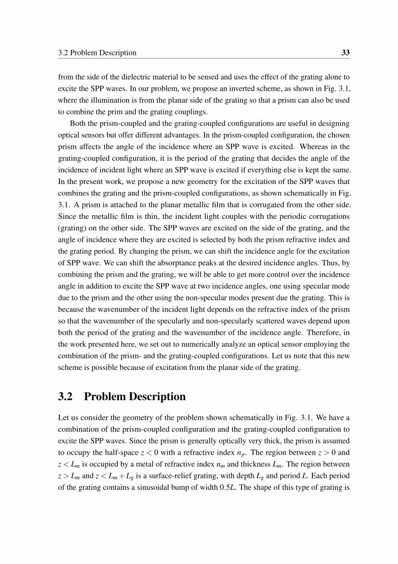
from the side of the dielectric material to be sensed and uses the effect of the grating alone toexcite the SPP waves. In our problem, we propose an inverted scheme, as shown in Fig. 3.1,where the illumination is from the planar side of the grating so that a prism can also be usedto combine the prim and the grating couplings.
Both the prism-coupled and the grating-coupled configurations are useful in designingoptical sensors but offer different advantages. In the prism-coupled configuration, the chosenprism affects the angle of the incidence where an SPP wave is excited. Whereas in thegrating-coupled configuration, it is the period of the grating that decides the angle of theincidence of incident light where an SPP wave is excited if everything else is kept the same.In the present work, we propose a new geometry for the excitation of the SPP waves thatcombines the grating and the prism-coupled configurations, as shown schematically in Fig.3.1. A prism is attached to the planar metallic film that is corrugated from the other side.Since the metallic film is thin, the incident light couples with the periodic corrugations(grating) on the other side. The SPP waves are excited on the side of the grating, and theangle of incidence where they are excited is selected by both the prism refractive index andthe grating period. By changing the prism, we can shift the incidence angle for the excitationof SPP wave. We can shift the absorptance peaks at the desired incidence angles. Thus, bycombining the prism and the grating, we will be able to get more control over the incidenceangle in addition to excite the SPP wave at two incidence angles, one using specular modedue to the prism and the other using the non-specular modes present due the grating. This isbecause the wavenumber of the incident light depends on the refractive index of the prismso that the wavenumber of the specularly and non-specularly scattered waves depend uponboth the period of the grating and the wavenumber of the incidence angle. Therefore, inthe work presented here, we set out to numerically analyze an optical sensor employing thecombination of the prism- and the grating-coupled configurations. Let us note that this newscheme is possible because of excitation from the planar side of the grating.
3.2 Problem Description
Let us consider the geometry of the problem shown schematically in Fig. 3.1. We have acombination of the prism-coupled configuration and the grating-coupled configuration toexcite the SPP waves. Since the prism is generally optically very thick, the prism is assumedto occupy the half-space z < 0 with a refractive index np. The region between z > 0 andz < Lm is occupied by a metal of refractive index nm and thickness Lm. The region betweenz > Lm and z < Lm +Lg is a surface-relief grating, with depth Lg and period L. Each periodof the grating contains a sinusoidal bump of width 0.5L. The shape of this type of grating is
34 Combination of Grating and Prism for Optical Sensing
chosen for the ease of fabrication. The region between z > Lm +Lg and z < Lm +Lg +Ld isoccupied by a dielectric material of refractive index nd and thickness Ld representing the fluidwhose refractive index is to be sensed. The half-space z > Lm +Lg +Ld is a semi-infinitemedium with a refractive index nt representing the transmission medium, which will be takento be the same as the fluid for numerical results later since fluid is optically very thick inpractical implementation. Taking the transmission medium to be the same as the fluid willalso eliminate the excitation of the waveguide modes.
To study the excitation of the SPP waves, we need to calculate the absorptance for ap-polarized incident plane wave. The peaks in the absorptance spectra will then be analyzedto ascertain the excitation of the SPP waves. Therefore, let us consider a p-polarized incidentplane wave propagating in the xz plane making an angle θ with the z axis. The incident,reflected and transmitted electric field phasors are given by,
Einc(r) = p+0 a(0)p exp
[i(k(0)x x+ k(0)zp z)
], z < 0 , (3.1)
Eref(r) =Nt
∑ℓ=−Nt
p−ℓ r(ℓ)p exp
[i(k(ℓ)x x− k(ℓ)zp z)
], z < 0 , (3.2)
and
Etr(r) =Nt
∑ℓ=−Nt
ptℓt(ℓ)p exp
(i{k(ℓ)x x
+ k(ℓ)zt [z− (Lm +Lg +Ld)]}), z > Lm +Lg +Ld ,
(3.3)
respectively, where a(0)p is the amplitude of the incident plane wave, and r(ℓ)p and t(ℓ)p are theunknown amplitudes of Floquet harmonics of order ℓ in the reflected and transmitted fields,respectively, where ℓ is the order of Floquet harmonic with ℓ ∈ {0,±1,±2...}. Here ℓ= 0corresponds to the specular component of reflected and transmitted fields, and ℓ = 0 are thenon-specular components. The parameter Nt in the summation is taken to be 21 (total termsin the sum is 2Nt +1 = 43), after ascertaining the convergence of the results within 0.5% ofthe results when Nt = 20. The other parameters are given by,
k(ℓ)zp =
√k2
0n2p − (k(ℓ)x )2 , (3.4)
k(ℓ)zt =
√k2
0n2t − (k(ℓ)x )2 , (3.5)

3.3 Numerical Results and Discussion 35
p±ℓ =
∓k(ℓ)zp ux + k(ℓ)x uz
k0np, (3.6)
and
ptℓ =
k(ℓ)zt ux + k(ℓ)x uz
k0nt. (3.7)
Linear reflectance and transmittance of order ℓ are defined as [91]
R(ℓ)pp =
∣∣∣∣∣ r(ℓ)p
a(0)P
∣∣∣∣∣2
Re[k(ℓ)zp ]
k(0)zp
(3.8)
and
T (ℓ)pp =
∣∣∣∣∣ t(ℓ)p
a(0)p
∣∣∣∣∣2
Re[k(ℓ)zt ]
k(0)zp
, (3.9)
respectively. Therefore, the absorptance is defined as
Ap = 1−∞
∑ℓ=−∞
(R(ℓ)
pp +T (ℓ)pp
). (3.10)
Let us note that 0 ≤ Ap ≤ 1 for energy conservation because the definitions (3.8) and (3.9)are the ratios of the reflected and transmitted power densities (z components of the Poyntingvector) of the ℓth Floquet mode, respectively, and the incident power. The component of thewavenumber along x-axis is given as
k(ℓ)x = k0np sinθ + ℓ(2π/L) . (3.11)
This equation shows that the wavenumber of the Floquet harmonics depends upon both therefractive index np of the prism refractive index and the order of the harmonic ℓ. An SPPwave is excited when this wavenumber is the same as the real part of the wavenumber ofthe possible SPP wave at the chosen interface. Therefore, both the prism and grating perioddetermine the angle θ and ℓ that will excite the SPP waves. We used the RCWA to findreflectance, transmittance and absorptance [29, 30, 5, 34].
3.3 Numerical Results and Discussion
We implemented the RCWA in Matlab to find the absorptances as a function of the incidenceangle θ and wavelength λ0. First we present the results of angular interrogation and then theresults of wavelength interrogation are presented. The metallic film thickness Lm = 20 nm,

36 Combination of Grating and Prism for Optical Sensing
the grating depth Lg = 40 nm, the dielectric medium thickness Ld = 1000 nm, and the prismnp = 1.7 were all kept fixed. Furthermore, nt = nd ∈ [1,1.5] was used since most fluids havethe refractive index in this range.
3.3.1 Angular Interrogation
For angular interrogation, change in the refractive index of the dielectric medium is sensedby determining the change in the incidence angle of excitation of the SPP wave. All theresults for the angular interrogation were computed at a wavelength of λ0 = 635 nm. Themetal was taken to be gold (nm = 0.14089+ 3.6318i). Figures 3.2(a) and (b) show theabsorptance spectrums for nt = nd ∈ [1,1.5] when the grating period L = 700 nm and 800nm, respectively, and the prism has a refractive index np = 1.7. Figure 3.2(c) shows theabsorptance when the refractive index of the prism is changed to 2.6 and the grating periodis L = 700 nm, showing the effect of the refractive index. In these spectra, two sets of peaksare identified: ℓ = 0 peaks when k(0)x ∼ Re(q) and ℓ = 1 peaks when k(1)x ∼ Re(q), where
q = k0
√n2
mn2d/(n
2m +n2
d) is the wavenumber of the possible SPP wave at the dielectric/metalinterface. Therefore, ℓ = 0 peaks are essentially the peaks representing the excitation ofSPP waves that are only due to the prism as they are independent of the grating period Land only depend upon np. The ℓ= 1 peaks are due to the combination of the prism and thegrating since they depend upon np and L. The change in the angular position of both thepeaks indicates that both the peaks can be used for optical sensing.
To verify that the absorptance peaks indeed represent the SPP waves, the x-componentof the time-averaged Poynting vector P(x,z) is plotted as a function of x and z in Fig. 3.3for both the peaks when nd = 1.2 and L = 700 nm. In Fig. 3.2(a), the absorptance peaks fornd = 1.2 are present at θ = 52.2 deg (ℓ= 0 peak) and 11.4 deg (ℓ= 1 peak). That is why wehave used these two angles in the Fig. 3.3 to plot the Poynting vector P(x,z). The localizationof the power density near the metal/dielectric interface indicates that an SPP wave indeedexists for both the peaks. Furthermore, the power is localized to the planar part of the gratingin Fig. 3.3(a) for the ℓ= 0 peak and the power is localized to the metal/dielectric interfacemore uniformly in Fig. 3.3(b) for the ℓ= 1 peak. Also, we can see the that the power densityis periodic along x axis, which should be the case because the geometry is periodic along thisaxis.
To analyze the usefulness of both the peaks for optical sensing, we computed the
Sensitivity =∆θ
∆nd, (3.12)

3.3 Numerical Results and Discussion 37
Fig. 3.2 Absorptance Ap as a function of incidence angle θ , Lm = 20 nm, Lg = 40 nm,Ld = 1000 nm, nt = nd , (a) L = 700 nm, np = 1.7, (b) L = 800 nm, np = 1.7, and (c) L = 700nm, np = 2.6. The horizontal arrows show the shift of peaks representing the excitation ofSPP wave.

38 Combination of Grating and Prism for Optical Sensing
Fig. 3.3 Variation of the x-component of the time averaged Poynting vector P(x,z) as afunction of x and z, when nd = nt = 1.2, L = 700 nm, Ld = 1000 nm, Lg = 40 nm, np = 1.7,(a) (ℓ= 0 peak) θ = 52.2 deg and (b) (ℓ= 1 peak) θ = 11.4 deg.
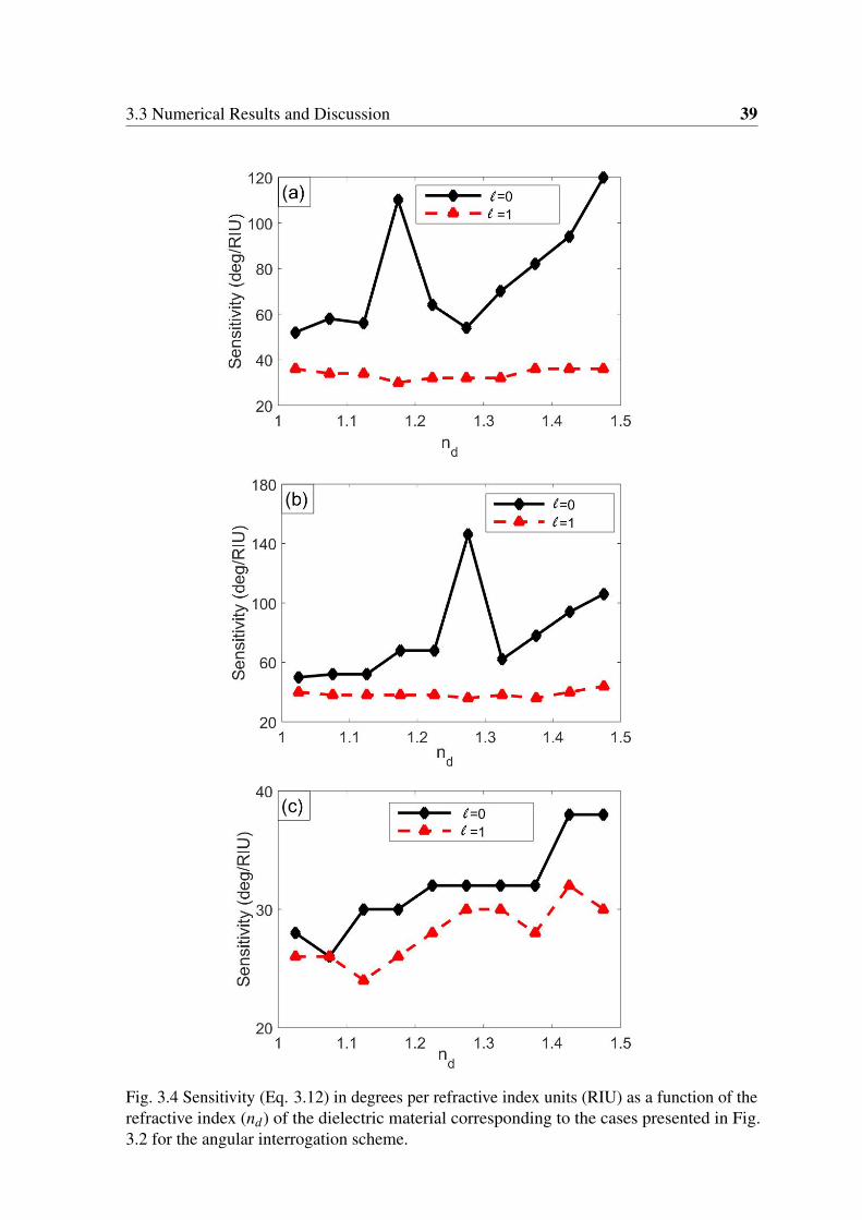
3.3 Numerical Results and Discussion 39
Fig. 3.4 Sensitivity (Eq. 3.12) in degrees per refractive index units (RIU) as a function of therefractive index (nd) of the dielectric material corresponding to the cases presented in Fig.3.2 for the angular interrogation scheme.

40 Combination of Grating and Prism for Optical Sensing
Fig. 3.5 Figure of merit (FOM) as a function of refractive index of the dielectric material(nd) corresponding to the cases presented in Fig. 3.2.

3.3 Numerical Results and Discussion 41
Fig. 3.6 Absorptance Ap as a function of wavelength λ0, when θ = 0 deg, np = 1.7, and (a)L = 700 nm, and (b) L = 800 nm.

42 Combination of Grating and Prism for Optical Sensing
Fig. 3.7 Graphical solution of Eq. (3.14): The right-hand side of the equation as a functionof λ0 is shown by a solid black straight line when ℓ= 1. The real parts of the solutions ofthe canonical problem q/k0 as a function of wavelength for different values of nd are alsoplotted. The spectral values of the intersections represent the solutions of the equation. Thevalues of the grating periods are (a) L = 700 nm and (b) L = 800 nm.

3.3 Numerical Results and Discussion 43
Fig. 3.8 Sensitivity (Eq. 3.15) in nm per refractive index units (RIU) as a function of therefractive index (nd) of the dielectric material for the wavelength interrogation scheme.
where ∆θ is the difference between the two incidence angles for the SPP wave excitation and∆nd is the difference between the refractive indices of the dielectric material. The sensitivityof the angular positions of both the peaks was computed and is presented in Fig. 3.4 when(a) L = 700 nm, np = 1.7, (b) L = 800 nm, np = 1.7, and (c) L = 700 nm, np = 2.6. A quickscan of the figures shows that the sensitivity of the ℓ= 0 peak is generally higher than theℓ= 1 peaks. Also, the sensitivity of ℓ= 0 peaks is almost independent of the grating periodL (as should be expected since the peak only depends on the refractive index of the prism)but inversely proportional to the refractive index of the prism, though the sensitivity of theℓ= 1 peak slightly increases with increase in the period L but is inversely proportional to therefractive index np of the prism. Furthermore, the sensitivity plots show that the sensitivity,in general, is dependent upon the refractive index of the fluid.
In actual experiments, however, it is not just the angular shift that is important in mea-surement of the change in the angular position of the peak for a change in the refractive indexof the dielectric material nd to be sensed. What is important is the change in the angularlocation with respect to the peak width. Therefore, we computed a Figure of merit (FOM)defined as
FOM =Sensitivity∆θFWHM
, (3.13)
where ∆θFWHM is the full width at half maximum of the absorption peak, and is presented inFig. 3.5. The figure indicates that the FOM is generally higher for the ℓ= 1 peak which isdue to the combination of the prism and the grating and is smaller for the ℓ= 0 peak which

44 Combination of Grating and Prism for Optical Sensing
is solely due to the prism. This is because the ℓ= 1 peaks are considerably sharper than theℓ= 0 peaks.
3.3.2 Wavelength Interrogation
For the wavelength interrogation, all the results were computed for normal incidence (θ = 0deg) but the absorptances were computed as a function of wavelength λ0. The refractive indexof the fluid-to-be-sensed and the prism were taken to be independent of the wavelength butthe refractive index of the metal (gold) was taken to be wavelength dependent. Figures 3.6(a)and (b) shows the absorptance spectra as a function of wavelength λ0 for nt = nd ∈ [1,1.5]when the grating period L = 700 nm and 800 nm, respectively. These absorptance peaksin the figures labelled as ℓ = 1 peaks represent the SPP waves. The shift in their spectralposition clearly indicates that this configuration can be used for the optical sensing.
To confirm that these absorptance peaks correspond to the excitation of SPP wave, weneed to see if they correlate with the solution of the canonical problem of SPP waves guidedby the planar gold/fluid interface. Since the refractive index of gold is taken to be wavelengthdependent, we need to solve the below nonlinear equation to find the wavelengths where theSPP waves can be excited for a given ℓ and L [5, 31]:
Re( q
k0
)= np sinθ + ℓ
λ0
L. (3.14)
We have solved this equation graphically, as shown Figs. 3.7(a) and (b) by finding theintersections of the left-hand side of this equation with the right-hand side. The left-handside is a nonlinear function of the wavelength as the canonical solution q depends on nd
and nm(λ0). The right-hand side is an equation of a straight line. The graphical solutionsshowed that the line ℓ = 1 for L = 700 nm intersects the canonical solution curves fordifferent values of nd at λ0 = {715, 788, 858, 930, 1000, 1070} nm. These values of λ0 arein excellent agreement with the peaks in Fig. 3.6(a) at λ0 = {700, 784, 854, 925, 995, 1065}nm. Similarly for L = 800 nm, Fig. 3.7(b) shows that the SPP waves should be excited atλ0 = {813, 895, 976, 1055, 1137, 1218} nm by ℓ = 1 Flouquet harmonics. The peaks inFig. 3.6(b) are present at λ0 = {811, 891, 972, 1052, 1133, 1213} nm showing an agreementbetween the canonical and grating results.
To examine the sensitivity of the proposed scheme in the wavelength interrogation scheme,the sensitivity is computed as
Sensitivity =∆λ0
∆nd, (3.15)
3.4 Conclusions 45
where ∆λ0 is the spectral shift between the two peaks for the SPP wave excitation whennd changes by ∆nd . The sensitivity is presented in Fig. 3.8 when (a) L = 700 nm and (b)L = 800 nm. The figures shows that the sensitivity for L = 800 nm is higher than the L = 700nm. Let us note that the sensitivity is not affected by np for the normal incidence in thewavelength interrogation because the term np sinθ = 0 for this case.
3.4 Conclusions
We theoretically analyzed the excitation of SPP waves using a combination of a prism and asurface-relief grating. Both the angular and the wavelength interrogation schemes in the newgeometry are proposed in this chapter. The combination made possible by an inverted gratingwith a prism attached to the planar side of the grating. It was seen that two types of absorptionpeaks are available to implement a plasmonic optical sensor. This can be used to sense thesame analyte at two different angles of incidence to increase confidence in measurement.Of the two absorption peaks, it was seen that the sensitivity of the angular location of thepeak to the change in the refractive index of the fluid is stronger for the peak excited by thespecular component of the field but the shift in the angular location with respect to the widthof the peak is somewhat higher for the non-specularly excited SPP waves. The promise ofthe sensing of the new geometry is also shown in the wavelength interrogation scheme. Theproposed configuration can be used to build more sensitive and more reliable plasmonicsensor. The sensitivity in the geometry proposed in this work can be tuned by changing theprism refractive index and the grating period.


Chapter 4
SPP Waves along the Direction ofPeriodicity of Photonic Crystal
In this chapter, excitation of surface plasmon-polariton waves is investigated at an interfaceof a metal and a one-dimensional photonic crystal (1DPC) along the direction of periodicityof the photonic crystal in a prism-coupled configuration. The RCWA is used to formulatethe problem and the absorptance spectra are obtained as a function of the incidence angle,the period, and the thickness of the photonic crystal. The correlation of the absorptancebands with the underlying canonical problem and the spatial power profiles confirmed theexcitation of SPP waves. The excitation of SPP waves at the interface of the 1DPC alongthe direction of the periodicity opens up new avenues for applications. This interface wasaccessed by illuminating the metal/1DPC interface from metallic side. The plan of thischapter is as follows: Introduction to the problem is given in Section 4.1. The description andbrief formulation of the problem are given in Section 4.2. Numerical results are presentedand discussed in Section 4.3, and concluding remarks are presented in Section 4.4.
4.1 Introduction
Excitation of SPP waves at an interface of a homogeneous material and a one-dimensionalphotonic crystal (1DPC) was first studied in 1978 [92]. These SPP waves are localized tothe interface which is perpendicular to the direction of periodicity of the 1DPC and haveseveral names in the literature like Tamm plasmon-polariton (TPP), surface Bragg waves, orjust SPP waves [93]. Surface waves guided by an interface of a metal and 1DPC has many
This chapter is based on “Kamran and Faryad, Excitation of surface plasmon polariton waves along thedirection of periodicity of a one-dimensional photonic crystal, Physical Review A, 99, 053811 (2019)”.
48 SPP Waves along the Direction of Periodicity of Photonic Crystal
applications, especially optical sensors of fluids and biochemicals [94, 95], light-couplers[96], directional emitter [97], and wave guides [98].
In all of this previous work, only excitation of surface wave guided by an interface of ahomogeneous medium and the photonic crystal was exploited in the direction perpendicularto the periodicity of the 1DPC [98–100]. The excitation of surface waves at metal/1DPCinterface along the direction of periodicity was neglected. Recently, a rigorous formulationof SPP waves’ propagation along the direction of the periodicity of the 1DPC was presentedin Ref. [101], where they obtained a dispersion equation and solved the canonical-boundaryvalue problem for the excitation of surface waves at metal/1DPC interface along the directionof periodicity.
However, the canonical boundary-value problem is not practically realizable, becauseboth the partnering materials are supposed to be semi-infinite. And, it is not always possibleto assume that the solutions predicted by the canonical problem can be realized in a prism-coupled configuration [102]. Therefore, we set out to investigate if the excitation of theSPP waves at an interface of a metal and 1DPC along the direction of the periodicity of thephotonic crystal in the prism-coupled configuration is possible as predicted by the canonicalproblem. For this purpose, the prism-coupled problem is formulated and solved using theRCWA [27, 28].
4.2 Problem Description
Let us consider the geometry of the problem schematically shown in Fig. 4.1. Let us assumethat SPP wave is guided by the interface of the metal and the 1DPC along the x axis. Let thehalf-space z < 0 be occupied by homogeneous medium (prism) with permittivity εp. Theregion 0 < z < Lm is occupied by a metal with permittivity εm and thickness Lm. The regionbetween z > Lm and z < Lm +Lpc is a photonic crystal of period Λ and thickness Lpc. Therelative permittivity of the photonic crystal is
εr(x) = εr(x±Λ) , Lm < z < Lm +Lpc . (4.1)
The permittivity of the photonic crystal can be expanded as a Fourier series with respect to x
εr(x) = ∑ℓ∈Z
ε(ℓ)r exp(iℓκxx) , Z ∈ {0,±1,±2, ...} , (4.2)
where κx = 2π/Λ, and
ε(0)r =
1Λ
∫Λ
0εr(x)dx , (4.3)

4.2 Problem Description 49
Fig. 4.1 Schematic representation of the geometry of the boundary-value problem. A p-polarized plane wave is incident upon metal/1DPC bilayer from inside a prism of relativepermittiity εp.
and
ε(ℓ)r =
1Λ
∫Λ
0εr(x)exp(−iℓκxx)dx , ℓ = 0. (4.4)
The region z > Lm +Lpc is a semi-infinite medium with permittivity εt .To predict the excitation of the SPP waves we need to compute the plane wave absorption
by the metal and the 1DPC and identify the absorption peaks that are independent of thethickness of the photonic crystal. Since the 1DPC is taken to be made up of isotropicmaterials, only a p-polarized incident plane wave can excite an SPP wave. For this purpose,let us consider a p-polarized plane wave propagating in the xz plane and be incident onthe metal from prism side making an angle θ with the z axis. The incident, reflected andtransmitted electric field phasors are given by
Einc(r) = p+0 a(0)p exp
{i[k(0)x x+ k(0)zp z
]}, z < 0 , (4.5)
Eref(r) =Nt
∑ℓ=−Nt
p−ℓ r(ℓ)p exp
[i(k(ℓ)x x− k(ℓ)zp z)
], z < 0 , (4.6)

50 SPP Waves along the Direction of Periodicity of Photonic Crystal
and
Etr(r) =Nt
∑ℓ=−Nt
ptℓt(ℓ)p exp
(i{k(ℓ)x x
+ k(ℓ)zt [z− (Lm +Lpc)]}), z > Lm +Lpc ,
(4.7)
respectively, in terms of the Floquet harmonics. Where a(0)p is the known amplitude of theincident electric field, r(ℓ)p and t(ℓ)p are the unknown field amplitude of the reflected andtransmitted electric fields of the ℓth Floquet harmonics, where ℓ is the order of the Floquetharmonics with ℓ ∈ {0,±1,±2...}. Here ℓ = 0 represents the specular component of thefields, and ℓ = 0 are the non-specular components of the fields. Other parameters are givenby
k(ℓ)zp =
√k2
0εp − (k(ℓ)x )2 , (4.8)
k(ℓ)zt =
√k2
0εt − (k(ℓ)x )2 , (4.9)
p±ℓ =
∓k(ℓ)zp ux + k(ℓ)x uz
k0√
ε p, (4.10)
and
ptℓ =
k(ℓ)zt ux + k(ℓ)x uz
k0√
ε t. (4.11)
The x component of the wave number is given by
k(ℓ)x = k0√
ε p sinθ + ℓ(2π/Λ) . (4.12)
To implement the RCWA, the field phasors are expanded in terms of Floquet harmonicsin region 0 ≤ z ≤ Lm +Lpc as
E(r) =Nt
∑ℓ=−Nt
[E(ℓ)
x (z)ux +E(ℓ)z (z)uz
]×exp(ik(ℓ)x x) , z ∈ [0,Lm +Lpc] ,
(4.13)
H(r) =Nt
∑ℓ=−Nt
H(ℓ)y (z)uy exp(ik(ℓ)x x)] , z ∈ [0,Lm +Lpc] , (4.14)
where Nt is an integer. Substituting Eqs. (4.13), and (4.14) in Maxwell curl postulates, weget two ordinary differential equations and one algebraic equation. The algebraic equation
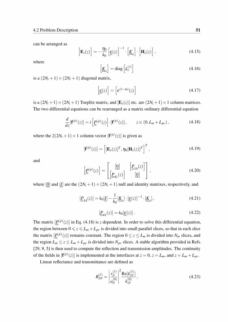
4.2 Problem Description 51
can be arranged as [Ez(z)
]=−η0
k0
[ε(z)
]−1·[Kx
]·[Hy(z)
], (4.15)
where [Kx
]= diag
[k(ℓ)x
](4.16)
is a (2Nt +1)× (2Nt +1) diagonal matrix,[ε(z)
]=[ε(ℓ−m)(z)
](4.17)
is a (2Nt +1)× (2Nt +1) Toeplitz matrix, and [Ex(z)] etc. are (2Nt +1)×1 column matrices.The two differential equations can be rearranged as a matrix ordinary differential equation
ddz
[f(p)(z)] = i[P(p)(z)
]·[f(p)(z)] , z ∈ (0,Lm +Lpc) , (4.18)
where the 2(2Nt +1)×1 column vector [f(p)(z)] is given as
[f(p)(z)] =[[Ex(z)]T ,η0[Hy(z)]T
]T, (4.19)
and [P(p)(z)
]=
[0] [
P14(z)][
P41(z)] [
0] , (4.20)
where [0] and [I] are the (2Nt +1)× (2Nt +1) null and identity matrixes, respectively, and
[P14(z)] = k0[I]−1k0[Kx] · [ε(z)]
−1 · [Kx] , (4.21)
[P41(z)] = k0[ε(z)] . (4.22)
The matrix [P(p)(z)] in Eq. (4.18) is z dependent. In order to solve this differential equation,the region between 0 ⩽ z ⩽ Lm +Lpc is divided into small parallel slices, so that in each slicethe matrix [P(p)(z)] remains constant. The region 0 ≤ z ≤ Lm is divided into Nm slices, andthe region Lm ≤ z ≤ Lm +Lpc is divided into Npc slices. A stable algorithm provided in Refs.[29, 9, 5] is then used to compute the reflection and transmission amplitudes. The continuityof the fields in [f(p)(z)] is implemented at the interfaces at z = 0, z = Lm, and z = Lm +Lpc.
Linear reflectance and transmittance are defined as
R(ℓ)pp =
∣∣∣∣∣ r(ℓ)p
a(0)p
∣∣∣∣∣2
Re[k(ℓ)zp ]
k(0)zp
, (4.23)

52 SPP Waves along the Direction of Periodicity of Photonic Crystal
and
T (ℓ)pp =
∣∣∣∣∣ t(ℓ)p
a(0)p
∣∣∣∣∣2
Re[k(ℓ)zt ]
k(0)zp
, (4.24)
respectively, so that the absorptance is
Ap = 1−Nt
∑ℓ=−Nt
(R(ℓ)
pp +T (ℓ)pp
). (4.25)
The reflection and transmission amplitudes are found using the rigorous coupled-waveanalysis (RCWA) using a stable algorithm [5, 29, 30, 34].
4.3 Numerical Results and Discussion
For representative numerical results, the 1DPC is taken to be the same as in Ref. [101] forcomparison of the results in this problem with those of the underlying canonical problemsolved in Ref. [101]. The 1DPC is made up of alternating layers of two dielectric mediumswith thicknesses a and b, and relative permittivities εa and εb, respectively. Both the layersare of equal thicknesses so that a = b = 0.5Λ and the relative permittivity is
εr(x) =
εa , 0 < x < 0.5Λ ,
εb , 0.5Λ < x < Λ .(4.26)
The Fourier coefficients for this permittivity profile are given as
ε(0)r =
εa + εb
2,
ε(ℓ)r = i(εb−εa)
ℓπ , ∀ ℓ= odd ,
ε(ℓ)r = 0 , ∀ ℓ= even .
(4.27)
For the numerical results in this section, free-space wavelength is fixed at λ0 = 633nm. The metal is chosen to be gold with the relative permittivity εm = −11.8+ 1.3i andthickness Lm = 10 nm. The parameter Nt in the summations is set to be 15 after ascertainingthe convergence of the results within 0.5% of the results when Nt = 14. Also, Nm = 1 andNpc = 1 were set for the computation of the absorptance since both the metal and the 1DPCare homogeneous along the z axis. The relative permittivities of the alternating layer inthe 1DPC are taken to be εa = (na)
2 + 10−6i and εb = (nb)2 + 10−6i, where na = 1.5 and
nb = 2. The reason behind choosing these values of na and nb is that the most of the dielectricmaterials have their refractive indexes around it in the visible range. For instance, many
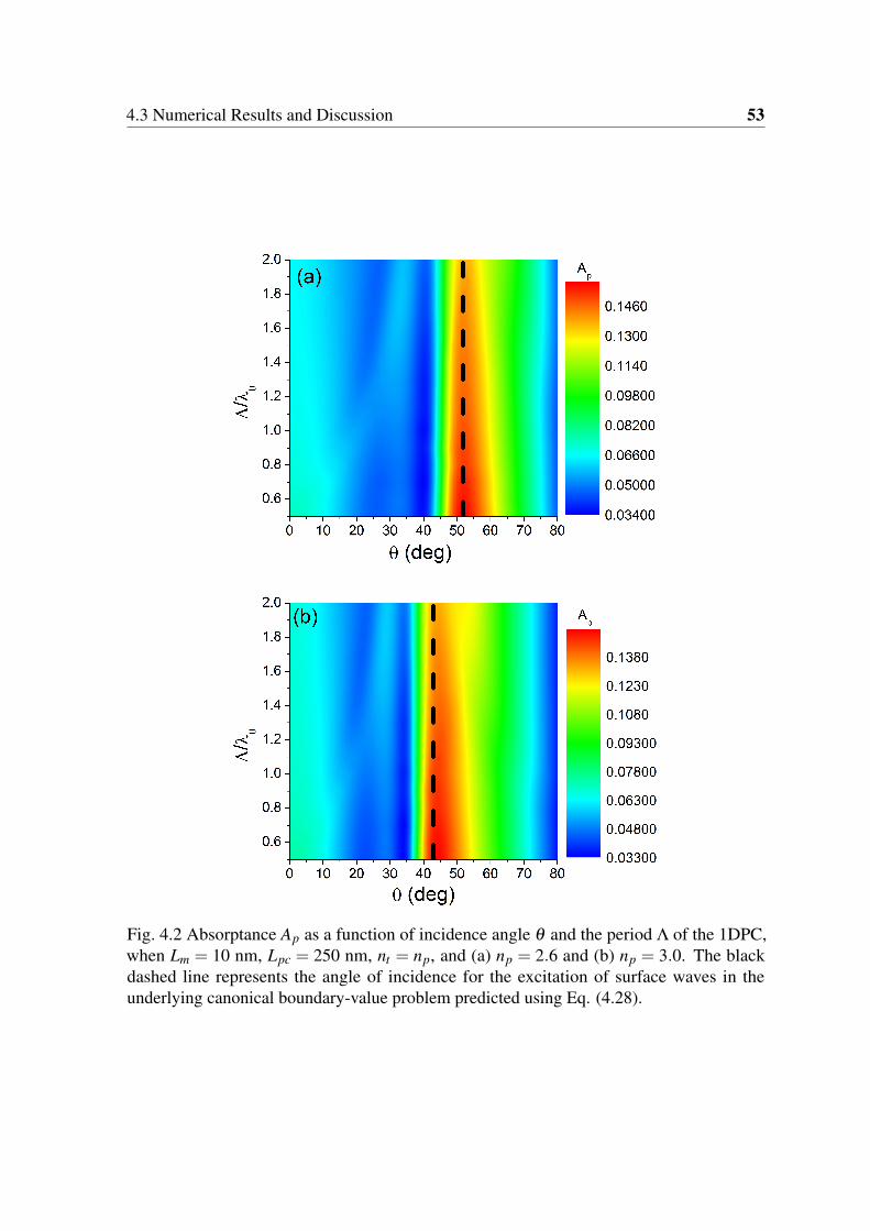
4.3 Numerical Results and Discussion 53
Fig. 4.2 Absorptance Ap as a function of incidence angle θ and the period Λ of the 1DPC,when Lm = 10 nm, Lpc = 250 nm, nt = np, and (a) np = 2.6 and (b) np = 3.0. The blackdashed line represents the angle of incidence for the excitation of surface waves in theunderlying canonical boundary-value problem predicted using Eq. (4.28).

54 SPP Waves along the Direction of Periodicity of Photonic Crystal
Fig. 4.3 Absorptance Ap as a function of incidence angle θ and the thickness Lpc of the1DPC when Lm = 10 nm, Λ = 1.0λ0 nm, nt = np, and (a) np = 2.6 and (b) np = 3.0. Theblack dashed line represents the angle of incidence for the excitation of surface waves in theunderlying canonical boundary-value problem predicted using Eq. (4.28).

4.3 Numerical Results and Discussion 55
Fig. 4.4 Variation of the x component of the time-averaged Poynting vector Px as a function ofx and z, when Lm = 10 nm, Lpc = 250 nm, np = 3.0, nt = np, θ = 44 deg and (a) Λ = 1.0λ0and (b) Λ = 1.5λ0.

56 SPP Waves along the Direction of Periodicity of Photonic Crystal
silica-based glasses have their refractive index as 1.5 and the refractive index of ZnO is 2 ata wavelength of 633 nm. The small imaginary part 10−6 is added for comparison with thecanonical problem where it was required for the computational purpose. The small imaginarypart also models the real materials more accurately as all materials are lossy even thoughthe losses are small in dielectric materials. The refractive index of the transmission mediumnt =
√εt is taken to be the same as that of the prism.
To delineate the excitation of SPP waves, the absorptance spectrum Ap as a function ofthe incidence angle θ and the period Λ of the 1DPC is presented in Fig. 4.2(a) for a prismwith refractive index np = 2.6 and the thickness of the 1DPC Lpc = 250 nm. A quick scan ofthe figure shows that an absorptance band around θ = 52 deg is present which indicates theexcitation of SPP wave. To confirm that this absorptance band correlates with the canonicalproblem, we can use Eq. 4.12 to find the θ predicted by the canonical problem as
θ = sin−1[
Re(q)− ℓ(2π/Λ)
k0np
], (4.28)
where q ∼ 2.04k0 is the wavenumber predicted by the canonical problem [101]. For theparameters used in Fig. 4.2(a), Eq. (4.28) gives θ ∼ 51.8 deg when ℓ = 0, which is inexcellent agreement with the position of the spectral band found as θ = 52 deg. Therefore, itcan be concluded that the SPP wave is being excited as a Floquet harmonic of order 0.
To see the effect of the refractive index of the prism, the absorptance were computed for aprism with np = 3.0 (all other parameters are the same as Fig. 4.2(a)) and is presented in Fig.4.2(b). Now, the absorptance band shifts to θ ∼ 44 deg. The canonical problem predicts theexcitation angle of θ ∼ 42.9 deg that is still an excellent agreement with the angular locationof our absorptance band.
To understand the effect of the thickness of the photonic crystal, the absorptance ispresented in Fig. 4.3 as a function of the incidence angle θ and the thickness Lpc of the1DPC for two values of the refractive index of the prism when Λ = 1.0λ0. The slight changein the incidence angle when the thickness of the photonic crystal increases is because ofthe fact that the SPP wave is localized to the interface on the photonic crystal side and isextended to about 100 nm as the location of the absorption band stops changing after thethickness is increased beyond 100 nm.
To check the spatial extent of the SPP waves on both sides of the interface, the time-averaged Poynting vector is computed at the incidence angle where the surface wave isexcited. For this purpose, the electric and magnetic field phasors are computed by dividingthe photonic crystal and the metallic layer into 1-nm thick slices parallel to the metal/1DPCinterface. Therefore, for the field and Poynting vector computation, the values of Nm = Lm/1

4.4 Conclusions 57
nm and Npc = Lpc/1 nm were taken so as to get 1 nm resolution on the z axis. Furthermore,ap = 1 Vm−1 was set. Across each slice, the field vector is computed by the solution of Eq.(4.18) as
[f(p)(z j)] = exp[i[P(p)](z j − z j−1)
]·[f(p)(z j−1)] ,
j ∈ {1,Nm +Npc}. (4.29)
After using the components of the field phasors in Eqs. (4.13) and (4.14), the x component ofthe time-averaged Poynting vector is given by
Px(x,z) =12
Re[E(x,z)×H∗(x,z)] . (4.30)
and is presented in Figs. 4.4(a) and (b) when Λ = 1.0λ0 and 1.5λ0, respectively, and θ = 44deg, Lpc = 250 nm, and np = 3.0. We can observe that the power density is localized to themetal/1DPC interface which is an indication of the excitation of surface waves. Furthermore,on the side of the photonic crystal, the power is localized to about 100 nm from the interface.This is in line with the conclusion drawn from Fig. 4.3.
4.4 Conclusions
In this chapter, the excitation of surface plasmon-polariton (SPP) waves guided by theinterface of a metal and a one-dimensional photonic crystal (1DPC) was shown along theinterface which contains the direction of periodicity of the photonic crystal. A prism-coupledconfiguration was used to excite the SPP waves using metallic films and the 1DPC of thefinite widths. Those absorptance bands were identified for plane wave incidence that remainunchanged by a change in the thickness of the 1DPC. The excitation angle in the prism-coupled configuration is in full agreement with the dispersion relation developed in thecanonical boundary-value problems [101].
In contrast to the SPP waves guided by an interface of a metal and a 1DPC which isperpendicular to the direction of periodicity of the photonic crystal, this work establishedthe excitation of the SPP waves on the long-neglected interface along the direction of theperiodicity. It is hoped that it will open up new avenues of the applications in sensing andimaging. Let us also note that multiple SPP waves of different wavenumbers were excitedwhen the direction of periodicity of the photonic crystal was perpendicular to the interface[34, 103, 104] but no such multiplicity exists in the present case.

Chapter 5
Anti-Reflection Coatings of Zero-IndexMetamaterial
In this chapter, anti-reflection coatings of zero index metamaterials (ZIMs) are proposedfor maximum absorption of light in solar cells. A thin layer of a ZIM is shown to help traplight inside a solar cell. The outer surface of a ZIM layer is planar, and the inner surfacehas periodic corrugations in order for the incident light to pass through but block the re-transmission of the light back into free space. Using rigorous calculations for light absorptionefficiency integrated over the AM1.5 solar spectrum, the basic design of the anti-reflectioncoating using a ZIM is studied by comparing the results with a common anti-reflectioncoating and a ZIM layer planar on both sides.
The plan of this chapter is as follows: Introduction to the problem is given in Section 5.1.Since a ZIM has both permittivity and permeability near zero, we present the specializedformulation of the RCWA in Section 5.2 for isotropic dielectric and magnetic materials. Thenumerical results are presented and discussed in Section 5.3. The conclusions are presentedin Section 5.4.
5.1 Introduction
The reflection of light from solar cells is one of the important factor in reducing the efficiencyof the cell to convert the sun light to electric power. For this reason, anti-reflection coatingsare used to minimize the reflections. The simplest anti-reflection coating was first observedby Lord Rayleigh in 19th century, when he observed that a tarnishing on a glass increasedthe transmittance in it instead of reflectance. Etching of a surface can also decrease the
This chapter is based on “Kamran and Faryad, Anti-reflection coatings of zero-index metamaterial for solarcells, AIP Advances 10, 025010 (2020)”.
60 Anti-Reflection Coatings of Zero-Index Metamaterial
reflectance from a surface as observed by Fraunhofer in 1817 [105]. The most commonlyused anti-reflection coating is a quarter-wave layer matching the impedance of the free-spaceto that of the substrate [106]. An optimized version of this anti-reflection coating is designedfor high efficiency silicon solar cell [107]. Anti-reflection coatings using metamaterials [108]and artificially designed surface-relief grating [109, 110] have also been proposed amongothers [111, 112]. These techniques have been developed for both the crystalline silicon andthin-film solar cells [113–115].
In addition to the anti-reflection coatings, other light trapping techniques are also beingused. For example, the localized surface plasmons using metallic nanoparticles and propagat-ing surface plasmon-polariton waves using surface-relief gratings [8, 116]. Furthermore, thetexturing of the surface of solar cell is a very well known and efficient technique for lighttrapping [117, 118]. Recently, photonic crystal have also been proposed for an enhancedlight trapping in thin film solar cells [119]. Nano-structuring can also be used to enhancelight trapping with the help of silicon nanowire [120].
Metamaterials are the composite materials, whose properties are engineered from theirconstituent materials. Zero-index metamaterial (ZIM) are the metamaterials with theirpermittivity and/or permeability near zero [59, 60]. Hence their refractive index is nearzero. When the refractive index is near zero, the phase velocity is very large inside thematerial. Consequently, the wavelength inside the material is also very large resulting in thephase being uniform throughout the medium [121]. Thus, an electromagnetic wave can onlypenetrate inside the ZIM if the shape of the wave fronts of the incident electromagnetic waveare of the same shape as of the interface of the ZIM. Therefore, if we design a layer of ZIMmedium with planar surface on the side of the incident solar light and corrugations on theside of active solar material, the light will couple into the solar cell but will not be able to exit.This must help increase the light absorption inside the solar cell. This chapter is dedicatedto test this hypothesis theoretically using rigorous calculations. The basic design is shownschematically in Fig. 5.1. We used the RCWA to compute the reflectance, transmittance, andabsorptance of the solar cell with periodically corrugated ZIM layer [5, 23, 24, 27].
5.2 Problem Description
Let us consider the schematic of the problem shown in Fig. 5.1. The half-space z < 0 is theincidence medium with the relative permittivity εa and relative permeability µa. The regionbetween z > 0 and z < LAR is occupied by a material that serves as an anti-reflection coating,with relative permittivity εAR and relative permeability µAR, and thickness LAR. The regionbetween z > LAR and z < LAR +Lz is occupied by the one-dimensional surface-releif grating

5.2 Problem Description 61
Fig. 5.1 Schematic representation of the geometry of the boundary-value problem. Theperiodically corrugated ZIM is a one-dimensional surface-relief grating between a planar ARcoating and the active material of the solar cell (silicon).
made of ZIM with relative permittivity εz and relative permeability µz, and thickness Lz. Theregion between z > LAR +Lz and z < LAR +Lz +Lg is a rectangular one-dimensional surface-releif grating along x axis with depth Lg, period L, and duty cycle ζ ∈ (0,1), with the relativepermittivity εg(x,z) = εg(x±L,z) and the relative permeability µg(x,z) = µg(x±L,z). Theregion between z > LAR + Lz + Lg and z < LAR + Lz + Lg + Ls is occupied by crystallinesilicon with relative permittivity εs and relative permeability µs, and thickness Ls. The regionbetween z > LAR +Lz +Lg +Ls and z < Lt is a metallic layer with relative permittivity εm
and relative permeability µm, and thickness Lm, where Lt = LAR +Lz +Lg +Ls +Lm. Thesemi-infinite medium z > Lt is a transmission medium with relative permittivity εt andrelative permeability µt .
Let a plane wave propagating in the region z < 0 incident on z = 0 interface making anangle θ with the z axis. The incident, reflected, and transmitted electric and magnetic fieldphasors in terms of Floquet harmonics can be written as
Einc(r) = ∑ℓ∈Z
[sℓa
(ℓ)s + p+
ℓ a(ℓ)p
]exp{
i[k(ℓ)x x+ k(ℓ)za z]}, z ⩽ 0 , (5.1)
η0Hinc(r) = na ∑ℓ∈Z
[p+ℓ a(ℓ)s − sℓa
(ℓ)p
]exp{
i[k(ℓ)x x+ k(ℓ)za z]}, z ⩽ 0 , (5.2)

62 Anti-Reflection Coatings of Zero-Index Metamaterial
Eref(r) = ∑ℓ∈Z
[sℓr
(ℓ)s + p−
ℓ r(ℓ)p
]exp{
i[k(ℓ)x x− k(ℓ)za z]}, z ⩽ 0 , (5.3)
η0Href(r) = na ∑ℓ∈Z
[p−ℓ r(ℓ)s − sℓr
(ℓ)p
]exp{
i[k(ℓ)x x− k(ℓ)za z]}, z ⩽ 0 , (5.4)
Etr(r) = ∑ℓ∈Z
[sℓt
(ℓ)s + pt
ℓt(ℓ)p
]exp{
i[k(ℓ)x x+ k(ℓ)zt (z−Lt)]}, z ⩾ Lt , (5.5)
η0Htr(r) = nt ∑ℓ∈Z
[ptℓt(ℓ)s − sℓt
(ℓ)p
]exp{
i[k(ℓ)x x+ k(ℓ)zt (z−Lt)]}, z ⩾ Lt , (5.6)
wherek(ℓ)x = k0na sinθ + ℓκx , κx = 2π/L, (5.7)
k(ℓ)za =
√[k0na
]2−[k(ℓ)x
]2, (5.8)
k(ℓ)zt =
√[k0nt
]2−[k(ℓ)x
]2, (5.9)
where na and nt are the refractive indices of the incidence and the transmission medium. InEqs. (5.1)–(5.6), a(0)s and a(0)p are the amplitudes of the s- and p-polarized incident planewaves, respectively, and a(ℓ)s = a(ℓ)p = 0∀ℓ = 0. Furthermore, r(ℓ)s and t(ℓ)s are unknownamplitudes of the Floquet harmonics of order ℓ in the s-polarized reflected and transmittedfields, respectively. Similarly, r(ℓ)p and t(ℓ)p are the amplitudes of the Floquet harmonics oforder ℓ in the p-polarized reflected and transmitted fields, respectively, where ℓ is the order ofFloquet harmonics with ℓ ∈ {0,±1,±2,±3...}. Let us note that ℓ= 0 represents the specularcomponent of the reflected and transmitted field, and ℓ = 0 are the non-specular components.
The s-polarization state is represented by the unit vector
sℓ = uy , (5.10)
the p-polarization state of the incident and reflected waves is represented by
p±ℓ =
∓k(ℓ)zp ux + k(ℓ)x uz
k0na, (5.11)
and the p-polarization state of the transmitted wave is represented by
ptℓ =
k(ℓ)zt ux + k(ℓ)x uz
k0nt. (5.12)

5.2 Problem Description 63
The RCWA demands that all the field phasors and permittivity are expressed as Fourier serieswith respect to x [30, 29, 34]. Fourier series for the relative permittivity and the relativepermeability can be written as
ε(x,z) =∞
∑ℓ=−∞
ε(ℓ)(z)exp(iℓκxx) , z ∈ [0,Lt ] , (5.13)
and
µ(x,z) =∞
∑ℓ=−∞
µ(ℓ)(z)exp(iℓκxx) , z ∈ [0,Lt ] , (5.14)
respectively, where
ε(0)(z) =
εAR , z ∈ [0,LAR] ,
εz , z ∈ [LAR,LAR +Lz] ,
1L
L∫0
εg(x,z)dx , z ∈ (LAR +Lz,LAR +Lz +Lg) ,
εs , z ∈ [LAR +Lz +Lg,LAR +Lz +Lg +Ls] ,
εm , z ∈ [LAR +Lz +Lg +Ls,Lt ] ,
(5.15)
µ(0)(z) =
µAR , z ∈ [0,LAR] ,
µz , z ∈ [LAR,LAR +Lz] ,
1L
L∫0
µg(x,z)dx , z ∈ (LAR +Lz,LAR +Lz +Lg) ,
µs , z ∈ [LAR +Lz +Lg,LAR +Lz +Lg +Ls] ,
µm , z ∈ [LAR +Lz +Lg +Ls,Lt ] ,
(5.16)
and
ε(ℓ)(x,z) =
1L
L∫0
εg(x,z)exp(−iℓκxx)dx , ℓ = 0 , z ∈ (LAR +Lz,LAR +Lz +Lg) ,
0 , otherwise ,(5.17)
µ(ℓ)(x,z) =
1L
L∫0
µg(x,z)exp(−iℓκxx)dx , ℓ = 0 , z ∈ (LAR +Lz,LAR +Lz +Lg) ,
0 , otherwise .(5.18)

64 Anti-Reflection Coatings of Zero-Index Metamaterial
Similarly, the field phasors in terms of Floquet harmonics in region 0 ⩽ z ⩽ Lt can be writtenas
E(r) =∞
∑ℓ=−∞
[E(ℓ)
x (z)ux +E(ℓ)y (z)uy +E(ℓ)
z (z)uz
]exp{
i[k(ℓ)x x]}
H(r) =∞
∑ℓ=−∞
[H(ℓ)
x (z)ux +H(ℓ)y (z)uy +H(ℓ)
z (z)uz
]exp{
i[k(ℓ)x x]} , z ∈ [0,Lt ] . (5.19)
The remaining method is a specialized case of the method described in Chapter 2 withangle ψ = 0. The matrix ordinary differential equation obtained is given by
ddz
[f(z)]= i[P(z)
]·[f(z)], z ∈ (0,Lt) , (5.20)
where [f(z)] is a column vector with 4(2Nt +1) components given as[f(z)]=[[Ex(z)]T , [Ey(z)]T ,η0[Hx(z)]T ,η0[Hy(z)]T
]T, (5.21)
and 4(2Nt +1)×4(2Nt +1) matrix [P(z)] is
[P(z)
]=
[0] [
0] [
0] [
P14(z)]
[0] [
0] [
P23(z)] [
0][
0] [
P32(z)] [
0] [
0][
P41(z)] [
0] [
0] [
0]
, (5.22)
with [P14(z)
]= k0
[µ(z)
]− 1
k0
[Kx
]·[ε(z)
]−1·[Kx
], (5.23)[
P23(z)]=−k0
[µ(z)
], (5.24)[
P32(z)]=
1k0
[Kx
]·[µ(z)
]−1·[Kx
]− k0
[ε(z)
], (5.25)[
P41(z)]= k0
[ε(z)
], (5.26)
where [0] is a (2Nt +1)× (2Nt +1) null matrix.

5.3 Numerical Results 65
5.2.1 Solar-Spectrum-Integrated (SSI) Absorption
The solar-spectrum-integrated (SSI) absorption efficiency of light can be defines as
SSI Absorption =
∫(At ×AM1.5)dλ∫(AM1.5)dλ
, t ∈ [p,s] , (5.27)
where At is the absorptance and t in the subscript represents the p- or s- polarized light, andAM1.5 is the solar spectrum.
λ0 (nm)
400 500 600 700 800
Ap
0
0.2
0.4
0.6
0.8
1
ZIM with periodic corrugations
ZIM replaced with air
ZIM replaced with MgF2
ZIM with planar interfaces (Lg=0)
Fig. 5.2 Absorptance Ap for p-polarized incident light as a function of wavelength λ0 forfour different configurations. Other parameters are LAR = 80 nm, Lz = 80 nm, Lg = 80 nm,Ls = 2000 nm, Lm = 80 nm, and L = 600 nm.
5.3 Numerical Results
To analyze the effect of periodically corrugated ZIM layer on the enhancement of lightabsorption in solar cells, we implemented the RCWA in Matlab and computed reflectances,transmittances, and absorptances to elucidate the effect of the ZIM corrugated layer on the

66 Anti-Reflection Coatings of Zero-Index Metamaterial
λ0 (nm)
400 500 600 700 800
As
0
0.2
0.4
0.6
0.8
1
ZIM with periodic corrugations
ZIM replaced with air
ZIM replaced with MgF2
ZIM with planar interfaces (Lg=0)
Fig. 5.3 Same as Fig. 5.2 except for s-polarized incident light.
L (nm)
100 300 500 700 900
SS
I (P
-Po
larize
d L
igh
t)
0.35
0.4
0.45
0.5
0.55
0.6
0.65
ZIM with periodic corrugations
ZIM replaced with air
ZIM replaced with MgF2
ZIM with planar interfaces (Lg=0)
Fig. 5.4 Solar spectrum integrated (SSI) Absorption for p-polarized incident light as afunction of period L for four different configurations as described in Fig. 5.2 (all otherparameters are same).

5.3 Numerical Results 67
L (nm)
100 300 500 700 900
SS
I (S
-Po
larize
d L
igh
t)
0.1
0.2
0.3
0.4
0.5
0.6
ZIM with periodic corrugations
ZIM replaced with air
ZIM replaced with MgF2
ZIM with planar interfaces (Lg=0)
Fig. 5.5 Same as Fig. 5.4 except for s-polarized incident light.
Ls (nm)
400 800 1200 1600 2000
SS
I (P
-Pol
ariz
ed L
ight
)
0.3
0.4
0.5
0.6
0.7ZIM with periodic corrugationsZIM replaced with airZIM replaced with MgF
2
ZIM with planar interfaces (Lg=0)
Fig. 5.6 SSI Absorption for p-polarized incident light as a function of thickness of siliconlayer Ls for four different configurations as described in Fig. 5.2 (all other parameters are thesame as in Fig. 5.2).

68 Anti-Reflection Coatings of Zero-Index Metamaterial
Ls (nm)
400 800 1200 1600 2000
SS
I (S
-Pol
ariz
ed L
ight
)
0.2
0.3
0.4
0.5
0.6
ZIM with periodic corrugationsZIM replaced with airZIM replaced with MgF
2
ZIM with planar interfaces (Lg=0)
Fig. 5.7 Same as Fig. 5.6 except for s-polarized incident light.
Lg (nm)
0 20 40 60 80 100
SS
I (P
-Po
larize
d L
igh
t)
0.2
0.3
0.4
0.5
0.6
0.7
ZIM with periodic corrugations
ZIM replaced with air
ZIM replaced with MgF2
Fig. 5.8 SSI Absorption for p-polarized incident light as a function of depth Lg of the periodiccorrugations for three different configurations (all other parameters are the same as in Fig.5.2).

5.3 Numerical Results 69
Lg (nm)
0 20 40 60 80 100
SS
I (S
-Pol
ariz
ed L
ight
)
0.2
0.3
0.4
0.5
0.6
ZIM with periodic corrugationsZIM replaced with airZIM replaced with MgF
2
Fig. 5.9 Same as Fig. 5.8 except for s-polarized incident light.
top of the solar cell. We chose our one-dimensional grating to be rectangular with
εg(x,z) =
εz , x ∈ (0,ζ L) ,
εs , x ∈ (ζ L,L) ,(5.28)
and
µg(x,z) =
µz , x ∈ (0,ζ L) ,
µs , x ∈ (ζ L,L) .(5.29)
This also helped in speeding up the computations as each region in the solar cell is homoge-neous along z axis and can be taken to comprise of one slice for the implementation of theRCWA. For representative results, the solar cell is taken to be made of crystalline silicon.On top of the ZIM layer, we assumed an anti-reflection layer of magnesium fluoride (MgF2)with a thickness of 80 nm. This thin layer of magnesium fluoride helped in minimizingthe reflections from the ZIM interface, so that maximum light gets in the active layer. Therelative permittivity and the relative permeability of the ZIM layer were taken to be 0.01. Letus note that such ZIM materials with a constant near-zero-index do not yet exist. However,for this proof-of-concept study, this constant value is assumed. The idea is to show theeffectiveness of the new design approach for the anti-reflection coatings. The consequence ofthis choice is that the proposed design will only work over the spectral of the ZIM where theindex is nearly constant. The thickness of the ZIM layer and the metallic layer is 80 nm, for

70 Anti-Reflection Coatings of Zero-Index Metamaterial
the metallic layer we used gold (Au). The period L of the rectangular periodic corrugation is600 nm, the duty cycle ζ = 0.5, and the depth of periodic corrugation Lg is taken to be 80 nm.The parameter Nt is taken to be 15 in the simulation after ascertaining the convergence of theresults within 0.5% of the results when Nt = 16 over the whole spectral range consideredin this thesis. The refractive index of magnesium fluoride is taken from Ref. [122], siliconfrom Ref. [123], and gold is taken from Ref. [124]. Furthermore, all numerical results arepresented for normal incidence θ = 0.
To see the effect of the presence of the corrugated ZIM layer, the absorptances Ap for p-and As for s-polarized incident light as a function of wavelength (λ0) are presented in Figs.5.2 and 5.3, respectively, for the following four configurations:
• the ZIM layer having periodic corrugations,
• the ZIM layer is replaced with air,
• the ZIM layer is replaced with MgF2, and
• the ZIM layer with the planar interfaces (Lg = 0).
Figures 5.2 and 5.3 show that the absorptances for ZIM layers are higher than when theyare replaced with MgF2 or air when λ0 is small. When λ0 is larger, the absorptances areoscillating as a function of λ0. This is because silicon is very lossy at smaller wavelengthsand losses reduce significantly when λ0 > 550 nm. However, the absorptances, in general,are largest for the corrugated ZIM layers. This is more pronounced for the p-polarized casethan for the s. This is in line with our expectations as the corrugations help trap the lightinside the active layer (silicon). Let us note that the oscillations in the absorption in Figs. 5.2and 5.3 are present regardless of the fact whether ZIM layer is present or not. This is becausethe silicon layer at larger wavelengths behave as a Fabry–Perot cavity. This is also confirmedby the increasing period of the oscillation as the wavelength increases because the width ofthe silicon layer as compared to operating wavelength decrease.
Since simple absorptance plots fail to show the actual impact of the ZIM layer directly, theSSI absorption efficiency was computed and analyzed. Figure 5.4 shows the SSI absorptionefficiency for the p-polarized incident light as a function of the period L of the periodiccorrugations of the ZIM layer. We can observe that the SSI absorption is considerablyhigher in the presence of the corrugated ZIM layer, supporting our hypothesis. Also, thevariation with respect to the period L of the corrugation is small beyond a threshold value.The optimum value of SSI absorption efficiency is achieved at L = 600 nm. Figure 5.5 showsthe SSI absorption efficiency for the s-polarized incident light as a function of the period Lof the periodic corrugation. In this case, again the SSI absorption efficiency is higher when

5.4 Conclusions 71
the ZIM layer is present. Here again the SSI absorption increases with the increase of periodL and remains more-or-less constant beyond a threshold value. This constant enhancementbeyond a threshold value of L indicates the robustness of the ZIM layer as AR coating. Thisalso makes sense if we consider the properties of the ZIM as they allow the coupling oflight only when the incident wavefront of light and the interface has same shape to allow theconstancy of the phase inside the ZIM.
To see if the proposed scheme of light trapping using a corrugated ZIM layer is valid forthin-film or thick-film solar cells, we have also plotted SSI absorption efficiency as a functionof the thickness of silicon layer (Ls). Figure 5.6 shows SSI absorption of a p-polarizedincident light as a function of thickness of silicon layer (Ls) for a fixed value of the period L.It can be observed that the ZIM layer with the periodic corrugation is absorbing maximumlight. Also silicon is the main absorbing layer in the solar cell, that is why by increasing thethickness of the silicon layer the SSI absorption also increases. Figure 5.7 shows the SSIabsorption for s-polarized incident light as a function of thickness of silicon layer (Ls). Boththe figures show that the corrugated ZIM layer gives the maximum SSI absorption efficiencyfor a thickness of the active layer from 400 nm to 2 µm. Therefore, the proposed design ofthe anti-reflection coating is useful for the thin as well thick solar cells.
To check the dependence of SSI absorption efficiency on the depth of the periodiccorrugations Lg, Fig. 5.8 shows the SSI absorption as a function of depth Lg. It can beobserved that by increasing the depth Lg of periodic corrugations the SSI absorption alsoincreases. Even at a very small value of Lg, the SSI absorption is higher in the case of ZIMlayer, this is the evidence that the presence of periodic corrugations helped in enhancementof the light abortion in solar cell. Figure 5.9 shows the SSI absorption as a function of Lg
for s-polarized incident light. In this case again we can see that the SSI absorption showingresults which are consistent with our hypothesis. Let us also note that the transmittance forour chosen solar cells is negligible for all cases because of a thick metallic back reflector.Therefore, all enhancement in the absorption is due to the decrease in the reflectance.
5.4 Conclusions
A new concept of anti-reflection coatings for the solar cells is discussed for the maximumabsorption of light. The proposed scheme uses the zero-index metamaterials (ZIM) withthe rectangular surface-relief grating, which found to be enhanced the light absorptionsignificantly for both the p- and the s- polarized incident light. A coating of ZIM with planarout surface and periodically corrugated inner surface was numerically investigated and the

72 Anti-Reflection Coatings of Zero-Index Metamaterial
integrated absorption efficiency for an AM1.5 incident solar flux is computed. This schemework with the same efficiency regardless of the thickness of the active layer of the solar cells.

Chapter 6
Concluding Remarks and FutureDirections
In this thesis, the problems of scattering by gratings were considered in inverted geometryusing the coupled-wave approach when the incidence was from the planar side of the grating.The first application was the SPP waves guided by an interface of a metal and a dielectricmaterial. This configuration was numerically investigated for optical sensing. A new schemewas introduced by combining a prism on the planar side of the grating to excite the SPPwaves. The new geometry was an inverted grating with a prism attached to the planar side ofthe grating. Two types of absorptance peaks were present to provide two different angles ofincidence to sense the same analyte and increased confidence in measurement. Sensitivity ofeach peak present in the absorptance spectrum was also computed. Sensitivity for the ℓ= 0peaks (due to prism) was found to be higher than the sensitivity for the ℓ = 1 peaks (dueto grating). Results for both angular and wavelength interrogation schemes were discussedfor this novel sensor. The proposed configuration in this thesis can be used to build moresensitive and more reliable plasmonic sensor. The sensitivity in the geometry proposed inthis work can be tuned by changing the prism refractive index and the grating period.
The second application was the excitation of SPP waves guided by the interface of ametal and a one-dimensional photonic crystal (1DPC) propagating along the direction ofperiodicity of the photonic crystal. Finite widths of metal and the 1DPC were used withthe prism-coupled configuration to excite the SPP wave. Those absorptance bands wereidentified for plane wave incidence that remain unchanged by a change in the thicknessof the 1DPC. The absorptance bands computed using the rigorous coupled-wave approach(RCWA) agreed excellently with the prediction of the canonical boundary-value problem.The spatial profiles of the power density showed an excellent localization of the SPP waves

74 Concluding Remarks and Future Directions
to the metal/1DPC interface. The excitation angle in the prism-coupled configuration wass infull agreement with the dispersion relation previously developed in [101].
In the third application, we proposed and theoretically analyzed a new concept of anti-reflection coatings for solar cells. These coatings were made of zero-index metamaterials(ZIM). The ZIM transmit light through them only if the incident light has the same phasefront as the shape of the incidence interface. Therefore, a coating with a planar outer surfaceand periodically corrugated inner surface was numerically investigated to see its effect onthe integrated absorption efficiency for an AM1.5 incident solar flux. It was found thatthese coatings enhance the light absorption significantly for both the p- and the s- polarizedincident light. Furthermore, it was found to work with the same efficiency regardless of thethickness of the active layer of the solar cells.
We hope that the inverted geometry explained in this thesis will open new avenues for theapplications in the field of optical sensing, imaging, solar energy harvesting, and waveguides.In our work, the gratings are illuminated from the planar interface. This proposed geometryfor the excitation of surface waves in grating-coupled configuration can easily be integratedwith the modern chip based technology. These chips are planar. Therefore, the integrationwith the electronic circuitry is easy with the planar interface. That is why the grating-coupledconfiguration is popular choice than the prism-coupled configuration for integration of opticswith electronics.
The work presented in this thesis provides a basic framework for plasmonic sensors usingcombined prism and gratings couplings, SPP waves along the direction of periodicity, andZIM anti-reflection coatings. In future, these foundations can be built upon to construct morereliable and sensitive sensors by exploring the combinations of prism and grating couplingsof more exotic sort, for example, by combing sensitive hyperbolic prism-coupled sensorswith gratings, or layered structures enabling long-range SPP waves. Similarly, the SPP wavespropagating along the direction of periodicity guided by the interface of 1DPC and metalcan be explored for plasmonic sensors. Also, oblique propagation at this interface can beinvestigated to find more general characteristics of SPP waves guided by such interface.Finally, the idea of ZIM anti-reflection coatings can be further established by consideringmore realistic geometries of solar cells that usually have multiple layers instead of one activelayer considered in this thesis. Also, in addition to the 1D gratings investigated in this thesis,2D gratings can be investigated to further explore the three concepts presented in this thesis.Therefore, the work presented in this thesis can engender new research areas in plasmonicsand solar cells in the near future.

References
[1] N. A. Hall and F. L. Degertekin, “Integrated optical interferometric detection methodfor micromachined capacitive acoustic transducers,” Appl. Phys. Lett. 80, 3859–3861(2002).
[2] T. K. Gaylord and M. G. Moharam, “Analysis and applications of optical diffraction bygratings,” Proc. IEEE 73, 894–937 (1985).
[3] H. Kogelnik, “Coupled wave theory for thick hologram gratings,” Bell Syst. Tech. J. 48,2909–2947 (1969).
[4] E. G. Loewen, “Diffraction gratings for spectroscopy,” J. Phys. E: Sci. Instrum. 3,953–961 (1970).
[5] M. Faryad and A. Lakhtakia, “Grating-coupled excitation of multiple surface plasmon-polariton waves,” Phys. Rev. A 84, 033852 (2011).
[6] P. Sheng, A. N. Bloch, and R. S. Stepleman, “Wavelength-selective absorption enhance-ment in thin-film solar cells,” Appl. Phys. Lett. 43, 579–581 (1983).
[7] C. Heine and R. H. Morf, “Submicrometer gratings for solar energy applications,” Appl.Opt. 34, 2476–2482 (1995).
[8] V. E. Ferry, M. A. Verschuuren, H. B. T. Li, E. Verhagen, R. J. Walters, R. E. I. Schropp,H. A. Atwater, and A. Polman, “Light trapping in ultrathin plasmonic solar cells,” Opt.Exp. 18, A237–A245 (2010).
[9] F. Wnag, M. W. Horn, and A. Lakhtakia, “Rigorous electromagnetic modeling of near-field phase-shifting contact lithography,” Microelectron. Eng. 71, 34–53 (2004).
[10] F. Wang, K. E. Weaver, A. Lakhtakia, and M. W. Horn, “Electromagnetic modeling ofnear-field phase-shifting contact lithography with broadband ultraviolet illumination,”Optik 116, 1–9 (2005).
76 References
[11] I. Shariv, Y. Amitai, and A. A. Friesem, “Compact holographic beam expander,” Opt.Lett. 18, 1268–1270 (1993).
[12] R. Shechter, Y. Amitai, and A. A. Friesem, “Compact beam expander with lineargratings,” Appl. Opt. 41, 1236–1240 (2002).
[13] D. L. Brundrett, T. K. Gaylord, and E. N. Glytsis, “Polarizing mirror/absorber forvisible wavelengths based on a silicon subwavelength grating: design and fabrication,”Appl. Opt. 37, 2534–2541 (1998).
[14] D. C. Flanders, “Submicrometer periodicity gratings as artificial anisotropic dielectrics,”Appl. Phys. Lett. 42, 492–494 (1983).
[15] S. Aoyama and T. Yamashita, “Grating beam splitting polarizer using multilayer resistmethod,” Proc SPIE 1545, 241–250 (1991).
[16] M. Quintanilla and A. M. de Frutos, “Holographic filter that transforms a Gaussian intoa uniform beam,” Appl. Opt. 20, 879–880 (1981).
[17] C. Y. Han, Y. Ishii, and K. Murata, “Reshaping collimated laser beams with Gaussianprofile to uniform profiles,” Appl. Opt. 22, 3644–3647 (1983).
[18] S. Ura, T. Suhara, H. Nishihara, and J. Koyama, “An integrated-optic disk pickupdevice,” J. Lightwave Tech. 4, 913–918 (1986).
[19] S. Nishiwaki, J. Asada, and S. Uchida, “Optical head employing a concentriccircularfocusing grating coupler,” Appl. Opt. 33, 1819–1827 (1994).
[20] S. Ura, H. Sunagawa, T. Suhara, and H. Nishihara, “Focusing grating couplers forpolarization detection,” J. Lightwave Tech. 6, 1028–1033 (1988).
[21] T. Suhara, T. Taniguchi, M. Uemukai, H. Nishihara, T. Hirata, S. Iio, and M. Suehiro,“Monolithic integrated-optic position/displacement sensor using waveguide gratings andQW-DFB laser,” IEEE Photon. Lett. 7, 1195–1197 (1995).
[22] T. Suhara, N. Nozaki, and H. Nishihara, “An integrated acoustooptic printer head,”Proceedings of the Fourth European Conference on Integrated Optics 87, 119–122(1987).
[23] M. G. Moharam and T. K. Gaylord, “Rigorous coupled-wave analysis of planar-gratingdiffraction,” J. Opt. Soc. Am. 71, 811–818 (1981).

References 77
[24] M. G. Moharam and T. K. Gaylord, “Diffraction analysis of dielectric surface-reliefgratings,” J. Opt. Soc. Am. 72, 1385–1392 (1982).
[25] M. G. Moharam and T. K. Gaylord, “Three-dimensional vector coupled-wave analysisof planar grating diffraction,” J. Opt. Soc. Am. 73, 1105–1112 (1983).
[26] M. G. Moharam and T. K. Gaylord, “Rigorous coupled-wave analysis of metallicsurface-relief gratings,” J. Opt. Soc. Am. 3, 1780–1787 (1986).
[27] E. N. Glytsis and T. K. Gaylord, “Rigorous three-dimensional coupled-wave diffractionanalysis of single and cascaded anisotropic gratings,” J. Opt. Soc. Am. A 4, 2061–2080(1987).
[28] N. Chateau and J. P. Hugonin, “Algorithm for the rigorous coupled-wave analysis ofgrating diffraction,” J. Opt. Soc. Am. A 11, 1321–1331 (1994).
[29] M. G. Moharam, E. B. Grann, D. A. Pommet, and T. K. Gaylord, “Formulation forstable and efficient implementation of the rigorous coupled-wave analysis of binarygratings,” J. Opt. Soc. Am. A 12, 1068–1076 (1995).
[30] L. Li, “Multilayer modal method for diffraction gratings of arbitrary profile, depth, andpermittivity,” J. Opt. Soc. Am. A 10, 2581–2591 (1993).
[31] H. Raether, Surface Plasmons on Smooth and Rough Surfaces and on Gratings,(Springer-Verlag, New York 1988).
[32] I. Abdulhalim, M. Zourob, and A. Lakhtakia, “Surface plasmon resonance for biosens-ing: a mini-review,” Electromagnetics 28, 214–242 (2008).
[33] J. Homola, Surface Plasmon Resonance Based Sensors, (Springer, Heidelberg, 2006).
[34] J. A. Polo, T. G. Mackay, and A. Lakhtakia, Electromagnetic surface waves: A modernperspective (Elsevier, 2013).
[35] T. Turbadar, “Complete absorption of light by thin metal films,” Proc Phys Soc. 73,40–44 (1959).
[36] E. Kretschmann and H. Raether, “Radiative decay of nonradiative surface plasmonsexcited by light,” Z. Naturforsch A23, 2135–2136 (1968).
[37] A. Otto, “Excitation of nonradiative surface plasma waves in silver by the method offrustrated total reflection,” Z. Phys 216, 398–410 (1968).

78 References
[38] P. C. Waterman, “Scattering by periodic surfaces,” J. Acoust. Soc. Am. 57, 791–802(1975).
[39] A. Lakhtakia, V. K. Varadan, and V. V. Varadan, “On filling up the grooves of a perfectlyconducting grating with a dielectric material,” J. Mod. opt. 38, 659–669 (1991).
[40] J. Chandezon, M. T. Dupuis, G. Cornet, and D. Maystre, “Multicoated gratings: adifferential formalism applicable in the entire optical region,” J. Opt. Soc. Am. 72,839–846 (1982).
[41] G. I. Stegeman, R. F. Wallis, and A. A. Maradudin, “Excitation of surface polaritons byend-fire coupling,” Opt. Lett. 8, 386–389 (1983).
[42] B. S. Boruah and R. Biswas, “An optical fiber based surface plasmon resonance tech-nique for sensing of lead ions: A toxic water pollutant”, Opt. Fiber Technol. 40, 152-156(2018).
[43] M. H. F. Meyer, M. Hartmann, and M. Keusgen, “SPR-based immunosensor for theCRP detection – A new method to detect a well known protein”, Biosens. Bioelectron.21, 1987-1990 (2006).
[44] J. Homola and M. Piliarik, “Surface plasmon resonance (SPR) sensors”, Springer SerChem Sens Biosens 4, 45–67 (2006).
[45] X. D. Hoa, A. G. Kirk, and M. Tabrizian, “Towards integrated and sensitive surfaceplasmon resonance biosensors: a review of recent progress,” Biosens. Bioelectron. 23,151-160 (2007).
[46] A. Gombert and A. Luque, “Photonics in photovoltaic systems,” Phys. Stat. Sol. (a)205, 2757–2565 (2008).
[47] H. A. Atwater and A. Polman, “Plasmonics for improved photovoltaic devices,” NatureMater. 9, 205–213 (2010).
[48] M. Coakley, “Growth and Optical Characterization of Zinc Oxide Nanowires forAnti-reflection Coatings for Solar Cells,” Dissertations and Theses. Paper 290 (2011).https://pdxscholar.library.pdx.edu/open_access_etds/290 , (accessed on 3 April, 2020).
[49] H. K. Raut, V. A. Ganesh, A. S. Nair, and S. Ramakrishna, “Anti-reflective coatings: Acritical, in-depth review,” Energy Environ. Sci. 4, 3779–3804 (2011).
References 79
[50] D. Chen, Y. Yan, E. Westenberg, D. Niebauer, N. Sakaitani, S. Chaudhuri, Y. Sato,and M. Takamatsu, “Development of anti-reflection (AR) coating on plastic panels fordisplay applications,” J. Sol-Gel Sci. Technol. 19, 77–82 (2000).
[51] S. Lee, S. Choi, and J. Yi, “Double-layer anti-reflection coating using MgF2 and CeO2
films on a crystalline silicon substrate,” Thin Solid Films 376, 208–213 (2000).
[52] A. Szeghalmi, M. Helgert, R. Brunner, F. Heyroth, U. Gösele, and M. Knez, “Atomiclayer deposition of Al2O3 and TiO2 multilayers for applications as bandpass filters andanti-reflection coatings,” Appl. Opt. 48, 1727–1732 (2009).
[53] J. H. Selj, A. Thøgersen, S. E. Foss, and E. S. Marstein, “Optimization of multilayerporous silicon antireflection coatings for silicon solar cells,” J. Appl. Phys 107, 074904(2010).
[54] D. M. Braun and R. L. Jungerman, “Broadband multilayer antireflection coating forsemiconductor laser facets,” Opt. Lett. 20, 1154–1156 (1995).
[55] S. J. Orfanidis, Electromagnetic Waves and Antenna (Chapter 6, https://www.ece.rutgers.edu/~orfanidi/ewa/, Accessed on 27 March 27 2020).
[56] N. Engheta and R. W. Ziolkowski, Metamaterials: Physics and engineering explo-rations, (John Wiley & Sons Inc., 2006).
[57] P. Markos and C. M. Soukoulis, “Transmission properties and effective electromagneticparameters of double negative metamaterials,” Opt. Express 11, 649–661 (2003).
[58] U. K. Chettiar, A. V. Kildishev, H. K. Yuan, W. Cai, S. Xiao, V. P. Drachev, and V. M.Shalaev, “Dual-band negative index metamaterial: double negative at 813 nm and singlenegative at 772 nm,” Opt. Lett. 32, 1671–1673 (2007).
[59] Y. Li, S. Kita, P. Munoz, O. Reshef, D. I. Vulis, M. Yin, M. Loncar, and E. Mazur,“On-chip zero-index metamaterials,” Nat. Photonics 9, 738–742 (2015).
[60] R. W. Ziolkowski, “ Propagation in and scattering from a matched metamaterial havinga zero index of refraction,” Phys. Rev. E 70, 046608 (2004).
[61] C. E. Kriegler, M. S. Rill, S. Linden, and M. Wegener, “Bianisotropic photonic meta-materials,” IEEE J. Sel. Top. Quantum Electron. 16, 367–375 (2010).

80 References
[62] M. S. Rill, C. E. Kriegler, M. Thiel, G. V. Freymann, S. Linden, and M. Wegener,“Negative-index bianisotropic photonic metamaterial fabricated by direct laser writingand silver shadow evaporation,” Opt. Lett. 34, 19–21 (2009).
[63] J. Hao, W. Yan, and M. Qiu, “Super-reflection and cloaking based on zero indexmetamaterial,” Appl. Phys. Lett. 96, 101109 (2010).
[64] A. Alu, M. G. Silveirinha, A. Salandrino, and N. Engheta, “Epsilon-near-zero metama-terials and electromagnetic sources: tailoring the radiation phase pattern,” Phys. Rev. B75, 155410 (2007).
[65] M. Silveirinha and N. Engheta, “Tunneling of electromagnetic energy through sub-wavelength channels and bends using epsilon-near-zero materials,” Phys. Rev. Lett. 97,157403 (2006).
[66] V. C. Nguyen, L. Chen, and K. Halterman, “Total transmission and total reflection byzero index metamaterials with defects,” Phys. Rev. Lett. 105, 233908 (2010).
[67] L. Sun, K. W. Yu, and X. Yang, “Integrated optical devices based on broadband epsilon-near-zero meta-atoms,” Opt. Lett. 37, 3096–3098 (2012).
[68] W. Zhua, I. D. Rukhlenko, and M. Premaratne, “Light amplification in zero-indexmetamaterial with gain inserts,” Appl. Phys. Lett. 101, 031907 (2012).
[69] M. W. Ashraf and M. Faryad, “Dirac-like cone dispersion in two-dimensional core-shelldielectric photonic crystals,” J. Nanophoton. 9, 093057 (2015).
[70] M. W. Ashraf and M. Faryad, “On the mapping of Dirac-like cone dispersion indielectric photonic crystals to an effective zero-index medium,” J. Opt. Soc. Am. B 33,1008–1013 (2016).
[71] L. Sun, J. Gao, and X. Yang, “Broadband epsilon-near-zero metamaterials with steplikemetal-dielectric multilayer structures,” Phys. Rev. B 87, 165134 (2013).
[72] Y. Li, B. Liang, Z. Gu, X. Zou, and J. Cheng, “Unidirectional acoustic transmissionthrough a prism with near-zero refractive index,” Appl. Phys. Lett. 103, 053505 (2013).
[73] Y. Fu, L. Xu, Z. H. Hang, and H. Chen, “Unidirectional transmission using array ofzero-refractive-index metamaterials,” Appl. Phys. Lett. 104, 193509 (2014).
References 81
[74] M. Faryad and A. Lakhtakia, “Multiple trains of same-color surface plasmon-polaritonsguided by the planar interface of a metal and a sculptured nematic thin film. Part V:Grating-coupled excitation,” J. Nanophoton. 5, 053527 (2011).
[75] H. Q. Zhang, S. Boussaad, and N. J. Tao, “High-performance differential surfaceplasmon resonance sensor using quadrant cell photodetector,” Rev. Sci. Instrum. 74,150–153 (2003).
[76] S. E. Swiontek, M. Faryad, and A. Lakhtakia, “Surface plasmonic polaritonic sensorusing a dielectric columnar thin film,” J. Nanophoton. 8, 083986 (2014).
[77] J. Dostalek, H. Vaisocherova, J. Homola, “Multichannel surface plasmon resonancebiosensor with wavelength division multiplexing,” Sensors and Actuators B 108, 758–764(2005).
[78] C. E. Jordan, A. G. Frutos, A. J. Thiel, and R. M. Corn, “Surface plasmon resonanceimaging measurements of DNA hybridization adsorption and streptavidin/DNA mul-tilayer formation at chemically modified gold surfaces,” Anal. Chem. 69, 4939–4947(1997).
[79] B. Sepulveda, A. Calle, L. M. Lechuga, and G. Armelles, “Highly sensitive detectionof biomolecules with the magneto-optic surface-plasmon-resonance sensor,” Opt. Lett.31, 1085–1087 (2006).
[80] W. Yuan, H. P. Ho, C. L. Wong, S. K. Kong and C. Lin, “Surface plasmon resonancebiosensor incorporated in a michelson interferometer with enhanced sensitivity,” IEEESensors J. 7, 70–73 (2007).
[81] K. V. Sreekanth, Y. Alapan, M. ElKabbash, A. M. Wen, E. Ilker, M. Hinczewski, U. A.Gurkan, N. F. Steinmetz, and G. Strangi, “Enhancing the angular sensitivity of plasmonicsensors using hyperbolic metamaterials,” Adv. Opt. Mater. 4, 1767–1772 (2016).
[82] F. Abbas and M. Faryad, “A highly sensitive multiplasmonic sensor using hyperbolicchiral sculptured thin films,” J. Appl. Phys. 122, 173104 (2017).
[83] J. Homola, H. B. Lu, and S. S. Yee, “Dual-channel surface plasmon resonance sensorwith spectral discrimination of sensing channels using dielectric overlayer,” Electron.Lett. 35, 1105–1106 (1999).
[84] J. Homola, H. B. Lu, G. G. Nenninger, J. Dostalek and S. S. Yee, “A novel multichannelsurface plasmon resonance biosensor,” Sensors and Actuators B 76, 403–410 (2001).

82 References
[85] P. Adam, J. Dostalek, and J. Homola, “Multiple surface plasmon spectroscopy for studyof biomolecular systems,” Sensors and Actuators B 113, 774–781 (2006).
[86] J. M. Brockman and S. M. Fernandez, “Grating-coupled surface plasmon resonance forrapid, label-free, array-based sensing, ” The Royal Soc. of Chem. 33, 37–40 (2001).
[87] J. Dostalek, J. Homola, and M. Miler, “Rich information format surface plasmonresonance biosensor based on array of diffraction gratings,” Sensors and Actuators B107, 154–161 (2005).
[88] D. W. Unfricht, S. L. Colpitts, S. M. Fernandez and M. A. Lynes, “Grating-coupledsurface plasmon resonance: A cell and protein microarray platform,” Proteomics 5,4432–4442 (2005).
[89] F. C. Chien, C. Y. Lin, J. N. Yih, K. L. Lee, C. W. Chang, P. K. Wei, C. C. Sun, and S. J.Chen, “Coupled waveguide–surface plasmon resonance biosensor with subwavelengthgrating,” Biosens. and Bioelectron. 22, 2737–2742 (2007).
[90] C. Thirstrup, W. Zong, M. Borre, H. Neff, H.C. Pedersen, and G. Holzhueter, “Diffrac-tive optical coupling element for surface plasmon resonance sensors,” Sensors andActuators B 100, 298–308 (2004).
[91] L. Fan, M. Faryad, G. Barber, T. E. Mallouk, P. B. Monk, and A. Lakhtakia, “Op-timization of a spectrum splitter using differential evolution algorithm for solar cellapplications,” J. Photonics Energy 5, 055099 (2015).
[92] P. Yeh, A. Yariv, and A. Y. Cho, “Optical surface waves in periodic layered media,”Appl. Phys. Lett. 32, 104–105 (1978).
[93] M. Kaliteevski, I. Iorsh, S. Brand, R. A. Abram, J. M. Chamberlain, A. V. Kavokin,and I. A. Shelykh, “Tamm plasmon-polaritons: Possible electromagnetic states at theinterface of a metal and a dielectric Bragg mirror,” Phys. Rev. B 76, 165415 (2007).
[94] V. N. Konopsky and E. V. Alieva, “Photonic crystal surface waves for optical biosensors,”Anal. Chem. 79, 4729–4735 (2007).
[95] M. Skorobogatiy and A. V. Kabashin, “Photon crystal waveguide-based surface plasmonresonance biosensor,” Appl. Phys. Lett. 89, 143518 (2006).
[96] E. Morino, L. Martín-Morino, and F. J. García-Vedal, “Efficient coupling of light intoand out of a photonic crystal waveguide via surface modes,” Photonics Nanostructures:Fundam. Appl. 2, 97–102 (2004).

References 83
[97] P. Kramper, M. Agio, C. M. Soukoulis, A. Birner, F. Muller, R. B. Wehrspohn, U.Gosele, and V. Sandoghdar, “Highly directional emission from photonic crystal waveg-uides of subwavelength width,” Phys. Rev. Lett. 92, 113903 (2004).
[98] H. K. Baghbadorani, D. Aurelio, J. Barvestani, and M. Liscidini, “Guided modes inphotonic crystal slabs supporting Bloch surface waves,” J. Opt. Soc. Am. B 35, 805–810(2018).
[99] R. D. Meade, K. D. Brommer, A. M. Rappe, and J. D. Joannopoulos, “ElectromagneticBloch waves at the surface of a photonic crystal,” Phys. Rev. B 44, 10961 (1991).
[100] J. Barvestani, M. Kalafi, A. Soltani-Vala, and A. Namdar, “Backward surface electro-magnetic waves in semi-infinite one-dimensional photonic crystals containing left-handedmaterials,” Phys. Rev. A 77, 013805 (2008).
[101] M. Rasheed and M. Faryad, “Rigorous formulation of surface plasmon-polariton wavespropagation along the direction of periodicity of one-dimensional photonic crystal,” J.Opt. Soc. Am. B 35, 2957–2962 (2018). Erratum: 36, 1396-1396 (2019).
[102] M. Faryad and A. Lakhtakia, “Grating-coupled excitation of the Uller–Zenneck surfacewave in the optical regime,” J. Opt. Soc. Am. B 31, 1706–1711 (2014).
[103] M. Faryad and A. Lakhtakia, “On surface plasmon-polariton waves guided by theinterface of a metal and a rugate filter with a sinusoidal refractive-index profile,” J. Opt.Soc. Am. B 27, 2218–2223 (2010).
[104] M. Faryad, “Differentiating surface plasmon-polariton waves and waveguide modesguided by interfaces with one-dimensional photonic crystals,” Appl. Phys. A 124, 102(2018).
[105] J. Fraunhofer, Versuche über die Ursachen des Anlaufens und Mattwerdens des Glasesund die Mittel, denselben zuvorzukommen 33–49, (Joseph von Fraunhofer’s GesammelteSchriften, Munich, 1888).
[106] G. Chartier, Introduction to Optics (Springer, 2005).
[107] J. Zhao and M. A. Green, “Optimized anti-reflection coatings for high-efficiencysilicon solar cells,” IEEE Trans. Electron Devices 38, 1925–1934 (1991).
[108] J. Zhang, P. A. R. Ade, P. Mauskopf, L. Moncelsi, G. Savini, and N. Whitehouse,“ New artificial dielectric metamaterial and its application as a terahertz antireflectioncoating,” Appl. Opt. 48, 6635–6642 (2009).

84 References
[109] A. Deinega, I. Valuev, B. Potapkin, and Y. Lozovik, “Minimizing light reflection fromdielectric textured surfaces,” J. Opt. Soc. Am. A 28, 770–777 (2011).
[110] Y. W. Chen, P. Y. Han, and X.-C. Zhang, “Tunable broadband antireflection structuresfor silicon at terahertz frequency,” Appl. Phys. Lett. 94, 041106 (2009).
[111] J. Kroll, J. Darmo, and K. Unterrainer, “Metallic wave-impedance matching layers forbroadband terahertz optical systems,” Opt. Express 15, 6552–6560 (2007).
[112] A. Thoman, A. Kern, H. Helm, and M. Walther, “Nanostructured gold films asbroadband terahertz antireflection coatings,” Phys. Rev. B 77, 195405 (2008).
[113] K. L. Chopra, P. D. Paulson, and V. Dutta, “ Thin-film solar cells: an overview,” Prog.Photovolt: Res. Appl. 12, 69–92 (2004).
[114] A. Shah, P. Torres, R. Tscharner, N. Wyrsch, and H. Keppner, “ Photovoltaic technol-ogy: The case for thin-film solar cells,” Science 285, 692–698 (1999).
[115] D. E. Carlson and C. R. Wronski, “Amorphous silicon solar cell,” Appl. Phys. Lett.28, 671–673 (1976).
[116] F. J. Beck, A. Polman, and K. R. Catchpole, “ Tunable light trapping for solar cellsusing localized surface plasmons,” J. Appl. Phys. 105, 114310 (2009).
[117] P. Campbell and M. A. Green, “Light trapping properties of pyramidally texturedsurfaces ,” J. Appl. Phys. 62, 243 (1987).
[118] K. J. Weber and A. W. Blakers, “A novel silicon texturization method based on etchingthrough a silicon nitride mask,” Prog. Photovolt: Res. Appl. 13, 691–695 (2005).
[119] D. Zhou and R. Biswas, “ Photonic crystal enhanced light-trapping in thin film solarcells,” J. Appl. Phys. 103, 093102 (2008).
[120] E. Garnett and P. Yang, “ Light trapping in silicon nanowire solar cells,” Nano Lett.10, 1082–1087 (2010).
[121] A. M. Mahmoud and N. Engheta, “Wave-matter interactions in epsilon-and-mu-near-zero structures,” Nat. Commun. 5, 5638 (2014).
[122] https://refractiveindex.info/?shelf=main&book=MgF2&page=Rodriguez-de_Marcos, for for the refractive index of magnesium fluoride; (accessed on 26 July, 2019).

References 85
[123] https://refractiveindex.info/?shelf=main&book=Si&page=Schinke, for for the refrac-tive index of silicon; (accessed on 26 July, 2019).
[124] https://refractiveindex.info/?shelf=main&book=Au&page=McPeak, for for the refrac-tive index of gold; (accessed on 26 July, 2019).

Chapter 7
Appendix 1
In this appendix the representative Matlab® codes are given for main results.
7.1 Code for Fig. 3.2
iota = sqrt(-1);
nm = 10^(-9);
lam_0 = 635*nm; %wavelength
epis =(0.14089+3.6318*iota)^2; %permittivity of gold
k_0=2*pi/lam_0; %wavenumber
L = 700*nm; %period
L1=0.5*L; %offset of grating
Lg = 40; %thickness of grating
Ld = 1000; %thickness of dielectric material to be sensed
d1 = 20*nm; %thickness of metal(gold)
d2=d1+Lg*nm;
d3=d2+Ld*nm;
Nt=21; %number of terms in the summation
Nm=1;
Ng=40;
Nd=1;
Ns=Nd+Ng+Nm;
zero=zeros((2*Nt)+1);
iden=eye((2*Nt)+1);
A=zeros(((2*Nt)+1),1); %incidence for p-polarized light

88 Appendix 1
A(Nt+1,1)=1;
step=(d2-d1)/Ng;
%%% plot angle
diff=0.1;
last=80;
%%%%%%%%%%%%
for kf=1:0.1:1.5
epidd=(kf+0.0001*iota)^2; %permittivity of dielectric material to be sensed
na=1.7; %refractive index of prism
ng=kf+0*iota; %refractive index of transmission medium
ag=1;
uu=1;
for tt=0:diff:last
disp(tt)
theta(uu)=tt*pi/180;
aa=1;
for n=-Nt:Nt
kapa(aa)=(k_0*na*sin(theta(uu)))+n*(2*pi/L);
alpha_na(aa)=sqrt(k_0^2*na^2-kapa(aa)^2);
alpha_ng(aa)=sqrt(k_0^2*ng^2-kapa(aa)^2);
aa=aa+1;
end
K=diag(kapa);
alpa_na=diag(alpha_na);
alpa_ng=diag(alpha_ng);
Yinc_e=-alpa_na/(k_0*na);
Yref_e=alpa_na/(k_0*na);
Ytr_e=-alpa_ng/(k_0*ng);
Yinc_h=-iden*na;
Yref_h=-iden*na;
Ytr_h=-iden*ng;
Zj=[Ytr_e;Ytr_h];
z=d2+step/2;
for q=Ns:-1:1
if q>Nm+Ng %dielectric material
delz(q)=(d3-d2)/Nd;
7.1 Code for Fig. 3.2 89
epim=epidd*iden;
elseif q>Nm && q<=Nm+Ng %grating part
delz(q)=(d2-d1)/Ng;
dd=1;
z=z-step;
x1=(L1/pi)*asin((z-d1)/(d2-d1));
for ee=-2*Nt:2*Nt
if ee==0;
epigg=((2*x1-L1)*(epidd-epis)+epidd*L)/L;
else epigg=iota*(epidd-epis)*(exp(-2*iota*pi*ee*x1/L)....
-exp(-2*iota*pi*ee*(L1-x1)/L))/(2*pi*ee);
end
epig(dd)=epigg;
dd=dd+1;
end
%%%%%%%% Toeplitz Matrix%%%%%%%%%%
ff=1;
for gg=(2*Nt)+1:-1:1;
row(ff)=epig(gg);
ff=ff+1;
end
hh=1;
for jj=(2*Nt)+1:(4*Nt)+1
col(hh)=epig(jj);
hh=hh+1;
end
epim=toeplitz(col,row);
elseif q>0 && q<=Nm %metallic part
delz(q)=d1/Nm;
epim=epis*iden;
end
%%%%% P Matrix %%%%%%%%%%%
%%%%% RCWA %%%%%%%%%%%%%
Pm=[zero k_0*iden-((K*inv(epim)*K))/k_0;(k_0*(epim)) zero];

90 Appendix 1
[Vm1,Gm1] = eig(Pm);
Gm2=diag(Gm1);
Gm_imag=imag(Gm2);
Gm_real=real(Gm2);
[Gm3, sortindex3]=sort(Gm_imag,'descend');
Gm_real1=Gm_real(sortindex3);
Gm=Gm_real1+iota*Gm3;
Djm=diag(Gm);
Djmup{q}=diag(Gm(1:(2*Nt)+1));
Djmlow=diag(Gm((2*Nt)+2:(4*Nt)+2));
Vm=Vm1(:,sortindex3);
if q==Ns
Wm=inv(Vm)*Zj;
else Wm=inv(Vm)*Zj1;
end
Wmup{q}=Wm(1:(2*Nt)+1,1:(2*Nt)+1);
Wmlow=Wm((2*Nt)+2:(4*Nt)+2,1:(2*Nt)+1);
facAm=expm(-iota*delz(q)*Djmlow)*Wmlow*inv(Wmup{q})*expm(iota*delz(q)*Djmup{q});
Zj1=Vm*[iden;facAm];
end
Z0up=Zj1(1:(2*Nt)+1,1:(2*Nt)+1);
Z0low=Zj1((2*Nt)+2:(4*Nt)+2,1:(2*Nt)+1);
fac22=[Z0up -Yref_e;Z0low -Yref_h];
TR=inv(fac22)*[Yinc_e;Yinc_h]*A;
T0=TR(1:(2*Nt)+1);
%%%%%%%%%%%% calculating T %%%%%%%%%%%%%%
for sw=1:Ns
if sw==1
T=inv(Wmup{sw})*expm(iota*delz(sw)*Djmup{sw})*T0;
else
T=inv(Wmup{sw})*expm(iota*delz(sw)*Djmup{sw})*T;
end
end
tpp=T;
rpp=TR((2*Nt)+2:(4*Nt)+2);

7.2 Code for Fig. 3.3 91
sumT=0;
sumR=0;
for vv=1:(2*Nt)+1
Tpp(vv)=(real(alpha_ng(vv))/alpha_na(Nt+1))*(abs(tpp(vv)))^2;
Rpp(vv)=(real(alpha_na(vv))/alpha_na(Nt+1))*(abs(rpp(vv)))^2;
sumT=sumT+Tpp(vv);
sumR=sumR+Rpp(vv);
end
sum=sumR+sumT;
%%%%%%%%%%% Absorptance %%%%%%%%%%%%
Ap(ag)=1-sum;
%%%%%%%%%%% Reflectance %%%%%%%%%%%%
Rp(ag)=sumR;
Rp0(ag)=Rpp(Nt+1);
%%%%%%%%%%% Transmittance %%%%%%%%%%%%
Tp(ag)=sumT;
uu=uu+1;
ag=ag+1;
end
plot(0:diff:last,Ap,'LineWidth',2)
xlabel('\theta (deg)')
ylabel('A_{p}')
hold on
end
7.2 Code for Fig. 3.3
iota = sqrt(-1);
nm = 10^(-9);
epi0=8.85*10^(-12); %permittivity of free space
meu0=4*pi*10^(-7); %permeability of free space
eta0=sqrt(meu0/epi0);
lam_0 = 635*nm; %wavelength
epis =(0.14089+3.6318*iota)^2; %permittivity of gold
k_0=2*pi/lam_0; %wavenumber
L = 700*nm; %period
92 Appendix 1
L1=0.5*L; %offset of grating
Lg = 40; %thickness of grating
Lm = 1000; %thickness of dielectric material to be sensed
D = 20;
d1 = D*nm; %thickness of metal (gold)
d2 = d1+Lg*nm;
d3 = d2+Lm*nm;
Nt = 21; %number of terms in the summation
Nd = D;
Ng = Lg;
Nm = Lm;
Ns=Nd+Ng+Nm;
zero=zeros((2*Nt)+1);
iden=eye((2*Nt)+1);
A=zeros(((2*Nt)+1),1); %incidence for p-polarized light
A(Nt+1,1)=1;
step=(d2-d1)/Ng;
na=1.7; %refractive index of prism
nn=1.2;
nd=nn+0.00001*iota;
ng=nn; %refractive index of transmission medium
epidd = nd^2;
tt=11.4; %%angle of incidence
disp(tt)
theta=tt*pi/180;
zs=1:Ns;
yy=1;
ppa=1;
for xx=0:0.004:2
x=xx*L;
aa=1;
for n=-Nt:Nt
kapa(aa)=(k_0*na*sin(theta))+n*(2*pi/L);
alpha_na(aa)=sqrt(k_0^2*na^2-kapa(aa)^2);
alpha_ng(aa)=sqrt(k_0^2*ng^2-kapa(aa)^2);
aa=aa+1;

7.2 Code for Fig. 3.3 93
end
K=diag(kapa);
alpa_na=diag(alpha_na);
alpa_ng=diag(alpha_ng);
Yinc_e=-alpa_na/(k_0*na);
Yref_e=alpa_na/(k_0*na);
Ytr_e=-alpa_ng/(k_0*ng);
Yinc_h=-iden*na;
Yref_h=-iden*na;
Ytr_h=-iden*ng;
ZNs=[Ytr_e;Ytr_h];
z=d2+step/2;
for q=Ns:-1:1
if q>Nd+Ng %dielectric material
delz(q)=(d3-d2)/Nm;
epim{q}=epidd*iden;
elseif q>Nd && q<=Nd+Ng %grating part
delz(q)=(d2-d1)/Ng;
dd=1;
z=z-step;
x1=(L1/pi)*asin((z-d1)/(d2-d1));
for ee=-2*Nt:2*Nt
if ee==0;
epigg=((2*x1-L1)*(epidd-epis)+epidd*L)/L;
else epigg=iota*(epidd-epis)*(exp(-2*iota*pi*ee*x1/L).....
-exp(-2*iota*pi*ee*(L1-x1)/L))/(2*pi*ee);
end
epig(dd)=epigg;
dd=dd+1;
end
%%%%%%%% Toeplitz Matrix%%%%%%%%%%
ff=1;
for gg=(2*Nt)+1:-1:1;
row(ff)=epig(gg);
ff=ff+1;
end
94 Appendix 1
hh=1;
for jj=(2*Nt)+1:(4*Nt)+1
col(hh)=epig(jj);
hh=hh+1;
end
epim{q}=toeplitz(col,row);
else
delz(q)=d1/Nd; %metallic part
epim{q}=epis*iden;
end
%%%%% P Matrix %%%%%%%%%%%
%%%%% RCWA %%%%%%%%%%%%%
Pm=[zero k_0*iden-((K*inv(epim{q})*K))/k_0;(k_0*(epim{q})) zero];
[Vm1,Gm1] = eig(Pm);
Gm2=diag(Gm1);
Gm_imag=imag(Gm2);
Gm_real=real(Gm2);
[Gm3, sortindex3]=sort(Gm_imag,'descend');
Gm_real1=Gm_real(sortindex3);
Gm=Gm_real1+iota*Gm3;
Djm=diag(Gm);
Djmup{q}=diag(Gm(1:(2*Nt)+1));
Djmlow=diag(Gm((2*Nt)+2:(4*Nt)+2));
Vm=Vm1(:,sortindex3);
if q==Ns
Wm=inv(Vm)*ZNs;
else Wm=inv(Vm)*Zj1{q+1};
end
Wmup{q}=Wm(1:(2*Nt)+1,1:(2*Nt)+1);
Wmlow=Wm((2*Nt)+2:(4*Nt)+2,1:(2*Nt)+1);
facAm=expm(-iota*delz(q)*Djmlow)*Wmlow*inv(Wmup{q}).....
*expm(iota*delz(q)*Djmup{q});
Zj1{q}=Vm*[iden;facAm];
end
Z0=Zj1{1};

7.2 Code for Fig. 3.3 95
Z0up=Z0(1:(2*Nt)+1,1:(2*Nt)+1);
Z0low=Z0((2*Nt)+2:(4*Nt)+2,1:(2*Nt)+1);
fac22=[Z0up -Yref_e;Z0low -Yref_h];
TR=inv(fac22)*[Yinc_e;Yinc_h]*A;
T0=TR(1:(2*Nt)+1);
%%%%%%%%%%%% calculating T %%%%%%%%%%%%%%
Tj{1}=inv(Wmup{1})*expm(iota*delz(1)*Djmup{1})*T0;
for sw=2:Ns
Tj{sw}=inv(Wmup{sw})*expm(iota*delz(sw)*Djmup{sw})*Tj{sw-1};
end
%%%%%%%%%%%%%%%%
kx=diag(K);
T=cell(1,Ns+1);
Z=cell(1,Ns+1);
T{1}=T0;
T(2:Ns+1)=Tj;
Z(1:Ns)=Zj1;
Z{Ns+1}=ZNs;
%%%%%%%% Calcialting f, Ex, Hy %%%%%%%%
for ba=1:Ns+1
fj{ba}=Z{ba}*T{ba};
temp=fj{ba};
Exx{ba}=temp(1:(2*Nt)+1);
Hyy{ba}=temp((2*Nt)+2:(4*Nt)+2)/eta0;
end
%%%%%%% Calcualting Px %%%%%%%%%%%
for ka=1:Ns
Ex_avg{ka}=(Exx{ka+1}+Exx{ka})/2;
Hy_avg{ka}=(Hyy{ka+1}+Hyy{ka})/2;
Ezz{ka}=(-eta0/k_0)*((epim{ka})^(-1))*K*Hy_avg{ka};
EE=Ezz{ka};
HH=Hy_avg{ka};
sumE=0;
96 Appendix 1
sumH=0;
for kd=-Nt:Nt
sumE=sumE+(EE(kd+Nt+1)*exp(iota*kapa(kd+Nt+1)*x));
sumH=sumH+(HH(kd+Nt+1)*exp(iota*kapa(kd+Nt+1)*x));
end
Px(ppa)=-0.5*real(sumE*conj(sumH));
XXa(ppa)=x/L;
ppa=ppa+1;
end
end
Zx=1;
for bj=1:501
for bk=1:Ns
ZZ(Zx)=bk;
Zx=Zx+1;
end
end
file1='0--2_L700_n11.xlsx';
xlswrite(file1,XXa',1,'A1')
xlswrite(file1,ZZ',1,'B1')
xlswrite(file1,Px',1,'C1')
AX1=XXa';
AX2=ZZ';
Ax3=Px';
7.3 Code for Fig. 3.4
n=[1:0.05:1.5];
for pp=1:length(n)-1
nd(pp)=(n(pp)+n(pp+1))/2;
end
%%%%%%%%%%% n=1 %%%%%%%%%%%%%

7.3 Code for Fig. 3.4 97
%angle of incidence when L=700nm and np=1.7
X71 = [4.7 6.5 8.2 9.9 11.4 13 14.6 16.2 18 19.8 21.6];
%angle of incidence when L=800nm and np=1.7
X81 = [8.4 10.4 12.3 14.2 16.1 18 19.8 21.7 23.5 25.5 27.7];
%angle of incidence when L=700nm and np=2.6
X71_p26 = [3 4.3 5.6 6.8 8.1 9.5 11 12.5 13.9 15.5 17];
%%%%%%%%%%% n=0 %%%%%%%%%%%%%
%angle of incidence when L=700nm and np=1.7
X70 = [38.4 41 43.9 46.7 52.2 55.4 58.1 61.6 65.7 70.4 76.4];
%angle of incidence when L=800nm and np=1.7
X80 = [38.3 40.8 43.4 46 49.4 52.8 60.1 63.2 67.1 71.8 77.1];
%angle of incidence when L=700nm and np=2.6
X70_p26 = [23.9 25.3 26.6 28.1 29.6 31.2 32.8 34.4 36 37.9 39.8];
for i=1:length(n)-1
%%%%%%%% calculating sensitivity%%%%%%%%%%%
sensi1(i)=(X71(i+1)-X71(i))/0.05;
sensi2(i)=(X70(i+1)-X70(i))/0.05;
sensi3(i)=(X81(i+1)-X81(i))/0.05;
sensi4(i)=(X80(i+1)-X80(i))/0.05;
sensi5(i)=(X71_p26(i+1)-X71_p26(i))/0.05;
sensi6(i)=(X70_p26(i+1)-X70_p26(i))/0.05;
end
plot(nd,sensi2,'k','LineWidth',3)
xlabel('n_d')
ylabel('Sensitivity (deg/RIU)')
hold on
plot(nd,sensi1,'k--','LineWidth',3)
figure
plot(nd,sensi4,'k','LineWidth',3)
xlabel('n_d')
ylabel('Sensitivity (deg/RIU)')
hold on
plot(nd,sensi3,'k--','LineWidth',3)
figure
plot(nd,sensi6,'k','LineWidth',3)
98 Appendix 1
xlabel('n_d')
ylabel('Sensitivity (deg/RIU)')
hold on
plot(nd,sensi5,'k--','LineWidth',3)
7.4 Code for Fig. 3.5
n=[1:0.05:1.5];
for pp=1:length(n)-1
nd(pp)=(n(pp)+n(pp+1))/2;
end
%%%%%%%%%%% n=1 %%%%%%%%%%%%%
%angle of incidence when L=700nm and np=1.7
X71 = [4.7 6.5 8.2 9.9 11.4 13 14.6 16.2 18 19.8 21.6];
%angle of incidence when L=800nm and np=1.7
X81 = [8.4 10.4 12.3 14.2 16.1 18 19.8 21.7 23.5 25.5 27.7];
%angle of incidence when L=700nm and np=2.6
X71_p26 = [3 4.3 5.6 6.8 8.1 9.5 11 12.5 13.9 15.5 17];
%%%%%%%%%%% n=0 %%%%%%%%%%%%%
%angle of incidence when L=700nm and np=1.7
X70 = [38.4 41 43.9 46.7 52.2 55.4 58.1 61.6 65.7 70.4 76.4];
%angle of incidence when L=800nm and np=1.7
X80 = [38.3 40.8 43.4 46 49.4 52.8 60.1 63.2 67.1 71.8 77.1];
%angle of incidence when L=700nm and np=2.6
X70_p26 = [23.9 25.3 26.6 28.1 29.6 31.2 32.8 34.4 36 37.9 39.8];
for i=1:length(n)-1
%%%%%%%% calculating sensitivity%%%%%%%%%%%
sensi1(i)=(X71(i+1)-X71(i))/0.05;
sensi2(i)=(X70(i+1)-X70(i))/0.05;
sensi3(i)=(X81(i+1)-X81(i))/0.05;
sensi4(i)=(X80(i+1)-X80(i))/0.05;
sensi5(i)=(X71_p26(i+1)-X71_p26(i))/0.05;

7.4 Code for Fig. 3.5 99
sensi6(i)=(X70_p26(i+1)-X70_p26(i))/0.05;
end
%%%%%%%%%%% n=1 %%%%%%%%%%%%%
%coordinates at y-axis when L=700nm and np=1.7
Y71 = [0.1299 0.147 0.1713 0.194 0.2083 .....
0.2016 0.178 0.1888 0.1759 0.1674 0.1628];
%FWHM when L=700nm and np=1.7
Y71_Full= [0.09245 0.09242 0.09756 0.1102 0.1057 .....
0.1137 0.1108 0.1193 0.1159 0.1188 0.1225];
%coordinates at y-axis when L=800nm and np=1.7
Y81 = [0.1297 0.1302 0.1366 0.1546 0.1631 .....
0.1843 0.2063 0.2211 0.2257 0.2132 0.2206];
%FWHM when L=800nm and np=1.7
Y81_Full = [0.09963 0.09751 0.09533 0.09544 0.09648 .....
0.09751 0.1063 0.1037 0.1139 0.1107 0.1224];
%coordinates at y-axis when L=700nm and np=2.6
Y71_p26 = [0.1164 0.1194 0.1239 0.1239 0.1185 .....
0.1172 0.1202 0.123 0.1258 0.1304 0.1377];
%FWHM when L=700nm and np=2.6
Y71_p26_Full = [0.09403 0.09516 0.09339 0.09432 0.09238 .....
0.0941 0.09561 0.09513 0.09869 0.09623 0.09991];
%%%%%%%%%%% n=0 %%%%%%%%%%%%%
%coordinates at y-axis when L=700nm and np=1.7
Y70 = [0.5109 0.548 0.6115 0.6618 0.7964 .....
0.7487 0.7564 0.7213 0.6821 0.6382 0.6278];
%FWHM when L=700nm and np=1.7
Y70_Full= [0.08773 0.1387 0.1073 0.1333 0.1141 .....
0.1596 0.1274 0.2152 0.1598 0.1912 0.2375];
%coordinates at y-axis when L=800nm and np=1.7
Y80 = [0.5492 0.5329 0.5614 0.6285 0.628 .....
0.6712 0.8314 0.817 0.7837 0.7528 0.7478];
%FWHM when L=800nm and np=1.7
Y80_Full= [0.09206 0.08404 0.08943 0.09952 0.0882 .....
0.0999 0.09658 0.1208 0.1421 0.1311 0.1667];
%coordinates at y-axis when L=700nm and np=2.
Y70_p26 = [0.4299 0.4324 0.4714 0.472 0.4492 .....

100 Appendix 1
0.4375 0.454 0.501 0.4962 0.4661 0.473];
%FWHM when L=700nm and np=2.6
Y70_p26_Full= [0.08587 0.09166 0.08673 0.09415 0.08643 .....
0.09606 0.08728 0.09734 0.09116 0.0983 0.09814];
Y1=(Y71+Y71_Full)./2;
Y2=(Y70+Y70_Full)./2;
Y3=(Y81+Y81_Full)./2;
Y4=(Y80+Y80_Full)./2;
Y5=(Y71_p26+Y71_p26_Full)./2;
Y6=(Y70_p26+Y70_p26_Full)./2;
% %%%%%%% delta theta %%%%%%
d71 = [4 5.7 7.3 9 10.4 11.9 13.4 15.2 16.7 18.4 20.1];
d70 = [37.3 39.7 42.1 44.7 48 51.4 54.4 57.8 61.4 66 71.6];
d81 = [7.7 9.6 11.4 13.3 15.1 16.9 18.6 20.3 22 23.6 25.6];
d80 = [37.3 39.6 42 44.5 47.3 50.4 54 57.5 61.4 65.9 71];
d71_p26 = [2.5 3.8 4.9 6.1 7.3 8.7 10.1 11.4 12.8 14.1 15.5];
d70_p26 = [23.3 24.4 25.9 27.2 28.6 30.1 31.6 33 34.5 36.2 37.9];
FWHM71=(X71-d71).*2;
FWHM70=(X70-d70).*2;
FWHM81=(X81-d81).*2;
FWHM80=(X80-d80).*2;
FWHM71_p26=(X71_p26-d71_p26).*2;
FWHM70_p26=(X70_p26-d70_p26).*2;
for jj=1:length(n)-1
avg71(jj)=FWHM71(jj)+FWHM71(jj+1)/2;
avg70(jj)=FWHM70(jj)+FWHM70(jj+1)/2;
avg81(jj)=FWHM81(jj)+FWHM81(jj+1)/2;
avg80(jj)=FWHM80(jj)+FWHM80(jj+1)/2;
avg71_p26(jj)=FWHM71_p26(jj)+FWHM71_p26(jj+1)/2;
avg70_p26(jj)=FWHM70_p26(jj)+FWHM70_p26(jj+1)/2;
end
for i=1:length(n)-1
%%%%%%%% calculating FOM %%%%%%%%%%%

7.5 Code for Fig. 3.7 101
FOM1(i)=sensi1(i)/avg71(i);
FOM2(i)=sensi2(i)/avg70(i);
FOM3(i)=sensi3(i)/avg81(i);
FOM4(i)=sensi4(i)/avg80(i);
FOM5(i)=sensi5(i)/avg71_p26(i);
FOM6(i)=sensi6(i)/avg70_p26(i);
end
plot(nd,FOM2,'k','LineWidth',4)
xlabel('n_d')
ylabel('FOM')
hold on
plot(nd,FOM1,'k--','LineWidth',4)
figure
plot(nd,FOM4,'k','LineWidth',4)
xlabel('n_d')
ylabel('FOM')
hold on
plot(nd,FOM3,'k--','LineWidth',4)
figure
plot(nd,FOM6,'k','LineWidth',4)
xlabel('n_d')
ylabel('FOM')
hold on
plot(nd,FOM5,'k--','LineWidth',4)
7.5 Code for Fig. 3.7
file1 = 'Gold_nk_500-1500.xlsx';
% Saving n and k for gold
lam1 = xlsread(file1,'A1:A1001');
nss1 = xlsread(file1,'B1:B1001');
kss1 = xlsread(file1,'C1:C1001');
lam = lam1';
ns = nss1';
k1 = kss1';
102 Appendix 1
iota = sqrt(-1);
nm = 10^(-9);
lam_0 = lam*nm;
L = 800*nm; %period
n_air=1.7; %refractive index of prism
fac=n_air*sin(0*pi/180);
for nd=1:0.1:1.5
epid=nd^2;
for aa=1:1001
epis =(ns(aa)+k1(aa)*iota)^2; %gold
q_k0(aa)=real(sqrt((epid*epis)/(epid+epis)));
end
plot(lam,(q_k0),'LineWidth',3)
xlabel('\lambda (nm)')
ylabel('Re(q/k_0)')
hold on
end
plot(lam,lam_0/L,'k','LineWidth',3,'HandleVisibility','off')
7.6 Code for Fig. 4.2
iota = sqrt(-1);
nm = 10^(-9);
lam_0 = 633*nm; %wavelength
epis =(-11.8+1.3*iota); %permittivity of gold
k_0=2*pi/lam_0; %wavenumber
zeta=0.5;
ind=1;
for aad=0.5:0.1:2.0
Lg = 250; %thickness of grating
L= aad*lam_0; %period
Lm=10; %thickness of metal (gold)
d1 = Lm*nm;
d2=d1+Lg*nm;

7.6 Code for Fig. 4.2 103
Nt=15;%number of terms in the summation
Nm=1;
Ng=1;
Ns=Ng+Nm;
zero=zeros((2*Nt)+1);
iden=eye((2*Nt)+1);
A=zeros(((2*Nt)+1),1); %incidence for p-polarized light
A(Nt+1,1)=1;
%%%% Materials in Photonic Crystal%%%
n1=1.5;
n2=2;
ep1=(n1)^2+iota*0.00000;
ep2=(n2)^2+iota*0.00000;
%%% plot angle
diff=1;
last=80;
%%%%%%% refractive index of prism and transmission media
na=2.6;
ng=2.6;
%%%%%%%%%%%%%%%%%%%%%%%%%%%%%%%%%%%%%%%%%%%%%
ag=1;
uu=1;
for tt=0:diff:last
Lpc(ind) = L/lam_0;
ang(ind) = tt;
disp(tt)
theta(uu)=tt*pi/180;
aa=1;
for n=-Nt:Nt
kapa(aa)=(k_0*na*sin(theta(uu)))+n*(2*pi/L);
alpha_na(aa)=sqrt(k_0^2*na^2-kapa(aa)^2);
alpha_ng(aa)=sqrt(k_0^2*ng^2-kapa(aa)^2);
aa=aa+1;
end
K=diag(kapa);
alpa_na=diag(alpha_na);

104 Appendix 1
alpa_ng=diag(alpha_ng);
Yinc_e=-alpa_na/(k_0*na);
Yref_e=alpa_na/(k_0*na);
Ytr_e=-alpa_ng/(k_0*ng);
Yinc_h=-iden*na;
Yref_h=-iden*na;
Ytr_h=-iden*ng;
Zj=[Ytr_e;Ytr_h];
for q=Ns:-1:1
if q>Nm %photoni crystal part
delz(q)=(d2-d1)/Ng;
dd=1;
for ee=-2*Nt:2*Nt
if ee==0;
epigg=(ep1-ep2)*zeta+ep2;
else epigg=iota*(ep2-ep1)*(1-.....
exp(-2*iota*pi*ee*zeta))/(2*pi*ee);
end
epig(dd)=epigg;
dd=dd+1;
end
%%%%%%%% Toeplitz Matrix%%%%%%%%%%
ff=1;
for gg=(2*Nt)+1:-1:1;
row(ff)=epig(gg);
ff=ff+1;
end
hh=1;
for jj=(2*Nt)+1:(4*Nt)+1
col(hh)=epig(jj);
hh=hh+1;
end
epim=toeplitz(col,row);
elseif q>0 && q<=Nm %metallic part
delz(q)=d1/Nm;
epim=epis*iden;
7.6 Code for Fig. 4.2 105
end
%%%%% P Matrix %%%%%%%%%%%
%%%%% RCWA %%%%%%%%%%%%%
Pm=[zero k_0*iden-((K*inv(epim)*K))/k_0;(k_0*(epim)) zero];
[Vm1,Gm1] = eig(Pm);
Gm2=diag(Gm1);
Gm_imag=imag(Gm2);
Gm_real=real(Gm2);
[Gm3, sortindex3]=sort(Gm_imag,'descend');
Gm_real1=Gm_real(sortindex3);
Gm=Gm_real1+iota*Gm3;
Djm=diag(Gm);
Djmup{q}=diag(Gm(1:(2*Nt)+1));
Djmlow=diag(Gm((2*Nt)+2:(4*Nt)+2));
Vm=Vm1(:,sortindex3);
if q==Ns
Wm=inv(Vm)*Zj;
else Wm=inv(Vm)*Zj1;
end
Wmup{q}=Wm(1:(2*Nt)+1,1:(2*Nt)+1);
Wmlow=Wm((2*Nt)+2:(4*Nt)+2,1:(2*Nt)+1);
facAm=expm(-iota*delz(q)*Djmlow)*Wmlow*inv(Wmup{q}).....
*expm(iota*delz(q)*Djmup{q});
Zj1=Vm*[iden;facAm];
end
Z0up=Zj1(1:(2*Nt)+1,1:(2*Nt)+1);
Z0low=Zj1((2*Nt)+2:(4*Nt)+2,1:(2*Nt)+1);
fac22=[Z0up -Yref_e;Z0low -Yref_h];
TR=inv(fac22)*[Yinc_e;Yinc_h]*A;
T0=TR(1:(2*Nt)+1);
%%%%%%%%%%%% calculating T %%%%%%%%%%%%%%
for sw=1:Ns
if sw==1
T=inv(Wmup{sw})*expm(iota*delz(sw)*Djmup{sw})*T0;
else
T=inv(Wmup{sw})*expm(iota*delz(sw)*Djmup{sw})*T;

106 Appendix 1
end
end
tpp=T;
rpp=TR((2*Nt)+2:(4*Nt)+2);
sumT=0;
sumR=0;
for vv=1:(2*Nt)+1
Tpp(vv)=(real(alpha_ng(vv))/alpha_na(Nt+1))*(abs(tpp(vv)))^2;
Rpp(vv)=(real(alpha_na(vv))/alpha_na(Nt+1))*(abs(rpp(vv)))^2;
sumT=sumT+Tpp(vv);
sumR=sumR+Rpp(vv);
end
sum=sumR+sumT;
%%%%%%%%%%% Absorptance %%%%%%%%%%%%
Ap(ind)=1-sum;
%%%%%%%%%%% Reflectance %%%%%%%%%%%%
Rp(ag)=sumR;
Rp0(ag)=Rpp(Nt+1);
%%%%%%%%%%% Transmittance %%%%%%%%%%%%
Tp(ag)=sumT;
uu=uu+1;
ag=ag+1;
ind=ind+1;
end
end
file1='test4.xlsx';
xlswrite(file1,ang',1,'A1')
xlswrite(file1,Lpc',1,'B1')
xlswrite(file1,Ap',1,'C1')
7.7 Code for Fig. 5.2
clear all
file1 = 'nk_cSi.xlsx';
file2 = 'nk_gold.xlsx';

7.7 Code for Fig. 5.2 107
file3 = 'AM1.5.xlsx';
file4 = 'MgF2.xlsx';
%%% Storing n and k values of crystalline silicon %%%
lam2 = xlsread(file1,'A1:A401');
nss1 = xlsread(file1,'B1:B401');
kss1 = xlsread(file1,'C1:C401');
lam1 = lam2'; %storing wavelength
ns1 = nss1';
k1 = kss1';
%%% Storing n and k values of gold %%%
nss2 = xlsread(file2,'B1:B401');
kss2 = xlsread(file2,'C1:C401');
ns2 = nss2';
k2 = kss2';
%%% Storing AM1.5 %%%
nss3 = xlsread(file3,'B1:B401');
ns3 = nss3';
%%% Storing n and k values of MgF2%%%
nss4 = xlsread(file4,'B1:B401');
kss4 = xlsread(file4,'C1:C401');
ns4 = nss4';
k4 = kss4';
%%%%%%%%%%%%%%%%%%%%%%%%%%%%%%%%%%%%%%
iota = sqrt(-1);
nm = 10^(-9);
lam = lam1*nm;
meuAR = 1; %permeability of anti-reflection coating
meus = 1; %permeability of silicon
meugold = 1; %permeability of gold
epi0=8.85*10^(-12);
meu0=4*pi*10^(-7);
c=1/sqrt(epi0*meu0);
eta0=sqrt(meu0/epi0);
L = 600*nm; %period
zeta=0.5;
L_AR = 80; %thickness of anti-reflection coating

108 Appendix 1
Lz = 80; %thickness of ZIM
Lg = 80; %thickness of grating
Ls = 2000; %thickness of silicon
Lgold = 80; %thickness of gold
d1 = L_AR*nm;
d2 = d1+Lz*nm;
d3 = d2+Lg*nm;
d4 = d3+Ls*nm;
d5 = d4+Lgold*nm;
Nt = 15; %number of terms in the summation
NAR = 1;
Nz = 1;
Ng = 1;
Nm = 1;
Ngold = 1;
Ns=NAR+Nz+Ng+Nm+Ngold;
zero=zeros((2*Nt)+1);
iden=eye((2*Nt)+1);
A=zeros(((2*Nt)+1),1); %incidence for p-polarized light
A(Nt+1,1)=1;
%%% plot angle
diff=1;
last=90;
%%%%%%%%%%%%
na=1; %refractive index of incidence medium
ng=1; %refractive index of transmission medium
nz=0.001; %refractive index of ZIM
ag=1;
uu=1;
dellam = 1*nm;
sumAM = 0;
for xb=1:401
AM(xb) = ns3(xb);
sumAM=sumAM+AM(xb)*dellam;
end
for tt=1:401

7.7 Code for Fig. 5.2 109
% disp(tt)
k_0=2*pi/lam(tt); %wavenumber
epAR = (ns4(tt)+iota*k4(tt))^2; %permittivity of anti-reflection coating
epis = (ns1(tt)+iota*k1(tt))^2; %permittivity of silicon
epigold = (ns2(tt)+iota*k2(tt))^2; %permittivity of gold
epidd = 0.01; %permittivity of ZIM
meudd = 0.01; %permeability of ZIM
ang=0;
theta=ang*pi/180;
aa=1;
for n=-Nt:Nt
kapa(aa)=(k_0*na*sin(theta))+n*(2*pi/L);
alpha_na(aa)=sqrt(k_0^2*na^2-kapa(aa)^2);
alpha_ng(aa)=sqrt(k_0^2*ng^2-kapa(aa)^2);
aa=aa+1;
end
K=diag(kapa);
alpa_na=diag(alpha_na);
alpa_ng=diag(alpha_ng);
Yinc_e=-alpa_na/(k_0*na);
Yref_e=alpa_na/(k_0*na);
Ytr_e=-alpa_ng/(k_0*ng);
Yinc_h=-iden*na;
Yref_h=-iden*na;
Ytr_h=-iden*ng;
Zj=[Ytr_e;Ytr_h];
for q=Ns:-1:1
if q>NAR+Nz+Ng+Nm %metallic part
delz(q)=(d5-d4)/Ngold;
epim=epigold*iden;
meum = meugold*iden;
elseif q>NAR+Nz+Ng && q<=NAR+Nz+Ng+Nm %silicon part
delz(q)=(d4-d3)/Nm;
epim = epis*iden;
meum = meus*iden;
elseif q>NAR+Nz && q<=NAR+Nz+Ng %grating part

110 Appendix 1
delz(q)=(d3-d2)/Ng;
dd=1;
for ee=-2*Nt:2*Nt
if ee==0;
epigg=(epis-epidd)*zeta+epidd;
meugg=(meus-meudd)*zeta+meudd;
else epigg=iota*(epidd-epis)*.....
(1-exp(-2*iota*pi*ee*zeta))/(2*pi*ee);
meugg=iota*(meudd-meus)*.....
(1-exp(-2*iota*pi*ee*zeta))/(2*pi*ee);
end
epig(dd)=epigg;
meug(dd) = meugg;
dd=dd+1;
end
%%%%%%%% Toeplitz Matrix%%%%%%%%%%
ff=1;
for gg=(2*Nt)+1:-1:1;
row(ff)=epig(gg);
rowmeu(ff)=meug(gg);
ff=ff+1;
end
hh=1;
for jj=(2*Nt)+1:(4*Nt)+1
col(hh)=epig(jj);
colmeu(hh)=meug(jj);
hh=hh+1;
end
epim = toeplitz(col,row);
meum = toeplitz(colmeu,rowmeu);
elseif q>NAR && q<=NAR+Nz %ZIM part
delz(q)=(d2-d1)/Nz;
epim = epidd*iden;
meum = meudd*iden;
elseif q>0 && q<=NAR %MgF2 part
delz(q)=d1/NAR;
7.7 Code for Fig. 5.2 111
epim = epAR*iden;
meum = meuAR*iden;
end
%%%%% P Matrix %%%%%%%%%%%
%%%%% RCWA %%%%%%%%%%%%%
Pm=[zero k_0*meum-((K*inv(epim)*K))/k_0;(k_0*(epim)) zero];
[Vm1,Gm1] = eig(Pm);
Gm2=diag(Gm1);
Gm_imag=imag(Gm2);
Gm_real=real(Gm2);
[Gm3, sortindex3]=sort(Gm_imag,'descend');
Gm_real1=Gm_real(sortindex3);
Gm=Gm_real1+iota*Gm3;
Djm=diag(Gm);
Djmup{q}=diag(Gm(1:(2*Nt)+1));
Djmlow=diag(Gm((2*Nt)+2:(4*Nt)+2));
Vm=Vm1(:,sortindex3);
if q==Ns
Wm=inv(Vm)*Zj;
else Wm=inv(Vm)*Zj1;
end
Wmup{q}=Wm(1:(2*Nt)+1,1:(2*Nt)+1);
Wmlow=Wm((2*Nt)+2:(4*Nt)+2,1:(2*Nt)+1);
facAm=expm(-iota*delz(q)*Djmlow)*Wmlow*inv(Wmup{q}).....
*expm(iota*delz(q)*Djmup{q});
Zj1=Vm*[iden;facAm];
end
Z0up=Zj1(1:(2*Nt)+1,1:(2*Nt)+1);
Z0low=Zj1((2*Nt)+2:(4*Nt)+2,1:(2*Nt)+1);
fac22=[Z0up -Yref_e;Z0low -Yref_h];
TR=inv(fac22)*[Yinc_e;Yinc_h]*A;
T0=TR(1:(2*Nt)+1);
%%%%%%%%%%%% calculating T %%%%%%%%%%%%%%
for sw=1:Ns
if sw==1
T=inv(Wmup{sw})*expm(iota*delz(sw)*Djmup{sw})*T0;

112 Appendix 1
else
T=inv(Wmup{sw})*expm(iota*delz(sw)*Djmup{sw})*T;
end
end
tpp=T;
rpp=TR((2*Nt)+2:(4*Nt)+2);
sumT=0;
sumR=0;
for vv=1:(2*Nt)+1
Tpp(vv)=(real(alpha_ng(vv))/alpha_na(Nt+1))*(abs(tpp(vv)))^2;
Rpp(vv)=(real(alpha_na(vv))/alpha_na(Nt+1))*(abs(rpp(vv)))^2;
sumT=sumT+Tpp(vv);
sumR=sumR+Rpp(vv);
end
sum=sumR+sumT;
%%%%%%%%%%% Absorptance %%%%%%%%%%%%
Ap(ag)=1-sum;
%%%%%%%%%%% Reflectance %%%%%%%%%%%%
Rp(ag)=sumR;
Rp0(ag)=Rpp(Nt+1);
%%%%%%%%%%% Transmittance %%%%%%%%%%%%
Tp(ag)=sumT;
%%%% Calculating SSI %%%%%
ss(ag)=Ap(ag)*AM(tt)*dellam;
uu=uu+1;
ag=ag+1;
end
sum_ss=0;
for xa=1:401
sum_ss=sum_ss+ss(xa);
end
SSI=sum_ss/sumAM
figure
plot(lam1,Ap,'LineWidth',2)
7.8 Code for Fig. 5.3 113
7.8 Code for Fig. 5.3
clear all
file1 = 'nk_cSi.xlsx';
file2 = 'nk_gold.xlsx';
file3 = 'AM1.5.xlsx';
file4 = 'MgF2.xlsx';
%%% Storing n and k values of crystalline silicon %%%
lam2 = xlsread(file1,'A1:A401');
nss1 = xlsread(file1,'B1:B401');
kss1 = xlsread(file1,'C1:C401');
lam1 = lam2'; %storing wavelength
ns1 = nss1';
k1 = kss1';
%%% Storing n and k values of gold %%%
nss2 = xlsread(file2,'B1:B401');
kss2 = xlsread(file2,'C1:C401');
ns2 = nss2';
k2 = kss2';
%%% Storing AM1.5 %%%
nss3 = xlsread(file3,'B1:B401');
ns3 = nss3';
%%% Storing n and k values of MgF2%%%
nss4 = xlsread(file4,'B1:B401');
kss4 = xlsread(file4,'C1:C401');
ns4 = nss4';
k4 = kss4';
%%%%%%%%%%%%%%%%%%%%%%%%%%%%%%%%%%%%%%
iota = sqrt(-1);
nm = 10^(-9);
lam = lam1*nm;
meuAR = 1; %permeability of anti-reflection coating
meus = 1; %permeability of silicon
meugold = 1; %permeability of gold
epi0=8.85*10^(-12);
meu0=4*pi*10^(-7);
c=1/sqrt(epi0*meu0);

114 Appendix 1
eta0=sqrt(meu0/epi0);
L = 600*nm;
zeta=0.5;
L_AR = 80; %thickness of anti-reflection coating
Lz = 80; %thickness of ZIM
Lg = 80; %thickness of grating
Ls = 2000; %thickness of silicon
Lgold = 80; %thickness of gold
d1 = L_AR*nm;
d2 = d1+Lz*nm;
d3 = d2+Lg*nm;
d4 = d3+Ls*nm;
d5 = d4+Lgold*nm;
Nt = 15; %number of terms in the summation
NAR = 1;
Nz = 1;
Ng = 1;
Nm = 1;
Ngold = 1;
Ns=NAR+Nz+Ng+Nm+Ngold;
zero=zeros((2*Nt)+1);
iden=eye((2*Nt)+1);
A=zeros(((2*Nt)+1),1); %incidence for s-polarized light
A(Nt+1,1)=1;
%%%%%%%%%%%%
na=1; %refractive index of incidence medium
ng=1; %refractive index of transmission medium
nz=0.001; %refractive index of ZIM
ag=1;
uu=1;
dellam = 1*nm;
sumAM = 0;
for xb=1:401
AM(xb) = ns3(xb);
sumAM=sumAM+AM(xb)*dellam;
end
7.8 Code for Fig. 5.3 115
for tt=1:401
disp(tt)
k_0=2*pi/lam(tt); %wavenumber
epAR = (ns4(tt)+iota*k4(tt))^2; %permittivity of anti-reflection coating
epis = (ns1(tt)+iota*k1(tt))^2; %permittivity of silicon
epigold = (ns2(tt)+iota*k2(tt))^2; %permittivity of gold
epidd = 0.01; %permittivity of ZIM
meudd = 0.01; %permeability of ZIM
ang=0;
theta=ang*pi/180;
aa=1;
for n=-Nt:Nt
kapa(aa)=(k_0*na*sin(theta))+n*(2*pi/L);
alpha_na(aa)=sqrt(k_0^2*na^2-kapa(aa)^2);
alpha_ng(aa)=sqrt(k_0^2*ng^2-kapa(aa)^2);
aa=aa+1;
end
K=diag(kapa);
alpa_na=diag(alpha_na);
alpa_ng=diag(alpha_ng);
Yinc_e=iden*na;
Yref_e=iden*na;
Ytr_e=iden*ng;
Yinc_h=-alpa_na/(k_0*na);
Yref_h=alpa_na/(k_0*na);
Ytr_h=-alpa_ng/(k_0*ng);
Zj=[Ytr_e;Ytr_h];
for q=Ns:-1:1
if q>NAR+Nz+Ng+Nm %metallic part
delz(q)=(d5-d4)/Ngold;
epim=epigold*iden;
meum = meugold*iden;
elseif q>NAR+Nz+Ng && q<=NAR+Nz+Ng+Nm %silicon part
delz(q)=(d4-d3)/Nm;
epim = epis*iden;
meum = meus*iden;
116 Appendix 1
elseif q>NAR+Nz && q<=NAR+Nz+Ng %grating part
delz(q)=(d2-d1)/Ng;
dd=1;
for ee=-2*Nt:2*Nt
if ee==0;
epigg=(epis-epidd)*zeta+epidd;
meugg=(meus-meudd)*zeta+meudd;
else epigg=iota*(epidd-epis)*.....
(1-exp(-2*iota*pi*ee*zeta))/(2*pi*ee);
meugg=iota*(meudd-meus)*.....
(1-exp(-2*iota*pi*ee*zeta))/(2*pi*ee);
end
epig(dd)=epigg;
meug(dd) = meugg;
dd=dd+1;
end
%%%%%%%% Toeplitz Matrix%%%%%%%%%%
ff=1;
for gg=(2*Nt)+1:-1:1;
row(ff)=epig(gg);
rowmeu(ff)=meug(gg);
ff=ff+1;
end
hh=1;
for jj=(2*Nt)+1:(4*Nt)+1
col(hh)=epig(jj);
colmeu(hh)=meug(jj);
hh=hh+1;
end
epim = toeplitz(col,row);
meum = toeplitz(colmeu,rowmeu);
elseif q>NAR && q<=NAR+Nz %ZIM part
delz(q)=(d2-d1)/Nz;
epim = epidd*iden;
meum = meudd*iden;
elseif q>0 && q<=NAR %MgF2 part

7.8 Code for Fig. 5.3 117
delz(q)=d1/NAR;
epim = epAR*iden;
meum = meuAR*iden;
end
%%%%% P Matrix %%%%%%%%%%%
%%%%% RCWA %%%%%%%%%%%%%
Pm=[zero -k_0*meum;((K*inv(meum)*K)/k_0)-k_0*(epim) zero];
[Vm1,Gm1] = eig(Pm);
Gm2=diag(Gm1);
Gm_imag=imag(Gm2);
Gm_real=real(Gm2);
[Gm3, sortindex3]=sort(Gm_imag,'descend');
Gm_real1=Gm_real(sortindex3);
Gm=Gm_real1+iota*Gm3;
Djm=diag(Gm);
Djmup{q}=diag(Gm(1:(2*Nt)+1));
Djmlow=diag(Gm((2*Nt)+2:(4*Nt)+2));
Vm=Vm1(:,sortindex3);
if q==Ns
Wm=inv(Vm)*Zj;
else Wm=inv(Vm)*Zj1;
end
Wmup{q}=Wm(1:(2*Nt)+1,1:(2*Nt)+1);
Wmlow=Wm((2*Nt)+2:(4*Nt)+2,1:(2*Nt)+1);
facAm=expm(-iota*delz(q)*Djmlow)*Wmlow*inv(Wmup{q}).....
*expm(iota*delz(q)*Djmup{q});
Zj1=Vm*[iden;facAm];
end
Z0up=Zj1(1:(2*Nt)+1,1:(2*Nt)+1);
Z0low=Zj1((2*Nt)+2:(4*Nt)+2,1:(2*Nt)+1);
fac22=[Z0up -Yref_e;Z0low -Yref_h];
TR=inv(fac22)*[Yinc_e;Yinc_h]*A;
T0=TR(1:(2*Nt)+1);
%%%%%%%%%%%% calculating T %%%%%%%%%%%%%%
for sw=1:Ns
if sw==1

118 Appendix 1
T=inv(Wmup{sw})*expm(iota*delz(sw)*Djmup{sw})*T0;
else
T=inv(Wmup{sw})*expm(iota*delz(sw)*Djmup{sw})*T;
end
end
tpp=T;
rpp=TR((2*Nt)+2:(4*Nt)+2);
sumT=0;
sumR=0;
for vv=1:(2*Nt)+1
Tpp(vv)=(real(alpha_ng(vv))/alpha_na(Nt+1))*(abs(tpp(vv)))^2;
Rpp(vv)=(real(alpha_na(vv))/alpha_na(Nt+1))*(abs(rpp(vv)))^2;
sumT=sumT+Tpp(vv);
sumR=sumR+Rpp(vv);
end
sum=sumR+sumT;
%%%%%%%%%%% Absorptance %%%%%%%%%%%%
Ap(ag)=1-sum;
%%%%%%%%%%% Reflectance %%%%%%%%%%%%
Rp(ag)=sumR;
Rp0(ag)=Rpp(Nt+1);
%%%%%%%%%%% Transmittance %%%%%%%%%%%%
Tp(ag)=sumT;
%%%% Calculating SSI %%%%%
ss(ag)=Ap(ag)*AM(tt)*dellam;
uu=uu+1;
ag=ag+1;
end
sum_ss=0;
for xa=1:401
sum_ss=sum_ss+ss(xa);
end
SSI=sum_ss/sumAM
plot(lam1,Ap,'LineWidth',2)
7.9 Code for Fig. 5.4 119
7.9 Code for Fig. 5.4
clear all
file1 = 'nk_cSi.xlsx';
file2 = 'nk_gold.xlsx';
file3 = 'AM1.5.xlsx';
file4 = 'MgF2.xlsx';
%%% Storing n and k values of crystalline silicon %%%
lam2 = xlsread(file1,'A1:A401');
nss1 = xlsread(file1,'B1:B401');
kss1 = xlsread(file1,'C1:C401');
lam1 = lam2'; %storing wavelength
ns1 = nss1';
k1 = kss1';
%%% Storing n and k values of gold %%%
nss2 = xlsread(file2,'B1:B401');
kss2 = xlsread(file2,'C1:C401');
ns2 = nss2';
k2 = kss2';
%%% Storing AM1.5 %%%
nss3 = xlsread(file3,'B1:B401');
ns3 = nss3';
%%% Storing n and k values of MgF2%%%
nss4 = xlsread(file4,'B1:B401');
kss4 = xlsread(file4,'C1:C401');
ns4 = nss4';
k4 = kss4';
%%%%%%%%%%%%%%%%%%%%%%%%%%%%%%%%%%%%%%
iota = sqrt(-1);
nm = 10^(-9);
lam = lam1*nm;
meuAR = 1; %permeability of anti-reflection coating
meus = 1; %permeability of silicon
meugold = 1; %permeability of gold
epi0=8.85*10^(-12);
meu0=4*pi*10^(-7);
c=1/sqrt(epi0*meu0);

120 Appendix 1
eta0=sqrt(meu0/epi0);
zeta=0.5;
L_AR = 80; %thickness of anti-reflection coating
Lz = 80; %thickness of ZIM
Lg = 80; %thickness of grating
Ls = 2000; %thickness of silicon
Lgold = 80; %thickness of gold
d1 = L_AR*nm;
d2 = d1+Lz*nm;
d3 = d2+Lg*nm;
d4 = d3+Ls*nm;
d5 = d4+Lgold*nm;
Nt = 15; %number of terms in the summation
NAR = 1;
Nz = 1;
Ng = 1;
Nm = 1;
Ngold = 1;
Ns=NAR+Nz+Ng+Nm+Ngold;
zero=zeros((2*Nt)+1);
iden=eye((2*Nt)+1);
A=zeros(((2*Nt)+1),1); %incidence for p-polarized light
A(Nt+1,1)=1;
va=100:50:900;
% va=[900];
for vc=1:length(va)
disp(va(vc));
L = va(vc)*nm;
%%%%%%%%%%%%
na=1; %refractive index of incidence medium
ng=1; %refractive index of transmission medium
nz=0.001; %refractive index of ZIM
ag=1;
uu=1;
dellam = 1*nm;
sumAM = 0;

7.9 Code for Fig. 5.4 121
for xb=1:401
AM(xb) = ns3(xb);
sumAM=sumAM+AM(xb)*dellam;
end
for tt=1:401
% disp(tt)
k_0=2*pi/lam(tt);
epAR = (ns4(tt)+iota*k4(tt))^2; %permittivity of anti-reflection coating
epis = (ns1(tt)+iota*k1(tt))^2; %permittivity of silicon
epigold = (ns2(tt)+iota*k2(tt))^2; %permittivity of gold
epidd = 0.01+iota*0.0; %permittivity of ZIM
meudd = 0.01+iota*0; %permeability of ZIM
ang=0;
theta=ang*pi/180;
aa=1;
for n=-Nt:Nt
kapa(aa)=(k_0*na*sin(theta))+n*(2*pi/L);
alpha_na(aa)=sqrt(k_0^2*na^2-kapa(aa)^2);
alpha_ng(aa)=sqrt(k_0^2*ng^2-kapa(aa)^2);
aa=aa+1;
end
K=diag(kapa);
alpa_na=diag(alpha_na);
alpa_ng=diag(alpha_ng);
Yinc_e=-alpa_na/(k_0*na);
Yref_e=alpa_na/(k_0*na);
Ytr_e=-alpa_ng/(k_0*ng);
Yinc_h=-iden*na;
Yref_h=-iden*na;
Ytr_h=-iden*ng;
Zj=[Ytr_e;Ytr_h];
for q=Ns:-1:1
if q>NAR+Nz+Ng+Nm %metallic part
delz(q)=(d5-d4)/Ngold;
epim=epigold*iden;

122 Appendix 1
meum = meugold*iden;
elseif q>NAR+Nz+Ng && q<=NAR+Nz+Ng+Nm %silicon part
delz(q)=(d4-d3)/Nm;
epim = epis*iden;
meum = meus*iden;
elseif q>NAR+Nz && q<=NAR+Nz+Ng %grating part
delz(q)=(d2-d1)/Ng;
dd=1;
for ee=-2*Nt:2*Nt
if ee==0;
epigg=(epis-epidd)*zeta+epidd;
meugg=(meus-meudd)*zeta+meudd;
else epigg=iota*(epidd-epis)*.....
(1-exp(-2*iota*pi*ee*zeta))/(2*pi*ee);
meugg=iota*(meudd-meus).....
*(1-exp(-2*iota*pi*ee*zeta))/(2*pi*ee);
end
epig(dd)=epigg;
meug(dd) = meugg;
dd=dd+1;
end
%%%%%%%% Toeplitz Matrix%%%%%%%%%%
ff=1;
for gg=(2*Nt)+1:-1:1;
row(ff)=epig(gg);
rowmeu(ff)=meug(gg);
ff=ff+1;
end
hh=1;
for jj=(2*Nt)+1:(4*Nt)+1
col(hh)=epig(jj);
colmeu(hh)=meug(jj);
hh=hh+1;
end
epim = toeplitz(col,row);
meum = toeplitz(colmeu,rowmeu);

7.9 Code for Fig. 5.4 123
elseif q>NAR && q<=NAR+Nz %ZIM part
delz(q)=(d2-d1)/Nz;
epim = epidd*iden;
meum = meudd*iden;
elseif q>0 && q<=NAR %MgF2 part
delz(q)=d1/NAR;
epim = epAR*iden;
meum = meuAR*iden;
end
%%%%% P Matrix %%%%%%%%%%%
%%%%% RCWA %%%%%%%%%%%%%
Pm=[zero k_0*meum-((K*inv(epim)*K))/k_0;(k_0*(epim)) zero];
[Vm1,Gm1] = eig(Pm);
Gm2=diag(Gm1);
Gm_imag=imag(Gm2);
Gm_real=real(Gm2);
[Gm3, sortindex3]=sort(Gm_imag,'descend');
Gm_real1=Gm_real(sortindex3);
Gm=Gm_real1+iota*Gm3;
Djm=diag(Gm);
Djmup{q}=diag(Gm(1:(2*Nt)+1));
Djmlow=diag(Gm((2*Nt)+2:(4*Nt)+2));
Vm=Vm1(:,sortindex3);
if q==Ns
Wm=inv(Vm)*Zj;
else Wm=inv(Vm)*Zj1;
end
Wmup{q}=Wm(1:(2*Nt)+1,1:(2*Nt)+1);
Wmlow=Wm((2*Nt)+2:(4*Nt)+2,1:(2*Nt)+1);
facAm=expm(-iota*delz(q)*Djmlow)*Wmlow*inv(Wmup{q}).....
*expm(iota*delz(q)*Djmup{q});
Zj1=Vm*[iden;facAm];
end
Z0up=Zj1(1:(2*Nt)+1,1:(2*Nt)+1);
Z0low=Zj1((2*Nt)+2:(4*Nt)+2,1:(2*Nt)+1);
fac22=[Z0up -Yref_e;Z0low -Yref_h];

124 Appendix 1
TR=inv(fac22)*[Yinc_e;Yinc_h]*A;
T0=TR(1:(2*Nt)+1);
%%%%%%%%%%%% calculating T %%%%%%%%%%%%%%
for sw=1:Ns
if sw==1
T=inv(Wmup{sw})*expm(iota*delz(sw)*Djmup{sw})*T0;
else
T=inv(Wmup{sw})*expm(iota*delz(sw)*Djmup{sw})*T;
end
end
tpp=T;
rpp=TR((2*Nt)+2:(4*Nt)+2);
sumT=0;
sumR=0;
for vv=1:(2*Nt)+1
Tpp(vv)=(real(alpha_ng(vv))/alpha_na(Nt+1))*(abs(tpp(vv)))^2;
Rpp(vv)=(real(alpha_na(vv))/alpha_na(Nt+1))*(abs(rpp(vv)))^2;
sumT=sumT+Tpp(vv);
sumR=sumR+Rpp(vv);
end
sum=sumR+sumT;
%%%%%%%%%%% Absorptance %%%%%%%%%%%%
Ap(ag)=1-sum;
%%%%%%%%%%% Reflectance %%%%%%%%%%%%
Rp(ag)=sumR;
Rp0(ag)=Rpp(Nt+1);
%%%%%%%%%%% Transmittance %%%%%%%%%%%%
Tp(ag)=sumT;
%%%% Calculating SSI %%%%%
ss(ag)=Ap(ag)*AM(tt)*dellam;
uu=uu+1;
ag=ag+1;
end
sum_ss=0;
for xa=1:401

7.9 Code for Fig. 5.4 125
sum_ss=sum_ss+ss(xa);
end
SSI(vc)=sum_ss/sumAM;
end
plot(va,SSI)