MRAM FINALEDIT PPT
22
Magnetoresistive Random Access Memory (MRAM) Vimal Kumar Shukla 2451-13-744-030 ME VLES DEPARTMENT OF ECE
Transcript of MRAM FINALEDIT PPT

Magnetoresistive Random Access Memory (MRAM)
Vimal Kumar Shukla
2451-13-744-030ME VLES
DEPARTMENT OF ECE

OUTLINE :IntroductionMagnetic Core RAMMRAM
Fixed LayerReading ProcessWriting ProcessCharacteristics
Other RAM TechnologiesMRAM Vs Other RAM TechnologiesFuture MRAM ImprovementsApplicationsReferences
M.V.S.R.E.C
13/12/2013 ME (VLES) 2451-13-744-030
2

Introduction
•Why can’t your pc simply turn on like your television?
•MRAM uses magnetism rather than electrical power to store bits of data.•No refresh is needed to retain the data.•For users of laptops and other mobile devices, such as MP3 players and cell phones, MRAM is the holy grail of longer battery life.
M.V.S.R.E.C
13/12/2013 ME (VLES) 2451-13-744-030
3

Magnetic Core RAM
By the early 1960’s, Magnetic Core RAM became largely universal as main memory, replacing drum memory
M.V.S.R.E.C
13/12/2013 ME (VLES) 2451-13-744-030
4

Magnetic Core RAM
• The memory cells consist of wired threaded tiny ferrite rings (cores).
• X and Y lines to apply the magnetic filed.
• Sense/Inhibit line to ‘read’ the current pulse when the polarization of the magnetic field changes.
M.V.S.R.E.C
13/12/2013 ME (VLES) 2451-13-744-030
5

Magnetic Tunnel Junction (MTJ)
Commonly used insulating materials are Aluminum oxide (Al2O3) and crystalline Magnesium oxide (MgO)
M.V.S.R.E.C
13/12/2013 ME (VLES) 2451-13-744-030
6
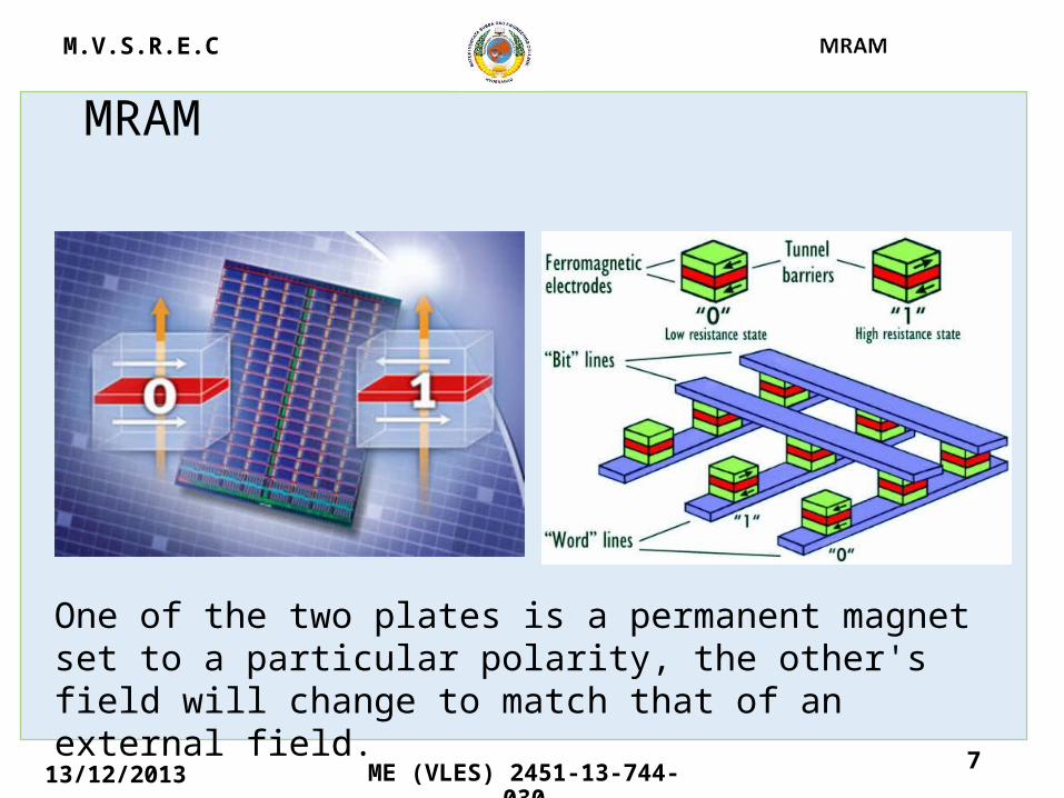
MRAM
One of the two plates is a permanent magnet set to a particular polarity, the other's field will change to match that of an external field.
M.V.S.R.E.C
13/12/2013 ME (VLES) 2451-13-744-030
7

MRAM: Fixed layer
The bottom layers give an effect of fixed (pinned) layer due to interlayer exchange coupling between ferromagnetic and spacer layer of synthetic antiferromagnetic.
M.V.S.R.E.C
13/12/2013 ME (VLES) 2451-13-744-030
8

MRAM: Reading process
• Transistor is “ON”
• Measuring of electrical resistance of a small sense current from a supply line through the cell to the ground.
M.V.S.R.E.C
13/12/2013 ME (VLES) 2451-13-744-030
9
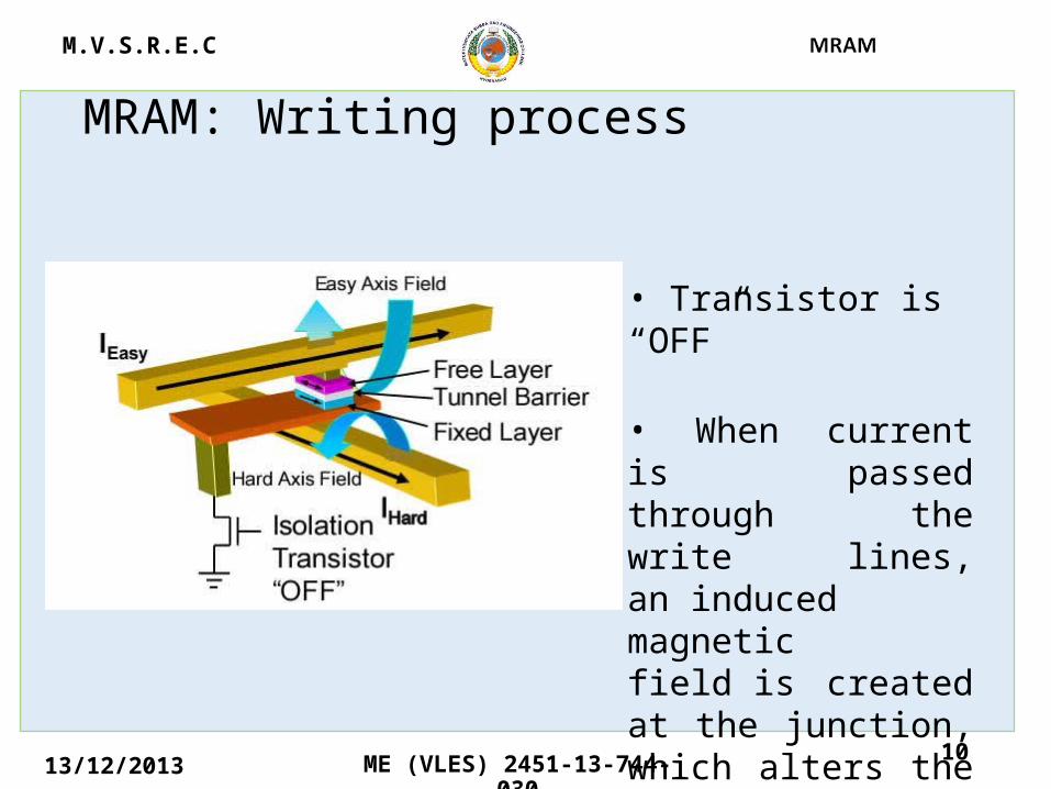
MRAM: Writing process
• Transistor is “OFF”
• When current is passed through the write lines, an induced magnetic field is created at the junction, which alters the polarity of the free layer.
M.V.S.R.E.C
13/12/2013 ME (VLES) 2451-13-744-030
10

MRAM: Writing process
• In order to change the polarity of the free layer, both fields are necessary.
• Only the bit in which current is applied in both hard and easy axis will be written. The other bits will remain half-select.
M.V.S.R.E.C
13/12/2013 ME (VLES) 2451-13-744-030
11

MRAM: Characteristics
• Non-volatility
• Infinite endurance
• High speed performance
• Low cost
M.V.S.R.E.C
13/12/2013 ME (VLES) 2451-13-744-030
12

Other RAM Technologies
Each bit of data is stored in a separate capacitor within an integrated circuitCharacteristics• Volatile• The highest density RAM currently available• The least expensive one• Moderately fast
DRAM
M.V.S.R.E.C
13/12/2013 ME (VLES) 2451-13-744-030
13

Other RAM Technologies
Each bit is stored on four transistors that form two cross-coupled inverters
Characteristics• Expensive• Volatile• Fast• Low power consumption• Less dense than DRAM
SRAM
M.V.S.R.E.C
13/12/2013 ME (VLES) 2451-13-744-030
14

Other RAM Technologies
Flash RAMStores information in an array of memory cells made from floating-gate transistorsCharacteristics• Cheap• Non-volatile• Slow• Enormously durable• Limited endurance
M.V.S.R.E.C
13/12/2013 ME (VLES) 2451-13-744-030
15

MRAM Vs Other RAM TechnologiesM.V.S.R.E.C
13/12/2013 ME (VLES) 2451-13-744-030
16
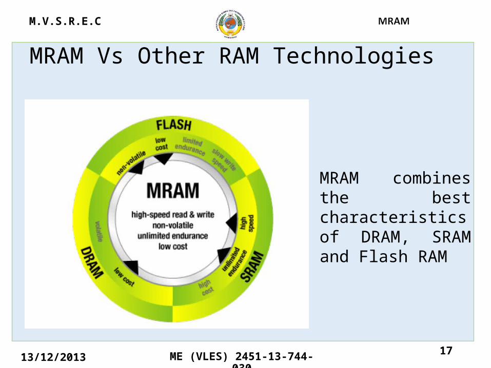
MRAM Vs Other RAM Technologies
MRAM combines the best characteristics of DRAM, SRAM and Flash RAM
M.V.S.R.E.C
13/12/2013 ME (VLES) 2451-13-744-030
17

Future MRAM Improvements
Thermal Assisted Switching
• Solves the first-generation selectivity and stability problems
• Cost-effective and scalable memory technology to at least the 32nm node
M.V.S.R.E.C
13/12/2013 ME (VLES) 2451-13-744-030
18

Future MRAM Improvements
Spin Torque Transfer
• No applied magnetic field• Utilizes heavily spin polarized current• The magnetization of nano-elements is flipped back and forth • Still has challenges in basic physics and materials to overcome
M.V.S.R.E.C
13/12/2013 ME (VLES) 2451-13-744-030
19

Applications
Aerospace and military systemsDigital camerasNotebooksSmart cardsCellular base stationsPersonal ComputersBattery-Backed SRAM replacementMedia players
M.V.S.R.E.C
13/12/2013 ME (VLES) 2451-13-744-030
20

Referrences
•wikipedia.org/wiki/Magnetoresistive_random-access_memory•www.nve-spintronics.com/mram-Operation•Past, Present and Future of MRAM NIST Magnetic Technology, 22 July 2003•www.sciencemag.org•Masood Qazi “Next Generation MRAM Development“, June 29 2010• Johan Åkerman, "Toward a Universal Memory", Science, Vol. 308. no. 5721 (22 April 2005), pp. 508 – 510, doi:10.1126/science.1110549
M.V.S.R.E.C
13/12/2013 ME (VLES) 2451-13-744-030
21

THANK YOU
M.V.S.R.E.C
13/12/2013 ME (VLES) 2451-13-744-030
22