3D Nanometer Tracking of Motile Microtubules on Reflective Surfaces
Molecular Electronics at Metal/Semiconductor Junctions. Si Inversion by Sub-Nanometer Molecular...
12
See discussions, stats, and author profiles for this publication at: https://www.researchgate.net/publication/230865843 Molecular Electronics at Metal/Semiconductor Junctions. Si Inversion by Sub-Nanometer Molecular Films Article in Nano Letters · May 2009 DOI: 10.1021/nl900953z · Source: PubMed CITATIONS 66 READS 29 11 authors, including: Omer Yaffe Weizmann Institute of Science 23 PUBLICATIONS 496 CITATIONS SEE PROFILE Luc Scheres Wageningen University & Research 31 PUBLICATIONS 692 CITATIONS SEE PROFILE Sreenivasa Reddy Puniredd Agency for Science, Technology and Research (… 54 PUBLICATIONS 912 CITATIONS SEE PROFILE Hossam Haick Technion - Israel Institute of Technology 197 PUBLICATIONS 5,212 CITATIONS SEE PROFILE All content following this page was uploaded by Luc Scheres on 01 December 2016. The user has requested enhancement of the downloaded file.
Transcript of Molecular Electronics at Metal/Semiconductor Junctions. Si Inversion by Sub-Nanometer Molecular...

Seediscussionsstatsandauthorprofilesforthispublicationathttpswwwresearchgatenetpublication230865843
MolecularElectronicsatMetalSemiconductorJunctionsSiInversionbySub-NanometerMolecularFilms
ArticleinNanoLettersmiddotMay2009
DOI101021nl900953zmiddotSourcePubMed
CITATIONS
66
READS
29
11authorsincluding
OmerYaffe
WeizmannInstituteofScience
23PUBLICATIONS496CITATIONS
SEEPROFILE
LucScheres
WageningenUniversityampResearch
31PUBLICATIONS692CITATIONS
SEEPROFILE
SreenivasaReddyPuniredd
AgencyforScienceTechnologyandResearch(hellip
54PUBLICATIONS912CITATIONS
SEEPROFILE
HossamHaick
Technion-IsraelInstituteofTechnology
197PUBLICATIONS5212CITATIONS
SEEPROFILE
AllcontentfollowingthispagewasuploadedbyLucSchereson01December2016
Theuserhasrequestedenhancementofthedownloadedfile
1
Molecular electronics at Metal Semiconductor Junctions
Si inversion by Sub-nm Molecular Films
Omer Yaffe Luc Scheres 1
Sreenivasa Reddy Puniredd 2
Nir Stein Ariel Biller Rotem Har Lavan
Hagay Shpaisman Han Zuilhof1 Hossam Haick
2 David Cahen and Ayelet Vilan
Dept of Materials amp Interfaces Weizmann Inst of Science Rehovot 76100 ISRAEL
1 Lab of Organic Chemistry Wageningen Univ Dreijenplein 8
6703 HB Wageningen the Netherlands
2 Dept Chemical Engineering and Russell Berrie Nanotechnology Inst Technion - Israel Inst
Technology Haifa 32000 Israel
Abstract Electronic transport across n-Si-alkyl monolayerHg junctions is at reverse and low
forward bias independent of alkyl chain-length from 18 down to 1 or 2 carbons This and further recent
results indicate that electron transport is minority rather than majority carrier-dominated occurs via
generation and recombination rather than (the earlier assumed) thermionic emission and as such is
rather insensitive to interface properties The (m)ethyl results show that binding organic molecules
directly to semiconductors provides semiconductormetal interface control options not accessible
otherwise
Keywords molecular electronics self assembled monolayer alkyl chain methyl ethyl MIS Si
2
Using a semiconductor especially Si instead of a metal as one of the electrodes to contact the
molecules not only adds another ldquoknobrdquo to turn to study transport through molecules but it also can
make molecular electronic junctions more relevant for potential future electronics Implicit in most of
the increasing efforts in this direction is the assumption that the molecules influence possibly even
control the junction charge transport characteristics In this and forthcoming reports we examine and try
to define when and in how far this assumption holds Specifically we use the n-Si-alkyl chainHg
junction often used in laboratory tests where Hg contacts a monolayer of CnH2n+1 alkyl chain
molecules bound by direct Si-C bonds to Si lt111gt1 Here we focus on how molecule-semiconductor
interaction can dictate the mechanisms of charge transport through these junctions
Understanding the transport mechanism(s) across molecular junctions is critical for rational design of
possible future molecule-based devices Previously1 charge transport across junctions with n-Si was
described as thermionic emission (TE) at low forward and reverse bias and tunneling at high forward
bias This model was extended further to include also p-Si2 We present and discuss here new
experimental results that point to diffusion and recombination of minority carriers rather than majority
carrier TE as the dominant transport mechanisms at low forward and reverse bias in n-Si-alkyl chainHg
junctions Minority carrier transport also explains earlier experimental results that are not consistent
with TE
In Fig 1 we show current density-voltage (J-V) characteristics of n-Si-alkyl chainHg junctions made
with (1-10) cm Si lt111gt The length of the alkyl chain CnH2n+1 varies from n = 18 down to 1 which
means that the monolayer thickness decreases from 22 down to 02 nm Monolayer preparation
followed and characterization agreed with literature descriptions for both bdquoshort‟ monolayers34
and
bdquolong‟ ones5 J-V curves were measured (see inset to Fig 1) at room temperature using a controlled
growth hanging Hg (999999 purity) drop (HMD) electrode apparatus (Polish Academy of Sciences)
and In-Ga eutectic as back contact in a controlled environment glove box with 10 relative humidity
3
Figure 1 J-V curves of n-Si-CnH2n+1Hg (n=1 2 4 12 16 and 18) Current densities where calculated using the
optically determined nominal contact area of 03 mm2 Bias is applied to the Hg Si is grounded Results are
logarithmic averages of at least 7 different junctions with a scan rate of 20 mVs Error bars represent standard
deviations The insets give ldquoartist‟ views of the junctions for bdquoshort‟ and bdquolong‟ monolayers (not to scale)
Remarkably the results are independent of molecular length at reverse and low (lt 04 V) forward bias
including those obtained with the very short n = 1 and n = 2 molecules This result is even more
surprising if we consider that the n = 2 coverage is ~50 as is the case for all the n 2 alkyl chains
used here while for n=1 the coverage is roughly double that ~ 100 an issue that is discussed further
below Molecular (organic insulator) length-dependence enters only at higher forward bias1 a bias range
that will be re-analyzed in a subsequent report Nevertheless the exponential current decay with length
(at high bias) proves that the molecular monolayer is not shorted electrically
The reverse and low forward bias length-independence for C12-C18 monolayers (that correspond to a
thickness range of 16 - 22 nm) was earlier interpreted in terms of a large Schottky barrier that creates
a charge transport ldquobottleneckrdquo leading to a negligible effect of differences in monolayer thickness1 By
adding n = 1 2 results (Fig1) the thickness range is significantly increased and still there is a lack of
dependence on molecular length This result is remarkable because using a basic tunneling model6 the
tunneling probability through the n=1 monolayer is nine orders of magnitude greater than that through
the n=18 monolayer
In view of these experimental findings we propose that the electrical characteristics of these junctions
are best described by diffusion and recombination of minority carriers as was done for MIS tunnel
diodes with SiO2 as an insulator57-9
If the built-in potential (ψbi) at a given semiconductor interface
exceeds the energy difference between the actual Fermi level EF and the intrinsic Fermi level Ei in the
bulk (ψB) the region of the semiconductor adjacent to the metal becomes inverted ie there are more
minority than majority carriers in that region If ψbi gt 2ψB the surface is in deep inversion10
4
Figure 2 shows a schematic energy band diagram (not to scale) for an inverted n-type MIS tunnel diode
Three basic charge transport processes under forward bias are indicated (1) majority carrier (electron)
TE attenuated by the tunneling barrier that is introduced by the molecular monolayer (2) recombination
of electrons and holes in the depletion layer (space charge region SCR) and (3) diffusion of minority
carrier (holes) in the bulk minority carrier injection Processes (2) and (3) depend mainly on intrinsic11
semiconductor properties and under specific conditions are not sensitive to the tunneling barrier
introduced by the insulator9
Figure 2 Energy-band diagram (not to scale) of inverted metal n-semiconductor contact with a thin insulating
interfacial layer (I) The three basic charge transport mechanisms that are shown are (1) majority carrier thermionic
emission attenuated by tunneling through the organic monolayer (2) recombination in the depletion region and (3)
diffusion of minority carriers in the bulk (with recombination either in the neutral region or at the back contact) The
thermionic emission barrier height (φb) is the difference between the metal work function (φM) and the semiconductor
electron affinity (χ) (φbi) is the built-in potential (ψB) is the energy difference between the Fermi level and the
intrinsic Fermi level in the bulk EC EV and EF are the conduction band minimum the valence band maximum and
the Fermi level respectively Ei is the intrinsic Fermi level (at the middle of the forbidden energy gap) After ref 10
Numerical calculations for charge transport through MIS tunnel diodes (Si-SiO2 SiO2 thickness 15-3
nm)8 showed that for a sufficiently large built-in potential ie if the surface is in deep inversion
charge transport will be governed solely by hole injection and generation-recombination at reverse and
low forward bias voltages In case of very thin insulators the junction is similar to an abrupt one-sided
p+-n junction
9 Earlier reverse bias C-V measurements
1213 that were confirmed by us (see Fig S1 in
supplementary information) indicate that the flat band potential (ψbi) of n-Si-alkyl chainHg is ~ 065
eV Since the calculated deep inversion potential (2ψB) of the moderately doped n-Si used here (Nd ~
1015
cm-3
) is ~ 06 eV10
we conclude that the Si surface is indeed in deep inversion at equilibrium14
5
Additional support for minority instead of majority carrier transport at reverse and low forward bias
comes from comparing the J-V characteristics for n-Si-C12 with Hg or Au as top metal contact (Fig 3)
If an n-semiconductor is in deep inversion further increasing the work-function of the top metal contact
will not affect the current at reverse and low forward bias15
To test if the n-Si is indeed in deep
inversion we used Au contacts as Au has 02 - 05 eV higher work function than Hg16
ldquoReady maderdquo
gold Au contacts were used to measure the J-V characteristics1718
The Au contact J-V curve overlaps
that obtained with Hg despite the work function difference The reason is that with the semiconductor in
deep inversion the minority-carrier current is limited by processes in the Si (recombination or
diffusion) independent of the band-bending or the presence of an interfacial insulator9
Figure 3 Comparison of junctions with Hg and Au contacts to n-Si-C12H25 Au contacts were ldquoready-maderdquo using a
ldquosoftrdquo deposition modified lift-off float-on method1718
See Fig 2 for more experimental details
The role of the insulator in the MIS tunnel diode can be a multiple one19
(i) suppress majority carrier
TE by introducing an additional tunneling barrier (ii) introduce an asymmetric tunneling barrier and by
that favor minority carrier controlled charge transport (iii) decrease the voltage drop on the
semiconductor depletion layer (iv) contribute an additional dipole and by that alter the semiconductor
band bending (v) reduce the surface recombination rates by passivating the surface states especially
those induced by direct metal ndash semiconductor interactions ie act as buffer between the metal and the
semiconductor20
The results with methyl and ethyl (n = 1 2) films which are ineffective as insulators
under our experimental conditions show that in the case of the Si-C interface effects (i) (ii) and (iii)
are negligible
As for effect (v) because Hg does not interact electronically with Si21
we cannot deduce from the Hg
result only if the organic insulating layer passivates metal-Si interactions in general However
6
additional preliminary (and as yet unpublished) results with ldquoready-maderdquo Au contacts suggest that
these molecules do not completely passivate such interactions
Therefore we conclude that (iv) the change in electrostatic potential due to the dipole layer introduced
by chemically binding a molecular monolayer (~ 038 eV for Si-CH322
) suffices to increase the built-in
potential (ψbi) to the level where the n-Si is in deep inversion and by that to make any majority carrier
charge transport negligible23
The fact that half coverage of ethyl can have the same effect as full
methyl coverage indicates that the former suffices for deep inversion and that the additional dipole that
likely results with the latter does not change this further
In principle close to ideal MIS-like behavior would be possible if we could passivate the Si surface with
a ldquoSi oxide monolayerrdquo However in practice this has not been possible till now while our results
clearly show that even half ethyl-coverage half H-termination or full methyl-coverage can provide
sufficient electrostatic change to passivate the Si and in this case to invert it without the need for a
(thicker) insulating layer
Minority carrier-controlled transport clarifies two previous experimental observations which seemed
inconsistent with (majority carrier) TE The first one is that the ~ 085 eV (effective) TE barrier height
derived from either room temperature J-V or reverse bias C-V (b = ψbi + (EC-EF)) measurements1212
is
almost twice the 045 eV activation energy extracted from the temperature dependence of current-
voltage characteristics (J-V-T)24
using in our experiments the same set of Si wafers J-V-T analysis
allows experimental extraction of the charge transport activation energy regardless of any a priori
assumed transport mechanism (via the Arrhenius relation) While the saturation current for TE is
proportional to
kT
q bexp where q is the elementary charge k is the Boltzmann constant T is the
absolute temperature and b is the barrier height the saturation current for recombination is proportional
to
kT
Eg
2exp where Eg is the semiconductor band gap
25 If we extract a ldquobarrier heightrdquo from J-V-T
data there is an implicit assumption that the charge transport is TE-controlled For n-Si-alkyl chainHg
junctions the experimentally extracted activation energy (~ 045 eV24
) is much closer to half the band
gap of Si (051 eV) than to the b value extracted from either room temperature J-V or C-V
measurements which points to recombination in the depletion region as the dominant charge transport
mechanism
The second result which can be explained by minority carrier-controlled charge transport but not by
TE is the variation of J-V-T characteristic of an n-Si-alkyl chainHg junction upon low energy electron
7
irradiation24
Irradiation was found to considerably increase the number of electronic states in the
monolayer (bdquodope‟ the monolayer) and this is expressed as a considerable net increase in current Yet
J-V-T analysis showed that the transport activation energy also increases (instead of decreasing to
explain the higher current)24
With the new understanding that junction transport before irradiation is
minority carrier-controlled we suggest that irradiation changes the equilibrium electronic state of the
junction from deep inversion to depletion In such a case the charge transport mechanism changes from
minority to majority carrier-controlled ie to TE attenuated by tunneling Although the activation
energy for TE is larger than that for recombination the net current still increases because of the much
higher concentration of majority than minority carriers Irradiation also decreased the ideality factor
toward that for ideal TE (= 1) from the originally higher value which would fit recombination26
We conclude that the well-studied n-Si-alkyl chainHg is in deep inversion at equilibrium (0 V) and at
room temperature Therefore charge transport at reverse and low forward bias is controlled by minority
carrier generation (at reverse bias) and by recombination and diffusion (at low forward bias) rather than
by majority carrier thermionic emission The indications for the minority carrier control are
the current is independent of molecular length at reverse and low forward bias
the experimentally measured built-in potential (ψbi) is larger than the minimal potential for deep
inversion (2ψB)
the current is independent of the work function of the metal electrode (which will hold for any
metal with a work function higher than that of Hg) and
the activation energy for charge transport is about half the Si band gap
While interface energetics (built-in potential) can be extracted from C-V measurements the shape of the
J-V curves is independent of interface properties over most of the bias range considered here
Recognizing inversion is a crucial step towards understanding the basic science of hybrid metal-
molecules-semiconductor (MMS) devices and mapping which molecular aspects control device
performance under different conditions We note that realizing that transport is by minority carriers
should be especially useful for solar-cell applications2728
29-31
Acknowledgements
We thank L Kronik L Segev (WIS) A Kahn (Princeton) J Pelz (Ohio state) and R Tung (CUNY) for fruitful
discussions the Israel Science Foundation ISF (Jerusalem) through its Converging Technology and Centre of
Excellence programs and the Minerva Foundation (Munich) for partial support and 21 Ventures for a generous
research grant HS holds an ISF convergent technology predoctoral fellowship HH holds the Horev Chair for
8
leader in Science and Technology and thanks the US-Israel BSF (Jerusalem) for financial support HS holds an
ISF converging technology pre-doctoral fellowship HZ thanks NanoNed funded by the Dutch Ministry of
Economic Affairs (project WSC6972) for financial support DC holds Rowland and Sylvia Schaefer chair of
Energy Research
Supporting Information Available Capacitance-Voltage measurements of varying monolayer thickness This material is
available free of charge via the Internet at httppubsacsorg
9
Supporting Information for
Molecular electronics at Metal Semiconductor Junctions
Si inversion by Sub-nm Molecular Films
Omer Yaffe Luc Scheres 1
Sreenivasa Reddy Puniredd 2
Nir Stein Ariel Biller Rotem Har Lavan
Hagay Shpaisman Han Zuilhof1 Hossam Haick
2 David Cahen and Ayelet Vilan
Capacitance-Voltage measurements on n-Si-CnH2n+1Hg junctions with monolayer thickness varying
from n = 1 (02 nm) to n = 18 (22 nm)
Figure S1
(1C2) - V plots of n-Si-CnH2n+1Hg (n = 1 2 4 12 14 16 and 18) junctions Dashed lines are
extrapolation to (1C2) = 0 where ψbi is extracted The slope is not identical because of small size
variation in the Hg drop Sample preparation is identical to that of Fig 1 Capacitance was measured
with an HP4284A precision LCR meter using a 10 mV AC amplitude at 500 kHz This frequency was
chosen so as not to be too low to prevent quasi-static behavior and to prevent possible interface states
from following the AC signal The impedance model used for the C-V measurements was a parallel
circuit of a resistor and capacitor 13
and the contact area for all measurements was 310-3
cm2
10
References
(1) Salomon A Bocking T Seitz O Markus T F A Chan C Zhao W Cahen D
Kahn A Phys Rev Lett 2005 95 266807
(2) Salomon A Boecking T Seitz O Markus T Amy F Chan C Zhao W Cahen
D Kahn A Adv Mater 2007 19 445-450
(3) Puniredd S R Assad O Haick H J Am Chem Soc 2008 130 9184-9185
(4) Puniredd S R Assad O Haick H J Am Chem Soc 2008 130 13727-13734
(5) Scheres L Arafat A Zuilhof H Langmuir 2007 23 8343-8346
(6) Simmons J G J Appl Phys 1963 34 1793-1803
(7) Tarr N G Pulfrey D L Camporese D S IEEE Trans Electron Devices 1983 30
1760
(8) Shewchun J Green M A King F D Solid-State Electron 1974 17 563
(9) Green M A King F D Shewchun J Solid-State Electron 1974 17 551
(10) Sze S M NG K K Physics of Semiconductor Devices third ed New York John
Wiley amp Sons Inc 2007
(11) Surface states can increase the recombination current an effect that is ignored here for
simplicity‟s sake
(12) Maldonado S Plass K E Knapp D Lewis N S J Phys Chem C 2007 111
17690-17699
(13) Faber E J de Smet L Olthuis W Zuilof H Sudholter E J Bergveld P Van den
Berg A ChemPhysChem 2005 6 2153-2166
(14) For devices with a surface potential larger than the inversion potential the intercept of
the 1C2 vs V curve with the voltage axis (V) is not the flat band potential but the lower limit for the
flat band potential This is because the increase in the depletion layer width with increasing surface
potential is minor for inverted surfaces compared to depleted surfaces (Shewchun loc cit)
(15) Camporese D S Pulfrey D L J AppPhys 1985 57 373
(16) The exact difference depends on how clean the gold is
(17) Shimizu K T Fabbri J D Jelincic J Melosh N A Adv Mater 2006 18 1499-
1504
(18) Vilan A Cahen D Adv Funct Mater 2002 12 795-807
(19) Fonash S J Solar Cell Device Physics Academic press Belton teaxs 1981
(20) Tung R T Mater Sci Eng R 2001 35 1
(21) Wittmer M Freeouf J L Phys Rev Lett 1992 69 2701
(22) Ralf H Rainer F Bengt J Wolfram J Lauren J W Nathan S L Phys Rev B
2005 72 045317
(23) (iv) the electrostatic effect of the adsorbate is naturally also the one that is critical for
sensors such as a CHEMFET (Northrop loccit) or MOCSER(Cahen et al loc cit)` those effects are
likely to be different for adsorption on bulk and nano sized (eg nanowires) substrates in part because
then bulk electrostatic analyses such as those used here are not or only partially applicable
(24) Seitz O Vilan A Cohen H Haeming M Schoell A Umbach E Kahn A
Cahen D Adv Funct Mater 2008 18 2102-2113
(25) Sah C T Noyce R N Shockley W Proceedings of the IRE 1957 45 1228
(26) We note that an ideality factor gt 1 can also have other reasons eg a tunnel barrier in
series with TE(Rhoderick loccit)
(27) Har-Lavan R Ron I Thieblemont F Cahen D App Phys Lett 2009 In press
(28) Maldonado S Knapp D Lewis N S J Am Chem Soc 2008 130 3300-3301
(29) Northop R B Introduction to Instrumentation and Measurements 2nd ed CRC press
Boca Raton 2005
11
(30) Cahen D Naaman R Vager Z Adv Funct Mater 2005 15 1571-1578
(31) Rhoderick E H Monographs in Electrical and Electronic Engineering Metal-
Semiconductor Contacts second ed Clarendon press Oxford 1988
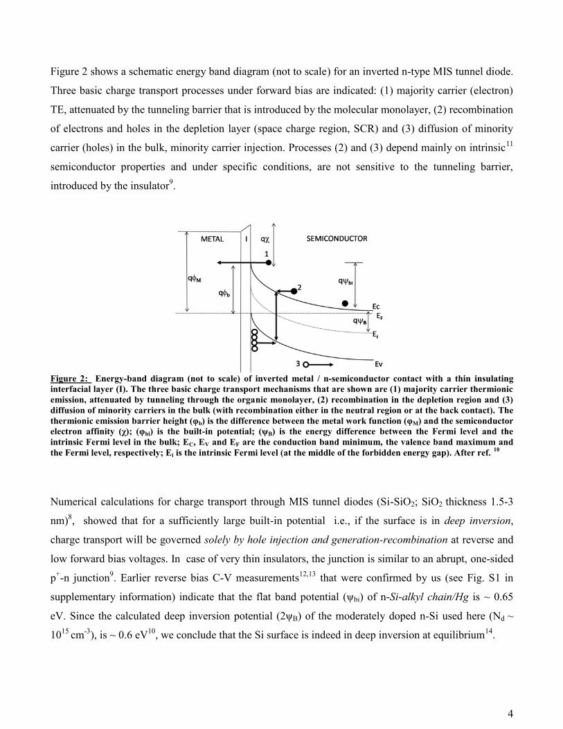

11
(30) Cahen D Naaman R Vager Z Adv Funct Mater 2005 15 1571-1578
(31) Rhoderick E H Monographs in Electrical and Electronic Engineering Metal-
Semiconductor Contacts second ed Clarendon press Oxford 1988