Modeling and simulation of composite plasmonic structures ...
176
Université de Clermont Auvergne Ecole doctorale des Sciences pour l’ingénieur THÈSE présentée pour obtenir le grade de DOCTEUR D’UNIVERSITÉ Spécialité doctorale “Electronique et systèmes” soutenue publiquement par Maha BEN RHOUMA le 24 Février 2021 Modeling and simulation of composite plasmonic structures based on graphene and metals Directeur de thèse : Kofi EDEE Co-directeur de thèse : Mauro ANTEZZA Jury: M.Dominique BARCHIESI Professeur UTT (Troyes) Rapporteur M. Fadi BAIDA Professeur FEMTO-ST (Besancon) Rapporteur Mme Ségolène CALLARD Professeur STMS/INL (Lyon) Examinatrice M. Brahim GUIZAL Professeur L2C( Montpellier) Président
-
Upload
khangminh22 -
Category
Documents
-
view
4 -
download
0
Transcript of Modeling and simulation of composite plasmonic structures ...
Université de Clermont AuvergneEcole doctorale des Sciences pour l’ingénieur
THÈSE
présentée pour obtenir le grade de
DOCTEUR D’UNIVERSITÉSpécialité doctorale “Electronique et systèmes”
soutenue publiquement par
Maha BEN RHOUMAle 24 Février 2021
Modeling and simulation of compositeplasmonic structures based on graphene
and metals
Directeur de thèse : Kofi EDEECo-directeur de thèse : Mauro ANTEZZA
Jury:
M.Dominique BARCHIESI Professeur UTT (Troyes) RapporteurM. Fadi BAIDA Professeur FEMTO-ST (Besancon) RapporteurMme Ségolène CALLARD Professeur STMS/INL (Lyon) ExaminatriceM. Brahim GUIZAL Professeur L2C( Montpellier) Président

• Le jour se lève,
• Sais-tu pourquoi le cri du coq se fait entendre?
• Le miroir de l’aube te dit qu’une nuit de ton existence s’en est allée.
• Le jour se lève,
• Tu n’as encore rien appris.
Omar Al Khayyâm - AL Rubâiyat (les quatrains)


À mon père, ma mère, mon frèreet mes deux sœurs

This research was financed by the French government IDEX-ISITE initiative16-IDEX-0001 (CAP 20-25)
v

Acknowledgments
Je suis reconnaissant à tousceux qui m’ont dit non. C’estgrace à eux que je suis moi-même
Albert Einstein
Cette thèse a été effectuée en codirection entre l’équipe "Électromagnétisme etNanophotonique" de l’institut Pascal (Université Clermont Auvergne) et l’Équipe "Ray-onnement Matière et Phénomènes Quantiques" du Laboratoire Charles Coulomb (Uni-versité de Montpellier). Par ailleurs, le projet dans lequel s’est inscrit ce travail de thèseétait réalisé en collaboration avec Jonathan FAN de l’université de Stanford (USA) etNikolay A. GIPPIUS du Skolkovo Institute of Science and Technology (Russie).
Je voudrais remercier tous les membres du jury d’avoir accepté d’examiner et évaluerce travail. Je tiens à remercier Monsieurs Fadi BAIDA et Dominique BARCHIESIqui m’ont fait l’honneur de rapporter sur mon travail de thèse. J’aimerais égalementremercier Madame Ségolène CALLARD qui a accepté d’examiner attentivement monmanuscrit de thèse et pour l’intérêt qu’elle a porté à mon travail.
Mes plus sincères remerciements s’adressent à mes deux encadrants: Kofi Edee etMauro Antezza qui m’ont fait confiance en me confiant ce sujet. Je leurs suis trèsreconnaissante de tous les précieux conseils et leçons scientifiques, leur soutien, leursencouragements, leurs disponibilités et leurs grandes qualités humaines. Merci Kofi dem’avoir accordé toute ta confiance et m’avoir laissé une grande liberté dans l’orientationde mon travail de thèse. Je voudrais également te remercier Mauro pour ta rigueurscientifique, ton soutien, ton aide, tes encouragements dans les moments difficiles et tagentillesse.
Je souhaite également remercier Brahim Guizal d’avoir accepté de présider le juryde ma soutenance de thèse. Merci Brahim pour toute l’aide et le soutien morale etscientifique qui tu m’a accordé et apporté depuis le début de ma première thèse en2013. Tu m’a transmis le goût pour la recherche par ton enthousiasme passionné etcommunicatif et tu m’a montré que le monde de la recherche pouvait être un universpassionnant. J’ai trop appris de toi non seulement sur le plan scientifique mais aussile plan personnel.
J’adresse également tous mes remerciements à l’ensemble des membre du Labora-toire Charles Coulomb, notamment les doctorants et les chercheurs de l’équipe "Théorie
vii
Acknowledgments
du Rayonnement Matière et Phénomènes Quantiques". Tout particulièrement, je tiensà remercier: Youssef, Chahine, Abir, Pierre...
Je tiens à remercier tous les membres de L’institut Pascal et l’équipe Électromag-nétisme et Nanophotonique pour leurs aide, conseils et soutien. Tout Particulièrement,je tiens à remercier Gérard Granet pour sa sympathie, sa gentillesse. Un grand merciaussi à Antoine Moreau et Rafik smaali pour leur gentillesse.
Je suis très reconnaissante à ma chère amie, Insaf, pour son soutien moral, son aideet ses encouragements durant ces années.
Je remercie également Madame Dominique Torrisani, Gestionnaire ED Sciencespour l’ingénieur pour son aide, sa gentillesse et sa bonne humeur.
Enfin, mes vifs remerciements vont à ma famille, mais surtout à mon père Ammarqui m’a soutenue durant mes études moralement et financièrement, qu’il trouve ici maprofonde gratitude. J’adresse des remerciements du même ordre à ma mère Najet, quim’a constamment encouragée et soutenue tout au long de ces années. Je vous remercievous deux pour tout le soutien et l’amour que vous me portez depuis mon enfance.
viii
Contents
Acknowledgments vii
Contents ix
Abstract 1
Résumé 3
Introduction 5
I Theoretical and numerical tools 13
1 Theoretical Background 151.1 Fundamentals of graphene . . . . . . . . . . . . . . . . . . . . . . . . . 16
1.1.1 Electronic properties . . . . . . . . . . . . . . . . . . . . . . . . 161.1.2 Graphene doping . . . . . . . . . . . . . . . . . . . . . . . . . . 201.1.3 Electromagnetic properties of graphene: Conductivity Model . . 22
1.2 Theory of graphene surface plasmons polaritons (SPPs) . . . . . . . . . 281.2.1 Surface plasmons polaritons at planar interfaces . . . . . . . . . 281.2.2 Surface plasmons polaritons on graphene (GSP) . . . . . . . . . 32
1.3 Conclusions . . . . . . . . . . . . . . . . . . . . . . . . . . . . . . . . . 45
2 Numerical Tools 512.1 Generic Physical Structure . . . . . . . . . . . . . . . . . . . . . . . . . 512.2 Numerical Methods . . . . . . . . . . . . . . . . . . . . . . . . . . . . . 52
2.2.1 Standard Fourier Modal Method (FMM) . . . . . . . . . . . . . 522.2.2 Fourier Modal Method with spatial adaptative resolution (FMM-
ASR) . . . . . . . . . . . . . . . . . . . . . . . . . . . . . . . . . 602.2.3 Aperiodic Fourier Modal Method: FMM with PML . . . . . . . 64
2.3 Numerical Examples involving graphene:Graphene-Strip Gratings . . . . . . . . . . . . . . . . . . . . . . . . . . 672.3.1 Graphene horizontal strips grating . . . . . . . . . . . . . . . . 672.3.2 Graphene Vertical strips grating . . . . . . . . . . . . . . . . . . 69
2.4 Conclusions . . . . . . . . . . . . . . . . . . . . . . . . . . . . . . . . . 72
ix
CONTENTS
II Hybrid Plasmonic Structures Based on Graphene 75
3 Metallic slit grating-Graphene composite structure 773.1 Extraordinary optical transmission . . . . . . . . . . . . . . . . . . . . 78
3.1.1 Extraordinary transmission : Two resonant mechanisms . . . . . 793.2 Coupling between subwavelength nano-slits lattice modes and metal-
insulator-graphene cavity modes: A semi-analytical model . . . . . . . 823.2.1 Physical system . . . . . . . . . . . . . . . . . . . . . . . . . . . 823.2.2 Modal analysis of the system . . . . . . . . . . . . . . . . . . . 843.2.3 Analysis of the Lorentz and Fano resonances of the system . . . 89
3.3 Conclusions . . . . . . . . . . . . . . . . . . . . . . . . . . . . . . . . . 92
III Non-reciprocity devices based on graphene and metals 99
4 Basic concepts 1014.1 Electromagnetic reciprocity and non reciprocity . . . . . . . . . . . . . 101
4.1.1 Time reversal symmetry of Maxwell’s equations . . . . . . . . . 1024.1.2 Reciprocity Theorem in Electromagnetism . . . . . . . . . . . . 1034.1.3 Non reciprocity with magnetic field . . . . . . . . . . . . . . . . 104
4.2 Graphene under a static magnetic bias . . . . . . . . . . . . . . . . . . 1154.2.1 Landau Levels in monolayer graphene . . . . . . . . . . . . . . . 1154.2.2 Reflection and transmission properties of a magnetized
graphene sheet . . . . . . . . . . . . . . . . . . . . . . . . . . . 1174.2.3 Surface magnetoplasmons polaritons on magnetically biased graphene
sheet (GSMP) . . . . . . . . . . . . . . . . . . . . . . . . . . . . 1234.2.4 Nonreciprocity and gyrotropy of graphene . . . . . . . . . . . . 125
4.3 Conclusions . . . . . . . . . . . . . . . . . . . . . . . . . . . . . . . . . 129
5 Propagation properties of a magnetically biased array of grapheneribbons 1335.1 Semi-analytical model for the analysis of a magnetically Biased subwave-
length graphene-strip-grating . . . . . . . . . . . . . . . . . . . . . . . 1345.1.1 Physical system . . . . . . . . . . . . . . . . . . . . . . . . . . . 1345.1.2 Theoretical Method . . . . . . . . . . . . . . . . . . . . . . . . . 1355.1.3 Numerical Results and discussion . . . . . . . . . . . . . . . . . 140
5.2 Conclusion . . . . . . . . . . . . . . . . . . . . . . . . . . . . . . . . . . 145
6 Theoretical analysis of Optical Hall effect in a 2D nano-cross-slitsgrating 1496.1 Statement . . . . . . . . . . . . . . . . . . . . . . . . . . . . . . . . . . 1506.2 Polarization independent EOT phenomenon through 2D cross-slits array 1516.3 Magneto-optical perturbation of the gap plasmon modes . . . . . . . . 1586.4 Conclusion . . . . . . . . . . . . . . . . . . . . . . . . . . . . . . . . . . 162
Conclusion and outlook 165
x
Abstract
This thesis work concerns the theoretical modeling and numerical simulations in theareas of nanophotonics (light-matter interactions at the nanoscale) in general and plas-monics in particular. This latter field has received considerable attention over the lastdecades arising from the unique and unusual optical properties of surface plasmons po-laritons such as the confinement and control of light at the subwavelength scale. NobleMetals such as gold and silver have usually been used as the building blocks for severalplasmonic structures in the visible range. However, in the infrared (IR) and terahertz(THz) frequencies, these materials exhibit very large losses and are hardly tunablewhich limits their application as performant plasmonic devices in these frequenciesranges. To overcome this problem, graphene, a two dimensional (2D) material madeof carbon atoms arranged in a honeycomb lattice, possessing extraordinary electrical,thermal, and optical properties, has emerged in the plasmonics field as a potential alter-native plasmonic material working in the mid-infrared and terahertz (THz) frequenciesranges. In this context, the purpose of this thesis is to develop theoretical models forthe study of novel graphene based plasmonic structures and construct numerical codesthat allow the simulation of their behavior.
The research presented in this work is articulated around two main axes: (i) the firstone concerns the study of hybrid plasmonic structures based on graphene and metalsin the absence of an external magnetic field (ii) the second is in the investigation ofthe magneto-optical and non-reciprocal properties of structures based on graphene andmetals subjected to an external static magnetic field.
In the framework of this thesis, three plasmonic structures of academic and techno-logical interests have been explored. The study of each of these structures was carriedout into two steps. In the first step, the structures in question were studied in an exactmanner using rigorous numerical methods. Once the exact calculation was establishedand to better understand the obtained results, an approximate semi-analytical modelwas developed for each structure to reproduce in a simple way the exact results. Thesesimple models allowed us to interpret and explain the optical spectra of the stud-ied structures in terms of some remarkable modes and to understand the underlyingphysics.
The First studied structure is a hybrid tunable plasmonic system consisting of a 1Darray of periodic subwavelength metal slits and a graphene sheet separated by a dielec-tric gap. By splitting the whole system into two coupled sub-systems which involve twokinds of couplings, we have proposed a semi analytical model allowing to fully describethe spectrums of this system and understand the origin of the resonances appearingin them. After that, we have been interested in two different structures. First, wedeveloped a simple and fast semi-analytical method to accurately and efficiently pre-
1
Abstract
dict the magneto-optical response of a one-dimensional graphene strip grating in thepresence of an external static magnetic field, in which the graphene is modeled as ananisotropic layer with atomic thickness and a frequency dependent complex permittiv-ity tensor. Finally, we have studied the magneto-optical and non-reciprocal propertiesof a plasmonic structure consisting of a 2D array of nano-slits perforating a gold film.By extending the 1D model developed for the first structure, we succeeded to studyand reproduce the magneto-optical spectra of this structure. First, we studied theresponse of the structure in the absence of a static magnetic field. Then, we added astatic magnetic field and filled the slits with an anisotropic gyrotropic material.
2
Résumé
Ce travail de thèse concerne la modélisation dans le domaine de la nanophotonique(interaction de la lumière avec des objets de taille nanométrique) et la plasmoniqueen particulier. Cette dernière est une thématique de recherche qui a connu un grandattrait au niveau international durant les dernières décennies découlant des propriétésoptiques uniques et inhabituelles des plasmons polaritons de surface (PPs) telles quele confinement et l’exaltation du champ EM à des échelles sub-longueur d’onde. LesPPS ont été découverts et étudiés dans le visible avec les métaux nobles tels que l’Oret l’Argent dont les fréquences plasma se situent dans cette gamme de fréquences.Cependant, dans le domaine THz, ces matériaux souffrent de pertes très importantesce qui dégrade leurs performances et limite plusieurs applications dans ce domainequi est devenu un domaine attrayant au cours des dernières années. Le grand intérêtpour cette gamme de fréquences découle de son importance pour diverses applicationstechnologiques déjà existantes pour les autres gammes de fréquences du spectre élec-tromagnétique et jusque-là non disponibles pour la gamme THz (imagerie médicaleet sécuritaire, capteurs d’agents chimiques et/ou biologiques, radars compacts...). Ceslimitations ont été surmontées, en partie, avec l’avènement du graphène, un seul feuilletde graphite, qui consiste en un arrangement périodique et bidimensionnel d’atomes decarbone disposés selon un réseau en nid d’abeilles. Ce matériau a suscité un immenseintérêt, à la fois de la part de la communauté scientifique et des industriels, en raison deses propriétés optiques et électrodynamiques particulières. En particulier, il est possiblede contrôler et de modifier sa conductivité via un dopage électrostatique ou chimique.Grâce à ces propriétés, le graphène peut supporter des PPS avec des propriétés excep-tionnelles telles qu’un confinement beaucoup plus important que celui des métaux etdes pertes qui sont relativement faibles dans les domaines THz et Infra-Rouge lointain.Ceci fait du graphène un matériau prometteur pour la réalisation de nouveaux disposi-tifs commandables/contrôlables dans les domaines THz et Infra-Rouge. C’est dans cecontexte très concurrentiel que se sont inscrits les travaux de cette thèse qui visentà mettre au point des modèles théoriques pour étudier des structures plasmoniques àbase de graphène et de construire des codes de calcul permettant la simulation de leurcomportement.
Les travaux présentés dans ce travail s’articulent autour de deux axes principaux :(i) le premier concerne l’étude de structures plasmoniques hybrides à base de graphèneet de métaux en absence de champ magnétique statique externe (ii) le second portesur l’investigation des propriétés magnéto-optiques et non-réciproques de structures àbase de graphène et de métaux soumises à l’effet d’un champ magnétique.
Dans le cadre de cette thèse, trois structures plasmoniques d’intérêt académique ettechnologique ont été explorées. L’étude de chacune de ces structures a été réalisée en
3
Résumé
deux étapes. Dans la première étape, les structures en question ont été étudiées demanière exacte en utilisant des méthodes numériques rigoureuses. Une fois le calcul ex-act établi et afin de mieux comprendre les résultats obtenus, un modèle semi-analytiqueapproché a été développé pour chaque structure afin de reproduire de manière simpleles résultats exacts trouvés par des calculs plus ou moins compliqués. Ces modèles sim-ples ont permis d’interpréter et d’expliquer les spectres optiques des structures étudiéesen termes de certains modes remarquables et de comprendre la physique sous-jacente.
La première structure étudiée est un système plasmonique hybride constitué d’unréseau périodique, 1D sub-longueur d’onde, fait de nano-fentes gravées dans un métal,le tout étant déposé sur une couche diélectrique elle même déposée sur une feuille degraphène. En divisant l’ensemble du système en deux sous-systèmes couplés qui met-tent en jeux deux types de couplages, nous avons proposé un modèle semi-analytiquepermettant de décrire les spectres de ce système et de comprendre l’origine des réso-nances qui y apparaissent. Par la suite, nous nous sommes intéressés à deux structuresdifférentes. Tout d’abord, nous avons développé une méthode semi-analytique simplepour prédire la réponse magnéto-optique d’un réseau périodique de nano-rubans degraphène soumis à l’effet d’un champ magnétique statique dans lequel le graphène estmodélisé comme une couche anisotrope avec une épaisseur atomique et une permittivitécomplexe dépendant de la fréquence. Enfin, nous avons étudié les propriétés magnéto-optiques et non-réciproques d’une structure plasmonique constituée d’un réseau 2D denano-fentes perforant un film d’Or. En étendant le modèle approché 1D développé pourla première structure, nous avons réussi à étudier et reproduire les spectres magnéto-optiques de cette structure. Dans un premier temps, nous avons étudié la réponsede la structure en absence de champ magnétique statique. Dans un deuxième temps,nous avons ajouté un champ magnétique statique et rempli les fentes par un milieugyrotrope.
4
Introduction
If the facts don’t fit the theorychange the facts
Albert Einstein
Over the last decades, the control of the behaviour of light as well as light-matterinteractions at the nanoscale, namely nanophotonics, has attracted intensive atten-tion among the scientific community and became among the most important researchsubjects of modern physics. Plasmonics, the central topic of this thesis, is an activesub-branch of nanophotonics that focuses on the analysis, study and manipulationof surface plasmons polaritons (SPPs) which are surface electromagnetic waves thatpropagate at the interfaces between insulating and conducting media as a result ofthe coupling between an external electromagnetic wave and collective oscillations offree charged carriers [1]. Historically, the first description of (SPPs) dates back tothe beginning of the twentieth century by Wood in 1902 [2] who observed the spec-tra of a continuous light source and diffracted by an optical diffraction grating. Henoticed a surprising phenomenon: "I was astounded to find that under certain con-ditions, the drop from maximum illumination to minimum, a drop certainly from 10to 1, occurred within a range of wavelengths not greater than the distance between thesodium lines". These phenomena was called Wood’s anomalies. One century after theWood’s discovery, plasmonics has attracted a growing and considerable interest arisingfrom the unique and important properties of surface plasmons polaritons, includingstrongly enhanced local fields at the subwavelength scale, tremendous sensitivity tochanges in the local environment, and the ability to localize energy to tiny volumesnot restricted by the wavelength of the exciting light. This makes them among themost important forms of strong light matter interactions and gave rise to a wide rangeof potential applications in many fields. For example, ultrasensitive biosensing [3, 4],photonic metamaterials [5], photovoltaic devices [6, 7], integrated optical circuits [8],subwavelength waveguides [9] and optical superlenses [10].
SPPs were first studied in the visible range over noble metals such as gold and sil-ver that were among the first materials used to devise and study plasmonic structures.Recently, the infrared (IR) and specifically the terahertz (THz) domains have becomeattractive for their benefits in various applications such as medical imaging [11], bi-ological studies, space exploration, communications [12] and security [13]. Therefore,extending plasmonic properties to the THz and IR spectra can enable many new ap-plications. However, in these frequencies ranges, the traditional plasmonic materialssuffer from very large losses and are hardly tunable which limits their applications andaffects the performances of the corresponding plasmonic devices. Hence, finding novel
5
Introduction
and alternative plasmonic materials able to manipulate and generate SPPs in the THzand IR ranges constitutes a great challenge.
In this context, doped graphene, has emerged in the plasmonics field as a potentialand promising plasmonic material working in in the mid-infrared and terahertz (THz)spectral windows. Graphene is a two dimensional 2D material made of carbon atomsarranged in a honeycomb lattice. Since its discovery in 2004 by Geim and Novoselov[14], this 2D material which, for decades, was predicted to be experimentally unviable,has generated great interest in scientific studies and technological developments dueto its unusual and fascinating, electronic, optical, mechanical and thermal propertieswhich originate from its linear electronic dispersion around the so-called Dirac pointsand to the massless nature of its charge carriers (Dirac fermions). Indeed, graphene dis-plays a high theoretical electron mobility that can reach up to 200000cm2V 1s1 [15], highthermal conductivity [16] and it also shows a good flexibility. Furthermore, graphene iswell known as a transparent material in the visible range where it absorbs only around2.3% of the incident electromagnetic wave [17]. This property makes graphene suitablefor various optical devices such as touch-screens and light emitting diodes (LED)[18].In addition to the aforementioned properties, graphene exhibits a wide range of elec-tromagnetic properties stemming from its unusual optical conductivity which can bedynamically tuned by electrostatic bias or chemical doping [19, 20, 21].
When graphene is doped via chemical or electrostatic doping , it behaves as anultra thin metal and can support surface plasmons polaritons similar to those guidedby noble metals. However, the graphene surface plasmons polaritons (GSPs) exhibitmany advantages compared to their counterparts in metals. In addition to the trans-verse magnetic (TM) surface plasmons polaritons usually supported by noble metals,graphene can support a new plasmonic mode in the transverse electric (TE) polar-ization [22, 23]. This last mode is specific for graphene and cannot exist in noblemetals since the imaginary part of the conductivity is always positive. For graphene,this mode can take place when the imaginary part of its optical conductivity becomesnegative i.e for frequencies above the interband threshold, the region of spectrum gov-erned by the interband transitions. However, due to the Landau damping occurring atthe interband threshold, (TE-GSP) can only exist in a very narrow frequency window(1.667 < ~ω/µc < 2, µc is the chemical potential of graphene). Moreover, these modesare weakly bound to the graphene surface and their experimental excitation has notbeen demonstrated. Furthermore, graphene TM- SPPs are reported to have a high con-finement and relatively low losses [24]. Another crucial advantage of SPPs in graphene,over those in noble metals, is their tunability stemming from the simplicity to controlof the chemical potential by electrical gating and doping. These extraordinary featuresof SPPs in graphene have been exploited for devising a variety of tunable plasmonicgraphene-based devices in the mid-infrared and terahertz regions of the spectrum suchas optical switches [25], antennas [26], absorbers [27], modulators [28] and sensors [29].
On another hand, it is well known that the conductivity of graphene can be alsotuned by a magnetic bias. Indeed, when a static magnetic field is applied perpendicularto the graphene sheet, a finite optical Hall conductivity appears and graphene becomesanisotropic with an asymmetric conductivity tensor. It is also shown that a magnet-ically biased graphene sheet can exhibit gyrotropic properties which leads to manymagneto-optical (MO) phenomena such as Giant Faraday rotation [30] and Kerr effect[31]. These phenomena are shown to exhibit non reciprocal properties which may be
6
Introduction
useful and crucial for the development of ultra-thin non reciprocal devices operating atthe microwave and terahertz frequency ranges [32, 33]. Furthermore, in the presence ofthe static magnetic field, plasmons and cyclotron excitations hybridise and lead to theappearance of graphene surface magnetoplasmons polaritons (GSMPPs). These modesdisplay various important properties and have a great potential in a lot of plasmonicnon reciprocal applications thanks to the combination of the plasmonic properties ofgraphene with the magneto-optics effects.
The purpose of this thesis is to explore light matter interactions in graphene in theframework of plasmonics. The research presented throughout this manuscript focuseson the theoretical and numerical study of graphene based plasmonic structures work-ing in the infrared and terahertz ranges. This thesis is articulated around two mainaxes. The first axis concerns the study of the behaviour of hybrid plasmonic struc-tures containing graphene while in the second we investigate the magneto-optical andnon-reciprocal properties of structures based on graphene and metals subjected to anexternal static magnetic field.
Dissertation outlineThe present thesis is structured into three parts, the first part can be viewed as anintroduction that gives the Theoretical and numerical tools, the second part is devotedto the investigation of hybrid plasmonic structures based on graphene and finally thelast one is dedicated to the study of magneto-optical and non-reciprocity properties ofstructures based on graphene and metals. Below, we provide a brief description of thecontent of each chapter.
chapter 1 | Theoretical BackgroundIn this first chapter, we provide the theoretical background necessary for under-standing this thesis. We begin with an overview of the electronic properties ofgraphene. Then, we describe the magneto-optical conductivity model of graphenecharacterizing its optical response. After a brief introduction on the foundationsof plasmonics, we discuss the different plasmonic modes that can propagate alonga graphene sheet and their existence conditions. Finally, we review the basicproperties of these modes
chapter 2 | Numerical ToolsThis chapter is dedicated to the description of the numerical tools that will beused in the analysis of the structures studied in this thesis. After presenting thegeneric multigrating structure, we describe and explain the different numericalmethods used for modelling it. In the last section of this chapter, a comparativestudy will be made between these methods in terms of convergence and stabilityto identify the most suitable one for each structure.
chapter 3 | Metallic slit grating-Graphene composite structureIn this chapter we present a semi-analytical model of the resonance phenomenaoccurring in a hybrid system made of a 1D array of periodic sub-wavelength slitsdeposited on an insulator/graphene layer. We show that the spectral response ofthis hybrid system can be fully explained by a simple semi-analytical model basedon a weak and a strong couplings between two elementary sub-systems. The firstelementary sub-system consists of a 1D array of periodic sub-wavelength slits
7
Introduction
viewed as a homogeneous medium. In this medium lives a metal-insulator-metallattice mode interacting with surface and cavity plasmon modes. A weak couplingwith surface plasmon modes on both faces of the perforated metal film leads toa broadband spectrum while a strong coupling between this first sub-system anda second one made of a graphene-insulator-metal gap leads to a narrow bandspectrum. We provide a semi-analytical model based on these two interactionsallowing to efficiently access the full spectrum of the hybrid system.
chapter 4 | Basic conceptsThis chapter reviews the theory and the basic concepts of the third part of thisthesis, we will present the notions of reciprocity and non reciprocity in general andin particular, we will focus on the non reciprocity caused by a static magneticfield. In the next part of this chapter, we will investigate graphene under thepresence of an external static magnetic field with focus on its gyrotropic and nonreciprocal properties.
chapter 5 |Propagation properties of a magnetically biased array of grapheneribbonsThis chapter is devoted to the theoretical study of the magneto-optical prop-erties of a magnetically-biased sub-wavelength graphene strip grating. For thispurpose, we propose a simple and fast semi analytical model that allows to suc-cessfully compute its transmittance and reflectance. It is based on the effectivemedium approach where the graphene is modelled as an anisotropic layer withatomic thickness and a frequency dependent and complex permittivity tensor.The accuracy of the proposed model will be validated by comparing it on the onehand with The PMM method and on the other hand with the effective mediumapproach proposed in [34].
chapter 6 | Theoretical analysis of Optical Hall effect in a 2D nano-cross-slits gratingIn this last chapter, We theoretically demonstrate the nonreciprocal behaviour,for circularly polarized electromagnetic waves, of a 2D crossed-grating made ofnano-slits filled with a gyrotropic material. We provide closed-form expressionsfor the reflection and transmission of the system, allowing one to fully describeand understand the extraordinary optical transmission (EOT) mechanism occur-ring in the system. When the slits are filled with a gyrotropic material, the struc-ture exhibits non-reciprocal unidirectional light transmission in the frequencyrange where the EOT occurs. This will be fully explained through the proposedmodal analytic analysis.
8

Bibliography
[1] Barchiesi. D Salvi. J. Measurement of thicknesses and optical properties of thinfilms from surface plasmon resonance (spr). Appl. Phys. A, (245-255), 2014. 5
[2] R.W. Wood. Xlii. on a remarkable case of uneven distribution of light in a diffrac-tion grating spectrum. The London, Edinburgh, and Dublin Philosophical Maga-zine and Journal of Science, 4(21):396–402, 1902. 5
[3] O. Lyandres N. C. Shah J. Zhao J. N. Anker, W. P. Hall and R. P. Van Duyne.Biosensing with plasmonic nanosensors. Nat. Mater, 7(6):442–453, 2008. 5
[4] Dominique Barchiesi. Surface Plasmon Resonance Biosensors: Model and Opti-mization. Pan Stanford Series on the High-Tech of Biotechnology. Pan StanfordPublishing, 2013. 5
[5] Nikolay I. Zheludev. A roadmap for metamaterials. Opt. Photon. News, 22(3):30–35, Mar 2011. 5
[6] H. A. Atwater and A. Polman. Plasmonics for improved photovoltaic devices,.Nat. Mater, 9(3):205, 2010. 5
[7] E. Stassen S. Xiao and N. A. Mortensen. Ultrathin silicon solar cells with enhancedphotocurrents assisted by plasmonic nanostructures. Journal of Nanophotonics,6(1):0661503, 2012. 5
[8] E. Devaux J. Y. Laluet S. I. Bozhevolnyi, V. S. Volkov and T. W. Ebbesen.Channel plasmon subwavelength waveguide components including interferometersand ring resonators,. Nature, 440(7083):508, 2006. 5
[9] J. A. Dionne, L. A. Sweatlock, H. A. Atwater, and A. Polman. Planar metalplasmon waveguides: frequency-dependent dispersion, propagation, localization,and loss beyond the free electron model. Phys. Rev. B, 72:075405, Aug 2005. 5
[10] J. B. Pendry. Negative refraction makes a perfect lens. Phys. Rev. Lett., 85:3966–3969, Oct 2000. 5
[11] KG Kudrin IV Reshetov KI Zaitsev, NV Chernomyrdin and SO Yurchenko. Ter-ahertz spectroscopy of pigmentary skin nevi in vivo. Optics and Spectroscopy,119(3):404–410, 2015. 5
[12] H. Sarieddeen, N. Saeed, T. Y. Al-Naffouri, and M. Alouini. Next generationterahertz communications: A rendezvous of sensing, imaging, and localization.IEEE Communications Magazine, 58(5):69–75, 2020. 5
9
BIBLIOGRAPHY
[13] John F Federici, Brian Schulkin, Feng Huang, Dale Gary, Robert Barat, FilipeOliveira, and David Zimdars. THz imaging and sensing for security applica-tions—explosives, weapons and drugs. Semiconductor Science and Technology,20(7):S266–S280, jun 2005. 5
[14] K. S. Novoselov, A. K. Geim, S. V. Morozov, D. Jiang, Y. Zhang, S. V. Dubonos,I. V. Grigorieva, and A. A. Firsov. Electric field effect in atomically thin carbonfilms. Science, 306(5696):666–669, 2004. 6
[15] K.I. Bolotin, K.J. Sikes, Z. Jiang, M. Klima, G. Fudenberg, J. Hone, P. Kim, andH.L. Stormer. Ultrahigh electron mobility in suspended graphene. Solid StateCommunications, 146(9):351 – 355, 2008. 6
[16] Wenzhong Bao Irene Calizo Desalegne Teweldebrhan Feng Miao Alexander A. Ba-landin, Suchismita Ghosh and Chun Ning Lau. Superior thermal conductivity ofsingle-layer graphene. Nano Lett, 8(3):902–907, 2008. 6, 20
[17] R. R. Nair, P. Blake, A. N. Grigorenko, K. S. Novoselov, T. J. Booth, T. Stauber,N. M. R. Peres, and A. K. Geim. Fine structure constant defines visual trans-parency of graphene. Science, 320(5881):1308–1308, 2008. 6
[18] T Hasan Francesco Bonaccorso, Z Sun and AC Ferrari. Graphene photonics andoptoelectronics. Nature photonics, 4(9):611–622, 2010. 6
[19] L. A. Falkovky. Optical properties of graphene. J.Phys.Conf.Ser, 129(1):2004,2008. 6, 26
[20] L. A. Falkovky and A. A. Varlamov. Space-timedispersion of graphene conductiv-ity. Eur.Phys.J.B, 56(4):281, 2007. 6, 26
[21] S. G. Sharapov V. P. Gusynin and J. p. Carbotte. Magneto-optical conductivityin graphene. J.Phys.Condens.Matter., 19(2):6222, 2007. 6, 26
[22] W. Hanson. Quasi transverse electromagnetic modes supported by a grapheneparallel-plate waveguide. J.App.Phys.Lett, 104:084314, 2008. 6, 33, 40
[23] S. A. Mikhailov and K. Ziegler. New electromagnetic mode in graphene. PRL,99(01):6803, 2007. 6, 33, 40, 41
[24] M. Kafesaki P. Tassin, T. Koschny and C. M. Soukoulis. A comparaison ofgraphene , superconductors and metals as conductors for metamaterials and plas-monics. Nat .Photonics, 6:259–264, 2012. 6, 43, 44
[25] J. S. Gómez-Díaz and J. Perruisseau-Carrier. Graphene-based plasmonic switchesat near infrared frequencies. Opt. Express, 21(13):15490–15504, Jul 2013. 6
[26] Patrice Genevet Nanfang Yu Yi Song Jing Kong Yu Yao, Mikhail A. Kats andFederico Capasso. Broad electrical tuning of graphene-loaded plasmonic antennas.Opt. Express, 13(3):15490–15504, 2013. 6
[27] M. Grande, M. A. Vincenti, T. Stomeo, G. V. Bianco, D. de Ceglia, N. Aközbek,V. Petruzzelli, G. Bruno, M. De Vittorio, M. Scalora, and A. D’Orazio. Graphene-based absorber exploiting guided mode resonances in one-dimensional gratings.Opt. Express, 22(25):31511–31519, Dec 2014. 6
10
BIBLIOGRAPHY
[28] Berardi Sensale-Rodriguez, Tian Fang, Rusen Yan, Michelle M. Kelly, DebdeepJena, Lei Liu, and Huili (Grace) Xing. Unique prospects for graphene-basedterahertz modulators. Applied Physics Letters, 99(11):113104, 2011. 6
[29] Daniel Rodrigo, Odeta Limaj, Davide Janner, Dordaneh Etezadi, F. Javier Gar-cía de Abajo, Valerio Pruneri, and Hatice Altug. Mid-infrared plasmonic biosens-ing with graphene. 349(6244):165–168, 2015. 6
[30] Andrew L. Walter Markus Ostler Aaron Bostwick Eli Rotenberg Thomas SeyllerDirk van der Marel Alexey B. Kuzmenko Iris Crassee, Julien Levallois. Giantfaraday rotation in single- and multilayer graphene. Nature Phys, (7):48–51, 2011.6, 133
[31] Toshihiko Yoshino. Theory for oblique-incidence magneto-optical faraday and kerreffects in interfaced monolayer graphene and their characteristic features. J. Opt.Soc. Am. B, 30(5):1085–1091, May 2013. 6, 133
[32] Jean-Marie Poumirol Alexey B. Kuzmenko Adrian M. Ionescu Juan R. MosigMichele Tamagnone, Clara Moldovan and Julien Perruisseau-Carrier. Near opti-mal graphene terahertz non-reciprocal isolator. Nature Communications, 7(11216),2016. 7
[33] Fei Gao Baile Zhang Hongsheng Chen Xiao Lin, Zuojia Wang. Atomically thinnonreciprocal optical isolation. Scientific Reports, 4(4190), 2014. 7
[34] J. S. Gomez-Diaz and A. Alù. Magnetically-biased graphene-based hyperbolicmetasurfaces. In 2016 IEEE International Symposium on Antennas and Propaga-tion (APSURSI), pages 359–360, June 2016. 8, 134, 140, 141, 142
11

Part I
Theoretical and numerical tools
13

Chapter 1Theoretical Background
If learning the truth is thescientist’s goal, then he mustmake himself the enemy of allthat he reads.
Ibn Al-Haytham
Contents1.1 Fundamentals of graphene . . . . . . . . . . . . . . . . . . . 16
1.1.1 Electronic properties . . . . . . . . . . . . . . . . . . . . . . 161.1.2 Graphene doping . . . . . . . . . . . . . . . . . . . . . . . . . 201.1.3 Electromagnetic properties of graphene: Conductivity Model 22
1.2 Theory of graphene surface plasmons polaritons (SPPs) . 281.2.1 Surface plasmons polaritons at planar interfaces . . . . . . . 281.2.2 Surface plasmons polaritons on graphene (GSP) . . . . . . . 32
1.3 Conclusions . . . . . . . . . . . . . . . . . . . . . . . . . . . . 45
In this chapter some fondamentals on graphene physics will be given. First, wewill present a brief overview of the electronic properties of graphene including thelattice and the electronic configuration resulting from that lattice. After that, we willreview the basic properties of the optical conductivity of graphene and introduce thefundamental concepts of plasmonics. These concepts will be used to investigate theelectromagnetic behavior of the surface plasmons polaritons guided by the grapheneand outline their properties
1.1 Fundamentals of graphene
1.1.1 Electronic propertiesIn this section, The electronic properties of graphene will be presented. First, wedescribe the crystal structure of graphene and the graphene carbon bonding. We thenapply these concepts to derive the electronic band structure of graphene by using thetight binding model and explain the relativistic behavior of the charge carriers nearthe Dirac point.
15
CHAPTER 1. THEORETICAL BACKGROUND
Crystal structure
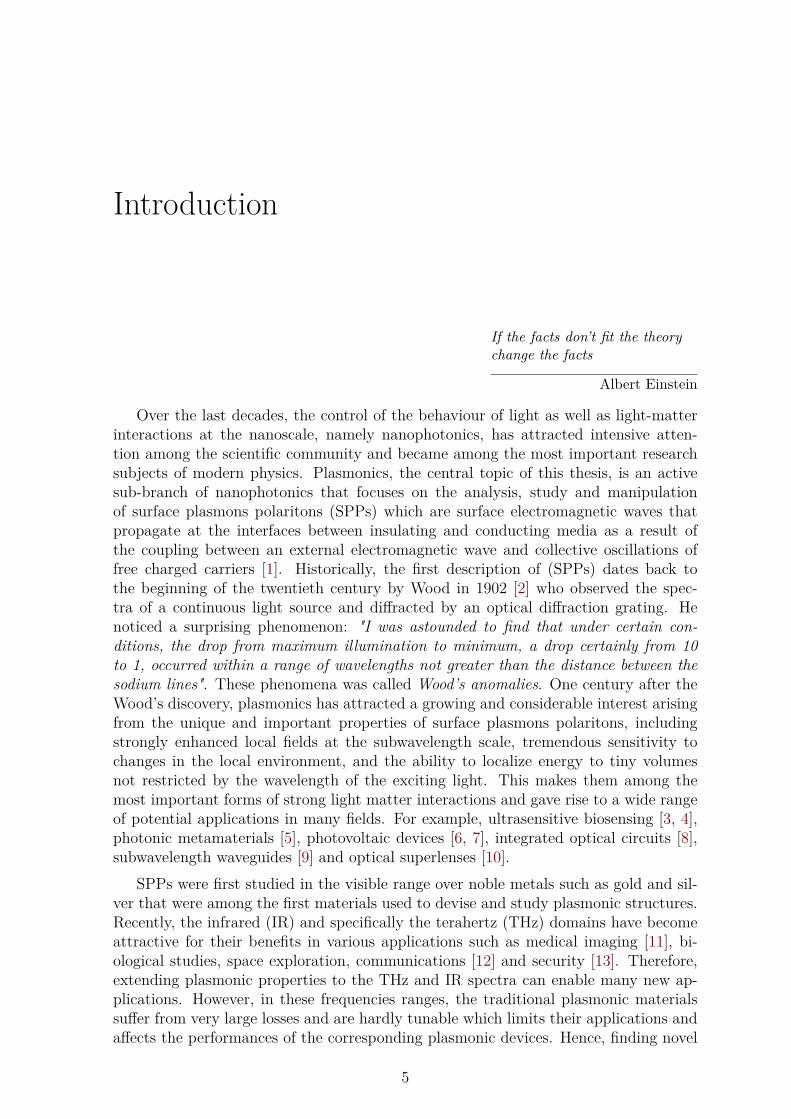
atom A
atom B
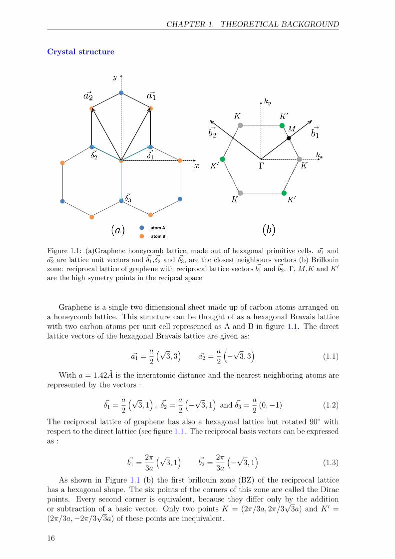
Figure 1.1: (a)Graphene honeycomb lattice, made out of hexagonal primitive cells. ~a1 and~a2 are lattice unit vectors and ~δ1,~δ2 and ~δ3, are the closest neighbours vectors (b) Brillouinzone: reciprocal lattice of graphene with reciprocal lattice vectors ~b1 and ~b2. Γ, M ,K and K ′are the high symetry points in the recipcal space
Graphene is a single two dimensional sheet made up of carbon atoms arranged ona honeycomb lattice. This structure can be thought of as a hexagonal Bravais latticewith two carbon atoms per unit cell represented as A and B in figure 1.1. The directlattice vectors of the hexagonal Bravais lattice are given as:
~a1 = a
2(√
3, 3)
~a2 = a
2(−√
3, 3)
(1.1)
With a = 1.42A is the interatomic distance and the nearest neighboring atoms arerepresented by the vectors :
~δ1 = a
2(√
3, 1), ~δ2 = a
2(−√
3, 1)and ~δ3 = a
2 (0,−1) (1.2)
The reciprocal lattice of graphene has also a hexagonal lattice but rotated 90 withrespect to the direct lattice (see figure 1.1. The reciprocal basis vectors can be expressedas :
~b1 = 2π3a(√
3, 1)
~b2 = 2π3a(−√
3, 1)
(1.3)
As shown in Figure 1.1 (b) the first brillouin zone (BZ) of the reciprocal latticehas a hexagonal shape. The six points of the corners of this zone are called the Diracpoints. Every second corner is equivalent, because they differ only by the additionor subtraction of a basic vector. Only two points K = (2π/3a, 2π/3
√3a) and K ′ =
(2π/3a,−2π/3√
3a) of these points are inequivalent.
16

CHAPTER 1. THEORETICAL BACKGROUND
The high symetry points are also presented in figure 1.1 (b). These points are Γ atthe center, M the center of an edge and inequivalent hexagonal corners K et K ′ of theBrillouin zone. The position of the M and K can be given by:
~ΓM = 2πa
(√3, 0
)~ΓK = 2π
a
(1/√
3, 3)
(1.4)
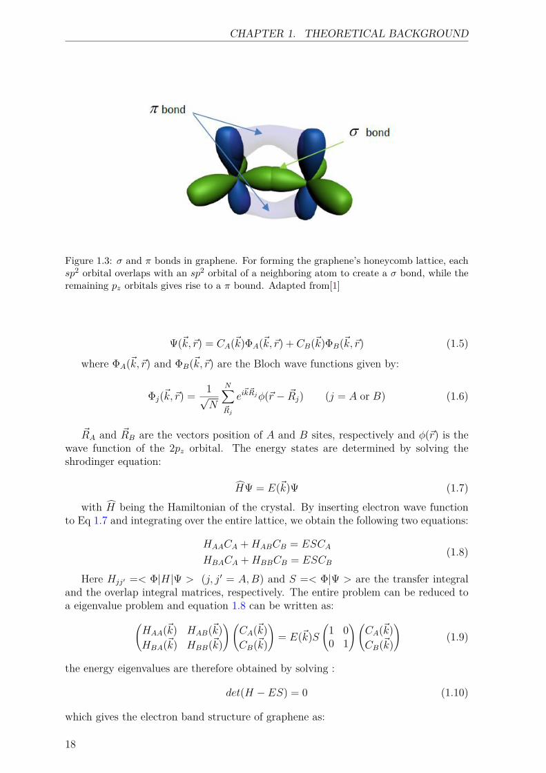
Carbon bonds in graphene
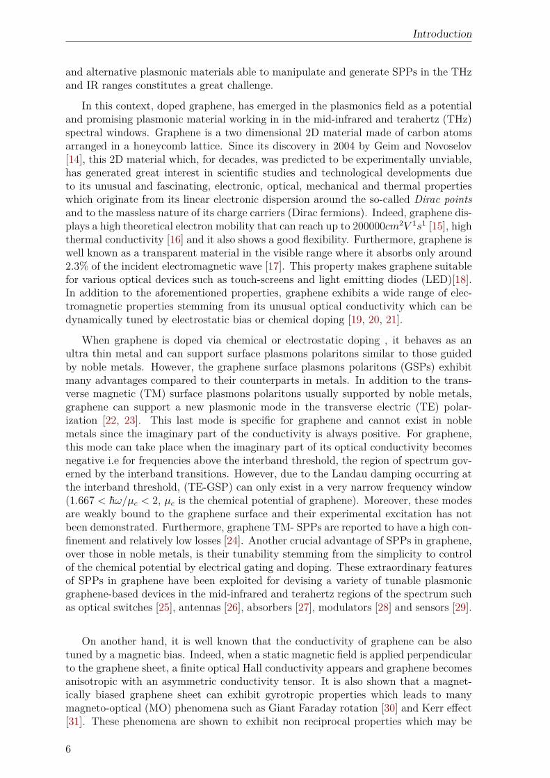
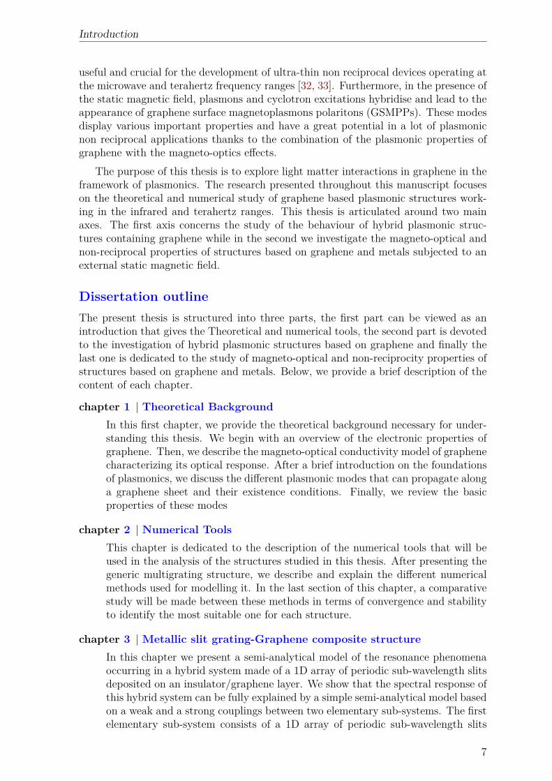
The carbon atom, the unique and principal constituent of graphene, has four valenceelectrons with an atomic configuration 2s22p2. In the crystalline phase, these fourvalence electrons give rise to four valence orbitals (2s, 2px, 2py, 2pz ), which canbe mixed in many different ways in spn, n = 1, 2, 3 hybridizations to form a varietyof carbon materials with different bonding configurations. In graphene, the valenceorbitals (2s, 2px, 2py) mix to produce three identical sp2 hyprid orbitals, which form120 angles in the plane of graphene (see Figure 1.2). These sp2 orbitals form threestrong, covalent σ bonds in the xy plane as shown in Figure 1.3. These bonds areresponsible for the rigidity and the mechanical stability of graphene. However, since theσ band in graphene is completly filled, its electrons do not contribute to the electronicproperties of graphene. Around the Fermi energy, the remaining pz-orbitals, whichhave a small overlap, give rise to weak delocalized covalent π bonds. It is this bondingthat are responsible for the electronic transport and optical properties of graphene.That is why, in the next section , in order to calculate the electronic band structure ofgraphene, we will adopt the tight binding method to model only the π band.
𝑠𝑝2
2𝑝𝑧
Figure 1.2: Graphical representation of the sp2 and spz orbitals in graphene. Adapted from[1]
The electronic Band Structure: Tight binding model
In the present section, we will use the tight-binding approximation to derive the elec-tronic dispersion relation of graphene. According to work done by Wallance [2], thismethod provides a good description of the band structure of graphene, where the over-lap of the 2pz orbitals is small. In this model and using the Bloch theorem, the wavefunction of the electron in graphene is described as a linear combination of the 2pzorbitals and can be written as the superposition of the orbitals of the carbon atoms Aand B:
17
CHAPTER 1. THEORETICAL BACKGROUND
Figure 1.3: σ and π bonds in graphene. For forming the graphene’s honeycomb lattice, eachsp2 orbital overlaps with an sp2 orbital of a neighboring atom to create a σ bond, while theremaining pz orbitals gives rise to a π bound. Adapted from[1]
Ψ(~k, ~r) = CA(~k)ΦA(~k, ~r) + CB(~k)ΦB(~k, ~r) (1.5)
where ΦA(~k, ~r) and ΦB(~k, ~r) are the Bloch wave functions given by:
Φj(~k, ~r) = 1√N
N∑~Rj
ei~k ~Rjφ(~r − ~Rj) (j = A or B) (1.6)
~RA and ~RB are the vectors position of A and B sites, respectively and φ(~r) is thewave function of the 2pz orbital. The energy states are determined by solving theshrodinger equation:
HΨ = E(~k)Ψ (1.7)with H being the Hamiltonian of the crystal. By inserting electron wave function
to Eq 1.7 and integrating over the entire lattice, we obtain the following two equations:
HAACA +HABCB = ESCA
HBACA +HBBCB = ESCB(1.8)
Here Hjj′ =< Φ|H|Ψ > (j, j′ = A,B) and S =< Φ|Ψ > are the transfer integraland the overlap integral matrices, respectively. The entire problem can be reduced toa eigenvalue problem and equation 1.8 can be written as:(
HAA(~k) HAB(~k)HBA(~k) HBB(~k)
)(CA(~k)CB(~k)
)= E(~k)S
(1 00 1
)(CA(~k)CB(~k)
)(1.9)
the energy eigenvalues are therefore obtained by solving :
det(H − ES) = 0 (1.10)
which gives the electron band structure of graphene as:
18
CHAPTER 1. THEORETICAL BACKGROUND
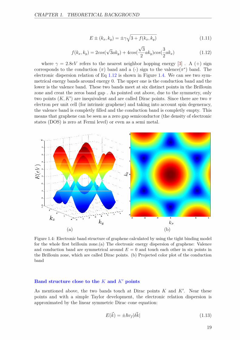
E ± (kx, ky) = ±γ√
3 + f(kx, ky) (1.11)
f(kx, ky) = 2cos(√
3aky) + 4cos(√
32 aky)cos(
32akx) (1.12)
where γ = 2.8eV refers to the nearest neighbor hopping energy [3] . A (+) signcorresponds to the conduction (π) band and a (-) sign to the valence(π∗) band. Theelectronic dispersion relation of Eq 1.12 is shown in Figure 1.4. We can see two sym-metrical energy bands around energy 0. The upper one is the conduction band and thelower is the valence band. These two bands meet at six distinct points in the Brillouinzone and creat the zeros band gap . As pointed out above, due to the symmetry, onlytwo points (K,K ′) are inequivalent and are called Dirac points. Since there are two πelectron per unit cell (for intrinsic graphene) and taking into account spin degeneracy,the valence band is completly filled and the conduction band is completly empty. Thismeans that graphene can be seen as a zero gap semiconductor (the density of electronicstates (DOS) is zero at Fermi level) or even as a semi metal.
(a) (b)
Figure 1.4: Electronic band structure of graphene calculated by using the tight binding modelfor the whole first brillouin zone.(a) The electronic energy dispersion of graphene: Valenceand conduction band are symmetrical around E = 0 and touch each other in six points inthe Brillouin zone, which are called Dirac points. (b) Projected color plot of the conductionband
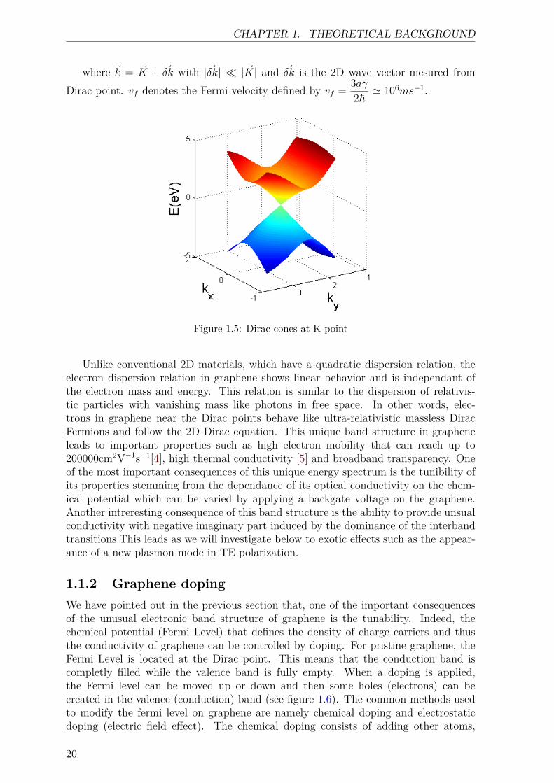
Band structure close to the K and K ′ points
As mentioned above, the two bands touch at Dirac points K and K ′. Near thesepoints and with a simple Taylor development, the electronic relation dispersion isapproximated by the linear symmetric Dirac cone equation:
E(~k) = ±~vf | ~δk| (1.13)
19
CHAPTER 1. THEORETICAL BACKGROUND
where ~k = ~K + ~δk with | ~δk| | ~K| and ~δk is the 2D wave vector mesured fromDirac point. vf denotes the Fermi velocity defined by vf = 3aγ
2~ ' 106ms−1.
Figure 1.5: Dirac cones at K point
Unlike conventional 2D materials, which have a quadratic dispersion relation, theelectron dispersion relation in graphene shows linear behavior and is independant ofthe electron mass and energy. This relation is similar to the dispersion of relativis-tic particles with vanishing mass like photons in free space. In other words, elec-trons in graphene near the Dirac points behave like ultra-relativistic massless DiracFermions and follow the 2D Dirac equation. This unique band structure in grapheneleads to important properties such as high electron mobility that can reach up to200000cm2V−1s−1[4], high thermal conductivity [5] and broadband transparency. Oneof the most important consequences of this unique energy spectrum is the tunibility ofits properties stemming from the dependance of its optical conductivity on the chem-ical potential which can be varied by applying a backgate voltage on the graphene.Another intreresting consequence of this band structure is the ability to provide unsualconductivity with negative imaginary part induced by the dominance of the interbandtransitions.This leads as we will investigate below to exotic effects such as the appear-ance of a new plasmon mode in TE polarization.
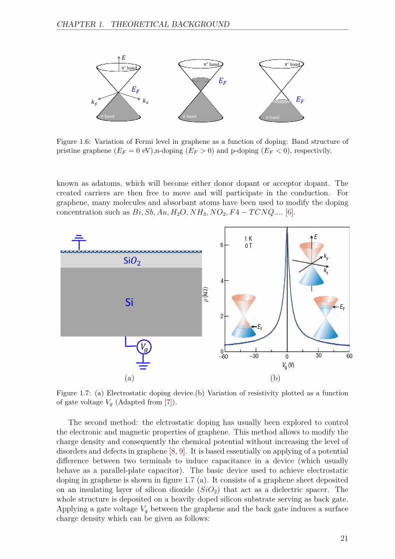
1.1.2 Graphene dopingWe have pointed out in the previous section that, one of the important consequencesof the unusual electronic band structure of graphene is the tunability. Indeed, thechemical potential (Fermi Level) that defines the density of charge carriers and thusthe conductivity of graphene can be controlled by doping. For pristine graphene, theFermi Level is located at the Dirac point. This means that the conduction band iscompletly filled while the valence band is fully empty. When a doping is applied,the Fermi level can be moved up or down and then some holes (electrons) can becreated in the valence (conduction) band (see figure 1.6). The common methods usedto modify the fermi level on graphene are namely chemical doping and electrostaticdoping (electric field effect). The chemical doping consists of adding other atoms,
20
CHAPTER 1. THEORETICAL BACKGROUND
π band
π∗ band
𝐸𝐹
π band
π∗ band
𝐸𝐹
π band
π∗ band
𝑘𝑥 𝑘𝑦
𝐸
𝐸𝐹
π band
Figure 1.6: Variation of Fermi level in graphene as a function of doping: Band structure ofpristine graphene (EF = 0 eV),n-doping (EF > 0) and p-doping (EF < 0), respectivily.
known as adatoms, which will become either donor dopant or acceptor dopant. Thecreated carriers are then free to move and will participate in the conduction. Forgraphene, many molecules and absorbant atoms have been used to modify the dopingconcentration such as Bi, Sb, Au,H2O,NH3, NO2, F4− TCNQ.... [6].
Si
Si𝑂2
𝑉𝑔
(a) (b)
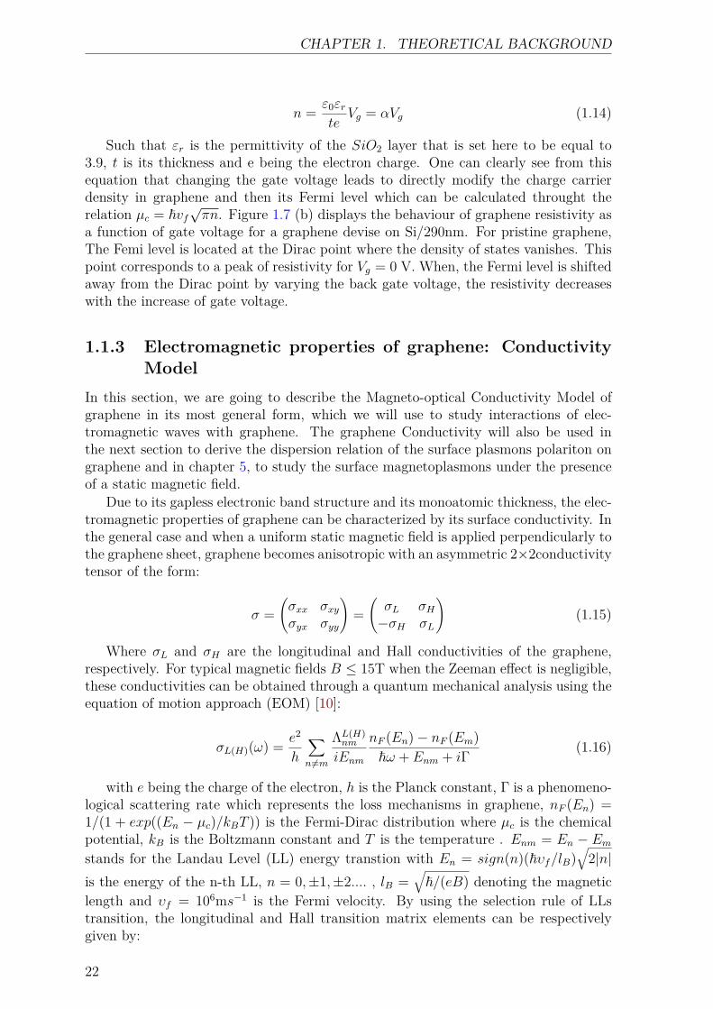
Figure 1.7: (a) Electrostatic doping device.(b) Variation of resistivity plotted as a functionof gate voltage Vg (Adapted from [7]).
The second method: the elctrostatic doping has usually been explored to controlthe electronic and magnetic properties of graphene. This method allows to modify thecharge density and consequently the chemical potential without increasing the level ofdisorders and defects in graphene [8, 9]. It is based essentially on applying of a potentialdifference between two terminals to induce capacitance in a device (which usuallybehave as a parallel-plate capacitor). The basic device used to achieve electrostaticdoping in graphene is shown in figure 1.7 (a). It consists of a graphene sheet depositedon an insulating layer of silicon dioxide (SiO2) that act as a dielectric spacer. Thewhole structure is deposited on a heavily doped silicon substrate serving as back gate.Applying a gate voltage Vg between the graphene and the back gate induces a surfacecharge density which can be given as follows:
21
CHAPTER 1. THEORETICAL BACKGROUND
n = ε0εrte
Vg = αVg (1.14)
Such that εr is the permittivity of the SiO2 layer that is set here to be equal to3.9, t is its thickness and e being the electron charge. One can clearly see from thisequation that changing the gate voltage leads to directly modify the charge carrierdensity in graphene and then its Fermi level which can be calculated throught therelation µc = ~vf
√πn. Figure 1.7 (b) displays the behaviour of graphene resistivity as
a function of gate voltage for a graphene devise on Si/290nm. For pristine graphene,The Femi level is located at the Dirac point where the density of states vanishes. Thispoint corresponds to a peak of resistivity for Vg = 0 V. When, the Fermi level is shiftedaway from the Dirac point by varying the back gate voltage, the resistivity decreaseswith the increase of gate voltage.
1.1.3 Electromagnetic properties of graphene: ConductivityModel
In this section, we are going to describe the Magneto-optical Conductivity Model ofgraphene in its most general form, which we will use to study interactions of elec-tromagnetic waves with graphene. The graphene Conductivity will also be used inthe next section to derive the dispersion relation of the surface plasmons polariton ongraphene and in chapter 5, to study the surface magnetoplasmons under the presenceof a static magnetic field.
Due to its gapless electronic band structure and its monoatomic thickness, the elec-tromagnetic properties of graphene can be characterized by its surface conductivity. Inthe general case and when a uniform static magnetic field is applied perpendicularly tothe graphene sheet, graphene becomes anisotropic with an asymmetric 2×2conductivitytensor of the form:
σ =(σxx σxyσyx σyy
)=(σL σH−σH σL
)(1.15)
Where σL and σH are the longitudinal and Hall conductivities of the graphene,respectively. For typical magnetic fields B ≤ 15T when the Zeeman effect is negligible,these conductivities can be obtained through a quantum mechanical analysis using theequation of motion approach (EOM) [10]:
σL(H)(ω) = e2
h
∑n6=m
ΛL(H)nm
iEnm
nF (En)− nF (Em)~ω + Enm + iΓ (1.16)
with e being the charge of the electron, h is the Planck constant, Γ is a phenomeno-logical scattering rate which represents the loss mechanisms in graphene, nF (En) =1/(1 + exp((En − µc)/kBT )) is the Fermi-Dirac distribution where µc is the chemicalpotential, kB is the Boltzmann constant and T is the temperature . Enm = En − Emstands for the Landau Level (LL) energy transtion with En = sign(n)(~υf/lB)
√2|n|
is the energy of the n-th LL, n = 0,±1,±2.... , lB =√~/(eB) denoting the magnetic
length and υf = 106ms−1 is the Fermi velocity. By using the selection rule of LLstransition, the longitudinal and Hall transition matrix elements can be respectivelygiven by:
22
CHAPTER 1. THEORETICAL BACKGROUND
ΛLnm =
~2υ2f
l2B(1 + δm,0 + δn,0) δ|m|−|n|,±1 (1.17)
ΛHnm = iΛL
nm
(δ|m|,|n|−1 − δ|m|−1,|n|
)(1.18)
It is of fundamental importance to notice that, in graphene, light/ matter interaction
0 100 200 300 400 500 600−10
−5
0
5
10
15
20
25
30
hω(meV )
σL(e
2/h
)
hω = 2µc
real partimaginary part
Intraband transitions
Interband Transitions
Figure 1.8: Real and imaginary parts of the longitudinal magneto-optical conductivity σL asa function of photon energy computed using the full quantum model for B = 7T , µc = 0.2eV ,T = 17K and Γ = 6.8meV
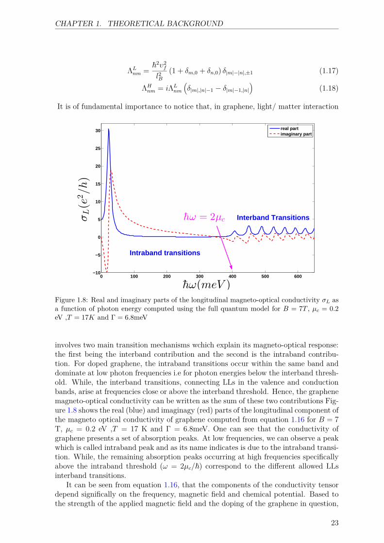
involves two main transition mechanisms wchich explain its magneto-optical response:the first being the interband contribution and the second is the intraband contribu-tion. For doped graphene, the intraband transitions occur within the same band anddominate at low photon frequencies i.e for photon energies below the interband thresh-old. While, the interband transitions, connecting LLs in the valence and conductionbands, arise at frequencies close or above the interband threshold. Hence, the graphenemagneto-optical conductivity can be written as the sum of these two contributions Fig-ure 1.8 shows the real (blue) and imaginagy (red) parts of the longitudinal component ofthe magneto optical conductivity of graphene computed from equation 1.16 for B = 7T, µc = 0.2 eV ,T = 17 K and Γ = 6.8meV. One can see that the conductivity ofgraphene presents a set of absorption peaks. At low frequencies, we can observe a peakwhich is called intraband peak and as its name indicates is due to the intraband transi-tion. While, the remaining absorption peaks occurring at high frequencies specificallyabove the intraband threshold (ω = 2µc/~) correspond to the different allowed LLsinterband transitions.
It can be seen from equation 1.16, that the components of the conductivity tensordepend significally on the frequency, magnetic field and chemical potential. Based tothe strength of the applied magnetic field and the doping of the graphene in question,
23
CHAPTER 1. THEORETICAL BACKGROUND
0 100 200 300 400 500 600 700−10
−5
0
5
10
15
hω(meV )
σL(e
2/h)
real partimaginary part
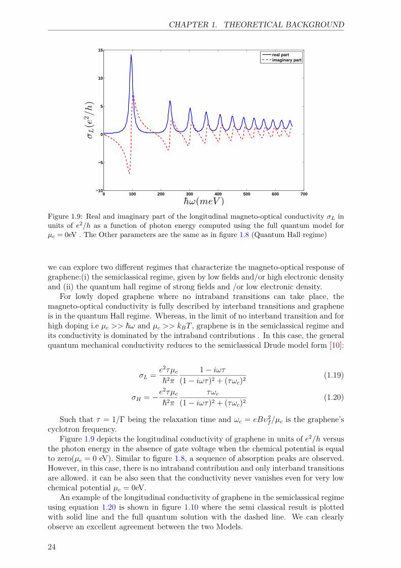
Figure 1.9: Real and imaginary part of the longitudinal magneto-optical conductivity σL inunits of e2/h as a function of photon energy computed using the full quantum model forµc = 0eV . The Other parameters are the same as in figure 1.8 (Quantum Hall regime)
we can explore two different regimes that characterize the magneto-optical response ofgraphene:(i) the semiclassical regime, given by low fields and/or high electronic densityand (ii) the quantum hall regime of strong fields and /or low electronic density.
For lowly doped graphene where no intraband transitions can take place, themagneto-optical conductivity is fully described by interband transitions and grapheneis in the quantum Hall regime. Whereas, in the limit of no interband transition and forhigh doping i.e µc >> ~ω and µc >> kBT , graphene is in the semiclassical regime andits conductivity is dominated by the intraband contributions . In this case, the generalquantum mechanical conductivity reduces to the semiclassical Drude model form [10]:
σL = e2τµc~2π
1− iωτ(1− iωτ)2 + (τωc)2 (1.19)
σH = −e2τµc~2π
τωc(1− iωτ)2 + (τωc)2 (1.20)
Such that τ = 1/Γ being the relaxation time and ωc = eBυ2f/µc is the graphene’s
cyclotron frequency.Figure 1.9 depicts the longitudinal conductivity of graphene in units of e2/h versus
the photon energy in the absence of gate voltage when the chemical potential is equalto zero(µc = 0 eV). Similar to figure 1.8, a sequence of absorption peaks are observed.However, in this case, there is no intraband contribution and only interband transitionsare allowed. it can be also seen that the conductivity never vanishes even for very lowchemical potential µc = 0eV.
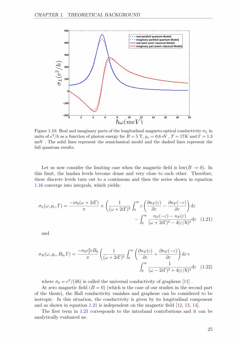
An example of the longitudinal conductivity of graphene in the semiclassical regimeusing equation 1.20 is shown in figure 1.10 where the semi classical result is plottedwith solid line and the full quantum solution with the dashed line. We can clearlyobserve an excellent agreement between the two Models.
24
CHAPTER 1. THEORETICAL BACKGROUND
0 2 4 6 8 10 12 14 16 18 20−200
−100
0
100
200
300
400
500
σL(e
2/h)
hω(meV )
real part(full quantum Model)imaginary part(full quantum Model)real part( semi−classical Model)imaginary part (semi−classical Model)
Figure 1.10: Real and imaginary parts of the longitudinal magneto-optical conductivity σL inunits of e2/h as a function of photon energy for B = 5 T, µc = 0.6 eV , T = 17K and Γ = 1.3meV . The solid lines represent the semiclassical model and the dashed lines represent thefull quantum results.
Let us now consider the limiting case when the magnetic field is low(B → 0). Inthis limit, the landau levels become dense and very close to each other. Therefore,these discrete levels turn out to a continuum and then the series shown in equation1.16 converge into integrals, which yields:
σL(ω, µc,Γ) = −iσ0(ω + 2iΓ)π
×(
1(ω + 2iΓ)2
∫ ∞0
ε
(∂nF (ε)∂ε
− ∂nF (−ε)∂ε
)dε
−∫ ∞
0
nF (−ε)− nF (ε)(ω + 2iΓ)2 − 4(ε/~)2 dε (1.21)
and
σH(ω, µc, B0,Γ) =−σ0v
2feB0
π
(1
(ω + 2iΓ)2
∫ ∞0
(∂nF (ε)∂ε
+ ∂nF (−ε)∂ε
)dε+∫ ∞
0
1(ω − 2iΓ)2 + 4(ε/~)2 dε (1.22)
where σ0 = e2/(4~) is called the universal conductivity of graphene [11] .At zero magnetic field (B = 0) (which is the case of our studies in the second part
of the thesis), the Hall conductivity vanishes and graphene can be considered to beisotropic. In this situation, the conductivity is given by its longitudinal componentand as shown in equation 1.21 is independent on the magnetic field [12, 13, 14].
The first term in 1.21 corresponds to the intraband contributions and it can beanalytically evaluated as:
25
CHAPTER 1. THEORETICAL BACKGROUND
σintra = i8σ0kBT
π(~ω + i~γ) ln(
2 cosh( µc2kBT
))
(1.23)
In general, the second term which is due to the interband contributions cannotbe evaluated analytically. However, it can be put into a more appropriate form fornumerical calculations as follows:
σinter = σ0
G(~ω2 ) + i4~ωπ
∫ ∞0
G(ε)− G(~ω2 )(~ω)2 − 4ε2 dε
(1.24)
With G(x) = sinh(x/kBT )cosh(µc/kBT ) + cosh(x/kBT ) .
At low temperatures when the conditions (kBT |µc|, ~ω) are fulfilled, the intra-band conductivity follows the usual Drude form that describes the collective behaviorof free electron :
σintra = σD = i4σ0µcπ(~ω + i~γ) (1.25)
In this limit, the interband term can be approximated as [12]
σinter = σ0
(θ(ω − 2µc)−
i
πln
∣∣∣∣∣ω + 2µcω − 2µc
∣∣∣∣∣)
(1.26)
where θ denotes the Heaviside step function presenting the condition necessary forinterband electron transitions at low temperatures.
1 1.2 1.4 1.6 1.8 2 2.2 2.4 2.6 2.8 3−1.5
−1
−0.5
0
0.5
1
ω
σ/σ0
ωs
σr/σ
0
σi/σ
0
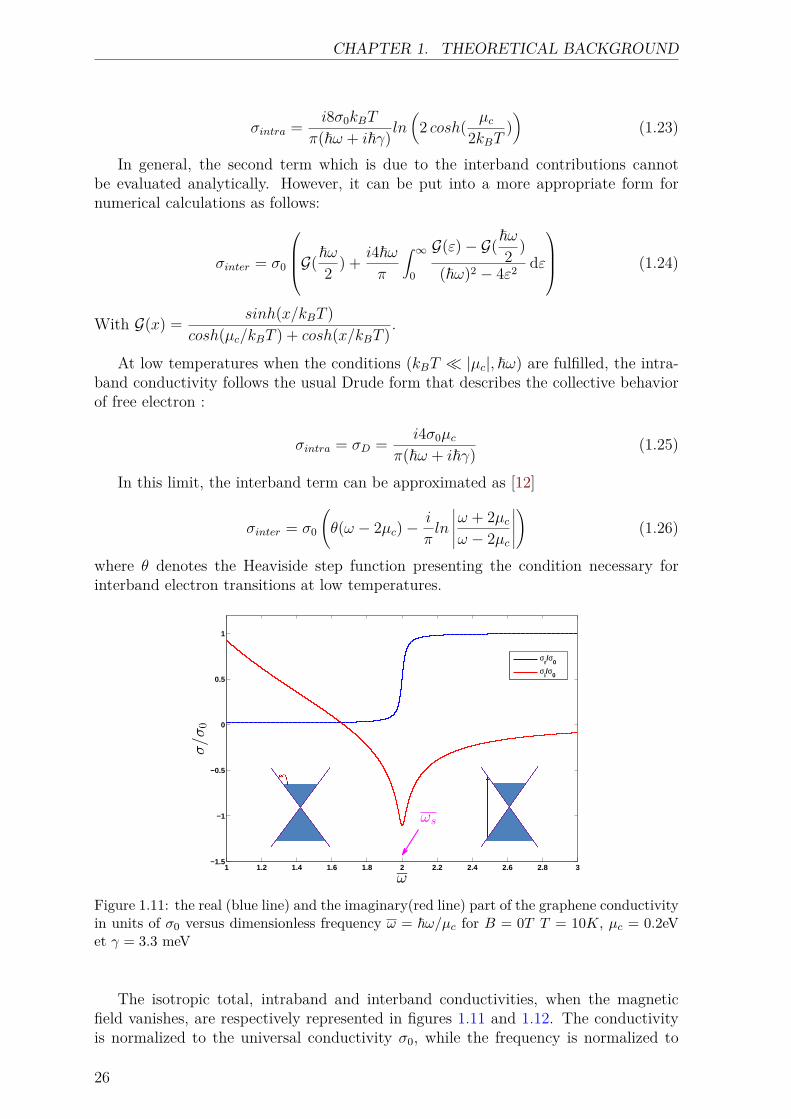
Figure 1.11: the real (blue line) and the imaginary(red line) part of the graphene conductivityin units of σ0 versus dimensionless frequency ω = ~ω/µc for B = 0T T = 10K, µc = 0.2eVet γ = 3.3 meV
The isotropic total, intraband and interband conductivities, when the magneticfield vanishes, are respectively represented in figures 1.11 and 1.12. The conductivityis normalized to the universal conductivity σ0, while the frequency is normalized to
26
CHAPTER 1. THEORETICAL BACKGROUND
0 0.02 0.04 0.06 0.08 0.1 0.12 0.14 0.16 0.18 0.20
10
20
30
40
50
60
70
80
ω
σintra/σ
0σintra
r/σ
0
σiintra/σ
0
(a)
0 0.5 1 1.5 2 2.5 3−2
−1.5
−1
−0.5
0
0.5
1
σinter/σ
0
ω
σinterr
/σ0
σinteri
/σ0
(b)
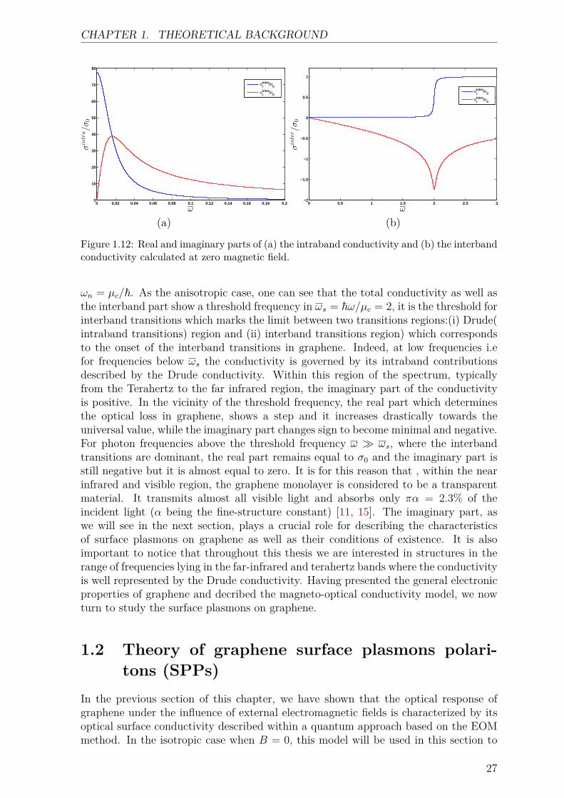
Figure 1.12: Real and imaginary parts of (a) the intraband conductivity and (b) the interbandconductivity calculated at zero magnetic field.
ωn = µc/~. As the anisotropic case, one can see that the total conductivity as well asthe interband part show a threshold frequency in ωs = ~ω/µc = 2, it is the threshold forinterband transitions which marks the limit between two transitions regions:(i) Drude(intraband transitions) region and (ii) interband transitions region) which correspondsto the onset of the interband transitions in graphene. Indeed, at low frequencies i.efor frequencies below ωs the conductivity is governed by its intraband contributionsdescribed by the Drude conductivity. Within this region of the spectrum, typicallyfrom the Terahertz to the far infrared region, the imaginary part of the conductivityis positive. In the vicinity of the threshold frequency, the real part which determinesthe optical loss in graphene, shows a step and it increases drastically towards theuniversal value, while the imaginary part changes sign to become minimal and negative.For photon frequencies above the threshold frequency ω ωs, where the interbandtransitions are dominant, the real part remains equal to σ0 and the imaginary part isstill negative but it is almost equal to zero. It is for this reason that , within the nearinfrared and visible region, the graphene monolayer is considered to be a transparentmaterial. It transmits almost all visible light and absorbs only πα = 2.3% of theincident light (α being the fine-structure constant) [11, 15]. The imaginary part, aswe will see in the next section, plays a crucial role for describing the characteristicsof surface plasmons on graphene as well as their conditions of existence. It is alsoimportant to notice that throughout this thesis we are interested in structures in therange of frequencies lying in the far-infrared and terahertz bands where the conductivityis well represented by the Drude conductivity. Having presented the general electronicproperties of graphene and decribed the magneto-optical conductivity model, we nowturn to study the surface plasmons on graphene.
1.2 Theory of graphene surface plasmons polari-tons (SPPs)
In the previous section of this chapter, we have shown that the optical response ofgraphene under the influence of external electromagnetic fields is characterized by itsoptical surface conductivity described within a quantum approach based on the EOMmethod. In the isotropic case when B = 0, this model will be used in this section to
27
CHAPTER 1. THEORETICAL BACKGROUND
study the surface plasmons polaritons propagating along a single graphene monolayerand to explaind some of their properties. Specifically we are interested in deriving theirdispersion relation which relates the frequency of (SPPs) to its wave vector. However,before going into the details of graphene (SPPs), we need to provide a brief reviewon the fondamentals of plasmonics. In particular, we focus on the properties of the(SPPs) propagating at metal-dielectric interfaces .
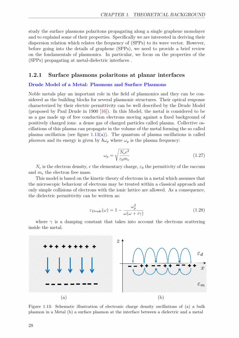
1.2.1 Surface plasmons polaritons at planar interfacesDrude Model of a Metal: Plasmons and Surface Plasmons
Noble metals play an important role in the field of plasmonics and they can be con-sidered as the building blocks for several plasmonic structures. Their optical responsecharacterized by their electric permittivity can be well described by the Drude Model(proposed by Paul Drude in 1900 [16]). In this Model, the metal is considered to beas a gas made up of free conduction electrons moving against a fixed background ofpositively charged ions: a dense gas of charged particles called plasma. Collective os-cillations of this plasma can propagate in the volume of the metal forming the so calledplasma oscillation (see figure 1.13(a)). The quantum of plasma oscillations is calledplasmon and its energy is given by ~ωp where ωp is the plasma frequency:
ωp =√Nee
2
ε0me
(1.27)
Ne is the electron density, e the elementary charge, ε0 the permitivity of the vaccumand me the electron free mass.
This model is based on the kinetic theory of electrons in a metal which assumes thatthe microscopic behaviour of electrons may be treated within a classical approach andonly simple collisions of electrons with the ionic lattice are allowed. As a consequence,the dielectric permittivity can be written as:
εDrude(ω) = 1−ω2p
ω(ω + iγ) (1.28)
where γ is a damping constant that takes into account the electrons scatteringinside the metal.
(a) (b)
Figure 1.13: Schematic illustration of electronic charge density oscillations of (a) a bulkplasmon in a Metal (b) a surface plasmon at the interface between a dielectric and a metal
28
CHAPTER 1. THEORETICAL BACKGROUND
There are two kinds of plasmons: the first one is the bulk or volume plasmon whichcorresponds to the oscillation of three-dimensional (3D) eletron gas occurring insidethe metal. When the Metal is not infinite but limited by a surface, a second kind ofplasmons is allowed: surface plasmons: the surface waves propagating at the interfacebetween a metal and a dielectric. These collective oscillations can couple to light,creating hybrid modes which are referred to as Surface Plasmons Polaritons(SPPs).The illustration of both bulk plasmons and surface plasmons are shown on Figure 1.13.Let us underline that, for the work presented within this thesis, we are only interestedin the SPP modes.
Existence conditions and dispersion relation
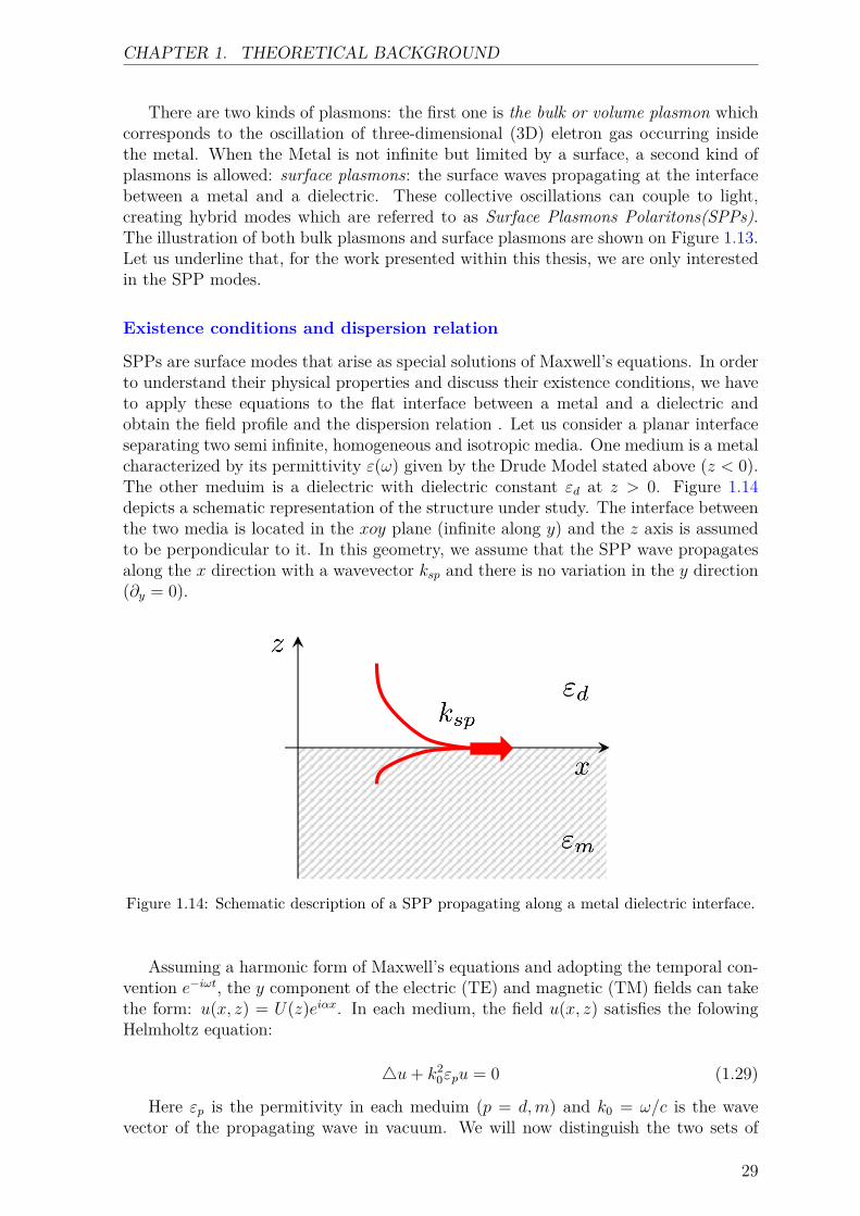
SPPs are surface modes that arise as special solutions of Maxwell’s equations. In orderto understand their physical properties and discuss their existence conditions, we haveto apply these equations to the flat interface between a metal and a dielectric andobtain the field profile and the dispersion relation . Let us consider a planar interfaceseparating two semi infinite, homogeneous and isotropic media. One medium is a metalcharacterized by its permittivity ε(ω) given by the Drude Model stated above (z < 0).The other meduim is a dielectric with dielectric constant εd at z > 0. Figure 1.14depicts a schematic representation of the structure under study. The interface betweenthe two media is located in the xoy plane (infinite along y) and the z axis is assumedto be perpondicular to it. In this geometry, we assume that the SPP wave propagatesalong the x direction with a wavevector ksp and there is no variation in the y direction(∂y = 0).
Figure 1.14: Schematic description of a SPP propagating along a metal dielectric interface.
Assuming a harmonic form of Maxwell’s equations and adopting the temporal con-vention e−iωt, the y component of the electric (TE) and magnetic (TM) fields can takethe form: u(x, z) = U(z)eiαx. In each medium, the field u(x, z) satisfies the folowingHelmholtz equation:
4u+ k20εpu = 0 (1.29)
Here εp is the permitivity in each meduim (p = d,m) and k0 = ω/c is the wavevector of the propagating wave in vacuum. We will now distinguish the two sets of
29

CHAPTER 1. THEORETICAL BACKGROUND
polarization modes of the electromagnetic field, The TM (transverse magnetic or p-polarized) mode corresponding to a magnetic field perpendicular to the incidence planeand TE(transverse electric or s-polarized) mode corresponding to a magnetic field lyingin the plane of incidence. In the case of TM polarization, only the Ex,Ez and Hy willbe non-zero, u(x, z) = Hy(x, z) and the equation 1.29 becomes:
∂2Hy
∂z2 + (k20εp − α2)Hy = 0 (1.30)
We are looking for bound solutions that propagate along the interface and decayaway from it. Thus, they can be expressed as :
Hmy = Aeiαxeγmz z < 0Hdy = Beiαxe−γdz z > 0 (1.31)
where α indicates the parallel component of the wave vector corresponding to thepropagation of the wave along the x direction.γd/m =
√α2 − k2
0εd/m are the componentsof the wave vector perpondicular to the interface and since the field evanescently decaysin this direction, they must have positive real part. A and B represent the amplitudesof the field in each of the two media. Applying the following boundary conditions atthe interface z = 0:
Hmy(z = 0) = Hdy(z = 0)
1εm
∂Hmy
∂z(z = 0) = 1
εd
∂Hdy
∂z(z = 0)
(1.32)
Yields: A = B
γ′mA = −γ′dB(1.33)
with γ′d(m) = γd(m)
εd(m), which gives :
γ′m + γ′d = 0 (1.34)
Let us analyze equation 1.34 to obtain the conditions which have to be fulfilledfor surface plasmons under TM polarization. One can see that since γd et γm havepositive real parts, this equation requires that εm et εd must have opposite signs. Thatmeans the permittivity of metal must be negative (εm < 0). This requirement is largelyfulfilled by many metals in the visible and near infrared ranges.
By following, a similar approach for TE polarization, the boundary conditions atthe interface lead to γm + γd = 0, which cannot be satisfied and consequently TE SPPmodes cannot exist and this set of solutions is thus discarded.
Replacing γd et γm by their expressions in equation 1.34, we obtain the SPP dis-persion relation:
ksp = α = k0
√εdεmεd + εm
(1.35)
It is worth noting that in addition to the condition stated above, this relationimposes a second condition on the permitivities of both media. Indeed, to have a prop-agative wave, ksp must have a real part. Since the product of the dielectric fonctions
30
CHAPTER 1. THEORETICAL BACKGROUND
is negative (εdεm < 0), the sum in the denominator of equation 1.35 should be alsonegative. This condition implies that:
ω < ωsp = ωp√1 + εd
(1.36)
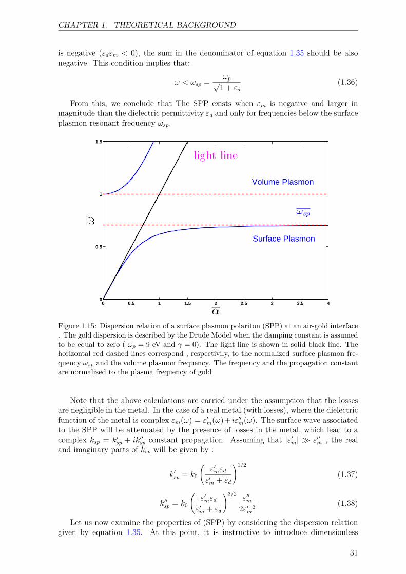
From this, we conclude that The SPP exists when εm is negative and larger inmagnitude than the dielectric permittivity εd and only for frequencies below the surfaceplasmon resonant frequency ωsp.
0 0.5 1 1.5 2 2.5 3 3.5 40
0.5
1
1.5
α
ω
ωsp
light line
Surface Plasmon
Volume Plasmon
Figure 1.15: Dispersion relation of a surface plasmon polariton (SPP) at an air-gold interface. The gold dispersion is described by the Drude Model when the damping constant is assumedto be equal to zero ( ωp = 9 eV and γ = 0). The light line is shown in solid black line. Thehorizontal red dashed lines correspond , respectivily, to the normalized surface plasmon fre-quency ωsp and the volume plasmon frequency. The frequency and the propagation constantare normalized to the plasma frequency of gold
Note that the above calculations are carried under the assumption that the lossesare negligible in the metal. In the case of a real metal (with losses), where the dielectricfunction of the metal is complex εm(ω) = ε′m(ω)+ iε′′m(ω). The surface wave associatedto the SPP will be attenuated by the presence of losses in the metal, which lead to acomplex ksp = k′sp + ik′′sp constant propagation. Assuming that |ε′m| ε′′m , the realand imaginary parts of ksp will be given by :
k′sp = k0
(ε′mεdε′m + εd
)1/2
(1.37)
k′′sp = k0
(ε′mεdε′m + εd
)3/2ε′′m
2ε′m2 (1.38)
Let us now examine the properties of (SPP) by considering the dispersion relationgiven by equation 1.35. At this point, it is instructive to introduce dimensionless
31
CHAPTER 1. THEORETICAL BACKGROUND
parameters. For that, we normalize the frequency and the wave vector accordingto gold’s plasma frequency: ω = ω/ωpAu and α = αc/ωpAu. Figure 1.15 shows thedispersion relation for a surface plasmon polariton in the interface between vacuum(εd = 1) and a metal, where, we use the Drude Model without loss (ωp = 9 eVcorresponding to fpAu = 2.176× 10¹⁵Hz and γ = 0) to calculate the gold permittivity.The free space dispersion relation of equation ω = α is also presented.
We can distinguish two energy branches in the dispersion relation curve. The firstbranch for which ω < ωsp, (ωsp = 1/
√1 + εd = 1/
√2) corresponds to a surface plasmon
polariton (SPP), while the second one for which ω > 1 represents the propagation ofbulk modes inside the metallic plasma. In this latter case, the metal is transparent(i.e εm > 0) and thus γd et γm become imaginary allowing then the propagation ofunbound radiation. For ω < ωsp < 1, the dispersion relation curve shows a gap forwhich no propagative mode can exist, since α is imaginary in this frequency region.At low frequencies, the dispersion relation follows closely the light line, so in thisregion the SPP possesses a photon like nature. When ω approaches gardually ωsp, thedispersion curve starts to depart from the light line. In the limit where ω → ωsp, thegroup velocity vg = ∂ω/∂α vanishes and the surface plasmon resonance can occur atthis frequency. In this case, the surface plasmon polariton ( that is a hybrid mode)becomes a pure surface plasmon.
As can be observed from figure 1.15, the SPP dispersion curve is always below thatof light and they do not cross at any point. In other words, for a given frequencythe wavevector of the SPP is always higher than that of light. As a result of thiswavevector mismatch, a direct excitation of SPPs with an electromagnetic wave is notpossible and we say that the SPP is a non radiative mode. To overcome this limitation,various special excitation techniques have been proposed to deal with the wavevectormismatch allowing then the coupling between light and SPPs. Having understoodthe properties of SPPs guided by a metallic interface, we are now ready to study theproperties of the surface plasmons polariton supported by a graphene sheet.
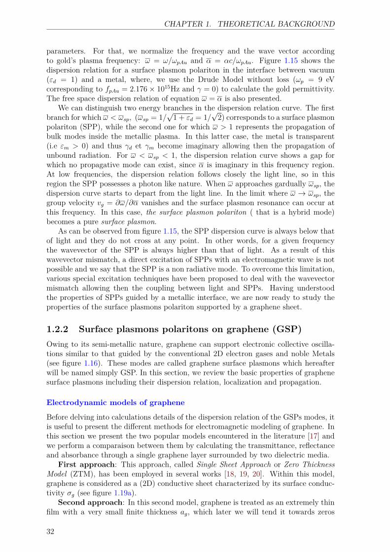
1.2.2 Surface plasmons polaritons on graphene (GSP)Owing to its semi-metallic nature, graphene can support electronic collective oscilla-tions similar to that guided by the conventional 2D electron gases and noble Metals(see figure 1.16). These modes are called graphene surface plasmons which hereafterwill be named simply GSP. In this section, we review the basic properties of graphenesurface plasmons including their dispersion relation, localization and propagation.
Electrodynamic models of graphene
Before delving into calculations details of the dispersion relation of the GSPs modes, itis useful to present the different methods for electromagnetic modeling of graphene. Inthis section we present the two popular models encountered in the literature [17] andwe perform a comparaison between them by calculating the transmittance, reflectanceand absorbance through a single graphene layer surrounded by two dielectric media.
First approach: This approach, called Single Sheet Approach or Zero ThicknessModel (ZTM), has been employed in several works [18, 19, 20]. Within this model,graphene is considered as a (2D) conductive sheet characterized by its surface conduc-tivity σg (see figure 1.19a).
Second approach: In this second model, graphene is treated as an extremely thinfilm with a very small finite thickness ag, which later we will tend it towards zeros
32
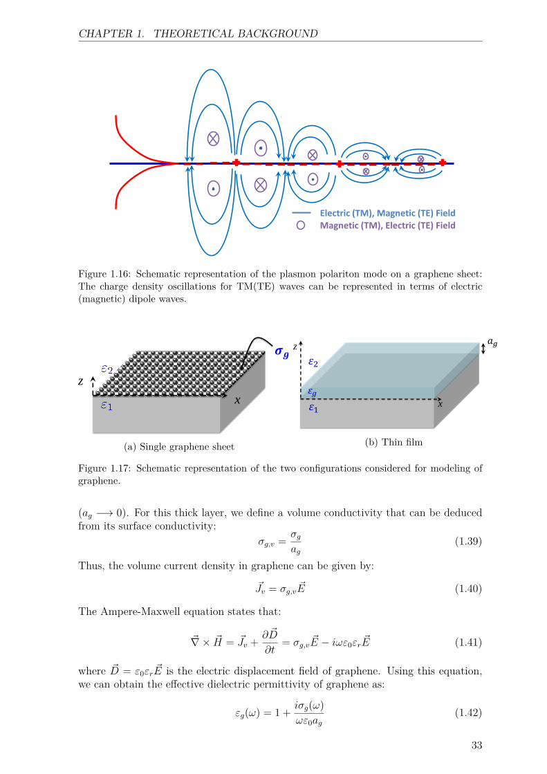
CHAPTER 1. THEORETICAL BACKGROUND
Electric (TM), Magnetic (TE) Field Magnetic (TM), Electric (TE) Field
Figure 1.16: Schematic representation of the plasmon polariton mode on a graphene sheet:The charge density oscillations for TM(TE) waves can be represented in terms of electric(magnetic) dipole waves.
𝝈𝒈
x
z
(a) Single graphene sheet
z
x
𝑎𝑔
𝜀1
𝜀𝑔
𝜀2
(b) Thin film
Figure 1.17: Schematic representation of the two configurations considered for modeling ofgraphene.
(ag −→ 0). For this thick layer, we define a volume conductivity that can be deducedfrom its surface conductivity:
σg,v = σgag
(1.39)
Thus, the volume current density in graphene can be given by:
~Jv = σg,v ~E (1.40)
The Ampere-Maxwell equation states that:
~∇× ~H = ~Jv + ∂ ~D
∂t= σg,v ~E − iωε0εr ~E (1.41)
where ~D = ε0εr ~E is the electric displacement field of graphene. Using this equation,we can obtain the effective dielectric permittivity of graphene as:
εg(ω) = 1 + iσg(ω)ωε0ag
(1.42)
33
CHAPTER 1. THEORETICAL BACKGROUND
So, by assuming a small (sub-nanometer) thickness ag, graphene can be consideredas a bulk material layer with an equivalent permittivity εg (see figure 1.19b). Thismodel can be named as Thin film’s effective thickness approach or bulk Model [21].
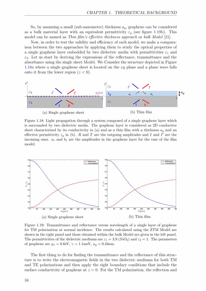
Now, in order to test the validity and efficiency of each model, we make a compara-ison between the two approaches by applying them to study the optical properties ofa single graphene layer embedded by two dielectric media with permittivities ε1 andε2. Let us start by deriving the expressions of the reflectance, transmittance and theabsorbance using the single sheet Model. We Consider the structure depicted in Figure1.18a where a single graphene sheet is located on the xy plane and a plane wave fallsonto it from the lower region (z < 0).
𝑥
I R
𝜎𝑔(𝜔)
𝑧
T I’
(a) Single graphene sheet
𝑥
I R
𝑧
𝜀𝑔 𝑎𝑔
T I’
𝑎1 𝑏1
(b) Thin film
Figure 1.18: Light propagation through a system composed of a single graphene layer whichis surrounded by two dielectric media. The graphene layer is considered as 2D conductivesheet characterized by its conductivity in (a) and as a thin film with a thickness ag and aneffective permittivity εg in (b). R and T are the outgoing amplitudes and I and I ′ are theincoming ones. a1 and b1 are the amplitudes in the graphene layer for the case of the filmmodel.
0 50 100 150 200 250 300 350 400 450 5000.1
0.2
0.3
0.4
0.5
0.6
0.7
0.8
0.9
λ(µm)
t σ,rσ
ReflectanceTransmittance
(a) Single graphene sheet
0 50 100 150 200 250 300 350 400 450 5000.1
0.2
0.3
0.4
0.5
0.6
0.7
0.8
0.9
λ(µm)
t ε,rε
ReflectanceTransmittance
(b) Thin film
Figure 1.19: Transmittance and reflectance versus wavelength of a single layer of graphenefor TM polarization at normal incidence. The results calculated using the ZTM Model areshown in the right panel and those obtained within the bulk Model are given in the left panel.The permittivities of the dielectric mediums are ε1 = 3.9 (SiO2) and ε2 = 1. The parametersof graphene are µc = 0.6eV, γ = 1.1meV, ag = 0.34nm.
The first thing to do for finding the transmittance and the reflectance of this struc-ture is to write the electromagnetic fields in the two dielectric mediums for both TMand TE polarizations and then apply the right boundary conditions that include thesurface conductivity of graphene at z = 0. For the TM polarization, the reflection and
34

CHAPTER 1. THEORETICAL BACKGROUND
the transmission coefficients can be obtained as:
RTM = k0γ′1 + γ′1γ
′2Z0σg − k0γ
′2
k0γ′1 + γ′1γ′2Z0σg + k0γ′2
(1.43)
TTM = 2k0γ′1
k0γ′1 + γ′1γ′2Z0σg + k0γ′2
(1.44)
And for the TE polarization case, we find:
RTE = γ1 − γ2 − k0Z0σgγ1 + γ2 + k0Z0σg
(1.45)
TTE = 2γ1
γ1 + γ2 + k0Z0σg(1.46)
The reflectance and the transmittance are then calculated as :
rTM = |RTM |2 and rTE = |RTE|2 (1.47)
tTM = γ′2γ′1|TTM |2 and tTE = γ2
γ1|TTE|2 (1.48)
Finally, the absorbance can be readily deduced from:
A = 1− r − t (1.49)
We turn now our attention to the second approach where the graphene layer can
0 50 100 150 200 250 300 350 400 450 5000
0.05
0.1
0.15
0.2
0.25
0.3
0.35
Absorbance
λ(µm)
ZTM Modelbulk Model
Figure 1.20: Absorbance as a function of the wavelength obtained using the Bulk Model (Reddashed line) and the ZTM Model (Black solid line). The parameters are the same as in figure1.19.
be seen as a slab with equivalent permittivity εg and thickness ag. In this case, thetransmission and reflection coefficients can be given by the following Fresnel coefficients:
R = r1 + φ1r2φ2
1 + r1r2φ1φ2(1.50)
T = t1t2φ2
1 + r1r2φ1φ2(1.51)
35
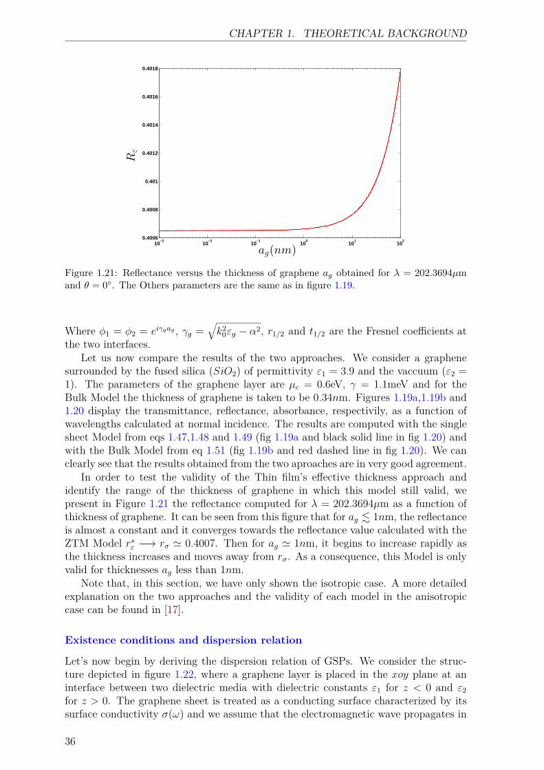
CHAPTER 1. THEORETICAL BACKGROUND
10−3
10−2
10−1
100
101
102
0.4006
0.4008
0.401
0.4012
0.4014
0.4016
0.4018
ag(nm)
Rε
Figure 1.21: Reflectance versus the thickness of graphene ag obtained for λ = 202.3694µmand θ = 0. The Others parameters are the same as in figure 1.19.
Where φ1 = φ2 = eiγgag , γg =√k2
0εg − α2, r1/2 and t1/2 are the Fresnel coefficients atthe two interfaces.
Let us now compare the results of the two approaches. We consider a graphenesurrounded by the fused silica (SiO2) of permittivity ε1 = 3.9 and the vaccuum (ε2 =1). The parameters of the graphene layer are µc = 0.6eV, γ = 1.1meV and for theBulk Model the thickness of graphene is taken to be 0.34nm. Figures 1.19a,1.19b and1.20 display the transmittance, reflectance, absorbance, respectivily, as a function ofwavelengths calculated at normal incidence. The results are computed with the singlesheet Model from eqs 1.47,1.48 and 1.49 (fig 1.19a and black solid line in fig 1.20) andwith the Bulk Model from eq 1.51 (fig 1.19b and red dashed line in fig 1.20). We canclearly see that the results obtained from the two aproaches are in very good agreement.
In order to test the validity of the Thin film’s effective thickness approach andidentify the range of the thickness of graphene in which this model still valid, wepresent in Figure 1.21 the reflectance computed for λ = 202.3694µm as a function ofthickness of graphene. It can be seen from this figure that for ag . 1nm, the reflectanceis almost a constant and it converges towards the reflectance value calculated with theZTM Model rsε −→ rσ ' 0.4007. Then for ag ' 1nm, it begins to increase rapidly asthe thickness increases and moves away from rσ. As a consequence, this Model is onlyvalid for thicknesses ag less than 1nm.
Note that, in this section, we have only shown the isotropic case. A more detailedexplanation on the two approaches and the validity of each model in the anisotropiccase can be found in [17].
Existence conditions and dispersion relation
Let’s now begin by deriving the dispersion relation of GSPs. We consider the struc-ture depicted in figure 1.22, where a graphene layer is placed in the xoy plane at aninterface between two dielectric media with dielectric constants ε1 for z < 0 and ε2for z > 0. The graphene sheet is treated as a conducting surface characterized by itssurface conductivity σ(ω) and we assume that the electromagnetic wave propagates in
36
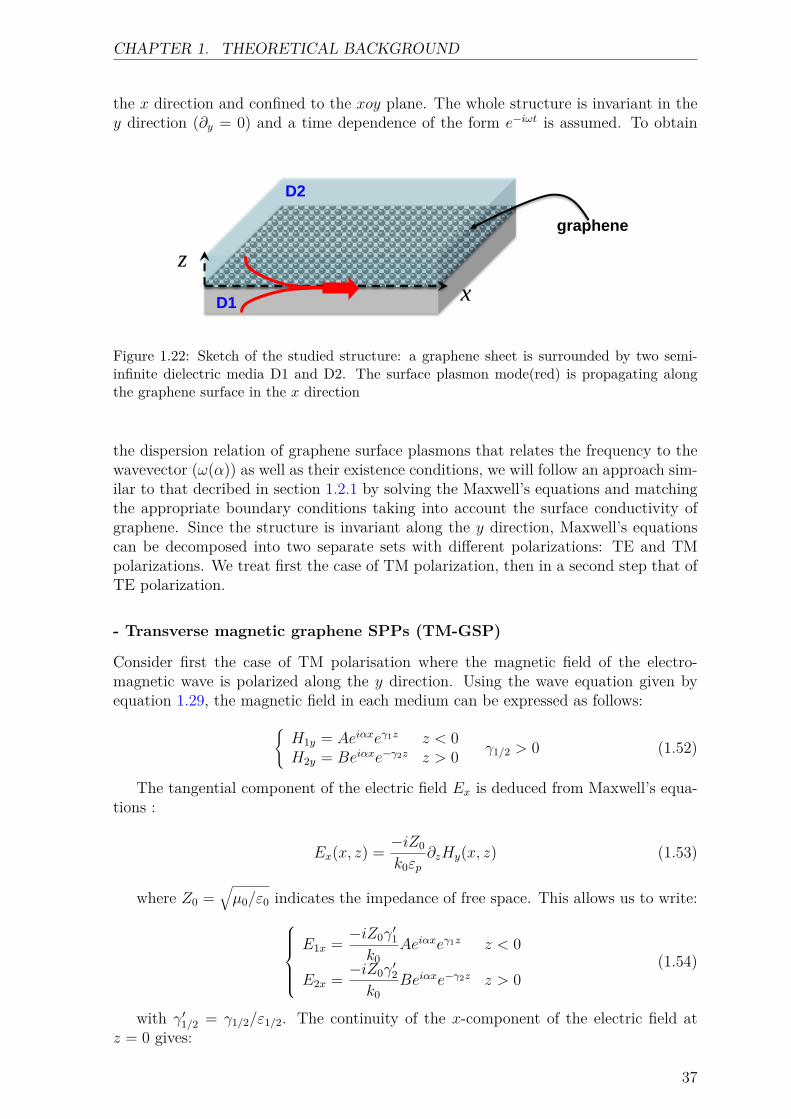
CHAPTER 1. THEORETICAL BACKGROUND
the x direction and confined to the xoy plane. The whole structure is invariant in they direction (∂y = 0) and a time dependence of the form e−iωt is assumed. To obtain
D1
D2
graphene
x
z
Figure 1.22: Sketch of the studied structure: a graphene sheet is surrounded by two semi-infinite dielectric media D1 and D2. The surface plasmon mode(red) is propagating alongthe graphene surface in the x direction
the dispersion relation of graphene surface plasmons that relates the frequency to thewavevector (ω(α)) as well as their existence conditions, we will follow an approach sim-ilar to that decribed in section 1.2.1 by solving the Maxwell’s equations and matchingthe appropriate boundary conditions taking into account the surface conductivity ofgraphene. Since the structure is invariant along the y direction, Maxwell’s equationscan be decomposed into two separate sets with different polarizations: TE and TMpolarizations. We treat first the case of TM polarization, then in a second step that ofTE polarization.
- Transverse magnetic graphene SPPs (TM-GSP)
Consider first the case of TM polarisation where the magnetic field of the electro-magnetic wave is polarized along the y direction. Using the wave equation given byequation 1.29, the magnetic field in each medium can be expressed as follows:
H1y = Aeiαxeγ1z z < 0H2y = Beiαxe−γ2z z > 0 γ1/2 > 0 (1.52)
The tangential component of the electric field Ex is deduced from Maxwell’s equa-tions :
Ex(x, z) = −iZ0
k0εp∂zHy(x, z) (1.53)
where Z0 =√µ0/ε0 indicates the impedance of free space. This allows us to write:
E1x = −iZ0γ′1
k0Aeiαxeγ1z z < 0
E2x = −iZ0γ′2
k0Beiαxe−γ2z z > 0
(1.54)
with γ′1/2 = γ1/2/ε1/2. The continuity of the x-component of the electric field atz = 0 gives:
37
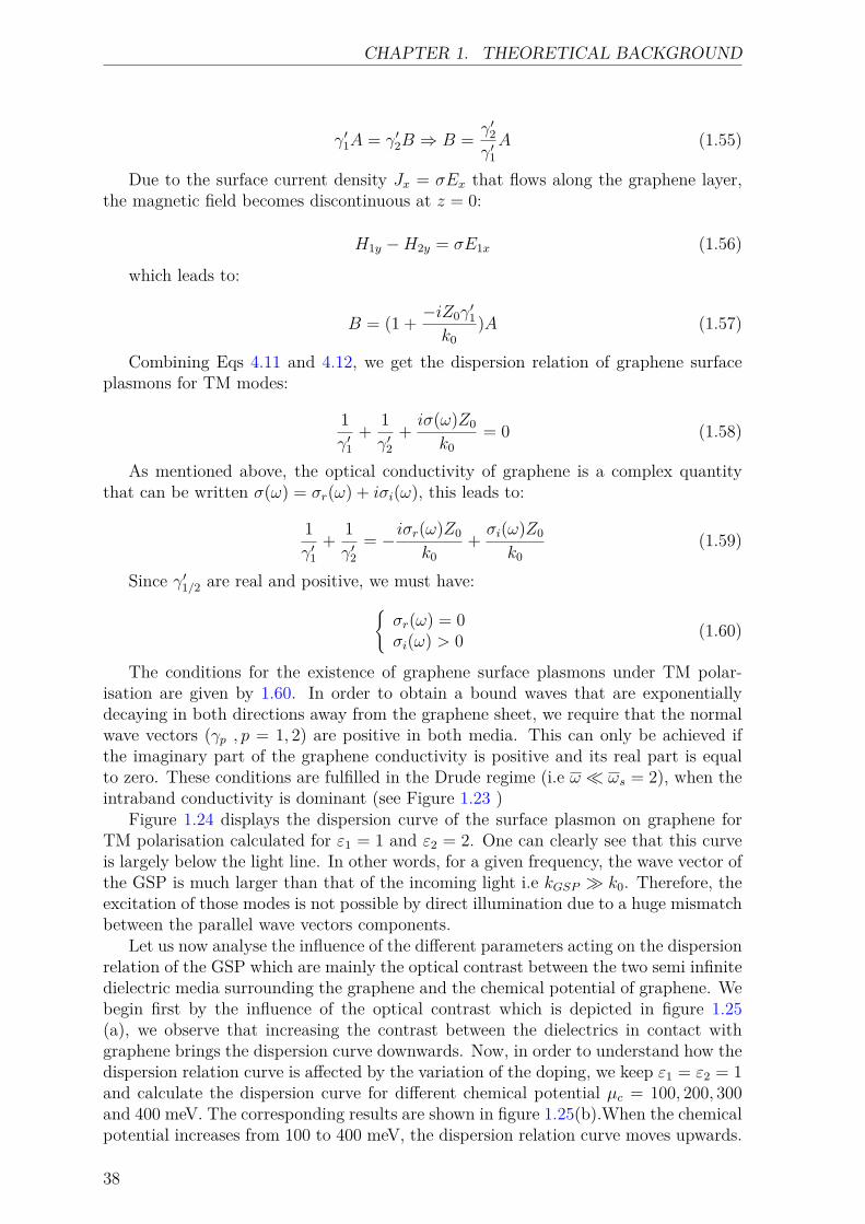
CHAPTER 1. THEORETICAL BACKGROUND
γ′1A = γ′2B ⇒ B = γ′2γ′1A (1.55)
Due to the surface current density Jx = σEx that flows along the graphene layer,the magnetic field becomes discontinuous at z = 0:
H1y −H2y = σE1x (1.56)
which leads to:
B = (1 + −iZ0γ′1
k0)A (1.57)
Combining Eqs 4.11 and 4.12, we get the dispersion relation of graphene surfaceplasmons for TM modes:
1γ′1
+ 1γ′2
+ iσ(ω)Z0
k0= 0 (1.58)
As mentioned above, the optical conductivity of graphene is a complex quantitythat can be written σ(ω) = σr(ω) + iσi(ω), this leads to:
1γ′1
+ 1γ′2
= −iσr(ω)Z0
k0+ σi(ω)Z0
k0(1.59)
Since γ′1/2 are real and positive, we must have:σr(ω) = 0σi(ω) > 0 (1.60)
The conditions for the existence of graphene surface plasmons under TM polar-isation are given by 1.60. In order to obtain a bound waves that are exponentiallydecaying in both directions away from the graphene sheet, we require that the normalwave vectors (γp , p = 1, 2) are positive in both media. This can only be achieved ifthe imaginary part of the graphene conductivity is positive and its real part is equalto zero. These conditions are fulfilled in the Drude regime (i.e ω ωs = 2), when theintraband conductivity is dominant (see Figure 1.23 )
Figure 1.24 displays the dispersion curve of the surface plasmon on graphene forTM polarisation calculated for ε1 = 1 and ε2 = 2. One can clearly see that this curveis largely below the light line. In other words, for a given frequency, the wave vector ofthe GSP is much larger than that of the incoming light i.e kGSP k0. Therefore, theexcitation of those modes is not possible by direct illumination due to a huge mismatchbetween the parallel wave vectors components.
Let us now analyse the influence of the different parameters acting on the dispersionrelation of the GSP which are mainly the optical contrast between the two semi infinitedielectric media surrounding the graphene and the chemical potential of graphene. Webegin first by the influence of the optical contrast which is depicted in figure 1.25(a), we observe that increasing the contrast between the dielectrics in contact withgraphene brings the dispersion curve downwards. Now, in order to understand how thedispersion relation curve is affected by the variation of the doping, we keep ε1 = ε2 = 1and calculate the dispersion curve for different chemical potential µc = 100, 200, 300and 400 meV. The corresponding results are shown in figure 1.25(b).When the chemicalpotential increases from 100 to 400 meV, the dispersion relation curve moves upwards.
38
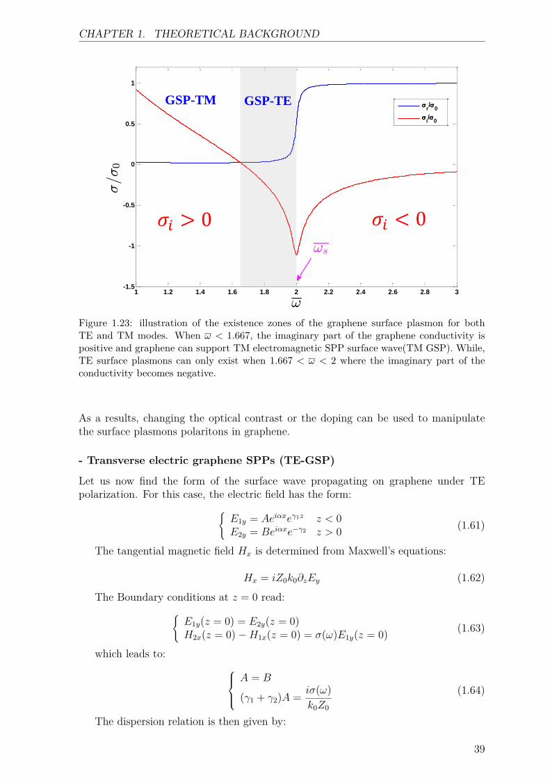
CHAPTER 1. THEORETICAL BACKGROUND
1 1.2 1.4 1.6 1.8 2 2.2 2.4 2.6 2.8 3-1.5
-1
-0.5
0
0.5
1
!
<=<
0
!s
r/
0
i/
0
𝜎𝑖 > 0 𝜎𝑖 < 0
GSP-TM GSP-TE
Figure 1.23: illustration of the existence zones of the graphene surface plasmon for bothTE and TM modes. When ω < 1.667, the imaginary part of the graphene conductivity ispositive and graphene can support TM electromagnetic SPP surface wave(TM GSP). While,TE surface plasmons can only exist when 1.667 < ω < 2 where the imaginary part of theconductivity becomes negative.
As a results, changing the optical contrast or the doping can be used to manipulatethe surface plasmons polaritons in graphene.
- Transverse electric graphene SPPs (TE-GSP)
Let us now find the form of the surface wave propagating on graphene under TEpolarization. For this case, the electric field has the form:
E1y = Aeiαxeγ1z z < 0E2y = Beiαxe−γ2 z > 0 (1.61)
The tangential magnetic field Hx is determined from Maxwell’s equations:
Hx = iZ0k0∂zEy (1.62)The Boundary conditions at z = 0 read:
E1y(z = 0) = E2y(z = 0)H2x(z = 0)−H1x(z = 0) = σ(ω)E1y(z = 0) (1.63)
which leads to: A = B
(γ1 + γ2)A = iσ(ω)k0Z0
(1.64)
The dispersion relation is then given by:
39
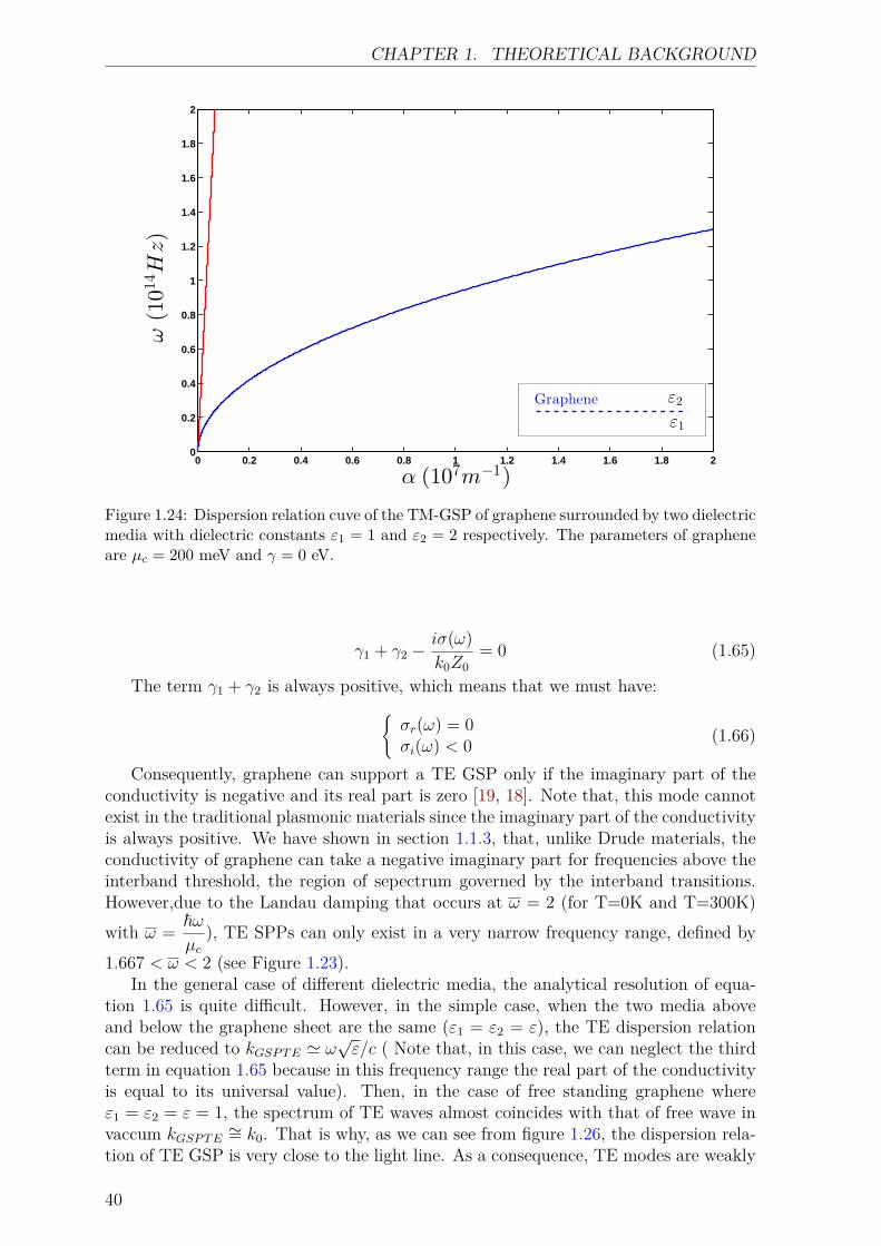
CHAPTER 1. THEORETICAL BACKGROUND
0 0.2 0.4 0.6 0.8 1 1.2 1.4 1.6 1.8 20
0.2
0.4
0.6
0.8
1
1.2
1.4
1.6
1.8
2
α (107m−1)
ω(101
4Hz)
ε2
ε1
Graphene
Ligne de lumière
Figure 1.24: Dispersion relation cuve of the TM-GSP of graphene surrounded by two dielectricmedia with dielectric constants ε1 = 1 and ε2 = 2 respectively. The parameters of grapheneare µc = 200 meV and γ = 0 eV.
γ1 + γ2 −iσ(ω)k0Z0
= 0 (1.65)
The term γ1 + γ2 is always positive, which means that we must have:σr(ω) = 0σi(ω) < 0 (1.66)
Consequently, graphene can support a TE GSP only if the imaginary part of theconductivity is negative and its real part is zero [19, 18]. Note that, this mode cannotexist in the traditional plasmonic materials since the imaginary part of the conductivityis always positive. We have shown in section 1.1.3, that, unlike Drude materials, theconductivity of graphene can take a negative imaginary part for frequencies above theinterband threshold, the region of sepectrum governed by the interband transitions.However,due to the Landau damping that occurs at ω = 2 (for T=0K and T=300K)with ω = ~ω
µc), TE SPPs can only exist in a very narrow frequency range, defined by
1.667 < ω < 2 (see Figure 1.23).In the general case of different dielectric media, the analytical resolution of equa-
tion 1.65 is quite difficult. However, in the simple case, when the two media aboveand below the graphene sheet are the same (ε1 = ε2 = ε), the TE dispersion relationcan be reduced to kGSPTE ' ω
√ε/c ( Note that, in this case, we can neglect the third
term in equation 1.65 because in this frequency range the real part of the conductivityis equal to its universal value). Then, in the case of free standing graphene whereε1 = ε2 = ε = 1, the spectrum of TE waves almost coincides with that of free wave invaccum kGSPTE ∼= k0. That is why, as we can see from figure 1.26, the dispersion rela-tion of TE GSP is very close to the light line. As a consequence, TE modes are weakly
40
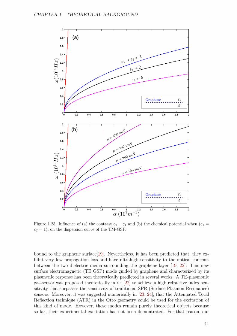
CHAPTER 1. THEORETICAL BACKGROUND
0 0.2 0.4 0.6 0.8 1 1.2 1.4 1.6 1.8 20
0.2
0.4
0.6
0.8
1
1.2
1.4
1.6
1.8
2
α(107m−1)
ω(101
4Hz)
ε2
ε1
Graphene
ε1 =ε2 =
1
ε2 =2
ε2 = 5
(a)
0 0.2 0.4 0.6 0.8 1 1.2 1.4 1.6 1.8 20
0.2
0.4
0.6
0.8
1
1.2
1.4
1.6
1.8
2
α (107m−1)
ω(101
4Hz)
ε2
ε1
Graphene
µ = 200meV
µ = 100 meV
µ= 300
meVµ= 400
meVligne de lumière(b)
Figure 1.25: Influence of (a) the contrast ε2 − ε1 and (b) the chemical potential when (ε1 =ε2 = 1), on the dispersion curve of the TM-GSP.
bound to the graphene surface[19]. Nevertheless, it has been predicted that, they ex-hibit very low propagation loss and have ultrahigh sensitivity to the optical contrastbetween the two dielectric media surrounding the graphene layer [19, 22]. This newsurface electromagnetic (TE GSP) mode guided by graphene and characterized by itsplasmonic response has been theoretically predicted in several works. A TE-plasmonicgas-sensor was proposed theoretically in ref [22] to achieve a high refractive index sen-sitivity that surpasses the sensitivity of traditional SPR (Surface Plasmon Resonance)sensors. Moreover, it was suggested numerically in [23, 24], that the Attenuated TotalReflection technique (ATR) in the Otto geometry could be used for the excitation ofthis kind of mode. However, these modes remain purely theoretical objects becauseso far, their experimental excitation has not been demontrated. For that reason, our
41
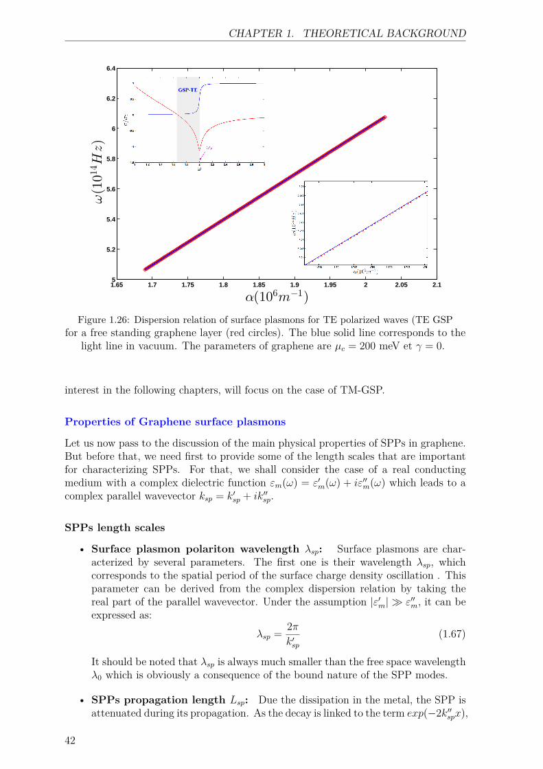
CHAPTER 1. THEORETICAL BACKGROUND
1.65 1.7 1.75 1.8 1.85 1.9 1.95 2 2.05 2.15
5.2
5.4
5.6
5.8
6
6.2
6.4
α(106m−1)
ω(101
4Hz)
Figure 1.26: Dispersion relation of surface plasmons for TE polarized waves (TE GSPfor a free standing graphene layer (red circles). The blue solid line corresponds to the
light line in vacuum. The parameters of graphene are µc = 200 meV et γ = 0.
interest in the following chapters, will focus on the case of TM-GSP.
Properties of Graphene surface plasmons
Let us now pass to the discussion of the main physical properties of SPPs in graphene.But before that, we need first to provide some of the length scales that are importantfor characterizing SPPs. For that, we shall consider the case of a real conductingmedium with a complex dielectric function εm(ω) = ε′m(ω) + iε′′m(ω) which leads to acomplex parallel wavevector ksp = k′sp + ik′′sp.
SPPs length scales
• Surface plasmon polariton wavelength λsp: Surface plasmons are char-acterized by several parameters. The first one is their wavelength λsp, whichcorresponds to the spatial period of the surface charge density oscillation . Thisparameter can be derived from the complex dispersion relation by taking thereal part of the parallel wavevector. Under the assumption |ε′m| ε′′m, it can beexpressed as:
λsp = 2πk′sp
(1.67)
It should be noted that λsp is always much smaller than the free space wavelengthλ0 which is obviously a consequence of the bound nature of the SPP modes.
• SPPs propagation length Lsp: Due the dissipation in the metal, the SPP isattenuated during its propagation. As the decay is linked to the term exp(−2k′′spx),
42
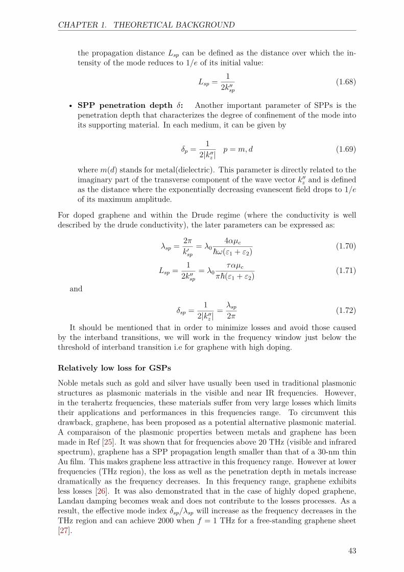
CHAPTER 1. THEORETICAL BACKGROUND
the propagation distance Lsp can be defined as the distance over which the in-tensity of the mode reduces to 1/e of its initial value:
Lsp = 12k′′sp
(1.68)
• SPP penetration depth δ: Another important parameter of SPPs is thepenetration depth that characterizes the degree of confinement of the mode intoits supporting material. In each medium, it can be given by
δp = 12|k′′z |
p = m, d (1.69)
where m(d) stands for metal(dielectric). This parameter is directly related to theimaginary part of the transverse component of the wave vector k′′z and is definedas the distance where the exponentially decreasing evanescent field drops to 1/eof its maximum amplitude.
For doped graphene and within the Drude regime (where the conductivity is welldescribed by the drude conductivity), the later parameters can be expressed as:
λsp = 2πk′sp
= λ04αµc
~ω(ε1 + ε2) (1.70)
Lsp = 12k′′sp
= λ0ταµc
π~(ε1 + ε2) (1.71)
and
δsp = 12|k′′z |
= λsp2π (1.72)
It should be mentioned that in order to minimize losses and avoid those causedby the interband transitions, we will work in the frequency window just below thethreshold of interband transition i.e for graphene with high doping.
Relatively low loss for GSPs
Noble metals such as gold and silver have usually been used in traditional plasmonicstructures as plasmonic materials in the visible and near IR frequencies. However,in the terahertz frequencies, these materials suffer from very large losses which limitstheir applications and performances in this frequencies range. To circumvent thisdrawback, graphene, has been proposed as a potential alternative plasmonic material.A comparaison of the plasmonic properties between metals and graphene has beenmade in Ref [25]. It was shown that for frequencies above 20 THz (visible and infraredspectrum), graphene has a SPP propagation length smaller than that of a 30-nm thinAu film. This makes graphene less attractive in this frequency range. However at lowerfrequencies (THz region), the loss as well as the penetration depth in metals increasedramatically as the frequency decreases. In this frequency range, graphene exhibitsless losses [26]. It was also demonstrated that in the case of highly doped graphene,Landau damping becomes weak and does not contribute to the losses processes. As aresult, the effective mode index δsp/λsp will increase as the frequency decreases in theTHz region and can achieve 2000 when f = 1 THz for a free-standing graphene sheet[27].
43
CHAPTER 1. THEORETICAL BACKGROUND
Figure 1.27: Comparaison of plasmonic properties of graphene and gold: Lsp/λspp as afunction of the frequency of the incident light [25]. The results for Au are for a 30-nm thickfilm at room temperature while the results for graphene are for a highly doping case and arecalculated from the experimental data in Ref [28] and from theoretical data in Ref [29].
High confinement of GSPs
As stated above, the confinement of SPPs into plasmonic materials is characterized byits penetration depth. The comparaison between graphene and silver(which is consid-ered as the best metallic plasmonic material) has shown that the penetration depthin graphene is a few orders smaller than that in silver [27]. In the other hand, theeffective SPP index λ0/λsp in metals is only slightly larger than √εd and since εd ofcommon dielectric does not exceed 10, the SPP index for metals are relatively small.For graphene, this index which is given by ~ω(ε1 + ε2)/4αµc is largely greater than 1.Therefore, GSPs are excellently confined to the surface of graphene with a SPP wave-length λsp much smaller than in free space. To summarize, the comparaison betweenhighly doped graphene and metals gives that metals are potential plasmonic materialsin the visible and near infrared region while highly doped graphene is more suitablefor the far infrared and the THz region.
The tunability of GSPs
One of the great advantages of SPPs in graphene over those in noble metals is theirtunability. We have shown in previous the sections that the conductivity of grapheneas well as the GSP dispersion relation are highly sensitive to some parameters such asthe chemical potential. We have also shown that the Fermi level in graphene can beeasily tuned by changing the carrier charge density by electrostatic gating or chemicaldoping. This is not possible with SPPs in noble metals. In the same way, the thresholdof interband transitions which defines the working frequency of graphene plasmonsstrongly depends on doping which makes it highly tunable by varying the graphenechemical potential [28, 30]. Although the working frequency of GSPs is in the THzregion because of the Landau damping at higher frequencies, it can be extended to the
44
CHAPTER 1. THEORETICAL BACKGROUND
mid infrared range by increased doping. For example, the working frequency can reachup 80 THz for µc = 0.246 eV and increase to achieve 250 THz for µc = 0.8eV [26].
1.3 ConclusionsIn this first chapter, we have presented the basic concepts that are important for un-derstanding this thesis. We have presented the direct and reciprocal lattice of grapheneand described its electronic band structure using the Tight binding model. Next, ac-cording to a quantum approach based on the EOM method, we have also determinedand explained the magneto-optical conductivity model of graphene characterizing itsoptical response. Using this model, we have then investigated the different plasmonicmodes that can propagate along a graphene sheet and their existence conditions. Fi-nally, we have reviewed the basic properties of these modes.
45

Bibliography
[1] N. chamanara and C. Caloz. Fundamentals of graphene magnetoplasmons: prin-cipales,structures and devices. Forum for Electromagnetic reseach methods andApplication Technologies (FERMAT), 10:1–15, 2015. 18, 19
[2] P. R. Wallace. Electric field effect in atomically thin carbon. Phys.Rev, 71(9):622,1947. 17
[3] N. M. R. Peres K. S. Novoselov A. H. Castro Neto, F. Guinea and A. K. Geim.The electronic properties of graphene. Rev.Mod.Phys, 81(1):109–162, 2009. 18
[4] Z. Jiang M. Klima G. Fudenberg J. Hone P. Kim K. I. Bolotin, K. J. Sikes andH. L. Stormer. Ultrahigh electron mobility in suspended graphene. Solid StateComm, 146(9-10):351–355, 2008. 20
[5] W. bao I. Calizo D. Teweldebhan F. Miao A. A. balandin, S. Ghosh and C. N. lau.Superior thermal conductivity of single layer graphene. Nano Lett, 8(3):902–907,2008. 6, 20
[6] C. Coletti, C. Riedl, D. S. Lee, B. Krauss, L. Patthey, K. von Klitzing, J. H. Smet,and U. Starke. Charge neutrality and band-gap tuning of epitaxial graphene onsic by molecular doping. Phys. Rev. B, 81:235401, Jun 2010. 21
[7] A. K. Geim and K. S. Novoselov. The rise of graphene. Nature Materials, 6(3):183–191, 2007. 21
[8] M. D. ventra J. N. Echstein C. D. Frisbie M. E. Gershenson A. M. GoldmanI. H. Inoue J. Mannhart A. J. Millis A. Forpurgo D. Natelson C. H. Ahn,A. Bhatttacharya and J. M. Triscone. Electrostatic modification of novel ma-terials. Rev.Mod.Phys, 78(4):1185, 2006. 22
[9] C. Casiraghi. Doping dependance of the raman peaks intensity of graphene closeto dirac point. Phys.Rev.B, 80(23):233407, 2009. 22
[10] Aires Ferreira, J. Viana-Gomes, Yu. V. Bludov, V. Pereira, N. M. R. Peres, andA. H. Castro Neto. Faraday effect in graphene enclosed in an optical cavity and theequation of motion method for the study of magneto-optical transport in solids.Phys. Rev. B, 84:235410, Dec 2011. 22, 24, 115
[11] A. N. Grigorenko K. S. Novoslov T. J. Booth T. stauber N .M. R. Peres R. R .Nair,P. Blake and A. K. Geim. Fine structure constatnt defines visual transparency ofgraphene. Sciences, 320(5881):1308, 2008. 25, 27
47
BIBLIOGRAPHY
[12] L. A. Falkovky. Optical properties of graphene. J.Phys.Conf.Ser, 129(1):2004,2008. 6, 26
[13] L. A. Falkovky and A. A. Varlamov. Space-timedispersion of graphene conductiv-ity. Eur.Phys.J.B, 56(4):281, 2007. 6, 26
[14] S. G. Sharapov V. P. Gusynin and J. p. Carbotte. Magneto-optical conductivityin graphene. J.Phys.Condens.Matter., 19(2):6222, 2007. 6, 26
[15] T. Hasan F. Bonaccorso, Z. Sun and A. C. Ferrari. Graphene photonics andoptoelectronics. Nature potonics, 9(4):611–622, 2010. 27
[16] P. Drude. Zur electronen theorie der metalle. Annalen der physik, 306(3):566–613,1900. 28
[17] Bruno Majérus, Evdokia Dremetsika, Michaël Lobet, Luc Henrard, and PascalKockaert. Electrodynamics of two-dimensional materials: Role of anisotropy.Phys. Rev. B, 98:125419, Sep 2018. 33, 36
[18] W. Hanson. Quasi transverse electromagnetic modes supported by a grapheneparallel-plate waveguide. J.App.Phys.Lett, 104:084314, 2008. 6, 33, 40
[19] S. A. Mikhailov and K. Ziegler. New electromagnetic mode in graphene. PRL,99(01):6803, 2007. 6, 33, 40, 41
[20] H. Buljan M. Jablan and M. Soljacis. Plasmonics in graphene at infrared frequen-cies. Phys.Rev. B, 80:245435, 2009. 33
[21] A.Vakil and N. Engheta. Transformation optics using graphene. Science,332(6035):1291–1294, 2011. 34
[22] M. A. Kol’chenko O. V. Kotov and Yu. E. Lozovik. Ultrahigh refractive index sen-sitivity of te-polarized electromagnetic waves in graphene at the inetrface betweentwo dielectric media. Opt.Express, 21(11):13533–13546, 2013. 41, 42
[23] S. G. Menabde D. R. Mason and N. Park. Unusual otto exctations dynamics andenchanced coupling of light to te plasmons in graphene. Opt.Express, 22(1):847–858, 2014. 42
[24] F. Ramos-Mendieta. Mid-indrared excitation of transverse electric modes in dopedgraphene. J.Appl.phys, 117(13):133101, 2015. 42
[25] M. Kafesaki P. Tassin, T. Koschny and C. M. Soukoulis. A comparaison ofgraphene , superconductors and metals as conductors for metamaterials and plas-monics. Nat .Photonics, 6:259–264, 2012. 6, 43, 44
[26] H. J. u Z. G. Dong T. J. Cui W. B. Lu, W. Zhu. Flexible transformation plasmonicsusing graphene. Opt.Express, 21(9):10475, 2013. 44, 45
[27] F. Garcia-Vidal A. Y. Nikitin, F. Guinea and L. Martin-Moreno. Field radiateda nanoemitter in graphene sheet. Phys.Rev.B, 84(19):195446, 2011. 44
[28] Z. Jiang Z. Hao M. C. Martin P. Kim H. L. Stormer Z. Q. Li, E. A. Henriksenand D. N .Basov. Dirac charge dynamics in graphene by infrared spectroscopy.Nat.Phys, 4:532–535, 2008. 44, 45
48

BIBLIOGRAPHY
[29] R. M. Ribeiro N. M. Peres and A. H. Castro Neto. Excitonic effets in the opticalconductivity of gates graphene. Phys Rev Lett, 105(5), 2010. 44
[30] S. Ryu L. E. Brus K. S. Kim Y-J. You, Y. Zhaao and P. Kim. Tuning the graphenework function by eletric fiels effet. Nano Lett, 9(10):3430–3434, 2009. 45
49

Chapter 2Numerical Tools
In every branch of knowledgethe progress is proportional tothe amount of facts on which tobuild
James Clerk Maxwell
Contents2.1 Generic Physical Structure . . . . . . . . . . . . . . . . . . . 512.2 Numerical Methods . . . . . . . . . . . . . . . . . . . . . . . 52
2.2.1 Standard Fourier Modal Method (FMM) . . . . . . . . . . . 522.2.2 Fourier Modal Method with spatial adaptative resolution (FMM-
ASR) . . . . . . . . . . . . . . . . . . . . . . . . . . . . . . . 602.2.3 Aperiodic Fourier Modal Method: FMM with PML . . . . . 64
2.3 Numerical Examples involving graphene:Graphene-Strip Gratings . . . . . . . . . . . . . . . . . . 67
2.3.1 Graphene horizontal strips grating . . . . . . . . . . . . . . . 672.3.2 Graphene Vertical strips grating . . . . . . . . . . . . . . . . 69
2.4 Conclusions . . . . . . . . . . . . . . . . . . . . . . . . . . . . 72
This chapter is devoted to the introduction of the numerical tools that will be usedin the analysis of the structures studied in this thesis. Since all these structures havethe common property of being either periodic or aperiodic diffractive structures, theirdynamics will be studied in the framework of the Fourier Model Method (FMM). Inthe first section, we will present the generic multigrating structure that can containgraphene gratings. Then in the next section, we will describe in detail the differentstandard numerical methods used for modelling the diffraction preoperties of electro-magnetic waves on this structure. After that, we will introduce the concept of perfectlymatched layers (PML) and combine it with the FMM Method to solve the problem ofthe aperiodic structures. Finally, we conclude with the last section by applying thesemethods that take into account graphene for solving the problem of light diffractionby two types of graphene grating systems. A comparative study will be made betweenthese methods in terms of convergence and stability to identify the most suitable onefor each structures.
51

CHAPTER 2. NUMERICAL TOOLS
2.1 Generic Physical Structure
𝑥
⋮
1
N
graphene
0 d
N+1
q
2d 3d 4d
𝜺𝟏𝟏 𝜺𝟏𝟐
𝜺𝟐
𝜺𝒒
𝜺𝑵𝟏 𝜺𝑵𝟐 𝜺𝑵𝟑
I
T I’
R
⋮
2 𝜎(𝜔)
Figure 2.1: Geometry of the diffraction problem: A graphene based multilayers structure inwhich each layer can be either a homogeneous medium or a garting with the period d
Before we start to develop and explain the different numerical methods, we firstpresent the system which is investigated. The general graphene based multilayeredgrating structure under study is schematically depicted in figure 2.1. It consists ofa stack of N layers where each of which can be either a periodic lamellar grating ora homogenous layer or vertical strip grating. This structure is embbeded betweentwo homogeneous dielectric media with permittivities εin and εout. All gratings sharethe same period d and the graphene can be inlayed in this strucrure under threeconfigurations: either continuous graphene layers or horizontal or vertical graphenestrip gratings. The whole structure is assumed to be invariant in the y direction and isilluminated from below by a monochromatic plane wave under the angle of incidence θ.The corresponding wavenumber is denoted k0 = 2π/λ, λ being the vaccum wavelengthand the time dependence will be assumed to be e−iωt. Here, we adopt the Thin film’seffective thickness approach explained in the previous chapter for modelling graphenein which the graphene layer is taken into account by its equivalent relative permittivity.
2.2 Numerical Methods
2.2.1 Standard Fourier Modal Method (FMM)The Fourier Modal (FMM) Method, also known as the rigourous coupled analysis(RCWA), is one of the most popular methods used for modeling diffraction from grat-
52
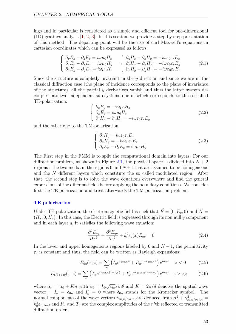
CHAPTER 2. NUMERICAL TOOLS
ings and in particular is considered as a simple and efficient tool for one-dimensional(1D) gratings analysis [1, 2, 3]. In this section, we provide a step by step presentationof this method. The departing point will be the use of curl Maxwell’s equations incartesian coordinates which can be expressed as follows:
∂yEz − ∂zEy = iωµ0Hx
∂zEx − ∂xEz = iωµ0Hy
∂xEy − ∂yEx = iωµ0Hz
∂yHz − ∂zHy = −iωε0εrEx∂zHx − ∂xHz = −iωε0εrEy∂xHy − ∂yHx = −iωε0εrEz
(2.1)
Since the structure is completly invariant in the y direction and since we are in theclassical diffraction case (the plane of incidence corresponds to the plane of invarianceof the structure), all the partial y derivatives vanish and thus the latter system de-couples into two independent sub-systems one of which corresponds to the so calledTE-polarization:
∂zEy = −iωµ0Hx
∂xEy = iωµ0Hz
∂zHx − ∂xHz = −iωε0εrEy
(2.2)
and the other one to the TM-polarization:∂zHy = iωε0εrEx∂xHy = −iωε0εrEz∂zEx − ∂xEz = iωµ0Hy
(2.3)
The First step in the FMM is to split the computational domain into layers. For ourdiffraction problem, as shown in Figure 2.1, the physical space is divided into N + 2regions : the two media in the regions 0 and N+1 that are assumed to be homogeneousand the N different layers which constitute the so called modulated region. Afterthat, the second step is to solve the wave equations everywhere and find the generalexpressions of the different fields before applying the boundary conditions. We considerfirst the TE polarization and treat afterwards the TM polarization problem.
TE polarization
Under TE polarization, the electromagnetic field is such that ~E = (0, Ey, 0) and ~H =(Hx, 0, Hz). In this case, the Electric field is expressed through its non null y componentand in each layer q, it satisfies the following wave equation:
∂2Eqy∂x2 + ∂2Eqy
∂z2 + k20εq(x)Eqy = 0 (2.4)
In the lower and upper homogeneous regions labeled by 0 and N + 1, the permittivityεq is constant and thus, the field can be written as Rayleigh expansions:
E0y(x, z) =∑n
(Ine
iγin,nz +Rne−iγin,nz
)eiαnx z < 0 (2.5)
E(N+1)y(x, z) =∑n
(Tne
iγout,n(z−zN ) + I ′ne−iγout,n(z−zN )
)eiαnx z > zN (2.6)
where αn = α0 + Kn with α0 = k0√εinsinθ and K = 2π/d denotes the spatial wave
vector . In = δ0n and I ′n = 0 where δ0n stands for the Kronecker symbol. Thenormal components of the wave vectors γin,n/out,n are deduced from α2
n + γ2in,n/out,n =
k20εin/out and Rn and Tn are the complex amplitudes of the n’th reflected or transmitted
diffraction order.
53
CHAPTER 2. NUMERICAL TOOLS
Let us now continue by considering the fields inside the modulated region 0 <z < zN . Using the Floquet-Bloch theorem, the electric field Eqy can be expanded ingeneralized Fourier series under the form:
Eqy(x, z) =∑n
Eqn(z)eiαnx ∀ q ∈ [1, . . . , N ] (2.7)
where Eqn are the Fourier coefficients in the qth layer. Moreover, since the permittivity
εq(x) is periodic, it can be expanded in Fourier series as follows:
εq(x) =∑p
εqpeiKpx ∀ q ∈ [1, . . . , N ] (2.8)
Substituting (2.7) and (2.8) into equation 2.4, one can find:
∑n
(d2Eqndz2 − α
2nEqn + k2
0∑p
εqn−pEqp
)eiαnx = 0 ∀ q ∈ [1, . . . , N ] (2.9)
Projecting on the (eiαnx)n∈Z basis, we get:
d2Eqndz2 − α
2nEqn + k2
0∑p
εqn−pEqp = 0 ∀n ∈ Z ∀ q ∈ [1, . . . , N ] (2.10)
Eigenvalue problem
So far, the Fourier series used in the above equations to describe the electric fieldand the permittivity are assumed to be infinite. At this stage and for the numericalimplementation, it is necessary to work with Fourier series truncated between −M and+M where M will be called the trunction order. Thus, in this case, equation 2.10 canbe written in Fourier space as:
d2Eq(z)dz2 =
(α2 − k2
0‖εq‖)Eq(z) (2.11)
which can be put in the following form:
E ′′q (z) = ATEq Eq(z) (2.12)
where ATEq = α2− k20‖εq‖, α2 = diag(α2
n) and Eq = [..., Eq,−1, Eq,0, Eq,1, ...]t is a columnvector of size (2M + 1)× 1 that contains the Fourier components of the electric field.‖εq‖ denotes the Toeplitz matrix of the permittivity in the qth layer whose elements aregiven by ‖εq‖ij = εq,(i−j). This equation has the standard form of a matrix eigenvalueproblem and can be considered as the master equation of the Fourier modal methodfor the case of TE polarization. We seek solutions of the form:
Eq(z) = eXqzE0q (2.13)
Inserting this solution into equation 2.12 leads to:
Eq(z) = eXqzE0q ⇒ X2q = ATEq (2.14)
Then, by diagonalizing the matrix AqTE for each layer, one can obtain:
ATEq = PqD2qP−1q ⇒ Xq = ±
√PqD2
qP−1q = ±PqDqP
−1q (2.15)
54
CHAPTER 2. NUMERICAL TOOLS
Where Dq is a diagonal matrix containing the complex square roots of the eigenvaluesof ATEq and Pq is the matrix of the corresponding eigenvectors. According to this result,two solutions are possible:
E1,2q (z) = Pqe
±DqzP−1q E0q = Pqe
±DqzE ′0q (2.16)
The first solution represents a mode that propagates and decays in the forward directionwhile the second solution represents a mode in the backward direction. The total fieldin the qth layer can then be written as a linear combination of these two latter solutions:
Eq(z) = Pq(eDq(z−zq−1)aq + e−Dq(z−zq)bq
)(2.17)
where aq = [..., aq,−1, aq,0, aq,1, ...]t and bq = [..., bq,−1, bq,0, b0,1, ...]t are the amplitudes offorward and backward propagating modes, respectively. Finally, by combining equa-tions (2.7) and (2.17), one gets the general expression of the total field in each layer:
Eqy =
∑n
[∑p
Pq,np(eDqp(z−zq−1)aq,p + e−Dqp(z−zq)bq,p
)]eiαnx (2.18)
It worth mentioning here that the eigenvalues Dqp are chosen in such a way thatRe(Dqp) + Im(Dqp) < 0.
TM polarization
Let us now pass to the formulation of the FMM in the TM polarization case. For that,we follow a methodology similar to that laid out above. In this case, the y componentof the magnetic field in each layer q fulfil the following wave equation:
~∇.[
1εq(x)
~∇Hqy(x, z)]
+ k20Hqy(x, z) = 0 (2.19)
Since εq is a function of x only, one can readily find:
∂x
(1
εq(x)∂xHqy
)+ 1εq(x)
∂2Hqy
∂2z+ k2
0Hqy = 0 (2.20)
Similarily to the TE polarization case, the magnetic fields for the homogeneous regions0 and N + 1 can be given by:
H0y(x, z) =∑n
(Ine
iγin,nz +Rne−iγin,nz
)eiαnx z < 0 (2.21)
H(N+1)y(x, z) =∑n
(Tne
iγout,n(z−zN ) + I ′ne−iγout,n(z−zN )
)eiαnx z > zN (2.22)
After having written the magnetic field as well as the permittivity for each layer insidethe modulated region as a pseudo-Fourier series and a Fourier series respectively andprojecting into Fourier space, we get the following matrix equation:
d2Hq(z)dz2 = ‖εq(x)‖
(α‖ 1εq(x)‖α− k
20Id
)Hq (2.23)
H′′q (z) = ATMq Hq(z) (2.24)
55
CHAPTER 2. NUMERICAL TOOLS
Where α is a diagonal matrix whose elements are αn, Id is the identity matrix and‖εq(x)‖ and ‖ 1
εq(x)‖ are The Toeplitz matrices associated with εq and its inverse.Unfortunately, the numerical results obtained from this formulation have shown veryslow convergence and severe numerical instabilities problems, especially in the caseof metallic gratings [4]. This problem owed its origin to the inadequate formulationof the eigenvalue problem and was related to the truncation process of the Fourierseries which is as mentionned above inevitable for the numerical implementation of themethod. In fact, this process does not preserve the continuity of certain components ofthe electromagnetic field at the points of discontinuity of the permittivity. Furthermorein 1996, it was found that the covergence has been improved by taking the inverse ofthe Toeplitz matrix of the permittivity function [5, 6]. In the same year, based on thisfinding, Lifeng Li investigated this problem and established a theory called Fourierfactorization[7, 8].
Fourier Factorization Rules
Let us now briefly discuss the factorization rules of Li. Consider first two periodic piece-wise continuous functions f(x) and g(x) such that their product is h(x) = f(x)g(x).In the Fourier space, their truncated Fourier coefficients are related by the so calledLaurent’s rule as:
hn =p=M∑p=−M
fn−pgp (2.25)
In order to rewrite equation 2.25 in a simple manner, let us introduce the followingmatrix notations. We denote by [g] the vector composed of the fourier coefficients ofg(x) and by ‖f‖ the Toeplitz matrix whose element are given by the (m−n)th Fouriercoefficient of function f . Using these notations the latter equation becomes:
[h] = ‖f‖[g] (2.26)
The present rule has been applied without precautions for years and as pointed outabove it was the main cause of the slow convergence in the TM case. The problemis that in some cases, the usual truncated Laurent Fourier series induce errors on thereconstruction of the product function h. For these special cases, Li has described threetheorems of considerable importance:
• if f(x) is discontinous and g(x) is continuous in others words if f and g haveno concurrent discontinuities then the Fourier coefficient of the product h can bederived using the above Laurent’s rule.
• if both f(x) and g(x) are discontinuous but h(x) is continuous, in this case, theproduct h should be constructed in Fourier space by the inverse rule
[h] = ‖1/f‖−1[g] (2.27)
• if the three functions are discontinued at the same point, neither laurent’s rulenor its inverse can be used.
Let us now return to the TM case and apply the correct rules in order to reformulate theeigenvalue problem. For that, taking into account the inverse rule and the continuityof the fields, the matrix AqTM can be written in a slighly different form as:
ATMq = ‖ 1εq(x)‖
−1(α‖εq(x)‖−1α− k2
0Id)
(2.28)
56
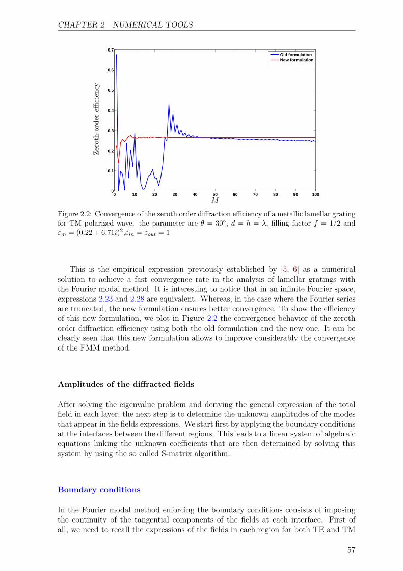
CHAPTER 2. NUMERICAL TOOLS
0 10 20 30 40 50 60 70 80 90 1000
0.1
0.2
0.3
0.4
0.5
0.6
0.7
M
Zeroth-order
efficiency
Old formulationNew formulation
Figure 2.2: Convergence of the zeroth order diffraction efficiency of a metallic lamellar gratingfor TM polarized wave. the parameter are θ = 30, d = h = λ, filling factor f = 1/2 andεm = (0.22 + 6.71i)2,εin = εout = 1
This is the empirical expression previously established by [5, 6] as a numericalsolution to achieve a fast convergence rate in the analysis of lamellar gratings withthe Fourier modal method. It is interesting to notice that in an infinite Fourier space,expressions 2.23 and 2.28 are equivalent. Whereas, in the case where the Fourier seriesare truncated, the new formulation ensures better convergence. To show the efficiencyof this new formulation, we plot in Figure 2.2 the convergence behavior of the zerothorder diffraction efficiency using both the old formulation and the new one. It can beclearly seen that this new formulation allows to improve considerably the convergenceof the FMM method.
Amplitudes of the diffracted fields
After solving the eigenvalue problem and deriving the general expression of the totalfield in each layer, the next step is to determine the unknown amplitudes of the modesthat appear in the fields expressions. We start first by applying the boundary conditionsat the interfaces between the different regions. This leads to a linear system of algebraicequations linking the unknown coefficients that are then determined by solving thissystem by using the so called S-matrix algorithm.
Boundary conditions
In the Fourier modal method enforcing the boundary conditions consists of imposingthe continuity of the tangential components of the fields at each interface. First ofall, we need to recall the expressions of the fields in each region for both TE and TM
57
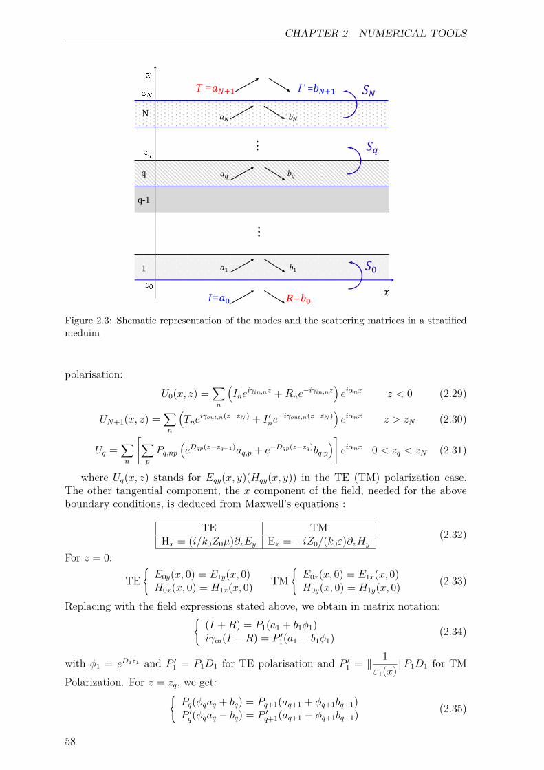
CHAPTER 2. NUMERICAL TOOLS
𝑎1 𝑏1
𝑎𝑞
𝑎𝑁 𝑏𝑁
1
q
N
𝑥
⋮
q-1
I=𝑎0 R=𝑏0
I’ =𝑏𝑁+1 T =𝑎𝑁+1
𝑆0
𝑆𝑞
𝑆𝑁
⋮
𝑏𝑞
Figure 2.3: Shematic representation of the modes and the scattering matrices in a stratifiedmeduim
polarisation:U0(x, z) =
∑n
(Ine
iγin,nz +Rne−iγin,nz
)eiαnx z < 0 (2.29)
UN+1(x, z) =∑n
(Tne
iγout,n(z−zN ) + I ′ne−iγout,n(z−zN )
)eiαnx z > zN (2.30)
Uq =∑n
[∑p
Pq,np(eDqp(z−zq−1)aq,p + e−Dqp(z−zq)bq,p
)]eiαnx 0 < zq < zN (2.31)
where Uq(x, z) stands for Eqy(x, y)(Hqy(x, y)) in the TE (TM) polarization case.The other tangential component, the x component of the field, needed for the aboveboundary conditions, is deduced from Maxwell’s equations :
TE TMHx = (i/k0Z0µ)∂zEy Ex = −iZ0/(k0ε)∂zHy
(2.32)
For z = 0:
TEE0y(x, 0) = E1y(x, 0)H0x(x, 0) = H1x(x, 0) TM
E0x(x, 0) = E1x(x, 0)H0y(x, 0) = H1y(x, 0) (2.33)
Replacing with the field expressions stated above, we obtain in matrix notation:(I +R) = P1(a1 + b1φ1)iγin(I −R) = P ′1(a1 − b1φ1) (2.34)
with φ1 = eD1z1 and P ′1 = P1D1 for TE polarisation and P ′1 = ‖ 1ε1(x)‖P1D1 for TM
Polarization. For z = zq, we get:Pq(φqaq + bq) = Pq+1(aq+1 + φq+1bq+1)P ′q(φqaq − bq) = P ′q+1(aq+1 − φq+1bq+1) (2.35)
58
CHAPTER 2. NUMERICAL TOOLS
where φq = eDq(zq−zq−1) and φq+1 = eDq+1(zq−zq+1). P ′q = PqDq for TE polarization and
P ′q = ‖ 1εq(x)‖PqDq for TM Polarization .
And for z = zN : PN(φNaN + bN) = (T + I ′)P ′N(φNaN − bN) = iγout(T − I ′)
(2.36)
With φN = eDN (zN−zN−1).Note that here R = [. . . , R−1, R0, R1 · · · ]t and T = [. . . , T−1, T0, T1 · · · ]t are the
vectors composed of amplitudes of the reflected and transmitted diffraction orders.While I = [. . . , 0, 1, 0 · · · ] and I ′ = [. . . , 0, 0, 0 · · · ] are the vectors composed of theamplitudes of incident waves. Thus, we end up with a set of 2N+2 algebraic equationslinking 2N + 2 unknown coefficients aq and bq. Many algorithms can be used to solvethis system. Among these, the most efficient and stable one is the S-matrix algorithmthat will be described in detail hereafter.
Scattering matrix Formalism
In this section, we will adopt the S-matrix formalism for our general multilayeredgrating problem in order to calculate the amplitudes of the diffracted field and show howto construct the global scattering matrix of the whole structure from the combinationof the transition matrices obtained for each interface z = zq by the use of a cascadingprocess (see figure 2.3). By definition, the scattering matrix provide a relation betweenthe outgoing amplitudes and the incoming ones and is given as follows:(
bqaq+1
)= Sq
(aqbq+1
)(2.37)
From equation (2.34), one can deduce the scattering matrix corresponding to the in-terface z = z0:(
b0a1
)=(−P0 P1P ′0 P ′1
)−1 (P0 −P1P ′0 P ′1
)(Id 00 φ1
)(a0b1
)(2.38)
(b0a1
)= S0
(a0b1
)(2.39)
S0 =(−P0 P1P ′0 P ′1
)−1 (P0 −P1P ′0 P ′1
)(Id 00 φ1
)(2.40)
In the same way, from (2.35), we can get:(bqaq+1
)=(−Pq Pq+1P ′q P ′q+1
)−1 (Pq −Pq+1P ′q P ′q+1
)(φq 00 φq+1
)(aqbq+1
)(2.41)
(bqaq+1
)= Sq
(aqbq+1
)(2.42)
Sq =(−Pq Pq+1P ′q P ′q+1
)−1 (Pq −Pq+1P ′q P ′q+1
)(φq 00 φq+1
)(2.43)
For z = zN , we find:(bNaN+1
)=(−PN PN+1P ′N P ′N+1
)−1 (PN −PN+1P ′N P ′N+1
)(φN 00 Id
)(aNbN+1
)(2.44)
59
CHAPTER 2. NUMERICAL TOOLS
(bNaN+1
)= SN
(aNbN+1
)(2.45)
SN =(−PN PN+1P ′N P ′N+1
)−1 (PN −PN+1P ′N P ′N+1
)(φN 00 Id
)(2.46)
Therefore, the global S-matrix connecting the reflection and transmission coefficientscan be expressed as: (
RT
)= S
(II ′
)(2.47)
S = S0 ? S1 ? .... ? SN (2.48)where the ? product S = Sa ? Sb between two matrices Sa and Sb is given by:
S11 = Sa11 + Sa12(1− Sb11Sa22)−1Sb11S
a21
S12 = Sa12(1− Sb11Sa22)−1Sb12
S21 = Sb21(1− Sa22Sb11)−1Sa21
S22 = Sb22 + Sb21(1− Sa22Sb11)−1Sa22S
b12
(2.49)
Finally, once this calculation is achieved and thereby the amplitudes of the diffractedfields are obtained, one can readily have access to the quantities of interests such asthe diffraction efficiency and fields distributions
2.2.2 Fourier Modal Method with spatial adaptative resolu-tion (FMM-ASR)
In the previous section, we have shown that the Fourier Modal method suffers from aslow convergence problems in the case of TM polarisation. This has been overcome byapplying the correct Fourier factorisation rules for discontinuous functions. Althoughthis implementation has tremendously improved the convergence of the FMM method,there remained the problem of so called Gibbs phenomenon at the discontinuity pointswhich inhibit the convergence of the Fourier series yielding to a slow convergence,especially in the case of metallic gratings. To tackle this latter limitation and acceleratethe convergence, Granet suggested in 1999 [9] to employ a new coordinate systemthat increases the spatial resolution in the neighborhood of the discontinuities of thepermittivity profile by stretching the coordinate around them. This concept is knownas Adaptative Spatial resolution (ASR). In 2001, the original approach proposed byGranet, was extented and reformulated for treating multilayered gratings with differenttransitions [10]. This latter modified approach involved two main steps, the first oneis to solve the eigenvalue problem for each layer with its own transformed coordinatesystem and the second step is to bring all the fields back to the original space for solvingthe boundary conditions. Despite the effectiveness of this modified formulation, it had amajor drawback : the computation of transformation matrices for each layer destroysthe stability of the S-matrix and it requires a nonnegligible additional computationtime. Later, in [11, 12], a numerical improvement of the FMM ASR was obtained byintroducing a much more stable formulation of the eigenvalue problem. They proposedan elegant and smart way consisting of solving merely the eigenvalue problem for onlyone homogeneous region and deducing then the solution of all the eigenvalue problemscorresponding to remainning homogeneous regions from this one. This allowed toavoid to solving the eigenvalue problem in all the homogeneous regions leading todrastic reduction of the computational load. In this section, we are going to describe
60
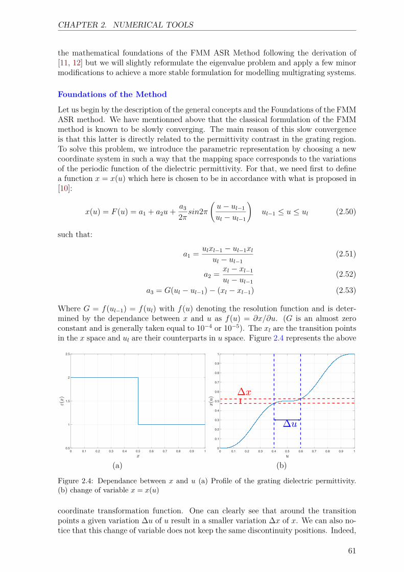
CHAPTER 2. NUMERICAL TOOLS
the mathematical foundations of the FMM ASR Method following the derivation of[11, 12] but we will slightly reformulate the eigenvalue problem and apply a few minormodifications to achieve a more stable formulation for modelling multigrating systems.
Foundations of the Method
Let us begin by the description of the general concepts and the Foundations of the FMMASR method. We have mentionned above that the classical formulation of the FMMmethod is known to be slowly converging. The main reason of this slow convergenceis that this latter is directly related to the permittivity contrast in the grating region.To solve this problem, we introduce the parametric representation by choosing a newcoordinate system in such a way that the mapping space corresponds to the variationsof the periodic function of the dielectric permittivity. For that, we need first to definea function x = x(u) which here is chosen to be in accordance with what is proposed in[10]:
x(u) = F (u) = a1 + a2u+ a3
2πsin2π(u− ul−1
ul − ul−1
)ul−1 ≤ u ≤ ul (2.50)
such that:
a1 = ulxl−1 − ul−1xlul − ul−1
(2.51)
a2 = xl − xl−1
ul − ul−1(2.52)
a3 = G(ul − ul−1)− (xl − xl−1) (2.53)
Where G = f(ul−1) = f(ul) with f(u) denoting the resolution function and is deter-mined by the dependance between x and u as f(u) = ∂x/∂u. (G is an almost zeroconstant and is generally taken equal to 10−4 or 10−5). The xl are the transition pointsin the x space and ul are their counterparts in u space. Figure 2.4 represents the above
0 0.1 0.2 0.3 0.4 0.5 0.6 0.7 0.8 0.9 10.5
1
1.5
2
2.5
(a)
0 0.1 0.2 0.3 0.4 0.5 0.6 0.7 0.8 0.9 10
0.1
0.2
0.3
0.4
0.5
0.6
0.7
0.8
0.9
1
(b)
Figure 2.4: Dependance between x and u (a) Profile of the grating dielectric permittivity.(b) change of variable x = x(u)
coordinate transformation function. One can clearly see that around the transitionpoints a given variation ∆u of u result in a smaller variation ∆x of x. We can also no-tice that this change of variable does not keep the same discontinuity positions. Indeed,
61
CHAPTER 2. NUMERICAL TOOLS
the discontinuities in the new basis can differ from the old basis and their positions aregiven by dividing the period d into equal parts according to the number of transitions.Furthermore, the new function is a periodic function with the same period as the di-electric permittivity of the grating and its derivative is minimal at the discontinuitiespoints.
Eigenvalue problem
We apply now the above variable change, then we get :
∂
∂x→ ∂u
∂x
∂
∂u= 1f
∂
∂u(2.54)
Using this notation equations 2.4 and 2.20 become:
1f
∂
∂u
(1f
∂Eqy∂u
)+ ∂2Eqy
∂z2 + k20εq(u)Eqy = 0 (TE) (2.55)
1f
∂
∂u
(1
εq(u)1f
∂Hqy
∂u
)+ 1εq(u)
∂2Hqy
∂z2 + k20Hqy = 0 (TM) (2.56)
In the u space the fields Ey and Hy are also pseudoperiodic with period d and thusthey can be expressed as a pseudo-Fourier series:
Uq(u, z) =∑n
Uqn(z)eiαnu (2.57)
Where U q represents either the transverse electric field for the TE polarization ortransverse magnetic field for the TM polarization. Now, inserting the expansion (2.57)into (2.55) and (2.56), written in Fourier space and using the correct rules of Fourierfactorization and the matrix notations, we obtain the desired eigenvalue problem:
d2Eq(z)dz2 =
(‖ 1f‖α‖ 1
f‖α− k2
0εq
)Eq(z) = ATEq Eq(z) (TE) (2.58)
d2Hq(z)dz2 = ‖ 1
εq(x)‖−1(‖ 1f‖α‖εq(x)‖−1‖ 1
f‖ α− k2
0Id
)Hq = ATMq Hq (TM) (2.59)
With ‖ 1f‖ being the Toeplitz matrix formed from the fourier coefficients of 1/f . Having
chosen a fitting coordinate u and solving the corresponding eigenvalue problem, thefields in each region q can be written in the same way as for the FMM method as:
Uq =∑n
[∑p
Pq,np(eDqp(z−zq−1)aq,p + e−Dqp(z−zq)bq,p
)]eiαnu q ∈ [0 . . . N + 1] (2.60)
where aq,p and bq,p are the unknown amplitudes that are to be determined by match-ing boundary conditions. It is important at this stage to emphasize that the exacteigenvalues do not depend on the chosen coordinates. While, the eigenvectors dependon the choice of the coordinate system and should therefore be projected on the samebasis for applying the boundary conditions.
Now, To find the unknown coefficients and afterwards the total fields expressions inall the regions, we proceed as follows: First, we still work completly in the transformed
62
CHAPTER 2. NUMERICAL TOOLS
space u using only one coordinate system x(u) for all the regions of the structure. Inthis situation, it is necessary to solve the eigenvalue problem in each layer and evenin the incident and transmission regions. Let us begin with the incident region. Theeigenvalue equation corresponding to this region can be given for both TE and TMpolarisation by the following equation:
d2U0(z)dz2 =
(‖ 1f‖α‖ 1
f‖α− k2
0εinId
)U0(z) = A0U0(z) (2.61)
A0 = ‖ 1f‖α‖ 1
f‖α− k2
0εinId (2.62)
Then, After solving this eigenvalue problem , we can get U0 in terms of the eigenvaluematrix D0 and the corresponding eigenvector matrix P0 as follows:
U0 = P0(eD0za0 + e−D0zb0) (2.63)
Consider now another homogeneous layer labeled by q and caracterized by its permit-tivity εq. The Aq matrix that corresponds to this medium can be written as:
Aq = ‖ 1f‖α‖ 1
f‖α− k2
0εqId (2.64)
Subtracting (2.64) and (2.62), One gets :
Aq = A0 + k20(εin − εq)Id (2.65)
Left multiplying by P0 and right multiplying by its inverse gives:
P0AqP−1q = D2
0 + k20(ε0 − εq)Id (2.66)
From this equation, one can clearly see that P0 can be also an eigenvector of Aqassociated to the eigenvalues D2
0 + k20(ε0 − εq)Id. As a result, all the homogeneous
regions are equivalent to the incident one since they share the same eigenvectors. Oncethe eigenvalues for all layers are solved and all field expressions are determined inspace u, by following the same way as we did in the classical FMM such that applyingthe boundary conditions and using the S-matrix algorithm, one can easily find thedistribution of the fields and then all diffraction efficiencies. The final step in ourstrategy is to transformed back the fields to the original space x. To this end , it isnecessary to projet the term eiαnu on the Fourier basis in x space. This can be achievedby the help of the transformation matrix [K] , whose elements (p,m) are given by:
[K]pm = 1d
∫ d
0f(u)exp(−iαpx(u) + iαmu) du (2.67)
Hence, all vectors Uu defined in the new coordinate system (u, y, z) can be straightfor-wardly transformed in the originate cartesien system (x, y, z) as follows:
Ux = [K]Uu (2.68)
In the end, it should be pointed out that this way of proceeding has the great advan-tage of using the same Fourier basis for all layers. This allows to write the continuityequations of the electromagnetic field through the interfaces without projecting thisone on the common basis of the original x space leading to a significant reduction ofthe computational cost. Another advantage for this strategy is that it allows to avoidthe instability problems coming from the transformation matrix [K].
63

CHAPTER 2. NUMERICAL TOOLS
2.2.3 Aperiodic Fourier Modal Method: FMM with PMLSo far, we have shown that the FMM method is a versatile and poweful tool for mod-elling periodic structures. However, several systems in nanophotonics are non-periodicstructures such that optical resonators [13], photonic crystal fibers [14], individualmetallic nano-particles [15] and photonic crystal waveguides [16]. Hence, it is of greatimportance to investigate the optical properties of non-periodic structures. One simpleand efficient way to simulate a general aperiodic structure by the use of the FMMmethod, is to insert artificial absorbing layers in the boundaries between adjacent peri-ods in order to truncate the infinite periodic system volume to a finite volume. Theseabsorbing layers should completely inhibit the interactions between neighboring peri-ods by minimizing backward parasitic reflections of light into the structure. In fact, thescattered light in a period is absorbed by these layers without reflection and the fieldsat the period boundary should decrease to zero. In this way, the single periods can beconsidered as isolated systems (see Figure 2.5). Such layer is called perfectly matched
Figure 2.5: Schematic illustration of a aperiodic structure (a single rectangular groove) andit equivalent artificially periodized system
layer (PML) and was first proposed by Berenger [17] in 1994 for the finite-differencetime domain (FDTD) method. Later, the original aproach was extented to three di-mensions by Katz and al [18] and to anisotropic media by Sacks and al [19]. Anotherinteresting formulation of The (PML) technique was introduced by Chew and al [20]through the complex coordinate stretching concept which is essentially the analyticalextension of the electromagnetic field in the complex space. It is on this last approachthat we will focus in the following.
In practical computations, the PML can be introduced in the computational domainusing a coordinate transformation. By this coordinate transformation, the boundariesexist in a complex space providing absorbing boundary conditions without reflection.Furthemore, the new absorbing coordinate system does not change Maxwell’s equationsas well as the wave propagation equation into the PML layer. An example of a complexcoordinate transformation can be given by:
S(x) =
1− iη if x ∈ [0, ePML] ∪ [d− ePML, d]1 otherwise (2.69)
Inside the PML, the complex variable change x is expressed as:
x =∫ x
0S(x) dx (2.70)
64
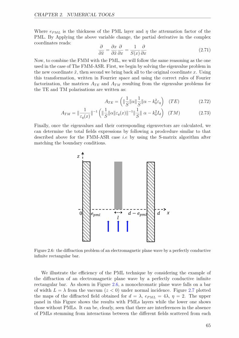
CHAPTER 2. NUMERICAL TOOLS
Where ePML is the thickness of the PML layer and η the attenuation factor of thePML. By Applying the above variable change, the partial derivative in the complexcoordinates reads:
∂
∂x= ∂x
∂x
∂
∂x= 1S(x)
∂
∂x(2.71)
Now, to combine the FMM with the PML, we will follow the same reasoning as the oneused in the case of The FMM-ASR. First, we begin by solving the eigenvalue problem inthe new coordinate x, then second we bring back all to the original coordinate x. Usingthis transformation, written in Fourrier space and using the correct rules of Fourierfactorization, the matrices ATE and ATM resulting from the eigenvalue problems forthe TE and TM polarisations are written as:
ATE =(‖ 1S‖α‖ 1
S‖α− k2
0εq
)(TE) (2.72)
ATM = ‖ 1εq(x)‖
−1(‖ 1S‖α‖εq(x)‖−1‖ 1
S‖ α− k2
0Id
)(TM) (2.73)
Finally, once the eigenvalues and their corresponding eigenvectors are calculated, wecan determine the total fields expressions by following a prodcedure similar to thatdescribed above for the FMM-ASR case i.e by using the S-matrix algorithm aftermatching the boundary conditions.
𝑧
𝑥 𝑑 𝑙
𝑒𝑝𝑚𝑙 0 𝑑 − 𝑒𝑝𝑚𝑙
Figure 2.6: the diffraction problem of an electromagnetic plane wave by a perfectly conductiveinfinite rectangular bar.
We illustrate the efficiency of the PML technique by considering the example ofthe diffraction of an electromagnetic plane wave by a perfectly conductive infiniterectangular bar. As shown in Figure 2.6, a monochromatic plane wave falls on a barof width L = λ from the vaccum (z < 0) under normal incidence. Figure 2.7 plottedthe maps of the diffracted field obtained for d = λ, ePML = 4λ, η = 2. The upperpanel in this Figure shows the results with PMLs layers while the lower one showsthose without PMLs. It can be, clearly, seen that there are interferences in the absenceof PMLs stemming from interactions between the different fields scattered from each
65
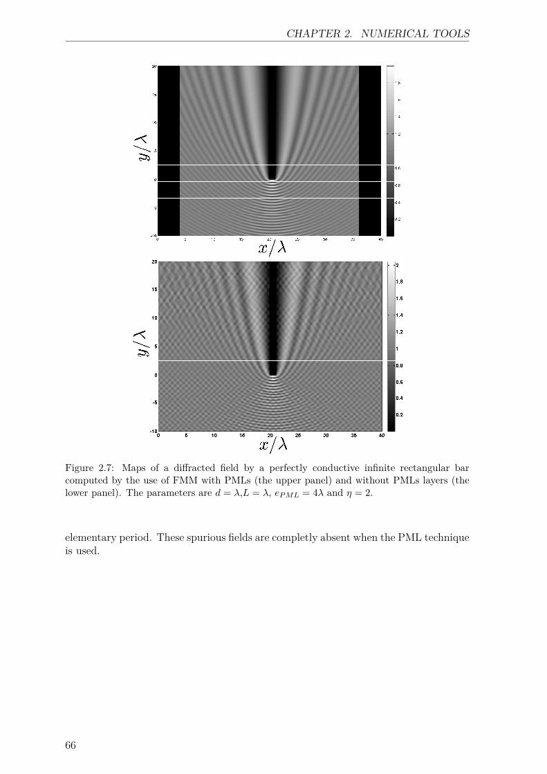
CHAPTER 2. NUMERICAL TOOLS
Figure 2.7: Maps of a diffracted field by a perfectly conductive infinite rectangular barcomputed by the use of FMM with PMLs (the upper panel) and without PMLs layers (thelower panel). The parameters are d = λ,L = λ, ePML = 4λ and η = 2.
elementary period. These spurious fields are completly absent when the PML techniqueis used.
66
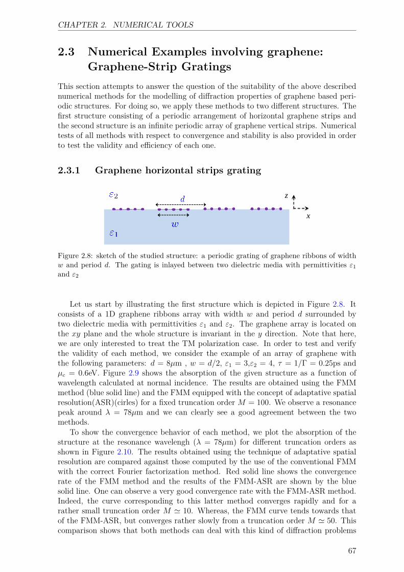
CHAPTER 2. NUMERICAL TOOLS
2.3 Numerical Examples involving graphene:Graphene-Strip Gratings
This section attempts to answer the question of the suitability of the above describednumerical methods for the modelling of diffraction properties of graphene based peri-odic structures. For doing so, we apply these methods to two different structures. Thefirst structure consisting of a periodic arrangement of horizontal graphene strips andthe second structure is an infinite periodic array of graphene vertical strips. Numericaltests of all methods with respect to convergence and stability is also provided in orderto test the validity and efficiency of each one.
2.3.1 Graphene horizontal strips grating
z
x
Figure 2.8: sketch of the studied structure: a periodic grating of graphene ribbons of widthw and period d. The gating is inlayed between two dielectric media with permittivities ε1and ε2
Let us start by illustrating the first structure which is depicted in Figure 2.8. Itconsists of a 1D graphene ribbons array with width w and period d surrounded bytwo dielectric media with permittivities ε1 and ε2. The graphene array is located onthe xy plane and the whole structure is invariant in the y direction. Note that here,we are only interested to treat the TM polarization case. In order to test and verifythe validity of each method, we consider the example of an array of graphene withthe following parameters: d = 8µm , w = d/2, ε1 = 3,ε2 = 4, τ = 1/Γ = 0.25ps andµc = 0.6eV. Figure 2.9 shows the absorption of the given structure as a function ofwavelength calculated at normal incidence. The results are obtained using the FMMmethod (blue solid line) and the FMM equipped with the concept of adaptative spatialresolution(ASR)(cirles) for a fixed truncation order M = 100. We observe a resonancepeak around λ = 78µm and we can clearly see a good agreement between the twomethods.
To show the convergence behavior of each method, we plot the absorption of thestructure at the resonance wavelengh (λ = 78µm) for different truncation orders asshown in Figure 2.10. The results obtained using the technique of adaptative spatialresolution are compared against those computed by the use of the conventional FMMwith the correct Fourier factorization method. Red solid line shows the convergencerate of the FMM method and the results of the FMM-ASR are shown by the bluesolid line. One can observe a very good convergence rate with the FMM-ASR method.Indeed, the curve corresponding to this latter method converges rapidly and for arather small truncation order M ' 10. Whereas, the FMM curve tends towards thatof the FMM-ASR, but converges rather slowly from a truncation order M ' 50. Thiscomparison shows that both methods can deal with this kind of diffraction problems
67
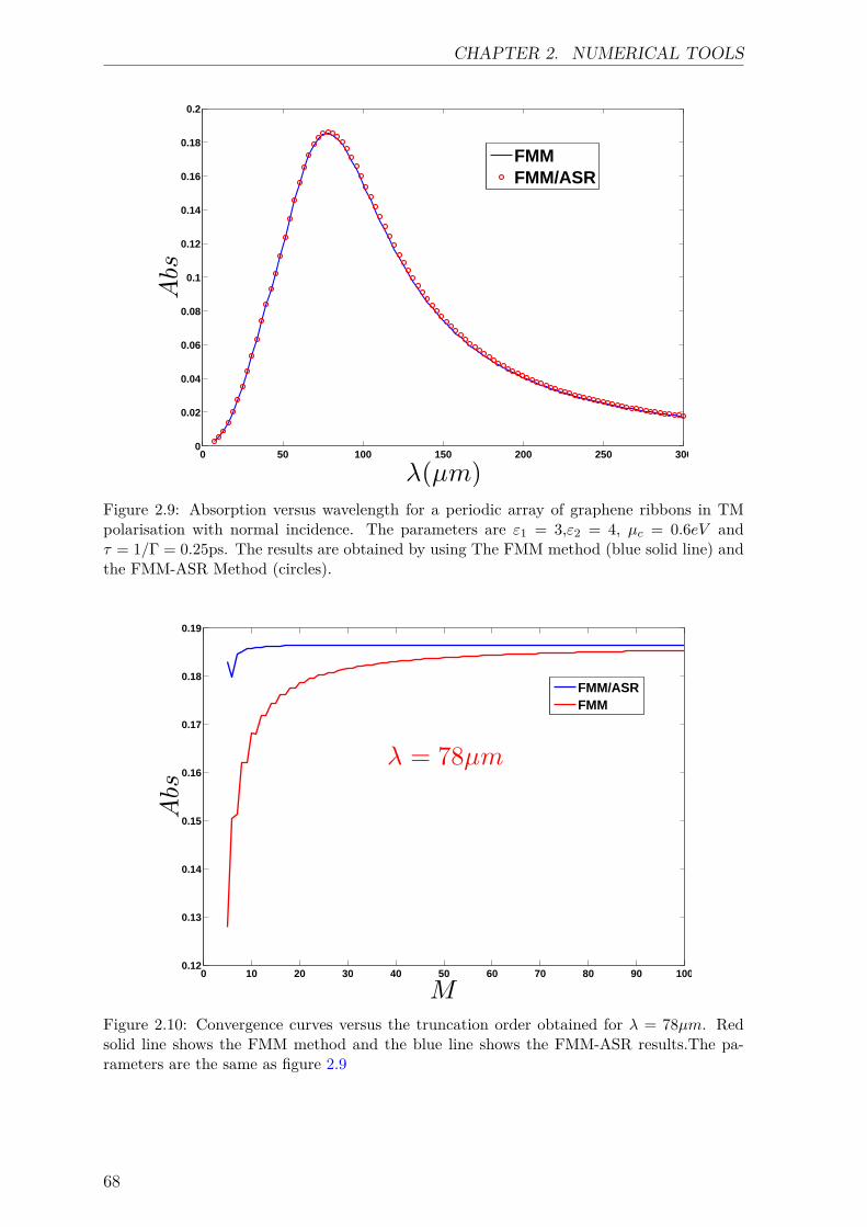
CHAPTER 2. NUMERICAL TOOLS
0 50 100 150 200 250 3000
0.02
0.04
0.06
0.08
0.1
0.12
0.14
0.16
0.18
0.2
Abs
λ(µm)
FMMFMM/ASR
Figure 2.9: Absorption versus wavelength for a periodic array of graphene ribbons in TMpolarisation with normal incidence. The parameters are ε1 = 3,ε2 = 4, µc = 0.6eV andτ = 1/Γ = 0.25ps. The results are obtained by using The FMM method (blue solid line) andthe FMM-ASR Method (circles).
0 10 20 30 40 50 60 70 80 90 1000.12
0.13
0.14
0.15
0.16
0.17
0.18
0.19
Abs
M
λ = 78µm
FMM/ASRFMM
Figure 2.10: Convergence curves versus the truncation order obtained for λ = 78µm. Redsolid line shows the FMM method and the blue line shows the FMM-ASR results.The pa-rameters are the same as figure 2.9
68
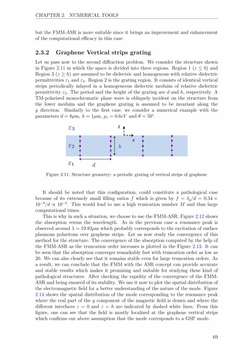
CHAPTER 2. NUMERICAL TOOLS
but the FMM-ASR is more suitable since it brings an improvement and enhancementof the computational efficacy in this case.
2.3.2 Graphene Vertical strips gratingLet us pass now to the second diffraction problem. We consider the structure shownin Figure 2.11 in which the space is divided into three regions. Region 1 (z ≤ 0) andRegion 3 (z ≥ h) are assumed to be dielectric and homogenous with relative dielectricpermittivities ε1 and ε3. Region 2 is the grating region. It consists of identical verticalstrips periodically inlayed in a homogeneous dielectric meduim of relative dielectricpermittivity ε2. The period and the height of the grating are d and h, respectively. ATM-polarized monochromatic plane wave is obliquely incident on the structure fromthe lower meduim and the graphene grating is assumed to be invariant along they direction. Similarly to the first case, we consider a numerical example with theparameters d = 8µm, h = 1µm, µc = 0.6eV and θ = 50.
z
x
Figure 2.11: Structure geometry: a periodic grating of vertical strips of graphene
It should be noted that this configuration, could constitute a pathological casebecause of its extremely small filling ratios f which is given by f = δg/d = 0.34 ×10⁻⁹/d ∝ 10−3. This would lead to use a high truncation number M and thus largecomputational times.
This is why in such a situation, we choose to use the FMM-ASR. Figure 2.12 showsthe absorption versus the wavelength. As in the previous case a resonance peak isobserved around λ = 19.82µm which probably corresponds to the excitation of surfaceplasmons polaritons over graphene strips. Let us now study the convergence of thismethod for the structure. The convergence of the absorption computed by the help ofthe FMM-ASR as the truncation order increases is plotted in the Figure 2.13. It canbe seen that the absorption converges remarkably fast with truncation order as low as20. We can also clearly see that it remains stable even for large truncation orders. Asa result, we can conclude that the FMM with the ASR concept can provide accurateand stable results which makes it promising and suitable for studying these kind ofpathological structures. After checking the rapidity of the convergence of the FMM-ASR and being ensured of its stability. We use it now to plot the spatial distribution ofthe electromagnetic field for a better understanding of the nature of the mode. Figure2.14 shows the spatial distribution of the mode corresponding to the resonance peakwhere the real part of the y component of the magnetic field is drawn and where thedifferent interfaces z = 0 and z = h are indicated by dashed white lines. From thisfigure, one can see that the field is mostly localized at the graphene vertical stripswhich confirms our above assumption that the mode corresponds to a GSP mode.
69
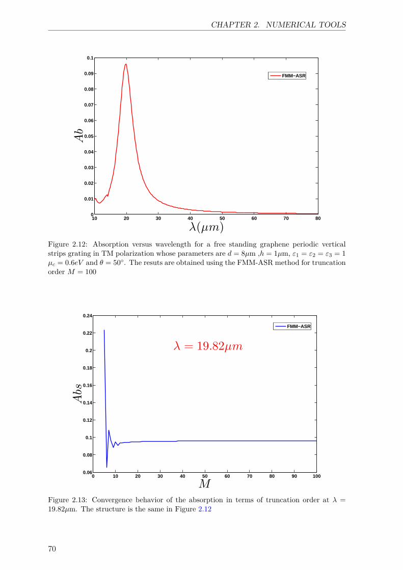
CHAPTER 2. NUMERICAL TOOLS
10 20 30 40 50 60 70 800
0.01
0.02
0.03
0.04
0.05
0.06
0.07
0.08
0.09
0.1
λ(µm)
Ab
FMM−ASR
Figure 2.12: Absorption versus wavelength for a free standing graphene periodic verticalstrips grating in TM polarization whose parameters are d = 8µm ,h = 1µm, ε1 = ε2 = ε3 = 1µc = 0.6eV and θ = 50. The resuts are obtained using the FMM-ASR method for truncationorder M = 100
0 10 20 30 40 50 60 70 80 90 1000.06
0.08
0.1
0.12
0.14
0.16
0.18
0.2
0.22
0.24
M
Abs
λ = 19.82µm
FMM−ASR
Figure 2.13: Convergence behavior of the absorption in terms of truncation order at λ =19.82µm. The structure is the same in Figure 2.12
70
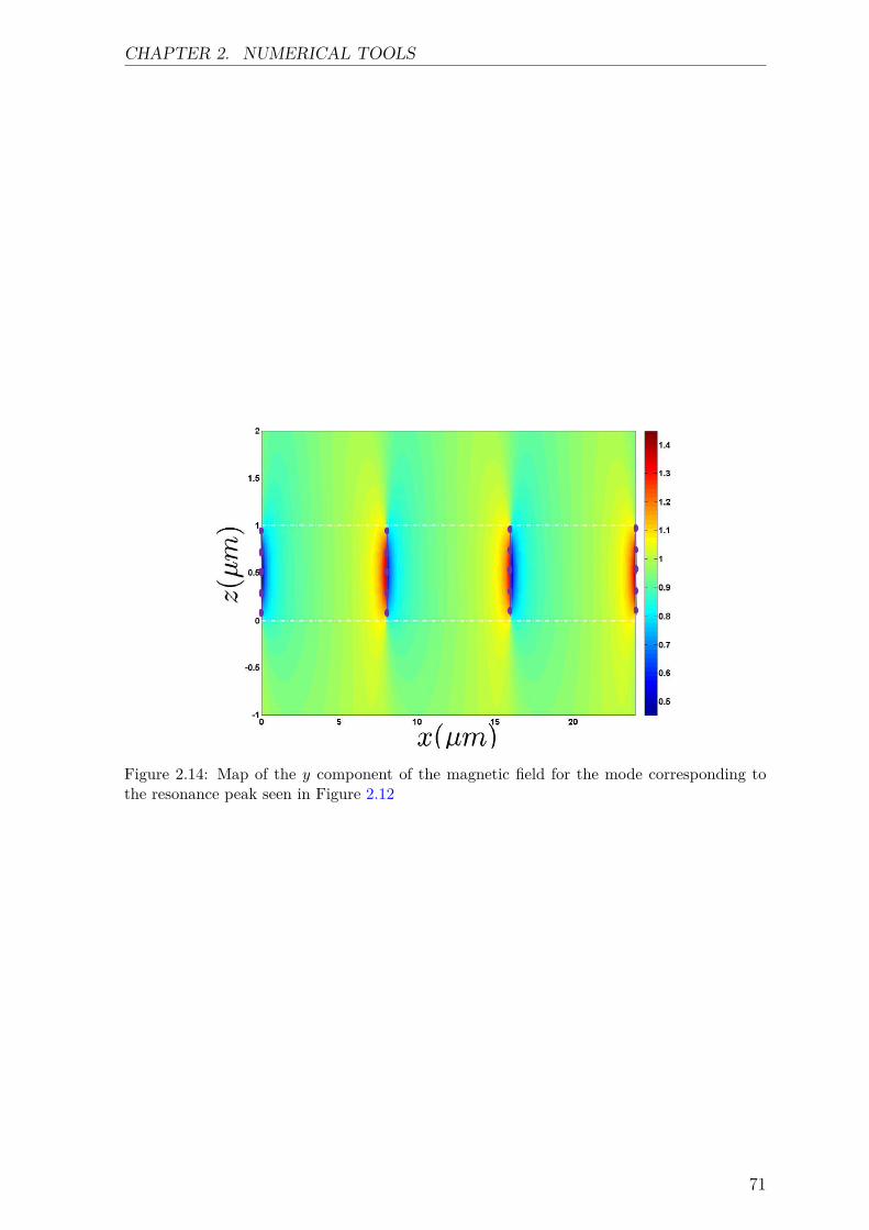
CHAPTER 2. NUMERICAL TOOLS
Figure 2.14: Map of the y component of the magnetic field for the mode corresponding tothe resonance peak seen in Figure 2.12
71
CHAPTER 2. NUMERICAL TOOLS
2.4 ConclusionsIn conclusion, we have presented the Fourier modal method (FMM) under its classicalform as well as the Fourier modal method equipped with the concept of adaptive spatialresolution (FMM-ASR) in order to adapt them for investigating general multilayeredgratings structures comprising graphene gratings. The FMM method is demontratedto be a poweful tool that enables to calculate the reflectance and transmittance spectrafor periodic structures as well as the fields distributions in these structures. However,it is shown that when the permittivity function is discontinuous, the latter methodis known to converge slowly in the case of TM polarization, especifically for metallicgratings. This problem was attributed to the use of wrong Fourier factorization rules.We have shown also that even the corret rules of Fourier factorization are applied,there remained a problem which is originated from the uniform spatial resolution ofthe Fourier expansion around the discontinuities points of the permitivity that doesnot take into account the genuine profil of the permittivity. This problem has beenovercome by the help of the concept of adaptative spatial resolution that allows toincrease the spatial resolution at the level of the discontinuities points using a newcoordinate system. We have seen that the implementation of this technique led to adrastic and significantly improvement in the performance of the FMM method in termof convergence and stability. We have then extented the FMM method to aperiodicstructures by placing perfectly matched layers at the lateral sides of the computationaldomain. Finally, in the last section, in order to test the reliability of these methods fortreating graphene gratings, we have applied them to two different configurations: thefirst structure was a 1D graphene ribbon array and the second one a periodic gratingof vertical strips of graphene. The comparison between the results obtained using theclassical FMM with the correct Fourier factorization method and those computed bythe FMM-ASR have shown that a better convergence rate has been achieved withthe FMM-ASR method for both configurations. This point makes it best suited formodeling these kind of structures.
72
Bibliography
[1] K. Knop. Rigorous diffraction theory for transmission phase gratings with deeprectangular grooves. J. Opt. Soc. Am., 68(9):1206–1210, Sep 1978. 52
[2] M. G. Moharam and T. K. Gaylord. Rigorous coupled-wave analysis of planar-grating diffraction. J. Opt. Soc. Am., 71(7):811–818, Jul 1981. 52
[3] M. G. Moharam and T. K. Gaylord. Diffraction analysis of dielectric surface-reliefgratings. J. Opt. Soc. Am., 72(10):1385–1392, Oct 1982. 52
[4] Lifeng Li and Charles W. Haggans. Convergence of the coupled-wave method formetallic lamellar diffraction gratings. J. Opt. Soc. Am. A, 10(6):1184–1189, Jun1993. 55
[5] G. Granet and B. Guizal. Efficient implementation of the coupled-wave methodfor metallic lamellar gratings in tm polarization. J. Opt. Soc. Am. A, 13(5):1019–1023, May 1996. 56
[6] Philippe Lalanne and G. Michael Morris. Highly improved convergence of thecoupled-wave method for tm polarization. J. Opt. Soc. Am. A, 13(4):779–784,Apr 1996. 56
[7] Lifeng Li. Use of fourier series in the analysis of discontinuous periodic structures.J. Opt. Soc. Am. A, 13(9):1870–1876, Sep 1996. 56
[8] Lifeng Li. Formulation and comparison of two recursive matrix algorithms formodeling layered diffraction gratings. J. Opt. Soc. Am. A, 13(5):1024–1035, May1996. 56
[9] Gérard Granet. Reformulation of the lamellar grating problem through the conceptof adaptive spatial resolution. J. Opt. Soc. Am. A, 16(10):2510–2516, Oct 1999.60
[10] T. Vallius and M. Honkanen. Reformulation of the fourier modal method withadaptive spatial resolution: application to multilevel profiles. Opt. Express,10(1):24–34, Jan 2002. 60, 61
[11] B. Guizal, H. Yala, and D. Felbacq. Reformulation of the eigenvalue problem in thefourier modal method with spatial adaptive resolution. Opt. Lett., 34(18):2790–2792, Sep 2009. 60, 61
73
BIBLIOGRAPHY
[12] Hakim Yala, Brahim Guizal, and Didier Felbacq. Fourier modal method withspatial adaptive resolution for structures comprising homogeneous layers. J. Opt.Soc. Am. A, 26(12):2567–2570, Dec 2009. 60, 61
[13] S. Spillane D. Armani, T. Kippenberg and K. Vahala. Ultra-high-q toroid micro-cavity on a chip. Nature., 421:925–928, 2003. 64
[14] Knight JC. Photonic crystal fibres. Nature., 424:847–851, 2003. 64
[15] N. Feth M. Konig M. Husnik, M. Klein. Absolute extinction cross-section ofindividual magnetic split-ring resonators. Nat. Photon., 2:614, 2008. 64
[16] Hamann HF McNab SJ Vlasov YA, O’Boyle M. Active control of slow light on achip with photonic crystal waveguides. Nature., 438:65, 2005. 64
[17] Jean-Pierre Berenger. A perfectly matched layer for the absorption of electromag-netic waves. Journal of Computational Physics, 114(2):185 – 200, 1994. 64
[18] D. S. Katz, E. T. Thiele, and A. Taflove. Validation and extension to threedimensions of the berenger pml absorbing boundary condition for fd-td meshes.IEEE Microwave and Guided Wave Letters, 4(8):268–270, 1994. 64
[19] Z. S. Sacks, D. M. Kingsland, R. Lee, and Jin-Fa Lee. A perfectly matchedanisotropic absorber for use as an absorbing boundary condition. IEEE Transac-tions on Antennas and Propagation, 43(12):1460–1463, 1995. 64
[20] Weng Cho Chew and William H. Weedon. A 3d perfectly matched medium frommodified maxwell’s equations with stretched coordinates. Microwave and OpticalTechnology Letters, 7(13):599–604, 1994. 64
74
Part II
Hybrid Plasmonic Structures Basedon Graphene
75

Chapter 3Metallic slit grating-Graphene compositestructure
The knowledge of anything,since all things have causes, isnot acquired or complete unlessit is known by its causes.
Avicenna
Contents3.1 Extraordinary optical transmission . . . . . . . . . . . . . . 78
3.1.1 Extraordinary transmission : Two resonant mechanisms . . . 793.2 Coupling between subwavelength nano-slits lattice modes
and metal-insulator-graphene cavity modes: A semi-analyticalmodel . . . . . . . . . . . . . . . . . . . . . . . . . . . . . . . 82
3.2.1 Physical system . . . . . . . . . . . . . . . . . . . . . . . . . . 823.2.2 Modal analysis of the system . . . . . . . . . . . . . . . . . . 843.2.3 Analysis of the Lorentz and Fano resonances of the system . 89
3.3 Conclusions . . . . . . . . . . . . . . . . . . . . . . . . . . . . 92
Extraordinary optical transmission (EOT) [1, 2, 3] through an opaque metallicfilm perforated with subwavelength slits has received great interest over the past twodecades because of its numerous applications in optoelectronics such as mid-infraredspatial light modulators, linear signal processing or biosensing. Many theoretical andexperimental works were carried out in order to understand and predict EOT and, espe-cially, to highlight the role of surface waves [4, 5, 6, 7]. More recently K.Edee provided,in [8], a simple and versatile model, for this phenomenon, involving only a specific modeliving in an equivalent homogeneous medium and a phase correction to account for sur-face waves. The proposed semi-analytical model is valid from the visible to the infraredfrequencies ranges. On the other hand, significant efforts have been made to createactive or tunable plasmonic devices operating from THz to mid-infrared frequencies.Thanks to its extraordinary electronic and optical properties, graphene, a single layerof arranged carbon atoms has attracted much attention in the last years. This mate-rial can support both TE and TM SPPs and can exhibit some remarkable properties
77
CHAPTER 3. METALLIC SLIT GRATING-GRAPHENE COMPOSITESTRUCTURE
such as flexible wideband tunability that can be exploited to build new plasmonic de-vices. The main challenge when designing a graphene-plasmon-based device is how toefficiently excite GSPs with a free space electromagnetic wave since there is a huge mo-mentum mismatch between the two electromagnetic modes. Generally two strategiesare used. The first one consists in patterning the graphene sheet into nano-resonators[9, 10, 11, 12, 13, 14, 15, 16, 17, 18, 19, 20, 21]. In this case a surface plasmon of the ob-tained structure which is very similar to the GSP is excited and an absorption rate closeto 100% can be reached. In particular, in [15], the authors presented an electricallytunable hybrid graphene-gold Fano resonator which consists of a square graphene patchand a square gold frame. They showed that the destructive interference between thenarrow- and broadband dipolar surface plasmons, which are induced respectively on thesurfaces of the graphene patch and the gold frame, leads to the plasmonic equivalentof electromagnetically induced transparency (EIT). However patterning a graphenesheet requires sophisticated processing techniques and deteriorates its extraordinarymobility. The second strategy consists in using a continuous graphene sheet instead ofundesirable patterned graphene structures[22, 23, 24, 25, 26, 27]. In this approach, thegraphene sheet is coupled with nano-scatterers such as nano-particles, or nano-gratings.Gao et al. proposed [22] to use diffractive gratings to create a guided-wave resonancein the graphene film that can be directly observed from the normal incidence trans-mission spectra. In [27] Zhao et al. studied a tunable plasmon-induced-transparencyeffect in a grating-coupled double-layer graphene hybrid system at far-infrared frequen-cies. They used a diffractive grating to couple a normally incident wave and plasmonicmodes living in a system of two graphene-films separated by a spacer. Zhang et al.[24] investigated optical field enhancements, in a wide mid-infrared band, originatingfrom the excitation of GSPs, by introducing a dielectric grating underneath a graphenemonolayer. Usually, the optical response of all grating-graphene based structures listedabove is performed thanks to the finite difference time domain method (FDTD) or tothe finite element method (FEM). However the features of these hybrid graphene-resonators devices are often linked to a plasmon resonance phenomenon. Therefore amodal method allowing for a full modal analysis of the couplings occurring in theseplasmonic systems seems more suitable. In this chapter, we investigate an optical tun-able plasmonic system involving two fundamental phenomena: an EOT phenomenonand a metal-insulator-graphene (M-I-G) cavity plasmon mode excitation. We proposea semi-analytical model allowing to fully describe the spectrum behaviour of an hy-brid plasmonic structure, made of a 1D periodic subwavelength slits array depositedon an insulator/graphene layers. The spectrum of the proposed hybrid system ex-hibits Lorentz and Fano-like resonances and also other broadband and narrow bandresonances that are efficiently captured by our simplified model. In order to explainthe origin of this particular behaviour, we first split the hybrid system into a coupleof sub-systems. Second, thanks to a modal analysis through the polynomial modalmethod (PMM: one of the most efficient methods for modeling the electromagneticproperties of periodic structures and available in our laboratory) [28, 29, 30, 31] andthe FMM-ASR presented in chapter 2, we demonstrate that the scattering parametersof each sub-system can be computed through a concept of weak and strong couplings.Finally we provide analytical expressions of the reflection and transmission coefficientsof the structure and describe the mechanisms leading to Lorentz and Fano resonancesoccurring in it.
78
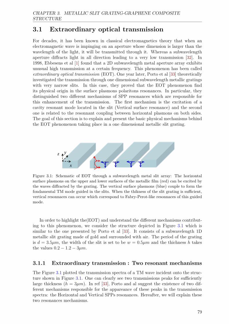
CHAPTER 3. METALLIC SLIT GRATING-GRAPHENE COMPOSITESTRUCTURE
3.1 Extraordinary optical transmissionFor decades, it has been known in classical electromagnetics theory that when anelectromagnetic wave is impinging on an aperture whose dimension is larger than thewavelength of the light, it will be transmitted through it. Whereas a subwavelengthaperture diffracts light in all direction leading to a very low transmission [32]. In1998, Ebbesens et al [1] found that a 2D subwavelength metal aperture array exhibitsunusual high transmission at a certain frequency. This phenomenon has been calledextraordinary optical transmission (EOT). One year later, Porto et al [33] theoreticallyinvestigated the transmission through one dimensional subwavelength metallic gratingswith very narrow slits. In this case, they proved that the EOT phenomenon findits physical origin in the surface plasmons polaritons resonances. In particular, theydistinguished two different mechanisms of SPP resonances which are responsible forthis enhancement of the transmission. The first mechanism is the excitation of acavity resonant mode located in the slit (Vertical surface resonance) and the secondone is related to the resonnant coupling between horizontal plasmons on both sides.The goal of this section is to explain and present the basic physical mechanisms behindthe EOT phenomenon taking place in a one dimensional metallic slit grating.
z
x
y
Figure 3.1: Schematic of EOT through a subwavelength metal slit array: The horizontalsurface plasmons on the upper and lower surfaces of the metallic film (red) can be excited bythe waves diffracted by the grating. The vertical surface plasmons (blue) couple to form thefondamental TM mode guided in the slits. When the thikness of the slit grating is sufficient,vertical resonnaces can occur which correspond to Fabry-Perot-like resonnaces of this guidedmode.
In order to highlight the(EOT) and understand the different mechanisms contribut-ing to this phenomenon, we consider the structure depicted in Figure 3.1 which issimilar to the one presented by Porto et al [33]. It consists of a subwavelength 1Dmetallic slit grating made of gold and surrounded with air. The period of the gratingis d = 3.5µm, the width of the slit is set to be w = 0.5µm and the thichness h takesthe values 0.2− 1.2− 3µm.
3.1.1 Extraordinary transmission : Two resonant mechanismsThe Figure 3.1 plotted the transmission spectra of a TM wave incident onto the struc-ture shown in Figure 3.1. One can clearly see two transmissions peaks for sufficientlylarge thickness (h = 3µm). In ref [33], Porto and al suggest the existence of two dif-ferent mechanisms responsible for the appareance of these peaks in the transmissionspectra: the Horizontal and Vertical SPPs resonances. Hereafter, we will explain thesetwo resonances mechanisms.
79
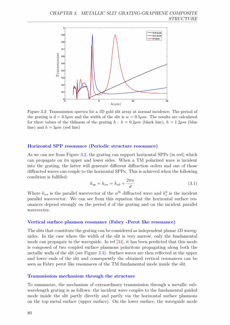
CHAPTER 3. METALLIC SLIT GRATING-GRAPHENE COMPOSITESTRUCTURE
0 5 10 150
0.1
0.2
0.3
0.4
0.5
0.6
0.7
0.8
0.9
1
λ(µm)
Transmission
h=0.2µmh=1.2µmh=3µm
Figure 3.2: Transmission spectra for a 1D gold slit array at normal incidence. The period ofthe grating is d = 3.5µm and the width of the slit is w = 0.5µm. The results are calculatedfor three values of the thikness of the grating h : h = 0.2µm (black line), h = 1.2µm (blueline) and h = 3µm (red line)
Horizontal SPP resonance (Periodic structure resonance)
As we can see from Figure 3.2, the grating can support horizontal SPPs (in red) whichcan propagate on its upper and lower sides. When a TM polarized wave is incidentinto the grating, the latter will generate different diffraction orders and one of thosediffracted waves can couple to the horizontal SPPs. This is achieved when the followingcondition is fulfilled:
ksp = kxn = kx0 + 2πnd
(3.1)
Where kxn is the parallel wavevector of the nth diffracted wave and k0x is the incident
parallel wavevector. We can see from this equation that the horizontal surface res-onances depend strongly on the period d of the grating and on the incident parallelwavevector.
Vertical surface plasmon resonance (Fabry -Perot like resonance)
The slits that constitute the grating can be considered as independent planar 1D waveg-uides. In the case where the width of the slit is very narrow, only the fundamentalmode can propagate in the waveguide. In ref [34], it has been predicted that this modeis composed of two coupled surface plasmons polaritons propagating along both themetallic walls of the slit (see Figure 3.3). Surface waves are then reflected at the upperand lower ends of the slit and consequently the obtained vertical resonances can beseen as Fabry perot like resonnaces of the TM fundamental mode inside the slit.
Transmission mechanism through the structure
To summarize, the mechanism of extraordinary transmission through a metallic sub-wavelength grating is as follows: the incident wave couples to the fundamental guidedmode inside the slit partly directly and partly via the horizontal surface plasmonson the top metal surface (upper surface). On the lower surface, the waveguide mode
80

CHAPTER 3. METALLIC SLIT GRATING-GRAPHENE COMPOSITESTRUCTURE
z
x
Figure 3.3: Shamatic representation of a 1D planar metallic waveguide with very narrowwidth. Inside the waveguide only the fundamental TM mode is propagative and is composedof two surface plasmons waves
couples with a propagative wave partly directly and partly via the horizontal surfaceplasmons on the bottom metal surface. As a result, the coupling between the upperand lower surface plasmons is achieved by the guided mode in the slit. This couplingis more effective in the case of symmetrical structure i.e when the permittivities of thesurrounding media are equal.
3.2 Coupling between subwavelength nano-slits lat-tice modes and metal-insulator-graphene cavitymodes: A semi-analytical model
3.2.1 Physical systemThe hybrid structure under study is presented in Fig. (3.4). It consists of two sub-systems. The first sub-system earlier studied in [8] is a sub-wavelength periodic array ofnano-slits with height h1 = 800nm, period d = 165nm << λ and slits-width s = 15nm.The relative permittivity of the material filling the slits is denoted by ε(s) while thedispersive relative permittivity of the metal (gold) is denoted by ε(m) and described bythe Drude-Lorentz model [35, 8, 36]. This first sub-structure is deposited on a dielectricspacer (with relative permittivity ε(2) = 1.542 and hight h2 = 10nm) itself deposited ona continuous graphene sheet. Here, the monolayer graphene is modeled as a thin filmwithin the Thin film’s effective thickness approach described previously in chapter 1.This hybrid structure is excited, from the upper medium (having relative permittivityε(0)) by a TM polarized plane wave (the magnetic field is parallel to the y axis). Thewave vector of the incident wave is denoted by ~K0 = k0 (α0~ex + β0~ey + γ0~ez), wherek0 = 2π/λ = ω/c denotes the wavenumber, λ being the wavelength and c the lightvelocity in vacuum. The relative permittivity of the lower region is denoted by ε(3).
As mentioned above in the introduction, the spectrum behaviour of the studiedhybrid plasmonic structure is performed through the FMM-ASR and PMM methods.
81
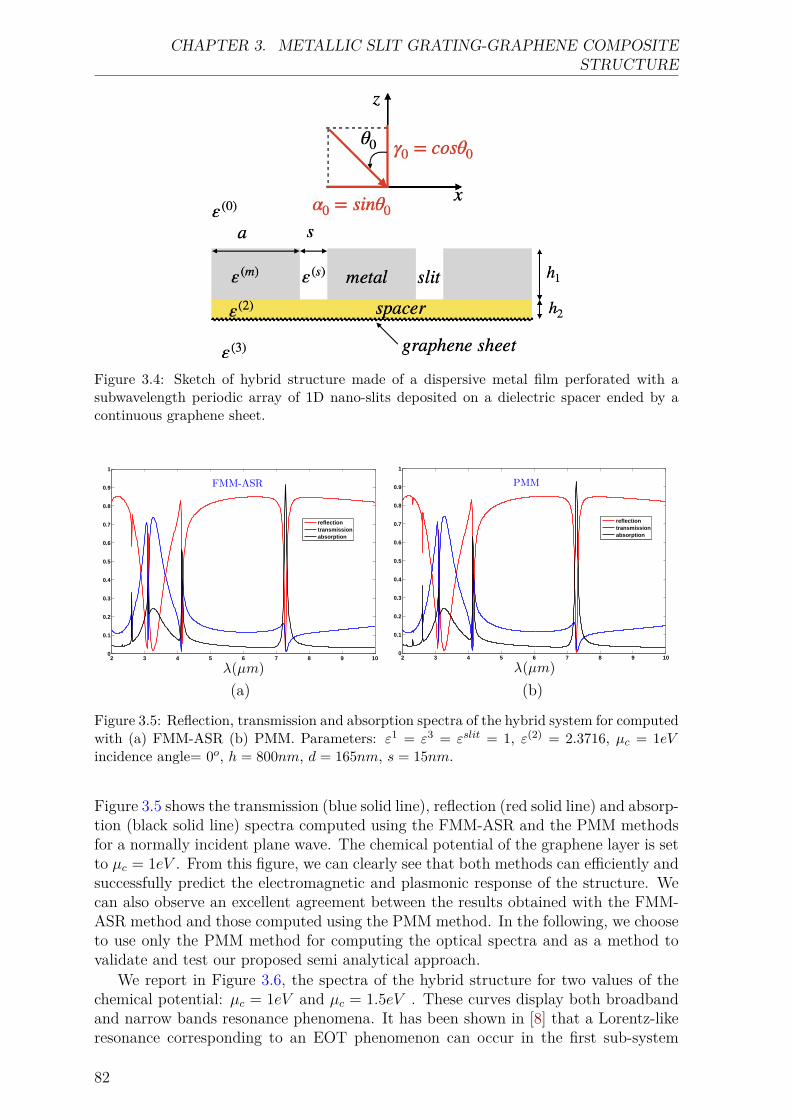
CHAPTER 3. METALLIC SLIT GRATING-GRAPHENE COMPOSITESTRUCTURE
Figure 3.4: Sketch of hybrid structure made of a dispersive metal film perforated with asubwavelength periodic array of 1D nano-slits deposited on a dielectric spacer ended by acontinuous graphene sheet.
2 3 4 5 6 7 8 9 100
0.1
0.2
0.3
0.4
0.5
0.6
0.7
0.8
0.9
1
λ(µm)
FMM-ASR
reflectiontransmissionabsorption
(a)
2 3 4 5 6 7 8 9 100
0.1
0.2
0.3
0.4
0.5
0.6
0.7
0.8
0.9
1
λ(µm)
PMM
reflectiontransmissionabsorption
(b)
Figure 3.5: Reflection, transmission and absorption spectra of the hybrid system for computedwith (a) FMM-ASR (b) PMM. Parameters: ε1 = ε3 = εslit = 1, ε(2) = 2.3716, µc = 1eVincidence angle= 0o, h = 800nm, d = 165nm, s = 15nm.
Figure 3.5 shows the transmission (blue solid line), reflection (red solid line) and absorp-tion (black solid line) spectra computed using the FMM-ASR and the PMM methodsfor a normally incident plane wave. The chemical potential of the graphene layer is setto µc = 1eV . From this figure, we can clearly see that both methods can efficiently andsuccessfully predict the electromagnetic and plasmonic response of the structure. Wecan also observe an excellent agreement between the results obtained with the FMM-ASR method and those computed using the PMM method. In the following, we chooseto use only the PMM method for computing the optical spectra and as a method tovalidate and test our proposed semi analytical approach.
We report in Figure 3.6, the spectra of the hybrid structure for two values of thechemical potential: µc = 1eV and µc = 1.5eV . These curves display both broadbandand narrow bands resonance phenomena. It has been shown in [8] that a Lorentz-likeresonance corresponding to an EOT phenomenon can occur in the first sub-system
82
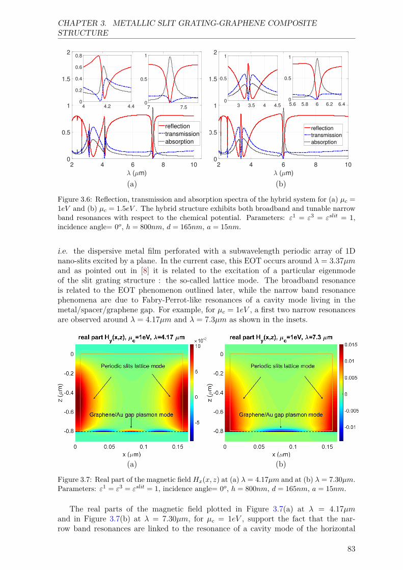
CHAPTER 3. METALLIC SLIT GRATING-GRAPHENE COMPOSITESTRUCTURE
2 4 6 8 10
( m)
0
0.5
1
1.5
2
reflection
transmission
absorption
7 7.50
0.5
1
4 4.2 4.40
0.2
0.4
0.6
0.8
(a)
2 4 6 8 10
( m)
0
0.5
1
1.5
2
reflection
transmission
absorption
5.6 5.8 6 6.2 6.40
0.5
1
3 3.5 4 4.50
0.5
1
(b)
Figure 3.6: Reflection, transmission and absorption spectra of the hybrid system for (a) µc =1eV and (b) µc = 1.5eV . The hybrid structure exhibits both broadband and tunable narrowband resonances with respect to the chemical potential. Parameters: ε1 = ε3 = εslit = 1,incidence angle= 0o, h = 800nm, d = 165nm, a = 15nm.
i.e. the dispersive metal film perforated with a subwavelength periodic array of 1Dnano-slits excited by a plane. In the current case, this EOT occurs around λ = 3.37µmand as pointed out in [8] it is related to the excitation of a particular eigenmodeof the slit grating structure : the so-called lattice mode. The broadband resonanceis related to the EOT phenomenon outlined later, while the narrow band resonancephenomena are due to Fabry-Perrot-like resonances of a cavity mode living in themetal/spacer/graphene gap. For example, for µc = 1eV , a first two narrow resonancesare observed around λ = 4.17µm and λ = 7.3µm as shown in the insets.
(a) (b)
Figure 3.7: Real part of the magnetic fieldHx(x, z) at (a) λ = 4.17µm and at (b) λ = 7.30µm.Parameters: ε1 = ε3 = εslit = 1, incidence angle= 0o, h = 800nm, d = 165nm, a = 15nm.
The real parts of the magnetic field plotted in Figure 3.7(a) at λ = 4.17µmand in Figure 3.7(b) at λ = 7.30µm, for µc = 1eV , support the fact that the nar-row band resonances are linked to the resonance of a cavity mode of the horizontal
83
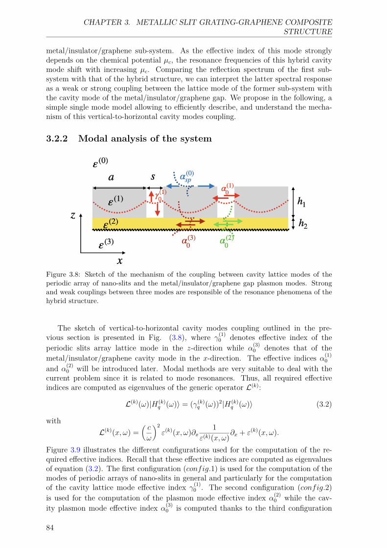
CHAPTER 3. METALLIC SLIT GRATING-GRAPHENE COMPOSITESTRUCTURE
metal/insulator/graphene sub-system. As the effective index of this mode stronglydepends on the chemical potential µc, the resonance frequencies of this hybrid cavitymode shift with increasing µc. Comparing the reflection spectrum of the first sub-system with that of the hybrid structure, we can interpret the latter spectral responseas a weak or strong coupling between the lattice mode of the former sub-system withthe cavity mode of the metal/insulator/graphene gap. We propose in the following, asimple single mode model allowing to efficiently describe, and understand the mecha-nism of this vertical-to-horizontal cavity modes coupling.
3.2.2 Modal analysis of the system
Figure 3.8: Sketch of the mechanism of the coupling between cavity lattice modes of theperiodic array of nano-slits and the metal/insulator/graphene gap plasmon modes. Strongand weak couplings between three modes are responsible of the resonance phenomena of thehybrid structure.
The sketch of vertical-to-horizontal cavity modes coupling outlined in the pre-vious section is presented in Fig. (3.8), where γ
(1)0 denotes effective index of the
periodic slits array lattice mode in the z-direction while α(3)0 denotes that of the
metal/insulator/graphene cavity mode in the x-direction. The effective indices α(1)0
and α(2)0 will be introduced later. Modal methods are very suitable to deal with the
current problem since it is related to mode resonances. Thus, all required effectiveindices are computed as eigenvalues of the generic operator L(k):
L(k)(ω)|H(k)q (ω)〉 = (γ(k)
q (ω))2|H(k)q (ω)〉 (3.2)
withL(k)(x, ω) =
(c
ω
)2ε(k)(x, ω)∂x
1ε(k)(x, ω)∂x + ε(k)(x, ω).
Figure 3.9 illustrates the different configurations used for the computation of the re-quired effective indices. Recall that these effective indices are computed as eigenvaluesof equation (3.2). The first configuration (config.1) is used for the computation of themodes of periodic arrays of nano-slits in general and particularly for the computationof the cavity lattice mode effective index γ
(1)0 . The second configuration (config.2)
is used for the computation of the plasmon mode effective index α(2)0 while the cav-
ity plasmon mode effective index α(3)0 is computed thanks to the third configuration
84
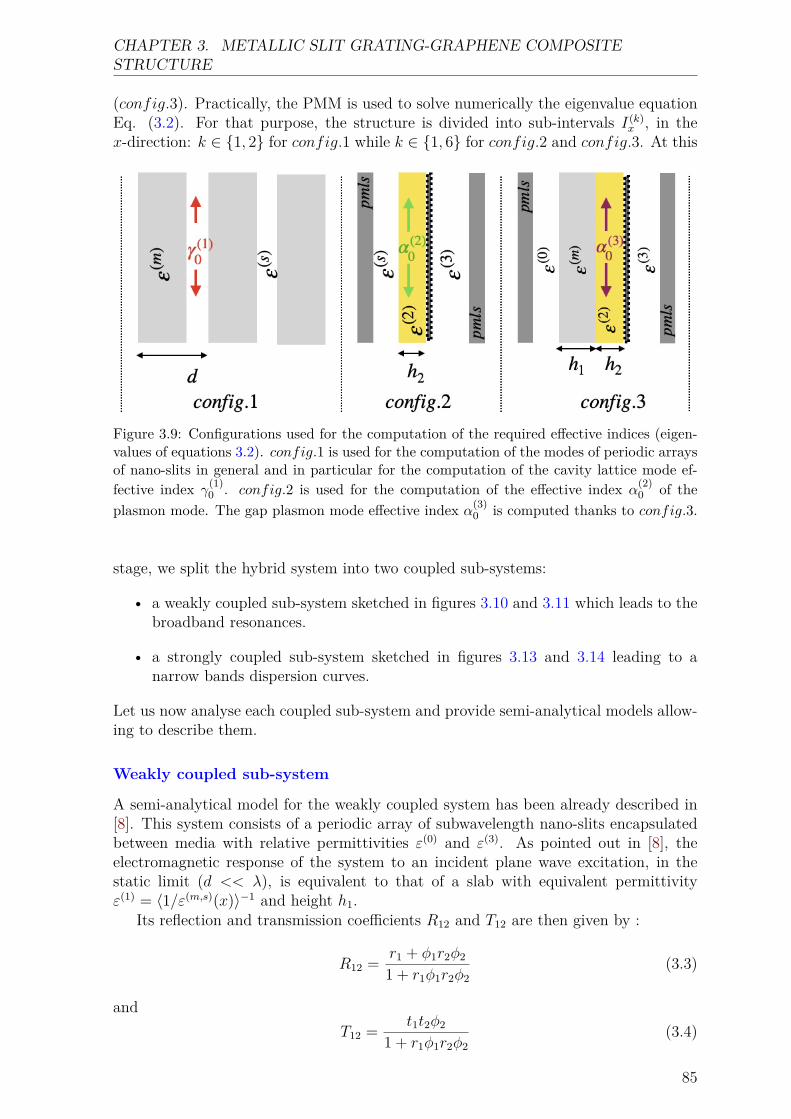
CHAPTER 3. METALLIC SLIT GRATING-GRAPHENE COMPOSITESTRUCTURE
(config.3). Practically, the PMM is used to solve numerically the eigenvalue equationEq. (3.2). For that purpose, the structure is divided into sub-intervals I(k)
x , in thex-direction: k ∈ 1, 2 for config.1 while k ∈ 1, 6 for config.2 and config.3. At this
Figure 3.9: Configurations used for the computation of the required effective indices (eigen-values of equations 3.2). config.1 is used for the computation of the modes of periodic arraysof nano-slits in general and in particular for the computation of the cavity lattice mode ef-fective index γ
(1)0 . config.2 is used for the computation of the effective index α
(2)0 of the
plasmon mode. The gap plasmon mode effective index α(3)0 is computed thanks to config.3.
stage, we split the hybrid system into two coupled sub-systems:
• a weakly coupled sub-system sketched in figures 3.10 and 3.11 which leads to thebroadband resonances.
• a strongly coupled sub-system sketched in figures 3.13 and 3.14 leading to anarrow bands dispersion curves.
Let us now analyse each coupled sub-system and provide semi-analytical models allow-ing to describe them.
Weakly coupled sub-system
A semi-analytical model for the weakly coupled system has been already described in[8]. This system consists of a periodic array of subwavelength nano-slits encapsulatedbetween media with relative permittivities ε(0) and ε(3). As pointed out in [8], theelectromagnetic response of the system to an incident plane wave excitation, in thestatic limit (d << λ), is equivalent to that of a slab with equivalent permittivityε(1) = 〈1/ε(m,s)(x)〉−1 and height h1.
Its reflection and transmission coefficients R12 and T12 are then given by :
R12 = r1 + φ1r2φ2
1 + r1φ1r2φ2(3.3)
andT12 = t1t2φ2
1 + r1φ1r2φ2(3.4)
85
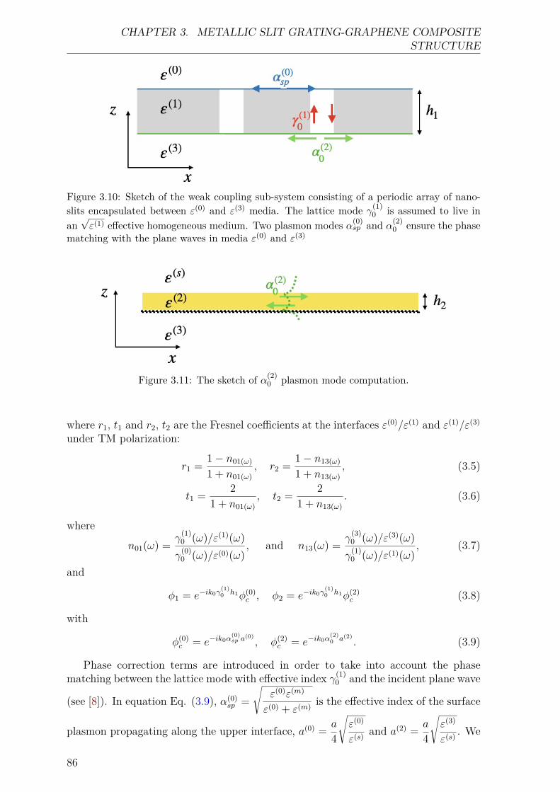
CHAPTER 3. METALLIC SLIT GRATING-GRAPHENE COMPOSITESTRUCTURE
Figure 3.10: Sketch of the weak coupling sub-system consisting of a periodic array of nano-slits encapsulated between ε(0) and ε(3) media. The lattice mode γ(1)
0 is assumed to live inan√ε(1) effective homogeneous medium. Two plasmon modes α(0)
sp and α(2)0 ensure the phase
matching with the plane waves in media ε(0) and ε(3)
Figure 3.11: The sketch of α(2)0 plasmon mode computation.
where r1, t1 and r2, t2 are the Fresnel coefficients at the interfaces ε(0)/ε(1) and ε(1)/ε(3)
under TM polarization:
r1 = 1− n01(ω)
1 + n01(ω), r2 = 1− n13(ω)
1 + n13(ω), (3.5)
t1 = 21 + n01(ω)
, t2 = 21 + n13(ω)
. (3.6)
where
n01(ω) = γ(1)0 (ω)/ε(1)(ω)γ
(0)0 (ω)/ε(0)(ω)
, and n13(ω) = γ(3)0 (ω)/ε(3)(ω)γ
(1)0 (ω)/ε(1)(ω)
, (3.7)
and
φ1 = e−ik0γ(1)0 h1φ(0)
c , φ2 = e−ik0γ(1)0 h1φ(2)
c (3.8)
with
φ(0)c = e−ik0α
(0)sp a
(0), φ(2)
c = e−ik0α(2)0 a(2)
. (3.9)
Phase correction terms are introduced in order to take into account the phasematching between the lattice mode with effective index γ(1)
0 and the incident plane wave
(see [8]). In equation Eq. (3.9), α(0)sp =
√ε(0)ε(m)
ε(0) + ε(m) is the effective index of the surface
plasmon propagating along the upper interface, a(0) = a
4
√ε(0)
ε(s) and a(2) = a
4
√ε(3)
ε(s) . We
86
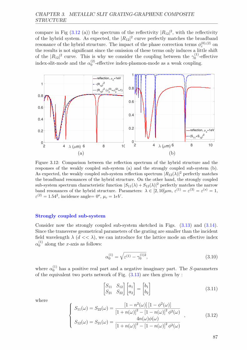
CHAPTER 3. METALLIC SLIT GRATING-GRAPHENE COMPOSITESTRUCTURE
compare in Fig (3.12 (a)) the spectrum of the reflectivity |R12|2, with the reflectivityof the hybrid system. As expected, the |R12|2 curve perfectly matches the broadbandresonance of the hybrid structure. The impact of the phase correction terms φ(0),(2)
c onthe results is not significant since the omission of these terms only induces a little shiftof the |R12|2 curve. This is why we consider the coupling between the γ(1)
0 -effectiveindex-slit-mode and the α(2)
0 -effective index-plasmon-mode as a weak coupling.
2 4 6 8 10 ( m)0
0.2
0.4
0.6
0.8
1
reflection, c=1eV
|R12
|2
|R12
|2 (
c
(0)=
c
(2)=1)
(a)2 4 6 8 10 ( m)
0
0.2
0.4
0.6
0.8
1
reflection, c=1eV
|S11
+S12
|2
(b)
Figure 3.12: Comparison between the reflection spectrum of the hybrid structure and theresponses of the weakly coupled sub-system (a) and the strongly coupled sub-system (b).As expected, the weakly coupled sub-system reflection spectrum |R12(λ)|2 perfectly matchesthe broadband resonances of the hybrid structure. On the other hand, the strongly coupledsub-system spectrum characteristic function |S11(λ) + S12(λ)|2 perfectly matches the narrowband resonances of the hybrid structure. Parameters: λ ∈ [2, 10]µm, ε(1) = ε(3) = ε(s) = 1,ε(2) = 1.542, incidence angle= 0o, µc = 1eV .
Strongly coupled sub-system
Consider now the strongly coupled sub-system sketched in Figs. (3.13) and (3.14).Since the transverse geometrical parameters of the grating are smaller than the incidentfield wavelength λ (d << λ), we can introduce for the lattice mode an effective indexα
(1)0 along the x-axis as follows:
α(1)0 =
√ε(1) − γ(1)2
0 , (3.10)
where α(1)0 has a positive real part and a negative imaginary part. The S-parameters
of the equivalent two ports network of Fig. (3.13) are then given by :[S11 S12S21 S22
] [a1a2
]=[b1b2
](3.11)
where S11(ω) = S22(ω) = [1− n2(ω)] [1− φ2(ω)]
[1 + n(ω)]2 − [1− n(ω)]2 φ2(ω)
S12(ω) = S21(ω) = 4n(ω)φ(ω)[1 + n(ω)]2 − [1− n(ω)]2 φ2(ω)
, (3.12)
87
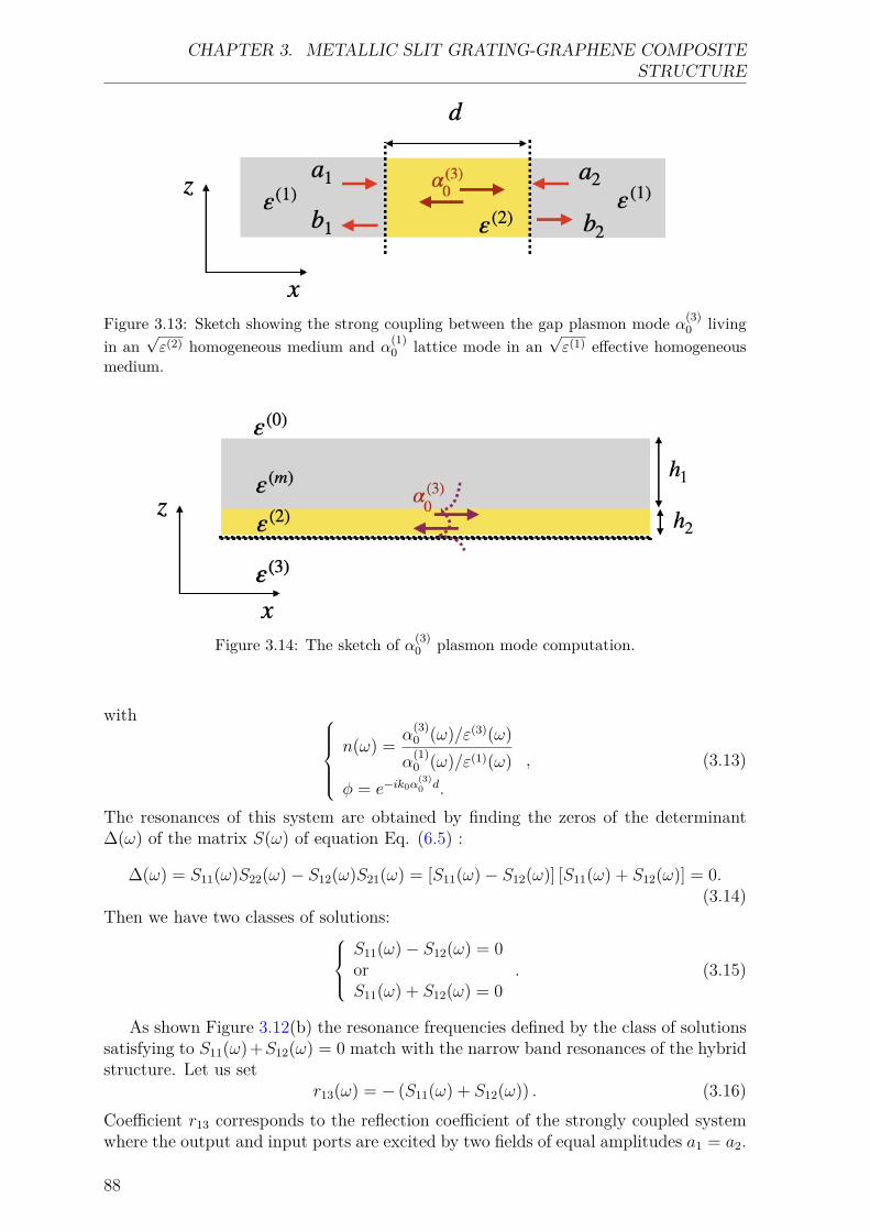
CHAPTER 3. METALLIC SLIT GRATING-GRAPHENE COMPOSITESTRUCTURE
Figure 3.13: Sketch showing the strong coupling between the gap plasmon mode α(3)0 living
in an√ε(2) homogeneous medium and α(1)
0 lattice mode in an√ε(1) effective homogeneous
medium.
Figure 3.14: The sketch of α(3)0 plasmon mode computation.
with n(ω) = α
(3)0 (ω)/ε(3)(ω)α
(1)0 (ω)/ε(1)(ω)
φ = e−ik0α(3)0 d.
, (3.13)
The resonances of this system are obtained by finding the zeros of the determinant∆(ω) of the matrix S(ω) of equation Eq. (6.5) :
∆(ω) = S11(ω)S22(ω)− S12(ω)S21(ω) = [S11(ω)− S12(ω)] [S11(ω) + S12(ω)] = 0.(3.14)
Then we have two classes of solutions:S11(ω)− S12(ω) = 0orS11(ω) + S12(ω) = 0
. (3.15)
As shown Figure 3.12(b) the resonance frequencies defined by the class of solutionssatisfying to S11(ω)+S12(ω) = 0 match with the narrow band resonances of the hybridstructure. Let us set
r13(ω) = − (S11(ω) + S12(ω)) . (3.16)Coefficient r13 corresponds to the reflection coefficient of the strongly coupled systemwhere the output and input ports are excited by two fields of equal amplitudes a1 = a2.
88
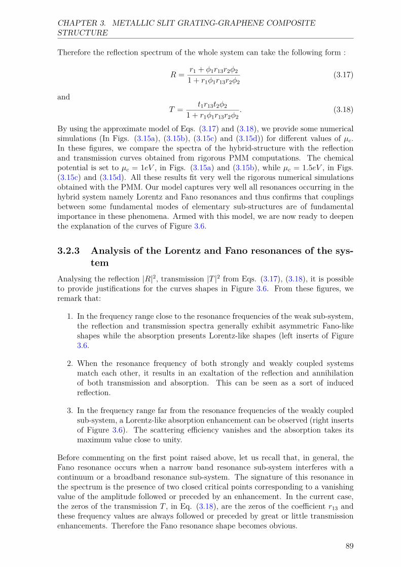
CHAPTER 3. METALLIC SLIT GRATING-GRAPHENE COMPOSITESTRUCTURE
Therefore the reflection spectrum of the whole system can take the following form :
R = r1 + φ1r13r2φ2
1 + r1φ1r13r2φ2(3.17)
andT = t1r13t2φ2
1 + r1φ1r13r2φ2. (3.18)
By using the approximate model of Eqs. (3.17) and (3.18), we provide some numericalsimulations (In Figs. (3.15a), (3.15b), (3.15c) and (3.15d)) for different values of µc.In these figures, we compare the spectra of the hybrid-structure with the reflectionand transmission curves obtained from rigorous PMM computations. The chemicalpotential is set to µc = 1eV , in Figs. (3.15a) and (3.15b), while µc = 1.5eV , in Figs.(3.15c) and (3.15d). All these results fit very well the rigorous numerical simulationsobtained with the PMM. Our model captures very well all resonances occurring in thehybrid system namely Lorentz and Fano resonances and thus confirms that couplingsbetween some fundamental modes of elementary sub-structures are of fundamentalimportance in these phenomena. Armed with this model, we are now ready to deepenthe explanation of the curves of Figure 3.6.
3.2.3 Analysis of the Lorentz and Fano resonances of the sys-tem
Analysing the reflection |R|2, transmission |T |2 from Eqs. (3.17), (3.18), it is possibleto provide justifications for the curves shapes in Figure 3.6. From these figures, weremark that:
1. In the frequency range close to the resonance frequencies of the weak sub-system,the reflection and transmission spectra generally exhibit asymmetric Fano-likeshapes while the absorption presents Lorentz-like shapes (left inserts of Figure3.6.
2. When the resonance frequency of both strongly and weakly coupled systemsmatch each other, it results in an exaltation of the reflection and annihilationof both transmission and absorption. This can be seen as a sort of inducedreflection.
3. In the frequency range far from the resonance frequencies of the weakly coupledsub-system, a Lorentz-like absorption enhancement can be observed (right insertsof Figure 3.6). The scattering efficiency vanishes and the absorption takes itsmaximum value close to unity.
Before commenting on the first point raised above, let us recall that, in general, theFano resonance occurs when a narrow band resonance sub-system interferes with acontinuum or a broadband resonance sub-system. The signature of this resonance inthe spectrum is the presence of two closed critical points corresponding to a vanishingvalue of the amplitude followed or preceded by an enhancement. In the current case,the zeros of the transmission T , in Eq. (3.18), are the zeros of the coefficient r13 andthese frequency values are always followed or preceded by great or little transmissionenhancements. Therefore the Fano resonance shape becomes obvious.
89
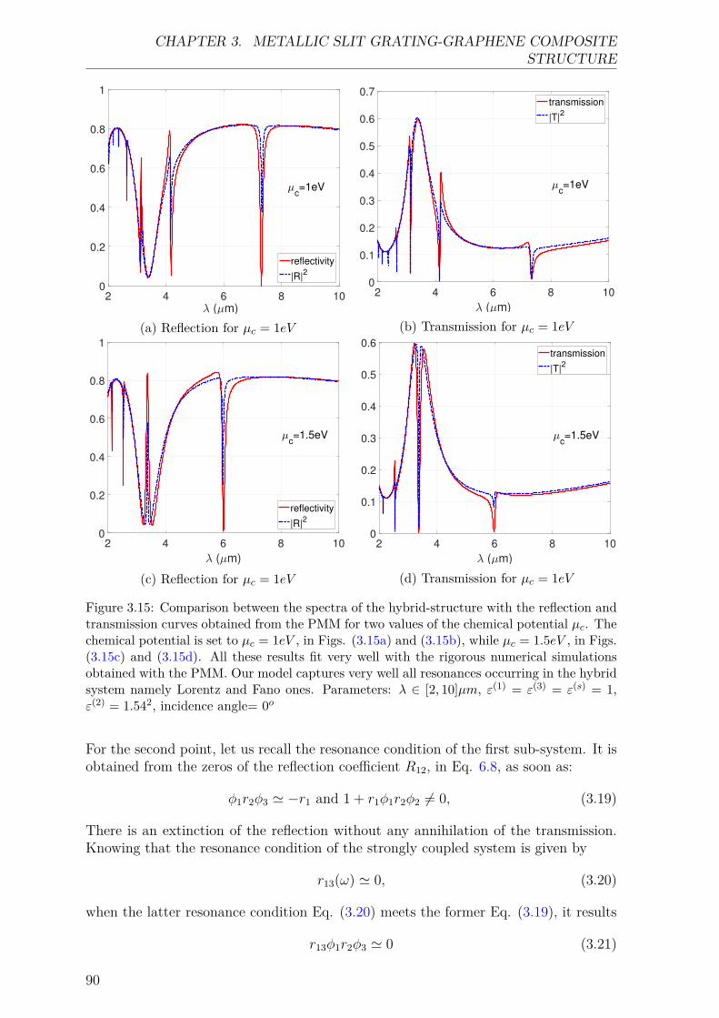
CHAPTER 3. METALLIC SLIT GRATING-GRAPHENE COMPOSITESTRUCTURE
2 4 6 8 10 ( m)
0
0.2
0.4
0.6
0.8
1
reflectivity
|R|2
c=1eV
(a) Reflection for µc = 1eV
2 4 6 8 10
( m)
0
0.1
0.2
0.3
0.4
0.5
0.6
0.7transmission
|T|2
c=1eV
(b) Transmission for µc = 1eV
2 4 6 8 10
( m)
0
0.2
0.4
0.6
0.8
1
reflectivity
|R|2
c=1.5eV
(c) Reflection for µc = 1eV
2 4 6 8 10
( m)
0
0.1
0.2
0.3
0.4
0.5
0.6transmission
|T|2
c=1.5eV
(d) Transmission for µc = 1eV
Figure 3.15: Comparison between the spectra of the hybrid-structure with the reflection andtransmission curves obtained from the PMM for two values of the chemical potential µc. Thechemical potential is set to µc = 1eV , in Figs. (3.15a) and (3.15b), while µc = 1.5eV , in Figs.(3.15c) and (3.15d). All these results fit very well with the rigorous numerical simulationsobtained with the PMM. Our model captures very well all resonances occurring in the hybridsystem namely Lorentz and Fano ones. Parameters: λ ∈ [2, 10]µm, ε(1) = ε(3) = ε(s) = 1,ε(2) = 1.542, incidence angle= 0o
For the second point, let us recall the resonance condition of the first sub-system. It isobtained from the zeros of the reflection coefficient R12, in Eq. 6.8, as soon as:
φ1r2φ3 ' −r1 and 1 + r1φ1r2φ2 6= 0, (3.19)
There is an extinction of the reflection without any annihilation of the transmission.Knowing that the resonance condition of the strongly coupled system is given by
r13(ω) ' 0, (3.20)
when the latter resonance condition Eq. (3.20) meets the former Eq. (3.19), it results
r13φ1r2φ3 ' 0 (3.21)
90
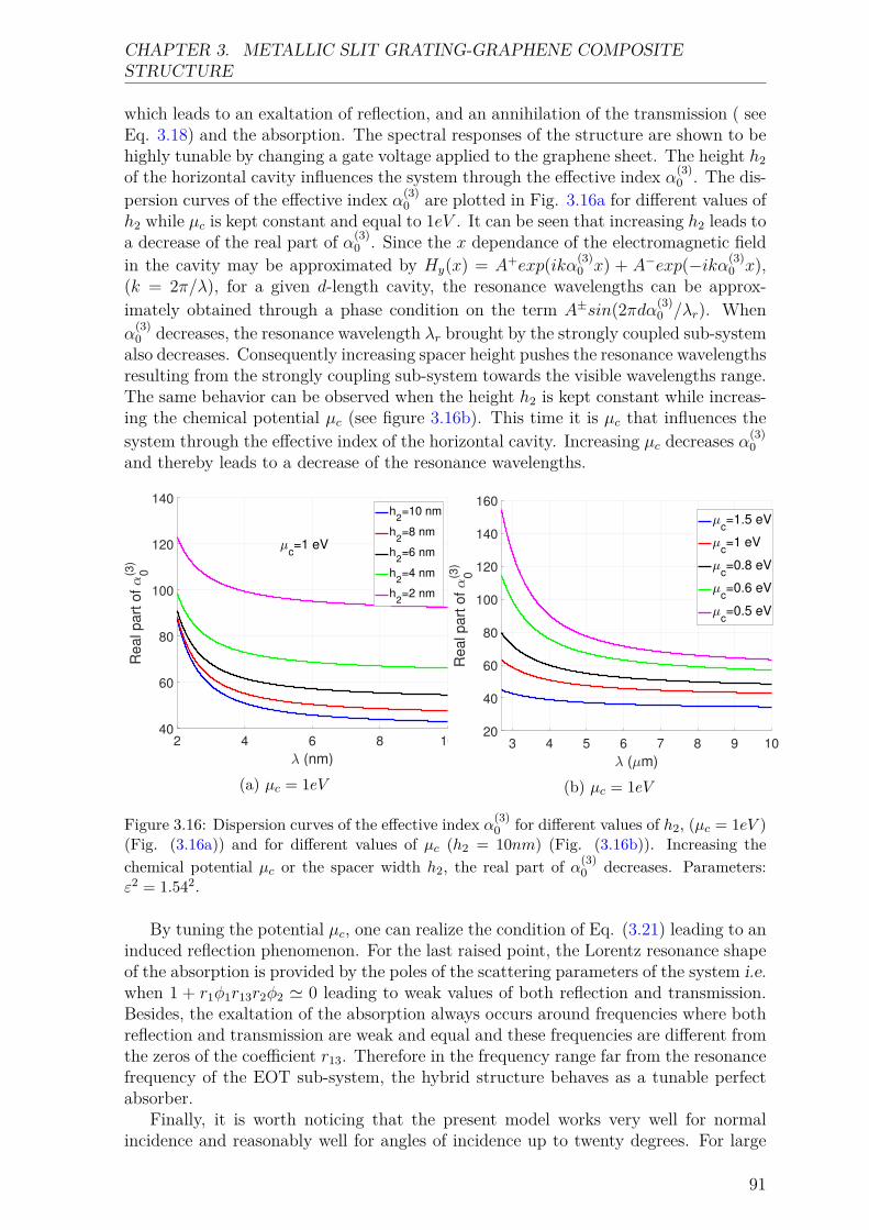
CHAPTER 3. METALLIC SLIT GRATING-GRAPHENE COMPOSITESTRUCTURE
which leads to an exaltation of reflection, and an annihilation of the transmission ( seeEq. 3.18) and the absorption. The spectral responses of the structure are shown to behighly tunable by changing a gate voltage applied to the graphene sheet. The height h2of the horizontal cavity influences the system through the effective index α(3)
0 . The dis-persion curves of the effective index α(3)
0 are plotted in Fig. 3.16a for different values ofh2 while µc is kept constant and equal to 1eV . It can be seen that increasing h2 leads toa decrease of the real part of α(3)
0 . Since the x dependance of the electromagnetic fieldin the cavity may be approximated by Hy(x) = A+exp(ikα(3)
0 x) + A−exp(−ikα(3)0 x),
(k = 2π/λ), for a given d-length cavity, the resonance wavelengths can be approx-imately obtained through a phase condition on the term A±sin(2πdα(3)
0 /λr). Whenα
(3)0 decreases, the resonance wavelength λr brought by the strongly coupled sub-system
also decreases. Consequently increasing spacer height pushes the resonance wavelengthsresulting from the strongly coupling sub-system towards the visible wavelengths range.The same behavior can be observed when the height h2 is kept constant while increas-ing the chemical potential µc (see figure 3.16b). This time it is µc that influences thesystem through the effective index of the horizontal cavity. Increasing µc decreases α(3)
0and thereby leads to a decrease of the resonance wavelengths.
2 4 6 8 10
(nm)
40
60
80
100
120
140
Re
al p
art
of
0(3)
h2=10 nm
h2=8 nm
h2=6 nm
h2=4 nm
h2=2 nm
c=1 eV
(a) µc = 1eV
3 4 5 6 7 8 9 10
( m)
20
40
60
80
100
120
140
160
Re
al p
art
of
0(3)
c=1.5 eV
c=1 eV
c=0.8 eV
c=0.6 eV
c=0.5 eV
(b) µc = 1eV
Figure 3.16: Dispersion curves of the effective index α(3)0 for different values of h2, (µc = 1eV )
(Fig. (3.16a)) and for different values of µc (h2 = 10nm) (Fig. (3.16b)). Increasing thechemical potential µc or the spacer width h2, the real part of α(3)
0 decreases. Parameters:ε2 = 1.542.
By tuning the potential µc, one can realize the condition of Eq. (3.21) leading to aninduced reflection phenomenon. For the last raised point, the Lorentz resonance shapeof the absorption is provided by the poles of the scattering parameters of the system i.e.when 1 + r1φ1r13r2φ2 ' 0 leading to weak values of both reflection and transmission.Besides, the exaltation of the absorption always occurs around frequencies where bothreflection and transmission are weak and equal and these frequencies are different fromthe zeros of the coefficient r13. Therefore in the frequency range far from the resonancefrequency of the EOT sub-system, the hybrid structure behaves as a tunable perfectabsorber.
Finally, it is worth noticing that the present model works very well for normalincidence and reasonably well for angles of incidence up to twenty degrees. For large
91
CHAPTER 3. METALLIC SLIT GRATING-GRAPHENE COMPOSITESTRUCTURE
angles of incidence, some new resonances appear in the spectra and are not capturedby our model
3.3 ConclusionsIn conclusion, we have proposed a simple model, allowing to deepen the comprehensionof the resonance phenomena involving the EOT phenomenon and a (M-I-G) gap plas-mon excitation. We consider a hybrid structure that consists of a 1D array of periodicsubwavelength slits ended by a gap.
For our analysis, this hybrid structure is split into two sub-systems. Each sub-system is driven by eigenmodes operating in an appropriate coupling regime. Thestudy of the first sub-system, characterised by modes operating in a weak couplingregime, allows to understand the broadband resonance of the hybrid system. Weprovided an analytical expression of the reflection and transmission coefficients of thisfirst sub-system. The behavior of the second sub-system, characterized by modesacting in a regime of strong coupling allows to understand the narrow-band natureof the hybrid system. Here, the resonance frequencies directly depend on the metal-insulator-graphene horizontal Perot Fabry cavity effective index. Since the real part ofthis effective index decreases by increasing the graphene sheet chemical potential, theresonance wavelengths of the system become perfectly tunable ; better yet an inducedreflection phenomenon or perfect absorption can be achieved with suited values of thegraphene sheet Fermi level. We proposed a spectral function allowing not only tocharacterize the resonance frequencies of this second sub-system, but also showed thatintroducing this spectral function into the reflection and transmission coefficients of thefirst sub-system, we obtain an analytical expression of the reflection and transmissioncoefficients of the global hybrid system which are successfully compared with thoseobtained with rigorous numerical simulations (through the PMM approach). Finally,armed with these analytical expressions, we provided a full description of the resonancephenomena occurring in the system.
Our analysis in terms of simple modes couplings can be extended to study thecoupling of the lattice modes with a substrate made by a non-reciprocal photonictopological materials, of particular interest for energy management and transport [37]and for atomic manipulation [38]. The analysis of such complex hybrid configurationsinvolving diffraction gratings coupled to hybrid graphene multilayer structures couldalso be applied to study and to estimate more complicated phenomena, like the Casimireffect [39] and the radiative heat transfer [40].
92
Bibliography
[1] H.F. Ghaemi T. Thio T.W. Ebbesen, H.J. Lezec and P.A. Wolff. Extraordinaryoptical transmission through sub-wavelenght hole arrays,”. Nature, (391):667–669,1998. 77, 79, 149
[2] F.I. Baida, Y. Poujet, B. Guizal, and D. Van Labeke. New design for en-hanced transmission and polarization control through near-field optical microscopyprobes. Optics Communications, 256(1):190–195, 2005. 77, 149
[3] Fadi I. Baida, Yannick Poujet, Jérôme Salvi, Daniel Van Labeke, and BrahimGuizal. Extraordinary transmission beyond the cut-off through sub- annular aper-ture arrays. Optics Communications, 282(7):1463–1466, 2009. 77, 149
[4] L. Aigouy, P. Lalanne, J. P. Hugonin, G. Julié, V. Mathet, and M. Mortier. Near-field analysis of surface waves launched at nanoslit apertures. Phys. Rev. Lett.,98:153902, Apr 2007. 77
[5] H. T. Liu and P. Lalanne. Microscopic theory of the extraordinary optical trans-mission. Nature, 452:728–731, 2008. 77, 149
[6] L. Martín-Moreno, F. J. García-Vidal, H. J. Lezec, K. M. Pellerin, T. Thio, J. B.Pendry, and T. W. Ebbesen. Theory of extraordinary optical transmission throughsubwavelength hole arrays. Phys. Rev. Lett., 86:1114–1117, Feb 2001. 77, 149
[7] A Yu Nikitin, Sergio G Rodrigo, F J García-Vidal, and L Martín-Moreno. In thediffraction shadow: Norton waves versus surface plasmon polaritons in the opticalregion. New Journal of Physics, 11(12):123020, dec 2009. 77
[8] Kofi Edee. Single mode approach with versatile surface wave phase correctionfor the extraordinary optical transmission comprehension of 1d period nano-slitsarrays. OSA Continuum, 1(2):613–624, Oct 2018. 77, 82, 83, 86, 87
[9] Sherrott M Lopez JJ Atwater HA Brar VW, Jang MS. Highly confined tunablemid-infrared plasmonics in graphene nanoresonators. Nano Lett, (6):2541–2547,2013. 78
[10] O. Limaj F. J. GarcÃa de Abajo V. Pruneri D. Rodrigo, A. Tittl and H. Altug.Damping pathways of mid-infrared plasmons in graphene nanostructures. LightSci Appl, (6):16277, 2013. 78
[11] Arya Fallahi and Julien Perruisseau-Carrier. Design of tunable biperiodic graphenemetasurfaces. Phys. Rev. B, 86:195408, Nov 2012. 78
93

BIBLIOGRAPHY
[12] Zheyu Fang, Yumin Wang, Andrea E. Schlather, Zheng Liu, Pulickel M. Ajayan,F. Javier García de Abajo, Peter Nordlander, Xing Zhu, and Naomi J. Halas.Active tunable absorption enhancement with graphene nanodisk arrays. NanoLetters, 14(1):299–304, 2014. PMID: 24320874. 78
[13] Wenjuan Zhu Yanqing Wu Marcus Freitag Xuesong Li Phaedon Avouris Feng-nian Xia Hugen Yan, Tony Low. Damping pathways of mid-infrared plasmons ingraphene nanostructures. Nature Photon, (7):394–399, 2013. 78
[14] Frank H. L. Koppens, Darrick E. Chang, and F. Javier García de Abajo. Grapheneplasmonics: A platform for strong light–matter interactions. Nano Letters,11(8):3370–3377, 2011. PMID: 21766812. 78
[15] M. Farhat M. Amin and H. Bagci. A dynamically reconfigurable fano metama-terial through graphene tuning for switching and sensing applications”. Sci Rep,(3):2105, 2013. 78
[16] A. Yu. Nikitin, F. Guinea, F. J. Garcia-Vidal, and L. Martin-Moreno. Surfaceplasmon enhanced absorption and suppressed transmission in periodic arrays ofgraphene ribbons. Phys. Rev. B, 85:081405, Feb 2012. 78
[17] Jared H. Strait, Parinita Nene, Wei-Min Chan, Christina Manolatou, Sandip Ti-wari, Farhan Rana, Joshua W. Kevek, and Paul L. McEuen. Confined plasmonsin graphene microstructures: Experiments and theory. Phys. Rev. B, 87:241410,Jun 2013. 78
[18] Hugen Yan, Xuesong Li, Bhupesh Chandra, George Tulevski, Yanqing Wu, MarcusFreitag, Wenjuan Zhu, Phaedon Avouris, and Fengnian Xia. Tunable infrared plas-monic devices using graphene/insulator stacks. Nature Nanotechnology, 7(5):330–334, May 2012. 78
[19] Sukosin Thongrattanasiri and F. Javier García de Abajo. Optical field enhance-ment by strong plasmon interaction in graphene nanostructures. Phys. Rev. Lett.,110:187401, Apr 2013. 78
[20] Soongyu Yi, Ming Zhou, Xi Shi, Qiaoqiang Gan, Jian Zi, and Zongfu Yu. Amultiple-resonator approach for broadband light absorption in a single layer ofnanostructured graphene. Opt. Express, 23(8):10081–10090, Apr 2015. 78
[21] Bo Zhao and Zhuomin M. Zhang. Strong plasmonic coupling between grapheneribbon array and metal gratings. ACS Photonics, 2(11):1611–1618, 2015. 78
[22] Weilu Gao, Jie Shu, Ciyuan Qiu, and Qianfan Xu. Excitation of plasmonic wavesin graphene by guided-mode resonances. ACS Nano, 6(9):7806–7813, 2012. PMID:22862147. 78
[23] Zizhuo Liu and Koray Aydin. Enhanced infrared transmission through goldnanoslit arrays via surface plasmons in continuous graphene. Opt. Express,24(24):27882–27889, Nov 2016. 78
[24] B. Wang T. Zhang, L Chen and X. Li. Tunable broadband plasmonic field enhance-ment on a graphene surface using a normal-incidence plane wave at mid-infraredfrequencies. Sci Rep, (5):11195, 2015. 78
94
BIBLIOGRAPHY
[25] Linlong Tang, Haofei Shi, Jun Yang, Chunlei Du, Fuhua Gao, Jianhua Zhu, andJinglei Du. Complete optical absorption in graphene by using nano-gratings toexcite graphene surface plasmons. Microelectronic Engineering, 145:58 – 61, 2015.Micro/Nano Devices and Systems 2014 An open focused special thematic issue ofMicroelectronic Engineering. 78
[26] Sheng-Xuan Xia, Xiang Zhai, Ling-Ling Wang, Bin Sun, Jian-Qiang Liu,and Shuang-Chun Wen. Dynamically tunable plasmonically induced trans-parency in sinusoidally curved and planar graphene layers. Optics express,24(16):17886—17899, August 2016. 78
[27] Xiaolei Zhao, Lin Zhu, Cai Yuan, and Jianquan Yao. Tunable plasmon-inducedtransparency in a grating-coupled double-layer graphene hybrid system at far-infrared frequencies. Opt. Lett., 41(23):5470–5473, Dec 2016. 78
[28] K. Edee and J. P. Plumey. Numerical scheme for the modal methodbased on subsectional gegenbauer polynomial expansion: application tobiperiodic binary grating. J. Opt. Soc. Am. A, 32(3):402–410, Marts , url = http://josaa.osa.org/abstract.cfm?URI=josaa-32-3-402, doi =10.1364/JOSAA.32.000402,. 78, 152
[29] K. Edee, J.-P. Plumey, A. Moreau, and B. Guizal. Matched coordinates in theframework of polynomial modal methods for complex metasurface modeling. J.Opt. Soc. Am. A, 35(4):608–615, Apr 2018 ,. 78
[30] Kofi Edee. Modal method based on subsectional gegenbauer polynomial expansionfor lamellar gratings. J. Opt. Soc. Am. A, 28(10):2006–2013, Oct 2011. 78, 150,151
[31] G. Granet K. Edee, I. Fenniche and B. Guizal. Modal method based on subsec-tional gegenbauer polynomial expansion for lamellar gratings: weighting function,convergence and stability. PIER, (133):17–35, 2013. 78
[32] H. A. Bethe. Theory of diffraction by small holes. Phys. Rev., 66:163–182, Oct1944. 78
[33] J. A. Porto, F. J. García-Vidal, and J. B. Pendry. Transmission resonances onmetallic gratings with very narrow slits. Phys. Rev. Lett., 83:2845–2848, Oct 1999.79
[34] S. Collin, F. Pardo, R. Teissier, and J.-L. Pelouard. Strong discontinuities in thecomplex photonic band structure of transmission metallic gratings. Phys. Rev. B,63:033107, Jan 2001. 80
[35] R. Brendel and D. Bormann. An infrared dielectric function model for amorphoussolids. Journal of Applied Physics, 71(1):1–6, 1992. 82, 150
[36] Aleksandar D. Rakić, Aleksandra B. Djurišić, Jovan M. Elazar, and Marian L.Majewski. Optical properties of metallic films for vertical-cavity optoelectronicdevices. Appl. Opt., 37(22):5271–5283, Aug 1998. 82, 150
[37] Pierre Doyeux, S. Ali Hassani Gangaraj, George W. Hanson, and Mauro An-tezza. Giant interatomic energy-transport amplification with nonreciprocal pho-tonic topological insulators. Phys. Rev. Lett., 119:173901, Oct 2017. 93
95
BIBLIOGRAPHY
[38] Mário G. Silveirinha, S. Ali Hassani Gangaraj, George W. Hanson, and Mauro An-tezza. Fluctuation-induced forces on an atom near a photonic topological material.Phys. Rev. A, 97:022509, Feb 2018. 93
[39] Riccardo Messina, Paulo A. Maia Neto, Brahim Guizal, and Mauro Antezza.Casimir interaction between a sphere and a grating. Phys. Rev. A, 92:062504,Dec 2015. 93
[40] Bo Zhao, Brahim Guizal, Zhuomin M. Zhang, Shanhui Fan, and Mauro An-tezza. Near-field heat transfer between graphene/hbn multilayers. Phys. Rev.B, 95:245437, Jun 2017. 93
96
Part III
Non-reciprocity devices based ongraphene and metals
97

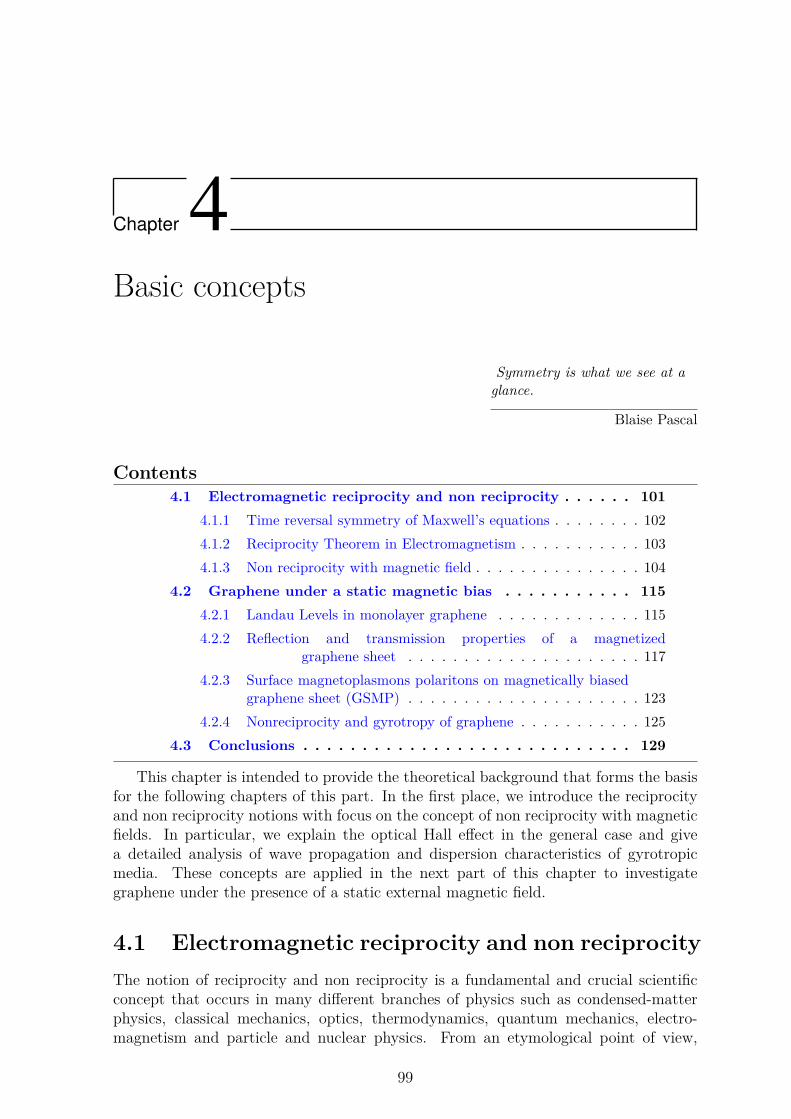
Chapter 4Basic concepts
Symmetry is what we see at aglance.
Blaise Pascal
Contents4.1 Electromagnetic reciprocity and non reciprocity . . . . . . 101
4.1.1 Time reversal symmetry of Maxwell’s equations . . . . . . . . 1024.1.2 Reciprocity Theorem in Electromagnetism . . . . . . . . . . . 1034.1.3 Non reciprocity with magnetic field . . . . . . . . . . . . . . . 104
4.2 Graphene under a static magnetic bias . . . . . . . . . . . 1154.2.1 Landau Levels in monolayer graphene . . . . . . . . . . . . . 1154.2.2 Reflection and transmission properties of a magnetized
graphene sheet . . . . . . . . . . . . . . . . . . . . . 1174.2.3 Surface magnetoplasmons polaritons on magnetically biased
graphene sheet (GSMP) . . . . . . . . . . . . . . . . . . . . . 1234.2.4 Nonreciprocity and gyrotropy of graphene . . . . . . . . . . . 125
4.3 Conclusions . . . . . . . . . . . . . . . . . . . . . . . . . . . . 129
This chapter is intended to provide the theoretical background that forms the basisfor the following chapters of this part. In the first place, we introduce the reciprocityand non reciprocity notions with focus on the concept of non reciprocity with magneticfields. In particular, we explain the optical Hall effect in the general case and givea detailed analysis of wave propagation and dispersion characteristics of gyrotropicmedia. These concepts are applied in the next part of this chapter to investigategraphene under the presence of a static external magnetic field.
4.1 Electromagnetic reciprocity and non reciprocityThe notion of reciprocity and non reciprocity is a fundamental and crucial scientificconcept that occurs in many different branches of physics such as condensed-matterphysics, classical mechanics, optics, thermodynamics, quantum mechanics, electro-magnetism and particle and nuclear physics. From an etymological point of view,
99
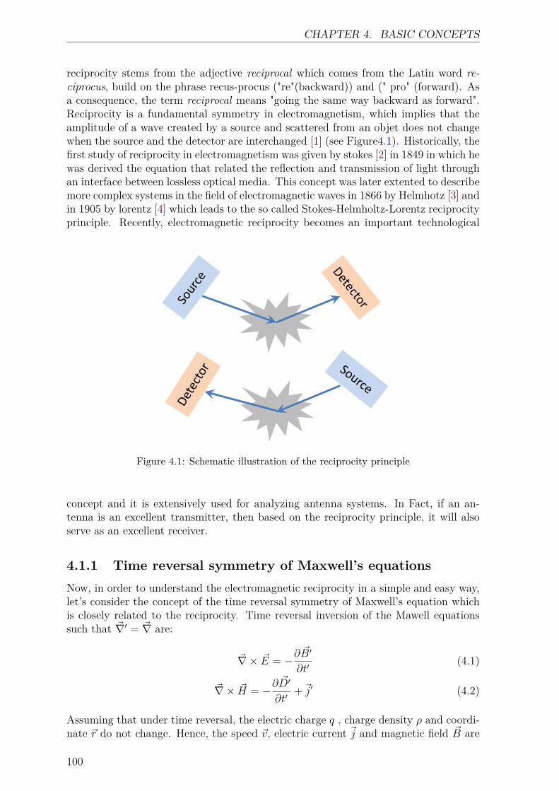
CHAPTER 4. BASIC CONCEPTS
reciprocity stems from the adjective reciprocal which comes from the Latin word re-ciprocus, build on the phrase recus-procus ("re"(backward)) and (" pro" (forward). Asa consequence, the term reciprocal means "going the same way backward as forward".Reciprocity is a fundamental symmetry in electromagnetism, which implies that theamplitude of a wave created by a source and scattered from an objet does not changewhen the source and the detector are interchanged [1] (see Figure4.1). Historically, thefirst study of reciprocity in electromagnetism was given by stokes [2] in 1849 in which hewas derived the equation that related the reflection and transmission of light throughan interface between lossless optical media. This concept was later extented to describemore complex systems in the field of electromagnetic waves in 1866 by Helmhotz [3] andin 1905 by lorentz [4] which leads to the so called Stokes-Helmholtz-Lorentz reciprocityprinciple. Recently, electromagnetic reciprocity becomes an important technological
Figure 4.1: Schematic illustration of the reciprocity principle
concept and it is extensively used for analyzing antenna systems. In Fact, if an an-tenna is an excellent transmitter, then based on the reciprocity principle, it will alsoserve as an excellent receiver.
4.1.1 Time reversal symmetry of Maxwell’s equationsNow, in order to understand the electromagnetic reciprocity in a simple and easy way,let’s consider the concept of the time reversal symmetry of Maxwell’s equation whichis closely related to the reciprocity. Time reversal inversion of the Mawell equationssuch that ~∇′ = ~∇ are:
~∇× ~E = −∂~B′
∂t′(4.1)
~∇× ~H = −∂~D′
∂t′+~j′ (4.2)
Assuming that under time reversal, the electric charge q , charge density ρ and coordi-nate ~r do not change. Hence, the speed ~v, electric current ~j and magnetic field ~B are
100
CHAPTER 4. BASIC CONCEPTS
odd with respect to time reversal. While, the electric field ~E and displacement ~D aretime reversal even(see table 4.1). Under these assumptions, we get:
~∇× ~E = −∂(− ~B)∂(−t) (4.3)
~∇× (− ~H) = − ∂( ~D)∂(−t) + (−~j) (4.4)
or by simplifying:
~∇× ~E = −∂~B
∂t(4.5)
~∇× ~H = ∂ ~D
∂t+~j (4.6)
These equations are identical to the original Maxewell equations. Thus, we can con-clude that the Maxwell equations are invariant under time reversal transformation. Wepass now to introduce the Lorentz reciprocity theorem which plays a very central rolein the electromagnetic reciprocity .
Physical Quantity Time Reversal ParityCharge density ρ(t)→ +ρ(−t) evenCurrent density ~j(t) → −~j(−t) oddDisplacement ~D(t) → + ~D(−t) evenElectric field ~E(t) → + ~E(−t) evenMagnetic field ~H(t) → − ~H(−t) oddMagnetic induction ~B(t) → − ~B(−t) oddMagnetization ~M(t) → − ~M(−t) oddPolarization density ~P (t) → +~P (−t) evenPoynting vector ~S(t) → −~S(−t) odd
Table 4.1: Transformation properties of the main electromagnetic quantitues under timereversal [5].
4.1.2 Reciprocity Theorem in ElectromagnetismIn this section, we shall derive the Lorentz reciprocity theorem for electromagneticfields. Let us Consider a volume V containing a current distribution j1 which gives riseto an electric fiels E1 and a magnetic field H1, where all three have time dependanceeiωt. Using the time harmonic Maxwell’s equations form, we get:
~∇× ~E1 = −iωµ ~H1 (4.7)
~∇× ~H1 = iωε ~E1 +~j1 (4.8)Similary, consider a second current distribution j2 which is completly contained withinthe same volume V . This new current distribution produces fields E2 and H2 that arerelated by the following equations:
~∇× ~E2 = −iωµ ~H2 (4.9)
101
CHAPTER 4. BASIC CONCEPTS
~∇× ~H2 = iωε ~E2 +~j2 (4.10)Now, let us take the dot product of H2 with each side of equation 4.7:
~H2.(~∇× ~E1) = −iωµ ~H1. ~H2 (4.11)
Similarly, let us take the dot product of E1 with each side of equation 4.10:
~E1.(~∇× ~H2) = iωε ~E1. ~E2 + ~E1.~j2 (4.12)
By subtracting Equation 4.11 from equation 4.12, we obtain:
~E1.(~∇× ~H2)− ~H2.(~∇× ~E1) = ~E1~j2 + iωε ~E1. ~E2 + iωµ ~H1. ~H2 (4.13)
Using the vector identity, the left side of this equation is written as:
~E1.(~∇× ~H2)− ~H2.(~∇× ~E1) = ~∇( ~H2 × ~E1) (4.14)
So, equation 4.13 becomes:
~∇( ~H2 × ~E1) = ~E1~j2 + iωε ~E1. ~E2 + iωµ ~H1. ~H2 (4.15)
Next, by following the same process, we find:
~∇( ~H1 × ~E2) = ~E2~j1 + iωε ~E1. ~E2 + iωµ ~H1. ~H2 (4.16)
Finally, subtracting equation 4.33 from equation 4.15, we obtain:
~∇( ~H2 × ~H1 − ~H1 × ~E2) = ~E1.~j2 − ~E2~j1 (4.17)
This equation is commonly known as the differential form of the Lorentz reciprocitytheorem. To obtain the associated form of this theorem which is applied to contiguousregions of space, we should integrate both sides of equation 4.17 over the volume V ,thus we get:∫ ∫ ∫
V
~∇( ~H2 × ~H1 − ~H1 × ~E2) dv =∫ ∫ ∫
V( ~E1.~j2 − ~E2.~j1) dv (4.18)
Using the divergence theorem to transform the left side, this equation can be expressedas: ∫ ∫
S( ~H2 × ~H1 − ~H1 × ~E2) ~ds =
∫ ∫ ∫V
( ~E1.~j2 − ~E2.~j1) dv (4.19)
where S is the closed mathematical surface which bounds V . If we now confine thesources to finite region of space, while allowing V to grow infinitely large, expanding toinclude all space. In this situation, the closest distance between any point containingnon-zero source current and S is infinite. Since field magnitude diminishes with distancefrom the source, all the fields are zeros on S. Thus the left side of (4.19) is zero andwe obtain: ∫ ∫ ∫
V( ~E1.~j2 − ~E2.~j1) dv = 0 (4.20)
which can be written as follows:∫ ∫ ∫V
~E1.~j2 dv =∫ ∫ ∫
V
~E2.~j1 dv (4.21)
This equation provides the intergral form of the lorentz reciprocity theorem whichrelates fields on the bounding surface to sources within the volume. The question now
102
CHAPTER 4. BASIC CONCEPTS
is why do we refer to this relationship as reciprocity? the answer is simply becausethe expression remains the same by interchanging the subscripts "1" and "2". In otherwords, a reaction of a reciprocal system is insensitive of the interchange of source andmeasurement locations.
The notion of non reciprocity refers to the absence of reciprocity and it requiresto break and violate the Lorentz theorem. In general, nonreciprocity in a system isbased on breaking the time reversal symmetry of light-matter interaction (time reversalbecomes asymmetric). This time reversal symmetry breaking can be achieved by anexternal bias for linear systems or by a combination of self-biasing and structuralasymmetry for nonlinear systems [5].
4.1.3 Non reciprocity with magnetic fieldWe have shown above that one way to achieve non reciprocity is by introducing an ex-ternal bias, for example by applying a static magnetic field. This applied magnetic fieldbreaks the time reversal symmetry of Maxwell equations as well as the reciprocity the-orem leading to the creation of an anisotropy and gyrotropic behavior in the medium.The interaction of a polarized light with such a meduim, also called gyrotropic media,affects its polarisation state yielding various magneto-optical effects. In the following,we first make a description of the Optical Hall effect to explain the occurence of theanisotropy in materials subjected to an external magnetic field. Then, we focus ourattention to the investigation of characteristics of electromagnetic waves propagationin gyrotropic meduim. Lastely, we introduce and define magneto-optical effects.
Optical Hall effect (OHE)
In this section the Optical Hall effect (OHE), an essential tool that we use throughoutthis part of the thesis, is discussed. First, we begin by giving a brief description ofthe static electric Hall effect. Next, we present the theoretical model that can able toexplain these phenomena.
The Optical Hall effect, developed by Mathias Schubert [6, 7], is a physical phe-nomenon that describes the external magnetic field induced optical anisotropy in con-ductive materials caused by the non-time-reciprocal response of electric charge carriers.This induced magneto optic anisotropy results from the motion of the free charge car-riers (FCCs) under the influence of the Lorentz force. The OHE is the equivalent ofthe classical static electric Hall effect at the optical frequencies, hence the name "op-tical". So, for a deeper understanding of this phenomenon, let us start by describingand explaining its electrical analogous.
The static electric Hall effect, discovered by the American physicist Edwin Hallin 1879 [8], is a phenomenon resulting from the interaction between the electric andmagnetic fields and moving charge carriers in a conducting medium. This effect isconsidered as an important and useful tool for the characterization of materials espe-cially semi conductors and metals and it permits easy and direct determination of thedensity and sign of the charge carriers in these materials. Hall found that when anelectrical current passes through a conductor material placed in a transverse magneticfield, a potential difference is appeared across the material in a direction perpendicularto both the current and to the magnetic field. This voltage is called Hall voltage and isproportional to the product between the current and the magnetic field. A schematicrepresentation of this effect in a thin conducting material is depicted in Figure 4.2.It shows a strip of conducting material placed in xoy plane where a magnetic field is
103
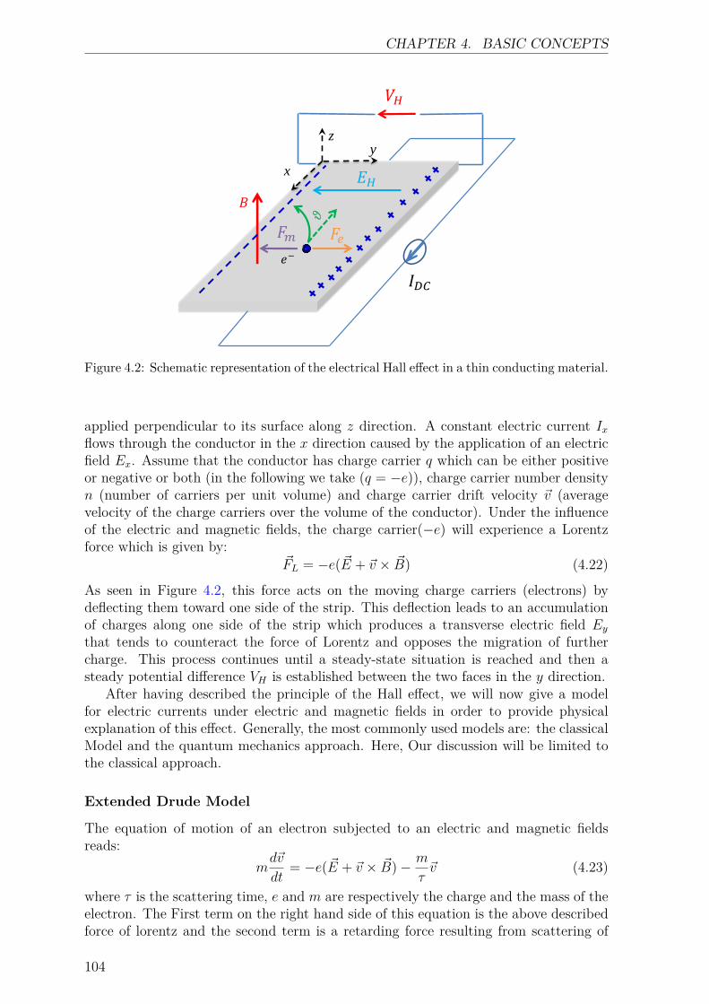
CHAPTER 4. BASIC CONCEPTS
𝐵
𝐼𝐷𝐶
𝐸𝐻
𝑉𝐻
z
x
y
𝑒−
𝐹𝑒 𝐹𝑚
Figure 4.2: Schematic representation of the electrical Hall effect in a thin conducting material.
applied perpendicular to its surface along z direction. A constant electric current Ixflows through the conductor in the x direction caused by the application of an electricfield Ex. Assume that the conductor has charge carrier q which can be either positiveor negative or both (in the following we take (q = −e)), charge carrier number densityn (number of carriers per unit volume) and charge carrier drift velocity ~v (averagevelocity of the charge carriers over the volume of the conductor). Under the influenceof the electric and magnetic fields, the charge carrier(−e) will experience a Lorentzforce which is given by:
~FL = −e( ~E + ~v × ~B) (4.22)
As seen in Figure 4.2, this force acts on the moving charge carriers (electrons) bydeflecting them toward one side of the strip. This deflection leads to an accumulationof charges along one side of the strip which produces a transverse electric field Eythat tends to counteract the force of Lorentz and opposes the migration of furthercharge. This process continues until a steady-state situation is reached and then asteady potential difference VH is established between the two faces in the y direction.
After having described the principle of the Hall effect, we will now give a modelfor electric currents under electric and magnetic fields in order to provide physicalexplanation of this effect. Generally, the most commonly used models are: the classicalModel and the quantum mechanics approach. Here, Our discussion will be limited tothe classical approach.
Extended Drude Model
The equation of motion of an electron subjected to an electric and magnetic fieldsreads:
md~v
dt= −e( ~E + ~v × ~B)− m
τ~v (4.23)
where τ is the scattering time, e and m are respectively the charge and the mass of theelectron. The First term on the right hand side of this equation is the above describedforce of lorentz and the second term is a retarding force resulting from scattering of
104
CHAPTER 4. BASIC CONCEPTS
electrons with impurities. At steady-state, the time derivative of v vanishes which leadsto:
vx = −eτm
(Ex + vyBz) (4.24)
vy = −eτm
(Ey − vxBz) (4.25)
vz = −eτm
Ez = 0 (4.26)
The current densities Jx and Jy are given by:
Jx = −nevx (4.27)Jy = −nevy (4.28)
Jz = 0 (4.29)
Using the definition of the cyclotron frequency ωc = eB
m, we can write:
(1 ωcτ−ωcτ 1
)(JxJy
)= e2nτ
m
(ExEy
)(4.30)
Ohm’s Law that relates the current density with the electric field is :
J = σE (4.31)
with σ is the conductivity. Thus Eq 4.30 can be written as the following form:(JxJy
)=(σxx σxyσyx σyy
)(ExEy
)(4.32)
whereσ =
(σxx σxyσyx σyy
)= e2nτ
m
11 + ω2
cτ2
(1 ωcτ−ωcτ 1
)(4.33)
By comparing with Eq 4.33, it is found that:
σ =(σxx σxy−σxy σxx
)=(σL σH−σH σL
)(4.34)
It is clearly seen from Eq 4.34 that the presence of the static magnetic field gives riseto a finite optical Hall conductivity σH which leads to generate an anisotropy in thematerial. Note that while the longitudinal optical conductivity is related to the lightabsorption, the optical Hall conductivity is the basic of the Magneto-optical effects,the subject of our next discussion. Hence studying the optical Hall effect is one of thekey tools for exploring magneto optical applications.
Gyrotropic medium
When passing through a meduim in the presence of a static magnetic field, the plane ofpolarisation of light can be rotated to the left or right. This effect is known as opticalgyrotropy and the medium is said to be gyrotropic. The noun ’Gyrotropy’ refers tothis rotating motion and is composed of the prefix ’gyro’ which comes from the AncientGreek word guros ’a circle’ and the suffix ’tropy ’ coming from Ancient Greek word
105
CHAPTER 4. BASIC CONCEPTS
tropía and meaning ’a turn’ or in science ’exhibiting a behavior’. Thus, the etymo-logical meaning of "gyrotropy" is ’exhibiting a rotational behavior’. As pointed out inthe previous section, a gyrotropic material is an anisotropic meduim whose optical andmagneto-optical properties are described within its relative permettivity and perme-ability tensors ε and µ . In the presence of a magnetic field, the components of thesetensors cease to be symmetric. The generalized symmetry of the kinetic coefficientsrequires that:
εik( ~B) = εki(− ~B) (4.35)For lossless material, the tensor should be hermitian:
εik = ε∗ki (4.36)
Equation 4.36 implies that the real and imaginary parts of εik must be respectivelysymmetrical and antisymmetrical:
ε′ik = ε′ki (4.37)ε′′ik = −ε′′ki (4.38)
Using Eq 4.35, we find that:
ε′ik( ~B) = ε′ki( ~B) = ε′ki(− ~B) (4.39)ε′′ik( ~B) = −ε′′ki( ~B) = −ε′′ki(− ~B) (4.40)
This gives the condition that in a lossless medium, the real and imaginary parts of thepermittivity tensor are even and odd functions of the applied field respectively. Theinverse tensor ε−1
ik = ηik has the same symmetry properties.
ε−1ik = ηik = η′ik + iη′′ik (4.41)
Since η′′ik is an antisymmetrical tensor of rank two, it should have an equivalent axialvector. Let consider ~G this vector. The relation between η′′ik and Gi is:
η′′ik = eiklGl (4.42)
where eikl is the antisymmetrical unit tensor. Thus, the relation between the electricalfield and electric displacement becomes:
Ei = (η′ik + ieiklGl)Dk = η′ikDk + i( ~D × ~G)i (4.43)
This is the characteristic equation of a gyrotropic meduim. The gyrotropic mediumis said to be electrically gyrotropic or gyroelectric if the relative permittivity tensor iswritten as the following form:
ε = ε1(I − ~b0~b0) + iε2(~b0 × I) + ε3~b0~b0 (4.44)µ = µ0I (4.45)
~b0 is the direction of the applied magnetic field ~B. The gyrotropic meduim becomesmagnetically gyrotropic or gyromagnetic if the relative permeability tensor is:
µ = µ1(I − ~b0~b0) + iµ2(~b0 × I) + µ3~b0~b0 (4.46)ε = ε0εrI (4.47)
106

CHAPTER 4. BASIC CONCEPTS
Assuming that the magnetic field is along z direction ( ~B = B~ez), the relative permit-tivity tensor and the relative permeability are given by the following matrix form:
ε =
ε1 −iε2 0iε2 ε1 00 0 ε3
(4.48)
µ =
µ1 −iµ2 0iµ2 µ1 00 0 µ3
(4.49)
The off diagonal components, which contain the gyration term ε2, are at the origin ofthe magneto-optical effects.
If the meduim is a lossless metal which is a geroelectric meduim, the permitivitytensor components can be expressed as:
ε1 = 1−ω2p
ω2 − ω2c
(4.50)
ε2 =ωcω
2p
ω(ω2 − ω2c )
(4.51)
ε3 = 1−ω2p
ω(4.52)
In the following subsections, we will analyze the propagation characteristics of an(EM) wave in a gyrotropic medium. Since all the structures studied in this part aregyroelectric media, we will give a detailed analysis of wave propagation and dispersioncharacteristics in a gyroelectric medium.
Dispersion relation for Gyrotropic meduim
First, we have to derive the dispersion relation for an electrically gyrotropic medium.Let us Consider the structure depicted in Figure 4.3 where a plane wave is incident onthe surface of a gyroelectric medium with a wave vector k and a static magnetic fieldis applied along the z direction ( ~B = B~ez). The gyroelectric medium is characterizedby its relative permitivity and permeability tensors given above by the equation 4.47.The angle between k and B is θ and the incident wave vector is defined as ~k = α~ex +β~ey + γ~ez = ~kρ + γ~ez where ~kρ = α~ex + β~ey, α = k sin θ cosφ, β = k sin θ sinφ andγ = kcosθ such that (α2 + β2 + γ2 = k2). Since under the influence of the magneticfield, carriers move in cyclotron orbits, all the components of the electric and magneticfields are present: ~E = (Ex, Ey, Ez) and ~H = (Hx, Hy, Hz). These components satisfythe following time harmonic Maxwell equations(with e−iωt dependance):
~∇× ~E = iωµ0 ~H (4.53)~∇× ~H = −iωε0ε ~E +~j (4.54)
In the source free region (~j = ~0), we find:∂yEz − ∂zEy = iωµ0Hx
∂zEx − ∂xEz = iωµ0Hy
∂xEy − ∂yEx = iωµ0Hz
(4.55)
107
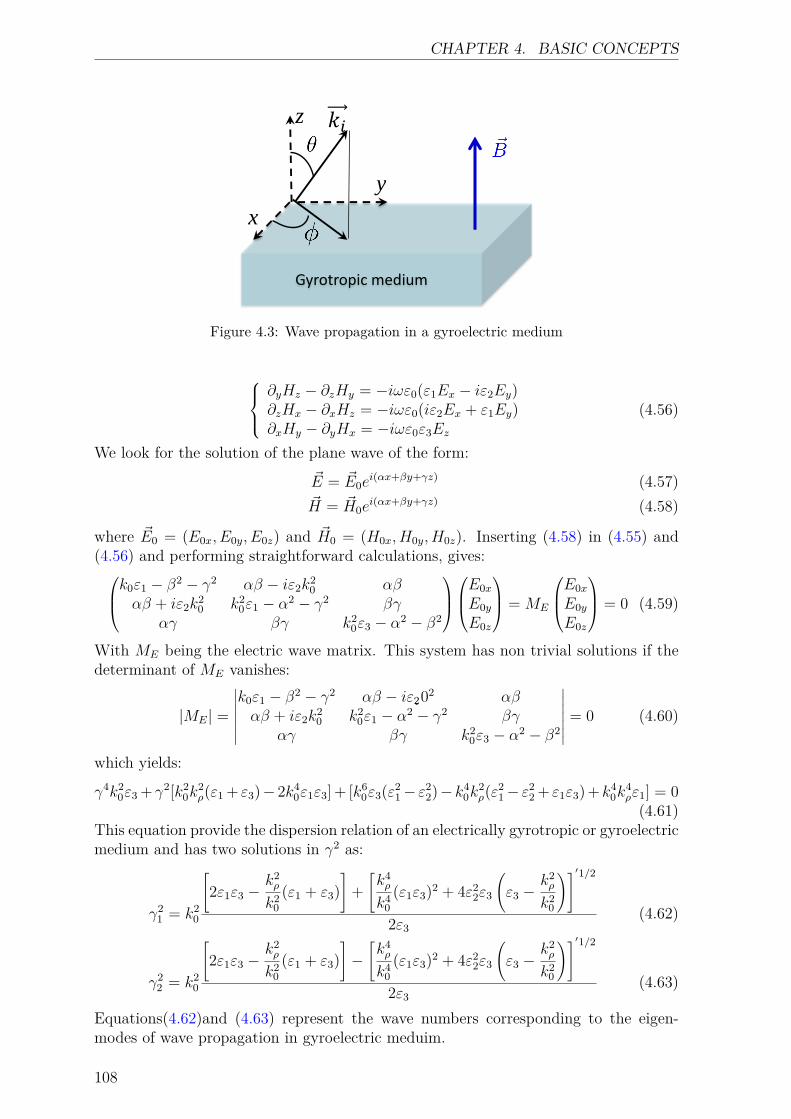
CHAPTER 4. BASIC CONCEPTS
Gyrotropic medium
z
x
y
𝑘𝑖
Figure 4.3: Wave propagation in a gyroelectric medium
∂yHz − ∂zHy = −iωε0(ε1Ex − iε2Ey)∂zHx − ∂xHz = −iωε0(iε2Ex + ε1Ey)∂xHy − ∂yHx = −iωε0ε3Ez
(4.56)
We look for the solution of the plane wave of the form:~E = ~E0e
i(αx+βy+γz) (4.57)~H = ~H0e
i(αx+βy+γz) (4.58)
where ~E0 = (E0x, E0y, E0z) and ~H0 = (H0x, H0y, H0z). Inserting (4.58) in (4.55) and(4.56) and performing straightforward calculations, gives:k0ε1 − β2 − γ2 αβ − iε2k
20 αβ
αβ + iε2k20 k2
0ε1 − α2 − γ2 βγαγ βγ k2
0ε3 − α2 − β2
E0xE0yE0z
= ME
E0xE0yE0z
= 0 (4.59)
With ME being the electric wave matrix. This system has non trivial solutions if thedeterminant of ME vanishes:
|ME| =
∣∣∣∣∣∣∣k0ε1 − β2 − γ2 αβ − iε202 αβαβ + iε2k
20 k2
0ε1 − α2 − γ2 βγαγ βγ k2
0ε3 − α2 − β2
∣∣∣∣∣∣∣ = 0 (4.60)
which yields:
γ4k20ε3 +γ2[k2
0k2ρ(ε1 + ε3)− 2k4
0ε1ε3] + [k60ε3(ε2
1− ε22)−k4
0k2ρ(ε2
1− ε22 + ε1ε3) +k4
0k4ρε1] = 0(4.61)
This equation provide the dispersion relation of an electrically gyrotropic or gyroelectricmedium and has two solutions in γ2 as:
γ21 = k2
0
[2ε1ε3 −
k2ρ
k20(ε1 + ε3)
]+[k4ρ
k40(ε1ε3)2 + 4ε2
2ε3
(ε3 −
k2ρ
k20
)]′1/22ε3
(4.62)
γ22 = k2
0
[2ε1ε3 −
k2ρ
k20(ε1 + ε3)
]−[k4ρ
k40(ε1ε3)2 + 4ε2
2ε3
(ε3 −
k2ρ
k20
)]′1/22ε3
(4.63)
Equations(4.62)and (4.63) represent the wave numbers corresponding to the eigen-modes of wave propagation in gyroelectric meduim.
108
CHAPTER 4. BASIC CONCEPTS
Propagation in Gyrotropic media
This subsection is dedicated to the investigation of the waves propagation in a gyro-electric meduim. First of all, it is important to emphasize that when the angle betweenthe magnetic field and the wave propagation θ is equal to 0 or π/2, the waves propa-gating within the medium will be named as principle waves. Hence, we can distinguishtwo type of propagation: when θ = 0 i.e the direction of propagation is parallel to thedirection of the magnetic field, the wave propagation is called longitudinal propaga-tion. When the direction of wave propagation is perpendicular of the direction of themagnetic field θ = π/2, the wave propagation is called transverse propagation.
Longitudinal Propagation (θ = 0) : Considering now the longitudinal propa-gation when θ = 0, in this case (4.62)and (4.63) reduce to:
k1 = γ1 = k0√ε1 + ε2 (4.64)
k2 = γ2 = k0√ε1 − ε2 (4.65)
From Maxwell equations and the helmotz equation we can deduce that the compo-nents of the electric field for θ = 0 satisfy the following equations:
E0x(k2
0ε1 − k2)− iε2E0y = 0 (4.66)
−iε2k20E0x + E0y
(k2
0ε1 − k2)
= 0 (4.67)E0zk
20ε3 = 0 (4.68)
One can clearly see that for a longitudinal propagation there is no electric fieldcomponent in the z direction i.e in the direction of propagation. While, the magneticfield H is transverse to the direction of propagation. Therefore, the two waves thatpropagate parallel to B are transverse electromagnetic waves. Substituting (4.64) in(4.68),gives:
E0x
E0y= −i (4.69)
This equation corresponds to a right handed circularly polarized (RCP) wave. Nowwhen (4.65) is substituted in (4.68) , we find:
E0x
E0y= i (4.70)
Which corresponds to the left handed circularly polarized(LCP) wave. The electricfields associated with the two waves can be expressed as:
~E1 = (~ex + i~ey)Aeiγ1z RCP (4.71)~E2 = (~ex − i~ey)Beiγ2z LCP (4.72)
Where A and B are arbitrary amplitudes. So, we can conclude that when an electro-magnetic wave propagates through a gyroelectric meduim with a vector wave parallelto the direction of B, the eigenmodes of propagation are right and left circularly po-larized waves. Let us consider now a linearly polarized electric field given by the sumof both circularly waves when A = B:
~E = ~E1 + ~E2 =(eiγ1z + eiγ2z
)~ex +
(ieiγ1z − ieiγ2z
)~ey (4.73)
109
CHAPTER 4. BASIC CONCEPTS
The polarisation of this wave can be obtained by:ExEy
= −i1 + ei(γ2−γ1)z
1− ei(γ2−γ1)z = −cot(γ2 − γ1
2 z)
(4.74)
From equation 4.74, it is found that the polarisation of the polarized wave rotates asthe wave propagates along the z direction by an angle θF :
θF = cot−1(γ2 − γ1
2 z)
= −(γ2 − γ1
2 z)
(4.75)
The rotation angle per unit of distance has the form:
ΘF = −(γ2 − γ1
2
)(4.76)
This rotation angle is called Faraday rotation.
Transverse Propagation (θ = 0) : As pointed out earlier, for this kind ofpropagation, the direction of wave propagation is perpondicular to the direction of themagnetic field i.e (θ = 90). By assuming a plane wave propagating along y directionequations (4.62)and (4.63) reduce to:
k1 = β1 = k0
√ε2
1 + ε22
ε1(4.77)
k2 = β2 = k0√ε3 (4.78)
In this case, from Maxwell equation we can obtain:
E0x(k2
0ε1 − k2)− iε2k
20E0y = 0 (4.79)
−iε2k20E0x + E0y
(k2
0ε1)
= 0 (4.80)E0z(k2
0ε3 − k2) = 0 (4.81)
By substituting (4.78) into (4.81), it is found that Eox and Eoy are equal to zeros andthe electric field has only one component along the z direction. Since the propagationconstant given in (4.78)is equal to the propagation constant of a wave propagating ina isotropic meduim and is independent of the magnetic field, this wave is called asordinary wave. Thus, we can see that the obtained wave is a linearly polarized wavewhose electric vector is parallel to B and is given by:
~E2 = Aeiβ2y~ez (4.82)
With A is an arbitrary amplitude. Now, when (4.77) is substitued in (4.81), we obtain:E0x
E0y= i
ε1
ε2(4.83)
The electric vector corresponding to this wave, known as extraordinary wave, has thefollowing form:
~E1 =(iε1
ε2~ex + ~ey
)Ceiβ1y (4.84)
Where C is an arbitrary constant. Finally, to summarize, in both cases θ = 0 andθ = 90, which correspond to longitudinal and transverse propagation, there exist twouncoupled waves wchich are known as principal waves. For the longitudinal propaga-tion, they are the right circularly polarized wave and the left circularly polorized wave.While for the transverse propagation, they are the ordinary wave and extraordinarywave.
110

CHAPTER 4. BASIC CONCEPTS
Magneto-optical (MO) effects
Magneto-optical effects are phenomena referring to changes in the polarisation state oflight after interacting with a magnetic material. Historically, the first magneto-opticaleffect was discovred by Michael Faraday in 1846 [9]. He found that the plane of linearlypolarized light was rotated after passing through a glass rod subjected to an externalmagnetic field parallel to the direction of the path of the light. This rotation wasknown as Faraday rotation. Thirty years later (1877), kerr found the correspondingmagneto-optical effect in reflection performed by a magnetized metallic iron mirror [10].According to the interaction of incident light with matter, the basic magneto-opticalcan be classified into three categories
• MO effects in reflection
• MO effects in transmission
• MO effects in absorption
For the last two categories of MO effects, we can distinguish two basic geometriesaccording to the orientation between the wave vector of light and the magnetic field.
• Faraday geometry: the light propagates parallel to the magnetic field (~k ‖ ~B)
• Voigt or Cotton-Mouton geometry: the light travels perpondicular to the direc-tion of the magnetic field (~k ⊥ ~B)
x z
y E
k
E
k
Figure 4.4: Schematic representation of the Faraday effect
As shown in the previous subsection, In Faraday geometry (longitudinal propagation),the eigen modes are left and right circularly polarized light and in Voigt geometry(transverse propagation) the eigenmodes are linearly polarized light. The symmetry isbroken and violated by the magneto-optical effects, which leads to induce an asymmetryof the propagation of the eigenmedes. For example, in Faraday geometry, left and rightcircularly polarized wave propagate differently. The difference between eigenmodes
111

CHAPTER 4. BASIC CONCEPTS
propagation can be explained by the effects of birefringence and dichroism. CircularBirefringence results from the difference between phase velocities for left and rightcircularly polarized light. As shown above This difference causes a rotation of theplane of polarisation of the wave by an angle ΘF . A shematic representation of thefaraday effect is shown in Figure 4.4 .
x z
y E
k
E
k
(a) MCD: Farady Geometry
x z
y
E
k
E
k
(b) MLD: Voight Geometry
Figure 4.5: Magneto-optical effects in Absorption depending on the geometry:(a) Magneticcircular dichroism (MCD).(b) Magnetic linear dichroism (MLD)
Dichroism arises when the two eigenmodes are absorbed differently by the magneticmedium. In the Fraday geometry, circular magnetic dichroism (MCD) is producedfrom the difference in absorption coefficients for left and right circularly polarizedEM wave. While, in the case of the Voigt geometry, dichroism, known as magneticlinear dichroism (MLD), is related to the difference between the absorption of thecomponents polarized parallel and perpendicular to the magnetic field (see Figure 4.5).MCD changes an incident linearly polarized EM wave into elliptically one and the MLDrotates an elliptically polarized wave by and angle.
We turn now our attention to the magnetooptical effects in reflection often knownas Kerr effects. These effects occur when an EM wave is reflected from a magnetizedmedium and are related to the change of the polarisation state of the reflected light.First, it is important to underline that when working in reflection, the polarisationstate is defined with respect to the plane of incidence. According to that, we candistingiush two linear polarizations: a linear polarisation ”s”, where the electric field isperpondicular to the plane of incidence, and a linear polarization ”p” where the electricfield is parallel to plane of incidence. These two linear polarizations are orthogonaland thus they can form a basis. Let us consider a magnetic medium subjected to alinearly polarized (s or p) wave. After reflection, an orthogonal polarisation appearsand we will have both s and p components. As a consequence, the reflected wavebecomes elliptically polarized which causes the rotation of the polarisation plane. Thisevolution of the polarisation state of light can be described in the framework of theJones formalism. The Jone vector J is defined as:
~J =(EsEp
)(4.85)
112
CHAPTER 4. BASIC CONCEPTS
Where Es and Ep represents the s and p polarized components of light. The totalintensity of the wave can be expressed as:
I = JJ∗ = (EsE∗s + EpE∗p) = (|Es|2 + |Ep|2) (4.86)
The change of the polarization state caused by the reflection can be described by thereflection matrix R:
R =(rss rpsrsp rpp
)(4.87)
where the coefficients are defined as the ratio between reflected and incident electro-magnetic waves:
rss = Ers
Eis
rpp =Erp
Eip
rsp = Ers
Eip
rps =Erp
Eis
(4.88)
Using these reflections coefficients, we can define the Kerr rotation Θs,p and ellipticityεs,p for s and p incident polarized light:
Θs + iεs = rsprss
Θp + iεp = rpsrpp
(4.89)
4.2 Graphene under a static magnetic biasIn this section, we are going to investigate and exploit the gyrotropic and propagationproperties of graphene in the presence of a magnetic bias. We start by describingthe quantized Landau levels in magnetically biased graphene which are important tounderstand and explain the magneto-optical conductivity model presented in chap-ter 1. Next, the reflection and transmission coefficients through a single anisotropicmonolayer graphene will be calculated. These calculations will be then used to de-rive the dispersion relation of surface magnetoplasmons polaritons propagating alonga magnetized graphene sheet.
4.2.1 Landau Levels in monolayer grapheneUnder the influence of a perpendicular magnetic field, the relativistic carriers in grapheneare deflected by the Lorentz force and move in cyclotron orbits. At sufficiently highfields, the continuum Dirac quasiparticle spectrum becomes a discrete spectrum ofdegenerated Landau levels (LLs) (see Figure 4.6) with energies given by [11, 12]:
En = sign(n)(~υflB
)√
2|n| = sign(n)υf√
2e~B|n| n = 0,±1,±2,±3... (4.90)
Where lB =√~/(eB) denotes the magnetic length and n is the LL index. Note that
this index can be positive or negative. The positive values correspond to electrons inconduction band. While the negative values correspond to the holes in valence band.From equation 4.90, one can see that the spectrum of quantized levels in graphene isdifferent from the usual landau quantization. In fact, in a conventional two dimensionalelectron gas, Landau quantization produces equidistant energy levels with energy dif-ference ~ωc [13], where ωc being the cyclotron frequency. While, in graphene as shownin Figure 4.7, the quantized landau energies are proportional to the square root of the
113
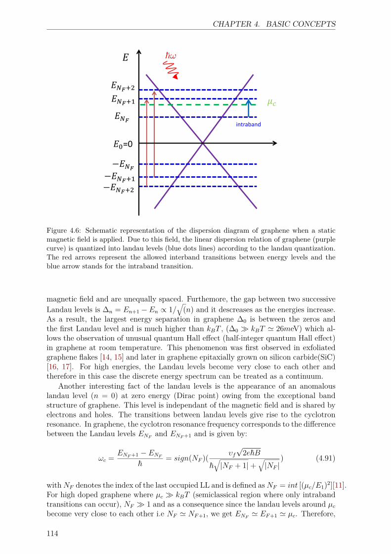
CHAPTER 4. BASIC CONCEPTS
𝐸
𝜇𝑐
𝐸0=0
𝐸𝑁𝐹
𝐸𝑁𝐹+1
𝐸𝑁𝐹+2
−𝐸𝑁𝐹
−𝐸𝑁𝐹+1 −𝐸𝑁𝐹+2
intraband
Figure 4.6: Schematic representation of the dispersion diagram of graphene when a staticmagnetic field is applied. Due to this field, the linear dispersion relation of graphene (purplecurve) is quantized into landau levels (blue dots lines) according to the landau quantization.The red arrows represent the allowed interband transitions between energy levels and theblue arrow stands for the intraband transition.
magnetic field and are unequally spaced. Furthemore, the gap between two successiveLandau levels is ∆n = En+1 −En ∝ 1/
√(n) and it descreases as the energies increase.
As a result, the largest energy separation in graphene ∆0 is between the zeros andthe first Landau level and is much higher than kBT , (∆0 kBT ' 26meV) which al-lows the observation of unusual quantum Hall effect (half-integer quantum Hall effect)in graphene at room temperature. This phenomenon was first observed in exfoliatedgraphene flakes [14, 15] and later in graphene epitaxially grown on silicon carbide(SiC)[16, 17]. For high energies, the Landau levels become very close to each other andtherefore in this case the discrete energy spectrum can be treated as a continuum.
Another interesting fact of the landau levels is the appearance of an anomalouslandau level (n = 0) at zero energy (Dirac point) owing from the exceptional bandstructure of graphene. This level is independant of the magnetic field and is shared byelectrons and holes. The transitions between landau levels give rise to the cyclotronresonance. In graphene, the cyclotron resonance frequency corresponds to the differencebetween the Landau levels ENF and ENF+1 and is given by:
ωc = ENF+1 − ENF~
= sign(NF )( υf√
2e~B~√|NF + 1|+
√|NF |
) (4.91)
withNF denotes the index of the last occupied LL and is defined asNF = int [(µc/E1)2][11].For high doped graphene where µc kBT (semiclassical region where only intrabandtransitions can occur), NF 1 and as a consequence since the landau levels around µcbecome very close to each other i.e NF ' NF+1, we get ENF ' EF+1 ' µc. Therefore,
114
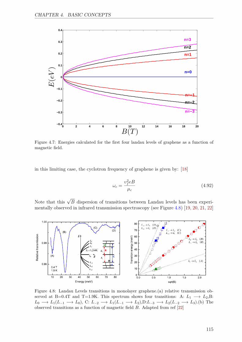
CHAPTER 4. BASIC CONCEPTS
0 2 4 6 8 10 12 14 16 18 20−0.4
−0.3
−0.2
−0.1
0
0.1
0.2
0.3
0.4
B(T )
E(eV)
n=3
n=2
n=1
n=0
n=−3
n=−2
n=−1
Figure 4.7: Energies calculated for the first four landau levels of graphene as a function ofmagnetic field.
in this limiting case, the cyclotron frequency of graphene is given by: [18]
ωc =υ2feB
µc(4.92)
Note that this√B dispersion of transitions between Landau levels has been experi-
mentally observed in infrared transmission spectroscopy (see Figure 4.8) [19, 20, 21, 22]
Figure 4.8: Landau Levels transitions in monolayer graphene.(a) relative transmission ob-served at B=0.4T and T=1.9K. This spectrum shows four transitions: A: L1 −→ L2,B:L0 −→ L1(L−1 −→ L0), C: L−2 −→ L1(L−1 −→ L2),D:L−3 −→ L2(L−2 −→ L3).(b) Theobserved transitions as a function of magnetic field B. Adapted from ref [22]
115
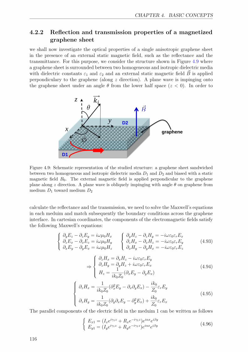
CHAPTER 4. BASIC CONCEPTS
4.2.2 Reflection and transmission properties of a magnetizedgraphene sheet
we shall now investigate the optical properties of a single anisotropic graphene sheetin the presence of an external static magnetic field, such as the reflectance and thetransmittance. For this purpose, we consider the structure shown in Figure 4.9 wherea graphene sheet is surrounded between two homogeneous and isotropic dielectric mediawith dielectric constants ε1 and ε2 and an external static magnetic field ~B is appliedperpondiculary to the graphene (along z direction). A plane wave is impinging ontothe graphene sheet under an angle θ from the lower half space (z < 0). In order to
D1
D2
graphene
z
x y
𝑘𝑖
Figure 4.9: Schematic representation of the studied structure: a graphene sheet sandwichedbetween two homogeneous and isotropic dielectric media D1 and D2 and biased with a staticmagnetic field B0. The external magnetic field is applied perpondicular to the grapheneplane along z direction. A plane wave is obliquely impinging with angle θ on graphene frommedium D1 toward medium D2
calculate the reflectance and the transmission, we need to solve the Maxwell’s equationsin each meduim and match subsequently the boundary conditions across the grapheneinterface. In cartesian coordinates, the components of the electromagnetic fields satisfythe following Maxwell’s equations:
∂yEz − ∂zEy = iωµ0Hx
∂zEx − ∂xEz = iωµ0Hy
∂xEy − ∂yEx = iωµ0Hz
∂yHz − ∂zHy = −iωε0εrEx∂zHx − ∂xHz = −iωε0εrEy∂xHy − ∂yHx = −iωε0εrEz
(4.93)
⇒
∂zHx = ∂xHz − iωε0εrEy∂zHy = ∂yHz + iωε0εrEx
Hz = 1ik0Z0
(∂xEy − ∂yEx)(4.94)
∂zHx = 1
ik0Z0(∂2xEy − ∂x∂yEx)−
ik0
Z0εrEy
∂zHy = 1ik0Z0
(∂y∂xEy − ∂2yEx) + ik0
Z0εrEx
(4.95)
The parallel components of the electric field in the meduim 1 can be written as followsEx1 = (Ixeiγ1z +Rxe
−iγ1z)eiαxeiβyEy1 = (Iyeiγ1z +Rye
−iγ1z)eiαxeiβy (4.96)
116

CHAPTER 4. BASIC CONCEPTS
Similarly, in meduim 2 the x and y components of E are given by:Ex2 = Txe
iγ2zeiαxeiβy
Ey2 = Tyeiγ2zeiαxeiβy
(4.97)
The x and y components of the magnetic field in each meduim can be deduced from4.95 and are expressed as:
Hx1 = − 1
k0Z0γ1((αβ(Ixeiγ1z −Rxe
−iγ1z) + (β2 + γ21)(Iyeiγ1z −Rye
−iγ1z)) eiαxeiβy
Hy1 = 1k0Z0γ1
(αβ(Iyeiγ1z −Rye
−iγ1z) + (α2 + γ21)(Ixeiγ1z −Rxe
−iγ1z))eiαxeiβy
(4.98)Hx2 = − 1
k0Z0γ2(αβTxeiγ2z + (β2 + γ2
2)Tyeiγ2z) eiαxeiβy
Hy2 = 1k0Z0γ2
(αβTyeiγ2z + (α2 + γ22)Txeiγ2z) eiαxeiβy
(4.99)
Let us now apply the boundary conditions at the interface which relate the electro-magnetic fields in the two dielectric media. The first boundary condition imposes thecontinuity of the tangential electric field at the interface of graphene while the secondcondition relates the tangential components of the magnetic field at the interface tothe surface current density over the graphene layer :
~ez ∧ ( ~E2 − ~E1) = ~0~ez ∧ ( ~H2 − ~H1) = ~J
(4.100)
Where ~J = σ ~E with σ is the conductivity tensor given in chapter 1. This leads us tofind:
Ex1 = Ex2Ey1 = Ey2Hx2 −Hx1 = Jy = σLEy − σHExHy2 −Hy1 = −Jx = −(σLEx + σHEy)
(4.101)
Enforcing these conditions at z = 0, we obtain:
Ix +Rx = TxIy +Ry = Ty1γ2
(αβTx + (β2 + γ22)Ty)−
1γ1
((αβ(Ix −Rx) + (β2 + γ21)(Iy −Ry)) = k0Z0(σHTx − σLTy)
1γ2
(αβTy + (α2 + γ22)Tx)−
1γ1
((αβ(Iy −Ry) + (α2 + γ21)(Ix −Rx)) = k0Z0(−σLTx − σHTy)
(4.102)This system of equations can be written in the following matrix form :
αβ
γ1− αβ
γ2+ k0Z0σH γ1 + β2
γ1− γ2 −
β2
γ2− k0Z0σL
γ1 + α2
γ1− γ2 −
α2
γ2− k0Z0σL
αβ
γ1− αβ
γ2− k0Z0σH
(IxIy
)=
αβ
γ1+ αβ
γ2− k0Z0σH γ1 + β2
γ1+ γ2 + β2
γ2+ k0Z0σL
γ1 + α2
γ1+ γ2 + α2
γ2+ k0Z0σL
αβ
γ1+ αβ
γ2+ k0Z0σH
(Rx
Ry
)(4.103)
117
CHAPTER 4. BASIC CONCEPTS
(Rx
Ry
)=
αβ
γ1+ αβ
γ2− k0Z0σH γ1 + β2
γ1+ γ2 + β2
γ2+ k0Z0σL
γ1 + α2
γ1+ γ2 + α2
γ2− k0Z0σL
αβ
γ1+ αβ
γ2+ k0Z0σH
−1
αβ
γ1− αβ
γ2+ k0Z0σH γ1 + β2
γ1− γ2 −
β2
γ2− k0Z0σL
γ1 + α2
γ1− γ2 −
α2
γ2− k0Z0σL
αβ
γ1− αβ
γ2+ k0Z0σH
(IxIy
)(4.104)
Therefore the reflected and incident fields can be connected by the Reflection MatrixMR as follows:
(Rx
Ry
)=(Rxx Rxy
Ryx Ryy
)(IxIy
)= MR
(IxIy
)(4.105)
where:
MR =
αβ
γ1+ αβ
γ2− k0Z0σH γ1 + β2
γ1+ γ2 + β2
γ2+ k0Z0σL
γ1 + α2
γ1+ γ2 + α2
γ2− k0Z0σL
αβ
γ1+ αβ
γ2+ k0Z0σH
−1
αβ
γ1− αβ
γ2+ k0Z0σH γ1 + β2
γ1− γ2 −
β2
γ2− k0Z0σL
γ1 + α2
γ1− γ2 −
α2
γ2− k0Z0σL
αβ
γ1− αβ
γ2+ k0Z0σH
(4.106)
In the simple case when ε1 = ε2, the reflection coefficients are expressed as:
Rxx = − 2(γ2 + β2)σL + 2αβσH + k0Z0γ(σ2L + σ2
H)
2(γ2 + k20ε)σL + 4γ k0
Z0ε+ k0Z0γ(σ2
L + σ2H)
(4.107)
Rxy = − 2(γ2 + β2)σH − 2αβσL
2(γ2 + k20ε)σL + 4γ k0
Z0ε+ k0Z0γ(σ2
L + σ2H)
(4.108)
Ryx = 2(γ2 + α2)σH + 2αβσL
2(γ2 + k20ε)σL + 4γ k0
Z0ε+ k0Z0γ(σ2
L + σ2H)
(4.109)
Ryy = − 2(γ2 + α2)σL − 2αβσH + k0Z0γ(σ2L + σ2
H)
2(γ2 + k20ε)σL + 4γ k0
Z0ε+ k0Z0γ(σ2
L + σ2H)
(4.110)
In addition, at normal incidence where α = β = 0, these expressions are simplified to:
118
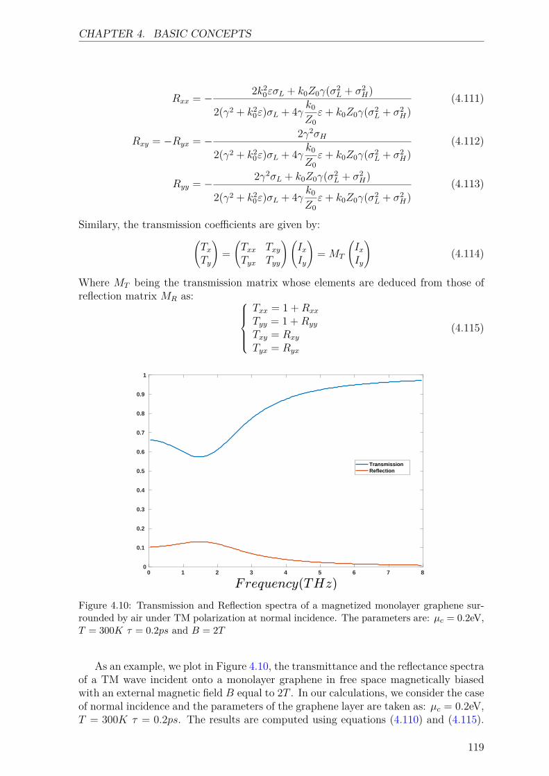
CHAPTER 4. BASIC CONCEPTS
Rxx = − 2k20εσL + k0Z0γ(σ2
L + σ2H)
2(γ2 + k20ε)σL + 4γ k0
Z0ε+ k0Z0γ(σ2
L + σ2H)
(4.111)
Rxy = −Ryx = − 2γ2σH
2(γ2 + k20ε)σL + 4γ k0
Z0ε+ k0Z0γ(σ2
L + σ2H)
(4.112)
Ryy = − 2γ2σL + k0Z0γ(σ2L + σ2
H)
2(γ2 + k20ε)σL + 4γ k0
Z0ε+ k0Z0γ(σ2
L + σ2H)
(4.113)
Similary, the transmission coefficients are given by:(TxTy
)=(Txx TxyTyx Tyy
)(IxIy
)= MT
(IxIy
)(4.114)
Where MT being the transmission matrix whose elements are deduced from those ofreflection matrix MR as:
Txx = 1 +Rxx
Tyy = 1 +Ryy
Txy = Rxy
Tyx = Ryx
(4.115)
0 1 2 3 4 5 6 7 80
0.1
0.2
0.3
0.4
0.5
0.6
0.7
0.8
0.9
1
TransmissionReflection
Figure 4.10: Transmission and Reflection spectra of a magnetized monolayer graphene sur-rounded by air under TM polarization at normal incidence. The parameters are: µc = 0.2eV,T = 300K τ = 0.2ps and B = 2T
As an example, we plot in Figure 4.10, the transmittance and the reflectance spectraof a TM wave incident onto a monolayer graphene in free space magnetically biasedwith an external magnetic field B equal to 2T . In our calculations, we consider the caseof normal incidence and the parameters of the graphene layer are taken as: µc = 0.2eV,T = 300K τ = 0.2ps. The results are computed using equations (4.110) and (4.115).
119
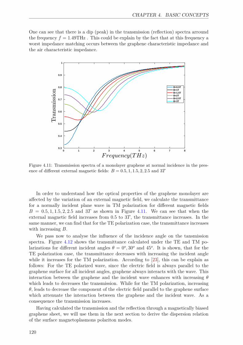
CHAPTER 4. BASIC CONCEPTS
One can see that there is a dip (peak) in the transmission (reflection) spectra arroundthe frequency f = 1.49THz . This could be explain by the fact that at this frequency aworst impedance matching occurs between the graphene characteristic impedance andthe air characteristic impedance.
0 1 2 3 4 5 6 7 80.3
0.4
0.5
0.6
0.7
0.8
0.9
1
B=0.5TB=1TB=1.5TB=2TB=2.5TB=3T
Figure 4.11: Transmission spectra of a monolayer graphene at normal incidence in the pres-ence of different external magnetic fields: B = 0.5, 1, 1.5, 2, 2.5 and 3T
In order to understand how the optical properties of the graphene monolayer areaffected by the variation of an external magnetic field, we calculate the transmittancefor a normally incident plane wave in TM polarization for different magnetic fieldsB = 0.5, 1, 1.5, 2, 2.5 and 3T as shown in Figure 4.11. We can see that when theexternal magnetic field increases from 0.5 to 3T , the transmittance increases. In thesame manner, we can find that for the TE polarization case, the transmittance increaseswith increasing B.
We pass now to analyse the influence of the incidence angle on the tansmissionspectra. Figure 4.12 shows the transmittance calculated under the TE and TM po-larizations for different incident angles θ = 0o, 30o and 45o. It is shown, that for theTE polarization case, the transmittance decreases with increasing the incident anglewhile it increases for the TM polarization. According to [23], this can be explain asfollows: For the TE polarized wave, since the electric field is always parallel to thegraphene surface for all incident angles, graphene always interacts with the wave. Thisinteraction between the graphene and the incident wave enhances with increasing θwhich leads to decreases the transmission. While for the TM polarization, increasingθ, leads to decrease the component of the electric field parallel to the graphene surfacewhich attenuate the interaction between the graphene and the incident wave. As aconsequence the transmission increases.
Having calculated the transmission and the reflection through a magnetically biasedgraphene sheet, we will use them in the next section to derive the dispersion relationof the surface magnetoplasmons polariton modes.
120
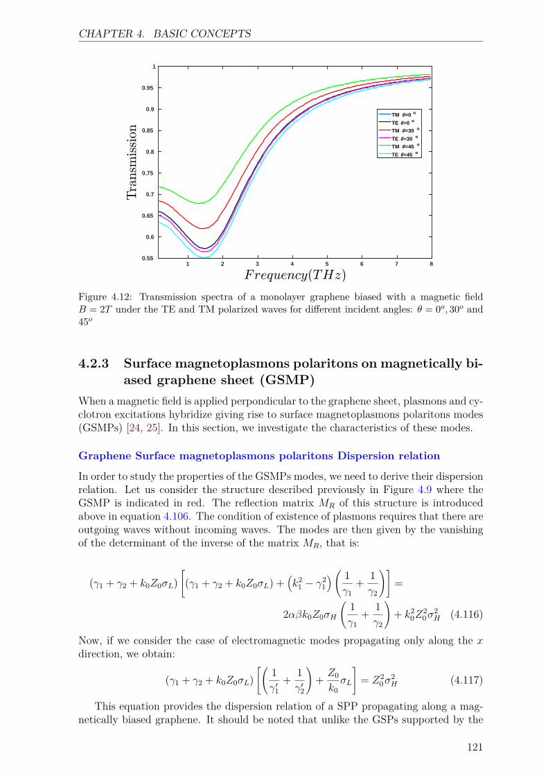
CHAPTER 4. BASIC CONCEPTS
1 2 3 4 5 6 7 80.55
0.6
0.65
0.7
0.75
0.8
0.85
0.9
0.95
1
TM =0 o
TE =0 o
TM =30 o
TE =30 o
TM =45 o
TE =45 o
Figure 4.12: Transmission spectra of a monolayer graphene biased with a magnetic fieldB = 2T under the TE and TM polarized waves for different incident angles: θ = 0o, 30o and45o
4.2.3 Surface magnetoplasmons polaritons on magnetically bi-ased graphene sheet (GSMP)
When a magnetic field is applied perpondicular to the graphene sheet, plasmons and cy-clotron excitations hybridize giving rise to surface magnetoplasmons polaritons modes(GSMPs) [24, 25]. In this section, we investigate the characteristics of these modes.
Graphene Surface magnetoplasmons polaritons Dispersion relation
In order to study the properties of the GSMPs modes, we need to derive their dispersionrelation. Let us consider the structure described previously in Figure 4.9 where theGSMP is indicated in red. The reflection matrix MR of this structure is introducedabove in equation 4.106. The condition of existence of plasmons requires that there areoutgoing waves without incoming waves. The modes are then given by the vanishingof the determinant of the inverse of the matrix MR, that is:
(γ1 + γ2 + k0Z0σL)[(γ1 + γ2 + k0Z0σL) +
(k2
1 − γ21
)( 1γ1
+ 1γ2
)]=
2αβk0Z0σH
(1γ1
+ 1γ2
)+ k2
0Z20σ
2H (4.116)
Now, if we consider the case of electromagnetic modes propagating only along the xdirection, we obtain:
(γ1 + γ2 + k0Z0σL)[(
1γ′1
+ 1γ′2
)+ Z0
k0σL
]= Z2
0σ2H (4.117)
This equation provides the dispersion relation of a SPP propagating along a mag-netically biased graphene. It should be noted that unlike the GSPs supported by the
121

CHAPTER 4. BASIC CONCEPTS
graphene sheet in the absence of a magnetic field which are pure TM or TE modes,surface magnetoplasmons polaritons in graphene are hybrid TM-TE modes. Thesehybrid modes result from the presence of the magnetic field that ensures the couplingbetween the TM and TE modes.
It should also be noted that in the absence of an external field B, we find thewell-known dispersion relations of the decoupled TE and TM SPPs modes:
(γ1 + γ2 + k0Z0σL)[(
1γ′1
+ 1γ′2
)+ Z0
k0σL
]= 0 (4.118)
⇒
(γ1 + γ2 + k0Z0σL) = 0 TE-GSP(
1γ′1
+ 1γ′2
)+ Z0
k0σL = 0 TM-GSP (4.119)
Figure 4.13 shows the dispersion relation of surface plasmons propagating on graphene
0 0.05 0.1 0.15 0.20.5
1
1.5
2
2.5
3
3.5
4
Figure 4.13: Dispersion relation of surface plasmons supported by a graphene sheet in freespace in the presence of an external magnetic field B = 2T . The parameters are taken to beas: µc = 0.5eV, τ =
sheet surrounded by air when an external magnetic field B = 2T is applied. Thecurve is computed from equation 4.117. In order to show the effect of the variationof the magnetic field on the GSMP relation dispersion, we plot in Figure 4.14 thedispersion curve for different magnetic fields. It is shown that Increasing B pushesthe dispersion curve upward. As a results, in addition to the chemical potential ofgraphene, applying an external magnetic field can be used to tune the surface plasmonpolariton on graphene.
122
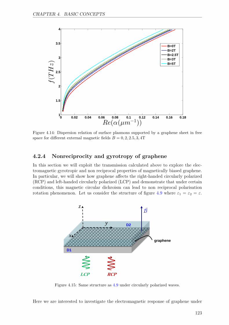
CHAPTER 4. BASIC CONCEPTS
0 0.02 0.04 0.06 0.08 0.1 0.12 0.14 0.16 0.181
1.5
2
2.5
3
3.5
4
Re(α(µm−1))
f(T
Hz)
B=0TB=2TB=2.5TB=3TB=5T
Figure 4.14: Dispersion relation of surface plasmons supported by a graphene sheet in freespace for different external magnetic fields B = 0, 2, 2.5, 3, 4T
4.2.4 Nonreciprocity and gyrotropy of grapheneIn this section we will exploit the transmission calculated above to explore the elec-tromagnetic gyrotropic and non reciprocal properties of magnetically biased graphene.In particular, we will show how graphene affects the right-handed circularly polarized(RCP) and left-handed circularly polarized (LCP) and demonstrate that under certainconditions, this magnetic circular dichroism can lead to non reciprocal polarisationrotation phenomenon. Let us consider the structure of figure 4.9 where ε1 = ε2 = ε.
D1
D2
z
x
y
LCP RCP
graphene
Figure 4.15: Same structure as 4.9 under circularly polarized waves.
Here we are interested to investigate the electromagnetic response of graphene under
123
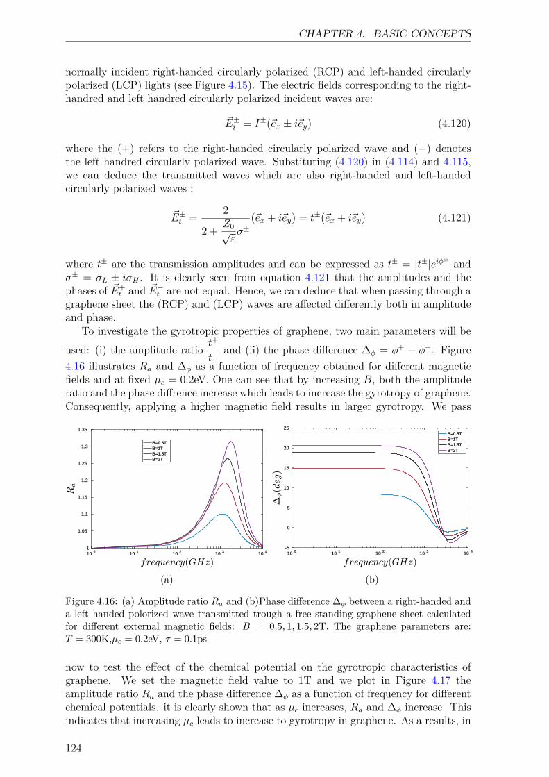
CHAPTER 4. BASIC CONCEPTS
normally incident right-handed circularly polarized (RCP) and left-handed circularlypolarized (LCP) lights (see Figure 4.15). The electric fields corresponding to the right-handred and left handred circularly polarized incident waves are:
~E±i = I±(~ex ± i~ey) (4.120)
where the (+) refers to the right-handed circularly polarized wave and (−) denotesthe left handred circularly polarized wave. Substituting (4.120) in (4.114) and 4.115,we can deduce the transmitted waves which are also right-handed and left-handedcircularly polarized waves :
~E±t = 2
2 + Z0√εσ±
(~ex + i~ey) = t±(~ex + i~ey) (4.121)
where t± are the transmission amplitudes and can be expressed as t± = |t±|eiφ± andσ± = σL ± iσH . It is clearly seen from equation 4.121 that the amplitudes and thephases of ~E+
t and ~E−t are not equal. Hence, we can deduce that when passing through agraphene sheet the (RCP) and (LCP) waves are affected differently both in amplitudeand phase.
To investigate the gyrotropic properties of graphene, two main parameters will beused: (i) the amplitude ratio t+
t−and (ii) the phase difference ∆φ = φ+ − φ−. Figure
4.16 illustrates Ra and ∆φ as a function of frequency obtained for different magneticfields and at fixed µc = 0.2eV. One can see that by increasing B, both the amplituderatio and the phase diffrence increase which leads to increase the gyrotropy of graphene.Consequently, applying a higher magnetic field results in larger gyrotropy. We pass
10 0 10 1 10 2 10 3 10 41
1.05
1.1
1.15
1.2
1.25
1.3
1.35
B=0.5TB=1TB=1.5TB=2T
(a)
10 0 10 1 10 2 10 3 10 4-5
0
5
10
15
20
25B=0.5TB=1TB=1.5TB=2T
(b)
Figure 4.16: (a) Amplitude ratio Ra and (b)Phase difference ∆φ between a right-handed anda left handed polorized wave transmitted trough a free standing graphene sheet calculatedfor different external magnetic fields: B = 0.5, 1, 1.5, 2T. The graphene parameters are:T = 300K,µc = 0.2eV, τ = 0.1ps
now to test the effect of the chemical potential on the gyrotropic characteristics ofgraphene. We set the magnetic field value to 1T and we plot in Figure 4.17 theamplitude ratio Ra and the phase difference ∆φ as a function of frequency for differentchemical potentials. it is clearly shown that as µc increases, Ra and ∆φ increase. Thisindicates that increasing µc leads to increase to gyrotropy in graphene. As a results, in
124
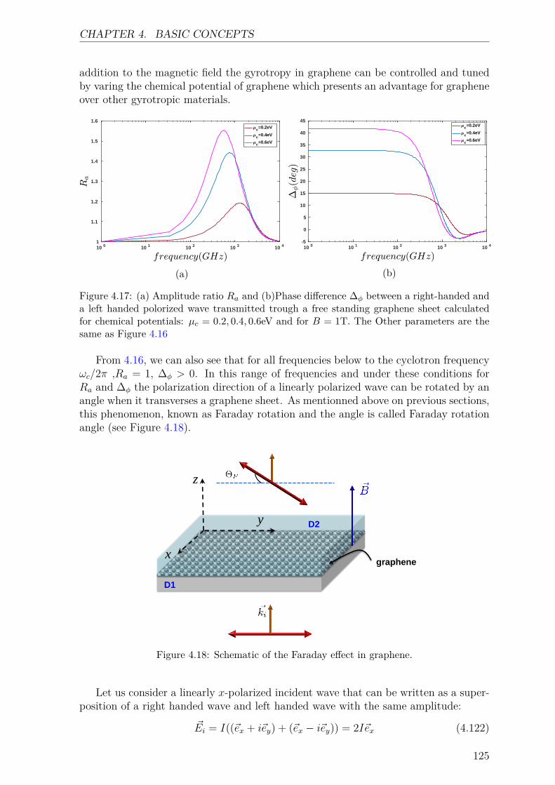
CHAPTER 4. BASIC CONCEPTS
addition to the magnetic field the gyrotropy in graphene can be controlled and tunedby varing the chemical potential of graphene which presents an advantage for grapheneover other gyrotropic materials.
10 0 10 1 10 2 10 3 10 41
1.1
1.2
1.3
1.4
1.5
1.6
c=0.2eV
c=0.4eV
c=0.6eV
(a)
10 0 10 1 10 2 10 3 10 4-5
0
5
10
15
20
25
30
35
40
45c=0.2eV
c=0.4eV
c=0.6eV
(b)
Figure 4.17: (a) Amplitude ratio Ra and (b)Phase difference ∆φ between a right-handed anda left handed polorized wave transmitted trough a free standing graphene sheet calculatedfor chemical potentials: µc = 0.2, 0.4, 0.6eV and for B = 1T. The Other parameters are thesame as Figure 4.16
From 4.16, we can also see that for all frequencies below to the cyclotron frequencyωc/2π ,Ra = 1, ∆φ > 0. In this range of frequencies and under these conditions forRa and ∆φ the polarization direction of a linearly polarized wave can be rotated by anangle when it transverses a graphene sheet. As mentionned above on previous sections,this phenomenon, known as Faraday rotation and the angle is called Faraday rotationangle (see Figure 4.18).
D1
D2
graphene
z
x
y
Figure 4.18: Schematic of the Faraday effect in graphene.
Let us consider a linearly x-polarized incident wave that can be written as a super-position of a right handed wave and left handed wave with the same amplitude:
~Ei = I((~ex + i~ey) + (~ex − i~ey)) = 2I~ex (4.122)
125
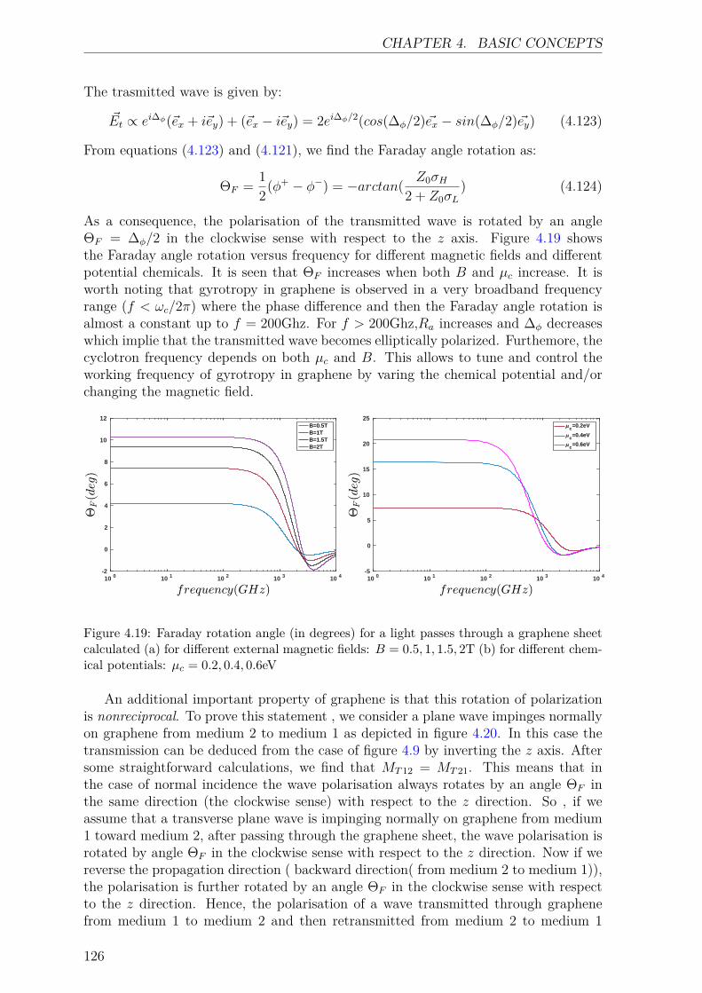
CHAPTER 4. BASIC CONCEPTS
The trasmitted wave is given by:
~Et ∝ ei∆φ(~ex + i~ey) + (~ex − i~ey) = 2ei∆φ/2(cos(∆φ/2)~ex − sin(∆φ/2)~ey) (4.123)
From equations (4.123) and (4.121), we find the Faraday angle rotation as:
ΘF = 12(φ+ − φ−) = −arctan( Z0σH
2 + Z0σL) (4.124)
As a consequence, the polarisation of the transmitted wave is rotated by an angleΘF = ∆φ/2 in the clockwise sense with respect to the z axis. Figure 4.19 showsthe Faraday angle rotation versus frequency for different magnetic fields and differentpotential chemicals. It is seen that ΘF increases when both B and µc increase. It isworth noting that gyrotropy in graphene is observed in a very broadband frequencyrange (f < ωc/2π) where the phase difference and then the Faraday angle rotation isalmost a constant up to f = 200Ghz. For f > 200Ghz,Ra increases and ∆φ decreaseswhich implie that the transmitted wave becomes elliptically polarized. Furthemore, thecyclotron frequency depends on both µc and B. This allows to tune and control theworking frequency of gyrotropy in graphene by varing the chemical potential and/orchanging the magnetic field.
10 0 10 1 10 2 10 3 10 4-2
0
2
4
6
8
10
12B=0.5TB=1TB=1.5TB=2T
10 0 10 1 10 2 10 3 10 4-5
0
5
10
15
20
25
c=0.2eV
c=0.4eV
c=0.6eV
Figure 4.19: Faraday rotation angle (in degrees) for a light passes through a graphene sheetcalculated (a) for different external magnetic fields: B = 0.5, 1, 1.5, 2T (b) for different chem-ical potentials: µc = 0.2, 0.4, 0.6eV
An additional important property of graphene is that this rotation of polarizationis nonreciprocal. To prove this statement , we consider a plane wave impinges normallyon graphene from medium 2 to medium 1 as depicted in figure 4.20. In this case thetransmission can be deduced from the case of figure 4.9 by inverting the z axis. Aftersome straightforward calculations, we find that MT 12 = MT 21. This means that inthe case of normal incidence the wave polarisation always rotates by an angle ΘF inthe same direction (the clockwise sense) with respect to the z direction. So , if weassume that a transverse plane wave is impinging normally on graphene from medium1 toward medium 2, after passing through the graphene sheet, the wave polarisation isrotated by angle ΘF in the clockwise sense with respect to the z direction. Now if wereverse the propagation direction ( backward direction( from medium 2 to medium 1)),the polarisation is further rotated by an angle ΘF in the clockwise sense with respectto the z direction. Hence, the polarisation of a wave transmitted through graphenefrom medium 1 to medium 2 and then retransmitted from medium 2 to medium 1
126
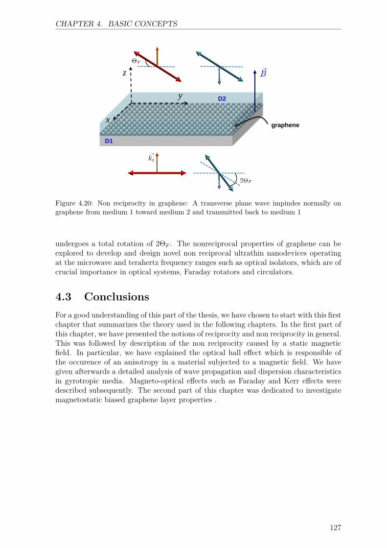
CHAPTER 4. BASIC CONCEPTS
D1
D2
graphene
z
x
y
Figure 4.20: Non reciprocity in graphene: A transverse plane wave impindes normally ongraphene from medium 1 toward medium 2 and transmitted back to medium 1
undergoes a total rotation of 2ΘF . The nonreciprocal properties of graphene can beexplored to develop and design novel non reciprocal ultrathin nanodevices operatingat the microwave and terahertz frequency ranges such as optical isolators, which are ofcrucial importance in optical systems, Faraday rotators and circulators.
4.3 ConclusionsFor a good understanding of this part of the thesis, we have chosen to start with this firstchapter that summarizes the theory used in the following chapters. In the first part ofthis chapter, we have presented the notions of reciprocity and non reciprocity in general.This was followed by description of the non reciprocity caused by a static magneticfield. In particular, we have explained the optical hall effect which is responsible ofthe occurence of an anisotropy in a material subjected to a magnetic field. We havegiven afterwards a detailed analysis of wave propagation and dispersion characteristicsin gyrotropic media. Magneto-optical effects such as Faraday and Kerr effects weredescribed subsequently. The second part of this chapter was dedicated to investigatemagnetostatic biased graphene layer properties .
127

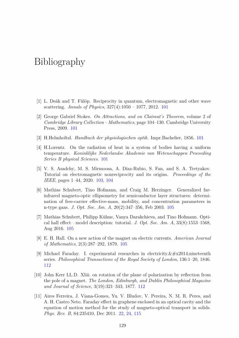
Bibliography
[1] L. Deák and T. Fülöp. Reciprocity in quantum, electromagnetic and other wavescattering. Annals of Physics, 327(4):1050 – 1077, 2012. 101
[2] George Gabriel Stokes. On Attractions, and on Clairaut’s Theorem, volume 2 ofCambridge Library Collection - Mathematics, page 104–130. Cambridge UniversityPress, 2009. 101
[3] H.Helmholtzl. Handbuch der physiologischen optik. Impr.Bachelier, 1856. 101
[4] H.Lorentz. On the radiation of heat in a system of bodies having a uniformtemperature. Koninklijke Nederlandse Akademie van Wetenschappen ProceedingSeries B physical Sciences. 101
[5] V. S. Asadchy, M. S. Mirmoosa, A. Díaz-Rubio, S. Fan, and S. A. Tretyakov.Tutorial on electromagnetic nonreciprocity and its origins. Proceedings of theIEEE, pages 1–44, 2020. 103, 104
[6] Mathias Schubert, Tino Hofmann, and Craig M. Herzinger. Generalized far-infrared magneto-optic ellipsometry for semiconductor layer structures: determi-nation of free-carrier effective-mass, mobility, and concentration parameters inn-type gaas. J. Opt. Soc. Am. A, 20(2):347–356, Feb 2003. 105
[7] Mathias Schubert, Philipp Kühne, Vanya Darakchieva, and Tino Hofmann. Opti-cal hall effect—model description: tutorial. J. Opt. Soc. Am. A, 33(8):1553–1568,Aug 2016. 105
[8] E. H. Hall. On a new action of the magnet on electric currents. American Journalof Mathematics, 2(3):287–292, 1879. 105
[9] Michael Faraday. I. experimental researches in electricity.—nineteenthseries. Philosophical Transactions of the Royal Society of London, 136:1–20, 1846.112
[10] John Kerr LL.D. Xliii. on rotation of the plane of polarization by reflection fromthe pole of a magnet. The London, Edinburgh, and Dublin Philosophical Magazineand Journal of Science, 3(19):321–343, 1877. 112
[11] Aires Ferreira, J. Viana-Gomes, Yu. V. Bludov, V. Pereira, N. M. R. Peres, andA. H. Castro Neto. Faraday effect in graphene enclosed in an optical cavity and theequation of motion method for the study of magneto-optical transport in solids.Phys. Rev. B, 84:235410, Dec 2011. 22, 24, 115
129
BIBLIOGRAPHY
[12] J. W. McClure. Diamagnetism of graphite. Phys. Rev., 104:666–671, Nov 1956.115
[13] L. D. Landau and E. M. Lifshitz. Quantum mechanics (non-relativistic theory.).Translated from the Russian. 115
[14] S. V. Morozov D. Jiang M. I. Katsnelson I. V.Grigorieva S. V. DubonosK. S. Novoselov, A. K. Geim and A. A. Firsov. Two-dimensional gas of mass-less dirac fermions in graphene. Nature. 115
[15] Stormer HL Kim P Zhang Y, Tan YW. Experimental observation of the quantumhall effect and berry’s phase in graphene. Nature. 115
[16] Johannes Jobst, Daniel Waldmann, Florian Speck, Roland Hirner, Duncan K.Maude, Thomas Seyller, and Heiko B. Weber. Quantum oscillations and quantumhall effect in epitaxial graphene. Phys. Rev. B, 81:195434, May 2010. 115
[17] Xiaosong Wu, Yike Hu, Ming Ruan, Nerasoa K Madiomanana, John Hankinson,Mike Sprinkle, Claire Berger, and Walt A. de Heer. Half integer quantum halleffect in high mobility single layer epitaxial graphene. Applied Physics Letters,95(22):223108, 2009. 115
[18] A. M. Witowski, M. Orlita, R. Stepniewski, A. Wysmołek, J. M. Baranowski,W. Strupiński, C. Faugeras, G. Martinez, and M. Potemski. Quasiclassical cy-clotron resonance of dirac fermions in highly doped graphene. Phys. Rev. B,82:165305, Oct 2010. 117, 133
[19] R. S. Deacon, K.-C. Chuang, R. J. Nicholas, K. S. Novoselov, and A. K. Geim. Cy-clotron resonance study of the electron and hole velocity in graphene monolayers.Phys. Rev. B, 76:081406, Aug 2007. 117
[20] E. A. Henriksen, P. Cadden-Zimansky, Z. Jiang, Z. Q. Li, L.-C. Tung, M. E.Schwartz, M. Takita, Y.-J. Wang, P. Kim, and H. L. Stormer. Interaction-inducedshift of the cyclotron resonance of graphene using infrared spectroscopy. Phys.Rev. Lett., 104:067404, Feb 2010. 117
[21] Z. Jiang, E. A. Henriksen, L. C. Tung, Y.-J. Wang, M. E. Schwartz, M. Y. Han,P. Kim, and H. L. Stormer. Infrared spectroscopy of landau levels of graphene.Phys. Rev. Lett., 98:197403, May 2007. 117
[22] M. L. Sadowski, G. Martinez, M. Potemski, C. Berger, and W. A. de Heer. Landaulevel spectroscopy of ultrathin graphite layers. Phys. Rev. Lett., 97:266405, Dec2006. 117
[23] Y. Ma, L. Shi, J. Wang, J. Li, Y. Liu, and Y. Ran. An analytical method toinvestigate propagation properties of magnetostatic biased graphene layers. IEEEAccess, 8:107177–107184, 2020. 121
[24] Yu. A. Bychkov and G. Martinez. Magnetoplasmon excitations in graphene forfilling factors ν 6 6. Phys. Rev. B, 77:125417, Mar 2008. 123
[25] Oleg L. Berman, Godfrey Gumbs, and Yurii E. Lozovik. Magnetoplasmons inlayered graphene structures. Phys. Rev. B, 78:085401, Aug 2008. 123
130
Chapter 5Propagation properties of a magneticallybiased array of graphene ribbons
Following ancient customs andtraditions does not mean thatthe dead are alive, but that theliving are dead.
Ibn Khaldun
Contents5.1 Semi-analytical model for the analysis of a magnetically
Biased subwavelength graphene-strip-grating . . . . . . . . 1345.1.1 Physical system . . . . . . . . . . . . . . . . . . . . . . . . . . 1345.1.2 Theoretical Method . . . . . . . . . . . . . . . . . . . . . . . 1355.1.3 Numerical Results and discussion . . . . . . . . . . . . . . . 140
5.2 Conclusion . . . . . . . . . . . . . . . . . . . . . . . . . . . . 145
In chapter 1, we have shown that the conductivity of graphene and therefore itselectromagnetic and plasmonic properties can be dynamically tuned by changing itschemical potential via electrostatic bias or chemical doping. We have also seen in chap-ter 4 that a magnetic bias can be applied to control the conductivity of graphene. Infact, when a perpendicular magnetic field is turned on, graphene becomes gyrotropicand exhibits non reciprocal properties [1]. This leads to many magneto-optical (MO)phenomena such as the half-integer quantum Hall effect[2], Giant Faraday rotation [3]and Kerr effects[4]. Furthemore, in the presence of the static magnetic field, plasmonsand cyclotron excitations hybridize which leads to the appearance of graphene sur-face magnetoplasmons (GSMPs). One of the great advantages of graphene over othersconventional plasmonic materials, is the high sensibility of magnetoplasmons to theapplication of an external magnetic field stemming from the comparable cyclotron fre-quency and plasmon frequency [5]. An additional advantage is that the cyclotron massof the charge carriers is small and can be tuned by doping. Moreover while cryogenictemperatures are required to observe magneto-optical effect in 2DEGs, in graphene,they already arise at room temperature. All This makes graphene the most promisingcandidate for use in tunable plasmonic nonreciprocal devices in the microwave andterahertz frequencies such as optical isolation[6] and absorbors[7].
131
CHAPTER 5. PROPAGATION PROPERTIES OF A MAGNETICALLY BIASEDARRAY OF GRAPHENE RIBBONS
Recently, graphene surface magneto-plasmons have been widely studied in severaltheoretical and experimental studies under various forms and configurations includingextended layers of graphene [8], nanoribbons [9, 10] and antidots[11]. It is shown thatthe excitation of GSMPs enhance significantly the MO effects of graphene structuresand strong magnetoplasmonics resonances have been observed in a patterned array ofgraphene antidots. As a result, it is a great interest to analytically and numericallyinvestigate the optical properties of patterned anisotropic graphene under magneticbias. Among these structures, periodic magnetically biased graphene ribbons arrayhas attracted a great deal of research interest and becomes one of the most studiedgraphene based structures.
Several and various numerical methods have been employed for modelling this struc-ture such that the Fourier Modal Method [10], the finite difference time-domain method[12] and discontinuous Galerkin time domain (DGTD) [13]. However, it is shown thatdue to the ultrathin nature of graphene, these numerical methods suffer from slow con-vergence rate and require too much computational effort. In addition to these numericalmethods, an analytical method has been proposed in [14] to study the electromagneticbehavior of strongly anisotropic metasurfaces implemented by a subwavelengh arrayof graphene strips. It is based on the effective medium approach (EMA) which wasapplied to the conductivity tensor of graphene by the help of electrostatic approach.Nevertheless, this method provide an accurate results only for structures at the ex-treme subwavelength regime (with infinitesimally small periodicity). More recently,an analytical method has been performed in [15] to analyse magnetically-biased arrayof graphene ribbons by solving the integral equations governing the induced surfacecurrent on the graphene ribbons. The major drawback of this method is that it doesnot take into account the interaction between neighboring ribbons which make it lessaccurate when one is dealing with strip gratings with small gaps.
To the best of our knowledge, there is no analytical or semi analytical method hasbeen presented to predict the electromagnetic response of a one dimensional graphenestrip grating in the presence of an external magnetic field when the graphene is modeledas a bulk material using an effective medium approach. Accordingly, in the presentwork, we provide a simple and fast semi analytical model for investigation of thepropagation properties of a 1D magnetically biased graphene-strip-grating. It is basedon an effective medium approach and a cumulative phase technique. In our Model,graphene is regarded as extremely thin anisotropic layer with a finite thickness andunlike the approach proposed in [14] the effective medium approach will be appliedto its permittivity tensor. Note that the present approach has two main advantagesover the above reported methods: (i) although this method is developed to deal withthe general case of a 1D magnetically biased graphene-strip-grating, it still valid evenfor a non magnetized structure where the magnetic bias is absent. (ii) this methodcan efficiently and accurately treat subwavelength graphene strip gratings with smallgaps as well as large gaps. The chapter is organized as follows: In section 5.1.1, weintroduce the physical system. The proposed semi analytical method will be explainedand described in detail in the next section. Finally, some numerical results are givenand discussed in the last section to illustrate the effectiveness of this approach. Theaccuracy of the proposed model will be validated by comparing it in the one handwith The PMM method and on the other hand with the effective medium approachproposed in [14].
132
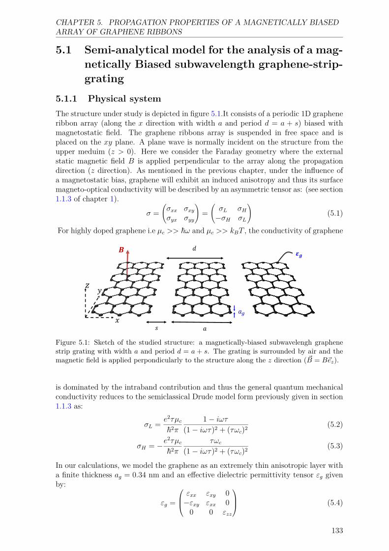
CHAPTER 5. PROPAGATION PROPERTIES OF A MAGNETICALLY BIASEDARRAY OF GRAPHENE RIBBONS
5.1 Semi-analytical model for the analysis of a mag-netically Biased subwavelength graphene-strip-grating
5.1.1 Physical systemThe structure under study is depicted in figure 5.1.It consists of a periodic 1D grapheneribbon array (along the x direction with width a and period d = a + s) biased withmagnetostatic field. The graphene ribbons array is suspended in free space and isplaced on the xy plane. A plane wave is normally incident on the structure from theupper meduim (z > 0). Here we consider the Faraday geometry where the externalstatic magnetic field B is applied perpendicular to the array along the propagationdirection (z direction). As mentioned in the previous chapter, under the influence ofa magnetostatic bias, graphene will exhibit an induced anisotropy and thus its surfacemagneto-optical conductivity will be described by an asymmetric tensor as: (see section1.1.3 of chapter 1).
σ =(σxx σxyσyx σyy
)=(σL σH−σH σL
)(5.1)
For highly doped graphene i.e µc >> ~ω and µc >> kBT , the conductivity of graphene
𝑩 𝑑
𝑎 𝑠
𝑧
𝑥
𝑦
𝑎𝑔
𝜺𝒈
Figure 5.1: Sketch of the studied structure: a magnetically-biased subwavelengh graphenestrip grating with width a and period d = a + s. The grating is surrounded by air and themagnetic field is applied perpondicularly to the structure along the z direction ( ~B = B~ez).
is dominated by the intraband contribution and thus the general quantum mechanicalconductivity reduces to the semiclassical Drude model form previously given in section1.1.3 as:
σL = e2τµc~2π
1− iωτ(1− iωτ)2 + (τωc)2 (5.2)
σH = −e2τµc~2π
τωc(1− iωτ)2 + (τωc)2 (5.3)
In our calculations, we model the graphene as an extremely thin anisotropic layer witha finite thickness ag = 0.34 nm and an effective dielectric permittivity tensor εg givenby:
εg =
εxx εxy 0−εxy εxx 0
0 0 εzz
(5.4)
133
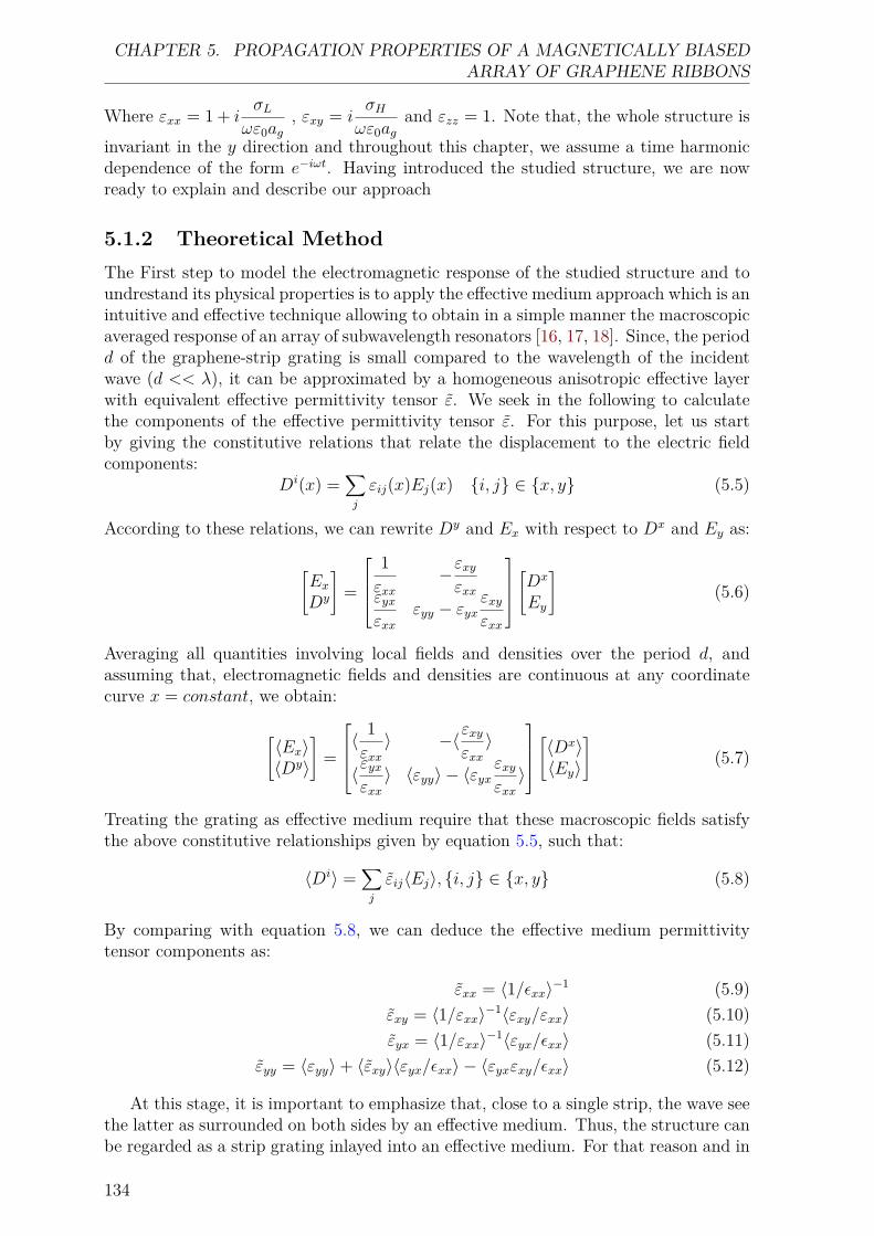
CHAPTER 5. PROPAGATION PROPERTIES OF A MAGNETICALLY BIASEDARRAY OF GRAPHENE RIBBONS
Where εxx = 1 + iσL
ωε0ag, εxy = i
σHωε0ag
and εzz = 1. Note that, the whole structure isinvariant in the y direction and throughout this chapter, we assume a time harmonicdependence of the form e−iωt. Having introduced the studied structure, we are nowready to explain and describe our approach
5.1.2 Theoretical MethodThe First step to model the electromagnetic response of the studied structure and toundrestand its physical properties is to apply the effective medium approach which is anintuitive and effective technique allowing to obtain in a simple manner the macroscopicaveraged response of an array of subwavelength resonators [16, 17, 18]. Since, the periodd of the graphene-strip grating is small compared to the wavelength of the incidentwave (d << λ), it can be approximated by a homogeneous anisotropic effective layerwith equivalent effective permittivity tensor ε. We seek in the following to calculatethe components of the effective permittivity tensor ε. For this purpose, let us startby giving the constitutive relations that relate the displacement to the electric fieldcomponents:
Di(x) =∑j
εij(x)Ej(x) i, j ∈ x, y (5.5)
According to these relations, we can rewrite Dy and Ex with respect to Dx and Ey as:
[ExDy
]=
1εxx
−εxyεxxεyx
εxxεyy − εyx
εxyεxx
[Dx
Ey
](5.6)
Averaging all quantities involving local fields and densities over the period d, andassuming that, electromagnetic fields and densities are continuous at any coordinatecurve x = constant, we obtain:
[〈Ex〉〈Dy〉
]=
〈1εxx〉 −〈εxy
εxx〉
〈εyxεxx〉 〈εyy〉 − 〈εyx
εxyεxx〉
[〈Dx〉〈Ey〉
](5.7)
Treating the grating as effective medium require that these macroscopic fields satisfythe above constitutive relationships given by equation 5.5, such that:
〈Di〉 =∑j
εij〈Ej〉, i, j ∈ x, y (5.8)
By comparing with equation 5.8, we can deduce the effective medium permittivitytensor components as:
εxx = 〈1/εxx〉−1 (5.9)εxy = 〈1/εxx〉−1〈εxy/εxx〉 (5.10)εyx = 〈1/εxx〉−1〈εyx/εxx〉 (5.11)
εyy = 〈εyy〉+ 〈εxy〉〈εyx/εxx〉 − 〈εyxεxy/εxx〉 (5.12)
At this stage, it is important to emphasize that, close to a single strip, the wave seethe latter as surrounded on both sides by an effective medium. Thus, the structure canbe regarded as a strip grating inlayed into an effective medium. For that reason and in
134
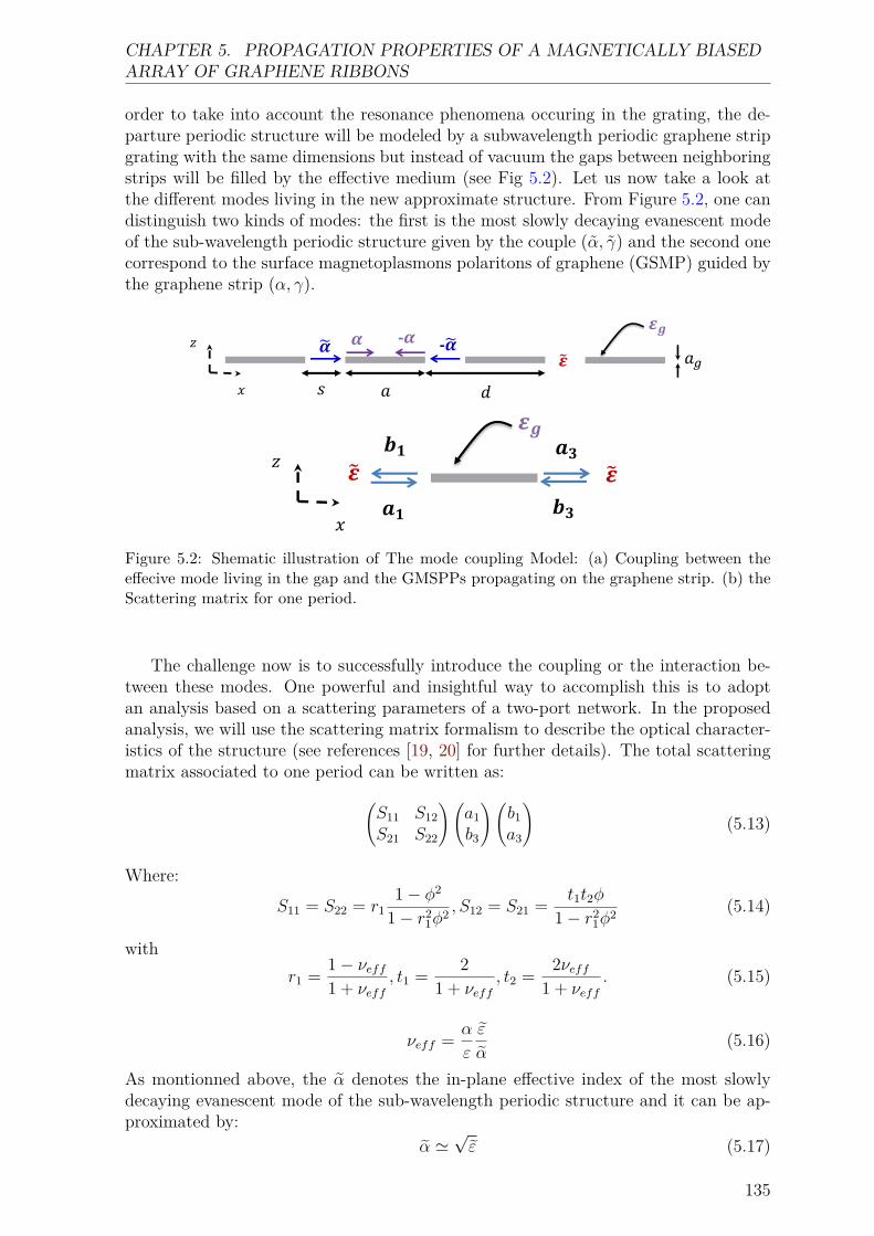
CHAPTER 5. PROPAGATION PROPERTIES OF A MAGNETICALLY BIASEDARRAY OF GRAPHENE RIBBONS
order to take into account the resonance phenomena occuring in the grating, the de-parture periodic structure will be modeled by a subwavelength periodic graphene stripgrating with the same dimensions but instead of vacuum the gaps between neighboringstrips will be filled by the effective medium (see Fig 5.2). Let us now take a look atthe different modes living in the new approximate structure. From Figure 5.2, one candistinguish two kinds of modes: the first is the most slowly decaying evanescent modeof the sub-wavelength periodic structure given by the couple (α, γ) and the second onecorrespond to the surface magnetoplasmons polaritons of graphene (GSMP) guided bythe graphene strip (α, γ).
𝑎 𝑠 𝑑
𝑎𝑔 𝜶 𝜶 -𝜶 -𝜶
𝜺
𝜺𝒈 𝑧
𝑥
𝑧
𝑥 𝒂𝟏
𝒃𝟏
𝒃𝟑
𝒂𝟑 𝜺 𝜺
𝜺𝒈
Figure 5.2: Shematic illustration of The mode coupling Model: (a) Coupling between theeffecive mode living in the gap and the GMSPPs propagating on the graphene strip. (b) theScattering matrix for one period.
The challenge now is to successfully introduce the coupling or the interaction be-tween these modes. One powerful and insightful way to accomplish this is to adoptan analysis based on a scattering parameters of a two-port network. In the proposedanalysis, we will use the scattering matrix formalism to describe the optical character-istics of the structure (see references [19, 20] for further details). The total scatteringmatrix associated to one period can be written as:(
S11 S12S21 S22
)(a1b3
)(b1a3
)(5.13)
Where:S11 = S22 = r1
1− φ2
1− r21φ
2 , S12 = S21 = t1t2φ
1− r21φ
2 (5.14)
withr1 = 1− νeff
1 + νeff, t1 = 2
1 + νeff, t2 = 2νeff
1 + νeff. (5.15)
νeff = α
ε
ε
α(5.16)
As montionned above, the α denotes the in-plane effective index of the most slowlydecaying evanescent mode of the sub-wavelength periodic structure and it can be ap-proximated by:
α '√ε (5.17)
135
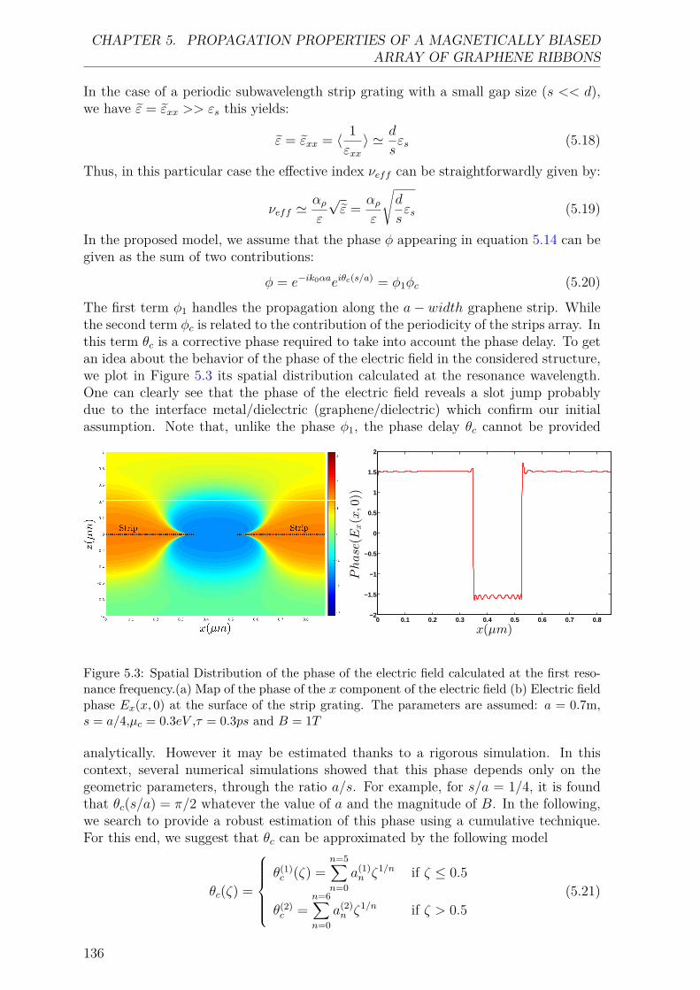
CHAPTER 5. PROPAGATION PROPERTIES OF A MAGNETICALLY BIASEDARRAY OF GRAPHENE RIBBONS
In the case of a periodic subwavelength strip grating with a small gap size (s << d),we have ε = εxx >> εs this yields:
ε = εxx = 〈 1εxx〉 ' d
sεs (5.18)
Thus, in this particular case the effective index νeff can be straightforwardly given by:
νeff 'αρε
√ε = αρ
ε
√d
sεs (5.19)
In the proposed model, we assume that the phase φ appearing in equation 5.14 can begiven as the sum of two contributions:
φ = e−ik0αaeiθc(s/a) = φ1φc (5.20)
The first term φ1 handles the propagation along the a− width graphene strip. Whilethe second term φc is related to the contribution of the periodicity of the strips array. Inthis term θc is a corrective phase required to take into account the phase delay. To getan idea about the behavior of the phase of the electric field in the considered structure,we plot in Figure 5.3 its spatial distribution calculated at the resonance wavelength.One can clearly see that the phase of the electric field reveals a slot jump probablydue to the interface metal/dielectric (graphene/dielectric) which confirm our initialassumption. Note that, unlike the phase φ1, the phase delay θc cannot be provided
0 0.1 0.2 0.3 0.4 0.5 0.6 0.7 0.8−2
−1.5
−1
−0.5
0
0.5
1
1.5
2
x(µm)
Phase(E
x(x,0))
Figure 5.3: Spatial Distribution of the phase of the electric field calculated at the first reso-nance frequency.(a) Map of the phase of the x component of the electric field (b) Electric fieldphase Ex(x, 0) at the surface of the strip grating. The parameters are assumed: a = 0.7m,s = a/4,µc = 0.3eV ,τ = 0.3ps and B = 1T
analytically. However it may be estimated thanks to a rigorous simulation. In thiscontext, several numerical simulations showed that this phase depends only on thegeometric parameters, through the ratio a/s. For example, for s/a = 1/4, it is foundthat θc(s/a) = π/2 whatever the value of a and the magnitude of B. In the following,we search to provide a robust estimation of this phase using a cumulative technique.For this end, we suggest that θc can be approximated by the following model
θc(ζ) =
θ(1)c (ζ) =
n=5∑n=0
a(1)n ζ1/n if ζ ≤ 0.5
θ(2)c =
n=6∑n=0
a(2)n ζ1/n if ζ > 0.5
(5.21)
136
CHAPTER 5. PROPAGATION PROPERTIES OF A MAGNETICALLY BIASEDARRAY OF GRAPHENE RIBBONS
0 0.5 1s/a
0.5
1
1.5
2
2.5
c
c(1)
c(2)
B=0 T
c=0.3 eV
Figure 5.4: Comparaison between the numerical results of the phase θc (red line) and theresults computed using the approximate model given by (5.21) and (5.22)(black dot linefor θ(1)
c and blue dasched line for θ(2)c ). The parameters are: λ = 30.35µm, a = 0.735µm,
B = 0T , µc = 0.3eV )
where ζ = s/a. Then, The coefficients of the above series are obtained numerically as:
θc(ζ) =θ(1)c (ζ) = ζ1/5 + 1.05ζ1/4 + 0.2ζ1/3 − 0.1ζ1/2 + 0.05ζ − 0.018 if ζ ≤ 0.5θ(2)c (ζ) = ζ1/6 + 0.955 if ζ > 0.5
(5.22)To show the reliability and the efficiency of the proposed approximate model, we plot inFigure 5.4 the behaviour of θc as a function of the ratio s/a for the following numericalparameters: λ = 30.35µm, a = 0.735µm, B = 0T , µc = 0.3eV . The numerical resultsare compared to those computed by the approximate model. The red solid line showsthe results obtained numerically and the results obtained using the approximate modelare depicted by the blue dasched and the black dot lines. One can see that the blueline that corresponds to θ(1)
c fits perfectly the red line for (s/a) ≥ 0.5. While the blackone corresponding to θ(2)
c matches with the latter for (s/a) > 0.5. Hence, we concludethat in this case, the behavior of the phase delay θc can be efficiently predicted by theabove proposed approximate model. Note that, although we have presented here onlythe case of the structure without magnetic bias, the model has been also verified forB 6= 0 and it is found that it remains valid and efficient for all values of B less than7T .
After having defined all the parameters required for determining the S-matrix.Let us now find the resonances modes of the system which are obtained by settingdet(S−1) = 0, since the S matrix is calculated for symmetric structure (the input andthe output medium are the same), it is found that the zeros of det(S−1) are the sameas those of det(S):
det(S) = S12(ω)S21(ω)− S11(ω)S22(ω) = 0 (5.23)
137

CHAPTER 5. PROPAGATION PROPERTIES OF A MAGNETICALLY BIASEDARRAY OF GRAPHENE RIBBONS
We get then two categories of solutions:
∆+ = S11(ω) + S12(ω) = 0, or ∆− = S11(ω)− S12(ω) = 0. (5.24)
To find out which one corresponds to the resonance modes of the system, we compareeach of them with the curves computed by the PMM method. As seen from Figure 5.5,the resonance frequency defined by the class of solutions satisfying to ∆+ = S11(ω) +S12(ω) matches with the resonant dip in the transmission spectrum of the structure.Thus, we can set:
t(ω) = − (S11(ω) + S12(ω)) (5.25)r(ω) = −(1− t(ω)) (5.26)
where t and r denote the transmissions and reflection coefficients resulting from theresonnace phenomena. In addition to this contribution, we should add a second term
15 20 25 30 35 400
0.1
0.2
0.3
0.4
0.5
0.6
0.7
0.8
0.9
1
ReflectionTransmission
| + | ²
Figure 5.5: Comparison between the transmittance spectra of the structure computed usingthe PMM method and the one given by |∆+|2. The parameters are the same as Figure 5.3
that take into account the contribution of a single strip of graphene. Therefore thetransmission and the reflection spectrums of the system can take the following form:
T = 12 (t+ Ts) (5.27)
R = 12 (r +Rs) (5.28)
Where Ts and Rs are respectively the transmission and reflection coefficients through agraphene monolayer. These coefficients are those calculated in the previous chapter andgiven by equations (4.110) and (4.115). Now, our semi analytical model is completedand in the next section, we will attempt to validate and test it.
5.1.3 Numerical Results and discussionIn this section, some numerical examples are provided to validate the proposed semianalytical model and demontrate its viability. For this purpose, we investigate the
138
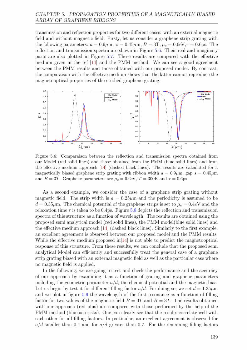
CHAPTER 5. PROPAGATION PROPERTIES OF A MAGNETICALLY BIASEDARRAY OF GRAPHENE RIBBONS
transmission and reflection properties for two different cases: with an external magneticfield and without magnetic field. Firsty, let us consider a graphene strip grating withthe following parameters: a = 0.9µm , s = 0.45µm, B = 3T, µc = 0.6eV,τ = 0.6ps. Thereflection and transmission spectra are shown in Figure 5.6. Their real and imaginaryparts are also plotted in Figure 5.7. These results are compared with the effectivemedium given in the ref [14] and the PMM method. We can see a good agreementbetween the PMM results and those obtained with our proposed model. By contrast,the comparaison with the effective medium shows that the latter cannot reproduce themagnetooptical properties of the studied graphene grating.
5 10 15 20 25 30 35 400
0.1
0.2
0.3
0.4
0.5
0.6
0.7
0.8
0.9
Our ModelPMM
eff Model
0 5 10 15 20 25 30 35 400
0.1
0.2
0.3
0.4
0.5
0.6
0.7
0.8
0.9
1
Our ModelPMM
eff Model
Figure 5.6: Comparaison between the reflection and transmission spectra obtained fromour Model (red solid lines) and those obtained from the PMM (blue solid lines) and fromthe effective medium approach [14] (dashed black lines). The results are calculated for amagnetically biased graphene strip grating with ribbon width a = 0.9µm, gap s = 0.45µmand B = 3T . Graphene parameters are µc = 0.6eV, T = 300K and τ = 0.6ps
As a second example, we consider the case of a graphene strip grating withoutmagnetic field. The strip width is a = 0.25µm and the periodicity is assumed to bed = 0.35µm. The chemical potential of the graphene strips is set to µc = 0.4eV and therelaxation time τ is taken to be 0.4ps. Figure 5.8 depicts the reflection and transmissionspectra of this structure as a function of wavelength. The results are obtained using theproposed semi analytical model (red solid lines), the PMM model(blue solid lines) andthe effective medium approach [14] (dashed black lines). Similarly to the first example,an excellent agreement is observed between our proposed model and the PMM results.While the effective medium proposed in[14] is not able to predict the magnetoopticalresponse of this structure. From these results, we can conclude that the proposed semianalytical Model can efficiently and successfully treat the general case of a graphenestrip grating biased with an external magnetic field as well as the particular case whereno magnetic field is applied.
In the following, we are going to test and check the performance and the accuracyof our approach by examining it as a function of grating and graphene parametersincluding the geometric parameter a/d, the chemical potential and the magnetic bias.Let us begin by test it for different filling factor a/d. For doing so, we set d = 1.35µmand we plot in figure 5.9 the wavelength of the first resonance as a function of fillingfactor for two values of the magnetic field B = 0T and B = 3T . The results obtainedwith our approach (red plus) are compared with those performed by the help of thePMM method (blue asterisks). One can clearly see that the results correlate well witheach other for all filling factors. In particular, an excellent agreement is observed fora/d smaller than 0.4 and for a/d greater than 0.7. For the remaining filling factors
139
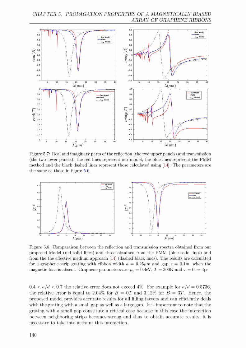
CHAPTER 5. PROPAGATION PROPERTIES OF A MAGNETICALLY BIASEDARRAY OF GRAPHENE RIBBONS
5 10 15 20 25 30 35 40-1
-0.9
-0.8
-0.7
-0.6
-0.5
-0.4
-0.3
-0.2
-0.1
0
Our ModelPMM
eff Model
5 10 15 20 25 30 35 40-0.5
-0.4
-0.3
-0.2
-0.1
0
0.1
0.2
0.3
0.4
0.5Our ModelPMM
eff Model
5 10 15 20 25 30 35 400
0.1
0.2
0.3
0.4
0.5
0.6
0.7
0.8
0.9
1
Our ModelPMM
eff Model
0 5 10 15 20 25 30 35 40-0.5
-0.4
-0.3
-0.2
-0.1
0
0.1
0.2
0.3
0.4
0.5
Our ModelPMM
eff Model
Figure 5.7: Real and imaginary parts of the reflection (the two upper panels) and transmission(the two lower panels). the red lines represent our model, the blue lines represent the PMMmethod and the black dashed lines represent those calculated using [14]. The parameters arethe same as those in figure 5.6.
8 10 12 14 16 18 20 22 240
0.1
0.2
0.3
0.4
0.5
0.6
0.7Our ModelPMM
eff Model
8 10 12 14 16 18 20 22 240
0.1
0.2
0.3
0.4
0.5
0.6
0.7
0.8
0.9
1
Our ModelPMM
eff Model
Figure 5.8: Comparaison between the reflection and transmission spectra obtained from ourproposed Model (red solid lines) and those obtained from the PMM (blue solid lines) andfrom the the effective medium approach [14] (dashed black lines). The results are calculatedfor a graphene strip grating with ribbon width a = 0.25µm and gap s = 0.1m, when themagnetic bias is absent. Graphene parameters are µc = 0.4eV, T = 300K and τ = 0. = 4ps
0.4 < a/d < 0.7 the relative error does not exceed 4%. For example for a/d = 0.5736,the relative error is equal to 2.04% for B = 0T and 3.12% for B = 3T . Hence, theproposed model provides accurate results for all filling factors and can efficiently dealswith the grating with a small gap as well as a large gap. It is important to note that thegrating with a small gap constitute a critical case because in this case the interactionbetween neighboring strips becomes strong and thus to obtain accurate results, it isnecessary to take into account this interaction.
140
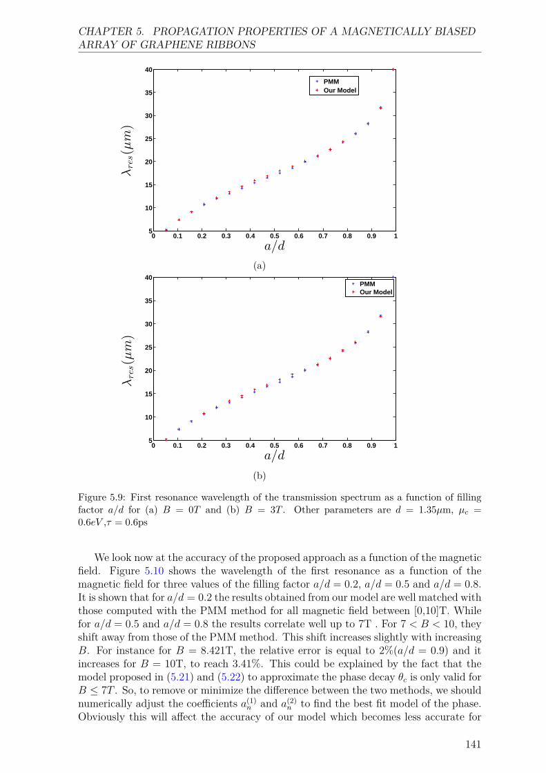
CHAPTER 5. PROPAGATION PROPERTIES OF A MAGNETICALLY BIASEDARRAY OF GRAPHENE RIBBONS
0 0.1 0.2 0.3 0.4 0.5 0.6 0.7 0.8 0.9 15
10
15
20
25
30
35
40
a/d
λres(µ
m)
PMMOur Model
(a)
0 0.1 0.2 0.3 0.4 0.5 0.6 0.7 0.8 0.9 15
10
15
20
25
30
35
40
a/d
λres(µ
m)
PMMOur Model
(b)
Figure 5.9: First resonance wavelength of the transmission spectrum as a function of fillingfactor a/d for (a) B = 0T and (b) B = 3T . Other parameters are d = 1.35µm, µc =0.6eV ,τ = 0.6ps
We look now at the accuracy of the proposed approach as a function of the magneticfield. Figure 5.10 shows the wavelength of the first resonance as a function of themagnetic field for three values of the filling factor a/d = 0.2, a/d = 0.5 and a/d = 0.8.It is shown that for a/d = 0.2 the results obtained from our model are well matched withthose computed with the PMM method for all magnetic field between [0,10]T. Whilefor a/d = 0.5 and a/d = 0.8 the results correlate well up to 7T . For 7 < B < 10, theyshift away from those of the PMM method. This shift increases slightly with increasingB. For instance for B = 8.421T, the relative error is equal to 2%(a/d = 0.9) and itincreases for B = 10T, to reach 3.41%. This could be explained by the fact that themodel proposed in (5.21) and (5.22) to approximate the phase decay θc is only valid forB ≤ 7T . So, to remove or minimize the difference between the two methods, we shouldnumerically adjust the coefficients a(1)
n and a(2)n to find the best fit model of the phase.
Obviously this will affect the accuracy of our model which becomes less accurate for
141
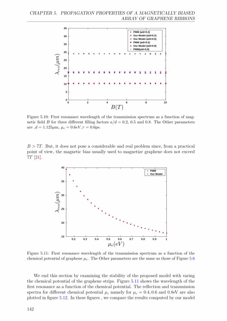
CHAPTER 5. PROPAGATION PROPERTIES OF A MAGNETICALLY BIASEDARRAY OF GRAPHENE RIBBONS
0 2 4 6 8 100
5
10
15
20
25
30
35
40
45PMM (a/d=0.2)Our Model (a/d=0.2)Our Model (a/d=0.5)PMM (a/d=0.5)Our Model (a/d=0.9)PMM(a/d=0.9)
Figure 5.10: First resonance wavelength of the transmission spectrum as a function of mag-netic field B for three different filling factors a/d = 0.2, 0.5 and 0.8. The Other parametersare ,d = 1.125µm, µc = 0.6eV ,τ = 0.6ps.
B > 7T . But, it does not pose a considerable and real problem since, from a practicalpoint of view, the magnetic bias usually used to magnetize graphene does not exceed7T [21].
0.2 0.3 0.4 0.5 0.6 0.7 0.8 0.9 115
20
25
30
35
40PMMOur Model
Figure 5.11: First resonance wavelength of the transmission spectrum as a function of thechemical potential of graphene µc. The Other parameters are the same as those of Figure 5.6
We end this section by examining the stability of the proposed model with varingthe chemical potential of the graphene strips. Figure 5.11 shows the wavelength of thefirst resonance as a function of the chemical potential. The reflection and transmissionspectra for different chemical potential µc namely for µc = 0.4, 0.6 and 0.8eV are alsoplotted in figure 5.12. In these figures , we compare the results computed by our model
142
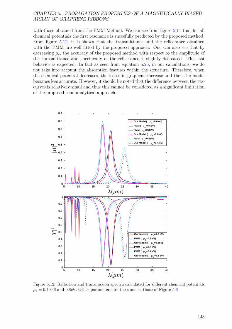
CHAPTER 5. PROPAGATION PROPERTIES OF A MAGNETICALLY BIASEDARRAY OF GRAPHENE RIBBONS
with those obtained from the PMM Method. We can see from figure 5.11 that for allchemical potentials the first resonance is succefully predicted by the proposed method.From figure 5.12, it is shown that the transmittance and the reflectance obtainedwith the PMM are well fitted by the proposed approach. One can also see that bydecreasing µc, the accuracy of the proposed method with respect to the amplitude ofthe transmittance and specifically of the reflectance is slightly decreased. This lastbehavior is expected. In fact as seen from equation 5.26, in our calculations, we donot take into account the absorption features within the structure. Therefore, whenthe chemical potential decreases, the losses in graphene increase and then the modelbecomes less accurate. However, it should be noted that the difference between the twocurves is relatively small and thus this cannot be considered as a significant limitationof the proposed semi analytical approach.
5 10 15 20 25 30 35 400
0.1
0.2
0.3
0.4
0.5
0.6
0.7
0.8
0.9
Our Model( c=0.6 eV)
PMM ( c=0.6eV)
PMM( c=0.8eV)
Our Model ( c=0.8eV)
PMM( c=0.4eV)
Our Model ( c=0.4 eV)
5 10 15 20 25 30 35 400
0.1
0.2
0.3
0.4
0.5
0.6
0.7
0.8
0.9
1
Our Model ( c=0.6 eV)
PMM ( c=0.6 eV)
Our Model ( c=0.8eV)
PMM ( c=0.8 eV)
PMM ( c=0.4 eV)
Our Model ( c=0.4 eV)
Figure 5.12: Reflection and transmission spectra calculated for different chemical potentialsµc = 0.4, 0.6 and 0.8eV. Other parameters are the same as those of Figure 5.6
143

CHAPTER 5. PROPAGATION PROPERTIES OF A MAGNETICALLY BIASEDARRAY OF GRAPHENE RIBBONS
5.2 ConclusionIn conclusion, in this chapter, we have presented a simple and fast semi analyticalmodel to compute the transmittance and reflectance of a magnetically-biased subwave-length graphene strip grating. It is based on the effective medium approach when thegraphene is modeled as an anisotropic layer with atomic thickness and a frequency-dependent and complex permittivity tensor. The proposed model is validated againstthe PMM method by numerical examples. The perfermance and the accuraty of thismethod has been also tested and checked as a function of the graphene and gratingparameters. We have first showed that this proposed method is a general approachthat can efficiently treat the structure when the magnetic field is applied and still valideven in the particular case of a structure without magnetic field which is not possiblewith the analytical methods already encountered in the literature. In addition to that,the study of the accuraty of the method as a fuction of the filling factor of the gratingrevealed that the proposed model can efficiency deal with the grating with a small gapas well as a large gap. Specifically, this method provides precise and reliable results inthe case of gratings with small gaps which constitute a complicated case to deal with.Throught this last structure it is possible to achieve a strong reflection ( near 90%)which could be of interest in devices that require high reflectivity such that reflectorsin certain frequency ranges.
144
Bibliography
[1] D. L. Sounas, H. S. Skulason, H. V. Nguyen, A. Guermoune, M. Siaj, T. Szkopek,and C. Caloz. Faraday rotation in magnetically biased graphene at microwavefrequencies. Applied Physics Letters, 102(19):191901, 2013. 133
[2] V. P. Gusynin and S. G. Sharapov. Unconventional integer quantum hall effect ingraphene. Phys. Rev. Lett., 95:146801, Sep 2005. 133
[3] Andrew L. Walter Markus Ostler Aaron Bostwick Eli Rotenberg Thomas SeyllerDirk van der Marel Alexey B. Kuzmenko Iris Crassee, Julien Levallois. Giantfaraday rotation in single- and multilayer graphene. Nature Phys, (7):48–51, 2011.6, 133
[4] Toshihiko Yoshino. Theory for oblique-incidence magneto-optical faraday and kerreffects in interfaced monolayer graphene and their characteristic features. J. Opt.Soc. Am. B, 30(5):1085–1091, May 2013. 6, 133
[5] A. M. Witowski, M. Orlita, R. Stepniewski, A. Wysmołek, J. M. Baranowski,W. Strupiński, C. Faugeras, G. Martinez, and M. Potemski. Quasiclassical cy-clotron resonance of dirac fermions in highly doped graphene. Phys. Rev. B,82:165305, Oct 2010. 117, 133
[6] Fei Gao Baile Zhang Hongsheng Chen Xiao Lin, Zuojia Wang. Atomically thinnonreciprocal optical isolation. Sci Rep, (4):4190, 2015. 133
[7] Min Wang, Yanqin Wang, Mingbo Pu, Chenggang Hu, Xiaoyu Wu, Zeyu Zhao,and Xiangang Luo. Circular dichroism of graphene-based absorber in static mag-netic field. Journal of Applied Physics, 115(15):154312, 2014. 133
[8] Bin Hu, Jin Tao, Ying Zhang, and Qi Jie Wang. Magneto-plasmonics in graphene-dielectric sandwich. Opt. Express, 22(18):21727–21738, Sep 2004. 133
[9] J. M. Poumirol, W. Yu, X. Chen, C. Berger, W. A. de Heer, M. L. Smith, T. Ohta,W. Pan, M. O. Goerbig, D. Smirnov, and Z. Jiang. Magnetoplasmons in quasineu-tral epitaxial graphene nanoribbons. Phys. Rev. Lett., 110:246803, Jun 2013. 133
[10] Mykhailo Tymchenko, Alexey Yu. Nikitin, and Luis Martín-Moreno. Faradayrotation due to excitation of magnetoplasmons in graphene microribbons. ACSNano, 7(11):9780–9787, 2013. PMID: 24079266. 133, 134
145
BIBLIOGRAPHY
[11] Tetiana M. Slipchenko Alexey Y. Nikitin Luis Martin-Moreno Jérôme Faist AlexeyB. Kuzmenko Jean-Marie Poumirol, Peter Q. Liu. Electrically controlled terahertzmagneto-optical phenomena in continuous and patterned graphene. Nat Commun,(8):14626, 2017. 133
[12] X. Wang, W. Yin, and Z. Chen. Matrix exponential fdtd modeling of magnetizedgraphene sheet. IEEE Antennas and Wireless Propagation Letters, 12:1129–1132,2013. 134
[13] P. Li and L. J. Jiang. Modeling of magnetized graphene from microwave to thzrange by dgtd with a scalar rbc and an ade. IEEE Transactions on Antennas andPropagation, 63(10):4458–4467, Oct 2015. 134
[14] J. S. Gomez-Diaz and A. Alù. Magnetically-biased graphene-based hyperbolicmetasurfaces. In 2016 IEEE International Symposium on Antennas and Propaga-tion (APSURSI), pages 359–360, June 2016. 8, 134, 140, 141, 142
[15] Mahdi Rahmanzadeh, Behzad Rejaei, Mohammad Memarian, and Amin Khavasi.Analytical and rigorous method for analysis of an array of magnetically-biasedgraphene ribbons. Opt. Express, 27(20):28395–28409, Sep 2019. 134
[16] J.M. Bell, G.H. Derrick, and R.C. McPhedran. Diffraction gratings in the quasi-static limit. Optica Acta: International Journal of Optics, 29(11):1475–1489, 1982.136
[17] Philippe Lalanne and Dominique Lemercier-lalanne. On the effective medium the-ory of subwavelength periodic structures. Journal of Modern Optics, 43(10):2063–2085, 1996. 136
[18] Philippe Lalanne and Dominique Lemercier-Lalanne. Depth dependence of theeffective properties of subwavelength gratings. J. Opt. Soc. Am. A, 14(2):450–459,Feb 1997. 136
[19] Kofi Edee. Understanding the plane wave excitation of the metal-insulator-metalgap plasmon mode of a nanoribbons periodic array: role of insulator-metal-insulator lattice mode. OSA Continuum, 2(2):389–399, Feb 2019. 137
[20] Kofi Edee, Maha Benrhouma, Mauro Antezza, Jonathan Albert Fan, and BrahimGuizal. Coupling between subwavelength nano-slit lattice modes and metal-insulator-graphene cavity modes: a semi-analytical model. OSA Continuum,2(4):1296–1309, Apr 2019. 137
[21] I. Crassee, M. Orlita, M. Potemski, A. L. Walter, M. Ostler, Th. Seyller, I. Gapo-nenko, J. Chen, and A. B. Kuzmenko. Intrinsic terahertz plasmons and magneto-plasmons in large scale monolayer graphene. Nano Letters, 12(5):2470–2474, 2012.PMID: 22519967. 143
146
Chapter 6Theoretical analysis of Optical Hall effect ina 2D nano-cross-slits grating
There is nothing more deceptivethan an obvious fact.
Arthur Conan Doyle, TheBoscombe Valley Mystery
Contents6.1 Statement . . . . . . . . . . . . . . . . . . . . . . . . . . . . . 150
6.2 Polarization independent EOT phenomenon through 2Dcross-slits array . . . . . . . . . . . . . . . . . . . . . . . . . . 151
6.3 Magneto-optical perturbation of the gap plasmon modes 158
6.4 Conclusion . . . . . . . . . . . . . . . . . . . . . . . . . . . . 162
As shown in chapter 5, the optical Hall effect can be considered as the physicalphenomenon related to the appearance of magnetically induced anisotropy in a mate-rial’s optical properties. This induced anisotropy leads to a non-reciprocal magneto-optical response of the anisotropic material. Significant efforts were made to createoptical materials allowing to combine both extraordinary optical transmission (EOT)[1, 2, 3, 4, 5, 6] and magneto optical effects in order to enhance the magneto opticalactivity, namely the Faraday and/or Kerr rotation(s), chirality for photonics materi-als. In all these works, both 1D and 2D geometries combining non reciprocal surfaceplasmon modes and magnetic effect are studied. The 1D base structure is consisted ofperiodic array of nano-ribbons [7, 8, 9, 10, 11, 12] or sub-wavelength slits, while the 2Dstructures are generally based on nano-holes with different shapes [13, 14, 15, 16]. Tothe best of our knowledge, the EOT phenomenon involving a 2D structure consistingof a periodic array of cross-slits grating has never been reported. Firstly, we show inthis chapter that, contrary to the case of periodic array of nano-holes, the 2D cross-slits grating can support fundamental guided cavity super-modes which are two-degreedegenerate in the case of uniaxial slit-material and symmetrical geometry. Therefore,the EOT phenomenon through this structure does not depend on the incident field po-larization. Secondly, we investigate the magneto optical activity in this structure whenthe slits are filled by an anisotropic gyroscopic material. The structure may support
147
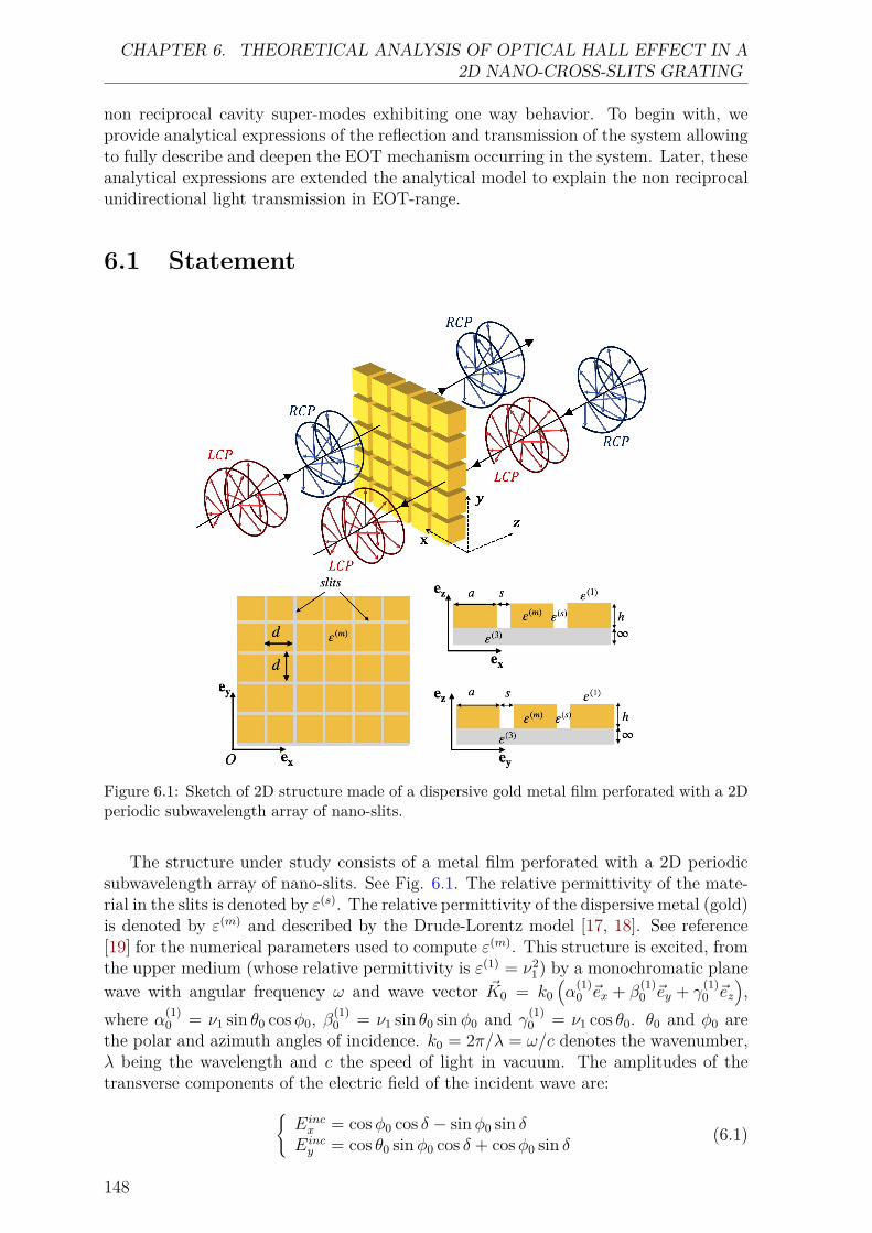
CHAPTER 6. THEORETICAL ANALYSIS OF OPTICAL HALL EFFECT IN A2D NANO-CROSS-SLITS GRATING
non reciprocal cavity super-modes exhibiting one way behavior. To begin with, weprovide analytical expressions of the reflection and transmission of the system allowingto fully describe and deepen the EOT mechanism occurring in the system. Later, theseanalytical expressions are extended the analytical model to explain the non reciprocalunidirectional light transmission in EOT-range.
6.1 Statement
Figure 6.1: Sketch of 2D structure made of a dispersive gold metal film perforated with a 2Dperiodic subwavelength array of nano-slits.
The structure under study consists of a metal film perforated with a 2D periodicsubwavelength array of nano-slits. See Fig. 6.1. The relative permittivity of the mate-rial in the slits is denoted by ε(s). The relative permittivity of the dispersive metal (gold)is denoted by ε(m) and described by the Drude-Lorentz model [17, 18]. See reference[19] for the numerical parameters used to compute ε(m). This structure is excited, fromthe upper medium (whose relative permittivity is ε(1) = ν2
1) by a monochromatic planewave with angular frequency ω and wave vector ~K0 = k0
(α
(1)0 ~ex + β
(1)0 ~ey + γ
(1)0 ~ez
),
where α(1)0 = ν1 sin θ0 cosφ0, β(1)
0 = ν1 sin θ0 sinφ0 and γ(1)0 = ν1 cos θ0. θ0 and φ0 are
the polar and azimuth angles of incidence. k0 = 2π/λ = ω/c denotes the wavenumber,λ being the wavelength and c the speed of light in vacuum. The amplitudes of thetransverse components of the electric field of the incident wave are:
Eincx = cosφ0 cos δ − sinφ0 sin δ
Eincy = cos θ0 sinφ0 cos δ + cosφ0 sin δ (6.1)
148
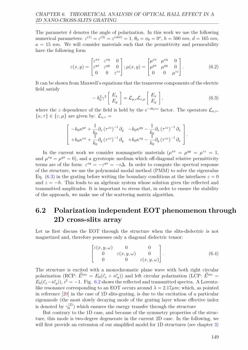
CHAPTER 6. THEORETICAL ANALYSIS OF OPTICAL HALL EFFECT IN A2D NANO-CROSS-SLITS GRATING
The parameter δ denotes the angle of polarization. In this work we use the followingnumerical parameters: ε(1) = ε(3) = ε(slit) = 1, θ0 = φ0 = 0o, h = 500 nm, d = 165 nm,a = 15 nm. We will consider materials such that the permittivity and permeabilityhave the following form
ε(x, y) =
εxx εxy 0εyx εyy 00 0 εzz
;µ(x, y) =
µxx µxy 0µyx µyy 00 0 µzz
. (6.2)
It can be shown fromMaxwell’s equations that the transverse components of the electricfield satisfy
− k20γ
2[ExEy
]= Lµ,εLε,µ
[ExEy
], (6.3)
where the z dependence of the field is held by the e−ik0γz factor. The operators Lκ,τ ,κ, τ ∈ ε, µ are given by: Lκ,τ = −k0κ
yx + 1k0∂x (τ zz)−1 ∂y −k0κ
yy − 1k0∂x (τ zz)−1 ∂x
+k0κxx + 1
k0∂y (τ zz)−1 ∂y +k0κ
xy − 1k0∂y (τ zz)−1 ∂x
.In the current work we consider nonmagnetic materials (µxx = µyy = µzz = 1,
and µxy = µyx = 0), and a gyrotropic medium which off-diagonal relative permittivityterms are of the form: εxy = −εyx = −i∆. In order to compute the spectral responseof the structure, we use the polynomial modal method (PMM) to solve the eigenvalueEq. (6.3) in the grating before writing the boundary conditions at the interfaces z = 0and z = −h. This leads to an algebraic system whose solution gives the reflected andtransmitted amplitudes. It is important to stress that, in order to ensure the stabilityof the approach, we make use of the scattering matrix algorithm.
6.2 Polarization independent EOT phenomenon through2D cross-slits array
Let us first discuss the EOT through the structure when the slits-dielectric is notmagnetized and, therefore possesses only a diagonal dielectric tensor:ε(x, y, ω) 0 0
0 ε(x, y, ω) 00 0 ε(x, y, ω)
. (6.4)
The structure is excited with a monochromatic plane wave with both right circularpolarization (RCP: ~Einc = E0(~ex + i~ey)) and left circular polarization (LCP: ~Einc =E0(~ex−i~ey)), i2 = −1. Fig. 6.2 shows the reflected and transmitted spectra. A Lorentz-like resonance corresponding to an EOT occurs around λ = 2.17µm; which, as pointedin reference [20] in the case of 1D slits-grating, is due to the excitation of a particulareigenmode (the most slowly decaying mode of the grating layer whose effective indexis denoted by γ(2)
0 ) which ensures the energy transfer through the structureBut contrary to the 1D case, and because of the symmetry properties of the struc-
ture, this mode is two-degree degenerate in the current 2D case. In the following, wewill first provide an extension of our simplified model for 1D structures (see chapter 3)
149
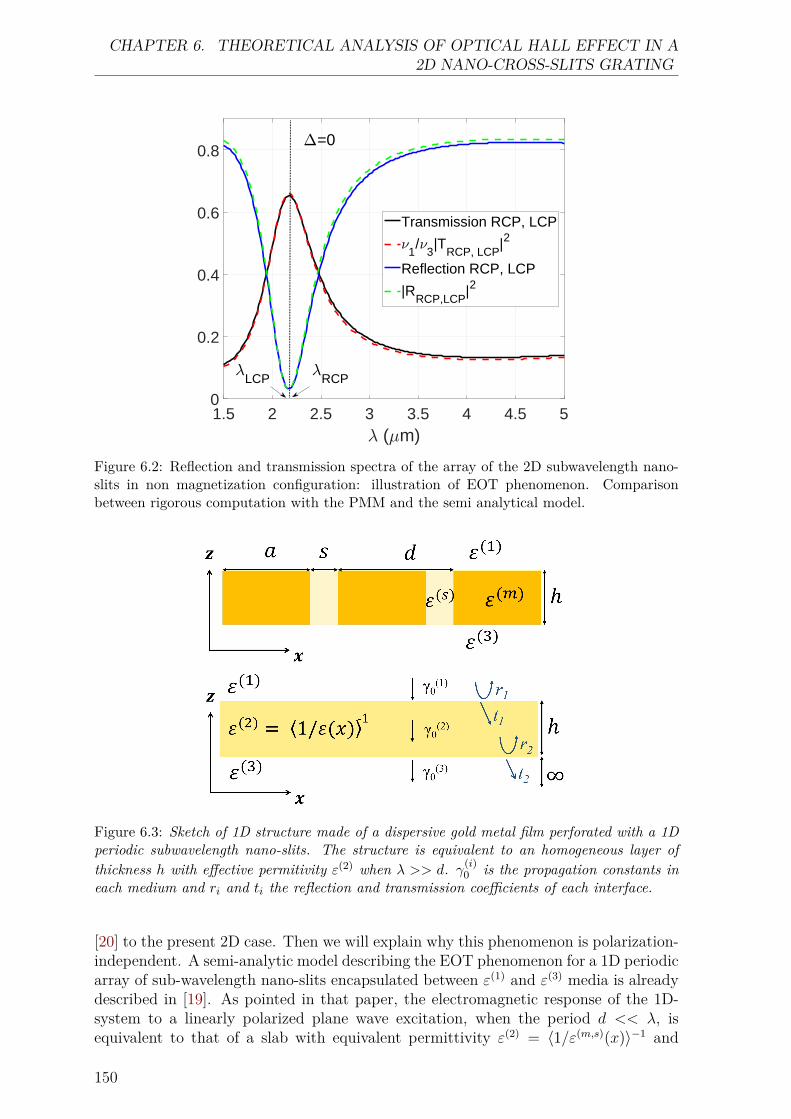
CHAPTER 6. THEORETICAL ANALYSIS OF OPTICAL HALL EFFECT IN A2D NANO-CROSS-SLITS GRATING
1.5 2 2.5 3 3.5 4 4.5 5 ( m)
0
0.2
0.4
0.6
0.8
Transmission RCP, LCP
1/
3|T
RCP, LCP|2
Reflection RCP, LCP
|RRCP,LCP
|2
LCP RCP
=0
Figure 6.2: Reflection and transmission spectra of the array of the 2D subwavelength nano-slits in non magnetization configuration: illustration of EOT phenomenon. Comparisonbetween rigorous computation with the PMM and the semi analytical model.
Figure 6.3: Sketch of 1D structure made of a dispersive gold metal film perforated with a 1Dperiodic subwavelength nano-slits. The structure is equivalent to an homogeneous layer ofthickness h with effective permitivity ε(2) when λ >> d. γ(i)
0 is the propagation constants ineach medium and ri and ti the reflection and transmission coefficients of each interface.
[20] to the present 2D case. Then we will explain why this phenomenon is polarization-independent. A semi-analytic model describing the EOT phenomenon for a 1D periodicarray of sub-wavelength nano-slits encapsulated between ε(1) and ε(3) media is alreadydescribed in [19]. As pointed in that paper, the electromagnetic response of the 1D-system to a linearly polarized plane wave excitation, when the period d << λ, isequivalent to that of a slab with equivalent permittivity ε(2) = 〈1/ε(m,s)(x)〉−1 and
150
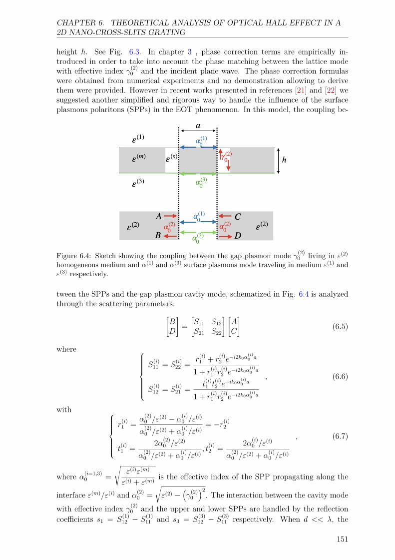
CHAPTER 6. THEORETICAL ANALYSIS OF OPTICAL HALL EFFECT IN A2D NANO-CROSS-SLITS GRATING
height h. See Fig. 6.3. In chapter 3 , phase correction terms are empirically in-troduced in order to take into account the phase matching between the lattice modewith effective index γ(2)
0 and the incident plane wave. The phase correction formulaswere obtained from numerical experiments and no demonstration allowing to derivethem were provided. However in recent works presented in references [21] and [22] wesuggested another simplified and rigorous way to handle the influence of the surfaceplasmons polaritons (SPPs) in the EOT phenomenon. In this model, the coupling be-
Figure 6.4: Sketch showing the coupling between the gap plasmon mode γ(2)0 living in ε(2)
homogeneous medium and α(1) and α(3) surface plasmons mode traveling in medium ε(1) andε(3) respectively.
tween the SPPs and the gap plasmon cavity mode, schematized in Fig. 6.4 is analyzedthrough the scattering parameters:[
BD
]=[S11 S12S21 S22
] [AC
](6.5)
where S
(i)11 = S
(i)22 = r
(i)1 + r
(i)2 e−i2k0α
(i)0 a
1 + r(i)1 r
(i)2 e−i2k0α
(i)0 a
S(i)12 = S
(i)21 = t
(i)1 t
(i)2 e−ik0α
(i)0 a
1 + r(i)1 r
(i)2 e−i2k0α
(i)0 a
, (6.6)
with r
(i)1 = α
(2)0 /ε(2) − α(i)
0 /ε(i)
α(2)0 /ε(2) + α
(i)0 /ε
(i)= −r(i)
2
t(i)1 = 2α(2)
0 /ε(2)
α(2)0 /ε(2) + α
(i)0 /ε
(i), t
(i)2 = 2α(i)
0 /ε(i)
α(2)0 /ε(2) + α
(i)0 /ε
(i)
, (6.7)
where α(i=1,3)0 =
√ε(i)ε(m)
ε(i) + ε(m) is the effective index of the SPP propagating along the
interface ε(m)/ε(i) and α(2)0 =
√ε(2) −
(γ
(2)0
)2. The interaction between the cavity mode
with effective index γ(2)0 and the upper and lower SPPs are handled by the reflection
coefficients s1 = S(1)12 − S
(1)11 and s3 = S
(3)12 − S
(3)11 respectively. When d << λ, the
151
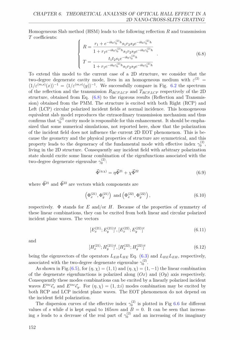
CHAPTER 6. THEORETICAL ANALYSIS OF OPTICAL HALL EFFECT IN A2D NANO-CROSS-SLITS GRATING
Homogeneous Slab method (HSM) leads to the following reflection R and transmissionT coefficients:
R = r1 + e−ik0γ(2)0 hs1r2s3e
−ik0γ(2)0 h
1 + r1e−ik0γ(2)0 hs1r2s3e−ik0γ
(2)0 h
T = t1t2s1e−ik0γ
(2)0 h
1 + r1e−ik0γ(2)0 hs1r2s3e−ik0γ
(2)0 h
. (6.8)
To extend this model to the current case of a 2D structure, we consider that thetwo-degree degenerate cavity mode, lives in an homogeneous medium with ε(2) =〈1/ε(m,s)(x)〉−1 = 〈1/ε(m,s)(y)〉−1. We successfully compare in Fig. 6.2 the spectrumof the reflection and the transmission RRCP,LCP and TRCP,LCP respectively of the 2Dstructure, obtained from Eq. (6.8) to the rigorous results (Reflection and Transmis-sion) obtained from the PMM. The structure is excited with both Right (RCP) andLeft (LCP) circular polarized incident fields at normal incidence. This homogeneousequivalent slab model reproduces the extraordinary transmission mechanism and thusconfirms that γ(2)
0 cavity mode is responsible for this enhancement. It should be empha-sized that some numerical simulations, not reported here, show that the polarizationof the incident field does not influence the current 2D EOT phenomenon. This is be-cause the geometry and the physical properties of structure are symmetrical, and thisproperty leads to the degeneracy of the fundamental mode with effective index γ(2)
0 ,living in the 2D structure. Consequently any incident field with arbitrary polarizationstate should excite some linear combination of the eigenfunctions associated with thetwo-degree degenerate eigenvalue γ(2)
0 :
~Φ(η,χ) = η~Φ21 + χ~Φ22 (6.9)
where ~Φ21 and ~Φ22 are vectors which components are(Φ(21)x ,Φ(21)
y
)and
(Φ(22)x ,Φ(22)
y
), (6.10)
respectively. Φ stands for E and/or H. Because of the properties of symmetry ofthese linear combinations, they can be excited from both linear and circular polarizedincident plane waves. The vectors
[E(21)x ;E(21)
y ]t, [E(22)x ;E(22)
y ]t (6.11)
and[H(21)
x ;H(21)y ]t, [H(22)
x ;H(22)y ]t (6.12)
being the eigenvectors of the operators LEHLHE Eq. (6.3) and LHELEH , respectively,associated with the two-degree degenerate eigenvalue γ(2)
0 .As shown in Fig.(6.5), for (η, χ) = (1, 1) and (η, χ) = (1,−1) the linear combination
of the degenerate eigenfunctions is polarized along (Ox) and (Oy) axis respectively.Consequently these modes combinations can be excited by a linearly polarized incidentwaves Einc~ex and Einc~ey. For (η, χ) = (1,±i) modes combination may be excited byboth RCP and LCP incident plane waves. The EOT phenomenon do not depend onthe incident field polarization.
The dispersion curves of the effective index γ(2)0 is plotted in Fig 6.6 for different
values of s while d is kept equal to 165nm and B = 0. It can be seen that increas-ing s leads to a decrease of the real part of γ(2)
0 and an increasing of its imaginary
152
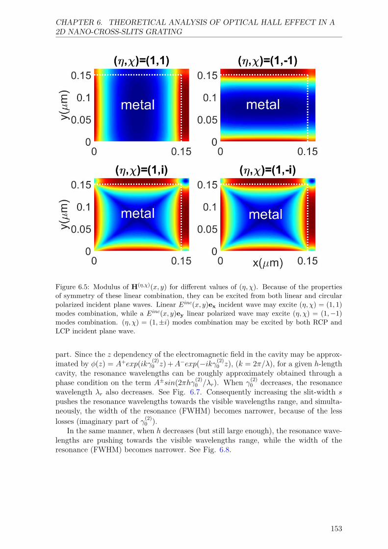
CHAPTER 6. THEORETICAL ANALYSIS OF OPTICAL HALL EFFECT IN A2D NANO-CROSS-SLITS GRATING
Figure 6.5: Modulus of H(η,χ)(x, y) for different values of (η, χ). Because of the propertiesof symmetry of these linear combination, they can be excited from both linear and circularpolarized incident plane waves. Linear Einc(x, y)ex incident wave may excite (η, χ) = (1, 1)modes combination, while a Einc(x, y)ey linear polarized wave may excite (η, χ) = (1,−1)modes combination. (η, χ) = (1,±i) modes combination may be excited by both RCP andLCP incident plane wave.
part. Since the z dependency of the electromagnetic field in the cavity may be approx-imated by φ(z) = A+exp(ikγ(2)
0 z) +A−exp(−ikγ(2)0 z), (k = 2π/λ), for a given h-length
cavity, the resonance wavelengths can be roughly approximately obtained through aphase condition on the term A±sin(2πhγ(2)
0 /λr). When γ(2)0 decreases, the resonance
wavelength λr also decreases. See Fig. 6.7. Consequently increasing the slit-width spushes the resonance wavelengths towards the visible wavelengths range, and simulta-neously, the width of the resonance (FWHM) becomes narrower, because of the lesslosses (imaginary part of γ(2)
0 ).In the same manner, when h decreases (but still large enough), the resonance wave-
lengths are pushing towards the visible wavelengths range, while the width of theresonance (FWHM) becomes narrower. See Fig. 6.8.
153
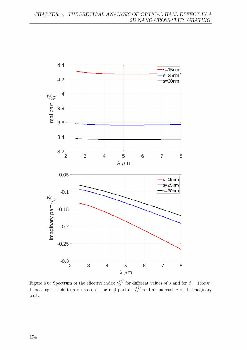
CHAPTER 6. THEORETICAL ANALYSIS OF OPTICAL HALL EFFECT IN A2D NANO-CROSS-SLITS GRATING
2 3 4 5 6 7 8 m
3.2
3.4
3.6
3.8
4
4.2
4.4
real
par
t 0(2
)
s=15nms=25nms=30nm
2 3 4 5 6 7 8 m
-0.3
-0.25
-0.2
-0.15
-0.1
-0.05
imag
inar
y pa
rt
0(2)
s=15nms=25nms=30nm
Figure 6.6: Spectrum of the effective index γ(2)0 for different values of s and for d = 165nm.
Increasing s leads to a decrease of the real part of γ(2)0 and an increasing of its imaginary
part.
154
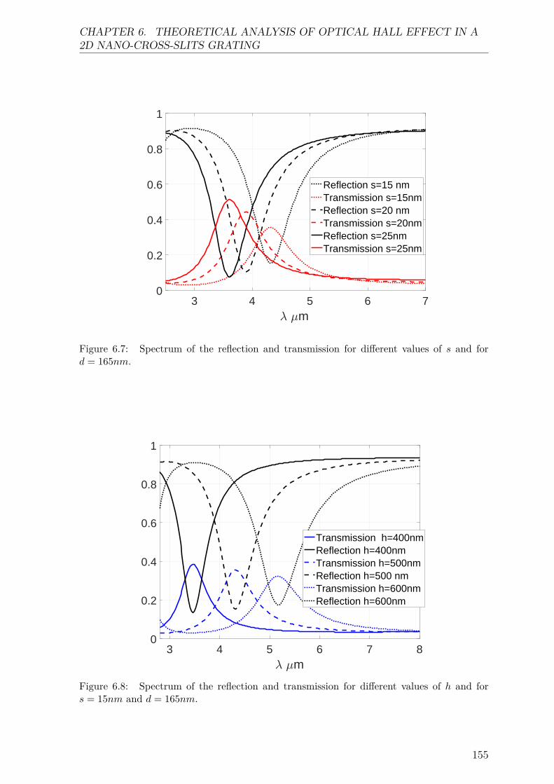
CHAPTER 6. THEORETICAL ANALYSIS OF OPTICAL HALL EFFECT IN A2D NANO-CROSS-SLITS GRATING
3 4 5 6 7 m
0
0.2
0.4
0.6
0.8
1
Reflection s=15 nmTransmission s=15nmReflection s=20 nmTransmission s=20nmReflection s=25nmTransmission s=25nm
Figure 6.7: Spectrum of the reflection and transmission for different values of s and ford = 165nm.
3 4 5 6 7 8 m
0
0.2
0.4
0.6
0.8
1
Transmission h=400nmReflection h=400nmTransmission h=500nmReflection h=500 nmTransmission h=600nmReflection h=600nm
Figure 6.8: Spectrum of the reflection and transmission for different values of h and fors = 15nm and d = 165nm.
155
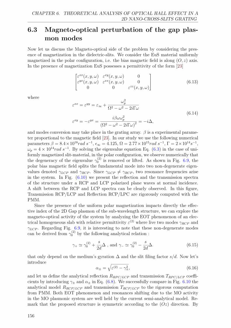
CHAPTER 6. THEORETICAL ANALYSIS OF OPTICAL HALL EFFECT IN A2D NANO-CROSS-SLITS GRATING
6.3 Magneto-optical perturbation of the gap plas-mon modes
Now let us discuss the Magneto-optical side of the problem by considering the pres-ence of magnetization in the dielectric-slits. We consider the EuS material uniformlymagnetized in the polar configuration, i.e. the bias magnetic field is along (O, z) axis.In the presence of magnetization EuS possesses a permittivity of the form [23]ε
xx(x, y, ω) εxy(x, y, ω) 0εyx(x, y, ω) εxx(x, y, ω) 0
0 0 εzz(x, y, ω)
(6.13)
whereεxx = εyy = ε∞ +
ω2p
Ω2 − ω2 − 2iΓω
εxy = −εyx =iβωω2
p
(Ω2 − ω2 − 2iΓω)2 = −i∆,(6.14)
and modes conversion may take place in the grating array. β is a experimental parame-ter proportional to the magnetic field [23]. In our study we use the following numericalparameters β = 8.4×10¹⁸rad s−1, ε∞ = 4.125, Ω = 2.77×10¹⁵rad s−1, Γ = 2×10¹⁴s−1,ωp = 4× 10¹⁴rad s−1. By solving the eigenvalue equation Eq. (6.3) in the case of uni-formly magnetized slit-material, in the polar configuration, we observe numerically thatthe degeneracy of the eigenvalue γ(2)
0 is removed or lifted. As shown in Fig. 6.9, thepolar bias magnetic field splits the fundamental mode into two non-degenerate eigen-values denoted γLCP and γRCP . Since γLCP 6= γRCP , two resonance frequencies arisein the system. In Fig. (6.10) we present the reflection and the transmission spectraof the structure under a RCP and LCP polarized plane waves at normal incidence.A shift between the RCP and LCP spectra can be clearly observed. In this figure,Transmission RCP/LCP and Reflection RCP/LPC are rigorously computed with thePMM.
Since the presence of the uniform polar magnetization impacts directly the effec-tive index of the 2D Gap plasmon of the sub-wavelength structure, we can explore themagneto-optical activity of the system by analyzing the EOT phenomenon of an elec-trical homogeneous slab with relative permittivity ε(2) where live two modes γRCP andγLCP . Regarding Fig. 6.9, it is interesting to note that these non-degenerate modescan be derived from γ
(2)0 by the following analytical relation :
γ+ ' γ(2)0 + s
2d∆ , and γ− ' γ(2)0 −
s
2d∆. (6.15)
that only depend on the medium’s gyration ∆ and the slit filing factor s/d. Now let’sintroduce
α± =√ε(2) − γ2
±, (6.16)and let us define the analytical reflection RRPC/LCP and transmission TRPC/LCP coeffi-cients by introducing γ± and α± in Eq. (6.8). We successfully compare in Fig. 6.10 theanalytical model RRCP/LCP and transmission TRCP/LCP to the rigorous computationfrom PMM. Both EOT phenomenon and resonances shifting due to the MO activityin the MO plasmonic system are well held by the current semi-analytical model. Re-mark that the proposed structure is symmetric according to the (Oz) direction. By
156
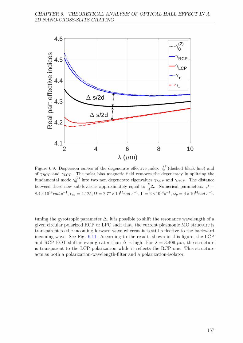
CHAPTER 6. THEORETICAL ANALYSIS OF OPTICAL HALL EFFECT IN A2D NANO-CROSS-SLITS GRATING
2 4 6 8 10 ( m)
4.1
4.2
4.3
4.4
4.5
4.6
Rea
l par
t effe
ctiv
e in
dice
s0(2)
RCP
LCP
+
-
s/2d
s/2d
Figure 6.9: Dispersion curves of the degenerate effective index γ(2)0 (dashed black line) and
of γRCP and γLCP . The polar bias magnetic field removes the degeneracy in splitting thefundamental mode γ(2)
0 into two non degenerate eigenvalues γLCP and γRCP . The distancebetween these new sub-levels is approximately equal to s
d∆. Numerical parameters: β =
8.4×10¹⁸rad s−1, ε∞ = 4.125, Ω = 2.77×10¹⁵rad s−1, Γ = 2×10¹⁴s−1, ωp = 4×10¹⁴rad s−1.
tuning the gyrotropic parameter ∆, it is possible to shift the resonance wavelength of agiven circular polarized RCP or LPC such that, the current plasmonic MO structure istransparent to the incoming forward wave whereas it is still reflective to the backwardincoming wave. See Fig. 6.11. According to the results shown in this figure, the LCPand RCP EOT shift is even greater than ∆ is high. For λ = 3.409 µm, the structureis transparent to the LCP polarization while it reflects the RCP one. This structureacts as both a polarization-wavelength-filter and a polarization-isolator.
157
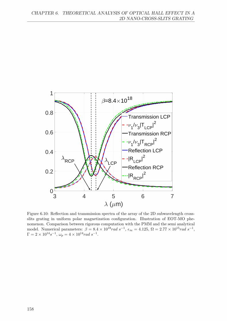
CHAPTER 6. THEORETICAL ANALYSIS OF OPTICAL HALL EFFECT IN A2D NANO-CROSS-SLITS GRATING
3 4 5 6 7 ( m)
0
0.2
0.4
0.6
0.8
1
Transmission LCP
1/
3|T
LCP|2
Transmission RCP
1/
3|T
RCP|2
Reflection LCP
|RLCP
|2
Reflection RCP
|RRCP
|2
LCPRCP
=8.4 1018
Figure 6.10: Reflection and transmission spectra of the array of the 2D subwavelength cross-slits grating in uniform polar magnetization configuration. Illustration of EOT-MO phe-nomenon. Comparison between rigorous computation with the PMM and the semi analyticalmodel. Numerical parameters: β = 8.4 × 10¹⁸rad s−1, ε∞ = 4.125, Ω = 2.77 × 10¹⁵rad s−1,Γ = 2× 10¹⁴s−1, ωp = 4× 10¹⁴rad s−1.
158
CHAPTER 6. THEORETICAL ANALYSIS OF OPTICAL HALL EFFECT IN A2D NANO-CROSS-SLITS GRATING
3 4 5 6 7 ( m)
0
0.2
0.4
0.6
0.8
1
Transmission LCPTransmission RCPReflection LCPReflection RCP
=9 1018
3 4 5 6 7 8 ( m)
0
0.2
0.4
0.6
0.8
1
Transmission LCPTransmission RCPReflection LCPReflection RCP
3.409 m
=9 1019
Figure 6.11: Illustration of EOT-MO phenomenon for β = 9× 10¹⁸rad s−1 and β = 9× 10¹⁹
. Numerical parameters: ε∞ = 4.125, Ω = 2.77 × 10¹⁵rad s−1, Γ = 2 × 10¹⁴s−1, ωp =4× 10¹⁴rad s−1.
159
CHAPTER 6. THEORETICAL ANALYSIS OF OPTICAL HALL EFFECT IN A2D NANO-CROSS-SLITS GRATING
6.4 ConclusionIn conclusion, we have proposed a theoretical analysis of a magneto optic plasmonicstructure based on a magneto optical activity, namely the nonreciprocity around EOTfrequency range. We provide a semi-analytical model based on a modal analysis ofthe system allowing efficient access to the full spectrum of the system. Our studyrevealed that when the proposed structure is symmetric, the fundamental mode isdegenerate. That is why the EOT phenomenon through such a structure is independentof the incident wave polarization. On the other hand, under a polar bias magneticfield the degeneracy of the fundamental mode of the structure is removed. Two EOTphenomena, each one associated with LCP and RCP polarizations, are then observed.This results in the non-reciprocity behavior of the proposed structure.
160
Bibliography
[1] H.F. Ghaemi T. Thio T.W. Ebbesen, H.J. Lezec and P.A. Wolff. Extraordinaryoptical transmission through sub-wavelenght hole arrays,”. Nature, (391):667–669,1998. 77, 79, 149
[2] L. Martín-Moreno, F. J. García-Vidal, H. J. Lezec, K. M. Pellerin, T. Thio, J. B.Pendry, and T. W. Ebbesen. Theory of extraordinary optical transmission throughsubwavelength hole arrays. Phys. Rev. Lett., 86:1114–1117, Feb 2001. 77, 149
[3] F. J. García de Abajo, R. Gómez-Medina, and J. J. Sáenz. Full transmissionthrough perfect-conductor subwavelength hole arrays. Phys. Rev. E, 72:016608,Jul 2005. 149
[4] H. T. Liu and P. Lalanne. "microscopic theory of the extraordinary optical trans-mission. Nature, (452):728–731, 2008. 77, 149
[5] F.I. Baida, Y. Poujet, B. Guizal, and D. Van Labeke. New design for en-hanced transmission and polarization control through near-field optical microscopyprobes. Optics Communications, 256(1):190–195, 2005. 77, 149
[6] Fadi I. Baida, Yannick Poujet, Jérôme Salvi, Daniel Van Labeke, and BrahimGuizal. Extraordinary transmission beyond the cut-off through sub- annular aper-ture arrays. Optics Communications, 282(7):1463–1466, 2009. 77, 149
[7] Magnetooptical effects in the metal-dielectric gratings. Optics Communications,278(1):104 – 109, 2007. 149
[8] Haibin Zhu and Chun Jiang. Nonreciprocal extraordinary optical transmissionthrough subwavelength slits in metallic film. Opt. Lett., 36(8):1308–1310, Apr2011. 149
[9] Hua Xu and Byoung Seung Ham. Investigation of extraordinary optical trans-mission and faraday effect in one-dimensional metallic-magnetic gratings. Opt.Express, 16(26):21375–21382, Dec 2008. 149
[10] L. Halagačka, M. Vanwolleghem, F. Vaurette, J. Ben Youssef, K. Postava, J. Piš-tora, and B. Dagens. Magnetoplasmonic nanograting geometry enables opticalnonreciprocity sign control. Opt. Express, 26(24):31554–31566, Nov 2018. 149
[11] Zhichao Ruan and Min Qiu. Enhanced transmission through periodic arrays ofsubwavelength holes: The role of localized waveguide resonances. Phys. Rev. Lett.,96:233901, Jun 2006. 149
161
BIBLIOGRAPHY
[12] Yuehui Lu, Min Hyung Cho, YoungPak Lee, and Joo Yull Rhee. Polarization-independent extraordinary optical transmission in one-dimensional metallic grat-ings with broad slits. Applied Physics Letters, 93(6):061102, 2008. 149
[13] V. I. Belotelov, L. L. Doskolovich, and A. K. Zvezdin. Extraordinary magneto-optical effects and transmission through metal-dielectric plasmonic systems. Phys.Rev. Lett., 98:077401, Feb 2007. 149
[14] Alexander B. Khanikaev, S. Hossein Mousavi, Gennady Shvets, and Yuri S.Kivshar. One-way extraordinary optical transmission and nonreciprocal spoofplasmons. Phys. Rev. Lett., 105:126804, Sep 2010. 149
[15] Victor Dmitriev, Fernando Paix ao, and Marcelo Kawakatsu. Enhancement offaraday and kerr rotations in three-layer heterostructure with extraordinary opticaltransmission effect. Opt. Lett., 38(7):1052–1054, Apr 2013. 149
[16] Daoyong Li, Chengxin Lei, Leyi Chen, Zhixiong Tang, Shaoyin Zhang, ShaolongTang, and Youwei Du. Waveguide plasmon resonance induced enhancement of themagneto-optics in a ag/bi:yig bilayer structure. J. Opt. Soc. Am. B, 32(9):2003–2008, Sep 2015. 149
[17] R. Brendel and D. Bormann. An infrared dielectric function model for amorphoussolids. Journal of Applied Physics, 71(1):1–6, 1992. 82, 150
[18] Aleksandar D. Rakić, Aleksandra B. Djurišić, Jovan M. Elazar, and Marian L.Majewski. Optical properties of metallic films for vertical-cavity optoelectronicdevices. Appl. Opt., 37(22):5271–5283, Aug 1998. 82, 150
[19] Kofi Edee. Single mode approach with versatile surface wave phase correctionfor the extraordinary optical transmission comprehension of 1d period nano-slitsarrays. OSA Continuum, 1(2):613–624, Oct 2018. 78, 150, 151
[20] K. Edee and J. P. Plumey. Numerical scheme for the modal method based onsubsectional gegenbauer polynomial expansion: application to biperiodic binarygrating. J. Opt. Soc. Am. A, 32(3):402–410, Mar 2015. 151
[21] Kofi Edee. Understanding the plane wave excitation of the metal-insulator-metalgap plasmon mode of a nanoribbons periodic array: role of insulator-metal-insulator lattice mode. OSA Continuum, 2(2):389–399, Feb 2019. 152
[22] Kofi Edee, Maha Benrhouma, Mauro Antezza, Jonathan Albert Fan, and BrahimGuizal. Coupling between subwavelength nano-slit lattice modes and metal-insulator-graphene cavity modes: a semi-analytical model. OSA Continuum,2(4):1296–1309, Apr 2019. 78, 152
[23] Dominik Floess and Harald Giessen. Nonreciprocal hybrid magnetoplasmonics.Reports on Progress in Physics, 81(11):116401, oct 2018. 158
162
Conclusion and outlook
I am not always good and noble.I am the hero of this story, but Ihave my off moments.
P. G. Wodehouse
In this thesis, we have exploited the extraordinary and unusual electromagnetic,optical and plasmonic properties of graphene for exploring and modelling graphenebased plasmonic structures of academic and technological interests. The research car-ried out and presented in this work is articulated around two main parts. The firstpart is focused on the study of hybrid plasmonic structures based on graphene whilethe second part is aimed at investigating the magneto-optical properties of structuresbased on graphene and metals subjected to an external static magnetic field. Let us, inthe following, summarize the main and important results obtained for these two parts.
After discussing and presenting the necessary basics and tools for this thesis inchapter 1, 2 and 4, we proposed in chapter 3 to investigate a hybrid plasmonic sys-tem consisting of a 1D array of periodic subwavelength metallic slits and a graphenesheet separated by a dielectric gap. This system puts in play two fundamental andimportant phenomena: an EOT phenomenon and a metal-insulator-graphene (M-I-G)cavity plasmon mode excitation. By the use of the PMM method, we have plottedthe transmission and reflection spectra of the proposed structure. The obtained re-sults revealed broadband and narrow band resonances. For a better understandingof the origin of these band resonances, we have proposed a semi analytical methodthat suggests to split the whole system into two coupled sub-systems. The first oneis a weakly coupled sub-system made of a periodic array of subwavelength metallicnano-slits whose electromagnetic response can be merely predicted by replacing it bya homogeneous slab with an equivalent permittivity. This allows us to analyticallyobtain its corresponding reflection and transmission coefficients. By comparing theanalytical results with the spectrum of the structure obtained by the PMM method,we showed that these approximated curves perfectly match the broadband resonancesof the hybrid structure. Additionally. it was shown that the narrow-band nature ofthe hybrid system can be u nderstood by studying the behaviour of a second stronglycoupled sub-system. It was also demonstrated that these resonances modes are linkedto the resonances of a metal/insulator/graphene horizontal Perot-Fabry cavity modes.Furthermore, we found that the effective index associated with these modes and thenthe resonance wavelengths of the system can be controlled and tuned by changing thechemical potential of graphene. By adjusting the chemical potential, we can achieve an
163
Conclusion and outlook
induced reflection phenomenon or perfect absorption within the structure. This find-ing may open up opportunities for various tunable applications such as reflectors andabsorbers. Finally, we provided analytical expressions for the reflection and transmis-sion coefficients of the global structure allowing to describe the resonance phenomenaoccurring in it. An interesting perspective is that our analysis can be extended tostudy more complex hybrid structures such as the coupling of the lattice modes with asubstrate made of a non-reciprocal photonic topological material and hybrid configura-tions involving diffraction gratings coupled to hybrid graphene multilayered structures.
In the second part of this work concerning the study of the magneto-optical proper-ties of structures based on graphene and metals, we have been interested in investigatingtwo different structures. In chapter 5, we developed a simple and fast semi analyticalmethod to accurately predict the optical response of a one dimensional graphene stripgrating in the presence of an external static magnetic field, in which the graphene ismodelled as an anisotropic layer with atomic thickness and a frequency dependent andcomplex permittivity tensor. The optical spectra are computed through an effectivemedium approach and a scattering formalism. This model is computationally efficientand can be readily applied to any graphene strip grating with different geometric pa-rameters. In particular, we showed that the proposed model can efficiency deal withgratings with small gaps as well as with large gaps, specifically, it provides precise andreliable results in the case of gratings with small gaps which constitute a complicatedcase to deal with. Moreover, we found that, although the proposed model can effi-ciently treat structures with static magnetic fields, it is still valid even for structureswhere the static magnetic field is absent. We further analysed the proposed approachas a function of the static magnetic field and found that it can provide accurate resultsfor all fields smaller than 7T. As a future work, we propose to employ this structurein the design of a spectrally and spatially tunable metasurface lens by exploiting thetunability of graphene magnetoplasmons.
Finally, chapter 6 has been dedicated to the study of magneto optical properties of a2D plasmonic structure composed of a periodic array of metal crossed-slits grating whenthe slits are filled with an anisotropic gyrotropic material. Firstly, we have provided asemi-analytical model based on a modal analysis of the system that allows to reproducethe full spectrum of the system and describe the EOT mechanism occurring in it.Secondly, we have employed these analytical expressions to explore the non reciprocalunidirectional light transmission in the frequency ranges where EOT occures.
164