Lower crustal earthquakes near the Ethiopian rift induced by magmatic processes
Upload
technicaluniCategory
view
3download
0
1
RIFT VALLEY INSTITUTE OF SCIENCE AND TECHNOLOGY- RVIST
DEPARTMENT OF ELECTRICAL AND ELECTRONIC ENGINEERING – EEE
CEEP/CEET MODULE II- 2015
COURSE TITLE: MICROELECTRONICS
Lecture notes
By
Dr. Cliff Orori Mosiori
(Ph.D- Electronics, M.Sc- Electronics, B.Ed –Physics)
©2015
2
Table of Contents INTRODUCTION ....................................................................................................................... 3
Evolution of Computers ............................................................................................................... 4
Computer Generations .................................................................................................................. 5
COMPUTER STRUCTURES ...................................................................................................... 6
BASIC MICROPROCESSOR SYSTEMS.................................................................................... 8
The Microprocessor Architecture.............................................................................................. 8
The Microprocessor .................................................................................................................. 9
A microprocessor system ........................................................................................................ 10
The physical appearance of a microprocessor ......................................................................... 11
Terms used in microprocessors ............................................................................................... 12
Internal Structure of microprocessor ....................................................................................... 13
Microprocessor Families ........................................................................................................ 15
The Microprocessor Components ........................................................................................... 15
1. The Control Unit ......................................................................................................... 16
2. Arithmetic Logic Unit (ALU)...................................................................................... 17
3. Registers ..................................................................................................................... 18
4. BUSES ....................................................................................................................... 20
Interfacing Devices ................................................................................................................ 23
8085 Microprocessor .............................................................................................................. 25
8085 System Bus .................................................................................................................... 28
8085 Pin description ............................................................................................................... 30
8085 Functional Description ................................................................................................... 34
The 8085 Programming Model ............................................................................................... 37
The 8085 Addressing Modes .................................................................................................. 39
Arithmetic Operations ............................................................................................................ 41
Types of Memory ................................................................................................................... 45
Secondary Memory ................................................................................................................ 46
Programming ............................................................................................................................. 49
Check next attachment for programming notes on: ..................................................................... 49

3
INTRODUCTION A computer is defined as a machine that is capable of taking in raw data (input) and
processing it into more meaningful output (information) under definite instructions
(programs) and stores the results for future use. Therefore a computer has four basic
operations or functions:
Input
Processing
Output
Storage
Definition of Terms in Computers
1. Data:
A collection of unorganized facts including words, symbols, numbers, images, sounds
etc with little or no meaning.
2. Data Processing:
The manipulation of data to give information by arithmetic (addition, subtraction,
multiplication, division etc) or logical operations (=, <, >, , , , etc)
3. Programs:
These are the step by step instructions used by the computer in data processing.
4. Information:
The finished product of data processing that has meaning and is useful for decision
making now and in future.
5. Hardware:
These are the tangible mechanical, electrical and electronic parts of a computer system.
6. Software:
4
These are the series of instruction that tell hardware what to do and how to do it.
Programs are part of software but not synonymous.
Evolution of Computers Computers have evolved from simple to complex. The ABACUS was used by the Chinese
and Japanese about 500BC. The slide rule was developed in 1632 and assisted in arithmetic
operations of addition and subtraction. Wilhem Schickard made the first mechanical
machine in 1632 which could add and subtract automatically. In 1647, Blaise Pascal
developed the ‘Mechanical Calculator’ which could add, subtract and convert sums of
money between the different coinages of the time. His intention was to ease the burden on his
father who had the task of reorganizing finances and taxes. G. W. Leibnitz made the
‘Leibnitz Stepped Rocker’ which could add, subtract, multiply, divide and extract square
roots.
Start of the Computer Age
Charles Babbage in 1832 developed the ‘Analytic Engine’ which could deal with
arithmetic problems and make decisions based on the results. Babbage is also called the
‘Father of the Modern Computer’ because he:
i. Established the architecture of the universal computer i.e. Arithmetic Logic
Unit (ALU), control unit, Input and output units.
ii. Used perforated cards/punched cards to communicate with the machine of
which it is still important today.
iii. Made a digital machine thus showing the way to later computers.
NB: His insights were remarkable but unfortunately his plans were too ambitious for the
technology of his time thus his machine was never fully completed as per his ideas.
Herman Hollerinth made a card punching and reading machine to help in the USA’s
census of 1890. He also formed a company better known today as the International Business
Machines (IBM). 1906, Lee De Forest developed the ‘Thermionic/Vacuum tube’ which
helped in later computer electronic circuits. 1937 to 1944 the Mark I was developed by
Howard Aiken with IBM’s support. It was electromechanical and used relays and switches.
In 1946 the Electronic Numerical Integrator And Calculator (ENIAC) was built for use

5
in World War two (WWII). It weighed 30 tones, had 18,000 vacuum tubes, occupied a 50 x
30 foot space and consumed 160 KW of power. 1947, W. Shockley, J. Bardeen and W.
Brattain invented the transfer of resistance device eventually called the transistor which
revolutionized computer development. In the late 1950’s, the integrated circuit (IC) was
developed paving way for the microprocessor developed in 1971 by Dr. Ted Hoff of Intel
Corporation who made the Intel 4004 microprocessor. The development of the computer
then became too fast and great.
Computer Generations The First Generation (1946 – 1956):
Mainly used the vacuum tubes which were short-lived consumed a lot of power and
generated a lot of heat. Speeds of up to 10K instructions per second and memories of 2KB
were reached. Modern computer architecture was developed by John Von Newman in 1945.
The Second Generation (1957 – 1963):
Relied on the transistor which is much more stable, lasts longer, consumes less power and
produces less heat compared to the vacuum tube. Magnetic core memories were developed
with up to 32KB of RAM. Speeds of 200K to 300K instructions per second were reached.
The Third Generation (1964 – 1979):
Relied on the integrated circuit (IC) which is made of combining many transistors, diodes
and other electronic semiconductor components in one ceramic or plastic package. The
magnetic disk memory was developed with up to 2MB of RAM. Speeds increased to five
million instructions per second (5MIPS). The first microcomputer was developed in 1974.
The Fourth Generation (1979 – 1989):
IC’s developed from the earlier Small Scale Integration (SSI) i.e. 1 – 10 transistors and
Medium Scale Integration (MSI) i.e. 10 – 100 transistors, to the Large Scale Integration
(LSI) i.e. 100 – 2000 transistors and Very Large Scale Integration (VLSI) i.e. 200,000 –
400,000 transistors per IC. Memories using magnetic disks, bubble memories and optical

6
disks (CD-ROM’s) were developed thus several hundred MB’s. Speeds up to 50MIPS were
reached. The Personal Computer (PC) was developed by the IBM Company.
The Fifth Generation (1990 – Present):
Merging of the computer and telecommunications was done with large scale computer
networking (internet) turning the world into a global village. Supercomputers with speeds
between one gigahertz (1GHz) to one Terahertz (1THz) have been developed. Computer
technology is changing by the day having found usage in virtually all human activities.
COMPUTER STRUCTURES The computer consists of two main parts:
Hardware
Software
The relationship and parts of these structures in figure 1:

7
The hardware parts consist of two main physical parts:
(i) System Unit:
This includes the mechanical, electrical and electronic parts that make up the main
computer parts i.e. the power supply unit, microprocessor system (motherboard and
CPU), the hard disk, the floppy drive(s), CD-ROM drive(s), zip drive and the casing
structure. The system unit can be an all in one, desktop or tower type.
NB: The CPU is just a part of the system unit on the motherboard and should not be
confused with the system unit.
(ii) Peripherals:
This consists of all input, output and other storage devices connected to the system
unit. Input devices include the keyboard, pointing devices(e.g. mouse, track ball,
light pen, touch screen, touch/track pad, pointing stick, joystick, pen input, pen
computing, graphics tablet, etc), scanning and reading devices (e.g. OCR, OMR,
MICR, POS terminals, scanner, etc), direct input from instruments (e.g. MIDI,
Computer Numerical Control (CNC) etc), video, audio and digital camera. The
output devices include printers, plotters, monitor/VDU, speakers, robots etc while
the other storage devices include USB flash disks, external drives, etc).

8
Key:
Commands or
Signal flow
(Control bus)
Data or Instruction
Flow (data bus)
The components of computer hardware include: Central Processing Unit (CPU); Storage;
Input and Output.
All microcomputers are fully dependent on their CPU and the buses hence the term the Bus
Oriented System. The same block diagram above in this case is now drawn to show the
relationship between the parts as represented by the buses and the CPU.
BASIC MICROPROCESSOR SYSTEMS
The Microprocessor Architecture
The microprocessor was born
In 1971 two companies in the USA, introduced the world to its future by producing
microprocessors. They were a young company called Intel and their rival, Texas
9
Instruments. The microprocessor, and its offspring, the microcontroller, were destined to
infiltrate every country, every means of production, and almost every home in the world.
There is now hardly a person on the planet that does not own or know of something that is
dependent on one of these devices. Yet curiously, so few people can give any sort of
answer to the simple question ‘What is a microprocessor?’ and ‘How does it work?’
The Microprocessor A microprocessor incorporates the functions of a computer's central processing unit
(CPU) on a single integrated circuit (IC) or at most a few integrated circuits. All modern
CPUs are microprocessors making the micro- prefix redundant. The microprocessor is a
multipurpose, programmable device that accepts digital data as input, processes it
according to instructions stored in its memory, and provides results as output. It is an
example of sequential digital logic, as it has internal memory. Microprocessors operate on
numbers and symbols represented in the binary numeral system.
The integration of a whole CPU onto a single chip or on a few chips greatly reduced the
cost of processing power. The integrated circuit processor was produced in large numbers
by highly automated processes, so unit cost was low. Single-chip processors increase
reliability as there are many fewer electrical connections to fail. As microprocessor
designs get faster, the cost of manufacturing a chip generally stays the same. Before
microprocessors, small computers had been implemented using racks of circuit boards
with many medium- and small-scale integrated circuits. Microprocessors integrated this
into one or a few large-scale ICs. Continued increases in microprocessor capacity have
since rendered other forms of computers almost completely obsolete with one or more
microprocessors used in everything from the smallest embedded systems and handheld
devices to the largest mainframes and supercomputers.
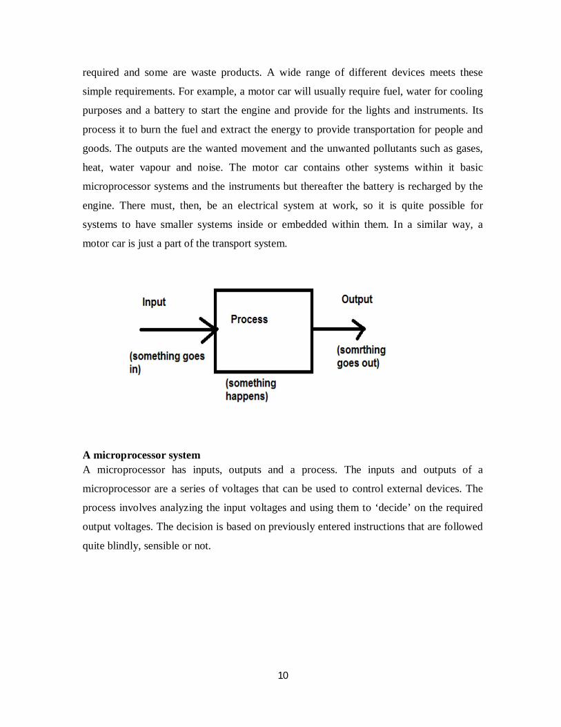
A system
The word ‘system’ is used to describe any organization or device that includes three
features. A system must have at least one input, one output and must do something, i.e. it
must contain a process. Often there are many inputs and outputs. Some of the outputs are
10
required and some are waste products. A wide range of different devices meets these
simple requirements. For example, a motor car will usually require fuel, water for cooling
purposes and a battery to start the engine and provide for the lights and instruments. Its
process it to burn the fuel and extract the energy to provide transportation for people and
goods. The outputs are the wanted movement and the unwanted pollutants such as gases,
heat, water vapour and noise. The motor car contains other systems within it basic
microprocessor systems and the instruments but thereafter the battery is recharged by the
engine. There must, then, be an electrical system at work, so it is quite possible for
systems to have smaller systems inside or embedded within them. In a similar way, a
motor car is just a part of the transport system.
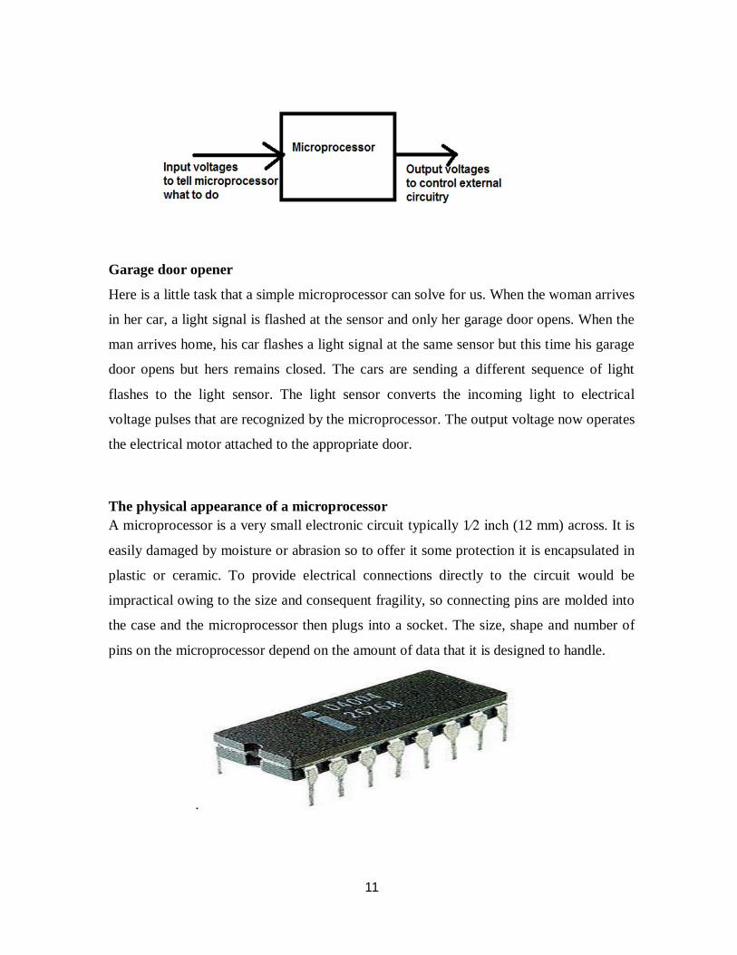
A microprocessor system A microprocessor has inputs, outputs and a process. The inputs and outputs of a
microprocessor are a series of voltages that can be used to control external devices. The
process involves analyzing the input voltages and using them to ‘decide’ on the required
output voltages. The decision is based on previously entered instructions that are followed
quite blindly, sensible or not.
11
Garage door opener
Here is a little task that a simple microprocessor can solve for us. When the woman arrives
in her car, a light signal is flashed at the sensor and only her garage door opens. When the
man arrives home, his car flashes a light signal at the same sensor but this time his garage
door opens but hers remains closed. The cars are sending a different sequence of light
flashes to the light sensor. The light sensor converts the incoming light to electrical
voltage pulses that are recognized by the microprocessor. The output voltage now operates
the electrical motor attached to the appropriate door.
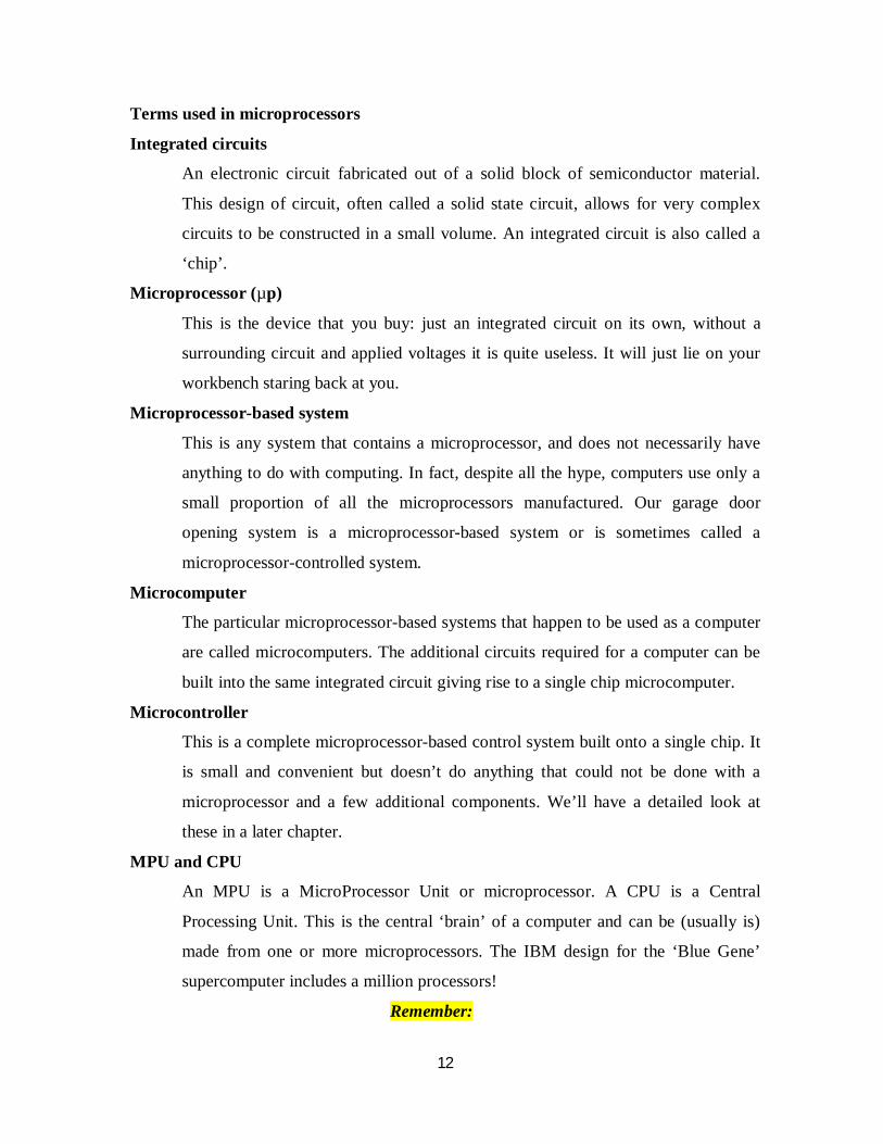
The physical appearance of a microprocessor A microprocessor is a very small electronic circuit typically 1⁄2 inch (12 mm) across. It is
easily damaged by moisture or abrasion so to offer it some protection it is encapsulated in
plastic or ceramic. To provide electrical connections directly to the circuit would be
impractical owing to the size and consequent fragility, so connecting pins are molded into
the case and the microprocessor then plugs into a socket. The size, shape and number of
pins on the microprocessor depend on the amount of data that it is designed to handle.
.
12
Terms used in microprocessors
Integrated circuits
An electronic circuit fabricated out of a solid block of semiconductor material.
This design of circuit, often called a solid state circuit, allows for very complex
circuits to be constructed in a small volume. An integrated circuit is also called a
‘chip’.
Microprocessor (µp)
This is the device that you buy: just an integrated circuit on its own, without a
surrounding circuit and applied voltages it is quite useless. It will just lie on your
workbench staring back at you.
Microprocessor-based system
This is any system that contains a microprocessor, and does not necessarily have
anything to do with computing. In fact, despite all the hype, computers use only a
small proportion of all the microprocessors manufactured. Our garage door
opening system is a microprocessor-based system or is sometimes called a
microprocessor-controlled system.
Microcomputer
The particular microprocessor-based systems that happen to be used as a computer
are called microcomputers. The additional circuits required for a computer can be
built into the same integrated circuit giving rise to a single chip microcomputer.
Microcontroller
This is a complete microprocessor-based control system built onto a single chip. It
is small and convenient but doesn’t do anything that could not be done with a
microprocessor and a few additional components. We’ll have a detailed look at
these in a later chapter.
MPU and CPU
An MPU is a MicroProcessor Unit or microprocessor. A CPU is a Central
Processing Unit. This is the central ‘brain’ of a computer and can be (usually is)
made from one or more microprocessors. The IBM design for the ‘Blue Gene’
supercomputer includes a million processors!
Remember:
13
*MPU is the thing
*CPU is the job.
Micro-
The word micro is used in electronics and in science generally, to mean ‘one-
millionth’ or 1/10–6. It has also entered general language to mean something very
small like a very small processor or microprocessor. It has also become an
abbreviation for microprocessor, microcomputer, microprocessor-based system or
a micro controller – indeed almost anything that has ‘micro’ in its name. In the
scientific sense, the word micro is represented by the Greek letter µ, (mu). It was
only a small step for microprocessor to become abbreviated to µP.
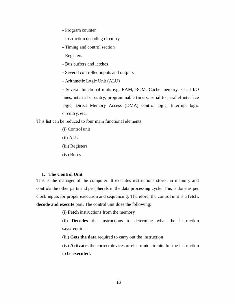
Internal Structure of microprocessor
The internal arrangement of a microprocessor varies depending on the age of the design
and the intended purposes of the microprocessor. The complexity of an integrated circuit
is bounded by physical limitations of the number of transistors that can be put onto one
chip, the number of package terminations that can connect the processor to other parts of
the system, the number of interconnections it is possible to make on the chip, and the heat
that the chip can dissipate. Advancing technology makes more complex and powerful
chips feasible to manufacture.

14
A minimal hypothetical microprocessor might only include an arithmetic logic unit (ALU)
and a control logic section. The ALU performs operations such as addition, subtraction,
and operations such as AND or OR. Each operation of the ALU sets one or more flags in a
status register, which indicate the results of the last operation (zero value, negative
number, overflow, or others). The control logic section retrieves instruction operation
codes from memory, and initiates whatever sequence of operations of the ALU requires to
carry out the instruction. A single operation code might affect many individual data paths,
registers, and other elements of the processor.
As integrated circuit technology advanced, it was feasible to manufacture more and more
complex processors on a single chip. The size of data objects became larger; allowing
more transistors on a chip allowed word sizes to increase from 4- and 8-bit words up to
today's 64-bit words. Additional features were added to the processor architecture; more
on-chip registers sped up programs, and complex instructions could be used to make more
compact programs. Floating-point arithmetic, for example, was often not available on 8-
bit microprocessors, but had to be carried out in software. Integration of the floating point
unit first as a separate integrated circuit and then as part of the same microprocessor chip,
sped up floating point calculations. The microprocessor performs several functions
classified into three categories:
(i) Microprocessor initiated operations
(ii) Internal data operations
(iii) Peripheral (external) initiated operations
In order to achieve this, the microprocessor uses a group of logic circuits and sets of
control signals. Early processors had these circuits in different chips hence the term
Micro Processing Unit (MPU) or Central Processing Unit (CPU). However, later
microprocessors have most of the necessary circuitry in one chip called the
Microprocessor Chip. The microprocessor is defined broadly as a programmable logic
chip. Therefore, if a number of devices or chips are used the term MPU or CPU is used
but if only one chip contains the circuitry needed then microprocessor chip is used. But

15
the terms MPU, CPU and microprocessor are used interchangeably/synonymously in
general day to day talk.
The microprocessor is usually found on the motherboard and the two are called the
microprocessor system. The complete set of devices required to make and operated a
computer i.e. microprocessor system (microprocessor and motherboard) and peripherals
(input, output and storage devices) form the microcomputer system.
Microprocessor Families
Microprocessor families depend on the manufacturers:
Intel
Intel has developed the 4004, 8008, 8080 and 8085 (8080A/8085A family), 8088,
80186, 80286, 80386, 80486, Pentium I, Pentium Pro, Pentium with MMXTM,
Pentium II, Pentium II Xeon, Celeron, Pentium III, Pentium III Xeon, Itanium and the
very latest Pentium Dual Core. Their processors are used to power PC’s.
Motorola
Motorola has developed the 6800, 68020, 68030, 68040 and PowerPC. Their processors
are used to power the Apple Macintosh computers.
American Device Manufacturers (AMD)
AMD and Cyrix make Intel-compatible generic microprocessor i.e. they have the same
internal design or architecture as Intel processors and perform the same functions but
often are less expensive.
Cyrix
Zilog Corporation
Zilog Corporation is known for the famous Z80 family of processors used in industrial
applications for process control.
Digital Equipment Corporation (DEC) etc.
The Microprocessor Components All microprocessors have the following:
- Internal buses and control lines
16
- Program counter
- Instruction decoding circuitry
- Timing and control section
- Registers
- Bus buffers and latches
- Several controlled inputs and outputs
- Arithmetic Logic Unit (ALU)
- Several functional units e.g. RAM, ROM, Cache memory, serial I/O
lines, internal circuitry, programmable timers, serial to parallel interface
logic, Direct Memory Access (DMA) control logic, Interrupt logic
circuitry, etc.
This list can be reduced to four main functional elements:
(i) Control unit
(ii) ALU
(iii) Registers
(iv) Buses
1. The Control Unit This is the manager of the computer. It executes instructions stored in memory and
controls the other parts and peripherals in the data processing cycle. This is done as per
clock inputs for proper execution and sequencing. Therefore, the control unit is a fetch,
decode and execute part. The control unit does the following:
(i) Fetch instructions from the memory
(ii) Decodes the instructions to determine what the instruction
says/requires
(iii) Gets the data required to carry out the instruction
(iv) Activates the correct devices or electronic circuits for the instruction
to be executed.
17
The control unit has the following parts:
(i) Program Manager (PM) or Sequence Control Register (SCR):
It is also referred to as the Timing and Control Unit. It controls the order of
execution of instructions as per the clock input signals. The timing and control
signals are sent to all the parts of the computer to coordinate the execution of
instructions.
(ii) Instruction Register:
This is used to store a copy of the instructions being processed. This ensures that
the instructions are readily available for decoding. For the 8085/8080A family it
is an 8-bit register.
(iii) Instruction Decoder:
It interprets the instructions to determine the type of action required and sends
signals to the control part so that the correct micro program is executed. In the
8080A/8085 family, it is together with the machine cycle encoding circuitry.
2. Arithmetic Logic Unit (ALU) It performs the arithmetic and logical operations for the whole computer system. The
accumulator (also called register A) holds one operand (part of the data being
processed) while the temporary register holds the other operand. The result is stored
in the accumulator which is an 8-bit register for the 8080A and 8085A microprocessors.
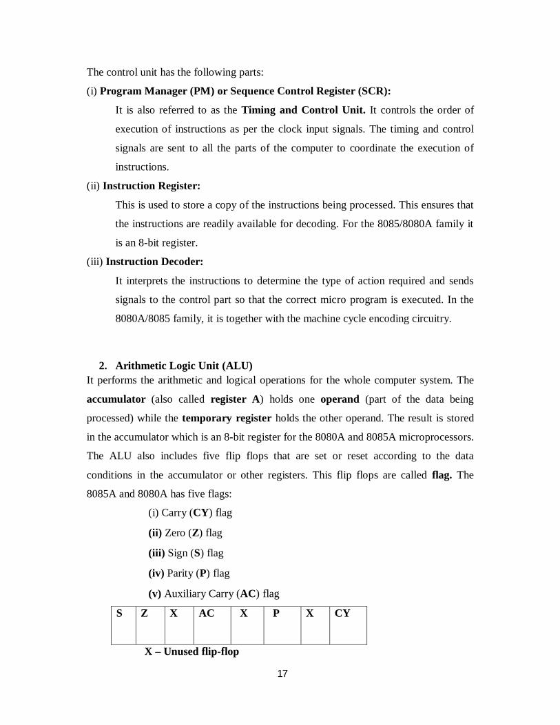
The ALU also includes five flip flops that are set or reset according to the data
conditions in the accumulator or other registers. This flip flops are called flag. The
8085A and 8080A has five flags:
(i) Carry (CY) flag
(ii) Zero (Z) flag
(iii) Sign (S) flag
(iv) Parity (P) flag
(v) Auxiliary Carry (AC) flag
S Z X AC X
P
X CY
X – Unused flip-flop

18
The flag register is 8-bit but three of them are unused. If an operation results in data
which is more than 8-bits, the carry (CY) flag is set to one i.e. CY = 1. If the result is
zero, the zero (Z) flag is set to one i.e. Z = 1. Therefore, flags are used by the
microprocessor to test the data conditions especially in conditional jump instructions
e.g. JC – Jump on carry instruction is implemented if the carry (CY) flag is set i.e. CY
= 1. The data conditions of the accumulator (register A) and the flag register can be
examined by the instruction Program Status Word (PSW) in the instruction set.
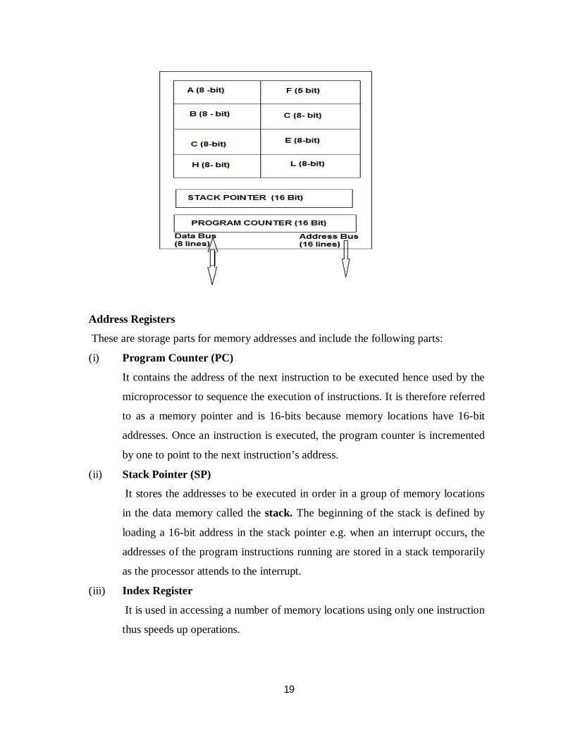
3. Registers These are fast but volatile memories found within the microprocessor. They include:
(i) Accumulator or Register A
(ii) Flags
(iii) Internal Registers
(iv) Program Counter (PC)
(v) Stack Pointer (SP)
(vi) Index Register
Internal Registers or Data registers
The size of this registers gives the amount of data that the processor can operate
on at a time. The 8085A/8080A have six general purpose registers which are
programmable i.e. a programmer can use them to load or transfer data. The six
are B, C, D, E, H and L as shown below. They can also be used while combined
together as register pairs i.e. BC, DE and HL register pairs. The accumulator and
the flag register are included though used solely for ALU operations.
19
Address Registers
These are storage parts for memory addresses and include the following parts:
(i) Program Counter (PC)
It contains the address of the next instruction to be executed hence used by the
microprocessor to sequence the execution of instructions. It is therefore referred
to as a memory pointer and is 16-bits because memory locations have 16-bit
addresses. Once an instruction is executed, the program counter is incremented
by one to point to the next instruction’s address.
(ii) Stack Pointer (SP)
It stores the addresses to be executed in order in a group of memory locations
in the data memory called the stack. The beginning of the stack is defined by
loading a 16-bit address in the stack pointer e.g. when an interrupt occurs, the
addresses of the program instructions running are stored in a stack temporarily
as the processor attends to the interrupt.
(iii) Index Register
It is used in accessing a number of memory locations using only one instruction
thus speeds up operations.
20
4. BUSES These are sets of communication lines for the various parts of the computer to function.
The microprocessor performs four operations:
(i) Memory Read: reads/copies data from memory
(ii) Memory Write: writes/copies data into memory
(iii) Input/Output (I/O) Read: Accepts data from input devices
(iv) I/O Write: Sends data to output devices
To perform these operations, the microprocessor goes through the following steps:
Step 1 – Identify the peripheral or memory location using its address
Step 2 – Transfer data
Step 3 – Provide timing or synchronisation signals
There are three types of buses each used to perform one of the above steps:
(1) Address Bus
(2) Data Bus
(3) Control Bus
(1) ADDRESS BUS
This is a unidirectional 16- line communication medium usually labelled A0 to
A15 and it only one way i.e. from the microprocessor to the peripherals
(8080/8085). The number of address lines gives the capacity of the
microprocessor to identify different memory locations e.g. 216 = 65,536 memory
locations. (This when rounded off and referred to as 64KB (1KB = 1024 Bytes).
Most 8-bit microprocessors have 16-address lines. The address lines carry the
memory location of data to be acted on by the microprocessor or the location or
register in an input or output device.
(2) DATA BUS
This is a bidirectional (two way) medium for transmission of data to and from the
microprocessor. It consists of 8-lines hence 28 = 256 different numbers. The data bus
determines the word length and register size of a microprocessor hence they are
named as per their data bus.

21
Microprocessor
No. of Data
Lines
Word Length Manufacturer
8080A/8085A 8 8-bits Intel
8088 8 8-bits Intel
80186 16 16-bits Intel
80286 16 16-bits Intel
6800 16 16-bits Motorola
Z80 16 16-bits Zilog
Corporation
80386,80486,
Pentium I
32 32-bits Intel
The data lines for an 8-bit microprocessor are usually labelled D0 to D7 i.e. 8-parallel
data lines carrying 8-bits of data or information simultaneously to or from different
parts of the computer. The data bus uses a bidirectional buffer i.e. allows data to flow
in both directions. It is also called the octal bus transceiver.
(3) CONTROL BUS
This are single lines that are unidirectional i.e. one way and do carry command
signals from the control unit to various parts of the computer system. The
microprocessor generates specific control signals for every operation it performs.
There are four main operations:
(i) I/O synchronisation
(ii) Memory Synchronisation
(iii) Microprocessor scheduling
(iv) Control various utilities
(i) Input/Output (I/O) Synchronisation:
Synchronisation is scheduling or sequencing of various activities to ensure that
there is no conflict or collusion and that all operations run smoothly and perfectly.

22
Therefore the control unit sends to these devices READ or WRITE signals
together represented as R/W or separately as RD and WR. A read command is to
activate an I/O device to load or input data to the data bus. If it is a dedicated
command it will carry an identifying letter or abbreviation e.g. input/output read is
IOR or memory read is MEMR etc The write command is used to make the
peripheral devices to take or output data to the data bus. It can also be dedicated to
specific devices e.g. IOW, MEMW etc Once an I/O device receives the R/W
signal, it generates an “acknowledge” signal to confirm the reception of the
command or signal.
(ii) Memory Synchronisation:
These are signals used to regulate and sequence the transfer of data from memory
or to memory. The READ, WRITE and READY signals are used. The READY
signal acknowledges data availability and readiness to transfer.
(iii) Microprocessor Scheduling:
These are signals geared towards sequencing the working of various parts of the
microprocessor in the data processing cycle. Therefore, they are microprocessor
internal commands.
(iv) Control Utilities:
These are specific peripheral or externally initiated signals for which individual
pins of the microprocessor are assigned. These are:
(a) Reset
(b) Interrupt
(c) Ready
(d) Hold
(a) Reset
When activated, all internal operations are suspended and the program counter is
cleared. The program execution then begins at the zero memory address.
(b) Interrupt
– the microprocessor can be interrupted from its normal execution of instructions
so as to deal with other instructions called service routines e.g. emergency

23
procedures, virus check/scanning etc. the microprocessor resumes its operations
after completing the service routine.
(c) Ready
– if the signal at the ready pin is low, the microprocessor enters a wait state. This is
used to synchronise slower peripheral devices with the microprocessor.
(d) Hold
– When the signal at the hold pin is high, the microprocessor gives up control of the
buses and allows an external peripheral device to use them e.g. during Direct Memory
Access (DMA).
5. POWER BUS
These are actual wires used to supply power to the various parts of the computer. They
can be two (+5V and 0V or +12V and 0V) or four (+12V, +5V, 0V and -5V) depending
on the type of microprocessor.
Interfacing Devices Interfacing devices are necessary to interconnect computer parts/components with
in bus oriented system. Interfacing components include:
(i) Buffer (ii) Decoder (iii) Encoder (iv) Latch
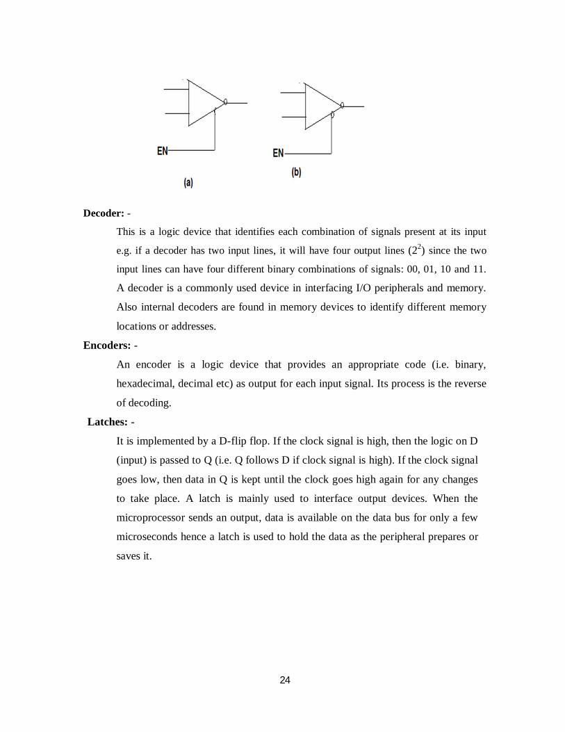
i) Buffers
- this is a logic circuit which amplifies the current or power of a signal. A simple buffer
gives the same output as the input but increases its driving capability hence known as a
driver. Buffers are commonly used to enable/disable the data and address bus and also
increase their signal driving capability.
Tri-state Devices:
These have three states: logic 1, logic 0 and high impedance.
- For (a) if the logic on the enable pin is 1, the device functions as an ordinary inverter. If it is
0, it will go into a high impedance state i.e. as if it were disconnected from the system.
- For (b) it will act as an inverter if the enable pin has logic 0 and go into high impedance if
the enable pin has 1.
24
Decoder: -
This is a logic device that identifies each combination of signals present at its input
e.g. if a decoder has two input lines, it will have four output lines (22) since the two
input lines can have four different binary combinations of signals: 00, 01, 10 and 11.
A decoder is a commonly used device in interfacing I/O peripherals and memory.
Also internal decoders are found in memory devices to identify different memory
locations or addresses.
Encoders: -
An encoder is a logic device that provides an appropriate code (i.e. binary,
hexadecimal, decimal etc) as output for each input signal. Its process is the reverse
of decoding.
Latches: -
It is implemented by a D-flip flop. If the clock signal is high, then the logic on D
(input) is passed to Q (i.e. Q follows D if clock signal is high). If the clock signal
goes low, then data in Q is kept until the clock goes high again for any changes
to take place. A latch is mainly used to interface output devices. When the
microprocessor sends an output, data is available on the data bus for only a few
microseconds hence a latch is used to hold the data as the peripheral prepares or
saves it.

25
8085 Microprocessor Internal Architecture of 8085 Microprocessor
Control Unit
Generates signals within μP to carry out the instruction, which has been decoded.
In reality causes certain connections between blocks of the μP to be opened or
closed, so that data goes where it is required, and so that ALU operations occur.
Arithmetic Logic Unit
The ALU performs the actual numerical and logic operation such as ‘add’,
‘subtract’, ‘AND’, ‘OR’, etc. it uses data from memory and from Accumulator to
perform arithmetic. Always stores result of operation in Accumulator.
Registers
The 8085-programming model includes six registers, one accumulator, and one
flag register, as shown in Figure above. In addition, it has two 16-bit registers: the
stack pointer and the program counter. They are described briefly as follows. The
8085 has six general-purpose registers to store 8-bit data; these are identified as B,
26
C, D, E, H, and L as shown in the figure above. They can be combined as register
pairs - BC, DE, and HL - to perform some 16-bit operations. The programmer can
use these registers to store or copy data into the registers by using data copy
instructions.
Accumulator
The accumulator is an 8-bit register that is a part of arithmetic/logic unit (ALU).
This register is used to store 8-bit data and to perform arithmetic and logical
operations. The result of an operation is stored in the accumulator. The
accumulator is also identified as register A.
Flags
The ALU includes five flip-flops, which are set or reset after an operation
according to data conditions of the result in the accumulator and other registers.
They are called Zero (Z), Carry (CY), Sign (S), Parity (P), and Auxiliary Carry
(AC) flags; they are listed in the Table and their bit positions in the flag register
are shown in the Figure below. The most commonly used flags are Zero, Carry,
and Sign. The microprocessor uses these flags to test data conditions.
For example, after an addition of two numbers, if the sum in the accumulator is
larger than eight bits, the flip-flop uses to indicate a carry -- called the Carry flag
(CY) – is set to one. When an arithmetic operation results in zero, the flip-flop
called the Zero (Z) flag is set to one. The first Figure shows an 8-bit register, called
the flag register, adjacent to the accumulator. However, it is not used as a register;
five bit positions out of eight are used to store the outputs of the five flip-flops.
The flags are stored in the 8-bit register so that the programmer can examine these
flags (data conditions) by accessing the register through an instruction.
These flags have critical importance in the decision-making process of the
microprocessor. The conditions (set or reset) of the flags are tested through the
software instructions. For example, the instruction JC (Jump on Carry) is
implemented to change the sequence of a program when CY flag is set. The
thorough understanding of flag is essential in writing assembly language programs.

27
Program Counter (PC)
This 16-bit register deals with sequencing the execution of instructions. This
register is a memory pointer. Memory locations have 16-bit addresses, and that is
why this is a 16-bit register. The microprocessor uses this register to sequence the
execution of the instructions. The function of the program counter is to point to the
memory address from which the next byte is to be fetched. When a byte (machine
code) is being fetched, the program counter is incremented by one to point to the
next memory location.
Stack Pointer (SP)
The stack pointer is also a 16-bit register used as a memory pointer. It points to a
memory location in R/W memory, called the stack. The beginning of the stack is
defined by loading 16-bit address in the stack pointer. The stack concept is
explained in the "Stack and Subroutines."
Instruction Register/Decoder
It is the temporary store for the current instruction of a program. Latest instruction
sent here from memory prior to execution. Decoder then takes instruction and
‘decodes’ or interprets the instruction. Decoded instruction then passed to next
stage.
Memory Address Register
Holds address, received from PC, of next program instruction. It feeds the address
bus with addresses of location of the program under execution.
Control Generator
Generates signals within μP to carry out the instruction which has been decoded. In
reality causes certain connections between blocks of the μP to be opened or closed,
so that data goes where it is required, and so that ALU operations occur.
Register Selector
This block controls the use of the register stack in the example. Just a logic circuit
which switches between different registers in the set will receive instructions from
Control Unit.

28
General Purpose Registers
μP requires extra registers for versatility. Can be used to store additional data
during a program. More complex processors may have a variety of differently
named registers.
Microprogramming
How does the μP knows what an instruction means, especially when it is only a
binary number? The microprogram in a μP/uC is written by the chip designer and
tells the μP/uC the meaning of each instruction μP/uC can then carry out operation.
8085 System Bus Typical system uses a number of busses, collection of wires, which transmit binary
numbers, one bit per wire. A typical microprocessor communicates with memory
and other devices (input and output) using three busses: Address Bus, Data Bus
and Control Bus.
Address Bus
One wire for each bit, therefore 16 bits = 16 wires. Binary number carried alerts
memory to ‘open’ the designated box. Data (binary) can then be put in or taken
out. The Address Bus consists of 16 wires, therefore 16 bits. Its "width" is 16 bits.
A 16 bit binary number allows 216 different numbers, or 32000 different numbers,
i.e. 0000000000000000 μP to 1111111111111111. Because memory consists of
boxes, each with a unique address, the size of the address bus determines the size
of memory, which can be used. To communicate with memory the microprocessor
sends an address on the address bus, eg 0000000000000011 (3 in decimal), to the
memory. The memory the selects box number 3 for reading or writing data.
Address bus is unidirectional, ie numbers only sent from microprocessor to
memory, not other way.
Question?: If you have a memory chip of size 256 kilobytes (256 x 1024 x 8 bits),
how many wires does the address bus need, in order to be able to specify an
address in this memory? Note: the memory is organized in groups of 8 bits per
location, therefore, how many locations must you be able to specify?

29
Data Bus
Data Bus: carries ‘data’, in binary form, between μP and other external units, such
as memory. Typical size is 8 or 16 bits. Size determined by size of boxes in
memory and μP size helps determine performance of μP. The Data Bus typically
consists of 8 wires. Therefore, 28 combinations of binary digits are possible. Data
bus used to transmit "data", ie information, results of arithmetic, etc between
memory and the microprocessor.
Bus is bi-directional. Size of the data bus determines what arithmetic can be done.
If only 8 bits wide then largest number is 11111111 (255 in decimal). Therefore,
larger numbers have to be broken down into chunks of 255. This slows
microprocessor. Data Bus also carries instructions from memory to the
microprocessor. Size of the bus therefore limits the number of possible instructions
to 256, each specified by a separate number.
Control Bus
Control Buses are various lines which have specific functions for coordinating and
controlling μP operations. Eg: Read/NotWrite line, single binary digit. Control
whether memory is being ‘written to’ (data stored in mem) or ‘read from’ (data
taken out of mem) 1 = Read, 0 = Write. May also include clock line(s) for
timing/synchronising, ‘interrupts’, ‘reset’ etc. Typically μP has 10 control lines.
The Control Bus carries control signals partly unidirectional, partly bi-directional.
Control signals are things like "read or write". This tells memory that we are either
reading from a location, specified on the address bus, or writing to a location
specified. Various other signals to the control and coordinate the operation of the
system.
Modern day microprocessors, like 80386, 80486 have much larger busses.
Typically, a 16 or 32 bit busses, which allow larger number of instructions, more
memory location, and faster arithmetic. Microcontrollers organized along same
lines, except: because microcontrollers have memory etc inside the chip, the busses
may all be internal. In the microprocessor the three busses are external to the chip
30
(except for the internal data bus). In case of external busses, the chip connects to
the busses via buffers, which are simply an electronic connection between external
bus and the internal data bus.
8085 Pin description Properties of 8085 microprocessor include the following;
Single + 5V SμPply
4 Vectored InterrμPts (One is Non Maskable)
Serial In/Serial Out Port
Decimal, Binary, and Double Precision Arithmetic
Direct Addressing Capability to 64K bytes of memory
The Intel 8085A is a new generation, complete 8 bit parallel central processing unit
(CPU). The 8085A uses a multiplexed data bus. The address is split between the 8-bit
address bus and the 8bit data bus. The following describes the function of each pin:
A6 - A1s (Output 3 State)
These are Address Buses. The most significant 8 bits of the memory address or the
8 bits of the I/0 address of which 3 stated during Hold and Halt modes.
AD0 - 7 (Input/Output 3 state)
Are multiplexed Address/Data Bus; Lower 8 bits of the memory address (or I/0
address) appear on the bus during the first clock cycle of a machine state. It then
becomes the data bus during the second and third clock cycles. 3 stated during
Hold and Halt modes.
ALE (Output)
Means the Address Latch Enable: It occurs during the first clock cycle of a
machine state and enables the address to get latched into the on chip latch of
peripherals. The falling edge of ALE is set to guarantee setup and hold times for
the address information. ALE can also be used to strobe the status information.
ALE is never 3 stated.
SO, S1 (Output)
These are Data Bus Status. Encoded status of the bus cycle:
S1 S0

31
O O HALT
0 1 WRITE
1 0 READ
1 1 FETCH
This shows that S1 can be used as an advanced R/W status.
RD (Output 3state)
READ; indicates the selected memory or 1/0 device is to be read and that the Data
Bus is available for the data transfer.
WR (Output 3state)
WRITE; indicates the data on the Data Bus is to be written into the selected
memory or 1/0 location. Data is set μP at the trailing edge of WR 3stated during
Hold and Halt modes.

32
READY (Input)
If Ready is high during a Read or Write cycle, it indicates that the memory or
peripheral is ready to send or receive data. If Ready is low, the CPU will wait for
Ready to go high before completing the read or write cycle.
HOLD (Input)
HOLD; indicates that another Master is requesting the use of the Address and Data
Buses. The CPU, upon receiving the Hold request will relinquish the use of buses
as soon as the completion of the current machine cycle. Internal processing can
continue. The processor can regain the buses only after the Hold is removed. When
the Hold is acknowledged, the Address, Data, RD, WR, and IO/M lines are
3stated.
HLDA (Output)
HOLD ACKNOWLEDGE; indicates that the CPU has received the Hold request
and that it will relinquish the buses in the next clock cycle. HLDA goes low after
the Hold request is removed. The CPU takes the buses one half clock cycles after
HLDA goes low.
INTR (Input)
INTERRΜPT REQUEST; is used as a general purpose interrupt. It is sampled
only during the next to the last clock cycle of the instruction. If it is active, the
Program Counter (PC) will be inhibited from incrementing and an INTA will be
issued. During this cycle a RESTART or CALL instruction can be inserted to jump
to the interrupt service routine. The INTR is enabled and disabled by software. It is
disabled by Reset and immediately after an interrupt is accepted.
INTA (Output)
INTERRΜPT ACKNOWLEDGE; is used instead of (and has the same timing as)
RD during the Instruction cycle after an INTR is accepted. It can be used to
activate the 8259 Interrupt chip or some other interrupt port.
RST 5.5
RST 6.5 - (Inputs)
RST 7.5
RESTART INTERRΜPTS
33
These three inputs have the same timing as I NTR except they cause an internal
RESTART to be automatically inserted.
RST 7.5 ~~ Highest Priority
RST 6.5
RST 5.5 o Lowest Priority
The priority of these interrupts is ordered as shown above. These interrupts have a
higher priority than the INTR.
TRAP (Input)
Trap interrupt is a non-maskable restart interrupt. It is recognized at the same time
INTR
It is unaffected by any mask or Interrupt Enable. It has the highest priority of any
interrupt.
RESET IN (Input)
Reset sets the Program Counter to zero and resets the Interrupt Enable and HLDA
flip-flops. None of the other flags or registers (except the instruction register) are
affected The CPU is held in the reset condition as long as Reset is applied.
RESET OUT (Output)
Indicates CPU is being reset. It can be used as a system RESET. The signal is
synchronized to the processor clock.
X1, X2 (Input)
Crystal or R/C network connections to set the internal clock generator X1 can also
be an external clock input instead of a crystal. The input frequency is divided by 2
to give the internal operating frequency.
CLK (Output)
Clock Output for use as a system clock when a crystal or R/ C network is used as
an input to the CPU. The period of CLK is twice the X1, X2 input period.
IO/M (Output)
IO/M indicates whether the Read/Write is to memory or l/O Tri-stated during Hold
and Halt modes.

34
SID (Input)
Serial input data line. The data on this line is loaded into accumulator bit 7
whenever a RIM instruction is executed.
SOD (output)
Serial output data line. The output SOD is set or reset as specified by the SIM
instruction.
Vcc - +5 volt suppply.
Vss - Ground Reference.
8085 Functional Description
The 8085A is a complete 8 bit parallel central processor. It requires a single +5 volt
sμPply. Its basic clock speed is 3 MHz thus improving on the present 8080's performance
with higher system speed. Also it is designed to fit into a minimum system of three IC's:
The CPU, a RAM/ IO, and a ROM or PROM/IO chip. The 8085A uses a multiplexed Data
Bus. The address is split between the higher 8-bit Address Bus and the lower 8bit
Address/Data Bus. During the first cycle the address is sent out. The lower 8bits are
latched into the peripherals by the Address Latch Enable (ALE). During the rest of the
machine cycle the Data Bus is used for memory or l/O data. The 8085A provides RD,
WR, and lO/Memory signals for bus control.
An Interrupt Acknowledge signal (INTA) is also provided. Hold, Ready, and all Interrupts
are synchronized. The 8085A also provides serial input data (SID) and serial output data
(SOD) lines for simple serial interface. In addition to these features, the 8085A has three
maskable, restart interrupts and one non-maskable trap interrupt. The 8085A provides RD,
WR and IO/M signals for Bus control.
Status Information
Status information is directly available from the 8085A. ALE serves as a status strobe.
The status is partially encoded, and provides the user with advanced timing of the type of
bus transfer being done. IO/M cycle status signal is provided directly also. Decoded So,
S1 Carries the following status information: HALT, WRITE, READ, FETCH

35
S1 can be interpreted as R/W in all bus transfers. In the 8085A the 8 LSB of address are
multiplexed with the data instead of status. The ALE line is used as a strobe to enter the
lower half of the address into the memory or peripheral address latch. This also frees extra
pins for expanded interrupt capability.
Interrupt and Serial l/O
The8085A has 5 interrupt inputs: INTR, RST5.5, RST6.5, RST 7.5, and TRAP. INTR is
identical in function to the 8080 INT. Each of the three RESTART inputs (5.5, 6.5. 7.5)
has a programmable mask. TRAP is also a RESTART interrupt except it is nonmaskable.
The three RESTART interrupts cause the internal execution of RST (saving the program

36
counter in the stack and branching to the RESTART address) if the interrupts are enabled
and if the interrupt mask is not set. The non-maskable TRAP causes the internal execution
of a RST independent of the state of the interrupt enable or masks.
The interrupts are arranged in a fixed priority that determines which interrupt is to be
recognized if more than one is pending as follows: TRAP highest priority, RST 7.5, RST
6.5, RST 5.5, INTR lowest priority This priority scheme does not take into account the
priority of a routine that was started by a higher priority interrupt. RST 5.5 can interrupt a
RST 7.5 routine if the interrupts were re-enabled before the end of the RST 7.5 routine.
The TRAP interrupt is useful for catastrophic errors such as power failure or bus error.
The TRAP input is recognized just as any other interrupt but has the highest priority. It is
not affected by any flag or mask. The TRAP input is both edge and level sensitive.
Basic System Timing
The 8085A has a multiplexed Data Bus. ALE is used as a strobe to sample the lower 8bits
of address on the Data Bus. Figure 2 shows an instruction fetch, memory read and l/ O
write cycle (OUT). Note that during the l/O write and read cycle that the l/O port address
is copied on both the upper and lower half of the address. As in the 8080, the READY line
is used to extend the read and write pulse lengths so that the 8085A can be used with slow
memory. Hold causes the CPU to relinquish the bus when it is through with it by floating
the Address and Data Buses.
System Interface
8085A family includes memory components, which are directly compatible to the 8085A
CPU. For example, a system consisting of the three chips, 8085A, 8156, and 8355 will
have the following features:
· 2K Bytes ROM
· 256 Bytes RAM
· 1 Timer/Counter
· 4 8bit l/O Ports
· 1 6bit l/O Port
37
· 4 Interrupt Levels
Serial In/Serial Out Ports
In addition to standard l/O, the memory mapped I/O offers an efficient l/O addressing
technique. With this technique, an area of memory address space is assigned for l/O
address, thereby, using the memory address for I/O manipulation. The 8085A CPU can
also interface with the standard memory that does not have the multiplexed address/data
bus.
The 8085 Programming Model
In the previous tutorial we described the 8085 microprocessor registers in reference to the
internal data operations. The same information is repeated here briefly to provide the
continuity and the context to the instruction set and to enable the readers who prefer to
focus initially on the programming aspect of the microprocessor. The 8085 programming
model includes six registers, one accumulator, and one flag register, as shown in Figure.
In addition, it has two 16-bit registers: the stack pointer and the program counter. They are
described briefly as follows:
Registers
The 8085 has six general-purpose registers to store 8-bit data; these are identified as
B,C,D,E,H, and L as shown in the figure above. They can be combined as register pairs -
BC, DE, and HL - to perform some 16-bit operations. The programmer can use these
registers to store or copy data into the registers by using data copy instructions.
Accumulator
The accumulator is an 8-bit register that is a part of arithmetic/logic unit (ALU). This
register is used to store 8-bit data and to perform arithmetic and logical operations. The
result of an operation is stored in the accumulator. The accumulator is also identified as
register A.

38
Flags
The ALU includes five flip-flops, which are set or reset after an operation according to
data conditions of the result in the accumulator and other registers. They are called Zero
(Z), Carry (CY), Sign (S), Parity (P), and Auxiliary Carry (AC) flags; their bit positions in
the flag register are shown in the Figure below. The most commonly used flags are Zero,
Carry, and Sign. The microprocessor uses these flags to test data conditions.
For example, after an addition of two numbers, if the sum in the accumulator is larger than
eight bits, the flip-flop uses to indicate a carry -- called the Carry flag (CY) – is set to one.
When an arithmetic operation results in zero, the flip-flop called the Zero (Z) flag is set to
one. The first Figure shows an 8-bit register, called the flag register, adjacent to the
accumulator. However, it is not used as a register; five bit positions out of eight are used
to store the outputs of the five flip-flops.
The flags are stored in the 8-bit register so that the programmer can examine these flags
(data conditions) by accessing the register through an instruction. These flags have critical
importance in the decision-making process of the microprocessor. The conditions (set or
reset) of the flags are tested through the software instructions. For example, the instruction
JC (Jump on Carry) is implemented to change the sequence of a program when CY flag is

39
set. The thorough understanding of flag is essential in writing assembly language
programs.
Program Counter (PC)
This 16-bit register deals with sequencing the execution of instructions. This register is a
memory pointer. Memory locations have 16-bit addresses, and that is why this is a 16-bit
register. The microprocessor uses this register to sequence the execution of the
instructions. The function of the program counter is to point to the memory address from
which the next byte is to be fetched. When a byte (machine code) is being fetched, the
program counter is incremented by one to point to the next memory location.
Stack Pointer (SP)
The stack pointer is also a 16-bit register used as a memory pointer. It points to a memory
location in R/W memory, called the stack. The beginning of the stack is defined by
loading 16-bit address in the stack pointer. This programming model will be used in
subsequent tutorials to examine how these registers are affected after the execution of an
instruction.
The 8085 Addressing Modes The instructions MOV B, A or MVI A, 82H are to copy data from a source into a
destination. In these instructions the source can be a register, an input port, or an 8-bit
number (00H to FFH). Similarly, a destination can be a register or an output port. The
sources and destination are operands. The various formats for specifying operands are
called the ADDRESSING MODES. For 8085, they are:
1. Immediate addressing.
2. Register addressing.
3. Direct addressing.
4. Indirect addressing.
(1) Immediate addressing
Data is present in the instruction. Load the immediate data to the destination provided.
40
Example: MVI R, data
(2) Register addressing
Data is provided through the registers.
Example: MOV Rd, Rs
(3) Direct addressing
Used to accept data from outside devices to store in the accumulator or send the data
stored in the accumulator to the outside device. Accept the data from the port 00H and
store them into the accumulator or Send the data from the accumulator to the port 01H.
Example: IN 00H or OUT 01H
(4) Indirect Addressing
This means that the Effective Address is calculated by the processor. And the contents of
the address (and the one following) is used to form a second address. The second address
is where the data is stored. Note that this requires several memory accesses; two accesses
to retrieve the 16-bit address and a further access (or accesses) to retrieve the data which is
to be loaded into the register.
Instruction Set Classification
An instruction is a binary pattern designed inside a microprocessor to perform a specific
function. The entire groμP of instructions, called the instruction set, determines what
functions the microprocessor can perform. These instructions can be classified into the
following five functional categories: data transfer (copy) operations, arithmetic operations,
logical operations, branching operations, and machine-control operations.
Data Transfer (Copy) Operations
This group of instructions copy data from a location called a source to another location
called a destination, without modifying the contents of the source. In technical manuals,
the term data transfer is used for this copying function. However, the term transfer is
misleading; it creates the impression that the contents of the source are destroyed when, in
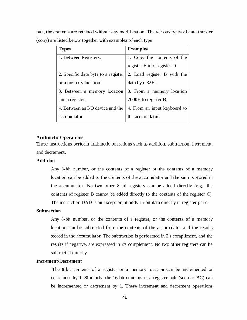
41
fact, the contents are retained without any modification. The various types of data transfer
(copy) are listed below together with examples of each type:
Types Examples
1. Between Registers.
1. Copy the contents of the
register B into register D.
2. Specific data byte to a register
or a memory location.
2. Load register B with the
data byte 32H.
3. Between a memory location
and a register.
3. From a memory location
2000H to register B.
4. Between an I/O device and the
accumulator.
4. From an input keyboard to
the accumulator.
Arithmetic Operations These instructions perform arithmetic operations such as addition, subtraction, increment,
and decrement.
Addition
Any 8-bit number, or the contents of a register or the contents of a memory
location can be added to the contents of the accumulator and the sum is stored in
the accumulator. No two other 8-bit registers can be added directly (e.g., the
contents of register B cannot be added directly to the contents of the register C).
The instruction DAD is an exception; it adds 16-bit data directly in register pairs.
Subtraction
Any 8-bit number, or the contents of a register, or the contents of a memory
location can be subtracted from the contents of the accumulator and the results
stored in the accumulator. The subtraction is performed in 2's compliment, and the
results if negative, are expressed in 2's complement. No two other registers can be
subtracted directly.
Increment/Decrement
The 8-bit contents of a register or a memory location can be incremented or
decrement by 1. Similarly, the 16-bit contents of a register pair (such as BC) can
be incremented or decrement by 1. These increment and decrement operations

42
differ from addition and subtraction in an important way; i.e., they can be
performed in any one of the registers or in a memory location.
Logical Operations
These instructions perform various logical operations with the contents of the
accumulator.
AND, OR Exclusive-OR
Any 8-bit number, or the contents of a register, or of a memory location can be
logically ANDed, Ored, or Exclusive-ORed with the contents of the accumulator.
The results are stored in the accumulator.
Rotate
Each bit in the accumulator can be shifted either left or right to the next position.
Compare
Any 8-bit number or the contents of a register, or a memory location can be
compared for equality, greater than, or less than, with the contents of the
accumulator.
Complement
- The contents of the accumulator can be complemented. All 0s are replaced by 1s
and all 1s are replaced by 0s.
Branching Operations
This group of instructions alters the sequence of program execution either
conditionally or unconditionally.
Jump
- Conditional jumps are an important aspect of the decision-making process in the
programming. These instructions test for a certain conditions (e.g., Zero or Carry
flag) and alter the program sequence when the condition is met. In addition, the
instruction set includes an instruction called unconditional jump.
Call, Return, and Restart
- These instructions change the sequence of a program either by calling a
subroutine or returning from a subroutine. The conditional Call and Return
instructions also can test condition flags.
43
Machine Control Operations
These instructions control machine functions such as Halt, Interrupt, or do nothing. The
microprocessor operations related to data manipulation can be summarized in four
functions:
1. copying data
2. performing arithmetic operations
3. performing logical operations
4. testing for a given condition and alerting the program sequence.
Some important aspects of the instruction set are noted below:
1. In data transfer, the contents of the source are not destroyed; only the
contents of the destination are changed. The data copy instructions do not
affect the flags.
2. Arithmetic and Logical operations are performed with the contents of the
accumulator, and the results are stored in the accumulator (with some
expectations). The flags are affected according to the results.
3. Any register including the memory can be used for increment and
decrement.
4. A program sequence can be changed either conditionally or by testing
for a given data condition.
Instruction Format
An instruction is a command to the microprocessor to perform a given task on a specified
data. Each instruction has two parts: one is task to be performed, called the operation
code (opcode), and the second is the data to be operated on, called the operand. The
operand (or data) can be specified in various ways. It may include 8-bit (or 16-bit) data, an
internal register, a memory location, or 8-bit (or 16-bit) address. In some instructions, the
operand is implicit.
Instruction word size
The 8085 instruction set is classified into the following three groups according to word
size:
1. One-word or 1-byte instructions
44
2. Two-word or 2-byte instructions
3. Three-word or 3-byte instructions
In the 8085, "byte" and "word" are synonymous because it is an 8-bit microprocessor.
However, instructions are commonly referred to in terms of bytes rather than words.
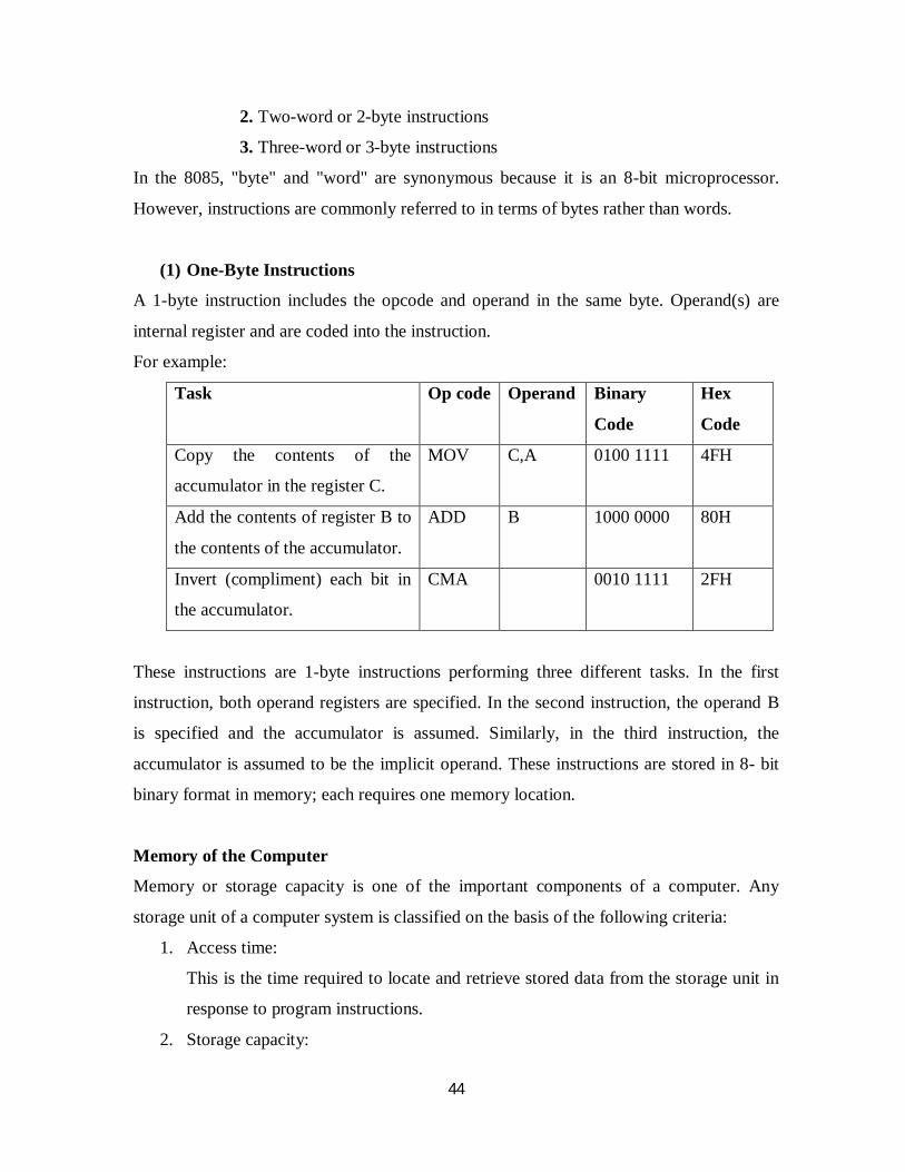
(1) One-Byte Instructions
A 1-byte instruction includes the opcode and operand in the same byte. Operand(s) are
internal register and are coded into the instruction.
For example:
Task Op code
Operand Binary
Code
Hex
Code
Copy the contents of the
accumulator in the register C.
MOV
C,A 0100 1111 4FH
Add the contents of register B to
the contents of the accumulator.
ADD
B 1000 0000 80H
Invert (compliment) each bit in
the accumulator.
CMA
0010 1111 2FH
These instructions are 1-byte instructions performing three different tasks. In the first
instruction, both operand registers are specified. In the second instruction, the operand B
is specified and the accumulator is assumed. Similarly, in the third instruction, the
accumulator is assumed to be the implicit operand. These instructions are stored in 8- bit
binary format in memory; each requires one memory location.
Memory of the Computer
Memory or storage capacity is one of the important components of a computer. Any
storage unit of a computer system is classified on the basis of the following criteria:
1. Access time:
This is the time required to locate and retrieve stored data from the storage unit in
response to program instructions.
2. Storage capacity:
45
It is the amount of data that can be stored in the storage unit.
3. Cost per bit of storage.
4. Units of memory:
The computer stores a character in the storage cells with binary (0,1) mechanism.
Thus the basic unit of memory is a bit (binary digit – 0,1). To store a character, a computer
requires 8 bits or 1 byte. This is called the ― word lengthǁ of the storage unit. Hence the
storage capacity of the computer is measured in the number of words it can store and is
expressed in terms of bytes. The different units of measurement are;
8 Bits = 1 Byte
210 (or) 1024 Bytes = 1 Kilo Byte (KB)
210 (or)1024 KB = 1 Mega Byte (MB)
210 (or)1024 MB = 1 Gega Byte (GB)
American Standard Code for Information Interchange (ASCII)
This code has given alphabets like some numbers which can be converted to
Binary form.
A- 65 …….Z – 90 and a – 97 ………. z – 121
By using these codes the alphabets can be converted to digital & hence to Binary
form.
Types of Memory A computer memory is of two types;
1. Primary Memory (Internal storage)
2. Secondary Memory (External storage)
Primary Memory
Primary memory is also called internal memory and is an important part of a computer. It
is the main area in a computer where the data is stored. The stored data can be recalled
instantly and correctly whenever desired. This memory can be quickly accessed by the
CPU for reading or storing information. Primary memory is further classified into two
types:
Random Access Memory (RAM)

46
Read- Only Memory (ROM)
RAM:
RAM is also known as read/write memory as information can be read from and written
onto it. RAM is a place in a computer that holds instructions for the computer, its
programs and the data. The CPU can directly access the data from RAM almost
immediately. However, the storage of data and instructions in RAM is temporary, till the
time the computer is running. It disappears from RAM as soon as the power to the
computer is switched off. i.e it is volatile memory.
ROM:
It is called Read-only memory as information can only be read from and not written or
changed onto ROM. ROM is the ‘built-in‘ memory of a computer. It stores some basic
input – output instructions put by the manufacturer to operate the computer. The storage of
data and instructions in ROM is permanent. It does not depend on the power supply. i.e it
is non-volatile memory.
Secondary Memory The primary memory which is faster (and hence expensive) is generally not sufficient for
large storage of data. As a result, additional memory, called the ―auxiliaryǁ or
―secondary memory is used. It is also referred as ―backup storageǁ as it is used to store
large volume of data on a permanent basis which can be transferred to the primary
memory whenever required for processing. Data are stored in secondary storage in the
same binary codes as in the main (primary memory) storage. Some of the devices of
secondary storages are Floppy Disk, Hard Disk, CD-ROM, DVD and Flash drive.
47
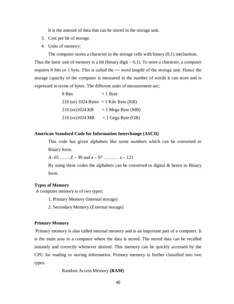
1. Floppy Disk:
It is also referred as ―Diskette: and is made of flexible Vinyl material. It has a
small hole on one side called ―Right protect notch
which protects accidental writing/deleting the information from the disk. There is
a hole in the centre through which the spindle of drive unit rotates the disk. The
disks are available in two sizes of 5.25 and 3.5 inches and these could be either
low density or high-density floppies. Storage capacity of floppies are measured in
kilobytes (KB) and megabytes (MB). The details about the storage capacities of
the floppies are presented below:
Floppy Disk Storage Capacity Size (Diameter)
Low Density 360 KB 5.25 inches
High Density 1.2 MB 5.25 inches
High Density 1.44 MB 3.5 inches
Extended 2.8 MB 3.5 inches
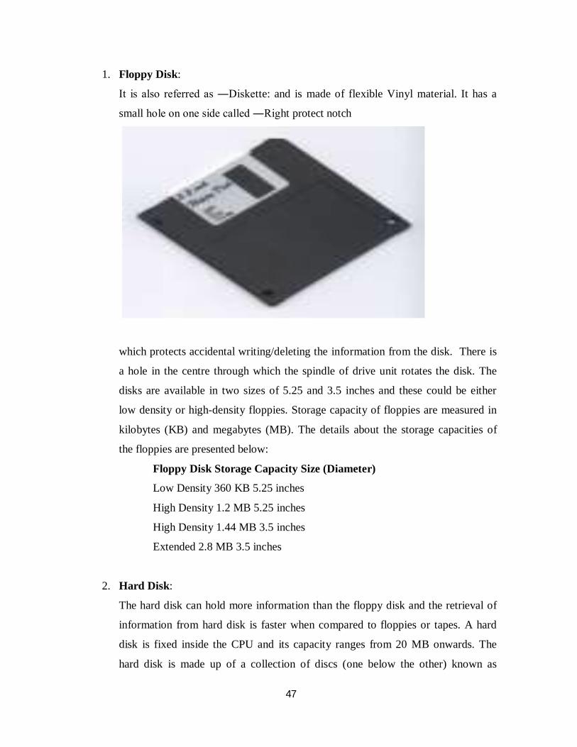
2. Hard Disk:
The hard disk can hold more information than the floppy disk and the retrieval of
information from hard disk is faster when compared to floppies or tapes. A hard
disk is fixed inside the CPU and its capacity ranges from 20 MB onwards. The
hard disk is made up of a collection of discs (one below the other) known as
48
platters on which the data is recorded. These platters are coated with magnetic
material. It is less sensitive to external environmental disorders and hence the
storage in hard disk is safe. A small hard disk might be as much as 25 times larger
than a floppy disk. Storage Capacity of hard disks varies from 20 MB to several
Gega bytes like 80GB, 160GB.
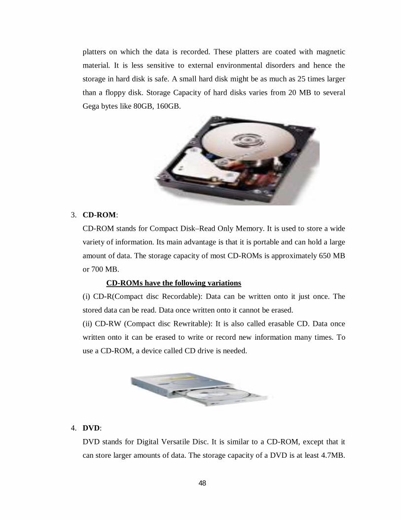
3. CD-ROM:
CD-ROM stands for Compact Disk–Read Only Memory. It is used to store a wide
variety of information. Its main advantage is that it is portable and can hold a large
amount of data. The storage capacity of most CD-ROMs is approximately 650 MB
or 700 MB.
CD-ROMs have the following variations
(i) CD-R(Compact disc Recordable): Data can be written onto it just once. The
stored data can be read. Data once written onto it cannot be erased.
(ii) CD-RW (Compact disc Rewritable): It is also called erasable CD. Data once
written onto it can be erased to write or record new information many times. To
use a CD-ROM, a device called CD drive is needed.
4. DVD:
DVD stands for Digital Versatile Disc. It is similar to a CD-ROM, except that it
can store larger amounts of data. The storage capacity of a DVD is at least 4.7MB.
49
DVDs that can store up to 17GBs are also available. Because of their capacity,
DVDs are used to store a very large multimedia presentations and movies that
combine high quality sound and graphics.
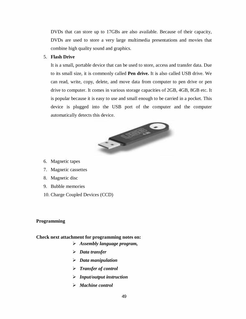
5. Flash Drive
It is a small, portable device that can be used to store, access and transfer data. Due
to its small size, it is commonly called Pen drive. It is also called USB drive. We
can read, write, copy, delete, and move data from computer to pen drive or pen
drive to computer. It comes in various storage capacities of 2GB, 4GB, 8GB etc. It
is popular because it is easy to use and small enough to be carried in a pocket. This
device is plugged into the USB port of the computer and the computer
automatically detects this device.
6. Magnetic tapes
7. Magnetic cassettes
8. Magnetic disc
9. Bubble memories
10. Charge Coupled Devices (CCD)
Programming
Check next attachment for programming notes on: Assembly language program,
Data transfer
Data manipulation
Transfer of control
Input/output instruction
Machine control

50
Memory organization
Memory mapping
Construct a memory map for 8085 microprocessor
Copyright © 2022 FDOKUMEN