
Theoretical aspects of high-speed supercavitation vehicle control
Upload
independentCategory
view
4download
0
MICROCONTROLLER BASED SPEED CONTROL OF INDUCTION
MOTOR USING V/F CONTROL
submitted in partial fulfillment of the requirements for the award of
Bachelor of Engineering
In
ELECTRICAL AND ELECTRONICS ENGINEERING
BY
SIDHARTHA SHANKAR RAY
2914233
DEPARTMENT OF ELECTRICAL AND ELECTRONICS ENGINEERING
SATHYABAMA UNIVERSITY(Established under Section 3 of UGC Act 1956)
JEPPIAAR NAGAR, OLD MAMALLAPURAM ROAD
CHENNAI 600119

APRIL 2013
SATHYABAMA UNIVERSITY(Established Under section 3 of the UGC Act, 1956)
Accredited with B++ Grade by NAACJEPPIAAR NAGAR, CHENNAI - 600 119
DEPARTMENT OF ELECTRICAL AND ELECTRONICS ENGINEERING BONAFIDE CERTIFICATE
This is to certify that this Project Report is the bonafide work of
Mr. SIDHARTHA SHANKAR RAY ( Reg.No 2914233) who carried out the
project entitled “MICROCONTROLLER BASED SPEED CONTROL OF INDUCTION
MOTOR USING V/F CONTROL” under our supervision from NOVEMBER 2012 to
March 2013.
INTERNAL GUIDE
Mr.S.JAYAPRAKASH
HEAD OF THE DEPARTMENT
Dr.V. SIVACHIDAMBARAMNATHAN

Submitted for Viva voce Examination held on
INTERNAL EXAMINER
EXTERNAL EXAMINER
CONTENTS
CHAPTER-1
1.1
Introduction.....................................................
..............................1
1.1.1
General..........................................................
........................1
1.1.2 Overview Of The
Thesis........................................................1
1.1.3 Objective Of The
Thesis........................................................1
1.1.4 Organisation Of The
Thesis...................................................2
CHAPTER-2

AIM AND SCOPE OF THE PRESENT
INVESTIGATION..................3
2.1
Objective........................................................
...............................3
2.2 Basis Of Im
Control..........................................................
.............3
2.3 Variable Frequency Drives (Vfd)
Basics......................................5
2.3.1 Components Of Vfd’s
Are......................................................5
2.4 Pi
Control..........................................................
............................6

2.4.1 The Process To
Control.........................................................6
2.4.2 Pi Control-
Definition.......................................................
.......7
2.4.3 Simulink Model Of The Pi-
Algorithm......................................9
2.4.4
Output...........................................................
.........................10
2.5 Spm, Based Igbt Power
Module..................................................11
2.6 Fsbb20ch60 - Smart Power
Module.............................................11
2.6.1 General
Description......................................................
.........11
2.7 Time Charts Of Spm Protective
Functions...................................13
2.8 Speed Torque Characteristics Of
Induction.................................14

2.9 V/F Control
Theory...........................................................
............15
2.10 Scalar Control Of Induction
Motor..........................................15
CHAPTER-3
EXPERIMENTAL METHODS AND ALGORITHM
USED......................17
3.1
General..........................................................
..................................17
3.2 Open And Closed Loop
Control....................................................17
3.2.1 Open Loop
Control..........................................................
...17
3.2.1.1 Block Diagram Of Open Loop
Control............................18
3.2.1.2 Execution Of Open Loop
Control.....................................19
3.2.1.3 Simulation Results Of Open
Loop V/F Control.................19

3.2.2 Closed Loop
Control..........................................................
.......21
3.2.2.1 Block Diagram Of Closed Loop
Control.............................22
3.2.2.2 Execution Of Closed Loop
Control.....................................23
3.2.2.3 Simulation Results Of Closed
Loop V/F Control................23
3.3. Hardware
Implementation...................................................
............24
3.3.1 Block Diagram Of Hardware
Implementation............................24
3.3.1.1 Rectifier
Unit.............................................................
...........25
3.3.1.2 Pwm-Voltage Source
Inverter.............................................25
3.3.1.3 Driver
Circuit..........................................................
..............27
3.3.1.4 Voltage Regulation
Circuit...................................................27
3.3.1.5
Microcontroller..................................................
...................27
3.3.2 Hardware Circuit
Diagram..........................................................
...28
3.3.2.1 Layout Diagram Of The
Components Of Hardware................29
3.3.2.2 Driver
Circuit..........................................................
..................30
3.3.2.3 Working Of Driver
Circuit..........................................................
31
3.3.2.3.1 And
Gate.............................................................
.............31
3.3.2.3.2
Optoisolator.....................................................
................31
3.3.2.3.3 Not
Gate.............................................................
.............31
3.3.2.3.4 Pwmis
Signal...........................................................
........31
3.3.2.3.5 Phase
Output...........................................................
........31
3.3 Smart Power Module
Circuit..........................................................
......32
3.3.1 Working Of Smart Power
Module..................................................33
3.3.1.1 Fsbb20ch60
Module...........................................................
.....33
3.3.1.2 Protection
Circuit..........................................................
...........33
3.4 Microcontroller
Circuit..........................................................
................34
3.4.1 Microcontroller Pin
Configuration...................................................3
6

3.5 Functional Circuit Of Flip
Flop............................................................3
8
CHAPTER -4
RESULTS AND DISCUSSION, PERFORMANCE
ANALYSIS..................40
4.1general...................................
..............................................................40
4.2 Open Loop Control
Results..........................................................
.......40
4.2.1 Tabulation For Open Loop
Control..............................................40
4.2.2 Graphs For The Results Of Open Loop
Control...........................41
4.2.3 Simulation Results For Open Loop
Control...................................43
4.3 Results Of Closed Loop
Control.........................................................4
4

4.3.1:Tabulation For Closed Loop
Control............................................44
4.3.2 Graphs For The Results Of Closed
Loop Control........................45
4.3.3 Tabulation For Finding The V/F
Ratio..........................................45
4.3.4 Simulation Results Of Closed Loop
Control.................................47
4.4 Performance
Analysis.........................................................
................48
4.4.1 To Drive The
Motor............................................................
............48
4.4.2 Operation Of The Entire
Hardware...............................................49
4.4.3 Oscilloscope
Results..........................................................
...........51
4.4.4
Hardware.........................................................
............................52

4.5
Advantages.......................................................
................................... 53
4.6
Application......................................................
......................................54
CHAPTER-5
SUMMARY AND
CONCLUSION.......................................................
........55
5.1
Summary..........................................................
...................................55
5.2
Conclusion.......................................................
.....................................56
LIST OF FIGURES
S.NO. DESCRIPTION PAGE NO.

Figure 2.1 Graph Showing V/F Control
4
Figure 2.2 VARIABLE FREQUENCY DRIVE
5
Figure 2.3 House Model With PI-Controller 6
Figure 2.4 BLOCK DIAGRAM OF PI CONTROLLER
8
Figure 2.5 GRAPH OF PI CONTROLLER
8
Figure 2.6 PI-Controller 9
Figure 2.7 Saturation Block To Constrain The Heat Output 9
Figure 2.8 Output 10
Figure 2.9 General View Of Spm Module
11
Figure 2.10 Spm (Top View)
12
Figure 2.11 Spm (Side View)
12
Figure 2.12 Under Voltage-Low Side
13
Figure 2.13 Under Voltage Protection-High Side
13
Figure 2.14. Speed Torque Characteristics Of
Induction Motor 14
Figure 2.15. Speed Torque Characteristics With V/F
Control 15
Figure 3.1 Block Diagram Of Open Loop
18
Figure 3.2 Output Speed Wave Form
19
Figure 3.3 Output Gate Pulses
20
Figure 3.4 Output Line Voltage Waveform
21
Figure.3.5 Block Diagram Of Closed Loop Control
22
Figure 3.6 Output Speed Waveform
23
Figure 3.7 Output Line Voltage Waveform
23
Figure 3.8 Block Diagram Of Hardware
Implementation 24

Figure 3.9 Diagram Of Rectifier Unit
25
Figure 3.10 Circuit Diagram Of PWM-Voltage Source
Inverter Circuit 26
Figure 3.11 Hardware Circuit Diagram
28
Figure 3.12 Layout Diagram Of Component Of Hard
Ware 29
Figure 3.13 Circuit Diagram Of Driver Circuit
30
Figure 3.14: Circuit Diagram Of Smart Power Module
32
Figure 3.15 Pin Configuration Of Microcontroller
34
Figure 3.16 Connection Of Microcontroller Circuit
35
Figure 3.17 Microcontroller DSPIC30F4011
37
Figure 3.18 Diagram Of Functional Circuit Of Flip
Flop 38
Figure 4.1: Frequency Vs. Modulation Index Graph
41

Figure 4.2: Actual Speed Vs Modulation Index Graph
42
Figure 4.3: Actual Speed Vs Frequency Graph
42
Figure 4.4: Open Loop Input Voltage And Time
43
Figure 4.5: Open Loop Input DC Voltage And Current
43
Figure 4.6: Actual Rotor Speed And Time
44
Figure 4.7: Set Speed And Actual Speed Graph
45
Figure 4.8: Voltage Vs Frequency Graph
46
Figure 4.9: Input Voltage Vs. Time
47
Figure 4.10: Set Speed/Voltage Speed Vs. Time Period
47
Figure 4.11 Operational Block Diagram To Drive The
Motor 48
Figure 4.12 Operational Block Diagram Of The
Hardware 49
Figure 4.13 CRO Output Of PWM Pulse.
51
Figure 4.14 CRO Output Of The Dc Voltage Applied To
The Motor 51
Figure 4.15 CRO Output Of The Motor Current
Waveform 52
Figure 4.16 Hardware Model
52
Figure 4.17 Connected Model Of Hardware
53
TABULAR INDEX
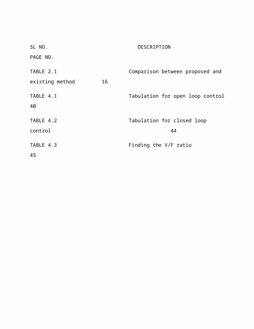
SL NO. DESCRIPTION
PAGE NO.
TABLE 2.1 Comparison between proposed and
existing method 16
TABLE 4.1 Tabulation for open loop control
40
TABLE 4.2 Tabulation for closed loop
control 44
TABLE 4.3 Finding the V/F ratio
45

ABSTRACT:
An induction motor can run only at its rated speed when it
is connected directly to the main supply. This is felt the
most in applications where input power is directly
proportional to the cube of motor speed. So we can reduce
the speed of the motor upto 20% and save the power upto
50%. As the semiconductor fabrication technology has
advanced than previous both the size and price have gone
than before. Due to this the usage of motor has already
been reduced where as it can be replaced by VFD(variable
frequency drive). The VFD not only controls the motor
speed, but can improve the motor's dynamic and steady
state characteristics as well. In addition, the VFD can
reduce the system’s average energy consumption.
Generally we use open loop control for controlling the
speed of a motor but for VF controlling we use the
closed loop control. It is also simple to implement and
cost effective. The on-chip hardware PWM modules, making

them on-chip hardware PWM modules, making them suitable
for 3-phase motor control applications.
VF CONTROL:
The base speed of the induction motor is directly
proportional to the supply frequency and the number of
poles of the motor. Since the number of poles is fixed by
design, the best way to vary the speed of the induction
motor is by varying the supply frequency. The torque is
directly proportional to the ratio of the applied voltage
and the frequency. This is exactly what VF control tries
to achieve.
ACKNOWLEDGEMENT
The satisfaction and elation that accompany the
successful completion of any task would be incomplete
without the mention of the people who have made it a
possibility. It is my great privilege to express my
gratitude and respect to all those who have guided me and
inspired me during the course of the project work.
First and foremost, I would express my sincere
gratitude to our beloved Chancellor Col. Dr. JEPPIAAR,
M.A., B.L., Ph.D., and also thanks to our Directors Dr.
MARIE JOHNSON, B.E., M.B.A., M.Phil., Ph.D and
Dr. MARIAZEENA JOHNSON, B.E., M.B.A., M.Phil., Ph.D for
providing me the necessary facilities for the completion of
my project. Also, I acknowledge our Vice Chancellor Dr.
B.SHEELA RANI, M.S (By Research)., Ph.D. for her constant
support and endorsement.
I also like to express my gratitude to Mrs. G. R. P.
LAKSHMI Head of the Department (Administrative and
Research) of Electrical and Electronics Engineering and Dr.
V. SIVACHIDAMBARANATHAN Head of the Department (Academics)
of Electrical and Electronics Engineering, Sathyabama
University for having been a constant source of support and
encouragement for the completion of the project.
I would also like to express my sincere thanks to my
internal guide of the project Mr.S.JAYAPRAKASH for his
constant guidance and supervision during the period of my
project work and for providing me the necessary facilities
for the completion of my project.
DECLARATION
I SIDHARTHA SHANKAR RAY hereby declare that the project titled
“MICROCONTROLLER BASED SPEED CONTROL OF INDUCTION MOTOR USING V/F
CONTROL”was done by me under the guidance of Mr.S.JAYAPRAKASH is
submitted in partial fulfillment of the requirements for the award of
the degree in BACHELOR OF ENGINEERING.
DATE:
PLACE:
SIGNATURE OF THE CANDIDATE

CHAPTER-1
1.1 INTRODUCTION
1.1.1 GENERAL
Industrial drive applications are generally classified into
constant speed and variable speed drives.Traditionally AC
machines have been used in constant speed ap- plications,whereas
DC machines were preferred for variable speed drives. DC machines
have the disadvantages of higher cost and maintenance problems
with commutators and brushes. Commutators and brushes do not
permit a machine to operate in dirty and explosive environment.
An AC machine overcomes the drawback of DC machines. Although
currently, the majority of variable speed drive applications use
DC machines, they are progressively being replaced by AC drives.
While there are different methods of speed control of induction
motor,Variable Voltage Variable Frequency (VVVF) or V/F is the
most common method of speed control. This method is most suitable
for applications without position control requirements or the
need for high accuracy of speed control. Examples of these
applications include heating, air conditioning, fans and blowers.

1.1.2 OVERVIEW OF THE THESIS
First, implementation of open loop and closed loop V/F control of
induction motor has been done using MATLAB Simulink toolbox and
corresponding waveforms are analyzed.
Finally, hardware implementation for open loop V/F control of
three phase induction motor is carried out and waveforms are
analyzed. A comparison is made between software implementation
and hardware implementation.
1.1.3 OBJECTIVE OF THE THESIS
To control the speed of three phase induction motor using V/F
control stregery.
1
1.1.4 ORGANISATION OF THE THESIS
This thesis is organized into five chapters including
introduction, brief description of the thesis and also it deals
with the objective and Organisation of the thesis. Chapter 2
deals with the discussion in detail about basics theory of V/F
control stregery of induction motor. Chapter 3 deals with
simulation and results of V/F control of induction motor.

2
CHAPTER-2
AIM AND SCOPE OF THE PRESENT INVESTIGATION:
2.1 OBJECTIVE:
To control the speed of an induction motor by varying
frequency as well as voltage.
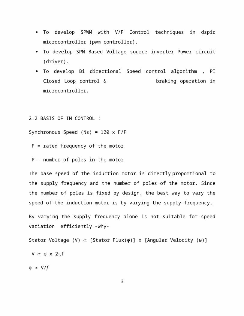
To develop SPWM with V/F Control techniques in dspic
microcontroller (pwm controller).
To develop SPM Based Voltage source inverter Power circuit
(driver).
To develop Bi directional Speed control algorithm , PI
Closed Loop control & braking operation in
microcontroller.
2.2 BASIS OF IM CONTROL :
Synchronous Speed (Ns) = 120 x F/P
F = rated frequency of the motor
P = number of poles in the motor
The base speed of the induction motor is directly proportional to
the supply frequency and the number of poles of the motor. Since
the number of poles is fixed by design, the best way to vary the
speed of the induction motor is by varying the supply frequency.
By varying the supply frequency alone is not suitable for speed
variation efficiently –why-
Stator Voltage (V) ∝ [Stator Flux(φ)] x [Angular Velocity (ω)]
V ∝ φ x 2πf
φ ∝ V/f
3

The torque developed by the motor is directly proportional to the
magnetic fields produced by the stator. So, the voltage applied
to the stator is directly proportional to the product of stator
flux and angular velocity. This makes the flux produced by the
stator proportional to the ratio of applied voltage and frequency
of supply. By varying the frequency, the speed of the motor can
be varied. Therefore, by varying the voltage and frequency by the
same ratio, flux and hence, the torque can be kept constant
throughout the speed range.
Fig
2.1: Graph showing V/F Control
4
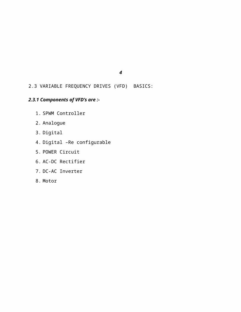
2.3 VARIABLE FREQUENCY DRIVES (VFD) BASICS:
2.3.1 Components of VFD’s are :-
1. SPWM Controller
2. Analogue
3. Digital
4. Digital –Re configurable
5. POWER Circuit
6. AC-DC Rectifier
7. DC-AC Inverter
8. Motor

FIG 2.2: VARIABLE FREQUENCY DRIVE
5
2.4 PI CONTROL :
Basic proportional and integral feedback control (PI)
How to tune the PI-controller
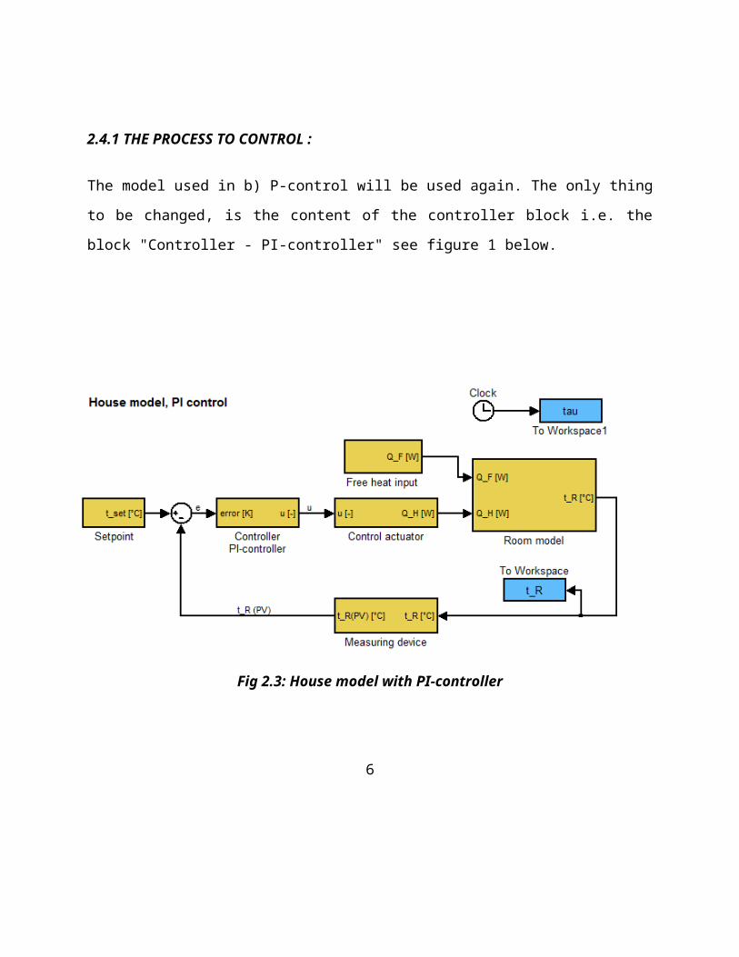
2.4.1 THE PROCESS TO CONTROL :
The model used in b) P-control will be used again. The only thing
to be changed, is the content of the controller block i.e. the
block "Controller - PI-controller" see figure 1 below.
Fig 2.3: House model with PI-controller
6

2.4.2 PI CONTROL- DEFINITION:
The definition af proportional feed back control is still
where
e ="error"
KP = Proportional gain
The definition of the integral feed back is
where KI is the integration gain factor.
In the PI controller we have a combination of P and I control,
ie.:
where

τI ="Integrationtime"[s]
τN = "Reset time" [s]
NB: There is - in the real life - some confusion in the use of
these two definitions.
7
FIG 2.4: BLOCK DIAGRAM OF PI CONTROLLER

FIG 2.5: GRAPH OF PI CONTROLLER
8
2.4.3 SIMULINK MODEL OF THE PI-ALGORITHM:
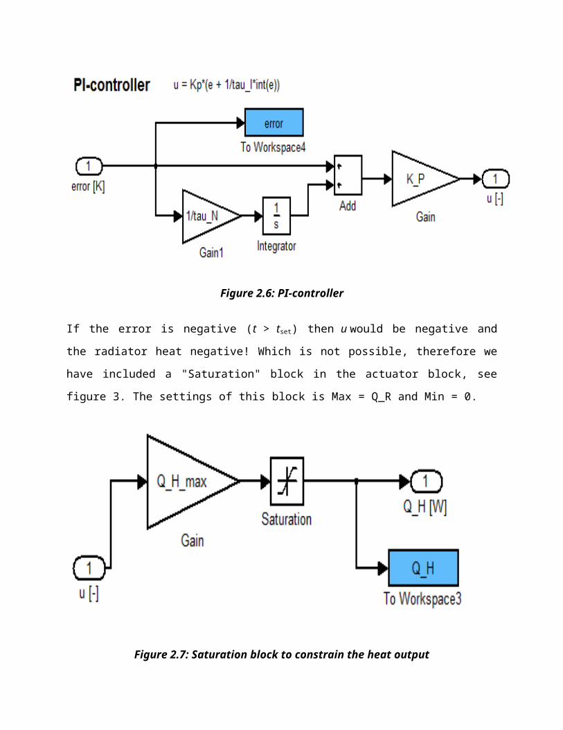
Figure 2.6: PI-controller
If the error is negative (t > tset) then u would be negative and
the radiator heat negative! Which is not possible, therefore we
have included a "Saturation" block in the actuator block, see
figure 3. The settings of this block is Max = Q_R and Min = 0.
Figure 2.7: Saturation block to constrain the heat output
9
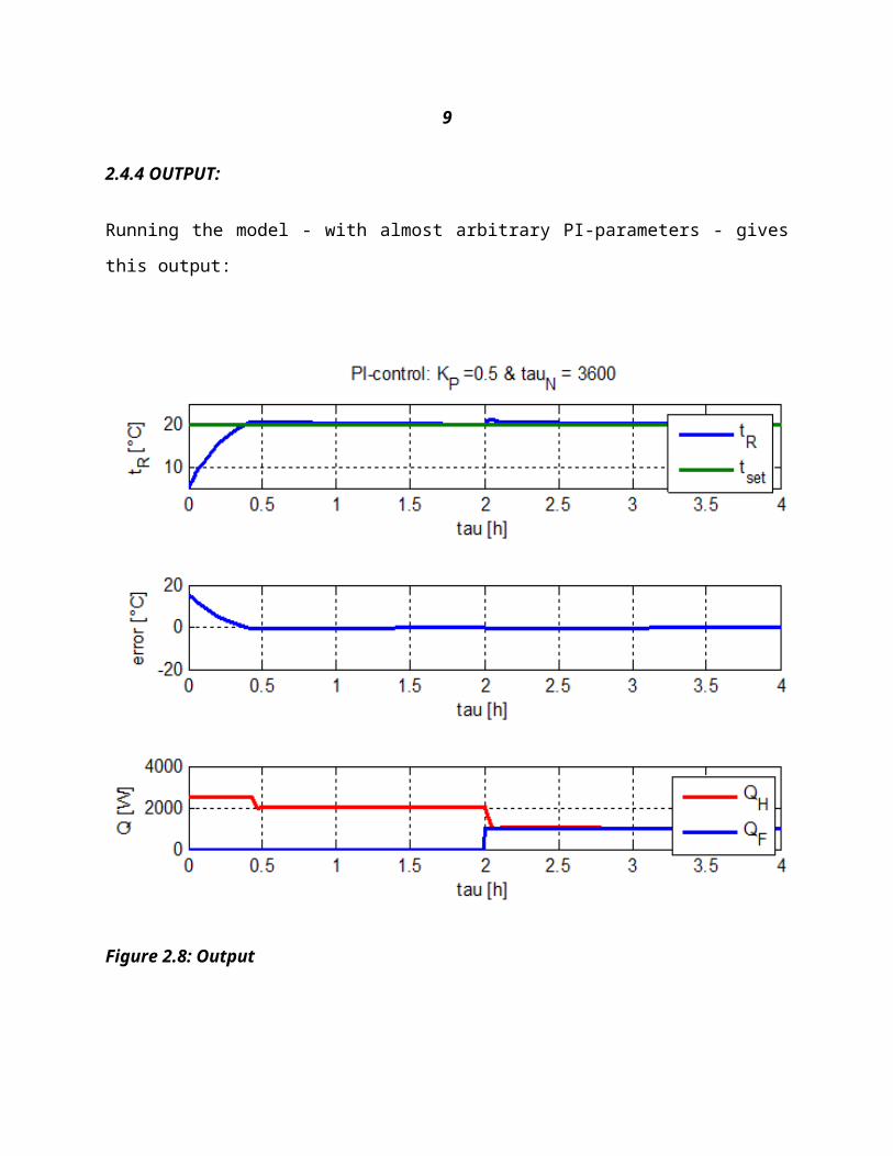
2.4.4 OUTPUT:
Running the model - with almost arbitrary PI-parameters - gives
this output:
Figure 2.8: Output

This is the the steady-state "off-set" is almost zero! Which is
the main benefit of the ingetration part of the PI-controller.
10
2.5 SPM, BASED IGBT POWER MODULE:
Specification
FSBB20ch60b
3phase,200v
1.8amp
3 phase source case induction motor
2.6 FSBB20CH60 - Smart Power Module:
2.6.1 General Description:
It is an advanced smart power module (SPMTM) that Fairchildhas
newly developed and designed to provide very compactand high
performance ac motor drives mainly targeting lowpowerinverter-
driven application like air conditioner and washing machine. It
combines optimized circuit protection and drivematched to low-
loss IGBTs. System reliability is furtherenhanced by the
integrated under-voltage lock-out and shortcircuitprotection. The
high speed built-in HVIC provides optocoupler-less single-supply
IGBT gate driving capability that furtherreduce the overall size
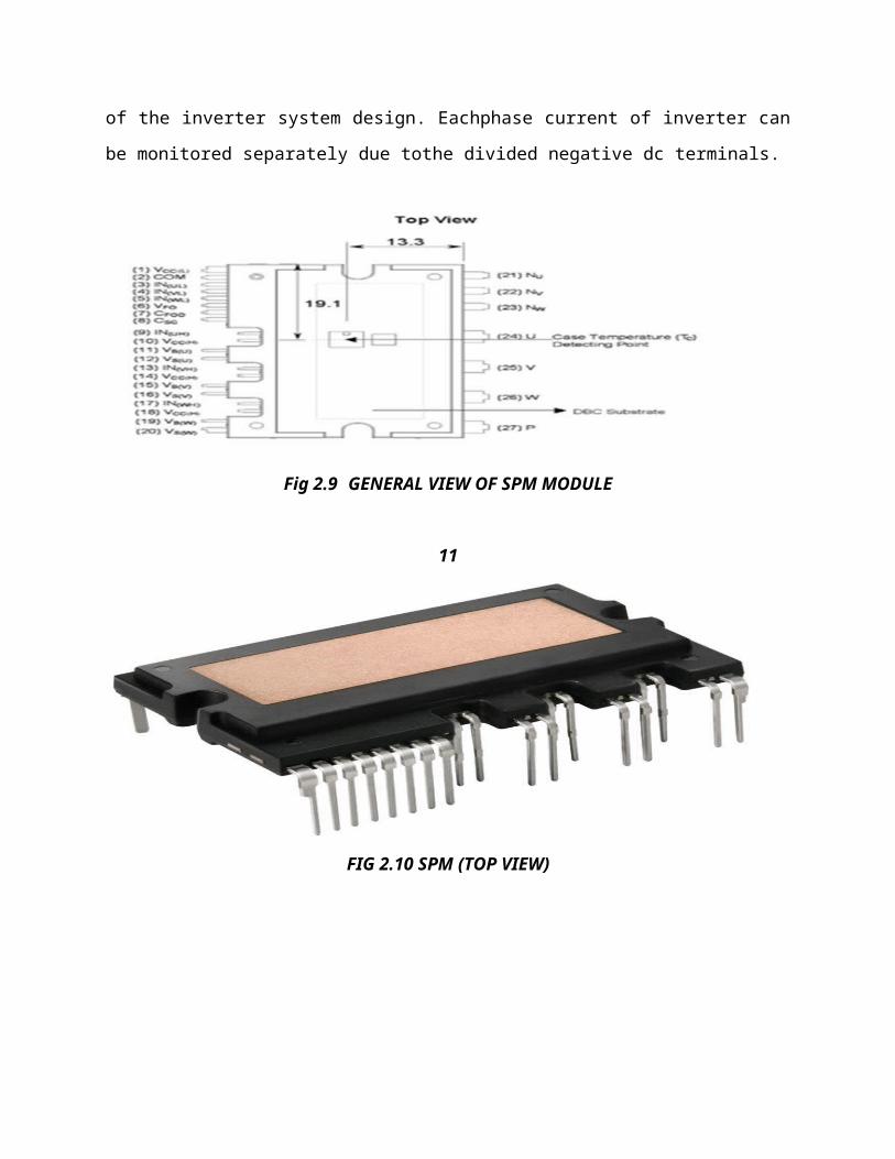
of the inverter system design. Eachphase current of inverter can
be monitored separately due tothe divided negative dc terminals.
Fig 2.9 GENERAL VIEW OF SPM MODULE
11
FIG 2.10 SPM (TOP VIEW)

FIG 2.11 SPM (SIDE VIEW)
12
2.7 TIME CHARTS OF SPM PROTECTIVE FUNCTIONS:
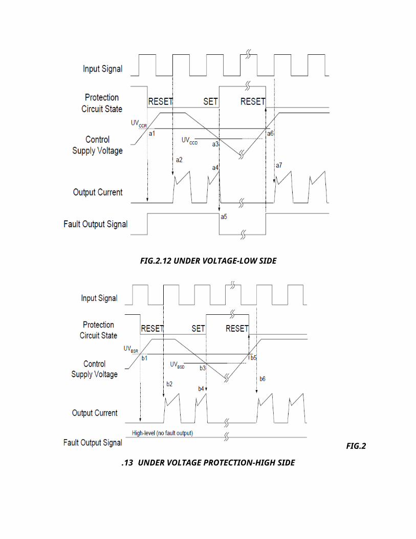
FIG.2.12 UNDER VOLTAGE-LOW SIDE
FIG.2
.13 UNDER VOLTAGE PROTECTION-HIGH SIDE

13
2.8 SPEED TORQUE CHARACTERISTICS OF INDUCTION:
Fig 2.14. Speed Torque Characteristics of Induction Motor
The x-axis shows slip speed, the y-axis shows torque and current,
the characteristics shown in Fig 2.1 are drawn with rated voltage
and frequency suppliedto the stator. During startup the motor
typically draws up to seven times the ratedcurrent. This high
current is result losses in the stator and rotor windings, and
lossesin the bearings due to the friction.At startup the motor
delivers 1.5 times the rated torque of the motor. This starting
torque is also called locked rotor torque .As the speed
increases, the currentdrawn by the motor reduces slightly. At the

base speed the motor draws the rated current and delivers the
rated torque .At base speed if the load on the motor shaft is
increased beyond its ratedtorque, the speed starts dropping and
slip increases.
The disadvantages like motor draws high current during start up,
torqueis highly non linear as speed varies. These drawbacks can
be overcome by using V/F control.
14
2.9 V/F CONTROL THEORY:
Fig.2.15. Speed Torque Characteristics With V/F Control
The base speed of the induction motor is directly proportional to
the supply frequency and the number of poles of the motor. Since
the number of poles is fixed by design, the best way to vary the
speed of the induction motor is by varying the supply frequency.
The torque developed by the induction motors is directly
proportional to the ratio of the applied voltage and the

frequency of supply. By varying the voltage and the frequency,
but keeping their ratio constant, throughout the speed range.
This exactly what v/f control tries to achieve.
2.10 SCALAR CONTROL OF INDUCTION MOTOR:
The following are the scalar control techniques of an induction
motor are given.
(1) Voltage/frequency (V/F) control
(2) Stator current and slip frequency control
Scalar control, as the name indicates, is due to magnitude
variation of control variables only and disregards the coupling
effect in the machine. For example, the voltage of a machine can
be controlled to control the flux, and frequency or slip can be
controlled to control the torque. However, flux and torque are
also the function of frequency and voltage, respectively.
15

TABLE 2.1 COMPARISON BETWEEN PROPOSED AND EXISTING METHOD
16
CHAPTER-3
EXPERIMENTAL METHODS AND ALGORITHM USED
3.1 GENERAL:
The V/F is simulated on MATLAB/Simulink
software. The actual system can be simulated with a high degree
of accuracy in this package. It provides a user interactive
platform and wide variety of numerical algorithm. This Chapter
discusses the realization of V/F control using Simulink block.
Matlab (Matrix laboratory) is an interactive software system for
numerical computations and graphics. As the name suggests, Matlab
is especially designed for matrix computations: solving systems
of linear equations, computing eigenvalues and eigenvectors,
factoring matrices, and so forth. Matlab is designed to solve
problems numerically, that is, in finite-precision arithmetic.
3.2 OPEN AND CLOSED LOOP CONTROL:
The experiment is conducted into two main steps.
They are-
1. Open loop control and
2. Closed loop control.
3.2.1 Open loop control:
The open loop control consists of –
a) MOSFET inverter,
b) IGBT module,
c) LCD screen,
d) 3 phase AC motor.
The operation of an ac induction motor is governed by two
principles:
1. Base speed is directly proportional to the frequency of the
alternating current applied to the stator and the number of
poles of the motor.
2. Torque is directly proportional to the ratio of applied
voltage and frequency of the applied
ac current.
The Figure shows the simulation diagram of open loop V/F control
of
three-phase induction motor. It consists DC source, three -phase
PWM inverter and
three phase induction motor. Dc source is connected to the dc
side of the converter.
In this reference speed is set. From that reference speed
frequency is determined
using the formula . V/F function block determines the amplitude
corresponding to that frequency. This frequency and amplitude are
used to update the PWM duty cycle. MOSFET based converter gives
the supply of the induction motor. Connecting the scope through
bus selector shows speed of the induction motor.

3.2.1.1 Block diagram of open loop control:
Fig.3.1: Block diagram of open loop
control
3.2.1.2 Execution of open loop control:
The open loop control is executed into the following steps –
I. The 220V is applied to a MOSFET inverter where the DC
voltage is converted into 3 phase AC voltage.
II. 3 phase AC voltage is applied to the motor through current
sensors.
III. The current input applied to the motor is measured through
the current sensors.
IV. The carrier signal is applied to the IGBT module.
V. The desired modulation index and frequency input is given to
the microcontroller and further applied to PWM module.
VI. Finally the six PWM wave is generated and drive the motor.
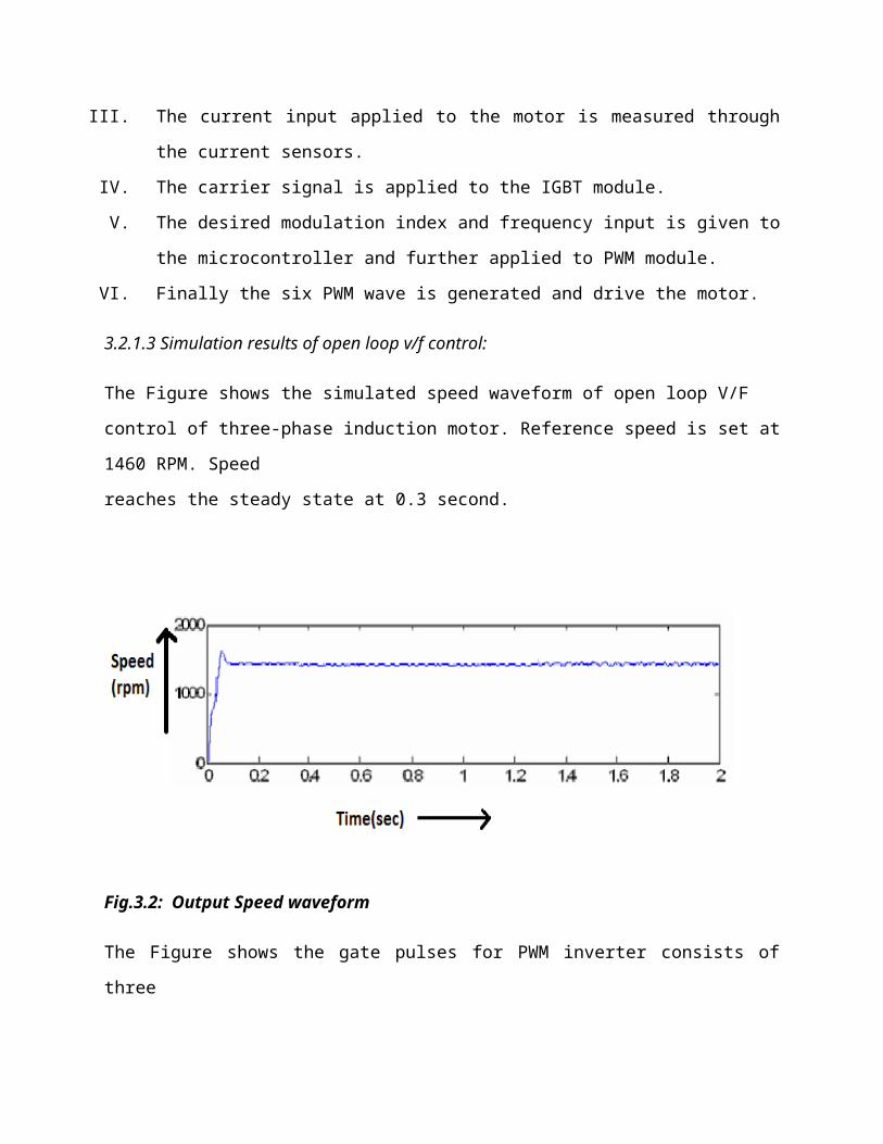
3.2.1.3 Simulation results of open loop v/f control:
The Figure shows the simulated speed waveform of open loop V/F
control of three-phase induction motor. Reference speed is set at
1460 RPM. Speed
reaches the steady state at 0.3 second.
Fig.3.2: Output Speed waveform
The Figure shows the gate pulses for PWM inverter consists of
three

legs, one for each phase. The gating signals for the three phase
inverters have a phase difference of 120°. The first pulse is
given to the positive switch of phase A, the pulse is given to
the positive switch of phase B the third to the positive switch
of
phase C.

Fig. 3.3: Output Gate Pulses
Fig. 3.4: Output line
voltage waveform
The Figure shows the simulated line-to-line voltage waveform of
open loop V/F control of three-phase induction motor. It is
observed that the voltage waveform is almost sinusoidal.
3.2.2 Closed loop control:
The closed loop control consists of –
a) MOSFET inverter,
b) IGBT module,
c) PI controller and
d) 3 Phase AC motor.
It consists DC source, three -phase PWM inverter and three phase
induction motor as open loop in addition to that it has PI
controller,limiter. Connecting the scope through bus
selector .Now the simulation circuit is run with closed loop
control shows speed of the induction motor.
3.2.2.1 Block diagram of closed loop control:

Fig.3.5:Block diagram of closed loop
control
3.2.2.2 Execution of closed loop control:
I. The execution of closed loop control is executed very
similar to the open loop control.
II. In extra the PI controller is added here for controlling the
error wave.
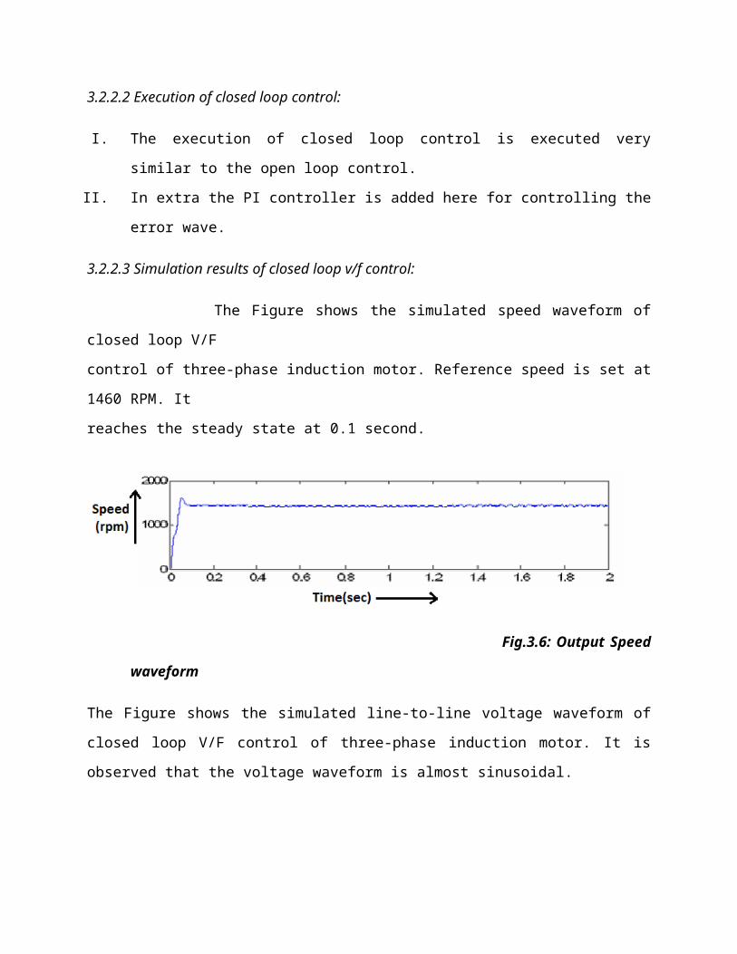
3.2.2.3 Simulation results of closed loop v/f control:
The Figure shows the simulated speed waveform of
closed loop V/F
control of three-phase induction motor. Reference speed is set at
1460 RPM. It
reaches the steady state at 0.1 second.
Fig.3.6: Output Speed
waveform
The Figure shows the simulated line-to-line voltage waveform of
closed loop V/F control of three-phase induction motor. It is
observed that the voltage waveform is almost sinusoidal.
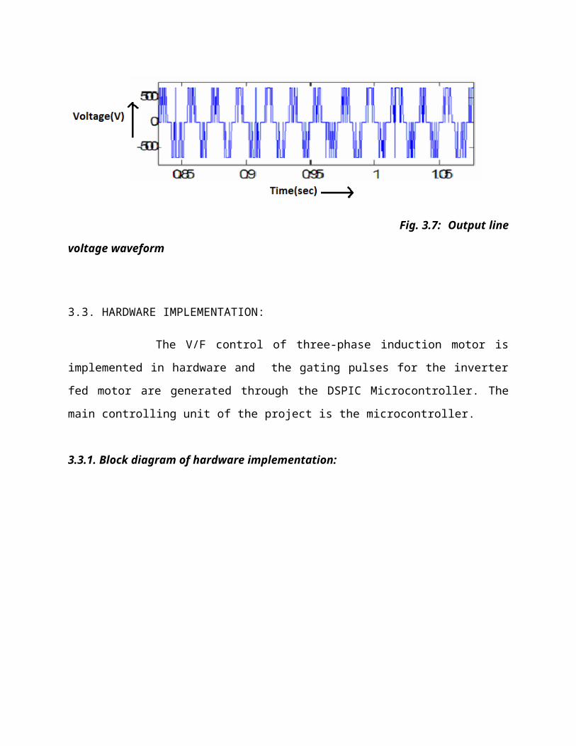
Fig. 3.7: Output line
voltage waveform
3.3. HARDWARE IMPLEMENTATION:
The V/F control of three-phase induction motor is
implemented in hardware and the gating pulses for the inverter
fed motor are generated through the DSPIC Microcontroller. The
main controlling unit of the project is the microcontroller.
3.3.1. Block diagram of hardware implementation:
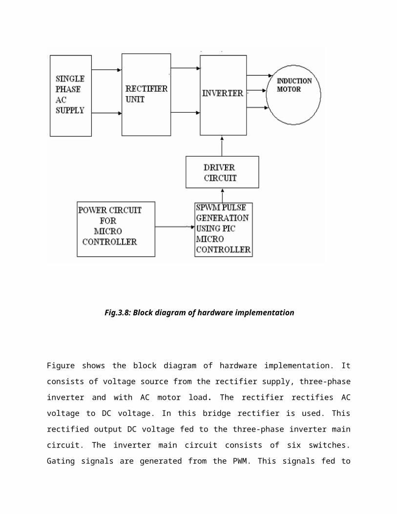
Fig.3.8: Block diagram of hardware implementation
Figure shows the block diagram of hardware implementation. It
consists of voltage source from the rectifier supply, three-phase
inverter and with AC motor load. The rectifier rectifies AC
voltage to DC voltage. In this bridge rectifier is used. This
rectified output DC voltage fed to the three-phase inverter main
circuit. The inverter main circuit consists of six switches.
Gating signals are generated from the PWM. This signals fed to
the MOSFET Gate terminals. Depends upon the Gating signal
inverter operates, this output fed to the AC load or motor.
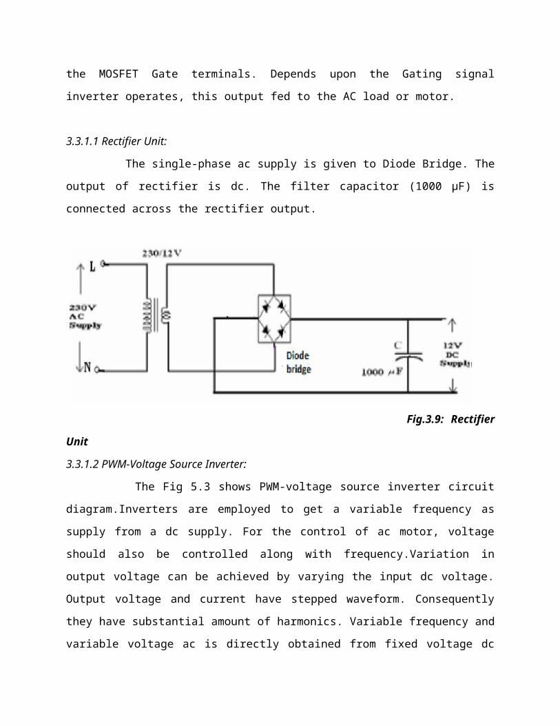
3.3.1.1 Rectifier Unit:
The single-phase ac supply is given to Diode Bridge. The
output of rectifier is dc. The filter capacitor (1000 μF) is
connected across the rectifier output.
Fig.3.9: Rectifier
Unit
3.3.1.2 PWM-Voltage Source Inverter:
The Fig 5.3 shows PWM-voltage source inverter circuit
diagram.Inverters are employed to get a variable frequency as
supply from a dc supply. For the control of ac motor, voltage
should also be controlled along with frequency.Variation in
output voltage can be achieved by varying the input dc voltage.
Output voltage and current have stepped waveform. Consequently
they have substantial amount of harmonics. Variable frequency and
variable voltage ac is directly obtained from fixed voltage dc

when the inverter is controlled by pulse width modulation the pwm
control also reduces harmonics in the output voltage and also it
eliminates the following draw back of 6-step inverter drives like
the motor losses increases at all speeds causing derating of
motor, torque pulsation at low speeds.
Fig.3.10: Circuit Diagram of PWM-Voltage Source Inverter Circuit Diagram
In this method, several pulses per half cycle are used as in case
of multiple pulse width modulation. Instead of maintaining the
width of all pulses the same as in the case of multiple pulse
modulation, the width of each pulses is varied proportional to
the amplitude of a sine wave evaluated at the center of the same
pulses. By comparing a sinusoidal reference signal with a

triangular carrier wave frequency, fc, the gating signal are
generated.
The PWM control has the following advantages,
(1) The output voltage control can be obtained without any
additional components
(2) With this type of control, lower order harmonics can be
eliminated of minimized along with its output voltage control.
The filtering requirements are minimized
as higher order harmonics can be filtered easily.
3.3.1.3 Driver circuit:
The driver circuit is the circuit which controls
the PWM waves and thereby controls the speed of the motor. The
driver circuits of AND gates, optoisolators, camparators, not
gates, Smart Power Module (SPM), current sensors etc.
3.3.1.4 Voltage regulation circuit or power circuit:
This circuit takes the input
power and gives the required power after regulating this. This
circuit regulates the voltage and gives the output of 5V which is
the operating voltage for the microcontroller.
The another 18V input is regulated
by an another voltage regulation circuit which consists of a
IC7815. It gives the output of 15V which is the operating voltage
of the driver circuit.

3.3.1.5 Microcontroller:
Microcontroller DCPIC30F4011 is used here.
This microcontroller operates at 5V and 10KHZ. An oscillator is
attached with the micro controller to generate 10KHZ. The
microcontroller generates the 6 PWM pulses which directly goes to
the driver circuit.
Below all the driver circuit, Smart Power
Module (SPM) and microcontroller is discussed elaborately with
their full circuit diagram.
3.3.2 Hardware circuit diagram:

Fig.3.11: Hardware Circuit
diagram
This is the full circuit diagram the entire
circuit. Here all the units such as microcontroller, SPM, Driver
circuit, protection circuit connection is shown as the actual
hardware model.

3.3.2.1 Layout diagram of the components of hardware:
Fig. 3.12: Layout diagram of the components of
hardware
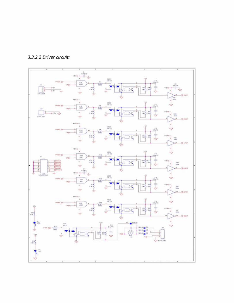
3.3.2.2 Driver circuit:
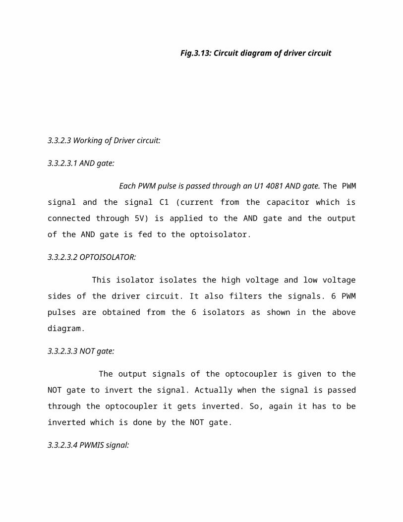
Fig.3.13: Circuit diagram of driver circuit
3.3.2.3 Working of Driver circuit:
3.3.2.3.1 AND gate:
Each PWM pulse is passed through an U1 4081 AND gate. The PWM
signal and the signal C1 (current from the capacitor which is
connected through 5V) is applied to the AND gate and the output
of the AND gate is fed to the optoisolator.
3.3.2.3.2 OPTOISOLATOR:
This isolator isolates the high voltage and low voltage
sides of the driver circuit. It also filters the signals. 6 PWM
pulses are obtained from the 6 isolators as shown in the above
diagram.
3.3.2.3.3 NOT gate:
The output signals of the optocoupler is given to the
NOT gate to invert the signal. Actually when the signal is passed
through the optocoupler it gets inverted. So, again it has to be
inverted which is done by the NOT gate.
3.3.2.3.4 PWMIS signal:

Here an extra PWM i.e. PWMIS is also used to
stimulate all the pulses so that we get a constant flow of PWM
pulses. PWMIS signal stimulates all the PWM waves to keep a
constant value of them.
3.3.2.3.5 Phase output:
Thus from 6 PWM waves we get 3 couples of signal.
They are as RTOP, RBOT, YTOP, YBOT, BTOP and BBOT.
Now these 6 signals goes to the Smart Power Module (SPM)
FSBB20CH60 module.
3.3 Smart Power Module circuit:

Fig.3.14: Circuit diagram of smart power module
3.3.1 Working of smart power module:
3.3.1.1 FSBB20CH60 module:

It is a 27 pin module. All the signals like RTOP,
RBOT, YTOP, YBOT, BTOP, BBOT is given to the module. Finally the
3 phase signal ( R, Y, B) is obtained as output from the module.
This 3 phase signal is then directly fed to the 3 phase induction
motor.
I. All the signals (RTOP, RBOT etc.) are fed to the FSBB20CH60
module.
II. There is a current resistance (IRES) signal which is also
fed to the FSBB20CH60 module.
III. Finally the output (three phase signals- R, Y, B) are
obtained through three INOUT devices.
IV. There are a few diodes and capacitors are connected with the
SPM module for filtering the signal.
V. A protection circuit is also included to process the higher
values without affecting the circuit.
3.3.1.2 Protection circuit:
The protection circuit consists of a comparators which
are used to detects that high voltage is coming. So, the
comparator does not allow the high voltage value through the
circuit.
Each comparator is fed from a 15V source.

When any fluctuation or disturbance is appeared, the
protection circuit responds and protect the main SPM as well
as the driver circuit.
3.4 Microcontroller circuit:
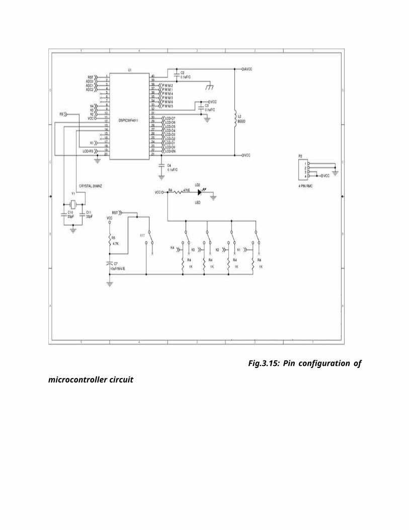
Fig.3.15: Pin configuration of
microcontroller circuit

Fig.3.16: Connection of microcontroller circuit

3.4.1 Microcontroller pin configuration:
PIN 1 -Reset
PIN 2-4 -Analog to digital converter
PIN 11 -Voltage Source
PIN 8-10 -K4,K3,K2 Signal
PIN 12,20 -Gnd
PIN 13,14 - Crystal Oscillator
PIN 17 - K1 signal
PIN 22-30 -LCD
PIN 33-38 -PWM signals.
Here, the pin configuration of the DSPIC
microcontroller has been given. There all the
functions of the pins are internally configured.
There is a crystal oscillator connected with the
microcontroller.

The signal K1 is given to the pin 17.
The signal K2,K3 and K4 is given to the pin 8 to
10.
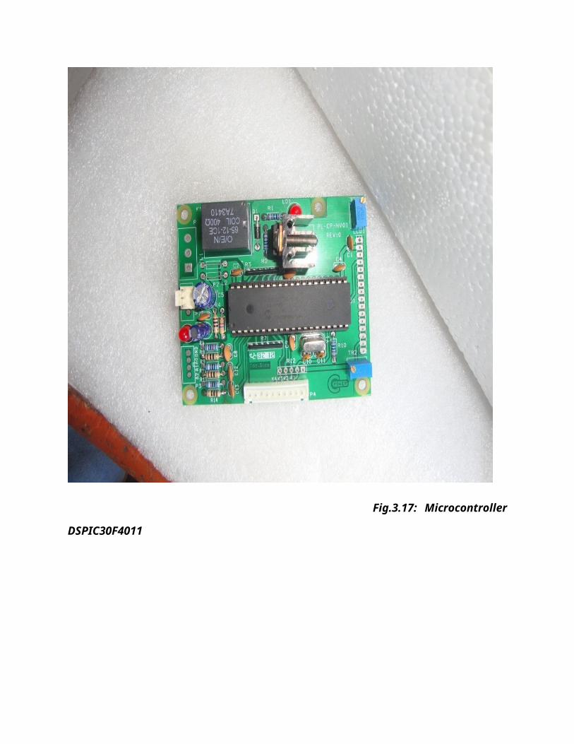
Fig.3.17: Microcontroller
DSPIC30F4011

3.5 Functional circuit of flip-flop:
Fig.3.18: Diagram of functional circuit of flip flop

The functional circuit is shown in the above diagram. For
protecting the entire hardware a protection circuit is
developed which flip flops and optoisolator and a few
diodes and resistors.
If any sudden high voltage is raised due to any
disturbances in supply voltages then the protection circuit
operates and it doesn’t allow the high voltage to the
circuit. Thus it prevents the circuit.
At normal condition the regular pulse or low current comes
at the pin 7 of the first flip flop.
Then the output Q bar is high and the output signal Q is
given as signal F1.
This output Q bar goes to the optoisolator.
At the optoisolator the high pulse signal is converted to
the low pulse signal SHUTDOWN1.
Then the low pulse signal SHUTDOWN1 is applied to the pin 7
of the second flip-flop.
So, the output Q bar of the second flip-flop is high which
is represented as signal C1 and it is applied to the AND
gate and the other output is given as F2.
When any disturbance or high voltage is appeared as COM1 at
the pin 7 of the first flip- flop.
So, the output Q bar is low which goes to the optoisolator.
After passing though the optoisolator it becomes high pulse
signal. This is referred as SHUTDOWN1.
Now this signal SHUTDOWN1 is applied to the pin7 of the
second flip-flop.
Now the output Q bar is low pulse signal. This gives the
input of the AND gate C1.
As the output Q bar is low C1 applied to AND gate is zero.
So, as per the operation of the AND gate the output is also
zero. So, the driver circuit as well as the motor remains
inactive and the entire hardware is very much safe.
CHAPTER- 4
RESULTS AND DISCUSSION, PERFORMANCE
ANALYSIS
4.1 GENERAL:
To analyze the speeds of the motor and to
control the speeds a few readings are taken both in open loop and
closed loop control. Simulation has become a very powerful tool
on the industry application as well as in academics, nowadays. It
is now essential for an electrical engineer to understand the
concept of simulation and learn its use in various applications.
Simulation is one of the best ways to study the system or circuit
behavior without damaging it .The tools for doing the simulation
in various fields are available in the market for engineering

professionals. Many industries are spending a considerable amount
of time and money in doing simulation before manufacturing their
product. In most of the research and development (R&D) work, the
simulation plays a very important role. Without simulation it is
quiet impossible to proceed further deails.
4.2 OPEN LOOP CONTROL RESULTS:
4.2.1 Tabulation for open loop control:
DC Volt = 200V (constant)
Serial
Number
Modulation
Index
(M.I)
Set
frequency
(HZ)
Actual
Speed
(RPM) 1
0.95
50
1462 2
0.77
40
1186 3
0.57
30
883 4
0.38
20
590 5
0.70
10
305Table 4.1: Tabulation for Open loop control
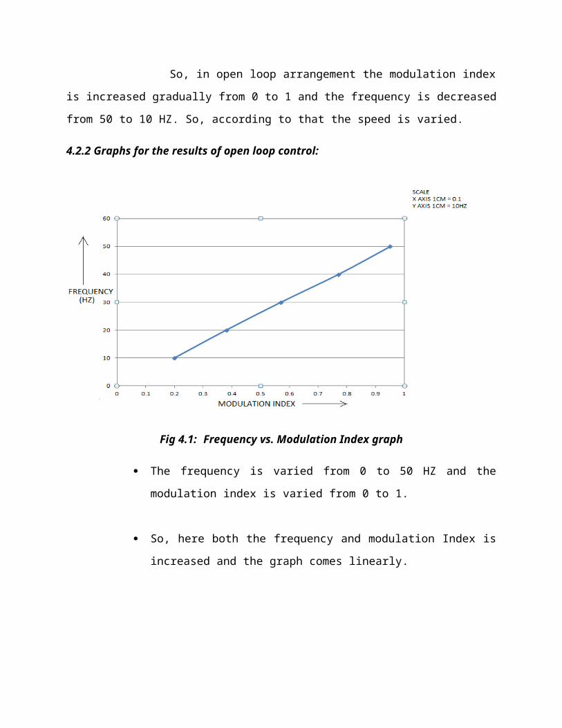
So, in open loop arrangement the modulation index
is increased gradually from 0 to 1 and the frequency is decreased
from 50 to 10 HZ. So, according to that the speed is varied.
4.2.2 Graphs for the results of open loop control:
Fig 4.1: Frequency vs. Modulation Index graph
The frequency is varied from 0 to 50 HZ and the
modulation index is varied from 0 to 1.
So, here both the frequency and modulation Index is
increased and the graph comes linearly.

Fig 4.2: Actual speed vs Modulation Index graph
When the modulation index is plotted with the
actual speed primarily the graph becomes in a
curve.
At higher values the graph remains almost
linear.
The modulation index is varied from 0 to 1
and the speed is varied upto 1450 rpm
( asynchronous speed).
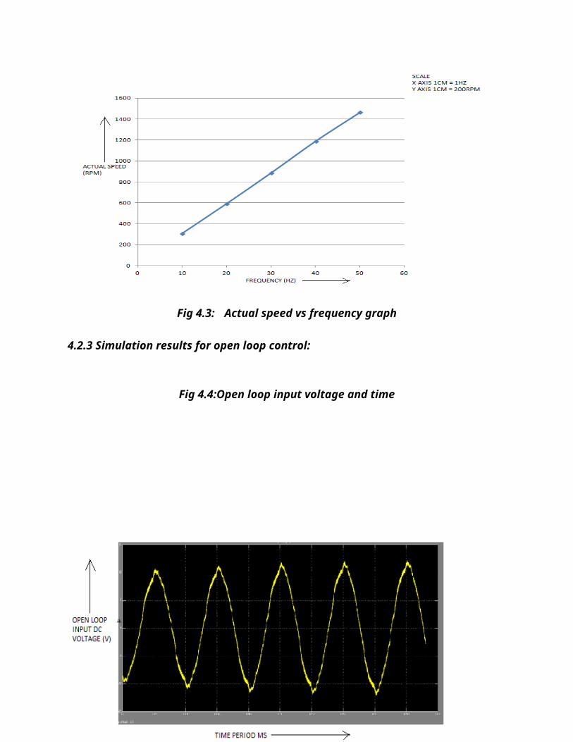
Fig 4.3: Actual speed vs frequency graph
4.2.3 Simulation results for open loop control:
Fig 4.4:Open loop input voltage and time
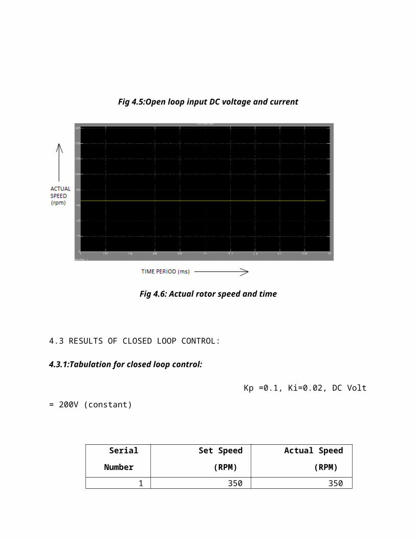
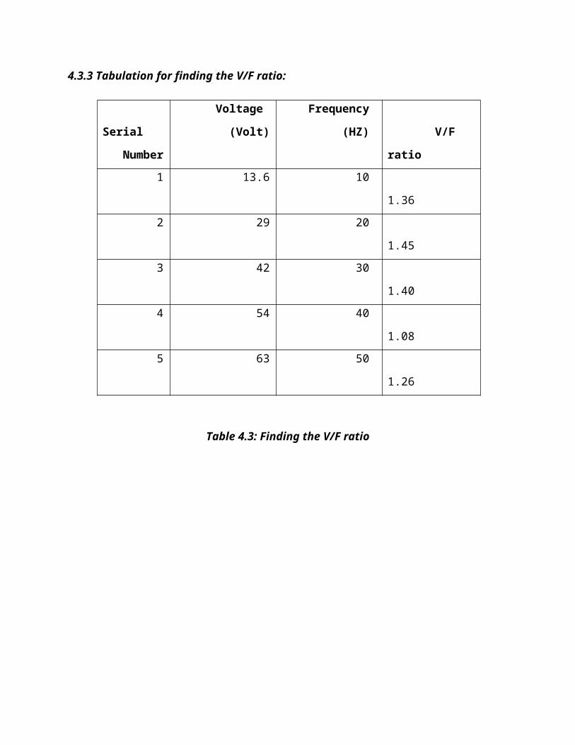
Fig 4.5:Open loop input DC voltage and current
Fig 4.6: Actual rotor speed and time
4.3 RESULTS OF CLOSED LOOP CONTROL:
4.3.1:Tabulation for closed loop control:
Kp =0.1, Ki=0.02, DC Volt
= 200V (constant)
Serial
Number
Set Speed
(RPM)
Actual Speed
(RPM) 1 350 350

2 550 550 3 950 950 4 1250 1250 5 1450 1450
Table 4.2: Closed loop control
4.3.2 Graphs for the results of closed loop control:
Fig 4.7: Set speed and Actual speed graph
Here the Kp and Ki value is kept constant. The Kp and Ki values
are 0.1 and 0.02 respectively. The dc voltage is also kept as
constant at 200V.
Here the values of actual speed
are accurately same as the set speed due the operation of closed
loop.
4.3.3 Tabulation for finding the V/F ratio:
Serial
Number
Voltage
(Volt)
Frequency
(HZ) V/F
ratio 1 13.6 10
1.36 2 29 20
1.45 3 42 30
1.40 4 54 40
1.08 5 63 50
1.26
Table 4.3: Finding the V/F ratio
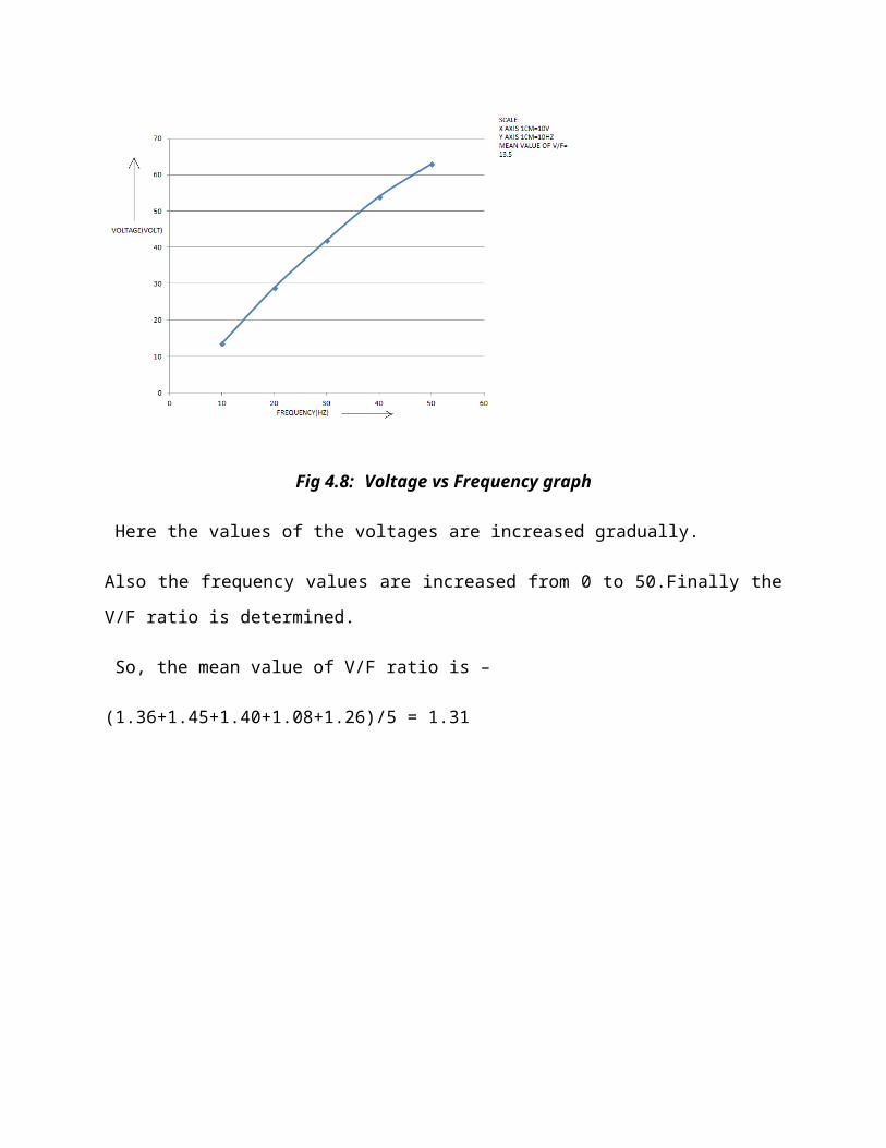
Fig 4.8: Voltage vs Frequency graph
Here the values of the voltages are increased gradually.
Also the frequency values are increased from 0 to 50.Finally the
V/F ratio is determined.
So, the mean value of V/F ratio is –
(1.36+1.45+1.40+1.08+1.26)/5 = 1.31
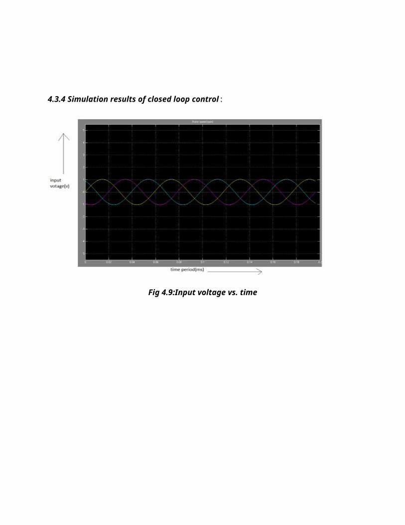
4.3.4 Simulation results of closed loop control:
Fig 4.9:Input voltage vs. time

Fig 4.10: Set speed/voltage speed vs. time period
4.4 PERFORMANCE ANALYSIS:
4.4.1 To drive the motor:

Fig 4.11 Operational block diagram to drive
the motor
I. To analyze the full operation of the hardware the driving of
the motor must to be understood well first.
II. The above block diagram explains the operation of driving
the motor.
III. The input supply is applied to the autotransformer. The
autotransformer is the device which takes the input supply
and give as the output voltage as the wish of the operator.
So we can vary the output voltage of the autotransformer as
our wish. That is the reason it is called variac otherwise.

IV. Now, we can gradually increase the output voltage of the
autotransformer which is applied to IGBT power module and
thereby goes to the motor.
V. We can keep the output voltage at any values like 100V, 150V
etc. But here we are keeping the output voltage in such a
value that it produces 200V after converted to dc.
VI. The isolation transformer connected with the autotransformer
is used to isolate
VII. The high disturbance from the current.
VIII. The single phase bridge rectifier is connected with the
isolation transformer.
IX. So, the output of the isolation transformer is converted to
DC voltage by the single phase bridge rectifier.
X. Now, the converted voltage is constant 200V. This is applied
to the smart power module which is also consists of the IGBT
devices.
XI. Now, finally the output current from the SPM is applied to
the motor to run the motor and also to control the speed of
the motor.

XII. The current is applied to the motor through the current
sensors for getting the current readings of the current
waves.
XIII. Fig- shows the current waveform which is given to the
motor.
4.4.2 Operation of the entire hardware:
Fig 4.12 Operational block diagram of the hardware
I. The operating voltage of the microcontroller is 5V, which is
supplied from the input voltage source. That voltage is
regulated by a voltage regulation circuit.
II. Here we are using 3 switches for the entire operation.
a) Increment switch,
b) Decrement switch and
c) Reset switch.
III. The increment and decrement switch is for increasing and
decreasing the values of the frequency, modulation index, set
speeds etc.
IV. Now, the microcontroller DSPIC30F4011 is operated at 5V and it
generates 6 PWM pulses.
V. This PWM pulses directly goes to the 3 phase inverter module
(smart power module- SPM) and thereby applied to the motor.
VI. Now, if the modulation index is varied the ON time and OFF
time of the PWM pulses are also varied.
VII. But if the frequency is varied then also the speed of the
motor is varied.
VIII. So, by varying the modulation index and the frequency the PWM
pulses are varied and thereby the speed of the motor is
varied.
IX. A LCD display is given where the inputs and the outputs are
visualized.
X. From table no. 4.1 we can see that in open loop the frequency
can be varied by using the increment or decrement switches and
the DC voltage is kept constant at 200V. So, with that the
modulation index is also varied and as the result the actual
motor speed is varied.
XI. From table no. 4.2 we can see that in closed loop the set
frequency we are giving is the same what we are getting as
motor actual speed.

XII. From table no. 4.3 we can see that by changing both the
voltage and the frequency the speed of the motor is varied.
So, the V/F ratio drives the motor speed. The mean value of
the V/F ratios we taken over the operation is 1.31.
4.4.3 Oscilloscope results:
4.13 CRO output of PWM pulse.

4.14 CRO output of the dc voltage
applied to the motor
4.15 CRO output of the motor current waveform
The PWM wave is obtained by connecting the CRO probes
to optoisolator terminal and supply terminal.
The motor current waveform is obtained by connecting
the CRO probes to the current sensor pins.
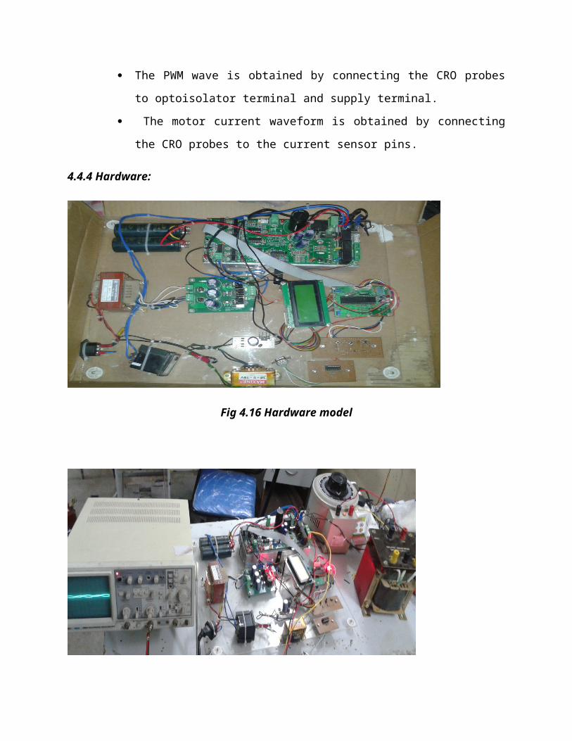
4.4.4 Hardware:
Fig 4.16 Hardware model

Fig 4.17 Connected model of Hardware
These are the actual hardware model which we have prepared. The
induction motor whose speed we have to control is connected with
it and the speed control is done by this hardware.
4.5 ADVANTAGES:
Easy programming,
Soft hardware control,
Rugged,
less power required,
Multiple duty cycle generator,
Multiple Conversion Sequencing Options,
Wide operating voltage range (2.5V to 5.5V),
Bidirectional operation.
4.6 APPLICATION:
From small appliances to the largest of mine mill drivers
and compressors
Centrifugal pump

Fixed speed and variable speed electric motor
Global market penetration
Home appliances applications like air conditioner and
washing machine.
Chapter – 5
SUMMARY AND CONCLUSIONS
5.1 SUMMARY:
This chapter describes the hardware implementation of the V/F
control of an induction motor using microcontroller.It includes
the development of hardware for microcontroller circuit, SPWM
pulses generation, optocoupler circuit was explained. For SPWM
pulses, the sine wave is generated from PIC microcontroller
(DSPIC30F4011) and ramp wave is generated through ramp generator
The output of the controller is given to the optocoupler circuit
which is used for protection and isolation purpose, in case of
commutation failure and short circuit due to the improper
trigger. From the optocoupler circuit the pulses are given to the
appropriate switches of the MOSFETs inverter fed induction motor.
The use of a Variable Speed Drive for a speed control
application usually offers an energy efficient and
environmentally friendly solution. The best opportunities for
energy savings, with subsequent economic savings, arise through
the laws which govern the operation of centrifugal fans and

pumps. Simple and straight forward VSD’s, such as the PWM
inverter drives, are available for applications where the speed
control accuracy is not critical. This compact inverter had its
hardware reduced to a minimum through the use of bridge inverter.
The variable speed drive with variable frequency control method
will offer new, low-cost solutions for light commercial and
consumer applications. The frequency range of the constructed
circuit is 10 Hz to 50 Hz at constant voltage for changing the
speed of induction motor between theoretical limits of 300 rpm to
1460 rpm if 50 Hz, single-phase AC
motors are used.
The speed of a 3-phase induction motor in open loop and closed
loop, supply voltage and frequency need to be varied with
constant ratio to each other. A low cost solution
of this control can be implemented in a DSPIC microcontroller.
This requires six PWMs to control a 3-phase inverter bridge. Many
DSPICmicro microcontrollers have two hardware PWMs.
5.2 CONCLUSION:
The speed of three-phase induction motor is being controlled by
varying supply voltage and frequency with constant (V/F) ratio.
It is simple, economic to easier to design and implement in open
loop. But the drawbacks of open loop is it doesn’t correct the
change in output also it doesn’t reach the steady state quickly.

These drawbacks can be overcome by modifying an open loop into a
closed loop system. In this project only open loop was
implemented in hardware.The project can be extended in future to
control the speed of induction motor in closed loop.
Copyright © 2022 FDOKUMEN