
MCF51JE256 - Reference Manual - NXP
692
MCF51JE256 Reference Manual An Energy-Efficient Solution from Freescale Devices Supported: MCF51JE256 MCF51JE128 Document Number: MCF51JE256 Rev. 2 12/2010 MCF51JE256 Reference Manual, Rev. 2
-
Upload
khangminh22 -
Category
Documents
-
view
1 -
download
0
Transcript of MCF51JE256 - Reference Manual - NXP

MCF51JE256 Reference ManualAn Energy-Efficient Solution from Freescale
Devices Supported:MCF51JE256MCF51JE128
Document Number: MCF51JE256Rev. 2
12/2010
MCF51JE256 Reference Manual, Rev. 2

How to Reach Us:
Home Page:www.freescale.com
Web Support:http://www.freescale.com/support
USA/Europe or Locations Not Listed:Freescale Semiconductor, Inc.Technical Information Center, EL5162100 East Elliot RoadTempe, Arizona 852841-800-521-6274 or +1-480-768-2130www.freescale.com/support
Europe, Middle East, and Africa:Freescale Halbleiter Deutschland GmbHTechnical Information CenterSchatzbogen 781829 Muenchen, Germany+44 1296 380 456 (English)+46 8 52200080 (English)+49 89 92103 559 (German)+33 1 69 35 48 48 (French)www.freescale.com/support
Japan:Freescale Semiconductor Japan Ltd. HeadquartersARCO Tower 15F1-8-1, Shimo-Meguro, Meguro-ku,Tokyo 153-0064Japan0120 191014 or +81 3 5437 [email protected]
Asia/Pacific:Freescale Semiconductor China Ltd.Exchange Building 23FNo. 118 Jianguo RoadChaoyang DistrictBeijing 100022China +86 10 5879 8000 [email protected]
Freescale Semiconductor Literature Distribution Center1-800-441-2447 or +1-303-675-2140Fax: +1-303-675-2150 [email protected]
Information in this document is provided solely to enable system and software implementers to use Freescale Semiconductor products. There are no express or implied copyright licenses granted hereunder to design or fabricate any integrated circuits or integrated circuits based on the information in this document.
Freescale Semiconductor reserves the right to make changes without further notice to any products herein. Freescale Semiconductor makes no warranty, representation or guarantee regarding the suitability of its products for any particular purpose, nor does Freescale Semiconductor assume any liability arising out of the application or use of any product or circuit, and specifically disclaims any and all liability, including without limitation consequential or incidental damages. “Typical” parameters that may be provided in Freescale Semiconductor data sheets and/or specifications can and do vary in different applications and actual performance may vary over time. All operating parameters, including “Typicals”, must be validated for each customer application by customer’s technical experts. Freescale Semiconductor does not convey any license under its patent rights nor the rights of others. Freescale Semiconductor products are not designed, intended, or authorized for use as components in systems intended for surgical implant into the body, or other applications intended to support or sustain life, or for any other application in which the failure of the Freescale Semiconductor product could create a situation where personal injury or death may occur. Should Buyer purchase or use Freescale Semiconductor products for any such unintended or unauthorized application, Buyer shall indemnify and hold Freescale Semiconductor and its officers, employees, subsidiaries, affiliates, and distributors harmless against all claims, costs, damages, and expenses, and reasonable attorney fees arising out of, directly or indirectly, any claim of personal injury or death associated with such unintended or unauthorized use, even if such claim alleges that Freescale Semiconductor was negligent regarding the design or manufacture of the part.
Freescale™ and the Freescale logo are trademarks of Freescale Semiconductor, Inc. All other product or service names are the property of their respective owners.
© Freescale Semiconductor, Inc. 2010. All rights reserved.
MCF51JE256RMRev. 2 12/2010
MCF51JE256 Reference Manual, Rev. 2

Freescale Semiconductor iii
ContentsChapter 1
Device Overview1.1 The MCF51JE256 Series Microcontroller . . . . . . . . . . . . . . . . . . . . . . . . . . . . . . . . . . . 1-1
1.1.1 Definition . . . . . . . . . . . . . . . . . . . . . . . . . . . . . . . . . . . . . . . . . . . . . . . . . . . . . . 1-11.1.2 Devices in the MCF51JE256 series . . . . . . . . . . . . . . . . . . . . . . . . . . . . . . . . . 1-1
1.2 MCF51JE256/128 Block Diagram . . . . . . . . . . . . . . . . . . . . . . . . . . . . . . . . . . . . . . . . . 1-21.2.1 Functional Units . . . . . . . . . . . . . . . . . . . . . . . . . . . . . . . . . . . . . . . . . . . . . . . . 1-41.2.2 Functional Versions . . . . . . . . . . . . . . . . . . . . . . . . . . . . . . . . . . . . . . . . . . . . . 1-5
1.3 V1 ColdFire Core . . . . . . . . . . . . . . . . . . . . . . . . . . . . . . . . . . . . . . . . . . . . . . . . . . . . . . 1-61.3.1 User Programming Model . . . . . . . . . . . . . . . . . . . . . . . . . . . . . . . . . . . . . . . . . 1-81.3.2 Supervisor Programming Model . . . . . . . . . . . . . . . . . . . . . . . . . . . . . . . . . . . . 1-8
1.4 System Clocks . . . . . . . . . . . . . . . . . . . . . . . . . . . . . . . . . . . . . . . . . . . . . . . . . . . . . . . . 1-91.4.1 System Clock Distribution . . . . . . . . . . . . . . . . . . . . . . . . . . . . . . . . . . . . . . . . . 1-91.4.2 System Clocks . . . . . . . . . . . . . . . . . . . . . . . . . . . . . . . . . . . . . . . . . . . . . . . . 1-111.4.3 Clock Gating . . . . . . . . . . . . . . . . . . . . . . . . . . . . . . . . . . . . . . . . . . . . . . . . . . 1-111.4.4 MCG Modes of Operation . . . . . . . . . . . . . . . . . . . . . . . . . . . . . . . . . . . . . . . . 1-111.4.5 MCG Mode State Diagram . . . . . . . . . . . . . . . . . . . . . . . . . . . . . . . . . . . . . . . 1-12
Chapter 2Pins and Connections
2.1 Device Pin Assignments . . . . . . . . . . . . . . . . . . . . . . . . . . . . . . . . . . . . . . . . . . . . . . . . 2-12.2 104-Pin MAPBGA . . . . . . . . . . . . . . . . . . . . . . . . . . . . . . . . . . . . . . . . . . . . . . . . . . . . . 2-12.3 100-Pin LQFP . . . . . . . . . . . . . . . . . . . . . . . . . . . . . . . . . . . . . . . . . . . . . . . . . . . . . . . . 2-32.4 81-Pin MAPBGA . . . . . . . . . . . . . . . . . . . . . . . . . . . . . . . . . . . . . . . . . . . . . . . . . . . . . . 2-42.5 80-Pin LQFP . . . . . . . . . . . . . . . . . . . . . . . . . . . . . . . . . . . . . . . . . . . . . . . . . . . . . . . . . 2-52.6 Pin Assignments . . . . . . . . . . . . . . . . . . . . . . . . . . . . . . . . . . . . . . . . . . . . . . . . . . . . . . 2-6
2.6.1 Pinout Summary . . . . . . . . . . . . . . . . . . . . . . . . . . . . . . . . . . . . . . . . . . . . . . . 2-102.6.2 Recommended System Connections . . . . . . . . . . . . . . . . . . . . . . . . . . . . . . 2-212.6.3 Interfacing the SCIs to Off-Chip Opto-Isolators . . . . . . . . . . . . . . . . . . . . . . . 2-222.6.4 Power . . . . . . . . . . . . . . . . . . . . . . . . . . . . . . . . . . . . . . . . . . . . . . . . . . . . . . . 2-222.6.5 Oscillator . . . . . . . . . . . . . . . . . . . . . . . . . . . . . . . . . . . . . . . . . . . . . . . . . . . . . 2-232.6.6 PTD1/CMPP2/RESET . . . . . . . . . . . . . . . . . . . . . . . . . . . . . . . . . . . . . . . . . . 2-242.6.7 PTE4/CMPP3/TPMCLK/IRQ . . . . . . . . . . . . . . . . . . . . . . . . . . . . . . . . . . . . . 2-242.6.8 Background / Mode Select (PTD0/BKGD/MS) . . . . . . . . . . . . . . . . . . . . . . . . 2-242.6.9 ADC Reference Pins (VREFH, VREFL) . . . . . . . . . . . . . . . . . . . . . . . . . . . . . . . 2-252.6.10 Bootloader Mode Select (BLMS) . . . . . . . . . . . . . . . . . . . . . . . . . . . . . . . . . . 2-252.6.11 USB Data Pins (USB_DP, USB_DN) . . . . . . . . . . . . . . . . . . . . . . . . . . . . . . . 2-25
MCF51JE256 Reference Manual, Rev. 2

iv Freescale Semiconductor
2.6.12 General-Purpose I/O and Peripheral Ports . . . . . . . . . . . . . . . . . . . . . . . . . . . 2-25
Chapter 3Modes of Operation
3.1 Introduction . . . . . . . . . . . . . . . . . . . . . . . . . . . . . . . . . . . . . . . . . . . . . . . . . . . . . . . . . . 3-13.2 Features . . . . . . . . . . . . . . . . . . . . . . . . . . . . . . . . . . . . . . . . . . . . . . . . . . . . . . . . . . . . . 3-13.3 Overview . . . . . . . . . . . . . . . . . . . . . . . . . . . . . . . . . . . . . . . . . . . . . . . . . . . . . . . . . . . . 3-23.4 Secure Mode . . . . . . . . . . . . . . . . . . . . . . . . . . . . . . . . . . . . . . . . . . . . . . . . . . . . . . . . . 3-63.5 Bootloader Mode . . . . . . . . . . . . . . . . . . . . . . . . . . . . . . . . . . . . . . . . . . . . . . . . . . . . . . 3-6
3.5.1 Entering Bootloader Mode . . . . . . . . . . . . . . . . . . . . . . . . . . . . . . . . . . . . . . . . 3-63.5.2 Entering User mode . . . . . . . . . . . . . . . . . . . . . . . . . . . . . . . . . . . . . . . . . . . . . 3-73.5.3 Active Background Mode and Bootloader Mode Arbitrage . . . . . . . . . . . . . . . . 3-73.5.4 Bootloader Operation . . . . . . . . . . . . . . . . . . . . . . . . . . . . . . . . . . . . . . . . . . . . 3-7
3.6 Run Modes . . . . . . . . . . . . . . . . . . . . . . . . . . . . . . . . . . . . . . . . . . . . . . . . . . . . . . . . . 3-103.6.1 Run Mode . . . . . . . . . . . . . . . . . . . . . . . . . . . . . . . . . . . . . . . . . . . . . . . . . . . . 3-103.6.2 Low-Power Run Mode (LPrun) . . . . . . . . . . . . . . . . . . . . . . . . . . . . . . . . . . . . 3-10
3.7 Wait Modes . . . . . . . . . . . . . . . . . . . . . . . . . . . . . . . . . . . . . . . . . . . . . . . . . . . . . . . . . 3-113.7.1 Wait Mode . . . . . . . . . . . . . . . . . . . . . . . . . . . . . . . . . . . . . . . . . . . . . . . . . . . . 3-113.7.2 Low-Power Wait Mode (LPwait) . . . . . . . . . . . . . . . . . . . . . . . . . . . . . . . . . . . 3-11
3.8 Stop Modes . . . . . . . . . . . . . . . . . . . . . . . . . . . . . . . . . . . . . . . . . . . . . . . . . . . . . . . . . 3-123.8.1 Stop2 Mode . . . . . . . . . . . . . . . . . . . . . . . . . . . . . . . . . . . . . . . . . . . . . . . . . . 3-133.8.2 Stop3 Mode . . . . . . . . . . . . . . . . . . . . . . . . . . . . . . . . . . . . . . . . . . . . . . . . . . 3-133.8.3 Stop4 Mode . . . . . . . . . . . . . . . . . . . . . . . . . . . . . . . . . . . . . . . . . . . . . . . . . . 3-14
3.9 On-Chip peripheral Modules in Stop and Low-power Modes . . . . . . . . . . . . . . . . . . . 3-143.10 Debug Mode . . . . . . . . . . . . . . . . . . . . . . . . . . . . . . . . . . . . . . . . . . . . . . . . . . . . . . . . 3-16
Chapter 4Memory
4.1 MCF51JE256 Series Memory Map . . . . . . . . . . . . . . . . . . . . . . . . . . . . . . . . . . . . . . . . 4-14.1.1 Register Addresses and Bit Assignments . . . . . . . . . . . . . . . . . . . . . . . . . . . . . 4-24.1.2 Detailed register addresses and bit assignments . . . . . . . . . . . . . . . . . . . . . . . 4-34.1.3 Flash Module Reserved Memory Locations . . . . . . . . . . . . . . . . . . . . . . . . . . 4-174.1.4 ColdFire Rapid GPIO Memory Map . . . . . . . . . . . . . . . . . . . . . . . . . . . . . . . . 4-184.1.5 ColdFire Interrupt Controller Memory Map . . . . . . . . . . . . . . . . . . . . . . . . . . . 4-18
4.2 RAM . . . . . . . . . . . . . . . . . . . . . . . . . . . . . . . . . . . . . . . . . . . . . . . . . . . . . . . . . . . . . . . 4-194.3 Flash Memory . . . . . . . . . . . . . . . . . . . . . . . . . . . . . . . . . . . . . . . . . . . . . . . . . . . . . . . 4-20
4.3.1 Features . . . . . . . . . . . . . . . . . . . . . . . . . . . . . . . . . . . . . . . . . . . . . . . . . . . . . 4-214.3.2 Dual Flash Controllers . . . . . . . . . . . . . . . . . . . . . . . . . . . . . . . . . . . . . . . . . . 4-214.3.3 Register Descriptions . . . . . . . . . . . . . . . . . . . . . . . . . . . . . . . . . . . . . . . . . . . 4-22
4.4 Functional Description . . . . . . . . . . . . . . . . . . . . . . . . . . . . . . . . . . . . . . . . . . . . . . . . . 4-284.4.1 Flash Command Operations . . . . . . . . . . . . . . . . . . . . . . . . . . . . . . . . . . . . . . 4-284.4.2 Flash Commands . . . . . . . . . . . . . . . . . . . . . . . . . . . . . . . . . . . . . . . . . . . . . . 4-304.4.3 Illegal Flash Operations . . . . . . . . . . . . . . . . . . . . . . . . . . . . . . . . . . . . . . . . . 4-374.4.4 Operating Modes . . . . . . . . . . . . . . . . . . . . . . . . . . . . . . . . . . . . . . . . . . . . . . 4-384.4.5 Flash Security . . . . . . . . . . . . . . . . . . . . . . . . . . . . . . . . . . . . . . . . . . . . . . . . . 4-38
MCF51JE256 Reference Manual, Rev. 2

Freescale Semiconductor v
4.4.6 Resets . . . . . . . . . . . . . . . . . . . . . . . . . . . . . . . . . . . . . . . . . . . . . . . . . . . . . . . 4-394.5 Security . . . . . . . . . . . . . . . . . . . . . . . . . . . . . . . . . . . . . . . . . . . . . . . . . . . . . . . . . . . . 4-39
4.5.1 Unsecuring the MCU using Backdoor Key Access . . . . . . . . . . . . . . . . . . . . . 4-40
Chapter 5Resets, Interrupts, and General System Control
5.1 Introduction . . . . . . . . . . . . . . . . . . . . . . . . . . . . . . . . . . . . . . . . . . . . . . . . . . . . . . . . . . 5-15.2 Features . . . . . . . . . . . . . . . . . . . . . . . . . . . . . . . . . . . . . . . . . . . . . . . . . . . . . . . . . . . . . 5-15.3 Microcontroller Reset . . . . . . . . . . . . . . . . . . . . . . . . . . . . . . . . . . . . . . . . . . . . . . . . . . . 5-1
5.3.1 Computer Operating Properly (COP) Watchdog . . . . . . . . . . . . . . . . . . . . . . . 5-25.3.2 Illegal Opcode Detect (ILOP) . . . . . . . . . . . . . . . . . . . . . . . . . . . . . . . . . . . . . . 5-35.3.3 Illegal Address Detect (ILAD) . . . . . . . . . . . . . . . . . . . . . . . . . . . . . . . . . . . . . . 5-3
5.4 Interrupts & Exceptions . . . . . . . . . . . . . . . . . . . . . . . . . . . . . . . . . . . . . . . . . . . . . . . . . 5-35.4.1 External Interrupt Request (IRQ) Pin . . . . . . . . . . . . . . . . . . . . . . . . . . . . . . . . 5-45.4.2 Interrupt Vectors, Sources, and Local Masks . . . . . . . . . . . . . . . . . . . . . . . . . . 5-5
5.5 Low-Voltage Detect (LVD) System . . . . . . . . . . . . . . . . . . . . . . . . . . . . . . . . . . . . . . . . . 5-95.5.1 Power-On Reset Operation . . . . . . . . . . . . . . . . . . . . . . . . . . . . . . . . . . . . . . . . 5-95.5.2 LVD Reset Operation . . . . . . . . . . . . . . . . . . . . . . . . . . . . . . . . . . . . . . . . . . . . 5-95.5.3 LVD Interrupt Operation . . . . . . . . . . . . . . . . . . . . . . . . . . . . . . . . . . . . . . . . . 5-105.5.4 Low-Voltage Warning (LVW) Interrupt Operation . . . . . . . . . . . . . . . . . . . . . . 5-10
5.6 Peripheral Clock Gating . . . . . . . . . . . . . . . . . . . . . . . . . . . . . . . . . . . . . . . . . . . . . . . . 5-105.7 Reset, Interrupt, and System Control Registers and Control Bits . . . . . . . . . . . . . . . . 5-10
5.7.1 Interrupt Pin Request Status and Control Register (IRQSC) . . . . . . . . . . . . . 5-115.7.2 System Reset Status Register (SRS) . . . . . . . . . . . . . . . . . . . . . . . . . . . . . . . 5-125.7.3 System Options 1 (SOPT1) Register . . . . . . . . . . . . . . . . . . . . . . . . . . . . . . . 5-135.7.4 System Options 2 (SOPT2) Register . . . . . . . . . . . . . . . . . . . . . . . . . . . . . . . 5-145.7.5 SIM Clock Set and Select Register (SIMCO) . . . . . . . . . . . . . . . . . . . . . . . . . 5-155.7.6 System Device Identification Register (SDIDH, SDIDL) . . . . . . . . . . . . . . . . . 5-165.7.7 System Clock Gating Control 1 Register (SCGC1) . . . . . . . . . . . . . . . . . . . . 5-175.7.8 System Clock Gating Control 2 Register (SCGC2) . . . . . . . . . . . . . . . . . . . . 5-185.7.9 System Clock Gating Control 3 Register (SCGC3) . . . . . . . . . . . . . . . . . . . . 5-185.7.10 System Options 3 Register (SOPT3) . . . . . . . . . . . . . . . . . . . . . . . . . . . . . . . 5-195.7.11 System Options 4 Register (SOPT4) . . . . . . . . . . . . . . . . . . . . . . . . . . . . . . . 5-215.7.12 System Options 5 Register (SOPT5) . . . . . . . . . . . . . . . . . . . . . . . . . . . . . . . 5-225.7.13 SIM Internal Peripheral Select Register (SIMIPS) . . . . . . . . . . . . . . . . . . . . . 5-225.7.14 Signature Register (Signature) . . . . . . . . . . . . . . . . . . . . . . . . . . . . . . . . . . . . 5-235.7.15 System Power Management Status and Control 1 Register (SPMSC1) . . . . 5-235.7.16 System Power Management Status and Control 2 Register (SPMSC2) . . . . 5-245.7.17 System Power Management Status and Control 3 Register (SPMSC3) . . . . 5-255.7.18 Flash Protection Disable Register (FPROTD) . . . . . . . . . . . . . . . . . . . . . . . . 5-265.7.19 Mini-FlexBus Pin Control 1 (MFBPC1) . . . . . . . . . . . . . . . . . . . . . . . . . . . . . . 5-275.7.20 Mini-FlexBus Pin Control 2 (MFBPC2) . . . . . . . . . . . . . . . . . . . . . . . . . . . . . . 5-285.7.21 Mini-FlexBus Pin Control 3 (MFBPC3) . . . . . . . . . . . . . . . . . . . . . . . . . . . . . . 5-295.7.22 Mini-FlexBus Pin Control 4 (MFBPC4) . . . . . . . . . . . . . . . . . . . . . . . . . . . . . . 5-30
MCF51JE256 Reference Manual, Rev. 2

vi Freescale Semiconductor
Chapter 6Parallel Input/Output Control
6.1 Port Data and Data Direction . . . . . . . . . . . . . . . . . . . . . . . . . . . . . . . . . . . . . . . . . . . . . 6-16.2 Pull-up, Slew Rate, and Drive Strength . . . . . . . . . . . . . . . . . . . . . . . . . . . . . . . . . . . . . 6-2
6.2.1 Port Internal Pull-up Enable . . . . . . . . . . . . . . . . . . . . . . . . . . . . . . . . . . . . . . . 6-26.2.2 Port Slew Rate Enable . . . . . . . . . . . . . . . . . . . . . . . . . . . . . . . . . . . . . . . . . . . 6-26.2.3 Port Drive Strength Select . . . . . . . . . . . . . . . . . . . . . . . . . . . . . . . . . . . . . . . . 6-36.2.4 Port Input Filter Enable . . . . . . . . . . . . . . . . . . . . . . . . . . . . . . . . . . . . . . . . . . . 6-3
6.3 ColdFire V1 Rapid GPIO Functionality . . . . . . . . . . . . . . . . . . . . . . . . . . . . . . . . . . . . . 6-36.4 Keyboard Interrupts . . . . . . . . . . . . . . . . . . . . . . . . . . . . . . . . . . . . . . . . . . . . . . . . . . . . 6-3
6.4.1 Edge Only Sensitivity . . . . . . . . . . . . . . . . . . . . . . . . . . . . . . . . . . . . . . . . . . . . 6-46.4.2 Edge and Level Sensitivity . . . . . . . . . . . . . . . . . . . . . . . . . . . . . . . . . . . . . . . . 6-46.4.3 Pull-up/Pull-down Resistors . . . . . . . . . . . . . . . . . . . . . . . . . . . . . . . . . . . . . . . 6-46.4.4 Keyboard Interrupt Initialization . . . . . . . . . . . . . . . . . . . . . . . . . . . . . . . . . . . . 6-4
6.5 Pin Behavior in Stop Modes . . . . . . . . . . . . . . . . . . . . . . . . . . . . . . . . . . . . . . . . . . . . . 6-56.6 Parallel I/O, Keyboard Interrupt, and Pin Control Registers . . . . . . . . . . . . . . . . . . . . . . 6-5
6.6.1 Port A Registers . . . . . . . . . . . . . . . . . . . . . . . . . . . . . . . . . . . . . . . . . . . . . . . . 6-56.6.2 Port B Registers . . . . . . . . . . . . . . . . . . . . . . . . . . . . . . . . . . . . . . . . . . . . . . . . 6-86.6.3 Port C Registers . . . . . . . . . . . . . . . . . . . . . . . . . . . . . . . . . . . . . . . . . . . . . . . 6-116.6.4 Port D Registers . . . . . . . . . . . . . . . . . . . . . . . . . . . . . . . . . . . . . . . . . . . . . . . 6-136.6.5 Port E Registers . . . . . . . . . . . . . . . . . . . . . . . . . . . . . . . . . . . . . . . . . . . . . . . 6-166.6.6 Port F Registers . . . . . . . . . . . . . . . . . . . . . . . . . . . . . . . . . . . . . . . . . . . . . . . 6-196.6.7 Port G Registers . . . . . . . . . . . . . . . . . . . . . . . . . . . . . . . . . . . . . . . . . . . . . . . 6-216.6.8 Port H Registers . . . . . . . . . . . . . . . . . . . . . . . . . . . . . . . . . . . . . . . . . . . . . . . 6-246.6.9 Port J Registers . . . . . . . . . . . . . . . . . . . . . . . . . . . . . . . . . . . . . . . . . . . . . . . 6-266.6.10 Keyboard Interrupt 1 (KBI1) Registers . . . . . . . . . . . . . . . . . . . . . . . . . . . . . . 6-296.6.11 Keyboard Interrupt 2 (KBI2) Registers . . . . . . . . . . . . . . . . . . . . . . . . . . . . . . 6-30
Chapter 7ColdFire Core
7.1 Introduction . . . . . . . . . . . . . . . . . . . . . . . . . . . . . . . . . . . . . . . . . . . . . . . . . . . . . . . . . . 7-17.1.1 Overview . . . . . . . . . . . . . . . . . . . . . . . . . . . . . . . . . . . . . . . . . . . . . . . . . . . . . . 7-1
7.2 Memory Map/Register Description . . . . . . . . . . . . . . . . . . . . . . . . . . . . . . . . . . . . . . . . 7-27.2.1 Data Registers (D0–D7) . . . . . . . . . . . . . . . . . . . . . . . . . . . . . . . . . . . . . . . . . . 7-47.2.2 Address Registers (A0–A6) . . . . . . . . . . . . . . . . . . . . . . . . . . . . . . . . . . . . . . . 7-47.2.3 Supervisor/User Stack Pointers (A7 and OTHER_A7) . . . . . . . . . . . . . . . . . . . 7-57.2.4 Condition Code Register (CCR) . . . . . . . . . . . . . . . . . . . . . . . . . . . . . . . . . . . . 7-57.2.5 Program Counter (PC) . . . . . . . . . . . . . . . . . . . . . . . . . . . . . . . . . . . . . . . . . . . 7-67.2.6 Vector Base Register (VBR) . . . . . . . . . . . . . . . . . . . . . . . . . . . . . . . . . . . . . . . 7-77.2.7 CPU Configuration Register (CPUCR) . . . . . . . . . . . . . . . . . . . . . . . . . . . . . . . 7-77.2.8 Status Register (SR) . . . . . . . . . . . . . . . . . . . . . . . . . . . . . . . . . . . . . . . . . . . . . 7-8
7.3 Functional Description . . . . . . . . . . . . . . . . . . . . . . . . . . . . . . . . . . . . . . . . . . . . . . . . . . 7-97.3.1 Instruction Set Architecture (ISA_C) . . . . . . . . . . . . . . . . . . . . . . . . . . . . . . . . . 7-97.3.2 Exception Processing Overview . . . . . . . . . . . . . . . . . . . . . . . . . . . . . . . . . . . 7-107.3.3 Processor Exceptions . . . . . . . . . . . . . . . . . . . . . . . . . . . . . . . . . . . . . . . . . . . 7-13
MCF51JE256 Reference Manual, Rev. 2

Freescale Semiconductor vii
7.3.4 Instruction Execution Timing . . . . . . . . . . . . . . . . . . . . . . . . . . . . . . . . . . . . . . 7-21
Chapter 8Multiply-Accumulate Unit (MAC)
8.1 Introduction . . . . . . . . . . . . . . . . . . . . . . . . . . . . . . . . . . . . . . . . . . . . . . . . . . . . . . . . . . 8-18.1.1 Overview . . . . . . . . . . . . . . . . . . . . . . . . . . . . . . . . . . . . . . . . . . . . . . . . . . . . . . 8-1
8.2 Memory Map/Register Definition . . . . . . . . . . . . . . . . . . . . . . . . . . . . . . . . . . . . . . . . . . 8-28.2.1 MAC Status Register (MACSR) . . . . . . . . . . . . . . . . . . . . . . . . . . . . . . . . . . . . 8-28.2.2 Mask Register (MASK) . . . . . . . . . . . . . . . . . . . . . . . . . . . . . . . . . . . . . . . . . . . 8-48.2.3 Accumulator Register (ACC) . . . . . . . . . . . . . . . . . . . . . . . . . . . . . . . . . . . . . . 8-5
8.3 Functional Description . . . . . . . . . . . . . . . . . . . . . . . . . . . . . . . . . . . . . . . . . . . . . . . . . . 8-68.3.1 Fractional Operation Mode . . . . . . . . . . . . . . . . . . . . . . . . . . . . . . . . . . . . . . . . 8-78.3.2 MAC Instruction Set Summary . . . . . . . . . . . . . . . . . . . . . . . . . . . . . . . . . . . . . 8-88.3.3 MAC Instruction Execution Times . . . . . . . . . . . . . . . . . . . . . . . . . . . . . . . . . . . 8-98.3.4 Data Representation . . . . . . . . . . . . . . . . . . . . . . . . . . . . . . . . . . . . . . . . . . . . . 8-98.3.5 MAC Opcodes . . . . . . . . . . . . . . . . . . . . . . . . . . . . . . . . . . . . . . . . . . . . . . . . . 8-9
Chapter 9Rapid GPIO (RGPIO)
9.1 Introduction . . . . . . . . . . . . . . . . . . . . . . . . . . . . . . . . . . . . . . . . . . . . . . . . . . . . . . . . . . 9-19.1.1 Overview . . . . . . . . . . . . . . . . . . . . . . . . . . . . . . . . . . . . . . . . . . . . . . . . . . . . . . 9-19.1.2 Features . . . . . . . . . . . . . . . . . . . . . . . . . . . . . . . . . . . . . . . . . . . . . . . . . . . . . . 9-29.1.3 Modes of Operation . . . . . . . . . . . . . . . . . . . . . . . . . . . . . . . . . . . . . . . . . . . . . 9-3
9.2 External Signal Description . . . . . . . . . . . . . . . . . . . . . . . . . . . . . . . . . . . . . . . . . . . . . . 9-39.2.1 Overview . . . . . . . . . . . . . . . . . . . . . . . . . . . . . . . . . . . . . . . . . . . . . . . . . . . . . . 9-39.2.2 Detailed Signal Descriptions . . . . . . . . . . . . . . . . . . . . . . . . . . . . . . . . . . . . . . . 9-3
9.3 Memory Map/Register Definition . . . . . . . . . . . . . . . . . . . . . . . . . . . . . . . . . . . . . . . . . . 9-49.3.1 RGPIO Data Direction (RGPIO_DIR) . . . . . . . . . . . . . . . . . . . . . . . . . . . . . . . . 9-59.3.2 RGPIO Data (RGPIO_DATA) . . . . . . . . . . . . . . . . . . . . . . . . . . . . . . . . . . . . . . 9-59.3.3 RGPIO Pin Enable (RGPIO_ENB) . . . . . . . . . . . . . . . . . . . . . . . . . . . . . . . . . . 9-69.3.4 RGPIO Clear Data (RGPIO_CLR) . . . . . . . . . . . . . . . . . . . . . . . . . . . . . . . . . . 9-69.3.5 RGPIO Set Data (RGPIO_SET) . . . . . . . . . . . . . . . . . . . . . . . . . . . . . . . . . . . . 9-79.3.6 RGPIO Toggle Data (RGPIO_TOG) . . . . . . . . . . . . . . . . . . . . . . . . . . . . . . . . . 9-7
9.4 Functional Description . . . . . . . . . . . . . . . . . . . . . . . . . . . . . . . . . . . . . . . . . . . . . . . . . . 9-89.5 Initialization Information . . . . . . . . . . . . . . . . . . . . . . . . . . . . . . . . . . . . . . . . . . . . . . . . . 9-89.6 Application Information . . . . . . . . . . . . . . . . . . . . . . . . . . . . . . . . . . . . . . . . . . . . . . . . . 9-8
9.6.1 Application 1: Simple Square-Wave Generation . . . . . . . . . . . . . . . . . . . . . . . . 9-99.6.2 Application 2: 16-bit Message Transmission using SPI Protocol . . . . . . . . . . . 9-9
Chapter 10Interrupt Controller (CF1_INTC)
10.1 Introduction . . . . . . . . . . . . . . . . . . . . . . . . . . . . . . . . . . . . . . . . . . . . . . . . . . . . . . . . 10-1310.1.1 Overview . . . . . . . . . . . . . . . . . . . . . . . . . . . . . . . . . . . . . . . . . . . . . . . . . . . . 10-1410.1.2 Features . . . . . . . . . . . . . . . . . . . . . . . . . . . . . . . . . . . . . . . . . . . . . . . . . . . . 10-1510.1.3 Modes of Operation . . . . . . . . . . . . . . . . . . . . . . . . . . . . . . . . . . . . . . . . . . . 10-16
MCF51JE256 Reference Manual, Rev. 2

viii Freescale Semiconductor
10.2 External Signal Description . . . . . . . . . . . . . . . . . . . . . . . . . . . . . . . . . . . . . . . . . . . . 10-1610.3 Memory Map/Register Definition . . . . . . . . . . . . . . . . . . . . . . . . . . . . . . . . . . . . . . . . 10-16
10.3.1 Force Interrupt Register (INTC_FRC) . . . . . . . . . . . . . . . . . . . . . . . . . . . . . . 10-1710.3.2 INTC Programmable Level 6, Priority {7,6} Registers (INTC_PL6P{7,6}) . . . 10-1810.3.3 INTC Wakeup Control Register (INTC_WCR) . . . . . . . . . . . . . . . . . . . . . . . 10-1910.3.4 INTC Set Interrupt Force Register (INTC_SFRC) . . . . . . . . . . . . . . . . . . . . 10-2010.3.5 INTC Clear Interrupt Force Register (INTC_CFRC) . . . . . . . . . . . . . . . . . . . 10-2110.3.6 INTC Software and Level-n IACK Registers (n = 1,2,3,...,7) . . . . . . . . . . . . . 10-21
10.4 Functional Description . . . . . . . . . . . . . . . . . . . . . . . . . . . . . . . . . . . . . . . . . . . . . . . . 10-2210.4.1 Handling of Non-Maskable Level 7 Interrupt Requests . . . . . . . . . . . . . . . . 10-23
10.5 Initialization Information . . . . . . . . . . . . . . . . . . . . . . . . . . . . . . . . . . . . . . . . . . . . . . . 10-2310.6 Application Information . . . . . . . . . . . . . . . . . . . . . . . . . . . . . . . . . . . . . . . . . . . . . . . 10-23
10.6.1 Emulation of the HCS08’s 1-Level IRQ Handling . . . . . . . . . . . . . . . . . . . . . 10-2310.6.2 Using INTC_PL6P{7,6} Registers . . . . . . . . . . . . . . . . . . . . . . . . . . . . . . . . . 10-2410.6.3 More on Software IACKs . . . . . . . . . . . . . . . . . . . . . . . . . . . . . . . . . . . . . . . 10-24
Chapter 11Programmable Analog Comparator (S08PRACMPV1)
11.1 Introduction . . . . . . . . . . . . . . . . . . . . . . . . . . . . . . . . . . . . . . . . . . . . . . . . . . . . . . . . . 11-111.1.1 PRACMP Configuration Information . . . . . . . . . . . . . . . . . . . . . . . . . . . . . . . . 11-111.1.2 PRACMP/TPM Configuration Information . . . . . . . . . . . . . . . . . . . . . . . . . . . . 11-111.1.3 PRACMP Clock Gating . . . . . . . . . . . . . . . . . . . . . . . . . . . . . . . . . . . . . . . . . . 11-111.1.4 Features . . . . . . . . . . . . . . . . . . . . . . . . . . . . . . . . . . . . . . . . . . . . . . . . . . . . . 11-311.1.5 Modes of Operation . . . . . . . . . . . . . . . . . . . . . . . . . . . . . . . . . . . . . . . . . . . . 11-311.1.6 Block Diagram . . . . . . . . . . . . . . . . . . . . . . . . . . . . . . . . . . . . . . . . . . . . . . . . 11-3
11.2 External Signal Description . . . . . . . . . . . . . . . . . . . . . . . . . . . . . . . . . . . . . . . . . . . . . 11-411.3 Memory Map and Register Definition . . . . . . . . . . . . . . . . . . . . . . . . . . . . . . . . . . . . . 11-5
11.3.1 PRACMP Control and Status Register (PRACMPCS) . . . . . . . . . . . . . . . . . . 11-511.3.2 PRACMP Control Register 0 (PRACMPC0) . . . . . . . . . . . . . . . . . . . . . . . . . . 11-611.3.3 PRACMP Control Register 1 (PRACMPC1) . . . . . . . . . . . . . . . . . . . . . . . . . . 11-711.3.4 PRACMP Control Register 2 (PRACMPC2) . . . . . . . . . . . . . . . . . . . . . . . . . . 11-8
11.4 Functional Description . . . . . . . . . . . . . . . . . . . . . . . . . . . . . . . . . . . . . . . . . . . . . . . . . 11-811.5 Setup and Operation of PRACMP . . . . . . . . . . . . . . . . . . . . . . . . . . . . . . . . . . . . . . . 11-911.6 Resets . . . . . . . . . . . . . . . . . . . . . . . . . . . . . . . . . . . . . . . . . . . . . . . . . . . . . . . . . . . . . 11-911.7 Interrupts . . . . . . . . . . . . . . . . . . . . . . . . . . . . . . . . . . . . . . . . . . . . . . . . . . . . . . . . . . 11-10
Chapter 12Analog-to-Digital Converter (S08ADC12V1)
12.1 Introduction . . . . . . . . . . . . . . . . . . . . . . . . . . . . . . . . . . . . . . . . . . . . . . . . . . . . . . . . . 12-112.1.1 ADC Reference Selection . . . . . . . . . . . . . . . . . . . . . . . . . . . . . . . . . . . . . . . . 12-112.1.2 Module Configurations . . . . . . . . . . . . . . . . . . . . . . . . . . . . . . . . . . . . . . . . . . 12-112.1.3 ADC Clock Gating . . . . . . . . . . . . . . . . . . . . . . . . . . . . . . . . . . . . . . . . . . . . . . 12-312.1.4 Features . . . . . . . . . . . . . . . . . . . . . . . . . . . . . . . . . . . . . . . . . . . . . . . . . . . . . 12-512.1.5 Block Diagram . . . . . . . . . . . . . . . . . . . . . . . . . . . . . . . . . . . . . . . . . . . . . . . . 12-5
12.2 External Signal Description . . . . . . . . . . . . . . . . . . . . . . . . . . . . . . . . . . . . . . . . . . . . . 12-6
MCF51JE256 Reference Manual, Rev. 2

Freescale Semiconductor ix
12.2.1 Analog Power (VDDAD) . . . . . . . . . . . . . . . . . . . . . . . . . . . . . . . . . . . . . . . . . . 12-712.2.2 Analog Ground (VSSAD) . . . . . . . . . . . . . . . . . . . . . . . . . . . . . . . . . . . . . . . . . 12-712.2.3 Voltage Reference High (VREFH) . . . . . . . . . . . . . . . . . . . . . . . . . . . . . . . . . . 12-712.2.4 Voltage Reference Low (VREFL) . . . . . . . . . . . . . . . . . . . . . . . . . . . . . . . . . . . 12-712.2.5 Analog Channel Inputs (ADx) . . . . . . . . . . . . . . . . . . . . . . . . . . . . . . . . . . . . . 12-7
12.3 Register Definition . . . . . . . . . . . . . . . . . . . . . . . . . . . . . . . . . . . . . . . . . . . . . . . . . . . . 12-712.3.1 Status and Control Register 1 (ADCSC1) . . . . . . . . . . . . . . . . . . . . . . . . . . . . 12-812.3.2 Configuration Register 1(ADCCFG1) . . . . . . . . . . . . . . . . . . . . . . . . . . . . . . . 12-912.3.3 Configuration Register 2 (ADCCFG2) . . . . . . . . . . . . . . . . . . . . . . . . . . . . . 12-1012.3.4 Data Result Registers (ADCRH:ADCRL) . . . . . . . . . . . . . . . . . . . . . . . . . . . 12-1112.3.5 Compare Value High Register (ADCCVH) . . . . . . . . . . . . . . . . . . . . . . . . . . 12-1212.3.6 Compare Value Low Register (ADCCVL) . . . . . . . . . . . . . . . . . . . . . . . . . . . 12-1212.3.7 Status and Control Register 2 (ADCSC2) . . . . . . . . . . . . . . . . . . . . . . . . . . . 12-1312.3.8 Status and Control Register 3 (ADCSC3) . . . . . . . . . . . . . . . . . . . . . . . . . . . 12-1412.3.9 ADC Offset Correction Register (ADCOFSH:ADCOFSL) . . . . . . . . . . . . . . . 12-1412.3.10ADC Plus-Side Gain Register (ADCPGH:ADCPGL) . . . . . . . . . . . . . . . . . . 12-1512.3.11ADC Minus-Side Gain Register (ADCMGH:ADCMGL) . . . . . . . . . . . . . . . . 12-1512.3.12ADC Plus-Side General Calibration Value Registers (ADCCLPx) . . . . . . . . 12-1612.3.13ADC Minus-Side General Calibration Value Registers (ADCCLMx) . . . . . . 12-1812.3.14Pin Control 1 Register (APCTL1) . . . . . . . . . . . . . . . . . . . . . . . . . . . . . . . . 12-2012.3.15Pin Control 2 Register (APCTL2) . . . . . . . . . . . . . . . . . . . . . . . . . . . . . . . . 12-2112.3.16Pin Control 3 Register (APCTL3) . . . . . . . . . . . . . . . . . . . . . . . . . . . . . . . . 12-22
12.4 Functional Description . . . . . . . . . . . . . . . . . . . . . . . . . . . . . . . . . . . . . . . . . . . . . . . . 12-2212.4.1 Clock Select and Divide Control . . . . . . . . . . . . . . . . . . . . . . . . . . . . . . . . . . 12-2312.4.2 Input Select and Pin Control . . . . . . . . . . . . . . . . . . . . . . . . . . . . . . . . . . . . . 12-2312.4.3 Hardware Trigger . . . . . . . . . . . . . . . . . . . . . . . . . . . . . . . . . . . . . . . . . . . . . 12-2312.4.4 Conversion Control . . . . . . . . . . . . . . . . . . . . . . . . . . . . . . . . . . . . . . . . . . . . 12-2412.4.5 Automatic Compare Function . . . . . . . . . . . . . . . . . . . . . . . . . . . . . . . . . . . . 12-2812.4.6 Calibration Function . . . . . . . . . . . . . . . . . . . . . . . . . . . . . . . . . . . . . . . . . . . 12-2812.4.7 User-Defined Offset Function . . . . . . . . . . . . . . . . . . . . . . . . . . . . . . . . . . . . 12-2912.4.8 Temperature Sensor . . . . . . . . . . . . . . . . . . . . . . . . . . . . . . . . . . . . . . . . . . . 12-3012.4.9 MCU Wait Mode Operation . . . . . . . . . . . . . . . . . . . . . . . . . . . . . . . . . . . . . . 12-3112.4.10MCU Stop3 Mode Operation . . . . . . . . . . . . . . . . . . . . . . . . . . . . . . . . . . . . 12-3112.4.11MCU Stop2 Mode Operation . . . . . . . . . . . . . . . . . . . . . . . . . . . . . . . . . . . . 12-32
12.5 Initialization Information . . . . . . . . . . . . . . . . . . . . . . . . . . . . . . . . . . . . . . . . . . . . . . . 12-3212.5.1 ADC Module Initialization Example . . . . . . . . . . . . . . . . . . . . . . . . . . . . . . . . 12-32
12.6 Application Information . . . . . . . . . . . . . . . . . . . . . . . . . . . . . . . . . . . . . . . . . . . . . . . 12-3412.6.1 External Pins and Routing . . . . . . . . . . . . . . . . . . . . . . . . . . . . . . . . . . . . . . 12-3412.6.2 Sources of Error . . . . . . . . . . . . . . . . . . . . . . . . . . . . . . . . . . . . . . . . . . . . . . 12-36
Chapter 13Cyclic Redundancy Check (CRC)
13.1 Introduction . . . . . . . . . . . . . . . . . . . . . . . . . . . . . . . . . . . . . . . . . . . . . . . . . . . . . . . . . 13-113.1.1 Features . . . . . . . . . . . . . . . . . . . . . . . . . . . . . . . . . . . . . . . . . . . . . . . . . . . . . 13-313.1.2 Modes of Operation . . . . . . . . . . . . . . . . . . . . . . . . . . . . . . . . . . . . . . . . . . . . 13-3
MCF51JE256 Reference Manual, Rev. 2

x Freescale Semiconductor
13.1.3 Block Diagram . . . . . . . . . . . . . . . . . . . . . . . . . . . . . . . . . . . . . . . . . . . . . . . . 13-413.2 External Signal Description . . . . . . . . . . . . . . . . . . . . . . . . . . . . . . . . . . . . . . . . . . . . . 13-413.3 Register Definition . . . . . . . . . . . . . . . . . . . . . . . . . . . . . . . . . . . . . . . . . . . . . . . . . . . 13-4
13.3.1 Memory Map . . . . . . . . . . . . . . . . . . . . . . . . . . . . . . . . . . . . . . . . . . . . . . . . . . 13-413.3.2 Register Descriptions . . . . . . . . . . . . . . . . . . . . . . . . . . . . . . . . . . . . . . . . . . . 13-5
13.4 Functional Description . . . . . . . . . . . . . . . . . . . . . . . . . . . . . . . . . . . . . . . . . . . . . . . . . 13-713.4.1 ITU-T (CCITT) Recommendations and Expected CRC Results . . . . . . . . . . . 13-713.4.2 Programming model extension for CF1Core . . . . . . . . . . . . . . . . . . . . . . . . . 13-813.4.3 Transpose feature . . . . . . . . . . . . . . . . . . . . . . . . . . . . . . . . . . . . . . . . . . . . . . 13-9
13.5 Initialization Information . . . . . . . . . . . . . . . . . . . . . . . . . . . . . . . . . . . . . . . . . . . . . . . 13-10
Chapter 14Carrier Modulator Timer (CMT)
14.1 Introduction . . . . . . . . . . . . . . . . . . . . . . . . . . . . . . . . . . . . . . . . . . . . . . . . . . . . . . . . . 14-114.2 Clock Selection . . . . . . . . . . . . . . . . . . . . . . . . . . . . . . . . . . . . . . . . . . . . . . . . . . . . . . 14-114.3 IRO Pin Description . . . . . . . . . . . . . . . . . . . . . . . . . . . . . . . . . . . . . . . . . . . . . . . . . . . 14-114.4 Features . . . . . . . . . . . . . . . . . . . . . . . . . . . . . . . . . . . . . . . . . . . . . . . . . . . . . . . . . . . . 14-314.5 CMT Block Diagram . . . . . . . . . . . . . . . . . . . . . . . . . . . . . . . . . . . . . . . . . . . . . . . . . . . 14-314.6 External Signal Descriptions . . . . . . . . . . . . . . . . . . . . . . . . . . . . . . . . . . . . . . . . . . . . 14-314.7 Register Definition . . . . . . . . . . . . . . . . . . . . . . . . . . . . . . . . . . . . . . . . . . . . . . . . . . . . 14-4
14.7.1 Carrier Generator Data Registers (CMTCGH1, CMTCGL1, CMTCGH2, and CMTCGL2) . . . . . . . . . . . . . . . . . . . . . . . . . . . . . . . . . . . . . . . . . . . . . . . . . . . 14-4
14.7.2 CMT Output Control Register (CMTOC) . . . . . . . . . . . . . . . . . . . . . . . . . . . . . 14-514.7.3 CMT Modulator Status and Control Register . . . . . . . . . . . . . . . . . . . . . . . . . 14-614.7.4 CMT Modulator Data Registers (CMTCMD1, CMTCMD2, CMTCMD3 and
CMTCMD4) . . . . . . . . . . . . . . . . . . . . . . . . . . . . . . . . . . . . . . . . . . . . . . . . . . . 14-814.8 Functional Description . . . . . . . . . . . . . . . . . . . . . . . . . . . . . . . . . . . . . . . . . . . . . . . . . 14-8
14.8.1 Carrier Generator . . . . . . . . . . . . . . . . . . . . . . . . . . . . . . . . . . . . . . . . . . . . . 14-1014.8.2 Modulator . . . . . . . . . . . . . . . . . . . . . . . . . . . . . . . . . . . . . . . . . . . . . . . . . . . 14-1214.8.3 Transmitter . . . . . . . . . . . . . . . . . . . . . . . . . . . . . . . . . . . . . . . . . . . . . . . . . . 14-1614.8.4 CMT Interrupts . . . . . . . . . . . . . . . . . . . . . . . . . . . . . . . . . . . . . . . . . . . . . . . 14-1614.8.5 Low-Power Mode Operation . . . . . . . . . . . . . . . . . . . . . . . . . . . . . . . . . . . . . 14-17
Chapter 1512-bit Digital to Analog Converter (DAC12LVLPv1)
15.1 Introduction . . . . . . . . . . . . . . . . . . . . . . . . . . . . . . . . . . . . . . . . . . . . . . . . . . . . . . . . . 15-115.1.1 DAC Clock Gating . . . . . . . . . . . . . . . . . . . . . . . . . . . . . . . . . . . . . . . . . . . . . . 15-115.1.2 DAC Vext and Vint Configuration . . . . . . . . . . . . . . . . . . . . . . . . . . . . . . . . . . . 15-115.1.3 DAC Hardware Trigger Configuration . . . . . . . . . . . . . . . . . . . . . . . . . . . . . . . 15-115.1.4 Features . . . . . . . . . . . . . . . . . . . . . . . . . . . . . . . . . . . . . . . . . . . . . . . . . . . . . 15-315.1.5 Block Diagram . . . . . . . . . . . . . . . . . . . . . . . . . . . . . . . . . . . . . . . . . . . . . . . . 15-3
15.2 Register Definition . . . . . . . . . . . . . . . . . . . . . . . . . . . . . . . . . . . . . . . . . . . . . . . . . . . . 15-415.2.1 DAC Data Register x (DACDATxH:DACDATxL) . . . . . . . . . . . . . . . . . . . . . . . 15-515.2.2 DAC Status Register (DACS) . . . . . . . . . . . . . . . . . . . . . . . . . . . . . . . . . . . . . 15-515.2.3 DAC Control Register (DACC0) . . . . . . . . . . . . . . . . . . . . . . . . . . . . . . . . . . . 15-6
MCF51JE256 Reference Manual, Rev. 2

Freescale Semiconductor xi
15.2.4 DAC Control Register1 (DACC1) . . . . . . . . . . . . . . . . . . . . . . . . . . . . . . . . . . 15-715.2.5 DAC Control Register 2 (DACC2) . . . . . . . . . . . . . . . . . . . . . . . . . . . . . . . . . . 15-8
15.3 Functional Description . . . . . . . . . . . . . . . . . . . . . . . . . . . . . . . . . . . . . . . . . . . . . . . . . 15-815.3.1 DAC Data Buffer Operation . . . . . . . . . . . . . . . . . . . . . . . . . . . . . . . . . . . . . . . 15-815.3.2 Resets . . . . . . . . . . . . . . . . . . . . . . . . . . . . . . . . . . . . . . . . . . . . . . . . . . . . . . . 15-915.3.3 Low Power Mode Operation . . . . . . . . . . . . . . . . . . . . . . . . . . . . . . . . . . . . . . 15-915.3.4 Background Mode Operation . . . . . . . . . . . . . . . . . . . . . . . . . . . . . . . . . . . . . 15-9
Chapter 16Inter-Integrated Circuit (S08IICV3)
16.1 Introduction . . . . . . . . . . . . . . . . . . . . . . . . . . . . . . . . . . . . . . . . . . . . . . . . . . . . . . . . . 16-116.1.1 Module Configuration . . . . . . . . . . . . . . . . . . . . . . . . . . . . . . . . . . . . . . . . . . . 16-116.1.2 IIC Clock Gating . . . . . . . . . . . . . . . . . . . . . . . . . . . . . . . . . . . . . . . . . . . . . . . 16-116.1.3 Features . . . . . . . . . . . . . . . . . . . . . . . . . . . . . . . . . . . . . . . . . . . . . . . . . . . . . 16-316.1.4 Modes of Operation . . . . . . . . . . . . . . . . . . . . . . . . . . . . . . . . . . . . . . . . . . . . 16-316.1.5 Block Diagram . . . . . . . . . . . . . . . . . . . . . . . . . . . . . . . . . . . . . . . . . . . . . . . . 16-4
16.2 External Signal Description . . . . . . . . . . . . . . . . . . . . . . . . . . . . . . . . . . . . . . . . . . . . . 16-416.2.1 SCL — Serial Clock Line . . . . . . . . . . . . . . . . . . . . . . . . . . . . . . . . . . . . . . . . 16-416.2.2 SDA — Serial Data Line . . . . . . . . . . . . . . . . . . . . . . . . . . . . . . . . . . . . . . . . . 16-4
16.3 Register Definition . . . . . . . . . . . . . . . . . . . . . . . . . . . . . . . . . . . . . . . . . . . . . . . . . . . . 16-516.3.1 Module Memory Map . . . . . . . . . . . . . . . . . . . . . . . . . . . . . . . . . . . . . . . . . . . 16-516.3.2 IIC Address Register 1 (IICA1) . . . . . . . . . . . . . . . . . . . . . . . . . . . . . . . . . . . . 16-516.3.3 IIC Frequency Divider Register (IICF) . . . . . . . . . . . . . . . . . . . . . . . . . . . . . . . 16-616.3.4 IIC Control Register (IICC1) . . . . . . . . . . . . . . . . . . . . . . . . . . . . . . . . . . . . . . 16-916.3.5 IIC Status Register (IICS) . . . . . . . . . . . . . . . . . . . . . . . . . . . . . . . . . . . . . . . 16-1016.3.6 IIC Data I/O Register (IICD) . . . . . . . . . . . . . . . . . . . . . . . . . . . . . . . . . . . . . 16-1116.3.7 IIC Control Register 2 (IICC2) . . . . . . . . . . . . . . . . . . . . . . . . . . . . . . . . . . . . 16-1316.3.8 IIC SMBus Control and Status Register (IICSMB) . . . . . . . . . . . . . . . . . . . . 16-1416.3.9 IIC Address Register 2 (IICA2) . . . . . . . . . . . . . . . . . . . . . . . . . . . . . . . . . . . 16-1516.3.10IIC SCL Low Time Out Register High (IICSLTH) . . . . . . . . . . . . . . . . . . . . . 16-1516.3.11IIC SCL LowTime Out register Low (IICSLTL) . . . . . . . . . . . . . . . . . . . . . . . 16-1516.3.12IIC Programmable Input Glitch Filter (IICFLT) . . . . . . . . . . . . . . . . . . . . . . . 16-16
16.4 Functional Description . . . . . . . . . . . . . . . . . . . . . . . . . . . . . . . . . . . . . . . . . . . . . . . . 16-1716.4.1 IIC Protocol . . . . . . . . . . . . . . . . . . . . . . . . . . . . . . . . . . . . . . . . . . . . . . . . . . 16-1716.4.2 10-bit Address . . . . . . . . . . . . . . . . . . . . . . . . . . . . . . . . . . . . . . . . . . . . . . . . 16-2116.4.3 Address Matching . . . . . . . . . . . . . . . . . . . . . . . . . . . . . . . . . . . . . . . . . . . . . 16-2216.4.4 System Management Bus Specification . . . . . . . . . . . . . . . . . . . . . . . . . . . . 16-22
16.5 Resets . . . . . . . . . . . . . . . . . . . . . . . . . . . . . . . . . . . . . . . . . . . . . . . . . . . . . . . . . . . . 16-2416.6 Interrupts . . . . . . . . . . . . . . . . . . . . . . . . . . . . . . . . . . . . . . . . . . . . . . . . . . . . . . . . . . 16-24
16.6.1 Byte Transfer Interrupt . . . . . . . . . . . . . . . . . . . . . . . . . . . . . . . . . . . . . . . . . 16-2516.6.2 Address Detect Interrupt . . . . . . . . . . . . . . . . . . . . . . . . . . . . . . . . . . . . . . . . 16-2516.6.3 Arbitration Lost Interrupt . . . . . . . . . . . . . . . . . . . . . . . . . . . . . . . . . . . . . . . . 16-2516.6.4 Timeouts Interrupt in SMbus . . . . . . . . . . . . . . . . . . . . . . . . . . . . . . . . . . . . . 16-2516.6.5 Programmable input glitch filter . . . . . . . . . . . . . . . . . . . . . . . . . . . . . . . . . . 16-26
16.7 Initialization/Application Information . . . . . . . . . . . . . . . . . . . . . . . . . . . . . . . . . . . . . 16-27
MCF51JE256 Reference Manual, Rev. 2

xii Freescale Semiconductor
16.8 SMBALERT# . . . . . . . . . . . . . . . . . . . . . . . . . . . . . . . . . . . . . . . . . . . . . . . . . . . . . . . 16-30
Chapter 17Multipurpose Clock Generator (S08MCGV3)
17.1 Introduction . . . . . . . . . . . . . . . . . . . . . . . . . . . . . . . . . . . . . . . . . . . . . . . . . . . . . . . . . 17-117.1.1 Clock Check & Select Function . . . . . . . . . . . . . . . . . . . . . . . . . . . . . . . . . . . 17-317.1.2 Clock Check & Select Control (CCSCTRL) . . . . . . . . . . . . . . . . . . . . . . . . . . 17-317.1.3 CCS XOSC1 Timer Register (CCSTMR1) . . . . . . . . . . . . . . . . . . . . . . . . . . . 17-417.1.4 CCS XOSC2 Timer Register (CCSTMR2) . . . . . . . . . . . . . . . . . . . . . . . . . . . 17-517.1.5 CCS Internal Reference Clock Timer Register (CCSTMRIR) . . . . . . . . . . . . . 17-517.1.6 Operation . . . . . . . . . . . . . . . . . . . . . . . . . . . . . . . . . . . . . . . . . . . . . . . . . . . . 17-517.1.7 Features . . . . . . . . . . . . . . . . . . . . . . . . . . . . . . . . . . . . . . . . . . . . . . . . . . . . . 17-617.1.8 Modes of Operation . . . . . . . . . . . . . . . . . . . . . . . . . . . . . . . . . . . . . . . . . . . . 17-8
17.2 External Signal Description . . . . . . . . . . . . . . . . . . . . . . . . . . . . . . . . . . . . . . . . . . . . . 17-817.3 Register Definition . . . . . . . . . . . . . . . . . . . . . . . . . . . . . . . . . . . . . . . . . . . . . . . . . . . . 17-8
17.3.1 MCG Control Register 1 (MCGC1) . . . . . . . . . . . . . . . . . . . . . . . . . . . . . . . . . 17-817.3.2 MCG Control Register 2 (MCGC2) . . . . . . . . . . . . . . . . . . . . . . . . . . . . . . . . 17-1017.3.3 MCG Trim Register (MCGTRM) . . . . . . . . . . . . . . . . . . . . . . . . . . . . . . . . . . 17-1117.3.4 MCG Status and Control Register (MCGSC) . . . . . . . . . . . . . . . . . . . . . . . . 17-1217.3.5 MCG Control Register 3 (MCGC3) . . . . . . . . . . . . . . . . . . . . . . . . . . . . . . . . 17-1317.3.6 MCG Control Register 4 (MCGC4) . . . . . . . . . . . . . . . . . . . . . . . . . . . . . . . . 17-1417.3.7 MCG Test Register (MCGT) . . . . . . . . . . . . . . . . . . . . . . . . . . . . . . . . . . . . . 17-15
17.4 Functional Description . . . . . . . . . . . . . . . . . . . . . . . . . . . . . . . . . . . . . . . . . . . . . . . . 17-1617.4.1 MCG Modes of Operation . . . . . . . . . . . . . . . . . . . . . . . . . . . . . . . . . . . . . . . 17-1617.4.2 MCG Mode State Diagram . . . . . . . . . . . . . . . . . . . . . . . . . . . . . . . . . . . . . . 17-1817.4.3 Mode Switching . . . . . . . . . . . . . . . . . . . . . . . . . . . . . . . . . . . . . . . . . . . . . . 17-1817.4.4 Bus Frequency Divider . . . . . . . . . . . . . . . . . . . . . . . . . . . . . . . . . . . . . . . . . 17-1917.4.5 Low Power Bit Usage . . . . . . . . . . . . . . . . . . . . . . . . . . . . . . . . . . . . . . . . . . 17-1917.4.6 Internal Reference Clock . . . . . . . . . . . . . . . . . . . . . . . . . . . . . . . . . . . . . . . 17-1917.4.7 External Reference Clock . . . . . . . . . . . . . . . . . . . . . . . . . . . . . . . . . . . . . . . 17-1917.4.8 Fixed Frequency Clock . . . . . . . . . . . . . . . . . . . . . . . . . . . . . . . . . . . . . . . . . 17-2017.4.9 MCGPLLSCLK Operation . . . . . . . . . . . . . . . . . . . . . . . . . . . . . . . . . . . . . . . 17-20
17.5 Initialization / Application Information . . . . . . . . . . . . . . . . . . . . . . . . . . . . . . . . . . . . 17-2117.5.1 MCG Module Initialization Sequence . . . . . . . . . . . . . . . . . . . . . . . . . . . . . . 17-2117.5.2 Using a 32.768 kHz Reference . . . . . . . . . . . . . . . . . . . . . . . . . . . . . . . . . . . 17-2317.5.3 MCG Mode Switching . . . . . . . . . . . . . . . . . . . . . . . . . . . . . . . . . . . . . . . . . . 17-2317.5.4 Calibrating the Internal Reference Clock (IRC) . . . . . . . . . . . . . . . . . . . . . . 17-32
Chapter 18Mini-FlexBus
18.1 Introduction . . . . . . . . . . . . . . . . . . . . . . . . . . . . . . . . . . . . . . . . . . . . . . . . . . . . . . . . . 18-118.1.1 Overview . . . . . . . . . . . . . . . . . . . . . . . . . . . . . . . . . . . . . . . . . . . . . . . . . . . . . 18-118.1.2 Features . . . . . . . . . . . . . . . . . . . . . . . . . . . . . . . . . . . . . . . . . . . . . . . . . . . . . 18-118.1.3 Modes of Operation . . . . . . . . . . . . . . . . . . . . . . . . . . . . . . . . . . . . . . . . . . . . 18-218.1.4 Module Configuration . . . . . . . . . . . . . . . . . . . . . . . . . . . . . . . . . . . . . . . . . . . 18-2
MCF51JE256 Reference Manual, Rev. 2

Freescale Semiconductor xiii
18.1.5 Mini-FlexBus Security Level . . . . . . . . . . . . . . . . . . . . . . . . . . . . . . . . . . . . . . 18-218.1.6 Mini-FlexBus Clock Gating . . . . . . . . . . . . . . . . . . . . . . . . . . . . . . . . . . . . . . . 18-2
18.2 External Signals . . . . . . . . . . . . . . . . . . . . . . . . . . . . . . . . . . . . . . . . . . . . . . . . . . . . . . 18-318.2.1 Address and Data Buses (FB_An, FB_Dn, FB_ADn) . . . . . . . . . . . . . . . . . . . 18-318.2.2 Chip Selects (FB_CS[1:0]) . . . . . . . . . . . . . . . . . . . . . . . . . . . . . . . . . . . . . . . 18-318.2.3 Output Enable (FB_OE) . . . . . . . . . . . . . . . . . . . . . . . . . . . . . . . . . . . . . . . . . 18-318.2.4 Read/Write (FB_R/W) . . . . . . . . . . . . . . . . . . . . . . . . . . . . . . . . . . . . . . . . . . . 18-318.2.5 Address Latch Enable (FB_ALE) . . . . . . . . . . . . . . . . . . . . . . . . . . . . . . . . . . 18-4
18.3 Memory Map/Register Definition . . . . . . . . . . . . . . . . . . . . . . . . . . . . . . . . . . . . . . . . . 18-418.3.1 Chip-Select Address Registers (CSAR0 – CSAR1) . . . . . . . . . . . . . . . . . . . . 18-418.3.2 Chip-Select Mask Registers (CSMR0 – CSMR1) . . . . . . . . . . . . . . . . . . . . . . 18-518.3.3 Chip-Select Control Registers (CSCR0 – CSCR1) . . . . . . . . . . . . . . . . . . . . . 18-6
18.4 Functional Description . . . . . . . . . . . . . . . . . . . . . . . . . . . . . . . . . . . . . . . . . . . . . . . . . 18-718.4.1 Chip-Select Operation . . . . . . . . . . . . . . . . . . . . . . . . . . . . . . . . . . . . . . . . . . 18-718.4.2 Data Transfer Operation . . . . . . . . . . . . . . . . . . . . . . . . . . . . . . . . . . . . . . . . . 18-818.4.3 Data Byte Alignment and Physical Connections . . . . . . . . . . . . . . . . . . . . . . . 18-918.4.4 Address/Data Bus Multiplexing . . . . . . . . . . . . . . . . . . . . . . . . . . . . . . . . . . . . 18-918.4.5 Bus Cycle Execution . . . . . . . . . . . . . . . . . . . . . . . . . . . . . . . . . . . . . . . . . . . . 18-918.4.6 Mini-FlexBus Timing Examples . . . . . . . . . . . . . . . . . . . . . . . . . . . . . . . . . . 18-1118.4.7 Bus Errors . . . . . . . . . . . . . . . . . . . . . . . . . . . . . . . . . . . . . . . . . . . . . . . . . . . 18-21
Chapter 19Programmable Delay Block (PDB)
19.1 Introduction . . . . . . . . . . . . . . . . . . . . . . . . . . . . . . . . . . . . . . . . . . . . . . . . . . . . . . . . . 19-119.1.1 Overview . . . . . . . . . . . . . . . . . . . . . . . . . . . . . . . . . . . . . . . . . . . . . . . . . . . . . 19-119.1.2 PDB Trigger Inputs . . . . . . . . . . . . . . . . . . . . . . . . . . . . . . . . . . . . . . . . . . . . . 19-1
19.2 ADC Hardware Triggers and Selects . . . . . . . . . . . . . . . . . . . . . . . . . . . . . . . . . . . . . . 19-119.2.1 Features . . . . . . . . . . . . . . . . . . . . . . . . . . . . . . . . . . . . . . . . . . . . . . . . . . . . . 19-319.2.2 Modes of Operation . . . . . . . . . . . . . . . . . . . . . . . . . . . . . . . . . . . . . . . . . . . . 19-319.2.3 Block Diagram . . . . . . . . . . . . . . . . . . . . . . . . . . . . . . . . . . . . . . . . . . . . . . . . 19-4
19.3 Memory Map and Registers . . . . . . . . . . . . . . . . . . . . . . . . . . . . . . . . . . . . . . . . . . . . 19-819.3.1 Memory Map . . . . . . . . . . . . . . . . . . . . . . . . . . . . . . . . . . . . . . . . . . . . . . . . . . 19-819.3.2 Registers Descriptions . . . . . . . . . . . . . . . . . . . . . . . . . . . . . . . . . . . . . . . . . . 19-819.3.3 Functional Description . . . . . . . . . . . . . . . . . . . . . . . . . . . . . . . . . . . . . . . . . 19-14
19.4 Resets . . . . . . . . . . . . . . . . . . . . . . . . . . . . . . . . . . . . . . . . . . . . . . . . . . . . . . . . . . . . 19-1519.5 Clocks . . . . . . . . . . . . . . . . . . . . . . . . . . . . . . . . . . . . . . . . . . . . . . . . . . . . . . . . . . . . 19-1519.6 Interrupts . . . . . . . . . . . . . . . . . . . . . . . . . . . . . . . . . . . . . . . . . . . . . . . . . . . . . . . . . . 19-15
Chapter 20Serial Communication Interface (S08SCIV4)
20.1 Introduction . . . . . . . . . . . . . . . . . . . . . . . . . . . . . . . . . . . . . . . . . . . . . . . . . . . . . . . . 20-1720.1.1 SCIx Clock Gating . . . . . . . . . . . . . . . . . . . . . . . . . . . . . . . . . . . . . . . . . . . . 20-1720.1.2 Module Configuration . . . . . . . . . . . . . . . . . . . . . . . . . . . . . . . . . . . . . . . . . . 20-1720.1.3 Module Block Diagram . . . . . . . . . . . . . . . . . . . . . . . . . . . . . . . . . . . . . . . . . 20-1820.1.4 Interfacing the SCIs to Off-Chip Opto-Isolators . . . . . . . . . . . . . . . . . . . . . . 20-19
MCF51JE256 Reference Manual, Rev. 2

xiv Freescale Semiconductor
20.1.5 Features . . . . . . . . . . . . . . . . . . . . . . . . . . . . . . . . . . . . . . . . . . . . . . . . . . . . 20-1920.1.6 Modes of Operation . . . . . . . . . . . . . . . . . . . . . . . . . . . . . . . . . . . . . . . . . . . 20-2020.1.7 Block Diagram . . . . . . . . . . . . . . . . . . . . . . . . . . . . . . . . . . . . . . . . . . . . . . . 20-21
20.2 Register Definition . . . . . . . . . . . . . . . . . . . . . . . . . . . . . . . . . . . . . . . . . . . . . . . . . . . 20-2320.2.1 SCI Baud Rate Registers (SCIxBDH, SCIxBDL) . . . . . . . . . . . . . . . . . . . . . 20-2320.2.2 SCI Control Register 1 (SCIxC1) . . . . . . . . . . . . . . . . . . . . . . . . . . . . . . . . . 20-2420.2.3 SCI Control Register 2 (SCIxC2) . . . . . . . . . . . . . . . . . . . . . . . . . . . . . . . . . 20-2520.2.4 SCI Status Register 1 (SCIxS1) . . . . . . . . . . . . . . . . . . . . . . . . . . . . . . . . . . 20-2620.2.5 SCI Status Register 2 (SCIxS2) . . . . . . . . . . . . . . . . . . . . . . . . . . . . . . . . . . 20-2820.2.6 SCI Control Register 3 (SCIxC3) . . . . . . . . . . . . . . . . . . . . . . . . . . . . . . . . . 20-2920.2.7 SCI Data Register (SCIxD) . . . . . . . . . . . . . . . . . . . . . . . . . . . . . . . . . . . . . . 20-30
20.3 Functional Description . . . . . . . . . . . . . . . . . . . . . . . . . . . . . . . . . . . . . . . . . . . . . . . . 20-3020.3.1 Baud Rate Generation . . . . . . . . . . . . . . . . . . . . . . . . . . . . . . . . . . . . . . . . . 20-3020.3.2 Transmitter Functional Description . . . . . . . . . . . . . . . . . . . . . . . . . . . . . . . . 20-3120.3.3 Receiver Functional Description . . . . . . . . . . . . . . . . . . . . . . . . . . . . . . . . . . 20-3220.3.4 Interrupts and Status Flags . . . . . . . . . . . . . . . . . . . . . . . . . . . . . . . . . . . . . 20-3420.3.5 Additional SCI Functions . . . . . . . . . . . . . . . . . . . . . . . . . . . . . . . . . . . . . . . 20-35
Chapter 2116-bit Serial Peripheral Interface (S08SPI16V5)
21.1 Introduction . . . . . . . . . . . . . . . . . . . . . . . . . . . . . . . . . . . . . . . . . . . . . . . . . . . . . . . . . 21-121.1.1 SPI1 Clock Gating . . . . . . . . . . . . . . . . . . . . . . . . . . . . . . . . . . . . . . . . . . . . . 21-121.1.2 Features . . . . . . . . . . . . . . . . . . . . . . . . . . . . . . . . . . . . . . . . . . . . . . . . . . . . . 21-321.1.3 Modes of Operation . . . . . . . . . . . . . . . . . . . . . . . . . . . . . . . . . . . . . . . . . . . . 21-321.1.4 Block Diagrams . . . . . . . . . . . . . . . . . . . . . . . . . . . . . . . . . . . . . . . . . . . . . . . . 21-4
21.2 External Signal Description . . . . . . . . . . . . . . . . . . . . . . . . . . . . . . . . . . . . . . . . . . . . . 21-621.2.1 SPSCK — SPI Serial Clock . . . . . . . . . . . . . . . . . . . . . . . . . . . . . . . . . . . . . . 21-621.2.2 MOSI — Master Data Out, Slave Data In . . . . . . . . . . . . . . . . . . . . . . . . . . . . 21-621.2.3 MISO — Master Data In, Slave Data Out . . . . . . . . . . . . . . . . . . . . . . . . . . . . 21-621.2.4 SS — Slave Select . . . . . . . . . . . . . . . . . . . . . . . . . . . . . . . . . . . . . . . . . . . . . 21-6
21.3 Register Definition . . . . . . . . . . . . . . . . . . . . . . . . . . . . . . . . . . . . . . . . . . . . . . . . . . . . 21-621.3.1 SPI Control Register 1 (SPIxC1) . . . . . . . . . . . . . . . . . . . . . . . . . . . . . . . . . . 21-721.3.2 SPI Control Register 2 (SPIxC2) . . . . . . . . . . . . . . . . . . . . . . . . . . . . . . . . . . 21-821.3.3 SPI Baud Rate Register (SPIxBR) . . . . . . . . . . . . . . . . . . . . . . . . . . . . . . . . 21-1021.3.4 SPI Status Register (SPIxS) . . . . . . . . . . . . . . . . . . . . . . . . . . . . . . . . . . . . . 21-1121.3.5 SPI Data Registers (SPIxDH:SPIxDL) . . . . . . . . . . . . . . . . . . . . . . . . . . . . . 21-1421.3.6 SPI Match Registers (SPIxMH:SPIxML) . . . . . . . . . . . . . . . . . . . . . . . . . . . . 21-1521.3.7 SPI Control Register 3 (SPIxC3) — enable FIFO feature . . . . . . . . . . . . . . . 21-1521.3.8 SPI Clear Interrupt Register (SPIxCI) . . . . . . . . . . . . . . . . . . . . . . . . . . . . . . 21-17
21.4 Functional Description . . . . . . . . . . . . . . . . . . . . . . . . . . . . . . . . . . . . . . . . . . . . . . . . 21-1821.4.1 General . . . . . . . . . . . . . . . . . . . . . . . . . . . . . . . . . . . . . . . . . . . . . . . . . . . . . 21-1821.4.2 Master Mode . . . . . . . . . . . . . . . . . . . . . . . . . . . . . . . . . . . . . . . . . . . . . . . . . 21-1821.4.3 Slave Mode . . . . . . . . . . . . . . . . . . . . . . . . . . . . . . . . . . . . . . . . . . . . . . . . . . 21-1921.4.4 SPI FIFO MODE . . . . . . . . . . . . . . . . . . . . . . . . . . . . . . . . . . . . . . . . . . . . . . 21-2121.4.5 Data Transmission Length . . . . . . . . . . . . . . . . . . . . . . . . . . . . . . . . . . . . . . 21-22
MCF51JE256 Reference Manual, Rev. 2

Freescale Semiconductor xv
21.4.6 SPI Clock Formats . . . . . . . . . . . . . . . . . . . . . . . . . . . . . . . . . . . . . . . . . . . . 21-2221.4.7 SPI Baud Rate Generation . . . . . . . . . . . . . . . . . . . . . . . . . . . . . . . . . . . . . . 21-2421.4.8 Special Features . . . . . . . . . . . . . . . . . . . . . . . . . . . . . . . . . . . . . . . . . . . . . . 21-2521.4.9 Error Conditions . . . . . . . . . . . . . . . . . . . . . . . . . . . . . . . . . . . . . . . . . . . . . . 21-2621.4.10Low-power Mode Options . . . . . . . . . . . . . . . . . . . . . . . . . . . . . . . . . . . . . . 21-2721.4.11SPI Interrupts . . . . . . . . . . . . . . . . . . . . . . . . . . . . . . . . . . . . . . . . . . . . . . . 21-28
21.5 Initialization/Application Information . . . . . . . . . . . . . . . . . . . . . . . . . . . . . . . . . . . . . 21-3021.5.1 SPI Module Initialization Example . . . . . . . . . . . . . . . . . . . . . . . . . . . . . . . . 21-30
Chapter 228-bit Serial Peripheral Interface (S08SPIV5)
22.1 Introduction . . . . . . . . . . . . . . . . . . . . . . . . . . . . . . . . . . . . . . . . . . . . . . . . . . . . . . . . . 22-122.1.1 SPI2 Clock Gating . . . . . . . . . . . . . . . . . . . . . . . . . . . . . . . . . . . . . . . . . . . . . 22-122.1.2 Features . . . . . . . . . . . . . . . . . . . . . . . . . . . . . . . . . . . . . . . . . . . . . . . . . . . . . 22-322.1.3 Modes of Operation . . . . . . . . . . . . . . . . . . . . . . . . . . . . . . . . . . . . . . . . . . . . 22-322.1.4 Block Diagrams . . . . . . . . . . . . . . . . . . . . . . . . . . . . . . . . . . . . . . . . . . . . . . . . 22-3
22.2 External Signal Description . . . . . . . . . . . . . . . . . . . . . . . . . . . . . . . . . . . . . . . . . . . . . 22-522.2.1 SPSCK — SPI Serial Clock . . . . . . . . . . . . . . . . . . . . . . . . . . . . . . . . . . . . . . 22-522.2.2 MOSI — Master Data Out, Slave Data In . . . . . . . . . . . . . . . . . . . . . . . . . . . . 22-622.2.3 MISO — Master Data In, Slave Data Out . . . . . . . . . . . . . . . . . . . . . . . . . . . . 22-622.2.4 SS — Slave Select . . . . . . . . . . . . . . . . . . . . . . . . . . . . . . . . . . . . . . . . . . . . . 22-6
22.3 Register Definition . . . . . . . . . . . . . . . . . . . . . . . . . . . . . . . . . . . . . . . . . . . . . . . . . . . . 22-622.3.1 SPI Control Register 1 (SPIxC1) . . . . . . . . . . . . . . . . . . . . . . . . . . . . . . . . . . 22-622.3.2 SPI Control Register 2 (SPIxC2) . . . . . . . . . . . . . . . . . . . . . . . . . . . . . . . . . . 22-822.3.3 SPI Baud Rate Register (SPIxBR) . . . . . . . . . . . . . . . . . . . . . . . . . . . . . . . . . 22-922.3.4 SPI Status Register (SPIxS) . . . . . . . . . . . . . . . . . . . . . . . . . . . . . . . . . . . . . 22-1022.3.5 SPI Data Register . . . . . . . . . . . . . . . . . . . . . . . . . . . . . . . . . . . . . . . . . . . . . 22-1122.3.6 SPI Match Register . . . . . . . . . . . . . . . . . . . . . . . . . . . . . . . . . . . . . . . . . . . . 22-11
22.4 Functional Description . . . . . . . . . . . . . . . . . . . . . . . . . . . . . . . . . . . . . . . . . . . . . . . . 22-1222.4.1 General . . . . . . . . . . . . . . . . . . . . . . . . . . . . . . . . . . . . . . . . . . . . . . . . . . . . . 22-1222.4.2 Master Mode . . . . . . . . . . . . . . . . . . . . . . . . . . . . . . . . . . . . . . . . . . . . . . . . . 22-1222.4.3 Slave Mode . . . . . . . . . . . . . . . . . . . . . . . . . . . . . . . . . . . . . . . . . . . . . . . . . . 22-1322.4.4 SPI Clock Formats . . . . . . . . . . . . . . . . . . . . . . . . . . . . . . . . . . . . . . . . . . . . 22-1422.4.5 SPI Baud Rate Generation . . . . . . . . . . . . . . . . . . . . . . . . . . . . . . . . . . . . . . 22-1622.4.6 Special Features . . . . . . . . . . . . . . . . . . . . . . . . . . . . . . . . . . . . . . . . . . . . . . 22-1722.4.7 Error Conditions . . . . . . . . . . . . . . . . . . . . . . . . . . . . . . . . . . . . . . . . . . . . . . 22-1822.4.8 Low-power Mode Options . . . . . . . . . . . . . . . . . . . . . . . . . . . . . . . . . . . . . . . 22-1922.4.9 SPI Interrupts . . . . . . . . . . . . . . . . . . . . . . . . . . . . . . . . . . . . . . . . . . . . . . . . 22-20
22.5 Initialization/Application Information . . . . . . . . . . . . . . . . . . . . . . . . . . . . . . . . . . . . . 22-2122.5.1 SPI Module Initialization Example . . . . . . . . . . . . . . . . . . . . . . . . . . . . . . . . 22-21
Chapter 23Time Of Day Module (S08TODV1)
23.1 Introduction . . . . . . . . . . . . . . . . . . . . . . . . . . . . . . . . . . . . . . . . . . . . . . . . . . . . . . . . . 23-123.1.1 TOD Clock Sources . . . . . . . . . . . . . . . . . . . . . . . . . . . . . . . . . . . . . . . . . . . . 23-1
MCF51JE256 Reference Manual, Rev. 2

xvi Freescale Semiconductor
23.1.2 TOD Modes of Operation . . . . . . . . . . . . . . . . . . . . . . . . . . . . . . . . . . . . . . . . 23-123.1.3 TOD Status after Stop2 Wakeup . . . . . . . . . . . . . . . . . . . . . . . . . . . . . . . . . . 23-123.1.4 Features . . . . . . . . . . . . . . . . . . . . . . . . . . . . . . . . . . . . . . . . . . . . . . . . . . . . . 23-323.1.5 Modes of Operation . . . . . . . . . . . . . . . . . . . . . . . . . . . . . . . . . . . . . . . . . . . . 23-323.1.6 Block Diagram . . . . . . . . . . . . . . . . . . . . . . . . . . . . . . . . . . . . . . . . . . . . . . . . 23-4
23.2 External Signal Description . . . . . . . . . . . . . . . . . . . . . . . . . . . . . . . . . . . . . . . . . . . . . 23-523.2.1 TOD Clock (TODCLK) . . . . . . . . . . . . . . . . . . . . . . . . . . . . . . . . . . . . . . . . . . 23-523.2.2 TOD Match Signal (TODMTCHS) . . . . . . . . . . . . . . . . . . . . . . . . . . . . . . . . . . 23-5
23.3 Register Descriptions . . . . . . . . . . . . . . . . . . . . . . . . . . . . . . . . . . . . . . . . . . . . . . . . . 23-523.3.1 TOD Control Register (TODC) . . . . . . . . . . . . . . . . . . . . . . . . . . . . . . . . . . . . 23-523.3.2 TOD Status and Control Register (TODSC) . . . . . . . . . . . . . . . . . . . . . . . . . . 23-623.3.3 TOD Match Register (TODM) . . . . . . . . . . . . . . . . . . . . . . . . . . . . . . . . . . . . . 23-823.3.4 TOD Counter Register (TODCNT) . . . . . . . . . . . . . . . . . . . . . . . . . . . . . . . . . 23-8
23.4 Functional Description . . . . . . . . . . . . . . . . . . . . . . . . . . . . . . . . . . . . . . . . . . . . . . . . . 23-823.4.1 TOD Counter Register . . . . . . . . . . . . . . . . . . . . . . . . . . . . . . . . . . . . . . . . . . 23-923.4.2 TOD Match Value . . . . . . . . . . . . . . . . . . . . . . . . . . . . . . . . . . . . . . . . . . . . . . 23-923.4.3 Match Write Complete . . . . . . . . . . . . . . . . . . . . . . . . . . . . . . . . . . . . . . . . . 23-1023.4.4 TOD Clock Select and Prescaler . . . . . . . . . . . . . . . . . . . . . . . . . . . . . . . . . 23-1123.4.5 Quarter-Second, One-Second, and Match Interrupts . . . . . . . . . . . . . . . . . . 23-1223.4.6 Resets . . . . . . . . . . . . . . . . . . . . . . . . . . . . . . . . . . . . . . . . . . . . . . . . . . . . . . 23-1323.4.7 Interrupts . . . . . . . . . . . . . . . . . . . . . . . . . . . . . . . . . . . . . . . . . . . . . . . . . . . 23-13
23.5 Initialization . . . . . . . . . . . . . . . . . . . . . . . . . . . . . . . . . . . . . . . . . . . . . . . . . . . . . . . . 23-1323.5.1 Initialization Sequence . . . . . . . . . . . . . . . . . . . . . . . . . . . . . . . . . . . . . . . . . 23-1323.5.2 Initialization Examples . . . . . . . . . . . . . . . . . . . . . . . . . . . . . . . . . . . . . . . . . 23-14
23.6 Application Information . . . . . . . . . . . . . . . . . . . . . . . . . . . . . . . . . . . . . . . . . . . . . . . 23-17
Chapter 24Timer/Pulse-Width Modulator (S08TPMV3)
24.1 Introduction . . . . . . . . . . . . . . . . . . . . . . . . . . . . . . . . . . . . . . . . . . . . . . . . . . . . . . . . . 24-124.1.1 ACMP/TPM Configuration Information . . . . . . . . . . . . . . . . . . . . . . . . . . . . . . 24-124.1.2 TPM External Clock . . . . . . . . . . . . . . . . . . . . . . . . . . . . . . . . . . . . . . . . . . . . 24-124.1.3 TPM Clock Gating . . . . . . . . . . . . . . . . . . . . . . . . . . . . . . . . . . . . . . . . . . . . . . 24-124.1.4 Features . . . . . . . . . . . . . . . . . . . . . . . . . . . . . . . . . . . . . . . . . . . . . . . . . . . . . 24-324.1.5 Modes of Operation . . . . . . . . . . . . . . . . . . . . . . . . . . . . . . . . . . . . . . . . . . . . 24-324.1.6 Block Diagram . . . . . . . . . . . . . . . . . . . . . . . . . . . . . . . . . . . . . . . . . . . . . . . . 24-4
24.2 Signal Description . . . . . . . . . . . . . . . . . . . . . . . . . . . . . . . . . . . . . . . . . . . . . . . . . . . . 24-624.2.1 Detailed Signal Descriptions . . . . . . . . . . . . . . . . . . . . . . . . . . . . . . . . . . . . . . 24-6
24.3 Register Definition . . . . . . . . . . . . . . . . . . . . . . . . . . . . . . . . . . . . . . . . . . . . . . . . . . . . 24-924.3.1 TPM Status and Control Register (TPMxSC) . . . . . . . . . . . . . . . . . . . . . . . . . 24-924.3.2 TPM-Counter Registers (TPMxCNTH:TPMxCNTL) . . . . . . . . . . . . . . . . . . . 24-1024.3.3 TPM Counter Modulo Registers (TPMxMODH:TPMxMODL) . . . . . . . . . . . . 24-1124.3.4 TPM Channel n Status and Control Register (TPMxCnSC) . . . . . . . . . . . . . 24-1224.3.5 TPM Channel Value Registers (TPMxCnVH:TPMxCnVL) . . . . . . . . . . . . . . 24-13
24.4 Functional Description . . . . . . . . . . . . . . . . . . . . . . . . . . . . . . . . . . . . . . . . . . . . . . . . 24-1524.4.1 Counter . . . . . . . . . . . . . . . . . . . . . . . . . . . . . . . . . . . . . . . . . . . . . . . . . . . . . 24-15
MCF51JE256 Reference Manual, Rev. 2

Freescale Semiconductor xvii
24.4.2 Channel Mode Selection . . . . . . . . . . . . . . . . . . . . . . . . . . . . . . . . . . . . . . . . 24-1624.5 Reset Overview . . . . . . . . . . . . . . . . . . . . . . . . . . . . . . . . . . . . . . . . . . . . . . . . . . . . . 24-19
24.5.1 General . . . . . . . . . . . . . . . . . . . . . . . . . . . . . . . . . . . . . . . . . . . . . . . . . . . . . 24-1924.5.2 Description of Reset Operation . . . . . . . . . . . . . . . . . . . . . . . . . . . . . . . . . . . 24-20
24.6 Interrupts . . . . . . . . . . . . . . . . . . . . . . . . . . . . . . . . . . . . . . . . . . . . . . . . . . . . . . . . . . 24-2024.6.1 General . . . . . . . . . . . . . . . . . . . . . . . . . . . . . . . . . . . . . . . . . . . . . . . . . . . . . 24-2024.6.2 Description of Interrupt Operation . . . . . . . . . . . . . . . . . . . . . . . . . . . . . . . . 24-20
Chapter 25USB On-the-GO (USBOTG)
25.0.1 Module Configuration . . . . . . . . . . . . . . . . . . . . . . . . . . . . . . . . . . . . . . . . . . . 25-325.0.2 USB Clock Gating . . . . . . . . . . . . . . . . . . . . . . . . . . . . . . . . . . . . . . . . . . . . . . 25-3
25.1 Overview . . . . . . . . . . . . . . . . . . . . . . . . . . . . . . . . . . . . . . . . . . . . . . . . . . . . . . . . . . . 25-325.2 Introduction . . . . . . . . . . . . . . . . . . . . . . . . . . . . . . . . . . . . . . . . . . . . . . . . . . . . . . . . . 25-3
25.2.1 USB . . . . . . . . . . . . . . . . . . . . . . . . . . . . . . . . . . . . . . . . . . . . . . . . . . . . . . . . 25-325.2.2 USB On-The-Go . . . . . . . . . . . . . . . . . . . . . . . . . . . . . . . . . . . . . . . . . . . . . . 25-525.2.3 USB-FS Features . . . . . . . . . . . . . . . . . . . . . . . . . . . . . . . . . . . . . . . . . . . . . 25-625.2.4 Modes of Operation . . . . . . . . . . . . . . . . . . . . . . . . . . . . . . . . . . . . . . . . . . . . 25-6
25.3 External Signal Description . . . . . . . . . . . . . . . . . . . . . . . . . . . . . . . . . . . . . . . . . . . . . 25-625.3.1 USB Pull-up/Pull-down Connections . . . . . . . . . . . . . . . . . . . . . . . . . . . . . . . 25-625.3.2 USB OTG Connections . . . . . . . . . . . . . . . . . . . . . . . . . . . . . . . . . . . . . . . . . . 25-7
25.4 Functional Description . . . . . . . . . . . . . . . . . . . . . . . . . . . . . . . . . . . . . . . . . . . . . . . . 25-825.4.1 Data Structures . . . . . . . . . . . . . . . . . . . . . . . . . . . . . . . . . . . . . . . . . . . . . . . 25-8
25.5 Programmers Interface . . . . . . . . . . . . . . . . . . . . . . . . . . . . . . . . . . . . . . . . . . . . . . . . 25-925.5.1 Buffer Descriptor Table . . . . . . . . . . . . . . . . . . . . . . . . . . . . . . . . . . . . . . . . . . 25-925.5.2 Rx vs. Tx as a USB Target Device or USB Host . . . . . . . . . . . . . . . . . . . . . 25-1025.5.3 Addressing Buffer Descriptor Table Entries . . . . . . . . . . . . . . . . . . . . . . . . . 25-1025.5.4 Buffer Descriptor Formats . . . . . . . . . . . . . . . . . . . . . . . . . . . . . . . . . . . . . . 25-1125.5.5 USB Transaction . . . . . . . . . . . . . . . . . . . . . . . . . . . . . . . . . . . . . . . . . . . . . 25-12
25.6 Memory Map/Register Definitions . . . . . . . . . . . . . . . . . . . . . . . . . . . . . . . . . . . . . . . 25-1425.6.1 Capability Registers . . . . . . . . . . . . . . . . . . . . . . . . . . . . . . . . . . . . . . . . . . . 25-15
25.7 OTG and Host Mode Operation . . . . . . . . . . . . . . . . . . . . . . . . . . . . . . . . . . . . . . . . 25-4025.7.1 Configuration of External Pull-up/Pull-down for USB . . . . . . . . . . . . . . . . . . 25-40
25.8 Host Mode Operation Examples . . . . . . . . . . . . . . . . . . . . . . . . . . . . . . . . . . . . . . . . 25-4225.9 On-The-Go Operation . . . . . . . . . . . . . . . . . . . . . . . . . . . . . . . . . . . . . . . . . . . . . . . . 25-44
25.9.1 OTG Dual Role A Device Operation . . . . . . . . . . . . . . . . . . . . . . . . . . . . . . 25-4425.9.2 OTG Dual Role B Device Operation . . . . . . . . . . . . . . . . . . . . . . . . . . . . . . 25-4625.9.3 Power . . . . . . . . . . . . . . . . . . . . . . . . . . . . . . . . . . . . . . . . . . . . . . . . . . . . . . 25-4725.9.4 USB Suspend State . . . . . . . . . . . . . . . . . . . . . . . . . . . . . . . . . . . . . . . . . . . 25-47
Chapter 26Voltage Reference Module (S08VREFV1)
26.1 Introduction . . . . . . . . . . . . . . . . . . . . . . . . . . . . . . . . . . . . . . . . . . . . . . . . . . . . . . . . . 26-126.1.1 VREF Configuration Information . . . . . . . . . . . . . . . . . . . . . . . . . . . . . . . . . . . 26-326.1.2 VREF Clock Gating . . . . . . . . . . . . . . . . . . . . . . . . . . . . . . . . . . . . . . . . . . . . . 26-3
MCF51JE256 Reference Manual, Rev. 2

xviii Freescale Semiconductor
26.1.3 Overview . . . . . . . . . . . . . . . . . . . . . . . . . . . . . . . . . . . . . . . . . . . . . . . . . . . . . 26-326.1.4 Features . . . . . . . . . . . . . . . . . . . . . . . . . . . . . . . . . . . . . . . . . . . . . . . . . . . . . 26-426.1.5 Modes of Operation . . . . . . . . . . . . . . . . . . . . . . . . . . . . . . . . . . . . . . . . . . . . 26-426.1.6 External Signal Description . . . . . . . . . . . . . . . . . . . . . . . . . . . . . . . . . . . . . . 26-4
26.2 Memory Map and Register Definition . . . . . . . . . . . . . . . . . . . . . . . . . . . . . . . . . . . . . 26-526.2.1 VREF Trim Register (VREFTRM) . . . . . . . . . . . . . . . . . . . . . . . . . . . . . . . . . . 26-526.2.2 VREF Status and Control Register (VREFSC) . . . . . . . . . . . . . . . . . . . . . . . . 26-6
26.3 Functional Description . . . . . . . . . . . . . . . . . . . . . . . . . . . . . . . . . . . . . . . . . . . . . . . . . 26-626.3.1 Voltage Reference Disabled, VREFEN=0 . . . . . . . . . . . . . . . . . . . . . . . . . . . . 26-726.3.2 Voltage Reference Enabled, VREFEN=1 . . . . . . . . . . . . . . . . . . . . . . . . . . . . 26-7
26.4 Initialization Information . . . . . . . . . . . . . . . . . . . . . . . . . . . . . . . . . . . . . . . . . . . . . . . . 26-7
Chapter 27Version 1 ColdFire Debug (CF1_DEBUG)
27.1 Introduction . . . . . . . . . . . . . . . . . . . . . . . . . . . . . . . . . . . . . . . . . . . . . . . . . . . . . . . . . 27-127.1.1 Overview . . . . . . . . . . . . . . . . . . . . . . . . . . . . . . . . . . . . . . . . . . . . . . . . . . . . . 27-227.1.2 Features . . . . . . . . . . . . . . . . . . . . . . . . . . . . . . . . . . . . . . . . . . . . . . . . . . . . . 27-327.1.3 Modes of Operations . . . . . . . . . . . . . . . . . . . . . . . . . . . . . . . . . . . . . . . . . . . 27-3
27.2 External Signal Descriptions . . . . . . . . . . . . . . . . . . . . . . . . . . . . . . . . . . . . . . . . . . . . 27-527.3 Memory Map/Register Definition . . . . . . . . . . . . . . . . . . . . . . . . . . . . . . . . . . . . . . . . . 27-6
27.3.1 Configuration/Status Register (CSR) . . . . . . . . . . . . . . . . . . . . . . . . . . . . . . . 27-727.3.2 Extended Configuration/Status Register (XCSR) . . . . . . . . . . . . . . . . . . . . . 27-1027.3.3 Configuration/Status Register 2 (CSR2) . . . . . . . . . . . . . . . . . . . . . . . . . . . . 27-1327.3.4 Configuration/Status Register 3 (CSR3) . . . . . . . . . . . . . . . . . . . . . . . . . . . . 27-1627.3.5 BDM Address Attribute Register (BAAR) . . . . . . . . . . . . . . . . . . . . . . . . . . . 27-1727.3.6 Address Attribute Trigger Register (AATR) . . . . . . . . . . . . . . . . . . . . . . . . . . 27-1827.3.7 Trigger Definition Register (TDR) . . . . . . . . . . . . . . . . . . . . . . . . . . . . . . . . . 27-1927.3.8 Program Counter Breakpoint/Mask Registers (PBR0–3, PBMR) . . . . . . . . . 27-2227.3.9 Address Breakpoint Registers (ABLR, ABHR) . . . . . . . . . . . . . . . . . . . . . . . 27-2427.3.10Data Breakpoint and Mask Registers (DBR, DBMR) . . . . . . . . . . . . . . . . . 27-2527.3.11PST Buffer (PSTB) . . . . . . . . . . . . . . . . . . . . . . . . . . . . . . . . . . . . . . . . . . . 27-26
27.4 Functional Description . . . . . . . . . . . . . . . . . . . . . . . . . . . . . . . . . . . . . . . . . . . . . . . . 27-2727.4.1 Background Debug Mode (BDM) . . . . . . . . . . . . . . . . . . . . . . . . . . . . . . . . . 27-2727.4.2 Real-Time Debug Support . . . . . . . . . . . . . . . . . . . . . . . . . . . . . . . . . . . . . . 27-5627.4.3 Trace Support . . . . . . . . . . . . . . . . . . . . . . . . . . . . . . . . . . . . . . . . . . . . . . . . 27-5627.4.4 Freescale-Recommended BDM Pinout . . . . . . . . . . . . . . . . . . . . . . . . . . . . 27-67
Appendix ARevision History
A.1 Changes Between Rev. 0 and Rev. 1 . . . . . . . . . . . . . . . . . . . . . . . . . . . . . . . . . . . . . . A-1A.2 Changes Between Rev. 1 and Rev. 2 . . . . . . . . . . . . . . . . . . . . . . . . . . . . . . . . . . . . . . A-2
MCF51JE256 Reference Manual, Rev. 2

Freescale Semiconductor xix
About This Book The primary objective of this reference manual is to define the processor for software and hardware developers. The information in this book is subject to change without notice, as described in the disclaimers on the title page. As with any technical documentation, the reader must use the most recent version of the documentation.
To locate any published errata or updates for this document, refer to the world-wide web at http://www.freescale.com/coldfire.
Portions of Chapter 25, “USB On-the-GO (USBOTG) Chapter 23, “Universal Serial Bus Interface – Host Module,” and Chapter 24, “Universal Serial Bus Interface – On-The-Go Module,”relating to the EHCI specification are Copyright © Intel Corporation 1999-2001. The EHCI specification is provided “As Is” with no warranties whatsoever, including any warranty of merchantability, non-infringement, fitness for any particular purpose, or any warranty otherwise arising out of any proposal, specification or sample. Intel disclaims all liability, including liability for infringement of any proprietary rights, relating to use of information in the EHCI specification. Intel may make changes to the EHCI specifications at any time, without notice.
Audience
This manual is intended for system software and hardware developers and applications programmers who want to develop products with this ColdFire processor. It is assumed that the reader understands operating systems, microprocessor system design, basic principles of software and hardware, and basic details of the ColdFire® architecture.
Suggested Reading
This section lists additional reading that provides background for the information in this manual as well as general information about ColdFire architecture.
General Information
Useful information about the ColdFire architecture and computer architecture in general:
• ColdFire Programmers Reference Manual (MCF5200PRM/AD)
• Using Microprocessors and Microcomputers: The Motorola Family, William C. Wray, Ross Bannatyne, Joseph D. Greenfield
• Computer Architecture: A Quantitative Approach, Second Edition, by John L. Hennessy and David A. Patterson.
• Computer Organization and Design: The Hardware/Software Interface, Second Edition, David A. Patterson and John L. Hennessy.
MCF51JE256 Reference Manual, Rev. 2

xx Freescale Semiconductor
ColdFire Documentation
ColdFire documentation is available from the sources listed on the back cover of this manual, as well as our web site, http://www.freescale.com/coldfire.
• Reference manuals — These books provide details about individual ColdFire implementations and are intended to be used in conjunction with the ColdFire Programmers Reference Manual.
• Data sheets — Data sheets provide specific data regarding pin-out diagrams, bus timing, signal behavior, and AC, DC, and thermal characteristics, as well as other design considerations.
• Product briefs — Each device has a product brief that provides an overview of its features. This document is roughly equivalent to the overview (Chapter 1) of an device’s reference manual.
• Application notes — These short documents address specific design issues useful to programmers and engineers working with Freescale Semiconductor processors.
Additional literature is published as new processors become available. For a current list of ColdFire documentation, refer to http://www.freescale.com/coldfire.
Conventions
This document uses the following notational conventions:
cleared/set When a bit takes the value zero, it is said to be cleared; when it takes a value of one, it is said to be set.
MNEMONICS In text, instruction mnemonics are shown in uppercase.
mnemonics In code and tables, instruction mnemonics are shown in lowercase.
italics Italics indicate variable command parameters.Book titles in text are set in italics.
0x0 Prefix to denote hexadecimal number
0b0 Prefix to denote binary number
REG[FIELD] Abbreviations for registers are shown in uppercase. Specific bits, fields, or ranges appear in brackets. For example, RAMBAR[BA] identifies the base address field in the RAM base address register.
nibble A 4-bit data unit
byte An 8-bit data unit
word A 16-bit data unit1
longword A 32-bit data unit
x In some contexts, such as signal encodings, x indicates a don’t care.
n Used to express an undefined numerical value
~ NOT logical operator
& AND logical operator
| OR logical operator1The only exceptions to this appear in the discussion of serial communication modules that support variable-length data
transmission units. To simplify the discussion these units are referred to as words regardless of length.
MCF51JE256 Reference Manual, Rev. 2

Freescale Semiconductor xxi
|| Field concatenation operator
OVERBAR An overbar indicates that a signal is active-low.
Register Figure Conventions
This document uses the following conventions for the register reset values:
— Undefined at reset.
u Unaffected by reset.
[signal_name] Reset value is determined by the polarity of the indicated signal.
The following register fields are used:
R 0 Indicates a reserved bit field in a memory-mapped register. These bits are always read as zeros.
W
R 1 Indicates a reserved bit field in a memory-mapped register. These bits are always read as ones.
W
R FIELDNAME Indicates a read/write bit.
W
R FIELDNAME Indicates a read-only bit field in a memory-mapped register.
W
R Indicates a write-only bit field in a memory-mapped register.
W FIELDNAME
R FIELDNAME Write 1 to clear: indicates that writing a 1 to this bit field clears it.
W w1c
R 0 Indicates a self-clearing bit.
W FIELDNAME
MCF51JE256 Reference Manual, Rev. 2

xxii Freescale Semiconductor
MCF51JE256 Reference Manual, Rev. 2

Freescale Semiconductor 1-1
Chapter 1 Device Overview
1.1 The MCF51JE256 Series Microcontroller
1.1.1 Definition
The MCF51JE256 and MCF51JE128 series microcontrollers are systems-on-chip (SoCs) that are based on the ColdFire® V1 core and:
• Operate at processor core speeds up to 50.33 MHz (peripherals operate at half of this speed).
• Integrate technologies that are important for today’s consumer and industrial applications, such as USB On-the-Go.
1.1.2 Devices in the MCF51JE256 series
There are two members of the MCF51JE256 series, each available in various packages, as shown in Table 1-1.
The MCF51JE256 series is summarized in the following tables.
Table 1-1. MCF51JE256 Series Package Availability
MCF51JE256 MCF51JE128
104-pin MAPBGA Yes —
100-pin LQFP Yes —
81-pin MAPBGA Yes Yes
80-pin LQFP Yes Yes
Table 1-2. MCF51JE256/128 Features by MCU and Package
Feature MCF51JE256 MCF51JE128
FLASH Size (bytes) 262144 131072
RAM Size (bytes) 32K 32K
Pin Quantity 104 100 81 80 81 80
Programmable Analog Comparator (PRACMP) yes yes yes yes yes yes
Debug Module (DBG) yes yes yes yes yes yes
Multipurpose Clock Generator (MCG) yes yes yes yes yes yes
Inter-Integrated Communication (IIC) yes yes yes yes yes yes
Interrupt Request Pin (IRQ) yes yes yes yes yes yes
MCF51JE256 Reference Manual, Rev. 2

Device Overview
1-2 Freescale Semiconductor
1.2 MCF51JE256/128 Block DiagramFigure 1-1 shows the connections between the MCF51JE256/ pins and modules.
Keyboard Interrupt (KBI) 16 16 16 16 16 16
Digital General Purpose I/O1 69 65 48 47 48 47
Power and Ground Pins 8 8 8 8 8 8
Time Of Day (TOD) yes yes yes yes yes yes
Serial Communications (SCI1) yes yes yes yes yes yes
Serial Communications (SCI2) yes yes yes yes yes yes
Serial Peripheral Interface (SPI1(FIFO)) yes yes yes yes yes yes
Serial Peripheral Interface(SPI2) yes yes yes yes yes yes
Carrier Modulator Timer Pin (IRO) yes yes yes yes yes yes
TPM Input Clock Pin (TPMCLK) yes yes yes yes yes yes
TPM1 Channels 4 4 4 4 4 4
TPM2 Channels 4 4 4 4 4 4
XOSC1 yes yes yes yes yes yes
XOSC2 yes yes yes yes yes yes
USB On-the-Go yes yes yes yes yes yes
Mini-FlexBus yes yes DATA2 DATA2 DATA2 DATA2
Rapid GPIO 16 16 9 9 9 9
Programmable Delay Block (PDB) yes yes yes yes yes yes
12-Bit SAR ADC Differential Channels3 4 4 4 4 4 4
12-Bit SAR ADC Single-Ended Channels 8 8 8 8 8 8
DAC Ouput Pin (DACO) yes yes yes yes yes yes
Voltage Reference Output Pin (VREFO) yes yes yes yes yes yes1 Port I/O count does not include BLMS, BKGD and IRQ. BLMS and BKGD are Output only, IRQ is input only.2 The 80/81 pin packages contain the Mini-FlexBus data pins to support an 8-bit data bus interface to external peripherals.3 Each differential channel is comprised of 2 pin inputs.
Table 1-2. MCF51JE256/128 Features by MCU and Package
Feature MCF51JE256 MCF51JE128
MCF51JE256 Reference Manual, Rev. 2

Device Overview
Freescale Semiconductor 1-3
Figure 1-1. MCF51JE256 Series Block Diagram
MCF51JE256 Reference Manual, Rev. 2

Device Overview
1-4 Freescale Semiconductor
1.2.1 Functional Units
Table 3 describes the functional units of the MCF51JE256/128devices.
Table 3. MCF51JE256/128 Functional Units
Unit Function
DAC (digital to analog converter) Used to output voltage levels.
12-BIT SAR ADC (analog-to-digital converter)
Measures analog voltages at up to 12 bits of resolution. The ADC has up to 12 single-ended inputs.
PDB (Programmable Delay Block) Precisely trigger the DAC FIFO buffer.
Mini-FlexBus Provides expansion capability for off-chip memory and peripherals.
USB On-the-Go Supports the USB On-the-Go dual-role controller.
CMT (Carrier Modulator Timer) Infrared output used for the Remote Controller operation.
MCG (Multipurpose Clock Generator) Provides clocking options for the device, including a phase-locked loop (PLL) and frequency-locked loop (FLL) for multiplying slower reference clock sources.
BDM (Background Debug Module) Provides single pin debugging interface (part of the V1 ColdFire core).
CF1 CORE (V1 ColdFire Core) Executes programs and interrupt handlers.
PRACMP Analog comparators for comparing external analog signals against each other, or a variety of reference levels.
COP (Computer Operating Properly) Software Watchdog.
IRQ (Interrupt Request) Single-pin high-priority interrupt (part of the V1 ColdFire core).
CRC (Cyclic Redundancy Check) High-speed CRC calculation.
DBG (Debug) Provides debugging and emulation capabilities (part of the V1 ColdFire. core)
FLASH (Flash Memory) Provides storage for program code, constants, and variables.
IIC (Inter-integrated Circuits) Supports standard IIC communications protocol and SMBus.
INTC (Interrupt Controller) Controls and prioritizes all device interrupts.
KBI1 & KBI2 Keyboard Interfaces 1 and 2.
LVD (Low-voltage Detect) Provides an interrupt to theColdFire V1 CORE in the event that the supply voltage drops below a critical value. The LVD can also be programmed to reset the device upon a low voltage event.
VREF (Voltage Reference) The Voltage Reference output is available for both on- and off-chip use.
RAM (Random-Access Memory) Provides stack and variable storage.
RGPIO (Rapid General-purpose Input/output)
Allows for I/O port access at CPU clock speeds. RGPIO is used to implement GPIO functionality.
SCI1, SCI2 (Serial Communications Interfaces)
Serial communications UARTs capable of supporting RS-232 and LIN protocols.
SIM (system integration unit)
MCF51JE256 Reference Manual, Rev. 2

Device Overview
Freescale Semiconductor 1-5
1.2.2 Functional Versions
Table 1-4 provides the functional version of the on-chip modules.
SPI1 (FIFO), SPI2 (Serial Peripheral Interfaces)
SPI1 and SPI2 provide standard master/slave capability. SPI contains a FIFO buffer in order to increase the throughput for this peripheral.
TPM1, TPM2 (Timer/PWM Module) Timer/PWM module can be used for a variety of generic timer operations as well as pulse-width modulation.
VREG (Voltage Regulator) Controls power management across the device.
XOSC1 and XOSC2 (Crystal Oscillators) These devices incorporate redundant crystal oscillators. One is intended primarily for use by the TOD, and the other by the CPU and other peripherals.
Table 1-4. Versions of On-Chip Modules
Module1 Version
Analog-to-Digital Converter (ADC12) 1
Digital to Analog Converter (DAC) 1
Programmable Delay Block (PDB) 1
Central Processing Unit — ColdFire V1 (CPU) 2
Inter-Integrated Circuit (IIC) 3
Multi-Purpose Clock Generator (MCG) 3
Low-Power Oscillator (XOSCVLP) 1
Carrier Modulator Timer (CMT) 1
Mini-FlexBus 1
On-Chip In-Circuit Debug/Emulator - ColdFire V1 (DBG) 1
Programable Analog Comparator (PRACMP) 1
Serial Communications Interface (SCI) 4
Serial Peripheral Interface (SPI) 5
Time-of-Day (TOD) 1
USB On-the-Go (USBOTG) 1
Timer Pulse-Width Modulator (TPM) 3
System Integration Module (SIM) 1
Table 3. MCF51JE256/128 Functional Units (Continued)
Unit Function
MCF51JE256 Reference Manual, Rev. 2

Device Overview
1-6 Freescale Semiconductor
1.3 V1 ColdFire CoreThe MCF51JE256/128 devices contain a version of the V1 ColdFire platform that is optimized for area and low power. The CPU implements ColdFire instruction set architecture revision C (ISA_C) with added capabilities:
• Hardware MAC support for 16X16 32 and 32X32 32 bit multiply-accumulate operations (32-bit accumulator)
• Upward compatibility with all other ColdFire cores (V2–V5)
An integrated multi-master crossbar switch on the ColdFire system busses provides access to system resources by the CPU.
For more details on the V1 ColdFire core, see Chapter 7, “ColdFire Core.”
A simplified block diagram of the V1 core including the processor and debug module is shown in Figure 1-2.
Cyclic Redundancy Check 3
Keyboard Interrupt 2
Voltage Reference (VREF) 1
Voltage Regulator (VREG) 1
Interrupt Request (IRQ) 3
Flash Wrapper 1
GPIO 0
Port Control 1
1Shaded Modules comprise the measurement engine.
Table 1-4. Versions of On-Chip Modules (Continued)
Module1 Version
MCF51JE256 Reference Manual, Rev. 2

Device Overview
Freescale Semiconductor 1-7
Figure 1-2. Simplified CF1Core and Low-Cost Platform Block Diagram
IA Generation
InstructionFetch Cycle
FIFOInstruction
Buffer
Decode & Select,Operand Fetch
AddressGeneration,
Execute
IFP
OEP
cf1_core
IAG
IC
IB
DSOC
AGEX
Debug
PFLASHPRAMControllerController
AHB
AttributesAddress
AHB
DataWrite
AHB
DataRead
Off-PlatformFlash Array
Off-PlatformRAM Array
Crossbar Lite
Switch
IPS
Off-PlatformIPS Bus
RGPIOController
RGPIOPins
Local Bus Ctlr
2 X 3
m0
s1 s0s3
Bridge
Port
ExternalIPS Bus
Splitter
ExternalBus
m1
328
MAC
PortSplitter
PROMController
Off-PlatformROM Array
Master
External
AHB
(USB)
Mini-
FlexBus
32 16 32
RPP_je256
MCF51JE256 Reference Manual, Rev. 2

Device Overview
1-8 Freescale Semiconductor
1.3.1 User Programming Model
Table 1-6 illustrates the integer portion of the user programming model. It consists of the following registers:
• 16 general-purpose 32-bit registers (D0–D7, A0–A7)
• 32-bit program counter (PC)
• 8-bit condition code register (CCR)
1.3.2 Supervisor Programming Model
System programmers use the supervisor programming model to implement operating system functions. All accesses that affect the control features of ColdFire processors must be made in supervisor mode and can be accessed only by privileged instructions. The supervisor programming model consists of the registers available in user mode as well as the registers listed in Table 1-6.
Table 1-5. Acronyms used in Figure 1-2
Acronym Meaning
IFP Instruction Fetch Pipeline
OEP Operand Fetch Pipeline
PST/DDATA Processor Status / Debug Data
BDC Background Debug Controller
BDM Background Debug Module
RTD Real Time Debug
AXBS Amba-AHB Crossbar Switch
INTC Interrupt Controller
IPS IP Skyblue Bus Controller
Table 1-6. Version 1 ColdFire CPU Programming Model
RegisterWidth(bits)
Reset Value
Supervisor/User Registers
Data Register 0 (D0) 32 0xCF1*_**29
Data Register 1 (D1) 32 0x010*0_10*0
Data Register 2–7 (D2–D7) 32 Undefined
Address Register 0–6 (A0–A6) 32 Undefined
Supervisor/User A7 Stack Pointer (A7) 32 Undefined
Program Counter (PC) 32Contents of memory at
0x00_0004
Condition Code Register (CCR) 8 Undefined
MCF51JE256 Reference Manual, Rev. 2

Device Overview
Freescale Semiconductor 1-9
1.4 System ClocksThis section discusses on-chip clock generation and distribution for the MCF51JE256 series devices.
1.4.1 System Clock Distribution
Figure 1-3 shows how clocks from the MCG and XOSCx are distributed to the microcontroller’s other functional units. Some modules in the microcontroller have selectable clock inputs. All memory-mapped registers associated with the modules (except RGPIO) are clocked with BUSCLK. The RGPIO registers are clocked with the CPU clock (MCGOUT).
Supervisor Registers
Status Register (SR) 16 0x27--
User/Supervisor A7 Stack Pointer (OTHER_A7) 32 Contents of memory at0x00_0000
Vector Base Register (VBR) 32 0x0000_0000
CPU Configuration Register (CPUCR) 32 0x0000_0000
Table 1-6. Version 1 ColdFire CPU Programming Model (Continued)
RegisterWidth(bits)
Reset Value
MCF51JE256 Reference Manual, Rev. 2

Device Overview
1-10 Freescale Semiconductor
Figure 1-3. System Clock Distribution Diagram
MCG
Note: The ADC has minimum and maximum frequency requirements. See the ADC chapter and the MCF51JE256 series Data Sheet. Flash memory has frequency requirements for program and erase operations. Each ADC also has it’s own internal asynchronous clock source, which is not shown above.
* The fixed frequency clock (FFCLK) is internally synchronized to the bus clock (BUSCLK) and must not exceed one half of the bus clock frequency.
XTA
L1
EX
TAL1
COP CMT KBIx &
TPM1
CPUDBG
RGPIO
SCI1SCI2
FSPI1SPI2
RAM & BDC USB_FS ADC FLASH IIC
MCGERCLK
LPOCLK
MCGFFCLK
MCGOUT
MCGLCLK
1 kHz
2
2
SYNC*FFCLK*
BUSCLK
GPIO
VREG
InterruptController
XOSC2 XOSC1
TOD
oscillator control
Clock Check& Select
XTA
L2
EX
TAL2
TPMCLK
PDB
MC
GIR
CLK
OSCOUT1
OSCOUT2
LPO
div 3
TPM2DAC
MCGPLLSCLK
Mini-
ROM
USB_ALTCLK
FlexBus
PRACMP
MCF51JE256 Reference Manual, Rev. 2

Device Overview
Freescale Semiconductor 1-11
1.4.2 System Clocks
Table 1-7 describes each of the system clocks.
1.4.3 Clock Gating
To save power, peripheral clocks can be shut off by programming the system clock gating registers. For details, refer to Section 5.7.7, “System Clock Gating Control 1 Register (SCGC1)”.
1.4.4 MCG Modes of Operation
The MCG operates in one of the modes described in Table 1-8.
Table 1-7. System Clocks
Clock Description
MCGOUT This clock source is used as the CPU clock and is divided by two to generate the peripheral bus clock. Control bits in the MCG control registers determine which of three clock sources is connected: • Internal reference clock • External reference clock • Frequency-locked loop (FLL) or phase-locked loop (PLL) outputThis clock drives the CPU, debug, RAM, and BDM directly and is divided by two to clock all peripherals (BUSCLK).See Chapter 17, “Multipurpose Clock Generator (S08MCGV3),” for details on configuring the MCGOUT clock.
MCGLCLK This clock source is derived from the digitally controlled oscillator (DCO) of the MCG. Development tools can select this internal self-clocked source to speed up BDC communications in systems where the bus clock is slow.
MCGERCLK MCG External Reference Clock—This is the external reference clock and can be selected as the alternate clock for the ADC.
MCGIRCLK MCG Internal Reference Clock—This is the internal reference clock and can be selected as the TOD clock source.
MCGFFCLK MCG Fixed-Frequency Clock—This clock is divided by 2 to generate the fixed frequency clock (FFCLK) after being synchronized to the bus clock. It can be selected as clock source for the TPM modules. The frequency of the FFCLK is determined by the settings of the MCG.
LPOCLK Low-Power Oscillator Clock—This clock is generated from an internal low-power oscillator that is completely independent of the MCG module. The LPOCLK can be selected as the clock source to the TOD or COP.
TPMCLK TPM Clock—An optional external clock source for the TPMs. This clock must be limited to one-quarter the frequency of the bus clock for synchronization.
MCGPLLSCLK This clock has a direct connection to the PLL output clock (running at 48 MHz) and thus allows the user to have the flexibility to run the MCGOUT at lower frequencies to conserve power.
ADACK (not shown)
The ADC module also has an internally generated asynchronous clock that allows it to run in STOP mode (ADACK). This signal is not available externally.
OSCOUT1 Low-power crystal oscillator output that can be used as the reference clock to the MCG or the TOD.
OSCOUT2 Low-power crystal oscillator output that can be used as the reference clock to the MCG.
MCF51JE256 Reference Manual, Rev. 2

Device Overview
1-12 Freescale Semiconductor
1.4.5 MCG Mode State Diagram
Figure 1-4 shows the valid state transitions for the MCG.
Table 1-8. MCG Modes
Mode Related field values1
1 For descriptions of the MCGC1, MCGC2, and MCGC3 registers, see Chapter 17, “Multipurpose Clock Generator (S08MCGV3)”. For a description of the XCSM register, see Chapter 27, “Version 1 ColdFire Debug (CF1_DEBUG)”.
Description
FLL Engaged Internal (FEI) • MCGC1[IREFS] = 1 • MCGC1[CLKS] = 00 • MCGC3[PLLS] = 0
Default. The MCG supplies a clock derived from one of the on-chip FLLs, which is sourced by the internal reference clock. Upon exiting reset, the default FLL is that which generates the x MHz bus / y MHz CPU clocks.
FLL Engaged External (FEE) • MCGC1[IREFS] = 0 • MCGC1[CLKS] = 00 • MCGC3[PLLS] = 0
The MCG supplies a clock derived from the FLL, which is sourced from an external reference clock (or crystal oscillator).
FLL Bypassed Internal (FBI) • MCGC1[IREFS] = 1 • MCGC1[CLKS] = 01 • MCGC3[PLLS] = 0 • XCSM[ENBDM] = 1 or
MCGC2[LP] = 0
The FLL is enabled and sourced by the internal reference clock but is bypassed. The MCGOUT clock is derived from the internal reference clock.
FLL Bypassed External (FBE) • MCGC1[IREFS] = 0 • MCGC1[CLKS] = 10 • MCGC3[PLLS] = 0 • XCSM[ENBDM] = 1 or
MCGC2[LP] = 0
The FLL is enabled and controlled by an external reference clock but is bypassed. The MCGOUT clock is derived from the external reference clock. The external reference clock can be an external crystal/resonator supplied by an XOSC1 or XOSC2 controlled by the MCG, or it can be another external clock source.
PLL Engaged External (PEE) • MCGC1[IREFS] = 0 • MCGC1[CLKS] = 00 • MCGC3[PLLS] = 1
The MCG supplies a clock derived from the PLL, which is sourced from an external reference clock (or crystal oscillator).
PLL Bypassed External (PBE) • MCGC1[IREFS] = 0 • MCGC1[CLKS] = 10 • MCGC3[PLLS] = 1 • XCSM[ENBDM] = 1 or
MCGC2[LP] = 0
The MCG supplies a clock MCGOUT derived from the external reference clock (or crystal oscillator). The PLL is also sourced from the external clock source but is bypassed.
Bypassed Low Power Internal (BLPI) • MCGC1[IREFS] = 1 • MCGC1[CLKS] = 01 • XCSM[ENBDM] = 0
and MCGC2[LP] = 1
The FLL and PLL are disabled and bypassed, and the MCG supplies MCGOUT derived from the internal reference clock.
Bypassed Low Power External (BLPE) • MCGC1[IREFS] = 0 • MCGC1[CLKS] = 10 • XCSM[ENBDM] = 0
and MCGC2[LP] = 1
The FLL and PLL are disabled and bypassed, and the MCG supplies MCGOUT derived from the external reference clock.
STOP
—
The FLL and PLL are disabled, and the internal or external reference clocks can be selected to be enabled or disabled. The microcontroller does not provide a microcontroller clock source unless BDC[ENBDM] is enabled.
MCF51JE256 Reference Manual, Rev. 2

Device Overview
Freescale Semiconductor 1-13
The IREFS and CLKS fields are contained within the MCG module definition. The LP bit is part of the on-chip power management controller (PMC) block.
The clock source for the BDC is controlled by the BDC clksw bit. Choices for the BDC clock are MCGOUT and the output from DCO.
Figure 1-4. MCG Mode State Diagram
Entered from any state when MCU enters stop
Returns to state that was active before MCU entered stop, unless RESET occurs while in stop.
Stop
PLL Bypassed External (PBE)
PLL Engaged External (PEE)
FLL Engaged External (FEE)
FLL Engaged Internal (FEI)
FLL Bypassed External (FBE)
FLL Bypassed Internal (FBI)
IREFS = 1CLKS = 00PLLS = 0
IREFS = 0CLKS = 00PLLS = 0
IREFS = 1CLKS = 01PLLS = 0
IREFS = 0CLKS = 10PLLS = 0
IREFS = 0CLKS = 00PLLS = 1
IREFS = 0CLKS = 10PLLS = 1
IREFS = 0CLKS = 10BDM Disabledand LP = 1
IREFS = 1CLKS = 01BDM Disabledand LP = 1
Bypassed Low Power
Internal (BLPI)
BypassedLow Power
External (BLPE)
BDM Enabledor LP = 0
BDM Enabledor LP = 0
BDM Enabledor LP=0
MCF51JE256 Reference Manual, Rev. 2

Device Overview
1-14 Freescale Semiconductor
MCF51JE256 Reference Manual, Rev. 2

Freescale Semiconductor 2-1
Chapter 2 Pins and ConnectionsThis section describes signals that connect to package pins. It includes pinout diagrams, recommended system connections, and detailed discussions of signals.
2.1 Device Pin AssignmentsThe following figures depict the various device pin assignments.
2.2 104-Pin MAPBGA
MCF51JE256 Reference Manual, Rev. 2

Pins and Connections
2-2 Freescale Semiconductor
The following figure shows the 104-pin MAPBGA pinout configuration.
1 2 3 4 5 6 7 8 9 10 11
A PTF6 PTF7 USB_DP USB_DM VUSB33 PTF4 PTF3 FB_AD12 PTJ7 PTJ5 PTJ4 A
B PTG0 PTA0 PTG3 VBUS PTF5 PTJ6 PTH0 PTE5 PTF0 PTF1 PTF2 B
C IRO PTG4 PTA6 PTG2 PTG6 PTG5 PTG7 PTH1 PTE4 PTE6 PTE7 C
D PTA5 PTA4 PTB1 VDD1 VDD2 VDD3 PTA1 PTE3 PTE2 D
E VSSA PTA7 PTB0 PTA2 PTJ3 PTE1 E
FVREFL PTG1 PTC7 PTJ2 PTJ0 PTJ1 F
GADP2 PTD5 PTD7 PTE0 G
HPTA3 VSS1 VSS2 VSS3 PTD4 PTD3 PTD2 H
JADP0 PTH7 PTH6 PTH4 PTH3 PTH2 PTD6 PTC2 PTC0 PTC1 J
K ADP1 PTH5 PTB6 PTB7 PTC3 PTD1 PTC4 PTC5 PTC6 K
LADP3 DACO VREFO VREFH VDDA PTB3 PTB2 PTD0 PTB5 PTB4 L
1 2 3 4 5 6 7 8 9 10 11
Figure 2-1. 104-Pin MAPBGA
MCF51JE256 Reference Manual, Rev. 2

Pins and Connections
Freescale Semiconductor 2-3
2.3 100-Pin LQFPThe following figure shows the 100-pin LQFP pinout configuration.
Figure 2-2. 100-Pin LQFP
PT
G0/
SP
SC
K1
PT
F7/
MIS
O1
PT
F6/
MO
SI1
VD
D1
VS
S1
VB
US
US
B_D
PU
SB
_DM
VU
SB
33
PT
F5/
KB
I2P
7/F
B_D
3/F
B_A
D9
PT
F4/
SD
A/F
B_D
4/F
B_A
D10
PT
F3/
SC
L/F
B_D
5/F
B_A
D11
FB
_AD
12
PT
J7/F
B_A
D13
PT
J6/F
B_A
D14
PT
J4/R
GP
IOP
15/F
B_A
D16
PT
F2/
TX
2/U
SB
_DM
_DO
WN
/TP
M2C
H0
PT
F1/
RX
2/U
SB
_DP
_DO
WN
/TP
M2C
H1
PT
F0/
US
B_I
D/T
PM
2CH
2
PT
E7/
US
B_V
BU
SV
LD/T
PM
2CH
3
PT
E6/
FB
_RW
/US
B_S
ES
SE
ND
/RX
2
PT
E5/
FB
_D7/
US
B_S
ES
SV
LD/T
X2
VD
D3
VS
S3
PT
J5/F
B_A
D15
PTC2/KBI1P5/SPSCK2/ADP6
1
2
3
4
5
6
7
8
9
10
11
12
13
14
15
16
17
18
19
20
21
22
23
24
25
PTA0/FB_D2/SS1
IRO
PTG5/FB_RW
PTG6/FB_AD19
PTG7/FB_AD18PTH0/FB_OE
PTA1/KBI1P0/TX1/FB_D1PTA2/KBI1P1/RX1/ADP4
PTA3/KBI1P2/FB_D6/ADP5
PTA5PTA6
PTB0
PTB1/BLMSVSSA
VREFL
100 LQFP
75
74
73
72
71
70
69
68
67
66
65
64
63
62
61
60
59
58
57
56
55
54
53
52
51
PTE3/KBI2P6/FB_AD8
PTE2/KBI2P5/RGPIOP14/FB_AD7PTE1/KBI2P4/RGPIOP13/FB_AD6
PTJ3/RGPIOP12/FB_AD5
PTJ2/FB_AD4PTJ1/FB_AD3
PTJ0/FB_AD2PTE0/KBI2P3/FB_ALE/FB_CS1
PTD7/USB_PULLUP(D+)/RX1
PTD6/USB_ALTCLK/TX1PTD5/SCL/RGPIOP11/TPM1CH3
PTD4/SDA/RGPIOP10/TPM1CH2
PTD3/USB_PULLUP(D+)/RGPIOP9/TPM1CH1
PTD2/USB_ALTCLK/RGPIOP8/TPM1CH0PTD1/CMPP2/RESETPTD0/BKGD/MS
PTC7/KBI2P2/CLKOUT/ADP11PTC6/KBI2P1/PRACMPO/ADP10
PTC5/KBI2P0/CMPP1/ADP9
PTC4/KBI1P7/CMPP0/ADP8
PTC1/MISO2/FB_D0/FB_AD1
PTC0/MOSI2/FB_OE/FB_CS0
100 99 98 97 96 95 94 93 92 91 90 89 88 87 86 85 84 83 82 81 80 79 78 77 76
26 27 28 29 30 31 32 33 34 35 36 37 38 39 40 41 42 43 44 45 46 47 48 49 50
DA
CO
VR
EF
O
VR
EF
H
VD
DA
VS
S2
PT
B2/
EX
TA
L1
PT
B3/
XT
AL1
VD
D2
PT
B4/
EX
TA
L2
PT
B5/
XT
AL2
PT
B6/
KB
I1P
3/R
GP
IOP
0/F
B_A
D17
PT
B7/
KB
I1P
4/R
GP
IOP
1/F
B_A
D0
PT
H2/
RG
PIO
P2/
FB
_D7
PT
H3/
RG
PIO
P3/
FB
_D6
PT
H4/
RG
PIO
P4/
FB
_D5
PT
H5/
RG
PIO
P5/
FB
_D4
PT
H6/
RG
PIO
P6/
FB
_D3
PT
H7/
RG
PIO
P7/
FB
_D2
PTH1/FB_D0
PTC3/KBI1P6/SS2/ADP7
PTE4/CMPP3/TPMCLK/IRQ
PTA4
PTA7
NCNC
ADP2NCNC
NC
NC
AD
P3
NC
NC
AD
P0
NC
AD
P1
NC
MCF51JE256 Reference Manual, Rev. 2

Pins and Connections
2-4 Freescale Semiconductor
2.4 81-Pin MAPBGAThe following figure shows the 81-pin MAPBGA pinout configuration.
1 2 3 4 5 6 7 8 9
A IRO PTG0 PTF6 USB_DP VBUS VUSB33 PTF4 PTF3 PTE4 A
B PTF7 PTA0 PTG1 USB_DM PTF5 PTE7 PTF1 PTF0 PTE3 B
C PTA4 PTA5 PTA6 PTA1 PTF2 PTE6 PTE5 PTE2 PTE1 C
D PTA7 PTB0 PTB1 PTA2 PTA3 PTD5 PTD7 PTE0 D
E VDD2 VDD3 VDD1 PTD2 PTD3 PTD6 E
F ADP2 VSS2 VSS3 VSS1 PTB7 PTC7 PTD4 F
GADP0 DACO ADP3 VREFO PTB6 PTC0 PTC1 PTC2 G
H ADP1 PTC3 PTC4 PTD0 PTC5 PTC6 H
J VSSA VREFL VREFH VDDA PTB2 PTB3 PTD1 PTB4 PTB5 J
1 2 3 4 5 6 7 8 9
Figure 2-3. 81-Pin MAPBGA
MCF51JE256 Reference Manual, Rev. 2

Pins and Connections
Freescale Semiconductor 2-5
2.5 80-Pin LQFPThe following figure shows the 80-pin LQFP pinout configuration.
Figure 2-4. 80-Pin LQFP
PTA0/FB_D2/SS1IRO
PTA1/KBI1P0/TX1/FB_D1PTA2/KBI1P1/RX1/ADP4
PTA3/KBI1P2/FB_D6/ADP5
PTA5PTA6
PTB0PTB1/BLMS
VSSAVREFL
1234567891011121314151617181920
21 22 23 24 25 26 27 28 29 30 31 32 33 34 35 36 37 38 39 40
6059585756555453525150494847464544434241
80 79 78 77 76 75 74 73 72 71 70 69 68 67 66 65 64 63 62 61
DA
CO
VR
EF
O
VR
EF
HV
DD
AV
SS
2P
TB
2/E
XT
AL1
PT
B3/
XT
AL1
VD
D2
PT
B4/
EX
TA
L2P
TB
5/X
TA
L2P
TB
6/K
BI1
P3/
RG
PIO
P0/
FB
_AD
17P
TB
7/K
BI1
P4/
RG
PIO
P1/
FB
_AD
0P
TC
0/M
OS
I2/F
B_O
E/F
B_C
S0
PTE3/KBI2P6/FB_AD8PTE2/KBI2P5/RGPIOP14/FB_AD7PTE1/KBI2P4/RGPIOP13/FB_AD6PTE0/KBI2P3/FB_ALE/FB_CS1PTD7/USB_PULLUP(D+)/RX1PTD6/USB_ALTCLK/TX1PTD5/SCL/RGPIOP11/TPM1CH3PTD4/SDA/RGPIOP10/TPM1CH2PTD3/USB_PULLUP(D+)/RGPIOP9/TPM1CH1PTD2/USB_ALTCLK/RGPIOP8/TPM1CH0PTD1/CMPP2/RESETPTD0/BKGD/MSPTC7/KBI2P2/CLKOUT/ADP11PTC6/KBI2P1/PRACMPO/ADP10PTC5/KBI2P0/CMPP1/ADP9PTC4/KBI1P7/CMPP0/ADP8PTC3/KBI1P6/SS2/ADP7PTC2/KBI1P5/SPSCK2/ADP6PTC1/MISO2/FB_D0/FB_AD1
PT
G0/
SP
SC
K1
PT
F7/
MIS
O1
PT
F6/
MO
SI1
VD
D1
VS
S1
VB
US
US
B_D
PU
SB
_DM
VU
SB
33P
TF
5/K
BI2
P7/
FB
_D3/
FB
_AD
9P
TF
4/S
DA
/FB
_D4/
FB
_AD
10P
TF
3/S
CL/
FB
_D5/
FB
_AD
11P
TF
2/T
X2/
US
B_D
M_D
OW
N/T
PM
2CH
0P
TF
1/R
X2/
US
B_D
P_D
OW
N/T
PM
2CH
1P
TF
0/U
SB
_ID
/TP
M2C
H2
PT
E7/
US
B_V
BU
SV
LD/T
PM
2CH
3P
TE
6/F
B_R
W/U
SB
_SE
SS
EN
D/R
X2
PT
E5/
FB
_D7/
US
B_S
ES
SV
LD/T
X2
VD
D3
VS
S3
80-Pin LQFP
PTE4/CMPP3/TPMCLK/IRQ
PTA4
PTA7
NCNC
ADP2NCNCNCNC
AD
P3
NC
NC
AD
P0
NC
AD
P1
NC
MCF51JE256 Reference Manual, Rev. 2

Pins and Connections
2-6 Freescale Semiconductor
2.6 Pin AssignmentsMCF51JE256/128 uses the HCS08 style of pin muxing to be Flexis-compatible. The pin defaults as GPIO and the alternate functions follow a priority where ALT3 has the highest priority. The following table shows the package pin assignments.
Table 2-1. Package Pin Assignments
Package
Default Function
Alternate1
Alternate2
Alternate3
Composite Pin Name
104
MA
PB
GA
100
LQ
FP
81 M
AP
BG
A
80 L
QF
P
B2 1 B2 1 PTA0 FB_D2 SS1 — PTA0/FB_D2/SS1
C1 2 A1 2 IRO — — — IRO
C6 3 — — PTG5 FB_RW — — PTG5/FB_RW
C5 4 — — PTG6 FB_AD19 — — PTG6/FB_AD19
C7 5 — — PTG7 FB_AD18 — — PTG7/FB_AD18
B7 6 — — PTH0 FB_OE — — PTH0/FB_OE
C8 7 — — PTH1 FB_D0 — — PTH1/FB_D0
D9 8 C4 3 PTA1 KBI1P0 TX1 FB_D1 PTA1/KBI1P0/TX1/FB_D1
E9 9 D5 4 PTA2 KBI1P1 RX1 ADP4 PTA2/KBI1P1/RX1/ADP4
H3 10 D6 5 PTA3 KBI1P2 FB_D6 ADP5 PTA3/KBI1P2/FB_D6/ADP5
D2 11 C1 6 PTA4 — — — PTA4
D1 12 C2 7 PTA5 — — — PTA5
C3 13 C3 8 PTA6 — — — PTA6
E2 14 D2 9 PTA7 — — — PTA7
E3 15 D3 10 PTB0 — — — PTB0
D3 16 D4 11 PTB1 BLMS — — PTB1/BLMS
E1 17 J1 12 VSSA — — — VSSA
F1 18 J2 13 VREFL — — — VREFL
F2 19 D1 14 — — — — NC
G2 20 E1 15 — — — — NC
G1 21 F2 16 ADP2 — — ADP2
H1 22 F1 17 — — — — NC
H2 23 E2 18 NC — — NC
F3 24 F3 19 — — — — NC
G3 25 E3 20 — — — — NC
MCF51JE256 Reference Manual, Rev. 2

Pins and Connections
Freescale Semiconductor 2-7
L2 26 G2 21 DACO — — — DACO
L1 27 G3 22 ADP3 — — ADP3
K1 28 H4 23 — — — — NC
K2 29 G4 24 NC — — NC
J1 30 G1 25 ADP0 — — — ADP0
J2 31 H1 26 NC — — — NC
L4 32 G5 27 VREFO — — — VREFO
K3 33 H3 28 ADP1 — — — ADP1
L3 34 H2 29 NC — — — NC
L5 35 J3 30 VREFH — — — VREFH
L6 36 J4 31 VDDA — — — VDDA
H6 37 F4 32 VSS2 — — — VSS2
L8 38 J5 33 PTB2 EXTAL1 — — PTB2/EXTAL1
L7 39 J6 34 PTB3 XTAL1 — — PTB3/XTAL1
D6 40 E4 35 VDD2 — — — VDD2
L11 41 J8 36 PTB4 EXTAL2 — — PTB4/EXTAL2
L10 42 J9 37 PTB5 XTAL2 — — PTB5/XTAL2
K5 43 G6 38 PTB6 KBI1P3 RGPIOP0 FB_AD17 PTB6/KBI1P3/RGPIOP0/FB_AD17
K6 44 F7 39 PTB7 KBI1P4 RGPIOP1 FB_AD0 PTB7/KBI1P4/RGPIOP1/FB_AD0
J7 45 — — PTH2 RGPIOP2 FB_D7 — PTH2/RGPIOP2/FB_D7
J6 46 — — PTH3 RGPIOP3 FB_D6 — PTH3/RGPIOP3/FB_D6
J5 47 — — PTH4 RGPIOP4 FB_D5 — PTH4/RGPIOP4/FB_D5
K4 48 — — PTH5 RGPIOP5 FB_D4 — PTH5/RGPIOP5/FB_D4
J4 49 — — PTH6 RGPIOP6 FB_D3 — PTH6/RGPIOP6/FB_D3
J3 50 — — PTH7 RGPIOP7 FB_D2 — PTH7/RGPIOP7/FB_D2
J10 51 G7 40 PTC0 MOSI2 FB_OE FB_CS0 PTC0/MOSI2/FB_OE/FB_CS0
J11 52 G8 41 PTC1 MISO2 FB_D0 FB_AD1 PTC1/MISO2/FB_D0/FB_AD1
J9 53 G9 42 PTC2 KBI1P5 SPSCK2 ADP6 PTC2/KBI1P5/SPSCK2/ADP6
K7 54 H5 43 PTC3 KBI1P6 SS2 ADP7 PTC3/KBI1P6/SS2/ADP7
Table 2-1. Package Pin Assignments (Continued)
Package
Default Function
Alternate1
Alternate2
Alternate3
Composite Pin Name
104
MA
PB
GA
100
LQ
FP
81 M
AP
BG
A
80 L
QF
P
MCF51JE256 Reference Manual, Rev. 2

Pins and Connections
2-8 Freescale Semiconductor
K9 55 H6 44 PTC4 KBI1P7 CMPP0 ADP8 PTC4/KBI1P7/CMPP0/ADP8
K10 56 H8 45 PTC5 KBI2P0 CMPP1 ADP9 PTC5/KBI2P0/CMPP1/ADP9
K11 57 H9 46 PTC6 KBI2P1 PRACMPO ADP10 PTC6/KBI2P1/PRACMPO/ADP10
F8 58 F8 47 PTC7 KBI2P2 CLKOUT ADP11 PTC7/KBI2P2/CLKOUT/ADP11
L9 59 H7 48 PTD0 BKGD MS — PTD0/BKGD/MS
K8 60 J7 49 PTD1 CMPP2 RESET — PTD1/CMPP2/RESET
H11 61 E7 50 PTD2 USB_ALTCLK RGPIOP8 TPM1CH0 PTD2/USB_ALTCLK/RGPIOP8/TPM1CH0
H10 62 E8 51 PTD3 USB_PULLUP (D+)
RGPIOP9 TPM1CH1 PTD3/USB_PULLUP(D+)/RGPIOP9/TPM1CH1
H9 63 F9 52 PTD4 SDA RGPIOP10 TPM1CH2 PTD4/SDA/RGPIOP10/TPM1CH2
G9 64 D7 53 PTD5 SCL RGPIOP11 TPM1CH3 PTD5/SCL/RGPIOP11/TPM1CH3
J8 65 E9 54 PTD6 USB_ALTCLK TX1 — PTD6/USB_ALTCLK/TX1
G10 66 D8 55 PTD7 USB_PULLUP (D+)
RX1 — PTD7/USB_PULLUP(D+) /RX1
G11 67 D9 56 PTE0 KBI2P3 FB_ALE FB_CS1 PTE0/KBI2P3/FB_ALE/FB_CS1
F10 68 — — PTJ0 FB_AD2 — — PTJ0/FB_AD2
F11 69 — — PTJ1 FB_AD3 — — PTJ1/FB_AD3
F9 70 — — PTJ2 FB_AD4 — — PTJ2/FB_AD4
E10 71 — — PTJ3 RGPIOP12 FB_AD5 — PTJ3/RGPIOP12/FB_AD5
E11 72 C9 57 PTE1 KBI2P4 RGPIOP13 FB_AD6 PTE1/KBI2P4/RGPIOP13/FB_AD6
D11 73 C8 58 PTE2 KBI2P5 RGPIOP14 FB_AD7 PTE2/KBI2P5/RGPIOP14/FB_AD7
D10 74 B9 59 PTE3 KBI2P6 FB_AD8 — PTE3/KBI2P6/FB_AD8
C9 75 A9 60 PTE4 CMPP3 TPMCLK IRQ PTE4/CMPP3/TPMCLK/IRQ
H8 76 F5 61 VSS3 — — — VSS3
D8 77 E5 62 VDD3 — — — VDD3
B8 78 C7 63 PTE5 FB_D7 USB_SESSVLD
TX2 PTE5/FB_D7/USB_SESSVLD/TX2
C10 79 C6 64 PTE6 FB_RW USB_SESSEND
RX2 PTE6/FB_RW/USB_SESSEND/RX2
C11 80 B6 65 PTE7 USB_VBUSVLD
TPM2CH3 — PTE7/USB_VBUSVLD/TPM2CH3
Table 2-1. Package Pin Assignments (Continued)
Package
Default Function
Alternate1
Alternate2
Alternate3
Composite Pin Name
104
MA
PB
GA
100
LQ
FP
81 M
AP
BG
A
80 L
QF
P
MCF51JE256 Reference Manual, Rev. 2

Pins and Connections
Freescale Semiconductor 2-9
B9 81 B8 66 PTF0 USB_ID TPM2CH2 — PTF0/USB_ID/TPM2CH2
B10 82 B7 67 PTF1 RX2 USB_DP_DOWN
TPM2CH1 PTF1/RX2/USB_DP_DOWN/TPM2CH1
B11 83 C5 68 PTF2 TX2 USB_DM_DOWN
TPM2CH0 PTF2/TX2/USB_DM_DOWN/TPM2CH0
A11 84 — — PTJ4 RGPIOP15 FB_AD16 — PTJ4/RGPIOP15/FB_AD16
A10 85 — — PTJ5 FB_AD15 — — PTJ5/FB_AD15
B6 86 — — PTJ6 FB_AD14 — — PTJ6/FB_AD14
A9 87 — — PTJ7 FB_AD13 — — PTJ7/FB_AD13
A8 88 — — FB_AD12 — — — FB_AD12
A7 89 A8 69 PTF3 SCL FB_D5 FB_AD11 PTF3/SCL/FB_D5/FB_AD11
A6 90 A7 70 PTF4 SDA FB_D4 FB_AD10 PTF4/SDA/FB_D4/FB_AD10
B5 91 B5 71 PTF5 KBI2P7 FB_D3 FB_AD9 PTF5/KBI2P7/FB_D3/FB_AD9
A5 92 A6 72 VUSB33 — — — VUSB33
A4 93 B4 73 USB_DM — — — USB_DM
A3 94 A4 74 USB_DP — — — USB_DP
B4 95 A5 75 VBUS — — — VBUS
H4 96 F6 76 VSS1 — — — VSS1
D4 97 E6 77 VDD1 — — — VDD1
A1 98 A3 78 PTF6 MOSI1 — — PTF6/MOSI1
A2 99 B1 79 PTF7 MISO1 — — PTF7/MISO1
B1 100 A2 80 PTG0 SPSCK1 — — PTG0/SPSCK1
F4 — A1 — PTG1 USB_SESSEND
— — PTG1/USB_SESSEND
C4 — — — PTG2 USB_DM_DOWN
— — PTG2/USB_DM_DOWN
B3 — — — PTG3 USB_DP_DOWN
— — PTG3/USB_DP_DOWN
C2 — — — PTG4 USB_SESSVLD — — PTG4/USB_SESSVLD
Table 2-1. Package Pin Assignments (Continued)
Package
Default Function
Alternate1
Alternate2
Alternate3
Composite Pin Name
104
MA
PB
GA
100
LQ
FP
81 M
AP
BG
A
80 L
QF
P
MCF51JE256 Reference Manual, Rev. 2

Pins and Connections
2-10 Freescale Semiconductor
Drive strength, pullup enable1, slew rate and input filter settings in the GPIO apply to any digital use of the associated pin.
2.6.1 Pinout Summary
The following tables identify pin options on a peripheral-by-peripheral basis.
1. There is one special case with regard to pullup enable functions. PTE4 can be programmed to operate as IRQ. When in that mode, the pullup enable is controlled via IRQSC[IRQPDD].
Table 2-2. RGPIO Pinout Summary
104MAPBGA
100LQFP
81MAPBGA
80LQFP
Default Function
Composite Pin Name RGPIO
K5 43 G6 38 PTB6 PTB6/KBI1P3/RGPIOP0/FB_AD17 RGPIOP0
K6 44 F7 39 PTB7 PTB7/KBI1P4/RGPIOP1/FB_AD0 RGPIOP1
H9 63 F9 52 PTD4 PTD4/SDA/RGPIOP10/TPM1CH2 RGPIOP10
G9 64 D7 53 PTD5 PTD5/SCL/RGPIOP11/TPM1CH3 RGPIOP11
E10 71 — — PTJ3 PTJ3/RGPIOP12/FB_AD5 RGPIOP12
E11 72 C9 57 PTE1 PTE1/KBI2P4/RGPIOP13/FB_AD6 RGPIOP13
D11 73 C8 58 PTE2 PTE2/KBI2P5/RGPIOP14/FB_AD7 RGPIOP14
A11 84 — — PTJ4 PTJ4/RGPIOP15/FB_AD16 RGPIOP15
J7 45 — — PTH2 PTH2/RGPIOP2/FB_D7 RGPIOP2
J6 46 — — PTH3 PTH3/RGPIOP3/FB_D6 RGPIOP3
J5 47 — — PTH4 PTH4/RGPIOP4/FB_D5 RGPIOP4
K4 48 — — PTH5 PTH5/RGPIOP5/FB_D4 RGPIOP5
J4 49 — — PTH6 PTH6/RGPIOP6/FB_D3 RGPIOP6
J3 50 — — PTH7 PTH7/RGPIOP7/FB_D2 RGPIOP7
H11 61 E7 50 PTD2 PTD2/USB_ALTCLK/RGPIOP8/TPM1CH0
RGPIOP8
H10 62 E8 51 PTD3 PTD3/USB_PULLUP(D+)/RGPIOP9/TPM1CH1
RGPIOP9
Table 2-3. PTA Pinout Summary
104MAPBGA
100LQFP
81MAPBGA
80LQFP
Default Function
Composite Pin Name PTA
B2 1 B2 1 PTA0 PTA0/FB_D2/SS1 PTA0
D9 8 C4 3 PTA1 PTA1/KBI1P0/TX1/FB_D1 PTA1
MCF51JE256 Reference Manual, Rev. 2

Pins and Connections
Freescale Semiconductor 2-11
E9 9 D5 4 PTA2 PTA2/KBI1P1/RX1/ADP4 PTA2
H3 10 D6 5 PTA3 PTA3/KBI1P2/FB_D6/ADP5 PTA3
D2 11 C1 6 PTA4 PTA4 PTA4
D1 12 C2 7 PTA5 PTA5 PTA5
C3 13 C3 8 PTA6 PTA6 PTA6
E2 14 D2 9 PTA7 PTA7 PTA7
Table 2-4. PTB Pinout Summary
104MAPBGA
100LQFP
81MAPBGA
80LQFP
Default Function
Composite Pin Name PTB
E3 15 D3 10 PTB0 PTB0 PTB0
D3 16 D4 11 PTB1 PTB1/BLMS PTB1
L8 38 J5 33 PTB2 PTB2/EXTAL1 PTB2
L7 39 J6 34 PTB3 PTB3/XTAL1 PTB3
L11 41 J8 36 PTB4 PTB4/EXTAL2 PTB4
L10 42 J9 37 PTB5 PTB5/XTAL2 PTB5
K5 43 G6 38 PTB6 PTB6/KBI1P3/RGPIOP0/FB_AD17 PTB6
K6 44 F7 39 PTB7 PTB7/KBI1P4/RGPIOP1/FB_AD0 PTB7
Table 2-5. PTC Pinout Summary
104MAPBGA
100LQFP
81MAPBGA
80LQFP
Default Function
Composite Pin Name PTC
J10 51 G7 40 PTC0 PTC0/MOSI2/FB_OE/FB_CS0 PTC0
J11 52 G8 41 PTC1 PTC1/MISO2/FB_D0/FB_AD1 PTC1
J9 53 G9 42 PTC2 PTC2/KBI1P5/SPSCK2/ADP6 PTC2
K7 54 H5 43 PTC3 PTC3/KBI1P6/SS2/ADP7 PTC3
K9 55 H6 44 PTC4 PTC4/KBI1P7/CMPP0/ADP8 PTC4
K10 56 H8 45 PTC5 PTC5/KBI2P0/CMPP1/ADP9 PTC5
K11 57 H9 46 PTC6 PTC6/KBI2P1/PRACMPO/ADP10 PTC6
F8 58 F8 47 PTC7 PTC7/KBI2P2/CLKOUT/ADP11 PTC7
Table 2-3. PTA Pinout Summary (Continued)
104MAPBGA
100LQFP
81MAPBGA
80LQFP
Default Function
Composite Pin Name PTA
MCF51JE256 Reference Manual, Rev. 2

Pins and Connections
2-12 Freescale Semiconductor
Table 2-6. PTD Pinout Summary
104MAPBGA
100LQFP
81MAPBGA
80LQFP
Default Function
Composite Pin Name PTD
L9 59 H7 48 PTD0 PTD0/BKGD/MS PTD0
K8 60 J7 49 PTD1 PTD1/CMPP2/RESET PTD1
H11 61 E7 50 PTD2 PTD2/USB_ALTCLK/RGPIOP8/TPM1CH0 PTD2
H10 62 E8 51 PTD3 PTD3/USB_PULLUP(D+)/RGPIOP9/TPM1CH1
PTD3
H9 63 F9 52 PTD4 PTD4/SDA/RGPIOP10/TPM1CH2 PTD4
G9 64 D7 53 PTD5 PTD5/SCL/RGPIOP11/TPM1CH3 PTD5
J8 65 E9 54 PTD6 PTD6/USB_ALTCLK/TX1 PTD6
G10 66 D8 55 PTD7 PTD7/USB_PULLUP(D+)/RX1 PTD7
Table 2-7. PTE Pinout Summary
104MAPBGA
100LQFP
81MAPBGA
80LQFP
Default Function
Composite Pin Name PTE
G11 67 D9 56 PTE0 PTE0/KBI2P3/FB_ALE/FB_CS1 PTE0
E11 72 C9 57 PTE1 PTE1/KBI2P4/RGPIOP13/FB_AD6 PTE1
D11 73 C8 58 PTE2 PTE2/KBI2P5/RGPIOP14/FB_AD7 PTE2
D10 74 B9 59 PTE3 PTE3/KBI2P6/FB_AD8 PTE3
C9 75 A9 60 PTE41
1 PTE4/CMPP3/TPMCLK/IRQ is limited to input-only for the port I/O function.
PTE4/CMPP3/TPMCLK/IRQ PTE4
B8 78 C7 63 PTE5 PTE5/FB_D7/USB_SESSVLD/TX2 PTE5
C10 79 C6 64 PTE6 PTE6/FB_RW/USB_SESSEND/RX2 PTE6
C11 80 B6 65 PTE7 PTE7/USB_VBUSVLD/TPM2CH3 PTE7
Table 2-8. PTF Pinout Summary
104MAPBGA
100LQFP
81MAPBGA
80LQFP
Default Function
Composite Pin Name PTF
B9 81 B8 66 PTF0 PTF0/USB_ID/TPM2CH2 PTF0
B10 82 B7 67 PTF1 PTF1/RX2/USB_DP_DOWN/TPM2CH1 PTF1
B11 83 C5 68 PTF2 PTF2/TX2/USB_DM_DOWN/TPM2CH0 PTF2
A7 89 A8 69 PTF3 PTF3/SCL/FB_D5/FB_AD11 PTF3
A6 90 A9 70 PTF4 PTF4/SDA/FB_D4/FB_AD10 PTF4
B5 91 B5 71 PTF5 PTF5/KBI2P7/FB_D3/FB_AD9 PTF5
MCF51JE256 Reference Manual, Rev. 2

Pins and Connections
Freescale Semiconductor 2-13
A1 98 A3 78 PTF6 PTF6/MOSI1 PTF6
A2 99 B1 79 PTF7 PTF7/MISO1 PTF7
Table 2-9. PTG Pinout Summary
104MAPBGA
100LQFP
81MAPBGA
80LQFP
Default Function
Composite Pin Name PTG
B1 100 A2 80 PTG0 PTG0/SPSCK1 PTG0
F4 — A1 — PTG1 PTG1 PTG1
C4 — — — PTG2 PTG2 PTG2
B3 — — — PTG3 PTG3 PTG3
C2 — — — PTG4 PTG4 PTG4
C6 3 — — PTG5 PTG5/FB_RW PTG5
C5 4 — — PTG6 PTG6/FB_AD19 PTG6
C7 5 — — PTG7 PTG7/FB_AD18 PTG7
Table 2-10. PTH Pinout Summary
104MAPBGA
100LQFP
81MAPBGA
80LQFP
Default Function
Composite Pin Name PTH
B7 6 — — PTH0 PTH0/FB_OE PTH0
C8 7 — — PTH1 PTH1/FB_D0 PTH1
J7 45 — — PTH2 PTH2/RGPIOP2/FB_D7 PTH2
J6 46 — — PTH3 PTH3/RGPIOP3/FB_D6 PTH3
J5 47 — — PTH4 PTH4/RGPIOP4/FB_D5 PTH4
K4 48 — — PTH5 PTH5/RGPIOP5/FB_D4 PTH5
J4 49 — — PTH6 PTH6/RGPIOP6/FB_D3 PTH6
J3 50 — — PTH7 PTH7/RGPIOP7/FB_D2 PTH7
Table 2-11. PTJ Pinout Summary
104MAPBGA
100LQFP
81MAPBGA
80LQFP
Default Function
Composite Pin Name PTJ
F10 68 — — PTJ0 PTJ0/FB_AD2 PTJ0
F11 69 — — PTJ1 PTJ1/FB_AD3 PTJ1
F9 70 — — PTJ2 PTJ2/FB_AD4 PTJ2
E10 71 — — PTJ3 PTJ3/RGPIOP12/FB_AD5 PTJ3
Table 2-8. PTF Pinout Summary (Continued)
104MAPBGA
100LQFP
81MAPBGA
80LQFP
Default Function
Composite Pin Name PTF
MCF51JE256 Reference Manual, Rev. 2

Pins and Connections
2-14 Freescale Semiconductor
A11 84 — — PTJ4 PTJ4/RGPIOP15/FB_AD16 PTJ4
A10 85 — — PTJ5 PTJ5/FB_AD15 PTJ5
B6 86 — — PTJ6 PTJ6/FB_AD14 PTJ6
A9 87 — — PTJ7 PTJ7/FB_AD13 PTJ7
Table 2-12. OSC1 Pinout Summary
104MAPBGA
100LQFP
81MAPBGA
80LQFP
Default Function
Composite Pin Name OSC1
L8 38 J5 33 PTB2 PTB2/EXTAL1 EXTAL1
L7 39 J6 34 PTB3 PTB3/XTAL1 XTAL1
Table 2-13. OSC2 Pinout Summary
104MAPBGA
100LQFP
81MAPBGA
80LQFP
Default Function
Composite Pin Name OSC2
L11 41 J8 36 PTB4 PTB4/EXTAL2 EXTAL2
L10 42 J9 37 PTB5 PTB5/XTAL2 XTAL2
Table 2-14. KBI1 Pinout Summary
104MAPBGA
100LQFP
81MAPBGA
80LQFP
Default Function
Composite Pin Name KBI1
D9 8 C4 3 PTA1 PTA1/KBI1P0/TX1/FB_D1 KBI1P0
E9 9 D5 4 PTA2 PTA2/KBI1P1/RX1/ADP4 KBI1P1
H3 10 D6 5 PTA3 PTA3/KBI1P2/FB_D6/ADP5 KBI1P2
K5 43 G6 38 PTB6 PTB6/KBI1P3/RGPIOP0/FB_AD17 KBI1P3
K6 44 F7 39 PTB7 PTB7/KBI1P4/RGPIOP1/FB_AD0 KBI1P4
J9 53 G9 42 PTC2 PTC2/KBI1P5/SPSCK2/ADP6 KBI1P5
K7 54 H5 43 PTC3 PTC3/KBI1P6/SS2/ADP7 KBI1P6
K9 55 H6 44 PTC4 PTC4/KBI1P7/CMPP0/ADP8 KBI1P7
Table 2-15. KBI2 Pinout Summary
104MAPBGA
100LQFP
81MAPBGA
80LQFP
Default Function
Composite Pin Name KBI2
K10 56 H8 45 PTC5 PTC5/KBI2P0/CMPP1/ADP9 KBI2P0
K11 57 H9 46 PTC6 PTC6/KBI2P1/PRACMPO/ADP10 KBI2P1
Table 2-11. PTJ Pinout Summary
104MAPBGA
100LQFP
81MAPBGA
80LQFP
Default Function
Composite Pin Name PTJ
MCF51JE256 Reference Manual, Rev. 2

Pins and Connections
Freescale Semiconductor 2-15
F8 58 F8 47 PTC7 PTC7/KBI2P2/CLKOUT/ADP11 KBI2P2
G11 67 D9 56 PTE0 PTE0/KBI2P3/FB_ALE/FB_CS1 KBI2P3
E11 72 C9 57 PTE1 PTE1/KBI2P4/RGPIOP13/FB_AD6 KBI2P4
D11 73 C8 58 PTE2 PTE2/KBI2P5/RGPIOP14/FB_AD7 KBI2P5
D10 74 B9 59 PTE3 PTE3/KBI2P6/FB_AD8 KBI2P6
B5 91 B5 71 PTF5 PTF5/KBI2P7/FB_D3/FB_AD9 KBI2P7
Table 2-16. SPI Pinout Summary
104MAPBGA
100LQFP
81MAPBGA
80LQFP
Default Function
Composite Pin Name SPI1
A2 99 B1 79 PTF7 PTF7/MISO1 MISO1
A1 98 A3 78 PTF6 PTF6/MOSI1 MOSI1
B1 100 A2 80 PTG0 PTG0/SPSCK1 SPSCK1
B2 1 B2 1 PTA0 PTA0/FB_D2/SS1 SS1
Table 2-17. SPI2 Pinout Summary
104MAPBGA
100LQFP
81MAPBGA
80LQFP
Default Function
Composite Pin Name SPI2
J11 52 G8 41 PTC1 PTC1/MISO2/FB_D0/FB_AD1 MISO2
J10 51 G7 40 PTC0 PTC0/MOSI2/FB_OE/FB_CS0 MOSI2
J9 53 G9 42 PTC2 PTC2/KBI1P5/SPSCK2/ADP6 SPSCK2
K7 54 H5 43 PTC3 PTC3/KBI1P6/SS2/ADP7 SS2
Table 2-18. IIC Pinout Summary
104MAPBGA
100LQFP
81MAPBGA
80LQFP
Default Function
Composite Pin Name IIC
G9 64 D7 53 PTD5 PTD5/SCL/RGPIOP11/TPM1CH3 SCL
A7 89 A8 69 PTF3 PTF3/SCL/FB_D5/FB_AD11 SCL
H9 63 F9 52 PTD4 PTD4/SDA/RGPIOP10/TPM1CH2 SDA
A6 90 A9 70 PTF4 PTF4/SDA/FB_D4/FB_AD10 SDA
Table 2-15. KBI2 Pinout Summary (Continued)
104MAPBGA
100LQFP
81MAPBGA
80LQFP
Default Function
Composite Pin Name KBI2
MCF51JE256 Reference Manual, Rev. 2

Pins and Connections
2-16 Freescale Semiconductor
Table 2-19. Other Pinout Summary
104MAPBGA
100LQFP
81MAPBGA
80LQFP
Default Function
Composite Pin Name Other
L9 59 H7 48 PTD0 PTD0/BKGD/MS BKGD/MS
F8 58 F8 47 PTC7 PTC7/KBI2P2/CLKOUT/ADP11 CLKOUT
C9 75 A9 60 PTE4 PTE4/CMPP3/TPMCLK/IRQ IRQ
K8 60 J7 49 PTD1 PTD1/CMPP2/RESET RESET
Table 2-20. MFB Pinout Summary
104MAPBGA
100LQFP
81MAPBGA
80LQFP
Default Function
Composite Pin Name MFB
K6 44 F7 39 PTB7 PTB7/KBI1P4/RGPIOP1/FB_AD0 FB_AD0
A8 88 — — FB_AD12 FB_AD12
A9 87 — — PTJ7 PTJ7/FB_AD13 FB_AD13
B6 86 — — PTJ6 PTJ6/FB_AD14 FB_AD14
A10 85 — — PTJ5 PTJ5/FB_AD15 FB_AD15
A11 84 — — PTJ4 PTJ4/RGPIOP15/FB_AD16 FB_AD16
K5 43 G6 38 PTB6 PTB6/KBI1P3/RGPIOP0/FB_AD17 FB_AD17
C7 5 — — PTG7 PTG7/FB_AD18 FB_AD18
C5 4 — — PTG6 PTG6/FB_AD19 FB_AD19
F10 68 — — PTJ0 PTJ0/FB_AD2 FB_AD2
F11 69 — — PTJ1 PTJ1/FB_AD3 FB_AD3
F9 70 — — PTJ2 PTJ2/FB_AD4 FB_AD4
E10 71 — — PTJ3 PTJ3/RGPIOP12/FB_AD5 FB_AD5
E11 72 C9 57 PTE1 PTE1/KBI2P4/RGPIOP13/FB_AD6 FB_AD6
D11 73 C8 58 PTE2 PTE2/KBI2P5/RGPIOP14/FB_AD7 FB_AD7
D10 74 B9 59 PTE3 PTE3/KBI2P6/FB_AD8 FB_AD8
G11 67 D9 56 PTE0 PTE0/KBI2P3/FB_ALE/FB_CS1 FB_ALE/FB_CS1
C8 7 — — PTH1 PTH1/FB_D0 FB_D0
J11 52 G8 41 PTC1 PTC1/MISO2/FB_D0/FB_AD1 FB_D0/FB_AD1
D9 8 C4 3 PTA1 PTA1/KBI1P0/TX1/FB_D1 FB_D1
B2 1 B2 1 PTA0 PTA0/FB_D2/SS1 FB_D2
J3 50 — — PTH7 PTH7/RGPIOP7/FB_D2 FB_D2
J4 49 — — PTH6 PTH6/RGPIOP6/FB_D3 FB_D3
MCF51JE256 Reference Manual, Rev. 2

Pins and Connections
Freescale Semiconductor 2-17
B5 91 B5 71 PTF5 PTF5/KBI2P7/FB_D3/FB_AD9 FB_D3/FB_AD9
K4 48 — — PTH5 PTH5/RGPIOP5/FB_D4 FB_D4
A6 90 A9 70 PTF4 PTF4/SDA/FB_D4/FB_AD10 FB_D4/FB_AD10
J5 47 — — PTH4 PTH4/RGPIOP4/FB_D5 FB_D5
A7 89 A8 69 PTF3 PTF3/SCL/FB_D5/FB_AD11 FB_D5/FB_AD11
H3 10 D6 5 PTA3 PTA3/KBI1P2/FB_D6/ADP5 FB_D6
J6 46 — — PTH3 PTH3/RGPIOP3/FB_D6 FB_D6
J7 45 — — PTH2 PTH2/RGPIOP2/FB_D7 FB_D7
B8 78 C7 63 PTE5 PTE5/FB_D7/USB_SESSVLD/TX2 FB_D7
B7 6 — — PTH0 PTH0/FB_OE FB_OE
J10 51 G7 40 PTC0 PTC0/MOSI2/FB_OE/FB_CS0 FB_OE/FB_CS0
C6 3 — — PTG5 PTG5/FB_RW FB_RW
C10 79 C6 64 PTE6 PTE6/FB_RW/USB_SESSEND/RX2 FB_RW
Table 2-21. DAC Pinout Summary
104MAPBGA
100LQFP
81MAPBGA
80LQFP
Default Function
Composite Pin Name DAC
L2 26 G2 21 DACO DACO DACO
Table 2-22. VREF Pinout Summary
104MAPBGA
100LQFP
81MAPBGA
80LQFP
Default Function
Composite Pin Name VREF
L4 32 G5 27 VREFO VREFO VREFO
Table 2-23. CMT Pinout Summary
104MAPBGA
100LQFP
81MAPBGA
80LQFP
Default Function
Composite Pin Name CMT
C1 2 A1 2 IRO IRO IRO
Table 2-20. MFB Pinout Summary (Continued)
104MAPBGA
100LQFP
81MAPBGA
80LQFP
Default Function
Composite Pin Name MFB
MCF51JE256 Reference Manual, Rev. 2

Pins and Connections
2-18 Freescale Semiconductor
Table 2-24. P/G Pinout Summary
104MAPBGA
100LQFP
81MAPBGA
80LQFP
Default Function
Composite Pin Name P/G
D4 97 E6 77 VDD1 VDD1 VDD1
D6 40 E4 35 VDD2 VDD2 VDD2
D8 77 E5 62 VDD3 VDD3 VDD3
L6 36 J4 31 VDDA VDDA VDDA
H4 96 F6 76 VSS1 VSS1 VSS1
H6 37 F4 32 VSS2 VSS2 VSS2
H8 76 F5 61 VSS3 VSS3 VSS3
E1 17 J1 12 VSSA VSSA VSSA
Table 2-25. USB Pinout Summary
104MAPBGA
100LQFP
81MAPBGA
80LQFP
Default Function
Composite Pin Name USB
H11 61 E7 50 PTD2 PTD2/USB_ALTCLK/RGPIOP8/TPM1CH0 USB_ALTCLK
J8 65 E9 54 PTD6 PTD6/USB_ALTCLK/TX1 USB_ALTCLK
A4 93 B4 73 USB_DM USB_DM USB_DM
B11 83 C5 68 PTF2 PTF2/TX2/USB_DM_DOWN/TPM2CH0 USB_DM_DOWN
C4 — — — PTG2 PTG2/USB_DM_DOWN USB_DM_DOWN
A3 94 A4 74 USB_DP USB_DP USB_DP
B10 82 B7 67 PTF1 PTF1/RX2/USB_DP_DOWN/TPM2CH1 USB_DP_DOWN
B3 — — — PTG3 PTG3/USB_DP_DOWN USB_DP_DOWN
B9 81 B8 66 PTF0 PTF0/USB_ID/TPM2CH2 USB_ID
H10 62 E8 51 PTD3 PTD3/USB_PULLUP(D+)/RGPIOP9/TPM1CH1
USB_PULLUP(D+)
G10 66 D8 55 PTD7 PTD7/USB_PULLUP(D+)/RX1 USB_PULLUP(D+)
C10 79 C6 64 PTE6 PTE6/FB_RW/USB_SESSEND/RX2 USB_SESSEND
F4 — 81 — PTG1 PTG1/USB_SESSEND USB_SESSEND
B8 78 C7 63 PTE5 PTE5/FB_D7/USB_SESSVLD/TX2 USB_SESSVLD
C2 — — — PTG4 PTG4/USB_SESSVLD USB_SESSVLD
C11 80 B6 65 PTE7 PTE7/USB_VBUSVLD/TPM2CH3 USB_VBUSVLD
B4 95 A5 75 VBUS VBUS VBUS
A5 92 A6 72 VUSB33 VUSB33 VUSB33
MCF51JE256 Reference Manual, Rev. 2

Pins and Connections
Freescale Semiconductor 2-19
Table 2-26. SCI1 Pinout Summary
104MAPBGA
100LQFP
81MAPBGA
80LQFP
Default Function
Composite Pin Name SCI1
E9 9 D5 4 PTA2 PTA2/KBI1P1/RX1/ADP4 RX1
G10 66 D8 55 PTD7 PTD7/USB_PULLUP(D+) /RX1 RX1
D9 8 C4 3 PTA1 PTA1/KBI1P0/TX1/FB_D1 TX1
J8 65 E9 54 PTD6 PTD6/USB_ALTCLK/TX1 TX1
Table 2-27. SCI2 Pinout Summary
104MAPBGA
100LQFP
81MAPBGA
80LQFP
Default Function
Composite Pin Name SCI2
C10 79 C6 64 PTE6 PTE6/FB_RW/USB_SESSEND/RX2 RX2
B10 82 B7 67 PTF1 PTF1/RX2/USB_DP_DOWN/TPM2CH1 RX2
B8 78 C7 63 PTE5 PTE5/FB_D7/USB_SESSVLD/TX2 TX2
B11 83 C5 68 PTF2 PTF2/TX2/USB_DM_DOWN/TPM2CH0 TX2
Table 2-28. PRACMP Pinout Summary
104MAPBGA
100LQFP
81MAPBGA
80LQFP
Default Function
Composite Pin Name PRACMP
K9 55 H6 44 PTC4 PTC4/KBI1P7/CMPP0/ADP8 CMPP0
K10 56 H8 45 PTC5 PTC5/KBI2P0/CMPP1/ADP9 CMPP1
K8 60 J7 49 PTD1 PTD1/CMPP2/RESET CMPP2
C9 75 A9 60 PTE4 PTE4/CMPP3/TPMCLK/IRQ CMPP3
K11 57 H9 46 PTC6 PTC6/KBI2P1/PRACMPO/ADP10 PRACMPO
Table 2-29. ADC Pinout Summary
104MAPBGA
100LQFP
81MAPBGA
80LQFP
Default Function
Composite Pin Name ADC
K11 57 H9 46 PTC6 PTC6/KBI2P1/PRACMPO/ADP10 ADP10
F8 58 F8 47 PTC7 PTC7/KBI2P2/CLKOUT/ADP11 ADP11
E9 9 D5 4 PTA2 PTA2/KBI1P1/RX1/ADP4 ADP4
H3 10 D6 5 PTA3 PTA3/KBI1P2/FB_D6/ADP5 ADP5
J9 53 G9 42 PTC2 PTC2/KBI1P5/SPSCK2/ADP6 ADP6
K7 54 H5 43 PTC3 PTC3/KBI1P6/SS2/ADP7 ADP7
K9 55 H6 44 PTC4 PTC4/KBI1P7/CMPP0/ADP8 ADP8
K10 56 H8 45 PTC5 PTC5/KBI2P0/CMPP1/ADP9 ADP9
J2 31 H1 26 NC NC NC
MCF51JE256 Reference Manual, Rev. 2
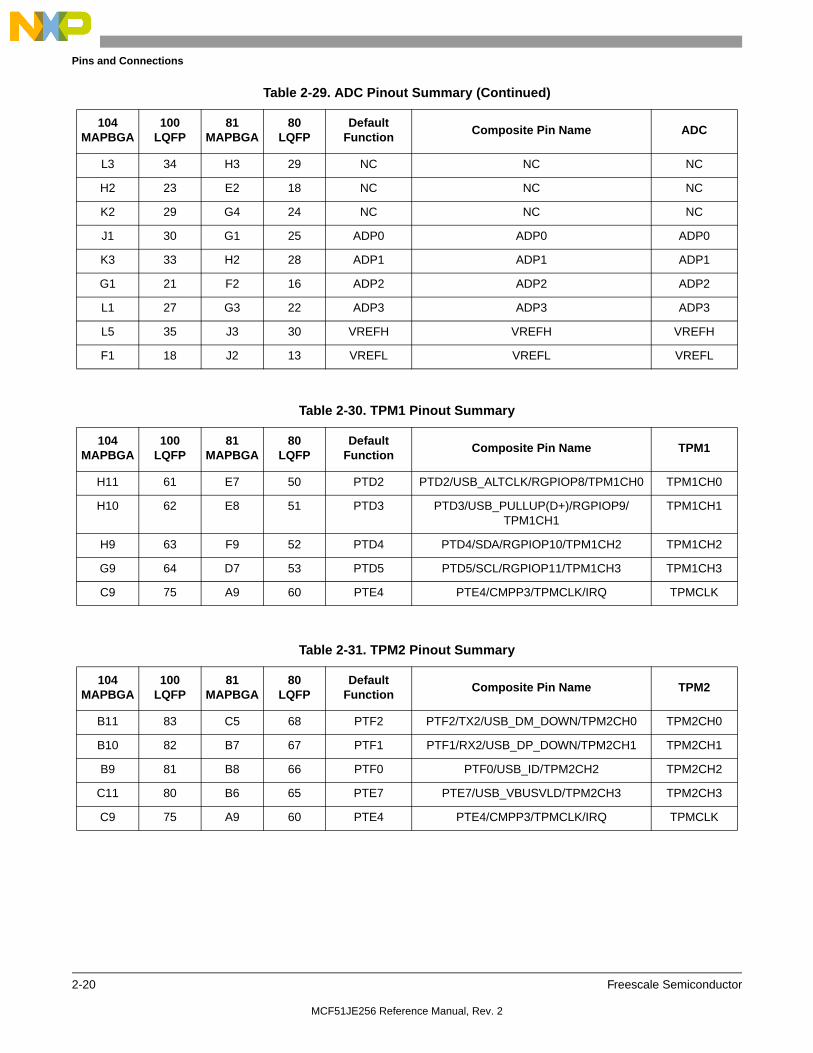
Pins and Connections
2-20 Freescale Semiconductor
L3 34 H3 29 NC NC NC
H2 23 E2 18 NC NC NC
K2 29 G4 24 NC NC NC
J1 30 G1 25 ADP0 ADP0 ADP0
K3 33 H2 28 ADP1 ADP1 ADP1
G1 21 F2 16 ADP2 ADP2 ADP2
L1 27 G3 22 ADP3 ADP3 ADP3
L5 35 J3 30 VREFH VREFH VREFH
F1 18 J2 13 VREFL VREFL VREFL
Table 2-30. TPM1 Pinout Summary
104MAPBGA
100LQFP
81MAPBGA
80LQFP
Default Function
Composite Pin Name TPM1
H11 61 E7 50 PTD2 PTD2/USB_ALTCLK/RGPIOP8/TPM1CH0 TPM1CH0
H10 62 E8 51 PTD3 PTD3/USB_PULLUP(D+)/RGPIOP9/TPM1CH1
TPM1CH1
H9 63 F9 52 PTD4 PTD4/SDA/RGPIOP10/TPM1CH2 TPM1CH2
G9 64 D7 53 PTD5 PTD5/SCL/RGPIOP11/TPM1CH3 TPM1CH3
C9 75 A9 60 PTE4 PTE4/CMPP3/TPMCLK/IRQ TPMCLK
Table 2-31. TPM2 Pinout Summary
104MAPBGA
100LQFP
81MAPBGA
80LQFP
Default Function
Composite Pin Name TPM2
B11 83 C5 68 PTF2 PTF2/TX2/USB_DM_DOWN/TPM2CH0 TPM2CH0
B10 82 B7 67 PTF1 PTF1/RX2/USB_DP_DOWN/TPM2CH1 TPM2CH1
B9 81 B8 66 PTF0 PTF0/USB_ID/TPM2CH2 TPM2CH2
C11 80 B6 65 PTE7 PTE7/USB_VBUSVLD/TPM2CH3 TPM2CH3
C9 75 A9 60 PTE4 PTE4/CMPP3/TPMCLK/IRQ TPMCLK
Table 2-29. ADC Pinout Summary (Continued)
104MAPBGA
100LQFP
81MAPBGA
80LQFP
Default Function
Composite Pin Name ADC
MCF51JE256 Reference Manual, Rev. 2

Pins and Connections
Freescale Semiconductor 2-21
2.6.2 Recommended System Connections
SYSTEMPOWER
VSS1
CBY0.1 F
CBLK10 F
+3.3 V +
VSS3
BKGD/MS
RESETOPTIONALMANUALRESET
PORTA
VDD
C2C1 X1
RF1 RS1
PORTB
PORTC
D
PORTE
VDDA/VREFH
VSSA/VREFL
CBYAD0.1 F
PORT
OPTIONALEMC
PROTECTION
VDD
4.7 kW–
0.1 F
XTAL1
EXTAL1
(NOTE 3)
(NOTE 1)
VDD1
C3C4 X2
RF2
RS2
Optional
XTAL2
EXTAL2
OSCILLATOR32KHz or 1-16MHz
LCDGlass
optoisolator
optoisolator
RX1
TX1
PORTF
PORTG
PORTH
PORTJ
SPI1
BACKGROUND
USB_DMUSB_DP
VUSB33
VDD2VDD3
VSS2
MFBExt. FlashExpansion
USB mini AB
21
345
ID
VBUS
When using the XOSCVLP module in low range and low power mode, the external components RF, RS, C1 and C2 are not required.
NOTE:
PTA1/KBI1P0/TX1/FB_D1PTA2/KBI1P1/RX1/ADP4PTA3/KBI1P2/FB_D6/ADP5PTA4PTA5PTA6PTA7
PTB0PTB1/BLMSPTB2/EXTAL1PTB3/XTAL1PTB4/EXTAL2PTB5/XTAL2PTB6/KBI1P3/RGPIOP0/FB_AD17PTB7/KBI1P4/RGPIOP1/FB_AD0
PTC0/MOSI2/FB_OE/FB_CS0PTC1/MISO2/FB_D0/FB_AD1PTC2/KBI1P5/SPSCK2/ADP6PTC3/KBI1P6/SS2/ADP7PTC4/KBI1P7/CMPP0/ADP8PTC5/KBI2P0/CMPP1/ADP9PTC6/KBI2P1/PRACMPO/ADP10
PTD0/BKGD/MS
PTD1/CMPP2/RESETPTD2/USB_ALTCLK/RGPIOP8/TPM1CH0PTD3/USB_PULLUP(D+)/RGPIOP9/TPM1CH1PTD4/SDA/RGPIOP10/TPM1CH2PTD5/SCL/RGPIOP11/TPM1CH3PTD6/USB_ALTCLK/TX1PTD7/USB_PULLUP(D+)/RX1
PTE0/KBI2P3/FB_ALE/FB_CS1PTE1/KBI2P4/RGPIOP13/FB_AD6PTE2/KBI2P5/RGPIOP14/FB_AD7PTE3/KBI2P6/FB_AD8PTE4/CMPP3/TPMCLK/IRQPTE5/FB_D7/USB_SESSVLD/TX2PTE6/FB_RW/USB_SESSEND/RX2PTE7/USB_VBUSVLD/TPM2CH3
PTC7/KBI2P2/CLKOUT/ADP11
PTF0/USB_ID/TPM2CH2PTF1/RX2/USB_DP_DOWN/TPM2CH1PTF2/TX2/USB_DM_DOWN/TPM2CH0PTF3/SCL/FB_D5/FB_AD11PTF4/SDA/FB_D4/FB_AD10PTF5/KBI2P7/FB_D3/FB_AD9PTF6/MOSI1PTF7/MISO1
PTA0/FB_D2/SS1
PTG0/SPSCK1PTG1/USB_SESSENDPTG2/USB_DM_DOWNPTG3/USB_DP_DOWNPTG4/USB_SESSVLDPTG5/FB_RWPTG6/FB_AD19PTG7/FB_AD18
PTH0/FB_OEPTH1/FB_D0
PTH2/RGPIOP2/FB_D7PTH3/RGPIOP3/FB_D6PTH4/RGPIOP4/FB_D5PTH5/RGPIOP5/FB_D4PTH6/RGPIOP6/FB_D3PTH7/RGPIOP7/FB_D2
PTJ0/FB_AD2PTJ1/FB_AD3PTJ2/FB_AD4
PTJ3/RGPIOP12/FB_AD5PTJ4/RGPIOP15/FB_AD16
PTJ5/FB_AD15PTJ6/FB_AD14PTJ7/FB_AD13
10 kW
0.1 F
0.1 F MCF51JE256VREFO
32KHz TOD OSCILLATOR
MCF51JE256 Reference Manual, Rev. 2

Pins and Connections
2-22 Freescale Semiconductor
Figure 2-5. Recommended System Connections
2.6.3 Interfacing the SCIs to Off-Chip Opto-Isolators
SCI1 is designed with twice the normal I/O drive capability on the TX1 pin. The RX pin can either be fed directly from the digital I/O buffer, or those signals can be pre-conditioned using the comparators as shown in Figure 2-6 Similarly, the TX output can be modulated with the output of one of the timers before being passed off chip.
Figure 2-6. On-Chip Signal Conditioning Associated with SCI RX and TX Pins
Controls for the circuitry shown in Figure 2-6 are discussed in Section 5.7.13, “SIM Internal Peripheral Select Register (SIMIPS).”
2.6.4 Power
VDD1,2,3 and VSS1,2,3 are the primary power supply pins for the microcontroller. This voltage source supplies power to all I/O buffer circuitry and to an internal voltage regulator. The internal voltage regulator provides regulated lower-voltage source to the CPU and other internal circuitry of the microcontroller.
opto
isolator
opto
isolator
RX1
TX1
digitalbuffer
analogcomparator
+
RX
TX
SCI1/2
Internal or external reference-
SIMIPS[RX1IN]
0
1
TPM Ch0 Output
SIMIPS[MODTX1]
SIMIPS[MTBASE1]
On-Chip Components Off-Chip Opto-Isolators
TPM Ch1 Output
MCF51JE256 Reference Manual, Rev. 2

Pins and Connections
Freescale Semiconductor 2-23
Typically, application systems have two separate capacitors across the power pins. In this case, there should be a bulk electrolytic capacitor, such as a 10 F tantalum capacitor, to provide bulk charge storage for the overall system and a 0.1 F ceramic bypass capacitor located as close to the microcontroller power pins as practical to suppress high-frequency noise. The MCF51JE256 has three VDD pins. Each pin must have a bypass capacitor for best noise suppression.
VDDA and VSSA are the analog power supply pins for the microcontroller. This voltage source supplies power to the ADC module. A 0.1 F ceramic bypass capacitor should be located as close to the microcontroller power pins as practical to suppress high-frequency noise.
VUSB33 maintains an output voltage of 3.3 V and sources enough current for the internal USB transceiver and USB pullup resistor. The VBUS input is used to supply the voltage necessary to power the internal USB 3.3V regulator. VUSB33 can also supply the internal USB when there is no VBUS supply and the internal USB regulator is disabled.
For VUSB33, two separate capacitors (4.7 F bulk electrolytic stability capacitor and 0.47 F ceramic bypass capacitors) must be connected across this pin to ground to decrease the output ripple of this voltage regulator when it is enabled.
2.6.5 Oscillator
Immediately after reset, the microcontroller uses an internally generated clock provided by the multipurpose clock generation (MCG) module.
The oscillator (XOSC1 or XOSC2) in this microcontroller is a Pierce oscillator that can accommodate a crystal or ceramic resonator. Optionally, an external clock source can be connected to the EXTAL input pin.
When using the oscillator module in low range and low power mode, the external components RF, RS, C1 and C2 are not required.
For using the oscillator module in other modes, refer to Figure 2-5 for the following discussion. RS (when used) and RF should be low-inductance resistors such as carbon composition resistors. Wire-wound resistors, and some metal film resistors, have too much inductance. C1 and C2 normally should be high-quality ceramic capacitors that are specifically designed for high-frequency applications.
RF is used to provide a bias path to keep the EXTAL input in its linear range during crystal startup; its value is not generally critical. Typical systems use 1 M to 10 M. Higher values are sensitive to humidity and lower values reduce gain and (in extreme cases) could prevent startup.
C1 and C2 are typically in the 5 pF to 25 pF range and are chosen to match the requirements of a specific crystal or resonator. Be sure to take into account printed circuit board (PCB) capacitance and microcontroller pin capacitance when selecting C1 and C2. The crystal manufacturer typically specifies a load capacitance that is the series combination of C1 and C2 (which are usually the same size). As a first-order approximation, use 10 pF as an estimate of combined pin and PCB capacitance for each oscillator pin (EXTAL and XTAL).
MCF51JE256 Reference Manual, Rev. 2

Pins and Connections
2-24 Freescale Semiconductor
2.6.6 PTD1/CMPP2/RESET
After a power-on reset (POR) the PTD1/CMPP2/RESET pin defaults to RESET. Clearing RSTPE in SOPT1 allows the pin to be a GPIO pin or as an input to the PRACMP. When configured as a GPIO, the pin will remain as a GPIO until the next POR or LVD reset. When enabled, the RESET pin can be used to reset the MCU from an external source when the pin is driven low. Internal power-on reset and low-voltage reset circuitry typically make external reset circuitry unnecessary. This pin is normally connected to the standard 6-pin background debug connector so a development system can directly reset the MCU system. A manual external reset can be added by supplying a simple switch to ground (pull reset pin low to force a reset).
Whenever any non-POR reset is initiated (whether from an external signal or from an internal system), the enabled RESET pin is driven low for about 66 bus cycles. The reset circuitry decodes the cause of reset and records it by setting a corresponding bit in the system reset status register (SRS).
In EMC-sensitive applications, an external RC filter is recommended on the reset pin. See Figure 2-5 for an example.
2.6.7 PTE4/CMPP3/TPMCLK/IRQ
The IRQ pin is the input source for the IRQ interrupt. If the IRQ function is not enabled, this pin can be used for other functions. In EMC-sensitive applications, an external RC filter is recommended on the IRQ pin. See Figure 2-5. for an example.
NOTE
The voltage on the internally pulled up IRQ pin when measured is below VDD. The internal gates connected to this pin are pulled to VDD. If the IRQ pin is required to drive to a VDD level, an external pullup must be used.
2.6.8 Background / Mode Select (PTD0/BKGD/MS)
During a power-on-reset (POR) or background debug force reset (see bit BDFR in Section 27.3.3, “Configuration/Status Register 2 (CSR2),” for more information), the BKGD/MS pin functions as a mode select pin. Immediately after any reset, the pin functions as the background pin and can be used for background debug communication.
If the BKGD/MS pin is unconnected, the microcontroller enters normal operating mode at the rising edge of the internal reset after a POR or forced BDC reset. If a debug system is connected to the 6-pin standard background debug header, it can hold BKGD/MS low during a POR or immediately after issuing a background debug force reset1, which forces the microcontroller to halt mode.
The BKGD/MS pin is used primarily for background debug controller (BDC) communications using a custom protocol that uses 16 clock cycles of the target microcontroller’s BDC clock per bit time. The target microcontroller’s BDC clock could be as fast as the bus clock rate, so there should never be any significant capacitance connected to the BKGD/MS pin that could interfere with background serial communications.
1. Specifically, BKGD must be held low through the first 16 cycles after deassertion of the internal reset.
MCF51JE256 Reference Manual, Rev. 2

Pins and Connections
Freescale Semiconductor 2-25
Although the BKGD/MS pin is a pseudo open-drain pin, the background debug communication protocol provides brief, actively driven, high speed-up pulses to ensure fast rise times. Small capacitances from cables and the absolute value of the internal pullup device play almost no role in determining rise and fall times on the BKGD/MS pin.
2.6.9 ADC Reference Pins (VREFH, VREFL)
The VREFH and VREFL pins are the voltage reference high and voltage reference low inputs, respectively, for the ADC module.
2.6.10 Bootloader Mode Select (BLMS)
During a power-on-reset (POR), the CPU detects the state of the PTB1/BLMS pin that functions as a mode select pin. When the BLMS pin is held low and BKGD/MS is not pulled low, the CPU enters the bootloader mode. During a power-on-reset (POR), an internal pullup device is automatically enabled in PTB1/BLMS pin. Immediately after reset rises the pin functions as a general-purpose output only pin and an internal pullup device is automatically disabled.
2.6.11 USB Data Pins (USB_DP, USB_DN)
The USB_DP (D+) and USB_DN (D–) pins are the analog input/output lines to/from full-speed internal USB transceiver. An optional internal pullup resistor for the USB_DP pin, RPUDP, is available. See Chapter 25, “USB On-the-GO (USBOTG)” for more details.
2.6.12 General-Purpose I/O and Peripheral Ports
The MCF51JE256 series microcontrollers support up to 69 general-purpose I/O pins, which are shared with on-chip peripheral functions (timers, serial I/O, ADC, ACMP, etc.).
When a port pin is configured as a general-purpose output or a peripheral uses the port pin as an output, software can select one of two drive strengths and enable or disable slew rate control. When a port pin is configured as a general-purpose input or a peripheral uses the port pin as an input, software can enable a pull-up device. Immediately after reset, all of these pins are configured as high-impedance general-purpose inputs with internal pull-up devices enabled.
When an on-chip peripheral system is controlling a pin, data direction control bits determine what is read from the port data registers, even though the peripheral controls the pin direction via the pin’s output buffer enable. For information about controlling these pins as general-purpose I/O pins, see Chapter 6, “Parallel Input/Output Control.”
NOTETo avoid extra current drain from floating input pins, the reset initialization routine in the application program should enable on-chip pullup devices or change the direction of unused or non-bonded pins to outputs so they do not float.
MCF51JE256 Reference Manual, Rev. 2

Pins and Connections
2-26 Freescale Semiconductor
MCF51JE256 Reference Manual, Rev. 2

Freescale Semiconductor 3-1
Chapter 3 Modes of Operation
3.1 IntroductionThe operating modes of the MCF51JE256 series MCUs are described in this chapter. Entry into each mode, exit from each mode, and functionality while in each of the modes are described.
The overall system mode is generally a function of a number of separate, but interrelated, variables: debug mode, security mode, power mode and clock mode. Clock modes were discussed in Section 17.4.1, “MCG Modes of Operation.” This chapter covers the other dimensions of the system operating mode.
3.2 Features• Debug mode for code development. For devices based on the V1 ColdFire core, such as those in
the MCF51JE256 series, debug mode and secure mode are mutually exclusive.
• Secure mode — BDC access to CPU resources is extremely restricted. It is possible to tell that the device has been secured, and to clear security, which involves mass erasing the on-chip flash memory. No other CPU access is allowed. Secure mode can be used in conjunction with each of the power modes below.
• Bootloader mode — Enables USB communications to external host for programming and erasing the FLASH as an alternate to using the BDC.
• Run mode — CPU clocks can be run at full speed, and the internal supply is fully regulated.
• LPrun mode — CPU and peripheral clocks are restricted to 250 kHz CPU clock and 125 kHz bus clock maximum and the internal supply is in soft regulation.
• Wait mode — The CPU shuts down to conserve power; peripheral clocks are running and full regulation is maintained.
• LPwait mode — CPU shuts down to conserve power; peripheral clocks are running at reduced speed (125 kHz maximum) and the internal supply is in soft regulation.
• Stop modes—System (CPU and peripheral) clocks are stopped.
— Stop4—All internal circuits are powered (full regulation mode) and internal clock sources at max frequency for fastest recovery, LVD enabled, no clocking to peripherals ENBDM=1.
— Stop3—All internal circuits are powered and clocks sources are at minimal values (BLPI or BLPE mode), LVD disabled, providing a good compromise between power utilization and speed of recovery. ENBDM=0.
— Stop2—Partial power-down of internal circuits; RAM content is retained. The lowest power mode for this device. A reset or IRQ is required to return from Stop2 mode.
MCF51JE256 Reference Manual, Rev. 2

Modes of Operation
3-2 Freescale Semiconductor
On the MCF51JE256 series MCUs, Wait, Stop2, Stop3 and Stop4 are all entered via the CPU STOP instruction. See Table 3-1 and subsequent sections of this chapter for details.
3.3 OverviewThe ColdFire CPU has two primary user modes of operation, run and stop. (The CPU also supports a halt mode that is used strictly for debug operations.) The STOP instruction is used to invoke stop and wait modes for this family of devices.
The Systems Option Register 1 (SOPT1) contains two bits which control operation of the STOP instruction. If SOPT1[WAITE] is set when STOP is executed, the wait mode is entered. Otherwise, if SOPT1[STOPE] is set, the CPU enters one of the stop modes. It is illegal to execute a STOP instruction if neither STOPE or WAITE are set. This results in reset assertion if the Instruction-related Reset Disable bit in the CPU Control Register (CPUCR[IRD]) is cleared or an illegal instruction exception if CPUCR[IRD] is set.
The MCF51JE256 series devices augment stop, wait, and run in a number of ways. The power management controller (PMC) can run the device in fully-regulated mode, standby mode, and partial power-down mode. Standby (loose regulation) or partial power-down can be programmed to occur naturally as a result of a STOP instruction. Additionally, standby mode can be explicitly invoked via the LPR (low-power) bit in the PMC System Power Management Status & Control Register 2 (SPMSC2[LPR]). Use of standby is limited to bus frequencies less than 125 kHz; and neither standby nor partial power-down are allowed when XCSR[ENBDM] bit is set to enable debugging in stop and wait modes.
During partial power-down mode, the regulator is in standby mode and much of the digital logic on the chip is switched off. These interactions can be seen schematically in Figure 3-1. This figure is for conceptual purposes only. It does not reflect any sequence or time dependencies between the PMC and other parts of the device, nor does it represent any actual design partitioning.
Figure 3-1. Power Modes — Conceptual Drawing
It is illegal for the software to have SPMSC2[PPDC] and SPMSC2[LPR] asserted concurrently. This restriction arises because the sequence of events from normal to low-power modes involves use of both bits. After entering a low-power mode, it is not possible to switch to another low-power mode.
STOP
SOPT1[STOPE]
SOPT1[WAITE]
SPMSC1[LVDE]
SPMSC1[LVDSE]
SPMSC2[PPDC]
In Stop ModePartial Power Down
Standby Enable
XCSR[ENBDM]
SPMSC2[LPR]
LVD Off
Standby
MCF51JE256 Reference Manual, Rev. 2
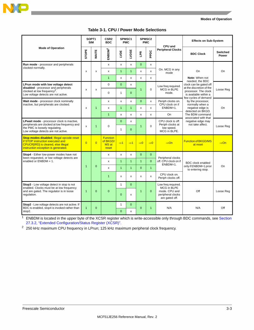
Modes of Operation
Freescale Semiconductor 3-3
Table 3-1. CPU / Power Mode Selections
Mode of Operation
SOPT1SIM
CSR2BDC
SPMSC1PMC
SPMSC2PMC
CPU andPeripheral Clocks
Effects on Sub-System
STO
PE
WA
ITE
EN
BD
M1
1 ENBDM is located in the upper byte of the XCSR register which is write-accessible only through BDC commands, see Section 27.3.2, “Extended Configuration/Status Register (XCSR)”.
LVD
E
LVD
SE
LP
R
PP
DC
BDC Clock SwitchedPower
Run mode - processor and peripherals clocked normally.
x x
x x x 0 x
On. MCG in any mode On
Note: When not needed, the BDC
clock can be gated off at the discretion of the processor. The clock is available within a
few cycles of demand by the processor, normally when a negative edge is
detected on BKGD. The BDM command associated with that negative edge may
not take affect.
Onx 1 1 x x
1 x x x x
LPrun mode with low voltage detect disabled - processor and peripherals clocked at low frequency2.Low voltage detects are not active.
2 250 kHz maximum CPU frequency in LPrun; 125 kHz maximum peripheral clock frequency.
x x
0 0 x
1 0Low freq required.
MCG in BLPE mode.
Loose Reg0 1 0
Wait mode - processor clock nominally inactive, but peripherals are clocked.
x 1
x x x 0 x Periph clocks on.CPU clock on if
ENBDM=1. Onx 1 1 x x
1 x x x x On
LPwait mode - processor clock is inactive, peripherals are clocked at low frequency and the PMC is loosely regulating.Low voltage detects are not active.
x 1 0
0 x
1 0
CPU clock is off.Periph clocks at
low speed.MCG in BLPE.
Loose Reg1 0
Stop modes disabled; Illegal opcode reset if STOP instruction executed and CPUCR[IRD] is cleared, else illegal instruction exception is generated.
0 0
Functionof BKGD/
MS atreset
1 1 0 0 On Function of BKGD/MS at reset
On
Stop4 - Either low-power modes have not been requested, or low voltage detects are enabled or ENBDM = 1.
1 0
x x x 0 0Peripheral clocks
off. CPU clock on if ENBDM=1. BDC clock enabled
only if ENBDM=1 prior to entering stop.
On
x 1 1 1 0
x 1 1 0 1
1 x x x x CPU clock on.Periph clocks off.
Stop3 - Low voltage detect in stop is not enabled. Clocks must be at low frequency and are gated. The regulator is in loose regulation.
1 0 0
1 0
1 0
Low freq required. MCG in BLPE
mode. CPU and peripheral clocks
are gated off.
Off Loose Reg0 x
Stop2 - Low voltage detects are not active. If BDC is enabled, stop4 is invoked rather than stop2.
1 01 0
0 1 N/A N/A Off0 x
MCF51JE256 Reference Manual, Rev. 2

Modes of Operation
3-4 Freescale Semiconductor
Figure 3-2. Allowable Power Mode Transitions for Mission Mode
Figure 3-2 illustrates mission mode state transitions allowed between the legal states shown in Table 3-1. RESET must be asserted low, or the TOD must issue a wakeup signal, in order to exit stop2. Only interrupt assertion is necessary to exit the other stop and wait modes.
Figure 3-3 takes the same set of states and transitions shown in Figure 3-2 and adds the BDM halt mode for development purposes. If BDM is enabled, the chip automatically shifts LP modes into their fully regulated equivalents. If software or debugger sets SPMSC2[LPR] while BDM is enabled, SPMSC2[LPRS] reflects the fact that the regulator is not in standby. Similarly, SPMSC2[PPDF] does not indicate a recovery from stop2 if XCSR[ENBDM] forced stop4 to occur in its place.1
Stated another way, if XCSR[ENBDM] has been set via the BDM interface, then the power management controller keeps (or puts) the regulator in full regulation despite other settings in the contrary. The states shown in Figure 3-3 then map as follows:
• LPrun Run
• LPwait Wait
• Stop3 Stop4
• Stop2 Stop4
From a software perspective (and disregarding PMC status bits), the system remains in the appropriate low-power state, and can be debugged as such.
See Section 3.7, “Wait Modes,” for a description of the various ways to enter halt mode.
1. This can have subtle impacts on recovery from stop. The IRQ input can wake the device from stop4 if it has been enabled for that purpose. A low on the RESETB pin wakes the device from stop2 (there is an asynchronous path to the power management controller in that state).
Mode Regulator State
Run Full On
Wait Full On
Stop4 Full On
LPrun Standby
LPwait Standby
Stop3 Standby
Stop2 Partial Power Off
Stop3
Stop2
LPwait
Stop4
Wait
Run LPrun
MCF51JE256 Reference Manual, Rev. 2

Modes of Operation
Freescale Semiconductor 3-5
Figure 3-3. All Allowable Power Mode Transitions for
Table 3-2 defines triggers for the various state transitions shown in Figure 3-2.
Table 3-2. Triggers for State Transition
Transition # From To Trigger
1
Run LPrunConfigure settings shown in Table 3-1, switch LPR=1 last
LPrun Run
Clear SPMSC2[LPR]
Interrupt when SPMSC2[LPWUI]=1
Negative transition on enabled BKGD/MS pin.
2
Run Stop2Pre-configure settings shown in Table 3-1, execute STOP instruction
Stop2 RunAssert zero on IRQ,RESET1 or TOD timeout. Reload environment from RAM.
3LPrun LPwait
LPwait LPrun Interrupt when SPMSC2[LPWUI]=0
4LPrun Stop3 Execute STOP instruction
Stop3 LPrun Interrupt when SPMSC2[LPWUI]=0
5LPwait Run Interrupt when SPMSC2[LPWUI]=1
Run LPwait Not supported.
6Run Wait
Wait Run Interrupt
7Run Stop4
Stop4 Run Interrupt
8Stop3 Run Interrupt when SPMSC2[LPWUI]=1
Run Stop3
Stop3
1
Stop2
LPwait
Stop4
Wait
Run LPrun
48
7
6 2
5 3
Halt
9
11
10
MCF51JE256 Reference Manual, Rev. 2

Modes of Operation
3-6 Freescale Semiconductor
Individual power states are discussed in more detail in the following sections.
3.4 Secure ModeWhile the MCU is in secure mode, there are severe restrictions on which debug commands can be used. In this mode, only the upper byte of the core’s XCSR, CSR2, and CSR3 registers can be accessed. See Chapter 27, “Version 1 ColdFire Debug (CF1_DEBUG),” for details.
3.5 Bootloader ModeUpon exiting reset, the CPU fetches the SR and PC from locations 0x0 and 0x4 out of the bootloader ROM and executes code starting at the newly set value of the PC. While executing out of the bootloader several qualification factors are examined to determine whether to continue executing bootloader code or begin executing user code. The bootloader ROM can be accessed in bootloader mode or user mode. This section describes the valid operations and protection mechanism in bootloader and user modes.
The following four items will be examined after each reset of the MCU.
• BLMS pin
• SIGNATURE semaphore byte
• Flash block CRC checksum
• CRC BYPASS byte
3.5.1 Entering Bootloader Mode
Bootloader mode can be entered in the following four conditions:
9Stop4 Halt
When a BACKGROUND command is received through the BKGD/MS pin (XCSR[ENBDM] must equal one).
Halt Stop4 Not supported.
10
Halt Run GO instruction issued via BDM
Run Halt
When a BACKGROUND command is received through the BKGD/MS pin ORWhen a HALT instruction is executed ORWhen encountering a BDM breakpoint
11Wait Halt
When a BACKGROUND command is received through the BKGD/MS pin (XCSR[ENBDM] must equal one).
Halt Wait Not supported.
1 An analog connection from this pin to the on-chip regulator wakes up the regulator, which then initiates a power-on-reset sequence.
Table 3-2. Triggers for State Transition
Transition # From To Trigger
MCF51JE256 Reference Manual, Rev. 2

Modes of Operation
Freescale Semiconductor 3-7
• When BLMS pin is low and BKGD/MS is not pulled low during power-on-reset (POR), the bootloader mode is entered directly with no other qualifications.
• When BLMS pin and BKGD/MS are high during power-on-reset (POR), a CHECKSUM BYPASS flash location is examined. If it is not equal to 0x00 or 0xFF, then the bootloader mode is entered.
• When BLMS pin and BKGD/MS are high during power-on-reset (POR), a CHECKSUM BYPASS flash location is examined. If it is equal to 0xFF, a flash CRC is calculated for the flash array and compared with a FLASHCRC 16-bit word. If the result does not match, then the bootloader mode is entered.
• After a reset (other than a power-on reset), the SIGNATURE semaphore byte is examined. If it is equal to 0xC3, then the bootloader mode is entered.
3.5.2 Entering User mode
User mode can be entered in the following three conditions:
• When BLMS pin and BKGD/MS are high during power-on-reset (POR), and the CHECKSUM BYPASS byte is equal to 0x00, the user mode is entered.
• When BLMS pin and BKGD/MS are high during power-on-reset (POR), and the CHECKSUM BYPASS byte is equal to 0xFF, a flash CRC is calculated for the flash array and compared with a FLASHCRC 16-bit word. If the result matches, the user mode is entered.
• When a reset occurs (other than a power-on reset), if the SIGNATURE semaphore is not equal to 0xC3, the user mode is entered.
3.5.3 Active Background Mode and Bootloader Mode Arbitrage
During POR, if both BKGD/MS and BLMS pins are low, active background mode is entered.
3.5.4 Bootloader Operation
This section describes the bootloader mechanism and bootloader flow chart.
The bootloader software is located in bootloader ROM. You can perform flash erasing and programming when:
• Bootloader mode is entered.
• Flash block checksum that has been calculated and flash block checksum do not match after power-on reset.
• SIGNATURE value in register matches.
3.5.4.1 Flash Block Checksum
Upon power-on reset (POR), if BLMSS = 0 and the value of checksum bypass is 0xFF, the bootloader calculates the flash checksum. The checksum is calculated for the Flash locations:
(0x0000_0000:0x0000_F7FF)
(0x0001_0800:0x0002_F7FF)
MCF51JE256 Reference Manual, Rev. 2

Modes of Operation
3-8 Freescale Semiconductor
(0x0003_0800: 0x0003_FFFF)
The calculated checksum are verified with a checksum written to the two bytes of the flash (FLASHCRC). If the checksum matches, the previous bootloader operation was successful and the MCU jumps to the user code entry and starts to execute user code. If the checksum does not match, it jumps to bootloader entry to wait for commands.
Flash block checksum calculation uses 16-bit CRC.
3.5.4.2 SIGNATURE Semaphore Register
After a reset (other than a power-on reset), the bootloader verifies SIGNATURE semaphore register. If SIGNATURE = 0xC3, the MCU jumps to bootloader entry to wait for commands. If not, it jumps to the user code entry and starts to execute user code.
Users are required to provide a mechanism in their application code to set the SIGNATURE to 0xC3 and initiate a reset if they want to re-enter bootloader mode after a successful user code has been programmed. Alternatively, BKGD mode can be entered and SIGNATURE can be updated using BDM commands and reset initiated with BKGD pin high.
3.5.4.3 Flash Partial Erase Semaphore
The value of flash partial erase is programmed by the user. Only when flash partial erase is programmed to 0x00, can the partial erase flash array command be supported by bootloader.
The value of this byte is 0xFF when the device is shipped from Freescale.
MCF51JE256 Reference Manual, Rev. 2

Modes of Operation
Freescale Semiconductor 3-9
3.5.4.4 Boot Mode Entry Flow Chart
Figure 3-4. Bootloader Flow Chart
Start
YES
YES
Power-on reset?
Jump to bootrom
BLMSS=1?
YES
YES
Bootloader Mode entered
NO
Regular reset
SIGNATURE=0xC3?
NOFlash checksum
match?
NO
NO
Jump to user code entry,User code executed.
YES
Jump to bootloader entry
CMD=Mass erase?
NO
NO
Initial bus frequency to 24 MHz,
Initial USB
Waiting for CMD
CMD=Program Flash?
CMD=Reset?
Put Pass/Fail on stack
YESPut Pass/Fail on stack
YES
NO
Change SIGNATURE=0xC3Change SIGNATURE=0xC3
Clear SIGNATURE
Checksum bypass=0xFF?
YES
NO
Calculate Flash block checksum
Checksum bypass=0x00?
NO
Jump to user code entry,User code executed.
YES
CMD=Partial erase?
NO
YESPut Pass/Fail on stack
Note: Only when FLASH PARTIAL ERASE=0x00, this command is valid.
Configure the pri-mary flash array
Note: The flash array select bit in the SOPT3 register must beconfigured as determined by the Non-Volatile Flash Array Select Register
Change SIGNATURE=0xC3
MCF51JE256 Reference Manual, Rev. 2

Modes of Operation
3-10 Freescale Semiconductor
3.6 Run Modes
3.6.1 Run Mode
Run mode is the normal operating mode for the MCF51JE256 series MCUs. This mode is selected after any internal reset including LVD and when both the BKGD/MS and BLMS pins are high after a POR exit or a BDC forced reset. Upon exiting reset, the CPU fetches the SR and PC from locations 0x0 and 0x4 out of the bootloader ROM and executes code starting at the newly set value of the PC.
NOTECPU during reset will access the bootloader ROM at 0x0 and 0x4 but non-reset CPU, multi-master or bdm accesses will read user Flash.
3.6.2 Low-Power Run Mode (LPrun)
In the low-power run mode, the on-chip voltage regulator is put into its standby (or loose regulation) state. In this state, the power consumption is reduced to a minimum that allows CPU functionality. Power consumption is reduced the most by disabling the clocks to all unused peripherals by clearing the corresponding bits in the SCGC1 and SCGC2 registers1.
Before entering this mode, the following conditions must be met:
• FBE2 is the selected clock mode for the MCG. For more information, see Table 38-26.
• MCGC2[HGO] is cleared.
• The bus frequency is less than 125 kHz.
• The ADC must be in low-power mode (ADLPC=1) or disabled.
• Low-voltage detect must be disabled. The LVDE and/or LVDSE bit in SPMSC1 register must be cleared.
• Flash programming/erasing is not allowed
After these conditions are met, low-power run mode can be entered by setting SPMSC2[LPR].
To re-enter standard run mode, clear the LPR bit. SPMSC2[LPRS] is a read-only status bit that can be used to determine if the regulator is in full-regulation mode or not. When LPRS is cleared, the regulator is in full-regulation mode and the MCU can run at full speed in any clock mode.
Assuming that SOPT1[BKGDPE] is set to enable BKGD/MS, the device also switches from LPrun to run mode when it detects a negative transition on the BKGD/MS pin.
Low-power run mode also provides the option to return to full regulation if any interrupt occurs. This is done by setting SPMSC2[LPWUI]. The MCG can then be set for full speed immediately in the interrupt service routine.
3.6.2.1 BDM in Low-Power Run Mode
Low-power run mode cannot be entered when the MCU is in active background debug mode.
1. System clock gating control registers 1 and 22. FLL bypassed external low-power
MCF51JE256 Reference Manual, Rev. 2

Modes of Operation
Freescale Semiconductor 3-11
If a device is in low-power run mode, a falling edge on an active BKGD/MS pin exits low-power run mode, clears the LPR and LPRS bits, and returns the device to normal run mode.
3.7 Wait Modes
3.7.1 Wait Mode
Wait mode is entered by executing a STOP instruction after configuring the device as per Table 3-1. If the WAITE control bit is set when STOP is executed, the Wait mode is entered. Upon execution of the STOP instruction, the CPU enters a low-power state in which it is not clocked.
The V1 ColdFire core does not differentiate between Stop and Wait modes. The difference between the two is at the device level. In Stop mode, most peripheral clocks are shut down; in Wait mode, they continue to run.
The ENBDM bit in the XCSR register must be set prior to entering Wait mode if the device is required to respond to BDM instructions after in Wait mode.
The low voltage detector, if enabled, can be configured to interrupt the CPU and exit Wait mode into Run mode.
When an interrupt request occurs, the CPU exits Wait mode and resumes processing, beginning with the stacking operations leading to the interrupt service routine.
3.7.2 Low-Power Wait Mode (LPwait)
Low-power wait mode is entered by executing a STOP instruction while the MCU is in low-power run mode and configured per Table 3-1. In the low-power wait mode, the on-chip voltage regulator remains in its standby state as in the low-power run mode. In this state, the power consumption is reduced to a minimum that allows most modules to maintain funtionality. Power consumption is reduced the most by disabling the clocks to all unused peripherals by clearing the corresponding bits in the SCGC registers.
Low-power run mode restrictions also apply to low-power wait mode.
If the LPWUI bit is set when the STOP instruction is executed, the voltage regulator returns to full regulation when wait mode is exited. The MCG can be set for full speed immediately in the interrupt service routine.
If the LPWUI bit is cleared when the STOP instruction is executed, the device returns to low-power run mode.
Any reset exits low-power wait mode, clears the LPR bit, and returns the device to normal run mode.
3.7.2.1 BDM in Low-Power Wait Mode
If a device is in low-power wait mode, a falling edge on an active BKGD/MS pin exits low-power wait mode, clears the LPR and LPRS bits, and returns the device to normal run mode.
MCF51JE256 Reference Manual, Rev. 2

Modes of Operation
3-12 Freescale Semiconductor
3.8 Stop ModesOne of three Stop modes are entered upon execution of a STOP instruction when SOPT1[STOPE] is set. SOPT1[WAITE] must be clear. In Stop3 mode, the bus and CPU clocks are halted. If the ENBDM bit is set prior to entering Stop4, only the peripheral clocks are halted. The MCG module can be configured to leave the reference clocks running. See Chapter 17, “Multipurpose Clock Generator (S08MCGV3)” for more information.
NOTE
If neither the WAITE nor STOPE bit is set when the CPU executes a STOP instruction, the MCU does not enter either of the stop modes. Instead, it initiates an illegal opcode reset (if CPUCR[IRD]=0) or generates an illegal instruction exception.
The Stop modes are selected by setting the appropriate bits in the SPMSC2 register. Table 3-1 shows all of the control bits that affect mode selection under various conditions. The selected mode is entered following the execution of a STOP instruction.
Entry into the active background mode from run mode is enabled if ENBDM in XCSR is set. Chapter 27, “Version 1 ColdFire Debug (CF1_DEBUG)” explains this register. If ENBDM is set when the CPU executes a STOP instruction, the system clocks to the background debug logic remain active, and the peripheral clocks get gated, when the MCU enters stop mode. Because of this behavior, background debug communication remains possible.
Most background commands are not available in Stop mode. The memory-access-with-status commands do not allow memory access, but they report an error indicating that the MCU is in Stop or Wait mode. The BACKGROUND command can be used to wake the MCU from Stop mode and enter Active Background debug mode if the ENBDM bit is set prior to entering Stop mode. After entering background debug mode, all background commands are available.
In addition, the MCG and XOSC continue operation in the clock configurations set prior to stop entry. Also, the voltage regulator does not enter its low-power standby state, but maintains full internal regulation.
Figure 3-5. Stop Modes
stop
LVDELVDSE
ENBDM
STOPE
WAITE
PPDC
STOP2
STOP3
STOP4
stop
LVDELVDSE
ENBDM
LVDELVDSE
ENBDM
STOPE
WAITE
PPDC
STOP2
STOP3
STOP4
MCF51JE256 Reference Manual, Rev. 2

Modes of Operation
Freescale Semiconductor 3-13
3.8.1 Stop2 Mode
Stop2 mode is entered by executing a STOP instruction under the conditions as shown in Table 3-1. Most of the internal circuitry of the MCU is powered off in Stop2 mode, with the exception of the RAM. Upon entering Stop2 mode, all I/O pin control signals are latched so that the pins retain their states during Stop2 mode. Exiting from Stop2 mode is performed by asserting either wake-up pin: RESET or IRQ.
NOTE
IRQ always functions as an active-low wakeup input when the MCU is in Stop2 mode, regardless of how the pin is configured before entering Stop2 mode. The pullup on this pin is always disabled in Stop2 mode. This pin must be driven or pulled high externally while in Stop2 mode.
In addition, the TOD interrupt can wake the MCU from Stop2 mode, if enabled and using the low power oscillator (LPO). If the TOD is using the external clock source (EREFSTEN = 1) or internal clock source (IREFSTEN = 1), then the TOD is disabled in Stop2 mode.
Upon wake-up from Stop2 mode, the MCU starts up as from a power-on reset (POR):
• All module control and status registers are reset.
• The LVD reset function is enabled, and the MCU remains in the reset state if VDD is below the LVD trip point (low trip point selected due to POR).
• The CPU takes the reset vector.
In addition to the above, upon waking up from Stop2 mode, SPMSC2[PPDF] is set. This flag is used to direct user code to go to a Stop2 recovery routine. PPDF remains set, and the I/O pin states remain latched until a 1 is written to SPMSC2[PPDACK]. To maintain I/O states for pins that were configured as general-purpose I/O before entering Stop2 mode, software must restore the contents of the I/O port registers, which have been saved in RAM, to the port registers before writing to SPMSC2[PPDACK]. If the port registers are not restored from RAM before writing to SPMSC2[PPDACK], then the pins switch to their reset states when SPMSC2[PPDACK] is written.
For pins that were configured as peripheral I/O, software must reconfigure the peripheral module that interfaces to the pin before writing to SPMSC2[PPDACK]. If the peripheral module is not enabled before writing to SPMSC2[PPDACK], the pins are controlled by their associated port control registers when the I/O latches are opened.
3.8.2 Stop3 Mode
Stop3 mode is entered by executing a STOP instruction under the conditions as shown in Table 3-1 (SPMSC2[PPDC] = 0 and SPMSC1[LVDSE] = 0). The states of all of the internal registers and logic, RAM contents, and I/O pin states are maintained. Stop3 mode can be exited by asserting RESET, or by an interrupt from one of the following sources: the USB resume interrupt, ADC, IRQ, KBI, or the ACMP. If Stop3 mode is exited by means of the RESET pin, then the MCU is reset and operation resumes after taking the reset vector. Exit by means of one of the internal interrupt sources results in the MCU taking the appropriate interrupt vector.
MCF51JE256 Reference Manual, Rev. 2

Modes of Operation
3-14 Freescale Semiconductor
3.8.3 Stop4 Mode
Stop4 mode is entered by executing a STOP instruction under the conditions shown in Table 3-1 (SPMSC1[LVDSE]=1). The states of all of the internal registers and logic, RAM contents, and I/O pin states are maintained. The MCG is configured to be running with the PLL or FLL engaged. Stop4 can be exited by asserting RESET, or by an interrupt from one of the following sources: the Time of Day (TOD) interrupt, the USB resume interrupt, LVD, ADC, IRQ, KBI, or the ACMP. If stop4 is exited by means of the RESET pin, the MCU is reset and operation resumes after taking the reset vector. Exit by means of one of the internal interrupt sources results in the MCU taking the appropriate interrupt vector.
3.8.3.1 LVD Enabled in Stop Mode
The LVD is capable of generating an interrupt or a reset when the supply voltage drops below the LVD voltage. If the LVD is enabled in stop (SPMSC1[LVDE] && SPMSC1[LVDSE] = 1) at the time the CPU executes a STOP instruction, then the voltage regulator remains active during Stop mode. If the user attempts to enter Stop2 mode with the LVD enabled for Stop mode, the MCU enters Stop4 mode instead. For the ADC to operate, the LVD must be left enabled when entering Stop4 mode. For the ACMP to operate when PRACMPC1[PRGINS] is set, the VREF must be left enabled when entering Stop4. For the OSC to operate with an external reference when MCGC2[RANGE] is set, the LVD must be left enabled when entering Stop4 mode.
3.9 On-Chip peripheral Modules in Stop and Low-power ModesWhen the MCU enters any stop mode (wait not included), system clocks to the internal peripheral modules are stopped. Even in the exception case (ENBDM = 1), where clocks to the background debug logic continue to operate, clocks to the peripheral systems are halted to reduce power consumption. Refer to Section 3.8.1, “Stop2 Mode,” and Section 3.8.2, “Stop3 Mode,” for specific information on system behavior in stop modes.
When the MCU enters LPwait or LPrun modes, system clocks to the internal peripheral modules continue based on the settings of the clock gating control registers (SCGC1 and SCGC2).
Table 3-3 defines terms used in Table 3-4 to describe operation of components on the chip in the various low-power modes.
Table 3-3. Abbreviations used in Table 3-4
Voltage Regulator Clocked1
1 Subject to module enables and settings of System Clock Gating Control Registers 1 and 2 (SCGC1 and SCGC2).
Not Clocked
Full Regulation FullOn FullNoClkFullADACK2
Soft Regulation SoftOn3 SoftNoClkDisabled
SoftADACK4
Off N/A Off
MCF51JE256 Reference Manual, Rev. 2

Modes of Operation
Freescale Semiconductor 3-15
2 This ADC-specific mode defines the case where the device is fully regulated and the normal peripheral clock is stopped. In this case, the ADC can run using its internally generated asynchronous ADACK clock.
3 Analog modules must be in their low-power mode when the device is operated in this state.4 This ADC-specific mode defines the case where the device is in soft regulation and the normal peripheral
clock is stopped. In this case, the ADC can only be run using its low-power mode and internally generated asynchronous ADACK clock.
Table 3-4. Low-Power Mode Behavior
PeripheralMode
Stop2 Stop3 Stop4 LPwait Wait Run LPrun
V1 ColdFire core Off Standby1 Standby SoftNoClk Standby On SoftOn
RAM Standby Standby Standby SoftNoClk Standby On SoftOn
Flash Off Standby Standby SoftNoClk On On SoftOn
Port I/O Registers Off Standby Standby SoftOn On On SoftOn
Mini-FlexBus Pin States Held2
Standby Standby — Standby On —
ADC,3 Off On On SoftOn On On SoftOn
ACMP Off On On SoftOn On On SoftOn
BDC/BDM Off Standby On SoftOn On On SoftOn
COP Off Standby Standby SoftOn On On SoftOn
Crystal Oscillator Optionally On
Optionally On OnAll Modes
RANGE=0HGO=0
OnAll Modes
On RANGE=0HGO=0
MCG Off On4 On — On On —
SIM Off On On — On On —
IIC Off Standby Standby SoftOn On On SoftOn
IRQ Off(Wake Up via POR)5
NoClk(Wake Up)
NoClk(Wake Up)
SoftOn On On SoftOn
KBI Off NoClk(Wake Up)
NoClk(Wake Up)
SoftOn On On SoftOn
LVD/LVW Off Standby On(Wake Up)
Disabled On On Disabled
TOD Optionally On if using XOSC1 or
LPO enabled
On(Wake Up)
On(Wake Up)
— On On —
SCIx Off Standby Standby SoftOn On On SoftOn
SPIx Off Standby Standby SoftOn On On SoftOn
DAC Off Standby Standby — On On —
VREF Off Standby Standby — On On —
USB (SIE and Transceiver)
Off Optionally On6 Optionally On6
— On On —
MCF51JE256 Reference Manual, Rev. 2

Modes of Operation
3-16 Freescale Semiconductor
3.10 Debug ModeDebug mode functions are managed through the background debug controller (BDC) in the V1 ColdFire core. The BDC provides the means for analyzing MCU operation during software development.
Debug commands are of two types:
• Non-intrusive commands, defined as commands that can be issued while the user program is running. Non-intrusive commands can be issued through the BKGD pin while the MCU is in Run mode; non-intrusive commands can also be executed when the MCU is in the Halt mode. Non-intrusive commands include:
— Memory access commands
— Memory-access-with-status commands
— Debug register access commands
— Miscellaneous commands such as BACKGROUND, READ_PSTB, and SYNC_PC
• Active background commands, which can only be executed while the MCU is in Halt mode. Active background commands include commands to:
— Read or write CPU registers
— Leave Halt mode to return to the user application program (GO)
The CPU Halt mode is entered in a number of ways:
• The BKGD/MS pin is low during POR
• The BKGD/MS pin is low immediately after issuing a background debug force reset (see Section 27.3.3, “Configuration/Status Register 2 (CSR2),” for details)
USB 3.3V Regulator
Off Optionally On7 Optionally On7
— On On —
TPMx Off Standby Standby SoftOn On On SoftOn
CMT Off Standby Standby — On On —
Voltage Regulator / PMC
Parital Shutdown.1kHz osc if
enabled
On On SoftOn1 kHz osc on
On On SoftOn1 kHz osc on
1 OFF=power off,clocks disabled; ON=power on,clocks enabled; Standby= power on, clocks disabled2 This behavior is due to operation of the I/O cells in conjunction with the PMC. The Mini-Flexbus does not actually save state
during the transitions through stop2.3 LVD must be enabled to run in stop if converting the bandgap channel.4 User must select BLPI or BLPE prior to entering STOP3 mode.5 The RESET pin also has a direct connection to the on-chip regulator wakeup input. Asserting a low on this pin while in STOP2
triggers the PMC to wakeup. As a result, the device undergoes a power-on-reset sequence.6 USBEN in CTL is set, else off.7 USBVREN in USBTRC0 is set to enable USB 3.3V Regulator, else off
Table 3-4. Low-Power Mode Behavior (Continued)
PeripheralMode
Stop2 Stop3 Stop4 LPwait Wait Run LPrun
MCF51JE256 Reference Manual, Rev. 2

Modes of Operation
Freescale Semiconductor 3-17
• A background debug force reset occurs and (CSR2[BDFR] = 1) and CSR2[BFHBR] = 1
• A computer operating properly reset occurs and CSR2[COPHR] = 1
• An illegal operand reset occurs and CSR2[IOPHR] = 1
• An illegal address reset occurs and CSR2[IADHR] = 1
• A BACKGROUND command is received through the BKGD/MS pin. If necessary, this wakes the part from Stop/Wait modes
• A HALT instruction is executed
• Encountering a BDM breakpoint and the trigger response is programmable to generate a halt
While in Halt mode, CPU waits for serial background commands rather than executing instructions from the user application program.
The BDC clock source is controlled by the XCSR[CLKSW] bit. When XCSR[CLKSW] is 1, the BDC serial clock is BUSCLK. When XCSR[CLKSW] is 0, the BDC serial clock is MCGLCLK. This signal is supplied from the on-chip DCO. Normally, MCGLCLK should be used when the device is in any of the following clock modes: FBE, FEI, FBI, and FEE. The FLL clocks are not available when the device is in BLPE and BLPI modes. In these cases, MCGOUT should be used.
The ENBDM bit determines whether the device can be placed in Halt mode, whether the CPU and BDC serial clocks continue to run in Stop modes, and if the regulator can be placed into Standby mode. Again, if booting to Halt mode, ENBDM and CLKSW are automatically set.
If ENBDM is cleared, the ColdFire core treats the HALT instruction as an illegal instruction and responds with a reset event (if CPUCR[IRD] = 0) or a processor exception (if CPUCR[IRD] = 1).
When the XCSR[ENBDM] is set, the device can be restarted from Stop/Wait via the BDM interface.
Most users will not need to be aware of these nuances because they are normally visible only to the development tools.
The debug interface is used to program a bootloader or user application program into the flash program memory before the MCU is operated in Run mode for the first time. When the MCU is shipped from the Freescale Semiconductor factory, the flash program memory is erased by default unless specifically noted, so there is no program that could be executed in run mode until the flash memory is initially programmed. The debug interface can also be used to erase and reprogram the flash memory after it has been previously programmed.
For additional information about the debug interface, refer to Chapter 27, “Version 1 ColdFire Debug (CF1_DEBUG).”
MCF51JE256 Reference Manual, Rev. 2

Modes of Operation
3-18 Freescale Semiconductor
MCF51JE256 Reference Manual, Rev. 2

Freescale Semiconductor 4-1
Chapter 4 Memory
4.1 MCF51JE256 Series Memory MapAs shown in Figure 4-1, on-chip memory in the MCF51JE256 series microcontrollers consists of RAM, Boot ROM, space available for off chip expansion and flash program memory for nonvolatile data storage, plus I/O and control/status registers.
Figure 4-1. MCF51JE256 Series Memory Maps
Slave
0x(00)04_0000
Peripherals
256 KBytes
Flash
0x(00)00_0000
0x(00)03_FFFF
CPU Address
0x(00)7F_FFFF0x(00)80_0000
0x(00)FF_7FFF0x(00)FF_8000
0x(00)FF_FFFF
128 KBytes
Flash0x(00)00_0000
0x(00)01_FFFF
CPU Address
MCF51JE256 MCF51JE128
Available for off-chip expansion
0x(00)02_0000
Reserved
0x(00)9F_FFFF0x(00)A0_0000
Available foroff-chip expansion
0x(00)BF_FFFF0x(00)C0_0000 ColdFire RGPIO0x(00)C0_000F0x(00)C0_0010
Unimplemented
0x(00)40_0000
USB Boot ROM
Reserved0x(00)30_0000
0x(00)30_1FFF
Reserved0x(00)3F_FFFF
Slave
RAM1
32 KBytes
Peripherals
0x(00)7F_FFFF0x(00)80_0000
0x(00)FF_7FFF0x(00)FF_8000
0x(00)FF_FFFF
Available for off-chip expansion
0x(00)9F_FFFF0x(00)A0_0000
Available foroff-chip expansion
0x(00)BF_FFFF0x(00)C0_0000 ColdFire RGPIO0x(00)C0_000F0x(00)C0_0010
Unimplemented
0x(00)40_0000
USB Boot ROM0x(00)30_0000
0x(00)30_1FFF
Reserved0x(00)3F_FFFF
RAM1
32 KBytes
RAM is wrapped and repeats every 0x7FFF. For example, address 0x(00)80_0000 can also be accessed at 0x(00)80_8000.
1.
MCF51JE256 Reference Manual, Rev. 2

Memory
4-2 Freescale Semiconductor
Regions within the memory map are subject to restrictions with regard to the types of CPU accesses allowed. These are outlined in Table 4-1. Non-supported access types terminate the bus cycle with an error (and would typically generate a system reset in response to the error termination).
Consistent with past ColdFire devices, flash configuration data is located at 0x(00)00_0400. The slave peripherals section of the memory map is further broken into the following sub-sections:0x(FF)FF_8000 – 0x(FF)FF_807F Direct-page peripheral regs
0x(FF)FF_9800 – 0x(FF)FF_994F High-page peripheral regs
0x(FF)FF_FFC0 – 0x(FF)FF_FFFF Interrupt controller
The section of memory at 0x(00)C0_0000 is assigned for use by the ColdFire Rapid GPIO module. See Table 4-7 for the rapid GPIO memory map and Chapter 9, “Rapid GPIO (RGPIO),” for further details on the module.
The MCF51JE256 series microcontrollers use an 8-bit peripheral bus. The bus bridge from the ColdFire system bus to the peripheral bus is capable of serializing 16-bit accesses into two 8-bit accesses and 32-bit access into four 8-bit accesses. This can be used to speed access to properly aligned peripheral registers. Not all peripheral registers are aligned to take advantage of this feature.
CPU accesses to those parts of the memory map marked as reserved in Figure 4-1 result in an illegal address reset if CPUCR[ARD] = 0 or an address error exception if CPUCR[ARD] = 1.
The lower 32 Kbytes of flash memory and slave peripherals section of the memory map are most efficiently accessed using the ColdFire absolute short addressing mode. RAM is most efficiently accessed using the A5-relative addressing mode (address register indirect with displacement mode).
4.1.1 Register Addresses and Bit Assignments
Peripheral registers in the MCF51JE256 series microcontrollers are divided into two groups:
• Direct-page registers — located at 0x(FF)FF_8000 in the memory map.
• High-page registers — located at 0x(FF)FF_9800 in the memory map.
There is no functional advantage to locating peripherals in the direct page versus the high page peripheral space for an MCF51JE256 series microcontroller. Both sets of registers may be efficiently accessed using
Table 4-1. CPU Access Type Allowed by Region
Base Address RegionRead Write
Byte Word Long Byte Word Long
0x(00)00_0000 Flash x x x — — x
0x(00)30_0000 Boot ROM x x x — — —
0x(00)80_0000 RAM x x x x x x
0x(00)C0_0000 Rapid GPIO x x x x x x
0x(FF)FF_8000 Peripherals x x x x x x
0x(FF)FF_E800 Mini-FlexBus x x x x x x
MCF51JE256 Reference Manual, Rev. 2

Memory
Freescale Semiconductor 4-3
the ColdFire absolute short addressing mode. The areas are differentiated to maintain documentation compatibility with the MC9S08JE128.
Peripheral register addresses for the MCF51JE256 series microcontrollers are shifted 0x(FF)FF_8000 compared with the MC9S08JE128 devices.
The ColdFire interrupt controller module is mapped in the peripheral space and occupies a 64-byte space at the upper end of memory. Accordingly, its address decode is defined as 0x(FF)FF_FFC0–0x(FF)FF_FFFF. This 64-byte space includes the program-visible interrupt controller registers as well as the space used for interrupt acknowledge (IACK) cycles.
There is a nonvolatile register area consisting of a block of 16 bytes in flash memory at 0x(00)00_0400–0x(00)00_040F. Nonvolatile register locations include:
— NVxPROT and NVxOPT are loaded into working registers at reset
— An 8-byte backdoor comparison key that optionally allows a user to gain controlled access to secure memory
Because the nonvolatile register locations are flash memory, they must be erased and programmed like other flash memory locations.
4.1.2 Detailed register addresses and bit assignments
Table 4-2 is a summary of all user-accessible direct-page registers and control bits.
In Table 4-2, the register names in column two are shown in bold to set them apart from the bit names to the right. Cells that are not associated with named bits are shaded. A shaded cell with a 0 indicates this unused bit always reads as a 0. Shaded cells with dashes indicate unused or reserved bit locations that could read as 1s or 0s. When writing to these bits, write a 0 unless otherwise specified.
Recall that ColdFire has a big endian byte addressable memory architecture. The most significant byte of each address is the lowest numbered as shown in Figure 4-2. Multi-byte operands (e.g., 16-bit words and 32-bit longwords) are referenced using an address pointing to the most significant (first) byte.
MCF51JE256 Reference Manual, Rev. 2

Memory
4-4 Freescale Semiconductor
Figure 4-2. ColdFire Memory Organization
Table 4-2. Direct-Page Register Summary
Address Name Bit 7 6 5 4 3 2 1 Bit 0
0x(FF)FF_8000 PTAD PTAD7 PTAD6 PTAD5 PTAD4 PTAD3 PTAD2 PTAD1 PTAD0
0x(FF)FF_8001 PTADD PTADD7 PTADD6 PTADD5 PTADD4 PTADD3 PTADD2 PTADD1 PTADD0
0x(FF)FF_8002 PTBD PTBD7 PTBD6 PTBD5 PTBD4 PTBD3 PTBD2 PTBD1 PTBD0
0x(FF)FF_8003 PTBDD PTBDD7 PTBDD6 PTBDD5 PTBDD4 PTBDD3 PTBDD2 PTBDD1 PTBDD0
0x(FF)FF_8004 PTCD PTCD7 PTCD6 PTCD5 PTCD4 PTCD3 PTCD2 PTCD1 PTCD0
0x(FF)FF_8005 PTCDD PTCDD7 PTCDD6 PTCDD5 PTCDD4 PTCDD3 PTCDD2 PTCDD1 PTCDD0
0x(FF)FF_8006 PTDD PTDD7 PTDD6 PTDD5 PTDD4 PTDD3 PTDD2 PTDD1 PTDD0
0x(FF)FF_8007 PTDDD PTDDD7 PTDDD6 PTDDD5 PTDDD4 PTDDD3 PTDDD2 PTDDD1 PTDDD0
0x(FF)FF_8008- (FF)FF_800F
RESERVED — — — — — — — —
0x(FF)FF_8010 DACDAT0H DDAT0[15:8]
0x(FF)FF_8011 DACDAT0L DDAT0[7:0]
0x(FF)FF_8012 DACDAT1H DDAT1[15:8]
0x(FF)FF_8013 DACDAT1L DDAT1[7:0]
0x(FF)FF_8014 DACDAT2H DDAT2[15:8]
0x(FF)FF_8015 DACDAT2L DDAT2[7:0]
0x(FF)FF_8016 DACDAT3H DDAT3[15:8]
0x(FF)FF_8017 DACDAT3L DDAT3[7:0]
0x(FF)FF_8018 DACDAT4H DDAT4[15:8]
0x(FF)FF_8019 DACDAT4L DDAT4[7:0]
Longword 0x(00)00_0000
Word 0x(00)00_0000 Word 0x(00)00_0002
Byte 0x(00)00_0000 Byte 0x(00)00_0001 Byte 0x(00)00_0002 Byte 0x(00)00_0003
Longword 0x(00)00_0004
Word 0x(00)00_0004 Word 0x(00)00_0006
Byte 0x(00)00_0004 Byte 0x(00)00_0005 Byte 0x(00)00_0006 Byte 0x(00)00_0007
Longword 0x(FF)FF_FFFC
Word 0x(FF)FF_FFFC Word 0x(FF)FF_FFFE
Byte 0x(FF)FF_FFFC Byte 0x(FF)FF_FFFD Byte 0x(FF)FF_FFFE Byte 0x(FF)FF_FFFF
31 24 23 16 15 8 7 0... ... ...
MCF51JE256 Reference Manual, Rev. 2
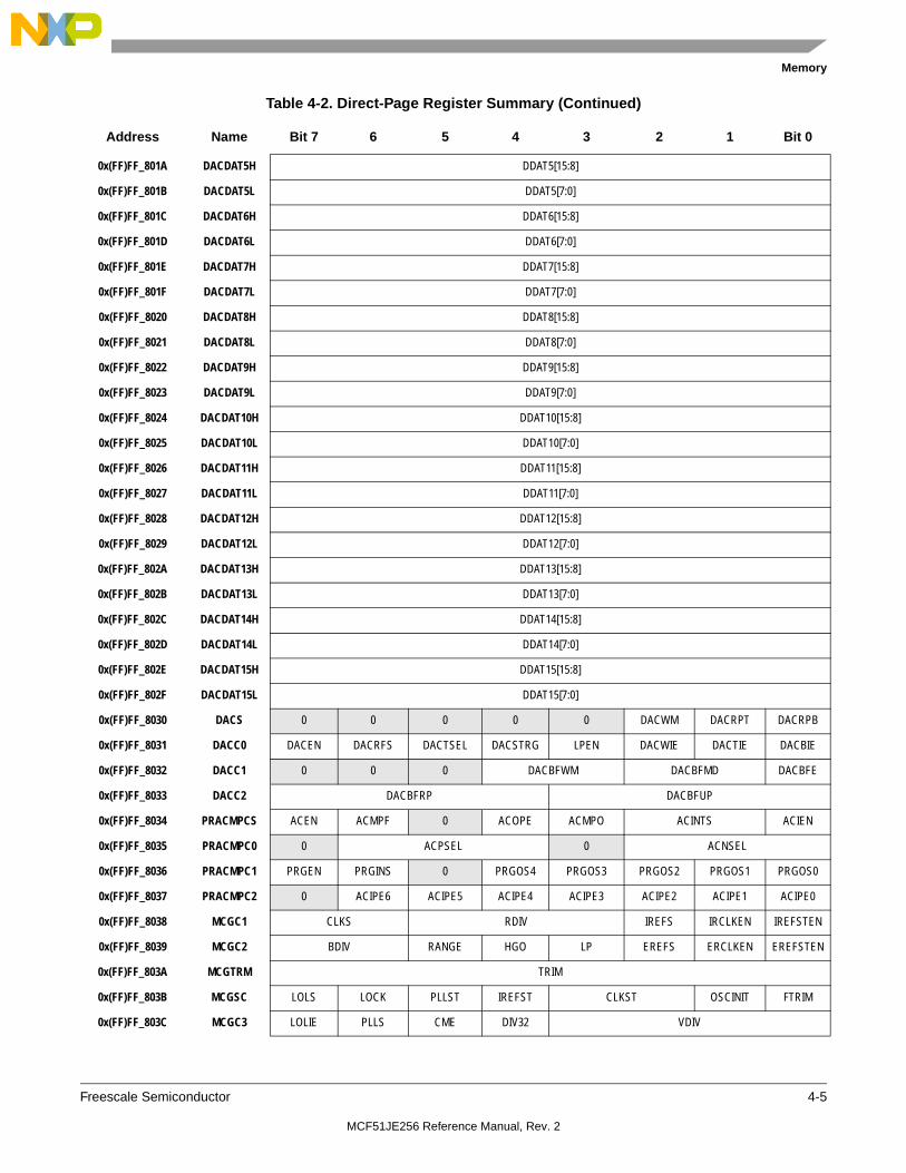
Memory
Freescale Semiconductor 4-5
0x(FF)FF_801A DACDAT5H DDAT5[15:8]
0x(FF)FF_801B DACDAT5L DDAT5[7:0]
0x(FF)FF_801C DACDAT6H DDAT6[15:8]
0x(FF)FF_801D DACDAT6L DDAT6[7:0]
0x(FF)FF_801E DACDAT7H DDAT7[15:8]
0x(FF)FF_801F DACDAT7L DDAT7[7:0]
0x(FF)FF_8020 DACDAT8H DDAT8[15:8]
0x(FF)FF_8021 DACDAT8L DDAT8[7:0]
0x(FF)FF_8022 DACDAT9H DDAT9[15:8]
0x(FF)FF_8023 DACDAT9L DDAT9[7:0]
0x(FF)FF_8024 DACDAT10H DDAT10[15:8]
0x(FF)FF_8025 DACDAT10L DDAT10[7:0]
0x(FF)FF_8026 DACDAT11H DDAT11[15:8]
0x(FF)FF_8027 DACDAT11L DDAT11[7:0]
0x(FF)FF_8028 DACDAT12H DDAT12[15:8]
0x(FF)FF_8029 DACDAT12L DDAT12[7:0]
0x(FF)FF_802A DACDAT13H DDAT13[15:8]
0x(FF)FF_802B DACDAT13L DDAT13[7:0]
0x(FF)FF_802C DACDAT14H DDAT14[15:8]
0x(FF)FF_802D DACDAT14L DDAT14[7:0]
0x(FF)FF_802E DACDAT15H DDAT15[15:8]
0x(FF)FF_802F DACDAT15L DDAT15[7:0]
0x(FF)FF_8030 DACS 0 0 0 0 0 DACWM DACRPT DACRPB
0x(FF)FF_8031 DACC0 DACEN DACRFS DACTSEL DACSTRG LPEN DACWIE DACTIE DACBIE
0x(FF)FF_8032 DACC1 0 0 0 DACBFWM DACBFMD DACBFE
0x(FF)FF_8033 DACC2 DACBFRP DACBFUP
0x(FF)FF_8034 PRACMPCS ACEN ACMPF 0 ACOPE ACMPO ACINTS ACIEN
0x(FF)FF_8035 PRACMPC0 0 ACPSEL 0 ACNSEL
0x(FF)FF_8036 PRACMPC1 PRGEN PRGINS 0 PRGOS4 PRGOS3 PRGOS2 PRGOS1 PRGOS0
0x(FF)FF_8037 PRACMPC2 0 ACIPE6 ACIPE5 ACIPE4 ACIPE3 ACIPE2 ACIPE1 ACIPE0
0x(FF)FF_8038 MCGC1 CLKS RDIV IREFS IRCLKEN IREFSTEN
0x(FF)FF_8039 MCGC2 BDIV RANGE HGO LP EREFS ERCLKEN EREFSTEN
0x(FF)FF_803A MCGTRM TRIM
0x(FF)FF_803B MCGSC LOLS LOCK PLLST IREFST CLKST OSCINIT FTRIM
0x(FF)FF_803C MCGC3 LOLIE PLLS CME DIV32 VDIV
Table 4-2. Direct-Page Register Summary (Continued)
Address Name Bit 7 6 5 4 3 2 1 Bit 0
MCF51JE256 Reference Manual, Rev. 2

Memory
4-6 Freescale Semiconductor
0x(FF)FF_803D MCGC4 0 0 DMX32 0 0 0 DRST / DRS
0x(FF)FF_803E-0x(FF)FF_803F
RESERVED — — — — — — — —
0x(FF)FF_8040 ADCSC1 COCO AIEN — ADCH
0x(FF)FF_8041-0x(FF)FF_8047
Reserved — — — — — — — —
0x(FF)FF_8048 ADCCFG1 ADLPC ADIV ADLSMP MODE ADICLK
0x(FF)FF_8049 ADCCFG2 0 0 0 0 ADACKEN ADHSC ADLSTS
0x(FF)FF_804A ADCRH D[15:8]
0x(FF)FF_804B ADCRL D[7:0]
0x(FF)FF_804C-0x(FF)FF_805B
Reserved — — — — — — — —
0x(FF)FF_805C VREFTRM TRM
0x(FF)FF_805D VREFSC VREFEN 0 0 0 0 VREFST MODE
0x(FF)FF_805E RESERVED — — — — — — — —
0x(FF)FF_805F IRQSC 0 IRQPDD IRQEDG IRQPE IRQF IRQACK IRQIE IRQMOD
0x(FF)FF_8060 IICA1 AD7 AD6 AD5 AD4 AD3 AD2 AD1 0
0x(FF)FF_8061 IICF MULT ICR
0x(FF)FF_8062 IICC1 IICEN IICIE MST TX TXAK RSTA 0 0
0x(FF)FF_8063 IICS TCF IAAS BUSY ARBL 0 SRW IICIF RXAK
0x(FF)FF_8064 IICD DATA
0x(FF)FF_8065 IICC2 GCAEN ADEXT 0 0 0 AD10 AD9 AD8
0x(FF)FF_8066 IICSMB FACK ALERTEN SIICAEN TCKSEL SLTF SHTF 0 0
0x(FF)FF_8067 IICA2 SAD7 SAD6 SAD5 SAD4 SAD3 SAD2 SAD1 0
0x(FF)FF_8068 IICSLTH SSLT15 SSLT14 SSLT13 SSLT12 SSLT11 SSLT10 SSLT9 SSLT8
0x(FF)FF_8069 IICSLTL SSLT7 SSLT6 SSLT5 SSLT4 SSLT3 SSLT2 SSLT1 SSLT0
0x(FF)FF_806A IICFLT 0 0 0 0 FLT3 FLT2 FLT1 FLT0
0x(FF)FF_806B RESERVED — — — — — — — —
0x(FF)FF_806C KBI1SC 0 0 0 0 KB1F KB1ACK KB1IE KBI1MOD
0x(FF)FF_806D KBI1PE KBI1PE7 KBI1PE6 KBI1PE5 KBI1PE4 KBI1PE3 KBI1PE2 KBI1PE1 KBI1PE0
0x(FF)FF_806E KBI1ES KB1EDG7 KB1EDG6 KB1EDG5 KB1EDG4 KB1EDG3 KB1EDG2 KB1EDG1 KB1EDG0
0x(FF)FF_806F RESERVED — — — — — — — —
0x(FF)FF_8070 SPI1C1 SPIE SPE SPTIE MSTR CPOL CPHA SSOE LSBFE
0x(FF)FF_8071 SPI1C2 SPMIE SPIMODE 0 MODFEN BIDIROE 0 SPISWAI SPC0
0x(FF)FF_8072 SPI1BR 0 SPPR2 SPPR1 SPPR0 SPR3 SPR2 SPR1 SPR0
0x(FF)FF_8073 SPI1S SPRF SPMF SPTEF MODF RNFULLF TNEARF TXFULLF RFIFOEF
Table 4-2. Direct-Page Register Summary (Continued)
Address Name Bit 7 6 5 4 3 2 1 Bit 0
MCF51JE256 Reference Manual, Rev. 2

Memory
Freescale Semiconductor 4-7
0x(FF)FF_8074 SPI1DH Bit 15 14 13 12 11 10 9 Bit 8
0x(FF)FF_8075 SPI1DL Bit 7 6 5 4 3 2 1 Bit 0
0x(FF)FF_8076 SPI1MH Bit 15 14 13 12 11 10 9 Bit 8
0x(FF)FF_8077 SPI1ML Bit 7 6 5 4 3 2 1 Bit 0
0x(FF)FF_8078 SPI1C3 0 0TNEAREF
MARKRNFULL MARK
INTCLR TNEARIEN RNFULLIEN FIFOMODE
0x(FF)FF_8079 SPI1CI TXFERR RXFERR TXFOF RXFOF TNEAREFCI RNFULLFCI SPTEFCI SPRFCI
0x(FF)FF_807A-0x(FF)FF_807B
RESERVED — — — — — — — —
0x(FF)FF_807C KBI2SC 0 0 0 0 KB2F KB2ACK KB2IE KBI2MOD
0x(FF)FF_807D KBI2PE KBI2PE7 KBI2PE6 KBI2PE5 KBI2PE4 KBI2PE3 KBI2PE2 KBI2PE1 KBI2PE0
0x(FF)FF_807E KBI2ES KB2EDG7 KB2EDG6 KB2EDG5 KB2EDG4 KB2EDG3 KB2EDG2 KB2EDG1 KB2EDG0
0x(FF)FF_807F RESERVED — — — — — — — —
Table 4-3. High-Page Register Summary
Address Name Bit 7 6 5 4 3 2 1 Bit 0
0x(FF)FF_9800 SRS POR PIN COP ILOP ILAD LOC LVD 0
0x(FF)FF_9801 Reserved — — — — — — — —
0x(FF)FF_9802 SOPT1 COPT1 COPT0 STOPE WAITE BLMSS MBSL BKGDPE RSTPE
0x(FF)FF_9803 SOPT2 COPCLKS COPWUSB_BIGEN
DCLKOUT_EN
CMT_CLK_SEL
— — ACIC
0x(FF)FF_9804-0x(FF)FF_9805
Reserved — — — — — — — —
0x(FF)FF_9806 SDIDH REV ID11 ID10 ID9 ID8
0x(FF)FF_9807 SDIDL ID7 ID6 ID5 ID4 ID3 ID2 ID1 ID0
0x(FF)FF_9808 SCGC1 CMT TPM2 TPM1 ADC DAC IIC SCI2 SCI1
0x(FF)FF_9809 SCGC2 USB PDB IRQ KBI PRACMP MFB SPI2 SPI1
0x(FF)FF_980A SCGC3 VREF CRC FLS2 FLS1 — — — —
0x(FF)FF_980B SOPT3 SCI2PS SCI1PS IICPS USBPS MB_DATA ARRAYSEL SCI1_PAD CMT_PAD
0x(FF)FF_980C SOPT4 — FBALEEN FBAD12FE FBAD12PUE FBAD12SRE FBAD12DSE IROSRE IRODSE
0x(FF)FF_980D SOPT51 — — — —
0x(FF)FF_980E SIMIPS ADCTRS RX1N — — MTBASE1 — MODTX1
0x(FF)FF_980F SIGNATURE SIGNATURE SEMAPHORE
0x(FF)FF_9810 CCSCTRL RANGE1 HGO1 ERCLKEN1 OSCINIT1 EREFS1 EN TEST SEL
0x(FF)FF_9811 CCSTMR1 CNT1
0x(FF)FF_9812 CCSTMR2 CNT2
Table 4-2. Direct-Page Register Summary (Continued)
Address Name Bit 7 6 5 4 3 2 1 Bit 0
MCF51JE256 Reference Manual, Rev. 2

Memory
4-8 Freescale Semiconductor
0x(FF)FF_9813 CCSTMRIR CNTIR
0x(FF)FF_9814 FPROTD — — — — — — — FPDIS
0x(FF)FF_9815 MFBPC1 MFBPEN_AD7 MFBPEN_AD6 MFBPEN_AD5 MFBPEN_AD4 MFBPEN_AD3 MFBPEN_AD2 MFBPEN_AD1 MFBPEN_AD0
0x(FF)FF_9816 MFBPC2MFBPEN_AD1
5MFBPEN_AD1
4MFBPEN_AD1
3MFBPEN_AD12 MFBPEN_AD11
MFBPEN_AD10
MFBPEN_AD9 MFBPEN_AD8
0x(FF)FF_9817 MFBPC3 MFBPEN_D3 MFBPEN_D2 MFBPEN_D1 MFBPEN_D0 MFBPEN_AD19MFBPEN_AD1
8MFBPEN_AD17 MFBPEN_AD16
0x(FF)FF_9818 MFBPC4 EN_CS1 EN_CS0 EN_OE EN_RW MFBPEN_D7 MFBPEN_D6 MFBPEN_D5 MFBPEN_D4
0x(FF)FF_9819 SIMCO — — — — — CS
0x(FF)FF_981A-0x(FF)FF_981B
Reserved — — — — — — — —
0x(FF)FF_981C SPMSC1 LVDF LVDACK LVDIE LVDRE LVDSE LVDE 0 BGBE
0x(FF)FF_981D SPMSC2 LPR LPRS LPWUI 0 PPDF PPDACK PPDE PPDC
0x(FF)FF_981E Reserved — — — — — — — —
0x(FF)FF_981F SPMSC3 LVwF LVWACK LVDV LVWV LVWIE 0 0 0
0x(FF)FF_9820-0x(FF)FF_982F
Reserved — — — — — — — —
0x(FF)FF_9830 PTED PTED7 PTED6 PTED5 PTED4 PTED3 PTED2 PTED1 PTED0
0x(FF)FF_9831 PTEDD PTEDD7 PTEDD6 PTEDD5 — PTEDD3 PTEDD2 PTEDD1 PTEDD0
0x(FF)FF_9832 PTFD PTFD7 PTFD6 PTFD5 PTFD4 PTFD3 PTFD2 PTFD1 PTFD0
0x(FF)FF_9833 PTFDD PTFDD7 PTFDD6 PTFDD5 PTFDD4 PTFDD3 PTFDD2 PTFDD1 PTFDD0
0x(FF)FF_9834-0x(FF)FF_9837
Reserved — — — — — — — —
0x(FF)FF_9838 SCI2BDH LBKDIE RXEDGIE 0 SBR12 SBR11 SBR10 SBR9 SBR8
0x(FF)FF_9839 SCI2BDL SBR7 SBR6 SBR5 SBR4 SBR3 SBR2 SBR1 SBR0
0x(FF)FF_983A SCI2C1 LOOPS SCISWAI RSRC M WAKE ILT PE PT
0x(FF)FF_983B SCI2C2 TIE TCIE RIE ILIE TE RE RWU SBK
0x(FF)FF_983C SCI2S1 TDRE TC RDRF IDLE OR NF FE PF
0x(FF)FF_983D SCI2S2 LBKDIF RXEDGIF 0 RXINV RWUID BRK13 LBKDE RAF
0x(FF)FF_983E SCI2C3 R8 T8 TXDIR TXINV ORIE NEIE FEIE PEIE
0x(FF)FF_983F SCI2D Bit 7 6 5 4 3 2 1 Bit 0
0x(FF)FF_9840 SPI2C1 SPI2E SP2E SP2TIE MSTR CPOL CPHA SSOE LSBFE
0x(FF)FF_9841 SPI2C2 SPMIE 0 0 MODFEN BIDIROE 0 SPI2SWAI SP2C0
0x(FF)FF_9842 SPI2BR 0 SP2PR2 SP2PR1 SP2PR0 SP2R3 SP2R2 SP2R1 SP2R0
0x(FF)FF_9843 SPI2S SP2RF 0 SP2TEF MODF 0 0 0 0
0x(FF)FF_9844 Reserved — — — — — — — —
0x(FF)FF_9845 SPI2D Bit 7 6 5 4 3 2 1 Bit 0
Table 4-3. High-Page Register Summary (Continued)
Address Name Bit 7 6 5 4 3 2 1 Bit 0
MCF51JE256 Reference Manual, Rev. 2
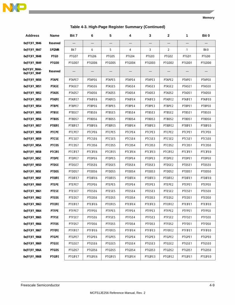
Memory
Freescale Semiconductor 4-9
0x(FF)FF_9846 Reserved — — — — — — — —
0x(FF)FF_9847 SPI2MR Bit 7 6 5 4 3 2 1 Bit 0
0x(FF)FF_9848 PTGD PTGD7 PTGD6 PTGD5 PTGD4 PTGD3 PTGD2 PTGD1 PTGD0
0x(FF)FF_9849 PTGDD PTGDD7 PTGDD6 PTGDD5 PTGDD4 PTGDD3 PTGDD2 PTGDD1 PTGDD0
0x(FF)FF_984A-0x(FF)FF_984F
Reserved — — — — — — — —
0x(FF)FF_9850 PTAPE PTAPE7 PTAPE6 PTAPE5 PTAPE4 PTAPE3 PTAPE2 PTAPE1 PTAPE0
0x(FF)FF_9851 PTASE PTASE7 PTASE6 PTASE5 PTASE4 PTASE3 PTASE2 PTASE1 PTASE0
0x(FF)FF_9852 PTADS PTADS7 PTADS6 PTADS5 PTADS4 PTADS3 PTADS2 PTADS1 PTADS0
0x(FF)FF_9853 PTAIFE PTAIFE7 PTAIFE6 PTAIFE5 PTAIFE4 PTAIFE3 PTAIFE2 PTAIFE1 PTAIFE0
0x(FF)FF_9854 PTBPE PTBPE7 PTBPE6 PTBPE5 PTBPE4 PTBPE3 PTBPE2 PTBPE1 PTBPE0
0x(FF)FF_9855 PTBSE PTBSE7 PTBSE6 PTBSE5 PTBSE4 PTBSE3 PTBSE2 PTBSE1 PTBSE0
0x(FF)FF_9856 PTBDS PTBDS7 PTBDS6 PTBDS5 PTBDS4 PTBDS3 PTBDS2 PTBDS1 PTBDS0
0x(FF)FF_9857 PTBIFE PTBIFE7 PTBIFE6 PTBIFE5 PTBIFE4 PTBIFE3 PTBIFE2 PTBIFE1 PTBIFE0
0x(FF)FF_9858 PTCPE PTCPE7 PTCPE6 PTCPE5 PTCPE4 PTCPE3 PTCPE2 PTCPE1 PTCPE0
0x(FF)FF_9859 PTCSE PTCSE7 PTCSE6 PTCSE5 PTCSE4 PTCSE3 PTCSE2 PTCSE1 PTCSE0
0x(FF)FF_985A PTCDS PTCDS7 PTCDS6 PTCDS5 PTCDS4 PTCDS3 PTCDS2 PTCDS1 PTCDS0
0x(FF)FF_985B PTCIFE PTCIFE7 PTCIFE6 PTCIFE5 PTCIFE4 PTCIFE3 PTCIFE2 PTCIFE1 PTCIFE0
0x(FF)FF_985C PTDPE PTDPE7 PTDPE6 PTDPE5 PTDPE4 PTDPE3 PTDPE2 PTDPE1 PTDPE0
0x(FF)FF_985D PTDSE PTDSE7 PTDSE6 PTDSE5 PTDSE4 PTDSE3 PTDSE2 PTDSE1 PTDSE0
0x(FF)FF_985E PTDDS PTDDS7 PTDDS6 PTDDS5 PTDDS4 PTDDS3 PTDDS2 PTDDS1 PTDDS0
0x(FF)FF_985F PTDIFE PTDIFE7 PTDIFE6 PTDIFE5 PTDIFE4 PTDIFE3 PTDIFE2 PTDIFE1 PTDIFE0
0x(FF)FF_9860 PTEPE PTEPE7 PTEPE6 PTEPE5 PTEPE4 PTEPE3 PTEPE2 PTEPE1 PTEPE0
0x(FF)FF_9861 PTESE PTESE7 PTESE6 PTESE5 PTESE4 PTESE3 PTESE2 PTESE1 PTESE0
0x(FF)FF_9862 PTEDS PTEDS7 PTEDS6 PTEDS5 PTEDS4 PTEDS3 PTEDS2 PTEDS1 PTEDS0
0x(FF)FF_9863 PTEIFE PTEIFE7 PTEIFE6 PTEIFE5 PTEIFE4 PTEIFE3 PTEIFE2 PTEIFE1 PTEIFE0
0x(FF)FF_9864 PTFPE PTFPE7 PTFPE6 PTFPE5 PTFPE4 PTFPE3 PTFPE2 PTFPE1 PTFPE0
0x(FF)FF_9865 PTFSE PTFSE7 PTFSE6 PTFSE5 PTFSE4 PTFSE3 PTFSE2 PTFSE1 PTFSE0
0x(FF)FF_9866 PTFDS PTFDS7 PTFDS6 PTFDS5 PTFDS4 PTFDS3 PTFDS2 PTFDS1 PTFDS0
0x(FF)FF_9867 PTFIFE PTFIFE7 PTFIFE6 PTFIFE5 PTFIFE4 PTFIFE3 PTFIFE2 PTFIFE1 PTFIFE0
0x(FF)FF_9868 PTGPE PTGPE7 PTGPE6 PTGPE5 PTGPE4 PTGPE3 PTGPE2 PTGPE1 PTGPE0
0x(FF)FF_9869 PTGSE PTGSE7 PTGSE6 PTGSE5 PTGSE4 PTGSE3 PTGSE2 PTGSE1 PTGSE0
0x(FF)FF_986A PTGDS PTGDS7 PTGDS6 PTGDS5 PTGDS4 PTGDS3 PTGDS2 PTGDS1 PTGDS0
0x(FF)FF_986B PTGIFE PTGIFE7 PTGIFE6 PTGIFE5 PTGIFE4 PTGIFE3 PTGIFE2 PTGIFE1 PTGIFE0
Table 4-3. High-Page Register Summary (Continued)
Address Name Bit 7 6 5 4 3 2 1 Bit 0
MCF51JE256 Reference Manual, Rev. 2

Memory
4-10 Freescale Semiconductor
0x(FF)FF_986C-0x(FF)FF_986F
Reserved — — — — — — — —
0x(FF)FF_9870 CMTCGH1 PH7 PH6 PH5 PH4 PH3 PH2 PH1 PH0
0x(FF)FF_9871 CMTCGL1 PL7 PL6 PL5 PL4 PL3 PL2 PL1 PL0
0x(FF)FF_9872 CMTCGH2 SH7 SH6 SH5 SH4 SH3 SH2 SH1 SH0
0x(FF)FF_9873 CMTCGL2 SL7 SL6 SL5 SL4 SL3 SL2 SL1 SL0
0x(FF)FF_9874 CMTOC IROL CMTPOL IROPEN 0 0 0 0 0
0x(FF)FF_9875 CMTMSC EOCF CMTDIV1 CMTDIV0 EXSPC BASE FSK EOCIE MCGEN
0x(FF)FF_9876 CMTCMD1 MB15 MB14 MB13 MB12 MB11 MB10 MB9 MB8
0x(FF)FF_9877 CMTCMD2 MB7 MB6 MB5 MB4 MB3 MB2 MB1 MB0
0x(FF)FF_9878 CMTCMD3 SB15 SB14 SB13 SB12 SB11 SB10 SB9 SB8
0x(FF)FF_9879 CMTCMD4 SB7 SB6 SB5 SB4 SB3 SB2 SB1 SB0
0x(FF)FF_987A-0x(FF)FF_988F
Reserved — — — — — — — —
0x(FF)FF_9890 CRCH Bit15 Bit14 Bit13 Bit12 Bit11 Bit10 Bit9 Bit8
0x(FF)FF_9891 CRCL Bit7 Bit6 Bit5 Bit4 Bit3 Bit2 Bit1 Bit0
0x(FF)FF_9892 Transpose Bit7 Bit6 Bit5 Bit4 Bit3 Bit2 Bit1 Bit0
0x(FF)FF_9893-0x(FF)FF_989B
Reserved — — — — — — — —
0x(FF)FF_989C TODC TODEN TODCLKS TODR TODCLKEN TODPS
0x(FF)FF_989D TODSC QSECF SECF MTCHF QSECIE SECIE MTCHIE MTCHEN MTCHWC
0x(FF)FF_989E TODM TODM MQSEC
0x(FF)FF_989F TODCNT TODCNT
0x(FF)FF_98A0 TPM2SC TOF TOIE CPWMS CLKSB CLKSA PS2 PS1 PS0
0x(FF)FF_98A1 TPM2CNTH Bit 15 14 13 12 11 10 9 Bit 8
0x(FF)FF_98A2 TPM2CNTL Bit 7 6 5 4 3 2 1 Bit 0
0x(FF)FF_98A3 TPM2MODH Bit 15 14 13 12 11 10 9 Bit 8
0x(FF)FF_98A4 TPM2MODL Bit 7 6 5 4 3 2 1 Bit 0
0x(FF)FF_98A5 TPM2C0SC CH0F CH0IE MS0B MS0A ELS0B ELS0A 0 0
0x(FF)FF_98A6 TPM2C0VH Bit 15 14 13 12 11 10 9 Bit 8
0x(FF)FF_98A7 TPM2C0VL Bit 7 6 5 4 3 2 1 Bit 0
0x(FF)FF_98A8 TPM2C1SC CH1F CH1IE MS1B MS1A ELS1B ELS1A 0 0
0x(FF)FF_98A9 TPM2C1VH Bit 15 14 13 12 11 10 9 Bit 8
0x(FF)FF_98AA TPM2C1VL Bit 7 6 5 4 3 2 1 Bit 0
0x(FF)FF_98AB TPM2C2SC CH2F CH2IE MS2B MS2A ELS2B ELS2A 0 0
0x(FF)FF_98AC TPM2C2VH Bit 15 14 13 12 11 10 9 Bit 8
Table 4-3. High-Page Register Summary (Continued)
Address Name Bit 7 6 5 4 3 2 1 Bit 0
MCF51JE256 Reference Manual, Rev. 2

Memory
Freescale Semiconductor 4-11
0x(FF)FF_98AD TPM2C2VL Bit 7 6 5 4 3 2 1 Bit 0
0x(FF)FF_98AE TPM2C3SC CH3F CH3IE MS3B MS3A ELS3B ELS3A 0 0
0x(FF)FF_98AF TPM2C3VH Bit 15 14 13 12 11 10 9 Bit 8
0x(FF)FF_98B0 TPM2C3VL Bit 7 6 5 4 3 2 1 Bit 0
0x(FF)FF_98B1-0x(FF)FF_98B7
Reserved — — — — — — — —
0x(FF)FF_98B8 SCI1BDH LBKDIE RXEDGIE 0 SBR12 SBR11 SBR10 SBR9 SBR8
0x(FF)FF_98B9 SCI1BDL SBR7 SBR6 SBR5 SBR4 SBR3 SBR2 SBR1 SBR0
0x(FF)FF_98BA SCI1C1 LOOPS SCISWAI RSRC M WAKE ILT PE PT
0x(FF)FF_98BB SCI1C2 TIE TCIE RIE ILIE TE RE RWU SBK
0x(FF)FF_98BC SCI1S1 TDRE TC RDRF IDLE OR NF FE PF
0x(FF)FF_98BD SCI1S2 LBKDIF RXEDGIF 0 RXINV RWUID BRK13 LBKDE RAF
0x(FF)FF_98BE SCI1C3 R8 T8 TXDIR TXINV ORIE NEIE FEIE PEIE
0x(FF)FF_98BF SCI1D Bit 7 6 5 4 3 2 1 Bit 0
0x(FF)FF_98C0 PDBSC PDBEN PDBIF PDBIE LDMOD TOS DACTOE LDOK
0x(FF)FF_98C1 PDBC1 PRESCALER TRIGSEL CONT MULT
0x(FF)FF_98C2 PDBC2 — — — — — — — SWTRIG
0x(FF)FF_98C3 PDBCHEN CHEN7 CHEN6 CHEN5 CHEN4 CHEN3 CHEN2 CHEN1 CHEN0
0x(FF)FF_98C4 PDBMODH MOD[15:8]
0x(FF)FF_98C5 PDBMODL MOD[7:0]
0x(FF)FF_98C6 PDBCNTH COUNT[15:8]
0x(FF)FF_98C7 PDBCNTL COUNT[7:0]
0x(FF)FF_98C8 PDBIDLYH IDELAY[15:8]
0x(FF)FF_98C9 PDBIDLYL IDELAY[7:0]
0x(FF)FF_98CA DACINTH DACINT[15:8]
0x(FF)FF_98CB DACINTL DACINT[7:0]
0x(FF)FF_98CC PDBDLYH DELAY[15:8]
0x(FF)FF_98CD PDBDLYL DELAY[7:0]
0x(FF)FF_98CE-(FF)FF_98DF
Reserved — — — — — — — —
0x(FF)FF_98E0 TPM1SC TOF TOIE CPWMS CLKSB CLKSA PS2 PS1 PS0
0x(FF)FF_98E1 TPM1CNTH Bit 15 14 13 12 11 10 9 Bit 8
0x(FF)FF_98E2 TPM1CNTL Bit 7 6 5 4 3 2 1 Bit 0
0x(FF)FF_98E3 TPM1MODH Bit 15 14 13 12 11 10 9 Bit 8
0x(FF)FF_98E4 TPM1MODL Bit 7 6 5 4 3 2 1 Bit 0
Table 4-3. High-Page Register Summary (Continued)
Address Name Bit 7 6 5 4 3 2 1 Bit 0
MCF51JE256 Reference Manual, Rev. 2

Memory
4-12 Freescale Semiconductor
0x(FF)FF_98E5 TPM1C0SC CH0F CH0IE MS0B MS0A ELS0B ELS0A 0 0
0x(FF)FF_98E6 TPM1C0VH Bit 15 14 13 12 11 10 9 Bit 8
0x(FF)FF_98E7 TPM1C0VL Bit 7 6 5 4 3 2 1 Bit 0
0x(FF)FF_98E8 TPM1C1SC CH1F CH1IE MS1B MS1A ELS1B ELS1A 0 0
0x(FF)FF_98E9 TPM1C1VH Bit 15 14 13 12 11 10 9 Bit 8
0x(FF)FF_98EA TPM1C1VL Bit 7 6 5 4 3 2 1 Bit 0
0x(FF)FF_98EB TPM1C2SC CH2F CH2IE MS2B MS2A ELS2B ELS2A 0 0
0x(FF)FF_98EC TPM1C2VH Bit 15 14 13 12 11 10 9 Bit 8
0x(FF)FF_98ED TPM1C2VL Bit 7 6 5 4 3 2 1 Bit 0
0x(FF)FF_98EE TPM1C3SC CH3F CH3IE MS3B MS3A ELS3B ELS3A 0 0
0x(FF)FF_98EF TPM1C3VH Bit 15 14 13 12 11 10 9 Bit 8
0x(FF)FF_98F0 TPM1C3VL Bit 7 6 5 4 3 2 1 Bit 0
0x(FF)FF_98F1-0x(FF)FF_98F7
Reserved — — — — — — — —
0x(FF)FF_98F8 ADCCVH CV[15:8]
0x(FF)FF_98F9 ADCCVL CV[7:0]
0x(FF)FF_98FA-0x(FF)FF_98FB
Reserved — — — — — — — —
0x(FF)FF_98FC ADCSC2 ADACT ADTRG ACFE ACFGT — 0 — —
0x(FF)FF_98FD ADCSC3 CAL CALF 0 0 ADCO — — —
0x(FF)FF_98FE ADCOFSH OFS[15:8]
0x(FF)FF_98FF ADCOFSL OFS[7:0]
0x(FF)FF_9900 ADCPGH PG[15:8]
0x(FF)FF_9901 ADCPGL PG[7:0]
0x(FF)FF_9902 ADCMGH MG[15:8]
0x(FF)FF_9903 ADCMGL MG[7:0]
0x(FF)FF_9904 ADCCLPD 0 0 CLPD
0x(FF)FF_9905 ADCCLPS 0 0 CLPS
0x(FF)FF_9906 ADCCLP4H 0 0 0 0 0 0 CLP4[9:8]
0x(FF)FF_9907 ADCCLP4L CLP4[7:0]
0x(FF)FF_9908 ADCCLP3H 0 0 0 0 0 0 0 CLP3[8]
0x(FF)FF_9909 ADCCLP3L CLP3[7:0]
0x(FF)FF_990A ADCCLP2 CLP2
0x(FF)FF_990B ADCCLP1 0 CLP1
0x(FF)FF_990C ADCCLP0 0 0 CLP0
Table 4-3. High-Page Register Summary (Continued)
Address Name Bit 7 6 5 4 3 2 1 Bit 0
MCF51JE256 Reference Manual, Rev. 2

Memory
Freescale Semiconductor 4-13
0x(FF)FF_990D Reserved — — — — — — — —
0x(FF)FF_990E ADCCLMD 0 0 CLMD
0x(FF)FF_990F ADCCLMS 0 0 CLMS
0x(FF)FF_9910 ADCCLM4H 0 0 0 0 0 0 CLM4[9:8]
0x(FF)FF_9911 ADCCLM4L CLM4[7:0]
0x(FF)FF_9912 ADCCLM3H 0 0 0 0 0 0 0 CLM3[8]
0x(FF)FF_9913 ADCCLM3L CLM3[7:0]
0x(FF)FF_9914 ADCCLM2 CLM2
0x(FF)FF_9915 ADCCLM1 0 CLM1
0x(FF)FF_9916 ADCCLM0 0 0 CLM0
0x(FF)FF_9917 APCTL1 ADPC7 ADPC6 ADPC5 ADPC4 ADPC3 ADPC2 ADPC1 ADPC0
0x(FF)FF_9918 APCTL2 ADPC15 ADPC14 ADPC13 ADPC12 ADPC11 ADPC10 ADPC9 ADPC8
0x(FF)FF_9919-0x(FF)FF_991F
Reserved — — — — — — — —
0x(FF)FF_9920 F1CDIV FDIVLD PRDIV8 FDIV
0x(FF)FF_9921 F1OPT KEYEN 0 0 0 0 SEC
0x(FF)FF_9922 Reserved — — — — — — — —
0x(FF)FF_9923 F1CNFG CBEIE CCIE KEYACC 0 0 0 0 0
0x(FF)FF_9924 F1PROT FPS FPOPEN
0x(FF)FF_9925 F1STAT FCBEF FCCF FPVIOL FACCERR 0 FBLANK 0 0
0x(FF)FF_9926 F1CMD 0 FCMD
0x(FF)FF_9927-0x(FF)FF_992F
Reserved — — — — — — — —
0x(FF)FF_9930 F2CDIV FDIVLD PRDIV8 FDIV
0x(FF)FF_9931 F2OPT KEYEN 0 0 0 0 SEC
0x(FF)FF_9932 Reserved — — — — — — — —
0x(FF)FF_9933 F2CNFG CBEIE CCIE KEYACC 0 0 0 0 0
0x(FF)FF_9934 F2PROT FPS FPOPEN
0x(FF)FF_9935 F2STAT FCBEF FCCF FPVIOL FACCERR 0 FBLANK 0 0
0x(FF)FF_9936 F2CMD 0 FCMD
0x(FF)FF_9937-0x(FF)FF_993F
Reserved — — — — — — — —
0x(FF)FF_9940 PTHD PTHD7 PTHD6 PTHD5 PTHD4 PTHD3 PTHD2 PTHD1 PTHD0
0x(FF)FF_9941 PTHDD PTHDD7 PTHDD6 PTHDD5 PTHDD4 PTHDD3 PTHDD2 PTHDD1 PTHDD0
0x(FF)FF_9942 PTJD PTJD7 PTJD6 PTJD5 PTJD4 PTJD3 PTJD2 PTJD1 PTJD0
0x(FF)FF_9943 PTJDD PTJDD7 PTJDD6 PTJDD5 PTJDD4 PTJDD3 PTJDD2 PTJDD1 PTJDD0
Table 4-3. High-Page Register Summary (Continued)
Address Name Bit 7 6 5 4 3 2 1 Bit 0
MCF51JE256 Reference Manual, Rev. 2

Memory
4-14 Freescale Semiconductor
0x(FF)FF_9944-0x(FF)FF_9947
Reserved — — — — — — — —
0x(FF)FF_9948 PTHPE PTHPE7 PTHPE6 PTHPE5 PTHPE4 PTHPE3 PTHPE2 PTHPE1 PTHPE0
0x(FF)FF_9949 PTHSE PTHSE7 PTHSE6 PTHSE5 PTHSE4 PTHSE3 PTHSE2 PTHSE1 PTHSE0
0x(FF)FF_994A PTHDS PTHDS7 PTHDS6 PTHDS5 PTHDS4 PTHDS3 PTHDS2 PTHDS1 PTHDS0
0x(FF)FF_994B PTHIFE PTHIFE7 PTHIFE6 PTHIFE5 PTHIFE4 PTHIFE3 PTHIFE2 PTHIFE1 PTHIFE0
0x(FF)FF_994C PTJPE PTJPE7 PTJPE6 PTJPE5 PTJPE4 PTJPE3 PTJPE2 PTJPE1 PTJPE0
0x(FF)FF_994D PTJSE PTJSE7 PTJSE6 PTJSE5 PTJSE4 PTJSE3 PTJSE2 PTJSE1 PTJSE0
0x(FF)FF_994E PTJDS PTJDS7 PTJDS6 PTJDS5 PTJDS4 PTJDS3 PTJDS2 PTJDS1 PTJDS0
0x(FF)FF_994F PTJIFE PTJIFE7 PTJIFE6 PTJIFE5 PTJIFE4 PTJIFE3 PTJIFE2 PTJIFE1 PTJIFE0
1 This location is reserved for Freescale internal testing. Do not write any value to this location. Writing a value to this location can affect on-chip LVD performance.
Table 4-4. USB Register Summary
Address Name Bit 7 6 5 4 3 2 1 Bit 0
0x(FF)FF_9A00 PERID 0 0 ID5 ID4 ID3 ID2 ID1 ID0
0x(FF)FF_9A04 IDCOMP 1 1 NID5 NID4 NID3 NID2 NID1 NID0
0x(FF)FF_9A08 REV REV7 REV6 REV5 REV4 REV3 REV2 REV1 REV0
0x(FF)FF_9A0C ADD_INFO IRQ_NUM 0 0 IEHOST
0x(FF)FF_9A10OTG_INT_
STATID_CHG 1_MSEC
LINE_STATE_
CHG—
SESS_VLD_CHG
B_SESS_CHG
—A_VBUS_CH
G
0x(FF)FF_9A14 OTG_INT_EN ID_EN 1_MSEC_ENLINE_
STATE_EN
—SESS_
VLD_ENB_SESS_EN — A_VBUS_EN
0x(FF)FF_9A18 OTG_STAT ID 1_MSEC_ENLINE_
STATE_STABLE
—SESS_
VLDB_SESS_EN
D—
A_VBUS_VLD
0x(FF)FF_9A1C OTG_CTRL DP_HIGH — DP_LOW DM_LOW — OTG_EN — —
0x(FF)FF_9A80 INT_STAT STALL ATTACH RESUME SLEEPTOK_DNE
SOF_TOK
ERRORUSB_RST
0x(FF)FF_9A84 INT_ENBSTALL_
ENATTACH_EN
RESUME_EN
SLEEP_EN
TOK_DNE_EN
SOF_TOK_EN
ERROR_ENUSB_
RST_EN
0x(FF)FF_9A88 ERR_STATBTS_ERR
—DMA_ERR
BTO_ERR
DFN8 CRC16CRC5_
EOFPID_ERR
0x(FF)FF_9A8C ERRENB BTSERR — BUFERR BTOERR DFN8 CRC16 PIDERR
0x(FF)FF_9A90 STAT ENDP [3:0] TX ODD — —
0x(FF)FF_9A94 CTL JSTATE SE0TXSUSPEND
/ TOKENBUSY
RESETHOST_ MODE_
ENRESUME
ODD_RST
USB_EN/ SOF_EN
Table 4-3. High-Page Register Summary (Continued)
Address Name Bit 7 6 5 4 3 2 1 Bit 0
MCF51JE256 Reference Manual, Rev. 2

Memory
Freescale Semiconductor 4-15
0x(FF)FF_9A98 ADDR LS_EN ADDR [6:0]
0x(FF)FF_9A9C BDT_PAGE_01BDT_BA15
BDT_BA14
BDT_BA13
BDT_BA12
BDT_BA11
BDT_BA10
BDT_BA9
NOT USED
0x(FF)FF_9AA0 FRM_NUML FRM7 FRM8 FRM5 FRM4 FRM3 FRM2 FRM1 FRM0
0x(FF)FF_9AA4 FRM_NUMH 0 0 0 0 0 FRM10 FRM9 FRM8
0x(FF)FF_9AA8 TOKEN TOKEN_PID TOKEN_ENDPT
0x(FF)FF_9AAC SOF_THLD CNT7 CNT6 CNT5 CNT4 CNT3 CNT2 CNT1 CNT0
0x(FF)FF_9AB0 BDT_PAGE_02BDT_BA23
BDT_BA22
BDT_BA21
BDT_BA20
BDT_BA19
BDT_BA18
BDT_BA17
BDT_BA16
0x(FF)FF_9AB4 BDT_PAGE_03BDT_BA31
BDT_BA30
BDT_BA29
BDT_BA28
BDT_BA27
BDT_BA26
BDT_BA25
BDT_BA24
0x(FF)FF_9AB8- 0x(FF)FF_9ABF
Reserved — — — — — — — —
0x(FF)FF_9AC0 ENDPT0HOST_
WO_HUBRETRY_DIS 0 EP_CTL_DIS EP_RX_EN
EP_TX_EN
EP_STALL
EP_HSHK
0x(FF)FF_9AC4 ENDPT1HOST_
WO_HUBRETRY_DIS 0 EP_CTL_DIS EP_RX_EN
EP_TX_EN
EP_STALL
EP_HSHK
0x(FF)FF_9AC8 ENDPT2HOST_
WO_HUBRETRY_DIS 0 EP_CTL_DIS EP_RX_EN
EP_TX_EN
EP_STALL
EP_HSHK
0x(FF)FF_9ACC ENDPT3HOST_
WO_HUBRETRY_DIS 0 EP_CTL_DIS EP_RX_EN
EP_TX_EN
EP_STALL
EP_HSHK
0x(FF)FF_9AD0 ENDPT4HOST_
WO_HUBRETRY_DIS 0 EP_CTL_DIS EP_RX_EN
EP_TX_EN
EP_STALL
EP_HSHK
0x(FF)FF_9AD4 ENDPT5HOST_
WO_HUBRETRY_DIS 0 EP_CTL_DIS EP_RX_EN
EP_TX_EN
EP_STALL
EP_HSHK
0x(FF)FF_9AD8 ENDPT6HOST_
WO_HUBRETRY_DIS 0 EP_CTL_DIS EP_RX_EN
EP_TX_EN
EP_STALL
EP_HSHK
0x(FF)FF_9ADC ENDPT7HOST_
WO_HUBRETRY_DIS 0 EP_CTL_DIS EP_RX_EN
EP_TX_EN
EP_STALL
EP_HSHK
0x(FF)FF_9AE0 ENDPT8HOST_
WO_HUBRETRY_DIS 0 EP_CTL_DIS EP_RX_EN
EP_TX_EN
EP_STALL
EP_HSHK
0x(FF)FF_9AE4 ENDPT9HOST_
WO_HUBRETRY_DIS 0 EP_CTL_DIS EP_RX_EN
EP_TX_EN
EP_STALL
EP_HSHK
0x(FF)FF_9AE8 ENDPT10HOST_
WO_HUBRETRY_DIS 0 EP_CTL_DIS EP_RX_EN
EP_TX_EN
EP_STALL
EP_HSHK
0x(FF)FF_9AEC ENDPT11HOST_
WO_HUBRETRY_DIS 0 EP_CTL_DIS EP_RX_EN
EP_TX_EN
EP_STALL
EP_HSHK
0x(FF)FF_9AF0 ENDPT12HOST_
WO_HUBRETRY_DIS 0 EP_CTL_DIS EP_RX_EN
EP_TX_EN
EP_STALL
EP_HSHK
0x(FF)FF_9AF4 ENDPT13HOST_
WO_HUBRETRY_DIS 0 EP_CTL_DIS EP_RX_EN
EP_TX_EN
EP_STALL
EP_HSHK
Table 4-4. USB Register Summary (Continued)
Address Name Bit 7 6 5 4 3 2 1 Bit 0
MCF51JE256 Reference Manual, Rev. 2

Memory
4-16 Freescale Semiconductor
0x(FF)FF_9AF8 ENDPT14HOST_
WO_HUBRETRY_DIS 0 EP_CTL_DIS EP_RX_EN
EP_TX_EN
EP_STALL
EP_HSHK
0x(FF)FF_9AFC ENDPT15HOST_
WO_HUBRETRY_DIS 0 EP_CTL_DIS EP_RX_EN
EP_TX_EN
EP_STALL
EP_HSHK
0x(FF)FF_9B00 USB_CTRL SUSP PDE — — — — CLK_SRC
0x(FF)FF_9B04USB_OTG_OBSERVE
DP_PU DP_PD 0 DM_PD — — — —
0x(FF)FF_9B08USB_OTG_CONTROL
— — —DPPULLUP_
NONOTGID
VBUSVLD
SESSVLD
SESSEND
0x(FF)FF_9B0C USBTRC0USB
RESETUSBPU
USBRESMEN
— —USB
VREN—
USB_RESUME_IN
T
0x(FF)FF_9B10 OTGPIN — USBIDDP
DOWNDM
DOWNPULLUP
VBUSVLD
SESSEND
SESSVLD
0x(FF)FF_9B11- 0x(FF)FF_9BFF
Reserved — — — — — — — —
Table 4-5. Mini-FlexBus Register Summary
Address Name Bit 7 6 5 4 3 2 1 Bit 0
0x(FF)FF_E800
MBCSAR0
BA[31:24]
0x(FF)FF_E801 BA[23:16]
0x(FF)FF_E802 — — — — — — — —
0x(FF)FF_E803 — — — — — — — —
0x(FF)FF_E804
MBCSMR0
BAM[31:24]
0x(FF)FF_E805 BAM[23:16]
0x(FF)FF_E806 — — — — — — — WP
0x(FF)FF_E807 — — — — — — — V
0x(FF)FF_E808
MBCSCR0
— — — — — — — —
0x(FF)FF_E809 — 0 ASET RDAH WRAH
0x(FF)FF_E80A WS MUX AA
0x(FF)FF_E80B PS — — — — — —
0x(FF)FF_E80C
MBCSAR1
BA[31:24]
0x(FF)FF_E80D BA[23:16]
0x(FF)FF_E80E — — — — — — — —
0x(FF)FF_E80F — — — — — — — —
Table 4-4. USB Register Summary (Continued)
Address Name Bit 7 6 5 4 3 2 1 Bit 0
MCF51JE256 Reference Manual, Rev. 2

Memory
Freescale Semiconductor 4-17
4.1.3 Flash Module Reserved Memory Locations
Several reserved flash memory locations, shown in Table 4-6, are used for storing values used by corresponding peripheral registers. These registers include an 8-byte backdoor key that can be used to gain access to secure memory resources. During reset events, the contents of the flash protection byte (NVxPROT) and flash nonvolatile byte (NVxOPT) in the reserved flash memory are transferred into the corresponding FxPROT and FxOPT registers in the high-page register area to control security and block protection options.
The factory trim values are stored in the flash information row (IFR)1 and are automatically loaded into the MCGTRM and MCGSC registers after any reset. The oscillator trim values stored in TRIM and
0x(FF)FF_E810
MBCSMR1
BAM[31:24]
0x(FF)FF_E811 BAM[23:16]
0x(FF)FF_E812 — — — — — — — WP
0x(FF)FF_E813 — — — — — — — V
0x(FF)FF_E814
MBCSCR1
SWS — —
0x(FF)FF_E815 SWSEN — ASET RDAH WRAH
0x(FF)FF_E816 WS MUX AA
0x(FF)FF_E817 PS BEM BSTR BSTW — — —
Table 4-6. Reserved Flash Memory Addresses
Address Register 7 6 5 4 3 2 1 0
0x(00)00_03FC–0x(00)00_03FD
Reserved — — — — — — — —
0x(00)00_03FE Storage of FTRIM 0 0 0 0 0 0 0 FTRIM
0x(00)00_03FF Storage of MCGTRM TRIM
0x(00)00_0400–0x(00)00_0407
8-Byte Backdoor Comparison Key
0x(00)00_0408 FCHKSH
0x(00)00_0409 FCHKSL
0x(00)00_040A CHKSBYP
0x(00)00_040B Partial_Erase_Semaphore
0x(00)00_040D NVxPROT FPS FPOPEN
0x(00)00_040E Reserved — — — — — — — —
0x(00)00_040F NVxOPT KEYEN 0 0 0 0 SEC
0x(00)00_0410 FLASHAS 0 0 0 0 0 0 ARRAYSEL1
1 Bit1 is the Flash Array Select Protection bit and Bit0 is the Flash Array Select bit. If Bit 1 = 0, then FLASHAS_Bit0 is copied to the SOPT3_ARRAYSEL bit. If Bit1 = 1, then nothing happens. This can be confusing for cases when flash is in an erased state.
Table 4-5. Mini-FlexBus Register Summary (Continued)
Address Name Bit 7 6 5 4 3 2 1 Bit 0
MCF51JE256 Reference Manual, Rev. 2

Memory
4-18 Freescale Semiconductor
FTRIM can be reprogrammed by third party programmers and must be copied into the corresponding MCG registers (MCGTRM and MCGSC) by user code to override the factory trim.
NOTEWhen the MCU is in active BDM, the trim value in the IFR is not loaded. Instead, the MCGTRM register resets to 0x80 and MCGSC[FTRIM] resets to zero.
Provided the key enable (KEYEN) bit is set, the 8-byte comparison key can be used to temporarily disengage memory security. This key mechanism can be accessed only through user code running in secure memory (A security key cannot be entered directly through background debug commands). This security key can be disabled completely by clearing the KEYEN bit. If the security key is disabled, the only way to disengage security is by mass-erasing the flash (normally through the background debug interface) and verifying the flash is blank.
4.1.4 ColdFire Rapid GPIO Memory Map
The rapid GPIO module is mapped into a 16-byte area starting at location 0xC0_0000. Its memory map is shown below in Table 4-7.
4.1.5 ColdFire Interrupt Controller Memory Map
The V1 ColdFire interrupt controller (CF1_INTC) register map is sparsely-populated, but retains compatibility with earlier ColdFire interrupt controller definitions. The CF1_INTC occupies the upper 64 bytes of the 4 GB address space and all memory locations are accessed as 8-bit (byte) operands.
1. IFR — Nonvolatile information memory that can only be accessed during production test. During production test, system initialization, configuration, and test information is stored in the IFR. This information cannot be read or modified in normal user or background debug modes.
Table 4-7. V1 ColdFire Rapid GPIO Memory Map
AddressRegister
NameBit 7 6 5 4 3 2 1 Bit 0
0x(00)C0_0000 RGPIO_DIR 15 14 13 12 11 10 9 8
0x(00)C0_0001 RGPIO_DIR 7 6 5 4 3 2 1 0
0x(00)C0_0002 RGPIO_DATA 15 14 13 12 11 10 9 8
0x(00)C0_0003 RGPIO_DATA 7 6 5 4 3 2 1 0
0x(00)C0_0004 RGPIO_ENB 15 14 13 12 11 10 9 8
0x(00)C0_0005 RGPIO_ENB 7 6 5 4 3 2 1 0
0x(00)C0_0006 RGPIO_CLR 15 14 13 12 11 10 9 8
0x(00)C0_0007 RGPIO_CLR 7 6 5 4 3 2 1 0
0x(00)C0_0008 Reserved — — — — — — — —
0x(00)C0_0009 Reserved — — — — — — — —
0x(00)C0_000A RGPIO_SET 15 14 13 12 11 10 9 8
0x(00)C0_000B RGPIO_SET 7 6 5 4 3 2 1 0
0x(00)C0_000C Reserved — — — — — — — —
0x(00)C0_000D Reserved — — — — — — — —
0x(00)C0_000E RGPIO_TOG 15 14 13 12 11 10 9 8
0x(00)C0_000F RGPIO_TOG 7 6 5 4 3 2 1 0
MCF51JE256 Reference Manual, Rev. 2
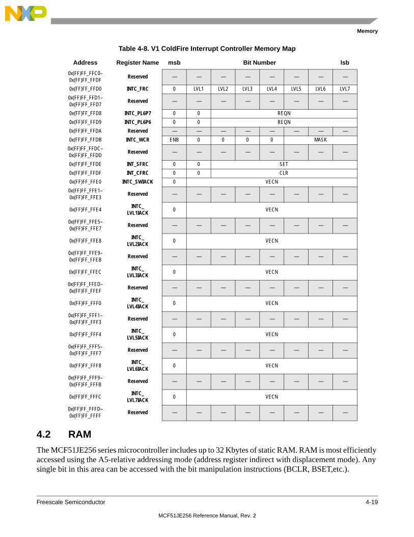
Memory
Freescale Semiconductor 4-19
4.2 RAMThe MCF51JE256 series microcontroller includes up to 32 Kbytes of static RAM. RAM is most efficiently accessed using the A5-relative addressing mode (address register indirect with displacement mode). Any single bit in this area can be accessed with the bit manipulation instructions (BCLR, BSET,etc.).
Table 4-8. V1 ColdFire Interrupt Controller Memory Map
Address Register Name msb Bit Number lsb
0x(FF)FF_FFC0–0x(FF)FF_FFDF
Reserved — — — — — — — —
0x(FF)FF_FFD0 INTC_FRC 0 LVL1 LVL2 LVL3 LVL4 LVL5 LVL6 LVL7
0x(FF)FF_FFD1–0x(FF)FF_FFD7
Reserved — — — — — — — —
0x(FF)FF_FFD8 INTC_PL6P7 0 0 REQN
0x(FF)FF_FFD9 INTC_PL6P6 0 0 REQN
0x(FF)FF_FFDA Reserved — — — — — — — —
0x(FF)FF_FFDB INTC_WCR ENB 0 0 0 0 MASK
0x(FF)FF_FFDC–0x(FF)FF_FFDD
Reserved — — — — — — — —
0x(FF)FF_FFDE INT_SFRC 0 0 SET
0x(FF)FF_FFDF INT_CFRC 0 0 CLR
0x(FF)FF_FFE0 INTC_SWIACK 0 VECN
0x(FF)FF_FFE1–0x(FF)FF_FFE3
Reserved — — — — — — — —
0x(FF)FF_FFE4INTC_
LVL1IACK0 VECN
0x(FF)FF_FFE5–0x(FF)FF_FFE7
Reserved — — — — — — — —
0x(FF)FF_FFE8INTC_
LVL2IACK0 VECN
0x(FF)FF_FFE9–0x(FF)FF_FFEB
Reserved — — — — — — — —
0x(FF)FF_FFECINTC_
LVL3IACK0 VECN
0x(FF)FF_FFED–0x(FF)FF_FFEF
Reserved — — — — — — — —
0x(FF)FF_FFF0INTC_
LVL4IACK0 VECN
0x(FF)FF_FFF1–0x(FF)FF_FFF3
Reserved — — — — — — — —
0x(FF)FF_FFF4INTC_
LVL5IACK0 VECN
0x(FF)FF_FFF5–0x(FF)FF_FFF7
Reserved — — — — — — — —
0x(FF)FF_FFF8INTC_
LVL6IACK0 VECN
0x(FF)FF_FFF9–0x(FF)FF_FFFB
Reserved — — — — — — — —
0x(FF)FF_FFFCINTC_
LVL7IACK0 VECN
0x(FF)FF_FFFD–0x(FF)FF_FFFF
Reserved — — — — — — — —
MCF51JE256 Reference Manual, Rev. 2

Memory
4-20 Freescale Semiconductor
At power-on, the contents of RAM are uninitialized. RAM data is unaffected by any reset provided that the supply voltage does not drop below the minimum value for RAM retention (VRAM).
4.3 Flash MemoryThe flash memory is for program storage and read-only data. In-circuit programming allows the operating program to be loaded into the flash memory after final assembly of the application product. It is possible to program the entire array through the single-wire background debug interface. Because no special voltages are needed for flash erase and programming operations, in-application programming is also possible through other software-controlled communication paths.
Flash memory is ideal for single-supply applications allowing for field reprogramming without requiring external high voltage sources for program or erase operations. The flash module includes a memory controller that executes commands to modify flash memory contents.
Array read access time is one bus cycle for bytes, aligned words, and aligned longwords.
Multiple accesses are needed for misaligned words and longword operands. For flash memory, an erased bit reads 1 and a programmed bit reads 0. It is not possible to read from a flash block while any command is executing on that specific flash block.
CAUTIONA flash block address must be in the erased state before being programmed. Cumulative programming of bits within a flash block address is not allowed except for status field updates required in EEPROM emulation applications.
Flash memory on this device must be programmed 32-bits at a time with long word address aligned when the low-voltage detect flag (LVDF) in the System Power Management Status and Control 1 register (SPMSC1) is clear. If SPMSC1[LVDF] is set, the programming sequence must be modified such that odd and even bytes are written separately. This device’s flash memory is organized as two 16-bit wide blocks interleaved to yield a 32-bit data path. When programming flash if LVDF is set, alternate bytes must be set to 0xFF as shown in Table 4-9. Failure to adhere to these guidelines may result in a partially programmed flash array.
Table 4-9. Alternate Bytes Setting
Addresses Desired Value Values Programmed
0x00 – 0x030x00 – 0x03
0x5555_AAAA0x55FF_AAFF0xFF55_FFAA
0x04 – 0x070x04 – 0x07
0xCCCC_CCCC0xCCFF_CCFF0xFFCC_FFCC
0x08 – 0x0B0x08 – 0x0B
0x1234_56780x12FF_56FF0xFF34_FF78
0x0C – 0x0F0x0C – 0x0F
0x9ABC_DEF00x9AFF_DEFF0xFFBC_FFF0
MCF51JE256 Reference Manual, Rev. 2

Memory
Freescale Semiconductor 4-21
4.3.1 Features
Features of the flash memory include:
• The MCF51JE256 series incorporate dual flash controllers, allowing the microcontroller to execute code from one flash array while programming the other.
• Flash size
— MCF51JE256: 262,144 bytes (256 sectors if 1024 bytes each)
— MCF51JE128: 131,072 (128 sectors of 1024 bytes each)
• Automated program and erase algorithm
• Fast program and sector erase operation
• Burst program command for faster flash array program times
• Single power supply program and erase
• Command interface for fast program and erase operation
• Up to 100,000 program/erase cycles at typical voltage and temperature
• Flexible block protection (on any 2-Kbyte memory boundary for each flash block)
• Security feature to prevent unauthorized access to on-chip memory and resources
• Auto power-down for low-frequency read accesses
4.3.2 Dual Flash Controllers
The MCF51JE256 and MCF51JE128 devices each separate available flash into two distinct blocks. Each block is controlled by its own, independent, flash controller. Memory mapping of the individual arrays is impacted by the current state of ARRAYSEL bit in the SOPT3 register as shown in Table 4-10. Upon initial power up, ARRAYSEL=0, and Array 1 is located at the bottom of the memory map with Array 2 above it. Setting ARRAYSEL=1 reverses the locations of the two arrays in the memory map. The V1 ColdFire core will normally boot from 0x(00)00_0000. The procedure to swap flash arrays must be located in RAM, and must include the following steps:
• Disable flash speculation by the V1 ColdFire CPU by setting CPUCR[FSD] to 1
• Disable all interrupts
• Toggle ARRAYSEL
• Re-enable interrupts
• If desired, re-enable flash seculation by the V1 ColdFire CPU by re-setting CPUCR[FSD] to 0
• jump back (using an indirect jump) to main application code residing in flash memory
Note that swapping flash arrays as discussed above does NOT change the location of the flash controllers in the memory map. Registers in FTSR1 and FTSR2 are fixed in the memory map. Only the flash arrays are impacted by changing ARRAYSEL.
MCF51JE256 Reference Manual, Rev. 2

Memory
4-22 Freescale Semiconductor
4.3.3 Register Descriptions
The flash controller (FTSR) contains a set of 12 control and status registers. Detailed descriptions of each register bit are provided in the sections that follow.
4.3.3.1 Flash Clock Divider Register (FxCDIV)
The FxCDIV register controls the length of timed events in program and erase algorithms executed by the flash memory controller. All bits in the FxCDIV register are readable and writable with restrictions as determined by the value of FDIVLD when writing to the FxCDIV register.
4.3.3.2 Flash Options Register (FxOPT and NVxOPT)
The FxOPT register holds all bits associated with the security of the MCU and flash module. All bits in the FxOPT register are readable but are not writable.
Table 4-10. Flash Array Base Address
ARRAYSEL Array MCF51JE256 MCF51JE128
0 (initial POR value) FTSR1 0x(00)00_0000 0x(00)00_0000
FTSR20x(00)02_0000 0x(00)01_0000
1 FTSR1
FTSR2 0x(00)00_0000 0x(00)00_0000
7 6 5 4 3 2 1 0
RFDIVLD PRDIV8 FDIV
W
Reset 0 0 0 0 0 0 0 0
Figure 4-3. Flash Clock Divider Register (FxCDIV)
Table 4-11. FxCDIV Field Descriptions
Field Description
7FDIVLD
Clock Divider Load Control. When writing to the FxCDIV register for the first time after a reset, the value of the FDIVLD bit written controls the future ability to write to the FxCDIV register:0 Writing a 0 to FDIVLD locks the FxCDIV register contents; all future writes to FxCDIV are ignored.1 Writing a 1 to FDIVLD keeps the FxCDIV register writable; next write to FxCDIV is allowed.When reading the FxCDIV register, the value of the FDIVLD bit read indicates the following:0 FxCDIV register has not been written to since the last reset.1 FxCDIV register has been written to since the last reset.
6PRDIV8
Enable Prescalar by 8.0 The bus clock is directly fed into the clock divider.1 The bus clock is divided by 8 before feeding into the clock divider.
5–0FDIV
Clock Divider Bits. The combination of PRDIV8 and FDIV[5:0] must divide the bus clock down to a frequency of 150 kHz–200 kHz. The minimum divide ratio is 2 (PRDIV8 = 0, FDIV = 0x01) and the maximum divide ratio is 512 (PRDIV8 = 1, FDIV = 0x3F).
MCF51JE256 Reference Manual, Rev. 2

Memory
Freescale Semiconductor 4-23
The FxOPT register is loaded from the flash configuration field during the reset sequence, indicated by F in Figure 4-4.
The security feature in the flash module is described in Section 4.4, “Functional Description”.
4.3.3.3 Flash Configuration Register (FxCNFG)
The FxCNFG register gates the security backdoor writes.
KEYACC is readable and writable while all remaining bits read 0 and are not writable. KEYACC is only writable if KEYEN is set to the enabled state (see Section 4.3.3.2, “Flash Options Register (FxOPT and NVxOPT)”).
NOTEFlash array reads are allowed while KEYACC is set.
7 6 5 4 3 2 1 0
R KEYEN 0 0 0 0 SEC
W
Reset F F 0 0 0 0 F F
Figure 4-4. Flash Options Register (FxOPT)
Table 4-12. FxOPT Field Descriptions
Field Description
7–6KEYEN
Backdoor Key Security Enable Bits. The KEYEN[1:0] bits define the enabling of backdoor key access to the flash module.00 Disabled01 Disabled (Preferred KEYEN state to disable Backdoor Key Access)10 Enabled11 Disabled
5–2 Reserved, should be cleared.
1–0SEC
Flash Security Bits. The SEC[1:0] bits define the security state of the MCU. If the flash module is unsecured using backdoor key access, the SEC[1:0] bits are forced to the unsecured state.00 Unsecured01 Unsecured10 Secured11 Unsecured
7 6 5 4 3 2 1 0
RCBEIE CCIE KEYACC
0 0 0 0 0
W
Reset 0 0 0 0 0 0 0 0
Figure 4-5. Flash Configuration Register (FxCNFG)
MCF51JE256 Reference Manual, Rev. 2

Memory
4-24 Freescale Semiconductor
4.3.3.4 Flash Protection Register (FxPROT and NVxPROT)
NOTEThe FxPROT register defines which flash sectors are protected against program or erase operations. FxPROT bits are readable and writable as long as the size of the protected flash memory is being increased. Any write to FxPROT that attempts to decrease the size of the protected flash memory is ignored.
MCF51JE256/128 have two flash blocks. Each block protection is configured by its respective FxPROT and NVxPROT registers. The flash block swap feature is described in Section 4.1.3, “Flash Module Reserved Memory Locations.” The protection follows the flash block instead of the memory addresses.
During the reset sequence, the FxPROT register is loaded from the flash protection byte in the flash configuration field, indicated by F in Figure 4-6. To change the flash protection loaded during the reset sequence, the flash sector containing the flash configuration field must be unprotected. Then, the flash protection byte must be reprogrammed.
Trying to alter data in any protected area in the flash memory results in a protection violation error and FxSTAT[FPVIOL] is set. The mass erase of the flash array is not possible if any of the flash sectors contained in the flash array are protected.
Table 4-13. FxCNFG Field Descriptions
Field Description
7CBEIE
Command Buffer Empty Interrupt Enable — The CBEIE bit enables an interrupt in case of an empty command buffer in the flash module.0 Command buffer empty interrupt disabled.1 An interrupt will be requested whenever the CBEIF flag (see Section 4.3.3.5, “Flash Status Register (FxSTAT)”) is set.
6CCIE
Command Complete Interrupt Enable — The CCIE bit enables an interrupt in case all commands have been completed in the flash module.0 Command complete interrupt disabled.1 An interrupt will be requested whenever the CCIF flag (see Section 4.3.3.5, “Flash Status Register (FxSTAT)”) is set.
5KEYACC
Enable Security Key Writing0 Writes to the flash block are interpreted as the start of a command write sequence.1 Writes to the flash block are interpreted as keys to open the backdoor.
4–0 Reserved,
7 6 5 4 3 2 1 0
RFPS FPOPEN
W
Reset F F F F F F F F
Figure 4-6. Flash Protection Register (FxPROT)
MCF51JE256 Reference Manual, Rev. 2

Memory
Freescale Semiconductor 4-25
Table 4-14. FxPROT Field Descriptions
Field Description
7–1FPS
Flash Protection Size. With FPOPEN set, the FPS bits determine the size of the protected flash address range as shown in Table 4-15.
0FPOPEN
Flash Protection Open0 Flash array fully protected.1 Flash array protected address range determined by FPS bits.
Table 4-15. Flash Protection Address Range
FPS FPOPEN Protected Address Range
Relative to Flash Array BaseProtected
Size
— 0 0x0_0000–0x1_FFFF 128 Kbytes
0x00–0x3F
1
0x0_0000–0x1_FFFF 128 Kbytes
0x40 0x0_0000–0x1_F7FF 126 Kbytes
0x41 0x0_0000–0x1_EFFF 124 Kbytes
0x42 0x0_0000–0x1_E7FF 122 Kbytes
0x43 0x0_0000–0x1_DFFF 120 Kbytes
0x44 0x0_0000–0x1_D7FF 118 Kbytes
0x45 0x0_0000–0x1_CFFF 116 Kbytes
0x46 0x0_0000-0x1_C7FF 114 Kbytes
MCF51JE256 Reference Manual, Rev. 2

Memory
4-26 Freescale Semiconductor
4.3.3.5 Flash Status Register (FxSTAT)
The FxSTAT register defines the operational status of the flash module. FCBEF, FPVIOL and FACCERR are readable and writable. FBLANK is readable and not writable. The remaining bits read 0 and are not writable.
0x47
1
0x0_0000–0x1_BFFF 112 Kbytes
... ... ...
0x5B 0x0_0000–0x1_1FFF 72 Kbytes
0x5C 0x0_0000–0x1_17FF 70 Kbytes
0x5D 0x0_0000–0x1_0FFF 68 Kbytes
0x5E 0x0_0000–0x1_07FF 66 Kbytes
0x5F 0x0_0000–0x0_FFFF 64 Kbytes
0x60 0x0_0000–0x0_F7FF 62 Kbytes
0x61 0x0_0000–0x0_EFFF 60 Kbytes
0x62 0x0_0000–0x0_E7FF 58 Kbytes
0x63 0x0_0000–0x0_DFFF 56 Kbytes
... ... ...
0x77 0x0_0000–0x0_3FFF 16 Kbytes
0x78 0x0_0000–0x0_37FF 14 Kbytes
0x79 0x0_0000–0x0_2FFF 12 Kbytes
0x7A 0x0_0000–0x0_27FF 10 Kbytes
0x7B 0x0_0000–0x0_1FFF 8 Kbytes
0x7C 0x0_0000–0x0_17FF 6 Kbytes
0x7D 0x0_0000–0x0_0FFF 4 Kbytes
0x7E 0x0_0000–0x0_07FF 2 Kbytes
0x7F No Protection 0 Kbytes
7 6 5 4 3 2 1 0
R FCBEF FCCF FPVIOL FACCERR 0 FBLANK 0 0
W w1c1 w1c w1c
Reset 1 1 0 0 0 0 0 0
1 w1c stands for writing 1 to clear.
Figure 4-7. Flash Status Register (FxSTAT)
Table 4-15. Flash Protection Address Range (Continued)
FPS FPOPEN Protected Address Range
Relative to Flash Array BaseProtected
Size
MCF51JE256 Reference Manual, Rev. 2

Memory
Freescale Semiconductor 4-27
4.3.3.6 Flash Command Register (FxCMD)
The FxCMD register is the flash command register. Bits 6–0 are readable and writable during a command write sequence, while bit 7 reads 0 and is not writable.
Table 4-16. FxSTAT Field Descriptions
Field Description
7FCBEF
Command Buffer Empty Flag. The FCBEF flag indicates that the command buffer is empty so that a new command write sequence can be started when performing burst programming. Writing a 0 to the FCBEF flag has no effect on FCBEF. Writing a 0 to FCBEF after writing an aligned address to the flash array memory, but before FCBEF is cleared, aborts a command write sequence and causes the FACCERR flag to be set. Writing a 0 to FCBEF outside of a command write sequence does not set the FACCERR flag. Writing a 1 to this bit clears it.0 Command buffers are full.1 Command buffers are ready to accept a new command.
6FCCF
Command Complete Flag. The FCCF flag indicates that there are no more commands pending. The FCCF flag is cleared when FCBEF is cleared and sets automatically upon completion of all active and pending commands. The FCCF flag does not set when an active program command completes and a pending burst program command is fetched from the command buffer. Writing to the FCCF flag has no effect on FCCF.0 Command in progress.1 All commands are completed.
5FPVIOL
Protection Violation Flag. The FPVIOL flag indicates an attempt was made to program or erase an address in a protected area of the flash memory during a command write sequence. Writing a 0 to the FPVIOL flag has no effect on FPVIOL. Writing a 1 to this bit clears it. While FPVIOL is set, it is not possible to launch a command or start a command write sequence.0 No protection violation detected.1 Protection violation has occurred.
4FACCERR
Access Error Flag. The FACCERR flag indicates an illegal access has occurred to the flash memory caused by either a violation of the command write sequence, issuing an illegal flash command (see Section 4.3.3.6, “Flash Command Register (FxCMD)”), or the execution of a CPU STOP instruction while a command is executing (FCCF = 0). Writing a 0 to the FACCERR flag has no effect on FACCERR. Writing a 1 to this bit clears it. While FACCERR is set, it is not possible to launch a command or start a command write sequence.0 No access error detected.1 Access error has occurred.
3 Reserved, must be cleared.
2FBLANK
Flag Indicating the Erase Verify Operation Status. When the FCCF flag is set after completion of an erase verify command, the FBLANK flag indicates the result of the erase verify operation. The FBLANK flag is cleared by the flash module when FCBEF is cleared as part of a new valid command write sequence. Writing to the FBLANK flag has no effect on FBLANK.0 Flash block verified as not erased.1 Flash block verified as erased.
1–0 Reserved, should be cleared.
7 6 5 4 3 2 1 0
R 0FCMD
W
Reset 0 0 0 0 0 0 0 0
Figure 4-8. Flash Command Register (FxCMD)
MCF51JE256 Reference Manual, Rev. 2

Memory
4-28 Freescale Semiconductor
4.4 Functional Description
4.4.1 Flash Command Operations
Flash command operations execute program, erase, and erase verify algorithms described in this section. The program and erase algorithms are controlled by the flash memory controller whose time base, FCLK, is derived from the bus clock via a programmable divider.
The next sections describe:
1. How to write the FCDIV register to set FCLK
2. Command write sequences to program, erase, and erase verify operations on the flash memory
3. Valid flash commands
4. Effects resulting from illegal flash command write sequences or aborting flash operations
4.4.1.1 Writing the FCDIV Register
Prior to issuing any flash command after a reset, write the FCDIV register to divide the bus clock within 150–200 kHz. The FCDIV[PRDIV8, FDIV] bits must be set as described in Figure 4-9.
For example, if the bus clock frequency is 25 MHz, FCDIV[FDIV] should be set to 0x0F (001111) and the FCDIV[PRDIV8] bit set to 1. The resulting FCLK frequency is then 195 kHz. In this case, the flash program and erase algorithm timings are increased over the optimum target by:
(200 - 195) 200 = 3% Eqn. 4-1
CAUTIONProgram and erase command execution time increase proportionally with the period of FCLK. Programming or erasing the flash memory with FCLK less than 150 kHz should be avoided. Setting FCDIV to a value such that FCLK is less than 150 kHz can destroy the flash memory due to overstress. Setting FCDIV to a value where FCLK is greater than 200 kHz can result in incomplete programming or erasure of the flash memory cells.
Table 4-17. FxCMD Field Descriptions
Field Description
7 Reserved, must be cleared.
6–0FCMD
Flash Command. Valid flash commands are shown below. Writing any command other than those listed sets the FACCERR flag in the FxSTAT register.0x05 Erase verify0x20 Program0x25 Burst program0x40 Sector erase0x41 Mass erase
MCF51JE256 Reference Manual, Rev. 2

Memory
Freescale Semiconductor 4-29
If the FCDIV register is written, the FDIVLD bit is automatically set. If the FDIVLD bit is 0, the FCDIV register has not been written since the last reset. If the FCDIV register has not been written to, the flash command loaded during a command write sequence does not execute and FSTAT[FACCERR] is set.
Figure 4-9. Determination Procedure for PRDIV8 and FDIV Bits
4.4.1.2 Command Write Sequence
The flash command controller supervises the command write sequence to execute program, erase, and erase verify algorithms.
Before starting a command write sequence, the FACCERR and FPVIOL flags in the FSTAT register must be clear and the FCBEF flag must be set (see Section 4.3.3.5).
set PRDIV8 = 1
yes
no
PRDIV8 = 0 (reset)
12.8MHz?
FCLK = (PRDCLK)/(1+FDIV[5:0])
PRDCLK = bus_clockPRDCLK = bus_clock/8
PRDCLK[kHz]/200 no
set FDIV[5:0] = PRDCLK[kHz]/200-1
yes
START
an integer?
set FDIV[5:0] = INT(PRDCLK[kHz]/200)
END
bus_clock
no
yes0.3MHz?
bus_clock ALL PROGRAM AND ERASECOMMANDS IMPOSSIBLE
Note: • FCLK is the clock of the flash timing control block • INT(x) is the integer part of x (e.g. INT(4.323) = 4)
MCF51JE256 Reference Manual, Rev. 2

Memory
4-30 Freescale Semiconductor
A command write sequence consists of three steps that must be strictly adhered to with writes to the flash module not permitted between the steps. However, flash register and array reads are allowed during a command write sequence. The basic command write sequence is as follows:
1. Write to a valid address in the flash array memory.
2. Write a valid command to the FCMD register.
3. Clear the FCBEF flag in the FSTAT register by writing a 1 to FCBEF to launch the command.
After a command is launched, the completion of the command operation is indicated by the setting of FSTAT[FCCF]. The FCCF flag sets upon completion of all active and buffered burst program commands.
4.4.2 Flash Commands
Table 4-18 summarizes the valid flash commands along with the effects of the commands on the flash block.
CAUTIONA flash block address must be in the erased state before being programmed. Cumulative programming of bits within a flash block address is not allowed except for status field updates required in EEPROM emulation applications.
4.4.2.1 Erase Verify Command
The erase verify operation verifies that the entire flash array memory is erased.
An example flow to execute the erase verify operation is shown in Figure 4-10. The erase verify command write sequence is as follows:
1. Write to a flash block address to start the command write sequence for the erase verify command. The address and data written are ignored.
2. Write the erase verify command, 0x05, to the FCMD register.
3. Clear the FCBEF flag in the FSTAT register by writing a 1 to FCBEF to launch the erase verify command.
Table 4-18. Flash Command Description
FCMDNVM
CommandFunction on Flash Memory
0x05 Erase Verify Verify all memory bytes in the flash array memory are erased.
If the flash array memory is erased, FSTAT[FBLANK] sets upon command completion.
0x20 Program Program an address in the flash array.
0x25 Burst Program Program an address in the flash array with the internal address incrementing after the program operation.
0x40 Sector Erase Erase all memory bytes in a sector of the flash array.
0x41 Mass Erase Erase all memory bytes in the flash array.
A mass erase of the full flash array is only possible when no protection is enabled prior to launching the command.
MCF51JE256 Reference Manual, Rev. 2

Memory
Freescale Semiconductor 4-31
After launching the erase verify command, FSTAT[FCCF] sets after the operation has completed. The number of bus cycles required to execute the erase verify operation is equal to the number of addresses in the flash array memory plus several bus cycles as measured from the time the FCBEF flag is cleared until the FCCF flag is set. Upon completion of the erase verify operation, FSTAT[FBLANK] is set if all addresses in the flash array memory are verified to be erased. If any address in the flash array memory is not erased, the erase verify operation terminates and FSTAT[FBLANK] remains cleared.
Figure 4-10. Example Erase Verify Command Flow
Write: Flash Block Address
Write: FCMD register
Write: FSTAT register
1.
2.
3.
Write: FSTAT registeryes
no
Access Error and
noBit Polling for
Read: FSTAT register
yes
Read: FSTAT register
no
START
yes
FCBEF Set?
Command
FCCF Set?
FACCERR/FPVIOL Set?
noErase Verify
yes
EXITFlash Block
FBLANK Set?
Write: FCDIV register
Read: FCDIV register
yes
noClock RegisterFDIVLD
Set?
Note: FCDIV needs toWrittenCheck
Protection ViolationCheck
Buffer Empty Check
and Dummy Data
Erase Verify Command 0x05
Clear FCBEF 0x80
Clear FACCERR/FPVIOL 0x30
Command CompletionCheck
Status
ErasedFlash BlockNot ErasedEXIT
be set after each reset
MCF51JE256 Reference Manual, Rev. 2

Memory
4-32 Freescale Semiconductor
4.4.2.2 Program Command
The program operation programs a previously erased address in the flash memory using an embedded algorithm. An example flow to execute the program operation is shown in Figure 4-11. The program command write sequence is as follows:
1. Write to a flash block address to start the command write sequence for the program command. The data written is programmed to the address written.
2. Write the program command, 0x20, to the FCMD register.
3. Clear the FCBEF flag in the FSTAT register by writing a 1 to FCBEF to launch the program command.
If an address to be programmed is in a protected area of the flash block, FSTAT[FPVIOL] sets and the program command does not launch. After the program command has successfully launched and the program operation has completed, FSTAT[FCCF] is set.
Figure 4-11. Example Program Command Flow
Write: Flash Array Address
Write: FCMD register
Write: FSTAT register
1.
2.
3.
Write: FSTAT registeryes
no
Access Error and
noBit Polling for
Read: FSTAT register
yes
Read: FSTAT register
no
START
yes
FCBEF Set?
Command
FCCF Set?
FACCERR/FPVIOL Set?
Write: FCDIV register
Read: FCDIV register
yes
noClock RegisterFDIVLD
Set?
Note: FCDIV needs toWrittenCheck
Protection ViolationCheck
Buffer Empty Check
and Program Data
Program Command 0x20
Clear FCBEF 0x80
Clear FACCERR/FPVIOL 0x30
Command CompletionCheck
EXIT
be set after each reset
MCF51JE256 Reference Manual, Rev. 2

Memory
Freescale Semiconductor 4-33
4.4.2.3 Burst Program Command
The burst program operation programs previously erased data in the flash memory using an embedded algorithm.
While burst programming, two internal data registers operate as a buffer and a register (2-stage FIFO) so that a second burst programming command along with the necessary data can be stored to the buffers while the first burst programming command remains in progress. This pipelined operation allows a time optimization when programming more than one consecutive address on a specific row in the flash array as the high voltage generation can be kept active in between two programming commands.
An example flow to execute the burst program operation is shown in Figure 4-12. The burst program command write sequence is as follows:
1. Write to a flash block address to start the command write sequence for the burst program command. The data written is programmed to the address written.
2. Write the program burst command, 0x25, to the FCMD register.
3. Clear the FCBEF flag in the FSTAT register by writing a 1 to FCBEF to launch the program burst command.
4. After the FCBEF flag in the FSTAT register returns to a 1, repeat steps 1 through 3. The address written is ignored but is incremented internally.
The burst program procedure can be used to program the entire flash memory even while crossing row boundaries within the flash array. If data to be burst programmed falls within a protected area of the flash array, FSTAT[FPVIOL] is set and the burst program command does not launch. After the burst program command has successfully launched and the burst program operation has completed, FSTAT[FCCF] is set unless a new burst program command write sequence has been buffered. By executing a new burst program command write sequence on sequential addresses after the FCBEF flag in the FSTAT register has been set, a greater than 50% faster programming time for the entire flash array can be effectively achieved when compared to using the basic program command.
MCF51JE256 Reference Manual, Rev. 2

Memory
4-34 Freescale Semiconductor
Figure 4-12. Example Burst Program Command Flow
4.4.2.4 Sector Erase Command
The sector erase operation erases all addresses in a 2Kbyte sector of flash memory using an embedded algorithm.
Write: Flash Array Address
Write: FCMD register
Write: FSTAT register
1.
2.
3.
Write: FSTAT registeryes
no
Access Error and
noBit Polling for
Read: FSTAT register
yes
Read: FSTAT register
no
START
yes
FCBEF Set?
Command
FCCF Set?
FACCERR/FPVIOL Set?
Write: FCDIV register
Read: FCDIV register
yes
noClock RegisterFDIVLD
Set?
Note: FCDIV needs toWrittenCheck
Protection ViolationCheck
Buffer Empty Check
and Program Data
Burst Program Command 0x25
Clear FCBEF 0x80
Clear FACCERR/FPVIOL 0x30
Command CompletionCheck
EXIT
be set after each reset
noBit Polling for
Read: FSTAT register
yes
FCBEF Set?Command Buffer Empty
Check
yesSequential
no
Next Address?Programming
Decision
MCF51JE256 Reference Manual, Rev. 2

Memory
Freescale Semiconductor 4-35
An example flow to execute the sector erase operation is shown in Figure 4-13. The sector erase command write sequence is as follows:
1. Write to a flash block address to start the command write sequence for the sector erase command. The flash address written determines the sector to be erased while the data written is ignored.
2. Write the sector erase command, 0x40, to the FCMD register.
3. Clear the FCBEF flag in the FSTAT register by writing a 1 to FCBEF to launch the sector erase command.
If a flash sector to be erased is in a protected area of the flash block, FSTAT[FPVIOL] is set and the sector erase command does not launch. After the sector erase command has successfully launched and the sector erase operation has completed, FSTAT[FCCF] is set.
Figure 4-13. Example Sector Erase Command Flow
Write: Flash Sector Address
Write: FCMD register
Write: FSTAT register
1.
2.
3.
Write: FSTAT registeryes
no
Access Error and
noBit Polling for
Read: FSTAT register
yes
Read: FSTAT register
no
START
yes
FCBEF Set?
Command
FCCF Set?
FACCERR/FPVIOL Set?
Write: FCDIV register
Read: FCDIV register
yes
noClock RegisterFDIVLD
Set?
Note: FCDIV needs toWrittenCheck
Protection ViolationCheck
Buffer Empty Check
and Dummy Data
Sector Erase Command 0x40
Clear FCBEF 0x80
Clear FACCERR/FPVIOL 0x30
Command CompletionCheck
EXIT
be set after each reset
MCF51JE256 Reference Manual, Rev. 2

Memory
4-36 Freescale Semiconductor
4.4.2.5 Mass Erase Command
The mass erase operation erases the entire flash array memory using an embedded algorithm. An example flow to execute the mass erase operation is shown in Figure 4-14. The mass erase command write sequence is as follows:
1. Write to a flash block address to start the command write sequence for the mass erase command. The address and data written is ignored.
2. Write the mass erase command, 0x41, to the FCMD register.
3. Clear the FCBEF flag in the FSTAT register by writing a 1 to FCBEF to launch the mass erase command.
If the flash array memory to be mass erased contains any protected area, FSTAT[FPVIOL] is set and the mass erase command does not launch. After the mass erase command has successfully launched and the mass erase operation has completed, FSTAT[FCCF] is set.
Figure 4-14. Example Mass Erase Command Flow
Write: Flash Memory Address
Write: FCMD register
Write: FSTAT register
1.
2.
3.
Write: FSTAT registeryes
no
Access Error and
noBit Polling for
Read: FSTAT register
yes
Read: FSTAT register
no
START
yes
FCBEF Set?
Command
FCCF Set?
FACCERR/FPVIOL Set?
Write: FCDIV register
Read: FCDIV register
yes
noClock RegisterFDIVLD
Set?
Note: FCDIV needs toWrittenCheck
Protection ViolationCheck
Buffer Empty Check
and Dummy Data
Mass Erase Command 0x41
Clear FCBEF 0x80
Clear FACCERR/FPVIOL 0x30
Command CompletionCheck
EXIT
be set after each reset
MCF51JE256 Reference Manual, Rev. 2

Memory
Freescale Semiconductor 4-37
NOTE
The BDM can also perform a mass erase and verify command. See Chapter 27, “Version 1 ColdFire Debug (CF1_DEBUG),” for details.
4.4.3 Illegal Flash Operations
4.4.3.1 Flash Access Violations
The FACCERR flag is set during the command write sequence if any of the following illegal steps are performed, causing the command write sequence to immediately abort:
1. Writing to a flash address before initializing the FCDIV register.
2. This scenario can cause an illegal address reset as this operation is not supported per the memory map. To cause an exception instead of a system reset, set the ADR bit of core register CPUCR. After setting the ADR bit, performing a write operation sets the FACCERR flag.
3. Writing to any flash register other than FCMD after writing to a flash address.
4. Writing to a second flash address in the same command write sequence.
5. Writing an invalid command to the FCMD register.
6. Writing a command other than burst program while FCBEF is set and FCCF is clear.
7. When security is enabled, writing a command other than erase verify or mass erase to the FCMD register when the write originates from a non-secure memory location or from the background debug mode.
8. Writing to a flash address after writing to the FCMD register.
9. Writing to any flash register other than FSTAT (to clear FCBEF) after writing to the FCMD register.
10. Writing a 0 to the FCBEF flag in the FSTAT register to abort a command write sequence.
The FACCERR flag is also set if the MCU enters stop mode while any command is active (FCCF=0). The operation is aborted immediately and, if burst programming, any pending burst program command is purged (see Section 4.4.4.2, “Stop Modes”).
The FACCERR flag does not set if any flash register is read during a valid command write sequence.
If the flash memory is read during execution of an algorithm (FCCF = 0), the read operation returns invalid data and the FACCERR flag is not set.
If the FACCERR flag is set in the FSTAT register, clear the FACCERR flag before starting another command write sequence (see Section 4.3.3.5, “Flash Status Register (FxSTAT)”).
4.4.3.2 Flash Protection Violations
The FPVIOL flag is set after the command is written to the FCMD register if any of the following illegal operations are attempted:
1. Writing the program command if the address written in the command write sequence was in a protected area of the flash array.
MCF51JE256 Reference Manual, Rev. 2

Memory
4-38 Freescale Semiconductor
2. Writing the sector erase command if the address written in the command write sequence was in a protected area of the flash array.
3. Writing the mass erase command while any flash protection is enabled.
As a result of any of the above, the command write sequence immediately aborts. If FSTAT[FPVIOL] is set, clear the FPVIOL flag before starting another command write sequence (see Section 4.3.3.5, “Flash Status Register (FxSTAT)”).
4.4.4 Operating Modes
4.4.4.1 Wait Mode
If a command is active (FCCF = 0) when the MCU enters wait mode, the active command and any buffered command is completed.
4.4.4.2 Stop Modes
If a command is active (FCCF = 0) when the MCU enters any stop mode, the operation is aborted. If the operation is program or erase, the flash array data being programmed or erased may be corrupted and the FCCF and FACCERR flags are set. If active, the high voltage circuitry to the flash array is immediately switched off when entering stop mode. Upon exit from stop mode, the FCBEF flag is set and any buffered command is not launched. The FACCERR flag must be cleared before starting a command write sequence (see Section 4.4.1.2, “Command Write Sequence”).
NOTEAs active commands are immediately aborted when the MCU enters stop mode, do not use the STOP instruction during program or erase operations.
Active commands continue when the MCU enters wait mode. Use of the STOP instruction when SOPT1[WAITE] is set is acceptable.
4.4.4.3 Background Debug Mode
In background debug mode, the FPROT register is writable without restrictions. If the MCU is unsecured, all flash commands listed in Table 4-12 can be executed. If the MCU is secured, only a compound mass erase and erase verify command can be executed. See Chapter 27, “Version 1 ColdFire Debug (CF1_DEBUG),” for details.
4.4.5 Flash Security
The flash module provides the necessary security information to the MCU. During each reset sequence, the flash module determines the security state of the MCU as defined in Section 4.1.3, “Flash Module Reserved Memory Locations”.
The contents of the flash security byte in the flash configuration field (see Section 4.3.3.3) must be changed directly by programming the flash security byte location when the MCU is unsecured and the
MCF51JE256 Reference Manual, Rev. 2

Memory
Freescale Semiconductor 4-39
sector containing the flash security byte is unprotected. If the flash security byte is left in a secured state, any reset causes the MCU to initialize into a secure operating mode.
4.4.6 Resets
4.4.6.1 Flash Reset Sequence
On each reset, the flash module executes a reset sequence to hold CPU activity while reading the following resources from the flash block:
• MCU control parameters (see Section 4.1.3)
• Flash protection byte (see Section 4.1.3 and Section 4.3.3.4)
• Flash nonvolatile byte (see Section 4.1.3)
• Flash security byte (see Section 4.1.3 and Section 4.3.3.2)
4.4.6.2 Reset While Flash Command Active
If a reset occurs while any flash command is in progress, that command is immediately aborted. The state of the flash array address being programmed or the sector/block being erased is not guaranteed.
4.4.6.3 Program and Erase Times
Before any program or erase command can be accepted, the flash clock divider (FCDIV) must be written to set the internal clock for the flash module to a frequency (fFCLK) between 150 kHz and 200 kHz.
If the initial flash event is a mass erase and verify from BDM, then CSR3[31:24] must be loaded before the XCSR is written to initiate the erase and verify. The data in the XCSR and CSR3 is then loaded into the flash’s FCDIV register. (See Section 27.3.4, “Configuration/Status Register 3 (CSR3)”). However, if the first flash event is executed by the processor directly, the flash’s FCDIV register is written directly, and the XCSR and CSR3 are not involved.
One period of the resulting clock (1/fFCLK) is used by the command processor to time program and erase pulses. An integer number of these timing pulses are used by the command processor to complete a program or erase command.
Program and erase times are given in the MCF51JE256 Data Sheet, order number MCF51JE256.
4.5 SecurityThe MCF51JE256/128 microcontroller includes circuitry to prevent unauthorized access to the contents of flash and RAM memory. When security is engaged, BDM access is restricted to the upper byte of the ColdFire CSR, XCSR, and CSR2 registers. RAM, flash memory, peripheral registers and most of the CPU register set are not available via BDM. Programs executing from internal memory have normal access to all microcontroller memory locations and resources.
The MCF51JE256/128 devices include two independent flash blocks in support of the robust update feature for on-chip flash. Each flash block has its own set of two security bits as described below. Security must be clear ON BOTH flash blocks in order for the device to be unsecured. This allows the device to
MCF51JE256 Reference Manual, Rev. 2

Memory
4-40 Freescale Semiconductor
remain secure, even when updating one of the two flash blocks during a code upgrade. The remainder of this section discusses security from the perspective of a single flash block. Routines for clearing flash security must be applied to both blocks before the device can be unsecured.
Security is engaged or disengaged based on the state of two nonvolatile register bits (SEC01, SEC00) in the FxOPT register. During reset, the contents of the nonvolatile location, NVxOPT, are copied from flash into the working FxOPT register in high-page register space. A user engages security by programming the NVxOPT location which can be done at the same time the flash memory is programmed. The 1:0 stage engages the security and other three combinations disengage security.
Upon exiting reset, the XCSR[25] bit in the ColdFire CPU is initialized to one if the device is secured, zero otherwise.
A user can choose to allow or disallow a security unlocking mechanism through an 8-byte backdoor security key. The security key can be written by the CPU executing from internal memory. It cannot be entered without the cooperation of a secure user program. The procedure for this is detailed in Section 4.5.1, “Unsecuring the MCU using Backdoor Key Access.”
Development tools will unsecure devices via an alternate BDM-based methodology shown in Figure 4-15. Because both RESET and BKGD pins can be reprogrammed via software, a power-on-reset is required to be absolutely certain of obtaining control of the device via BDM, which is a required prerequisite for clearing security. Other methods (outlined in red in Figure 4-15) can also be used, but may not work under all circumstances.
This device supports two levels of security. Both restrict BDM communications as outlined above. In addition, SOPT1[SL] (see Section 5.7.3, “System Options 1 (SOPT1) Register”) can be used to enable/disable off-chip data accesses through the Mini-FlexBus interface. Off-chip op code accesses through the Mini-FlexBus are always disallowed when security is enabled.
4.5.1 Unsecuring the MCU using Backdoor Key Access
The MCU may be unsecured by using the backdoor key access feature that requires knowledge of the contents of the backdoor keys (see Section 4.1.3, “Flash Module Reserved Memory Locations”). If the KEYEN[1:0] bits are in the enabled state (see Section 4.3.3.2, “Flash Options Register (FxOPT and NVxOPT)”) and the KEYACC bit is set, a write to a backdoor key address in the flash memory triggers a comparison between the written data and the backdoor key data stored in the flash memory. If all backdoor keys are written to the correct addresses in the correct order and the data matches the backdoor keys stored in the flash memory, the MCU is unsecured. The data must be written to the backdoor keys sequentially. Values 0x0000_0000 and 0xFFFF_FFFF are not permitted as backdoor keys. While the KEYACC bit is set, reads of the flash memory return valid data.
The user code stored in the flash memory must have a method of receiving the backdoor keys from an external stimulus. This external stimulus would typically be through one of the on-chip serial ports.
If the KEYEN[1:0] bits are in the enabled state (see Section 4.3.3.2, “Flash Options Register (FxOPT and NVxOPT)”), the MCU can be unsecured by the backdoor key access sequence described below:
1. Set FxCNFG[KEYACC].
MCF51JE256 Reference Manual, Rev. 2

Memory
Freescale Semiconductor 4-41
2. Execute three NOP instructions to provide time for the backdoor state machine to load the starting address and number of keys required into the flash state machine.
3. Sequentially write the correct longwords to the flash address(es) containing the backdoor keys.
4. Clear the KEYACC bit. Depending on the user code used to write the backdoor keys, a wait cycle (NOP) may be required before clearing the KEYACC bit.
5. If all data written match the backdoor keys, the MCU is unsecured and the SEC[1:0] bits in the NVxOPT register are forced to an unsecured state.
The backdoor key access sequence is monitored by an internal security state machine. An illegal operation during the backdoor key access sequence causes the security state machine to lock, leaving the MCU in the secured state. A reset of the MCU causes the security state machine to exit the lock state and allows a new backdoor key access sequence to be attempted. The following operations during the backdoor key access sequence lock the security state machine:
1. If any of the keys written does not match the backdoor keys programmed in the flash array.
2. If the keys are written in the wrong sequence.
3. If any of the keys written are all 0’s or all 1’s.
4. If the KEYACC bit does not remain set while the keys are written.
5. If any of the keys are written on successive MCU clock cycles.
6. Executing a STOP instruction before all keys have been written.
After the backdoor keys have been correctly matched, the MCU is unsecured. After the MCU is unsecured, the flash security byte can be programmed to the unsecure state, if desired.
In the unsecure state, you have full control of the contents of the backdoor keys by programming the associated addresses in the flash configuration field (see Section 4.1.3, “Flash Module Reserved Memory Locations”).
The security as defined in the flash security byte is not changed by using the backdoor key access sequence to unsecure. The stored backdoor keys are unaffected by the backdoor key access sequence. After the next reset of the MCU, the security state of the flash module is determined by the flash security byte. The backdoor key access sequence has no effect on the program and erase protections defined in the flash protection register (FxPROT).
It is not possible to unsecure the MCU by using the backdoor key access sequence in background debug mode (BDM) as the MCU does not allow flash array writes in BDM to the flash module.
MCF51JE256 Reference Manual, Rev. 2

Memory
4-42 Freescale Semiconductor
Figure 4-15. Procedure for Clearing Security on MCF51JE256/128 MCUs via the BDM Port 1
N = number of cycles for SIM to release internal reset. Adder of 16 imposed by the ColdFire core.
BKGD=0 during reset willensure that ENBDM comes up "1"
secure state unknown / unpowered
secure state unknown, CPU halted, FEI 10MHz clock, sync required
secure state unknown,, CPU halted, FEI 10MHz clock, synchronized to debugger
hold BKGD=0, apply power, wait N+16 cycles for POR to de-assert
SYNC
set PRDIV8 and clock divider fields in CSR3
write xcsr[31:24]=0x87 to initiate erase/verifyof flash memory
read xcsr[25] to confirm erase/verify complete
on-chip flash is erased and un-secure
write csr2[25:24]=11 to initiate BDM reset to halt orwrite csr2[25:0]=01 to initiate BDM reset to run
Device is unsecure
no
yes
xcsr[31:24]==0x87
STOP
STOP already unsecured
error conditioncheck code or device
The FTSR is responsible for supplyingan "erase completed and verified" flagfor use by the core in this step.
FLL Enabled, Internal Reference (FEI) at 10MHz is reset default for the ICS
Ways to enter BDM halt mode:
1. BKGD=0 during POR2. BKGD=0 during BDM reset3. BFHBR=1 during BDM reset4. COP reset and CSR2[COPHR]=15. Illegal op code reset and
CSR2[IOPHR]=16. Illegal address reset and
CSR2[IADHR]=17. Loss of Lock reset with
CSR2[LOLHR]=18. Issue BACKGROUND cmd via BDM
interface9. HALT instruction10.BDM breakpoint11.ColdFire Fault-on-Fault
Of these, only method (1) is guaranteed to work under all circumstances.
Read XCSR
xcsr[31:24] != 1000 01-1
xcsr[25]=0
Delay "TBD" cycles
A
The write IS required.
1
1. The last three steps are optional, but recommended.
MCF51JE256 Reference Manual, Rev. 2

Memory
Freescale Semiconductor 4-43
Figure 4-16. Procedure for Clearing Security on MCF51JE256/128 MCUs via the BDM Port 2
secure state unknown / unpowered
secure state unknown, CPU halted, FEI 10MHz clock, sync required
secure state unknown,, CPU halted, FEI 10MHz clock, synchronized to debugger
hold BKGD=0, apply power, wait N+16 cycles for POR to de-assert
SYNC
set PRDIV8 and clock divider fields in CSR3
write xcsr[31:24]=0x8F to transfer divider info to FTSR
xcsr[31:24]==0x87
STOP
STOP already unsecured
error conditioncheck code or device
N = number of cycles for SIM to release internal reset. Adder of 16 imposed by the ColdFire core.
BKGD=0 during reset willensure that ENBDM comes up "1"
FLL Enabled, Internal Reference (FEI) at 10MHz is reset default for the ICS
Read XCSR
xcsr[31:24] != 1000 01-1
xcsr[25]=0
Write PTIMER bits to CSR3
write xcsr[31:24]=0x97 to transfer PTIMER info to FTSR and initiate erase/verify of flash memory
A
MCF51JE256 Reference Manual, Rev. 2

Memory
4-44 Freescale Semiconductor
MCF51JE256 Reference Manual, Rev. 2

Freescale Semiconductor 5-1
Chapter 5 Resets, Interrupts, and General System Control
5.1 IntroductionThis section discusses basic reset and interrupt mechanisms and the various sources of reset and interrupt on an MCF51JE256 series microcontroller. Some interrupt sources from peripheral modules are discussed in greater detail within other sections of this document. This section gathers basic information about all reset and interrupt sources in one place for easy reference.
5.2 FeaturesReset and interrupt features include:
• Multiple sources of reset for flexible system configuration and reliable operation
• System reset status (SRS) register to indicate source of most recent reset
• Separate interrupt vector for most modules (reduces polling overhead) (see Table 5-1)
5.3 Microcontroller ResetResetting the microcontroller provides a way to start processing from a known set of initial conditions. When the ColdFire processor exits reset, it fetches initial 32-bit values for the supervisor stack pointer and program counter from locations 0x(00)00_0000 and 0x(00)00_0004 respectively. On-chip peripheral modules are disabled and I/O pins are initially configured as general-purpose high-impedance inputs with pull-up devices disabled.
The MCF51JE256 series microcontrollers have the following sources for reset:
• Power-on reset (POR)
• External pin reset (PIN)
• Computer operating properly (COP) timer
• Illegal opcode detect (ILOP)
• Illegal address detect (ILAD)
• Low-voltage detect (LVD)
• Clock generator (MCG) loss of clock reset (LOC)• Background debug forced reset
Each of these sources, with the exception of the background debug forced reset, has an associated bit in the system reset status register (SRS).
MCF51JE256 Reference Manual, Rev. 2

Resets, Interrupts, and General System Control
5-2 Freescale Semiconductor
5.3.1 Computer Operating Properly (COP) Watchdog
The COP watchdog is intended to force a system reset when the application software fails to execute as expected. To prevent a system reset from the COP timer (when it is enabled), application software must reset the COP counter periodically. If the application program gets lost and fails to reset the COP counter before it times out, a system reset is generated to force the system back to a known starting point.
After any reset, the COP watchdog is enabled (see Section 5.7.3, “System Options 1 (SOPT1) Register,” for additional information). If the COP watchdog is not used in an application, it can be disabled by clearing SOPT1[COPT].
The COP counter is reset by writing 0x55 and 0xAA (in this order) to the address of SRS during the selected timeout period. Writes do not affect the data in the read-only SRS. As soon as the write sequence is done, the COP timeout period is restarted. If the program fails to do this during the time-out period, the microcontroller resets. Also, if any value other than 0x55 or 0xAA is written to SRS, the microcontroller is immediately reset.
The SOPT2[COPCLKS] field (see Section 5.7.4, “System Options 2 (SOPT2) Register,” for additional information) selects the clock source used for the COP timer. The clock source options are the bus clock or an internal 1 kHz LPOCLK source. With each clock source, there are three associated time-outs controlled by SOPT1[COPT]. Table 5-7 summarizes the control functions of the COPCLKS and COPT bits. The COP watchdog defaults to operation from the 1 kHz LPOCLK source and the longest time-out (210 cycles).
When the bus clock source is selected, windowed COP operation is available by setting SOPT2[COPW]. In this mode, writes to the SRS register to clear the COP timer must occur in the last 25% of the selected timeout period. A premature write immediately resets the microcontroller. When the 1 kHz LPOCLK source is selected, windowed COP operation is not available.
The COP counter is initialized by the first writes to the SOPT1 and SOPT2 registers and after any system reset. Subsequent writes to SOPT1 and SOPT2 have no effect on COP operation. Even if the application uses the reset default settings of the COPT, COPCLKS, and COPW bits, the user should write to the write-once SOPT1 and SOPT2 registers during reset initialization to lock in the settings. This prevents accidental changes if the application program gets lost.
The write to SRS that services (clears) the COP counter should not be placed in an interrupt service routine (ISR) because the ISR could continue to be executed periodically even if the main application program fails.
If the bus clock source is selected, the COP counter does not increment while the microcontroller is in background debug mode or while the system is in stop mode. The COP counter resumes when the microcontroller exits background debug mode or stop mode.
If the 1 kHz LPOCLK source is selected, the COP counter is re-initialized to zero upon entry to background debug mode or stop mode and begins from zero upon exit from background debug mode or stop mode.
MCF51JE256 Reference Manual, Rev. 2

Resets, Interrupts, and General System Control
Freescale Semiconductor 5-3
5.3.2 Illegal Opcode Detect (ILOP)
The default configuration of the V1 ColdFire core enables the generation of an MCU reset in response to the processor's attempted execution of an illegal instruction (except for the ILLEGAL opcode), illegal line A, illegal line F instruction or the detection of a privilege violation (attempted execution of a supervisor instruction while in user mode).
The attempted execution of the STOP instruction with (SOPT[STOPE] = 0 && SOPT[WAITE] = 0) is treated as an illegal instruction.
The attempted execution of the HALT instruction with XCSR[ENBDM] = 0 is treated as an illegal instruction.
The processor generates a reset in response to any of these events if CPUCR[IRD] = 0. If this configuration bit is set, the processor generates the appropriate exception instead of forcing a reset.
5.3.3 Illegal Address Detect (ILAD)
The default configuration of the V1 ColdFire core enables the generation of an MCU reset in response to any processor-detected address error, bus error termination, RTE format error or fault-on-fault condition.
The processor generates a reset if CPUCR[ARD] = 0. If this configuration bit is set, the processor generates the appropriate exception instead of forcing a reset, or simply halts the processor in response to the fault-on-fault condition.
5.4 Interrupts & ExceptionsThe interrupt architecture of ColdFire utilizes a 3-bit encoded interrupt priority level sent from the interrupt controller to the core, providing 7 levels of interrupt requests. Level 7 represents the highest priority interrupt level, while level 1 is the lowest priority. The processor samples for active interrupt requests once per instruction by comparing the encoded priority level against a 3-bit interrupt mask value (I) contained in bits 10:8 of the processor’s status register (SR). If the priority level is greater than the SR[I] field at the sample point, the processor suspends normal instruction execution and initiates interrupt exception processing.
Level 7 interrupts are treated as non-maskable and edge-sensitive within the processor, while levels 1-6 are treated as level-sensitive and may be masked depending on the value of the SR[I] field. For correct operation, the ColdFire processor requires that, after asserted, the interrupt source remain asserted until explicitly disabled by the interrupt service routine.
During the interrupt exception processing, the CPU does the following tasks in order:
1. enters supervisor mode,
2. disables trace mode,
3. uses the vector provided by the INTC when the interrupt was signaled (if CPUCR[IACK] = 0) or explicitly fetches an 8-bit vector from the INTC (if CPUCR[IACK] = 1).
This byte-sized operand fetch during exception processing is known as the interrupt acknowledge (IACK) cycle. The fetched data provides an index into the exception vector table that contains up to 256 addresses
MCF51JE256 Reference Manual, Rev. 2

Resets, Interrupts, and General System Control
5-4 Freescale Semiconductor
(depending upon the specific device), each pointing to the beginning of a specific exception service routine.
In particular, the first 64 exception vectors are reserved for the processor to manage reset, error conditions (access, address), arithmetic faults, system calls, etc. Vectors 64–255 are reserved for interrupt service routines. The MCF51JE256 series microcontrollers support 37 peripheral interrupt sources and an additional seven software interrupt sources. These are mapped into the standard seven ColdFire interrupt levels, with up to 9 levels of prioritization within a given level by the V1 ColdFire interrupt controller. See Table 5-1 for details.
After the interrupt vector number has been retrieved, the processor continues by creating a stack frame in memory. For ColdFire, all exception stack frames are two longwords in length, and contain 32 bits of vector and status register data, along with the 32-bit program counter value of the instruction that was interrupted. After the exception stack frame is stored in memory, the processor accesses the 32-bit pointer from the exception vector table using the vector number as the offset, and then jumps to that address to begin execution of the service routine. After the status register is stored in the exception stack frame, the SR[I] mask field is set to the level of the interrupt being acknowledged, effectively masking that level and all lower values while in the service routine.
All ColdFire processors guarantee that the first instruction of the service routine is executed before interrupt sampling is resumed. By making this initial instruction a load of the SR, interrupts can be safely disabled, if required. Optionally, the processor can be configured to automatically raise the mask level to 7 for any interrupt during exception processing by setting CPUCR[IME] = 1.
During the execution of the service routine, the appropriate actions must be performed on the peripheral to negate the interrupt request.
For more information on exception processing, see the ColdFire Programmer’s Reference Manual. For additional information specific to this device, see Chapter 27, “Version 1 ColdFire Debug (CF1_DEBUG).”
5.4.1 External Interrupt Request (IRQ) Pin
External interrupts are managed by the IRQ status and control register, IRQSC. When the IRQ function is enabled, synchronous logic monitors the pin for edge-only or edge-and-level events. When the microcontroller is in stop mode and system clocks are shut down, a separate asynchronous path is used, so the IRQ pin (if enabled) can wake the microcontroller.
NOTE• This pin does not contain a clamp diode to VDD and should not be driven
above VDD.
• The voltage measured on the internally pulled up IRQ pin will not be pulled to VDD. The internal gates connected to this pin are pulled to VDD. The IRQ pullup should not be used to pull up components external to the microcontroller.
MCF51JE256 Reference Manual, Rev. 2

Resets, Interrupts, and General System Control
Freescale Semiconductor 5-5
5.4.1.1 Pin Configuration Options
The IRQ pin enable (IRQPE) control bit in IRQSC must be set for the IRQ pin to act as the interrupt request (IRQ) input. As an IRQ input, the user can choose the polarity of edges or levels detected (IRQEDG), whether the pin detects edges-only or edges and levels (IRQMOD), and whether an event causes an interrupt or only sets the IRQF flag that can be polled by software (IRQIE).
The IRQ pin, when enabled, defaults to use an internal pull device (IRQPDD = 0), configured as a pull-up or pull-down depending on the polarity chosen. If the user desires to use an external pull-up or pull-down, the IRQPDD can be set to turn off the internal device.
NOTE• This pin does not contain a clamp diode to VDD and should not be driven
above VDD.
• The voltage measured on the internally pulled up IRQ pin is not pulled to VDD. The internal gates connected to this pin are pulled to VDD. The IRQ pullup should not be used to pull up components external to the microcontroller.
5.4.1.2 Edge and Level Sensitivity
The IRQMOD control bit re-configures the detection logic so it detects edge events and pin levels. In the edge and level detection mode, the IRQF status flag becomes set when an edge is detected (when the IRQ pin changes from the deasserted to the asserted level), but the flag is continuously set (and cannot be cleared) as long as the IRQ pin remains at the asserted level.
5.4.2 Interrupt Vectors, Sources, and Local Masks
Table 5-1 shows address assignments for reset and interrupt vectors. The vector names shown in this table are the labels used in the Freescale Semiconductor-provided equate file for the MCF51JE256 series microcontrollers. The table is sorted by priority of the sources, with higher-priority sources at the top of the table. The force_lvl entries do not follow the address and vector number order of the surrounding vectors.
Table 5-1. Address Assignments for Reset and Interrupt Vectors
VectorNumber(s)
Vector Address Offset
Interrupt Level
Priority within Level
Stacked Program Counter
Assignment
0 0x000 — N/A — Initial supervisor stack pointer
1 0x004 — N/A — Initial program counter
2–63 — — N/A — Reserved for internal CPU
exceptions (see Table 7-6)
MCF51JE256 Reference Manual, Rev. 2

Resets, Interrupts, and General System Control
5-6 Freescale Semiconductor
— — 7 7-5 — Reserved
64 0x100 7 mid Next IRQ_pin
65 0x104 7 3 Next Low_voltage_detect
66 0x108 7 2 Next Loss of Lock
67 0x10C 7 1 Next Reserved
— — 6 7 — Reserved for remapped vector #1
— — 6 6 — Reserved for remapped vector #2
68 0x110 6 5 Next PDB
69 0x114 6 4 Next DAC
70 0x118 6 3 Next SPI1
71 0x11C 6 2 Next ADC
72 0x120 6 1 Next USB_Status
73 0x124 5 7 Next TPM1_ch0
74 0x128 5 6 Next TPM1_ch1
75 0x12C 5 5 Next TPM1_ch2
76 0x130 5 4 Next TPM1_ch3
77 0x134 5 3 Next TPM1_ovfl
78 0x138 5 2 Next SPI2
79 0x13C 5 1 Next CMT
80 0x140 4 7 Next TPM2_ch0
81 0x144 4 6 Next TPM2_ch1
82 0x148 4 5 Next TPM2_ch2
83 0x14C 4 4 Next TPM2_ch3
84 0x150 4 3 Next TPM2_ovfl
85 0x154 4 2 Next IIC
86 0x158 4 1 Next PRACMP
87 0x15C 3 7 Next SCI1_err
88 0x160 3 6 Next SCI1_rx
89 0x164 3 5 Next SCI1_tx
Table 5-1. Address Assignments for Reset and Interrupt Vectors (Continued)
VectorNumber(s)
Vector Address Offset
Interrupt Level
Priority within Level
Stacked Program Counter
Assignment
MCF51JE256 Reference Manual, Rev. 2

Resets, Interrupts, and General System Control
Freescale Semiconductor 5-7
90 0x168 3 4 Next SCI2_err
91 0x16C 3 3 Next SCI2_rx
92 0x170 3 2 Next SCI2_tx
93 0x174 3 1 Next EXPANSION
94 0x178 2 7 Next EXPANSION
95 0x17C 2 6 Next KBI1
96 0x180 2 5 Next KBI2
97 0x184 2 4 Next TOD
98 0x188 2 3 Next EXPANSION
99 0x18C 2 2 Next EXPANSION
100 0x190 2 1 Next EXPANSION
101 0x194 1 7 Next EXPANSION
102 0x198 1 6 Next EXPANSION
103 0x19C 7 0 Next Level 7 Software Interrupt
104 0x1A0 6 0 Next Level 6 Software Interrupt
105 0x1A4 5 0 Next Level 5 Software Interrupt
106 0x1A8 4 0 Next Level 4 Software Interrupt
107 0x1AC 3 0 Next Level 3 Software Interrupt
108 0x1B0 2 0 Next Level 2 Software Interrupt
109 0x1B4 1 0 Next Level 1 Software Interrupt
110 0x1B8 1 5 Next EXPANSION
111 0x1BC 1 4 Next EXPANSION
112 0x1C0 1 3 Next FTSR1
113 0x1C4 1 2 Next FTSR2
114 0x1C8 1 1 Next EXPANSION
115 0x1CC N/A N/A Next Reserved
Table 5-1. Address Assignments for Reset and Interrupt Vectors (Continued)
VectorNumber(s)
Vector Address Offset
Interrupt Level
Priority within Level
Stacked Program Counter
Assignment
MCF51JE256 Reference Manual, Rev. 2
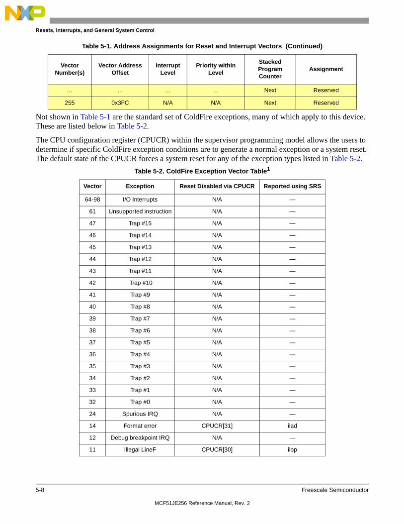
Resets, Interrupts, and General System Control
5-8 Freescale Semiconductor
Not shown in Table 5-1 are the standard set of ColdFire exceptions, many of which apply to this device. These are listed below in Table 5-2.
The CPU configuration register (CPUCR) within the supervisor programming model allows the users to determine if specific ColdFire exception conditions are to generate a normal exception or a system reset. The default state of the CPUCR forces a system reset for any of the exception types listed in Table 5-2.
… … … … Next Reserved
255 0x3FC N/A N/A Next Reserved
Table 5-2. ColdFire Exception Vector Table1
Vector Exception Reset Disabled via CPUCR Reported using SRS
64-98 I/O Interrupts N/A —
61 Unsupported instruction N/A —
47 Trap #15 N/A —
46 Trap #14 N/A —
45 Trap #13 N/A —
44 Trap #12 N/A —
43 Trap #11 N/A —
42 Trap #10 N/A —
41 Trap #9 N/A —
40 Trap #8 N/A —
39 Trap #7 N/A —
38 Trap #6 N/A —
37 Trap #5 N/A —
36 Trap #4 N/A —
35 Trap #3 N/A —
34 Trap #2 N/A —
33 Trap #1 N/A —
32 Trap #0 N/A —
24 Spurious IRQ N/A —
14 Format error CPUCR[31] ilad
12 Debug breakpoint IRQ N/A —
11 Illegal LineF CPUCR[30] ilop
Table 5-1. Address Assignments for Reset and Interrupt Vectors (Continued)
VectorNumber(s)
Vector Address Offset
Interrupt Level
Priority within Level
Stacked Program Counter
Assignment
MCF51JE256 Reference Manual, Rev. 2

Resets, Interrupts, and General System Control
Freescale Semiconductor 5-9
5.5 Low-Voltage Detect (LVD) SystemThe MCF51JE256/128 microcontroller includes a system to protect against low voltage conditions to protect memory contents and control microcontroller system states during supply voltage variations. The system is comprised of a power-on reset (POR) circuit and a LVD circuit with a user-selectable trip voltage, either high (VLVDH) or low (VLVDL). The LVD circuit is enabled when the SPMSC1[LVDE] bit is set and the trip voltage is selected by the SPMSC3[LVDV] bit. The LVD is disabled upon entering Stop2 or Stop3 modes unless the LVDSE bit is set. If both LVDE and LVDSE are set when the STOP instruction is processed, the device will enter STOP4 mode. The LVD can be left enabled in this mode.
5.5.1 Power-On Reset Operation
When power is initially applied to the microcontroller, or when the supply voltage drops below the power-on reset re-arm voltage level, VPOR, the POR circuit will cause a reset condition. As the supply voltage rises, the LVD circuit will hold the microcontroller in reset until the supply has risen above the LVD low threshold, VLVDL. Both the POR bit and the LVD bit in SRS are set following a POR.
5.5.2 LVD Reset Operation
The LVD can be configured to generate a reset upon detection of a low voltage condition by setting LVDRE to 1. The low voltage detection threshold is determined by the LVDV bit. After an LVD reset has occurred, the LVD system will hold the microcontroller in reset until the supply voltage has risen above the low voltage detection threshold. The LVD bit in the SRS register is set following either an LVD reset or POR.
10 Illegal LineA CPUCR[30] ilop
9 Trace N/A —
8 Privileged Violation CPUCR[30] ilop
4 Illegal instruction CPUCR[30] ilop2
3 Address error CPUCR[31] ilad
2 Access error CPUCR[31] ilad
n/a Flt-on-Flt Halt CPUCR[31] ilad
1 Exception vector numbers not appearing in this table are not applicable to the V1 core and are “reserved”.
2 The execution of the ILLEGAL instruction (0x4AFC) always generates an illegal instruction exception, regardless of the state of CPUCR[30].
Table 5-2. ColdFire Exception Vector Table1 (Continued)
Vector Exception Reset Disabled via CPUCR Reported using SRS
MCF51JE256 Reference Manual, Rev. 2

Resets, Interrupts, and General System Control
5-10 Freescale Semiconductor
5.5.3 LVD Interrupt Operation
When a low-voltage condition is detected and the LVD circuit is configured using SPMSC1 for interrupt operation (LVDE set, LVDIE set, and LVDRE clear), then LVDF in SPMSC1 will be set and an LVD interrupt request will occur. To clear the LVDF bit, write a 1 to the LVDACK bit in SPMSC1.
5.5.4 Low-Voltage Warning (LVW) Interrupt Operation
The LVD system has a low voltage warning flag (LVWF) to indicate that the supply voltage is approaching, but is above, the LVD voltage. The LVW also has an interrupt associated with it, enabled by setting the SPMSC3[LVWIE] bit. If enabled, an LVW interrupt request will occur when the LVWF is set. Write a 1 to the SPMSC3[LVWACK] bit to clear LVWF. There are two user-selectable trip voltages for the LVW, one high (VLVWH) and one low (VLVWL). Use the SPMSC3[LVWV] bit to select the trip voltage.
5.6 Peripheral Clock GatingThe MCF51JE256 series microcontroller includes a clock gating system to manage the bus clock sources to the individual peripherals. Using this system, the user can enable or disable the bus clock to each of the peripherals at the clock source, eliminating unnecessary clocks to peripherals which are not in use; thereby reducing the overall run and wait mode currents.
Out of reset, all peripheral clocks will be enabled. For lowest possible run or wait currents, user software should disable the clock source to any peripheral not in use. The actual clock will be enabled or disabled immediately following the write to the clock gating control registers (SCGC1, SCGC2, SCGC3). Any peripheral with a gated clock can not be used unless its clock is enabled. Writing to the registers of a peripheral with a disabled clock has no effect.
NOTEYour software should disable the peripheral before disabling the clocks to the peripheral. When clocks are re-enabled to a peripheral, the peripheral registers need to be re-initialized by software.
In stop modes, the bus clock is disabled for all gated peripherals, regardless of the settings in the SCGC1, SCGC2, and SCGC3 registers.
5.7 Reset, Interrupt, and System Control Registers and Control BitsOne 8-bit register in the direct page register space and eight 8-bit registers in the high-page register space are related to reset and interrupt systems.
Refer to Section 4.1.2, “Detailed register addresses and bit assignments,” for the absolute address assignments for all registers. This section refers to registers and control bits only by their names. A Freescale-provided equate or header file is used to translate these names into the appropriate absolute addresses.
Some control bits in the SOPT1 and SPMSC2 registers are related to modes of operation. Although brief descriptions of these bits are provided here, the related functions are discussed in greater detail in Chapter 3, “Modes of Operation.”
MCF51JE256 Reference Manual, Rev. 2

Resets, Interrupts, and General System Control
Freescale Semiconductor 5-11
5.7.1 Interrupt Pin Request Status and Control Register (IRQSC)
This direct page register includes status and control bits used to configure the IRQ function, report status, and acknowledge IRQ events.
7 6 5 4 3 2 1 0
R 0IRQPDD IRQEDG IRQPE
IRQF 0IRQIE IRQMOD
W IRQACK
Reset 0 0 0 0 0 0 0 0
Figure 5-1. Interrupt Request Status and Control Register (IRQSC)
Table 5-3. IRQSC Register Field Descriptions
Field Description
7 Reserved, should be cleared.
6IRQPDD
Interrupt Request (IRQ) Pull Device Disable— This read/write control bit is used to disable the internal pull-up/pull-down device when the IRQ pin is enabled (IRQPE = 1) allowing for an external device to be used.0 IRQ pull device enabled if IRQPE = 1.1 IRQ pull device disabled if IRQPE = 1.
5IRQEDG
Interrupt Request (IRQ) Edge Select — This read/write control bit is used to select the polarity of edges or levels on the IRQ pin that cause IRQF to be set. The IRQMOD control bit determines whether the IRQ pin is sensitive to both edges and levels or only edges. When IRQEDG = 1 and the internal pull device is enabled, the pull-up device is reconfigured as an optional pull-down device.0 IRQ is falling edge or falling edge/low-level sensitive.1 IRQ is rising edge or rising edge/high-level sensitive.
4IRQPE
IRQ Pin Enable — This read/write control bit enables the IRQ pin function. When this bit is set the IRQ pin can be used as an external interrupt request.0 IRQ pin function is disabled.1 IRQ pin function is enabled.
3IRQF
IRQ Flag — This read-only status bit indicates when an interrupt request event has occurred.0 No IRQ request.1 IRQ event detected.
2IRQACK
IRQ Acknowledge — This write-only bit is used to acknowledge interrupt request events (write 1 to clear IRQF). Writing 0 has no meaning or effect. Reads always return 0. If edge-and-level detection is selected (IRQMOD = 1), IRQF cannot be cleared while the IRQ pin remains at its asserted level.
1IRQIE
IRQ Interrupt Enable — This read/write control bit determines whether IRQ events generate an interrupt request.0 Interrupt request when IRQF set is disabled (use polling).1 Interrupt requested when IRQF = 1.
0IRQMOD
IRQ Detection Mode — This read/write control bit selects edge-only detection or edge-and-level detection. The IRQEDG control bit determines the polarity of edges and levels that are detected as interrupt request events. See Section 5.4.1.2, “Edge and Level Sensitivity” for more details.0 IRQ event on falling edges or rising edges only.1 IRQ event on falling edges and low levels or on rising edges and high levels.
MCF51JE256 Reference Manual, Rev. 2

Resets, Interrupts, and General System Control
5-12 Freescale Semiconductor
5.7.2 System Reset Status Register (SRS)
This high page register includes read-only status flags to indicate the source of the most recent reset. When a debug host forces reset by setting CSR2[BDFR], none of the status bits in SRS is set. To reset the COP counter, write 0x55 and 0xAA (in this order) to the address of SRS during the selected timeout period. The reset state of these bits depends on what caused the microcontroller to reset.
7 6 5 4 3 2 1 0
R POR PIN COP ILOP ILAD LOC LVD 0
W Writing any value to SRS address clears COP watchdog timer.
POR: 1 0 0 0 0 0 1 0
LVD: u 0 0 0 0 0 1 0
Any otherreset:
0 Note1 Note1 Note1 Note1 0 0 0
1 Any of these reset sources that are active at the time of reset entry causes the corresponding bit(s) to be set. Bits corresponding to sources that are not active at the time of reset entry are cleared.
Figure 5-2. System Reset Status (SRS)
Table 5-4. SRS Register Field Descriptions
Field Description
7POR
Power-On Reset — Reset was caused by the power-on detection logic. Because the internal supply voltage was ramping up at the time, the low-voltage reset (LVD) status bit is also set to indicate that the reset occurred while the internal supply was below the LVD threshold.0 Reset not caused by POR.1 POR caused reset.
6PIN
External Reset Pin — Reset was caused by an active-low level on the external reset pin.0 Reset not caused by external reset pin.1 Reset came from external reset pin.
5COP
Computer Operating Properly (COP) Watchdog — Reset was caused by the COP watchdog timer timing out. This reset source can be blocked by SOPT1[COPT] = 0b00.0 Reset not caused by COP timeout.1 Reset caused by COP timeout.
4ILOP
Illegal Opcode — Reset was caused by an attempt to execute an unimplemented or illegal opcode. This includes any illegal instruction [except the ILLEGAL (0x4AFC) opcode] or a privilege violation (execution of a privileged instruction in user mode). The STOP instruction is considered illegal if stop is disabled by ((SOPT[STOPE] = 0) && (SOPT[WAITE] = 0)). The HALT instruction is considered illegal if the BDM interface is disabled by XCSR[ENBDM] = 0.0 Reset not caused by an illegal opcode.1 Reset caused by an illegal opcode.
3ILAD
Illegal Address — Reset was caused by the processor's attempted access of an illegal address in the memory map, an address error, an RTE format error or the fault-on-fault condition. All the illegal address resets are enabled when CPUCR[ARD] = 0. When CPUCR[ARD] = 1, then the appropriate processor exception is generated instead of the reset, or if a fault-on-fault condition is reached, the processor simply halts. 0 Reset not caused by an illegal access.1 Reset caused by an illegal access.
MCF51JE256 Reference Manual, Rev. 2

Resets, Interrupts, and General System Control
Freescale Semiconductor 5-13
5.7.3 System Options 1 (SOPT1) Register
This high-page register has four write-once bits and one write anytime bit. For the write-once bits, only the first write after reset is honored. All bits in the register can be read at any time. Any subsequent attempt to write a write-once bit is ignored to avoid accidental changes to these sensitive settings. SOPT1 should be written to during the reset initialization program to set the desired controls, even if the desired settings are the same as the reset settings.
2LOC
Loss-of-Clock Reset — Reset was caused by a loss of external clock.
0 Reset not caused by a loss of external clock.1 Reset caused by a loss of external clock.
1LVD
Low Voltage Detect — If the LVD is enabled with LVDRE set, and the supply drops below the LVD trip voltage, an LVD reset occurs. This bit is also set by POR.0 Reset not caused by LVD trip or POR.1 Reset caused by LVD trip or POR.
7 6 5 4 3 2 1 0
RCOPT1 STOPE1 WAITE
BLMSSMBSL BKGDPE1 RSTPE1
W
POR: 1 1 0 1 0 0 1 1
LVD: 1 1 0 1 0 0 1 1
Any otherreset:
1 1 0 1 0 0 1 u
1 These bits can be written only one time after reset. Subsequent writes are ignored.
Figure 5-3. System Options 1 (SOPT1) Register
Table 5-5. SOPT1 Field Descriptions
Field Description
7–6COPT
COP Watchdog Timeout — These write-once bits select the timeout period of the COP. COPT along with SOPT2[COPCLKS] defines the COP timeout period as described in Table 5-7.
5STOPE
Stop Mode Enable — This write-once bit is used to enable stop mode. If stop and wait modes are disabled and a user program attempts to execute a STOP instruction, an illegal opcode reset may be generated depending on CPUCR[IRD].
4WAITE
WAIT Mode Enable — This write-anytime bit is used to enable WAIT mode. If stop and wait modes are disabled and a user program attempts to execute a STOP instruction, an illegal opcode reset may be generated depending on CPUCR[IRD].
3BLMSS
Boot Loader Mode Select Status— This Read only bit shows the status of the BLMS bit during the last Power on Reset.0 BLMS pin was high at last POR1 BLMS pin was low at last POR.
Table 5-4. SRS Register Field Descriptions (Continued)
Field Description
MCF51JE256 Reference Manual, Rev. 2

Resets, Interrupts, and General System Control
5-14 Freescale Semiconductor
5.7.4 System Options 2 (SOPT2) Register
This high page register contains bits to configure microcontroller specific features on the MCF51JE256 series microcontrollers.
2MBSL
Mini-FlexBus Security Level — If security is enabled via the mechanisms outlined in Section 18.1.5, “Mini-FlexBus Security Level,” then this bit affects what CPU operations can access off-chip via the Mini-FlexBus interface. This bit has no effect if security is not enabled. 0 All off-chip access (opcode and data) via the Mini-FlexBus is disallowed.1 Off-chip opcode accessed are disallowed. Data accesses are allowed.
1BKGDPE
Background Debug Mode Pin Enable — This write-once bit when set enables the PTD0/BKGD/MS pin to function as BKGD/MS. When clear, the pin functions as one of its output only alternative functions. This pin defaults to the BKGD/MS function following any MCU reset.0 PTD0/BKGD/MS pin functions as PTD0.1 PTD0/BKGD/MS pin functions as BKGD/MS.
0RSTPE
RESET Pin Enable — When set, this write-once bit enables the PTD1/CMPP2/RESET pin to function as RESET. When clear, the pin functions as an open-drain output only. This pin defaults to its RESET function following an MCU POR or LVD. When RSTPE is set, an internal pullup device is enabled on RESET.0 PTD1/CMPP2/RESET pin functions as PTD1.1 PTD1/CMPP2/RESET pin functions as RESET.
7 6 5 4 3 2 1 0
RCOPCLKS1 COPW1 USB_
BIGENDCLKOUT_EN
CMT_CLK_SEL
0 0ACIC
W
Reset: 0 0 1 0 0 0 0 0
1 This bit can be written to only one time after reset. Additional writes are ignored.
Figure 5-4. System Options 2 (SOPT2) Register
Table 5-6. SOPT2 Register Field Descriptions
Field Description
7COPCLKS
COP Watchdog Clock Select — This write-once bit selects the clock source of the COP watchdog.0 Internal 1 kHz LPOCLK is source to COP.1 Bus clock is source to COP.
6COPW
COP Window Mode — This write-once bit specifies whether the COP operates in Normal or Window mode. In Window mode, the 0x55–0xAA write sequence to the SRS register must occur within the last 25% of the selected period; any write to the SRS register during the first 75% of the selected period resets the microcontroller.0 Normal mode1 Window mode
5USB_BIGEND
USB Big Endian — This bit is used to control the endianess (byte order) in USB:0 Little Endian1 Big Endian
Table 5-5. SOPT1 Field Descriptions (Continued)
Field Description
MCF51JE256 Reference Manual, Rev. 2

Resets, Interrupts, and General System Control
Freescale Semiconductor 5-15
5.7.5 SIM Clock Set and Select Register (SIMCO)
This register controls operation of the CLKOUT pin. The CS field in this register controls the output mux function for the CLKOUT pin. The various clock sources must be enabled/disabled via the appropriate controls elsewhere in the device.
4CLKOUT_EN
Clock Output Enable — This bit is used to mux out the BUSCLK clock to PTC7.0 BUSCLK is not available on the external pin PTC7.1 BUSCLK is available on the external pin PTC7.
3CMT_CLK_SEL
CMT Clock Select — This bit selects between BUSCLK and BUSCLK/3 to the CMT module.0 Clock source to CMT is BUSCLK.1 Clock source to CMT is BUSCLK/3.
0ACIC
Analog Comparator to Input Capture Enable— This bit connects the output of the ACMP to TPM1 input channel 0. See Chapter 11, “Programmable Analog Comparator (S08PRACMPV1),” and Chapter 24, “Timer/Pulse-Width Modulator (S08TPMV3),” for more details on this feature.0 ACMP output not connected to TPM1 input channel 0.1 ACMP output connected to TPM1 input channel 0.
Table 5-7. COP Configuration Options
Control BitsClock Source
COP Window1 Opens (SOPT2[COPW] = 1)
1 Windowed COP operation requires the user to clear the COP timer in the last 25% of the selected timeout period. This column displays the minimum number of clock counts required before the COP timer can be reset when in windowed COP mode (SOPT2[COPW] = 1).
COP Overflow CountSOPT2[COPCLKS] SOPT1[COPT]
N/A 00 N/A N/A COP is disabled
0 01 1 kHz LPOCLK N/A 25 cycles (32 ms2)
2 Values shown in milliseconds based on tLPO = 1 ms.
0 10 1 kHz LPOCLK N/A 28 cycles (256 ms2)
0 11 1 kHz LPOCLK N/A 210 cycles (1,024 ms2)
1 01 BUSCLK 6,144 cycles 213 cycles1
1 10 BUSCLK 49,152 cycles 216 cycles1
1 11 BUSCLK 196,608 cycles 218 cycles1
7 6 5 4 3 2 1 0
R 0 0 0 0 0CS
W —1
1 Bit 7 of SIMCO register is reserved for internal Freescale testing. Writing a “1” to this bit impacts TPM1 external clock selection.
Reset: 0 0 0 0 0 0 0 0
Table 5-6. SOPT2 Register Field Descriptions (Continued)
Field Description
MCF51JE256 Reference Manual, Rev. 2

Resets, Interrupts, and General System Control
5-16 Freescale Semiconductor
5.7.6 System Device Identification Register (SDIDH, SDIDL)
These high page read-only registers are included so host development systems can identify the ColdFire derivative. This allows the development software to recognize where specific memory blocks, registers, and control bits are located in a target microcontroller.
Additional configuration information about the ColdFire core and memory system is loaded into the 32-bit D0 (core) and D1 (memory) registers at reset. This information can be stored into memory by the system startup code for later use by configuration-sensitive application code.
Table 5-8. SIMCO Bit Field Descriptions
Field Description
7–3 Reserved
2–0CS
CLKOUT Select000 CLKOUT = 0001 CLKOUT = Crystal oscillator 1010 CLKOUT = Crystal oscillator 2011 CLKOUT = internal RC oscillator100 CLKOUT = BUSCLK101 CLKOUT = CPUCLK110 CLKOUT = LPOCLK111 CLKOUT = ADC asynchronous clock
7 6 5 4 3 2 1 0
R REV ID11 ID10 ID9 ID8
W
Reset: — — — — 1 1 0 0
Figure 5-5. System Device Identification Register — High (SDIDH)
Table 5-9. SDIDH Register Field Descriptions
Field Description
7–4REV
Revision Number. This field indicates the chip revision number.
3–0ID[11:8]
Part Identification Number — Each derivative in the ColdFire family has a unique identification number. The MCF51JE256 series microcontrollers are hard coded to the value 0xC04. See also ID bits in Table 5-10.
7 6 5 4 3 2 1 0
R ID7 ID6 ID5 ID4 ID3 ID2 ID1 ID0
W
Reset: 0 0 0 0 0 1 0 0
Figure 5-6. System Device Identification Register — Low (SDIDL)
MCF51JE256 Reference Manual, Rev. 2

Resets, Interrupts, and General System Control
Freescale Semiconductor 5-17
5.7.7 System Clock Gating Control 1 Register (SCGC1)
This high page register contains control bits to enable or disable the bus clock to the CMT, TPMx, ADC, DAC, IIC, and SCIx modules. Gating off the clocks to unused peripherals is used to reduce the microcontroller’s run and wait currents. See Section 5.6, “Peripheral Clock Gating,” for more information.
Table 5-10. SDIDL Register Field Descriptions
Field Description
7–0ID[7–0]
Part Identification Number — Each derivative in the ColdFire family has a unique identification number. The MCF51JE256 series microcontrollers are hard coded to the value 0xC04. See also ID bits in Table 5-9.
7 6 5 4 3 2 1 0
RCMT TPM2 TPM1 ADC DAC IIC SCI2 SCI1
W
Reset: 1 1 1 1 1 1 1 1
Figure 5-7. System Clock Gating Control 1 Register (SCGC1)
Table 5-11. SCGC1 Register Field Descriptions
Field Description
7CMT
CMT Clock Gate Control — This bit controls the clock gate to the CMT module.0 Bus clock to the CMT module is disabled.1 Bus clock to the CMT module is enabled.
6TPM2
TPM2 Clock Gate Control — This bit controls the clock gate to the TPM2 module.0 Bus clock to the TPM2 module is disabled.1 Bus clock to the TPM2 module is enabled.
5TPM1
TPM1 Clock Gate Control — This bit controls the clock gate to the TPM1 module.0 Bus clock to the TPM1 module is disabled.1 Bus clock to the TPM1 module is enabled.
4ADC
ADC Clock Gate Control — This bit controls the clock gate to the ADC module.0 Bus clock to the ADC module is disabled.1 Bus clock to the ADC module is enabled.
3DAC
DAC Clock Gate Control — This bit controls the clock gate to the DAC module.0 Bus clock to the DAC module is disabled.1 Bus clock to the DAC module is enabled.
2IIC
IIC Clock Gate Control — This bit controls the clock gate to the IIC1 module.0 Bus clock to the IIC module is disabled.1 Bus clock to the IIC module is enabled.
1SCI2
SCI2 Clock Gate Control — This bit controls the clock gate to the SCI2 module.0 Bus clock to the SCI2 module is disabled.1 Bus clock to the SCI2 module is enabled.
0SCI1
SCI1 Clock Gate Control — This bit controls the clock gate to the SCI1 module.0 Bus clock to the SCI1 module is disabled.1 Bus clock to the SCI1 module is enabled.
MCF51JE256 Reference Manual, Rev. 2

Resets, Interrupts, and General System Control
5-18 Freescale Semiconductor
5.7.8 System Clock Gating Control 2 Register (SCGC2)
This high page register contains control bits to enable or disable the bus clock to the USB, PDB, IRQ, KBI, ACMP, Mini-FlexBus, and SPIx modules. Gating off the clocks to unused peripherals is used to reduce the microcontroller’s run and wait currents. See Section 5.6, “Peripheral Clock Gating,” for more information.
5.7.9 System Clock Gating Control 3 Register (SCGC3)
This high page register contains control bits to enable or disable the bus clock to the following modules:
• VREF
• FLSx
7 6 5 4 3 2 1 0
RUSB PDB IRQ KBI PRACMP MFB SPI2 SPI1
W
POR: 1 1 1 1 1 1 1 1
Figure 5-8. System Clock Gating Control 2 Register (SCGC2)
Table 5-12. SCGC2 Register Field Descriptions
Field Description
7USB
USB Clock Gate Control — This bit controls the bus clock gate to the USB module.0 Bus clock to the USB module is disabled.1 Bus clock to the USB module is enabled.
6PDB
PDB Clock Gate Control — This bit controls the bus clock gate to the PDB registers.0 Bus clock to PDB registers is disabled.1 Bus clock to PDB registers is enabled.
5IRQ
IRQ Clock Gate Control — This bit controls the bus clock gate to the IRQ module.0 Bus clock to the IRQ module is disabled.1 Bus clock to the IRQ module is enabled.
4KBI
KBI Clock Gate Control — This bit controls the clock gate to both of the KBI modules.0 Bus clock to the KBI modules is disabled.1 Bus clock to the KBI modules is enabled.
3PRACMP
PRACMP Clock Gate Control — This bit controls the clock gate to the PRACMP modules.0 Bus clock to the PRACMP module is disabled.1 Bus clock to the PRACMP module is enabled.
2MFB
MFB Clock Gate Control — This bit controls the bus clock gate to the MFB module. Only the bus clock is gated; the clock source of MFB is not controlled by this bit.0 Bus clock to the MFB module is disabled.1 Bus clock to the MFB module is enabled.
1SPI2
SPI2 Clock Gate Control — This bit controls the clock gate to the SPI2 module.0 Bus clock to the SPI2 module is disabled.1 Bus clock to the SPI2 module is enabled.
0SPI1
SPI1 Clock Gate Control — This bit controls the clock gate to the SPI1 module.0 Bus clock to the SPI1 module is disabled.1 Bus clock to the SPI1 module is enabled.
MCF51JE256 Reference Manual, Rev. 2

Resets, Interrupts, and General System Control
Freescale Semiconductor 5-19
Gating off the clocks to unused peripherals is used to reduce the microcontroller’s run and wait currents. See Section 5.6, “Peripheral Clock Gating,” for more information.
5.7.10 System Options 3 Register (SOPT3)
This register contains a bit that controls the pad drive strength for the CMT module.
7 6 5 4 3 2 1 0
RVREF CRC FLS2 FLS1
— — — —
W
Reset: 1 1 1 1 1 1 1 1
Figure 5-9. System Clock Gating Control 3 Register (SCGC3)
Table 5-13. SCGC3 Register Field Descriptions
Field Description
7VREF
VREF Clock Gate Control — This bit controls the clock gate to the VREF module.0 Bus clock to the VREF module is disabled.1 Bus clock to the VREF module is enabled.
6CRC
CRC Clock Gate Control — This bit controls the clock gate to the CRC module.0 Bus clock to the CRC module is disabled.1 Bus clock to the CRC module is enabled.
5FLS2
FLS2 Clock Gate Control — This bit controls the clock gate to the FLS2 module.0 Bus clock to the FLS2 module is disabled.1 Bus clock to the FLS2 module is enabled.
4FLS1
FLS1 Clock Gate Control — This bit controls the clock gate to the FLS1 module.0 Bus clock to the FLS1 module is disabled.1 Bus clock to the FLS1 module is enabled.
7 6 5 4 3 2 1 0
RSCI2PS SCI1PS IICPS USB_PS MB_DATA ARRAYSEL SCI1_PAD CMT_PAD
W
Reset: 0 0 0 0 0 u1
1 This bit is reinitialized by POR, all other resets do not affect this bit.
0 0
POR: 0 0 0 0 0 0 0 0
Figure 5-10. System Options 3 Register (SOPT3)
MCF51JE256 Reference Manual, Rev. 2

Resets, Interrupts, and General System Control
5-20 Freescale Semiconductor
Table 5-14. SOPT3 Field Descriptions
Field Description
7SCI2PS
Configures TX2 and RX2 signal locations.0 PTE5, PTE61 PTF1, PTF2
6SCI1PS
Configures TX1 and RX1 signal locations.0 PTA1, PTA21 PTD6, PTD7
5IICPS
Configures SDA and SCL signal locations.0 PTD4, PTD51 PTF4, PTF3
4USB_PS
Configures USB signals as described below:0
USB_SESSVLD pin PTG4 USB_SESSEND pin PTG1 USB_PULLUP(D+) pin PTD3USB_DP_DOWN pin PTG3 USB_DM_DOWN pin PTG2 USB_ALTCLK pin PTD2
1USB_SESSVLD pin PTE5USB_SESSEND pin PTE6 USB_PULLUP(D+) pin PTD7 USB_DP_DOWN pin PTF1 USB_DM_DOWN pin PTF2 USB_ALTCLK pin PTD6
3MB_DATA
Mini-FlexBus data bus configuration bit — This bit determines which MFB signals are routed to which pins as described below:MB_DATA = 0
FB_D0 pin PTH1 FB_D2 pin PTH7 FB_D3 pin PTH6 FB_D4 pin PTH5 FB_D5 pin PTH4 FB_D6 pin PTH3 FB_D7 pin PTH2 FB_RW pin PTG5 FB_OE pin PTH0
MB_DATA = 1FB_D0 pin PTC1 FFB_D2 pin PTA0 FB_D3 pin PTF5 FB_D4 pin PTF4 FB_D5 pin PTF3 FB_D6 pin PTA3 FB_D7 pin PTE5 FB_RW pin PTE6 FB_OE pin PTC0
2ARRAYSEL
Array select — This bit determines the mapping of the 2 flash arrays as described in Table 4-10.
MCF51JE256 Reference Manual, Rev. 2

Resets, Interrupts, and General System Control
Freescale Semiconductor 5-21
5.7.11 System Options 4 Register (SOPT4)
This register contains bits that control the drive strength and slew rate of various ports.
1SCI1_PAD
SCI_PAD pad drive strength — This bit controls the SCI1 TX(PTD6) pad drive strength by connecting two pads together.0 single-pad drive strength1 dual-pads bounding drive strength
0CMT_PAD
CMT pad drive strength — This bit controls the CMT pad drive strength by connecting two pads together.0 single-pad drive strength1 dual-pads bounding drive strength
7 6 5 4 3 2 1 0
R 0FBALEEN FBAD12IFE FBAD12PUE FBAD12SRE FBAD12DSE IROSRE IRODSE
W
Reset: 0 0 0 0 0 0 0 0
Figure 5-11. System Options 4 Register (SOPT4)
Table 5-15. SOPT4 Field Descriptions
Field Description
7 Reserved, should be cleared.
6FBALEEN
Mini-FlexBus address latch enable1 The ALE function is provided on the PTE0 pin if the EN_CS1 is set and the Mini-Flexbus is enabled.0 Address latch disable.
5FBAD12FE
Input filter enable for the pin where the FB_AD12 signal is located1 Input filter enable.0 Input filter disable.
4FBAD12PUE
Pull-up enable for the pin where the FB_AD12 signal is located1 Pull-up enable.0 Pull-up disable.
3FBAD12SRE
Output slew rate control enable for the pin where the FB_AD12 signal is located1 Output slew rate control enable.0 Output slew rate control disable.
2FBAD12DSE
Drive strength control enable for the pin where the FB_AD12 signal is located1 Drive strength control enable.0 Drive strength control disable.
1IROSRE
Output slew rate control enable for IRO pin1 Output slew rate control enable.0 Output slew rate control disable.
0IRODSE
Drive strength control enable for IRO pin1 Drive strength control enable.0 Drive strength control disable.
Table 5-14. SOPT3 Field Descriptions (Continued)
Field Description
MCF51JE256 Reference Manual, Rev. 2

Resets, Interrupts, and General System Control
5-22 Freescale Semiconductor
5.7.12 System Options 5 Register (SOPT5)
CAUTIONThis location is reserved for Freescale internal testing. Do not write any value to this location. Writing a value to this location can affect on-chip LVD performance.
5.7.13 SIM Internal Peripheral Select Register (SIMIPS)
The fields in this register control source used for the SCI1 RX pin, as well as modulation choice for the SCI1 TX pin. The various clock sources used for modulation purposes must be enabled/disabled via the appropriate controls elsewhere in the device. See Figure 2-6 for an illustration of these controls in action.
7 6 5 4 3 2 1 0
RADCTRS RX1IN
0 0MTBASE1
0MODTX1
W
Reset: 0 0 0 0 0 0 0 0
Figure 5-12. SIM Internal Peripheral Select Register (SIMIPS)
Table 5-16. SIMIPS Register Bit Fields
Field Description
7ADCTRS
ADC Hardware Trigger Select0 PDB is the source of ADHWT. This is the default case for user applications.1 TOD interrupt is the source of ADHWT. The typical application is to use the ADC for the VDD measurements.
6RX1IN
SCI1 RX Input Pin Select0 RX1 is fed from the digital input pin (assuming RX1 is enabled on that pin)1 RX1 is fed from the output of comparator 1
3-2MTBASE1
SCI1 TX Modulation Time Base Select00 TPM1CH001 TPM1CH110 TPM2CH011 TPM2CH1
0MODTX1
Modulate TX10 Do not modulate the output of SCI11 Modulate the output of SCI1 with the timebase selected via the MTBASE1 field
MCF51JE256 Reference Manual, Rev. 2

Resets, Interrupts, and General System Control
Freescale Semiconductor 5-23
5.7.14 Signature Register (Signature)
5.7.15 System Power Management Status and Control 1 Register (SPMSC1)
This high page register contains status and control bits to support the low voltage detect function, and to enable the bandgap voltage reference for use by the ADC module. This register should be written during the user’s reset initialization program to set the desired controls even if the desired settings are the same as the reset settings.
7 6 5 4 3 2 1 0
RSignature Semaphore
W
POR: 0 0 0 0 0 0 0 0
Figure 5-13. Signature Register (Signature)
Table 5-17. Signature Register Field Descriptions
Field Description
7:0Signature
The SIGNATURE semaphore is used as the semaphore to jump to bootloader mode or not after regular reset.
This byte only can be cleared by power-on reset (POR), content retains after regular reset.
7 6 5 4 3 2 1 0
R LVDF1 0LVDIE LVDRE2 LVDSE LVDE2
0BGBE
W LVDACK
Reset: 0 0 0 1 1 1 0 0
1 LVDF is set in the case when VSupply transitions below the trip point or after reset and VSupply is already below VLVW.2 This bit can be written only one time after reset. Additional writes are ignored.
Figure 5-14. System Power Management Status and Control 1 Register (SPMSC1)
Table 5-18. SPMSC1 Register Field Descriptions
Field Description
7LVDF
Low-Voltage Detect Flag — The LVDF bit indicates the low-voltage detect status.0 Low-voltage detect is not present.1 Low-voltage detect is present or was present.
6LVDACK
Low-Voltage Detect Acknowledge — If LVDF = 1, a low-voltage condition has occurred. To acknowledge this low-voltage detect, write 1 to LVDACK, which automatically clears LVDF to 0 if the low-voltage detect is no longer present.
5LVDIE
Low-Voltage Detect Interrupt Enable — This bit enables hardware interrupt requests for LVDF.0 Hardware interrupt disabled (use polling).1 Request a hardware interrupt when LVDF = 1.
MCF51JE256 Reference Manual, Rev. 2

Resets, Interrupts, and General System Control
5-24 Freescale Semiconductor
5.7.16 System Power Management Status and Control 2 Register (SPMSC2)
This high page register contains status and control bits to configure the low power run and wait modes as well as configure the stop mode behavior of the microcontroller.
SPMSC2 is not reset when exiting from STOP2.
4LVDRE
Low-Voltage Detect Reset Enable — This write-once bit enables LVDF events to generate a hardware reset (provided LVDE = 1).0 LVDF does not generate hardware resets.1 Force an MCU reset when an enabled low-voltage detect event occurs.
3LVDSE
Low-Voltage Detect Stop Enable — Provided LVDE = 1, this read/write bit determines whether the low-voltage detect function operates when the MCU is in stop mode.0 Low-voltage detect disabled during stop mode.1 Low-voltage detect enabled during stop mode.
2LVDE
Low-Voltage Detect Enable — This write-once bit enables low-voltage detect logic and qualifies the operation of other bits in this register.0 LVD logic disabled.1 LVD logic enabled.
0BGBE
Bandgap Buffer Enable — This bit enables an internal buffer for the bandgap voltage reference for use by the ADC module on one of its internal channels.0 Bandgap buffer disabled.1 Bandgap buffer enabled.
7 6 5 4 3 2 1 0
RLPR
LPRSLPWUI
0 PPDF 0PPDE1
1 PPDE is a write-once bit that can be used to permanently disable the PPDC bit.
PPDCW PPDACK
Reset: 0 0 0 0 - 0 1 0
Figure 5-15. System Power Management Status and Control 2 Register (SPMSC2)
Table 5-19. SPMSC2 Bit Field Descriptions
Field Description
7LPR
Low-Power Regulator Control — The LPR bit controls entry into the low-power run and low-power wait modes in which the voltage regulator is put into standby. This bit cannot be set if PPDC=1. If PPDC and LPR are set in a single write instruction, only PPDC is actually set. LPR is cleared when an interrupt occurs in low-power mode and the LPWUI bit is 1.0 Low-power run and low-power wait modes are disabled.1 Low-power run and low-power wait modes are requested.
6LPRS
Low-Power Regulator Status — This read-only status bit indicates that the voltage regulator has entered into standby for the low-power run or wait mode.0 The voltage regulator is not currently in standby.1 The voltage regulator is currently in standby.
Table 5-18. SPMSC1 Register Field Descriptions (Continued)
Field Description
MCF51JE256 Reference Manual, Rev. 2

Resets, Interrupts, and General System Control
Freescale Semiconductor 5-25
1 See the MCF51JE256 Data Sheet Electrical Characteristics appendix for minimum and maximum values.
5.7.17 System Power Management Status and Control 3 Register (SPMSC3)
This register reports the status of the low voltage warning function and is used to select the low voltage detect trip voltage. SPMSC3 is not reset when exiting from stop2.
5LPWUI
Low-Power Wake-Up on Interrupt — This bit controls whether or not the voltage regulator exits standby when any active MCU interrupt occurs.0 The voltage regulator remains in standby on an interrupt.1 The voltage regulator exits standby on an interrupt. LPR is cleared.
4 RESERVED
3PPDF
Partial Power-Down Flag — This read-only status bit indicates that the microcontroller has recovered from Stop2 mode.0 Microcontroller has not recovered from Stop2 mode.1 Microcontroller recovered from Stop2 mode.
2PPDACK
Partial Power-Down Acknowledge — Writing a 1 to PPDACK clears the PPDF bit.
1PPDE
Partial Power-Down Enable —The write-once PPDE bit can be used to lockout the partial power-down feature. This is a write-once bit.0 Partial power-down is not enabled.1 Partial power-down is enabled and controlled via the PPDC bit.
0PPDC
Partial Power-Down Control — The PPDC bit controls which power-down mode is selected. This bit cannot be set if LPR = 1. If PPDC and LPR are set in a single write instruction, only PPDC will actually be set. PPDE must be set in order for PPDC to be set.0 Stop3 low power mode enabled.1 Stop2 partial power-down mode enabled.
7 6 5 4 3 2 1 0
R LVWF 0LVDV LVWV LVWIE
0 0 0
W LVWACK
POR: 01 0 0 0 0 0 0 0
LVR: 01 0 U U 0 0 0 0
Otherresets:
01 0 U U 0 0 0 0
1 LVWF is set when VSupply transitions below the trip point or after reset and VSupply is already below VLVW.
Figure 5-16. System Power Management Status and Control 3 Register (SPMSC3)
Table 5-19. SPMSC2 Bit Field Descriptions (Continued)
Field Description
MCF51JE256 Reference Manual, Rev. 2

Resets, Interrupts, and General System Control
5-26 Freescale Semiconductor
5.7.18 Flash Protection Disable Register (FPROTD)
The FPROTD register provides a secure way for the USB bootrom code to overwrite the flash block protection registers. Back to back writes of 0x55 and 0xAA to FROTD, provided the device is in bootmode sets the FPDIS bit. The FPDIS bit is used as a signal to the flash module to allow writes to each block protection register.
Any writes other than 0x55 followed by 0xAA clears the FPDIS bit.
Table 5-20. SPMSC3 Bit Field Descriptions
Field Description
7LVWF
Low-Voltage Warning Flag — The LVWF bit indicates the low voltage warning status.0 Low voltage warning not present.1 Low voltage warning is present or was present.
6LVWACK
Low-Voltage Warning Acknowledge — Writing a 1 to LVWACK clears LVWF if a low voltage warning is not present.
5LVDV
Low-Voltage Detect Voltage Select — The LVDV bit selects the LVD trip point voltage (VLVD).0 Low trip point selected (VLVD = VLVDL).1 High trip point selected (VLVD = VLVDH).
4LVWV
Low-Voltage Warning Voltage Select — The LVWV bit selects the LVW trip point voltage (VLVW).0 Low trip point selected (VLVW = VLVWL).1 High trip point selected (VLVW = VLVWH).
3LVWIE
Low-Voltage Warning Interrupt Enable — This bit enables hardware interrupt requests for LVWF. 0 Hardware interrupt disabled (use polling).1 Request a hardware interrupt when LVWF is set.
2–0 Reserved, should be cleared.
Table 5-21. LVD and LVW Trip Point Typical Values1
1 Note: Data in this table may not be up-to-date. Please refer to the DC Characteristics table in the MCF51JE256 series Data Sheet for the latest values.
LVDV:LVWV LVW Trip Point LVD Trip Point
00 VLVWL = 2.15 VLVDL = 1.86
01 VLVWH = 2.6
10Not Recommended
VLVWL = 2.15 VLVDH = 2.33
11 VLVWH = 2.6
MCF51JE256 Reference Manual, Rev. 2

Resets, Interrupts, and General System Control
Freescale Semiconductor 5-27
5.7.19 Mini-FlexBus Pin Control 1 (MFBPC1)
When the Mini-FlexBus is enabled this register is used to enable or disable the Mini-FlexBus functionality for the associated pin. Each of the 32 Mini-FlexBus signals has a corresponding enable bit as described below.
7 6 5 4 3 2 1 0
R 0 0 0 0 0 0 0 FPDIS
W See Note
Reset: 0 0 0 0 0 0 0 0
1 Back to back writes of 0x55 and 0xAA, set FPDIS, any other back to back data clears FPDIS.
Figure 5-17. Flash Protection Disable Register (FPROTD)
Table 5-22. FPROTD Field Descriptions
Field Description
0FPDIS
This bit is set when the device is in bootmode and back to back writes of 0x55 and 0xAA occur. It is cleared during any writes other than 0x55 followed by 0xAA.0 Writes to the flash block protection registers are not allowed1 Writes to flash block protection registers are allowed
7 6 5 4 3 2 1 0
R MFBPEN_AD7
MFBPEN_AD6
MFBPEN_AD5
MFBPEN_AD4
MFBPEN_AD3
MFBPEN_AD2
MFBPEN_AD1
MFBPEN_AD0W
POR: 0 0 0 0 0 0 0 0
LVR: 0 0 0 0 0 0 0 0
Otherresets:
0 0 0 0 0 0 0 0
Figure 5-18. Mini-FlexBus Pin Control 1 (MFBPC1)
Table 5-23. MFBPC1 Field Descriptions
Field Description
7MFBPEN_AD7
Mini-FlexBus pin control for FB_AD70 FB_AD7 functionality disabled1 FB_AD7 functionality enabled if the Mini-FlexBus is enabled.
6MFBPEN_AD6
Mini-FlexBus pin control for FB_AD60 FB_AD6 functionality disabled1 FB_AD6 functionality enabled if the Mini-FlexBus is enabled.
5MFBPEN_AD5
Mini-FlexBus pin control for FB_AD50 FB_AD5 functionality disabled1 FB_AD5 functionality enabled if the Mini-FlexBus is enabled.
MCF51JE256 Reference Manual, Rev. 2

Resets, Interrupts, and General System Control
5-28 Freescale Semiconductor
5.7.20 Mini-FlexBus Pin Control 2 (MFBPC2)
When the Mini-FlexBus is enabled this register is used to enable or disable the Mini-FlexBus functionality for the associated pin. Each of the 32 Mini-FlexBus signals has a corresponding enable bit as described below.
4MFBPEN_AD4
Mini-FlexBus pin control for FB_AD40 FB_AD4 functionality disabled1 FB_AD4 functionality enabled if the Mini-FlexBus is enabled.
3MFBPEN_AD3
Mini-FlexBus pin control for FB_AD30 FB_AD3 functionality disabled1 FB_AD3 functionality enabled if the Mini-FlexBus is enabled.
2MFBPEN_AD2
Mini-FlexBus pin control for FB_AD20 FB_AD2 functionality disabled1 FB_AD2 functionality enabled if the Mini-FlexBus is enabled.
1MFBPEN_AD1
Mini-FlexBus pin control for FB_AD10 FB_AD1 functionality disabled1 FB_AD1 functionality enabled if the Mini-FlexBus is enabled.
0MFBPEN_AD0
Mini-FlexBus pin control for FB_AD00 FB_AD0 functionality disabled1 FB_AD0 functionality enabled if the Mini-FlexBus is enabled.
7 6 5 4 3 2 1 0
R MFBPEN_AD15
MFBPEN_AD14
MFBPEN_AD13
MFBPEN_AD12
MFBPEN_AD11
MFBPEN_AD10
MFBPEN_AD9
MFBPEN_AD8W
POR: 0 0 0 0 0 0 0 0
LVR: 0 0 0 0 0 0 0 0
Otherresets:
0 0 0 0 0 0 0 0
Figure 5-19. Mini-FlexBus Pin Control 2 (MFBPC2)
Table 5-24. MFBPC2 Field Descriptions
Field Description
7MFBPEN_AD15
Mini-FlexBus pin control for FB_AD150 FB_AD15 functionality disabled1 FB_AD15 functionality enabled if the Mini-FlexBus is enabled.
6MFBPEN_AD14
Mini-FlexBus pin control for FB_AD140 FB_AD14 functionality disabled1 FB_AD14 functionality enabled if the Mini-FlexBus is enabled.
5MFBPEN_AD13
Mini-FlexBus pin control for FB_AD130 FB_AD13 functionality disabled1 FB_AD13 functionality enabled if the Mini-FlexBus is enabled.
Table 5-23. MFBPC1 Field Descriptions (Continued)
Field Description
MCF51JE256 Reference Manual, Rev. 2
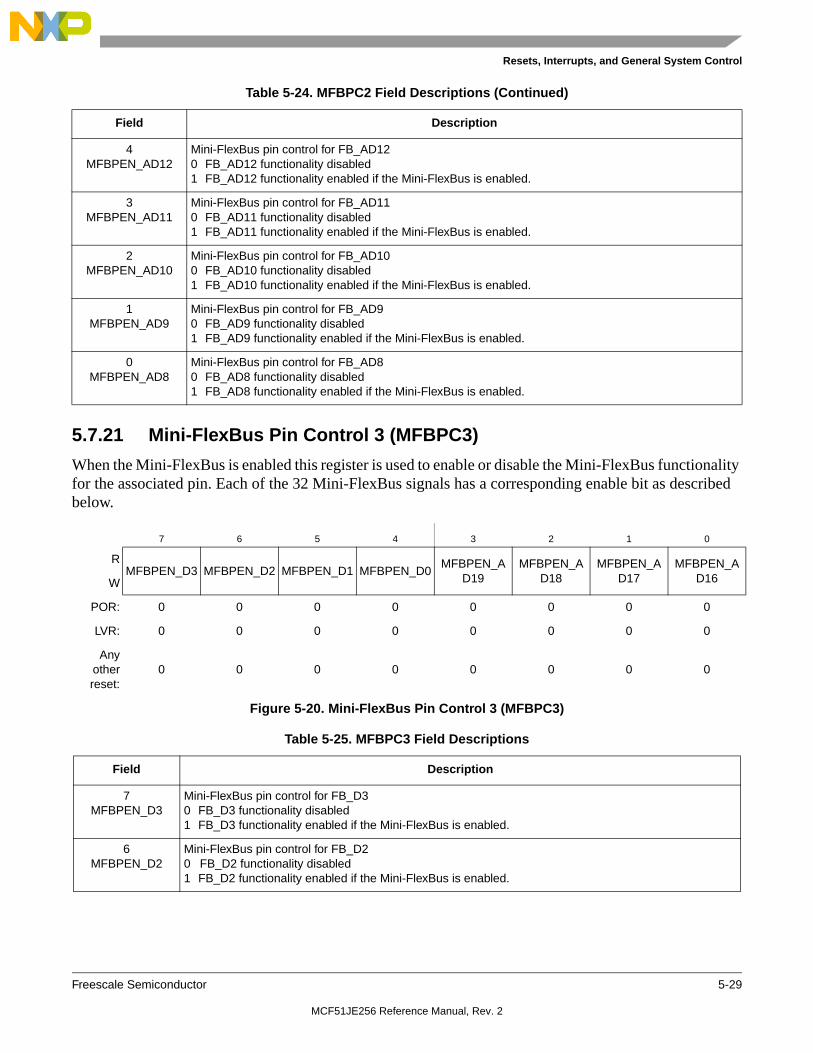
Resets, Interrupts, and General System Control
Freescale Semiconductor 5-29
5.7.21 Mini-FlexBus Pin Control 3 (MFBPC3)
When the Mini-FlexBus is enabled this register is used to enable or disable the Mini-FlexBus functionality for the associated pin. Each of the 32 Mini-FlexBus signals has a corresponding enable bit as described below.
4MFBPEN_AD12
Mini-FlexBus pin control for FB_AD120 FB_AD12 functionality disabled1 FB_AD12 functionality enabled if the Mini-FlexBus is enabled.
3MFBPEN_AD11
Mini-FlexBus pin control for FB_AD110 FB_AD11 functionality disabled1 FB_AD11 functionality enabled if the Mini-FlexBus is enabled.
2MFBPEN_AD10
Mini-FlexBus pin control for FB_AD100 FB_AD10 functionality disabled1 FB_AD10 functionality enabled if the Mini-FlexBus is enabled.
1MFBPEN_AD9
Mini-FlexBus pin control for FB_AD90 FB_AD9 functionality disabled1 FB_AD9 functionality enabled if the Mini-FlexBus is enabled.
0MFBPEN_AD8
Mini-FlexBus pin control for FB_AD80 FB_AD8 functionality disabled1 FB_AD8 functionality enabled if the Mini-FlexBus is enabled.
7 6 5 4 3 2 1 0
RMFBPEN_D3 MFBPEN_D2 MFBPEN_D1 MFBPEN_D0
MFBPEN_AD19
MFBPEN_AD18
MFBPEN_AD17
MFBPEN_AD16W
POR: 0 0 0 0 0 0 0 0
LVR: 0 0 0 0 0 0 0 0
Anyotherreset:
0 0 0 0 0 0 0 0
Figure 5-20. Mini-FlexBus Pin Control 3 (MFBPC3)
Table 5-25. MFBPC3 Field Descriptions
Field Description
7MFBPEN_D3
Mini-FlexBus pin control for FB_D30 FB_D3 functionality disabled1 FB_D3 functionality enabled if the Mini-FlexBus is enabled.
6MFBPEN_D2
Mini-FlexBus pin control for FB_D20 FB_D2 functionality disabled1 FB_D2 functionality enabled if the Mini-FlexBus is enabled.
Table 5-24. MFBPC2 Field Descriptions (Continued)
Field Description
MCF51JE256 Reference Manual, Rev. 2

Resets, Interrupts, and General System Control
5-30 Freescale Semiconductor
5.7.22 Mini-FlexBus Pin Control 4 (MFBPC4)
When the Mini-FlexBus is enabled this register is used to enable or disable the Mini-FlexBus functionality for the associated pin. Each of the 32 Mini-FlexBus signals has a corresponding enable bit as described below.
5MFBPEN_D1
Mini-FlexBus pin control for FB_D10 FB_D1 functionality disabled1 FB_D1 functionality enabled if the Mini-FlexBus is enabled.
4MFBPEN_D0
Mini-FlexBus pin control for FB_D00 FB_D0 functionality disabled1 FB_D0 functionality enabled if the Mini-FlexBus is enabled.
3MFBPEN_AD19
Mini-FlexBus pin control for FB_AD190 FB_AD19 functionality disabled1 FB_AD19 functionality enabled if the Mini-FlexBus is enabled.
2MFBPEN_AD18
Mini-FlexBus pin control for FB_AD180 FB_AD18 functionality disabled1 FB_AD18 functionality enabled if the Mini-FlexBus is enabled.
1MFBPEN_AD17
Mini-FlexBus pin control for FB_AD170 FB_AD17 functionality disabled1 FB_AD 17 functionality enabled if the Mini-FlexBus is enabled.
0MFBPEN_AD16
Mini-FlexBus pin control for FB_AD160 FB_AD16 functionality disabled1 FB_AD16 functionality enabled if the Mini-FlexBus is enabled.
7 6 5 4 3 2 1 0
REN_CS1 EN_CS0 EN_OE EN_RW MFBPEN_D7 MFBPEN_D6 MFBPEN_D5 MFBPEN_D4
W
POR: 0 0 0 0 0 0 0 0
LVR: 0 0 0 0 0 0 0 0
Anyotherreset:
0 0 0 0 0 0 0 0
Figure 5-21. Mini-FlexBus Pin Control 4 (MFBPC4)
Table 5-25. MFBPC3 Field Descriptions (Continued)
Field Description
MCF51JE256 Reference Manual, Rev. 2

Resets, Interrupts, and General System Control
Freescale Semiconductor 5-31
Table 5-26. MFBPC4 Field Descriptions
Field Description
7EN_CS1
Mini-FlexBus pin control for FB_CS1/FB_ALE0 FB_CS1/ALE functionality disabled1 FB_CS1/ALE functionality enabled if the Mini-FlexBus is enabled.
6EN_CS0
Mini-FlexBus pin control for FB_CS00 FB_CS0 functionality disabled1 FB_CS0 functionality enabled if the Mini-FlexBus is enabled.
5EN_OE
Mini-FlexBus pin control for FB_OE0 FB_OE functionality disabled1 FB_OE functionality enabled if the Mini-FlexBus is enabled.
4EN_RW
Mini-FlexBus pin control for FB_RW0 FB_RW functionality disabled1 FB_RW functionality enabled if the Mini-FlexBus is enabled.
3MFBPEN_D7
Mini-FlexBus pin control for FB_D70 FB_D7 functionality disabled1 FB_D7 functionality enabled if the Mini-FlexBus is enabled.
2MFBPEN_D6
Mini-FlexBus pin control for FB_D60 FB_D6 functionality disabled1 FB_D6 functionality enabled if the Mini-FlexBus is enabled.
1MFBPEN_D5
Mini-FlexBus pin control for FB_D50 FB_D5 functionality disabled1 FB_D5 functionality enabled if the Mini-FlexBus is enabled.
0MFBPEN_D4
Mini-FlexBus pin control for FB_D40 FB_D4 functionality disabled1 FB_D4 functionality enabled if the Mini-FlexBus is enabled.
MCF51JE256 Reference Manual, Rev. 2

Resets, Interrupts, and General System Control
5-32 Freescale Semiconductor
MCF51JE256 Reference Manual, Rev. 2
Freescale Semiconductor 6-1
Chapter 6 Parallel Input/Output ControlThis section explains software controls related to parallel input/output (I/O) and pin control. The MCF51JE256 series MCUs have up to nine parallel I/O ports which include a total of 69 I/O pins and one input-only pin, and 2 output only pins. See Chapter 2, “Pins and Connections,” for more information about pin assignments and external hardware considerations of these pins.
In addition to standard I/O port functionality, some port pins have set/clear/toggle functions which are integrated as part of the ColdFire core itself to improve edge resolution on those pins. See Section 6.3, “ColdFire V1 Rapid GPIO Functionality,” and Chapter 9, “Rapid GPIO (RGPIO),” for additional details.
Many port pins are shared with on-chip peripherals such as time systems, communication systems, or keyboard interrupts as shown in Figure 1-1. The peripheral modules have priority over the general-purpose I/O functions so that when a peripheral is enabled, the I/O functions associated with the shared pins may be disabled.
After reset, the shared peripheral functions are disabled and the pins are configured as inputs (PTxDDn = 0). The pin control functions for each pin are configured as follows: slew rate control enabled (PTxSEn = 1), low drive strength selected (PTxDSn = 0), and internal pull-ups disabled (PTxPEn = 0).
NOTENot all general-purpose I/O pins are available on all packages. To avoid extra current drain from floating input pins, the user’s reset initialization routine in the application program must either enable on-chip pull-up devices or change the direction of unconnected pins to outputs so the pins do not float.
6.1 Port Data and Data DirectionReading and writing of parallel I/Os are performed through the port data registers. The direction, either input or output, is controlled through the port data direction registers. The parallel I/O port function for an individual pin is illustrated in the block diagram shown in Figure 6-1.
The data direction control bit (PTxDDn) determines whether the output buffer for the associated pin is enabled, and also controls the source for port data register reads. The input buffer for the associated pin is always enabled unless the pin is enabled as an analog function or is an output-only pin.
When a shared digital function is enabled for a pin, the output buffer is controlled by the shared function. However, the data direction register bit will continue to control the source for reads of the port data register.
When a shared analog function is enabled for a pin, both the input and output buffers are disabled. A value of 0 is read for any port data bit where the bit is an input (PTxDDn = 0) and the input buffer is disabled. In general, whenever a pin is shared with both an alternate digital function and an analog function, the analog
MCF51JE256 Reference Manual, Rev. 2

Parallel Input/Output Control
6-2 Freescale Semiconductor
function has priority such that if both the digital and analog functions are enabled, the analog function controls the pin.
It is good programming practice to write to the port data register before changing the direction of a port pin to become an output. This ensures that the pin will not be driven momentarily with an old data value that happened to be in the port data register.
Figure 6-1. Classic Parallel I/O Block Diagram: Ports A-H, J
6.2 Pull-up, Slew Rate, and Drive StrengthA set of high page registers are used to control pull-ups, slew rate, and drive strength for the pins. They may also be used in conjunction with the peripheral functions on these pins. These registers are associated with the parallel I/O ports, but operate independently of the parallel I/O registers.
6.2.1 Port Internal Pull-up Enable
An internal pull-up device can be enabled for each port pin by setting the corresponding bit in the pull-up enable register (PTxPEn). The pull-up device is disabled if the pin is configured as an output by the parallel I/O control logic or any shared peripheral function regardless of the state of the corresponding pull-up enable register bit. The pull-up device is also disabled if the pin is controlled by an analog function.
6.2.2 Port Slew Rate Enable
Slew rate control can be enabled for each port pin by setting the corresponding bit in the slew rate control register (PTxSEn). When enabled, slew control limits the rate at which an output can transition in order to reduce EMC emissions. Slew rate control has no effect on pins that are configured as inputs.
QD
QD
1
0
Port Read
PTxDDn
PTxDn
Output Enable
Output Data
Input DataSynchronizerData
BUSCLK
Port Data Register
Data Direction Control
MCF51JE256 Reference Manual, Rev. 2

Parallel Input/Output Control
Freescale Semiconductor 6-3
6.2.3 Port Drive Strength Select
An output pin can be selected to have high output drive strength by setting the corresponding bit in the drive strength select register (PTxDSn). When high drive is selected, a pin is capable of sourcing and sinking greater current. Even though every I/O pin can be selected as high drive, the user must ensure that the total current source and sink limits for the MCU are not exceeded. Drive strength selection is intended to affect the DC behavior of I/O pins. However, the AC behavior is also affected. High drive allows a pin to drive a greater load with the same switching speed as a low drive enabled pin into a smaller load. Because of this, the EMC emissions may be affected by enabling pins as high drive.
6.2.4 Port Input Filter Enable
The pad cells used on this device incorporate optional low pass filters on the digital input functions. These may be enabled by setting the appropriate bit in the input filter enable register (PTxIFE[n]) corresponding to a given pin. When set high, a low pass filter (10MHz to 30MHz bandwidth) is enabled in the logic input path. When set low, the filter is bypassed.
The filter is enabled during and after reset by setting the associated PTxIFE bit. The filter is disabled through software control by clearing the associated PTxIFE bit.
6.3 ColdFire V1 Rapid GPIO FunctionalityThe V1 ColdFire core is capable of performing higher speed I/O via its system bus, which does not have latency penalties associated with the on-chip peripheral bus bridge. The ColdFire core contains separate set/clear/data registers which reside at address 0xC0_0000. This functionality can be programmed to take priority on some ports.
This functionality is further defined in Chapter 9, “Rapid GPIO (RGPIO).”
6.4 Keyboard InterruptsSome port pins can be configured as keyboard interrupt inputs and as an external means of waking the MCU from stop or wait low-power modes. The block diagram for each keyboard interrupt logic is shown Figure 6-2.
Figure 6-2. Port Interrupt Block Diagram
KBEDGn
D Q
CK
CLR
VDD
KBIMOD
KBIE
KEYBOARDINTERRUPT FF
KBACK
RESET
SYNCHRONIZER
KBF
STOP BYPASSSTOP
BUSCLK
KBIPEn0
1
S
KBIPE00
1
S
KBEDG0
KBIxP0
KBIxPn
KBIINTERRUPTREQUEST
MCF51JE256 Reference Manual, Rev. 2

Parallel Input/Output Control
6-4 Freescale Semiconductor
Writing to the KBIPEn bits in the keyboard x interrupt pin enable register (KBIxPE) independently enables or disables each port pin. Each port can be configured as edge sensitive or edge and level sensitive based on the KBIMOD bit in the keyboard interrupt status and control register (KBIxSC). Edge sensitivity can be software programmed to be either falling or rising; the level can be either low or high. The polarity of the edge or edge and level sensitivity is selected using the KBEDGn bits in the keyboard interrupt edge select register (KBIxES).
Synchronous logic is used to detect edges. Prior to detecting an edge, enabled port inputs must be at the deasserted logic level. A falling edge is detected when an enabled port input signal is seen as a logic 1 (the deasserted level) during one bus cycle and then a logic 0 (the asserted level) during the next cycle. A rising edge is detected when the input signal is seen as a logic 0 during one bus cycle and then a logic 1 during the next cycle.
6.4.1 Edge Only Sensitivity
A valid edge on an enabled port pin will set KBF in KBIxSC. If the KBIxSC[KBIE] bit is set, an interrupt request will be presented to the CPU. Clearing of KBF is accomplished by writing a 1 to KBIxSC[KBACK].
6.4.2 Edge and Level Sensitivity
A valid edge or level on an enabled port pin will set the KBIxSC[KBF] bit. If KBIxSC[KBIE] is set, an interrupt request will be presented to the CPU. Clearing of KBF is accomplished by writing a 1 to KBIxSC[KBACK], provided all enabled port inputs are at their deasserted levels. KBF will remain set if any enabled port pin is asserted while attempting to clear by writing a 1 to KBACK.
6.4.3 Pull-up/Pull-down Resistors
The keyboard interrupt pins can be configured to use an internal pull-up/pull-down resistor using the associated I/O port pull-up enable register. If an internal resistor is enabled, the KBIxES register is used to select whether the resistor is a pull-up (KBEDGn = 0) or a pull-down (KBEDGn = 1).
6.4.4 Keyboard Interrupt Initialization
When an interrupt pin is first enabled, it is possible to get a false interrupt flag. To prevent a false interrupt request during pin interrupt initialization, the user should do the following:
1. Mask interrupts by clearing KBIxSC[KBIE].
2. Select the pin polarity by setting the appropriate KBIxES[KBEDGn] bits.
3. If using internal pull-up/pull-down device, configure the associated pull enable bits in KBIxPE.
4. Enable the interrupt pins by setting the appropriate KBIxPE[KBIPEn] bits.
5. Write to KBIxSC[KBACK] to clear any false interrupts.
6. Set KBIxSC[KBIE] to enable interrupts.
MCF51JE256 Reference Manual, Rev. 2

Parallel Input/Output Control
Freescale Semiconductor 6-5
6.5 Pin Behavior in Stop ModesPin behavior following execution of a STOP instruction depends on the stop mode that is entered. An explanation of pin behavior for the various stop modes follows:
• Stop2 mode is a partial power-down mode, whereby I/O latches are maintained in their state as before the STOP instruction was executed (port states are lost and will need to be restored upon exiting stop2). CPU register status and the state of I/O registers should be saved in RAM before the STOP instruction is executed to place the MCU in Stop2 mode.Upon recovery from Stop2 mode, before accessing any I/O, the user should examine the state of the SPMSC2[PPDF] bit. If the PPDF bit is cleared, I/O must be initialized as if a power-on-reset had occurred. If the PPDF bit is set, I/O register states should be restored from the values saved in RAM before the STOP instruction was executed and peripherals may require initialization or restoration to their pre-stop condition. The user must then write a 1 to the SPMSC2[PPDACK] bit. Access to I/O is now permitted again in the user application program.
• In Stop3 and Stop4 modes, all I/O is maintained because internal logic circuity stays powered. Upon recovery, normal I/O function is available to the user.
6.6 Parallel I/O, Keyboard Interrupt, and Pin Control RegistersThis section provides information about the registers associated with the parallel I/O ports. The data and data direction registers and the keyboard interrupt registers are located in page zero of the memory map. The pull-up, slew rate, drive strength, and interrupt control registers are located in the high page section of the memory map.
Refer to tables in Chapter 4, “Memory,” for the absolute address assignments for all parallel I/O and their pin control registers. This section refers to registers and control bits only by their names. A Freescale Semiconductor-provided equate or header file normally is used to translate these names into the appropriate absolute addresses.
6.6.1 Port A Registers
Port A is an 8bit Input Output Port.
On reset the pins will default to the input state and under the I/O control.
Port A is controlled by the registers listed below.
6.6.1.1 Port A Data Register (PTAD)
7 6 5 4 3 2 1 0
RPTAD7 PTAD6 PTAD5 PTAD4 PTAD3 PTAD2 PTAD1 PTAD0
W
Reset: 0 0 0 0 0 0 0 0
Figure 6-3. Port A Data Register (PTAD)
MCF51JE256 Reference Manual, Rev. 2

Parallel Input/Output Control
6-6 Freescale Semiconductor
6.6.1.2 Port A Data Direction Register (PTADD)
6.6.1.3 Port A Pull Enable Register (PTAPE)
Table 6-1. PTAD Register Field Descriptions
Field Description
7–0PTADn
Port A Data Register Bits — For port A pins that are inputs, reads return the logic level on the pin. For port A pins that are configured as outputs, reads return the last value written to this register.Writes are latched into all bits of this register. For port A pins that are configured as outputs, the logic level is driven out the corresponding MCU pin.Reset forces PTAD to all 0s, but these 0s are not driven out the corresponding pins because reset also configures all port pins as high-impedance inputs with pull-ups/pull-downs disabled.
7 6 5 4 3 2 1 0
RPTADD7 PTADD6 PTADD5 PTADD4 PTADD3 PTADD2 PTADD1 PTADD0
W
Reset: 0 0 0 0 0 0 0 0
Figure 6-4. Port A Data Direction Register (PTADD)
Table 6-2. PTADD Register Field Descriptions
Field Description
7–0PTADDn
Data Direction for Port A Bits — These read/write bits control the direction of port A pins and what is read for PTAD reads. 0 Input (output driver disabled) and reads return the pin value. 1 Output driver enabled for port A bit n and PTAD reads return the contents of PTADn.
7 6 5 4 3 2 1 0
RPTAPE7 PTAPE6 PTAPE5 PTAPE4 PTAPE3 PTAPE2 PTAPE1 PTAPE0
W
Reset: 0 0 0 0 0 0 0 0
Figure 6-5. Internal Pull Enable for Port A Register (PTAPE)
Table 6-3. PTAPE Register Field Descriptions
Field Description
7–0PTAPEn
Internal Pull Enable for Port A Bits — Each of these control bits determines if the internal pull-up device is enabled for the associated PTA pin. For port A pins that are configured as outputs, these bits have no effect and the internal pull devices are disabled.0 Internal pull-up device disabled for port A bit n.1 Internal pull-up device enabled for port A bit n.
MCF51JE256 Reference Manual, Rev. 2

Parallel Input/Output Control
Freescale Semiconductor 6-7
6.6.1.4 Port A Slew Rate Enable Register (PTASE)
6.6.1.5 Port A Drive Strength Selection Register (PTADS)
7 6 5 4 3 2 1 0
RPTASE7 PTASE6 PTASE51 PTASE4 PTASE3 PTASE2 PTASE1 PTASE0
W
Reset: 0 0 0 0 0 0 0 0
1 PTASE5 has no effect on the open drain PTA5 pin.
Figure 6-6. Slew Rate Enable for Port A Register (PTASE)
Table 6-4. PTASE Register Field Descriptions
Field Description
7–0PTASEn
Output Slew Rate Enable for Port A Bits — Each of these control bits determines if the output slew rate control is enabled for the associated PTA pin. For port A pins that are configured as inputs, these bits have no effect.0 Output slew rate control disabled for port A bit n.1 Output slew rate control enabled for port A bit n.
7 6 5 4 3 2 1 0
RPTADS7 PTADS6 PTADS51 PTADS4 PTADS3 PTADS2 PTADS1 PTADS0
W
Reset: 0 0 0 0 0 0 0 0
1 PTADS5 has no effect on the open drain PTA5 pin.
Figure 6-7. Drive Strength Selection for Port A Register (PTADS)
Table 6-5. PTADS Register Field Descriptions
Field Description
7–0PTADSn
Output Drive Strength Selection for Port A Bits — Each of these control bits selects between low and high output drive for the associated PTA pin. For port A pins that are configured as inputs, these bits have no effect.0 Low output drive strength selected for port A bit n.1 High output drive strength selected for port A bit n.
MCF51JE256 Reference Manual, Rev. 2

Parallel Input/Output Control
6-8 Freescale Semiconductor
6.6.1.6 Port A Input Filter Enable Register (PTAIFE)
The Port A pin incorporates an optional input low-pass filter. Set the associated PTAIFE bit during and after reset to enable the filter. To disable the filter, clear the associated PTAIFE bit through software control.
6.6.2 Port B Registers
Port B is controlled by the registers listed below.
6.6.2.1 Port B Data Register (PTBD)
7 6 5 4 3 2 1 0
RPTAIFE7 PTAIFE6 PTAIFE5 PTAIFE4 PTAIFE3 PTAIFE2 PTAIFE1 PTAIFE0
W
Reset: 1 1 1 1 1 1 1 1
Figure 6-8. Input Filter Enable for Port A Register (PTAIFE)
Table 6-6. PTAIFE Register Field Descriptions
Field Description
7–0PTAIFEn
Input Filter Enable for Port A Bits — Input low-pass filter enable control bits for PTA pins.0 Input filter disabled.1 Input filter enabled.
7 6 5 4 3 2 1 0
RPTBD7 PTBD6 PTBD5 PTBD4 PTBD3 PTBD2 PTBD11
1 Reading PTBD1 always returns the contents of PTBD1 regardless of the setting of the PTBDD1 bit.
PTBD0W
Reset: 0 0 0 0 0 0 0 0
Figure 6-9. Port B Data Register (PTBD)
Table 6-7. PTBD Register Field Descriptions
Field Description
7–0PTBDn
Port B Data Register Bits — For port B pins that are inputs, reads return the logic level on the pin. For port B pins that are configured as outputs, reads return the last value written to this register.Writes are latched into all bits of this register. For port B pins that are configured as outputs, the logic level is driven out the corresponding MCU pin. Reset forces PTBD to all 0s, but these 0s are not driven out the corresponding pins because reset also configures all port pins as high-impedance inputs with pull-ups/pull-downs disabled.
MCF51JE256 Reference Manual, Rev. 2

Parallel Input/Output Control
Freescale Semiconductor 6-9
6.6.2.2 Port B Data Direction Register (PTBDD)
6.6.2.3 Port B Pull Enable Register (PTBPE)
6.6.2.4 Port B Slew Rate Enable Register (PTBSE)
7 6 5 4 3 2 1 0
RPTBDD7 PTBDD6 PTBDD5 PTBDD4 PTBDD3 PTBDD2 PTBDD11
1 PTBDD1 has no effect on the output only PTB1 pin.
PTBDD0W
Reset: 0 0 0 0 0 0 0 0
Figure 6-10. Port B Data Direction Register (PTBDD)
Table 6-8. PTBDD Register Field Descriptions
Field Description
7–0PTBDDn
Data Direction for Port B Bits — These read/write bits control the direction of port B pins and what is read for PTBD reads. 0 Input (output driver disabled) and reads return the pin value. 1 Output driver enabled for port B bit n and PTBD reads return the contents of PTBDn.
7 6 5 4 3 2 1 0
RPTBPE7 PTBPE6 PTBPE5 PTBPE4 PTBPE3 PTBPE2 PTBPE11
1 PTBPE1 has no effect on the output only PTB1 pin.
PTBPE0W
Reset: 0 0 0 0 0 0 0 0
Figure 6-11. Internal Pull Enable for Port B Register (PTBPE)
Table 6-9. PTBPE Register Field Descriptions
Field Description
7–0PTBPEn
Internal Pull Enable for Port B Bits — Each of these control bits determines if the internal pull-up device is enabled for the associated PTB pin. For port B pins that are configured as outputs, these bits have no effect and the internal pull devices are disabled.0 Internal pull-up device disabled for port B bit n.1 Internal pull-up device enabled for port B bit n.
7 6 5 4 3 2 1 0
RPTBSE7 PTBSE6 PTBSE5 PTBSE4 PTBSE3 PTBSE2 PTBSE1 PTBSE0
W
Reset: 0 0 0 0 0 0 0 0
Figure 6-12. Slew Rate Enable for Port B Register (PTBSE)
MCF51JE256 Reference Manual, Rev. 2

Parallel Input/Output Control
6-10 Freescale Semiconductor
6.6.2.5 Port B Drive Strength Selection Register (PTBDS)
6.6.2.6 Port B Input Filter Enable Register (PTBIFE)
The Port B pin incorporates an optional input low-pass filter. Set the associated PTBIFE bit during and after reset to enable the filter. To disable the filter, clear the associated PTBIFE bit through software control.
Table 6-10. PTBSE Register Field Descriptions
Field Description
7–0PTBSEn
Output Slew Rate Enable for Port B Bits — Each of these control bits determines if the output slew rate control is enabled for the associated PTB pin. For port B pins that are configured as inputs, these bits have no effect.0 Output slew rate control disabled for port B bit n.1 Output slew rate control enabled for port B bit n.
7 6 5 4 3 2 1 0
RPTBDS7 PTBDS6 PTBDS5 PTBDS4 PTBDS3 PTBDS2 PTBDS1 PTBDS0
W
Reset: 0 0 0 0 0 0 0 0
Figure 6-13. Drive Strength Selection for Port B Register (PTBDS)
Table 6-11. PTBDS Register Field Descriptions
Field Description
7–0PTBDSn
Output Drive Strength Selection for Port B Bits — Each of these control bits selects between low and high output drive for the associated PTB pin. For port B pins that are configured as inputs, these bits have no effect.0 Low output drive strength selected for port B bit n.1 High output drive strength selected for port B bit n.
7 6 5 4 3 2 1 0
RPTBIFE7 PTBIFE6 PTBIFE5 PTBIFE4 PTBIFE3 PTBIFE2 PTBIFE1 PTBIFE0
W
Reset: 1 1 1 1 1 1 1 1
Figure 6-14. Input Filter Enable for Port B Register (PTBIFE)
Table 6-12. PTBIFE Register Field Descriptions
Field Description
7–0PTBIFEn
Input Filter Enable for Port B Bits — Input low-pass filter enable control bits for PTB pins.0 Input filter disabled.1 Input filter enabled.
MCF51JE256 Reference Manual, Rev. 2

Parallel Input/Output Control
Freescale Semiconductor 6-11
6.6.3 Port C Registers
Port C is controlled by the registers listed below.
6.6.3.1 Port C Data Register (PTCD)
6.6.3.2 Port C Data Direction Register (PTCDD)
7 6 5 4 3 2 1 0
RPTCD7 PTCD6 PTCD5 PTCD4 PTCD3 PTCD2 PTCD1 PTCD0
W
Reset: 0 0 0 0 0 0 0 0
Figure 6-15. Port C Data Register (PTCD)
Table 6-13. PTCD Register Field Descriptions
Field Description
7–0PTCDn
Port C Data Register Bits — For port C pins that are inputs, reads return the logic level on the pin. For port C pins that are configured as outputs, reads return the last value written to this register.Writes are latched into all bits of this register. For port C pins that are configured as outputs, the logic level is driven out the corresponding MCU pin. Reset forces PTCD to all 0s, but these 0s are not driven out the corresponding pins because reset also configures all port pins as high-impedance inputs with pull-ups disabled.
7 6 5 4 3 2 1 0
RPTCDD7 PTCDD6 PTCDD5 PTCDD4 PTCDD3 PTCDD2 PTCDD1 PTCDD0
W
Reset: 0 0 0 0 0 0 0 0
Figure 6-16. Port C Data Direction Register (PTCDD)
Table 6-14. PTCDD Register Field Descriptions
Field Description
7–0PTCDDn
Data Direction for Port C Bits — These read/write bits control the direction of port C pins and what is read for PTCD reads. 0 Input (output driver disabled) and reads return the pin value. 1 Output driver enabled for port C bit n and PTCD reads return the contents of PTCDn.
MCF51JE256 Reference Manual, Rev. 2

Parallel Input/Output Control
6-12 Freescale Semiconductor
6.6.3.3 Port C Pull Enable Register (PTCPE)
6.6.3.4 Port C Slew Rate Enable Register (PTCSE)
6.6.3.5 Port C Drive Strength Selection Register (PTCDS)
7 6 5 4 3 2 1 0
RPTCPE7 PTCPE6 PTCPE5 PTCPE4 PTCPE3 PTCPE2 PTCPE1 PTCPE0
W
Reset: 0 0 0 0 0 0 0 0
Figure 6-17. Internal Pull Enable for Port C Register (PTCPE)
Table 6-15. PTCPE Register Field Descriptions
Field Description
7–0PTCPEn
Internal Pull Enable for Port C Bits — Each of these control bits determines if the internal pull-up device is enabled for the associated PTC pin. For port C pins that are configured as outputs, these bits have no effect and the internal pull devices are disabled.0 Internal pull-up device disabled for port C bit n.1 Internal pull-up device enabled for port C bit n.
7 6 5 4 3 2 1 0
RPTCSE7 PTCSE6 PTCSE5 PTCSE4 PTCSE3 PTCSE2 PTCSE1 PTCSE0
W
Reset: 0 0 0 0 0 0 0 0
Figure 6-18. Slew Rate Enable for Port C Register (PTCSE)
Table 6-16. PTCSE Register Field Descriptions
Field Description
7–0PTCSEn
Output Slew Rate Enable for Port C Bits — Each of these control bits determines if the output slew rate control is enabled for the associated PTC pin. For port C pins that are configured as inputs, these bits have no effect.0 Output slew rate control disabled for port C bit n.1 Output slew rate control enabled for port C bit n.
7 6 5 4 3 2 1 0
RPTCDS7 PTCDS6 PTCDS5 PTCDS4 PTCDS3 PTCDS2 PTCDS1 PTCDS0
W
Reset: 0 0 0 0 0 0 0 0
Figure 6-19. Drive Strength Selection for Port C Register (PTCDS)
MCF51JE256 Reference Manual, Rev. 2

Parallel Input/Output Control
Freescale Semiconductor 6-13
6.6.3.6 Port C Input Filter Enable Register (PTCIFE)
The Port C pin incorporates an optional input low-pass filter. Set the associated PTCIFE bit during and after reset to enable the filter. To disable the filter, clear the associated PTCIFE bit through software control.
6.6.4 Port D Registers
Port D is controlled by the registers listed below.
PTD0 is an output only pin, so the control bits for input functions have no effect on this pin.
6.6.4.1 Port D Data Register (PTDD)
Table 6-17. PTCDS Register Field Descriptions
Field Description
7–0PTCDSn
Output Drive Strength Selection for Port C Bits — Each of these control bits selects between low and high output drive for the associated PTC pin. For port C pins that are configured as inputs, these bits have no effect.0 Low output drive strength selected for port C bit n.1 High output drive strength selected for port C bit n.
7 6 5 4 3 2 1 0
RPTCIFE7 PTCIFE6 PTCIFE5 PTCIFE4 PTCIFE3 PTCIFE2 PTCIFE1 PTCIFE0
W
Reset: 1 1 1 1 1 1 1 1
Figure 6-20. Input Filter Enable for Port C Register (PTCIFE)
Table 6-18. PTCIFE Register Field Descriptions
Field Description
7–0PTCIFEn
Input Filter Enable for Port C Bits — Input low-pass filter enable control bits for PTC pins.0 Input filter disabled.1 Input filter enabled.
7 6 5 4 3 2 1 0
RPTDD7 PTDD6 PTDD5 PTDD4 PTDD3 PTDD2 PTDD1 PTDD01
1 Reads of bit PTDD0 always return the contents of the PTDD0, regardless of the value stored in the PTDDD0 bit.
W
Reset: 0 0 0 0 0 0 0 0
Figure 6-21. Port D Data Register (PTDD)
MCF51JE256 Reference Manual, Rev. 2

Parallel Input/Output Control
6-14 Freescale Semiconductor
6.6.4.2 Port D Data Direction Register (PTDDD)
6.6.4.3 Port D Pull Enable Register (PTDPE)
Table 6-19. PTDD Register Field Descriptions
Field Description
7–0PTDDn
Port D Data Register Bits — For port D pins that are inputs, reads return the logic level on the pin. For port D pins that are configured as outputs, reads return the last value written to this register.Writes are latched into all bits of this register. For port D pins that are configured as outputs, the logic level is driven out the corresponding MCU pin. Reset forces PTDD to all 0s, but these 0s are not driven out the corresponding pins because reset also configures all port pins as high-impedance inputs with pull-ups/pull-downs disabled.
7 6 5 4 3 2 1 0
RPTDDD7 PTDDD6 PTDDD5 PTDDD4 PTDDD3 PTDDD2 PTDDD1 PTDDD01
1 PTDDD0 has no effect in the output only PTD0 pin
W
Reset: 0 0 0 0 0 0 0 0
Figure 6-22. Port D Data Direction Register (PTDDD)
Table 6-20. PTDDD Register Field Descriptions
Field Description
7–0PTDDDn
Data Direction for Port D Bits — These read/write bits control the direction of port D pins and what is read for PTDD reads.0 Input (output driver disabled) and reads return the pin value.1 Output driver enabled for port D bit n and PTDD reads return the contents of PTDDn.
7 6 5 4 3 2 1 0
RPTDPE7 PTDPE6 PTDPE5 PTDPE4 PTDPE3 PTDPE2 PTDPE1 PTDPE01
1 PTDPE0 has no effect in the output only PTD0 pin
W
Reset: 0 0 0 0 0 0 0 0
Figure 6-23. Internal Pull Enable for Port D Register (PTDPE)
Table 6-21. PTDPE Register Field Descriptions
Field Description
7–0PTDPEn
Internal Pull Enable for Port D Bits — Each of these control bits determines if the internal pull-up device is enabled for the associated PTD pin. For port D pins that are configured as outputs, these bits have no effect and the internal pull devices are disabled.0 Internal pull-up device disabled for port D bit n.1 Internal pull-up device enabled for port D bit n.
MCF51JE256 Reference Manual, Rev. 2

Parallel Input/Output Control
Freescale Semiconductor 6-15
6.6.4.4 Port D Slew Rate Enable Register (PTDSE)
6.6.4.5 Port D Drive Strength Selection Register (PTDDS)
6.6.4.6 Port D Input Filter Enable Register (PTDIFE)
The Port D pin incorporates an optional input low-pass filter. Set the associated PTDIFE bit during and after reset to enable the filter. To disable the filter, clear the associated PTDIFE bit through software control.
7 6 5 4 3 2 1 0
RPTDSE7 PTDSE6 PTDSE5 PTDSE4 PTDSE3 PTDSE2 PTDSE1 PTDSE0
W
Reset: 0 0 0 0 0 0 0 0
Figure 6-24. Slew Rate Enable for Port D Register (PTDSE)
Table 6-22. PTDSE Register Field Descriptions
Field Description
7–0PTDSEn
Output Slew Rate Enable for Port D Bits — Each of these control bits determines if the output slew rate control is enabled for the associated PTD pin. For port D pins that are configured as inputs, these bits have no effect.0 Output slew rate control disabled for port D bit n.1 Output slew rate control enabled for port D bit n.
7 6 5 4 3 2 1 0
RPTDDS7 PTDDS6 PTDDS5 PTDDS4 PTDDS3 PTDDS2 PTDDS1 PTDDS0
W
Reset: 0 0 0 0 0 0 0 0
Figure 6-25. Drive Strength Selection for Port D Register (PTDDS)
Table 6-23. PTDDS Register Field Descriptions
Field Description
7–0PTDDSn
Output Drive Strength Selection for Port D Bits — Each of these control bits selects between low and high output drive for the associated PTD pin. For port D pins that are configured as inputs, these bits have no effect.0 Low output drive strength selected for port D bit n.1 High output drive strength selected for port D bit n.
7 6 5 4 3 2 1 0
RPTDIFE7 PTDIFE6 PTDIFE5 PTDIFE4 PTDIFE3 PTDIFE2 PTDIFE1 PTDIFE0
W
Reset: 1 1 1 1 1 1 1 1
Figure 6-26. Input Filter Enable for Port D Register (PTDIFE)
MCF51JE256 Reference Manual, Rev. 2

Parallel Input/Output Control
6-16 Freescale Semiconductor
6.6.5 Port E Registers
Port E is controlled by the registers listed below.
PTE4 is an input only pin. The control bits for input functions do not have an effect on this pin.
6.6.5.1 Port E Data Register (PTED)
6.6.5.2 Port E Data Direction Register (PTEDD)
Table 6-24. PTDIFE Register Field Descriptions
Field Description
7–0PTDIFEn
Input Filter Enable for Port D Bits — Input low-pass filter enable control bits for PTD pins.0 Input filter disabled.1 Input filter enabled.
7 6 5 4 3 2 1 0
RPTED7 PTED6 PTED5 PTED41
1 Reads of bit PTED4 always return the pin value.
PTED3 PTED2 PTED1 PTED0W
Reset: 0 0 0 0 0 0 0 0
Figure 6-27. Port E Data Register (PTED)
Table 6-25. PTED Register Field Descriptions
Field Description
7–0PTEDn
Port E Data Register Bits — For port E pins that are inputs, reads return the logic level on the pin. For port E pins that are configured as outputs, reads return the last value written to this register.Writes are latched into all bits of this register. For port E pins that are configured as outputs, the logic level is driven out the corresponding MCU pin.Reset forces PTED to all 0s, but these 0s are not driven out the corresponding pins because reset also configures all port pins as high-impedance inputs with pull-ups disabled.
7 6 5 4 3 2 1 0
RPTEDD7 PTEDD6 PTEDD5 0 PTEDD3 PTEDD2 PTEDD1 PTEDD0
W
Reset: 0 0 0 0 0 0 0 0
Figure 6-28. Port E Data Direction Register (PTEDD)
MCF51JE256 Reference Manual, Rev. 2

Parallel Input/Output Control
Freescale Semiconductor 6-17
P
6.6.5.3 Port E Pull Enable Register (PTEPE)
6.6.5.4 Port E Slew Rate Enable Register (PTESE)
Table 6-26. PTEDD Register Field Descriptions
Field Description
7–0PTEDDn
Data Direction for Port E Bits — These read/write bits control the direction of port E pins and what is read for PTED reads.0 Input (output driver disabled) and reads return the pin value.1 Output driver enabled for port E bit n and PTED reads return the contents of PTEDn.
Table 6-27. PTETOG Register Field Descriptions
Field Description
7–0PTETOGn
Toggle Enable for Port E Bits — Writing any bit to one in this location will toggle the corresponding bit in the data register. Writing a zero to any bit in this register has no effect.0 Corresponding PTEDn maintains current value.1 Corresponding PTEDn is toggled once.
7 6 5 4 3 2 1 0
RPTEPE7 PTEPE6 PTEPE5 PTEPE4 PTEPE3 PTEPE2 PTEPE1 PTEPE0
W
Reset: 0 0 0 0 0 0 0 0
Figure 6-29. Internal Pull Enable for Port E Register (PTEPE)
Table 6-28. PTEPE Register Field Descriptions
Field Description
7–0PTEPEn
Internal Pull Enable for Port E Bits — Each of these control bits determines if the internal pull-up device is enabled for the associated PTE pin. For port E pins that are configured as outputs, these bits have no effect and the internal pull devices are disabled.0 Internal pull-up device disabled for port E bit n.1 Internal pull-up device enabled for port E bit n.
7 6 5 4 3 2 1 0
RPTESE7 PTESE6 PTESE5 PTESE41
1 PTE4SE has no effect on the PTE4 pin
PTESE3 PTESE2 PTESE1 PTESE0W
Reset: 0 0 0 0 0 0 0 0
Figure 6-30. Slew Rate Enable for Port E Register (PTESE)
MCF51JE256 Reference Manual, Rev. 2

Parallel Input/Output Control
6-18 Freescale Semiconductor
6.6.5.5 Port E Drive Strength Selection Register (PTEDS)
6.6.5.6 Port E Input Filter Enable Register (PTEIFE)
The Port E pin incorporates an optional input low-pass filter. Set the associated PTEIFE bit during and after reset to enable the filter. To disable the filter, clear the associated PTEIFE bit through software control.
Table 6-29. PTESE Register Field Descriptions
Field Description
7–0PTESEn
Output Slew Rate Enable for Port E Bits — Each of these control bits determines if the output slew rate control is enabled for the associated PTE pin. For port E pins that are configured as inputs, these bits have no effect.0 Output slew rate control disabled for port E bit n.1 Output slew rate control enabled for port E bit n.
7 6 5 4 3 2 1 0
RPTEDS7 PTEDS6 PTEDS5 PTEDS41
1 PTEDS4 has no effect on the PTE4 pin
PTEDS3 PTEDS2 PTEDS1 PTEDS0W
Reset: 0 0 0 0 0 0 0 0
Figure 6-31. Drive Strength Selection for Port E Register (PTEDS)
Table 6-30. PTEDS Register Field Descriptions
Field Description
7–0PTEDSn
Output Drive Strength Selection for Port E Bits — Each of these control bits selects between low and high output drive for the associated PTE pin. For port E pins that are configured as inputs, these bits have no effect.0 Low output drive strength selected for port E bit n.1 High output drive strength selected for port E bit n.
7 6 5 4 3 2 1 0
RPTEIFE7 PTEIFE6 PTEIFE5 PTEIFE4 PTEIFE3 PTEIFE2 PTEIFE1 PTEIFE0
W
Reset: 1 1 1 1 1 1 1 1
Figure 6-32. Input Filter Enable for Port E Register (PTEIFE)
Table 6-31. PTEIFE Register Field Descriptions
Field Description
7–0PTEIFEn
Input Filter Enable for Port E Bits — Input low-pass filter enable control bits for PTE pins.0 Input filter disabled.1 Input filter enabled.
MCF51JE256 Reference Manual, Rev. 2

Parallel Input/Output Control
Freescale Semiconductor 6-19
6.6.6 Port F Registers
Port F is controlled by the registers listed below.
PTF6 is an output only pin, so the control bits for input functions have no effect on this pin.
6.6.6.1 Port F Data Register (PTFD)
6.6.6.2 Port F Data Direction Register (PTFDD)
7 6 5 4 3 2 1 0
RPTFD7 PTFD6 PTFD5 PTFD4 PTFD3 PTFD2 PTFD1 PTFD0
W
Reset: 0 0 0 0 0 0 0 0
Figure 6-33. Port F Data Register (PTFD)
Table 6-32. PTFD Register Field Descriptions
Field Description
7–0PTFDn
Port F Data Register Bits — For port F pins that are inputs, reads return the logic level on the pin. For port F pins that are configured as outputs, reads return the last value written to this register.Writes are latched into all bits of this register. For port F pins that are configured as outputs, the logic level is driven out the corresponding MCU pin. Reset forces PTFD to all 0s, but these 0s are not driven out the corresponding pins because reset also configures all port pins as high-impedance inputs with pull-ups disabled.
7 6 5 4 3 2 1 0
RPTFDD7 PTFDD6 PTFDD5 PTFDD4 PTFDD3 PTFDD2 PTFDD1 PTFDD0
W
Reset: 0 0 0 0 0 0 0 0
Figure 6-34. Port F Data Direction Register (PTFDD)
Table 6-33. PTFDD Register Field Descriptions
Field Description
7–0PTFDDn
Data Direction for Port F Bits — These read/write bits control the direction of port F pins and what is read for PTFD reads.0 Input (output driver disabled) and reads return the pin value. 1 Output driver enabled for port F bit n and PTFD reads return the contents of PTFDn.
MCF51JE256 Reference Manual, Rev. 2

Parallel Input/Output Control
6-20 Freescale Semiconductor
6.6.6.3 Port F Pull Enable Register (PTFPE)
6.6.6.4 Port F Slew Rate Enable Register (PTFSE)
6.6.6.5 Port F Drive Strength Selection Register (PTFDS)
7 6 5 4 3 2 1 0
RPTFPE7 PTFPE6 PTFPE5 PTFPE4 PTFPE3 PTFPE2 PTFPE1 PTFPE0
W
Reset: 0 0 0 0 0 0 0 0
Figure 6-35. Internal Pull Enable for Port F Register (PTFPE)
Table 6-34. PTFPE Register Field Descriptions
Field Description
7–0PTFPEn
Internal Pull Enable for Port F Bits — Each of these control bits determines if the internal pull-up device is enabled for the associated PTF pin. For port F pins that are configured as outputs, these bits have no effect and the internal pull devices are disabled.0 Internal pull-up device disabled for port F bit n.1 Internal pull-up device enabled for port F bit n.
7 6 5 4 3 2 1 0
RPTFSE7 PTFSE6 PTFSE5 PTFSE4 PTFSE3 PTFSE2 PTFSE1 PTFSE0
W
Reset: 0 0 0 0 0 0 0 0
Figure 6-36. Slew Rate Enable for Port F Register (PTFSE)
Table 6-35. PTFSE Register Field Descriptions
Field Description
7–0PTFSEn
Output Slew Rate Enable for Port F Bits — Each of these control bits determines if the output slew rate control is enabled for the associated PTF pin. For port F pins that are configured as inputs, these bits have no effect.0 Output slew rate control disabled for port F bit n.1 Output slew rate control enabled for port F bit n.
7 6 5 4 3 2 1 0
RPTFDS7 PTFDS6 PTFDS5 PTFDS4 PTFDS3 PTFDS2 PTFDS1 PTFDS0
W
Reset: 0 0 0 0 0 0 0 0
Figure 6-37. Drive Strength Selection for Port F Register (PTFDS)
MCF51JE256 Reference Manual, Rev. 2

Parallel Input/Output Control
Freescale Semiconductor 6-21
6.6.6.6 Port F Input Filter Enable Register (PTFIFE)
The Port F pin incorporates an optional input low-pass filter. Set the associated PTFIFE bit during and after reset to enable the filter. To disable the filter, clear the associated PTFIFE bit through software control.
6.6.7 Port G Registers
Port G is controlled by the registers listed below.
6.6.7.1 Port G Data Register (PTGD)
Table 6-36. PTFDS Register Field Descriptions
Field Description
7–0PTFDSn
Output Drive Strength Selection for Port F Bits — Each of these control bits selects between low and high output drive for the associated PTF pin. For port F pins that are configured as inputs, these bits have no effect.0 Low output drive strength selected for port F bit n.1 High output drive strength selected for port F bit n.
7 6 5 4 3 2 1 0
RPTFIFE7 PTFIFE6 PTFIFE5 PTFIFE4 PTFIFE3 PTFIFE2 PTFIFE1 PTFIFE0
W
Reset: 1 1 1 1 1 1 1 1
Figure 6-38. Input Filter Enable for Port F Register (PTFIFE)
Table 6-37. PTFIFE Register Field Descriptions
Field Description
7–0PTFIFEn
Input Filter Enable for Port F Bits — Input low-pass filter enable control bits for PTF pins.0 Input filter disabled.1 Input filter enabled.
7 6 5 4 3 2 1 0
RPTGD7 PTGD6 PTGD5 PTGD4 PTGD3 PTGD2 PTGD1 PTGD0
W
Reset: 0 0 0 0 0 0 0 0
Figure 6-39. Port G Data Register (PTGD)
MCF51JE256 Reference Manual, Rev. 2

Parallel Input/Output Control
6-22 Freescale Semiconductor
6.6.7.2 Port G Data Direction Register (PTGDD)
6.6.7.3 Port G Pull Enable Register (PTGPE)
Table 6-38. PTGD Register Field Descriptions
Field Description
7–0PTGDn
Port G Data Register Bits — For port G pins that are inputs, reads return the logic level on the pin. For port G pins that are configured as outputs, reads return the last value written to this register.Writes are latched into all bits of this register. For port G pins that are configured as outputs, the logic level is driven out the corresponding MCU pin.Reset forces PTGD to all 0s, but these 0s are not driven out the corresponding pins because reset also configures all port pins as high-impedance inputs with pull-ups disabled.
7 6 5 4 3 2 1 0
RPTGDD7 PTGDD6 PTGDD5 PTGDD4 PTGDD3 PTGDD2 PTGDD1 PTGDD0
W
Reset: 0 0 0 0 0 0 0 0
Figure 6-40. Port G Data Direction Register (PTGDD)
Table 6-39. PTGDD Register Field Descriptions
Field Description
7–0PTGDDn
Data Direction for Port G Bits — These read/write bits control the direction of port G pins and what is read for PTGD reads. 0 Input (output driver disabled) and reads return the pin value.1 Output driver enabled for port G bit n and PTGD reads return the contents of PTGDn.
7 6 5 4 3 2 1 0
RPTGPE7 PTGPE6 PTGPE5 PTGPE4 PTGPE3 PTGPE2 PTGPE1 PTGPE0
W
Reset: 0 0 0 0 0 0 0 0
Figure 6-41. Internal Pull Enable for Port G Register (PTGPE)
Table 6-40. PTGPE Register Field Descriptions
Field Description
7–0PTGPEn
Internal Pull Enable for Port G Bits — Each of these control bits determines if the internal pull-up device is enabled for the associated PTG pin. For port G pins that are configured as outputs, these bits have no effect and the internal pull devices are disabled.0 Internal pull-up device disabled for port G bit n.1 Internal pull-up device enabled for port G bit n.
MCF51JE256 Reference Manual, Rev. 2

Parallel Input/Output Control
Freescale Semiconductor 6-23
6.6.7.4 Port G Slew Rate Enable Register (PTGSE)
6.6.7.5 Port G Drive Strength Selection Register (PTGDS)
6.6.7.6 Port G Input Filter Enable Register (PTGIFE)
The Port G pin incorporates an optional input low-pass filter. Set the associated PTGIFE bit during and after reset to enable the filter. To disable the filter, clear the associated PTGIFE bit through software control.
7 6 5 4 3 2 1 0
RPTGSE7 PTGSE6 PTGSE5 PTGSE4 PTGSE3 PTGSE2 PTGSE1 PTGSE0
W
Reset: 0 0 0 0 0 0 0 0
Figure 6-42. Slew Rate Enable for Port G Register (PTGSE)
Table 6-41. PTGSE Register Field Descriptions
Field Description
7–0PTGSEn
Output Slew Rate Enable for Port G Bits — Each of these control bits determines if the output slew rate control is enabled for the associated PTG pin. For port G pins that are configured as inputs, these bits have no effect.0 Output slew rate control disabled for port G bit n.1 Output slew rate control enabled for port G bit n.
7 6 5 4 3 2 1 0
RPTGDS7 PTGDS6 PTGDS5 PTGDS4 PTGDS3 PTGDS2 PTGDS1 PTGDS0
W
Reset: 0 0 0 0 0 0 0 0
Figure 6-43. Drive Strength Selection for Port G Register (PTGDS)
Table 6-42. PTGDS Register Field Descriptions
Field Description
7–0PTGDSn
Output Drive Strength Selection for Port G Bits — Each of these control bits selects between low and high output drive for the associated PTG pin. For port G pins that are configured as inputs, these bits have no effect.0 Low output drive strength selected for port G bit n.1 High output drive strength selected for port G bit n.
7 6 5 4 3 2 1 0
RPTGIFE7 PTGIFE6 PTGIFE5 PTGIFE4 PTGIFE3 PTGIFE2 PTGIFE1 PTGIFE0
W
Reset: 1 1 1 1 1 1 1 1
Figure 6-44. Input Filter Enable for Port G Register (PTGIFE)
MCF51JE256 Reference Manual, Rev. 2

Parallel Input/Output Control
6-24 Freescale Semiconductor
6.6.8 Port H Registers
Port H is controlled by the registers listed below.
6.6.8.1 Port H Data Register (PTHD)
6.6.8.2 Port H Data Direction Register (PTHDD)
Table 6-43. PTGIFE Register Field Descriptions
Field Description
7–0PTGIFEn
Input Filter Enable for Port G Bits — Input low-pass filter enable control bits for PTG pins.0 Input filter disabled.1 Input filter enabled.
7 6 5 4 3 2 1 0
RPTHD7 PTHD6 PTHD5 PTHD4 PTHD3 PTHD2 PTHD1 PTHD0
W
Reset: 0 0 0 0 0 0 0 0
Figure 6-45. Port H Data Register (PTHD)
Table 6-44. PTHD Register Field Descriptions
Field Description
7–0PTHDn
Port H Data Register Bits — For port H pins that are inputs, reads return the logic level on the pin. For port H pins that are configured as outputs, reads return the last value written to this register.Writes are latched into all bits of this register. For port H pins that are configured as outputs, the logic level is driven out the corresponding MCU pin.Reset forces PTHD to all 0s, but these 0s are not driven out the corresponding pins because reset also configures all port pins as high-impedance inputs with pull-ups disabled.
7 6 5 4 3 2 1 0
RPTHDD7 PTHDD6 PTHDD5 PTHDD4 PTHDD3 PTHDD2 PTHDD1 PTHDD0
W
Reset: 0 0 0 0 0 0 0 0
Figure 6-46. Port H Data Direction Register (PTHDD)
Table 6-45. PTHDD Register Field Descriptions
Field Description
7–0PTHDDn
Data Direction for Port H Bits — These read/write bits control the direction of port H pins and what is read for PTHD reads.0 Input (output driver disabled) and reads return the pin value. 1 Output driver enabled for port H bit n and PTHD reads return the contents of PTHDn.
MCF51JE256 Reference Manual, Rev. 2

Parallel Input/Output Control
Freescale Semiconductor 6-25
6.6.8.3 Port H Pull Enable Register (PTHPE)
6.6.8.4 Port H Slew Rate Enable Register (PTHSE)
6.6.8.5 Port H Drive Strength Selection Register (PTHDS)
7 6 5 4 3 2 1 0
RPTHPE4 PTHPE3 PTHPE2 PTHPE1 PTHPE0
W
Reset: 0 0 0 0 0 0 0 0
Figure 6-47. Internal Pull Enable for Port H Register (PTHPE)
Table 6-46. PTHPE Register Field Descriptions
Field Description
4–0PTHPEn
Internal Pull Enable for Port H Bits — Each of these control bits determines if the internal pull-up device is enabled for the associated PTH pin. For port H pins that are configured as outputs, these bits have no effect and the internal pull devices are disabled.0 Internal pull-up device disabled for port H bit n.1 Internal pull-up device enabled for port H bit n.
7 6 5 4 3 2 1 0
RPTHSE7 PTHSE6 PTHSE5 PTHSE4 PTHSE3 PTHSE2 PTHSE1 PTHSE0
W
Reset: 0 0 0 0 0 0 0 0
Figure 6-48. Slew Rate Enable for Port H Register (PTHSE)
Table 6-47. PTHSE Register Field Descriptions
Field Description
7–0PTHSEn
Output Slew Rate Enable for Port H Bits — Each of these control bits determines if the output slew rate control is enabled for the associated PTH pin. For port H pins that are configured as inputs, these bits have no effect.0 Output slew rate control disabled for port H bit n.1 Output slew rate control enabled for port H bit n.
7 6 5 4 3 2 1 0
RPTHDS7 PTHDS6 PTHDS5 PTHDS4 PTHDS3 PTHDS2 PTHDS1 PTHDS0
W
Reset: 0 0 0 0 0 0 0 0
Figure 6-49. Drive Strength Selection for Port H Register (PTHDS)
MCF51JE256 Reference Manual, Rev. 2

Parallel Input/Output Control
6-26 Freescale Semiconductor
6.6.8.6 Port H Input Filter Enable Register (PTHIFE)
The Port H pin incorporates an optional input low-pass filter. Set the associated PTHIFE bit during and after reset to enable the filter. To disable the filter, clear the associated PTHIFE bit through software control.
6.6.9 Port J Registers
Port J is controlled by the registers listed below.
6.6.9.1 Port J Data Register (PTJD)
Table 6-48. PTHDS Register Field Descriptions
Field Description
7–0PTHDSn
Output Drive Strength Selection for Port H Bits — Each of these control bits selects between low and high output drive for the associated PTH pin. For port H pins that are configured as inputs, these bits have no effect.0 Low output drive strength selected for port H bit n.1 High output drive strength selected for port H bit n.
7 6 5 4 3 2 1 0
RPTHIFE7 PTHIFE6 PTHIFE5 PTHIFE4 PTHIFE3 PTHIFE2 PTHIFE1 PTHIFE0
W
Reset: 1 1 1 1 1 1 1 1
Figure 6-50. Input Filter Enable for Port H Register (PTHIFE)
Table 6-49. PTHIFE Register Field Descriptions
Field Description
7–0PTHIFEn
Input Filter Enable for Port H Bits — Input low-pass filter enable control bits for PTH pins.0 Input filter disabled.1 Input filter enabled.
7 6 5 4 3 2 1 0
RPTJD7 PTJD6 PTJD5 PTJD4 PTJD3 PTJD2 PTJD1 PTJD0
W
Reset: 0 0 0 0 0 0 0 0
Figure 6-51. Port J Data Register (PTJD)
MCF51JE256 Reference Manual, Rev. 2

Parallel Input/Output Control
Freescale Semiconductor 6-27
6.6.9.2 Port J Data Direction Register (PTJDD)
6.6.9.3 Port J Pull Enable Register (PTJPE)
Table 6-50. PTJD Register Field Descriptions
Field Description
7–0PTJDn
Port J Data Register Bits — For port J pins that are inputs, reads return the logic level on the pin. For port J pins that are configured as outputs, reads return the last value written to this register.Writes are latched into all bits of this register. For port J pins that are configured as outputs, the logic level is driven out the corresponding MCU pin.Reset forces PTJD to all 0s, but these 0s are not driven out the corresponding pins because reset also configures all port pins as high-impedance inputs with pull-ups disabled.
7 6 5 4 3 2 1 0
RPTJDD7 PTJDD6 PTJDD5 PTJDD4 PTJDD3 PTJDD2 PTJDD1 PTJDD0
W
Reset: 0 0 0 0 0 0 0 0
Figure 6-52. Port J Data Direction Register (PTJDD)
Table 6-51. PTJDD Register Field Descriptions
Field Description
7–0PTJDDn
Data Direction for Port J Bits — These read/write bits control the direction of port J pins and what is read for PTJD reads.0 Input (output driver disabled) and reads return the pin value. 1 Output driver enabled for port J bit n and PTJD reads return the contents of PTJDn.
7 6 5 4 3 2 1 0
RPTJPE7 PTJPE6 PTJPE5 PTJPE4 PTJPE3 PTJPE2 PTJPE1 PTJPE0
W
Reset: 0 0 0 0 0 0 0 0
Figure 6-53. Internal Pull Enable for Port J Register (PTJPE)
Table 6-52. PTJPE Register Field Descriptions
Field Description
4–0PTJPEn
Internal Pull Enable for Port J Bits — Each of these control bits determines if the internal pull-up device is enabled for the associated PTJ pin. For port J pins that are configured as outputs, these bits have no effect and the internal pull devices are disabled.0 Internal pull-up device disabled for port J bit n.1 Internal pull-up device enabled for port J bit n.
MCF51JE256 Reference Manual, Rev. 2

Parallel Input/Output Control
6-28 Freescale Semiconductor
6.6.9.4 Port J Slew Rate Enable Register (PTJSE)
6.6.9.5 Port J Drive Strength Selection Register (PTJDS)
6.6.9.6 Port J Input Filter Enable Register (PTJIFE)
The Port J pin incorporates an optional input low-pass filter. Set the associated PTJIFE bit during and after reset to enable the filter. To disable the filter, clear the associated PTJIFE bit through software control.
7 6 5 4 3 2 1 0
RPTJSE7 PTJSE6 PTJSE5 PTJSE4 PTJSE3 PTJSE2 PTJSE1 PTJSE0
W
Reset: 0 0 0 0 0 0 0 0
Figure 6-54. Slew Rate Enable for Port J Register (PTJSE)
Table 6-53. PTJSE Register Field Descriptions
Field Description
7–0PTJSEn
Output Slew Rate Enable for Port J Bits — Each of these control bits determines if the output slew rate control is enabled for the associated PTJ pin. For port J pins that are configured as inputs, these bits have no effect.0 Output slew rate control disabled for port J bit n.1 Output slew rate control enabled for port J bit n.
7 6 5 4 3 2 1 0
RPTJDS7 PTJDS6 PTJDS5 PTJDS4 PTJDS3 PTJDS2 PTJDS1 PTJDS0
W
Reset: 0 0 0 0 0 0 0 0
Figure 6-55. Drive Strength Selection for Port J Register (PTJDS)
Table 6-54. PTJDS Register Field Descriptions
Field Description
7–0PTJDSn
Output Drive Strength Selection for Port J Bits — Each of these control bits selects between low and high output drive for the associated PTJ pin. For port J pins that are configured as inputs, these bits have no effect.0 Low output drive strength selected for port J bit n.1 High output drive strength selected for port J bit n.
7 6 5 4 3 2 1 0
RPTJIFE7 PTJIFE6 PTJIFE5 PTJIFE4 PTJIFE3 PTJIFE2 PTJIFE1 PTJIFE0
W
Reset: 1 1 1 1 1 1 1 1
Figure 6-56. Input Filter Enable for Port J Register (PTJIFE)
MCF51JE256 Reference Manual, Rev. 2

Parallel Input/Output Control
Freescale Semiconductor 6-29
6.6.10 Keyboard Interrupt 1 (KBI1) Registers
KBI1 is controlled by the registers listed below. Table 6-56 shows KBI1 pin mapping to the port I/O pins.
6.6.10.1 KBI1 Interrupt Status and Control Register (KBI1SC)
Table 6-55. PTJIFE Register Field Descriptions
Field Description
7–0PTJIFEn
Input Filter Enable for Port J Bits — Input low-pass filter enable control bits for PTJ pins.0 Input filter disabled.1 Input filter enabled.
Table 6-56. KBI1 Pin Mapping
Port pin PTC4 PTC3 PTC2 PTB7 PTB6 PTA3 PTA2 PTA1
KBI1 pin KBI1P7 KBI1P6 KBI1P5 KBI1P4 KBI1P3 KBI1P2 KBI1P1 KBI1P0
7 6 5 4 3 2 1 0
R 0 0 0 0 KB1F 0KB1IE KBI1MOD
W KB1ACK
Reset: 0 0 0 0 0 0 0 0
Figure 6-57. KBI1 Interrupt Status and Control Register (KBI1SC)
Table 6-57. KBI1SC Register Field Descriptions
Field Description
7–4 Reserved, should be cleared.
3KB1F
KBI1 Interrupt Flag — KBF indicates when a KBI1 interrupt is detected. Writes have no effect on KBF.0 No KBI1 interrupt detected.1 KBI1 interrupt detected.
2KB1ACK
KBI1 Interrupt Acknowledge — Writing a 1 to KBACK is part of the flag clearing mechanism. KBACK always reads as 0.
1KB1IE
KBI1 Interrupt Enable — KBIE determines whether a KBI1 interrupt is requested.0 KBI1 interrupt request not enabled.1 KBI1 interrupt request enabled.
0KBI1MOD
KBI1 Detection Mode — KBIMOD (along with the KBI1ES bits) controls the detection mode of the KBI1 interrupt pins.0 KBI1 pins detect edges only.1 KBI1 pins detect both edges and levels.
MCF51JE256 Reference Manual, Rev. 2

Parallel Input/Output Control
6-30 Freescale Semiconductor
6.6.10.2 KBI1 Interrupt Pin Select Register (KBI1PE)
6.6.10.3 KBI1 Interrupt Edge Select Register (KBI1ES)
6.6.11 Keyboard Interrupt 2 (KBI2) Registers
KBI2 is controlled by the registers listed below. Table 6-56 shows KBI2 pin mapping to the port I/O pins.
7 6 5 4 3 2 1 0
RKBI1PE7 KBI1PE6 KBI1PE5 KBI1PE4 KBI1PE3 KBI1PE2 KBI1PE1 KBI1PE0
W
Reset: 0 0 0 0 0 0 0 0
Figure 6-58. KBI1 Interrupt Pin Select Register (KBI1PE)
Table 6-58. KBI1PE Register Field Descriptions
Field Description
7–0KBI1PEn
KBI1 Interrupt Pin Selects — Each of the KBIPEn bits enable the corresponding KBI1 interrupt pin.0 Pin not enabled as interrupt.1 Pin enabled as interrupt.
7 6 5 4 3 2 1 0
RKB1EDG7 KB1EDG6 KB1EDG5 KB1EDG4 KB1EDG3 KB1EDG2 KB1EDG1 KB1EDG0
W
Reset: 0 0 0 0 0 0 0 0
Figure 6-59. KBI1 Edge Select Register (KBI1ES)
Table 6-59. KBI2ES Register Field Descriptions
Field Description
7–0KBEDGn
KBI2 Edge Selects — Each of the KBEDGn bits serves a dual purpose by selecting the polarity of the active interrupt edge as well as selecting a pull-up or pull-down device if enabled.0 A pull-up device is connected to the associated pin and detects falling edge/low level for interrupt generation.1 A pull-down device is connected to the associated pin and detects rising edge/high level for interrupt
generation.
Table 6-60. KBI2 Pin Mapping
Port pin PTF5 PTE3 PTE2 PTE1 PTE0 PTC7 PTC6 PTC5
KBI2 pin KBI2P7 KBI2P6 KBI2P5 KBI2P4 KBI2P3 KBI2P2 KBI2P1 KBI2P0
MCF51JE256 Reference Manual, Rev. 2

Parallel Input/Output Control
Freescale Semiconductor 6-31
6.6.11.1 KBI2 Interrupt Status and Control Register (KBI2SC)
6.6.11.2 KBI2 Interrupt Pin Select Register (KBI2PE)
7 6 5 4 3 2 1 0
R 0 0 0 0 KB2F 0KB2IE KBI2MOD
W KB2ACK
Reset: 0 0 0 0 0 0 0 0
Figure 6-60. KBI2 Interrupt Status and Control Register (KBI2SC)
Table 6-61. KBI2SC Register Field Descriptions
Field Description
7–4 Reserved, should be cleared.
3KB2F
KBI2 Interrupt Flag — KBF indicates when a KBI2 interrupt is detected. Writes have no effect on KBF.0 No KBI2 interrupt detected.1 KBI2 interrupt detected.
2KB2ACK
KBI2 Interrupt Acknowledge — Writing a 1 to KBACK is part of the flag clearing mechanism. KBACK always reads as 0.
1KB2IE
KBI2 Interrupt Enable — KBIE determines whether a KBI2 interrupt is requested.0 KBI2 interrupt request not enabled.1 KBI2 interrupt request enabled.
0KBI2MOD
KBI2 Detection Mode — KBIMOD (along with the KBI2ES bits) controls the detection mode of the KBI2 interrupt pins.0 KBI2 pins detect edges only.1 KBI2 pins detect both edges and levels.
7 6 5 4 3 2 1 0
RKBI2PE7 KBI2PE6 KBI2PE5 KBI2PE4 KBI2PE3 KBI2PE2 KBI2PE1 KBI2PE0
W
Reset: 0 0 0 0 0 0 0 0
Figure 6-61. KBI2 Interrupt Pin Select Register (KBI2PE)
Table 6-62. KBI2PE Register Field Descriptions
Field Description
7–0KBI2PEn
KBI2 Interrupt Pin Selects — Each of the KBIPEn bits enable the corresponding KBI2 interrupt pin.0 Pin not enabled as interrupt.1 Pin enabled as interrupt.
MCF51JE256 Reference Manual, Rev. 2

Parallel Input/Output Control
6-32 Freescale Semiconductor
6.6.11.3 KBI2 Interrupt Edge Select Register (KBI2ES)
7 6 5 4 3 2 1 0
RKB2EDG7 KB2EDG6 KB2EDG5 KB2EDG4 KB2EDG3 KB2EDG2 KB2EDG1 KB2EDG0
W
Reset: 0 0 0 0 0 0 0 0
Figure 6-62. KBI2 Edge Select Register (KBI2ES)
Table 6-63. KBI2ES Register Field Descriptions
Field Description
7–0KB2EDGn
KBI2 Edge Selects — Each of the KBEDGn bits serves a dual purpose by selecting the polarity of the active interrupt edge as well as selecting a pull-up or pull-down device if enabled.0 A pull-up device is connected to the associated pin and detects falling edge/low level for interrupt generation.1 A pull-down device is connected to the associated pin and detects rising edge/high level for interrupt
generation.
MCF51JE256 Reference Manual, Rev. 2

Freescale Semiconductor 7-1
Chapter 7 ColdFire Core
7.1 IntroductionThis section describes the organization of the Version 1 (V1) ColdFire® processor core and an overview of the program-visible registers. For detailed information on instructions, see the ISA_C definition in the ColdFire Family Programmer’s Reference Manual.
7.1.1 Overview
As with all ColdFire cores, the V1 ColdFire core is comprised of two separate pipelines decoupled by an instruction buffer.
Figure 7-1. V1 ColdFire Core Pipelines
The instruction fetch pipeline (IFP) is a two-stage pipeline for prefetching instructions. The prefetched instruction stream is then gated into the two-stage operand execution pipeline (OEP), that decodes the
Instruction
Instruction
FIFO
Decode & Select,
Address
IAG
IC
IB
DSOC
AGEX
Instruction Buffer
Address Generation
Fetch Cycle
Generation,Execute
Operand Fetch
Instruction
Operand
PipelineExecution
FetchPipeline
Address [ :0]23
Read Data[31:0]
Write Data[31:0]
MCF51JE256 Reference Manual, Rev. 2

ColdFire Core
7-2 Freescale Semiconductor
instruction, fetches the required operands, and then executes the required function. Because the IFP and OEP pipelines are decoupled by an instruction buffer serving as a FIFO queue, the IFP is able to prefetch instructions in advance of their actual use by the OEP thereby minimizing time stalled waiting for instructions.
The V1 ColdFire core pipeline stages include the following:
• Two-stage instruction fetch pipeline (IFP) (plus optional instruction buffer stage)
— Instruction address generation (IAG) — Calculates the next prefetch address
— Instruction fetch cycle (IC)—Initiates prefetch on the processor’s local bus
— Instruction buffer (IB) — Optional buffer stage minimizes fetch latency effects using FIFO queue
• Two-stage operand execution pipeline (OEP)
— Decode and select/operand fetch cycle (DSOC)—Decodes instructions and fetches the required components for effective address calculation, or the operand fetch cycle
— Address generation/execute cycle (AGEX)—Calculates operand address or executes the instruction
When the instruction buffer is empty, opcodes are loaded directly from the IC cycle into the operand execution pipeline. If the buffer is not empty, the IFP stores the contents of the fetched instruction in the IB until it is required by the OEP. The instruction buffer on the V1 core contains three longwords of storage.
For register-to-register and register-to-memory store operations, the instruction passes through both OEP stages once. For memory-to-register and read-modify-write memory operations, an instruction is effectively staged through the OEP twice; the first time to calculate the effective address and initiate the operand fetch on the processor’s local bus, and the second time to complete the operand reference and perform the required function defined by the instruction.
The resulting pipeline and local bus structure allow the V1 ColdFire core to deliver sustained high performance across a variety of demanding embedded applications.
7.2 Memory Map/Register DescriptionThe following sections describe the processor registers in the user and supervisor programming models. The programming model is selected based on the processor privilege level (user mode or supervisor mode) as defined by the S bit of the status register (SR). Table 7-1 lists the processor registers.
The user-programming model consists of the following registers:
• 16 general-purpose 32-bit registers (D0–D7, A0–A7)
• 32-bit program counter (PC)
• 8-bit condition code register (CCR)
• MAC registers
— One 32-bit accumulator (ACC) register
— One 16-bit mask register (MASK)
— 8-bit Status register (MACSR)
(described fully in Chapter 8, “Multiply-Accumulate Unit (MAC)”)
MCF51JE256 Reference Manual, Rev. 2

ColdFire Core
Freescale Semiconductor 7-3
The supervisor programming model is to be used only by system control software to implement restricted operating system functions, I/O control, and memory management. All accesses that affect the control features of ColdFire processors are in the supervisor programming model, that consists of registers available in user mode as well as the following control registers:
• 16-bit status register (SR)
• 32-bit supervisor stack pointer (SSP)
• 32-bit vector base register (VBR)
• 32-bit CPU configuration register (CPUCR)
Table 7-1. ColdFire Core Programming Model
BDM Command1 RegisterWidth(bits)
Access Reset ValueWritten with
MOVEC2 Section/Page
Supervisor/User Access Registers
Load: 0x60Store: 0x40
Data Register 0 (D0) 32 R/W See 7.3.3.14/7-18
No 7.2.1/7-4
Load: 0x61Store: 0x41
Data Register 1 (D1) 32 R/W See 7.3.3.14/7-18
No 7.2.1/7-4
Load: 0x6–7Store: 0x4–7
Data Register –7 (D–D7) 32 R/W POR: UndefinedElse: Unaffected
No 7.2.1/7-4
Load: 0x68–EStore: 0x48–E
Address Register 0–6 (A0–A6) 32 R/W POR: UndefinedElse: Unaffected
No 7.2.2/7-4
Load: 0x6FStore: 0x4F
User A7 Stack Pointer (A7) 32 R/W POR: UndefinedElse: Unaffected
No 7.2.3/7-5
Load: 0xE4Store: 0xC4
MAC Status Register (MACSR) 8 R/W 0x00 No 8.2.1/8-2
Load: 0xE5Store: 0xC5
MAC Address Mask Register (MASK) 16 R/W 0xFFFF No 8.2.2/8-4
Load: 0xE6Store: 0xC6
MAC Accumulator (ACC) 32 R/W POR: UndefinedElse: Unaffected
No 8.2.3/8-5
Load: 0xEEStore: 0xCE
Condition Code Register (CCR) 8 R/W POR: UndefinedElse: Unaffected
No 7.2.4/7-5
Load: 0xEFStore: 0xCF
Program Counter (PC) 32 R/W Contents of location
0x(00)00_0004
No 7.2.5/7-6
Supervisor Access Only Registers
Load: 0xE0Store: 0xC0
Supervisor A7 Stack Pointer (OTHER_A7)
32 R/W Contents of location
0x(00)00_0000
No 7.2.3/7-5
Load: 0xE1Store: 0xC1
Vector Base Register (VBR) 32 R/W See section Yes; Rc = 0x801
7.2.6/7-7
Load: 0xE2Store: 0xC2
CPU Configuration Register (CPUCR) 32 W See section Yes; Rc = 0x802
7.2.7/7-7
MCF51JE256 Reference Manual, Rev. 2

ColdFire Core
7-4 Freescale Semiconductor
7.2.1 Data Registers (D0–D7)
D0–D7 data registers are for bit (1-bit), byte (8-bit), word (16-bit) and longword (32-bit) operations; they can also be used as index registers.
NOTERegisters D0 and D1 contain hardware configuration details after reset. See Section 7.3.3.14, “Reset Exception” for more details.
7.2.2 Address Registers (A0–A6)
These registers can be used as software stack pointers, index registers, or base address registers. They can also be used for word and longword operations.
Load: 0xEEStore: 0xCE
Status Register (SR) 16 R/W 0x27-- No 7.2.8/7-8
1 The values listed in this column represent the 8-bit BDM command code used when accessing the core registers via the 1-pin BDM port. For more information see Chapter 27, “Version 1 ColdFire Debug (CF1_DEBUG).” (These BDM commands are not similar to other ColdFire processors.)
2 If the given register is written using the MOVEC instruction, the 12-bit control register address (Rc) is also specified.
BDM: Load: 0x60 + n; n = 0-7 (Dn)
Store: 0x40 + n; n = 0-7 (Dn)
Access: User read/writeBDM read/write
31 30 29 28 27 26 25 24 23 22 21 20 19 18 17 16 15 14 13 12 11 10 9 8 7 6 5 4 3 2 1 0
RData
W
Reset(D2-D7)
– – – – – – – – – – – – – – – – – – – – – – – – – – – – – – – –
Reset(D0, D1)
See Section 7.3.3.14, “Reset Exception”
Figure 7-2. Data Registers (D0–D7)
BDM: Load: 0x68 + n; n = 0–6 (An)
Store: 0x48 + n; n = 0–6 (An)
Access: User read/writeBDM read/write
31 30 29 28 27 26 25 24 23 22 21 20 19 18 17 16 15 14 13 12 11 10 9 8 7 6 5 4 3 2 1 0
RAddress
W
Reset – – – – – – – – – – – – – – – – – – – – – – – – – – – – – – – –
Figure 7-3. Address Registers (A0–A6)
Table 7-1. ColdFire Core Programming Model (Continued)
BDM Command1 RegisterWidth(bits)
Access Reset ValueWritten with
MOVEC2 Section/Page
MCF51JE256 Reference Manual, Rev. 2

ColdFire Core
Freescale Semiconductor 7-5
7.2.3 Supervisor/User Stack Pointers (A7 and OTHER_A7)
The ColdFire architecture supports two independent stack pointer (A7) registers—the supervisor stack pointer (SSP) and the user stack pointer (USP). The hardware implementation of these two program-visible 32-bit registers does not identify one as the SSP and the other as the USP. Instead, the hardware uses one 32-bit register as the active A7 and the other as OTHER_A7. Thus, the register contents are a function of the processor operation mode, as shown in the following:if SR[S] = 1
then A7 = Supervisor Stack PointerOTHER_A7 = User Stack Pointer
else A7 = User Stack PointerOTHER_A7 = Supervisor Stack Pointer
The BDM programming model supports direct reads and writes to the (active) A7 and OTHER_A7. It is the responsibility of the external development system to determine, based on the setting of SR[S], the mapping of A7 and OTHER_A7 to the two program-visible definitions (SSP and USP).
To support dual stack pointers, the following two supervisor instructions are included in the ColdFire instruction set architecture to load/store the USP:
move.l Ay,USP;move to USPmove.l USP,Ax;move from USP
These instructions are described in the ColdFire Family Programmer’s Reference Manual. All other instruction references to the stack pointer, explicit or implicit, access the active A7 register.
NOTEThe USP must be initialized using the move.l Ay,USP instruction before any entry into user mode.
The SSP is loaded during reset exception processing with the contents of location 0x(00)00_0000.
7.2.4 Condition Code Register (CCR)
The CCR is the LSB of the processor status register (SR). Bits 4–0 act as indicator flags for results generated by processor operations. The extend bit (X) is also an input operand during multiprecision arithmetic computations.
BDM: Load: 0x6F (A7)
Store: 0x4F (A7)Load: 0xE0 (OTHER_A7)
Store: 0xC0 (OTHER_A7)
Access: A7: User or BDM read/writeOTHER_A7: Supervisor or BDM read/write
31 30 29 28 27 26 25 24 23 22 21 20 19 18 17 16 15 14 13 12 11 10 9 8 7 6 5 4 3 2 1 0
RAddress
W
Reset – – – – – – – – – – – – – – – – – – – – – – – – – – – – – – – –
Figure 7-4. Stack Pointer Registers (A7 and OTHER_A7)
MCF51JE256 Reference Manual, Rev. 2

ColdFire Core
7-6 Freescale Semiconductor
NOTEThe CCR register must be explicitly loaded after reset and before any compare (CMP), Bcc, or Scc instructions are executed.
7.2.5 Program Counter (PC)
The PC contains the currently executing instruction address. During instruction execution and exception processing, the processor automatically increments PC contents or places a new value in the PC. The PC is a base address for PC-relative operand addressing.
The PC is initially loaded during reset exception processing with the contents at location 0x(00)00_0004.
BDM: LSB of Status Register (SR)Load: 0xEE (SR)
Store: 0xCE (SR)
Access: User read/writeBDM read/write
7 6 5 4 3 2 1 0
R 0 0 0X N Z V C
W
Reset: 0 0 0 — — — — —
Figure 7-5. Condition Code Register (CCR)
Table 7-2. CCR Field Descriptions
Field Description
7–5 Reserved, must be cleared.
4X
Extend condition code bit. Set to the C-bit value for arithmetic operations; otherwise not affected or set to a specified result.
3N
Negative condition code bit. Set if most significant bit of the result is set; otherwise cleared.
2Z
Zero condition code bit. Set if result equals zero; otherwise cleared.
1V
Overflow condition code bit. Set if an arithmetic overflow occurs implying the result cannot be represented in operand size; otherwise cleared.
0C
Carry condition code bit. Set if a carry out of the operand msb occurs for an addition or if a borrow occurs in a subtraction; otherwise cleared.
BDM: Load: 0xEF (PC)
Store: 0xCF (PC)
Access: User read/writeBDM read/write
31 30 29 28 27 26 25 24 23 22 21 20 19 18 17 16 15 14 13 12 11 10 9 8 7 6 5 4 3 2 1 0
R 0 0 0 0 0 0 0 0Address
W
Reset 0 0 0 0 0 0 0 0 – – – – – – – – – – – – – – – – – – – – – – – –
Figure 7-6. Program Counter Register (PC)
MCF51JE256 Reference Manual, Rev. 2

ColdFire Core
Freescale Semiconductor 7-7
7.2.6 Vector Base Register (VBR)
The VBR contains the base address of the exception vector table in the memory. To access the vector table, the displacement of an exception vector is added to the value in VBR. The lower 20 bits of the VBR are not implemented by ColdFire processors. They are assumed to be zero, forcing the table to be aligned on a 1 MB boundary.
7.2.7 CPU Configuration Register (CPUCR)
The CPUCR provides supervisor mode configurability of specific core functionality. Certain hardware features can be enabled/disabled individually based on the state of the CPUCR.
BDM: 0x801 (VBR)Load: 0xE1 (VBR)
Store: 0xC1 (VBR)
Access: Supervisor read/writeBDM read/write
31 30 29 28 27 26 25 24 23 22 21 20 19 18 17 16 15 14 13 12 11 10 9 8 7 6 5 4 3 2 1 0
R 0 0 0 0 0 0 0 0 Base Address
– – – – – – – – – – – – – – – – – – – –
W
Reset 0 0 0 0 0 0 0 0 0 0 0 0 – – – – – – – – – – – – – – – – – – – –
Figure 7-7. Vector Base Register (VBR)
BDM: 0x802 (CPUCR)
Load: 0xE2 (CPUCR)
Store: 0xC2 (CPUCR)
Access: Supervisor read/writeBDM read/write
31 30 29 28 27 26 25 24 23 22 21 20 19 18 17 16 15 14 13 12 11 10 9 8 7 6 5 4 3 2 1 0
Reset 0 0 0 0 0 0 0 0 – – – – – – – – – – – – – – – – – – – – – – – –
Figure 7-8. CPU Configuration Register (CPUCR)
Table 7-3. CPUCR Field Descriptions
Field Description
31ARD
Address-related reset disable. Used to disable the generation of a reset event in response to a processor exception caused by an address error, a bus error, an RTE format error, or a fault-on-fault halt condition.0 The detection of these types of exception conditions or the fault-on-fault halt condition generate a reset event.
1 No reset is generated in response to these exception conditions.
30IRD
Instruction-related reset disable. Used to disable the generation of a reset event in response to a processor exception caused by the attempted execution of an illegal instruction (except for the ILLEGAL opcode), illegal line A, illegal line F instructions, or a privilege violation.0 The detection of these types of exception conditions generate a reset event.
1 No reset is generated in response to these exception conditions.
In addition, because the V1 ColdFire core supports a 16 MB address space, the upper byte of the VBR is also forced to zero. The VBR can be used to relocate the exception vector table from its default position in the flash memory (address 0x(00)00_0000) to the base of the RAM (address 0x(00)80_0000) if needed.
MCF51JE256 Reference Manual, Rev. 2

ColdFire Core
7-8 Freescale Semiconductor
7.2.8 Status Register (SR)
The SR stores the processor status and includes the CCR, the interrupt priority mask, and other control bits. In supervisor mode, software can access the entire SR. In user mode, only the lower 8 bits (CCR) are accessible. The control bits indicate the following states for the processor: trace mode (T bit), supervisor or user mode (S bit), and master or interrupt state (M bit). All defined bits in the SR have read/write access when in supervisor mode.
NOTEThe lower byte of the SR (the CCR) must be loaded explicitly after reset and before any compare (CMP), Bcc, or Scc instructions execute.
29IAE
Interrupt acknowledge (IACK) enable. Forces the processor to generate an IACK read cycle from the interrupt controller during exception processing to retrieve the vector number of the interrupt request being acknowledged. The processor’s execution time for an interrupt exception is slightly improved when this bit is cleared.0 The processor uses the vector number provided by the interrupt controller at the time the request is signaled.1 IACK read cycle from the interrupt controller is generated.
28IME
Interrupt mask enable. Forces the processor to raise the interrupt level mask (SR[I]) to 7 during every interrupt exception.0 As part of an interrupt exception, the processor sets SR[I] to the level of the interrupt being serviced.1 As part of an interrupt exception, the processor sets SR[I] to 7. This disables all level 1-6 interrupt requests but
allows recognition of the edge-sensitive level 7 requests.
27BWD
Buffered write disable. The ColdFire core is capable of marking processor memory writes as bufferable or non-bufferable.0 Writes are buffered and the bus cycle is terminated immediately with zero wait states.1 Disable the buffering of writes. In this configuration, the write transfer is terminated based on the response time of
the addressed destination memory device.Note: If buffered writes are enabled (BWD = 0), any error status is lost as the immediate termination of the data
transfer assumes an error-free completion.
26 Reserved, must be cleared.
25FSD
Flash speculation disabled. Disables certain performance-enhancing features related to address speculation in the flash memory controller.0 The flash controller tries to speculate on read accesses to improve processor performance by minimizing the exposed flash memory access time. Recall the basic flash access time is two processor cycles.1 Certain flash address speculation is disabled.
–0 Reserved, must be cleared.
BDM: Load: 0xEE (SR)
Store: 0xCE (SR)
Access: Supervisor read/writeBDM read/write
System Byte Condition Code Register (CCR)
15 14 13 12 11 10 9 8 7 6 5 4 3 2 1 0
RT
0S M
0I
0 0 0X N Z V C
W
Reset 0 0 1 0 0 1 1 1 0 0 0 — — — — —
Figure 7-9. Status Register (SR)
Table 7-3. CPUCR Field Descriptions (Continued)
Field Description
MCF51JE256 Reference Manual, Rev. 2

ColdFire Core
Freescale Semiconductor 7-9
7.3 Functional Description
7.3.1 Instruction Set Architecture (ISA_C)
The original ColdFire instruction set architecture (ISA_A) was derived from the M68000 family opcodes based on extensive analysis of embedded application code. The ISA was optimized for code compiled from high-level languages where the dominant operand size was the 32-bit integer declaration. This approach minimized processor complexity and cost, while providing excellent performance for compiled applications.
After the initial ColdFire compilers were created, developers noted there were certain ISA additions that would enhance code density and overall performance. Additionally, as users implemented ColdFire-based designs into a wide range of embedded systems, they found certain frequently-used instruction sequences that could be improved by the creation of additional instructions.
The original ISA definition minimized support for instructions referencing byte- and word-sized operands. Full support for the move byte and move word instructions was provided, but the only other opcodes supporting these data types are CLR (clear) and TST (test). A set of instruction enhancements has been implemented in subsequent ISA revisions, ISA_B and ISA_C. The added opcodes primarily addressed three areas:
1. Enhanced support for byte and word-sized operands
2. Enhanced support for position-independent code
3. Miscellaneous instruction additions to address new functionality
Table 7-5 summarizes the instructions added to revision ISA_A to form revision ISA_C. For more details see the ColdFire Family Programmer’s Reference Manual.
Table 7-4. SR Field Descriptions
Field Description
15T
Trace enable. When set, the processor performs a trace exception after every instruction.
14 Reserved, must be cleared.
13S
Supervisor/user state.
0 User mode
1 Supervisor mode
12M
Master/interrupt state. Bit is cleared by an interrupt exception and software can set it during execution of the RTE or move to SR instructions.
11 Reserved, must be cleared.
10–8I
Interrupt level mask. Defines current interrupt level. Interrupt requests are inhibited for all priority levels less than or equal to current level, except edge-sensitive level 7 requests, which cannot be masked.
7–0CCR
Refer to Section 7.2.4, “Condition Code Register (CCR)”.
MCF51JE256 Reference Manual, Rev. 2

ColdFire Core
7-10 Freescale Semiconductor
7.3.2 Exception Processing Overview
Exception processing for ColdFire processors is streamlined for performance. The ColdFire processors differ from the M68000 family because they include:
• A simplified exception vector table
• Reduced relocation capabilities using the vector-base register
• A single exception stack frame format
All ColdFire processors use an instruction restart exception model. Exception processing includes all actions from fault condition detection to the initiation of fetch for first handler instruction. Exception processing is comprised of four major steps:
1. The processor makes an internal copy of the SR and then enters supervisor mode by setting the S bit and disabling trace mode by clearing the T bit. The interrupt exception also forces the M bit to be cleared and the interrupt priority mask to set to current interrupt request level.
Table 7-5. Instruction Enhancements over Revision ISA_A
Instruction Description
BITREV The contents of the destination data register are bit-reversed; that is, new Dn[31] equals old Dn[0], new Dn[30] equals old Dn[1], ..., new Dn[0] equals old Dn[31].
BYTEREV The contents of the destination data register are byte-reversed; that is, new Dn[31:24] equals old Dn[7:0], ..., new Dn[7:0] equals old Dn[31:24].
FF1 The data register, Dn, is scanned, beginning from the most-significant bit (Dn[31]) and ending with the least-significant bit (Dn[0]), searching for the first set bit. The data register is then loaded with the offset count from bit 31 where the first set bit appears.
MOV3Q.L Moves 3-bit immediate data to the destination location.
Move from USP User Stack Pointer Destination register
Move to USP Source register User Stack Pointer
MVS.{B,W} Sign-extends source operand and moves it to destination register.
MVZ.{B,W} Zero-fills source operand and moves it to destination register.
SATS.L Performs saturation operation for signed arithmetic and updates destination register, depending on CCR[V] and bit 31 of the register.
TAS.B Performs indivisible read-modify-write cycle to test and set addressed memory byte.
Bcc.L Branch conditionally, longword
BSR.L Branch to sub-routine, longword
CMP.{B,W} Compare, byte and word
CMPA.W Compare address, word
CMPI.{B,W} Compare immediate, byte and word
MOVEI Move immediate, byte and word to memory using Ax with displacement
STLDSR Pushes the contents of the status register onto the stack and then reloads the status register with the immediate data value.
MCF51JE256 Reference Manual, Rev. 2

ColdFire Core
Freescale Semiconductor 7-11
3. The processor saves the current context by creating an exception stack frame on the system stack. The exception stack frame is created at a 0-modulo-4 address on top of the system stack pointed to by the supervisor stack pointer (SSP). As shown in Figure 7-10, the processor uses a simplified fixed-length stack frame for all exceptions. The exception type determines whether the program counter placed in the exception stack frame defines the location of the faulting instruction (fault) or the address of the next instruction to be executed (next).
4. The processor calculates the address of the first instruction of the exception handler. By definition, the exception vector table is aligned on a 1 MB boundary. This instruction address is generated by fetching an exception vector from the table located at the address defined in the vector base register. The index into the exception table is calculated as (4 vector number). After the exception vector has been fetched, the vector contents determine the address of the first instruction of the desired handler. After the instruction fetch for the first opcode of the handler has initiated, exception processing terminates and normal instruction processing continues in the handler.
The table contains 256 exception vectors; the first 64 are defined for the core and the remaining 192 are device-specific peripheral interrupt vectors. See Chapter 10, “Interrupt Controller (CF1_INTC)” for details on the device-specific interrupt sources.
For the V1 ColdFire core, the table is partially populated with the first 64 reserved for internal processor exceptions, while vectors 64-102 are reserved for the peripheral I/O requests and the seven software interrupts. Vectors 103–255 are unused and reserved.
Table 7-6. Exception Vector Assignments
VectorNumber(s)
VectorOffset (Hex)
StackedProgramCounter
Assignment
0 0x000 — Initial supervisor stack pointer
1 0x004 — Initial program counter
2 0x008 Fault Access error
3 0x00C Fault Address error
4 0x010 Fault Illegal instruction
5–7 0x014–0x01C — Reserved
8 0x020 Fault Privilege violation
2. The processor determines the exception vector number. For all faults except interrupts, the processor performs this calculation based on exception type. For interrupts, the processor performs an interrupt-acknowledge (IACK) bus cycle to obtain the vector number from the interrupt controller if CPUCR[IAE] is set. The IACK cycle is mapped to special locations within the interrupt controller’s address space with the interrupt level encoded in the address. If CPUCR[IAE] is cleared, the processor uses the vector number supplied by the interrupt controller at the time the request was signaled for improved performance.
All ColdFire processors support a 1024-byte vector table aligned on any 1 MB address boundary (see Table 7-6). For the V1 ColdFire core, the only practical locations for the vector table are based at 0x(00)00_0000 in the flash or 0x(00)80_0000 in the internal SRAM.
MCF51JE256 Reference Manual, Rev. 2

ColdFire Core
7-12 Freescale Semiconductor
All ColdFire processors inhibit interrupt sampling during the first instruction of all exception handlers. This allows any handler to disable interrupts effectively, if necessary, by raising the interrupt mask level contained in the status register. In addition, the ISA_C architecture includes an instruction (STLDSR) that stores the current interrupt mask level and loads a value into the SR. This instruction is specifically intended for use as the first instruction of an interrupt service routine that services multiple interrupt requests with different interrupt levels. Finally, the V1 ColdFire core includes the CPUCR[IME] bit that forces the processor to automatically raise the mask level to 7 during the interrupt exception, removing the need for any explicit instruction in the service routine to perform this function. For more details, see ColdFire Family Programmer’s Reference Manual.
7.3.2.1 Exception Stack Frame Definition
Figure 7-10 shows exception stack frame. The first longword contains the 16-bit format/vector word (F/V) and the 16-bit status register, and the second longword contains the 32-bit program counter address.
The 16-bit format/vector word contains three unique fields:
9 0x024 Next Trace
10 0x028 Fault Unimplemented line-A opcode
11 0x02C Fault Unimplemented line-F opcode
12 0x030 Next Debug interrupt
13 0x034 — Reserved
14 0x038 Fault Format error
15–23 0x03C–0x05C — Reserved
24 0x060 Next Spurious interrupt
25–31 0x064–0x07C — Reserved
32–47 0x080–0x0BC Next Trap # 0-15 instructions
48–60 0x0C0–0x0F0 — Reserved
61 0x0F4 Fault Unsupported instruction
62–63 0x0F8–0x0FC — Reserved
64–102 0x100–0x198 Next Device-specific interrupts
103–255 0x19C–0x3FC — Reserved
1 Fault refers to the PC of the instruction that caused the exception. Next refers to the PC of the instruction that follows the instruction that caused the fault.
31 30 29 28 27 26 25 24 23 22 21 20 19 18 17 16 15 14 13 12 11 10 9 8 7 6 5 4 3 2 1 0
SSP Format FS[3:2] Vector FS[1:0] Status Register
+ 0x4 Program Counter
Figure 7-10. Exception Stack Frame Form
Table 7-6. Exception Vector Assignments (Continued)
VectorNumber(s)
VectorOffset (Hex)
StackedProgramCounter
Assignment
MCF51JE256 Reference Manual, Rev. 2

ColdFire Core
Freescale Semiconductor 7-13
• A 4-bit format field at the top of the system stack is always written with a value of 4, 5, 6, or 7 by the processor, indicating a two-longword frame format. See Table 7-7.
• There is a 4-bit fault status field, FS[3:0], at the top of the system stack. This field is defined for access and address errors only and written as zeros for all other exceptions. See Table 7-8.
• The 8-bit vector number, vector[7:0], defines the exception type and is calculated by the processor for all internal faults and represents the value supplied by the interrupt controller in case of an interrupt. See Table 7-6.
7.3.3 Processor Exceptions
7.3.3.1 Access Error Exception
The default operation of the V1 ColdFire processor is the generation of an illegal address reset event if an access error (also known as a bus error) is detected. If CPUCR[ARD] is set, the reset is disabled and a processor exception is generated as detailed below.
The exact processor response to an access error depends on the memory reference being performed. For an instruction fetch, the processor postpones the error reporting until the faulted reference is needed by an
Table 7-7. Format Field Encodings
Original SSP @ Time of Exception, Bits 1:0
SSP @ 1st Instruction of
HandlerFormat Field
00 Original SSP - 8 0100
01 Original SSP - 9 0101
10 Original SSP - 10 0110
11 Original SSP - 11 0111
Table 7-8. Fault Status Encodings
FS[3:0] Definition
00xx Reserved
0100 Error on instruction fetch
0101 Reserved
011x Reserved
1000 Error on operand write
1001 Reserved
101x Reserved
1100 Error on operand read
1101 Reserved
111x Reserved
MCF51JE256 Reference Manual, Rev. 2

ColdFire Core
7-14 Freescale Semiconductor
instruction for execution. Therefore, faults during instruction prefetches followed by a change of instruction flow do not generate an exception. When the processor attempts to execute an instruction with a faulted opword and/or extension words, the access error is signaled and the instruction is aborted. For this type of exception, the programming model has not been altered by the instruction generating the access error.
If the access error occurs on an operand read, the processor immediately aborts the current instruction’s execution and initiates exception processing. In this situation, any address register updates attributable to the auto-addressing modes, (for example, (An)+,-(An)), have already been performed, so the programming model contains the updated An value. In addition, if an access error occurs during a MOVEM instruction loading from memory, any registers already updated before the fault occurs contain the operands from memory.
The V1 ColdFire processor uses an imprecise reporting mechanism for access errors on operand writes. Because the actual write cycle may be decoupled from the processor’s issuing of the operation, the signaling of an access error appears to be decoupled from the instruction that generated the write. Accordingly, the PC contained in the exception stack frame merely represents the location in the program when the access error was signaled. All programming model updates associated with the write instruction are completed. The NOP instruction can collect access errors for writes. This instruction delays its execution until all previous operations, including all pending write operations, are complete. If any previous write terminates with an access error, it is guaranteed to be reported on the NOP instruction.
7.3.3.2 Address Error Exception
The default operation of the V1 ColdFire processor is the generation of an illegal address reset event if an address error is detected. If CPUCR[ARD] equals 1, then the reset is disabled and a processor exception is generated as detailed below.
Any attempted execution transferring control to an odd instruction address (if bit 0 of the target address is set) results in an address error exception.
Any attempted use of a word-sized index register (Xn.w) or a scale factor of eight on an indexed effective addressing mode generates an address error, as does an attempted execution of a full-format indexed addressing mode, which is defined by bit 8 of extension word 1 being set.
If an address error occurs on an RTS instruction, the Version 1 ColdFire processor overwrites the faulting return PC with the address error stack frame.
7.3.3.3 Illegal Instruction Exception
The default operation of the V1 ColdFire processor is the generation of an illegal opcode reset event if an illegal instruction is detected. If CPUCR[IRD] is set, the reset is disabled and a processor exception is generated as detailed below. There is one special case involving the ILLEGAL opcode (0x4AFC);
attempted execution of this instruction always generates an illegal instruction exception, regardless of the state of the CPUCR[IRD] bit.
The ColdFire variable-length instruction set architecture supports three instruction sizes: 16, 32, or 48 bits. The first instruction word is known as the operation word (or opword), while the optional words are known as extension word 1 and extension word 2. The opword is further subdivided into three sections: the upper
MCF51JE256 Reference Manual, Rev. 2

ColdFire Core
Freescale Semiconductor 7-15
four bits segment the entire ISA into 16 instruction lines, the next 6 bits define the operation mode (opmode), and the low-order 6 bits define the effective address. See Figure 7-11. The opword line definition is shown in Table 7-9.
Figure 7-11. ColdFire Instruction Operation Word (Opword) Format
In the original M68000 ISA definition, lines A and F were effectively reserved for user-defined operations (line A) and co-processor instructions (line F). Accordingly, there are two unique exception vectors associated with illegal opwords in these two lines.
Any attempted execution of an illegal 16-bit opcode (except for line-A and line-F opcodes) generates an illegal instruction exception (vector 4). Additionally, any attempted execution of any non-MAC line-A and most line-F opcodes generate their unique exception types, vector numbers 10 and 11, respectively. ColdFire cores do not provide illegal instruction detection on the extension words on any instruction, including MOVEC.
15 14 13 12 11 10 9 8 7 6 5 4 3 2 1 0
Line OpMode Effective Address
Mode Register
Table 7-9. ColdFire Opword Line Definition
Opword[Line] Instruction Class
0x0 Bit manipulation, Arithmetic and Logical Immediate
0x1 Move Byte
0x2 Move Long
0x3 Move Word
0x4 Miscellaneous
0x5 Add (ADDQ) and Subtract Quick (SUBQ), Set according to Condition Codes (Scc)
0x6 PC-relative change-of-flow instructionsConditional (Bcc) and unconditional (BRA) branches, subroutine calls (BSR)
0x7 Move Quick (MOVEQ), Move with sign extension (MVS) and zero fill (MVZ)
0x8 Logical OR (OR)
0x9 Subtract (SUB), Subtract Extended (SUBX)
0xA MAC, Move 3-bit Quick (MOV3Q)
0xB Compare (CMP), Exclusive-OR (EOR)
0xC Logical AND (AND), Multiply Word (MUL)
0xD Add (ADD), Add Extended (ADDX)
0xE Arithmetic and logical shifts (ASL, ASR, LSL, LSR)
0xF Write DDATA (WDDATA), Write Debug (WDEBUG)
MCF51JE256 Reference Manual, Rev. 2

ColdFire Core
7-16 Freescale Semiconductor
The V1 ColdFire processor also detects two special cases involving illegal instruction conditions:
1. If execution of the stop instruction is attempted and neither low-power stop nor wait modes are enabled, the processor signals an illegal instruction.
2. If execution of the halt instruction is attempted and BDM is not enabled (XCSR[ENBDM] equals 0), the processor signals an illegal instruction.
In both cases, the processor response is then dependent on the state of CPUCR[IRD]— a reset event or a processor exception.
7.3.3.4 Privilege Violation
The default operation of the V1 ColdFire processor is the generation of an illegal opcode reset event if a privilege violation is detected. If CPUCR[IRD] is set, the reset is disabled and a processor exception is generated as detailed below.
The attempted execution of a supervisor mode instruction while in user mode generates a privilege violation exception. See ColdFire Programmer’s Reference Manual for a list of supervisor-mode instructions.
There is one special case involving the HALT instruction. Normally, this opcode is a supervisor mode instruction, but if the debug module's CSR[UHE] is set, then this instruction can be also be executed in user mode for debugging purposes.
7.3.3.5 Trace Exception
To aid in program development, all ColdFire processors provide an instruction-by-instruction tracing capability. While in trace mode, indicated by setting of the SR[T] bit, the completion of an instruction execution (for all but the stop instruction) signals a trace exception. This functionality allows a debugger to monitor program execution.
The stop instruction has the following effects:
1. The instruction before the stop executes and then generates a trace exception. In the exception stack frame, the PC points to the stop opcode.
2. When the trace handler is exited, the stop instruction executes, loading the SR with the immediate operand from the instruction.
3. The processor then generates a trace exception. The PC in the exception stack frame points to the instruction after the stop, and the SR reflects the value loaded in the previous step.
If the processor is not in trace mode and executes a stop instruction where the immediate operand sets SR[T], hardware loads the SR and generates a trace exception. The PC in the exception stack frame points to the instruction after the stop, and the SR reflects the value loaded in step 2.
Because ColdFire processors do not support any hardware stacking of multiple exceptions, it is the responsibility of the operating system to check for trace mode after processing other exception types. As an example, consider a TRAP instruction execution while in trace mode. The processor initiates the trap exception and then passes control to the corresponding handler. If the system requires that a trace exception be processed, it is the responsibility of the trap exception handler to check for this condition (SR[T] in the
MCF51JE256 Reference Manual, Rev. 2

ColdFire Core
Freescale Semiconductor 7-17
exception stack frame set) and pass control to the trace handler before returning from the original exception.
7.3.3.6 Unimplemented Line-A Opcode
The default operation of the V1 ColdFire processor is the generation of an illegal opcode reset event if an unimplemented line-A opcode is detected. If CPUCR[IRD] is set, the reset is disabled and a processor exception is generated as detailed below.
A line-A opcode is defined when bits 15-12 of the opword are 0b1010. This exception is generated by the attempted execution of an undefined line-A opcode.
7.3.3.7 Unimplemented Line-F Opcode
The default operation of the V1 ColdFire processor is the generation of an illegal opcode reset event if an unimplemented line-F opcode is detected. If CPUCR[IRD] is set, the reset is disabled and a processor exception is generated as detailed below.
A line-F opcode is defined when bits 15-12 of the opword are 0b1111. This exception is generated when attempting to execute an undefined line-F opcode.
7.3.3.8 Debug Interrupt
See Chapter 27, “Version 1 ColdFire Debug (CF1_DEBUG),” for a detailed explanation of this exception, which is generated in response to a hardware breakpoint register trigger. The processor does not generate an IACK cycle, but rather calculates the vector number internally (vector number 12). Additionally, SR[M,I] are unaffected by the interrupt.
7.3.3.9 RTE and Format Error Exception
The default operation of the V1 ColdFire processor is the generation of an illegal address reset event if an RTE format error is detected. If CPUCR[ARD] is set, the reset is disabled and a processor exception is generated as detailed below.
When an RTE instruction is executed, the processor first examines the 4-bit format field to validate the frame type. For a ColdFire core, any attempted RTE execution (where the format is not equal to {4,5,6,7}) generates a format error. The exception stack frame for the format error is created without disturbing the original RTE frame and the stacked PC pointing to the RTE instruction.
The selection of the format value provides some limited debug support for porting code from M68000 applications. On M68000 family processors, the SR was located at the top of the stack. On those processors, bit 30 of the longword addressed by the system stack pointer is typically zero. Thus, if an RTE is attempted using this old format, it generates a format error on a ColdFire processor.
If the format field defines a valid type, the processor: (1) reloads the SR operand, (2) fetches the second longword operand, (3) adjusts the stack pointer by adding the format value to the auto-incremented address after the fetch of the first longword, and then (4) transfers control to the instruction address defined by the second longword operand within the stack frame.
MCF51JE256 Reference Manual, Rev. 2

ColdFire Core
7-18 Freescale Semiconductor
7.3.3.10 TRAP Instruction Exception
The TRAP #n instruction always forces an exception as part of its execution and is useful for implementing system calls. The TRAP instruction may be used to change from user to supervisor mode.
This set of 16 instructions provides a similar but expanded functionality compared to the S08’s SWI (software interrupt) instruction. Do not confuse these instructions and their functionality with the software-scheduled interrupt requests, which are handled like normal I/O interrupt requests by the interrupt controller. The processing of the software-scheduled IRQs can be masked, based on the interrupt priority level defined by the SR[I] field.
7.3.3.11 Unsupported Instruction Exception
If execution of a valid instruction is attempted but the required hardware is not present in the processor, an unsupported instruction exception is generated. The instruction functionality can then be emulated in the exception handler, if desired.
All ColdFire cores record the processor hardware configuration in the D0 register immediately after the negation of RESET. See Section 7.3.3.14, “Reset Exception,” for details.
7.3.3.12 Interrupt Exception
Interrupt exception processing includes interrupt recognition and the fetch of the appropriate vector from the interrupt controller using an IACK cycle or using the previously-supplied vector number, under control of CPUCR[IAE]. See Chapter 10, “Interrupt Controller (CF1_INTC),” for details on the interrupt controller.
7.3.3.13 Fault-on-Fault Halt
The default operation of the V1 ColdFire processor is the generation of an illegal address reset event if a fault-on-fault halt condition is detected. If CPUCR[ARD] is set, the reset is disabled and the processor is halted as detailed below.
If a ColdFire processor encounters any type of fault during the exception processing of another fault, the processor immediately halts execution with the catastrophic fault-on-fault condition. A reset is required to to exit this state.
7.3.3.14 Reset Exception
Asserting the reset input signal (RESET) to the processor causes a reset exception. The reset exception has the highest priority of any exception; it provides for system initialization and recovery from catastrophic failure. Reset also aborts any processing in progress when the reset input is recognized. Processing cannot be recovered.
The reset exception places the processor in the supervisor mode by setting the SR[S] bit and disables tracing by clearing the SR[T] bit. This exception also clears the SR[M] bit and sets the processor’s SR[I] field to the highest level (level 7, 0b111). Next, the VBR is initialized to zero (0x0000_0000). The control registers specifying the operation of any memories (e.g., cache and/or RAM modules) connected directly to the processor are disabled.
MCF51JE256 Reference Manual, Rev. 2

ColdFire Core
Freescale Semiconductor 7-19
NOTEOther implementation-specific registers are also affected. Refer to each module in this reference manual for details on these registers.
After the processor is granted the bus, it performs two longword read-bus cycles. The first longword at address 0x(00)00_0000 is loaded into the supervisor stack pointer and the second longword at address 0x(00)00_0004 is loaded into the program counter. After the initial instruction is fetched from memory, program execution begins at the address in the PC. If an access error or address error occurs before the first instruction is executed, the processor enters the fault-on-fault state.
ColdFire processors load hardware configuration information into the D0 and D1 general-purpose registers after system reset. The hardware configuration information is loaded immediately after the reset-in signal is negated. This allows an emulator to read out the contents of these registers via the BDM to determine the hardware configuration.
Information loaded into D0 defines the processor hardware configuration as shown in Figure 7-12.
BDM: Load: 0x60 (D0)
Store: 0x40 (D0)
Access: User read-onlyBDM read-only
31 30 29 28 27 26 25 24 23 22 21 20 19 18 17 16
R PF VER REV
W
Reset 1 1 0 0 1 1 1 1 0 0 0 1 0 0 0
15 14 13 12 11 10 9 8 7 6 5 4 3 2 1 0
R MAC DIV 0 0 0 0 ISA DEBUG
W
Reset 1 0 0 0 0 0 0 1 0 1 0 0 1
Figure 7-12. D0 Hardware Configuration Info
Table 7-10. D0 Hardware Configuration Info Field Description
Field Description
31–24PF
Processor family. This field is fixed to a hex value of 0xCF indicating a ColdFire core is present.
23–20VER
ColdFire core version number. Defines the hardware microarchitecture version of ColdFire core.0001 V1 ColdFire core (This is the value used for this device.)0010 V2 ColdFire core 0011 V3 ColdFire core 0100 V4 ColdFire core 0101 V5 ColdFire coreElse Reserved for future use
19–16REV
Processor revision number. The default is 0b000.
15MAC
MAC present. This bit signals if the optional multiply-accumulate (MAC) execution engine is present in processor core.0 MAC execute engine not present in core. 1 MAC execute engine is present in core. (This is the value used for this device.)
MCF51JE256 Reference Manual, Rev. 2

ColdFire Core
7-20 Freescale Semiconductor
Information loaded into D1 defines the local memory hardware configuration as shown in the figure below.
14DIV
Divide present. This bit signals if the hardware divider (DIV) is present in the processor core.0 Divide execute engine not present in core. 1 Divide execute engine is present in core.
–8 Reserved.
7–4ISA
ISA revision. Defines the instruction-set architecture (ISA) revision level implemented in ColdFire processor core.0000 ISA_A0001 ISA_B0010 ISA_C (This is the value used for this device.)1000 ISA_A+Else Reserved
3–0DEBUG
Debug module revision number. Defines revision level of the debug module used in the ColdFire processor core.0000 DEBUG_A0001 DEBUG_B0010 DEBUG_C0011 DEBUG_D0100 DEBUG_E1001 DEBUG_B+ (This is the value used for this device.)1011 DEBUG_D+1111 DEBUG_D+PST BufferElse Reserved
BDM: Load: 0x61 (D1)
Store: 0x41 (D1)
Access: User read-onlyBDM read-only
31 30 29 28 27 26 25 24 23 22 21 20 19 18 17 16
R 0 0 0 1 0 0 0 0 FLASHSZ 0 0 0
W
15 14 13 12 11 10 9 8 7 6 5 4 3 2 1 0
R 0 0 0 1 ROMSZ SRAMSZ 0 0 0
W
Figure 7-13. D1 Hardware Configuration Info
Table 7-10. D0 Hardware Configuration Info Field Description (Continued)
Field Description
MCF51JE256 Reference Manual, Rev. 2

ColdFire Core
Freescale Semiconductor 7-21
7.3.4 Instruction Execution Timing
This section presents processor instruction execution times in terms of processor-core clock cycles. The number of operand references for each instruction is enclosed in parentheses following the number of processor clock cycles. Each timing entry is presented as C(R/W) where:
• C is the number of processor clock cycles, including all applicable operand fetches and writes, and all internal core cycles required to complete the instruction execution.
• R/W is the number of operand reads (R) and writes (W) required by the instruction. An operation performing a read-modify-write function is denoted as (1/1).
Table 7-11. D1 Hardware Configuration Information Field Description
Field Description
31–24 Reserved.
23–19FLASHSZ
Flash bank size. 00000-01110 No flash10000 64 KB flash10010 128 KB flash10011 96 KB flash10100 256 KB flash10110 512 KB flashElse Reserved for future use
18–16 Reserved
15–12 Reserved, resets to 0b0001
11–8ROMSZ
Boot ROM size. Indicates the size of the boot ROM.0000 No boot ROM0001 512 bytes0010 1 KB0011 2 KB0100 4 KB0101 8 KB0110 16 KB0111 32 KBElse Reserved for future use
7–3SRAMSZ
SRAM bank size.00000 No SRAM00010 512 bytes00100 1 KB00110 2 KB01000 4 KB01010 8 KB01100 16 KB01111 24 KB 01110 32 KB10000 64 KB10010 128 KBElse Reserved for future use
2–0 Reserved.
MCF51JE256 Reference Manual, Rev. 2

ColdFire Core
7-22 Freescale Semiconductor
This section includes the assumptions concerning the timing values and the execution time details.
7.3.4.1 Timing Assumptions
For the timing data presented in this section, these assumptions apply:
1. The OEP is loaded with the opword and all required extension words at the beginning of each instruction execution. This implies that the OEP does not wait for the IFP to supply opwords and/or extension words.
2. The OEP does not experience any sequence-related pipeline stalls. The most common example of stall involves consecutive store operations, excluding the MOVEM instruction. For all STORE operations (except MOVEM), certain hardware resources within the processor are marked as busy for two clock cycles after the final decode and select/operand fetch cycle (DSOC) of the store instruction. If a subsequent STORE instruction is encountered within this 2-cycle window, it is stalled until the resource again becomes available. Thus, the maximum pipeline stall involving consecutive STORE operations is two cycles. The MOVEM instruction uses a different set of resources and this stall does not apply.
3. The OEP completes all memory accesses without any stall conditions caused by the memory itself. Thus, the timing details provided in this section assume that an infinite zero-wait state memory is attached to the processor core.
4. All operand data accesses are aligned on the same byte boundary as the operand size; for example, 16-bit operands aligned on 0-modulo-2 addresses, 32-bit operands aligned on 0-modulo-4 addresses.
The processor core decomposes misaligned operand references into a series of aligned accesses as shown in Table 7-12.
7.3.4.2 MOVE Instruction Execution Times
Table 7-13 lists execution times for MOVE.{B,W} instructions; Table 7-14 lists timings for MOVE.L.
NOTEFor all tables in this section, the execution time of any instruction using the PC-relative effective addressing modes is the same for the comparable An-relative mode.
Table 7-12. Misaligned Operand References
address[1:0] SizeBus
OperationsAdditional
C(R/W)
01 or 11 Word Byte, Byte 2(1/0) if read1(0/1) if write
01 or 11 Long Byte, Word, Byte
3(2/0) if read2(0/2) if write
10 Long Word, Word 2(1/0) if read1(0/1) if write
MCF51JE256 Reference Manual, Rev. 2

ColdFire Core
Freescale Semiconductor 7-23
The nomenclature xxx.wl refers to both forms of absolute addressing, xxx.w and xxx.l.
ET with {<ea> = (d16,PC)} equals ET with {<ea> = (d16,An)}
ET with {<ea> = (d8,PC,Xi*SF)} equals ET with {<ea> = (d8,An,Xi*SF)}
Table 7-13. MOVE Byte and Word Execution Times
SourceDestination
Rx (Ax) (Ax)+ -(Ax) (d16,Ax) (d8,Ax,Xi*SF) xxx.wl
Dy 1(0/0) 1(0/1) 1(0/1) 1(0/1) 1(0/1) 2(0/1) 1(0/1)
Ay 1(0/0) 1(0/1) 1(0/1) 1(0/1) 1(0/1) 2(0/1) 1(0/1)
(Ay) 2(1/0) 3(1/1) 3(1/1) 3(1/1) 3(1/1) 4(1/1)) 3(1/1)
(Ay)+ 2(1/0) 3(1/1) 3(1/1) 3(1/1) 3(1/1) 4(1/1)) 3(1/1)
-(Ay) 2(1/0) 3(1/1) 3(1/1) 3(1/1) 3(1/1) 4(1/1)) 3(1/1)
(d16,Ay) 2(1/0) 3(1/1) 3(1/1) 3(1/1) 3(1/1) — —
(d8,Ay,Xi*SF) 3(1/0) 4(1/1) 4(1/1) 4(1/1) — — —
xxx.w 2(1/0) 3(1/1) 3(1/1) 3(1/1) — — —
xxx.l 2(1/0) 3(1/1) 3(1/1) 3(1/1) — — —
(d16,PC) 2(1/0) 3(1/1) 3(1/1) 3(1/1) 3(1/1) — —
(d8,PC,Xi*SF) 3(1/0) 4(1/1) 4(1/1) 4(1/1)) — — —
#xxx 1(0/0) 3(0/1) 3(0/1) 3(0/1) 1(0/1) — —
Table 7-14. MOVE Long Execution Times
SourceDestination
Rx (Ax) (Ax)+ -(Ax) (d16,Ax) (d8,Ax,Xi*SF) xxx.wl
Dy 1(0/0) 1(0/1) 1(0/1) 1(0/1) 1(0/1) 2(0/1) 1(0/1)
Ay 1(0/0) 1(0/1) 1(0/1) 1(0/1) 1(0/1) 2(0/1) 1(0/1)
(Ay) 2(1/0) 2(1/1) 2(1/1) 2(1/1) 2(1/1) 3(1/1) 2(1/1)
(Ay)+ 2(1/0) 2(1/1) 2(1/1) 2(1/1) 2(1/1) 3(1/1) 2(1/1)
-(Ay) 2(1/0) 2(1/1) 2(1/1) 2(1/1) 2(1/1) 3(1/1) 2(1/1)
(d16,Ay) 2(1/0) 2(1/1) 2(1/1) 2(1/1) 2(1/1) — —
(d8,Ay,Xi*SF) 3(1/0) 3(1/1) 3(1/1) 3(1/1) — — —
xxx.w 2(1/0) 2(1/1) 2(1/1) 2(1/1) — — —
xxx.l 2(1/0) 2(1/1) 2(1/1) 2(1/1) — — —
(d16,PC) 2(1/0) 2(1/1) 2(1/1) 2(1/1) 2(1/1) — —
(d8,PC,Xi*SF) 3(1/0) 3(1/1) 3(1/1) 3(1/1) — — —
#xxx 1(0/0) 2(0/1) 2(0/1) 2(0/1) — — —
MCF51JE256 Reference Manual, Rev. 2

ColdFire Core
7-24 Freescale Semiconductor
7.3.4.3 Standard One Operand Instruction Execution Times
7.3.4.4 Standard Two Operand Instruction Execution Times
Table 7-15. One Operand Instruction Execution Times
Opcode <EA>Effective Address
Rn (An) (An)+ -(An) (d16,An) (d8,An,Xn*SF) xxx.wl #xxx
BITREV Dx 1(0/0) — — — — — — —
BYTEREV Dx 1(0/0) — — — — — — —
CLR.B <ea> 1(0/0) 1(0/1) 1(0/1) 1(0/1) 1(0/1) 2(0/1) 1(0/1) —
CLR.W <ea> 1(0/0) 1(0/1) 1(0/1) 1(0/1) 1(0/1) 2(0/1) 1(0/1) —
CLR.L <ea> 1(0/0) 1(0/1) 1(0/1) 1(0/1) 1(0/1) 2(0/1) 1(0/1) —
EXT.W Dx 1(0/0) — — — — — — —
EXT.L Dx 1(0/0) — — — — — — —
EXTB.L Dx 1(0/0) — — — — — — —
FF1 Dx 1(0/0) — — — — — — —
NEG.L Dx 1(0/0) — — — — — — —
NEGX.L Dx 1(0/0) — — — — — — —
NOT.L Dx 1(0/0) — — — — — — —
SATS.L Dx 1(0/0) — — — — — — —
SCC Dx 1(0/0) — — — — — — —
SWAP Dx 1(0/0) — — — — — — —
TAS.B <ea> — 3(1/1) 3(1/1) 3(1/1) 3(1/1) 4(1/1) 3(1/1) —
TST.B <ea> 1(0/0) 2(1/0) 2(1/0) 2(1/0) 2(1/0) 3(1/0) 2(1/0) 1(0/0)
TST.W <ea> 1(0/0) 2(1/0) 2(1/0) 2(1/0) 2(1/0) 3(1/0) 2(1/0) 1(0/0)
TST.L <ea> 1(0/0) 2(1/0) 2(1/0) 2(1/0) 2(1/0) 3(1/0) 2(1/0) 1(0/0)
Table 7-16. Two Operand Instruction Execution Times
Opcode <EA>
Effective Address
Rn (An) (An)+ -(An)(d16,An)(d16,PC)
(d8,An,Xn*SF)(d8,PC,Xn*SF)
xxx.wl #xxx
ADD.L <ea>,Rx 1(0/0) 3(1/0) 3(1/0) 3(1/0) 3(1/0) 4(1/0) 3(1/0) 1(0/0)
ADD.L Dy,<ea> — 3(1/1) 3(1/1) 3(1/1) 3(1/1) 4(1/1) 3(1/1) —
ADDI.L #imm,Dx 1(0/0) — — — — — — —
ADDQ.L #imm,<ea> 1(0/0) 3(1/1) 3(1/1) 3(1/1) 3(1/1) 4(1/1) 3(1/1) —
ADDX.L Dy,Dx 1(0/0) — — — — — — —
MCF51JE256 Reference Manual, Rev. 2

ColdFire Core
Freescale Semiconductor 7-25
AND.L <ea>,Rx 1(0/0) 3(1/0) 3(1/0) 3(1/0) 3(1/0) 4(1/0) 3(1/0) 1(0/0)
AND.L Dy,<ea> — 3(1/1) 3(1/1) 3(1/1) 3(1/1) 4(1/1) 3(1/1) —
ANDI.L #imm,Dx 1(0/0) — — — — — — —
ASL.L <ea>,Dx 1(0/0) — — — — — — 1(0/0)
ASR.L <ea>,Dx 1(0/0) — — — — — — 1(0/0)
BCHG Dy,<ea> 2(0/0) 4(1/1) 4(1/1) 4(1/1) 4(1/1) 5(1/1) 4(1/1) —
BCHG #imm,<ea> 2(0/0) 4(1/1) 4(1/1) 4(1/1) 4(1/1) — — —
BCLR Dy,<ea> 2(0/0) 4(1/1) 4(1/1) 4(1/1) 4(1/1) 5(1/1) 4(1/1) —
BCLR #imm,<ea> 2(0/0) 4(1/1) 4(1/1) 4(1/1) 4(1/1) — — —
BSET Dy,<ea> 2(0/0) 4(1/1) 4(1/1) 4(1/1) 4(1/1) 5(1/1) 4(1/1) —
BSET #imm,<ea> 2(0/0) 4(1/1) 4(1/1) 4(1/1) 4(1/1) — — —
BTST Dy,<ea> 2(0/0) 3(1/0) 3(1/0) 3(1/0) 3(1/0) 4(1/0) 3(1/0) —
BTST #imm,<ea> 1(0/0) 3(1/0) 3(1/0) 3(1/0) 3(1/0) — — —
CMP.B <ea>,Rx 1(0/0) 3(1/0) 3(1/0) 3(1/0) 3(1/0) 4(1/0) 3(1/0) 1(0/0)
CMP.W <ea>,Rx 1(0/0) 3(1/0) 3(1/0) 3(1/0) 3(1/0) 4(1/0) 3(1/0) 1(0/0)
CMP.L <ea>,Rx 1(0/0) 3(1/0) 3(1/0) 3(1/0) 3(1/0) 4(1/0) 3(1/0) 1(0/0)
CMPI.B #imm,Dx 1(0/0) — — — — — — —
CMPI.W #imm,Dx 1(0/0) — — — — — — —
CMPI.L #imm,Dx 1(0/0) — — — — — — —
EOR.L Dy,<ea> 1(0/0) 3(1/1) 3(1/1) 3(1/1) 3(1/1) 4(1/1) 3(1/1) —
EORI.L #imm,Dx 1(0/0) — — — — — — —
LEA <ea>,Ax — 1(0/0) — — 1(0/0) 2(0/0) 1(0/0) —
LSL.L <ea>,Dx 1(0/0) — — — — — — 1(0/0)
LSR.L <ea>,Dx 1(0/0) — — — — — — 1(0/0)
MOVEQ.L #imm,Dx — — — — — — — 1(0/0)
OR.L <ea>,Rx 1(0/0) 3(1/0) 3(1/0) 3(1/0) 3(1/0) 4(1/0) 3(1/0) 1(0/0)
OR.L Dy,<ea> — 3(1/1) 3(1/1) 3(1/1) 3(1/1) 4(1/1) 3(1/1) —
ORI.L #imm,Dx 1(0/0) — — — — — — —
SUB.L <ea>,Rx 1(0/0) 3(1/0) 3(1/0) 3(1/0) 3(1/0) 4(1/0) 3(1/0) 1(0/0)
SUB.L Dy,<ea> — 3(1/1) 3(1/1) 3(1/1) 3(1/1) 4(1/1) 3(1/1) —
SUBI.L #imm,Dx 1(0/0) — — — — — — —
SUBQ.L #imm,<ea> 1(0/0) 3(1/1) 3(1/1) 3(1/1) 3(1/1) 4(1/1) 3(1/1) —
SUBX.L Dy,Dx 1(0/0) — — — — — — —
Table 7-16. Two Operand Instruction Execution Times (Continued)
Opcode <EA>
Effective Address
Rn (An) (An)+ -(An)(d16,An)(d16,PC)
(d8,An,Xn*SF)(d8,PC,Xn*SF)
xxx.wl #xxx
MCF51JE256 Reference Manual, Rev. 2

ColdFire Core
7-26 Freescale Semiconductor
7.3.4.5 Miscellaneous Instruction Execution Times
Table 7-17. Miscellaneous Instruction Execution Times
Opcode <EA>Effective Address
Rn (An) (An)+ -(An) (d16,An) (d8,An,Xn*SF) xxx.wl #xxx
LINK.W Ay,#imm 2(0/1) — — — — — — —
MOV3Q.L #imm,<ea> 1(0/0) 1(0/1) 1(0/1) 1(0/1) 1(0/1) 2(0/1) 1(0/1) —
MOVE.L Ay,USP 3(0/0) — — — — — — —
MOVE.L USP,Ax 3(0/0) — — — — — — —
MOVE.W CCR,Dx 1(0/0) — — — — — — —
MOVE.W <ea>,CCR 1(0/0) — — — — — — 1(0/0)
MOVE.W SR,Dx 1(0/0) — — — — — — —
MOVE.W <ea>,SR 7(0/0) — — — — — — 7(0/0) 2
MOVEC Ry,Rc 9(0/1) — — — — — — —
MOVEM.L <ea>, and list
— 1+n(n/0) — — 1+n(n/0) — — —
MOVEM.L and list,<ea>
— 1+n(0/n) — — 1+n(0/n) — — —
MVS <ea>,Dx 1(0/0) 2(1/0) 2(1/0) 2(1/0) 2(1/0) 3(1/0) 2(1/0) 1(0/0)
MVZ <ea>,Dx 1(0/0) 2(1/0) 2(1/0) 2(1/0) 2(1/0) 3(1/0) 2(1/0) 1(0/0)
NOP 3(0/0) — — — — — — —
PEA <ea> — 2(0/1) — — 2(0/1) 4 3(0/1) 5 2(0/1) —
PULSE 1(0/0) — — — — — — —
STLDSR #imm — — — — — — — 5(0/1)
STOP #imm — — — — — — — 3(0/0) 3
TRAP #imm — — — — — — — 12(1/2)
TPF 1(0/0) — — — — — — —
TPF.W 1(0/0) — — — — — — —
TPF.L 1(0/0) — — — — — — —
UNLK Ax 2(1/0) — — — — — — —
WDDATA <ea> — 3(1/0) 3(1/0) 3(1/0) 3(1/0) 4(1/0) 3(1/0) —
WDEBUG <ea> — 5(2/0) — — 5(2/0) — — —1The n is the number of registers moved by the MOVEM opcode.2If a MOVE.W #imm,SR instruction is executed and imm[13] equals 1, the execution time is 1(0/0).3The execution time for STOP is the time required until the processor begins sampling continuously for interrupts.4PEA execution times are the same for (d16,PC).5PEA execution times are the same for (d8,PC,Xn*SF).
MCF51JE256 Reference Manual, Rev. 2

ColdFire Core
Freescale Semiconductor 7-27
7.3.4.6 MAC Instruction Execution Times
7.3.4.7 Branch Instruction Execution Times
Table 7-18. MAC Instruction Execution Times
Opcode <EA>
Effective Address
Rn (An) (An)+ -(An) (d16,An)(d8,An,Xn*SF)
xxx.wl #xxx
MAC.L Ry, Rx 3(0/0) — — — — — — —
MAC.L Ry, Rx, <ea>, Rw — (1/0) (1/0) (1/0) (1/0)1 — — —
MAC.W Ry, Rx 1(0/0) — — — — — — —
MAC.W Ry, Rx, <ea>, Rw — (1/0) (1/0) (1/0) (1/0)1
1 Effective address of (d16,PC) not supported
— — —
MOVE.L <ea>y, Racc 1(0/0) — — — — — — 1(0/0)
MOVE.L <ea>y, MACSR 2(0/0) — — — — — — 2(0/0)
MOVE.L <ea>y, Rmask 1(0/0) — — — — — — 1(0/0)
MOVE.L Racc, <ea>x 1(0/0)2
2 Storing the accumulator requires one additional processor clock cycle when rounding is performed
— — — — — — —
MOVE.L MACSR, <ea>x 1(0/0) — — — — — — —
MOVE.L Rmask, <ea>x 1(0/0) — — — — — — —
MSAC.L Ry, Rx 3(0/0) — — — — — — —
MSAC.W Ry, Rx 1(0/0) — — — — — — —
MSAC.L Ry, Rx, <ea>, Rw — (1/0) (1/0) (1/0) (1/0)1 — — —
MSAC.W Ry, Rx, <ea>, Rw — (1/0) (1/0) (1/0) (1/0)1 — — —
MULS.L <ea>y, Dx 5(0/0) (1/0) (1/0) (1/0) (1/0) — — —
MULS.W <ea>y, Dx 3(0/0) (1/0) (1/0) (1/0) (1/0) (1/0) (1/0) 3(0/0)
MULU.L <ea>y, Dx 5(0/0) (1/0) (1/0) (1/0) (1/0) — — —
MULU.W <ea>y, Dx 3(0/0) (1/0) (1/0) (1/0) (1/0) (1/0) (1/0) 3(0/0)
Table 7-19. General Branch Instruction Execution Times
Opcode <EA>
Effective Address
Rn (An) (An)+ -(An)(d16,An)(d16,PC)
(d8,An,Xi*SF)(d8,PC,Xi*SF)
xxx.wl #xxx
BRA — — — — 2(0/1) — — —
BSR — — — — 3(0/1) — — —
JMP <ea> — 3(0/0) — — 3(0/0) 4(0/0) 3(0/0) —
MCF51JE256 Reference Manual, Rev. 2

ColdFire Core
7-28 Freescale Semiconductor
JSR <ea> — 3(0/1) — — 3(0/1) 4(0/1) 3(0/1) —
RTE — — 7(2/0) — — — — —
RTS — — 5(1/0) — — — — —
Table 7-20. Bcc Instruction Execution Times
OpcodeForwardTaken
ForwardNot Taken
BackwardTaken
BackwardNot Taken
Bcc 3(0/0) 1(0/0) 2(0/0) 3(0/0)
Table 7-19. General Branch Instruction Execution Times (Continued)
Opcode <EA>
Effective Address
Rn (An) (An)+ -(An)(d16,An)(d16,PC)
(d8,An,Xi*SF)(d8,PC,Xi*SF)
xxx.wl #xxx
MCF51JE256 Reference Manual, Rev. 2

Freescale Semiconductor 8-1
Chapter 8 Multiply-Accumulate Unit (MAC)
8.1 IntroductionThis chapter describes the functionality, microarchitecture, and performance of the multiply-accumulate (MAC) unit in the ColdFire family of processors.
8.1.1 Overview
The MAC design provides a set of DSP operations that can improve the performance of embedded code while supporting the integer multiply instructions of the baseline ColdFire architecture.
The MAC provides functionality in three related areas:
1. Signed and unsigned integer multiplication
2. Multiply-accumulate operations supporting signed and unsigned integer operands as well as signed, fixed-point, and fractional operands
3. Miscellaneous register operations
The MAC features a three-stage execution pipeline optimized for 16-bit operands, with a 16x16 multiply array and a single 32-bit accumulator.
The three areas of functionality are addressed in detail in following sections. The logic required to support this functionality is contained in a MAC module (Figure 8-1).
Figure 8-1. Multiply-Accumulate Functionality Diagram
8.1.1.1 Introduction to the MAC
The MAC is an extension of the basic multiplier in most microprocessors. It is typically implemented in hardware within an architecture and supports rapid execution of signal processing algorithms in fewer
X
+/-
Operand Y Operand X
Shift 0,1,-1
Accumulator(s)
MCF51JE256 Reference Manual, Rev. 2

Multiply-Accumulate Unit (MAC)
8-2 Freescale Semiconductor
cycles than comparable non-MAC architectures. For example, small digital filters can tolerate some variance in an algorithm’s execution time, but larger, more complicated algorithms such as orthogonal transforms may have more demanding speed requirements beyond scope of any processor architecture and may require full DSP implementation.
To balance speed, size, and functionality, the ColdFire MAC is optimized for a small set of operations that involve multiplication and cumulative additions. Specifically, the multiplier array is optimized for single-cycle pipelined operations with a possible accumulation after product generation. This functionality is common in many signal processing applications. The ColdFire core architecture is also modified to allow an operand to be fetched in parallel with a multiply, increasing overall performance for certain DSP operations.
Consider a typical filtering operation where the filter is defined as in Equation 8-1.
Eqn. 8-1
Here, the output y(i) is determined by past output values and past input values. This is the general form of an infinite impulse response (IIR) filter. A finite impulse response (FIR) filter can be obtained by setting coefficients a(k) to zero. In either case, the operations involved in computing such a filter are multiplies and product summing. To show this point, reduce Equation 8-1 to a simple, four-tap FIR filter, shown in Equation 8-2, in which the accumulated sum is a past data values and coefficients sum.
Eqn. 8-2
8.2 Memory Map/Register DefinitionThe following table and sections explain the MAC registers:
8.2.1 MAC Status Register (MACSR)
The MAC status register (MACSR) contains a 4-bit operational mode field and condition flags. Operational mode bits control whether operands are signed or unsigned and whether they are treated as integers or fractions. These bits also control the overflow/saturation mode and the way in which rounding is performed. Negative, zero, and overflow condition flags are also provided.
Table 8-1. MAC Memory Map
BDM1 RegisterWidth(bits)
Access Reset Value Section/Page
Read: 0xE4Write: 0xC4
MAC Status Register (MACSR) 8 R/W 0x00 8.2.1/8-2
Read: 0xE5Write: 0xC5
MAC Address Mask Register (MASK) 16 R/W 0xFFFF 8.2.2/8-4
Read: 0xE6Write: 0xC6
Accumulator (ACC) 32 R/W Undefined 8.2.3/8-5
1 For more information see Chapter 27, “Version 1 ColdFire Debug (CF1_DEBUG).”
y i a k y i k–
k 1=
N 1–
b k x i k–
k 0=
N 1–
+=
y i b k x i k–
k 0=
3
b 0 x i b 1 x i 1– b 2 x i 2– b 3 x i 3– + + += =
MCF51JE256 Reference Manual, Rev. 2

Multiply-Accumulate Unit (MAC)
Freescale Semiconductor 8-3
BDM: Read: 0xE4 (MACSR)
Write: 0xC4
Access: Supervisor read/writeBDM read/write
7 6 5 4 3 2 1 0
ROMC S/U F/I R/T N Z V C
W
Reset: 0 0 0 0 0 0 0 0
Figure 8-2. MAC Status Register (MACSR)
Table 8-2. MACSR Field Descriptions
Field Description
7OMC
Overflow saturation mode. Enables or disables saturation mode on overflow. If set, the accumulator is set to the appropriate constant (see S/U field description) on any operation that overflows the accumulator. After saturation, the accumulator remains unaffected by any other MAC or MSAC instructions until the overflow bit is cleared or the accumulator is directly loaded.
6S/U
Signed/unsigned operations.
In integer mode:S/U determines whether operations performed are signed or unsigned. It also determines the accumulator value during saturation, if enabled.0 Signed numbers. On overflow, if OMC is enabled, the accumulator saturates to the most positive
(0x7FFF_FFFF) or the most negative (0x8000_0000) number, depending on the instruction and the product value that overflowed.
1 Unsigned numbers. On overflow, if OMC is enabled, the accumulator saturates to the smallest value (0x0000_0000) or the largest value (0xFFFF_FFFF), depending on the instruction.
In fractional mode:S/U controls rounding while storing the accumulator to a general-purpose register.0 Move accumulator without rounding to a 16-bit value. Accumulator is moved to a general-purpose
register as a 32-bit value.1 The accumulator is rounded to a 16-bit value using the round-to-nearest (even) method when moved to
a general-purpose register. See Section 8.3.1.1, “Rounding”. The resulting 16-bit value is stored in the lower word of the destination register. The upper word is zero-filled. This rounding procedure does not affect the accumulator value.
5F/I
Fractional/integer mode. Determines whether input operands are treated as fractions or integers.0 Integers can be represented in signed or unsigned notation, depending on the value of S/U.1 Fractions are represented in signed, fixed-point, two’s complement notation. Values range from -1 to
1 - 2-15 for 16-bit fractions and -1 to 1 - 2-31 for 32-bit fractions. See Section 8.3.4, “Data Representation."
4R/T
Round/truncate mode. Controls rounding procedure for MSAC.L instructions when in fractional mode.0 Truncate. The product’s lsbs are dropped before it is combined with the accumulator. 1 Round-to-nearest (even). The 64-bit product of two 32-bit, fractional operands is rounded to the nearest
32-bit value. If the low-order 32 bits equal 0x8000_0000, the upper 32 bits are rounded to the nearest even (lsb = 0) value. See Section 8.3.1.1, “Rounding”.
3N
Negative. Set if the msb of the result is set, otherwise cleared. N is affected only by MAC, MSAC, and load operations; it is not affected by MULS and MULU instructions.
2Z
Zero. Set if the result equals zero, otherwise cleared. This bit is affected only by MAC, MSAC, and load operations; it is not affected by MULS and MULU instructions.
MCF51JE256 Reference Manual, Rev. 2
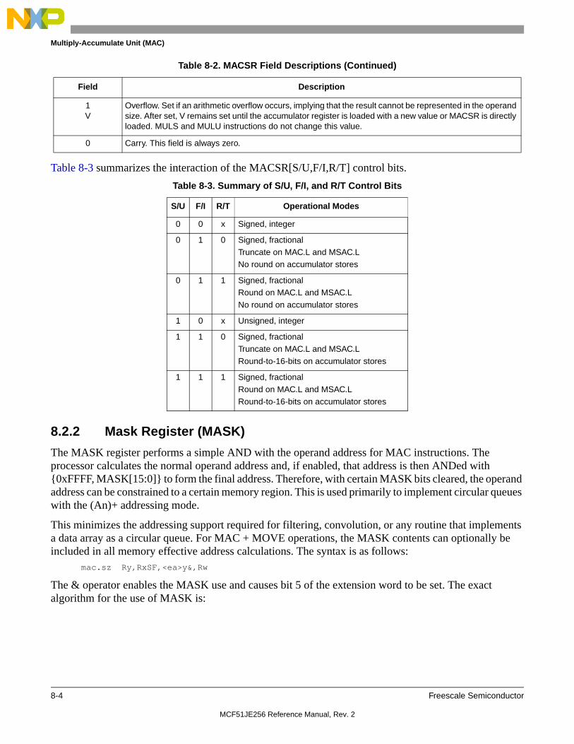
Multiply-Accumulate Unit (MAC)
8-4 Freescale Semiconductor
Table 8-3 summarizes the interaction of the MACSR[S/U,F/I,R/T] control bits.
8.2.2 Mask Register (MASK)
The MASK register performs a simple AND with the operand address for MAC instructions. The processor calculates the normal operand address and, if enabled, that address is then ANDed with {0xFFFF, MASK[15:0]} to form the final address. Therefore, with certain MASK bits cleared, the operand address can be constrained to a certain memory region. This is used primarily to implement circular queues with the (An)+ addressing mode.
This minimizes the addressing support required for filtering, convolution, or any routine that implements a data array as a circular queue. For MAC + MOVE operations, the MASK contents can optionally be included in all memory effective address calculations. The syntax is as follows:
mac.sz Ry,RxSF,<ea>y&,Rw
The & operator enables the MASK use and causes bit 5 of the extension word to be set. The exact algorithm for the use of MASK is:
1V
Overflow. Set if an arithmetic overflow occurs, implying that the result cannot be represented in the operand size. After set, V remains set until the accumulator register is loaded with a new value or MACSR is directly loaded. MULS and MULU instructions do not change this value.
0 Carry. This field is always zero.
Table 8-3. Summary of S/U, F/I, and R/T Control Bits
S/U F/I R/T Operational Modes
0 0 x Signed, integer
0 1 0 Signed, fractional
Truncate on MAC.L and MSAC.LNo round on accumulator stores
0 1 1 Signed, fractionalRound on MAC.L and MSAC.L
No round on accumulator stores
1 0 x Unsigned, integer
1 1 0 Signed, fractionalTruncate on MAC.L and MSAC.L
Round-to-16-bits on accumulator stores
1 1 1 Signed, fractional
Round on MAC.L and MSAC.L
Round-to-16-bits on accumulator stores
Table 8-2. MACSR Field Descriptions (Continued)
Field Description
MCF51JE256 Reference Manual, Rev. 2

Multiply-Accumulate Unit (MAC)
Freescale Semiconductor 8-5
if extension word, bit [5] = 1, the MASK bit, thenif <ea> = (An)
oa = An & {0xFFFF, MASK}
if <ea> = (An)+oa = AnAn = (An + 4) & {0xFFFF, MASK}
if <ea> =-(An)oa = (An - 4) & {0xFFFF, MASK}An = (An - 4) & {0xFFFF, MASK}
if <ea> = (d16,An)oa = (An + se_d16) & {0xFFFF0x, MASK}
Here, oa is the calculated operand address and se_d16 is a sign-extended 16-bit displacement. For auto-addressing modes of post-increment and pre-decrement, the updated An value calculation is also shown.
Use of the post-increment addressing mode, {(An)+} with the MASK is suggested for circular queue implementations.
8.2.3 Accumulator Register (ACC)
The accumulator register store 32-bits of the MAC operation result.
Figure 8-4. Accumulator Register (ACC)
BDM: Read: 0xE5 (MASK)Write: 0xC5
Access: User read/writeBDM read/write
15 14 13 12 11 10 9 8 7 6 5 4 3 2 1 0
RMASK
W
Reset 1 1 1 1 1 1 1 1 1 1 1 1 1 1 1 1
Figure 8-3. Mask Register (MASK)
Table 8-4. MASK Field Descriptions
Field Description
15–0MASK
Performs a simple AND with the operand address for MAC instructions.
BDM: Read: 0xE6 (ACC)Write: 0xC6
Access: User read/writeBDM read/write
31 30 29 28 27 26 25 24 23 22 21 20 19 18 17 16 15 14 13 12 11 10 9 8 7 6 5 4 3 2 1 0
RAccumulator
W
Reset – – – – – – – – – – – – – – – – – – – – – – – – – – – – – – – –
MCF51JE256 Reference Manual, Rev. 2

Multiply-Accumulate Unit (MAC)
8-6 Freescale Semiconductor
8.3 Functional DescriptionThe MAC speeds execution of ColdFire integer-multiply instructions (MULS and MULU) and provides additional functionality for multiply-accumulate operations. By executing MULS and MULU in the MAC, execution times are minimized and deterministic compared to the 2-bit/cycle algorithm with early termination that the OEP normally uses if no MAC hardware is present.
The added MAC instructions to the ColdFire ISA provide for the multiplication of two numbers, followed by the addition or subtraction of the product to or from the value in the accumulator. Optionally, the product may be shifted left or right by 1 bit before addition or subtraction. Hardware support for saturation arithmetic can be enabled to minimize software overhead when dealing with potential overflow conditions. Multiply-accumulate operations support 16- or 32-bit input operands in these formats:
• Signed integers
• Unsigned integers
• Signed, fixed-point, fractional numbers
The MAC is optimized for 16-bit multiplications to keep the area consumption low. Two 16-bit operands produce a 32-bit product. Longword operations are performed by reusing the 16-bit multiplier array at the expense of a small amount of extra control logic. Again, the product of two 32-bit operands is a 32-bit result. For longword integer operations, only the least significant 32 bits of the product are calculated. For fractional operations, the entire 64-bit product is calculated and then truncated or rounded to a 32-bit result using the round-to-nearest (even) method.
Because the multiplier array is implemented in a three-stage pipeline, MAC instructions have an effective issue rate of 1 cycle for word operations, 3 cycles for longword integer operations, and 4 cycles for 32-bit fractional operations.
All arithmetic operations use register-based input operands, and summed values are stored in the accumulator. Therefore, an additional MOVE instruction is needed to store data in a general-purpose register.
The need to move large amounts of data presents an obstacle to obtaining high throughput rates in DSP engines. Existing ColdFire instructions can accommodate these requirements. A MOVEM instruction can efficiently move large data blocks. The ability to load an operand simultaneously from memory into a register and execute a MAC instruction makes some DSP operations such as filtering and convolution more manageable.
The programming model includes a mask register (MASK), which can optionally be used to generate an operand address during MAC + MOVE instructions. The register application with auto-increment addressing mode supports efficient implementation of circular data queues for memory operands.
Table 8-5. ACC Field Descriptions
Field Description
31–0Accumulator
Store 32-bits of the result of the MAC operation.
MCF51JE256 Reference Manual, Rev. 2

Multiply-Accumulate Unit (MAC)
Freescale Semiconductor 8-7
8.3.1 Fractional Operation Mode
This section describes behavior when the fractional mode is used (MACSR[F/I] is set).
8.3.1.1 Rounding
When the processor is in fractional mode, there are two operations during which rounding can occur:
1. The 32-bit accumulator is moved into a general purpose register. If MACSR[S/U] is cleared, the accumulator is stored as is in the destination register; if it is set, the 32-bit value is rounded to a 16-bit value using the round-to-nearest (even) method. The resulting 16-bit number is stored in the lower word of the destination register. The upper word is zero-filled. The accumulator value is unaffected by this rounding procedure.
2. Execution of a MAC (or MSAC) instruction with 32-bit operands. If MACSR[R/T] is zero, multiplying two 32-bit numbers creates a 64-bit product truncated to the upper 32 bits; otherwise, it is rounded using round-to-nearest (even) method.
To understand the round-to-nearest-even method, consider the following example involving the rounding of a 32-bit number, R0, to a 16-bit number. Using this method, the 32-bit number is rounded to the closest 16-bit number possible. Let the high-order 16 bits of R0 be named R0.U and the low-order 16 bits be R0.L.
• If R0.L is less than 0x8000, the result is truncated to the value of R0.U.
• If R0.L is greater than 0x8000, the upper word is incremented (rounded up).
• If R0.L is 0x8000, R0 is half-way between two 16-bit numbers. In this case, rounding is based on the lsb of R0.U, so the result is always even (lsb = 0).
— If the lsb of R0.U equals 1 and R0.L equals 0x8000, the number is rounded up.
— If the lsb of R0.U equals 0 and R0.L equals 0x8000, the number is rounded down.
This method minimizes rounding bias and creates as statistically correct an answer as possible.
The rounding algorithm is summarized in the following pseudocode:if R0.L < 0x8000
then Result = R0.Uelse if R0.L > 0x8000
then Result = R0.U + 1else if lsb of R0.U = 0 /* R0.L = 0x8000 */
then Result = R0.Uelse Result = R0.U + 1
The round-to-nearest-even technique is also known as convergent rounding.
8.3.1.2 Saving and Restoring the MAC Programming Model
The presence of rounding logic in the MAC output datapath requires special care during the MAC’s save/restore process. In particular, any result rounding modes must be disabled during the save/restore process so the exact bit-wise contents of the MAC registers are accessed. Consider the memory structure containing the MAC programming model:struct macState {
int acc;int mask;
MCF51JE256 Reference Manual, Rev. 2

Multiply-Accumulate Unit (MAC)
8-8 Freescale Semiconductor
int macsr;} macState;
The following assembly language routine shows the proper sequence for a correct MAC state save. This code assumes all Dn and An registers are available for use, and the memory location of the state save is defined by A7.MAC_state_save:
move.l macsr,d7 ; save the macsrclr.l d0 ; zero the register to ... move.l d0,macsr ; disable rounding in the macsrmove.l acc,d5 ; save the accumulator move.l mask,d6 ; save the address maskmovem.l #0x00e0,(a7) ; move the state to memory
This code performs the MAC state restore:MAC_state_restore:
movem.l (a7),#0x00e0; restore the state from memorymove.l #0,macsr ; disable rounding in the macsrmove.l d5,acc ; restore the accumulator move.l d6,mask ; restore the address maskmove.l d7,macsr ; restore the macsr
Executing this sequence type can correctly save and restore the exact state of the MAC programming model.
8.3.1.3 MULS/MULU
MULS and MULU are unaffected by fractional-mode operation; operands remain assumed to be integers.
8.3.1.4 Scale Factor in MAC or MSAC Instructions
The scale factor is ignored while the MAC is in fractional mode.
8.3.2 MAC Instruction Set Summary
Table 8-6 summarizes MAC unit instructions.
Table 8-6. MAC Instruction Summary
Command Mnemonic Description
Multiply Signed muls <ea>y,Dx Multiplies two signed operands yielding a signed result
Multiply Unsigned mulu <ea>y,Dx Multiplies two unsigned operands yielding an unsigned result
Multiply Accumulate mac Ry,RxSFmsac Ry,RxSF
Multiplies two operands, then adds/subtracts the product to/from the accumulator
Multiply Accumulate with Load
mac Ry,RxSF,Rwmsac Ry,RxSF,Rw
Multiplies two operands, combines the product to the accumulator while loading a register with the memory operand
Load Accumulator move.l {Ry,#imm},ACC Loads the accumulator with a 32-bit operand
Store Accumulator move.l ACC,Rx Writes the contents of the accumulator to a CPU register
MCF51JE256 Reference Manual, Rev. 2

Multiply-Accumulate Unit (MAC)
Freescale Semiconductor 8-9
8.3.3 MAC Instruction Execution Times
The instruction execution times for the MAC can be found in Section 7.3.4.6, “MAC Instruction Execution Times”.
8.3.4 Data Representation
MACSR[S/U,F/I] selects one of the following three modes, where each mode defines a unique operand type:
1. Two’s complement signed integer: In this format, an N-bit operand value lies in the range -2(N-1) < operand < 2(N-1) - 1. The binary point is right of the lsb.
2. Unsigned integer: In this format, an N-bit operand value lies in the range 0 < operand < 2N - 1. The binary point is right of the lsb.
3. Two’s complement, signed fractional: In an N-bit number, the first bit is the sign bit. The remaining bits signify the first N-1 bits after the binary point. Given an N-bit number, aN-1aN-2aN-3... a2a1a0, its value is given by the equation in Equation 8-3.
Eqn. 8-3
This format can represent numbers in the range -1 < operand < 1 - 2-(N-1).
For words and longwords, the largest negative number that can be represented is -1, whose internal representation is 0x8000 and 0x8000_0000, respectively. The largest positive word is 0x7FFF or (1 - 2-15); the most positive longword is 0x7FFF_FFFF or (1 - 2-31). Thus, the number range for these signed fractional numbers is [-1.0, ..., 1.0].
8.3.5 MAC Opcodes
MAC opcodes are described in the ColdFire Programmer’s Reference Manual.
Remember the following:
• Unless otherwise noted, the value of MACSR[N,Z] is based on the result of the final operation that involves the product and the accumulator.
• The overflow (V) flag is managed differently. It is set if the complete product cannot be represented as a 32-bit value (this applies to 32 32 integer operations only) or if the combination of the
Load MACSR move.l {Ry,#imm},MACSR Writes a value to MACSR
Store MACSR move.l MACSR,Rx Write the contents of MACSR to a CPU register
Store MACSR to CCR move.l MACSR,CCR Write the contents of MACSR to the CCR
Load MAC Mask Reg move.l {Ry,#imm},MASK Writes a value to the MASK register
Store MAC Mask Reg move.l MASK,Rx Writes the contents of the MASK to a CPU register
Table 8-6. MAC Instruction Summary (Continued)
Command Mnemonic Description
value 1 aN 1– – 2 i 1 N–+ – ai
i 0=
N 2–
+=
MCF51JE256 Reference Manual, Rev. 2

Multiply-Accumulate Unit (MAC)
8-10 Freescale Semiconductor
product with the accumulator cannot be represented in the given number of bits. This indicator is treated as a sticky flag, meaning after set, it remains set until the accumulator or the MACSR is directly loaded. See Section 8.2.1, “MAC Status Register (MACSR)”.
• The optional 1-bit shift of the product is specified using the notation {<< | >>} SF, where <<1 indicates a left shift and >>1 indicates a right shift. The shift is performed before the product is added to or subtracted from the accumulator. Without this operator, the product is not shifted. If the MAC is in fractional mode (MACSR[F/I] is set), SF is ignored and no shift is performed. Because a product can overflow, the following guidelines are implemented:
— For unsigned word and longword operations, a zero is shifted into the product on right shifts.
— For signed, word operations, the sign bit is shifted into the product on right shifts unless the product is zero. For signed, longword operations, the sign bit is shifted into the product unless an overflow occurs or the product is zero, in which case a zero is shifted in.
— For all left shifts, a zero is inserted into the lsb position.
The following pseudocode explains basic MAC or MSAC instruction functionality. This example is presented as a case statement covering the three basic operating modes with signed integers, unsigned integers, and signed fractionals. Throughout this example, a comma-separated list in curly brackets, {}, indicates a concatenation operation.switch (MACSR[6:5]) /* MACSR[S/U, F/I] */{
case 0: /* signed integers */if (MACSR.OMC == 0 || MACSR.V == 0)
then {MACSR.V = 0/* select the input operands */if (sz == word)
then {if (U/Ly == 1)then operandY[31:0] = {sign-extended Ry[31], Ry[31:16]}else operandY[31:0] = {sign-extended Ry[15], Ry[15:0]}
if (U/Lx == 1)then operandX[31:0] = {sign-extended Rx[31], Rx[31:16]}else operandX[31:0] = {sign-extended Rx[15], Rx[15:0]}
}else {operandY[31:0] = Ry[31:0]
operandX[31:0] = Rx[31:0]}
/* perform the multiply */product[63:0] = operandY[31:0] * operandX[31:0]
/* check for product overflow */if ((product[63:31] != 0x0000_0000_0) && (product[63:31] != 0xffff_ffff_1))
then { /* product overflow */MACSR.V = 1if (inst == MSAC && MACSR.OMC == 1)
then if (product[63] == 1)then result[31:0] = 0x7fff_ffffelse result[31:0] = 0x8000_0000
else if (MACSR.OMC == 1)then /* overflowed MAC,
saturationMode enabled */if (product[63] == 1)
MCF51JE256 Reference Manual, Rev. 2

Multiply-Accumulate Unit (MAC)
Freescale Semiconductor 8-11
then result[31:0] = 0x8000_0000else result[31:0] = 0x7fff_ffff
}
/* scale product before combining with accumulator */switch (SF) /* 2-bit scale factor */{
case 0: /* no scaling specified */break;
case 1: /* SF = “<< 1” */if (product[31] ^ product[30])
then {MACSR.V = 1if (inst == MSAC && MACSR.OMC == 1)
then if (product[63] == 1)then result[31:0] = 0x7fff_ffffelse result[31:0] = 0x8000_0000
else if (MACSR.OMC == 1)then /* overflowed MAC,
saturationMode enabled */if (product[63] == 1)
then result[31:0] = 0x8000_0000else result[31:0] = 0x7fff_ffff
}else product[31:0] = {product[30:0], 0}
break;case 2: /* reserved encoding */
break;case 3: /* SF = “>> 1” */
if (MACSR.OMC == 0 || MACSR.V = 0)then product[31:0] = {product[31], product[31:1]}
break;}
/* combine with accumulator */if (MACSR.V == 0)
then {if (inst == MSAC)then result[31:0] = acc[31:0] - product[31:0]else result[31:0] = acc[31:0] + product[31:0]
}
/* check for accumulation overflow */if (accumulationOverflow == 1)
then {MACSR.V = 1if (MACSR.OMC == 1)
then /* accumulation overflow,saturationMode enabled */
if (result[31] == 1)then result[31:0] = 0x7fff_ffffelse result[31:0] = 0x8000_0000
}
/* transfer the result to the accumulator */acc[31:0] = result[31:0]MACSR.N = result[31]if (result[31:0] == 0x0000_0000)
then MACSR.Z = 1else MACSR.Z = 0
MCF51JE256 Reference Manual, Rev. 2

Multiply-Accumulate Unit (MAC)
8-12 Freescale Semiconductor
}break;case 1:case 3: /* signed fractionals */
if (MACSR.OMC == 0 || MACSR.V == 0)then {
MACSR.V = 0if (sz == word)
then {if (U/Ly == 1)then operandY[31:0] = {Ry[31:16], 0x0000}else operandY[31:0] = {Ry[15:0], 0x0000}
if (U/Lx == 1)then operandX[31:0] = {Rx[31:16], 0x0000}else operandX[31:0] = {Rx[15:0], 0x0000}
}else {operandY[31:0] = Ry[31:0]
operandX[31:0] = Rx[31:0]}
/* perform the multiply */product[63:0] = (operandY[31:0] * operandX[31:0]) << 1
/* check for product rounding */if (MACSR.R/T == 1)
then { /* perform convergent rounding */if (product[31:0] > 0x8000_0000)
then product[63:32] = product[63:32] + 1else if ((product[31:0] == 0x8000_0000) && (product[32] == 1))
then product[63:32] = product[63:32] + 1}
/* combine with accumulator */if (inst == MSAC)
then result[31:0] = acc[31:0] - product[63:32]else result[31:0] = acc[31:0] + product[63:32]
/* check for accumulation overflow */if (accumulationOverflow == 1)
then {MACSR.V = 1if (MACSR.OMC == 1)
then /* accumulation overflow,saturationMode enabled */
if (result[31] == 1)then result[31:0] = 0x7fff_ffffelse result[31:0] = 0x8000_0000
}
/* transfer the result to the accumulator */acc[31:0] = result[31:0]MACSR.N = result[31]if (result[31:0] == 0x0000_0000)
then MACSR.Z = 1else MACSR.Z = 0
}break;
MCF51JE256 Reference Manual, Rev. 2

Multiply-Accumulate Unit (MAC)
Freescale Semiconductor 8-13
case 2: /* unsigned integers */if (MACSR.OMC == 0 || MACSR.V == 0)
then {MACSR.V = 0/* select the input operands */if (sz == word)
then {if (U/Ly == 1)then operandY[31:0] = {0x0000, Ry[31:16]}else operandY[31:0] = {0x0000, Ry[15:0]}
if (U/Lx == 1)then operandX[31:0] = {0x0000, Rx[31:16]}else operandX[31:0] = {0x0000, Rx[15:0]}
}else {operandY[31:0] = Ry[31:0]
operandX[31:0] = Rx[31:0]}
/* perform the multiply */product[63:0] = operandY[31:0] * operandX[31:0]
/* check for product overflow */if (product[63:32] != 0x0000_0000)
then { /* product overflow */MACSR.V = 1if (inst == MSAC && MACSR.OMC == 1)
then result[31:0] = 0x0000_0000else if (MACSR.OMC == 1)
then /* overflowed MAC,saturationMode enabled */
result[31:0] = 0xffff_ffff}
/* scale product before combining with accumulator */switch (SF) /* 2-bit scale factor */{
case 0: /* no scaling specified */break;
case 1: /* SF = “<< 1” */if (product[31] == 1)
then {MACSR.V = 1if (inst == MSAC && MACSR.OMC == 1)
then result[31:0] = 0x0000_0000else if (MACSR.OMC == 1)
then /* overflowed MAC,saturationMode enabled */
result[31:0] = 0xffff_ffff}else product[31:0] = {product[30:0], 0}
break;case 2: /* reserved encoding */
break;case 3: /* SF = “>> 1” */
product[31:0] = {0, product[31:1]}break;
}
/* combine with accumulator */
MCF51JE256 Reference Manual, Rev. 2

Multiply-Accumulate Unit (MAC)
8-14 Freescale Semiconductor
if (MACSR.V == 0)then {if (inst == MSAC)
then result[31:0] = acc[31:0] - product[31:0]else result[31:0] = acc[31:0] + product[31:0]
}
/* check for accumulation overflow */if (accumulationOverflow == 1)
then {MACSR.V = 1if (inst == MSAC && MACSR.OMC == 1)
then result[31:0] = 0x0000_0000else if (MACSR.OMC == 1)
then /* overflowed MAC,saturationMode enabled */
result[31:0] = 0xffff_ffff}
/* transfer the result to the accumulator */acc[31:0] = result[31:0]MACSR.N = result[31]if (result[31:0] == 0x0000_0000)
then MACSR.Z = 1else MACSR.Z = 0
}break;}
MCF51JE256 Reference Manual, Rev. 2

Freescale Semiconductor 9-1
Chapter 9 Rapid GPIO (RGPIO)
9.1 IntroductionThe Rapid GPIO (RGPIO) module provides a 16-bit general-purpose I/O module directly connected to the processor’s high-speed 32-bit local bus. This connection plus support for single-cycle, zero wait-state data transfers allows the RGPIO module to provide improved pin performance when compared to more traditional GPIO modules located on the internal slave peripheral bus.
Many of the pins associated with a device may be used for several different functions. Their primary functions are to provide external interfaces to access off-chip resources. When not used for their primary function, many of the pins may be used as general-purpose digital I/O (GPIO) pins. The definition of the exact pin functions and the affected signals is specific to each device. Every GPIO port, including the RGPIO module, has registers that configure, monitor, and control the port pins.
9.1.1 Overview
The RGPIO module provides 16-bits of high-speed GPIO functionality, mapped to the processor’s bus. The key features of this module include:
• 16 bits of high-speed GPIO functionality connected to the processor’s local 32-bit bus
• Memory-mapped device connected to the ColdFire core’s local bus
— Support for all access sizes: byte, word, and longword
— All reads and writes complete in a single data phase cycle for zero wait-state response
• Data bits can be accessed directly or via alternate addresses to provide set, clear, and toggle functions
— Alternate addresses allow set, clear, toggle functions using simple store operations without the need for read-modify-write references
• Unique data direction and pin enable control registers
• Package pin toggle rates typically 1.5–3.5x faster than comparable pin mapped onto peripheral bus
A simplified block diagram of the RGPIO module is shown in Figure 9-1. The details of the pin muxing and pad logic are device-specific.
MCF51JE256 Reference Manual, Rev. 2

Rapid GPIO (RGPIO)
9-2 Freescale Semiconductor
Figure 9-1. RGPIO Block Diagram
9.1.2 Features
The major features of the RGPIO module providing 16 bits of high-speed general-purpose input/output are:
• Small memory-mapped device connected to the processor’s local bus
— All memory references complete in a single cycle to provide zero wait-state responses
— Located in processor’s high-speed clock domain
• Simple programming model
— Four 16-bit registers, mapped as three program-visible locations
– Register for pin enables
– Register for controlling the pin data direction
– Register for storing output pin data
– Register for reading current pin state
decode
mux
31
31
0
31 31 1516 16 0
31 16
15 0
0
rgpio_enable rgpio_direction rgpio_data_out rgpio_data_in
Control
Pin Muxing + Pad Logic
RGPIO module
RGPIO[15:0]
data from module
data to module
address
Local Bus
DirectionPin Enables Write D ata
Read D ata
MCF51JE256 Reference Manual, Rev. 2

Rapid GPIO (RGPIO)
Freescale Semiconductor 9-3
– The two data registers (read, write) are mapped to a single program-visible location
— Alternate addresses to perform data set, clear, and toggle functions using simple writes
— Separate read and write programming model views enable simplified driver software
– Support for any access size (byte, word, or longword)
9.1.3 Modes of Operation
The RGPIO module does not support any special modes of operation. As a memory-mapped device located on the processor’s high-speed local bus, it responds based strictly on memory address and does not consider the operating mode (supervisor, user) of its references.
9.2 External Signal Description
9.2.1 Overview
As shown in Figure 9-1, the RGPIO module’s interface to external logic is indirect via the device pin-muxing and pad logic. For a list of the associated RGPIO input/output signals, see Table 9-1.
9.2.2 Detailed Signal Descriptions
Table 9-2 provides descriptions of the RGPIO module’s input and output signals.
Table 9-1. RGPIO Module External I/O Signals
Signal Name Type Description
RGPIO[15:0] I/O RGPIO Data Input/Output
Table 9-2. RGPIO Detailed Signal Descriptions
Signal I/O Description
RGPIO[15:0] I/O Data Input/Output. When configured as an input, the state of this signal is reflected in the read data register. When configured as an output, this signal is the output of the write data register.
State Meaning
Asserted—Input: Indicates the RGPIO pin was sampled as a logic high at the time of the read.Output: Indicates a properly-enabled RGPIO output pin is to be driven high.
Negated—Input: Indicates the RGPIO pin was sampled as a logic low at the time of the read.Output: Indicates a properly-enabled RGPIO output pin is to be driven low.
Timing Assertion/Negation—Input: Anytime. The input signal is sampled at the rising-edge of the processor’s high-speed clock on the data phase cycle of a read transfer of this register.Output: Occurs at the rising-edge of the processor’s high-speed clock on the data phase cycle of a write transfer to this register. This output is asynchronously cleared by system reset.
MCF51JE256 Reference Manual, Rev. 2

Rapid GPIO (RGPIO)
9-4 Freescale Semiconductor
9.3 Memory Map/Register DefinitionThe RGPIO module provides a compact 16-byte programming model based at a system memory address of 0x(00)C0_0000 (noted as RGPIO_BASE throughout the chapter). As previously noted, the programming model views are different between reads and writes as this enables simplified software for manipulation of the RGPIO pins.
Additionally, the RGPIO programming model is defined with a 32-bit organization. The basic size of each program-visible register is 16 bits, but the programming model may be referenced using byte (8-bit), word (16-bit) or longword (32-bit) accesses. Performance is typically maximized using 32-bit accesses.
NOTEWrites to the two-byte fields at RGPIO_BASE + 0x8 and RGPIO_BASE + 0xC are allowed, but do not affect any program-visible register within the RGPIO module.
Table 9-3. RGPIO Write Memory Map
Offset Address
RegisterWidth (bits)
Access Reset Value Section/Page
0x00 RGPIO Data Direction Register (RGPIO_DIR) 16 W 0x0000 9.3.1/9-5
0x02 RGPIO Write Data Register (RGPIO_DATA) 16 W 0x0000 9.3.2/9-5
0x04 RGPIO Pin Enable Register (RGPIO_ENB) 16 W 0x0000 9.3.3/9-6
0x06 RGPIO Write Data Clear Register (RGPIO_CLR) 16 W N/A 9.3.4/9-6
0x0A RGPIO Write Data Set Register (RGPIO_SET) 16 W N/A 9.3.5/9-7
0x0E RGPIO Write Data Toggle Register (RGPIO_TOG) 16 W N/A 9.3.6/9-7
Table 9-4. RGPIO Read Memory Map
Offset Address
RegisterWidth (bits)
Access Reset Value Section/Page
0x00 RGPIO Data Direction Register (RGPIO_DIR) 16 R 0x0000 9.3.1/9-5
0x02 RGPIO Write Data Register (RGPIO_DATA) 16 R 0x0000 9.3.2/9-5
0x04 RGPIO Pin Enable Register (RGPIO_ENB) 16 R 0x0000 9.3.3/9-6
0x06 RGPIO Write Data Register (RGPIO_DATA) 16 R 0x0000 9.3.2/9-5
0x08 RGPIO Data Direction Register (RGPIO_DIR) 16 R 0x0000 9.3.1/9-5
0x0A RGPIO Write Data Register (RGPIO_DATA) 16 R 0x0000 9.3.2/9-5
0x0C RGPIO Data Direction Register (RGPIO_DIR) 16 R 0x0000 9.3.1/9-5
0x0E RGPIO Write Data Register (RGPIO_DATA) 16 R 0x0000 9.3.2/9-5
MCF51JE256 Reference Manual, Rev. 2

Rapid GPIO (RGPIO)
Freescale Semiconductor 9-5
9.3.1 RGPIO Data Direction (RGPIO_DIR)
The read/write RGPIO_DIR register defines whether a properly-enabled RGPIO pin is configured as an input or output:
• Setting any bit in RGPIO_DIR configures a properly-enabled RGPIO port pin as an output
• Clearing any bit in RGPIO_DIR configures a properly-enabled RGPIO port pin as an input
At reset, all bits in the RGPIO_DIR are cleared.
Figure 9-2. RGPIO Data Direction Register (RGPIO_DIR)
9.3.2 RGPIO Data (RGPIO_DATA)
The RGPIO_DATA register specifies the write data for a properly-enabled RGPIO output pin or the sampled read data value for a properly-enabled input pin. An attempted read of the RGPIO_DATA register returns undefined data for disabled pins, since the data value is dependent on the device-level pin muxing and pad implementation. The RGPIO_DATA register is read/write. At reset, all bits in the RGPIO_DATA registers are cleared.
To set bits in a RGPIO_DATA register, directly set the RGPIO_DATA bits or set the corresponding bits in the RGPIO_SET register. To clear bits in the RGPIO_DATA register, directly clear the RGPIO_DATA bits, or clear the corresponding bits in the RGPIO_CLR register. Setting a bit in the RGPIO_TOG register inverts (toggles) the state of the corresponding bit in the RGPIO_DATA register.
Offset: RGPIO_Base + 0x0 (RGPIO_DIR)RGPIO_Base + 0x8
RGPIO_Base + 0xC
Access: Read/writeRead-onlyRead-only
15 14 13 12 11 10 9 8 7 6 5 4 3 2 1 0
RDIR
W
Reset 0 0 0 0 0 0 0 0 0 0 0 0 0 0 0 0
Table 9-5. RGPIO_DIR Field Descriptions
Field Description
15–0DIR
Data direction.0 A properly-enabled RGPIO pin is configured as an input1 A properly-enabled RGPIO pin is configured as an output
MCF51JE256 Reference Manual, Rev. 2

Rapid GPIO (RGPIO)
9-6 Freescale Semiconductor
Figure 9-3. RGPIO Data Register (RGPIO_DATA)
9.3.3 RGPIO Pin Enable (RGPIO_ENB)
The RGPIO_ENB register configures the corresponding package pin as a RGPIO pin instead of the normal GPIO pin mapped onto the peripheral bus.
The RGPIO_ENB register is read/write. At reset, all bits in the RGPIO_ENB are cleared, disabling the RGPIO functionality.
Figure 9-4. RGPIO Enable Register (RGPIO_ENB)
9.3.4 RGPIO Clear Data (RGPIO_CLR)
The RGPIO_CLR register provides a mechanism to clear specific bits in the RGPIO_DATA by performing a simple write. Clearing a bit in RGPIO_CLR clears the corresponding bit in the RGPIO_DATA register.
Offset: RGPIO_Base + 0x2 (RGPIO_DATA)
RGPIO_Base + 0x6
RGPIO_Base + 0xARGPIO_Base + 0xE
Access: Read/writeRead/Indirect WriteRead/Indirect WriteRead/Indirect Write
15 14 13 12 11 10 9 8 7 6 5 4 3 2 1 0
RDATA
W
Reset 0 0 0 0 0 0 0 0 0 0 0 0 0 0 0 0
Table 9-6. RGPIO_DATA Field Descriptions
Field Description
15–0DATA
RGPIO data.0 A properly-enabled RGPIO output pin is driven with a logic 0, or a properly-enabled RGPIO input pin was read as
a logic 01 A properly-enabled RGPIO output pin is driven with a logic 1, or a properly-enabled RGPIO input pin was read as
a logic 1
Offset: RGPIO_Base + 0x4 (RGPIO_ENB) Access: Read/write
15 14 13 12 11 10 9 8 7 6 5 4 3 2 1 0
RENB
W
Reset 0 0 0 0 0 0 0 0 0 0 0 0 0 0 0 0
Table 9-7. RGPIO_ENB Field Descriptions
Field Description
15–0ENB
Enable pin for RGPIO0 The corresponding package pin is configured for use as a normal GPIO pin, not a RGPIO1 The corresponding package pin is configured for use as a RGPIO pin
MCF51JE256 Reference Manual, Rev. 2

Rapid GPIO (RGPIO)
Freescale Semiconductor 9-7
Setting it has no effect. The RGPIO_CLR register is write-only; reads of this address return the RGPIO_DATA register.
Figure 9-5. RGPIO Clear Data Register (RGPIO_CLR)
9.3.5 RGPIO Set Data (RGPIO_SET)
The RGPIO_SET register provides a mechanism to set specific bits in the RGPIO_DATA register by performing a simple write. Setting a bit in RGPIO_SET asserts the corresponding bit in the RGPIO_DATA register. Clearing it has no effect. The RGPIO_SET register is write-only; reads of this address return the RGPIO_DATA register.
Figure 9-6. RGPIO Set Data Register (RGPIO_SET)
9.3.6 RGPIO Toggle Data (RGPIO_TOG)
The RGPIO_TOG register provides a mechanism to invert (toggle) specific bits in the RGPIO_DATA register by performing a simple write. Setting a bit in RGPIO_TOG inverts the corresponding bit in the RGPIO_DATA register. Clearing it has no effect. The RGPIO_TOG register is write-only; reads of this address return the RGPIO_DATA register.
Offset: RGPIO_Base + 0x6 (RGPIO_CLR) Access: Write-only
15 14 13 12 11 10 9 8 7 6 5 4 3 2 1 0
R
W CLR
Reset — — — — — — — — — — — — — — — —
Table 9-8. RGPIO_CLR Field Descriptions
Field Description
15–0CLR
Clear data bit0 Clears the corresponding bit in the RGPIO_DATA register1 No effect
Offset: RGPIO_Base + 0xA (RGPIO_SET) Access: Write-only
15 14 13 12 11 10 9 8 7 6 5 4 3 2 1 0
R
W SET
Reset — — — — — — — — — — — — — — — —
Table 9-9. RGPIO_SET Field Descriptions
Field Description
15–0SET
Set data bit0 No effect1 Sets the corresponding bit in the RGPIO_DATA register
MCF51JE256 Reference Manual, Rev. 2

Rapid GPIO (RGPIO)
9-8 Freescale Semiconductor
Figure 9-7. RGPIO Toggle Data Register (RGPIO_TOG)
9.4 Functional DescriptionThe RGPIO module is a relatively-simple design with its behavior controlled by the program-visible registers defined within its programming model.
The RGPIO module is connected to the processor’s local two-stage pipelined bus with the stages of the ColdFire core’s operand execution pipeline (OEP) mapped directly onto the bus. This structure allows the processor access to the RGPIO module for single-cycle pipelined reads and writes with a zero wait-state response (as viewed in the system bus data phase stage).
9.5 Initialization InformationThe reset state of the RGPIO module disables the entire 16-bit data port. Prior to using the RGPIO port, software typically:
• Enables the appropriate pins in RGPIO_ENB
• Configures the pin direction in RGPIO_DIR
• Defines the contents of the data register (RGPIO_DATA)
9.6 Application InformationThis section examines the relative performance of the RGPIO output pins for two simple applications
• The processor executes a loop to toggle an output pin for a specific number of cycles, producing a square-wave output
• The processor transmits a 16-bit message using a three-pin SPI-like interface with a serial clock, serial chip select, and serial data bit.
In both applications, the relative speed of the GPIO output is presented as a function of the location of the output bit (RGPIO versus peripheral bus GPIO).
Offset: RGPIO_Base + 0xE (RGPIO_TOG) Access: Write-only
15 14 13 12 11 10 9 8 7 6 5 4 3 2 1 0
R
W TOG
Reset — — — — — — — — — — — — — — — —
Table 9-10. RGPIO_TOG Field Descriptions
Field Description
15–0TOG
Toggle data.0 No effect1 Inverts the corresponding bit in RGPIO_DATA
MCF51JE256 Reference Manual, Rev. 2

Rapid GPIO (RGPIO)
Freescale Semiconductor 9-9
9.6.1 Application 1: Simple Square-Wave Generation
In this example, several different instruction loops are executed, each generating a square-wave output with a 50% duty cycle. For this analysis, the executed code is mapped into the processor’s RAM. This configuration is selected to remove any jitter from the output square wave caused by the limitations defined by the two-cycle flash memory accesses and restrictions on the initiation of a flash access. The following instruction loops were studied:
• BCHG_LOOP — In this loop, a bit change instruction was executed using the GPIO data byte as the operand. This instruction performs a read-modify-write operation and inverts the addressed bit. A pulse counter is decremented until the appropriate number of square-wave pulses have been generated.
• SET+CLR_LOOP — For this construct, two store instructions are executed: one to set the GPIO data pin and another to clear it. Single-cycle NOP instructions (the tpf opcode) are included to maintain the 50% duty cycle of the generated square wave. The pulse counter is decremented until the appropriate number of square-wave pulse have been generated.
The square-wave output frequency was measured and the relative performance results are presented in Table 9-11. The relative performance is stated as a fraction of the processor’s operating frequency, defined as f MHz. The performance of the BCHG loop operating on a GPIO output is selected as the reference.
NOTEThe square-wave frequency is measured from rising-edge to rising-edge, where the output wave has a 50% duty cycle.
9.6.2 Application 2: 16-bit Message Transmission using SPI Protocol
In this second example, a 16-bit message is transmitted using three programmable output pins. The output pins include a serial clock, an active-high chip select, and the serial data bit. The software is configured to sample the serial data bit at the rising-edge of the clock with the data sent in a most-significant to least-significant bit order. The resulting 3-bit output is shown in Figure 9-8.
Figure 9-8. GPIO SPI Example Timing Diagram
Table 9-11. Square-Wave Output Performance
Loop
Peripheral Bus-mapped GPIO RGPIO
Sq-WaveFrequency
Frequency @CPU f = 50 MHz
RelativeSpeed
Sq-WaveFrequency
Frequency @CPU f = 50 MHz
RelativeSpeed
bchg (1/24) f MHz 2.083 MHz 1.00x (1/14) f MHz 3.571 MHz 1.71x
set+clr (+toggle) (1/12) f MHz 4.167 MHz 2.00x (1/8) f MHz 6.250 MHz 3.00x
15 14 13 2 1 0
gpio_cs
gpio_clk
gpio_data
MCF51JE256 Reference Manual, Rev. 2

Rapid GPIO (RGPIO)
9-10 Freescale Semiconductor
For this example, the processing of the SPI message is considerably more complex than the generation of a simple square wave of the previous example. The code snippet used to extract the data bit from the message and build the required GPIO data register writes is shown in Figure 9-9.# subtest: send a 16-bit message via a SPI interface using a RGPIO
# the SPI protocol uses a 3-bit value: clock, chip-select, data # the data is centered around the rising-edge of the clock align 16 send_16b_spi_message_rgpio:00510: 4fef fff4 lea -12(%sp),%sp # allocate stack space00514: 48d7 008c movm.l &0x8c,(%sp) # save d2,d3,d700518: 3439 0080 0582 mov.w RAM_BASE+message2,%d2 # get 16-bit message0051e: 760f movq.l &15,%d3 # static shift count00520: 7e10 movq.l &16,%d7 # message bit length00522: 207c 00c0 0003 mov.l &RGPIO_DATA+1,%a0 # pointer to low-order data byte00528: 203c 0000 ffff mov.l &0xffff,%d0 # data value for _ENB and _DIR regs0052e: 3140 fffd mov.w %d0,-3(%a0) # set RGPIO_DIR register00532: 3140 0001 mov.w %d0,1(%a0) # set RGPIO_ENB register
00536: 223c 0001 0000 mov.l &0x10000,%d1 # d1[17:16] = {clk, cs}0053c: 2001 mov.l %d1,%d0 # copy into temp reg0053e: e6a8 lsr.l %d3,%d0 # align in d0[2:0]00540: 5880 addq.l &4,%d0 # set clk = 100542: 1080 mov.b %d0,(%a0) # initialize data00544: 6002 bra.b L%1 align 4 L%1:00548: 3202 mov.w %d2,%d1 # d1[17:15] = {clk, cs, data}0054a: 2001 mov.l %d1,%d0 # copy into temp reg0054c: e6a8 lsr.l %d3,%d0 # align in d0[2:0]0054e: 1080 mov.b %d0,(%a0) # transmit data with clk = 000550: 5880 addq.l &4,%d0 # force clk = 100552: e38a lsl.l &1,%d2 # d2[15] = new message data bit00554: 51fc tpf # preserve 50% duty cycle00556: 51fc tpf00558: 51fc tpf0055a: 51fc tpf0055c: 1080 mov.b %d0,(%a0) # transmit data with clk = 10055e: 5387 subq.l &1,%d7 # decrement loop counter00560: 66e6 bne.b L%1 00562: c0bc 0000 fff5 and.l &0xfff5,%d0 # negate chip-select00568: 1080 mov.b %d0,(%a0) # update gpio 0056a: 4cd7 008c movm.l (%sp),&0x8c # restore d2,d3,d70056e: 4fef 000c lea 12(%sp),%sp # deallocate stack space00572: 4e75 rts
Figure 9-9. GPIO SPI Code Example
The resulting SPI performance, as measured in the effective Mbps transmission rate for the 16-bit message, is shown in Table 9-12.
MCF51JE256 Reference Manual, Rev. 2

Rapid GPIO (RGPIO)
Freescale Semiconductor 9-11
Table 9-12. Emulated SPI Performance using GPIO Outputs
Peripheral Bus-mapped GPIO RGPIO
SPI Speed @CPU f = 50 MHz
RelativeSpeed
SPI Speed @CPU f = 50 MHz
RelativeSpeed
2.063 Mbps 1.00x 3.809 Mbps 1.29x
MCF51JE256 Reference Manual, Rev. 2

Rapid GPIO (RGPIO)
9-12 Freescale Semiconductor
MCF51JE256 Reference Manual, Rev. 2

Freescale Semiconductor 10-13
Chapter 10 Interrupt Controller (CF1_INTC)
10.1 IntroductionThe CF1_INTC interrupt controller (CF1_INTC) is intended for use in low-cost microcontroller designs using the Version 1 (V1) ColdFire processor core. In keeping with the general philosophy for devices based on this low-end 32-bit processor, the interrupt controller generally supports less programmability compared to similar modules in other ColdFire microcontrollers and embedded microprocessors. However, CF1_INTC provides the required functionality with a minimal silicon cost.
These requirements guide the CF1_INTC module definition to support Freescale’s Controller Continuum:
• The priorities of the interrupt requests between comparable HCS08 and V1 ColdFire devices are identical.
• Supports a mode of operation (through software convention with hardware assists) equivalent to the S08’s interrupt processing with only one level of nesting.
• Leverages the current ColdFire interrupt controller programming model and functionality, but with a minimal hardware implementation and cost.
Table 10-1 provides a high-level architectural comparison between HCS08 and ColdFire exception processing as these differences are important in the definition of the CF1_INTC module. Throughout this document, the term IRQ refers to an interrupt request and ISR refers to an interrupt service routine to process an interrupt exception.
Table 10-1. Exception Processing Comparison
Attribute HCS08 V1 ColdFire
Exception Vector Table 32 two-byte entries, fixed location at upper end of memory
four-byte entries, located at lower end of memory at reset, relocatable with the VBR
More on Vectors 2 for CPU + 30 for IRQs, reset at upper address
64 for CPU + for IRQs, reset at lowest address
Exception Stack Frame 5-byte frame: CCR, A, X, PC 8-byte frame: F/V, SR, PC; General-purpose registers (An, Dn) must be saved/restored by the ISR
Interrupt Levels 1 = f(CCR[I]) 7= f (SR[I]) with automatic hardware support for nesting
Non-Maskable IRQ Support No Yes, with level 7 interrupts
Core-enforced IRQ Sensitivity No Level 7 is edge sensitive, else level sensitive
INTC Vectoring Fixed priorities and vector assignments Fixed priorities and vector assignments, plus any 2 IRQs can be remapped as the highest priority level 6 requests
MCF51JE256 Reference Manual, Rev. 2

Interrupt Controller (CF1_INTC)
10-14 Freescale Semiconductor
10.1.1 Overview
Interrupt exception processing includes interrupt recognition, aborting the current instruction execution stream, storing an 8-byte exception stack frame in the memory, calculation of the appropriate vector, and passing control to the specified interrupt service routine.
Unless specifically noted otherwise, all ColdFire processors sample for interrupts once during each instruction’s execution during the first cycle of execution in the OEP. Additionally, all ColdFire processors use an instruction restart exception model.
The ColdFire processor architecture defines a 3-bit interrupt priority mask field in the processor’s status register (SR[I]). This field, and the associated hardware, support seven levels of interrupt requests with the processor providing automatic nesting capabilities. The levels are defined in descending numeric order with 7 > 6 ... > 1. Level 7 interrupts are treated as non-maskable, edge-sensitive requests while levels 6–1 are maskable, level-sensitive requests. The SR[I] field defines the processor’s current interrupt level. The processor continuously compares the encoded IRQ level from CF1_INTC against SR[I]. Recall that interrupt requests are inhibited for all levels less than or equal to the current level, except the edge-sensitive level 7 request that cannot be masked.
Exception processing for ColdFire processors is streamlined for performance and includes all actions from detecting the fault condition to the initiation of fetch for the first handler instruction. Exception processing is comprised of four major steps.
1. The processor makes an internal copy of the status register (SR) and enters supervisor mode by setting SR[S] and disabling trace mode by clearing SR[T]. The occurrence of an interrupt exception also forces the master mode (M) bit to clear and the interrupt priority mask (I) to set to the level of the current interrupt request.
2. The processor determines the exception vector number. For all faults except interrupts, the processor performs this calculation based on the exception type. For interrupts, the processor performs an IACK bus cycle to obtain the vector number from the interrupt controller if CPUCR[IAE] equals 1. The IACK cycle is mapped to special locations within the interrupt controller’s IPS address space with the interrupt level encoded in the address. If CPUCR[IAE] equals 0, the processor uses the vector number supplied by the interrupt controller at the time the request was signaled (for improved performance).
3. The processor saves the current context by creating an exception stack frame on the system stack. As a result, exception stack frame is created at a 0-modulo-4 address on top of the system stack defined by the supervisor stack pointer (SSP). The processor uses an 8-byte stack frame for all exceptions. It contains the vector number of the exception, the contents of the status register at the time of the exception, and the program counter (PC) at the time of the exception. The exception
Software IACK No Yes
Exit Instruction from ISR RTI RTE
Table 10-1. Exception Processing Comparison (Continued)
Attribute HCS08 V1 ColdFire
MCF51JE256 Reference Manual, Rev. 2

Interrupt Controller (CF1_INTC)
Freescale Semiconductor 10-15
type determines whether the program counter placed in the exception stack frame defines the location of the faulting instruction (fault) or the address of the next instruction to be executed (next). For interrupts, the stacked PC is always the address of the next instruction to be executed.
4. The processor calculates the address of the first instruction of the exception handler. By definition, the exception vector table is aligned on a 1MB boundary. This instruction address is generated by fetching a 32-bit exception vector from the table located at the address defined in the vector base register (VBR). The index into the exception table is calculated as (4 vector number). After the exception vector has been fetched, the contents of the vector serves as a 32-bit pointer to the address of the first instruction of the desired handler. After the instruction fetch for the first opcode of the handler has been initiated, exception processing terminates and normal instruction processing continues in the handler.
All ColdFire processors support a 1024-byte vector table aligned on any 1-MB address boundary. For the V1 ColdFire core, the only practical locations for the vector table are based at 0x(00)00_0000 in the flash or 0x(00)80_0000 in the RAM. The table contains 256 exception vectors; the first 64 are reserved for internal processor exceptions, and the remaining 192 are device-specific interrupt vectors. The IRQ assignment table is partially populated depending on the exact set of peripherals for the given device.
The basic ColdFire interrupt controller supports up to 63 request sources mapped as nine priorities for each of the seven supported levels (7 levels 9 priorities per level). Within the nine priorities within a level, the mid-point is typically reserved for package-level IRQ inputs. The levels and priorities within the level follow a descending order: 7 > 6 > ... > 1 > 0.
The HCS08 architecture supports a 32-entry exception vector table: the first two vectors are reserved for internal CPU/system exceptions and the remaining are available for I/O interrupt requests. The requirement for an exact match between the interrupt requests and priorities across two architectures means the sources are mapped to a sparsely-populated two-dimensional ColdFire array of seven interrupt levels and nine priorities within the level. The following association between the HCS08 and ColdFire vector numbers applies:
ColdFire Vector Number = 62 + HCS08 Vector Number
The CF1_INTC performs a cycle-by-cycle evaluation of the active requests and signals the highest-level, highest-priority request to the V1 ColdFire core in the form of an encoded interrupt level and the exception vector associated with the request. The module also includes a byte-wide interface to access its programming model. These interfaces are shown in the simplified block diagram of Figure 10-1.
Figure 10-1. CF1_INTC Block Diagram
10.1.2 Features
The Version 1 ColdFire interrupt controller includes:
• Memory-mapped off-platform slave module
— 64-byte space located at top end of memory: 0x(FF)FF_FFC0–0x(FF)FF_FFFF
— Programming model accessed via the peripheral bus
— Encoded interrupt level and vector sent directly to processor core
• Support of peripheral I/O interrupt requests plus seven software (one per level) interrupt requests
MCF51JE256 Reference Manual, Rev. 2

Interrupt Controller (CF1_INTC)
10-16 Freescale Semiconductor
• Fixed association between interrupt request source and level plus priority
— I/O requests assigned across seven available levels and nine priorities per level
— Exactly matches HCS08 interrupt request priorities
— Up to two requests can be remapped to the highest maskable level + priority
• Unique vector number for each interrupt source
— ColdFire vector number = 62 + HCS08 vector number
— Details on IRQ and vector assignments are device-specific
• Support for service routine interrupt acknowledge (software IACK) read cycles for improved system performance
• Combinatorial path provides wakeup signal from wait mode
10.1.3 Modes of Operation
The CF1_INTC module does not support any special modes of operation. As a memory-mapped slave peripheral located on the platform’s slave bus, it responds based strictly on the memory addresses of the connected bus.
One special behavior of the CF1_INTC deserves mention. When the device enters a wait mode and certain clocks are disabled, there is an input signal that can be asserted to enable a purely-combinational logic path for monitoring the assertion of an interrupt request. After a request of unmasked level is asserted, this combinational logic path asserts an output signal that is sent to the clock generation logic to re-enable the internal device clocks to exit the low-power mode.
10.2 External Signal DescriptionThe CF1_INTC module does not include any external interfaces.
10.3 Memory Map/Register DefinitionThe CF1_INTC module provides a 64-byte programming model mapped to the upper region of the 16 MB address space. All the register names are prefixed with INTC_ as an abbreviation for the full module name.
The programming model is referenced using 8-bit accesses. Attempted references to undefined (reserved) addresses or with a non-supported access type (for example, a write to a read-only register) generate a bus error termination.
The programming model follows the definition from previous ColdFire interrupt controllers. This compatibility accounts for the various memory holes in this module’s memory map.
The CF1_INTC module is based at address 0x(FF)FF_FFC0 (referred to as CF1_INTC_BASE throughout the chapter) and occupies the upper 64 bytes of the peripheral space. The module memory map is shown in Table 10-2.
MCF51JE256 Reference Manual, Rev. 2

Interrupt Controller (CF1_INTC)
Freescale Semiconductor 10-17
10.3.1 Force Interrupt Register (INTC_FRC)
The INTC_FRC register allows software to generate a unique interrupt for each possible level at the lowest priority within the level for functional or debug purposes. These interrupts may be self-scheduled by setting one or more of the bits in the INTC_FRC register. In some cases, the handling of a normal interrupt request may cause critical processing by the service routine along with the scheduling (using the INTC_FRC register) of a lower priority level interrupt request to be processed at a later time for less-critical task handling.
The INTC_FRC register may be modified directly using a read-modify-write sequence or through a simple write operation using the set/clear force interrupt registers (INTC_SFRC, INTC_CFRC).
NOTETake special notice of the bit numbers within this register, –. This is for compatibility with other ColdFire interrupt controllers.
Table 10-2. CF1_INTC Memory Map
Offset Address
Register Name Register DescriptionWidth (bits)
Access Reset ValueSection/
Page
0x1 INTC_FRC CF1_INTC Force Interrupt Register 8 R/W 0x00 10.3.1/10-17
0x18 INTC_PL6P7 CF1_INTC Programmable Level 6, Priority 7 8 R/W 0x00 10.3.2/10-18
0x19 INTC_PL6P6 CF1_INTC Programmable Level 6, Priority 6 8 R/W 0x00 10.3.2/10-18
0x1B INTC_WCR CF1_INTC Wakeup Control Register 8 R/W 10.3.3/10-19
0x1E INTC_SFRC CF1_INTC Set Interrupt Force Register 8 Write — 10.3.4/10-20
0x1F INTC_CFRC CF1_INTC Clear Interrupt Force Register 8 Write — 10.3.5/10-21
0x20 INTC_SWIACK CF1_INTC Software Interrupt Acknowledge 8 Read 0x00 10.3.6/10-21
0x24 INTC_LVL1IACK CF1_INTC Level 1 Interrupt Acknowledge 8 Read 0x18 10.3.6/10-21
0x28 INTC_LVL2IACK CF1_INTC Level 2 Interrupt Acknowledge 8 Read 0x18 10.3.6/10-21
0x2C INTC_LVL3IACK CF1_INTC Level 3 Interrupt Acknowledge 8 Read 0x18 10.3.6/10-21
0x30 INTC_LVL4IACK CF1_INTC Level 4 Interrupt Acknowledge 8 Read 0x18 10.3.6/10-21
0x34 INTC_LVL5IACK CF1_INTC Level 5 Interrupt Acknowledge 8 Read 0x18 10.3.6/10-21
0x38 INTC_LVL6IACK CF1_INTC Level 6 Interrupt Acknowledge 8 Read 0x18 10.3.6/10-21
0x3C INTC_LVL7IACK CF1_INTC Level 7 Interrupt Acknowledge 8 Read 0x18 10.3.6/10-21
MCF51JE256 Reference Manual, Rev. 2

Interrupt Controller (CF1_INTC)
10-18 Freescale Semiconductor
10.3.2 INTC Programmable Level 6, Priority {7,6} Registers (INTC_PL6P{7,6})
The level seven interrupt requests cannot have their levels reassigned. However, any of the remaining peripheral interrupt requests can be reassigned as the highest priority maskable requests using these two registers (INTC_PL6P7 and INTC_PL6P6). The vector number associated with the interrupt requests does not change. Rather, only the interrupt request's level and priority are altered, based on the contents of the INTC_PL6P{7,6} registers.
Offset: CF1_INTC_BASE + 0x1 (INTC_FRC) Access: Read/Write
R 0LVL1 LVL2 LVL3 LVL4 LVL5 LVL6 LVL7
W
Reset 0 0 0 0 0 0 0 0
Figure 10-2. Force Interrupt Register (INTC_FRC)
Table 10-3. INTC_FRC Field Descriptions
Field Description
Reserved, must be cleared.
LVL1Force Level 1 interrupt.0 Negates the forced level 1 interrupt request.1 Forces a level 1 interrupt request.
LVL2Force Level 2 interrupt.0 Negates the forced level 2 interrupt request.1 Forces a level 2 interrupt request.
LVL3Force Level 3 interrupt.0 Negates the forced level 3 interrupt request.1 Forces a level 3 interrupt request.
LVL4Force Level 4 interrupt.0 Negates the forced level 4 interrupt request.1 Forces a level 4 interrupt request.
LVL5Force Level 5 interrupt.0 Negates the forced level 5 interrupt request.1 Forces a level 5 interrupt request.
LVL6Force Level 6 interrupt.0 Negates the forced level 6 interrupt request.1 Forces a level 6 interrupt request.
LVL7Force Level 7 interrupt.0 Negates the forced level 7 interrupt request.1 Forces a level 7 interrupt request.
MCF51JE256 Reference Manual, Rev. 2

Interrupt Controller (CF1_INTC)
Freescale Semiconductor 10-19
NOTEThe requests associated with the INTC_FRC register have a fixed level and priority that cannot be altered.
The INTC_PL6P7 register specifies the highest-priority, maskable interrupt request that is defined as the level six, priority seven request. The INTC_PL6P6 register specifies the second-highest-priority, maskable interrupt request defined as the level six, priority six request. Reset clears both registers, disabling any request re-mapping.
For an example of the use of these registers, see Section 10.6.2, “Using INTC_PL6P{7,6} Registers.”
10.3.3 INTC Wakeup Control Register (INTC_WCR)
The interrupt controller provides a combinatorial logic path to generate a special wakeup signal to exit from the wait mode. The INTC_WCR register defines wakeup condition for interrupt recognition during wait mode. This mode of operation works as follows:
1. Write to the INTC_WCR to enable this operation (set INTC_WCR[ENB]) and define the interrupt mask level needed to force the core to exit wait mode (INTC_WCR[MASK]). The maximum value of INTC_WCR[MASK] is 0x6 (0b110). The INTC_WCR is enabled with a mask level of 0 as the default after reset.
2. Execute a stop instruction to place the processor into wait mode.
3. After the processor is stopped, the interrupt controller enables special logic that evaluates the incoming interrupt sources in a purely combinatorial path; no clocked storage elements are involved.
4. If an active interrupt request is asserted and the resulting interrupt level is greater than the mask value contained in INTC_WCR[MASK], the interrupt controller asserts the wakeup output signal. This signal is routed to the clock generation logic to exit the low-power mode and resume processing.
Offset: CF1_INTC_BASE + 0x18 (INTC_PL6P7)
CF1_INTC_BASE + 0x19 (INTC_PL6P6)
Access: Read/Write
7 6 5 4 3 2 1 0
R 0 0REQN
W
Reset 0 0 0 0 0 0 0 0
Figure 10-3. Programmable Level 6, Priority {7,6} Registers (INTC_PL6P{7,6})
Table 10-4. INTC_PL6P{7,6} Field Descriptions
Field Description
7–6 Reserved, must be cleared.
5–0REQN
Request number. Defines the peripheral IRQ number to be remapped as the level 6, priority 7 (for INTC_PL6P7) request and level 6, priority 6 (for INTC_PL6P6) request.Note: The value must be a valid interrupt number. Unused or reserved interrupt numbers are ignored.
MCF51JE256 Reference Manual, Rev. 2

Interrupt Controller (CF1_INTC)
10-20 Freescale Semiconductor
Typically, the interrupt mask level loaded into the processor's status register field (SR[I]) during the execution of the stop instruction matches the INTC_WCR[MASK] value.
The interrupt controller's wakeup signal is defined as:wakeup = INTC_WCR[ENB] & (level of any asserted_int_request > INTC_WCR[MASK])
10.3.4 INTC Set Interrupt Force Register (INTC_SFRC)
The INTC_SFRC register provides a simple memory-mapped mechanism to set a given bit in the INTC_FRC register to assert a specific level interrupt request. The data value written causes the appropriate bit in the INTC_FRC register to be set. Attempted reads of this register generate an error termination.
This register is provided so interrupt service routines can generate a forced interrupt request without the need to perform a read-modify-write sequence on the INTC_FRC register.
Figure 10-5. INTC_SFRC Register
Offset: CF1_INTC_BASE + 0x1B (INTC_WCR) Access: Read/Write
7 6 5 4 3 2 1 0
RENB
0 0 0 0MASK
W
Reset 0 0 0 0 0 0 0
Figure 10-4. Wakeup Control Register (INTC_WCR)
Table 10-5. INTC_WCR Field Descriptions
Field Description
7ENB
Enable wakeup signal.0 Wakeup signal disabled1 Enables the assertion of the combinational wakeup signal to the clock generation logic.
6–3 Reserved, must be cleared.
2–0MASK
Interrupt mask level. Defines the interrupt mask level during wait mode and is enforced by the hardware to be within the range 0–6. If INTC_WCR[ENB] is set, when an interrupt request of a level higher than MASK occurs, the interrupt controller asserts the wakeup signal to the clock generation logic.
Offset: CF1_INTC_BASE + 0x1E (INTC_SFRC) Access: Write-only
7 6 5 4 3 2 1 0
R
W SET
Reset 0 0 0 0 0 0 0 0
MCF51JE256 Reference Manual, Rev. 2

Interrupt Controller (CF1_INTC)
Freescale Semiconductor 10-21
10.3.5 INTC Clear Interrupt Force Register (INTC_CFRC)
The INTC_CFRC register provides a simple memory-mapped mechanism to clear a given bit in the INTC_FRC register to negate a specific level interrupt request. The data value on the register write causes the appropriate bit in the INTC_FRC register to be cleared. Attempted reads of this register generate an error termination.
This register is provided so interrupt service routines can negate a forced interrupt request without the need to perform a read-modify-write sequence on the INTC_FRC register.
Figure 10-6. INTC_CFRC Register
10.3.6 INTC Software and Level-n IACK Registers (n = 1,2,3,...,7)
The eight read-only interrupt acknowledge (IACK) registers can be explicitly addressed by the memory-mapped accesses or implicitly addressed by a processor-generated interrupt acknowledge cycle during exception processing when CPUCR[IAE] is set. In either case, the interrupt controller's actions are similar.
First, consider an IACK cycle to a specific level, a level-n IACK. When this type of IACK arrives in the interrupt controller, the controller examines all currently-active level-n interrupt requests, determines the highest priority within the level, and then responds with the unique vector number corresponding to that specific interrupt source. The vector number is supplied as the data for the byte-sized IACK read cycle.
Table 10-6. INTC_SFRC Field Descriptions
Field Description
7–6 Reserved, must be cleared.
5–0SET
For data values within the range, the corresponding bit in the INTC_FRC register is set, as defined below.Note: Data values outside this range do not affect the INTC_FRC register. It is recommended the data values be
restricted to the () range to ensure compatibility with future devices.
Offset: CF1_INTC_BASE + 0x1F (INTC_CFRC) Access: Write-only
7 6 5 4 3 2 1 0
R
W 0 0 CLR
Reset 0 0 0 0 0 0 0 0
Table 10-7. INTC_CFRC Field Descriptions
Field Description
7–6 Reserved, must be cleared.
5–0CLR
For data values within the range, the corresponding bit in the INTC_FRC register is cleared, as defined below.Note: Data values outside this range do not affect the INTC_FRC register. It is recommended the data values be
restricted to the () range to ensure compatibility with future devices.
MCF51JE256 Reference Manual, Rev. 2

Interrupt Controller (CF1_INTC)
10-22 Freescale Semiconductor
If there is no active interrupt source at the time of the level-n IACK, a special spurious interrupt vector (vector number 24 (0x18)) is returned. It is the responsibility of the service routine to manage this error situation.
This protocol implies the interrupting peripheral is not accessed during the acknowledge cycle because the interrupt controller completely services the acknowledge. This means the interrupt source must be explicitly disabled in the peripheral device by the interrupt service routine. This approach provides unique vector capability for all interrupt requests, regardless of the complexity of the peripheral device.
Second, the interrupt controller also supports the concept of a software IACK. This is the ability to query the interrupt controller near the end of an interrupt service routine (after the current interrupt request has been negated) to determine if there are any pending (but currently masked) interrupt requests. If the response to the software IACK's byte operand read is non-zero, the service routine uses the returned value as the vector number of the highest pending interrupt request and passes control to the appropriate new handler. If the returned value is zero, there is no pending interrupt request.
This process avoids the overhead of a context restore and RTE instruction execution, followed immediately by another interrupt exception and context save. In system environments with high rates of interrupt activity, this mechanism can noticeably improve overall performance. For additional details on software IACKs, see Section 10.6.3, “More on Software IACKs.”
10.4 Functional DescriptionThe basic operation of the CF1_INTC is detailed in the preceding sections. This section describes special rules applicable to non-maskable level seven interrupt requests and the module’s interfaces.
Offset: CF1_INTC_BASE + 0x20 (INTC_SWIACK)CF1_INTC_BASE + 0x20 + (4n) (INTC_LVLnIACK)
Access: Read-only
7 6 5 4 3 2 1 0
R 0 VECN
W
SWIACK Reset 0 0 0 0 0 0 0 0
LVLnIACK Reset 0 0 0 1 1 0 0 0
Table 10-8. Software and Level-n IACK Registers (INTC_SWIACK, INTC_LVLnIACK)
Table 10-9. INTC_SWIACK, INTC_LVLnIACK Field Descriptions
Field Description
7 Reserved, must be cleared.
6–0VECN
Vector number. Indicates the appropriate vector number.
For the SWIACK register, it is the highest-level, highest-priority request currently being asserted in the CF1_INTC module. If there are no pending requests, VECN is zero.
For the LVLnIACK register, it is the highest priority request within the specified level-n. If there are no pending requests within the level, VECN is 0x18 (24) to signal a spurious interrupt.
MCF51JE256 Reference Manual, Rev. 2

Interrupt Controller (CF1_INTC)
Freescale Semiconductor 10-23
10.4.1 Handling of Non-Maskable Level 7 Interrupt Requests
The CPU treats level seven interrupts as non-maskable, edge-sensitive requests, while levels one through six are maskable, level-sensitive requests. As a result of this definition, level seven interrupt requests are a special case. The edge-sensitive nature of these requests means the encoded 3-bit level input from the CF1_INTC to the V1 ColdFire core must change state before the CPU detects an interrupt. A non-maskable interrupt (NMI) is generated each time the encoded interrupt level changes to level seven (regardless of the SR[I] field) and each time the SR[I] mask changes from seven to a lower value while the encoded request level remains at seven.
10.5 Initialization InformationThe reset state of the CF1_INTC module enables the default IRQ mappings and clears any software-forced interrupt requests (INTC_FRC is cleared). Immediately after reset, the CF1_INTC begins its cycle-by-cycle evaluation of any asserted interrupt requests and forms the appropriate encoded interrupt level and vector information for the V1 Coldfire processor core. The ability to mask individual interrupt requests using the interrupt controller’s IMR is always available, regardless of the level of a particular interrupt request.
10.6 Application InformationThis section discusses three application topics: emulation of the HCS08’s one level interrupt nesting structure, elevating the priority of two IRQs, and more details on the operation of the software interrupt acknowledge (SWIACK) mechanism.
10.6.1 Emulation of the HCS08’s 1-Level IRQ Handling
As noted in Table 10-1, the HCS08 architecture specifies a 1-level IRQ nesting capability. Interrupt masking is controlled by CCR[I], the interrupt mask flag: clearing CCR[I] enables interrupts, while setting CCR[I] disables interrupts. The ColdFire architecture defines seven interrupt levels, controlled by the 3-bit interrupt priority mask field in the status register, SR[I], and the hardware automatically supports nesting of interrupts.
To emulate the HCS08’s 1-level IRQ capabilities on V1 ColdFire, only two SR[I] settings are used:
• Writing 0 to SR[I] enables interrupts.
• Writing 7 to SR[I] disables interrupts.
The ColdFire core treats the level seven requests as non-maskable, edge-sensitive interrupts.
ColdFire processors inhibit interrupt sampling during the first instruction of all exception handlers. This allows any handler to effectively disable interrupts, if necessary, by raising the interrupt mask level contained in the status register as the first instruction in the ISR. In addition, the V1 instruction set architecture (ISA_C) includes an instruction (STLDSR) that stores the current interrupt mask level and loads a value into the SR. This instruction is specifically intended for use as the first instruction of an interrupt service routine that services multiple interrupt requests with different interrupt levels. For more details see the ColdFire Family Programmer’s Reference Manual. A MOVE-to-SR instruction also performs a similar function.
MCF51JE256 Reference Manual, Rev. 2

Interrupt Controller (CF1_INTC)
10-24 Freescale Semiconductor
To emulate the HCS08’s 1-level IRQ nesting mechanisms, the ColdFire implementation enables interrupts by clearing SR[I] (typically when using RTE to return to a process) and disables interrupts upon entering every interrupt service routine by one of three methods:
1. Execution of STLDSR #0x2700 as the first instruction of an ISR.
2. Execution of MOVE.w #0x2700,SR as the first instruction of an ISR.
3. Static assertion of CPUCR[IME] that forces the processor to load SR[I] with seven automatically upon the occurrence of an interrupt exception. Because this method removes the need to execute multi-cycle instructions of #1 or #2, this approach improves system performance.
10.6.2 Using INTC_PL6P{7,6} Registers
Section 10.3.2, “INTC Programmable Level 6, Priority {7,6} Registers (INTC_PL6P{7,6}),” describes control registers that provide the ability to dynamically alter the request level and priority of two IRQs. Specifically, these registers provide the ability to reassign two IRQs to be the highest level 6 (maskable) requests. Consider the following example.
Suppose the system operation desires to remap the receive and transmit interrupt requests of a serial communication device (SCI1) as the highest two maskable interrupts. The default assignments for the SCI1 transmit and receive interrupts are:
• sci1_rx = interrupt source = vector = level , priority
• sci1_tx = interrupt source = vector = level , priority
To remap these two requests, the INTC_PL6P{7,6} registers are programmed with the desired interrupt source number:
• Setting INTC_PL6P7 to , remaps sci1_rx as level 6, priority 7.
• Setting INTC_PL6P6 to , remaps sci1_tx as level 6, priority 6.
The reset state of the INTC_PL6P{7,6} registers disables any request remapping.
10.6.3 More on Software IACKs
As previously mentioned, the notion of a software IACK refers to the ability to query the interrupt controller near the end of an interrupt service routine (after the current interrupt request has been cleared) to determine if there are any pending (but currently masked) interrupt requests. If the response to the software IACK’s byte operand read is non-zero, the service routine uses the value as the vector number of the highest pending interrupt request and passes control to the appropriate new handler. This process avoids the overhead of a context restore and RTE instruction execution, followed immediately by another interrupt exception and context save. In system environments with high rates of interrupt activity, this mechanism can improve overall system performance noticeably.
To illustrate this concept, consider the following ISR code snippet shown in Figure 10-7.
MCF51JE256 Reference Manual, Rev. 2

Interrupt Controller (CF1_INTC)
Freescale Semiconductor 10-25
Figure 10-7. ISR Code Snippet with SWIACK
This snippet includes the prologue and epilogue for an interrupt service routine as well as code needed to perform software IACK.
At the entry point (irqxx_entry), there is a two-instruction prologue to allocate space on the supervisor stack to save the four volatile registers (d0, d1, a0, a1) defined in the ColdFire application binary interface. After saving these registers, the ISR continues at the alternate entry point.
The software IACK is performed near the end of the ISR, after the source of the current interrupt request is negated. First, the appropriate memory-mapped byte location in the interrupt controller is read (PC = 0x5C0). The CF1_INTC module returns the vector number of the highest priority pending request. If no request is pending, zero is returned. The compare instruction is needed to manage a special case involving pending level seven requests. Because the level seven requests are non-maskable, the ISR is interrupted to service one of these requests. To avoid any race conditions, this check ignores the level seven vector numbers. The result is the conditional branch (PC = 0x5C8) is taken if there are no pending requests or if the pending request is a level seven.
If there is a pending non-level seven request, execution continues with a three instruction sequence to calculate and then branch to the appropriate alternate ISR entry point. This sequence assumes the exception vector table is based at address 0x(00)00_0000 and that each ISR uses the same two-instruction prologue shown here. The resulting alternate entry point is a fixed offset (8 bytes) from the normal entry point defined in the exception vector table.
The ISR epilogue includes a three instruction sequence to restore the volatile registers from the stack and return from the interrupt exception.
This example is intentionally simple, but does show how performing the software IACK and passing control to an alternate entry point when there is a pending but masked interrupt request can avoid the execution of the ISR epilogue, another interrupt exception, and the ISR prologue.
align 4irqxx_entry:
00588: 4fef fff0 lea -16(sp),sp # allocate stack space0058c: 48d7 0303 movem.l #0x0303,(sp) # save d0/d1/a0/a1 on stack
irqxx_alternate_entry:00590: ....
irqxx_swiack:005c0: 71b8 ffe0 mvz.b INTC_SWIACK.w,d0 # perform software IACK005c4: 0c00 0041 cmpi.b #0x41,d0 # pending IRQ or level 7?005c8: 6f0a ble.b irqxx_exit # no pending IRQ, then exit005ca: 91c8 sub.l a0,a0 # clear a0005cc: 2270 0c00 move.l 0(a0,d0.l*4),a1 # fetch pointer from xcpt table005d0: 4ee9 0008 jmp 8(a1) # goto alternate isr entry point
align 4irqxx_exit:
005d4: 4cd7 0303 movem.l (sp),#0x0303 # restore d0/d1/a0/a1005d8: 4fef 0010 lea 16(sp),sp # deallocate stack space005dc: 4e73 rte # return from handler
MCF51JE256 Reference Manual, Rev. 2

Interrupt Controller (CF1_INTC)
10-26 Freescale Semiconductor
MCF51JE256 Reference Manual, Rev. 2

Freescale Semiconductor 11-1
Chapter 11 Programmable Analog Comparator (S08PRACMPV1)
11.1 IntroductionThe PRACMP is a CMOS comparator with a programmable reference input. The comparator has up to four (4) input pins, each of them can be compared with any input pins. An internal programmable reference generator divides the Vin into 32 levels; the Vin can be selected from two external sources. Output of this reference generator can be one of the eight selectable inputs to the comparator. The comparator circuit is designed to operate across the full range of the supply voltage (rail-to-rail operation).
11.1.1 PRACMP Configuration Information
When using the bandgap reference voltage for input to PRACMP, enable the VREF output to supply a reference signal to the PRACMP. See the VREF module chapter for information on how to enable the VREF output. For the value of the bandgap voltage reference, see the data sheet for this device.
NOTEFor these devices, Vin2 is connected to VREFO. Therefore, the PRGINS bit in the PRACMPC1 register selects:
• VREFO when PRGINS=0
• VDD when PRGINS=1
11.1.2 PRACMP/TPM Configuration Information
The PRACMP module can be configured to connect the output of the analog comparator to TPM1 input capture channel 0 by setting the ACIC bit in SOPT2. With ACIC set, the TPM1CH0 pin is not available externally regardless of the configuration of the TPM1 module.
11.1.3 PRACMP Clock Gating
Use the PRACMP bit in the SCGC2 register to gate on and off the bus clock to the PRACMP module. This bit is set after any reset which enables the bus clock to this module. To conserve power, clear the PRACMP bitto disable the clock to this module when not in use. See 5.6, “Peripheral Clock Gating,” for details.
MCF51JE256 Reference Manual, Rev. 2

Programmable Analog Comparator (S08PRACMPV1)
11-2 Freescale Semiconductor
Figure 11-1. Block Diagram Highlighting PRACMP Block and Pins
/
MCF51JE256 Reference Manual, Rev. 2

Programmable Analog Comparator (S08PRACMPV1)
Freescale Semiconductor 11-3
11.1.4 Features
PRACMP features include:
• MCF51JE256 series On-chip programmable reference generator output (1/32 Vin to Vin, step is 1/32 Vin, Vin can be selected from external VDD and internal VREFO)
• Typically 5 mV of input offset
• Less than 40 A in enable mode and less than 1 nA in disable mode (excluding programmable reference generator)
• Fixed ACMP hysteresis which is from 3 mV to 20 mV
• Up to eight selectable comparator inputs; each input can be compared with any input by any polarity sequence
• Selectable interrupt on rising edge, falling edge, or either rising or falling edges of comparator output
• Remains operational in stop3 mode
11.1.5 Modes of Operation
This section defines the PRACMP operation in wait, stop, and background debug modes.
11.1.5.1 Operation in Wait Mode
The PRACMP continues to operate in wait mode if enabled. The interrupt can wake up the MCU if enabled.
11.1.5.2 Operation in Stop Mode
The PRACMP (including PRG and ACMP) continues to operate in stop3 mode if enabled. If ACIEN is set, a PRACMP interrupt still can be generated to wake the MCU up from stop3 mode.
If the stop3 is exited by an interrupt, the PRACMP remains the setting before entering the stop. If stop3 is exited with a reset, the PRACMP goes into its reset.
To conserve power, turn it off if its output is not used as a reference input of ACMP, because the PRG consumes additional power.
In stop2 mode, the PRACMP is shut down completely. Any waking up from stop2 brings PRACMP to its reset state.
11.1.5.3 Operation in Background Mode
When the MCU is in active background debug mode, the PRACMP continues operating normally.
11.1.6 Block Diagram
The block diagram of the PRACMP module is shown in Figure 11-2.
MCF51JE256 Reference Manual, Rev. 2

Programmable Analog Comparator (S08PRACMPV1)
11-4 Freescale Semiconductor
Figure 11-2. PRACMP Block Diagram
11.2 External Signal DescriptionThe output of PRACMP can also be mapped to an external pin. When the output is mapped to an external pin, register bit ACOPE controls the pin to enable/disable the PRACMP output function.
+
–
Output
Interrupt
Enable ACMP Input Pins
Edge Detection
Stop mode
PRG output
External VDD Internal VREFO
PRGINS
PRGOS[4:0]
PRGEN
MUX
Vin
MU
X
32-le
vel
Vin2Vin1
ACIPEN[6:0]
ACPSEL[2:0]
ACMP
PRG
ACEN
ACOPEEnable ACMP output pin
ACMPO
ACINTS[1:0]
ACMPF
MU
XM
UX
ACNSEL[2:0]
ACIEN
MU
X
External Reference 0External Reference 1
External Reference 3External Reference 4External Reference 5External Reference 6
MCF51JE256 Reference Manual, Rev. 2

Programmable Analog Comparator (S08PRACMPV1)
Freescale Semiconductor 11-5
11.3 Memory Map and Register DefinitionTable 11-1 is the memory map of the programmable reference analog comparator (PRACMP).
Refer to the direct-page register summary in the memory chapter of this reference manual for the absolute address assignments for all PRACMP registers.
11.3.1 PRACMP Control and Status Register (PRACMPCS)
Table 11-1. Module Memory Map
Address Use Access
Base + $0 PRACMP Control and Status Register (PRACMPCS) Read/Write
Base + $1 PRACMP Control Register 0 (PRACMPC0) Read/Write
Base + $2 PRACMP Control Register 1 (PRACMPC1) Read/Write
Base + $3 PRACMP Control Register 2 (PRACMPC2) Read/Write
7 6 5 4 3 2 1 0
RACEN ACMPF ACOPE
ACMPOACINTS ACIEN
W
Reset 0 0 0 0 0 0 0 0
Unimplemented or Reserved
Figure 11-3. PRACMP Control and Status Register (PRACMPCS)
Table 11-2. PRACMPCS Descriptions
Field Description
7ACEN
ACMP enable control bit 0 The ACMP is disabled1 The ACMP is enabled
6ACMPF
ACMP Interrupt Flag Bit — Synchronously set by hardware when ACMP output has a valid edge defined by ACINTS[1:0]. The setting of this bit lags the ACMPO 2 bus clocks. Clear ACMPF bit by writing a 0 to this bit. Writing a 1 to this bit has not effect.
4ACOPE
ACMP Output Pin Enable — ACOPE enables the pad logic so that the output can be placed onto an external pin0 Output of ACMP can’t be placed onto external pin1 Output of ACMP can be placed onto external pin
3ACMPO
ACMP Output Bit — ACMP output is synchronized by bus clock to form this bit. It changes following the ACMP output. This bit is a read only bit. • Set when the output of the ACMP is high • Cleared when the output of the ACMP is low • After any reset or when the ACMP is disabled, this bit is read as 0.
MCF51JE256 Reference Manual, Rev. 2

Programmable Analog Comparator (S08PRACMPV1)
11-6 Freescale Semiconductor
11.3.2 PRACMP Control Register 0 (PRACMPC0)
2:1ACINTS
[1:0]
ACMP Interrupt Select — Determines the sensitivity modes of the interrupt trigger.00 ACMP interrupt on output falling or rising edge01 ACMP interrupt on output falling edge10 ACMP interrupt on output rising edge11 Reserved
0ACIEN
ACMP Interrupt Enable — Enables an ACMP CPU interrupt 1 Enable the ACMP Interrupt 0 Disable the ACMP Interrupt
7 6 5 4 3 2 1 0
RACPSEL ACNSEL1
1 Selects negative input, same as ACPSEL
W
Reset 0 0 0 0 0 0 0 0
Unimplemented or Reserved
Figure 11-4. PRACMP Control Register 0 (PRACMPC0)
Table 11-3. PRACMPC0 Field Descriptions
Field Description
6:4ACPSEL[2:0]
ACMP Positive Input Select1
000 External reference 0, CMPP0001 External reference 1, CMPP1010 External reference 2, CMPP2011 External reference 3, CMPP3100 RESERVED101 RESERVED110 Buffered Bandgap Voltage , PMC bandgap VREF111 Internal PRG output, external VDD, VREF out
1 Do not configure ACPSEL and ACNSEL to use the same value to operate the comparator. Selecting the same channel for the comparator may cause an unstable oscilliation on the output of the comparator.
2:0ACNSEL[2:0]
ACMP Negative Input Select1
000 External reference 0, CMPP0001 External reference 1, CMPP1010 External reference 2, CMPP2011 External reference 3, CMPP3100 RESERVED101 RESERVED110 Buffered Bandgap Voltage , PMC bandgap VREF111 Internal PRG output, external VDD, VREF out
Table 11-2. PRACMPCS Descriptions (Continued)
Field Description
MCF51JE256 Reference Manual, Rev. 2
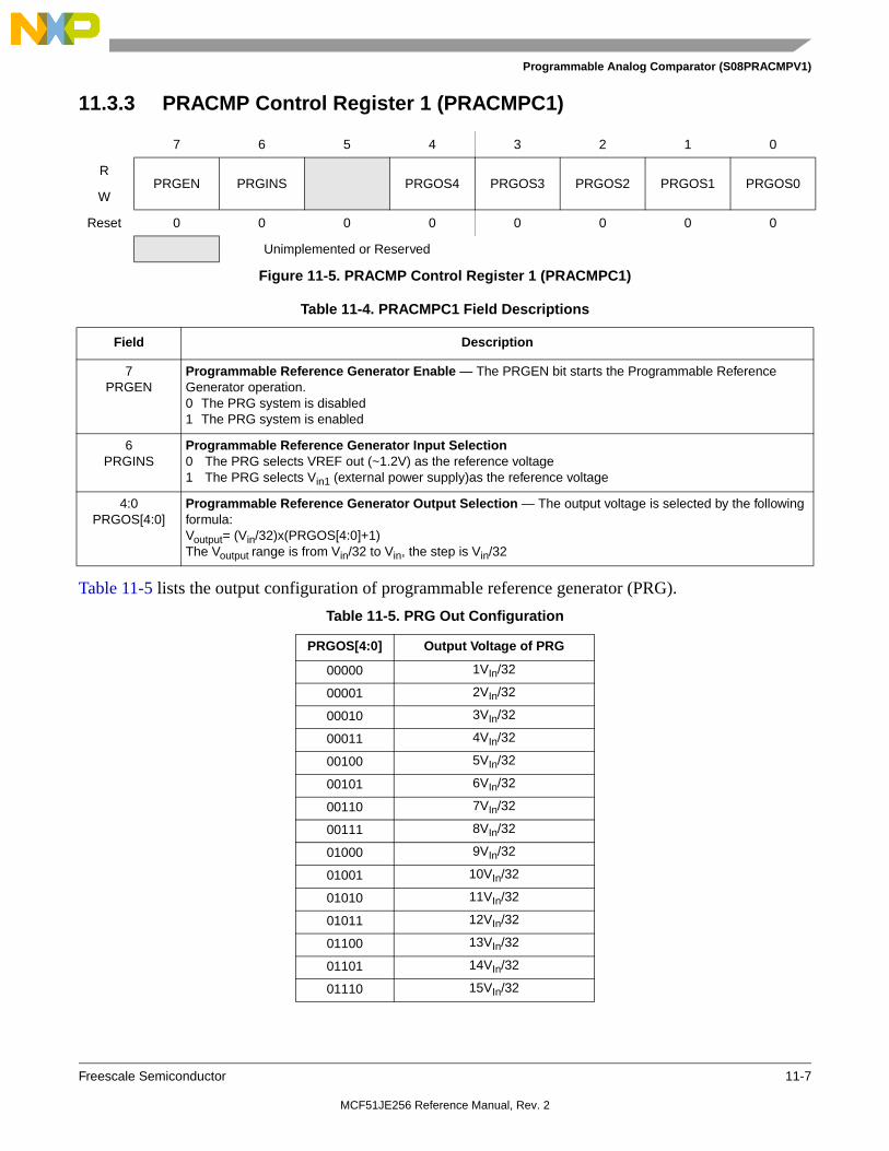
Programmable Analog Comparator (S08PRACMPV1)
Freescale Semiconductor 11-7
11.3.3 PRACMP Control Register 1 (PRACMPC1)
Table 11-5 lists the output configuration of programmable reference generator (PRG).
7 6 5 4 3 2 1 0
RPRGEN PRGINS PRGOS4 PRGOS3 PRGOS2 PRGOS1 PRGOS0
W
Reset 0 0 0 0 0 0 0 0
Unimplemented or Reserved
Figure 11-5. PRACMP Control Register 1 (PRACMPC1)
Table 11-4. PRACMPC1 Field Descriptions
Field Description
7PRGEN
Programmable Reference Generator Enable — The PRGEN bit starts the Programmable Reference Generator operation.0 The PRG system is disabled1 The PRG system is enabled
6PRGINS
Programmable Reference Generator Input Selection0 The PRG selects VREF out (~1.2V) as the reference voltage1 The PRG selects Vin1 (external power supply)as the reference voltage
4:0PRGOS[4:0]
Programmable Reference Generator Output Selection — The output voltage is selected by the following formula:Voutput= (Vin/32)x(PRGOS[4:0]+1)The Voutput range is from Vin/32 to Vin, the step is Vin/32
Table 11-5. PRG Out Configuration
PRGOS[4:0] Output Voltage of PRG
00000 1VIn/32
00001 2VIn/32
00010 3VIn/32
00011 4VIn/32
00100 5VIn/32
00101 6VIn/32
00110 7VIn/32
00111 8VIn/32
01000 9VIn/32
01001 10VIn/32
01010 11VIn/32
01011 12VIn/32
01100 13VIn/32
01101 14VIn/32
01110 15VIn/32
MCF51JE256 Reference Manual, Rev. 2

Programmable Analog Comparator (S08PRACMPV1)
11-8 Freescale Semiconductor
11.3.4 PRACMP Control Register 2 (PRACMPC2)
11.4 Functional DescriptionThe PRACMP module is functionally composed of two parts: programmable reference generator (PRG) and analog comparator (ACMP).
01111 16VIn/32
10000 17VIn/32
10001 18VIn/32
10010 19VIn/32
10011 20VIn/32
10100 21VIn/32
10101 22VIn/32
10110 23VIn/32
10111 24VIn/32
11000 25VIn/32
11001 26VIn/32
11010 27VIn/32
11011 28VIn/32
11100 29VIn/32
11101 30VIn/32
11110 31VIn/32
11111 VIn
7 6 5 4 3 2 1 0
R 0ACIPE6 ACIPE5 ACIPE4 ACIPE3 ACIPE2 ACIPE1 ACIPE0
W
Reset 0 0 0 0 0 0 0 0
Unimplemented or Reserved
Figure 11-6. PRACMP Control Register 2 (PRACMPC2)
Table 11-6. PRACMPC2 Field Descriptions
Field Description
6:0ACIPE6:ACIPE0
ACMP Input Pin Enable — This 7-bit register controls if the corresponding PRACMP external pin can be driven an analog input.0 The corresponding external analog input is not allowed 1 The corresponding external analog input is allowed
Table 11-5. PRG Out Configuration (Continued)
PRGOS[4:0] Output Voltage of PRG
MCF51JE256 Reference Manual, Rev. 2

Programmable Analog Comparator (S08PRACMPV1)
Freescale Semiconductor 11-9
The programmable reference generator (PRG) includes a 32-level DAC (digital to analog convertor) and relevant control logic. PRG can select one of two reference inputs, Vin1(external Vdd) or Vin2(internal regulated Vdd), as the DAC input Vin by setting PRGINS bit of PRACMPC1. After the DAC is enabled, it converts the data set in PRGOS[4:0] bits of PRACMPC1 to a stepped analog output which is fed into ACMP as an internal reference input. This stepped analog ouput is also mapped out of the module. The output voltage range is from Vin/32 to Vin..The step size is Vin/32.
The ACMP can achieve the analog comparison between positive input and negative input, and then give out a digital output and relevant interrupt. Both the positive and negative input of ACMP can be selected from the eight common inputs: seven external reference inputs and one internal reference input from the PRG output. The positive input of ACMP is selected by ACPSEL[2:0] bits of PRACMPC0 and the negative input is selected by ACNSEL[2:0] bits of PRACMPC0. Any pair of the eight inputs can be compared by configuring the PRACMPC0 with the appropriate value.
After the ACMP is enabled by setting ACEN in PRACMPCS, the comparison result appears as a digital output. Whenever a valid edge defined in ACINTS[1:0] occurs, the ACMPF bit in PRACMPCS register is asserted. If ACIEN is set, a PRACMP CPU interrupt occurs. The valid edge is defined by ACINTS[1:0].When ACINTS[1:0] = 00, both the rising edge and falling edge on the ACMP output are valid. When ACINTS[1:0] = 01, only the falling edge on ACMP output is valid. When ACINTS[1:0] = 10, only rising edge on ACMP output is valid. ACINTS[1:0] = 11 is reserved.
The ACMP output is synchronized by the bus clock to generate ACMPO bit in PRACMPCS so that the CPU can read the comparison. In stop3 mode if the output of ACMP is changed, ACMPO can’t be updated in time. The output can be synchronized and the ACMPO bit can be updated upon the waking up of the CPU because of the availability of the bus clock. The ACMPO changes following the comparison result, so it can serve as a tracking flag that continuously indicates the voltage delta on the inputs.
If a reference input external to the chip is selected as an input of ACMP, the corresponding ACIPE bit of PRACMPC2 should be set to enable the input from pad interface. If the output of the ACMP needs to be put onto the external pin, the ACOPE bit of PRACMPCS must enable the ACMP pin function of pad logic.
11.5 Setup and Operation of PRACMP The two parts of PRACMP (PRG and ACMP) can be set up and operated independently. But if the PRG works as an input of the ACMP, the PRG must be configured before the ACMP is enabled.
Because the input-switching can cause problems on the ACMP inputs, the user should complete the input selection before enabling the ACMP and should not change the input selection setting when the ACMP is enabled to avoid unexpected output. Similarly, because the programmable reference generator (PRG) experiences a setup delay after the PRGOS[4:0] is changed, the user should complete the setting of PRGOS[4:0] before PRG is enabled.
11.6 ResetsDuring a reset the PRACMP is configured in the default mode. Both ACMP and PRG are disabled.
MCF51JE256 Reference Manual, Rev. 2

Programmable Analog Comparator (S08PRACMPV1)
11-10 Freescale Semiconductor
11.7 InterruptsNOTE
If the bus clock is available when a valid edge (as defined in ACINTS[1:0]) occurs, the ACMPF bit in PRACMPCS register is asserted.
• If ACIEN is set, a PRACMP interrupt event occurs. The ACMPF bit remains asserted until the PRACMP interrupt is cleared by software
• When in stop3 mode, a valid edge on ACMP output generates an asynchronous interrupt which can wake the MCU up from stop3. To clear the interrupt, write a 0 to the ACMPF bit.
MCF51JE256 Reference Manual, Rev. 2

Freescale Semiconductor 12-1
Chapter 12 Analog-to-Digital Converter (S08ADC12V1)
12.1 IntroductionThe 12-bit analog-to-digital converter (ADC) is a successive approximation ADC designed for operation within an integrated microcontroller system-on-chip.
NOTEIn this device, VDDA external pin is referred to as VDDAD and VSSA external pin is referred to as VSSAD.
12.1.1 ADC Reference Selection
External VREFL and VREFH pins are the ADC conversion reference.
12.1.2 Module Configurations
This section provides device-specific information for configuring the ADC on MCF51JE256 series.
12.1.2.1 Configurations for Stop Modes
The ADC, if enabled, must be configured to use the asynchronous clock source, ADACK, to meet the ADC minimum frequency requirements. The VREF output must be enabled in order to convert the bandgap channel in stop mode.
12.1.2.2 Single-Ended Channel Assignments
The ADC single-ended channel assignments for the MCF51JE256 series devices are shown in Table 12-1. Reserved channels convert to an unknown value.
Table 12-1. ADC Single-Ended Channel Assignment
ADCH Channel Input Pin Control ADCH Channel Input Pin Control
00000 AD0 ADP0 ADPC0 10000 AD16 Reserved N/A
00001 AD1 ADP1 ADPC1 10001 AD17 Reserved N/A
00010 AD2 ADP2 ADPC2 10010 AD18 Reserved N/A
00011 AD3 ADP3 ADPC3 10011 AD19 Reserved N/A
00100 AD4 PTA2/KBI1P1/RX1/ADP4 ADPC4 10100 AD20 Reserved N/A
00101 AD5 PTA3/KBI1P2/FB_D6/ADP5 ADPC5 10101 AD21 Reserved N/A
MCF51JE256 Reference Manual, Rev. 2

Analog-to-Digital Converter (S08ADC12V1)
12-2 Freescale Semiconductor
NOTEEnable the VREF output to supply the bandgap voltage. See Chapter 26, “Voltage Reference Module (S08VREFV1),” for information on how to enable the VREF output. For the value of the bandgap voltage reference, see the data sheet.
12.1.2.3 Alternate Clock
The ADC is capable of performing conversions using the MCU bus clock, the bus clock divided by two, the local asynchronous clock (ADACK) within the module, or the alternate clock (ALTCLK). The ALTCLK on the MCF51JE256 series is connected to the MCGERCLK. See Chapter 17, “Multipurpose Clock Generator (S08MCGV3)” for more information.
12.1.2.4 Hardware Trigger
The ADC hardware trigger can be provided from the:
• Time of Day (TOD) Module
• Programmable Delay Block (PDB) Module
The ADCTRS bit from the SIMIPS register selects the hardware trigger source.
12.1.2.5 Temperature Sensor
The ADC module includes a temperature sensor whose output is connected to one of the ADC analog channel inputs. Equation 12-1 provides an approximate transfer function of the temperature sensor.
00110 AD6 PTC2/KBI1P5/SPSCK2/ADP6 ADPC6 10110 AD22 Reserved N/A
00111 AD7 PTC3/KBI1P6/SS2/ADP7 ADPC7 10111 AD23 Reserved N/A
01000 AD8 PTC4/KBI1P7/CMPP0/ADP8 ADPC8 11000 AD24 Reserved N/A
01001 AD9 PTC5/KBI2P0/CMPP1/ADP9 ADPC9 11001 R Reserved N/A
01010 AD10 PTC6/KBI2P1/PACMPO/ADP10 ADPC10 11010 Temp Single-ended
Temperature Sensor1
N/A
01011 AD11 PTC7/KBI2P2/CLKOUT/ADP11 ADPC11 11011 Bandgap PMC Bandgap N/A
01100 AD12 Reserved N/A 11100 R Reserved N/A
01101 AD13 Reserved N/A 11101 VREFH VREFH N/A
01110 AD14 Reserved N/A 11110 R Reserved N/A
01111 AD15 Reserved N/A 11111 Module Disabled
None N/A
1 1 For information, see Section 12.1.2.5, “Temperature Sensor.”
Table 12-1. ADC Single-Ended Channel Assignment (Continued)
ADCH Channel Input Pin Control ADCH Channel Input Pin Control
MCF51JE256 Reference Manual, Rev. 2

Analog-to-Digital Converter (S08ADC12V1)
Freescale Semiconductor 12-3
Temp = 25 - ((VTEMP -VTEMP25) m) Eqn. 12-1
where:
— VTEMP is the voltage of the temperature sensor channel at the ambient temperature.
— VTEMP25 is the voltage of the temperature sensor channel at 25C.
— m is the hot or cold voltage versus temperature slope in V/C.
For temperature calculations, use the VTEMP25 and m values in the data sheet.
In application code, the user reads the temperature sensor channel, calculates VTEMP, and compares it to VTEMP25. If VTEMP is greater than VTEMP25 the cold slope value is applied in Equation 12-1. If VTEMP is less than VTEMP25 the hot slope value is applied in Equation 12-1.
12.1.3 ADC Clock Gating
The bus clock to the ADC can be gated on and off using the ADC bit in SCGC1. This bit is set after any reset, which enables the bus clock to this module. To conserve power, the ADC bit can be cleared to disable the clock to this module when not in use. See Section 5.7.7, “System Clock Gating Control 1 Register (SCGC1),” for details.
MCF51JE256 Reference Manual, Rev. 2

Analog-to-Digital Converter (S08ADC12V1)
12-4 Freescale Semiconductor
Figure 12-1. Block Diagram with ADC Module Highlighted
MCF51JE256 Reference Manual, Rev. 2

Analog-to-Digital Converter (S08ADC12V1)
Freescale Semiconductor 12-5
12.1.4 Features
Features of the ADC module include:
• Linear successive approximation algorithm with up to 12-bit resolution
• Output Modes: Single-ended 12-bit, 10-bit and 8-bit modes
• Output in right-justified unsigned format for single-ended
• Single or continuous conversion (automatic return to idle after single conversion)
• Configurable sample time and conversion speed/power
• Conversion complete / Hardware average complete flag and interrupt
• Input clock selectable from up to four sources
• Operation in wait or stop3 modes for lower noise operation
• Asynchronous clock source for lower noise operation with option to output the clock
• Selectable asynchronous hardware conversion trigger with hardware channel select
• Automatic compare with interrupt for less-than, greater-than or equal-to programmable value
• Temperature sensor
• Self-Calibration mode
12.1.5 Block Diagram
Figure 12-2 provides a block diagram of the ADC module.
MCF51JE256 Reference Manual, Rev. 2
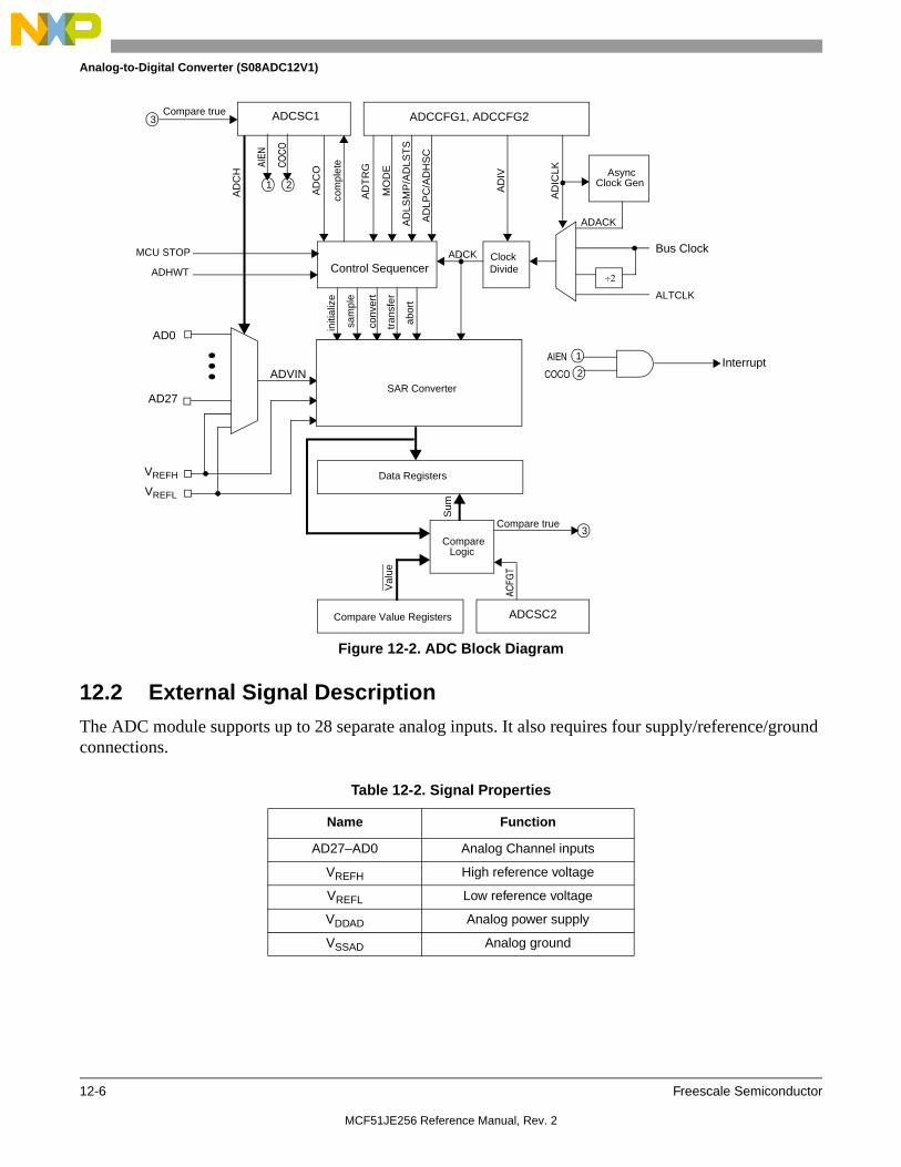
Analog-to-Digital Converter (S08ADC12V1)
12-6 Freescale Semiconductor
Figure 12-2. ADC Block Diagram
12.2 External Signal DescriptionThe ADC module supports up to 28 separate analog inputs. It also requires four supply/reference/ground connections.
Table 12-2. Signal Properties
Name Function
AD27–AD0 Analog Channel inputs
VREFH High reference voltage
VREFL Low reference voltage
VDDAD Analog power supply
VSSAD Analog ground
AD0
• • •
AD27
VREFH
VREFL
ADVIN
AD
CH
Control Sequencer
initi
aliz
e
sam
ple
conv
ert
tran
sfer
abor
t
ClockDivide
ADCK
AsyncClock Gen
Bus Clock
ALTCLK
AD
ICLK
AD
IV
ADACK
AD
CO
AD
LSM
P/A
DLS
TS
AD
LPC
/AD
HS
C
MO
DE
com
plet
e
Data Registers
SAR Converter
Compare Value Registers
Compare
Val
ue
Sum
AIEN
CO
CO
InterruptAIEN
COCOA
DT
RG
1
2
1 2
MCU STOP
ADHWT
Logic
ACFG
T
3Compare true
3Compare true ADCCFG1, ADCCFG2ADCSC1
ADCSC2
MCF51JE256 Reference Manual, Rev. 2

Analog-to-Digital Converter (S08ADC12V1)
Freescale Semiconductor 12-7
12.2.1 Analog Power (VDDAD)
The ADC analog portion uses VDDAD as its power connection. In some packages, VDDAD is connected internally to VDD. If externally available, connect the VDDAD pin to the same voltage potential as VDD. External filtering may be necessary to ensure clean VDDAD for good results.
12.2.2 Analog Ground (VSSAD)
The ADC analog portion uses VSSAD as its ground connection. In some packages, VSSAD is connected internally to VSS. If externally available, connect the VSSAD pin to the same voltage potential as VSS.
12.2.3 Voltage Reference High (VREFH)
VREFH is the high reference voltage for the converter. In some packages, VREFH is connected internally to VDDAD. If externally available, VREFH may be connected to the same potential as VDDAD or may be driven by an external source between the minimum VDDAD spec and the VDDAD potential (VREFH must never exceed VDDAD).
12.2.4 Voltage Reference Low (VREFL)
VREFL is the low-reference voltage for the converter. In some packages, VREFL is connected internally to VSSAD. If externally available, connect the VREFL pin to the same voltage potential as VSSAD.
12.2.5 Analog Channel Inputs (ADx)
The ADC module supports up to 28 separate analog inputs. An input is selected for conversion through the ADCH channel select bits.
12.3 Register Definition
These memory-mapped registers control and monitor operation of the ADC:
• Status and channel control registers, ADCSC1
• Configuration registers, ADCCFG1 and ADCCFG2
• Data result registers, ADCRH:ADCRL
• Compare value registers, ADCCVH, ADCCVL
• General status and control registers, ADCSC2 and ADCSC3
• Configuration registers, ADCCFG1 and ADCCFG2
• Pin enable registers, APCTL1, APCTL2, APCTL3, and APCTL4
• Offset Correction Registers, ADCOFSH and ADCOFSL
• Plus-input gain registers, ADCPGH and ADCPGL
• Minus-input gain registers, ADCMGH and ADCMGL
MCF51JE256 Reference Manual, Rev. 2

Analog-to-Digital Converter (S08ADC12V1)
12-8 Freescale Semiconductor
• Plus-side general calibration registers, ADCCLP0, ADCCLP1, ADCCLP2, ADCCLP3H, ADCCLP3L, ADCCLP4H, ADCCLP4L, ADCCLSP, ADDCLDP
• Minus-side general calibration registers, ADCCLM0, ADCCLM1, ADCCLM2, ADCCLM3H, ADCCLM3L, ADCCLM4H, ADCCLM4L, ADCCLSM, ADDCLDM
12.3.1 Status and Control Register 1 (ADCSC1)
This section describes the function of the ADC status and control register (ADCSC1). Writing ADCSC1 aborts the current conversion and initiates a new conversion (if the ADCH bits are equal to a value other than all 1s)
7 6 5 4 3 2 1 0
R COCOAIEN
01
1 This bit is reserved and must always be 0.
ADCHW
Reset: 0 0 0 1 1 1 1 1
Figure 12-3. Status and Channel Control Register 1n (ADCSC1)
Table 12-3. ADCSC1:ADCSC1 Field Descriptions
Field Description
7COCO
Conversion Complete Flag. The COCO flag is a read-only bit set each time a conversion is completed when the compare function is disabled (ACFE = 0). When the compare function is enabled (ACFE = 1), the COCO flag is set upon completion of a conversion only if the compare result is true. This bit is cleared when ADCSC1 is written or when ADCRL is read.0 Conversion not completed1 Conversion completed
6AIEN
Interrupt Enable AIEN enables conversion complete interrupts. When COCO becomes set while AIEN is high, an interrupt is asserted.0 Conversion complete interrupt disabled1 Conversion complete interrupt enabled
4:0ADCH
Input Channel Select. The ADCH bits form a 5-bit field that selects one of the input channels. The input channels are detailed in Table 12-4.The successive approximation converter subsystem is turned off when the channel select bits are all set. This feature allows for explicit disabling of the ADC and isolation of the input channel from all sources. Terminating continuous conversions this way prevents an additional, single conversion from being performed. It is not necessary to set the channel select bits to all ones to place the ADC in a low-power state when continuous conversions are not enabled because the module automatically enters a low-power state when a conversion completes.
Table 12-4. Input Channel Select
ADCH Input Select ADCH
00000–01111 AD0–15 00000–01111
10000–11011 AD16–27 10000–11011
MCF51JE256 Reference Manual, Rev. 2

Analog-to-Digital Converter (S08ADC12V1)
Freescale Semiconductor 12-9
12.3.2 Configuration Register 1(ADCCFG1)
ADCCFG1 selects the mode of operation, clock source, clock divide, and configure for low power or long sample time.
11100 Reserved 11100
11101 VREFH 11101
11110 Reserved 11110
11111 Module disabled 11111
7 6 5 4 3 2 1 0
RADLPC ADIV ADLSMP MODE ADICLK
W
Reset: 0 0 0 0 0 0 0 0
Figure 12-4. Configuration Register (ADCCFG1)
Table 12-5. ADCCFG1 Register Field Descriptions
Field Description
7ADLPC
Low-Power Configuration - ADLPC controls the power configuration of the successive approximation converter. This optimizes power consumption when higher sample rates are not required.0 Normal power configuration1 Low power configuration: The power is reduced at the expense of maximum clock speed.
6:5ADIV
Clock Divide Select - ADIV selects the divide ratio used by the ADC to generate the internal clock ADCK. Table 12-6 shows the available clock configurations.
4ADLSMP
Sample Time Configuration - ADLSMP selects between different sample times based on the conversion mode selected. This bit adjusts the sample period to allow higher impedance inputs to be accurately sampled or to maximize conversion speed for lower impedance inputs. Longer sample times can also be used to lower overall power consumption when continuous conversions are enabled if high conversion rates are not required. When ADLSMP=1, the Long Sample Time Select bits (ADLSTS[1:0]) can select the extent of the long sample time.0 Short sample time1 Long sample time (The ADLTS bits can select the extent of the long sample time)
3:2MODE
Conversion Mode Selection - MODE bits are used to select between the ADC resolution mode. See Table 12-7.
1:0ADICLK
Input Clock Select - ADICLK bits select the input clock source to generate the internal clock ADCK. See Table 12-8.
Table 12-6. Clock Divide Select
ADIV Divide Ratio Clock Rate
00 1 Input clock
01 2 Input clock 2
Table 12-4. Input Channel Select (Continued)
ADCH Input Select ADCH
MCF51JE256 Reference Manual, Rev. 2

Analog-to-Digital Converter (S08ADC12V1)
12-10 Freescale Semiconductor
12.3.3 Configuration Register 2 (ADCCFG2)
ADCCFG2 selects the special high speed configuration for very high speed conversions, and selects the long sample time duration during long sample mode.
10 4 Input clock 4
11 8 Input clock 8
Table 12-7. Conversion Modes
MODE Conversion Mode Description
00 single-ended 8-bit conversion
01 single-ended 12-bit conversion
10 single-ended 10-bit conversion
11 Reserved
Table 12-8. Input Clock Select
ADICLK Selected Clock Source
00 Bus clock
01 Bus clock divided by 2
10 Alternate clock (ALTCLK)
11 Asynchronous clock (ADACK)
7 6 5 4 3 2 1 0
R 0 0 0 0ADACKEN ADHSC ADLSTS
W
Reset: 0 0 0 0 0 0 0 0
Figure 12-5. Configuration Register 2(ADCCFG2)
Table 12-6. Clock Divide Select
ADIV Divide Ratio Clock Rate
MCF51JE256 Reference Manual, Rev. 2

Analog-to-Digital Converter (S08ADC12V1)
Freescale Semiconductor 12-11
12.3.4 Data Result Registers (ADCRH:ADCRL)
The Data Result Registers (ADCRH:ADCRL) contain the result of an ADC conversion of the channel selected by the status and channel control register (ADCSC1). Reading ADCRH prevents the ADC from transferring subsequent conversion results into the result registers until ADCRL is read. If ADCRL is not read until after the next conversion is completed, the intermediate conversion result is lost. In 8-bit single-ended mode, there is no interlocking with ADCRL.
Table 12-9. ADCCFG2 Register Field Descriptions
Field Description
3ADACKEN
Asynchronous clock output enable - ADACKEN enables the ADC’s asynchronous clock source and the clock source output regardless of the conversion and input clock select (ADICLK bits) status of the ADC. Based on MCU configuration the asynchronous clock may be used by other modules (see module introduction section). Setting this bit allows the clock to be used even while the ADC is idle or operating from a different clock source. Also, latency of initiating a single or first-continuous conversion with the asynchronous clock selected is reduced since the ADACK clock is already operational.0 Asynchronous clock output disabled; Asynchronous clock only enabled if selected by ADICLK and a
conversion is active1 Asynchronous clock and clock output enabled regardless of the state of the ADC
2ADHSC
High Speed Configuration- ADHSC configures the ADC for very high speed operation. The conversion sequence is altered (4 ADCK cycles added to the conversion time) to allow higher speed conversion clocks.0 Normal conversion sequence selected1 High speed conversion sequence selected (4 additional ADCK cycles to total conversion time)
1:0ADLSTS
[1:0]
Long Sample Time Select - ADLSTS selects between the extended sample times when long sample time is selected (ADLSMP=1). This allows higher impedance inputs to be accurately sampled or to maximize conversion speed for lower impedance inputs. Longer sample times can also be used to lower overall power consumption when continuous conversions are enabled if high conversion rates are not required.00 Default longest sample time (20 extra ADCK cycles; 24 ADCK cycles total)01 12 extra ADCK cycles; 16 ADCK cycles total sample time10 6 extra ADCK cycles; 10 ADCK cycles total sample time11 2 extra ADCK cycles; 6 ADCK cycles total sample time
7 6 5 4 3 2 1 0
R D[11:8]
W
Reset: 0 0 0 0 0 0 0 0
Figure 12-6. Data Result High Register (ADCRH)
7 6 5 4 3 2 1 0
R D[7:0]
W
Reset: 0 0 0 0 0 0 0 0
Figure 12-7. Data Result Low Register (ADCRL)
MCF51JE256 Reference Manual, Rev. 2

Analog-to-Digital Converter (S08ADC12V1)
12-12 Freescale Semiconductor
ADCRH contains the upper bits of the result of a conversion based on the conversion mode. ADCRL contains the lower eight bits of the result of a conversion, or all eight bits of an 8-bit single-ended conversion. Unused bits in the ADCRH register are cleared. For example, when configured for 10-bit single-ended mode, D[11:10] are cleared.
Table 12-10 below describes the behavior of the data result registers in the different modes of operation.
12.3.5 Compare Value High Register (ADCCVH)
In 12-bit mode, the ADCCVH register holds the upper four bits of the 12-bit compare value. These bits are compared to the upper four bits of the result following a conversion in 12-bit mode when the compare function is enabled.
In 10-bit mode, the ADCCVH register holds the upper two bits of the 10-bit compare value (ADCV9 – ADCV8). These bits are compared to the upper two bits of the result following a conversion in 10-bit mode when the compare function is enabled.
In 8-bit mode, ADCCVH is not used during compare.
12.3.6 Compare Value Low Register (ADCCVL)
This register holds the lower 8 bits of the 12-bit or 10-bit compare value or all 8 bits of the 8-bit compare value. Bits ADCV7:ADCV0 are compared to the lower 8 bits of the result following a conversion in 12-bit, 10-bit or 8-bit mode.
Table 12-10. Data Result Register Description
Conversion Mode
DATA
FormatD
11
D10 D9
D8
D7
D6
D5
D4
D3
D2
D1
D0
12b single-ended D D D D D D D D D D D D unsigned right justified
10b single-ended 0 0 D D D D D D D D D D unsigned right justified
8b single-ended 0 0 0 0 D D D D D D D D unsigned right justified
D: Data .
7 6 5 4 3 2 1 0
R 0 0 0 0CV[11:8}
W
Reset: 0 0 0 0 0 0 0 0
Figure 12-8. Compare Value High Register (ADCCVH)
MCF51JE256 Reference Manual, Rev. 2

Analog-to-Digital Converter (S08ADC12V1)
Freescale Semiconductor 12-13
12.3.7 Status and Control Register 2 (ADCSC2)
The ADCSC2 register contains the conversion active, hardware/software trigger select, compare function and voltage reference select of the ADC module.
7 6 5 4 3 2 1 0
RCV[7:0]
W
Reset: 0 0 0 0 0 0 0 0
Figure 12-9. Compare Value Low Register (ADCCVL)
7 6 5 4 3 2 1 0
R ADACTADTRG ACFE ACFGT R1
1 Bits 3, 1 and 0 are reserved bits that must always be written to 0.
0R1 R1
W
Reset: 0 0 0 0 0 0 0 0
Figure 12-10. Status and Control Register 2 (ADCSC2)
Table 12-11. ADCSC2 Register Field Descriptions
Field Description
7ADACT
Conversion Active - ADACT indicates that a conversion or hardware averaging is in progress. ADACT is set when a conversion is initiated and cleared when a conversion is completed or aborted.0 Conversion not in progress1 Conversion in progress
6ADTRG
Conversion Trigger Select - ADTRG selects the type of trigger used for initiating a conversion. Two types of trigger are selectable: software trigger and hardware trigger. When software trigger is selected, a conversion is initiated following a write to ADCSC1. When hardware trigger is selected, a conversion is initiated following the assertion of the ADHWT input. Refer to Section 12.4.4.1 for more information on initiating conversions.0 Software trigger selected1 Hardware trigger selected
5ACFE
Compare Function Enable - ACFE enables the compare function.0 Compare function disabled1 Compare function enabled
4ACFGT
Compare Function Greater Than Enable. Configures the compare function to trigger when the result of the conversion of the input being monitored is greater than or equal to the compare value. The compare function defaults to triggering when the result of the compare of the input being monitored is less than the compare value.0 Compare triggers when input is less than compare level1 Compare triggers when input is greater than or equal to compare level.
MCF51JE256 Reference Manual, Rev. 2

Analog-to-Digital Converter (S08ADC12V1)
12-14 Freescale Semiconductor
12.3.8 Status and Control Register 3 (ADCSC3)
The ADCSC3 register controls the calibration, continuous convert and hardware averaging functions of the ADC module.
12.3.9 ADC Offset Correction Register (ADCOFSH:ADCOFSL)
The ADC Offset Correction Register (ADCOFSH:ADCOFSL) contains the user-selected or calibration-generated offset error correction value.
This register is a 2’s complement, left justified, 16b value formed by the concatenation of:
• ADCOFSH
• ADCOFSL
The value in the offset correction registers (ADCOFSH:ADCOFSL) is subtracted from the conversion and the result is transferred into the result registers (ADCRH:ADCRL).
NOTEIf the result is above the maximum or below the minimum result value, it is forced to the appropriate limit for the current mode of operation.
7 6 5 4 3 2 1 0
RCAL
CALF 0 0ADCO R1
1 Bits are reserved bits that must always be written to 0.
R1 R1
W
Reset: 0 0 0 0 0 0 0 0
Figure 12-11. Status and Control Register 3 (ADCSC3)
Table 12-12. ADCSC3 Register Field Descriptions
Field Description
7CAL
Calibration - CAL begins the calibration sequence when set. This bit stays set while the calibration is in progress and is cleared when the calibration sequence is complete. The CALF bit must be checked to determine the result of the calibration sequence. Once started, the calibration routine cannot be interrupted by writes to the ADC registers or the results will be invalid and the CALF bit will set. Setting the CAL bit will abort any current conversion.
6CALF
Calibration Failed Flag - CALF displays the result of the calibration sequence. The calibration sequence will fail if ADTRG = 1, any ADC register is written, or any stop mode is entered before the calibration sequence completes.The CALF bit is cleared by writing a 1 to this bit.0 Calibration completed normally.1 Calibration failed. ADC accuracy specifications are not guaranteed.
3ADCO
Continuous Conversion Enable - ADCO enables continuous conversions.Refer to Section 12.4.4.1 for more information on initiating conversions.0 One conversion or one set of conversions if the hardware average function is enabled (AVGE=1) after initiating
a conversion.1 Continuous conversions or sets of conversions if the hardware average function is enabled (AVGE=1) after
initiating a conversion.
MCF51JE256 Reference Manual, Rev. 2

Analog-to-Digital Converter (S08ADC12V1)
Freescale Semiconductor 12-15
For additional information, please see Section 12.4.7.
12.3.10 ADC Plus-Side Gain Register (ADCPGH:ADCPGL)
The Plus-Side Gain Register (ADCPGH:ADCPGL) contains the gain error correction for the overall conversion in single-ended mode. ADCPGH:ADCPGL represent a 16 bit floating point number representation of the gain adjustment factor, with the decimal point fixed between ADPG15 and ADPG14. This register must be written by the user with the value described in the calibration procedure or the gain error specifications may not be met.
12.3.11 ADC Minus-Side Gain Register (ADCMGH:ADCMGL)
The Minus-Side Gain Register (ADCMGH:ADCMGL) represent a 16-bit floating point number representation of the gain adjustment factor, with the decimal point fixed between ADPG15 and ADPG14.
7 6 5 4 3 2 1 0
ROFS[15:8]
W
Reset: 0 0 0 0 0 0 0 0
Figure 12-12. Offset Calibration High Register (ADCOFSH)
7 6 5 4 3 2 1 0
ROFS[7:0]
W
Reset: 0 0 0 0 0 0 0 0
Figure 12-13. Offset Calibration Low Register (ADCOFSL)
7 6 5 4 3 2 1 0
RPG[15:8]
W
Reset: 1 0 0 0 0 0 1 1
Figure 12-14. ADC Plus Gain High Register (ADCPGH)
7 6 5 4 3 2 1 0
RPG[7:0]
W
Reset: 0 0 0 1 0 0 0 0
Figure 12-15. ADC Plus Gain Low Register (ADCPGL)
MCF51JE256 Reference Manual, Rev. 2

Analog-to-Digital Converter (S08ADC12V1)
12-16 Freescale Semiconductor
This register must be written by the user with the value described in the calibration procedure or the gain error specifications may not be met.
12.3.12 ADC Plus-Side General Calibration Value Registers (ADCCLPx)
The Plus-Side General Calibration Value Registers (ADCCLPx) contain calibration information that is generated by the calibration function. These registers contain seven calibration values of varying widths: CLP0[5:0], CLP1[6:0], CLP2[7:0], CLP3[8:0], CLP4[9:0], CLPS[5:0], and CLPD[5:0]. ADCCLPx are automatically set once the self calibration sequence is done (CAL is cleared). If these registers are written by the user after calibration, the linearity error specifications may not be met.
7 6 5 4 3 2 1 0
RMG[15:8]
W
Reset: 1 0 0 0 0 0 1 1
Figure 12-16. ADC Gain Register (ADCMGH)
7 6 5 4 3 2 1 0
RMG[7:0]
W
Reset: 0 0 0 1 0 0 0 0
Figure 12-17. ADC Gain Register (ADCMGL)
7 6 5 4 3 2 1 0
R 0 0CLPD[5:0]
W
Reset: 0 0 0 1 1 1 0 1
Figure 12-18. Plus-Side General Calibration Register (ADCCLPD)
7 6 5 4 3 2 1 0
R 0 0CLPS[5:0]
W
Reset: 0 0 1 0 0 0 0 0
Figure 12-19. Plus-Side General Calibration Register (ADCCLPS)
MCF51JE256 Reference Manual, Rev. 2

Analog-to-Digital Converter (S08ADC12V1)
Freescale Semiconductor 12-17
7 6 5 4 3 2 1 0
R 0 0 0 0 0 0CLP4[9:8]
W
Reset: 0 0 0 0 0 0 1 0
Figure 12-20. Plus-Side General Calibration Register (ADCCLP4H)
7 6 5 4 3 2 1 0
RCLP4[7:0]
W
Reset: 0 0 0 0 0 0 0 0
Figure 12-21. Plus-Side General Calibration Register (ADCCLP4L)
7 6 5 4 3 2 1 0
R 0 0 0 0 0 0 0CLP3[8]
W
Reset: 0 0 0 0 0 0 0 1
Figure 12-22. Plus-Side General Calibration Register (ADCCLP3H)
7 6 5 4 3 2 1 0
RCLP3[7:0]
W
Reset: 0 0 0 0 0 0 0 0
Figure 12-23. Plus-Side General Calibration Register (ADCCLP3L)
7 6 5 4 3 2 1 0
RCLP2[7:0]
W
Reset: 1 0 0 0 0 0 0 0
Figure 12-24. Plus-Side General Calibration Register (ADCCLP2)
7 6 5 4 3 2 1 0
R 0CLP1[6:0]
W
Reset: 0 1 0 0 0 0 0 0
Figure 12-25. Plus-Side General Calibration Register (ADCCLP1)
MCF51JE256 Reference Manual, Rev. 2

Analog-to-Digital Converter (S08ADC12V1)
12-18 Freescale Semiconductor
12.3.13 ADC Minus-Side General Calibration Value Registers (ADCCLMx)
ADCCLMx contain calibration information that is generated by the calibration function. These registers contain seven calibration values of varying widths: CLM0[5:0], CLM1[6:0], CLM2[7:0], CLM3[8:0], CLM4[9:0], CLMS[5:0], and CLMD[5:0]. ADCCLMx are automatically set once the self calibration sequence is done (CAL is cleared). If these registers are written by the user after calibration, the linearity error specifications may not be met.
7 6 5 4 3 2 1 0
R 0 0CLP0[5:0]
W
Reset: 0 0 1 0 0 0 0 0
Figure 12-26. Plus-Side General Calibration Register (ADCCLP0)
7 6 5 4 3 2 1 0
R 0 0CLMD[5:0]
W
Reset: 0 0 0 1 1 1 0 1
Figure 12-27. Minus-Side General Calibration Register (ADCCLMD)
7 6 5 4 3 2 1 0
R 0 0CLMS[5:0]
W
Reset: 0 0 1 1 0 0 0 1
Figure 12-28. Minus-Side General Calibration Register (ADCCLMS)
7 6 5 4 3 2 1 0
R 0 0 0 0 0 0CLM4[9:8]
W
Reset: 0 0 0 0 0 0 1 1
Figure 12-29. Minus-Side General Calibration Register (ADCCLM4H)
7 6 5 4 3 2 1 0
RCLM4[7:0]
W
Reset: 0 0 0 1 0 0 0 0
Figure 12-30. Minus-Side General Calibration Register (ADCCLM4L)
MCF51JE256 Reference Manual, Rev. 2
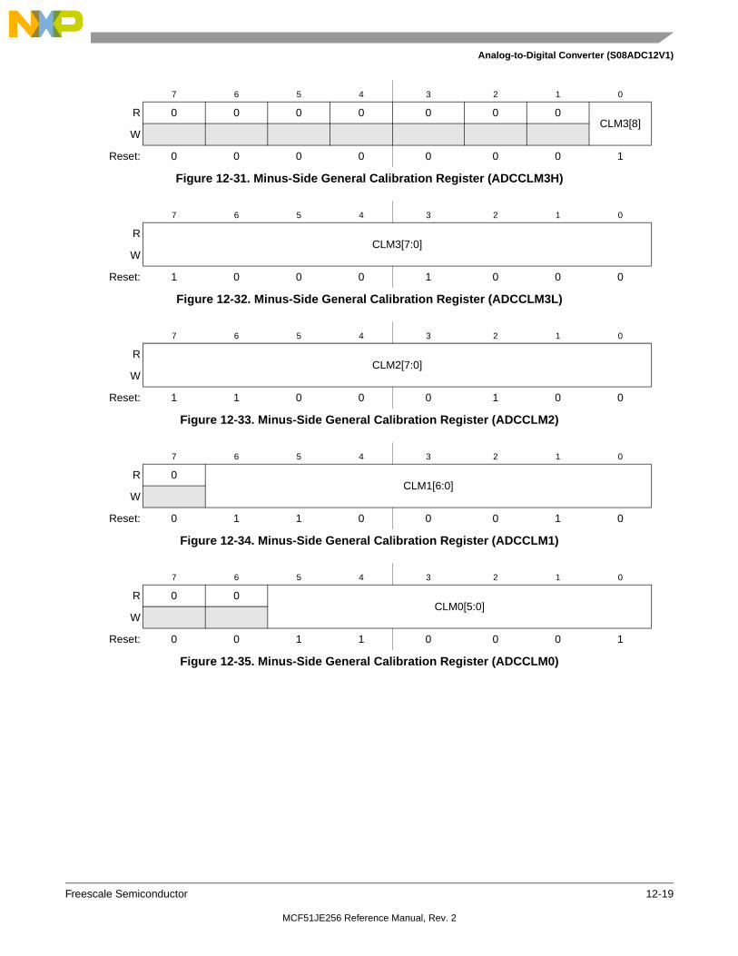
Analog-to-Digital Converter (S08ADC12V1)
Freescale Semiconductor 12-19
7 6 5 4 3 2 1 0
R 0 0 0 0 0 0 0CLM3[8]
W
Reset: 0 0 0 0 0 0 0 1
Figure 12-31. Minus-Side General Calibration Register (ADCCLM3H)
7 6 5 4 3 2 1 0
RCLM3[7:0]
W
Reset: 1 0 0 0 1 0 0 0
Figure 12-32. Minus-Side General Calibration Register (ADCCLM3L)
7 6 5 4 3 2 1 0
RCLM2[7:0]
W
Reset: 1 1 0 0 0 1 0 0
Figure 12-33. Minus-Side General Calibration Register (ADCCLM2)
7 6 5 4 3 2 1 0
R 0CLM1[6:0]
W
Reset: 0 1 1 0 0 0 1 0
Figure 12-34. Minus-Side General Calibration Register (ADCCLM1)
7 6 5 4 3 2 1 0
R 0 0CLM0[5:0]
W
Reset: 0 0 1 1 0 0 0 1
Figure 12-35. Minus-Side General Calibration Register (ADCCLM0)
MCF51JE256 Reference Manual, Rev. 2

Analog-to-Digital Converter (S08ADC12V1)
12-20 Freescale Semiconductor
12.3.14 Pin Control 1 Register (APCTL1)
The pin control registers disable the I/O port control of MCU pins used as analog inputs. APCTL1 is used to control the pins associated with channels 0–7 of the ADC module.
7 6 5 4 3 2 1 0
RADPC[7:0]
W
Reset: 0 0 0 0 0 0 0 0
Figure 12-36. Pin Control 1 Register (APCTL1)
Table 12-13. APCTL1 Register Field Descriptions
Field Description
7ADPC7
ADC Pin Control 7 - ADPC7 controls the pin associated with channel AD7.0 AD7 pin I/O control enabled1 AD7 pin I/O control disabled
6ADPC6
ADC Pin Control 6 - ADPC6 controls the pin associated with channel AD6.0 AD6 pin I/O control enabled1 AD6 pin I/O control disabled
5ADPC5
ADC Pin Control 5- ADPC5 controls the pin associated with channel AD5.0 AD5 pin I/O control enabled1 AD5 pin I/O control disabled
4ADPC4
ADC Pin Control 4 - ADPC4 controls the pin associated with channel AD4.0 AD4 pin I/O control enabled1 AD4 pin I/O control disabled
3ADPC3
ADC Pin Control 3 - ADPC3 controls the pin associated with channel AD3.0 AD3 pin I/O control enabled1 AD3 pin I/O control disabled
2ADPC2
ADC Pin Control 2 - ADPC2 controls the pin associated with channel AD2.0 AD2 pin I/O control enabled1 AD2 pin I/O control disabled
1ADPC1
ADC Pin Control 1 - ADPC1 controls the pin associated with channel AD1.0 AD1 pin I/O control enabled1 AD1 pin I/O control disabled
0ADPC0
ADC Pin Control 0 - ADPC0 controls the pin associated with channel AD0.0 AD0 pin I/O control enabled1 AD0 pin I/O control disabled
MCF51JE256 Reference Manual, Rev. 2

Analog-to-Digital Converter (S08ADC12V1)
Freescale Semiconductor 12-21
12.3.15 Pin Control 2 Register (APCTL2)
APCTL2 controls channels 8–15 of the ADC module.
7 6 5 4 3 2 1 0
RADPC[15:8]
W
Reset: 0 0 0 0 0 0 0 0
Figure 12-37. Pin Control 2 Register (APCTL2)
Table 12-14. APCTL2 Register Field Descriptions
Field Description
7ADPC15
ADC Pin Control 15 - ADPC15 controls the pin associated with channel AD15.0 AD15 pin I/O control enabled1 AD15 pin I/O control disabled
6ADPC14
ADC Pin Control 14 - ADPC14 controls the pin associated with channel AD14.0 AD14 pin I/O control enabled1 AD14 pin I/O control disabled
5ADPC13
ADC Pin Control 13 - ADPC13 controls the pin associated with channel AD13.0 AD13 pin I/O control enabled1 AD13 pin I/O control disabled
4ADPC12
ADC Pin Control 12 - ADPC12 controls the pin associated with channel AD12.0 AD12 pin I/O control enabled1 AD12 pin I/O control disabled
3ADPC11
ADC Pin Control 11 - ADPC11 controls the pin associated with channel AD11.0 AD11 pin I/O control enabled1 AD11 pin I/O control disabled
2ADPC10
ADC Pin Control 10 - ADPC10 controls the pin associated with channel AD10.0 AD10 pin I/O control enabled1 AD10 pin I/O control disabled
1ADPC9
ADC Pin Control 9 - ADPC9 controls the pin associated with channel AD9.0 AD9 pin I/O control enabled1 AD9 pin I/O control disabled
0ADPC8
ADC Pin Control 8 - ADPC8 controls the pin associated with channel AD8.0 AD8 pin I/O control enabled1 AD8 pin I/O control disabled
MCF51JE256 Reference Manual, Rev. 2

Analog-to-Digital Converter (S08ADC12V1)
12-22 Freescale Semiconductor
12.3.16 Pin Control 3 Register (APCTL3)
APCTL3 controls channels 23–16 of the ADC module.
12.4 Functional DescriptionThe ADC module is disabled during reset, stop2 or when the ADCH bits are all high. The module is idle when a conversion has completed and another conversion has not been initiated. When idle and the asynchronous clock output enable is disabled (ADACKEN=0), the module is in its lowest power state. The ADC can perform an analog-to-digital conversion on any of the software selectable channels. All modes perform conversion by a successive approximation algorithm.
7 6 5 4 3 2 1 0
RADPC[23:16]
W
Reset: 0 0 0 0 0 0 0 0
Figure 12-38. Pin Control 3 Register (APCTL3)
Table 12-15. APCTL3 Register Field Descriptions
Field Description
7ADPC23
ADC Pin Control 23 - ADPC23 controls the pin associated with channel AD23.0 AD23 pin I/O control enabled1 AD23 pin I/O control disabled
6ADPC22
ADC Pin Control 22 - ADPC22 controls the pin associated with channel AD22.0 AD22 pin I/O control enabled1 AD22 pin I/O control disabled
5ADPC21
ADC Pin Control 21 - ADPC21 controls the pin associated with channel AD21.0 AD21 pin I/O control enabled1 AD21 pin I/O control disabled
4ADPC20
ADC Pin Control 20 - ADPC20 controls the pin associated with channel AD20.0 AD20 pin I/O control enabled1 AD20 pin I/O control disabled
3ADPC19
ADC Pin Control 19 - ADPC19 controls the pin associated with channel AD19.0 AD19 pin I/O control enabled1 AD19 pin I/O control disabled
2ADPC18
ADC Pin Control 18 - ADPC18 controls the pin associated with channel AD18.0 AD18 pin I/O control enabled1 AD18 pin I/O control disabled
1ADPC17
ADC Pin Control 17 - ADPC17 controls the pin associated with channel AD17.0 AD17 pin I/O control enabled1 AD17 pin I/O control disabled
0ADPC16
ADC Pin Control 16 - ADPC16 controls the pin associated with channel AD16.0 AD16 pin I/O control enabled1 AD16 pin I/O control disabled
MCF51JE256 Reference Manual, Rev. 2

Analog-to-Digital Converter (S08ADC12V1)
Freescale Semiconductor 12-23
To meet accuracy specifications, the ADC module must be calibrated using the on chip calibration function. Calibration is recommended to be done after any reset. See Section 12.4.6 for details on how to perform calibration.
When the conversion is completed, the result is placed in the data registers (ADCRH and ADCRL). The conversion complete flag (COCO) is then set and an interrupt is generated if the respective conversion complete interrupt has been enabled (AIENn=1).
The ADC module has the capability of automatically comparing the result of a conversion with the contents of the compare value registers. The compare function is enabled by setting the ACFE bit and operates with any of the conversion modes and configurations.
12.4.1 Clock Select and Divide Control
One of four clock sources can be selected as the clock source for the ADC module. This clock source is then divided by a configurable value to generate the input clock to the converter (ADCK). The clock is selected from one of the following sources by means of the ADICLK bits.
• The bus clock. This is the default selection following reset.
• The bus clock divided by two. For higher bus clock rates, this allows a maximum divide by 16 of the bus clock with using the ADIV bits.
• ALTCLK, as defined for this MCU (See module section introduction).
• The asynchronous clock (ADACK). This clock is generated from a clock source within the ADC module. Conversions are possible using ADACK as the input clock source while the MCU is in stop3 mode. Refer to Section 12.4.4.4 for more information.
Whichever clock is selected, its frequency must fall within the specified frequency range for ADCK. If the available clocks are too slow, the ADC may not perform according to specifications. If the available clocks are too fast, the clock must be divided to the appropriate frequency. This divider is specified by the ADIV bits and can be divide-by 1, 2, 4, or 8.
12.4.2 Input Select and Pin Control
The pin control registers (APCTL1, APCTL2, APCTL3, and APCTL4) disable the I/O port control of the pins used as analog inputs.When a pin control register bit is set, the following conditions are forced for the associated MCU pin:
• The output buffer is forced to its high impedance state.
• The input buffer is disabled. A read of the I/O port returns a zero for any pin with its input buffer disabled.
• The pullup is disabled.
12.4.3 Hardware Trigger
The ADC module has a selectable asynchronous hardware conversion trigger, ADHWT, that is enabled when the ADTRG bit is set. This source is not available on all MCUs. Consult the module introduction for information on the ADHWT source specific to this MCU.
MCF51JE256 Reference Manual, Rev. 2

Analog-to-Digital Converter (S08ADC12V1)
12-24 Freescale Semiconductor
When ADHWT source is available and hardware trigger is enabled (ADTRG=1), a conversion is initiated on the rising edge of ADHWT. If a conversion is in progress when a rising edge occurs, the rising edge is ignored. In continuous convert configuration, only the initial rising edge to launch continuous conversions is observed. The hardware trigger function operates in conjunction with any of the conversion modes and configurations.
12.4.4 Conversion Control
Conversions can be performed in 12-bit mode, 10-bit mode, or 8-bit mode as determined by the MODE bits. Conversions can be initiated by a software or hardware trigger. In addition, the ADC module can be configured for low power operation, long sample time, continuous conversion, and automatic compare of the conversion result to a software determined compare value.
12.4.4.1 Initiating Conversions
A conversion is initiated:
• Following a write to ADCSC1 (with ADCH bits not all 1’s) if software triggered operation is selected (ADTRG=0).
• Following a hardware trigger (ADHWT) event if hardware triggered operation is selected (ADTRG=1)
• Following the transfer of the result to the data registers when continuous conversion is enabled (ADCO=1).
If continuous conversions are enabled, a new conversion is automatically initiated after the completion of the current conversion. In software triggered operation (ADTRG=0), continuous conversions begin after ADCSC1 is written and continue until aborted. In hardware triggered operation (ADTRG=1), continuous conversions begin after a hardware trigger event and continue until aborted.
12.4.4.2 Completing Conversions
A conversion is completed when the result of the conversion is transferred into the data result registers, ADCRH and ADCRL. If the compare functions are disabled, this is indicated by the setting of COCO. If the compare function is enabled, COCO sets and conversion result data is transferred only if the compare condition is true. An interrupt is generated if AIEN is high at the time that COCO is set.In all modes except 8-bit single-ended conversions, a blocking mechanism prevents a new result from overwriting previous data in ADCRH and ADCRL if the previous data is in the process of being read (the ADCRH register has been read but the ADCRL register has not). When blocking is active, the conversion result data transfer is blocked, COCO is not set, and the new result is lost. In the case of single conversions with the compare function enabled and the compare condition false, blocking has no effect and ADC operation is terminated. In all other cases of operation, when a conversion result data transfer is blocked, another conversion is initiated regardless of the state of ADCO (single or continuous conversions enabled).
MCF51JE256 Reference Manual, Rev. 2

Analog-to-Digital Converter (S08ADC12V1)
Freescale Semiconductor 12-25
NOTE
If continuous conversions are enabled, the blocking mechanism could result in the loss of data occurring at specific timepoints. To avoid this issue, the data must be read in fewer cycles than an ADC conversion time, accounting for interrupt or software polling loop latency.
If single conversions are enabled, the blocking mechanism could result in several discarded conversions and excess power consumption. To avoid this issue, the data registers must not be read after initiating a single conversion until the conversion completes.
12.4.4.3 Aborting Conversions
Any conversion in progress is aborted when:
• Writing ADCSC1 while ADCSC1 is actively controlling a conversion aborts the current conversion. In software trigger mode (ADTRG=0), a write to ADCSC1 initiates a new conversion (if the ADCH bits are equal to a value other than all 1s).
• A write to any ADC register besides the ADCSC1 register occurs. This indicates a mode of operation change has occurred and the current conversion is therefore invalid.
• The MCU is reset or enters stop2 mode.
• The MCU enters stop3 mode with ADACK not enabled.
When a conversion is aborted, the contents of the data registers, ADCRH and ADCRL are not altered. The data registers continue to be the values transferred after the completion of the last successful conversion. If the conversion was aborted by a reset or stop2, ADCRH:ADCRL return to their reset states.
12.4.4.4 Power Control
The ADC module remains in its idle state until a conversion is initiated. If ADACK is selected as the conversion clock source but the asynchronous clock output is disabled (ADACKEN=0), the ADACK clock generator will also remain in its idle state (disabled) until a conversion is initiated. If the asynchronous clock output is enabled (ADACKEN=1), it will remain active regardless of the state of the ADC or the MCU power mode.
Power consumption when the ADC is active can be reduced by setting ADLPC. This results in a lower maximum value for fADCK (see the electrical specifications).
12.4.4.5 Sample Time and Total Conversion Time
The total conversion time depends upon: the sample time (as determined by ADLSMP and ADLSTS bits), the MCU bus frequency, the conversion mode (as determined by MODE bits), the high speed configuration (ADHSC bit), and the frequency of the conversion clock (fADCK).
The ADHSC bit is used to configure a higher clock input frequency. This will allow faster overall conversion times. In order to meet internal A/D converter timing requirements the ADHSC bit adds
MCF51JE256 Reference Manual, Rev. 2

Analog-to-Digital Converter (S08ADC12V1)
12-26 Freescale Semiconductor
additional ADCK cycles. Conversions with ADHSC = 1 take four more ADCK cycles. ADHSC should be used when the ADCLK exceeds the limit for ADHSC = 0.
After the module becomes active, sampling of the input begins. ADLSMP and ADLSTS select between sample times based on the conversion mode that is selected. When sampling is complete, the converter is isolated from the input channel and a successive approximation algorithm is performed to determine the digital value of the analog signal. The result of the conversion is transferred to ADCRH and ADCRL upon completion of the conversion algorithm.
If the bus frequency is less than the fADCK frequency, precise sample time for continuous conversions cannot be guaranteed when short sample is enabled (ADLSMP=0). The maximum total conversion time is determined by the clock source chosen and the divide ratio selected. The clock source is selectable by the ADICLK bits, and the divide ratio is specified by the ADIV bits. The maximum total conversion time for all configurations is summarized in the equation that follows. Refer to Table 12-16 through Table 12-19 for the variables referenced in the equation.
Conversion Time Equation Eqn. 12-2
Table 12-16. Single or First Continuous Time Adder (SFCAdder)
AD
LS
MP
AD
AC
KE
N
AD
ICL
K
Single or First Continuous Time Adder (SFCAdder)
1 x 0x, 10 3 ADCK cycles + 5 bus clock cycles
1 1 11 3 ADCK cycles + 5 bus clock cycles1
1 ADACKEN must be 1 for at least 5us prior to the conversion is initiated to achieve this time
1 0 11 5s + 3 ADCK cycles + 5 bus clock cycles
0 x 0x, 10 5 ADCK cycles + 5 bus clock cycles
0 1 11 5 ADCK cycles + 5 bus clock cycles1
0 0 11 5s + 5 ADCK cycles + 5 bus clock cycles
Table 12-17. Base Conversion Time (BCT)
Mo
de Base Conversion
Time (BCT)
8b se 17 ADCK cycles
10b s.e. 20 ADCK cycles
12b s.e. 20 ADCK cycles
ConversionTime SFCAdder BCT LSTAdder HSCAdder+ + +=
MCF51JE256 Reference Manual, Rev. 2

Analog-to-Digital Converter (S08ADC12V1)
Freescale Semiconductor 12-27
NOTE
The ADCK frequency must be between fADCK minimum and fADCK maximum to meet ADC specifications.
12.4.4.6 Conversion Time Examples
The following examples use Equation 12-2 and the information provided in Table 12-16 through Table 12-19.
12.4.4.6.1 Typical conversion time configuration
A typical configuration for ADC conversion is: 10-bit mode, with the bus clock selected as the input clock source, the input clock divide-by-1 ratio selected, and a bus frequency of 8 MHz, long sample time disabled and high speed conversion disabled. The conversion time for a single conversion is calculated by using Equation 12-2 and the information provided in Table 12-16 through Table 12-19. The following table lists the variables of Equation 12-2.
Table 12-18. Long Sample Time Adder (LSTAdder)
AD
LS
MP
AD
LS
TS
Long Sample Time Adder (LSTAdder)
0 xx 0 ADCK cycles
1 00 20 ADCK cycles
1 01 12 ADCK cycles
1 10 6 ADCK cycles
1 11 2 ADCK cycles
Table 12-19. High-Speed Conversion time Adder (HSCAdder)
ADHSCHigh Speed
Conversion Time Adder (HSCAdder)
0 0 ADCK cycles
1 4 ADCK cycles
Table 12-20. Typical Conversion Time
Variable Time
SFCAdder 5 ADCK cycles + 5 bus clock cycles
BCT 20 ADCK cycles
MCF51JE256 Reference Manual, Rev. 2

Analog-to-Digital Converter (S08ADC12V1)
12-28 Freescale Semiconductor
The resulting conversion time is generated using the parameters listed in Table 12-20. So for Bus clock equal to 8 MHz and ADCK equal to 8 MHz the resulting conversion time is 3.75 us.
12.4.5 Automatic Compare Function
The compare function can be configured to check if the result is less than or greater-than-or-equal-to a compare value. The compare mode is determined by ACFGT. After the input is sampled and converted, the compare value (ADCCVH:ADCCVL) is used as described in Table 12-21.
If the condition selected evaluates true, COCO is set.
Upon completion of a conversion while the compare function is enabled, if the compare condition is not true, COCO is not set and the conversion result data will not be transferred to the result register. An ADC interrupt is generated upon the setting of COCO if the respective ADC interrupt is enabled (AIEN=1).
NOTE
The compare function can monitor the voltage on a channel while the MCU is in wait or stop3 mode. The ADC interrupt wakes the MCU when the compare condition is met.
12.4.6 Calibration Function
The ADC contains a self-calibration function that is required to achieve the specified accuracy. Calibration must be run or valid calibration values written after any reset and before a conversion is initiated. The calibration function sets the offset calibration value and the plus-side and minus-side calibration values.
The offset calibration value is automatically stored in the ADC Offset Correction Registers (ADCOFSH and ADCOFSL) and the plus-side and minus-side calibration values are automatically stored in the ADC Plus-Side and Minus-Side Calibration registers (CLPD, CLPS, CLP4, CLP3, CLP2, CLP1, CLP0 and CLMD, CLMS, CLP4, CLM3, CLM2, CLM1, CLM0). The user must configure the ADC correctly prior
LSTAdder 0
HSCAdder 0
Table 12-21. Compare Modes
AC
FG
T
Function Compare Mode Description
0 Less than threshold Compare true if the result is less than the ADCCV registers.
1 Greater than or equal to threshold Compare true if the result is greater than or equal to ADCCV registers.
Table 12-20. Typical Conversion Time (Continued)
Variable Time
MCF51JE256 Reference Manual, Rev. 2

Analog-to-Digital Converter (S08ADC12V1)
Freescale Semiconductor 12-29
to calibration, and must generate the plus-side and minus-side gain calibration results and store them in the ADC GAIN registers (ADCPGH and ADCPGL) after the calibration function completes.
Prior to calibration, the user must configure the ADC’s clock source and frequency, low power configuration, voltage reference selection, sample time and the high speed configuration according to the application’s clock source availability and needs. If the application uses the ADC in a wide variety of configurations, the configuration for which the highest accuracy is required should be selected, or multiple calibrations can be done for the different configurations. The input channel, conversion mode continuous function, compare function, and resolution mode are all ignored during the calibration function.
To initiate calibration, the user sets the CAL bit and the calibration will automatically begin if the ADTRG bit = 0. If ADTRG = 1, the CAL bit will not get set and the calibration fail flag (CALF) will be set. While calibration is active, no ADC register can be written and no stop mode may be entered or the calibration routine will be aborted causing the CAL bit to clear and the CALF bit to set. At the end of a calibration sequence the COCO bit of the ADSC1A register will be set. The AIEN1 bit can be used to allow an interrupt to occur at the end of a calibration sequence. If at the end of calibration routine the CALF bit is not set, the automatic calibration routine completed successfully.
To complete calibration, the user must generate the gain calibration values using the following procedure:
• Initialize (clear) a 16b variable in RAM.
• Add the following plus-side calibration results CLP0, CLP1, CLP2, CLP3, CLP4, and CLPS to the variable.
• Divide the variable by two.
• Set the MSB of the variable.
• The previous two steps can be achieved by setting the carry bit, rotating-right through the carry bit on the high byte and again on the low byte.
• Store the value in the plus-side gain calibration registers ADCPGH and ADCPGL.
• Repeat procedure for the minus-side gain calibration value.
When complete the user may reconfigure and use the ADC as desired. A second calibration may also be performed if desired by clearing and again setting the CAL bit.
Overall the calibration routine may take as many as 14000 ADCK cycles and 100 bus cycles, depending on the results and the clock source chosen. For an 8 MHz clock source this is about 1.7 msec. To reduce this latency, the calibration values (offset, plus- and minus-side gain, and plus- and minus-side calibration values) may be stored in flash after an initial calibration and recovered prior to the first ADC conversion. This should reduce the calibration latency to 20 register store operations on all subsequent power, reset, or stop2 mode recoveries.
12.4.7 User-Defined Offset Function
The ADC Offset Correction Register (ADCOFSH:ADCOFSL) contains the user selected or calibration generated offset error correction value. This register is a 2’s complement, left justified, 16b value formed by the concatenation of ADCOFSH and ADCOFSL. The value in the offset correction registers (ADCOFSH:ADCOFSL) is subtracted from the conversion and the result is transferred into the result
MCF51JE256 Reference Manual, Rev. 2

Analog-to-Digital Converter (S08ADC12V1)
12-30 Freescale Semiconductor
registers (ADCRH:ADCRL). If the result is above the maximum or below the minimum result value, it is forced to the appropriate limit for the current mode of operation.
The formatting of the ADC Offset Correction Register is different from the Data Result Registers (ADCRH:ADCRL) to preserve the resolution of the calibration value regardless of the conversion mode selected. Lower order bits are ignored in lower resolution modes. For example, in 8b single-ended mode, the bits OFS[14:7] are subtracted from D[7:0]; bit OFS[15] indicates the sign (negative numbers are effectively added to the result) and bits OFS[6:0] are ignored. ADCOFSH is automatically set according to calibration requirements once the self calibration sequence is done (CAL is cleared). Write ADCOFSH:ADCOFSL to override the calibration result if desired. If the Offset Correction Register is written to a value that is different from the calibration value, the ADC error specifications may not be met. It is recommended that the value generated by the calibration function be stored in memory before overwriting with a specified value.
NOTEThere is an effective limit to the values of Offset that can be set. If the magnitude of the offset is too great, the results of the conversions cap off at the limits.
Use the offset calibration function to remove application offsets or DC bias values. The Offset Correction Registers ADCOFSH and ADCOFSL may be written with a number in 2’s complement format and this offset will be subtracted from the result (or hardware averaged value). To add an offset, store the negative offset in 2’s complement format and the effect will be an addition. An offset correction that results in an out-of-range value will be forced to the minimum or maximum value (the minimum value for single-ended conversions is 0x0000).
To preserve accuracy, the calibrated offset value initially stored in the ADCOFS registers must be added to the user defined offset. For applications which may change the offset repeatedly during operation, it is recommended to store the initial offset calibration value in flash so that it can be recovered and added to any user offset adjustment value -nd the sum stored in the ADCOFS registers.
12.4.8 Temperature Sensor
The ADC module includes a temperature sensor whose output is connected to one of the ADC analog channel inputs. Equation 12-3 provides an approximate transfer function of the temperature sensor.
Temp = 25 - ((VTEMP -VTEMP25) m) Eqn. 12-3
where:
— VTEMP is the voltage of the temperature sensor channel at the ambient temperature.
— VTEMP25 is the voltage of the temperature sensor channel at 25C.
— m is the hot or cold voltage versus temperature slope in V/C.
For temperature calculations, use the VTEMP25 and m values from the ADC Electricals table.
In application code, you read the temperature sensor channel, calculate VTEMP, and compare to VTEMP25. If VTEMP is greater than VTEMP25, the cold slope value is applied in Equation 12-3. If VTEMP is less than VTEMP25, the hot slope value is applied in Equation 12-3.
MCF51JE256 Reference Manual, Rev. 2

Analog-to-Digital Converter (S08ADC12V1)
Freescale Semiconductor 12-31
For more information on using the temperature sensor, consult AN3031.
12.4.9 MCU Wait Mode Operation
Wait mode is a lower power-consumption standby mode from which recovery is fast because the clock sources remain active. If a conversion is in progress when the MCU enters wait mode, it continues until completion. Conversions can be initiated while the MCU is in wait mode by means of the hardware trigger or if continuous conversions are enabled.
The bus clock, bus clock divided by two, and ADACK are available as conversion clock sources while in wait mode. The use of ALTCLK as the conversion clock source in wait is dependent on the definition of ALTCLK for this MCU. Consult the module introduction for information on ALTCLK specific to this MCU.
If the compare and hardware averaging functions are disabled, a conversion complete event sets the COCO and generates an ADC interrupt to wake the MCU from wait mode if the respective ADC interrupt is enabled (AIEN=1). If the hardware averaging function is enabled the COCO will set (and generate an interrupt if enabled) when the selected number of conversions are complete. If the compare function is enabled the COCO will set (and generate an interrupt if enabled) only if the compare conditions are met. If a single conversion is selected and the compare trigger is not met, the ADC will return to its idle state and cannot wake the MCU from wait mode unless a new conversion is initiated by the hardware trigger.
12.4.10 MCU Stop3 Mode Operation
Stop mode is a low power-consumption standby mode during which most or all clock sources on the MCU are disabled.
12.4.10.1 Stop3 Mode With ADACK Disabled
If the asynchronous clock, ADACK, is not selected as the conversion clock, executing a stop instruction aborts the current conversion and places the ADC in its idle state. The contents of the ADC registers, including ADCRH and ADCRL, are unaffected by stop3 mode. After exiting from stop3 mode, a software or hardware trigger is required to resume conversions.
12.4.10.2 Stop3 Mode With ADACK Enabled
If ADACK is selected as the conversion clock, the ADC continues operation during stop3 mode. For guaranteed ADC operation, the MCU’s voltage regulator must remain active during stop3 mode. Consult the module introduction for configuration information for this MCU.
If a conversion is in progress when the MCU enters stop3 mode, it continues until completion. Conversions can be initiated while the MCU is in stop3 mode by means of the hardware trigger or if continuous conversions are enabled.
If the compare and hardware averaging functions are disabled, a conversion complete event sets the COCO and generates an ADC interrupt to wake the MCU from stop3 mode if the respective ADC interrupt is enabled (AIEN = 1). The result register will contain the data from the first completed conversion that occurred during stop3 mode. If the hardware averaging function is enabled the COCO will set (and
MCF51JE256 Reference Manual, Rev. 2

Analog-to-Digital Converter (S08ADC12V1)
12-32 Freescale Semiconductor
generate an interrupt if enabled) when the selected number of conversions are complete. If the compare function is enabled the COCO will set (and generate an interrupt if enabled) only if the compare conditions are met. If a single conversion is selected and the compare is not true, the ADC will return to its idle state and cannot wake the MCU from stop3 mode unless a new conversion is initiated by another hardware trigger.
NOTE
The ADC module can wake the system from low-power stop and cause the MCU to begin consuming run-level currents without generating a system level interrupt. To prevent this scenario, software should ensure the conversion result data transfer blocking mechanism (discussed in Section 12.4.4.2, “Completing Conversions) is cleared when entering stop3 and continuing ADC conversions.
12.4.11 MCU Stop2 Mode Operation
The ADC module is automatically disabled when the MCU enters stop2 mode. All module registers contain their reset values following exit from stop2. Therefore, the module must be re-enabled and re-configured following exit from stop2.
12.5 Initialization InformationThis section gives an example that provides some basic direction on how to initialize and configure the ADC module. You can configure the module for 8-, 10-, or 12-bit single-ended resolution, single or continuous conversion, and a polled or interrupt approach, among many other options. Refer to Table 12-6, Table 12-7, and Table 12-8 for information used in this example.
NOTE
Hexadecimal values designated by a preceding 0x, binary values designated by a preceding %, and decimal values have no preceding character.
12.5.1 ADC Module Initialization Example
12.5.1.1 Initialization Sequence
Before the ADC module can be used to complete conversions, an initialization procedure must be performed. A typical sequence is as follows:
1. Calibrate the ADC by following the calibration instructions in Section 12.4.6, “Calibration Function.
2. Update the configuration register (ADCCFG) to select the input clock source and the divide ratio used to generate the internal clock, ADCK. This register is also used for selecting sample time and low-power configuration.
3. Update status and control register 2 (ADCSC2) to select the conversion trigger (hardware or software) and compare function options, if enabled.
MCF51JE256 Reference Manual, Rev. 2

Analog-to-Digital Converter (S08ADC12V1)
Freescale Semiconductor 12-33
4. Update status and control register 3 (ADSC3) to select whether conversions will be continuous or completed only once (ADCO) and to select whether to perform hardware averaging.
5. Update status and control register (ADCSC1) to select conversion complete interrupts. The input channel on which conversions will be performed is also selected here.
12.5.1.2 Pseudo-Code Example
In this example, the ADC module is set up with interrupts enabled to perform a single 10-bit conversion at low power with a long sample time on input channel 1, where the internal ADCK clock is derived from the bus clock divided by 1.
ADCCFG = 0x98 (%10011000)Bit 7 ADLPC 1 Configures for low power (lowers maximum clock speed.
Bit 6:5 ADIV 00 Sets the ADCK to the input clock 1.
Bit 4 ADLSMP 1 Configures for long sample time.
Bit 3:2 MODE 10 Sets mode at 10-bit conversions.
Bit 1:0 ADICLK 00 Selects bus clock as input clock source.
ADCSC2 = 0x00 (%00000000)Bit 7 ADACT 0 Flag indicates if a conversion is in progress.
Bit 6 ADTRG 0 Software trigger selected.
Bit 5 ACFE 0 Compare function disabled.
Bit 4 ACFGT 0 Not used in this example.
Bit 3:2 00 Reserved, always reads zero.
Bit 1:0 00 Reserved for Freescale’s internal use; always write zero.
ADCSC1 = 0x41 (%01000001)Bit 7 COCO 0 Read-only flag which is set when a conversion completes.
Bit 6 AIEN 1 Conversion complete interrupt enabled.
Bit 5 ADCO 0 One conversion only (continuous conversions disabled).
Bit 4:0 ADCH 00001 Input channel 1 selected as ADC input channel.
ADCRH/L = 0xxxHolds results of conversion. Read high byte (ADCRH) before low byte (ADCRL) so thatconversion data cannot be overwritten with data from the next conversion.
ADCCVH/L = 0xxxHolds compare value when compare function enabled.
APCTL1=0x02 AD1 pin I/O control disabled. All other AD pins remain general purpose I/O pins.
APCTL2=0x00All other AD pins remain general purpose I/O pins.
MCF51JE256 Reference Manual, Rev. 2

Analog-to-Digital Converter (S08ADC12V1)
12-34 Freescale Semiconductor
Figure 12-39. Initialization Flowchart for Example
12.6 Application InformationThis section contains information for using the ADC module in applications. The ADC has been designed to be integrated into a microcontroller for use in embedded control applications requiring an A/D converter.
12.6.1 External Pins and Routing
The following sections discuss the external pins associated with the ADC module and how they should be used for best results.
12.6.1.1 Analog Supply Pins
The ADC module has analog power and ground supplies (VDDAD and VSSAD) available as separate pins on some devices. VSSAD is shared on the same pin as the MCU digital VSS on some devices. On other devices, VSSAD and VDDAD are shared with the MCU digital supply pins. In these cases, there are separate pads for the analog supplies bonded to the same pin as the corresponding digital supply so that some degree of isolation between the supplies is maintained.
Yes
No
Reset
Initialize ADCADCCFG = 0x98
ADCSC1 = 0x41ADCSC2 = 0x00
CheckCOCO =1?
Read ADCRHThen ADCRL ToClear COCO Bit
Continue
MCF51JE256 Reference Manual, Rev. 2

Analog-to-Digital Converter (S08ADC12V1)
Freescale Semiconductor 12-35
When available on a separate pin, both VDDAD and VSSAD must be connected to the same voltage potential as their corresponding MCU digital supply (VDD and VSS) and must be routed carefully for maximum noise immunity and bypass capacitors placed as near as possible to the package.
If separate power supplies are used for analog and digital power, the ground connection between these supplies must be at the VSSAD pin. This should be the only ground connection between these supplies if possible. The VSSAD pin makes a good single point ground location.
12.6.1.2 Analog Voltage Reference Pins
The ADC module has analog power and ground supplies (VDDAD and VSSAD) available as separate pins on some devices. VSSAD is shared on the same pin as the MCU digital VSS on some devices. On other devices, VSSAD and VDDAD are shared with the MCU digital supply pins. In these cases, there are separate pads for the analog supplies bonded to the same pin as the corresponding digital supply so that some degree of isolation between the supplies is maintained.
When available on a separate pin, both VDDAD and VSSAD must be connected to the same voltage potential as their corresponding MCU digital supply (VDD and VSS) and must be routed carefully for maximum noise immunity and bypass capacitors placed as near as possible to the package.
If separate power supplies are used for analog and digital power, the ground connection between these supplies must be at the VSSAD pin. This should be the only ground connection between these supplies if possible. The VSSAD pin makes a good single point ground location.
12.6.1.3 Analog Input Pins
The external analog inputs are typically shared with digital I/O pins on MCU devices. The pin I/O control is disabled by setting the appropriate control bit in one of the pin control registers. Conversions can be performed on inputs without the associated pin control register bit set. It is recommended that the pin control register bit always be set when using a pin as an analog input. This avoids problems with contention because the output buffer is in its high impedance state and the pullup is disabled. Also, the input buffer draws DC current when its input is not at VDD or VSS. Setting the pin control register bits for all pins used as analog inputs should be done to achieve lowest operating current.
Empirical data shows that capacitors on the analog inputs improve performance in the presence of noise or when the source impedance is high. Use of 0.01 F capacitors with good high-frequency characteristics is sufficient. These capacitors are not necessary in all cases, but when used they must be placed as near as possible to the package pins and be referenced to VSSA.
For proper conversion, the input voltage must fall between VREFH and VREFL. If the input is equal to or exceeds VREFH, the converter circuit converts the signal to 0xFFF (full scale 12-bit representation), 0x3FF (full scale 10-bit representation) or 0xFF (full scale 8-bit representation). If the input is equal to or less than VREFL, the converter circuit converts it to 0x000. Input voltages between VREFH and VREFL are straight-line linear conversions. There is a brief current associated with VREFL when the sampling capacitor is charging.
For minimal loss of accuracy due to current injection, pins adjacent to the analog input pins should not be transitioning during conversions.
MCF51JE256 Reference Manual, Rev. 2

Analog-to-Digital Converter (S08ADC12V1)
12-36 Freescale Semiconductor
12.6.2 Sources of Error
Several sources of error exist for A/D conversions. These are discussed in the following sections.
12.6.2.1 Sampling Error
For proper conversions, the input must be sampled long enough to achieve the proper accuracy. Given the maximum input resistance of approximately 7k and input capacitance of approximately 5.5 pF, sampling to within 1/4LSB (at 12-bit resolution) can be achieved within the minimum sample window (3.5 cycles @ 8 MHz maximum ADCK frequency) provided the resistance of the external analog source (RAS) is kept below 2 k.
Higher source resistances or higher-accuracy sampling is possible by setting ADLSMP and changing the ADLSTS bits (to increase the sample window) or decreasing ADCK frequency to increase sample time.
12.6.2.2 Pin Leakage Error
Leakage on the I/O pins can cause conversion error if the external analog source resistance (RAS) is high. If this error cannot be tolerated by the application, keep RAS lower than VDDAD / (2N*ILEAK) for less than 1/4LSB leakage error (N = 8 in 8-bit, 10 in 10-bit or 12 in 12-bit mode).
12.6.2.3 Noise-Induced Errors
System noise that occurs during the sample or conversion process can affect the accuracy of the conversion. The ADC accuracy numbers are guaranteed as specified only if the following conditions are met:
• There is a 0.1 F low-ESR capacitor from VREFH to VREFL.
• There is a 0.1 F low-ESR capacitor from VDDAD to VSSAD.
• If inductive isolation is used from the primary supply, an additional 1 F capacitor is placed from VDDAD to VSSAD.
• VSSAD (and VREFL, if connected) is connected to VSS at a quiet point in the ground plane.
• Operate the MCU in wait or stop3 mode before initiating (hardware triggered conversions) or immediately after initiating (hardware or software triggered conversions) the ADC conversion.
— For software triggered conversions, immediately follow the write to ADCSC1 with a stop instruction.
— For stop3 mode operation, select ADACK as the clock source. Operation in stop3 reduces VDD noise but increases effective conversion time due to stop recovery.
• There is no I/O switching, input or output, on the MCU during the conversion.
There are some situations where external system activity causes radiated or conducted noise emissions or excessive VDD noise is coupled into the ADC. In these situations, or when the MCU cannot be placed in wait or stop3 or I/O activity cannot be halted, these recommended actions may reduce the effect of noise on the accuracy:
• Place a 0.01 F capacitor (CAS) on the selected input channel to VREFL or VSSAD (this improves noise issues, but affects the sample rate based on the external analog source resistance).
MCF51JE256 Reference Manual, Rev. 2

Analog-to-Digital Converter (S08ADC12V1)
Freescale Semiconductor 12-37
• Average the result by converting the analog input many times in succession and dividing the sum of the results. Four samples are required to eliminate the effect of a 1LSB, one-time error.
• Reduce the effect of synchronous noise by operating off the asynchronous clock (ADACK) and averaging. Noise that is synchronous to ADCK cannot be averaged out.
12.6.2.4 Code Width and Quantization Error
The ADC quantizes the ideal straight-line transfer function into 4096 steps (in 12-bit mode). Each step ideally has the same height (1 code) and width. The width is defined as the delta between the transition points to one code and the next. The ideal code width for an N bit converter (in this case N can be 8, 10 or 12), defined as 1LSB, is:
1 lsb = (VREFH - VREFL) / 2N Eqn. 12-4
There is an inherent quantization error due to the digitization of the result. For 8-bit or 10-bit conversions the code transitions when the voltage is at the midpoint between the points where the straight line transfer function is exactly represented by the actual transfer function. Therefore, the quantization error will be 1/2 lsb in 8- or 10-bit mode. As a consequence, however, the code width of the first (0x000) conversion is only 1/2 lsb and the code width of the last (0xFF or 0x3FF) is 1.5 lsb.
For 12-bit conversions the code transitions only after the full code width is present, so the quantization error is 1 lsb to 0 lsb and the code width of each step is 1 lsb.
12.6.2.5 Linearity Errors
The ADC may also exhibit non-linearity of several forms. Every effort has been made to reduce these errors but the system should be aware of them because they affect overall accuracy. These errors are:
• Zero-scale error (EZS) (sometimes called offset) — This error is defined as the difference between the actual code width of the first conversion and the ideal code width (1/2 lsb in 8-bit or 10-bit modes and 1 lsb in 12-bit mode). If the first conversion is 0x001, the difference between the actual 0x001 code width and its ideal (1 lsb) is used.
• Full-scale error (EFS) — This error is defined as the difference between the actual code width of the last conversion and the ideal code width (1.5 lsb in 8-bit or 10-bit modes and 1LSB in 12-bit mode). If the last conversion is 0x3FE, the difference between the actual 0x3FE code width and its ideal (1LSB) is used.
• Differential non-linearity (DNL) — This error is defined as the worst-case difference between the actual code width and the ideal code width for all conversions.
• Integral non-linearity (INL) — This error is defined as the highest-value the (absolute value of the) running sum of DNL achieves. More simply, this is the worst-case difference of the actual transition voltage to a given code and its corresponding ideal transition voltage, for all codes.
• Total unadjusted error (TUE) — This error is defined as the difference between the actual transfer function and the ideal straight-line transfer function and includes all forms of error.
MCF51JE256 Reference Manual, Rev. 2

Analog-to-Digital Converter (S08ADC12V1)
12-38 Freescale Semiconductor
12.6.2.6 Code Jitter, Non-Monotonicity, and Missing Codes
Analog-to-digital converters are susceptible to three special forms of error. These are code jitter, non-monotonicity, and missing codes.
Code jitter is when, at certain points, a given input voltage converts to one of two values when sampled repeatedly. Ideally, when the input voltage is infinitesimally smaller than the transition voltage, the converter yields the lower code (and vice-versa). However, even small amounts of system noise can cause the converter to be indeterminate (between two codes) for a range of input voltages around the transition voltage. This range is normally around ±1/2 lsb in 8-bit or 10-bit mode, or around 2 lsb in 12-bit mode, and increases with noise.
This error may be reduced by repeatedly sampling the input and averaging the result. Additionally the techniques discussed in Section 12.6.2.3 reduces this error.
Non-monotonicity is defined as when, except for code jitter, the converter converts to a lower code for a higher input voltage. Missing codes are those values never converted for any input value.
In 8-bit or 10-bit mode, the ADC is guaranteed to be monotonic and have no missing codes.
MCF51JE256 Reference Manual, Rev. 2

Freescale Semiconductor 13-1
Chapter 13 Cyclic Redundancy Check (CRC)
13.1 IntroductionThe CRC block provides hardware acceleration for CRC16-CCITT compliancy with x16 + x12 + x5 + 1 polynomial. It is implemented on the 8-bit peripheral bus, and provides a very simple programming interface of only two 8-bit registers. The V1 ColdFire 8-bit peripheral bus bridge serializes 16-bit accesses into two 8-bit accesses, so both registers can be read/written using a single 16-bit read/write instruction.
This peripheral is available in both RUN and LPRUN modes.
NOTEFor details on low-power mode operation, refer to Table 3-4 in Chapter 3, “Modes of Operation”.
MCF51JE256 Reference Manual, Rev. 2

Cyclic Redundancy Check (CRC)
13-2 Freescale Semiconductor
Figure 13-1. Block Diagram with the CRC Module Highlighted
MCF51JE256 Reference Manual, Rev. 2

Cyclic Redundancy Check (CRC)
Freescale Semiconductor 13-3
13.1.1 Features
Features of the CRC module include:
• Hardware CRC generator circuit using 16-bit shift register
• CRC16-CCITT compliancy with x16 + x12 + x5 + 1 polynomial
• Error detection for all single, double, odd, and most multi-bit errors
• Programmable initial seed value
• High-speed CRC calculation
• Optional feature to transpose input data and CRC result via transpose register, required on applications where bytes are in LSb (Least Significant bit) format.
13.1.2 Modes of Operation
This section defines the CRC operation in run, wait, and stop modes.
• Run Mode — This is the basic mode of operation.
• Wait Mode — The CRC module is operational.
• Stop 2 Modes —The CRC module is not functional in these modes and will be put into its reset state upon recovery from stop.
• Stop 3 Mode — In this mode, the CRC module will go into a low-power standby state. Any CRC calculations in progress will stop and resume after the CPU goes into run mode.
MCF51JE256 Reference Manual, Rev. 2

Cyclic Redundancy Check (CRC)
13-4 Freescale Semiconductor
13.1.3 Block DiagramFigure 13-2 provides a block diagram of the CRC module.
Figure 13-2. Cyclic Redundancy Check (CRC) Module Block Diagram
13.2 External Signal DescriptionThere are no CRC signals that connect off chip.
13.3 Register Definition
13.3.1 Memory Map
Table 13-1. CRC Register Summary
Name 7 6 5 4 3 2 1 0
CRCH (offset=0)
RBit 15 Bit 14 Bit 13 Bit 12 Bit 11 Bit 10 Bit 9 Bit 8
W
15 14 13 12 11 1 03 24 6 5......
CRC Low Register (CRCL)
CRC High Register (CRCH)
7 0
15 8
16-bit CRC Generator Circuit
MCF51JE256 Reference Manual, Rev. 2

Cyclic Redundancy Check (CRC)
Freescale Semiconductor 13-5
NOTEThe transpose feature (offset=2) is optional. If this feature is required by the MCU, parameter TRANSPOSE_FEATURE should be 1’b1. Otherwise, it should be 1’b0 (default).
NOTEOffsets 4,5,6 and 7 are also mapped onto the CRCL register. This is an alias only used on CF1Core (version 1 of ColdFire core) and should be ignored for HCS08 cores. See Section 13.4.2, “Programming model extension for CF1Core for more details.
13.3.2 Register Descriptions
The CRC module includes:
• A 16-bit CRC result and seed register (CRCH:CRCL)
• An 8-bit transpose register to convert from LSb to MSb format (or vice-versa) when required by the application
Refer to the direct-page register summary in the Memory chapter of this data sheet for the absolute address assignments for all CRC registers. This section refers to registers only by their names. A Freescale-provided equate or header file is used to translate these names into the appropriate absolute addresses.
13.3.2.1 CRC High Register (CRCH)
CRCL(offset=1)
RBit 7 Bit 6 Bit 5 Bit 4 Bit 3 Bit 2 Bit 1 Bit 0
W
TRANSPOSE(offset=2)
RBit 7 Bit 6 Bit 5 Bit 4 Bit 3 Bit 2 Bit 1 Bit 0
W
7 6 5 4 3 2 1 0
RBit 15 Bit 14 Bit 13 Bit 12 Bit 11 Bit 10 Bit 9 Bit 8
W
Reset 0 0 0 0 0 0 0 0
Figure 13-3. CRC High Register (CRCH)
Table 13-1. CRC Register Summary
Name 7 6 5 4 3 2 1 0
MCF51JE256 Reference Manual, Rev. 2

Cyclic Redundancy Check (CRC)
13-6 Freescale Semiconductor
13.3.2.2 CRC Low Register (CRCL)
13.3.2.3 Transpose Register (TRANSPOSE)
Table 13-2. Register Field Descriptions
Field Description
7:0CRCH
CRCH — This is the high byte of the 16-bit CRC register. A write to CRCH will load the high byte of the initial 16-bit seed value directly into bits 15-8 of the shift register in the CRC generator. The CRC generator will then expect the low byte of the seed value to be written to CRCL and loaded directly into bits 7-0 of the shift register. Once both seed bytes written to CRCH:CRCL have been loaded into the CRC generator, and a byte of data has been written to CRCL, the shift register will begin shifting. A read of CRCH will read bits 15-8 of the current CRC calculation result directly out of the shift register in the CRC generator.
7 6 5 4 3 2 1 0
RBit 7 Bit 6 Bit 5 Bit 4 Bit 3 Bit 2 Bit 1 Bit 0
W
Reset 0 0 0 0 0 0 0 0
Figure 13-4. CRC Low Register (CRCL)
Table 13-3. Register Field Descriptions
Field Description
7:0CRCL
CRCL — This is the low byte of the 16-bit CRC register. Normally, a write to CRCL will cause the CRC generator to begin clocking through the 16-bit CRC generator. As a special case, if a write to CRCH has occurred previously, a subsequent write to CRCL will load the value in the register as the low byte of a 16-bit seed value directly into bits 7-0 of the shift register in the CRC generator. A read of CRCL will read bits 7-0 of the current CRC calculation result directly out of the shift register in the CRC generator.
7 6 5 4 3 2 1 0
RBit 7 Bit 6 Bit 5 Bit 4 Bit 3 Bit 2 Bit 1 Bit 0
W
Reset 0 0 0 0 0 0 0 0
Figure 13-5. CRC High Register (CRCH)
Table 13-4. Register Field Descriptions
Field Description
7:0TRANSP
OSE
TRANSPOSE -- This register is used to transpose data, converting from LSb to MSb (or vice-versa). The byte to be transposed should be first written to TRANSPOSE and then subsequent reads from TRANSPOSE will return the transposed value of the last written byte (bit 7 becomes bit 0, bit 6 becomes bit 1, and so forth).
MCF51JE256 Reference Manual, Rev. 2
Cyclic Redundancy Check (CRC)
Freescale Semiconductor 13-7
13.4 Functional DescriptionTo enable the CRC function, a write to the CRCH register will trigger the first half of the seed mechanism which will place the CRCH value directly into bits 15-8 of the CRC generator shift register. The CRC generator will then expect a write to CRCL to complete the seed mechanism.
As soon as the CRCL register is written to, its value will be loaded directly into bits 7-0 of the shift register, and the second half of the seed mechanism will be complete. This value in CRCH:CRCL will be the initial seed value in the CRC generator.
Now the first byte of the data on which the CRC calculation will be applied should be written to CRCL. This write after the completion of the seed mechanism will trigger the CRC module to begin the CRC checking process. The CRC generator will shift the bits in the CRCL register (MSB first) into the shift register of the generator. One Bus cycle after writing to CRCL all 8 bits have been shifted into the CRC generator, and then the result of the shifting, or the value currently in the shift register, can be read directly from CRCH:CRCL, and the next data byte to include in the CRC calculation can be written to the CRCL register.
This next byte will then also be shifted through the CRC generator’s 16-bit shift register, and after the shifting has been completed, the result of this second calculation can be read directly from CRCH:CRCL.
After each byte has finished shifting, a new CRC result will appear in CRCH:CRCL, and an additional byte may be written to the CRCL register to be included within the CRC16-CCITT calculation. A new CRC result will appear in CRCH:CRCL each time 8-bits have been shifted into the shift register.
To start a new CRC calculation, write to CRCH, and the seed mechanism for a new CRC calculation will begin again.
13.4.1 ITU-T (CCITT) Recommendations and Expected CRC Results
The CRC polynomial 0x1021 (x16 + x12 + x5 + 1) is popularly known as CRC-CCITT since it was initially proposed by the ITU-T (formerly CCITT) committee.
Although the ITU-T recommendations are very clear about the polynomial to be used, 0x1021, they accept variations in the way the polynomial is implemented:
• ITU-T V.41 implements the same circuit shown in Figure 13-2, but it recommends a SEED = 0x0000.
• ITU-T T.30 and ITU-T X.25 implement the same circuit shown in Figure 13-2, but they recommend the final CRC result to be negated (one-complement operation). Also, they recommend a SEED = 0xFFFF.
Moreover, it is common to find circuits in literature slightly different from the one suggested by the recommendations above, but also known as CRC-CCITT circuits (many variations require the message to be augmented with zeros).
The circuit implemented in the CRC module is exactly the one suggested by the ITU-T V.41 recommendation, with an added flexibility of a programmable SEED. As in ITU-T V.41, no augmentation is needed and the CRC result is not negated. Table 13-5 shows some expected results that can be used as
MCF51JE256 Reference Manual, Rev. 2

Cyclic Redundancy Check (CRC)
13-8 Freescale Semiconductor
a reference. Notice that these are ASCII string messages. For example, message “123456789” is encoded with bytes 0x31 to 0x39 (see ASCII table).
Table 13-5. Expected CRC results
13.4.2 Programming model extension for CF1Core
The CRC module extends its original programming model to allow faster CRC calculations on CF1 cores. Memory offsets 0x4, 0x5, 0x6 and 0x7 are mapped (aliased) onto the CRCL register, in a way that the CF1Core can execute 32-bit store instructions to write data to the CRC module. The code should use a single mov.l store instruction to send four bytes beginning at address 0x4, which will be decomposed by the platform into four sequential/consecutive byte writes to offsets 0x4-0x7 (all aliased to the CRCL position).
In addition, reads from 0x4-0x7 return the contents of the CRCL register. Reads from 0x2-0x3 (unused/reserved) return 0x00. Writes to 0x2-0x3 have no effect.
Due to internal CF1Core characteristics, this approach provides a greater data transfer rate than the original programming model used on HCS08 (single byte writes to CRCL position). Figure 13-6 illustrates a message calculation on CF1Core.
ASCII String MessageSEED
(initial CRC value)CRC result
“A” 0x0000 0x58e5
“A” 0xffff 0xb915
“A” 0x1d0f1
1 One common variation of CRC-CCITT require the message to be augmented with zeros and a SEED=0xFFFF. The CRC module will give the same results of this alternative implementation when SEED=0x1D0F and no message augmentation.
0x9479
“123456789” 0x0000 0x31c3
“123456789” 0xffff 0x29b1
“123456789” 0x1d0f1 0xe5cc
A string of 256 upper case “A” characters with no line breaks
0x0000 0xabe3
A string of 256 upper case “A” characters with no line breaks
0xffff 0xea0b
A string of 256 upper case “A” characters with no line breaks
0x1d0f1 0xe938
MCF51JE256 Reference Manual, Rev. 2

Cyclic Redundancy Check (CRC)
Freescale Semiconductor 13-9
Figure 13-6. CRC calculation of ASCII message “123456789” (0x31 to 0x39) on CF1Core
13.4.3 Transpose feature
The CRC module provides an optional feature to transpose data (invert bit order). This feature is specially useful on applications where the LSb format is used, since the CRC CCITT expects data in the MSb format. In that case, before writing new data bytes to CRCL, these bytes should be transposed as follows:
1. Write data byte to TRANSPOSE register
2. Read data from TRANSPOSE register (subsequent reads will result in the transposed value of the last written data)
3. Write transposed byte to CRCL.
After all data is fed into CRC, the CRCH:CRCL result is available in the MSb format. Then, these two bytes should also be transposed: the values read from CRCH:CRCL should be written/read to/from the TRANSPOSE register.
Although the transpose feature was initially designed to address LSb applications interfacing with the CRC module, it is important to notice that this feature is not necessarily tied to CRC applications. Since it was designed as an independent register, any application should be able to transpose data by writing/reading to/from the TRANSPOSE register (e.g. Big endian / Little endian conversion in USB).
ipg_clk
ips_rwb
ips_addr
ips_module_en
ips_xfr_wait
ips_wdata
ips_rdata
0x0 0x1 0x4 0x5 0x6 0x7 0x4 0x5 0x6 0x7 0x1 0x0
0xff 0x31 0x32 0x33 0x34 0x35 0x36 0x37 0x38 0x39
0x1
0x29 0xb1
load seed (0xffff)
write data (0x31 to 0x39),mov.l + mov.l + mov.b
stallcycle*
read CRCresult
1 2 3 4 5 6 7 8 9 10 11 12 13 14 15 16
* On cycle 13, there is a read-after-write hazard, since calculation of 0x39 data is underway. ips_xfr_wait is asserted to signalize a stall cycle (the IPS master should wait until cycle 14 to read the CRC result).
MCF51JE256 Reference Manual, Rev. 2

Cyclic Redundancy Check (CRC)
13-10 Freescale Semiconductor
13.5 Initialization InformationTo initialize the CRC Module and initiate a CRC16-CCITT calculation, follow this procedure:
1. Write high byte of initial seed value to CRCH.
2. Write low byte of initial seed value to CRCL.
3. Write first byte of data on which CRC is to be calculated to CRCL (an alternative option is offered for CF1Cores. See Section 13.4.2, “Programming model extension for CF1Core).
4. In the next bus cycle after step 3, if desired, the CRC result from the first byte can be read from CRCH:CRCL.
5. Repeat steps 3-4 until the end of all data to be checked.
MCF51JE256 Reference Manual, Rev. 2

Freescale Semiconductor 14-1
Chapter 14 Carrier Modulator Timer (CMT)
14.1 IntroductionThe CMT consists of a carrier generator, modulator, and transmitter that drives the infrared out (IRO) pin.
14.2 Clock SelectionThe SOPT2[CMT_CLK_SEL] bit selects between bus clock and bus clock divided by 3 as the CMT input clock. This bit can be used to implement a slower timebase for the CMT, when in high bus speed configurations.
NOTEIn the S08 JE core, the bus clock is the only clock source for CMT.
14.3 IRO Pin DescriptionThe IRO pin is the only pin associated with the CMT. The pin is driven by the transmitter output when the CMTMSC[MCGEN] bit and the CMTOC[IROPEN] bit are set. If MCGEN is clear and the IROPEN bit is set, the pin is driven by the CMTOC[IROL] bit. This enables user software to directly control the state of the IRO pin by writing to the IROL bit. If IROPEN is clear, the pin is disabled and is not driven by the CMT module. This is so the CMT can be configured as a modulo timer for generating periodic interrupts without causing pin activity.
MCF51JE256 Reference Manual, Rev. 2
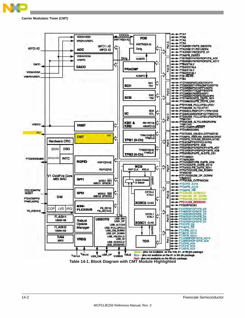
Carrier Modulator Timer (CMT)
14-2 Freescale Semiconductor
Table 14-1. Block Diagram with CMT Module Highlighted
MCF51JE256 Reference Manual, Rev. 2

Carrier Modulator Timer (CMT)
Freescale Semiconductor 14-3
14.4 FeaturesThe CMT consists of a carrier generator, modulator, and transmitter which drives the infrared out pin. The features of this module include:
• Four modes of operation
— Time with independent control of high and low times
— Baseband
— Frequency shift key (FSK)
— Direct software control of IRO pin
• Extended space operation in time, baseband, and FSK modes
• Selectable input clock divide: 1, 2, 4, or 8
• Interrupt on end of cycle
— Ability to disable IRO pin and use as timer interrupt
14.5 CMT Block Diagram
Figure 14-1. Carrier Modulator Transmitter Module Block Diagram
14.6 External Signal DescriptionsThere is only one pin associated with the CMT, the IRO pin. The pin is driven by the transmitter output when the MCGEN bit in the CMTMSC register is set and the IROPEN bit in the CMTOC register is set. If the MCGEN bit is clear and the IROPEN bit is set, the pin is driven by the IROL bit in the CMTOC register. This enables user software to directly control the state of the IRO pin by writing to the IROL bit.
CARRIERGENERATOR MODULATOR
CARRIEROUT (fcg)
MODULATOROUT
TRANSMITTEROUTPUT
BASE
FSKPRIMARY/SECONDARY SELECT
CMT REGISTERS
IROPIN
EOC
FLAG
EOC
INT EN
MIR
EQ
AND BUS INTERFACE
CMT
CMTCLK
CMTDIV
CLOCKCONTROL
MC
GEN
EXSPC
CM
TPOL
CMTCG
REGS
CMTCM
D REGS
IRO
L
INTERNAL BUS IIREQ
IRO
PEN
input clock
MCF51JE256 Reference Manual, Rev. 2

Carrier Modulator Timer (CMT)
14-4 Freescale Semiconductor
If the IROPEN bit is clear, the pin is disabled and is not driven by the CMT module. This is so the CMT can be configured as a modulo timer for generating periodic interrupts without causing pin activity.
14.7 Register DefinitionThe following registers control and monitor CMT operation:
• CMT carrier generator data registers (CMTCGH1, CMTCGL1, CMTCGH2, CMTCGL2)
• CMT output control register (CMTOC)
• CMT modulator status and control register (CMTMSC)
• CMT modulator period data registers (CMTCMD1, CMTCMD2, CMTCMD3, CMTCMD4)
14.7.1 Carrier Generator Data Registers (CMTCGH1, CMTCGL1, CMTCGH2, and CMTCGL2)
The carrier generator data registers contain the primary and secondary high and low values for generating the carrier output.
CMTCGH1 7 6 5 4 3 2 1 0
Read:PH7 PH6 PH5 PH4 PH3 PH2 PH1 PH0
Write:
Reset: U U U U U U U U
CMTCGL1 7 6 5 4 3 2 1 0
Read:PL7 PL6 PL5 PL4 PL3 PL2 PL1 PL0
Write:
Reset: U U U U U U U U
CMTCGH2 7 6 5 4 3 2 1 0
Read:SH7 SH6 SH5 SH4 SH3 SH2 SH1 SH0
Write:
Reset: U U U U U U U U
CMTCGL2 7 6 5 4 3 2 1 0
Read:SL7 SL6 SL5 SL4 SL3 SL2 SL1 SL0
Write:
Reset: U U U U U U U U
Figure 14-2. CMT Carrier Generator Data Registers (CMTCGH1, CMTCGL1, CMTCGH2, CMTCGL2)
MCF51JE256 Reference Manual, Rev. 2

Carrier Modulator Timer (CMT)
Freescale Semiconductor 14-5
14.7.2 CMT Output Control Register (CMTOC)
This register is used to control the IRO output of the CMT module.
Table 14-2. Carrier High and Low Time Data Values
Carrier Data Values Description
Primary Carrier High and Low Time Data Values
PH0–PH7 and PL0–PL7
When selected, these bits contain the number of input clocks required to generate the carrier high and low time periods. When operating in time mode (see Section 14.8.2.1, “Time Mode”) this register pair is always selected. When operating in FSK mode (see Section 14.8.2.3, “FSK Mode”) this register pair and the secondary register pair are alternately selected under control of the modulator. The primary carrier high and low time values are undefined out of reset. These bits must be written to nonzero values before the carrier generator is enabled to avoid spurious results.
Secondary Carrier High and Low Time Data Values
SH0–SH7 and SL0–SL7
When selected, these bits contain the number of input clocks required to generate the carrier high and low time periods. When operating in time mode (see Section 14.8.2.1, “Time Mode”) this register pair is never selected. When operating in FSK mode (see Section 14.8.2.3, “FSK Mode”) this register pair and the primary register pair are alternately selected under control of the modulator. The secondary carrier high and low time values are undefined out of reset. These bits must be written to nonzero values before the carrier generator is enabled when operating in FSK mode.
7 6 5 4 3 2 1 0
RIROL CMTPOL IROPEN
0 0 0 0 0
W
Reset: 0 0 0 0 0 0 0 0
Figure 14-3. CMT Output Control Register (CMTOC)Table 14-3. PRACMPxCS Field Descriptions
Field Description
7IROL
IRO Latch ControlReading IROL reads the state of the IRO latch. Writing IROL changes the state of the IRO pin when the MCGEN bit in the CMTMSC register is clear and the IROPEN bit is set.
MCF51JE256 Reference Manual, Rev. 2

Carrier Modulator Timer (CMT)
14-6 Freescale Semiconductor
14.7.3 CMT Modulator Status and Control Register
The CMT modulator status and control register (CMTMSC) contains the modulator and carrier generator enable (MCGEN), end of cycle interrupt enable (EOCIE), FSK mode select (FSK), baseband enable (BASE), extended space (EXSPC), prescaler (CMTDIV) bits, and the end of cycle (EOCF) status bit.
6CMTPOL
CMT Output PolarityThe CMTPOL bit controls the polarity of the IRO pin output of the CMT.1 IRO pin is active high0 IRO pin is active low
5IROPEN
IRO Pin EnableThe IROPEN bit is used to enable and disable the IRO pin. When the pin is enabled, it is an output which drives out either the CMT transmitter output or the state of the IROL bit depending on whether the MCGEN bit in the CMTMSC register is set or not. Also, the state of the output is either inverted or not depending on the state of the CMTPOL bit. When the pin is disabled, it is in a high impedance state so as not to draw any current. The pin is disabled during reset.0 IRO pin disabled1 IRO pin enabled as output
7 6 5 4 3 2 1 0
R EOCFCMTDIV EXSPC BASE FSK EOCIE MCGEN
W
Reset: 0 0 0 0 0 0 0 0
Figure 14-4. CMT Modulator Status and Control Register (CMTMSC)
Table 14-3. PRACMPxCS Field Descriptions (Continued)
Field Description
MCF51JE256 Reference Manual, Rev. 2

Carrier Modulator Timer (CMT)
Freescale Semiconductor 14-7
Table 14-4. PRACMPxCS Field Descriptions
Field Description
7EOCF
End Of Cycle Status FlagThe EOCF bit is set when: • The modulator is not currently active and the MCGEN bit is set to begin the initial CMT transmission. • At the end of each modulation cycle while the MCGEN bit is set. This is recognized when a match occurs
between the contents of the space period register and the down counter. At this time, the counter is initialized with the (possibly new) contents of the mark period buffer, CMTCMD1 and CMTCMD2, and the space period register is loaded with the (possibly new) contents of the space period buffer, CMTCMD3 and CMTCMD4.
This flag is cleared by a read of the CMTMSC register followed by an access of CMTCMD2 or CMTCMD4.In the case where the MCGEN bit is cleared and then set before the end of the modulation cycle, EOCF will not be set when MCGEN is set, but will be set at the end of the current modulation cycle.0 No end of modulation cycle occurrence since flag last cleared1 End of modulator cycle has occurred
6–5CMTDIV
CMT Clock Divide PrescalerThe CMT clock divide prescaler causes the CMT to be clocked at the CMT input clock frequency, or the CMT input clock frequency divided by 1, 2 ,4, or 8. Since these bits are not double buffered, they should not be changed during a transmission.00 CMT input clock 101 CMT input clock 210 CMT input clock 411 CMT input clock 8
4EXSPC
Extended Space EnableThe EXSPC bit enables extended space operation1 Extended space enabled0 Extended space disabled
3BASE
Baseband EnableWhen set, the BASE bit disables the carrier generator and forces the carrier output high for generation of baseband protocols. When BASE is clear, the carrier generator is enabled and the carrier output toggles at the frequency determined by values stored in the carrier data registers. See Section 14.8.2.2, “Baseband Mode”. This bit is cleared by reset. This bit is not double buffered and should not be written to during a transmission.0 Baseband mode disabled1 Baseband mode enabled
2FSK
FSK Mode SelectThe FSK bit enables FSK operation0 CMT operates in Time or Baseband mode1 CMT operates in FSK mode
1EOCIE
End of Cycle Interrupt EnableA CPU interrupt will be requested when EOCF is set if EOCIE is high.0CPU interrupt disabled1 CPU interrupt enabled
0MCGEN
Modulator and Carrier Generator EnableSetting MCGEN will initialize the carrier generator and modulator and will enable all clocks. Once enabled, the carrier generator and modulator will function continuously. When MCGEN is cleared, the current modulator cycle will be allowed to expire before all carrier and modulator clocks are disabled (to save power) and the modulator output is forced low. To prevent spurious operation, the user should initialize all data and control registers before enabling the system.0 Modulator and carrier generator disabled1 Modulator and carrier generator enabled
MCF51JE256 Reference Manual, Rev. 2

Carrier Modulator Timer (CMT)
14-8 Freescale Semiconductor
14.7.4 CMT Modulator Data Registers (CMTCMD1, CMTCMD2, CMTCMD3 and CMTCMD4)
The modulator data registers control the mark and space periods of the modulator for all modes. The contents of these registers are transferred to the modulator down counter and space period register upon the completion of a modulation period.
14.8 Functional DescriptionThe CMT module consists of a carrier generator, a modulator, a transmitter output and control registers. The block diagram is shown in Figure 14-1. The module has three main modes of operation:
• Time
• Baseband
• Frequency shift key (FSK).
When operating in time mode, the user independently defines the high and low times of the carrier signal to determine both period and duty cycle. The carrier generator resolution is 125 ns when operating with an 8 MHz internal bus frequency and the CMTMSC[CMTDIV] equal 00. The carrier generator can generate
CMTCMD1 7 6 5 4 3 2 1 0
RMB15 MB14 MB13 MB12 MB11 MB10 MB9 MB8
W
Reset: Unaffected by Reset
CMTCMD2 7 6 5 4 3 2 1 0
RMB7 MB6 MB5 MB4 MB3 MB2 MB1 MB0
W
Reset: Unaffected by Reset
CMTCMD3 7 6 5 4 3 2 1 0
RSB15 SB14 SB13 SB12 SB11 SB10 SB9 SB8
W
Reset: Unaffected by Reset
CMTCMD4 7 6 5 4 3 2 1 0
RSB7 SB6 SB5 SB4 SB3 SB2 SB1 SB0
W
Reset: Unaffected by Reset
Figure 14-5. CMT Modulator Data Registers (CMTCMD1, CMTCMD2, CMTCMD3 and CMTCMD4)
MCF51JE256 Reference Manual, Rev. 2

Carrier Modulator Timer (CMT)
Freescale Semiconductor 14-9
signals with periods between 250 ns (4 MHz) and 127.5 s (7.84 kHz) in steps of 125 ns. The table below shows the relationship between the clock divide bits and the carrier generator resolution, minimum carrier generator period, and minimum modulator period.
Table 14-5. Clock Divide
The possible duty cycle options will depend upon the number of counts required to complete the carrier period. For example, a 1.6 MHz signal has a period of 625 ns and will therefore require 5 x 125 ns counts to generate. These counts may be split between high and low times, so the duty cycles available will be 20% (one high, four low), 40% (two high, three low), 60% (three high, two low) and 80% (four high, one low).
For lower frequency signals with larger periods, higher resolution (as a percentage of the total period) duty cycles are possible.
When the BASE bit in the CMT modulator status and control register (CMTMSC) is set, the carrier output (fcg) to the modulator is held to IRO pin active level continuously to allow for the generation of baseband protocols.
A third mode allows the carrier generator to alternate between two sets of high and low times. When operating in FSK mode, the generator will toggle between the two sets when instructed by the modulator, allowing the user to dynamically switch between two carrier frequencies without CPU intervention.
The modulator provides a simple method to control protocol timing. The modulator has a minimum resolution of 1.0 s with an 8 MHz internal CMT input clock. It can count bus clocks (to provide real-time control) or it can count carrier clocks (for self-clocked protocols). See Section 14.8.2, “Modulator” for more details.
The transmitter output block controls the state of the infrared out pin (IRO). The modulator output is gated on to the IRO pin when the modulator/carrier generator is enabled.
A summary of the possible modes is shown in Table 14-6.
CMT Input Clock (MHz)
CMTDIVCarrier Generator Resolution (s)
Min Carrier Generator Period
(s)
MinModulator Period
(s)
8 00 0.125 0.25 1.0
8 01 0.25 0.5 2.0
8 10 0.5 1.0 4.0
8 11 1.0 2.0 8.0
Table 14-6. CMT Modes of Operation
ModeMCGEN
Bit1BASEBit2
FSKBit(2)
EXSPCBit
Comment
Time 1 0 0 0 fcg controlled by primary high and low registers. fcg transmitted to IRO pin when modulator gate is open.
MCF51JE256 Reference Manual, Rev. 2

Carrier Modulator Timer (CMT)
14-10 Freescale Semiconductor
14.8.1 Carrier Generator
The carrier signal is generated by counting a register-selected number of input clocks (125 ns for an 8 MHz bus) for both the carrier high time and the carrier low time. The period is determined by the total number of clocks counted. The duty cycle is determined by the ratio of high time clocks to total clocks counted. The high and low time values are user programmable and are held in two registers.
An alternate set of high/low count values is held in another set of registers to allow the generation of dual frequency FSK (frequency shift keying) protocols without CPU intervention.
NOTE
Only non-zero data values are allowed. The carrier generator will not work if any of the count values are equal to zero.
The MCGEN bit in the CMTMSC register must be set and the BASE bit must be cleared to enable carrier generator clocks. When the BASE bit is set, the carrier output to the modulator is held to IRO pin active level continuously. The block diagram is shown in Figure 14-1.
Baseband 1 1 x 0 fcg is always active level. IRO pin active level when modulator gate is open.
FSK 1 0 1 0 fcg control alternates between primary high/low registers and secondary high/low registers.fcg transmitted to IRO pin when modulator gate is open.
Extended Space
1 x x 1 Setting the EXSPC bit causes subsequent modulator cycles to be spaces (modulator out not asserted) for the duration of the modulator period (mark and space times).
IRO Latch 0 x x x IROL bit controls state of IRO pin.
1 To prevent spurious operation, initialize all data and control registers before beginning a transmission (MCGEN=1).2 These bits are not double buffered and should not be changed during a transmission (while MCGEN=1).
Table 14-6. CMT Modes of Operation (Continued)
ModeMCGEN
Bit1BASEBit2
FSKBit(2)
EXSPCBit
Comment
MCF51JE256 Reference Manual, Rev. 2

Carrier Modulator Timer (CMT)
Freescale Semiconductor 14-11
Figure 14-6. Carrier Generator Block Diagram
The high/low time counter is an 8-bit up counter. After each increment, the contents of the counter are compared with the appropriate high or low count value register. When the compare value is reached, the counter is reset to a value of 0x01, and the compare is redirected to the other count value register.
Assuming that the high time count compare register is currently active, a valid compare will cause the carrier output to be driven IRO pin active level. The counter will continue to increment (starting at reset value of 0x01). When the value stored in the selected low count value register is reached, the counter will again be reset and the carrier output will be driven IRO pin inactive level.
The cycle repeats, automatically generating a periodic signal which is directed to the modulator. The lowest frequency (maximum period) and highest frequency (minimum period) which can be generated are defined as:
fmax = fCMTCLK(2 x 1) Hz Eqn. 14-1
fmin = fCMTCLK(2 x (28 – 1)) Hz Eqn. 14-2
In the general case, the carrier generator output frequency is:
fcg = fCMTCLK (Highcount + Lowcount) Hz Eqn. 14-3
Where:
0 < Highcount < 256 and 0 < Lowcount < 256
The duty cycle of the carrier signal is controlled by varying the ratio of high time to low + high time. As the input clock period is fixed, the duty cycle resolution will be proportional to the number of counts required to generate the desired carrier period.
CLK8-BIT UP COUNTER
=?
=?
CLR
CLO
CK
AND
OU
TPU
T C
ON
TRO
L
PRIMARY HIGH COUNT REGISTER
SECONDARY HIGH COUNT REGISTER
PRIMARY/
SELECT
CARRIER OUT (fcg)
SECONDARY
PRIMARY LOW COUNT REGISTER
SECONDARY LOW COUNT REGISTER
CMTCLKBASE
FSK
MCGEN
MCF51JE256 Reference Manual, Rev. 2

Carrier Modulator Timer (CMT)
14-12 Freescale Semiconductor
Eqn. 14-4
14.8.2 Modulator
The modulator has three main modes of operation:
• The modulator can gate the carrier onto the modulator output (Time mode)
• The modulator can control the logic level of the modulator output (Baseband mode)
• The modulator can count carrier periods and instruct the carrier generator to alternate between two carrier frequencies whenever a modulation period (mark + space counts) expires (FSK mode)
The modulator includes a 17-bit down counter with underflow detection. The counter is loaded from the 16-bit modulation mark period buffer registers, CMTCMD1 and CMTCMD2. The most significant bit is loaded with a logic zero and serves as a sign bit. When the counter holds a positive value, the modulator gate is open and the carrier signal is driven to the transmitter block.
When the counter underflows, the modulator gate is closed and a 16-bit comparator is enabled which compares the logical complement of the value of the down counter with the contents of the modulation space period register which has been loaded from the registers, CMTCMD3 and CMTCMD4.
When a match is obtained the cycle repeats by opening the modulator gate, reloading the counter with the contents of CMTCMD1 and CMTCMD2, and reloading the modulation space period register with the contents of CMTCMD3 and CMTCMD4.
Should the contents of the modulation space period register be all zeroes, the match will be immediate and no space period will be generated (for instance, for FSK protocols which require successive bursts of different frequencies).
The MCGEN bit in the CMTMSC register must be set to enable the modulator timer.
Duty Cycle HighcountHighcount Lowcount+----------------------------------------------------------------=
MCF51JE256 Reference Manual, Rev. 2

Carrier Modulator Timer (CMT)
Freescale Semiconductor 14-13
Figure 14-7. Modulator Block Diagram
14.8.2.1 Time Mode
When the modulator operates in time mode (MCGEN bit is set, BASE bit is clear, and FSK bit is clear), the modulation mark period consists of an integer number of CMTCLK8 clock periods. The modulation space period consists of zero or an integer number of CMTCLK8 clock periods. With an 8 MHz bus and CMTDIV = 00, the modulator resolution is 1 s and has a maximum mark and space period of about 65.535 ms each. See Figure 14-8 for an example of the time mode and baseband mode outputs.
The mark and space time equations for time and baseband mode are:
tmark = (CMTCMD1:CMTCMD2 + 1) fCMTCLK Eqn. 14-5
tspace = CMTCMD3:CMTCMD4 fCMTCLK Eqn. 14-6
where CMTCMD1:CMTCMD2 and CMTCMD3:CMTCMD4 are the decimal values of the concatenated registers.
=?
0
CO
UN
TER
CMTCLOCK
CMTCMD1:CMTCMD2
CMTCMD3:CMTCMD4
SPACE PERIOD REGISTER *
17-BIT DOWN COUNTER *
* DENOTES HIDDEN REGISTER
16 BITS
16 BITS
MS
BIT
16
16
MODULE INTERRUPT REQUEST
8CLOCK CONTROL
CARRIER OUT (fcg)
LOAD
SYSTEM CONTROLEOC FLAG SET
MODULATOR GATEOUT
PRIMARY/SECONDARY SELECT
.
.
MODULATOR
EXSPC
MODE
EOC
IE
BASE
FSK
MCF51JE256 Reference Manual, Rev. 2

Carrier Modulator Timer (CMT)
14-14 Freescale Semiconductor
Figure 14-8. Example CMT Output in Time and Baseband Modes
14.8.2.2 Baseband Mode
Baseband mode (MCGEN bit is set and BASE bit is set) is a derivative of time mode, where the mark and space period is based on (CMTCLK8) counts. The mark and space calculations are the same as in time mode. In this mode the modulator output will be at active level for the duration of the mark period and at an inactive level for the duration of a space period. See Figure 14-8 for an example of the output for both baseband and time modes. In the example, the carrier out frequency (fcg) is generated with a high count of 0x01 and a low count of 0x02 which results in a divide of 3 of CMTCLK with a 33% duty cycle. The modulator down counter was loaded with the value 0x0003 and the space period register with 0x0002.
NOTE
The waveforms in Figure 14-8 and Figure 14-9 are for the purpose of conceptual illustration and are not meant to represent precise timing relationships between the signals shown.
14.8.2.3 FSK Mode
When the modulator operates in FSK mode (MCGEN bit is set, FSK bit is set, and BASE bit is clear), the modulation mark and space periods consist of an integer number of carrier clocks (space period can be zero). When the mark period expires, the space period is transparently started (as in time mode). The carrier generator toggles between primary and secondary data register values whenever the modulator space period expires.
Modulator Gate
CMTCLK 8
IRO pin (time mode)
IRO pin
Mark Space Mark
Carrier out (fcg)
(baseband mode)CMTOC[CMTPOL]=0
MCF51JE256 Reference Manual, Rev. 2

Carrier Modulator Timer (CMT)
Freescale Semiconductor 14-15
The space period provides an interpulse gap (no carrier). If CMTCMD3:CMTCMD4 = 0x0000, then the modulator and carrier generator will switch between carrier frequencies without a gap or any carrier glitches (zero space).
Using timing data for carrier burst and interpulse gap length calculated by the CPU, FSK mode can automatically generate a phase-coherent, dual-frequency FSK signal with programmable burst and interburst gaps.
The mark and space time equations for FSK mode are:
tmark = (CMTCMD1:CMTCMD2 + 1) fcg Eqn. 14-7
tspace = CMTCMD3:CMTCMD4 fcg Eqn. 14-8
Where fcg is the frequency output from the carrier generator. The example in figure below shows what the IRO pin output looks like in FSK mode with the following values: CMTCMD1:CMTCMD2 = 0x0003, CMTCMD3:CMTCMD4 = 0x0002, primary carrier high count = 0x01, primary carrier low count = 0x02, secondary carrier high count = 0x03, and secondary carrier low count = 0x01.
Figure 14-9. Example CMT Output in FSK Mode
14.8.2.4 Extended Space Operation
In either time, baseband or FSK mode, the space period can be made longer than the maximum possible value of the space period register. Setting the EXSPC bit in the CMTMSC register will force the modulator to treat the next modulation period (beginning with the next load of the counter and space period register) as a space period equal in length to the mark and space counts combined. Subsequent modulation periods will consist entirely of these extended space periods with no mark periods. Clearing EXSPC will return the modulator to standard operation at the beginning of the next modulation period.
14.8.2.4.1 EXSPC Operation in Time Mode
To calculate the length of an extended space in time or baseband modes, add the mark and space times and multiply by the number of modulation periods that EXSPC is set.
MARK1 SPACE1 MARK2 SPACE2 MARK1 SPACE1 MARK2MODULATOR GATE
CARRIER OUT (fcg)
IRO PIN
MCF51JE256 Reference Manual, Rev. 2

Carrier Modulator Timer (CMT)
14-16 Freescale Semiconductor
texspace = (tmark + tspace) x (number of modulation periods) Eqn. 14-9
For an example of extended space operation, see Figure 14-10.
NOTEThe EXSPC feature can be used to emulate a zero mark event.
Figure 14-10. Extended Space Operation
14.8.2.4.2 EXSPC Operation in FSK Mode
In FSK mode, the modulator continues to count carrier out clocks, alternating between the primary and secondary registers at the end of each modulation period.
To calculate the length of an extended space in FSK mode, one needs to know whether the EXSPC bit was set on a primary or secondary modulation period, as well as the total number of both primary and secondary modulation periods completed while the EXSPC bit is high. A status bit for the current modulation is not accessible to the CPU. If necessary, software should maintain tracking of the current modulation cycle (primary or secondary). The extended space period ends at the completion of the space period time of the modulation period during which the EXSPC bit is cleared.
If the EXSPC bit was set during a primary modulation cycle, use the equation:
texspace = (tspace)p + (tmark + tspace)s + (tmark + tspace)p +... Eqn. 14-10
Where the subscripts p and s refer to mark and space times for the primary and secondary modulation cycles.
If the EXSPC bit was set during a secondary modulation cycle, use the equation:
texspace = (tspace)s + (tmark + tspace)p + (tmark + tspace)s +... Eqn. 14-11
14.8.3 Transmitter
The transmitter output block controls the state of the infrared out pin (IRO). The modulator output is gated on to the IRO pin when the modulator/carrier generator is enabled. When the modulator/carrier generator is disabled, the IRO pin is controlled by the state of the IRO latch.
A polarity bit in the CMTOC register enables the IRO pin to be high true or low true.
14.8.4 CMT Interrupts
The end of cycle flag (EOCF) is set when:
SET EXSPC CLEAR EXSPC
MCF51JE256 Reference Manual, Rev. 2

Carrier Modulator Timer (CMT)
Freescale Semiconductor 14-17
• The modulator is not currently active and the MCGEN bit is set to begin the initial CMT transmission
• At the end of each modulation cycle (when the counter is reloaded from CMTCMD1:CMTCMD2) while the MCGEN bit is set
In the case where the MCGEN bit is cleared and then set before the end of the modulation cycle, the EOCF bit will not be set when the MCGEN is set, but will become set at the end of the current modulation cycle.
When the MCGEN becomes disabled, the CMT module does not set the EOC flag at the end of the last modulation cycle.
The EOCF bit is cleared by reading the CMT modulator status and control register (CMTMSC) followed by an access of CMTCMD2 or CMTCMD4.
If the EOC interrupt enable (EOCIE) bit is high when the EOCF bit is set, the CMT module will generate an interrupt request. The EOCF bit must be cleared within the interrupt service routine to prevent another interrupt from being generated after exiting the interrupt service routine.
The EOC interrupt is coincident with loading the down-counter with the contents of CMTCMD1:CMTCMD2 and loading the space period register with the contents of CMTCMD3:CMTCMD4. The EOC interrupt provides a means for the user to reload new mark/space values into the modulator data registers. Modulator data register updates will take effect at the end of the current modulation cycle. Note that the down-counter and space period register are updated at the end of every modulation cycle, irrespective of interrupt handling and the state of the EOCF flag.
14.8.5 Low-Power Mode Operation
14.8.5.1 Wait Mode Operation
During wait mode the CMT, if enabled, will continue to operate normally. However, there will be no new codes or changes of pattern mode while in wait mode, because the CPU is not operating.
14.8.5.2 Stop3 Mode Operation
During Stop3 mode, clocks to the CMT module are halted. No registers are affected.
Note that because the clocks are halted, the CMT will resume upon exit from Stop3. Software should ensure that the Stop3 mode is not entered while the modulator is still in operation to prevent the IRO pin from being asserted while in Stop3 mode. This may require a time-out period from the time that the MCGEN bit is cleared to allow the last modulator cycle to complete.
14.8.5.3 Stop2 Mode Operation
During Stop2 mode, the CMT module is completely powered off internally and the IRO pin state at the time that Stop2 mode is entered is latched and held. To prevent the IRO pin from being asserted while in Stop2 mode, software should assure that the pin is not active when entering Stop2 mode. Upon wake-up from Stop2 mode, the CMT module will be in the reset state.
MCF51JE256 Reference Manual, Rev. 2

Carrier Modulator Timer (CMT)
14-18 Freescale Semiconductor
14.8.5.4 Background Mode Operation
When the microcontroller is in active background mode, the CMT temporarily suspends all counting until the microcontroller returns to normal user mode.
MCF51JE256 Reference Manual, Rev. 2

Freescale Semiconductor 15-1
Chapter 15 12-bit Digital to Analog Converter (DAC12LVLPv1)
15.1 IntroductionThe 12-bit Digital to Analog converter (DAC) can provide a voltage output on the DACO pin. Figure 15-1 shows the block diagram with the DAC highlighted.
15.1.1 DAC Clock Gating
The bus clock to the DAC can be gated on and off using the DAC bit in SCGC1. These bits are set after any reset, which enables the bus clock to this module. To conserve power, these bits can be cleared to disable the clock to this module when not in use. See Section 5.6, “Peripheral Clock Gating,” for details.
15.1.2 DAC Vext and Vint Configuration
On this device, Vext is connected to VDDA and Vint is connected to the bandgap voltage, Vrefo.
15.1.3 DAC Hardware Trigger Configuration
On this device, the hardware trigger is connected to the PDB output.
MCF51JE256 Reference Manual, Rev. 2

12-bit Digital to Analog Converter (DAC12LVLPv1)
15-2 Freescale Semiconductor
Figure 15-1. Block Diagram Highlighting DAC Blocks and Pins
MCF51JE256 Reference Manual, Rev. 2

12-bit Digital to Analog Converter (DAC12LVLPv1)
Freescale Semiconductor 15-3
15.1.4 Features
The DAC module features include:
• 1.8 V — 3.6 V operation.
• On-chip programmable reference generator output (1/4096 Vin to Vin, step is 1/4096 Vin)
• Vin can be selected from two reference sources:
— While VDDA is 1.8 V ~ 3.6 V, VREFH_EXT (VDDA) can be used and guaranteed.
— While VDDA is 2.4 V ~ 3.6 V, both VREFH_INT (output of VREF) and VREFH_EXT (VDDA) can be used and guaranteed.
• Optional operation in STOP3 mode
• 16-word data buffer supported with configurable watermark and multiple operation modes
15.1.5 Block Diagram
Figure 15-2 is the block diagram of the DAC module.
MCF51JE256 Reference Manual, Rev. 2

12-bit Digital to Analog Converter (DAC12LVLPv1)
15-4 Freescale Semiconductor
Figure 15-2. DAC Block Diagram
15.2 Register DefinitionThe DAC has 20 8-bit registers to control analog comparator and programmable voltage divider to perform the Digital to Analog functions.
Vint
MU
X
4096
-leve
l
DACEN
DACDAT[11:0]
MUX
Vext
Vin
DACRFS
Vo
Vout
+
-VDD
AMP Buffer
DATA
12
DACBFMD
DACSWTRG
DACBFEN
DACBFUP
DACBFWM
DACBFRP
DAC Hardware Trigger DACBFWMF
DACBWIE
DACBFRPTF
DACBTIE
DACBFRPBF
DACBBIE
&
&
&
ORdac_interrupt
DACTSEL
BUFFER
LPEN
MCF51JE256 Reference Manual, Rev. 2

12-bit Digital to Analog Converter (DAC12LVLPv1)
Freescale Semiconductor 15-5
15.2.1 DAC Data Register x (DACDATxH:DACDATxL)
When the DAC Buffer is not enabled, DACDAT0[11:0] controls the output voltage based on the following formula.
Vout = Vin * (1+DACDAT0[11:0])/4096 Eqn. 15-1
When the DAC Buffer is enabled, DACDATx[11:0] is mapped to the 16-word buffer. Refer to 3.1 “DAC Buffer Operation” for details.
When writing a new value to DAC Data Register x (DACDATxH:DACDATxL), the write order should be DACDATxH first, then DACDATxL. Otherwise the value will not be properly loaded to the effective DAC hard block and a mismatch between the DAC output may be observed. Reading DACDATx as the write-value does not mean the value is properly loaded to the DAC hard block. Therefore, the write sequence of high byte first then low byte must be followed.
15.2.2 DAC Status Register (DACS)
NOTEIf one of the flag is set, it must be cleared by software, or it will keep it’s value. Write zero value to the status register, the relevant bit (s) will be cleared. It’s no effect to write 1 to this register. After reset, DACRPT is set, it can be cleared by software if needed. The flag registers can be set only when the data buffer status is changed.
7 6 5 4 3 2 1 0
RDACDATx[7:0]
W
Reset 0 0 0 0 0 0 0 0
Figure 15-3. DAC Data Register x Low (DACDATxL)
7 6 5 4 3 2 1 0
RDACDATx[11:8]
W
Reset 0 0 0 0 0 0 0 0
Figure 15-4. DAC Data Register x High (DACDATxH)
7 6 5 4 3 2 1 0
R DACWM DACRPT DACRPB
W 0 0 0
Reset 0 0 0 0 0 0 1 0
Figure 15-5. DAC Status Register
MCF51JE256 Reference Manual, Rev. 2

12-bit Digital to Analog Converter (DAC12LVLPv1)
15-6 Freescale Semiconductor
15.2.3 DAC Control Register (DACC0)
Table 15-1. DAC Status Register
Field Description
7:3 Reserved
2DACWM
DAC buffer watermark flag. 0 The DAC buffer read pointer doesn’t reach the watermark level1 The DAC buffer read pointer reaches the watermark level
1DACRPT
DAC buffer read pointer top position flag.0 The DAC buffer read pointer is not zero1 The DAC buffer read pointer is zero
0DACRPB
DAC buffer read pointer bottom position flag.0 The DAC buffer read pointer isn’t equal to the DACBFUP1 The DAC buffer read pointer is equal to the DACBFUP.
7 6 5 4 3 2 1 0
RDACEN DACRFS DACTSEL DACSTRG LPEN DACWIE DACTIE DACBIE
W
Reset 0 0 0 0 0 0 0 0
Figure 15-6. DAC Control Register 0 (DACC0)
Table 15-2. DACC0 Field Descriptions
Field Description
7DACEN
DAC enable — The DACEN bit starts the Programmable Reference Generator operation.0 The DAC system is disabled.1 The DAC system is enabled.
6DACRFS
DAC Reference Select 0 The DAC selects Vint as the reference voltage.1 The DAC selects Vext as the reference voltage.
5DACTSEL
DAC trigger select0 The DAC hardware trigger is selected.1 The DAC software trigger is selected.
4DACSTRG
DAC software trigger — active high. This is a write-only bit; it is always “0” when read. If the DAC software trigger is selected and buffer enabled, writing a 1 to this bit advances the buffer read pointer once.0 The DAC soft trigger is not valid.1 The DAC soft trigger is valid.
3LPEN
DAC low power control0 High power mode.1 Low power mode.
2DACWIE
DAC buffer watermark interrupt enable. 0 The DAC buffer watermark interrupt is disabled. 1 The DAC buffer watermark interrupt is enabled.
MCF51JE256 Reference Manual, Rev. 2
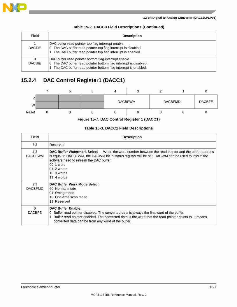
12-bit Digital to Analog Converter (DAC12LVLPv1)
Freescale Semiconductor 15-7
15.2.4 DAC Control Register1 (DACC1)
1DACTIE
DAC buffer read pointer top flag interrupt enable.0 The DAC buffer read pointer top flag interrupt is disabled.1 The DAC buffer read pointer top flag interrupt is enabled.
0DACBIE
DAC buffer read pointer bottom flag interrupt enable.0 The DAC buffer read pointer bottom flag interrupt is disabled.1 The DAC buffer read pointer bottom flag interrupt is enabled.
7 6 5 4 3 2 1 0
RDACBFWM DACBFMD DACBFE
W
Reset 0 0 0 0 0 0 0 0
Figure 15-7. DAC Control Register 1 (DACC1)
Table 15-3. DACC1 Field Descriptions
Field Description
7:3 Reserved
4:3DACBFWM
DAC Buffer Watermark Select — When the word number between the read pointer and the upper address is equal to DACBFWM, the DACWM bit in status register will be set. DACWM can be used to inform the software need to refresh the DAC buffer. 00 1 word01 2 words10 3 words11 4 words
2:1DACBFMD
DAC Buffer Work Mode Select 00 Normal mode01 Swing mode10 One-time scan mode11 Reserved
0DACBFE
DAC Buffer Enable0 Buffer read pointer disabled. The converted data is always the first word of the buffer. 1 Buffer read pointer enabled. The converted data is the word that the read pointer points to. It means
converted data can be from any word of the buffer.
Table 15-2. DACC0 Field Descriptions (Continued)
Field Description
MCF51JE256 Reference Manual, Rev. 2

12-bit Digital to Analog Converter (DAC12LVLPv1)
15-8 Freescale Semiconductor
15.2.5 DAC Control Register 2 (DACC2)
15.3 Functional DescriptionThe 12-bit Digital-to-Analog Convertor (DAC12LVLP) module can select one of two reference inputs Vin1 and Vin2 as the DAC reference voltage (Vin) by DACRFS bit of DACC0 register. Refer to the module introduction for information on the source for Vext and Vint. When the DAC12LVLP is enabled, it converts the data in DACDAT0[11:0] or the data from the DAC data buffer to a stepped analog output voltage. The output voltage range is from Vin/4096 to Vin, and the step is Vin/4096.
15.3.1 DAC Data Buffer Operation
When the DAC is enabled and the buffer isn’t enabled, the DAC12LVLP module always converts the data in DACDAT0 to analog output voltage.
When both the DAC and the buffer are enabled, the DAC12LVLP converts the data in the data buffer to analog output voltage. The data buffer read pointer advances to the next word in the event the hardware trigger or the software trigger occurs. Refer to the DAC12LVLP Introduction section for the hardware trigger connection. The data buffer can be configured to operate in normal mode, swing mode, or one-time scan mode. When the buffer operation is switched from one mode to another, the read pointer doesn’t change. The read pointer can be set to any value between 0 and DACBFUP by writing DACBFRP in DACC2.
15.3.1.1 Buffer Normal Mode
This is the default mode. The buffer works as a circular buffer. The read pointer increases by one every time when the trigger occurs. When the read pointer reaches the upper limit, it goes to the zero directly in the next trigger event.
7 6 5 4 3 2 1 0
RDACBFRP DACBFUP
W
Reset 0 0 0 0 1 1 1 1
Figure 15-8. DAC Control Register 2 (DACC2)
Table 15-4. DACC2 Field Descriptions
Field Description
7:4DACBFRP
DAC Buffer Read Pointer — These 4 bits keep the current value of the buffer read pointer
3:0DACBFUP
DAC Buffer Upper Limit — These 4 bits select the buffer’s upper limit. The buffer read pointer cannot exceed it.
MCF51JE256 Reference Manual, Rev. 2

12-bit Digital to Analog Converter (DAC12LVLPv1)
Freescale Semiconductor 15-9
15.3.1.2 Buffer Swing Mode
This mode is similar to the Normal mode. But when the read pointer reaches the upper limit, it doesn’t go to the zero. It will descend by one in the next trigger events until zero is reached.
15.3.1.3 Buffer One-time Scan Mode
The read pointer increases by one every time the trigger occurs. When it reaches the upper limit, it stops. If the read pointer is reset to an address other than the upper limit, it will increase to the upper address and then stop.
NOTEIf the software set the read pointer to the upper limit, the read pointer will not advance in this mode.
15.3.2 Resets
During reset, the DAC12LVLP is configured in the default mode. DAC12LVLP is disabled.
15.3.3 Low Power Mode Operation
15.3.3.1 Wait Mode Operation
In wait mode, the DAC12LVLP operates normally if enabled.
15.3.3.2 Stop Mode Operation
The DAC12LVLP continues to operate in stop3 mode if enabled, the output voltage will hold the value before STOP.
In stop2 mode, the DAC12LVLP is fully shut down.
15.3.4 Background Mode Operation
When the MCU is in active background mode, the DAC12LVLP operates normally.
MCF51JE256 Reference Manual, Rev. 2

12-bit Digital to Analog Converter (DAC12LVLPv1)
15-10 Freescale Semiconductor
MCF51JE256 Reference Manual, Rev. 2

Freescale Semiconductor 16-1
Chapter 16 Inter-Integrated Circuit (S08IICV3)
16.1 IntroductionThe inter-integrated circuit (IIC) provides a method of communication between a number of devices. The interface is designed to operate up to 100 kbps with maximum bus loading and timing. The device is capable of operating at higher baud rates, up to a maximum of clock/20, with reduced bus loading. The maximum communication length and the number of devices that can be connected are limited by a maximum bus capacitance of 400 pF.
NOTE• MCF51JE256 series devices do not include stop1 mode. Please ignore
references to stop1.
• The SDA and SCL should not be driven above VDD. These pins are pseudo open-drain and contain a protection diode to VDD.
16.1.1 Module Configuration
The IIC module pins, SDA and SCL can be repositioned under software control using IICPS in SOPT3 as shown in Table 16-1. IICPS in SOPT3 selects which general-purpose I/O ports are associated with IIC operation.
16.1.2 IIC Clock Gating
The bus clock to the IIC can be gated on and off using the IIC bit in SCGC1. This bit is set after any reset, which enables the bus clock to this module. To conserve power, the IIC bit can be cleared to disable the clock to this module when not in use. See Section 5.7.7, “System Clock Gating Control 1 Register (SCGC1),” for details.
Table 16-1. IIC Position Options
IICPS in SOPT3 Port Pin for SDA Port Pin for SCL
0 (default) PTD4 PTD5
1 PTF4 PTF3
MCF51JE256 Reference Manual, Rev. 2

Inter-Integrated Circuit (S08IICV3)
16-2 Freescale Semiconductor
Figure 16-1. Block Diagram with IIC Module Highlighted
Supports System Management Bus Specification (SMBus), version 2.
MCF51JE256 Reference Manual, Rev. 2

Inter-Integrated Circuit (S08IICV3)
Freescale Semiconductor 16-3
16.1.3 Features
The IIC includes these distinctive features:
• Compatible with IIC bus standard
• Multi-master operation
• Software programmable for one of 64 different serial clock frequencies
• Software selectable acknowledge bit
• Interrupt driven byte-by-byte data transfer
• Arbitration lost interrupt with automatic mode switching from master to slave
• Calling address identification interrupt
• START and STOP signal generation/detection
• Repeated START signal generation/detection
• Acknowledge bit generation/detection
• Bus busy detection
• General call recognition
• 10-bit address extension
• Support System Management Bus Specification(SMBus), version2
• Programmable glitch input filter
16.1.4 Modes of Operation
A brief description of the IIC in the various MCU modes follows:
• Run mode — This is the basic mode of operation. To conserve power in this mode, disable the module.
• Wait mode — The module continues to operate while the MCU is in wait mode and can provide a wake-up interrupt.
• Stop mode — The IIC is inactive in stop3 mode for reduced power consumption. The STOP instruction does not affect IIC register states. Stop2 will reset the register contents.
MCF51JE256 Reference Manual, Rev. 2

Inter-Integrated Circuit (S08IICV3)
16-4 Freescale Semiconductor
16.1.5 Block Diagram
Figure 16-2 is a block diagram of the IIC.
Figure 16-2. IIC Functional Block Diagram
16.2 External Signal DescriptionThis section describes each user-accessible pin signal.
16.2.1 SCL — Serial Clock Line
The bidirectional SCL is the serial clock line of the IIC system.
16.2.2 SDA — Serial Data Line
The bidirectional SDA is the serial data line of the IIC system.
INPUT FILTERSYNC
IN/OUTDATASHIFT
REGISTER
ADDRESSCOMPARE
INTERRUPT
CLOCKCONTROL
STARTSTOP
ARBITRATIONACK/NACK
CTRL_REG FREQ_REG ADDR_REG STATUS_REG DATA_REG
ADDR_DECODE DATA_MUX
DATA BUS
SCL SDA
ADDRESS
CONTROLTIMEOUTS
MCF51JE256 Reference Manual, Rev. 2

Inter-Integrated Circuit (S08IICV3)
Freescale Semiconductor 16-5
16.3 Register Definition
16.3.1 Module Memory Map
The IIC has ten 8-bit registers. The base address of the module is hardware programmable. The IIC register map is fixed and begins at the module’s base address. Table 16-2 summarizes the IIC module’s address space. The following section describes the bit-level arrangement and functionality of each register.
Table 16-2. Module Memory Map
This section consists of the IIC register descriptions in address order.
Refer to the direct-page register summary in the Memory chapter of this document for the absolute address assignments for all IIC registers. This section refers to registers and control bits only by their names. A Freescale-provided equate or header file is used to translate these names into the appropriate absolute addresses.
NOTEIf SMBus is selected, then the IICFLT’s address is $000A, or it should be $0006.
16.3.2 IIC Address Register 1 (IICA1)
Address Use Access
Base + $0000 IIC Address Register 1 (IICA1) read/write
Base + $0001 IIC Frequency Divider Register (IICF) read/write
Base + $0002 IIC Control Register 1 (IICC1) read/write
Base + $0003 IIC Status Register (IICS) read
Base + $0004 IIC Data IO Register (IICD) read/write
Base + $0005 IIC Control Register 2 (IICC2) read/write
Base + $0006 IIC input programmable filter (IICFLT) read/write
Base + $0006 SMBUS IIC Control and Status Register (IICSMB) read/write
Base + $0007 IIC Address Register 2 (IICA2) read/write
Base + $0008 IIC SCL Low Time Out Register High (IICSLTH) read/write
Base + $0009 IIC SCL Low Time Out Register Low (IICSLTL) read/write
Base + $000A IIC input programmable filter (IICFLT) read/write
7 6 5 4 3 2 1 0
RAD7 AD6 AD5 AD4 AD3 AD2 AD1
0
W
Reset 0 0 0 0 0 0 0 0
= Unimplemented or Reserved
Figure 16-3. IIC Address Register 1 (IICA1)
MCF51JE256 Reference Manual, Rev. 2

Inter-Integrated Circuit (S08IICV3)
16-6 Freescale Semiconductor
16.3.3 IIC Frequency Divider Register (IICF)
Table 16-3. IICA1 Field Descriptions
Field Description
7:1AD[7:1]
Slave Address 1— The AD[7:1] field contains the slave address to be used by the IIC module. This field is used on the 7-bit address scheme and the lower seven bits of the 10-bit address scheme.
7 6 5 4 3 2 1 0
RMULT ICR
W
Reset 0 0 0 0 0 0 0 0
Figure 16-4. IIC Frequency Divider Register (IICF)
Table 16-4. IICF Field Descriptions
Field Description
7:6MULT
IIC Multiplier Factor — The MULT bits define the multiplier factor mul. This factor is used along with the SCL divider to generate the IIC baud rate. The multiplier factor mul as defined by the MULT bits is provided below.00 mul = 0101 mul = 0210 mul = 0411 Reserved
5:0ICR
IIC Clock Rate — The ICR bits are used to prescale the bus clock for bit rate selection. These bits and the MULT bits are used to determine the IIC baud rate, the SDA hold time, the SCL Start hold time and the SCL Stop hold time. Table 16-5 provides the SCL divider and hold values for corresponding values of the ICR.
The SCL divider multiplied by multiplier factor mul is used to generate IIC baud rate.
IIC baud rate = bus speed (Hz)/(mul * SCL divider) Eqn. 16-1
SDA hold time is the delay from the falling edge of SCL (IIC clock) to the changing of SDA (IIC data).
SDA hold time = bus period (s) * mul * SDA hold value Eqn. 16-2
SCL Start hold time is the delay from the falling edge of SDA (IIC data) while SCL is high (Start condition) to the falling edge of SCL (IIC clock).
SCL Start hold time = bus period (s) * mul * SCL Start hold value Eqn. 16-3
SCL Stop hold time is the delay from the rising edge of SCL (IIC clock) to the rising edge of SDASDA (IIC data) while SCL is high (Stop condition).
SCL Stop hold time = bus period (s) * mul * SCL Stop hold value Eqn. 16-4
MCF51JE256 Reference Manual, Rev. 2

Inter-Integrated Circuit (S08IICV3)
Freescale Semiconductor 16-7
For example if the bus speed is 8MHz, the table below shows the possible hold time values with different ICR and MULT selections to achieve an IIC baud rate of 100kbps.
MULT ICRHold times (s)
SDA SCL Start SCL Stop
0x2 0x00 3.500 3.000 5.500
0x1 0x07 2.500 4.000 5.250
0x1 0x0B 2.250 4.000 5.250
0x0 0x14 2.125 4.250 5.125
0x0 0x18 1.125 4.750 5.125
MCF51JE256 Reference Manual, Rev. 2

Inter-Integrated Circuit (S08IICV3)
16-8 Freescale Semiconductor
Table 16-5. IIC Divider and Hold Values
ICR(hex)
SCL Divider
SDA HoldValue
SCL Hold(Start) Value
SCL Hold(Stop) Value
ICR(hex)
SCL Divider
SDA HoldValue
SCL Hold(Start) Value
SCL Hold(Stop) Value
00 20 7 6 11 20 160 17 78 81
01 22 7 7 12 21 192 17 94 97
02 24 8 8 13 22 224 33 110 113
03 26 8 9 14 23 256 33 126 129
04 28 9 10 15 24 288 49 142 145
05 30 9 11 16 25 320 49 158 161
06 34 10 13 18 26 384 65 190 193
07 40 10 16 21 27 480 65 238 241
08 28 7 10 15 28 320 33 158 161
09 32 7 12 17 29 384 33 190 193
0A 36 9 14 19 2A 448 65 222 225
0B 40 9 16 21 2B 512 65 254 257
0C 44 11 18 23 2C 576 97 286 289
0D 48 11 20 25 2D 640 97 318 321
0E 56 13 24 29 2E 768 129 382 385
0F 68 13 30 35 2F 960 129 478 481
10 48 9 18 25 30 640 65 318 321
11 56 9 22 29 31 768 65 382 385
12 64 13 26 33 32 896 129 446 449
13 72 13 30 37 33 1024 129 510 513
14 80 17 34 41 34 1152 193 574 577
15 88 17 38 45 35 1280 193 638 641
16 104 21 46 53 36 1536 257 766 769
17 128 21 58 65 37 1920 257 958 961
18 80 9 38 41 38 1280 129 638 641
19 96 9 46 49 39 1536 129 766 769
1A 112 17 54 57 3A 1792 257 894 897
1B 128 17 62 65 3B 2048 257 1022 1025
1C 144 25 70 73 3C 2304 385 1150 1153
1D 160 25 78 81 3D 2560 385 1278 1281
1E 192 33 94 97 3E 3072 513 1534 1537
1F 240 33 118 121 3F 3840 513 1918 1921
MCF51JE256 Reference Manual, Rev. 2

Inter-Integrated Circuit (S08IICV3)
Freescale Semiconductor 16-9
16.3.4 IIC Control Register (IICC1)
7 6 5 4 3 2 1 0
RIICEN IICIE MST TX TXAK RSTA
W
Reset 0 0 0 0 0 0 0 0
= Unimplemented or Reserved
Figure 16-5. IIC Control Register (IICC1)
Table 16-6. IICC1 Field Descriptions
Field Description
7IICEN
IIC Enable — The IICEN bit determines whether the IIC module is enabled.0 IIC is not enabled.1 IIC is enabled.
6IICIE
IIC Interrupt Enable — The IICIE bit determines whether an IIC interrupt is requested.0 IIC interrupt request not enabled.1 IIC interrupt request enabled.
5MST
Master Mode Select — When the MST bit is changed from a 0 to a 1, a START signal is generated on the bus and master mode is selected. When this bit changes from a 1 to a 0 a STOP signal is generated and the mode of operation changes from master to slave.0 Slave mode.1 Master mode.
4TX
Transmit Mode Select — The TX bit selects the direction of master and slave transfers. In master mode this bit should be set according to the type of transfer required. Therefore, for address cycles, this bit will always be high. When addressed as a slave this bit should be set by software according to the SRW bit in the status register.0 Receive.1 Transmit.
3TXAK
Transmit Acknowledge Enable — This bit specifies the value driven onto the SDA during data acknowledge cycles for both master and slave receivers. There are two conditions will effect NAK/ACK generation.If FACK (fast NACK/ACK) is cleared,0 An acknowledge signal will be sent out to the bus on the following receiving data byte.1 No acknowledge signal response is sent to the bus on the following receiving data byte. If FASK bit is set. no ACK or NACK is sent out after receiving one data byte until this TXAK bit is written0 An acknowledge signal will be sent out to the bus on the current receiving data byte1 No acknowledge signal response is sent to the bus on the current receiving data byteNote: SCL is held to low until TXAK is written.
2RSTA
(Write Only read always 0)
Repeat START — Writing a 1 to this bit will generate a repeated START condition provided it is the current master. Attempting a repeat at the wrong time will result in loss of arbitration.0 No repeat start detected in bus operation.1 Repeat start generated.
MCF51JE256 Reference Manual, Rev. 2
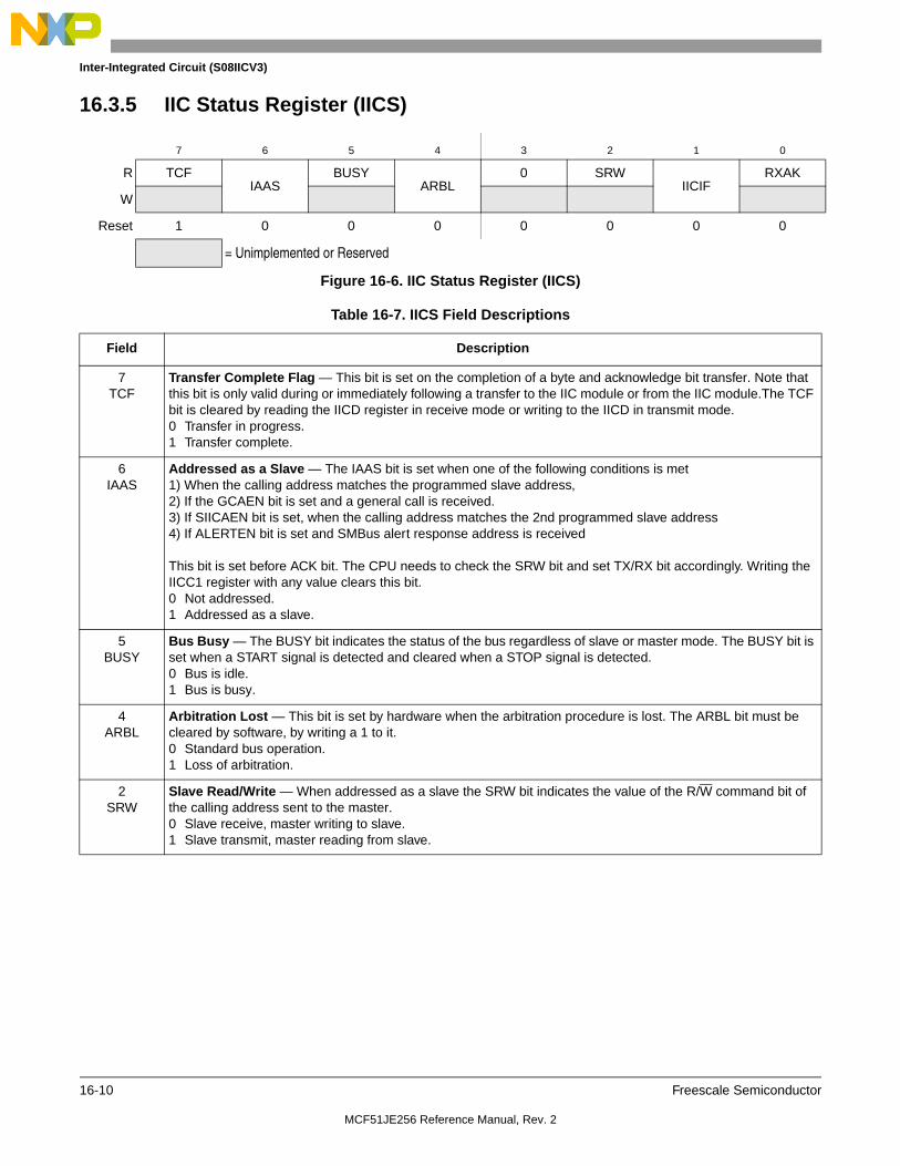
Inter-Integrated Circuit (S08IICV3)
16-10 Freescale Semiconductor
16.3.5 IIC Status Register (IICS)
7 6 5 4 3 2 1 0
R TCFIAAS
BUSYARBL
0 SRWIICIF
RXAK
W
Reset 1 0 0 0 0 0 0 0
= Unimplemented or Reserved
Figure 16-6. IIC Status Register (IICS)
Table 16-7. IICS Field Descriptions
Field Description
7TCF
Transfer Complete Flag — This bit is set on the completion of a byte and acknowledge bit transfer. Note that this bit is only valid during or immediately following a transfer to the IIC module or from the IIC module.The TCF bit is cleared by reading the IICD register in receive mode or writing to the IICD in transmit mode.0 Transfer in progress.1 Transfer complete.
6IAAS
Addressed as a Slave — The IAAS bit is set when one of the following conditions is met1) When the calling address matches the programmed slave address, 2) If the GCAEN bit is set and a general call is received.3) If SIICAEN bit is set, when the calling address matches the 2nd programmed slave address 4) If ALERTEN bit is set and SMBus alert response address is received
This bit is set before ACK bit. The CPU needs to check the SRW bit and set TX/RX bit accordingly. Writing the IICC1 register with any value clears this bit.0 Not addressed.1 Addressed as a slave.
5BUSY
Bus Busy — The BUSY bit indicates the status of the bus regardless of slave or master mode. The BUSY bit is set when a START signal is detected and cleared when a STOP signal is detected.0 Bus is idle.1 Bus is busy.
4ARBL
Arbitration Lost — This bit is set by hardware when the arbitration procedure is lost. The ARBL bit must be cleared by software, by writing a 1 to it. 0 Standard bus operation.1 Loss of arbitration.
2SRW
Slave Read/Write — When addressed as a slave the SRW bit indicates the value of the R/W command bit of the calling address sent to the master. 0 Slave receive, master writing to slave.1 Slave transmit, master reading from slave.
MCF51JE256 Reference Manual, Rev. 2

Inter-Integrated Circuit (S08IICV3)
Freescale Semiconductor 16-11
16.3.6 IIC Data I/O Register (IICD)
NOTEWhen transitioning out of master receive mode, the IIC mode should be switched before reading the IICD register to prevent an inadvertent initiation of a master receive data transfer.
In slave mode, the same functions are available after an address match has occurred.
Note that the TX bit in IICC must correctly reflect the desired direction of transfer in master and slave modes for the transmission to begin. For instance, if the IIC is configured for master transmit but a master receive is desired, then reading the IICD will not initiate the receive.
1IICIF
IIC Interrupt Flag — The IICIF bit is set when an interrupt is pending. This bit must be cleared by software, by writing a 1 to it in the interrupt routine. One of the following events can set the IICIF bit:
• One byte transfer including ACK/NACK bit completes if FACK = 0 • One byte transfer including ACK/NACK bit completes if FACK = 1 and this byte is an address byte• One byte transfer excluding ACK/NCAK bit completes if FACK = 1 and this byte is a data byte. an ACK or
NACK is sent out on the bus by writing 0 or 1 to TXAK after this bit is set.• Match of slave addresses to calling address (Primary Slave address, General Call address, Alert
Response address, and Second Slave address) (Received address is stored in data register)• Arbitration lost• Timeouts in SMBus mode except high timeout
0 No interrupt pending.1 Interrupt pending. NOTE: The IICIF will be cleared right after 1 bus cycle delay after writing a logic 1 to it.
0RXAK
Receive Acknowledge — When the RXAK bit is low, it indicates an acknowledge signal has been received after the completion of one byte of data transmission on the bus. If the RXAK bit is high it means that no acknowledge signal is detected.0 Acknowledge received.1 No acknowledge received.
7 6 5 4 3 2 1 0
RDATA
W
Reset 0 0 0 0 0 0 0 0
Figure 16-7. IIC Data I/O Register (IICD)
Table 16-8. IICD Field Descriptions
Field Description
7:0DATA
Data — In master transmit mode, when data is written to the IICD, a data transfer is initiated. The most significant bit is sent first. In master receive mode, reading this register initiates receiving of the next byte of data.
Table 16-7. IICS Field Descriptions (Continued)
Field Description
MCF51JE256 Reference Manual, Rev. 2

Inter-Integrated Circuit (S08IICV3)
16-12 Freescale Semiconductor
Reading the IICD will return the last byte received while the IIC is configured in either master receive or slave receive modes. The IICD does not reflect every byte that is transmitted on the IIC bus, nor can software verify that a byte has been written to the IICD correctly by reading it back.
In master transmit mode, the first byte of data written to IICD following assertion of MST (Start bit) or assertion of RSTA bit (repeated Start ) is used for the address transfer and should comprise of the calling address (in bit 7 to bit 1) concatenated with the required R/W bit (in position bit 0).
MCF51JE256 Reference Manual, Rev. 2
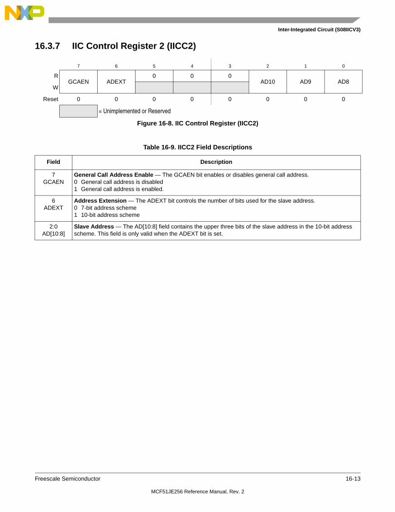
Inter-Integrated Circuit (S08IICV3)
Freescale Semiconductor 16-13
16.3.7 IIC Control Register 2 (IICC2)
7 6 5 4 3 2 1 0
RGCAEN ADEXT
0 0 0AD10 AD9 AD8
W
Reset 0 0 0 0 0 0 0 0
= Unimplemented or Reserved
Figure 16-8. IIC Control Register (IICC2)
Table 16-9. IICC2 Field Descriptions
Field Description
7GCAEN
General Call Address Enable — The GCAEN bit enables or disables general call address.0 General call address is disabled1 General call address is enabled.
6ADEXT
Address Extension — The ADEXT bit controls the number of bits used for the slave address.0 7-bit address scheme1 10-bit address scheme
2:0AD[10:8]
Slave Address — The AD[10:8] field contains the upper three bits of the slave address in the 10-bit address scheme. This field is only valid when the ADEXT bit is set.
MCF51JE256 Reference Manual, Rev. 2

Inter-Integrated Circuit (S08IICV3)
16-14 Freescale Semiconductor
16.3.8 IIC SMBus Control and Status Register (IICSMB)
NOTE
NOTE
1. A master can assume that the bus is free if it detects that the clock and data signals have been high for greater than THIGH,MAX, however, the SHTF will rise in bus transmission process but bus idle state.
2. When TCKSEL=1 there is no meaning to monitor SHTF since the bus speed is too high to match the protocol of SMBus.
7 6 5 4 3 2 1 0
RFACK ALERTEN SIICAEN TCKSEL SLTF
SHTF
W
Reset 0 0 0 0 0 0 0 0
= Unimplemented or Reserved
Table 16-10. IICSMB Field Descriptions
Field Description
7FACK
Fast NACK/ACK enable — For SMBus Packet Error Checking, CPU should be able to issue an ACK or NACK according to the result of receiving data byte. 0 ACK or NACK will be sent out on the following receiving data byte.1 Writing an 0 to TXAK after receiving data byte will generate an ACK; Writing an 1 to TXAK after receiving data byte will generate a NACK
6ALERTEN
SMBus Alert Response Address Enable — The ALERTEN bit enables or disable SMBus alert response address.0 SMBus alert response address matching is disabled1 SMBus alert response address matching is enabled.
5SIICAEN
Second IIC Address Enable — The SIICAEN bit enables or disable SMBus device default address.0 IIC Address Register 2 matching is disabled.1 IIC Address Register 2 matching is enabled.
4TCKSEL
Time Out Counter Clock Select— This bit selects the clock sources of Time Out Counter0 Time Out Counter counts at bus/64 frequency1 Time Out Counter counts at the bus frequency
3SLTF
SCL Low Timeout Flag — This read-only bit is set to logic 1 when IICSLT loaded non zero value (LoValue) and a SCL Low Time Out occurs. This bit is cleared by software, by writting a logic 1 to it or IICIF.0 No LOW TIME OUT occurs.1 A LOW TIME OUT occurs. Note: LOW TIME OUT function is disabled when IIC SCL LOW TIMER OUT register is set to zero
2SHTF
SCL High Timeout Flag — This read-only bit is set to logic 1 when SCL and SDA are held high more than clock * LoValue/512, which indicates the Bus Free. This bit is cleared automatically.0 No HIGH TIMEOUT occurs.1 An HIGH TIMEOUT occurs.
MCF51JE256 Reference Manual, Rev. 2

Inter-Integrated Circuit (S08IICV3)
Freescale Semiconductor 16-15
16.3.9 IIC Address Register 2 (IICA2)
16.3.10 IIC SCL Low Time Out Register High (IICSLTH)
16.3.11 IIC SCL LowTime Out register Low (IICSLTL)
7 6 5 4 3 2 1 0
RSAD7 SAD6 SAD5 SAD4 SAD3 SAD2 SAD1
0
W
Reset 1 1 0 0 0 0 1 0
= Unimplemented or Reserved
Field Description
7:1SAD[7:1]
SMBUs Address — The AD[7:1] field contains the slave address to be used by the SMBus. This field is used on the device default address or other related address
7 6 5 4 3 2 1 0
RSSLT15 SSLT14 SSLT13 SSLT12 SSLT11 SSLT10 SSLT9 SSLT8
W
Reset 0 0 0 0 0 0 0 0
= Unimplemented or Reserved
Field Description
7:0SSLT[15:8]
The value in this register is the most significant byte of SCL low time out value that determines the time-out period of SCL low.
7 6 5 4 3 2 1 0
RSSLT7 SSLT6 SSLT5 SSLT4 SSLT3 SSLT2 SSLT1 SSLT0
W
Reset 0 0 0 0 0 0 0 0
= Unimplemented or Reserved
MCF51JE256 Reference Manual, Rev. 2

Inter-Integrated Circuit (S08IICV3)
16-16 Freescale Semiconductor
16.3.12 IIC Programmable Input Glitch Filter (IICFLT)
Table 16-11. IICFLT Field Descriptions
Field Description
7:0SSLT[7:0]
The value in this register is the least significant byte of SCL low time out value that determines the time-out period of SCL low..
7 6 5 4 3 2 1 0
R 0 0 0 0FLT3 FLT2 FLT1 FLT0
W
Reset 0 0 0 0 0 0 0 0
= Unimplemented or Reserved
Field Description
3:0FLT
IIC Programmable Filter Factor contain the programming controls for the width of glitch (in terms of bus clock cycles) the filtershould absorb; in other words, the filter does not let glitches less than or equal to this width setting pass.FLT[3:0]
0000 No Filter / Bypass0001 Filter glitches up to width of 1 (half) IPBUS clock cycle0010 Filter glitches up to width of 2 (half) IPBUS clock cycles0011 Filter glitches up to width of 3 (half) IPBUS clock cycles0100 Filter glitches up to width of 4 (half) IPBUS clock cycles0101 Filter glitches up to width of 5 (half) IPBUS clock cycles0110 Filter glitches up to width of 6 (half) IPBUS clock cycles0111 Filter glitches up to width of 7 (half) IPBUS clock cycles1000 Filter glitches up to width of 8 (half) IPBUS clock cycle1001 Filter glitches up to width of 9 (half) IPBUS clock cycles1010 Filter glitches up to width of 10 (half) IPBUS clock cycles1011 Filter glitches up to width of 11 (half) IPBUS clock cycles1100 Filter glitches up to width of 12 (half) IPBUS clock cycles1101 Filter glitches up to width of 13 (half) IPBUS clock cycles1110 Filter glitches up to width of 14 (half) IPBUS clock cycles1111 Filter glitches up to width of 15 (half) IPBUS clock cycles
NOTE: The width of the FLT is an integration option which can be changed in different SoCs
And Also the clock source used is an integration configurative option - It could be the 2X IPBus clock or the IPbus clock - which one needs to be identified at architectural definition. For the 4-bit definitions above, hard descriptions of "half" IPBUS clock cycles will not be the case when the IPBUS clock is used for filtering logic.
MCF51JE256 Reference Manual, Rev. 2
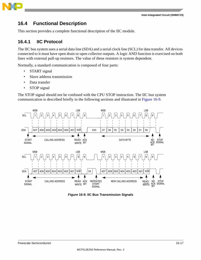
Inter-Integrated Circuit (S08IICV3)
Freescale Semiconductor 16-17
16.4 Functional DescriptionThis section provides a complete functional description of the IIC module.
16.4.1 IIC Protocol
The IIC bus system uses a serial data line (SDA) and a serial clock line (SCL) for data transfer. All devices connected to it must have open drain or open collector outputs. A logic AND function is exercised on both lines with external pull-up resistors. The value of these resistors is system dependent.
Normally, a standard communication is composed of four parts:
• START signal
• Slave address transmission
• Data transfer
• STOP signal
The STOP signal should not be confused with the CPU STOP instruction. The IIC bus system communication is described briefly in the following sections and illustrated in Figure 16-9.
Figure 16-9. IIC Bus Transmission Signals
SCL
SDA
STARTSIGNAL
ACKBIT
1 2 3 4 5 6 7 8
MSB LSB
1 2 3 4 5 6 7 8
MSB LSB
STOPSIGNAL
NO
SCL
SDA
1 2 3 4 5 6 7 8
MSB LSB
1 2 5 6 7 8
MSB LSB
REPEATED
3 4
9 9
AD7 AD6 AD5 AD4 AD3 AD2 AD1 R/W XXX D7 D6 D5 D4 D3 D2 D1 D0
CALLING ADDRESS READ/ DATA BYTE
AD7 AD6 AD5 AD4 AD3 AD2 AD1 R/W AD7 AD6 AD5 AD4 AD3 AD2 AD1 R/W
NEW CALLING ADDRESS
9 9
XX
ACKBITWRITE
STARTSIGNAL
STARTSIGNAL
ACKBIT
CALLING ADDRESS READ/WRITE
STOPSIGNAL
NOACKBIT
READ/WRITE
MCF51JE256 Reference Manual, Rev. 2

Inter-Integrated Circuit (S08IICV3)
16-18 Freescale Semiconductor
16.4.1.1 START Signal
When the bus is free; in other words, no master device is engaging the bus (both SCL and SDA lines are at logical high), a master may initiate communication by sending a START signal. As shown in Figure 16-9, a START signal is defined as a high-to-low transition of SDA while SCL is high. This signal denotes the beginning of a new data transfer (each data transfer may contain several bytes of data) and brings all slaves out of their idle states.
16.4.1.2 Slave Address Transmission
The first byte of data transferred immediately after the START signal is the slave address transmitted by the master. This is a seven-bit calling address followed by a R/W bit. The R/W bit tells the slave the desired direction of data transfer.
1 = Read transfer, the slave transmits data to the master.0 = Write transfer, the master transmits data to the slave.
Only the slave with a calling address that matches the one transmitted by the master will respond by sending back an acknowledge bit. This is done by pulling the SDA low at the 9th clock (see Figure 16-9).
No two slaves in the system may have the same address. If the IIC module is the master, it must not transmit an address that is equal to its own slave address. The IIC cannot be master and slave at the same time. However, if arbitration is lost during an address cycle, the IIC will revert to slave mode and operate correctly even if it is being addressed by another master.
16.4.1.3 Data Transfer
Before successful slave addressing is achieved, the data transfer can proceed byte-by-byte in a direction specified by the R/W bit sent by the calling master.
All transfers that come after an address cycle are referred to as data transfers, even if they carry sub-address information for the slave device
Each data byte is 8 bits long. Data may be changed only while SCL is low and must be held stable while SCL is high as shown in Figure 16-9. There is one clock pulse on SCL for each data bit, the MSB being transferred first. Each data byte is followed by a 9th (acknowledge) bit, which is signalled from the receiving device. An acknowledge is signalled by pulling the SDA low at the ninth clock. In summary, one complete data transfer needs nine clock pulses.
If the slave receiver does not acknowledge the master in the 9th bit time, the SDA line must be left high by the slave. The master interprets the failed acknowledge as an unsuccessful data transfer.
If the master receiver does not acknowledge the slave transmitter after a data byte transmission, the slave interprets this as an end of data transfer and releases the SDA line.
In either case, the data transfer is aborted and the master does one of two things:
• Relinquishes the bus by generating a STOP signal.
• Commences a new calling by generating a repeated START signal.
MCF51JE256 Reference Manual, Rev. 2

Inter-Integrated Circuit (S08IICV3)
Freescale Semiconductor 16-19
16.4.1.4 STOP Signal
The master can terminate the communication by generating a STOP signal to free the bus. However, the master may generate a START signal followed by a calling command without generating a STOP signal first. This is called repeated START. A STOP signal is defined as a low-to-high transition of SDA while SCL at logical 1 (see Figure 16-9).
The master can generate a STOP even if the slave has generated an acknowledge at which point the slave must release the bus.
16.4.1.5 Repeated START Signal
As shown in Figure 16-9, a repeated START signal is a START signal generated without first generating a STOP signal to terminate the communication. This is used by the master to communicate with another slave or with the same slave in different mode (transmit/receive mode) without releasing the bus.
16.4.1.6 Arbitration Procedure
The IIC bus is a true multi-master bus that allows more than one master to be connected on it. If two or more masters try to control the bus at the same time, a clock synchronization procedure determines the bus clock, for which the low period is equal to the longest clock low period and the high is equal to the shortest one among the masters. The relative priority of the contending masters is determined by a data arbitration procedure, a bus master loses arbitration if it transmits logic 1 while another master transmits logic 0. The losing masters immediately switch over to slave receive mode and stop driving SDA output. In this case, the transition from master to slave mode does not generate a STOP condition. Meanwhile, a status bit is set by hardware to indicate loss of arbitration.
16.4.1.7 Clock Synchronization
Because wire-AND logic is performed on the SCL line, a high-to-low transition on the SCL line affects all the devices connected on the bus. The devices start counting their low period and after a device’s clock has gone low, it holds the SCL line low until the clock high state is reached. However, the change of low to high in this device clock may not change the state of the SCL line if another device clock is still within its low period. Therefore, synchronized clock SCL is held low by the device with the longest low period. Devices with shorter low periods enter a high wait state during this time (see Figure 16-10). When all devices concerned have counted off their low period, the synchronized clock SCL line is released and pulled high. There is then no difference between the device clocks and the state of the SCL line and all the devices start counting their high periods. The first device to complete its high period pulls the SCL line low again.
MCF51JE256 Reference Manual, Rev. 2

Inter-Integrated Circuit (S08IICV3)
16-20 Freescale Semiconductor
Figure 16-10. IIC Clock Synchronization
16.4.1.8 Handshaking
The clock synchronization mechanism can be used as a handshake in data transfer. Slave devices may hold the SCL low after completion of one byte transfer (9 bits). In such case, it halts the bus clock and forces the master clock into wait states until the slave releases the SCL line.
16.4.1.9 Clock Stretching
The clock synchronization mechanism can be used by slaves to slow down the bit rate of a transfer. After the master has driven SCL low the slave can drive SCL low for the required period and then release it. If the slave SCL low period is greater than the master SCL low period then the resulting SCL bus signal low period is stretched.
SCL1
SCL2
SCL
INTERNAL COUNTER RESET
DELAY START COUNTING HIGH PERIOD
MCF51JE256 Reference Manual, Rev. 2

Inter-Integrated Circuit (S08IICV3)
Freescale Semiconductor 16-21
16.4.2 10-bit Address
For 10-bit addressing, 0x11110 is used for the first 5 bits of the first address byte. Various combinations of read/write formats are possible within a transfer that includes 10-bit addressing.
16.4.2.1 Master-Transmitter Addresses a Slave-Receiver
The transfer direction is not changed (see Table 16-12). When a 10-bit address follows a START condition, each slave compares the first seven bits of the first byte of the slave address (11110XX) with its own address and tests whether the eighth bit (R/W direction bit) is 0. It is possible that more than one device will find a match and generate an acknowledge (A1). Each slave that finds a match will compare the eight bits of the second byte of the slave address with its own address, but only one slave will find a match and generate an acknowledge (A2). The matching slave will remain addressed by the master until it receives a STOP condition (P) or a repeated START condition (Sr) followed by a different slave address.
After the master-transmitter has sent the first byte of the 10-bit address, the slave-receiver will see an IIC interrupt. User software must ensure that for this interrupt, the contents of IICD are ignored and not treated as valid data.
16.4.2.2 Master-Receiver Addresses a Slave-Transmitter
The transfer direction is changed after the second R/W bit (see Table 16-13). Up to and including acknowledge bit A2, the procedure is the same as that described for a master-transmitter addressing a slave-receiver. After the repeated START condition (Sr), a matching slave remembers that it was addressed before. This slave then checks whether the first seven bits of the first byte of the slave address following Sr are the same as they were after the START condition (S), and tests whether the eighth (R/W) bit is 1. If there is a match, the slave considers that it has been addressed as a transmitter and generates acknowledge A3. The slave-transmitter remains addressed until it receives a STOP condition (P) or a repeated START condition (Sr) followed by a different slave address.
After a repeated START condition (Sr), all other slave devices will also compare the first seven bits of the first byte of the slave address with their own addresses and test the eighth (R/W) bit. However, none of them will be addressed because R/W = 1 (for 10-bit devices), or the 11110XX slave address (for 7-bit devices) does not match.
After the master-receiver has sent the first byte of the 10-bit address, the slave-transmitter will see an IIC interrupt. User software must ensure that for this interrupt, the contents of IICD are ignored and not treated as valid data.
SSlave Address 1st 7 bits R/W
A1Slave Address 2nd byte
A2 Data A ... Data A/A P11110 + AD10 + AD9 0 AD[8:1]
Table 16-12. Master-Transmitter Addresses Slave-Receiver with a 10-bit Address
SSlave Address
1st 7 bitsR/W
A1Slave Address
2nd byte A2 SrSlave Address
1st 7 bitsR/W
A3 Data A ... Data A P
11110 + AD10 + AD9 0 AD[8:1] 11110 + AD10 + AD9 1
Table 16-13. Master-Receiver Addresses a Slave-Transmitter with a 10-bit Address
MCF51JE256 Reference Manual, Rev. 2

Inter-Integrated Circuit (S08IICV3)
16-22 Freescale Semiconductor
16.4.3 Address Matching
All received Addresses can be requested in 7-bit or 10-bit address. IIC Address Register 1, which contains IIC primary slave address, always participates the address matching process. If the GCAEN bit is set, general call will participate the address matching process. If the ALERTEN bit is set, alert response will participate the address matching process. If SIICAEN bit is set, the IIC Address Register 2 will participate the address matching process.
When the IIC responds to one of above mentioned address, it acts as a slave-receiver and the IAAS bit is set after the address cycle. Software need to read the IICD register after the first byte transfer to determine which the address is matched.
16.4.4 System Management Bus Specification
SMBus provides a control bus for system and power management related tasks. A system may use SMBus to pass messages to and from devices instead of tripping individual control lines. Removing the individual control lines reduces pin count. Accepting messages ensures future expandability.With System Management Bus, a device can provide manufacturer information, tell the system what its model/part number is, save its state for a suspend event, report different types of errors, accept control parameters, and return its status.
16.4.4.1 Timeouts
The TTIMEOUT,MIN parameter allows a master or slave to conclude that a defective device is holding the clock low indefinitely or a master is intentionally trying to drive devices off the bus. It is highly recommended that a slave device release the bus (stop driving the bus and let SCL and SDA float high) when it detects any single clock held low longer than TTIMEOUT,MIN. Devices that have detected this condition should reset their communication and be able to receive a new START condition in no later than TTIMEOUT,MAX.
SMBus defines a clock low time-out, TTIMEOUT of 35 ms and specifies TLOW: SEXT as the cumulative clock low extend time for a slave device and specifies TLOW: MEXT as the cumulative clock low extend time for a master device.
16.4.4.1.1 SCL Low Timeout
If the SCL line is held low by a slave device on the bus, no further communication is possible. Furthermore, the master cannot force the SCL line high to correct the error condition. To solve this problem, the SMBus protocol specifies that devices participating in a transfer must detect any clock cycle held low longer than a “timeout” value condition. Devices that have detected the timeout condition must reset the communication. When active master, if the IIC detects that SMBCLK low has exceeded the value of TTIMEOUT,MIN it must generate a stop condition within or after the current data byte in the transfer process. When slave, upon detection of the TTIMEOUT,MIN condition, the IIC shall reset its communication and be able to receive a new START condition.
MCF51JE256 Reference Manual, Rev. 2

Inter-Integrated Circuit (S08IICV3)
Freescale Semiconductor 16-23
16.4.4.1.2 SCL High (SMBus Free) Timeout
The IIC shall assume that the bus is idle, when it has determined that the SMBCLK and SMBDAT signals have been high for at least THIGH:MAX.HIGH timeout can occur in two ways: 1) HIGH timeout detected after a STOP condition appears on the bus; 2) HIGH timeout detected after a START condition, but before a STOP condition appears on the bus.Any master detecting either scenario can assume the bus is free then SHTF rises. HIGH timeout occurred in scenario 2 if it ever detects that both the following is true:BUSY bit is high and SHTF is high.
16.4.4.1.3 CSMBCLK TIMEOUT MEXT
Figure1-10: Timeout measurement intervals illustrates the definition of the timeout intervals, TLOW:SEXT
and TLOW:MEXT. When master mode, the I2C must not cumulatively extend its clock cycles for a period greater than TLOW:MEXT within a byte, where each byte is defined as START-to-ACK, ACK-to-ACK, or ACK-to-STOP. When CSMBCLK TIMEOUT MEXT occurs SMBus MEXT will rise and also trigger the SLTF.
16.4.4.1.4 CSMBCLK TIMEOUT SEXT
A Master is allowed to abort the transaction in progress to any slave that violates the TLOW:SEXT or TTIMEOUT,MIN specifications. This can be accomplished by the Master issuing a STOP condition at the conclusion of the byte transfer in progress. When slave, the I2C must not cumulatively extend its clock cycles for a period greater than TLOW:SEXT during any message from the initial START to the STOP. When CSMBCLK TIMEOUT SEXT occurs SEXT will rise and also trigger SLTF.
Figure 16-11. Timeout measurement intervals
NOTECSMBCLK TIMEOUT SEXT and MEXT are optional functions which will be implemented in second step.
StopStart TLOW:SEXT
TLOW:MEXT TLOW:MEXT TLOW:MEXT
ClkAck ClkAck
SCL
SDA
MCF51JE256 Reference Manual, Rev. 2

Inter-Integrated Circuit (S08IICV3)
16-24 Freescale Semiconductor
16.4.4.2 FAST ACK and NACK
To improve reliability and communication robustness, implementation of Packet Error Checking (PEC) by SMBus devices is optional for SMBus devices but required for devices participating in and only during the Address Resolution Protocol (ARP) process. The PEC is a CRC-8 error checking byte, calculated on all the message bytes. The PEC is appended to the message by the device that supplied the last data byte. If the PEC is present but not correct, a NACK is issued by receiver. Otherwise an ACK will be issued. In order to calculate the CRC-8 by software, this module can hold SCL line to low after receiving eighth SCL (bit 8th) if this byte is a data byte. So software can determine whether an ACK or NACK should be sent out to the bus by setting or clearing TXAK bit if FASK (fast ACK/NACK enable bit) is enabled.
SMBus requires devices to acknowledge their own address always, as a mechanism to detect a removable devices presence on the bus (battery, docking station, etc.) Besides to indicate a slave device busy condition, SMBus is using the NACK mechanism also to indicate the reception of an invalid command or data. Since such a condition may occur on the last byte of the transfer, it is required that SMBus devices have the ability to generate the not acknowledge after the transfer of each byte and before the completion of the transaction. This is important because SMBus does not provide any other resend signaling. This difference in the use of the NACK signaling has implications on the specific implementation of the SMBus port, especially in devices that handle critical system data such as the SMBus host and the SBS components.
NOTEIn the last byte of master receive slave transmit mode, the master should send NACK to bus so FACK should be switched off before the last byte transmit.
16.5 ResetsThe IIC is disabled after reset. The IIC cannot cause an MCU reset.
16.6 InterruptsThe IIC generates a single interrupt.
An interrupt from the IIC is generated when any of the events in Table 16-14 occur, provided the IICIE bit is set. The interrupt is driven by bit IICIF (of the IIC status register) and masked with bit IICIE (of the IIC control register). The IICIF bit must be cleared by software by writing a 1 to it in the interrupt routine. The user can determine the interrupt type by reading the status register. For SMBus timeouts interrupt, the interrupt is driven by SLTF and masked with bit IICIE. The SLTF bit must be cleared by software by
MCF51JE256 Reference Manual, Rev. 2

Inter-Integrated Circuit (S08IICV3)
Freescale Semiconductor 16-25
writing a 1 to it in the interrupt routine. The user can determine the interrupt type by reading the status register.
NOTEIn Master receive mode, the FACK should be set zero before the last byte transfer.
16.6.1 Byte Transfer Interrupt
The TCF (transfer complete flag) bit is set at the falling edge of the 9th clock to indicate the completion of byte transfer.
16.6.2 Address Detect Interrupt
When the calling address matches the programmed slave address (IIC address register) or when the GCAEN bit is set and a general call is received, the IAAS bit in the status register is set. The CPU is interrupted, provided the IICIE is set. The CPU must check the SRW bit and set its Tx mode accordingly.
16.6.3 Arbitration Lost Interrupt
The IIC is a true multi-master bus that allows more than one master to be connected on it. If two or more masters try to control the bus at the same time, the relative priority of the contending masters is determined by a data arbitration procedure. The IIC module asserts this interrupt when it loses the data arbitration process and the ARBL bit in the status register is set.
Arbitration is lost in the following circumstances:
• SDA sampled as a low when the master drives a high during an address or data transmit cycle.
• SDA sampled as a low when the master drives a high during the acknowledge bit of a data receive cycle.
• A START cycle is attempted when the bus is busy.
• A repeated START cycle is requested in slave mode.
• A STOP condition is detected when the master did not request it.
This bit must be cleared by software by writing a 1 to it.
16.6.4 Timeouts Interrupt in SMbus
When IICIE is set, the IIC asserts a timeout interrupt output SLTF upon detection of any of the mentioned timeout conditions, with one exception. The HIGH TIMEOUT mechanism shall not be used to influence
Table 16-14. Interrupt Summary
Interrupt Source Status Flag Local Enable
Complete 1-byte transfer TCF IICIF IICIE
Match of received calling address IAAS IICIF IICIE
Arbitration Lost ARBL IICIF IICIE
SMBus Timeout Interrupt Flag SLTF IICIF IICIE
MCF51JE256 Reference Manual, Rev. 2

Inter-Integrated Circuit (S08IICV3)
16-26 Freescale Semiconductor
the timeout interrupt output, because the HIGH TIMEOUT indicates an idle condition on the bus.And SLTF will rise when it matches the HIGH TIMEOUT and fall automatically to just indicate the bus status.
16.6.5 Programmable input glitch filter
An IIC glitch filter has been added outside the IIC legacy modules, but within the IIC package. This filter can absorb glitches on the IIC clock and data lines for I2C module. The width of the glitch to absorb can be specified in terms of number of half bus clock cycles. A single glitch filter control register is provided as IICFLT. Effectively, any down-up-down or up-down-up transition on the data line that occurs within the number of clock cycles programmed here is ignored by the IIC.the programmer only needs to specify the size of glitch (in terms of bus clock cycles) for the filter to absorb and not pass.
MCF51JE256 Reference Manual, Rev. 2

Inter-Integrated Circuit (S08IICV3)
Freescale Semiconductor 16-27
16.7 Initialization/Application Information
Module Initialization (Slave)1. Write: IICC2
— to enable or disable general call— to select 10-bit or 7-bit addressing mode
2. Write: IICA1— to set the slave address
3. Write: IICC1— to enable IIC and interrupts
4. Initialize RAM variables (IICEN = 1 and IICIE = 1) for transmit data5. Initialize RAM variables used to achieve the routine shown in Figure 16-12
Module Initialization (Master)1. Write: IICF
— to set the IIC baud rate (example provided in this chapter)2. Write: IICC1
— to enable IIC and interrupts3. Initialize RAM variables (IICEN = 1 and IICIE = 1) for transmit data4. Initialize RAM variables used to achieve the routine shown in Figure 16-125. Write: IICC1
— to enable TX6. Write: IICC1
— to enable MST (master mode)7. Write: IICD
— with the address of the target slave. (The LSB of this byte will determine whether the communication is master receive or transmit.)
Module UseThe routine shown in Figure 16-12 can handle both master and slave IIC operations. For slave operation, an incoming IIC message that contains the proper address will begin IIC communication. For master operation, communication must be initiated by writing to the IICD register.
0
IICF
IICA1
Baud rate = BUSCLK / (2 x MULT x (SCL DIVIDER))
TX TXAK RSTA 0 0IICC1 IICEN IICIE MST
Module configuration
ARBL 0 SRW IICIF RXAKIICS TCF IAAS BUSY
Module status flags
Register Model
AD[7:1]
Address to which the module will respond when addressed as a slave (in slave mode)
MULT ICR
IICD DATA
Data register; Write to transmit IIC data read to read IIC data
0 AD10 AD9 AD8IICC2 GCAEN ADEXT
Address configuration
00
IICFLT FLT3 FLT2 FLT1 FLT00 0 0 0
IIC Programmable Input Glitch Filter
MCF51JE256 Reference Manual, Rev. 2

Inter-Integrated Circuit (S08IICV3)
16-28 Freescale Semiconductor
Figure 16-12. Typical IIC Interrupt Routine
Clear
Master Mode
?
Tx/Rx ?
Last Byte Transmitted
?
RXAK=0 ?
End of Addr Cycle (Master Rx)
?
Write NextByte to IICD
Switch to Rx Mode
Dummy Read from IICD
Generate Stop Signal
Read Data from IICD and Store
Set TXACK =1Generate
Stop Signal
2nd Last Byte to Be Read
?
Last Byte to Be Read
?
Arbitration Lost
?
Clear ARBL
IAAS=1 ?
IAAS=1 ?
SRW=1 ?
TX/RX ?
Set TX Mode
Write Data to IICD
Set RX Mode
Dummy Read from IICD
ACK fromReceiver
?
Tx Next Byte
Read Data from IICD and Store
Switch to Rx Mode
Dummy Read from IICD
RTI
Y N
Y
Y Y
Y
Y
Y
Y
Y
Y
N
N
N
NN
N
N
N
N
Y
TX RX
RX
TX(Write)
(Read)
N
IICIF
Address Transfer Data Transfer
(MST = 0)
(MST = 0)
See Note 1
NOTES:1. If general call is enabled, a check must be done to determine whether the received address was a general call address (0x00). If the received address was a
general call address, then the general call must be handled by user software.2. When 10-bit addressing is used to address a slave, the slave will see an interrupt following the first byte of the extended address. User software must ensure that
for this interrupt, the contents of IICD are ignored and not treated as a valid data transfer.
See Note 2
MCF51JE256 Reference Manual, Rev. 2

Inter-Integrated Circuit (S08IICV3)
Freescale Semiconductor 16-29
Figure 16-14. Typical IIC SMBus Interrupt Routine
Master Mode
?
Tx/Rx ?
Last Byte Transmitted
?
RXAK=0 ?
End of Addr Cycle (Master Rx)
?
Write NextByte to IICD
Switch to Rx Mode
Dummy Read from IICD
Generate Stop Signal
Read Data from IICD and Store
Set TXACK =1Generate
Stop Signal
2nd Last Byte to Be Read
?
Last Byte to Be Read
?
Arbitration Lost
?
Clear ARBL
IAAS=1 ?
IAAS=1 ?
SRW=1 ?
TX/RX ?
Set TX Mode
Write Data to IICD
Set RX Mode
Dummy Read from IICD
ACK fromReceiver
?
Tx Next Byte
Read Data from IICD and Store
Switch to Rx Mode
Dummy Read from IICD
RTI
Y N
Y
Y Y
Y
Y
Y
Y
Y
Y
N
N
N
NN
N
N
N
N
Y
TX RX
RX
TX(Write)
(Read)
N
Address Transfer
(MST = 0)
(MST = 0)
See Note 1
NOTES:1. If general call siicaen is enabled, a check must be done to determine whether the received address was a general call address (0x00) or SMbus device default
address. If the received address was one of them, then it must be handled by user software.2. Flow chart1 means figure 1-12 Typical IIC Interrupt Routine.3. Delay about 1-2bit scl cycle waiting data register updated then clear IICIF
Y NFACK?
Flow Chart1 See Note 2
Clear IICIFSet Fack = 0
Set TXAKTo proper Value
Clear IICIF
Clear IICIF
Set TXAK to Proper Value
Clear IICIF
SLTF?NY
Clear IICIF
See Note 3
MCF51JE256 Reference Manual, Rev. 2

Inter-Integrated Circuit (S08IICV3)
16-30 Freescale Semiconductor
16.8 SMBALERT# Another optional signal is an interrupt line for devices that want to trade their ability to master for a pin.
SMBALERT# is a wired-AND signal just as the SMBCLK and SMBDAT signals are. SMBALERT# is
used in conjunction with the SMBus General Call Address. Messages invoked with the SMBus are 2 bytes
long. (Now there is no ALERT# port in current block)
A slave-only device can signal the host through SMBALERT# that it wants to talk. The host processes the
interrupt and simultaneously accesses all SMBALERT# devices through the Alert Response Address
(ARA). Only the device(s) which pulled SMBALERT# low will acknowledge the Alert Response Address.
The host performs a modified Receive Byte operation. The 7 bit device address provided by the slave
transmit device is placed in the 7 most significant bits of the byte. The eighth bit can be a zero or one.
If more than one device pulls SMBALERT# low, the highest priority (lowest address) device will win
communication rights via standard arbitration during the slave address transfer.
After acknowledging the slave address the device must disengage its SMBALERT# pulldown. If the host
still sees SMBALERT# low when the message transfer is complete, it knows to read the ARA again.
A host which does not implement the SMBALERT# signal may periodically access the ARA.
Table 0-1. A 7-bit-Addressable Device Responds to an ARA
NOTE: The user should put Device Address on bus by software after response to the Alert response address in current block.
s Alert Response Address Rd A Device Address A P
MCF51JE256 Reference Manual, Rev. 2

Freescale Semiconductor 17-1
Chapter 17 Multipurpose Clock Generator (S08MCGV3)
17.1 IntroductionThe multipurpose clock generator (MCG) module provides several clock source choices for this device. The module contains a frequency-locked loop (FLL) and a phase-locked loop (PLL) that are controllable by an internal or an external reference clock. The module can select either of the FLL or PLL clocks or either of the internal or external reference clocks as a source for the MCU system clock. The selected clock source is passed through a reduced bus divider that allows a lower output clock frequency to be derived.
For USB operation on this series of devices, the MCG must be configured for PLL engaged external (PEE) mode to achieve a MCGOUT frequency of 48 MHz.
These devices are unique in that they support a Time of Day module which includes a dedicated oscillator. The TOD oscillator can also be used as the reference clock into the MCG.
MCF51JE256 Reference Manual, Rev. 2

Multipurpose Clock Generator (S08MCGV3)
17-2 Freescale Semiconductor
Figure 17-1. Block Diagram with MCG Module Highlighted
MCF51JE256 Reference Manual, Rev. 2

Multipurpose Clock Generator (S08MCGV3)
Freescale Semiconductor 17-3
17.1.1 Clock Check & Select Function
The “Clock Check & Select” feature of the following figures is a very simple block used to check the oscillator clocks for activity and control the mux which selects the external clock for the MCG. This function is implemented external to the MCG module itself, and is specific to this device.
The four registers that comprise this operation are described in the following table.
Figure 17-2. A subset of Figure 1-3
17.1.2 Clock Check & Select Control (CCSCTRL)
Table 17-1. Clock Check & Select Registers
Register Function
CCSCTRL Clock Check & Select Control Register
CCSTMR1 8-bit counter incremented by XOSC1 timebase
CCSTMR2 8-bit counter incremented by XOSC2 timebase
CCSTMRIR 8-bit counter incremented via IR clock timebase
7 6 5 4 3 2 1 0
RRANGE1 HGO1 ERCLKEN1 OSCINIT1 EREFS1 EN TEST SEL
W
Reset: 0 0 0 0 1 0 0 0
Figure 17-3. Clock Check & Select Control Register (CCSCTRL)
MCG
XTA
L1
EX
TAL1
XOSC2 XOSC1
oscillator control
Clock Check& Select
XTA
L2
EX
TAL2
MC
GIR
CL
K
OSCOUT1
OSCOUT2
TOD
oscillator control
MCF51JE256 Reference Manual, Rev. 2

Multipurpose Clock Generator (S08MCGV3)
17-4 Freescale Semiconductor
17.1.3 CCS XOSC1 Timer Register (CCSTMR1)
Table 17-2. CCS Control Register Field Descriptions
Field Description
7RANGE1
Frequency Range Select — Selects the frequency range for the external oscillator 1 (XOSC1).0 Low frequency range selected for the external oscillator.1 High frequency range selected for the external oscillator.
6HGO1
High-Gain Oscillator Select — The HGO bit controls the external oscillator 1 (XOSC1) mode of operation.0 Configures external oscillator for low-power operation.1 Configures external oscillator for high-gain operation.
5ERCLKEN1
External Clock Enable — The ERCLKEN1 bit enables the external reference clock provided by XOSC1 for use as MCGERCLK.0 MCGERCLK inactive.1 MCGERCLK active.
4OSCINIT1
Oscillator Initialization — The OSCINIT1 bit indicates the external clock source has finished its initialization cycles and is stabilized.
3EREFS1
External Reference Select — The EREFS1 bit selects the source for the external reference clock of the MCG when using XOSC1.0 External Clock Source requested.1 Oscillator requested.
2EN
Enable bit — The EN bit disables inputs to the clock check counter to save power.0 The OSCOUT1, OSCOUT2, and MCGIRCLK inputs to the clock check counters are disabled for power saving. 1 The clock inputs are enabled.
1TEST
Test bit — Writing a “1” to this bit clears CCSTMR1, CCSTMR2 and CCSTMRIR. The three counters will then begin incrementing until any one of the three hits 0xFF, at which point the test completes, and TEST is cleared.
0SEL
Select bit — The SEL bit selects the external clock input to the MCG. This bit should only be changed when the MCG is NOT utilizing the external clock input.0 XOSC2 is selected as the external clock input to the MCGand XOSC1 is selected to the TOD (default).1 XOSC1 is selected as the external clock input to the MCGand TOD.
7 6 5 4 3 2 1 0
R CNT1
W
Reset: 0 0 0 0 0 0 0 0
Figure 17-4. CCS XOSC1 Timer Register (CCSTMR1)
Table 17-3. CCSTMR1 Register Field Descriptions
Field Description
7-0CNT1
CNT1 — This register is one of three used to compare XOSC1, XOSC2 and internal relaxation oscillator frequencies. It is initialized to zero upon a write of “1” to CCSCTRL[TEST]. It contains a valid value once CCSCTRL[TEST] resets itself to “0”. By comparing the values of the three registers, application code can determine the crude health of the various clock sources.
MCF51JE256 Reference Manual, Rev. 2

Multipurpose Clock Generator (S08MCGV3)
Freescale Semiconductor 17-5
17.1.4 CCS XOSC2 Timer Register (CCSTMR2)
17.1.5 CCS Internal Reference Clock Timer Register (CCSTMRIR)
17.1.6 Operation
The clock check and select (CCS) feature is a basic clock monitor of the internal reference clock and two XOSC clocks using the following 8-bit counters:
• CCSTMRIR
The major purpose of this feature is to monitor the stability and availability of the XOSC clocks and provide a rough frequency measurement of the three clock sources. The registers are 8-bit so the maximum count is 255.
Basically, whichever counter reaches 255 first sends a stop signal to the other two counters. It takes approximately 3 clock cycles for the stop signal to sync with the other two counters. Software can then
7 6 5 4 3 2 1 0
R CNT2
W
Reset: 0 0 0 0 0 0 0 0
Figure 17-5. CCS XOSC2 Timer Register (CCSTMR2)
Table 17-4. CCSTMR2 Register Field Descriptions
Field Description
7-0CNT2
CNT2 —This register is one of three used to compare XOSC1, XOSC2 and internal relaxation oscillator frequencies. It is initialized to zero upon a write of “1” to CCSCTRL[TEST]. It contains a valid value once CCSCTRL[TEST] resets itself to “0”. By comparing the values of the three registers, application code can determine the crude health of the various clock sources.
7 6 5 4 3 2 1 0
R CNTIR
W
Reset: 0 0 0 0 0 0 0 0
Figure 17-6. CCS Internal Reference Clock Timer Register (CCSTMRIR)
Table 17-5. CCSTMRIR Register Field Descriptions
Field Description
7-0CNTIR
CNTIR —This register is one of three used to compare XOSC1, XOSC2 and internal relaxation oscillator frequencies. It is initialized to zero upon a write of “1” to CCSCTRL[TEST]. It contains a valid value once CCSCTRL[TEST] resets itself to “0”. By comparing the values of the three registers, application code can determine the crude health of the various clock sources.
MCF51JE256 Reference Manual, Rev. 2

Multipurpose Clock Generator (S08MCGV3)
17-6 Freescale Semiconductor
compare the three registers to obtain a crude (3/256 is ~1.2%) measurement of how well the three frequencies correlate.
NOTE
The clock check feature should only be used to check the stability and availability of the XOSC clocks. CCS is not intended to be used as an accurate frequency measurement of the clocks.
17.1.7 Features
Key features of the MCG module are:
• Frequency-locked loop (FLL)
— Internal or external reference clock can be used to control the FLL
• Phase-locked loop (PLL)
— Voltage-controlled oscillator (VCO)
— Modulo VCO frequency divider
— Phase/Frequency detector
— Integrated loop filter
— Lock detector with interrupt capability
• Internal reference clock
— Nine trim bits for accuracy
— Can be selected as the clock source for the MCU
• External reference clock
— Control for a separate crystal oscillator
— Clock monitor with reset capability
— Can be selected as the clock source for the MCU
• Reference divider is provided
• Clock source selected can be divided down by 1, 2, 4, or 8
• BDC clock (MCGLCLK) is provided as a constant divide-by-2 of the DCO output whether in an FLL or PLL mode.Three selectable digitally controlled oscillators (DCOs) optimized for different frequency ranges.
• Option to maximize DCO output frequency for a 32,768 Hz external reference clock source.
• The PLL can be used to drive MCGPLLSCLK even when MCGOUT is driven from one of the reference clocks (PBE mode).
MCF51JE256 Reference Manual, Rev. 2

Multipurpose Clock Generator (S08MCGV3)
Freescale Semiconductor 17-7
Figure 17-7. Multipurpose Clock Generator (MCG) Block Diagram
NOTEThe MCG requires the attachment of a crystal oscillator (XOSC) module, which provides an external reference clock.
RDIV
TRIM
Crystal Oscillator
IREFS
(XOSC) (required)
CLKS
n=0-7
/ 2n
n=0-3
/ 2n
InternalReference
Clock
BDIV
MCGLCLK
MCGOUT
MCGIRCLK
EREFS
HGO
EREFSTEN
RANGE
IREFSTEN
MCGERCLK
LP
MCGFFCLK
DCOOUT
PLL
VDIV
/(4,8,12,...,48)
VCOPhase
DetectorChargePump
InternalFilter
LockDetector
LOCK
ClockMonitor
OSCINIT
VCOOUT
Multipurpose Clock Generator (MCG)
LP
ERCLKEN
IRCLKENCME
LOC
/ 2
PLLS LOLS
/ 25
DIV32
IREFST CLKST OSCINIT
FTRIM
DRST
DCOM
DCOL
Filter
FLLDMX32
DRS
DCOH
External Reference Clock
MCGFFCLKVALID
MCGPLLSCLK
MCF51JE256 Reference Manual, Rev. 2

Multipurpose Clock Generator (S08MCGV3)
17-8 Freescale Semiconductor
17.1.8 Modes of Operation
There are several modes of operation for the MCG. For details, see Section 17.4.1, “MCG Modes of Operation.”
17.2 External Signal DescriptionThere are no MCG signals that connect off chip.
17.3 Register Definition
17.3.1 MCG Control Register 1 (MCGC1)
7 6 5 4 3 2 1 0
RCLKS RDIV IREFS IRCLKEN IREFSTEN
W
Reset: 0 0 0 0 0 1 0 0
Figure 17-8. MCG Control Register 1 (MCGC1)
Table 17-6. MCG Control Register 1 Field Descriptions
Field Description
7:6CLKS
Clock Source Select — Selects the system clock source.00 Encoding 0 — Output of FLL or PLL is selected.01 Encoding 1 — Internal reference clock is selected.10 Encoding 2 — External reference clock is selected.11 Encoding 3 — Reserved, defaults to 00.
5:3RDIV
External Reference Divider — Selects the amount to divide down the external reference clock. If the FLL is selected, the resulting frequency must be in the range 31.25 kHz to 39.0625 kHz. If the PLL is selected, the resulting frequency must be in the range 1 MHz to 2 MHz. See Table 17-7 and Table 17-8 for the divide-by factors.
2IREFS
Internal Reference Select — Selects the reference clock source. 1 Internal reference clock selected0 External reference clock selected
1IRCLKEN
Internal Reference Clock Enable — Enables the internal reference clock for use as MCGIRCLK.1 MCGIRCLK active0 MCGIRCLK inactive
0IREFSTEN
Internal Reference Stop Enable — Controls whether or not the internal reference clock remains enabled when the MCG enters stop mode.1 Internal reference clock stays enabled in stop if IRCLKEN is set or if MCG is in FEI, FBI, or BLPI mode before
entering stop0 Internal reference clock is disabled in stop
MCF51JE256 Reference Manual, Rev. 2

Multipurpose Clock Generator (S08MCGV3)
Freescale Semiconductor 17-9
Table 17-7. FLL External Reference Divide Factor
RDIVDivide Factor
RANGE:DIV320:X
RANGE:DIV321:0
RANGE:DIV321:1
0 1 1 32
1 2 2 64
2 4 4 128
3 8 8 256
4 16 16 512
5 32 32 1024
6 64 64 Reserved
7 128 128 Reserved
Table 17-8. PLL External Reference Divide Factor
RDIV Divide Factor
0 1
1 2
2 4
3 8
4 16
5 32
6 64
7 128
MCF51JE256 Reference Manual, Rev. 2

Multipurpose Clock Generator (S08MCGV3)
17-10 Freescale Semiconductor
17.3.2 MCG Control Register 2 (MCGC2)
7 6 5 4 3 2 1 0
RBDIV RANGE HGO LP EREFS ERCLKEN EREFSTEN
W
Reset: 0 1 0 0 0 0 0 0
Figure 17-9. MCG Control Register 2 (MCGC2)
Table 17-9. MCG Control Register 2 Field Descriptions
Field Description
7:6BDIV
Bus Frequency Divider — Selects the amount to divide down the clock source selected by the CLKS bits in the MCGC1 register. This controls the bus frequency.00 Encoding 0 — Divides selected clock by 101 Encoding 1 — Divides selected clock by 2 (reset default)10 Encoding 2 — Divides selected clock by 411 Encoding 3 — Divides selected clock by 8
5RANGE
Frequency Range Select — Selects the frequency range for the crystal oscillator or external clock source.1 High frequency range selected for the crystal oscillator of 1 MHz to 16 MHz (1 MHz to 40 MHz for external
clock source)0 Low frequency range selected for the crystal oscillator of 32 kHz to 100 kHz (32 kHz to 1 MHz for external
clock source)
4HGO
High Gain Oscillator Select — Controls the crystal oscillator mode of operation.1 Configure crystal oscillator for high gain operation0 Configure crystal oscillator for low power operation
3LP
Low Power Select — Controls whether the FLL (or PLL) is disabled in bypassed modes.1 FLL (or PLL) is disabled in bypass modes (lower power).0 FLL (or PLL) is not disabled in bypass modes.
2EREFS
External Reference Select — Selects the source for the external reference clock.1 Oscillator requested0 External Clock Source requested
1ERCLKEN
External Reference Enable — Enables the external reference clock for use as MCGERCLK.1 MCGERCLK active0 MCGERCLK inactive
0 EREFSTEN
External Reference Stop Enable — Controls whether or not the external reference clock remains enabled when the MCG enters stop mode.1 External reference clock stays enabled in stop if ERCLKEN is set or if MCG is in FEE, FBE, PEE, PBE, or
BLPE mode before entering stop0 External reference clock is disabled in stop
MCF51JE256 Reference Manual, Rev. 2

Multipurpose Clock Generator (S08MCGV3)
Freescale Semiconductor 17-11
17.3.3 MCG Trim Register (MCGTRM)
7 6 5 4 3 2 1 0
RTRIM1
1 A value for TRIM is loaded during reset from a factory programmed location when not in any BDM mode. If in a BDM mode, a default value of 0x80 is loaded.
W
Figure 17-10. MCG Trim Register (MCGTRM)
Table 17-10. MCG Trim Register Field Descriptions
Field Description
7:0TRIM
MCG Trim Setting — Controls the internal reference clock frequency by controlling the internal reference clock period. The TRIM bits are binary weighted (i.e., bit 1 will adjust twice as much as bit 0). Increasing the binary value in TRIM will increase the period, and decreasing the value will decrease the period.
An additional fine trim bit is available in MCGSC as the FTRIM bit.
If a TRIM[7:0] value stored in nonvolatile memory is to be used, it’s the user’s responsibility to copy that value from the nonvolatile memory location to this register.
MCF51JE256 Reference Manual, Rev. 2

Multipurpose Clock Generator (S08MCGV3)
17-12 Freescale Semiconductor
17.3.4 MCG Status and Control Register (MCGSC)
7 6 5 4 3 2 1 0
R LOLS LOCK PLLST IREFST CLKST OSCINITFTRIM1
1 A value for FTRIM is loaded during reset from a factory programmed location when not in any BDM mode. If in a BDM mode, a default value of 0x0 is loaded.
W
Reset: 0 0 0 1 0 0 0
Figure 17-11. MCG Status and Control Register (MCGSC)
Table 17-11. MCG Status and Control Register Field Description
Field Description
7LOLS
Loss of Lock Status — This bit is a sticky indication of lock status for the FLL or PLL. LOLS is set when lock detection is enabled and after acquiring lock, the FLL or PLL output frequency has fallen outside the lock exit frequency tolerance, Dunl. LOLIE determines whether an interrupt request is made when set. LOLS is cleared by reset or by writing a logic 1 to LOLS when LOLS is set. Writing a logic 0 to LOLS has no effect.0 FLL or PLL has not lost lock since LOLS was last cleared.1 FLL or PLL has lost lock since LOLS was last cleared.
6LOCK
Lock Status — Indicates whether the FLL or PLL has acquired lock. Lock detection is disabled when both the FLL and PLL are disabled. If the lock status bit is set, changing the value of DMX32, DRS[1:0] and IREFS bits in FBE, FBI, FEE and FEI modes; DIV32 bit in FBE and FEE modes; TRIM[7:0] bits in FBI and FEI modes; RDIV[2:0] bits in FBE, FEE, PBE and PEE modes; VDIV[3:0] bits in PBE and PEE modes; and PLLS bit, causes the lock status bit to clear and stay clear until the FLL or PLL has reacquired lock. Entry into BLPI, BLPE or stop mode also causes the lock status bit to clear and stay cleared until the exit of these modes and the FLL or PLL has reacquired lock.0 FLL or PLL is currently unlocked.1 FLL or PLL is currently locked.
5PLLST
PLL Select Status — The PLLST bit indicates the current source for the PLLS clock. The PLLST bit does not update immediately after a write to the PLLS bit due to internal synchronization between clock domains.0 Source of PLLS clock is FLL clock.1 Source of PLLS clock is PLL clock.
4IREFST
Internal Reference Status — The IREFST bit indicates the current source for the reference clock. The IREFST bit does not update immediately after a write to the IREFS bit due to internal synchronization between clock domains.0 Source of reference clock is external reference clock (oscillator or external clock source as determined by the
EREFS bit in the MCGC2 register).1 Source of reference clock is internal reference clock.
3:2CLKST
Clock Mode Status — The CLKST bits indicate the current clock mode. The CLKST bits do not update immediately after a write to the CLKS bits due to internal synchronization between clock domains.00 Encoding 0 — Output of FLL is selected.01 Encoding 1 — Internal reference clock is selected.10 Encoding 2 — External reference clock is selected.11 Encoding 3 — Output of PLL is selected.
MCF51JE256 Reference Manual, Rev. 2

Multipurpose Clock Generator (S08MCGV3)
Freescale Semiconductor 17-13
17.3.5 MCG Control Register 3 (MCGC3)
1OSCINIT
OSC Initialization — If the external reference clock is selected by ERCLKEN or by the MCG being in FEE, FBE, PEE, PBE, or BLPE mode, and if EREFS is set, then this bit is set after the initialization cycles of the crystal oscillator clock have completed. This bit is only cleared when either EREFS is cleared or when the MCG is in either FEI, FBI, or BLPI mode and ERCLKEN is cleared.
0FTRIM
MCG Fine Trim — Controls the smallest adjustment of the internal reference clock frequency. Setting FTRIM will increase the period and clearing FTRIM will decrease the period by the smallest amount possible.
If an FTRIM value stored in nonvolatile memory is to be used, it’s the user’s responsibility to copy that value from the nonvolatile memory location to this register’s FTRIM bit.
7 6 5 4 3 2 1 0
RLOLIE PLLS CME DIV32 VDIV
W
Reset: 0 0 0 0 0 0 0 1
Figure 17-12. MCG PLL Register (MCGPLL)
Table 17-12. MCG PLL Register Field Descriptions
Field Description
7LOLIE
Loss of Lock Interrupt Enable — Determines if an interrupt request is made following a loss of lock indication. The LOLIE bit only has an effect when LOLS is set.0 No request on loss of lock.1 Generate an interrupt request on loss of lock.
6PLLS
PLL Select — Controls whether the PLL or FLL is selected. If the PLLS bit is clear, the PLL is disabled in all modes. If the PLLS is set, the FLL is disabled in all modes.1 PLL is selected0 FLL is selected
5CME
Clock Monitor Enable — Determines if a reset request is made following a loss of external clock indication. The CME bit should only be set to a logic 1 when either the MCG is in an operational mode that uses the external clock (FEE, FBE, PEE, PBE, or BLPE) or the external reference is enabled (ERCLKEN=1 in the MCGC2 register). Whenever the CME bit is set to a logic 1, the value of the RANGE bit in the MCGC2 register should not be changed. If the external reference clock is set to be disabled when the MCG enters STOP mode (EREFSTEN=0), then the CME bit should be set to a logic 0 before the MCG enters STOP mode. Otherwise a reset request may occur while in STOP mode.0 Clock monitor is disabled.1 Generate a reset request on loss of external clock.
Table 17-11. MCG Status and Control Register Field Description (Continued)
Field Description
MCF51JE256 Reference Manual, Rev. 2

Multipurpose Clock Generator (S08MCGV3)
17-14 Freescale Semiconductor
17.3.6 MCG Control Register 4 (MCGC4)
4DIV32
Divide-by-32 Enable — Controls an additional divide-by-32 factor to the external reference clock for the FLL when RANGE bit is set. When the RANGE bit is 0, this bit has no effect. Writes to this bit are ignored if PLLS bit is set. 0 Divide-by-32 is disabled.1 Divide-by-32 is enabled when RANGE=1.
3:0VDIV
VCO Divider — Selects the amount to divide down the VCO output of PLL. The VDIV bits establish the multiplication factor (M) applied to the reference clock frequency.0000 Encoding 0 — Reserved.0001 Encoding 1 — Multiply by 4.0010 Encoding 2 — Multiply by 8.0011 Encoding 3 — Multiply by 12.0100 Encoding 4 — Multiply by 16.0101 Encoding 5 — Multiply by 20.0110 Encoding 6 — Multiply by 24.0111 Encoding 7 — Multiply by 28.1000 Encoding 8 — Multiply by 32.1001 Encoding 9 — Multiply by 36.1010 Encoding 10 — Multiply by 40.1011 Encoding 11 — Multiply by 44.1100 Encoding 12 — Multiply by 48.1101 Encoding 13 — Reserved (default to M=48).111x Encoding 14-15 — Reserved (default to M=48).
7 6 5 4 3 2 1 0
R 0 0DMX32
0 0 0 DRST
W DRS
Reset: 0 0 0 0 0 0 0 0
Figure 17-13. MCG Control Register 4 (MCGC4)
Table 17-12. MCG PLL Register Field Descriptions (Continued)
Field Description
MCF51JE256 Reference Manual, Rev. 2

Multipurpose Clock Generator (S08MCGV3)
Freescale Semiconductor 17-15
17.3.7 MCG Test Register (MCGT)
Table 17-13. MCG Test and Control Register Field Descriptions
Field Description
7:6 Reserved for test, user code should not write 1’s to these bits.
5DMX32
DCO Maximum frequency with 32.768 kHz reference — The DMX32 bit controls whether or not the DCO frequency range is narrowed to its maximum frequency with a 32.768 kHz reference. See Table 17-14.0 DCO has default range of 25%.1 DCO is fined tuned for maximum frequency with 32.768 kHz reference.
4:2 Reserved for test, user code should not write 1’s to these bits.
1:0DRSTDRS
DCO Range Status — The DRST read bits indicate the current frequency range for the FLL output, DCOOUT. See Table 17-14. The DRST bits do not update immediately after a write to the DRS field due to internal synchronization between clock domains. The DRST bits are not valid in BLPI, BLPE, PBE or PEE mode and it reads zero regardless of the DCO range selected by the DRS bits.
DCO Range Select — The DRS bits select the frequency range for the FLL output, DCOOUT. Writes to the DRS bits while either the LP or PLLS bit is set are ignored.00Low range.01Mid range.10High range.11Reserved
Table 17-14. DCO frequency range1
1 The resulting bus clock frequency should not exceed the maximum specified bus clock frequency of the device.
DRS DMX32 Reference range FLL factor DCO range00 0 31.25 - 39.0625 kHz 512 16 - 20 MHz
1 32.768 kHz 608 19.92 MHz01 0 31.25 - 39.0625 kHz 1024 32 - 40 MHz
1 32.768 kHz 1216 39.85 MHz10 0 31.25 - 39.0625 kHz 1536 48-60 MHz
1 32.768 kHz 1824 59.77 MHz
11 Reserved
Table 17-15. MCG Test Register Field Descriptions
Field Description
7:6 Reserved for test, user code should not write 1’s to these bits.
5 Reserved, user code should not write 1’s to these bits
4:1 Reserved for test, user code should not write 1’s to these bits.
0 Reserved, user code should not write 1’s to these bits
MCF51JE256 Reference Manual, Rev. 2

Multipurpose Clock Generator (S08MCGV3)
17-16 Freescale Semiconductor
17.4 Functional Description
17.4.1 MCG Modes of Operation
The MCG operates in one of the modes described in Table 17-16.
NOTEThe MCG restricts transitions between modes. For the permitted transitions, see Section 17.4.2, “MCG Mode State Diagram.”
Table 17-16. MCG Modes of Operation
Mode Related field values Description
FLL Engaged Internal (FEI)
• MCGC1[IREFS] = 1 • MCGC1[CLKS] = 00 • MCGC3[PLLS] = 0
Default. MCGOUT is derived from the FLL clock, which is controlled by the internal reference clock. The FLL clock frequency locks to a multiplication factor, as selected by the DRS[1:0] and DMX32 bits, times the internal reference frequency. MCGLCLK is derived from the FLL, and the PLL is disabled in a low-power state.
FLL Engaged External (FEE)
• MCGC1[IREFS] = 0 • MCGC1[CLKS] = 00 • MCGC1[RDIV] is programmed
to divide the reference clock to be within the range of 31.2500 to 39.0625 kHz.
• MCGC3[PLLS] = 0
MCGOUT is derived from the FLL clock, which is controlled by the external reference clock. The external reference clock that is enabled can be produced by an external crystal, ceramic resonator, or another external clock source connected to the required crystal oscillator (XOSC). The FLL clock frequency locks to a multiplication factor, as selected by the DRS[1:0] and DMX32 bits, times the external reference frequency, as specified by MCGC1[RDIV], MCGC2[RANGE], and MCGC3[DIV32]. MCGLCLK is derived from the FLL, and the PLL is disabled in a low-power state.
FLL Bypassed Internal (FBI)
• MCGC1[IREFS] = 1 • MCGC1[CLKS] = 01 • MCGC2[LP] = 0 (or the BDM is
enabled) • MCGC3[PLLS] = 0
MCGOUT is derived from the internal reference clock; the FLL is operational, but its output clock is not used. This mode is useful to allow the FLL to acquire its target frequency while the MCGOUT clock is driven from the internal reference clock.MCGOUT is derived from the internal reference clock. The FLL clock is controlled by the internal reference clock, and the FLL clock frequency locks to a multiplication factor, as selected by the DRS[1:0] and DMX32 bits, times the internal reference frequency. MCGLCLK is derived from the FLL, and the PLL is disabled in a low-power state.
FLL Bypassed External (FBE)
• MCGC1[IREFS] = 0 • MCGC1[CLKS] = 10 • MCGC1[RDIV] is programmed
to divide the reference clock to be within the range of 31.2500 to 39.0625 kHz
• MCGC2[LP] = 0 (or the BDM is enabled)
• MCGC3[PLLS] = 0
MCGOUT is derived from the external reference clock; the FLL is operational, but its output clock is not used. This mode is useful to allow the FLL to acquire its target frequency while MCGOUT is driven from the external reference clock.MCGOUT is derived from the external reference clock. The external reference clock that is enabled can be produced by an external crystal, ceramic resonator, or another external clock source connected to the required crystal oscillator (XOSC).The FLL clock is controlled by the external reference clock, and the FLL clock frequency locks to a multiplication factor, as selected by the DRS[1:0] and DMX32 bits, times the external reference frequency, as selected by MCGC1[RDIV], MCGC2[RANGE], and MCGC3[DIV32]. MCGLCLK is derived from the FLL, and the PLL is disabled in a low-power state.
MCF51JE256 Reference Manual, Rev. 2

Multipurpose Clock Generator (S08MCGV3)
Freescale Semiconductor 17-17
PLL Engaged External (PEE)
• MCGC1[IREFS] = 0 • MCGC1[CLKS] = 00 • MCGC1[RDIV] is programmed
to divide the reference clock to be within the range of 1 to 2 MHz.
• PLLS = 1
MCGOUT is derived from the PLL clock, which is controlled by the external reference clock. The external reference clock that is enabled can be produced by an external crystal, ceramic resonator, or another external clock source connected to the required crystal oscillator (XOSC). The PLL clock frequency locks to a multiplication factor, as specified by MCGC3[VDIV], times the external reference frequency, as specified by MCGC1[RDIV], MCGC2[RANGE], and MCGC3[DIV32]. If the BDM is enabled, MCGLCLK is derived from the DCO (open-loop mode) divided by two. If the BDM is not enabled, the FLL is disabled in a low-power state.In this mode, MCGT[DRST] is read as a 0 regardless of the value of MCGT[DRS].
PLL Bypassed External (PBE)
• MCGC1[IREFS] = 0 • MCGC1[CLKS] = 10 • MCGC1[RDIV] is programmed
to divide the reference clock to be within the range of 1 to 2 MHz.
• MCGC2[LP] = 0 • MCGC3[PLLS] = 1
MCGOUT is derived from the external reference clock; the PLL is operational, but its output clock is not used. This mode is useful to allow the PLL to acquire its target frequency while MCGOUT is driven from the external reference clock.MCGOUT is derived from the external reference clock. The external reference clock that is enabled can be produced by an external crystal, ceramic resonator, or another external clock source connected to the required crystal oscillator (XOSC). The PLL clock frequency locks to a multiplication factor, as specified by MCGC3[VDIV], times the external reference frequency, as specified by MCGC1[RDIV], MCGC2[RANGE], and MCGC3[DIV32]. If the BDM is enabled, MCGLCLK is derived from the DCO (open-loop mode) divided by two. If the BDM is not enabled, the FLL is disabled in a low-power state.In this mode, MCGT[DRST] is read as a 0 regardless of the value of MCGT[DRS].
Bypassed Low Power Internal (BLPI)
• MCGC1[IREFS] = 1 • MCGC1[CLKS] =
01MCGC3[PLLS] = 0 • MCGC2[LP] = 1 (and the BDM
is disabled)
MCGOUT is derived from the internal reference clock.The PLL and FLL are disabled, and MCGLCLK is not available for BDC communications. If the BDM becomes enabled, the mode switches to FLL bypassed internal (FBI) mode.In this mode, MCGT[DRST] is read as a 0 regardless of the value of MCGT[DRS].
Bypassed Low Power External (BLPE)
• MCGC1[IREFS] = 0 • MCGC1[CLKS] = 10 • MCGC2[LP] = 1 (and the BDM
is disabled)
MCGOUT is derived from the external reference clock. The external reference clock that is enabled can be produced by an external crystal, ceramic resonator, or another external clock source connected to the required crystal oscillator (XOSC).The PLL and FLL are disabled, and MCGLCLK is not available for BDC communications. If the BDM becomes enabled, the mode switches to one of the bypassed external modes as determined by the state of MCGC3[PLLS].In this mode, MCGT[DRST] is read as a 0 regardless of the value of MCGT[DRS].
Table 17-16. MCG Modes of Operation (Continued)
Mode Related field values Description
MCF51JE256 Reference Manual, Rev. 2
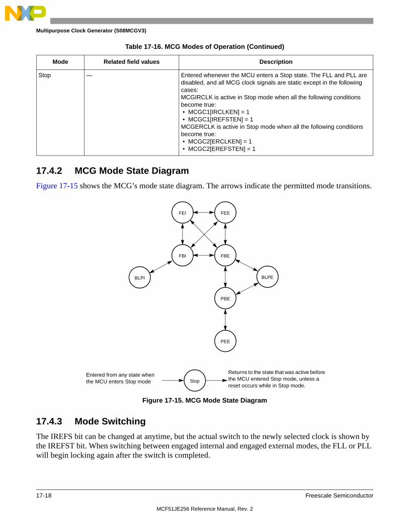
Multipurpose Clock Generator (S08MCGV3)
17-18 Freescale Semiconductor
17.4.2 MCG Mode State Diagram
Figure 17-15 shows the MCG’s mode state diagram. The arrows indicate the permitted mode transitions.
Figure 17-15. MCG Mode State Diagram
17.4.3 Mode Switching
The IREFS bit can be changed at anytime, but the actual switch to the newly selected clock is shown by the IREFST bit. When switching between engaged internal and engaged external modes, the FLL or PLL will begin locking again after the switch is completed.
Stop — Entered whenever the MCU enters a Stop state. The FLL and PLL are disabled, and all MCG clock signals are static except in the following cases:MCGIRCLK is active in Stop mode when all the following conditions become true: • MCGC1[IRCLKEN] = 1 • MCGC1[IREFSTEN] = 1MCGERCLK is active in Stop mode when all the following conditions become true: • MCGC2[ERCLKEN] = 1 • MCGC2[EREFSTEN] = 1
Table 17-16. MCG Modes of Operation (Continued)
Mode Related field values Description
Entered from any state when the MCU enters Stop mode
Returns to the state that was active before the MCU entered Stop mode, unless a reset occurs while in Stop mode.
FEI FEE
FBEFBI
PBE
PEE
BLPI BLPE
Stop
MCF51JE256 Reference Manual, Rev. 2

Multipurpose Clock Generator (S08MCGV3)
Freescale Semiconductor 17-19
The CLKS bits can also be changed at anytime, but the actual switch to the newly selected clock is shown by the CLKST bits. If the newly selected clock is not available, the previous clock will remain selected.
The DRS bits can be changed at anytime except when LP bit is 1. If the DRS bits are changed while in FLL engaged internal (FEI) or FLL engaged external (FEE), the bus clock remains at the previous DCO range until the new DCO starts. When the new DCO starts the bus clock switches to it. After switching to the new DCO the FLL remains unlocked for several reference cycles. Once the selected DCO startup time is over, the FLL is locked. The completion of the switch is shown by the DRST bits.
For details see Figure 17-15.
17.4.4 Bus Frequency Divider
The BDIV bits can be changed at anytime and the actual switch to the new frequency will occur immediately.
17.4.5 Low Power Bit Usage
The low power bit (LP) is provided to allow the FLL or PLL to be disabled and thus conserve power when these systems are not being used. The DRS bit can not be written while LP bit is 1.However, in some applications it may be desirable to enable the FLL or PLL and allow it to lock for maximum accuracy before switching to an engaged mode. Do this by writing the LP bit to 0.
17.4.6 Internal Reference Clock
When IRCLKEN is set the internal reference clock signal will be presented as MCGIRCLK, which can be used as an additional clock source. The MCGIRCLK frequency can be re-targeted by trimming the period of the internal reference clock. This can be done by writing a new value to the TRIM bits in the MCGTRM register. Writing a larger value will decrease the MCGIRCLK frequency, and writing a smaller value to the MCGTRM register will increase the MCGIRCLK frequency. The TRIM bits will effect the MCGOUT frequency if the MCG is in FLL engaged internal (FEI), FLL bypassed internal (FBI), or bypassed low power internal (BLPI) mode. The TRIM and FTRIM value is initialized by POR but is not affected by other resets.
Until MCGIRCLK is trimmed, programming low reference divider (RDIV) factors may result in MCGOUT frequencies that exceed the maximum chip-level frequency and violate the chip-level clock timing specifications (see the Device Overview chapter).
If IREFSTEN and IRCLKEN bits are both set, the internal reference clock will keep running during stop mode in order to provide a fast recovery upon exiting stop.
17.4.7 External Reference Clock
The MCG module can support an external reference clock with frequencies between 31.25 kHz to 40 MHz in all modes. When ERCLKEN is set, the external reference clock signal will be presented as MCGERCLK, which can be used as an additional clock source. When IREFS = 1, the external reference clock will not be used by the FLL or PLL and will only be used as MCGERCLK. In these modes, the
MCF51JE256 Reference Manual, Rev. 2

Multipurpose Clock Generator (S08MCGV3)
17-20 Freescale Semiconductor
frequency can be equal to the maximum frequency the chip-level timing specifications will support (see the Device Overview chapter).
If EREFSTEN and ERCLKEN bits are both set or the MCG is in FEE, FBE, PEE, PBE or BLPE mode, the external reference clock will keep running during stop mode in order to provide a fast recovery upon exiting stop.
If CME bit is written to 1, the clock monitor is enabled. If the external reference falls below a certain frequency (floc_high or floc_low depending on the RANGE bit in the MCGC2), the MCU will reset. The LOC bit in the System Reset Status (SRS) register will be set to indicate the error.
17.4.8 Fixed Frequency Clock
The MCG presents the divided reference clock as MCGFFCLK for use as an additional clock source. The MCGFFCLK frequency must be no more than 1/4 of the MCGOUT frequency to be valid.
17.4.9 MCGPLLSCLK Operation
This clock is intended for use in systems which include a USB interface. It allows the MCG to supply a 48MHz clock to the USB. This same clock can be used to derive MCGOUT. Alternately, MCGOUT can be derived from either internal or external reference clock. This allows the CPU to run at a lower frequency (to conserve power) while the USB continues to monitor traffic.
Note that the FLL can not be used for generation of the system clocks while the PLL is supplying MCGPLLSCLK.
MCF51JE256 Reference Manual, Rev. 2

Multipurpose Clock Generator (S08MCGV3)
Freescale Semiconductor 17-21
17.5 Initialization / Application InformationThis section describes how to initialize and configure the MCG module in application. The following sections include examples on how to initialize the MCG and properly switch between the various available modes.
17.5.1 MCG Module Initialization Sequence
The MCG comes out of reset configured for FEI mode with the BDIV set for divide-by-2. The internal reference will stabilize in tirefst microseconds before the FLL can acquire lock. As soon as the internal reference is stable, the FLL will acquire lock in tfll_acquire milliseconds.
NOTEIf the internal reference is not already trimmed, the BDIV value should not be changed to divide-by-1 without first trimming the internal reference. Failure to do so could result in the MCU running out of specification.
17.5.1.1 Initializing the MCG
Because the MCG comes out of reset in FEI mode, the only MCG modes which can be directly switched to upon reset are FEE, FBE, and FBI modes (see Figure 17-15). Reaching any of the other modes requires first configuring the MCG for one of these three initial modes. Care must be taken to check relevant status bits in the MCGSC register reflecting all configuration changes within each mode.
To change from FEI mode to FEE or FBE modes, follow this procedure:
1. Enable the external clock source by setting the appropriate bits in MCGC2.
2. If the RANGE bit (bit 5) in MCGC2 is set, set DIV32 in MCGC3 to allow access to the proper RDIV values.
3. Write to MCGC1 to select the clock mode.
— If entering FEE mode, set RDIV appropriately, clear the IREFS bit to switch to the external reference, and leave the CLKS bits at %00 so that the output of the FLL is selected as the system clock source.
— If entering FBE, clear the IREFS bit to switch to the external reference and change the CLKS bits to %10 so that the external reference clock is selected as the system clock source. The RDIV bits should also be set appropriately here according to the external reference frequency because although the FLL is bypassed, it is still on in FBE mode.
— The internal reference can optionally be kept running by setting the IRCLKEN bit. This is useful if the application will switch back and forth between internal and external modes. For minimum power consumption, leave the internal reference disabled while in an external clock mode.
4. Once the proper configuration bits have been set, wait for the affected bits in the MCGSC register to be changed appropriately, reflecting that the MCG has moved into the proper mode.
— If ERCLKEN was set in step 1 or the MCG is in FEE, FBE, PEE, PBE, or BLPE mode, and EREFS was also set in step 1, wait here for the OSCINIT bit to become set indicating that the
MCF51JE256 Reference Manual, Rev. 2

Multipurpose Clock Generator (S08MCGV3)
17-22 Freescale Semiconductor
external clock source has finished its initialization cycles and stabilized. Typical crystal startup times are given in Appendix A, “Electrical Characteristics”.
— If in FEE mode, check to make sure the IREFST bit is cleared and the LOCK bit is set before moving on.
— If in FBE mode, check to make sure the IREFST bit is cleared, the LOCK bit is set, and the CLKST bits have changed to %10 indicating the external reference clock has been appropriately selected. Although the FLL is bypassed in FBE mode, it is still on and will lock in FBE mode.
5. Write to the MCGC4 register to determine the DCO output (MCGOUT) frequency range. Make sure that the resulting bus clock frequency does not exceed the maximum specified bus clock frequency of the device.
— By default, with DMX32 cleared to 0, the FLL multiplier for the DCO output is 512. For greater flexibility, if a mid-range FLL multiplier of 1024 is desired instead, set the DRS[1:0] bits to %01 for a DCO output frequency of 33.55 MHz. If a high-range FLL multiplier of 1536 is desired instead, set the DRS[1:0] bits to %10 for a DCO output frequency of 50.33 MHz.
— When using a 32.768 kHz external reference, if the maximum low-range DCO frequency that can be achieved with a 32.768 kHz reference is desired, set the DRS[1:0] bits to %00 and set the DMX32 bit to 1. The resulting DCO output (MCGOUT) frequency with the new multiplier of 608 will be 19.92 MHz.
— When using a 32.768 kHz external reference, if the maximum mid-range DCO frequency that can be achieved with a 32.768 kHz reference is desired, set the DRS[1:0] bits to %01 and set the DMX32 bit to 1. The resulting DCO output (MCGOUT) frequency with the new multiplier of 1216 will be 39.85 MHz.
— When using a 32.768 kHz external reference, if the maximum high-range DCO frequency that can be achieved with a 32.768 kHz reference is desired, set the DRS[1:0] bits to %10 and set the DMX32 bit to 1. The resulting DCO output (MCGOUT) frequency with the new multiplier of 1824 will be 59.77 MHz.
6. Wait for the LOCK bit in MCGSC to become set, indicating that the FLL has locked to the new multiplier value designated by the DRS and DMX32 bits.
NOTESetting DIV32 (bit 4) in MCGC3 is strongly recommended for FLL external modes when using a high frequency range (RANGE = 1) external reference clock. The DIV32 bit is ignored in all other modes.
To change from FEI clock mode to FBI clock mode, follow this procedure:
1. Change the CLKS bits in MCGC1 to %01 so that the internal reference clock is selected as the system clock source.
2. Wait for the CLKST bits in the MCGSC register to change to %01, indicating that the internal reference clock has been appropriately selected.
MCF51JE256 Reference Manual, Rev. 2

Multipurpose Clock Generator (S08MCGV3)
Freescale Semiconductor 17-23
17.5.2 Using a 32.768 kHz Reference
In FEE and FBE modes, if using a 32.768 kHz external reference, at the default FLL multiplication factor of 512, the DCO output (MCGOUT) frequency is 16.78 MHz at high-range. If the DRS[1:0] bits are set to %01, the multiplication factor is doubled to 1024, and the resulting DCO output frequency is 33.55 Mhz at mid-range. If the DRS[1:0] bits are set to %10, the multiplication factor is set to 1536, and the resulting DCO output frequency is 50.33 Mhz at high-range. Make sure that the resulting bus clock frequency does not exceed the maximum specified bus clock frequency of the device.
Setting the DMX32 bit in MCGC4 to 1 increases the FLL multiplication factor to allow the 32.768 kHz reference to achieve its maximum DCO output frequency. When the DRS[1:0] bits are set to %00, the 32.768 kHz reference can achieve a high-range maximum DCO output of 19.92 MHz with a multiplier of 608. When the DRS[1:0] bits are set to %01, the 32.768 kHz reference can achieve a mid-range maximum DCO output of 39.85 MHz with a multiplier of 1216. When the DRS[1:0] bits are set to %10, the 32.768 kHz reference can achieve a high-range maximum DCO output of 59.77 MHz with a multiplier of 1824. Make sure that the resulting bus clock frequency does not exceed the maximum specified bus clock frequency of the device.
In FBI and FEI modes, setting the DMX32 bit is not recommended. If the internal reference is trimmed to a frequency above 32.768 kHz, the greater FLL multiplication factor could potentially push the microcontroller system clock out of specification and damage the part.
17.5.3 MCG Mode Switching
When switching between operational modes of the MCG, certain configuration bits must be changed in order to properly move from one mode to another. Each time any of these bits are changed (PLLS, IREFS, CLKS, or EREFS), the corresponding bits in the MCGSC register (PLLST, IREFST, CLKST, or OSCINIT) must be checked before moving on in the application software.
Additionally, care must be taken to ensure that the reference clock divider (RDIV) is set properly for the mode being switched to. For instance, in PEE mode, if using a 4 MHz crystal, RDIV must be set to %001 (divide-by-2) or %010 (divide -by-4) in order to divide the external reference down to the required frequency between 1 and 2 MHz.
If switching to FBE or FEE mode, first setting the DIV32 bit will ensure a proper reference frequency is sent to the FLL clock at all times.
In FBE, FEE, FBI, and FEI modes, at any time, the application can switch the FLL multiplication factor between 512, 1024, and 1536 with the DRS[1:0] bits in MCGC4. Writes to the DRS[1:0] bits will be ignored if LP=1 or PLLS=1.
The RDIV and IREFS bits should always be set properly before changing the PLLS bit so that the FLL or PLL clock has an appropriate reference clock frequency to switch to. The table below shows MCGOUT
MCF51JE256 Reference Manual, Rev. 2

Multipurpose Clock Generator (S08MCGV3)
17-24 Freescale Semiconductor
frequency calculations using RDIV, BDIV, and VDIV settings for each clock mode. The bus frequency is equal to MCGOUT divided by 2.
1R is the reference divider selected by the RDIV bits, B is the bus frequency divider selected by the BDIV bits, F is the FLL factor selected by the DRS[1:0] and DMX32 bits, and M is the multiplier selected by the VDIV bits.
This section will include 3 mode switching examples using an 8 MHz external crystal. If using an external clock source less than 1 MHz, the MCG should not be configured for any of the PLL modes (PEE and PBE).
17.5.3.1 Example 1: Moving from FEI to PEE Mode: External Crystal = 8 MHz, Bus Frequency = 16 MHz
In this example, the MCG will move through the proper operational modes from FEI to PEE mode until the 8 MHz crystal reference frequency is set to achieve a bus frequency of 16 MHz. Because the MCG is in FEI mode out of reset, this example also shows how to initialize the MCG for PEE mode out of reset. First, the code sequence will be described. Then a flowchart will be included which illustrates the sequence.
1. First, FEI must transition to FBE mode:
a) MCGC2 = 0x36 (%00110110)
– BDIV (bits 7 and 6) set to %00, or divide-by-1
– RANGE (bit 5) set to 1 because the frequency of 8 MHz is within the high frequency range
– HGO (bit 4) set to 1 to configure the crystal oscillator for high gain operation
– EREFS (bit 2) set to 1, because a crystal is being used
– ERCLKEN (bit 1) set to 1 to ensure the external reference clock is active
Table 17-17. MCGOUT Frequency Calculation Options
Clock Mode fMCGOUT1 Note
FEI (FLL engaged internal) (fint * F ) / B Typical fMCGOUT = 16 MHz immediately after reset.
FEE (FLL engaged external) (fext / R *F) / B fext / R must be in the range of 31.25 kHz to 39.0625 kHz
FBE (FLL bypassed external) fext / B fext / R must be in the range of 31.25 kHz to 39.0625 kHz
FBI (FLL bypassed internal) fint / B Typical fint = 32 kHz
PEE (PLL engaged external) [(fext / R) * M] / B fext / R must be in the range of 1 MHz to 2 MHz
PBE (PLL bypassed external) fext / B fext / R must be in the range of 1 MHz to 2 MHz
BLPI (Bypassed low power internal) fint / B
BLPE (Bypassed low power external) fext / B
MCF51JE256 Reference Manual, Rev. 2
Multipurpose Clock Generator (S08MCGV3)
Freescale Semiconductor 17-25
b) Loop until OSCINIT (bit 1) in MCGSC is 1, indicating the crystal selected by the EREFS bit has been initialized.
c) Because RANGE = 1, set DIV32 (bit 4) in MCGC3 to allow access to the proper RDIV bits while in an FLL external mode.
d) MCGC1 = 0x98 (%10011000)
– CLKS (bits 7 and 6) set to %10 in order to select external reference clock as system clock source
– RDIV (bits 5-3) set to %011, or divide-by-256 because 8MHz / 256 = 31.25 kHz which is in the 31.25 kHz to 39.0625 kHz range required by the FLL
– IREFS (bit 2) cleared to 0, selecting the external reference clock
e) Loop until IREFST (bit 4) in MCGSC is 0, indicating the external reference is the current source for the reference clock
f) Loop until CLKST (bits 3 and 2) in MCGSC is %10, indicating that the external reference clock is selected to feed MCGOUT
2. Then, FBE must transition either directly to PBE mode or first through BLPE mode and then to PBE mode:
a) BLPE: If a transition through BLPE mode is desired, first set LP (bit 3) in MCGC2 to 1.
b) BLPE/PBE: MCGC3 = 0x58 (%01011000)
– PLLS (bit 6) set to 1, selects the PLL. At this time, with an RDIV value of %011, the FLL reference divider of 256 is switched to the PLL reference divider of 8 (see Table 17-8), resulting in a reference frequency of 8 MHz/ 8 = 1 MHz. In BLPE mode,changing the PLLS bit only prepares the MCG for PLL usage in PBE mode
– DIV32 (bit 4) still set at 1. Because the MCG is in a PLL mode, the DIV32 bit is ignored. Keeping it set at 1 makes transitions back into an FLL external mode easier.
– VDIV (bits 3-0) set to %1000, or multiply-by-32 because 1 MHz reference * 32= 32MHz. In BLPE mode, the configuration of the VDIV bits does not matter because the PLL is disabled. Changing them only sets up the multiply value for PLL usage in PBE mode
c) BLPE: If transitioning through BLPE mode, clear LP (bit 3) in MCGC2 to 0 here to switch to PBE mode
d) PBE: Loop until PLLST (bit 5) in MCGSC is set, indicating that the current source for the PLLS clock is the PLL
e) PBE: Then loop until LOCK (bit 6) in MCGSC is set, indicating that the PLL has acquired lock
3. Lastly, PBE mode transitions into PEE mode:
a) MCGC1 = 0x18 (%00011000)
– CLKS (bits7 and 6) in MCGSC1 set to %00 in order to select the output of the PLL as the system clock source
MCF51JE256 Reference Manual, Rev. 2

Multipurpose Clock Generator (S08MCGV3)
17-26 Freescale Semiconductor
b) Loop until CLKST (bits 3 and 2) in MCGSC are %11, indicating that the PLL output is selected to feed MCGOUT in the current clock mode
– Now, With an RDIV of divide-by-8, a BDIV of divide-by-1, and a VDIV of multiply-by-32, MCGOUT = [(8 MHz / 8) * 32] / 1 = 32 MHz, and the bus frequency is MCGOUT / 2, or 16 MHz
MCF51JE256 Reference Manual, Rev. 2

Multipurpose Clock Generator (S08MCGV3)
Freescale Semiconductor 17-27
Figure 17-16. Flowchart of FEI to PEE Mode Transition using an 8 MHz crystal
MCGC2 = $36
CHECK
OSCINIT = 1 ?
CHECK
IREFST = 0?
CHECKCLKST = %10?
ENTERBLPE MODE ?
MCGC2 = $3E(LP = 1)
MCGC3 = $58
INBLPE MODE ?
(LP=1)
MCGC2 = $36(LP = 0)
CHECKPLLST = 1?
MCGC1 = $18
CHECKLOCK = 1?
CHECKCLKST = %11?
CONTINUE
IN PEE MODE
START
IN FEI MODE
YES
YES
YES
YES
YES
YES
YES
YES
NO
NO
NO
NO
NO
NO
NO
NO
MCGC1 = $98
MCGC3 = $11(DIV32 = 1)
MCF51JE256 Reference Manual, Rev. 2

Multipurpose Clock Generator (S08MCGV3)
17-28 Freescale Semiconductor
17.5.3.2 Example 2: Moving from PEE to BLPI Mode: Bus Frequency =16 kHz
In this example, the MCG will move through the proper operational modes from PEE mode with an 8MHz crystal configured for an 16 MHz bus frequency (see previous example) to BLPI mode with a 16 kHz bus frequency.First, the code sequence will be described. Then a flowchart will be included which illustrates the sequence.
1. First, PEE must transition to PBE mode:
a) MCGC1 = 0x98 (%10011000)
– CLKS (bits 7 and 6) set to %10 in order to switch the system clock source to the external reference clock
b) Loop until CLKST (bits 3 and 2) in MCGSC are %10, indicating that the external reference clock is selected to feed MCGOUT
2. Then, PBE must transition either directly to FBE mode or first through BLPE mode and then to FBE mode:
a) BLPE: If a transition through BLPE mode is desired, first set LP (bit 3) in MCGC2 to 1
b) BLPE/FBE: MCGC3 = 0x18(%00011000)
– PLLS (bit 6) clear to 0 to select the FLL. At this time, with an RDIV value of %011, the PLL reference divider of 8 is switched to an FLL divider of 256 (see Table 17-7), resulting in a reference frequency of 8 MHz / 256 = 31.25 kHz. If RDIV was not previously set to %011 (necessary to achieve required 31.25-39.06 kHz FLL reference frequency with an 8 MHz external source frequency), it must be changed prior to clearing the PLLS bit. In BLPE mode,changing this bit only prepares the MCG for FLL usage in FBE mode. With PLLS = 0, the VDIV value does not matter.
– DIV32 (bit 4) set to 1 (if previously cleared), automatically switches RDIV bits to the proper reference divider for the FLL clock (divide-by-256)
c) BLPE: If transitioning through BLPE mode, clear LP (bit 3) in MCGC2 to 0 here to switch to FBE mode
d) FBE: Loop until PLLST (bit 5) in MCGSC is clear, indicating that the current source for the PLLS clock is the FLL
e) FBE: Optionally, loop until LOCK (bit 6) in the MCGSC is set, indicating that the FLL has acquired lock. Although the FLL is bypassed in FBE mode, it is still enabled and running.
3. Next, FBE mode transitions into FBI mode:
a) MCGC1 = 0x5C (%01011100)
– CLKS (bits7 and 6) in MCGSC1 set to %01 in order to switch the system clock to the internal reference clock
MCF51JE256 Reference Manual, Rev. 2

Multipurpose Clock Generator (S08MCGV3)
Freescale Semiconductor 17-29
– IREFS (bit 2) set to 1 to select the internal reference clock as the reference clock source
– RDIV (bits 5-3) remain unchanged because the reference divider does not affect the internal reference.
b) Loop until IREFST (bit 4) in MCGSC is 1, indicating the internal reference clock has been selected as the reference clock source
c) Loop until CLKST (bits 3 and 2) in MCGSC are %01, indicating that the internal reference clock is selected to feed MCGOUT
4. Lastly, FBI transitions into BLPI mode.
a) MCGC2 = 0x08 (%00001000)
– LP (bit 3) in MCGSC is 1
– RANGE, HGO, EREFS, ERCLKEN, and EREFSTEN bits are ignored when the IREFS bit (bit2) in MCGC is set. They can remain set, or be cleared at this point.
MCF51JE256 Reference Manual, Rev. 2

Multipurpose Clock Generator (S08MCGV3)
17-30 Freescale Semiconductor
Figure 17-17. Flowchart of PEE to BLPI Mode Transition using an 8 MHz crystal
MCGC1 = $98
CHECK
CLKST = %10 ?
MCGC2 = $3E
MCGC1 = $5C
CHECKIREFST = 0?
CHECKCLKST = %01?
CONTINUE
IN BLPI MODE
START
IN PEE MODE
MCGC3 = $18
ENTER
BLPE MODE ?
INBLPE MODE ?
(LP=1)
MCGC2 = $36(LP = 0)
CHECKPLLST = 0?
OPTIONAL:
= 1?
MCGC2 = $08
YES
YES
YES
YES
YES
YES
YES
NO
NO
NO
NO
NO
NO
NO
CHECK LOCK
(LP = 1)
MCF51JE256 Reference Manual, Rev. 2

Multipurpose Clock Generator (S08MCGV3)
Freescale Semiconductor 17-31
17.5.3.3 Example 3: Moving from BLPI to FEE Mode: External Crystal = 8 MHz, Bus Frequency = 16 MHz
In this example, the MCG will move through the proper operational modes from BLPI mode at a 16 kHz bus frequency running off of the internal reference clock (see previous example) to FEE mode using an 8MHz crystal configured for a 16 MHz bus frequency. First, the code sequence will be described. Then a flowchart will be included which illustrates the sequence.
1. First, BLPI must transition to FBI mode.
a) MCGC2 = 0x00 (%00000000)
– LP (bit 3) in MCGSC is 0
b) Optionally, loop until LOCK (bit 6) in the MCGSC is set, indicating that the FLL has acquired lock. Although the FLL is bypassed in FBI mode, it is still enabled and running.
2. Next, FBI will transition to FEE mode.
a) MCGC2 = 0x36 (%00110110)
– RANGE (bit 5) set to 1 because the frequency of 8 MHz is within the high frequency range
– HGO (bit 4) set to 1 to configure the crystal oscillator for high gain operation
– EREFS (bit 2) set to 1, because a crystal is being used
– ERCLKEN (bit 1) set to 1 to ensure the external reference clock is active
b) Loop until OSCINIT (bit 1) in MCGSC is 1, indicating the crystal selected by the EREFS bit has been initialized.
c) MCGC1 = 0x18 (%00011000)
– CLKS (bits 7 and 6) set to %00 in order to select the output of the FLL as system clock source
– RDIV (bits 5-3) remain at %011, or divide-by-256 for a reference of 8 MHz / 256 = 31.25 kHz.
– IREFS (bit 1) cleared to 0, selecting the external reference clock
d) Loop until IREFST (bit 4) in MCGSC is 0, indicating the external reference clock is the current source for the reference clock
e) Optionally, loop until LOCK (bit 6) in the MCGSC is set, indicating that the FLL has reacquired lock.
f) Loop until CLKST (bits 3 and 2) in MCGSC are %00, indicating that the output of the FLL is selected to feed MCGOUT
g) Now, with a 31.25 kHz reference frequency, a fixed DCO multiplier of 512, and a bus divider of 1, MCGOUT = 31.25 kHz * 512 / 1 = 16 MHz. Therefore, the bus frequency is 8 MHz.
h) At this point, by default, the DRS[1:0] bits in MCGC4 are set to %00 and DMX32 in MCGC4 is cleared to 0. If a bus frequency of 16MHz is desired instead, set the DRS[1:0] bits to $01 to switch the FLL multiplication factor from 512 to 1024 and loop until LOCK (bit 6) in MCGSC is set, indicating that the FLL has reacquired LOCK. To return the bus frequency to 8 MHz, set the DRS[1:0] bits to %00 again, and the FLL multiplication factor will switch back to 512. Then loop again until the LOCK bit is set.
MCF51JE256 Reference Manual, Rev. 2

Multipurpose Clock Generator (S08MCGV3)
17-32 Freescale Semiconductor
Figure 17-18. Flowchart of BLPI to FEE Mode Transition using an 8 MHz crystal
17.5.4 Calibrating the Internal Reference Clock (IRC)
The IRC is calibrated by writing to the MCGTRM register first, then using the FTRIM bit to “fine tune” the frequency. We will refer to this total 9-bit value as the trim value, ranging from 0x000 to 0x1FF, where the FTRIM bit is the LSB.
The trim value after reset is the factory trim value unless the device resets into any BDM mode in which case it is 0x800. Writing a larger value will decrease the frequency and smaller values will increase the frequency. The trim value is linear with the period, except that slight variations in wafer fab processing produce slight non-linearities between trim value and period. These non-linearities are why an iterative
MCGC2 = $36
CHECK
OSCINIT = 1 ?
MCGC1 = $18
CHECK
IREFST = 0?
CHECKCLKST = %00?
CONTINUE
IN FEE MODE
START
IN BLPI MODE
YES
YES
NO
NO
NO
MCGC2 = $00
OPTIONAL:CHECK LOCK
= 1?
YES
NO
YES
OPTIONAL:CHECK LOCK
= 1?
YES
NO
MCF51JE256 Reference Manual, Rev. 2

Multipurpose Clock Generator (S08MCGV3)
Freescale Semiconductor 17-33
trimming approach to search for the best trim value is recommended. In Example 4: Internal Reference Clock Trim later in this section, this approach will be demonstrated.
If a user specified trim value has been found for a device (to replace the factory trim value), this value can be stored in FLASH memory to save the value. If power is removed from the device, the IRC can easily be re-trimmed to the user specified value by copying the saved value from FLASH to the MCG registers. Freescale identifies recommended FLASH locations for storing the trim value for each MCU. Consult the memory map in the data sheet for these locations.
17.5.4.1 Example 4: Internal Reference Clock Trim
For applications that require a user specified tight frequency tolerance, a trimming procedure is provided that will allow a very accurate internal clock source. This section outlines one example of trimming the internal oscillator. Many other possible trimming procedures are valid and can be used.
In the example below, the MCG trim will be calibrated for the 9-bit MCGTRM and FTRIM collective value. This value will be referred to as TRMVAL.
MCF51JE256 Reference Manual, Rev. 2

Multipurpose Clock Generator (S08MCGV3)
17-34 Freescale Semiconductor
Figure 17-19. Trim Procedure
In this particular case, the MCU has been attached to a PCB and the entire assembly is undergoing final test with automated test equipment. A separate signal or message is provided to the MCU operating under user provided software control. The MCU initiates a trim procedure as outlined in Figure 17-19 while the tester supplies a precision reference signal.
If the intended bus frequency is near the maximum allowed for the device, it is recommended to trim using a reference divider value (RDIV setting) of twice the final value. After the trim procedure is complete, the reference divider can be restored. This will prevent accidental overshoot of the maximum clock frequency.
Initial conditions:1) Clock supplied from ATE has 500 sec duty period2) MCG configured for internal reference with 8MHz bus
START TRIM PROCEDURE
CONTINUE
CASE STATEMENT
COUNT > EXPECTED = 500
.
MEASUREINCOMING CLOCK WIDTH
TRMVAL = $100
COUNT < EXPECTED = 500
COUNT = EXPECTED = 500
TRMVAL =
TRMVAL =
TRMVAL - 256/ (2**n) TRMVAL + 256/ (2**n)
n = n + 1
(COUNT = # OF BUS CLOCKS / 8)
(DECREASING TRMVAL INCREASES THE FREQUENCY)
(INCREASING TRMVAL DECREASES THE FREQUENCY)
NO
YESIS n > 9?
(RUNNING TOO SLOW)
(RUNNING TOO FAST)
n=1
STORE MCGTRM ANDFTRIM VALUES IN
NON-VOLATILE MEMORY
MCF51JE256 Reference Manual, Rev. 2

Freescale Semiconductor 18-1
Chapter 18 Mini-FlexBus
18.1 IntroductionThis chapter describes external bus data transfer operations and error conditions. It describes transfers initiated by the ColdFire processor (or any other bus master) and includes detailed timing diagrams showing the interaction of signals in supported bus operations.
The Mini-FlexBus is a subset of the FlexBus module found on other ColdFire microprocessors. The Mini-FlexBus minimizes package pin-outs while maintaining a high level of configurability and functionality.
NOTE
• In this chapter, unless otherwise noted, clock refers to the FB_CLK used for the external bus (fsys).
18.1.1 Overview
A multi-function external bus interface called the Mini-FlexBus interface controller is provided on the device with basic functionality of interfacing to slave-only devices. It can be directly connected to the following asynchronous or synchronous devices with little or no additional circuitry:
• External ROMs
• Flash memories
• Programmable logic devices
• Other simple target (slave) devices
For asynchronous devices, a simple chip-select based interface can be used.
The Mini-FlexBus interface has up to two general purpose chip-selects, FB_CS[1:0]. The actual number of chip selects available depends upon the device and its pin configuration.
18.1.2 Features
Key Mini-FlexBus features include:
• Two independent, user-programmable chip-select signals (FB_CS[1:0]) that can interface with external SRAM, PROM, EPROM, EEPROM, flash, and other peripherals
• 8- and 16-bit port sizes with configuration for multiplexed or non-multiplexed address and data buses
• Byte-, word-, longword-, and 16-byte line-sized transfers
MCF51JE256 Reference Manual, Rev. 2

Mini-FlexBus
18-2 Freescale Semiconductor
• Programmable address-setup time with respect to the assertion of chip select
• Programmable address-hold time with respect to the negation of chip select and transfer direction
18.1.3 Modes of Operation
The external interface is a configurable multiplexed bus set to one of the following modes:
18.1.4 Module Configuration
A subset of the Mini-FlexBus signals can be repositioned under software control using SOPT3[MB_DATA] as shown in Table 18-1. This functionality allows the 81-pin MAPBGA and 80-pin LQFP devices a minimal functionality data bus to interface with slave devices. SOPT3[MB_DATA] selects which general-purpose I/O ports are associated with Mini-FlexBus operation.
18.1.5 Mini-FlexBus Security Level
SOPT1[MBSL] controls the Mini-FlexBus security level. This bit has no effect if security is not enabled. If security is enabled and MBSL is set, off-chip opcode accesses via the Mini-FlexBus are disallowed, while data accesses are allowed.
18.1.6 Mini-FlexBus Clock Gating
The bus clock to the Mini-FlexBus can be gated on and off using SCGC2[MFB]. This bit is set after any reset, which enables the bus clock to this module. When this module is not in use, clear the MFB bit t o disable the clock and conserve power. See Section 5.6, “Peripheral Clock Gating,” for details.
• Up to a 20-bit address (non-multiplexed) with 8-bit data
• Up to a 20-bit address (multiplexed) with 16-bit data (write masking of upper/lower bytes not supported)
• Up to a 20-bit address (multiplexed) with 8-bit data
Table 18-1. Mini-FlexBus Position Options
SOPT3[MB_DATA] FB_D0 FB_D2 FB_D3 FB_D4 FB_D5 FB_D6 FB_D7 FB_R/W FB_OE
0 (default) PTH1 PTH7 PTH6 PTH5 PTH4 PTH3 PTH2 PTG5 PTH0
1 PTC1 PTA0 PTF5 PTF4 PTF3 PTA3 PTE5 PTE6 PTC0
MCF51JE256 Reference Manual, Rev. 2

Mini-FlexBus
Freescale Semiconductor 18-3
18.2 External SignalsThis section describes the external signals involved in data-transfer operations.
18.2.1 Address and Data Buses (FB_An, FB_Dn, FB_ADn)
In non-multiplexed mode, the FB_An and FB_Dn buses carry the address and data, respectively.
In multiplexed mode, the FB_ADn bus carries the address and data. The full -bit address is driven on the first clock of a bus cycle (address phase). Following the first clock, the data is driven on the bus (data phase). During the data phase, the address continues driving on the pins not used for data. For example, in 16-bit mode the address continues driving on FB_AD[ : ] and in 8-bit mode the address continues driving on FB_AD[ : ].
18.2.2 Chip Selects (FB_CS[1:0])
The chip-select signal indicates which device is selected. A particular chip-select asserts when the transfer address is within the device’s address space, as defined in the base- and mask-address registers. The actual number of chip selects available depends upon the pin configuration.
18.2.3 Output Enable (FB_OE)
The output enable signal (FB_OE) is sent to the interfacing memory and/or peripheral to enable a read transfer. FB_OE is only asserted during read accesses when a chip select matches the current address decode.
18.2.4 Read/Write (FB_R/W)
The processor drives the FB_R/W signal to indicate the current bus operation direction. It is driven high during read bus cycles and low during write bus cycles.
Table 18-2. Mini-FlexBus Signal Summary
Signal Name I/O Description
FB_A[19:0] I/O In a non-multiplexed configuration: Address bus.
In a multiplexed configuration: Address/data bus, FB_AD[19:0].
FB_D[7:0] I/O In a non-multiplexed configuration: Data bus.In a multiplexed configuration: Not used.
FB_CS[1:0] O General purpose chip-selects. In multiplexed mode, only FB_CS0 is available. FB_CS1 is multiplexed with FB_ALE on a configurable package pin.
FB_OE O Output enable
FB_R/W O Read/write. 1 = Read, 0 = Write
FB_ALE O Address latch enable. This signal is multiplexed with FB_CS1 on a configurable package pin.
20
19 1619 8
MCF51JE256 Reference Manual, Rev. 2

Mini-FlexBus
18-4 Freescale Semiconductor
18.2.5 Address Latch Enable (FB_ALE)
The assertion of FB_ALE indicates that the device has begun a bus transaction and the address and attributes are valid. FB_ALE is asserted for one bus clock cycle. FB_ALE may be used externally to capture the bus transfer address (Figure 18-7).
18.3 Memory Map/Register DefinitionThe following tables describe the registers and bit meanings for configuring chip-select operation. Table 18-3 shows the chip-select register memory map.
The actual number of chip select registers available depends upon the device and its pin configuration. If the device does not support certain chip select signals or the pin is not configured for a chip-select function, then that corresponding set of chip-select registers has no effect on an external pin.
NOTE
You must set CSMR0[V] before the chip select registers take effect.
18.3.1 Chip-Select Address Registers (CSAR0 – CSAR1)
The CSARn registers specify the chip-select base addresses.
NOTEThe only applicable address range for which the chip-selects can be active are 0x(00)40_0000 – 0x(00)7F_FFFF. Set the CSARn and CSMRn registers appropriately before accessing this region.
Table 18-3. Mini-FlexBus Chip Select Memory Map
Offset RegisterWidth(bits)
Access Reset ValueSection/
Page
0x000x0C
Chip-Select Address Register (CSARn)n = 0 – 1
32 R/W 0x0000_0000 18.3.1/18-4
0x040x10
Chip-Select Mask Register (CSMRn)n = 0 – 1
32 R/W 0x0000_0000 18.3.2/18-5
0x080x14
Chip-Select Control Register (CSCRn)n = 0 – 1
32 R/W See Section 18.3.3/18-6
Address: 0x00 (CSAR0)
0x0C (CSAR1)
Access: User read/write
31 30 29 28 27 26 25 24 23 22 21 20 19 18 17 16 15 14 13 12 11 10 9 8 7 6 5 4 3 2 1 0
RBA
0 0 0 0 0 0 0 0 0 0 0 0 0 0 0 0
W
Reset 0 0 0 0 0 0 0 0 0 0 0 0 0 0 0 0 0 0 0 0 0 0 0 0 0 0 0 0 0 0 0 0
Figure 18-1. Chip-Select Address Registers (CSARn)
MCF51JE256 Reference Manual, Rev. 2

Mini-FlexBus
Freescale Semiconductor 18-5
18.3.2 Chip-Select Mask Registers (CSMR0 – CSMR1)
CSMRn registers specify the address mask and allowable access types for the respective chip-selects.
Table 18-4. CSARn Field Descriptions
Field Description
31–16BA
Base address. Defines the base address for memory dedicated to chip-select FB_CSn. BA is compared to bits 31–16 on the internal address bus to determine if chip-select memory is being accessed.
15–0 Reserved, must be cleared.
Address: 0x04 (CSMR0)
0x10 (CSMR1)
Access: User read/write
31 30 29 28 27 26 25 24 23 22 21 20 19 18 17 16 15 14 13 12 11 10 9 8 7 6 5 4 3 2 1 0
RBAM
0 0 0 0 0 0 0WP
0 0 0 0 0 0 0V
W
Reset 0 0 0 0 0 0 0 0 0 0 0 0 0 0 0 0 0 0 0 0 0 0 0 0 0 0 0 0 0 0 0 0
Figure 18-2. Chip-Select Mask Registers (CSMRn)
Table 18-5. CSMRn Field Descriptions
Field Description
31–16BAM
Base address mask. Defines the chip-select block size by masking address bits. Setting a BAM bit causes the corresponding CSAR bit to be a don’t care in the decode.0 Corresponding address bit is used in chip-select decode.1 Corresponding address bit is a don’t care in chip-select decode.
The block size for FB_CSn is 2n; n = (number of bits set in respective CSMR[BAM]) + 16.For example, if CSAR0 equals 0x0040 and CSMR0[BAM] equals 0x000, FB_CS0 addresses two discontinuous
64 KB memory blocks: one from 0x40_0000 – 0x40_FFFF and one from 0x48_0000 – 0x48_FFFF.Likewise, for FB_CS0 to access 2 MB of address space starting at location 0x40_0000, FB_CS1 must begin at the
next byte after FB_CS0 for a 1 MB address space. Therefore, CSAR0 equals 0x0040, CSMR0[BAM] equals 0x001F, CSAR1 equals 0x0060, and CSMR1[BAM] equals 0x000F.
15–9 Reserved, must be cleared.
8WP
Write protect. Controls write accesses to the address range in the corresponding CSAR. Attempting to write to the range of addresses for which CSARn[WP] is set results in a bus error termination of the internal cycle and no external cycle.0 Read and write accesses are allowed1 Only read accesses are allowed
7–1 Reserved, must be cleared.
0V
Valid bit. Indicates whether the corresponding CSAR, CSMR, and CSCR contents are valid. Programmed chip-selects do not assert until V bit is set. Reset clears each CSMRn[V].Note: At reset, no chip-select can be used until the CSMR0[V] is set. Afterward, FB_CS[1:0] functions as
programmed.
0 Chip-select invalid1 Chip-select valid
MCF51JE256 Reference Manual, Rev. 2

Mini-FlexBus
18-6 Freescale Semiconductor
18.3.3 Chip-Select Control Registers (CSCR0 – CSCR1)
Each CSCRn controls the auto-acknowledge, address setup and hold times, port size, and number of wait states.
Address: 0x08 (CSCR0)
0x14 (CSCR1)
Access: User read/write
31 30 29 28 27 26 25 24 23 22 21 20 19 18 17 16
R 0 0 0 0 0 0 0 0 0 0ASET RDAH WRAH
W
Reset: CSCR0 0 0 0 0 0 0 0 0 0 0 1 1 1 1 1 1
Reset: CSCR1 0 0 0 0 0 0 0 0 0 0 0 0 0 0 0 0
15 14 13 12 11 10 9 8 7 6 5 4 3 2 1 0
RWS MUX AA PS
0 0 0 0 0 0
W
Reset: CSCR0 1 1 1 1 1 1 0 1 0 1 0 0 0 0 0 0
Reset: CSCR1 0 0 0 0 0 0 0 0 0 0 0 0 0 0 0 0
Figure 18-3. Chip-Select Control Registers (CSCRn)
Table 18-6. CSCRn Field Descriptions
Field Description
31–22 Reserved, must be cleared
21–20ASET
Address setup. This field controls the assertion of the chip-select with respect to assertion of a valid address and attributes. The address and attributes are considered valid at the same time FB_ALE asserts.00 Assert FB_CSn on first rising clock edge after address is asserted. (Default FB_CS1)01 Assert FB_CSn on second rising clock edge after address is asserted.10 Assert FB_CSn on third rising clock edge after address is asserted.11 Assert FB_CSn on fourth rising clock edge after address is asserted. (Default FB_CS0)
19–18RDAH
Read address hold or deselect. This field controls the address and attribute hold time after the termination during a read cycle that hits in the chip-select address space.Note: The hold time applies only at the end of a transfer. Therefore, during a transfer to a port size smaller than the
transfer size, the hold time is only added after the last bus cycle.The number of cycles the address and attributes are held after FB_CSn negation depends on the value of CSCRn[AA] as shown below.
RDAH AA = 1
00(FB_CS1 Default)
0 cycles
01 1 cycles
10 2 cycles
11(FB_CS0 Default)
3 cycles
MCF51JE256 Reference Manual, Rev. 2

Mini-FlexBus
Freescale Semiconductor 18-7
18.4 Functional Description
18.4.1 Chip-Select Operation
Each chip-select has a dedicated set of registers for configuration and control:
• Chip-select address registers (CSARn) control the base address space of the chip-select. See Section 18.3.1, “Chip-Select Address Registers (CSAR0 – CSAR1).”
• Chip-select mask registers (CSMRn) provide 16-bit address masking and access control. See Section 18.3.2, “Chip-Select Mask Registers (CSMR0 – CSMR1).”
• Chip-select control registers (CSCRn) provide port size, wait-state generation, address setup and hold times, and automatic acknowledge generation features. See Section 18.3.3, “Chip-Select Control Registers (CSCR0 – CSCR1).”
17–16WRAH
Write address hold or deselect. This field controls the address, data, and attribute hold time after the termination of a write cycle that hits in the chip-select address space.Note: The hold time applies only at the end of a transfer. Therefore, during a transfer to a port size smaller than the
transfer size, the hold time is only added after the last bus cycle.
00 Hold address and attributes one cycle after FB_CSn negates on writes. (Default FB_CS1)01 Hold address and attributes two cycles after FB_CSn negates on writes.10 Hold address and attributes three cycles after FB_CSn negates on writes.11 Hold address and attributes four cycles after FB_CSn negates on writes. (Default FB_CS0)
15–10WS
Wait states. The number of wait states inserted after FB_CSn asserts and before an internal transfer acknowledge is generated (WS = 0 inserts zero wait states, WS = 0x3F inserts 63 wait states).
9MUX
Multiplexed mode. Selects between multiplexed and non-multiplexed address/data bus.0 Non-multiplexed configuration. Address information is driven on FB_ADn and data is read/written on FB_dn.
1 Multiplexed configuration. Address information is driven on FB_ADn, and low-order address lines (FB_AD[7:0] for byte port size or FB_AD[15:0] for word port size) must be latched using the falling edge of FB_ALE as the latch enable. Data is read/written on FB_AD[7:0] for byte port size and FB_AD[15:0] for word port size.
8AA
Auto-acknowledge enable. Determines the assertion of the internal transfer acknowledge for accesses specified by the chip-select address. This bit must be set.0 Reserved1 Internal transfer acknowledge is asserted as specified by WS
Note: This bit must be set, since only internal termination is supported by the Mini-FlexBus.
7–6PS
Port size. Specifies the data port width associated with each chip-select. It determines where data is driven during write cycles and where data is sampled during read cycles.00 Reserved01 8-bit port size. Valid data sampled and driven on FB_D[7:0]1x 16-bit port size. Valid data sampled and driven on FB_AD[15:0]. Only supported in multiplexed mode.
5–0 Reserved, must be cleared.
Table 18-6. CSCRn Field Descriptions (Continued)
Field Description
MCF51JE256 Reference Manual, Rev. 2

Mini-FlexBus
18-8 Freescale Semiconductor
18.4.1.1 General Chip-Select Operation
When a bus cycle is routed to the Mini-FlexBus, the device first compares its address with the base address and mask configurations programmed for chip-selects 0 and 1 (configured in CSCR0 – CSCR1). The results depend on if the address matches or not as shown in Table 18-7.
18.4.1.2 8- and 16-Bit Port Sizing
Static bus sizing is programmable through the port size bits, CSCR[PS]. The processor always drives a 20-bit address on the FB_AD bus regardless of the external device’s address size. The external device must connect its address lines to the appropriate FB_AD bits from FB_AD0 upward. Its data bus must be connected to FB_AD[7:0] in non-multiplexed mode (CSCR[MUX] = 0) or FB_AD0 to FB_ADn in multiplexed mode (CSCR[MUX] = 1) where n = 15 if CSCR[PS] = 1x or n = 7 if CSCR[PS] = 01. No bit ordering is required when connecting address and data lines to the FB_AD bus. For example, a full 16-bit address/16-bit data device connects its addr[15:0] to FB_AD[16:1] and data[15:0] to FB_AD[15:0]. See Figure 18-4 for a graphical connection.
18.4.2 Data Transfer Operation
Data transfers between the chip and other devices involve these signals:
The address, write data, FB_ALE, FB_CSn, and all attribute signals change on the rising edge of the Mini-FlexBus clock (FB_CLK). Read data is latched into the device on the rising edge of the clock.
The Mini-FlexBus supports byte-, word-, longword-, and 16-byte (line) operand transfers and allows accesses to 8- and 16-bit data ports.Transfer parameters (address setup and hold, port size, the number of wait states for the external device being accessed, automatic internal transfer termination enable or disable) are programmed in the chip-select control registers (CSCRs). See Section 18.3.3, “Chip-Select Control Registers (CSCR0 – CSCR1).”
Table 18-7. Results of Address Comparison
Address Matches CSARn?
Result
Yes,one CSAR
The appropriate chip-select is asserted, generating an external bus cycle as defined in the chip-select control register.
If CSMR[WP] is set and a write access is performed, the internal bus cycle terminates with a bus error, no chip select is asserted, and no external bus cycle is performed.
No The internal bus cycle terminates with a bus error, no chip select is asserted, and no external bus cycle is performed.
Yes,multiple CSARs
The internal bus cycle terminates with a bus error, no chip select is asserted, and no external bus cycle is performed.
• Address/data bus (FB_AD[19:0])
• Control signals (FB_ALE, FB_CSn, FB_OE)
• Attribute signals (FB_R/W)
MCF51JE256 Reference Manual, Rev. 2

Mini-FlexBus
Freescale Semiconductor 18-9
18.4.3 Data Byte Alignment and Physical Connections
The device aligns data transfers in Mini-FlexBus byte lanes with the number of lanes depending on the data port width. Figure 18-4 shows the byte lanes that external memory connects to and the sequential transfers of a longword transfer for the supported port sizes . For example, an 8-bit memory connects to the single lane FB_AD[7:0]. A longword transfer through this 8-bit port takes four transfers, starting with the MSB to the LSB.
Figure 18-4. Connections for External Memory Port Sizes
18.4.4 Address/Data Bus Multiplexing
The interface supports a single -bit wide multiplexed address and data bus (FB_AD[ :0]). The full -bit address is always driven on the first clock of a bus cycle. During the data phase, the FB_AD[ :0]
lines used for data are determined by the programmed port size for the corresponding chip select. The device continues to drive the address on any FB_AD[ :0] lines not used for data.
The table below lists the supported combinations of address and data bus widths.
18.4.5 Bus Cycle Execution
As shown in Figure 18-7 and Figure 18-9, basic bus operations occur in four clocks:
1. S0: At the first clock edge, the address, attributes, and FB_ALE are driven.
2. S1: FB_CSn is asserted at the second rising clock edge to indicate the device selected; by that time, the address and attributes are valid and stable. FB_ALE is negated at this edge.
Table 18-9. Mini-FlexBus Multiplexed Operating Modes
Port Size & PhaseFB_AD
[19:16] [15:8] [7:0]
16-b
it Address phase Address
Data phase Address Data
8-b
it Address phase Address
Data phase Address Data
Data Bus
Byte 08-Bit Port
16-Bit Port
Byte 1
Byte 2
Byte 3
Byte 1Byte 0
Byte 3Byte 2
External
Memory
MemoryDriven with
addressvalues
FB_AD[7:0]FB_AD[15:8]
Multiplexed Mode
Data Bus
Byte 08-Bit Port
Byte 1
Byte 2
Byte 3
External
Memory
FB_D[7:0]
Non-multiplexed Mode
20 1920 15
15
MCF51JE256 Reference Manual, Rev. 2

Mini-FlexBus
18-10 Freescale Semiconductor
For a write transfer, data is driven on the bus at this clock edge and continues to be driven until one clock cycle after FB_CSn negates. For a read transfer, data is also driven into the device during this cycle.
3. S2: Read data is sampled on the third clock edge. After this edge read data can be tri-stated.
4. S3: FB_CSn is negated at the fourth rising clock edge. This last clock of the bus cycle uses what would be an idle clock between cycles to provide hold time for address, attributes, and write data.
18.4.5.1 Data Transfer Cycle States
An on-chip state machine controls the data-transfer operation in the device. Figure 18-5 shows the state-transition diagram for basic read and write cycles.
Figure 18-5. Data-Transfer-State-Transition Diagram
Table 18-10 describes the states as they appear in subsequent timing diagrams.
Table 18-10. Bus Cycle States
State Cycle Description
S0 All The read or write cycle is initiated. On the rising clock edge, the device places a valid address on FB_AD[19:0], asserts FB_ALE, and drives FB_R/W high for a read and low for a write.
S1 All FB_ALE is negated on the rising edge of FB_CLK, and FB_CSn is asserted. Data is driven on FB_AD[X:0] for writes, and FB_AD[X:0] is tristated for reads. Address continues to be driven on the FB_AD pins that are unused for data.
Read Data is driven by the external device before the next rising edge of FB_CLK (the rising edge that begins S2).
S2 All FB_CSn is negated and the internal system bus transfer is completed.
Read The processor latches data on the rising clock edge entering S2. The external device can stop driving data after this edge. However, data can be driven until the end of S3 or any additional address hold cycles.
S3 All Address, data, and FB_R/W go invalid off the rising edge of FB_CLK at the beginning of S3, terminating the read or write cycle.
S0
S1
S2
Wait States
S3
Next Cycle
MCF51JE256 Reference Manual, Rev. 2

Mini-FlexBus
Freescale Semiconductor 18-11
18.4.6 Mini-FlexBus Timing Examples
18.4.6.1 Basic Read Bus Cycle
During a read cycle, the ColdFire device receives data from memory or a peripheral device. Figure 18-6 is a read cycle flowchart.
NOTEThroughout this chapter FB_AD[X:0] indicates a 16-, or 8-bit wide data bus. FB_AD[ ] is an address bus that can be -bits in width.
Figure 18-6. Read Cycle Flowchart
The read cycle timing diagram is shown in Figure 18-7.
NOTEThe processor drives the data lines during the first clock cycle of the transfer with the full 20-bit address. This may be ignored by standard connected devices using non-multiplexed address and data buses. However, some applications may find this feature beneficial.
19:X+1 12-, or 4
1. Select the appropriate slave device.
1. Decode address.
1. Set FB_R/W to read.
Assert FB_CSn.2.
1. Mini-FlexBus asserts internal transfer
1. Start next cycle.
ColdFire device System
2. Place address on FB_AD[19:0].
2. Drive data on FB_AD[X:0].
3. Assert FB_ALE.
1. Negate FB_ALE.
acknowledge (auto-acknowledge).
MCF51JE256 Reference Manual, Rev. 2

Mini-FlexBus
18-12 Freescale Semiconductor
Figure 18-7. Basic Read-Bus Cycle
18.4.6.2 Basic Write Bus Cycle
During a write cycle, the device sends data to memory or to a peripheral device. Figure 18-8 shows the write cycle flowchart.
Figure 18-8. Write-Cycle Flowchart
FB_CLK
FB_R/W
S0 S1 S2 S3
FB_ALE
Mux’d Bus
Non-Mux’d BusFB_A[19:0]
FB_D[7:0]
FB_AD[X:0]
FB_CSn, FB_OE
DATA
DATA
ADDR[19:0]
ADDR[X:0]
ADDR[19:X+1]
S0
FB_AD[19:X+1]
1. Select the appropriate slave device.
1. Decode address.
1. Set FB_R/W to write.
Assert FB_CSn.2.
1.
1. Start next cycle.
ColdFire device System
Drive data.3.
2. Place address on FB_AD[19:0].
2. Latch data on FB_AD[X:0].
3. Assert FB_ALE.
1. Negate FB_ALE.
Mini-FlexBus asserts internal transferacknowledge (auto-acknowledge).
MCF51JE256 Reference Manual, Rev. 2

Mini-FlexBus
Freescale Semiconductor 18-13
Figure 18-9 shows the write cycle timing diagram.
Figure 18-9. Basic Write-Bus Cycle
18.4.6.3 Bus Cycle Sizing
This section shows timing diagrams for various port size scenarios. Figure 18-10 illustrates the basic byte read transfer to an 8-bit device with no wait states. The address is driven on the full FB_AD[19:8] bus in
FB_CLK
FB_R/W
FB_ALE
FB_OE
S0 S2 S3
DATA
S1
DATA
Mux’d Bus
Non-Mux’d BusFB_A[19:0] ADDR[19:0]
FB_D[7:0]
ADDR[X:0]
FB_AD[19:X+1]
FB_AD[X:0]
ADDR[19:X+1]
FB_CSn
S0
MCF51JE256 Reference Manual, Rev. 2

Mini-FlexBus
18-14 Freescale Semiconductor
the first clock. The device tristates FB_AD[ on the second clock and continues to drive address on FB_AD[ ] throughout the bus cycle. The external device returns the read data on FB_AD[7:0].
Figure 18-10. Single Byte-Read Transfer
Figure 18-11 shows the similar configuration for a write transfer. The data is driven from the second clock on FB_AD[7:0].
Figure 18-11. Single Byte-Write Transfer
7:0]19:8
FB_CLK
S0 S1 S2 S3
FB_R/W
FB_ALE
DATA[7:0]
DATA[7:0]
Mux’d Bus
Non-Mux’d BusFB_A[19:0] ADDR[19:0]
ADDR[19:8]
FB_D[7:0]
ADDR[7:0]
FB_AD[19:8]
FB_AD[7:0]
FB_CSn, FB_OE
S0
FB_CLK
S0 S1 S2 S3
FB_R/W
FB_ALE
FB_OE
DATA[7:0]
DATA[7:0]
Mux’d Bus
Non-Mux’d BusFB_A[19:0]
ADDR[19:8]
ADDR[19:0]
FB_D[7:0]
ADDR[7:0]
FB_AD[19:8]
FB_AD[7:0]
FB_CSn
S0
MCF51JE256 Reference Manual, Rev. 2

Mini-FlexBus
Freescale Semiconductor 18-15
Figure 18-12 illustrates the basic word read transfer to a 16-bit device with no wait states. The address is driven on the full FB_AD[19:0] bus in the first clock. The device tristates FB_AD[ on the second clock and continues to drive the address on FB_AD[ ] throughout the bus cycle. The external device returns the read data on FB_AD[15:0].
NOTEIn non-multiplexed mode, the Mini-FlexBus does not support connection to a 16-bit device.
Figure 18-12. Single Word-Read Transfer
Figure 18-13 shows the similar configuration for a write transfer. The data is driven from the second clock on FB_AD[15:0].
NOTEIn non-multiplexed mode, the Mini-FlexBus does not support connection to a 16-bit device.
15:0]19:16
FB_CLK
S0 S1 S2 S3
FB_AD[15:0]
FB_R/W
FB_ALE
FB_AD[19:16]
DATA[15:0]
ADDR[19:16]
ADDR[15:0]
Mux’d Bus
FB_CSn, FB_OE
S0
MCF51JE256 Reference Manual, Rev. 2

Mini-FlexBus
18-16 Freescale Semiconductor
Figure 18-13. Single Word-Write Transfer
18.4.6.4 Timing Variations
The Mini-FlexBus module has several features that can change the timing characteristics of a basic read- or write-bus cycle to provide additional address setup, address hold, and time for a device to provide or latch data.
18.4.6.4.1 Wait States
Wait states can be inserted before each beat of a transfer by programming the CSCRn registers. Wait states can give the peripheral or memory more time to return read data or sample write data.
FB_CLKS0 S1 S2 S3
FB_AD[15:0]
FB_R/W
FB_ALE
FB_OE
DATA[15:0]
FB_AD[19:16] ADDR[19:16]
ADDR[15:0]
Mux’d Bus
FB_CSn
S0
MCF51JE256 Reference Manual, Rev. 2

Mini-FlexBus
Freescale Semiconductor 18-17
Figure 18-14 and Figure 18-15 show the basic read and write bus cycles (also shown in Figure 18-7 and Figure 18-12) with the default of no wait states.
Figure 18-14. Basic Read-Bus Cycle (No Wait States)
Figure 18-15. Basic Write-Bus Cycle (No Wait States)
FB_CLK
FB_R/W
FB_ALE
S0 S1 S2 S3
DATA
DATA
Mux’d Bus
Non-Mux’d Bus
FB_A[19:0] ADDR[19:0]
FB_D[7:0]
ADDR[X:0]
FB_AD[19:X+1] ADDR[19:X+1]
FB_AD[X:0]
FB_CSn, FB_OE
S0
FB_CLK
FB_R/W
FB_ALE
FB_OE
S0 S1 S2 S3
DATA
DATA
Mux’d Bus
Non-Mux’d BusFB_A[19:0] ADDR[19:0]
FB_D[7:0]
ADDR[X:0]
FB_AD[19:X+1] ADDR[19:X+1]
FB_AD[X:0]
FB_CSn
S0
MCF51JE256 Reference Manual, Rev. 2

Mini-FlexBus
18-18 Freescale Semiconductor
If wait states are used, the S1 state repeats continuously until the chip-select auto-acknowledge unit asserts internal transfer acknowledge. Figure 18-16 and Figure 18-17 show a read and write cycle with one wait state.
Figure 18-16. Read-Bus Cycle (One Wait State)
Figure 18-17. Write-Bus Cycle (One Wait State)
FB_CLK
FB_R/W
FB_ALE
S0 S1 WS S2 S3
DATA
DATA
Mux’d Bus
Non-Mux’d BusFB_A[19:0] ADDR[19:0]
FB_D[7:0]
ADDR[X:0]
FB_AD[19:X+1] ADDR[19:X+1]
FB_AD[X:0]
FB_CSn, FB_OE
S0
FB_CLK
FB_R/W
FB_ALE
FB_OE
S0 S1 WS S2 S3
DATA
DATA
Mux’d Bus
Non-Mux’d BusFB_A[19:0]
DATA
ADDR[19:0]
FB_D[7:0]
ADDR[X:0]
FB_AD[19:X+1] ADDR[19:X+1]
FB_AD[X:0]
FB_CSn
S0
MCF51JE256 Reference Manual, Rev. 2

Mini-FlexBus
Freescale Semiconductor 18-19
18.4.6.4.2 Address Setup and Hold
The timing of the assertion and negation of the chip selects, byte selects, and output enable can be programmed on a chip-select basis. Each chip-select can be programmed to assert one to four clocks after address-latch enable (FB_ALE) is asserted. Figure 18-18 and Figure 18-19 show read- and write-bus cycles with two clocks of address setup.
Figure 18-18. Read-Bus Cycle with Two-Clock Address Setup (No Wait States)
Figure 18-19. Write-Bus Cycle with Two Clock Address Setup (No Wait States)
FB_CLK
FB_R/W
FB_ALE
S0 AS S1 S2 S3
DATA
DATA
Mux’d Bus
Non-Mux’d BusFB_A[19:0] ADDR[19:0]
FB_D[7:0]
ADDR[X:0]
FB_AD[19:X+1] ADDR[19:X+1]
FB_AD[X:0]
FB_CSn, FB_OE
S0
FB_CLK
FB_R/W
FB_ALE
FB_OE
S0 AS S1 S2 S3
DATA
DATA
Mux’d Bus
Non-Mux’d Bus
FB_A[19:0] ADDR[19:0]
FB_D[7:0]
ADDR[X:0]
FB_AD[19:X+1] ADDR[19:X+1]
FB_AD[X:0]
FB_CSn
S0
MCF51JE256 Reference Manual, Rev. 2

Mini-FlexBus
18-20 Freescale Semiconductor
In addition to address setup, a programmable address hold option for each chip select exists. Address and attributes can be held one to four clocks after chip-select, byte-selects, and output-enable negate. Figure 18-20 and Figure 18-21 show read and write bus cycles with two clocks of address hold.
Figure 18-20. Read Cycle with Two-Clock Address Hold (No Wait States)
Figure 18-21. Write Cycle with Two-Clock Address Hold (No Wait States)
FB_CLK
FB_R/W
FB_ALE
S0 S1 S2 S3AH
DATA
DATA
Mux’d Bus
Non-Mux’d Bus
FB_A[19:0] ADDR[19:8]
ADDR[19:8]
FB_D[7:0]
ADDR[X:0]
FB_AD[19:8]
FB_AD[X:0]
FB_CSn, FB_OE
S0
FB_CLK
FB_R/W
FB_ALE
FB_OE
S0 S1 S2 S3AH
DATA
DATA
Mux’d Bus
Non-Mux’d BusFB_A[19:0] ADDR[19:0]
FB_D[7:0]
ADDR[X:0]
FB_AD[19:X+1] ADDR[19:X+1]
FB_AD[X:0]
FB_CSn
S0
MCF51JE256 Reference Manual, Rev. 2

Mini-FlexBus
Freescale Semiconductor 18-21
Figure 18-22 shows a bus cycle using address setup, wait states, and address hold.
Figure 18-22. Write Cycle with Two-Clock Address Setup andTwo-Clock Hold (One Wait State)
18.4.7 Bus Errors
There are certain accesses to the Mini-FlexBus that cause the system bus to hang. It is important to have a good access-error handler to manage these conditions.
One such access is if CSCRn[AA] is cleared, the system hangs. Four other types of accesses cause the access to terminate with a bus error.
• Mini-Flexbus module disabled using the platform peripheral power management control. Mini-FlexBus accesses cause an error termination on the bus and prohibit the access to the Mini-FlexBus.
• Attempted writes to space defined as write protected (CSMRn[WP] is set) are terminated with an error response and the access is inhibited to the Mini-FlexBus.
• Mini-FlexBus access not hitting in either chip select region is terminated with an error response and the access is inhibited to the Mini-FlexBus.
• Mini-FlexBus access hitting in both chip select regions is terminated with an error response and the access is inhibited to the Mini-FlexBus
FB_CLK
FB_R/W
FB_ALE
FB_OE
S0 AS S1 WS S2 S3AH
DATA
DATA
Mux’d Bus
Non-Mux’d BusFB_A[19:0] ADDR[19:0]
FB_D[7:0]
ADDR[X:0]
FB_AD[19:X+1] ADDR[19:X+1]
FB_AD[X:0]
FB_CSn
S0
MCF51JE256 Reference Manual, Rev. 2

Mini-FlexBus
18-22 Freescale Semiconductor
MCF51JE256 Reference Manual, Rev. 2

Freescale Semiconductor 19-1
Chapter 19 Programmable Delay Block (PDB)
19.1 IntroductionThis simple timer is used to control the hardware triggering of the ADC and the DAC so that precise timing between DAC updates and ADC conversions can be achieved.
19.1.1 Overview
Many applications need to synchronize the time at which multiple ADC samples are taken with respect to an external trigger or event. The Programmable Delay Block provides controllable delays from either an external trigger or a programmable interval tick to the sample trigger input of one or more ADCs. The PDB also can generate a hardware trigger to the DAC. This signal can be used to advance the DAC Buffer pointer in order to change sensor biasing while ADC conversions are being triggered.
19.1.2 PDB Trigger Inputs
The PDB on these devices has three input trigger sources that initiate the PDB operation. The three sources are:
• ACMP output (ACMPO)
• When ADC Conversion Complete flag (ADCSC1_COCO) is set.
• Software Trigger
To select the input trigger source, set the TRIGSEL bits in the PDBC1 register as described in the following table.
19.2 ADC Hardware Triggers and SelectsWhen the ADC conversion is completed and the PDB is used as an ADC hardware trigger source, the ADCSC1_COCO bit can be used as the input trigger source for the PDB (if configured that way). In other
Table 19-1. Selecting the PDB Input Trigger Source
Input Trigger SourcePDBC1 Register Value for
TRIGSEL bitsConnected to
ACMPO 0b001 TRIGGERIN1
ADCSC1_COCO 0b000 TRIGGERIN0
Software Trigger 0b111 —
MCF51JE256 Reference Manual, Rev. 2

Programmable Delay Block (PDB)
19-2 Freescale Semiconductor
words, the PDB and ADC can trigger each other cyclically and indefinitely until otherwise aborted. The following table explains the ADHWT and ADHWTS source as referenced in the ADC chapter.
MCF51JE256 Reference Manual, Rev. 2

Programmable Delay Block (PDB)
Freescale Semiconductor 19-3
Figure 19-1. Block Diagram with the PDB Module Highlighted
19.2.1 Features• Eight channels
— Each channel supplies a single trigger output event
— Each trigger output is independently enabled and individually controlled
— Each channel can be triggered from a programmed delay or from previous channel acknowledgment
• All channel trigger outputs can be ORed together to schedule multiple conversions from one input trigger event
• Prescaler options to support divided-by-1 up to divided-by-2560
• DAC Trigger Interval Register (16-bit) that is used to place the interval count between DAC hardware trigger output signals
• Multiple sources for PDB input triggering
— Single software trigger input
— Up to 3 trigger inputs from either on-chip or off-chip sources
• Positive transition of trigger_in will initiate the PDB primary counter
• Continuous trigger or single shot mode supported
• Bypass mode supported
• One programmable interrupt
19.2.2 Modes of Operation
Modes of operation include:
Disabled Counter is off and all trigger outputs are low.
Enabled OneShot Counter is enabled and restarted at count zero upon receiving a positive edge on the trigger input. Each Trigger output asserts once per input trigger.
Enabled Continuous Counter is enabled and restarted at count zero. The counter will be rolled over to zero again when the count reaches the value specified in the MOD internal buffer, and counting restarts. This enables a continuous stream of triggers out as a result of a single trigger input.Enabled BypassedThe input trigger bypasses the PDB logic entirely. It is possible to bypass all or only one of the trigger outputs; Therefore this mode can be used in conjunction with any of the above.
NOTE
• For all of the Enabled modes, if the DAC hardware trigger output is enabled each time the count reaches the DAC interval count value, a trigger signal is sent to the DAC.
MCF51JE256 Reference Manual, Rev. 2

Programmable Delay Block (PDB)
19-4 Freescale Semiconductor
19.2.3 Block Diagram
Figure 19-2. PDB Block Diagram
Figure 19-2. illustrates the basic structure of the PDB block. It contains a primary counter whose output is compared against several different digital values.
The time between assertion of the trigger input (software or hardware trigger) to the point at which the ADC output trigger is asserted depends upon the following factors:
• Trigger input to Pre-Trigger = (PRESCALER x PDBDLYH:L) + 1 peripheral bus clock cycle
• Add one additional bus clock cycle to determine the time at which the trigger output changes.
Figure 19-3. is an example of OneShot mode. The trigger delay for the ADC is set by the value placed in the PDBDLYH:L register. The PDB trigger input signal is from a separate module or software trigger.
MCF51JE256 Reference Manual, Rev. 2

Programmable Delay Block (PDB)
Freescale Semiconductor 19-5
The third digital value, modulus, resets the counter to zero at the end of the count. If the CONT bit in the PDBC1 is set, the counter resumes a new count. Otherwise, the timer operation will cease until the next trigger input event occurs.
The DAC Interval Register (DACINTH:L) determines the time between DAC hardware trigger pulses. If the DAC trigger output is enabled (DACTOE is set) each time the PDB counter register increments the number of counts placed in the DACINTH:L registers, the PDB will output a DAC trigger pulse.
Together the DAC trigger pulse and the ADC trigger pulses allow precise timing of DAC updates and ADC measurements.
The following 16-bit registers impact PDB operation:
• Channel Delay register (PDBDLYH:L)
• Modulus register (PDBMODH:L)
• Interrupt Delay register (PDBIDLYH:L)
• DAC Trigger Interval register (DACINTH:L)
Like all 16-bit registers, these internal registers are buffered and any values written to them are written first to their buffer registers. The circumstances that cause these registers to be updated with the values from their buffer registers are summarized in the following table according to the current operation mode.
Table 19-2. Updating the registers that impact PDB operation
Operation ModePDBSC Register
Value UpdatesLDOK bit LDMOD bit
Any mode Write 1 0Immediately after write 1 to LDOK.
Figure 19-3. Delay between PDB trigger input to output ADC trigger
Pre-Trigger
Trigger ADC
PDBDLY
PDB Trigger input
MCF51JE256 Reference Manual, Rev. 2

Programmable Delay Block (PDB)
19-6 Freescale Semiconductor
Values written to any of these registers after a logic 1 is written to the LDOK bit, are ignored and the associated buffer register is not updated until the existing values in the buffer registers are loaded into the internal registers. Read the LDOK bit to determine if the values in buffer registers have been loaded into internal registers and have taken effect.
The PDB 16-bit counter operates on up count mode. The two read-only counter registers contain the high and low bytes of the value in the PDB counter. Reading either byte latches the contents of both bytes into a buffer where they remain latched until another read of either bytes is performed. Odd-numbered reads return new data from the counter. Even-numbered reads return latched data.
The following figures are examples of the LDMOD bit effects. The PDB Counter is configured in continuous mode where it repeats counting up and rolling over to 0 after matching a fixed PDB Modulus (PDBMOD) register value. The black arrows represent Pre-Triggers based on previous PDB delay registers value. The red arrows represent Pre-Triggers based on new effective PDB delay registers value.
Figure 19-4. Registers Update with LDMOD bit = 0 in Continuous Mode
Continuous Write 1 1Immediately after counter rolls over.
OneShot Write 1 1Immediately after
trigger signal received.
Symbol Description
Attempts to write a new value to PDB delay (PDBDLY) registers.
Pre-Triggers based on previous PDB delay registers value.
Pre-Triggers based on new effective PDB delay registers value.
Pre-Triggers are asserted when the PDB Counter reaches the corresponding effective PDBDLY value.
Table 19-2. Updating the registers that impact PDB operation (Continued)
Operation ModePDBSC Register
Value UpdatesLDOK bit LDMOD bit
MCF51JE256 Reference Manual, Rev. 2

Programmable Delay Block (PDB)
Freescale Semiconductor 19-7
In Figure 19-4, new values for PDBDLY registers do not become effective until after the LDOK is written to 1. The new values become effective immediately after LDOK is written to 1.
Figure 19-5. Registers Update with LDMODE Bit = 1 in Continuous Mode
In Figure 19-5, new values for PDBDLY registers do not become effective until after the LDOK is written to 1 and PDB Counter rolls over to 0. The LDOK bit is held at high until PDB Counter rolls over to 0. This bit can be used to indicate when the new delay registers values become effective.
Symbol Description
Attempts to write a new value to PDB delay (PDBDLY) registers.
Pre-Triggers based on previous PDB delay registers value.
Pre-Triggers based on new effective PDB delay registers value.
Pre-Triggers are asserted when the PDB Counter reaches the corresponding effective PDBDLY value.
MCF51JE256 Reference Manual, Rev. 2

Programmable Delay Block (PDB)
19-8 Freescale Semiconductor
19.3 Memory Map and Registers
19.3.1 Memory Map
19.3.2 Registers Descriptions
19.3.2.1 PDB Status and Control Register (PDBSC)
This register contains status and control bits for the Programmable Delay Block.
Figure 19-6. PDB Status and Control Register (PDBSC)
Offset Register Description
0x00 PDBSC PDB Status and Control Register
0x01 PDBC1 PDB Control Register 1
0x02 PDBC2 PDB Control Register 2
0x03 PDBCHEN PDB Channel Enable
0x04 PDBMODH PDB Modulus Register High
0x05 PDBMODL PDB Modulus Register Low
0x06 PDBCNTH PDB Counter Register High
0x07 PDBCNTL PDB Counter Register Low
0x08 PDBIDLYH PDB Interrupt Delay Register High
0x09 PDBIDLYL PDB Interrupt Delay Register Low
0x0A DACINTH DAC Trigger Interval Register High
0x0B DACINTL DAC Trigger Interval Register Low
0x0C PDBDLYH PDB Delay n Register High
0x0D PDBDLYL PDB Delay n Register Low
7 6 5 4 3 2 1 0R
PDBEN PDBIF PDBIE LDMOD TOS DACTOE LDOKW
RESET: 0 0 0 0 0 0 0 0
= Reserved or unused
MCF51JE256 Reference Manual, Rev. 2

Programmable Delay Block (PDB)
Freescale Semiconductor 19-9
Table 19-3. PDBSC Register Field Descriptions
Field Description
7PDBEN
PDB module Enable0 Counter is off and all trigger signals are disabled.1 Counter is enabled.
6PDBIF
PDB Interrupt FlagThis bit is set when a successful compare of value of counter and the IDELAY internal buffer occurs. Clear this bit by writing logic one to it.
5PDBIE
PDB Interrupt Enable0 Interrupt requests disabled1 Interrupt requests enabled
4LDMOD
Load Mode Select0 Internal registers of PDBDLYnH:L, PDBMODH:L, PDBIDLYH:L and DACINTH:L are updated with values of
their buffer registers and take effect immediately after logic 1 is written into LDOK bit1 Internal registers of PDBDLYnH:L, PDBMODH:L, PDBIDLYH:L, and DACINTH:L are updated with values of
their buffer registers and take effect when the counter rolls over in continuous mode or trigger signal is received in one shot mode after logic 1 is written into LDOK bit
3:2TOS
Trigger Output Select00 Counter delay is bypassed01 Trigger A is function of Channel A Delay only10 RESERVED NOTE: Do not write 10 to the TOS bits. Writing 10 to the TOS bits can have unexpected trigger
output.11 Reserved
1DACTOE
DAC Trigger Output Enable0 No DAC trigger output1 DAC interval register defines the number of PDB counts between DAC trigger outputs.
0LDOK
Load OK — Writing logic 1 to this bit loads values in buffer registers of PDBDLYnH:L, PDBMODH:L, PDBIDLYH:L and DACINTH:L into their internal registers. The internal delay registers, modulus value, interrupt delay and DAC trigger interval value will take effect immediately if LDMOD = 0, or when the counter rolls over in continuous mode or trigger signal is received in one shot mode if LDMOD = 1. Any value written to any one of the above registers, after a logic 1 being written to LDOK bit, will be ignored and buffer register will not be updated until the values in buffer registers are loaded into the internal registers. This bit is cleared when the values in buffer registers are loaded into internal registers. Writing logic “0” to this bit has no effect.Reading this bit can determine if the values in buffer registers are loaded into internal registers and take effect.
MCF51JE256 Reference Manual, Rev. 2
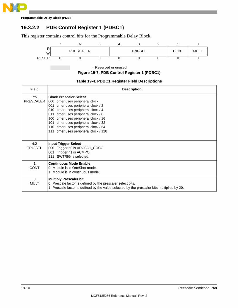
Programmable Delay Block (PDB)
19-10 Freescale Semiconductor
19.3.2.2 PDB Control Register 1 (PDBC1)
This register contains control bits for the Programmable Delay Block.
Figure 19-7. PDB Control Register 1 (PDBC1)
Table 19-4. PDBC1 Register Field Descriptions
7 6 5 4 3 2 1 0R
PRESCALER TRIGSEL CONT MULTW
RESET: 0 0 0 0 0 0 0 0
= Reserved or unused
Field Description
7:5PRESCALER
Clock Prescaler Select000 timer uses peripheral clock001 timer uses peripheral clock / 2010 timer uses peripheral clock / 4011 timer uses peripheral clock / 8100 timer uses peripheral clock / 16101 timer uses peripheral clock / 32110 timer uses peripheral clock / 64111 timer uses peripheral clock / 128
4:2TRIGSEL
Input Trigger Select000 TriggerIn0 is ADCSC1_COCO.001 TriggerIn1 is ACMPO.111 SWTRIG is selected.
1CONT
Continuous Mode Enable0 Module is in OneShot mode.1 Module is in continuous mode.
0MULT
Multiply Prescaler bit0 Prescale factor is defined by the prescaler select bits.1 Prescale factor is defined by the value selected by the prescaler bits multiplied by 20.
MCF51JE256 Reference Manual, Rev. 2

Programmable Delay Block (PDB)
Freescale Semiconductor 19-11
19.3.2.3 PDB Control Register 2 (PDBC2)
This register is used to enable each of the acknowledgment detect input for each of the channels.
Figure 19-8. PDB Control Register (PDBC2)
Table 19-5. PDBC2 Register Field Descriptions
7 6 5 4 3 2 1 0R
— — — — — — —W SWTRIG
RESET: 0 0 0 0 0 0 0 0
= Reserved or unused
Field Description
7:1Reserved
RESERVED — NOTE: Do not set Bit 1 through Bit 7 to 1. Writing 1 to any of Bits 1 - 7 can cause unforeseen ADC behavior.
0SWTRIG
Software Trigger— When TRIGSEL = 3’b111 and the module is enabled, writing a one to this field triggers a reset and restart of the counter.
MCF51JE256 Reference Manual, Rev. 2

Programmable Delay Block (PDB)
19-12 Freescale Semiconductor
19.3.2.4 PDB Channel Enable Register (PDBCHEN)
This register is used to enable or disable each of the trigger outputs associated with channel 0 to 7.
Figure 19-9. PDB Channel Enable Register (PDBCHEN)
Table 19-6. PDBCHEN Register Field Descriptions
NOTEBit 1 to bit 7 are reset to 1s. Make sure you clear them when using the PDB. Only CHEN0 should be set to 1 when the PDB is used to trigger an ADC conversion. Do not set any bit from bit 1 to bit 7 to one.
19.3.2.5 PDB Modulus Registers (PDBMODH:PDBMODL)
These registers specify the period of the counter in terms of peripheral bus clock cycles. When the counter reaches this value, it will be reset back to all zeroes. If the PDBCS_CONT is set, the count will begin anew. Reads of these registers will return the value of internal registers that is taking affect for the current period of the PDB.
Figure 19-10. PDB Modulus Register High (PDBMODH)
Figure 19-11. PDB Modulus Register Low (PDBMODL)
7 6 5 4 3 2 1 0R
— — — — — — — CHEN0W
RESET: 1 1 1 1 1 1 1 1
= Reserved or unused
Field Description
7:1Reserved
RESERVED — NOTE: Bit 1 through Bit 7 are reset to 1s. Make sure you write them to all zero when using the PDB. Only CHEN0 should be set to 1 when the PDB is used to trigger an ADC conversion. Do not set Bit 1 through Bit 7 to one.
0CHEN0
PDB channel enable bits0 Channel n trigger outputs are disabled and held low.1 Channel n trigger outputs are enabled.
7 6 5 4 3 2 1 0R
MOD[15:8]W
RESET: 1 1 1 1 1 1 1 1
= Reserved or unused
7 6 5 4 3 2 1 0R
MOD[7:0]W
RESET: 1 1 1 1 1 1 1 1
= Reserved or unused
MCF51JE256 Reference Manual, Rev. 2

Programmable Delay Block (PDB)
Freescale Semiconductor 19-13
19.3.2.6 PDB Counter Registers (PDBCNTH:PDBCNTL)
This is a 16-bit counter which operates on up-count mode. The two read-only counter registers contain the high and low bytes of the value in the PDB counter. Reading either byte latches the contents of both bytes into a buffer where they remain latched until PDBCNTH or PDBCNTL is read.
Figure 19-12. PDB Counter Register High (PDBCNTH)
Figure 19-13. PDB Counter Register Low (PDBCNTL)
19.3.2.7 PDB Interrupt Delay Register (PDBIDLYH:PDBIDLYL)
These registers can be used to read and write the value to schedule the PDB interrupt. This feature can be used to schedule an independent interrupt at some point in the PDB cycle. Reads of these registers return the value of internal registers that is taking affect for the current period of the PDB.
Figure 19-14. PDB Interrupt Delay Register High (PDBIDLYH)
Figure 19-15. PDB Interrupt Delay Register Low (PDBIDLYL)
PDBSC_IE must be set in order for an interrupt to be issued as a result of the count value equaling IDELAY. However, PDBSC_IF is set whenever the count value equals IDELAY.
19.3.2.8 DAC Interval Registers (DACINTH:DACINTL)
These registers specify the time between DAC hardware trigger pulses. If the DAC trigger output is enabled (DACTOE) each time the PDB counter register increments the number of counts placed in the
7 6 5 4 3 2 1 0R COUNT[15:8]W
RESET: 0 0 0 0 0 0 0 0
= Reserved or unused
7 6 5 4 3 2 1 0R COUNT[7:0]W
RESET: 0 0 0 0 0 0 0 0
= Reserved or unused
7 6 5 4 3 2 1 0R
IDELAY[15:8]W
RESET: 1 1 1 1 1 1 1 1
= Reserved or unused
7 6 5 4 3 2 1 0R
IDELAY[7:0]W
RESET: 1 1 1 1 1 1 1 1
= Reserved or unused
MCF51JE256 Reference Manual, Rev. 2

Programmable Delay Block (PDB)
19-14 Freescale Semiconductor
DACINTH:L registers, the PDB outputs a DAC trigger pulse. Reads of these registers return the value of internal registers that is taking affect for the current period of the PDB.
Figure 19-16. DAC Interval Register High (DACINTH)
Figure 19-17. DAC Interval Register Low (DACINTL)
19.3.2.9 PDB Delay Registers (PDBDLYH:PDBDLYL)
This register is used to specify the delay from assertion of TriggerIn to assertion of the Trigger outputs. The delay is only applicable if the module is enabled and the associated output trigger has not been bypassed. The delay is in terms of peripheral clock cycles. Reads of this register will return the value of internal registers that is taking affect for the current period of the PDB.
Figure 19-18. PDB Delay n Register High (PDBDLYH)
Figure 19-19. PDB Delay n Register Low (PDBDLYL)
19.3.3 Functional Description
19.3.3.1 Impact of Using the Prescaler on Timing Resolution
Use of prescalers greater than 1 limit the count/delay accuracy in terms of peripheral clock cycles (to the modulus of the prescaler value). If the prescaler is set to div 2, then the only values of total peripheral clocks that can be detected are even values; if div is set to 4, then the only values of total peripheral clocks
7 6 5 4 3 2 1 0R
DACINT[15:8]W
RESET: 0 0 0 0 0 0 0 0
= Reserved or unused
7 6 5 4 3 2 1 0R
DACINT[7:0]W
RESET: 0 0 0 0 0 0 0 0
= Reserved or unused
7 6 5 4 3 2 1 0R
DELAY[15:8]W
RESET: 0 0 0 0 0 0 0 0
= Reserved or unused
7 6 5 4 3 2 1 0R
DELAY[7:0]W
RESET: 0 0 0 0 0 0 0 0
= Reserved or unused
MCF51JE256 Reference Manual, Rev. 2

Programmable Delay Block (PDB)
Freescale Semiconductor 19-15
that can be decoded as detected are mod (4) and so forth. If the users want to set a really long delay value and used div 128, then they would be limited to an resolution of 128 bus clocks.
Therefore, use the lowest possible prescaler for a given application.
19.4 ResetsThis module has a single reset input, corresponding to the chip-wide peripheral reset. After reset, all registers are set to their reset values.
19.5 ClocksThis module has a single clock input, the peripheral bus clock.
19.6 InterruptsThis module has one interrupt source. When a successful comparison of the counter value and the IDELAY internal buffer occurs, the PDBIF is set. If the PDBIE is set, an interrupt is generated. Write a 1 to the PDBIF bit to clear the interrupt.
MCF51JE256 Reference Manual, Rev. 2

Programmable Delay Block (PDB)
19-16 Freescale Semiconductor
MCF51JE256 Reference Manual, Rev. 2

Freescale Semiconductor 20-17
Chapter 20 Serial Communication Interface (S08SCIV4)
20.1 IntroductionThe SCI allows asynchronous serial communications with peripheral devices and other CPUs.
NOTEIgnore any references to stop1 low-power mode in this chapter, because this device does not support it.
For details on low-power mode operation, refer to Table 3-4 in Chapter 3, “Modes of Operation”.
20.1.1 SCIx Clock Gating
The bus clock to the SCIx can be gated on and off using the SCIx bit in SCGC1. This bit is set after any reset, which enables the bus clock to this module. To conserve power, the SCIx bit can be cleared to disable the clock to this module when not in use. See Section 5.7.7, “System Clock Gating Control 1 Register (SCGC1),” for details.
20.1.2 Module Configuration
The SCI1 and SCI2 module pins can be repositioned via software-control using SCIxPS in SOPT3 as shown in Table 20-1 and Table 20-2. SCIxPS in SOPT3 selects which general-purpose I/O ports are associated with SCI operation.
Table 20-1. SCI1 Position Options
SCI1PS in SOPT3 Port Pin for TX1 Port Pin for RX1
0 (default) PTA1 PTA2
1 PTD6 PTD7
Table 20-2. SCI2 Position Options
SCI2PS in SOPT3 Port Pin for TX2 Port Pin for RX2
0 (default) PTE5 PTE6
1 PTF2 PTF1
MCF51JE256 Reference Manual, Rev. 2

Serial Communication Interface (S08SCIV4)
20-18 Freescale Semiconductor
20.1.3 Module Block DiagramFigure 20-1 shows a block diagram of the SCIx module.
Figure 20-1. Block Diagram with the SCI Module highlighted
MCF51JE256 Reference Manual, Rev. 2

Serial Communication Interface (S08SCIV4)
Freescale Semiconductor 20-19
20.1.4 Interfacing the SCIs to Off-Chip Opto-Isolators
SCI1 is designed with twice the normal I/O drive capability on the TX1 pin. The RX pin can either be fed directly from the digital I/O buffer, or those signals can be pre-conditioned using the comparators as shown in Figure 20-2 Similarly, the TX output can be modulated with the output of one of the timers before being passed off chip.
Figure 20-2. On-Chip Signal Conditioning Associated with SCI11 RX and TX Pins
Controls for the circuitry shown in Figure 20-2 are discussed in Section 5.7.13, “SIM Internal Peripheral Select Register (SIMIPS).”
20.1.5 Features
Features of SCI module include:
• Full-duplex, standard non-return-to-zero (NRZ) format
• Double-buffered transmitter and receiver with separate enables
opto
isolator
opto
isolator
RX1
TX1
digitalbuffer
analogcomparator
+
RX
TX
SCI1
Internal or external reference-
SIMIPS[RX1IN]
0
1
TPM Ch0 Output
SIMIPS[MODTX1]
SIMIPS[MTBASE1]
On-Chip Components Off-Chip Opto-Isolators
TPM Ch1 Output
MCF51JE256 Reference Manual, Rev. 2

Serial Communication Interface (S08SCIV4)
20-20 Freescale Semiconductor
• Programmable baud rates (13-bit modulo divider)
• Interrupt-driven or polled operation:
— Transmit data register empty and transmission complete
— Receive data register full
— Receive overrun, parity error, framing error, and noise error
— Idle receiver detect
— Active edge on receive pin
— Break detect supporting LIN
• Hardware parity generation and checking
• Programmable 8-bit or 9-bit character length
• Receiver wakeup by idle-line or address-mark
• Optional 13-bit break character generation / 11-bit break character detection
• Selectable transmitter output polarity
20.1.6 Modes of Operation
See Section 20.3, “Functional Description,” for details concerning SCI operation in the following modes:
• 8- and 9-bit data modes
• Stop mode operation
• Loop mode
• Single-wire mode
MCF51JE256 Reference Manual, Rev. 2
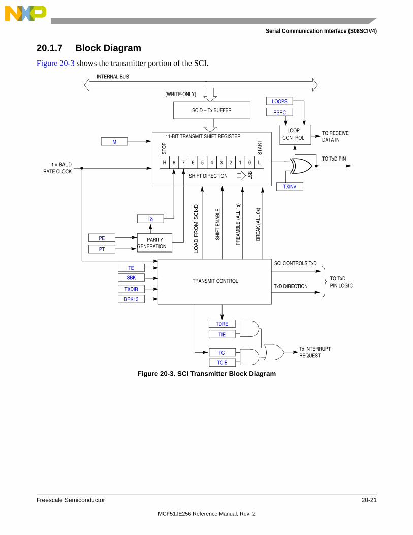
Serial Communication Interface (S08SCIV4)
Freescale Semiconductor 20-21
20.1.7 Block Diagram
Figure 20-3 shows the transmitter portion of the SCI.
Figure 20-3. SCI Transmitter Block Diagram
H 8 7 6 5 4 3 2 1 0 L
SCID – Tx BUFFER
(WRITE-ONLY)
INTERNAL BUS
STO
P
11-BIT TRANSMIT SHIFT REGISTER
STAR
T
SHIFT DIRECTION LSB
1 BAUDRATE CLOCK
PARITYGENERATION
TRANSMIT CONTROL
SHIF
T EN
ABLE
PREA
MBL
E (A
LL 1
s)
BREA
K (A
LL 0
s)SCI CONTROLS TxD
TxD DIRECTIONTO TxDPIN LOGIC
LOOPCONTROL
TO RECEIVEDATA IN
TO TxD PIN
Tx INTERRUPTREQUEST
LOOPS
RSRC
TIE
TC
TDRE
M
PT
PE
TCIE
TE
SBK
T8
TXDIR
LOA
D F
RO
M S
CIx
D
TXINV
BRK13
MCF51JE256 Reference Manual, Rev. 2

Serial Communication Interface (S08SCIV4)
20-22 Freescale Semiconductor
Figure 20-4 shows the receiver portion of the SCI.
Figure 20-4. SCI Receiver Block Diagram
H 8 7 6 5 4 3 2 1 0 L
SCID – Rx BUFFER
(READ-ONLY)
INTERNAL BUS
STO
P
11-BIT RECEIVE SHIFT REGISTER
STAR
T
SHIFT DIRECTION
LSB
FROM RxD PIN
RATE CLOCK
Rx INTERRUPTREQUEST
DATA RECOVERY
DIVIDE16 BAUD
SINGLE-WIRELOOP CONTROL
WAKEUPLOGIC
ALL
1s
MSB
FROMTRANSMITTER
ERROR INTERRUPTREQUEST
PARITYCHECKING
BY 16
RDRF
RIE
IDLE
ILIE
OR
ORIE
FE
FEIE
NF
NEIE
PF
LOOPS
PEIEPT
PE
RSRC
WAKE
ILTRWU
M
LBKDIF
LBKDIE
RXEDGIF
RXEDGIE
ACTIVE EDGEDETECT
RXINV
LBKDE
RWUID
MCF51JE256 Reference Manual, Rev. 2

Serial Communication Interface (S08SCIV4)
Freescale Semiconductor 20-23
20.2 Register DefinitionThe SCI has eight 8-bit registers to control baud rate, select SCI options, report SCI status, and for transmit/receive data.
Refer to the direct-page register summary in the Memory chapter of the MCF51JE256 series Reference Manual for the absolute address assignments for all SCI registers. This section refers to registers and control bits only by their names. A Freescale-provided equate or header file is used to translate these names into the appropriate absolute addresses.
20.2.1 SCI Baud Rate Registers (SCIxBDH, SCIxBDL)
This pair of registers controls the prescale divisor for SCI baud rate generation. To update the 13-bit baud rate setting [SBR12:SBR0], first write to SCIxBDH to buffer the high half of the new value and then write to SCIxBDL. The working value in SCIxBDH does not change until SCIxBDL is written.
SCIxBDL is reset to a non-zero value, so after reset the baud rate generator remains disabled until the first time the receiver or transmitter is enabled (RE or TE bits in SCIxC2 are written to 1).
7 6 5 4 3 2 1 0
RLBKDIE RXEDGIE
0SBR12 SBR11 SBR10 SBR9 SBR8
W
Reset 0 0 0 0 0 0 0 0
= Unimplemented or Reserved
Figure 20-5. SCI Baud Rate Register (SCIxBDH)
Table 20-3. SCIxBDH Field Descriptions
Field Description
7LBKDIE
LIN Break Detect Interrupt Enable (for LBKDIF)0 Hardware interrupts from LBKDIF disabled (use polling).1 Hardware interrupt requested when LBKDIF flag is 1.
6RXEDGIE
RxD Input Active Edge Interrupt Enable (for RXEDGIF)0 Hardware interrupts from RXEDGIF disabled (use polling).1 Hardware interrupt requested when RXEDGIF flag is 1.
4:0SBR[12:8]
Baud Rate Modulo Divisor — The 13 bits in SBR[12:0] are referred to collectively as BR, and they set the modulo divide rate for the SCI baud rate generator. When BR = 0, the SCI baud rate generator is disabled to reduce supply current. When BR = 1 to 8191, the SCI baud rate = BUSCLK/(16BR). See also BR bits in Table 20-4.
MCF51JE256 Reference Manual, Rev. 2

Serial Communication Interface (S08SCIV4)
20-24 Freescale Semiconductor
20.2.2 SCI Control Register 1 (SCIxC1)
This read/write register is used to control various optional features of the SCI system.
7 6 5 4 3 2 1 0
RSBR7 SBR6 SBR5 SBR4 SBR3 SBR2 SBR1 SBR0
W
Reset 0 0 0 0 0 1 0 0
Figure 20-6. SCI Baud Rate Register (SCIxBDL)
Table 20-4. SCIxBDL Field Descriptions
Field Description
7:0SBR[7:0]
Baud Rate Modulo Divisor — These 13 bits in SBR[12:0] are referred to collectively as BR, and they set the modulo divide rate for the SCI baud rate generator. When BR = 0, the SCI baud rate generator is disabled to reduce supply current. When BR = 1 to 8191, the SCI baud rate = BUSCLK/(16BR). See also BR bits in Table 20-3.
7 6 5 4 3 2 1 0
RLOOPS SCISWAI RSRC M WAKE ILT PE PT
W
Reset 0 0 0 0 0 0 0 0
Figure 20-7. SCI Control Register 1 (SCIxC1)
Table 20-5. SCIxC1 Field Descriptions
Field Description
7LOOPS
Loop Mode Select — Selects between loop back modes and normal 2-pin full-duplex modes. When LOOPS = 1, the transmitter output is internally connected to the receiver input.0 Normal operation — RxD and TxD use separate pins.1 Loop mode or single-wire mode where transmitter outputs are internally connected to receiver input. (See
RSRC bit that follows.) RxD pin is not used by SCI.
6SCISWAI
SCI Stops in Wait Mode0 SCI clocks continue to run in wait mode so the SCI can be the source of an interrupt that wakes up the CPU.1 SCI clocks freeze while CPU is in wait mode.
5RSRC
Receiver Source Select — This bit has no meaning or effect unless the LOOPS bit is set to 1. When LOOPS = 1, the receiver input is internally connected to the TxD pin and RSRC determines whether this connection is also connected to the transmitter output.0 Provided LOOPS = 1, RSRC = 0 selects internal loop back mode and the SCI does not use the RxD pins.1 Single-wire SCI mode where the TxD pin is connected to the transmitter output and receiver input.
4M
9-Bit or 8-Bit Mode Select0 Normal — start + 8 data bits (LSB first) + stop.1 Receiver and transmitter use 9-bit data characters
start + 8 data bits (LSB first) + 9th data bit + stop.
MCF51JE256 Reference Manual, Rev. 2

Serial Communication Interface (S08SCIV4)
Freescale Semiconductor 20-25
20.2.3 SCI Control Register 2 (SCIxC2)
This register can be read or written at any time.
3WAKE
Receiver Wakeup Method Select — Refer to Section 20.3.3.2, “Receiver Wakeup Operation” for more information.0 Idle-line wakeup.1 Address-mark wakeup.
2ILT
Idle Line Type Select — Setting this bit to 1 ensures that the stop bit and logic 1 bits at the end of a character do not count toward the 10 or 11 bit times of logic high level needed by the idle line detection logic. Refer to Section 20.3.3.2.1, “Idle-Line Wakeup” for more information.0 Idle character bit count starts after start bit.1 Idle character bit count starts after stop bit.
1PE
Parity Enable — Enables hardware parity generation and checking. When parity is enabled, the most significant bit (MSB) of the data character (eighth or ninth data bit) is treated as the parity bit.0 No hardware parity generation or checking.1 Parity enabled.
0PT
Parity Type — Provided parity is enabled (PE = 1), this bit selects even or odd parity. Odd parity means the total number of 1s in the data character, including the parity bit, is odd. Even parity means the total number of 1s in the data character, including the parity bit, is even.0 Even parity.1 Odd parity.
7 6 5 4 3 2 1 0
RTIE TCIE RIE ILIE TE RE RWU SBK
W
Reset 0 0 0 0 0 0 0 0
Figure 20-8. SCI Control Register 2 (SCIxC2)
Table 20-6. SCIxC2 Field Descriptions
Field Description
7TIE
Transmit Interrupt Enable (for TDRE)0 Hardware interrupts from TDRE disabled (use polling).1 Hardware interrupt requested when TDRE flag is 1.
6TCIE
Transmission Complete Interrupt Enable (for TC)0 Hardware interrupts from TC disabled (use polling).1 Hardware interrupt requested when TC flag is 1.
5RIE
Receiver Interrupt Enable (for RDRF)0 Hardware interrupts from RDRF disabled (use polling).1 Hardware interrupt requested when RDRF flag is 1.
4ILIE
Idle Line Interrupt Enable (for IDLE)0 Hardware interrupts from IDLE disabled (use polling).1 Hardware interrupt requested when IDLE flag is 1.
Table 20-5. SCIxC1 Field Descriptions (Continued)
Field Description
MCF51JE256 Reference Manual, Rev. 2

Serial Communication Interface (S08SCIV4)
20-26 Freescale Semiconductor
20.2.4 SCI Status Register 1 (SCIxS1)
This register has eight read-only status flags. Writes have no effect. Special software sequences (which do not involve writing to this register) clear these status flags.
3TE
Transmitter Enable0 Transmitter off.1 Transmitter on.TE must be 1 in order to use the SCI transmitter. When TE = 1, the SCI forces the TxD pin to act as an output for the SCI system.When the SCI is configured for single-wire operation (LOOPS = RSRC = 1), TXDIR controls the direction of traffic on the single SCI communication line (TxD pin).TE also can be used to queue an idle character by writing TE = 0 then TE = 1 while a transmission is in progress. Refer to Section 20.3.2.1, “Send Break and Queued Idle” for more details.When TE is written to 0, the transmitter keeps control of the port TxD pin until any data, queued idle, or queued break character finishes transmitting before allowing the pin to revert to a general-purpose I/O pin.
2RE
Receiver Enable — When the SCI receiver is off, the RxD pin reverts to being a general-purpose port I/O pin. If LOOPS = 1 the RxD pin reverts to being a general-purpose I/O pin even if RE = 1.0 Receiver off.1 Receiver on.
1RWU
Receiver Wakeup Control — This bit can be written to 1 to place the SCI receiver in a standby state where it waits for automatic hardware detection of a selected wakeup condition. The wakeup condition is either an idle line between messages (WAKE = 0, idle-line wakeup), or a logic 1 in the most significant data bit in a character (WAKE = 1, address-mark wakeup). Application software sets RWU and (normally) a selected hardware condition automatically clears RWU. Refer to Section 20.3.3.2, “Receiver Wakeup Operation” for more details.0 Normal SCI receiver operation.1 SCI receiver in standby waiting for wakeup condition.
0SBK
Send Break — Writing a 1 and then a 0 to SBK queues a break character in the transmit data stream. Additional break characters of 10 or 11 (13 or 14 if BRK13 = 1) bit times of logic 0 are queued as long as SBK = 1. Depending on the timing of the set and clear of SBK relative to the information currently being transmitted, a second break character may be queued before software clears SBK. Refer to Section 20.3.2.1, “Send Break and Queued Idle” for more details.0 Normal transmitter operation.1 Queue break character(s) to be sent.
7 6 5 4 3 2 1 0
R TDRE TC RDRF IDLE OR NF FE PF
W
Reset 1 1 0 0 0 0 0 0
= Unimplemented or Reserved
Figure 20-9. SCI Status Register 1 (SCIxS1)
Table 20-6. SCIxC2 Field Descriptions (Continued)
Field Description
MCF51JE256 Reference Manual, Rev. 2

Serial Communication Interface (S08SCIV4)
Freescale Semiconductor 20-27
Table 20-7. SCIxS1 Field Descriptions
Field Description
7TDRE
Transmit Data Register Empty Flag — TDRE is set out of reset and when a transmit data value transfers from the transmit data buffer to the transmit shifter, leaving room for a new character in the buffer. To clear TDRE, read SCIxS1 with TDRE = 1 and then write to the SCI data register (SCIxD).0 Transmit data register (buffer) full.1 Transmit data register (buffer) empty.
6TC
Transmission Complete Flag — TC is set out of reset and when TDRE = 1 and no data, preamble, or break character is being transmitted. 0 Transmitter active (sending data, a preamble, or a break).1 Transmitter idle (transmission activity complete).TC is cleared automatically by reading SCIxS1 with TC = 1 and then doing one of the following three things:
• Write to the SCI data register (SCIxD) to transmit new data• Queue a preamble by changing TE from 0 to 1• Queue a break character by writing 1 to SBK in SCIxC2
5RDRF
Receive Data Register Full Flag — RDRF becomes set when a character transfers from the receive shifter into the receive data register (SCIxD). To clear RDRF, read SCIxS1 with RDRF = 1 and then read the SCI data register (SCIxD).0 Receive data register empty.1 Receive data register full.
4IDLE
Idle Line Flag — IDLE is set when the SCI receive line becomes idle for a full character time after a period of activity. When ILT = 0, the receiver starts counting idle bit times after the start bit. So if the receive character is all 1s, these bit times and the stop bit time count toward the full character time of logic high (10 or 11 bit times depending on the M control bit) needed for the receiver to detect an idle line. When ILT = 1, the receiver doesn’t start counting idle bit times until after the stop bit. So the stop bit and any logic high bit times at the end of the previous character do not count toward the full character time of logic high needed for the receiver to detect an idle line.To clear IDLE, read SCIxS1 with IDLE = 1 and then read the SCI data register (SCIxD). After IDLE has been cleared, it cannot become set again until after a new character has been received and RDRF has been set. IDLE will get set only once even if the receive line remains idle for an extended period.0 No idle line detected.1 Idle line was detected.
3OR
Receiver Overrun Flag — OR is set when a new serial character is ready to be transferred to the receive data register (buffer), but the previously received character has not been read from SCIxD yet. In this case, the new character (and all associated error information) is lost because there is no room to move it into SCIxD. To clear OR, read SCIxS1 with OR = 1 and then read the SCI data register (SCIxD).0 No overrun.1 Receive overrun (new SCI data lost).
2NF
Noise Flag — The advanced sampling technique used in the receiver takes seven samples during the start bit and three samples in each data bit and the stop bit. If any of these samples disagrees with the rest of the samples within any bit time in the frame, the flag NF is set at the same time as the RDRF flag is set for the character. To clear NF, read SCIxS1 and then read the SCI data register (SCIxD).0 No noise detected.1 Noise detected in the received character in SCIxD.
MCF51JE256 Reference Manual, Rev. 2

Serial Communication Interface (S08SCIV4)
20-28 Freescale Semiconductor
20.2.5 SCI Status Register 2 (SCIxS2)
This register contains one read-only status flag.
1FE
Framing Error Flag — FE is set at the same time as RDRF when the receiver detects a logic 0 where the stop bit was expected. This suggests the receiver was not properly aligned to a character frame. To clear FE, read SCIxS1 with FE = 1 and then read the SCI data register (SCIxD).0 No framing error detected. This does not guarantee the framing is correct.1 Framing error.
0PF
Parity Error Flag — PF is set at the same time as RDRF when parity is enabled (PE = 1) and the parity bit in the received character does not agree with the expected parity value. To clear PF, read SCIxS1 and then read the SCI data register (SCIxD).0 No parity error. 1 Parity error.
7 6 5 4 3 2 1 0
RLBKDIF RXEDGIF
0RXINV RWUID BRK13 LBKDE
RAF
W
Reset 0 0 0 0 0 0 0 0
= Unimplemented or Reserved
Figure 20-10. SCI Status Register 2 (SCIxS2)
Table 20-8. SCIxS2 Field Descriptions
Field Description
7LBKDIF
LIN Break Detect Interrupt Flag — LBKDIF is set when the LIN break detect circuitry is enabled and a LIN break character is detected. LBKDIF is cleared by writing a “1” to it.0 No LIN break character has been detected.1 LIN break character has been detected.
6RXEDGIF
RxD Pin Active Edge Interrupt Flag — RXEDGIF is set when an active edge (falling if RXINV = 0, rising if RXINV=1) on the RxD pin occurs. RXEDGIF is cleared by writing a “1” to it.0 No active edge on the receive pin has occurred.1 An active edge on the receive pin has occurred.
4RXINV1
Receive Data Inversion — Setting this bit reverses the polarity of the received data input.0 Receive data not inverted1 Receive data inverted
3RWUID
Receive Wake Up Idle Detect— RWUID controls whether the idle character that wakes up the receiver sets the IDLE bit.0 During receive standby state (RWU = 1), the IDLE bit does not get set upon detection of an idle character.1 During receive standby state (RWU = 1), the IDLE bit gets set upon detection of an idle character.
2BRK13
Break Character Generation Length — BRK13 selects a longer transmitted break character length. The state of this bit does not affect the detection of a framing error.0 Break character is transmitted with length of 10 bit times (11 if M = 1)1 Break character is transmitted with length of 13 bit times (14 if M = 1)
Table 20-7. SCIxS1 Field Descriptions (Continued)
Field Description
MCF51JE256 Reference Manual, Rev. 2

Serial Communication Interface (S08SCIV4)
Freescale Semiconductor 20-29
When using an internal oscillator in a LIN system, it is necessary to raise the break detection threshold by one bit time. Under the worst case timing conditions allowed in LIN, it is possible that a 0x00 data character can appear to be 10.26 bit times long at a slave running 14% faster than the master. This would trigger normal break detection circuitry designed to detect a 10 bit break symbol. When the LBKDE bit is set, framing errors are inhibited and the break detection threshold changes from 10 bits to 11 bits, preventing false detection of a 0x00 data character as a LIN break symbol.
20.2.6 SCI Control Register 3 (SCIxC3)
1LBKDE
LIN Break Detection Enable— LBKDE selects a longer break character detection length. While LBKDE is set, framing error (FE) and receive data register full (RDRF) flags are prevented from setting.0 Break character is detected at length of 10 bit times (11 if M = 1).1 Break character is detected at length of 11 bit times (12 if M = 1).
0RAF
Receiver Active Flag — RAF is set when the SCI receiver detects the beginning of a valid start bit, and RAF is cleared automatically when the receiver detects an idle line. This status flag can be used to check whether an SCI character is being received before instructing the MCU to go to stop mode.0 SCI receiver idle waiting for a start bit.1 SCI receiver active (RxD input not idle).
1 Setting RXINV inverts the RxD input for all cases: data bits, start and stop bits, break, and idle.
7 6 5 4 3 2 1 0
R R8T8 TXDIR TXINV ORIE NEIE FEIE PEIE
W
Reset 0 0 0 0 0 0 0 0
= Unimplemented or Reserved
Figure 20-11. SCI Control Register 3 (SCIxC3)
Table 20-9. SCIxC3 Field Descriptions
Field Description
7R8
Ninth Data Bit for Receiver — When the SCI is configured for 9-bit data (M = 1), R8 can be thought of as a ninth receive data bit to the left of the MSB of the buffered data in the SCIxD register. When reading 9-bit data, read R8 before reading SCIxD because reading SCIxD completes automatic flag clearing sequences which could allow R8 and SCIxD to be overwritten with new data.
6T8
Ninth Data Bit for Transmitter — When the SCI is configured for 9-bit data (M = 1), T8 may be thought of as a ninth transmit data bit to the left of the MSB of the data in the SCIxD register. When writing 9-bit data, the entire 9-bit value is transferred to the SCI shift register after SCIxD is written so T8 should be written (if it needs to change from its previous value) before SCIxD is written. If T8 does not need to change in the new value (such as when it is used to generate mark or space parity), it need not be written each time SCIxD is written.
5TXDIR
TxD Pin Direction in Single-Wire Mode — When the SCI is configured for single-wire half-duplex operation (LOOPS = RSRC = 1), this bit determines the direction of data at the TxD pin.0 TxD pin is an input in single-wire mode.1 TxD pin is an output in single-wire mode.
Table 20-8. SCIxS2 Field Descriptions (Continued)
Field Description
MCF51JE256 Reference Manual, Rev. 2

Serial Communication Interface (S08SCIV4)
20-30 Freescale Semiconductor
20.2.7 SCI Data Register (SCIxD)
This register is actually two separate registers. Reads return the contents of the read-only receive data buffer and writes go to the write-only transmit data buffer. Reads and writes of this register are also involved in the automatic flag clearing mechanisms for the SCI status flags.
20.3 Functional DescriptionThe SCI allows full-duplex, asynchronous, NRZ serial communication among the MCU and remote devices, including other MCUs. The SCI comprises a baud rate generator, transmitter, and receiver block. The transmitter and receiver operate independently, although they use the same baud rate generator. During normal operation, the MCU monitors the status of the SCI, writes the data to be transmitted, and processes received data. The following describes each of the blocks of the SCI.
20.3.1 Baud Rate Generation
As shown in Figure 20-13, the clock source for the SCI baud rate generator is the bus-rate clock.
4TXINV1
Transmit Data Inversion — Setting this bit reverses the polarity of the transmitted data output.0 Transmit data not inverted1 Transmit data inverted
3ORIE
Overrun Interrupt Enable — This bit enables the overrun flag (OR) to generate hardware interrupt requests.0 OR interrupts disabled (use polling).1 Hardware interrupt requested when OR = 1.
2NEIE
Noise Error Interrupt Enable — This bit enables the noise flag (NF) to generate hardware interrupt requests.0 NF interrupts disabled (use polling).1 Hardware interrupt requested when NF = 1.
1FEIE
Framing Error Interrupt Enable — This bit enables the framing error flag (FE) to generate hardware interrupt requests.0 FE interrupts disabled (use polling).1 Hardware interrupt requested when FE = 1.
0PEIE
Parity Error Interrupt Enable — This bit enables the parity error flag (PF) to generate hardware interrupt requests.0 PF interrupts disabled (use polling).1 Hardware interrupt requested when PF = 1.
1 Setting TXINV inverts the TxD output for all cases: data bits, start and stop bits, break, and idle.
7 6 5 4 3 2 1 0
R R7 R6 R5 R4 R3 R2 R1 R0
W T7 T6 T5 T4 T3 T2 T1 T0
Reset 0 0 0 0 0 0 0 0
Figure 20-12. SCI Data Register (SCIxD)
Table 20-9. SCIxC3 Field Descriptions (Continued)
Field Description
MCF51JE256 Reference Manual, Rev. 2

Serial Communication Interface (S08SCIV4)
Freescale Semiconductor 20-31
Figure 20-13. SCI Baud Rate Generation
SCI communications require the transmitter and receiver (which typically derive baud rates from independent clock sources) to use the same baud rate. Allowed tolerance on this baud frequency depends on the details of how the receiver synchronizes to the leading edge of the start bit and how bit sampling is performed.
The MCU resynchronizes to bit boundaries on every high-to-low transition. In the worst case, there are no such transitions in the full 10- or 11-bit time character frame so any mismatch in baud rate is accumulated for the whole character time. For a SCI system whose bus frequency is driven by a crystal, the allowed baud rate mismatch is about ±4.5 % for 8-bit data format and about ±4 % for 9-bit data format. Although baud rate modulo divider settings do not always produce baud rates that exactly match standard rates, it is normally possible to get within a few percent, which is acceptable for reliable communications.
20.3.2 Transmitter Functional Description
This section describes the overall block diagram for the SCI transmitter, as well as specialized functions for sending break and idle characters. The transmitter block diagram is shown in Figure 20-3.
The transmitter output (TxD) idle state defaults to logic high (TXINV = 0 following reset). The transmitter output is inverted by setting TXINV = 1. The transmitter is enabled by setting the TE bit in SCIxC2. This queues a preamble character that is one full character frame of the idle state. The transmitter then remains idle until data is available in the transmit data buffer. Programs store data into the transmit data buffer by writing to the SCI data register (SCIxD).
The central element of the SCI transmitter is the transmit shift register that is 10 or 11 bits long depending on the setting in the M control bit. For the remainder of this section, assume M = 0, selecting the normal 8-bit data mode. In 8-bit data mode, the shift register holds a start bit, eight data bits, and a stop bit. When the transmit shift register is available for a new SCI character, the value waiting in the transmit data register is transferred to the shift register (synchronized with the baud rate clock) and the transmit data register empty (TDRE) status flag is set to indicate another character can be written to the transmit data buffer at SCIxD.
If no new character is waiting in the transmit data buffer after a stop bit is shifted out the TxD pin, the transmitter sets the transmit complete flag and enters an idle mode, with TxD high, waiting for more characters to transmit.
Writing 0 to TE does not immediately release the pin to be a general-purpose I/O pin. Any transmit activity in progress must first be completed. This includes data characters in progress, queued idle characters, and queued break characters.
SBR12:SBR0
DIVIDE BYTx BAUD RATE
Rx SAMPLING CLOCK(16 BAUD RATE)
BAUD RATE GENERATOR OFF IF [SBR12:SBR0] = 0
BUSCLK
BAUD RATE =BUSCLK
[SBR12:SBR0] 16
16
MODULO DIVIDE BY(1 THROUGH 8191)
MCF51JE256 Reference Manual, Rev. 2

Serial Communication Interface (S08SCIV4)
20-32 Freescale Semiconductor
20.3.2.1 Send Break and Queued Idle
The SBK control bit in SCIxC2 sends break characters originally used to gain the attention of old teletype receivers. Break characters are a full character time of logic 0 (10 bit times including the start and stop bits). A longer break of 13 bit times can be enabled by setting BRK13 = 1. Normally, a program would wait for TDRE to become set to indicate the last character of a message has moved to the transmit shifter, then write 1 and then write 0 to the SBK bit. This action queues a break character to be sent as soon as the shifter is available. If SBK remains 1 when the queued break moves into the shifter (synchronized to the baud rate clock), an additional break character is queued. If the receiving device is another Freescale Semiconductor SCI, the break characters are received as 0s in all eight data bits and a framing error (FE = 1) occurs.
When idle-line wakeup is used, a full character time of idle (logic 1) is needed between messages to wake up any sleeping receivers. Normally, a program would wait for TDRE to become set to indicate the last character of a message has moved to the transmit shifter, then write 0 and then write 1 to the TE bit. This action queues an idle character to be sent as soon as the shifter is available. As long as the character in the shifter does not finish while TE = 0, the SCI transmitter never actually releases control of the TxD pin. If there is a possibility of the shifter finishing while TE = 0, set the general-purpose I/O controls so the pin shared with TxD is an output driving a logic 1. This ensures that the TxD line looks like a normal idle line even if the SCI loses control of the port pin between writing 0 and then 1 to TE.
The length of the break character is affected by the BRK13 and M bits as shown below.
20.3.3 Receiver Functional Description
In this section, the receiver block diagram (Figure 20-4) is a guide for the overall receiver functional description. Next, the data sampling technique used to reconstruct receiver data is described in more detail. Finally, two variations of the receiver wakeup function are explained.
Set RXINV = 1 to invert the receiver input. Set the RE bit in SCIxC2 to enable the receiver. Character frames consist of a start bit of logic 0, eight (or nine) data bits (LSB first), and a stop bit of logic 1. For information about 9-bit data mode, refer to Section •, “8- and 9-bit data modes.” For the remainder of this discussion, assume the SCI is configured for normal 8-bit data mode.
After receiving the stop bit into the receive shifter, and provided the receive data register is not already full, the data character is transferred to the receive data register and the receive data register full (RDRF) status flag is set. If RDRF was already set indicating the receive data register (buffer) was already full, the overrun (OR) status flag is set and the new data is lost. Because the SCI receiver is double-buffered, the program has one full character time after RDRF is set before the data in the receive data buffer must be read to avoid a receiver overrun.
Table 20-10. Break Character Length
BRK13 M Break Character Length
0 0 10 bit times
0 1 11 bit times
1 0 13 bit times
1 1 14 bit times
MCF51JE256 Reference Manual, Rev. 2

Serial Communication Interface (S08SCIV4)
Freescale Semiconductor 20-33
When a program detects that the receive data register is full (RDRF = 1), it reads SCIxD to get the data from the receive data register. The RDRF flag is cleared automatically when the program that handles receive data issues a 2-step sequence. Refer to Section 20.3.4, “Interrupts and Status Flags” for more details about flag clearing.
20.3.3.1 Data Sampling Technique
The SCI receiver uses a 16 baud rate clock for sampling. To search for a falling edge on the RxD serial data input pin, the receiver starts taking logic level samples at 16 times the baud rate. A falling edge is defined as a logic 0 sample after three consecutive logic 1 samples. The 16 baud rate clock divides the bit time into 16 segments labeled RT1 through RT16. When a falling edge is located, three more samples are taken at RT3, RT5, and RT7 to make sure this was a real start bit and not merely noise. If at least two of these three samples are 0, the receiver assumes it is synchronized to a receive character.
The receiver then samples each bit time, including the start and stop bits, at RT8, RT9, and RT10 to determine the logic level for that bit. The logic level is interpreted to be that of the majority of the samples taken during the bit time. In the case of the start bit, the bit is assumed to be 0 if at least two of the samples at RT3, RT5, and RT7 are 0 even if one or all of the samples taken at RT8, RT9, and RT10 are 1s. If any sample in any bit time (including the start and stop bits) in a character frame fails to agree with the logic level for that bit, the noise flag (NF) is set when the received character is transferred to the receive data buffer.
The falling edge detection logic continuously looks for falling edges. If an edge is detected, the sample clock is resynchronized to bit times. This improves the reliability of the receiver in the presence of noise or mismatched baud rates. It does not improve worst case analysis because some characters do not have any extra falling edges anywhere in the character frame.
In the case of a framing error, provided the received character was not a break character, the sampling logic that searches for a falling edge is filled with three logic 1 samples so that a new start bit can be detected almost immediately.
In the case of a framing error, the receiver is inhibited from receiving any new characters until the framing error flag is cleared. The receive shift register continues to function, but a complete character cannot transfer to the receive data buffer if FE remains set.
20.3.3.2 Receiver Wakeup Operation
Receiver wakeup is a hardware mechanism that allows an SCI receiver to ignore the characters in a message intended for a different SCI receiver. In such a system, all receivers evaluate the first character(s) of each message, and as soon as they determine the message is intended for a different receiver, they write logic 1 to the receiver wake up (RWU) control bit in SCIxC2. When RWU bit is set, the status flags associated with the receiver (with the exception of the idle bit, IDLE, when RWUID bit is set) are inhibited from setting. This eliminates the need for software overhead to handle unimportant message characters. At the end of a message, or at the beginning of the next message, all receivers automatically force RWU to 0 so all receivers wake up in time to look at the first character(s) of the next message.
MCF51JE256 Reference Manual, Rev. 2

Serial Communication Interface (S08SCIV4)
20-34 Freescale Semiconductor
20.3.3.2.1 Idle-Line Wakeup
When WAKE = 0, the receiver is configured for idle-line wakeup. In this mode, RWU is cleared automatically when the receiver detects a full character time of the idle-line level. The M control bit selects 8-bit or 9-bit data mode that determines how many bit times of idle are needed to constitute a full character time (10 or 11 bit times because of the start and stop bits).
When RWU is one and RWUID is zero, the idle condition that wakes up the receiver does not set the IDLE flag. The receiver wakes up and waits for the first data character of the next message which sets the RDRF flag and generate an interrupt if enabled. When RWUID is one, any idle condition sets the IDLE flag and generates an interrupt if enabled, regardless of whether RWU is zero or one.
The idle-line type (ILT) control bit selects one of two ways to detect an idle line. When ILT = 0, the idle bit counter starts after the start bit so the stop bit and any logic 1s at the end of a character count toward the full character time of idle. When ILT = 1, the idle bit counter does not start until after a stop bit time, so the idle detection is not affected by the data in the last character of the previous message.
20.3.3.2.2 Address-Mark Wakeup
When WAKE = 1, the receiver is configured for address-mark wakeup. In this mode, RWU is cleared automatically when the receiver detects a logic 1 in the most significant bit of a received character (eighth bit in M = 0 mode and ninth bit in M = 1 mode).
Address-mark wakeup allows messages to contain idle characters, but requires the MSB be reserved for use in address frames. The logic 1 MSB of an address frame clears the RWU bit before the stop bit is received and sets the RDRF flag. In this case, the character with the MSB set is received even though the receiver was sleeping during most of this character time.
20.3.4 Interrupts and Status Flags
The SCI system has three separate interrupt vectors to reduce the amount of software needed to isolate the cause of the interrupt. One interrupt vector is associated with the transmitter for TDRE and TC events. Another interrupt vector is associated with the receiver for RDRF, IDLE, RXEDGIF and LBKDIF events. A third vector is used for OR, NF, FE, and PF error conditions. Local interrupt enable masks can separately mask each of these ten interrupt sources. Software can still poll the flags when the local masks are cleared to disable generation of hardware interrupt requests.
The SCI transmitter has two status flags that can generate hardware interrupt requests. Transmit data register empty (TDRE) indicates available room in the transmit data buffer to write another transmit character to SCIxD. If the transmit interrupt enable (TIE) bit is set, a hardware interrupt is requested when TDRE = 1. Transmit complete (TC) indicates that the transmitter is finished transmitting all data, preamble, and break characters and is idle with TxD at the inactive level. This flag is often used in systems with modems to determine when it is safe to turn off the modem. If the transmit complete interrupt enable (TCIE) bit is set, a hardware interrupt will be requested whenever TC = 1. Instead of hardware interrupts, software polling may be used to monitor the TDRE and TC status flags if the corresponding TIE or TCIE local interrupt masks are 0s.
MCF51JE256 Reference Manual, Rev. 2

Serial Communication Interface (S08SCIV4)
Freescale Semiconductor 20-35
When a program detects that the receive data register is full (RDRF = 1), it gets the data from the receive data register by reading SCIxD. The RDRF flag is cleared by reading SCIxS1 while RDRF = 1 and then reading SCIxD.
When polling is used, this sequence is naturally satisfied in the normal course of the user program. If hardware interrupts are used, SCIxS1 must be read in the interrupt service routine (ISR). Normally, this is done in the ISR anyway to check for receive errors, so the sequence is automatically satisfied.
The IDLE status flag includes logic that prevents it from getting set repeatedly when the RxD line remains idle for an extended period of time. IDLE is cleared by reading SCIxS1 while IDLE = 1 and then reading SCIxD. After IDLE has been cleared, it cannot become set again until the receiver has received at least one new character and has set RDRF.
If the associated error was detected in the received character that caused RDRF to be set, the error flags — noise flag (NF), framing error (FE), and parity error flag (PF) — are set at the same time as RDRF. These flags are not set in overrun cases.
If RDRF was already set when a new character is ready to be transferred from the receive shifter to the receive data buffer, the overrun (OR) flag is set instead of the data along with any associated NF, FE, or PF condition is lost.
At any time, an active edge on the RxD serial data input pin causes the RXEDGIF flag to set. The RXEDGIF flag is cleared by writing a “1” to it. This function does depend on the receiver being enabled (RE = 1).
20.3.5 Additional SCI Functions
The following sections describe additional SCI functions.
20.3.5.1 8- and 9-Bit Data Modes
The SCI system (transmitter and receiver) can be configured to operate in 9-bit data mode by setting the M control bit in SCIxC1. In 9-bit mode, there is a ninth data bit to the left of the MSB of the SCI data register. For the transmit data buffer, this bit is stored in T8 in SCIxC3. For the receiver, the ninth bit is held in R8 in SCIxC3.
For coherent writes to the transmit data buffer, write to the T8 bit before writing to SCIxD.
If the bit value to be transmitted as the ninth bit of a new character is the same as for the previous character, it is not necessary to write to T8 again. When data is transferred from the transmit data buffer to the transmit shifter, the value in T8 is copied at the same time data is transferred from SCIxD to the shifter.
Typically, use the 9-bit data mode in conjunction with parity to allow eight bits of data plus the parity in the ninth bit. Or use it with address-mark wakeup so the ninth data bit can serve as the wakeup bit. In custom protocols, the ninth bit can also serve as a software-controlled marker.
20.3.5.2 Stop Mode Operation
During all stop modes, clocks to the SCI module are halted.
MCF51JE256 Reference Manual, Rev. 2

Serial Communication Interface (S08SCIV4)
20-36 Freescale Semiconductor
In stop2 modes, all SCI register data is lost and must be re-initialized upon recovery from these two stop modes. No SCI module registers are affected in stop3 mode.
The receive input active edge detect circuit remains active in stop3 mode, but not in stop2. An active edge on the receive input brings the CPU out of stop3 mode if the interrupt is not masked (RXEDGIE = 1).
Note, because the clocks are halted, the SCI module resumes operation upon exit from stop (only in stop3 mode). Software should ensure stop mode is not entered while there is a character being transmitted out of or received into the SCI module.
20.3.5.3 Loop Mode
When LOOPS = 1, the RSRC bit in the same register chooses between loop mode (RSRC = 0) or single-wire mode (RSRC = 1). Loop mode is sometimes used to check software, independent of connections in the external system, to help isolate system problems. In this mode, the transmitter output is internally connected to the receiver input and the RxD pin is not used by the SCI, so it reverts to a general-purpose port I/O pin.
20.3.5.4 Single-Wire Operation
When LOOPS = 1, the RSRC bit in the same register chooses between loop mode (RSRC = 0) or single-wire mode (RSRC = 1). Single-wire mode is used to implement a half-duplex serial connection. The receiver is internally connected to the transmitter output and to the TxD pin. The RxD pin is not used and reverts to a general-purpose port I/O pin.
In single-wire mode, the TXDIR bit in SCIxC3 controls the direction of serial data on the TxD pin. When TXDIR = 0, the TxD pin is an input to the SCI receiver and the transmitter is temporarily disconnected from the TxD pin so an external device can send serial data to the receiver. When TXDIR = 1, the TxD pin is an output driven by the transmitter. In single-wire mode, the internal loop back connection from the transmitter to the receiver causes the receiver to receive characters that are sent out by the transmitter.
MCF51JE256 Reference Manual, Rev. 2

Freescale Semiconductor 21-1
Chapter 21 16-bit Serial Peripheral Interface (S08SPI16V5)
21.1 IntroductionThe SPI1 in these devices is a 16-bit serial peripheral interface (SPI) module with FIFO.
NOTEThere are two SPI modules on this device. Replace SPIx with the appropriate peripheral designation (SPI1 or SPI2), depending upon your use:
• SPI1 — for the 16-bit SPI with FIFO module.
• SPI2 — for the 8-bit SPI module.
21.1.1 SPI1 Clock Gating
The bus clock to the SPI1 can be gated on and off using the SPI1 bit in SCGC2. These bits are set after any reset, which enables the bus clock to this module. To conserve power, these bits can be cleared to disable the clock to this module when not in use. See Section 5.7.8, “System Clock Gating Control 2 Register (SCGC2),” for details.
MCF51JE256 Reference Manual, Rev. 2

16-bit Serial Peripheral Interface (S08SPI16V5)
21-2 Freescale Semiconductor
Figure 21-1. Block Diagram with SPI1 Module Highlighted
MCF51JE256 Reference Manual, Rev. 2

16-bit Serial Peripheral Interface (S08SPI16V5)
Freescale Semiconductor 21-3
21.1.2 Features
The SPI includes these distinctive features:
• Master mode or slave mode operation
• Full-duplex or single-wire bidirectional mode
• Programmable transmit bit rate
• Double-buffered transmit and receive data register
• Serial clock phase and polarity options
• Slave select output
• Mode fault error flag with CPU interrupt capability
• Control of SPI operation during wait mode
• Selectable MSB-first or LSB-first shifting
• Programmable 8- or 16-bit data transmission length
• Receive data buffer hardware match feature
• 64-bit FIFO mode for high speed/large amounts of data transfers.
21.1.3 Modes of Operation
The SPI functions in three modes, run, wait, and stop.
• Run Mode
This is the basic mode of operation.
• Wait Mode
SPI operation in wait mode is a configurable low-power mode, controlled by the SPISWAI bit located in the SPIxC2 register. In wait mode, if the SPISWAI bit is clear, the SPI operates like in Run Mode. If the SPISWAI bit is set, the SPI goes into a power conservative state, with the SPI clock generation turned off. If the SPI is configured as a master, any transmission in progress stops, but is resumed after CPU goes into Run Mode. If the SPI is configured as a slave, reception and transmission of a byte continues, so that the slave stays synchronized to the master.
• Stop Mode
The SPI is inactive in stop3/stop4 mode for reduced power consumption. If the SPI is configured as a master, any transmission in progress stops, but is resumed after the CPU goes into Run Mode. If the SPI is configured as a slave, reception and transmission of a data continues, so that the slave stays synchronized to the master.
The SPI is completely disabled in all other stop modes. When the CPU wakes from these stop modes, all SPI register content will be reset.
This is a high level description only, detailed descriptions of operating modes are contained in section Section 21.4.10, “Low-power Mode Options.”
MCF51JE256 Reference Manual, Rev. 2

16-bit Serial Peripheral Interface (S08SPI16V5)
21-4 Freescale Semiconductor
21.1.4 Block Diagrams
This section includes block diagrams showing SPI system connections, the internal organization of the SPI module, and the SPI clock dividers that control the master mode bit rate.
21.1.4.1 SPI System Block Diagram
Figure 21-2 shows the SPI modules of two MCUs connected in a master-slave arrangement. The master device initiates all SPI data transfers. During a transfer, the master shifts data out (on the MOSI pin) to the slave while simultaneously shifting data in (on the MISO pin) from the slave. The transfer effectively exchanges the data that was in the SPI shift registers of the two SPI systems. The SPSCK signal is a clock output from the master and an input to the slave. The slave device must be selected by a low level on the slave select input (SS pin). In this system, the master device has configured its SS pin as an optional slave select output.
Figure 21-2. SPI System Connections
21.1.4.2 SPI Module Block Diagram
Figure 21-3 is a block diagram of the SPI module. The central element of the SPI is the SPI shift register. Data is written to the double-buffered transmitter (write to SPIxDH:SPIxDL) and gets transferred to the SPI shift register at the start of a data transfer. After shifting in 8 or 16 bits (as determined by SPIMODE bit) of data, the data is transferred into the double-buffered receiver where it can be read (read from SPIxDH:SPIxDL). Pin multiplexing logic controls connections between MCU pins and the SPI module.
Additionally there is an 8-byte receive FIFO and an 8-byte transmit FIFO that once enabled provide features to allow less CPU interrupts to occur when transmitting/receiving high volume/high speed data. When FIFO mode is enabled, the SPI can still function in either 8-bit or 16-bit mode (as per SPIMODE bit) and 3 additional flags help monitor the FIFO status and two of these flags can provide CPU interrupts.
SPI SHIFTER
CLOCKGENERATOR
SPI SHIFTER
SS
SPSCK
MISO
MOSI
SS
SPSCK
MISO
MOSI
MASTER SLAVE
8 OR 16 BITS8 OR 16 BITS
MCF51JE256 Reference Manual, Rev. 2

16-bit Serial Peripheral Interface (S08SPI16V5)
Freescale Semiconductor 21-5
When the SPI is configured as a master, the clock output is routed to the SPSCK pin, the shifter output is routed to MOSI, and the shifter input is routed from the MISO pin.
When the SPI is configured as a slave, the SPSCK pin is routed to the clock input of the SPI, the shifter output is routed to MISO, and the shifter input is routed from the MOSI pin.
In the external SPI system, simply connect all SPSCK pins to each other, all MISO pins together, and all MOSI pins together. Peripheral devices often use slightly different names for these pins.
Figure 21-3. SPI Module Block Diagram
SPI SHIFT REGISTER
SHIFTCLOCK
SHIFTDIRECTION
Rx BUFFERFULL
Tx BUFFEREMPTY
SHIFTOUT
SHIFTIN
ENABLESPI SYSTEM
CLOCKLOGICCLOCK GENERATOR
BUS RATECLOCK
MASTER/SLAVE
MODE SELECT
MODE FAULTDETECTION
MASTER CLOCK
SLAVE CLOCK
SPIINTERRUPTREQUEST
PIN CONTROL
M
S
MASTER/SLAVE
MOSI(MOMI)
MISO(SISO)
SPSCK
SS
M
S
S
M
MODF
SPE
LSBFE
MSTR
SPRF SPTEF
SPTIE
SPIE
MODFEN
SSOE
SPC0
BIDIROE
SPIBR
Tx BUFFER (WRITE SPIxDH:SPIxDL)
Rx BUFFER (READ SPIxDH:SPIxDL)8 OR 16 BIT MODE
SPIMODE
16-BIT COMPARATORSPMFSPMIE
SPIxMH:SPIxML
16-BIT LATCH
FIFOMODE-
Tx FIFO (8-byte deep)
Rx FIFO (8-byte deep)
RNFULLIEN
RNFULLF
TNEARIEN
TNEAREF
MCF51JE256 Reference Manual, Rev. 2

16-bit Serial Peripheral Interface (S08SPI16V5)
21-6 Freescale Semiconductor
21.2 External Signal DescriptionThe SPI optionally shares four port pins. The function of these pins depends on the settings of SPI control bits. When the SPI is disabled (SPE = 0), these four pins revert to being general-purpose port I/O pins that are not controlled by the SPI.
21.2.1 SPSCK — SPI Serial Clock
When the SPI is enabled as a slave, this pin is the serial clock input. When the SPI is enabled as a master, this pin is the serial clock output.
21.2.2 MOSI — Master Data Out, Slave Data In
When the SPI is enabled as a master and SPI pin control zero (SPC0) is 0 (not bidirectional mode), this pin is the serial data output. When the SPI is enabled as a slave and SPC0 = 0, this pin is the serial data input. If SPC0 = 1 to select single-wire bidirectional mode, and master mode is selected, this pin becomes the bidirectional data I/O pin (MOMI). Also, the bidirectional mode output enable bit determines whether the pin acts as an input (BIDIROE = 0) or an output (BIDIROE = 1). If SPC0 = 1 and slave mode is selected, this pin is not used by the SPI and reverts to being a general-purpose port I/O pin.
21.2.3 MISO — Master Data In, Slave Data Out
When the SPI is enabled as a master and SPI pin control zero (SPC0) is 0 (not bidirectional mode), this pin is the serial data input. When the SPI is enabled as a slave and SPC0 = 0, this pin is the serial data output. If SPC0 = 1 to select single-wire bidirectional mode, and slave mode is selected, this pin becomes the bidirectional data I/O pin (SISO) and the bidirectional mode output enable bit determines whether the pin acts as an input (BIDIROE = 0) or an output (BIDIROE = 1). If SPC0 = 1 and master mode is selected, this pin is not used by the SPI and reverts to being a general-purpose port I/O pin.
21.2.4 SS — Slave Select
When the SPI is enabled as a slave, this pin is the low-true slave select input. When the SPI is enabled as a master and mode fault enable is off (MODFEN = 0), this pin is not used by the SPI and reverts to being a general-purpose port I/O pin. When the SPI is enabled as a master and MODFEN = 1, the slave select output enable bit determines whether this pin acts as the mode fault input (SSOE = 0) or as the slave select output (SSOE = 1).
21.3 Register DefinitionThe SPI has above 8-bit registers to select SPI options, control baud rate, report SPI status, hold an SPI data match value, and for transmit/receive data.
Refer to the direct-page register summary in the Memory chapter of this data sheet for the absolute address assignments for all SPI registers. This section refers to registers and control bits only by their names, and a Freescale-provided equate or header file is used to translate these names into the appropriate absolute addresses.
MCF51JE256 Reference Manual, Rev. 2

16-bit Serial Peripheral Interface (S08SPI16V5)
Freescale Semiconductor 21-7
21.3.1 SPI Control Register 1 (SPIxC1)
This read/write register includes the SPI enable control, interrupt enables, and configuration options.
7 6 5 4 3 2 1 0
RSPIE SPE SPTIE MSTR CPOL CPHA SSOE LSBFE
W
Reset 0 0 0 0 0 1 0 0
Figure 21-4. SPI Control Register 1 (SPIxC1)
Table 21-1. SPIxC1 Field Descriptions
Field Description
7SPIE
FIFOMODE=0SPI Interrupt Enable (for SPRF and MODF) — This is the interrupt enable for SPI receive buffer full (SPRF) and mode fault (MODF) events.0 Interrupts from SPRF and MODF inhibited (use polling)1 When SPRF or MODF is 1, request a hardware interrupt
FIFOMODE=1SPI Read FIFO Full Interrupt Enable — This bit when set enables the SPI to interrupt the CPU when the Receive FIFO is full. An interrupt will occur when SPRF flag is set or MODF is set.0 Read FIFO Full Interrupts are disabled1 Read FIFO Full Interrupts are enabled
6SPE
SPI System Enable — This bit enables the SPI system and dedicates the SPI port pins to SPI system functions. If SPE is cleared, SPI is disabled and forced into idle state, and all status bits in the SPIxS register are reset.0 SPI system inactive1 SPI system enabled
5SPTIE
SPI Transmit Interrupt Enable — FIFOMODE=0 This is the interrupt enable bit for SPI transmit buffer empty (SPTEF). An interrupt occurs when the SPI transmit buffer is empty (SPTEF is set)
FIFOMODE=1This is the interrupt enable bit for SPI transmit FIFO empty (SPTEF). An interrupt occurs when the SPI transmit FIFO is empty (SPTEF is set)
0 Interrupts from SPTEF inhibited (use polling)1 When SPTEF is 1, hardware interrupt requested
4MSTR
Master/Slave Mode Select — This bit selects master or slave mode operation. 0 SPI module configured as a slave SPI device1 SPI module configured as a master SPI device
3CPOL
Clock Polarity — This bit selects an inverted or non-inverted SPI clock. To transmit data between SPI modules, the SPI modules must have identical CPOL values.This bit effectively places an inverter in series with the clock signal from a master SPI or to a slave SPI device. Refer to Section 21.4.6, “SPI Clock Formats” for more details.0 Active-high SPI clock (idles low)1 Active-low SPI clock (idles high)
MCF51JE256 Reference Manual, Rev. 2

16-bit Serial Peripheral Interface (S08SPI16V5)
21-8 Freescale Semiconductor
21.3.2 SPI Control Register 2 (SPIxC2)
This read/write register is used to control optional features of the SPI system. Bits 5 and 2 are not implemented and always read 0.
2CPHA
Clock Phase — This bit selects one of two clock formats for different kinds of synchronous serial peripheral devices. Refer to Section 21.4.6, “SPI Clock Formats” for more details.0 First edge on SPSCK occurs at the middle of the first cycle of a data transfer1 First edge on SPSCK occurs at the start of the first cycle of a data transfer
1SSOE
Slave Select Output Enable — This bit is used in combination with the mode fault enable (MODFEN) bit in SPIxC2 and the master/slave (MSTR) control bit to determine the function of the SS pin as shown in Table 21-2.
0LSBFE
LSB First (Shifter Direction) — This bit does not affect the position of the MSB and LSB in the data register. Reads and writes of the data register always have the MSB in bit 7 (or bit 15 in 16-bit mode).0 SPI serial data transfers start with most significant bit1 SPI serial data transfers start with least significant bit
Table 21-2. SS Pin Function
MODFEN SSOE Master Mode Slave Mode
0 0 General-purpose I/O (not SPI) Slave select input
0 1 General-purpose I/O (not SPI) Slave select input
1 0 SS input for mode fault Slave select input
1 1 Automatic SS output Slave select input
7 6 5 4 3 2 1 0
RSPMIE SPIMODE
0MODFEN BIDIROE
0SPISWAI SPC0
W
Reset 0 0 0 0 0 0 0 0
= Unimplemented or Reserved
Figure 21-5. SPI Control Register 2 (SPIxC2)
Table 21-1. SPIxC1 Field Descriptions (Continued)
Field Description
MCF51JE256 Reference Manual, Rev. 2

16-bit Serial Peripheral Interface (S08SPI16V5)
Freescale Semiconductor 21-9
Table 21-3. SPIxC2 Register Field Descriptions
Field Description
7SPMIE
SPI Match Interrupt Enable — This is the interrupt enable for the SPI receive data buffer hardware match (SPMF) function. 0 Interrupts from SPMF inhibited (use polling).1 When SPMF = 1, requests a hardware interrupt.
6SPIMODE
SPI 8- or 16-bit Mode — This bit allows the user to select either an 8-bit or 16-bit SPI data transmission length. In master mode, a change of this bit will abort a transmission in progress, force the SPI system into idle state, and reset all status bits in the SPIxS register. Refer to section Section 21.4.5, “Data Transmission Length,” for details.0 8-bit SPI shift register, match register, and buffers.1 16-bit SPI shift register, match register, and buffers.
4MODFEN
Master Mode-Fault Function Enable — When the SPI is configured for slave mode, this bit has no meaning or effect. (The SS pin is the slave select input.) In master mode, this bit determines how the SS pin is used (refer to Table 21-2 for details)0 Mode fault function disabled, master SS pin reverts to general-purpose I/O not controlled by SPI1 Mode fault function enabled, master SS pin acts as the mode fault input or the slave select output
3BIDIROE
Bidirectional Mode Output Enable — When bidirectional mode is enabled by SPI pin control 0 (SPC0) = 1, BIDIROE determines whether the SPI data output driver is enabled to the single bidirectional SPI I/O pin. Depending on whether the SPI is configured as a master or a slave, it uses either the MOSI (MOMI) or MISO (SISO) pin, respectively, as the single SPI data I/O pin. When SPC0 = 0, BIDIROE has no meaning or effect.0 Output driver disabled so SPI data I/O pin acts as an input1 SPI I/O pin enabled as an output
1SPISWAI
SPI Stop in Wait Mode — This bit is used for power conservation while in wait.0 SPI clocks continue to operate in wait mode1 SPI clocks stop when the MCU enters wait mode
0SPC0
SPI Pin Control 0 — This bit enables bidirectional pin configurations as shown in Table 21-4.0 SPI uses separate pins for data input and data output.1 SPI configured for single-wire bidirectional operation.
Table 21-4. Bidirectional Pin Configurations
Pin Mode SPC0 BIDIROE MISO MOSI
Master Mode of Operation
Normal 0 X Master In Master Out
Bidirectional 1 0 MISO not used by SPI Master In
1 Master I/O
Slave Mode of Operation
Normal 0 X Slave Out Slave In
Bidirectional 1 0 Slave In MOSI not used by SPI
1 Slave I/O
MCF51JE256 Reference Manual, Rev. 2

16-bit Serial Peripheral Interface (S08SPI16V5)
21-10 Freescale Semiconductor
21.3.3 SPI Baud Rate Register (SPIxBR)
This register is used to set the prescaler and bit rate divisor for an SPI master. This register may be read or written at any time.
7 6 5 4 3 2 1 0
R 0SPPR2 SPPR1 SPPR0 SPR3 SPR2 SPR1 SPR0
W
Reset 0 0 0 0 0 0 0 0
= Unimplemented or Reserved
Figure 21-6. SPI Baud Rate Register (SPIxBR)
Table 21-5. SPIxBR Register Field Descriptions
Field Description
6:4SPPR[2:0]
SPI Baud Rate Prescale Divisor — This 3-bit field selects one of eight divisors for the SPI baud rate prescaler as shown in Table 21-6. The input to this prescaler is the bus rate clock (BUSCLK). The output of this prescaler drives the input of the SPI baud rate divider (see Figure 21-19). See Section 21.4.7, “SPI Baud Rate Generation,” for details.
3:0SPR[3:0]
SPI Baud Rate Divisor — This 4-bit field selects one of nine divisors for the SPI baud rate divider as shown in Table 21-7. The input to this divider comes from the SPI baud rate prescaler (see Figure 21-19). See Section 21.4.7, “SPI Baud Rate Generation,” for details.
Table 21-6. SPI Baud Rate Prescaler Divisor
SPPR2:SPPR1:SPPR0 Prescaler Divisor
0:0:0 1
0:0:1 2
0:1:0 3
0:1:1 4
1:0:0 5
1:0:1 6
1:1:0 7
1:1:1 8
MCF51JE256 Reference Manual, Rev. 2

16-bit Serial Peripheral Interface (S08SPI16V5)
Freescale Semiconductor 21-11
21.3.4 SPI Status Register (SPIxS)
This register has eight read-only status bits. Writes have no meaning or effect.
1 Note: PoR values of TNEAREF and RFIFOEF is 0. If status register is reset due to change of SPIMODE, FIFOMODE or SPE than, if FIFOMODE = 1, TNEAREF and RFIFOEF resets to 1 else if FIFOMODE = 0, TNEAREF and RFIFOEF resets to 0
This register has 4 additional flags RNFULLF, TNEARF, TXFULLF and RFIFOEF which provide mechanisms to support an 8-byte FIFO mode. When in 8-byte FIFO mode, the function of SPRF and SPTEF differ slightly from the normal buffered modes, mainly in how these flags are cleared by the amount available in the transmit and receive FIFOs.
Table 21-7. SPI Baud Rate Divisor
SPR3:SPR2:SPR1:SPR0 Rate Divisor
0:0:0:0 2
0:0:0:1 4
0:0:1:0 8
0:0:1:1 16
0:1:0:0 32
0:1:0:1 64
0:1:1:0 128
0:1:1:1 256
1:0:0:0 512
All other combinations Reserved
7 6 5 4 3 2 1 0
R SPRF SPMF SPTEF MODF RNFULLF TNEAREF TXFULLF RFIFOEF
W
Reset 0 0 1 0 0 01 0 01
= Unimplemented or Reserved
Figure 21-7. SPI Status Register (SPIxS)
MCF51JE256 Reference Manual, Rev. 2

16-bit Serial Peripheral Interface (S08SPI16V5)
21-12 Freescale Semiconductor
Table 21-8. SPIxS Register Field Descriptions
Field Description
7SPRF
SPI Read Buffer Full Flag — SPRF is set at the completion of an SPI transfer to indicate that received data may be read from the SPI data register (SPIxDH:SPIxDL). SPRF is cleared by reading SPRF while it is set, then reading the SPI data register.0 No data available in the receive data buffer.1 Data available in the receive data buffer.
FIFOMODE=1 SPI Read FIFO FULL Flag — This bit indicates the status of the Read FIFO when FIFOMODE enabled. The SPRF is set when the read FIFO has received 64bits (4 words or 8 bytes) of data from the shifter and there has been no CPU reads of SPIxDH:SPIxDL. SPRF is cleared by reading the SPI Data Register, which empties the FIFO, assuming another SPI message is not received.
0 Read FIFO is not Full1 Read FIFO is Full.
6SPMF
SPI Match Flag — SPMF is set after SPRF = 1 when the value in the receive data buffer matches the value in SPIxMH:SPIxML. To clear the flag, read SPMF when it is set, then write a 1 to it.0 Value in the receive data buffer does not match the value in SPIxMH:SPIxML registers.1 Value in the receive data buffer matches the value in SPIxMH:SPIxML registers.
5SPTEF
SPI Transmit Buffer Empty Flag — This bit is set when the transmit data buffer is empty. It is cleared by reading SPIxS with SPTEF set, followed by writing a data value to the transmit buffer at SPIxDH:SPIxDL. SPIxS must be read with SPTEF = 1 before writing data to SPIxDH:SPIxDL or the SPIxDH:SPIxDL write will be ignored. SPTEF is automatically set when all data from the transmit buffer transfers into the transmit shift register. For an idle SPI, data written to SPIxDH:SPIxDL is transferred to the shifter almost immediately so SPTEF is set within two bus cycles allowing a second data to be queued into the transmit buffer. After completion of the transfer of the data in the shift register, the queued data from the transmit buffer will automatically move to the shifter and SPTEF will be set to indicate there is room for new data in the transmit buffer. If no new data is waiting in the transmit buffer, SPTEF simply remains set and no data moves from the buffer to the shifter.0 SPI transmit buffer not empty1 SPI transmit buffer empty
FIFOMODE=1 SPI Transmit FIFO Empty Flag — This bit when in FIFOMODE now changed to provide status of the FIFO rather than an 8or16-bit buffer. This bit is set when the Transmit FIFO is empty. It is cleared by writing a data value to the transmit FIFO at SPIxDH:SPIxDL. SPTEF is automatically set when all data from transmit FIFO transfers into the transmit shift register. For an idle SPI, data written to SPIxDH:SPIxDL is transferred to the shifter almost immediately so SPTEF is set within two bus cycles, a second write of data to the SPIxDH:SPIxDL will clear this SPTEF flag. After completion of the transfer of the data in the shift register, the queued data from the transmit FIFO will automatically move to the shifter and SPTEF will be set only when all data written to the transmit FIFO has been transferred to the shifter. If no new data is waiting in the transmit FIFO, SPTEF simply remains set and no data moves from the buffer to the shifter.0 SPI FIFO not empty1 SPI FIFO empty
4MODF
Master Mode Fault Flag — MODF is set if the SPI is configured as a master and the slave select input goes low, indicating some other SPI device is also configured as a master. The SS pin acts as a mode fault error input only when MSTR = 1, MODFEN = 1, and SSOE = 0; otherwise, MODF will never be set. MODF is cleared by reading MODF while it is 1, then writing to SPI control register 1 (SPIxC1).0 No mode fault error1 Mode fault error detected
MCF51JE256 Reference Manual, Rev. 2

16-bit Serial Peripheral Interface (S08SPI16V5)
Freescale Semiconductor 21-13
For FIFO management there are two other important flags that are used to help make the operation more efficient when transferring large amounts of data. These are the Receive FIFO Nearly Full Flag (RNFULLF) and the Transmit FIFO Nearly Empty Flag (TNEAREF). Both these flags provide a “watermark” feature of the FIFOs to allow continuous transmissions of data when running at high speed.
The RNFULLF flag can generate an interrupt if the RNFULLIEN bit in the SPIxC3 Register is set which allows the CPU to start emptying the Receive FIFO without delaying the reception of subsequent bytes. The user can also determine if all data in Receive FIFO has been read by monitoring the RFIFOEF flag.
The TNEAREF flag can generate an interrupt if the TNEARIEN bit n the SPIxC3 Register is set which allows the CPU to start filling the Transmit FIFO before it is empty and thus provide a mechanism to have no breaks in SPI transmission.
NOTESPIxS and both TX and RX FIFOs gets reset due to change in SPIMODE, FIFOMODE or SPE. PoR values of SPIxS are show in Figure 21-7 and Figure 21-8.
Figure 21-7 and Figure 21-8 shows the reset values due to change of modes after PoR.
3RNFULLF
Receive FIFO Nearly Full Flag — This flag is set when more than three16bit words or six 8bit bytes of data remain in the receive FIFO provided SPIxC3[4] = 0 or when more than two 16bit words or four 8bit bytes of data remain in the receive FIFO provided SPIxC3[4] = 1. It has no function if FIFOMODE=0. 0 Receive FIFO has received less than 48bits/32bits (See SPIxC3[4]).1 Receive FIFO has received 48bits/32bits(See SPIxC3[4]) or more.
2TNEAREF
Transmit FIFO Nearly Empty Flag — This flag is set when only one 16bit word or 2 8bit bytes of data remain in the transmit FIFO provided SPIxC3[5] = 0 or when only two 16bit words or 4 8bit bytes of data remain in the transmit FIFO provided SPIxC3[5] =1. If FIFOMODE is not enabled this bit should be ignored.0 Transmit FIFO has more than 16bits/32bits (See SPIxC3[5]) left to transmit.1 Transmit FIFO has 16bits/32 bits (See SPIxC3[5])or less left to transmit
1TXFULLF
Transmit FIFO Full Flag - This bit indicates status of transmit FIFO when FIFO mode is enabled. This flag is set when there are 8 bytes in transmit FIFO. If FIFOMODE is not enabled this bit should be ignored.0 Transmit FIFO has less than 8 bytes.1 Transmit FIFO has 8 bytes of data.
0RFIFOEF
SPI Read FIFO Empty Flag — This bit indicates the status of the Read FIFO when FIFOMODE enabled. If FIFOMODE is not enabled this bit should be ignored.0 Read FIFO has data. Reads of the SPIxDH:SPIxDL registers in 16-bit mode or SPIxDL register in 8-bit mode
will empty the Read FIFO. 1 Read FIFO is empty.
Table 21-8. SPIxS Register Field Descriptions
Field Description
MCF51JE256 Reference Manual, Rev. 2
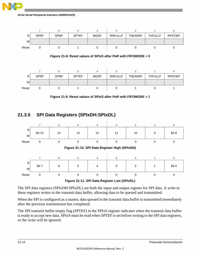
16-bit Serial Peripheral Interface (S08SPI16V5)
21-14 Freescale Semiconductor
Figure 21-8. Reset values of SPIxS after PoR with FIFOMODE = 0
Figure 21-9. Reset values of SPIxS after PoR with FIFOMODE = 1
21.3.5 SPI Data Registers (SPIxDH:SPIxDL)
The SPI data registers (SPIxDH:SPIxDL) are both the input and output register for SPI data. A write to these registers writes to the transmit data buffer, allowing data to be queued and transmitted.
When the SPI is configured as a master, data queued in the transmit data buffer is transmitted immediately after the previous transmission has completed.
The SPI transmit buffer empty flag (SPTEF) in the SPIxS register indicates when the transmit data buffer is ready to accept new data. SPIxS must be read when SPTEF is set before writing to the SPI data registers, or the write will be ignored.
7 6 5 4 3 2 1 0
R SPRF SPMF SPTEF MODF RNFULLF TNEAREF TXFULLF RFIFOEF
W
Reset 0 0 1 0 0 0 0 0
7 6 5 4 3 2 1 0
R SPRF SPMF SPTEF MODF RNFULLF TNEAREF TXFULLF RFIFOEF
W
Reset 0 0 1 0 0 1 0 1
7 6 5 4 3 2 1 0
RBit 15 14 13 12 11 10 9 Bit 8
W
Reset 0 0 0 0 0 0 0 0
Figure 21-10. SPI Data Register High (SPIxDH)
7 6 5 4 3 2 1 0
RBit 7 6 5 4 3 2 1 Bit 0
W
Reset 0 0 0 0 0 0 0 0
Figure 21-11. SPI Data Register Low (SPIxDL)
MCF51JE256 Reference Manual, Rev. 2

16-bit Serial Peripheral Interface (S08SPI16V5)
Freescale Semiconductor 21-15
Data may be read from SPIxDH:SPIxDL any time after SPRF is set and before another transfer is finished. Failure to read the data out of the receive data buffer before a new transfer ends causes a receive overrun condition and the data from the new transfer is lost.
In 8-bit mode, only SPIxDL is available. Reads of SPIxDH will return all 0s. Writes to SPIxDH will be ignored.
In 16-bit mode, reading either byte (SPIxDH or SPIxDL) latches the contents of both bytes into a buffer where they remain latched until the other byte is read. Writing to either byte (SPIxDH or SPIxDL) latches the value into a buffer. When both bytes have been written, they are transferred as a coherent 16-bit value into the transmit data buffer.
21.3.6 SPI Match Registers (SPIxMH:SPIxML)
These read/write registers contain the hardware compare value, which sets the SPI match flag (SPMF) when the value received in the SPI receive data buffer equals the value in the SPIxMH:SPIxML registers.
In 8-bit mode, only SPIxML is available. Reads of SPIxMH will return all 0s. Writes to SPIxMH will be ignored.
In 16-bit mode, reading either byte (SPIxMH or SPIxML) latches the contents of both bytes into a buffer where they remain latched until the other byte is read. Writing to either byte (SPIxMH or SPIxML) latches the value into a buffer. When both bytes have been written, they are transferred as a coherent value into the SPI match registers.
21.3.7 SPI Control Register 3 (SPIxC3) — enable FIFO feature
The SPI Control Register 3 introduces a 64-bit FIFO function on both transmit and receive buffers to be utilized on the SPI. Utilizing this FIFO feature allows the SPI to provide high speed transfers of large amounts of data without consuming large amounts of the CPU bandwidth.
7 6 5 4 3 2 1 0
RBit 15 14 13 12 11 10 9 Bit 8
W
Reset 0 0 0 0 0 0 0 0
Figure 21-12. SPI Match Register High (SPIxMH)
7 6 5 4 3 2 1 0
RBit 7 6 5 4 3 2 1 Bit 0
W
Reset 0 0 0 0 0 0 0 0
Figure 21-13. SPI Match Register Low (SPIxML)
MCF51JE256 Reference Manual, Rev. 2

16-bit Serial Peripheral Interface (S08SPI16V5)
21-16 Freescale Semiconductor
Enabling this FIFO function will effect the behavior of some of the Read/Write Buffer flags in the SPIxS register namely:
• The SPRF of the SPIxS register will be set when the Receive FIFO is filled and will interrupt the CPU if the SPIE in the SPIxC1 register is set.
and
• The SPTEF of the SPIxS register will be set when the Transmit FIFO is empty, and will interrupt the CPU if the SPTIE bit is set in the SPIxC1 register. See SPIxC1 and SPIxS registers.
FIFO mode is enabled by setting the FIFOMODE bit, and provides the SPI with an 8-byte receive FIFO and an 8-byte transmit FIFO to reduce the amount of CPU interrupts for high speed/high volume data transfers.
Two interrupt enable bits TNEARIEN and RNFULLIEN provide CPU interrupts based on the “watermark” feature of the TNEARF and RNFULLF flags of the SPIxS register.Note: This register has six read/write control bits. Bits 7 through 6 are not implemented and always read 0. Writes have no
meaning or effect. Write to this register happens only when FIFOMODE bit is 1.
7 6 5 4 3 2 1 0
R0 0
TNEAREF MARK
RNFULL MARK
INTCLR TNEARIEN RNFULLIEN FIFOMODE
W
Reset 0 0 0 0 0 0 0 0
= Unimplemented or Reserved
Figure 21-14. SPI Control Register (SPIxC3S)
Table 21-9. SPIxC3S Register Field Descriptions
Field Description
5TNEAREF
MARK
Transmit FIFO Nearly Empty Water Mark — This bit selects the mark after which TNEAREF flag is asserted.0 TNEAREF is set when Transmit FIFO has16bits or less.1 TNEAREF is set when Transmit FIFO has 32bits or less.
4RNFULLF
MARK
Receive FIFO Nearly Full Water Mark — This bit selects the mark for which RNFULLF flag is asserted0 RNFULLF is set when Receive FIFO has 48bits or more1 RNFULLF is set when Receive FIFO has 32bits or more.
3INTCLR
Interrupt Clearing Mechanism Select — This bit selects the mechanism by which SPRF, SPTEF, TNEAREF, RNFULLF interrupts gets cleared.0 Interrupts gets cleared when respective flags gets cleared depending on the state of FIFOs1 Interrupts gets cleared by writing to the SPIxCI respective bits.
2TNEARIEN
Transmit FIFO Nearly Empty Interrupt Enable — Writing to this bit enables the SPI to interrupt the CPU when the TNEAREF flag is set. This is an additional interrupt on the SPI and will only interrupt the CPU if SPTIE in the SPIxC1 register is also set. This bit is ignored and has no function if FIFOMODE=0.0 No interrupt on Transmit FIFO Nearly Empty Flag being set.1 Enable interrupts on Transmit FIFO Nearly Empty Flag being set.
MCF51JE256 Reference Manual, Rev. 2

16-bit Serial Peripheral Interface (S08SPI16V5)
Freescale Semiconductor 21-17
21.3.8 SPI Clear Interrupt Register (SPIxCI)
The SPI Clear Interrupt register has 4 bits dedicated for clearing the interrupts. Writing 1 to these bits clears the respective interrupts if INTCLR bit in SPIxCR3 is set.
It also have 2 bits to indicate the transmit FIFO and receive FIFO overrun conditions. When receive FIFO is full and a data is received RXFOF flag is set. Similarly, when transmit FIFO is full and write happens to SPIDR TXFOF is set. These flags get cleared when a read happens to this register with the flags set.
There are two more bits to indicate the error flags. These flags gets set when due to some spurious reasons entries in FIFO becomes greater than 8. At this point all the flags in status register gets reset and entries in FIFO are flushed with respective error flags set. These flags are cleared when a read happen at SPIxCI with the error flags set.Note: Bits [7:4] are read-only bits. These bits gets cleared when a read happens to this register with the flags set. Bits [3:0] are
clear interrupts bits which clears the interrupts by writing 1 to respective bits. Reading these bits always return 0.
1RNFULLIEN
Receive FIFO Nearly Full Interrupt Enable — Writing to this bit enables the SPI to interrupt the CPU when the RNEARFF flag is set. This is an additional interrupt on the SPI and will only interrupt the CPU if SPIE in the SPIxC1 register is also set. This bit is ignored and has no function if FIFOMODE=0.0 No interrupt on RNEARFF being set.1 Enable interrupts on RNEARFF being set.
0FIFOMODE
SPI FIFO Mode Enable — This bit enables the SPI to utilize a 64bit FIFO (8 bytes 4 16-bit words) for both transmit and receive buffers. 0 Buffer mode disabled.1 Data available in the receive data buffer.
7 6 5 4 3 2 1 0
R TXFERR RXFERR TXFOF RXFOFTNEAREFCI RNFULLFCI SPTEFCI SPRFCI
W
Reset 0 0 0 0 0 0 0 0
= Unimplemented or Reserved
Table 21-10. SPIxCI Register Field Descriptions
Field Description
7TXFERR
Transmit FIFO Error Flag- This flag indicates that TX FIFO error occurred because entries in FIFO goes above 8.0 No TX FIFO error occurred.1 TX FIFO error occurred.
6RXFERR
Receive FIFO Error Flag- This flag indicates that RX FIFO error occurred because entries in FIFO goes above 8.0 No RX FIFO error occurred.1 RX FIFO error occurred.
Table 21-9. SPIxC3S Register Field Descriptions
Field Description
MCF51JE256 Reference Manual, Rev. 2

16-bit Serial Peripheral Interface (S08SPI16V5)
21-18 Freescale Semiconductor
21.4 Functional Description
21.4.1 General
The SPI system is enabled by setting the SPI enable (SPE) bit in SPI Control Register 1. While the SPE bit is set, the four associated SPI port pins are dedicated to the SPI function as:
• Slave select (SS)
• Serial clock (SPSCK)
• Master out/slave in (MOSI)
• Master in/slave out (MISO)
An SPI transfer is initiated in the master SPI device by reading the SPI status register (SPIxS) when SPTEF = 1 and then writing data to the transmit data buffer (write to SPIxDH:SPIxDL). When a transfer is complete, received data is moved into the receive data buffer. The SPIxDH:SPIxDL registers act as the SPI receive data buffer for reads and as the SPI transmit data buffer for writes.
The clock phase control bit (CPHA) and a clock polarity control bit (CPOL) in the SPI Control Register 1 (SPIxC1) select one of four possible clock formats to be used by the SPI system. The CPOL bit simply selects a non-inverted or inverted clock. The CPHA bit is used to accommodate two fundamentally different protocols by sampling data on odd numbered SPSCK edges or on even numbered SPSCK edges.
The SPI can be configured to operate as a master or as a slave. When the MSTR bit in SPI control register 1 is set, master mode is selected, when the MSTR bit is clear, slave mode is selected.
21.4.2 Master Mode
The SPI operates in master mode when the MSTR bit is set. Only a master SPI module can initiate transmissions. A transmission begins by reading the SPIxS register while SPTEF = 1 and writing to the
5TXFOF
TX FIFO Overflow Flag- This Flag indicates that TX FIFO overflow condition has occurred.0 TX FIFO overflow condition has not occurred.1 TX FIFO overflow condition occurred.
4RXFOF
RX FIFO Overflow Flag - This Flag indicates that RX FIFO overflow condition has occurred.0 RX FIFO overflow condition has not occurred.1 RX FIFO overflow condition occurred.
3TNEAREFCI
Transmit FIFO Nearly Empty Flag Clear Interrupt Register — Write of 1 clears the TNEAREF interrupt provided SPIxC3[3] is set.
2RNFULLFCI
Receive FIFO Nearly Full Flag Clear Interrupt Register — Write of 1 clears the RNFULLF interrupt provided SPIxC3[3] is set.
1SPTEFCI
Transmit FIFO Empty Flag Clear Interrupt Register — Write of 1 clears the SPTEF interrupt provided SPIxC3[3] is set.
0SPRFCI
Receive FIFO Full Flag Clear Interrupt Register — Write of 1 clears the TNEAREF interrupt provided SPIxC3[3] is set.
Table 21-10. SPIxCI Register Field Descriptions
Field Description
MCF51JE256 Reference Manual, Rev. 2

16-bit Serial Peripheral Interface (S08SPI16V5)
Freescale Semiconductor 21-19
master SPI data registers. If the shift register is empty, the byte immediately transfers to the shift register. The data begins shifting out on the MOSI pin under the control of the serial clock.
• SPSCK
The SPR3, SPR2, SPR1, and SPR0 baud rate selection bits in conjunction with the SPPR2, SPPR1, and SPPR0 baud rate preselection bits in the SPI Baud Rate register control the baud rate generator and determine the speed of the transmission. The SPSCK pin is the SPI clock output. Through the SPSCK pin, the baud rate generator of the master controls the shift register of the slave peripheral.
• MOSI, MISO pin
In master mode, the function of the serial data output pin (MOSI) and the serial data input pin (MISO) is determined by the SPC0 and BIDIROE control bits.
• SS pin
If MODFEN and SSOE bit are set, the SS pin is configured as slave select output. The SS output becomes low during each transmission and is high when the SPI is in idle state.
If MODFEN is set and SSOE is cleared, the SS pin is configured as input for detecting mode fault error. If the SS input becomes low this indicates a mode fault error where another master tries to drive the MOSI and SPSCK lines. In this case, the SPI immediately switches to slave mode, by clearing the MSTR bit and also disables the slave output buffer MISO (or SISO in bidirectional mode). So the result is that all outputs are disabled and SPSCK, MOSI and MISO are inputs. If a transmission is in progress when the mode fault occurs, the transmission is aborted and the SPI is forced into idle state.
This mode fault error also sets the mode fault (MODF) flag in the SPI Status Register (SPIxS). If the SPI interrupt enable bit (SPIE) is set when the MODF flag gets set, then an SPI interrupt sequence is also requested.
When a write to the SPI Data Register in the master occurs, there is a half SPSCK-cycle delay. After the delay, SPSCK is started within the master. The rest of the transfer operation differs slightly, depending on the clock format specified by the SPI clock phase bit, CPHA, in SPI Control Register 1 (see Section 21.4.6, “SPI Clock Formats).
NOTE
A change of the bits CPOL, CPHA, SSOE, LSBFE, MODFEN, SPC0, BIDIROE with SPC0 set, SPIMODE, FIFOMODE, SPPR2-SPPR0 and SPR3-SPR0 in master mode will abort a transmission in progress and force the SPI into idle state. The remote slave cannot detect this, therefore the master has to ensure that the remote slave is set back to idle state.
21.4.3 Slave Mode
The SPI operates in slave mode when the MSTR bit in SPI Control Register1 is clear.
• SPSCK
In slave mode, SPSCK is the SPI clock input from the master.
• MISO, MOSI pin
MCF51JE256 Reference Manual, Rev. 2

16-bit Serial Peripheral Interface (S08SPI16V5)
21-20 Freescale Semiconductor
In slave mode, the function of the serial data output pin (MISO) and serial data input pin (MOSI) is determined by the SPC0 bit and BIDIROE bit in SPI Control Register 2.
• SS pin
The SS pin is the slave select input. Before a data transmission occurs, the SS pin of the slave SPI must be low. SS must remain low until the transmission is complete. If SS goes high, the SPI is forced into idle state.
The SS input also controls the serial data output pin, if SS is high (not selected), the serial data output pin is high impedance, and, if SS is low the first bit in the SPI Data Register is driven out of the serial data output pin. Also, if the slave is not selected (SS is high), then the SPSCK input is ignored and no internal shifting of the SPI shift register takes place.
Although the SPI is capable of duplex operation, some SPI peripherals are capable of only receiving SPI data in a slave mode. For these simpler devices, there is no serial data out pin.
NOTE
When peripherals with duplex capability are used, take care not to simultaneously enable two receivers whose serial outputs drive the same system slave’s serial data output line.
As long as no more than one slave device drives the system slave’s serial data output line, it is possible for several slaves to receive the same transmission from a master, although the master would not receive return information from all of the receiving slaves.
If the CPHA bit in SPI Control Register 1 is clear, odd numbered edges on the SPSCK input cause the data at the serial data input pin to be latched. Even numbered edges cause the value previously latched from the serial data input pin to shift into the LSB or MSB of the SPI shift register, depending on the LSBFE bit.
If the CPHA bit is set, even numbered edges on the SPSCK input cause the data at the serial data input pin to be latched. Odd numbered edges cause the value previously latched from the serial data input pin to shift into the LSB or MSB of the SPI shift register, depending on the LSBFE bit.
When CPHA is set, the first edge is used to get the first data bit onto the serial data output pin. When CPHA is clear and the SS input is low (slave selected), the first bit of the SPI data is driven out of the serial data output pin. After the eighth (SPIMODE = 0) or sixteenth (SPIMODE = 1) shift, the transfer is considered complete and the received data is transferred into the SPI data registers. To indicate transfer is complete, the SPRF flag in the SPI Status Register is set.
NOTE
A change of the bits CPOL, CPHA, SSOE, LSBFE, MODFEN, SPC0 and BIDIROE with SPC0 set FIFOMODE and SPIMODE in slave mode will corrupt a transmission in progress and has to be avoided.
MCF51JE256 Reference Manual, Rev. 2

16-bit Serial Peripheral Interface (S08SPI16V5)
Freescale Semiconductor 21-21
21.4.4 SPI FIFO MODE
SPI works in FIFO mode when SPIxC3[0] bit is set. When in FIFO mode SPI RX buffer and SPI TX buffer is replaced by a 8 byte deep FIFO as shown in figure above.
spidh:l_rx_reg
Read Access
IPBus (ips_rdata[7:0])
SPI_REG_BLOCK
SPI_CORE_SHFR
Load
Control
shfr_rx_reg
SPI Data Register
FIFO depth = 8 bytesFIFO Ctrlr
Figure 21-15. SPIH:L read side structural overview in FIFO mode
RX- FIFO
spidh:l_tx_reg
Read Access
IPBus (ips_rdata[7:0])
SPI_REG_BLOCK
SPI_CORE_SHFR
Read
Control shfr_tx_reg
SPI Data Register
FIFO depth = 8 bytesFIFO Ctrlr
Figure 21-16. SPIH:L write side structural overview in FIFO mode
TX- FIFO
MCF51JE256 Reference Manual, Rev. 2

16-bit Serial Peripheral Interface (S08SPI16V5)
21-22 Freescale Semiconductor
21.4.5 Data Transmission Length
The SPI can support data lengths of 8 or 16 bits. The length can be configured with the SPIMODE bit in the SPIxC2 register.
In 8-bit mode (SPIMODE = 0), the SPI Data Register is comprised of one byte: SPIxDL. The SPI Match Register is also comprised of only one byte: SPIxML. Reads of SPIxDH and SPIxMH will return zero. Writes to SPIxDH and SPIxMH will be ignored.
In 16-bit mode (SPIMODE = 1), the SPI Data Register is comprised of two bytes: SPIxDH and SPIxDL. Reading either byte (SPIxDH or SPIxDL) latches the contents of both bytes into a buffer where they remain latched until the other byte is read. Writing to either byte (SPIxDH or SPIxDL) latches the value into a buffer. When both bytes have been written, they are transferred as a coherent 16-bit value into the transmit data buffer.
In 16-bit mode, the SPI Match Register is also comprised of two bytes: SPIxMH and SPIxML. There is no buffer mechanism for the reading of SPIxMH and SPIxML since they can only be changed by writing at CPU side. Writing to either byte (SPIxMH or SPIxML) latches the value into a buffer. When both bytes have been written, they are transferred as a coherent 16-bit value into the transmit data buffer.
Any switching between 8- and 16-bit data transmission length (controlled by SPIMODE bit) in master mode will abort a transmission in progress, force the SPI system into idle state, and reset all status bits in the SPIxS register. To initiate a transfer after writing to SPIMODE, the SPIxS register must be read with SPTEF = 1, and data must be written to SPIxDH:SPIxDL in 16-bit mode (SPIMODE = 1) or SPIxDL in 8-bit mode (SPIMODE = 0).
In slave mode, user software should write to SPIMODE only once to prevent corrupting a transmission in progress.
NOTEData can be lost if the data length is not the same for both master and slave devices.
21.4.6 SPI Clock Formats
To accommodate a wide variety of synchronous serial peripherals from different manufacturers, the SPI system has a clock polarity (CPOL) bit and a clock phase (CPHA) control bit to select one of four clock formats for data transfers. CPOL selectively inserts an inverter in series with the clock. CPHA chooses between two different clock phase relationships between the clock and data.
Figure 21-17 shows the clock formats when SPIMODE = 0 (8-bit mode) and CPHA = 1. At the top of the figure, the eight bit times are shown for reference with bit 1 starting at the first SPSCK edge and bit 8 ending one-half SPSCK cycle after the eighth SPSCK edge. The MSB first and LSB first lines show the order of SPI data bits depending on the setting in LSBFE. Both variations of SPSCK polarity are shown, but only one of these waveforms applies for a specific transfer, depending on the value in CPOL. The SAMPLE IN waveform applies to the MOSI input of a slave or the MISO input of a master. The MOSI waveform applies to the MOSI output pin from a master and the MISO waveform applies to the MISO output from a slave. The SS OUT waveform applies to the slave select output from a master (provided MODFEN and SSOE = 1). The master SS output goes to active low one-half SPSCK cycle before the start
MCF51JE256 Reference Manual, Rev. 2

16-bit Serial Peripheral Interface (S08SPI16V5)
Freescale Semiconductor 21-23
of the transfer and goes back high at the end of the eighth bit time of the transfer. The SS IN waveform applies to the slave select input of a slave.
Figure 21-17. SPI Clock Formats (CPHA = 1)
When CPHA = 1, the slave begins to drive its MISO output when SS goes to active low, but the data is not defined until the first SPSCK edge. The first SPSCK edge shifts the first bit of data from the shifter onto the MOSI output of the master and the MISO output of the slave. The next SPSCK edge causes both the master and the slave to sample the data bit values on their MISO and MOSI inputs, respectively. At the third SPSCK edge, the SPI shifter shifts one bit position which shifts in the bit value that was just sampled, and shifts the second data bit value out the other end of the shifter to the MOSI and MISO outputs of the master and slave, respectively. When CPHA = 1, the slave’s SS input is not required to go to its inactive high level between transfers.
Figure 21-18 shows the clock formats when SPIMODE = 0 and CPHA = 0. At the top of the figure, the eight bit times are shown for reference with bit 1 starting as the slave is selected (SS IN goes low), and bit 8 ends at the last SPSCK edge. The MSB first and LSB first lines show the order of SPI data bits depending on the setting in LSBFE. Both variations of SPSCK polarity are shown, but only one of these waveforms applies for a specific transfer, depending on the value in CPOL. The SAMPLE IN waveform applies to the MOSI input of a slave or the MISO input of a master. The MOSI waveform applies to the MOSI output
BIT TIME #(REFERENCE)
MSB FIRSTLSB FIRST
SPSCK(CPOL = 0)
SPSCK(CPOL = 1)
SAMPLE IN(MISO OR MOSI)
MOSI(MASTER OUT)
MISO(SLAVE OUT)
SS OUT(MASTER)
SS IN(SLAVE)
BIT 7BIT 0
BIT 6BIT 1
BIT 2BIT 5
BIT 1BIT 6
BIT 0BIT 7
1 2 6 7 8
...
...
...
MCF51JE256 Reference Manual, Rev. 2

16-bit Serial Peripheral Interface (S08SPI16V5)
21-24 Freescale Semiconductor
pin from a master and the MISO waveform applies to the MISO output from a slave. The SS OUT waveform applies to the slave select output from a master (provided MODFEN and SSOE = 1). The master SS output goes to active low at the start of the first bit time of the transfer and goes back high one-half SPSCK cycle after the end of the eighth bit time of the transfer. The SS IN waveform applies to the slave select input of a slave.
Figure 21-18. SPI Clock Formats (CPHA = 0)
When CPHA = 0, the slave begins to drive its MISO output with the first data bit value (MSB or LSB depending on LSBFE) when SS goes to active low. The first SPSCK edge causes both the master and the slave to sample the data bit values on their MISO and MOSI inputs, respectively. At the second SPSCK edge, the SPI shifter shifts one bit position which shifts in the bit value that was just sampled and shifts the second data bit value out the other end of the shifter to the MOSI and MISO outputs of the master and slave, respectively. When CPHA = 0, the slave’s SS input must go to its inactive high level between transfers.
21.4.7 SPI Baud Rate Generation
As shown in Figure 21-19, the clock source for the SPI baud rate generator is the bus clock. The three prescale bits (SPPR2:SPPR1:SPPR0) choose a prescale divisor of 1, 2, 3, 4, 5, 6, 7, or 8. The three rate select bits (SPR3:SPR2:SPR1:SPR0) divide the output of the prescaler stage by 2, 4, 8, 16, 32, 64, 128, 256 or 512 to get the internal SPI master mode bit-rate clock.
BIT TIME #(REFERENCE)
MSB FIRSTLSB FIRST
SPSCK(CPOL = 0)
SPSCK(CPOL = 1)
SAMPLE IN(MISO OR MOSI)
MOSI(MASTER OUT)
MISO(SLAVE OUT)
SS OUT(MASTER)
SS IN(SLAVE)
BIT 7BIT 0
BIT 6BIT 1
BIT 2BIT 5
BIT 1BIT 6
BIT 0BIT 7
1 2 6 7 8...
...
...
MCF51JE256 Reference Manual, Rev. 2

16-bit Serial Peripheral Interface (S08SPI16V5)
Freescale Semiconductor 21-25
The baud rate generator is activated only when the SPI is in the master mode and a serial transfer is taking place. In the other cases, the divider is disabled to decrease IDD current.
The baud rate divisor equation is as follows except those reserved combinations in Table 21-7:
The baud rate can be calculated with the following equation:
Figure 21-19. SPI Baud Rate Generation
21.4.8 Special Features
21.4.8.1 SS Output
The SS output feature automatically drives the SS pin low during transmission to select external devices and drives it high during idle to deselect external devices. When SS output is selected, the SS output pin is connected to the SS input pin of the external device.
The SS output is available only in master mode during normal SPI operation by asserting the SSOE and MODFEN bits as shown in Table 21-2.
The mode fault feature is disabled while SS output is enabled.
NOTE
Care must be taken when using the SS output feature in a multi-master system since the mode fault feature is not available for detecting system errors between masters.
21.4.8.2 Bidirectional Mode (MOMI or SISO)
The bidirectional mode is selected when the SPC0 bit is set in SPI Control Register 2 (see Section Table 21-11., “Normal Mode and Bidirectional Mode.”) In this mode, the SPI uses only one serial data pin for the interface with external device(s). The MSTR bit decides which pin to use. The MOSI pin becomes the serial data I/O (MOMI) pin for the master mode, and the MISO pin becomes serial data I/O (SISO) pin for the slave mode. The MISO pin in master mode and MOSI pin in slave mode are not used by the SPI.
BaudRateDivisor SPPR 1+ 2 SPR 1+ =
Baud Rate BusClock BaudRateDivisor=
DIVIDE BY2, 4, 8, 16, 32, 64, 128, 256 or 512
DIVIDE BY1, 2, 3, 4, 5, 6, 7, or 8
PRESCALER BAUD RATE DIVIDER
SPPR2:SPPR1:SPPR0 SPR3:SPR2:SPR1:SPR0
BUS CLOCKMASTERSPIBIT RATE
MCF51JE256 Reference Manual, Rev. 2

16-bit Serial Peripheral Interface (S08SPI16V5)
21-26 Freescale Semiconductor
The direction of each serial I/O pin depends on the BIDIROE bit. If the pin is configured as an output, serial data from the shift register is driven out on the pin. The same pin is also the serial input to the shift register.
The SPSCK is output for the master mode and input for the slave mode.
The SS is the input or output for the master mode, and it is always the input for the slave mode.
The bidirectional mode does not affect SPSCK and SS functions.
NOTE
In bidirectional master mode, with mode fault enabled, both data pins MISO and MOSI can be occupied by the SPI, though MOSI is normally used for transmissions in bidirectional mode and MISO is not used by the SPI. If a mode fault occurs, the SPI is automatically switched to slave mode, in this case MISO becomes occupied by the SPI and MOSI is not used. This has to be considered, if the MISO pin is used for another purpose.
21.4.9 Error Conditions
The SPI has one error condition:
• Mode fault error
21.4.9.1 Mode Fault Error
If the SS input becomes low while the SPI is configured as a master, it indicates a system error where more than one master may be trying to drive the MOSI and SPSCK lines simultaneously. This condition is not
Table 21-11. Normal Mode and Bidirectional Mode
When SPE = 1 Master Mode MSTR = 1 Slave Mode MSTR = 0
Normal ModeSPC0 = 0
Bidirectional ModeSPC0 = 1
SPI
MOSI
MISO
Serial Out
Serial In
SPI
MOSI
MISO
Serial In
Serial Out
SPI
MOMISerial Out
Serial In
BIDIROE SPI
SISO
Serial In
Serial Out
.
BIDIROE
MCF51JE256 Reference Manual, Rev. 2

16-bit Serial Peripheral Interface (S08SPI16V5)
Freescale Semiconductor 21-27
permitted in normal operation, and the MODF bit in the SPI status register is set automatically provided the MODFEN bit is set.
In the special case where the SPI is in master mode and MODFEN bit is cleared, the SS pin is not used by the SPI. In this special case, the mode fault error function is inhibited and MODF remains cleared. In case the SPI system is configured as a slave, the SS pin is a dedicated input pin. Mode fault error doesn’t occur in slave mode.
If a mode fault error occurs the SPI is switched to slave mode, with the exception that the slave output buffer is disabled. So SPSCK, MISO and MOSI pins are forced to be high impedance inputs to avoid any possibility of conflict with another output driver. A transmission in progress is aborted and the SPI is forced into idle state.
If the mode fault error occurs in the bidirectional mode for a SPI system configured in master mode, output enable of the MOMI (MOSI in bidirectional mode) is cleared if it was set. No mode fault error occurs in the bidirectional mode for the SPI system configured in slave mode.
The mode fault flag is cleared automatically by a read of the SPI Status Register (with MODF set) followed by a write to SPI Control Register 1. If the mode fault flag is cleared, the SPI becomes a normal master or slave again.
21.4.10 Low-power Mode Options
21.4.10.1 SPI in Run Mode
In run mode with the SPI system enable (SPE) bit in the SPI control register clear, the SPI system is in a low-power, disabled state. SPI registers can still be accessed, but clocks to the core of this module are disabled.
21.4.10.2 SPI in Wait Mode
SPI operation in wait mode depends upon the state of the SPISWAI bit in SPI Control Register 2.
• If SPISWAI is clear, the SPI operates normally when the CPU is in wait mode
• If SPISWAI is set, SPI clock generation ceases and the SPI module enters a power conservation state when the CPU is in wait mode.
— If SPISWAI is set and the SPI is configured for master, any transmission and reception in progress stops at wait mode entry. The transmission and reception resumes when the SPI exits wait mode.
– If SPISWAI is set and the SPI is configured as a slave, any transmission and reception in progress continues if the SPSCK continues to be driven from the master. This keeps the slave synchronized to the master and the SPSCK.
If the master transmits data while the slave is in wait mode, the slave will continue to send out data consistent with the operation mode at the start of wait mode (i.e., if the slave is currently sending its SPIxDH:SPIxDL to the master, it will continue to send the same byte. Otherwise, if the slave is currently sending the last data received byte from the master, it will continue to send each previously receive data from the master byte).
MCF51JE256 Reference Manual, Rev. 2

16-bit Serial Peripheral Interface (S08SPI16V5)
21-28 Freescale Semiconductor
NOTE
Care must be taken when expecting data from a master while the slave is in wait or stop3 mode. Even though the shift register will continue to operate, the rest of the SPI is shut down (i.e. a SPRF interrupt will not be generated until exiting stop or wait mode). Also, the data from the shift register will not be copied into the SPIxDH:SPIxDL registers until after the slave SPI has exited wait or stop mode. A SPRF flag and SPIxDH:SPIxDL copy is only generated if wait mode is entered or exited during a tranmission. If the slave enters wait mode in idle mode and exits wait mode in idle mode, neither a SPRF nor a SPIxDH:SPIxDL copy will occur.
21.4.10.3 SPI in Stop Mode
Stop3 mode is dependent on the SPI system. Upon entry to stop3 mode, the SPI module clock is disabled (held high or low). If the SPI is in master mode and exchanging data when the CPU enters stop mode, the transmission is frozen until the CPU exits stop mode. After stop, data to and from the external SPI is exchanged correctly. In slave mode, the SPI will stay synchronized with the master.
The stop mode is not dependent on the SPISWAI bit.
In all other stop modes, the SPI module is completely disabled. After stop, all registers are reset to their default values, and the SPI module must be re-initialized.
21.4.10.4 Reset
The reset values of registers and signals are described in Section 21.3, “Register Definition.” which details the registers and their bit-fields.
• If a data transmission occurs in slave mode after reset without a write to SPIxDH:SPIxDL, it will transmit garbage, or the data last received from the master before the reset.
• Reading from the SPIxDH:SPIxDL after reset will always read zeros.
21.4.10.5 Interrupts
The SPI only originates interrupt requests when the SPI is enabled (SPE bit in SPIxC1 set). The following is a description of how the SPI makes a request and how the MCU should acknowledge that request. The interrupt vector offset and interrupt priority are chip dependent.
21.4.11 SPI Interrupts
There are four flag bits, three interrupt mask bits, and one interrupt vector associated with the SPI system. The SPI interrupt enable mask (SPIE) enables interrupts from the SPI receiver full flag (SPRF) and mode fault flag (MODF). The SPI transmit interrupt enable mask (SPTIE) enables interrupts from the SPI transmit buffer empty flag (SPTEF). The SPI match interrupt enable mask bit (SPIMIE) enables interrupts from the SPI match flag (SPMF). When one of the flag bits is set, and the associated interrupt mask bit is set, a hardware interrupt request is sent to the CPU. If the interrupt mask bits are cleared, software can poll the associated flag bits instead of using interrupts. The SPI interrupt service routine (ISR) should check
MCF51JE256 Reference Manual, Rev. 2

16-bit Serial Peripheral Interface (S08SPI16V5)
Freescale Semiconductor 21-29
the flag bits to determine what event caused the interrupt. The service routine should also clear the flag bit(s) before returning from the ISR (usually near the beginning of the ISR).
21.4.11.1 MODF
MODF occurs when the master detects an error on the SS pin. The master SPI must be configured for the MODF feature (see Table 21-2). Once MODF is set, the current transfer is aborted and the following bit is changed:
• MSTR=0, The master bit in SPIxC1 resets.
The MODF interrupt is reflected in the status register MODF flag. Clearing the flag will also clear the interrupt. This interrupt will stay active while the MODF flag is set. MODF has an automatic clearing process which is described in Section 21.3.4, “SPI Status Register (SPIxS).”
21.4.11.2 SPRF
SPRF occurs when new data has been received and copied to the SPI receive data buffer. In 8-bit mode, SPRF is set only after all 8 bits have been shifted out of the shift register and into SPIxDL. In 16-bit mode, SPRF is set only after all 16 bits have been shifted out of the shift register and into SPIxDH:SPIxDL.
Once SPRF is set, it does not clear until it is serviced. SPRF has an automatic clearing process which is described in Section 21.3.4, “SPI Status Register (SPIxS).” In the event that the SPRF is not serviced before the end of the next transfer (i.e. SPRF remains active throughout another transfer), the latter transfers will be ignored and no new data will be copied into the SPIxDH:SPIxDL.
21.4.11.3 SPTEF
SPTEF occurs when the SPI transmit buffer is ready to accept new data. In 8-bit mode, SPTEF is set only after all 8 bits have been moved from SPIxDL into the shifter. In 16-bit mode, SPTEF is set only after all 16 bits have been moved from SPIxDH:SPIxDL into the shifter.
Once SPTEF is set, it does not clear until it is serviced. SPTEF has an automatic clearing process which is described in Section 21.3.4, “SPI Status Register (SPIxS).
21.4.11.4 SPMF
SPMF occurs when the data in the receive data buffer is equal to the data in the SPI match register. In 8-bit mode, SPMF is set only after bits 8–0 in the receive data buffer are determined to be equivalent to the value in SPIxML. In 16-bit mode, SPMF is set after bits 15–0 in the receive data buffer are determined to be equivalent to the value in SPIxMH:SPIxML.
21.4.11.5 TNEAREF
TNEAREF flag is set when only one 16bit words or 2 8bit bytes of data remain in the transmit FIFO provided SPIxC3[5] = 0 or when only two 16bit words or 4 8bit bytes of data remain in the transmit FIFO provided SPIxC3[5] =1. If FIFOMODE is not enabled this bit should be ignored.
MCF51JE256 Reference Manual, Rev. 2

16-bit Serial Peripheral Interface (S08SPI16V5)
21-30 Freescale Semiconductor
Clearing of this interrupts depends on state of SPIxC3[3] and the status of TNEAREF as described Section 21.3.4, “SPI Status Register (SPIxS)
21.4.11.6 RNFULLF
RNFULLF is set when more than three16bit words or six 8bit bytes of data remain in the receive FIFO provided SPIxC3[4] = 0 or when more than two 16bit words or four 8bit bytes of data remain in the receive FIFO provided SPIxC3[4] = 1.
Clearing of this interrupts depends on state of SPIxC3[3] and the status of RNFULLF as described Section 21.3.4, “SPI Status Register (SPIxS)
21.5 Initialization/Application Information
21.5.1 SPI Module Initialization Example
21.5.1.1 Initialization Sequence
Before the SPI module can be used for communication, an initialization procedure must be carried out, as follows:
1. Update control register 1 (SPIxC1) to enable the SPI and to control interrupt enables. This register also sets the SPI as master or slave, determines clock phase and polarity, and configures the main SPI options.
2. Update control register 2 (SPIxC2) to enable additional SPI functions such as the SPI match interrupt feature, the master mode-fault function, and bidirectional mode output. 8- or 16-bit mode select and other optional features are controlled here as well.
3. Update the baud rate register (SPIxBR) to set the prescaler and bit rate divisor for an SPI master.
4. Update the hardware match register (SPIxMH:SPIxML) with the value to be compared to the receive data register for triggering an interrupt if hardware match interrupts are enabled.
5. In the master, read SPIxS while SPTEF = 1, and then write to the transmit data register (SPIxDH:SPIxDL) to begin transfer.
21.5.1.2 Pseudo—Code Example
In this example, the SPI module will be set up for master mode with only hardware match interrupts enabled. The SPI will run in 16-bit mode at a maximum baud rate of bus clock divided by 2. Clock phase and polarity will be set for an active-high SPI clock where the first edge on SPSCK occurs at the start of the first cycle of a data transfer.
MCF51JE256 Reference Manual, Rev. 2

16-bit Serial Peripheral Interface (S08SPI16V5)
Freescale Semiconductor 21-31
SPIxC1=0x54(%01010100)Bit 7 SPIE = 0 Disables receive and mode fault interrupts
Bit 6 SPE = 1 Enables the SPI system
Bit 5 SPTIE = 0 Disables SPI transmit interrupts
Bit 4 MSTR = 1 Sets the SPI module as a master SPI device
Bit 3 CPOL = 0 Configures SPI clock as active-high
Bit 2 CPHA = 1 First edge on SPSCK at start of first data transfer cycle
Bit 1 SSOE = 0 Determines SS pin function when mode fault enabled
Bit 0 LSBFE = 0 SPI serial data transfers start with most significant bit
SPIxC2 = 0xC0(%11000000)Bit 7 SPMIE = 1 SPI hardware match interrupt enabled
Bit 6 SPIMODE = 1 Configures SPI for 16-bit mode
Bit 5 = 0 Unimplemented
Bit 4 MODFEN = 0 Disables mode fault function
Bit 3 BIDIROE = 0 SPI data I/O pin acts as input
Bit 2 = 0 Unimplemented
Bit 1 SPISWAI = 0 SPI clocks operate in wait mode
Bit 0 SPC0 = 0 uses separate pins for data input and output
SPIxBR = 0x00(%00000000)Bit 7 = 0 Unimplemented
Bit 6:4 = 000 Sets prescale divisor to 1
Bit 3:0 = 0000 Sets baud rate divisor to 2
SPIxS = 0x00(%00000000)Bit 7 SPRF = 0 Flag is set when receive data buffer is full
Bit 6 SPMF = 0 Flag is set when SPIMH/L = receive data buffer
Bit 5 SPTEF = 0 Flag is set when transmit data buffer is empty
Bit 4 MODF = 0 Mode fault flag for master mode
Bit 3:0 = 0 FIFOMODE is not enabled
SPIxMH = 0xXXIn 16-bit mode, this register holds bits 8–15 of the hardware match buffer. In 8-bit mode, writes to this register will be ignored.
SPIxML = 0xXXHolds bits 0–7 of the hardware match buffer.
SPIxDH = 0xxxIn 16-bit mode, this register holds bits 8–15 of the data to be transmitted by the transmit buffer and received by the receive buffer.
MCF51JE256 Reference Manual, Rev. 2

16-bit Serial Peripheral Interface (S08SPI16V5)
21-32 Freescale Semiconductor
Figure 21-20. Initialization Flowchart Example for SPI Master Device in 16-bit Mode for FIFOMODE = 0
SPIxDL = 0xxx Holds bits 0–7 of the data to be transmitted by the transmit buffer and received by the receive buffer.
INITIALIZE SPISPIxC1 = 0x54SPIxC2 = 0xC0SPIxBR = 0x00SPIxMH = 0xXX
RESET
YES
READ SPMF WHILE SET TO CLEAR FLAG,
THEN WRITE A 1 TO IT
CONTINUE
SPMF = 1?
READSPIxDH:SPIxDL
SPRF = 1?
WRITE TOSPIxDH:SPIxDL
SPTEF = 1?
NO
NO
NO
YES
YES
YES
MCF51JE256 Reference Manual, Rev. 2

16-bit Serial Peripheral Interface (S08SPI16V5)
Freescale Semiconductor 21-33
Figure 21-21. Initialization Flowchart Example for SPI Master Device in 16-bit Mode for FIFOMODE=1
INITIALIZE SPISPIxC1 = 0x54SPIxC2 = 0xC0SPIxBR = 0x00
= 0xXX
RESET
RNFULLF = 1/SPRF = 1
?
READ
RFIFOEF = 1?
WRITE TO
YES
YES
Set FIFOMODE
YES
TXFULLF = 1?
YES
CONTINUE
MCF51JE256 Reference Manual, Rev. 2

16-bit Serial Peripheral Interface (S08SPI16V5)
21-34 Freescale Semiconductor
MCF51JE256 Reference Manual, Rev. 2

Freescale Semiconductor 22-1
Chapter 22 8-bit Serial Peripheral Interface (S08SPIV5)
22.1 IntroductionFigure 22-1 shows the block diagram with the SPI2 highlighted.
NOTEThere are two SPI modules on this device. Replace SPIx with the appropriate peripheral designation (SPI1 or SPI2), depending upon your use:
• SPI1 — for the 16-bit SPI with FIFO module.
• SPI2 — for the 8-bit SPI module.
22.1.1 SPI2 Clock Gating
The bus clock to the SPI2 can be gated on and off using the SPI2 bit in SCGC2. These bits are set after any reset which enables the bus clock to this module. To conserve power, these bits can be cleared to disable the clock to this module when not in use. See Section 5.7.8, “System Clock Gating Control 2 Register (SCGC2),” for details.
MCF51JE256 Reference Manual, Rev. 2

8-bit Serial Peripheral Interface (S08SPIV5)
22-2 Freescale Semiconductor
Figure 22-1. Block Diagram Highlighting SPI2 Block and Pins
MCF51JE256 Reference Manual, Rev. 2

8-bit Serial Peripheral Interface (S08SPIV5)
Freescale Semiconductor 22-3
22.1.2 Features
The SPI includes these distinctive features:
• Master mode or slave mode operation
• Full-duplex or single-wire bidirectional mode
• Programmable transmit bit rate
• Double-buffered transmit and receive data register
• Serial clock phase and polarity options
• Slave select output
• Mode fault error flag with CPU interrupt capability
• Control of SPI operation during wait mode
• Selectable MSB-first or LSB-first shifting
• Receive data buffer hardware match feature
22.1.3 Modes of Operation
The SPI functions in three modes, run, wait, and stop.
• Run Mode
This is the basic mode of operation.
• Wait Mode
SPI operation in wait mode is a configurable low-power mode, controlled by the SPISWAI bit located in the SPIxC2 register. In wait mode, if the SPISWAI bit is clear, the SPI operates like in Run Mode. If the SPISWAI bit is set, the SPI goes into a power conservative state, with the SPI clock generation turned off. If the SPI is configured as a master, any transmission in progress stops, but is resumed after CPU goes into Run Mode. If the SPI is configured as a slave, reception and transmission of a byte continues, so that the slave stays synchronized to the master.
• Stop Mode
The SPI is inactive in stop3/stop4 mode for reduced power consumption. If the SPI is configured as a master, any transmission in progress stops, but is resumed after the CPU goes into Run Mode. If the SPI is configured as a slave, reception and transmission of a data continues, so that the slave stays synchronized to the master.
The SPI is completely disabled in all other stop modes. When the CPU wakes from these stop modes, all SPI register content will be reset.
This is a high level description only, detailed descriptions of operating modes are contained in section Section 22.4.8, “Low-power Mode Options.”
22.1.4 Block Diagrams
This section includes block diagrams showing SPI system connections, the internal organization of the SPI module, and the SPI clock dividers that control the master mode bit rate.
MCF51JE256 Reference Manual, Rev. 2

8-bit Serial Peripheral Interface (S08SPIV5)
22-4 Freescale Semiconductor
22.1.4.1 SPI System Block Diagram
Figure 22-2 shows the SPI modules of two MCUs connected in a master-slave arrangement. The master device initiates all SPI data transfers. During a transfer, the master shifts data out (on the MOSI pin) to the slave while simultaneously shifting data in (on the MISO pin) from the slave. The transfer effectively exchanges the data that was in the SPI shift registers of the two SPI systems. The SPSCK signal is a clock output from the master and an input to the slave. The slave device must be selected by a low level on the slave select input (SS pin). In this system, the master device has configured its SS pin as an optional slave select output.
Figure 22-2. SPI System Connections
22.1.4.2 SPI Module Block Diagram
Figure 22-3 is a block diagram of the SPI module. The central element of the SPI is the SPI shift register. Data is written to the double-buffered transmitter (write to SPIxD) and gets transferred to the SPI shift register at the start of a data transfer. After shifting in 8 or 16 bits (as determined by SPIMODE bit) of data, the data is transferred into the double-buffered receiver where it can be read (read from SPIxD). Pin multiplexing logic controls connections between MCU pins and the SPI module.
When the SPI is configured as a master, the clock output is routed to the SPSCK pin, the shifter output is routed to MOSI, and the shifter input is routed from the MISO pin.
When the SPI is configured as a slave, the SPSCK pin is routed to the clock input of the SPI, the shifter output is routed to MISO, and the shifter input is routed from the MOSI pin.
In the external SPI system, simply connect all SPSCK pins to each other, all MISO pins together, and all MOSI pins together. Peripheral devices often use slightly different names for these pins.
SPI SHIFTER
CLOCKGENERATOR
SPI SHIFTER
SS
SPSCK
MISO
MOSI
SS
SPSCK
MISO
MOSI
MASTER SLAVE
8 BITS8 BITS
MCF51JE256 Reference Manual, Rev. 2

8-bit Serial Peripheral Interface (S08SPIV5)
Freescale Semiconductor 22-5
Figure 22-3. SPI Module Block Diagram
22.2 External Signal DescriptionThe SPI optionally shares four port pins. The function of these pins depends on the settings of SPI control bits. When the SPI is disabled (SPE = 0), these four pins revert to being general-purpose port I/O pins that are not controlled by the SPI.
22.2.1 SPSCK — SPI Serial Clock
When the SPI is enabled as a slave, this pin is the serial clock input. When the SPI is enabled as a master, this pin is the serial clock output.
SPI SHIFT REGISTER
SHIFTCLOCK
SHIFTDIRECTION
Rx BUFFERFULL
Tx BUFFEREMPTY
SHIFTOUT
SHIFTIN
ENABLESPI SYSTEM
CLOCKLOGICCLOCK GENERATOR
BUS RATECLOCK
MASTER/SLAVE
MODE SELECT
MODE FAULTDETECTION
MASTER CLOCK
SLAVE CLOCK
SPIINTERRUPTREQUEST
PIN CONTROL
M
S
MASTER/SLAVE
MOSI(MOMI)
MISO(SISO)
SPSCK
SS
M
S
S
M
MODF
SPE
LSBFE
MSTR
SPRF SPTEF
SPTIE
SPIE
MODFEN
SSOE
SPC0
BIDIROE
SPIBR
SPIMODE
FIFOMODE-
Rx BUFFER (READ SPIxD)
Tx BUFFER (WRITE SPIxD)
8-BIT COMPARATORSPMFSPMIE
SPIxMR
MCF51JE256 Reference Manual, Rev. 2

8-bit Serial Peripheral Interface (S08SPIV5)
22-6 Freescale Semiconductor
22.2.2 MOSI — Master Data Out, Slave Data In
When the SPI is enabled as a master and SPI pin control zero (SPC0) is 0 (not bidirectional mode), this pin is the serial data output. When the SPI is enabled as a slave and SPC0 = 0, this pin is the serial data input. If SPC0 = 1 to select single-wire bidirectional mode, and master mode is selected, this pin becomes the bidirectional data I/O pin (MOMI). Also, the bidirectional mode output enable bit determines whether the pin acts as an input (BIDIROE = 0) or an output (BIDIROE = 1). If SPC0 = 1 and slave mode is selected, this pin is not used by the SPI and reverts to being a general-purpose port I/O pin.
22.2.3 MISO — Master Data In, Slave Data Out
When the SPI is enabled as a master and SPI pin control zero (SPC0) is 0 (not bidirectional mode), this pin is the serial data input. When the SPI is enabled as a slave and SPC0 = 0, this pin is the serial data output. If SPC0 = 1 to select single-wire bidirectional mode, and slave mode is selected, this pin becomes the bidirectional data I/O pin (SISO) and the bidirectional mode output enable bit determines whether the pin acts as an input (BIDIROE = 0) or an output (BIDIROE = 1). If SPC0 = 1 and master mode is selected, this pin is not used by the SPI and reverts to being a general-purpose port I/O pin.
22.2.4 SS — Slave Select
When the SPI is enabled as a slave, this pin is the low-true slave select input. When the SPI is enabled as a master and mode fault enable is off (MODFEN = 0), this pin is not used by the SPI and reverts to being a general-purpose port I/O pin. When the SPI is enabled as a master and MODFEN = 1, the slave select output enable bit determines whether this pin acts as the mode fault input (SSOE = 0) or as the slave select output (SSOE = 1).
22.3 Register DefinitionThe SPI has above 8-bit registers to select SPI options, control baud rate, report SPI status, hold an SPI data match value, and for transmit/receive data.
Refer to the direct-page register summary in the Memory chapter of this data sheet for the absolute address assignments for all SPI registers. This section refers to registers and control bits only by their names, and a Freescale-provided equate or header file is used to translate these names into the appropriate absolute addresses.
22.3.1 SPI Control Register 1 (SPIxC1)
This read/write register includes the SPI enable control, interrupt enables, and configuration options.
7 6 5 4 3 2 1 0
RSPIE SPE SPTIE MSTR CPOL CPHA SSOE LSBFE
W
Reset 0 0 0 0 0 1 0 0
Figure 22-4. SPI Control Register 1 (SPIxC1)
MCF51JE256 Reference Manual, Rev. 2

8-bit Serial Peripheral Interface (S08SPIV5)
Freescale Semiconductor 22-7
Table 22-1. SPIxC1 Field Descriptions
Field Description
7SPIE
FIFOMODE=0SPI Interrupt Enable (for SPRF and MODF) — This is the interrupt enable for SPI receive buffer full (SPRF) and mode fault (MODF) events.0 Interrupts from SPRF and MODF inhibited (use polling)1 When SPRF or MODF is 1, request a hardware interrupt
FIFOMODE=1SPI Read FIFO Full Interrupt Enable — This bit when set enables the SPI to interrupt the CPU when the Receive FIFO is full. An interrupt will occur when SPRF flag is set or MODF is set.0 Read FIFO Full Interrupts are disabled1 Read FIFO Full Interrupts are enabled
6SPE
SPI System Enable — This bit enables the SPI system and dedicates the SPI port pins to SPI system functions. If SPE is cleared, SPI is disabled and forced into idle state, and all status bits in the SPIxS register are reset.0 SPI system inactive1 SPI system enabled
5SPTIE
SPI Transmit Interrupt Enable — FIFOMODE=0 This is the interrupt enable bit for SPI transmit buffer empty (SPTEF). An interrupt occurs when the SPI transmit buffer is empty (SPTEF is set)
FIFOMODE=1This is the interrupt enable bit for SPI transmit FIFO empty (SPTEF). An interrupt occurs when the SPI transmit FIFO is empty (SPTEF is set)
0 Interrupts from SPTEF inhibited (use polling)1 When SPTEF is 1, hardware interrupt requested
4MSTR
Master/Slave Mode Select — This bit selects master or slave mode operation. 0 SPI module configured as a slave SPI device1 SPI module configured as a master SPI device
3CPOL
Clock Polarity — This bit selects an inverted or non-inverted SPI clock. To transmit data between SPI modules, the SPI modules must have identical CPOL values.This bit effectively places an inverter in series with the clock signal from a master SPI or to a slave SPI device. Refer to Section 22.4.4, “SPI Clock Formats” for more details.0 Active-high SPI clock (idles low)1 Active-low SPI clock (idles high)
2CPHA
Clock Phase — This bit selects one of two clock formats for different kinds of synchronous serial peripheral devices. Refer to Section 22.4.4, “SPI Clock Formats” for more details.0 First edge on SPSCK occurs at the middle of the first cycle of a data transfer1 First edge on SPSCK occurs at the start of the first cycle of a data transfer
1SSOE
Slave Select Output Enable — This bit is used in combination with the mode fault enable (MODFEN) bit in SPIxC2 and the master/slave (MSTR) control bit to determine the function of the SS pin as shown in Table 22-2.
0LSBFE
LSB First (Shifter Direction) — This bit does not affect the position of the MSB and LSB in the data register. Reads and writes of the data register always have the MSB in bit 7 (or bit 15 in 16-bit mode).0 SPI serial data transfers start with most significant bit1 SPI serial data transfers start with least significant bit
MCF51JE256 Reference Manual, Rev. 2

8-bit Serial Peripheral Interface (S08SPIV5)
22-8 Freescale Semiconductor
22.3.2 SPI Control Register 2 (SPIxC2)
This read/write register is used to control optional features of the SPI system. Bits 6, 5 and 2 are not implemented and always read 0.
Table 22-2. SS Pin Function
MODFEN SSOE Master Mode Slave Mode
0 0 General-purpose I/O (not SPI) Slave select input
0 1 General-purpose I/O (not SPI) Slave select input
1 0 SS input for mode fault Slave select input
1 1 Automatic SS output Slave select input
7 6 5 4 3 2 1 0
RSPMIE
0 0MODFEN BIDIROE
0SPISWAI SPC0
W
Reset 0 0 0 0 0 0 0 0
= Unimplemented or Reserved
Figure 22-5. SPI Control Register 2 (SPIxC2)
Table 22-3. SPIxC2 Register Field Descriptions
Field Description
7SPMIE
SPI Match Interrupt Enable — This is the interrupt enable for the SPI receive data buffer hardware match (SPMF) function. 0 Interrupts from SPMF inhibited (use polling).1 When SPMF = 1, requests a hardware interrupt.
4MODFEN
Master Mode-Fault Function Enable — When the SPI is configured for slave mode, this bit has no meaning or effect. (The SS pin is the slave select input.) In master mode, this bit determines how the SS pin is used (refer to Table 22-2 for details)0 Mode fault function disabled, master SS pin reverts to general-purpose I/O not controlled by SPI1 Mode fault function enabled, master SS pin acts as the mode fault input or the slave select output
3BIDIROE
Bidirectional Mode Output Enable — When bidirectional mode is enabled by SPI pin control 0 (SPC0) = 1, BIDIROE determines whether the SPI data output driver is enabled to the single bidirectional SPI I/O pin. Depending on whether the SPI is configured as a master or a slave, it uses either the MOSI (MOMI) or MISO (SISO) pin, respectively, as the single SPI data I/O pin. When SPC0 = 0, BIDIROE has no meaning or effect.0 Output driver disabled so SPI data I/O pin acts as an input1 SPI I/O pin enabled as an output
1SPISWAI
SPI Stop in Wait Mode — This bit is used for power conservation while in wait.0 SPI clocks continue to operate in wait mode1 SPI clocks stop when the MCU enters wait mode
0SPC0
SPI Pin Control 0 — This bit enables bidirectional pin configurations as shown in Table 22-4.0 SPI uses separate pins for data input and data output.1 SPI configured for single-wire bidirectional operation.
MCF51JE256 Reference Manual, Rev. 2

8-bit Serial Peripheral Interface (S08SPIV5)
Freescale Semiconductor 22-9
22.3.3 SPI Baud Rate Register (SPIxBR)
This register is used to set the prescaler and bit rate divisor for an SPI master. This register may be read or written at any time.
Table 22-4. Bidirectional Pin Configurations
Pin Mode SPC0 BIDIROE MISO MOSI
Master Mode of Operation
Normal 0 X Master In Master Out
Bidirectional 1 0 MISO not used by SPI Master In
1 Master I/O
Slave Mode of Operation
Normal 0 X Slave Out Slave In
Bidirectional 1 0 Slave In MOSI not used by SPI
1 Slave I/O
7 6 5 4 3 2 1 0
R 0SPPR2 SPPR1 SPPR0 SPR3 SPR2 SPR1 SPR0
W
Reset 0 0 0 0 0 0 0 0
= Unimplemented or Reserved
Figure 22-6. SPI Baud Rate Register (SPIxBR)
Table 22-5. SPIxBR Register Field Descriptions
Field Description
6:4SPPR[2:0]
SPI Baud Rate Prescale Divisor — This 3-bit field selects one of eight divisors for the SPI baud rate prescaler as shown in Table 22-6. The input to this prescaler is the bus rate clock (BUSCLK). The output of this prescaler drives the input of the SPI baud rate divider (see Figure 22-12). See Section 22.4.5, “SPI Baud Rate Generation,” for details.
3:0SPR[3:0]
SPI Baud Rate Divisor — This 4-bit field selects one of nine divisors for the SPI baud rate divider as shown in Table 22-7. The input to this divider comes from the SPI baud rate prescaler (see Figure 22-12). See Section 22.4.5, “SPI Baud Rate Generation,” for details.
Table 22-6. SPI Baud Rate Prescaler Divisor
SPPR2:SPPR1:SPPR0 Prescaler Divisor
0:0:0 1
0:0:1 2
0:1:0 3
0:1:1 4
1:0:0 5
1:0:1 6
MCF51JE256 Reference Manual, Rev. 2

8-bit Serial Peripheral Interface (S08SPIV5)
22-10 Freescale Semiconductor
22.3.4 SPI Status Register (SPIxS)
This register has four read-only status bits. Bits 3 through 0 are not implemented and always read 0. Writes have no meaning or effect.
1:1:0 7
1:1:1 8
Table 22-7. SPI Baud Rate Divisor
SPR3:SPR2:SPR1:SPR0 Rate Divisor
0:0:0:0 2
0:0:0:1 4
0:0:1:0 8
0:0:1:1 16
0:1:0:0 32
0:1:0:1 64
0:1:1:0 128
0:1:1:1 256
1:0:0:0 512
All other combinations Reserved
7 6 5 4 3 2 1 0
R SPRF SPMF SPTEF MODF 0 0 0 0
W
Reset 0 0 1 0 0 0 0 0
= Unimplemented or Reserved
Figure 22-7. SPI Status Register (SPIxS)
Table 22-8. SPIxS Register Field Descriptions
Field Description
7SPRF
SPI Read Buffer Full Flag — SPRF is set at the completion of an SPI transfer to indicate that received data may be read from the SPI data register (SPIxD). SPRF is cleared by reading SPRF while it is set, then reading the SPI data register.0 No data available in the receive data buffer.1 Data available in the receive data buffer.
6SPMF
SPI Match Flag — SPMF is set after SPRF = 1 when the value in the receive data buffer matches the value in SPIxMR. To clear the flag, read SPMF when it is set, then write a 1 to it.0 Value in the receive data buffer does not match the value in SPIxMR registers.1 Value in the receive data buffer matches the value in SPIxMR registers.
Table 22-6. SPI Baud Rate Prescaler Divisor (Continued)
SPPR2:SPPR1:SPPR0 Prescaler Divisor
MCF51JE256 Reference Manual, Rev. 2

8-bit Serial Peripheral Interface (S08SPIV5)
Freescale Semiconductor 22-11
22.3.5 SPI Data Register
The SPI data register is both the input and output register for SPI data. A write to this register writes to the transmit data buffer, allowing data to be queued and transmitted.
When the SPI is configured as a master, data queued in the transmit data buffer is transmitted immediately after the previous transmission has completed.
The SPI transmit buffer empty flag (SPTEF) in the SPIxS register indicates when the transmit data buffer is ready to accept new data. SPIxS must be read when SPTEF is set before writing to the SPI data register, or the write will be ignored.
Data may be read from SPIxD any time after SPRF is set and before another transfer is finished. Failure to read the data out of the receive data buffer before a new transfer ends causes a receive overrun condition and the data from the new transfer is lost.
22.3.6 SPI Match Register
This register contains the hardware compare value, which sets the SPI match flag (SPMF) when the value received in the SPI receive data buffer equals the value in the SPIxMR register.
5SPTEF
SPI Transmit Buffer Empty Flag — This bit is set when the transmit data buffer is empty. It is cleared by reading SPIxS with SPTEF set, followed by writing a data value to the transmit buffer at SPIxD. SPIxS must be read with SPTEF = 1 before writing data to SPIxD or the SPIxD write will be ignored. SPTEF is automatically set when all data from the transmit buffer transfers into the transmit shift register. For an idle SPI, data written to SPIxD is transferred to the shifter almost immediately so SPTEF is set within two bus cycles allowing a second data to be queued into the transmit buffer. After completion of the transfer of the data in the shift register, the queued data from the transmit buffer will automatically move to the shifter and SPTEF will be set to indicate there is room for new data in the transmit buffer. If no new data is waiting in the transmit buffer, SPTEF simply remains set and no data moves from the buffer to the shifter.0 SPI transmit buffer not empty1 SPI transmit buffer empty
4MODF
Master Mode Fault Flag — MODF is set if the SPI is configured as a master and the slave select input goes low, indicating some other SPI device is also configured as a master. The SS pin acts as a mode fault error input only when MSTR = 1, MODFEN = 1, and SSOE = 0; otherwise, MODF will never be set. MODF is cleared by reading MODF while it is 1, then writing to SPI control register 1 (SPIxC1).0 No mode fault error1 Mode fault error detected
7 6 5 4 3 2 1 0
RBit 7 6 5 4 3 2 1 Bit 0
W
Reset 0 0 0 0 0 0 0 0
Figure 22-8. SPI Data Register(SPIxD)
Table 22-8. SPIxS Register Field Descriptions
Field Description
MCF51JE256 Reference Manual, Rev. 2

8-bit Serial Peripheral Interface (S08SPIV5)
22-12 Freescale Semiconductor
22.4 Functional Description
22.4.1 General
The SPI system is enabled by setting the SPI enable (SPE) bit in SPI Control Register 1. While the SPE bit is set, the four associated SPI port pins are dedicated to the SPI function as:
• Slave select (SS)
• Serial clock (SPSCK)
• Master out/slave in (MOSI)
• Master in/slave out (MISO)
An SPI transfer is initiated in the master SPI device by reading the SPI status register (SPIxS) when SPTEF = 1 and then writing data to the transmit data buffer (write to SPIxD). When a transfer is complete, received data is moved into the receive data buffer. The SPIxD register acts as the SPI receive data buffer for reads and as the SPI transmit data buffer for writes.
The clock phase control bit (CPHA) and a clock polarity control bit (CPOL) in the SPI Control Register 1 (SPIxC1) select one of four possible clock formats to be used by the SPI system. The CPOL bit simply selects a non-inverted or inverted clock. The CPHA bit is used to accommodate two fundamentally different protocols by sampling data on odd numbered SPSCK edges or on even numbered SPSCK edges.
The SPI can be configured to operate as a master or as a slave. When the MSTR bit in SPI control register 1 is set, master mode is selected, when the MSTR bit is clear, slave mode is selected.
22.4.2 Master Mode
The SPI operates in master mode when the MSTR bit is set. Only a master SPI module can initiate transmissions. A transmission begins by reading the SPIxS register while SPTEF = 1 and writing to the master SPI data registers. If the shift register is empty, the byte immediately transfers to the shift register. The data begins shifting out on the MOSI pin under the control of the serial clock.
• SPSCK
The SPR3, SPR2, SPR1, and SPR0 baud rate selection bits in conjunction with the SPPR2, SPPR1, and SPPR0 baud rate preselection bits in the SPI Baud Rate register control the baud rate generator and determine the speed of the transmission. The SPSCK pin is the SPI clock output. Through the SPSCK pin, the baud rate generator of the master controls the shift register of the slave peripheral.
• MOSI, MISO pin
7 6 5 4 3 2 1 0
RBit 7 6 5 4 3 2 1 Bit 0
W
Reset 0 0 0 0 0 0 0 0
Figure 22-9. SPI Match Register(SPIxMR)
MCF51JE256 Reference Manual, Rev. 2

8-bit Serial Peripheral Interface (S08SPIV5)
Freescale Semiconductor 22-13
In master mode, the function of the serial data output pin (MOSI) and the serial data input pin (MISO) is determined by the SPC0 and BIDIROE control bits.
• SS pin
If MODFEN and SSOE bit are set, the SS pin is configured as slave select output. The SS output becomes low during each transmission and is high when the SPI is in idle state.
If MODFEN is set and SSOE is cleared, the SS pin is configured as input for detecting mode fault error. If the SS input becomes low this indicates a mode fault error where another master tries to drive the MOSI and SPSCK lines. In this case, the SPI immediately switches to slave mode, by clearing the MSTR bit and also disables the slave output buffer MISO (or SISO in bidirectional mode). So the result is that all outputs are disabled and SPSCK, MOSI and MISO are inputs. If a transmission is in progress when the mode fault occurs, the transmission is aborted and the SPI is forced into idle state.
This mode fault error also sets the mode fault (MODF) flag in the SPI Status Register (SPIxS). If the SPI interrupt enable bit (SPIE) is set when the MODF flag gets set, then an SPI interrupt sequence is also requested.
When a write to the SPI Data Register in the master occurs, there is a half SPSCK-cycle delay. After the delay, SPSCK is started within the master. The rest of the transfer operation differs slightly, depending on the clock format specified by the SPI clock phase bit, CPHA, in SPI Control Register 1 (see Section 22.4.4, “SPI Clock Formats).
NOTE
A change of the bits CPOL, CPHA, SSOE, LSBFE, MODFEN, SPC0, BIDIROE with SPC0 set, SPPR2-SPPR0 and SPR3-SPR0 in master mode will abort a transmission in progress and force the SPI into idle state. The remote slave cannot detect this, therefore the master has to ensure that the remote slave is set back to idle state.
22.4.3 Slave Mode
The SPI operates in slave mode when the MSTR bit in SPI Control Register1 is clear.
• SPSCK
In slave mode, SPSCK is the SPI clock input from the master.
• MISO, MOSI pin
In slave mode, the function of the serial data output pin (MISO) and serial data input pin (MOSI) is determined by the SPC0 bit and BIDIROE bit in SPI Control Register 2.
• SS pin
The SS pin is the slave select input. Before a data transmission occurs, the SS pin of the slave SPI must be low. SS must remain low until the transmission is complete. If SS goes high, the SPI is forced into idle state.
The SS input also controls the serial data output pin, if SS is high (not selected), the serial data output pin is high impedance, and, if SS is low the first bit in the SPI Data Register is driven out of the serial data
MCF51JE256 Reference Manual, Rev. 2

8-bit Serial Peripheral Interface (S08SPIV5)
22-14 Freescale Semiconductor
output pin. Also, if the slave is not selected (SS is high), then the SPSCK input is ignored and no internal shifting of the SPI shift register takes place.
Although the SPI is capable of duplex operation, some SPI peripherals are capable of only receiving SPI data in a slave mode. For these simpler devices, there is no serial data out pin.
NOTE
When peripherals with duplex capability are used, take care not to simultaneously enable two receivers whose serial outputs drive the same system slave’s serial data output line.
As long as no more than one slave device drives the system slave’s serial data output line, it is possible for several slaves to receive the same transmission from a master, although the master would not receive return information from all of the receiving slaves.
If the CPHA bit in SPI Control Register 1 is clear, odd numbered edges on the SPSCK input cause the data at the serial data input pin to be latched. Even numbered edges cause the value previously latched from the serial data input pin to shift into the LSB or MSB of the SPI shift register, depending on the LSBFE bit.
If the CPHA bit is set, even numbered edges on the SPSCK input cause the data at the serial data input pin to be latched. Odd numbered edges cause the value previously latched from the serial data input pin to shift into the LSB or MSB of the SPI shift register, depending on the LSBFE bit.
When CPHA is set, the first edge is used to get the first data bit onto the serial data output pin. When CPHA is clear and the SS input is low (slave selected), the first bit of the SPI data is driven out of the serial data output pin. After the eighth shift, the transfer is considered complete and the received data is transferred into the SPI data registers. To indicate transfer is complete, the SPRF flag in the SPI Status Register is set.
NOTE
A change of the bits CPOL, CPHA, SSOE, LSBFE, MODFEN, SPC0 and BIDIROE with SPC0 setin slave mode will corrupt a transmission in progress and has to be avoided.
22.4.4 SPI Clock Formats
To accommodate a wide variety of synchronous serial peripherals from different manufacturers, the SPI system has a clock polarity (CPOL) bit and a clock phase (CPHA) control bit to select one of four clock formats for data transfers. CPOL selectively inserts an inverter in series with the clock. CPHA chooses between two different clock phase relationships between the clock and data.
Figure 22-10 shows the clock formats when CPHA = 1. At the top of the figure, the eight bit times are shown for reference with bit 1 starting at the first SPSCK edge and bit 8 ending one-half SPSCK cycle after the eighth SPSCK edge. The MSB first and LSB first lines show the order of SPI data bits depending on the setting in LSBFE. Both variations of SPSCK polarity are shown, but only one of these waveforms applies for a specific transfer, depending on the value in CPOL. The SAMPLE IN waveform applies to the MOSI input of a slave or the MISO input of a master. The MOSI waveform applies to the MOSI output pin from a master and the MISO waveform applies to the MISO output from a slave. The SS OUT waveform applies to the slave select output from a master (provided MODFEN and SSOE = 1). The master
MCF51JE256 Reference Manual, Rev. 2

8-bit Serial Peripheral Interface (S08SPIV5)
Freescale Semiconductor 22-15
SS output goes to active low one-half SPSCK cycle before the start of the transfer and goes back high at the end of the eighth bit time of the transfer. The SS IN waveform applies to the slave select input of a slave.
Figure 22-10. SPI Clock Formats (CPHA = 1)
When CPHA = 1, the slave begins to drive its MISO output when SS goes to active low, but the data is not defined until the first SPSCK edge. The first SPSCK edge shifts the first bit of data from the shifter onto the MOSI output of the master and the MISO output of the slave. The next SPSCK edge causes both the master and the slave to sample the data bit values on their MISO and MOSI inputs, respectively. At the third SPSCK edge, the SPI shifter shifts one bit position which shifts in the bit value that was just sampled, and shifts the second data bit value out the other end of the shifter to the MOSI and MISO outputs of the master and slave, respectively. When CPHA = 1, the slave’s SS input is not required to go to its inactive high level between transfers.
Figure 22-11 shows the clock formats when CPHA = 0. At the top of the figure, the eight bit times are shown for reference with bit 1 starting as the slave is selected (SS IN goes low), and bit 8 ends at the last SPSCK edge. The MSB first and LSB first lines show the order of SPI data bits depending on the setting in LSBFE. Both variations of SPSCK polarity are shown, but only one of these waveforms applies for a specific transfer, depending on the value in CPOL. The SAMPLE IN waveform applies to the MOSI input
BIT TIME #(REFERENCE)
MSB FIRSTLSB FIRST
SPSCK(CPOL = 0)
SPSCK(CPOL = 1)
SAMPLE IN(MISO OR MOSI)
MOSI(MASTER OUT)
MISO(SLAVE OUT)
SS OUT(MASTER)
SS IN(SLAVE)
BIT 7BIT 0
BIT 6BIT 1
BIT 2BIT 5
BIT 1BIT 6
BIT 0BIT 7
1 2 6 7 8
...
...
...
MCF51JE256 Reference Manual, Rev. 2

8-bit Serial Peripheral Interface (S08SPIV5)
22-16 Freescale Semiconductor
of a slave or the MISO input of a master. The MOSI waveform applies to the MOSI output pin from a master and the MISO waveform applies to the MISO output from a slave. The SS OUT waveform applies to the slave select output from a master (provided MODFEN and SSOE = 1). The master SS output goes to active low at the start of the first bit time of the transfer and goes back high one-half SPSCK cycle after the end of the eighth bit time of the transfer. The SS IN waveform applies to the slave select input of a slave.
Figure 22-11. SPI Clock Formats (CPHA = 0)
When CPHA = 0, the slave begins to drive its MISO output with the first data bit value (MSB or LSB depending on LSBFE) when SS goes to active low. The first SPSCK edge causes both the master and the slave to sample the data bit values on their MISO and MOSI inputs, respectively. At the second SPSCK edge, the SPI shifter shifts one bit position which shifts in the bit value that was just sampled and shifts the second data bit value out the other end of the shifter to the MOSI and MISO outputs of the master and slave, respectively. When CPHA = 0, the slave’s SS input must go to its inactive high level between transfers.
22.4.5 SPI Baud Rate Generation
As shown in Figure 22-12, the clock source for the SPI baud rate generator is the bus clock. The three prescale bits (SPPR2:SPPR1:SPPR0) choose a prescale divisor of 1, 2, 3, 4, 5, 6, 7, or 8. The three rate
BIT TIME #(REFERENCE)
MSB FIRSTLSB FIRST
SPSCK(CPOL = 0)
SPSCK(CPOL = 1)
SAMPLE IN(MISO OR MOSI)
MOSI(MASTER OUT)
MISO(SLAVE OUT)
SS OUT(MASTER)
SS IN(SLAVE)
BIT 7BIT 0
BIT 6BIT 1
BIT 2BIT 5
BIT 1BIT 6
BIT 0BIT 7
1 2 6 7 8...
...
...
MCF51JE256 Reference Manual, Rev. 2

8-bit Serial Peripheral Interface (S08SPIV5)
Freescale Semiconductor 22-17
select bits (SPR3:SPR2:SPR1:SPR0) divide the output of the prescaler stage by 2, 4, 8, 16, 32, 64, 128, 256 or 512 to get the internal SPI master mode bit-rate clock.
The baud rate generator is activated only when the SPI is in the master mode and a serial transfer is taking place. In the other cases, the divider is disabled to decrease IDD current.
The baud rate divisor equation is as follows except those reserved combinations in Table 22-7:
The baud rate can be calculated with the following equation:
Figure 22-12. SPI Baud Rate Generation
22.4.6 Special Features
22.4.6.1 SS Output
The SS output feature automatically drives the SS pin low during transmission to select external devices and drives it high during idle to deselect external devices. When SS output is selected, the SS output pin is connected to the SS input pin of the external device.
The SS output is available only in master mode during normal SPI operation by asserting the SSOE and MODFEN bits as shown in Table 22-2.
The mode fault feature is disabled while SS output is enabled.
NOTE
Care must be taken when using the SS output feature in a multi-master system since the mode fault feature is not available for detecting system errors between masters.
22.4.6.2 Bidirectional Mode (MOMI or SISO)
The bidirectional mode is selected when the SPC0 bit is set in SPI Control Register 2 (see Section Table 22-9., “Normal Mode and Bidirectional Mode.”) In this mode, the SPI uses only one serial data pin for the interface with external device(s). The MSTR bit decides which pin to use. The MOSI pin becomes the serial data I/O (MOMI) pin for the master mode, and the MISO pin becomes serial data I/O (SISO) pin for the slave mode. The MISO pin in master mode and MOSI pin in slave mode are not used by the SPI.
BaudRateDivisor SPPR 1+ 2 SPR 1+ =
Baud Rate BusClock BaudRateDivisor=
DIVIDE BY2, 4, 8, 16, 32, 64, 128, 256 or 512
DIVIDE BY1, 2, 3, 4, 5, 6, 7, or 8
PRESCALER BAUD RATE DIVIDER
SPPR2:SPPR1:SPPR0 SPR3:SPR2:SPR1:SPR0
BUS CLOCKMASTERSPIBIT RATE
MCF51JE256 Reference Manual, Rev. 2

8-bit Serial Peripheral Interface (S08SPIV5)
22-18 Freescale Semiconductor
The direction of each serial I/O pin depends on the BIDIROE bit. If the pin is configured as an output, serial data from the shift register is driven out on the pin. The same pin is also the serial input to the shift register.
The SPSCK is output for the master mode and input for the slave mode.
The SS is the input or output for the master mode, and it is always the input for the slave mode.
The bidirectional mode does not affect SPSCK and SS functions.
NOTE
In bidirectional master mode, with mode fault enabled, both data pins MISO and MOSI can be occupied by the SPI, though MOSI is normally used for transmissions in bidirectional mode and MISO is not used by the SPI. If a mode fault occurs, the SPI is automatically switched to slave mode, in this case MISO becomes occupied by the SPI and MOSI is not used. This has to be considered, if the MISO pin is used for another purpose.
22.4.7 Error Conditions
The SPI has one error condition:
• Mode fault error
22.4.7.1 Mode Fault Error
If the SS input becomes low while the SPI is configured as a master, it indicates a system error where more than one master may be trying to drive the MOSI and SPSCK lines simultaneously. This condition is not
Table 22-9. Normal Mode and Bidirectional Mode
When SPE = 1 Master Mode MSTR = 1 Slave Mode MSTR = 0
Normal ModeSPC0 = 0
Bidirectional ModeSPC0 = 1
SPI
MOSI
MISO
Serial Out
Serial In
SPI
MOSI
MISO
Serial In
Serial Out
SPI
MOMISerial Out
Serial In
BIDIROE SPI
SISO
Serial In
Serial Out
.
BIDIROE
MCF51JE256 Reference Manual, Rev. 2

8-bit Serial Peripheral Interface (S08SPIV5)
Freescale Semiconductor 22-19
permitted in normal operation, and the MODF bit in the SPI status register is set automatically provided the MODFEN bit is set.
In the special case where the SPI is in master mode and MODFEN bit is cleared, the SS pin is not used by the SPI. In this special case, the mode fault error function is inhibited and MODF remains cleared. In case the SPI system is configured as a slave, the SS pin is a dedicated input pin. Mode fault error doesn’t occur in slave mode.
If a mode fault error occurs the SPI is switched to slave mode, with the exception that the slave output buffer is disabled. So SPSCK, MISO and MOSI pins are forced to be high impedance inputs to avoid any possibility of conflict with another output driver. A transmission in progress is aborted and the SPI is forced into idle state.
If the mode fault error occurs in the bidirectional mode for a SPI system configured in master mode, output enable of the MOMI (MOSI in bidirectional mode) is cleared if it was set. No mode fault error occurs in the bidirectional mode for the SPI system configured in slave mode.
The mode fault flag is cleared automatically by a read of the SPI Status Register (with MODF set) followed by a write to SPI Control Register 1. If the mode fault flag is cleared, the SPI becomes a normal master or slave again.
22.4.8 Low-power Mode Options
22.4.8.1 SPI in Run Mode
In run mode with the SPI system enable (SPE) bit in the SPI control register clear, the SPI system is in a low-power, disabled state. SPI registers can still be accessed, but clocks to the core of this module are disabled.
22.4.8.2 SPI in Wait Mode
SPI operation in wait mode depends upon the state of the SPISWAI bit in SPI Control Register 2.
• If SPISWAI is clear, the SPI operates normally when the CPU is in wait mode
• If SPISWAI is set, SPI clock generation ceases and the SPI module enters a power conservation state when the CPU is in wait mode.
— If SPISWAI is set and the SPI is configured for master, any transmission and reception in progress stops at wait mode entry. The transmission and reception resumes when the SPI exits wait mode.
– If SPISWAI is set and the SPI is configured as a slave, any transmission and reception in progress continues if the SPSCK continues to be driven from the master. This keeps the slave synchronized to the master and the SPSCK.
If the master transmits data while the slave is in wait mode, the slave will continue to send out data consistent with the operation mode at the start of wait mode (i.e., if the slave is currently sending its SPIxD to the master, it will continue to send the same byte. Otherwise, if the slave is currently sending the last data received byte from the master, it will continue to send each previously receive data from the master byte).
MCF51JE256 Reference Manual, Rev. 2

8-bit Serial Peripheral Interface (S08SPIV5)
22-20 Freescale Semiconductor
NOTE
Care must be taken when expecting data from a master while the slave is in wait or stop3 mode. Even though the shift register will continue to operate, the rest of the SPI is shut down (i.e. a SPRF interrupt will not be generated until exiting stop or wait mode). Also, the data from the shift register will not be copied into the SPIxD registers until after the slave SPI has exited wait or stop mode. A SPRF flag and SPIxD copy is only generated if wait mode is entered or exited during a tranmission. If the slave enters wait mode in idle mode and exits wait mode in idle mode, neither a SPRF nor a SPIxD copy will occur.
22.4.8.3 SPI in Stop Mode
Stop3 mode is dependent on the SPI system. Upon entry to stop3 mode, the SPI module clock is disabled (held high or low). If the SPI is in master mode and exchanging data when the CPU enters stop mode, the transmission is frozen until the CPU exits stop mode. After stop, data to and from the external SPI is exchanged correctly. In slave mode, the SPI will stay synchronized with the master.
The stop mode is not dependent on the SPISWAI bit.
In all other stop modes, the SPI module is completely disabled. After stop, all registers are reset to their default values, and the SPI module must be re-initialized.
22.4.8.4 Reset
The reset values of registers and signals are described in Section 22.3, “Register Definition.” which details the registers and their bit-fields.
• If a data transmission occurs in slave mode after reset without a write to SPIxD, it will transmit garbage, or the data last received from the master before the reset.
• Reading from the SPIxD after reset will always read zeros.
22.4.8.5 Interrupts
The SPI only originates interrupt requests when the SPI is enabled (SPE bit in SPIxC1 set). The following is a description of how the SPI makes a request and how the MCU should acknowledge that request. The interrupt vector offset and interrupt priority are chip dependent.
22.4.9 SPI Interrupts
There are four flag bits, three interrupt mask bits, and one interrupt vector associated with the SPI system. The SPI interrupt enable mask (SPIE) enables interrupts from the SPI receiver full flag (SPRF) and mode fault flag (MODF). The SPI transmit interrupt enable mask (SPTIE) enables interrupts from the SPI transmit buffer empty flag (SPTEF). The SPI match interrupt enable mask bit (SPIMIE) enables interrupts from the SPI match flag (SPMF). When one of the flag bits is set, and the associated interrupt mask bit is set, a hardware interrupt request is sent to the CPU. If the interrupt mask bits are cleared, software can poll the associated flag bits instead of using interrupts. The SPI interrupt service routine (ISR) should check
MCF51JE256 Reference Manual, Rev. 2

8-bit Serial Peripheral Interface (S08SPIV5)
Freescale Semiconductor 22-21
the flag bits to determine what event caused the interrupt. The service routine should also clear the flag bit(s) before returning from the ISR (usually near the beginning of the ISR).
22.4.9.1 MODF
MODF occurs when the master detects an error on the SS pin. The master SPI must be configured for the MODF feature (see Table 22-2). Once MODF is set, the current transfer is aborted and the following bit is changed:
• MSTR=0, The master bit in SPIxC1 resets.
The MODF interrupt is reflected in the status register MODF flag. Clearing the flag will also clear the interrupt. This interrupt will stay active while the MODF flag is set. MODF has an automatic clearing process which is described in Section 22.3.4, “SPI Status Register (SPIxS).”
22.4.9.2 SPRF
SPRF occurs when new data has been received and copied to the SPI receive data buffer. Once SPRF is set, it does not clear until it is serviced. SPRF has an automatic clearing process which is described in Section 22.3.4, “SPI Status Register (SPIxS).” In the event that the SPRF is not serviced before the end of the next transfer (i.e. SPRF remains active throughout another transfer), the latter transfers will be ignored and no new data will be copied into the SPIxD.
22.4.9.3 SPTEF
SPTEF occurs when the SPI transmit buffer is ready to accept new data. Once SPTEF is set, it does not clear until it is serviced. SPTEF has an automatic clearing process which is described in Section 22.3.4, “SPI Status Register (SPIxS).
22.4.9.4 SPMF
SPMF occurs when the data in the receive data buffer is equal to the data in the SPI match register.
22.5 Initialization/Application Information
22.5.1 SPI Module Initialization Example
22.5.1.1 Initialization Sequence
Before the SPI module can be used for communication, an initialization procedure must be carried out, as follows:
1. Update control register 1 (SPIxC1) to enable the SPI and to control interrupt enables. This register also sets the SPI as master or slave, determines clock phase and polarity, and configures the main SPI options.
MCF51JE256 Reference Manual, Rev. 2

8-bit Serial Peripheral Interface (S08SPIV5)
22-22 Freescale Semiconductor
2. Update control register 2 (SPIxC2) to enable additional SPI functions such as the SPI match interrupt feature, the master mode-fault function, and bidirectional mode output and other optional features are controlled here as well.
3. Update the baud rate register (SPIxBR) to set the prescaler and bit rate divisor for an SPI master.
4. Update the hardware match register (SPIxMR) with the value to be compared to the receive data register for triggering an interrupt if hardware match interrupts are enabled.
5. In the master, read SPIxS while SPTEF = 1, and then write to the transmit data register (SPIxD) to begin transfer.
22.5.1.2 Pseudo—Code Example
In this example, the SPI module will be set up for master mode with only hardware match interrupts enabled. The SPI will run at a maximum baud rate of bus clock divided by 2. Clock phase and polarity will be set for an active-high SPI clock where the first edge on SPSCK occurs at the start of the first cycle of a data transfer.
SPIxC1=0x54(%01010100)Bit 7 SPIE = 0 Disables receive and mode fault interrupts
Bit 6 SPE = 1 Enables the SPI system
Bit 5 SPTIE = 0 Disables SPI transmit interrupts
Bit 4 MSTR = 1 Sets the SPI module as a master SPI device
Bit 3 CPOL = 0 Configures SPI clock as active-high
Bit 2 CPHA = 1 First edge on SPSCK at start of first data transfer cycle
Bit 1 SSOE = 0 Determines SS pin function when mode fault enabled
Bit 0 LSBFE = 0 SPI serial data transfers start with most significant bit
SPIxC2 = 0x80(%10000000)Bit 7 SPMIE = 1 SPI hardware match interrupt enabled
Bit 6 = 0 Unimplemented
Bit 5 = 0 Unimplemented
Bit 4 MODFEN = 0 Disables mode fault function
Bit 3 BIDIROE = 0 SPI data I/O pin acts as input
Bit 2 = 0 Unimplemented
Bit 1 SPISWAI = 0 SPI clocks operate in wait mode
Bit 0 SPC0 = 0 uses separate pins for data input and output
SPIxBR = 0x00(%00000000)Bit 7 = 0 Unimplemented
Bit 6:4 = 000 Sets prescale divisor to 1
Bit 3:0 = 0000 Sets baud rate divisor to 2
MCF51JE256 Reference Manual, Rev. 2

8-bit Serial Peripheral Interface (S08SPIV5)
Freescale Semiconductor 22-23
SPIxS = 0x00(%00000000)Bit 7 SPRF = 0 Flag is set when receive data buffer is full
Bit 6 SPMF = 0 Flag is set when SPIMR = receive data buffer
Bit 5 SPTEF = 0 Flag is set when transmit data buffer is empty
Bit 4 MODF = 0 Mode fault flag for master mode
Bit 3:0 = 0 Unimplemented
SPIxMR = 0xXXHolds bits 0–7 of the hardware match buffer.
SPIxD = 0xxx Holds bits 0–7 of the data to be transmitted by the transmit buffer and received by the receive buffer.
MCF51JE256 Reference Manual, Rev. 2

8-bit Serial Peripheral Interface (S08SPIV5)
22-24 Freescale Semiconductor
Figure 22-13. Initialization Flowchart Example for SPI Master Device
INITIALIZE SPISPIxC1 = 0x54SPIxC2 = 0x80SPIxBR = 0x00SPIxMR = 0xXX
RESET
YES
READ SPMF WHILE SET TO CLEAR FLAG,
THEN WRITE A 1 TO IT
CONTINUE
SPMF = 1?
READSPIxD
SPRF = 1?
WRITE TOSPIxD
SPTEF = 1?
NO
NO
NO
YES
YES
YES
MCF51JE256 Reference Manual, Rev. 2

Freescale Semiconductor 23-1
Chapter 23 Time Of Day Module (S08TODV1)
23.1 IntroductionThe time of day module (TOD) consists of one 8-bit counter, one 6-bit match register, several binary-based and decimal-based prescaler dividers, three clock source options, and one interrupt that can be used for quarter second, one second and match conditions. This module can be used for time-of-day, calendar or any task scheduling functions. It can also serve as a cyclic wake up from low-power modes without the need of external components.
23.1.1 TOD Clock Sources
The TOD module can be clocked from the MCGIRCLK, XOSC1 or the LPO.
23.1.2 TOD Modes of Operation
All clock sources are available in all modes except stop2. The XOSC1 and LPO can be enabled as the clock source of the TOD in stop2.
23.1.3 TOD Status after Stop2 Wakeup
The registers associated with the TOD are unaffected after a stop2 wakeup.
MCF51JE256 Reference Manual, Rev. 2

Time Of Day Module (S08TODV1)
23-2 Freescale Semiconductor
Figure 23-1. Block Diagram Highlighting TOD Block and Pins
MCF51JE256 Reference Manual, Rev. 2

Time Of Day Module (S08TODV1)
Freescale Semiconductor 23-3
23.1.4 Features
Time of day module features include:
• 8-bit counter register that increments every 0.25 seconds
• Prescaler that handles standard input frequencies
• Configurable interrupts
— Quarter second
— One second
— Match
• Match functionality enabled by a control bit
• Counter reset on match to facilitate time-keeping software
• Operation in low-power modes: LPrun, wait, LPwait, stop3, and stop2
• Option to use internal 1 kHz low-power oscillator (LPO)
• TOD clock output (TODCLK)
23.1.5 Modes of Operation
The TOD module supports five low-power operation modes:
Table 23-1. TOD Operation Modes
Mode Operation
Stop2 In stop2 mode the TOD module can use an external clock source or the internal 1 KHz LPO as an input. The TOD clock input MCGIRCLK is not available in stop2 mode. In stop2 mode, all interrupt sources (quarter second, 1 second, and match) are capable of waking the MCU from stop2 mode. • If selected, the external clock source must be enabled to operate in stop mode. (EREFSTEN) • If enabled, the TODCLK signal is generated.
Stop3 In stop3 mode the TOD module can use an external clock source, the internal 1 kHz LPO or MCGIRCLK as an input. In stop3 mode all interrupt sources (quarter second, 1 second, and match) are capable of waking the MCU from stop3 mode. • If selected, the external clock source must be enabled to operate in stop mode. (EREFSTEN) • If selected, the internal clock source must be enabled to operate in stop mode. (IREFSTEN) • If enabled, the TODCLK signal is generated.
LPWait In low-power wait mode the TOD reference clock continues to run. All interrupt sources (quarter second, 1 second, and match) are capable of waking the MCU from low-power wait mode.
If enabled, the TODCLK signal is generated.
Wait In wait mode the TOD reference clock continues to run. All interrupt sources (quarter second, 1 second, and match) are capable of waking the MCU from wait mode.
If enabled, the TODCLK signal is generated.
LPRun In low-power run mode the TOD reference clock continues to run. All interrupt sources (quarter second, 1 second, and match) are capable of waking the MCU from low-power run mode.
If enabled, the TODCLK signal is generated.
MCF51JE256 Reference Manual, Rev. 2

Time Of Day Module (S08TODV1)
23-4 Freescale Semiconductor
23.1.6 Block Diagram
Figure 23-2 is a block diagram of the TOD module.
Figure 23-2. TOD Block Diagram
PrescalerOSCOUT 4 Hz
TODCLKS
TODPS
TODE
8 bit Match Register
Interrupt logic
8-bit counter register
QSECIE
QSECF
SECIE
SECF
MTCHIE
MTCHF
1 Hz
6-bit match value
TODCLK
TODR
1 kHz LPO
MCGIRCLK
MTCHEN
MCF51JE256 Reference Manual, Rev. 2

Time Of Day Module (S08TODV1)
Freescale Semiconductor 23-5
23.2 External Signal DescriptionThe TOD module can output TODCLK. This clock can be used by other modules.
23.2.1 TOD Clock (TODCLK)
A clock can be provided for other modules. The TODPS bits are used to create the TOD clock. The TODCLKEN bit in the TODC register can enable or disable the TOD clock. If enabled, the TODCLK signal will be generated in low power modes.
23.2.2 TOD Match Signal (TODMTCHS)
The TOD module has output (TODMTCHS) that is set when the TOD match condition occurs. This output does not depend the value on the MTCHIE bit. For example, this output can be used to start an ADC conversion (ADC hardware trigger). This output is cleared automatically.
23.3 Register DescriptionsThis section consists of register descriptions. Each description includes a standard register diagram. Details of register bit and field function follow the register diagrams, in bit order.
23.3.1 TOD Control Register (TODC)
Read: anytime
Write:TODEN, TODR anytime.
Table 23-2. Signal Properties
Name Function
TODCLK Clock output to be used by other modules.
TODMTCHS TOD match signal
7 6 5 4 3 2 1 0
RTODEN TODCLKS
0TODCLKEN TODPS2 TODPS1 TODPS0
W TODR
Reset 0 0 0 0 0 0 0 1
= Unimplemented or Reserved
Figure 23-3. TOD Control Register (TODC)
MCF51JE256 Reference Manual, Rev. 2

Time Of Day Module (S08TODV1)
23-6 Freescale Semiconductor
23.3.2 TOD Status and Control Register (TODSC)
Read: anytime
Write: anytime
Table 23-3. TODC Field Descriptions
Field Description
7TODEN
Time of Day Enable— The TODEN bit enables the TOD module.0 TOD module disabled and the TODCNT is reset to $00 and the 4 Hz generator is cleared.1 TOD module enabled.
6:5TODCLKS
TOD Clock Source— The TOD module has three possible clock sources. This bit field is used to select which clock source is the basis for the TOD. Do not change TODCLKS if TODEN = 1.00 Selects the OSCOUT clock as the TOD clock source 01 1 kHz LPO as the TOD clock source10 Selects the internal reference clock as the TOD clock source11 Reserved
4TODR
TOD Reset— Reset the TOD counter to $00 and the 4 Hz generator is cleared. When this bit is set, all TOD counts are cleared, allowing counting to begin at exactly $00. This bit always reads as 0. 0 No operation.1 TOD counter register reset to $00.
3TODCLKEN
TOD Clock Enable— The TODCLKEN bit enables the TOD clock, which can be used by other MCU peripherals.0 TOD clock output disabled.1 TOD clock output enabled.
2:0TODPS[2:0]
TOD Prescaler Bits— The TOD prescaler bits are used to divide TOD reference clocks to create a 4 Hz timebase. Do not change TODPS if TODEN = 1.000 1kHz prescaler (Use for 1 kHz LPO)001 Use for 32.768 kHz (TODCLK = 32.768kHz)010 Use for 32 kHz (TODCLK = 32kHz)011 Use for 38.4 kHz (TODCLK = 38.4kHz)100 Use for 4.9152 MHz (TODCLK = 38.4 kHz)101 Use for 4 MHz (TODCLK = 32kHz)110 Use for 8 MHz (TODCLK = 32kHz)111 Use for 16 MHz (TODCLK = 32kHz)
7 6 5 4 3 2 1 0
RQSECF SECF MTCHF QSECIE SECIE MTCHIE MTCHEN
MTCHWC
W
Reset 0 0 0 0 0 0 0 0
= Unimplemented or Reserved
Figure 23-4. TOD Status Register (TODSC)
MCF51JE256 Reference Manual, Rev. 2

Time Of Day Module (S08TODV1)
Freescale Semiconductor 23-7
C
Table 23-4. TODSC Field Descriptions
Field Description
7QSECF
Quarter-Second Interrupt Flag—QSECF indicates a quarter-second condition occurred. Write a 1 to QSECF to clear the interrupt flag .0 Quarter -second interrupt condition has not occurred.1 Quarter-second interrupt condition has occurred.
6SECF
Second Interrupt Flag— SECF indicates a one-second condition occurred. Write a 1 to SECF to clear the interrupt flag .0 One-second interrupt condition has not occurred.1 One-second interrupt condition has occurred.
5MTCHF
Match Interrupt Flag— MTCHF indicates the match condition occurred. Write a 1 to the MTCHF to clear the interrupt flag. 0 Match interrupt condition has not occurred.1 Match interrupt condition has occurred.
4QSECIE
Quarter-Second Interrupt Enable— Enables or disables quarter-second interrupt. The quarter-second interrupt occurs every time the TOD counter register increments.0 Quarter-second interrupt disabled.1 Quarter-second interrupt enabled.
3SECIE
Second Interrupt Enable— Enables or disables one-second interrupt. The one-second interrupt occurs every fourth count of the TOD counter register.0 One-second interrupt disabled.1 One-second interrupt enabled.
2MTCHIE
Match Interrupt Enable— Enables/disables the match interrupt. The match interrupt condition occurs when the match functionality is enabled (MTCHEN = 1) and the TOD counter register reaches the value in the match register0 Match interrupt disabled.1 Match interrupt enabled.
1MTCHEN
Match Function Enable— Enables/disables the match functionality. This bit must be set for the match interrupt to occur when the TOD counter register reaches the value in the match register. When a match occurs, the upper 6 bits of the counter register are reset to 0.0 Match function disabled.1 Match function enabled.
0MTCHWC
Match Write Complete— This bit indicates when writes to the match register have been completed. When the match register is written this bit is set, when the match register is completed this bit is cleared automatically.0 Last write to the TOD match register is comlete.1 Write to the TOD match register is not complete.
MCF51JE256 Reference Manual, Rev. 2

Time Of Day Module (S08TODV1)
23-8 Freescale Semiconductor
23.3.3 TOD Match Register (TODM)
Read: anytime
23.3.4 TOD Counter Register (TODCNT)
Read: anytime
23.4 Functional DescriptionThis section provides a complete functional description of the TOD block, detailing the operation of the design from the end-user perspective.
7 6 5 4 3 2 1 0
RTODM
MQSEC
W
Reset 0 0 0 0 0 0 0 0
= Unimplemented or Reserved
Figure 23-5. TOD Match Register (TODM)
Table 23-5. TODM Field Descriptions
Field Description
7:2TODM
TOD Match Value— The 6 bit match value is compared against the upper 6 bits of the TOD counter register and a match occurs when the TOD counter register reaches the value in the TOD match register. The lower 2 bits of the TOD match register (MQSEC) are preloaded by hardware with the lower 2 bits of TODCNT when the match value is written. When a match occurs and MTCHEN = 1, the match Interrupt flag is asserted and the upper 6 bits of the TOD counter register are reset to 0.
1:0MQSEC
Match Quarter-Second Bits—These bits are preloaded with the lower 2 bits of TODCNT when the match value is written. These bits are read only.
7 6 5 4 3 2 1 0
R TODCNT
W
Reset 0 0 0 0 0 0 0 0
= Unimplemented or Reserved
Figure 23-6. TOD Counter Register (TODCNT)
Table 23-6. TODCNT Field Descriptions
Field Description
7:0TODCNT
TOD Counter Register— The TOD count register contains the current state of the TOD quarter-second counter.
MCF51JE256 Reference Manual, Rev. 2

Time Of Day Module (S08TODV1)
Freescale Semiconductor 23-9
Before enabling the TOD module by asserting the TODEN bit in the TODC register, the proper clock source and prescaler must be selected. Out of reset, the TOD module is configured with default settings, but these settings are not optimal for every application. The default settings configure TOD operation for an external 32.768 KHz oscillator. The TOD module provides a prescaler that allows several versatile configuration settings for the input clock source Refer to the TODPS bit field description in Table 23-3 to see the different input clock sources that can be used.
The TOD clock source and the TOD prescaler must be modified only if the TOD is disabled. (TODEN = 0)
Selection of the proper clock source and prescaler settings is critical because these settings are used to create the 4 Hz internal time base that is the basis for the TOD counter register. This ensures that quarter-second and one-second interrupts will occur at the appropriate times. The match interrupt can be used to generate interrupts at intervals that are multiple seconds.
Time of day can be maintained using software and the TOD module.
23.4.1 TOD Counter Register
The TOD counter is an 8-bit counter that starts at $00 and increments until $FF. After $FF is reached, the counter rolls over to $00. This creates up to 256 counts.
A 4 Hz signal is the reference clock to the TOD counter. Each tick in the TOD counter is 0.25 of a second and 4 ticks are a second. The second and quarter-second interrupts depend on proper initialization of the TOD prescaler and clock source bits.
The TODR bit in the TODC register can be used to reset the TOD counter to $00. The TODR bit also resets the 4 Hz generator ensuring that all TOD counting is starting at absolute zero time.
If the match function is enabled (MTCHEN = 1), the match flag is set when the TOD counter register reaches the value in the TOD match register and the upper 6 bits of the TOD counter register are reset to 0.
23.4.2 TOD Match Value
The TOD match value is used to generate interrupts at multiple second intervals. The TOD match value is a 6-bit value that can be set to any value from $00 to $3F. To enable match functionality, the MTCHEN bit must be set. Always configure the TODM value before setting the MTCHEN bit, this ensures that the next Match condition will occur at the desired setting.
When TODM is written,the lower 2 bits of the TODCNT are preloaded into MQSEC (the lower 2 bits of the TODM register). When TODCNT reaches the value in the TOD match register, a match condition is generated, the MTCHF is set, and the upper 6 bits of the TOD counter register are reset to 0.
For example, if the match value is set to $3C and the lower 2 bits of the TODCNT are 00, a match condition occurs when the counter transitions from $EF to $F0.
TOD Counter Register = $F0
1 1 1 1 0 0 0 0
MCF51JE256 Reference Manual, Rev. 2

Time Of Day Module (S08TODV1)
23-10 Freescale Semiconductor
When the match condition occurs, the upper six bits of the TOD counter register are reset to 0. The lower two bits are not affected, ensureing that one-second and quarter-second interrupt functions are not affected by a match. No time counts are lost during this time, therefore, the time interval between match conditions is exactly the same. For this case, as long as the match value is not changed, the next match condition occurs after 240 TOD counts or 1 minute. This operation facilitates timekeeping by generating a match condition after every minute.
The match value can also be used to facilitate alarm timeouts. For example, to generate an interrupt in 1 minute past the current time.
So if the TOD counter register is $50, the TOD match value must be set to $10 to generate an interrupt 1 minute past the time when the counter was $50. This can be calculated by the following algorithm.
Match value = (TOD counter register/4 + The TOD match value for 1 minute) and mask overvflow Eqn. 23-1
Match value = ($50/4 + $3C) and $3F = $10 Eqn. 23-2
When the match condition occurs, the upper six bits of the TOD counter register reset to 0. If the match register is not changed, the next match condition occurs when the upper six bits of the TOD counter matches the match value ($10). This occurs when the TOD counter reaches $40 or 64 TOD quarter-second counts. The next match condition occurs in 16 seconds, not 1 minute.
If the TOD match value is written to a value that is below the current value of the upper six bits of the TOD counter register, the match condition does not occur until the TOD counter has rolled over and matched the TOD match value. For example, if the TOD counter is $FF and the TOD match value is written to $01 then the match interrupt occurs after eight TOD counter ticks (2 seconds). Subsequent match interrupts occur every second.
If the TOD match value is written from a value that is close to the current value of the TODCNT register to a new value, the match condition may still occur at the old TOD match value. The TOD match value will be valid if it is changed when the TODCNT is 2 TODCNT values from the current TOD match value.
If the TOD match value is written to $00 and the TODCNT is reset by the TODR bit or by disabling and enabling the TOD module, the TOD match condition will not be valid. Care should be taken when writing the TOD match value to $00 because the TOD match interrupt may not occur at the expected time interval if the TOD match value is written to $00 and the TODCNT is reset.
The MTCHIE bit is used to enable or disable an interrupt when a match condition occurs.
23.4.3 Match Write Complete
When writing the TOD Match Value it may be necessary to monitor the MTCHWC bit for the case of back-to-back writes of the TOD match value. If the second write is done while MTCHWC = 1, the write
TOD Match Value = $3C MQSEC
1 1 1 1 0 0 0 0
MCF51JE256 Reference Manual, Rev. 2

Time Of Day Module (S08TODV1)
Freescale Semiconductor 23-11
does not occur. The MTCHWC can be used to verify that the last TOD match register write is complete. Normal TOD use does not require back-to-back writes of the TOD match register.
23.4.4 TOD Clock Select and Prescaler
The TOD module defaults to operate using a 32.768 kHz clock input. Three possible clock sources are available to the TOD module:
• OSCOUT (TODCLKS = 00)
• Internal 1kHz LPO (TODCLKS =01)
• MCGIRCLK (TODCLKS =10)
NOTESelect the appropriate clock source for the desired accuracy. OSCOUT is as accurate as the external source, MCGIRCLK is as accurate as the MCG specifications, and the 1 kHz LPO is the least accurate clock source.
Table 23-7 shows the TOD clock tree. The clock tree shows the three possible clock sources and the TOD clock output.
Figure 23-7. TOD Clock Tree
The TOD prescaler has dividers to generate the 4 Hz reference input to the TOD counter register. Setting the TODPS bits correctly configures internal dividers to generate the 4 Hz signal. The TOD prescaler also uses dividers to generate the TOD clock output. The TODPS must not be changed if TODEN = 1.
23.4.4.1 TOD Clock Output
The TOD module can be configured to generate a TOD clock. The TOD clock is available for use by other peripherals of the microcontroller as determined by the SOC guide. The TOD clock output is enabled with the TODCLKEN bit in the TODC register.
The TOD prescaler contains dividers for low and high frequency inputs as described in the TODPS bit description. The following table shows the value of TOD clock for various inputs.
OSCOUT
MCGIRCLK
TODCLKSTODCLK
4 HzTOD counter register
TODCLKEN
TOD Prescaler
32.768 KHz
4MHz8 MHz
38.4KHz4.9152MHz
16 MHz
32KHz
1 kHz
1 kHz LPO
MCF51JE256 Reference Manual, Rev. 2

Time Of Day Module (S08TODV1)
23-12 Freescale Semiconductor
23.4.5 Quarter-Second, One-Second, and Match Interrupts
The TOD module contains quarter-second, one-second, and match interrupts to facilitate time of day applications. These interrupts have corresponding flags (QSECF, SECF, and MTCHF) that are set when the conditions are met and for the case of MTCHF the match functionality must be enabled (MTCHEN =1). These flags are set regardless if the interrupt is enabled using the coresponding interrupt enable bits. These flags must be cleared to allow the next interrupt to occur.
23.4.5.1 Quarter-Second Interrupt
The TOD counter register is a quarter-second counter. Each tick in this counter represents a quarter second. If the quarter-second interrupt is enabled (QSECIE = 1), each tick in this register results in a TOD interrupt. For example, when the TOD counter register changes from $01 to $02, the QSECF is set and the interrupt is generated. To clear the QSECF, an interrupt service routine must write a 1 to it so that the next quarter-second interrupt can occur.
23.4.5.2 One-Second Interrupt
The one-second interrupt is enabled by the SECIE bit in the TODSC register. When the one-second interrupt is enabled, an interrupt is generated every four counts of the TOD counter register. For example, when the TOD counter register changes from $03 to $04, the SECF is set and an interrupt is generated. To clear the SECF, an interrupt service routine must write a 1 to it so that the next one-second interrupt can occur.
If both the quarter-second and one-second interrupts are enabled, only one interrupt is generated when the TOD counter register changes from $03 to $04. The QSECF and the SECF are set and both must be cleared by the TOD interrupt service routine.
23.4.5.3 Match Interrupt
The TOD match functionality can be used to generate interrupts at multiple-second time intervals. This functionality must be enabled using the MTCHEN bit. If MTCHEN = 1, the TOD match interrupt occurs when the TOD counter register reaches the value that is placed in the TODM and the MTCHIE bit is set.
Input TODPS[2:0] TOD Clock
1 kHz LPO 000 -
32.768 KHz 001 32.768 KHz
32 KHz 010 32 KHz
38.4 KHz 011 38.4 KHz
4.9152 MHz 100 38.4 kHz
4 MHz 101 32 kHz
8 MHz 110 32kHz
16 MHz 111 32 kHz
MCF51JE256 Reference Manual, Rev. 2

Time Of Day Module (S08TODV1)
Freescale Semiconductor 23-13
NOTEThe TOD match value (TODM) should always be written before enabling the match functionality (MTCHEN = 1).
To generate an interrupt after 4 seconds, the TOD match value must be written to a value that is four counts past the upper six bits of the TOD counter register. See Section 23.3.3, “TOD Match Register (TODM),” for an example. When the TOD counter register reaches the value placed in TODM, the MTCHF is set and an interrupt is generated. The upper six bits of the TOD counter are reset. An interrupt service routine must clear the MTCHF by writing a 1 to it so that the next match interrupt can occur. All interrupt flags that are set must be cleared by the TOD interrupt service routine so that the interrupt may occur again.
If the MTCHIE bit is not set when MTCHEN =1, then match conditions will occur, the MTCHF will be set, and the upper six bits of the TOD counter register will reset to 0 after the match condition has occured.
23.4.6 Resets
During a reset, the TOD module is configured in the default mode. The default mode includes the following settings:
• TODEN is cleared, TOD is disabled
• TODCLKS is cleared and TODPS = 001, defaults to 32.768 kHz external oscillator clock source
• All TOD interrupts are disabled
• MTCHEN is cleared, match condition is disabled
• TOD counter register and TOD match register are cleared
23.4.7 Interrupts
See Section 23.4.5, “Quarter-Second, One-Second, and Match Interrupts.”
23.5 InitializationThis section provides a recommended initialization sequence for the TOD module and also includes initialization examples for several possible TOD application scenarios.
23.5.1 Initialization Sequence
This list provides a recommended initialization sequence for the TOD module.
1. Configure the TODC register
a) Configure TOD clock source (TODCLKS bit)
b) Configure the proper TOD prescaler (TODPS bits)
2. Write the TOD match register (optional)
a) Write the TOD match value to the desired value (TODM register)
3. Enable the TODSC register(optional)
a) Enable match functionality
MCF51JE256 Reference Manual, Rev. 2

Time Of Day Module (S08TODV1)
23-14 Freescale Semiconductor
b) Enable desired TOD interrupts (QSECIE, SECIE, MTCHIE bits)
4. Enable TODC register
a) (Optional) Enable TOD clock output (TODCLKEN bit)
b) Enable the TOD module (TODEN bit)
23.5.2 Initialization Examples
This section provides initialization information for configurating the TOD. Each example details the register and bit field values required to achieve the appropriate TOD configuration for a given TOD application scenario. Table 23-7 lists each example and the setup requirements.
These examples illustrate the flexibility of the TOD module to be configured to meet a range of application requirements including:
• Clock inputs/sources
• Required interrupt timeout
• TOD clock output
23.5.2.1 Initialization Example 1
TOD setup requirements for example 1 are reiterated in Table 23-8:
Table 23-9 lists the required setup values required to initialize the TOD as specified in example 1:
Table 23-7. TOD Application Scenarios
ExampleTOD Clock
Source
Required Interrupt Timeout
TOD Clock Output
1 External32.768 kHz
0.25 sec. no
2 Internal38.4 kHz
1 sec. no
3 Internal1 kHz LPO
approx.1 min.
no
Table 23-8. TOD Setup Requirements (Example 1)
ExampleTOD Clock
Source
Required Interrupt Timeout
TOD clock Output
1 External32.768 kHz
0.25 sec. no
MCF51JE256 Reference Manual, Rev. 2

Time Of Day Module (S08TODV1)
Freescale Semiconductor 23-15
Table 23-9. Initialization Register Values for Example 1
RegisterBit or
Bit FieldBinary Value
Comment
TODC100X1001
TODEN 1 Enable the TOD module, last step of initialization
TODCLKS 00 Use OSCOUT for external 32.768 KHz TOD clock source
TODR X TOD reset optional
TODCLKEN 0 TOD clock output is disabled
TODPS 001 For 32.768 KHz, TODPS is set to 001
TODSC1XX1000x
QSECF 1 Clear the quarter-second interrupt QSECF
SECF X One-second interrupt is not used
MTCHF X Match interrupt is not used
QSECIE 1 Enable quarter-second interrupts
SECIE 0 One-second interrupt is not used
MTCHIE 0 Match interrupt is not used
MTCHEN 0 Match functionality is disabled
MTCHWC X Match complete flag not used
TODM$XX
TODM $XX Match value is not used
MCF51JE256 Reference Manual, Rev. 2
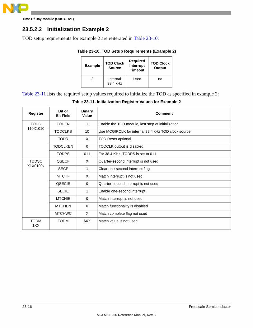
Time Of Day Module (S08TODV1)
23-16 Freescale Semiconductor
23.5.2.2 Initialization Example 2
TOD setup requirements for example 2 are reiterated in Table 23-10:
Table 23-11 lists the required setup values required to initialize the TOD as specified in example 2:
Table 23-10. TOD Setup Requirements (Example 2)
ExampleTOD Clock
Source
Required Interrupt Timeout
TOD Clock Output
2 Internal38.4 kHz
1 sec. no
Table 23-11. Initialization Register Values for Example 2
RegisterBit or
Bit FieldBinary Value
Comment
TODC110X1010
TODEN 1 Enable the TOD module, last step of initialization
TODCLKS 10 Use MCGIRCLK for internal 38.4 kHz TOD clock source
TODR X TOD Reset optional
TODCLKEN 0 TODCLK output is disabled
TODPS 011 For 38.4 KHz, TODPS is set to 011
TODSCX1X0100x
QSECF X Quarter-second interrupt is not used
SECF 1 Clear one-second interrupt flag
MTCHF X Match interrupt is not used
QSECIE 0 Quarter-second interrupt is not used
SECIE 1 Enable one-second interrupt
MTCHIE 0 Match interrupt is not used
MTCHEN 0 Match functionality is disabled
MTCHWC X Match complete flag not used
TODM$XX
TODM $XX Match value is not used
MCF51JE256 Reference Manual, Rev. 2

Time Of Day Module (S08TODV1)
Freescale Semiconductor 23-17
23.5.2.3 Initialization Example 3
TOD setup requirements for example 3 are reiterated in Table 23-12:
Table 23-13 lists the required setup values required to initialize the TOD as specified in Example 3:
23.6 Application InformationThe most common application for the TOD module is keeping the time of day. The TOD module can be used to keep track of the second, minute, hour, day, month, and year. To accomplish these tasks, software is used to count quarter seconds or seconds. Seconds are added up in RAM until they reach minutes, minutes are added up until they reach hours, and so forth.
Table 23-12. TOD Setup Requirements (Example 3)
ExampleTOD Clock
Source
Required Interrupt Timeout
TOD Clock Output
3 Internal 1 kHz LPO
approx.1 min.
no
Table 23-13. Initialization Register Values for Example 3
RegisterBit or
Bit fieldBinary Value
Comment
TODC10110000
TODEN 1 Enable the TOD module, last step of initialization
TODCLKS 01 Use for internal 1 kHz low-power oscillator TOD clock source
TODR 1 TOD reset to begin TOD counts at $00
TODCLKEN 0 TODCLK output disabled
TODPS 000 For 1 KHz low-power oscillator,TODPS is set to 000
TODSCXX10011x
QSECF X Quarter-second interrupt is not used
SECF X One-second interrupt is not used
MTCHF 1 Clear match interrupt flag
QSECIE 0 Quarter-second interrupt is not used
SECIE 0 One-second interrupt is not used
MTCHIE 1 Match interrupt is enabled
MTCHEN 1 Match functionality is enabled
MTCHWC X Match complete flag not used
TODM111100XX
TODM $3C Match value is set to $3C to generate an interrupt after $F0 or 240 counts of the TOD counter register. Always write the match value before setting the MTCHEN bit.
MCF51JE256 Reference Manual, Rev. 2

Time Of Day Module (S08TODV1)
23-18 Freescale Semiconductor
MCF51JE256 Reference Manual, Rev. 2

Freescale Semiconductor 24-1
Chapter 24 Timer/Pulse-Width Modulator (S08TPMV3)
24.1 IntroductionThese devices contain two 4-channel TPM peripherals: TPM1 and TPM2.
24.1.1 ACMP/TPM Configuration Information
The ACMP module can be configured to connect the output of the analog comparator to the TPM1 input capture channel 0 by setting the corresponding ACIC bit in SOPT2. With ACIC set, the TPM1CH0 pin is not available externally regardless of the configuration of the TPM1 module.
24.1.2 TPM External Clock
Both the TPM modules on these devices use the TCLK pin.
24.1.3 TPM Clock Gating
The bus clock to the TPMs can be gated on and off using the TPM2 bit and TPM1 bit in SCGC1. These bits are set after any reset that enables the bus clock to this module. To conserve power, these bits can be cleared to disable the clock to this module when not in use. See Section 5.6, “Peripheral Clock Gating,” for details.
MCF51JE256 Reference Manual, Rev. 2

Timer/Pulse-Width Modulator (S08TPMV3)
24-2 Freescale Semiconductor
Figure 24-1. Block Diagram Highlighting TPM Blocks and Pins
MCF51JE256 Reference Manual, Rev. 2

Timer/Pulse-Width Modulator (S08TPMV3)
Freescale Semiconductor 24-3
24.1.4 Features
The TPM includes these distinctive features:
• One to eight channels:
— Each channel is input capture, output compare, or edge-aligned PWM
— Rising-edge, falling-edge, or any-edge input capture trigger
— Set, clear, or toggle output compare action
— Selectable polarity on PWM outputs
• Module is configured for buffered, center-aligned pulse-width-modulation (CPWM) on all channels
• Timer clock source selectable as bus clock, fixed frequency clock, or an external clock
— Prescale taps for divide-by 1, 2, 4, 8, 16, 32, 64, or 128 used for any clock input selection
— Fixed frequency clock is an additional clock input to allow the selection of an on chip clock source other than bus clock
— Selecting external clock connects TPM clock to a chip level input pin therefore allowing to synchronize the TPM counter with an off chip clock source
• 16-bit free-running or modulus count with up/down selection
• One interrupt per channel and one interrupt for TPM counter overflow
24.1.5 Modes of Operation
In general, TPM channels are independently configured to operate in input capture, output compare, or edge-aligned PWM modes. A control bit allows the whole TPM (all channels) to switch to center-aligned PWM mode. When center-aligned PWM mode is selected, input capture, output compare, and edge-aligned PWM functions are not available on any channels of this TPM module.
When the MCU is in active BDM background or BDM foreground mode, the TPM temporarily suspends all counting until the MCU returns to normal user operating mode. During stop mode, all TPM input clocks are stopped, so the TPM is effectively disabled until clocks resume. During wait mode, the TPM continues to operate normally. If the TPM does not need to produce a real time reference or provide the interrupt sources needed to wake the MCU from wait mode, the power can then be saved by disabling TPM functions before entering wait mode.
• Input capture mode
When a selected edge event occurs on the associated MCU pin, the current value of the 16-bit timer counter is captured into the channel value register and an interrupt flag bit is set. Rising edges, falling edges, any edge, or no edge (disable channel) are selected as the active edge that triggers the input capture.
• Output compare mode
When the value in the timer counter register matches the channel value register, an interrupt flag bit is set, and a selected output action is forced on the associated MCU pin. The output compare action is selected to force the pin to zero, force the pin to one, toggle the pin, or ignore the pin (used for software timing functions).
MCF51JE256 Reference Manual, Rev. 2

Timer/Pulse-Width Modulator (S08TPMV3)
24-4 Freescale Semiconductor
• Edge-aligned PWM mode
The value of a 16-bit modulo register plus 1 sets the period of the PWM output signal. The channel value register sets the duty cycle of the PWM output signal. You can also choose the polarity of the PWM output signal. Interrupts are available at the end of the period and at the duty-cycle transition point. This type of PWM signal is called edge-aligned because the leading edges of all PWM signals are aligned with the beginning of the period that is same for all channels within a TPM.
• Center-aligned PWM mode
Twice the value of a 16-bit modulo register sets the period of the PWM output, and the channel-value register sets the half-duty-cycle duration. The timer counter counts up until it reaches the modulo value and then counts down until it reaches zero. As the count matches the channel value register while counting down, the PWM output becomes active. When the count matches the channel value register while counting up, the PWM output becomes inactive. This type of PWM signal is called center-aligned because the centers of the active duty cycle periods for all channels are aligned with a count value of zero. This type of PWM is required for types of motors used in small appliances.
This is a high-level description only. Detailed descriptions of operating modes are in later sections.
24.1.6 Block Diagram
The TPM uses one input/output (I/O) pin per channel, TPMxCHn (timer channel n) where n is the channel number (1–8). The TPM shares its I/O pins with general purpose I/O port pins (refer to I/O pin descriptions in full-chip specification for the specific chip implementation).
Figure 24-2 shows the TPM structure. The central component of the TPM is the 16-bit counter that can operate as a free-running counter or a modulo up/down counter. The TPM counter (when operating in normal up-counting mode) provides the timing reference for the input capture, output compare, and edge-aligned PWM functions. The timer counter modulo registers, TPMxMODH:TPMxMODL, control the modulo value of the counter (the values 0x0000 or 0xFFFF effectively make the counter free running). Software can read the counter value at any time without affecting the counting sequence. Any write to either half of the TPMxCNT counter resets the counter, regardless of the data value written.
MCF51JE256 Reference Manual, Rev. 2

Timer/Pulse-Width Modulator (S08TPMV3)
Freescale Semiconductor 24-5
Figure 24-2. TPM Block Diagram
Prescaler
16-bit comparator
PS[2:0]
TOF
TOIE
InterruptTPM counter
logic
16-bit comparator
16-bit latch
ELS0B ELS0A Portchannel 0
CH0IE
CH0F
logic
Interruptlogic
CPWMS
MS0B MS0A
counter reset
CLKSB:CLKSA
³(1, 2, 4, 8, 16, 32, 64 or 128)
bus clock
external clock synchronizer
16-bit comparator
16-bit latch
channel 1 ELS1B ELS1A
CH1IE
CH1F
TP
M c
ount
er
Portlogic
Interruptlogic
MS1B MS1A
16-bit comparator
16-bit latch
channel 7 ELS7B ELS7A
CH7IE
CH7F
Portlogic
Interruptlogic
MS7B MS7A
up to 8 channels
TPMxMODH:TPMxMODL
TPMxC0VH:TPMxC0VL
TPMxC1VH:TPMxC1VL
TPMxCH0
TPMxCH1
TPMxC7VH:TPMxC7VL
TPMxCH7
fixed frequency clock
(16-bit counter)
no clock selected(TPM counter disable)
MCF51JE256 Reference Manual, Rev. 2

Timer/Pulse-Width Modulator (S08TPMV3)
24-6 Freescale Semiconductor
The TPM channels are programmable independently as input capture, output compare, or edge-aligned PWM channels. Alternately, the TPM can be configured to produce CPWM outputs on all channels. When the TPM is configured for CPWMs (the counter operates as an up/down counter) input capture, output compare, and EPWM functions are not practical.
24.2 Signal DescriptionTable 24-1 shows the user-accessible signals for the TPM. The number of channels are varied from one to eight. When an external clock is included, it can be shared with the same pin as any TPM channel; however, it could be connected to a separate input pin. Refer to the I/O pin descriptions in full-chip specification for the specific chip implementation.
24.2.1 Detailed Signal Descriptions
24.2.1.1 EXTCLK — External Clock Source
The external clock signal can share the same pin as a channel pin, however the channel pin can not be used for channel I/O function when external clock is selected. If this pin is used as an external clock (CLKSB:CLKSA = 1:1), the channel can still be configured to output compare mode therefore allowing its use as a timer (ELSnB:ELSnA = 0:0).
For proper TPM operation, the external clock frequency must not exceed one-fourth of the bus clock frequency.
24.2.1.2 TPMxCHn — TPM Channel n I/O Pins
The TPM channel does not control the I/O pin when ELSnB:ELSnA or CLKSB:CLKSA are cleared so it normally reverts to general purpose I/O control. When CPWMS is set and ELSnB:ELSnA are not cleared, all TPM channels are configured for center-aligned PWM and the TPMxCHn pins are all controlled by TPM. When CPWMS is cleared, the MSnB:MSnA control bits determine whether the channel is configured for input capture, output compare, or edge-aligned PWM.
When a channel is configured for input capture (CPWMS = 0, MSnB:MSnA = 0:0, and ELSnB:ELSnA 0:0), the TPMxCHn pin is forced to act as an edge-sensitive input to the TPM. ELSnB:ELSnA control bits determine what polarity edge or edges trigger input capture events. The channel input signal is synchronized on the bus clock. This implies the minimum pulse width—that can
Table 24-1. Signal Properties
Name Function
EXTCLK1
1 The external clock pin can be shared with any channel pin. However, depending upon full-chip implementation, this signal could be connected to a separate external pin.
External clock source that is selected to drive the TPM counter.
TPMxCHn2
2 n = channel number (1–8)
I/O pin associated with TPM channel n.
MCF51JE256 Reference Manual, Rev. 2

Timer/Pulse-Width Modulator (S08TPMV3)
Freescale Semiconductor 24-7
be reliably detected—on an input capture pin is four bus clock periods (with ideal clock pulses as near as two bus clocks can be detected).
When a channel is configured for output compare (CPWMS = 0, MSnB:MSnA = 0:1, and ELSnB:ELSnA 0:0), the TPMxCHn pin is an output controlled by the TPM. The ELSnB:ELSnA bits determine whether the TPMxCHn pin is toggled, cleared, or set each time the 16-bit channel value register matches the TPM counter.
When the output compare toggle mode is initially selected, the previous value on the pin is driven out until the next output compare event, the pin is then toggled.
When a channel is configured for edge-aligned PWM (CPWMS = 0, MSnB = 1, and ELSnB:ELSnA 0:0), the TPMxCHn pin is an output controlled by the TPM, and ELSnB:ELSnA bits control the polarity of the PWM output signal. When ELSnB is set and ELSnA is cleared, the TPMxCHn pin is forced high at the start of each new period (TPMxCNT=0x0000), and it is forced low when the channel value register matches the TPM counter. When ELSnA is set, the TPMxCHn pin is forced low at the start of each new period (TPMxCNT=0x0000), and it is forced high when the channel value register matches the TPM counter.
Figure 24-3. High-true pulse of an edge-aligned PWM
Figure 24-4. Low-true pulse of an edge-aligned PWM
When the TPM is configured for center-aligned PWM (CPWMS = 1 and ELSnB:ELSnA 0:0), the TPMxCHn pins are outputs controlled by the TPM, and ELSnB:ELSnA bits control the polarity of the PWM output signal. If ELSnB is set and ELSnA is cleared, the corresponding TPMxCHn pin is cleared when the TPM counter is counting up, and the channel value register matches the TPM counter; and it is
CHnF bit
TOF bit
0... 1 2 3 4 5 6 7 8 0 1 2 ...
TPMxMODH:TPMxMODL = 0x0008TPMxCnVH:TPMxCnVL = 0x0005
TPMxCNTH:TPMxCNTL
TPMxCHn
CHnF bit
TOF bit
0... 1 2 3 4 5 6 7 8 0 1 2 ...
TPMxMODH:TPMxMODL = 0x0008TPMxCnVH:TPMxCnVL = 0x0005
TPMxCNTH:TPMxCNTL
TPMxCHn
MCF51JE256 Reference Manual, Rev. 2

Timer/Pulse-Width Modulator (S08TPMV3)
24-8 Freescale Semiconductor
set when the TPM counter is counting down, and the channel value register matches the TPM counter. If ELSnA is set, the corresponding TPMxCHn pin is set when the TPM counter is counting up and the channel value register matches the TPM counter; and it is cleared when the TPM counter is counting down and the channel value register matches the TPM counter.
Figure 24-5. High-true pulse of a center-aligned PWM
Figure 24-6. Low-true pulse of a center-aligned PWM
CHnF bit
TOF bit
... 7 8 7 6 5 4 3 2 1 0 1 2 3 4 5 6 7 8 7 6 5 ...
TPMxMODH:TPMxMODL = 0x0008TPMxCnVH:TPMxCnVL = 0x0005
TPMxCNTH:TPMxCNTL
TPMxCHn
CHnF bit
TOF bit
... 7 8 7 6 5 4 3 2 1 0 1 2 3 4 5 6 7 8 7 6 5 ...
TPMxMODH:TPMxMODL = 0x0008TPMxCnVH:TPMxCnVL = 0x0005
TPMxCNTH:TPMxCNTL
TPMxCHn
MCF51JE256 Reference Manual, Rev. 2

Timer/Pulse-Width Modulator (S08TPMV3)
Freescale Semiconductor 24-9
24.3 Register Definition
24.3.1 TPM Status and Control Register (TPMxSC)
TPMxSC contains the overflow status flag and control bits used to configure the interrupt enable, TPM configuration, clock source, and prescale factor. These controls relate to all channels within this timer module.
7 6 5 4 3 2 1 0
R TOFTOIE CPWMS CLKSB CLKSA PS2 PS1 PS0
W 0
Reset 0 0 0 0 0 0 0 0
Figure 24-7. TPM Status and Control Register (TPMxSC)
Table 24-2. TPMxSC Field Descriptions
Field Description
7TOF
Timer overflow flag. This read/write flag is set when the TPM counter resets to 0x0000 after reaching the modulo value programmed in the TPM counter modulo registers. Clear TOF by reading the TPM status and control register when TOF is set and then writing a logic 0 to TOF. If another TPM overflow occurs before the clearing sequence is completed, the sequence is reset so TOF remains set after the clear sequence was completed for the earlier TOF. This is done so a TOF interrupt request cannot be lost during the clearing sequence for a previous TOF. Reset clears TOF. Writing a logic 1 to TOF has no effect.0 TPM counter has not reached modulo value or overflow.1 TPM counter has overflowed.
6TOIE
Timer overflow interrupt enable. This read/write bit enables TPM overflow interrupts. If TOIE is set, an interrupt is generated when TOF equals one. Reset clears TOIE.0 TOF interrupts inhibited (use for software polling).1 TOF interrupts enabled.
5CPWMS
Center-aligned PWM select. This read/write bit selects CPWM operating mode. By default, the TPM operates in up-counting mode for input capture, output compare, and edge-aligned PWM functions. Setting CPWMS reconfigures the TPM to operate in up/down counting mode for CPWM functions. Reset clears CPWMS.0 All channels operate as input capture, output compare, or edge-aligned PWM mode as selected by the
MSnB:MSnA control bits in each channel’s status and control register.1 All channels operate in center-aligned PWM mode.
4–3CLKS[B:A]
Clock source selection bits. As shown in Table 24-3, this 2-bit field is used to disable the TPM counter or select one of three clock sources to TPM counter and counter prescaler.
2–0PS[2:0]
Prescale factor select. This 3-bit field selects one of eight division factors for the TPM clock as shown in Table 24-4. This prescaler is located after any clock synchronization or clock selection so it affects the clock selected to drive the TPM counter. The new prescale factor affects the selected clock on the next bus clock cycle after the new value is updated into the register bits.
Table 24-3. TPM Clock Selection
CLKSB:CLKSA TPM Clock to Prescaler Input
00 No clock selected (TPM counter disable)
MCF51JE256 Reference Manual, Rev. 2

Timer/Pulse-Width Modulator (S08TPMV3)
24-10 Freescale Semiconductor
24.3.2 TPM-Counter Registers (TPMxCNTH:TPMxCNTL)
The two read-only TPM counter registers contain the high and low bytes of the value in the TPM counter. Reading either byte (TPMxCNTH or TPMxCNTL) latches the contents of both bytes into a buffer where they remain latched until the other half is read. This allows coherent 16-bit reads in big-endian or little-endian order that makes this more friendly to various compiler implementations. The coherency mechanism is automatically restarted by an MCU reset or any write to the timer status/control register (TPMxSC).
Reset clears the TPM counter registers. Writing any value to TPMxCNTH or TPMxCNTL also clears the TPM counter (TPMxCNTH:TPMxCNTL) and resets the coherency mechanism, regardless of the data involved in the write.
01 Bus clock
10 Fixed frequency clock
11 External clock
Table 24-4. Prescale Factor Selection
PS[2:0] TPM Clock Divided-by
000 1
001 2
010 4
011 8
100 16
101 32
110 64
111 128
7 6 5 4 3 2 1 0
R TPMxCNT[15:8]
W Any write to TPMxCNTH clears the 16-bit counter
Reset 0 0 0 0 0 0 0 0
Figure 24-8. TPM Counter Register High (TPMxCNTH)
Table 24-3. TPM Clock Selection
CLKSB:CLKSA TPM Clock to Prescaler Input
MCF51JE256 Reference Manual, Rev. 2

Timer/Pulse-Width Modulator (S08TPMV3)
Freescale Semiconductor 24-11
When BDM is active, the timer counter is frozen (this is the value you read). The coherency mechanism is frozen so the buffer latches remain in the state they were in when the BDM became active, even if one or both counter halves are read while BDM is active. This assures that if you were in the middle of reading a 16-bit register when BDM became active, it reads the appropriate value from the other half of the 16-bit value after returning to normal execution.
In BDM mode, writing any value to TPMxSC, TPMxCNTH, or TPMxCNTL registers resets the read coherency mechanism of the TPMxCNTH:TPMxCNTL registers, regardless of the data involved in the write.
24.3.3 TPM Counter Modulo Registers (TPMxMODH:TPMxMODL)
The read/write TPM modulo registers contain the modulo value for the TPM counter. After the TPM counter reaches the modulo value, the TPM counter resumes counting from 0x0000 at the next clock, and the overflow flag (TOF) becomes set. Writing to TPMxMODH or TPMxMODL inhibits the TOF bit and overflow interrupts until the other byte is written. Reset sets the TPM counter modulo registers to 0x0000 that results in a free running timer counter (modulo disabled).
Writes to any of the registers TPMxMODH and TPMxMODL actually writes to buffer registers and the registers are updated with the value of their write buffer according to the value of CLKSB:CLKSA bits:
• If CLKSB and CLKSA are cleared, the registers are updated when the second byte is written
• If CLKSB and CLKSA are not cleared, the registers are updated after both bytes were written, and the TPM counter changes from (TPMxMODH:TPMxMODL – 1) to (TPMxMODH:TPMxMODL). If the TPM counter is a free-running counter, the update is made when the TPM counter changes from 0xFFFE to 0xFFFF
The latching mechanism is manually reset by writing to the TPMxSC address (whether BDM is active or not).
When BDM is active, the coherency mechanism is frozen (unless reset by writing to TPMxSC register) so the buffer latches remain in the state they were in when the BDM became active, even if one or both halves of the modulo register are written while BDM is active. Any write to the modulo registers bypasses the buffer latches and directly writes to the modulo register while BDM is active.
7 6 5 4 3 2 1 0
R TPMxCNT[7:0]
W Any write to TPMxCNTL clears the 16-bit counter
Reset 0 0 0 0 0 0 0 0
Figure 24-9. TPM Counter Register Low (TPMxCNTL)
7 6 5 4 3 2 1 0
RTPMxMOD[15:8]
W
Reset 0 0 0 0 0 0 0 0
Figure 24-10. TPM Counter Modulo Register High (TPMxMODH)
MCF51JE256 Reference Manual, Rev. 2

Timer/Pulse-Width Modulator (S08TPMV3)
24-12 Freescale Semiconductor
Reset the TPM counter before writing to the TPM modulo registers to avoid confusion about when the first counter overflow occurs.
24.3.4 TPM Channel n Status and Control Register (TPMxCnSC)
TPMxCnSC contains the channel-interrupt-status flag and control bits that configure the interrupt enable, channel configuration, and pin function.
7 6 5 4 3 2 1 0
RTPMxMOD[7:0]
W
Reset 0 0 0 0 0 0 0 0
7 6 5 4 3 2 1 0
R CHnFCHnIE MSnB MSnA ELSnB ELSnA
0 0
W 0
Reset 0 0 0 0 0 0 0 0
= Unimplemented or Reserved
Figure 24-12. TPM Channel n Status and Control Register (TPMxCnSC)
Table 24-5. TPMxCnSC Field Descriptions
Field Description
7CHnF
Channel n flag. When channel n is an input capture channel, this read/write bit is set when an active edge occurs on the channel n input. When channel n is an output compare or edge-aligned/center-aligned PWM channel, CHnF is set when the value in the TPM counter registers matches the value in the TPM channel n value registers. When channel n is an edge-aligned/center-aligned PWM channel and the duty cycle is set to 0% or 100%, CHnF is not set even when the value in the TPM counter registers matches the value in the TPM channel n value registers.A corresponding interrupt is requested when this bit is set and channel n interrupt is enabled (CHnIE = 1). Clear CHnF by reading TPMxCnSC while this bit is set and then writing a logic 0 to it. If another interrupt request occurs before the clearing sequence is completed CHnF remains set. This is done so a CHnF interrupt request is not lost due to clearing a previous CHnF.Reset clears this bit. Writing a logic 1 to CHnF has no effect.0 No input capture or output compare event occurred on channel n.1 Input capture or output compare event on channel n.
6CHnIE
Channel n interrupt enable. This read/write bit enables interrupts from channel n. Reset clears this bit.0 Channel n interrupt requests disabled (use for software polling).1 Channel n interrupt requests enabled.
5MSnB
Mode select B for TPM channel n. When CPWMS is cleared, setting the MSnB bit configures TPM channel n for edge-aligned PWM mode. Refer to the summary of channel mode and setup controls in Table 24-6.
MCF51JE256 Reference Manual, Rev. 2

Timer/Pulse-Width Modulator (S08TPMV3)
Freescale Semiconductor 24-13
24.3.5 TPM Channel Value Registers (TPMxCnVH:TPMxCnVL)
These read/write registers contain the captured TPM counter value of the input capture function or the output compare value for the output compare or PWM functions. The channel registers are cleared by reset.
4MSnA
Mode select A for TPM channel n. When CPWMS and MSnB are cleared, the MSnA bit configures TPM channel n for input capture mode or output compare mode. Refer to Table 24-6 for a summary of channel mode and setup controls.Note: If the associated port pin is not stable for at least two bus clock cycles before changing to input capture
mode, it is possible to get an unexpected indication of an edge trigger.
3–2ELSnBELSnA
Edge/level select bits. Depending upon the operating mode for the timer channel as set by CPWMS:MSnB:MSnA and shown in Table 24-6, these bits select the polarity of the input edge that triggers an input capture event, select the level that is driven in response to an output compare match, or select the polarity of the PWM output.If ELSnB and ELSnA bits are cleared, the channel pin is not controlled by TPM. This configuration can be used by software compare only, because it does not require the use of a pin for the channel.
Table 24-6. Mode, Edge, and Level Selection
CPWMS MSnB:MSnA ELSnB:ELSnA Mode Configuration
X XX 00 Pin is not controlled by TPM. It is reverted to general purpose I/O or other peripheral control
0 00 01 Input capture Capture on rising edge only
10 Capture on falling edge only
11 Capture on rising or falling edge
01 00 Output compare Software compare only
01 Toggle output on channel match
10 Clear output on channel match
11 Set output on channel match
1X 10 Edge-aligned PWM
High-true pulses (clear output on channel match)
X1 Low-true pulses (set output on channel match)
1 XX 10 Center-aligned PWM
High-true pulses (clear output on channel match when TPM counter is counting up)
X1 Low-true pulses (set output on channel match when TPM counter is counting up)
7 6 5 4 3 2 1 0
RTPMxCnV[15:8]
W
Reset 0 0 0 0 0 0 0 0
Figure 24-13. TPM Channel Value Register High (TPMxCnVH)
Table 24-5. TPMxCnSC Field Descriptions (Continued)
Field Description
MCF51JE256 Reference Manual, Rev. 2

Timer/Pulse-Width Modulator (S08TPMV3)
24-14 Freescale Semiconductor
In input capture mode, reading either byte (TPMxCnVH or TPMxCnVL) latches the contents of both bytes into a buffer where they remain latched until the other half is read. This latching mechanism also resets (becomes unlatched) when the TPMxCnSC register is written (whether BDM mode is active or not). Any write to the channel registers is ignored during the input capture mode.
When BDM is active, the coherency mechanism is frozen (unless reset by writing to TPMxCnSC register) so the buffer latches remain in the state they were in when the BDM became active, even if one or both halves of the channel register are read while BDM is active. This assures that if you were in the middle of reading a 16-bit register when BDM became active, it reads the appropriate value from the other half of the 16-bit value after returning to normal execution. The value read from the TPMxCnVH and TPMxCnVL registers in BDM mode is the value of these registers and not the value of their read buffer.
In output compare or PWM modes, writing to either byte (TPMxCnVH or TPMxCnVL) latches the value into a buffer. After both bytes were written, they are transferred as a coherent 16-bit value into the timer-channel registers according to the value of CLKSB:CLKSA bits and the selected mode:
• If CLKSB and CLKSA are cleared, the registers are updated when the second byte is written.
• If CLKSB and CLKSA are not cleared and in output compare mode, the registers are updated after the second byte is written and on the next change of the TPM counter (end of the prescaler counting).
• If CLKSB and CLKSA are not cleared and in EPWM or CPWM modes, the registers are updated after both bytes were written, and the TPM counter changes from (TPMxMODH:TPMxMODL – 1) to (TPMxMODH:TPMxMODL). If the TPM counter is a free-running counter, the update is made when the TPM counter changes from 0xFFFE to 0xFFFF.
The latching mechanism is manually reset by writing to the TPMxCnSC register (whether BDM mode is active or not). This latching mechanism allows coherent 16-bit writes in either big-endian or little-endian order that is friendly to various compiler implementations.
When BDM is active, the coherency mechanism is frozen so the buffer latches remain in the state they were in when the BDM became active even if one or both halves of the channel register are written while BDM is active. Any write to the channel registers bypasses the buffer latches and directly write to the channel register while BDM is active. The values written to the channel register while BDM is active are used for PWM and output compare operation after normal execution resumes. Writes to the channel registers while BDM is active do not interfere with partial completion of a coherency sequence. After the coherency mechanism is fully exercised, the channel registers are updated using the buffered values (while BDM was not active).
7 6 5 4 3 2 1 0
RTPMxCnV[7:0]
W
Reset 0 0 0 0 0 0 0 0
Figure 24-14. TPM Channel Value Register Low (TPMxCnVL)
MCF51JE256 Reference Manual, Rev. 2

Timer/Pulse-Width Modulator (S08TPMV3)
Freescale Semiconductor 24-15
24.4 Functional DescriptionAll TPM functions are associated with a central 16-bit counter that allows flexible selection of the clock and prescale factor. There is also a 16-bit modulo register associated with this counter.
The CPWMS control bit chooses between center-aligned PWM operation for all channels in the TPM (CPWMS=1) or general purpose timing functions (CPWMS=0) where each channel can independently be configured to operate in input capture, output compare, or edge-aligned PWM mode. The CPWMS control bit is located in the TPM status and control register because it affects all channels within the TPM and influences the way the main counter operates. (In CPWM mode, the counter changes to an up/down mode rather than the up-counting mode used for general purpose timer functions.)
The following sections describe TPM counter and each of the timer operating modes (input capture, output compare, edge-aligned PWM, and center-aligned PWM). Because details of pin operation and interrupt activity depend upon the operating mode, these topics are covered in the associated mode explanation sections.
24.4.1 Counter
All timer functions are based on the main 16-bit counter (TPMxCNTH:TPMxCNTL). This section discusses selection of the clock, end-of-count overflow, up-counting vs. up/down counting, and manual counter reset.
24.4.1.1 Counter Clock Source
The 2-bit field, CLKSB:CLKSA, in the timer status and control register (TPMxSC) disables the TPM counter or selects one of three clock sources to TPM counter (Table 24-3). After any MCU reset, CLKSB and CLKSA are cleared so no clock is selected and the TPM counter is disabled (TPM is in a very low power state). You can read or write these control bits at any time. Disabling the TPM counter by writing 00 to CLKSB:CLKSA bits, does not affect the values in the TPM counter or other registers.
The fixed frequency clock is an alternative clock source for the TPM counter that allows the selection of a clock other than the bus clock or external clock. This clock input is defined by chip integration. You can refer chip specific documentation for further information. Due to TPM hardware implementation limitations, the frequency of the fixed frequency clock must not exceed the bus clock frequency. The fixed frequency clock has no limitations for low frequency operation.
The external clock passes through a synchronizer clocked by the bus clock to assure that counter transitions are properly aligned to bus clock transitions.Therefore, in order to meet Nyquist criteria considering also jitter, the frequency of the external clock source must not exceed 1/4 of the bus clock frequency.
When the external clock source is shared with a TPM channel pin, this pin must not be used in input capture mode. However, this channel can be used in output compare mode with ELSnB:ELSnA = 0:0 for software timing functions. In this case, the channel output is disabled, but the channel match events continue to set the appropriate flag.
MCF51JE256 Reference Manual, Rev. 2

Timer/Pulse-Width Modulator (S08TPMV3)
24-16 Freescale Semiconductor
24.4.1.2 Counter Overflow and Modulo Reset
An interrupt flag and enable are associated with the 16-bit main counter. The flag (TOF) is a software-accessible indication that the timer counter has overflowed. The enable signal selects between software polling (TOIE = 0) where no interrupt is generated, or interrupt-driven operation (TOIE = 1) where the interrupt is generated whenever the TOF is set.
The conditions causing TOF to become set depend on whether the TPM is configured for center-aligned PWM (CPWMS = 1). If CPWMS is cleared and there is no modulus limit, the 16-bit timer counter counts from 0x0000 through 0xFFFF and overflows to 0x0000 on the next counting clock. TOF is set at the transition from 0xFFFF to 0x0000. When a modulus limit is set, TOF is set at the transition from the value set in the modulus register to 0x0000. When the TPM is in center-aligned PWM mode (CPWMS = 1), the TOF flag is set as the counter changes direction at the end of the count value set in the modulus register (at the transition from the value set in the modulus register to the next lower count value). This corresponds to the end of a PWM period (the 0x0000 count value corresponds to the center of a period).
24.4.1.3 Counting Modes
The main timer counter has two counting modes. When center-aligned PWM is selected (CPWMS = 1), the counter operates in up/down counting mode. Otherwise, the counter operates as a simple up counter. As an up counter, the timer counter counts from 0x0000 through its terminal count and continues with 0x0000. The terminal count is 0xFFFF or a modulus value in TPMxMODH:TPMxMODL.
When center-aligned PWM operation is specified, the counter counts up from 0x0000 through its terminal count and then down to 0x0000 where it changes back to up counting. The terminal count value and 0x0000 are normal length counts (one timer clock period long). In this mode, the timer overflow flag (TOF) is set at the end of the terminal-count period (as the count changes to the next lower count value).
24.4.1.4 Manual Counter Reset
The main timer counter can be manually reset at any time by writing any value to TPMxCNTH or TPMxCNTL. Resetting the counter in this manner also resets the coherency mechanism in case only half of the counter was read before resetting the count.
24.4.2 Channel Mode Selection
If CPWMS is cleared, MSnB and MSnA bits determine the basic mode of operation for the corresponding channel. Choices include input capture, output compare, and edge-aligned PWM.
24.4.2.1 Input Capture Mode
With the input capture function, the TPM can capture the time at which an external event occurs. When an active edge occurs on the pin of an input capture channel, the TPM latches the contents of the TPM counter into the channel-value registers (TPMxCnVH:TPMxCnVL). Rising edges, falling edges, or any edge is chosen as the active edge that triggers an input capture.
In input capture mode, the TPMxCnVH and TPMxCnVL registers are read only.
MCF51JE256 Reference Manual, Rev. 2

Timer/Pulse-Width Modulator (S08TPMV3)
Freescale Semiconductor 24-17
When either half of the 16-bit capture register is read, the other half is latched into a buffer to support coherent 16-bit accesses in big-endian or little-endian order. The coherency sequence can be manually reset by writing to TPMxCnSC.
An input capture event sets a flag bit (CHnF) that optionally generates a CPU interrupt request.
While in BDM, the input capture function works as configured. When an external event occurs, the TPM latches the contents of the TPM counter (frozen because of the BDM mode) into the channel value registers and sets the flag bit.
24.4.2.2 Output Compare Mode
With the output compare function, the TPM can generate timed pulses with programmable position, polarity, duration, and frequency. When the counter reaches the value in TPMxCnVH:TPMxCnVL registers of an output compare channel, the TPM can set, clear, or toggle the channel pin.
Writes to any of TPMxCnVH and TPMxCnVL registers actually write to buffer registers. In output compare mode, the TPMxCnVH:TPMxCnVL registers are updated with the value of their write buffer only after both bytes were written and according to the value of CLKSB:CLKSA bits:
• If CLKSB and CLKSA are cleared, the registers are updated when the second byte is written
• If CLKSB and CLKSA are not cleared, the registers are updated at the next change of the TPM counter (end of the prescaler counting) after the second byte is written.
The coherency sequence can be manually reset by writing to the channel status/control register (TPMxCnSC).
An output compare event sets a flag bit (CHnF) that optionally generates a CPU interrupt request.
24.4.2.3 Edge-Aligned PWM Mode
This type of PWM output uses the normal up-counting mode of the timer counter (CPWMS=0) and can be used when other channels in the same TPM are configured for input capture or output compare functions. The period of this PWM signal is determined by the value of the modulus register (TPMxMODH:TPMxMODL) plus 1. The duty cycle is determined by the value of the timer channel register (TPMxCnVH:TPMxCnVL). The polarity of this PWM signal is determined by ELSnA bit. 0% and 100% duty cycle cases are possible.
The time between the modulus overflow and the channel match value (TPMxCnVH:TPMxCnVL) is the pulse width or duty cycle (Figure 24-15). If ELSnA is cleared, the counter overflow forces the PWM signal high, and the channel match forces the PWM signal low. If ELSnA is set, the counter overflow forces the PWM signal low, and the channel match forces the PWM signal high.
MCF51JE256 Reference Manual, Rev. 2

Timer/Pulse-Width Modulator (S08TPMV3)
24-18 Freescale Semiconductor
Figure 24-15. EPWM period and pulse width (ELSnA=0)
When the channel value register is set to 0x0000, the duty cycle is 0%. A 100% duty cycle is achieved by setting the timer-channel register (TPMxCnVH:TPMxCnVL) to a value greater than the modulus setting. This implies that the modulus setting must be less than 0xFFFF in order to get 100% duty cycle.
The timer channel registers are buffered to ensure coherent 16-bit updates and to avoid unexpected PWM pulse widths. Writes to any of the registers TPMxCnVH and TPMxCnVL actually write to buffer registers. In edge-aligned PWM mode, the TPMxCnVH:TPMxCnVL registers are updated with the value of their write buffer according to the value of CLKSB:CLKSA bits:
• If CLKSB and CLKSA are cleared, the registers are updated when the second byte is written
• If CLKSB and CLKSA are not cleared, the registers are updated after both bytes were written, and the TPM counter changes from (TPMxMODH:TPMxMODL – 1) to (TPMxMODH:TPMxMODL). If the TPM counter is a free-running counter, the update is made when the TPM counter changes from 0xFFFE to 0xFFFF.
24.4.2.4 Center-Aligned PWM Mode
This type of PWM output uses the up/down counting mode of the timer counter (CPWMS=1). The channel match value in TPMxCnVH:TPMxCnVL determines the pulse width (duty cycle) of the PWM signal while the period is determined by the value in TPMxMODH:TPMxMODL. TPMxMODH:TPMxMODL must be kept in the range of 0x0001 to 0x7FFF because values outside this range can produce ambiguous results. ELSnA determines the polarity of the CPWM signal.
pulse width = 2 (TPMxCnVH:TPMxCnVL)
period = 2 (TPMxMODH:TPMxMODL); TPMxMODH:TPMxMODL = 0x0001–0x7FFF
If TPMxCnVH:TPMxCnVL is zero or negative (bit 15 set), the duty cycle is 0%. If TPMxCnVH:TPMxCnVL is a positive value (bit 15 clear) and is greater than the non-zero modulus setting, the duty cycle is 100% because the channel match never occurs. This implies the usable range of periods set by the modulus register is 0x0001 through 0x7FFE (0x7FFF if you do not need to generate 100% duty cycle). This is not a significant limitation. The resulting period is much longer than required for normal applications.
All zeros in TPMxMODH:TPMxMODL is a special case that must not be used with center-aligned PWM mode. When CPWMS is cleared, this case corresponds to the counter running free from 0x0000 through 0xFFFF. When CPWMS is set, the counter needs a valid match to the modulus register somewhere other than at 0x0000 in order to change directions from up-counting to down-counting.
period
pulse width
overflow overflow overflow
channelmatch
channelmatch
channelmatch
TPMxCHn
MCF51JE256 Reference Manual, Rev. 2

Timer/Pulse-Width Modulator (S08TPMV3)
Freescale Semiconductor 24-19
The channel match value in the TPM channel registers (times two) determines the pulse width (duty cycle) of the CPWM signal (Figure 24-16). If ELSnA is cleared, a channel match occurring while counting up clears the CPWM output signal and a channel match occurring while counting down sets the output. The counter counts up until it reaches the modulo setting in TPMxMODH:TPMxMODL, then counts down until it reaches zero. This sets the period equal to two times TPMxMODH:TPMxMODL.
Figure 24-16. CPWM period and pulse width (ELSnA=0)
Center-aligned PWM outputs typically produce less noise than edge-aligned PWMs because fewer I/O pin transitions are lined up at the same system clock edge. This type of PWM is also required for some types of motor drives.
Input capture, output compare, and edge-aligned PWM functions do not make sense when the counter is operating in up/down counting mode so this implies that all active channels within a TPM must be used in CPWM mode when CPWMS is set.
The timer channel registers are buffered to ensure coherent 16-bit updates and to avoid unexpected PWM pulse widths. Writes to any of the registers TPMxCnVH and TPMxCnVL actually write to buffer registers. In center-aligned PWM mode, the TPMxCnVH:TPMxCnVL registers are updated with the value of their write buffer according to the value of CLKSB:CLKSA bits:
• If CLKSB and CLKSA are cleared, the registers are updated when the second byte is written
• If CLKSB and CLKSA are not cleared, the registers are updated after both bytes were written, and the TPM counter changes from (TPMxMODH:TPMxMODL – 1) to (TPMxMODH:TPMxMODL). If the TPM counter is a free-running counter, the update is made when the TPM counter changes from 0xFFFE to 0xFFFF.
When TPMxCNTH:TPMxCNTL equals TPMxMODH:TPMxMODL, the TPM can optionally generate a TOF interrupt (at the end of this count).
24.5 Reset Overview
24.5.1 General
The TPM is reset whenever any MCU reset occurs.
period
pulse width
TPM counter =
TPM counter = 0
TPM counter =channel match(count down)
channel match(count up)
TPMxCHn
2 TPMxMODH:TPMxMODL
2 TPMxCnVH:TPMxCnVL
TPMxMODH:TPMxMODLTPMxMODH:TPMxMODL
MCF51JE256 Reference Manual, Rev. 2

Timer/Pulse-Width Modulator (S08TPMV3)
24-20 Freescale Semiconductor
24.5.2 Description of Reset Operation
Reset clears TPMxSC that disables TPM counter clock and overflow interrupt (TOIE=0). CPWMS, MSnB, MSnA, ELSnB, and ELSnA are all cleared. This configures all TPM channels for input capture operation and the associated pins are not controlled by TPM.
24.6 Interrupts
24.6.1 General
The TPM generates an optional interrupt for the main counter overflow and an interrupt for each channel. The meaning of channel interrupts depends on each channel’s mode of operation. If the channel is configured for input capture, the interrupt flag is set each time the selected input capture edge is recognized. If the channel is configured for output compare or PWM modes, the interrupt flag is set each time the main timer counter matches the value in the 16-bit channel value register.
All TPM interrupts are listed in Table 24-7.
The TPM module provides high-true interrupt signals.
24.6.2 Description of Interrupt Operation
For each interrupt source in the TPM, a flag bit is set upon recognition of the interrupt condition such as timer overflow, channel input capture, or output compare events. This flag is read (polled) by software to determine that the action has occurred, or an associated enable bit (TOIE or CHnIE) can be set to enable the interrupt generation. While the interrupt enable bit is set, the interrupt is generated whenever the associated interrupt flag is set. Software must perform a sequence of steps to clear the interrupt flag before returning from the interrupt-service routine.
TPM interrupt flags are cleared by a two-step process including a read of the flag bit while it is set followed by a write of zero to the bit. If a new event is detected between these two steps, the sequence is reset and the interrupt flag remains set after the second step to avoid the possibility of missing the new event.
Table 24-7. Interrupt Summary
InterruptLocal
EnableSource Description
TOF TOIE Counter overflow Set each time the TPM counter reaches its terminal count (at transition to its next count value)
CHnF CHnIE Channel event An input capture event or channel match took place on channel n
MCF51JE256 Reference Manual, Rev. 2

Timer/Pulse-Width Modulator (S08TPMV3)
Freescale Semiconductor 24-21
24.6.2.1 Timer Overflow Interrupt (TOF) Description
The meaning and details of operation for TOF interrupts varies slightly depending upon the mode of operation of the TPM system (general purpose timing functions versus center-aligned PWM operation). The flag is cleared by the two step sequence described above.
24.6.2.1.1 Normal Case
When CPWMS is cleared, TOF is set when the timer counter changes from the terminal count (the value in the modulo register) to 0x0000. If the TPM counter is a free-running counter, the update is made when the TPM counter changes from 0xFFFF to 0x0000.
24.6.2.1.2 Center-Aligned PWM Case
When CPWMS is set, TOF is set when the timer counter changes direction from up-counting to down-counting at the end of the terminal count (the value in the modulo register).
24.6.2.2 Channel Event Interrupt Description
The meaning of channel interrupts depends on the channel’s current mode (input capture, output compare, edge-aligned PWM, or center-aligned PWM).
24.6.2.2.1 Input Capture Events
When a channel is configured as an input capture channel, the ELSnB:ELSnA bits select if channel pin is not controlled by TPM, rising edges, falling edges, or any edge as the edge that triggers an input capture event. When the selected edge is detected, the interrupt flag is set. The flag is cleared by the two-step sequence described in Section 24.6.2, “Description of Interrupt Operation.”
24.6.2.2.2 Output Compare Events
When a channel is configured as an output compare channel, the interrupt flag is set each time the main timer counter matches the 16-bit value in the channel value register. The flag is cleared by the two-step sequence described in Section 24.6.2, “Description of Interrupt Operation.”
24.6.2.2.3 PWM End-of-Duty-Cycle Events
When the channel is configured for edge-aligned PWM, the channel flag is set when the timer counter matches the channel value register that marks the end of the active duty cycle period. When the channel is configured for center-aligned PWM, the timer count matches the channel value register twice during each PWM cycle. In this CPWM case, the channel flag is set at the start and at the end of the active duty cycle period when the timer counter matches the channel value register. The flag is cleared by the two-step sequence described in Section 24.6.2, “Description of Interrupt Operation.”
MCF51JE256 Reference Manual, Rev. 2

Timer/Pulse-Width Modulator (S08TPMV3)
24-22 Freescale Semiconductor
MCF51JE256 Reference Manual, Rev. 2

Freescale Semiconductor 25-1
Chapter 25 USB On-the-GO (USBOTG)
NOTEPortions of Chapter 25, “USB On-the-GO (USBOTG),” relating to the EHCI specification are Copyright © Intel Corporation 1999-2001. The EHCI specification is provided as is with no warranties whatsoever, including any warranty of merchantability, non-infringement, fitness for any particular purpose, or any warranty otherwise arising out of any proposal, specification or sample. Intel disclaims all liability, including liability for infringement of any proprietary rights, relating to use of information in the EHCI specification. Intel may make changes to the EHCI specifications at any time, without notice.
For OTG operations, external circuitry is required to manage the host negotiation protocol (HNP) and session request protocol (SRP). External ICs that are capable of providing the OTG VBUS with support.
For HNP and SRP, as well as support for programmable pullup and pulldown resistors on the USB DP and DM lines are available from various manufacturers.
MCF51JE256 Reference Manual, Rev. 2

USB On-the-GO (USBOTG)
25-2 Freescale Semiconductor
Figure 25-1. Block Diagram with the USB Module highlighted
MCF51JE256 Reference Manual, Rev. 2
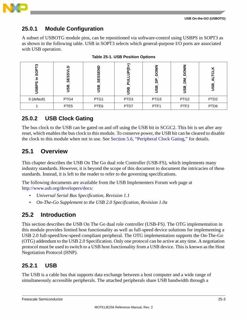
USB On-the-GO (USBOTG)
Freescale Semiconductor 25-3
25.0.1 Module Configuration
A subset of USBOTG module pins, can be repositioned via software-control using USBPS in SOPT3 as as shown in the following table. USB in SOPT3 selects which general-purpose I/O ports are associated with USB operation.
25.0.2 USB Clock Gating
The bus clock to the USB can be gated on and off using the USB bit in SCGC2. This bit is set after any reset, which enables the bus clock to this module. To conserve power, the USB bit can be cleared to disable the clock to this module when not in use. See Section 5.6, “Peripheral Clock Gating,” for details.
25.1 Overview
This chapter describes the USB On The Go dual role Controller (USB-FS), which implements many industry standards. However, it is beyond the scope of this document to document the intricacies of these standards. Instead, it is left to the reader to refer to the governing specifications.
The following documents are available from the USB Implementers Forum web page at http://www.usb.org/developers/docs:
• Universal Serial Bus Specification, Revision 1.1
• On-The-Go Supplement to the USB 2.0 Specification, Revision 1.0a
25.2 Introduction This section describes the USB On The Go dual role controller (USB-FS). The OTG implementation in this module provides limited host functionality as well as full-speed device solutions for implementing a USB 2.0 full-speed/low-speed compliant peripheral. The OTG implementation supports the On-The-Go (OTG) addendum to the USB 2.0 Specification. Only one protocol can be active at any time. A negotiation protocol must be used to switch to a USB host functionality from a USB device. This is known as the Host Negotiation Protocol (HNP).
25.2.1 USB
The USB is a cable bus that supports data exchange between a host computer and a wide range of simultaneously accessible peripherals. The attached peripherals share USB bandwidth through a
Table 25-1. USB Position Options
US
BP
S in
SO
PT
3
US
B_S
ES
SV
LD
US
B_S
ES
SE
ND
US
B_P
UL
LU
P(D
+)
US
B_D
P_D
OW
N
US
B_D
M_D
OW
N
US
B_A
LTC
LK
0 (default) PTG4 PTG1 PTD3 PTG3 PTG2 PTD2
1 PTE5 PTE6 PTD7 PTF1 PTF2 PTD6
MCF51JE256 Reference Manual, Rev. 2

USB On-the-GO (USBOTG)
25-4 Freescale Semiconductor
host-scheduled, token-based protocol. The bus allows peripherals to be attached, configured, used, and detached while the host and other peripherals are in operation.
USB software provides a uniform view of the system for all application software, hiding implementation details making application software more portable. It manages the dynamic attach and detach of peripherals.
There is only one host in any USB system. The USB interface to the host computer system is referred to as the Host Controller.
There may be multiple USB devices in any system such as joysticks, speakers, printers, etc. USB devices present a standard USB interface in terms of comprehension, response, and standard capability.
The host initiates transactions to specific peripherals, while the device responds to control transactions. The device sends and receives data to and from the host using a standard USB data format. USB 2.0 full-speed /low-speed peripherals operate at 12Mb/s or 1.5 MB/s.
For additional information, refer to the USB2.0 specification [2].
Figure 25-2. Example USB 2.0 System Configuration
HostSoftware
USB Cable
USB Cable
USB Cables
Host PC
External Hub
USB Cable
External Hub
USB Peripherals
RootHub
MCF51JE256 Reference Manual, Rev. 2

USB On-the-GO (USBOTG)
Freescale Semiconductor 25-5
25.2.2 USB On-The-Go
USB (Universal Serial Bus) is a popular standard for connecting peripherals and portable consumer electronic devices such as digital cameras and hand-held computers to host PCs. The On-The-Go (OTG) Supplement to the USB Specification extends USB to peer-to-peer application. Using USB OTG technology consumer electronics, peripherals and portable devices can connect to each other (for example, a digital camera can connect directly to a printer, or a keyboard can connect to a Personal Digital Assistant) to exchange data.
With the USB On-The-Go product, you can develop a fully USB-compliant peripheral device that can also assume the role of a USB host. Software determines the role of the device based on hardware signals, and then initializes the device in the appropriate mode of operation (host or peripheral) based on how it is connected. After connecting the devices can negotiate using the OTG protocols to assume the role of host or peripheral based on the task to be accomplished.
For additional information, refer to the On-The-Go Supplement to the USB 2.0 Specification [3].
Figure 25-3. Example USB 2.0 On-The-Go Configurations
Download Songs
Hot Sync
Swap Songs
Keyboard Input
Print Photos
MCF51JE256 Reference Manual, Rev. 2

USB On-the-GO (USBOTG)
25-6 Freescale Semiconductor
25.2.3 USB-FS Features • USB 1.1 and 2.0 compliant full-speed device controller
• 16-Bidirectional end points
• DMA or FIFO data stream interfaces
• Low-power consumption
• On-The-Go protocol logic
25.2.4 Modes of Operation
For details on low-power mode operation, refer to Table 3-2.
USB functions in three modes: run, wait, and stop.
25.2.4.1 Run Mode
This is the basic mode of operation.
25.2.4.2 Wait Mode
The system wakes up from wait mode when USB asserts an interrupt.
25.2.4.3 Stop Mode
When USB detects that there is no activity on the USB bus for more than 3 ms, the sleep bit in the INT_STAT register gets set. This bit can cause an interrupt. After clearing the interrupt, you can choose whether to have the device go into STOP4/STOP3 mode.
Before having the device go into the STOP3/STOP4 mode, the following programming is recommended:
1. Program the USBRESMEN bit in the USBTRC0 register to 1 to wake up the system through an asynchronous interrupt because of activity on the USB bus.
2. Program the SUSP bit in the USB_CTL register so that the receive and transmit control signals are disabled on the transceiver for low-power consumption.
When the Sync Interrupt corresponding to this Async interrupt occurs (bit 0 of the USBTRC0 register), you must clear the SUSP bit in the USB_CTRL register, so that the state machine in the USB controller can detect RESUME signaling on USB.
25.3 External Signal Description
25.3.1 USB Pull-up/Pull-down Connections
Figure 25-4 depicts the USB Pull-up/Pull-down control signals and the DPlus and DMinus lines.
MCF51JE256 Reference Manual, Rev. 2
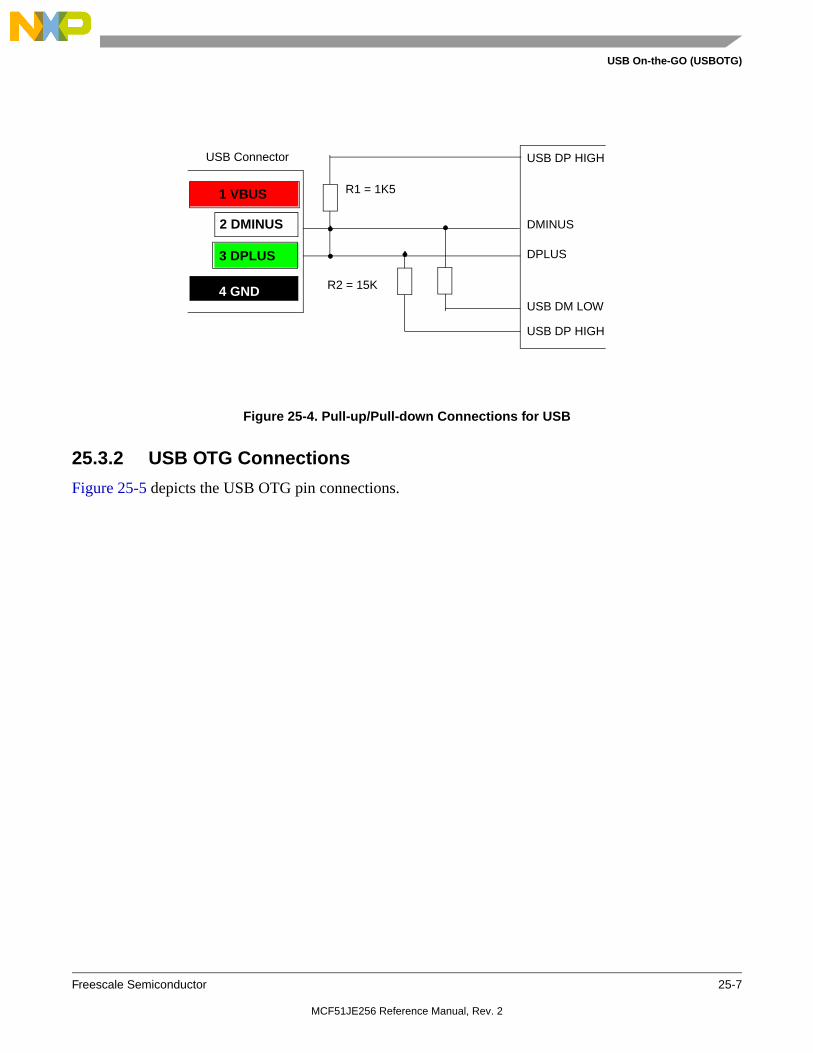
USB On-the-GO (USBOTG)
Freescale Semiconductor 25-7
Figure 25-4. Pull-up/Pull-down Connections for USB
25.3.2 USB OTG Connections
Figure 25-5 depicts the USB OTG pin connections.
2 DMINUS
3 DPLUS
4 GND
1 VBUS
R2 = 15K
R1 = 1K5
USB DP HIGH
DMINUS
DPLUS
USB DM LOW
USB DP HIGH
USB Connector
MCF51JE256 Reference Manual, Rev. 2

USB On-the-GO (USBOTG)
25-8 Freescale Semiconductor
Figure 25-5. OTG connections for USB
As shown in Figure 25-5, USB_VBUS_CHG, USB_VBUS_DSCHG, and USB_VBUS_ON are not controlled through any of the register bits within the USB controller. You should use the GPIOs to control these outputs.
25.4 Functional Description The USB-FS 2.0 full-speed/low-speed module communicates with the ColdFire processor core through status and control registers, and data structures in memory.
25.4.1 Data Structures
The function of the device operation is to transfer a request in the memory image to and from the Universal Serial Bus. To efficiently manage USB endpoint communications the USB-FS implements a Buffer Descriptor Table (BDT) in system memory. See Figure 25-6.
2 DMINUS
3 DPLUS
5 GND
1 VBUS
Power Controller
VUSB32-OTG
USB_VBUS_CHG
USB_VBUS_DSCHG
USB_VBUS_ON
USB_ID
USB Mini-A/B
USB_B_SESS_END
USB_A_VBUS_VLD
USB_SESS_VLD
4 ID
VREF
Connector
10 k
750
330
0.3 V
2.1 V
4.4 V -
+
-
+
-
+
MCF51JE256 Reference Manual, Rev. 2

USB On-the-GO (USBOTG)
Freescale Semiconductor 25-9
25.5 Programmers Interface
25.5.1 Buffer Descriptor Table
To efficiently manage USB endpoint communications the USB-FS implements a Buffer Descriptor Table (BDT) in system memory. The BDT resides on a 512 byte boundary in system memory and is pointed to by the BDT Page Registers. Every endpoint direction requires two eight-byte Buffer Descriptor entries. Therefore, a system with 16 fully bidirectional endpoints would require 512 bytes of system memory to implement the BDT. The two Buffer Descriptor (BD) entries allows for an EVEN BD and ODD BD entry for each endpoint direction. This allows the microprocessor to process one BD while the USB-FS is processing the other BD. Double buffering BDs in this way allows the USB-FS to easily transfer data at the maximum throughput provided by USB.
The software API intelligently manages buffers for the USB-FS by updating the BDT when needed. This allows the USB-FS to efficiently manage data transmission and reception, while the microprocessor performs communication overhead processing and other function dependent applications. Because the buffers are shared between the microprocessor and the USB-FS a simple semaphore mechanism is used to distinguish who is allowed to update the BDT and buffers in system memory. A semaphore bit, the OWN bit, is cleared to 0 when the BD entry is owned by the microprocessor. The microprocessor is allowed read and write access to the BD entry and the buffer in system memory when the OWN bit is 0. When the OWN bit is set to 1, the BD entry and the buffer in system memory are owned by the USB-FS. The USB-FS now has full read and write access and the microprocessor should not modify the BD or its corresponding data buffer. The BD also contains indirect address pointers to where the actual buffer resides in system memory. This indirect address mechanism is shown in the following diagram.
Figure 25-6. Buffer Descriptor Table
•••
System Memory
Current
Endpoint
BDT
Start of Buffer•••
End of Buffer
Buffer in Memory
BDT Page000ODDINEND_POINTBDT_PAGE Registers
MCF51JE256 Reference Manual, Rev. 2

USB On-the-GO (USBOTG)
25-10 Freescale Semiconductor
25.5.2 Rx vs. Tx as a USB Target Device or USB Host
The USB-FS core can function as a USB target device, or as a USB hosts, and may switch modes of operation between host and target device under software control. In either mode, USB host or USB target device, the same data paths and buffer descriptors are used for the transmission and reception of data. For this reason, a USB-FS core centric nomenclature is used to describe the direction of the data transfer between the USB-FS core and the USB. Rx or receive is used to describe transfers that move data from the USB to memory, and Tx, or transmit is used to describe transfers that move data from memory to the USB. The following table shows how the data direction corresponds to the USB token type in host and target device applications.
25.5.3 Addressing Buffer Descriptor Table Entries
To access endpoint data via the USB-FS or microprocessor, the addressing mechanism of the Buffer Descriptor Table must be understood. As stated earlier, the Buffer Descriptor Table occupies up to 512 bytes of system memory. Sixteen bidirectional endpoints can be supported with a full BDT of 512 bytes. Sixteen bytes are needed for each USB endpoint direction. Applications with less than 16 End Points require less RAM to implement the BDT. The BDT Page Registers point to the starting location of the BDT. The BDT must be located on a 512-byte boundary in system memory. All enabled TX and RX endpoint BD entries are indexed into the BDT to allow easy access via the USB-FS or ColdFire Core.
When the USB-FS receives a USB token on an enabled endpoint it uses its integrated DMA controller to interrogate the BDT. The USB-FS must read the corresponding endpoint BD entry and determine if it owns the BD and corresponding buffer in system memory. To compute the entry point in to the BDT, the BDT_PAGE registers is concatenated with the current endpoint and the TX and ODD fields to form a 32-bit address. This address mechanism is shown in the following diagrams:
Figure 25-7. BDT Address Calculation
Table 25-2. Data Direction for USB Hostor USB Target
Rx Tx
Device OUT or Setup IN
Host IN Out or Setup
31:24 23:16 15:9 8:5 4 3 2:0
BDT_PAGE_03 BDT_PAGE_02 BDT_PAGE_01[7:1] End Point IN ODD 000
Table 25-3. BDT Address Calculation Fields
Field Description
BDT_PAGE BDT_PAGE registers in the Control Register Block
END_POINT END POINT field from the USB TOKEN
TX 1 for an TX transmit transfers and 0 for an RX receive transfers
MCF51JE256 Reference Manual, Rev. 2

USB On-the-GO (USBOTG)
Freescale Semiconductor 25-11
25.5.4 Buffer Descriptor Formats
The Buffer Descriptors (BD) provide endpoint buffer control information for the USB-FS and microprocessor. The Buffer Descriptors have different meaning based on who is reading the BD in memory. The USB-FS Controller uses the data stored in the BDs to determine:
• Who owns the buffer in system memory
• Data0 or Data1 PID
• Release Own upon packet completion
• No address increment (FIFO Mode)
• Data toggle synchronization enable
• How much data is to be transmitted or received
• Where the buffer resides in system memory
While the microprocessor uses the data stored in the BDs to determine:
• Who owns the buffer in system memory
• Data0 or Data1 PID
• The received TOKEN PID
• How much data was transmitted or received
• Where the buffer resides in system memory
The format for the BD is shown in the following figure.
Figure 25-8. Buffer Descriptor Byte Format
ODD This bit is maintained within the USB-FS SIE. It corresponds to the buffer currently in use. The buffers are used in a ping-pong fashion.
31:26 25:16 15:8 7 6 5 4 3 2 1 0
RSVD BC
(10-Bits) RSVD OWN DATA0/1
KEEP/ TOK_PID[3]
NINC/ TOK_PID[2]
DTS/ 5TOK_PID[1]
BDT_STALL/ TOK_PID[0]
0 0
Buffer Address (32-Bits)
Table 25-4. Buffer Descriptor Byte Fields
Field Description
31 – 26RSVD
Reserved
25 – 16BC[9:0]
The Byte Count bits represent the 10-bit Byte Count. The USB-FS SIE changes this field upon the completion of a RX transfer with the byte count of the data received.
15 – 8RSVD
Reserved
Table 25-3. BDT Address Calculation Fields
MCF51JE256 Reference Manual, Rev. 2

USB On-the-GO (USBOTG)
25-12 Freescale Semiconductor
25.5.5 USB Transaction
When the USB-FS transmits or receives data, it computes the BDT address using the address generation shown in Table 2. After the BDT has been read and if the OWN bit equals 1, the SIE transfers the data via the DMA to or from the buffer pointed to by the ADDR field of the BD. When the TOKEN is complete, the USB-FS updates the BDT and change the OWN bit to 0 if KEEP is 0. The STAT register is updated and the TOK_DNE interrupt is set. When the microprocessor processes the TOK_DNE interrupt it reads the status register, this gives the microprocessor all the information it needs to process the endpoint. At this point, the microprocessor allocates a new BD so additional USB data can be transmitted or received for that endpoint, and process then the last BD. The following figure shows a time line how a typical USB token would be processed.
7OWN
If OWN=1 USB-FS has exclusive access to the BD. If OWN=0 the microprocessor has exclusive access to the BD. This OWN bit determines who currently owns the buffer. The SIE generally writes a 0 to this bit when it has completed a token, except when KEEP=1. The USB-FS ignores all other fields in the BD when OWN=0. The microprocessor has access to the entire BD when OWN=0. This byte of the BD should always be the last byte the microprocessor updates when it initializes a BD. After the BD has been assigned to the USB-FS, the microprocessor should not change it in any way.
6DATA0/1
This bit defines if a DATA0 field (DATA0/1=0) or a DATA1 (DATA0/1=1) field was transmitted or received. It is unchanged by the USB-FS.
5KEEP/
TOK_PID[3]
If KEEP equals 1, after the OWN bit is set it remains owned by the USB-FS forever. KEEP must equal 0 to allow the USB-FS to release the BD when a token has been processed. Typically this bit is set to 1 with ISO endpoints that are feeding a FIFO. The microprocessor is not informed that a token has been processed, the data is simply transferred to or from the FIFO. The NINC bit is normally also set when KEEP=1 to prevent address increment. If KEEP=1 this bit is unchanged by the USB-FS, otherwise bit 3 of the current token PID is written back in to the BD by the USB-FS.
4NINC/
TOK_PID[2]
The No INCrement bit disables the DMA engine address increment. This forces the DMA engine to read or write from the same address. This is useful for endpoints when data needs to be read from or written to a single location such as a FIFO. Typically this bit is set with the KEEP bit for ISO endpoints that are interfacing to a FIFO. If KEEP=1 this bit is unchanged by the USB-FS, otherwise bit 2 of the current token PID is written back in to the BD by the USB-FS.
3DTS/
TOK_PID[1]
Setting this bit enables the USB-FS to perform Data Toggle Synchronization. When this bit is 0 no Data Toggle Synchronization is performed. If KEEP=1 this bit is unchanged by the USB-FS, otherwise bit 1 of the current token PID is written back in to the BD by the USB-FS.
2BDT_STALL TOK_PID[0]
Setting this bit causes the USB-FS to issue a STALL handshake if a token is received by the SIE that would use the BDT in this location. The BDT is not consumed by the SIE (the owns bit remains and the rest of the BDT are unchanged) when a BDT-STALL bit is set. If KEEP=1 this bit is unchanged by the USB-FS, otherwise bit 0 of the current token PID is written back in to the BD by the USB-FS
TOK_PID[n] Bits [5:2] can also represent the current token PID. The current token PID is written back in to the BD by the USB-FS when a transfer completes. The values written back are the token PID values from the USB specification: 0x1 for an OUT token, 0x9 for and IN token or 0xd for a SETUP token. In host mode this field is used to report the last returned PID or a transfer status indication. The possible values returned are: 0x3 DATA0, 0xb DATA1, 0x2 ACK, 0xe STALL, 0xa NAK, 0x0 Bus Timeout, 0xf Data Error.
1–0Reserved
Reserved, should read as zeroes
ADDR[31:0] The Address bits represent the 32 -bit buffer address in system memory. These bits are unchanged by the USB-FS.
Table 25-4. Buffer Descriptor Byte Fields (Continued)
MCF51JE256 Reference Manual, Rev. 2

USB On-the-GO (USBOTG)
Freescale Semiconductor 25-13
Figure 25-9. USB Token Transaction
The USB has two sources for the DMA overrun error. First, the memory latency on the BVCI initiator interface may be too high and cause the receive FIFO to overflow. This is predominantly a hardware performance issue, usually caused by transient memory access issues. Second, the packet received may be larger than the negotiated MaxPacket size. This would be caused by a software bug.
In the first case, the USB responds with a NAK or Bus Timeout (BTO - See bit 4 in Section 25.6.1.11, “Error Interrupt Status Register (ERR_STAT)”) as appropriate for the class of transaction. The DMA_ERR bit is set in the ERR_STAT register of the core for host and device modes of operation. Depending on the values of the INT_ENB and ERR_ENB register, the core may assert an interrupt to notify the processor of the DMA error. In device mode, the BDT is not written back nor is the TOK_DNE interrupt triggered because it is assumed that a second attempt is queued and succeed in the future. For host mode, the TOK_DNE interrupt fires and the TOK_PID field of the BDT is 1111 to indicate the DMA latency error. Host mode software can decide to retry or move to another item in its schedule.
In the second case of oversized data packets the USB specification is ambiguous. It assumes correct software drivers on both sides. The overrun is not due to memory latency but due to a lack of space to put the excess data. NAKing the packet may cause another retransmission of the already oversized packet data. In response to oversized packets, the USB core continues ACKing the packet for non-isochronous transfers. The data written to memory is clipped to the MaxPacket size so as not to corrupt system memory. The core asserts the DMA_ERR bit of the ERR_STAT register (which could trigger an interrupt, as above) and a TOK_DNE interrupt fires. The TOK_PID field of the BDT is not 1111 because the DMA_ERR is not due to latency. The packet length field written back to the BDT is the MaxPacket value that represents the length of the clipped data actually written to memory. The software can decide an appropriate course of action from here for future transactions such as stalling the endpoint, canceling the transfer, disabling the endpoint, etc.
SETUP TOKEN DATA ACK
USB RST SOF
SOFInterrupt Generated
TOK_DNEInterrupt Generated
IN TOKEN DATA ACK
TOK_DNEInterrupt Generated
OUT TOKEN DATA ACK
TOK_DNEInterrupt Generated
USB_RSTInterrupt Generated
USB Host Function
MCF51JE256 Reference Manual, Rev. 2

USB On-the-GO (USBOTG)
25-14 Freescale Semiconductor
25.6 Memory Map/Register DefinitionsThis section provides the memory map and detailed descriptions of all USB interface registers. The memory map of the USB interface is shown in Table 25-5.
Table 25-5. USB Interface Memory Map
Offset Address Register Acronym Bits
USB OTG Registers
IPSBAR + 0x1C_0000 Peripheral ID Register PER_ID 8
IPSBAR + 0x1C_0004 Peripheral ID Complement Register ID_COMP 8
IPSBAR + 0x1C_0008 Peripheral Revision Register REV 8
IPSBAR + 0x1C_000C Peripheral Additional Info Register ADD_INFO 8
IPSBAR + 0x1C_0010 OTG Interrupt Status Register OTG_INT_STAT 8
IPSBAR + 0x1C_0014 OTG Interrupt Control Register OTG_INT_EN 8
IPSBAR + 0x1C_0018 OTG Status Register OTG_STATUS 8
IPSBAR + 0x1C_001C OTG Control Register OTG_CTRL 8
IPSBAR + 0x1C_0080 Interrupt Status Register INT_STAT 8
IPSBAR + 0x1C_0084 Interrupt Enable Register INT_ENB 8
IPSBAR + 0x1C_0088 Error Interrupt Status Register ERR_STAT 8
IPSBAR + 0x1C_008C Error Interrupt Enable Register ERR_ENG 8
IPSBAR + 0x1C_0090 Status Register STAT 8
IPSBAR + 0x1C_0094 Control Register CTL 8
IPSBAR + 0x1C_0098 Address Register ADDR 8
IPSBAR + 0x1C_009C BDT Page Register 1 BDT_PAGE_01 8
IPSBAR + 0x1C_00A0 Frame Number Register Low FRM_NUML 8
IPSBAR + 0x1C_00A4 Frame Number Register High FRM_NUMH 8
IPSBAR + 0x1C_00A8 Token Register TOKEN 8
IPSBAR + 0x1C_00AC SOF Threshold Register SOF_THLD 8
IPSBAR + 0x1C_00B0 BDT Page Register 2 BDT_PAGE_02 8
IPSBAR + 0x1C_00B4 BDT Page Register 3 BDT_PAGE_03 8
IPSBAR + 0x1C_00C0 Endpoint Control Register 0 ENDPT0 8
IPSBAR + 0x1C_00C4 Endpoint Control Register 1 ENDPT1 8
IPSBAR + 0x1C_00C8 Endpoint Control Register 2 ENDPT2 8
IPSBAR + 0x1C_00CC Endpoint Control Register 3 ENDPT3 8
IPSBAR + 0x1C_00D0 Endpoint Control Register 4 ENDPT4 8
IPSBAR + 0x1C_00D4 Endpoint Control Register 5 ENDPT5 8
IPSBAR + 0x1C_00D8 Endpoint Control Register 6 ENDPT6 8
IPSBAR + 0x1C_00DC Endpoint Control Register 7 ENDPT7 8
MCF51JE256 Reference Manual, Rev. 2

USB On-the-GO (USBOTG)
Freescale Semiconductor 25-15
The following sections provide details about the registers in the USB OTG memory map.
25.6.1 Capability Registers
The capability registers specify the software limits, restrictions, and capabilities of the host/device controller implementation. Most of these registers are defined by the EHCI specification. Registers that are not defined by the EHCI specification are noted in their descriptions.
IPSBAR + 0x1C_00E0 Endpoint Control Register 8 ENDPT8 8
IPSBAR + 0x1C_00E4 Endpoint Control Register 9 ENDPT9 8
IPSBAR + 0x1C_00E8 Endpoint Control Register 10 ENDPT10 8
IPSBAR + 0x1C_00EC Endpoint Control Register 11 ENDPT11 8
IPSBAR + 0x1C_00F0 Endpoint Control Register 12 ENDPT12 8
IPSBAR + 0x1C_00F4 Endpoint Control Register 13 ENDPT13 8
IPSBAR + 0x1C_00F8 Endpoint Control Register 14 ENDPT14 8
IPSBAR + 0x1C_00FC Endpoint Control Register 15 ENDPT15 8
IPSBAR + 0x1C_0100 USB Control Register USB_CTRL 8
IPSBAR + 0x1C_0104 USB OTG Observe Register USB_OTG_OBSERVE 8
IPSBAR + 0x1C_0108 USB OTG Control Register USB_OTG_CONTROL 8
IPSBAR + 0x1C_010C USB Transceiver and Regulator Control Register 0 USBTRC0 8
IPSBAR + 0x1C_0110 OTG Pin Control Register OTGPIN 8
Table 25-5. USB Interface Memory Map (Continued)
Offset Address Register Acronym Bits
MCF51JE256 Reference Manual, Rev. 2

USB On-the-GO (USBOTG)
25-16 Freescale Semiconductor
25.6.1.1 Peripheral ID Register (PER_ID)
The Peripheral ID Register reads back the value of 0x04. This value is defined for the USB Peripheral. Figure 25-10 shows the PER_ID register.
25.6.1.2 Peripheral ID Complement Register (ID_COMP)
The Peripheral ID Complement Register reads back the complement of the Peripheral ID Register. For the USB Peripheral, this is the value 0xFB. Figure 25-11 shows the ID_COMP register.
IPSBAROffset: 0x1C_0000 (PER_ID) Access: User read-only
7 6 5 4 3 2 1 0
R 0 0 ID5 ID4 ID3 ID2 ID1 ID0
W
Reset: 0 0 0 0 0 1 0 0
Figure 25-10. Peripheral ID Register (PER_ID)
Table 25-12. PER_ID Field Descriptions
Field Description
7–6 These bits always read zeros
5–0IDx
Peripheral identification bits. These bits always read 0x04 (00_0100).
IPSBAROffset:
0x1C_0004 (ID_COMP) Access: User read-only
7 6 5 4 3 2 1 0
R 1 1 NID5 NID4 NID3 NID2 NID1 NID0
W
Reset: 1 1 1 1 1 0 1 1
Figure 25-11. Peripheral ID Complement Register
Table 25-13. ID_COMP Field Descriptions
Field Description
7–6 These bits always read ones
5–0NIDx
Ones complement of peripheral identification bits.
MCF51JE256 Reference Manual, Rev. 2

USB On-the-GO (USBOTG)
Freescale Semiconductor 25-17
25.6.1.3 Peripheral Revision Register (REV)
This register contains the revision number of the USB Module. Figure 25-12 shows the REV register.
25.6.1.4 Peripheral Additional Info Register (ADD_INFO)
The Peripheral Additional info Register reads back the value of the fixed Interrupt Request Level (IRQ_NUM) along with the Host Enable bit. If set to 1, the Host Enable bit indicates the USB peripheral is operating in host mode. Figure 25-13 shows the ADD_INFO register.
IPSBAROffset:
0x1C_0008 (REV) Access: User read-only
7 6 5 4 3 2 1 0
R REV7 REV6 REV5 REV4 REV3 REV2 REV1 REV0
W
Reset: 0 0 1 1 0 0 1 1
Figure 25-12. Peripheral Revision Register
Table 25-14. REV Field Descriptions
Field Description
7–0REVx
REV[7:0] indicate the revision number of the USB Core.
IPSBAROffset:
0x1C_000C (ADD_INFO) Access: User read-only
7 6 5 4 3 2 1 0
R IRQ_NUM 0 0 IEHOST
W
Reset: 0 0 0 0 0 0 0 1
Figure 25-13. Peripheral Additional Info Register
Table 25-15. ADD_INFO Field Descriptions
Field Description
7–3IRQ_NUM
Assigned Interrupt Request Number.
2–1Reserved
RESERVED. These bits read back zeros.
0IEHOST
This bit is set if host mode is enabled.
MCF51JE256 Reference Manual, Rev. 2

USB On-the-GO (USBOTG)
25-18 Freescale Semiconductor
25.6.1.5 OTG Interrupt Status Register (OTG_INT_STAT)
The OTG Interrupt Status Register records changes of the ID sense and VBUS signals. Software can read this register to determine which event has caused an interrupt. Only bits that have changed since the last software read are set. Writing a one to a bit clears the associated interrupt. Figure 25-14 shows the OTG_INT_STAT register.
IPSBAROffset:
0x1C_0010 (OTG_INT_STAT) Access: User read/write
7 6 5 4 3 2 1 0
RID_CHG 1_MSEC
LINE_STATE_CHG
Reserved SESS_VLD_CHG
B_SESS_CHG
Reserved A_VBUS_CHGW – –
Reset: 0 1 1 X 0 0 X 0
Figure 25-14. OTG Interrupt Status Register
Table 25-16. OTG_INT_STAT Field Descriptions
Field Description
7ID_CHG
This bit is set when a change in the ID Signal from the USB connector is sensed.
61_MSEC
This bit is set when the 1 millisecond timer expires. This bit stays asserted until cleared by software. The interrupt must be serviced every millisecond to avoid losing 1msec counts.
5LINE_STAT
_CHG
This bit is set when the USB line state changes. The interrupt associated with this bit can be used to detect Reset, Resume, Connect, and Data Line Pulse signals.
4Reserved
Reserved
3SESS_VLD
_CHG
This bit is set when a change in VBUS is detected indicating a session valid or a session no longer valid
2B_SESS
_CHG
This bit is set when a change in VBUS is detected on a B device.
1Reserved
Reserved
0A_VBUS
_CHG
This bit is set when a change in VBUS is detected on an A device.
MCF51JE256 Reference Manual, Rev. 2

USB On-the-GO (USBOTG)
Freescale Semiconductor 25-19
25.6.1.6 OTG Interrupt Control Register (OTG_INT_EN)
The OTG Interrupt Control Register enables the corresponding interrupt status bits defined in the OTG Interrupt Status Register. Figure 25-15 shows the OTG_INT_EN register.
IPSBAROffset:
0x1C_0014 (OTG_INT_EN) Access: User read/write
7 6 5 4 3 2 1 0
RID_EN
1_MSEC_EN
LINE_STATE_EN
Reserved SESS_VLD_EN
B_SESS_EN
Reserved A_VBUS_ENW – –
Reset: 0 0 0 X 0 0 X 0
Figure 25-15. OTG Interrupt Control Register
Table 25-17. OTG_INT_EN Field Descriptions
Field Description
7ID_EN
ID interrupt enable 0 The ID interrupt is disabled1 The ID interrupt is enabled
61_MSEC_EN
1 millisecond interrupt enable0 The 1msec timer interrupt is disabled1 The 1msec timer interrupt is enabled
5LINE_STATE
_EN
Line State change interrupt enable0 The LINE_STAT_CHG interrupt is disabled1 The LINE_STAT_CHG interrupt is enabled
4 Reserved.
3SESS_VLD
_EN
Session valid interrupt enable 0 The SESS_VLD_CHG interrupt is disabled1 The SESS_VLD_CHG interrupt is enabled
2B_SESS_EN
B Session END interrupt enable 0 The B_SESS_CHG interrupt is disabled1 The B_SESS_CHG interrupt is enabled
1 Reserved.
0A_VBUS_EN
A VBUS Valid interrupt enable 0 The A_VBUS_CHG interrupt is disabled1 The A_VBUS_CHG interrupt is enabled
MCF51JE256 Reference Manual, Rev. 2

USB On-the-GO (USBOTG)
25-20 Freescale Semiconductor
25.6.1.7 Interrupt Status Register (OTG_STAT)
The Interrupt Status Register displays the actual value from the external comparator outputs of the ID pin and VBUS. Figure 25-16 shows the OTG_STAT register.
IPSBAROffset: 0x1C_0018 (OTG_STAT) Access: User read/write
7 6 5 4 3 2 1 0
RID 1_MSEC_EN
LINE_STATE_STABLE
ReservedSESS_VLD
B_SESS_END
Reserved A_VBUS_VLDW – –
Reset: 0 0 1 X 0 0 X 0
Figure 25-16. Interrupt Status Register
Table 25-18. OTG_STAT Field Descriptions
Field Description
7ID
Indicates the current state of the ID pin on the USB connector0 Indicates a Type A cable has been plugged into the USB connector1 Indicates no cable is attached or a Type B cable has been plugged into the USB connector
61_MSEC_EN
This bit is reserved for the 1msec count, but it is not useful to software.
5LINE_STATE
_STABLE
This bit indicates that the internal signals that control the LINE_STATE_CHG bit (bit 5) of the OTG_INT_STAT register have been stable for at least 1 millisecond. First read the LINE_STATE_CHG bit, and then read this bit. If this bit reads as 1, then the value of LINE_STATE_CHG can be considered stable. 0 The LINE_STAT_CHG bit is not yet stable1 The LINE_STAT_CHG bit has been debounced and is stable
4 Reserved.
3SESS_VLD
Session Valid 0 The VBUS voltage is below the B session Valid threshold1 The VBUS voltage is above the B session Valid threshold
2B_SESS
_END
B Session END 0 The VBUS voltage is above the B session End threshold1 The VBUS voltage is below the B session End threshold
1 Reserved.
0A_VBUS
_VLD
A VBUS Valid 0 The VBUS voltage is below the A VBUS Valid threshold1 The VBUS voltage is above the A VBUS Valid threshold
MCF51JE256 Reference Manual, Rev. 2

USB On-the-GO (USBOTG)
Freescale Semiconductor 25-21
25.6.1.8 OTG Control Register (OTG_CTRL)
The OTG Control Register controls the operation of VBUS and Data Line termination resistors. Figure 25-17 shows the OTG_CTRL register.
IPSBAROffset:
0x1C_001C (OTG_CTRL) Access: User read/write
7 6 5 4 3 2 1 0
RDP_HIGH DP_LOW DM_LOW OTG_EN
W
Reset: 0 0 0 0 0 0 0 0
Figure 25-17. OTG Control Register
Table 25-19. OTG_CTRL Field Descriptions
Field Description
7DP_HIGH
D+ Data Line pull-up resistor enable0 D+ pull-up resistor is not enabled1 D+ pull-up resistor is enabled
6Reserved
Reserved.
5DP_LOW
D+ Data Line pull-down resistor enable0 D+ pull-down resistor is not enabled1 D+ pull-down resistor is enabledThis bit should always be enabled together with bit 4 (DM_LOW)
4DM_LOW
D- Data Line pull-down resistor enable0 D- pull-down resistor is not enabled1 D- pull-down resistor is enabledThis bit should always be enabled together with bit 5 (DP_LOW)
3Reserved
Reserved.
2OTG_EN
On-The-Go pull-up/pull-down resistor enable0 If USB_EN is set and HOST_MODE is clear in the Control Register (CTL), then the D+ Data Line pull-up
resistors are enabled. If HOST_MODE is set the D+ and D- Data Line pull-down resistors are engaged. 1 The pull-up and pull-down controls in this register are used
1Reserved
Reserved.
0Reserved
Reserved.
MCF51JE256 Reference Manual, Rev. 2

USB On-the-GO (USBOTG)
25-22 Freescale Semiconductor
25.6.1.9 Interrupt Status Register (INT_STAT)
The Interrupt Status Register contains bits for each of the interrupt sources within the USB Module. Each of these bits are qualified with their respective interrupt enable bits (see Section 25.6.1.10, “Interrupt Enable Register (INT_ENB)”). All bits of this register are logically OR’d together along with the OTG Interrupt Status Register (OTG_STAT) to form a single interrupt source for the ColdFire core. After an interrupt bit has been set it may only be cleared by writing a one to the respective interrupt bit. This register contains the value of 0x00 after a reset. Figure 25-18 shows the INT_STAT register.
IPSBAROffset:
0x1C_0080 (INT_STAT) Access: User read/write
7 6 5 4 3 2 1 0
RSTALL ATTACH RESUME SLEEP TOK_DNE SOF_TOK ERROR USB_RST
W
Reset: 0 0 0 0 0 0 0 0
Figure 25-18. Interrupt Status Register
Table 25-20. INT_STAT Field Descriptions
Field Description
7STALL
Stall InterruptIn Target mode this bit is asserted when a STALL handshake is sent by the SIE.In Host mode this bit is set when the USB Module detects a STALL acknowledge during the handshake phase of a USB transaction. This interrupt can be use to determine is the last USB transaction was completed successfully or if it stalled.
6ATTACH
Attach InterruptThis bit is set when the USB Module detects an attach of a USB device. This signal is only valid if HOST_MODE_EN is true. This interrupt signifies that a peripheral is now present and must be configured.
5RESUME
This bit is set depending upon the DP/DM signals, and can be used to signal remote wake-up signaling on the USB bus. When not in suspend mode this interrupt should be disabled.
4SLEEP
This bit is set when the USB Module detects a constant idle on the USB bus for 3 milliseconds. The sleep timer is reset by activity on the USB bus.
3TOK_DNE
This bit is set when the current token being processed has completed. The ColdFire core should immediately read the STAT register to determine the EndPoint and BD used for this token. Clearing this bit (by writing a one) causes the STAT register to be cleared or the STAT holding register to be loaded into the STAT register.
2SOF_TOK
This bit is set when the USB Module receives a Start Of Frame (SOF) token. In Host mode this bit is set when the SOF threshold is reached, so that software can prepare for the next SOF.
1ERROR
This bit is set when any of the error conditions within the ERR_STAT register occur. The ColdFire core must then read the ERR_STAT register to determine the source of the error.
0USB_RST
This bit is set when the USB Module has decoded a valid USB reset. This informs the Microprocessor that it should write 0x00 into the address register and enable endpoint 0. USB_RST is set after a USB reset has been detected for 2.5 microseconds. It is not asserted again until the USB reset condition has been removed and then reasserted.
MCF51JE256 Reference Manual, Rev. 2

USB On-the-GO (USBOTG)
Freescale Semiconductor 25-23
25.6.1.10 Interrupt Enable Register (INT_ENB)
The Interrupt Enable Register contains enable bits for each of the interrupt sources within the USB Module. Setting any of these bits enables the respective interrupt source in the INT_STAT register. This register contains the value of 0x00 after a reset. Figure 25-19 shows the INT_ENB register.
IPSBAROffset:
0x1C_0084 (INT_ENB) Access: User read/write
7 6 5 4 3 2 1 0
RSTALL_EN ATTACH_EN
RESUME_EN
SLEEP_ENTOK_DNE
_ENSOF_TOK
_ENERROR_E
NUSB_RST
_ENW
Reset: 0 0 0 0 0 0 0 0
Figure 25-19. Interrupt Enable Register
Table 25-21. INT_ENB Field Descriptions
Field Description
7STALL_EN
STALL Interrupt Enable0 The STALL interrupt is not enabled1 The STALL interrupt is enabled
6ATTACH_EN
ATTACH Interrupt Enable0 The ATTACH interrupt is not enabled1 The ATTACH interrupt is enabled
5RESUME_EN
RESUME Interrupt Enable0 The RESUME interrupt is not enabled1 The RESUME interrupt is enabled
4SLEEP_EN
SLEEP Interrupt Enable0 The SLEEP interrupt is not enabled1 The SLEEP interrupt is enabled
3TOK_DNE
_EN
TOK_DNE Interrupt Enable0 The TOK_DNE interrupt is not enabled1 The TOK_DNE interrupt is enabled
2SOF_TOK
_EN
SOF_TOK Interrupt Enable0 The SOF_TOK interrupt is not enabled1 The SOF_TOK interrupt is enabled
1ERROR_EN
ERROR Interrupt Enable0 The ERROR interrupt is not enabled1 The ERROR interrupt is enabled
0USB_RST
_EN
USB_RST Interrupt Enable0 The USB_RST interrupt is not enabled1 The USB_RST interrupt is enabled
MCF51JE256 Reference Manual, Rev. 2

USB On-the-GO (USBOTG)
25-24 Freescale Semiconductor
25.6.1.11 Error Interrupt Status Register (ERR_STAT)
The Error Interrupt Status Register contains enable bits for each of the error sources within the USB Module. Each of these bits are qualified with their respective error enable bits (see Section 25.6.1.12, “Error Interrupt Enable Register (ERR_ENB)”). All bits of this Register are logically OR’d together and the result placed in the ERROR bit of the INT_STAT register. After an interrupt bit has been set it may only be cleared by writing a one to the respective interrupt bit. Each bit is set as soon as the error conditions is detected. Therefore, the interrupt does not typically correspond with the end of a token being processed. This register contains the value of 0x00 after a reset. Figure 25-20 shows the ERR_STAT register.
IPSBAROffset: 0x1C_0088 (ERR_STAT) Access: User read/write
7 6 5 4 3 2 1 0
RBTS_ERR
ReservedDMA_ERR BTO_ERR DFN8 CRC16 CRC5_EOF PID_ERR
W –
Reset: 0 0 0 0 0 0 0 0
Figure 25-20. Error Interrupt Status Register
Table 25-22. ERR_STAT Field Descriptions
Field Description
7BTS_ERR
This bit is set when a bit stuff error is detected. If set, the corresponding packet is rejected due to the error.
6 Reserved
5DMA_ERR
This bit is set if the USB Module has requested a DMA access to read a new BDT but has not been given the bus before it needs to receive or transmit data. If processing a TX transfer this would cause a transmit data underflow condition. If processing a RX transfer this would cause a receive data overflow condition. This interrupt is useful when developing device arbitration hardware for the microprocessor and the USB Module to minimize bus request and bus grant latency. This bit is also set if a data packet to or from the host is larger than the buffer size allocated in the BDT. In this case the data packet is truncated as it is put into buffer memory.
4BTO_ERR
This bit is set when a bus turnaround timeout error occurs. The USB Module contains a bus turnaround timer that keeps track of the amount of time elapsed between the token and data phases of a SETUP or OUT TOKEN or the data and handshake phases of a IN TOKEN. If more than 16 bit times are counted from the previous EOP before a transition from IDLE, a bus turnaround timeout error occurs.
3DFN8
This bit is set if the data field received was not 8 bits in length. USB Specification 1.0 requires that data fields be an integral number of bytes. If the data field was not an integral number of bytes, this bit is set.
2CRC16
This bit is set when a data packet is rejected due to a CRC16 error.
1CRC5_EOF
This error interrupt has two functions. When the USB Module is operating in peripheral mode (HOST_MODE_EN=0), this interrupt detects CRC5 errors in the token packets generated by the host. If set the token packet was rejected due to a CRC5 error. When the USB Module is operating in host mode (HOST_MODE_EN=1), this interrupt detects End Of Frame (EOF) error conditions. This occurs when the USB Module is transmitting or receiving data and the SOF counter reaches zero. This interrupt is useful when developing USB packet scheduling software to ensure that no USB transactions cross the start of the next frame.
0PID_ERR
This bit is set when the PID check field fails.
MCF51JE256 Reference Manual, Rev. 2

USB On-the-GO (USBOTG)
Freescale Semiconductor 25-25
25.6.1.12 Error Interrupt Enable Register (ERR_ENB)
The Error Interrupt Enable Register contains enable bits for each of the error interrupt sources within the USB Module. Setting any of these bits enables the respective interrupt source in the ERR_STAT register. Each bit is set as soon as the error conditions is detected. Therefore, the interrupt does not typically correspond with the end of a token being processed. This register contains the value of 0x00 after a reset. Figure 25-21 shows the ERR_ENB register.
IPSBAROffset:
0x1C_008C (ERR_ENB)
Access: User read/write
7 6 5 4 3 2 1 0
R BTS_ERR_EN
Reserved DMA_ERR_EN
BTO_ERR_EN
DFN8_EN CRC16_ENCRC5_EOF
_ENPID_ERR
_ENW –
Reset: 0 0 0 0 0 0 0 0
Figure 25-21. Error Interrupt Enable Register
Table 25-23. ERR_ENB Field Descriptions
Field Description
7BTS_ERR
_EN
BTS_ERR Interrupt Enable0 The BTS_ERR interrupt is not enabled1 The BTS_ERR interrupt is enabled
6 Reserved
5DMA_ERR
_EN
DMA_ERR Interrupt Enable0 The DMA_ERR interrupt is not enabled1 The DMA_ERR interrupt is enabled
4BTO_ERR
_EN
BTO_ERR Interrupt Enable0 The BTO_ERR interrupt is not enabled1 The BTO_ERR interrupt is enabled
3DFN8_EN
DFN8 Interrupt Enable0 The DFN8 interrupt is not enabled1 The DFN8 interrupt is enabled
2CRC16_EN
CRC16 Interrupt Enable0 The CRC16 interrupt is not enabled1 The CRC16 interrupt is enabled
1CRC5_EOF
_EN
CRC5/EOF Interrupt Enable0 The CRC5/EOF interrupt is not enabled1 The CRC5/EOF interrupt is enabled
0PID_ERR
_EN
PID_ERR Interrupt Enable0 The PID_ERR interrupt is not enabled1 The PID_ERR interrupt is enabled
MCF51JE256 Reference Manual, Rev. 2

USB On-the-GO (USBOTG)
25-26 Freescale Semiconductor
25.6.1.13 Status Register (STAT)
The Status Register reports the transaction status within the USB Module. When the ColdFire core has received a TOK_DNE interrupt the Status Register should be read to determine the status of the previous endpoint communication. The data in the status register is valid when the TOK_DNE interrupt bit is asserted. The STAT register is actually a read window into a status FIFO maintained by the USB Module. When the USB Module uses a BD, it updates the Status Register. If another USB transaction is performed before the TOK_DNE interrupt is serviced, the USB Module stores the status of the next transaction in the STAT FIFO. Thus the STAT register is actually a four byte FIFO that allows the ColdFire core to process one transaction while the SIE is processing the next transaction. Clearing the TOK_DNE bit in the INT_STAT register causes the SIE to update the STAT register with the contents of the next STAT value. If the data in the STAT holding register is valid, the SIE immediately reasserts to TOK_DNE interrupt. Figure 25-22 shows the STAT register.
IPSBAROffset:
0x1C_0090 (STAT) Access: User read-only
7 6 5 4 3 2 1 0
R ENDP TX ODD Reserved Reserved
W
Reset: 0 0 0 0 0 0 0 0
Figure 25-22. Status Register
Table 25-24. STAT Field Descriptions
Field Description
7 - 5ENDP[3:0]
This four-bit field encodes the endpoint address that received or transmitted the previous token. This allows the ColdFire core to determine which BDT entry was updated by the last USB transaction.
3TX
Transmit Indicator0 The most recent transaction was a Receive operation1 The most recent transaction was a Transmit operation
2ODD
this bit is set if the last Buffer Descriptor updated was in the odd bank of the BDT.
1 - 0 Reserved
MCF51JE256 Reference Manual, Rev. 2

USB On-the-GO (USBOTG)
Freescale Semiconductor 25-27
25.6.1.14 Control Register (CTL)
The Control Register provides various control and configuration information for the USB Module. Figure 25-23 shows the CTL register.
IPSBAROffset:
0x1C_0094 (CTL) Access: User read/write
7 6 5 4 3 2 1 0
RJSTATE SE0
TXSUSPEND/TOKENBUSY
RESETHOST_
MODE_ENRESUME ODD_RST
USB_EN/SOF_ENW
Reset: 0 0 0 0 0 0 0 0
Figure 25-23. Control Register
Table 25-25. CTL Field Descriptions
Field Description
7JSTATE
Live USB differential receiver JSTATE signal. The polarity of this signal is affected by the current state of LS_EN (See)
6SE0
Live USB Single Ended Zero signal
5TXSUSPEND/TOKENBUSY
When the USB Module is in Host mode TOKEN_BUSY is set when the USB Module is busy executing a USB token and no more token commands should be written to the Token Register. Software should check this bit before writing any tokens to the Token Register to ensure that token commands are not lost. In Target mode TXD_SUSPEND is set when the SIE has disabled packet transmission and reception. Clearing this bit allows the SIE to continue token processing. This bit is set by the SIE when a Setup Token is received allowing software to dequeue any pending packet transactions in the BDT before resuming token processing.
4RESET
Setting this bit enables the USB Module to generate USB reset signaling. This allows the USB Module to reset USB peripherals. This control signal is only valid in Host mode (HOST_MODE_EN=1). Software must set RESET to 1 for the required amount of time and then clear it to 0 to end reset signaling. For more information on RESET signaling see Section 7.1.4.3 of the USB specification version 1.0.
3HOST_
MODE_EN
When set to 1, this bit enables the USB Module to operate in Host mode. In host mode, the USB module performs USB transactions under the programmed control of the host processor.
2RESUME
When set to 1 this bit enables the USB Module to execute resume signaling. This allows the USB Module to perform remote wake-up. Software must set RESUME to 1 for the required amount of time and then clear it to 0. If the HOST_MODE_EN bit is set, the USB module appends a Low Speed End of Packet to the Resume signaling when the RESUME bit is cleared. For more information on RESUME signaling see Section 7.1.4.5 of the USB specification version 1.0.
1ODD_RST
Setting this bit to 1 resets all the BDT ODD ping/pong bits to 0, which then specifies the EVEN BDT bank.
0USB_EN/SOF_EN
USB Enable0 The USB Module is disabled1 The USB Module is enabled. Setting this bit causes the SIE to reset all of its ODD bits to the BDTs. Therefore, setting this bit resets much of the logic in the SIE. When host mode is enabled, clearing this bit causes the SIE to stop sending SOF tokens.
MCF51JE256 Reference Manual, Rev. 2

USB On-the-GO (USBOTG)
25-28 Freescale Semiconductor
25.6.1.15 Address Register (ADDR)
The Address Register holds the unique USB address that the USB Module decodes when in Peripheral mode (HOST_MODE_EN=0). When operating in Host mode (HOST_MODE_EN=1) the USB Module transmits this address with a TOKEN packet. This enables the USB Module to uniquely address an USB peripheral. In either mode, the USB_EN bit within the control register must be set. The Address Register is reset to 0x00 after the reset input becomes active or the USB Module decodes a USB reset signal. This action initializes the Address Register to decode address 0x00 as required by the USB specification. Figure 25-24 shows the ADDR register.
IPSBAROffset: 0x1C_0098 (ADDR) Access: User read/write
7 6 5 4 3 2 1 0
RLS_EN ADDR
W
Reset: 0 0 0 0 0 0 0 0
Figure 25-24. ADDR Register
Table 25-26. ADDR Field Descriptions
Field Description
7LS_EN
Low Speed Enable bit. This bit informs the USB Module that the next token command written to the token register must be performed at low speed. This enables the USB Module to perform the necessary preamble required for low-speed data transmissions.
6–0ADDR
USB address. This 7-bit value defines the USB address that the USB Module decodes in peripheral mode, or transmit when in host mode.
MCF51JE256 Reference Manual, Rev. 2

USB On-the-GO (USBOTG)
Freescale Semiconductor 25-29
25.6.1.16 BDT Page Register 1 (BDT_PAGE_01)
The Buffer Descriptor Table Page Register 1 contains an 8-bit value used to compute the address where the current Buffer Descriptor Table (BDT) resides in system memory. Figure 25-25 shows the BDT Page Register 1.
IPSBAROffset:
0x1C_009C (BDT_PAGE_01) Access: User read/write
7 6 5 4 3 2 1 0
RBDT_BA15 BDT_BA14 BDT_BA13 BDT_BA12 BDT_BA11 BDT_BA10 BDT_BA9 NOT USED
W
Reset: 0 0 0 0 0 0 0 0
Figure 25-25. BDT_PAGE_01 Register
Table 25-27. BDT_PAGE_01 Field Descriptions
Field Description
7 – 1BDT_
BA[15:8]
This 7 bit field provides address bits 15 through 9 of the BDT base address, which defines where the Buffer Descriptor Table resides in system memory.
0NOT USED
This bit is always zero. The 32-bit BDT Base Address is always aligned on 512 byte boundaries in memory.
MCF51JE256 Reference Manual, Rev. 2

USB On-the-GO (USBOTG)
25-30 Freescale Semiconductor
25.6.1.17 Frame Number Register Low/High (FRM_NUML, FRM_NUMH)
The Frame Number Register contains an 11-bit value used to compute the address where the current Buffer Descriptor Table (BDT) resides in system memory. Figure 25-26 shows the FRM_NUML Register.
IPSBAROffset:
0x1C_00A0 (FRM_NUML) Access: User read-only
7 6 5 4 3 2 1 0
R FRM7 FRM6 FRM5 FRM4 FRM3 FRM2 FRM1 FRM0
W
Reset: 0 0 0 0 0 0 0 0
Figure 25-26. FRM_NUML Register
Table 25-28. FRM_NUML Field Descriptions
Field Description
7–0FRM[7:0]
These 8 bits represent the low-order bits of the11-bit Frame Number
IPSBAROffset:
0x1C_00A4 (FRM_NUMH)
Access: User read-only
7 6 5 4 3 2 1 0
R 0 0 0 0 0 FRM10 FRM9 FRM8
W
Reset: 0 0 0 0 0 0 0 0
Figure 25-27. FRM_NUMH Register
Table 25-29. FRM_NUMH Field Descriptions
Field Description
2–0FRM[10:8]
These 3 bits represent the high-order bits of the11-bit Frame Number
7–3NOT USED
This bits always read zero.
MCF51JE256 Reference Manual, Rev. 2

USB On-the-GO (USBOTG)
Freescale Semiconductor 25-31
25.6.1.18 Token Register (TOKEN)
The Token Register is used to perform USB transactions when in host mode (HOST_MODE_EN=1). When the ColdFire core processor wishes to execute a USB transaction to a peripheral, it writes the TOKEN type and endpoint to this register. After this register has been written, the USB module begins the specified USB transaction to the address contained in the address register. The ColdFire core should always check that the TOKEN_BUSY bit in the control register is not set before performing a write to the Token Register. This ensures token commands are not overwritten before they can be executed. The address register and endpoint control register 0 are also used when performing a token command and therefore must also be written before the Token Register. The address register is used to correctly select the USB peripheral address transmitted by the token command. The endpoint control register determines the handshake and retry policies used during the transfer. Figure 25-28 shows the TOKEN Register.
IPSBAROffset:
0x1C_00A8 (TOKEN) Access: User read/write
7 6 5 4 3 2 1 0
RTOKEN_PID TOKEN_ENDPT
W
Reset: 0 0 0 0 0 0 0 0
Figure 25-28. TOKEN Register
Table 25-30. TOKEN Field Descriptions
Field Description
7 – 4TOKEN_ENDPT
This 4 bit field holds the Endpoint address for the token command. The four bit value written must be a valid endpoint.
3 – 0TOKEN_PID
This 4-bit field contains the token type executed by the USB Module.Valid tokens are: TOKEN_PID=0001 OUT Token USB Module performs an OUT (TX) transactionTOKEN_PID=1001 IN Token USB Module performs an In (RX) transactionTOKEN_PID=1101 SETUP Token USB Module performs a SETUP (TX) transaction
MCF51JE256 Reference Manual, Rev. 2

USB On-the-GO (USBOTG)
25-32 Freescale Semiconductor
25.6.1.19 SOF Threshold Register (SOF_THLD)
The SOF Threshold Register is used only in Hosts mode (HOST_MODE_EN=1). When in Host mode, the 14-bit SOF counter counts the interval between SOF frames. The SOF must be transmitted every 1msec so the SOF counter is loaded with a value of 12000. When the SOF counter reaches zero, a Start Of Frame (SOF) token is transmitted. The SOF threshold register is used to program the number of USB byte times before the SOF to stop initiating token packet transactions. This register must be set to a value that ensures that other packets are not actively being transmitted when the SOF time counts to zero. When the SOF counter reaches the threshold value, no more tokens are transmitted until after the SOF ha been transmitted. The value programmed into the threshold register must reserve enough time to ensure the worst case transaction completes. In general the worst case transaction is a IN token followed by a data packet from the target followed by the response from the host. The actual time required is a function of the maximum packet size on the bus. Typical values for the SOF threshold are: 64-byte packets=74; 32-byte packets=42; 16-byte packets=26; 8-byte packets=18. Figure 25-29 shows the SOF_THLD Register.
IPSBAROffset:
0x1C_00AC (SOF_THLD) Access: User read/write
7 6 5 4 3 2 1 0
RCNT7 CNT6 CNT5 CNT4 CNT3 CNT2 CNT1 CNT0
W
Reset: 0 0 0 0 0 0 0 0
Figure 25-29. SOF_THLD Register
Table 25-31. SOF_THLD Field Descriptions
Field Description
7 – 0CNT[7:0]
This 8 bit field represents the SOF count threshold in byte times.
MCF51JE256 Reference Manual, Rev. 2

USB On-the-GO (USBOTG)
Freescale Semiconductor 25-33
25.6.1.20 BDT Page Register 2 (BDT_PAGE_02)
The Buffer Descriptor Table Page Register 2 contains an 8-bit value used to compute the address where the current Buffer Descriptor Table (BDT) resides in system memory. See Section 25.6.1.16, “BDT Page Register 1 (BDT_PAGE_01)” for more information on the format of the Buffer Descriptor Table. Figure 25-30 shows the BDT Page Register 2.
25.6.1.21 BDT Page Register 3 (BDT_PAGE_03)
The Buffer Descriptor Table Page Register 3 contains an 8-bit value used to compute the address where the current Buffer Descriptor Table (BDT) resides in system memory. See Section 25.6.1.16, “BDT Page Register 1 (BDT_PAGE_01)” for more information on the format of the Buffer Descriptor Table. Figure 25-31 shows the BDT Page Register 3.
IPSBAROffset: 0x1C_00B0 (BDT_PAGE_02) Access: User read/write
7 6 5 4 3 2 1 0
RBDT_BA23 BDT_BA22 BDT_BA21 BDT_BA20 BDT_BA19 BDT_BA18 BDT_BA17 BDT_BA16
W
Reset: 0 0 0 0 0 0 0 0
Figure 25-30. BDT_PAGE_02 Register
Table 25-32. BDT_PAGE_02 Field Descriptions
Field Description
7 – 0BDT_
BA[23:16]
This 8 bit field provides address bits 23 through 16 of the BDT base address, which defines where the Buffer Descriptor Table resides in system memory.
IPSBAROffset: 0x1C_00B4 (BDT_PAGE_03)
Access: User read/write
7 6 5 4 3 2 1 0
RBDT_BA31 BDT_BA30 BDT_BA29 BDT_BA28 BDT_BA27 BDT_BA26 BDT_BA25 BDT_BA24
W
Reset: 0 0 0 0 0 0 0 0
Figure 25-31. BDT_PAGE_03 Register
Table 25-33. BDT_PAGE_03 Field Descriptions
Field Description
7 – 0BDT_
BA[31:24]
This 8 bit field provides address bits 31through 24 of the BDT base address, which defines where the Buffer Descriptor Table resides in system memory.
MCF51JE256 Reference Manual, Rev. 2

USB On-the-GO (USBOTG)
25-34 Freescale Semiconductor
25.6.1.22 Endpoint Control Registers 0 – 15 (ENDPT0–15)
The Endpoint Control Registers contain the endpoint control bits for each of the 16 endpoints available within the USB Module for a decoded address. The format for these registers is shown in the following figure. Endpoint 0 (ENDPT0) is associated with control pipe 0, which is required for all USB functions. Therefore, after a USB_RST interrupt occurs the ColdFire core should set the ENDPT0 register to contain 0x0D.
In Host mode ENDPT0 is used to determine the handshake, retry and low speed characteristics of the host transfer. For Host mode control, bulk and interrupt transfers the EP_HSHK bit should be set to 1. Fort Isochronous transfers it should be set to 0. Common values to use for ENDPT0 in host mode are 0x4D for Control, Bulk, and Interrupt transfers, and 0x4C for Isochronous transfers.
Figure 25-32 shows the Endpoint Control Registers.
IPSBAROffsets:
0x1C_00C0 (ENDPT0)0x1C_00C4 (ENDPT1)0x1C_00C8 (ENDPT2)0x1C_00CC (ENDPT3)0x1C_00D0 (ENDPT4)0x1C_00D4 (ENDPT5)0x1C_00D8 (ENDPT6)0x1C_00DC (ENDPT7)0x1C_00E0 (ENDPT8)0x1C_00E4 (ENDPT9)0x1C_00E8 (ENDPT10)0x1C_00EC (ENDPT11)0x1C_00F0 (ENDPT12)0x1C_00F4 (ENDPT13)0x1C_00F8 (ENDPT14)0x1C_00FC (ENDPT15)
Access: User read/write
7 6 5 4 3 2 1 0
R HOST_WO_HUB
RETRY_DIS0 EP_CTL
_DISEP_RX
_ENEP_TX
_ENEP_STALL EP_HSHK
W
Reset: 0 0 0 0 0 0 0 0
Figure 25-32. Endpoint Control Registers
Table 25-34. Endpoint Control Registers Field Descriptions
Field Description
7HOST_WO
_HUB
This is a Host mode only bit and is only present in the control register for endpoint 0 (ENDPT0). When set this bit allows the host to communicate to a directly connected low speed device. When cleared, the host produces the PRE_PID then switch to low speed signaling when sending a token to a low speed device as required to communicate with a low speed device through a hub.
6RETRY_DIS
This is a Host mode only bit and is only present in the control register for endpoint 0 (ENDPT0). When set this bit causes the host to not retry NAK’ed (Negative Acknowledgement) transactions. When a transaction is NAKed, the BDT PID field is updated with the NAK PID, and the TOKEN_DNE interrupt is set. When this bit is cleared NAKed transactions is retried in hardware. This bit must be set when the host is attempting to poll an interrupt endpoint.
MCF51JE256 Reference Manual, Rev. 2

USB On-the-GO (USBOTG)
Freescale Semiconductor 25-35
5 Reserved
4EP_CTL_DIS
This bit, when set, disables control (SETUP) transfers. When cleared, control transfers are enabled. This applies if and only if the EP_RX_EN and EP_TX_EN bits are also set. SeeTable 25-35
3EP_RX_EN
This bit, when set, enables the endpoint for RX transfers. SeeTable 25-35
2EP_TX_EN
This bit, when set, enables the endpoint for TX transfers. SeeTable 25-35
1EP_STALL
When set this bit indicates that the endpoint is called. This bit has priority over all other control bits in the EndPoint Enable Register, but it is only valid if EP_TX_EN=1 or EP_RX_EN=1. Any access to this endpoint causes the USB Module to return a STALL handshake. After an endpoint is stalled it requires intervention from the Host Controller.
0EP_HSHK
When set this bet enables an endpoint to perform handshaking during a transaction to this endpoint. This bit is generally set unless the endpoint is Isochronous.
Table 25-35. Endpoint Direction and Control
EPL_CTL_DIS EP_RX_EN EP_TX_EN Endpoint Enable / Direction Control
X 0 0 Disable Endpoint
X 0 1 Enable Endpoint for TX transfers only
X 1 0 Enable Endpoint for RX transfers only
1 1 1 Enable Endpoint for RX and TX transfers
0 1 1 Enable Endpoint for RX and TX as well as control (SETUP) transfers
Table 25-34. Endpoint Control Registers Field Descriptions (Continued)
Field Description
MCF51JE256 Reference Manual, Rev. 2

USB On-the-GO (USBOTG)
25-36 Freescale Semiconductor
25.6.1.23 USB Control Register (USB_CTRL)
25.6.1.24 USB OTG Observe Register (USB_OTG_OBSERVE)
IPSBAROffset:
0x1C_0100 (USB_CTRL) Access: User read/write
7 6 5 4 3 2 1 0
RSUSP PDE
— — — —CLK_SRC
W
Reset: 1 1 0 0 0 0 1 1
Figure 25-33. USB Control Register
Table 25-36. USB_CTRL Field Descriptions
Field Description
7SUSP
Places the USB transceiver into the suspend state.0 USB transceiver is not in suspend state.1 USB transceiver is in suspend state.
6PDE
Enables the non-functional weak pulldowns on the USB transceiver0 Weak pulldowns are disabled on D+ and D–1 Weak pulldowns are enabled on D+ and D–
5 –2 Reserved
1-0CLK_SRC
Determines the clock source for the USB 48 MHz clock
00 USB_ALT_CLK pin (External clock that can feed in from PTG0)
01 - 11 System clock source (MCGPLLSCLK)
IPSBAROffset:
0x1C_0104 (USB_OTG_OBSERVE)
Access: User read/write
7 6 5 4 3 2 1 0
RDP_PU DP_PD
0DM_PD
— — — 1
W —
Reset: 0 0 0 0 0 0 0 0
Figure 25-34. USB OTG Observe Register
MCF51JE256 Reference Manual, Rev. 2

USB On-the-GO (USBOTG)
Freescale Semiconductor 25-37
25.6.1.25 USB OTG Control Register (USB_OTG_CONTROL)
Table 25-37. USB_OTG_OBSERVE Field Descriptions
Field Description
7DP_PU
Provides observability of the D+ Pull Up signal output from the USB OTG module. This bit is useful when interfacing to an external OTG control module via a serial interface.0 D+ pullup disabled.1 D+ pullup enabled.
6DP_PD
Provides observability of the D+ Pull Down signal output from the USB OTG module. Useful when interfacing to an external OTG control module via a serial interface.0 D+ pulldown disabled.1 D+ pulldown enabled.
5Reserved
Reserved. Should always read zero.
4DM_PD
Provides observability of the D+ Pull Down signal output from the USB OTG module. Useful when interfacing to an external OTG control module via a serial interface.0 D+ pulldown disabled.1 D+ pulldown enabled.
3-0Reserved
Reserved
IPSBAROffset: 0x1C_0108 (USB_OTG_CONTROL)
Access: User read/write
7 6 5 4 3 2 1 0
R — — — DPPULLUP_NONOTG
ID VBUSVLD SESSVLD SESSENDW
Reset: 0 0 0 0 0 0 0 0
Figure 25-35. USB OTG Control Register
Table 25-38. USB_OTG_CONTROL Field Descriptions
Field Description
7 — 5 Reserved
4DPPULLUP_
NONOTG
Provides control of the DP PULLUP in the USB OTG module, if USB is configured in non-OTG device mode.0 DP Pull up in non-OTG device mode is not enabled.1 DP Pull up in non-OTG device mode is enabled.
3ID
Provides control of the USB ID signal into the USB OTG module if a pin has not been configured for this function. Useful when interfacing to an external OTG control module via a serial interface.0 USB ID input is negated.1 USB ID input is asserted.
2VBUSVLD
Provides control of the VBUS Valid signal into the USB OTG module if a pin has not been configured for this function. Useful when interfacing to an external OTG control module via a serial interface.0 VBUS Valid input is negated.1 VBUS Valid input is asserted.
MCF51JE256 Reference Manual, Rev. 2

USB On-the-GO (USBOTG)
25-38 Freescale Semiconductor
25.6.1.26 USB Transceiver and Regulator Control Register 0 (USBTRC0)
1SESSVLD
Provides observability of the Session Valid signal output from the USB OTG module. Useful when interfacing to an external OTG control module via a serial interface.0 Session Valid input is negated.1 Session Valid input is asserted.
0SESSEND
Provides observability of the Session End signal output from the USB OTG module. Useful when interfacing to an external OTG control module via a serial interface.0 Session End input is negated.1 Session End input is asserted.
Access: User read/write
7 6 5 4 3 2 1 0
RUSBRESET USBPU
USBRESMEN
— —USBVREN
— USB_RESUME_INTW
Reset: 0 0 0 0 0 0 0 0
Figure 25-36. USB Transceiver and Regulator Control Register 0 (USBTRC0)
Table 25-39. USBTRC0 Field Descriptions
Field Description
7USBRESET
USB reset bit. This bit generates a hard reset to the USB module, including USB PHY and USB VREG enables. After this bit is set and the reset occurs, this bit is automatically cleared.0 Normal USB module operation1 Returns the USB module to its reset state
6USBPU
Pull-up source bit. This bit determines the source of the pull-up resistor on the USBDP line.0 Internal USBDP pull-up resistor is disabled; the application can use an external pull-up resistor1 Internal USBDP pull-up resistor is enabled
5USBRESME
N
USB resume event enable bit. This bit, when set, allows the USB module to send an asynchronous wakeup event to the MCU upon detection of resume signaling on the USB bus. The MCU then re-enables clocks to the USB module. It is used for low-power suspend mode when USB module clocks are stopped. This bit should be set only after SLEEPF=1. Async wakeup only works in device mode.0 USB asynchronous wakeup from suspend mode disabled1 USB asynchronous wakeup from suspend mode enabled
4–3 Reserved, should be cleared.
2USBVREN
USB voltage regulator enable bit. This bit enables the on-chip 3.3V USB voltage regulator.0 On-chip USB voltage regulator is disabled (OFF MODE)1 On-chip USB voltage regulator is enabled for Active or Standby mode
1 Reserved
0USB_RESUM
E_INT
USB Asynchronous Interrupt — This bit’s value is interpreted as follows:0 No interrupt was generated1 Interrupt was generated because of the USB asynchronous interrupt
Table 25-38. USB_OTG_CONTROL Field Descriptions
Field Description
MCF51JE256 Reference Manual, Rev. 2
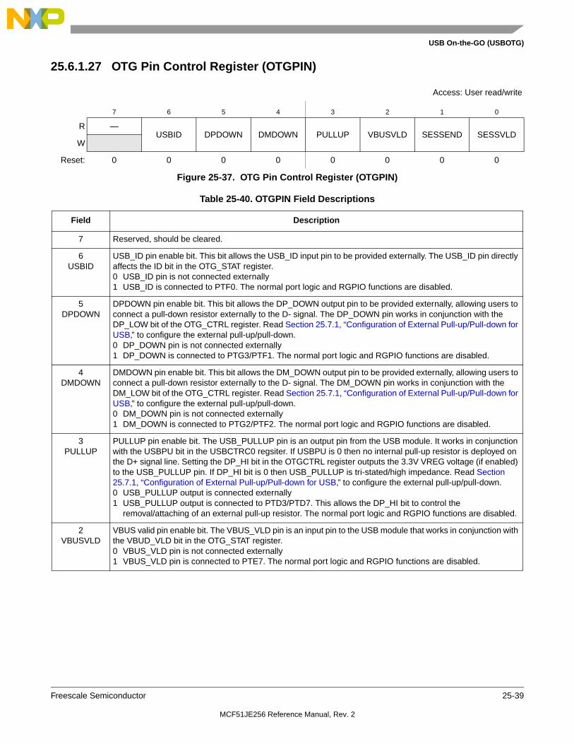
USB On-the-GO (USBOTG)
Freescale Semiconductor 25-39
25.6.1.27 OTG Pin Control Register (OTGPIN)
Access: User read/write
7 6 5 4 3 2 1 0
R —USBID DPDOWN DMDOWN PULLUP VBUSVLD SESSEND SESSVLD
W
Reset: 0 0 0 0 0 0 0 0
Figure 25-37. OTG Pin Control Register (OTGPIN)
Table 25-40. OTGPIN Field Descriptions
Field Description
7 Reserved, should be cleared.
6USBID
USB_ID pin enable bit. This bit allows the USB_ID input pin to be provided externally. The USB_ID pin directly affects the ID bit in the OTG_STAT register.0 USB_ID pin is not connected externally1 USB_ID is connected to PTF0. The normal port logic and RGPIO functions are disabled.
5DPDOWN
DPDOWN pin enable bit. This bit allows the DP_DOWN output pin to be provided externally, allowing users to connect a pull-down resistor externally to the D- signal. The DP_DOWN pin works in conjunction with the DP_LOW bit of the OTG_CTRL register. Read Section 25.7.1, “Configuration of External Pull-up/Pull-down for USB,” to configure the external pull-up/pull-down.0 DP_DOWN pin is not connected externally1 DP_DOWN is connected to PTG3/PTF1. The normal port logic and RGPIO functions are disabled.
4DMDOWN
DMDOWN pin enable bit. This bit allows the DM_DOWN output pin to be provided externally, allowing users to connect a pull-down resistor externally to the D- signal. The DM_DOWN pin works in conjunction with the DM_LOW bit of the OTG_CTRL register. Read Section 25.7.1, “Configuration of External Pull-up/Pull-down for USB,” to configure the external pull-up/pull-down.0 DM_DOWN pin is not connected externally1 DM_DOWN is connected to PTG2/PTF2. The normal port logic and RGPIO functions are disabled.
3PULLUP
PULLUP pin enable bit. The USB_PULLUP pin is an output pin from the USB module. It works in conjunction with the USBPU bit in the USBCTRC0 regsiter. If USBPU is 0 then no internal pull-up resistor is deployed on the D+ signal line. Setting the DP_HI bit in the OTGCTRL register outputs the 3.3V VREG voltage (if enabled) to the USB_PULLUP pin. If DP_HI bit is 0 then USB_PULLUP is tri-stated/high impedance. Read Section 25.7.1, “Configuration of External Pull-up/Pull-down for USB,” to configure the external pull-up/pull-down.0 USB_PULLUP output is connected externally1 USB_PULLUP output is connected to PTD3/PTD7. This allows the DP_HI bit to control the
removal/attaching of an external pull-up resistor. The normal port logic and RGPIO functions are disabled.
2VBUSVLD
VBUS valid pin enable bit. The VBUS_VLD pin is an input pin to the USB module that works in conjunction with the VBUD_VLD bit in the OTG_STAT register.0 VBUS_VLD pin is not connected externally1 VBUS_VLD pin is connected to PTE7. The normal port logic and RGPIO functions are disabled.
MCF51JE256 Reference Manual, Rev. 2

USB On-the-GO (USBOTG)
25-40 Freescale Semiconductor
25.7 OTG and Host Mode Operation The Host Mode logic allows devices such as digital cameras and palmtop computers to function as a USB Host Controller. The OTG logic adds an interface to allow the OTG Host Negotiation and Session Request Protocols (HNP and SRP) to be implemented in software. Host Mode allows a peripheral such as a digital camera to be connected directly to a USB compliant printer. Digital photos can then be easily printed without having to upload them to a PC. In the palmtop computer application, a USB compliant keyboard/mouse can be connected to the palmtop computer with the obvious advantages of easier interaction.
Host mode is intended for use in handheld-portable devices to allow easy connection to simple HID class devices such as printers and keyboards. It is NOT intended to perform the functions of a full OHCI or UHCI compatible host controller found on PC motherboards. The USB-FS is not supported by Windows 98 as a USB host controller. Host mode allows bulk, Isochronous, interrupt and control transfers. Bulk data transfers are performed at nearly the full USB bus bandwidth. Support is provided for ISO transfers, but the number of ISO streams that can be practically supported is affected by the interrupt latency of the processor servicing the token during interrupts from the SIE. Custom drivers must be written to support Host mode operation.
Setting the HOST_MODE_EN bit in the CTL register enables host Mode. The USB-FS core can only operate as a peripheral device or in Host Mode. It cannot operate in both modes simultaneously. When HOST_MODE is enabled, only endpoint zero is used. All other endpoints should be disabled by software.
25.7.1 Configuration of External Pull-up/Pull-down for USB
The OTG_CTL, CTL, and USB_OTG_CONTROL register bit values control the external pull-up and pull-down for the USB controller.
To configure pull-down on the DM line from the USB controller in OTG mode, set these bits:
• OTG_CTL [OTG_EN] = 1
• OTG_CTL [DM_LOW] = 1
To configure pull-down on the DM line from the USB controller in host mode, set these bits:
• OTG_CTL [OTG_EN] = 0
1SESSEND
Session end pin enable bit. The SESS_END pin is an input pin to the USB module that works in conjunction with the SESS_END bit in the OTG_STAT register.0 SESS_END pin is not connected externally)1 SESS_END pin is connected to PTG1/PTE6. The normal port logic and RGPIO functions are disabled.
0SESSVLD
Session valid pin enable bit. The SESS_VLD pin is an input pin to the USB module that works in conjunction with the SESS_VLD bit in the OTG_STAT register.0 SESS_VLD pin is not connected externally1 SESS_VLD pin is connected to PTG4/PTE5. The normal port logic and RGPIO functions are disabled.
Table 25-40. OTGPIN Field Descriptions (Continued)
Field Description
MCF51JE256 Reference Manual, Rev. 2

USB On-the-GO (USBOTG)
Freescale Semiconductor 25-41
• CTL [Host_Mode_en] = 1
After the USB controller generates the pull-down on the DM line, use the configuration explained in Table 25-41 to route the pull-down to the external pin.
To configure pull-down on the DP line from the USB controller in OTG mode, set these bits:
• OTG_CTL [OTG_EN] = 1
• OTG_CTL [DP_LOW] = 1
To configure pull-down on the DP line from the USB controller in host mode, set these bits:
• OTG_CTL [OTG_EN] = 0
• CTL [Host_Mode_en] = 1
After the USB controller generates the pull-down on the DP line, use the configuration explained in Table 25-42 to route the pull-down to the external pin.
To configure pull-up on the DP line from the USB controller in OTG mode, set these bits:
• OTG_CTL [OTG_EN] = 1
• OTG_CTL [DP_HIGH] = 1
Table 25-41. DM Line Pull-down Configuration
DMDOWN (OTGPIN)
Pull Down on DM from
USB Controller
Description
0 x USB_DM_DOWN stays as normal I/O. The DM line has no internal pull-down connected. Additionaly, you can use this configuration to provide a tri-state on the pin when the DM line uses an external pull-down resistor. Configure the pin as input with pull-up disabled in order to get a tri-state on the pin.
1 0 USB_DM_DOWN becomes an external pull-down control (USB_DM_DOWN should output Vdd). The DM line has no internal pull-down connected.
1 1 USB_DM_DOWN becomes an external pull-down control (USB_DM_DOWN should output Vss). The DM line has no internal pull-down connected.
Table 25-42. DP Line Pull-down Configuration
DPDOWN (OTGPIN)
Pull Down on DP from
USB Controller
Description
0 x USB_DP_DOWN stays as normal I/O. The DP line has no internal pull-down connected. Additionally, you can use this configuration to provide a tri-state on the pin when the DP line uses an external pull-down resistor. Configure the pin as input with pull-up disabled in order to get a tri-state on the pin.
1 0 USB_DP_DOWN becomes an external pull-down control (USB_DP_DOWN should output Vdd). The DP line has no internal pull-down connected.
1 1 USB_DP_DOWN becomes an external pull-down control (USB_DP_DOWN should output Vss). The DP line has no internal pull-down connected.
MCF51JE256 Reference Manual, Rev. 2

USB On-the-GO (USBOTG)
25-42 Freescale Semiconductor
To configure pull-up on the DP line from the USB controller in device mode, set these bits:
• USB_OTG_CONTROL [DPPULLUP_NONOTG] = 1
• CTL [USB_EN] = 1
• OTG_CTL [OTG_EN] = 0
After the USB controller generates the pull-up on the DP line, use the configuration explained in Table 25-43 to route the pull-up to the internal transceiver or the external pin.
25.8 Host Mode Operation Examples The following sections illustrate the steps required to perform USB host functions using the USB-FS core. The following sections are useful to understand the interaction of the hardware and the software at a detailed level, but an understanding of the interactions at this level is not required to write host applications using the API software.
To enable host mode and discover a connected device:
1. Enable Host Mode (CTL[HOST_MODE_EN]=1). Pull down resistors enabled, pull-up disabled. SOF generation begins. SOF counter loaded with 12,000. Eliminate noise on the USB by disabling Start of Frame packet generation by writing the USB enable bit to 0 (CTL[USB_EN]=0).
2. Enable the ATTACH interrupt (INT_ENB[ATTACH]=1).
3. Wait for ATTACH interrupt (INT_STAT[ATTACH]). Signaled by USB Target pull-up resistor changing the state of DPLUS or DMINUS from 0 to 1 (SE0 to J or K state).
4. Check the state of the JSTATE and SE0 bits in the control register. If the JSTATE bit is 0 then the connecting device is low speed. If the connecting device is low speed then set the low speed bit in the address registers (ADDR[LS_EN]=1) and the host the host without hub bit in endpoint 0 register control (EP_CTL0[HOST_WO_HUB]=1).
5. Enable RESET (CTL[RESET]=1) for 10 ms
6. Enable SOF packet to keep the connected device from going to suspend (CTL[USB_EN=1])
Table 25-43. DP Line Pull-up Configuration
PULLUP (OTGPIN)
USBPU (USBTRC0)
Pull Up on DP from
USB Controller
Description
0 0 0 USB_PULLUP(D+) stays as normal I/O. The DP line has no internal pull-up connected. Additionally, you can use this configuration to provide a tri-state on the pin when the DP line uses an external pull-up resistor. Configure the pin as input with pull-up disabled in order to get a tri-state on the pin.
0 1 1 USB_PULLUP(D+) stays as normal I/O. The DP line has an internal pull-up connected
1 0 0 USB_PULLUP(D+) becomes an external pull-up control (USB_PULLUP(D+) should output Vss). The DP line has no internal pull-up connected.
1 0 1 USB_PULLUP(D+) becomes an external pull up-control (USB_PULLUP(D+) should output Vdd). The DP line has no internal pull-up connected.
MCF51JE256 Reference Manual, Rev. 2

USB On-the-GO (USBOTG)
Freescale Semiconductor 25-43
7. Start enumeration by sending a sequence of Chapter 9, device frame work packets to the default control pipe of the connected device.
To complete a control transaction to a connected device:
1. Complete all steps discover a connected device
2. Set up the endpoint control register for bidirectional control transfers EP_CTL0[4:0] = 0x0d.
3. Place a copy of the device framework setup command in a memory buffer. See Chapter 9 of the USB 2.0 specification [2] for information on the device framework command set.
4. Initialize current (even or odd) TX EP0 BDT to transfer the 8 bytes of command data for a device framework command (i.e. a GET DEVICE DESCRIPTOR).
— Set the BDT command word to 0x00080080 – Byte count to 8, own bit to 1
— Set the BDT buffer address field to the start address of the 8 byte command buffer
5. Set the USB device address of the target device in the address register (ADDR[6:0]). After the USB bus reset, the device USB address is zero. It is set to some other value (usually 1) by the Set Address device framework command.
6. Write the token register with a SETUP to Endpoint 0 the target device default control pipe (TOKEN=0xD0). This initiates a setup token on the bus followed by a data packet. The device handshake is returned in the BDT PID field after the packets complete. When the BDT is written a token done (INT_STAT[TOK_DNE]) interrupt is asserted. This completes the setup phase of the setup transaction as referenced in chapter 9 of the USB specification.
7. To initiate the data phase of the setup transaction (i.e., get the data for the GET DEVICE descriptor command) set up a buffer in memory for the data to be transferred.
8. Initialize the current (even or odd) TX EP0 BDT to transfer the data.
— Set the BDT command word to 0x004000C0 – Byte count to the length of the data buffer in this case 64, own bit to 1, Data toggle to Data1.
— Set the BDT buffer address field to the start address of the data buffer
9. Write the token register with a IN or OUT token to Endpoint 0 the target device default control pipe, an IN token for a GET DEVICE DESCRIPTOR command (TOKEN=0x90). This initiates an IN token on the bus followed by a data packet from the device to the host. When the data packet completes the BDT is written and a token done (INT_STAT[TOK_DNE]) interrupt is asserted. For control transfers with a single packet data phase this completes the data phase of the setup transaction as referenced in chapter 9 of the USB specification.
10. To initiate the Status phase of the setup transaction set up a buffer in memory to receive or send the zero length status phase data packet.
11. Initialize the current (even or odd) TX EP0 BDT to transfer the status data.
— Set the BDT command word to 0x00000080 – Byte count to the length of the data buffer in this case 0, own bit to 1, Data toggle to Data0.
— Set the BDT buffer address field to the start address of the data buffer
12. Write the token register with a IN or OUT token to Endpoint 0 the target device default control pipe, an OUT token for a GET DEVICE DESCRIPTOR command (TOKEN=0x10). This initiates an OUT token on the bus followed by a zero length data packet from the host to the device. When
MCF51JE256 Reference Manual, Rev. 2
USB On-the-GO (USBOTG)
25-44 Freescale Semiconductor
the data packet completes the BDT is written with the handshake form the device and a token done (INT_STAT[TOK_DNE]) interrupt is asserted. This completes the data phase of the setup transaction as referenced in chapter 9 of the USB specification.
To send a Full speed bulk data transfer to a target device:
1. Complete all steps discover a connected device and to configure a connected device. Write the ADDR register with the address of the target device. Typically, there is only one other device on the USB bus in host mode so it is expected that the address is 0x01 and should remain constant.
2. Write the ENDPT0 to 0x1D register to enable transmit and receive transfers with handshaking enabled.
3. Setup the Even TX EP0 BDT to transfer up to 64 bytes.
4. Set the USB device address of the target device in the address register (ADDR[6:0]).
5. Write the TOKEN register with an OUT token to the desired endpoint. The write to this register triggers the USB-FS transmit state machines to begin transmitting the TOKEN and the data.
6. Setup the Odd TX EP0 BDT to transfer up to 64 bytes.
7. Write the TOKEN register with an OUT token as in step 4. Two Tokens can be queued at a time to allow the packets to be double buffered to achieve maximum throughput.
8. Wait for the TOK_DNE interrupt. This indicates one of the BDTs has been released back to the microprocessor and that the transfer has completed. If the target device asserts NAKs, the USB-FS continues to retry the transfer indefinitely without processor intervention unless the RETRY_DIS retry disable bit is set in the EP0 control register. If the retry disable bit is set, the handshake (ACK, NAK, STALL, or ERROR (0xf)) is returned in the BDT PID field. If a stall interrupt occurs, the pending packet must be dequeued and the error condition in the target device cleared. If a RESET interrupt occurs (SE0 for more than 2.5us), the target has detached.
9. After the TOK_DNE interrupt occurs, the BDTs can be examined and the next data packet queued by returning to step 2.
25.9 On-The-Go Operation The USB-OTG core provides sensors and controls to enable On-The-Go (OTG) operation. These sensors are used by the OTG API software to implement the Host Negotiation Protocol (HNP) and Session Request Protocol (SRP). API calls are provided to give access the OTG protocol control signals, and include the OTG capabilities in the device application. The following state machines show the OTG operations involved with HNP and SRP protocols from either end of the USB cable.
25.9.1 OTG Dual Role A Device Operation
A device is considered the A device because of the type of cable attached. If the USB Type A connector or the USB Type Mini A connector is plugged into the device, he is considered the A device.
A dual role A device operates as the following flow diagram and state description table illustrates.
MCF51JE256 Reference Manual, Rev. 2

USB On-the-GO (USBOTG)
Freescale Semiconductor 25-45
Figure 25-38. Dual Role A Device Flow Diagram
Table 25-44. State Descriptions for Figure 25-38
State Action Response
A_IDLE If ID Interrupt. The cable has been un-plugged or a Type B cable has been attached. The device now acts as a Type B device.
Go to B_IDLE
If the A application wants to use the bus or if the B device is doing an SRP as indicated by an A_SESS_VLD Interrupt or Attach or Port Status Change Interrupt check data line for 5 –10 msec pulsing.
Go to A_WAIT_VRISE Turn on DRV_VBUS
A_WAIT_VRISE If ID Interrupt or if A_VBUS_VLD is false after 100 msec The cable has been changed or the A device cannot support the current required from the B device.
Go to A_WAIT_VFALL Turn off DRV_VBUS
If A_VBUS_VLD interrupt Go to A_WAIT_BCON
A_WAIT_BCON After 200 msec without Attach or ID Interrupt. (This could wait forever if desired.)
Go to A_WAIT_FALL Turn off DRV_VBUS
A_VBUS_VLD Interrupt and B device attaches Go to A_HOST Turn on Host Mode
A_HOST Enumerate Device determine OTG Support.
If A_VBUS_VLD/ Interrupt or A device is done and doesn’t think he wants to do something soon or the B device disconnects
Go to A_WAIT_VFALL Turn off Host Mode Turn off DRV_VBUS
If the A device is finished with session or if the A device wants to allow the B device to take bus.
Go to A_SUSPEND
ID Interrupt or the B device disconnects Go to A_WAIT_BCON
A_IDLE
A_WAIT_VFALL A_WAIT_VRISE
A_PERIPHERAL
A_SUSPEND
B_IDLE
A_WAIT_BCON
A_HOST
MCF51JE256 Reference Manual, Rev. 2

USB On-the-GO (USBOTG)
25-46 Freescale Semiconductor
25.9.2 OTG Dual Role B Device Operation
A device is considered a B device if it connected to the bus with a USB Type B cable or a USB Type Mini B cable.
A dual role B device operates as the following flow diagram and state description table illustrates.
Figure 25-39. Dual Role B Device Flow Diagram
A_SUSPEND
If ID Interrupt, or if 150 msec B disconnect timeout (This timeout value could be longer) or if A_VBUS_VLD\ Interrupt
Go to A_WAIT_VFALL Turn off DRV_VBUS
If HNP enabled, and B disconnects in 150 msec then B device is becoming the host.
Go to A_PERIPHERAL Turn off Host Mode
If A wants to start another session Go to A_HOST
A_PERIPHERAL If ID Interrupt or if A_VBUS_VLD interrupt Go to A_WAIT_VFALL Turn off DRV_VBUS.
If 3 –200 msec of Bus Idle Go to A_WAIT_BCON Turn on Host Mode
A_WAIT_VFALL If ID Interrupt or (A_SESS_VLD/ & b_conn/) Go to A_IDLE
Table 25-45. State Descriptions for Figure 25-39
State Action Response
B_IDLE If ID\ Interrupt. A Type A cable has been plugged in and the device should now respond as a Type A device.
Go to A_IDLE
If B_SESS_VLD Interrupt. The A device has turned on VBUS and begins a session.
Go to B_PERIPHERAL Turn on DP_HIGH
If B application wants the bus and Bus is Idle for 2 ms and the B_SESS_END bit is set, the B device can perform an SRP.
Go to B_SRP_INIT Pulse CHRG_VBUS Pulse DP_HIGH 5-10 ms
Table 25-44. State Descriptions for Figure 25-38 (Continued)
State Action Response
B_IDLE
B_HOST B_SRP_INIT
B_WAIT_ACON
A_IDLE
B_PERIPHERAL
MCF51JE256 Reference Manual, Rev. 2

USB On-the-GO (USBOTG)
Freescale Semiconductor 25-47
25.9.3 Power
The USB-FS core is a fully synchronous static design. The power used by the design is dependant on the application usage of the core. Applications that transfer more data or cause a greater number of packets to be sent consumes a greater amount of power.
Because the design is synchronous and static, reducing the transitions on the clock net may conserve power. This may be done in the following ways.
The first is to reduce the clock frequency to the USB module. The clock frequency may not be reduced below the minimum recommended operating frequency of the USB module without first disabling the USB operation and disconnecting (via software disconnect) the USB module from the USB bus.
Alternately, the clock may be shut off to the core to conserve power. Again, this may only be done after the USB operations on the bus have been disabled and the device has been disconnected from the USB.
25.9.4 USB Suspend State
USB bus powered devices are required to respond to a 3ms lack of activity on the USB bus by going into a suspend state. Software is notified of the suspend condition via the transition in the port status and control register. Optionally, an interrupt can be generated that is controlled by the interrupt enable register. In the suspend state, a USB device has a maximum USB bus power budget of 500uA. To achieve that level of power conservation, most of the device circuits need to be switched off. When the clock is disabled to the USB-FScore all functions are disabled, but all operational states are retained. The transceiver VP and VM signals can be used to construct a circuit able to detect the resume signaling on the bus and restore the clocks to the rest of the circuit when the USB host takes the bus out of the suspend state.
B_SRP_INIT If ID\ Interrupt or SRP Done (SRP must be done in less than 100 msecs.)
Go to B_IDLE
B_PERIPHERAL If HNP enabled and the bus is suspended and B wants the bus, the B device can become the host.
Go to B_WAIT_ACON Turn off DP_HIGH
B_WAIT_ACON If A connects, an attach interrupt is received Go to B_HOST Turn on Host Mode
If ID\ Interrupt or B_SESS_VLD/ Interrupt If the cable changes or if VBUS goes away, the host doesn’t support us. Go to B_IDLE
Go to B_IDLE
If 3.125 ms expires or if a Resume occurs Go to B_PERIPHERAL
B_HOST If ID\ Interrupt or B_SESS_VLD\ Interrupt If the cable changes or if VBUS goes away, the host doesn’t support us.
Go to B_IDLE
If B application is done or A disconnects Go to B_PERIPHERAL
Table 25-45. State Descriptions for Figure 25-39 (Continued)
State Action Response
MCF51JE256 Reference Manual, Rev. 2

USB On-the-GO (USBOTG)
25-48 Freescale Semiconductor
MCF51JE256 Reference Manual, Rev. 2

Freescale Semiconductor 26-1
Chapter 26 Voltage Reference Module (S08VREFV1)
26.1 IntroductionThe Voltage Reference is intended to supply an accurate voltage output that is trimmable by an 8-bit reg-ister in 0.5 mV steps. A nominal trim value to achieve the specified VREF voltage is automatically loaded upon a reset into the VREF Trim Register. The voltage reference can be used to provide a refer-ence voltage to external peripherals or as a reference to analog peripherals such as the ADC or ACMP.
Figure 26 shows the block diagram with the VREF highlighted.
MCF51JE256 Reference Manual, Rev. 2

Voltage Reference Module (S08VREFV1)
26-2 Freescale Semiconductor
Figure 26-1. Block Diagram with VREF Module Highlighted
MCF51JE256 Reference Manual, Rev. 2

Voltage Reference Module (S08VREFV1)
Freescale Semiconductor 26-3
26.1.1 VREF Configuration Information
This device uses the VREF module to provide the bandgap signal. The bandgap signal is provided to the following periperhals:
• ADC
• DAC
• ACMP
26.1.2 VREF Clock Gating
The bus clock to the VREF can be gated on and off using the VREF bit in SCGC1. These bits are set after any reset which enables the bus clock to this module. To conserve power, these bits can be cleared to disable the clock to this module when not in use. See Section 5.6, “Peripheral Clock Gating,” for details.
26.1.3 Overview
The Voltage Reference optimizes the existing bandgap and bandgap buffer system. Unity gain amplifiers ease the design and keep power consumption low. The 8-bit trim register is user accessible so that the voltage reference can be trimmed in application.
Figure 26-2. Voltage Reference Block Diagram
+
–
+
–
VREFTRIM
TIGHT-REGULATION BUFFER
LOW-POWER BUFFER
8 BITS
VREFSC_VREFEN
VREFSC_MODE2 BITS
VREFST
VREFOVREFO
BANDGAP
100nF1
1. This cap is required in tight-regulation buffer mode only otherwise this cap should be removed.
MCF51JE256 Reference Manual, Rev. 2

Voltage Reference Module (S08VREFV1)
26-4 Freescale Semiconductor
The voltage reference contains trim resolution of 0.5mV per step. The buffer has modes with improved high-current swing output. In addition, a low-power buffer mode is available for use with ADCs or DACs. The voltage reference can be output on a dedicated output pin1.
26.1.4 Features
The Voltage Reference module has the following features:
• Programmable trim register with 0.5mV steps, automatically loaded with factory trimmed value upon reset
• Programmable mode selection:
— Off
— Bandgap out (or stabilization delay)
— Low-power buffer mode
— Tight-regulation buffer mode
• 1.15 V output at room temperature2
• Dedicated output pin VREFO
26.1.5 Modes of Operation
The Voltage Reference continues normal operation in Run, Wait, LPRun, and LPWait modes. The Voltage Reference module can be enabled to operate in STOP3 mode.
26.1.6 External Signal Description
Table 26-1 shows the Voltage Reference signals properties.
1. In Tight-Regulation buffer mode, a 100nF capacitor is required to be connected between the VREFO pad and the ground.2. Please refer to datasheet for details.
Table 26-1. Signal Properties
Name Function I/O Reset Pull Up
VREFO Internally generated voltage reference output
O — —
MCF51JE256 Reference Manual, Rev. 2

Voltage Reference Module (S08VREFV1)
Freescale Semiconductor 26-5
26.2 Memory Map and Register Definition
26.2.1 VREF Trim Register (VREFTRM)
The VREFTRM register contains eight bits that contain the trim data for the Voltage Reference as described in Table 26-2.
Figure 26-3. VREF Trim Register (VREFTRM)
Register address: Base + 0x00
7 6 5 4 3 2 1 0R
TRM[7:0]W
Reset: X X X X X X X X
Table 26-2. VREFTRM Register Field Descriptions
Field Description
7:0TRM[7:0]
Trim Bits 7:0These bits change the resulting VREF output by ±0.5mV for each step.
Table 26-3. VREFTRM Register Settings
TRM7 TRM6 TRM5 TRM4 TRM3 TRM2 TRM1 TRM0VREF (mV)
1 0 0 0 0 0 0 0 max
1 0 0 0 0 0 0 1 max-0.5
1 0 0 0 0 0 1 0 max-1.0
1 0 0 0 0 0 1 1 max-1.5
1 . . . . . . . . . . . .
1 1 1 1 1 1 0 0 mid+1.5
1 1 1 1 1 1 0 1 mid+1.0
1 1 1 1 1 1 1 0 mid+0.5
1 1 1 1 1 1 1 1 mid
0 0 0 0 0 0 0 0 mid-0.5
0 0 0 0 0 0 0 1 mid-1.0
0 0 0 0 0 0 1 0 mid-1.5
0 0 0 0 0 0 1 1 mid-2.0
0 . . . . . . . . . . . .
0 1 1 1 1 1 0 0 min+1.5
0 1 1 1 1 1 0 1 min+1.0
0 1 1 1 1 1 1 0 min+0.5
0 1 1 1 1 1 1 1 min
MCF51JE256 Reference Manual, Rev. 2

Voltage Reference Module (S08VREFV1)
26-6 Freescale Semiconductor
26.2.2 VREF Status and Control Register (VREFSC)
The VREF status and control register contains the control bits used to enable the internal voltage reference and select the buffer mode to be used.
Figure 26-4. Voltage Reference Control Register (VREFSC)
26.3 Functional DescriptionThe Voltage Reference is a bandgap buffer system. Unity gain amplifiers are used.
The Voltage Reference can be used in two main cases. It can be used as a reference to analog peripherals such as an ADC channel or analog comparator input. For this case, the low-power buffer can be used. When the tight-regulation buffer is enabled, VREFO can be used both internally and externally.
Table 26-5 shows all possible functional configurations of the Voltage Reference.
Table 26-5. Voltage Reference Functional Configurations
Register address: Base + 0x01
7 6 5 4 3 2 1 0R
VREFEN0 0 0 0 VREFST
MODEW
Reset: 0 0 0 0 0 0 0 0
Table 26-4. VREFSC Register Field Descriptions
Field Description
7VREFEN
Internal Voltage Reference Enable — This bit is used to enable the Voltage Reference module. 0 the Voltage Reference module is disabled1 the Voltage Reference module is enabled
2VREFST
Internal Voltage Reference Stable — This bit indicates that the Voltage Reference module has completed its startup and stabilization.0 Voltage Reference module is disabled or not stable1 Voltage Reference module is stable
1:0MODE[1:0]
Mode selection — These bits are used to select the modes of operation for the Voltage Reference module.00 Bandgap on only, for stabilization and startup01 Low-power buffer enabled10 Tight-regulation buffer enabled11 RESERVED
VREFEN MODE[1:0] Configuration Functionality
0 X Voltage Reference Disabled Off
1 00 Voltage Reference Enabled, Bandgap on only
Startup and Standby
1 01 Voltage Reference Enabled, Low-Power buffer on
Can be used for internal peripherals only and VREFO pin should not be loaded
1 10Voltage Reference Enabled, Tight-Regulation buffer on
Can be used both internally and externally. A 100nF capacitor is required on VREFO and 10mA max drive strength is allowed.
1 11 Voltage Reference Disabled RESERVED
MCF51JE256 Reference Manual, Rev. 2

Voltage Reference Module (S08VREFV1)
Freescale Semiconductor 26-7
26.3.1 Voltage Reference Disabled, VREFEN=0
When VREFEN=0, the Voltage Reference is disabled, all bandgap and buffers are disabled. The Voltage Reference is in off mode.
26.3.2 Voltage Reference Enabled, VREFEN=1
When VREFEN=1, the Voltage Reference is enabled, and different modes should be set by the Mode[1:0] bits.
26.3.2.1 Mode[1:0]=00
The internal bandgap is on to generate an accurate voltage output that can be trimmed by the bits TRM[7:0] in 0.5 mV steps. The bandgap requires some time for startup and stabilization. The VREFST bit can be monitored to determine if the stabilization and startup is complete.
Both low-power buffer and tight-regulation buffer are disabled in this mode, and there is no buffered voltage output. The Voltage Reference is in standby mode.
26.3.2.2 Mode[1:0]=01
The internal bandgap is on.
The low-power buffer is enabled to generate a buffered internal voltage. It can be used as a reference to internal analog peripherals such as an ADC channel or analog comparator input.
26.3.2.3 Mode[1:0]=10
The internal bandgap is on.
The tight-regulation buffer is enabled to generate a buffered voltage to VREFO with load regulation less than 100 uV/mA. A 100nF capacitor is required on VREFO pin and it is allowed to drive 10 mA maximum current. VREFO can be used internally and/or externally.
26.3.2.4 Mode[1:0]=11
RESERVED
26.4 Initialization InformationThe Voltage Reference requires some time for startup and stabilization. Once the VREFEN bit is set, the VREFST bit can be monitored to determine if the stabilization and startup is complete.
When the Voltage Reference is already enabled and stabilized, changing the Mode selection bits (MODE[1:0]) will not clear the VREFST bit, but there will be some startup time before the output voltage is stabilized when the low-power buffer or tight-regulation buffer is enabled, and there will be some setting time when a step change of the load current occurs.
MCF51JE256 Reference Manual, Rev. 2

Voltage Reference Module (S08VREFV1)
26-8 Freescale Semiconductor
MCF51JE256 Reference Manual, Rev. 2

Freescale Semiconductor 27-1
Chapter 27 Version 1 ColdFire Debug (CF1_DEBUG)
27.1 IntroductionThis chapter describes the capabilities defined by the Version 1 ColdFire debug architecture. The Version 1 ColdFire core supports BDM functionality using the HCS08’s single-pin interface. The traditional 3-pin full-duplex ColdFire BDM serial communication protocol based on 17-bit data packets is replaced with the HCS08 debug protocol where all communication is based on an 8-bit data packet using a single package pin (BKGD).
An on-chip trace buffer allows a stream of compressed processor execution status packets to be recorded for subsequent retrieval to provide program (and partial data) trace capabilities.
The following sections in this chapter provide details on the BKGD pin, the background debug serial interface controller (BDC), a standard 6-pin BDM connector, the BDM command set as well as real-time debug and trace capabilities. The V1 definition supports revision B+ (DEBUG_B+) of the ColdFire debug architecture.
A simplified block diagram of the V1 core including the processor and debug module is shown in Figure 27-1.
MCF51JE256 Reference Manual, Rev. 2

Version 1 ColdFire Debug (CF1_DEBUG)
27-2 Freescale Semiconductor
Figure 27-1. Simplified Version 1 ColdFire Core Block Diagram
27.1.1 Overview
Debug support is divided into three areas:
• Background debug mode (BDM)—Provides low-level debugging in the ColdFire processor core. In BDM, the processor core is halted and a variety of commands can be sent to the processor to access memory, registers, and peripherals. The external emulator uses a one-pin serial communication protocol. See Section 27.4.1, “Background Debug Mode (BDM)”.
• Real-time debug support—Use of the full BDM command set requires the processor to be halted, which many real-time embedded applications cannot support. The core includes a variety of internal breakpoint registers which can be configured to trigger and generate a special interrupt. The resulting debug interrupt lets real-time systems execute a unique service routine that can quickly save the contents of key registers and variables and return the system to normal operation. The external development system can then access the saved data, because the hardware supports
Central Processing Unit
Debug
Version 1 ColdFire Core (CF1Core)
IFP
OEP
BDC CFx
BDM
PST/DDATA
RTD
addr
rdatawdata
BKGD
RESET
IPL_B[2:0]
IFP — Instruction fetch pipelineOEP — Operand execution pipelineBDC — Background debug controllerCFxBDM — ColdFire background debug modulePST/DDATA — Processor status/debug dataRTD — Real-time debug
(CF1Cpu)
(CF1Dbg)
attb
MCF51JE256 Reference Manual, Rev. 2

Version 1 ColdFire Debug (CF1_DEBUG)
Freescale Semiconductor 27-3
concurrent operation of the processor and BDM-initiated memory commands. In addition, the option is provided to allow interrupts to occur. See Section 27.4.2, “Real-Time Debug Support”.
• Program trace support—The ability to determine the dynamic execution path through an application is fundamental for debugging. The V1 solution implements a trace buffer that records processor execution status and data, which can be subsequently accessed by the external emulator system to provide program (and optional partial data) trace information. See Section 27.4.3, “Trace Support”.
There are two fields in debug registers which provide revision information: the hardware revision level in CSR and the 1-pin debug hardware revision level in CSR2. Table 27-1 summarizes the various debug revisions.
27.1.2 Features
The Version 1 ColdFire debug definition supports the following features:
• Classic ColdFire DEBUG_B+ functionality mapped into the single-pin BDM interface
• Real time debug support, with 6 hardware breakpoints (4 PC, 1 address pair and 1 data) that can be configured into a 1- or 2-level trigger with a programmable response (processor halt or interrupt)
• Capture of compressed processor status and debug data into on-chip trace buffer provides program (and optional slave bus data) trace capabilities
• On-chip trace buffer provides programmable start/stop recording conditions plus support for obtrusive or PC-profiling modes
• Debug resources are accessible via single-pin BDM interface or the privileged WDEBUG instruction from the core
27.1.3 Modes of Operations
V1 ColdFire devices typically implement a number of modes of operation, including run, wait, and stop modes. Additionally, the operation of the core’s debug module is highly dependent on a number of chip configurations which determine its operating state.
When operating in secure mode, as defined by a 2-bit field in the flash memory examined at reset, BDM access to debug resources is extremely restricted. It is possible to tell that the device has been secured, and
Table 27-1. Debug Revision Summary
Revision CSR[HRL] CSR2[D1HRL] Enhancements
A 0000 N/A Initial ColdFire debug definition
B 0001 N/A BDM command execution does not affect hardware breakpoint logicAdded BDM address attribute register (BAAR)BKPT configurable interrupt (CSR[BKD])Level 1 and level 2 triggers on OR condition, in addition to ANDSYNC_PC command to display the processor’s current PC
B+ 1001 N/A Added 3 PC breakpoint registers PBR1–3
CF1_B+ 1001 0001 Converted to HCS08 1-pin BDM serial interfaceAdded PST compression and on-chip PST/DDATA buffer for program trace
MCF51JE256 Reference Manual, Rev. 2

Version 1 ColdFire Debug (CF1_DEBUG)
27-4 Freescale Semiconductor
to clear security, which involves mass erasing the on-chip flash memory. No other debug access is allowed. Secure mode can be used in conjunction with each of the wait and stop low-power modes.
If the BDM interface is not enabled, access to the debug resources is limited in the same manner as a secure device.
If the device is not secure and the BDM interface is enabled (XCSR[ENBDM] is set), the device is operating in debug mode and additional resources are available via the BDM interface. In this mode, the status of the processor (running, stopped, or halted) determines which BDM commands may be used.
Debug mode functions are managed through the background debug controller (BDC) in the Version 1 ColdFire core. The BDC provides the means for analyzing MCU operation during software development.
BDM commands can be classified into three types as shown in Table 27-2.
For more information on these three BDM command classifications, see Section 27.4.1.5, “BDM Command Set Summary.”
The core’s halt mode is entered in a number of ways:
• The BKGD pin is low during POR
• The BKGD pin is low immediately after a BDM-initiated force reset (see CSR2[BDFR] in Section 27.3.3, “Configuration/Status Register 2 (CSR2),” for details)
• A background debug force reset occurs (CSR2[BDFR] is set) and CSR2[BFHBR] is set
• A computer operating properly reset occurs and CSR2[COPHR] is set
• An illegal operand reset occurs and CSR2[IOPHR] is set
• An illegal address reset occurs and CSR2[IADHR] is set
• A BACKGROUND command is received through the BKGD pin. If necessary, this wakes the device from STOP/WAIT modes.
• A properly-enabled (XCSR[ENBDM] is set) HALT instruction is executed
• Encountering a BDM breakpoint and the trigger response is programmed to generate a halt
• Reaching a PSTB trace buffer full condition when operating in an obtrusive recording mode (CSR2[PSTBRM] is set to 01 or 11)
Table 27-2. BDM Command Types
Command TypeFlash
Secure?BDM? Core Status Command Set
Always-availableSecure or Unsecure
Enabled or Disabled
— • Read/write access to XCSR[31–24], CSR2[31–24],
CSR3[31–24]
Non-intrusive Unsecure Enabled Run, Halt
• Memory access • Memory access with status • Debug register access • BACKGROUND
Active background Unsecure Enabled Halt • Read or write CPU registers (also available in stop mode) • Single-step the application • Exit halt mode to return to the application program (GO)
MCF51JE256 Reference Manual, Rev. 2

Version 1 ColdFire Debug (CF1_DEBUG)
Freescale Semiconductor 27-5
While in halt mode, the core waits for serial background commands rather than executing instructions from the application program.
Figure 27-2. Debug Modes State Transition Diagram
Figure 27-2 contains a simplified view of the V1 ColdFire debug mode states. The XCSR[CLKSW] bit controls the BDC clock source. When CLKSW is set, the BDC serial clock frequency is half the CPU clock. When CLKSW is cleared, the BDC serial clock is supplied from an alternate clock source.
The ENBDM bit determines if the device can be placed in halt mode, if the core and BDC serial clocks continue to run in STOP modes, and if the regulator can be placed into standby mode. Again, if booting to halt mode, XCSR[ENBDM, CLKSW] are automatically set.
If ENBDM is cleared, the ColdFire core treats the HALT instruction as an illegal instruction and generates a reset (if CPUCR[IRD] is cleared) or an exception (if CPUCR[IRD] is set) if execution is attempted.
If XCSR[ENBDM] is set, the device can be restarted from STOP/WAIT via the BDM interface.
27.2 External Signal DescriptionsTable 27-3 describes the debug module’s 1-pin external signal (BKGD). A standard 6-pin debug connector is shown in Section 27.4.4, “Freescale-Recommended BDM Pinout”.
Table 27-3. Debug Module Signals
Signal Description
Background Debug (BKGD)
Single-wire background debug interface pin. The primary function of this pin is for bidirectional serial communication of background debug mode commands and data. During reset, this pin selects between starting in active background (halt) mode or starting the application program. This pin also requests a timed sync response pulse to allow a host development tool to determine the correct clock frequency for background debug serial communications.
DebugHalt
ENBDM=1
NormalOperationENBDM=0
NormalOperationENBDM=1
AnyState
CPU clock/2 is usedas the BDM clock
CLKSW=1
Return to Halt viaBACKGROUND command,
HALT instruction, orBDM breakpoint trigger
BDM GOcommand
clear ENBDMvia BDM
SetENBDM
Debug not enabledBDM & CPU clocks are not
enabled in STOP modes
Debug is enabledCPU clocks continueduring STOP modes
CLKSW=0POR with BKGD=1 or
BDFR, BFHBR, and BKGD=1 or
BDFR=1 and BFHBR=0 orany other reset
(POR or BDFR=1) with BKGD=0 orBDFR and BFHBR= 1 or
COP reset and CSR2[COPHR]=1 orIllegal op reset and CSR2[IOPHR]=1 or
Illegal address reset and CSR2[IADHR]=1 or
MCF51JE256 Reference Manual, Rev. 2

Version 1 ColdFire Debug (CF1_DEBUG)
27-6 Freescale Semiconductor
27.3 Memory Map/Register DefinitionIn addition to the BDM commands that provide access to the processor’s registers and the memory subsystem, the debug module contains a number of registers. Most of these registers (all except the PST/DDATA trace buffer) are also accessible (write-only) from the processor’s supervisor programming model by executing the WDEBUG instruction. Thus, the breakpoint hardware in the debug module can be read (certain registers) or written by the external development system using the serial debug interface or written by the operating system running on the processor core. Software is responsible for guaranteeing that accesses to these resources are serialized and logically consistent. The hardware provides a locking mechanism in the CSR to allow the external development system to disable any attempted writes by the processor to the breakpoint registers (setting CSR[IPW]). BDM commands must not be issued during the processor’s execution of the WDEBUG instruction to configure debug module registers or the resulting behavior is undefined.
These registers, shown in Table 27-4, are treated as 32-bit quantities regardless of the number of implemented bits and unimplemented bits are reserved and must be cleared. These registers are also accessed through the BDM port by the commands, WRITE_DREG and READ_DREG, described in Section 27.4.1.5, “BDM Command Set Summary.” These commands contain a 5-bit field, DRc, that specifies the register, as shown in Table 27-4.
Table 27-4. Debug Module Memory Map
DRc Register NameWidth(bits)
Access Reset ValueSection/
Page
0x00 Configuration/status register (CSR) 32 R/W (BDM),W (CPU)
0x0090_0000 27.3.1/27-7
0x01 Extended Configuration/Status Register (XCSR) 32 R/W1 (BDM),W (CPU)
0x0000_0000 27.3.2/27-10
0x02 Configuration/Status Register 2 (CSR2) 32 R/W1 (BDM),W (CPU)
See Section 27.3.3/27-13
0x03 Configuration/Status Register 3 (CSR3) 322 R/W1 (BDM),W (CPU)
0x0000_0000 27.3.4/27-16
0x05 BDM address attribute register (BAAR) 322 W 0x0000_0005 27.3.5/27-17
0x06 Address attribute trigger register (AATR) 322 W 0x0000_0005 27.3.6/27-18
0x07 Trigger definition register (TDR) 32 W 0x0000_0000 27.3.7/27-19
0x08 PC breakpoint register 0 (PBR0) 32 W Undefined,Unaffected
27.3.8/27-22
0x09 PC breakpoint mask register (PBMR) 32 W Undefined,Unaffected
27.3.8/27-22
0x0C Address breakpoint high register (ABHR) 32 W Undefined,Unaffected
27.3.9/27-24
0x0D Address breakpoint low register (ABLR) 32 W 0x0000_0000 27.3.9/27-24
0x0E Data breakpoint register (DBR) 32 W 0x0000_0000 27.3.10/27-25
0x0F Data breakpoint mask register (DBMR) 32 W 0x0000_0000 27.3.10/27-25
MCF51JE256 Reference Manual, Rev. 2

Version 1 ColdFire Debug (CF1_DEBUG)
Freescale Semiconductor 27-7
NOTEDebug control registers can be written by the external development system or the CPU through the WDEBUG instruction. These control registers are write-only from the programming model and they can be written through the BDM port using the WRITE_DREG command. In addition, the four configuration/status registers (CSR, XCSR, CSR2, CSR3) can be read through the BDM port using the READ_DREG command.
The ColdFire debug architecture supports a number of hardware breakpoint registers that can be configured into single- or double-level triggers based on the PC or operand address ranges with an optional inclusion of specific data values. The triggers can be configured to halt the processor or generate a debug interrupt exception. Additionally, these same breakpoint registers can be used to specify start/stop conditions for recording in the PST trace buffer.
The core includes four PC breakpoint triggers and a set of operand address breakpoint triggers with two independent address registers (to allow specification of a range) and an optional data breakpoint with masking capabilities. Core breakpoint triggers are accessible through the serial BDM interface or written through the supervisor programming model using the WDEBUG instruction.
27.3.1 Configuration/Status Register (CSR)
CSR defines the debug configuration for the processor and memory subsystem and contains status information from the breakpoint logic. CSR is accessible from the programming model using the WDEBUG instruction and through the BDM port using the READ_DREG and WRITE_DREG commands.
0x18 PC breakpoint register 1 (PBR1) 32 W PBR1[0] = 0 27.3.8/27-22
0x1A PC breakpoint register 2 (PBR2) 32 W PBR2[0] = 0 27.3.8/27-22
0x1B PC breakpoint register 3 (PBR3) 32 W PBR3[0] = 0 27.3.8/27-22
— PST Trace Buffer n (PSTBn); n = 0–11 (0xB) 32 R (BDM)3 Undefined,Unaffected
27.4.1.5.12/27-46
1 The most significant bytes of the XCSR, CSR2, and CSR3 registers support special control functions and are writeable via BDM using the WRITE_XCSR_BYTE, WRITE_CSR2_BYTE, and WRITE_CSR3_BYTE commands. They can be read from BDM using the READ_XCSR_BYTE, READ_CSR2_BYTE, and READ_CSR3_BYTE commands. These 3 registers, along with the CSR, can also be referenced as 32-bit quantities using the BDM READ_DREG and WRITE_DREG commands, but the WRITE_DREG command only writes bits 23–0 of these three registers.
2 Each debug register is accessed as a 32-bit value; undefined fields are reserved and must be cleared.3 The contents of the PST trace buffer is only read from BDM (32 bits per access) using READ_PSTB commands.
Table 27-4. Debug Module Memory Map (Continued)
DRc Register NameWidth(bits)
Access Reset ValueSection/
Page
MCF51JE256 Reference Manual, Rev. 2

Version 1 ColdFire Debug (CF1_DEBUG)
27-8 Freescale Semiconductor
DRc[4:0]: 0x00 (CSR) Access: Supervisor write-onlyBDM read/write
31 30 29 28 27 26 25 24 23 22 21 20 19 18 17 16
R BSTAT FOF TRG HALT BKPT HRL 0BKD
0IPW
W
Reset 0 0 0 0 0 0 0 0 1 0 0 1 0 0 0 0
15 14 13 12 11 10 9 8 7 6 5 4 3 2 1 0
R 0TRC
0DDC UHE BTB
0NPL IPI SSM
0 0FID DDH
W
Reset 0 0 0 0 0 0 0 0 0 0 0 0 0 0 0 0
Figure 27-3. Configuration/Status Register (CSR)
Table 27-5. CSR Field Descriptions
Field Description
31–28BSTAT
Breakpoint status. Provides read-only status (from the BDM port only) information concerning hardware breakpoints. BSTAT is cleared by a TDR write, by a CSR read when a level-2 breakpoint is triggered, or a level-1 breakpoint is triggered and the level-2 breakpoint is disabled.The PSTB value that follows the PSTB entry of 0x1B is 0x20 + (2 BSTAT).0000 No breakpoints enabled0001 Waiting for level-1 breakpoint0010 Level-1 breakpoint triggered0101 Waiting for level-2 breakpoint0110 Level-2 breakpoint triggered
27FOF
Fault-on-fault. Indicates a catastrophic halt occurred and forced entry into BDM. FOF is cleared by reset or when CSR is read (from the BDM port only).
26TRG
Hardware breakpoint trigger. Indicates a hardware breakpoint halted the processor core and forced entry into BDM. Reset, the debug GO command, or reading CSR (from the BDM port only) clears TRG.
25HALT
Processor halt. Indicates the processor executed a HALT and forced entry into BDM. Reset, the debug GO command, or reading CSR (from the BDM port only) clears HALT.
24BKPT
Breakpoint assert. Indicates when either: • The BKPT input was asserted, • BDM BACKGROUND command received, or • The PSTB halt on full condition, CSR2[PSTBH], sets.This forces the processor into a BDM halt. Reset, the debug GO command, or reading CSR (from the BDM port only) clears BKPT.
23–20HRL
Hardware revision level. Indicates, from the BDM port only, the level of debug module functionality. An emulator can use this information to identify the level of functionality supported.0000 Revision A 0001 Revision B0010 Revision C0011 Revision D1001 Revision B+ (The value used for this device)1011 Revision D+
19 Reserved, must be cleared.
MCF51JE256 Reference Manual, Rev. 2

Version 1 ColdFire Debug (CF1_DEBUG)
Freescale Semiconductor 27-9
18BKD
Breakpoint disable. Disables the BACKGROUND command functionality, and allows the execution of the BACKGROUND command to generate a debug interrupt.0 Normal operation1 The receipt of a BDM BACKGROUND command signals a debug interrupt to the ColdFire core. The processor
makes this interrupt request pending until the next sample point occurs, when the exception is initiated. In the ColdFire architecture, the interrupt sample point occurs once per instruction. There is no support for nesting debug interrupts.
17 Reserved, must be cleared.
16IPW
Inhibit processor writes. Inhibits processor-initiated writes to the debug module’s programming model registers. IPW can be modified only by commands from the BDM interface.
15 Reserved, must be cleared.
14TRC
Force emulation mode on trace exception.0 Processor enters supervisor mode.1 Processor enters emulator mode when a trace exception occurs.
13 Reserved, must be cleared.
12–11DDC
Debug data control. Controls peripheral bus operand data capture for DDATA, which displays the number of bytes defined by the operand reference size (a marker) before the actual data; byte displays 8 bits, word displays 16 bits, and long displays 32 bits (one nibble at a time across multiple PSTCLK clock cycles). See Table 27-26. A non-zero value enables partial data trace capabilities.00 No operand data is displayed.01 Capture all write data.10 Capture all read data.11 Capture all read and write data.
10UHE
User halt enable. Selects the CPU privilege level required to execute the HALT instruction. The core must be operating with XCSR[ENBDM] set to execute any HALT instruction, else the instruction is treated as an illegal opcode.0 HALT is a supervisor-only instruction.1 HALT is a supervisor/user instruction.
9–8BTB
Branch target bytes. Defines the number of bytes of branch target address DDATA displays. See Section 27.4.3.1, “Begin Execution of Taken Branch (PST = 0x05).”00 No target address capture01 Lower 2 bytes of the target address1x Lower 3 bytes of the target address
7 Reserved, must be cleared.
6NPL
Non-pipelined mode. Determines if the core operates in pipelined mode.0 Pipelined mode1 Non-pipelined mode. The processor effectively executes one instruction at a time with no overlap. This typically
adds five cycles to the execution time of each instruction. Given an average execution latency of ~2 cycles per instruction, throughput in non-pipeline mode would be ~7 cycles per instruction, approximately 25% - 33% of pipelined performance.
Regardless of the NPL state, a triggered PC breakpoint is always reported before the triggering instruction executes. In normal pipeline operation, the occurrence of an address and/or data breakpoint trigger is imprecise. In non-pipeline mode, these triggers are always reported before the next instruction begins execution and trigger reporting can be considered precise.
Table 27-5. CSR Field Descriptions (Continued)
Field Description
MCF51JE256 Reference Manual, Rev. 2

Version 1 ColdFire Debug (CF1_DEBUG)
27-10 Freescale Semiconductor
27.3.2 Extended Configuration/Status Register (XCSR)
The 32-bit XCSR is partitioned into two sections: the upper byte contains status and command bits always accessible to the BDM interface, even if debug mode is disabled. This status byte is also known as XCSR_SB. The lower 24 bits contain fields related to the generation of automatic SYNC_PC commands, which can be used to periodically capture and display the current program counter (PC) in the PST trace buffer (if properly configured).
There are multiple ways to reference the XCSR. They are summarized in Table 27-6.
5IPI
Ignore pending interrupts when in single-step mode.0 Core services any pending interrupt requests signalled while in single-step mode.1 Core ignores any pending interrupt requests signalled while in single-step mode.
4SSM
Single-step mode enable.0 Normal mode.1 Single-step mode. The processor halts after execution of each instruction. While halted, any BDM command
can be executed. On receipt of the GO command, the processor executes the next instruction and halts again. This process continues until SSM is cleared.
3–2 Reserved, must be cleared.
1FID
Force ipg_debug. The core generates this output to the device, signaling it is in debug mode.0 Do not force the assertion of ipg_debug1 Force the assertion of ipg_debug
0DDH
Disable ipg_debug due to a halt condition. The core generates an output to the other modules in the device, signaling it is in debug mode. By default, this output signal is asserted when the core halts. 0 Assert ipg_debug if the core is halted1 Negate ipg_debug due to the core being halted
Table 27-6. XCSR Reference Summary
Method Reference Details
READ_XCSR_BYTE Reads XCSR[31–24] from the BDM interface. Available in all modes.
WRITE_XCSR_BYTE Writes XCSR[31–24] from the BDM interface. Available in all modes.
READ_DREG Reads XCSR[31–0] from the BDM interface. Classified as a non-intrusive BDM command.
WRITE_DREG Writes XCSR[23–0] from the BDM interface. Classified as a non-intrusive BDM command.
WDEBUG instruction Writes XCSR[23–0] during the core’s execution of WDEBUG instruction. This instruction is a privileged supervisor-mode instruction.
Table 27-5. CSR Field Descriptions (Continued)
Field Description
MCF51JE256 Reference Manual, Rev. 2

Version 1 ColdFire Debug (CF1_DEBUG)
Freescale Semiconductor 27-11
DRc: 0x01 (XCSR) Access: Supervisor write-onlyBDM read/write
31 30 29 28 27 26 25 24 23 22 21 20 19 18 17 16
R CPUHALT
CPUSTOP
CSTAT CLKSW
SEC ENBDM
0 0 0 0 0 0 0 0
W ESEQC ERASE
Reset 0 0 0 0 0 0 0 0 0 0 0 0 0 0 0 0
15 14 13 12 11 10 9 8 7 6 5 4 3 2 1 0
R 0 0 0 0 0 0 0 0 0 0 0 0 0APCSC
APCENBW
Reset 0 0 0 0 0 0 0 0 0 0 0 0 0 0 0 0
Figure 27-4. Extended Configuration/Status Register (XCSR)
Table 27-7. XCSR Field Descriptions
Field Description
31CPUHALT
Indicates that the CPU is in the halt state. The CPU state may be running, stopped, or halted, which is determined by the CPUHALT and CPUSTOP bits as shown below.
30CPUSTOP
Indicates that the CPU is in the stop state. The CPU state may be running, stopped, or halted, which is determined by the CPUHALT and CPUSTOP bits as shown in the CPUHALT bit description.
XCSR[CPUHALT]
XCSR[CPUSTOP]
CPU State
0 0 Running
0 1 Stopped
1 0 Halted
MCF51JE256 Reference Manual, Rev. 2

Version 1 ColdFire Debug (CF1_DEBUG)
27-12 Freescale Semiconductor
29–27CSTAT (R)
ESEQC (W)
During reads, indicates the BDM command status.000 Command done, no errors001 Command done, data invalid01x Command done, illegal1xx Command busy, overrun
If an overrun is detected (CSTAT = 1xx), the following sequence is suggested to clear the source of the error:1. Issue a SYNC command to reset the BDC channel.2. The host issues a BDM NOP command.3. The host checks the channel status using a READ_XCSR_BYTE command.4. If XCSR[CSTAT] = 000
then status is okay; proceedelse
Halt the CPU with a BDM BACKGROUND commandRepeat steps 1,2,3If XCSR[CSTAT] 000, then reset device
During writes, the ESEQC field is used for the erase sequence control during flash programming. ERASE must also be set for this bit to have an effect.000 User mass eraseElse ReservedNote: See the Memory chapter for a detailed description of the algorithm for clearing security.
26CLKSW
Select source for serial BDC communication clock.0 Alternate, asynchronous BDC clock, typically 10 MHz1 Synchronous bus clock (CPU clock divided by 2)
The initial state of the XCSR[CLKSW] bit is loaded by the hardware in response to certain reset events and the state of the BKGD pin as described in Figure 27-2.
25SEC (R)
ERASE (W)
The read value of this bit typically defines the status of the flash security field.0 Flash security is disabled1 Flash security is enabled
In addition, the SEC bit is context-sensitive during reads. After a mass-erase sequence has been initiated by BDM, it acts as a flash busy flag. When the erase operation is complete and the bit is cleared, it returns to reflect the status of the chip security.0 Flash is not busy performing a BDM mass-erase sequence1 Flash is busy performing a BDM mass-erase sequence
During writes, this bit qualifies XCSR[ESEQC] for the write modes shown in the ESEQC field description.0 Do not perform a mass-erase of the flash.1 Perform a mass-erase of the flash, using the sequence specified in the XCSR[ESEQC] field.
24ENBDM
Enable BDM.0 BDM mode is disabled1 Active background mode is enabled (assuming the flash is not secure)
23–3 Reserved for future use by the debug module, must be cleared.
Table 27-7. XCSR Field Descriptions (Continued)
Field Description
MCF51JE256 Reference Manual, Rev. 2

Version 1 ColdFire Debug (CF1_DEBUG)
Freescale Semiconductor 27-13
27.3.3 Configuration/Status Register 2 (CSR2)
The 32-bit CSR2 is partitioned into two sections. The upper byte contains status and configuration bits always accessible to the BDM interface, even if debug mode is disabled. The lower 24 bits contain fields related to the configuration of the PST trace buffer (PSTB).
There are multiple ways to reference CSR2. They are summarized in Table 27-8.
2–1APCSC
Automatic PC synchronization control. Determines the periodic interval of PC address captures, if XCSR[APCENB] is set. When the selected interval is reached, a SYNC_PC command is sent to the ColdFire CPU. For more information on the SYNC_PC operation, see the APCENB description.
The chosen frequency depends on CSR2[APCDIV16] as shown in the equation and table below:
Eqn. 27-1
0APCENB
Automatic PC synchronization enable. Enables the periodic output of the PC which can be used for PST/DDATA trace synchronization and code profiling.As described in XCSR[APCSC], when the enabled periodic timer expires, a SYNC_PC command is sent to the ColdFire CPU which generates a forced instruction fetch of the next instruction. The PST/DDATA module captures the target address as defined by CSR[9] (two bytes if CSR[9] is cleared, three bytes if CSR[9] is set). This produces a PST sequence of the PST marker indicating a 2- or 3-byte address, followed by the captured instruction address.0 Automatic PC synchronization disabled1 Automatic PC synchronization enabled
Table 27-8. CSR2 Reference Summary
Method Reference Details
READ_CSR2_BYTE Reads CSR2[31–24] from the BDM interface. Available in all modes.
WRITE_CSR2_BYTE Writes CSR2[31–24] from the BDM interface. Available in all modes.
READ_DREG Reads CSR2[31–0] from the BDM interface. Classified as a non-intrusive BDM command.
Table 27-7. XCSR Field Descriptions (Continued)
Field Description
PC address capture period 2APCSC 1+
1024
16APCDIV16
----------------------------------------------------------=
XCSR[APCENB]
CSR2[APCDIV16]
XCSR[APCSC]
SYNC_PC Interval
1 0 00 2048 cycles
1 0 01 4096 cycles
1 0 10 8192 cycles
1 0 11 16384 cycles
1 1 00 128 cycles
1 1 01 256 cycles
1 1 10 512 cycles
1 1 11 1024 cycles
MCF51JE256 Reference Manual, Rev. 2

Version 1 ColdFire Debug (CF1_DEBUG)
27-14 Freescale Semiconductor
WRITE_DREG Writes CSR2[23–0] from the BDM interface. Classified as a non-intrusive BDM command.
WDEBUG Instruction Writes CSR2[23–0] during the core’s execution of WDEBUG instruction. This instruction is a privileged supervisor-mode instruction.
DRc: 0x02 (CSR2) Access: Supervisor read-onlyBDM read/write
31 30 29 28 27 26 25 24 23 22 21 20 19 18 17 16
Power-onReset
0 0 0 0 0 0 0 0 0 0 0 0 0 0 0 1
OtherReset
0 0 u u u 0 u 0 0 0 0 0 0 0 0 1
15 14 13 12 11 10 9 8 7 6 5 4 3 2 1 0
R PSTBWA 0 APCDIV16
0PSTBRM PSTBSS
W PSTBR
Reset Unaffected and Undefined 0 0 0 0 0 0 0 0
Figure 27-5. Configuration/Status Register 2 (CSR2)
Table 27-9. CSR2 Field Descriptions
Field Description
31PSTBP
PST buffer stop. Signals if a PST buffer stop condition has been reached.0 A PST trace buffer stop condition has not been reached1 A PST trace buffer stop condition has been reached
25BFHBR
BDM force halt on BDM reset. Determines operation of the device after a BDM reset. This bit is cleared after a power-on reset and is unaffected by any other reset.0 The device enters normal operation mode following a BDM reset.1 The device enters in halt mode following a BDM reset, as if the BKGD pin was held low after a power-on-reset
or standard BDM-initiated reset.Note: This bit can only change state if XCSR[ENBDM] = 1 and the flash is unsecure.
24BDFR
Background debug force reset. Forces a BDM reset to the device. This bit always reads as 0 after the reset has been initiated.0 No reset initiated.1 Force a BDM reset.
23PSTBH
PST trace buffer halt. Indicates if the processor is halted due to the PST trace buffer being full when recording in a obtrusive mode.0 PST trace buffer not full1 CPU halted due to PST trace buffer being full in obtrusive mode
22–21PSTBST
PST trace buffer state. Indicates the current state of the PST trace buffer recording.00 PSTB disabled01 PSTB enabled and waiting for the start condition10 PSTB enabled, recording and waiting for the stop condition11 PSTB enabled, completed recording after the stop condition was reached
Table 27-8. CSR2 Reference Summary (Continued)
Method Reference Details
MCF51JE256 Reference Manual, Rev. 2

Version 1 ColdFire Debug (CF1_DEBUG)
Freescale Semiconductor 27-15
20 Reserved, must be cleared.
19–16D1HRL
Debug 1-pin hardware revision level. Indicates the hardware revision level of the 1-pin debug module implemented in the ColdFire core. For this device, this field is 0x1.
15–8PSTBWA
PST trace buffer write address. Indicates the current write address of the PST trace buffer. The most significant bit of this field is sticky; if set, it remains set until a PST/DDATA reset event occurs. As the ColdFire core inserts PST and DDATA packets into the trace buffer, this field is incremented. The value of the write address defines the next location in the PST trace buffer to be loaded. In other words, the contents of PSTB[PSTBWA-1] is the last valid entry in the trace buffer.The msb of this field can be used to determine if the entire PST trace buffer has been loaded with valid data.
The PSTBWA is unaffected when a buffer stop condition has been reached, the buffer is disabled, or a system reset occurs. This allows the contents of the PST trace buffer to be retrieved after these events to assist in debug.Note: Since this device contains a 64-entry trace buffer, PSTBWA[6] is always zero.
7PSTBR
PST trace buffer reset. Generates a reset of the PST trace buffer logic, which clears PSTBWA and PSTBST. The same resources are reset when a disabled trace buffer becomes enabled and upon the receipt of a BDM GO command when operating in obtrusive trace mode. These reset events also clear any accumulation of PSTs. This bit always reads as a zero.0 Do not force a PST trace buffer reset1 Force a PST trace buffer reset
6APCDIV16
Automatic PC synchronization divide cycle counts by 16. This bit divides the cycle counts for automatic SYNC_PC command insertion by 16. See the APCSC and APCENB field descriptions.
5 Reserved, must be cleared.
Table 27-9. CSR2 Field Descriptions (Continued)
Field Description
PSTBWA[7]PSTB Valid Data Locations
(Oldest to Newest)
0 0, 1, ... PSTBWA-1
1 PSTBWA, PSTBWA+1,..., 0, 1, PSTBWA-1
MCF51JE256 Reference Manual, Rev. 2

Version 1 ColdFire Debug (CF1_DEBUG)
27-16 Freescale Semiconductor
27.3.4 Configuration/Status Register 3 (CSR3)
CSR3 contains the BDM flash clock divider (BFCDIV) value in a format similar to HCS08 devices.
There are multiple ways to reference CSR3. They are summarized in Table 27-10.
4–3PSTBRM
PST trace buffer recording mode. Defines the trace buffer recording mode. The start and stop recording conditions are defined by the PSTBSS field.00 Non-obstrusive, normal recording mode01 Obtrusive, normal recording10 Non-obtrusive, PC profile recording. Automatic PC synchronization must be enabled (see XCSR[APCSC,
APCENB], CSR2[APCDIV16], and CSR[BTB]).11 Obtrusive, PC profile recording. Automatic PC synchronization must be enabled (see XCSR[APCSC,
APCENB], CSR2[APCDIV16], and CSR[BTB]).The terms obtrusive and non-obtrusive are defined as: • Non-obtrusive—The core is not halted. The PST trace buffer is overwritten unless a PSTB start/stop
combination results in less than or equal to 64 PSTB captures. • Obtrusive—The core is halted when the PSTB trace buffer reaches its full level (full before overwriting). The
PSTB trace buffer contents are available by the BDM PSTB_READ commands. The PSTB trace buffer write address resets and the CPU resumes upon a BDM GO command.
2–0PSTBSS
PST trace buffer start/stop definition. Specifies the start and stop conditions for PST trace buffer recording. In certain cases, the start and stop conditions are defined by the breakpoint registers. The remaining breakpoint registers are available for trigger configurations.
Table 27-10. CSR3 Reference Summary
Method Reference Details
READ_CSR3_BYTE Reads CSR3[31–24] from the BDM interface. Available in all modes.
WRITE_CSR3_BYTE Writes CSR3[31–24] from the BDM interface. Available in all modes.
READ_DREG Reads CSR3[31–0] from the BDM interface. Classified as a non-intrusive BDM command.
WRITE_DREG Writes CSR3[23–0] from the BDM interface. Classified as a non-intrusive BDM command.
WDEBUG Instruction No operation during the core’s execution of a WDEBUG instruction
Table 27-9. CSR2 Field Descriptions (Continued)
Field Description
PSTBSS Start Condition Stop Condition
000 Trace buffer disabled, no recording
001 Unconditional recording
010ABxR{& DBR/DBMR}
PBR0/PBMR
011 PBR1
100PBR0/PBMR
ABxR{& DBR/DBMR}
101 PBR1
110PBR1
ABxR{& DBR/DBMR}
111 PBR0/PBMR
MCF51JE256 Reference Manual, Rev. 2

Version 1 ColdFire Debug (CF1_DEBUG)
Freescale Semiconductor 27-17
27.3.5 BDM Address Attribute Register (BAAR)
BAAR defines the address space for memory-referencing BDM commands. BAAR[R, SZ] are loaded directly from the BDM command, while the lower five bits can be programmed from the external development system. BAAR is loaded any time AATR is written and is initialized to a value of 0x05, setting supervisor data as the default address space. The upper 24 bits of this register are reserved for future use and any attempted write of these bits is ignored.
DRc: 0x03 (CSR3) Access: Supervisor write-onlyBDM read/write
31 30 29 28 27 26 25 24 23 22 21 20 19 18 17 16
R 0 BFCDIV8
BFCDIV0 0 0 0 0 0 0 0
W
Reset 0 0 0 0 0 0 0 0 0 0 0 0 0 0 0 0
15 14 13 12 11 10 9 8 7 6 5 4 3 2 1 0
R 0 0 0 0 0 0 0 0 0 0 0 0 0 0 0 0
W
Reset 0 0 0 0 0 0 0 0 0 0 0 0 0 0 0 0
Figure 27-6. Configuration/Status Register 3 (CSR3)
Table 27-11. CSR3 Field Descriptions
Field Description
31 Reserved, must be cleared.
30BFCDIV8
BDM flash clock divide by 8.0 Input to the flash clock divider is the bus clock1 Input to the flash clock divider is the bus clock divided by 8
29–24BFCDIV
BDM flash clock divider. The BFCDIV8 and BFCDIV fields specify the frequency of the internal flash clock when performing a mass erase operation initiated by setting XCSR[ERASE]. These fields must be loaded with the appropriate values prior to the setting of XCSR[ERASE] to initiate a mass erase operation in the flash memory.
This field divides the bus clock (or the bus clock divided by 8 if BFCDIV8 is set) by the value defined by the BFCDIV plus one. The resulting frequency of the internal flash clock must fall within the range of 150–200 kHz for proper flash operations. Program/erase timing pulses are one cycle of this internal flash clock, which corresponds to a range of 5–6.7 s. The automated programming logic uses an integer number of these pulses to complete an erase or program operation.
if BFCDIV8 = 0, then fFCLK = fBus ÷ (BFCDIV + 1)if BFCDIV8 = 1, then fFCLK = fBus ÷ (8 × (BFCDIV + 1)
where fFCLK is the frequency of the flash clock and fBus is the frequency of the bus clock.
23–0 Reserved for future use by the debug module, must be cleared.
MCF51JE256 Reference Manual, Rev. 2

Version 1 ColdFire Debug (CF1_DEBUG)
27-18 Freescale Semiconductor
27.3.6 Address Attribute Trigger Register (AATR)
AATR defines address attributes and a mask to be matched in the trigger. The register value is compared with address attribute signals from the processor’s high-speed local bus, as defined by the setting of the trigger definition register (TDR). AATR is accessible in supervisor mode as debug control register 0x06 using the WDEBUG instruction and through the BDM port using the WRITE_DREG command.
DRc: 0x05 (BAAR) Access: Supervisor write-onlyBDM write-only
31 30 29 28 27 26 25 24 23 22 21 20 19 18 17 16 15 14 13 12 11 10 9 8 7 6 5 4 3 2 1 0
R
W 0 0 0 0 0 0 0 0 0 0 0 0 0 0 0 0 0 0 0 0 0 0 0 0 R SZ TT TM
Reset 0 0 0 0 0 0 0 0 0 0 0 0 0 0 0 0 0 0 0 0 0 0 0 0 0 0 0 0 0 1 0 1
Figure 27-7. BDM Address Attribute Register (BAAR)
Table 27-12. BAAR Field Descriptions
Field Description
31–8 Reserved for future use by the debug module, must be cleared.
7R
Read/Write.0 Write1 Read
6–5SZ
Size.00 Longword01 Byte10 Word11 Reserved
4–3TT
Transfer type. See the TT definition in the AATR description, Section 27.3.6, “Address Attribute Trigger Register (AATR)”.
2–0TM
Transfer modifier. See the TM definition in the AATR description, Section 27.3.6, “Address Attribute Trigger Register (AATR)”.
DRc: 0x06 (AATR) Access: Supervisor write-onlyBDM write-only
31 30 29 28 27 26 25 24 23 22 21 20 19 18 17 16 15 14 13 12 11 10 9 8 7 6 5 4 3 2 1 0
R
W 0 0 0 0 0 0 0 0 0 0 0 0 0 0 0 0 RM SZM TTM TMM R SZ TT TM
Reset 0 0 0 0 0 0 0 0 0 0 0 0 0 0 0 0 0 0 0 0 0 0 0 0 0 0 0 0 0 1 0 1
Figure 27-8. Address Attribute Trigger Register (AATR)
MCF51JE256 Reference Manual, Rev. 2

Version 1 ColdFire Debug (CF1_DEBUG)
Freescale Semiconductor 27-19
27.3.7 Trigger Definition Register (TDR)
TDR configures the operation of the hardware breakpoint logic that corresponds with the ABHR/ABLR/AATR, PBR/PBR1/PBR2/PBR3/PBMR, and DBR/DBMR registers within the debug module. TDR controls the actions taken under the defined conditions. Breakpoint logic may be configured as one- or two-level trigger. TDR[31–16] defines the second-level trigger, and TDR[15–0] defines the first-level trigger.
NOTEThe debug module has no hardware interlocks. To prevent spurious breakpoint triggers while the breakpoint registers are being loaded, disable TDR (clear TDR[L2EBL,L1EBL]) before defining triggers.
Table 27-13. AATR Field Descriptions
Field Description
31–16 Reserved, must be cleared.
15RM
Read/write mask. Masks the R bit in address comparisons.
14–13SZM
Size mask. Masks the corresponding SZ bit in address comparisons.
12–11TTM
Transfer type mask. Masks the corresponding TT bit in address comparisons.
10–8TMM
Transfer modifier mask. Masks the corresponding TM bit in address comparisons.
7R
Read/write. R is compared with the R/W signal of the processor’s local bus.
6–5SZ
Size. Compared to the processor’s local bus size signals.00 Longword01 Byte10 Word11 Reserved
4–3TT
Transfer type. Compared with the local bus transfer type signals. These bits also define the TT encoding for BDM memory commands.00 Normal processor accessElse Reserved
2–0TM
Transfer modifier. Compared with the local bus transfer modifier signals, which give supplemental information for each transfer type. These bits also define the TM encoding for BDM memory commands (for backward compatibility).000 Reserved001 User-mode data access010 User-mode code access011 Reserved100 Reserved101 Supervisor-mode data access110 Supervisor-mode code access111 Reserved
MCF51JE256 Reference Manual, Rev. 2

Version 1 ColdFire Debug (CF1_DEBUG)
27-20 Freescale Semiconductor
A write to TDR clears the CSR trigger status bits, CSR[BSTAT]. TDR is accessible in supervisor mode as debug control register 0x07 using the WDEBUG instruction and through the BDM port using the WRITE_DREG command.
DRc: 0x07 (TDR) Access: Supervisor write-onlyBDM write-only
Second Level Trigger
31 30 29 28 27 26 25 24 23 22 21 20 19 18 17 16
R
W TRC L2EBL L2ED L2DI L2EA L2EPC L2PCI
Reset 0 0 0 0 0 0 0 0 0 0 0 0 0 0 0 0
First Level Trigger
15 14 13 12 11 10 9 8 7 6 5 4 3 2 1 0
R
W L2T L1T L1EBL L1ED L1DI L1EA L1EPC L1PCI
Reset 0 0 0 0 0 0 0 0 0 0 0 0 0 0 0 0
Figure 27-9. Trigger Definition Register (TDR)
Table 27-14. TDR Field Descriptions
Field Description
31–30TRC
Trigger response control. Determines how the processor responds to a completed trigger condition. The trigger response is displayed on PST.00 Display on PST only01 Processor halt10 Debug interrupt11 Reserved
29L2EBL
Enable level 2 breakpoint. Global enable for the breakpoint trigger. 0 Disables all level 2 breakpoints1 Enables all level 2 breakpoint triggers
28–22L2ED
Enable level 2 data breakpoint. Setting an L2ED bit enables the corresponding data breakpoint condition based on the size and placement on the processor’s local data bus. Clearing all ED bits disables data breakpoints.
TDR Bit Description
28 Data longword. Entire processor’s local data bus.
27 Lower data word.
26 Upper data word.
25 Lower lower data byte. Low-order byte of the low-order word.
24 Lower middle data byte. High-order byte of the low-order word.
23 Upper middle data byte. Low-order byte of the high-order word.
22 Upper upper data byte. High-order byte of the high-order word.
MCF51JE256 Reference Manual, Rev. 2

Version 1 ColdFire Debug (CF1_DEBUG)
Freescale Semiconductor 27-21
21L2DI
Level 2 data breakpoint invert. Inverts the logical sense of all the data breakpoint comparators. This can develop a trigger based on the occurrence of a data value other than the DBR contents.0 No inversion1 Invert data breakpoint comparators.
20–18L2EA
Enable level 2 address breakpoint. Setting an L2EA bit enables the corresponding address breakpoint. Clearing all three bits disables the breakpoint.
17L2EPC
Enable level 2 PC breakpoint.0 Disable PC breakpoint1 Enable PC breakpoint
16L2PCI
Level 2 PC breakpoint invert.0 The PC breakpoint is defined within the region defined by PBRn and PBMR.1 The PC breakpoint is defined outside the region defined by PBRn and PBMR.
15L2T
Level 2 trigger. Determines the logic operation for the trigger between the PC_condition and the (Address_range and Data) condition where the inclusion of a Data_condition is optional. The ColdFire debug architecture supports the creation of single or double-level triggers.0 Level 2 trigger = PC_condition && (Address_range && Data_condition)1 Level 2 trigger = PC_condition || (Address_range && Data_condition)
14L1T
Level 1 trigger. Determines the logic operation for the trigger between the PC_condition and the (Address_range and Data) condition where the inclusion of a Data_condition is optional. The ColdFire debug architecture supports the creation of single or double-level triggers.0 Level 1 trigger = PC_condition && (Address_range && Data_condition)1 Level 1 trigger = PC_condition || (Address_range && Data_condition)
13L1EBL
Enable level 1 breakpoint. Global enable for the breakpoint trigger. 0 Disables all level 1 breakpoints1 Enables all level 1 breakpoint triggers
Table 27-14. TDR Field Descriptions (Continued)
Field Description
TDR Bit Description
20 Address breakpoint inverted. Breakpoint is based outside the range between ABLR and ABHR.
19 Address breakpoint range. The breakpoint is based on the inclusive range defined by ABLR and ABHR.
18 Address breakpoint low. The breakpoint is based on the address in the ABLR.
MCF51JE256 Reference Manual, Rev. 2

Version 1 ColdFire Debug (CF1_DEBUG)
27-22 Freescale Semiconductor
27.3.8 Program Counter Breakpoint/Mask Registers (PBR0–3, PBMR)
The PBRn registers define instruction addresses for use as part of the trigger. These registers’ contents are compared with the processor’s program counter register when the appropriate valid bit is set (for PBR1–3) and TDR is configured appropriately. PBR0 bits are masked by setting corresponding PBMR bits (PBMR has no effect on PBR1–3). Results are compared with the processor’s program counter register, as defined in TDR. The PC breakpoint registers, PBR1–3, have no masking associated with them, but do include a
12–6L1ED
Enable level 1 data breakpoint. Setting an L1ED bit enables the corresponding data breakpoint condition based on the size and placement on the processor’s local data bus. Clearing all L1ED bits disables data breakpoints.
5L1DI
Level 1 data breakpoint invert. Inverts the logical sense of all the data breakpoint comparators. This can develop a trigger based on the occurrence of a data value other than the DBR contents.0 No inversion1 Invert data breakpoint comparators.
4–2L1EA
Enable level 1 address breakpoint. Setting an L1EA bit enables the corresponding address breakpoint. Clearing all three bits disables the address breakpoint.
1L1EPC
Enable level 1 PC breakpoint.0 Disable PC breakpoint1 Enable PC breakpoint
0L1PCI
Level 1 PC breakpoint invert. 0 The PC breakpoint is defined within the region defined by PBRn and PBMR.1 The PC breakpoint is defined outside the region defined by PBRn and PBMR.
Table 27-14. TDR Field Descriptions (Continued)
Field Description
TDR Bit Description
12 Data longword. Entire processor’s local data bus.
11 Lower data word.
10 Upper data word.
9 Lower lower data byte. Low-order byte of the low-order word.
8 Lower middle data byte. High-order byte of the low-order word.
7 Upper middle data byte. Low-order byte of the high-order word.
6 Upper upper data byte. High-order byte of the high-order word.
TDR Bit Description
4 Enable address breakpoint inverted. Breakpoint is based outside the range between ABLR and ABHR.
3 Enable address breakpoint range. The breakpoint is based on the inclusive range defined by ABLR and ABHR.
2 Enable address breakpoint low. The breakpoint is based on the address in the ABLR.
MCF51JE256 Reference Manual, Rev. 2

Version 1 ColdFire Debug (CF1_DEBUG)
Freescale Semiconductor 27-23
valid bit. These registers’ contents are compared with the processor’s program counter register when TDR is configured appropriately.
The PC breakpoint registers are accessible in supervisor mode using the WDEBUG instruction and through the BDM port using the WRITE_DREG command using values shown in Section 27.4.1.4, “BDM Command Set Descriptions”.
NOTEVersion 1 ColdFire core devices implement a 24-bit, 16 MB address map. When programming these registers with a 32-bit address, the upper byte must be zero-filled.
Figure 27-12 shows PBMR. PBMR is accessible in supervisor mode using the WDEBUG instruction and via the BDM port using the WRITE_DREG command. PBMR only masks PBR0.
DRc: 0x08 (PBR0) Access: Supervisor write-onlyBDM write-only
31 30 29 28 27 26 25 24 23 22 21 20 19 18 17 16 15 14 13 12 11 10 9 8 7 6 5 4 3 2 1 0
R
W Address
Reset – – – – – – – – – – – – – – – – – – – – – – – – – – – – – – – –
Figure 27-10. Program Counter Breakpoint Register 0 (PBR0)
Table 27-15. PBR0 Field Descriptions
Field Description
31–0Address
PC breakpoint address. The address to be compared with the PC as a breakpoint trigger. Because all instruction sizes are multiples of 2 bytes, bit 0 of the address should always be zero.
DRc: 0x18 (PBR1)0x1A (PBR2)0x1C (PBR3)
Access: Supervisor write-onlyBDM write-only
31 30 29 28 27 26 25 24 23 22 21 20 19 18 17 16 15 14 13 12 11 10 9 8 7 6 5 4 3 2 1 0
R
W Address V
Reset – – – – – – – – – – – – – – – – – – – – – – – – – – – – – – – 0
Figure 27-11. Program Counter Breakpoint Register n (PBRn, n = 1,2,3)
Table 27-16. PBRn Field Descriptions
Field Description
31–1Address
PC breakpoint address. The 31-bit address to be compared with the PC as a breakpoint trigger.
0V
Valid bit. This bit must be set for the PC breakpoint to occur at the address specified in the Address field.0 PBR is disabled.1 PBR is enabled.
MCF51JE256 Reference Manual, Rev. 2
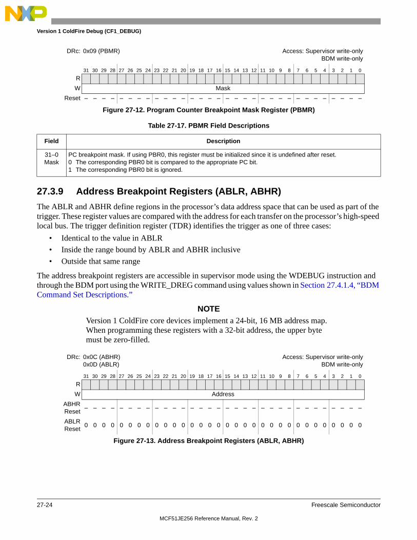
Version 1 ColdFire Debug (CF1_DEBUG)
27-24 Freescale Semiconductor
27.3.9 Address Breakpoint Registers (ABLR, ABHR)
The ABLR and ABHR define regions in the processor’s data address space that can be used as part of the trigger. These register values are compared with the address for each transfer on the processor’s high-speed local bus. The trigger definition register (TDR) identifies the trigger as one of three cases:
• Identical to the value in ABLR
• Inside the range bound by ABLR and ABHR inclusive
• Outside that same range
The address breakpoint registers are accessible in supervisor mode using the WDEBUG instruction and through the BDM port using the WRITE_DREG command using values shown in Section 27.4.1.4, “BDM Command Set Descriptions.”
NOTEVersion 1 ColdFire core devices implement a 24-bit, 16 MB address map. When programming these registers with a 32-bit address, the upper byte must be zero-filled.
DRc: 0x09 (PBMR) Access: Supervisor write-onlyBDM write-only
31 30 29 28 27 26 25 24 23 22 21 20 19 18 17 16 15 14 13 12 11 10 9 8 7 6 5 4 3 2 1 0
R
W Mask
Reset – – – – – – – – – – – – – – – – – – – – – – – – – – – – – – – –
Figure 27-12. Program Counter Breakpoint Mask Register (PBMR)
Table 27-17. PBMR Field Descriptions
Field Description
31–0Mask
PC breakpoint mask. If using PBR0, this register must be initialized since it is undefined after reset.0 The corresponding PBR0 bit is compared to the appropriate PC bit.1 The corresponding PBR0 bit is ignored.
DRc: 0x0C (ABHR)0x0D (ABLR)
Access: Supervisor write-onlyBDM write-only
31 30 29 28 27 26 25 24 23 22 21 20 19 18 17 16 15 14 13 12 11 10 9 8 7 6 5 4 3 2 1 0
R
W Address
ABHRReset
– – – – – – – – – – – – – – – – – – – – – – – – – – – – – – – –
ABLRReset
0 0 0 0 0 0 0 0 0 0 0 0 0 0 0 0 0 0 0 0 0 0 0 0 0 0 0 0 0 0 0 0
Figure 27-13. Address Breakpoint Registers (ABLR, ABHR)
MCF51JE256 Reference Manual, Rev. 2

Version 1 ColdFire Debug (CF1_DEBUG)
Freescale Semiconductor 27-25
27.3.10 Data Breakpoint and Mask Registers (DBR, DBMR)
DBR specifies data patterns used as part of the trigger into debug mode. DBR bits are masked by setting corresponding DBMR bits, as defined in TDR.
DBR and DBMR are accessible in supervisor mode using the WDEBUG instruction and through the BDM port using the WRITE_DREG commands.
The DBR supports aligned and misaligned references. Table 27-22 shows the relationships between processor address, access size, and location within the 32-bit data bus.
Table 27-18. ABLR Field Description
Field Description
31–0Address
Low address. Holds the 32-bit address marking the lower bound of the address breakpoint range. Breakpoints for specific addresses are programmed into ABLR.
Table 27-19. ABHR Field Description
Field Description
31–0Address
High address. Holds the 32-bit address marking the upper bound of the address breakpoint range.
DRc[4:0]: 0x0E (DBR)0x0F (DBMR)
Access: Supervisor write-onlyBDM write-only
31 30 29 28 27 26 25 24 23 22 21 20 19 18 17 16 15 14 13 12 11 10 9 8 7 6 5 4 3 2 1 0
R
W Data (DBR); Mask (DBMR)
Reset 0 0 0 0 0 0 0 0 0 0 0 0 0 0 0 0 0 0 0 0 0 0 0 0 0 0 0 0 0 0 0 0
Figure 27-14. Data Breakpoint & Mask Registers (DBR, DBMR)
Table 27-20. DBR Field Descriptions
Field Description
31–0Data
Data breakpoint value. Contains the value to be compared with the data value from the processor’s local bus as a breakpoint trigger.
Table 27-21. DBMR Field Descriptions
Field Description
31–0Mask
Data breakpoint mask. The 32-bit mask for the data breakpoint trigger. 0 The corresponding DBR bit is compared to the appropriate bit of the processor’s local data bus1 The corresponding DBR bit is ignored
MCF51JE256 Reference Manual, Rev. 2

Version 1 ColdFire Debug (CF1_DEBUG)
27-26 Freescale Semiconductor
27.3.10.1 Resulting Set of Possible Trigger Combinations
The resulting set of possible breakpoint trigger combinations consists of the following options where || denotes logical OR, && denotes logical AND, and {} denotes an optional additional trigger term:
One-level triggers of the form:if (PC_breakpoint)if (PC_breakpoint || Address_breakpoint{&& Data_breakpoint})if (Address_breakpoint {&& Data_breakpoint})
Two-level triggers of the form:if (PC_breakpoint)
then if (Address_breakpoint{&& Data_breakpoint})
if (Address_breakpoint {&& Data_breakpoint})then if (PC_breakpoint)
In these examples, PC_breakpoint is the logical summation of the PBR0/PBMR, PBR1, PBR2, and PBR3 breakpoint registers; Address_breakpoint is a function of ABHR, ABLR, and AATR; Data_breakpoint is a function of DBR and DBMR. In all cases, the data breakpoints can be included with an address breakpoint to further qualify a trigger event as an option.
The breakpoint registers can also be used to define the start and stop recording conditions for the PST trace buffer. For information on this functionality, see Section 27.3.3, “Configuration/Status Register 2 (CSR2)”.
27.3.11 PST Buffer (PSTB)
The PST trace buffer contains 64 six-bit entries, packed consecutively into 12 longword locations. See Figure 27-15 for an illustration of how the buffer entries are packed.
The write pointer for the trace buffer is available as CSR2[PSTBWA]. Using this pointer, it is possible to determine the oldest-to-newest entries in the trace buffer.
Table 27-22. Access Size and Operand Data Location
Address[1–0] Access Size Operand Location
00 Byte D[31–24]
01 Byte D[23–16]
10 Byte D[15–8]
11 Byte D[7–0]
0x Word D[31–16]
1x Word D[15–0]
xx Longword D[31–0]
MCF51JE256 Reference Manual, Rev. 2

Version 1 ColdFire Debug (CF1_DEBUG)
Freescale Semiconductor 27-27
Figure 27-15. PST Trace Buffer Entries and Locations
27.4 Functional Description
27.4.1 Background Debug Mode (BDM)
This section provides details on the background debug serial interface controller (BDC) and the BDM command set.
The BDC provides a single-wire debug interface to the target MCU. As shown in the Version 1 ColdFire core block diagram of Figure 27-1, the BDC module interfaces between the single-pin (BKGD) interface and the remaining debug modules, including the ColdFire background debug logic, the real-time debug hardware, and the PST/DDATA trace logic. This interface provides a convenient means for programming the on-chip flash and other non-volatile memories. The BDC is the primary debug interface for development and allows non-intrusive access to memory data and traditional debug features such as run/halt control, read/write of core registers, breakpoints, and single instruction step.
Features of the background debug controller (BDC) include:
• Single dedicated pin for mode selection and background communications
• Special BDC registers not located in system memory map
• SYNC command to determine target communications rate
• Non-intrusive commands for memory access
• Active background (halt) mode commands for core register access
• GO command to resume execution
• BACKGROUND command to halt core or wake CPU from low-power modes
• Oscillator runs in stop mode, if BDM enabled
Core registernumber (CRN) 31 30 29 28 27 26 25 24 23 22 21 20 19 18 17 16 15 14 13 12 11 10 9 8 7 6 5 4 3 2 1 0
0x10 TB #00 TB #01 TB #02 TB #03 TB #04 05[5:4]
0x11 TB #05[3:0] TB #06 TB #07 TB #08 TB #09 TB #10[5:2]
0x12 10[1:0] TB #11 TB #12 TB #13 TB #14 TB #15
0x13 TB #16 TB #17 TB #18 TB #19 TB #20 21[5:4]
0x14 TB #21[3:0] TB #22 TB #23 TB #24 TB #25 TB #26[5:2]
0x15 26[1:0] TB #27 TB #28 TB #29 TB #30 TB #31
0x16 TB #32 TB #33 TB #34 TB #35 TB #36 37[5:4]
0x17 TB #37[3:0] TB #38 TB #39 TB #40 TB #41 TB #42[5:2]
0x18 42[1:0] TB #43 TB #44 TB #45 TB #46 TB #47
0x19 TB #48 TB #49 TB #50 TB #51 TB #52 53[5:4]
0x1A TB #53[3:0] TB #54 TB #55 TB #56 TB #57 TB #58[5:2]
0x1B 58[1:0] TB #59 TB #60 TB #61 TB #62 TB #63
MCF51JE256 Reference Manual, Rev. 2

Version 1 ColdFire Debug (CF1_DEBUG)
27-28 Freescale Semiconductor
Based on these features, BDM is useful for the following reasons:
• In-circuit emulation is not needed, so physical and electrical characteristics of the system are not affected.
• BDM is always available for debugging the system and provides a communication link for upgrading firmware in existing systems.
• Provides high-speed memory downloading, especially useful for flash programming
• Provides absolute control of the processor, and thus the system. This feature allows quick hardware debugging with the same tool set used for firmware development.
27.4.1.1 CPU Halt
Although certain BDM operations can occur in parallel with CPU operations, unrestricted BDM operation requires the CPU to be halted. The sources that can cause the CPU to halt are listed below in order of priority. Recall that the default configuration of the Version 1 ColdFire core (CF1Core) defines the occurrence of certain exception types to automatically generate a system reset. Some of these fault types include illegal instructions, privilege errors, address errors, and bus error terminations, with the response under control of the processor’s CPUCR[ARD, IRD] bits.
Table 27-23. CPU Halt Sources
Halt Source Halt Timing Description
Fault-on-fault Immediate
Refers to the occurrence of any fault while exception processing. For example, a bus error is signaled during exception stack frame writes or while fetching the first instruction in the exception service routine.
CPUCR[ARD] = 1 Immediately enters halt.
CPUCR[ARD] = 0 Reset event is initiated.
Hardware breakpoint trigger
PendingHalt is made pending in the processor. The processor samples for pending halt and interrupt conditions once per instruction. When a pending condition is asserted, the processor halts execution at the next sample point.
HALT instruction Immediate
BDM disabledCPUCR[IRD] = 0
A reset is initiated since attempted execution of an illegal instruction
CPUCR[IRD] = 1 An illegal instruction exception is generated.
BDM enabled,supervisor mode
Processor immediately halts execution at the next instruction sample point. The processor can be restarted by a BDM GO command. Execution continues at the instruction after HALT.
BDM enabled,user mode
CSR[UHE] = 0CPUCR[IRD] = 0
A reset event is initiated, because a privileged instruction was attempted in user mode.
CSR[UHE] = 0CPUCR[IRD] = 1
A privilege violation exception is generated.
CSR[UHE] = 1
Processor immediately halts execution at the next instruction sample point. The processor can be restarted by a BDM GO command. Execution continues at the instruction after HALT.
MCF51JE256 Reference Manual, Rev. 2

Version 1 ColdFire Debug (CF1_DEBUG)
Freescale Semiconductor 27-29
The processor’s run/stop/halt status is always accessible in XCSR[CPUHALT,CPUSTOP]. Additionally, CSR[27–24] indicate the halt source, showing the highest priority source for multiple halt conditions. This field is cleared by a read of the CSR. A processor halt due to the PSTB full condition as indicated by CSR2[PSTH] is also reflected in CSR[BKPT]. The debug GO command clears CSR[26–24] and CSR2[PSTBH].
27.4.1.2 Background Debug Serial Interface Controller (BDC)
BDC serial communications use a custom serial protocol first introduced on the M68HC12 Family of microcontrollers and later used in the M68HCS08 family. This protocol assumes that the host knows the
BACKGROUND command
Pending
BDM disabled orflash secure
Illegal command response and BACKGROUND command is ignored.
BDM enabled and flash unsecure
Processor is running
Halt is made pending in the processor. The processor samples for pending halt and interrupt conditions once per instruction. When a pending condition is asserted, the processor halts execution at the next sample point.
Processor isstopped
Processing of the BACKGROUND command is treated in a special manner. The processor exits the stopped mode and enters the halted state, at which point all BDM commands may be exercised. When restarted, the processor continues by executing the next sequential instruction (the instruction following STOP).
PSTB full condition Pending PSTB
PSTB obtrusive recording mode pends halt in the processor if the trace buffer reaches its full threshold (full is defined as before the buffer is overwritten). When a pending condition is asserted, the processor halts at the next sample point.
BKGD held lowfor 2 bus clocks
after reset negated for POR or BDM
reset
Immediate
Flash unsecure
Enters debug mode with XCSR[ENBDM, CLKSW] set. The full set of BDM commands is available and debug can proceed.If the core is reset into a debug halt condition, the processor’s response to the GO command depends on the BDM command(s) performed while it was halted. Specifically, if the PC register was loaded, the GO command causes the processor to exit halted state and pass control to the instruction address in the PC, bypassing normal reset exception processing. If the PC was not loaded, the GO command causes the processor to exit halted state and continue reset exception processing.
Flash secure
Enters debug mode with XCSR[ENBDM, CLKSW] set. The allowable commands are limited to the always-available group. A GO command to start the processor is not allowed. The only recovery actions in this mode are: • Issue a BDM reset setting CSR2[BDFR] with CSR2[BDHBR] cleared
and the BKGD pin held high to reset into normal operating mode • Erase the flash to unsecure the memory and then proceed with debug • Power cycle the device with the BKGD pin held high to reset into the
normal operating mode
Table 27-23. CPU Halt Sources (Continued)
Halt Source Halt Timing Description
MCF51JE256 Reference Manual, Rev. 2

Version 1 ColdFire Debug (CF1_DEBUG)
27-30 Freescale Semiconductor
communication clock rate determined by the target BDC clock rate. The BDC clock rate may be the system bus clock frequency or an alternate frequency source depending on the state of XCSR[CLKSW]. All communication is initiated and controlled by the host which drives a high-to-low edge to signal the beginning of each bit time. Commands and data are sent most significant bit (msb) first. For a detailed description of the communications protocol, refer to Section 27.4.1.3, “BDM Communication Details”.
If a host is attempting to communicate with a target MCU that has an unknown BDC clock rate, a SYNC command may be sent to the target MCU to request a timed synchronization response signal from which the host can determine the correct communication speed. After establishing communications, the host can read XCSR and write the clock switch (CLKSW) control bit to change the source of the BDC clock for further serial communications if necessary.
BKGD is a pseudo-open-drain pin and there is an on-chip pullup so no external pullup resistor is required. Unlike typical open-drain pins, the external RC time constant on this pin, which is influenced by external capacitance, plays almost no role in signal rise time. The custom protocol provides for brief, actively driven speed-up pulses to force rapid rise times on this pin without risking harmful drive level conflicts. Refer to Section 27.4.1.3, “BDM Communication Details,” for more details.
When no debugger pod is connected to the standard 6-pin BDM interface connector (Section 27.4.4, “Freescale-Recommended BDM Pinout”), the internal pullup on BKGD chooses normal operating mode. When a development system is connected, it can pull BKGD and RESET low, release RESET to select active background (halt) mode rather than normal operating mode, and then release BKGD. It is not necessary to reset the target MCU to communicate with it through the background debug interface. There is also a mechanism to generate a reset event in response to setting CSR2[BDFR].
27.4.1.3 BDM Communication Details
The BDC serial interface requires the external host controller to generate a falling edge on the BKGD pin to indicate the start of each bit time. The external controller provides this falling edge whether data is transmitted or received.
BKGD is a pseudo-open-drain pin that can be driven by an external controller or by the MCU. Data is transferred msb first at 16 BDC clock cycles per bit (nominal speed). The interface times-out if 512 BDC clock cycles occur between falling edges from the host. If a time-out occurs, the status of any command in progress must be determined before new commands can be sent from the host. To check the status of the command, follow the steps detailed in the bit description of XCSR[CSTAT] in Table 27-7.
The custom serial protocol requires the debug pod to know the target BDC communication clock speed. The clock switch (CLKSW) control bit in the XCSR[31–24] register allows you to select the BDC clock source. The BDC clock source can be the bus clock or the alternate BDC clock source. When the MCU is reset in normal user mode, CLKSW is cleared and that selects the alternate clock source. This clock source is a fixed frequency independent of the bus frequency so it does change if the user modifies clock generator settings. This is the preferred clock source for general debugging.
When the MCU is reset in active background (halt) mode, CLKSW is set which selects the bus clock as the source of the BDC clock. This CLKSW setting is most commonly used during flash memory programming because the bus clock can usually be configured to operate at the highest allowed bus frequency to ensure the fastest possible flash programming times. Because the host system is in control of
MCF51JE256 Reference Manual, Rev. 2

Version 1 ColdFire Debug (CF1_DEBUG)
Freescale Semiconductor 27-31
changes to clock generator settings, it knows when a different BDC communication speed should be used. The host programmer also knows that no unexpected change in bus frequency could occur to disrupt BDC communications.
Normally, setting CLKSW should not be used for general debugging because there is no way to ensure the application program does not change the clock generator settings. This is especially true in the case of application programs that are not yet fully debugged.
After any reset (or at any other time), the host system can issue a SYNC command to determine the speed of the BDC clock. CLKSW may be written using the serial WRITE_XCSR_BYTE command through the BDC interface. CLKSW is located in the special XCSR byte register in the BDC module and it is not accessible in the normal memory map of the ColdFire core. This means that no program running on the processor can modify this register (intentionally or unintentionally).
The BKGD pin can receive a high- or low-level or transmit a high- or low-level. The following diagrams show timing for each of these cases. Interface timing is synchronous to clocks in the target BDC, but asynchronous to the external host. The internal BDC clock signal is shown for reference in counting cycles.
Figure 27-16 shows an external host transmitting a logic 1 or 0 to the BKGD pin of a target MCU. The host is asynchronous to the target so there is a 0–1 cycle delay from the host-generated falling edge to where the target perceives the beginning of the bit time. Ten target BDC clock cycles later, the target senses the bit level on the BKGD pin. Typically, the host actively drives the pseudo-open-drain BKGD pin during host-to-target transmissions to speed up rising edges. Because the target does not drive the BKGD pin during the host-to-target transmission period, there is no need to treat the line as an open-drain signal during this period.
Figure 27-16. BDC Host-to-Target Serial Bit Timing
Figure 27-17 shows the host receiving a logic 1 from the target MCU. Because the host is asynchronous to the target MCU, there is a 0–1 cycle delay from the host-generated falling edge on BKGD to the perceived start of the bit time in the target MCU. The host holds the BKGD pin low long enough for the target to recognize it (at least two target BDC cycles). The host must release the low drive before the target
EARLIEST START
TARGET SENSES BIT LEVEL
10 CYCLES
SYNCHRONIZATIONUNCERTAINTY
BDC CLOCK(TARGET MCU)
HOSTTRANSMIT 1
HOSTTRANSMIT 0
PERCEIVED STARTOF BIT TIME
OF NEXT BIT
MCF51JE256 Reference Manual, Rev. 2

Version 1 ColdFire Debug (CF1_DEBUG)
27-32 Freescale Semiconductor
MCU drives a brief active-high speedup pulse seven cycles after the perceived start of the bit time. The host should sample the bit level about 10 cycles after it started the bit time.
Figure 27-17. BDC Target-to-Host Serial Bit Timing (Logic 1)
Figure 27-18 shows the host receiving a logic 0 from the target MCU. Because the host is asynchronous to the target MCU, there is a 0–1 cycle delay from the host-generated falling edge on BKGD to the start of the bit time as perceived by the target MCU. The host initiates the bit time, but the target MCU finishes it. Because the target wants the host to receive a logic 0, it drives the BKGD pin low for 13 BDC clock cycles, then briefly drives it high to speed up the rising edge. The host samples the bit level about 10 cycles after starting the bit time.
HOST SAMPLES BKGD PIN
10 CYCLES
BDC CLOCK(TARGET MCU)
HOST DRIVETO BKGD PIN
TARGET MCUSPEEDUP PULSE
PERCEIVED STARTOF BIT TIME
HIGH-IMPEDANCE
HIGH-IMPEDANCE HIGH-IMPEDANCE
BKGD PINR-C RISE
10 CYCLES
EARLIEST STARTOF NEXT BIT
MCF51JE256 Reference Manual, Rev. 2

Version 1 ColdFire Debug (CF1_DEBUG)
Freescale Semiconductor 27-33
Figure 27-18. BDM Target-to-Host Serial Bit Timing (Logic 0)
27.4.1.4 BDM Command Set Descriptions
This section presents detailed descriptions of the BDM commands.
The V1 BDM command set is based on transmission of one or more 8-bit data packets per operation. Each operation begins with a host-to-target transmission of an 8-bit command code packet. The command code definition broadly maps the operations into four formats as shown in Figure 27-19.
10 CYCLES
BDC CLOCK(TARGET MCU)
HOST DRIVETO BKGD PIN
TARGET MCUDRIVE AND
PERCEIVED STARTOF BIT TIME
HIGH-IMPEDANCE
BKGD PIN
10 CYCLES
SPEED-UP PULSE
SPEEDUPPULSE
EARLIEST STARTOF NEXT BIT
HOST SAMPLES BKGD PIN
MCF51JE256 Reference Manual, Rev. 2

Version 1 ColdFire Debug (CF1_DEBUG)
27-34 Freescale Semiconductor
Miscellaneous Commands
7 6 5 4 3 2 1 0
W 0 0 R/W 0 MSCMD
R/W Optional Command Extension Byte (Data)
Memory Commands
7 6 5 4 3 2 1 0
W 0 0 R/W 1 SZ MCMD
W if addr,R/W if data
Command Extension Bytes (Address, Data)
Core Register Commands
7 6 5 4 3 2 1 0
W CRG R/W CRN
R/W Command Extension Bytes (Data)
PST Trace Buffer Read Commands
7 6 5 4 3 2 1 0
W 0 1 0 CRN
R Trace Buffer Data[31–24], see Figure 27-15
R Trace Buffer Data[23–16], see Figure 27-15
R Trace Buffer Data[15–08], see Figure 27-15
R Trace Buffer Data[07–00], see Figure 27-15
Figure 27-19. BDM Command Encodings
MCF51JE256 Reference Manual, Rev. 2

Version 1 ColdFire Debug (CF1_DEBUG)
Freescale Semiconductor 27-35
Table 27-24. BDM Command Field Descriptions
Field Description
5R/W
Read/Write. 0 Command is performing a write operation. 1 Command is performing a read operation.
3–0MSCMD
Miscellaneous command. Defines the miscellaneous command to be performed.0000 No operation0001 Display the CPU’s program counter (PC) plus optional capture in the PST trace buffer0010 Enable the BDM acknowledge communication mode0011 Disable the BDM acknowledge communication mode0100 Force a CPU halt (background)1000 Resume CPU execution (go)1101 Read/write of the debug XCSR most significant byte1110 Read/write of the debug CSR2 most significant byte1111 Read/write of the debug CSR3 most significant byte
3–2SZ
Memory operand size. Defines the size of the memory reference.00 8-bit byte01 16-bit word10 32-bit long
1–0MCMD
Memory command. Defines the type of the memory reference to be performed.00 Simple write if R/W = 0; simple read if R/W = 101 Write + status if R/W = 0; read + status if R/W = 110 Fill if R/W = 0; dump if R/W = 111 Fill + status if R/W = 0; dump + status if R/W = 1
7–6CRG
Core register group. Defines the core register group to be referenced.01 CPU’s general-purpose registers (An, Dn) or PST trace buffer10 Debug’s control registers11 CPU’s control registers (PC, SR, VBR, CPUCR,...)
4–0CRN
Core register number. Defines the specific core register (its number) to be referenced. All other CRN values are reserved.
CRG CRN Register
01
0x00–0x07 D0–7
0x08–0x0F A0–7
0x10–0x1B PST Buffer 0–11
10 DRc[4:0] as described in Table 27-4
11
0x00 OTHER_A7
0x01 VBR
0x02 CPUCR
0x04 MACSR
0x05 MASK
0x06 ACC
0x0E SR
0x0F PC
MCF51JE256 Reference Manual, Rev. 2

Version 1 ColdFire Debug (CF1_DEBUG)
27-36 Freescale Semiconductor
27.4.1.5 BDM Command Set Summary
Table 27-25 summarizes the BDM command set. Subsequent paragraphs contain detailed descriptions of each command. The nomenclature below is used in Table 27-25 to describe the structure of the BDM commands.
Commands begin with an 8-bit hexadecimal command code in the host-to-target direction (most significant bit first)
/ = separates parts of the commandd = delay 32 target BDC clock cyclesad24 = 24-bit memory address in the host-to-target directionrd8 = 8 bits of read data in the target-to-host directionrd16 = 16 bits of read data in the target-to-host directionrd32 = 32 bits of read data in the target-to-host directionrd.sz = read data, size defined by sz, in the target-to-host directionwd8 = 8 bits of write data in the host-to-target directionwd16 = 16 bits of write data in the host-to-target directionwd32 = 32 bits of write data in the host-to-target directionwd.sz = write data, size defined by sz, in the host-to-target directionss = the contents of XCSR[31:24] in the target-to-host direction (STATUS)sz = memory operand size (0b00 = byte, 0b01 = word, 0b10 = long)crn = core register numberWS = command suffix signaling the operation is with status
Table 27-25. BDM Command Summary
CommandMnemonic
CommandClassification
ACKif Enb?1
CommandStructure
Description
SYNC Always Available
N/A N/A2 Request a timed reference pulse to determine the target BDC communication speed
ACK_DISABLE Always Available
No 0x03/d Disable the communication handshake. This command does not issue an ACK pulse.
ACK_ENABLE Always Available
Yes 0x02/d Enable the communication handshake. Issues an ACK pulse after the command is executed.
BACKGROUND Non-Intrusive Yes 0x04/d Halt the CPU if ENBDM is set. Otherwise, ignore as illegal command.
DUMP_MEM.sz Non-Intrusive Yes (0x32+4 x sz)/d/rd.sz Dump (read) memory based on operand size (sz). Used with READ_MEM to dump large blocks of memory. An initial READ_MEM is executed to set up the starting address of the block and to retrieve the first result. Subsequent DUMP_MEM commands retrieve sequential operands.
MCF51JE256 Reference Manual, Rev. 2

Version 1 ColdFire Debug (CF1_DEBUG)
Freescale Semiconductor 27-37
DUMP_MEM.sz_WS Non-Intrusive No (0x33+4 x sz)/d/ss/rd.sz Dump (read) memory based on operand size (sz) and report status. Used with READ_MEM{_WS} to dump large blocks of memory. An initial READ_MEM{_WS} is executed to set up the starting address of the block and to retrieve the first result. Subsequent DUMP_MEM{_WS} commands retrieve sequential operands.
FILL_MEM.sz Non-Intrusive Yes (0x12+4 x sz)/wd.sz/d Fill (write) memory based on operand size (sz). Used with WRITE_MEM to fill large blocks of memory. An initial WRITE_MEM is executed to set up the starting address of the block and to write the first operand. Subsequent FILL_MEM commands write sequential operands.
FILL_MEM.sz_WS Non-Intrusive No (0x13+4 x sz)/wd.sz/d/ss Fill (write) memory based on operand size (sz) and report status. Used with WRITE_MEM{_WS} to fill large blocks of memory. An initial WRITE_MEM{_WS} is executed to set up the starting address of the block and to write the first operand. Subsequent FILL_MEM{_WS} commands write sequential operands.
GO Non-Intrusive Yes 0x08/d Resume the CPU’s execution3
NOP Non-Intrusive Yes 0x00/d No operation
READ_CREG Active Background
Yes (0xE0+CRN)/d/rd32 Read one of the CPU’s control registers
READ_DREG Non-Intrusive Yes (0xA0+CRN)/d/rd32 Read one of the debug module’s control registers
READ_MEM.sz Non-Intrusive Yes (0x30+4 x sz)/ad24/d/rd.sz Read the appropriately-sized (sz) memory value from the location specified by the 24-bit address
READ_MEM.sz_WS Non-Intrusive No (0x31+4 x sz)/ad24/d/ss/rd.sz Read the appropriately-sized (sz) memory value from the location specified by the 24-bit address and report status
READ_PSTB Non-Intrusive Yes (0x40+CRN)/d/rd32 Read the requested longword location from the PST trace buffer
READ_Rn Active Background
Yes (0x60+CRN)/d/rd32 Read the requested general-purpose register (An, Dn) from the CPU
READ_XCSR_BYTE Always Available
No 0x2D/rd8 Read the most significant byte of the debug module’s XCSR
READ_CSR2_BYTE Always Available
No 0x2E/rd8 Read the most significant byte of the debug module’s CSR2
READ_CSR3_BYTE Always Available
No 0x2F/rd8 Read the most significant byte of the debug module’s CSR3
Table 27-25. BDM Command Summary (Continued)
CommandMnemonic
CommandClassification
ACKif Enb?1
CommandStructure
Description
MCF51JE256 Reference Manual, Rev. 2

Version 1 ColdFire Debug (CF1_DEBUG)
27-38 Freescale Semiconductor
27.4.1.5.1 SYNC
The SYNC command is unlike other BDC commands because the host does not necessarily know the correct speed to use for serial communications until after it has analyzed the response to the SYNC command.
To issue a SYNC command, the host:
1. Drives the BKGD pin low for at least 128 cycles of the slowest possible BDC clock (bus clock or device-specific alternate clock source).
2. Drives BKGD high for a brief speed-up pulse to get a fast rise time. (This speedup pulse is typically one cycle of the host clock which is as fast as the maximum target BDC clock.)
3. Removes all drive to the BKGD pin so it reverts to high impedance.
4. Listens to the BKGD pin for the sync response pulse.
Upon detecting the sync request from the host (which is a much longer low time than would ever occur during normal BDC communications), the target:
1. Waits for BKGD to return to a logic high.
SYNC_PC Non-Intrusive Yes 0x01/d Display the CPU’s current PC and capture it in the PST trace buffer
WRITE_CREG Active Background
Yes (0xC0+CRN)/wd32/d Write one of the CPU’s control registers
WRITE_DREG Non-Intrusive Yes (0x80+CRN)/wd32/d Write one of the debug module’s control registers
WRITE_MEM.sz Non-Intrusive Yes (0x10+4 x sz)/ad24/wd.sz/d Write the appropriately-sized (sz) memory value to the location specified by the 24-bit address
WRITE_MEM.sz_WS Non-Intrusive No (0x11+4 x sz)/ad24/wd.sz/d/ss Write the appropriately-sized (sz) memory value to the location specified by the 24-bit address and report status
WRITE_Rn Active Background
Yes (0x40+CRN)/wd32/d Write the requested general-purpose register (An, Dn) of the CPU
WRITE_XCSR_BYTE Always Available
No 0x0D/wd8 Write the most significant byte of the debug module’s XCSR
WRITE_CSR2_BYTE Always Available
No 0x0E/wd8 Write the most significant byte of the debug module’s CSR2
WRITE_CSR3_BYTE Always Available
No 0x0F/wd8 Write the most significant byte of the debug module’s CSR3
1 This column identifies if the command generates an ACK pulse if operating with acknowledge mode enabled. See Section 27.4.1.5.3, “ACK_ENABLE,” for addition information.
2 The SYNC command is a special operation which does not have a command code.3 If a GO command is received while the processor is not halted, it performs no operation.
Table 27-25. BDM Command Summary (Continued)
CommandMnemonic
CommandClassification
ACKif Enb?1
CommandStructure
Description
MCF51JE256 Reference Manual, Rev. 2

Version 1 ColdFire Debug (CF1_DEBUG)
Freescale Semiconductor 27-39
2. Delays 16 cycles to allow the host to stop driving the high speed-up pulse.
3. Drives BKGD low for 128 BDC clock cycles.
4. Drives a 1-cycle high speed-up pulse to force a fast rise time on BKGD.
5. Removes all drive to the BKGD pin so it reverts to high impedance.
The host measures the low time of this 128-cycle sync response pulse and determines the correct speed for subsequent BDC communications. Typically, the host can determine the correct communication speed within a few percent of the actual target speed and the serial protocol can easily tolerate this speed error.
27.4.1.5.2 ACK_DISABLE
Disables the serial communication handshake protocol. The subsequent commands, issued after the ACK_DISABLE command, do not execute the hardware handshake protocol. This command is not followed by an ACK pulse.
27.4.1.5.3 ACK_ENABLE
Enables the hardware handshake protocol in the serial communication. The hardware handshake is implemented by an acknowledge (ACK) pulse issued by the target MCU in response to a host command. The ACK_ENABLE command is interpreted and executed in the BDC logic without the need to interface with the CPU. However, an acknowledge (ACK) pulse is issued by the target device after this command is executed. This feature can be used by the host to evaluate if the target supports the hardware handshake protocol. If the target supports the hardware handshake protocol, subsequent commands are enabled to execute the hardware handshake protocol, otherwise this command is ignored by the target.
For additional information about the hardware handshake protocol, refer to Section 27.4.1.6, “Serial Interface Hardware Handshake Protocol,” and Section 27.4.1.7, “Hardware Handshake Abort Procedure.”
Disable host/target handshake protocol Always Available
0x03
host target
DLY
Enable host/target handshake protocol Always Available
0x02
host target
DLY
MCF51JE256 Reference Manual, Rev. 2

Version 1 ColdFire Debug (CF1_DEBUG)
27-40 Freescale Semiconductor
27.4.1.5.4 BACKGROUND
Provided XCSR[ENBDM] is set (BDM enabled), the BACKGROUND command causes the target MCU to enter active background (halt) mode as soon as the current CPU instruction finishes. If ENBDM is cleared (its default value), the BACKGROUND command is ignored.
A delay of 32 BDC clock cycles is required after the BACKGROUND command to allow the target MCU to finish its current CPU instruction and enter active background mode before a new BDC command can be accepted.
After the target MCU is reset into a normal operating mode, the host debugger would send a WRITE_XCSR_BYTE command to set ENBDM before attempting to send the BACKGROUND command the first time. Normally, the development host would set ENBDM once at the beginning of a debug session or after a target system reset, and then leave the ENBDM bit set during debugging operations. During debugging, the host would use GO commands to move from active background mode to normal user program execution and would use BACKGROUND commands or breakpoints to return to active background mode.
27.4.1.5.5 DUMP_MEM.sz, DUMP_MEM.sz_WS
Enter active background mode (if enabled) Non-intrusive
0x04
host target
DLY
DUMP_MEM.sz
Read memory specified by debug address register, then increment address
Non-intrusive
0x32Memory data[7-0]
host target
DLY
target host
0x36Memory
data[15-8]Memory data[7-0]
host target
DLY
target host
target host
0x3AMemory
data[31-24]Memory
data[23-16]Memory
data[15-8]Memory data[7-0]
host target
DLY
target host
target host
target host
target host
MCF51JE256 Reference Manual, Rev. 2

Version 1 ColdFire Debug (CF1_DEBUG)
Freescale Semiconductor 27-41
DUMP_MEM{_WS} is used with the READ_MEM{_WS} command to access large blocks of memory. An initial READ_MEM{_WS} is executed to set-up the starting address of the block and to retrieve the first result. If an initial READ_MEM{_WS} is not executed before the first DUMP_MEM{_WS}, an illegal command response is returned. The DUMP_MEM{_WS} command retrieves subsequent operands. The initial address is incremented by the operand size (1, 2, or 4) and saved in a temporary register. Subsequent DUMP_MEM{_WS} commands use this address, perform the memory read, increment it by the current operand size, and store the updated address in the temporary register. If the with-status option is specified, the core status byte (XCSR_SB) contained in XCSR[31–24] is returned before the read data. XCSR_SB reflects the state after the memory read was performed.
NOTEDUMP_MEM{_WS} does not check for a valid address; it is a valid command only when preceded by NOP, READ_MEM{_WS}, or another DUMP_MEM{_WS} command. Otherwise, an illegal command response is returned. NOP can be used for inter-command padding without corrupting the address pointer.
The size field (sz) is examined each time a DUMP_MEM{_WS} command is processed, allowing the operand size to be dynamically altered. The examples show the DUMP_MEM.B{_WS}, DUMP_MEM.W{_WS} and DUMP_MEM.L{_WS} commands.
DUMP_MEM.sz_WS
Read memory specified by debug address register with status, then increment address
Non-intrusive
0x33 XCSR_SBMemory data[7-0]
host target
DLY
target host
target host
0x37 XCSR_SBMemory
data[15-8]Memory data[7-0]
host target
DLY
target host
target host
target host
0x3B XCSR_SBMemory
data[31-24]Memory
data[23-16]Memory
data[15-8]Memory data[7-0]
host target
DLY
target host
target host
target host
target host
target host
MCF51JE256 Reference Manual, Rev. 2

Version 1 ColdFire Debug (CF1_DEBUG)
27-42 Freescale Semiconductor
27.4.1.5.6 FILL_MEM.sz, FILL_MEM.sz_WS
FILL_MEM{_WS} is used with the WRITE_MEM{_WS} command to access large blocks of memory. An initial WRITE_MEM{_WS} is executed to set up the starting address of the block and write the first datum. If an initial WRITE_MEM{_WS} is not executed before the first FILL_MEM{_WS}, an illegal command response is returned. The FILL_MEM{_WS} command stores subsequent operands. The initial address is incremented by the operand size (1, 2, or 4) and saved in a temporary register. Subsequent WRITE_MEM{_WS} commands use this address, perform the memory write, increment it by the current operand size, and store the updated address in the temporary register. If the with-status option is specified,
FILL_MEM.sz
Write memory specified by debug address register, then increment address
Non-intrusive
0x12Memory data[7-0]
host target
host target
DLY
0x16Memory
data[15-8]Memory data[7-0]
host target
host target
host target
DLY
0x1AMemory
data[31-24]Memory
data[23-16]Memory
data[15-8]Memory data[7-0]
host target
host target
host target
host target
host target
DLY
FILL_MEM.sz_WS
Write memory specified by debug address register with status, then increment address
Non-intrusive
0x13Memory data[7-0]
XCSR_SB
host target
host target
DLY
target host
0x17Memory
data[15-8]Memory data[7-0]
XCSR_SB
host target
host target
host target
DLY
target host
0x1BMemory
data[31-24]Memory
data[23-16]Memory
data[15-8]Memory data[7-0]
XCSR_SB
host target
host target
host target
host target
host target
DLY
target host
MCF51JE256 Reference Manual, Rev. 2

Version 1 ColdFire Debug (CF1_DEBUG)
Freescale Semiconductor 27-43
the core status byte (XCSR_SB) contained in XCSR[31–24] is returned after the write data. XCSR_SB reflects the state after the memory write was performed.
NOTEFILL_MEM{_WS} does not check for a valid address; it is a valid command only when preceded by NOP, WRITE_MEM{_WS}, or another FILL_MEM{_WS} command. Otherwise, an illegal command response is returned. NOP can be used for intercommand padding without corrupting the address pointer.
The size field (sz) is examined each time a FILL_MEM{_WS} command is processed, allowing the operand size to be dynamically altered. The examples show the FILL_MEM.B{_WS}, FILL_MEM.W{_WS} and FILL_MEM.L{_WS} commands.
27.4.1.5.7 GO
This command is used to exit active background (halt) mode and begin (or resume) execution of the application’s instructions. The CPU’s pipeline is flushed and refilled before normal instruction execution resumes. Prefetching begins at the current address in the PC and at the current privilege level. If any register (such as the PC or SR) is altered by a BDM command while the processor is halted, the updated value is used when prefetching resumes. If a GO command is issued and the CPU is not halted, the command is ignored.
27.4.1.5.8 NOP
NOP performs no operation and may be used as a null command where required.
Go Non-intrusive
0x08
host target
DLY
No operation Non-intrusive
0x00
host target
DLY
MCF51JE256 Reference Manual, Rev. 2

Version 1 ColdFire Debug (CF1_DEBUG)
27-44 Freescale Semiconductor
27.4.1.5.9 READ_CREG
If the processor is halted, this command reads the selected control register and returns the 32-bit result. This register grouping includes the PC, SR, CPUCR, MACSR, MASK, ACC, VBR, and OTHER_A7. Accesses to processor control registers are always 32-bits wide, regardless of implemented register width. The register is addressed through the core register number (CRN). See Table 27-24 for the CRN details when CRG is 11.
If the processor is not halted, this command is rejected as an illegal operation and no operation is performed.
27.4.1.5.10 READ_DREG
This command reads the selected debug control register and returns the 32-bit result. This register grouping includes the CSR, XCSR, CSR2, and CSR3. Accesses to debug control registers are always 32-bits wide, regardless of implemented register width. The register is addressed through the core register number (CRN). See Table 27-4 for CRN details.
Read CPU control register Active Background
0xE0+CRNCREG data
[31-24]CREG data
[23-16]CREG data
[15-8]CREG data
[7-0]
host target
DLY
target host
target host
target host
target host
Read debug control register Non-intrusive
0xA0+CRNDREG data
[31-24]DREG data
[23-16]DREG data
[15-8]DREG data
[7-0]
host target
DLY
target host
target host
target host
target host
MCF51JE256 Reference Manual, Rev. 2

Version 1 ColdFire Debug (CF1_DEBUG)
Freescale Semiconductor 27-45
27.4.1.5.11 READ_MEM.sz, READ_MEM.sz_WS
Read data at the specified memory address. The reference address is transmitted as three 8-bit packets (msb to lsb) immediately after the command packet. The access attributes are defined by BAAR[TT,TM]. The hardware forces low-order address bits to zeros for word and longword accesses to ensure these accesses are on 0-modulo-size alignments. If the with-status option is specified, the core status byte (XCSR_SB) contained in XCSR[31–24] is returned before the read data. XCSR_SB reflects the state after the memory read was performed.
READ_MEM.sz
Read memory at the specified address Non-intrusive
0x30 Address[23-0]Memory data[7-0]
host target
host target
DLY
target host
0x34 Address[23-0]Memory
data[15-8]Memory data[7-0]
host target
host target
DLY
target host
target host
0x38 Address[23-0]Memory
data[31-24]Memory
data[23-16]Memory
data[15-8]Memory data[7-0]
host target
host target
DLY
target host
target host
target host
target host
READ_MEM.sz_WS
Read memory at the specified address with status Non-intrusive
0x31 Address[23-0] XCSR_SBMemory data[7-0]
host target
host target
DLY
target host
target host
0x35 Address[23-0] XCSR_SBMemory
data [15-8]Memory
data [7-0]
host target
host target
DLY
target host
target host
target host
0x39 Address[23-0] XCSR_SBMemory
data[31-24]Memory
data[23-16]Memory
data [15-8]Memory
data [7-0]
host target
host target
DLY
target host
target host
target host
target host
target host
MCF51JE256 Reference Manual, Rev. 2

Version 1 ColdFire Debug (CF1_DEBUG)
27-46 Freescale Semiconductor
The examples show the READ_MEM.B{_WS}, READ_MEM.W{_WS} and READ_MEM.L{_WS} commands.
27.4.1.5.12 READ_PSTB
Read 32 bits of captured PST/DDATA values from the trace buffer at the specified address. The PST trace buffer contains 64 six-bit entries, packed consecutively into 12 longword locations. See Figure 27-15 for an illustration of how the buffer entries are packed.
27.4.1.5.13 READ_Rn
If the processor is halted, this command reads the selected CPU general-purpose register (An, Dn) and returns the 32-bit result. See Table 27-24 for the CRN details when CRG is 01.
If the processor is not halted, this command is rejected as an illegal operation and no operation is performed.
27.4.1.5.14 READ_XCSR_BYTE
Read the special status byte of XCSR (XCSR[31–24]). This command can be executed in any mode.
Read PST trace buffer at the specified address Non-intrusive
0x40+CRNPSTB data
[31-24]PSTB data
[23-16]PSTB data
[15-8]PSTB data
[7-0]
host target
DLY
target host
target host
target host
target host
Read general-purpose CPU register Active Background
0x60+CRNRn data [31–24]
Rn data[23–16]
Rn data [15–8]
Rn data [7–0]
host target
DLY
target host
target host
target host
target host
Read XCSR Status Byte Always Available
0x2DXCSR
[31–24]
host target
target host
MCF51JE256 Reference Manual, Rev. 2

Version 1 ColdFire Debug (CF1_DEBUG)
Freescale Semiconductor 27-47
27.4.1.5.15 READ_CSR2_BYTE
Read the most significant byte of CSR2 (CSR2[31–24]). This command can be executed in any mode.
27.4.1.5.16 READ_CSR3_BYTE
Read the most significant byte of the CSR3 (CSR3[31–24]). This command can be executed in any mode.
27.4.1.5.17 SYNC_PC
Capture the processor’s current PC (program counter) and display it on the PST/DDATA signals. After the debug module receives the command, it sends a signal to the ColdFire core that the current PC must be displayed. The core responds by forcing an instruction fetch to the next PC with the address being captured by the DDATA logic. The DDATA logic captures a 2- or 3-byte instruction address, based on CSR[9]. If CSR[9] is cleared, then a 2-byte address is captured, else a 3-byte address is captured. The specific sequence of PST and DDATA values is defined as:
1. Debug signals a SYNC_PC command is pending.
2. CPU completes the current instruction.
3. CPU forces an instruction fetch to the next PC, generating a PST = 0x5 value indicating a taken branch. DDATA captures the instruction address corresponding to the PC. DDATA generates a PST marker signalling a 2- or 3-byte address as defined by CSR[9] (CSR[9] = 0, 2-byte; CSR[9] = 1, 3-byte) and displays the captured PC address.
This command can be used to provide a PC synchronization point between the core’s execution and the application code in the PST trace buffer. It can also be used to dynamically access the PC for performance
Read CSR2 Status Byte Always Available
0x2ECSR2
[31–24]
host target
target host
Read CSR3 Status Byte Always Available
0x2FCSR3
[31–24]
host target
target host
Synchronize PC to PST/DDATA Signals Non-intrusive
0x01
host target
DLY
MCF51JE256 Reference Manual, Rev. 2

Version 1 ColdFire Debug (CF1_DEBUG)
27-48 Freescale Semiconductor
monitoring as the execution of this command is considerably less obtrusive to the real-time operation of an application than a BACKGROUND/read-PC/GO command sequence.
27.4.1.5.18 WRITE_CREG
If the processor is halted, this command writes the 32-bit operand to the selected control register. This register grouping includes the PC, SR, CPUCR, MACSR, MASK, ACC, VBR, and OTHER_A7. Accesses to processor control registers are always 32-bits wide, regardless of implemented register width. The register is addressed through the core register number (CRN). See Table 27-24 for the CRN details when CRG is 11.
If the processor is not halted, this command is rejected as an illegal operation and no operation is performed.
27.4.1.5.19 WRITE_DREG
This command writes the 32-bit operand to the selected debug control register. This grouping includes all the debug control registers ({X}CSRn, BAAR, AATR, TDR, PBRn, PBMR, ABxR, DBR, DBMR). Accesses to debug control registers are always 32-bits wide, regardless of implemented register width. The register is addressed through the core register number (CRN). See Table 27-4 for CRN details.
NOTEWhen writing XCSR, CSR2, or CSR3, WRITE_DREG only writes bits 23–0. The upper byte of these debug registers is only written with the special WRITE_XCSR_BYTE, WRITE_CSR2_BYTE, and WRITE_CSR3_BYTE commands.
Write CPU control register Active Background
0xC0+CRNCREG data
[31–24]CREG data
[23–16]CREG data
[15–8]CREG data
[7–0]
host target
host target
host target
host target
host target
DLY
Write debug control register Non-intrusive
0x80+CRNDREG data
[31–24]DREG data
[23–16]DREG data
[15–8]DREG data
[7–0]
host target
host target
host target
host target
host target
DLY
MCF51JE256 Reference Manual, Rev. 2

Version 1 ColdFire Debug (CF1_DEBUG)
Freescale Semiconductor 27-49
27.4.1.5.20 WRITE_MEM.sz, WRITE_MEM.sz_WS
Write data at the specified memory address. The reference address is transmitted as three 8-bit packets (msb to lsb) immediately after the command packet. The access attributes are defined by BAAR[TT,TM]. The hardware forces low-order address bits to zeros for word and longword accesses to ensure these accesses are on 0-modulo-size alignments. If the with-status option is specified, the core status byte (XCSR_SB) contained in XCSR[31–24] is returned after the read data. XCSR_SB reflects the state after the memory write was performed.
The examples show the WRITE_MEM.B{_WS}, WRITE_MEM.W{_WS}, and WRITE_MEM.L{_WS} commands.
WRITE_MEM.sz
Write memory at the specified address Non-intrusive
0x10 Address[23-0]Memory data[7–0]
host target
host targethost target
DLY
0x14 Address[23-0]Memory
data[15–8]Memory data[7–0]
host target
host targethost target
host target
DLY
0x18 Address[23-0]Memory
data[31–24]Memory
data[23–16]Memory
data[15–8]Memory data[7–0]
host target
host targethost target
host target
host target
host target
DLY
WRITE_MEM.sz_WS
Write memory at the specified address with status Non-intrusive
0x11 Address[23-0]Memory data[7–0]
XCSR_SB
host target
host target
host target
DLY
target host
0x15 Address[23-0]Memory
data[15–8]Memory data[7–0]
XCSR_SB
host target
host target
host target
host target
DLY
target host
0x19 Address[23-0]Memory
data[31–24]Memory
data[23–16]Memory
data[15–8]Memory data[7–0]
XCSR_SB
host target
host target
host target
host target
host target
host target
DLY
target host
MCF51JE256 Reference Manual, Rev. 2

Version 1 ColdFire Debug (CF1_DEBUG)
27-50 Freescale Semiconductor
27.4.1.5.21 WRITE_Rn
If the processor is halted, this command writes the 32-bit operand to the selected CPU general-purpose register (An, Dn). See Table 27-24 for the CRN details when CRG is 01.
If the processor is not halted, this command is rejected as an illegal operation and no operation is performed.
27.4.1.5.22 WRITE_XCSR_BYTE
Write the special status byte of XCSR (XCSR[31–24]). This command can be executed in any mode.
27.4.1.5.23 WRITE_CSR2_BYTE
Write the most significant byte of CSR2 (CSR2[31–24]). This command can be executed in any mode.
27.4.1.5.24 WRITE_CSR3_BYTE
Write the most significant byte of CSR3 (CSR3[31–24]). This command can be executed in any mode.
Write general-purpose CPU register Active Background
0x40+CRNRn data [31–24]
Rn data [23–16]
Rn data [15–8]
Rn data [7–0]
host target
host target
host target
host target
host target
DLY
Write XCSR Status Byte Always Available
0x0DXCSR Data
[31–24]
host target
host target
Write CSR2 Status Byte Always Available
0x0ECSR2 Data
[31–24]
host target
host target
Write CSR3 Status Byte Always Available
0x0FCSR3 Data
[31–24]
host target
host target
MCF51JE256 Reference Manual, Rev. 2

Version 1 ColdFire Debug (CF1_DEBUG)
Freescale Semiconductor 27-51
27.4.1.5.25 BDM Accesses of the MAC Registers
The presence of rounding logic in the output datapath of the MAC requires special care for BDM-initiated reads and writes of its programming model. In particular, any result rounding modes must be disabled during the read/write process so the exact bit-wise MAC register contents are accessed.
For example, a BDM read of the accumulator (ACC) must be preceded by two commands accessing the MAC status register, as shown in the following sequence: BdmReadACC (
rcreg macsr; // read current macsr contents and savewcreg #0,macsr; // disable all rounding modes rcreg ACC; // read the desired accumulator wcreg #saved_data,macsr;// restore the original macsr
)
Likewise, to write an accumulator register, the following BDM sequence is needed:BdmWriteACC (
rcreg macsr; // read current macsr contents and savewcreg #0,macsr; // disable all rounding modeswcreg #data,ACC; // write the desired accumulatorwcreg #saved_data,macsr;// restore the original macsr
)
For more information on saving and restoring the complete MAC programming model, see Section 8.3.1.2, “Saving and Restoring the MAC Programming Model.”
27.4.1.6 Serial Interface Hardware Handshake Protocol
BDC commands that require CPU execution are ultimately treated at the core clock rate. Because the BDC clock source can be asynchronous relative to the bus frequency when CLKSW is cleared, it is necessary to provide a handshake protocol so the host can determine when an issued command is executed by the CPU. This section describes this protocol.
The hardware handshake protocol signals to the host controller when an issued command was successfully executed by the target. This protocol is implemented by a low pulse (16 BDC clock cycles) followed by a brief speedup pulse on the BKGD pin, generated by the target MCU when a command, issued by the host, has been successfully executed. See Figure 27-20. This pulse is referred to as the ACK pulse. After the ACK pulse is finished, the host can start the data-read portion of the command if the last-issued command was a read command, or start a new command if the last command was a write command or a control command (BACKGROUND, GO, NOP, SYNC_PC). The ACK pulse is not issued earlier than 32 BDC clock cycles after the BDC command was issued. The end of the BDC command is assumed to be the 16th BDC clock cycle of the last bit. This minimum delay assures enough time for the host to recognize the ACK pulse. There is no upper limit for the delay between the command and the related ACK pulse, because the command execution depends on the CPU bus frequency, which in some cases could be slow compared to the serial communication rate. This protocol allows great flexibility for pod designers, because it does not rely on any accurate time measurement or short response time to any event in the serial communication.
MCF51JE256 Reference Manual, Rev. 2

Version 1 ColdFire Debug (CF1_DEBUG)
27-52 Freescale Semiconductor
Figure 27-20. Target Acknowledge Pulse (ACK)
NOTEIf the ACK pulse was issued by the target, the host assumes the previous command was executed. If the CPU enters a stop mode prior to executing a non-intrusive command, the command is discarded and the ACK pulse is not issued. After entering a stop mode, the BDC command is no longer pending and the XCSR[CSTAT] value of 001 is kept until the next command is successfully executed.
Figure 27-21 shows the ACK handshake protocol in a command level timing diagram. A READ_MEM.B command is used as an example:
1. The 8-bit command code is sent by the host, followed by the address of the memory location to be read.
2. The target BDC decodes the command and sends it to the CPU.
3. Upon receiving the BDC command request, the CPU schedules a execution slot for the command.
4. The CPU temporarily stalls the instruction stream at the scheduled point, executes the READ_MEM.B command and then continues.
This process is referred to as cycle stealing. The READ_MEM.B appears as a single-cycle operation to the processor, even though the pipelined nature of the Operand Execution Pipeline requires multiple CPU clock cycles for it to actually complete. After that, the debug module tracks the execution of the READ_MEM.b command as the processor resumes the normal flow of the application program. After detecting the READ_MEM.B command is done, the BDC issues an ACK pulse to the host controller, indicating that the addressed byte is ready to be retrieved. After detecting the ACK pulse, the host initiates the data-read portion of the command.
16 CYCLES
BDC CLOCK(TARGET MCU)
TARGETTRANSMITS
HIGH-IMPEDANCE
BKGD PIN
HIGH-IMPEDANCE
MINIMUM DELAY FROM THE BDC COMMAND
32 CYCLES
EARLIESTSTART OFNEXT BIT
SPEED UP PULSE
16th CYCLE OF THELAST COMMAD BIT
ACK PULSE
MCF51JE256 Reference Manual, Rev. 2

Version 1 ColdFire Debug (CF1_DEBUG)
Freescale Semiconductor 27-53
Figure 27-21. Handshake Protocol at Command Level
Unlike a normal bit transfer, where the host initiates the transmission by issuing a negative edge in the BKGD pin, the serial interface ACK handshake pulse is initiated by the target MCU. The hardware handshake protocol in Figure 27-21 specifies the timing when the BKGD pin is being driven, so the host should follow these timing relationships to avoid the risks of an electrical conflict at the BKGD pin.
The ACK handshake protocol does not support nested ACK pulses. If a BDC command is not acknowledged by an ACK pulse, the host first needs to abort the pending command before issuing a new BDC command. When the CPU enters a stop mode at about the same time the host issues a command that requires CPU execution, the target discards the incoming command. Therefore, the command is not acknowledged by the target, meaning that the ACK pulse is not issued in this case. After a certain time, the host could decide to abort the ACK protocol to allow a new command. Therefore, the protocol provides a mechanism where a command (a pending ACK) could be aborted. Unlike a regular BDC command, the ACK pulse does not provide a timeout. In the case of a STOP instruction where the ACK is prevented from being issued, it would remain pending indefinitely if not aborted. See the handshake abort procedure described in Section 27.4.1.7, “Hardware Handshake Abort Procedure.”
27.4.1.7 Hardware Handshake Abort Procedure
The abort procedure is based on the SYNC command. To abort a command that has not responded with an ACK pulse, the host controller generates a sync request (by driving BKGD low for at least 128 serial clock cycles and then driving it high for one serial clock cycle as a speedup pulse). By detecting this long low pulse on the BKGD pin, the target executes the sync protocol (see Section 27.4.1.5.1, “SYNC”), and assumes that the pending command and therefore the related ACK pulse, are being aborted. Therefore, after the sync protocol completes, the host is free to issue new BDC commands.
Because the host knows the target BDC clock frequency, the SYNC command does not need to consider the lowest possible target frequency. In this case, the host could issue a SYNC close to the 128 serial clock cycles length, providing a small overhead on the pulse length to assure the sync pulse is not misinterpreted by the target.
It is important to notice that any issued BDC command that requires CPU execution is scheduled for execution by the pipeline based on the dynamic state of the machine, provided the processor does not enter any of the stop modes. If the host aborts a command by sending the sync pulse, it should then read XCSR[CSTAT] after the sync response is issued by the target, checking for CSTAT cleared, before
READ_MEM.B
BDC ISSUES THE
BYTE IS NEW BDC COMMANDBKGD PIN ADDRESS[23–0]
CPU EXECUTES THEREAD_MEM.BCOMMAND
RETRIEVED
HOST TARGET
HOST TARGET
HOST TARGET
DEBUG DECODESTHE COMMAND
ACK PULSE (NOT TO SCALE)
MCF51JE256 Reference Manual, Rev. 2

Version 1 ColdFire Debug (CF1_DEBUG)
27-54 Freescale Semiconductor
attempting to send any new command that requires CPU execution. This prevents the new command from being discarded at the debug/CPU interface, due to the pending command being executed by the CPU. Any new command should be issued only after XCSR[CSTAT] is cleared.
There are multiple reasons that could cause a command to take too long to execute, measured in terms of the serial communication rate: The BDC clock frequency could be much faster than the CPU clock frequency, or the CPU could be accessing a slow memory, which would cause pipeline stall cycles to occur. All commands referencing the CPU registers or memory require access to the processor’s local bus to complete. If the processor is executing a tight loop contained within a single aligned longword, the processor may never successfully grant the internal bus to the debug command. For example:
align 4label1: nop
bra.b label1or
align 4label2: bra.w label2
These two examples of tight loops exhibit the BDM lockout behavior. If the loop spans across two longwords, there are no issues, so the recommended construct is:
align 4label3: bra.l label3
The hardware handshake protocol is appropriate for these situations, but the host could also decide to use the software handshake protocol instead. In this case, if XCSR[CSTAT] is 001, there is a BDC command pending at the debug/CPU interface. The host controller should monitor XCSR[CSTAT] and wait until it is 000 to be able to issue a new command that requires CPU execution. However, if the XCSR[CSTAT] is 1xx, the host should assume the last command failed to execute. To recover from this condition, the following sequence is suggested:
1. Issue a SYNC command to reset the BDC communication channel.
2. The host issues a BDM NOP command.
3. The host reads the channel status using a READ_XCSR_BYTE command.
4. If XCSR[CSTAT] is 000then the status is okay; proceedelse
Halt the CPU using a BDM BACKGROUND commandRepeat steps 1,2,3If XCSR[CSTAT] is 000, then proceed, else reset the device
Figure 27-22 shows a SYNC command aborting a READ_MEM.B. After the command is aborted, a new command could be issued by the host.
NOTEFigure 27-22 signal timing is not drawn to scale.
MCF51JE256 Reference Manual, Rev. 2

Version 1 ColdFire Debug (CF1_DEBUG)
Freescale Semiconductor 27-55
Figure 27-22. ACK Abort Procedure at the Command Level
Figure 27-23 a shows a conflict between the ACK pulse and the sync request pulse. This conflict could occur if a pod device is connected to the target BKGD pin and the target is already executing a BDC command. Consider that the target CPU is executing a pending BDC command at the exact moment the pod is being connected to the BKGD pin. In this case, an ACK pulse is issued at the same time as the SYNC command. In this case there is an electrical conflict between the ACK speedup pulse and the sync pulse. Because this is not a probable situation, the protocol does not prevent this conflict from happening.
Figure 27-23. ACK Pulse and SYNC Request Conflict
The hardware handshake protocol is enabled by the ACK_ENABLE command and disabled by the ACK_DISABLE command. It also allows for pod devices to choose between the hardware handshake protocol or the software protocol that monitors the XCSR status byte. The ACK_ENABLE and ACK_DISABLE commands are:
• ACK_ENABLE — Enables the hardware handshake protocol. The target issues the ACK pulse when a CPU command is executed. The ACK_ENABLE command itself also has the ACK pulse as a response.
READ_MEM.B READ_XCSR_BYTEBKGD PIN ADDRESS[23-0]
HOST TARGET
BDC DECODES
READ_MEM.B CMDIS ABORTED BY THE SYNC REQUEST
NEW BDC COMMAND
AND CPU TRYS TO EXECUTETHE READ_MEM.B CMD
HOST TARGET HOST TARGET
SYNC RESPONSEFROM THE TARGET
NEW BDC COMMAND
(NOT TO SCALE) (NOT TO SCALE)
BDC CLOCK(TARGET MCU)
TARGET MCUDRIVES TO
BKGD PIN
BKGD PIN
16 CYCLES
SPEEDUP PULSE
HIGH-IMPEDANCE
HOSTDRIVES SYNCTO BKGD PIN
HOST AND TARGET
ACK PULSE
HOST SYNC REQUEST PULSE
AT LEAST 128 CYCLES
ELECTRICAL CONFLICT
DRIVE TO BKGD PIN
MCF51JE256 Reference Manual, Rev. 2

Version 1 ColdFire Debug (CF1_DEBUG)
27-56 Freescale Semiconductor
• ACK_DISABLE — Disables the ACK pulse protocol. In this case, the host should verify the state of XCSR[CSTAT] to evaluate if there are pending commands and to check if the CPU’s operating state has changed to or from active background mode via XCSR[31–30].
The default state of the protocol, after reset, is hardware handshake protocol disabled.
The commands that do not require CPU execution, or that have the status register included in the retrieved bit stream, do not perform the hardware handshake protocol. Therefore, the target does not respond with an ACK pulse for those commands even if the hardware protocol is enabled. Conversely, only commands that require CPU execution and do not include the status byte perform the hardware handshake protocol. See the third column in Table 27-25 for the complete enumeration of this function.
An exception is the ACK_ENABLE command, which does not require CPU execution but responds with the ACK pulse. This feature can be used by the host to evaluate if the target supports the hardware handshake protocol. If an ACK pulse is issued in response to this command, the host knows that the target supports the hardware handshake protocol. If the target does not support the hardware handshake protocol the ACK pulse is not issued. In this case, the ACK_ENABLE command is ignored by the target, because it is not recognized as a valid command.
27.4.2 Real-Time Debug Support
The ColdFire family supports debugging real-time applications. For these types of embedded systems, the processor must continue to operate during debug. The foundation of this area of debug support is that while the processor cannot be halted to allow debugging, the system can generally tolerate the small intrusions with minimal effect on real-time operation.
NOTEThe details regarding real-time debug support will be supplied at a later time.
27.4.3 Trace Support
For the baseline V1 ColdFire core and its single debug signal, support for trace functionality is completely redefined. The V1 solution provides an on-chip PST/DDATA trace buffer (known as the PSTB) to record the stream of PST and DDATA values.
As a review, the classic ColdFire debug architecture supports real-time trace via the PST/DDATA output signals. For this functionality, the following apply:
• One (or more) PST value is generated for each executed instruction
• Branch target instruction address information is displayed on all non-PC-relative change-of-flow instructions, where the user selects a programmable number of bytes of target address
— Displayed information includes PST marker plus target instruction address as DDATA
— Captured address creates the appropriate number of DDATA entries, each with 4 bits of address
• Optional data trace capabilities are provided for accesses mapped to the slave peripheral bus
— Displayed information includes PST marker plus captured operand value as DDATA
— Captured operand creates the appropriate number of DDATA entries, each with 4 bits of data
MCF51JE256 Reference Manual, Rev. 2

Version 1 ColdFire Debug (CF1_DEBUG)
Freescale Semiconductor 27-57
The resulting PST/DDATA output stream, with the application program memory image, provides an instruction-by-instruction dynamic trace of the execution path.
Even with the application of a PST trace buffer, problems associated with the PST bandwidth and associated fill rate of the buffer remain. Given that there is one (or more) PST entry per instruction, the PSTB would fill rapidly without some type of data compression.
Consider the following example to illustrate the PST compression algorithm. Most sequential instructions generate a single PST = 1 value. Without compression, the execution of ten sequential instructions generates a stream of ten PST = 1 values. With PST compression, the reporting of any PST = 1 value is delayed so that consecutive PST = 1 values can be accumulated. When a PST 1 value is reported, the maximum accumulation count is reached, or a debug data value is captured, a single accumulated PST value is generated. Returning to the example with compression enabled, the execution of ten sequential instructions generates a single PST value indicating ten sequential instructions have been executed.
This technique has proven to be effective at significantly reducing the average PST entries per instruction and PST entries per machine cycle. The application of this compression technique makes the application of a useful PST trace buffer for the V1 ColdFire core realizable. The resulting 5-bit PST definitions are shown in Table 27-26.
Table 27-26. CF1 Debug Processor Status Encodings
PST[4:0] Definition
0x00 Continue execution. Many instructions execute in one processor cycle. If an instruction requires more processor clock cycles, subsequent clock cycles are indicated by driving PST with this encoding.
0x01 Begin execution of one instruction. For most instructions, this encoding signals the first processor clock cycle of an instruction’s execution. Certain change-of-flow opcodes, plus the PULSE and WDDATA instructions, generate different encodings.
0x02 Reserved
0x03 Entry into user-mode. Signaled after execution of the instruction that caused the ColdFire processor to enter user mode.
0x04 Begin execution of PULSE and WDDATA instructions. PULSE defines triggers or markers for debug and/or performance analysis. WDDATA lets the core write any operand (byte, word, or longword) directly to the DDATA port, independent of debug module configuration. When WDDATA is executed, a value of 0x04 is signaled on the PST port, followed by the appropriate marker, and then the data transfer on the DDATA port. The number of captured data bytes depends on the WDDATA operand size.
0x05 Begin execution of taken branch or SYNC_PC BDM command. For some opcodes, a branch target address may be displayed on DDATA depending on the CSR settings. CSR also controls the number of address bytes displayed, indicated by the PST marker value preceding the DDATA nibble that begins the data output. This encoding also indicates that the SYNC_PC command has been processed.
0x06 Reserved
0x07 Begin execution of return from exception (RTE) instruction.
0x08–0x0B Indicates the number of data bytes to be loaded into the PST trace buffer. The capturing of peripheral bus data references is controlled by CSR[DDC].0x08 Begin 1-byte data transfer on DDATA0x09 Begin 2-byte data transfer on DDATA0x0A Reserved0x0B Begin 4-byte data transfer on DDATA
MCF51JE256 Reference Manual, Rev. 2

Version 1 ColdFire Debug (CF1_DEBUG)
27-58 Freescale Semiconductor
27.4.3.1 Begin Execution of Taken Branch (PST = 0x05)
The PST is 0x05 when a taken branch is executed. For some opcodes, a branch target address may be loaded into the trace buffer (PSTB) depending on the CSR settings. CSR also controls the number of address bytes loaded that is indicated by the PST marker value immediately preceding the DDATA entry in the PSTB that begins the address entries.
0x0C–0x0F Indicates the number of address bytes to be loaded into the PST trace buffer. The capturing of branch target addresses is controlled by CSR[BTB].0x0C Reserved0x0D Begin 2-byte address transfer on DDATA (Displayed address is shifted right 1: ADDR[16:1])0x0E Begin 3-byte address transfer on DDATA (Displayed address is shifted right 1: ADDR[23:1])0x0F Reserved
0x10–0x11 Reserved
0x12 Completed execution of 2 sequential instructions
0x13 Completed execution of 3 sequential instructions
0x14 Completed execution of 4 sequential instructions
0x15 Completed execution of 5 sequential instructions
0x16 Completed execution of 6 sequential instructions
0x17 Completed execution of 7 sequential instructions
0x18 Completed execution of 8 sequential instructions
0x19 Completed execution of 9 sequential instructions
0x1A Completed execution of 10 sequential instructions
0x1B This value signals there has been a change in the breakpoint trigger state machine. It appears as a single marker for each state change and is immediately followed by a DDATA value signaling the new breakpoint trigger state encoding.The DDATA breakpoint trigger state value is defined as (0x20 + 2 CSR[BSTAT]):0x20 No breakpoints enabled0x22 Waiting for a level-1 breakpoint0x24 Level-1 breakpoint triggered0x2A Waiting for a level-2 breakpoint0x2C Level-2 breakpoint triggered
0x1C Exception processing. This value signals the processor has encountered an exception condition. Although this is a multi-cycle mode, there are only two PST = 0x1C values recorded before the mode value is suppressed.
0x1D Emulator mode exception processing. This value signals the processor has encountered a debug interrupt or a properly-configured trace exception. Although this is a multi-cycle mode, there are only two PST = 0x1D values recorded before the mode value is suppressed.
0x1E Processor is stopped. This value signals the processor has executed a STOP instruction. Although this is a multi-cycle mode because the ColdFire processor remains stopped until an interrupt or reset occurs, there are only two PST = 0x1E values recorded before the mode value is suppressed.
0x1F Processor is halted. This value signals the processor has been halted. Although this is a multi-cycle mode because the ColdFire processor remains halted until a BDM go command is received or reset occurs, there are only two PST = 0x1F values recorded before the mode value is suppressed.
Table 27-26. CF1 Debug Processor Status Encodings (Continued)
PST[4:0] Definition
MCF51JE256 Reference Manual, Rev. 2

Version 1 ColdFire Debug (CF1_DEBUG)
Freescale Semiconductor 27-59
Multiple byte DDATA values are displayed in least-to-most-significant order. The processor captures only those target addresses associated with taken branches that use a variant addressing mode (RTE and RTS instructions, JMP and JSR instructions using address register indirect or indexed addressing modes, and all exception vectors).
The simplest example of a branch instruction using a variant address is the compiled code for a C language case statement. Typically, the evaluation of this statement uses the variable of an expression as an index into a table of offsets, where each offset points to a unique case within the structure. For such change-of-flow operations, the ColdFire processor loads the PSTB as follows:
1. Load PST=0x05 to identify that a taken branch is executed.
2. Optionally load the marker for the target address capture. Encodings 0x0D or 0x0E identify the number of bytes loaded into the PSTB.
3. The new target address is optionally available in the PSTB. The number of bytes of the target address loaded is configurable (2 or 3 bytes, where the encoding is 0x0D and 0x0E, respectively).
Another example of a variant branch instruction is a JMP (A0) instruction. Figure 27-24 shows the PSTB entries that indicate a JMP (A0) execution, assuming CSR[BTB] was programmed to display the lower two bytes of an address.
The PST of 0x05 indicates a taken branch and the marker value 0x0D indicates a 2-byte address. Therefore, the following entries display the lower two bytes of address register A0, right-shifted by 1, in least-to-most-significant nibble order. The next PST entry after the JMP instruction completes depends on the target instruction. See Section 27.4.3.2, “PST Trace Buffer (PSTB) Entry Format,” for entry descriptions explaining the 2-bit prefix before each address nibble.
PST/DDATA Values Description
0x05 Taken Branch
0x0D 2-byte Address Marker
{10, Address[4:1]} Address >> 1
{10, Address[8:5]}
{10, Address[12:9]}
{10, Address[16:13]}
Figure 27-24. Example JMP Instruction Output in PSTB
MCF51JE256 Reference Manual, Rev. 2

Version 1 ColdFire Debug (CF1_DEBUG)
27-60 Freescale Semiconductor
27.4.3.2 PST Trace Buffer (PSTB) Entry Format
As PST and DDATA values are captured and loaded in the trace buffer, each entry is six bits in size therefore, the type of the entry can easily be determined when post-processing the PSTB. See Figure 27-25.
Figure 27-25. V1 PST/DDATA Trace Buffer Entry Format
27.4.3.3 PST/DDATA Example
In this section, an example showing the behavior of the PST/DDATA functionality is detailed. Consider the following interrupt service routine that counts the interrupt, negates the IRQ, performs a software IACK, and then exits. This example is presented here because it exercises a considerable set of the PST/DDATA capabilities.
_isr:01074: 46fc 2700 mov.w &0x2700,%sr # disable interrupts01078: 2f08 mov.l %a0,-(%sp) # save a00107a: 2f00 mov.l %d0,-(%sp) # save d00107c: 302f 0008 mov.w (8,%sp),%d0 # load format/vector word01080: e488 lsr.l &2,%d0 # align vector number01082: 0280 0000 00ff andi.l &0xff,%d0 # isolate vector number01088: 207c 0080 1400 mov.l &int_count,%a0 # base of interrupt counters _isr_entry1:0108e: 52b0 0c00 addq.l &1,(0,%a0,%d0.l*4) # count the interrupt01092: 11c0 a021 mov.b %d0,IGCR0+1.w # negate the irq01096: 1038 a020 mov.b IGCR0.w,%d0 # force the write to complete0109a: 4e71 nop # synchronize the pipelines0109c: 71b8 ffe0 mvz.b SWIACK.w,%d0 # software iack: pending irq?010a0: 0c80 0000 0041 cmpi.l %d0,&0x41 # level 7 or none pending?010a6: 6f08 ble.b _isr_exit # yes, then exit010a8: 52b9 0080 145c addq.l &1,swiack_count # increment the swiack count010ae: 60de bra.b _isr_entry1 # continue at entry1 _isr_exit:010b0: 201f mov.l (%sp)+,%d0 # restore d0010b2: 205f mov.l (%sp)+,%a0 # restore a0010b4: 4e73 rte # exit
This ISR executes mostly as straight-line code: there is a single conditional branch @ PC = 0x10A6, which is taken in this example. The following description includes the PST and DDATA values generated as this
5 4 3 2 1 0
PSTB[PST] 0 PST[4:0]
DataPSTB[DDATA]
1 R/W Data[3:0]
AddressPSTB[DDATA]
1 0 Address[3:0]1
1 Depending on which nibble is displayed (as determined by CSR[9:8]), Address[3:0] sequentially (least-to-most-significant nibble order) displays four bits of the real CPU address [16:1] or [24:1].
Reset: — — — — — —
MCF51JE256 Reference Manual, Rev. 2

Version 1 ColdFire Debug (CF1_DEBUG)
Freescale Semiconductor 27-61
code snippet executes. In this example, the CSR setting enables only the display of 2-byte branch addresses. Operand data captures are not enabled. The sequence begins with an interrupt exception:interrupt exception occurs @ pc = 5432 while in user mode # pst = 1c, 1c, 05, 0d # ddata = 2a, 23, 28, 20 # trg_addr = 083a << 1 # trg_addr = 1074 _isr:01074: 46fc 2700 mov.w &0x2700,%sr # pst = 0101078: 2f08 mov.l %a0,-(%sp) # pst = 010107a: 2f00 mov.l %d0,-(%sp) # pst = 010107c: 302f 0008 mov.w (8,%sp),%d0 # pst = 0101080: e488 lsr.l &2,%d0 # pst = 0101082: 0280 0000 00ff andi.l &0xff,%d0 # pst = 0101088: 207c 0080 1400 mov.l &int_count,%a0 # pst = 010108e: 52b0 0c00 addq.l &1,(0,%a0,%d0.l*4) # pst = 0101092: 11c0 a021 mov.b %d0,IGCR0+1.w # pst = 01, 08 # ddata = 30, 30 # wdata.b = 0x0001096: 1038 a020 mov.b IGCR0.w,%d0 # pst = 01, 08 # ddata = 28, 21 # rdata.b = 0x180109a: 4e71 nop # pst = 010109c: 71b8 ffe0 mvz.b SWIACK.w,%d0 # pst = 01, 08 # ddata = 20, 20 # rdata.b = 0x00010a0: 0c80 0000 0041 cmpi.l %d0,&0x41 # pst = 01010a6: 6f08 ble.b _isr_exit # pst = 05 (taken branch)010b0: 201f mov.l (%sp)+,%d0 # pst = 01010b2: 205f mov.l (%sp)+,%a0 # pst = 01010b4: 4e73 rte # pst = 07, 03, 05, 0d # ddata = 29, 21, 2a, 22 # trg_addr = 2a19 << 1 # trg_addr = 5432
As the PSTs are compressed, the resulting stream of 6-bit hexadecimal entries is loaded into consecutive locations in the PST trace buffer:PSTB[*]= 1c, 1c, 05, 0d, // interrupt exception
2a, 23, 28, 20, // branch target addr = 10741a, // 10 sequential insts13, // 3 sequential insts05, 12, // taken_branch + 2 sequential07, 03, 05, 0d, // rte, entry into user mode29, 21, 2a, 22 // branch target addr = 5432
Architectural studies on the compression algorithm determined an appropriate size for the PST trace buffer. Using a suite of ten MCU benchmarks, a 64-entry PSTB was found to capture an average window of time of 520 processor cycles with program trace using 2-byte addresses enabled.
MCF51JE256 Reference Manual, Rev. 2

Version 1 ColdFire Debug (CF1_DEBUG)
27-62 Freescale Semiconductor
27.4.3.4 Processor Status, Debug Data Definition
This section specifies the ColdFire processor and debug module’s generation of the processor status (PST) and debug data (DDATA) output on an instruction basis. In general, the PST/DDATA output for an instruction is defined as follows:
PST = 0x01, {PST = 0x0[89B], DDATA = operand}
where the {...} definition is optional operand information defined by the setting of the CSR, and [...] indicates the presence of one value from the list.
The CSR provides capabilities to display operands based on reference type (read, write, or both). A PST value {0x08, 0x09, or 0x0B} identifies the size and presence of valid data to follow in the PST trace buffer (PSTB) {1, 2, or 4 bytes, respectively}. Additionally, CSR[DDC] specifies whether operand data capture is enabled and what size. Also, for certain change-of-flow instructions, CSR[BTB] provides the capability to display the target instruction address in the PSTB (2 or 3 bytes) using a PST value of 0x0D or 0x0E, respectively.
27.4.3.4.1 User Instruction Set
Table 27-27 shows the PST/DDATA specification for user-mode instructions. Rn represents any {Dn, An} register. In this definition, the y suffix generally denotes the source, and x denotes the destination operand. For a given instruction, the optional operand data is displayed only for those effective addresses referencing memory. The DD nomenclature refers to the DDATA outputs.
Table 27-27. PST/DDATA Specification for User-Mode Instructions
Instruction Operand Syntax PST/DDATA
add.l <ea>y,Dx PST = 0x01, {PST = 0x0B, DD = source operand}
add.l Dy,<ea>x PST = 0x01, {PST = 0x0B, DD = source}, {PST = 0x0B, DD = destination}
adda.l <ea>y,Ax PST = 0x01, {PST = 0x0B, DD = source operand}
addi.l #<data>,Dx PST = 0x01
addq.l #<data>,<ea>x PST = 0x01, {PST = 0x0B, DD = source}, {PST = 0x0B, DD = destination}
addx.l Dy,Dx PST = 0x01
and.l <ea>y,Dx PST = 0x01, {PST = 0x0B, DD = source operand}
and.l Dy,<ea>x PST = 0x01, {PST = 0x0B, DD = source}, {PST = 0x0B, DD = destination}
andi.l #<data>,Dx PST = 0x01
asl.l {Dy,#<data>},Dx PST = 0x01
asr.l {Dy,#<data>},Dx PST = 0x01
bcc.{b,w,l} if taken, then PST = 0x05, else PST = 0x01
bchg.{b,l} #<data>,<ea>x PST = 0x01, {PST = 0x08, DD = source}, {PST = 0x08, DD = destination}
bchg.{b,l} Dy,<ea>x PST = 0x01, {PST = 0x08, DD = source}, {PST = 0x08, DD = destination}
bclr.{b,l} #<data>,<ea>x PST = 0x01, {PST = 0x08, DD = source}, {PST = 0x08, DD = destination}
MCF51JE256 Reference Manual, Rev. 2

Version 1 ColdFire Debug (CF1_DEBUG)
Freescale Semiconductor 27-63
bclr.{b,l} Dy,<ea>x PST = 0x01, {PST = 0x08, DD = source}, {PST = 0x08, DD = destination}
bitrev.l Dx PST = 0x01
bra.{b,w,l} PST = 0x05
bset.{b,l} #<data>,<ea>x PST = 0x01, {PST = 0x08, DD = source}, {PST = 0x08, DD = destination}
bset.{b,l} Dy,<ea>x PST = 0x01, {PST = 0x08, DD = source}, {PST = 0x08, DD = destination}
bsr.{b,w,l} PST = 0x05, {PST = 0x0B, DD = destination operand}
btst.{b,l} #<data>,<ea>x PST = 0x01, {PST = 0x08, DD = source operand}
btst.{b,l} Dy,<ea>x PST = 0x01, {PST = 0x08, DD = source operand}
byterev.l Dx PST = 0x01
clr.b <ea>x PST = 0x01, {PST = 0x08, DD = destination operand}
clr.l <ea>x PST = 0x01, {PST = 0x0B, DD = destination operand}
clr.w <ea>x PST = 0x01, {PST = 0x09, DD = destination operand}
cmp.b <ea>y,Dx PST = 0x01, {0x08, source operand}
cmp.l <ea>y,Dx PST = 0x01, {PST = 0x0B, DD = source operand}
cmp.w <ea>y,Dx PST = 0x01, {0x09, source operand}
cmpa.l <ea>y,Ax PST = 0x01, {PST = 0x0B, DD = source operand}
cmpa.w <ea>y,Ax PST = 0x01, {0x09, source operand}
cmpi.b #<data>,Dx PST = 0x01
cmpi.l #<data>,Dx PST = 0x01
cmpi.w #<data>,Dx PST = 0x01
eor.l Dy,<ea>x PST = 0x01, {PST = 0x0B, DD = source}, {PST = 0x0B, DD = destination}
eori.l #<data>,Dx PST = 0x01
ext.l Dx PST = 0x01
ext.w Dx PST = 0x01
extb.l Dx PST = 0x01
illegal PST = 0x011
jmp <ea>y PST = 0x05, {PST = 0x0[DE], DD = target address}2
jsr <ea>y PST = 0x05, {PST = 0x0[DE], DD = target address}, {PST = 0x0B, DD = destination operand}2
lea.l <ea>y,Ax PST = 0x01
link.w Ay,#<displacement> PST = 0x01, {PST = 0x0B, DD = destination operand}
lsl.l {Dy,#<data>},Dx PST = 0x01
lsr.l {Dy,#<data>},Dx PST = 0x01
Table 27-27. PST/DDATA Specification for User-Mode Instructions (Continued)
Instruction Operand Syntax PST/DDATA
MCF51JE256 Reference Manual, Rev. 2

Version 1 ColdFire Debug (CF1_DEBUG)
27-64 Freescale Semiconductor
mov3q.l #<data>,<ea>x PST = 0x01, {PST = 0x0B,DD = destination operand}
move.b <ea>y,<ea>x PST = 0x01, {PST = 0x08, DD = source}, {PST = 0x08, DD = destination}
move.l <ea>y,<ea>x PST = 0x01, {PST = 0x0B, DD = source}, {PST = 0x0B, DD = destination}
move.w <ea>y,<ea>x PST = 0x01, {PST = 0x09, DD = source}, {PST = 0x09, DD = destination}
move.w CCR,Dx PST = 0x01
move.w {Dy,#<data>},CCR PST = 0x01
movea.l <ea>y,Ax PST = 0x01, {PST = 0x0B, DD = source}
movea.w <ea>y,Ax PST = 0x01, {PST = 0x09, DD = source}
movem.l #list,<ea>x PST = 0x01, {PST = 0x0B, DD = destination},...
movem.l <ea>y,#list PST = 0x01, {PST = 0x0B, DD = source},...
moveq.l #<data>,Dx PST = 0x01
muls.l <ea>y,Dx PST = 0x01, {PST = 0x0B, DD = source operand}
muls.w <ea>y,Dx PST = 0x01, {PST = 0x09, DD = source operand}
mulu.l <ea>y,Dx PST = 0x01, {PST = 0x0B, DD = source operand}
mulu.w <ea>y,Dx PST = 0x01, {PST = 0x09, DD = source operand}
mvs.b <ea>y,Dx PST = 0x01, {0x08, source operand}
mvs.w <ea>y,Dx PST = 0x01, {0x09, source operand}
mvz.b <ea>y,Dx PST = 0x01, {0x08, source operand}
mvz.w <ea>y,Dx PST = 0x01, {0x09, source operand}
neg.l Dx PST = 0x01
negx.l Dx PST = 0x01
nop PST = 0x01
not.l Dx PST = 0x01
or.l <ea>y,Dx PST = 0x01, {PST = 0x0B, DD = source operand}
or.l Dy,<ea>x PST = 0x01, {PST = 0x0B, DD = source}, {PST = 0x0B, DD = destination}
ori.l #<data>,Dx PST = 0x01
pea.l <ea>y PST = 0x01, {PST = 0x0B, DD = destination operand}
pulse PST = 0x04
rts PST = 0x01, {PST = 0x0B, DD = source operand}, PST = 0x05, {PST = 0x0[DE], DD = target address}
sats.l Dx PST = 0x01
scc.b Dx PST = 0x01
sub.l <ea>y,Dx PST = 0x01, {PST = 0x0B, DD = source operand}
Table 27-27. PST/DDATA Specification for User-Mode Instructions (Continued)
Instruction Operand Syntax PST/DDATA
MCF51JE256 Reference Manual, Rev. 2

Version 1 ColdFire Debug (CF1_DEBUG)
Freescale Semiconductor 27-65
sub.l Dy,<ea>x PST = 0x01, {PST = 0x0B, DD = source}, {PST = 0x0B, DD = destination}
suba.l <ea>y,Ax PST = 0x01, {PST = 0x0B, DD = source operand}
subi.l #<data>,Dx PST = 0x01
subq.l #<data>,<ea>x PST = 0x01, {PST = 0x0B, DD = source}, {PST = 0x0B, DD = destination}
subx.l Dy,Dx PST = 0x01
swap.w Dx PST = 0x01
tas.b <ea>x PST = 0x01, {0x08, source}, {0x08, destination}
tpf PST = 0x01
tpf.l #<data> PST = 0x01
tpf.w #<data> PST = 0x01
trap #<data> PST = 0x011
tst.b <ea>x PST = 0x01, {PST = 0x08, DD = source operand}
tst.l <ea>y PST = 0x01, {PST = 0x0B, DD = source operand}
tst.w <ea>y PST = 0x01, {PST = 0x09, DD = source operand}
unlk Ax PST = 0x01, {PST = 0x0B, DD = destination operand}
wddata.b <ea>y PST = 0x04, {PST = 0x08, DD = source operand}
wddata.l <ea>y PST = 0x04, {PST = 0x0B, DD = source operand}
wddata.w <ea>y PST = 0x04, {PST = 0x09, DD = source operand}
1 During normal exception processing, the PSTB is loaded with two successive 0x1C entries indicating the exception processing state. The exception stack write operands, as well as the vector read and target address of the exception handler may also be displayed.Exception Processing:
PST = 0x1C, 0x1C,
{PST = 0x0B,DD = destination}, // stack frame
{PST = 0x0B,DD = destination}, // stack frame
{PST = 0x0B,DD = source}, // vector read
PST = 0x05,{PST = 0x0[DE],DD = target} // handler PC
A similar set of PST/DD values is generated in response to an emulator mode excetion. For these events (caused by a debug interrupt or properly-enabled trace exception), the initial PST values are 0x1D, 0x1D and the remaining sequence is equivalent to normal exception processing.
The PST/DDATA specification for the reset exception is shown below:Exception Processing:
PST = 0x1C, 0x1C,PST = 0x05,{PST = 0x0[DE],DD = target} // initial PC
The initial references at address 0 and 4 are never captured nor displayed because these accesses are treated as instruction fetches.For all types of exception processing, the PST = 0x1C (or 0x1D) value is driven for two trace buffer entries.
Table 27-27. PST/DDATA Specification for User-Mode Instructions (Continued)
Instruction Operand Syntax PST/DDATA
MCF51JE256 Reference Manual, Rev. 2

Version 1 ColdFire Debug (CF1_DEBUG)
27-66 Freescale Semiconductor
Table 27-28 shows the PST/DDATA specification for the MAC instructions.
27.4.3.4.2 Supervisor Instruction Set
The supervisor instruction set has complete access to the user mode instructions plus the opcodes shown below. The PST/DDATA specification for these opcodes is shown in Table 27-29.
2 For JMP and JSR instructions, the optional target instruction address is displayed only for those effective address fields defining variant addressing modes. This includes the following <ea>x values: (An), (d16,An), (d8,An,Xi), (d8,PC,Xi).
Table 27-28. PST/DDATA Values for Multiply-Accumulate Instructions
Instruction Operand Syntax PST/DDATA
mac.l Ry,Rx PST = 0x1
mac.l Ry,Rx,<ea>y,Rw PST = 0x1, {PST = 0xB, DD = source operand}
mac.w Ry,Rx PST = 0x1
mac.w Ry,Rx,ea,Rw PST = 0x1, {PST = 0xB, DD = source operand}
move.l {Ry,#<data>},ACC PST = 0x1
move.l {Ry,#<data>},MACSR PST = 0x1
move.l {Ry,#<data>},MASK PST = 0x1
move.l ACC,Rx PST = 0x1
move.l MACSR,CCR PST = 0x1
move.l MACSR,Rx PST = 0x1
move.l MASK,Rx PST = 0x1
msac.l Ry,Rx PST = 0x1
msac.l Ry,Rx,<ea>y,Rw PST = 0x1, {PST = 0xB, DD = source}, {PST = 0xB, DD = destination}
msac.w Ry,Rx PST = 0x1
msac.w Ry,Rx,<ea>y,Rw PST = 0x1, {PST = 0xB, DD = source}, {PST = 0xB, DD = destination}
Table 27-29. PST/DDATA Specification for Supervisor-Mode Instructions
Instruction Operand Syntax PST/DDATA
halt PST = 0x1F,PST = 0x1F
move.l Ay,USP PST = 0x01
move.l USP,Ax PST = 0x01
move.w SR,Dx PST = 0x01
move.w {Dy,#<data>},SR PST = 0x01, {PST = 0x03}
movec.l Ry,Rc PST = 0x01
MCF51JE256 Reference Manual, Rev. 2

Version 1 ColdFire Debug (CF1_DEBUG)
Freescale Semiconductor 27-67
The move-to-SR, STLDSR, and RTE instructions include an optional PST = 0x3 value, indicating an entry into user mode.
Similar to the exception processing mode, the stopped state (PST = 0x1E) and the halted state (PST = 0x1F) display this status for two entries when the ColdFire processor enters the given mode.
27.4.4 Freescale-Recommended BDM Pinout
Typically, a relatively simple interface pod is used to translate commands from a host computer into commands for the custom serial interface to the single-wire background debug system. Depending on the development tool vendor, this interface pod may use a standard RS-232 serial port, a parallel printer port, or some other type of communications such as a universal serial bus (USB) to communicate between the host PC and the pod. The pod typically connects to the target system with ground, the BKGD pin, RESET, and sometimes VDD. An open-drain connection to reset allows the host to force a target system reset, useful to regain control of a lost target system or to control startup of a target system before the on-chip nonvolatile memory has been programmed. Sometimes VDD can be used to allow the pod to use power from the target system to avoid the need for a separate power supply. However, if the pod is powered separately, it can be connected to a running target system without forcing a target system reset or otherwise disturbing the running application program.
Figure 27-26. Recommended BDM Connector
rte PST = 0x07, {PST = 0x0B, DD = source operand}, {PST = 0x03}, {PST = 0x0B,DD = source operand},
PST = 0x05, {PST = 0x0[DE], DD = target address}
stldsr.w #imm PST = 0x01, {PST = 0x0B, DD = destination operand, PST = 0x03}
stop #<data> PST = 0x1E, PST = 0x1E
wdebug.l <ea>y PST = 0x01, {PST = 0x0B, DD = source, PST = 0x0B, DD = source}
Table 27-29. PST/DDATA Specification for Supervisor-Mode Instructions (Continued)
Instruction Operand Syntax PST/DDATA
246
GNDRESETVDD
135
BKGDNo ConnectNo Connect
MCF51JE256 Reference Manual, Rev. 2

Version 1 ColdFire Debug (CF1_DEBUG)
27-68 Freescale Semiconductor
MCF51JE256 Reference Manual, Rev. 2

Freescale Semiconductor A-1
Appendix A Revision HistoryThis appendix lists the major changes between versions of the MCF51JE256 reference manual.
A.1 Changes Between Rev. 0 and Rev. 1Table A-1. Rev. 0 to Rev. 1 Changes
Chapter Description
All Removed BGA packaging from books.
AllCleaned up miscellaneous typos, non-standard formats, incorrectly-applied conditions, and ill-defined variables.
4 Identified previously blank memory address 0x(FF)FF_805E as RESERVED.
4 Corrected memory address 0x(FF)FF_98C1 register from PDBCTRL1 to PDBC1.
4 Corrected memory address 0x(FF)FF_98C2 register from PDBCTRL2 to PDBC2.
4 Corrected memory address 0x(FF)FF_98C8 register from PDBIDELAYAH to PDBIDLYH.
4 Corrected memory address 0x(FF)FF_98C9 register from PDBIDELYAL to PDBIDLYL.
4 Corrected memory address 0x(FF)FF_98CA register from DACINTVH to DACINTH.
4 Corrected memory address 0x(FF)FF_98CB register from DACINTVL to DACINTL.
4 Corrected memory address 0x(FF)FF_9920 register from FTSR1FCDIV to F1CDIV.
4 Corrected memory address 0x(FF)FF_9921 register from FTSR1FOPT to F1OPT.
4 Corrected memory address 0x(FF)FF_9923 register from FTSR1FCNG to F1CNG.
4 Corrected memory address 0x(FF)FF_9924 register from FTSR1FPROT to F1PROT.
4 Corrected memory address 0x(FF)FF_9925 register from FTSR1FSTAT to F1STAT.
4 Corrected memory address 0x(FF)FF_9926 register from FTSR1FCMD to F1CMD.
4 Corrected memory address 0x(FF)FF_9930 register from FTSR2FCDIV to F2CDIV.
4 Corrected memory address 0x(FF)FF_9931 register from FTSR2FOPT to F2OPT.
4 Corrected memory address 0x(FF)FF_9933 register from FTSR2FCNG to F2CNG.
4 Corrected memory address 0x(FF)FF_9934 register from FTSR2FPROT to F2PROT.
4 Corrected memory address 0x(FF)FF_9935 register from FTSR2FSTAT to F2STAT.
4 Corrected memory address 0x(FF)FF_9936 register from FTSR2FCMD to F2CMD.
11 Removed section 11.1.3.
MCF51JE256 Reference Manual, Rev. 2

Revision History
A-2 Freescale Semiconductor
A.2 Changes Between Rev. 1 and Rev. 2
19 Updated the PDB block guide to the latest version.
19Added new sections to the PDB introduction: 19.1.2. PDB Trigger Inputs and 19.1.3 Trigger Acknoweledgement Inputs.
Table A-2. Rev. 1 to Rev. 2 Changes
Chapter Description
All
Cleaned up miscellaneous typos, non-standard formats, incorrectly-applied conditions, and ill-defined variables.
Updated the block diagram to: • Removed VREFH and VREFL from the DAC module. • Connected Ports F, G, H, and J to the bus. • Highlighted the appropriate modules as appropriate to the chapter. • Corrected the PTE4/CMPP3/TPMCLK/IRQ text.
2Corrected Figure 2-9. Recommended System Connections so that the oscillator resistors are on the XTAL instead of EXTAL lines.
5SOPT1 Bit MBSL description revised so that it states:0 All off-chip access (opcode and data) via the Mini-FlexBus is disallowed.
5 SOTPT5 Register and Bit 7 of the SIMCO register are reserved for Freescale Internal testing.
5Added note to identify that the LVD and LVW Trip Point Typical values were preliminary and should refer to the DC Characteristics table in the data sheet for the actual values.
12Revised the Differential Channel Assignments so that: • ADCH 11011 Input reads PMC Bandgap. • ADCH 11100 Channel reads R and Input reads Reserved.
12
Revised Signle-Ended Channel Assignments so that the: • Input column for Channels AD14-AD24 reads “Reserved.” • ADCH 11011 Input reads PMC Bandgap. • ADCH 11100 Channel reads R and Input reads Reserved.
12 Added Time of Day module as a hardware trigger.
15 Updated the DAC block guide.
16 Revised so that the IIC module includes information on Digital Filter (IIC_SMBUSV3).
19Updated the PDB. Revised Table 20-1 Selecting the PDB Input Trigger Source so that PDBC1 Register Value for TRIGSEL bits is 0b001 in row 1 and 0b000 in row 2.
19 Added table explaining the ADC Hardware Triggers and Selects.
19 Removed the TwoShot mode paragraphs and accompanying figure.
19 Revised the two Registers Update with LDMOD bit figures to be more comprehensive.
19Added several notes to PDB sections to identify that this device has eight (8) PDB channels where n is mentioned as 0 to 7 in this chapter. However, the corresponding PDBDLYn registers are labeled as PDBDLYA to PDBDLYH in the memory map.
Table A-1. Rev. 0 to Rev. 1 Changes (Continued)
Chapter Description
MCF51JE256 Reference Manual, Rev. 2

Revision History
Freescale Semiconductor A-3
20Corrected Table 21-1. SCI1 Position Options so that: • 0 (Default) > PTA1 > PTA2 • 1 > PTD6 > PTD7
25 Revised so that the USB OTG module is now the DM Controller version.
Table A-2. Rev. 1 to Rev. 2 Changes (Continued)
Chapter Description
MCF51JE256 Reference Manual, Rev. 2

Revision History
A-4 Freescale Semiconductor
MCF51JE256 Reference Manual, Rev. 2

MCF51JE256 Reference Manual, Rev. 2

MCF51JE256RMRev. 2 , 12/2010
How to Reach Us:
Home Page:www.freescale.com
E-mail:[email protected]
USA/Europe or Locations Not Listed:Freescale SemiconductorTechnical Information Center, CH3701300 N. Alma School RoadChandler, Arizona 85224+1-800-521-6274 or [email protected]
Europe, Middle East, and Africa:Freescale Halbleiter Deutschland GmbHTechnical Information CenterSchatzbogen 781829 Muenchen, Germany+44 1296 380 456 (English)+46 8 52200080 (English)+49 89 92103 559 (German)+33 1 69 35 48 48 (French)[email protected]
Japan:Freescale Semiconductor Japan Ltd.HeadquartersARCO Tower 15F1-8-1, Shimo-Meguro, Meguro-ku,Tokyo 153-0064Japan0120 191014 or +81 3 5437 [email protected]
Asia/Pacific:Freescale Semiconductor China Ltd.Exchange Building 23FNo. 118 Jianguo RoadChaoyang DistrictBeijing 100022China+86 10 5879 [email protected]
For Literature Requests Only:Freescale Semiconductor Literature Distribution Centerhttp://compass.freescale.net/go/1680632911-800-441-2447 or 1-303-675-2140Fax: [email protected]
Information in this document is provided solely to enable system and software implementers to use Freescale Semiconductor products. There are no express or implied copyright licenses granted hereunder to design or fabricate any integrated circuits or integrated circuits based on the information in this document.
Freescale Semiconductor reserves the right to make changes without further notice to any products herein. Freescale Semiconductor makes no warranty, representation or guarantee regarding the suitability of its products for any particular purpose, nor does Freescale Semiconductor assume any liability arising out of the application or use of any product or circuit, and specifically disclaims any and all liability, including without limitation consequential or incidental damages. “Typical” parameters that may be provided in Freescale Semiconductor data sheets and/or specifications can and do vary in different applications and actual performance may vary over time. All operating parameters, including “Typicals”, must be validated for each customer application by customer’s technical experts. Freescale Semiconductor does not convey any license under its patent rights nor the rights of others. Freescale Semiconductor products are not designed, intended, or authorized for use as components in systems intended for surgical implant into the body, or other applications intended to support or sustain life, or for any other application in which the failure of the Freescale Semiconductor product could create a situation where personal injury or death may occur. Should Buyer purchase or use Freescale Semiconductor products for any such unintended or unauthorized application, Buyer shall indemnify and hold Freescale Semiconductor and its officers, employees, subsidiaries, affiliates, and distributors harmless against all claims, costs, damages, and expenses, and reasonable attorney fees arising out of, directly or indirectly, any claim of personal injury or death associated with such unintended or unauthorized use, even if such claim alleges that Freescale Semiconductor was negligent regarding the design or manufacture of the part.
Freescale™ and the Freescale logo are trademarks of Freescale Semiconductor, Inc.All other product or service names are the property of their respective owners.
© Freescale Semiconductor, Inc. 2009-2010. All rights reserved.
MCF51JE256 Reference Manual, Rev. 2