PRELIMINARY - NXP
36
PRELIMINARY MPE603E7VEC/D (Motorola Order Number) 9/97 ™ The PowerPC name is a registered trademark and the PowerPC logotype and PowerPC 603 are trademarks of International Busines Machines Corporation, used by Motorola under license from International Business Machines Corporation. FLOTHERM is a registered trademark of Flomerics Ltd., UK. This document contains information on a new product under development by Motorola. Motorola reserves the right to change or discontinue this product without notice. © Motorola Inc., 1997. All rights reserved. PID7v-EC603e Hardware Specifications Advance Information EC603e Embedded RISC Microprocessor Family: PID7v-EC603e Hardware Specifications The EC603e is implemented in both a 2.5-volt version (PID 0007v EC603e microprocessor, abbreviated as PID7v-EC603e) and a 3.3-volt version (PID 0006 EC603e microprocessor, abbreviated as PID6-EC603e). This document describes the pertinent physical characteristics of the PID7v-EC603e. For functional characteristics of the processor, refer to the MPC603e/EC603e RISC Microprocessor User’s Manual. The PID7v-EC603e microprocessor from Motorola is an implementation of the PowerPC ® family of reduced instruction set computing (RISC) microprocessors. The EC603e microprocessor for embedded systems is functionally equivalent to the MPC603e with the exception of the floating-point unit which is not supported on the EC603e. This document contains the following topics: Topic Page Section 1.1, “Overview” 2 Section 1.2, “Features” 3 Section 1.3, “General Parameters” 4 Section 1.4, “Electrical and Thermal Characteristics” 4 Section 1.5, “Pin Assignments” 15 Section 1.6, “Pinout Listings” 17 Section 1.7, “Package Descriptions” 21 Section 1.8, “System Design Information” 25 Section 1.9, “Ordering Information” 31 Appendix A, “General Handling Recommendations for the C4-CQFP” 32 Freescale Semiconductor, I Freescale Semiconductor, Inc. For More Information On This Product, Go to: www.freescale.com nc... ARCHIVED BY FREESCALE SEMICONDUCTOR, INC. 2006
-
Upload
khangminh22 -
Category
Documents
-
view
1 -
download
0
Transcript of PRELIMINARY - NXP
PRELIMIN
ARY
MPE603E7VEC/D(Motorola Order Number)
9/97
™
The PowerPC name is a registered trademark and the PowerPC logotype and PowerPC 603 are trademarks of International Busines Machines Corporation, used by Motorola under license from International Business Machines Corporation. FLOTHERM is a registered trademark of Flomerics Ltd., UK.This document contains information on a new product under development by Motorola. Motorola reserves the right to change or discontinue this product without notice.© Motorola Inc., 1997. All rights reserved.
PID
7v-E
C60
3e H
ardw
are
Spe
cific
atio
ns
Advance Information
EC603e Embedded RISC Microprocessor Family:
PID7v-EC603e Hardware Specifications
The EC603e is implemented in both a 2.5-volt version (PID 0007v EC603emicroprocessor, abbreviated as PID7v-EC603e) and a 3.3-volt version (PID 0006 EC603emicroprocessor, abbreviated as PID6-EC603e). This document describes the pertinentphysical characteristics of the PID7v-EC603e. For functional characteristics of theprocessor, refer to the
MPC603e/EC603e RISC Microprocessor User’s Manual
.
The PID7v-EC603e microprocessor from Motorola is an implementation of the PowerPC
®
family of reduced instruction set computing (RISC) microprocessors. The EC603emicroprocessor for embedded systems is functionally equivalent to the MPC603e with theexception of the floating-point unit which is not supported on the EC603e.
This document contains the following topics:
Topic Page
Section 1.1, “Overview” 2Section 1.2, “Features” 3Section 1.3, “General Parameters” 4Section 1.4, “Electrical and Thermal Characteristics” 4Section 1.5, “Pin Assignments” 15Section 1.6, “Pinout Listings” 17Section 1.7, “Package Descriptions” 21Section 1.8, “System Design Information” 25Section 1.9, “Ordering Information” 31Appendix A, “General Handling Recommendations for the C4-CQFP” 32
Fre
esc
ale
Se
mic
on
du
cto
r, I
Freescale Semiconductor, Inc.
For More Information On This Product, Go to: www.freescale.com
nc
...
AR
CH
IVE
D B
Y F
RE
ES
CA
LE S
EM
ICO
ND
UC
TOR
, IN
C. 2
006

PRELIMIN
ARY
2 PID7v-EC603e Hardware Specifications
PRELIMINARY—SUBJECT TO CHANGE WITHOUT NOTICE
To locate any published errata or updates for this document, refer to the website at http://www.mot.com/SPS/PowerPC/.
1.1 Overview
This section describes the features of the PID7v-EC603e and describes briefly how those units interact.
The PID7v-EC603e is a low-power implementation of the PowerPC microprocessor family of reducedinstruction set computing (RISC) microprocessors. The PID7v-EC603e implements the 32-bit portion of thePowerPC architecture specification, which provides 32-bit effective addresses, integer data types of 8, 16,and 32 bits. For 64-bit PowerPC microprocessors, the PowerPC architecture provides 64-bit integer datatypes, 64-bit addressing, and other features required to complete the 64-bit architecture.
The PID7v-EC603e provides four software controllable power-saving modes. Three of the modes (the nap,doze, and sleep modes) are static in nature, and progressively reduce the amount of power consumed by theprocessor. The fourth is a dynamic power management mode that causes the functional units in the PID7v-EC603e to automatically enter a low-power mode when the functional units are idle without affectingoperational performance, software execution, or any external hardware.
The PID7v-EC603e is a superscalar processor capable of issuing and retiring as many as three instructionsper clock. Instructions can execute out of order for increased performance; however, the PID7v-EC603emakes completion appear sequential.
The PID7v-EC603e integrates four execution units—an integer unit (IU), a branch processing unit (BPU),a load/store unit (LSU), and a system register unit (SRU). The ability to execute five instructions in paralleland the use of simple instructions with rapid execution times yield high efficiency and throughput forPID7v-EC603e–based systems. Most integer instructions execute in one clock cycle.
The PID7v-EC603e provides independent on-chip, 16-Kbyte, four-way set-associative, physicallyaddressed caches for instructions and data and on-chip instruction and data memory management units(MMUs). The MMUs contain 64-entry, two-way set-associative, data and instruction translation lookasidebuffers (DTLB and ITLB) that provide support for demand-paged virtual memory address translation andvariable-sized block translation. The TLBs and caches use a least-recently used (LRU) replacementalgorithm. The PID7v-EC603e also supports block address translation through the use of two independentinstruction and data block address translation (IBAT and DBAT) arrays of four entries each. Effectiveaddresses are compared simultaneously with all four entries in the BAT array during block translation. Inaccordance with the PowerPC architecture, if an effective address hits in both the TLB and BAT array, theBAT translation takes priority.
The PID7v-EC603e has a selectable 32- or 64-bit data bus and a 32-bit address bus. The PID7v-EC603einterface protocol allows multiple masters to compete for system resources through a central externalarbiter. The PID7v-EC603e provides a three-state coherency protocol that supports the exclusive, modified,and invalid cache states. This protocol is a compatible subset of the MESI (modified/exclusive/shared/invalid) four-state protocol and operates coherently in systems that contain four-state caches. The PID7v-EC603e supports single-beat and burst data transfers for memory accesses, and supports memory-mappedI/O.
The PID7v-EC603e uses an advanced, 2.5/3.3-V CMOS process technology and maintains full interfacecompatibility with TTL devices.
Fre
esc
ale
Se
mic
on
du
cto
r, I
Freescale Semiconductor, Inc.
For More Information On This Product, Go to: www.freescale.com
nc
...
AR
CH
IVE
D B
Y F
RE
ES
CA
LE S
EM
ICO
ND
UC
TOR
, IN
C. 2
006

PRELIMIN
ARY
PID7v-EC603e Hardware Specifications 3
PRELIMINARY—SUBJECT TO CHANGE WITHOUT NOTICE
1.2 Features
This section summarizes features of the PID7v-EC603e’s implementation of the PowerPC architecture.Major features of the PID7v-EC603e are as follows:
• High-performance, superscalar microprocessor
— As many as three instructions issued and retired per clock
— As many as five instructions in execution per clock
— Single-cycle execution for most instructions
• Four independent execution units and one register file
— BPU featuring static branch prediction
— A 32-bit IU
— LSU for data transfer between data cache and GPRs
— SRU that executes condition register (CR), special-purpose register (SPR) instructions, and integer add/compare instructions
— Thirty-two GPRs for integer operands
• High instruction and data throughput
— Zero-cycle branch capability (branch folding)
— Programmable static branch prediction on unresolved conditional branches
— Instruction fetch unit capable of fetching two instructions per clock from the instruction cache
— A six-entry instruction queue that provides lookahead capability
— Independent pipelines with feed-forwarding that reduces data dependencies in hardware
— 16-Kbyte data cache—four-way set-associative, physically addressed; LRU replacement algorithm
— 16-Kbyte instruction cache—four-way set-associative, physically addressed; LRU replacement algorithm
— Cache write-back or write-through operation programmable on a per page or per block basis
— BPU that performs CR lookahead operations
— Address translation facilities for 4-Kbyte page size, variable block size, and 256-Mbyte segment size
— A 64-entry, two-way set-associative ITLB
— A 64-entry, two-way set-associative DTLB
— Four-entry data and instruction BAT arrays providing 128-Kbyte to 256-Mbyte blocks
— Software table search operations and updates supported through fast trap mechanism
— 52-bit virtual address; 32-bit physical address
• Facilities for enhanced system performance
— A 32- or 64-bit split-transaction external data bus with burst transfers
— Support for one-level address pipelining and out-of-order bus transactions
Fre
esc
ale
Se
mic
on
du
cto
r, I
Freescale Semiconductor, Inc.
For More Information On This Product, Go to: www.freescale.com
nc
...
AR
CH
IVE
D B
Y F
RE
ES
CA
LE S
EM
ICO
ND
UC
TOR
, IN
C. 2
006
PRELIMIN
ARY
4 PID7v-EC603e Hardware Specifications
PRELIMINARY—SUBJECT TO CHANGE WITHOUT NOTICE
• Integrated power management
— Low-power 2.5/3.3-volt design
— Internal processor/bus clock multiplier that provides 2/1, 2.5/1, 3/1, 3.5/1, 4/1, 4.5/1, 5/1, 5.5/1, and 6/1 ratios
— Three power saving modes: doze, nap, and sleep
— Automatic dynamic power reduction when internal functional units are idle
• In-system testability and debugging features through JTAG boundary-scan capability
1.3 General Parameters
The following list provides a summary of the general parameters of the PID7v-EC603e:
Technology 0.35
µ
m CMOS, five-layer metal
Die size 10.5 mm x 7.5 mm (79 mm
2
)
Transistor count 2.6 million
Logic design Fully-static
Package Surface mount 240-pin ceramic quad flat pack (CQFP)or 255 ceramic ball grid array (CBGA)
Core power supply 2.5
±
5% V dc
I/O power supply 3.3
±
5% V dc
1.4 Electrical and Thermal Characteristics
This section provides the AC and DC electrical specifications and thermal characteristics for the PID7v-EC603e.
1.4.1 DC Electrical Characteristics
The tables in this section describe the PID7v-EC603e DC electrical characteristics. Table 1 provides theabsolute maximum ratings.
Fre
esc
ale
Se
mic
on
du
cto
r, I
Freescale Semiconductor, Inc.
For More Information On This Product, Go to: www.freescale.com
nc
...
AR
CH
IVE
D B
Y F
RE
ES
CA
LE S
EM
ICO
ND
UC
TOR
, IN
C. 2
006
PRELIMIN
ARY
PID7v-EC603e Hardware Specifications 5
PRELIMINARY—SUBJECT TO CHANGE WITHOUT NOTICE
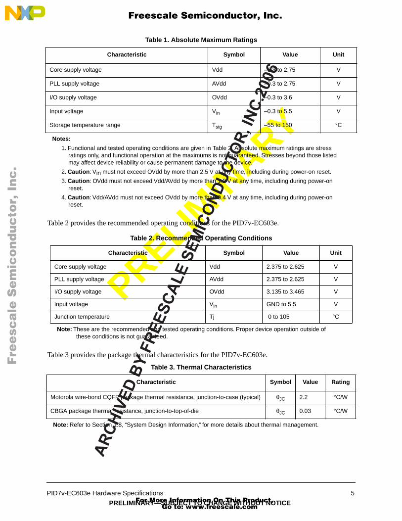
Table 2 provides the recommended operating conditions for the PID7v-EC603e.
Table 3 provides the package thermal characteristics for the PID7v-EC603e.
Table 1. Absolute Maximum Ratings
Characteristic Symbol Value Unit
Core supply voltage Vdd –0.3 to 2.75 V
PLL supply voltage AVdd –0.3 to 2.75 V
I/O supply voltage OVdd –0.3 to 3.6 V
Input voltage V
in
–0.3 to 5.5 V
Storage temperature range T
stg
–55 to 150
°
C
Notes:
1. Functional and tested operating conditions are given in Table 2. Absolute maximum ratings are stress ratings only, and functional operation at the maximums is not guaranteed. Stresses beyond those listed may affect device reliability or cause permanent damage to the device.
2.
Caution
: Vin must not exceed OVdd by more than 2.5 V at any time, including during power-on reset.
3.
Caution
: OVdd must not exceed Vdd/AVdd by more than 1.2 V at any time, including during power-on reset.
4.
Caution
: Vdd/AVdd must not exceed OVdd by more than 0.4 V at any time, including during power-on reset.
Table 2. Recommended Operating Conditions
Characteristic Symbol Value Unit
Core supply voltage Vdd 2.375 to 2.625 V
PLL supply voltage AVdd 2.375 to 2.625 V
I/O supply voltage OVdd 3.135 to 3.465 V
Input voltage V
in
GND to 5.5 V
Junction temperature Tj 0 to 105
°
C
Note:
These are the recommended and tested operating conditions. Proper device operation outside of these conditions is not guaranteed.
Table 3. Thermal Characteristics
Characteristic Symbol Value Rating
Motorola wire-bond CQFP package thermal resistance, junction-to-case (typical)
θ
JC
2.2
°
C/W
CBGA package thermal resistance, junction-to-top-of-die
θ
JC
0.03
°
C/W
Note:
Refer to Section 1.8, “System Design Information,” for more details about thermal management.
Fre
esc
ale
Se
mic
on
du
cto
r, I
Freescale Semiconductor, Inc.
For More Information On This Product, Go to: www.freescale.com
nc
...
AR
CH
IVE
D B
Y F
RE
ES
CA
LE S
EM
ICO
ND
UC
TOR
, IN
C. 2
006
PRELIMIN
ARY
6 PID7v-EC603e Hardware Specifications
PRELIMINARY—SUBJECT TO CHANGE WITHOUT NOTICE
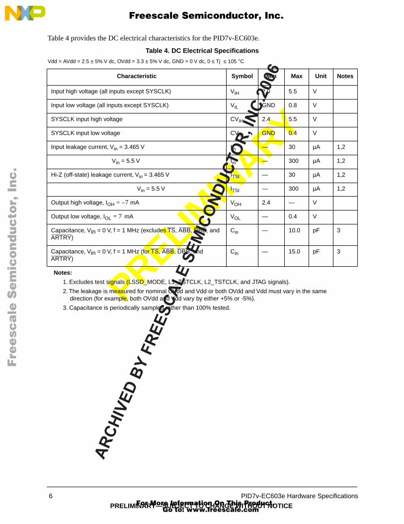
Table 4 provides the DC electrical characteristics for the PID7v-EC603e.
Table 4. DC Electrical Specifications
Vdd = AVdd = 2.5
±
5% V dc, OVdd = 3.3
±
5% V dc, GND = 0 V dc, 0
≤
Tj
≤
105
°
C
Characteristic Symbol Min Max Unit Notes
Input high voltage (all inputs except SYSCLK) V
IH
2.0 5.5 V
Input low voltage (all inputs except SYSCLK) V
IL
GND 0.8 V
SYSCLK input high voltage CV
IH
2.4 5.5 V
SYSCLK input low voltage CV
IL
GND 0.4 V
Input leakage current, V
in
= 3.465 V I
in
— 30
µ
A 1,2
V
in
= 5.5 V I
in
— 300
µ
A 1,2
Hi-Z (off-state) leakage current, V
in
= 3.465 V I
TSI
— 30
µ
A 1,2
V
in
= 5.5 V I
TSI
— 300
µ
A 1,2
Output high voltage, I
OH
= –7
mA V
OH
2.4 — V
Output low voltage, I
OL
= 7
mA V
OL
— 0.4 V
Capacitance, Vin = 0 V, f = 1 MHz (excludes TS, ABB, DBB, and ARTRY)
C
in
— 10.0 pF 3
Capacitance, Vin = 0 V, f = 1 MHz (for TS, ABB, DBB, and ARTRY)
C
in
— 15.0 pF 3
Notes:
1. Excludes test signals (LSSD_MODE, L1_TSTCLK, L2_TSTCLK, and JTAG signals).
2. The leakage is measured for nominal OVdd and Vdd or both OVdd and Vdd must vary in the same direction (for example, both OVdd and Vdd vary by either +5% or -5%).
3. Capacitance is periodically sampled rather than 100% tested.
Fre
esc
ale
Se
mic
on
du
cto
r, I
Freescale Semiconductor, Inc.
For More Information On This Product, Go to: www.freescale.com
nc
...
AR
CH
IVE
D B
Y F
RE
ES
CA
LE S
EM
ICO
ND
UC
TOR
, IN
C. 2
006
PRELIMIN
ARY
PID7v-EC603e Hardware Specifications 7
PRELIMINARY—SUBJECT TO CHANGE WITHOUT NOTICE
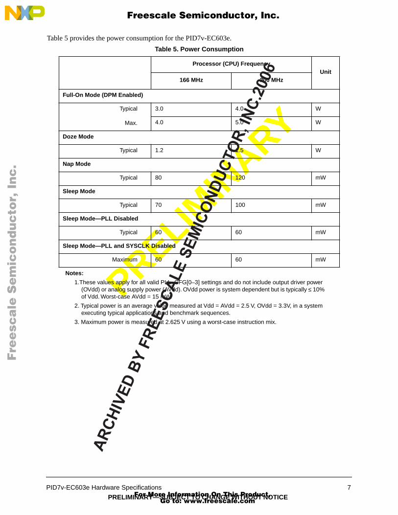
Table 5 provides the power consumption for the PID7v-EC603e.
Table 5. Power Consumption
Processor (CPU) FrequencyUnit
166 MHz 200 MHz
Full-On Mode (DPM Enabled)
Typical
Max.
3.0 4.0 W
4.0 5.0 W
Doze Mode
Typical 1.2 1.5 W
Nap Mode
Typical 80 120 mW
Sleep Mode
Typical 70 100 mW
Sleep Mode—PLL Disabled
Typical 60 60 mW
Sleep Mode—PLL and SYSCLK Disabled
Maximum 60 60 mW
Notes:
1.These values apply for all valid PLL_CFG[0–3] settings and do not include output driver power (OVdd) or analog supply power (AVdd). OVdd power is system dependent but is typically
≤
10% of Vdd. Worst-case AVdd = 15 mW.
2. Typical power is an average value measured at Vdd = AVdd = 2.5 V, OVdd = 3.3V, in a system executing typical applications and benchmark sequences.
3. Maximum power is measured at 2.625 V using a worst-case instruction mix.
Fre
esc
ale
Se
mic
on
du
cto
r, I
Freescale Semiconductor, Inc.
For More Information On This Product, Go to: www.freescale.com
nc
...
AR
CH
IVE
D B
Y F
RE
ES
CA
LE S
EM
ICO
ND
UC
TOR
, IN
C. 2
006
PRELIMIN
ARY
8 PID7v-EC603e Hardware Specifications
PRELIMINARY—SUBJECT TO CHANGE WITHOUT NOTICE
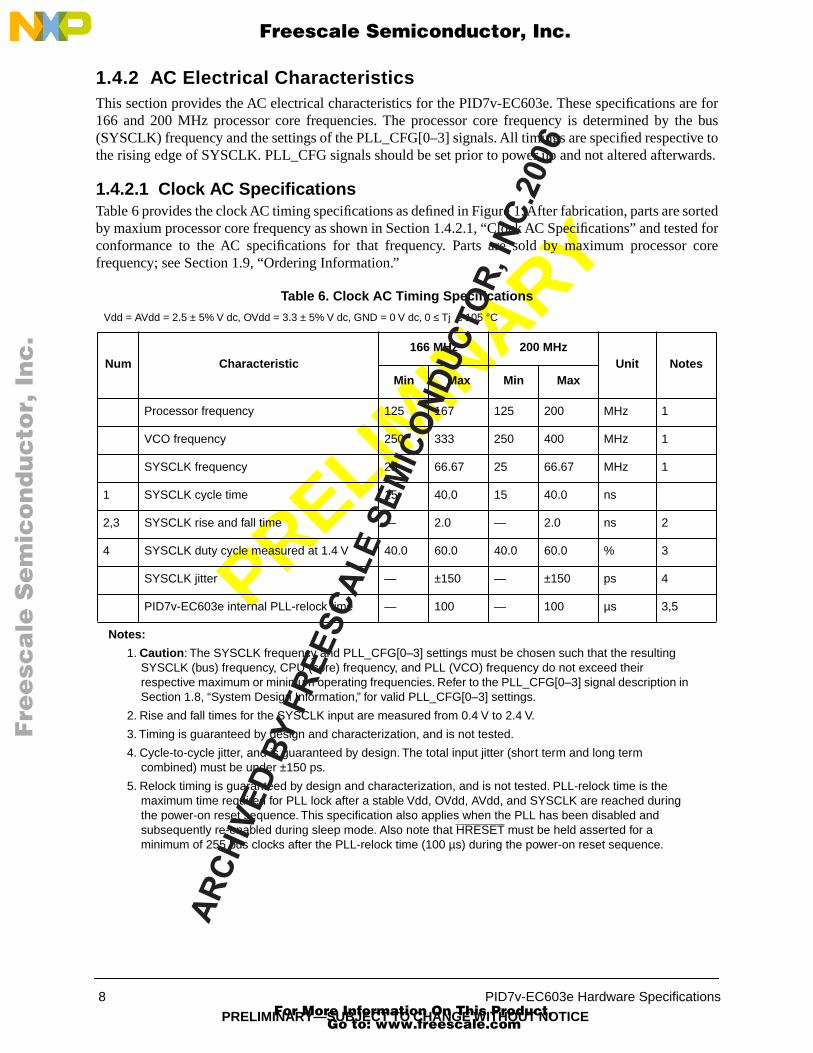
1.4.2 AC Electrical CharacteristicsThis section provides the AC electrical characteristics for the PID7v-EC603e. These specifications are for166 and 200 MHz processor core frequencies. The processor core frequency is determined by the bus(SYSCLK) frequency and the settings of the PLL_CFG[0–3] signals. All timings are specified respective tothe rising edge of SYSCLK. PLL_CFG signals should be set prior to power up and not altered afterwards.
1.4.2.1 Clock AC SpecificationsTable 6 provides the clock AC timing specifications as defined in Figure 1. After fabrication, parts are sortedby maxium processor core frequency as shown in Section 1.4.2.1, “Clock AC Specifications” and tested forconformance to the AC specifications for that frequency. Parts are sold by maximum processor corefrequency; see Section 1.9, “Ordering Information.”
Table 6. Clock AC Timing Specifications
Vdd = AVdd = 2.5 ± 5% V dc, OVdd = 3.3 ± 5% V dc, GND = 0 V dc, 0 ≤ Tj ≤ 105 °C
Num Characteristic166 MHz 200 MHz
Unit NotesMin Max Min Max
Processor frequency 125 167 125 200 MHz 1
VCO frequency 250 333 250 400 MHz 1
SYSCLK frequency 25 66.67 25 66.67 MHz 1
1 SYSCLK cycle time 15 40.0 15 40.0 ns
2,3 SYSCLK rise and fall time — 2.0 — 2.0 ns 2
4 SYSCLK duty cycle measured at 1.4 V 40.0 60.0 40.0 60.0 % 3
SYSCLK jitter — ±150 — ±150 ps 4
PID7v-EC603e internal PLL-relock time — 100 — 100 µs 3,5
Notes:
1. Caution: The SYSCLK frequency and PLL_CFG[0–3] settings must be chosen such that the resulting SYSCLK (bus) frequency, CPU (core) frequency, and PLL (VCO) frequency do not exceed their respective maximum or minimum operating frequencies. Refer to the PLL_CFG[0–3] signal description in Section 1.8, “System Design Information,” for valid PLL_CFG[0–3] settings.
2. Rise and fall times for the SYSCLK input are measured from 0.4 V to 2.4 V.
3. Timing is guaranteed by design and characterization, and is not tested.
4. Cycle-to-cycle jitter, and is guaranteed by design. The total input jitter (short term and long term combined) must be under ±150 ps.
5. Relock timing is guaranteed by design and characterization, and is not tested. PLL-relock time is the maximum time required for PLL lock after a stable Vdd, OVdd, AVdd, and SYSCLK are reached during the power-on reset sequence. This specification also applies when the PLL has been disabled and subsequently re-enabled during sleep mode. Also note that HRESET must be held asserted for a minimum of 255 bus clocks after the PLL-relock time (100 µs) during the power-on reset sequence.
Fre
esc
ale
Se
mic
on
du
cto
r, I
Freescale Semiconductor, Inc.
For More Information On This Product, Go to: www.freescale.com
nc
...
AR
CH
IVE
D B
Y F
RE
ES
CA
LE S
EM
ICO
ND
UC
TOR
, IN
C. 2
006
PRELIMIN
ARY
PID7v-EC603e Hardware Specifications 9
PRELIMINARY—SUBJECT TO CHANGE WITHOUT NOTICE
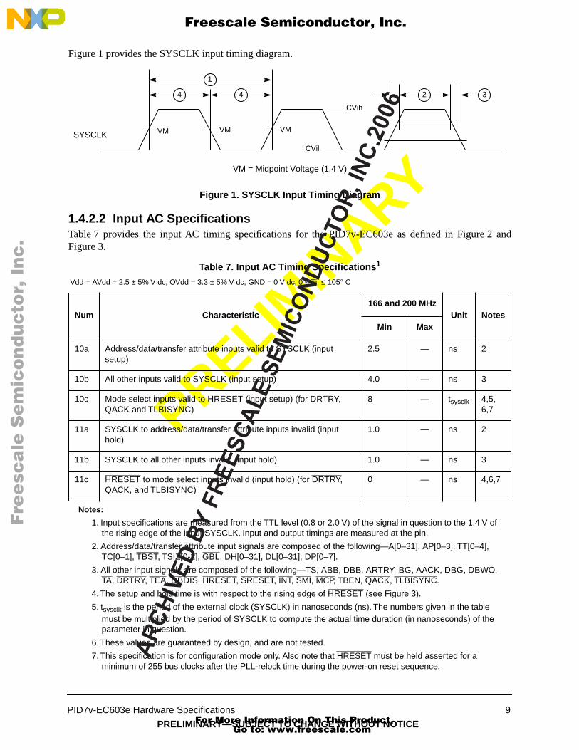
Figure 1 provides the SYSCLK input timing diagram.
Figure 1. SYSCLK Input Timing Diagram
1.4.2.2 Input AC SpecificationsTable 7 provides the input AC timing specifications for the PID7v-EC603e as defined in Figure 2 andFigure 3.
Table 7. Input AC Timing Specifications1
Vdd = AVdd = 2.5 ± 5% V dc, OVdd = 3.3 ± 5% V dc, GND = 0 V dc, 0 ≤ Tj ≤ 105° C
Num Characteristic166 and 200 MHz
Unit NotesMin Max
10a Address/data/transfer attribute inputs valid to SYSCLK (input setup)
2.5 — ns 2
10b All other inputs valid to SYSCLK (input setup) 4.0 — ns 3
10c Mode select inputs valid to HRESET (input setup) (for DRTRY, QACK and TLBISYNC)
8 — tsysclk 4,5,6,7
11a SYSCLK to address/data/transfer attribute inputs invalid (input hold)
1.0 — ns 2
11b SYSCLK to all other inputs invalid (input hold) 1.0 — ns 3
11c HRESET to mode select inputs invalid (input hold) (for DRTRY, QACK, and TLBISYNC)
0 — ns 4,6,7
Notes:
1. Input specifications are measured from the TTL level (0.8 or 2.0 V) of the signal in question to the 1.4 V of the rising edge of the input SYSCLK. Input and output timings are measured at the pin.
2. Address/data/transfer attribute input signals are composed of the following—A[0–31], AP[0–3], TT[0–4], TC[0–1], TBST, TSIZ[0-2], GBL, DH[0–31], DL[0–31], DP[0–7].
3. All other input signals are composed of the following—TS, ABB, DBB, ARTRY, BG, AACK, DBG, DBWO, TA, DRTRY, TEA, DBDIS, HRESET, SRESET, INT, SMI, MCP, TBEN, QACK, TLBISYNC.
4. The setup and hold time is with respect to the rising edge of HRESET (see Figure 3).
5. tsysclk is the period of the external clock (SYSCLK) in nanoseconds (ns). The numbers given in the table must be multiplied by the period of SYSCLK to compute the actual time duration (in nanoseconds) of the parameter in question.
6. These values are guaranteed by design, and are not tested.
7. This specification is for configuration mode only. Also note that HRESET must be held asserted for a minimum of 255 bus clocks after the PLL-relock time during the power-on reset sequence.
VM
CVil
CVih
SYSCLK
2 34
VM = Midpoint Voltage (1.4 V)
4
1
VM VM
Fre
esc
ale
Se
mic
on
du
cto
r, I
Freescale Semiconductor, Inc.
For More Information On This Product, Go to: www.freescale.com
nc
...
AR
CH
IVE
D B
Y F
RE
ES
CA
LE S
EM
ICO
ND
UC
TOR
, IN
C. 2
006
PRELIMIN
ARY
10 PID7v-EC603e Hardware Specifications
PRELIMINARY—SUBJECT TO CHANGE WITHOUT NOTICE
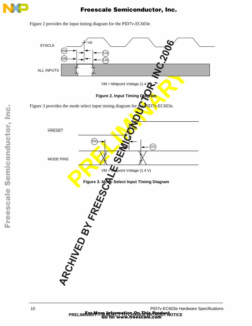
Figure 2 provides the input timing diagram for the PID7v-EC603e.
Figure 2. Input Timing Diagram
Figure 3 provides the mode select input timing diagram for the PID7v-EC603e.
Figure 3. Mode Select Input Timing Diagram
VMSYSCLK
ALL INPUTS
VM = Midpoint Voltage (1.4 V)
10a
10b
11a
11b
MODE PINS
HRESET
10c
11c
VM = Midpoint Voltage (1.4 V)
VM
Fre
esc
ale
Se
mic
on
du
cto
r, I
Freescale Semiconductor, Inc.
For More Information On This Product, Go to: www.freescale.com
nc
...
AR
CH
IVE
D B
Y F
RE
ES
CA
LE S
EM
ICO
ND
UC
TOR
, IN
C. 2
006
PRELIMIN
ARY
PID7v-EC603e Hardware Specifications 11
PRELIMINARY—SUBJECT TO CHANGE WITHOUT NOTICE
1.4.2.3 Output AC SpecificationsTable 8 provides the output AC timing specifications for the PID7v-EC603e as defined in Figure 4.
Table 8. Output AC Timing Specifications1
Vdd = AVdd = 2.5 ± 5% V dc, OVdd = 3.3 ± 5%, GND = 0 V dc, 0 ≤ Tj ≤ 105 °C, CL = 50 pF (unless otherwise noted)
Num Characteristic166 and 200 MHz
Unit NotesMin Max
12 SYSCLK to output driven (output enable time) 1.0 — ns
13a SYSCLK to output valid (5.5 V to 0.8 V—TS, ABB, ARTRY, DBB) — 9.0 ns 3
13b SYSCLK to output valid (TS, ABB, ARTRY, DBB) — 8.0 ns 5
14a SYSCLK to output valid (5.5 V to 0.8 V—all except TS, ABB, ARTRY, DBB)
— 11.0 ns 3
14b SYSCLK to output valid (all except TS, ABB, ARTRY, DBB) — 9.0 ns 5
15 SYSCLK to output invalid (output hold) 1.0 — ns 2
16 SYSCLK to output high impedance (all except ARTRY, ABB, DBB) — 8.5 ns
17 SYSCLK to ABB, DBB, high impedance after precharge — 1.0 tsysclk 4,6
18 SYSCLK to ARTRY high impedance before precharge — 8.0 ns
19 SYSCLK to ARTRY precharge enable 0.2 * tsysclk + 1.0
— ns 2,4,7
20 Maximum delay to ARTRY precharge — 1.0 tsysclk 4,7
21 SYSCLK to ARTRY high impedance after precharge — 2.0 tsysclk 5,7
Notes:
1. All output specifications are measured from the 1.4 V of the rising edge of SYSCLK to the TTL level (0.8 V or 2.0 V) of the signal in question. Both input and output timings are measured at the pin (see Figure 4).
2. This minimum parameter assumes CL = 0 pF.
3. SYSCLK to output valid (5.5 V to 0.8 V) includes the extra delay associated with discharging the external voltage from 5.5 V to 0.8 V instead of from Vdd to 0.8 V (5-V CMOS levels instead of 3.3-V CMOS levels).
4. tsysclk is the period of the external bus clock (SYSCLK) in nanoseconds (ns). The numbers given in the table must be multiplied by the period of SYSCLK to compute the actual time duration (in nanoseconds) of the parameter in question.
5. Output signal transitions from GND to 2.0 V or Vdd to 0.8 V.
6. Nominal precharge width for ABB and DBB is 0.5 tsysclk.
7. Nominal precharge width for ARTRY is 1.0 tsysclk.
Fre
esc
ale
Se
mic
on
du
cto
r, I
Freescale Semiconductor, Inc.
For More Information On This Product, Go to: www.freescale.com
nc
...
AR
CH
IVE
D B
Y F
RE
ES
CA
LE S
EM
ICO
ND
UC
TOR
, IN
C. 2
006
PRELIMIN
ARY
12 PID7v-EC603e Hardware Specifications
PRELIMINARY—SUBJECT TO CHANGE WITHOUT NOTICE
Figure 4 provides the output timing diagram for the PID7v-EC603e.
Figure 4. Output Timing Diagram
SYSCLK
12
14
13
15
16
TS
ARTRY
ABB, DBB
VM VM
VM = Midpoint Voltage (1.4 V)
VM
13
20
18
17
21
19
15
16
ALL OUTPUTS(Except TS, ABB,
DBB, ARTRY)
Fre
esc
ale
Se
mic
on
du
cto
r, I
Freescale Semiconductor, Inc.
For More Information On This Product, Go to: www.freescale.com
nc
...
AR
CH
IVE
D B
Y F
RE
ES
CA
LE S
EM
ICO
ND
UC
TOR
, IN
C. 2
006
PRELIMIN
ARY
PID7v-EC603e Hardware Specifications 13
PRELIMINARY—SUBJECT TO CHANGE WITHOUT NOTICE
1.4.3 JTAG AC Timing SpecificationsTable 9 provides the JTAG AC timing specifications as defined in Figure 5 through Figure 8.
Figure 5 provides the JTAG clock input timing diagram.
Figure 5. JTAG Clock Input Timing Diagram
Table 9. JTAG AC Timing Specifications
Vdd = AVdd = 2.5 ± 5% V dc, OVdd = 3.3 ± 5%, GND = 0 V dc, 0 ≤ Tj ≤ 105° C, CL = 50 pF
Num Characteristic Min Max Unit Notes
TCK frequency of operation 0 16 MHz
1 TCK cycle time 62.5 — ns
2 TCK clock pulse width measured at 1.4 V 25 — ns
3 TCK rise and fall times 0 3 ns
4 TRST setup time to TCK rising edge 13 — ns 1
5 TRST assert time 40 — ns
6 Boundary scan input data setup time 6 — ns 2
7 Boundary scan input data hold time 27 — ns 2
8 TCK to output data valid 4 25 ns 3
9 TCK to output high impedance 3 24 ns 3
10 TMS, TDI data setup time 0 — ns
11 TMS, TDI data hold time 25 — ns
12 TCK to TDO data valid 4 24 ns
13 TCK to TDO high impedance 3 15 ns
Notes:
1. TRST is an asynchronous signal. The setup time is for test purposes only.
2. Non-test signal input timing with respect to TCK.
3. Non-test signal output timing with respect to TCK.
TCK
22
1
VMVMVM
33
VM = Midpoint Voltage (1.4 V)
Fre
esc
ale
Se
mic
on
du
cto
r, I
Freescale Semiconductor, Inc.
For More Information On This Product, Go to: www.freescale.com
nc
...
AR
CH
IVE
D B
Y F
RE
ES
CA
LE S
EM
ICO
ND
UC
TOR
, IN
C. 2
006
PRELIMIN
ARY
14 PID7v-EC603e Hardware Specifications
PRELIMINARY—SUBJECT TO CHANGE WITHOUT NOTICE
Figure 6 provides the TRST timing diagram.
Figure 6. TRST Timing Diagram
Figure 7 provides the boundary-scan timing diagram.
Figure 7. Boundary-Scan Timing Diagram
Figure 8 provides the test access port timing diagram.
Figure 8. Test Access Port Timing Diagram
4
5
TRST
TCK VM
Input Data Valid
Output Data Valid
Output Data Valid
TCK
Data Inputs
Data Outputs
Data Outputs
Data Outputs
6 7
8
8
9
VMVM
Input Data Valid
Output Data Valid
Output Data Valid
TCK
TDI, TMS
TDO
TDO
TDO
10 11
12
12
13
VM VM
Fre
esc
ale
Se
mic
on
du
cto
r, I
Freescale Semiconductor, Inc.
For More Information On This Product, Go to: www.freescale.com
nc
...
AR
CH
IVE
D B
Y F
RE
ES
CA
LE S
EM
ICO
ND
UC
TOR
, IN
C. 2
006
PRELIMIN
ARY
PID7v-EC603e Hardware Specifications 15
PRELIMINARY—SUBJECT TO CHANGE WITHOUT NOTICE
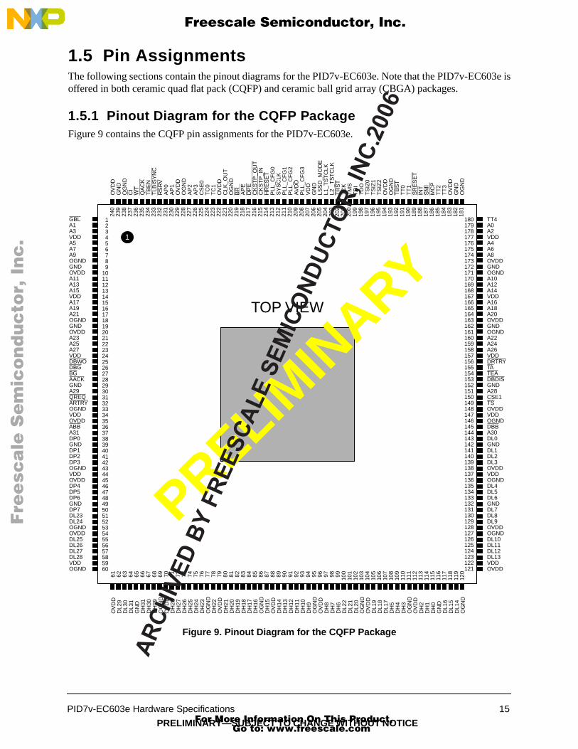
1.5 Pin AssignmentsThe following sections contain the pinout diagrams for the PID7v-EC603e. Note that the PID7v-EC603e isoffered in both ceramic quad flat pack (CQFP) and ceramic ball grid array (CBGA) packages.
1.5.1 Pinout Diagram for the CQFP PackageFigure 9 contains the CQFP pin assignments for the PID7v-EC603e.
Figure 9. Pinout Diagram for the CQFP Package
GBLA1A3VDDA5A7A9OGNDGNDOVDDA11A13A15VDDA17A19A21OGNDGNDOVDDA23A25A27VDDDBWODBGBGAACKGNDA29QREQARTRYOGNDVDDOVDDABBA31DP0GNDDP1DP2DP3OGNDVDDOVDDDP4DP5DP6GNDDP7DL23DL24OGNDOVDDDL25DL26DL27DL28VDDOGND
TT4A0A2VDDA4A6A8OVDDGNDOGNDA10A12A14VDDA16A18A20OVDDGNDOGNDA22A24A26VDDDRTRYTATEADBDISGNDA28CSE1TSOVDDVDDOGNDDBBA30DL0GNDDL1DL2DL3OVDDVDDOGNDDL4DL5DL6GNDDL7DL8DL9OVDDOGNDDL10DL11DL12DL13VDDOVDD
123456789
101112131415161718192021222324252627282930313233343536373839404142434445464748495051525354555657585960
180179178177176175174173172171170169168167166165164163162161160159158157156155154153152151150149148147146145144143142141140139138137136135134133132131130129128127126125124123122121
OV
DD
GN
DO
GN
DC
IW
TQ
AC
KT
BE
NT
LBIS
YN
CR
SR
VA
P0
AP
1O
VD
DO
GN
DA
P2
AP
3C
SE
0T
C0
TC
1O
VD
DC
LK_O
UT
OG
ND
BR
AP
ED
PE
CK
ST
P_O
UT
CK
ST
P_I
NH
RE
SE
TP
LL_C
FG
0S
YS
CLK
PLL
_CF
G1
PLL
_CF
G2
AV
DD
PLL
_CF
G3
VD
DG
ND
LSS
D_M
OD
EL1
_TS
TC
LKL2
_T
ST
CLK
TR
ST
TC
KT
MS
TD
IT
DO
TS
IZ0
TS
IZ1
TS
IZ2
OV
DD
OG
ND
TB
ST
TT
0T
T1
SR
ES
ET
INT
SM
IM
CP
TT
2T
T3
OV
DD
GN
DO
GN
D
240
239
238
237
236
235
234
233
232
231
230
229
228
227
226
225
224
223
222
221
220
219
218
217
216
215
214
213
212
211
210
209
208
207
206
205
204
203
202
201
200
199
198
197
196
195
194
193
192
191
190
189
188
187
186
185
184
183
182
181
OV
DD
DL2
9D
L30
DL3
1G
ND
DH
31D
H30
DH
29O
GN
DO
VD
DD
H28
DH
27D
H26
DH
25D
H24
DH
23O
GN
DD
H22
OV
DD
DH
21D
H20
DH
19D
H18
DH
17D
H16
OG
ND
DH
15O
VD
DD
H14
DH
13D
H12
DH
11D
H10
DH
9O
GN
DO
VD
DD
H8
DH
7D
H6
DL2
2D
L21
DL2
0O
GN
DO
VD
DD
L19
DL1
8D
L17
DH
5D
H4
DH
3O
GN
DO
VD
DD
H2
DH
1D
H0
GN
DD
L16
DL1
5D
L14
OG
ND
61 62 63 64 65 66 67 68 69 70 71 72 73 74 75 76 77 78 79 80 81 82 83 84 85 86 87 88 89 90 91 92 93 94 95 96 97 98 99 100
101
102
103
104
105
106
107
108
109
110
111
112
113
114
115
116
117
118
119
120
1
TOP VIEW
PRELIMIN
ARY
Fre
esc
ale
Se
mic
on
du
cto
r, I
Freescale Semiconductor, Inc.
For More Information On This Product, Go to: www.freescale.com
nc
...
AR
CH
IVE
D B
Y F
RE
ES
CA
LE S
EM
ICO
ND
UC
TOR
, IN
C. 2
006
PRELIMIN
ARY
16 PID7v-EC603e Hardware Specifications
PRELIMINARY—SUBJECT TO CHANGE WITHOUT NOTICE
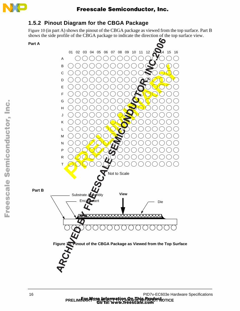
1.5.2 Pinout Diagram for the CBGA PackageFigure 10 (in part A) shows the pinout of the CBGA package as viewed from the top surface. Part Bshows the side profile of the CBGA package to indicate the direction of the top surface view.
Part A
Figure 10. Pinout of the CBGA Package as Viewed from the Top Surface
A
B
C
D
E
F
G
H
J
K
L
M
N
P
R
T
01 02 03 04 05 06 07 08 09 10 11 12 13 14 15 16
Not to Scale
Part BSubstrate Assembly
Encapsulant
View
Die
Fre
esc
ale
Se
mic
on
du
cto
r, I
Freescale Semiconductor, Inc.
For More Information On This Product, Go to: www.freescale.com
nc
...
AR
CH
IVE
D B
Y F
RE
ES
CA
LE S
EM
ICO
ND
UC
TOR
, IN
C. 2
006
PRELIMIN
ARY
PID7v-EC603e Hardware Specifications 17
PRELIMINARY—SUBJECT TO CHANGE WITHOUT NOTICE
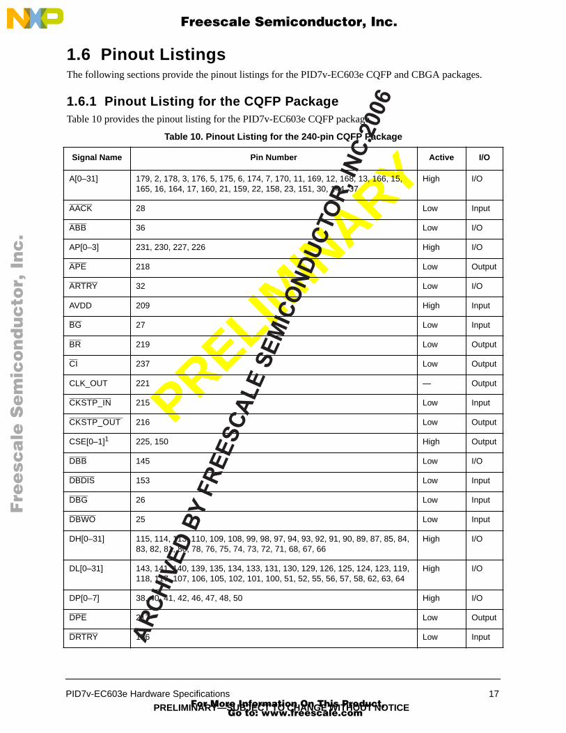
1.6 Pinout ListingsThe following sections provide the pinout listings for the PID7v-EC603e CQFP and CBGA packages.
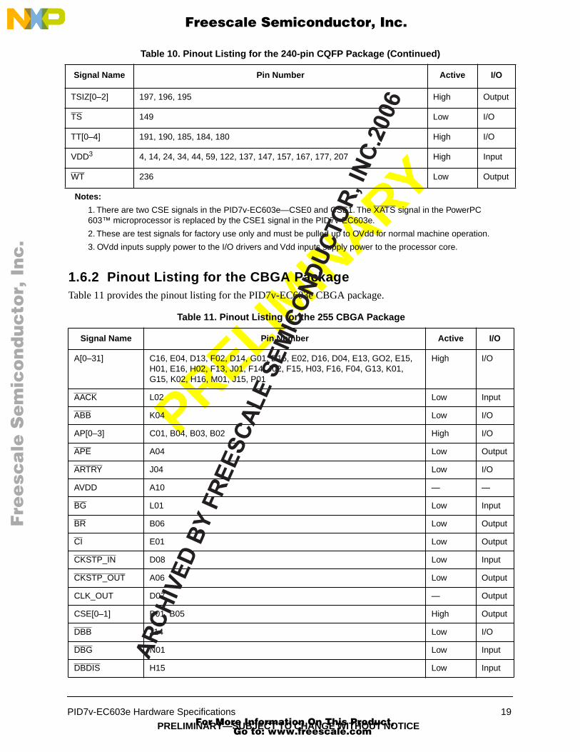
1.6.1 Pinout Listing for the CQFP PackageTable 10 provides the pinout listing for the PID7v-EC603e CQFP package.
Table 10. Pinout Listing for the 240-pin CQFP Package
Signal Name Pin Number Active I/O
A[0–31] 179, 2, 178, 3, 176, 5, 175, 6, 174, 7, 170, 11, 169, 12, 168, 13, 166, 15, 165, 16, 164, 17, 160, 21, 159, 22, 158, 23, 151, 30, 144, 37
High I/O
AACK 28 Low Input
ABB 36 Low I/O
AP[0–3] 231, 230, 227, 226 High I/O
APE 218 Low Output
ARTRY 32 Low I/O
AVDD 209 High Input
BG 27 Low Input
BR 219 Low Output
CI 237 Low Output
CLK_OUT 221 — Output
CKSTP_IN 215 Low Input
CKSTP_OUT 216 Low Output
CSE[0–1]1 225, 150 High Output
DBB 145 Low I/O
DBDIS 153 Low Input
DBG 26 Low Input
DBWO 25 Low Input
DH[0–31] 115, 114, 113, 110, 109, 108, 99, 98, 97, 94, 93, 92, 91, 90, 89, 87, 85, 84, 83, 82, 81, 80, 78, 76, 75, 74, 73, 72, 71, 68, 67, 66
High I/O
DL[0–31] 143, 141, 140, 139, 135, 134, 133, 131, 130, 129, 126, 125, 124, 123, 119, 118, 117, 107, 106, 105, 102, 101, 100, 51, 52, 55, 56, 57, 58, 62, 63, 64
High I/O
DP[0–7] 38, 40, 41, 42, 46, 47, 48, 50 High I/O
DPE 217 Low Output
DRTRY 156 Low Input
Fre
esc
ale
Se
mic
on
du
cto
r, I
Freescale Semiconductor, Inc.
For More Information On This Product, Go to: www.freescale.com
nc
...
AR
CH
IVE
D B
Y F
RE
ES
CA
LE S
EM
ICO
ND
UC
TOR
, IN
C. 2
006
PRELIMIN
ARY
18 PID7v-EC603e Hardware Specifications
PRELIMINARY—SUBJECT TO CHANGE WITHOUT NOTICE
GBL 1 Low I/O
GND 9, 19, 29, 39, 49, 65, 116, 132, 142, 152, 162, 172, 182, 206, 239 Low Input
HRESET 214 Low Input
INT 188 Low Input
LSSD_MODE2 205 Low Input
L1_TSTCLK2 204 — Input
L2_TSTCLK2 203 — Input
MCP 186 Low Input
OGND 8, 18, 33, 43, 53, 60, 69, 77, 86, 95, 103, 111, 120, 127, 136, 146, 161, 171, 181, 193, 220, 228, 238
Low Input
OVDD3 10, 20, 35, 45, 54, 61, 70, 79, 88, 96, 104, 112, 121, 128, 138, 148, 163, 173, 183, 194, 222, 229, 240
High Input
PLL_CFG[0–3] 213, 211, 210, 208 High Input
QACK 235 Low Input
QREQ 31 Low Output
RSRV 232 Low Output
SMI 187 Low Input
SRESET 189 Low Input
SYSCLK 212 — Input
TA 155 Low Input
TBEN 234 High Input
TBST 192 Low I/O
TC[0–1] 224, 223 High Output
TCK 201 — Input
TDI 199 High Input
TDO 198 High Output
TEA 154 Low Input
TLBISYNC 233 Low Input
TMS 200 High Input
TRST 202 Low Input
Table 10. Pinout Listing for the 240-pin CQFP Package (Continued)
Signal Name Pin Number Active I/O
Fre
esc
ale
Se
mic
on
du
cto
r, I
Freescale Semiconductor, Inc.
For More Information On This Product, Go to: www.freescale.com
nc
...
AR
CH
IVE
D B
Y F
RE
ES
CA
LE S
EM
ICO
ND
UC
TOR
, IN
C. 2
006
PRELIMIN
ARY
PID7v-EC603e Hardware Specifications 19
PRELIMINARY—SUBJECT TO CHANGE WITHOUT NOTICE
1.6.2 Pinout Listing for the CBGA PackageTable 11 provides the pinout listing for the PID7v-EC603e CBGA package.
TSIZ[0–2] 197, 196, 195 High Output
TS 149 Low I/O
TT[0–4] 191, 190, 185, 184, 180 High I/O
VDD3 4, 14, 24, 34, 44, 59, 122, 137, 147, 157, 167, 177, 207 High Input
WT 236 Low Output
Notes:
1. There are two CSE signals in the PID7v-EC603e—CSE0 and CSE1. The XATS signal in the PowerPC 603™ microprocessor is replaced by the CSE1 signal in the PID7v-EC603e.
2. These are test signals for factory use only and must be pulled up to OVdd for normal machine operation.
3. OVdd inputs supply power to the I/O drivers and Vdd inputs supply power to the processor core.
Table 11. Pinout Listing for the 255 CBGA Package
Signal Name Pin Number Active I/O
A[0–31] C16, E04, D13, F02, D14, G01, D15, E02, D16, D04, E13, GO2, E15, H01, E16, H02, F13, J01, F14, J02, F15, H03, F16, F04, G13, K01, G15, K02, H16, M01, J15, P01
High I/O
AACK L02 Low Input
ABB K04 Low I/O
AP[0–3] C01, B04, B03, B02 High I/O
APE A04 Low Output
ARTRY J04 Low I/O
AVDD A10 — —
BG L01 Low Input
BR B06 Low Output
CI E01 Low Output
CKSTP_IN D08 Low Input
CKSTP_OUT A06 Low Output
CLK_OUT D07 — Output
CSE[0–1] B01, B05 High Output
DBB J14 Low I/O
DBG N01 Low Input
DBDIS H15 Low Input
Table 10. Pinout Listing for the 240-pin CQFP Package (Continued)
Signal Name Pin Number Active I/O
Fre
esc
ale
Se
mic
on
du
cto
r, I
Freescale Semiconductor, Inc.
For More Information On This Product, Go to: www.freescale.com
nc
...
AR
CH
IVE
D B
Y F
RE
ES
CA
LE S
EM
ICO
ND
UC
TOR
, IN
C. 2
006
PRELIMIN
ARY
20 PID7v-EC603e Hardware Specifications
PRELIMINARY—SUBJECT TO CHANGE WITHOUT NOTICE
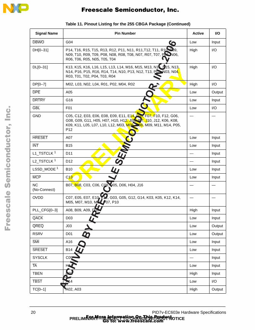
DBWO G04 Low Input
DH[0–31] P14, T16, R15, T15, R13, R12, P11, N11, R11,T12, T11, R10, P09, N09, T10, R09, T09, P08, N08, R08, T08, N07, R07, T07, P06, N06, R06, T06, R05, N05, T05, T04
High I/O
DL[0–31] K13, K15, K16, L16, L15, L13, L14, M16, M15, M13, N16, N15, N13, N14, P16, P15, R16, R14, T14, N10, P13, N12, T13, P03, N03, N04, R03, T01, T02, P04, T03, R04
High I/O
DP[0–7] M02, L03, N02, L04, R01, P02, M04, R02 High I/O
DPE A05 Low Output
DRTRY G16 Low Input
GBL F01 Low I/O
GND C05, C12, E03, E06, E08, E09, E11, E14, F05, F07, F10, F12, G06, G08, G09, G11, H05, H07, H10, H12, J05, J07, J10, J12, K06, K08, K09, K11, L05, L07, L10, L12, M03, M06, M08, M09, M11, M14, P05, P12
— —
HRESET A07 Low Input
INT B15 Low Input
L1_TSTCLK 1 D11 — Input
L2_TSTCLK 1 D12 — Input
LSSD_MODE 1 B10 Low Input
MCP C13 Low Input
NC (No-Connect)
B07, B08, C03, C06, C08, D05, D06, H04, J16 — —
OVDD C07, E05, E07, E10, E12, G03, G05, G12, G14, K03, K05, K12, K14, M05, M07, M10, M12, P07, P10
— —
PLL_CFG[0–3] A08, B09, A09, D09 High Input
QACK D03 Low Input
QREQ J03 Low Output
RSRV D01 Low Output
SMI A16 Low Input
SRESET B14 Low Input
SYSCLK C09 — Input
TA H14 Low Input
TBEN C02 High Input
TBST A14 Low I/O
TC[0–1] A02, A03 High Output
Table 11. Pinout Listing for the 255 CBGA Package (Continued)
Signal Name Pin Number Active I/O
Fre
esc
ale
Se
mic
on
du
cto
r, I
Freescale Semiconductor, Inc.
For More Information On This Product, Go to: www.freescale.com
nc
...
AR
CH
IVE
D B
Y F
RE
ES
CA
LE S
EM
ICO
ND
UC
TOR
, IN
C. 2
006
PRELIMIN
ARY
PID7v-EC603e Hardware Specifications 21
PRELIMINARY—SUBJECT TO CHANGE WITHOUT NOTICE
1.7 Package DescriptionsThe following sections provide the package parameters and the mechanical dimensions for the PID7v-EC603e. Note that the PID7v-EC603e is currently offered in two types of CQFP packages—the Motorolawire-bond CQFP and the ceramic ball grid array (CBGA) package.
1.7.1 Motorola Wire-Bond CQFP Package DescriptionThe following sections provide the package parameters and mechanical dimensions for the Motorola wire-bond CQFP package.
1.7.1.1 Package ParametersThe package parameters are as provided in the following list. The package type is 32 mm x 32 mm, 240-pinceramic quad flat pack.
Package outline 32 mm x 32 mm
Interconnects 240
Pitch 0.5 mm (20 mil)
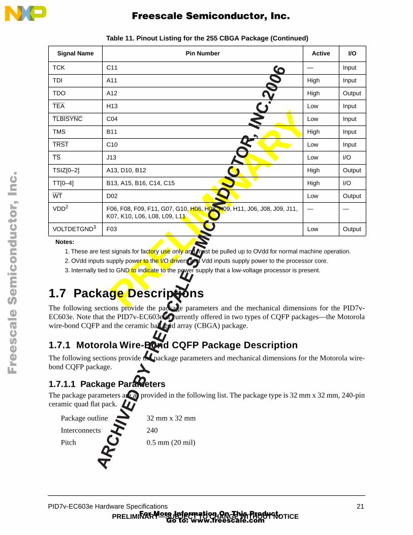
TCK C11 — Input
TDI A11 High Input
TDO A12 High Output
TEA H13 Low Input
TLBISYNC C04 Low Input
TMS B11 High Input
TRST C10 Low Input
TS J13 Low I/O
TSIZ[0–2] A13, D10, B12 High Output
TT[0–4] B13, A15, B16, C14, C15 High I/O
WT D02 Low Output
VDD2 F06, F08, F09, F11, G07, G10, H06, H08, H09, H11, J06, J08, J09, J11, K07, K10, L06, L08, L09, L11
— —
VOLTDETGND3 F03 Low Output
Notes:
1. These are test signals for factory use only and must be pulled up to OVdd for normal machine operation.
2. OVdd inputs supply power to the I/O drivers and Vdd inputs supply power to the processor core.
3. Internally tied to GND to indicate to the power supply that a low-voltage processor is present.
Table 11. Pinout Listing for the 255 CBGA Package (Continued)
Signal Name Pin Number Active I/O
Fre
esc
ale
Se
mic
on
du
cto
r, I
Freescale Semiconductor, Inc.
For More Information On This Product, Go to: www.freescale.com
nc
...
AR
CH
IVE
D B
Y F
RE
ES
CA
LE S
EM
ICO
ND
UC
TOR
, IN
C. 2
006
PRELIMIN
ARY
22 PID7v-EC603e Hardware Specifications
PRELIMINARY—SUBJECT TO CHANGE WITHOUT NOTICE
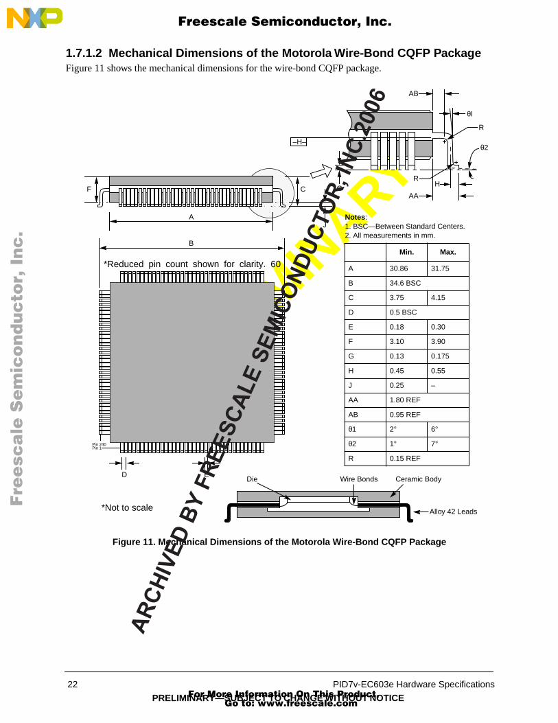
1.7.1.2 Mechanical Dimensions of the Motorola Wire-Bond CQFP PackageFigure 11 shows the mechanical dimensions for the wire-bond CQFP package.
Figure 11. Mechanical Dimensions of the Motorola Wire-Bond CQFP Package
Min. Max.
A 30.86 31.75
B 34.6 BSC
C 3.75 4.15
D 0.5 BSC
E 0.18 0.30
F 3.10 3.90
G 0.13 0.175
H 0.45 0.55
J 0.25 –
AA 1.80 REF
AB 0.95 REF
θ1 2° 6°
θ2 1° 7°
R 0.15 REF
–H–
AB
θI
R
R
AA
θ2
H
Pin 240
C
A
B
Pin 1
D E
*Not to scale
GF
J
Die Wire Bonds Ceramic Body
Alloy 42 Leads
Notes: 1. BSC—Between Standard Centers.2. All measurements in mm.
*Reduced pin count shown for clarity. 60
Fre
esc
ale
Se
mic
on
du
cto
r, I
Freescale Semiconductor, Inc.
For More Information On This Product, Go to: www.freescale.com
nc
...
AR
CH
IVE
D B
Y F
RE
ES
CA
LE S
EM
ICO
ND
UC
TOR
, IN
C. 2
006
PRELIMIN
ARY
PID7v-EC603e Hardware Specifications 23
PRELIMINARY—SUBJECT TO CHANGE WITHOUT NOTICE
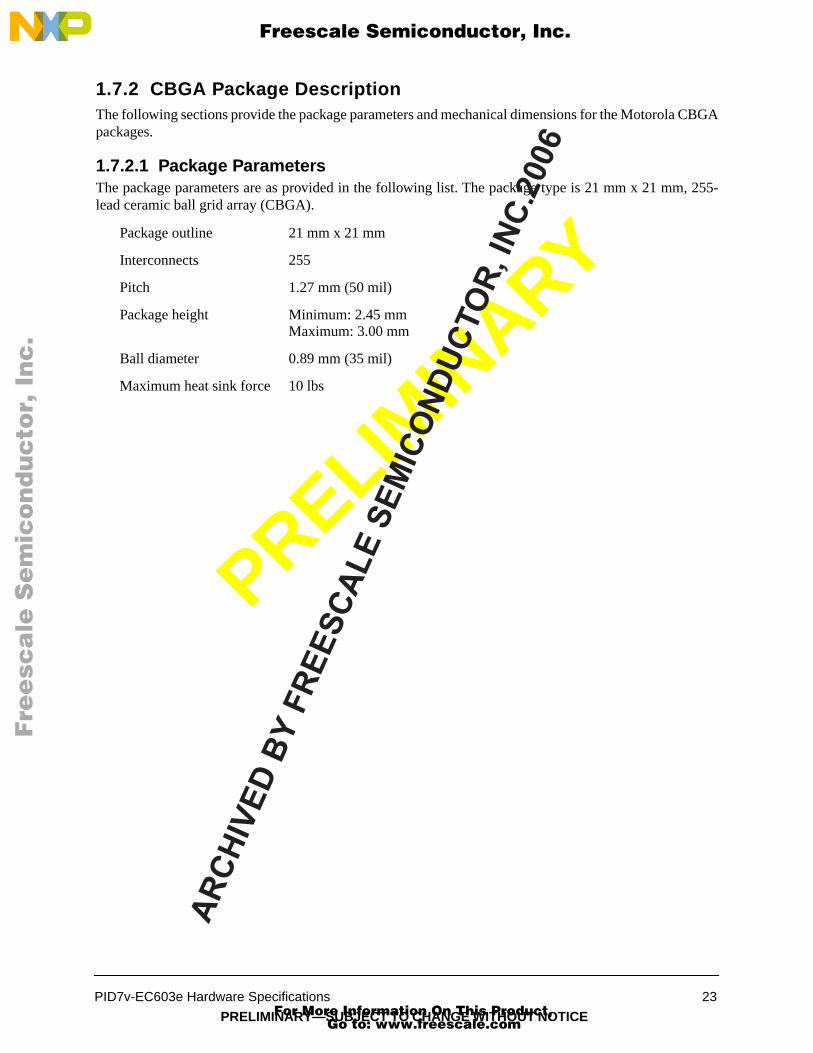
1.7.2 CBGA Package DescriptionThe following sections provide the package parameters and mechanical dimensions for the Motorola CBGApackages.
1.7.2.1 Package ParametersThe package parameters are as provided in the following list. The package type is 21 mm x 21 mm, 255-lead ceramic ball grid array (CBGA).
Package outline 21 mm x 21 mm
Interconnects 255
Pitch 1.27 mm (50 mil)
Package height Minimum: 2.45 mm Maximum: 3.00 mm
Ball diameter 0.89 mm (35 mil)
Maximum heat sink force 10 lbs
Fre
esc
ale
Se
mic
on
du
cto
r, I
Freescale Semiconductor, Inc.
For More Information On This Product, Go to: www.freescale.com
nc
...
AR
CH
IVE
D B
Y F
RE
ES
CA
LE S
EM
ICO
ND
UC
TOR
, IN
C. 2
006
PRELIMIN
ARY
24 PID7v-EC603e Hardware Specifications
PRELIMINARY—SUBJECT TO CHANGE WITHOUT NOTICE
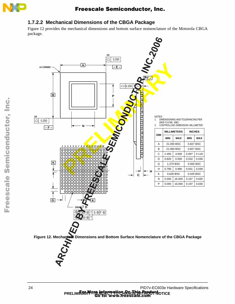
1.7.2.2 Mechanical Dimensions of the CBGA PackageFigure 12 provides the mechanical dimensions and bottom surface nomenclature of the Motorola CBGApackage.
Figure 12. Mechanical Dimensions and Bottom Surface Nomenclature of the CBGA Package
DIMMILLIMETERS INCHES
MIN MAX MIN MAX
A 21.000 BSC 0.827 BSC
B 21.000 BSC 0.827 BSC
C 2.450 3.000 0.097 0.118
D 0.820 0.930 0.032 0.036
G 1.270 BSC 0.050 BSC
H 0.790 0.990 0.031 0.039
K 0.635 BSC 0.025 BSC
N 5.000 16.000 0.197 0.630
P 5.000 16.000 0.197 0.630
NOTES:1. DIMENSIONING AND TOLERANCING PER
ANSI Y14.5M, 1982.2. CONTROLLING DIMENSION: MILLIMETER.
0.200
FT
255X
A
2X
A1 CORNER
P
N
0.200
2X
– E –
1 2 3 4 5 6 7 8 9 10 11 12 13 14 15 16
ABCDEFGHJKLMNPRT
E0.300
T0.150
D
CH
0.150 T
B
– F –
K
K
G
S
S
S S
– T –
Fre
esc
ale
Se
mic
on
du
cto
r, I
Freescale Semiconductor, Inc.
For More Information On This Product, Go to: www.freescale.com
nc
...
AR
CH
IVE
D B
Y F
RE
ES
CA
LE S
EM
ICO
ND
UC
TOR
, IN
C. 2
006
PRELIMIN
ARY
PID7v-EC603e Hardware Specifications 25
PRELIMINARY—SUBJECT TO CHANGE WITHOUT NOTICE
1.8 System Design InformationThis section provides electrical and thermal design recommendations for successful application of thePID7v-EC603e.
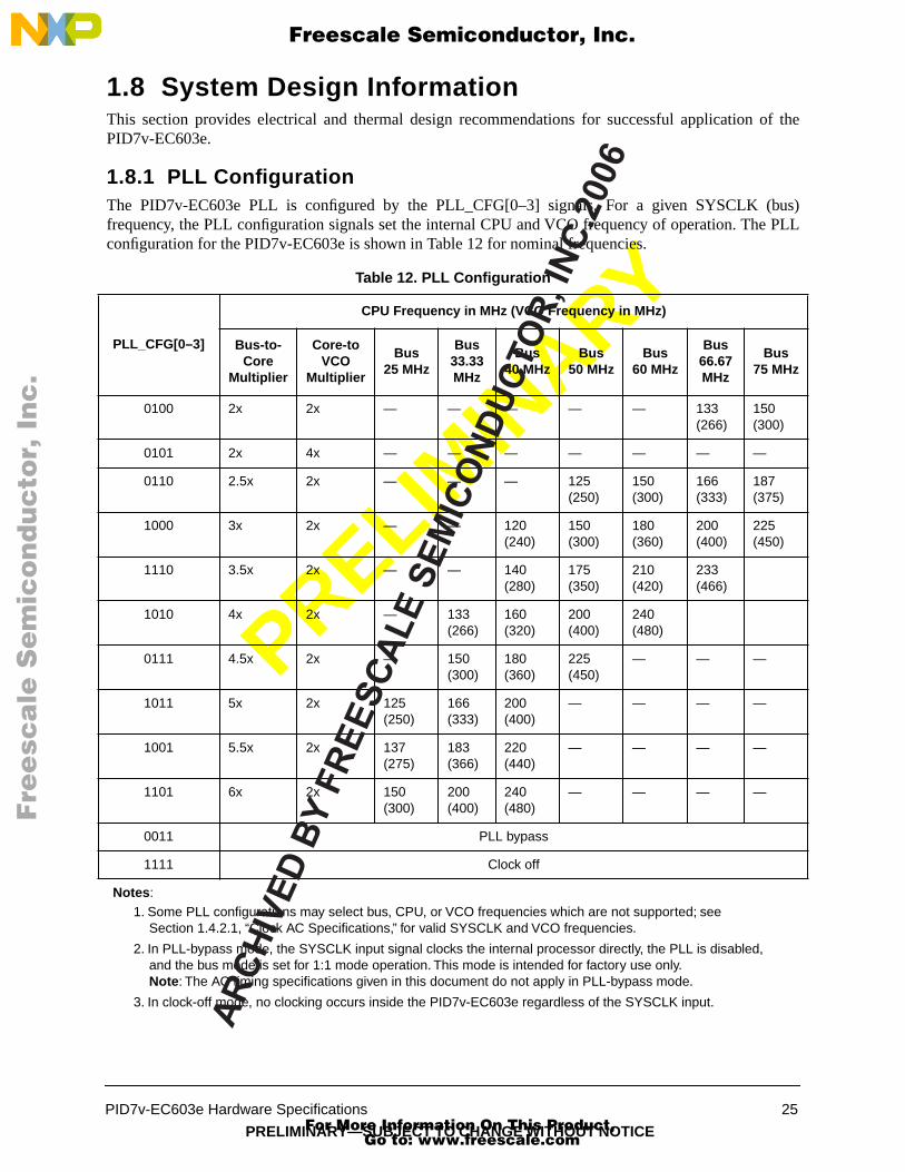
1.8.1 PLL ConfigurationThe PID7v-EC603e PLL is configured by the PLL_CFG[0–3] signals. For a given SYSCLK (bus)frequency, the PLL configuration signals set the internal CPU and VCO frequency of operation. The PLLconfiguration for the PID7v-EC603e is shown in Table 12 for nominal frequencies.
Table 12. PLL Configuration
PLL_CFG[0–3]
CPU Frequency in MHz (VCO Frequency in MHz)
Bus-to-Core
Multiplier
Core-toVCO
Multiplier
Bus25 MHz
Bus33.33 MHz
Bus40 MHz
Bus50 MHz
Bus60 MHz
Bus66.67 MHz
Bus75 MHz
0100 2x 2x — — — — — 133 (266)
150(300)
0101 2x 4x — — — — — — —
0110 2.5x 2x — — — 125(250)
150(300)
166(333)
187(375)
1000 3x 2x — — 120 (240)
150(300)
180(360)
200(400)
225(450)
1110 3.5x 2x — — 140(280)
175(350)
210 (420)
233 (466)
1010 4x 2x — 133(266)
160(320)
200(400)
240 (480)
0111 4.5x 2x — 150(300)
180(360)
225 (450)
— — —
1011 5x 2x 125(250)
166(333)
200(400)
— — — —
1001 5.5x 2x 137(275)
183 (366)
220 (440)
— — — —
1101 6x 2x 150(300)
200(400)
240 (480)
— — — —
0011 PLL bypass
1111 Clock off
Notes: 1. Some PLL configurations may select bus, CPU, or VCO frequencies which are not supported; see
Section 1.4.2.1, “Clock AC Specifications,” for valid SYSCLK and VCO frequencies.
2. In PLL-bypass mode, the SYSCLK input signal clocks the internal processor directly, the PLL is disabled, and the bus mode is set for 1:1 mode operation. This mode is intended for factory use only. Note: The AC timing specifications given in this document do not apply in PLL-bypass mode.
3. In clock-off mode, no clocking occurs inside the PID7v-EC603e regardless of the SYSCLK input.
Fre
esc
ale
Se
mic
on
du
cto
r, I
Freescale Semiconductor, Inc.
For More Information On This Product, Go to: www.freescale.com
nc
...
AR
CH
IVE
D B
Y F
RE
ES
CA
LE S
EM
ICO
ND
UC
TOR
, IN
C. 2
006
PRELIMIN
ARY
26 PID7v-EC603e Hardware Specifications
PRELIMINARY—SUBJECT TO CHANGE WITHOUT NOTICE
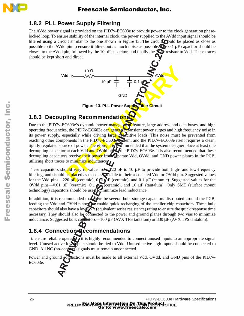
1.8.2 PLL Power Supply FilteringThe AVdd power signal is provided on the PID7v-EC603e to provide power to the clock generation phase-locked loop. To ensure stability of the internal clock, the power supplied to the AVdd input signal should befiltered using a circuit similar to the one shown in Figure 13. The circuit should be placed as close aspossible to the AVdd pin to ensure it filters out as much noise as possible. The 0.1 µF capacitor should beclosest to the AVdd pin, followed by the 10 µF capacitor, and finally the 10 Ω resistor to Vdd. These tracesshould be kept short and direct.
Figure 13. PLL Power Supply Filter Circuit
1.8.3 Decoupling RecommendationsDue to the PID7v-EC603e’s dynamic power management feature, large address and data buses, and highoperating frequencies, the PID7v-EC603e can generate transient power surges and high frequency noise inits power supply, especially while driving large capacitive loads. This noise must be prevented fromreaching other components in the PID7v-EC603e system, and the PID7v-EC603e itself requires a clean,tightly regulated source of power. Therefore, it is recommended that the system designer place at least onedecoupling capacitor at each Vdd and OVdd pin of the PID7v-EC603e. It is also recommended that thesedecoupling capacitors receive their power from separate Vdd, OVdd, and GND power planes in the PCB,utilizing short traces to minimize inductance.
These capacitors should vary in value from 220 pF to 10 µF to provide both high- and low-frequencyfiltering, and should be placed as close as possible to their associated Vdd or OVdd pin. Suggested valuesfor the Vdd pins—220 pF (ceramic), 0.01 µF (ceramic), and 0.1 µF (ceramic). Suggested values for theOVdd pins—0.01 µF (ceramic), 0.1 µF (ceramic), and 10 µF (tantalum). Only SMT (surface mounttechnology) capacitors should be used to minimize lead inductance.
In addition, it is recommended that there be several bulk storage capacitors distributed around the PCB,feeding the Vdd and OVdd planes, to enable quick recharging of the smaller chip capacitors. These bulkcapacitors should also have a low ESR (equivalent series resistance) rating to ensure the quick response timenecessary. They should also be connected to the power and ground planes through two vias to minimizeinductance. Suggested bulk capacitors—100 µF (AVX TPS tantalum) or 330 µF (AVX TPS tantalum).
1.8.4 Connection RecommendationsTo ensure reliable operation, it is highly recommended to connect unused inputs to an appropriate signallevel. Unused active low inputs should be tied to Vdd. Unused active high inputs should be connected toGND. All NC (no-connect) signals must remain unconnected.
Power and ground connections must be made to all external Vdd, OVdd, and GND pins of the PID7v-EC603e.
Vdd AVdd 10 Ω
10 µF 0.1 µF
GND
Fre
esc
ale
Se
mic
on
du
cto
r, I
Freescale Semiconductor, Inc.
For More Information On This Product, Go to: www.freescale.com
nc
...
AR
CH
IVE
D B
Y F
RE
ES
CA
LE S
EM
ICO
ND
UC
TOR
, IN
C. 2
006
PRELIMIN
ARY
PID7v-EC603e Hardware Specifications 27
PRELIMINARY—SUBJECT TO CHANGE WITHOUT NOTICE
1.8.5 Pull-up Resistor RequirementsThe PID7v-EC603e requires high-resistive (weak: 10 KΩ) pull-up resistors on several control signals of thebus interface to maintain the control signals in the negated state after they have been actively negated andreleased by the PID7v-EC603e or other bus master. These signals are—TS, ABB, DBB, and ARTRY.
In addition, the PID7v-EC603e has three open-drain style outputs that require pull-up resistors (weak orstronger: 4.7 KΩ–10 KΩ) if they are used by the system. These signals are—APE, DPE, and CKSTP_OUT.
During inactive periods on the bus, the address and transfer attributes on the bus are not driven by any masterand may float in the high-impedance state for relatively long periods of time. Since the PID7v-EC603e mustcontinually monitor these signals for snooping, this float condition may cause excessive power draw by theinput receivers on the PID7v-EC603e. It is recommended that these signals be pulled up through weak (10KΩ) pull-up resistors or restored in some manner by the system. The snooped address and transfer attributeinputs are—A[0–31], AP[0–3], TT[0–4], TBST, and GBL.
The data bus input receivers are normally turned off when no read operation is in progress and do not requirepull-up resistors on the data bus.
1.8.6 Thermal Management Information This section provides thermal management data for the PID7v-EC603e. The information found in the firstsub-sections is based on a typical desktop configuration using a 240 lead, 32 mm x 32 mm, Motorola wire-bond CQFP package. The heat sink used for this data is a pinfin configuration from Thermalloy, part number2338. The data found in the subsequent sub-sections concerns PID7v-EC603e’s packaged in the 255-lead21 mm multi-layer ceramic (MLC), ceramic BGA package. Data is shown for two cases, the exposed-diecase (no heat sink) and using the Thermalloy 2338-pin fin heat sink.
1.8.6.1 Motorola Wire-Bond CQFP PackageThis section provides thermal management data for the PID7v-EC603e; this information is based on atypical desktop configuration using a 240 lead, 32 mm x 32 mm, Motorola wire-bond CQFP package. Theheat sink used for this data is a pinfin configuration from Thermalloy, part number 2338.
1.8.6.1.1 Thermal Characteristics The thermal characteristics for a wire-bond CQFP package are as follows:
Thermal resistance (junction-to-case) = Rθjc or θjc = 2.2° C/Watt (junction-to-case)
1.8.6.1.2 Thermal Management ExampleThe following example is based on a typical desktop configuration using a Motorola wire-bond CQFPpackage. The heat sink used for this data is a pinfin heat sink #2338 attached to the wire-bond CQFPpackage with thermal grease.
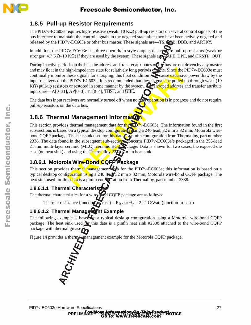
Figure 14 provides a thermal management example for the Motorola CQFP package.
Fre
esc
ale
Se
mic
on
du
cto
r, I
Freescale Semiconductor, Inc.
For More Information On This Product, Go to: www.freescale.com
nc
...
AR
CH
IVE
D B
Y F
RE
ES
CA
LE S
EM
ICO
ND
UC
TOR
, IN
C. 2
006
PRELIMIN
ARY
28 PID7v-EC603e Hardware Specifications
PRELIMINARY—SUBJECT TO CHANGE WITHOUT NOTICE
Figure 14. Motorola CQFP Thermal Management Example
The junction temperature can be calculated from the junction-to-ambient thermal resistance, as follows:
Junction temperature: Tj = Ta + Rθja * P
or
Tj = Ta + (Rθjc + Rcs + Rsa) * P
Where:
Ta is the ambient temperature in the vicinity of the device
Rθja is the junction-to-ambient thermal resistance
Rθjc is the junction-to-case thermal resistance of the device
Rcs is the case-to-heat sink thermal resistance of the interface material
Rsa is the heat sink-to-ambient thermal resistance
P is the power consumed by the device
In this environment, it can be assumed that all the heat is consumed to the ambient through the heat sink, sothe junction-to-ambient thermal resistance is the sum of the resistances from the junction to the case, fromthe case to the heat sink, and from the heat sink to the ambient.
Note that verification of external thermal resistance and case temperature should be performed for eachapplication. Thermal resistance can vary considerably due to many factors including degree of airturbulence.
For a power consumption of 2.5 Watts in an ambient temperature of 40 °C at 1 m/sec with the heat sinkmeasured above, the junction temperature of the device would be as follows:
Tj = Ta + Rθja * P
Tj = 40 °C + (10 °C/Watt * 2.5 Watts) = 65 °C
which is well within the reliability limits of the device.
0 1 2 3 5
0
5
10
15
20
25
30
35
Motorola Wire-Bond CQFP
With Heat Sink
Forced Convection (m/sec)
Jun
ctio
n-t
o-A
mb
ien
t Th
erm
al
Res
ista
nce
(°C
/wat
t)
4
Fre
esc
ale
Se
mic
on
du
cto
r, I
Freescale Semiconductor, Inc.
For More Information On This Product, Go to: www.freescale.com
nc
...
AR
CH
IVE
D B
Y F
RE
ES
CA
LE S
EM
ICO
ND
UC
TOR
, IN
C. 2
006

PRELIMIN
ARY
PID7v-EC603e Hardware Specifications 29
PRELIMINARY—SUBJECT TO CHANGE WITHOUT NOTICE
Notes:
1. Junction-to-ambient thermal resistance is based on measurements on single-sided printed circuit boards per SEMI (Semiconductor Equipment and Materials International) G38-87 in natural convection.
2. Junction-to-case thermal resistance is based on measurements using a cold plate per SEMI G30-88 with the exception that the cold plate temperature is used for the case temperature.
The vendors who supply heat sinks are Aavid Engineering, IERC, Thermalloy, and Wakefield Engineering.Contact information for these vendors follows:
Thermalloy 214-243-43212021 W. Valley View Lane P.O. Box 810839Dallas, TX 75731
International Electronic Research Corporation (IERC) 818-842-7277135 W. Magnolia Blvd. Burbank, CA 91502
Aavid Engineering 603-528-3400One Kool PathLaconic, NH 03247-0440
Wakefield Engineering 617-245-590060 Audubon Rd.Wakefield, MA 01880
Ultimately, the final selection of an appropriate heat sink depends on many factors, such as thermalperformance at a given air velocity, spatial volume, mass, attachment method, assembly, and cost.
1.8.6.2 Motorola CBGA PackageThe data found in this section concerns PID7v-EC603e’s packaged in the 255-lead 21 mm multi-layerceramic (MLC), ceramic BGA package. Data is shown for two cases, the exposed-die case (no heat sink)and using the Thermalloy 2338-pin fin heat sink.
1.8.6.2.1 Thermal Characteristics The internal thermal resistance for this package is negligible due to the exposed die design. A heat sink isattached directly to the silicon die surface only when external thermal enhancement is necessary.
Additionally, the CBGA package offers an exceptional thermal connection to the card and power planes.Heat generated at the chip is consumed through the package, the heat sink (when used) and the card. Theparallel heat flow paths result in the lowest overall thermal resistance as well as offer significantly betterpower consumption capability when a heat sink is not used.
1.8.6.2.2 Thermal Management Example The following example is based on a typical desktop configuration using a solder-bump 21 mm CBGApackage. The heat sink shown is the Thermalloy pinfin heat sink #2338 attached directly to the exposed diewith a two-stage thermally conductive epoxy.
The calculations are performed exactly as shown in the previous section.
Fre
esc
ale
Se
mic
on
du
cto
r, I
Freescale Semiconductor, Inc.
For More Information On This Product, Go to: www.freescale.com
nc
...
AR
CH
IVE
D B
Y F
RE
ES
CA
LE S
EM
ICO
ND
UC
TOR
, IN
C. 2
006
PRELIMIN
ARY
30 PID7v-EC603e Hardware Specifications
PRELIMINARY—SUBJECT TO CHANGE WITHOUT NOTICE
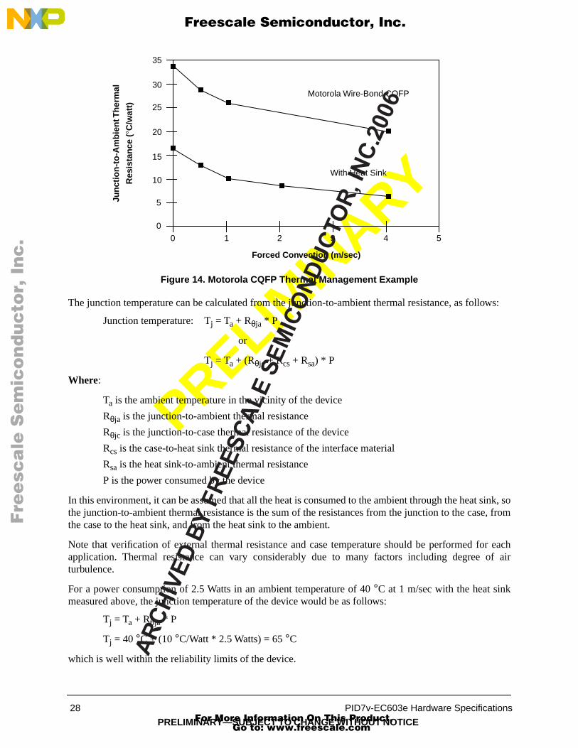
Figure 17 shows typical thermal performance data for the 21 mm CBGA package mounted to a test card.
Figure 15. CBGA Thermal Management Example
Temperature calculations are also performed identically to those in the previous section. For a powerconsumption of 2.5 Watts in an ambient of 40° C at 1.0 m/sec, the associated overall thermal resistance andjunction temperature, found in Table 13, will result.
Vendors such as Aavid Engineering Inc., Thermalloy, and Wakefield Engineering can supply heat sinks witha wide range of thermal performance. Refer to Section 1.8.6.1.2, “Thermal Management Example,” forcontact information.
Table 13. Thermal Resistance and Junction Temperature
Configuration θja (°C/W) Tj (°C)
Exposed die (no heat sink) 18.4 86
With 2338 heat sink 5.3 53
Approach Air Velocity (m/sec)
0
5
10
15
20
0 1 2 3 4
CBGA with Exposed Die
25
5
CBGA with Thermalloy2338B-Pin Fin Heat Sink
Assumptions:1. 2P card with 1 OZ Cu planes2. 63 mm x 76 mm card3. Air flow on both sides of card4. Vertical orientation5. 2-stage epoxy heat sink attach
θ ja
(°C
/W)
Fre
esc
ale
Se
mic
on
du
cto
r, I
Freescale Semiconductor, Inc.
For More Information On This Product, Go to: www.freescale.com
nc
...
AR
CH
IVE
D B
Y F
RE
ES
CA
LE S
EM
ICO
ND
UC
TOR
, IN
C. 2
006
PRELIMIN
ARY
PID7v-EC603e Hardware Specifications 31
PRELIMINARY—SUBJECT TO CHANGE WITHOUT NOTICE
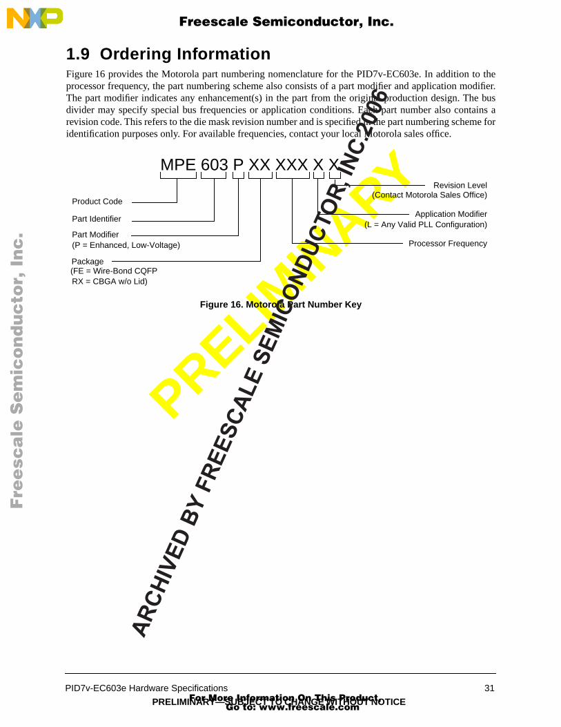
1.9 Ordering InformationFigure 16 provides the Motorola part numbering nomenclature for the PID7v-EC603e. In addition to theprocessor frequency, the part numbering scheme also consists of a part modifier and application modifier.The part modifier indicates any enhancement(s) in the part from the original production design. The busdivider may specify special bus frequencies or application conditions. Each part number also contains arevision code. This refers to the die mask revision number and is specified in the part numbering scheme foridentification purposes only. For available frequencies, contact your local Motorola sales office.
Figure 16. Motorola Part Number Key
MPE 603 P XX XXX X X
Product Code
Part Identifier
Part Modifier
Application Modifier
(P = Enhanced, Low-Voltage)
(FE = Wire-Bond CQFP
(L = Any Valid PLL Configuration)
Package
RX = CBGA w/o Lid)
Processor Frequency
(Contact Motorola Sales Office)Revision Level
Fre
esc
ale
Se
mic
on
du
cto
r, I
Freescale Semiconductor, Inc.
For More Information On This Product, Go to: www.freescale.com
nc
...
AR
CH
IVE
D B
Y F
RE
ES
CA
LE S
EM
ICO
ND
UC
TOR
, IN
C. 2
006

PRELIMIN
ARY
32 PID7v-EC603e Hardware Specifications
PRELIMINARY—SUBJECT TO CHANGE WITHOUT NOTICE
Appendix AGeneral Handling Recommendations for the
C4-CQFPThe following list provides a few guidelines for package handling:
• Handle the electrostatic discharge sensitive (ESD) package with care before, during, and after processing.
• Do not apply any load to exceed 3 Kg after assembly.
• Components should not be hot-dip tinned.
• The package encapsulation is an acrylated urethane. Use adequate ventilation (local exhaust) for all elevated temperature processes.
The package parameters are as follows:
Heat sink adhesive AIEG-7655
IBM reference drawing 99F4869
Test socket Yamaichi QFP-PO 0.5-240P
Signal 165
Power/ground 75
Total 240
A.1 Package Environmental, Operation, Shipment, and Storage Requirements
The environmental, operation, shipment, and storage requirements are as follows:
• Make sure that the package is suitable for continuous operation under business office environments.
— Operating environment: 10° C to 40° C, 8% to 80% relative humidity
— Storage environment: 1° C to 60° C, up to 80% relative humidity
— Shipping environment: 40° C to 60° C, 5% to 100% relative humidity
• This component is qualified to meet JEDEC moisture Class 2.
After expiration of shelf life, packages may be baked at 120° C (+10/–5° C) for 4 hours minimum and then be used or repackaged. Shelf life is as specified by JEDEC for moisture Class 2 components.
A.2 Card Assembly RecommendationsThis section provides recommendations for card assembly process. Follow these guidelines for cardassembly.
• This component is supported for aqueous, IR, convection reflow, and vapor phase card assembly processes.
• The temperature of packages should not exceed 220° C for longer than 5 minutes.
• The package entering a cleaning cycle must not be exposed to temperature greater than that occurring during solder reflow or hot air exposure.
• It is not recommended to re-attach a package that is removed after card assembly.
Fre
esc
ale
Se
mic
on
du
cto
r, I
Freescale Semiconductor, Inc.
For More Information On This Product, Go to: www.freescale.com
nc
...
AR
CH
IVE
D B
Y F
RE
ES
CA
LE S
EM
ICO
ND
UC
TOR
, IN
C. 2
006

PRELIMIN
ARY
PID7v-EC603e Hardware Specifications 33
PRELIMINARY—SUBJECT TO CHANGE WITHOUT NOTICE
During the card assembly process, no solvent can be used with the C4FP, and no more than 3 Kg of forcemust be applied normal to the top of the package prior to, during, or after card assembly. Other details ofthe card assembly process follow:
Solder paste Either water soluble (for example, Alpha 1208) or no clean
Solder stencil thickness 0.152 mm
Solder stencil aperature Width reduced to 0.03 mm from the board pad width
Placement tool Panasonic MPA3 or equivalent
Solder reflow Infrared, convection, or vapor phase
Solder reflow profile Infrared and/or convection• Average ramp-up—0.48 to 1.8° C/second
• Time above 183° C—45 to 145 seconds
• Minimum lead temperature—200° C
• Maximum lead temperature—240° C
• Maximum C4FP temperature—245° C
Vapor phase• Preheat (board)—60° C to 150° C
• Time above 183° C—60 to 145 seconds
• Minimum lead temperature—200° C
• Maximum C4FP temperature—220° C
• Egress temperature—below 150° C
Clean after reflow De-ionized (D.I.) water if water-soluble paste is used• Cleaner requirements—conveyorized, in-line
• Minimum of four washing chambers
—Pre-clean chamber: top and bottom sprays, minimum top-side pressure of 25 psig, water temperature of 70° C minimum, dwell time of 24 seconds minimum, water is not re-used, water flow rate of 30 liters/minute.
—Wash chamber #1: top and bottom sprays, minimum top-side pressure of 48 psig, minimum bottom-side pressure of 44 psig, water temperature of 62.5° C (±2.5° C), dwell time of 48 seconds minimum, water flow rate of 350 liters/minute.
—Wash chamber #2: top and bottom sprays, minimum top-side pressure of 32 psig, minimum bottom-side pressure of 28 psig, water temperature of 72.5° C (±2.5° C), dwell time of 48 seconds minimum, water flow rate of 325 liters/minute.
—Final rinse chamber: top and bottom sprays, minimum top-side pressure of 25 psig, water temperature of 72.5° C minimum, dwell time of 24 seconds minimum, water flow rate of 30 liters/minute.
• No cleaning required if “no clean solder paste” is used
Touch-up and repair Water soluble (for example, Kester 450) or No Clean Flux
C4FP removal Hot air rework
C4FP replace Hand solder
Fre
esc
ale
Se
mic
on
du
cto
r, I
Freescale Semiconductor, Inc.
For More Information On This Product, Go to: www.freescale.com
nc
...
AR
CH
IVE
D B
Y F
RE
ES
CA
LE S
EM
ICO
ND
UC
TOR
, IN
C. 2
006

PRELIMIN
ARY
34 PID7v-EC603e Hardware Specifications
PRELIMINARY—SUBJECT TO CHANGE WITHOUT NOTICE
Fre
esc
ale
Se
mic
on
du
cto
r, I
Freescale Semiconductor, Inc.
For More Information On This Product, Go to: www.freescale.com
nc
...
AR
CH
IVE
D B
Y F
RE
ES
CA
LE S
EM
ICO
ND
UC
TOR
, IN
C. 2
006

PRELIMIN
ARY
PID7v-EC603e Hardware Specifications 35
PRELIMINARY—SUBJECT TO CHANGE WITHOUT NOTICE
Fre
esc
ale
Se
mic
on
du
cto
r, I
Freescale Semiconductor, Inc.
For More Information On This Product, Go to: www.freescale.com
nc
...
AR
CH
IVE
D B
Y F
RE
ES
CA
LE S
EM
ICO
ND
UC
TOR
, IN
C. 2
006
Information in this document is provided solely to enable system and software implementers to use PowerPC microprocessors. There are no express or impliedcopyright licenses granted hereunder to design or fabricate PowerPC integrated circuits or integrated circuits based on the information in this document.
Motorola reserves the right to make changes without further notice to any products herein. Motorola makes no warranty, representation or guaranteeregarding the suitability of its products for any particular purpose, nor does Motorola assume any liability arising out of the application or use of any product orcircuit, and specifically disclaims any and all liability, including without limitation consequential or incidental damages. “Typical” parameters can and do vary indifferent applications. All operating parameters, including “Typicals” must be validated for each customer application by customer’s technical experts. Motoroladoes not convey any license under its patent rights nor the rights of others. Motorola products are not designed, intended, or authorized for use as componentsin systems intended for surgical implant into the body, or other applications intended to support or sustain life, or for any other application in which the failureof the Motorola product could create a situation where personal injury or death may occur. Should Buyer purchase or use Motorola products for any suchunintended or unauthorized application, Buyer shall indemnify and hold Motorola and its officers, employees, subsidiaries, affiliates, and distributors harmlessagainst all claims, costs, damages, and expenses, and reasonable attorney fees arising out of, directly or indirectly, any claim of personal injury or deathassociated with such unintended or unauthorized use, even if such claim alleges that Motorola was negligent regarding the design or manufacture of the part.
Motorola and are registered trademarks of Motorola, Inc. Mfax is a trademark of Motorola, Inc. Motorola, Inc. is an Equal Opportunity/Affirmative ActionEmployer.
IBM is a trademark of International Business Machines Corporation. The PowerPC name is a registered trademark and the PowerPC logotype and PowerPC 603 are trademarks of International Business Machines Corporation
used by Motorola under license from International Business Machines Corporation.FLOTHERM is a registered trademark of Flomerics Ltd., UK.
Motorola Literature Distribution Centers:USA/EUROPE: Motorola Literature Distribution; P.O. Box 5405; Denver, Colorado 80217; Tel.: 1-800-441-2447 or 1-303-675-2140; World Wide Web Address: http://ldc.nmd.com/JAPAN: Nippon Motorola Ltd SPD, Strategic Planning Office 4-32-1, Nishi-Gotanda Shinagawa-ku, Tokyo 141, Japan Tel.: 81-3-5487-8488ASIA/PACIFC: Motorola Semiconductors H.K. Ltd.; 8B Tai Ping Industrial Park, 51 Ting Kok Road, Tai Po, N.T., Hong Kong; Tel.: 852-26629298
Mfax™: [email protected]; TOUCHTONE 1-602-244-6609; US & Canada ONLY (800) 774-1848; World Wide Web Address: http://sps.motorola.com/mfaxINTERNET: http://motorola.com/sps
Technical Information: Motorola Inc. SPS Customer Support Center 1-800-521-6274; electronic mail address: [email protected] Comments: FAX (512) 891-2638, Attn: RISC Applications Engineering.World Wide Web Addresses: http://www.mot.com/SPS/PowerPC/
http://www.mot.com/SPS/RISC/netcomm/
MPE603E7VEC/D
Fre
esc
ale
Se
mic
on
du
cto
r, I
Freescale Semiconductor, Inc.
For More Information On This Product, Go to: www.freescale.com
nc
...
AR
CH
IVE
D B
Y F
RE
ES
CA
LE S
EM
ICO
ND
UC
TOR
, IN
C. 2
006