wpc low-power wireless charging solution - NXP Community
39
PUBLIC USE EMMANUEL T. NANA PRODUCT APPLICATIONS ENGINEER SESSION #: FTF-MHW-N1923 THURSDAY, MAY 19, 2016 (11:00 AM) WPC LOW-POWER WIRELESS CHARGING SOLUTION ULTRA-SMALL ONE-CHIP LOW-POWER Qi TRANSMITTER
-
Upload
khangminh22 -
Category
Documents
-
view
4 -
download
0
Transcript of wpc low-power wireless charging solution - NXP Community
PUBLIC USE
EMMANUEL T. NANA
PRODUCT APPLICATIONS ENGINEER
SESSION #: FTF-MHW-N1923
THURSDAY, MAY 19, 2016 (11:00 AM)
WPC LOW-POWER WIRELESS CHARGING
SOLUTION
ULTRA-SMALL ONE-CHIP
LOW-POWER Qi TRANSMITTER
PUBLIC USE1 FTF-MHW-N1923 PUBLIC USE1 FTF-MHW-N1923
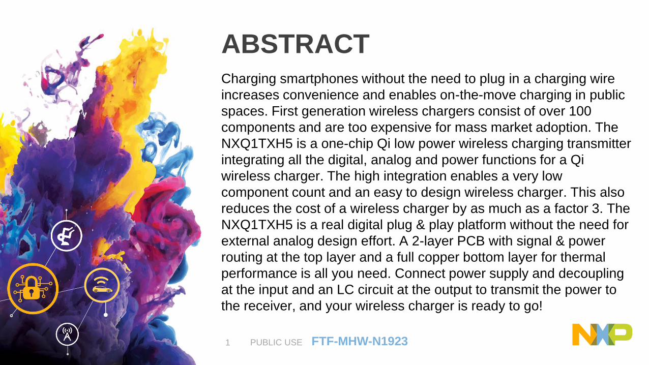
ABSTRACTCharging smartphones without the need to plug in a charging wire
increases convenience and enables on-the-move charging in public
spaces. First generation wireless chargers consist of over 100
components and are too expensive for mass market adoption. The
NXQ1TXH5 is a one-chip Qi low power wireless charging transmitter
integrating all the digital, analog and power functions for a Qi
wireless charger. The high integration enables a very low
component count and an easy to design wireless charger. This also
reduces the cost of a wireless charger by as much as a factor 3. The
NXQ1TXH5 is a real digital plug & play platform without the need for
external analog design effort. A 2-layer PCB with signal & power
routing at the top layer and a full copper bottom layer for thermal
performance is all you need. Connect power supply and decoupling
at the input and an LC circuit at the output to transmit the power to
the receiver, and your wireless charger is ready to go!
PUBLIC USE2 FTF-MHW-N1923 PUBLIC USE2 FTF-MHW-N1923
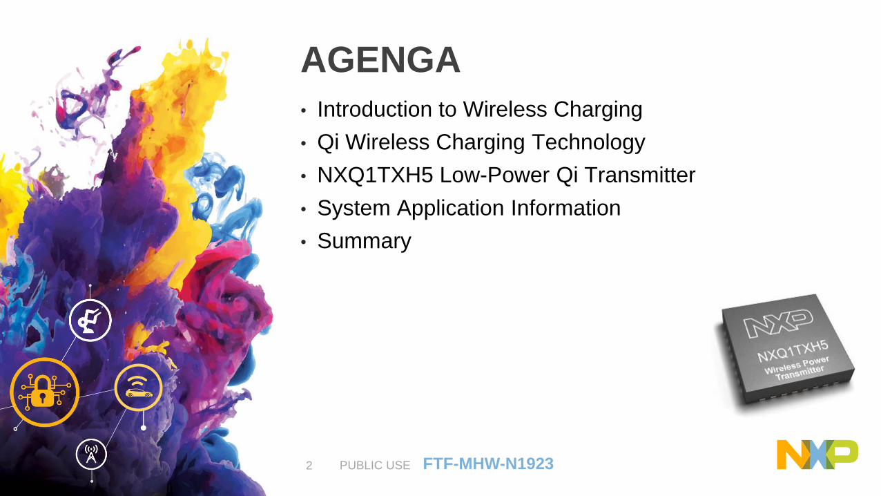
AGENGA
• Introduction to Wireless Charging
• Qi Wireless Charging Technology
• NXQ1TXH5 Low-Power Qi Transmitter
• System Application Information
• Summary

PUBLIC USE3 FTF-MHW-N1923
INTRODUCTION TO
WIRELESS
CHARGING

PUBLIC USE4 FTF-MHW-N1923
PUBLIC USE5 FTF-MHW-N1923
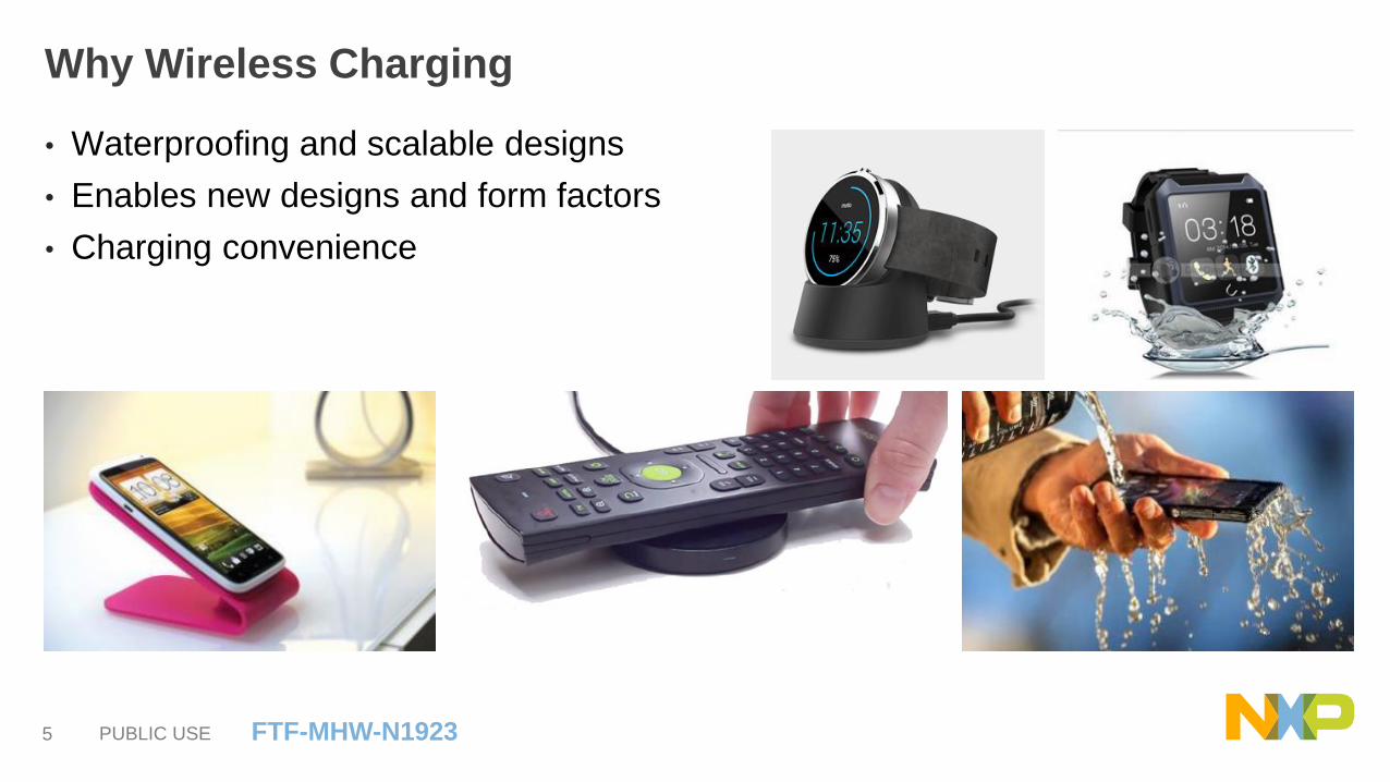
Why Wireless Charging
• Waterproofing and scalable designs
• Enables new designs and form factors
• Charging convenience

PUBLIC USE6 FTF-MHW-N1923
Wireless Power – Technology Overview
Inductive Coupling Magnetic Resonant Coupling
Coreless Transformer Resonant Coupling
mm z-distance
100..205 kHz
RF PowerLF Power
ASK Modulation
on Power Carrier
Bluetooth 4.0
Low-Energy
(2.4Ghz)
informationinformation
d<D
D
cm z-distance
6.78 MHz ± 15kHz
ASK Modulation
on Power Carrier
information
mm z-distance
201.. 304 kHz

PUBLIC USE7 FTF-MHW-N1923
Wireless Power System – Overview & Comparison
(Qi) System
PowerCircuit
Power Amp /Driver / MOSFETs
Tx
coilRx
coil
AC/DCWall
Adapter
TX RX
Control & ProtectionBLE
TX RX
PowerCircuit
Power Amp Driver
MOSFETs
Tx
coil
Rx
coilAC/DCWall
Adapter
Rectifier DC/DCDC/DC
(A4WP) System
A4WP – Rezence WPC – Qi
Communication/Control Bluetooth In-band ASK
User Experience Freedom of placement Coil alignment needed
Coil Sizes Customizable Specified
TX: RX connections Up to 8 1:1
Technology Emerging Mature
Control & Protection
Control&
Protection
Rectifier DC/DC
BLE
Control&
Protection MCUMCU

PUBLIC USE8 FTF-MHW-N1923
NXP Wireless Charging Solution Overview
BrightnessContrast
• NXP has a solid competitive position, supporting both Qi and A4WP standards
• NXP can offer interesting differentiators (like NFC)
• NXP makes wireless charging CHEAPER, BETTER, SMARTER
Wireless Charging Solutions from NXP
• Receivers
– Rezence (aka A4WP)
– Qi
– PMA
• Transmitters
– Qi
– PMA
RX TX

PUBLIC USE9 FTF-MHW-N1923
Qi-Enabled Phones Available Already
• Low power Qi is mature, simple, and low cost
• Medium power specification supports up to 15W
• Shared mode (more phones on charger) draft specification available

PUBLIC USE10 FTF-MHW-N1923
Wireless Chargers in Automotive
PUBLIC USE11 FTF-MHW-N1923
Qi WIRELESS
CHARGING
TECHNOLOGY

PUBLIC USE12 FTF-MHW-N1923
Qi System – Power and Control Loop
direction of
power transfer
feedback using backscatter
modulation of power carrier
pwr control loop
Tx Rx
AC
mains
Full/Half
bridge
inverter
Monitoring
&
(de)modulation
Supply
AC-DC
Converter Rsynchronous
rectifier
Rx
controller
PWR
RX device
Control(PWM/DAC/GPIO)
TX
pad
TX
Controller
PUBLIC USE13 FTF-MHW-N1923
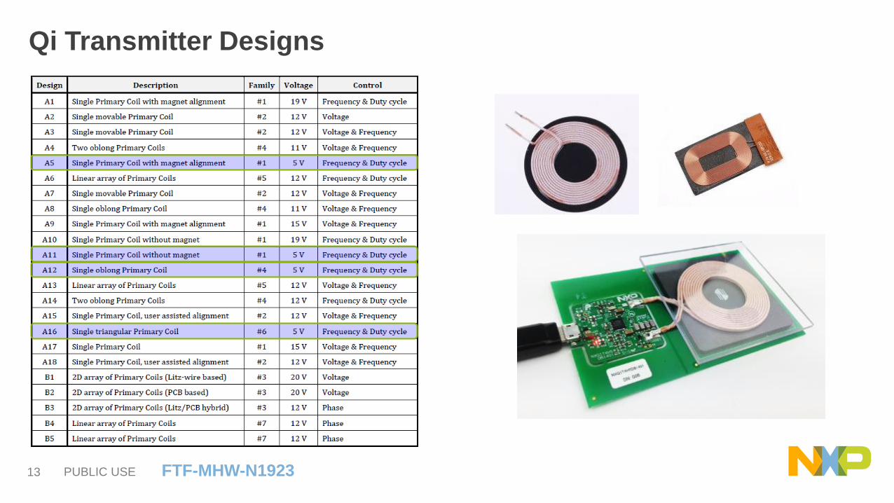
Qi Transmitter Designs
PUBLIC USE14 FTF-MHW-N1923
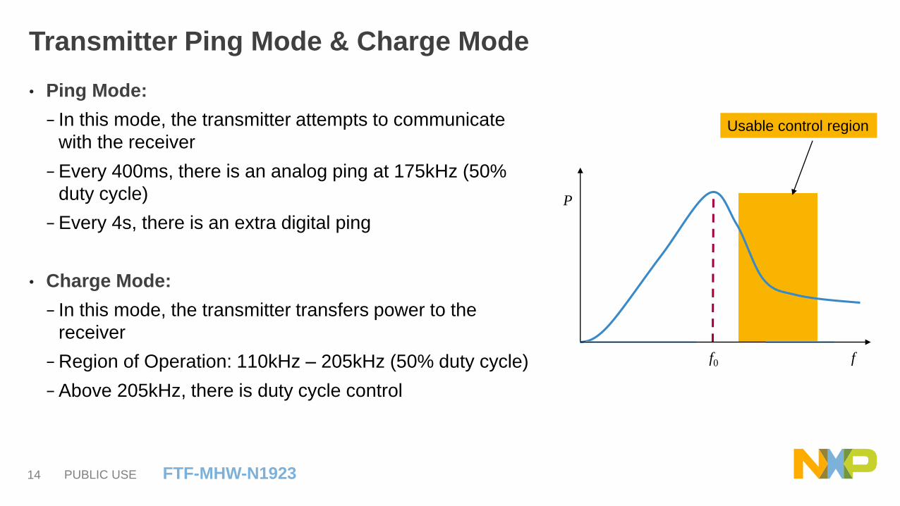
Transmitter Ping Mode & Charge Mode
• Ping Mode:
− In this mode, the transmitter attempts to communicate
with the receiver
− Every 400ms, there is an analog ping at 175kHz (50%
duty cycle)
− Every 4s, there is an extra digital ping
• Charge Mode:
− In this mode, the transmitter transfers power to the
receiver
− Region of Operation: 110kHz – 205kHz (50% duty cycle)
− Above 205kHz, there is duty cycle control
ff0
P
Usable control region

PUBLIC USE15 FTF-MHW-N1923
Communication & Power Transfer
Power
Communication
Pad Device
Power Transmitter Power Receiver
ASK (load) modulation
communication channel

PUBLIC USE16 FTF-MHW-N1923
Qi Control Loop
• Receiver modulates load by
− Switching modulation resistor (Rm), or
− Switching modulation capacitor (Cm)
Transmitter
Cp
Lp
+
-
Receiver
Cd
Ls
Cs
C Rm
ModulationModulation
Cm
IpVp
Load
Power Modulation
Depth
pwr control loop
direction of
power transfer
feedback using backscatter
modulation of power carrier
Tx Rx

PUBLIC USE17 FTF-MHW-N1923
NXQ1TXH5
LOW-POWER Qi
TRANSMITTER

PUBLIC USE18 FTF-MHW-N1923
NXQ1TXH5: 5V Low-Power Qi Transmitter
• Features:
− Integrates A5, A11, A12, & A16 WPC Qi V1.2
analog and digital functions for 5W System
Specification
− Average output power up to 8W
− Easy FOD Control for coil and caps
− Internal voltage and current measurement circuits
− On-chip analog and digital filters for robust ASK detection
− No external OpAmp, filter, or biasing circuit needed
− Less than 10 external passive components required
− Low cost 32.768kHz external crystal for low power
oscillator to achieve standby current of <30µA; System
Standby Power of 10mW (typ)
− DSP wakeup by special device detect function
− Supports NFC tag applications with delayed startup
− Operates supply from 3.5V to 5.25V
− Small 5mm x 5mm HVQFN32 package
− Qi Certified
• Applications:
− Wearable Charger
− Mobile Charger
− Applications requiring
USB power, low cost
and low standby power
NXQ1TXH5/101

PUBLIC USE19 FTF-MHW-N1923
NXQ1TXH5: Dual ASK Channels for Safe Communication
Also possible to
measure RMS
coil current for
better FOD with
misalignment
101
Dual ASKCustomer
LED & FOD
Configuration

PUBLIC USE20 FTF-MHW-N1923
NXQ1TXH5: Static Power Reduction Configuration
• CNF1 (Pin 32) Setting via R7:VSPR < 0.04V: No SPR, No SPL
0.085V < VSPR < 1.29V: SPRLEVEL (mA) = 1000 x (VSPR / 1.2 + 0.43 ), adjustable from 500 to 1500 mA
1.335 < VSPR < VDDP: No SPR, SPL on
• With R11=390 kΩ, corresponding values of R7 are:R7 < 3 kΩ (0 Ω): No SPR, No SPL
7 kΩ < R7 < 136 kΩ: SPRLEVEL (mA) = 1000 x (VSPR / 1.2 + 0.43 )
R7 > 142 kΩ: No SPR, SPL on
• Determine value of R7 (SPR between 500 mA &1,500 mA):500 mA: R7 = 7 kΩ
1000 mA: R7 = 62 kΩ
1500 mA: R7 = 135 kΩ

PUBLIC USE21 FTF-MHW-N1923
NXQ1TXH5: FOD Threshold Configuration
• CNF3 (Pin 2) Setting via R9:VFOD_TH < 0.04V: FOD disable (R9 = 0 Ω, save resistor)
0.25 V < VFOD_TH < 1.29 V: FODTH (mW) = 1000 x (VFOD_TH / 1.5), adjustable from 166 to 860 mW
1.335 < VFOD_TH < VDDP: Default (350 mW), same as VFOD_TH = 525 mV (R9 ~47kΩ), but saving R9 (no mount)
• With R11=390kΩ, corresponding values of R9 are:R9 < 3 kΩ (0 Ω): FOD disable
21 kΩ < R9 < 136 kΩ: FODTH (mW) = 1000 x (VFOD_TH / 1.5)
R9 > 142 kΩ Reserved
• Determine value of R9:FODTH = 200 mW: R9 = 25 kΩ
FODTH = 400 mW: R9 = 53 kΩ
FODTH = 600 mW: R9 = 86 kΩ
FODTH = 800 mW: R9 = 123 kΩ
PUBLIC USE22 FTF-MHW-N1923
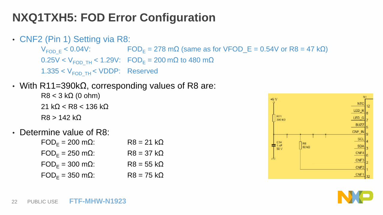
NXQ1TXH5: FOD Error Configuration
• CNF2 (Pin 1) Setting via R8:VFOD_E < 0.04V: FODE = 278 mΩ (same as for VFOD_E = 0.54V or R8 = 47 kΩ)
0.25V < VFOD_TH < 1.29V: FODE = 200 mΩ to 480 mΩ
1.335 < VFOD_TH < VDDP: Reserved
• With R11=390kΩ, corresponding values of R8 are:R8 < 3 kΩ (0 ohm)
21 kΩ < R8 < 136 kΩ
R8 > 142 kΩ
• Determine value of R8:FODE = 200 mΩ: R8 = 21 kΩ
FODE = 250 mΩ: R8 = 37 kΩ
FODE = 300 mΩ: R8 = 55 kΩ
FODE = 350 mΩ: R8 = 75 kΩ
PUBLIC USE23 FTF-MHW-N1923
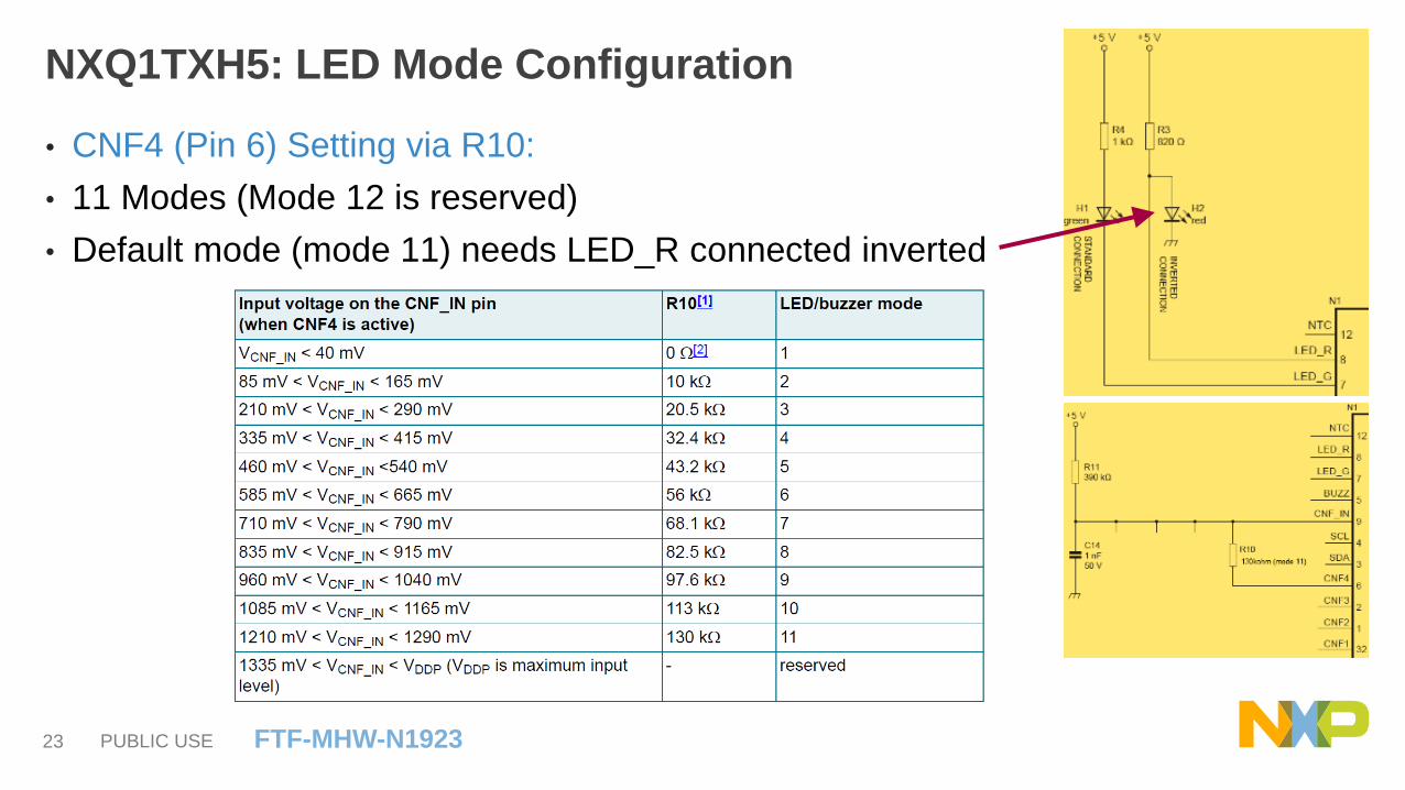
NXQ1TXH5: LED Mode Configuration
• CNF4 (Pin 6) Setting via R10:
• 11 Modes (Mode 12 is reserved)
• Default mode (mode 11) needs LED_R connected inverted

PUBLIC USE24 FTF-MHW-N1923
NXQ1TXH5: LED Modes

PUBLIC USE25 FTF-MHW-N1923
Designing with NXQ1TXH5 (Schematic)
Dual ASK
PUBLIC USE26 FTF-MHW-N1923
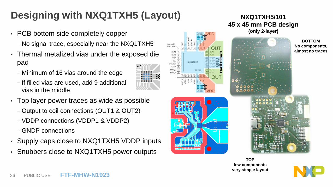
Designing with NXQ1TXH5 (Layout)
• PCB bottom side completely copper
− No signal trace, especially near the NXQ1TXH5
• Thermal metalized vias under the exposed die
pad
− Minimum of 16 vias around the edge
− If filled vias are used, add 9 additional
vias in the middle
• Top layer power traces as wide as possible
− Output to coil connections (OUT1 & OUT2)
− VDDP connections (VDDP1 & VDDP2)
− GNDP connections
• Supply caps close to NXQ1TXH5 VDDP inputs
• Snubbers close to NXQ1TXH5 power outputs
NXQ1TXH5/101
45 x 45 mm PCB design(only 2-layer)
BOTTOM
No components,
almost no traces
TOP
few components
very simple layout
PUBLIC USE27 FTF-MHW-N1923
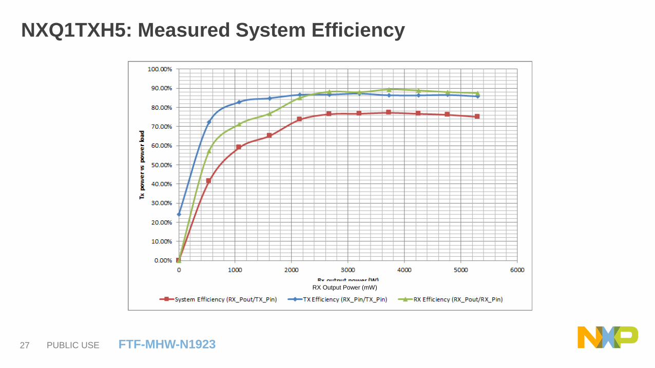
NXQ1TXH5: Measured System Efficiency
RX Output Power (mW)

PUBLIC USE28 FTF-MHW-N1923
NXQ1TXH5: Qi Certification Document
Low EMI without chock or shielding

PUBLIC USE29 FTF-MHW-N1923
SYSTEM
APPLICATION
INFORMATION
PUBLIC USE30 FTF-MHW-N1923
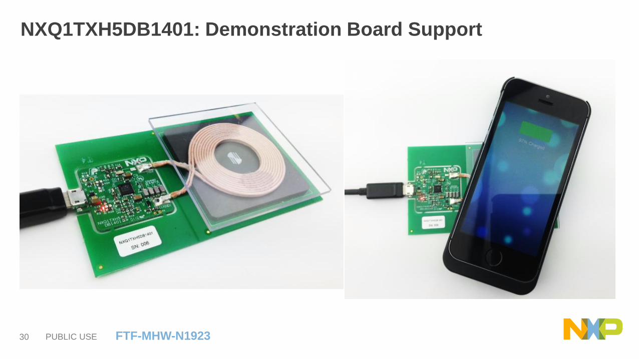
NXQ1TXH5DB1401: Demonstration Board Support

PUBLIC USE31 FTF-MHW-N1923
NXQ1TXH5: Scalable PCB Size (for Wearable Applications)
8.5W Transmitter(50mm for 5W RX out)
5W Transmitter(30mm)
3W Transmitter(20mm)
• 2-layer PCB
• Very low component count.
• Components on top-side only
• Easy for PCB design & manufacturing
• High efficiency (>70%)
• PCB Area scalable with power. PCB area only serves as heatsink:
– 30 mm diameter for TX design to deliver 3W at RX output (5W transmitter power)
– 20mm diameter for 2W design to deliver 2W at RX output (3W transmitter power)

PUBLIC USE32 FTF-MHW-N1923
NXQ1TXH5: In Samsung Gear S2 Wireless Charger (Wearable)
• NXQ1TXH5 with patched ROM to charge Gear S2− NXQ1TXH5 + LPC812 (for update with differences to Qi standard)
− Gear S2 transmitter coil connected to NXQ1TXH5DB1401
− Updated NXQ1TXH5 does not need LPC812 for same function
• Demo board NXQ1TXH5DB1402 configured as:− Red LED indicates charging
− Green LED indicates charged
− Foreign object detection switched off
• PCB area for Gear S2 design can be less than 50% of
5W PCB area with NXQ1TXH5
1.5W Solution
NXP Board Gear S2 Board
Gear S2 Design Analysis

PUBLIC USE33 FTF-MHW-N1923
Portable Qi Charger – Based on NXQ1TXH5

PUBLIC USE34 FTF-MHW-N1923
Qi Chargers – Based on NXQ1TXH5

PUBLIC USE35 FTF-MHW-N1923
SUMMARY

PUBLIC USE36 FTF-MHW-N1923
Summary
• NXQ1TXH5 Value Proposition
– Fully integrated, low-power Qi Wireless Transmitter
– 50% lower cost in the application than any other solution
– Compliant to WPC Qi V1.2, with easy FOD tuning
– Extremely low component counts for based Wireless Charger
– Peak system efficiency of 75%
– Extremely low standby power of ~10mW
– Low EMI by use of Class D audio expertise of NXP
– High efficiency and cool running by NXP C14P technology with low RDS(on)
• NXQ1TXA5 Suitability in Wearable Applications
– Very Low internal power consumption
– High system efficiency (>70%) at low power (1.5W); peak efficiency of 74%
– Integrated power stages with low switching loss
– Excellent fit for Wearable Qi Chargers

PUBLIC USE38 FTF-MHW-N1923
ATTRIBUTION STATEMENT
NXP, the NXP logo, NXP SECURE CONNECTIONS FOR A SMARTER WORLD, CoolFlux, EMBRACE, GREENCHIP, HITAG, I2C BUS, ICODE, JCOP, LIFE VIBES, MIFARE, MIFARE Classic, MIFARE
DESFire, MIFARE Plus, MIFARE FleX, MANTIS, MIFARE ULTRALIGHT, MIFARE4MOBILE, MIGLO, NTAG, ROADLINK, SMARTLX, SMARTMX, STARPLUG, TOPFET, TrenchMOS, UCODE, Freescale,
the Freescale logo, AltiVec, C 5, CodeTEST, CodeWarrior, ColdFire, ColdFire+, C Ware, the Energy Efficient Solutions logo, Kinetis, Layerscape, MagniV, mobileGT, PEG, PowerQUICC, Processor Expert,
QorIQ, QorIQ Qonverge, Ready Play, SafeAssure, the SafeAssure logo, StarCore, Symphony, VortiQa, Vybrid, Airfast, BeeKit, BeeStack, CoreNet, Flexis, MXC, Platform in a Package, QUICC Engine,
SMARTMOS, Tower, TurboLink, and UMEMS are trademarks of NXP B.V. All other product or service names are the property of their respective owners. ARM, AMBA, ARM Powered, Artisan, Cortex,
Jazelle, Keil, SecurCore, Thumb, TrustZone, and μVision are registered trademarks of ARM Limited (or its subsidiaries) in the EU and/or elsewhere. ARM7, ARM9, ARM11, big.LITTLE, CoreLink,
CoreSight, DesignStart, Mali, mbed, NEON, POP, Sensinode, Socrates, ULINK and Versatile are trademarks of ARM Limited (or its subsidiaries) in the EU and/or elsewhere. All rights reserved. Oracle and
Java are registered trademarks of Oracle and/or its affiliates. The Power Architecture and Power.org word marks and the Power and Power.org logos and related marks are trademarks and service marks
licensed by Power.org. © 2015–2016 NXP B.V.