MPC8569-MDS-PB HWGS_v3.1.fm - NXP
38
Freescale Semiconductor Hardware Getting Started Guide © Freescale Semiconductor, Inc., 09/2008. All rights reserved. This document describes the MPC8569E-MDS-PB and its related hardware kit. The MPC8569E-MDS-PB getting started procedure explains and verifies the board’s basic operation in a step-by-step format. Settings for switches, jumpers, LEDs, and push buttons are shown, and there are instructions for connecting peripheral devices. The MPC8569E-MDS-PB functions with an integrated development environment (IDE), such as Freescale’s CodeWarrior™, but instructions for working with the IDE are beyond the scope of this document. NOTE! The terms PEX and PCIe are interchangeable. However, as the modules are stamped “PEX”, the document uses this term. Contents 1 Revisions Table . . . . . . . . . . . . . . . . . . . . . . . . . . . . . . . 2 2 Definitions, Acronyms, and Abbreviations . . . . . . . . . . 2 3 Related Reading . . . . . . . . . . . . . . . . . . . . . . . . . . . . . . 5 4 Hardware Kit Contents . . . . . . . . . . . . . . . . . . . . . . . . . 6 5 Schematic CS and PS Views . . . . . . . . . . . . . . . . . . . . . 7 6 Switch Default Settings . . . . . . . . . . . . . . . . . . . . . . . . . 8 7 Connector Default Settings . . . . . . . . . . . . . . . . . . . . . 15 8 Push Buttons . . . . . . . . . . . . . . . . . . . . . . . . . . . . . . . . 17 9 LED Lights . . . . . . . . . . . . . . . . . . . . . . . . . . . . . . . . . 18 10 Board Control Status Registers (BCSR) . . . . . . . . . . . 19 11 Memory Map . . . . . . . . . . . . . . . . . . . . . . . . . . . . . . . . 29 12 Working Environment . . . . . . . . . . . . . . . . . . . . . . . . . 30 13 Getting Started Procedures . . . . . . . . . . . . . . . . . . . . . 31 14 SerDes-Module Set-ups . . . . . . . . . . . . . . . . . . . . . . . 33 How to Reach Us . . . . . . . . . . . . . . . . . . . . . . . . . . . . . 36 MPC8569E-MDS-PB Document Number: MPC8569E-MDS-PB_HGS Rev. 3.1
-
Upload
khangminh22 -
Category
Documents
-
view
0 -
download
0
Transcript of MPC8569-MDS-PB HWGS_v3.1.fm - NXP

Freescale SemiconductorHardware Getting Started Guide
© Freescale Semiconductor, Inc., 09/2008. All rights reserved.
This document describes the MPC8569E-MDS-PB and its related hardware kit. The MPC8569E-MDS-PB getting started procedure explains and verifies the board’s basic operation in a step-by-step format.
Settings for switches, jumpers, LEDs, and push buttons are shown, and there are instructions for connecting peripheral devices.
The MPC8569E-MDS-PB functions with an integrated development environment (IDE), such as Freescale’s CodeWarrior™, but instructions for working with the IDE are beyond the scope of this document.NOTE!
The terms PEX and PCIe are interchangeable. However, as the modules are stamped “PEX”, the document uses this term.
Contents1 Revisions Table . . . . . . . . . . . . . . . . . . . . . . . . . . . . . . .22 Definitions, Acronyms, and Abbreviations . . . . . . . . . .23 Related Reading . . . . . . . . . . . . . . . . . . . . . . . . . . . . . .54 Hardware Kit Contents . . . . . . . . . . . . . . . . . . . . . . . . .65 Schematic CS and PS Views . . . . . . . . . . . . . . . . . . . . .76 Switch Default Settings . . . . . . . . . . . . . . . . . . . . . . . . .87 Connector Default Settings . . . . . . . . . . . . . . . . . . . . .158 Push Buttons . . . . . . . . . . . . . . . . . . . . . . . . . . . . . . . .179 LED Lights . . . . . . . . . . . . . . . . . . . . . . . . . . . . . . . . .18
10 Board Control Status Registers (BCSR) . . . . . . . . . . .1911 Memory Map . . . . . . . . . . . . . . . . . . . . . . . . . . . . . . . .2912 Working Environment . . . . . . . . . . . . . . . . . . . . . . . . .3013 Getting Started Procedures . . . . . . . . . . . . . . . . . . . . .3114 SerDes-Module Set-ups . . . . . . . . . . . . . . . . . . . . . . .33
How to Reach Us . . . . . . . . . . . . . . . . . . . . . . . . . . . . .36
MPC8569E-MDS-PB
Document Number: MPC8569E-MDS-PB_HGSRev. 3.1

MPC8569E-MDS-PB Hardware Getting Started, Rev. 3.1
2 Freescale Semiconductor
Revisions Table
1 Revisions TableTable 1. Revisions Table
2 Definitions, Acronyms, and Abbreviations
Date Rev. Author Tech Editor Description
19 Jan 2009 1.0 Vladimir Yukht Hadas Khen HWGS Rev. 1.0
12 Mar 2009 2.0 Vladimir Yukht Hadas Khen BCSR changes.
31 Mar 2009 2.1 Vladimir Yukht Hadas Khen RCW changes
5 May 2009 2.2 Vladimir Yukht Hadas Khen BCSR, terminology, reference document changes, and new photos (Bootwiz).
21 May 2009 3.0 Vladimir Yukht Hadas Khen Revised content
22 June 2009 3.1 Vladimir Yukht Hadas Khen BCSR changes
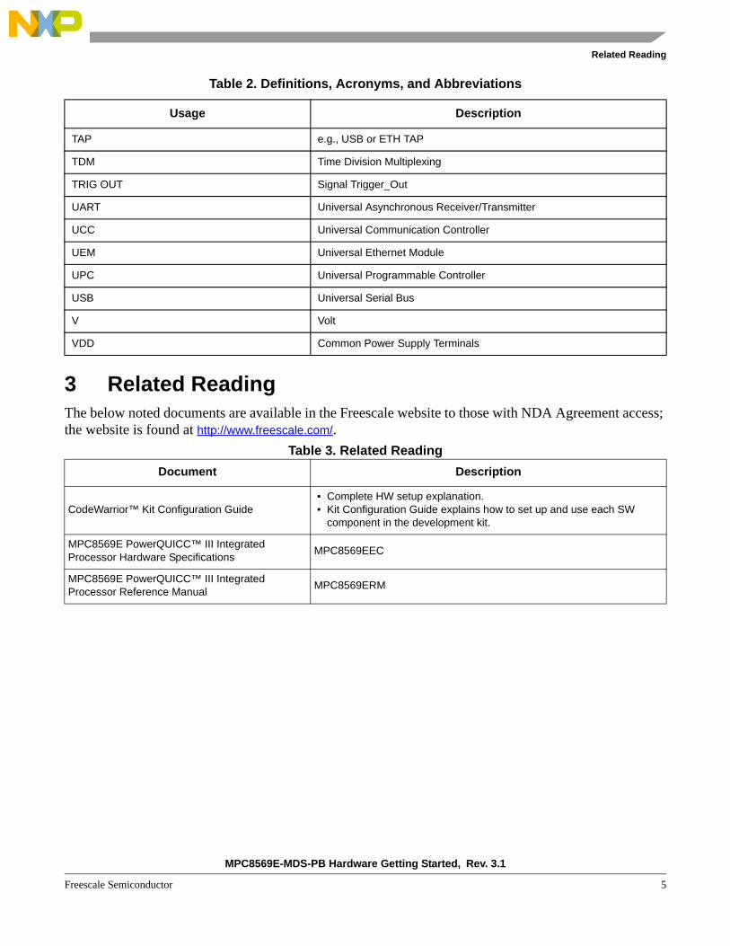
Table 2. Definitions, Acronyms, and Abbreviations
Usage Description
ADDR Address
ADS Application Development System
BCSR Board Control and Status Register
BVDD Local Bus Volt Direct Current
CCB Platform Clock
CKE DDR Clock Enable
CLKIN Clock Input; interchangeable with SYSCLK
CLKOUT Clock Output
CNTR ISP Control PLD Integrated SW Programming
COP Common On-Chip Processor
CPU Central Processing Unit
CS Component Side
DDR Double Data Rate
DIP Dual-in-Line Package (switches)
DUART Dual Universal Asynchronous Receiver/Transmitter
e500 CPU Core Name
ECC Error Detection and Correction
EEPROM Electrical Erasable Programmable Memory

MPC8569E-MDS-PB Hardware Getting Started, Rev. 3.1
Freescale Semiconductor 3
Definitions, Acronyms, and Abbreviations
eLBC Enhanced Local Bus Controller
EN Enable
EP End Point
ETH Ethernet
FCM NAND Flash Control Machine
FSL Freescale Semiconductor
GETH Gigabit Ethernet (also GbE)
GPCM General Purpose Chip-Select Machine
Host MPC8569E
HRESET Hard Reset
HW Hardware
I2C Inter-Integrated Circuit multi-master serial computer bus
IDE Integrated Development Environment
IO Input/Output
IRSENSE Service Voltage Drop Testing
JTAG Joint Test Access Group (IEEE® Std. 1149.1™)
LED Light-emitting Diode
LYNX Internal terminology; interchangeable with SerDes
LVDD QUICC Engine Block UCC1-UCC4 Voltage
MCK(E) DDR Master Clock
MDIC DDR Memory Driver Impedance Calibration
MEMC Memory Controller
MMC Multi Media Card
MPI Metallized Particle Interconnect Matrix
NAND FLASH Memory
NMI Non-Maskable Interrupt
nMVRST Marvell PHY Reset Signal
NOR Flash Memory
PB MPC8569E-MDS Processor Board
PCI Peripheral Components Interconnect
PCIe PCI Express = PCIe = PEX
Table 2. Definitions, Acronyms, and Abbreviations
Usage Description

MPC8569E-MDS-PB Hardware Getting Started, Rev. 3.1
4 Freescale Semiconductor
Definitions, Acronyms, and Abbreviations
PEX PCI Express = PEX = PCIe
PHY Physical Layer
PIB Platform I/O Board
PLD Programmable Logic Device
PLL Phased Lock Loop
POST FA_AND Service Failure Analysis
PRESET Power-on-Reset
PS Print Side
PS ISP PS Control PLD Integrated SW Programming
PTP Precision Time Protocol
QE Quick Engine
RC Root Complex
RCW Reset Configuration Word
REG CFG Configuration Register
RGMII Reduced General Media Independent Interface
RMII Reduced Media Independent Interface
ROM Read Only Memory
RTC Real Time Clock
SD Secure Digital Card
SDHC Secure Digital High Capacity Card
SerDes • Serializer/Deserializer • High Speed Serial Communication Lines; e.g., PEX (PCIe), SRIO,
SGMII, etc.
SGMII Serial Gigabit Media Independent Interface
SHMOO Graphical representation of selected test parameters in an electronic circuit.
SMII Serial Media Independent Interface
SODIMM Mini DIMM Form Factor
SRESET Soft Reset
SRIO Serial RapidIO
SW Switch
SYSCLK System Clock; interchangeable with CLKIN
Table 2. Definitions, Acronyms, and Abbreviations
Usage Description
MPC8569E-MDS-PB Hardware Getting Started, Rev. 3.1
Freescale Semiconductor 5
Related Reading
3 Related ReadingThe below noted documents are available in the Freescale website to those with NDA Agreement access; the website is found at http://www.freescale.com/.
Table 3. Related Reading
TAP e.g., USB or ETH TAP
TDM Time Division Multiplexing
TRIG OUT Signal Trigger_Out
UART Universal Asynchronous Receiver/Transmitter
UCC Universal Communication Controller
UEM Universal Ethernet Module
UPC Universal Programmable Controller
USB Universal Serial Bus
V Volt
VDD Common Power Supply Terminals
Document Description
CodeWarrior™ Kit Configuration Guide • Complete HW setup explanation. • Kit Configuration Guide explains how to set up and use each SW
component in the development kit.
MPC8569E PowerQUICC™ III Integrated Processor Hardware Specifications MPC8569EEC
MPC8569E PowerQUICC™ III Integrated Processor Reference Manual MPC8569ERM
Table 2. Definitions, Acronyms, and Abbreviations
Usage Description

MPC8569E-MDS-PB Hardware Getting Started, Rev. 3.1
6 Freescale Semiconductor
Hardware Kit Content
4 Hardware Kit ContentNOTE!
The terms PEX and PCIe are interchangeable. However, as the modules are stamped “PEX”, the document uses this term.
Hardware Kit Contents Figure 1. HW Kit Inventory
Processor Board and Modules1. MPC8569E-MDS-PB (1)2. UEM (2)3. SRIOx1 (2) and plastic screws (2)4. PEXx2 (1) and plastic screw (1)5. SRIO_LOOPBACK CARD (2)6. Bootwiz (1)
Cables7. RS-232 standard serial cable with two
9-pin connectors (2)8. FSL adaptor cable with one 10-pin
and two RS-232 connectors (1)9. ETH cables (4) with RJ45 connectors10.ETH loop-back cables (4)
Power Supply and USB TAP11.AC/DC 5V/8A power supply12.CodeWarrior USB TAP
Miscellaneous13.Allen key14.UEM plastic guide pins (6)15.Auxiliary UTAP to CNTR-ISP
connector (1)
Printed Matter (not shown in Figure 1) • MPC8569E-MDS-PB HW Getting Started • Freescale Warranty Card: 920-75133 • Safety Notice: 926-75254 • Contact Information Sheet: 920-90570-00
1
3 4 5 62
7 8 9 10
11 12 13 14 15

MPC8569E-MDS-PB Hardware Getting Started, Rev. 3.1
Freescale Semiconductor 7
MPC8569E-MDS-PB Schematic CS and PS Views
5 MPC8569E-MDS-PB Schematic CS and PS Views
Figure 2. MPC8569E-MDS-PB Component Side (CS) View
Figure 3. MPC8569E-MDS-PB Print Side (PS) View
1
2
73 71
74 72
J2
203
2041
2
21
22
61 41
42
73 71
74 72 62
93
J3
94
113
114
153 133
134
173
174 154
203 193
204
TP76
TP77
TP66
TP49
TP78
TP41TP50
TP82
TP81
TP83
TP80
TP79
TP68
TP69
TP33
TP73TP74
TP34
TP65
TP45
TP46
TP62
TP47
TP75
TP48
TP61
TP35
TP39
TP57
TP60
TP31
TP53
TP70
TP54
TP43
TP72
TP44
TP58
TP59
TP71
TP55
TP63TP56
TP27
TP37
TP8
TP7
TP32
TP64
TP5
TP26TP24
TP14
TP13
TP21
TP11
TP23
TP9
TP29
TP18
TP28
TP10
TP30
TP19
TP22
TP17
TP25
TP12
TP16 TP20
R38
MP2
MP1
MP3
MP4
C26C25
C59
C60
C39
C70
C69
C73
C52
C168
C171
C169
C153
C46
C47
C64
C65
C85
C97
C111
C112
C142
C144
C141
C125
C134
C41
C62
C166
C27
C37
C31
C105
C138
C121
C119
C99
C114
C116
C100
C115
C101
C77
C90C88
C84
C148
C89
C66
C68
C126
C63
C109
C132C146
C110
C129
C96
C127
C128
C67
C149
C147C130
C145
C48
C133
C131
C29
C152
C33
C24
C18
C16
C5
C11
C17
C12
C19
C170
C154
C38 C40
C86
C72
C50
C49
C51
C71
C87
C74
C30
C95
C108
C156
C98
C172
C173
C163
C1
C80
C58
C165
C76
C93
C43
C124
C151
C14
C137
C139
C102
C140
C57
C118
C55
C35
C78
C82
C106
C91
C92
C120
C104
C113
C159
C143
C155
C160
C36
C32
C22C21
C20
C23
C44
C164
C75
C94
C42
C123
C150
C15
C136
C103
C122
C56
C117
C54
C34
C79
C81
C107
C2
C13
C167
C3
R43
R41
R55
R71
R72
R24
9
R19
5
R19
4
R19
3
R19
2
R19
1
R190
R79
R189
R153
R204
R248
R51
R203
R202
R201
R200
R199
R198
R197
R247
R25
6
R25
5
R25
4
R25
3
R25
2
R25
1
R246
R25
0
R22
5
R245
R244
R24
3R22
4
R19
6
R187
R226
R222
R233
R230
R231
R232
R33
R32
R93
R94
R29
R28
R19
R25
R26
R18
R12
R3
R22
R214
R213
R179
R17
8
R161
R160
R181
R18
0
R18
2
R18
3
R108
R107
R106R163
R141
R140
R42
R159
R139
R165
R138
R188
R54
R53
R61
R60
R62
R149
R2
R14
R13
R116
R86
R150
R131
R47
R37
R20
8
R21
0
R205
R207
R215
R217
R185
R186
R85
R117
R89
R40R30
R39
R91
R162
R119
R118
R14
7R144
R88
R164
R56
R31
R148
R167
R168
R87
R209
R206
R216
R184
R130
R129
R90
R229
R228
R227
R221
R220
R218
R219R223
R234
R235
R236
R237
R238
R239
R24
0
R24
2
R241
R34 R35
R45
R46
R135
R114
R136
R211
R212
R105
R67
R74
R68
R69
R73
R101
R97
R115
R102
R100
R92
R95
R80
R96
R104
R103
R158
R157
R137
R24
R23
R17
R16
R7
R156
R174
R173
R154
R171
R113
R172
R155
R64
R65
R66
R52
R63
R152
R132
R151
R133
R77
R75
R48
R49
R175
R98
R99
R17
6
R17
7
R78
R76
R82
R81
R84
R83
R70
R134
R44
R111
R112
R109
R110
R58
R57
R120
R121
R122
R14
5
R123
R14
6
R124
R142
R125
R143
R126
R127
R11
R10
R50
R59
R166
R4
R27
R15
R1
R6
R128
R21
R9
R8
R20
U71
U68
TP51
TP15
TP52
TP42
TP40
TP38
L8+
L5
F
D
B
P
M
K
H
Y
T
V
AH
AF
AD
AB
23 25 27
22 24 26 28
15 17 19 21
U45
14 16 18 20
7 9 11 13
6 8 10 12
E
C
A1 53
N
L
J
G
AA
W
U
R
AG
AE
AC
2 4N1
U58
A1
N9
A9
U23
N1
U23
A1
N9
A9
TP3
TP67
TP6
TP2
TP36
TP1
TP4
+
BT1
L6
L7
L4L9
L10
L3
L11
L2
L1
1J9
1J8
J4
1
D8
D1
D9
D11
D2D5
CA
D12
D6
D3
D10
D7
D4
LD1
LD2
C7
C83
C45
C157
C61
C53
C135
+
C28
C10
+
C9
+
C8
+
C6
C158
31
Q1 P2
2
31
U12
1
1J25J23
1J24
1
J181
J191
1J26
Q2
12
3
3
R5
1
1
U562
3
SW31
SW21
SW41
2
1
T1
3
4
Y2
1
4
4
Y1
1
J20
J22
U42
1
U39
1
1
U36
1
U17
1
U16
U27
1
U28
1
U53
1
U38
1
U9
1
U33
1
U8
1
U1
1
U34
15
U18
1
U3
1
5
4
J12
8
1
J11
5
4
8
1
ON
SW1
12
34
U15
1
U2
1 458
U50
145 8
J115
10
9P1
2
1
109
J21
21
RN1
156
10
4
1
5
6
U51
9
10
1
4
5
U19
6
9
10
2
1
U13
14
10
2
1
U5
10
U7
1
12
U29
1516
SW7
87654
ON
321
SW9
87654
ON
321
876
SW8ON
54321
876
SW10ON
54321
SW5
87654321
ON
876
SW6
54321
ON
1
10
15
16
J1412
11
13
14
1
10
15
16
J612
11
13
14
12
J13
1516
U4
1
59
13
1
U10U11
1
U441
1
U66
U26
1
U30
1
U40
1
1
U35
U22
1
U55
1
U62
1
U6
1
U521
U61
1
U41
1
U59
1
U541
U251
U48
1
U24
1
U20
1
U37
1
U60
1
U31
1
U43
1
1
U14
U63
1
U47
1
U70
29
10
11 20
1
1912
U64
1912
29
10
11 20
1
U57
19
12
29
10
11
20
1
U69
19
29
10
1120
1
12
2532
U49
17
24
9 16
1
8
1
U21
U46
1
1
U32
2524
U67
481
56
29
U65
1
28
602
J16591
1
J15
59
260
60J17
2
591
60J10
2
591
1
J5
59
260
602
J7591
BH1
BH2
BH3
BH4
GND
GND
GND
GND
USB
GETH2
GETH1
GE
TH4
GET
H3
RS-232
TRIG_OUT
ASLEEP
DDR3
DDR2
SERDES CLK
FSEL0FSEL1SSC0SSC1
I_CORE VDD
VDD_OUT
VDD_REG
PS-ISP
3V3 REG_CFG5V_IN
5V_IN
PWR
_O
N/O
FFH
RST
SRST
LED1 LED2 LED3
CNTR_ISP
COP
PWR_FAILED
PWR_ON
2V5_GETH
FA_ANG FA_AND FA_VDD IRSENSEPOST
DDR QE
CLOCK I/O
BOOT AUX
EXT_SYSCLK
EXT_PTPCLK
SER
DES
fSE
RD
ES e
SER
DES
aSE
RD
ES b
2V5UEM
1V8
NOR FLASH
CORE_VOLT
3V3
SYS CLK PTP CLK
12345678
SYS PLL0SYS PLL1
SYS PLL2
CORE PLL0
CORE PLL1CORE PLL2SRDS REFCLK
12345678
ROM LOC0ROM LOC1
ROM LOC2ROM LOC3CPU CFG
SEQ0SEQ1SOURCE
12345678
HOST/AGT0HOST/AGT1
HOST/AGT2PLAT SPEEDCORE SPEED
ELBC ECCPLL FUSEREAD FUSE
1234
5678
PLL0PLL1
PLL2
SDHCLVDD SEL0
12345678
CLK PLL0CLK PLL1
CLK PLL2FB SELTYPE
MODESPEEDFIX
PLL3
PLL4
LVDD SEL1
1234
5678
PORT SEL0PORT SEL1
PORT SEL2PORT SEL3RIO ID5
RIO ID6RIO ID7RIO SYS SIZE
SYS PLL3
SYS CLK SEL PTP CLK SEL
REM
OTE
ON
/OFF
TEST
GET
H2
GET
H1
C430
C501
U75
TP116
TP107TP108
TP105
TP102
TP103TP104
TP100
TP101
TP99
TP113TP111TP112
TP114
TP115
TP109
TP106
R432
R400
R520
R433R438
R458R
463
R439
R521
R485
R519
R278
R2981
MP7
MP6
MP5
C497
C496
C355
C261
C323
C268
C233
C379
C270
C367
C192
C264
C232
C239
C238
C420
C244
C245
C201
C199
C205
C203
C259
C248
C250
C191
C487
C206C207
C421
C583C584 C580
C581
C578 C577 C573 C572
C567
C326
C427
C500 C
498C329
C372
C371
C494
C488
C493
C489
C208
C480
C217
C177C178
C530
C277
C481
C252
C213
C518
C416
C415
C175
C417
C558
C224
C369
C325
C479
C556 C553
C314
C181
C254
C215
C227
C365
C570
C301
C300
C495
C271
C362
C532
C377
C413
C547 C546
C582C585
C579C586
C576 C574 C571C575
C568
C569
C529
C526
C253
C214C225
C324
C554
C555C551
C593
C550
C598
C597
C376
C412
C435
C505
C436
C356
C382
C235
C234
C260
C263
C229
C223
C267
C269
C266
C262
C231
C230
C237
C240
C236
C241
C197
C242C246
C243C
247
C198
C200
C486
C202
C204
C281
C249
C328
C524
C483
C523
C485
C522
C419
C521
C562
C545
C542
C540
C594C595
C560
C563
C284
C251
C295
C283
C273
C282
C293
C290
C360
C296
C358
C359
C316
C292
C287 C279
C425
C428
C426
C499
C289
C302
C330 C
331C373
C491C490
C257
C422
C258
C492
C210
C520
C211
C418
C478
C176
C591
C256
C476
C311
C533
C552
C548
C590
C534
C589
C525
C587
C528
C368
C364
C265
C221
C222
C180
C564
C559
C541
C566
C543
C539
C320
C291
C318
C298
C321
C319
C276
C327
C537
C596
C544
C538
C565 C561
C299
C315
C294
C322
C297
C317
C219
C188C189
C190
C220 C218
C228
C477
C312
C549
C536
C592
C535
C588
C482
C274
C187
C285
C275
C484
C182R686
R685
R684
R457R484
R650
R651 R
646
R645
R317
R649
R268
R647
R260
R384
R383
R382
R505
R470
R471
R506R507R565R566R567R568R569
R589R588R587R586R585R584R583
R518
R576R577R578R579R580R581R582
R623
R355
R320 R319
R296R294
R603
R549R550R548R547
R610R608
R553
R605R555
R607
R369
R344R347
R346 R343
R375
R352
R372R371
R374
R489
R488
R616
R615
R682R680R678R676
R671
R673
R667
R359
R669
R661
R665
R659
R663
R430
R392
R481
R480
R282 R299
R266
R277
R281
R443
R311R310
R297
R511
R509
R594R595
R528
R597
R535
R526
R596
R530
R525
R536
R531R534
R529R527
R523
R524
R487R522
R592R593
R591
R590
R357 R356
R378
R435
R478
R339
R340
R335
R336R337R338
R308
R318
R295 R293
R315
R292
R654
R655
R407
R408
R532
R533
R381
R262
R280
R279
R273 R272
R289
R334
R309
R440
R462
R600R601
R366R367
R542
R401
R399
R541
R544
R341
R365
R543
R561
R559
R502R503
R562
R564
R644
R642
R517 R516 R512
R514R570
R572
R573
R575R617
R619
R434
R396
R558
R482
R267
R360
R361
R417 R416
R452
R501
R556
R500R499 R498
R497
R496
R495
R494R493
R326R325 R350
R349
R348
R345R324R323
R418
R419R420
R421
R454
R453
R422
R423
R431
R451
R491
R312
R450
R394
R508
R358
R379
R560
R504
R563
R643
R515
R513
R571
R574
R618
R477
R472
R609
R606
R554
R377R376
R370R373
R353
R622R621
R626
R625
R628 R620
R624
R627
R629R630
R631R632
R633
R635
R634
R639 R636
R640
R637
R638R641 R614
R557
R613R681R679R677
R675 R674
R612R670
R672
R666R668
R660
R664 R658
R662
R611
R327
R328R329
R330
R460R464
R653
R602
R652
R437
R405
R368
R404
R461R442R441
R538
R540
R539
R537
R402
R448
R411
R412
R413
R380
R414
R415
R473
R474
R475
R476
R313
R333 R331
R332
R455
R466
R467
R445R444
R447
R446
R490
R468
R492
R395R397
R604
R406
R436
R364
R398
R363
R316
R306
R314
R307
R546R551
R342R354
R287
R283R286
R274
R285
R303
R552
R351R545
R469
R322
R321
R258 R257
R656
R657
R409
R410
R427R426R425R424
R386R385R388
R387
R428R
429
R391
R390
R389
R393
R479
R483
R486
R459
R269
R300
R302
R261
R291
R290
R465
R403
R301
R683
R265
R259
R263R276
R598
R264
R599
R288
R270R271
R275
R284
R304
R362
R510
R449
R648
R456
R305
1L13
KJ
HG
FE
U99
BA
DC
5
1
10
15
20
30
25
KJ
HB
GFE
DC
U100
A
5
1
10
15
20
30
25
KJ
HG
B FEA
DC
U97
5
1
10
15
20
30
25
KJ
HG
FE
D
U96
BA C
5
1
10
15
20
30
25
Y4
4
1
1U104
TP97
TP96
TP98
TP89TP93TP92
TP91TP90
TP95 TP94TP87 TP86
L19
L20
L22
L161
L181
V
U86
A1
18
C392
C342
C353 C341C332C346
C303
C307
C308
C387
C468
C456C393
C394
C467
C455
C463
C451
C400C402
C517
C516 C515
C506
C444C442
C441
C380
C344 C333
C345
C334
C343C352
C405
C306C309
C439
C438
C433C437
C511
C509
C507
C513
C465
C453
C464
C452
C460
C448
C399 C390
C396C459
C447
C458
C466
C454
C404
C395
C391
C403
C401
C469
C381C384
C503
C409 C386
C350 C338
C349 C339
C335
C351
C304
C310
C410 C398C461
C449
C457C462
C446C450
C445
C397
C388
C472
C504
C474
C514
C440
C443
C385
C389
C305
C354 C340
C337
C407
C348
C336C347
C383
C429C434
C378
C502C508
C510
C512
C471C408
C406
C470
C411
C473
TP88
TP85
TP84
TP110
QZ1L17
L29
L26
L23
L25
L15
L24L21
L12
L14
C431
C432
C363
C423C424
C280
C288
C286
C278
C255
C366
C361
C179
C196
C195
C193
C194
C272
+C184
+C183
C313
C370
C557
C475
C519
C209
+C216
C185
+
+C186
C226
C212
C527C531
C357
C374C414
C375
D13
4
13
2Q71
3
3
Q512
Q612
3
Y5
1 4
1Y3
4
1
U108
1
U107
1
U120U121
1
U1051
U106
1
U811
U124
1
U85
1U91
1
1
U101
1
U76
5
1U79
U95
1
U77
1
U78 1
1
5L27
1
5L28
Q3
45
18
U73
1
U87
5 814
U1021 4
58
U82
1 458
U721
45
8
U88
1
U1091
U981
Q4
81
54
45
U74
18
1
4
8U1105
1U89
RN4
101
65
RN31
56
10
RN8
1
56
10
110 RN6
56
1
5
10 RN5
6
1
5
RN7
6
10
RN10
1
56
10 1
5
RN9
6
10
RN21
56
10
4
5
6
1
U112
9
10
U90
45
69110
4
U111 5
6
19
10
U94
146 9
105
U93
45
6
110
9
U125
19
10
45
6
2 1 9
P3
5 4 38 7 61011
U123
981
16
U83
9 12
13
14
16
8
5
U117
1
U1161
U92
1
U113
1912
29
101120
1
19 2
20 1U114
12
91011
1211
1920
910
U1152 1
U80
16
7
19 24
1213
18
1415
1
U12228
24
U103
3225
1
1716
98
12
U84
23
134
481
U119
2524
1
24
U118
48
25
NAND FLASH
SD CARD
RIS
ER L
L
RIS
ER L
RIS
ER R
RIS
ER R
R

MPC8569E-MDS-PB Hardware Getting Started, Rev. 3.1
8 Freescale Semiconductor
Switch Default Settings
6 Switch Default SettingsThe MPC8569E-MDS-PB has dual-in-line package (DIP) switches; see Figure 5.
Default DIP switch positions establish MPC8569E-MDS-PB clock modes; see Table 4.NOTE!
Ensure DIP switches are set according to default values.
Figure 4. MPC8569E-MDS-PB DIP-Switch Locations
Table 4. MPC8569E-MDS-PB Default Configurations
Mode Value
BVDD Voltage 3.3V only
CCB Clock 533MHz
SYSCLK (CLKIN) 66.67 MHz
Core Clock 1067MHz MHz
DDR CLK 400 MHz (DDR3)
LVDD1 and LVDD2 Voltage 2.5V
PTP CLK 66.67 MHz
QE Clock 533MHz
RTC CLK 66.67 MHz
SerDes REF CLK 100 MHz
SRIO 2.5 GBaud
VDD Voltage 1.1V
SW5 & SW6
SW7 & SW8
SW9 & SW10
SW1

MPC8569E-MDS-PB Hardware Getting Started, Rev. 3.1
Freescale Semiconductor 9
Switch Default Settings
SW1 Configuration: SerDes CLK
SW1.1-SW1.4: SerDes Reference Clock • Sets reference clock value for MPC8569 SerDes module. • Sets reference clock values for external PEX/SRIO/SGMII interfaces. • (Default) 100 MHZ and no spread.
SW5 Configuration: DDR3
NOTE!Switch positions related to DDR2 usage are marked with the symbol:
SW5.1- SW5.3: DDR Complex Clock PLL Ratio • Establish clock ratio between SYSCLK input and DDR complex clock.
SW5.4: DDR PLL Feedback Select • ‘0’: Local/Shorter feedback path selected • ’1’: (Default) Longer feedback path selected (matches insertion delay of DDR,QE and
Platform
SW5.5: DDR SDRAM Type • ‘0’: (Default) DDR3, 1.5V, CKE low at reset. • ’1’: DDR2, 1.8V, CKE low at reset.
SW5.6: DRAM Mode • ‘0’: Primary and secondary DDR is enabled (32-bit width data bus). • ‘1’: (Default) Primary DDR is enabled (64-bit width data bus); secondary DDR is disabled.
SW5.7: DDR Speed • ‘1’: (Default) DDR clock frequency < 500MHz. • ‘0’: DDR clock frequency > or = to 500MHz.
SW5.8: Disables DDR2 Phase Reset Logic • ‘0’: DDR controller disables MCKE at reset; a few cycles later MCK is disabled. • ’1’: (Default) At reset, DDR controller simultaneously disables MCK and MCKE.
4321
ON ’0’
SSC1SSC0FSEL1FSEL0 FSEL0 FSEL1 Q0:Q1 SSC0 SSC1 SPREAD%
0 (ON) 0 (ON) 25 MHz 0 (ON) 0 (ON) CENTER +/- 0.251 (OFF) 0 (ON) 100 MHz 1 (OFF) 0 (ON) DOWN -0.50 (ON) 1 (OFF) 125 MHz 0 (ON) 1 (OFF) DOWN -0.75
1 (OFF) 1 (OFF) 25 OMHz 1 (OFF) 1 (OFF) NO SPREAD
87654321
FIXSPEEDMODETYPEFB SELCLK_PLL2CLK_PLL1
ON ’0’
CLK_PLL0 Value (Binary) DDR Complex Clock:SYSCLK Ratio
000 3:1001 4:1010 5:1011 6:1100 8:1101 10:1110 (Default) 12:1111 Synchronous Mode*
*Synchronous mode: DDR data rate = CCB clock.

MPC8569E-MDS-PB Hardware Getting Started, Rev. 3.1
10 Freescale Semiconductor
Switch Default Settings
SW6 Configuration: QE
SW6.1-SW6.5: QUICC Engine PLL Configuration • QUICC Engine Clock: defined by a multiplier & divisor applied to the SYSCLK input signal:
QUICC Engine clock = SYSCLK *cfg_qe_pll[0:4]
SW6.6: SDHC Card Detect Polarity Select • ‘0’: SDHC card-detect polarity is inverted. • ’1’: (Default) SDHC card-detect polarity isn’t inverted.
SW6.7: QE UCC1 and UCC3 Voltage Select • ‘0’: QUICC Engine UCC1&3 GB Ethernet interface operates at 3.3V. • ’1’: (Default) QUICC Engine UCC1&3 GB Ethernet interface operates at 2.5V.
SW6.8: QE UCC2 and UCC4 Voltage Select • ‘0’: QUICC Engine UCC2&4 GB Ethernet interface operates at 3.3V. • ’1’: (Default) QUICC Engine UCC2&4 GB Ethernet interface operates at 2.5V.
87654321
LVDD_SEL1LVDD_SEL0SDHCQE_PLL4QE_PLL3QE_PLL2QE_PLL1
ON ’0’
QE_PLL0
Value (Binary)* Multiplier0_0000 160_0010 20_0011 30_0100 40_0101 50_0110 60_0111 70_1000 (Default) 80_1001 90_1010 10*All other combinations are reserved.

MPC8569E-MDS-PB Hardware Getting Started, Rev. 3.1
Freescale Semiconductor 11
Switch Default Settings
SW7 Configuration: CLOCKSW7.1-SW7.4: CCB Clock PLL Ratio • System PLL inputs establish the clock ratio between SYSCLK input and the Platform Clock
(CCB) used by MPC8569E.
SW7.5-SW7.7: e500 Core PLL Ratios • Establish ratio between e500 core and e500 core complex bus (CCB) clocks.
SW7.8: SerDes Reference Clock Configuration • ‘0’: SerDes expects a 125 MHz reference clock frequency. • ’1’: (Default) SerDes expects a 100 MHz reference clock frequency.
87654321
SRDS REFCLKCORE_PLL2CORE_PLL1CORE_PLL0SYS_PLL3SYS_PLL2SYS_PLL1
ON ’0’
SYS_PLL0Value (Binary) CCB Clock:
SYSCLK Ratio0000 Reserved0001 Reserved0010 2:10011 3:10100 4:10101 5:10110 6:10111 7:11000 (Default) 8:11001 Reserved1010 Reserved1011 Reserved1100 Reserved1101 Reserved1110 Reserved1111 Reserved
Value (Binary) e500 Core:CCB Clock Ratio
000 4:1001 9:2 (4.5:1)010 1:1011 3:2 (1.5:1)100 (Default) 2:1101 5:2 (2.5:1)110 3:1111 7:2 (3.5:1)

MPC8569E-MDS-PB Hardware Getting Started, Rev. 3.1
12 Freescale Semiconductor
Switch Default Settings
SW8 Configuration: I/O
NOTE!100 MHz clock reference (set cfg_srds_refclk to 1).
125 MHz clock reference (set cfg_srds_refclk to 0).
SW8.1-SW8.4: I/O Port Selection
SW8.5-SW8.7: RapidIO Device ID of the MPC8569E • Specifies lower-order bits (3) for use by hosts on the RapidIO interface. • (Default) If configured as a RapidIO host then the upper-order device ID bits default to ‘0’. • If configured as a RapidIO agent then the upper-order device ID bits default to ‘1’. • Regardless of host/agent mode configuration, unconnected cfg_device_ID_1[n] inputs
default to ‘1’.
SW8.8: RapidIO System Size • ‘0’: Large system size with a maximum of 65,536 devices. • ‘1’: (Default) Small system size with a maximum of 256 devices.
87654321
RIO_SYS_SIZERIO_ID7RIO_ID6RIO_ID5PORT_SEL3PORT_SEL2PORT_SEL1
ON ’0’
PORT_SEL0
Value(Binary) Description SerDes Reference
Clock Speed
0000 - PCI Express x1 (2.5 Gbps), Lane A 100 MHz
0001- SRIO1 1x (2.5 Gbps), Lane A- SRIO2 1x (2.5 Gbps), Lane B- SGMII x2 (1.25 Gbps; half-speed), Lanes E–F
100 MHz
0010- SRIO1 1x (2.5 Gbps; half-speed), Lane A- SRIO2 1x (2.5 Gbps; half-speed), Lane B- SGMII x2 (1.25 Gbps; half-speed), Lanes E–F
100 MHz
0011 - SRIO1 1x (3.125 Gbps), Lane A- SRIO2 1x (3.125 Gbps), Lane B 125 MHz
0100 - PCI Express x1 (2.5 Gbps), Lane A- SGMII x2 (1.25 Gbps; half-speed), Lanes E–F 100 MHz
0101 - PCI Express x2 (2.5 Gbps), Lanes A–B- SGMII x2 (1.25 Gbps; half-speed), Lanes E–F 100 MHz
0110- PCI Express x1 (2.5 Gbps), Lane A- SRIO1 1x (2.5 Gbps), Lane E- SRIO2 1x (2.5 Gbps), Lane F
100 MHz
0111(Default)
- PCI Express x2 (2.5 Gbps), Lanes A–B- SRIO1 1x (2.5 Gbps), Lane E- SRIO2 1x (2.5 Gbps), Lane F
100 MHz
1000- PCI Express x2 (2.5 Gbps), Lanes A–B- SRIO1 1x (2.5 Gbps—half speed), Lane E- SRIO2 1x (2.5 Gbps—half speed), Lane F
100 MHz
1001 - SRIO1 4x (1.25 Gbps; half-speed), Lanes A–B, E–F 100 MHz
1010 - SRIO1 4x (2.5 Gbps), Lanes A–B, E–F 100 MHz1011 - SRIO1 4x (3.125 Gbps), Lanes A–B, E–F 125 MHz
1100- PCI Express x1 (2.5 Gbps), Lane A- SRIO2 x1 (2.5 Gbps; half-speed), Lane B- SGMII x2 (1.25 Gbps; half-speed), Lanes E–F
100 MHz
1101 - Serdes disabled; Lanes A-B, E-F are powered-off -1110 - Reserved -
1111 - PCI Express x4 (2.5 Gbps), Lanes A–B, E–F 100 MHz

MPC8569E-MDS-PB Hardware Getting Started, Rev. 3.1
Freescale Semiconductor 13
Switch Default Settings
SW9 Configuration: BOOTSW9.1-SW9.4: Boot ROM Location
SW9.5: CPU Boot Configuration • ‘0’: CPU boot hold-off mode. Until configured by an external master the e500 core can’t
boot. • ‘1’: (Default) Until configured by an external master the e500 core can’t boot.
SW9.6-SW9.7: Boot Sequencer Configuration • 00: Reserved • 01: Uses normal I2C address mode. Boot sequencer is enabled. Loads configuration
information from an I2C1 interface ROM; a valid ROM must be present. • 10: Uses extended I2C address mode. Boot sequencer is enabled. Loads configuration
information from an I2C1 interface ROM; a valid ROM must be present. • 11: (Default) I2C ROMs not accessed. Boot sequencer is disabled.
SW9.8: Reset Configuration Source • ‘0’: RCW is read through I2C. • ‘1’: (Default) RCW is read through IO pin sampling.
87654321
SOURCESEQ1SEQ0CPU_CFGROM_LOC3ROM_LOC2ROM_LOC1
ON ’0’
ROM_LOC0
Value (Binary) Description0000 PCI Express0001 Reserved0010 SRIO 10011 SRIO 20100 DDR Controller 10101 DDR Controller 20110 Reserved0111 ON-chip Boot ROM (eSDHC configuration)
1000 Local bus FCM8-bit NAND FLASH small page
1001 Reserved
1010 Local bus FCM8-bit NAND FLASH large page
1011 Reserved1100 Reserved1101 (Default) Local bus GPCM; 8-bit ROM1110 Local bus GPCM; 16-bit ROM1111 Local bus GPCM; 16-bit ROM

MPC8569E-MDS-PB Hardware Getting Started, Rev. 3.1
14 Freescale Semiconductor
Switch Default Settings
SW10 Configuration: AUX
SW10.1-SW10.3: Host/Agent Configuration
SW10.4: Platform Speed • ‘0’: CCB frequency is < 333 MHz. • ‘1’: (Default) CCB frequency is > or = to 333 MHz.
SW10.5: Core speed • ‘1’: Core clock frequency is < or = to 1000 MHz. • ‘0’: (Default) Core clock frequency is > 1000 MHz.
SW10.6: eLBC ECC Enable • ‘0’: (Default) eLBC ECC is disabled after POR. • ‘1’: eLBC ECC is enabled after POR.
SW10.7: Fuse PLL Override Disable • ‘0’: PLL parameters are controlled by fuse bits. • ‘1’: (Default) PLL parameters are controlled by plugs.
SW10.8: Fuse Read Enable • ‘0’: Fuse reads are disabled during the reset sequence. • ‘1’: (Default) Fuse reads are enabled during reset sequence.
87654321
READ FUSEPLL FUSEELBC ECCCORE SPEEDPLAT SPEEDHOST_AGT2HOST_AGT1
ON ’0’
HOST_AGT0
Value (Binary) Description
000 MPC8569E acts as an Agent for PCI Express (EP)and both SRIO interfaces.
001 MPC8569E acts as an Agent for both SRIO interfaces.010 Reserved011 Reserved100 Reserved101 Reserved110 MPC8569E acts as a PCI Express EP.111 (Default) MPC8569E acts as the Host-processor/RC.

MPC8569E-MDS-PB Hardware Getting Started, Rev. 3.1
Freescale Semiconductor 15
Connector Default Settings
7 Connector Default SettingsThe below table, Table 5, lists factory default connector, header, and socket settings for the MPC8569E-MDS-PB. Figure 6 marks the location of the listed connector types.
Table 5. MPC8569E-MDS-PB Connector Default Settings
# Type Description Function
J1 Connector USB (Default) OPEN
J2 Socket DDR1 (64/32-bit) SODIMM 64-bit/modified 32-bit if both MEMC1&2 controllers in use.
J3 Socket DDR2 (32-bit) SODIMM 64-bit if both MEMC1&2 controllers in use.
J4 Header CPU FAN MPC8569_5V_FAN
J5 Header GETH4 (Default) OPEN
J6 Header GETH2 (Default) OPEN
J7 Header SerDes f (Default) OPEN
J8 Header Remote ON/OFF (Default) Unassembled
J9 Header TEST (Default) OPEN
J10 Header SerDes a (Default) OPEN
J11 Socket System Clock Oscillator: 66.67 MHz (Default) Inserted
J12 Socket PTP Clock Oscillator: 66.67 MHz (Default) Inserted
J13 16-pin Header COP Interconnection External USB-TAP interconnection.
J14 Header GETH1 (Default) OPEN
J15 Header GETH3 (Default) OPEN
J16 Header SerDes e (Default) OPEN
J17 Header SerDes b (Default) OPEN
J18 Header System Clock Source Selection 1-2: External SYSCLK; 2-3: (Default) Onboard SYSCLK
J19 Header PTP Clock Source Selection 1-2: External SYSCLK; 2-3: (Default) Onboard SYSCLK
J20 SMB Connector External System Clock Source (Default) OPEN
J21 10-pin Header Dual RS-232 External Connection Interconnection with RS-232 adapter cable.
J22 SMB Connector External PTP Clock Source (Default) OPEN
J23 3-pin Header POST FA_AND (Default) Unassembled
J24 3-pin Header POST FA_ANG (Default) Unassembled
J25 3-pin Header POST FA_VDD (Default) Unassembled
J26 3-pin Header IRSENSE (Default) Unassembled
J27 MPC8569 Socket MPI Socket; located on PS. (Default) Assembled
MPC8569E-MDS-PB Hardware Getting Started, Rev. 3.1
16 Freescale Semiconductor
Connector Default Settings
Figure 5. MPC8569E-MDS-PB Connectors
U29 1 16-pin Header CNTR ISP Used for BCSR programming.
U65 Socket NOR Flash Socket (Default) Insert NOR Flash device.
U118 Socket NAND Flash Socket; located on PS. (Default) Insert NAND Flash device.
P1 10-pin Header PS ISP Used for PS-cntr. PLD programming.
P2 Connector 5V IN power jack MPC8569E-MDS-PB 5V power jack.
P3 Socket SD Card Slot; located on PS. Used for SD/MMC card insertion.
1 An auxiliary connector (UTAP to CNTR-ISP) is used to reprogram the U86 onboard PLD Altera. Insert auxiliary connector into U29 header then attach USB TAP connector to auxiliary connector.
Table 5. MPC8569E-MDS-PB Connector Default Settings
# Type Description Function
Component Side
Print Side
J1 J4
J5J6
J14
J7 J8 J9J10
J11 J12 J13
J15 J16 J17 U65
J18-19J20J22
J21 J23 - 26
U29
U118
P1
P2
P3
J27(under heat sink)
J2 J3
MPC8569E-MDS-PB Hardware Getting Started, Rev. 3.1
Freescale Semiconductor 17
Push Buttons
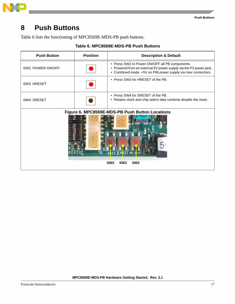
8 Push ButtonsTable 6 lists the functioning of MPC8569E-MDS-PB push buttons.
Table 6. MPC8569E-MDS-PB Push Buttons
Push Button Position Description & Default
SW2: POWER-ON/OFF • Press SW2 to Power-ON/OFF all PB components. • Powered from an external 5V power supply via the P2 power jack. • Combined mode: +5V on PIB power supply via riser connectors.
SW3: HRESET • Press SW3 for HRESET of the PB.
SW4: SRESET • Press SW4 for SRESET of the PB. • Retains clock and chip-select data contents despite the reset.
Figure 6. MPC8569E-MDS-PB Push Button Locations
SW2SW3SW2
MPC8569E-MDS-PB Hardware Getting Started, Rev. 3.1
18 Freescale Semiconductor
LED Lights
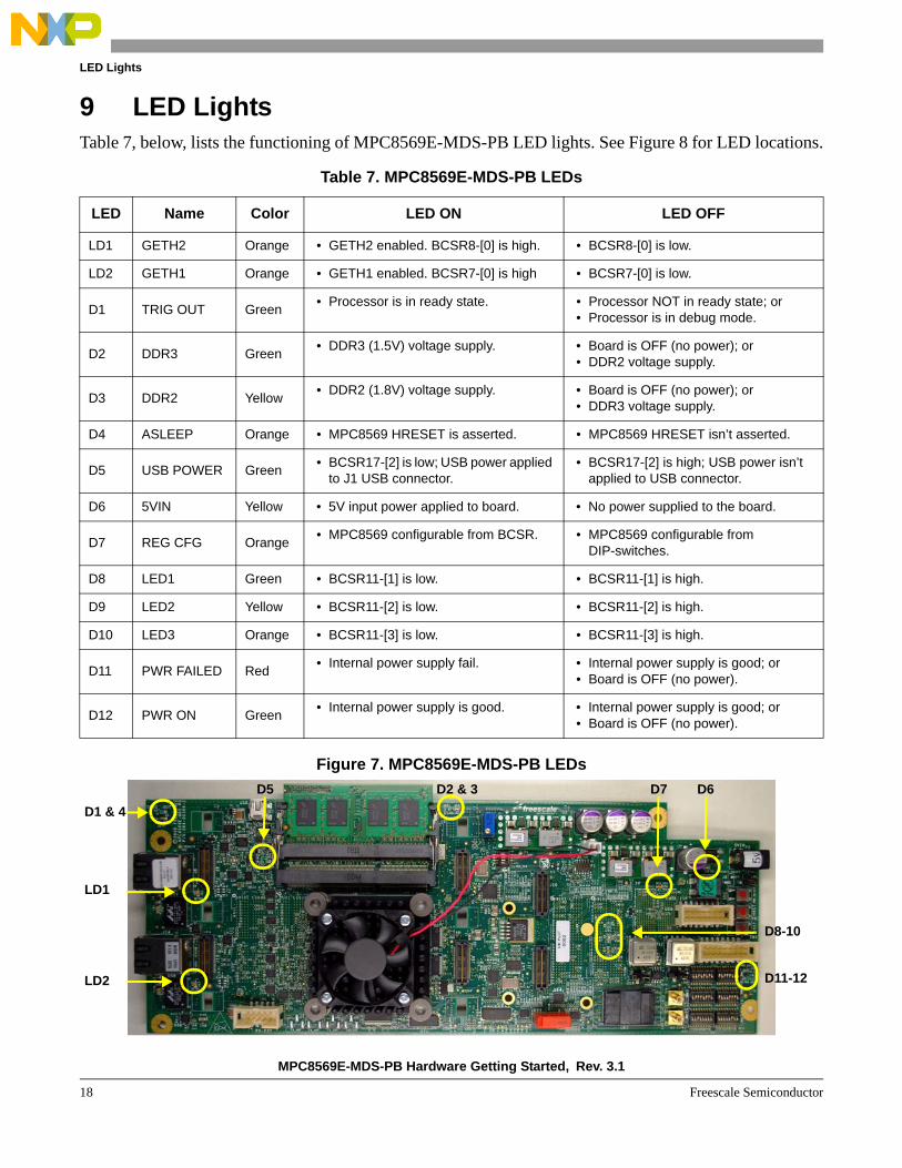
9 LED LightsTable 7, below, lists the functioning of MPC8569E-MDS-PB LED lights. See Figure 8 for LED locations.
Figure 7. MPC8569E-MDS-PB LEDs
Table 7. MPC8569E-MDS-PB LEDs
LED Name Color LED ON LED OFF
LD1 GETH2 Orange • GETH2 enabled. BCSR8-[0] is high. • BCSR8-[0] is low.
LD2 GETH1 Orange • GETH1 enabled. BCSR7-[0] is high • BCSR7-[0] is low.
D1 TRIG OUT Green • Processor is in ready state. • Processor NOT in ready state; or • Processor is in debug mode.
D2 DDR3 Green • DDR3 (1.5V) voltage supply. • Board is OFF (no power); or • DDR2 voltage supply.
D3 DDR2 Yellow • DDR2 (1.8V) voltage supply. • Board is OFF (no power); or • DDR3 voltage supply.
D4 ASLEEP Orange • MPC8569 HRESET is asserted. • MPC8569 HRESET isn’t asserted.
D5 USB POWER Green • BCSR17-[2] is low; USB power applied to J1 USB connector.
• BCSR17-[2] is high; USB power isn’t applied to USB connector.
D6 5VIN Yellow • 5V input power applied to board. • No power supplied to the board.
D7 REG CFG Orange • MPC8569 configurable from BCSR. • MPC8569 configurable from DIP-switches.
D8 LED1 Green • BCSR11-[1] is low. • BCSR11-[1] is high.
D9 LED2 Yellow • BCSR11-[2] is low. • BCSR11-[2] is high.
D10 LED3 Orange • BCSR11-[3] is low. • BCSR11-[3] is high.
D11 PWR FAILED Red • Internal power supply fail. • Internal power supply is good; or • Board is OFF (no power).
D12 PWR ON Green • Internal power supply is good. • Internal power supply is good; or • Board is OFF (no power).
LD1
LD2
D1 & 4D5 D2 & 3 D7 D6
D8-10
D11-12

MPC8569E-MDS-PB Hardware Getting Started, Rev. 3.1
Freescale Semiconductor 19
Board Control Status Registers (BCSR)
10 Board Control Status Registers (BCSR)
10.1 BCSR0Table 8. BCSR0 Register
10.2 BCSR1Table 9. BCSR1 Register
Bit Config Signals Function Default Att
[0:3] CFG_SYS_PLL[0:3] Establishes clock ratio between SYSCLK and CCB. SW7[1:4] sampled at HRESET. [1000] R,W
[4:6] CFG_CORE_PLL[0:2] Sets ratio between e500 Core PLL clock and CCB. SW7[5:7] sampled at HRESET [100] R,W
[7] CFG_SRDS_REFCLK • 0: SerDes expects 125 MHz reference clock frequency. • 1 (Default): SerDes expects 100 MHz reference clock
frequency.
SW7[8] sampled at HRESET [1] R,W
Bit Config Signals Function Default Att
[0:2] CFG_DDR_CLK_PLL[0:2] Configure DDR PLL ratio.
SW5[1:3] sampled at HRESET. • DDR2 [100] • DDR3 [110]
R,W
[3] CFG_DDR_FB_SEL
DDR QE and Platform PLL Feedback Select • 0: gclk-matched/long DDR, QE, and Platform PLLs
feedback path. • 1 (Default): local/short DDR PLL feedback path.
SW5[4] sampled at HRESET [1] R,W
[4] CFG_DDR_TYPEDDR Dram Type (DDR2 or DDR3) • 0: DDR3 of 1.5V and low CKE at reset. • 1 (Default): DDR2 of 1.8V and low CKE at reset.
SW5[5] sampled at HRESET. • DDR3 [0] • DDR2 [1]
R,W
[5] CFG_DDR_MODE
DDR Dram Mode (1x64 or 2x32) • 0: Primary and Secondary DDR is enabled (32-bit width
data bus). • 1 (Default): Primary DDR is enabled (64-bit width data
bus) but secondary DDR is disabled.
SW5[6] sampled at HRESET [1]
R,W
[6] CFG_DDR_SPEED
DDR speed configuration input configures internal logic for proper operation of the DDR. • 0: DDR clock frequency < 500MHz. • 1: DDR clock frequency is > or = 500MHz.
SW5[7] sampled at HRESET [0]
R,W
[7] DDR_FIX • 1: At reset, DDR disables both MCK and MCKE. • 0: DDR disables MCKE at reset; a few cycles later MCK
is disabled.
SW5[8] sampled at HRESET [1]
R,W
MPC8569E-MDS-PB Hardware Getting Started, Rev. 3.1
20 Freescale Semiconductor
Board Control Status Registers (BCSR)
10.3 BCSR2Table 10. BCSR2 Register
10.4 BCSR3Table 11. BCSR3 Register
10.5 BCSR4Table 12. BCSR4 Register
Bit Config Signals Function Default Att
[0:4] CFG_QE_PLL[0:4]
• A multiplier and divisor, applied to SYSCLK input, define the QE clock:
– QE Clock=SYSCLK*(CFG QE PLL[0:4]/CFG_QE_CLK)
SW6[1:5] sampled at HRESET [01000] R,W
[5] SDHCSDHC Card Detect Polarity Select • 0: SDHC card-detect polarity is inverted. • 1 (Default): SDHC card-detect polarity isn’t inverted.
SW6[6] sampled at HRESET [1] R,W
[6:7] CFG_LVDD_VSEL[0:1]Voltage Select Dedicated Pins • QE UCC1 and UCC3 Voltage Select • QE UCC2 and UCC4 Voltage Select
SW6[6:7] sampled at HRESET [11] R,W
Bit Config Signals Function Default Att
[0:3] CFG_PORT_SEL[0:3] IO Select Configuration for SerDes. SW8[1:4] sampled at HRESET [0111] R,W
[4:6] CFG_RIO_ID[5:7] RapidIO Device ID [5:7]. SW8[5:7] sampled at HRESET [000] R,W
[7] CFG_RIO_SYS_SIZE
RapidIO System Size • 0: Large system size with a maximum of 65,536
devices. • 1: Small system size with a maximum of 256 devices.
SW8[8] sampled at HRESET [1] R,W
Bit Config Signals Function Default Att
[0:3] CFG_ROM_LOC[0:3] Selects physical location of boot ROM. SW9[1:4] sampled at HRESET [1101] R,W
[4] CFG_BOOT_CPU
Specifies Boot Configuration Mode: • 0: CPU Boot Hold-off Mode; e500 core boots after
configuration by an external master. • 1 (Default): e500 core boots without being configured
by an external master.
SW9[5] sampled at HRESET [1] R,W
[5:6] CFG_BOOT_SEQ[0:1]
Boot Sequencer • Allows Boot Sequencer to load serial ROM (on I2C1
port) configuration data before the host configures the MPC8569E.
SW9[6:7] sampled at HRESET [11] R,W

MPC8569E-MDS-PB Hardware Getting Started, Rev. 3.1
Freescale Semiconductor 21
Board Control Status Registers (BCSR)
10.6 BCSR5Table 13. BCSR5 Register
10.7 BCSR6Table 14. BCSR6 Register description
[7] CFG_SOURCE
Reset Configuration Source bit lets users select RCW source. • 0: RCW is read through I2C. • 1: RCW is read through IO pin sampling.
SW9[8] sampled at HRESET [1] R/W
Bit Config Signals Function Default Att
[0:2] CFG_HOST_AGT[0:2] MPC8569E configured to act as a host or agent to another interface master (PEX and SRIO).
SW10[1:3] sampled at HRESET [111] R,W
[3] CFG_PLAT_SPEED
Platform speed configuration input configures internal logic for proper operation with CCB frequencies. • 0: CCB frequency < 333 MHz • 1: CCB frequency > or = 333 MHz.
SW10[4] sampled at HRESET [1] R,W
[4] CFG_CORE_SPEED
Core speed configuration input configures internal logic for proper operation with core clock frequencies. • 0: Core clock frequency < or = to 1000MHz. • 1: Core clock frequency > 1000MHz.
SW10[5] sampled at HRESET [1] R,W
[5] CFG_ELBC_ECC
POR configuration input enables eLBC ECC checking on booted external local bus interface. • 0: eLBC ECC disabled after POR. • 1: eLBC ECC enabled after POR.
SW10[5] sampled at HRESET [0]
R,W
[6] CFG_FUSE_OVR_DIS • 0: Fuse PLL override is enabled. • 1: Fuse PLL override is disabled.
SW10[6] sampled at HRESET [1]
R,W
[7] CFG_FUSE_READ
Fuse Read Enable • 0: Fuse reads are disabled during reset sequence. • 1 (Default): Fuse reads are enabled during reset
sequence.
SW10[7] sampled at HRESET [1] R,W
Bit Config Signals Function Default Att
[0] UPC1_EN
• 1: Enable UPC1, ATM, or POS • 0: Disable UPC1 OR enable TDM1A, TDM1B,
TDM1E, TDM1F, TDM1G, TDM1H, TDM2A, TDM2C, TDM2D, TDM2E, RMII5, RMII7, RMII8, TDM2G, TDM2F, and RMII6
[1] R,W
[1] RUPC1POS_EN • 1: Enable UPC1POS • 0: Disable UPC1POS OR enable TDM2A and TDM1B [1] R,W
Bit Config Signals Function Default Att

MPC8569E-MDS-PB Hardware Getting Started, Rev. 3.1
22 Freescale Semiconductor
Board Control Status Registers (BCSR)
10.8 BCSR7Table 15. BCSR7 Register description
[2] RUPC1ADDR_EN • 1: Enable UPC1ADDR, ATM, or POS • 0: Disable UPC1ADDR
(Unsupported: SMII8 and SMII6)[1] R,W
[3] RUPC1DEV2 • 1: Enable UPC1DEV2, ATM, or POS • 0: Disable UPC1DEV2 OR enable TDM2C and UCC3 [1] R,W
[4] SD_CARD_1bit • 1: Enable SD serial mode AND disable I2C2 • 0: Disable SD serial mode AND enable I2C2 [0] R,W
[5] SD_CARD_4bits • 1: Enable SD Card nibble mode (SD_CARD_1bit
should be “1”) AND disable DUART0 and I2C2 bus • 0: Enable DUART0 AND disable SD Card nibble mode
[0] R,W
[6] TDM2G • UPC1_EN = 0(BCSR6[7], disable) • If bit =1, TDM2G is enabled • RMII7(BCSR6[7] should be = 0
[1] R,W
[7] RMII7 • UPC1_EN = 0((BCSR6[7], disable) • If bit =1, RMII7 is enabled • TDM2G(BCSR6[6] should be = 0)
[1] R,W
Bit Config Signals Function Default Att
[0] UCC1_GETH • 1: Enable UCC1_GETH, RGMII, or RTBI • 0: Disable UCC1_GETH OR enable UCC1_RMII
(RMII1) on PIB[1] R,W
[1] UCC1_RGMII • 1: Enable RGMII • 0: Disable RTBI AND enable RMII on PIB [1] R,W
[2] UCC1_RTBI • 1: Enable RTBI • 0: Disable RGMII AND enable RMII on PIB [0] R,W
[3] G1DIS_125 • 1: Disable PHY1 clock_out 125MHz • 0: Enable [0] R,W
[4] G1ENA_XC • 1: Enable • 0: Disable [0] R,W
[5] UCC1/UCC2 GETHRST • 1: Normal operation • 0: Reset (nMVRST) Marvel UCC1 and UCC2 [1] R,W
[6] BRDWP • BRD (EEPROM I2C Memory): write protected for I2C
Flash • 0: Not protected
[1] R,W
[7] BOOTWP • 1: Not protected. • Boot write protected [0] R,W
Bit Config Signals Function Default Att

MPC8569E-MDS-PB Hardware Getting Started, Rev. 3.1
Freescale Semiconductor 23
Board Control Status Registers (BCSR)
10.9 BCSR8Table 16. BCSR8 Register
10.10 BCSR9Table 17. BCSR9 Register
Bit Config Signals Function Default Att
[0] UCC2_GETH • 1: Enable UCC2_GETH, RGMII, or RTBI • 0: Disable UCC2_GETH OR enable UCC2_RMII
(RMII2) on PIB[1] R,W
[1] UCC2_RGMII • 1: Enable RGMII • 0: Disable RTBI AND enable RMII on PIB
[1] R,W
[2] UCC2_RTBI • 1: Enable RTBI • 0: Disable RGMII AND enable RMII on PIB
[0] R,W
[3] G2DIS_125 • 1: Disable PHY2 clock_out 125MHz • 0: Enable PHY2 clock_out 125MHz
[0] R,W
[4] G2ENA_XC • 1: Enable • 0: Disable
[0] R,W
[5] CS_NOR • 1: Boot from NAND_FLASH • 0: Boot from NOR_FLASH
[0] R,W
[6] UEM Marvell PHY RESET • 1: RESET UEM3 (UCC3) and UEM4 (UCC4) • 0: Normal operation
[0] R,W
[7] DDRDRV_SEL • 1: MEMC1,2: MDIC0,1=36.5OHm • 0: MEMC1,2: MDIC0,1=18OHm
[1] R,W
Bit Config Signals Function Default Att
[0] UCC3_GETH
• 1: Enable UCC3_GETH– Use UEM module on PB for RGMII or RTBI.
• 0: Disable UCC3_GETH OR enable (depending upon UCC3_RMII bit) UCC3_RMII (RMII3) on PIB or TDM1C
[1] R,W
[1] UCC3_RGMII • 1: Enable RGMII on UEM • 0: Disable RTBI on UEM AND enable RMII3 on PIB
[1] R,W
[2] UCC3_RTBI • 1: Enable RTBI on UEM • 0: Disable RGMII on UEM AND enable RMII3 on PIB
[0] R,W
[3] UCC3_RMII
• If UCC3_GETH = 0 – then bit = 1 enables UCC3_RMII on PIB– then bit =0 enables TDM1C and UPC1_DEV2
• If UCC3_GETH = 1– then bit has no effect
[0] R,W

MPC8569E-MDS-PB Hardware Getting Started, Rev. 3.1
24 Freescale Semiconductor
Board Control Status Registers (BCSR)
10.11 BCSR10Table 18. BCSR10 Register
[4] RMII3__nSMII3 • 1: Enable RMII on PB (UEM) • 0: Enable SMII on PB (UEM) UCC6
(SMII unsupported)[1] R,W
[5] R_SMII3_nRMII3 • 1: Enable SMII on PB (UEM) UCC6
(SMII unsupported) • 0: Enable RMII on PB (UEM)
[0] R,W
[6] RESERVED RESERVED [1] R,W
[7] nMVPHY_MICPHY3Select UEM-assembled Marvell PHY or Micrel PHY. • 1: Micrel • 0: Marvel
[0] R,W
Bit Config Signals Function Default Att
[0] UCC4_GETH
• 1: Enable UCC4_GETHUse UEM module on PB for RGMII or RTBI.
• 0: Disable UCC4_GETH OR enable UCC4_RMII (RMII4) on PIB or TDM1C
[1] R,W
[1] UCC4_RGMII • 1: Enable RGMII on UEM • 0: Disable RTBI on UEM AND enable RMII3 on PIB
[1] R,W
[2] UCC4_RTBI • 1: Enable RTBI on UEM • 0: Disable RGMII on UEM AND enable RMII3 on PIB
[0] R,W
[3] RMII4__nSMII4 • 1: Enable RMII on PB (UEM) • 0: Enable SMII on PB (UEM) UCC8
(SMII unsupported)[1] R,W
[4] R_SMII4_nRMII4 • 0: Enable RMII on PB (UEM) • 1: Enable SMII on PB (UEM) UCC8
(SMII unsupported)[0] R,W
[5] nMVPHY_MICPHY4 Select UEM assembled Marvell PHY or Micrel PHY. [0] R,W
[6] RnMICRST • 0: Micrel PHY Reset on both UCC3- & UCC4-connected
UEMs • 1: Normal operation
[0] R,W
[7] RMV_SEL_FREQ_34
• 1: Marvell PHY, UCC3 & UCC4 have 25MHz input on UEM
• 0: Marvell PHY, UCC3 & UCC4 have 125MHz input on UEM
[0] R,W
Bit Config Signals Function Default Att

MPC8569E-MDS-PB Hardware Getting Started, Rev. 3.1
Freescale Semiconductor 25
Board Control Status Registers (BCSR)
10.12 BCSR11Table 19. BCSR11 Register
10.13 BCSR12Table 20. BCSR12 Register
Bit Config Signals Function Default Att
[0] REGISTER_CONFIG • 0: Board configured through DIP-switches • 1: Board configured through BCSR registers [0] R,W
[1] LED1 1: LED ON [0] R,W
[2] LED2 1: LED ON [0] R,W
[3] LED3 1: LED ON [0] R,W
[4] R_SLEW0
Select slew rate for GETH input clock.
[0] R,W
[5] R_SLEW [1] R,W
[6] SSC0
Select SerDes clock synthesizer spread spectrum mode.
[1] R,W
[7] SSC1 [1] R,W
Bit Config Signals Function Default Att
[0] PCIE_CLKDIS • 1: Enable PEX clock • 0: Disable PEX clock [1] R,W
[1] TRIGIN For internal use only (0) [Z] R,W
[2] RMII6 • 1: Enable RMII6 (on PIB) and TDM2F 1
• 0: Disable RMII6 AND enable ATM or POS [1] R,W
[3] RMII8 • 1: Enable RMII8 (on PIB) • 0: Disable RMII8 AND enable TDM1H [0] R,W
Slew RateSLEW0 SLEW1 (V/ns)
0 0 41 0 30 1 21 1 1
Setting
SSC0 SSC1 SPREAD%
0 (ON) 0 (ON) CENTER +/- 0.251 (OFF) 0 (ON) DOWN -0.50 (ON) 1 (OFF) DOWN -0.75
1 (OFF) 1 (OFF) NO SPREAD
MPC8569E-MDS-PB Hardware Getting Started, Rev. 3.1
26 Freescale Semiconductor
Board Control Status Registers (BCSR)
10.14 BCSR13Table 21. BCSR13 Register
10.15 BCSR14Table 22. BCSR14 Register
10.16 BCSR15Table 23. BCSR15 Register
[4] TDM2D_2F_DIS • 1: For RMII6 on PIB • 0: For UPC1 or TDM2D or TDM2F [0] R,W
[5] RGETH_CLKSEL • 1: UEM ref clk = 125MHz • 0: UEM ref clk = 50MHz [1] R,W
[6] RESET_PIB • 1: RESET RMII PHY, TDM framer, and/ or ATM PHY • 0: Normal operation for RMII PHY, TDM framer, and/
or ATM PHY [0] R,W
[7] ISOLATE_GPIO • 1: For RMII6 and RMII7 operation • 0: For UPC1 operation [0] R,W
1 I2C PCA9555 address 26H should drive output register 1[0] to 1.
Bit Config Signals Function Default Att
[0:7] R_PS[0:7] Internal Use Only [1:1] R,W
Bit Config Signals Function Default Att
[0:4] R_PS[8:12] Internal Use Only [11111] R,W
[5] TDM1G_EN • 1: TDM1G_EN enabled • 0: TDM1G_EN disabled [0] R,W
[6] PRESENCE 3UEM inserted into J15 • 1: Present • 0: Not present
[X] R
[7] PRESENCE 4UEM inserted into J5 • 1: Present • 0: Not present
[X] R
Bit Config Signals Function Default Att
[0] G3ENA_XC • 1: Enable • 0: Disable [0] R,W
Bit Config Signals Function Default Att

MPC8569E-MDS-PB Hardware Getting Started, Rev. 3.1
Freescale Semiconductor 27
Board Control Status Registers (BCSR)
10.17 BCSR16Table 24. BCSR16 Register
[1] G4ENA_XC • 1: Enable • 0: Disable [0] R,W
[2] G3DIS_125 • 1: Disable PHY3 clock_out 125MHz • 0: Enable PHY3 clock_out 125MHz [0] R,W
[3] G4DIS_125 • 1: Disable PHY4 clock_out 125Mhx • 0: Enable [0] R,W
[4] SMII6 DIS
• 1: Disable SMII6 AND enable RMII6, TDM1C, UPC1 Dev2, and UCC3
• 0: Enable SMII6 and TDM2D(SMII unsupported)
[1] R,W
[5] SMII8 DIS
• 1: Enable UCC8 RMII on PIB and TDM1H AND disable SMII8.
• 0: Enable SMII8(SMII unsupported)
[1] R,W
[6] TDM1F • 1: Enable TDM1F • 0: Disable TDM1F [1] R,W
[7] RUART1_nQEUART • 1: Enable QE_UART • 0: Enable UART1, TDM1D, and TDM2B [0] R,W
Bit Config Signals Function Default Att
[0] PORESET PWR_ON Reset/HRESET • 0: Active [1] R,W
[1] TSEC0MST Reserved [1] R,W
[2] TSEC1MST Reserved [1] R,W
[3] TSEC2MST Reserved [1] R,W
[4] TSEC3MST Reserved [1] R,W
[5] TSEC4MST Reserved [1] R,W
[6] TDM1C_DEV2
• 1: Enable UPC1 Device2 • 0: Disable UPC1 Device 2 OR enable RMII3 on
PIB,TDM1C and TDM2C
• If bit = 0 then RMII3 is enabled • Dev2- RxEN_B[2] • TDM2c-TSYNC • TDM1c
[0] R,W
[7] RESERVED - [0] R,W
Bit Config Signals Function Default Att

MPC8569E-MDS-PB Hardware Getting Started, Rev. 3.1
28 Freescale Semiconductor
Board Control Status Registers (BCSR)
10.18 BCSR17Table 25. BCSR17 Register
10.19 BCSR18Table 26. BCSR18 Register
Bit Config Signals Function Default Att
[0] RnUSBEN • 1: Disable USB AND enable TDM1B • 0: Enable USB [1] R,W
[1] RnUSBLOWSPD • 1: USB full-speed (12Mb/s) • 0: USB low-speed (1.5Mb/s) [0] R,W
[2] RnUSBVCC
• 0: USB acts as Device– USB powered from an external host– Enables RMII6 and TDM1G
• 1: USB acts as Host– USB supplies power to external device
[0] R,W
[3] RUSB_MODEUSB Mode • 1: Host • 0: Device
[0] R,W
[4] RPRESENCE_FUEM inserted into J7 • 1: Present • 0: Not present
[x] R
[5] RPRESENCE_EUEM inserted into J16 • 1: Present • 0: Not present
[x] R
[6] RFLASH_RDY • 1: Ready • 0: Busy [x] R
[7] FLASH_nWP • 0: FLASH Write Protect • 1: FLASH normal operation [0] R,W
Bit Config Signals Function Value Att
[0:3] REV • BCSR revision • Four bit revision coding current version R,W
[4:7] SUBREV • BCSR SUB revision • Four bit revision coding sub version R,W

MPC8569E-MDS-PB Hardware Getting Started, Rev. 3.1
Freescale Semiconductor 29
Memory Map
11 Memory Map
11.1 MPC8569E PB Memory Map
NOTE!The memory map has NOT been finalized.
Access to MPC8569 memory slaves is controlled by the MPC8569 memory controller. Table 27 is only a recommended memory map; it is a "soft" map device. Users are free to move addresses around the map.
Table 27. MPC8569E-MDS-PB Memory Map (with NOR Flash as Boot Source)
ADDRESS RANGE Block Allocation Port Size
00000000 - 1FFFFFFFDDR3/DDR3 Memory Controller
MEMC1 (512MB) 32
00000000 - 3FFFFFFF MEMC1 (Integrated Mode) 1GB 64
20000000 - 3FFFFFFF MEMC2 (512MB) 32
40000000 - 7FFFFFFF Reserved 1GB
80000000 - 9FFFFFFF SRIO1 Outbound Window (512 MB) x4 lane
A0000000 - BFFFFFFF SRIO2 Outbound Window (512 MB) x4 lane
C0000000 - DFFFFFFF PEX Outbound Window (512 MB) x4 lane
E0000000 - E00FFFFF MPC8569 Internal Map Internal Memory Register Space (1 MB) 32
E0100000 - E03FFFFF Reserved For future MPC8569 derivatives (3 MB) -
E0400000 - E047FFFF L2SRAM 1MB
E0480000 - F7FFFFFF Reserved 400MB
F8000000 - F8007FFF BCSR on CS1 Altera (32KB) 8
F8008000 - F800FFFF CS4 PIB (32KB) 8
F8010000 - F8017FFF CS5 PIB (32KB) 8
FA018000 - FFFFFFFF Reserved 100MB
FC000000 - FDFFFFFF NAND Flash on CS3/CS0 Samsung: K9F5608U0D-PCB0 (32MB) 8
FE000000 - FFFFFFFF NOR Flash on CS0/CS3 Spansion: S29GL256N11TFIV2O (32MB) 8

MPC8569E-MDS-PB Hardware Getting Started, Rev. 3.1
30 Freescale Semiconductor
Working Environment
12 Working EnvironmentTable 28. MPC8569E-MDS-PB Working Environment Modes
Mode Optional Expansion Description
StandalonePEX RC
Includes the noted modules: • GETH3 & 4 UEM • SerDes Lane e, f SRIOx1 or UEM (SGMII mode) • SerDes Lane a, b SRIOx1 • SerDes Lane a, b PEXx2 • 1xDDR3 SODIMMx64 or 2xDDR3x32 SODIMM
• PB powered, via P2, by an external 5V power supply (included in kit).
• [Option] PEX EP powered, via P2 of PEXx2, by an external 12V power supply.
PIB-combined ModeMPC9569-MDS-PB on PIB
Includes the noted modules: • GETH3 & 4 UEM • SerDes Lane e, f SRIOx1 or UEM (SGMII mode) • SerDes Lane a, b SRIOx1 • SerDes Lane a, b PEXx2 • 1xDDR3 SODIMMx64 or 2xDDR3x32 SODIMM
• PB powered from PIB via bottom riser connectors.
• [Option] PEX EP powered, via P2 of PEXx2, from an external 12V power supply.

MPC8569E-MDS-PB Hardware Getting Started, Rev. 3.1
Freescale Semiconductor 31
Getting Started Procedures
13 Getting Started ProceduresThis section outlines “Getting Started” procedures for the MPC8569E-MDS-PB including use of the JTAG connectivity unit. Optional modules are detailed in Section 12.
Procedure 1: Check hardware kit contents (Section 4).
Procedure 2: Check PB default switch settings (Section 6).
Procedure 3: Check PB default connector settings (Section 7).
Procedure 4: Establish working environment (Section 12).
Procedure 5: Insert plastic guide pins into PB.
1. Insert three guide pins. Pins hold UEM modules used in RGMII and RTBI modes.
2. Insert three guide pins. Pins hold UEM modules (SGMII mode) used for SerDes Options 1, 2 and 3. See Section 12, Set-up 1.
Procedure 6: Assemble and connect 5V power supply.
NOTE!Ensure Power-OFF.
1. Assemble AC/DC power supply kit:a) Cable with country-specific wall
outlet plug.b) Power supply unit and cable with
plug (for board connection).
2. Connect the AC/DC power supply cable to the 5V IN on-board jack (P2).
3. Plug the power cable into the wall outlet.
SerDes Guide Pins (3)Guide Pins (3)
AC/DC Power Supply
P2

MPC8569E-MDS-PB Hardware Getting Started, Rev. 3.1
32 Freescale Semiconductor
Getting Started Procedures
Procedure 7: Perform initial board power-up and check LEDs (Section 7-8).
CAUTION!Prevent damage to the USB TAP; connect only after initial board reset.
1. Power PB via an external 5V power supply; LED D6 glows yellow.2. Press SW2 to Power-ON all PB components.3. Check for completion of PRESET sequence; indicated by steady lights from LEDs D1, D2 or D3, and D12. 4. Press SW2 to Power-OFF all PB components.
Procedure 8: Connect CodeWarrior USB TAP to the PB.
CAUTION!To avoid damage, follow steps for aligning and connecting the Bootwiz.
NOTE!Freescale’s CodeWarrior USB TAP enables CodeWarrior IDE software to work with the PB.
1. Align Bootwiz module with its CS facing the board’s printed “COP” text. The PS must face switches SW5 - SW10.
2. Connect the Bootwiz module to the J13 COP board connector.
3. Attach the USB-TAP cable to the Bootwiz module’s J2 connector.
4. Press button SW2 to Power-ON all PB components.
5. Check for completion of the reset sequence.
Procedure 9: Attach cables per user development needs and planned board use.
1. Connect FSL adaptor cable to J21 on PB.
2. Connect RS-232 (male) cable to COM1/2 (UART0/1) of FSL adaptor cable.
3. Connect RS-232 (female) to a PC.4. Connect GETH loopback (shown in
picture) or ETH cables with RJ45 connectors to the Ethernet ports: – J14 for GETH1– J6 for GETH2
5. Continue as per CodeWarrior Kit Configuration Guide instructions.
SW2
J13
Bootwiz CSPS
Bootwiz CS
GETH Loopbacks
J6
J14
J21
FSL Adaptor(with COM1/2)
RS-232 (male)

MPC8569E-MDS-PB Hardware Getting Started, Rev. 3.1
Freescale Semiconductor 33
SerDes Module Set-ups
14 SerDes Module Set-upsThis section details SerDes options
SerDes Options
1. Select a configuration scenario from the available options
2. Follow the steps for a given option, Options 1 through 5, below.
3. Plug 5V power cable into P2.
4. Press SW2 to Power-ON.
NOTE!Options 2 through 5: PEX EP board 12V DC power is supplied via the corresponding PEX-expansion module power jack.
a
b
e
f
Option 1 Option 2,3 Option 4.5
SGMIIx1
SGMIIx1
SGMIIx1
SGMIIx1
PEX x2
12V
PEX x2
12V
SRIOx1
A1
H1
A10
H10
SRIOx1
A1
H1
A10
H10
SRIOx1
A1
H1
A10
H10
SRIOx1
A1
H1
A10
H10
2.5Gbaudx2 PEX5
2.5Gbaudx1 PEX-4
PEX at 2.5Gbaudx2 PEXSGMIISGMII3
PEX at 2.5Gbaudx1 PEX-SGMIISGMII2
SRIO at 2.5Gbaudx1 SRIO1SGMIISGMII1
Frequency Information
abef
Lanes
2.5Gbaudx2 PEX5
2.5Gbaudx1 PEX-x1 SRIO1x1 SRIO24
PEX at 2.5Gbaudx2 PEXSGMIISGMII3
PEX at 2.5Gbaudx1 PEX-SGMIISGMII2
SRIO at 2.5Gbaudx1 SRIO1x1 SRIO2SGMIISGMII1
Frequency Information
abef
Lanes
x1 SRIO2 x1 SRIO1
Option

MPC8569E-MDS-PB Hardware Getting Started, Rev. 3.1
34 Freescale Semiconductor
SerDes Module Set-ups
SerDes Option 1: two UEM & two SRIOx1
a) Insert UEM (used in SGMII mode) modules into J16 and J7.
b) Connect ETH RJ45 cables to UEM modules.
a) Insert SRIOx1 modules into J10 and J17; stabilize with plastic screws.
b) Insert SRIO loopback into assembled SRIOx1 modules.
SerDes Option 2: two UEM & one PEXx1 (x1 mode)
a) Insert UEM modules into J16 and J7.b) Connect ETH RJ45 cables to UEM
modules.c) Insert PEXx2 into J10 and J17. d) PEX slot now available as RC port x1.
SerDes Option 3: two UEM & one PEXx2 (x2 mode)
a) Repeat first three steps of Option 2.b) PEX slot now available as RC port x2.
See SerDes Option 2 photos.
UEM SRIOx1& Loopback
RJ45 Cables
RJ45 Cables
SRIOx1UEM Loopback
UEM PEX
RJ45 Cables
RJ45 Cables
UEM PEX

MPC8569E-MDS-PB Hardware Getting Started, Rev. 3.1
Freescale Semiconductor 35
SerDes Module Set-ups
SerDes Option 4: two SRIOx1 & one PEXx1 (x1 mode)
a) Insert SRIOx1 modules into J16 and J7.
b) Insert SRIO loopback into SRIOx1 modules.
c) Insert PEXx2 into J10 and J17.d) PEX slot now available as RC port x1.
SerDes Option 5: two SRIOx1 & one PEXx2 (x2 mode)
a) Repeat first three steps of Option 4.b) PEX slot now available as RC port x2.
See SerDes Option 4 photos.
SRIOx1 Loopback
PEX
LoopbackSRIOx1
PEX

MPC8569E-MDS-PB Hardware Getting Started, Rev. 3.1
36 Freescale Semiconductor
SerDes Module Set-ups

MPC8569E-MDS-PB Hardware Getting Started, Rev. 3.1
Freescale Semiconductor 37
SerDes Module Set-ups
How to Reach Us:Home Page: www.freescale.com
Web Support: http://www.freescale.com/support
USA/Europe or Locations Not Listed: Freescale Semiconductor, Inc.Technical Information Center, EL5162100 East Elliot Road Tempe, Arizona 85284 +1-800-521-6274 or+1-480-768-2130www.freescale.com/support
Europe, Middle East, and Africa:Freescale Halbleiter Deutschland GmbHTechnical Information CenterSchatzbogen 781829 Muenchen, Germany+44 1296 380 456 (English) +46 8 52200080 (English)+49 89 92103 559 (German)+33 1 69 35 48 48 (French) www.freescale.com/support
Japan: Freescale Semiconductor Japan Ltd. HeadquartersARCO Tower 15F1-8-1, Shimo-Meguro, Meguro-ku Tokyo 153-0064Japan 0120 191014 or+81 3 5437 [email protected]
Asia/Pacific: Freescale Semiconductor Hong Kong Ltd. Technical Information Center2 Dai King Street Tai Po Industrial Estate Tai Po, N.T., Hong Kong +800 2666 [email protected]
For Literature Requests Only:Freescale Semiconductor
Literature Distribution Center P.O. Box 5405Denver, Colorado 80217 +1-800 441-2447 or+1-303-675-2140Fax: +1-303-675-2150LDCForFreescaleSemiconductor
@hibbertgroup.com
Information in this document is provided solely to enable system and software implementers to
use Freescale Semiconductor products. There are no express or implied copyright licenses
granted hereunder to design or fabricate any integrated circuits or integrated circuits based on
the information in this document.
Freescale Semiconductor reserves the right to make changes without further notice to any
products herein. Freescale Semiconductor makes no warranty, representation or guarantee
regarding the suitability of its products for any particular purpose, nor does Freescale
Semiconductor assume any liability arising out of the application or use of any product or
circuit, and specifically disclaims any and all liability, including without limitation
consequential or incidental damages. “Typical” parameters which may be provided in Freescale
Semiconductor data sheets and/or specifications can and do vary in different applications and
actual performance may vary over time. All operating parameters, including “Typicals” must
be validated for each customer application by customer’s technical experts. Freescale
Semiconductor does not convey any license under its patent rights nor the rights of others.
Freescale Semiconductor products are not designed, intended, or authorized for use as
components in systems intended for surgical implant into the body, or other applications
intended to support or sustain life, or for any other application in which the failure of the
Freescale Semiconductor product could create a situation where personal injury or death may
occur. Should Buyer purchase or use Freescale Semiconductor products for any such
unintended or unauthorized application, Buyer shall indemnify and hold Freescale
Semiconductor and its officers, employees, subsidiaries, affiliates, and distributors harmless
against all claims, costs, damages, and expenses, and reasonable attorney fees arising out of,
directly or indirectly, any claim of personal injury or death associated with such unintended or
unauthorized use, even if such claim alleges that Freescale Semiconductor was negligent
regarding the design or manufacture of the part.
Freescale™ and the Freescale logo are trademarks of Freescale Semiconductor, Inc. The Power Architecture and Power.org word marks and the Power and Power.org logos and related marks are trademarks and service marks licensed by Power.org. The PowerPC name is a trademark of IBM Corp. and is used under license. IEEE 1149.1, is a registered trademark of the Institute of Electrical and Electronics Engineers, Inc. (IEEE). This product is not endorsed or approved by the IEEE. All other product or service names are the property of their respective owners.
© Freescale Semiconductor, Inc.,2008. All rights reserved.

MPC8569E-MDS-PB Hardware Getting Started, Rev. 3.1
38 Freescale Semiconductor
SerDes Module Set-ups