
MSC8254 Reference Manual - NXP
1270
MSC8254 Reference Manual Quad Core Digital Signal Processor MSC8254RM Rev 0, July 2011
-
Upload
khangminh22 -
Category
Documents
-
view
0 -
download
0
Transcript of MSC8254 Reference Manual - NXP

MSC8254 Reference ManualQuad Core Digital Signal Processor
MSC8254RMRev 0, July 2011
Information in this document is provided solely to enable system and software implementers to use Freescale Semiconductor products. There are no express or implied copyright licenses granted hereunder to design or fabricate any integrated circuits or integrated circuits based on the information in this document.
Freescale Semiconductor reserves the right to make changes without further notice to any products herein. Freescale Semiconductor makes no warranty, representation or guarantee regarding the suitability of its products for any particular purpose, nor does Freescale Semiconductor assume any liability arising out of the application or use of any product or circuit, and specifically disclaims any and all liability, including without limitation consequential or incidental damages. “Typical” parameters which may be provided in Freescale Semiconductor data sheets and/or specifications can and do vary in different applications and actual performance may vary over time. All operating parameters, including “Typicals” must be validated for each customer application by customer’s technical experts. Freescale Semiconductor does not convey any license under its patent rights nor the rights of others. Freescale Semiconductor products are not designed, intended, or authorized for use as components in systems intended for surgical implant into the body, or other applications intended to support or sustain life, or for any other application in which the failure of the Freescale Semiconductor product could create a situation where personal injury or death may occur. Should Buyer purchase or use Freescale Semiconductor products for any such unintended or unauthorized application, Buyer shall indemnify and hold Freescale Semiconductor and its officers, employees, subsidiaries, affiliates, and distributors harmless against all claims, costs, damages, and expenses, and reasonable attorney fees arising out of, directly or indirectly, any claim of personal injury or death associated with such unintended or unauthorized use, even if such claim alleges that Freescale Semiconductor was negligent regarding the design or manufacture of the part.
Freescale, the Freescale logo, and CodeWarrior are trademarks of Freescale Semiconductor, Inc., Reg. U.S. Pat. & Tm. Off. QUICC Engine is a trademark of Freescale Semiconductor, Inc. All other product or service names are the property of their respective owners.
© 2009–2011 Freescale Semiconductor, Inc.
MSC8254RMRev. 07/2011
How to Reach Us:
Home Page: www.freescale.com
Web Support: http://www.freescale.com/support
USA/Europe or Locations Not Listed: Freescale Semiconductor, Inc.Technical Information Center, EL5162100 East Elliot Road Tempe, Arizona 85284 +1-800-521-6274 or+1-480-768-2130www.freescale.com/support
Europe, Middle East, and Africa:Freescale Halbleiter Deutschland GmbHTechnical Information CenterSchatzbogen 781829 Muenchen, Germany+44 1296 380 456 (English) +46 8 52200080 (English)+49 89 92103 559 (German)+33 1 69 35 48 48 (French) www.freescale.com/support
Japan: Freescale Semiconductor Japan Ltd. HeadquartersARCO Tower 15F1-8-1, Shimo-Meguro, Meguro-ku Tokyo 153-0064Japan 0120 191014 or+81 3 5437 [email protected]
Asia/Pacific: Freescale Semiconductor China Ltd. Exchange Building 23FNo. 118 Jianguo RoadChaoyang DistrictBeijing 100022China+86 010 5879 [email protected]
For Literature Requests Only:Freescale Semiconductor
Literature Distribution Center +1-800 441-2447 or+1-303-675-2140Fax: +1-303-675-2150LDCForFreescaleSemiconductor
@hibbertgroup.com

1Overview
2SC3850 Core Overview
4Chip-Level Arbitration and Switching System (CLASS)
7Clocks
13
Direct Memory Access (DMA) Controller 14
High Speed Serial Interface (HSSI) 15
Serial RapidIO Controller
TDM Interface 19
UART
23
I2C
External Signals
Reset
Boot Program
Memory Map
MSC8154 SC3850 DSP Subsystem
Timers
Hardware Semaphores
Debugging, Profiling, and Performance Monitoring
3
5
6
8
9
18
20
22
24
DDR-SDRAM Controller
11
Interrupt Handling
12
16
QUICC Engine Subsystem
Internal Memory Subsystem
10
GPIO
21
25
General Configuration Registers
17PCI Express Controller

1 Overview
2 SC3850 Core Overview
4 Chip-Level Arbitration and Switching System (CLASS)
7 Clocks
13
Direct Memory Access (DMA) Controller14
High Speed Serial Interface (HSSI)15
Serial RapidIO Controller
TDM Interface19
UART
23
I2C
External Signals
Reset
Boot Program
Memory Map
MSC8154 SC3850 DSP Subsystem
Timers
Hardware Semaphores
Debugging, Profiling, and Performance Monitoring
3
5
6
8
9
18
20
22
24
DDR-SDRAM Controller
11
Interrupt Handling
12
16
QUICC Engine Subsystem
Internal Memory Subsystem
10
GPIO
21
25
General Configuration Registers
17 PCI Express Controller

Contents
1 Overview1.1 Features . . . . . . . . . . . . . . . . . . . . . . . . . . . . . . . . . . . . . . . . . . . . . . . . . . . . . . . . 1-21.2 Block Diagram . . . . . . . . . . . . . . . . . . . . . . . . . . . . . . . . . . . . . . . . . . . . . . . . . . 1-121.3 Architecture . . . . . . . . . . . . . . . . . . . . . . . . . . . . . . . . . . . . . . . . . . . . . . . . . . . . 1-121.4 StarCore SC3850 DSP Subsystem. . . . . . . . . . . . . . . . . . . . . . . . . . . . . . . . . . . 1-121.4.1 Enhancements . . . . . . . . . . . . . . . . . . . . . . . . . . . . . . . . . . . . . . . . . . . . . . . . . 1-141.4.2 StarCore SC3850 DSP Core . . . . . . . . . . . . . . . . . . . . . . . . . . . . . . . . . . . . . . 1-141.4.3 L1 Instruction Cache . . . . . . . . . . . . . . . . . . . . . . . . . . . . . . . . . . . . . . . . . . . . 1-161.4.4 L1 Data Cache. . . . . . . . . . . . . . . . . . . . . . . . . . . . . . . . . . . . . . . . . . . . . . . . . 1-161.4.5 L2 Unified Cache/M2 Memory. . . . . . . . . . . . . . . . . . . . . . . . . . . . . . . . . . . . 1-161.4.6 Memory Management Unit (MMU) . . . . . . . . . . . . . . . . . . . . . . . . . . . . . . . . 1-171.4.7 Debug and Profiling Unit (DPU) . . . . . . . . . . . . . . . . . . . . . . . . . . . . . . . . . . 1-171.4.8 Extended Programmable Interrupt Controller . . . . . . . . . . . . . . . . . . . . . . . . 1-171.4.9 Timer . . . . . . . . . . . . . . . . . . . . . . . . . . . . . . . . . . . . . . . . . . . . . . . . . . . . . . . 1-181.5 Chip-Level Arbitration and Switching System (CLASS) . . . . . . . . . . . . . . . . . 1-181.6 M3 Memory . . . . . . . . . . . . . . . . . . . . . . . . . . . . . . . . . . . . . . . . . . . . . . . . . . . . 1-181.7 Clocks. . . . . . . . . . . . . . . . . . . . . . . . . . . . . . . . . . . . . . . . . . . . . . . . . . . . . . . . . 1-191.8 DDR Controllers (DDRC1 and DDRC2). . . . . . . . . . . . . . . . . . . . . . . . . . . . . . 1-191.9 DMA Controller . . . . . . . . . . . . . . . . . . . . . . . . . . . . . . . . . . . . . . . . . . . . . . . . . 1-201.10 High Speed System Interface . . . . . . . . . . . . . . . . . . . . . . . . . . . . . . . . . . . . . . . 1-201.10.1 Serial RapidIO Subsystem . . . . . . . . . . . . . . . . . . . . . . . . . . . . . . . . . . . . . . . 1-211.10.1.1 Serial RapidIO and Host Interactions. . . . . . . . . . . . . . . . . . . . . . . . . . . . . . 1-221.10.1.2 RapidIO Messaging Unit (RMU) Operation . . . . . . . . . . . . . . . . . . . . . . . . 1-231.10.2 PCI Express . . . . . . . . . . . . . . . . . . . . . . . . . . . . . . . . . . . . . . . . . . . . . . . . . . . 1-241.10.3 OCN-DMA Controllers. . . . . . . . . . . . . . . . . . . . . . . . . . . . . . . . . . . . . . . . . . 1-251.10.4 OCN Fabric . . . . . . . . . . . . . . . . . . . . . . . . . . . . . . . . . . . . . . . . . . . . . . . . . . . 1-251.10.5 SRIO Port Controller Modules (SRIOn). . . . . . . . . . . . . . . . . . . . . . . . . . . . . 1-251.10.6 SerDes PHY Interfaces . . . . . . . . . . . . . . . . . . . . . . . . . . . . . . . . . . . . . . . . . . 1-251.11 QUICC Engine Subsystem. . . . . . . . . . . . . . . . . . . . . . . . . . . . . . . . . . . . . . . . . 1-261.11.1 Ethernet Controllers . . . . . . . . . . . . . . . . . . . . . . . . . . . . . . . . . . . . . . . . . . . . 1-271.11.2 Serial Peripheral Interface (SPI) . . . . . . . . . . . . . . . . . . . . . . . . . . . . . . . . . . . 1-281.12 TDM. . . . . . . . . . . . . . . . . . . . . . . . . . . . . . . . . . . . . . . . . . . . . . . . . . . . . . . . . . 1-281.13 Global Interrupt Controller (GIC) . . . . . . . . . . . . . . . . . . . . . . . . . . . . . . . . . . . 1-291.14 UART. . . . . . . . . . . . . . . . . . . . . . . . . . . . . . . . . . . . . . . . . . . . . . . . . . . . . . . . . 1-29
MSC8254 Reference Manual, Rev. 0
Freescale Semiconductor v

Contents
1.15 Timers . . . . . . . . . . . . . . . . . . . . . . . . . . . . . . . . . . . . . . . . . . . . . . . . . . . . . . . . 1-291.16 Hardware Semaphores . . . . . . . . . . . . . . . . . . . . . . . . . . . . . . . . . . . . . . . . . . . . 1-291.17 Virtual Interrupts . . . . . . . . . . . . . . . . . . . . . . . . . . . . . . . . . . . . . . . . . . . . . . . . 1-301.18 I2C Interface. . . . . . . . . . . . . . . . . . . . . . . . . . . . . . . . . . . . . . . . . . . . . . . . . . . . 1-301.19 GPIOs. . . . . . . . . . . . . . . . . . . . . . . . . . . . . . . . . . . . . . . . . . . . . . . . . . . . . . . . . 1-301.20 Boot Options . . . . . . . . . . . . . . . . . . . . . . . . . . . . . . . . . . . . . . . . . . . . . . . . . . . 1-301.21 JTAG . . . . . . . . . . . . . . . . . . . . . . . . . . . . . . . . . . . . . . . . . . . . . . . . . . . . . . . . . 1-311.22 Developer Environment . . . . . . . . . . . . . . . . . . . . . . . . . . . . . . . . . . . . . . . . . . . 1-321.22.1 Tools . . . . . . . . . . . . . . . . . . . . . . . . . . . . . . . . . . . . . . . . . . . . . . . . . . . . . . . . 1-321.22.2 Application Software. . . . . . . . . . . . . . . . . . . . . . . . . . . . . . . . . . . . . . . . . . . . 1-331.23 Example Applications . . . . . . . . . . . . . . . . . . . . . . . . . . . . . . . . . . . . . . . . . . . . 1-331.23.1 Use Case 1: 3G-LTE Basic System. . . . . . . . . . . . . . . . . . . . . . . . . . . . . . . . . 1-331.23.2 Use Case 2: 3G-LTE System . . . . . . . . . . . . . . . . . . . . . . . . . . . . . . . . . . . . . 1-341.23.3 Use Case 3: 3G-LTE System . . . . . . . . . . . . . . . . . . . . . . . . . . . . . . . . . . . . . 1-341.23.4 Use Case 4: TD-SCDMA System . . . . . . . . . . . . . . . . . . . . . . . . . . . . . . . . . . 1-351.23.5 Use Case 5: WiMAX Basic System . . . . . . . . . . . . . . . . . . . . . . . . . . . . . . . . 1-351.23.6 Use Case 6: WiMAX System . . . . . . . . . . . . . . . . . . . . . . . . . . . . . . . . . . . . . 1-361.23.7 Use Case 7: WCDMA Basic System . . . . . . . . . . . . . . . . . . . . . . . . . . . . . . . 1-36
2 SC3850 Core Overview2.1 Core Architecture Features . . . . . . . . . . . . . . . . . . . . . . . . . . . . . . . . . . . . . . . . . 2-22.2 StarCore SC3850 Core Architecture . . . . . . . . . . . . . . . . . . . . . . . . . . . . . . . . . . 2-4
3 External Signals3.1 Power Signals. . . . . . . . . . . . . . . . . . . . . . . . . . . . . . . . . . . . . . . . . . . . . . . . . . . . 3-43.2 Clock Signals . . . . . . . . . . . . . . . . . . . . . . . . . . . . . . . . . . . . . . . . . . . . . . . . . . . . 3-53.3 Reset and Configuration Signals . . . . . . . . . . . . . . . . . . . . . . . . . . . . . . . . . . . . . 3-63.4 Memory Controller 1 and 2 . . . . . . . . . . . . . . . . . . . . . . . . . . . . . . . . . . . . . . . . 3-103.5 SerDes Multiplexed Signals for the Serial RapidIO, PCI Express, and
SGMII Interfaces . . . . . . . . . . . . . . . . . . . . . . . . . . . . . . . . . . . . . . . . . . . . . . . . 3-113.6 TDM and Ethernet Signals. . . . . . . . . . . . . . . . . . . . . . . . . . . . . . . . . . . . . . . . . 3-163.7 Serial Peripheral Interface (SPI) Signal Summary . . . . . . . . . . . . . . . . . . . . . . 3-203.8 GPIO/Maskable Interrupt Signal Summary . . . . . . . . . . . . . . . . . . . . . . . . . . . . 3-203.9 Timer Signals . . . . . . . . . . . . . . . . . . . . . . . . . . . . . . . . . . . . . . . . . . . . . . . . . . . 3-253.10 UART Signals . . . . . . . . . . . . . . . . . . . . . . . . . . . . . . . . . . . . . . . . . . . . . . . . . . 3-263.11 I2C Signals . . . . . . . . . . . . . . . . . . . . . . . . . . . . . . . . . . . . . . . . . . . . . . . . . . . . . 3-263.12 External DMA Signals . . . . . . . . . . . . . . . . . . . . . . . . . . . . . . . . . . . . . . . . . . . . 3-273.13 Other Interrupt Signals. . . . . . . . . . . . . . . . . . . . . . . . . . . . . . . . . . . . . . . . . . . . 3-283.14 OCE Event and JTAG Test Access Port Signals . . . . . . . . . . . . . . . . . . . . . . . . 3-29
MSC8254 Reference Manual, Rev. 0
vi Freescale Semiconductor

Contents
4 Chip-Level Arbitration and Switching System (CLASS)4.1 CLASS Features. . . . . . . . . . . . . . . . . . . . . . . . . . . . . . . . . . . . . . . . . . . . . . . . . . 4-24.2 Functional Description. . . . . . . . . . . . . . . . . . . . . . . . . . . . . . . . . . . . . . . . . . . . . 4-34.2.1 Expander Module and Transaction Flow . . . . . . . . . . . . . . . . . . . . . . . . . . . . . 4-44.2.2 Multiplexer and Arbiter Module . . . . . . . . . . . . . . . . . . . . . . . . . . . . . . . . . . . . 4-44.2.2.1 CLASS Arbiter . . . . . . . . . . . . . . . . . . . . . . . . . . . . . . . . . . . . . . . . . . . . . . . . 4-44.2.2.1.1 Weighted Arbitration . . . . . . . . . . . . . . . . . . . . . . . . . . . . . . . . . . . . . . . . . . . 4-54.2.2.1.2 Late Arbitration . . . . . . . . . . . . . . . . . . . . . . . . . . . . . . . . . . . . . . . . . . . . . . . 4-54.2.2.1.3 Priority Masking . . . . . . . . . . . . . . . . . . . . . . . . . . . . . . . . . . . . . . . . . . . . . . . 4-54.2.2.1.4 Auto Priority Upgrade . . . . . . . . . . . . . . . . . . . . . . . . . . . . . . . . . . . . . . . . . . 4-54.2.2.2 CLASS Multiplexer . . . . . . . . . . . . . . . . . . . . . . . . . . . . . . . . . . . . . . . . . . . . 4-54.2.3 Normalizer Module . . . . . . . . . . . . . . . . . . . . . . . . . . . . . . . . . . . . . . . . . . . . . . 4-64.2.4 CLASS Control Interface (CCI) . . . . . . . . . . . . . . . . . . . . . . . . . . . . . . . . . . . . 4-64.3 MSC8254 Initiator CLASS Access Priorities . . . . . . . . . . . . . . . . . . . . . . . . . . . 4-64.4 CLASS Error Interrupts . . . . . . . . . . . . . . . . . . . . . . . . . . . . . . . . . . . . . . . . . . . . 4-84.5 CLASS Debug Profiling Unit . . . . . . . . . . . . . . . . . . . . . . . . . . . . . . . . . . . . . . . 4-94.5.1 Profiling. . . . . . . . . . . . . . . . . . . . . . . . . . . . . . . . . . . . . . . . . . . . . . . . . . . . . . . 4-94.5.2 Watch Point Unit . . . . . . . . . . . . . . . . . . . . . . . . . . . . . . . . . . . . . . . . . . . . . . . 4-104.5.3 Event Selection . . . . . . . . . . . . . . . . . . . . . . . . . . . . . . . . . . . . . . . . . . . . . . . . 4-114.5.4 Debug and Profiling Events . . . . . . . . . . . . . . . . . . . . . . . . . . . . . . . . . . . . . . 4-144.6 CLASS Reset . . . . . . . . . . . . . . . . . . . . . . . . . . . . . . . . . . . . . . . . . . . . . . . . . . . 4-144.6.1 Soft Reset . . . . . . . . . . . . . . . . . . . . . . . . . . . . . . . . . . . . . . . . . . . . . . . . . . . . 4-144.6.2 Hard Reset . . . . . . . . . . . . . . . . . . . . . . . . . . . . . . . . . . . . . . . . . . . . . . . . . . . . 4-144.7 Limitations . . . . . . . . . . . . . . . . . . . . . . . . . . . . . . . . . . . . . . . . . . . . . . . . . . . . . 4-144.8 Programming Model . . . . . . . . . . . . . . . . . . . . . . . . . . . . . . . . . . . . . . . . . . . . . 4-154.8.1 CLASS Priority Mapping Registers (C0PMRx) . . . . . . . . . . . . . . . . . . . . . . . 4-164.8.2 CLASS Priority Auto Upgrade Value Registers (C0PAVRx) . . . . . . . . . . . . 4-184.8.3 CLASS Priority Auto Upgrade Control Registers (C0PACRx) . . . . . . . . . . . 4-194.8.4 CLASS Error Address Registers (C0EARx) . . . . . . . . . . . . . . . . . . . . . . . . . 4-204.8.5 CLASS Error Extended Address Registers (C0EEARx) . . . . . . . . . . . . . . . . 4-214.8.6 CLASS Initiator Profiling Configuration Registers (C0IPCRx) . . . . . . . . . . 4-234.8.7 CLASS Initiator Watch Point Control Registers (C0IWPCRx) . . . . . . . . . . . 4-254.8.8 CLASS Arbitration Weight Registers (C0AWRx) . . . . . . . . . . . . . . . . . . . . . 4-264.8.9 CLASS0 Start Address Decoder x (C0SADx) . . . . . . . . . . . . . . . . . . . . . . . . 4-274.8.10 CLASS End Address Decoder x (C0EADx). . . . . . . . . . . . . . . . . . . . . . . . . . 4-284.8.11 CLASS Attributes Decoder x (C0ATDx) . . . . . . . . . . . . . . . . . . . . . . . . . . . . 4-294.8.12 CLASS IRQ Status Register (C0ISR) . . . . . . . . . . . . . . . . . . . . . . . . . . . . . . 4-304.8.13 CLASS IRQ Enable Register (C0IER) . . . . . . . . . . . . . . . . . . . . . . . . . . . . . 4-314.8.14 CLASS Target Profiling Configuration Register (C0TPCR) . . . . . . . . . . . . . 4-324.8.15 CLASS Profiling Control Register (C0PCR) . . . . . . . . . . . . . . . . . . . . . . . . . 4-334.8.16 CLASS Watch Point Control Registers (C0WPCR) . . . . . . . . . . . . . . . . . . . 4-34
MSC8254 Reference Manual, Rev. 0
Freescale Semiconductor vii

Contents
4.8.17 CLASS Watch Point Access Configuration Register (C0WPACR) . . . . . . . 4-364.8.18 CLASS Watch Point Extended Access Configuration Register
(C0WPEACR) . . . . . . . . . . . . . . . . . . . . . . . . . . . . . . . . . . . . . . . . . . . . . . . . 4-374.8.19 CLASS Watch Point Address Mask Registers (C0WPAMR) . . . . . . . . . . . . 4-384.8.20 CLASS Profiling Time-Out Registers (C0PTOR) . . . . . . . . . . . . . . . . . . . . . 4-394.8.21 CLASS Target Watch Point Control Registers (C0TWPCR) . . . . . . . . . . . . 4-404.8.22 CLASS Profiling IRQ Status Register (C0PISR) . . . . . . . . . . . . . . . . . . . . . . 4-414.8.23 CLASS Profiling IRQ Enable Register (C0PIER) . . . . . . . . . . . . . . . . . . . . . 4-424.8.24 CLASS Profiling Reference Counter Register (C0PRCR) . . . . . . . . . . . . . . . 4-424.8.25 CLASS Profiling General Counter Registers (C0PGCRx) . . . . . . . . . . . . . . . 4-434.8.26 CLASS Arbitration Control Register (C0ACR) . . . . . . . . . . . . . . . . . . . . . . . 4-44
5 Reset5.1 Reset Operations . . . . . . . . . . . . . . . . . . . . . . . . . . . . . . . . . . . . . . . . . . . . . . . . . 5-15.1.1 Reset Sources . . . . . . . . . . . . . . . . . . . . . . . . . . . . . . . . . . . . . . . . . . . . . . . . . . 5-25.1.2 Reset Actions. . . . . . . . . . . . . . . . . . . . . . . . . . . . . . . . . . . . . . . . . . . . . . . . . . . 5-25.1.3 Power-On Reset Flow . . . . . . . . . . . . . . . . . . . . . . . . . . . . . . . . . . . . . . . . . . . . 5-35.1.4 Detailed Power-On Reset Flow. . . . . . . . . . . . . . . . . . . . . . . . . . . . . . . . . . . . . 5-45.1.5 HRESET Flow. . . . . . . . . . . . . . . . . . . . . . . . . . . . . . . . . . . . . . . . . . . . . . . . . . 5-75.1.6 SRESET Flow . . . . . . . . . . . . . . . . . . . . . . . . . . . . . . . . . . . . . . . . . . . . . . . . . . 5-75.2 Reset Configuration . . . . . . . . . . . . . . . . . . . . . . . . . . . . . . . . . . . . . . . . . . . . . . . 5-85.2.1 Reset Configuration Signals . . . . . . . . . . . . . . . . . . . . . . . . . . . . . . . . . . . . . . . 5-85.2.2 Reset Configuration Words Source. . . . . . . . . . . . . . . . . . . . . . . . . . . . . . . . . . 5-85.2.3 Reset Configuration Input Signal Selection and Reset Sequence Duration . . . 5-95.2.4 Reset Configuration Words . . . . . . . . . . . . . . . . . . . . . . . . . . . . . . . . . . . . . . . . 5-95.2.5 Loading The Reset Configuration Words . . . . . . . . . . . . . . . . . . . . . . . . . . . . . 5-95.2.5.1 Loading From an I2C EEPROM (RCW_SRC[0–2] = 001 or 010) . . . . . . . 5-105.2.5.1.1 Using The Boot Sequencer For Reset Configuration . . . . . . . . . . . . . . . . . . 5-105.2.5.1.2 EEPROM Slave Address . . . . . . . . . . . . . . . . . . . . . . . . . . . . . . . . . . . . . . . 5-105.2.5.1.3 EEPROM Data Format In Reset Configuration Mode. . . . . . . . . . . . . . . . . 5-105.2.5.1.4 Single Device Loading From I2C EEPROM . . . . . . . . . . . . . . . . . . . . . . . . 5-115.2.5.1.5 Loading Multiple Devices From a Single I2C EEPROM. . . . . . . . . . . . . . . 5-115.2.5.2 Loading Multiplexed RCW from External Pins (RCW_SRC[0–2] = 000) . 5-135.2.5.3 Loading Reduced RCW From External Pins (RCW_SRC[0–2] = 011) . . . 5-145.2.5.3.1 Reduced External Reset Configuration Word Low Field Values . . . . . . . . 5-145.2.5.3.2 Reduced External Reset Configuration Word High Field Values . . . . . . . . 5-155.2.5.4 Default Reset Configuration Words (RCW_SRC[0–2] = 100 or 101). . . . . 5-155.2.5.4.1 Hard Coded Reset Configuration Word Low Field Values . . . . . . . . . . . . . 5-155.2.5.4.2 Hard Coded Reset Configuration Word High Field Values . . . . . . . . . . . . . 5-165.3 Reset Programming Model . . . . . . . . . . . . . . . . . . . . . . . . . . . . . . . . . . . . . . . . 5-175.3.1 Reset Configuration Word Low Register (RCWLR) . . . . . . . . . . . . . . . . . . . 5-17
MSC8254 Reference Manual, Rev. 0
viii Freescale Semiconductor

Contents
5.3.2 Reset Configuration Word High Register (RCWHR). . . . . . . . . . . . . . . . . . . 5-195.3.3 Reset Status Register (RSR) . . . . . . . . . . . . . . . . . . . . . . . . . . . . . . . . . . . . . . 5-225.3.4 Reset Protection Register (RPR) . . . . . . . . . . . . . . . . . . . . . . . . . . . . . . . . . . . 5-245.3.5 Reset Control Register (RCR). . . . . . . . . . . . . . . . . . . . . . . . . . . . . . . . . . . . . 5-255.3.6 Reset Control Enable Register (RCER) . . . . . . . . . . . . . . . . . . . . . . . . . . . . . 5-26
6 Boot Program6.1 Functional Description. . . . . . . . . . . . . . . . . . . . . . . . . . . . . . . . . . . . . . . . . . . . . 6-26.1.1 Private Configuration . . . . . . . . . . . . . . . . . . . . . . . . . . . . . . . . . . . . . . . . . . . . 6-36.1.2 Shared Configuration . . . . . . . . . . . . . . . . . . . . . . . . . . . . . . . . . . . . . . . . . . . . 6-36.1.3 Patch Mode . . . . . . . . . . . . . . . . . . . . . . . . . . . . . . . . . . . . . . . . . . . . . . . . . . . . 6-46.1.4 Multi Device Support for the I2C Bus. . . . . . . . . . . . . . . . . . . . . . . . . . . . . . . . 6-46.1.5 Example Configuration . . . . . . . . . . . . . . . . . . . . . . . . . . . . . . . . . . . . . . . . . . . 6-66.2 Boot Modes . . . . . . . . . . . . . . . . . . . . . . . . . . . . . . . . . . . . . . . . . . . . . . . . . . . . . 6-96.2.1 I2C EEPROM . . . . . . . . . . . . . . . . . . . . . . . . . . . . . . . . . . . . . . . . . . . . . . . . . . 6-96.2.2 Ethernet . . . . . . . . . . . . . . . . . . . . . . . . . . . . . . . . . . . . . . . . . . . . . . . . . . . . . . 6-136.2.2.1 DHCP Client. . . . . . . . . . . . . . . . . . . . . . . . . . . . . . . . . . . . . . . . . . . . . . . . . 6-156.2.2.2 TFTP Client . . . . . . . . . . . . . . . . . . . . . . . . . . . . . . . . . . . . . . . . . . . . . . . . . 6-166.2.2.3 Boot File Format. . . . . . . . . . . . . . . . . . . . . . . . . . . . . . . . . . . . . . . . . . . . . . 6-166.2.3 Simple Ethernet Boot . . . . . . . . . . . . . . . . . . . . . . . . . . . . . . . . . . . . . . . . . . . 6-196.2.3.1 Simple Ethernet Boot Flow . . . . . . . . . . . . . . . . . . . . . . . . . . . . . . . . . . . . . 6-196.2.3.2 Simple Ethernet Boot Ports . . . . . . . . . . . . . . . . . . . . . . . . . . . . . . . . . . . . . 6-196.2.3.3 Boot File Format. . . . . . . . . . . . . . . . . . . . . . . . . . . . . . . . . . . . . . . . . . . . . . 6-206.2.4 Serial RapidIO Interconnect . . . . . . . . . . . . . . . . . . . . . . . . . . . . . . . . . . . . . . 6-216.2.4.1 Serial RapidIO Without I2C Support . . . . . . . . . . . . . . . . . . . . . . . . . . . . . . 6-216.2.4.2 Serial RapidIO Interface with I2C Support . . . . . . . . . . . . . . . . . . . . . . . . . 6-226.2.5 SPI . . . . . . . . . . . . . . . . . . . . . . . . . . . . . . . . . . . . . . . . . . . . . . . . . . . . . . . . . . 6-226.3 Jump to User Code . . . . . . . . . . . . . . . . . . . . . . . . . . . . . . . . . . . . . . . . . . . . . . . 6-226.4 System after Boot. . . . . . . . . . . . . . . . . . . . . . . . . . . . . . . . . . . . . . . . . . . . . . . . 6-236.5 Boot Errors . . . . . . . . . . . . . . . . . . . . . . . . . . . . . . . . . . . . . . . . . . . . . . . . . . . . . 6-23
7 Clocks7.1 Clock Generation Components and Modes . . . . . . . . . . . . . . . . . . . . . . . . . . . . . 7-27.2 .Programming Model . . . . . . . . . . . . . . . . . . . . . . . . . . . . . . . . . . . . . . . . . . . . . . 7-47.2.1 System Clock Control Register (SCCR) . . . . . . . . . . . . . . . . . . . . . . . . . . . . . . 7-47.2.2 Clock General Purpose Register 0 (CLK_GPR0) . . . . . . . . . . . . . . . . . . . . . . . 7-5
8 General Configuration Registers8.1 Programming Model . . . . . . . . . . . . . . . . . . . . . . . . . . . . . . . . . . . . . . . . . . . . . . 8-18.2 Detailed Register Descriptions. . . . . . . . . . . . . . . . . . . . . . . . . . . . . . . . . . . . . . . 8-28.2.1 General Configuration Register 1 (GCR1) . . . . . . . . . . . . . . . . . . . . . . . . . . . . 8-2
MSC8254 Reference Manual, Rev. 0
Freescale Semiconductor ix

Contents
8.2.2 General Configuration Register 2 (GCR2) . . . . . . . . . . . . . . . . . . . . . . . . . . . . 8-38.2.3 General Status Register 1 (GSR1). . . . . . . . . . . . . . . . . . . . . . . . . . . . . . . . . . . 8-58.2.4 High Speed Serial Interface Status Register (HSSI_SR) . . . . . . . . . . . . . . . . . 8-78.2.5 DDR General Control Register (DDR_GCR). . . . . . . . . . . . . . . . . . . . . . . . . 8-108.2.6 High Speed Serial Interface Control Register 1 (HSSI_CR1) . . . . . . . . . . . . 8-128.2.7 High Speed Serial Interface Control Register 2 (HSSI_CR2) . . . . . . . . . . . . 8-158.2.8 QUICC Engine Control Register (QECR) . . . . . . . . . . . . . . . . . . . . . . . . . . . 8-168.2.9 GPIO Pull-Up Enable Register (GPUER). . . . . . . . . . . . . . . . . . . . . . . . . . . . 8-178.2.10 GPIO Input Enable Register (GIER). . . . . . . . . . . . . . . . . . . . . . . . . . . . . . . . 8-188.2.11 System Part and Revision ID Register (SPRIDR) . . . . . . . . . . . . . . . . . . . . . 8-198.2.12 General Control Register 4 (GCR4) . . . . . . . . . . . . . . . . . . . . . . . . . . . . . . . . 8-208.2.13 General Control Register 5 (GCR5) . . . . . . . . . . . . . . . . . . . . . . . . . . . . . . . . 8-228.2.14 General Status Register 2 (GSR2). . . . . . . . . . . . . . . . . . . . . . . . . . . . . . . . . . 8-248.2.15 Core Subsystem Slave Port Priority Control Register (TSPPCR) . . . . . . . . . 8-268.2.16 QUICC Engine First External Request Multiplex Register (CPCE1R) . . . . . 8-278.2.17 QUICC Engine Second External Request Multiplex Register (CPCE2R) . . . 8-288.2.18 QUICC Engine Third External Request Multiplex Register (CPCE3R) . . . . 8-298.2.19 QUICC Engine Fourth External Request Multiplex Register (CPCE4R). . . . 8-308.2.20 General Control Register 10 (GCR10) . . . . . . . . . . . . . . . . . . . . . . . . . . . . . . 8-318.2.21 General Interrupt Register 1 (GIR1) . . . . . . . . . . . . . . . . . . . . . . . . . . . . . . . . 8-328.2.22 General Interrupt Enable Register 1 (GIER1_x). . . . . . . . . . . . . . . . . . . . . . . 8-348.2.23 General Interrupt Register 3 (GIR3) . . . . . . . . . . . . . . . . . . . . . . . . . . . . . . . . 8-368.2.24 General Interrupt Enable Register 3 for Cores 0–3 (GIER3_x) . . . . . . . . . . . 8-388.2.25 General Interrupt Register 5 (GIR5) . . . . . . . . . . . . . . . . . . . . . . . . . . . . . . . . 8-398.2.26 General Interrupt Enable Register 5 (GIER5_x). . . . . . . . . . . . . . . . . . . . . . . 8-408.2.27 General Control Register 11 (GCR11) . . . . . . . . . . . . . . . . . . . . . . . . . . . . . . 8-418.2.28 General Control Register 12 (GCR12) . . . . . . . . . . . . . . . . . . . . . . . . . . . . . . 8-428.2.29 DMA Request0 Control Register (GCR_DREQ0) . . . . . . . . . . . . . . . . . . . . . 8-448.2.30 DMA Request1 Control Register (GCR_DREQ1) . . . . . . . . . . . . . . . . . . . . . 8-488.2.31 DMA Done Control Register (GCR_DDONE) . . . . . . . . . . . . . . . . . . . . . . . 8-528.2.32 DDR1 General Configuration Register (DDR1_GCR). . . . . . . . . . . . . . . . . . 8-558.2.33 DDR2 General Configuration Register (DDR2_GCR). . . . . . . . . . . . . . . . . . 8-568.2.34 Core Subsystem Slave Port General Configuration Register
(CORE_SLV_GCR) . . . . . . . . . . . . . . . . . . . . . . . . . . . . . . . . . . . . . . . . . . . . 8-57
9 Memory Map9.1 Shared Memory Address Space . . . . . . . . . . . . . . . . . . . . . . . . . . . . . . . . . . . . . . 9-19.2 Shared SC3850 DSP Core Subsystem M2/L2 Memories . . . . . . . . . . . . . . . . . . 9-29.3 SC3850 DSP Core Subsystem Internal Address Space . . . . . . . . . . . . . . . . . . . . 9-39.4 CCSR Address Space. . . . . . . . . . . . . . . . . . . . . . . . . . . . . . . . . . . . . . . . . . . . . . 9-49.5 Initiators Views of the System Address Space . . . . . . . . . . . . . . . . . . . . . . . . . . 9-5
MSC8254 Reference Manual, Rev. 0
x Freescale Semiconductor

Contents
9.5.1 SC3850 (Data) View of the System Address Space . . . . . . . . . . . . . . . . . . . . . 9-59.5.2 Peripherals View of the System Address Space . . . . . . . . . . . . . . . . . . . . . . . . 9-69.6 Detailed System Memory Map . . . . . . . . . . . . . . . . . . . . . . . . . . . . . . . . . . . . . . 9-6
10 MSC8254 SC3850 DSP Subsystem10.1 SC3850 DSP Core Subsystem Features. . . . . . . . . . . . . . . . . . . . . . . . . . . . . . . 10-210.2 SC3850 Core . . . . . . . . . . . . . . . . . . . . . . . . . . . . . . . . . . . . . . . . . . . . . . . . . . . 10-310.3 Instruction Channel . . . . . . . . . . . . . . . . . . . . . . . . . . . . . . . . . . . . . . . . . . . . . . 10-410.3.1 Instruction Cache . . . . . . . . . . . . . . . . . . . . . . . . . . . . . . . . . . . . . . . . . . . . . . 10-410.3.2 Instruction Fetch Unit . . . . . . . . . . . . . . . . . . . . . . . . . . . . . . . . . . . . . . . . . . . 10-510.4 Data Channel . . . . . . . . . . . . . . . . . . . . . . . . . . . . . . . . . . . . . . . . . . . . . . . . . . . 10-510.4.1 Data Cache . . . . . . . . . . . . . . . . . . . . . . . . . . . . . . . . . . . . . . . . . . . . . . . . . . . 10-510.4.2 Data Fetch Unit . . . . . . . . . . . . . . . . . . . . . . . . . . . . . . . . . . . . . . . . . . . . . . . 10-610.4.3 Write-Back Buffer . . . . . . . . . . . . . . . . . . . . . . . . . . . . . . . . . . . . . . . . . . . . . 10-710.4.4 Write-Through Buffer . . . . . . . . . . . . . . . . . . . . . . . . . . . . . . . . . . . . . . . . . . 10-710.4.5 Data Control Unit . . . . . . . . . . . . . . . . . . . . . . . . . . . . . . . . . . . . . . . . . . . . . . 10-710.4.6 Write Queue . . . . . . . . . . . . . . . . . . . . . . . . . . . . . . . . . . . . . . . . . . . . . . . . . . 10-810.5 Memory Management Unit (MMU) . . . . . . . . . . . . . . . . . . . . . . . . . . . . . . . . . 10-810.6 L2 Cache . . . . . . . . . . . . . . . . . . . . . . . . . . . . . . . . . . . . . . . . . . . . . . . . . . . . . . 10-910.7 On-Chip Emulator and Debug and Profiling Unit . . . . . . . . . . . . . . . . . . . . . 10-1010.8 Extended Programmable Interrupt Controller . . . . . . . . . . . . . . . . . . . . . . . . . 10-1110.9 Timer . . . . . . . . . . . . . . . . . . . . . . . . . . . . . . . . . . . . . . . . . . . . . . . . . . . . . . . . 10-1110.10 Interfaces . . . . . . . . . . . . . . . . . . . . . . . . . . . . . . . . . . . . . . . . . . . . . . . . . . . . . 10-1110.10.1 QBus to MBus Interface Bridge . . . . . . . . . . . . . . . . . . . . . . . . . . . . . . . . . . 10-1110.10.2 MBus to DMA Bridge. . . . . . . . . . . . . . . . . . . . . . . . . . . . . . . . . . . . . . . . . . 10-1110.11 Entering and Exiting Wait and Stop States Safely. . . . . . . . . . . . . . . . . . . . . . 10-1210.11.1 Wait State . . . . . . . . . . . . . . . . . . . . . . . . . . . . . . . . . . . . . . . . . . . . . . . . . . . 10-1210.11.2 Stop State. . . . . . . . . . . . . . . . . . . . . . . . . . . . . . . . . . . . . . . . . . . . . . . . . . . . 10-1210.11.2.1 Procedure for Entering DSP Subsystem Stop State Safely . . . . . . . . . . . . 10-1210.11.2.2 Procedure for Exiting the Stop State Safely . . . . . . . . . . . . . . . . . . . . . . . . 10-13
11 Internal Memory Subsystem11.1 Memory Management Unit (MMU) . . . . . . . . . . . . . . . . . . . . . . . . . . . . . . . . . 11-211.2 Instruction Channel (ICache and IFU). . . . . . . . . . . . . . . . . . . . . . . . . . . . . . . . 11-311.3 Data Channel and Write Queue (DCache) . . . . . . . . . . . . . . . . . . . . . . . . . . . . . 11-511.4 L2 Unified Cache/M2 Memory . . . . . . . . . . . . . . . . . . . . . . . . . . . . . . . . . . . . . 11-811.5 M3 Memory . . . . . . . . . . . . . . . . . . . . . . . . . . . . . . . . . . . . . . . . . . . . . . . . . . . 11-1211.6 Internal Boot ROM . . . . . . . . . . . . . . . . . . . . . . . . . . . . . . . . . . . . . . . . . . . . . 11-12
12 DDR SDRAM Memory Controller12.1 Features . . . . . . . . . . . . . . . . . . . . . . . . . . . . . . . . . . . . . . . . . . . . . . . . . . . . . . . 12-2
MSC8254 Reference Manual, Rev. 0
Freescale Semiconductor xi

Contents
12.2 Functional Description. . . . . . . . . . . . . . . . . . . . . . . . . . . . . . . . . . . . . . . . . . . . 12-312.2.1 DDR SDRAM Interface Operation . . . . . . . . . . . . . . . . . . . . . . . . . . . . . . . . . 12-712.2.2 DDR SDRAM Organization . . . . . . . . . . . . . . . . . . . . . . . . . . . . . . . . . . . . . . 12-812.2.3 DDR SDRAM Address Multiplexing . . . . . . . . . . . . . . . . . . . . . . . . . . . . . . 12-1012.3 JEDEC Standard DDR SDRAM Interface Commands . . . . . . . . . . . . . . . . . . 12-1512.4 DDR SDRAM Clocking and Interface Timing . . . . . . . . . . . . . . . . . . . . . . . . 12-2012.4.1 Clock Distribution . . . . . . . . . . . . . . . . . . . . . . . . . . . . . . . . . . . . . . . . . . . . . 12-2412.4.2 DDR SDRAM Mode-Set Command Timing . . . . . . . . . . . . . . . . . . . . . . . . 12-2512.4.3 DDR SDRAM Registered DIMM Mode . . . . . . . . . . . . . . . . . . . . . . . . . . . 12-2512.4.4 DDR SDRAM Write Timing Adjustments . . . . . . . . . . . . . . . . . . . . . . . . . . 12-2612.4.5 DDR SDRAM Refresh . . . . . . . . . . . . . . . . . . . . . . . . . . . . . . . . . . . . . . . . . 12-2812.4.5.1 DDR SDRAM Refresh Timing . . . . . . . . . . . . . . . . . . . . . . . . . . . . . . . . . 12-2812.4.5.2 DDR SDRAM Refresh and Power-Saving Modes. . . . . . . . . . . . . . . . . . . 12-2912.4.6 DDR Data Beat Ordering . . . . . . . . . . . . . . . . . . . . . . . . . . . . . . . . . . . . . . . 12-3112.4.7 Page Mode and Logical Bank Retention. . . . . . . . . . . . . . . . . . . . . . . . . . . . 12-3212.5 Error Checking and Correction . . . . . . . . . . . . . . . . . . . . . . . . . . . . . . . . . . . . 12-3212.6 Error Management . . . . . . . . . . . . . . . . . . . . . . . . . . . . . . . . . . . . . . . . . . . . . . 12-3512.7 Set-Up and Initialization . . . . . . . . . . . . . . . . . . . . . . . . . . . . . . . . . . . . . . . . . 12-3612.7.1 Programming Differences Between Memory Types. . . . . . . . . . . . . . . . . . . 12-4012.7.2 DDR SDRAM Initialization Sequence . . . . . . . . . . . . . . . . . . . . . . . . . . . . . 12-4412.8 Memory Controller Programming Model . . . . . . . . . . . . . . . . . . . . . . . . . . . . 12-4412.8.1 Chip-Select Bounds (MnCSx_BNDS) . . . . . . . . . . . . . . . . . . . . . . . . . . . . . 12-4612.8.2 Chip-Select x Configuration Register (MnCSx_CONFIG) . . . . . . . . . . . . . 12-4712.8.3 Chip-Select x Configuration Register 2 (MnCSx_CONFIG_2) . . . . . . . . . . 12-4912.8.4 DDR SDRAM Timing Configuration 3 (MnTIMING_CFG_3). . . . . . . . . . 12-5012.8.5 DDR SDRAM Timing Configuration Register 0 (MnTIMING_CFG_0) . . 12-5212.8.6 DDR SDRAM Timing Configuration Register 1 (MnTIMING_CFG_1) . . 12-5512.8.7 DDR SDRAM Timing Configuration Register 2 (MnTIMING_CFG_2) . . 12-6012.8.8 DDR SDRAM Control Configuration Register (MnDDR_SDRAM_CFG). 12-6512.8.9 DDR SDRAM Control Configuration Register 2
(MnDDR_SDRAM_CFG_2) . . . . . . . . . . . . . . . . . . . . . . . . . . . . . . . . . . . . 12-6712.8.10 DDR SDRAM Mode Configuration Register (MnDDR_SDRAM_MODE) 12-7012.8.11 DDR SDRAM Mode Configuration 2 Register
(MnDDR_SDRAM_MODE_2) . . . . . . . . . . . . . . . . . . . . . . . . . . . . . . . . . . 12-7112.8.12 DDR SDRAM Mode Control Register (MnDDR_SDRAM_MD_CNTL). . 12-7112.8.13 DDR SDRAM Interval Configuration Register
(MnDDR_SDRAM_INTERVAL) . . . . . . . . . . . . . . . . . . . . . . . . . . . . . . . . 12-7412.8.14 DDR SDRAM Data Initialization Register (MnDDR_DATA_INIT) . . . . . 12-7512.8.15 DDR SDRAM Clock Control Configuration Register
(MnDDR_SDRAM_CLK_CNTL) . . . . . . . . . . . . . . . . . . . . . . . . . . . . . . . . 12-7512.8.16 DDR SDRAM Initialization Address Register (MnDDR_INIT_ADDR) . . 12-76
MSC8254 Reference Manual, Rev. 0
xii Freescale Semiconductor

Contents
12.8.17 DDR Initialization Enable (MnDDR_INIT_EN) . . . . . . . . . . . . . . . . . . . . . 12-7712.8.18 DDR SDRAM Timing Configuration 4 (MnTIMING_CFG_4). . . . . . . . . . 12-7812.8.19 DDR SDRAM Timing Configuration 5 (MnTIMING_CFG_5). . . . . . . . . . 12-8012.8.20 DDR ZQ Calibration Control (MnDDR_ZQ_CNTL) . . . . . . . . . . . . . . . . . 12-8212.8.21 DDR Write Leveling Control (MnDDR_WRLVL_CNTL) . . . . . . . . . . . . . 12-8412.8.22 DDR Write Leveling Control 2 (MnDDR_WRLVL_CNTL_2). . . . . . . . . . 12-8712.8.23 DDR Write Leveling Control 3 (MnDDR_WRLVL_CNTL_3). . . . . . . . . . 12-9012.8.24 DDR Pre-Drive Conditioning Control (MnDDR_PD_CNTL) . . . . . . . . . . . 12-9312.8.25 DDR Self Refresh Counter (MnDDR_SR_CNTR) . . . . . . . . . . . . . . . . . . . 12-9612.8.26 DDR SDRAM Register Control Words 1 (MnDDR_SDRAM_RCW_1) . . 12-9712.8.27 DDR SDRAM Register Control Words 2 (MnDDR_SDRAM_RCW_2) . . 12-9812.8.28 DDR Debug Status Register 1 (MnDDRDSR_1) . . . . . . . . . . . . . . . . . . . . . 12-9912.8.29 DDR Debug Status Register 2 (MnDDRDSR_2) . . . . . . . . . . . . . . . . . . . . 12-10012.8.30 DDR Control Driver Register 1 (MnDDRCDR_1). . . . . . . . . . . . . . . . . . . 12-10012.8.31 DDR Control Driver Register 2 (MnDDRCDR_2). . . . . . . . . . . . . . . . . . . 12-10412.8.32 DDR SDRAM IP Block Revision 1 Register (MnDDR_IP_REV1) . . . . . 12-10512.8.33 DDR SDRAM IP Block Revision 2 Register (MnDDR_IP_REV2) . . . . . 12-10512.8.34 DDR SDRAM Memory Data Path Error Injection Mask High Register
(MnDATA_ERR_INJECT_HI) . . . . . . . . . . . . . . . . . . . . . . . . . . . . . . . . . 12-10612.8.35 DDR SDRAM Memory Data Path Error Injection Mask Low Register
(MnDATA_ERR_INJECT_LO) . . . . . . . . . . . . . . . . . . . . . . . . . . . . . . . . . 12-10612.8.36 DDR SDRAM Memory Data Path Error Injection Mask ECC Register
(MnERR_INJECT) . . . . . . . . . . . . . . . . . . . . . . . . . . . . . . . . . . . . . . . . . . . 12-10712.8.37 DDR SDRAM Memory Data Path Read Capture Data High Register
(MnCAPTURE_DATA_HI) . . . . . . . . . . . . . . . . . . . . . . . . . . . . . . . . . . . . 12-10812.8.38 DDR SDRAM Memory Data Path Read Capture Data Low Register
(MnCAPTURE_DATA_LO) . . . . . . . . . . . . . . . . . . . . . . . . . . . . . . . . . . . 12-10812.8.39 DDR SDRAM Memory Data Path Read Capture ECC Register
(MnCAPTURE_ECC). . . . . . . . . . . . . . . . . . . . . . . . . . . . . . . . . . . . . . . . . 12-10912.8.40 DDR SDRAM Memory Error Detect Register (MnERR_DETECT) . . . . . 12-10912.8.41 DDR SDRAM Memory Error Disable Register (MnERR_DISABLE) . . . 12-11012.8.42 DDR SDRAM Memory Error Interrupt Enable Register
(MnERR_INT_EN) . . . . . . . . . . . . . . . . . . . . . . . . . . . . . . . . . . . . . . . . . . . 12-11212.8.43 DDR SDRAM Memory Error Attributes Capture Register
(MnCAPTURE_ATTRIBUTES) . . . . . . . . . . . . . . . . . . . . . . . . . . . . . . . . 12-11312.8.44 DDR SDRAM Memory Error Address Capture Register
(MnCAPTURE_ADDRESS) . . . . . . . . . . . . . . . . . . . . . . . . . . . . . . . . . . . 12-11412.8.45 DDR SDRAM Single-Bit ECC Memory Error Management Register
(MnERR_SBE) . . . . . . . . . . . . . . . . . . . . . . . . . . . . . . . . . . . . . . . . . . . . . . 12-11412.8.46 Debug Register 2 (MnDEBUG_2) . . . . . . . . . . . . . . . . . . . . . . . . . . . . . . . 12-115
MSC8254 Reference Manual, Rev. 0
Freescale Semiconductor xiii

Contents
13 Interrupt Handling13.1 Global Interrupt Controller (GIC) . . . . . . . . . . . . . . . . . . . . . . . . . . . . . . . . . . . 13-213.2 General Configuration Block . . . . . . . . . . . . . . . . . . . . . . . . . . . . . . . . . . . . . . . 13-313.2.1 Interrupt Groups . . . . . . . . . . . . . . . . . . . . . . . . . . . . . . . . . . . . . . . . . . . . . . . 13-313.2.2 External Interrupts. . . . . . . . . . . . . . . . . . . . . . . . . . . . . . . . . . . . . . . . . . . . . . 13-413.2.3 Interrupt Handling . . . . . . . . . . . . . . . . . . . . . . . . . . . . . . . . . . . . . . . . . . . . . . 13-513.3 Interrupt Mapping . . . . . . . . . . . . . . . . . . . . . . . . . . . . . . . . . . . . . . . . . . . . . . . 13-613.4 Core Interrupt Mesh . . . . . . . . . . . . . . . . . . . . . . . . . . . . . . . . . . . . . . . . . . . . . 13-2213.5 Programming Model . . . . . . . . . . . . . . . . . . . . . . . . . . . . . . . . . . . . . . . . . . . . 13-2313.5.1 Global Interrupt Controller . . . . . . . . . . . . . . . . . . . . . . . . . . . . . . . . . . . . . . 13-2313.5.1.1 Virtual Interrupt Generation Register (VIGR) . . . . . . . . . . . . . . . . . . . . . . 13-2313.5.1.2 Virtual Interrupt Status Register (VISR) . . . . . . . . . . . . . . . . . . . . . . . . . . 13-2413.5.2 General Interrupt Configuration . . . . . . . . . . . . . . . . . . . . . . . . . . . . . . . . . . 13-2613.5.3 Programming Restrictions. . . . . . . . . . . . . . . . . . . . . . . . . . . . . . . . . . . . . . . 13-26
14 Direct Memory Access (DMA) Controller14.1 Operating Modes . . . . . . . . . . . . . . . . . . . . . . . . . . . . . . . . . . . . . . . . . . . . . . . . 14-214.2 Buffer Types . . . . . . . . . . . . . . . . . . . . . . . . . . . . . . . . . . . . . . . . . . . . . . . . . . . 14-214.2.1 One-Dimensional Simple Buffer. . . . . . . . . . . . . . . . . . . . . . . . . . . . . . . . . . . 14-414.2.2 One-Dimensional Cyclic Buffer . . . . . . . . . . . . . . . . . . . . . . . . . . . . . . . . . . . 14-514.2.3 One-Dimensional Chained Buffer. . . . . . . . . . . . . . . . . . . . . . . . . . . . . . . . . . 14-614.2.4 One-Dimensional Incremental Buffer . . . . . . . . . . . . . . . . . . . . . . . . . . . . . . . 14-714.2.5 One-Dimensional Complex Buffers With Dual Cyclic Buffers . . . . . . . . . . . 14-814.2.6 Two-Dimensional Simple Buffer . . . . . . . . . . . . . . . . . . . . . . . . . . . . . . . . . . 14-914.2.7 Three-Dimensional Simple Buffer . . . . . . . . . . . . . . . . . . . . . . . . . . . . . . . . 14-1114.2.8 Four-Dimensional Simple Buffer . . . . . . . . . . . . . . . . . . . . . . . . . . . . . . . . . 14-1214.2.9 Multi-Dimensional Chained Buffer . . . . . . . . . . . . . . . . . . . . . . . . . . . . . . . 14-1514.2.10 Two-Dimensional Cyclic Buffer . . . . . . . . . . . . . . . . . . . . . . . . . . . . . . . . . . 14-1714.2.11 Three-Dimensional Cyclic Buffer . . . . . . . . . . . . . . . . . . . . . . . . . . . . . . . . . 14-1814.3 Arbitration Types . . . . . . . . . . . . . . . . . . . . . . . . . . . . . . . . . . . . . . . . . . . . . . . 14-1914.3.1 Round-Robin Arbitration . . . . . . . . . . . . . . . . . . . . . . . . . . . . . . . . . . . . . . . 14-1914.3.2 EDF Arbitration. . . . . . . . . . . . . . . . . . . . . . . . . . . . . . . . . . . . . . . . . . . . . . . 14-2014.3.2.1 Issuing Interrupts . . . . . . . . . . . . . . . . . . . . . . . . . . . . . . . . . . . . . . . . . . . . 14-2114.3.2.2 Counter Control . . . . . . . . . . . . . . . . . . . . . . . . . . . . . . . . . . . . . . . . . . . . . 14-2114.3.2.3 Clock Source to the Counters . . . . . . . . . . . . . . . . . . . . . . . . . . . . . . . . . . . 14-2214.4 Interrupts . . . . . . . . . . . . . . . . . . . . . . . . . . . . . . . . . . . . . . . . . . . . . . . . . . . . . 14-2214.4.1 Maskable Interrupts. . . . . . . . . . . . . . . . . . . . . . . . . . . . . . . . . . . . . . . . . . . . 14-2214.4.2 Nonmaskable Interrupts . . . . . . . . . . . . . . . . . . . . . . . . . . . . . . . . . . . . . . . . 14-2214.5 Profiling . . . . . . . . . . . . . . . . . . . . . . . . . . . . . . . . . . . . . . . . . . . . . . . . . . . . . . 14-2314.6 DMA Peripheral Interface . . . . . . . . . . . . . . . . . . . . . . . . . . . . . . . . . . . . . . . . 14-2314.6.1 Modes of Operation. . . . . . . . . . . . . . . . . . . . . . . . . . . . . . . . . . . . . . . . . . . . 14-23
MSC8254 Reference Manual, Rev. 0
xiv Freescale Semiconductor

Contents
14.6.2 Configuration and Control Registers. . . . . . . . . . . . . . . . . . . . . . . . . . . . . . . 14-2414.6.3 Functional Description . . . . . . . . . . . . . . . . . . . . . . . . . . . . . . . . . . . . . . . . . 14-2514.6.3.1 Request Signal . . . . . . . . . . . . . . . . . . . . . . . . . . . . . . . . . . . . . . . . . . . . . . 14-2514.6.3.2 Done Signal . . . . . . . . . . . . . . . . . . . . . . . . . . . . . . . . . . . . . . . . . . . . . . . . 14-2514.6.3.3 Signal Operation . . . . . . . . . . . . . . . . . . . . . . . . . . . . . . . . . . . . . . . . . . . . . 14-2514.6.4 Using the DMA Peripheral Interface Block . . . . . . . . . . . . . . . . . . . . . . . . . 14-2614.7 DMA Programming Model . . . . . . . . . . . . . . . . . . . . . . . . . . . . . . . . . . . . . . . 14-2714.7.1 DMA Buffer Descriptor Base Registers x (DMABDBRx). . . . . . . . . . . . . . 14-2814.7.2 DMA Controller Channel Configuration Registers x (DMACHCRx) . . . . . 14-2914.7.3 DMA Controller Global Configuration Register (DMAGCR) . . . . . . . . . . . 14-3114.7.4 DMA Channel Enable Register (DMACHER) . . . . . . . . . . . . . . . . . . . . . . . 14-3114.7.5 DMA Channel Disable Register (DMACHDR) . . . . . . . . . . . . . . . . . . . . . . 14-3214.7.6 DMA Channel Freeze Register (DMACHFR) . . . . . . . . . . . . . . . . . . . . . . . 14-3314.7.7 DMA Channel Defrost Register (DMACHDFR).. . . . . . . . . . . . . . . . . . . . . 14-3314.7.8 DMA Time-To-Dead Line Registers x (DMAEDFTDLx) . . . . . . . . . . . . . . 14-3414.7.9 DMA EDF Control Register (DMAEDFCTRL). . . . . . . . . . . . . . . . . . . . . . 14-3514.7.10 DMA EDF Mask Register (DMAEDFMR) . . . . . . . . . . . . . . . . . . . . . . . . . 14-3514.7.11 DMA EDF Mask Update Register (DMAEDFMUR). . . . . . . . . . . . . . . . . . 14-3614.7.12 DMA EDF Status Register (DMAEDFSTR) . . . . . . . . . . . . . . . . . . . . . . . . 14-3814.7.13 DMA Mask Register (DMAMR) . . . . . . . . . . . . . . . . . . . . . . . . . . . . . . . . . 14-3814.7.14 DMA Mask Update Register (DMAMUR). . . . . . . . . . . . . . . . . . . . . . . . . . 14-3914.7.15 DMA Status Register (DMASTR) . . . . . . . . . . . . . . . . . . . . . . . . . . . . . . . . 14-4014.7.16 DMA Error Register (DMAERR) . . . . . . . . . . . . . . . . . . . . . . . . . . . . . . . . . 14-4114.7.17 DMA Debug Event Status Register (DMADESR) . . . . . . . . . . . . . . . . . . . . 14-4314.7.18 DMA Local Profiling Configuration Register (DMALPCR) . . . . . . . . . . . . 14-4314.7.19 DMA Round-Robin Priority Group Update Register (DMARRPGUR) . . . 14-4414.7.20 DMA Channel Active Status Register (DMACHASTR) . . . . . . . . . . . . . . . 14-4514.7.21 DMA Channel Freeze Status Register (DMACHFSTR) . . . . . . . . . . . . . . . 14-4514.7.22 DMA Channel Buffer Descriptors . . . . . . . . . . . . . . . . . . . . . . . . . . . . . . . . 14-4514.7.22.1 Buffer Attributes (BD_ATTR) . . . . . . . . . . . . . . . . . . . . . . . . . . . . . . . . . . 14-4914.7.22.2 Multi-Dimensional Buffer Attributes (BD_MD_ATTR) . . . . . . . . . . . . . . 14-52
15 High Speed Serial Interface (HSSI) Subsystem15.1 HSSI Subsystem Block Diagram . . . . . . . . . . . . . . . . . . . . . . . . . . . . . . . . . . . . 15-215.2 OCN Fabric . . . . . . . . . . . . . . . . . . . . . . . . . . . . . . . . . . . . . . . . . . . . . . . . . . . . 15-315.3 DMA Controllers . . . . . . . . . . . . . . . . . . . . . . . . . . . . . . . . . . . . . . . . . . . . . . . . 15-415.3.1 Overview . . . . . . . . . . . . . . . . . . . . . . . . . . . . . . . . . . . . . . . . . . . . . . . . . . . . . 15-515.3.2 Features . . . . . . . . . . . . . . . . . . . . . . . . . . . . . . . . . . . . . . . . . . . . . . . . . . . . . . 15-515.3.3 Modes of Operation. . . . . . . . . . . . . . . . . . . . . . . . . . . . . . . . . . . . . . . . . . . . . 15-515.4 Functional Description. . . . . . . . . . . . . . . . . . . . . . . . . . . . . . . . . . . . . . . . . . . . 15-715.4.1 DMA Channel Operation . . . . . . . . . . . . . . . . . . . . . . . . . . . . . . . . . . . . . . . . 15-7
MSC8254 Reference Manual, Rev. 0
Freescale Semiconductor xv

Contents
15.4.1.1 Source/Destination Transaction Size Calculations. . . . . . . . . . . . . . . . . . . . 15-715.4.1.2 Basic DMA Mode Transfer . . . . . . . . . . . . . . . . . . . . . . . . . . . . . . . . . . . . . 15-915.4.1.2.1 Basic Direct Mode . . . . . . . . . . . . . . . . . . . . . . . . . . . . . . . . . . . . . . . . . . . . 15-915.4.1.2.2 Basic Direct Single-Write Start Mode . . . . . . . . . . . . . . . . . . . . . . . . . . . . 15-1015.4.1.2.3 Basic Chaining Mode . . . . . . . . . . . . . . . . . . . . . . . . . . . . . . . . . . . . . . . . . 15-1015.4.1.2.4 Basic Chaining Single-Write Start Mode . . . . . . . . . . . . . . . . . . . . . . . . . . 15-1115.4.1.2.5 Extended DMA Mode Transfer . . . . . . . . . . . . . . . . . . . . . . . . . . . . . . . . . 15-1215.4.1.3 Channel Continue Mode for Cascading Transfer Chains. . . . . . . . . . . . . . 15-1315.4.1.3.1 Basic Mode. . . . . . . . . . . . . . . . . . . . . . . . . . . . . . . . . . . . . . . . . . . . . . . . . 15-1415.4.1.3.2 Extended Mode. . . . . . . . . . . . . . . . . . . . . . . . . . . . . . . . . . . . . . . . . . . . . . 15-1415.4.1.4 Channel Abort . . . . . . . . . . . . . . . . . . . . . . . . . . . . . . . . . . . . . . . . . . . . . . 15-1415.4.1.5 Bandwidth Control . . . . . . . . . . . . . . . . . . . . . . . . . . . . . . . . . . . . . . . . . . . 15-1515.4.1.6 Channel State . . . . . . . . . . . . . . . . . . . . . . . . . . . . . . . . . . . . . . . . . . . . . . . 15-1515.4.1.7 Illustration of Stride Size and Stride Distance . . . . . . . . . . . . . . . . . . . . . . 15-1515.4.2 DMA Transfer Interfaces . . . . . . . . . . . . . . . . . . . . . . . . . . . . . . . . . . . . . . . 15-1615.4.3 DMA Errors. . . . . . . . . . . . . . . . . . . . . . . . . . . . . . . . . . . . . . . . . . . . . . . . . . 15-1615.4.4 DMA Descriptors . . . . . . . . . . . . . . . . . . . . . . . . . . . . . . . . . . . . . . . . . . . . . 15-1715.4.5 Local Access ATMU Registers. . . . . . . . . . . . . . . . . . . . . . . . . . . . . . . . . . . 15-1915.4.6 Limitations and Restrictions . . . . . . . . . . . . . . . . . . . . . . . . . . . . . . . . . . . . . 15-1915.5 OCN-to-MBus (O2M) Bridges . . . . . . . . . . . . . . . . . . . . . . . . . . . . . . . . . . . . 15-2115.6 SRIO Port Controller Modules (SRIOn) . . . . . . . . . . . . . . . . . . . . . . . . . . . . . 15-2115.7 SerDes PHY Interfaces . . . . . . . . . . . . . . . . . . . . . . . . . . . . . . . . . . . . . . . . . . 15-2115.8 HSSI Programming Model. . . . . . . . . . . . . . . . . . . . . . . . . . . . . . . . . . . . . . . . 15-2115.8.1 Mode Registers 0–3 (DnMR[0–3]). . . . . . . . . . . . . . . . . . . . . . . . . . . . . . . . 15-2415.8.2 Status Registers (DnSRn) . . . . . . . . . . . . . . . . . . . . . . . . . . . . . . . . . . . . . . . 15-2715.8.3 Current Link Descriptor Extended Address Registers (DnECLNDARn). . . 15-2915.8.4 Current Link Descriptor Address Registers (DnCLNDARn): . . . . . . . . . . . 15-3015.8.5 Source Attributes Registers (DnSATRn) . . . . . . . . . . . . . . . . . . . . . . . . . . . 15-3115.8.6 Source Address Registers (DnSARn) . . . . . . . . . . . . . . . . . . . . . . . . . . . . . . 15-3215.8.7 Destination Attributes Registers (DnDATRn). . . . . . . . . . . . . . . . . . . . . . . . 15-3315.8.8 Destination Address Registers (DnDARn) . . . . . . . . . . . . . . . . . . . . . . . . . . 15-3415.8.9 Byte Count Registers (DnBCRn). . . . . . . . . . . . . . . . . . . . . . . . . . . . . . . . . . 15-3515.8.10 Extended Next Link Descriptor Address Registers (DnENLNDARn) . . . . . 15-3615.8.11 Next Link Descriptor Address Registers (DnNLNDARn) . . . . . . . . . . . . . . 15-3715.8.12 Extended Current List Descriptor Address Registers (DnECLSDARn). . . . 15-3815.8.13 Current List Descriptor Address Registers (DnCLSDARn) . . . . . . . . . . . . . 15-3915.8.14 Extended Next List Descriptor Address Registers (DnENLSDARn) . . . . . . 15-4015.8.15 Next List Descriptor Address Registers (DnNLSDARn) . . . . . . . . . . . . . . . 15-4115.8.16 Source Stride Registers (DnSSRn) . . . . . . . . . . . . . . . . . . . . . . . . . . . . . . . . 15-4215.8.17 Destination Stride Registers (DnDSRn) . . . . . . . . . . . . . . . . . . . . . . . . . . . . 15-4315.8.18 DMA General Status Register (DnDGSR)) . . . . . . . . . . . . . . . . . . . . . . . . . 15-44
MSC8254 Reference Manual, Rev. 0
xvi Freescale Semiconductor

Contents
15.8.19 Local Access Window Base Address Registers 0–9 (DnLAWBAR[0–9]) . 15-4615.8.20 Local Access Window Attributes Registers 0–9 (DnLAWAR[0–9]) . . . . . . 15-4715.8.21 OCN-to-MBus Configuration Registers (O2MCR[0–1]) . . . . . . . . . . . . . . . 15-4915.8.22 OCN-to-MBus Error Attribute Registers (O2MEAR[0–1]) . . . . . . . . . . . . . 15-5015.8.23 OCN-to-MBus Error Address Registers (O2MEADR[0–1]) . . . . . . . . . . . . 15-5215.8.24 OCN-to-MBus Error Status Registers (O2MESR[0–1]). . . . . . . . . . . . . . . . 15-5315.8.25 OCN-to-MBus Interrupt Enable Registers (O2MIER[0–1]). . . . . . . . . . . . . 15-5415.8.26 OCN-to-MBus Error Capture Enable Registers (O2MECER[0–1]). . . . . . . 15-5515.8.27 SRDS Control Register 0 (SRDSnCR0) . . . . . . . . . . . . . . . . . . . . . . . . . . . . 15-5615.8.28 SRDS Control Register 1 (SRDSnCR1) . . . . . . . . . . . . . . . . . . . . . . . . . . . . 15-5915.8.29 SRDS Control Register 2 (SRDSnCR2) . . . . . . . . . . . . . . . . . . . . . . . . . . . . 15-6215.8.30 SRDS Control Register 3 (SRDSnCR3) . . . . . . . . . . . . . . . . . . . . . . . . . . . . 15-6315.8.31 SRDS Control Register 4 (SRDSnCR4) . . . . . . . . . . . . . . . . . . . . . . . . . . . . 15-6515.8.32 SRDS Control Register 5 (SRDSnCR5) . . . . . . . . . . . . . . . . . . . . . . . . . . . . 15-6715.8.33 SRDS Control Register 6 (SRDSnCR6) . . . . . . . . . . . . . . . . . . . . . . . . . . . . 15-68
16 Serial RapidIO Controller16.1 Introduction . . . . . . . . . . . . . . . . . . . . . . . . . . . . . . . . . . . . . . . . . . . . . . . . . . . . 16-316.1.1 Features . . . . . . . . . . . . . . . . . . . . . . . . . . . . . . . . . . . . . . . . . . . . . . . . . . . . . . 16-316.1.2 Operating Modes . . . . . . . . . . . . . . . . . . . . . . . . . . . . . . . . . . . . . . . . . . . . . . . 16-516.1.3 1x/4x LP-Serial Signals. . . . . . . . . . . . . . . . . . . . . . . . . . . . . . . . . . . . . . . . . . 16-516.1.4 RapidIO Interface Activation . . . . . . . . . . . . . . . . . . . . . . . . . . . . . . . . . . . . . 16-616.1.4.1 Initialization for Booting the MSC8254 DSP . . . . . . . . . . . . . . . . . . . . . . . 16-616.1.4.2 Initialization for Non-Boot Operation . . . . . . . . . . . . . . . . . . . . . . . . . . . . . 16-616.2 RapidIO Interface Basics . . . . . . . . . . . . . . . . . . . . . . . . . . . . . . . . . . . . . . . . . . 16-616.2.1 RapidIO Transactions . . . . . . . . . . . . . . . . . . . . . . . . . . . . . . . . . . . . . . . . . . . 16-716.2.2 RapidIO Packet Format . . . . . . . . . . . . . . . . . . . . . . . . . . . . . . . . . . . . . . . . . . 16-816.2.3 RapidIO Control Symbol Summary . . . . . . . . . . . . . . . . . . . . . . . . . . . . . . . . 16-916.2.4 Accessing Configuration Registers via RapidIO Packets . . . . . . . . . . . . . . . 16-1116.2.4.1 Inbound Maintenance Accesses . . . . . . . . . . . . . . . . . . . . . . . . . . . . . . . . . 16-1116.2.4.2 RapidIO Non-Maintenance Accesses Using LCSBA1CSR. . . . . . . . . . . . 16-1216.2.4.3 RapidIO Maintenance Accesses . . . . . . . . . . . . . . . . . . . . . . . . . . . . . . . . . 16-1216.2.4.3.1 Guidelines. . . . . . . . . . . . . . . . . . . . . . . . . . . . . . . . . . . . . . . . . . . . . . . . . . 16-1216.2.4.3.2 Outbound Maintenance Accesses. . . . . . . . . . . . . . . . . . . . . . . . . . . . . . . . 16-1216.2.5 RapidIO ATMU Implementation . . . . . . . . . . . . . . . . . . . . . . . . . . . . . . . . . 16-1316.2.5.1 RapidIO Outbound ATMU. . . . . . . . . . . . . . . . . . . . . . . . . . . . . . . . . . . . . 16-1316.2.5.2 Outbound Windows . . . . . . . . . . . . . . . . . . . . . . . . . . . . . . . . . . . . . . . . . . 16-1516.2.5.3 Window Size and Segmented Windows. . . . . . . . . . . . . . . . . . . . . . . . . . . 16-1616.2.5.3.1 Valid Hits to Multiple ATMU Windows . . . . . . . . . . . . . . . . . . . . . . . . . . 16-4016.2.5.3.2 Window Boundary Crossing Errors . . . . . . . . . . . . . . . . . . . . . . . . . . . . . . 16-4116.2.5.4 RapidIO Inbound ATMU . . . . . . . . . . . . . . . . . . . . . . . . . . . . . . . . . . . . . . 16-42
MSC8254 Reference Manual, Rev. 0
Freescale Semiconductor xvii

Contents
16.2.5.4.1 Hits to Multiple ATMU Windows . . . . . . . . . . . . . . . . . . . . . . . . . . . . . . . 16-4416.2.5.4.2 Window Boundary Crossing Errors . . . . . . . . . . . . . . . . . . . . . . . . . . . . . . 16-4416.2.6 Generating Link-Request/Reset-Device . . . . . . . . . . . . . . . . . . . . . . . . . . . . 16-4516.2.7 Outbound Drain Mode . . . . . . . . . . . . . . . . . . . . . . . . . . . . . . . . . . . . . . . . . 16-4616.2.8 Input Port Disable Mode . . . . . . . . . . . . . . . . . . . . . . . . . . . . . . . . . . . . . . . . 16-4716.2.9 Software Assisted Error Recovery Register Support . . . . . . . . . . . . . . . . . . 16-4716.2.10 Errors and Error Handling. . . . . . . . . . . . . . . . . . . . . . . . . . . . . . . . . . . . . . . 16-4816.2.10.1 RapidIO Error Description . . . . . . . . . . . . . . . . . . . . . . . . . . . . . . . . . . . . . 16-4816.2.10.2 Physical Layer RapidIO Errors . . . . . . . . . . . . . . . . . . . . . . . . . . . . . . . . . 16-5016.2.10.3 Logical Layer RapidIO Errors . . . . . . . . . . . . . . . . . . . . . . . . . . . . . . . . . . 16-5316.3 RapidIO Message Unit. . . . . . . . . . . . . . . . . . . . . . . . . . . . . . . . . . . . . . . . . . . 16-7916.3.1 Features . . . . . . . . . . . . . . . . . . . . . . . . . . . . . . . . . . . . . . . . . . . . . . . . . . . . . 16-7916.3.2 Outbound Message Controller Operation . . . . . . . . . . . . . . . . . . . . . . . . . . . 16-8016.3.2.1 Direct Mode . . . . . . . . . . . . . . . . . . . . . . . . . . . . . . . . . . . . . . . . . . . . . . . . 16-8016.3.2.2 Software Error Handling . . . . . . . . . . . . . . . . . . . . . . . . . . . . . . . . . . . . . . 16-8316.3.2.3 Disabling and Enabling the Message Controller . . . . . . . . . . . . . . . . . . . . 16-8416.3.2.4 Hardware Error Handling . . . . . . . . . . . . . . . . . . . . . . . . . . . . . . . . . . . . . . 16-8416.3.2.5 Chaining Mode . . . . . . . . . . . . . . . . . . . . . . . . . . . . . . . . . . . . . . . . . . . . . . 16-8816.3.2.5.1 Changing Descriptor Queues in Chaining Mode . . . . . . . . . . . . . . . . . . . . 16-9116.3.2.5.2 Preventing Queue Overflow in Chaining Mode. . . . . . . . . . . . . . . . . . . . . 16-9116.3.2.5.3 Switching Between Direct and Chaining Modes . . . . . . . . . . . . . . . . . . . . 16-9116.3.2.5.4 Chaining Mode Descriptor Format. . . . . . . . . . . . . . . . . . . . . . . . . . . . . . . 16-9216.3.2.5.5 Chaining Mode Controller Interrupts . . . . . . . . . . . . . . . . . . . . . . . . . . . . . 16-9316.3.2.6 Software Error Handling . . . . . . . . . . . . . . . . . . . . . . . . . . . . . . . . . . . . . . 16-9416.3.2.7 Hardware Error Handling . . . . . . . . . . . . . . . . . . . . . . . . . . . . . . . . . . . . . . 16-9516.3.2.8 Outbound Message Controller Arbitration . . . . . . . . . . . . . . . . . . . . . . . . . 16-9616.3.3 Inbound Message Controller Operation . . . . . . . . . . . . . . . . . . . . . . . . . . . . 16-9716.3.3.1 Inbound Message Controller Initialization . . . . . . . . . . . . . . . . . . . . . . . . . 16-9816.3.3.2 Inbound Controller Operation . . . . . . . . . . . . . . . . . . . . . . . . . . . . . . . . . . 16-9816.3.3.3 Message Steering . . . . . . . . . . . . . . . . . . . . . . . . . . . . . . . . . . . . . . . . . . . 16-10016.3.3.4 Retry Response Conditions . . . . . . . . . . . . . . . . . . . . . . . . . . . . . . . . . . . 16-10016.3.3.5 Inbound Message Controller Interrupts . . . . . . . . . . . . . . . . . . . . . . . . . . 16-10016.3.3.6 Software Error Handling . . . . . . . . . . . . . . . . . . . . . . . . . . . . . . . . . . . . . 16-10116.3.3.7 Hardware Error Handling . . . . . . . . . . . . . . . . . . . . . . . . . . . . . . . . . . . . . 16-10216.3.3.8 Programming Errors . . . . . . . . . . . . . . . . . . . . . . . . . . . . . . . . . . . . . . . . . 16-10716.3.3.9 Disabling and Enabling the Inbound Message Controller . . . . . . . . . . . . 16-10716.3.4 RapidIO Message Passing Logical Specification Register Bits . . . . . . . . . 16-10816.4 RapidIO Doorbell. . . . . . . . . . . . . . . . . . . . . . . . . . . . . . . . . . . . . . . . . . . . . . 16-10816.4.1 Features . . . . . . . . . . . . . . . . . . . . . . . . . . . . . . . . . . . . . . . . . . . . . . . . . . . . 16-10816.4.2 Doorbell Controller . . . . . . . . . . . . . . . . . . . . . . . . . . . . . . . . . . . . . . . . . . . 16-10916.4.3 Outbound Doorbell Controller . . . . . . . . . . . . . . . . . . . . . . . . . . . . . . . . . . 16-110
MSC8254 Reference Manual, Rev. 0
xviii Freescale Semiconductor

Contents
16.4.3.1 Interrupts. . . . . . . . . . . . . . . . . . . . . . . . . . . . . . . . . . . . . . . . . . . . . . . . . . 16-11116.4.3.2 Software Error Handling . . . . . . . . . . . . . . . . . . . . . . . . . . . . . . . . . . . . . 16-11116.4.3.3 Hardware Error Handling . . . . . . . . . . . . . . . . . . . . . . . . . . . . . . . . . . . . . 16-11216.4.3.4 Programming Errors . . . . . . . . . . . . . . . . . . . . . . . . . . . . . . . . . . . . . . . . . 16-11416.4.4 Inbound Doorbell Controller . . . . . . . . . . . . . . . . . . . . . . . . . . . . . . . . . . . . 16-11516.4.4.1 Doorbell Queue Entry Format . . . . . . . . . . . . . . . . . . . . . . . . . . . . . . . . . 16-11616.4.4.2 Retry Response Conditions . . . . . . . . . . . . . . . . . . . . . . . . . . . . . . . . . . . 16-11716.4.4.3 Doorbell Controller Interrupts . . . . . . . . . . . . . . . . . . . . . . . . . . . . . . . . . 16-11716.4.4.4 Transaction Errors . . . . . . . . . . . . . . . . . . . . . . . . . . . . . . . . . . . . . . . . . . 16-11816.4.4.5 Software Error Handling . . . . . . . . . . . . . . . . . . . . . . . . . . . . . . . . . . . . . 16-11816.4.4.6 Hardware Error Handling . . . . . . . . . . . . . . . . . . . . . . . . . . . . . . . . . . . . . 16-11816.4.4.7 Programming Errors . . . . . . . . . . . . . . . . . . . . . . . . . . . . . . . . . . . . . . . . . 16-12116.4.4.8 Disabling and Enabling the Doorbell Controller . . . . . . . . . . . . . . . . . . . 16-12216.4.4.9 RapidIO Message Passing Logical Specification Registers . . . . . . . . . . . 16-12216.5 Port-Write Controller . . . . . . . . . . . . . . . . . . . . . . . . . . . . . . . . . . . . . . . . . . . 16-12316.5.1 Port-Write Controller Initialization. . . . . . . . . . . . . . . . . . . . . . . . . . . . . . . 16-12316.5.2 Port-Write Controller Operation . . . . . . . . . . . . . . . . . . . . . . . . . . . . . . . . . 16-12416.5.3 Port-Write Controller Interrupts . . . . . . . . . . . . . . . . . . . . . . . . . . . . . . . . . 16-12416.5.4 Discarding Port-Writes . . . . . . . . . . . . . . . . . . . . . . . . . . . . . . . . . . . . . . . . 16-12516.5.5 Transaction Errors . . . . . . . . . . . . . . . . . . . . . . . . . . . . . . . . . . . . . . . . . . . . 16-12516.5.6 Software Error Handling . . . . . . . . . . . . . . . . . . . . . . . . . . . . . . . . . . . . . . . 16-12516.5.7 Hardware Error Handling . . . . . . . . . . . . . . . . . . . . . . . . . . . . . . . . . . . . . . 16-12516.5.8 Disabling and Enabling the Port-Write Controller . . . . . . . . . . . . . . . . . . . 16-12816.5.9 RapidIO Message Passing Logical Specification Registers . . . . . . . . . . . . 16-12916.6 RapidIO Programming Model . . . . . . . . . . . . . . . . . . . . . . . . . . . . . . . . . . . . 16-12916.6.1 Device Identity Capability Register (DIDCAR) . . . . . . . . . . . . . . . . . . . . . 16-13316.6.2 Device Information Capability Register (DICAR) . . . . . . . . . . . . . . . . . . . 16-13316.6.3 Assembly Identity Capability Register (AIDCAR) . . . . . . . . . . . . . . . . . . 16-13416.6.4 Assembly Information Capability Register (AICAR). . . . . . . . . . . . . . . . . 16-13416.6.5 Processing Element Features Capability Register (PEFCAR) . . . . . . . . . . 16-13516.6.6 Source Operations Capability Register (SOCAR) . . . . . . . . . . . . . . . . . . . 16-13616.6.7 Destination Operations Capability Register (DOCAR) . . . . . . . . . . . . . . . 16-13816.6.8 Mailbox Command and Status Register (MCSR) . . . . . . . . . . . . . . . . . . . . 16-13916.6.9 Port Write and Doorbell Command and Status Register (PWDCSR) . . . . 16-14116.6.10 Processing Element Logical Layer Control Command and Status Register
(PELLCCSR)16-14216.6.11 Local Configuration Space Base Address 1 Command and Status Register
(LCSBA1CSR)16-14316.6.12 Base Device ID Command and Status Register (BDIDCSR) . . . . . . . . . . . 16-14416.6.13 Host Base Device ID Lock Command and Status Register (HBDIDLCSR) . . 16-
145
MSC8254 Reference Manual, Rev. 0
Freescale Semiconductor xix

Contents
16.6.14 Component Tag Command and Status Register (CTCSR) . . . . . . . . . . . . . 16-14616.6.15 Port Maintenance Block Header 0 (PMBH0) . . . . . . . . . . . . . . . . . . . . . . . 16-14716.6.16 Port Link Time-Out Control Command and Status Register (PLTOCCSR)16-14816.6.17 Port Response Time-Out Control Command and Status Register
(PRTOCCSR) . . . . . . . . . . . . . . . . . . . . . . . . . . . . . . . . . . . . . . . . . . . . . . . 16-14916.6.18 Port General Control Command and Status Register (PGCCSR). . . . . . . . 16-15016.6.19 Port 0–1 Link Maintenance Request Command and Status Register
(PnLMREQCSR) . . . . . . . . . . . . . . . . . . . . . . . . . . . . . . . . . . . . . . . . . . . . 16-15116.6.20 Port 0–1 Link Maintenance Response Command and Status Register
(PnLMRESPCSR). . . . . . . . . . . . . . . . . . . . . . . . . . . . . . . . . . . . . . . . . . . . 16-15216.6.21 Port 0–1 Local ackID Command and Status Register (PnLASCR) . . . . . . 16-15316.6.22 Port 0–1 Error and Status Command and Status Register (PnESCSR). . . . 16-15416.6.23 Port 0–1 Control Command and Status Register (PnCCSR) . . . . . . . . . . . 16-15616.6.24 Error Reporting Block Header (ERBH) . . . . . . . . . . . . . . . . . . . . . . . . . . . 16-15816.6.25 Logical/Transport Layer Error Detect Command and Status Register
(LTLEDCSR) . . . . . . . . . . . . . . . . . . . . . . . . . . . . . . . . . . . . . . . . . . . . . . . 16-15816.6.26 Logical/Transport Layer Error Enable Command and Status Register
(LTLEECSR) . . . . . . . . . . . . . . . . . . . . . . . . . . . . . . . . . . . . . . . . . . . . . . . 16-16016.6.27 Logical/Transport Layer Address Capture Command and Status Register
(LTLACCSR) . . . . . . . . . . . . . . . . . . . . . . . . . . . . . . . . . . . . . . . . . . . . . . . 16-16116.6.28 Logical/Transport Layer Device ID Capture Command and Status Register \
(LTLDIDCCSR) . . . . . . . . . . . . . . . . . . . . . . . . . . . . . . . . . . . . . . . . . . . . . 16-16216.6.29 Logical/Transport Layer Control Capture Command and Status Register
(LTLCCCSR) . . . . . . . . . . . . . . . . . . . . . . . . . . . . . . . . . . . . . . . . . . . . . . . 16-16316.6.30 Port 0–1 Error Detect Command and Status Register (PnEDCSR) . . . . . . 16-16416.6.31 Port 0–1 Error Rate Enable Command and Status Register (PnERECSR). 16-16516.6.32 Port 0–1 Error Capture Attributes Command and Status Register
(PnECACSR) . . . . . . . . . . . . . . . . . . . . . . . . . . . . . . . . . . . . . . . . . . . . . . . 16-16616.6.33 Port 0–1 Packet/Control Symbol Error Capture Command and Status Register
(PnPCSECCSR) . . . . . . . . . . . . . . . . . . . . . . . . . . . . . . . . . . . . . . . . . . . . . 16-16816.6.34 Port 0–1 Packet Error Capture Command and Status Register 1
(PnPECCSR1) . . . . . . . . . . . . . . . . . . . . . . . . . . . . . . . . . . . . . . . . . . . . . . . 16-16916.6.35 Port 0–1 Packet Error Capture Command and Status Register 2
(PnPECCSR2) . . . . . . . . . . . . . . . . . . . . . . . . . . . . . . . . . . . . . . . . . . . . . . . 16-17016.6.36 Port 0–1 Packet Error Capture Command and Status Register 3
(PnPECCSR3) . . . . . . . . . . . . . . . . . . . . . . . . . . . . . . . . . . . . . . . . . . . . . . . 16-17116.6.37 Port 0–1 Error Rate Command and Status Register (PnERCSR) . . . . . . . . 16-17216.6.38 Port 0–1 Error Rate Threshold Command and Status Register
(PnERTCSR). . . . . . . . . . . . . . . . . . . . . . . . . . . . . . . . . . . . . . . . . . . . . . . . 16-17316.6.39 Logical Layer Configuration Register (LLCR). . . . . . . . . . . . . . . . . . . . . . 16-17416.6.40 Error/Port-Write Status Register (EPWISR). . . . . . . . . . . . . . . . . . . . . . . . 16-175
MSC8254 Reference Manual, Rev. 0
xx Freescale Semiconductor

Contents
16.6.41 Logical Retry Error Threshold Configuration Register (LRETCR) . . . . . . 16-17616.6.42 Physical Retry Error Threshold Configuration Register (PRETCR) . . . . . 16-17716.6.43 Port 0–1 Alternate Device ID Command and Status Register
(PnADIDCSR) . . . . . . . . . . . . . . . . . . . . . . . . . . . . . . . . . . . . . . . . . . . . . . 16-17816.6.44 Port 0–1 Pass-Through Accept-All Configuration Register (PnPTAACR) 16-17916.6.45 Port 0–1 Logical Outbound Packet Time-to-Live Configuration Register
(PnLOPTTLCR) . . . . . . . . . . . . . . . . . . . . . . . . . . . . . . . . . . . . . . . . . . . . . 16-18016.6.46 Port 0–1 Implementation Error Command and Status Register (PnIECSR) 16-18116.6.47 Port 0–1 Serial Link Command and Status Register (PnSLCSR). . . . . . . . 16-18216.6.48 Port 0–1 Serial Link Error Injection Configuration Register (PnSLEICR) 16-18316.6.49 IP Block Revision Register 1 (IPBRR1) . . . . . . . . . . . . . . . . . . . . . . . . . . . 16-18416.6.50 IP Block Revision Register 2 (IPBRR2) . . . . . . . . . . . . . . . . . . . . . . . . . . . 16-18416.6.51 Port 0–1 RapidIO Outbound Window Translation Address Registers x
(PnROWTARx). . . . . . . . . . . . . . . . . . . . . . . . . . . . . . . . . . . . . . . . . . . . . . 16-18516.6.52 Port 0–1 RapidIO Outbound Window Translation Extended Address
Registers x (PnROWTEARx) . . . . . . . . . . . . . . . . . . . . . . . . . . . . . . . . . . . 16-18616.6.53 Port 0–1 RapidIO Outbound Window Base Address Registers x
(PnROWBARx) . . . . . . . . . . . . . . . . . . . . . . . . . . . . . . . . . . . . . . . . . . . . . 16-18716.6.54 Port 0–1 RapidIO Outbound Window Attributes Registers x
(PnROWARx) . . . . . . . . . . . . . . . . . . . . . . . . . . . . . . . . . . . . . . . . . . . . . . . 16-18816.6.55 Port 0–1 RapidIO Outbound Window Segment 1–3 Registers 1–8
(PnROWSxRy) . . . . . . . . . . . . . . . . . . . . . . . . . . . . . . . . . . . . . . . . . . . . . . 16-19016.6.56 Port 0–1 RapidIO Inbound Window Translation Address Registers x
(PnRIWTARx) . . . . . . . . . . . . . . . . . . . . . . . . . . . . . . . . . . . . . . . . . . . . . . 16-19116.6.57 Port 0–1 RapidIO Inbound Window Base Address Registers x
(PnRIWBARx) . . . . . . . . . . . . . . . . . . . . . . . . . . . . . . . . . . . . . . . . . . . . . . 16-19216.6.58 Port 0–1 RapidIO Inbound Window Attributes Registers x (PnRIWARx) 16-19316.6.59 Outbound Message x Mode Registers (OMxMR) . . . . . . . . . . . . . . . . . . . 16-19416.6.60 Outbound Message x Status Registers (OMxSR) . . . . . . . . . . . . . . . . . . . . 16-19616.6.61 Outbound Message x Descriptor Queue Dequeue Pointer Address Registers
(DMxDQDPAR) . . . . . . . . . . . . . . . . . . . . . . . . . . . . . . . . . . . . . . . . . . . . . 16-19816.6.62 Outbound Message x Source Address Registers (OMxSAR). . . . . . . . . . . 16-19916.6.63 Outbound Message x Destination Port Register (OMxDPR) . . . . . . . . . . . 16-20016.6.64 Outbound Message x Destination Attributes Register (OMxDATR) . . . . . 16-20116.6.65 Outbound Message x Double-Word Count Register (DMxDCR) . . . . . . . 16-20216.6.66 Outbound Message x Descriptor Queue Enqueue Pointer Address Registers
(OMxDQEPAR) . . . . . . . . . . . . . . . . . . . . . . . . . . . . . . . . . . . . . . . . . . . . . 16-20316.6.67 Outbound Message x Retry Error Threshold Configuration Register
(OMxRETCR). . . . . . . . . . . . . . . . . . . . . . . . . . . . . . . . . . . . . . . . . . . . . . . 16-20416.6.68 Outbound Message x Multicast Group Registers (OMxMGR) . . . . . . . . . 16-20516.6.69 Outbound Message x Multicast List Registers (OMxMLR). . . . . . . . . . . . 16-206
MSC8254 Reference Manual, Rev. 0
Freescale Semiconductor xxi

Contents
16.6.70 Inbound Message x Mode Registers (IMxMR). . . . . . . . . . . . . . . . . . . . . . 16-20716.6.71 Inbound Message x Status Registers (IMxSR) . . . . . . . . . . . . . . . . . . . . . . 16-20916.6.72 Inbound Message x Frame Queue Dequeue Pointer Address Registers
(IMxFQDPAR) . . . . . . . . . . . . . . . . . . . . . . . . . . . . . . . . . . . . . . . . . . . . . . 16-21116.6.73 Inbound Message x Frame Queue Enqueue Pointer Address Registers
(IMxFQEPAR) . . . . . . . . . . . . . . . . . . . . . . . . . . . . . . . . . . . . . . . . . . . . . . 16-21216.6.74 Inbound Message x Maximum Interrupt Report Interval Registers
(IMxMIRIR) . . . . . . . . . . . . . . . . . . . . . . . . . . . . . . . . . . . . . . . . . . . . . . . . 16-21316.6.75 Outbound Doorbell Mode Register (ODMR) . . . . . . . . . . . . . . . . . . . . . . . 16-21416.6.76 Outbound Doorbell Status Register (ODSR) . . . . . . . . . . . . . . . . . . . . . . . 16-21516.6.77 Outbound Doorbell Destination Port Register (ODDPR) . . . . . . . . . . . . . . 16-21616.6.78 Outbound Doorbell Destination Attributes Register (ODDATR). . . . . . . . 16-21716.6.79 Outbound Doorbell Retry Error Threshold Configuration Register
(ODRETCR) . . . . . . . . . . . . . . . . . . . . . . . . . . . . . . . . . . . . . . . . . . . . . . . . 16-21816.6.80 Inbound Doorbell Mode Registers (IDMR) . . . . . . . . . . . . . . . . . . . . . . . . 16-21916.6.81 Inbound Doorbell Status Register (IDSR) . . . . . . . . . . . . . . . . . . . . . . . . . 16-22116.6.82 Inbound Doorbell Queue Dequeue Pointer Address Register (IDQDPAR) 16-22216.6.83 Inbound Doorbell Queue Enqueue Pointer Address Registers
(IDQEPAR) . . . . . . . . . . . . . . . . . . . . . . . . . . . . . . . . . . . . . . . . . . . . . . . . 16-22316.6.84 Inbound Doorbell Maximum Interrupt Report Interval Register
(IDMIRIR) . . . . . . . . . . . . . . . . . . . . . . . . . . . . . . . . . . . . . . . . . . . . . . . . . 16-22416.6.85 Inbound Port-Write Mode Register (IPWMR) . . . . . . . . . . . . . . . . . . . . . . 16-22516.6.86 Inbound Port-Write Status Register (IPWSR) . . . . . . . . . . . . . . . . . . . . . . 16-22616.6.87 Inbound Port-Write Queue Base Address Register (IPWQBAR). . . . . . . . 16-227
17 PCI Express Controller17.1 Overview . . . . . . . . . . . . . . . . . . . . . . . . . . . . . . . . . . . . . . . . . . . . . . . . . . . . . . 17-117.1.1 Outbound Transactions . . . . . . . . . . . . . . . . . . . . . . . . . . . . . . . . . . . . . . . . . . 17-217.1.2 Inbound Transactions . . . . . . . . . . . . . . . . . . . . . . . . . . . . . . . . . . . . . . . . . . . 17-317.2 Features . . . . . . . . . . . . . . . . . . . . . . . . . . . . . . . . . . . . . . . . . . . . . . . . . . . . . . . 17-417.3 Functional Description. . . . . . . . . . . . . . . . . . . . . . . . . . . . . . . . . . . . . . . . . . . . 17-517.3.1 Modes of Operation. . . . . . . . . . . . . . . . . . . . . . . . . . . . . . . . . . . . . . . . . . . . . 17-617.3.2 PCI Express Transactions . . . . . . . . . . . . . . . . . . . . . . . . . . . . . . . . . . . . . . . . 17-617.3.2.1 Byte Ordering . . . . . . . . . . . . . . . . . . . . . . . . . . . . . . . . . . . . . . . . . . . . . . . . 17-717.3.2.2 Byte Order for Configuration Transactions . . . . . . . . . . . . . . . . . . . . . . . . . 17-917.3.2.3 Transaction Ordering Rules . . . . . . . . . . . . . . . . . . . . . . . . . . . . . . . . . . . . . 17-917.3.2.4 Memory Space Addressing. . . . . . . . . . . . . . . . . . . . . . . . . . . . . . . . . . . . . 17-1017.3.2.5 I/O Space Addressing . . . . . . . . . . . . . . . . . . . . . . . . . . . . . . . . . . . . . . . . . 17-1017.3.2.6 Configuration Space Addressing . . . . . . . . . . . . . . . . . . . . . . . . . . . . . . . . 17-1117.3.2.7 Serialization of Configuration and I/O Writes . . . . . . . . . . . . . . . . . . . . . . 17-1117.3.3 Messages . . . . . . . . . . . . . . . . . . . . . . . . . . . . . . . . . . . . . . . . . . . . . . . . . . . . 17-11
MSC8254 Reference Manual, Rev. 0
xxii Freescale Semiconductor

Contents
17.3.3.1 Outbound ATMU Message Generation . . . . . . . . . . . . . . . . . . . . . . . . . . . 17-1217.3.3.2 Inbound Messages . . . . . . . . . . . . . . . . . . . . . . . . . . . . . . . . . . . . . . . . . . . 17-1317.3.4 Error Handling. . . . . . . . . . . . . . . . . . . . . . . . . . . . . . . . . . . . . . . . . . . . . . . . 17-1517.3.4.1 PCI Express Error Logging and Signaling . . . . . . . . . . . . . . . . . . . . . . . . . 17-1517.3.4.2 PCI Express Controller Internal Interrupt Sources. . . . . . . . . . . . . . . . . . . 17-1717.3.4.3 Error Conditions . . . . . . . . . . . . . . . . . . . . . . . . . . . . . . . . . . . . . . . . . . . . . 17-1817.3.5 Interrupts . . . . . . . . . . . . . . . . . . . . . . . . . . . . . . . . . . . . . . . . . . . . . . . . . . . . 17-2117.3.6 Initial Credit Advertisement . . . . . . . . . . . . . . . . . . . . . . . . . . . . . . . . . . . . . 17-2217.3.7 Power Management. . . . . . . . . . . . . . . . . . . . . . . . . . . . . . . . . . . . . . . . . . . . 17-2217.3.8 L2/L3 Ready Link State . . . . . . . . . . . . . . . . . . . . . . . . . . . . . . . . . . . . . . . . 17-2317.3.9 Hot Reset . . . . . . . . . . . . . . . . . . . . . . . . . . . . . . . . . . . . . . . . . . . . . . . . . . . . 17-2317.3.10 Link Down. . . . . . . . . . . . . . . . . . . . . . . . . . . . . . . . . . . . . . . . . . . . . . . . . . . 17-2417.3.11 Initialization/Application Information . . . . . . . . . . . . . . . . . . . . . . . . . . . . . 17-2417.4 Programming Model . . . . . . . . . . . . . . . . . . . . . . . . . . . . . . . . . . . . . . . . . . . . 17-2417.4.1 PCI Express Memory Mapped Registers . . . . . . . . . . . . . . . . . . . . . . . . . . . 17-2517.4.1.1 PCI Express Configuration Access Registers. . . . . . . . . . . . . . . . . . . . . . . 17-2717.4.1.1.1 PCI Express Configuration Address Register (PEX_CONFIG_ADDR). . 17-2717.4.1.1.2 PCI Express Configuration Data Register (PEX_CONFIG_DATA). . . . . 17-2817.4.1.1.3 PCI Express Outbound Completion Timeout Register
(PEX_OTB_CPL_TOR). . . . . . . . . . . . . . . . . . . . . . . . . . . . . . . . . . . . . . . 17-2917.4.1.1.4 PCI Express Configuration Retry Timeout Register
(PEX_CONF_RTY_TOR) . . . . . . . . . . . . . . . . . . . . . . . . . . . . . . . . . . . . . 17-3017.4.1.1.5 PCI Express Configuration Register (PEX_CONFIG) . . . . . . . . . . . . . . . 17-3017.4.1.2 PCI Express Power Management Event and Message Registers . . . . . . . . 17-3117.4.1.2.1 PCI Express PME and Message Detect Register (PEX_PME_MES_DR) 17-3117.4.1.2.2 PCI Express PME and Message Disable Register
(PEX_PME_MES_DISR) . . . . . . . . . . . . . . . . . . . . . . . . . . . . . . . . . . . . . 17-3317.4.1.2.3 PCI Express PME and Message Interrupt Enable Register
(PEX_PME_MES_IER) . . . . . . . . . . . . . . . . . . . . . . . . . . . . . . . . . . . . . . . 17-3417.4.1.2.4 PCI Express Power Management Command Register (PEX_PMCR). . . . 17-3617.4.1.2.5 PCI Express Link Width Control Register (PEX_LWCR) . . . . . . . . . . . . 17-3717.4.1.2.6 PCI Express Link Width Status Register (PEX_LWSR) . . . . . . . . . . . . . 17-3817.4.1.2.7 PCI Express Link Speed Control Register (PEX_LSCR) . . . . . . . . . . . . . 17-3917.4.1.2.8 PCI Express Link Speed Status Register (PEX_LSSR) . . . . . . . . . . . . . . . 17-4017.4.1.3 PCI Express IP Block Revision Registers . . . . . . . . . . . . . . . . . . . . . . . . . 17-4117.4.1.3.1 IP Block Revision Register 1 (PEX_IP_BLK_REV1). . . . . . . . . . . . . . . . 17-4117.4.1.3.2 IP Block Revision Register 2 (PEX_IP_BLK_REV2). . . . . . . . . . . . . . . . 17-4117.4.1.4 PCI Express ATMU Registers . . . . . . . . . . . . . . . . . . . . . . . . . . . . . . . . . . 17-4217.4.1.4.1 PCI Express Outbound ATMU Registers. . . . . . . . . . . . . . . . . . . . . . . . . . 17-4217.4.1.4.2 PCI Express Outbound Translation Address Registers (PEXOTARn) . . . 17-42
MSC8254 Reference Manual, Rev. 0
Freescale Semiconductor xxiii

Contents
17.4.1.4.3 PCI Express Outbound Translation Extended Address Registers(PEXOTEARn). . . . . . . . . . . . . . . . . . . . . . . . . . . . . . . . . . . . . . . . . . . . . . 17-43
17.4.1.4.4 PCI Express Outbound Window Base Address Registers(PEXOWBARn) . . . . . . . . . . . . . . . . . . . . . . . . . . . . . . . . . . . . . . . . . . . . . 17-44
17.4.1.4.5 PCI Express Outbound Window Attributes Registers (PEXOWARn) . . . 17-4517.4.1.4.6 PCI Express Inbound ATMU Registers . . . . . . . . . . . . . . . . . . . . . . . . . . . 17-4717.4.1.4.7 EP Inbound ATMU Implementation . . . . . . . . . . . . . . . . . . . . . . . . . . . . . 17-4717.4.1.4.8 RC Inbound ATMU Implementation . . . . . . . . . . . . . . . . . . . . . . . . . . . . . 17-4717.4.1.4.9 PCI Express Inbound Translation Address Registers (PEXITARn) . . . . . 17-4817.4.1.4.10 PCI Express Inbound Window Base Address Register 1 (PEXIWBAR1) 17-4917.4.1.4.11 PCI Express Inbound Window Base Address Registers (PEXIWBARn) . 17-5017.4.1.4.12 PCI Express Inbound Window Base Extended Address Registers
(PEXIWBEARn) . . . . . . . . . . . . . . . . . . . . . . . . . . . . . . . . . . . . . . . . . . . . 17-5117.4.1.4.13 PCI Express Inbound Window Attributes Registers (PEXIWARn) . . . . . 17-5217.4.1.5 PCI Express Error Management Registers . . . . . . . . . . . . . . . . . . . . . . . . . 17-5417.4.1.5.1 PCI Express Error Detect Register (PEX_ERR_DR) . . . . . . . . . . . . . . . . 17-5417.4.1.5.2 PCI Express Error Interrupt Enable Register (PEX_ERR_EN) . . . . . . . . . 17-5617.4.1.5.3 PCI Express Error Disable Register (PEX_ERR_DISR) . . . . . . . . . . . . . . 17-5817.4.1.5.4 PCI Express Error Capture Status Register (PEX_ERR_CAP_STAT) . . . 17-5917.4.1.5.5 PCI Express Error Capture Register 0 (PEX_ERR_CAP_R0) . . . . . . . . . 17-6017.4.1.5.6 PCI Express Error Capture Register 1 (PEX_ERR_CAP_R1) . . . . . . . . . 17-6117.4.1.5.7 PCI Express Error Capture Register 2 (PEX_ERR_CAP_R2) . . . . . . . . . 17-6317.4.1.5.8 PCI Express Error Capture Register 3 (PEX_ERR_CAP_R3) . . . . . . . . . 17-6417.4.1.6 PCI Express Configuration Space Access . . . . . . . . . . . . . . . . . . . . . . . . . 17-6517.4.1.6.1 RC Configuration Register Access. . . . . . . . . . . . . . . . . . . . . . . . . . . . . . . 17-6517.4.1.6.2 PCI Express Configuration Access Register Mechanism . . . . . . . . . . . . . 17-6617.4.1.6.3 Outbound ATMU Configuration Mechanism (RC-Only) . . . . . . . . . . . . . 17-6617.4.1.6.4 EP Configuration Register Access . . . . . . . . . . . . . . . . . . . . . . . . . . . . . . . 17-6717.4.1.7 PCI Compatible Configuration Headers. . . . . . . . . . . . . . . . . . . . . . . . . . . 17-6717.4.1.7.1 Common PCI Compatible Configuration Header Registers . . . . . . . . . . . 17-6717.4.1.7.2 PCI Express Vendor ID Register—Offset 0x00. . . . . . . . . . . . . . . . . . . . . 17-6817.4.1.7.3 PCI Express Device ID Register—Offset 0x02 . . . . . . . . . . . . . . . . . . . . . 17-6817.4.1.7.4 PCI Express Command Register—Offset 0x04 . . . . . . . . . . . . . . . . . . . . . 17-6817.4.1.7.5 PCI Express Status Register—Offset 0x06 . . . . . . . . . . . . . . . . . . . . . . . . 17-7017.4.1.7.6 PCI Express Revision ID Register—Offset 0x08 . . . . . . . . . . . . . . . . . . . 17-7117.4.1.7.7 PCI Express Class Code Register—Offset 0x09 . . . . . . . . . . . . . . . . . . . . 17-7117.4.1.7.8 PCI Express Cache Line Size Register—Offset 0x0C . . . . . . . . . . . . . . . . 17-7217.4.1.7.9 PCI Express Latency Timer Register—0x0D . . . . . . . . . . . . . . . . . . . . . . 17-7217.4.1.7.10 PCI Express Header Type Register—0x0E . . . . . . . . . . . . . . . . . . . . . . . . 17-7317.4.1.7.11 PCI Express BIST Register—0x0F . . . . . . . . . . . . . . . . . . . . . . . . . . . . . . 17-7317.4.1.7.12 Type 0 Configuration Header . . . . . . . . . . . . . . . . . . . . . . . . . . . . . . . . . . . 17-73
MSC8254 Reference Manual, Rev. 0
xxiv Freescale Semiconductor

Contents
17.4.1.7.13 PCI Express Base Address Registers—0x10–0x27 . . . . . . . . . . . . . . . . . . 17-7417.4.1.7.14 PCI Express Subsystem Vendor ID Register (EP-Mode Only)—0x2C. . . 17-7617.4.1.7.15 PCI Express Subsystem ID Register (EP-Mode Only)—0x2E . . . . . . . . . 17-7717.4.1.7.16 Capabilities Pointer Register—0x34 . . . . . . . . . . . . . . . . . . . . . . . . . . . . . 17-7717.4.1.7.17 PCI Express Interrupt Line Register (EP-Mode Only)—0x3C . . . . . . . . . 17-7817.4.1.7.18 PCI Express Interrupt Pin Register—0x3D . . . . . . . . . . . . . . . . . . . . . . . . 17-7817.4.1.7.19 PCI Express Minimum Grant Register (EP-Mode Only)—0x3E . . . . . . . 17-7817.4.1.7.20 PCI Express Maximum Latency Register (EP-Mode Only)—0x3F . . . . . 17-7917.4.1.7.21 Type 1 Configuration Header . . . . . . . . . . . . . . . . . . . . . . . . . . . . . . . . . . . 17-7917.4.1.7.22 PCI Express Base Address Register 0—0x10 . . . . . . . . . . . . . . . . . . . . . . 17-8017.4.1.7.23 PCI Express Primary Bus Number Register—Offset 0x18 . . . . . . . . . . . . 17-8017.4.1.7.24 PCI Express Secondary Bus Number Register—Offset 0x19 . . . . . . . . . . 17-8117.4.1.7.25 PCI Express Subordinate Bus Number Register—Offset 0x1A . . . . . . . . 17-8117.4.1.7.26 PCI Express Secondary Latency Timer Register—0x1B. . . . . . . . . . . . . . 17-8117.4.1.7.27 PCI Express I/O Base Register—0x1C . . . . . . . . . . . . . . . . . . . . . . . . . . . 17-8217.4.1.7.28 PCI Express I/O Limit Register—0x1D. . . . . . . . . . . . . . . . . . . . . . . . . . . 17-8217.4.1.7.29 PCI Express Secondary Status Register—0x1E. . . . . . . . . . . . . . . . . . . . . 17-8317.4.1.7.30 PCI Express Memory Base Register—0x20 . . . . . . . . . . . . . . . . . . . . . . . 17-8417.4.1.7.31 PCI Express Memory Limit Register—0x22 . . . . . . . . . . . . . . . . . . . . . . . 17-8417.4.1.7.32 PCI Express Prefetchable Memory Base Register—0x24 . . . . . . . . . . . . . 17-8517.4.1.7.33 PCI Express Prefetchable Memory Limit Register—0x26 . . . . . . . . . . . . 17-8517.4.1.7.34 PCI Express Prefetchable Base Upper 32 Bits Register—0x28. . . . . . . . . 17-8617.4.1.7.35 PCI Express Prefetchable Limit Upper 32 Bits Register—0x2C. . . . . . . . 17-8617.4.1.7.36 PCI Express I/O Base Upper 16 Bits Register—0x30 . . . . . . . . . . . . . . . . 17-8717.4.1.7.37 PCI Express I/O Limit Upper 16 Bits Register—0x32 . . . . . . . . . . . . . . . 17-8717.4.1.7.38 Capabilities Pointer Register—0x34 . . . . . . . . . . . . . . . . . . . . . . . . . . . . . 17-8817.4.1.7.39 PCI Express Interrupt Line Register—0x3C . . . . . . . . . . . . . . . . . . . . . . . 17-8817.4.1.7.40 PCI Express Interrupt Pin Register—0x3D . . . . . . . . . . . . . . . . . . . . . . . . 17-8817.4.1.7.41 PCI Express Bridge Control Register—0x3E . . . . . . . . . . . . . . . . . . . . . . 17-8917.4.1.8 PCI Compatible Device-Specific Configuration Space . . . . . . . . . . . . . . . 17-9017.4.1.8.1 PCI Express Power Management Capability ID Register—0x44 . . . . . . . 17-9117.4.1.8.2 PCI Express Power Management Capabilities Register—0x46. . . . . . . . . 17-9117.4.1.8.3 PCI Express Power Management Status and Control Register—0x48 . . . 17-9217.4.1.8.4 PCI Express Power Management Data Register—0x4B . . . . . . . . . . . . . . 17-9217.4.1.8.5 PCI Express Capability ID Register—0x4C . . . . . . . . . . . . . . . . . . . . . . . 17-9317.4.1.8.6 PCI Express Capabilities Register—0x4E . . . . . . . . . . . . . . . . . . . . . . . . . 17-9317.4.1.8.7 PCI Express Device Capabilities Register—0x50 . . . . . . . . . . . . . . . . . . . 17-9417.4.1.8.8 PCI Express Device Control Register—0x54 . . . . . . . . . . . . . . . . . . . . . . 17-9517.4.1.8.9 PCI Express Device Status Register—0x56. . . . . . . . . . . . . . . . . . . . . . . . 17-9517.4.1.8.10 PCI Express Link Capabilities Register—0x58 . . . . . . . . . . . . . . . . . . . . . 17-9617.4.1.8.11 PCI Express Link Control Register—0x5C . . . . . . . . . . . . . . . . . . . . . . . . 17-96
MSC8254 Reference Manual, Rev. 0
Freescale Semiconductor xxv

Contents
17.4.1.8.12 PCI Express Link Status Register—0x5E . . . . . . . . . . . . . . . . . . . . . . . . . 17-9717.4.1.8.13 PCI Express Slot Capabilities Register—0x60 . . . . . . . . . . . . . . . . . . . . . 17-9717.4.1.8.14 PCI Express Slot Control Register—0x64 . . . . . . . . . . . . . . . . . . . . . . . . . 17-9817.4.1.8.15 PCI Express Slot Status Register—0x66 . . . . . . . . . . . . . . . . . . . . . . . . . . 17-9917.4.1.8.16 PCI Express Root Control Register (RC Mode Only)—0x68 . . . . . . . . . . 17-9917.4.1.8.17 PCI Express Root Status Register (RC Mode Only)—0x6C . . . . . . . . . . 17-10017.4.1.8.18 PCI Express MSI Message Capability ID Register
(EP Mode Only)—0x70 . . . . . . . . . . . . . . . . . . . . . . . . . . . . . . . . . . . . . . 17-10017.4.1.8.19 PCI Express MSI Message Control Register (EP Mode Only)—0x72 . . 17-10117.4.1.8.20 PCI Express MSI Message Address Register (EP Mode Only)—0x74 . . 17-10117.4.1.8.21 PCI Express MSI Message Upper Address Register
(EP Mode Only)—0x78 . . . . . . . . . . . . . . . . . . . . . . . . . . . . . . . . . . . . . . 17-10217.4.1.8.22 PCI Express MSI Message Data Register (EP Mode Only)—0x7C . . . . 17-10217.4.1.9 PCI Express Extended Configuration Space . . . . . . . . . . . . . . . . . . . . . . 17-10317.4.1.9.1 PCI Express Advanced Error Reporting Capability ID Register—0x100 17-10417.4.1.9.2 PCI Express Uncorrectable Error Status Register—0x104 . . . . . . . . . . . 17-10417.4.1.9.3 PCI Express Uncorrectable Error Mask Register—0x108. . . . . . . . . . . . 17-10517.4.1.9.4 PCI Express Uncorrectable Error Severity Register—0x10C . . . . . . . . . 17-10617.4.1.9.5 PCI Express Correctable Error Status Register—0x110 . . . . . . . . . . . . . 17-10717.4.1.9.6 PCI Express Correctable Error Mask Register—0x114. . . . . . . . . . . . . . 17-10817.4.1.9.7 PCI Express Advanced Error Capabilities and Control Register—0x118 17-10917.4.1.9.8 PCI Express Header Log Register—0x11C–0x12B. . . . . . . . . . . . . . . . . 17-11017.4.1.9.9 PCI Express Root Error Command Register—0x12C . . . . . . . . . . . . . . . 17-11117.4.1.9.10 PCI Express Root Error Status Register—0x130. . . . . . . . . . . . . . . . . . . 17-11117.4.1.9.11 PCI Express Correctable Error Source ID Register—0x134 . . . . . . . . . . 17-11217.4.1.9.12 PCI Express Error Source ID Register—0x136 . . . . . . . . . . . . . . . . . . . . 17-11217.4.1.9.13 LTSSM State Control Register—0x400. . . . . . . . . . . . . . . . . . . . . . . . . . 17-11317.4.1.9.14 LTSSM State Status Register—0x404 . . . . . . . . . . . . . . . . . . . . . . . . . . . 17-11417.4.1.9.15 PCI Express ACK Replay Timeout Register
(PEX_ACK_REPLAY_TIMEOUT)—0x434 . . . . . . . . . . . . . . . . . . . . . 17-11617.4.1.9.16 PCI Express Controller Core Clock Ratio Register—0x440 . . . . . . . . . . 17-11717.4.1.9.17 PCI Express Power Management Timer Register—0x450 . . . . . . . . . . . 17-11717.4.1.9.18 PCI Express PME Time-Out Register (EP-Mode Only)—0x454 . . . . . . 17-11817.4.1.9.19 PCI Express Subsystem Vendor ID Update Register
(EP Mode Only)—0x478 . . . . . . . . . . . . . . . . . . . . . . . . . . . . . . . . . . . . . 17-11917.4.1.9.20 Configuration Ready Register—0x4B0 . . . . . . . . . . . . . . . . . . . . . . . . . . 17-11917.4.1.9.21 PME_To_Ack Timeout Register (RC-Mode Only)—0x590 . . . . . . . . . . 17-12017.4.1.9.22 Secondary Status Interrupt Mask Register (RC-Mode Only)—0x5A0 . . 17-12117.4.1.9.23 Gen2 Control Register . . . . . . . . . . . . . . . . . . . . . . . . . . . . . . . . . . . . . . . 17-122
MSC8254 Reference Manual, Rev. 0
xxvi Freescale Semiconductor

Contents
18 QUICC Engine Subsystem18.1 Overview . . . . . . . . . . . . . . . . . . . . . . . . . . . . . . . . . . . . . . . . . . . . . . . . . . . . . . 18-218.2 RISC Processors. . . . . . . . . . . . . . . . . . . . . . . . . . . . . . . . . . . . . . . . . . . . . . . . . 18-318.2.1 SC3850 Core Interface . . . . . . . . . . . . . . . . . . . . . . . . . . . . . . . . . . . . . . . . . . 18-318.2.2 Peripheral Interface . . . . . . . . . . . . . . . . . . . . . . . . . . . . . . . . . . . . . . . . . . . . . 18-418.2.3 Parameter RAM. . . . . . . . . . . . . . . . . . . . . . . . . . . . . . . . . . . . . . . . . . . . . . . . 18-418.2.4 Buffer Descriptors (BDs) . . . . . . . . . . . . . . . . . . . . . . . . . . . . . . . . . . . . . . . . 18-518.2.5 Multithreading. . . . . . . . . . . . . . . . . . . . . . . . . . . . . . . . . . . . . . . . . . . . . . . . . 18-618.2.6 Serial Numbers (SNUMs) . . . . . . . . . . . . . . . . . . . . . . . . . . . . . . . . . . . . . . . . 18-718.2.7 IRAM . . . . . . . . . . . . . . . . . . . . . . . . . . . . . . . . . . . . . . . . . . . . . . . . . . . . . . . 18-818.3 Serial DMA Controller. . . . . . . . . . . . . . . . . . . . . . . . . . . . . . . . . . . . . . . . . . . . 18-818.3.1 Data Paths . . . . . . . . . . . . . . . . . . . . . . . . . . . . . . . . . . . . . . . . . . . . . . . . . . . . 18-818.3.2 SDMA and Bus Error . . . . . . . . . . . . . . . . . . . . . . . . . . . . . . . . . . . . . . . . . . . 18-918.3.2.1 Simple Recovery from Bus Error . . . . . . . . . . . . . . . . . . . . . . . . . . . . . . . . . 18-918.3.2.2 Selective Peripheral Recovery Procedure . . . . . . . . . . . . . . . . . . . . . . . . . 18-1018.3.3 SDMA and Reset. . . . . . . . . . . . . . . . . . . . . . . . . . . . . . . . . . . . . . . . . . . . . . 18-1018.3.4 MBus Access. . . . . . . . . . . . . . . . . . . . . . . . . . . . . . . . . . . . . . . . . . . . . . . . . 18-1018.3.5 SDMA Internal Resource . . . . . . . . . . . . . . . . . . . . . . . . . . . . . . . . . . . . . . . 18-1118.4 Clocking . . . . . . . . . . . . . . . . . . . . . . . . . . . . . . . . . . . . . . . . . . . . . . . . . . . . . . 18-1118.4.1 Multiplexer Logic . . . . . . . . . . . . . . . . . . . . . . . . . . . . . . . . . . . . . . . . . . . . . 18-1118.4.2 Baud-Rate Generators (BRGs) . . . . . . . . . . . . . . . . . . . . . . . . . . . . . . . . . . . 18-1318.5 Interrupt Controller . . . . . . . . . . . . . . . . . . . . . . . . . . . . . . . . . . . . . . . . . . . . . 18-1418.6 UCCs . . . . . . . . . . . . . . . . . . . . . . . . . . . . . . . . . . . . . . . . . . . . . . . . . . . . . . . . 18-1418.7 Ethernet Controllers . . . . . . . . . . . . . . . . . . . . . . . . . . . . . . . . . . . . . . . . . . . . . 18-1618.7.1 Operating Modes . . . . . . . . . . . . . . . . . . . . . . . . . . . . . . . . . . . . . . . . . . . . . . 18-1818.7.1.1 RGMII Mode . . . . . . . . . . . . . . . . . . . . . . . . . . . . . . . . . . . . . . . . . . . . . . . 18-1818.7.1.2 SGMII Mode . . . . . . . . . . . . . . . . . . . . . . . . . . . . . . . . . . . . . . . . . . . . . . . 18-1818.7.2 Ethernet Physical Interfaces . . . . . . . . . . . . . . . . . . . . . . . . . . . . . . . . . . . . . 18-1818.7.2.1 Reduced Gigabit Media-Independent Interface (RGMII) Signals . . . . . . . 18-1918.7.2.1.1 RGMII Signals . . . . . . . . . . . . . . . . . . . . . . . . . . . . . . . . . . . . . . . . . . . . . . 18-1918.7.2.1.2 RGMII Signal Configuration . . . . . . . . . . . . . . . . . . . . . . . . . . . . . . . . . . . 18-2018.7.2.2 Serial Gigabit Media-Independent Interface (SGMII) Signals . . . . . . . . . 18-2018.7.2.2.1 SGMII Signals . . . . . . . . . . . . . . . . . . . . . . . . . . . . . . . . . . . . . . . . . . . . . . 18-2118.7.2.2.2 SGMII Signal Configuration . . . . . . . . . . . . . . . . . . . . . . . . . . . . . . . . . . . 18-2118.7.3 Controlling PHY Links (Management Interface) . . . . . . . . . . . . . . . . . . . . . 18-2218.7.4 Ethernet Controller Initialization . . . . . . . . . . . . . . . . . . . . . . . . . . . . . . . . . 18-2218.8 Serial Peripheral Interface (SPI) . . . . . . . . . . . . . . . . . . . . . . . . . . . . . . . . . . . 18-2318.8.1 SPI Operating Modes . . . . . . . . . . . . . . . . . . . . . . . . . . . . . . . . . . . . . . . . . . 18-2418.8.1.1 SPI as a Master Device. . . . . . . . . . . . . . . . . . . . . . . . . . . . . . . . . . . . . . . . 18-2418.8.1.2 SPI as a Slave Device . . . . . . . . . . . . . . . . . . . . . . . . . . . . . . . . . . . . . . . . . 18-2618.8.2 SPI in Multi-Master Operation . . . . . . . . . . . . . . . . . . . . . . . . . . . . . . . . . . . 18-26
MSC8254 Reference Manual, Rev. 0
Freescale Semiconductor xxvii

Contents
18.8.3 External Signal Configuration. . . . . . . . . . . . . . . . . . . . . . . . . . . . . . . . . . . . 18-2818.8.4 SPI Transmission and Reception Process . . . . . . . . . . . . . . . . . . . . . . . . . . . 18-2818.9 Programming Model . . . . . . . . . . . . . . . . . . . . . . . . . . . . . . . . . . . . . . . . . . . . 18-29
19 TDM Interface19.1 Typical Configurations . . . . . . . . . . . . . . . . . . . . . . . . . . . . . . . . . . . . . . . . . . . 19-519.2 TDM Basics . . . . . . . . . . . . . . . . . . . . . . . . . . . . . . . . . . . . . . . . . . . . . . . . . . . . 19-619.2.1 Common Signals for the TDM Modules. . . . . . . . . . . . . . . . . . . . . . . . . . . . . 19-819.2.2 Receiver and Transmitter Independent or Shared Operation . . . . . . . . . . . . 19-1019.2.3 TDM Data Structures . . . . . . . . . . . . . . . . . . . . . . . . . . . . . . . . . . . . . . . . . . 19-1319.2.4 Serial Interface . . . . . . . . . . . . . . . . . . . . . . . . . . . . . . . . . . . . . . . . . . . . . . . 19-1519.2.4.1 Sync Out Configuration . . . . . . . . . . . . . . . . . . . . . . . . . . . . . . . . . . . . . . . 19-1519.2.4.2 Sync In Configuration . . . . . . . . . . . . . . . . . . . . . . . . . . . . . . . . . . . . . . . . 19-1619.2.4.3 Serial Interface Synchronization . . . . . . . . . . . . . . . . . . . . . . . . . . . . . . . . 19-1819.2.4.4 Reverse Data Order . . . . . . . . . . . . . . . . . . . . . . . . . . . . . . . . . . . . . . . . . . 19-2019.2.5 TDM Local Memory . . . . . . . . . . . . . . . . . . . . . . . . . . . . . . . . . . . . . . . . . . . 19-2219.2.6 Buffers Mapped on System Memory . . . . . . . . . . . . . . . . . . . . . . . . . . . . . . 19-2319.2.6.1 Data Buffer Size and A/m-law Channels . . . . . . . . . . . . . . . . . . . . . . . . . . 19-2319.2.6.2 Data Buffer Address . . . . . . . . . . . . . . . . . . . . . . . . . . . . . . . . . . . . . . . . . . 19-2419.2.6.3 Threshold Pointers and Interrupts . . . . . . . . . . . . . . . . . . . . . . . . . . . . . . . 19-2619.2.6.4 Unified Buffer Mode . . . . . . . . . . . . . . . . . . . . . . . . . . . . . . . . . . . . . . . . . 19-2819.2.7 Adaptation Machine . . . . . . . . . . . . . . . . . . . . . . . . . . . . . . . . . . . . . . . . . . . 19-3019.3 TDM Power Saving . . . . . . . . . . . . . . . . . . . . . . . . . . . . . . . . . . . . . . . . . . . . . 19-3119.4 Channel Activation . . . . . . . . . . . . . . . . . . . . . . . . . . . . . . . . . . . . . . . . . . . . . 19-3119.5 Loopback Support . . . . . . . . . . . . . . . . . . . . . . . . . . . . . . . . . . . . . . . . . . . . . . 19-3219.6 TDM Initialization . . . . . . . . . . . . . . . . . . . . . . . . . . . . . . . . . . . . . . . . . . . . . . 19-3319.7 TDM Programming Model . . . . . . . . . . . . . . . . . . . . . . . . . . . . . . . . . . . . . . . 19-3419.7.1 Configuration Registers. . . . . . . . . . . . . . . . . . . . . . . . . . . . . . . . . . . . . . . . . 19-3619.7.1.1 TDMx General Interface Register (TDMxGIR). . . . . . . . . . . . . . . . . . . . . 19-3619.7.1.2 TDMx Receive Interface Register (TDMxRIR). . . . . . . . . . . . . . . . . . . . . 19-4319.7.1.3 TDMx Transmit Interface Register (TDMxTIR) . . . . . . . . . . . . . . . . . . . . 19-4519.7.1.4 TDMx Receive Frame Parameters (TDMxRFP) . . . . . . . . . . . . . . . . . . . . 19-4719.7.1.5 TDMx Transmit Frame Parameters (TDMxTFP) . . . . . . . . . . . . . . . . . . . 19-5019.7.1.6 TDMx Receive Data Buffer Size (TDMxRDBS) . . . . . . . . . . . . . . . . . . . 19-5219.7.1.7 TDMx Transmit Data Buffer Size (TDMxTDBS) . . . . . . . . . . . . . . . . . . . 19-5319.7.1.8 TDMx Receive Global Base Address. . . . . . . . . . . . . . . . . . . . . . . . . . . . . 19-5319.7.1.9 TDMx Transmit Global Base Address . . . . . . . . . . . . . . . . . . . . . . . . . . . . 19-5419.7.1.10 TDMx Transmit Force Register (TDMxTFR) . . . . . . . . . . . . . . . . . . . . . . 19-5419.7.1.11 TDMx Receive Force Register (TDMxRFR). . . . . . . . . . . . . . . . . . . . . . . 19-5519.7.1.12 TDMx Parity Control Register (TDMxPCR) . . . . . . . . . . . . . . . . . . . . . . . 19-5619.7.2 Control Registers. . . . . . . . . . . . . . . . . . . . . . . . . . . . . . . . . . . . . . . . . . . . . . 19-56
MSC8254 Reference Manual, Rev. 0
xxviii Freescale Semiconductor
Contents
19.7.2.1 TDMx Adaptation Control Register . . . . . . . . . . . . . . . . . . . . . . . . . . . . . . 19-5619.7.2.2 TDMx Receive Control Register . . . . . . . . . . . . . . . . . . . . . . . . . . . . . . . . 19-5719.7.2.3 TDMx Transmit Control Register (TDMxTCR) . . . . . . . . . . . . . . . . . . . . 19-5819.7.2.4 TDMx Receive Data Buffer First Threshold (TDMxRDBFT) . . . . . . . . . 19-5819.7.2.5 TDMx Transmit Data Buffer First Threshold . . . . . . . . . . . . . . . . . . . . . . 19-5919.7.2.6 TDMx Receive Data Buffer Second Threshold . . . . . . . . . . . . . . . . . . . . . 19-6019.7.2.7 TDMx Transmit Data Buffer Second Threshold . . . . . . . . . . . . . . . . . . . . 19-6019.7.2.8 TDMx Receive Channel Parameter Register n . . . . . . . . . . . . . . . . . . . . . 19-6119.7.2.9 TDMx Transmit Channel Parameter Register n . . . . . . . . . . . . . . . . . . . . . 19-6219.7.2.10 TDMx Receive Interrupt Enable Register (TDMXRIER) . . . . . . . . . . . . . 19-6319.7.2.11 TDMx Transmit Interrupt Enable Register (TDMxTIER) . . . . . . . . . . . . . 19-6419.7.3 Status Registers . . . . . . . . . . . . . . . . . . . . . . . . . . . . . . . . . . . . . . . . . . . . . . . 19-6519.7.3.1 TDMx Adaptation Sync Distance Register (TDMxASDR). . . . . . . . . . . . 19-6519.7.3.2 TDMx Receive Data Buffers Displacement Register (TDMxRDBDR) . . 19-6619.7.3.3 TDMx Transmit Data Buffer Displacement Register (TDMxTDBDR) . . 19-6619.7.3.4 TDMx Receive Number of Buffers (TDMxRNB) . . . . . . . . . . . . . . . . . . . 19-6719.7.3.5 TDMx Transmitter Number of Buffers (TDMxTNB) . . . . . . . . . . . . . . . . 19-6819.7.3.6 TDMx Receive Event Register (TDMxRER) . . . . . . . . . . . . . . . . . . . . . . 19-6819.7.3.7 TDMx Transmit Event Register (TDMxTER) . . . . . . . . . . . . . . . . . . . . . . 19-6919.7.3.8 TDMx Adaptation Status Register (TDMxASR) . . . . . . . . . . . . . . . . . . . . 19-7019.7.3.9 TDMx Receive Status Register (TDMxRSR) . . . . . . . . . . . . . . . . . . . . . . 19-7119.7.3.10 TDMx Transmit Status Register (TDMxTSR). . . . . . . . . . . . . . . . . . . . . . 19-7219.7.3.11 TDMx Parity Error Register (TDMxPER) . . . . . . . . . . . . . . . . . . . . . . . . . 19-73
20 UART20.1 Transmitter . . . . . . . . . . . . . . . . . . . . . . . . . . . . . . . . . . . . . . . . . . . . . . . . . . . . . 20-620.1.1 Character Transmission. . . . . . . . . . . . . . . . . . . . . . . . . . . . . . . . . . . . . . . . . . 20-720.1.2 Break Characters . . . . . . . . . . . . . . . . . . . . . . . . . . . . . . . . . . . . . . . . . . . . . . . 20-920.1.3 Idle Characters. . . . . . . . . . . . . . . . . . . . . . . . . . . . . . . . . . . . . . . . . . . . . . . . 20-1020.1.4 Parity Bit Generation. . . . . . . . . . . . . . . . . . . . . . . . . . . . . . . . . . . . . . . . . . . 20-1020.2 Receiver . . . . . . . . . . . . . . . . . . . . . . . . . . . . . . . . . . . . . . . . . . . . . . . . . . . . . . 20-1020.2.1 Character Reception . . . . . . . . . . . . . . . . . . . . . . . . . . . . . . . . . . . . . . . . . . . 20-1120.2.2 Data Sampling . . . . . . . . . . . . . . . . . . . . . . . . . . . . . . . . . . . . . . . . . . . . . . . . 20-1220.2.3 Framing Error . . . . . . . . . . . . . . . . . . . . . . . . . . . . . . . . . . . . . . . . . . . . . . . . 20-1720.2.4 Parity Error . . . . . . . . . . . . . . . . . . . . . . . . . . . . . . . . . . . . . . . . . . . . . . . . . . 20-1820.2.5 Break Characters . . . . . . . . . . . . . . . . . . . . . . . . . . . . . . . . . . . . . . . . . . . . . . 20-1820.2.6 Baud-Rate Tolerance. . . . . . . . . . . . . . . . . . . . . . . . . . . . . . . . . . . . . . . . . . . 20-1820.2.6.1 Slow Data Tolerance . . . . . . . . . . . . . . . . . . . . . . . . . . . . . . . . . . . . . . . . . 20-1920.2.6.2 Fast Data Tolerance . . . . . . . . . . . . . . . . . . . . . . . . . . . . . . . . . . . . . . . . . . 20-2020.2.7 Receiver Wake-Up . . . . . . . . . . . . . . . . . . . . . . . . . . . . . . . . . . . . . . . . . . . . 20-2020.2.7.1 Idle Input Line Wake-Up (WAKE = 0) . . . . . . . . . . . . . . . . . . . . . . . . . . . 20-21
MSC8254 Reference Manual, Rev. 0
Freescale Semiconductor xxix

Contents
20.2.7.2 Address Mark Wake-Up (WAKE = 1) . . . . . . . . . . . . . . . . . . . . . . . . . . . . 20-2120.3 Reset Initialization . . . . . . . . . . . . . . . . . . . . . . . . . . . . . . . . . . . . . . . . . . . . . . 20-2120.4 Modes of Operation . . . . . . . . . . . . . . . . . . . . . . . . . . . . . . . . . . . . . . . . . . . . . 20-2220.4.1 Run Mode . . . . . . . . . . . . . . . . . . . . . . . . . . . . . . . . . . . . . . . . . . . . . . . . . . . 20-2220.4.2 Single-Wire Operation . . . . . . . . . . . . . . . . . . . . . . . . . . . . . . . . . . . . . . . . . 20-2220.4.3 Loop Operation . . . . . . . . . . . . . . . . . . . . . . . . . . . . . . . . . . . . . . . . . . . . . . . 20-2320.4.4 Stop Mode . . . . . . . . . . . . . . . . . . . . . . . . . . . . . . . . . . . . . . . . . . . . . . . . . . . 20-2320.4.5 Receiver Standby Mode . . . . . . . . . . . . . . . . . . . . . . . . . . . . . . . . . . . . . . . . 20-2320.5 Interrupt Operation. . . . . . . . . . . . . . . . . . . . . . . . . . . . . . . . . . . . . . . . . . . . . . 20-2420.6 UART Programming Model . . . . . . . . . . . . . . . . . . . . . . . . . . . . . . . . . . . . . . 20-2420.6.1 SCI Baud-Rate Register (SCIBR) . . . . . . . . . . . . . . . . . . . . . . . . . . . . . . . . . 20-2520.6.2 SCI Control Register (SCICR) . . . . . . . . . . . . . . . . . . . . . . . . . . . . . . . . . . . 20-2620.6.3 SCI Status Register (SCISR). . . . . . . . . . . . . . . . . . . . . . . . . . . . . . . . . . . . . 20-2920.6.4 SCI Data Register (SCIDR) . . . . . . . . . . . . . . . . . . . . . . . . . . . . . . . . . . . . . 20-3120.6.5 SCI Data Direction Register (SCIDDR) . . . . . . . . . . . . . . . . . . . . . . . . . . . . 20-32
21 Timers21.1 Device-Level Timers . . . . . . . . . . . . . . . . . . . . . . . . . . . . . . . . . . . . . . . . . . . . . 21-121.1.1 Features . . . . . . . . . . . . . . . . . . . . . . . . . . . . . . . . . . . . . . . . . . . . . . . . . . . . . . 21-221.1.2 Timer Module Architecture. . . . . . . . . . . . . . . . . . . . . . . . . . . . . . . . . . . . . . . 21-221.1.3 Setting Up Counters for Cascaded Operation . . . . . . . . . . . . . . . . . . . . . . . . . 21-321.1.3.1 Operation of the Cascaded Timer. . . . . . . . . . . . . . . . . . . . . . . . . . . . . . . . . 21-421.1.3.2 Cascading Restrictions . . . . . . . . . . . . . . . . . . . . . . . . . . . . . . . . . . . . . . . . . 21-421.1.4 Timer Operating Modes . . . . . . . . . . . . . . . . . . . . . . . . . . . . . . . . . . . . . . . . . 21-521.1.4.1 One-Shot Mode . . . . . . . . . . . . . . . . . . . . . . . . . . . . . . . . . . . . . . . . . . . . . . 21-721.1.4.2 Pulse Output Mode . . . . . . . . . . . . . . . . . . . . . . . . . . . . . . . . . . . . . . . . . . . . 21-721.1.4.3 Fixed Frequency PWM Mode . . . . . . . . . . . . . . . . . . . . . . . . . . . . . . . . . . . 21-721.1.4.4 Variable Frequency PWM Mode . . . . . . . . . . . . . . . . . . . . . . . . . . . . . . . . . 21-821.1.5 Timer Compare Functionality . . . . . . . . . . . . . . . . . . . . . . . . . . . . . . . . . . . . 21-1021.1.5.1 Compare Preload Registers . . . . . . . . . . . . . . . . . . . . . . . . . . . . . . . . . . . . 21-1121.1.5.2 Capture Register Use . . . . . . . . . . . . . . . . . . . . . . . . . . . . . . . . . . . . . . . . . 21-1121.1.5.3 Broadcast from an Initiator Timer . . . . . . . . . . . . . . . . . . . . . . . . . . . . . . . 21-1221.1.6 Resets and Interrupts . . . . . . . . . . . . . . . . . . . . . . . . . . . . . . . . . . . . . . . . . . . 21-1221.1.6.1 Timer Compare Interrupts . . . . . . . . . . . . . . . . . . . . . . . . . . . . . . . . . . . . . 21-1221.1.6.2 Timer Overflow Interrupts . . . . . . . . . . . . . . . . . . . . . . . . . . . . . . . . . . . . . 21-1321.1.6.3 Timer Input Edge Interrupts . . . . . . . . . . . . . . . . . . . . . . . . . . . . . . . . . . . . 21-1321.2 SC3850 DSP Core Subsystem Timers . . . . . . . . . . . . . . . . . . . . . . . . . . . . . . . 21-1321.3 Software Watchdog Timers . . . . . . . . . . . . . . . . . . . . . . . . . . . . . . . . . . . . . . . 21-1321.3.1 Features . . . . . . . . . . . . . . . . . . . . . . . . . . . . . . . . . . . . . . . . . . . . . . . . . . . . . 21-1421.3.2 Modes of Operation. . . . . . . . . . . . . . . . . . . . . . . . . . . . . . . . . . . . . . . . . . . . 21-1421.3.3 Software WDT Servicing . . . . . . . . . . . . . . . . . . . . . . . . . . . . . . . . . . . . . . . 21-15
MSC8254 Reference Manual, Rev. 0
xxx Freescale Semiconductor
Contents
21.4 Timers Programming Model . . . . . . . . . . . . . . . . . . . . . . . . . . . . . . . . . . . . . . 21-1621.4.1 Device-Level Timers. . . . . . . . . . . . . . . . . . . . . . . . . . . . . . . . . . . . . . . . . . . 21-1621.4.1.1 Timer Channel Control Registers (TMRnCTLx) . . . . . . . . . . . . . . . . . . . . 21-1721.4.1.2 Timer Channel Status and Control Registers (TMRnSCTLx) . . . . . . . . . . 21-1921.4.1.3 Timer Channel Compare 1 Registers (TMRnCMP1x). . . . . . . . . . . . . . . . 21-2121.4.1.4 Timer Channel Compare 2 Registers (TMRnCMP2x). . . . . . . . . . . . . . . . 21-2121.4.1.5 Timer Channel Compare Load 1 Registers (TMRnCMPLD1x) . . . . . . . . 21-2221.4.1.6 Timer Channel Compare Load 2 Registers (TMRnCMPLD2x) . . . . . . . . 21-2221.4.1.7 Timer Channel Comparator Status and Control Registers \
(TMRnCOMSCx). . . . . . . . . . . . . . . . . . . . . . . . . . . . . . . . . . . . . . . . . . . . 21-2221.4.1.8 Timer Channel Capture Registers (TMRnCAPx) . . . . . . . . . . . . . . . . . . . 21-2321.4.1.9 Timer Channel Load Registers (TMRnLOADx) . . . . . . . . . . . . . . . . . . . . 21-2421.4.1.10 Timer Channel Hold Registers (TMRnHOLDx) . . . . . . . . . . . . . . . . . . . . 21-2421.4.1.11 Timer Channel Counter Registers (TMRnCNTRx) . . . . . . . . . . . . . . . . . . 21-2421.4.2 SC3850 DSP Core Subsystem Timers . . . . . . . . . . . . . . . . . . . . . . . . . . . . . 21-2421.4.3 Software Watchdog Timers. . . . . . . . . . . . . . . . . . . . . . . . . . . . . . . . . . . . . . 21-2521.4.3.1 System Watchdog Control Register 0–7 (SWCRR[0–7]) . . . . . . . . . . . . . 21-2621.4.3.2 System Watchdog Count Register 0–7 (SWCNR[0–7]) . . . . . . . . . . . . . . 21-2721.4.3.3 System Watchdog Service Register 0–7 (SWSRR[0–7]). . . . . . . . . . . . . . 21-27
22 GPIO22.1 Features . . . . . . . . . . . . . . . . . . . . . . . . . . . . . . . . . . . . . . . . . . . . . . . . . . . . . . . 22-122.2 GPIO Block Diagram. . . . . . . . . . . . . . . . . . . . . . . . . . . . . . . . . . . . . . . . . . . . . 22-222.3 GPIO Connection Functions . . . . . . . . . . . . . . . . . . . . . . . . . . . . . . . . . . . . . . . 22-322.4 GPIO Programming Model . . . . . . . . . . . . . . . . . . . . . . . . . . . . . . . . . . . . . . . . 22-522.4.1 Pin Open-Drain Register (PODR). . . . . . . . . . . . . . . . . . . . . . . . . . . . . . . . . . 22-622.4.2 Pin Data Register (PDAT). . . . . . . . . . . . . . . . . . . . . . . . . . . . . . . . . . . . . . . . 22-722.4.3 Pin Data Direction Register (PDIR) . . . . . . . . . . . . . . . . . . . . . . . . . . . . . . . . 22-822.4.4 Pin Assignment Register (PAR) . . . . . . . . . . . . . . . . . . . . . . . . . . . . . . . . . . . 22-922.4.5 Pin Special Options Register (PSOR) . . . . . . . . . . . . . . . . . . . . . . . . . . . . . . 22-10
23 Hardware Semaphores
24 I2C24.1 Features . . . . . . . . . . . . . . . . . . . . . . . . . . . . . . . . . . . . . . . . . . . . . . . . . . . . . . . 24-224.2 Modes of Operation . . . . . . . . . . . . . . . . . . . . . . . . . . . . . . . . . . . . . . . . . . . . . . 24-224.3 I2C Module Functional Blocks . . . . . . . . . . . . . . . . . . . . . . . . . . . . . . . . . . . . . 24-324.3.1 Clock Control . . . . . . . . . . . . . . . . . . . . . . . . . . . . . . . . . . . . . . . . . . . . . . . . . 24-324.3.2 Input Synchronization . . . . . . . . . . . . . . . . . . . . . . . . . . . . . . . . . . . . . . . . . . . 24-324.3.3 Digital Input Filter. . . . . . . . . . . . . . . . . . . . . . . . . . . . . . . . . . . . . . . . . . . . . . 24-324.3.4 Transaction Monitoring. . . . . . . . . . . . . . . . . . . . . . . . . . . . . . . . . . . . . . . . . . 24-4
MSC8254 Reference Manual, Rev. 0
Freescale Semiconductor xxxi

Contents
24.3.5 Arbitration Control . . . . . . . . . . . . . . . . . . . . . . . . . . . . . . . . . . . . . . . . . . . . . 24-424.3.6 Transfer Control . . . . . . . . . . . . . . . . . . . . . . . . . . . . . . . . . . . . . . . . . . . . . . . 24-424.3.7 In/Out Data Shift Register. . . . . . . . . . . . . . . . . . . . . . . . . . . . . . . . . . . . . . . . 24-524.3.8 Address Compare . . . . . . . . . . . . . . . . . . . . . . . . . . . . . . . . . . . . . . . . . . . . . . 24-524.4 Functional Description. . . . . . . . . . . . . . . . . . . . . . . . . . . . . . . . . . . . . . . . . . . . 24-624.4.1 START Condition . . . . . . . . . . . . . . . . . . . . . . . . . . . . . . . . . . . . . . . . . . . . . . 24-624.4.2 Target Address Transmission . . . . . . . . . . . . . . . . . . . . . . . . . . . . . . . . . . . . . 24-724.4.3 Repeated START Condition . . . . . . . . . . . . . . . . . . . . . . . . . . . . . . . . . . . . . . 24-724.4.4 STOP Condition . . . . . . . . . . . . . . . . . . . . . . . . . . . . . . . . . . . . . . . . . . . . . . . 24-824.4.5 Arbitration Procedure . . . . . . . . . . . . . . . . . . . . . . . . . . . . . . . . . . . . . . . . . . . 24-824.4.6 Clock Synchronization . . . . . . . . . . . . . . . . . . . . . . . . . . . . . . . . . . . . . . . . . . 24-924.4.7 Handshaking . . . . . . . . . . . . . . . . . . . . . . . . . . . . . . . . . . . . . . . . . . . . . . . . . . 24-924.4.8 Clock Stretching . . . . . . . . . . . . . . . . . . . . . . . . . . . . . . . . . . . . . . . . . . . . . . . 24-924.5 Initialization/Application Information . . . . . . . . . . . . . . . . . . . . . . . . . . . . . . . . 24-924.5.1 Initialization Sequence . . . . . . . . . . . . . . . . . . . . . . . . . . . . . . . . . . . . . . . . . 24-1024.5.2 Generation of START . . . . . . . . . . . . . . . . . . . . . . . . . . . . . . . . . . . . . . . . . . 24-1024.5.3 Post-Transfer Software Response . . . . . . . . . . . . . . . . . . . . . . . . . . . . . . . . . 24-1024.5.4 Generation of STOP . . . . . . . . . . . . . . . . . . . . . . . . . . . . . . . . . . . . . . . . . . . 24-1124.5.5 Generation of Repeated START . . . . . . . . . . . . . . . . . . . . . . . . . . . . . . . . . . 24-1124.5.6 Generation of I2C_SCL When I2C_SDA Low. . . . . . . . . . . . . . . . . . . . . . . 24-1124.5.7 Target Mode Interrupt Service Routine . . . . . . . . . . . . . . . . . . . . . . . . . . . . 24-1224.5.8 Target Transmitter and Received Acknowledge . . . . . . . . . . . . . . . . . . . . . . 24-1224.5.9 Loss of Arbitration and Forcing of Target Mode . . . . . . . . . . . . . . . . . . . . . 24-1224.5.10 Interrupt Service Routine Flowchart . . . . . . . . . . . . . . . . . . . . . . . . . . . . . . . 24-1224.6 Programming Model . . . . . . . . . . . . . . . . . . . . . . . . . . . . . . . . . . . . . . . . . . . . 24-1424.6.1 I2C Address Register (I2CADR) . . . . . . . . . . . . . . . . . . . . . . . . . . . . . . . . . 24-1424.6.2 I2C Frequency Divider Register (I2CFDR) . . . . . . . . . . . . . . . . . . . . . . . . . 24-1524.6.3 I2C Control Register (I2CCR) . . . . . . . . . . . . . . . . . . . . . . . . . . . . . . . . . . . 24-1624.6.4 I2C Status Register (I2CSR) . . . . . . . . . . . . . . . . . . . . . . . . . . . . . . . . . . . . . 24-1724.6.5 I2C Data Register (I2CDR). . . . . . . . . . . . . . . . . . . . . . . . . . . . . . . . . . . . . . 24-1924.6.6 Digital Filter Sampling Rate Register (I2CDFSRR). . . . . . . . . . . . . . . . . . . 24-19
25 Debugging, Profiling, and Performance Monitoring25.1 TAP, Boundary Scan, and OCE. . . . . . . . . . . . . . . . . . . . . . . . . . . . . . . . . . . . . 25-125.1.1 Overview . . . . . . . . . . . . . . . . . . . . . . . . . . . . . . . . . . . . . . . . . . . . . . . . . . . . . 25-225.1.2 TAP Controller . . . . . . . . . . . . . . . . . . . . . . . . . . . . . . . . . . . . . . . . . . . . . . . . 25-525.1.3 Instruction Decoding . . . . . . . . . . . . . . . . . . . . . . . . . . . . . . . . . . . . . . . . . . . . 25-625.1.4 Multi-Core JTAG and OCE Module Concept. . . . . . . . . . . . . . . . . . . . . . . . 25-1025.1.5 Enabling the OCE Module . . . . . . . . . . . . . . . . . . . . . . . . . . . . . . . . . . . . . . 25-1025.1.6 DEBUG_REQUEST and ENABLE_ONCE Commands . . . . . . . . . . . . . . . 25-1125.1.7 RD_STATUS Command. . . . . . . . . . . . . . . . . . . . . . . . . . . . . . . . . . . . . . . . 25-12
MSC8254 Reference Manual, Rev. 0
xxxii Freescale Semiconductor

Contents
25.1.8 Reading/Writing OCE Registers Through JTAG . . . . . . . . . . . . . . . . . . . . . 25-1225.1.9 Signalling a Debug Request . . . . . . . . . . . . . . . . . . . . . . . . . . . . . . . . . . . . . 25-1325.1.10 EE_CTRL Modifications for the MSC8254 . . . . . . . . . . . . . . . . . . . . . . . . . 25-1425.1.11 ESEL_DM and EDCA_CTRL Register Programming. . . . . . . . . . . . . . . . . 25-1525.1.12 Real-Time Debug Request . . . . . . . . . . . . . . . . . . . . . . . . . . . . . . . . . . . . . . 25-1525.1.13 Exiting Debug Mode . . . . . . . . . . . . . . . . . . . . . . . . . . . . . . . . . . . . . . . . . . . 25-1625.1.14 General JTAG Mode Restrictions . . . . . . . . . . . . . . . . . . . . . . . . . . . . . . . . . 25-1725.1.15 JTAG and OCE Module Programming Model . . . . . . . . . . . . . . . . . . . . . . . 25-1725.1.15.1 Identification Register . . . . . . . . . . . . . . . . . . . . . . . . . . . . . . . . . . . . . . . . 25-1725.1.15.2 Boundary Scan Register (BSR) . . . . . . . . . . . . . . . . . . . . . . . . . . . . . . . . . 25-1825.1.15.3 Shift Registers . . . . . . . . . . . . . . . . . . . . . . . . . . . . . . . . . . . . . . . . . . . . . . 25-2025.1.15.4 Bypass Register . . . . . . . . . . . . . . . . . . . . . . . . . . . . . . . . . . . . . . . . . . . . . 25-2025.1.15.5 Identification Register . . . . . . . . . . . . . . . . . . . . . . . . . . . . . . . . . . . . . . . . 25-2125.2 Debug and Profiling . . . . . . . . . . . . . . . . . . . . . . . . . . . . . . . . . . . . . . . . . . . . . 25-2225.2.1 Features . . . . . . . . . . . . . . . . . . . . . . . . . . . . . . . . . . . . . . . . . . . . . . . . . . . . . 25-2225.2.2 Entering Debug Mode . . . . . . . . . . . . . . . . . . . . . . . . . . . . . . . . . . . . . . . . . . 25-2325.2.3 Exiting Debug mode . . . . . . . . . . . . . . . . . . . . . . . . . . . . . . . . . . . . . . . . . . . 25-2325.2.4 SC3850 Debug and Profiling . . . . . . . . . . . . . . . . . . . . . . . . . . . . . . . . . . . . 25-2425.2.5 L1 ICache and DCache Debug and Profiling . . . . . . . . . . . . . . . . . . . . . . . . 25-2425.2.6 DMA Controller Debug and Profiling . . . . . . . . . . . . . . . . . . . . . . . . . . . . . 25-2425.2.6.1 Debug Errors . . . . . . . . . . . . . . . . . . . . . . . . . . . . . . . . . . . . . . . . . . . . . . . 25-2425.2.6.2 Profiling Unit . . . . . . . . . . . . . . . . . . . . . . . . . . . . . . . . . . . . . . . . . . . . . . . 25-2525.2.7 CLASS Modules . . . . . . . . . . . . . . . . . . . . . . . . . . . . . . . . . . . . . . . . . . . . . . 25-2525.2.7.1 Debug . . . . . . . . . . . . . . . . . . . . . . . . . . . . . . . . . . . . . . . . . . . . . . . . . . . . . 25-2525.2.7.2 CLASS Debug Profiling Unit (CDPU) . . . . . . . . . . . . . . . . . . . . . . . . . . . 25-2525.2.8 QUICC Engine Debug and Profiling . . . . . . . . . . . . . . . . . . . . . . . . . . . . . . 25-2725.2.8.1 Trace Buffer . . . . . . . . . . . . . . . . . . . . . . . . . . . . . . . . . . . . . . . . . . . . . . . . 25-2725.2.8.2 Loopback Modes . . . . . . . . . . . . . . . . . . . . . . . . . . . . . . . . . . . . . . . . . . . . 25-2725.2.9 TDM Debug and Profiling . . . . . . . . . . . . . . . . . . . . . . . . . . . . . . . . . . . . . . 25-2825.2.9.1 Debug . . . . . . . . . . . . . . . . . . . . . . . . . . . . . . . . . . . . . . . . . . . . . . . . . . . . . 25-2825.2.9.2 TDM Loopback Support. . . . . . . . . . . . . . . . . . . . . . . . . . . . . . . . . . . . . . . 25-2825.2.10 RapidIO Debug and Profiling . . . . . . . . . . . . . . . . . . . . . . . . . . . . . . . . . . . . 25-2825.2.10.1 Debug Errors . . . . . . . . . . . . . . . . . . . . . . . . . . . . . . . . . . . . . . . . . . . . . . . 25-2825.2.10.2 Profiling Unit . . . . . . . . . . . . . . . . . . . . . . . . . . . . . . . . . . . . . . . . . . . . . . . 25-2925.2.11 Software Watchdog (SWT). . . . . . . . . . . . . . . . . . . . . . . . . . . . . . . . . . . . . . 25-2925.2.12 Profiling Unit Programming Model . . . . . . . . . . . . . . . . . . . . . . . . . . . . . . . 25-2925.2.12.1 DPU Control Register (DP_CR) . . . . . . . . . . . . . . . . . . . . . . . . . . . . . . . . 25-3025.2.12.2 DPU Status Register (DP_SR) . . . . . . . . . . . . . . . . . . . . . . . . . . . . . . . . . 25-3225.2.12.3 DPU Monitor Register (DP_MR) . . . . . . . . . . . . . . . . . . . . . . . . . . . . . . . 25-3325.2.12.4 DPU PID Detection Reference Value Register (DP_RPID) . . . . . . . . . . . 25-3525.2.12.5 DPU DID Detection Reference Value Register (DP_RDID) . . . . . . . . . . 25-35
MSC8254 Reference Manual, Rev. 0
Freescale Semiconductor xxxiii

Contents
25.2.12.6 DPU Counter Triad A Control Register (DP_TAC) . . . . . . . . . . . . . . . . . 25-3625.2.12.7 DPU Counter Triad B Control Register (DP_TBC) . . . . . . . . . . . . . . . . . 25-3925.2.12.8 DPU Counter A0 Control Register (DP_CA0C) . . . . . . . . . . . . . . . . . . . . 25-4125.2.12.9 DPU Counter A0 Value Register (DP_CA0V) . . . . . . . . . . . . . . . . . . . . . 25-4425.2.12.10 DPU Counter A1 Control Register (DP_CA1C) . . . . . . . . . . . . . . . . . . . . 25-4425.2.12.11 DPU Counter A1 Value Registers (DP_CA1V) . . . . . . . . . . . . . . . . . . . . 25-4725.2.12.12 DPU Counter A2 Control Register (DP_CA2C) . . . . . . . . . . . . . . . . . . . . 25-4725.2.12.13 DPU Counter A2 Value Registers (DP_CA2V) . . . . . . . . . . . . . . . . . . . . 25-5025.2.12.14 DPU Counter B0 Control Register (DP_CB0C) . . . . . . . . . . . . . . . . . . . . 25-5025.2.12.15 DPU Counter B0 Value Registers (DP_CB0V) . . . . . . . . . . . . . . . . . . . . 25-5325.2.12.16 DPU Counter B1 Control Register (DP_CB1C) . . . . . . . . . . . . . . . . . . . . 25-5325.2.12.17 DPU Counter B1 Value Registers (DP_CB1V) . . . . . . . . . . . . . . . . . . . . 25-5625.2.12.18 DPU Counter B2 Control Register (DP_CB2C) . . . . . . . . . . . . . . . . . . . 25-5625.2.12.19 DPU Counter B2 Value Registers (DP_CB2V) . . . . . . . . . . . . . . . . . . . . 25-5925.2.12.20 DPU Trace Control Register (DP_TC) . . . . . . . . . . . . . . . . . . . . . . . . . . . 25-5925.2.12.21 DPU VTB Start Address Register (DP_TSA) . . . . . . . . . . . . . . . . . . . . . 25-6325.2.12.22 DPU VTB End Address Register (DP_TEA) . . . . . . . . . . . . . . . . . . . . . . 25-6425.2.12.23 DPU Trace Event Request Register (DP_TER) . . . . . . . . . . . . . . . . . . . . 25-6525.2.12.24 DPU Trace Write Pointer Register (DP_TW) . . . . . . . . . . . . . . . . . . . . . 25-6625.2.12.25 DPU Trace Data Register (DP_TD) . . . . . . . . . . . . . . . . . . . . . . . . . . . . . 25-6725.3 Performance Monitor . . . . . . . . . . . . . . . . . . . . . . . . . . . . . . . . . . . . . . . . . . . . 25-6725.3.1 Functional Description . . . . . . . . . . . . . . . . . . . . . . . . . . . . . . . . . . . . . . . . . 25-6925.3.1.1 Performance Monitor Interrupts . . . . . . . . . . . . . . . . . . . . . . . . . . . . . . . . . 25-6925.3.1.2 Event Counting . . . . . . . . . . . . . . . . . . . . . . . . . . . . . . . . . . . . . . . . . . . . . . 25-6925.3.1.3 Threshold Events . . . . . . . . . . . . . . . . . . . . . . . . . . . . . . . . . . . . . . . . . . . . 25-7025.3.1.4 Chaining . . . . . . . . . . . . . . . . . . . . . . . . . . . . . . . . . . . . . . . . . . . . . . . . . . . 25-7025.3.1.5 Performance Monitor Events . . . . . . . . . . . . . . . . . . . . . . . . . . . . . . . . . . . 25-7125.3.1.6 Performance Monitor Examples. . . . . . . . . . . . . . . . . . . . . . . . . . . . . . . . . 25-7725.3.2 Performance Monitor Programming Model . . . . . . . . . . . . . . . . . . . . . . . . . 25-7925.3.2.1 Performance Monitor Global Control Register (PMGC) . . . . . . . . . . . . . . 25-8025.3.2.2 Performance Monitor Local Control A0 Register (PMLCA0). . . . . . . . . . 25-8125.3.2.3 Performance Monitor Local Control A[1–8] (PMLCA[1–8]) . . . . . . . . . . 25-8225.3.2.4 Performance Monitor Local Control B[1–8] (PMLCB[1–8]) . . . . . . . . . . 25-8325.3.2.5 Performance Monitor Counter 0 (PMC0). . . . . . . . . . . . . . . . . . . . . . . . . . 25-8425.3.2.6 Performance Monitor Counter 1–8 (PMC[1–8]) . . . . . . . . . . . . . . . . . . . . 25-85
MSC8254 Reference Manual, Rev. 0
xxxiv Freescale Semiconductor

About This Book
The MSC8254 device is the fourth generation of Freescale high-end multicore DSP devices. It builds upon the proven success of the previous multicore DSPs and is designed to bolster the rapidly changing and expanding wireless markets, such as 3GPP, TD-SCDMA, 3G-LTE, and WiMAX. Its tool suite provides a full-featured development environment for C/C++ and assembly languages as well as ease of integration with third-party software, such as off-the-shelf libraries and a real-time operating system. The MSC8254 device includes four DSP core subsystems, a large internal memory subsystem and DDR memory controller for external memory, and a variety of communication processors and interfaces.
Each DSP core subsystem includes an SC3850 DSP core, a 32 KB 8-way level 1 ICache, a 32 KB 8-way level 1 DCache, 512 KB level 2 cache configurable as M2 memory, a memory management unit, an embedded programmable interrupt controller (EPIC) with up to 256 interrupts and 32 priority levels, two general-purpose 32-bit timers, an on-chip emulator (OCE), a debug and profiling unit (DPU), a JTAG test access port (TAP), and two low-power operating modes (Wait and Stop). Interface from the cores to the memories and external interfaces is through a chip-level arbitration and switching system (CLASS).
Four DSP Core SubsystemsCommunications
Memory Subsystem
Includes a PCI Express interface, two serial RapidIO® interfaces, four 512-channel (256 transmit and 256 receive) TDM interfaces, a UART interface, an I2C interface, eight timer input/outputs, and a QUICC Engine module with two 1000Base-T Ethernet controllers and an SPI. In addition, the global interrupt controller (GIC) consolidates all chip-maskable and non-maskable interrupts and routes them to NMI_OUT, INT_OUT, and to the cores. The hardware semaphores allow initiators to protect and reserve the system hardware resources.
The memory subsystem includes 1056 KB of shared M3 memory, two DDR-SDRAM controller to access up to 0.5 GB of DDR2/3 external memory, and a 32-channel direct memory access (DMA) controller optimized for DDR-SDRAM.
Processors and Interfaces
TDMSerial RapidIO
DDR Interfaces
Ethernet
1056 KB M3Memory
512 KB L2 Cache/
32 KB
ICache
PCI Express
EthernetQUICC
UART
I2CTimers Engine
Module SPI
StarCore
Core SubsystemSC3850
M2 MemoryL1
32 KB
DCacheL1
Per Core Subsystem
DDRMemory
Controller
Serial RapidIO
HS
SI
SerDes Interfaces
MSC8254 Reference Manual, Rev. 0
Freescale Semiconductor xxxv

Before Using This Manual—Important Note
This manual describes the structure and function of the MSC8254 device. The information in this manual is subject to change without notice, as described in the disclaimers on the title page of this manual. As with any technical documentation, it is your responsibility as the reader to ensure that you are using the most recent version of the documentation. For more information, contact your sales representative.
Before using this manual, determine whether it is the latest revision and whether there are errata or addenda. To locate any published errata or updates associated with this manual or this product, refer to the Freescale web site. The address for the web site is listed on the back cover of this manual.
Audience and Helpful Hints
This manual is intended for software and hardware developers and applications programmers who want to develop products with the MSC8254. It is assumed that you have a working knowledge of DSP technology and that you may be familiar with Freescale products based on StarCore technology.
For your convenience, the chapters of this manual are organized to make the information flow as predictably as possible. When feasible, the information in each chapter follows this general sequence:
General description, block diagram, features, and architecture
Functional description with operating modes and example applications and programming
Programming Model (registers)
In chapters that include a Programming Model section, this section is the last one in the chapter, or module subsection for those chapters that include multiple modules, and describes all registers for the module discussed. The Programming Model section begins with a bulleted overview of the registers that includes the page number where the description of each register begins.
MSC8254 Reference Manual, Rev. 0
xxxvi Freescale Semiconductor

Notational Conventions and Definitions
This manual uses the following notational conventions:
On the MSC8254 device, the SC3850 cores are 16-bit DSP processors. The following table shows the SC3850 assembly language data types. For details, see the StarCore SC3850 DSP Core Reference Manual.
The following table lists the SC3850 C language data types recognized by the StarCore C compiler. For details, see the StarCore SC100 C Compiler User’s Manual (MNSC100CC/D).
mnemonics Instruction mnemonics appear in lowercase bold.
COMMAND names
Command names are set in small caps, as follows: GRACEFUL STOP TRANSMIT or ENTER HUNT MODE.
italics Book titles in text are set in italics, as are cross-referenced section titles. Also, italics are used for emphasis and to highlight the main items in bulleted lists.
0x Prefix to denote a hexadecimal number.
0b Prefix to denote a binary number.
REG[FIELD] Abbreviations or acronyms for registers or buffer descriptors appear in uppercase text. Specific bits, fields, or numeric ranges appear in brackets. For example, ICR[INIT] refers to the Force Initialization bit in the host Interface Control Register.
ACTIVE HIGH SIGNALS
Names of active high signals appear in sans serif capital letters, as follows: TT[04], TSIZ[0–3], and DP[0–7].
ACTIVE LOWSIGNALS
Signal names of active low signals appear in sans serif capital letters with an overbar, as follows: DBG, AACK, and EXT_BG[2].
x A lowercase italicized x in a register or signal name indicates that there are multiple registers or signals with this name. For example, BRCGx refers to BRCG[1–8], and MxMR refers to the MAMR/MBMR/MCMR registers.
Name SC3850
Byte/Octet 8 bitsHalf Word 8 bits
Word 16 bitsLong/Long Word/2 Words 32 bits
Quad Word/4 Words 64 bits
Name Size
char/unsigned char 8 bitsshort/unsigned short 16 bits
int/unsigned int 16 bits
MSC8254 Reference Manual, Rev. 0
Freescale Semiconductor xxxvii

Conventions for Registers
The Programming Model section of each chapter includes a register bit table for each register in that module, as well as a table describing each bit in the register. The register bit table not only shows the names and positions of the bits/bit fields but also their reset value, value after boot, and their type (Read/Write). For registers that are not changed by the system boot, no boot line is listed. The register address is shown with the register name and mnemonic. Reserved bits/fields are indicated with a long dash (—). In the RSR shown below, all of the bits are read/write (R/W). Other registers may include read-only (R) and write-only (W) bits. Notice that the least significant bit (LSB) is 0, or big-endian order.
Organization
Following is a summary and a brief description of the chapters of this manual:
Chapter 1, Overview. Features, descriptive overview of main modules, configurations, and application examples.
Chapter 2, SC3850 Core Overview. Target markets, features, overview of development tools, descriptive overview of main modules.
Chapter 3, External Signals. Identifies the external signals, lists signal groupings, including the number of signal connections in each group, and describes each signal within a functional group.
Chapter 4, Chip-Level Arbitration and Switching System (CLASS). Describes the system switch fabric that allows multi-initiator access to the internal memory and devices and enables high-bandwidth internal data transfers with few bottlenecks.
fractional short 16 bitslong/unsigned long 32 bitsfractional long 32 bits
pointer 32 bits
RSR Reset Status Register
Bit 31 30 29 28 27 26 25 24 23 22 21 20 19 18 17 16
RSTSRC — RIO SW1 SW2 SW3 — BSFType R/W
Reset 0 0 0 0 0 0 0 0 0 0 0 0 0 0 0 0
Bit 15 14 13 12 11 10 9 8 7 6 5 4 3 2 1 0
— SWSR SWHR — JPO JH JS — SW – SRS HRSType R/WReset 0 0 0 0 0 0 0 0 0 0 0 0 0 0 1 1
Name Size
MSC8254 Reference Manual, Rev. 0
xxxviii Freescale Semiconductor

Chapter 5, Reset. Covers reset sources, causes, and configurations; gives examples of different reset configuration scenarios, including systems with multiple MSC8254 devices.
Chapter 6, Boot Program. Describes the bootloader program that loads and executes source code to initialize the MSC8254 after it completes a reset sequence and programs its registers for the required mode of operation. This chapter covers selection of bootloader modes, normal sequence of events for bootloading a source program, and booting in a multi-processor environment.
Chapter 7, Clocks. Contains an overview of the MSC8254 clock modules.
Chapter 8, General Configuration Registers. Contains a detailed description of the general configuration registers.
Chapter 9, Memory Map. Defines the address spaces for all MSC8254 modules; includes cross references to all registers discussed.
Chapter 10, MSC8254 SC3850 DSP Subsystem. Describes the structure of the DSP core subsystem, which includes the SC3850 core, the instruction cache (ICache), the data cache (DCache), L2/M2 memory, memory management unit (MMU), two 32-bit timers, the embedded programmable interrupt controller (EPIC), and the on-chip emulator (OCE).
Chapter 11, Internal Memory Subsystem. Describes the structure and operation of the L1 ICache, L1 DCache, L2/M2 memory, and M3 memory.
Chapter 12, DDR SDRAM Memory Controller. Describes the how the memory controller interface works and how to program it. This interface increases the efficiency of accesses through the DDR memory controller to external DDR memory.
Chapter 13, Interrupt Handling. Discusses the interrupt controllers that provide maximum flexibility in handling MSC8254 interrupts, enabling interrupts to be handled by the SC3850 cores internally, by an external host, or by a combination of the two; also discusses source priority schemes.
Chapter 14, Direct Memory Access (DMA) Controller. Describes the different DMA operating modes, transfer types, and buffer types. The chapter also gives procedures for programming different types of transfers. The multi-channel DMA controller includes hardware support for up to 16 time-multiplexed channels including buffer alignment. The DMA controller supports flyby transactions on either bus. and enables hot swaps between channels, by using time-multiplexed channels that impose no cost in clock cycles.
Chapter 15, High Speed Serial Interface (HSSI) Subsystem. Describes subsystem that supports and multiplexes the Serial RapidIO, PCI Express, and SGMII signals across the dual SerDes PHY ports and how the dedicated DMA controllers support the serial RapidIO interfaces and PCI Express interface and how to program them.
Chapter 16, Serial RapidIO Controller. Describes the how the serial RapidIO interfaces work and how to program them.
MSC8254 Reference Manual, Rev. 0
Freescale Semiconductor xxxix

Chapter 17, PCI Express Controller. Describes the how the PCI Express interface works and how to program it.
Chapter 18, QUICC Engine Subsystem. Describes the QUICC Engine module, the Ethernet controllers, and the serial peripheral interface (SPI). Detailed information is referenced in the QUICC Engine™ Block Reference Manual with Protocol Interworking (QEIWRM).
Chapter 19, TDM Interface. Describes the four TDM interfaces. Each can handle up to 256 bidirectional channels. The interfaces support the serial bus rate and format for most standard TDM buses, including T1 and E1 highways, pulse-code modulation (PCM) highway, and the ISDN buses in both basic and primary rates.
Chapter 20, UART. Describes the UART interface, which is a full-duplex serial port used to communicate with other devices.
Chapter 21, Timers. Discusses the 32 identical 16-bit general-purpose timers residing in two timer modules (A and B) that each have their set of configuration registers.
Chapter 22, GPIO. Discusses the thirty-two GPIO signals. Sixteen of the signals can be configured as external interrupt inputs. Each pin is multiplexed with other signals and can be configured as a general-purpose input, general-purpose output, or a dedicated peripheral pin.
Chapter 23, Hardware Semaphores. Describes the function and programming of the hardware semaphores, which control resource sharing.
Chapter 24, I2C. Describes the I2C interface. which allows the MSC8254 to boot from a serial EEPROM device.
Chapter 25, Debugging, Profiling, and Performance Monitoring. Includes aspects of the JTAG implementation that are specific to the SC3850 core and should be used with the supporting IEEE Std. 1149.1 documentation. The discussion covers the items that the standard requires to be defined and provides additional information specific to the MSC8254 implementation. Also includes debugging resources available in the SC3850 DSP core subsystem, including the OCE modules, and L2 ICache module.
MSC8254 Reference Manual, Rev. 0
xl Freescale Semiconductor

Other MSC8254 Documentation
You can find the following documents on the Freescale Semiconductor web site listed on the back cover of this manual.
MSC8254 Technical Data Sheet (MSC8254). Details the signals, AC/DC characteristics, clock signal characteristics, package and pinout, and electrical design considerations of the MSC8254 device.
QUICC Engine™ Block Reference Manual with Protocol Interworking (QEIWRM). Describes all functional blocks supported by the QUICC Engine technology, provides detailed programming registers and guidelines, and indicates which QUICC Engine blocks and functionality are supported by specified Freescale products.
Application Notes. Cover various programming topics related to the StarCore DSP core and the MSC8254 device.
Further Reading
The following documents are available with a signed non-disclosure agreement (see your Freescale representative or distributor for details):
SC3850 DSP Core Reference Manual. Covers the SC3850 core architecture, control registers, clock registers, program control, on-chip emulator (OCE), and instruction set.
SC3850 DSP Core Subsystem Reference Manual. Covers the SC3850 DSP core subsystem which includes an SC3850 DSP core, a memory management unit (MMU), and instruction channel with L1 ICache, a data channel with L1 DCache, an embedded programmable interrupt controller (EPIC), real-time debug support with the core OCE and a JTAG interface and a debug and profiling unit (DPU), and a dual timer.
MSC8254 Reference Manual, Rev. 0
Freescale Semiconductor xli

Document Change History
Revision Date Change Description
0 Jul 2011 Initial public release
Replaces MSC8254_6 Reference Manual, Rev. 0 from April 2010.
• Chapter 4, Chip-Level Arbitration and Switching System (CLASS). – Removed all references to CLASS MBus Target Configuration Registers (C0MTCRn), CLASS
Start Address Decoder 7 (C0SAD7), CLASS End Address Decoder 7 (C0EAD7), and CLASS Attributes Decoder 7 (C0ATD7).
– Added Section 4.3, MSC8254 Initiator CLASS Access Priorities.– Remove the reference to Target Switch events from Table 4-2
• Chapter 6, Boot Program– Updated Figure 6-1.– Updated Steps 10 and 11 in Section 6.1.4, Multi Device Support for the I2C Bus, on page 6-4.– Updated Section 6.2.4.1, Serial RapidIO Without I2C Support, on page 6-21.– Updated Figure 6-10.
• Chapter 7, Clocks– Added Clock Mode 19 to Table 7-1 and Table 7-2.– Fixed RPTE field in figure layout in Section 7.2.2, Clock General Purpose Register 0
(CLK_GPR0), on page 7-5.• Chapter 8, General Configuration Registers
– Corrected PARTID value in System Part and Revision ID Register (SPRIDR). • Chapter 9, Memory Map
– Deleted C0MTCRn, C0SAD7, C0EAD7, C0ATD7, P0PCR, and P1PCR from Table 9-7.• Chapter 12, DDR SDRAM Memory Controller
– Updated Figure 12-4 to change length of arrows between banks and total size of each bank (from 64 Mbytes to 256 Mbytes).
– Changed heading of fourth and fifth columns in Table 12-3 from 32-bit to 64-bit.• Chapter 13, Interrupt Handling
– Changed core mesh interrupts from level-only to level or edge inTable 13-6.• Chapter 15, High Speed Serial Interface (HSSI) Subsystem
– Added OCN-to-MBus control registers in Section 15.8, HSSI Programming Model.• Chapter 16, Serial RapidIO Controller
– Converted list of registers to Table 16-44.– Removed references to Port [0–1] Physical Configuration Registers (PnPCR).– Corrected DI value in DIDCAR.
• Chapter 17, PCI Express Controller– Added new section Section 17.4.1.9.15, PCI Express ACK Replay Timeout Register
(PEX_ACK_REPLAY_TIMEOUT)—0x434, on page 17-116.• Chapter 25, Debugging, Profiling, and Performance Monitoring
– Removed references to trigger mode including PMLCB0.– Updated the settings values for DP_TC[CSS] in Table 25-32.– Updated the list of performance monitor events in Table 25-38.– Corrected JTAG ID value.
MSC8254 Reference Manual, Rev. 0
xlii Freescale Semiconductor

Overview 1The MSC8254 device is the fourth generation of Freescale high-end multicore DSP devices that target the communications infrastructure and delivers the industry’s highest level of performance and integration. It builds upon the proven success of the previous multicore DSPs and is designed to bolster the rapidly changing and expanding wireless markets, such as 3GPP, TD-SCDMA, 3G-LTE, and WiMAX. The MSC8254 is carefully optimized for minimal cost, power, and area per channel. The highly flexible, fully-programmable and powerful MSC8254 broadband wireless access DSP offers tremendous processing power while maintaining a competitive price and high performance.
The highly integrated MSC8254 DSP device includes the following:
Four StarCore SC3850 DSP subsystems each running at up to 1 GHz with an architecture optimized for wireless applications.
Two DDR2/3 memory controllers high-speed industry-standard memory interface.
High-Speed Serial Interface (HSSI) subsystem that supports
— Two serial RapidIO interfaces— Two Gigabit serial Ethernet interfaces— One PCI-Express controller
QUICC Engine RISC-based subsystem to guarantee reliable data transport over packet networks while significantly off loading such processing from the DSP cores that supports:
— Two gigabit Ethernet controllers with RGMII and SGMII support— One SPI
Four 256-channel time-division multiplexing (TDM) interfaces
16 bidirectional channels DMA controller
UART interface
I2C interface
MSC8254 Reference Manual, Rev.0
Freescale Semiconductor 1-1

Overview
1.1 Features
The MSC8254 includes the following features:
StarCore DSP subsystem. The DSP subsystem includes:
— StarCore SC3850 core
• Running at up to 1 GHz
• Up to 8000 16-bit MMACS. A MAC operation includes a multiply-accumulate command with the associated data moves and a pointer update.
• Backwards binary compatible with the SC140 and SC3400 architectures.
• Data Arithmetic and Logic Unit (DALU) containing 4 ALUs, each capable of performing 2 16 × 16 multiply accumulate operations, effectively doubling the performance of convolution-based kernels relative to the SC3400 core
• New instructions double the performance of complex and extended precision multiplication.
• Address Generating Unit (AGU) containing 2 Address Arithmetic Units (AAU)
• Up to six instructions executed in a single clock cycle: 4 DALU and 2 AGU instructions
• Variable-length Execution Set (VLES) execution model.
• 16 data registers, 40 bits each; 27 address registers, 32 bits each.
• Hardware support for fractional and integer data types.
• Four hardware loops with near-zero cycle overhead
• Very rich 16-bit wide orthogonal instruction set.
• Application specific instructions for Viterbi and Multimedia.
• Special SIMD (Single instruction, multiple data) instructions working on 2-word or 4-byte operands packed in a register, enabling to perform 2 to 4 operations per instruction (8 to 16 operations per VLES)
• New dedicated instructions accelerate FFTs enabling a 40% cycle count reduction and improved SNR
• User and Supervisor privilege levels, supporting a protected SW model
• New instructions and features to improve control code performance
• Precise exceptions for memory accesses enabling good RTOS support and Soft Error corrections
• Branch Target Buffer (BTB) for acceleration of change of flow operations
— L1 ICache:
• 32 Kbytes
• 8 ways with 16 lines of 256 bytes per line
• Multi-task support
MSC8254 Reference Manual, Rev.0
1-2 Freescale Semiconductor

Features
• Real-time support through locking flexible boundaries
• Line pre-fetch capability
• Software coherency support
• Software pre-fetch support by core instructions
— L1 DCache:
• 32 Kbytes
• 8 ways with 16 lines of 256 bytes per line
• Capable of serving two data accesses in parallel (XA, XB)
• Multi-task support
• Real-time support through locking flexible boundaries
• Software coherency support
• Writing policy programmable per memory segment as either write-back or write-through
• 0.25 Kbytes Write-back Buffer (WBB)
• Six 64-bit entry WTB
• Line pre-fetch capability
• Software pre-fetch, synchronize, and flush support by core instructions
— Unified L2 Cache/M2 Memory:
• 512 Kbyte
• 8 ways with 1024 indexes and a 64 byte line
• Physically addressed
• Dynamically configured as a DMA accessible M2 Memory
• Maximum user flexibility for real time support through address partitioning of the cache
• Support various write policies and methods to reduce cache inclusiveness
• Multi-channel, two dimensional software pre-fetch support
• Software coherency support with seamless transition from L1 cache coherency operation.
— Memory management unit (MMU):
• Highly flexible memory mapping capability
• Provides virtual to physical address translation
• Provides task protection
• Supports multi-tasking
• Supports precise interrupts. Enabling to have an open RTOS.
MSC8254 Reference Manual, Rev.0
Freescale Semiconductor 1-3

Overview
— Debug and Profiling Unit (DPU) block:
• Supports the debugging and profiling of the platform in cooperation with the OCE Block
• Supports various breakpoint and event counting options
• Supports real-time tracing to the main memory with the Trace Write Buffer (TWB)
— Extended programmable interrupt controller (EPIC)
• 256 interrupts
• 32 priority levels with NMI support
— Two general-purpose 32-bit timers— Low-power design with the following modes of operation:
• Wait processing state for peripheral operation
• Stop processing state
— ECC/EDC support.
Chip-level arbitration and switching system (CLASS)
— A full fabric that arbitrates between the DSP cores and other CLASS masters to the core M2 memory, shared M3 memory, DDR SDRAM controllers, and the device configuration control and status registers (CCSRs).
— High bandwidth.— Non-blocking allows parallel accesses from multiple initiators to multiple targets.— Fully pipelined.— Low latency.— Per target arbitration highly optimized to the target characteristics using prioritized
round-robin arbitration.— Reduces data flow bottlenecks and enables high-bandwidth internal data transfers.
Internal memory. The 4608 Kbyte internal memory space includes:
— 32 Kbyte L1 ICache per core.— 32 Kbyte L1 DCache per core.— 512 Kbyte unified L2 Cache / M2 Memory per core.— 1056 Kbyte shared M3 memory. 1024 Kbyte of M3 memory can be turned off to save
power, if necessary, which reduces the M3 memory size to 32 Kbyte.— 96 Kbyte boot ROM accessible from the cores.
Clocks
— Three input clocks:
• Input clock.
• Two differential input clocks (one per each serial RapidIO PLL).
— Five PLLs:
• Three system PLLs
• Two Serial RapidIO PLLs.
MSC8254 Reference Manual, Rev.0
1-4 Freescale Semiconductor

Features
— Clock ratios selected during reset via reset configuration pins. — Clock modes user-configurable after reset.
Two DDR Controllers, each supporting:
— Up to 400 MHz clock rate (800 MHz data rate).— Supports both DDR2 and DDR3 devices— Programmable timing supporting both DDR2 and DDR3 SDRAM (but not
simultaneously)— Support for a 64-bit data interface (72 bits including ECC), up to 800 MHz data rate,
for DDR2 and DDR3— Support for a 32-bit data interface (40 bits including ECC), up to 800 MHz data rate,
for DDR2 and DDR3— Full ECC support for single-bit error correction and multi-bit error detection up to the
maximum specified data rates for DDR2 and DDR3— Two banks of memory via two chip selects. Each chip select supports up to 512
Mbytes, but the sum of the memory cannot exceed 512 Mbyte total (1 Gbyte total for the two controllers).
— DRAM chip configurations from 64 Mbits to 4 Gbits with x8/x16 data ports— Support burst lengths of 4 beats for DDR2 devices— Support burst lengths of 4 (burst chop) and 8 beats for DDR3 devices— Sleep mode support for self-refresh SDRAM— On-die termination support— Supports auto refreshing— Support for both Unbuffered and Registered DIMMs
DMA Controller
— 32 unidirectional channels, providing up to 16 memory-to-memory channels.— Buffer descriptor programing model.— Up to 1024 buffer descriptors per channel direction provide a total of 32 Kbyte buffer
descriptors. Buffer descriptors can reside in M2 or DDR memories.— Priority-based time-multiplexing between channels, using four internal priority groups
with round-robin arbitration between channels on equal priority group.— Earliest deadline first (EDF) priority scheme that assures task completion on time.— Flexible channel configuration with all channels supporting all features.— A flexible buffer configuration, including:
• Simple buffers
• Cyclic buffers
• Single address buffers (I/O device).
• Incremental address buffers
• Chained buffers
• 1D to 4D buffers, optimized for video applications
• 1D or 2–4D complex buffers, a combination of buffer types
MSC8254 Reference Manual, Rev.0
Freescale Semiconductor 1-5

Overview
— Two external DMA request (DREQ) and two DONE signal lines that allow an external device to trigger DMA transfers.
— High bandwidth— Optimized for DDR SDRAM
High-Speed Serial Interface (HSSI)
— Serial RapidIO® Subsystem
• Two serial RapidIO ports supporting x1/x4 operation up to 3.125 Gbaud with a RapidIO messaging unit and two RapidIO DMA units.
• Each x1/x4 serial RapidIO endpoint operates at 1.25/2.5/3.125 Gbaud and complies with the following parts of Specification 1.2 of the RapidIO trade association interconnect specification:
— Part I (input and output logical specifications)
— Part II (message passing logical specification)
— Part III (common transport specification)
— Part VI (physical layer x1 LP-serial specification)
— Part VIII (error management extension specification)
• Each serial RapidIO port supports read, write, messages, doorbells, and maintenance accesses:
— Small and large transport information field only
— All priorities flow
— Pass-through between the two ports that allows cascading devices using the serial RapidIO and enabling message/data path between the two serial RapidIO ports without core intervention. A message/data that is not designated for the specific device passes through it to the next device.
• RapidIO Messaging Unit supports:
— Two outbound message queues
— Two inbound message queues
— One outbound doorbell queue
— One inbound doorbell queue
— One inbound port-write queue
• Each RapidIO DMA unit supports:
— Four high-speed/high-bandwidth channels accessible by local and remote masters
— Basic DMA operation modes (direct, simple chaining)
— Extended DMA operation modes (advanced chaining and stride capability)
MSC8254 Reference Manual, Rev.0
1-6 Freescale Semiconductor

Features
— Programmable bandwidth control between channels
— Up to 256 bytes for DMA sub-block transfers to maximize performance over the RapidIO interface
— Three priority levels supported for source and destination transactions
— PCI-Express Controller
• Complies with the PCI Express™ Base Specification, Revision 1.0a
• Supports root complex (RC) and endpoint (EP) configurations
• 32- and 64-bit address support
• x4, x2, and x1 link support
• Supports accesses to all PCI Express memory and I/O address spaces (requestor only)
• Supports posting of processor-to-PCI Express and PCI Express-to-memory write
• Supports strong and relaxed transaction ordering rules
• PCI Express configuration registers (type 0 in EP mode, type 1 in RC mode)
• Baseline and advanced error reporting support
• One virtual channel (VC0)
• 256-byte maximum payload size (MAX_PAYLOAD_SIZE)
• Supports three inbound general-purpose translation windows and one configuration window
• Supports four outbound translation windows and one default window
• Supports eight non-posted and four posted PCI Express transactions
• Supports up to six priority 0 internal platform reads and eight priority 0 to 2 internal platform writes. (The maximum number of outstanding transactions at any given time is eight.)
• Credit-based flow control management
• Supports PCI Express messages and interrupts
— Dual x4 SerDes Ports:
• Port 1 supports x4 serial RapidIO interface or x1 serial RapidIO interface and two SGMII ports
• Port 2 supports x1/x4 serial RapidIO interface or x1/x2/x4 PCI Express interface and two SGMII ports
The QUICC Engine subsystem includes dual RISC processors and 48-Kbyte multi-master RAM to handle the Ethernet and SPI interfaces, thus off loading the tasks from the cores. The three communication controllers support:
— Two Ethernet Controllers
• Two Ethernet physical interfaces:
MSC8254 Reference Manual, Rev.0
Freescale Semiconductor 1-7

Overview
— 1000 Mbps SGMII protocol using a 4-pin SerDes interface multiplexed through the HSSI SerDes port.
— 1000 Mbps RGMII protocol
• MAC-to-MAC connection in all modes
• Full-duplex operations
• Full-duplex flow control feature (IEEE Std. 802.3x™)
• Receive flow control frames
• Detection of all erroneous frames as defined by IEEE Std. 802.3®-2002
• Multi-buffer data structure
• Diagnostic modes: Internal and external loopback mode and echo mode
• Serial management interface MDC/MDIO
• Transmitter network management and diagnostics
• Receiver network management and diagnostics
• VLAN Support
• IEEE Std. 802.1p/Q™ QoS
• Eight Tx/Rx queues
• Queuing decision for IP/MAC/UDP filtering based on MAC destination addresses, IP destination address, and UDP destination port
• Programmable maximum frame length
• Enhanced MIB statistics
• Optional shift of data buffer by two bytes for L3 header alignments
• Extended features
— IP header checksum verification and calculation
— Parsing of frame headers and adding a frame control block at the frame head, containing L3 and L4 information for CPU acceleration
— Serial peripheral interface (SPI)
• Four-signal interface (SPIMOSI, SPIMISO, SPICLK and SPISEL)
• Full-duplex operation
• Works with 32-bit data characters, or with a range from 4-bit to 16-bit data characters•Supports back-to-back character transmission and reception
• Supports master or slave SPI mode
• Supports multiple-master environment
• Continuous transfer mode for automatic scanning of a peripheral
• Maximum clock rate is (QUICC Engine clock)/8 in master mode and (QUICC Engine clock)/4 in slave mode (not in back-to-back operation)
• Independent programmable baud rate generator
MSC8254 Reference Manual, Rev.0
1-8 Freescale Semiconductor

Features
• Programmable clock phase and polarity
• Local loopback capability for testing
• Open-drain outputs support multimaster configuration
• Communication with Ethernet PHY for configuration and status (MIIMCOM-MII management communication protocol)
• Multi-MIIMCOM environment with up to 32 PHYs
• Programmable clock gap between two characters in master mode
• Controlled by the DSP cores and the QUICC Engine RISC processors according to user configuration.
TDM
— Backward-compatible with the MSC8102/MSC812x/MSC814x TDM interface— All the four TDM modules together support up to 1K time-slots for receive and 1K
time-slots for transmit— Up to four independent TDM modules:
• Independent receive and transmit mode. Independent transmitter and receiver. Transmitter input clock, output data, and frame sync can be configured as either input or output. Up to 256 transmit channels and up to 256 receive channels. Receiver input clock, input data, and input frame sync.
• Shared sync and clock mode. Two receive and two transmit links share the same clock and frame sync. The sync can be configured as either input or output. Up to 128 transmit channels and 128 receive channels.
• Shared data link. Up to four full-duplex data links can operate as either transmit or receive. All links have the same clock and frame sync. Each link supports up to 128 channels.
— Word size of 2, 4, 8, or 16-bit. All the channels share the same size.— Hardware A-law/μ-law conversion— Up to 62.5 Mbps data rate for all TDM modules— Up to 16 Mbyte per channel buffer (granularity 8 bytes), where A/μ law buffer size has
double size (16-byte granularity)— Separate or shared interrupts for receive and transmit with two programmable receive
and two programmable transmit thresholds for double buffering— Each channel can be programmed as active or inactive— Support either 0.5 ms (4 frames) or 1 ms (8 frames) latency— Glueless interface to E1/T1 framers
I/O Interrupt Concentrator consolidates all chip maskable interrupt and non-maskable interrupt sources and routes them to INT_OUT, NMI_OUT, and the cores.
UART
— Bit rate up to 6.25 Mbps— Two signals for transmit data and receive data
MSC8254 Reference Manual, Rev.0
Freescale Semiconductor 1-9

Overview
— Full-duplex operation— Standard mark/space non-return-to-zero (NRZ) format— 13-bit baud rate selection— Programmable 8-bit or 9-bit data format— Separately enabled transmitter and receiver— Programmable transmitter output polarity— Separate receiver and transmitter interrupt requests— Receiver framing error detection— Hardware parity checking— 1/16 bit-time noise detection— Single-wire and loop operations
Timers
— Two general-purpose 32-bit timers for RTOS support per SC3850 core— Four TMR modules, each with the following features:
• Four 16-bit timers
• Cascadable timers
• Count up/down
• Programmable count modulo
• Count once or repeatedly
• Counters are preload able
• Compare registers can be preloaded
• Counters can share available inputs
• Separate prescaler for each counter
• Each counter has capture and compare capability
• Can use one of the following clock sources: system clock, TDM clock input, or external clock input
— Eight software watchdog timer (SWT) modules
Eight programmable hardware semaphores, locked by simple write access without need for read-modify-write operation by the DSP core.
Virtual interrupts
— Generation of 32 virtual interrupts by a simple write access— Generation of virtual NMI by a simple write access
I2C interface
— Two-wire interface— Multi-master operational— Calling address identification interrupt— START and STOP signal generation/detection— Acknowledge bit generation/detection
MSC8254 Reference Manual, Rev.0
1-10 Freescale Semiconductor

Features
— Bus busy detection— Programmable clock frequency— On-chip filtering for spikes on the bus
General-purpose input/output (GPIO) ports:
— 32 GPIO ports — Each GPIO port can either serve the on-device peripherals or act as a programmable
I/O pin — Sixteen GPIO pins can be configured as external interrupt inputs— All ports are bidirectional — All ports are set as GPIO inputs at system reset — All port values can be read while the pin is connected to an internal peripheral — All ports have open-drain output capability
Boot interface options:
— Ethernet— Serial RapidIO interface— I2C— SPI
JTAG. Test Access Port (TAP) and Boundary Scan Architecture designed to comply with IEEE Std. 1149.1™.
Reduced power dissipation
— Very low power CMOS design— Low-power standby modes— Optimized power management circuitry (instruction-dependent, peripheral-dependent,
and mode-dependent)— Technology: The MSC8254 device is manufactured using CMOS 45 nm SOI
technology.
MSC8254 Reference Manual, Rev.0
Freescale Semiconductor 1-11

Overview
1.2 Block Diagram
A block diagram of the MSC8254 is shown in Figure 1-1.
1.3 Architecture
The MSC8254 architecture is carefully optimized to achieve the maximum channel density for a given device area, power, and cost. Also, the MSC8254 is a derivative of the same system internal platform Freescale uses to implement new DSPs. Therefore, Freescale can swiftly spin off DSP devices from the same platform and provide the customer with familiar modules and programming models.
1.4 StarCore SC3850 DSP Subsystem
Figure 1-2 shows the block diagram of the StarCore SC3850 DSP subsystem, which contains the SC3850 core, the ICache, the DCache, the MMU for task and memory protection and address translation and two write buffers. In addition, there is an interrupt controller, two timers, a debug and profiling unit, and a trace write buffer. The SC3850 core fetches instructions through a 128-bit wide program bus (P-bus), and it fetches data through two 64-bit wide data buses (Xa-bus
Figure 1-1. MSC8254 Block Diagram
JTAG
RMU
Note: The arrow direction indicates master or slave.
DDR Interface 64/32-bit
4 TD
Ms
DM
A
I/O-InterruptConcentrator
UART
Clocks
Timers
Reset
Semaphores
Other
DDR
CLASS
High-Speed Serial Interface
Modules
QUICC Engine
Four TDMs 256-Channels each
x4 3.125 Gbaud
Boot ROM
I2C
VirtualInterrupts
Controller
SPI
DMA
Serial
DMA
Serial
x4 3.125 Gbaud
Four DSP Cores at 1 GHz
SGMII
Two SGMII
RGMII RGMII
M3 Memory1056 Kbyte
PCI-EX x1/x2/x4
SubsystemDual RISC Processors
EthernetEthernetSPI
SC3850
DSP Core
512 Kbyte
32 Kbyte 32 KbyteL1
ICacheL1
DCache
L2 Cache / M2 Memory
RapidIO RapidIO
DDR Interface 64/32-bit
DDRController
PCIExpr
SerDes 1 SerDes 2
x2
Two SGMII
MSC8254 Reference Manual, Rev.0
1-12 Freescale Semiconductor

StarCore SC3850 DSP Subsystem
and Xb-bus). After a brief overview of the DSP platform, this section presents a subsection on each part of the platform.
Instruction/data read accesses are performed as follows:
Non-cacheable instructions/data are read from the target memory (for example, M2 memory).
Cacheable instructions/data are read from the ICache/DCache. If they do not reside in the cache (a miss), they are first fetched directly from the target memory.
There are three write policies when writing data outside the core:
Cacheable write-back. Information is written only to the cache. The modified cache lines are written to main memory only when they are replaced. The subsequent write-back buffer is combined with the write-allocate write-miss policy in which the required lines are loaded to the cache whenever a write-miss occurs.
Cacheable write-through. Both the cache and the higher-level memory are updated during every write operation. In the StarCore SC3850 DSP subsystem, the write-through buffer is a non-write allocate buffer. Therefore, a cacheable write-through access does not update the cache unless there is a hit.
Non-cacheable. The write is direct to memory and is not written to the cache. A hazard mechanism ensures that read accesses read updated data.
The DSP subsystem supports a Real-Time Operating System (RTOS) as follows:
Virtual-to-physical address translation in the MMU.
Figure 1-2. StarCore SC3850 DSP Subsystem Block Diagram
32 Kbyte AddressTranslation
TaskProtection
32 Kbyte
(WTB) (WBB)
EPIC
Interrupts
P-busXa-busXb-bus
DQBus
Debug Support
OCE30
512 Kbyte L2 Cache / M2 Memory
MMU
Timer
128 bits master
IQBus
DPU
SC3850Core
TWB
Write-ThroughBuffer
Write-BackBufferInstruction
CacheData
Cache
bus to CLASS128 bits slave bus from CLASS
MSC8254 Reference Manual, Rev.0
Freescale Semiconductor 1-13

Overview
Two privilege levels: user and supervisor.
Memory protection.
Precise exceptions upon an MMU violation enabling dynamic memory management.
The embedded programmable interrupt controller (EPIC) handles up to 256 interrupts with 32 priorities, 222 of which are external platform inputs.
1.4.1 Enhancements
Table 1-1 summarizes the major improvements and benefits of the SC3850 DSP core and subsystem. For enhancement details, see the SC3850 DSP Core Reference Manual.
1.4.2 StarCore SC3850 DSP Core
The SC3850 core is a flexible, programmable DSP core that handles compute-intensive communications applications, providing high performance, low power, and high code density. It is fully binary-backward compatible with the MSC8101, MSC8102, MSC8103, MSC8112, MSC8113, MSC8122, MSC8126, MSC8144, and MSC8144E DSPs, and it introduces many new features and enhancements.
The SC3850 core includes a data arithmetic logic unit (DALU) that contains four arithmetic logic units (ALUs). The core also includes an address generation unit (AGU) that contains two address
Table 1-1. SC3850 DSP Core and Subsystem Major Benefits
No. FeatureType
DSP/ControlHighlights Benefit
1 Dual Multiply ALU
DSP • Eight 16 × 16 multiplications per cycle
• Complex operations• Mixed/Double precision
multiplications support
Double the throughput of convolution based kernels, complex arithmetics, and mixed/double precision multiplications
3 Condition Handling instruction set architecture
Control • Parallel condition computation Accelerate decision making in control code
4 Microarchitecture core stall reduction
Both • HW loop stall removal• BTB enlargement• Deeper speculation depth• Misc. stall reductions
Significant control cycle improvements and a friendlier compiler target
5 Private L2 cache Both • Low latency • Unified program and data
Significant out-of-the-box improvement
6 Cache instruction set architecture
Both • Cache fetch• Cache flush/sync• Cache allocation
Significant increase in core utilizationSimplified cache coherency management
7 Microarchitecture cache stall reduction
Both • Write stall hiding• Read contention buffer
Significant increase in core utilization
MSC8254 Reference Manual, Rev.0
1-14 Freescale Semiconductor

StarCore SC3850 DSP Subsystem
arithmetic units. The SC3850 efficiently deploys the variable-length execution set (VLES) execution model, allowing grouping of up to 4 DALU and 2 AGU instructions in a single clock cycle without sacrificing code size for unused execution slots.
Each ALU has two 16-bit × 16-bit multipliers and a 40-bit accumulation capability, a 40-bit parallel barrel shifter and a 40-bit adder/subtractor. Each ALU performs one MAC operation per clock cycle, so a single core running at 1 GHz can perform up to 8 GMACS. Each AAU in the AGU can perform one address calculation and drive one data memory access per cycle. Data access widths are flexible from 8 to 64 bits. The AGU can support a throughput of up to 128 Gbps between the core and the memory.
Arithmetic operations use both fractional and integer data types, enabling the user to choose an individual style of code development or to use coding techniques derived from an application-specific standard. Parts of many algorithms use data with reduced width such as 8 or 16 bits. For better efficiency, the SC3850 core also supports single-instruction multiple-data (SIMD) instructions working on 2-word or 4-byte operands packed in a register. This packing allows the core to perform 2 to 4 operations per instruction (a maximum of 10 to 18 operation per VLES including AGU operations).
A new dual 20-bit packed data format enables you to accumulate two multiplication results from the dual multiply ALU into a single register with guard bits. Alternatively, accumulation of both multiplies can be combined into a single 40-bit accumulator (dot product). In addition, the SC3850 supports special instructions to support special operations, such as Viterbi and video applications.
Although the SC3850 is a DSP, the rich instruction set also gives special attention to control code, making the SC3850 core ideal for applications that embed DSP and communications operations as general control code. Among the features that support control code are the interlocked pipeline that solves dependency hazards. The powerful SC3850 compiler translates code written in C/C++ into parallel fetch sets and maintains high code density and/or high performance by taking advantage of these features and the compiler-friendly instruction set. Even compiled pure control code yields results with high code density.
The SC3850 core supports general micro-controller capabilities, making it a suitable target for advanced operating systems. These capabilities include support for user and supervisor privilege levels that enable (with the off-core MMU) a protected software model implementation. Precise exceptions for memory accesses allow implementation of advanced memory management schemes and soft error correction.
The SC3850 core includes a dynamic branch prediction mechanism that contains a 48-entry branch target buffer (BTB) to improve performance by reducing the change of flow latency.
MSC8254 Reference Manual, Rev.0
Freescale Semiconductor 1-15

Overview
1.4.3 L1 Instruction Cache
The instruction channel, which comprises the instruction cache (ICache) and the instruction fetch unit (IFU), provides the core with instructions that are stored in higher-level memory. The ICache operates at core speed and stores recently accessed instructions. Whenever an addressed instruction (from the cacheable memory area) is found in the array, it is immediately made available to the core (ICache hit). When the required address is not found in the array, it is loaded to the ICache from the external (off-subsystem) memory by the IFU (ICache miss). The IFU operates in parallel with the core to implement a HW line prefetching algorithm that loads the ICache with information that has a high probability of being needed soon. This action reduces the number of cache misses. When an instruction is addressed from a non-cacheable area, the IFU fetches it directly to the XP bus of the core without writing it to the cache.
1.4.4 L1 Data Cache
The data channel comprises the data cache (DCache), the data fetch unit (DFU), the data control unit (DCU), the write-back buffer (WBB), and the write-through buffer (WTB). This two-way channel reads and writes information from the core to/from higher-level memory (M2 or L2) and control memory (internal blocks and external peripherals) spaces.
The DCache, which operates at core speed, keeps the recently accessed data. When addressed data (from a cacheable memory area) is found in the array, it is immediately made available to the core (DCache hit) in a read and updated if written to. When the required address is not found in the array, a DCache miss occurs, and the DFU loads the data to the DCache from the external (off-subsystem) memory and drives it to the core. The DFU operates in parallel with the core and implements a HW line prefetch algorithm that loads the DCache with information that has a high probability of being needed soon, thus reducing the number of data cache misses.
The channel differentiates between cacheable and non-cacheable addresses. For cacheable addresses, it supports the write-back allocate and write-through writing policies. The selection is made on an address segment basis, as programmed in the MMU. The data channel supports the arrangement of data in big-endian formats. Core data types can be byte, word, long (4 bytes), or 2 long (8 bytes) wide.
1.4.5 L2 Unified Cache/M2 Memory
The L2 cache processes data and program accesses to the external M3/DDR memory. Caching the accesses requested by the L1 subsystem reduces the average penalty of accessing the high latency M3. The L2 cache includes a slave arbitration and tag unit, cache logic and arrays, along with a write buffer for write back and write through accesses, fetch logic to fetch data from the off platform memory upon a miss or a non-cacheable access, and a master arbiter that arbitrates between the different internal units.
MSC8254 Reference Manual, Rev.0
1-16 Freescale Semiconductor
StarCore SC3850 DSP Subsystem
1.4.6 Memory Management Unit (MMU)
The MMU performs three main functions:
Memory hardware protection for instruction and data access with two privilege levels (user and supervisor).
High-speed address translation from virtual to physical address to support memory relocation.
Cache and bus controls for advanced memory management
Memory protection increases the reliability of the system so that errant tasks cannot ruin the privileged state and the state of other tasks. Program and data accesses from the core can occur at either the user or supervisor level. The MMU checks each access to determine whether it matches the permissions defined for this task in the memory attributes and translation table (MATT). If it does not, the access is killed and a memory exception is generated.
1.4.7 Debug and Profiling Unit (DPU)
The on-chip emulator (OCE) and the debug and profiling unit (DPU) are hardware blocks for debugging and profiling. The OCE performs the following tasks:
Communicates with the host debugger through the SoC JTAG test access port (TAP) controller
Enables the SC3850 core to enter the debug processing state upon a varied set of conditions to:
— Single step — Execute core commands inserted from the host debugger to upload and download
memory and core registers.
Sets up to six address-related breakpoints on either PC or a data address
Sets a data breakpoint on a data value, optionally combined with a data address
Generates the PC tracing flow, optionally filtered to a subset of events such as only jumps/returns from subroutine, interrupts, and so on.
The DPU has the following characteristics:
Enables parallel counting of subsystem events in six dedicated counters, from more than 40 events
Filters, processes, and adds task ID and profiling information on the OCE PC trace information
1.4.8 Extended Programmable Interrupt Controller
The internal extended programmable interrupt controller (EPIC) manages internal and external interrupts. The EPIC handles up to 256 interrupts, 222 of which are external subsystem inputs.
MSC8254 Reference Manual, Rev.0
Freescale Semiconductor 1-17

Overview
The rest of the interrupts serve internal subsystem conditions. The external interrupts can be configured as either maskable interrupts or non-maskable interrupts (NMIs). The EPIC can handle 33 levels of interrupt priorities, of which 32 levels are maskable at the core and 1 level is NMI.
1.4.9 Timer
The timer block includes two 32-bit general-purpose counters with pre-loading capability. It counts clocks at the core frequency. It is intended mainly for operating system use.
1.5 Chip-Level Arbitration and Switching System (CLASS)
The CLASS is the central internal interconnect system for the MSC8254 device. The CLASS is a non-blocking, full-fabric interconnect that allows any initiator to access any target in parallel with another initiator-target couple. The CLASS uses a fully pipelined low latency design. The CLASS demonstrates per-target prioritized round-robin arbitration, highly optimized to the target characteristics. The CLASS operates at 500 MHz, and is separate from the SC3850 core frequency to provide an optimized trade-off between power dissipation, memory technology, and miss latency. Controlling the intradevice data flow, the CLASS reduces bottle necks and permits high bandwidth fully pipe-lined traffic.
The CLASS initiators are:
Four SC3850 DSP subsystems
HSSI
Peripheral group (TDM, QUICC Engine subsystem, and JTAG)
Two DMA ports
The CLASS targets are:
Configuration control and status registers (CCSRs)
Three core ports (each shared by two cores)
Two DDR controllers
M3 memory
1.6 M3 Memory
The 1056 KB M3 memory can be used for both program and data and eliminates the need for an external memory in a variety of applications, thus reducing board space, power dissipation, and cost. The M3 memory has a 128-bit wide port and runs at 500 MHz using dense memory technology. The M3 memory supports partial, full, and burst accesses. The M3 memory includes hidden refresh with a low probability of conflict with core accesses, and it supports burstable
MSC8254 Reference Manual, Rev.0
1-18 Freescale Semiconductor

Clocks
accesses. If the full M3 memory is not required, power can be turned off to 1024 MB to reduce power consumption.
1.7 Clocks
The MSC8254 device has three input clocks:
A shared input clock.
Two differential input clock for HSSI dual-SerDes port interface.
The MSC8254 device includes five PLLs:
Three system PLLs to support the different internal system clock requirements required by the peripherals and interfaces.
Two SerDes PLLs.
The ratios between the system clocks are selected during reset via reset configuration pins. The clock ratios are selected from a fixed table called clock modes table. The clock modes can be changed by the user after reset.
1.8 DDR Controllers (DDRC1 and DDRC2)
The DDR SDRAM interface is useful when the channel storage size is relatively big (as for a modem) and also when more channels are required to supplement the internal memory. When the MSC8254 device works with channel data stored in the DDR SDRAM, the DMA controller can swap the data to and from the M2 memory, thus enabling the L1 DCache to fetch from M2 memory instead of accessing the DDR SDRAM memory directly. Fetch latency is thus reduced, significantly improving the average clock cycles required per task. The M2 and M3 memories are large enough to accommodate the number of channels processed by the DSP subsystems for a variety of packet telephony and wireless transcoding application, such as basic G.711 voice coding, G.729 or G.723 premium voice coding, AMR, and EFR. However, it is not large enough for such memory-consuming applications as a V.90 modem, especially when high channel densities are required. For these applications, the MSC8254 can interface with JEDEC-compliant DDR2 or DDR3 SDRAM devices. A DDR SDRAM can be used not only as an extension for the M2 and M3 memories but also to store code. In a typical application, infrequently used code is either swapped into M2/M3 memory when needed or executed directly from an external DDR SDRAM. The DDR SDRAM interface frequency is decoupled from the DSP subsystem frequency, and it has a separate PLL to deliver the required frequency according to the bandwidth requirements. It is 16/32 bits wide and can interface with up to two 16-bit wide devices, or four 8-bit wide devices. It has a separate strobe per byte. Two logical banks (chip select) are supported, each with logical programmable bank start and end addresses. A bank size of up to 128 MB is supported. Programmable parameters allow for a variety of SDRAM organizations and timings. Using data mask bits, the SDRAM controller enables partial write operations to
MSC8254 Reference Manual, Rev.0
Freescale Semiconductor 1-19

Overview
bytes in a word or words in a burst. Optional ECC protection is provided for the DDR SDRAM data bus. Using ECC, the memory controller detects all two-bit errors and corrects all single-bit errors within the 32-bit data bus. For ECC, an additional ECC DDR SDRAM device is usually needed. Both the data DDR SDRAM and the ECC DDR SDRAM should have the same CAS latency. There is page retention for up to four simultaneous open pages, and the number of clocks for which the pages are kept open is programmable. Pages are replaced using a pseudo-LRU replacement algorithm.
1.9 DMA Controller
The DMA controller enables data movement and rearrangement while the DSP cores work independently. The DMA controller transfers blocks of data to and from the M2 memory, M3 memory, and the DDR SDRAM controller. It has 16 high-speed bidirectional channels and can be commanded from each of the DSP subsystems, as well as from an off-device initiator through the RapidIO or PCI using BDs. All channels are capable of complex data movement and advanced transaction chaining. Operations such as descriptor fetches and block transfers are initiated by each of the sixteen channels. Full duplex operation allows the DMA controller to read data from one target and store it in its internal memory while concurrently writing another buffer to another a target. This capability can be used extensively when data is read from the M3 memory and written into the M2 memory. The bidirectional DMA controller reads from one of the CLASS target ports while writing to the second one. The DMA controller supports smart arbitration algorithms such as round robin, bandwidth control, and a timer-based mechanism using an earliest deadline first (EDF) algorithm.
1.10 High Speed System Interface
The High Speed Serial Interface (HSSI) is a 8-port (two x4 SerDes PHYs) serial communications subsystem that supports the following multiplexed serial interface combinations:
Two x1/x4 Serial RapidIO ports
One x1/x4 Serial RapidIO ports, one x1 Serial RapidIO port, and two SGMII ports
One x1/x4 Serial RapidIO port and a PCI Express port
One x1 Serial RapidIO port, two SGMII ports, and a PCI Express port
To support these interfaces, the HSSI includes the following blocks:
One RapidIO controller with two ports and one RapidIO Messaging Unit (RMU)
One PCI Express controller with a bridge to the OCN fabric.
One 8-port OCN fabric with two DMA controllers to connect between the RapidIO and PCI Express controllers and the system CLASS module
Two SRIO port controllers to link the RMU and OCN fabric to the SerDes ports.
Two SerDes interfaces to connect to the external signal interface.
MSC8254 Reference Manual, Rev.0
1-20 Freescale Semiconductor

High Speed System Interface
These communication interfaces allow the cores to execute the data processing code and be relieved from the data transfer and handling overhead for processing serial data flow.
Figure 1-3 shows a block diagram of the HSSI.
1.10.1 Serial RapidIO Subsystem
RapidIO is a high-performance, point-to-point, low-pin-count, packet-switched system-level interconnect that can be used in a variety of applications as an open standard. The RapidIO architecture provides a rich variety of features including high data bandwidth, low-latency capability, and support for high-performance I/O devices, as well as providing message-passing and software-managed programming models. The Serial RapidIO subsystem consists of a Serial RapidIO controller supporting two ports and a RapidIO Message Unit (RMU). The MSC8254 device can either connect directly to a host or to a Serial RapidIO switch. Each port in the switch is point-to-point connected to the MSC8254 device through a serial RapidIO link. This link typically carries packets in both directions. Packets ready for processing are transported from the host to the MSC8254, and the processed packets are transported from the MSC8254 back to the host.
Figure 1-3. HSSI Block Diagram
OCN Fabric
Port 2
Port 1
Port 3 Port 7Port 6
Port 4Port 0 Port 5
RMU SRIO0 SRIO1 PCI Express
PCI Expressto OCN Bridge
SerDes 2 PHY2PHY1SerDes 1
OCNDMA0
DMA to OCNBridge
OCNDMA1
DMA to OCNBridge
OCN to MBusBridge
OCN to MBusBridge
HSSI to MBus Bridge
Serial RapidIO x4 Interface at 3.125 Gbaudor PCI-Express
Serial RapidIO x4 Interface at 3.125 Gbaudor two SGMII
QU
ICC
Eng
ine
Sub
syst
em
HSSI
QU
ICC
Engine S
ubsystem
MSC8254 Reference Manual, Rev.0
Freescale Semiconductor 1-21

Overview
1.10.1.1 Serial RapidIO and Host Interactions
The Serial RapidIO controller directs the traffic flow between a host processor and the MSC8254 device through the RMU. The host and the MSC8254 communicate as follows:
The host may send messages to the destination MSC8254 device, which are sent back to the host after processing along with a short doorbell interrupt to indicate that the packets have been processed.
Messages eliminate the latency of read accesses. The host writes to the MSC8254 and the MSC8254 writes to the host. In addition, messages can be used in applications where the host does not know the internal memory structure of the target DSP.
The host may directly access the data in the MSC8254 memory for both reads and writes. It handshakes with the software running on a DSP core through a ring of descriptors in MSC8254 memory.
The host may access the data in MSC8254 memory for both reads and writes, but instead of maintaining a ring of descriptors in the MSC8254 memory, it uses buffer descriptors (BDs) that are messaged from the DSP core to the host.
The host may put all the data buffers into its memory and have the MSC8254 access the data.
Any initiator on the RapidIO system can access any internal memory space as well as the DDR SDRAM using NREAD, NWRITE, MESSAGE, and DOORBELLS. In addition, it can configure the RapidIO messaging and configuration unit using MAINTENANCE packets.
In the receive path, the following steps occur:
1. The clock is recovered using a dedicated PLL.
2. The data is deserialized, 8b/10b decoded, checked for the correct CRC, and passed to the higher-level protocol logic.
3. The control symbols are stripped and used to interface with the other peers without core intervention.
4. NWRITE packets are written to the destination memory.
5. MESSAGES are directed to the RapidIO messaging unit from which they are forwarded to their destination queue/memory location.
6. RESPONSE messages are associated with their respective NREAD and go back to the internal initiator that initiated the transaction.
On the transmit path, packets are buffered. The CRC is calculated and arbitration is performed between packet data and control symbols. The data stream then passes through the 8b/10b encoder and the serializer and transmitted on the RapidIO link. The RapidIO endpoints support link initialization and training according to the RapidIO specification. The buffers in the RapidIO
MSC8254 Reference Manual, Rev.0
1-22 Freescale Semiconductor

High Speed System Interface
endpoints support packets of up to 256 bytes and four priority levels for both the receive and the transmit.
1.10.1.2 RapidIO Messaging Unit (RMU) Operation
The messaging unit is divided into five parts:
Inbound message controllers.
Outbound message controllers.
Inbound doorbell controllers.
Outbound doorbell controller.
Inbound maintenance controller.
The message receiver performs the following steps:
1. Filters the received packets into multiple queues (controllers) based on selected (programmable) fields in the RapidIO message header (for example, mailbox number and letter number). This filtering mechanism can be used for filtering the messages to the different SC3850 cores or filtering the messages according to their size to the right queue.
2. Writes the message to a receive buffer pre-allocated by the SC3850 core.
3. Post-increments the buffer write pointer.
4. Optionally interrupts the SC3850 core. The core can then read the buffer, process the message data, and update the read pointer of the buffer by writing it to the messaging controller.
The doorbell receiver functions in much the same way except for filtering according to a selected field in the header only.
The message transmitter performs the following steps:
1. The SC3850 core sets the registers in the controller with the message parameters (read pointer, message length, destination, buffer size, available messages.)
— Optionally, the SC3850 core initiates only a pointer to a BD queue.— The messaging controller reads the BD that includes the message parameters.
2. The controller reads data from memory according to predefined parameters.
3. The controller encapsulates the message and transfer it to a RapidIO endpoint.
4. The RapidIO endpoint sends the message.
5. Acknowledges are transferred from the RapidIO endpoint to the RMU.
6. Upon completion of a message the controller can:
— Send an interrupt to the core, waiting for a new sets of parameters.
MSC8254 Reference Manual, Rev.0
Freescale Semiconductor 1-23

Overview
— Proceed to the next message in queue according to the previous parameters.— Proceed to the next BD in queue.
The doorbell transmitter performs the following steps:
1. The SC3850 core sets the registers in the controller with the doorbell parameters (doorbell data, destination)
2. The controller encapsulates the doorbell and transfers it to the RapidIO endpoint.
3. The RapidIO endpoint sends the message.
4. Acknowledges are transferred from the RapidIO endpoint to the RMU.
5. Upon completion of a message the controller can send an interrupt to the SC3850 core and wait for a new sets of parameters.
1.10.2 PCI Express
The PCI Express controller connects to a 2.5-GHz serial interface configurable for up to a x4 interface. As both an initiator and a target device, the PCI Express interface is capable of high-bandwidth data transfer and is designed to support next generation I/O devices. When selected and enabled by the device configuration, the PCI Express interface performs link width negotiation and exchanges flow control credits with its link partner after it completes its reset sequence. Once link autonegotiation is successful, the controller is available to transfer data.
The PCI Express controller can be configured to operate as either a PCI Express root complex (RC) or an endpoint (EP) device. An RC device connects the core processor/memory subsystem to I/O devices while an EP device typically denotes a peripheral or I/O device. In RC mode, a PCI Express type 1 configuration header is used; in EP mode, a PCI Express type 0 configuration header is used.
As an initiator, the PCI Express controller supports memory read and write operations with a maximum transaction size of 256 bytes. In RC mode, the controller also supports configuration and I/O transactions. As a target interface, the PCI Express controller accepts read and write operations to local memory space. When configured as an EP device, the PCI Express controller accepts configuration transactions to the internal PCI Express configuration registers. Message generation and acceptance are supported in both RC and EP modes. Locked transactions and inbound I/O transactions are not supported.
MSC8254 Reference Manual, Rev.0
1-24 Freescale Semiconductor

High Speed System Interface
1.10.3 OCN-DMA Controllers
The MSC8254 includes two dedicated DMA controllers that transfer blocks of data between the serial RapidIO controller and the PCI Express controller and the local address space independent of the DSP cores. This offloads the data management processing from the cores. Each dedicated DMA controller offers the following features:
Four high-speed/high-bandwidth channels accessible by local and remote masters
Basic DMA operation modes (direct, simple chaining)
Extended DMA operation modes (advanced chaining and stride capability)
Cascading descriptor chains
Misaligned transfers
Programmable bandwidth control between channels
Three priority levels supported for source and destination transactions
Interrupt on error and completed segment, list, or link
An Address Translation Management Unit (ATMU) with 10 local access address windows. The ATMU translates a request address into a logical device source/destination.
1.10.4 OCN Fabric
The On-Chip Network (OCN) fabric is a non-blocking high speed interconnect used for embedded system devices. The MSC8254 DSP HSSI uses an 8-port OCN to connect between the Serial RapidIO Controller, the PCI Express controller, the two supporting DMA controllers and the dual SerDes PHYs. The OCN requires no programming and provides a seamless interface for the HSSI.
1.10.5 SRIO Port Controller Modules (SRIOn)
The SRIO0 and SRIO1 modules provide an interface bridge between the RMU and the two SerDes PHYs. The units require no programming, but transfers through the SRIO modules can be tracked by the performance monitor.
1.10.6 SerDes PHY Interfaces
The HSSI includes two 4-port SerDes interfaces that are multiplexed between the two Serial RapidIO ports, the PCI Express port, and the two SGMII ports from the QUICC Engine subsystem. Multiplexing configuration is done using the HSSI general configuration registers.
MSC8254 Reference Manual, Rev.0
Freescale Semiconductor 1-25

Overview
1.11 QUICC Engine Subsystem
The MSC8254 QUICC Engine module is a versatile communications engine based on a subset of the MPC83XX QUICC Engine subsystem that integrates several communications peripheral controllers. The QUICC Engine module combines interface hardware and RISC firmware to support multimedia packet operations. The QUICC Engine module includes control registers and an interrupt controller to allow the DSP cores to control and monitor operations. These registers configure certain global options and create specific commands related to the communication protocols. The cores issue commands by writing to the QUICC Engine module Command Register (QECMDR). These commands are used to initialize the RISC processors and each specific communications controller while the RISC engines are running. The QUICC Engine module includes various blocks to provide the system with an efficient way to handle data communication tasks, including:
Two RISC processors, each of which provide:— One instruction per clock
— Code execution from internal ROM or multi-port RAM
— 32-bit RISC architecture
— Up to sixteen internal software timers maintained in the multi-port RAM
— Interface with the core processors through a 48-KB dual-port RAM and virtual DMA channels for each interface controller
— Ability to handle serial protocols and virtual DMA
Multi-initiator 48-KB multi-port RAM
48-KB instruction RAM (IRAM)
Serial DMA channel
Three full-duplex communications controllers:
— Communications controllers 1 and 3 support IEEE 802.3/Fast Ethernet controllers
Interrupt controller
Multiplexer and timers logic
Baud-rate generators
The internal clocks (RCLK/TCLK) for each communications controller can be programmed to use either an external or internal source. The rate of these clocks can be up to one-half of the QUICC Engine module clock frequency. However, the ability of an interface to support a sustained bit stream depends on the protocol settings and other factors.
MSC8254 Reference Manual, Rev.0
1-26 Freescale Semiconductor

QUICC Engine Subsystem
Figure 1-4 shows the MSC8254 QUICC Engine module block diagram.
1.11.1 Ethernet Controllers
The two identical gigabit Ethernet controllers are based on the enhanced PowerQUICC II™ Ethernet controller with network statistics. The Ethernet controllers support two standard MAC-PHY interfaces to connect to an external Ethernet transceiver:
1000 Mbps SGMII with SerDes support
1000 Mbps RGMII (full duplex only)
The Ethernet transmitter requires little core intervention. After the software driver initializes the system, the Ethernet controller activates its transmit scheduler. As a result, the controller starts polling the first transmit buffer descriptor (TxBD) in one of the eight transmit queues as chosen by the scheduler. The TxBD ring is polled every 512 transmit clocks. If TxBD[R] bit is set, the Ethernet controller begins moving transmit buffers from memory to the Tx virtual FIFO. The Ethernet MAC transmitter takes data from Tx virtual FIFO and transmits the data through the appropriate interface (RGMII/SGMII) to the physical media. The transmitter, once initialized, runs until the end-of-frame (EOF) condition is detected, unless a collision within the collision window occurs (in half-duplex mode) or an abort condition is encountered. The Ethernet Controller receiver can perform pattern matching, data extraction, Ethernet type recognition, CRC checking, VLAN detection, short frame checking, and maximum frame-length checking.
Figure 1-4. QUICC Engine Module Block Diagram
Ethernet
Peripheral Bus
SDMAs
Multi-InitiatorRAM 48 KB
RGMII/SGMII
ControllerEthernetController
RGMII/SGMII
CLASS
32-Bit
Processor
ROM
RISC32-Bit
Processor
ROM
RISC
IRAM
MSC8254 Reference Manual, Rev.0
Freescale Semiconductor 1-27

Overview
1.11.2 Serial Peripheral Interface (SPI)
The serial peripheral interface (SPI) allows the exchange of data with other devices containing an SPI. The SPI also communicates with peripheral devices such as EEPROMs, real-time clocks, A/D converters, and ISDN devices. The SPI is a full-duplex, synchronous, character-oriented channel that supports a four-wire interface (receive, transmit, clock, and slave select). The SPI block consists of transmitter and receiver sections, an independent baud-rate generator, and a control unit. The transmitter and receiver sections use the same clock, which is derived from the SPI baud rate generator in master mode and generated externally in slave mode. During an SPI transfer, data is sent and received simultaneously.
1.12 TDM
The TDM interface connects gluelessly to common telecommunication framers, such as T1 and E1. It can interface with multiple buses, such as H-MVIP/H.110 devices, TSI, and codecs such as AC-97. It provides a total 4096 channels that are timing compliant with their clock, sync and data signals. The TDM is composed of eight identical and independent modules. Each TDM module can be configured in one of the following modes:
Independent receive and transmit mode. The transmitter has an input clock, output data and a frame sync that can be configured as either input or output. There are up to 256 transmit channels and up to 256 receive channels. The receiver has an input clock, input data, and an input frame sync.
Shared sync and clock mode. Two receive and two transmit links share the same clock and the frame sync: The sync can be configured as either input or output. Each of the two transmit and receive links supports up to 128 channels.
Shared data link mode. Up to four full-duplex data links, which operate as either transmit or receive, have the same clock and frame sync. Each link supports up to 128 channels.
If all are used, the TDM modules can support up to 500 Mbps (250 Mbps Tx and 250 Mbps Rx) with a clock frequency up to 62.5 MHz (62.5 Mbps × 4 TDMs in each direction). Each channel can be 2, 4, 8, or 16 bits wide. All the channels share the same width during the TDM operation. When the slot size is 8 bits wide, the selected channels can be defined as A-law/µ-law. These channels are converted to 13/14 bits, which are padded into 16 bits and stored in memory. Each receive and transmit channel can be active or not. An active channel has a configurable buffer located in either in M2, M3, or DDR memory. The TDMs support either 0.5 ms (4 frames) or 1 ms (8 frames) latency. The buffers of one TDM interface are the same size and are filled/emptied at the same rate. A-law/u-law buffers are filled at twice the rate, so their buffer size is twice that of the transparent channels. For receive, the buffers of specific TDM interface fill at the same rate and therefore share the same write pointer relative to the beginning of the buffer. When the write pointer reaches a predetermined threshold, an interrupt to the SC3850 core is generated. The SC3850 core empties the buffers while the TDM continues to fill the buffers until a second
MSC8254 Reference Manual, Rev.0
1-28 Freescale Semiconductor

Global Interrupt Controller (GIC)
threshold line is reached and then an additional interrupt is generated to the SC3850 core. The SC3850 core empties the data between the first and the second threshold lines. Both the first and the second threshold lines are programmable. Using these threshold lines, the SC3850 core and the TDM can perform a double-buffer handshake. For transmit, the SC3850 core fills all the buffers of a TDM interface, and the TDM empties them. A similar method employing two threshold line interrupts is used for a double-buffer handshake between the SC3850 core and the TDM. You can program the interrupt as either shared for receive and transmit or separated.
1.13 Global Interrupt Controller (GIC)
The GIC receives the external and internal NMI and maskable interrupt sources and routes them to the SC3850 cores, to the INT_OUT lines, or to the NMI_OUT lines.
1.14 UART
The UART is used mainly for debugging. It provides a full-duplex port for serial communications by transmit data (TXD) and receive data (RXD) lines. During reception, the UART generates an interrupt request when a new character is available to the UART data register. During transmission, the UART generates an interrupt request when its data register can be written with new character. When accepting an interrupt request, an SC3850 core or external host should read the UART status register to identify the interrupt source and service it accordingly.
1.15 Timers
The MSC8254 device contains 16 identical 16-bit timers divided into four groups. Each group (TMR) contains four identical 16-bit timers, each with a prescaler, a counter, a load register, a hold register, a capture register, two compare registers, two status registers, and a control register. In addition, each SC3850 subsystem includes two general purpose 32-bit timers. The MSC8254 device also includes 8 software watchdog timers. Each of the software watchdog timers can be used by any of the cores within MSC8254 as well as by an external host.
1.16 Hardware Semaphores
There are eight coded hardware semaphores. Each semaphore is an 8-bit register with a selective write protection mechanism. When the register value is zero, it is writable to any new value. When the register value is not zero, it is writable only to zero. Each SC3850 core/host/task has a unique predefined lock number (8-bit code). When trying to lock the semaphore, the SC3850 core writes its lock number to the semaphore and then reads it. If the read value equals its lock number, the semaphore belongs to that host and is essentially locked. An SC3850 core/host/task releases the semaphore by writing a 0 to it.
MSC8254 Reference Manual, Rev.0
Freescale Semiconductor 1-29

Overview
1.17 Virtual Interrupts
The global interrupt controller generates 26 virtual interrupts including 16 maskable interrupts, 8 VNMIs, and 2 interrupts for external interrupt and NMI outputs (INT_OUT and NMI_OUT, respectively). A virtual interrupt/VNMI is generated via a write access to the Virtual Interrupt Generation Register (VIGR) by one of the SC3850 cores or an external host CPU.
1.18 I2C Interface
The inter-integrated circuit (I2C) controller enables the MSC8254 to exchange data with other I2C devices, such as microcontrollers, EEPROMs, real-time clock devices, A/D converters, and LCD displays. The I2C controller uses a synchronous, multi-initiator bus that can connect several integrated circuits on a board. Two signals, serial data (SDA) and serial clock (SCL), carry information between the integrated circuits connected to it.
1.19 GPIOs
The MSC8254 has 32 general-purpose I/O (GPIO) ports that are multiplexed as either GPIO ports or dedicated peripheral interface ports. As GPIOs, each port is configured as an input or output (with a register for data output that is read or written at any time) by GPIO configuration registers. These registers also select the alternate functions and enable the open-drain function when ports are configured as outputs. In addition to the GPIO configuration registers, two general configuration registers (GPUER and GIER) also control the functionality when the ports are configured as inputs. The default configuration out of reset selects the primary GPIO input function with internal pull-ups. However, the ports are also disabled. GIER is used to enable the individual input ports and GPUER can disable the pull-ups for each port. Sixteen of the GPIs can also be configured as IRQ inputs. If configured as output, the GPIO ports can also be configured as open-drain (that is, configured in an active low wired-OR configuration on the board). In this mode, an output drives a zero voltage but goes to tri-state when driving a high voltage. The dedicated MSC8254 peripheral functions multiplexed with the GPIO ports are grouped to maximize the usefulness of the ports in the greatest number of MSC8254 applications.
1.20 Boot Options
The boot program in the internal boot ROM initializes the MSC8254 after it completes a reset sequence. The MSC8254 device can boot from an external host through the serial RapidIO interface or download a user boot program through the I2C, SPI, or Ethernet ports.
MSC8254 Reference Manual, Rev.0
1-30 Freescale Semiconductor

JTAG
1.21 JTAG
The dedicated user-accessible test access port (TAP) is fully compatible with IEEE Std. 1149.1. The MSC8254 device supports circuit-board test strategies based on this standard. For details on the standard, refer to the standard documentation.
MSC8254 Reference Manual, Rev.0
Freescale Semiconductor 1-31

Overview
1.22 Developer Environment
Freescale supplies a complete set of DSP development tools for the MSC8254 device. The tools provide easier and more robust ways for designers to develop optimized DSP systems. Whether the application targets a 3G-LTE, TD-SCDMA, or WiMAX system, the development environment gives the designers everything they need to exploit the advanced capabilities of the MSC8254 architecture.
1.22.1 Tools
The MSC8254 tool components include the following:
Integrated development environment (IDE). Easy-to-use graphical user interface and project manager for configuring and managing multiple build configurations.
C compiler with in-line assembly. The developer can generate highly optimized DSP code by exploiting the StarCore multiple-ALU architecture, with parallel fetch sets and high code density.
Librarian. The developer can create application-specific DSP libraries for modularity.
Linker. The developer can efficiently produce executables from object code and partition memory according to the application architecture; the linker supports code overlay.
Multi-Core Debugger. Seamlessly integrated real-time, non-intrusive, multi-mode, multi-core, and multi-DSP debugger handles highly optimized DSP algorithms. The developer can choose to debug in source code, assembly code, or mixed mode. Supports RTOS-aware debugger.
Royalty-free RTOS. Included with package and includes a graphical user interface (GUI) called Kernel Aware that shows task information, interrupts, and other processing elements.
Software Simulator. Full chip simulation (FCS) that allows the developer to design an application and run it on the simulator before running it on the silicon. FCS is integrated under integrator developer environment (IDE), the simulator provides customers with tools to create projects and debug them as they would on silicon (high speed simultaneous transfers). In addition, there is an SC3850 subsystem performance accurate (PACC) simulator that is approximately 95% cycle accurate.
Profiler. The developer can analyze and identify program design inefficiencies.
High Speed Run Control. USB TAP high speed host-target interface allows users to program in Flash memory, ROM, and cache.
Host Platform Support. Microsoft Windows and Solaris.
Development Board. The application development system (ADS).
Kit for MSC8254. A complete system for developing and debugging real-time hardware and software.
MSC8254 Reference Manual, Rev.0
1-32 Freescale Semiconductor

Example Applications
1.22.2 Application Software
Freescale offers a broad range of DSP applications through its third-party application software partners; these applications target IP telephony, telephony modem, wireless and multimedia transcoding, and wireless base stations. Applications and software modules are listed in Table 1-2.
.
1.23 Example Applications
This section describes seven use cases.
1.23.1 Use Case 1: 3G-LTE Basic System
The system shown in Figure 1-5 can be used as a 10 MHz FDD LTE system supporting 2 × 2 UL MIMO, 2 × 2 DL MIMO, 50 Mbps DL, 25 Mbps UL.
Table 1-2. Application Software Modules
Application Modules
Baseband WiMAX solution supporting Wave 1 features with future extension to Wave 2 and beyond.
3G-LTE evolving kernels library.
Optimized FFT kernels, including matrix multiplication, and so forth.
Device Drivers and Example Code
DMA driver, serial RapidIO driver, TDM driver, Ethernet driver, UART driver, memory allocation, and interrupt handling.
StarCore Libraries Rich set of StarCore software libraries, including: Math (Part 1 and 2), Signal, Complex vector, Control function, Frequency domain, Filter, Common, Image Processing, Communication, and Matrix.
Figure 1-5. Use Case 1: 3G-LTE Basic System
RF
MPC8526
x1GigE
MSC8154
SerialRapidIO
x4Serial
RapidIO
x1SerialRapidIO
RLC, MAC Uplink, Downlink
MSC8254 Reference Manual, Rev.0
Freescale Semiconductor 1-33

Overview
1.23.2 Use Case 2: 3G-LTE System
The system shown in Figure 1-6 can be used as an LTE 10 MHz FDD, 2 × 4 UL MIMO, 4 × 2 DL MIMO, 50 Mbit/s DL, 25 Mbps UL, 3 sectors.
1.23.3 Use Case 3: 3G-LTE System
The system shown in Figure 1-7 can be used as an LTE 20 MHz FDD, 2 × 2 DL MIMO, 2 × 2 UL MIMO, 100 Mbit/s DL, 50 Mbps UL, 1 sector.
Figure 1-6. Use Case 2: 3G-LTE System
Figure 1-7. Use Case 3: 3G-LTE System
RF
MPC8526
x1GigESerial
RapidIO
MSC8154
x4 SerialRapidIO
Serial
SwitchRapidIO
MSC8154
x4 SerialRapidIO
MSC8154
x4 SerialRapidIO
DDR DDR DDR
RF
MPC85xx
x1GigE
MSC8154
SerialRapidIO
x4Serial
RapidIO
x1SerialRapidIO
MSC8154
x4Serial
RapidIO
x4SerialRapidIO
DDR DDR
MSC8254 Reference Manual, Rev.0
1-34 Freescale Semiconductor

Example Applications
1.23.4 Use Case 4: TD-SCDMA System
The system shown in Figure 1-8 can be used as a TD-SCDMA 1.6 MHz TDD, 8 × 8 no MIMO, 6 carriers.
1.23.5 Use Case 5: WiMAX Basic System
The system shown in Figure 1-9 can be used as a WiMAX 10 MHz TDD, 2 × 2 MIMO, 1 sector.
Figure 1-8. Use Case 4: TD-SCDMA System
Figure 1-9. Use Case 5: WiMAX Basic System
RF
MPC85xx
x1GigEBridge
SerialRapidIO
x4SerialRapidIO
CPRI
MSC8154
x4 SerialRapidIO
Serial
SwitchRapidIO
MSC8154
x4 SerialRapidIO
DDR DDR
Note: Two devices may be required to support 6 carriers supporting chip-rate and symbol rate,depending on the system configuration.
RF
MPC8526
x1GigE
Bridge
SerialRapidIO
x4SerialRapidIO
CPRI
MSC8154
x4Serial
RapidIO
x4SerialRapidIO
DDR
RLC, MAC, MAC-hs Uplink, Downlink
MSC8254 Reference Manual, Rev.0
Freescale Semiconductor 1-35

Overview
1.23.6 Use Case 6: WiMAX System
The system shown in Figure 1-10 can be used as a WiMAX 10 MHz TDD, 4 × 4 MIMO, 4 sectors.
1.23.7 Use Case 7: WCDMA Basic System
The system shown in Figure 1-11 can be used as a WCDMA 5 MHz FDD, 2 × 1, no MIMO, 3 sectors.
Figure 1-10. Use Case 6: WiMAX System
Figure 1-11. Use Case 7: WiMAX System
RF
MPC8572
x1GigE
Bridge
SerialRapidIO
x4 SerialRapidIO CPRI
MSC8154
x4SerialRapidIO
DD
R
MPC8572
x1GigE Serial
RapidIO
MSC8154
x4SerialRapidIO
DD
R
SerialRapidIOSwitch
x4 SerialRapidIO
RF
MPC8526
x1GigE
FPGA
SerialRapidIO
x4SerialRapidIO
CPRI
MSC8154
x4Serial
RapidIO
x4SerialRapidIO
DDR
RLC, MAC Uplink, Downlink IF, Routing, Spread/Despread,DUC/DDC
MSC8254 Reference Manual, Rev.0
1-36 Freescale Semiconductor

SC3850 Core Overview 2The SC3850 digital signal processing (DSP) core features an innovative architecture that addresses the key market needs of DSP applications, especially in the fields of wireline and wireless infrastructure, subscriber communication, and multimedia packet transfer. This flexible DSP core supports compute-intensive applications by providing high performance, low power, efficient compile, and high code density. Each high-performance core is binary compatible with the SC140 core used in the MSC81xx DSP family, the SC1400 core, and the SC3400 core used in the MSC8144 family and delivers up to 8000 16-bit MMACS using an internal 1 GHz clock at 1 V. A MAC operation includes a multiply-accumulate command with the associated data moves and a pointer update.
The StarCore SC3850 DSP core and subsystem is an evolution of the StarCore® SC3400 DSP core and subsystem that enhances many of the original core and subsystem components and optimizes overall performance and memory hierarchy to target future application needs. Optimizations target:
Improved control/compiled code performance
Better operation of DSP intensive kernels
Minimizing memory system stalls to increase core use.
Note: See the SC3850 DSP Core Reference Manual for a detailed description of core functionality and instruction set. The manual is only available with a signed non-disclosure agreement. Contact your local Freescale sales office or representative for details.
MSC8254 Reference Manual, Rev. 0
Freescale Semiconductor 2-1

SC3850 Core Overview
2.1 Core Architecture FeaturesKey features of the SC3850 DSP core include the following:
• Main core resources
— 4 Data ALU execution units
— 2 integer and address generation units
— Sixteen 40-bit data registers with 8 guard bits, freely accessible by Data ALU instructions
— Sixteen 32-bit address registers, freely accessible by Address generation instructions
• Instruction set
— 16-bit instruction set, expandable to 32 and 48 instructions
— High orthogonality of operands
— Rich instruction set for DSP and control features
— A very good compiler target
• Very high execution parallelism
— Up to six instructions executed in a single clock cycle, statically scheduled
— Variable Length Execution Set (VLES) execution model
— Up to 4 Data ALU instructions and 2 Memory access/integer instructions per cycle
• Data type support
— Byte (8-bit), word (16-bit) and long (32-bit) data widths, supported by instructions and memory moves
— Both Integer (signed and unsigned) and fractional data types
— Packed fractional complex data type
— Several packed data types (2 to 4 objects on the same register) for SIMD operations
• Very high numerical throughput for DSP operations
— Each Data ALU can perform two 16x16 multiplications per cycle (total of 8 multiplications for all ALUs), which can be used for:
– Dot product acceleration (40 + (16x16) + (16x16))
– SIMD2 multiplication and accumulation into two 20-bit register portions
– Acceleration of Complex multiplication
– Acceleration of extended precision multiplication
— Some performance summary metrics are listed in Table 2-1:
Table 2-1. Multiplication Throughput Summary Figures for the SC3850
Operation Precision Instructions per Operation Result Throughput (4 ALUs)
Real multiply 16 × 16 0.5 8
16 × 32 1 4
32 × 32 2 2
Complex multiply
16 × 16 2 2
16 × 32 4 1
MSC8254 Reference Manual, Rev. 0
2-2 Freescale Semiconductor

Core Architecture Features
• Application specific instructions for acceleration the following algorithms
— FFT
— Video processing
— Viterbi
— Baseband operations
• High throughput memory interface
— Unified, 32-bit byte addressable memory space
— Dual Harvard architecture that permits one 128-bit program access and two 64-bit data accesses per cycle
— Core to data memory throughput of up to 16 Giga Bytes per second, at 1 GHz core frequency
— Support of Big Endian, Little Endian and Mixed endian memory policies
• Powerful address generation model
— Zero overhead modulo arithmetic support for address pointers
— Several
• Advanced pipeline
— 12 stage, fully interlocked pipeline
— No stalls for memory load to register, MAC operation, and result storage to memory
— Speculation of conditionally executed instructions and change of flow execution paths
• Control features
— Zero-overhead hardware loops with up to four levels of nesting
— A Branch Target Buffer (BTB) for accelerating execution of change of flow instructions
• OS support
— Precise memory exception support, for advanced OS
— User and Supervisor privilege levels, supporting a protected, task oriented execution model
— Full support for memory protection and address translation in the off-core MMU
— Exception and Normal stack pointer for software stack support
— Low task switch overhead using wide stack save and restore instructions
• Rich set of real-time debug capabilities through an On-Chip Emulator (OCE)
— Real-time PC, data address and data breakpoint capabilities
— Up to six hardware breakpoint channels, and unlimited debugger-enabled SW breakpoints
— Single stepping
— Externally forced instructions in debug mode by the host processor
— Precise detection of PC breakpoints
— PC tracing with filtering and compression options
— Support for Nexus IEEE-ISTO 5001-2003 standard with off-core ready modules
• Low Power Design
— Low-power Wait and Stop instructions
— A very low power design
— Fully static logic
MSC8254 Reference Manual, Rev. 0
Freescale Semiconductor 2-3

SC3850 Core Overview
2.2 StarCore SC3850 Core Architecture
The SC3850 core contains a Data Arithmetic and Logic Unit (DALU) with four ALUs, and an Address Generation Unit (AGU) that includes two Address Arithmetic Units (AAU). The SC3850 efficiently deploys the variable-length execution set (VLES) execution model, allowing to group up to 4 DALU and 2 AGU instructions in a single clock cycle without sacrificing code size for execution slots that are not used. Figure 2-1 shows a block diagram of the SC3850 DSP core.
The SC3850 uses dual-multiply ALUs supporting two 16-bit × 16-bit multipliers that can accumulate results into 40-bit wide destination data registers. In addition, it has a 40-bit parallel barrel shifter. Each ALU performs two MAC operations per clock cycle, so that a single core running at up to 1 GHz can perform 8 billion multiply-accumulates per second (GMACS). This rate is for both 16-bit operands, 8-bit operands, or mixed 8-bit and 16-bit operands.
Each AAU in the AGU can perform one address calculation and drive one data memory access per cycle. Data access widths are flexible and can be between 8 to 64 bits wide. The AGU can support a throughput of up to 128 Gbps between the core and the memory.
The program sequencer manages the instruction fetching from the program memory, dispatching the VLES to the execution units, performing change of flow (COF) and HW loop management
Figure 2-1. SC3850 DSP Core Block Diagram
Instruction bus
OCE
BMU
SC3850 DSP Core
DALUAGUPSEQ
Inte
rnal
bus
2 AAUs
Program Sequencer
AGURegister File
DALU Register File
Data and Program Memory
4 ALUs(2 16 × 16 MAC each)
XP
A
XP
D
XA
A
XB
A
XA
D
XB
D
32 128 32 32 64 64
Resource Stall Unit (RSU)
BTB
MSC8254 Reference Manual, Rev. 0
2-4 Freescale Semiconductor

StarCore SC3850 Core Architecture
and exception processing. It includes a 48-entry branch target buffer which is used to accelerate the execution of COF operation.
The Resource Stall Unit (RSU) detects dependency hazards and resource requirements as defined by the code semantics. It then activates the internal operand bypass logic or inserts stalls as needed.
The SC3850 supports general microcontroller capabilities that make it a suitable target for advanced operating systems, including support for user and supervisor privilege levels that, with the MMU, enable implementation of a protected software model. The SC3850 supports precise exceptions for program and data accesses, allowing designs to implement advanced memory management schemes and soft error correction. The SC3850 also includes a 48-entry Branch Target Buffer (BTB) that improves performance by reducing the change of flow latency.
MSC8254 Reference Manual, Rev. 0
Freescale Semiconductor 2-5

SC3850 Core Overview
MSC8254 Reference Manual, Rev. 0
2-6 Freescale Semiconductor

External Signals 3The MSC8254 external signals are organized into functional groups. Table 3-1 lists the functional groups and references the table that gives a detailed listing of signals within each group.
Some signals are only sampled during the power-on reset sequence; most of these signal lines are are used by other modules and subsystems during normal operation. Signal multiplexing is determined at the following three levels:
I/O Multiplexing. TDM channels and RGMII channels sharing. Selected during power-on reset by the GE1/GE2 bits in the high part of the Reset Configuration Word (see Chapter 5, Reset for details). Ethernet selections (RGMII/SGMII) are configured by the Ethernet registers (see the QUICC Engine Block Reference Manual with Protocol Interworking for details).
SerDes Multiplexing. Serial RapidIO interfaces, PCI Express interface, and SGMII sharing on the 8-lane SerDes interface. Configured by the Reset Configuration Word (see Chapter 5, Reset for details).
Table 3-1. MSC8254 Functional Signal Groupings
Functional Group Detailed Description
Power and ground Table 3-3 on page 3-4
Clock Table 3-4 on page 3-5
Reset and Configuration Table 3-5 on page 3-6
DDR Memory Controllers Table 3-6 on page 3-10
SerDes Multiplexers (Serial RapidIO controllers, PCI Express interface, and SGMII signals) Table 3-7 on page 3-11
TDM and Ethernet Table 3-8 on page 3-16
Serial peripheral interface (SPI) Table 3-9 on page 3-20
GPIOs and maskable Interrupts Table 3-10 on page 3-20
Timers Table 3-11 on page 3-25
UART Table 3-12 on page 3-26
I2C Table 3-13 on page 3-26
External DMA Interface Table 3-14 on page 3-27
NMI/INT_OUT/NMI_OUT Table 3-15 on page 3-28
OCE module and JTAG Test Access Port Table 3-16 on page 3-29
MSC8254 Reference Manual, Rev. 0
Freescale Semiconductor 3-1

External Signals
MSC8254 Reference Manual, Rev. 0
GPIO Multiplexing. GPIOs, IRQs, I2C, SPI, DMA external request interface, Timers, and UART sharing. Configured by GPIO configuration registers (see Chapter 22, GPIO for details).
The values of the GE1/GE2 RCW bits determine the sharing of signal lines between the TDM interfaces and the RGMII signals for Ethernet controllers 1 and 2. Table 3-2 lists the signal groups supported by each of the available multiplexing modes.
The PCI Express, serial RapidIO interfaces, and the Ethernet SGMIIs share the two SerDes interfaces. Access to the SerDes interface blocks is configured via the RCW bits (see Chapter 5, Reset for details).
The thirty-two GPIO ports have configurable functionality. Sixteen of the GPIO lines can be configured as IRQ inputs through the GPIO configuration registers; four of these lines can also be configured as the DMA external interface. Fifteen of the other sixteen GPIO lines are multiplexed with other interface units including the SPI, timers, UART, and I2C signals. The specific function is selected through configuration of the GPIO registers (see Chapter 22, GPIO for details).
Figure 3-1 summarizes the various MSC8254 external signal multiplexing options.
Table 3-2. Ethernet/TDM Multiplexing by GE1/GE2 Bit Values
RCW[GE1]Value
RCW[GE2]Value
Interfaces
TDM0 TDM1 TDM2 TDM3 GE1 RGMII GE2 RGMII
0 0 Available Available Available Available Unavailable Unavailable
0 1 Unavailable Unavailable Available Available Unavailable Available
1 0 Available Available Unavailable Unavailable Available Unavailable
1 1 Unavailable Unavailable Unavailable Unavailable Available Available
3-2 Freescale Semiconductor
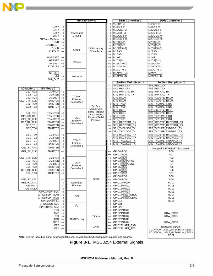
MSC8254 Device DDR Controller 1 DDR Controller 2
Power and Ground
DDR Memory Controllers
→ M1A[15–0] M2A[15–0]1.0 V → → M1BA[2–0] M2BA[2–0]1.5 V → ↔ M1DQ[63–0] M2DQ[63–0]1.8 V → → M1DM[8–0] M2DM[8–0]2.5 V → ↔ M1DQS[8–0] M2DQS[8–0]
M1VREF, M2VREF → ↔ M1DQS[8–0] M2DQS[8–0]GND → → M1CK[0–2] M2CK[0–2]
GNDRIOPLL → → M1CK[0–2] M2CK[0–2]CLKIN →
Clocks→ M1CKE[0–1] M2CKE[0–1]
CLKOUT ← → M1RAS M2RAS→ M1CAS M2CAS
PORESET →
Resets
→ M1WE M2WEHRESET ↔ → M1CS[0–1] M2CS[0–1]SRESET ↔ ↔ M1ECC[0–7] M2ECC[0–7]
STOP_BS → ↔ M1MDIC[0–1] M2MDIC[0–1]→ M1ODT[0–1] M2ODT[0–1]
INT_OUT ←Interrupts
→ M1APAR_OUT M2APAR_OUTNMI → ← M1APAR_IN M2APAR_IN
NMI_OUT ←
SerDes Multiplexers
Serial RapidIO Controllers/PCI Express/Serial
Ethernet
SerDes Multiplexer 1 SerDes Multiplexer 2← SR1_REF_CLK SR2_REF_CLK
I/O Mode 1 I/O Mode 0 ← SR1_REF_CLK SR2_REF_CLKGE2_RD2 TDM0RCK ↔
TDM0/Ethernet
Controller 2
← SR1_IMP_CAL_RX SR2_IMP_CAL_RXGE2_TD2 TDM0RSN ↔ ← SR1_IMP_CAL_TX SR2_IMP_CAL_TXGE2_RD3 TDM0RDT ↔ ← SR1_RXD0 SR2_RXD0/PE_RXD0
GE2_GTX_CLK TDM0TCK ↔ ← SR1_RXD0 SR2_RXD0/PE_RXD0GE2_RD0 TDM0TSN ↔ → SR1_TXD0 SR2_TXD0/PE_TXD0GE2_TD3 TDM0TDT ↔ → SR1_TXD0 SR2_TXD0/PE_TXD0
← SR1_RXD1 SR2_RXD1/PE_RXD1GE2_RD1 TDM1RCK ↔
TDM1/Ethernet
Controller 2
← SR1_RXD1 SR2_RXD1/PE_RXD1GE2_RX_CTL TDM1RSN ↔ → SR1_TXD1 SR2_TXD1/PE_TXD1GE2_TX_CLK TDM1RDT ↔ → SR1_TXD1 SR2_TXD1/PE_TXD1GE2_RX_CLK TDM1TCK → ← SR1_RXD2/SG1_RX SR2_RXD2/PE_RXD2/SG1_RX
GE2_TD1 TDM1TSN ↔ ← SR1_RXD2/SG1_RX SR2_RXD2/PE_RXD2/SG1_RXGE2_TD0 TDM1TDT ↔ → SR1_TXD2/SG1_TX SR2_TXD2/PE_TXD2/SG1_TX
→ SR1_TXD2/SG1_TX SR2_TXD2/PE_TXD2/SG1_TXGE1_TD0 TDM2RCK ↔
TDM2/ Ethernet
Controller 1
← SR1_RXD3/SG2_RX SR2_RXD3/PE_RXD3/SG2_RXGE1_TD2 TDM2RSN ↔ ← SR1_RXD3/SG2_RX SR2_RXD3/PE_RXD3/SG2_RXGE1_TD1 TDM2RDT ↔ → SR1_TXD3/SG2_TX SR2_TXD3/PE_TXD3/SG2_TXGE1_TD3 TDM2TCK → → SR1_TXD3/SG2_TX SR2_TXD3/PE_TXD3/SG2_TX
GE1_TX_CTL TDM2TSN ↔Sampled at PORESET deassertion
GE1_TX_CLK TDM2TDT ↔
GPIO
↔ GPIO0/IRQ0 RC0↔ GPIO1/IRQ1 RC1
GE1_GTX_CLK TDM3RCK ↔
TDM3/Ethernet
Controller 1
↔ GPIO2/IRQ2 RC2GE1_RD1 TDM3RSN ↔ ↔ GPIO3/IRQ3/DRQ1 RC3GE1_RD0 TDM3RDT ↔ ↔ GPIO4/IRQ4/DDN1 RC4GE1_RD2 TDM3TCK → ↔ GPIO5/IRQ5 RC5
GE1_RX_CLK TDM3TSN ↔ ↔ GPIO6/IRQ6 RC6GE1_RD3 TDM3TDT ↔ ↔ GPIO7/IRQ7 RC7
↔ GPIO8/IRQ8 RC8GE2_TX_CTL ←
Dedicated Ethernet
↔ GPIO9/IRQ9 RC9GE1_RX_CTL → ↔ GPIO10/IRQ10 RC10
GE_MDC ← ↔ GPIO11/IRQ11 RC11GE_MDIO ↔ ↔ GPIO12/IRQ12 RC12
GPIO17/SPI_SCK ↔
SPI
↔ GPIO13/IRQ13 RC13GPIO18/SPI_MOSI ↔ ↔ GPIO14/IRQ14/DRQ0 RC14GPIO19/SPI_MISO ↔ ↔ GPIO15/IRQ15/DDN0 RC15
GPIO20/SPI_SL ↔ ↔ GPIO16 RC16GPIO30/I2C_SCL ↔
I2C↔ GPIO21
GPIO31/I2C_SDA ↔ ↔ GPIO22TCK →
JTAG/DebugTimers
↔ GPIO23/TMR0TMS → ↔ GPIO24/TMR1 RCW_SRC2TDI → ↔ GPIO25/TMR2 RCW_SRC1
TDO ← ↔ GPIO26/TMR3TRST → ↔ GPIO27/TMR4 RCW_SRC0
EE0 →UART
↔ GPIO28/UART_RXDDedicated signals:
RC17/RCW_LSEL0, RC18/RCW_LSEL1, RC19/RCW_LSEL2, RC20/RCW_LSEL3,
RC21
EE1 ← ↔ GPIO29/UART_TXD
Note: See the individual signal description tables for details about individual power supplies and grounds.
Figure 3-1. MSC8254 External Signals
MSC8254 Reference Manual, Rev. 0
Freescale Semiconductor 3-3

External Signals
3.1 Power Signals
Table 3-3. Power and Ground Inputs
Nominal Voltage
Signal Name Symbol Description
1.0 V
VDD VDD Power for Core Subsystems 0–5A dedicated well-regulated power source for core subsystems 0–5. Provide an extremely low impedance path to the VDD power rail and adequate external decoupling capacitors.
M3VDD VDDM3 Power for M3 MemoryA dedicated well-regulated power source for 1 Mbyte of the M3 memory. Provide an extremely low impedance path to the VDD power rail and adequate external decoupling capacitors. This input can be disabled when not used to reduce system power requirements. When this input is disabled, 32 Kbyte of M3 memory remains active.
PLL0_AVDD VDDPLL1 System PLL 0 PowerA dedicated well-regulated power for the system Phase Lock Loops (PLLs).
PLL1_AVDD VDDPLL1 System PLL 1 PowerA dedicated well-regulated power for the system Phase Lock Loops (PLLs).
PLL2_AVDD VDDPLL1 System PLL 2 PowerA dedicated well-regulated power for the system Phase Lock Loops (PLLs).
1.0 V (Differential)
SXPVDD1 VDDSXP1 Serial RapidIO Interface 1 Pad PowerA dedicated well-regulated power for the Serial RapidIO interface 1 pad circuitry.
SXPVDD2 VDDSXP2 Serial RapidIO Interface 2 Pad PowerA dedicated well-regulated power for the Serial RapidIO interface 2 pad circuitry.
SXCVDD1 VDDSXC1 Serial RapidIO Interface 1 Core PowerA dedicated well-regulated power for the Serial RapidIO interface 1 core circuitry.
SXCVDD2 VDDSXC2 Serial RapidIO Interface 2 Core PowerA dedicated well-regulated power for the Serial RapidIO interface 2 core circuitry.
SR1_PLL_AVDD VDDPLL1 Serial RapidIO PLL 1 PowerA dedicated well-regulated power for the system Phase Lock Loops (PLLs).
SR2_PLL_AVDD VDDPLL1 Serial RapidIO PLL 2 PowerA dedicated well-regulated power for the system Phase Lock Loops (PLLs).
1.5 V or 1.8 V
GVDD1 VDDDDR1 SSTL IO Driver Power (1.5 V or 1.8 V)A dedicated power source for the DDR controller 1 DRAM interface buffers. Provide adequate external decoupling capacitors. The external decoupling capacitors recommendations are listed in the MSC8254 Technical Data Sheet.
GVDD2 VDDDDR2 SSTL IO Driver Power (1.5 V or 1.8 V)A dedicated power source for the DDR controller 2 DRAM interface buffers. Provide adequate external decoupling capacitors. The external decoupling capacitors recommendations are listed in the MSC8254 Technical Data Sheet.
GVDD1 × 0.5 VM1VREF M1VREF SSTL Reference Power
A reference power level for the DDR controller 1 memory interface.
MSC8254 Reference Manual, Rev. 0
3-4 Freescale Semiconductor

Clock Signals
Note: The external decoupling capacitors recommendations are listed in the MSC8254 Technical Data Sheet.
3.2 Clock Signals
GVDD2 × 0.5 VM2VREF M2VREF SSTL Reference Power
A reference power level for the DDR controller 2 memory interface.
2.5 V
NVDD VDDIO Input/Output PowerThe power source for the external I/O signal lines. Provide adequate external decoupling capacitors. The external decoupling capacitors recommendations are listed in the MSC8254 Technical Data Sheet.
QVDD VDDPLL0 Input/Output PowerThe power source for the external clock, reset, OCE, and JTAG signal lines. Provide adequate external decoupling capacitors. The external decoupling capacitors recommendations are listed in the MSC8254 Technical Data Sheet.
0 V (GND)
VSS GND System GroundAn isolated ground for the internal processing logic and I/O buffers. This connection must be tied externally to all chip ground connections, except GNDSXC and GNDSXP.
SR1_PLL_AGND GNDRIO1PLL RapidIO Interface 1 PLL GroundGround dedicated for RapidIO Interface 1 PLL use. The connection should be provided with an extremely low-impedance path to ground.
SR2_PLL_AGND GNDRIO2PLL RapidIO Interface 2 PLL GroundGround dedicated for RapidIO interface 2 PLL use. The connection should be provided with an extremely low-impedance path to ground.
SXCVSS1 GNDSXC1 RapidIO Interface 1 Core GroundA ground for the RapidIO port 1 Core circuitry.
SXCVSS2 GNDSXC2 RapidIO Interface 2 Core GroundA ground for the RapidIO port 2 Core circuitry.
SXPVSS1 GNDSXP1 RapidIO Interface 1 Pad GroundA ground for the RapidIO port 1 Pad circuitry.
SXPVSS2 GNDSXP2 RapidIO Interface 2 Pad GroundA ground for the RapidIO port 2 Pad circuitry.
Table 3-4. Clock Signals
Signal Name Type Signal Description
CLKIN Input Clock InPrimary clock input to the MSC8254 PLLs.
CLKOUT Output Clock OutThe bus clock output.
Table 3-3. Power and Ground Inputs (Continued)
Nominal Voltage
Signal Name Symbol Description
MSC8254 Reference Manual, Rev. 0
Freescale Semiconductor 3-5

External Signals
3.3 Reset and Configuration Signals
Table 3-5. Reset and Configuration Signals
Signal Name Type Signal Description
PORESET Input Power-On ResetWhen asserted, this line causes the MSC8254 to enter power-on reset state. Internally, this signal also resets the TAP and debugging modules. The power-on reset flow resets the MSC8254 device, configures various device attributes including its clock modes, and drives HRESET and SRESET as open-drain outputs.
HRESET Input/ Output
Hard ResetWhen asserted as an input, this signal causes the MSC8254 to abort all current internal and external transactions, set most registers to their default state, and enter the hard reset state. This signal must be asserted for at least 32 CLKIN cycles. While the device is in the hard reset state, it drives HRESET and SRESET as open-drain outputs. This signal requires an external pull-up resistor. The signal is tri-stated after the hard reset flow is complete.
SRESET Input/ Output
Soft ResetWhen asserted as an input, this signal causes the MSC8254 to enter the soft reset state, about all current internal transactions, configure most registers with their default values, and cause the cores to enter their reset state. The signal does not affect I/O signal functionality or direction or memory controller operations. While the device is in the soft reset state, it drives the SRESET as an open-drain output. This signal requires an external pull-up resistor. The signal is tri-stated after the soft reset flow is complete.
STOP_BS Input Stop Boot SequencerThis signal is valid only when the reset configuration words are being loaded from an I2C EEPROM using the boot sequencer and is asserted only for a reset target device to prevent the loading of the reset configuration words until allowed by the Boot ROM. The signal level must be asserted as long as HRESET is asserted. For the reset master or a single device reading from I2C EEPROM, you must drive this low during the reset sequence. For details, see Chapter 5, Reset. This signal is also used for booting after reset (for details, see Chapter 6, Boot Program).
RCW_SRC0
GPIO27
TMR4
Input
Input/ Output
Input/ Output
Reset Configuration Word Source 0Along with the RCW_SRC[1–2], this signal is sampled at the deassertion of PORESET to identify the source of the reset configuration word. The required signal level must be maintained as long as HRESET is asserted.
General-Purpose Input Output 27One of 32 GPIO pins used as GPIO or as a dedicated input or output. For details, see Chapter 22, GPIO.
Timer 4Configured as input to the counter or output from the counter. Selected through the GPIO configuration. For details, see Chapter 22, GPIO. For functional details, see Chapter 21, Timers.
MSC8254 Reference Manual, Rev. 0
3-6 Freescale Semiconductor

Reset and Configuration Signals
RCW_SRC1
GPIO25
TMR2
Input
Input/ Output
Input/ Output
Reset Configuration Word Source 1Along with the RCW_SRC[0, 2], this signal is sampled at the deassertion of PORESET to identify the source of the reset configuration word. The required signal level must be maintained as long as HRESET is asserted.
General-Purpose Input Output 25One of 32 GPIO pins used as GPIO or as a dedicated input or output. For details, see Chapter 22, GPIO.
Timer 2Configured as input to the counter or output from the counter. Selected through the GPIO configuration. For details, see Chapter 22, GPIO. For functional details, see Chapter 21, Timers.
RCW_SRC2
GPIO24
TMR1
Input
Input/ Output
Input/ Output
Reset Configuration Word Source 2Along with the RCW_SRC[0–1], this signal is sampled at the deassertion of PORESET to identify the source of the reset configuration word. The required signal level must be maintained as long as HRESET is asserted.
General-Purpose Input Output 24One of 32 GPIO pins used as GPIO or as a dedicated input or output. For details, see Chapter 22, GPIO.
Timer 1Configured as input to the counter or output from the counter. Selected through the GPIO configuration. For details, see Chapter 22, GPIO. For functional details, see Chapter 21, Timers.
RC[0–2]
GPIO[0–2]
IRQ[0–2]
Input
Input/ Output
Input
Reset Configuration Word Bit 0–2Sampled during the assertion of PORESET to set part of the bits of the Reset Configuration Word Registers.
General-Purpose Input Output 0–2Three of the 32 GPIO pins used as GPIO or as a dedicated input or output. For details, see Chapter 22, GPIO.
Interrupt Request 0–2External lines that can request a service routine via the internal interrupt controller. Selected through GPIO configuration. For details, see Chapter 22, GPIO. For functional details, see Chapter 13, Interrupt Handling.
RC3
GPIO3
IRQ3
DRQ1
Input
Input/ Output
Input
Input
Reset Configuration Word Bit 3Sampled during the assertion of PORESET to set part of the bits of the Reset Configuration Word Registers.
General-Purpose Input Output 3One of the 32 GPIOs. For details, see Chapter 22, GPIO.
Interrupt Request 3External line that can request a service routine via the internal interrupt controller. For details, see Chapter 13, Interrupt Handling.
DMA External Request 1When enabled by GPIO multiplexing, asserting this input triggers external DMA request 1. For details, see Chapter 14, Direct Memory Access (DMA) Controller,
Table 3-5. Reset and Configuration Signals (Continued)
Signal Name Type Signal Description
MSC8254 Reference Manual, Rev. 0
Freescale Semiconductor 3-7

External Signals
RC4
GPIO4
IRQ4
DDN1
Input
Input/ Output
Input
Output
Reset Configuration Word Bit 4Sampled during the assertion of PORESET to set part of the bits of the Reset Configuration Word Registers.
General-Purpose Input Output 4One of the 32 GPIOs. For details, see Chapter 22, GPIO.
Interrupt Request 4External line that can request a service routine via the internal interrupt controller. For details, see Chapter 13, Interrupt Handling.
DMA External DONE Indication 1When enabled by GPIO multiplexing, this signal is asserted to indicate that DMA request 1 is done. For details, see Chapter 14, Direct Memory Access (DMA) Controller,
RC[5–13]
GPIO[5–13]
IRQ[5–13]
Input
Input/ Output
Input
Reset Configuration Word Bit 5–13Sampled during the assertion of PORESET to set part of the bits of the Reset Configuration Word Registers.
General-Purpose Input Output 5–13Nine of the 32 GPIO pins used as GPIO or as a dedicated input or output. For details, see Chapter 22, GPIO.
Interrupt Request 5–13External lines that can request a service routine via the internal interrupt controller. Selected through GPIO configuration. For details, see Chapter 22, GPIO. For functional details, see Chapter 13, Interrupt Handling.
RC14
GPIO14
IRQ14
DRQ0
Input
Input/ Output
Input
Input
Reset Configuration Word Bit 14Sampled during the assertion of PORESET to set part of the bits of the Reset Configuration Word Registers.
General-Purpose Input Output 14One of the 32 GPIOs. For details, see Chapter 22, GPIO.
Interrupt Request 14External line that can request a service routine via the internal interrupt controller. For details, see Chapter 13, Interrupt Handling.
DMA External Request 0When enabled by GPIO multiplexing, asserting this input triggers external DMA request 0. For details, see Chapter 14, Direct Memory Access (DMA) Controller,
Table 3-5. Reset and Configuration Signals (Continued)
Signal Name Type Signal Description
MSC8254 Reference Manual, Rev. 0
3-8 Freescale Semiconductor

Reset and Configuration Signals
RC15
GPIO15
IRQ15
DDN0
Input
Input/ Output
Input
Output
Reset Configuration Word Bit 15Sampled during the assertion of PORESET to set part of the bits of the Reset Configuration Word Registers.
General-Purpose Input Output 15One of the 32 GPIOs. For details, see Chapter 22, GPIO.
Interrupt Request 15External line that can request a service routine via the internal interrupt controller. For details, see Chapter 13, Interrupt Handling.
DMA External DONE Indication 0When enabled by GPIO multiplexing, this signal is asserted to indicate that DMA request 0 is done. For details, see Chapter 14, Direct Memory Access (DMA) Controller,
RC16
GPIO16
Input
Input/ Output
Reset Configuration Word Bit 16Sampled during the assertion of PORESET to set part of the bits of the Reset Configuration Word Registers.
General-Purpose Input Output 16One of 32 GPIO pins used as GPIO or as a dedicated input or output. For details, see Chapter 22, GPIO.
RC17
RCW_LSEL0
Input
Output
Reset Configuration Word Bit 17If RCW_SRC[0–2] equals 011, this input is sampled during the assertion of PORESET to set part of the bits of the Reset Configuration Word Registers.
Reset Configuration Word Lane 0 SelectIf RCW_SRC[0–2] equals 000, this signal is used to enable loading of Lane 0 (RCWLR bits 15–0) of the RCW via RC[15–0] when asserted. See Chapter 5, Reset for details.
RC18
RCW_LSEL1
Input
Output
Reset Configuration Word Bit 18If RCW_SRC[0–2] equals 011, this input is sampled during the assertion of PORESET to set part of the bits of the Reset Configuration Word Registers.
Reset Configuration Word Lane 1 SelectIf RCW_SRC[0–2] equals 000, this signal is used to enable loading of Lane 1 (RCWLR bits 31–16) of the RCW via RC[15–0] when asserted. See Chapter 5, Reset for details.
RC19
RCW_LSEL2
Input
Output
Reset Configuration Word Bit 19If RCW_SRC[0–2] equals 011, this input is sampled during the assertion of PORESET to set part of the bits of the Reset Configuration Word Registers.
Reset Configuration Word Lane 2 SelectIf RCW_SRC[0–2] equals 000, this signal is used to enable loading of Lane 2 (RCWHR bits 15–0) of the RCW via RC[15–0] when asserted. See Chapter 5, Reset for details.
RC20
RCW_LSEL3
Input
Output
Reset Configuration Word Bit 20If RCW_SRC[0–2] equals 011, this input is sampled during the assertion of PORESET to set part of the bits of the Reset Configuration Word Registers.
Reset Configuration Word Lane 3 SelectIf RCW_SRC[0–2] equals 000, this signal is used to enable loading of Lane 3 (RCWHR bits 31–16) of the RCW via RC[15–0] when asserted. See Chapter 5, Reset for details.
Table 3-5. Reset and Configuration Signals (Continued)
Signal Name Type Signal Description
MSC8254 Reference Manual, Rev. 0
Freescale Semiconductor 3-9

External Signals
3.4 Memory Controller 1 and 2
Refer to Chapter 12, DDR SDRAM Memory Controller for details on configuring these signals.
RC21 Input Reset Configuration Word Bit 21If RCW_SRC[0–2] equals 011, this input is sampled during the assertion of PORESET to set part of the bits of the Reset Configuration Word Registers. If RCW_SRC[0–2] does not equal 011, this input is ignored.
Note: When RCW_SRC[0–2] equals 011, RC[0–21] are valid only for driving a reduced external reset configuration word value. The signals are sampled during the assertion of PORESET to set part of the bits of the Reset Configuration Word Registers. The required signal levels must be maintained as long as HRESET is asserted. All other signal drivers connected to these inputs must be tri-stated while HRESET is asserted. When RCW_SRC[0–2] equals 000, the device loads all 64 bits of the RCW via RC[0–15] in four beats. In this case, RC[17–20] function as RCW_LSEL[0–3] outputs that are asserted to load the RCW 16 bits at a time and RC21 is ignored. See Chapter 5, Reset for details.
Table 3-6. Memory Controller Signals
Signal Name Type Description
M1A[15–0]M2A[15–0]
Output Address BusThe memory interface address bus used to connect to external memory devices. MA0 is the lsb of the address driven by the DDR controller.
M1BA[2–0]M2BA[2–0]
Output Bank AddressSelects the DDR DRAM bank. Each DDR SDRAM can support four or eight logically addressable sub-banks. MBA0 must connect to bit zero of the SDRAM input bank address. This line is asserted during the mode register set command to specify the extended mode register.
M1DQ[63–0]M2DQ[63–0]
Input/Output
Data BusThe MSC8254 device drives the bus during write cycles and the external memory drives the bus during read cycles.
M1DM[8–0]M2DM[8–0]
Output DDR SDRAM Data Output MaskMasks unwanted data bytes transferred during a burst write. These signals are used to support sub-burst-size transactions (such as single-byte writes) on SDRAM in which all transactions occur in multi-byte bursts. MDM0 corresponds to the MSB and MDM7 corresponds to the LSB. MDM8 acts as the ECC data mask.
M1DQS[8–0]M2DQS[8–0]
Input/Output DDR SDRAM DQSStrobe for byte-lane data capture. The signals are inputs driven by the DDR SRAM with read data and outputs driven by the DDR controller with write data. The data strobes may be single-ended or differential. Bit 8 is used as the ECC data mask.
M1DQS[8–0]M2DQS[8–0]
Input/Output DDR SDRAM DQS ComplementComplement strobe for byte-lane data capture. The signals are inputs driven by the DDR SRAM with read data and outputs driven by the DDR controller with write data. The data strobes may be single-ended or differential.
M1ECC[7–0]M2ECC[7–0]
Input/Output DDR Error Checking and Correcting CodesAs normal mode outputs the ECC signals represent the state of ECC driven by the DDR controller on writes.
Table 3-5. Reset and Configuration Signals (Continued)
Signal Name Type Signal Description
MSC8254 Reference Manual, Rev. 0
3-10 Freescale Semiconductor

SerDes Multiplexed Signals for the Serial RapidIO, PCI Express, and SGMII Interfaces
3.5 SerDes Multiplexed Signals for the Serial RapidIO, PCI Express, and SGMII Interfaces
Refer to Chapter 5, Reset, Chapter 17, PCI Express Controller, Chapter 16, Serial RapidIO Controller, and the QUICC Engine Block Reference Manual with Protocol Interworking for configuration information.
M1CK[2–0]M2CK[2–0]
Output DDR Clock Out The DDR clock output. Each signal is part of a differential pair.
M1CK[2–0]M2CK[2–0]
Output DDR Clock Out InvertedThe inverted DDR clock. Each signal is part of a differential pair.
M1CKE[1–0]M2CKE[1–0]
Output Clock EnableWhen asserted, this signal enables the DDR clock for the DDR DRAM.
M1RASM2RAS
Output Row Address StrobeConnects to DDR DRAM RAS input. This line is asserted for activate commands and is used for mode register set and refresh commands.
M1CASM2CAS
Output Column Address StrobeConnects to DDR DRAM CAS input. This line is asserted for read or write transactions and for mode register set, refresh, and precharge commands.
M1WEM2WE
Output Write EnableConnects to DDR DRAM WE input.
M1CS[0–1]M2CS[0–1]
Output Chip Select 0–1Enables specific memory devices or peripherals connected to the bus.
M1MDIC[0–1]M2MDIC[0–1]
Input/Output Driver Impedance CalibrationThese lines are used for automatic calibration of the DDR I/O.
M1ODT[0–1]M2ODT[0–1]
Output On-Die TerminationMemory controller outputs for the ODT to the SDRAM. Each signal represents the corresponding chip select.
M1APAR_OUTM2APAR_OUT
Output Parity OutputIf enabled, drives the parity bit for the bus.
M1APAR_INM2APAR_IN
Input Parity InputReceives the error indication from an open-drain parity error signal.
Table 3-7. SerDes Multiplexed Signals
Signal Name Type Description
SR1_IMP_CAL_RX Input Serial RapidIO Controller 1 Receiver Impedance Control SignalReceiver impedance calibration control signal.
SR1_IMP_CAL_TX Input Serial RapidIO Controller 1 Transmitter Impedance Control SignalTransmitter impedance calibration control signal.
SR1_RXD0 Input Serial RapidIO Controller 1 Receive Data 0Serial data input for a x1 or x4 link. Each signal is part of a differential pair.
Table 3-6. Memory Controller Signals (Continued)
Signal Name Type Description
MSC8254 Reference Manual, Rev. 0
Freescale Semiconductor 3-11
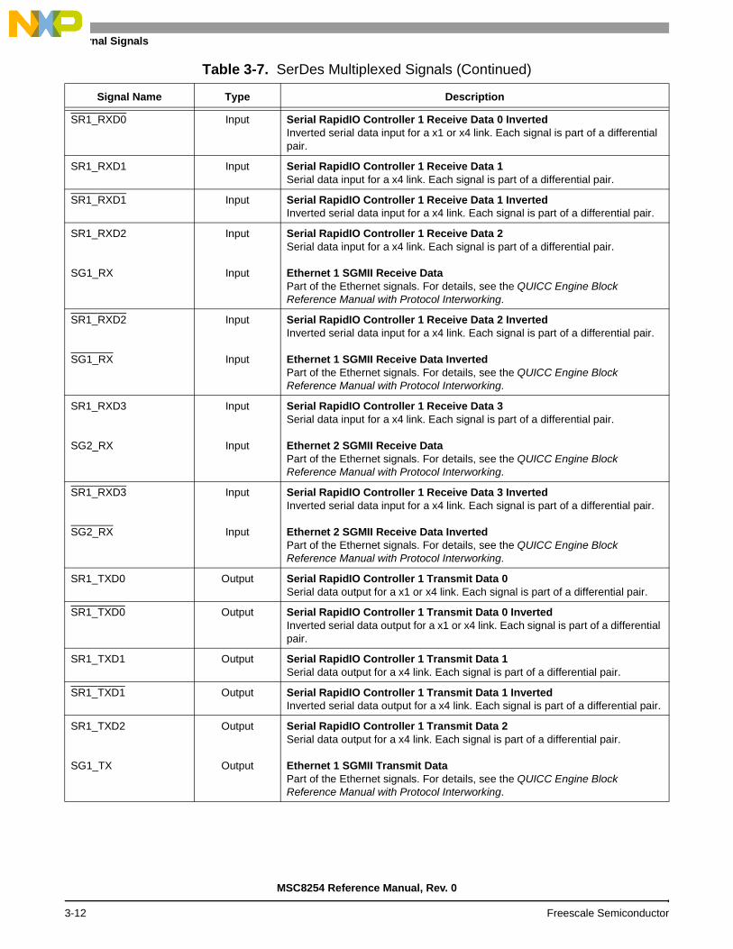
External Signals
SR1_RXD0 Input Serial RapidIO Controller 1 Receive Data 0 InvertedInverted serial data input for a x1 or x4 link. Each signal is part of a differential pair.
SR1_RXD1 Input Serial RapidIO Controller 1 Receive Data 1Serial data input for a x4 link. Each signal is part of a differential pair.
SR1_RXD1 Input Serial RapidIO Controller 1 Receive Data 1 InvertedInverted serial data input for a x4 link. Each signal is part of a differential pair.
SR1_RXD2
SG1_RX
Input
Input
Serial RapidIO Controller 1 Receive Data 2Serial data input for a x4 link. Each signal is part of a differential pair.
Ethernet 1 SGMII Receive DataPart of the Ethernet signals. For details, see the QUICC Engine Block Reference Manual with Protocol Interworking.
SR1_RXD2
SG1_RX
Input
Input
Serial RapidIO Controller 1 Receive Data 2 InvertedInverted serial data input for a x4 link. Each signal is part of a differential pair.
Ethernet 1 SGMII Receive Data InvertedPart of the Ethernet signals. For details, see the QUICC Engine Block Reference Manual with Protocol Interworking.
SR1_RXD3
SG2_RX
Input
Input
Serial RapidIO Controller 1 Receive Data 3Serial data input for a x4 link. Each signal is part of a differential pair.
Ethernet 2 SGMII Receive DataPart of the Ethernet signals. For details, see the QUICC Engine Block Reference Manual with Protocol Interworking.
SR1_RXD3
SG2_RX
Input
Input
Serial RapidIO Controller 1 Receive Data 3 InvertedInverted serial data input for a x4 link. Each signal is part of a differential pair.
Ethernet 2 SGMII Receive Data InvertedPart of the Ethernet signals. For details, see the QUICC Engine Block Reference Manual with Protocol Interworking.
SR1_TXD0 Output Serial RapidIO Controller 1 Transmit Data 0Serial data output for a x1 or x4 link. Each signal is part of a differential pair.
SR1_TXD0 Output Serial RapidIO Controller 1 Transmit Data 0 InvertedInverted serial data output for a x1 or x4 link. Each signal is part of a differential pair.
SR1_TXD1 Output Serial RapidIO Controller 1 Transmit Data 1Serial data output for a x4 link. Each signal is part of a differential pair.
SR1_TXD1 Output Serial RapidIO Controller 1 Transmit Data 1 InvertedInverted serial data output for a x4 link. Each signal is part of a differential pair.
SR1_TXD2
SG1_TX
Output
Output
Serial RapidIO Controller 1 Transmit Data 2Serial data output for a x4 link. Each signal is part of a differential pair.
Ethernet 1 SGMII Transmit DataPart of the Ethernet signals. For details, see the QUICC Engine Block Reference Manual with Protocol Interworking.
Table 3-7. SerDes Multiplexed Signals (Continued)
Signal Name Type Description
MSC8254 Reference Manual, Rev. 0
3-12 Freescale Semiconductor

SerDes Multiplexed Signals for the Serial RapidIO, PCI Express, and SGMII Interfaces
SR1_TXD2
SG1_TX
Output
Output
Serial RapidIO Controller 1 Transmit Data 2 InvertedInverted serial data output for a x4 link. Each signal is part of a differential pair.
Ethernet 1 SGMII Transmit Data InvertedPart of the Ethernet signals. For details, see the QUICC Engine Block Reference Manual with Protocol Interworking.
SR1_TXD3
SG2_TX
Output
Output
Serial RapidIO Controller 1 Transmit Data 3Serial data output for a x4 link. Each signal is part of a differential pair.
Ethernet 2 SGMII Transmit DataPart of the Ethernet signals. For details, see the QUICC Engine Block Reference Manual with Protocol Interworking.
SR1_TXD3
SG2_TX
Output
Output
Serial RapidIO Controller 1 Transmit Data 3 InvertedInverted serial data output for a x4 link. Each signal is part of a differential pair.
Ethernet 2 SGMII Transmit Data InvertedPart of the Ethernet signals. For details, see the QUICC Engine Block Reference Manual with Protocol Interworking.
SR1_REF_CLK Input Serial RapidIO Controller 1 Reference ClockReference clock signal. Each signal is part of a differential pair. For SGMII operation, this provides the input clock.
SR1_REF_CLK Input Serial RapidIO Controller 1 Reference Clock InvertedInverted reference clock signal. Each signal is part of a differential pair. For SGMII operation, this provides the input clock.
SR2_IMP_CAL_RX Input Serial RapidIO Controller 2 Receiver Impedance Control SignalReceiver impedance calibration control signal.
SR2_IMP_CAL_TX Input Serial RapidIO Controller 2 Transmitter Impedance Control SignalTransmitter impedance calibration control signal.
SR2_RXD0
PE_RXD0
Input
Input
Serial RapidIO Controller 2 Receive Data 0Serial data input for a x1 or x4 link. Each signal is part of a differential pair.
PCI Express Receive Data 0Serial data input. Each signal is part of a differential pair. For details, see Chapter 17, PCI Express Controller.
SR2_RXD0
PE_RXD0
Input
Input
Serial RapidIO Controller 2 Receive Data 0 InvertedInverted serial data input for a x1 or x4 link. Each signal is part of a differential pair.
PCI Express Receive Data 0 InvertedInverted serial data input. Each signal is part of a differential pair. For details, see Chapter 17, PCI Express Controller.
SR2_RXD1
PE_RXD1
SG2_RX
Input
Input
Input
Serial RapidIO Controller 2 Receive Data 1Serial data input for a x4 link. Each signal is part of a differential pair.
PCI Express Receive Data 1Serial data input. Each signal is part of a differential pair. For details, see Chapter 17, PCI Express Controller.
Ethernet 2 SGMII Receive DataPart of the Ethernet signals. For details, see the QUICC Engine Block Reference Manual with Protocol Interworking.
Table 3-7. SerDes Multiplexed Signals (Continued)
Signal Name Type Description
MSC8254 Reference Manual, Rev. 0
Freescale Semiconductor 3-13

External Signals
SR2_RXD1
PE_RXD1
SG2_RX
Input
Input
Input
Serial RapidIO Controller 2 Receive Data 1 InvertedInverted serial data input for a x4 link. Each signal is part of a differential pair.
PCI Express Receive Data 1 InvertedInverted serial data input. Each signal is part of a differential pair. For details, see Chapter 17, PCI Express Controller.
Ethernet 2 SGMII Receive Data InvertedPart of the Ethernet signals. For details, see the QUICC Engine Block Reference Manual with Protocol Interworking.
SR2_RXD2
PE_RXD2
SG1_RX
Input
Input
Input
Serial RapidIO Controller 2 Receive Data 2Serial data input for a x4 link. Each signal is part of a differential pair.
PCI Express Receive Data 2Serial data input. Each signal is part of a differential pair. For details, see Chapter 17, PCI Express Controller.
Ethernet 1 SGMII Receive DataPart of the Ethernet signals. For details, see the QUICC Engine Block Reference Manual with Protocol Interworking.
SR2_RXD2
PE_RXD2
SG1_RX
Input
Input
Input
Serial RapidIO Controller 2 Receive Data 2 InvertedInverted serial data input for a x4 link. Each signal is part of a differential pair.
PCI Express Receive Data 2 InvertedInverted serial data input. Each signal is part of a differential pair. For details, see Chapter 17, PCI Express Controller.
Ethernet 1 SGMII Receive Data InvertedPart of the Ethernet signals. For details, see the QUICC Engine Block Reference Manual with Protocol Interworking.
SR2_RXD3
PE_RXD3
Input
Input
Serial RapidIO Controller 2 Receive Data 3Serial data input for a x4 link. Each signal is part of a differential pair.
PCI Express Receive Data 3Serial data input. Each signal is part of a differential pair. For details, see Chapter 17, PCI Express Controller.
SR2_RXD3
PEI_RXD0
Input
Input
Serial RapidIO Controller 2 Receive Data 3 InvertedInverted serial data input for a x4 link. Each signal is part of a differential pair.
PCI Express Receive Data 1 InvertedInverted serial data input. Each signal is part of a differential pair. For details, see Chapter 17, PCI Express Controller.
SR2_TXD0
PE_TXD0
Output
Output
Serial RapidIO Controller 2 Transmit Data 0Serial data output for a x1 or x4 link. Each signal is part of a differential pair.
PCI Express Transmit Data 0Serial data output. Each signal is part of a differential pair. For details, see Chapter 17, PCI Express Controller.
Table 3-7. SerDes Multiplexed Signals (Continued)
Signal Name Type Description
MSC8254 Reference Manual, Rev. 0
3-14 Freescale Semiconductor

SerDes Multiplexed Signals for the Serial RapidIO, PCI Express, and SGMII Interfaces
SR2_TXD0
PE_TXD0
Output
Output
Serial RapidIO Controller 2 Transmit Data 0 InvertedInverted serial data output for a x1 or x4 link. Each signal is part of a differential pair.
PCI Express Transmit Data 0 InvertedSerial data output. Each signal is part of a differential pair. For details, see Chapter 17, PCI Express Controller.
SR2_TXD1
PE_TXD1
SG2_TX
Output
Output
Output
Serial RapidIO Controller 2 Transmit Data 1Serial data output for a x1 or x4 link. Each signal is part of a differential pair.
PCI Express Transmit Data 1Serial data output. Each signal is part of a differential pair. For details, see Chapter 17, PCI Express Controller.
Ethernet 2 SGMII Transmit DataPart of the Ethernet signals. For details, see the QUICC Engine Block Reference Manual with Protocol Interworking.
SR2_TXD1
PE_TXD1
SG2_TX
Output
Output
Output
Serial RapidIO Controller 2 Transmit Data 1 InvertedInverted serial data output for a x1 or x4 link. Each signal is part of a differential pair.
PCI Express Transmit Data 1 InvertedInverted serial data output. Each signal is part of a differential pair. For details, see Chapter 17, PCI Express Controller.
Ethernet 2 SGMII Transmit Data InvertedPart of the Ethernet signals. For details, see the QUICC Engine Block Reference Manual with Protocol Interworking.
SR2_TXD2
PE_TXD2
SG1_TX
Output
Output
Output
Serial RapidIO Controller 2 Transmit Data 2Serial data output for a x1 or x4 link. Each signal is part of a differential pair.
PCI Express Transmit Data 2Serial data output. Each signal is part of a differential pair. For details, see Chapter 17, PCI Express Controller.
Ethernet 1 SGMII Transmit DataPart of the Ethernet signals. For details, see the QUICC Engine Block Reference Manual with Protocol Interworking.
SR2_TXD2
PE_TXD2
SG1_TX
Output
Output
Output
Serial RapidIO Controller 2 Transmit Data 2 InvertedInverted serial data output for a x1 or x4 link. Each signal is part of a differential pair.
PCI Express Transmit Data 2 InvertedSerial data output. Each signal is part of a differential pair. For details, see Chapter 17, PCI Express Controller.
Ethernet 1 SGMII Transmit Data InvertedPart of the Ethernet signals. For details, see the QUICC Engine Block Reference Manual with Protocol Interworking.
Table 3-7. SerDes Multiplexed Signals (Continued)
Signal Name Type Description
MSC8254 Reference Manual, Rev. 0
Freescale Semiconductor 3-15

External Signals
3.6 TDM and Ethernet Signals
The TDM and RGMII signals are listed together because they are multiplexed using the same signal lines. The GE1 and GE2 bits in the RCW control the selection between the TDM signals and the RGMII signals. See Table 3-2 on page 3-2 for a detailed description of the multiplexing options. Table 3-8 describes the signals in this group.
SR2_TXD3
PE_TXD3
Output
Output
Serial RapidIO Controller 2 Transmit Data 3Serial data output for a x4 link. Each signal is part of a differential pair.
PCI Express Transmit Data 3Serial data output. Each signal is part of a differential pair. For details, see Chapter 17, PCI Express Controller.
SR2_TXD3
PE_TXD3
Output
Output
Serial RapidIO Controller 2 Transmit Data 3 InvertedInverted serial data output for a x1 or x4 link. Each signal is part of a differential pair.
PCI Express Transmit Data 3 InvertedSerial data output. Each signal is part of a differential pair. For details, see Chapter 17, PCI Express Controller.
SR2_REF_CLK Input Serial RapidIO Controller 2 Reference ClockReference clock signal. Each signal is part of a differential pair. For SGMII operation, this provides the input clock.
SR2_REF_CLK Input Serial RapidIO Controller 2 Reference Clock InvertedInverted reference clock signal. Each signal is part of a differential pair. For SGMII operation, this provides the input clock.
Note: For proper definition of serial RapidIO modes (x1/x4), PCI Express, and SGMII, configure the interfaces using the Reset Configuration Word settings. For details, see Chapter 5, Reset.
Table 3-8. TDM and Ethernet Signals
Signal Name Type Description
TDM3TDT
GE1_RD3
Input/ Output
Input
TDM3 Serial Transmitter DataThe serial transmit data signal for TDM 3. For configuration details, see Chapter 19, TDM Interface.
Ethernet 1 Receive Data 3For details, see the QUICC Engine Block Reference Manual with Protocol Interworking.
TDM3TCK
GE1_RD2
Input
Input
TDM3 Transmit ClockTransmit Clock for TDM 3. For configuration details, see Chapter 19, TDM Interface.
Ethernet 1 Receive Data 2For details, see the QUICC Engine Block Reference Manual with Protocol Interworking.
TDM3TSN
GE1_RX_CLK
Input/ Output
Input
TDM3 Transmit Frame Sync Transmit frame sync for TDM 3. See Chapter 19, TDM Interface.
Ethernet 1 Receive ClockFor details, see the QUICC Engine Block Reference Manual with Protocol Interworking.
Table 3-7. SerDes Multiplexed Signals (Continued)
Signal Name Type Description
MSC8254 Reference Manual, Rev. 0
3-16 Freescale Semiconductor

TDM and Ethernet Signals
TDM3RDT
GE1_RD0
Input/ Output
Input
TDM3 Serial Receiver DataThe receive data signal for TDM 3. For configuration details, see Chapter 19, TDM Interface.
Ethernet 1 Receive Data 0For details, see the QUICC Engine Block Reference Manual with Protocol Interworking.
TDM3RCK
GE1_GTX_CLK
Input/ Output
Output
TDM3 Receive ClockThe receive clock signal for TDM 3. For configuration details, see Chapter 19, TDM Interface.
Ethernet 1 Output Transmit ClockFor details, see the QUICC Engine Block Reference Manual with Protocol Interworking.
TDM3RSN
GE1_RD1
Input/ Output
Input
TDM3 Receive Frame SyncThe receive sync signal for TDM 3. For configuration details, see Chapter 19, TDM Interface.
Ethernet 1 Receive Data 1For details, see the QUICC Engine Block Reference Manual with Protocol Interworking.
TDM2TDT
GE1_TX_CLK
Input/ Output
Input
TDM2 Serial Transmitter DataThe transmit data signal for TDM 2. For configuration details, see Chapter 19, TDM Interface.
Ethernet 1 Transmit ClockFor details, see the QUICC Engine Block Reference Manual with Protocol Interworking.
TDM2TCK
GE1_TD3
Input
Output
TDM 2 Transmit ClockTransmit clock for TDM 2. For configuration details, see Chapter 19, TDM Interface.
Ethernet 1 Transmit Data 3For details, see the QUICC Engine Block Reference Manual with Protocol Interworking.
TDM2TSN
GE1_TX_CTL
Input/ Output
Output
TDM2 Transmit frame Sync Transmit frame sync for TDM 2. For configuration details, see Chapter 19, TDM Interface.
Ethernet 1 Transmit ControlFor details, see the QUICC Engine Block Reference Manual with Protocol Interworking.
TDM2RDT
GE1_TD1
Input/ Output
Output
TDM2 Serial Receiver DataThe receive data signal for TDM 2. For configuration details, see Chapter 19, TDM Interface.
Ethernet 1 Transmit Data 1For details, see the QUICC Engine Block Reference Manual with Protocol Interworking.
TDM2RCK
GE1_TD0
Input/ Output
Output
TDM2 Receive ClockThe receive clock signal for TDM 2. For configuration details, see Chapter 19, TDM Interface.
Ethernet 1 Transmit Data 0For details, see the QUICC Engine Block Reference Manual with Protocol Interworking.
TDM2RSN
GE1_TD2
Input/ Output
Output
TDM2 Receive Frame SyncThe receive sync signal for TDM 2. For configuration details, see Chapter 19, TDM Interface.
Ethernet 1 Transmit Data 2For details, see the QUICC Engine Block Reference Manual with Protocol Interworking.
TDM1TDT
GE2_TD0
Input/ Output
Output
TDM1 Serial Transmitter DataThe transmit data signal for TDM 1. For configuration details, see Chapter 19, TDM Interface.
Ethernet 2 Transmit Data 0For details, see the QUICC Engine Block Reference Manual with Protocol Interworking.
Table 3-8. TDM and Ethernet Signals (Continued)
Signal Name Type Description
MSC8254 Reference Manual, Rev. 0
Freescale Semiconductor 3-17

External Signals
TDM1TCK
GE2_RX_CLK
Input
Input
TDM1 Transmit ClockTransmit clock for TDM 1. For configuration details, see Chapter 19, TDM Interface.
Ethernet 2 Receive ClockFor details, see the QUICC Engine Block Reference Manual with Protocol Interworking.
TDM1TSN
GE2_TD1
Input/ Output
Output
TDM1 Transmit Frame Sync Transmit frame sync for TDM 1. For configuration details, see Chapter 19, TDM Interface.
Ethernet 2 Transmit Data 1For details, see the QUICC Engine Block Reference Manual with Protocol Interworking.
TDM1RDT
GE2_TX_CLK
Input/ Output
Input
TDM1 Serial Receiver DataThe receive data signal for TDM 1. For configuration details, see Chapter 19, TDM Interface.
Ethernet 2 Transmit ClockFor details, see the QUICC Engine Block Reference Manual with Protocol Interworking.
TDM1RCK
GE2_RD1
Input/ Output
Input
TDM1 Receive ClockThe receive clock signal for TDM 1. For configuration details, see Chapter 19, TDM Interface.
Ethernet 2 Receive Data 1For details, see the QUICC Engine Block Reference Manual with Protocol Interworking.
TDM1RSN
GE2_RX_CTL
Input/ Output
Input
TDM1 Receive Frame SyncThe receive sync signal for TDM 1. For configuration details, see Chapter 19, TDM Interface.
Ethernet 2 Receive ControlFor details, see the QUICC Engine Block Reference Manual with Protocol Interworking.
TDM0TDT
GE2_TD3
Input/ Output
Output
TDM0 Serial Transmitter DataThe transmit data signal for TDM 0. For configuration details, see Chapter 19, TDM Interface.
Ethernet 2 Transmit Data 3For details, see the QUICC Engine Block Reference Manual with Protocol Interworking.
TDM0TCK
GE2_GTX_CLK
Input
Output
TDM 0 Transmit ClockTransmit Clock for TDM 0. For configuration details, see Chapter 19, TDM Interface.
Ethernet 2 Output Transmit ClockFor details, see the QUICC Engine Block Reference Manual with Protocol Interworking.
TDM0TSN
GE2_RD0
Input/ Output
Input
TDM0 Transmit Frame Sync Transmit Frame Sync for TDM 0. For configuration details, see Chapter 19, TDM Interface.
Ethernet 2 Receive Data 0For details, see the QUICC Engine Block Reference Manual with Protocol Interworking.
TDM0RDT
GE2_RD3
Input/ Output
Input
TDM0 Serial Receiver Data The receive data signal for TDM 0. For configuration details, see Chapter 19, TDM Interface.
Ethernet 2 Receive Data 3For details, see the QUICC Engine Block Reference Manual with Protocol Interworking.
TDM0RCK
GE2_RD2
Input/ Output
Input
TDM0 Receive ClockThe receive clock signal for TDM 0. For configuration details, see Chapter 19, TDM Interface.
Ethernet 2 Receive Data 2For details, see the QUICC Engine Block Reference Manual with Protocol Interworking.
Table 3-8. TDM and Ethernet Signals (Continued)
Signal Name Type Description
MSC8254 Reference Manual, Rev. 0
3-18 Freescale Semiconductor

TDM and Ethernet Signals
TDM0RSN
GE2_TD2
Input/ Output
Output
TDM0 Receive Frame SyncThe receive sync signal for TDM 0. For configuration details, see Chapter 19, TDM Interface.
Ethernet 2 Transmit Data 2For details, see the QUICC Engine Block Reference Manual with Protocol Interworking.
GE2_TX_CTL Output Ethernet 2 Transmit ControlFor details, see the QUICC Engine Block Reference Manual with Protocol Interworking.
GE1_RX_CTL Input Ethernet 1 Receive ControlFor details, see the QUICC Engine Block Reference Manual with Protocol Interworking.
GE_MDC Output Ethernet Management Data ClockFor details, see the QUICC Engine Block Reference Manual with Protocol Interworking.
GE_MDIO Input/ Output
Ethernet Management Data Input/OutputFor details, see the QUICC Engine Block Reference Manual with Protocol Interworking.
Table 3-8. TDM and Ethernet Signals (Continued)
Signal Name Type Description
MSC8254 Reference Manual, Rev. 0
Freescale Semiconductor 3-19

External Signals
3.7 Serial Peripheral Interface (SPI) Signal SummaryTable 3-9 summarizes the Serial Peripheral Interface (SPI) signal lines, which are available in all modes.
3.8 GPIO/Maskable Interrupt Signal Summary
Some of the GPIO and interrupt lines are multiplexed with other interfaces. Some of the lines are independent. In addition to the hardware interrupt inputs, there are also several signal lines used to reroute interrupts between the cores and an external host processor. Table 3-16 summarizes the GPIO and interrupt signal lines.
Table 3-9. SPI Signals
Signal Name Type Signal Description
GPIO20
SPI_SL
Input/ Output
Input
General-Purpose Input Output 20One of 32 GPIOs. For details, see Chapter 22, GPIO. Valid in all modes.
SPI SelectEnable input to the SPI slave in single master mode. In multi-master environment, SPI_SL detects an error when more one master is operating. Assertion of an SPI_SL, while it is master, causes an error.
GPIO19
SPI_MISO
Input/ Output
Input/ Output
General-Purpose Input Output 19One of 32 GPIOs. For details, see Chapter 22, GPIO. Valid in all modes
SPI Master Input Slave OutputWhen the SPI is a master, SPI_SCK is the clock input signal that shifts received data in from SPI_MOSI and transmitted data out through SPI_MISO.
GPIO18
SPI_MOSI
Input/ Output
Input/ Output
General-Purpose Input Output 18One of 32 GPIOs. For details, see Chapter 22, GPIO. Valid in all modes.
SPI Master Output Slave InputWhen the SPI is a master, SPI_SCK is the clock input signal that shifts received data in from SPI_MOSI and transmitted data out through SPI_MISO.
GPIO17
SPI_SCK
Input/ Output
Input/ Output
General-Purpose Input Output 17One of 32 GPIOs. For details, see Chapter 22, GPIO. Valid in all modes.
SPI ClockGated clock, active only during data transfers. Four combinations of SPI_SCK phase and polarity can be configured. When the SPI is a master, SPI_SCK is the clock output signal that shifts received data in from SPI_MOSI and transmitted data out through SPI_MISO.
Table 3-10. GPIO and Maskable Interrupt Summary
Signal Name Type Description
GPIO31
I2C_SDA
Input/ Output
Input/ Output
General-Purpose Input Output 31One of 32 GPIOs. For details, see Chapter 22, GPIO.
I2C-Bus Data LineThis is the data line for the I2C bus. For details, see Chapter 24, I2C.
MSC8254 Reference Manual, Rev. 0
3-20 Freescale Semiconductor

GPIO/Maskable Interrupt Signal Summary
GPIO30
I2C_SCL
Input/ Output
Input/ Output
General-Purpose Input Output 30One of 32 GPIOs. For details, see Chapter 22, GPIO.
I2C-Bus Clock LineThis the clock line for the I2C bus. For details, see Chapter 24, I2C.
GPIO29
UART_TXD
Input/ Output
Output
General-Purpose Input Output 29One of 32 GPIOs. For details, see Chapter 22, GPIO.
UART Transmit DataFor details, see Chapter 20, UART.
GPIO28
UART_RXD
Input/ Output
Input/ Output
General-Purpose Input Output 28One of 32 GPIOs. For details, see Chapter 22, GPIO.
UART Receive DataFor details, see Chapter 20, UART.
GPIO27
TMR4
RCW_SRC0
Input/ Output
Input/ Output
Input
General-Purpose Input Output 27One of 32 GPIOs. For details, see Chapter 22, GPIO.
Timer 4Configured as input to the counter or output from the counter. Selected through the GPIO configuration. For details, see Chapter 22, GPIO. For timer functional details, see Chapter 21, Timers.
Reset Configuration Word Source 0Along with the RCW_SRC[1–2], this signal is sampled at the deassertion of PORESET to identify the source of the reset configuration word. The required signal level must be maintained as long as HRESET is asserted.
GPIO26
TMR3
Input/ Output
Input/ Output
General-Purpose Input/Output 26One of 32 GPIOs. For details, see Chapter 22, GPIO..Timer 3Configured as input to the counter or output from the counter. Selected through the GPIO configuration. For details, see Chapter 22, GPIO. For timer functional details, see Chapter 21, Timers.
GPIO25
TMR2
RCW_SRC1
Input/ Output
Input/Output
Input
General-Purpose Input Output 25One of 32 GPIOs. For details, see Chapter 22, GPIO.
Timer 2Configured as input to the counter or output from the counter. Selected through the GPIO configuration. For details, see Chapter 22, GPIO. For timer functional details, see Chapter 21, Timers.
Reset Configuration Word Source 1Along with the RCW_SRC[0,2], this signal is sampled at the deassertion of PORESET to identify the source of the reset configuration word. The required signal level must be maintained as long as HRESET is asserted.
Table 3-10. GPIO and Maskable Interrupt Summary (Continued)
Signal Name Type Description
MSC8254 Reference Manual, Rev. 0
Freescale Semiconductor 3-21

External Signals
GPIO24
TMR1
RCW_SRC2
Input/ Output
Input/Output
Input
General-Purpose Input Output 24One of 32 GPIOs. For details, see Chapter 22, GPIO.
Timer 1Configured as input to the counter or output from the counter. Selected through the GPIO configuration. For details, see Chapter 22, GPIO. For timer functional details, see Chapter 21, Timers.
Reset Configuration Word Source 2Along with the RCW_SRC[0–1], this signal is sampled at the deassertion of PORESET to identify the source of the reset configuration word. The required signal level must be maintained as long as HRESET is asserted.
GPIO23
TMR0
Input/ Output
Input/Output
General-Purpose Input Output 23One of 32 GPIOs. For details, see Chapter 22, GPIO.
Timer 0Configured as input to the counter or output from the counter. Selected through the GPIO configuration. For details, see Chapter 22, GPIO. For timer functional details, see Chapter 21, Timers.
GPIO22 Input/ Output
General-Purpose Input Output 22One of 32 GPIOs. For details, see Chapter 22, GPIO.
GPIO21 Input/ Output
General-Purpose Input Output 21One of 32 GPIOs. For details, see Chapter 22, GPIO.
GPIO20
SPI_SL
Input/ Output
Input
General-Purpose Input Output 20One of 32 GPIOs. For details, see Chapter 22, GPIO.
SPI SelectEnable input to the SPI slave in single master mode. In multi-master environment, SPI_SL detects an error when more one master is operating. Assertion of an SPI_SL, while it is master, causes an error. For details, see the QUICC Engine Block Reference Manual with Protocol Interworking.
GPIO19
SPI_MISO
Input/ Output
Input/ Output
General-Purpose Input Output 19One of 32 GPIOs. For details, see Chapter 22, GPIO.
SPI Master Input Slave OutputWhen the SPI is a master, SPI_SCK is the clock input signal that shifts received data in from SPI_MOSI and transmitted data out through SPI_MISO. For details, see the QUICC Engine Block Reference Manual with Protocol Interworking.
GPIO18
SPI_MOSI
Input/ Output
Input/ Output
General-Purpose Input Output 18One of 32 GPIOs. For details, see Chapter 22, GPIO.
SPI Master Output Slave InputWhen the SPI is a master, SPI_SCK is the clock input signal that shifts received data in from SPI_MOSI and transmitted data out through SPI_MISO. For details, see the QUICC Engine Block Reference Manual with Protocol Interworking.
GPIO17
SPI_SCK
Input/ Output
Input/ Output
General-Purpose Input Output 17One of 32 GPIOs. For details, see Chapter 22, GPIO.
SPI ClockGated clock, active only during data transfers. Four combinations of SPI_SCK phase and polarity can be configured. When the SPI is a master, SPI_SCK is the clock output signal that shifts received data in from SPI_MOSI and transmitted data out through SPI_MISO. For details, see the QUICC Engine Block Reference Manual with Protocol Interworking.
Table 3-10. GPIO and Maskable Interrupt Summary (Continued)
Signal Name Type Description
MSC8254 Reference Manual, Rev. 0
3-22 Freescale Semiconductor

GPIO/Maskable Interrupt Signal Summary
GPIO16
RC16
Input/ Output
Input
General-Purpose Input Output 16One of 32 GPIOs. For details, see Chapter 22, GPIO.
Reset Configuration Word Bit 16Sampled during the assertion of PORESET to set part of the bits of the Reset Configuration Word Registers.
GPIO15
IRQ15
DDN0
RC15
Input/ Output
Input
Output
Input
General-Purpose Input Output 15One of the 32 GPIOs. For details, see Chapter 22, GPIO.
Interrupt Request 15External line that can request a service routine via the internal interrupt controller. For details, see Chapter 13, Interrupt Handling.
DMA External DONE Indication 0When enabled by GPIO multiplexing, this signal is asserted to indicate that DMA request 0 is done. For details, see Chapter 14, Direct Memory Access (DMA) Controller,
Reset Configuration Word Bit 15Sampled during the assertion of PORESET to set part of the bits of the Reset Configuration Word Registers.
GPIO14
IRQ14
DRQ0
RC14
Input/ Output
Input
Input
Input
General-Purpose Input Output 14One of the 32 GPIOs. For details, see Chapter 22, GPIO.
Interrupt Request 14External line that can request a service routine via the internal interrupt controller. For details, see Chapter 13, Interrupt Handling.
DMA External Request 0When enabled by GPIO multiplexing, asserting this input triggers external DMA request 0. For details, see Chapter 14, Direct Memory Access (DMA) Controller,
Reset Configuration Word Bit 14Sampled during the assertion of PORESET to set part of the bits of the Reset Configuration Word Registers.
GPIO[13–5]
IRQ[13–5]
RC[13–5]
Input/ Output
Input
Input
General-Purpose Input Output 13–5Nine of the 32 GPIOs. For details, see Chapter 22, GPIO.
Interrupt Request 13–5External lines that can request a service routine via the internal interrupt controller. For details, see Chapter 13, Interrupt Handling.
Reset Configuration Word Bit 13–5Sampled during the assertion of PORESET to set part of the bits of the Reset Configuration Word Registers.
Table 3-10. GPIO and Maskable Interrupt Summary (Continued)
Signal Name Type Description
MSC8254 Reference Manual, Rev. 0
Freescale Semiconductor 3-23

External Signals
GPIO4
IRQ4
DDN1
RC4
Input/ Output
Input
Output
Input
General-Purpose Input Output 4One of the 32 GPIOs. For details, see Chapter 22, GPIO.
Interrupt Request 4External lines that can request a service routine via the internal interrupt controller. For details, see Chapter 13, Interrupt Handling.
DMA External DONE Indication 1When enabled by GPIO multiplexing, this signal is asserted to indicate that DMA request 1 is done. For details, see Chapter 14, Direct Memory Access (DMA) Controller,
Reset Configuration Word Bit 4Sampled during the assertion of PORESET to set part of the bits of the Reset Configuration Word Registers.
GPIO3
IRQ3
DRQ1
RC3
Input/ Output
Input
Input
Input
General-Purpose Input Output 3One of the 32 GPIOs. For details, see Chapter 22, GPIO.
Interrupt Request 3External line that can request a service routine via the internal interrupt controller. For details, see Chapter 13, Interrupt Handling.
DMA External Request 1When enabled by GPIO multiplexing, asserting this input triggers external DMA request 1. For details, see Chapter 14, Direct Memory Access (DMA) Controller,
Reset Configuration Word Bit 3Sampled during the assertion of PORESET to set part of the bits of the Reset Configuration Word Registers.
GPIO[2–0]
IRQ[2–0]
RC[2–0]
Input/ Output
Input
Input
General-Purpose Input Output 2–0Three of the 32 GPIOs. For details, see Chapter 22, GPIO.
Interrupt Request 2–0External lines that can request a service routine via the internal interrupt controller. For details, see Chapter 13, Interrupt Handling.
Reset Configuration Word Bit 2–0Sampled during the assertion of PORESET to set part of the bits of the Reset Configuration Word Registers.
Table 3-10. GPIO and Maskable Interrupt Summary (Continued)
Signal Name Type Description
MSC8254 Reference Manual, Rev. 0
3-24 Freescale Semiconductor

Timer Signals
3.9 Timer Signals
Table 3-11 describes the signals in this group.
Table 3-11. Timer Signals
Signal Name Type Description
TMR4
GPIO27
RCW_SRC0
Input/ Output
Input/ Output
Input
Timer 4Configured as input to the counter or output from the counter. Selected through the GPIO configuration. For details, see Chapter 22, GPIO. For timer functional details, see Chapter 21, Timers.
General-Purpose Input Output 27One of 32 GPIOs. For details, see Chapter 22, GPIO.
Reset Configuration Word Source 0Along with the RCW_SRC[0–1], this signal is sampled at the deassertion of PORESET to identify the source of the reset configuration word. The required signal level must be maintained as long as HRESET is asserted.
TMR3
GPIO26
Input/ Output
Input/ Output
Timer 3Configured as input to the counter or output from the counter. Selected through the GPIO configuration. For details, see Chapter 22, GPIO. For timer functional details, see Chapter 21, Timers.
General-Purpose Input Output 26One of 32 GPIOs. For details, see Chapter 22, GPIO.
TMR2
GPIO25
RCW_SRC1
Input/ Output
Input/ Output
Input
Timer 2Configured as input to the counter or output from the counter. Selected through the GPIO configuration. For details, see Chapter 22, GPIO. For timer functional details, see Chapter 21, Timers.
General-Purpose Input Output 25One of 32 GPIOs. For details, see Chapter 22, GPIO.
Reset Configuration Word Source 1Along with the RCW_SRC[0,2], this signal is sampled at the deassertion of PORESET to identify the source of the reset configuration word. The required signal level must be maintained as long as HRESET is asserted.
TMR1
GPIO24
RCW_SRC2
Input/ Output
Input/ Output
Input
Timer 1Configured as input to the counter or output from the counter. Selected through the GPIO configuration. For details, see Chapter 22, GPIO. For timer functional details, see Chapter 21, Timers.
General-Purpose Input Output 24One of 32 GPIOs. For details, see Chapter 22, GPIO.
Reset Configuration Word Source 2Along with the RCW_SRC[0–1], this signal is sampled at the deassertion of PORESET to identify the source of the reset configuration word. The required signal level must be maintained as long as HRESET is asserted.
MSC8254 Reference Manual, Rev. 0
Freescale Semiconductor 3-25

External Signals
3.10 UART Signals
3.11 I2C Signals
TMR0
GPIO23
Input/ Output
Input/ Output
Timer 0Configured as input to the counter or output from the counter. Selected through the GPIO configuration. For details, see Chapter 22, GPIO. For timer functional details, see Chapter 21, Timers.
General-Purpose Input Output 23One of 32 GPIOs. For details, see Chapter 22, GPIO.
Table 3-12. UART Signals
Signal Name Type Description
UART_TXD
GPIO29
Output
Input/ Output
UART Transmit DataSelected through the GPIO configuration. For details, see Chapter 22, GPIO. For functional details, see Chapter 20, UART.
General-Purpose Input Output 29One of 32 GPIOs. For details, see Chapter 22, GPIO.
UART_RXD
GPIO28
Input/ Output
Input/ Output\
UART Receive DataSelected through the GPIO configuration. For details, see Chapter 22, GPIO. For functional details, see Chapter 20, UART.
General-Purpose Input Output 28One of 32 GPIO pins used as GPIO or as a dedicated input or output. For details, see Chapter 22, GPIO.
Table 3-13. I2C Signals
Signal Name
Type Description
I2C_SDA
GPIO31
Input/ Output
Input/ Output
I2C-Bus Data LineThis is the data line for the I2C bus. Selected through the GPIO configuration. For details, see Chapter 22, GPIO. For functional details, see Chapter 24, I2C.
General-Purpose Input Output 31One of 32 GPIOs. For details, see Chapter 22, GPIO. Valid in all modes.
I2C_SCL
GPIO30
Input/ Output
Input/ Output
I2C-Bus Clock LineThis the clock line for the I2C bus. Selected through the GPIO configuration. For details, see Chapter 22, GPIO. For functional details, see Chapter 24, I2C.
General-Purpose Input/Output 30One of 32 GPIOs. For details, see Chapter 22, GPIO. Valid in all modes.
Table 3-11. Timer Signals (Continued)
Signal Name Type Description
MSC8254 Reference Manual, Rev. 0
3-26 Freescale Semiconductor

External DMA Signals
3.12 External DMA Signals
Table 3-14. External DMA Signals
Signal Name
Type Description
DDN0
GPIO15
IRQ15
RC15
Output
Input/ Output
Input
Input
DMA External DONE Indication 0When enabled by GPIO multiplexing, this signal is asserted to indicate that DMA request 0 is done. For details, see Chapter 14, Direct Memory Access (DMA) Controller,
General-Purpose Input Output 15One of the 32 GPIOs. For details, see Chapter 22, GPIO.
Interrupt Request 15External line that can request a service routine via the internal interrupt controller. For details, see Chapter 13, Interrupt Handling.
Reset Configuration Word Bit 15Sampled during the assertion of PORESET to set part of the bits of the Reset Configuration Word Registers.
DRQ0
GPIO14
IRQ14
RC14
Input
Input/ Output
Input
Input
DMA External Request 0When enabled by GPIO multiplexing, asserting this input triggers external DMA request 0. For details, see Chapter 14, Direct Memory Access (DMA) Controller,
General-Purpose Input Output 14One of the 32 GPIOs. For details, see Chapter 22, GPIO.
Interrupt Request 14External line that can request a service routine via the internal interrupt controller. For details, see Chapter 13, Interrupt Handling.
Reset Configuration Word Bit 14Sampled during the assertion of PORESET to set part of the bits of the Reset Configuration Word Registers.
DDN1
GPIO4
IRQ4
RC4
Output
Input/ Output
Input
Input
DMA External DONE Indication 1When enabled by GPIO multiplexing, this signal is asserted to indicate that DMA request 1 is done. For details, see Chapter 14, Direct Memory Access (DMA) Controller,
General-Purpose Input Output 4One of the 32 GPIOs. For details, see Chapter 22, GPIO.
Interrupt Request 4External lines that can request a service routine via the internal interrupt controller. For details, see Chapter 13, Interrupt Handling.
Reset Configuration Word Bit 4Sampled during the assertion of PORESET to set part of the bits of the Reset Configuration Word Registers.
MSC8254 Reference Manual, Rev. 0
Freescale Semiconductor 3-27

External Signals
3.13 Other Interrupt Signals
Table 3-15 summarizes the other interrupt signal lines.
DRQ1
GPIO3
IRQ3
RC3
Input
Input/ Output
Input
Input
DMA External Request 1When enabled by GPIO multiplexing, asserting this input triggers external DMA request 1. For details, see Chapter 14, Direct Memory Access (DMA) Controller,
General-Purpose Input Output 3One of the 32 GPIOs. For details, see Chapter 22, GPIO.
Interrupt Request 3External line that can request a service routine via the internal interrupt controller. For details, see Chapter 13, Interrupt Handling.
Reset Configuration Word Bit 3Sampled during the assertion of PORESET to set part of the bits of the Reset Configuration Word Registers.
Table 3-15. Other Interrupt Signals
Signal Name Type Description
INT_OUT Output Interrupt OutputAn open-drain output driven from the MSC8254 virtual interrupt 24. Assertion of this output indicates that an unmasked interrupt is pending in the MSC8254 internal interrupt controller.
NMI Input Non-Maskable Interrupt An external device may assert this line to generate a non-maskable interrupt to the MSC8254 device.
NMI_OUT Output Non-Maskable Interrupt OutputAn open-drain pin driven from the MSC8254 virtual interrupt 25. Assertion of this output indicates that a non-maskable interrupt is pending in the MSC8254 internal interrupt controller, waiting to be handled by an external host.
Table 3-14. External DMA Signals (Continued)
Signal Name
Type Description
MSC8254 Reference Manual, Rev. 0
3-28 Freescale Semiconductor
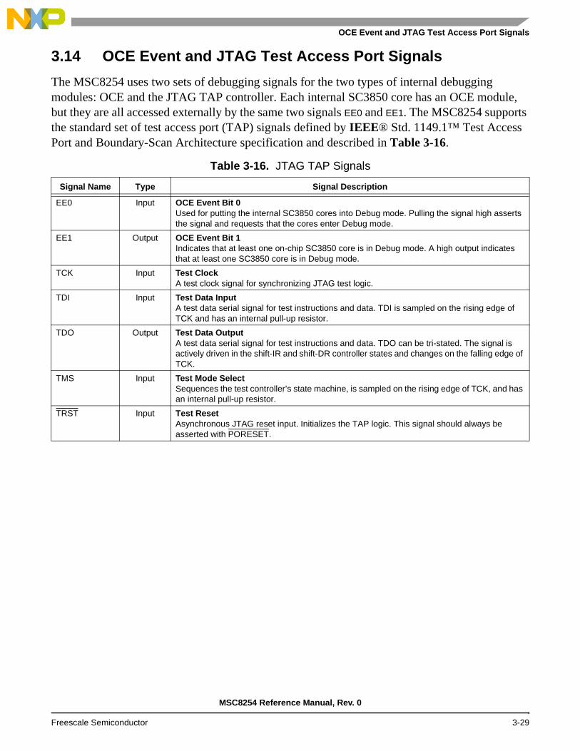
OCE Event and JTAG Test Access Port Signals
3.14 OCE Event and JTAG Test Access Port Signals
The MSC8254 uses two sets of debugging signals for the two types of internal debugging modules: OCE and the JTAG TAP controller. Each internal SC3850 core has an OCE module, but they are all accessed externally by the same two signals EE0 and EE1. The MSC8254 supports the standard set of test access port (TAP) signals defined by IEEE® Std. 1149.1™ Test Access Port and Boundary-Scan Architecture specification and described in Table 3-16.
Table 3-16. JTAG TAP Signals
Signal Name Type Signal Description
EE0 Input OCE Event Bit 0Used for putting the internal SC3850 cores into Debug mode. Pulling the signal high asserts the signal and requests that the cores enter Debug mode.
EE1 Output OCE Event Bit 1Indicates that at least one on-chip SC3850 core is in Debug mode. A high output indicates that at least one SC3850 core is in Debug mode.
TCK Input Test ClockA test clock signal for synchronizing JTAG test logic.
TDI Input Test Data InputA test data serial signal for test instructions and data. TDI is sampled on the rising edge of TCK and has an internal pull-up resistor.
TDO Output Test Data OutputA test data serial signal for test instructions and data. TDO can be tri-stated. The signal is actively driven in the shift-IR and shift-DR controller states and changes on the falling edge of TCK.
TMS Input Test Mode SelectSequences the test controller’s state machine, is sampled on the rising edge of TCK, and has an internal pull-up resistor.
TRST Input Test ResetAsynchronous JTAG reset input. Initializes the TAP logic. This signal should always be asserted with PORESET.
MSC8254 Reference Manual, Rev. 0
Freescale Semiconductor 3-29

External Signals
MSC8254 Reference Manual, Rev. 0
3-30 Freescale Semiconductor

Chip-Level Arbitration and Switching System (CLASS) 4The Chip Level Arbitration and Switching System (CLASS) is the central internal interconnect system for the MSC8254 device. The CLASS is a non-blocking, full-fabric interconnect that allows any initiator to access any target in parallel with another initiator-target couple. The CLASS uses a fully pipelined low latency design. The CLASS demonstrates per-target prioritized round-robin arbitration, highly optimized to the target characteristics. The CLASS operates at 500 MHz, and is separate from the SC3850 core frequency to provide an optimized trade-off between power dissipation, memory technology, and miss latency. Controlling the intradevice data flow, the CLASS reduces bottle necks and permits high bandwidth fully pipe-lined traffic. The CLASS system is ready for use and does not require any special configuration to perform non-blocking pipelined transactions from any initiator to any memory. The configurable arbitration features described in this chapter are for fine-tuning the system for specific application requirements.
The twelve CLASS initiators are:
Four SC3850 core subsystems (initiator ports 0–3)
SerDes bridge shared by two Serial RapidIO controllers and the PCI Express controller (initiator port 8)
Peripherals bridge shared by the SEC, four TDM interfaces, SPI, RGMII, SGMII, and JTAG interface (initiator port 9)
Two DMA controllers (initiator ports 10–11)
The eight CLASS targets are:
Configuration Control and Status Registers (CCSR) (target port 0)
Two core subsystem bridges (two core subsystems per bridge) (target ports 3–4)
Two DDR controllers (target ports 5–6)
M3 memory (target port 7)
MSC8254 Reference Manual, Rev. 0
Freescale Semiconductor 4-1

Chip-Level Arbitration and Switching System (CLASS)
The CLASS initiators and targets are shown in Figure 4-1. The arrows indicate the address direction from initiator to target.
4.1 CLASS Features
The CLASS modules implement the following features:
Non blocking, full fabric interconnect.
Full bandwidth utilization toward each of the targets.
Allows full pipeline when a specific initiator accesses a specific target.
Allows full pipeline when accesses are generated by one or more initiators to specific targets.
Read transactions can have a maximum pipeline of 16 acknowledged requests before completing the transaction toward the initiator.
Write transactions can have a maximum pipeline of 3 acknowledged requests before completing the transaction toward the initiator.
Programmable priority mapping.
Programmable auto priority upgrade.
Address decoding for target selection and multi target demultiplexing:
— Programmable address space start/end registers per target, for flexible address decoding (resolution of 4 KB). Not supported in the reduced configuration option.
— Fixed priority between address decoding results which allows overlapping address windows and deduction of address windows.
Figure 4-1. CLASS Initiators and Targets in the MSC8254 Device
DDRM3
Extended DMA ControllerSerDes Peripherals
Chip Level Arbitration and Switching System (CLASS)
Core0Extended
Core1Extended
Core2Extended
Core3
CCSRNot
Controller 1
Target Devices
Initiator Devices
BridgeBridge
Initiator Ports0
Target Ports0 1 2 3 4 5 6 7
1 2 3 4 5 6 7 8 9 10 11
UsedDDR
Controller 2
ExtendedCore 2–3
Bridge
ExtendedCore 0–1
Bridge
Not Used
NotUsed
MSC8254 Reference Manual, Rev. 0
4-2 Freescale Semiconductor

Functional Description
Per-target arbitration algorithm:
— 4 level prioritization — Each level implements pseudo round-robin arbitration algorithm.— Weighted arbitration — Optimized data bus utilization mode
Programmable masking priority for starvation elimination.
Multiplexing the initiator buses according to the arbitration winner.
Normalizing mode that splits non-aligned transactions according to the target capabilities (maximal burst size, power-of-2 burst, burst alignment, full size burst, data-beat alignment, wrap size)
Error detection and handling:
— The CLASS identifies illegal addresses; addresses that do not belong to any of the address windows or fall inside the negative windows.
— The CLASS stores the illegal address, reports the error, and generates an interrupt.
Debug and profiling unit (CDPU) support.
4.2 Functional Description
The CLASS is a non blocking interconnect between up to 16 initiators and up to 16 targets. The main sub-blocks of the CLASS are: expander, multiplexer and arbiter, normalizer, and the CLASS control interface (CCI) unit that implements the interface and interrupt lines and the CLASS register files. The CLASS also implements an inherent debug and profiling unit (CDPU).
To implement the protocol that deals with the point-to-point bus, the CLASS includes an expander module per initiator that performs address decoding and is used as sampling stage on the initiator side. Each expander module can detect an error address and generate an interrupt. For more details about the expander module see Section 4.2.1. From the target side, the CLASS includes a multiplexer and arbiter module and a normalizer module for each target. The multiplexer and arbiter module performs a pseudo round-robin (RR) arbitration algorithm between all the initiators and concentrates them toward one target. For details about multiplexer and arbiter module see Section 4.2.2. Each multiplexer and arbiter module has a dedicated normalizer module that is used as the sampling stage on the target side. The normalizer can also be used for normalizing transactions. For more details about normalizer module see Section 4.2.3.
MSC8254 Reference Manual, Rev. 0
Freescale Semiconductor 4-3

Chip-Level Arbitration and Switching System (CLASS)
4.2.1 Expander Module and Transaction Flow
Each expander module connects to one initiator. The expander module performs address decoding according to the configuration register settings. Each target is presented by a start address and an end address that define a window in the memory space. The address decoding is done by checking whether the transaction address hits one of the active windows. Each expander module is connected to all of the multiplexer and arbiter blocks in the CLASS to implement a full-fabric and non-blocking interconnect between any initiator to any target. If the address decoding hits in more than one window, the CLASS arbiter chooses a window by fixed priority arbitration (target 0 has the lowest priority). After detecting the requested target and the arbiter selects the target window, the expander module starts a transaction toward the associated multiplexer and arbiter module. The CLASS prevents the possibility of simultaneous accessing to more than one target by the same initiator. If there are accesses from one initiator to different targets, the expander module start the transactions to other targets only after all the open accesses to the current target are completed. The expander module is a sampling stage of transaction. For each request (address + attribute), write data is sampled from the initiator and driven to the normalizer module through multiplexer and arbiter module in the following clock cycle; read data is sampled from the normalizer module through multiplexer and arbiter module and driven to the initiator in the following clock cycle.
4.2.2 Multiplexer and Arbiter Module
The multiplexer and arbiter module connects to all the expander modules on one side and to a dedicated normalizer module on the other side. The multiplexer and arbiter module block is a pure logic data path design, that supports up to 16 initiators, performs an arbitration, and concentrates them towards a specific target normalizer module.
4.2.2.1 CLASS Arbiter
The CLASS arbiter performs weighted arbitration algorithm for requestors simultaneously using a pseudo round-robin arbitration algorithm for each of the priority levels and chooses the highest level request. The CLASS arbiter supports four priority levels, where 3 is the highest and 0 is the lowest. The arbitration operation can be done every clock cycle or delayed according to the number of datums of acknowledged transaction (Late Arbitration mode). The CLASS arbiter supports priority upgrade, so the initiator can upgrade the priority level at any clock cycle.
To eliminate starvation for initiators with low priority, the Masking Priority should be enabled. Starvation can occur when the higher priority initiators access continuously and the lower priority initiators can not perform any access (no priority upgrade ability by the initiator and auto priority upgrade in the expander module is disabled). When the Masking Priority is enabled, the arbiter dedicates slots for lower priority initiator in which the higher priority initiators are masked.
MSC8254 Reference Manual, Rev. 0
4-4 Freescale Semiconductor

Functional Description
4.2.2.1.1 Weighted Arbitration
The CLASS arbiter supports limited weighted arbitration. Weighted arbitration is needed to apply non-uniform distribution of the bandwidth from all initiators toward each target. Weighted arbitration is configurable per CLASS target and gives configurable weights to each initiator. The CLASS arbiter ensures that when a weighted initiator wins the arbitration, it performs Weight + 1 consecutive transactions before transferring control to another initiator with the same or lower priority level.
4.2.2.1.2 Late Arbitration
In late arbitration mode, the request is initiated by the class arbiters as late as possible. At the end of a data burst, this can give better or worse performance for the initiators. The performance depends on the bursty character of the application and the utilization to the target. This mode is activated/deactivated by the appropriate bit in the C0ACR (see Section 4.8.26, CLASS Arbitration Control Register (C0ACR)).
4.2.2.1.3 Priority Masking
When C0ACR[PME] is set, the class arbiters are configured to preserve cycle slots for low priority accesses. They reserve 1/16 of all cycles for priority 0, 2/16 of all cycles for priority 1 or 0, and 2/16 of all cycles for priority 2, 1, or 0. This mode can decrease overall performance. This is one of two approaches to eliminate starvation. The other is to use auto-priority upgrade.
4.2.2.1.4 Auto Priority Upgrade
This mode is activated by setting the C0PACRx[AUE] bit (see Section 4.8.3, CLASS Priority Auto Upgrade Control Registers (C0PACRx)). When active, a pending request has its priority upgraded to the next higher priority after a specified number of cycles specified by C0PAVRx[AUV] (see Section 4.8.2, CLASS Priority Auto Upgrade Value Registers (C0PAVRx)). The upgrade level and timing depend on the current priority value assigned, as follows:
For priority 0 requests, the priority is upgraded to priority 1 after AUV cycles.
For priority 1 requests, the priority is upgraded to priority 2 after AUV/2 cycles.
For priority 2 requests, the priority is upgraded to priority 3 (highest) after AUV/4 cycles.
The upgrade process continues until the request is processed or it reaches priority 3.
4.2.2.2 CLASS Multiplexer
The CLASS multiplexer includes two FIFOs that connect between the appropriate initiator and the target. The FIFO depth is 16, thus enabling the multiplexer and arbiter module to deal with 16 open transactions, which received their request acknowledge and are waiting for the end-of-data or end-of-transaction signals. The CLASS multiplexer is pure logic for the data path and does not cause any latency.
MSC8254 Reference Manual, Rev. 0
Freescale Semiconductor 4-5

Chip-Level Arbitration and Switching System (CLASS)
4.2.3 Normalizer Module
Each normalizer module is connected to the appropriate multiplexer and arbiter module on one side and to a specific CLASS target interface on the other side. Each normalizer module is used as a sampler for full pipeline towards the target. The normalizer module is the only module within the CLASS that can manipulate the transaction (for example, splitting non-aligned transactions). An internal signal is used to indicate that optimization is needed. Only the last normalizer module on the way to the target is used for normalization. All the other normalizer modules should be used only as samplers. The normalizer module supports the fast confirm mechanism for writes.
4.2.4 CLASS Control Interface (CCI)
The CLASS control interface (CCI) enables access to the CLASS configuration, control, and status registers. All write accesses to these registers should use supervisor mode. See Section 4.8 for programming details.
4.3 MSC8254 Initiator CLASS Access Priorities
Table 4-1 summarizes the priorities of the CLASS initiators when accessing targets over the CLASS. The priority listed in this table is the priority of the accesses by the initiator before any CLASS remapping (that is, C0PMRx = 0x3210). If the CLASS is remapped (using C0PMRx), this table represents the arrival priority of the initiator to the CLASS and not the new mapped value. Note that start-up code (for example, the CodeWarrior initialization files) and boot code can change the value of C0PMRx from its reset value.
Table 4-1. Initiator CLASS Access Priorities
Initiator Priority 0 Priority 1 Priority 2 Priority 3 comments
Cores and subsystems - Prefetch
“Low” priority (0) NA NA NA
Cores and subsystems - Read
NA NA “High” priority (2) NA A core read transaction reaches the CLASS in case of L1/L2 miss or non-cacheable address
Cores and subsystems - Write
“Low” priority (0) - Normal write
NA “High” priority (2) - If the write stalls
the core
NA
SRIO - Inbound (IO, Maintenance, Doorbell)
SRIO priority (0) SRIO priority (1) SRIO priority (2) NA
SRIO - Inbound (Message)
NA SRIO priority (0), SRIO priority (1)
SRIO priority (2) NA SRIO priority (0) and (1) both result in CLASS priority 1
RMU - BD Read NA NA Priority (2) NA
MSC8254 Reference Manual, Rev. 0
4-6 Freescale Semiconductor

MSC8254 Initiator CLASS Access Priorities
RMU - DATA Read (Outbound Doorbell or Message)
Priority (0),Priority (1)
Priority (2) NA NA Serial RapidIO priority (0) and (1) both result in CLASS priority 0
OCNDMA BD Read (0) NA NA NA
OCNDMA DATA Read/Write
(0) NA NA NA
System DMA BD Read
NA NA NA (3)
System DMA DATA Read/Write
PP (0) PP (1) PP (2) PP (3) See Section 14.7.22.1, Buffer Attributes (BD_ATTR) and Section 14.7.22.2, Multi-Dimensional Buffer Attributes (BD_MD_ATTR).
PCI Express Inbound
NA NA (2) NA
TDM NA Default Priority (1) NA Emergency (Defined by programmable threshold of TDM
FIFO fill)
QUICC Engine subsystem
Normal mode (0) Normal mode (1) Normal mode (2) Normal/emergency mode (3)
See Section 18.3.4, MBus Access and the Serial DMA Mode Register (SDMR) in the QUICC Engine Block Reference Manual with Interworking Protocol.
Table 4-1. Initiator CLASS Access Priorities (Continued)
Initiator Priority 0 Priority 1 Priority 2 Priority 3 comments
MSC8254 Reference Manual, Rev. 0
Freescale Semiconductor 4-7

Chip-Level Arbitration and Switching System (CLASS)
4.4 CLASS Error Interrupts
The CLASS can generate one error interrupt that is common for all initiators. The error interrupt is created when the CLASS receives a transaction request with an illegal address. Illegal addresses are defined as any one of the following 2 cases:
1. An address which does not belong to any of the address space windows of the enabled address decoders.
2. An address which falls within any of the address space windows of the enabled error address decoders.
When an illegal address is identified by the CLASS, the following events occur.
The associated AEIx bit in the CISR is set.
The address that was identified as illegal is stored in the associated CEARx and CEEARx. These registers are locked until the associated AEIx bit in the CISR is cleared either by a hardware reset or by writing 1 to this bit.
Note: If the associated AEIx bit in the CISR is already set when the illegal address is identified (due to a prior illegal address), then the new error address is not stored.
If the corresponding AEIEx bit in the CIER is set, an IRQ is issued.
The CLASS does not initiate a transaction to any target. However, the CLASS will continue normally on the initiator side until completion, and report the error. In case of a read transaction, the CLASS delivers invalid data to the initiator.
If, at the time of the error transaction, there are open transactions that did not receive the end-of-transaction, the expander module stalls all new transaction until all prior transactions receive the end-of-transaction, close the error transaction, report the end-of-transaction, report the error, and only then continue with subsequent transactions.
Any subsequent requests with a legal address are serviced normally.
Note: The CLASS does not produce an error when a transaction starts inside a target address window and finishes outside of the window. This situation must be avoided by the user. If it occurs, the results are unpredictable.
The error interrupt is logically ORed with internal error interrupts. The internal error interrupts are associated with each initiator. Thus, the CLASS error interrupt is asserted when at least one internal interrupt is asserted.
MSC8254 Reference Manual, Rev. 0
4-8 Freescale Semiconductor

CLASS Debug Profiling Unit
4.5 CLASS Debug Profiling Unit
The CLASS supports debug and profiling measurements by the CLASS debug and profiling unit (CDPU).
4.5.1 Profiling
The user can configure the desired measurement in the CIPCRs and CTPCRs.
Note: For each CLASS module, only one PMM field among all C0IPCRx and C0TPCRx can be greater than 0 during profiling.
You can activate the CDPU by:
Writing a 1 to the CPCR[PE] bit.
Configuring a watch point event in CPCR[WPEC] field.
The CDPU is deactivated by:
Writing a 0 to the CPCR[PE] bit.
Configuring a watch point event in CPCR[WPEC] field.
Reaching a time-out in the CPTOR when the CPCR[TOE] bit is set.
CPRCR overflow.
After the desired profiling mode has been chosen, activate the CDPU to perform the measurement. At the beginning of every measurement, the CLASS Profiling Reference Counter (CPRCR) starts counting the clock cycles. Read the CPISR[OVE] bit to verify that the measurement is complete and that the profiling counter values are valid. If the CPISR[OVE] is clear, read the profiling counters CPRCR and CPGCR and analyze the results.
MSC8254 Reference Manual, Rev. 0
Freescale Semiconductor 4-9

Chip-Level Arbitration and Switching System (CLASS)
4.5.2 Watch Point Unit
The CLASS includes a watch point unit (WPU) for each of the initiator interfaces and for each of the target interfaces. The WPU can compare programmed values to the real transactions and generate a watch point event when a match occurs.
Note: For each CLASS module, only one WPEN field can be set among all C0IWPCRx and C0TWPCRx when snooping watch point events. That is, only one watch point unit can be active at a time.
Use the following steps to use the watch point unit:
1. Clear C0PCR.
2. Clear C0IPCRx and C0TPCR.
3. For the time-out mechanism, program C0PTOR and set the C0PCR[TOE] bit.
4. Define the transaction to be monitored by writing the desired configuration to C0WPCR, C0WPACR, C0WPEACR, and C0WPAMR.
5. Enable the watch point units through C0IWPCRx and C0TWPCR.
6. Set the C0WPRCR[CE] bit to enable counting of the watch point events. If you use the watch point events to enable/disable the profiling unit according to WPCE, clear this bit.
7. After the measurement are finished check the following registers:
— Read the C0PISR[OVE] bit. — In time-out mode, read C0PRCR.— If C0PISR[OVE] is set or if C0PRCR is equal to C0PTOR, the results are not valid.— Read C0PGCRx to get the number of watch point events during the measurement.
MSC8254 Reference Manual, Rev. 0
4-10 Freescale Semiconductor

CLASS Debug Profiling Unit
4.5.3 Event Selection
Events are selected using a combination of the CLASS watch point and profiling registers. Table 4-2 lists the measurement modes, the required configuration settings, and the events measured by the specific CLASS Profiling General Registers for each CLASS module. See Section 4.8 for the register details.
Table 4-2. C0PGCRx Events Selection
Measurement Mode
Configuration Settings for Each Mode Events Measured
C0WPCR [CE]
C0TPCR [TT]
C0TPCR [PMM]
C0IPCRx [PMM]
C0PGCR0 C0PGCR1 C0PGCR2 C0PGCR3
None selected 0 — 00 00000 — — — —
Initiator Priority and Auto-Upgrade
0 — 00 00001 No. of Initiator
Requests with
Priority 1
No. of Initiator
Requests with
Priority 2
No. of Initiator
Requests with
Priority 3
No. of Initiator Auto-
Upgrade
Allows the user to profile a statistical distribution of transaction priorities. This information can be used to consider whether other arbitration methods (priority mapping, Auto-upgrade, weighted arbitration, priority mask enable) should be considered
Initiator Access Type
0 — 00 00010 Initiator Pending Request
cycles (not acknow- ledged)
No. of Initiator Read
Requests
No. of Initiator
Real Write Requests
(not confirmed)
No. of Initiator
Fast Write Requests
(not confirmed)
Real/Fast confirmation refers to the type of eot for writes that are requested per MBus transaction.• Real means that for coherency reasons the eot for write should be high only after the data is written to
the target.• Fast means that for performance reasons the eot can be high even before the data is written to the
target.Real/Fast confirmation support is initiator dependent and the user cannot change the related settings. A summary follows below:• DSP Cores
− Write through uses fast confirmation− Write through with SYNCIO generate real confirmation − Last burst in a line write-back is sent with real confirmation
• DMA. Channel transfers come with fast confirm and real confirm on the last data of a transfer.• Serial RapidIO Inbound Transactions. When the transfer comes with a response (NWRITE_R), the last
data uses real confirmation and fast confirm for the previous transfer. For NWRITE, data is transferred with fast confirmation
• Serial RapidIO Outbound Transactions. Supports fast confirm on the last data transfer per channel transfer and fast confirm for the previous transfer.
• QUICC Engine and PCI Express Transactions. Always uses real confirmation The resulting information can be used to redesign the code to minimize stalls related to real confirmations. Use of large transactions reduces the number of real confirmations because they are only required for the last beat of the transfer.
Initiator Stall 0 — 00 00011 No. of Write After
Read (WAR) events
No. of stall cycles due
to WAR events
— No. of stall cycles due
to TS events
By managing WAR and target switching, an initiator can enhance the performance for memory accesses and thus minimize run time. Note: Stall at the initiator does not mean that the initiator target data phase is idle; it indicates the delay
after which the next access from the initiator starts at the target after a WAR or TS event.
MSC8254 Reference Manual, Rev. 0
Freescale Semiconductor 4-11

Chip-Level Arbitration and Switching System (CLASS)
Initiator Priority Upgrade
0 — 00 00100 Initiator Sample 0 Upgrade cycles
Initiator Sample 1 Upgrade cycles
Initiator Sample 2 Upgrade cycles
—
Initiator Priority Upgrade measurement counts the number of cycles a low-priority transaction is upgraded because a high-priority transaction was scheduled into the CLASS pipeline. This upgrading mechanism is necessary to reduce the service latency of newly issued transactions because the CLASS is ordered in nature and does not do preemption. A high-priority transaction could otherwise be delayed by preceding lower priority accesses for long periods of time. The upgrade is to the priority level of the high-priority transaction and it is only possible if the transaction is upgradable. The upgrade attribute of a transaction is initiator dependent and it is hard-wired. The system DMA is the only initiator issuing non-upgradable transactions. The counter measurements take place in the early stages of the CLASS pipeline at different sample locations. Transactions in sample 0 are older than transactions on sample 1, and transactions in sample 1 are older than the ones in sample 2. Any type of priority upgrade, including auto-upgrade, is captured by these counters. These counters provide a good view of the starvation dynamics of the system.
Initiator Priority Non-Upgrade
0 — 00 00101 Initiator Sample 0
No Upgrade cycles
Initiator Sample 1
No Upgrade cycles
Initiator Sample 2
No Upgrade cycles
—
Initiator Priority No-Upgrade measurement counts the number of cycles an older low-priority transaction is not upgraded despite the fact that a newer high-priority is scheduled by the same initiator. Compare with “Initiator Priority Upgrade”. This applies only to System DMA transactions because they are not upgradable by default. All other initiator transactions can be upgraded. These counts are not very useful for performance analysis, but they provide a good view of the starvation dynamics of the system.
Initiator Supervisor
0 — 00 00110 Request pending cycles
No. of supervisor accesses
No. of non- supervisor accesses
—
Supervisor/user accesses can be used to profile the amount of time the OS spends running and how much time is left for the users application. Effective for evaluating the core subsystem supervisor/user mode usage. The implementation depends on the values configured in M_DSDAx[DAPU]/M_DSDAx[DAPS], and so forth. See the SC3850 Core Subsystem Reference Manual for configuration details.
Initiator Bandwidth
0 — 00 00111 No. of Initiator
Read Data Acknow- ledges.
No. of Initiator
Write Data Acknow- ledges
— —
Can be used to profile the number of data reads and writes. The amount of data that passes through the initiator port = [(NumberOfReadAck + NumberOfWriteAck) × W]. where W is the port width. Note that an access may be smaller than the port width.
Initiator-target Bandwidth
0 — 00 10000 + T No. of Read Data Acknow- ledges
between Initiator
and Target T
No. of Write Data Acknow- ledges
between Initiator
and Target T
— —
Can be used to profile the number of data reads and writes. between an initiator and a specific target The amount of data that passes through the initiator port = [(NumberOfReadAck + NumberOfWriteAck) × W]. where W is the port width. Note that an access may be smaller than the port width.
Table 4-2. C0PGCRx Events Selection (Continued)
Measurement Mode
Configuration Settings for Each Mode Events Measured
C0WPCR [CE]
C0TPCR [TT]
C0TPCR [PMM]
C0IPCRx [PMM]
C0PGCR0 C0PGCR1 C0PGCR2 C0PGCR3
MSC8254 Reference Manual, Rev. 0
4-12 Freescale Semiconductor
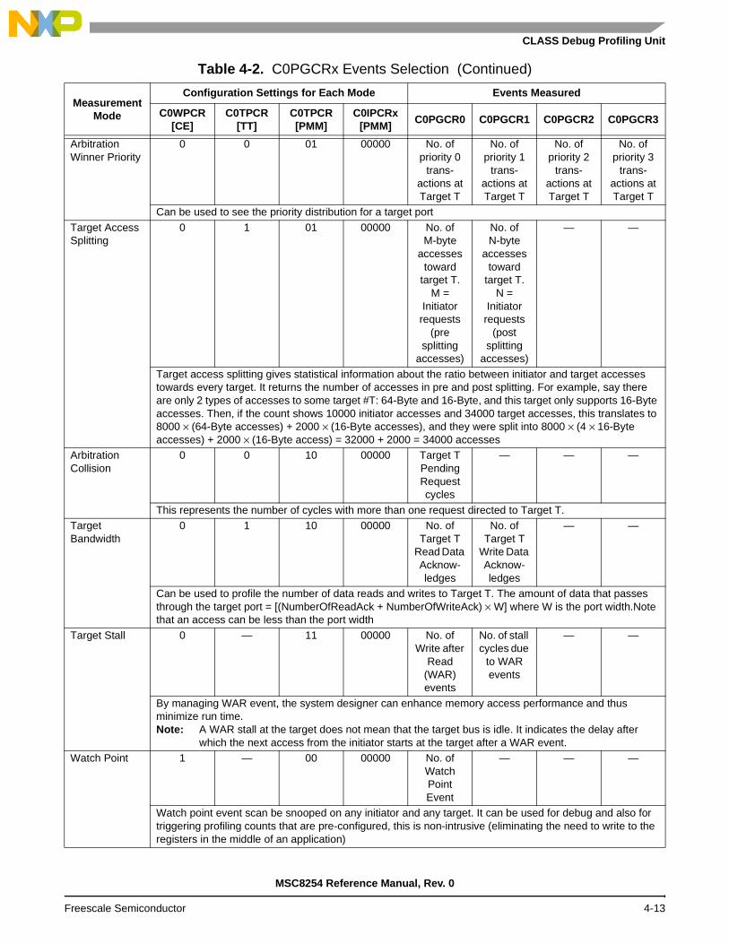
CLASS Debug Profiling Unit
Arbitration Winner Priority
0 0 01 00000 No. of priority 0
trans- actions at Target T
No. of priority 1
trans- actions at Target T
No. of priority 2
trans- actions at Target T
No. of priority 3
trans- actions at Target T
Can be used to see the priority distribution for a target port
Target Access Splitting
0 1 01 00000 No. of M-byte
accesses toward
target T. M =
Initiator requests
(pre splitting
accesses)
No. of N-byte
accesses toward
target T. N =
Initiator requests
(post splitting
accesses)
— —
Target access splitting gives statistical information about the ratio between initiator and target accesses towards every target. It returns the number of accesses in pre and post splitting. For example, say there are only 2 types of accesses to some target #T: 64-Byte and 16-Byte, and this target only supports 16-Byte accesses. Then, if the count shows 10000 initiator accesses and 34000 target accesses, this translates to 8000 × (64-Byte accesses) + 2000 × (16-Byte accesses), and they were split into 8000 × (4 × 16-Byte accesses) + 2000 × (16-Byte access) = 32000 + 2000 = 34000 accesses
Arbitration Collision
0 0 10 00000 Target T Pending Request cycles
— — —
This represents the number of cycles with more than one request directed to Target T.Target Bandwidth
0 1 10 00000 No. of Target T
Read Data Acknow- ledges
No. of Target T
Write Data Acknow- ledges
— —
Can be used to profile the number of data reads and writes to Target T. The amount of data that passes through the target port = [(NumberOfReadAck + NumberOfWriteAck) × W] where W is the port width.Note that an access can be less than the port width
Target Stall 0 — 11 00000 No. of Write after
Read (WAR) events
No. of stall cycles due
to WAR events
— —
By managing WAR event, the system designer can enhance memory access performance and thus minimize run time. Note: A WAR stall at the target does not mean that the target bus is idle. It indicates the delay after
which the next access from the initiator starts at the target after a WAR event. Watch Point 1 — 00 00000 No. of
Watch Point Event
— — —
Watch point event scan be snooped on any initiator and any target. It can be used for debug and also for triggering profiling counts that are pre-configured, this is non-intrusive (eliminating the need to write to the registers in the middle of an application)
Table 4-2. C0PGCRx Events Selection (Continued)
Measurement Mode
Configuration Settings for Each Mode Events Measured
C0WPCR [CE]
C0TPCR [TT]
C0TPCR [PMM]
C0IPCRx [PMM]
C0PGCR0 C0PGCR1 C0PGCR2 C0PGCR3
MSC8254 Reference Manual, Rev. 0
Freescale Semiconductor 4-13

Chip-Level Arbitration and Switching System (CLASS)
4.5.4 Debug and Profiling Events
The CLASS generates two event interrupts:
Watch point event (WPE)
Overflow event (OVE)
4.6 CLASS Reset
The CLASS implements 2 kinds of reset:
Synchronous hard reset.
Synchronous soft reset.
4.6.1 Soft Reset
This kind of reset has the following effects:
All the CLASS state machines return to their idle state.
All the CLASS operation FFs return to their idle state.
The CLASS configuration registers are reset as described in the table for each register in Section 4.8, Programming Model.
4.6.2 Hard Reset
This reset brings all states machines to idle state and sets all CLASS registers to the reset values.
4.7 LimitationsThe CLASS does not support split transaction between targets. A split transaction starts inside a targets address space but ends outside of this window. The CLASS does not report an error in this event and the results are unpredictable. You must avoid this situation.
The CLASS does not support pipelined transactions between different targets by the same initiator. The pipeline is stalled until all transaction to one target are closed before issuing a transaction to a different target.
Arbitration Fairness. Requests with the higher priority levels may cause transactions with lower priority levels not to be acknowledged, resulting in a starvation condition. This situation can be prevented by using the auto priority upgrade supported by the expander module and/or by the multiplexer and arbiter module priority mask mechanism.
Do not allow cores to access each other.
MSC8254 Reference Manual, Rev. 0
4-14 Freescale Semiconductor

Programming Model
4.8 Programming Model
All the CLASS registers are 32-bit registers. All the read and write accesses are executed through the bus. The CLASS modules use the following registers:
CLASS Priority Mapping Registers (see page 4-16)CLASS Priority Auto Upgrade Value Registers (see page 4-18)CLASS Priority Auto Upgrade Control Registers (see page 4-19)
CLASS Error Address Registers (see page 4-20)
CLASS Error Extended Address Registers (see page 4-21)
CLASS Initiator Profiling Configuration Registers (see page 4-23)CLASS Initiator Watch Point Control Registers (see page 4-25)CLASS Arbitration Weight Registers (see page 4-26)CLASS Start Address Decoder x (see page 4-27)CLASS End Address Decoder x (see page 4-28)CLASS Attributes Decoder x (see page 4-29)CLASS IRQ Status Register (see page 4-30)CLASS IRQ Enable Register (see page 4-31)CLASS Target Profiling Configuration Register (see page 4-32)CLASS Profiling Control Register (see page 4-33)CLASS Watch Point Control Register (see page 4-34)CLASS Watch Point Access Configuration Register (page 4-36)CLASS Watch Point Extended Access Configuration Register (see page 4-37)CLASS Watch Point Address Mask Register (see page 4-38)CLASS Profiling Time Out Register (see page 4-39)CLASS Target Watch Point Control Register (see page 4-40)CLASS Profiling IRQ Status Register (see page 4-41)CLASS Profiling IRQ Enable Register (see page 4-42)CLASS Profiling Reference Counter Register (see page 4-42)CLASS Profiling General Counter Registers (see page 4-43)CLASS Arbitration Control Register (see page 4-44)
Note: The base address for addressing CLASS registers is 0xFFF18000.
MSC8254 Reference Manual, Rev. 0
Freescale Semiconductor 4-15

Chip-Level Arbitration and Switching System (CLASS)
4.8.1 CLASS Priority Mapping Registers (C0PMRx)
C0PMRx is used as a look-up table for mapping the priority received from the initiator. By default the input priority is mapped to an identical value on the output. This register also enables/disables the priority derivation feature.
Note: You cannot write to this register while there are open CLASS transactions. The boot overrides the default reset value for C0PMR[0–5] only.
Table 4-3 lists the C0PMRx bit field descriptions.
C0PMR[0–11] CLASS Priority Mapping Registers Offset 0x800 + x*0x04
Bit 31 30 29 28 27 26 25 24 23 22 21 20 19 18 17 16
— PB
Type R/WReset 0 0 0 0 0 0 0 0 0 0 0 0 0 0 0 0Boot 0 0 0 0 0 0 0 0 0 0 0 0 0 0 0 0
Bit 15 14 13 12 11 10 9 8 7 6 5 4 3 2 1 0
— PM3 — PM2 — PM1 — PM0
Type R/WReset 0 0 1 1 0 0 1 0 0 0 0 1 0 0 0 0Boot 0 0 1 1 0 0 1 0 0 0 0 1 0 0 0 1
Table 4-3. C0PMRx Bit Descriptions
Name Reset Description Settings
—31–17
0 Reserved. Write to 0 for future compatibility.
PB16
0 Priority BypassEnables/disables the priority derivation mechanism.
0 Filter the mapped priority with the priority derivation mechanism.
1 Pass the mapped priority from initiator to target with no filtering.
—15–14
0 Reserved. Write to 0 for future compatibility.
PM313–12
11 Priority Mapping 3Holds the priority value assigned to transactions that arrive with a value of 3.
00 Priority 001 Priority 110 Priority 211 Priority 3
—11–10
0 Reserved. Write to 0 for future compatibility.
PM29–8
10 Priority Mapping 2Holds the priority value assigned to transactions that arrive with a value of 2.
00 Priority 001 Priority 110 Priority 211 Priority 3
—7–6
0 Reserved. Write to 0 for future compatibility.
PM15–4
01 Priority Mapping 1Holds the priority value assigned to transactions that arrive with a value of 1.
00 Priority 001 Priority 110 Priority 211 Priority 3
MSC8254 Reference Manual, Rev. 0
4-16 Freescale Semiconductor

Programming Model
—3–2
0 Reserved. Write to 0 for future compatibility.
PM01–0
0 Priority Mapping 0Holds the priority value assigned to transactions that arrive with a value of 0.
00 Priority 001 Priority 110 Priority 211 Priority 3
Table 4-3. C0PMRx Bit Descriptions (Continued)
Name Reset Description Settings
MSC8254 Reference Manual, Rev. 0
Freescale Semiconductor 4-17
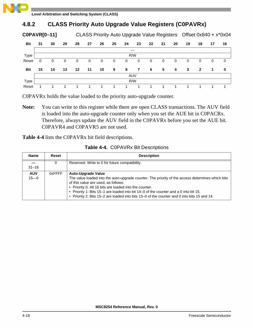
Chip-Level Arbitration and Switching System (CLASS)
4.8.2 CLASS Priority Auto Upgrade Value Registers (C0PAVRx)
C0PAVRx holds the value loaded to the priority auto-upgrade counter.
Note: You can write to this register while there are open CLASS transactions. The AUV field is loaded into the auto-upgrade counter only when you set the AUE bit in C0PACRx. Therefore, always update the AUV field in the C0PAVRx before you set the AUE bit. C0PAVR4 and C0PAVR5 are not used.
Table 4-4 lists the C0PAVRx bit field descriptions.
C0PAVR[0–11] CLASS Priority Auto Upgrade Value Registers Offset 0x840 + x*0x04
Bit 31 30 29 28 27 26 25 24 23 22 21 20 19 18 17 16
—
Type R/WReset 0 0 0 0 0 0 0 0 0 0 0 0 0 0 0 0
Bit 15 14 13 12 11 10 9 8 7 6 5 4 3 2 1 0
AUVType R/W
Reset 1 1 1 1 1 1 1 1 1 1 1 1 1 1 1 1
Table 4-4. C0PAVRx Bit Descriptions
Name Reset Description
—31–16
0 Reserved. Write to 0 for future compatibility.
AUV15—0
0xFFFF Auto-Upgrade ValueThe value loaded into the auto-upgrade counter. The priority of the access determines which bits of this value are used, as follows:• Priority 0: All 16 bits are loaded into the counter.• Priority 1: Bits 15–1 are loaded into bit 14–0 of the counter and a 0 into bit 15.• Priority 2: Bits 15–2 are loaded into bits 13–0 of the counter and 0 into bits 15 and 14.
MSC8254 Reference Manual, Rev. 0
4-18 Freescale Semiconductor

Programming Model
4.8.3 CLASS Priority Auto Upgrade Control Registers (C0PACRx)
C0PACRx controls the priority auto-upgrade mechanism.
Note: You can write to this register while there are open CLASS transactions. C0PACR4 and C0PACR5 are not used.
Table 4-5 lists the C0PACRx bit field descriptions.
C0PACR[0–11] CLASS Priority Auto Upgrade Control Registers Offset 0x880 + x*0x04
Bit 31 30 29 28 27 26 25 24 23 22 21 20 19 18 17 16
—
Type R/WReset 0 0 0 0 0 0 0 0 0 0 0 0 0 0 0 0
Bit 15 14 13 12 11 10 9 8 7 6 5 4 3 2 1 0
— AUEType R/W
Reset 0 0 0 0 0 0 0 0 0 0 0 0 0 0 0 0
Table 4-5. C0PACRx Bit Descriptions
Name Reset Description Settings
—31–1
0 Reserved. Write to 0 for future compatibility.
AUE0
0 Auto-Upgrade EnableEnables/disables the auto-upgrade mechanism.
Note: This bit can only be cleared by a hardware reset.
0 Auto-upgrade mechanism disabled.1 Auto-upgrade mechanism enabled.
MSC8254 Reference Manual, Rev. 0
Freescale Semiconductor 4-19
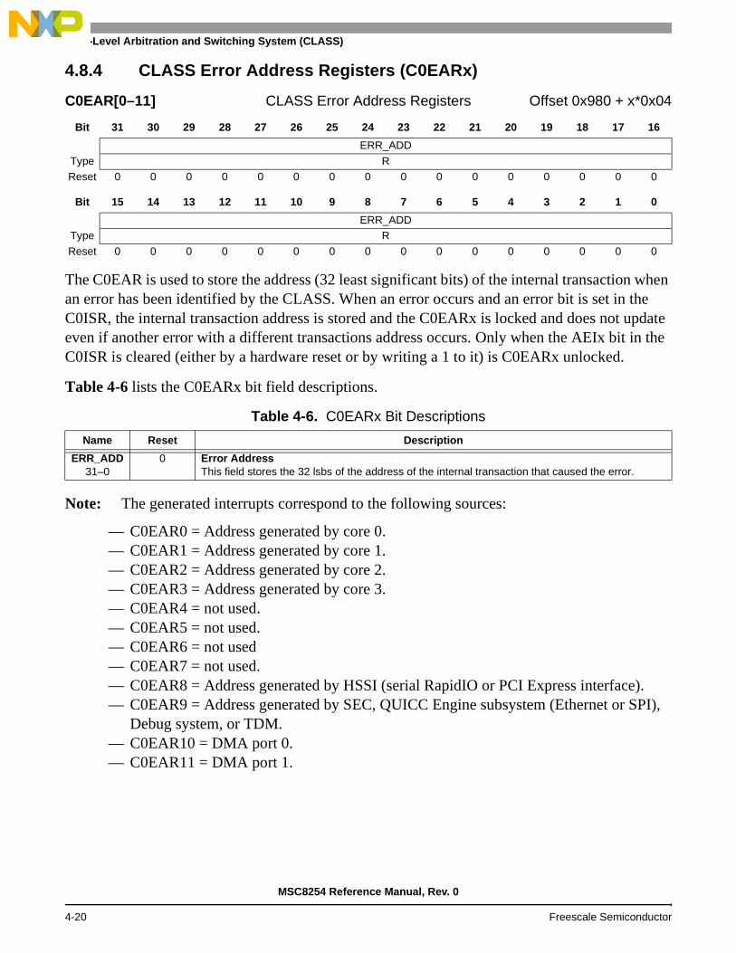
Chip-Level Arbitration and Switching System (CLASS)
4.8.4 CLASS Error Address Registers (C0EARx)
The C0EAR is used to store the address (32 least significant bits) of the internal transaction when an error has been identified by the CLASS. When an error occurs and an error bit is set in the C0ISR, the internal transaction address is stored and the C0EARx is locked and does not update even if another error with a different transactions address occurs. Only when the AEIx bit in the C0ISR is cleared (either by a hardware reset or by writing a 1 to it) is C0EARx unlocked.
Table 4-6 lists the C0EARx bit field descriptions.
Note: The generated interrupts correspond to the following sources:
— C0EAR0 = Address generated by core 0.— C0EAR1 = Address generated by core 1.— C0EAR2 = Address generated by core 2.— C0EAR3 = Address generated by core 3.— C0EAR4 = not used.— C0EAR5 = not used.— C0EAR6 = not used— C0EAR7 = not used.— C0EAR8 = Address generated by HSSI (serial RapidIO or PCI Express interface).— C0EAR9 = Address generated by SEC, QUICC Engine subsystem (Ethernet or SPI),
Debug system, or TDM.— C0EAR10 = DMA port 0.— C0EAR11 = DMA port 1.
C0EAR[0–11] CLASS Error Address Registers Offset 0x980 + x*0x04
Bit 31 30 29 28 27 26 25 24 23 22 21 20 19 18 17 16
ERR_ADD
Type RReset 0 0 0 0 0 0 0 0 0 0 0 0 0 0 0 0
Bit 15 14 13 12 11 10 9 8 7 6 5 4 3 2 1 0
ERR_ADDType R
Reset 0 0 0 0 0 0 0 0 0 0 0 0 0 0 0 0
Table 4-6. C0EARx Bit Descriptions
Name Reset Description
ERR_ADD31–0
0 Error AddressThis field stores the 32 lsbs of the address of the internal transaction that caused the error.
MSC8254 Reference Manual, Rev. 0
4-20 Freescale Semiconductor

Programming Model
4.8.5 CLASS Error Extended Address Registers (C0EEARx)
The C0EEAR stores the most significant 4 bits of the address of the internal transaction when an error has been identified by the CLASS. This register also stores the attributes and the source ID of this transaction. When an error occurs and an error bit is set in the C0ISR, the internal transaction address is stored and the C0EEAR is locked and is not updated even if another error with a different transactions address/attributes occurs. Only when the AEI bit in the CISR is cleared (either by a hardware reset or by writing a 1 to it) is C0EEAR unlocked.
Note: C0EEAR4 and C0EEAR5 are not used.
Table 4-7 lists the C0EEARx bit field descriptions.
C0EEAR[0–11] CLASS Extended Error Address Registers Offset 0x9C0 + x*0x04
Bit 31 30 29 28 27 26 25 24 23 22 21 20 19 18 17 16
— RW
Type RReset 0 0 0 0 0 0 0 0 0 0 0 0 0 0 0 0
Bit 15 14 13 12 11 10 9 8 7 6 5 4 3 2 1 0
— SA — SRC_ID ERR_ADDType R
Reset 0 0 0 0 0 0 0 0 0 0 0 0 0 0 0 0
Table 4-7. C0EEARx Bit Descriptions
Name Reset Description Settings
—31–17
0 Reserved. Write to 0 for future compatibility.
RW16
0 Read/WriteThis field indicates whether the transaction that caused the error was a read or a write.
0 Write.1 Read.
—15
0 Reserved. Write to 0 for future compatibility.
SA14
0 Supervisor AccessThis field indicates whether the transaction that caused the error was in supervisor mode.
0 Not supervisor.1 Supervisor.
—13–9
0 Reserved. Write to 0 for future compatibility.
SRC_ID8–4
0 Source IDIdentifies the source ID of the initiator that caused the error.
0x00 Core 00x01 Core 10x02 Core 20x03 Core 30x08 DMA Controller0x09 DMA Controller0x0B QUICC Engine subsystem0x0C Serial RapidIO Port 00x0D Serial RapidIO Port 10x0E TDMAll other values reserved.
ERR_ADD3–0
0 Error AddressThis field stores the 4 msbs of the address of the internal transaction that caused the error.
MSC8254 Reference Manual, Rev. 0
Freescale Semiconductor 4-21

Chip-Level Arbitration and Switching System (CLASS)
MSC8254 Reference Manual, Rev. 0
4-22 Freescale Semiconductor

Programming Model
4.8.6 CLASS Initiator Profiling Configuration Registers (C0IPCRx)
C0IPCRx controls the CLASS initiator profiling measurements. Each initiator has a dedicated C0IPCR which is numbered according to the initiator number within each CLASS module. The CLASS can perform only one measurement for a specific module at a time. Select the desired measurement for the initiator, enter the PMM value in the associated C0IPCR and make sure all the other C0IPCR and the C0TPCR for that CLASS are cleared.
Note: Only one PMM field among all C0IPCRx and C0TPCR can be greater than 0 during profiling. C0IPCR4 and C0IPCR5 are not used.
Table 4-8 lists the C0IPCRx bit field descriptions.
C0IPCR[0–11] CLASS Initiator Profiling Configuration Registers‘Offset 0xA00 + x*0x04
Bit 31 30 29 28 27 26 25 24 23 22 21 20 19 18 17 16
—
Type R/WReset 0 0 0 0 0 0 0 0 0 0 0 0 0 0 0 0
Bit 15 14 13 12 11 10 9 8 7 6 5 4 3 2 1 0
— PMMType R/W
Reset 0 0 0 0 0 0 0 0 0 0 0 0 0 0 0 0
Table 4-8. C0IPCRx Bit Descriptions
Name Reset Description Settings
—31–5
0 Reserved. Write to 0 for future compatibility.
PMM4–0
0 Profiling Measurement ModeDetermines the profiling measurement mode for the matching initiator.
Note: This register can only be cleared by a hardware reset.
00000 No measurement.00001 Initiator priority and auto-upgrade.00010 Initiator access type.00011 Initiator stall.00100 Initiator priority upgrade.00101 Initiator priority non-upgrade.00110 Initiator supervisor.00111 Initiator bandwidth.01000–01111 reserved10000 Target 0 bandwidth.10001 Target 1 bandwidth.10010 reserved.10011 Target 3 bandwidth.10100 Target 4 bandwidth.10101 Target 5 bandwidth.10110 Target 6 bandwidth.10111 Target 7 bandwidth.11000–11111 reserved
MSC8254 Reference Manual, Rev. 0
Freescale Semiconductor 4-23

Chip-Level Arbitration and Switching System (CLASS)
Table 4-9. Initiator Numbers
Initiator Number
Initiator Module
0 DSP core subsystem 0
1 DSP core subsystem 1
2 DSP core subsystem 2
3 DSP core subsystem 3
4 reserved
5 reserved
6 reserved
7 reserved
8 HSSI
9 SEC, Ethernet, SPI, TDM, or Debug
10 DMA port 0
11 DMA port 1
MSC8254 Reference Manual, Rev. 0
4-24 Freescale Semiconductor

Programming Model
4.8.7 CLASS Initiator Watch Point Control Registers (C0IWPCRx)
C0IWPCRx controls the Watch Point Unit operation for the associated initiator. The Watch Point Unit monitors a specific access defined by the C0WPCRx, C0WPACRx, C0WPEACRx, and C0WPAMR. Each initiator can be enabled/disabled to monitor the selected access. You can write to this register while there are open CLASS transactions.
Note: Only one WPEN field can be set among all C0IWPCRx and C0TWPCRx when snooping watch point events. C0IWPCR4 and C0IWPCR5 are not used.
Table 4-10 lists the C0IWPCRx bit field descriptions.
C0IWPCR[0–11] CLASS Initiator Watch Point Control Registers Offset 0xA40 + x*0x04
Bit 31 30 29 28 27 26 25 24 23 22 21 20 19 18 17 16
—
Type R/WReset 0 0 0 0 0 0 0 0 0 0 0 0 0 0 0 0
Bit 15 14 13 12 11 10 9 8 7 6 5 4 3 2 1 0
— WPENType R/W
Reset 0 0 0 0 0 0 0 0 0 0 0 0 0 0 0 0
Table 4-10. C0IWPCRx Bit Descriptions
Name Reset Description Settings
—31–1
0 Reserved. Write to 0 for future compatibility.
WPEN0
0 Watch Point EnableEnables/disables the auto-upgrade mechanism.
Note: This bit can only be cleared by a hardware reset.
0 The watch point is disabled.1 The watch point is enabled.
MSC8254 Reference Manual, Rev. 0
Freescale Semiconductor 4-25

Chip-Level Arbitration and Switching System (CLASS)
4.8.8 CLASS Arbitration Weight Registers (C0AWRx)
The value in C0AWRx determines the arbitration weight for the associated initiator. An initiator with arbitration weight of W is allowed to initiate up to W+1 consecutive transactions.
Note: When another initiator requests for access with higher priority level, the CLASS Arbiter chooses the higher priority request instead of the weighted winner. C0AWR4 and C0AWR5 are not used.
Table 4-11 lists the C0AWRx bit field descriptions.
Using the reset values can result in poor initial system performance. Table 4-11 lists the recommended initial arbitration weight settings to apply after reset to increase initial performance levels during application development. These are just initial recommendations and can be changed by the designer according to the application requirements. However, the recommended settings will yield much higher performance than using the hardware default values. As a general rule, these recommended settings select a weighted arbitration of 3 for cores, RapidIO controllers, and other peripheral controllers; these are controlled by C0AWR0 through C0AWR9. Use a weighted arbitration of 7 for DMA transactions, which are controlled by C0AWR10 and C0AWR11. Also, see Table 4-29 for recommended initial settings for the CLASS Arbitration Control Register (C0ACR).
C0AWR[0–11] CLASS Arbitration Weight Registers Offset 0xA80 + x*0x04
Bit 31 30 29 28 27 26 25 24 23 22 21 20 19 18 17 16
—
Type R/WReset 0 0 0 0 0 0 0 0 0 0 0 0 0 0 0 0
Bit 15 14 13 12 11 10 9 8 7 6 5 4 3 2 1 0
— WEIGHTType R/W
Reset 0 0 0 0 0 0 0 0 0 0 0 0 0 0 0 0
Table 4-11. C0AWRx Bit Descriptions
Name Reset Description Settings
—31–4
0 Reserved. Write to 0 for future compatibility.
WEIGHT3–0
0 WeightContains the arbitration weight assigned to the associated initiator.
Note: This register can only be cleared by a hardware reset.
Recommended Values:0011 Use for C0AWR0 through C0AWR90111 Use for C0AWR10 and C0AWR11
MSC8254 Reference Manual, Rev. 0
4-26 Freescale Semiconductor

Programming Model
4.8.9 CLASS0 Start Address Decoder x (C0SADx)
C0SADx configure the address decoding of CLASS toward the DDR controllers (C0SAD5 and C0SAD6). They contain the start address of the window assigned to the specific port.
Note: To ensure proper operation, never modify the contents of the register while the specific decoder is enabled. Always clear the associated CATDx[DEN] bit before changing the contents of C0SADx.
These registers are reset by a hardware reset only. Table 4-25 lists the C0SADx bit field descriptions.
Note: Never write to these registers when there are open transactions being handled by the CLASS to the specified target controlled by the register.
C0SAD5 CLASS0 Start Address Decoders Offset 0xC00 +x*0x04C0SAD6
Bit 31 30 29 28 27 26 25 24 23 22 21 20 19 18 17 16
— SA35 SA34 SA33 SA32 SA31 SA30 SA29 SA28Type R/W
ResetSAD5 0 0 0 0 0 0 0 0 0 0 0 0 0 1 0 0SAD6 0 0 0 0 0 0 0 0 0 0 0 0 1 0 0 0
Bit 15 14 13 12 11 10 9 8 7 6 5 4 3 2 1 0
SA27 SA26 SA25 SA24 SA23 SA22 SA21 SA20 SA19 SA18 SA17 SA16 SA15 SA14 SA13 SA12
Type R/WResetSAD5 0 0 0 0 0 0 0 0 0 0 0 0 0 0 0 0
Table 4-12. C0SADx Bit Descriptions
Name Reset Description
—31–24
0 Reserved. Write to 0 for future compatibility.
SA[35–12]23–0
Port 5 = 0x040000 (DDR1 start)Port 6 = 0x080000 (DDR2 start)
Start Address 35–12The 24 msb of the start address of the specified port window. The lsbs are all zeros.
MSC8254 Reference Manual, Rev. 0
Freescale Semiconductor 4-27

Chip-Level Arbitration and Switching System (CLASS)
4.8.10 CLASS End Address Decoder x (C0EADx)
C0EADx configure the address decoding of CLASS toward the DDR controllers (C0EAD5 and C0EAD6). They contain the end address of the window assigned to the specific port.
Note: To ensure proper operation, never modify the contents of the register while the specific decoder is enabled. Always clear the associated CATDx[DEN] bit before changing the contents of C0EADx.
These registers are reset by a hardware reset only. Table 4-25 lists the C0EADx bit field descriptions.
Note: Never write to these registers when there are open transactions being handled by the CLASS to the specified target controlled by the register.
C0EAD5 CLASS End Address Decoders Offset 0xC40 + x*0x04C0EAD6
Bit 31 30 29 28 27 26 25 24 23 22 21 20 19 18 17 16
— EA35 EA34 EA33 EA32 EA31 EA30 EA29 EA28Type R/W
ResetEAD5 0 0 0 0 0 0 0 0 0 0 0 0 0 1 0 1EAD6 0 0 0 0 0 0 0 0 0 0 0 0 1 0 0 1
Bit 15 14 13 12 11 10 9 8 7 6 5 4 3 2 1 0
EA27 EA26 EA25 EA24 EA23 EA22 EA21 EA20 EA19 EA18 EA17 EA16 EA15 EA14 EA13 EA12
Type R/WResetEAD5 1 1 1 1 1 1 1 1 1 1 1 1 1 1 1 1
EAD6 1 1 1 1 1 1 1 1 1 1 1 1 1 1 1 1
Table 4-13. C0EADx Bit Descriptions
Name Reset Description
—31–24
0 Reserved. Write to 0 for future compatibility.
EA[35–12]23–0
Port 5 = 0x05FFFF (DDR1 end)Port 6 = 0x09FFFF (DDR2 end)
End Address 35–12The 24 msb of the end address of the specified port window. The lsbs are all zeros. You must make sure that this value is greater than or equal to the start address for the same window. If the end address is equal to the start address, the window size is 4 Kbytes.
MSC8254 Reference Manual, Rev. 0
4-28 Freescale Semiconductor

Programming Model
4.8.11 CLASS Attributes Decoder x (C0ATDx)
C0ATDx controls the functionality of each specific decoder for CLASS toward the DDR controllers (C0ATD5 and C0ATD6). They contain the bit that enables/disables the specific port.
If a decoder is disabled, it never indicates a hit, even if the address corresponds to the decoder address window. In this case the CLASS treats the space as if it is not assigned to any port. However, any transaction that was acknowledged up to and including the cycle in which DEN is cleared continues normally until completed.
Note: To ensure proper operation, do not enable the specific decoder before the start and end addresses are specified in the associated C0SADx and C0EADx.
These registers are reset by a hardware reset only. Table 4-25 lists the C0ATDx bit field descriptions.
Note: Never write to these registers when there are open transactions being handled by the CLASS to the specified target controlled by the register.
C0ATD5 CLASS0 Attributes Decoders Offset 0xC80 + X*0x04C0ATD6
Bit 31 30 29 28 27 26 25 24 23 22 21 20 19 18 17 16
—Type R/W
Reset 0 0 0 0 0 0 0 0 0 0 0 0 0 0 0 0
Bit 15 14 13 12 11 10 9 8 7 6 5 4 3 2 1 0
— DENType R/WReset 0 0 0 0 0 0 0 0 0 0 0 0 0 0 0 1
Table 4-14. C0ATDx Bit Descriptions
Name Reset Description Settings
—31–1
0 Reserved. Write to 0 for future compatibility.
DEN0
1 Decoder EnableEnables/disables the specified decoder.
0 Disables the decoder.1 Enables the decoder.
MSC8254 Reference Manual, Rev. 0
Freescale Semiconductor 4-29

Chip-Level Arbitration and Switching System (CLASS)
4.8.12 CLASS IRQ Status Register (C0ISR)
The C0ISR indicates when an event occurs that requires the generation of an interrupt. There is a dedicated bit for each initiator. An interrupt is generated only when a status bit is set and the corresponding bit in the IRQ Enable register is set. Bits are cleared by writing ones to them. Writing a zero has no effect.
Note: You can write to or read this register at any time. The register is reset by a hard or soft reset.
Table 4-15 lists the C0ISR bit field descriptions.
C0ISR CLASS IRQ Status Register Offset 0xD80
Bit 31 30 29 28 27 26 25 24 23 22 21 20 19 18 17 16
—
Type R/WReset 0 0 0 0 0 0 0 0 0 0 0 0 0 0 0 0
Bit 15 14 13 12 11 10 9 8 7 6 5 4 3 2 1 0
— AEI11 AEI10 AEI9 AEI8 AEI7 AEI6 AEI5 AEI4 AEI3 AEI2 AEI1 AEI0Type R/W
Reset 0 0 0 0 0 0 0 0 0 0 0 0 0 0 0 0
Table 4-15. C0ISR Bit Descriptions
Name Reset Description Settings
—31–12
0 Reserved. Write to 0 for future compatibility.
AEI[11–0]11–0
0 Address Error Interrupt 11–0A bit is set if for a received transaction request, it does not belong to any port address space or falls inside one of the error areas.
0 No error.1 Error detected.
MSC8254 Reference Manual, Rev. 0
4-30 Freescale Semiconductor

Programming Model
4.8.13 CLASS IRQ Enable Register (C0IER)
The C0IER is used to enable/disable the generation of interrupts that have occurred. There is a dedicated bit for each initiator. If a C0IER bit is cleared the corresponding bit in the C0ISR is masked. This register is reset by the hardware reset only.
Table 4-16 lists the C0IER bit field descriptions.
C0IER CLASS IRQ Enable Register Offset 0xDC0
Bit 31 30 29 28 27 26 25 24 23 22 21 20 19 18 17 16
—
Type R/WReset 0 0 0 0 0 0 0 0 0 0 0 0 0 0 0 0
Bit 15 14 13 12 11 10 9 8 7 6 5 4 3 2 1 0
— AEIE11 AEIE10 AEIE9 AEIE8 AEIE7 AEIE6 AEIE5 AEIE4 AEIE3 AEIE2 AEIE1 AEIE0
Type R/W
Reset 0 0 0 0 0 0 0 0 0 0 0 0 0 0 0 0
Table 4-16. C0IER Bit Descriptions
Name Reset Description Settings
—31–12
0 Reserved. Write to 0 for future compatibility.
AEIE[11–0]11–0
0 Address Error Interrupt EnableUsed to enable/disable the address error interrupt for an initiator.
0 Interrupt masked.1 Interrupt enabled.
MSC8254 Reference Manual, Rev. 0
Freescale Semiconductor 4-31

Chip-Level Arbitration and Switching System (CLASS)
4.8.14 CLASS Target Profiling Configuration Register (C0TPCR)
C0TPCR is used to control the CLASS target profiling measurements. Each CLASS module can perform only one measurement for a specific module at a time. Use the values of TT and TN to select the module. Use the PMM value to select the measurement. Only write the PMM value to this register when all the C0IPCRx are cleared.
Note: For each CLASS module, you can only monitor one transaction. Therefore, only one PMM field in C0IPCRx and C0TPCR can be greater than 0 during profiling.
Table 4-17 lists the C0TPCR bit field descriptions.
C0TPCR CLASS Target Profiling Configuration Register Offset 0xE00
Bit 31 30 29 28 27 26 25 24 23 22 21 20 19 18 17 16
—
Type R/WReset 0 0 0 0 0 0 0 0 0 0 0 0 0 0 0 0
Bit 15 14 13 12 11 10 9 8 7 6 5 4 3 2 1 0
— TT — TN — PMMType R/W
Reset 0 0 0 0 0 0 0 0 0 0 0 0 0 0 0 0
Table 4-17. C0TPCR Bit Descriptions
Name Reset Description Settings
—31–13
0 Reserved. Write to 0 for future compatibility.
TT12
0 Target TypeSelects the module used for target profiling. Used with PMM. See PMM settings.
0 Arbiter.1 Normalizer.
—11
0 Reserved. Write to 0 for future compatibility.
TN10–8
0 Target NumberIndicates the number of selected target.
000 CCSR001 reserved010 reserved011 Core 2 and 3 Bridge100 Core 0 and 1 Bridge101 DDR1110 DDR2111 M3
MSC8254 Reference Manual, Rev. 0
4-32 Freescale Semiconductor

Programming Model
4.8.15 CLASS Profiling Control Register (C0PCR)
C0PCR controls the CLASS profiling operation. The register is reset only by a hardware reset. Table 4-18 lists the C0PCR bit field descriptions.
—7–2
0 Reserved. Write to 0 for future compatibility.
PMM1–0
0 Profiling Measurement ModeSelects the profiling measurement for the selected target.
If TT = 0:00 No profiling measurement.01 Arbitration winner priority measurement.10 Collisions measurement.11 reserved.If TT = 1:00 No profiling measurement.01 Transaction splitting measurement.10 Bandwidth measurement.11 Stall measurement.
C0PCR CLASS Profiling Control Register Offset 0xE04
Bit 31 30 29 28 27 26 25 24 23 22 21 20 19 18 17 16
—
Type R/WReset 0 0 0 0 0 0 0 0 0 0 0 0 0 0 0 0
Bit 15 14 13 12 11 10 9 8 7 6 5 4 3 2 1 0
— WPEC — TOE — PEType R/W
Reset 0 0 0 0 0 0 0 0 0 0 0 0 0 0 0 0
Table 4-18. C0PCR Bit Descriptions
Name Reset Description Settings
—31–10
0 Reserved. Write to 0 for future compatibility.
WPEC9–8
0 Watch Point Event ConfigurationControls the effects of a Watch Point Unit event.
00 No effect.01 Assertion of watch point event sets PE.10 Assertion of watch point event clears PE.11 Assertion of watch point event toggles PE.
—7–5
0 Reserved. Write to 0 for future compatibility.
TOE4
0 Time-Out EnableEnables/disables the time-out mechanism.
0 Time-out function disabled.1 Time-out function enabled.
—3–1
0 Reserved. Write to 0 for future compatibility.
PE0
0 Profiling EnableEnables/disables the debug profiling unit operation.
0 Profiling unit disabled.1 Profiling unit enabled.
Table 4-17. C0TPCR Bit Descriptions (Continued)
Name Reset Description Settings
MSC8254 Reference Manual, Rev. 0
Freescale Semiconductor 4-33

Chip-Level Arbitration and Switching System (CLASS)
4.8.16 CLASS Watch Point Control Registers (C0WPCR)
C0WPCR controls the CLASS watch point unit operation. You can configure this register to monitor a selected access type and count the number of times it occurs. The register is reset only by a hardware reset. Table 4-19 lists the C0WPCR bit field descriptions.
C0WPCR CLASS Watch Point Control Registers Offset 0xE08
Bit 31 30 29 28 27 26 25 24 23 22 21 20 19 18 17 16
— UPE
Type R/WReset 0 0 0 0 0 0 0 0 0 0 0 0 0 0 0 0
Bit 15 14 13 12 11 10 9 8 7 6 5 4 3 2 1 0
WCE EATE — SIE PRE BCE ATRE ATAE — SPVE RWE AE CEType R/W
Reset 0 0 0 0 0 0 0 0 0 0 0 0 0 0 0 0
Table 4-19. C0WPCR Bit Descriptions
Name Reset Description Settings
—31–17
0 Reserved. Write to 0 for future compatibility.
UPE16
0 Upgradeable Compare EnableEnables/disables the time-out mechanism.
0 Upgradeable type compare disabled.1 Upgradeable type compare with C0WPEACR
enabled.WCE
150 Write-with-Confirm Compare Enable
Enables/disables the write-with-confirm type comparison.
0 Write-with-confirm type compare disabled.1 Write-with-confirm type compare with
C0WPEACR enabled.EATE
140 EOT Attributes Compare Enable
Enables/disables the EOT attributes comparison.
0 EOT attributes compare disabled.1 EOT attributes compare with C0WPEACR
enabled.—13
0 Reserved. Write to 0 for future compatibility.
SIE12
0 Source ID Compare EnableEnables/disables the source ID comparison.
0 Source ID compare disabled.1 Source ID compare with C0WPEACR enabled.
PRE11
0 Priority Level Compare EnableEnables/disables the priority level comparison.
0 Priority level compare disabled.1 Priority level compare with C0WPEACR
enabled.
BCE10
0 Byte Count Compare EnableEnables/disables the byte count field comparison.
0 Byte count compare disabled.1 Byte count compare with the field in
C0WPEACR enabled.
ATRE9
0 Atomic Result Compare EnableEnables/disables the atomic result type comparison.
0 Atomic result type compare disabled.1 Atomic result type compare with C0WPACR
enabled.
ATAE8
0 Atomic Access Compare EnableEnables/disables the atomic access type comparison.
0 Atomic access type compare disabled.1 Atomic access type compare with C0WPACR
enabled.
—7–4
0 Reserved. Write to 0 for future compatibility.
SPVE3
0 Supervisor Access Compare EnableEnables/disables supervisor access comparison.
0 Supervisor type compare disabled.1 Supervisor type compare with C0WRACR
enabled.
MSC8254 Reference Manual, Rev. 0
4-34 Freescale Semiconductor

Programming Model
RWE2
0 Read/Write Compare EnableEnables/disables read/write type comparison.
0 Read/write type compare disabled.1 Read/write type compare with C0WPACR
enabled.AE1
0 Address Compare EnableEnables/disables comparison of the access address.
0 Address compare disabled.1 Address compare with C0WPACR enabled.
CE0
0 Count EnableEnables/disables the counter for watch point events.
0 Counter 1 disabled for watch point events.1 Counter 1 enabled for watch point events.
Table 4-19. C0WPCR Bit Descriptions (Continued)
Name Reset Description Settings
MSC8254 Reference Manual, Rev. 0
Freescale Semiconductor 4-35

Chip-Level Arbitration and Switching System (CLASS)
4.8.17 CLASS Watch Point Access Configuration Register (C0WPACR)
C0WPACR, along with C0WPEACR, configures the selected access to monitor. The watch point monitoring occurs only if the respective function is enabled in the C0WPCR. The register is reset only by a hardware reset. Table 4-20 lists the C0WPACR bit field descriptions.
C0WPACR CLASS Watch Point Access Configuration Registers Offset 0xE0C
Bit 31 30 29 28 27 26 25 24 23 22 21 20 19 18 17 16
ATR ATA — SPV RW ADDR
Type R/WReset 0 0 0 0 0 0 0 0 0 0 0 0 0 0 0 0
Bit 15 14 13 12 11 10 9 8 7 6 5 4 3 2 1 0
ADDRType R/W
Reset 0 0 0 0 0 0 0 0 0 0 0 0 0 0 0 0
Table 4-20. C0WPACR Bit Descriptions
Name Reset Description Settings
ATR31
0 Atomic ResultDefines the atomic result type to monitor.
0 Atomic access failed.1 Atomic access succeeded.
ATA30
0 Atomic AccessDefines the atomic access type to monitor.
0 Non-atomic access.1 Atomic access.
—29–26
0 Reserved. Write to 0 for future compatibility.
SPV25
0 Supervisor AccessDefines the supervisor access type to monitor.
0 Non-supervisor access.1 Supervisor access.
RW24
0 Read/Write AccessDefines the access type to monitor.
0 Write.1 Read.
ADDR23–0
0 Address[35–12]This field, along with the ADDM field in C0WPAWMR, defines the start and range of the addresses the watch point unit monitors.Note: For every bit in
C0WPAMR[ADDM] that is cleared, make sure the corresponding bit is cleared in the ADDR. The bit location in ADDM (b) corresponds to the b + 12 bit location in ADDR.
MSC8254 Reference Manual, Rev. 0
4-36 Freescale Semiconductor

Programming Model
4.8.18 CLASS Watch Point Extended Access Configuration Register (C0WPEACR)
C0WPEACR, along with C0WPACR, configures the selected access to monitor. The watch point monitoring occurs only if the respective function is enabled in the C0WPCR. The register is reset only by a hardware reset. Table 4-21 lists the C0WPEACR bit field descriptions.
C0WPEACR CLASS Watch Point Extended Access Configuration Register Offset 0xE10
Bit 31 30 29 28 27 26 25 24 23 22 21 20 19 18 17 16
UP WC — EATTR —Type R/W
Reset 0 0 0 0 0 0 0 0 0 0 0 0 0 0 0 0
Bit 15 14 13 12 11 10 9 8 7 6 5 4 3 2 1 0
SI PR BCType R/WReset 0 0 0 0 0 0 0 0 0 0 0 0 0 0 0 0
Table 4-21. C0WPEACR Bit Descriptions
Name Reset Description Settings
UP31
0 Upgradeable AccessDefines the upgradeable access type to monitor.
0 Non-upgradeable access.1 Upgradeable access.
WC30
0 Write-with-Confirm AccessDefines the write-with-confirm access type to monitor.
0 Fast confirm access.1 Write-with-confirm access.
—29–28
0 Reserved. Write to 0 for future compatibility.
EATTR27–24
0 EOT AttributesDefines the EOT attributes to monitor.
0x0–0x7 Reserved0x8 Target port 0 CCSRs0x9 Reserved0xA Reserved0xB Target port 3 Cores 2 and 30xC‘ Target port 4 Cores 0 and 10xD Target port 5 DDRC1 memory0xE Target port 6 DDRC2 memory0xF Target port 7 M3 memory
—23–16
0 Reserved. Write to 0 for future compatibility.
MSC8254 Reference Manual, Rev. 0
Freescale Semiconductor 4-37

Chip-Level Arbitration and Switching System (CLASS)
4.8.19 CLASS Watch Point Address Mask Registers (C0WPAMR)
C0WPAMR controls the address range monitored by the watch point unit. The register is reset only by a hardware reset. Table 4-22 lists the C0WPAMR bit field descriptions.
SI15–11
0 SourceDefines the source ID to monitor.
0x00 Core00x01 Core10x02 Core20x03 Core30x04 reserved0x05 reserved0x06 reserved0x07 reserved0x08 SerDes Bridge0x09 Peripherals Bridge0x0A DMA Port 00x0B DMA Port 1
PR10–9
0 PriorityDefines the priority level to monitor.
00 Priority 0 (highest)01 Priority 110 Priority 211 Priority 3 (lowest)
BC8–0
0 Byte CountThis field defines the value of the byte count that the watch point unit monitors.
The byte count to monitor can be from 1 to 511 bytes.
C0WPAMR CLASS Watch Point Address Mask Registers Offset 0xE14
Bit 31 30 29 28 27 26 25 24 23 22 21 20 19 18 17 16
—Type R/W
Reset 0 0 0 0 0 0 0 0 0 0 0 0 0 0 0 0
Bit 15 14 13 12 11 10 9 8 7 6 5 4 3 2 1 0
— ADDMType R/WReset 0 0 0 0 0 0 0 0 0 0 0 0 0 0 0 0
Table 4-21. C0WPEACR Bit Descriptions (Continued)
Name Reset Description Settings
MSC8254 Reference Manual, Rev. 0
4-38 Freescale Semiconductor

Programming Model
4.8.20 CLASS Profiling Time-Out Registers (C0PTOR)
C0PTOR is used to stop the profiling unit operation. When the C0PRCR reaches the value stored in C0PTOR and C0PCR[TOE] is set, the CLASS clears the C0PCR[PE] bit to disable the profiling unit. When C0PCR[PE] clears, the CLASS stops all profiling counters. The register is reset only by a hardware reset. Table 4-23 lists the C0PTOR bit field descriptions.
Table 4-22. C0WPAMR Bit Descriptions
Name Reset Description Settings
—31–8
0 Reserved. Write to 0 for future compatibility.
ADDM7–0
0 Address MaskDefines the range and alignment of the address to monitor if address monitoring is enabled. The start address is defined in C0WPACR[ADDR].Note: For every bit in ADDM
that is cleared, make sure the corresponding bit is cleared in the C0WPACR.
00000000 Aligned with a range of 1 MB.10000000 Aligned with a range of 512 KB.11000000 Aligned with a range of 256 KB.11100000 Aligned with a range of 128 KB.11110000 Aligned with a range of 64 KB.11111000 Aligned with a range of 32 KB.11111100 Aligned with a range of 16 KB.11111110 Aligned with a range of 8 KB.11111111 Aligned with a range of 4 KB.All other values are reserved.
C0PTOR CLASS Profiling Time-Out Registers Offset 0xE18
Bit 31 30 29 28 27 26 25 24 23 22 21 20 19 18 17 16
TOType R/W
Reset 1 1 1 1 1 1 1 1 1 1 1 1 1 1 1 1
Bit 15 14 13 12 11 10 9 8 7 6 5 4 3 2 1 0
TOType R/WReset 1 1 1 1 1 1 1 1 1 1 1 1 1 1 1 1
Table 4-23. C0PTOR Bit Descriptions
Name Reset Description
TO31–0
0xFFFFFFFF Time-Out Holds the time-out value used to stop the profiling unit when the time-out function is enabled.
MSC8254 Reference Manual, Rev. 0
Freescale Semiconductor 4-39

Chip-Level Arbitration and Switching System (CLASS)
4.8.21 CLASS Target Watch Point Control Registers (C0TWPCR)
The C0TWPCR controls the watch point unit operation for CLASS targets. The watch point unit monitors a specific access defined in C0WPCR, C0WPACR, C0WPEACR, and C0WPAMR. Each target can be enabled/disabled for monitoring the specified access type. The register is reset by a hard reset only.
Note: Only one WPEN field can be set among all the C0IWPCRx and C0TWPCR. That is, only one watch point unit can be active at a time.
Table 4-15 lists the C0TWPCR bit field descriptions.
C0TWPCR CLASS Target Watch Point Control Registers Offset 0xE1C
Bit 31 30 29 28 27 26 25 24 23 22 21 20 19 18 17 16
—
Type R/WReset 0 0 0 0 0 0 0 0 0 0 0 0 0 0 0 0
Bit 15 14 13 12 11 10 9 8 7 6 5 4 3 2 1 0
— WPEN7 WPEN6 WPEN5 WPEN4 WPEN3 WPEN2 WPEN1 WPEN0
Type R/W
Reset 0 0 0 0 0 0 0 0 0 0 0 0 0 0 0 0
Table 4-24. C0TWPCR Bit Descriptions
Name Reset Description Settings
—31–8
0 Reserved. Write to 0 for future compatibility.
WPEN[7–0]7–0
0 Watch Point Enable 7–0Each bit enables monitoring of access by the associated target.
0 The watch point unit for the associated target is disabled.
1 The watch point unit for the associated target is enabled.
MSC8254 Reference Manual, Rev. 0
4-40 Freescale Semiconductor

Programming Model
4.8.22 CLASS Profiling IRQ Status Register (C0PISR)
C0PISR indicates that a watch point event occurred or that the C0PRCR overflowed. An interrupt is generated if the status bit is set and the corresponding bit in C0PIERx is set to enable the interrupt. You can write to or read the register at any time. Write a 1 to a bit to clear it; writing a 0 has no effect. The register is reset by a hard or soft reset. Table 4-25 lists the C0PISR bit field descriptions.
C0PISR CLASS Profiling IRQ Status Registers Offset 0xE20
Bit 31 30 29 28 27 26 25 24 23 22 21 20 19 18 17 16
—
Type R/WReset 0 0 0 0 0 0 0 0 0 0 0 0 0 0 0 0
Bit 15 14 13 12 11 10 9 8 7 6 5 4 3 2 1 0
— WPE OVEType R/W
Reset 0 0 0 0 0 0 0 0 0 0 0 0 0 0 0 0
Table 4-25. C0PISR Bit Descriptions
Name Reset Description Settings
—31–2
0 Reserved. Write to 0 for future compatibility.
WPE1
0 Watch Point EventEnables monitoring of access by the associated target.
0 No watch point event occurred.1 Watch point event captured.
OVE0
0 Overflow EventEnables monitoring of access by the associated target.
0 No overflow occurred.1 C0PRCR overflowed (reached 0xFFFFFFFF)
during the last measurement.
MSC8254 Reference Manual, Rev. 0
Freescale Semiconductor 4-41

Chip-Level Arbitration and Switching System (CLASS)
4.8.23 CLASS Profiling IRQ Enable Register (C0PIER)
C0PIER enables/disables the generation of interrupts by the debug profiling unit. You can write to the register at any time. The register is reset by a hard reset only. Table 4-26 lists the C0PIER bit field descriptions.
4.8.24 CLASS Profiling Reference Counter Register (C0PRCR)
C0PRCR is the reference counter for all profiling measurements. This read-only register counts the number of cycles occurring during the profiling measurement or during the watch point unit operation. The counter starts counting from zero when the profiling unit is enabled. The C0PRCR stops when the profiling unit is disabled, or when the C0PRCR reaches the value stored in C0PTOR and TOE is set, which causes the CLASS to clear the PE bit to disable the profiling
C0PIER CLASS Profiling IRQ Enable Registers Offset 0xE24
Bit 31 30 29 28 27 26 25 24 23 22 21 20 19 18 17 16
—
Type R/WReset 0 0 0 0 0 0 0 0 0 0 0 0 0 0 0 0
Bit 15 14 13 12 11 10 9 8 7 6 5 4 3 2 1 0
— WPEE OVEEType R/W
Reset 0 0 0 0 0 0 0 0 0 0 0 0 0 0 0 0
Table 4-26. C0PIER Bit Descriptions
Name Reset Description Settings
—31–2
0 Reserved. Write to 0 for future compatibility.
WPEE1
0 Watch Point Event EnableEnables/disables a watch point interrupt.
0 Watch point interrupt is masked.1 Watch point interrupt is enabled.
OVEE0
0 Overflow Event EnableEnables/disables an overflow interrupt.
0 Overflow interrupt is masked.1 Overflow interrupt is enabled.
C0PRCR CLASS Profiling Reference Counter Registers Offset 0xE40
Bit 31 30 29 28 27 26 25 24 23 22 21 20 19 18 17 16
C0T
Type RReset 0 0 0 0 0 0 0 0 0 0 0 0 0 0 0 0
Bit 15 14 13 12 11 10 9 8 7 6 5 4 3 2 1 0
CNTType R
Reset 0 0 0 0 0 0 0 0 0 0 0 0 0 0 0 0
MSC8254 Reference Manual, Rev. 0
4-42 Freescale Semiconductor

Programming Model
unit. When PE clears, the CLASS stops all profiling counters. The register is reset only by a hardware reset only. Table 4-27 lists the C0PRCR bit field descriptions.
4.8.25 CLASS Profiling General Counter Registers (C0PGCRx)
C0PGCRx is used to count profiling unit or watch point unit events. This read-only register counts the number of cycles occurring during the profiling measurement or during the watch point unit operation. The counter starts counting from zero when the profiling unit is enabled. The C0PRCR stops when the profiling unit is disabled, or when the C0PRCR reaches the value stored in C0PTOR and TOE is set, which causes the CLASS to clear the PE bit to disable the profiling unit. When PE clears, the CLASS stops all profiling counters. The register is reset only by a hardware reset. Table 4-28 lists the C0PGCR bit field descriptions.
Table 4-27. C0PRCR Bit Descriptions
Name Reset Description
CNT31–0
0 Counter Holds the reference counter for the profilers.
C0PGCR[0–3] CLASS Profiling General Counter Registers Offset 0xE44 + x*0x04
Bit 31 30 29 28 27 26 25 24 23 22 21 20 19 18 17 16
CNTType R
Reset 0 0 0 0 0 0 0 0 0 0 0 0 0 0 0 0
Bit 15 14 13 12 11 10 9 8 7 6 5 4 3 2 1 0
CNTType RReset 0 0 0 0 0 0 0 0 0 0 0 0 0 0 0 0
Table 4-28. C0PGCR Bit Descriptions
Name Reset Description
CNT31–0
0 Counter Holds the counter value of the selected measurement. Table 4-2 lists the measurements counted by each counter for each configuration combination.
MSC8254 Reference Manual, Rev. 0
Freescale Semiconductor 4-43

Chip-Level Arbitration and Switching System (CLASS)
4.8.26 CLASS Arbitration Control Register (C0ACR)
The C0ACR controls the CLASS arbiters. There is a dedicated bit for each arbiter that controls the Late Arbitration mode of the associated arbiter. When Late Arbitration mode is enabled, the arbiter delays the decision according to the size of the last winner access. The arbiter calculates the number of cycles to allow until a winner decision must be made. This is done to keep the bus always full, and make the winner decision as late as possible. When Late Arbitration mode is disabled, the arbiter makes a decision every clock cycle.The register is reset by a hard reset only. Table 4-29 lists the C0ACR bit field descriptions.
C0ACR CLASS Arbitration Control Registers Offset 0xFC0
Bit 31 30 29 28 27 26 25 24 23 22 21 20 19 18 17 16
— PME —
Type R/WReset 0 0 0 0 0 0 0 0 0 0 0 0 0 0 0 0
Bit 15 14 13 12 11 10 9 8 7 6 5 4 3 2 1 0
— LA7 LA6 LA5 LA4 LA3 LA2 LA1 LA0Type R/W
Reset 0 0 0 0 0 0 0 0 0 0 0 0 0 0 0 0
Table 4-29. C0ACR Bit Descriptions
Name Reset Description Settings
—31–29
0 Reserved. Write to 0 for future compatibility.
PME28
0 Priority Mask EnableEnables/disables the operation of the priority mask unit for starvation elimination.
0 Priority mask disabled.1 Priority mask enabled.
—27–8
0 Reserved. Write to 0 for future compatibility.
LA[7–0]7–0
0 Late Arbitration 7–0Enables/disables late arbitration mode for the associated arbiter.Note: As with the arbitration weight (see
Section 4.8.8, CLASS Arbitration Weight Registers (C0AWRx), on page 4-26), the default value for this field does not yield optimal performance. Freescale recommends that after reset, write a value of 0xFC to this field. This value assigns late arbitration to the cores, the M2 memory, DDR memory, and the M3 memory. This is just an initial value, and can be changed according to the application requirements and system traffic.
0 Late arbitration disabled.1 Late arbitration enabled.
MSC8254 Reference Manual, Rev. 0
4-44 Freescale Semiconductor

Reset 5The reset and control signals provide many options for MSC8254 operation by configuring various modes and features during power-on reset. Most of these features are configured by loading a reset configuration word to the MSC8254 device that combine with a few direct configuration inputs sampled during the reset sequence. This section describes the various ways to reset and configure the MSC8254 device.
5.1 Reset Operations
The MSC8254 has several inputs to the reset logic:
Power-on reset (PORESET)
External hard reset (HRESET)
External soft reset (SRESET)
Software watchdog reset
JTAG reset
RapidIO reset
Software hard reset
Software soft reset
All of these reset sources are fed into the reset controller and, depending on the source of the reset, different actions are taken. The reset status register described in Section 5.3.3 indicates the last sources to cause a reset.
MSC8254 Reference Manual, Rev. 0
Freescale Semiconductor 5-1

Reset
5.1.1 Reset Sources
Table 5-1 describes reset sources.
5.1.2 Reset Actions
The MSC8254 reset control logic determines the cause of reset, synchronizes it if necessary, and resets the appropriate internal hardware. Each reset flow has different impact on the device logic. Power-on reset has the greatest impact, resetting the entire device, including clock logic and error capture registers. Hard reset resets the entire device excluding clock logic and error capture registers, while Soft reset initializes the internal logic while maintaining the system configuration. All reset types generate a reset to the cores. The memory controllers, system protection logic, interrupt controller, and I/O pins are initialized only on hard reset. Soft reset initializes the internal logic while maintaining the system configuration. Asserting external SRESET generates a soft reset to the DSP cores and to the remainder of the device. Table 5-2 identifies reset actions for each reset source.
Table 5-1. Reset Sources
Name Description
Power-on reset (PORESET) Input pin. Asserting this pin initiates the power-on reset flow that resets all the device and configures various attributes of the device including its clock modes.
Hard reset (HRESET) This is a bidirectional I/O pin. The MSC8254 can detect an external assertion of HRESET only if it occurs while the MSC8254 is not asserting reset. During HRESET, SRESET is asserted. HRESET is an open-drain pin.
Soft reset (SRESET) Bidirectional I/O pin. The MSC8254 can only detect an external assertion of SRESET if it occurs while the MSC8254 is not asserting reset. SRESET is an open-drain pin.
Software watchdog reset After the MSC8254 watchdog timer counts to zero, a software watchdog reset is generated. The enabled software watchdog event then generates an internal hard reset sequence.
RapidIO reset When the RapidIO logic asserts the RapidIO hard reset signal, an internal hard reset sequence is generated.
JTAG reset When JTAG logic asserts the JTAG soft reset signal, an internal soft reset sequence is generated.
Software hard reset A hard reset sequence can be initialized by writing to a memory mapped register (RCR)
Software soft reset A soft reset sequence can be initialized by writing to a memory mapped register (RCR)
MSC8254 Reference Manual, Rev. 0
5-2 Freescale Semiconductor

Reset Operations
5.1.3 Power-On Reset Flow
Assertion of the external PORESET signal initiates the power-on reset flow. PORESET should be asserted externally for at least 32 input clock cycles after stable external power is applied to the MSC8254 device. When PORESET is deasserted, the MSC8254 starts the configuration process. The MSC8254 asserts HRESET and SRESET throughout the power-on reset sequence, including during configuration. Configuration time varies according to the configuration source and CLKIN frequency. Initially, the reset configuration inputs are sampled to determine the configuration source and the input clock division mode. Next, the MSC8254 starts loading the reset configuration words. When the clock mode values in the reset configuration word low load, the PLLs begin to lock, after locking, each PLL distributes clock signals to the device. When all clocks are locked and the reset configuration words are loaded, HRESET is released. SRESET is released 21 or 36 clocks later (depending on the reset configuration word source).
Table 5-2. Reset Actions for Each Reset Source
Reset Source
Clocks and PLLs
Reset LogicError Capture
Registers
Performance Monitor HSSI PLLs and Logic
TimersCLASS (most registers, see Section 4.8, Programming
Model, on page 4-15 for details)
Reset Configuration
Words Loaded
Other Internal Logic
HRESET Driven
SRESET and Soft
Reset Driven to
Cores
• Power-on reset
Yes Yes Yes Yes Yes Yes
• External hard reset
• Software watchdog reset
• RapidIO reset
• Software hard reset
No Yes No Yes Yes Yes
• External soft reset
• JTAG soft reset
• Software soft reset
No No No Yes No Yes
MSC8254 Reference Manual, Rev. 0
Freescale Semiconductor 5-3

Reset
5.1.4 Detailed Power-On Reset Flow
The detailed power-on reset (PORESET) flow for the MSC8254 is as follows:
1. The user asserts PORESET (and optionally HRESET).
2. Power is applied to meet the specifications in the MSC8254 Technical Data Sheet.
3. The user asserts PORESET (and optionally HRESET) causing all registers to be initialized to their default states and most I/O drivers to be tri-stated (some clock, clock enabled, and system control signals are active).
4. The user applies a stable CLKIN signal and stable reset configuration inputs (RCW_SRC, RC, STOP_BS).
5. Deassert PORESET after at least 32 stable CLKIN clock cycles; counting the 32 cycles should only start after VDDIO has reached its nominal value as specified in the MSC8254 Technical Data Sheet.
6. The device samples the reset configuration input signals to determine the reset configuration word source.
7. The device starts loading the reset configuration word. Loading time depends on the reset configuration word source.
8. Once Reset Configuration Word Low is loaded, the system PLL begins to lock. 9. The device keeps driving HRESET low until all PLLs are locked and the reset
configuration words are loaded.10. Deassert the optional HRESET, if not done earlier.
Note: The JTAG logic must always be initialized by asserting TRST. There is no need to assert SRESET when HRESET is asserted.
11. The internal reset to the cores and the remaining logic is deasserted. I/O drivers are enabled.
12. After HRESET is deasserted, it can take 41000 OCN cycles for the SerDes block to exit reset and lock its internal PLL. Read the HSSI_SR[SERDES1_RST_DONE] and HSSI_SR[SERDES2_RST_DONE] bits to determine when the SerDes reset is complete. See the High Speed Serial Interface Status Register (HSSI_SR] description in Chapter 8 General Configuration Registers for details.
13. If enabled, the HSSI complex interfaces are now ready to accept external requests, and the core boot code fetch can proceed, if enabled. The MSC8254 is now in its ready state.
Figure 5-1 shows a timing diagram of the power-on reset flow.
MSC8254 Reference Manual, Rev. 0
5-4 Freescale Semiconductor

Reset Operations
Figure 5-1. Power-On Reset Flow
CLKIN
PORESET
TRST
SRESET
HRESET
Reset Configuration
Reset Configuration
(input)
(output)
(output)
(input)
input signals
Words loading
PLLs are locked (no external indication)
Min. 32 CLKIN cycles
Device is ready
End loading reset configuration words.Duration depends on source
Start loading reset configuration words
stable clock
MSC8254 Reference Manual, Rev. 0
Freescale Semiconductor 5-5

Reset
Figure 5-2 shows a timing diagram of power-on reset flow with RCW_SRC = 000. In this mode,the external pins RC[15–0] are sampled four times in order to get all the 64 bits RCW.
Figure 5-2. Power-on Reset Flow for RCW_SRC = 000
CLKIN
PORESET
TRST
SRESET
HRESET
Reset Configuration
(input)
(output)
(output)
(input)
input signals
RC[15:0]
PLLs are locked (no external
indication)
Min. 32 CLKIN cycles
Device is ready
End loading reset configuration words.Start loading reset
configuration words
stable clock
RC
WLR
[15:0]
RC
WLR
[31:16]
RC
WH
R[15:0]
RC
WH
R[31:16]
RCW_LSEL_0
(input)
(output)
RCW_LSEL_1(output)
RCW_LSEL_2(output)
RCW_LSEL_3(output)
MSC8254 Reference Manual, Rev. 0
5-6 Freescale Semiconductor

Reset Operations
5.1.5 HRESET Flow
The HRESET flow may be initiated externally by asserting HRESET or internally when the MSC8254 detects a reason to assert HRESET. In both cases, the device continues asserting HRESET and SRESET throughout the HRESET flow. The hard reset sequence time is 1286 CLKIN cycles. The reset configuration source, the reset configuration word, and the input clock division mode are not affected by hard reset (they are only affected by a power-on reset), so the MSC8254 immediately configures the device. After the configuration sequence completes, the MSC8254 releases both HRESET and SRESET signals and exits the HRESET flow. Use an external pull-up resistor to deassert the signals. After deassertion is detected, the device waits for a 16-cycle period before testing the presence of an external (hard/soft) reset. The HSSI complex logic and PLL are out of reset after about 41000 OCN cycles. Read the HSSI_SR[SERDES1_RST_DONE] and HSSI_SR[SERDES2_RST_DONE] bits to determine when the SerDes reset is complete. See the High Speed Serial Interface Status Register (HSSI_SR] description in Chapter 8 General Configuration Registers for details.
Note: Because the MSC8254 does not sample the reset configuration signals (RCW_SRC, RC, STOP_BS) during a hard reset flow, setting a new value on those pins (different from the settings during power-on reset) has no effect.
Figure 5-3 shows a timing diagram of the hard reset flow.
5.1.6 SRESET Flow
The SRESET flow is initiated externally by asserting SRESET or internally when the MSC8254 detects a cause to assert SRESET. In both cases, the MSC8254 asserts SRESET for 512 CLKIN clock cycles, after which the MSC8254 releases SRESET and exits the SRESET state. An external pull-up resistor should be used to deassert SRESET; after deassertion is detected, the device waits for a 16-cycle period before testing for the presence of an external (hard/soft) reset. When SRESET is asserted, internal hardware is reset, but the hard reset configuration does not change.
Figure 5-3. Hard Reset Flow
CLKIN
PORESET
SRESET
HRESET
Reset Configuration
(input)
(input or output)
(output)
input signals
Device is ready
stable clock
MSC8254 Reference Manual, Rev. 0
Freescale Semiconductor 5-7

Reset
5.2 Reset Configuration
The MSC8254 is initialized using two complementary methods. Initially, a small number of input signals (RCW_SRC[0–2]) are sampled during the first two CLKIN cycles after the deassertion of PORESET (during the power-on reset flow). These signals determine whether a reset configuration word is required and the device source interface from which it is loaded (see Table 5-1). The RCW_SRC[0–2] signals should remain valid until the deassertion of HRESET. Depending on the configuration signal values, the MSC8254 may continue with loading the reset configuration word.
5.2.1 Reset Configuration Signals
Reset configuration input signals are located on device pins that have other functions when the device is not in the reset state. These input signals sampled values are written into registers during the assertion of PORESET after a stable clock is supplied (the power-on reset flow). The inputs must be pulled high or low by external resistors as long as HRESET is asserted. During the PORESET flow, all other signal drivers connected to these signals must be tri-stated. Refer to the MSC8254 Technical Data Sheet for the recommended resistor values used to pull reset configuration signals high or low. The values loaded from these sampled inputs are accessible to software through memory-mapped registers described in Section 5.3. They are used to configure the device operation.
5.2.2 Reset Configuration Words Source
The reset configuration word source options permit the MSC8254 to load reset configuration words from an EEPROM via the I2C interface, a combination of external pins and hard-coded values, or to use hard-coded default options.
Note: The value of the reset configuration signals affects the duration of power-on and hard reset sequences.
Table 5-3. Reset Configuration Word Sources (Defined by RCW_SRC[0–2])
Value(Binary)
Meaning
000 Multiplexed external RCW loading. The RCW is driven by external logic on RC[15–0]. The RCW_LSEL[3–0] selects which bits should be driven on RC[15–0].
001 Reset configuration word is loaded from an I2C EEPROM in 8-bit addressing mode. The internal MSC8254 hardware reads the RCW from EEPROM slave address 1010000 (or 1010111 in case of multi device and reset slave) with single byte addressing.
010 Reset configuration word is loaded from an I2C EEPROM in 16-bit addressing mode. MSC8254 hardware reads the RCW from EEPROM slave address 1010000 (or 1010111 in case of multi device and reset slave) with two byte addressing.
011 Some bits of the reset configuration word are loaded from external pins and others by default.
100 Hard coded option #1. Reset configuration word is loaded from internal hard coded option 1.
101 Hard coded option #2. Reset configuration word is loaded from internal hard coded option 2.
MSC8254 Reference Manual, Rev. 0
5-8 Freescale Semiconductor

Reset Configuration
5.2.3 Reset Configuration Input Signal Selection and Reset Sequence Duration
Table 5-4 shows how to pull down (0) or pull up (1) the reset configuration input signals (RCW_SRC) for various configurations. The reset sequence duration is measured from the deassertion of PORESET to the deassertion of HRESET. The SRESET signal is deasserted 21 CLKIN cycles after the deassertion of HRESET for sources that do not use the I2C interface and 36 CLKIN cycles for sources that use the I2C interface.
5.2.4 Reset Configuration Words
Various device functions are initialized by loading the reset configuration words during the power-on reset flow. All configurable features are reconfigured only during a power-on reset flow. The MSC8254 decides which interface is used according to reset configuration input signals, as described in Section 5.2.2.
Section 5.3 describes the functions and modes configured by the reset configuration words. Note that the reset configuration settings are accessible to software through the following read-only memory-mapped registers:
Reset Configuration Word Low Register (RCWLR). See Section 5.3.1 for details.
Reset Configuration Word High Register (RCWHR). See Section 5.3.2 for details.
Reset Status Register (RSR). See Section 5.3.3 for details.
5.2.5 Loading The Reset Configuration Words
The MSC8254 loads the reset configuration words from an I2C serial EEPROM, or combination of default values and external pins, or uses a hard-coded configuration, as selected by the reset configuration inputs described in Section 5.2.2. The following subsections describe these options in detail.
Table 5-4. Selecting Reset Configuration Input Signals
CLKIN Frequency
RCW_SRC[0–2]Reset Sequence
Duration in CLKIN Cycles
Duration in ms
66 MHz 000, 011–101 17426 0.264
66 MHz 001, 010 255156 3.866
100 MHz 000, 011-101 17426 0.174
100 MHz 001, 010 255156 2.552
MSC8254 Reference Manual, Rev. 0
Freescale Semiconductor 5-9

Reset
5.2.5.1 Loading From an I2C EEPROM (RCW_SRC[0–2] = 001 or 010)
When a MSC8254 is configured by the reset configuration input signals to load the reset configuration words from an EEPROM via the I2C interface, it uses the I2C unit boot sequencer in a special mode. In this mode, the I2C boot sequencer is activated to load the reset configuration words while the rest of the device remains in the reset state (HRESET is asserted).
5.2.5.1.1 Using The Boot Sequencer For Reset Configuration
Note: For detailed description about the I2C interface and the boot sequencer, refer to Chapter 24, I2C.
When used to load the reset configuration words, the I2C module addresses the first EEPROM, reads the preamble, and then reads the first two data structures. The device latches the reset configuration words internally and the I2C module enters its reset state until HRESET is deasserted. There should be no other I2C traffic when the boot sequencer is active. After HRESET is deasserted, the boot sequencer mode is disabled.
5.2.5.1.2 EEPROM Slave Address
A reset master MSC8254 is selected by holding its STOP_BS signal low during the power-on reset flow. The reset master uses 0b1010000 for the EEPROM calling address. A reset slave uses 0b1010111 for the EEPROM calling address. The EEPROM to be addressed must contain the reset configuration information and be programmed to respond to the 0b1010000 address. The EEPROM device must have address inputs connected to GND in multi device reset applications. No additional EEPROMs are accessed by the boot sequencer in reset configuration mode. See also Section 5.2.5.1.5, Loading Multiple Devices From a Single I2C EEPROM, on page 5-11.
5.2.5.1.3 EEPROM Data Format In Reset Configuration Mode
The I2C module expects a specific data format in the EEPROM. The first three bytes should be the preamble and should contain a value of 0xAA55AA. The I2C module verifies that this preamble is correctly detected before proceeding further. The two reset configuration words, should follow the preamble and should use the required format provided in Section 6.2.2.3, Boot File Format, on page 6-16. Within each configuration word, the first 3 bytes are reserved and must contain the value 0xFFFFFF. After the first 3 bytes, 4 bytes of data should hold the desired value of the reset configuration word. The boot sequencer assumes that a big endian address is stored in the EEPROM.
If a preamble fail or any other I2C bus error is detected, the device stops processing and remains in a hard reset state with HRESET asserted and most of the I/O drivers are disabled. If reset configuration word loading from the EEPROM fails, the user must assert the PORESET signal for at least 100 µs duration to resume operation.
MSC8254 Reference Manual, Rev. 0
5-10 Freescale Semiconductor

Reset Configuration
5.2.5.1.4 Single Device Loading From I2C EEPROM
The MSC8254 can be the only device loading the reset configuration word from the I2C EEPROM. In this case STOP_BS pin must be driven low during the power on and hard reset sequences. The hardware connection is shown in Figure 5-4.
5.2.5.1.5 Loading Multiple Devices From a Single I2C EEPROM
When the MSC8254 device shares the I2C EEPROM device with other MSC8254 devices to load the reset configuration words, one device must be a reset master and the rest must be reset slaves. The definition of reset slave or reset master is latched internally during power-on reset sequence. In this mode, the RCW_SRC inputs must be the same for all slaves and the master.
The reset configuration implementation involves a software for the reset master and glue logic. The hardware connection is shown in Figure 5-5. The STOP_BS signal input to the reset master must be driven low during the power on reset sequence while all the slaves inputs must be driven high. During the power on reset assertion, the master cannot drive the STOP_BS output bus because its role as master is not enabled yet. Pull-ups are required; refer to the MSC8254 Technical Data Sheet for appropriate resistor values to pull the slave STOP_BS input signal high.
In the first stage of reset configuration, the reset master reads its own reset configuration words. It accesses the I2C EEPROM while all other reset slaves are stopped. When PORESET is deasserted, the STOP_BS is latched in the reset block after few cycles and defines the reset master and slaves. It also keeps all the reset slave I2C controllers in idle state while the reset master starts to access the EEPROM slave using address 0b1010000. Then the reset master must exit from reset and run the internal code.
In the second stage, the reset master reads the slave RCWs and stores the values in its memory. See Chapter 6, Boot Program for how to determine the number of reset slaves to be configured. The reset master core reads the slave RCWs from the I2C EEPROM. Then, it configures its I2C controller to emulate an EEPROM device for each reset slave. The reset master emulates EEPROM using the slave address 0b1010111.
Figure 5-4. Single Device I2C Reset Configuration
HRESET
PORESET
I2C EEPROM
STOP_BS
I2C_SDA
I2C_SCL
I2C_SDA
I2C_SCL
VDD
VDD
SRESET
3
MSC8156ERCW_SRC[0–2]
MSC8254 Reference Manual, Rev. 0
Freescale Semiconductor 5-11

Reset
In the last stage, the reset master releases the STOP_BS for each slave in a known order. The released reset slave accesses the I2C bus to read from slave address 0b1010111. The order of reading the slave RCWs is the order for their connection.
Note: The STOP_SLV_BS glue logic supports a five pin bus. For up to five reset slaves, the master drives STOP_SLV_BS directly to the selected slave. For five to fifteen slaves, the glue logic encodes the signals from the master and selects the slave to drive with STOP_SLV_BS based on its decoded value.
The external reset logic may reset the system as a unit, or it may be configured to reset individual devices. Individual resets permit redundancy support during system debugging to allow problematic devices to be disabled and replaced by a redundant device.
Multi device is described in detail in Section 6.1.4, Multi Device Support for the I2C Bus, on page 6-4.
Figure 5-5. Multi Device I2C Reset Configuration Hardware
HRESET
PORESET
I2C EPROM
STOP_BS
I2C_SDA
I2C_SCL
I2C_SDAI2C_SCL
VDD
VDD
SRESET
RCW_SRC[0–2] MSC8156E
3
HRESET
PORESETSTOP_BS
I2C_SDAI2C_SCL
SRESET
MSC8156E
GPIO
VDD
Decoder
Reset LogicA[0–2]
RCW_SRC[0–2]
MSC8254 Reference Manual, Rev. 0
5-12 Freescale Semiconductor

Reset Configuration
5.2.5.2 Loading Multiplexed RCW from External Pins (RCW_SRC[0–2] = 000)
When the MSC8254 device is configured to use the multiplexed loading method, it latches all bits of the reset configuration word from the external pins. In this case, the sampled RCW bits are transferred with RCW_LSEL[0–3] glue logic using the hardware shown in Figure 5-6. In this mode, the 64 bits of the RCW are loaded in four passes using only RC[15–0]. RC16 is not used, and RC[20–17] are redefined as the lane select signals (RCW_LSEL[0–3], respectively), which provide the gating signals for each set of 16 bits transferred. .
Figure 5-2 on page 5-6 shows the timing of the gating signals and indicates which RCW bits are loaded by each lane signal. See Figure 3-1 on page 3-3 for a detailed description of the lane select signals. The gating summary is as follows:
Lane 0 (RCW_LSEL0) gates RC[15–0] to RCWLR bits 15–0
Lane 1 (RCW_LSEL1) gates RC[15–0] to RCWLR bits 31–16
Lane 2 (RCW_LSEL2) gates RC[15–0] to RCWHR bits 15–0
Lane 3 (RCW_LSEL3) gates RC[15–0] to RCWHR bits 31–16
Figure 5-6. Multiplexed External Pins Reset Configuration
HRESET
PORESET
STOP_BS
SRESET
RCW_SRC3
MSC8254
RC16
RCW_LSEL[0–3]4
4
MSC8254 Reference Manual, Rev. 0
Freescale Semiconductor 5-13

Reset
5.2.5.3 Loading Reduced RCW From External Pins (RCW_SRC[0–2] = 011)
When the MSC8254 device is configured to use the reduced RCW, the MSC8254 latches some bits of the reset configuration word from external pins. The other bits of the RCWs are loaded from default hard coded values. The hardware connection is shown in Figure 5-7.
5.2.5.3.1 Reduced External Reset Configuration Word Low Field Values
Table 5-5 defines the combined External and Hard Coded Reset Configuration Word Low field values.
Figure 5-7. External Pins Reduced Reset Configuration
Table 5-5. Combined External and Hard Coded Reset Configuration Word Low Values
Bits Name Value Meaning
31–30 CLKO 00 Select PLL0 divided output clock to be driven on CLKO
29 — 0 Reserved. Should be cleared.
28–24 S2P 0, RC[21–18] S2P. See Table 5-9 for details.
22–20 S1P 0, RC[17–15] S1P. See Table 5-9 for details.
19–18 — 00 Reserved. Should be cleared.
17 SCLK2 RC14 SerDes2 (RapidIO interface 2) reference clock. A 0 selects 100 Mhz and a 1 selects 125 MHz. See Table 5-9 for details and limitations.
16 SCLK1 RC14 SerDes1 (RapidIO interface 1) reference clock. This clock is identical to SCLK2 in reduced mode and is driven by RC14.
15–6 — 0000000000 Reserved. Should be cleared.
5–0 MODCK 00, RC[13–10] MODCK[5–4] = 00, MODCK[3–0] = RC[13–10].
HRESET
PORESETSTOP_BS
SRESET
RCW_SRC[0–2]3
RC[21–0]MSC8156E
MSC8254 Reference Manual, Rev. 0
5-14 Freescale Semiconductor

Reset Configuration
5.2.5.3.2 Reduced External Reset Configuration Word High Field Values
Table 5-6 defines the combined External and Hard Coded Reset Configuration Word High field values.
5.2.5.4 Default Reset Configuration Words (RCW_SRC[0–2] = 100 or 101)
When the MSC8254 device is configured not to load the RCW from I2C EEPROM or external pins, it can be initialized using one of the two hard-coded default options listed in Table 5-7 and Table 5-8.
5.2.5.4.1 Hard Coded Reset Configuration Word Low Field Values
Table 5-7 defines the Hard Coded Reset Configuration Word Low field values.
Table 5-6. Combined External and Hard Coded Reset Configuration Word High Field Values
Bits Name Value Meaning
31–30 — 00 Reserved. Should be cleared.
29 EWDT 0 Disable Watch Dog Timers.
28 PRDY 0 PCI Express not ready.
27–24 BPRT 0, RC[9–7] See for details Table 5-10.
23 RIO 1 RapidIO access enabled.
22 RPT RC6 RapidIO pass-through enable bit.
21 RHE 0 RapidIO host mode disabled.
20–19 — 00 Reserved. Should be cleared.
18 RM 0 Not reset master.
17 BP 0 Boot patch disabled.
16–13 — 00000 Reserved. Should be cleared.
12 GE1 RC5 0 - TDM2 and TDM3 are driven on pins.1 - RGMII of GE1 is driven on pins.
11 GE2 RC4 0 - TDM0 and TDM1 are driven on pins.1 - RGMII of GE2 is driven on pins.
10 R1A 0 SerDes Port 1 RapidIO interface does not accept all.
9 R2A 0 SerDes Port 2 RapidIO interface does not accept all.
8–3 DEVID 00, RC[3–0] DEVID[5–4] = 00, DEVID[3–0] = RC[3–0]
2 — 0 Reserved. Should be cleared.
1 RMU 0 RMU access local memory on internal port number 0
0 CTLS 1 Common transport type is Large System.
Table 5-7. Hard Coded Reset Configuration Word Low Field Values
Bits Name Value Meaning
31–30 CLKO 00 Select PLL0 divided output clock to be driven on CLKO
29 — 0 Reserved. Should be cleared.
MSC8254 Reference Manual, Rev. 0
Freescale Semiconductor 5-15

Reset
5.2.5.4.2 Hard Coded Reset Configuration Word High Field Values
Table 5-8 defines the Hard Coded Reset Configuration Word High field values.
28–24 S2P 01010 SerDes Port 2 PCI Express 1x, SGMII1, SGMII2
23–20 S1P 0011 SerDes Port 1 Serial RapidIO 4x 3.125 GHz
19–18 — 00 Reserved. Should be cleared.
17 SCLK2 1 SerDes2 (RapidIO interface 2) reference clock is 125 MHz
16 SCLK1 1 SerDes1 (RapidIO interface 1) reference clock is 125 MHz
15–6 — 0000000000 Reserved. Should be cleared.
5–0 MODCK 000000000001
RCW_SRC = 100.RCW_SRC = 101
Table 5-8. Hard Coded Reset Configuration Word High Field Values
Bits Name Value Meaning
31–30 — 00 Reserved. Should be cleared
29 EWDT 0 Disable Watch Dog Timers
28 PRDY 0 PCI Express not ready.
27–24 BPRT 0000 In Hard Coded RCW, this field is ignored, and the boot port is Serial RapidIO interface 1
23 RIO 1 RapidIO access is enabled.
22 RPT 0 RapidIO pass-through is disabled.
21 RHE 0 RapidIO host mode is disabled.
20-19 — 00 Reserved. Should be cleared
18 RM 0 Not reset master
17 BP 0 Boot patch disabled.
16–13 — 00000 Reserved. Should be cleared
12 GE1 1 RGMII GE1 on GPIO pins
11 GE2 1 RGMII GE2 on GPIO pins
10 R1A 0 SerDes Port 1 RapidIO interface does not accept all
9 R2A 0 SerDes Port 2 RapidIO interface does not accept all
8-3 DEVID 000000 Device ID
2 — 0 Reserved. Should be cleared
1 RMU 0 RMU access local memory on internal port number 0
0 CTLS 1 Common transport type is Large System.
Table 5-7. Hard Coded Reset Configuration Word Low Field Values (Continued)
Bits Name Value Meaning
MSC8254 Reference Manual, Rev. 0
5-16 Freescale Semiconductor

Reset Programming Model
5.3 Reset Programming Model
This section describes the following reset registers in detail:
Reset Configuration Word Low Register (RCWLR), page 5-17.
Reset Configuration Word High Register (RCWHR), page 5-19.
Reset Status Register (RSR), page 5-22.
Reset Protection Register (RPR), page 5-24.
Reset Control Register (RCR), page 5-25.
Reset Control Enable Register (RCER), page 5-26.
Note: The Reset register base address is 0xFFF24800.
5.3.1 Reset Configuration Word Low Register (RCWLR)
The RCWLR is a read-only register set according to the reset configuration word low loaded during the reset flow. Table 5-9 defines the RCWLR bit fields.
RCWLR Reset Configuration Word Low Register Offset 0x00
Bit 31 30 29 28 27 26 25 24 23 22 21 20 19 18 17 16
CLKO — S2P S1P — SCLK2 SCLK1
Type RReset Value depends on the reset configuration word low loaded during reset flow.
Bit 15 14 13 12 11 10 9 8 7 6 5 4 3 2 1 0
—PLL1 DIS
— MODCK
Type RReset Value depends on the reset configuration word low loaded during reset flow.
Table 5-9. RCWLR Bit Descriptions
Name Reset Description Settings
CLKO31–30
0 CLKOUT SourceThis field selects the source for CLKOUT. See Chapter 7, Clocks for source clock definitions.
00 PLL0 divided output clock.
01 PLL1 divided output clock.
10 PLL2 divided output clock.
11 CLKOUT is always low.
—29
0 Reserved. Write to zero for future compatibility.
MSC8254 Reference Manual, Rev. 0
Freescale Semiconductor 5-17

Reset
S2P28–24
0 SerDes2 ProtocolSelects the SerDes protocol to use.Note: It is valid to program RCWLR[S1P]
and RCWLR[S2P] to have SGMII1 on both ports, SGMII2 on both ports, or to have SGMII1 and SGMII2 on both ports. An internal multiplexer always routes only two physical connections to the QUICC Engine controllers. If the SGMII interfaces are configured by S1P and S2P, SGMII1 (if selected by S1P and S2P) is physically connected to SerDes Port 1 and SGMII2 (if selected by S1P and S2P) is physically connected to SerDes Port 2
00000 No protocol active.00001 RapidIO 4x 1.25 GHz00010 RapidIO 4x 2.5 GHz00011 RapidIO 4x 3.125 GHz00100 RapidIO 1x 3.125 GHz00101 RapidIO 1x 1.25 GHz/SGMII1/SGMII200110 RapidIO 1x 2.5 GHz/SGMII1/SGMII200111 RapidIO 1x 1.25 GHz/SGMII201000 Reserved01001 Reserved01010 PCI Express 1x/SGMII1/SGMII201011 PCI Express 1x/SGMII201100 PCI Express 1x/RapidIO 1x 1.25 GHz01101 PCI Express 4x01110 PCI Express 2x/SGMII1/SGMII201111 Reserved.10000 PCI Express 1x/RapidIO 1x 2.5 GHz10001 PCI Express 1x10010 RapidIO 1x 1.25 GHz10011 RapidIO 1x 2.5 GHz10100 RapidIO 1x 2.5 GHz/SGMII210101 Reserved.10110 PCI Express 2x/SGMII210111 PCI Express 2x/RapidIO 1x 1.25 GHz11000 PCI Express 2x/RapidIO 1x 2.5 GHz11001 PCI Express 2x11010–11111 Reserved
S1P23–20
0 SerDes1 ProtocolSelects the SerDes protocol to use.Note: It is valid to program RCWLR[S1P]
and RCWLR[S2P] to have SGMII1 on both ports, SGMII2 on both ports, or to have SGMII1 and SGMII2 on both ports. An internal multiplexer always routes only two physical connections to the QUICC Engine controllers. If the SGMII interfaces are configured by S1P and S2P, SGMII1 (if selected by S1P and S2P) is physically connected to SerDes Port 1 and SGMII2 (if selected by S1P and S2P) is physically connected to SerDes Port 2
0000 No protocol active.0001 RapidIO 4x 1.25 GHz0010 RapidIO 4x 2.5 GHz0011 RapidIO 4x 3.125 GHz0100 RapidIO 1x 3.125 GHz0101 RapidIO 1x 1.25 GHz/SGMII1/SGMII20110 RapidIO 1x 2.5 GHz/SGMII1/SGMII20111 RapidIO 1x 1.25 GHz/SGMII11000 RapidIO 1x 2.5 GHz/SGMII11001 RapidIO 1x 1.25 GHz1010 RapidIO 1x 2.5 GHz1011–1111 Reserved.
—19–18
0 Reserved. Write to zero for future compatibility.
SCLK217
0 SerDes2 Reference ClockSelects the SerDes2 reference clock. 100 MHz clock can work for all protocols and frequencies except for 3.125 Gbaud RapidIO; 125 MHz works for all protocols and frequencies with no exceptions.
0 SerDes reference clock = 100 MHz.
1 SerDes reference clock = 125 MHz.
Table 5-9. RCWLR Bit Descriptions (Continued)
Name Reset Description Settings
MSC8254 Reference Manual, Rev. 0
5-18 Freescale Semiconductor

Reset Programming Model
5.3.2 Reset Configuration Word High Register (RCWHR)
The RCWHR is a read-only register that derives its values from the reset configuration word high loaded during the reset flow. Table 5-10 defines the RCWHR bit fields.
SCLK116
0 SerDes1 Reference ClockSelects the SerDes1 reference clock. 100 MHz clock can work for all protocols and frequencies except for 3.125Gbaud RapidIO; 125 MHz works for all protocols and frequencies with no exceptions.
0 SerDes reference clock = 100 MHz.
1 SerDes reference clock = 125 MHz.
—15–8
0 Reserved. Write to zero for future compatibility.
PLL1DIS7
0 Disable PLL1Setting this bit disables PLL1. When using clock modes 1 or 37, set this bit to reduce power consumption.
0 PLL1 enabled.
1 PLL1 disabled.
—6
0 Reserved. Write to zero for future compatibility.
MODCK5–0
0 Clock ModeDefines the clock operating mode.
See Chapter 7, Clocks.
RCWHR Reset Configuration Word High Register Offset 0x04
Bit 31 30 29 28 27 26 25 24 23 22 21 20 19 18 17 16
— RC EWDT PRDY BPRT RIO RPT RHE SBETH — RM BP —Type R
Reset Value depends on the reset configuration word high loaded during reset flow.
Bit 15 14 13 12 11 10 9 8 7 6 5 4 3 2 1 0
— GE1 GE2 R1A R2A DEVID — RMU CTLSType RReset Value depends on the reset configuration word high loaded during reset flow.
Table 5-10. RCWHR Bit Descriptions
Name Description Settings
—31
Reserved. Write to one for future compatibility.
RC30
Selects PCI Express RC ModeWhen set, selects the PCI Express root complex (RC) mode of operation. An RC device connects the core processor/memory subsystem to I/O devices while an EP device typically denotes a peripheral or I/O device. See Section 17.1 for details. This field is always 0 in the preconfigured modes (reduced RCW or hard-coded).
0 PCI Express end point (EP) mode on the PCI Express bus.
1 PCI Express root complex (RC) mode on the PCI Express bus.
Table 5-9. RCWLR Bit Descriptions (Continued)
Name Reset Description Settings
MSC8254 Reference Manual, Rev. 0
Freescale Semiconductor 5-19

Reset
EWDT29
Enable Watchdog TimersSelects the status of the software watchdog timers when coming out of reset. The user can override this value by writing to any of the System Watchdog Control Registers (SWCRR[SWEN]) during system initialization.
0 Watchdog timers initially disabled.
1 Watchdog timers initially enabled.
PRDY28
PCI Express ReadyIndicates whether the PCI Express controller is ready to be configured.
0 PCI Express not ready.
1 PCI Express ready.
BPRT27–24
Boot Port SelectDefines the boot port interface configuration.If RapidIO port is selected as boot port, the RapidIO interface, used for boot port, must be configured to a valid RapidIO protocol using fields S1P/S2P in RCWLR.
0000 I2C.0001 RapidIO interface without I2C0010 RapidIO interface with I2C0011 SPI0100 RGMII1 without I2C0101 SGMII1 without I2C0110 RGMII1 with I2C0111 SGMII1 with I2C1000 RGMII2 without I2C1001 SGMII2 without I2C1010 RGMII2 with I2C1011 SGMII2 with I2C1100–1111 Reserved.
RIO23
RapidIO Host Access EnableEnables RapidIO host access to internal memory after boot. When this bit is set, host access is enabled for the following configurations:• BPRT. Chosen host is SGMII.• S1P/S2P. One port is configured as SGMII for
boot and the other SerDes does not contain SGMII.
Note: For both modes, any lane not used for SGMII closes after boot is disabled. To use these lanes after boot, the user should open the lanes as part of the boot code execution.
0 Host access after boot disabled.
1 Host access after boot enabled.
RPT22
RapidIO Pass-Through EnableSelects the reset value of P0PTAACR[PTE] and P1PTAACR[PTE] which determines whether pass-through is disabled or enabled.
0 Pass-through disabled. (P0PTAACR[PTE] and P1PTAACR[PTE] reset value is 0)
1 Pass-through enabled. (P0PTAACR[PTE] and P1PTAACR[PTE] reset value is 1)
RHE21
RapidIO Host EnableSelects whether the RapidIO controller can act as a host. When enabled as host, it uses the base device ID (RapidIO register BDIDCSR) taken from the three least significant bits of the device ID (RCWHR[DEVID]).
0 RapidIO controller is agent.
1 RapidIO controller is host.
SBETH20
Simple Boot Over EthernetIndicates whether the device uses a simple boot over Ethernet. See Section 6.2.3 for details. This field is always 0 in the preconfigured modes (reduced RCW or hard-coded).
0 Not simple boot over Ethernet.
1 Simple boot over Ethernet.
—19
Reserved. Write to zero for future compatibility.
Table 5-10. RCWHR Bit Descriptions (Continued)
Name Description Settings
MSC8254 Reference Manual, Rev. 0
5-20 Freescale Semiconductor

Reset Programming Model
Note: The value of fields in the reset configuration word registers (RCWLR and RCWHR) reflect only their state during the reset flow. Some of these parameters and modes can be modified by changing their values in other unit memory mapped registers. Modifying values in other unit memory mapped registers does not affect RCWLR and RCWHR.
RM18
Reset MasterThis bit should be set when the device is a reset master or when booting from a dedicated I2C EEPROM device.
0 Reset slave.
1 Reset master.
BP17
Boot PatchThis bit enables loading patch code for booting from I2C.
0 Boot patch disabled.
1 Boot patch enabled.
—16–13
Reserved. Write to zero for future compatibility.
GE112
GE1 SelectSelects the pins multiplexing between GE1 and TDM[2–3].
0 TDM[2–3] signals are driven on pins.
1 RGMII1 signals are driven on pins.
GE211
GE2 SelectSelects the pins multiplexing between GE2 and TDM[0–1].
0 TDM[0–1] signals are driven on pins.
1 RGMII2 signals are driven on pins.
R1A10
RapidIO Interface 1 Accept AllSelects the reset value of P0PTAACR[AA]. When set, RapidIO Interface 1 accepts all device IDs.
0 Do not accept all device IDs. (P0PTAACR[AA] reset value is 0).
1 Accept all device IDs. (P0PTAACR[AA] reset value is 1).
R2A9
RapidIO Interface 2 Accept AllSelects the reset value of P1PTAACR[AA]. When set, RapidIO Interface 2 accepts all device IDs.
0 Do not accept all device IDs. (P1PTAACR[AA] reset value is 0).
1 Accept all device IDs. (P1PTAACR[AA] reset value is 1).
DEVID8–3
Device IDStores the value of the signals sampled during reset.
000000 Master device/Device 0.000001–111111 Slave device number (from 1 to 63).
—2
Reserved. Write to zero for future compatibility.
RMU1
RapidIO RMU Local Memory Access Internal Port SelectSelects the internal port, the RMU uses, to access local memory.
0 Access local memory using internal port 0 [OCN to MBus Bridge 0 (O2M0)].
1 Access local memory using internal port 1[OCN to MBus Bridge 1 (O2M1)].
CTLS0
RapidIO Common Transport Large SystemThis value is written to the RapidIO register PEFCAR[CTLS]
0 Common transport type is small system
1 Common transport type is large system
Table 5-10. RCWHR Bit Descriptions (Continued)
Name Description Settings
MSC8254 Reference Manual, Rev. 0
Freescale Semiconductor 5-21

Reset
5.3.3 Reset Status Register (RSR)
The reset status register captures various reset events in the device. This register fields are sticky and can be cleared by writing 1, writing 0 has no effect (except RM field which is read-only). Table 5-11 defines the RSR bit fields.
RSR Reset Status Register Offset 0x10
Bit 31 30 29 28 27 26 25 24 23 22 21 20 19 18 17 16
RCWSRC — SW0 SW1 SW2 SW3 SW4 SW5 SW6 SW7
Type R/WReset RCW_SRC[0–2] 1 0 0 0 0 0 0 0 0 0 0 0 0
Bit 15 14 13 12 11 10 9 8 7 6 5 4 3 2 1 0
— BSF SWSR SWHR RM JPO JH JS — RIO2 RIO1 SRS HRSType R/W
Reset 0 0 0 0 0 0 0 0 0 0 0 0 0 0 0 0
Table 5-11. RSR Bit Descriptions
Name Reset Description Settings
RCWSRC31–29
0 Reset Configuration Word SourceStores the value of the RCW_SRC[0–2] signals sampled during reset. See Section 5.2.2, Reset Configuration Words Source. Changing this field has no effect.
000 Multiplexed external RCW loading.001 I2C EEPROM in 8-bit addressing mode.010 I2C EEPROM in 16-bit addressing mode.011 Input pins and default settings.100 Hard coded option 1.101 Hard coded option 2.
—28–24
10000 Reserved. Write to 0b10000 for future compatibility.
SW023
0 Software Watchdog Timer 0Indicates whether watchdog timer 0 expired.
0 Software watchdog timer 0 not expired.
1 Software watchdog timer 0 expired.
SW122
0 Software Watchdog Timer 1Indicates whether watchdog timer 1 expired.
0 Software watchdog timer 1 not expired.
1 Software watchdog timer 1 expired.
SW221
0 Software Watchdog Timer 2Indicates whether watchdog timer 2 expired.
0 Software watchdog timer 2 not expired.
1 Software watchdog timer 2 expired.
SW320
0 Software Watchdog Timer 3Indicates whether watchdog timer 3 expired.
0 Software watchdog timer 3 not expired.
1 Software watchdog timer 3 expired.
SW419
0 Software Watchdog Timer 4Indicates whether watchdog timer 4 expired.
0 Software watchdog timer 4 not expired.
1 Software watchdog timer 4 expired.
SW518
0 Software Watchdog Timer 5Indicates whether watchdog timer 5 expired.
0 Software watchdog timer 5 not expired.
1 Software watchdog timer 5 expired.
SW617
0 Software Watchdog Timer 6Indicates whether watchdog timer 6 expired.
0 Software watchdog timer 6 not expired.
1 Software watchdog timer 6 expired.
SW716
0 Software Watchdog Timer 7Indicates whether watchdog timer 7 expired.
0 Software watchdog timer 7 not expired.
1 Software watchdog timer 7 expired.
—15
0 Reserved. Write to zero for future compatibility.
MSC8254 Reference Manual, Rev. 0
5-22 Freescale Semiconductor

Reset Programming Model
Note: The RSR accumulates reset events. For example, because a software watchdog timer expiration results in a hard reset that in turn results in a soft reset, RSR[SWSR], RSR[SRS], and RSR[HRS] are all set after a software watchdog reset. These must be cleared individually. RSR only returns to its complete reset value when a power-on reset occurs.
BSF14
0 Boot Sequencer FailIf set, indicates the I2C boot sequencer has failed while loading the reset configuration words.
0 No boot sequencer failure.
1 Boot sequencer failure.
SWSR13
0 Software Soft ResetIndicates whether a software soft reset has occurred.
0 No software soft reset.
1 Software soft reset initiated.
SWHR12
0 Software Hard ResetIndicates whether a software hard reset has occurred.
0 No software hard reset.
1 Software hard reset initiated.
RM11
0 Reset MasterIndicates whether the device is the reset master.
0 Reset slave.
1 Reset master.
JPO10
0 JTAG Power-On ResetIndicates whether a power-on reset request was received via a JTAG command. When this bit is set, out of reset, it also sets RSR[HRS] and RSR[SRS].
0 No JTAG power-on reset request.
1 JTAG power-on reset request received.
JH9
0 JTAG Hard ResetIndicates whether JTAG hard reset request was received via a JTAG command.
0 No JTAG hard reset.
1 JTAG hard reset initiated.
JS8
0 JTAG Soft ResetIndicates whether JTAG soft reset request was received via a JTAG command.
0 No JTAG reset.
1 JTAG soft reset initiated.
—7–4
0 Reserved. Write to zero for future compatibility.
RIO23
0 RapidIO Interface 2 Reset StatusIndicates whether the RapidIO interface 2 received a reset request.
0 No reset request received.
1 Reset request received.
RIO12
0 RapidIO Interface 1 Reset StatusIndicates whether the RapidIO interface 1 received a reset request.
0 No reset request received.
1 Reset request received.
SRS1
0 Soft Reset StatusWhen an external or internal soft reset event is detected, SRS is set.
0 No soft reset event.
1 A soft reset event was detected.
HRS0
0 Hard Reset StatusWhen an external or internal hard reset event is detected, HRS is set.
0 No hard reset event.
1 A hard reset event was detected.
Table 5-11. RSR Bit Descriptions (Continued)
Name Reset Description Settings
MSC8254 Reference Manual, Rev. 0
Freescale Semiconductor 5-23

Reset
5.3.4 Reset Protection Register (RPR)
The RPR enables or disables writing to the reset control register (RCR). The RPR protects unintended software reset requests due to writes to the reset control register (RCR). To enable the RPR, write the value 0x52535445 (“RSTE” in ASCII) to the RPR. When enabled, the control register enable bit in the reset control enable register (RCER[CRE]) is set. Reading the RPR always returns all zeros. To disable writes to the RCR, write a 1 to the RCER[CRE] bit. Table 5-12 defines the bit fields of RPR.
RPR Reset Protection Register Offset 0x18
Bit 31 30 29 28 27 26 25 24 23 22 21 20 19 18 17 16
RCPW
Type R/WReset 0 0 0 0 0 0 0 0 0 0 0 0 0 0 0 0
Bit 15 14 13 12 11 10 9 8 7 6 5 4 3 2 1 0
RCPWType R/W
Reset 0 0 0 0 0 0 0 0 0 0 0 0 0 0 0 0
Table 5-12. RPR Bit Descriptions
Name Reset Description
RCPW31–0
0 Reset Control Protection WordProtects unintended software reset request caused by writes to the RCR. Write the value 0x52535445 (“RSTE” in ASCII) to the RCPW to enable the RCR. When the RCR is enabled, the RCER[CRE] bit is set. Reading the RPR always returns all zeros. To disable write to the RCR, write a 1 to RCER[CRE].
MSC8254 Reference Manual, Rev. 0
5-24 Freescale Semiconductor
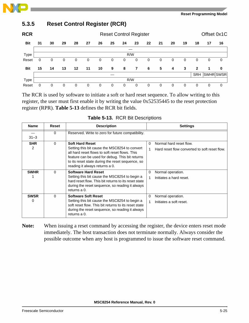
Reset Programming Model
5.3.5 Reset Control Register (RCR)
The RCR is used by software to initiate a soft or hard reset sequence. To allow writing to this register, the user must first enable it by writing the value 0x52535445 to the reset protection register (RPR). Table 5-13 defines the RCR bit fields.
Note: When issuing a reset command by accessing the register, the device enters reset mode immediately. The host transaction does not terminate normally. Always consider the possible outcome when any host is programmed to issue the software reset command.
RCR Reset Control Register Offset 0x1C
Bit 31 30 29 28 27 26 25 24 23 22 21 20 19 18 17 16
—
Type R/WReset 0 0 0 0 0 0 0 0 0 0 0 0 0 0 0 0
Bit 15 14 13 12 11 10 9 8 7 6 5 4 3 2 1 0
— SRH SWHR SWSRType R/W
Reset 0 0 0 0 0 0 0 0 0 0 0 0 0 0 0 0
Table 5-13. RCR Bit Descriptions
Name Reset Description Settings
—31–3
0 Reserved. Write to zero for future compatibility.
SHR2
0 Soft Hard ResetSetting this bit cause the MSC8254 to convert all hard reset flows to soft reset flows. This feature can be used for debug. This bit returns to its reset state during the reset sequence, so reading it always returns a 0.
0 Normal hard reset flow.
1 Hard reset flow converted to soft reset flow.
SWHR1
0 Software Hard ResetSetting this bit cause the MSC8254 to begin a hard reset flow. This bit returns to its reset state during the reset sequence, so reading it always returns a 0.
0 Normal operation.
1 Initiates a hard reset.
SWSR0
0 Software Soft ResetSetting this bit cause the MSC8254 to begin a soft reset flow. This bit returns to its reset state during the reset sequence, so reading it always returns a 0.
0 Normal operation.
1 Initiates a soft reset.
MSC8254 Reference Manual, Rev. 0
Freescale Semiconductor 5-25

Reset
5.3.6 Reset Control Enable Register (RCER)
The reset control enable register shown in indicates by the CRE field that the reset protection register (RPR) was accessed with a value that enables the reset control register (RCR). Table 5-14 defines the RCER bit fields.
RCER Reset Control Enable Register Offset 0x20
Bit 31 30 29 28 27 26 25 24 23 22 21 20 19 18 17 16
—
Type R/WReset 0 0 0 0 0 0 0 0 0 0 0 0 0 0 0 0
Bit 15 14 13 12 11 10 9 8 7 6 5 4 3 2 1 0
— CREType R/W
Reset 0 0 0 0 0 0 0 0 0 0 0 0 0 0 0 0
Table 5-14. RCER Bit Descriptions
Name Reset Description Settings
—31–1
0 Reserved. Write to zero for future compatibility.
CRE0
0 Control Register EnabledIndicates the status of the reset control register (RCR). Writing 1 to this bit disables the RCR and clears this bit. Writing zero has no effect.
0 RCR is disabled.
1 The enable value is written to the reset protection register (RPR) to enable the RCR.
MSC8254 Reference Manual, Rev. 0
5-26 Freescale Semiconductor

Boot Program 6The boot program initializes the MSC8254 after it completes a reset sequence. The MSC8254 can boot from an external host through the RapidIO interface or download a user boot program through the I2C, SPI, or Ethernet ports. The default boot code is located in an internal 96 KB ROM at 0xFEF00000–0xFEF17FFF and is accessible to all cores. For readability, the internal boot code is written in C and is based on the Freescale SmartDSP OS.
When cores finish the reset sequence, they all jump to the ROM starting address (0xFEF00000), and run the boot code. Specific tasks may differ based on the core ID.
Note: Boot data is located in the M3 memory at 0xC0101C00–0xC0107FFF (25 KB). Do not write to this area during boot loading.
When the cores finish the boot sequence, they all jump to a user-defined address.
Special conditions for boot code operation include the following:
The boot code services the watchdog timer if the EWDT bit in the reset configuration word high register (RCWHR) is set (recommended).
If the boot process fails, the core goes into a debug state and writes an indication of the root error cause to address 0xC0101C04 in M3 memory (see Section 6.5, Boot Errors, on page 6-23 for details).
The boot program does not configure the DDR controller. Therefore, if you want to place data in the DDR memory, you must first configure the DDR controller to support the type of DDR memory in the system. To configure the controller, write the configuration data to the DDR controller memory-mapped registers before writing data to the DDR memory. See Chapter 12, DDR SDRAM Memory Controller for details.
In any reset state other than PORESET, the device does not execute the multi-device support for using the reset configuration word (RCW) flow with I2C as described in Section 6.1.4. The rest of the boot flow remains the same as described in this chapter.
The boot code is run by all cores. Task differ by core ID.
Note: Parity error checking is not supported by the boot code because parity errors are unlikely to occur.
MSC8254 Reference Manual, Rev. 0
Freescale Semiconductor 6-1

Boot Program
6.1 Functional Description
The boot code is divided into four parts shown in Figure 6-1:
Private configuration (all cores). Includes general configuration of all cores.
Shared configuration (core 0). Includes general configuration of internal CLASS, I2C, RapidIO interface, and QUICC Engine subsystem.
Patch mode. Allows loading patch code for boot from I2C.
Boot mode select (core 0). This part includes downloading of code from one of the MSC8254 bootable ports as defined by the RCWHR[BPRT] field.
Boot completion. All cores complete the boot operation and jump to a user-specified address.
Figure 6-1. Boot Sequence Diagram
Boot patch through I2C
PrivateConfiguration
SharedConfiguration
Core 0?
Yes
No
HSMPR[0] = 0?
No
Yes
Boot Mode
I2C Code
EthernetCode
SimpleEthernet
Serial
Code
All Cores Jump ToUser Code
Select?
Core 0 Releases Cores 1–Nby Hardware Semaphore
HSMPR[0] = 0
RapidIO SPICode
Code
Boot patch through I2C
MSC8254 Reference Manual, Rev. 0
6-2 Freescale Semiconductor

Functional Description
6.1.1 Private Configuration
Private configuration includes the following:
VBA register initialization. The value stored in ROM (0xFEF17000) is used to initialize the Vector Base Address (VBA) register in the SC3850 core. After initialization of the VBA register, any interrupt places the core in debug mode.
The EPIC is programmed to handle all NMIs correctly.
The L1 ICache is enabled.
The stack pointer is set to reside in the M3 memory space dedicated to the boot operation.
The Error Detection Code (EDC) exception is enabled.
Note: The EPIC, L1 ICache, and MMU are part of the SC3850 DSP core subsystem. See the the MSC8156 SC3850 DSP Core Subsystem Reference Manual for configuration details. The manual is only available with a signed non-disclosure agreement (NDA). Contact your Freescale sales office or representative for more information.
6.1.2 Shared Configuration
The shared configuration includes the following:
If the I2C controller is used to load the RCW for multi-device slaves (see Section 6.1.4, Multi Device Support for the I2C Bus, on page 6-4) the necessary number of GPIO lines from the {GPIO[0–3], GPIO[21]} of the master device are set to output and used to drive STOP_BS signals as follows:
— For up to 5 slaves, the lines drive the signals directly, and the number of lines equals the number of slaves.
— For up to 15 slaves, using glue logic to drive the STOP_BS signals; the number of required lines is equal to .
If RCWHR[RIO] is set or boot is over the RapidIO interface:
— LCSBA1CSR is set to 0x1FFE0000, thereby allowing the configuration register space to be physically mapped. This allows configuration and maintenance of the registers through regular read and write operations rather than by maintenance operations.
— The necessary bits of HSSI_CR1[0:1] are set in order to disable the tri-state on the Serial RapidIO lanes.
— The necessary bits of P0CCSR and P1CCSR (RapidIO) are set to force 1x or 4x based on RCWLR[S1P] and RCWLR[S2P].
QUICC Engine module priority is set to be 1 with emergency not masked (that is SDMR[EB1_PR] = 01).
1 numSlaves2log+
MSC8254 Reference Manual, Rev. 0
Freescale Semiconductor 6-3
Boot Program
6.1.3 Patch Mode
Patch mode is defined as follows:
Patch Mode is enabled when RCWHR[BP] is set. See Chapter 5, Reset for details.
Boot loads patch code from I2C and executes in the same manner as boot over I2C.
After the patch is executed, the patch code jumps to the address in the boot code defined in address 0xC0101C14. The jump address can be changed by the patch code. By default, the boot code continues Boot Flow from same place after returning from the patch loading.
Execution continues to load boot code from the boot port defined by RCWHR[BPRT]. If boot port is I2C, the boot code generates an error and the core goes into a debug state.
6.1.4 Multi Device Support for the I2C Bus
The MSC8254 can share the I2C EEPROM device with other MSC8254 devices for loading the reset configuration word (RCW), as well as for reading configuration during boot loading and execution. When the bus is shared, the bus must distinguish among reset masters, reset slaves, and EEPROM slaves:
The reset master (indicated by RCWHR[RM]) holds the STOP_BS signals of all the slaves high and releases them one by one, thus arbitrating which slave has access to the bus at any moment. When the master deasserts STOP_BS for a slave, the slave device attempts to access an EEPROM at address 0x57. The actual EEPROM address is 0x50, but the master emulates the EEPROM using address 0x57 to drive the RCW to each slave in turn.
There are a number of assumptions and limitations imposed when multiple devices share the I2C bus:
1. For each EEPROM in the system, there must be at least one EEPROM master. The EEPROM master is also the reset master (RCWHR[RM])
2. For each EEPROM, there can be 0 or more EEPROM slaves. An EEPROM slave is defined as a device that reads is RCW from the EEPROM and uses data on the bus during boot. The number of EEPROM slaves is stored as a single byte at address 0x8F of the EEPROM.
3. For each EEPROM, there can be 0 or more reset slaves. A reset slave is defined as a device that only reads its RCW from the EEPROM but does not read data from it during boot. The number of reset slaves is stored as a single byte at address 0x11 of the EEPROM.
4. Every EEPROM slave must also be a reset slave.
5. There may be up to 15 reset slaves per EEPROM
MSC8254 Reference Manual, Rev. 0
6-4 Freescale Semiconductor

Functional Description
6. As a consequence of the conditions listed in 1–5, the limitations on the number of slaves is defined as 0 ≤ #EEPROM slaves ≤ #reset slaves ≤ 15
7. The lowest numbered reset slave must be a higher numbered slave than the highest numbered EEPROM slave (for example, if EEPROM slaves are slaves 0–4, then reset slaves are slaves 5–12).
8. EEPROM slaves must be numbered sequentially from 0 upward.
9. All devices connected to the same EEPROM must have PORESET asserted simultaneously, that is, no single device go through the PORESET sequence without the others.
10. For multi-device RCW only. The EEPROM master can have HRESET/SRESET asserted without the slaves being reset as well. Each reset slave can have its HRESET/SRESET asserted without the master being reset.
11. For multi-device RCW and Boot using I2C. If the EEPROM master has its HRESET/SRESET asserted, the EEPROM slaves must have their HRESET/SRESET asserted as well. Each reset slaves can have its HRESET/SRESET asserted without the master being reset. However, there must be external logic that performs the actions that the master performs during its boot sequence. The logic may be implemented as periodic polling by the master, asserting NMI to the reset master, or using an FPGA or other implementation.
12. If there is a shared EEPROM in use in any stage of the reset/boot flow (RCW, serial RapidIO interface configuration, MAC address, I2C boot), all devices MUST load their RCW from the shared EEPROM.
Note: If the reset master (RCWHR[RM]) fails (due to a stuck I2C_SDA) to read the data at 0x11 or 0x8F of the EEPROM or fails during the sequence of driving the RCW to the reset slaves, the core goes into a debug state and writes the appropriate error code to the M3 memory (see Section 6.5).
MSC8254 Reference Manual, Rev. 0
Freescale Semiconductor 6-5

Boot Program
6.1.5 Example Configuration
Figure 6-2 describes a I2C multi device system in which MSC8254 #0 is a reset master and MSC8254 #1 is a reset slave. The reset master uses {GPIO[0–3], GPIO[21]} to release the reset slaves. The MSC8254 boot supports up to 15 slaves on a single EEPROM (for RCW). There are two possibilities as to how the reset slave STOP_BS signals are handled:
If there are 5 slaves or less, connect each GPIO line directly to one of the slaves. The master deasserts and asserts the lines when necessary.
If there are more than 5 slaves, GPIO[21] is used to latch the values of GPIO[0–3] into the decoder glue logic (latch when high). This value indicates which of the slave STOP_BS signals to pull low. When an all 1 values are latched, all STOP_BS signals should be pulled high.
Figure 6-2. I2C Multi Device System
HRESET
PORESET
I2C EPROM
STOP_BS
I2C_SDA
I2C_SCL
I2C_SDA
I2C_SCL
VDD
VDD
SRESET
RCW_SRC
DSP Device 0
3
HRESET
PORESETSTOP_BS
I2C_SDA
I2C_SCLSRESET
RCW_SRC
DSP Device 1
3
GPIO
VDD
Decoder
Reset Logic
A[0–2]
MSC8254 Reference Manual, Rev. 0
6-6 Freescale Semiconductor

Functional Description
Figure 6-3 shows the I2C initialization and multi device support.
Figure 6-3. I2C initialization and Multi Device Support
Yes
Encoded STOP_SLV_BS == 0Decoded STOP_SLV_BS == 0
No
Write freq. division ratio& sampling rate
RCWLR[MODCK] need to reach 400 KHz
numSlaves > 5 YesNo
Last Slave?
No
PCMR0[INP_RNG]
1. Read slave RCW and generate STOP
2. Configure I2C controller to emulateEEPROM with address 0x57
1. Reload time out counter
2. Drive corresponding slave RCWs
3. Disable time out counter
RCWHR[RM]
RCWHR[BPRC] = I2C
NoYes
End of flow
No
Yes
No
Yes
All STOP_BS == 1
RCWHR[BPRC] = I2C
STOP_BS == 1
MSC8254 Reference Manual, Rev. 0
Freescale Semiconductor 6-7

Boot Program
The following stages are performed to serve as the master chip on a multi-device board.
1. The MSC8254 reads RSR to determine if the reset is PORESET. If it is not PORESET, this section of the boot is bypassed entirely.
2. The MSC8254 reads RCWHR[RM] to determine if it is the master on the multi-device board or a slave on the multi-device board.
3. If the MSC8254 is the master on the multi-device board:
a. I2CFDR and I2CDFSSR are programed based on the following data— RCWLR[MODCK]— RSR[RSTSRC]The frequency used for I2C_SCL is set as closely as possible to 400 kHz.
b. The Reset master reads the slaves RCW from their location in the I2C EEPROM (with address 0x50) and stores them into M3.
c. The reset masters I2C controller is configured to work as an EEPROM (slave mode) with address 0x57.
d. The reset master deassert STOP_BS for the current slave (directly or via the decoder).e. The reset master:
• Drives preamble 0xAA55AA• Drives header 0xFFFFFF• Drives RCWLR• Drives header 0xFFFFFF• Drives RCWHRfor each read request of the reset slave, and then generates a STOP condition on the bus in order to free it up because the slave I2C controller does not generate a STOP condition.
f. Repeat steps a–e for all slaves.g. {GPIO[0–3}, GPIO[21]} are set to 0x1F thus deasserting all the slaves STOP_BS
signals, and the master can continue performing its boot flow.4. After getting its RCS, the reset slave starts to run the boot program.
Note: If the MSC8254 is a an EEPROM slave, the boot waits until STOP_BS is to pulled high before continuing with the boot program, thus allowing all reset slaves to read their reset word before any device tries to access the EEPROM for boot code.
MSC8254 Reference Manual, Rev. 0
6-8 Freescale Semiconductor

Boot Modes
6.2 Boot Modes
The Boot Mode is selected by the value in the RCWHR[BPRT] field. The following sections describe the operation of each boot mode.
6.2.1 I2C EEPROM
The MSC8254 boot expects the I2C EEPROM to be divided in to four sections:
1. Reset words. This section starts at address 0x0000 of the EEPROM and includes the reset words for the reset master, an indication as to the number of reset slaves and the reset words for all the slaves.
2. Reserved.
3. Boot configuration. This section starts at address 0x0090 of the EEPROM and can contain one of the following:
— MAC addresses for up to 64 devices (6 bytes per address). The boot knows to associate each address with the appropriate device based on an offset of 6 × RCWHR[DEVID]. The expected format is consecutive 6 byte fields.
— Serial RapidIO configuration. This option allows the user to configure up to 471 registers and should be used to set the appropriate values of HSSI_CR1 and HSSI_CR2 in the general configuration block. The expected format is address, data pairs. The 8 bytes following the last pair should always be set to {0xFFFFFFFF, 0xFFFFFFFF}, regardless of the actual number of pairs placed in the EEPROM to signal that no more configurations are necessary.
4. Boot code. This section starts at address 0x0210 of the EEPROM and contains the user code. The boot code must be of the size (n × 4) + m[bytes], where n is any integer greater than or equal to 0 and m is either 0 or 1. If n is larger than 0, the value in the Destination Address field must be 32-bit aligned.
Note: Although not all sections are used by all boot options, the section addresses are fixed. However, any section not used by a specific boot option can be used for general purposes within the following guideline examples:
• In a system with only two DSP devices that supports multi-device boot, only addresses 0x0 to 0x19 within the reset word section must carry the appropriate valid values, as shown in Figure 6-4. Addresses 0x20 to 0x89 are available for any general-purpose use.
• For boot scenarios without I2C support, addresses 0x90 to 0x20F are available for any general-purpose use.
1.47 pairs along with 8 bytes end flag of {0xFFFFFFFF, 0xFFFFFFFF} is the amount that fits in the same space as 64 MAC addresses ( )64 6⋅( ) 2 4⋅( )⁄ 47 1+=
MSC8254 Reference Manual, Rev. 0
Freescale Semiconductor 6-9
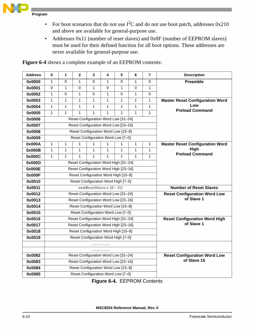
Boot Program
• For boot scenarios that do not use I2C and do not use boot patch, addresses 0x210 and above are available for general-purpose use.
• Addresses 0x11 (number of reset slaves) and 0x8F (number of EEPROM slaves) must be used for their defined function for all boot options. These addresses are never available for general-purpose use.
Figure 6-4 shows a complete example of an EEPROM contents:
Address 0 1 2 3 4 5 6 7 Description
0x0000 1 0 1 0 1 0 1 0 Preamble
0x0001 0 1 0 1 0 1 0 1
0x0002 1 0 1 0 1 0 1 0
0x0003 1 1 1 1 1 1 1 1 Master Reset Configuration Word Low
Preload Command0x0004 1 1 1 1 1 1 1 1
0x0005 1 1 1 1 1 1 1 1
0x0006 Reset Configuration Word Low [31–24]
0x0007 Reset Configuration Word Low [23–16]
0x0008 Reset Configuration Word Low [15–8]
0x0009 Reset Configuration Word Low [7–0]
0x000A 1 1 1 1 1 1 1 1 Master Reset Configuration Word High
Preload Command0x000B 1 1 1 1 1 1 1 1
0x000C 1 1 1 1 1 1 1 1
0x000D Reset Configuration Word High [31–24]
0x000E Reset Configuration Word High [23–16]
0x000F Reset Configuration Word High [15–8]
0x0010 Reset Configuration Word High [7–0]
0x0011 Number of Reset Slaves
0x0012 Reset Configuration Word Low [31–24] Reset Configuration Word Lowof Slave 10x0013 Reset Configuration Word Low [23–16]
0x0014 Reset Configuration Word Low [15–8]
0x0015 Reset Configuration Word Low [7–0]
0x0016 Reset Configuration Word High [31–24] Reset Configuration Word Highof Slave 10x0017 Reset Configuration Word High [23–16]
0x0018 Reset Configuration Word High [15–8]
0x0019 Reset Configuration Word High [7–0]
..................
..................
0x0082 Reset Configuration Word Low [31–24] Reset Configuration Word Lowof Slave 150x0083 Reset Configuration Word Low [23–16]
0x0084 Reset Configuration Word Low [15–8]
0x0085 Reset Configuration Word Low [7–0]
Figure 6-4. EEPROM Contents
numResetSlaves 0 15–[ ]∈
MSC8254 Reference Manual, Rev. 0
6-10 Freescale Semiconductor

Boot Modes
0x0086 Reset Configuration Word High [31–24] Reset Configuration Word Highof Slave 150x0086 Reset Configuration Word High [23–16]
0x0088 Reset Configuration Word High [15–8]
0x0089 Reset Configuration Word High [7–0]
0x008A .................. Reserved
0x008B ..................
0x008C ..................
0x008D ..................
0x008E ..................
0x008F 15 ≤ numResetSlaves ≤ numEEPROMslaves ≤ 0 Number of EEPROM Slaves
0x0090 Configuration/MAC Address First Byte
..................
0x020F Configuration Last Byte/ Device 0x2F Last MAC Address Byte
0x0210 1 0 1 1 1 1 1 1 Block Control (Block #0)
0x0211 size[0–7] Block Size
0x0212 size[8–15]
0x0213 size[16–23]
0x0214 NBA[31–24] Next Block Address
0x0215 NBA[23–16]
0x0216 NBA[15–8]
0x0217 NBA[7–0]
0x0218 DA[31–24] Destination Address
0x0219 DA[23–16]
0x021A DA[15–8]
0x021B DA[7–0]
CODE
Payload Data
Checksum[15–8] Checksum and Checksum
Checksum[7–0]
Checksum[15–8]
Checksum[7–0]1 0 1 1 1 1 1 1 Block Control (Block #1)
..................
End of EEPROM
Note: The value shown for Block Control is an example only.
Address 0 1 2 3 4 5 6 7 Description
Figure 6-4. EEPROM Contents (Continued)
MSC8254 Reference Manual, Rev. 0
Freescale Semiconductor 6-11

Boot Program
The I2C boot loading is performed with the I2C controller. To allow for EEPROMs of up to 64 Kbytes, 19-bit addressing is used. The 7 most significant bits (msb) of the I2C slave address are always 0b1010000. The I2C controller expects a specific memory image when trying to read data from the EEPROM. The I2C memory image consists of the following:
1. Block Control. A 1-byte control field that contains:
— 1 bit of CSE. A 1 indicates that the checksum is enabled.— 1 reserved bit that should be cleared (0).— 6 bits of CHIP_ID indicate the destination chip. 0x3F means broadcast.
2. Block Size. These 3 bytes represent the number of bytes in the payload data field (e.g if the payload size is 12 bytes, Block Size = {0x00, 0x00, 0x0C}).
3. Next Block Address. The address in which the next block is located. If the next block address equals 0x0 the bootloader assumes that the next block is sequential. If next block address equals 0xFFFFFFFF, this block is the end block.
4. Destination Address. The address to which the payload data should be written.
5. Payload Data. Holds 1≤size<216 bytes (up to 64 Kbytes) of data to be written to on-device memory according to the destination address.
6. Checksum. A 2-byte field that holds the XOR of all previous data (Block Control and on). The boot code XORs each received 2 bytes with the previous checksum value and verifies the validation by comparing it to this field.
7. Checksum. A 2-byte field that holds bitwise-not of the Checksum.
The I2C bootloader expects the 4 bytes of Checksum and Checksum regardless of the CSE value. If the Checksum is disabled, these 4 bytes are not checked. By using Checksum and Checksum, the boot ensures that all values of the bits are real values and that there are no stuck signals. If both Checksum and Checksum are erroneous in a block, core 0 enters the debug state.
The I2C_SCL frequency is set as closely to 400KHz as possible, as mentioned in Section 6.1.4. For each block, the Software I2C read access begins with the boot code driving the device select ({A0,A1,A2} = 0b000) and 2 bytes of address, followed by a RESTART condition. The I2C slave drives its data (beginning with the Block Control byte) until the end of the block. The last byte of each block is not acknowledged by the MSC8254. After the ninth unacknowledged bit, the boot code generates a STOP condition. Figure 6-5 describes the Software I2C read access.
MSC8254 Reference Manual, Rev. 0
6-12 Freescale Semiconductor

Boot Modes
6.2.2 EthernetThe MSC8254 device can load files through the Ethernet port using DHCP (Dynamic Host Configuration Protocol) and TFTP (Trivial File Transfer Protocol).Supports RGMII @1000 Mbps and SGMII @1000 Mbps full duplex.
For DHCP, each client must have its own unique MAC (Media Access Control) address. This MAC address can be based on RCWHR[DEVID] or be user-defined.
This DHCP implementation supports IPv4.
Booting over Ethernet is enabled on GE1 (UCC1) and GE2 (UCC3) depending on the values of the following bit fields:
RCWHR[BPRT]. Determines which ports to use for boot loading.
— 0x4 = RGMII1 without I2C— 0x5 = SGMII1 without I2C— 0x6 = RGMII1 with I2C— 0x7 = SGMII1 with I2C— 0x8 = RGMII2 without I2C— 0x9 = SGMII2 without I2C— 0xA = RGMII2 with I2C— 0xB = SGMII2 with I2C
RCWHR[GE1]. Determines whether the signals lines are TDM[2–3] or RGMII1.
RCWHR[GE2]. Determines whether the signal lines are TDM[0–1] or RGMII2
RCWLR[S1P]. Determines which SGMII signals are enabled on SerDes port 1:
— 0x5 = SGMII1 and SGMII2.— 0x6 = SGMII1 and SGMII2— 0x7 = SGMII1— 0x8 = SGMII1
RCWLR[S2P]. Determines which SGMII signals are enabled on SerDes port 2.
— 0x5 = SGMII1 and SGMII2— 0x6 = SGMII1 and SGMII2
Figure 6-5. I2C Read Access
A0 A1 A2DEVICE SELECT
ST
AR
T
BYTE ADDRA8A7A4A3 A5 A6 A9 A10
BYTE ADDRA16A15A12A11 A13 A14 A17 A18
R/W
ACK ACK
A0 A1 A2
DEVICE SELECT
ST
AR
T
ACK
R/W
ACK ACK
NO ACK
STOP
ACK
Note: A0 and D0 are the most significant bits.
1 10 0 1 0 1 0DATA OUT 1
D5D4D1D0 D2 D3 D7D6
DATA OUT ND5D4D1D0 D2 D3 D7D6
ST
OP
=0 =0 =0
MSC8254 Reference Manual, Rev. 0
Freescale Semiconductor 6-13

Boot Program
— 0x7 = SGMII2— 0xA = SGMII1 and SGMII2— 0xB = SGMII2— 0xE = SGMII1 and SGMII2— 0x14 = SGMII2— 0x16 = SGMII2
Note: It is valid to program RCWLR[S1P] and RCWLR[S2P] to have SGMII1 on both ports, SGMII2 on both ports, or to have SGMII1 and SGMII2 on both ports. An internal multiplexer always routes only two physical connections to the QUICC Engine controllers. If the SGMII interfaces are configured by S1P and S2P, SGMII1 (if selected by S1P and S2P) is physically connected to SerDes Port 1 and SGMII2 (if selected by S1P and S2P) is physically connected to SerDes Port 2
Figure 6-6 describes the Ethernet bootloader flow.
Figure 6-6. Ethernet Bootloader Flow
DHCPClient
DHCPServer
filename, next server address
TFTPServer
TFTP Data Block TemporaryStorageSpace In M3
Read S-Record
application code InternalMemory Space
TFTPClient
CodeInstallation
BOOT CODE
MSC8254 Reference Manual, Rev. 0
6-14 Freescale Semiconductor

Boot Modes
:The Ethernet bootloader flow includes:
1. Configuring the QUICC Engine drivers based on RCWHR[BPRT].
2. Finding a DHCP server and receive configuration parameters (filename, server address, and so on).
3. Reading a block of the boot file, in S-Record format, from a TFTP server.
4. Processing each TFTP data block and placing it in its memory destination.
5. Sending a TFTP acknowledge to the TFTP server.
6. Repeating steps 2–5 until the end of the data is transferred.
6.2.2.1 DHCP Client
The basic steps that occur when a DHCP client requests an IP address from a DHCP server are shown in Figure 6-7.
The client sends a DHCP DISCOVER broadcast message to locate a DHCP server.
A DHCP server offers configuration parameters (such as an IP address, a TFTP server IP address, bootfile name...).
The client returns a formal request for the first offered IP address to the DHCP server in a DHCPREQUEST broadcast message.
The DHCP server confirms that the IP address has been allocated to the client by returning a DHCPACK unicast message to the client.
There are two possibilities for setting the MSC8254 MAC address during the boot:
User defined and read from an I2C EEPROM. See Section 6.2.1 for details.
Predefined default using the following fields:
— A constant of 32 bits: {0x1E, 0xF7, 0xD5, 0x00} — 8 bits consisting of (RCWHR[DEVID]) (aligned to the right and padded with 0)— A constant of 8 bits: {0x00}
Figure 6-7. DHCP Transactions
DHCP Discover (broadcast)
DHCP Offer (unicast)
DHCP Request (broadcast)
DHCP Ack (unicast)
DHCPCLIENT
DHCPSERVER
MSC8254 Reference Manual, Rev. 0
Freescale Semiconductor 6-15

Boot Program
The predefined option is configured to be an individual locally administered address in accordance with IEEE Std. 802-2001™. This MAC address scheme allows for more that 8 unique MAC addresses per device by changing the last 4 bit values, thus allowing each core to have 2 MAC addresses for use during operational mode.
6.2.2.2 TFTP Client
This implementation supports three types of messages: TFTP REQUEST, TFTP DATA and TFTP ACK. Figure 6-8 describes the TFTP handshake.
The TFTP transfer is initiated by the client when it issues a TFTP REQUEST (which contains the file name to download).
In response, the server provides the application with a series of TFTP DATA messages.
The client handshakes each data block by issuing a TFTP ACK allowing the server to proceed with subsequent TFTP DATA messages.
This process repeats until all data blocks are received.
6.2.2.3 Boot File Format
The Ethernet bootloader expects an application file in the form of an S-Record file. The S-Record file is a text representation of the binary program code. The S-Record file structure is describes in Figure 6-9.
Figure 6-8. TFTP Transactions
TFTP REQUEST
TFTP DATA
TFTP ACKTFTP
CLIENTTFTP
SERVER
TFTP DATA (last)
TFTP ACK
MSC8254 Reference Manual, Rev. 0
6-16 Freescale Semiconductor

Boot Modes
Each line of an S-Record file corresponds to any of the following: start record, data record, or end record. Each record is terminated with a line feed.
Note: The S-Record that is downloaded during boot over Ethernet should include no whitespaces (including newlines).
A record has the following format:
S<type><length><address><data><checksum>
Note: This implementation supports only record of types: S0, S3 or S7.
The description of fields is described in Table 6-1.
S0 Record. Starting record. The address and data fields are ignored and checksum check is executed.
S3 Record. Data record. The address field is interpreted as a 4-byte address. The data field is composed of memory loadable data.
Figure 6-9. S-Record File Structure
Table 6-1. S-Record description of Fields
FieldWidth in
CharactersDescription
S<type> 2 The type of record (S0, S3 or S7)
<length> 2 The count of remaining character pairs in the record
<address> 4 The address at which the data field is to be loaded into memory
<data> ≤64 The memory loadable data or descriptive information
<checksum> 2 The least significant byte of the ones complement of the sum of the byte values represented by the pairs of characters making up the length, the address, and the data fields
Start Record
Data Record 1
Data Record 2
Data Record n
End Record
MSC8254 Reference Manual, Rev. 0
Freescale Semiconductor 6-17

Boot Program
S7 Record. Termination record. The address fields is interpreted as the 4-byte address to which to jump after boot. No checksum check is executed.
Shown below is a typical S-record format file:
S0030000FCS30D00002FE731DC3180BEF09E7062S705000000000C
The S0 record is composed as follows:
S0. Indicating it is a starting record.
03. Hexadecimal 03 (decimal 3). Indicating that three character pairs (or ASCII bytes) follow.
0000. Information string (ignored)
FC. Checksum field.
The S3 record is composed as follows:
S3. Indicating it is a data record to be loaded at a 4-byte address.
0D. Hexadecimal D (decimal 13), representing a 4 byte address, 8 bytes of binary data, and a 1 byte checksum, follow.
00002FE7. Eight character 4-byte address field.
31DC3180BEF09E70. 8-character pairs representing the actual binary data.
62. Checksum field.
The S7 record is composed as follows:
S7. Indicating it is the last record.
05. Hexadecimal 05 (decimal 5). Indicating that five character pairs (4 byte address and a 1 byte checksum follow).
00000000. Address field to jump to at the end of boot (is written to 0xC0101C10).
0C. Checksum field.
Each S-Record line includes an address field that maps the lines data content to a memory location in MSC8254. Core 0 moves the data to this address.
Note: Because the MSC8254 uses 32-bit addressing, use of S3 and S7 is recommended.
MSC8254 Reference Manual, Rev. 0
6-18 Freescale Semiconductor

Boot Modes
6.2.3 Simple Ethernet Boot
The MSC8254 supports a simple Ethernet boot mode. This mode is selected by setting the RCWHR[SBETH] bit during the PORESET sequence (see Section 5.3.2 for details).
6.2.3.1 Simple Ethernet Boot Flow
The simple Ethernet boot mode uses the following sequence for processing:
The bootloader configures the QUICC Engine subsystem drivers based on the RCWHR[BPRT].
There are two possibilities for setting the MAC address during the boot. See Section 6.2.2.1 for details.
When the Ethernet interface is configured, the bootloader sends the start handshake data 0x17171717.
The boot data is read a block at a time by the bootloader using a simple Ethernet frame format:
<MAC Dest><MAC Source><Type><2 Bytes Data_Length><4 Bytes Address><Data>
Simple boot over Ethernet packets should have the ethertype field of the MAC header set to 0x0004.
The bootloader processes each data block: <data_length><address><data> and places it in the destination memory location.
The bootloader continues to process blocks until the end handshake data 0xA5A5A5A5 is written to address 0xC0101C00.
All cores jump to the address written in 0xC0101C10. The value in the address should be written during the boot loading process.
6.2.3.2 Simple Ethernet Boot Ports
Booting over Ethernet is enabled on GE1 (UCC1) and GE2 (UCC3) depending on the values of RCWHR[BPRT], RCWHR[GE1], RCWHR[GE2], RCWLR[S1P] and RCWLR[S2P].
Note: Use the following guidelines to configure bits to support the selected boot modes:
For boot over Ethernet in RGMII mode the following bits should be configured:
— RCWHR[GE1] = 1 for boot over port 1— RCWHR[GE2] = 1 for boot over port 2
MSC8254 Reference Manual, Rev. 0
Freescale Semiconductor 6-19
Boot Program
6.2.3.3 Boot File Format
The Ethernet bootloader expects an application file in the format of a Simple Ethernet frame. The Simple Ethernet frame has the following format:
<Length><Address><Data>
The description of fields is described in Table 6-2.
Each Simple Ethernet address field maps the data content to a memory location in the DSP. Core 0 moves the data to this address. The following example shows a typical Simple-Ethernet packet for End-of-handshake between the Ethernet master and the MSC8254 boot:
1E7FD50000001E7FD510000000040004C0101C00A5A5A5A5
The End-of-handshake packet sent by the Ethernet Master comprises the following:
1E7FD5000000, Destination MAC address (default MSC8254 address)
1E7FD5100000. Source MAC address.
0004. Ethernet type. The MSC8254 expects Ethernet type 0x0004.
0004. Length is 4 bytes.
C0101C00. The address at which the data field is to be loaded into memory. This is the Handshake address for the MSC8254.
A5A5A5A5. Handshake data.
Table 6-2. Simple Ethernet Description of Fields
FieldWidth in
CharactersDescription
<length> 2 The count of remaining character pairs in the record
<address> 4 The address at which the data field is to be loaded into memory
<data> The memory loadable data or descriptive information
MSC8254 Reference Manual, Rev. 0
6-20 Freescale Semiconductor

Boot Modes
6.2.4 Serial RapidIO Interconnect
In this procedure a Serial RapidIO master waits for the MSC8254 boot program to finish its default initialization and then initializes the device by typically loading code and data to the on device memory.
6.2.4.1 Serial RapidIO Without I2C Support
The boot code configures HSSI_CR[0–1] and PxCCSR according to RCWLR[S1P] and RCWLR[S2P] and writes 0x17171717 to address 0xC0101C00. The flow is:
1. Disable port by writing to PxCCS register.
2. Set x1 or x4 by writing to PxCCSR.
3. Enable lanes by writing to the HSSI_CR1[0–1].
4. Enable the port by writing to PxCCSR.
5. Afterwards, it polls this address until the serial RapidIO master writes 0xA5A5A5A5 to it, thereby indicating that it has finished its code loading.
Figure 6-10 describes the boot flow from Serial RapidIO interconnect.
Figure 6-10. Serial RapidIO Interface Boot Flow
Set 0xC0101C00
Disable tri-state on lanes
read address 0xC0101C00
==0xA5A5A5A5 No
Yes
boot mode select = Serial RapidIO interface
Continue Boot Flow
to 0x17171717
MSC8254 Reference Manual, Rev. 0
Freescale Semiconductor 6-21

Boot Program
6.2.4.2 Serial RapidIO Interface with I2C Support
The user can place {addr, data} pairs in the I2C EEPROM to configure various registers. The address field should be as seen by the SC3850 DSP core. This feature is most commonly used to configure registers in the general configuration block (see Section 6.2.1, I2C EEPROM, on page 6-9 for details). The boot supports up to 47 such pairs. The 8 bytes following the last pair should always be set to {0xFFFFFFFF, 0xFFFFFFFF}, regardless of the actual number of pairs placed in the I2C EEPROM.
Note: Multiple devices connected to a shared EEPROM see the same address/data pairs.
6.2.5 SPI
The MSC8254 can boot from a Flash memory on the SPI. The boot expects a Flash memory that latches on the rising edge of the clock and on which data is valid after the falling edge. The chip-select should be a CS low signal. The boot code expects to see the same data format used for the I2C EEPROM (see described in Section 6.2.1, I2C EEPROM, on page 6-9, item 4 for details on the boot code requirements) starting at address 0 of the SPI.
A shared SPI bus is arbitrated by all the devices connected to it by polling CS. All signals should be connected as open-drain if more than one device is connected to the SPI flash. The SPI bus will run no faster than 400 KHz to support multiple devices connected with an open drain.
Note: If the RCW is read from EEPROM, the device for which RCWHR[RM] equals 1 should have RCWHR[DEVID] of 0. Using this configuration setting saves on arbitration cycles towards the SPI flash.
Note: During boot over SPI, the pins described in Chapter 22, GPIO are used per their SPI functionality. In addition, GPIO23 is used as a chip-select signal (CS) to control access to the SPI Flash memory.
6.3 Jump to User Code
Before finishing its tasks the boot code preforms these actions:
If RCWHR[RIO] is cleared, the boot code disables host accesses by RapidIO interface to internal memory space by putting the lanes into tri-state high impedance state.
Invalidate all range of ICaches and close MMU program windows.
Core internal registers (other than R0 and VBA) are set to 0x00000000.
All configurations which were done by the boot code are cleared.
— Module registers— GPIO configurations— Write 0x00000000 to GIER (see Chapter 8, General Configuration Registers) to clear
the register.
MSC8254 Reference Manual, Rev. 0
6-22 Freescale Semiconductor

System after Boot
— Disable all interrupts (NMI excluded)— Clear all QUICC Engine registers by writing 1 to QECMDR[RST]
0x900D900D is written to 0xC0101C0C in M3 indicating that the boot has finished executing.
All cores jump to the address written in 0xC0101C10. The value in this address should be written during the boot loading process.
6.4 System after Boot All MATTs in the MMUs are set to their reset value values (except M_xSDBx[PBS] which is set to 0x2).
L1 I-Cache is enabled, but there are no cacheable windows.
All NMIs will be configured as NMIs in the EPIC.
VBA equals 0xFEF17000. Any interrupt in the EPIC puts the core in debug.
EDC is enabled.
Core register values are not guaranteed and should be initialized before use.
6.5 Boot Errors
If the boot code fails, an indication as to the root cause is written to 0xC0101C04. The possible reasons are listed in Table 6-3.
Table 6-3. Boot Error Codes
Error Code Description
0x003FEFFF Catastrophic Error. SmartDSP OS Function failed
0x003FEFFE DHCP server time out
0x003FEFFD Corrupted boot file. The possible causes are:• Checksum wrong in TFTP file• Checksum wrong in I2C file• Unsupported S-Record type
0x003FEFFC TFTP server time out
0x003FEFFA TFTP server sent ERROR code (05)
0x003FEFF9 Unsupported boot port
0x003FEFF8 Reset slave does not respond
0x003FEFF5 Boot over Ethernet or RapidIO isn’t supported with current RCW configuration
0x003FEFF4 Too many I2C RCW slaves in address 0x11 of the EEPROM
0x003FEFF3 Error in protocol between I2C RCW master and slave
0x003FEFF2 Boot port trying to write to area designated for boot (0xC0101C18–0xC0107FFF)
0x003FEFF1 In patch mode, the boot port is I2C.
0x0027EFFE Lost arbitration on I2C us.
0x0027EFFD Time-out on I2C acknowledge (9th clock).
MSC8254 Reference Manual, Rev. 0
Freescale Semiconductor 6-23

Boot Program
0x0027EFFC Stuck I2C_SDA (I2C bus).
0x00000000 Unexpected debug condition in the SC3850 Core (unexpected interrupt, EE0 asserted and so on)
Table 6-3. Boot Error Codes
Error Code Description
MSC8254 Reference Manual, Rev. 0
6-24 Freescale Semiconductor

Clocks 7The clock circuits contains five PLLs:
Three PLLs driven from a single CLKIN signal generated by a crystal-based oscillator that generate the clocks for the DSP core subsystems, the internal CLASS buses, the RapidIO controller, the QUICC Engine subsystem, the TDM interfaces, internal memory, the DDR-SDRAM memory controllers, and the PCI Express interface.
Two PLLs that generate clocks for the SerDes interfaces in the HSSI.
MSC8254 Reference Manual, Rev. 0
Freescale Semiconductor 7-1

Clocks
7.1 Clock Generation Components and Modes
The clock generation components and clock scheme are shown in Figure 7-1.
Each PLL uses its input clock to generate a fast clock that is synchronized to the input clock. The fast clock is distributed to each of the clock dividers to generate the clocks that are distributed to the system blocks. The clock circuits are locked, according to the selected clock mode, when the first stage of the system reset configuration is done (reset configuration is controlled by the RESET block). The clock circuits are initialized after the first phase of the reset configuration, when the low part of the reset configuration word is loaded, according to the selected clock mode.
Figure 7-1. MSC8254 Clock Scheme
CLKIN DIVPLL0
PLL1
SerDes1 PLLSerDes1_REF_CLK SERDES1CLK
SerDes PLL = SerDes Clock
Note: The source for CLKOUT is selected at reset via the Reset Configuration Word (RCW). See Chapter 5, Reset for details.
SerDes2 PLLSerDes2_REF_CLK SERDES2CLK
SerDes PLL = SerDes Clock
DSP Core Subsystem 0
HSSI Subsystem
QUICC Engine Subsystem
DDR1 Controller
CLASS SubsystemPLL 0 clk 0
1PLL 0 clk
PLL 1 clk
DIVPLL 0 clk 0
1PLL 1 clk
DIVPLL 0 clk 0
1PLL 1 clk
DIVPLL 0 clk 0
1PLL 1 clk
DDR2 Controller
DIVPLL 0 clk 0
1PLL 2 clk
DIVPLL 0 clk 0
1PLL 2 clk
DIVPLL 0 clk 0
1PLL 2 clk
PLL 1 clk
PLL 2 clk
DSP Core Subsystem 1
DSP Core Subsystem 2
DSP Core Subsystem 3
PLL2
not used
MSC8254 Reference Manual, Rev. 0
7-2 Freescale Semiconductor

Clock Generation Components and Modes
The MSC8254 clock modes are listed in Table 7-1.
Notes: 1. The color of each cell, states which PLL drives its clock domain. PLL 0 is red, PLL1 is yellow, and PLL2 is blue with white lettering.
2. In clock modes 1 and 37, PLL1 is not used. In order to save power and reduce noise, this PLL should be disabled by setting bit 7 of RCW low (for RCW details, see Chapter 5, Reset).
CLK_OUT pin can be driven from either PLL with selection determined by the value of RCWLR[CLKO] (bits 31–30 of the low part of the reset configuration word—for details, see Chapter 5, Reset). The possible CLK_OUT frequencies are listed in Table 7-2.
Table 7-1. MSC8254 Clock Modes
Mode CLKIN PLL0 PLL1 PLL2 CLASSDSP Core
SubsystemsHSSI
QUICC Engine
SubsystemDDR1 DDR2
0 100 900 1000 800 500 1000 333 500 800 800
1 66.67 800 0 667 400 800 267 400 667 667
4 100 900 1000 667 500 1000 333 450 667 667
19 100 900 1000 800 450 1000 333 500 800 800
21 100 900 1000 667 450 1000 333 450 667 667
36 100 900 1000 800 500 1000 333 500 800 267
37 66.67 800 0 667 400 800 267 400 667 267
39 100 900 1000 667 500 1000 333 450 667 222
45 100 900 1000 667 450 1000 333 450 667 222
Table 7-2. MSC8254 CLK_OUT Frequencies
Mode PLL0 PLL1 PLL2 CLK_OUT from PLL0 CLK_OUT from PLL1 CLK_OUT from PLL2
0 900 1000 800 75 100 80
1 800 0 667 66.67 6.7 66.67
4 900 1000 667 75 100 66.67
19 900 1000 800 75 100 80
21 900 1000 667 75 100 66.67
36 900 1000 800 75 100 80
37 800 0 667 66.67 6.7 66.67
39 900 1000 667 75 100 66.67
45 900 1000 667 75 100 66.67
MSC8254 Reference Manual, Rev. 0
Freescale Semiconductor 7-3

Clocks
7.2 .Programming Model
The registers covered in this section are as follows:
System Clock Control Register (SCCR), page 7-4.
Clock General Purpose Register 0 (CLK_GRP0), page 7-5.
Note: The clock registers use a base address of: 0xFFF24000.
7.2.1 System Clock Control Register (SCCR)
The SCCR can be used to shut down the clock for some of the clock domains. This register can only be reset by a power-on reset. Table 7-3 defines the SCCR bit fields.
SCCR System Clock Control Register Offset 0x000
Bit 31 30 29 28 27 26 25 24 23 22 21 20 19 18 17 16
—Type R/WReset 0 0 0 0 0 0 0 0 0 0 0 0 0 0 0 0
Bit 15 14 13 12 11 10 9 8 7 6 5 4 3 2 1 0
CLASS DIS
CORE 3-0DIS
— HSSI DIS
QEDIS — DDR1 DIS
DDR2 DIS
—
Type R/WReset 0 0 0 0 0 0 0 0 0 0 0 0 0 0 0 0
Table 7-3. SCCR Bit Descriptions
Name Reset Description Settings
—31–16
0 Reserved. Write to zero for future compatibility.
CLASSDIS15
0 CLASS Clock Domain DisableUsed to disable the CLASS clock domain to conserve power.
0 CLASS clock domain enabled.
1 CLASS clock domain disabled.
CORE3-0 DIS14
0 Core 3–0 Clock Domain DisableUsed to disable the Core 3–0 clock domain to conserve power.
0 Core 3–0 clock domain enabled.
1 Core 3–0 clock domain disabled.
—13
0 Reserved. Write to zero for future compatibility.
HSSIDIS12
0 HSSI Clock Domain DisableUsed to disable the HSSI clock domain to conserve power.
0 HSSI clock domain enabled.
1 HSSI clock domain disabled.
QEDIS11
0 QUICC Engine Clock Domain DisableUsed to disable the QUICC Engine subsystem clock domain to conserve power.
0 QUICC Engine clock domain enabled.
1 QUICC Engine clock domain disabled.
—10
0 Reserved. Write to zero for future compatibility.
MSC8254 Reference Manual, Rev. 0
7-4 Freescale Semiconductor

.Programming Model
7.2.2 Clock General Purpose Register 0 (CLK_GPR0)
The CLK_GPR0 is used to set the RapidIO prescale value to yield the 8 MHz clock required for event timing. Table 7-4 defines the CLK_GPR0 bit fields.
DDR1DIS9
0 DDR1 Clock Domain DisableUsed to disable the DDR1 controller clock domain to conserve power.
0 DDR1 clock domain enabled.
1 DDR1 clock domain disabled.
DDR2DIS8
0 DDR2 Clock Domain DisableUsed to disable the DDR2 controller clock domain to conserve power.
0 DDR2 clock domain enabled.
1 DDR2 clock domain disabled.
—7–0
0 Reserved. Write to zero for future compatibility.
CLK_GPR0 Clock General Purpose Register 0 Offset 0x004
Bit 31 30 29 28 27 26 25 24 23 22 21 20 19 18 17 16
—Type RReset Determined by MODCK
Bit 15 14 13 12 11 10 9 8 7 6 5 4 3 2 1 0
— RPTE
Type R R/WReset Determined by MODCK
Table 7-4. CLK_GPR0 Bit Descriptions
Name Reset Description Settings
—31–6
MODCK value
Reserved.
RPTE5–0
MODCK value
RapidIO Prescaler for Timed Event ClockThis value is used to scale the OCN clock (which is equal to the HSSI clock that is derived from the MODCK settings; see Table 7-1) to yield an 8 MHz clock used by the RapidIO subsystem to calculate different event times. The value to enter into this field is computed by the formula: (ocn_clk_freq/8 MHz) – 1, rounded to the nearest whole value (ocn_clk_freq = HSSI clock frequency). The default is selected by the MODCK settings at power-up reset.
100000 For MODCK 1 and 37.
101001 For MODCK 0, 4, 21, 36, 39, 45
All other values reserved.
Table 7-3. SCCR Bit Descriptions (Continued)
Name Reset Description Settings
MSC8254 Reference Manual, Rev. 0
Freescale Semiconductor 7-5

Clocks
MSC8254 Reference Manual, Rev. 0
7-6 Freescale Semiconductor

General Configuration Registers 8The MSC8254 device includes a general configuration block that includes fifty-six 32-bit registers. This block provides sets of control and status registers for modules in the device that do not include their own control and status registers.
8.1 Programming Model
The general configuration registers include the following:
General Control Register 1 (GCR1), see page 8-2General Control Register 2 (GCR2), see page 8-3General Status Register 1 (GSR1), see page 8-5High Speed Serial Interface Status Register (HSSI_SR), see page 8-7DDR General Configuration Register (DDR_GCR), see page 8-10High Speed Serial Interface Control Register 1 (HSSI_CR1), see page 8-12High Speed Serial Interface Control Register 2 (HSSI_CR2), see page 8-15QUICC Engine Control Register (QECR), see page 8-16GPIO Pull-Up Enable Register (GPUER), see page 8-17GPIO Input Enable Register (GIER), see page 8-18System Part and Revision ID Register (SPRIDR), see page 8-19General Control Register 4 (GCR4), see page 8-20General Control Register 5 (GCR5), see page 8-22General Status Register 2 (GSR2), see page 8-24Core Subsystem Slave Port Priority Control Register (TSPPCR), see page 8-26QUICC Engine First External Request Multiplex Register (CPCE1R), see page 8-27QUICC Engine Second External Request Multiplex Register (CPCE2R). see page 8-28QUICC Engine Third External Request Multiplex Register (CPCE3R), see page 8-29QUICC Engine Fourth External Request Multiplex Register (CPCE4R), see page 8-30General Control Register 10 (GCR10), page 8-31General Interrupt Register 1 (GIR1), see page 8-32General Interrupt Enable Register 1 for Cores 0–5 (GIER1_[0–5]), see page 8-34General Interrupt Register 3 (GIR3), see page 8-36
MSC8254 Reference Manual, Rev. 0
Freescale Semiconductor 8-1

General Configuration Registers
General Interrupt Enable Register 3 for Cores 0–5 (GIER3_[0–5]), see page 8-38General Interrupt Register 5 (GIR5), see page 8-39General Interrupt Enable Register 5 for Cores 0–5 (GIER5_[0–5]), see page 8-40General Control Register 11 (GCR11), see page 8-41General Control Register 12 (GCR12), see page 8-42DMA Request0 Control Register (GCR_DREQ0), see page 8-44DMA Request1 Control Register (GCR_DREQ1), see page 8-48DMA Done Control Register (GCR_DDONE), see page 8-52
DDR1 General Configuration Register (DDR1_GCR), see page 8-55DDR2 General Configuration Register (DDR2_GCR), see page 8-56
Core Subsystem Slave Port General Configuration Register (CORE_SLV_GCR), see page 8-57
Note: The base address for the general configuration registers is: 0xFFF28000.
8.2 Detailed Register Descriptions
8.2.1 General Configuration Register 1 (GCR1)
GCR1 General Configuration Register 1 Offset 0x00
Bit 31 30 29 28 27 26 25 24
—Type R R/W
Reset 0 0 0 0 0 0 0 0
Bit 23 22 21 20 19 18 17 16
— UART_STOPType R/WReset 0 0 0 0 0 0 0 0
Bit 15 14 13 12 11 10 9 8
— DDR2_PIPE_LMT DDR1_PIPE_LMT
Type R/WReset 0 1 0 0 0 0 1 0
Bit 7 6 5 4 3 2 1 0
DDR1_PIPE_LMT TDM_PIPE_LMTType R/W
Reset 0 0 0 1 0 0 0 0
MSC8254 Reference Manual, Rev. 0
8-2 Freescale Semiconductor

Detailed Register Descriptions
GCR1 configures various general functions for the MSC8254 device. Table 8-1 lists the GCR1 bit field descriptions.
8.2.2 General Configuration Register 2 (GCR2)
Table 8-1. GCR1 Bit Descriptions
Name Reset Description Settings
—31–17
0 Reserved. Write to 0 for future compatibility.
UART_STOP16
0 UART StopStops the UART clock.
0 Normal operation.1 UART clock stopped.
—15
0 Reserved. Write to 0 for future compatibility.
DDR2_PIPE_LMT14–10
10000 DDR2 Pipeline LimitSpecifies the DDR2 complex pipeline depth.
DDR1_PIPE_LMT9–5
10000 DDR1 Pipeline LimitSpecifies the DDR1 complex pipeline depth.
TDM_PIPE_LMT4–0
10000 TDM Pipeline LimitSpecifies the TDM complex pipeline depth.
GCR2 General Configuration Register 2 Offset 0x04
Bit 31 30 29 28 27 26 25 24
—
Type R/WReset 0 0 0 0 0 0 0 0
Bit 23 22 21 20 19 18 17 16
— DMA_DBGType R/W
Reset 0 0 0 0 0 0 0 0
Bit 15 14 13 12 11 10 9 8
—CORE3_STP_
ENCORE2_STP_
ENCORE1_STP_
ENCORE0_STP_
EN
Type R/WReset 0 0 0 0 0 0 0 0
Bit 7 6 5 4 3 2 1 0
— CORE3_DBG_REQ
CORE2_DBG_REQ
CORE1_DBG_REQ
CORE0_DBG_REQ
Type R/WReset 0 0 0 0 0 0 0 0
MSC8254 Reference Manual, Rev. 0
Freescale Semiconductor 8-3
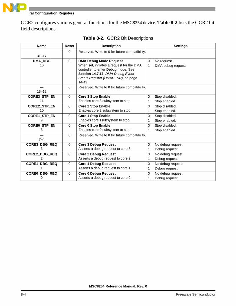
General Configuration Registers
GCR2 configures various general functions for the MSC8254 device. Table 8-2 lists the GCR2 bit field descriptions.
Table 8-2. GCR2 Bit Descriptions
Name Reset Description Settings
—31–17
0 Reserved. Write to 0 for future compatibility.
DMA_DBG16
0 DMA Debug Mode RequestWhen set, initiates a request for the DMA controller to enter Debug mode. See Section 14.7.17, DMA Debug Event Status Register (DMADESR), on page 14-43
0 No request.1 DMA debug request.
—15–12
0 Reserved. Write to 0 for future compatibility.
CORE3_STP_EN11
0 Core 3 Stop EnableEnables core 3 subsystem to stop.
0 Stop disabled.1 Stop enabled.
CORE2_STP_EN10
0 Core 2 Stop EnableEnables core 2 subsystem to stop.
0 Stop disabled.1 Stop enabled.
CORE1_STP_EN9
0 Core 1 Stop EnableEnables core 1subsystem to stop.
0 Stop disabled.1 Stop enabled.
CORE0_STP_EN8
0 Core 0 Stop EnableEnables core 0 subsystem to stop.
0 Stop disabled.1 Stop enabled.
—7–4
0 Reserved. Write to 0 for future compatibility.
CORE3_DBG_REQ3
0 Core 3 Debug RequestAsserts a debug request to core 3.
0 No debug request.1 Debug request.
CORE2_DBG_REQ2
0 Core 2 Debug RequestAsserts a debug request to core 2.
0 No debug request.1 Debug request.
CORE1_DBG_REQ1
0 Core 1 Debug RequestAsserts a debug request to core 1.
0 No debug request.1 Debug request.
CORE0_DBG_REQ0
0 Core 0 Debug RequestAsserts a debug request to core 0.
0 No debug request.1 Debug request.
MSC8254 Reference Manual, Rev. 0
8-4 Freescale Semiconductor

Detailed Register Descriptions
8.2.3 General Status Register 1 (GSR1)
GSR1 reports the status various general functions for the MSC8254 device. Table 8-3 lists the GSR1 bit field descriptions.
GSR1 General Status Register 1 Offset 0x08
Bit 31 30 29 28 27 26 25 24
— CORE_ WAIT_ACK3
CORE_ WAIT_ACK2
CORE_ WAIT_ACK1
CORE_ WAIT_ACK0
Type R
Reset 0 0 0 0 0 0 0 0
Bit 23 22 21 20 19 18 17 16
— CORE_ STOP_ACK3
CORE_ STOP_ACK2
CORE_ STOP_ACK1
CORE_ STOP_ACK0
Type RReset 0 0 0 0 0 0 0 0
Bit 15 14 13 12 11 10 9 8
— M3_PU_1 M3_PU_0 —Type R
Reset 0 0 0 0 0 0 0 0
Bit 7 6 5 4 3 2 1 0
—CORE_DBG_
STS3CORE_DBG_
STS2CORE_DBG_
STS1CORE_DBG_
STS0
Type RReset 0 0 0 0 0 0 0 0
Table 8-3. GSR1 Bit Descriptions
Name Reset Description Settings
—31–28
0 Reserved. Write to 0 for future compatibility.
CORE_WAIT_ACK327
0 Core Wait Acknowledge 3Reflects whether core 3 subsystem is in Wait state.
0 Core subsystem not in Wait state.1 Core subsystem in Wait state.
CORE_WAIT_ACK226
0 Core2 Wait Acknowledge 2Reflects whether core 2 subsystem is in Wait state
0 Core subsystem not in Wait state.1 Core subsystem in Wait state.
CORE_WAIT_ACK125
0 Core1 Wait Acknowledge 1Reflects whether core 1 subsystem is in Wait state.
0 Core subsystem not in Wait state.1 Core subsystem in Wait state.
CORE_WAIT_ACK024
0 Core Wait Acknowledge 0Reflects whether core 0 subsystem is in Wait state.
0 Core subsystem not in Wait state.1 Core subsystem in Wait state.
—23–20
0 Reserved. Write to 0 for future compatibility.
CORE_STOP_ACK319
0 Core Stop Acknowledge 3Reflects whether core 3 subsystem is in Stop state.
0 Core subsystem not in Stop state.1 Core subsystem in Stop state.
MSC8254 Reference Manual, Rev. 0
Freescale Semiconductor 8-5
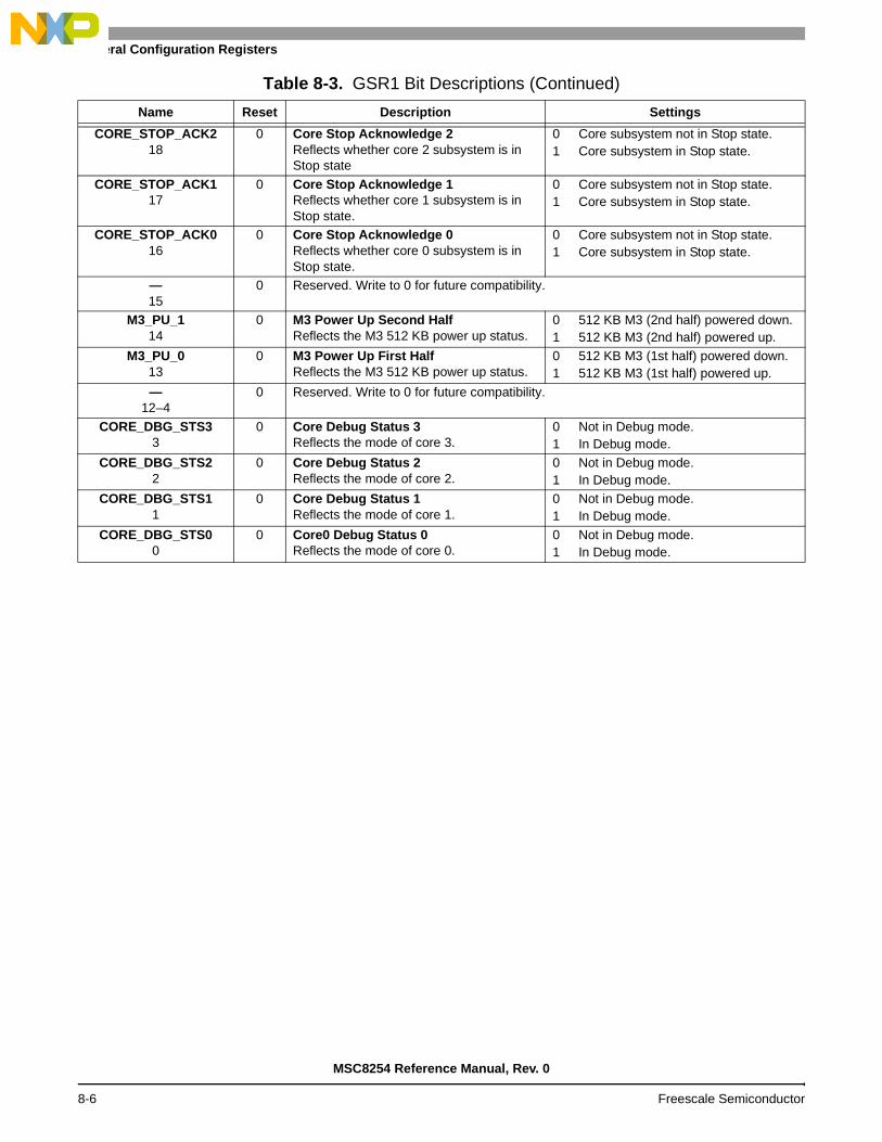
General Configuration Registers
CORE_STOP_ACK218
0 Core Stop Acknowledge 2Reflects whether core 2 subsystem is in Stop state
0 Core subsystem not in Stop state.1 Core subsystem in Stop state.
CORE_STOP_ACK117
0 Core Stop Acknowledge 1Reflects whether core 1 subsystem is in Stop state.
0 Core subsystem not in Stop state.1 Core subsystem in Stop state.
CORE_STOP_ACK016
0 Core Stop Acknowledge 0Reflects whether core 0 subsystem is in Stop state.
0 Core subsystem not in Stop state.1 Core subsystem in Stop state.
—15
0 Reserved. Write to 0 for future compatibility.
M3_PU_114
0 M3 Power Up Second HalfReflects the M3 512 KB power up status.
0 512 KB M3 (2nd half) powered down.1 512 KB M3 (2nd half) powered up.
M3_PU_013
0 M3 Power Up First HalfReflects the M3 512 KB power up status.
0 512 KB M3 (1st half) powered down.1 512 KB M3 (1st half) powered up.
—12–4
0 Reserved. Write to 0 for future compatibility.
CORE_DBG_STS33
0 Core Debug Status 3Reflects the mode of core 3.
0 Not in Debug mode.1 In Debug mode.
CORE_DBG_STS22
0 Core Debug Status 2Reflects the mode of core 2.
0 Not in Debug mode.1 In Debug mode.
CORE_DBG_STS11
0 Core Debug Status 1Reflects the mode of core 1.
0 Not in Debug mode.1 In Debug mode.
CORE_DBG_STS00
0 Core0 Debug Status 0Reflects the mode of core 0.
0 Not in Debug mode.1 In Debug mode.
Table 8-3. GSR1 Bit Descriptions (Continued)
Name Reset Description Settings
MSC8254 Reference Manual, Rev. 0
8-6 Freescale Semiconductor

Detailed Register Descriptions
8.2.4 High Speed Serial Interface Status Register (HSSI_SR)
HSSI_SR controls part of the SerDes operation for the MSC8254 device. The register is reset on a Hard reset. Write accesses can only be performed in Supervisor mode. Table 8-4 lists the HSSI_SR bit field descriptions.
HSSI_SR High Speed Serial Interface Status Register Offset 0x0C
Bit 31 30 29 28 27 26 25 24
— SERDES2_ PD DMA1_PD SRIO1_PD SERDES1_ PD
Type R
Reset 0 0 0 0 0 0 0 0
Bit 23 22 21 20 19 18 17 16
SERDES1_PD DMA0_PD SRIO0_PD PEX_PD OCN_PD RMU_PD SRIO1_STOP_ACK
Type RReset 0 0 0 0 0 0 0 0
Bit 15 14 13 12 11 10 9 8
SRIO0_STOP_ACK
— SERDES2_ RST_DONE
SERDES2_ PD
SRIO_1_ IDLESRIO_1_OB_IDLE
Type RReset 0 0 0 0 0 0 0 0
Bit 7 6 5 4 3 2 1 0
SERDES1_RST_DONE
SERDES1_ PD
SRIO_0_ IDLESRIO_0_OB_IDLE
PEX_OB_ IDLE
PEX_IDLE — RMU_IDLE
Type R
Reset 0 0 0 0 0 0 0 0
Table 8-4. HSSI_SR Bit Descriptions
Name Reset Description Settings
—31–30
0 Reserved. Write to 0 for future compatibility.
SERDES2_PD29–27
000 SERDES2 Power Down StatusIndicates the power status of the SERDES2 port. Can be powered down by the Reset Control Word or GCR control.
000 Power up.111 Power down.All other values reserved.
DMA1_PD26
0 DMA1 Power Down StatusIndicates the power status of DMA1. Can be powered down by the Reset Control Word or GCR control.
0 Power up.1 Power down.
SRIO1_PD25
0 Serial RapidIO Interface 1 Power Down StatusIndicates the power status of the serial RapidIO interface 1. Can be powered down by the Reset Control Word or GCR control.
0 Power up.1 Power down.
SERDES1_PD24–22
000 SERDES1 Power Down StatusIndicates the power status of the SERDES2 port. Can be powered down by the Reset Control Word or GCR control.
000 Power up.111 Power down.All other values reserved.
MSC8254 Reference Manual, Rev. 0
Freescale Semiconductor 8-7

General Configuration Registers
DMA0_PD21
0 DMA0 Power Down StatusIndicates the power status of DMA0. Can be powered down by the Reset Control Word or GCR control.
0 Power up.1 Power down.
SRIO0_PD20
0 Serial RapidIO Interface 0 Power Down StatusIndicates the power status of the serial RapidIO interface 0. Can be powered down by the Reset Control Word or GCR control.
0 Power up.1 Power down.
PEX_PD19
0 PCI Express Power Down StatusIndicates the power status of the PCI Express interface. Can be powered down by the Reset Control Word or GCR control.
0 Power up.1 Power down.
OCN_PD18
0 OCN Fabric Power Down StatusIndicates the power status of the OCN fabric. Can be powered down by the Reset Control Word or GCR control.
0 Power up.1 Power down.
RMU_PD17
0 RapidIO Messaging Unit Power Down StatusIndicates the power status of the RapidIO Messaging Unit. Can be powered down by the Reset Control Word or GCR control.
0 Power up.1 Power down.
SRIO1_STOP_ACK16
0 Serial RapidIO Interface 1 Stop Acknowledge StatusIndicates the serial RapidIO interface 1 Stop Acknowledge status.
0 Not stopped.1 Stop ACK issued.
SRIO0_STOP_ACK15
0 Serial RapidIO Interface 0 Stop Acknowledge StatusIndicates the serial RapidIO interface 0 Stop Acknowledge status.
0 Not stopped.1 Stop ACK issued.
—14–12
0 Reserved. Write to 0 for future compatibility.
SERDES2_RST_DONE11
0 SERDES2 Reset DoneIndicates whether the SERDES2 has completed the reset sequence.Note: Although the reset value is 0, the bit will
change to 1 within 160 µs after reset depending on whether the SerDes port is used.
0 Reset not complete.1 Reset complete.
SERDES2_PD10
0 SERDES2 Power Down StatusIndicates the power status of the SERDES2 PHY.
0 Power up.1 Power down (PLL is not working).
SRIO1_IDLE9
0 SRIO1 IdleIndicates whether the SRIO1 unit is idle, that is, no transactions in progress.
0 Active.1 Idle.
SRIO1_OB_IDLE8
0 SRIO1 Outbound IdleIndicates whether the SRIO1 outbound activity is idle, that is, no outbound transactions in progress.
0 Active.1 Idle.
SERDES1_RST_DONE7
0 SERDES1 Reset DoneIndicates whether the SERDES1 has completed the reset sequence.Note: Although the reset value is 0, the bit will
change to 1 within 160 µs after reset depending on whether the SerDes port is used.
0 Reset not complete.1 Reset complete.
Table 8-4. HSSI_SR Bit Descriptions (Continued)
Name Reset Description Settings
MSC8254 Reference Manual, Rev. 0
8-8 Freescale Semiconductor

Detailed Register Descriptions
SERDES1_PD6
0 SERDES1 Power Down StatusIndicates the power status of the SERDES1 PHY.
0 Power up.1 Power down (PLL is not working).
SRIO0_IDLE5
0 SRIO0 IdleIndicates whether the SRIO0 unit is idle, that is, no transactions in progress.
0 Active.1 Idle.
SRIO0_OB_IDLE4
0 SRIO0 Outbound IdleIndicates whether the SRIO0 outbound activity is idle, that is, no outbound transactions in progress.
0 Active.1 Idle.
PEX_OB_IDLE3
0 PCI Express Outbound IdleIndicates whether the PCI Express outbound activity is idle, that is, no outbound transactions in progress.
0 Active.1 Idle.
PEX_IDLE2
0 PCI Express IdleIndicates whether the PCI Express is idle, that is, no transactions in progress.
0 Active.1 Idle.
—1
0 Reserved. Write to 0 for future compatibility.
RMU_IDLE0
0 RMU IdleIndicates whether the RMU is idle, that is, no transactions in progress.
0 Active.1 Idle.
Table 8-4. HSSI_SR Bit Descriptions (Continued)
Name Reset Description Settings
MSC8254 Reference Manual, Rev. 0
Freescale Semiconductor 8-9

General Configuration Registers
8.2.5 DDR General Control Register (DDR_GCR)
DDR_GCR controls the DDR operation the MSC8254 device. The register is reset on a Hard reset. Write accesses can only be performed in Supervisor mode. Table 8-5 lists the DDR_GCR bit field descriptions.
DDR_GCR DDR General Control Register Offset 0x10
Bit 31 30 29 28 27 26 25 24
—DDR2_GCR_
VSELType R R/W
Reset 0 0 0 0 1 1 0 1
Bit 23 22 21 20 19 18 17 16
— DDR2_COP_TERMSEL_OVERRIDE_ VALUE
DDR2_COP_ TERMSEL_ OVERRIDE_
EN
DDR2_ DISABLE_BIT
_DESKEW
—
Type R/WReset 0 0 0 0 0 0 0 0
Bit 15 14 13 12 11 10 9 8
—DDR1_GCR_
VSELType R/W
Reset 0 0 0 0 1 1 0 1
Bit 7 6 5 4 3 2 1 0
— DDR1_COP_TERMSEL_OVERRIDE_ VALUE
DDR1_COP_ TERMSEL_ OVERRIDE_
EN
DDR1_ DISABLE_BIT
_DESKEW
—
Type R/WReset 0 0 0 0 0 0 0 0
Table 8-5. DDR_GCR Bit Descriptions
Name Reset Description Settings
—31–25
0 Reserved. Write to 0 for future compatibility.
DDR2_GCR_VSEL24
1 DDRC2 Voltage SelectIndicates the type of memory used.
0 DDR3.1 DDR2.
—23–22
0 Reserved. Write to 0 for future compatibility.
DDR2_COP_TERMSEL_OVERRIDE_VALUE
21–19
0 DDRC2 Termination Select Override ValueSets the value for the termination select override.
DDR2_COP_TERMSEL_OVERRIDE_EN
18
0 DDRC2 Termination Select Override EnableDisables/enables the termination select override.
0 Disable1 Enable.
MSC8254 Reference Manual, Rev. 0
8-10 Freescale Semiconductor

Detailed Register Descriptions
DDR2_DISABLE_BIT_ DESKEW
17
0 DDRC2 Disable Per-Bit DeskewDisables/enables per-bit deskew calibration initialization.
0 Enable.1 Disable.
—16–9
0 Reserved. Write to 0 for future compatibility.
DDR1_GCR_VSEL8
1 DDRC1 Voltage SelectIndicates the type of memory used.
0 DDR3.1 DDR2.
—7–6
0 Reserved. Write to 0 for future compatibility.
DDR1_COP_TERMSEL_OVERRIDE_VALUE
5–3
0 DDRC1 Termination Select Override ValueSets the value for the termination select override.
DDR1_COP_TERMSEL_OVERRIDE_EN
2
0 DDRC1 Termination Select Override EnableDisables/enables the termination select override.
0 Disable1 Enable.
DDR1_DISABLE_BIT_ DESKEW
1
0 DDRC1 Disable Per-Bit DeskewDisables/enables per-bit deskew calibration initialization.
0 Enable.1 Disable.
—0
0 Reserved. Write to 0 for future compatibility.
Table 8-5. DDR_GCR Bit Descriptions (Continued)
Name Reset Description Settings
MSC8254 Reference Manual, Rev. 0
Freescale Semiconductor 8-11

General Configuration Registers
8.2.6 High Speed Serial Interface Control Register 1 (HSSI_CR1)
HSSI_CR1 controls various functions within the SerDes block for the MSC8254 device. The register is reset on a hard reset. Write accesses can only be performed in Supervisor mode. Table 8-6 lists the HSSI_CR1 bit field descriptions.
HSSI_CR1 High Speed Serial Interface Control Register 1 Offset 0x14
Bit 31 30 29 28 27 26 25 24
SERDES2_ STOP
SERDES2_ CB_ PD
SERDES2_ ISOR_PD
SERDES2_ DOZE
— SRIO1_DOZE —
Type R/W
Reset 0 0 0 0 0 0 0 0
Bit 23 22 21 20 19 18 17 16
SRIO1_PD — SRIO1_ECC_D
SERDES1_ CB_ PD
SERDES1_ ISOR_PD
SERDES1_ DOZE
—
Type R/WReset 0 0 0 0 0 0 0 0
Bit 15 14 13 12 11 10 9 8
SRIO0_DOZE — SRIO0_PD — — SERDES1_ STOP
PEX_PD PEX_DOZE
Type R/WReset 0 0 0 0 0 0 0 0
Bit 7 6 5 4 3 2 1 0
— OCN_PD RMU_PD RMU_DOZE — SERDES2_ CONFIG_ DISABLE
SERDES1_ CONFIG_ DISABLE
Type R/WReset 0 0 0 0 0 0 1 1
Table 8-6. HSSI_CR1 Bit Descriptions
Name Reset Description Settings
SERDES2_STOP31
0 SERDES2 PHY StopHolds the SERDES2 PHY in reset.
0 PHY not stopped.1 PHY stopped.
SERDES2_CB_PD30
0 SERDES2 Control Block Power DownShuts down SERDES2 control block ring power.
0 Power up.1 Power down.
SERDES2_ISOR_PD29
0 SERDES2 Isolation Ring Power DownShuts down SERDES2 isolation ring power.
0 Power up.1 Power down.
SERDES2_DOZE28
0 SERDES2 DozeUsed to select Doze mode, in which all register accesses are acknowledged, but writes are not written and reads do not contain valid data. Setting this bit prevents lockup of the device internal bus while the SerDes port is stopped.
0 Normal operation.1 Doze mode.
—27–26
0 Reserved. Write to 0 for future compatibility.
MSC8254 Reference Manual, Rev. 0
8-12 Freescale Semiconductor

Detailed Register Descriptions
SRIO1_DOZE25
0 Serial RapidIO Interface 1 DozeUsed to select Doze mode, in which all register accesses are acknowledged, but writes are not written and reads do not contain valid data. Setting this bit prevents lockup of the device internal bus while the Serial RapidIO interface clock is stopped.
0 Normal operation.1 Doze mode.
—24
0 Reserved. Write to 0 for future compatibility.
SRIO1_PD23
0 Serial RapidIO Interface 1 Power DownShuts down serial RapidIO interface 1 power.
0 Power up.1 Power down.
—22–21
0 Reserved. Write to 0 for future compatibility.
SERDES1_CB_PD20
0 SERDES1 Control Block Power DownShuts down SERDES1 control block ring power.
0 Power up.1 Power down.
SERDES1_ISOR_PD19
0 SERDES1 Isolation Ring Power DownShuts down SERDES1 isolation ring power.
0 Power up.1 Power down.
SERDES1_DOZE18
0 SERDES1 DozeUsed to select Doze mode, in which all register accesses are acknowledged, but writes are not written and reads do not contain valid data. Setting this bit prevents lockup of the device internal bus while the SerDes port is stopped.
0 Normal operation.1 Doze mode.
—17–16
0 Reserved. Write to 0 for future compatibility.
SRIO0_DOZE15
0 Serial RapidIO Interface 0 DozeUsed to select Doze mode, in which all register accesses are acknowledged, but writes are not written and reads do not contain valid data. Setting this bit prevents lockup of the device internal bus while the Serial RapidIO clock is stopped.
0 Normal operation.1 Doze mode.
—14
0 Reserved. Write to 0 for future compatibility.
SRIO0_PD13
0 Serial RapidIO Interface 0 Power DownShuts down serial RapidIO interface 0 power.
0 Power up.1 Power down.
—12–11
0 Reserved. Write to 0 for future compatibility.
SERDES1_STOP10
0 SERDES1 PHY StopHolds the SERDES1 PHY in reset.
0 PHY not stopped.1 PHY stopped.
PEX_PD9
0 PCI Express Power DownShuts down PCI Express power.
0 Power up.1 Power down.
PEX_DOZE8
0 PCI Express DozeUsed to select Doze mode, in which all register accesses are acknowledged, but writes are not written and reads do not contain valid data. Setting this bit prevents lockup of the device internal bus while the PCI Express clock is stopped.
0 Normal operation.1 Doze mode.
Table 8-6. HSSI_CR1 Bit Descriptions (Continued)
Name Reset Description Settings
MSC8254 Reference Manual, Rev. 0
Freescale Semiconductor 8-13

General Configuration Registers
—7–6
0 Reserved. Write to 0 for future compatibility.
OCN_PD5
0 OCN Power DownShuts down OCN fabric power.
0 Power up.1 Power down.
RMU_PD4
0 RMU Power DownShuts down RMU power.
0 Power up.1 Power down.
RMU_DOZE3
0 RMU DozeUsed to select Doze mode, in which all register accesses are acknowledged, but writes are not written and reads do not contain valid data. Setting this bit prevents lockup of the device internal bus while the RMU is stopped.
0 Normal operation.1 Doze mode.
—2 0 Reserved. Write to 0 for future compatibility.SERDES2_CONFIG_
DISABLE1
1 SERDES2 SRDS2CR2 OverrideEnables/disables SERDES2 SRDS2CR2. When enabled (1), overrides the values in SRDS2CR2[X3SA/X3SB/X3SE/X3SF] and forces them to be 1. This forces all four SerDes lanes to be tri-stated. When disabled (0), there is no override and the values defined for each channel by SRDS2CR2[X3SA/X3SB/X3SE/X3SF] are used to determine whether the port is in a normal operation mode or tri-stated. The value of this bit has no effect on any other fields in SRDS2CR2 and only overrides the specified fields.
0 Disabled.1 Enabled.
SERDES1_CONFIG_ DISABLE
0
1 SERDES1 SRDS1CR2 OverrideEnables/disables SERDES1 SRDS1CR2. When enabled (1), overrides the values in SRDS1CR2[X3SA/X3SB/X3SE/X3SF] and forces them to be 1. This forces all four SerDes lanes to be tri-stated. When disabled (0), there is no override and the values defined for each channel by SRDS1CR2[X3SA/X3SB/X3SE/X3SF] are used to determine whether the port is in a normal operation mode or tri-stated. The value of this bit has no effect on any other fields in SRDS1CR2 and only overrides the specified fields.
0 Disabled.1 Enabled.
Note: Doze mode is a special mode used by the MSC8254 to allow register reads/writes to continue and be acknowledged without changing or reporting any register contents while the peripheral clocking is stopped. Processing of reads/writes can continue after the peripheral has entered power down mode. Without Doze mode, the device could hang up waiting for a response from the peripheral. This mode permits acknowledgement of the read or write, but does not read or write any meaningful data.
Table 8-6. HSSI_CR1 Bit Descriptions (Continued)
Name Reset Description Settings
MSC8254 Reference Manual, Rev. 0
8-14 Freescale Semiconductor

Detailed Register Descriptions
8.2.7 High Speed Serial Interface Control Register 2 (HSSI_CR2)
HSSI_CR2 controls various functions within the SerDes block for the MSC8254 device. The register is reset on a hard reset. Write accesses can only be performed in Supervisor mode. Table 8-7 lists the HSSI_CR2 bit field descriptions.
HSSI_CR2 High Speed Serial Interface Control Register 2 Offset 0x18
Bit 31 30 29 28 27 26 25 24
—
Type RReset 0 0 0 0 0 0 0 0
Bit 23 22 21 20 19 18 17 16
—
Type RReset 0 0 0 0 0 0 0 0
Bit 15 14 13 12 11 10 9 8
—
Type RReset 0 0 0 0 0 0 0 0
Bit 7 6 5 4 3 2 1 0
— MAG2SB_ STOP
— RMU_COL_D
Type R R/WReset 0 0 0 0 0 0 0 0
Table 8-7. HSSI_CR2 Bit Descriptions
Name Reset Description Settings
—31–3
0 Reserved. Write to 0 for future compatibility.
MAG2SB_STOP2
0 MBus to SBus StopStops the master bus to slave bus bridge. The MBus is the internal bus controlled by internal master devices. The SBus is used to access internal registers. This bridge is the interface between the MBus and the SBus. To prevent. lockup if a master device read/writes a peripheral register when the clock is stopped, the MBus completes the access, but read data is invalid and no data is written. This bit can be used to determine if read data is valid or if the write occurred.
0 Not stopped.1 Stopped.
—1
0 Reserved. Write to 0 for future compatibility.
RMU_COL_D0
0 RapidIO Messaging Unit Collision DisableEnables/disables the RMU collision detection.
0 Collision detection enabled.
1 Collision detection disabled.
MSC8254 Reference Manual, Rev. 0
Freescale Semiconductor 8-15

General Configuration Registers
8.2.8 QUICC Engine Control Register (QECR)
QECR controls various functions within the QUICC Engine module for the MSC8254 device. The register is reset on a Hard reset. Write accesses can only be performed in Supervisor mode. Table 8-8 lists the QECR bit field descriptions.
QECR QUICC Engine Control Register Offset 0x1C
Bit 31 30 29 28 27 26 25 24
—
Type RReset 0 0 0 0 0 0 0 0
Bit 23 22 21 20 19 18 17 16
—Type R
Reset 0 0 0 0 0 0 0 0
Bit 15 14 13 12 11 10 9 8
—
Type R
Reset 0 0 0 0 0 0 0 0
Bit 7 6 5 4 3 2 1 0
— ENET_SGMII_MODE1
ENET_SGMII_MODE0
—
Type R R/WReset 0 0 0 0 0 0 0 0
Table 8-8. QECR Bit Descriptions
Name Reset Description Settings
—31–4
0 Reserved. Write to 0 for future compatibility.
ENET_SGMII_MODE13
0 Selects GMII or RGMII for Ethernet Controller 2Selects SGMII mode for Ethernet controller 2.
0 RGMII selected.1 SGMII selected.
ENET_SGMII_MODE02
0 Selects GMII or RGMII for Ethernet Controller 1Selects SGMII mode for Ethernet controller 1.
0 RGMII1 selected.1 SGMII1 selected.
—1–0
0 Reserved. Write to 0 for future compatibility.
MSC8254 Reference Manual, Rev. 0
8-16 Freescale Semiconductor

Detailed Register Descriptions
8.2.9 GPIO Pull-Up Enable Register (GPUER)
GPUER enables/disables the individual GPIO pull-up resistors. The register is reset on a Hard reset. Write accesses can only be performed in Supervisor mode. Table 8-9 lists the GPUER bit field descriptions.
GPUER GPIO Pull-Up Enable Register Offset 0x20
Bit 31 30 29 28 27 26 25 24
PUE_B31 PUE_B30 PUE_B29 PUE_B28 PUE_B27 PUE_B26 PUE_B25 PUE_B24
Type R/WReset 0 0 0 0 0 0 0 0
Bit 23 22 21 20 19 18 17 16
PUE_B23 PUE_B22 PUE_B21 PUE_B20 PUE_B19 PUE_B18 PUE_B17 PUE_B16Type R/W
Reset 0 0 0 0 0 0 0 0
Bit 15 14 13 12 11 10 9 8
PUE_B15 PUE_B14 PUE_B13 PUE_B12 PUE_B11 PUE_B10 PUE_B9 PUE_B8
Type R/W
Reset 0 0 0 0 0 0 0 0
Bit 7 6 5 4 3 2 1 0
PUE_B7 PUE_B6 PUE_B5 PUE_B4 PUE_B3 PUE_B2 PUE_B1 PUE_B0Type R/WReset 0 0 0 0 0 0 0 0
Table 8-9. GPUER Bit Descriptions
Name Reset Description Settings
PUE_B[31–0]31–0
0 Pull-Up Enable 31–0Each bit in this field enables/disables the GPIO pull-up resistor corresponding to the bit index number.
0 Pull-up input is enabled.1 Pull-up input is disabled.
MSC8254 Reference Manual, Rev. 0
Freescale Semiconductor 8-17

General Configuration Registers
8.2.10 GPIO Input Enable Register (GIER)
GIER enables/disables the individual GPIO signals. The register is reset on a hard reset. Write accesses can only be performed in Supervisor mode. Table 8-10 lists the GIER bit field descriptions.
GIER GPIO Input Enable Register Offset 0x24
Bit 31 30 29 28 27 26 25 24
IE31 IE30 IE29 IE28 IE27 IE26 IE25 IE24
Type R/WReset 0 0 0 0 0 0 0 0
Bit 23 22 21 20 19 18 17 16
IE23 IE22 IE21 IE20 IE19 IE18 IE17 IE16Type R/W
Reset 0 0 0 0 0 0 0 0
Bit 15 14 13 12 11 10 9 8
IE15 IE14 IE13 IE12 IE11 IE10 IE9 IE8
Type R/W
Reset 0 0 0 0 0 0 0 0
Bit 7 6 5 4 3 2 1 0
IE7 IE6 IE5 IE4 IE3 IE2 IE1 IE0Type R/WReset 0 0 0 0 0 0 0 0
Table 8-10. GIER Bit Descriptions
Name Reset Description Settings
IE[31–0]31–0
0 Input Enable 31–0Each bit in this field enables/disables the individual GPIO corresponding to the bit index number.
0 Input is disabled.1 Input is enabled.
MSC8254 Reference Manual, Rev. 0
8-18 Freescale Semiconductor

Detailed Register Descriptions
8.2.11 System Part and Revision ID Register (SPRIDR)
SPRIDR provides information about the device and revision numbers. Table 8-11 lists the SPRIDR bit field descriptions.
SPRIDR System Part and Revision ID Register Offset 0x28
Bit 31 30 29 28 27 26 25 24
PARTID
Type RReset 1 0 0 0 0 0 1 1
Bit 23 22 21 20 19 18 17 16
PARTIDType R
Reset 0 0 0 0 0 1 0 0
Bit 15 14 13 12 11 10 9 8
REVIDType RReset 0 0 0 0 0 0 0 0
Bit 7 6 5 4 3 2 1 0
REVID
Type RReset 0 0 0 0 0 0 0 0
Table 8-11. SPRIDR Bit Descriptions
Name Reset Description
PARTID31–16
0x8304 Part IdentificationMask-programmed with a code corresponding to the device number.
REVID15–0
0x0000 Revision IdentificationMask-programmed with a code corresponding to the revision number of the part identified by the PARTID value.
MSC8254 Reference Manual, Rev. 0
Freescale Semiconductor 8-19

General Configuration Registers
8.2.12 General Control Register 4 (GCR4)
GCR4 controls the delay lines for UCC1 and UCC3. The register is reset on a Hard reset. Write accesses can only be performed in Supervisor mode.
The MSC8254 Data Sheet includes recommended default values for this register to use with a standard RGMII PHY device. AN3811 Using GCR4 to Adjust Ethernet Timing in MSC8144 DSPs (available under NDA) provides guidelines for adjusting GCR4 values for specific applications, if required. Although this application note is directed toward designs using the MSC8144 DSP, the procedures used to adjust GCR4 apply to the MSC8254 DSP.
Table 8-8 lists the GCR4 bit field descriptions.
GCR4 General Control Register 4 Offset 0x30
Bit 31 30 29 28 27 26 25 24
—
Type R/WReset 0 0 0 0 0 0 0 0
Bit 23 22 21 20 19 18 17 16
— UCC3RCLKID UCC3TCLKIDType R/W
Reset 0 0 0 0 0 0 0 0
Bit 15 14 13 12 11 10 9 8
UCC3CLKOD UCC3RXDD UCC3TXDD UCC1RCLKID
Type R/W
Reset 0 0 0 0 0 0 0 0
Bit 7 6 5 4 3 2 1 0
UCC1TCLKID UCC1CLKOD UCC1RXDD UCC1TXDDType R/WReset 0 0 0 0 0 0 0 0
Table 8-12. GCR4 Bit Descriptions
Name Reset Description Settings
—31–20
0 Reserved. Write to 0 for future compatibility.
UCC3RCLKID19–18
0 UCC3 RX Clock In DelayAdds a delay to the specified signal.
00 No delay.01 One delay unit.10 Two delay units.11 Three delay units.
UCC3TCLKID17–16
0 UCC3 TX Clock In DelayAdds a delay to the specified signal.
00 No delay.01 One delay unit.10 Two delay units.11 Three delay units.
MSC8254 Reference Manual, Rev. 0
8-20 Freescale Semiconductor

Detailed Register Descriptions
UCC3CLKOD15–14
0 UCC3 Clock Out DelayAdds a delay to the specified signal.
00 No delay.01 One delay unit.10 Two delay units.11 Three delay units.
UCC3RXDD13–12
0 UCC3 RX Data DelayAdds a delay to the specified signal.
00 No delay.01 One delay unit.10 Two delay units.11 Three delay units.
UCC3TXDD11–10
0 UCC3 TX Data DelayAdds a delay to the specified signal.
00 No delay.01 One delay unit.10 Two delay units.11 Three delay units.
UCC1RCLKID9–8
0 UCC1 RX Clock In DelayAdds a delay to the specified signal.
00 No delay.01 One delay unit.10 Two delay units.11 Three delay units.
UCC1TCLKID7–6
0 UCC1 TX Clock In DelayAdds a delay to the specified signal.
00 No delay.01 One delay unit.10 Two delay units.11 Three delay units.
UCC1CLKOD5–4
0 UCC1 Clock Out DelayAdds a delay to the specified signal.
00 No delay.01 One delay unit.10 Two delay units.11 Three delay units.
UCC1RXDD3–2
0 UCC1 RX Data DelayAdds a delay to the specified signal.
00 No delay.01 One delay unit.10 Two delay units.11 Three delay units.
UCC1TXDD1–0
0 UCC1 TX Data DelayAdds a delay to the specified signal.
00 No delay.01 One delay unit.10 Two delay units.11 Three delay units.
Note: The clock for the delay unit is the TX clock.
Table 8-12. GCR4 Bit Descriptions (Continued)
Name Reset Description Settings
MSC8254 Reference Manual, Rev. 0
Freescale Semiconductor 8-21

General Configuration Registers
8.2.13 General Control Register 5 (GCR5)
GCR5 performs various control functions. All bits are cleared on reset.
GCR5 General Control Register 5 Offset 0x34
Bit 31 30 29 28 27 26 25 24
—
Type R/W
Reset 0 0 0 0 0 0 0 0
Bit 23 22 21 20 19 18 17 16
—
Type R/W
Reset 0 0 0 0 0 0 0 0
Bit 15 14 13 12 11 10 9 8
— PEX_IRQ_ OUT
OCNDMA1_ POWER DOWN
OCNDMA1_ DOZE
OCNDMA1_ STOP
—
Type R/W
Reset 0 0 0 0 0 0 0 0
Bit 7 6 5 4 3 2 1 0
— OCNDMA0_ POWER DOWN
OCNDMA0_ DOZE
OCNDMA0_ STOP
—
Type R/W
Reset 0 0 0 0 0 0 0 0
Table 8-13. GCR5 Bit Descriptions
Name Reset Description Settings
—31–13
0 Reserved. Write to zero for future compatibility.
PEX_IRQ_ OUT12
0 PCI Express Message Signal Interrupt
Triggers the PCI Express message signal interrupt.
0 No PCI Express message.
1 PCI Express message interrupt.
OCNDMA1_ POWER DOWN
11
0 OCNDMA 1 Complex Power Down
Makes the OCNDMA1 complex power down.
0 OCNDMA1 powered up.
1 OCNDMA1 power down (Stop ACK).
OCNDMA1_ DOZE
10
0 OCNDMA 1 DozeUsed to select Doze mode, in which all register accesses are acknowledged, but writes are not written and reads do not contain valid data. Setting this bit prevents lockup of the device internal bus while the OCNDMA1 is stopped.
0 Normal operation.
1 Doze mode.
MSC8254 Reference Manual, Rev. 0
8-22 Freescale Semiconductor

Detailed Register Descriptions
OCNDMA1_ STOP
9
0 OCNDMA 1 Stop
Makes the OCNDMA1 enter Stop mode.
0 OCNDMA1 normal operation.
1 OCNDMA1 Stop mode.
—8–4
0 Reserved. Write to zero for future compatibility.
OCNDMA0_ POWER DOWN
3
0 OCNDMA 0 Complex Power DownDrives the ips_wait signal to 0 in preparation for power down to avoid ips transactions becoming stuck.
0 OCNDMA0 powered up.
1 OCNDMA0 power down (Stop ACK).
OCNDMA0_ DOZE
2
0 OCNDMA 0 DozeUsed to select Doze mode, in which all register accesses are acknowledged, but writes are not written and reads do not contain valid data. Setting this bit prevents lockup of the device internal bus while the OCNDMA0 is stopped.
0 Normal operation.
1 Doze mode.
OCNDMA0_ STOP
1
0 OCNDMA 0 Stop
Makes the OCNDMA0 enter Stop mode.
0 OCNDMA0 normal operation.
1 OCNDMA0 Stop mode.
—0
0 Reserved. Write to zero for future compatibility.
Table 8-13. GCR5 Bit Descriptions (Continued)
Name Reset Description Settings
MSC8254 Reference Manual, Rev. 0
Freescale Semiconductor 8-23

General Configuration Registers
8.2.14 General Status Register 2 (GSR2)
GSR2 reflects the status of various functions. All bits are cleared on reset.
GSR2 General Status Register 2 Offset 0x38
Bit 31 30 29 28 27 26 25 24
DDR2_IDLE_MEM
DDR2_YMMC_STOP_ACK
DDR1_IDLE_MEM
DDR1_YMMC_STOP_ACK
—
Type R
Reset 1 0 1 0 0 0 0 0
Bit 23 22 21 20 19 18 17 16
— CORE_STOP_REQ3
CORE_STOP_REQ2
CORE_STOP_REQ1
CORE_STOP_REQ0
Type R
Reset 0 0 0 0 0 0 0 0
Bit 15 14 13 12 11 10 9 8
—
Type R
Reset 0 0 0 0 0 0 0 0
Bit 7 6 5 4 3 2 1 0
— SCOP_IDLE — OCNDMA1_ IDLE
— OCNDMA0_ IDL:E
—
Type R
Reset 0 0 1 0 1 0 1 0
Table 8-14. GSR2 Bit Descriptions
Name Reset Description Settings
DDR2_IDLE_MEM
31
0 DDR2 Controller IdleReflects the current status of DDR Controller 2.
0 Memory controller 2 active.
1 Memory controller 2 idle.
DDR2_YMMC_STOP_ACK
30
0 DDR2 Controller Refresh ModeReflects the current status of DDR Controller 2 refresh mode.
0 Memory controller 2 not in self-refresh mode.
1 Memory controller 2 in self-refresh mode.
DDR1_IDLE_MEM
29
0 DDR1 Controller IdleReflects the current status of DDR Controller 1.
0 Memory controller 1 active.
1 Memory controller 1 idle.
DDR1_YMMC_STOP_ACK
30
0 DDR1 Controller Refresh ModeReflects the current status of DDR Controller 1 refresh mode.
0 Memory controller 1 not in self-refresh mode.
1 Memory controller 1 in self-refresh mode.
—27–20
0 Reserved. Write to zero for future compatibility.
MSC8254 Reference Manual, Rev. 0
8-24 Freescale Semiconductor

Detailed Register Descriptions
CORE_STOP_REQ3
19
0 Core 3 Stop RequestReflects whether a core stop was requested.
0 Core 3 stop not requested.
1 Core 3 stop requested.
CORE_STOP_REQ2
18
0 Core 2 Stop RequestReflects whether a core stop was requested.
0 Core 2 stop not requested.
1 Core 2 stop requested.
CORE_STOP_REQ1
17
0 Core 1 Stop RequestReflects whether a core stop was requested.
0 Core 1 stop not requested.
1 Core 1 stop requested.
CORE_STOP_REQ0
16
0 Core 0 Stop RequestReflects whether a core stop was requested.
0 Core 0 stop not requested.
1 Core 0 stop requested.
—15–6
0 Reserved. Write to zero for future compatibility.
SCOP_IDLE5
0 SEC IdleReflects the current status of the SEC block.
0 Active
1 Idle
—4
0 Reserved. Write to zero for future compatibility.
OCNDMA1_ IDLE
3
0 OCNDMA1 IdleReflects the current status of the OCNDMA1 block.
0 Active
1 Idle
—2
0 Reserved. Write to zero for future compatibility.
OCNDMA0_ IDLE
1
0 OCNDMA0 IdleReflects the current status of the OCNDMA0 block.
0 Active
1 Idle
—0
0 Reserved. Write to zero for future compatibility.
Table 8-14. GSR2 Bit Descriptions (Continued)
Name Reset Description Settings
MSC8254 Reference Manual, Rev. 0
Freescale Semiconductor 8-25

General Configuration Registers
8.2.15 Core Subsystem Slave Port Priority Control Register (TSPPCR)
TSPPCR reflects the priority assigned to the core subsystem slave ports.
TSPPCR Core Subsystem Slave Port Priority Control Register Offset 0x3C
Bit 31 30 29 28 27 26 25 24
—
Type R
Reset 0 0 0 0 0 0 0 0
Bit 23 22 21 20 19 18 17 16
—
Type R
Reset 0 0 0 0 0 0 0 0
Bit 15 14 13 12 11 10 9 8
—
Type R
Reset 0 0 0 0 0 0 0 0
Bit 7 6 5 4 3 2 1 0
— SPP_P3_MAPSPP_P2_MAPSPP_P1_MAPSPP_P0_MAP
Type R R/W
Reset 0 0 0 0 1 1 0 0
Table 8-15. TSPPCR Bit Descriptions
Name Reset Description Settings
—31–4
0x0000000 Reserved. Write to zero for future compatibility.
SPP_P3_MAP3
1 Slave Port Mapping for Priority 3
Indicates the priority for the core slave port.
0 All transactions with priority 3 are assigned priority 0.
1 All transactions with priority 3 are assigned priority 1.
SPP_P2_MAP2
1 Slave Port Mapping for Priority 2
Indicates the priority for the core slave port.
0 All transactions with priority 2 are assigned priority 0.
1 All transactions with priority 2 are assigned priority 1.
SPP_P1_MAP1
0 Slave Port Mapping for Priority 1
Indicates the priority for the core slave port.
0 All transactions with priority 1 are assigned priority 0.
1 All transactions with priority 1 are assigned priority 1.
SPP_P0_MAP0
0 Slave Port Mapping Priority 0
Indicates the priority for the core slave port.
0 All transactions with priority 0 are assigned priority 0.
1 All transactions with priority 0 are assigned priority 1.
MSC8254 Reference Manual, Rev. 0
8-26 Freescale Semiconductor

Detailed Register Descriptions
8.2.16 QUICC Engine First External Request Multiplex Register (CPCE1R)
CPE1R determines how the first QUICC Engine external request is assigned. All bits are cleared on reset.
CPCE1R QUICC Engine First External Request Multiplex Register Offset 0x40
Bit 31 30 29 28 27 26 25 24
—
Type R
Reset 0 0 0 0 0 0 0 0
Bit 23 22 21 20 19 18 17 16
—
Type R
Reset 0 0 0 0 0 0 0 0
Bit 15 14 13 12 11 10 9 8
—
Type R
Reset 0 0 0 0 0 0 0 0
Bit 7 6 5 4 3 2 1 0
— QE_INT1_MNG
Type R R/W
Reset 0 0 0 0 0 0 0 0
Table 8-16. CPE1R Bit Descriptions
Name Reset Description Settings
—31–2
0 Reserved. Write to zero for future compatibility.
QE_INT1_ MNG1–0
0 QUICC Engine External Request 1 Multiplexing
Indicates how to process the external request.
00 RapidIO interrupt.01 Reserved.10 SEC primary interrupt.11 Reserved.
MSC8254 Reference Manual, Rev. 0
Freescale Semiconductor 8-27

General Configuration Registers
8.2.17 QUICC Engine Second External Request Multiplex Register (CPCE2R)
CPE2R determines how the second QUICC Engine external request is assigned. All bits are cleared on reset.
CPCE2R QUICC Engine Second External Request Multiplex Register Offset 0x44
Bit 31 30 29 28 27 26 25 24
—
Type R
Reset 0 0 0 0 0 0 0 0
Bit 23 22 21 20 19 18 17 16
—
Type R
Reset 0 0 0 0 0 0 0 0
Bit 15 14 13 12 11 10 9 8
—
Type R
Reset 0 0 0 0 0 0 0 0
Bit 7 6 5 4 3 2 1 0
— QE_INT2_MNG
Type R R/W
Reset 0 0 0 0 0 0 0 0
Table 8-17. CPE2R Bit Descriptions
Name Reset Description Settings
—31–2
0 Reserved. Write to zero for future compatibility.
QE_INT2_ MNG1–0
0 QUICC Engine External Request 2 Multiplexing
Indicates how to process the external request.
00 RapidIO interrupt.01 Reserved.10 SEC primary interrupt.11 Reserved.
MSC8254 Reference Manual, Rev. 0
8-28 Freescale Semiconductor

Detailed Register Descriptions
8.2.18 QUICC Engine Third External Request Multiplex Register (CPCE3R)
CPE3R determines how the third QUICC Engine external request is assigned. All bits are cleared on reset.
CPCE3R QUICC Engine Third External Request Multiplex Register Offset 0x48
Bit 31 30 29 28 27 26 25 24
—
Type R
Reset 0 0 0 0 0 0 0 0
Bit 23 22 21 20 19 18 17 16
—
Type R
Reset 0 0 0 0 0 0 0 0
Bit 15 14 13 12 11 10 9 8
—
Type R
Reset 0 0 0 0 0 0 0 0
Bit 7 6 5 4 3 2 1 0
— QE_INT3_MNG
Type R R/W
Reset 0 0 0 0 0 0 0 0
Table 8-18. CPE3R Bit Descriptions
Name Reset Description Settings
—31–2
0 Reserved. Write to zero for future compatibility.
QE_INT3_ MNG1–0
0 QUICC Engine External Request 3 Multiplexing
Indicates how to process the external request.
00 RapidIO interrupt.01 Reserved.10 SEC primary interrupt.11 Reserved.
MSC8254 Reference Manual, Rev. 0
Freescale Semiconductor 8-29
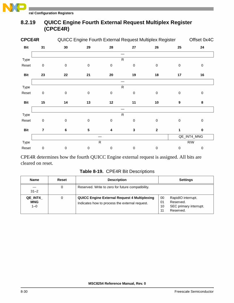
General Configuration Registers
8.2.19 QUICC Engine Fourth External Request Multiplex Register (CPCE4R)
CPE4R determines how the fourth QUICC Engine external request is assigned. All bits are cleared on reset.
CPCE4R QUICC Engine Fourth External Request Multiplex Register Offset 0x4C
Bit 31 30 29 28 27 26 25 24
—
Type R
Reset 0 0 0 0 0 0 0 0
Bit 23 22 21 20 19 18 17 16
—
Type R
Reset 0 0 0 0 0 0 0 0
Bit 15 14 13 12 11 10 9 8
—
Type R
Reset 0 0 0 0 0 0 0 0
Bit 7 6 5 4 3 2 1 0
— QE_INT4_MNG
Type R R/W
Reset 0 0 0 0 0 0 0 0
Table 8-19. CPE4R Bit Descriptions
Name Reset Description Settings
—31–2
0 Reserved. Write to zero for future compatibility.
QE_INT4_ MNG1–0
0 QUICC Engine External Request 4 Multiplexing
Indicates how to process the external request.
00 RapidIO interrupt.01 Reserved.10 SEC primary interrupt.11 Reserved.
MSC8254 Reference Manual, Rev. 0
8-30 Freescale Semiconductor

Detailed Register Descriptions
8.2.20 General Control Register 10 (GCR10)
GCR10 is used to control the DDR controller clocks.
GCR10 General Control Register 10 Offset 0x74
Bit 31 30 29 28 27 26 25 24
—
Type R/W
Reset 1 1 1 1 1 1 1 1
Bit 23 22 21 20 19 18 17 16
—
Type R/W
Reset 1 1 1 1 1 1 1 1
Bit 15 14 13 12 11 10 9 8
—
Type R/W
Reset 0 1 1 1 1 1 1 1
Bit 7 6 5 4 3 2 1 0
— MCK1_EN_ DDR1
MCK2_EN_ DDR1
MCK1_EN_ DDR2
MCK2_EN_ DDR2
Type R/W
Reset 1 1 1 1 1 1 1 1
Table 8-20. GCR10 Bit Descriptions
Name Reset Description Settings
—31–4
0xFFFFFFF Reserved. Write to zero for future compatibility.
MCK1_EN_DDR13
1 DDR1 MCK1 EnableEnables/disables MCK1 for DDR1
0 Disabled.
1 Enabled
MCK2_EN_DDR12
1 DDR1 MCK2 EnableEnables/disables MCK2 for DDR1
0 Disabled.
1 Enabled
MCK1_EN_DDR21
1 DDR2 MCK1 EnableEnables/disables MCK1 for DDR2
0 Disabled.
1 Enabled
MCK2_EN_DDR20
1 DDR2 MCK2 EnableEnables/disables MCK2 for DDR2
0 Disabled.
1 Enabled
MSC8254 Reference Manual, Rev. 0
Freescale Semiconductor 8-31

General Configuration Registers
8.2.21 General Interrupt Register 1 (GIR1)
GIR1 includes the interrupt status of several events that are rare. Those bits are not sticky and only sample the events. The GIR1 is reset by a hard reset event. All bits are cleared on reset.
GIR1 General Interrupt Register 1 Offset 0x80
Bit 31 30 29 28 27 26 25 24
SWT7 SWT6 SWT5 SWT4 SWT3 SWT2 SWT1 SWT0
Type R/W
Reset 0 0 0 0 0 0 0 0
Bit 23 22 21 20 19 18 17 16
O2M1_ERR O2M0_ERR — DMA_ERR CE_IECC CE_DECC — TDM_P0ECC
Type R/W
Reset 0 0 0 0 0 0 0 0
Bit 15 14 13 12 11 10 9 8
—
Type R/W
Reset 0 0 0 0 0 0 0 0
Bit 7 6 5 4 3 2 1 0
TDM3_TERR TDM3_RERR TDM2_TERR TDM2_RERR TDM1_TERR TDM1_RERR TDM0_TERR TDM0_RERR
Type R/W
Reset 0 0 0 0 0 0 0 0
Table 8-21. GIR1 Bit Descriptions
Name Reset Description Settings
SWT731
0 Software Watchdog Timer 7Reflects the status of the watchdog timer interrupt. See Section 21.3, Software Watchdog Timers.
0 Interrupt not asserted
1 Interrupt asserted
SWT630
0 Software Watchdog Timer 6Reflects the status of the watchdog timer interrupt. See Section 21.3, Software Watchdog Timers.
0 Interrupt not asserted
1 Interrupt asserted
SWT529
0 Software Watchdog Timer 5Reflects the status of the watchdog timer interrupt. See Section 21.3, Software Watchdog Timers.
0 Interrupt not asserted
1 Interrupt asserted
SWT428
0 Software Watchdog Timer 4Reflects the status of the watchdog timer interrupt. See Section 21.3, Software Watchdog Timers.
0 Interrupt not asserted
1 Interrupt asserted
SWT327
0 Software Watchdog Timer 3Reflects the status of the watchdog timer interrupt. See Section 21.3, Software Watchdog Timers.
0 Interrupt not asserted
1 Interrupt asserted
SWT226
0 Software Watchdog Timer 2Reflects the status of the watchdog timer interrupt.See Section 21.3, Software Watchdog Timers.
0 Interrupt not asserted
1 Interrupt asserted
MSC8254 Reference Manual, Rev. 0
8-32 Freescale Semiconductor

Detailed Register Descriptions
SWT125
0 Software Watchdog Timer 1Reflects the status of the watchdog timer interrupt. See Section 21.3, Software Watchdog Timers.
0 Interrupt not asserted
1 Interrupt asserted
SWT024
0 Software Watchdog Timer 0Reflects the status of the watchdog timer interrupt. See Section 21.3, Software Watchdog Timers.
0 Interrupt not asserted
1 Interrupt asserted
O2M1_ERR23
0 O2M 1 ErrorReflects the status of the O2M1 error interrupt. Possible causes for an interrupt include:• Unsupported packet type detected on the OCN
outbound interface.• OCN end-of-packet signal is asserted before the
expected end-of-transaction.• Data error. Data is corrupted on the O2M bridge.
0 Interrupt not asserted
1 Interrupt asserted
O2M0_ERR22
0 O2M 0 ErrorReflects the status of the O2M0 error interrupt. Possible causes for an interrupt include:• Unsupported packet type detected on the OCN
outbound interface.• OCN end-of-packet signal is asserted before the
expected end-of-transaction.• Data error. Data is corrupted on the O2M bridge.
0 Interrupt not asserted
1 Interrupt asserted
—21
0 Reserved. Write to zero for future compatibility.
DMA_ERR20
0 DMA ErrorReflects the status of the DMA error interrupt. See Section 14.7.16, DMA Error Register (DMAERR).
0 Interrupt not asserted
1 Interrupt asserted
CE_IECC19
0 QUICC Engine IRAM ErrorReflects the status of the QUICC Engine IRAM ECC error interrupt.
0 Interrupt not asserted
1 Interrupt asserted
CE_DECC18
0 QUICC Engine DRAM ErrorReflects the status of the QUICC Engine DRAM ECC error interrupt.
0 Interrupt not asserted
1 Interrupt asserted
—17
0 Reserved. Write to zero for future compatibility.
TDM_P0ECC16
0 TDM Parity ErrorReflects the ORed status of the TDM[0–3] parity error interrupts.
0 Interrupt not asserted
1 Interrupt asserted
—15–8
0 Reserved. Write to zero for future compatibility.
TDM3_TERR7
0 TDM3 Transmit ErrorReflects the status of the TDM3 transmit error interrupt.
0 Interrupt not asserted
1 Interrupt asserted
TDM3_RERR6
0 TDM3 Receive ErrorReflects the status of the TDM3 receive error interrupt.
0 Interrupt not asserted
1 Interrupt asserted
TDM2_TERR5
0 TDM2 Transmit ErrorReflects the status of the TDM2 transmit error interrupt.
0 Interrupt not asserted
1 Interrupt asserted
Table 8-21. GIR1 Bit Descriptions (Continued)
Name Reset Description Settings
MSC8254 Reference Manual, Rev. 0
Freescale Semiconductor 8-33
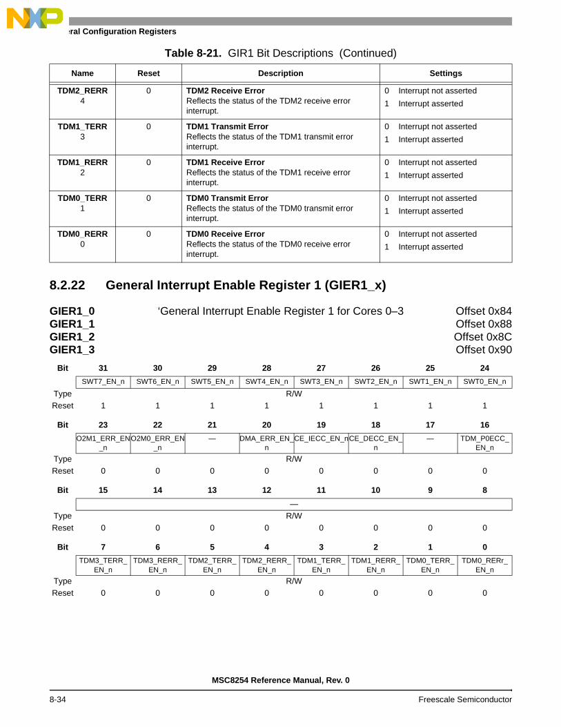
General Configuration Registers
8.2.22 General Interrupt Enable Register 1 (GIER1_x)
TDM2_RERR4
0 TDM2 Receive ErrorReflects the status of the TDM2 receive error interrupt.
0 Interrupt not asserted
1 Interrupt asserted
TDM1_TERR3
0 TDM1 Transmit ErrorReflects the status of the TDM1 transmit error interrupt.
0 Interrupt not asserted
1 Interrupt asserted
TDM1_RERR2
0 TDM1 Receive ErrorReflects the status of the TDM1 receive error interrupt.
0 Interrupt not asserted
1 Interrupt asserted
TDM0_TERR1
0 TDM0 Transmit ErrorReflects the status of the TDM0 transmit error interrupt.
0 Interrupt not asserted
1 Interrupt asserted
TDM0_RERR0
0 TDM0 Receive ErrorReflects the status of the TDM0 receive error interrupt.
0 Interrupt not asserted
1 Interrupt asserted
GIER1_0 ‘General Interrupt Enable Register 1 for Cores 0–3 Offset 0x84GIER1_1 Offset 0x88GIER1_2 Offset 0x8CGIER1_3 Offset 0x90
Bit 31 30 29 28 27 26 25 24
SWT7_EN_n SWT6_EN_n SWT5_EN_n SWT4_EN_n SWT3_EN_n SWT2_EN_n SWT1_EN_n SWT0_EN_n
Type R/WReset 1 1 1 1 1 1 1 1
Bit 23 22 21 20 19 18 17 16
O2M1_ERR_EN_n
O2M0_ERR_EN_n
— DMA_ERR_EN_n
CE_IECC_EN_nCE_DECC_EN_n
— TDM_P0ECC_ EN_n
Type R/WReset 0 0 0 0 0 0 0 0
Bit 15 14 13 12 11 10 9 8
—Type R/W
Reset 0 0 0 0 0 0 0 0
Bit 7 6 5 4 3 2 1 0
TDM3_TERR_ EN_n
TDM3_RERR_ EN_n
TDM2_TERR_ EN_n
TDM2_RERR_ EN_n
TDM1_TERR_ EN_n
TDM1_RERR_ EN_n
TDM0_TERR_ EN_n
TDM0_RERr_ EN_n
Type R/WReset 0 0 0 0 0 0 0 0
Table 8-21. GIR1 Bit Descriptions (Continued)
Name Reset Description Settings
MSC8254 Reference Manual, Rev. 0
8-34 Freescale Semiconductor
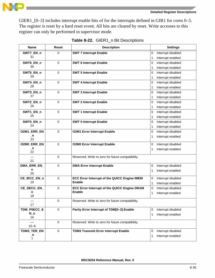
Detailed Register Descriptions
GIER1_[0–3] includes interrupt enable bits of for the interrupts defined in GIR1 for cores 0–5. The register is reset by a hard reset event. All bits are cleared by reset. Write accesses to this register can only be performed in supervisor mode.
Table 8-22. GIER1_n Bit Descriptions
Name Reset Description Settings
SWT7_EN_n31
0 SWT 7 Interrupt Enable 0 Interrupt disabled
1 Interrupt enabled
SWT6_EN_n30
0 SWT 6 Interrupt Enable 0 Interrupt disabled
1 Interrupt enabled
SWT5_EN_n29
0 SWT 5 Interrupt Enable 0 Interrupt disabled
1 Interrupt enabled
SWT4_EN_n28
0 SWT 4 Interrupt Enable 0 Interrupt disabled
1 Interrupt enabled
SWT3_EN_n27
0 SWT 3 Interrupt Enable 0 Interrupt disabled
1 Interrupt enabled
SWT2_EN_n26
0 SWT 2 Interrupt Enable 0 Interrupt disabled
1 Interrupt enabled
SWT1_EN_n25
0 SWT 1 Interrupt Enable 0 Interrupt disabled
1 Interrupt enabled
SWT0_EN_n24
0 SWT 0 Interrupt Enable 0 Interrupt disabled
1 Interrupt enabled
O2M1_ERR_EN_n23
0 O2M1 Error Interrupt Enable 0 Interrupt disabled
1 Interrupt enabled
O2M0_ERR_EN_n22
0 O2M0 Error Interrupt Enable 0 Interrupt disabled
1 Interrupt enabled
—21
0 Reserved. Write to zero for future compatibility.
DMA_ERR_EN_n20
0 DMA Error Interrupt Enable 0 Interrupt disabled
1 Interrupt enabled
CE_IECC_EN_n19
0 ECC Error Interrupt of the QUICC Engine IMEM Enable
0 Interrupt disabled
1 Interrupt enabled
CE_DECC_EN_n18
0 ECC Error Interrupt of the QUICC Engine DRAM Enable
0 Interrupt disabled
1 Interrupt enabled
—17
0 Reserved. Write to zero for future compatibility.
TDM_P0ECC_EN_n16
0 Parity Error Interrupt of TDM[0–3] Enable 0 Interrupt disabled
1 Interrupt enabled
—15–8
0 Reserved. Write to zero for future compatibility.
TDM3_TER_EN_n7
0 TDM3 Transmit Error Interrupt Enable 0 Interrupt disabled
1 Interrupt enabled
MSC8254 Reference Manual, Rev. 0
Freescale Semiconductor 8-35

General Configuration Registers
8.2.23 General Interrupt Register 3 (GIR3)
TDM3_RER_EN_n6
0 TDM3 Receive Error Interrupt Enable 0 Interrupt disabled
1 Interrupt enabled
TDM2_TER_EN_n5
0 TDM2 Transmit Error Interrupt Enable 0 Interrupt disabled
1 Interrupt enabled
TDM2_RER_EN_n4
0 TDM2 Receive Error Interrupt Enable 0 Interrupt disabled
1 Interrupt enabled
TDM1_TER_EN_n3
0 TDM1 Transmit Error Interrupt Enable 0 Interrupt disabled
1 Interrupt enabled
TDM1_RER_EN_n2
0 TDM1 Receive Error Interrupt Enable 0 Interrupt disabled
1 Interrupt enabled
TDM0_TER_EN_n1
0 TDM0 Transmit Error Interrupt Enable 0 Interrupt disabled
1 Interrupt enabled
TDM0_RER_EN_n0
0 TDM0 Receive Error Interrupt Enable 0 Interrupt disabled
1 Interrupt enabled
GIR3 General Interrupt Register 3 Offset 0xA4
Bit 31 30 29 28 27 26 25 24
—
Type R/WReset 0 0 0 0 0 0 0 0
Bit 23 22 21 20 19 18 17 16
— DDR2_ERR DDR1_ERR —
Type R/W
Reset 0 0 0 0 0 0 0 0
Bit 15 14 13 12 11 10 9 8
— PM
Type R/WReset 0 0 0 0 0 0 0 0
Bit 7 6 5 4 3 2 1 0
— CLS0_ERR — CLS0_WP CLS0_OV
Type R/WReset 0 0 0 0 0 0 0 0
Table 8-22. GIER1_n Bit Descriptions
Name Reset Description Settings
MSC8254 Reference Manual, Rev. 0
8-36 Freescale Semiconductor

Detailed Register Descriptions
GIR3 includes interrupt status of some debug/profiling events within MSC8254. Those bits are not sticky but only sample the events. The GIR3 register is reset by a hard reset event. All bits are cleared on reset.
Table 8-23. GIR3 Bit Descriptions
Name Reset Description Settings
—31–23
0 Reserved. Write to zero for future compatibility.
DDR2_ERR22
0 DDR2 Error InterruptReflects the status of the interrupt. See Section 12.6, Error Management.
0 Interrupt not asserted
1 Interrupt asserted
DDR1_ERR21
0 DDR1 Error InterruptReflects the status of the interrupt. See Section 12.6, Error Management.
0 Interrupt not asserted
1 Interrupt asserted
—20–9
0 Reserved. Write to zero for future compatibility.
PM8
0 Performance Monitor InterruptReflects the performance monitor interrupt
0 Interrupt not asserted
1 Interrupt asserted
—7–5
0 Reserved. Write to zero for future compatibility.
CLS0_ERR4
0 CLASS0 Error Interrupt
Reflects CLASS0 Error Interrupt
0 Interrupt not asserted
1 Interrupt asserted
—3–2
0 Reserved. Write to zero for future compatibility.
CLS0_WP1
0 CLASS0 Watchpoint Interrupt
Reflects Class0 watchpoint interrupt
0 Interrupt not asserted
1 Interrupt asserted
CLS0_OV0
0 CLASS0 Overrun Interrupt
Reflects CLASS0 overrun interrupt
0 Interrupt not asserted
1 Interrupt asserted
MSC8254 Reference Manual, Rev. 0
Freescale Semiconductor 8-37

General Configuration Registers
8.2.24 General Interrupt Enable Register 3 for Cores 0–3 (GIER3_x)
GIER3_[0–3] include interrupt enable bits for cores 0–3 for debug/profiling events within MSC8254. GIER3_[0–3] are reset by a hard reset event. All bits are cleared on reset. Write accesses to this register can be performed only in supervisor mode.
GIER3_0 General Interrupt Enable Register 3 for Cores 0–3 Offset 0xA8GIER3_1 Offset 0xACGIER3_2 Offset 0xB0GIER3_3 Offset 0xB4
Bit 31 30 29 28 27 26 25 24
—
Type R/W
Reset 0 0 0 0 0 0 0 0
Bit 23 22 21 20 19 18 17 16
— DDR2_ERR_EN_n
DDR1_ERR_EN_n
—
Type R/W
Reset 0 0 0 0 0 0 0 0
Bit 15 14 13 12 11 10 9 8
— PM_EN_n
Type R/W
Reset 0 0 0 0 0 0 0 0
Bit 7 6 5 4 3 2 1 0
— CLS0_ERR_EN_n
— CLS0_WP_EN_n
CLS0_OV_EN_n
Type R/W
Reset 0 0 0 0 0 0 0 0
Table 8-24. GIER3_[0–5] Bit Descriptions
Name Reset Description Settings
—31–23
0 Reserved. Write to zero for future compatibility.
DDR2_ERR_EN_n22
0 DDR2 Error Interrupt Enable 0 Interrupt disabled
1 Interrupt enabled
DDR1_ERR_EN_n21
0 DDR1 Error Interrupt Enable 0 Interrupt disabled
1 Interrupt enabled
—20–9
0 Reserved. Write to zero for future compatibility.
PM_EN_n8
0 Performance Monitor Interrupt Enable 0 Interrupt disabled
1 Interrupt enabled
—7–5
0 Reserved. Write to zero for future compatibility.
MSC8254 Reference Manual, Rev. 0
8-38 Freescale Semiconductor

Detailed Register Descriptions
8.2.25 General Interrupt Register 5 (GIR5)
GIR5 includes interrupt status of some internal events within MSC8254. Those bits are sticky and cleared by writing a 1 to the bit. The GIR5 register is reset by a hard reset event. All bits are cleared on reset. Write accesses to this register can only be performed in supervisor mode.
CLS0_ERR_EN_n4
0 CLASS0 Error Interrupt Enable 0 Interrupt disabled
1 Interrupt enabled
—3–2
0 Reserved. Write to zero for future compatibility.
CLS0_WP_EN_n1
0 CLASS0 Watchpoint Interrupt Enable 0 Interrupt disabled
1 Interrupt enabled
CLS0_OV_EN_n0
0 CLASS0 Overrun Interrupt Enable 0 Interrupt disabled
1 Interrupt enabled
GIR5 General Interrupt Register 5 Offset 0xEC
Bit 31 30 29 28 27 26 25 24
—Type W1CReset 0 0 0 0 0 0 0 0
Bit 23 22 21 20 19 18 17 16
—
Type W1CReset 0 0 0 0 0 0 0 0
Bit 15 14 13 12 11 10 9 8
—Type W1C
Reset 0 0 0 0 0 0 0 0
Bit 7 6 5 4 3 2 1 0
— T2_T3_AE T0_T1_AEType W1CReset 0 0 0 0 0 0 0 0
Table 8-25. GIR5 Bit Descriptions
Name Reset Description Settings
—31–2
0 Reserved. Write to zero for future compatibility.
T2_T3_AE1
0 Core 2 or Core3 L2/M2 Access Error InterruptReflects L2/M2 Access Error Interrupt which occurs when the referenced core is in Stop mode.One of the cores tried to access core subsystem 2 or core subsystem 3 M2/L2 memory.
0 Interrupt not asserted
1 Interrupt asserted
Table 8-24. GIER3_[0–5] Bit Descriptions
Name Reset Description Settings
MSC8254 Reference Manual, Rev. 0
Freescale Semiconductor 8-39
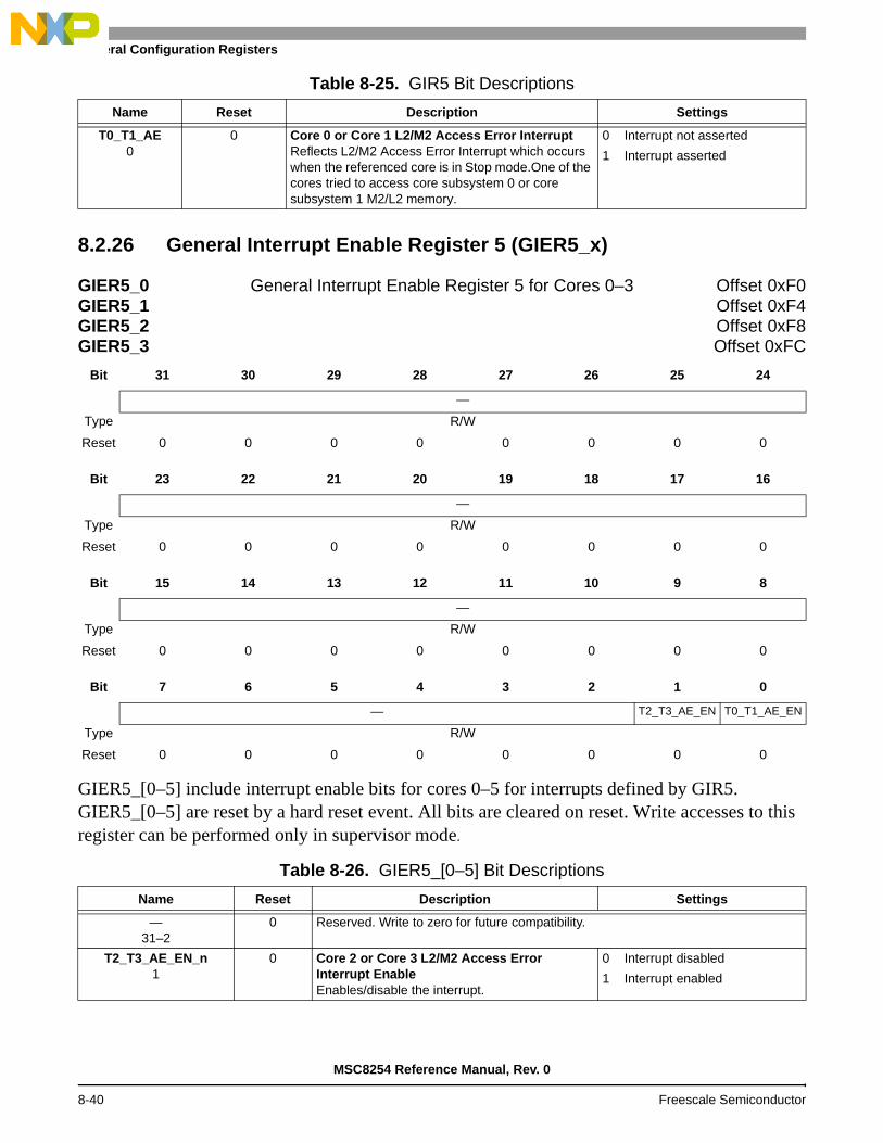
General Configuration Registers
8.2.26 General Interrupt Enable Register 5 (GIER5_x)
GIER5_[0–5] include interrupt enable bits for cores 0–5 for interrupts defined by GIR5. GIER5_[0–5] are reset by a hard reset event. All bits are cleared on reset. Write accesses to this register can be performed only in supervisor mode.
T0_T1_AE0
0 Core 0 or Core 1 L2/M2 Access Error InterruptReflects L2/M2 Access Error Interrupt which occurs when the referenced core is in Stop mode.One of the cores tried to access core subsystem 0 or core subsystem 1 M2/L2 memory.
0 Interrupt not asserted
1 Interrupt asserted
GIER5_0 General Interrupt Enable Register 5 for Cores 0–3 Offset 0xF0GIER5_1 Offset 0xF4GIER5_2 Offset 0xF8GIER5_3 Offset 0xFC
Bit 31 30 29 28 27 26 25 24
—
Type R/W
Reset 0 0 0 0 0 0 0 0
Bit 23 22 21 20 19 18 17 16
—
Type R/W
Reset 0 0 0 0 0 0 0 0
Bit 15 14 13 12 11 10 9 8
—
Type R/W
Reset 0 0 0 0 0 0 0 0
Bit 7 6 5 4 3 2 1 0
— T2_T3_AE_EN T0_T1_AE_EN
Type R/W
Reset 0 0 0 0 0 0 0 0
Table 8-26. GIER5_[0–5] Bit Descriptions
Name Reset Description Settings
—31–2
0 Reserved. Write to zero for future compatibility.
T2_T3_AE_EN_n1
0 Core 2 or Core 3 L2/M2 Access Error Interrupt EnableEnables/disable the interrupt.
0 Interrupt disabled
1 Interrupt enabled
Table 8-25. GIR5 Bit Descriptions
Name Reset Description Settings
MSC8254 Reference Manual, Rev. 0
8-40 Freescale Semiconductor

Detailed Register Descriptions
8.2.27 General Control Register 11 (GCR11)
GCR11 controls the initial values for weighted and late arbitration operation of the peripheral system. All bits are cleared on reset.
T0_T1_AE_EN_n0
0 Core 0 or Core 1 L2/M2 Access Error Interrupt EnableEnables/disable the interrupt.
0 Interrupt disabled
1 Interrupt enabled
GCR11 General Control Register 11 Offset 0x110
Bit 31 30 29 28 27 26 25 24
— PERIPHER_ SYS_LATE_
ARBITARTION
Type R/WReset 0 0 0 0 0 0 0 0
Bit 23 22 21 20 19 18 17 16
—
Type R/WReset 0 0 0 0 0 0 0 0
Bit 15 14 13 12 11 10 9 8
— PERIPHER_ SYS_INIT2_WEIGHTType R/W
Reset 0 0 0 0 0 0 0 0
Bit 7 6 5 4 3 2 1 0
PERIPHER_ SYS_INIT1_WEIGHT PERIPHER_ SYS_INIT0_WEIGHTType R/WReset 0 0 0 0 0 0 0 0
Table 8-27. GCR11 Bit Descriptions
Name Reset Description Settings
—31–25
0 Reserved. Write to zero for future compatibility.
PERIPHER_ SYS_LATE_
ARBITRATION24
0 Late ArbitrationEnables/disables late arbitration for the peripheral system.
0 Do not allow late arbitration.
1 Allow late arbitration.
—23–12
0 Reserved. Write to zero for future compatibility.
PERIPHER_ SYS_INIT2_
WEIGHT11–8
0 Initial TDM Arbitration WeightSets the initial weight given to TDM transactions for peripheral system arbitration.
Table 8-26. GIER5_[0–5] Bit Descriptions
Name Reset Description Settings
MSC8254 Reference Manual, Rev. 0
Freescale Semiconductor 8-41

General Configuration Registers
8.2.28 General Control Register 12 (GCR12)
GCR12 controls the initial values for weighted and late arbitration operation of the HSSI CLASS. All bits are cleared on reset.
PERIPHER_ SYS_INIT1_
WEIGHT7–4
0 Initial QUICC Engine Module Arbitration WeightSets the initial weight given to the QUICC Engine module for peripheral system arbitration.
PERIPHER_ SYS_INIT0_
WEIGHT3–0
0 Initial SEC Arbitration WeightSets the initial weight given to the SEC for peripheral system arbitration.
GCR12 General Control Register 12 Offset 0x114
Bit 31 30 29 28 27 26 25 24
—Type R/W
Reset 0 0 0 0 0 0 0 0
Bit 23 22 21 20 19 18 17 16
— HSSI_SYS_ LATE_
ARBITARTION
Type R/W
Reset 0 0 0 0 0 0 0 0
Bit 15 14 13 12 11 10 9 8
—Type R/WReset 0 0 0 0 0 0 0 0
Bit 7 6 5 4 3 2 1 0
HSSI_SYS_INIT1_WEIGHT HSSI_SYS_INIT0_WEIGHT
Type R/WReset 0 0 0 0 0 0 0 0
Table 8-28. GCR12 Bit Descriptions
Name Reset Description Settings
—31–17
0 Reserved. Write to zero for future compatibility.
HSSI_SYS_ LATE_
ARBITRATION16
0 Late ArbitrationEnables/disables late arbitration for the HSSI system.
0 Do not allow late arbitration.
1 Allow late arbitration.
—15–8
0 Reserved. Write to zero for future compatibility.
Table 8-27. GCR11 Bit Descriptions (Continued)
Name Reset Description Settings
MSC8254 Reference Manual, Rev. 0
8-42 Freescale Semiconductor

Detailed Register Descriptions
HSSI_SYS_ INIT1_
WEIGHT7–4
0 HSSI Internal Interface 1 Arbitration WeightSets the initial weight given to the internal interface 1 (MBus side) of the HSSI. The interface can have a maximum weight of 16.
0000 Weight = 10001 Weight = 20010 Weight = 30011 Weight = 40100 Weight = 50101 Weight = 60110 Weight = 70111 Weight = 81000 Weight = 91001 Weight = 101010 Weight = 111011 Weight = 121100 Weight = 131101 Weight = 141110 Weight = 151111 Weight = 16
HSSI_SYS_ INIT0_
WEIGHT3–0
0 HSSI Internal Interface 0 Arbitration WeightSets the initial weight given to the internal interface 0 (MBus side) of the HSSI. The interface can have a maximum weight of 16.
0000 Weight = 10001 Weight = 20010 Weight = 30011 Weight = 40100 Weight = 50101 Weight = 60110 Weight = 70111 Weight = 81000 Weight = 91001 Weight = 101010 Weight = 111011 Weight = 121100 Weight = 131101 Weight = 141110 Weight = 151111 Weight = 16
Table 8-28. GCR12 Bit Descriptions (Continued)
Name Reset Description Settings
MSC8254 Reference Manual, Rev. 0
Freescale Semiconductor 8-43

General Configuration Registers
8.2.29 DMA Request0 Control Register (GCR_DREQ0)
GCR_DREQ0 associates an external peripheral DMA request 0 to the DMA Controller channel with its destination or source. The user must clear the corresponding bits for a channel for memory-only transactions.
GCR_DREQ0 DMA Request0 Control Register Offset 0x120
Bit 31 30 29 28 27 26 25 24
DMA_DREQ0_D15
DMA_DREQ0_S15
DMA_DREQ0_D14
DMA_DREQ0_S14
DMA_DREQ0_D13
DMA_DREQ0_S13
DMA_DREQ0_D12
DMA_DREQ0_S12
Type R/W
Reset 0 0 0 0 0 0 0 0
Bit 23 22 21 20 19 18 17 16
DMA_DREQ0_D11
DMA_DREQ0_S11
DMA_DREQ0_D10
DMA_DREQ0_S10
DMA_DREQ0_D9
DMA_DREQ0_S9
DMA_DREQ0_D8
DMA_DREQ0_S8
Type R/W
Reset 0 0 0 0 0 0 0 0
Bit 15 14 13 12 11 10 9 8
DMA_DREQ0_D7
DMA_DREQ0_S7
DMA_DREQ0_D6
DMA_DREQ0_S6
DMA_DREQ0_D5
DMA_DREQ0_S5
DMA_DREQ0_D4
DMA_DREQ0_S4
Type R/W
Reset 0 0 0 0 0 0 0 0
Bit 7 6 5 4 3 2 1 0
DMA_DREQ0_D3
DMA_DREQ0_S3
DMA_DREQ0_D2
DMA_DREQ0_S2
DMA_DREQ0_D1
DMA_DREQ0_S1
DMA_DREQ0_D0
DMA_DREQ0_S0
Type R/W
Reset 0 0 0 0 0 0 0 0
Table 8-29. GCR_DREQ0 Bit Descriptions
Name Reset Description Settings
DMA_DREQ0_D1531
0 DMA DREQ0 Destination Channel 15Associates the DREQ with the destination for Channel 15.
0 DREQ not associated with Channel 15 destination.
1 DREQ associated with Channel 15 destination.
DMA_DREQ0_S1530
0 DMA DREQ0 Source Channel 15Associates the DREQ with the source for Channel 15.
0 DREQ not associated with Channel 15 source.
1 DREQ associated with Channel 15 source.
DMA_DREQ0_D1429
0 DMA DREQ0 Destination Channel 14Associates the DREQ with the destination for Channel 14.
0 DREQ not associated with Channel 14 destination.
1 DREQ associated with Channel 14 destination.
MSC8254 Reference Manual, Rev. 0
8-44 Freescale Semiconductor

Detailed Register Descriptions
DMA_DREQ0_S1428
0 DMA DREQ0 Source Channel 14Associates the DREQ with the source for Channel 14.
0 DREQ not associated with Channel 14 source.
1 DREQ associated with Channel 14 source.
DMA_DREQ0_D1327
0 DMA DREQ0 Destination Channel 13Associates the DREQ with the destination for Channel 13.
0 DREQ not associated with Channel 13 destination.
1 DREQ associated with Channel 13 destination.
DMA_DREQ0_S1326
0 DMA DREQ0 Source Channel 13Associates the DREQ with the source for Channel 13.
0 DREQ not associated with Channel 13 source.
1 DREQ associated with Channel 13 source.
DMA_DREQ0_D1225
0 DMA DREQ0 Destination Channel 12Associates the DREQ with the destination for Channel 12.
0 DREQ not associated with Channel 12 destination.
1 DREQ associated with Channel 12 destination.
DMA_DREQ0_S1224
0 DMA DREQ0 Source Channel 12Associates the DREQ with the source for Channel 12.
0 DREQ not associated with Channel 12 source.
1 DREQ associated with Channel 12 source.
DMA_DREQ0_D1123
0 DMA DREQ0 Destination Channel 11Associates the DREQ with the destination for Channel 11.
0 DREQ not associated with Channel 11 destination.
1 DREQ associated with Channel 11 destination.
DMA_DREQ0_S1122
0 DMA DREQ0 Source Channel 11Associates the DREQ with the source for Channel 11.
0 DREQ not associated with Channel 11 source.
1 DREQ associated with Channel 11 source.
DMA_DREQ0_D1021
0 DMA DREQ0 Destination Channel 10Associates the DREQ with the destination for Channel 10.
0 DREQ not associated with Channel 10 destination.
1 DREQ associated with Channel 10 destination.
DMA_DREQ0_S1020
0 DMA DREQ0 Source Channel 10Associates the DREQ with the source for Channel 10.
0 DREQ not associated with Channel 10 source.
1 DREQ associated with Channel 10 source.
DMA_DREQ0_D919
0 DMA DREQ0 Destination Channel 9Associates the DREQ with the destination for Channel 9.
0 DREQ not associated with Channel 9 destination.
1 DREQ associated with Channel 9 destination.
DMA_DREQ0_S918
0 DMA DREQ0 Source Channel 9Associates the DREQ with the source for Channel 9.
0 DREQ not associated with Channel 9 source.
1 DREQ associated with Channel 9 source.
Table 8-29. GCR_DREQ0 Bit Descriptions (Continued)
Name Reset Description Settings
MSC8254 Reference Manual, Rev. 0
Freescale Semiconductor 8-45

General Configuration Registers
DMA_DREQ0_D817
0 DMA DREQ0 Destination Channel 8Associates the DREQ with the destination for Channel 8.
0 DREQ not associated with Channel 8 destination.
1 DREQ associated with Channel 8 destination.
DMA_DREQ0_S816
0 DMA DREQ0 Source Channel 8Associates the DREQ with the source for Channel 8.
0 DREQ not associated with Channel 8 source.
1 DREQ associated with Channel 8 source.
DMA_DREQ0_D715
0 DMA DREQ0 Destination Channel 7Associates the DREQ with the destination for Channel 7.
0 DREQ not associated with Channel 7 destination.
1 DREQ associated with Channel 7 destination.
DMA_DREQ0_S714
0 DMA DREQ0 Source Channel 7Associates the DREQ with the source for Channel 7.
0 DREQ not associated with Channel 7 source.
1 DREQ associated with Channel 7 source.
DMA_DREQ0_D613
0 DMA DREQ0 Destination Channel 6Associates the DREQ with the destination for Channel 6.
0 DREQ not associated with Channel 6 destination.
1 DREQ associated with Channel 6 destination.
DMA_DREQ0_S612
0 DMA DREQ0 Source Channel 6Associates the DREQ with the source for Channel 6.
0 DREQ not associated with Channel 6 source.
1 DREQ associated with Channel 6 source.
DMA_DREQ0_D511
0 DMA DREQ0 Destination Channel 5Associates the DREQ with the destination for Channel 5.
0 DREQ not associated with Channel 5 destination.
1 DREQ associated with Channel 5 destination.
DMA_DREQ0_S510
0 DMA DREQ0 Source Channel 5Associates the DREQ with the source for Channel 5.
0 DREQ not associated with Channel 5 source.
1 DREQ associated with Channel 5 source.
DMA_DREQ0_D49
0 DMA DREQ0 Destination Channel 4Associates the DREQ with the destination for Channel 4.
0 DREQ not associated with Channel 4 destination.
1 DREQ associated with Channel 4 destination.
DMA_DREQ0_S48
0 DMA DREQ0 Source Channel 4Associates the DREQ with the source for Channel 4.
0 DREQ not associated with Channel 4 source.
1 DREQ associated with Channel 4 source.
DMA_DREQ0_D37
0 DMA DREQ0 Destination Channel 3Associates the DREQ with the destination for Channel 3.
0 DREQ not associated with Channel 3 destination.
1 DREQ associated with Channel 3 destination.
Table 8-29. GCR_DREQ0 Bit Descriptions (Continued)
Name Reset Description Settings
MSC8254 Reference Manual, Rev. 0
8-46 Freescale Semiconductor

Detailed Register Descriptions
DMA_DREQ0_S36
0 DMA DREQ0 Source Channel 3Associates the DREQ with the source for Channel 3.
0 DREQ not associated with Channel 3 source.
1 DREQ associated with Channel 3 source.
DMA_DREQ0_D25
0 DMA DREQ0 Destination Channel 2Associates the DREQ with the destination for Channel 2.
0 DREQ not associated with Channel 2 destination.
1 DREQ associated with Channel 2 destination.
DMA_DREQ0_S24
0 DMA DREQ0 Source Channel 2Associates the DREQ with the source for Channel 2.
0 DREQ not associated with Channel 2 source.
1 DREQ associated with Channel 2 source.
DMA_DREQ0_D13
0 DMA DREQ0 Destination Channel 1Associates the DREQ with the destination for Channel 1.
0 DREQ not associated with Channel 1 destination.
1 DREQ associated with Channel 1 destination.
DMA_DREQ0_S12
0 DMA DREQ0 Source Channel 1Associates the DREQ with the source for Channel 1.
0 DREQ not associated with Channel 1 source.
1 DREQ associated with Channel 1 source.
DMA_DREQ0_D01
0 DMA DREQ0 Destination Channel 0Associates the DREQ with the destination for Channel 0.
0 DREQ not associated with Channel 0 destination.
1 DREQ associated with Channel 0 destination.
DMA_DREQ0_S00
0 DMA DREQ0 Source Channel 0Associates the DREQ with the source for Channel 0.
0 DREQ not associated with Channel 0 source.
1 DREQ associated with Channel 0 source.
Table 8-29. GCR_DREQ0 Bit Descriptions (Continued)
Name Reset Description Settings
MSC8254 Reference Manual, Rev. 0
Freescale Semiconductor 8-47

General Configuration Registers
8.2.30 DMA Request1 Control Register (GCR_DREQ1)
GCR_DREQ1 associates an external peripheral DMA request 1 to the DMA Controller channel with its destination or source. The user must clear the corresponding bits for a channel for memory-only transactions.
GCR_DREQ1 DMA Request1 Control Register Offset 0x124
Bit 31 30 29 28 27 26 25 24
DMA_DREQ1_D15
DMA_DREQ1_S15
DMA_DREQ1_D14
DMA_DREQ1_S14
DMA_DREQ1_D13
DMA_DREQ1_S13
DMA_DREQ1_D12
DMA_DREQ1_S12
Type R/W
Reset 0 0 0 0 0 0 0 0
Bit 23 22 21 20 19 18 17 16
DMA_DREQ1_D11
DMA_DREQ1_S11
DMA_DREQ1_D10
DMA_DREQ1_S10
DMA_DREQ1_D9
DMA_DREQ1_S9
DMA_DREQ1_D8
DMA_DREQ1_S8
Type R/W
Reset 0 0 0 0 0 0 0 0
Bit 15 14 13 12 11 10 9 8
DMA_DREQ1_D7
DMA_DREQ1_S7
DMA_DREQ1_D6
DMA_DREQ1_S6
DMA_DREQ1_D5
DMA_DREQ1_S5
DMA_DREQ1_D4
DMA_DREQ1_S4
Type R/W
Reset 0 0 0 0 0 0 0 0
Bit 7 6 5 4 3 2 1 0
DMA_DREQ1_D3
DMA_DREQ1_S3
DMA_DREQ1_D2
DMA_DREQ1_S2
DMA_DREQ1_D1
DMA_DREQ1_S1
DMA_DREQ1_D0
DMA_DREQ1_S0
Type R/W
Reset 0 0 0 0 0 0 0 0
Table 8-30. GCR_DREQ1 Bit Descriptions
Name Reset Description Settings
DMA_DREQ1_D1531
0 DMA DREQ1 Destination Channel 15Associates the DREQ with the destination for Channel 15.
0 DREQ not associated with Channel 15 destination.
1 DREQ associated with Channel 15 destination.
DMA_DREQ1_S1530
0 DMA DREQ1 Source Channel 15Associates the DREQ with the source for Channel 15.
0 DREQ not associated with Channel 15 source.
1 DREQ associated with Channel 15 source.
DMA_DREQ1_D1429
0 DMA DREQ1 Destination Channel 14Associates the DREQ with the destination for Channel 14.
0 DREQ not associated with Channel 14 destination.
1 DREQ associated with Channel 14 destination.
MSC8254 Reference Manual, Rev. 0
8-48 Freescale Semiconductor

Detailed Register Descriptions
DMA_DREQ1_S1428
0 DMA DREQ1 Source Channel 14Associates the DREQ with the source for Channel 14.
0 DREQ not associated with Channel 14 source.
1 DREQ associated with Channel 14 source.
DMA_DREQ1_D1327
0 DMA DREQ1 Destination Channel 13Associates the DREQ with the destination for Channel 13.
0 DREQ not associated with Channel 13 destination.
1 DREQ associated with Channel 13 destination.
DMA_DREQ1_S1326
0 DMA DREQ1 Source Channel 13Associates the DREQ with the source for Channel 13.
0 DREQ not associated with Channel 13 source.
1 DREQ associated with Channel 13 source.
DMA_DREQ1_D1225
0 DMA DREQ1 Destination Channel 12Associates the DREQ with the destination for Channel 12.
0 DREQ not associated with Channel 12 destination.
1 DREQ associated with Channel 12 destination.
DMA_DREQ1_S1224
0 DMA DREQ1 Source Channel 12Associates the DREQ with the source for Channel 12.
0 DREQ not associated with Channel 12 source.
1 DREQ associated with Channel 12 source.
DMA_DREQ1_D1123
0 DMA DREQ1 Destination Channel 11Associates the DREQ with the destination for Channel 11.
0 DREQ not associated with Channel 11 destination.
1 DREQ associated with Channel 11 destination.
DMA_DREQ1_S1122
0 DMA DREQ1 Source Channel 11Associates the DREQ with the source for Channel 11.
0 DREQ not associated with Channel 11 source.
1 DREQ associated with Channel 11 source.
DMA_DREQ1_D1021
0 DMA DREQ1 Destination Channel 10Associates the DREQ with the destination for Channel 10.
0 DREQ not associated with Channel 10 destination.
1 DREQ associated with Channel 10 destination.
DMA_DREQ1_S1020
0 DMA DREQ1 Source Channel 10Associates the DREQ with the source for Channel 10.
0 DREQ not associated with Channel 10 source.
1 DREQ associated with Channel 10 source.
DMA_DREQ1_D919
0 DMA DREQ1 Destination Channel 9Associates the DREQ with the destination for Channel 9.
0 DREQ not associated with Channel 9 destination.
1 DREQ associated with Channel 9 destination.
DMA_DREQ1_S918
0 DMA DREQ1 Source Channel 9Associates the DREQ with the source for Channel 9.
0 DREQ not associated with Channel 9 source.
1 DREQ associated with Channel 9 source.
Table 8-30. GCR_DREQ1 Bit Descriptions (Continued)
Name Reset Description Settings
MSC8254 Reference Manual, Rev. 0
Freescale Semiconductor 8-49

General Configuration Registers
DMA_DREQ1_D817
0 DMA DREQ1 Destination Channel 8Associates the DREQ with the destination for Channel 8.
0 DREQ not associated with Channel 8 destination.
1 DREQ associated with Channel 8 destination.
DMA_DREQ1_S816
0 DMA DREQ1 Source Channel 8Associates the DREQ with the source for Channel 8.
0 DREQ not associated with Channel 8 source.
1 DREQ associated with Channel 8 source.
DMA_DREQ1_D715
0 DMA DREQ1 Destination Channel 7Associates the DREQ with the destination for Channel 7.
0 DREQ not associated with Channel 7 destination.
1 DREQ associated with Channel 7 destination.
DMA_DREQ1_S714
0 DMA DREQ1 Source Channel 7Associates the DREQ with the source for Channel 7.
0 DREQ not associated with Channel 7 source.
1 DREQ associated with Channel 7 source.
DMA_DREQ1_D613
0 DMA DREQ1 Destination Channel 6Associates the DREQ with the destination for Channel 6.
0 DREQ not associated with Channel 6 destination.
1 DREQ associated with Channel 6 destination.
DMA_DREQ1_S612
0 DMA DREQ1 Source Channel 6Associates the DREQ with the source for Channel 6.
0 DREQ not associated with Channel 6 source.
1 DREQ associated with Channel 6 source.
DMA_DREQ1_D511
0 DMA DREQ1 Destination Channel 5Associates the DREQ with the destination for Channel 5.
0 DREQ not associated with Channel 5 destination.
1 DREQ associated with Channel 5 destination.
DMA_DREQ1_S510
0 DMA DREQ1 Source Channel 5Associates the DREQ with the source for Channel 5.
0 DREQ not associated with Channel 5 source.
1 DREQ associated with Channel 5 source.
DMA_DREQ1_D49
0 DMA DREQ1 Destination Channel 4Associates the DREQ with the destination for Channel 4.
0 DREQ not associated with Channel 4 destination.
1 DREQ associated with Channel 4 destination.
DMA_DREQ1_S48
0 DMA DREQ1 Source Channel 4Associates the DREQ with the source for Channel 4.
0 DREQ not associated with Channel 4 source.
1 DREQ associated with Channel 4 source.
DMA_DREQ1_D37
0 DMA DREQ1 Destination Channel 3Associates the DREQ with the destination for Channel 3.
0 DREQ not associated with Channel 3 destination.
1 DREQ associated with Channel 3 destination.
Table 8-30. GCR_DREQ1 Bit Descriptions (Continued)
Name Reset Description Settings
MSC8254 Reference Manual, Rev. 0
8-50 Freescale Semiconductor

Detailed Register Descriptions
DMA_DREQ1_S36
0 DMA DREQ1 Source Channel 3Associates the DREQ with the source for Channel 3.
0 DREQ not associated with Channel 3 source.
1 DREQ associated with Channel 3 source.
DMA_DREQ1_D25
0 DMA DREQ1 Destination Channel 2Associates the DREQ with the destination for Channel 2.
0 DREQ not associated with Channel 2 destination.
1 DREQ associated with Channel 2 destination.
DMA_DREQ1_S24
0 DMA DREQ1 Source Channel 2Associates the DREQ with the source for Channel 2.
0 DREQ not associated with Channel 2 source.
1 DREQ associated with Channel 2 source.
DMA_DREQ1_D13
0 DMA DREQ1 Destination Channel 1Associates the DREQ with the destination for Channel 1.
0 DREQ not associated with Channel 1 destination.
1 DREQ associated with Channel 1 destination.
DMA_DREQ1_S12
0 DMA DREQ1 Source Channel 1Associates the DREQ with the source for Channel 1.
0 DREQ not associated with Channel 1 source.
1 DREQ associated with Channel 1 source.
DMA_DREQ1_D01
0 DMA DREQ1 Destination Channel 0Associates the DREQ with the destination for Channel 0.
0 DREQ not associated with Channel 0 destination.
1 DREQ associated with Channel 0 destination.
DMA_DREQ1_S00
0 DMA DREQ1 Source Channel 0Associates the DREQ with the source for Channel 0.
0 DREQ not associated with Channel 0 source.
1 DREQ associated with Channel 0 source.
Table 8-30. GCR_DREQ1 Bit Descriptions (Continued)
Name Reset Description Settings
MSC8254 Reference Manual, Rev. 0
Freescale Semiconductor 8-51

General Configuration Registers
8.2.31 DMA Done Control Register (GCR_DDONE)
GCR_DONE controls DMA external request DONE for requestor 1 and 2.
GCR_DDONE DMA Done Control Register Offset 0x128
Bit 31 30 29 28 27 26 25 24
—
Type R/W
Reset 0 0 0 0 0 0 0 0
Bit 23 22 21 20 19 18 17 16
—
Type R/W
Reset 0 0 0 0 0 0 0 0
Bit 15 14 13 12 11 10 9 8
— V1 DONE1_CH
Type R/W
Reset 0 0 0 0 0 0 0 0
Bit 7 6 5 4 3 2 1 0
— V0 DONE0_CH
Type R/W
Reset 0 0 0 0 0 0 0 0
Table 8-31. GCR_DDONE Bit Descriptions
Name Reset Description Settings
—31–14
0 Reserved. Write to zero for future compatibility.
V113
0 Valid DONE1Indicates whether the value of DONE1_CH is valid.
0 DONE1_CH is not valid.
1 DONE1_CH is valid.
MSC8254 Reference Manual, Rev. 0
8-52 Freescale Semiconductor

Detailed Register Descriptions
DONE1_CH12–8
0 DMA DONE1 Channel SelectDefines the unidirectional channel that drives the DONE1 signal. The signal is valid when GCR_DDONE[V1] is set.
00000 Channel 0 source.00001 Channel 0 destination.00010 Channel 1 source.00011 Channel 1 destination.00100 Channel 2 source.00101 Channel 2 destination.00110 Channel 3 source.00111 Channel 3 destination.01000 Channel 4 source.01001 Channel 4 destination.01010 Channel 5 source.01011 Channel 5 destination.01100 Channel 6 source.01101 Channel 6 destination.01110 Channel 7 source.01111 Channel 7 destination.10000 Channel 8 source.10001 Channel 8 destination.10010 Channel 9 source.10011 Channel 9 destination.10100 Channel 10 source.10101 Channel 10 destination.10110 Channel 11 source.10111 Channel 11 destination.11000 Channel 12 source.11001 Channel 12 destination.11010 Channel 13 source.11011 Channel 13 destination.11100 Channel 14 source.11101 Channel 14 destination.11110 Channel 15 source.11111 Channel 15 destination.
—7–6
0 Reserved. Write to zero for future compatibility.
Table 8-31. GCR_DDONE Bit Descriptions (Continued)
Name Reset Description Settings
MSC8254 Reference Manual, Rev. 0
Freescale Semiconductor 8-53

General Configuration Registers
V05
0 Valid DONE0Indicates whether the value of DONE0_CH is valid.
0 DONE0_CH is not valid.
1 DONE0_CH is valid.
DONE0_CH4–0
0 DMA DONE0 Channel SelectDefines the unidirectional channel that drives the DONE0 signal. The signal is valid when GCR_DDONE[V0] is set.
00000 Channel 0 source.00001 Channel 0 destination.00010 Channel 1 source.00011 Channel 1 destination.00100 Channel 2 source.00101 Channel 2 destination.00110 Channel 3 source.00111 Channel 3 destination.01000 Channel 4 source.01001 Channel 4 destination.01010 Channel 5 source.01011 Channel 5 destination.01100 Channel 6 source.01101 Channel 6 destination.01110 Channel 7 source.01111 Channel 7 destination.10000 Channel 8 source.10001 Channel 8 destination.10010 Channel 9 source.10011 Channel 9 destination.10100 Channel 10 source.10101 Channel 10 destination.10110 Channel 11 source.10111 Channel 11 destination.11000 Channel 12 source.11001 Channel 12 destination.11010 Channel 13 source.11011 Channel 13 destination.11100 Channel 14 source.11101 Channel 14 destination.11110 Channel 15 source.11111 Channel 15 destination.
Table 8-31. GCR_DDONE Bit Descriptions (Continued)
Name Reset Description Settings
MSC8254 Reference Manual, Rev. 0
8-54 Freescale Semiconductor

Detailed Register Descriptions
8.2.32 DDR1 General Configuration Register (DDR1_GCR)
DDR1_GCR controls part of the DDR1 operation. All bits are cleared on a hard reset event.
DDR1_GCR DDR1 General Configuration Register Offset 0x12C
Bit 31 30 29 28 27 26 25 24
—
Type R/W
Reset 0 0 0 0 0 0 0 0
Bit 23 22 21 20 19 18 17 16
—
Type R/W
Reset 0 0 0 0 0 0 0 0
Bit 15 14 13 12 11 10 9 8
—
Type R/W
Reset 0 0 0 0 0 0 0 0
Bit 7 6 5 4 3 2 1 0
— DDR1_STOP DDR1_DOZE DDR1_PWR_DOWN
Type R/W
Reset 0 0 0 0 0 0 0 0
Table 8-32. DDR1_GCR Bit Descriptions
Name Reset Description Settings
—31–3
0 Reserved. Write to zero for future compatibility.
DDR1_STOP2
0 DDR1 StopWith the DDRC Stop ACK, actively stops the controller and DDR memory clock. If the memory is not put in self-refresh mode prior to activating Stop mode, data is lost.
0 DDR1 Stop not requested.
1 DDR1 Stop requested.
DDR1_DOZE1
0 DDR1 DozeUsed to select Doze mode, in which all register accesses are acknowledged, but writes are not written and reads do not contain valid data. Setting this bit prevents lockup of the device internal bus while the DDR controller 1 is stopped.Note: To conserve power, when DDR1 is not used by an
application, set this bit as soon as possible after reset. This step should be included as part of the initialization code.
0 Normal operation.
1 Doze mode.
DDR1_ POWER_
DOWN0
0 DDR1 Power DownWhen set, powers down all DDR1 areas with gated clocks.
0 DDR1 power up.
1 DDR1 power down.
MSC8254 Reference Manual, Rev. 0
Freescale Semiconductor 8-55

General Configuration Registers
8.2.33 DDR2 General Configuration Register (DDR2_GCR)
DDR2_GCR controls part of the DDR2 operation. All bits are cleared on a hard reset event.
DDR2_GCR DDR2 General Configuration Register Offset 0x130
Bit 31 30 29 28 27 26 25 24
—
Type R/W
Reset 0 0 0 0 0 0 0 0
Bit 23 22 21 20 19 18 17 16
—
Type R/W
Reset 0 0 0 0 0 0 0 0
Bit 15 14 13 12 11 10 9 8
—
Type R/W
Reset 0 0 0 0 0 0 0 0
Bit 7 6 5 4 3 2 1 0
— DDR2_STOP DDR2_DOZE DDR2_PWR_DOWN
Type R/W
Reset 0 0 0 0 0 0 0 0
Table 8-33. DDR2_GCR Bit Descriptions
Name Reset Description Settings
—31–3
0 Reserved. Write to zero for future compatibility.
DDR2_STOP2
0 DDR2 StopWith the DDRC Stop ACK, actively stops the controller and DDR memory clock. If the memory is not put in self-refresh mode prior to activating Stop mode, data is lost.
0 DDR2 Stop not requested.
1 DDR2 Stop requested.
DDR2_DOZE1
0 DDR2 DozeUsed to select Doze mode, in which all register accesses are acknowledged, but writes are not written and reads do not contain valid data. Setting this bit prevents lockup of the device internal bus while the DDR2 controller is stopped.Note: To conserve power, when DDR2 is not used by an
application, set this bit as soon as possible after reset. This step should be included as part of the initialization code.
0 Normal operation.
1 Doze mode.
DDR2_ POWER_
DOWN0
0 DDR2 Power DownWhen set, powers down all DDR2 areas with gated clocks.
0 DDR2 power up.
1 DDR2 power down.
MSC8254 Reference Manual, Rev. 0
8-56 Freescale Semiconductor

Detailed Register Descriptions
8.2.34 Core Subsystem Slave Port General Configuration Register (CORE_SLV_GCR)
CORE_SLV_GCR controls the status of the slave ports for the core subsystems.
CORE_SLV_GCRCore Subsystem Slave Port General Configuration Register Offset 0x138
Bit 31 30 29 28 27 26 25 24
—
Type R/W
Reset 0 0 0 0 0 0 0 0
Bit 23 22 21 20 19 18 17 16
—
Type R/W
Reset 0 0 0 0 0 0 0 0
Bit 15 14 13 12 11 10 9 8
—
Type R/W
Reset 0 0 0 0 0 0 0 0
Bit 7 6 5 4 3 2 1 0
— CORE_SLV_WIN_CLOSE3
CORE_SLV_WIN_CLOSE2
CORE_SLV_WIN_CLOSE1
CORE_SLV_WIN_CLOSE0
Type R/W
Reset 0 0 0 0 0 0 0 0
Table 8-34. CORE_SLV_GCR Bit Descriptions
Name Reset Description Settings
—31–4
0 Reserved. Write to zero for future compatibility.
CORE_SLV_ WIN_CLOSE3
3
0 Peripheral Access to Core 3 L2/M2 DisableSet the bit to 1 to disable accesses by the device peripherals (that is, DMAC, QUICC Engine module, and so on) to M2/L2 in core 3.
0 Enable peripheral access to Core 3 M2/L2 memory.
1 Disable peripheral access to Core 3 M2/L2 memory.
CORE_SLV_ WIN_CLOSE2
2
0 Peripheral Access to Core 2 L2/M2 DisableSet the bit to 1 to disable accesses by the device peripherals (that is, DMAC, QUICC Engine module, and so on) to M2/L2 in core 2.
0 Enable peripheral access to Core 2 M2/L2 memory.
1 Disable peripheral access to Core 2 M2/L2 memory.
CORE_SLV_ WIN_CLOSE1
1
0 Peripheral Access to Core 1 L2/M2 DisableSet the bit to 1 to disable accesses by the device peripherals (that is, DMAC, QUICC Engine module, and so on) to M2/L2 in core 1.
0 Enable peripheral access to Core 15 M2/L2 memory.
1 Disable peripheral access to Core 1 M2/L2 memory.
CORE_SLV_ WIN_CLOSE0
0
0 Peripheral Access to Core 0 L2/M2 DisableSet the bit to 1 to disable accesses by the device peripherals (that is, DMAC, QUICC Engine module, and so on) to M2/L2 in core 0.
0 Enable peripheral access to Core 0 M2/L2 memory.
1 Disable peripheral access to Core 0 M2/L2 memory.
MSC8254 Reference Manual, Rev. 0
Freescale Semiconductor 8-57

General Configuration Registers
MSC8254 Reference Manual, Rev. 0
8-58 Freescale Semiconductor

Memory Map 9This section describes the memory map of MSC8254.
The MSC8254 incorporates four address groups:
Shared memory (M3, DDR, and QUICC Engine subsystem) address space.
Shared SC3850 DSP core subsystem M2/L2 memories
SC3850 DSP core subsystem internal address space is accessible only by the SC3850 core. Each SC3850 core can access its own internal address space.
Control Configuration and Status Registers (CCSR) address space.
9.1 Shared Memory Address Space
The shared memory address space resides within addresses 0x40000000–0xFEFFFFFF. It includes the M3 memory, two DDR memories, QUICC Engine subsystem, and the boot ROM.
Note: The CCSR address space is not part of the shared memory space because the SC3850 DSP core subsystem internal memory resides in the middle (the CCSR address space starts at address 0xFFF10000).
Table 9-1. Shared Memory Address Space
Address Purpose Size in Bytes
0x40000000–0x5FFFFFFF DDR1 Memory (default value) 512 M
0x60000000–0x7FFFFFFF Reserved; used for DDR1 memory if configured for 1 GB. 512 M
0x80000000–0x9FFFFFFF DDR2 Memory (default value) 512 M
0xA0000000–0xBFFFFFFF Reserved; used for DDR2 memory if configured for 1 GB 512 M
0xC0000000–0xC0107FFF M3 Memory 1 M + 32 K
0xC0108000–0xFECFFFFF Reserved 511 M – 32 K
0xFED00000–0xFEDFFFFF Reserved 1 M
0xFEE00000–0xFEE3FFFF QUICC Engine Subsystem 256 K
0xFEE40000–0xFEEFFFFF Reserved (QUICC Engine Subsystem) 768 K
0xFEF00000–0xFEF17FFF Boot ROM 96 K
0xFEF18000–0xFEFFFFFF Reserved 928 K
MSC8254 Reference Manual, Rev. 0
Freescale Semiconductor 9-1

Memory Map
9.2 Shared SC3850 DSP Core Subsystem M2/L2 Memories
Each SC3850 core subsystem includes 512 KB of level-2 memory that can be partitioned into M2 memory and L2 cache. The minimal size of each partition is 64 KB and each core can have a unique combination of M2 and L2 memory partitions. The partition size can be changed during operation, but the user must make sure that all ongoing accesses are terminated before making the change. The default partitioning out of reset defines all of the level-2 memory as shared M2 memory. The boot program configures the MMU to support that configuration and sets the CLASS values accordingly.
When partitioned as M2 memory, the memory is available as a shared memory that can be used as private memory by the core to which it belongs and accessed by all other system masters and external hosts, but not by the other cores. Although the M2 memories have different physical addresses, all cores use a virtual address of 0x0 to access its own M2 memory and uses MMU translation to access the correct memory space.
When partitioned as L2 cache memory, the L2 cache can be accessed by the core to which it belongs and by other masters in the system, but not by other cores. The L2 accesses are translated through the core subsystem slave ports to the L2 cache, allowing DDR access for specific core cache. The size in bytes shown in Table 9-2 indicates the total DDR access range.
The shared M2/L2 memory space resides within the address range 0x20000000–0x3FFFFFFF and includes all cores.
As shown at the Table 9-2, when an initiator other than the core accesses L2 cache, its address range is limited to 32 MB. Before hitting the cache, this address range is always mapped to the first 32 MB of DDR0 which uses the address range 0x40000000–0x41FFFFFF. The mapping is the same for all DSP subsystems. If L2 acts as a shared cache by the core and the additional initiators, this feature has the following benefits:
In the DMA model in which the DMA controller transfers data to L2 cache and the core can use it, the scheduling restriction between DMA job completion and core job start is relaxed (in comparison to DMA and M2). If the core starts reading data not written by the DMA controller, a miss is generated to the DDR and data is read directly.
If an initiator must read the same data from DDR several times to save DDR bandwidth, the data resides in L2 after the first read and is than read from L2 repeatedly without having to access the DDR memory.
This feature can be used in conjunction with cache partitioning in which the cache can be used as two separate caches, one for the core and the other for another initiator.
Table 9-2. Shared M2/L2 Memories Address Space
Address Purpose Size in Bytes
0x20000000–0x27FFFFFF Reserved 128 M0x28000000–0x29FFFFFF DDR through Core 3 L2 32 M
MSC8254 Reference Manual, Rev. 0
9-2 Freescale Semiconductor

SC3850 DSP Core Subsystem Internal Address Space
9.3 SC3850 DSP Core Subsystem Internal Address Space
Each SC3850 core can access the internal address space of its DSP core subsystem. The SC3850 internal address space is located from address 0xFF000000–0xFFF0FFFF (15 MB + 64 KB). Table 9-3 lists details for the DSP core subsystem internal address space.
Note: See the MSC8156 SC3850 DSP Subsystem Reference Manual for details.
0x2A000000–0x2BFFFFFF DDR through Core 2 L2 32 M0x2C000000–0x2DFFFFFF DDR through Core 1 L2 32 M
0x2E000000–0x2FFFFFFF DDR through Core 0 L2 32 M0x30000000–0x3007FFFF Core 0 M2 memory 512 K max.0x30080000–0x30FFFFFF Reserved 16 M – 512 K
0x31000000–0x3107FFFF Core 1 M2 memory 512 K max.0x31080000–0x31FFFFFF Reserved 16 M – 512 K0x32000000–0x3207FFFF Core 2 M2 memory 512 K max.
0x32080000–0x32FFFFFF Reserved 16 M – 512 K0x33000000–0x3307FFFF Core 3 M2 memory 512 K max.0x35080000–0x37FFFFFF Reserved 80 M – 512 K
Note: Each of the M2 memory areas is configurable in size in 64 KB increments starting from the lowest 64 KB address block up to the maximum 512 KB. Any blocks not allocated as M2 memory are reserved.
Table 9-3. SC3850 DSP Core Subsystem Internal Address Space
Address Purpose Size (Bytes) Remarks
0xFF000000–0xFFEFFDFF Reserved 15 M – 5120xFFEFFE00–0xFFEFFFFF OCE 512 User/Supervisor0xFFF000002–0xFFF003FF Reserved 1K
0xFFF00400–0xFFF007FF EPIC 1K Supervisor0xFFF00800–0xFFF00BFF Data Cache registers 1K Supervisor0xFFF00C00–0xFFF00FFF Instruction Cache registers 1K Supervisor
0xFFF01000–0xFFF05FFF Reserved 20 K0xFFF06000–0xFFF09FFF MMU 16 K Supervisor0xFFF0A000–0xFFF0A2FF DPU 768 User/Supervisor
0xFFF0A300–0xFFF0A3FF TIMERS 256 User/Supervisor0xFFF0A400–0xFFF0FFFF Reserved 23 K
Note: Access in both User and Supervisor modes is allowed only if enabled via the EMR[EMEA] bit in the core.
Table 9-2. Shared M2/L2 Memories Address Space (Continued)
Address Purpose Size in Bytes
MSC8254 Reference Manual, Rev. 0
Freescale Semiconductor 9-3

Memory Map
9.4 CCSR Address Space
The MSC8254 CCSR is mapped within a contiguous block of memory. The size of the CCSR in MSC8254 is 956 KB. Table 9-4 details the CCSR address space.
Table 9-4. CCSR Address Space
Address Purpose Size (Bytes)
0xFFF10000–0xFFF103FF DMA 1 K0xFFF10400–0xFFF17FFF Reserved 31 K
0xFFF18000–0xFFF18FFF CLASS Registers 4 K0xFFF19000–0xFFF1BFFF Reserved 12 K0xFFF1C000–0xFFF1FFFF Reserved 16 K
0xFFF20000–0xFFF21FFF DDR Controller 1 8 K0xFFF22000–0xFFF23FFF DDR Controller 2 8 K0xFFF24000–0xFFF2407F Clock 128
0xFFF24080–0xFFF247FF reserved 2 K – 1280xFFF24800–0xFFF248FF Reset 2560xFFF24900–0xFFF24BFF reserved 768
0xFFF24C00–0xFFF24CFF I2C 2560xFFF24D00–0xFFF24FFF reserved 7680xFFF25000–0xFFF250FF Watch Dog Timers 256
0xFFF25100–0xFFF251FF 2560xFFF25200–0xFFF252FF 2560xFFF25300–0xFFF253FF 256
0xFFF25400–0xFFF254FF 2560xFFF25500–0xFFF255FF 2560xFFF25600–0xFFF256FF 256
0xFFF25700–0xFFF257FF 2560xFFF25800–0xFFF25FFF reserved 2K0xFFF26000–0xFFF260FF Timers 256
0xFFF26100–0xFFF261FF 2560xFFF26200–0xFFF262FF 2560xFFF26300–0xFFF263FF 256
0xFFF26400–0xFFF26BFF Reserved 2K0xFFF26C00–0xFFF26C3F UART 640xFFF26C40–0xFFF26FFF Reserved 1K – 64
0xFFF27000–0xFFF270FF GIC Registers 2560xFFF27100–0xFFF271FF Hardware Semaphores 2560xFFF27200–0xFFF272FF GPIO Registers 256
0xFFF27300–0xFFF27FFF Reserved 4 K – 7680xFFF28000–0xFFF281FF General Configuration Registers 5120xFFF28200–0xFFF2FFFF Reserved 16 K – 32
0xFFF30000–0xFFF33FFF TDM0 Registers 16 K0xFFF34000–0xFFF37FFF TDM1 Registers 16 K0xFFF38000–0xFFF3BFFF TDM2 Registers 16 K
0xFFF3C000–0xFFF3FFFF TDM3 Registers 16 K0xFFF40000–0xFFF7FFFF Reserved 256 K0xFFF80000–0xFFF9FFFF RapidIO Registers 128 K
0xFFFA0000–0xFFFA0FFF Reserved 4 K0xFFFA1000–0xFFFA103F OCN Crossbar Switch to MBus0 64
MSC8254 Reference Manual, Rev. 0
9-4 Freescale Semiconductor

Initiators Views of the System Address Space
9.5 Initiators Views of the System Address Space
Addressing within the system address space depends on the device addressing the system memory space. The following sections define how the cores, system peripherals, and the Security Engine address this space.
9.5.1 SC3850 (Data) View of the System Address Space
Table 9-5 describes the system address space as seen by each SC3850 core subsystem.
0xFFFA1040–0xFFFA107F OCN Crossbar Switch to MBus1 640xFFFA1080–0xFFFA7FFF Reserved 28 K – 128
0xFFFA8000–0xFFFA8FFF Dedicated DMA Controller 0 Registers 4 K0xFFFA9000–0xFFFA9FFF DMA Controller 0 to OCN 4 K0xFFFAA000–0xFFFAAFFF Dedicated DMA Controller 1 Registers 4 K
0xFFFAB000–0xFFFABFFF DMA Controller 1 to OCN 4 K0xFFFAC000–0xFFFAC07F SerDes PHY 0 Registers 1280xFFFAC080–0xFFFACFFF Reserved 4 K – 128
0xFFFAD000–0xFFFAD07F SerDes PHY 1 Registers 1280xFFFAD080–0xFFFB6FFF Reserved 40 K – 1280xFFFB7000–0xFFFB7FFF PCI Express Registers 4 K
0xFFFB8000–0xFFFBAFFF Reserved 12 K0xFFFBB000–0xFFFBB7FF RapidIO/PCI Express Security Bridge Registers 2 K0xFFFBB800–0xFFFBB8FF Performance Monitor Registers 256
0xFFFBB900–0xFFFCFFFF Reserved 82 K – 2560xFFFD0000–0xFFFDFFFF Security Engine Registers 64 K0xFFFDE000–0xFFFFEFFF Reserved 128 K
Table 9-5. SC3850 (Data) View of the System Address Space
Address Purpose Size (Bytes)
0x00000000–0x2FFFFFFF Reserved 768 M
The allocation of the memory space from 0x30000000–0x3FFFFFFF is core subsystem dependent as follows:
Core 00x30000000–0x3007FFFF Private M2 memory (size is configurable) 512 K maximum0x30080000–0x3FFFFFFF Reserved 256 M – 512 K
Core 10x30000000–0x30FFFFFF Reserved 16 M0x31000000–0x3107FFFF Private M2 memory (size is configurable) 512 K maximum0x31080000–0x3FFFFFFF Reserved 240 M – 512 K
Core 20x30000000–0x31FFFFFF Reserved 32 M0x32000000–0x3207FFFF Private M2 memory (size is configurable) 512 K maximum0x32080000–0x3FFFFFFF Reserved 224 M – 512 K
Core 30x30000000–0x32FFFFFF Reserved 48 M0x33000000–0x3307FFFF Private M2 memory (size is configurable) 512 K maximum0x33080000–0x3FFFFFFF Reserved 208 M – 512 K
Note: Each core subsystem L2 memory can be allocated in 64 KB increments starting from the lowest 64 KB address block up to the maximum 512 KB. Any blocks not allocated as M2 memory are reserved.
0x40000000–0xFEFFFFFF Shared Memory Address Space 3 G – 528 M0xFF000000–0xFFF0FFFF SC3850 DSP core subsystem Internal Address Space 15 M + 64 K
Table 9-4. CCSR Address Space (Continued)
Address Purpose Size (Bytes)
MSC8254 Reference Manual, Rev. 0
Freescale Semiconductor 9-5

Memory Map
9.5.2 Peripherals View of the System Address Space
Table 9-6 describes the system address space as seen by the MSC8254 peripherals (RapidIO and PCI Express controllers, JTAG, QUICC Engine subsystem, TDM, and DMA).
An external initiator (to the MSC8254 device) can generate accesses to the system address space using the:
Test Access Port/JTAG with direct addressing.
The RapidIO subsystem/PCI Express controller using the RapidIO/PCI Express inbound address translation.
9.6 Detailed System Memory Map
0xFFF10000–0xFFFFEFFF CCSR Address Space 956 K0xFFFFF000–0xFFFFFFFF Reserved 4 K
Table 9-6. Peripherals View of the System Address Space
Address Purpose Size (Bytes)
0x00000000–0x1FFFFFFF Reserved 512 M
0x20000000–0x3FFFFFFF Shared L2/M2 Memory Space 512 M
0x40000000–0xFEFFFFFF Shared Memory Address Space 3 G – 528 M
0xFF000000–0xFFF0FFFF Reserved 15M + 64K
0xFFF10000–0xFFFFEFFF CCSR Address Space 956 K
0xFFFFF000–0xFFFFFFFF Reserved 4 K
Table 9-7. Detailed System Memory Map
Address Name/Status Acronym
0x00000000– 0x3FFFFFFF
Reserved
0x40000000– 0xFEFFFFFF
Shared memory
• 0x40000000– 0x5FFFFFFF
DDR1 memory
• 0x60000000– 0x7FFFFFFF
reserved
• 0x80000000– 0x9FFFFFFF
DDR2 Memory
• 0xA0000000– 0xBFFFFFFF
reserved
• 0xC0000000– 0xC010FFFF
M3 Memory
Table 9-5. SC3850 (Data) View of the System Address Space
Address Purpose Size (Bytes)
MSC8254 Reference Manual, Rev. 0
9-6 Freescale Semiconductor

Detailed System Memory Map
• 0xC0108000– 0xFEDFFFFF
reserved
• 0xFEE00000– 0xFEE3FFFF
QUICC Engine Subsystem. See QUICC Engine™ Block Reference Manual with Protocol Interworking (QEIWRM) for register details.
− 0xFEE00000 IRAM Address Register IADD
− 0xFEE00004 IRAM Data Register IDATA
− 0xFEE00008– 0xFEE0007F
reserved
− 0xFEE00080 QUICC Engine Interrupt Configuration Register CICR
− 0xFEE00084 QUICC Engine System Interrupt Vector Register CIVEC
− 0xFEE00088 QUICC Engine Interrupt Pending Register CRIPNR
− 0xFEE0008C QUICC Engine System Interrupt Pending Register CIPNR
− 0xFEE00090 QUICC Engine Interrupt Priority Register (XCC) CIPXCC
− 0xFEE00094– 0xFEE00097
reserved
− 0xFEE00098 QUICC Engine Interrupt Priority Register (WCC) CIPWCC
− 0xFEE0009C QUICC Engine Interrupt Priority Register (ZCC) CIPZCC
− 0xFEE000A0 QUICC Engine System Interrupt Mask Register CIMR
− 0xFEE000A4 QUICC Engine RISC Interrupt Mask Register CRIMR
− 0xFEE000A8 QUICC Engine System Interrupt Control Register CICNR
− 0xFEE000AC– 0xFEE000AF
reserved
− 0xFEE000B0 QUICC Engine System Interrupt Priority Register for RISC Tasks A
CIPRTA
− 0xFEE000B4– 0xFEE000BB
reserved
− 0xFEE000BC QUICC Engine System RISC Interrupt Control Register CRICR
− 0xFEE000C0– 0xFEE000DF
reserved
− 0xFEE000E0 QUICC Engine High System Interrupt Vector Register CHIVEC
− 0xFEE000E4– 0xFEE000FF
reserved
− 0xFEE00100 QUICC Engine Command Register CECR
− 0xFEE00104– 0xFEE00107
reserved
− 0xFEE00108 QUICC Engine Command Data Register CECDR
− 0xFEE0010C– 0xFEE0011B
reserved
− 0xFEE0011C QUICC Engine Time-Stamp Control Register CETSCR
− 0xFEE00120– 0xFEE0012F
reserved
− 0xFEE00130 QUICC Engine Virtual Task Event Register CEVTER
− 0xFEE00134 QUICC Engine Virtual Task Mask Register CEVTMR
− 0xFEE00138 QUICC Engine RAM Control Register CERCR
Table 9-7. Detailed System Memory Map (Continued)
Address Name/Status Acronym
MSC8254 Reference Manual, Rev. 0
Freescale Semiconductor 9-7
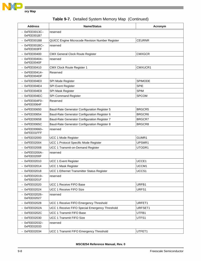
Memory Map
− 0xFEE0013C– 0xFEE001B7
reserved
− 0xFEE001B8 QUICC Engine Microcode Revision Number Register CEURNR
− 0xFEE001BC– 0xFEE003FF
reserved
− 0xFEE00400 CMX General Clock Route Register CMXGCR
− 0xFEE00404– 0xFEE0040F
reserved
− 0xFEE00410 CMX Clock Route Register 1 CMXUCR1
− 0xFEE00414– 0xFEE004DF
Reserved
− 0xFEE004E0 SPI Mode Register SPIMODE
− 0xFEE004E4 SPI Event Register SPIE
− 0xFEE004E8 SPI Mask Register SPIM
− 0xFEE004EC SPI Command Register SPCOM
− 0xFEE004F0– 0xFEE0064F
Reserved
− 0xFEE00650 Baud-Rate Generator Configuration Register 5 BRGCR5
− 0xFEE00654 Baud-Rate Generator Configuration Register 6 BRGCR6
− 0xFEE00658 Baud-Rate Generator Configuration Register 7 BRGCR7
− 0xFEE0065C Baud-Rate Generator Configuration Register 8 BRGCR8
− 0xFEE00660– 0xFEE01FFF
reserved
− 0xFEE02000 UCC 1 Mode Register GUMR1
− 0xFEE02004 UCC 1 Protocol Specific Mode Register UPSMR1
− 0xFEE02008 UCC 1 Transmit-on-Demand Register UTODR1
− 0xFEE0200A– 0xFEE0200F
reserved
− 0xFEE02010 UCC 1 Event Register UCCE1
− 0xFEE02014 UCC 1 Mask Register UCCM1
− 0xFEE02018 UCC 1 Ethernet Transmitter Status Register UCCS1
− 0xFEE02019– 0xFEE0201F
reserved
− 0xFEE02020 UCC 1 Receive FIFO Base URFB1
− 0xFEE02024 UCC 1 Receive FIFO Size URFS1
− 0xFEE02026– 0xFEE02027
reserved
− 0xFEE02028 UCC 1 Receive FIFO Emergency Threshold URFET1
− 0xFEE0202A UCC 1 Receive FIFO Special Emergency Threshold URFSET1
− 0xFEE0202C UCC 1 Transmit FIFO Base UTFB1
− 0xFEE02030 UCC 1 Transmit FIFO Size UTFS1
− 0xFEE02032– 0xFEE02033
reserved
− 0xFEE02034 UCC 1 Transmit FIFO Emergency Threshold UTFET1
Table 9-7. Detailed System Memory Map (Continued)
Address Name/Status Acronym
MSC8254 Reference Manual, Rev. 0
9-8 Freescale Semiconductor

Detailed System Memory Map
− 0xFEE02036– 0xFEE02037
reserved
− 0xFEE02038 UCC 1 Transmit FIFO Transmit Threshold UTFTT1
− 0xFEE0203A– 0xFEE0203B
reserved
− 0xFEE0203C UCC 1 Transmit Polling Timer UFPT1
− 0xFEE0203E– 0xFEE0203F
reserved
− 0xFEE02040 UCC 1 Retry Counter Register URTRY1
− 0xFEE02044– 0xFEE0208F
reserved
− 0xFEE02090 UCC 1 General Extended Mode Register GUEMR1
− 0xFEE02094– 0xFEE020FF
reserved
− 0xFEE02100 Ethernet 1 MAC Configuration Register 1 E1MACCFG1
− 0xFEE02104 Ethernet 1 MAC Configuration Register 2 E1MACCFG2
− 0xFEE02108 Ethernet 1 Interframe Gap Register E1IPGFG
− 0xFEE0210A– 0xFEE0210B
reserved
− 0xFEE0210C Ethernet 1 Half-Duplex Register HAFDUP1
− 0xFEE02110– 0xFEE0211F
reserved
− 0xFEE02120 Ethernet 1 MII Management Configuration Register MIIMCFG1
− 0xFEE02124 Ethernet 1 MII Management Command Register MIIMCOM1
− 0xFEE02128 Ethernet 1 MII Management Address Register MIIMADD1
− 0xFEE0212C Ethernet 1 MII Management Control Register MIIMCON1
− 0xFEE02130 Ethernet 1 MII Management Status Register MIIMSTAT1
− 0xFEE02134 Ethernet 1 MII Management Indication Register MIIMIND1
− 0xFEE0213C Ethernet 1 Interface Status Register IFSTAT1
− 0xFEE02140 Ethernet 1 Station Address Pt. 1 Register E1MACSTNADDDR1
− 0xFEE02144 Ethernet 1 Station Address Pt. 2 Register E1MACSTNADDR2
− 0xFEE02148– 0xFEE0214F
reserved
− 0xFEE02150 Ethernet 1 MAC Parameter Register UEMPR1
− 0xFEE02154 Ethernet 1 Ten-Bit Interface Physical Address Register UTBIPAR1
− 0xFEE02158 Ethernet 1 Statistical Control Register UESCR1
− 0xFEE0215C– 0xFEE0217F
reserved
− 0xFEE02180 Ethernet 1 Tx 64-byte Frames E1TX64
− 0xFEE02184 Ethernet 1 Tx 65- to 127-byte Frames E1TX127
− 0xFEE02188 Ethernet 1 Tx 128- to 255-byte Frames E1TX255
− 0xFEE0218C Ethernet 1 Rx 64-byte Frames E1RX64
− 0xFEE02190 Ethernet 1 Rx 65- to 127-byte Frames E1RX127
− 0xFEE02194 Ethernet 1 Rx 128- to 255-byte Frames E1RX255
Table 9-7. Detailed System Memory Map (Continued)
Address Name/Status Acronym
MSC8254 Reference Manual, Rev. 0
Freescale Semiconductor 9-9

Memory Map
− 0xFEE02198 Ethernet 1 Octet Transmitted OK E1TXOK
− 0xFEE0219C Ethernet 1 Tx Pause Frames E1TXCF
− 0xFEE021A0 Ethernet 1 Multicast Frame Transmitted OK E1TMCA
− 0xFEE021A4 Ethernet 1 Broadcast Frames Transmitted OK E1TBCA
− 0xFEE021A8 Ethernet 1 Number of Frames Received OK E1RXFOK
− 0xFEE021AC Ethernet 1 Rx Octets OK E1RBYT
− 0xFEE021B0 Ethernet 1 Rx Octets E1RXBOK
− 0xFEE021B4 Ethernet 1 Multicast Frame Received OK E1RMCA
− 0xFEE021B8 Ethernet 1 Broadcast Frames Received OK E1RBCA
− 0xFEE021BC Ethernet 1 Statistic Counters Carry Register E1SCAR
− 0xFEE021C0 Ethernet 1 Statistic Counters Carry Mask Register E1SCAM
− 0xFEE021C4– 0xFEE021FF
reserved
− 0xFEE02200 UCC 3 General Mode Register GUMR3
− 0xFEE02204 UCC 3 Protocol Specific Mode Register UPSMR3
− 0xFEE02208 UCC 3 Transmit-on-Demand Register UTODR3
− 0xFEE0220A– 0xFEE0220F
reserved
− 0xFEE02210 UCC 3 Event Register UCCE3
− 0xFEE02214 UCC 3 Mask Registers UCCM3
− 0xFEE02218 UCC 3 Status Register UCCS3
− 0xFEE02219– 0xFEE0221F
reserved
− 0xFEE02220 UCC 3 Receive FIFO Base URFB3
− 0xFEE02224 UCC 3 Receive FIFO Size URFS3
− 0xFEE02226– 0xFEE02227
reserved
− 0xFEE02228 UCC 3 Receive FIFO Emergency Threshold URFET3
− 0xFEE0222A UCC 3 Receive FIFO Special Emergency Threshold URFSET3
− 0xFEE0222C UCC 3 Transmit FIFO Base UTFB3
− 0xFEE02230 UCC 3 Transmit FIFO Size UTFS3
− 0xFEE02232– 0xFEE02233
reserved
− 0xFEE02234 UCC 3 Transmit FIFO Emergency Threshold UTFET3
− 0xFEE02236– 0xFEE02237
reserved
− 0xFEE02238 UCC 3 Transmit FIFO Transmit Threshold UTFTT3
− 0xFEE0223A– 0xFEE0223B
reserved
− 0xFEE0223C UCC 3 Transmit Polling Timer UFPT3
− 0xFEE0223E– 0xFEE0223F
reserved
− 0xFEE02240 UCC 3 Retry Counter URTRY3
Table 9-7. Detailed System Memory Map (Continued)
Address Name/Status Acronym
MSC8254 Reference Manual, Rev. 0
9-10 Freescale Semiconductor

Detailed System Memory Map
− 0xFEE02244– 0xFEE0228F
reserved
− 0xFEE02290 UCC 3 General Extended Mode Register GUEMR3
− 0xFEE02294– 0xFEE022FF
reserved
− 0xFEE02300 Ethernet 2 MAC Configuration Register 1 E2MACCFG1
− 0xFEE02304 Ethernet 2 MAC Configuration Register 2 E2MACCFG2
− 0xFEE02308 Ethernet 2 Interframe Gap Register E2IPGIFG
− 0xFEE0230A– 0xFEE0230B
reserved
− 0xFEE0230C Ethernet 2 Half-Duplex Register HAFDUP3
− 0xFEE02310– 0xFEE0231F
reserved
− 0xFEE02320 Ethernet 2 MII Management Configuration Register MIIMCFG3
− 0xFEE02324 Ethernet 2 MII Management Command Register MIIMCOM3
− 0xFEE02328 Ethernet 2 MII Management Address Register MIIMADD3
− 0xFEE0232C Ethernet 2 MII Management Control Register MIIMCON3
− 0xFEE02330 Ethernet 2 MII Management Status Register MIIMSTAT3
− 0xFEE02334 Ethernet 2 MII Management Indication Register MIIMIND3
− 0xFEE02338– 0xFEE0233B
reserved
− 0xFEE0233C Ethernet 2 Interface Status Register IFSTAT3
− 0xFEE02340 Ethernet 2 Station Address Pt. 1 Register E2MACSTNADDR1
− 0xFEE02344 Ethernet 2 Station Address Pt. 2 Register E2MACSTNADDR2
− 0xFEE02348– 0xFEE0234F
reserved
− 0xFEE02350 Ethernet 2 Ethernet MAC Parameter Register UEMPR3
− 0xFEE02354 Ethernet 2 Ten-Bit Interface Physical Address Register TBIPAR3
− 0xFEE02358 Ethernet 2 Ethernet Statistical Control Register UESCR3
− 0xFEE0235C– 0xFEE0237F
reserved
− 0xFEE02380 Ethernet 2 Tx 64-byte Frames E2TX64
− 0xFEE02384 Ethernet 2 Tx 65- to 127-byte Frames E2TX127
− 0xFEE02388 Ethernet 2 Tx 128- to 255-byte Frames E2TX255
− 0xFEE0238C Ethernet 2 Rx 64-byte Frames E2RX64
− 0xFEE02390 Ethernet 2 Rx 65- to 127-byte Frames E2RX127
− 0xFEE02394 Ethernet 2 Rx 128- to 255-byte Frames E2RX255
− 0xFEE02398 Ethernet 2 Octet Transmitted OK E2TXOK
− 0xFEE0239C Ethernet 2 Tx Pause Frames E2TXCF
− 0xFEE023A0 Ethernet 2 Multicast Frame Transmitted OK E2TMCA
− 0xFEE023A4 Ethernet 2 Broadcast Frames Transmitted OK E2TBCA
− 0xFEE023A8 Ethernet 2 Number of Frames Received OK E2RXFOK
− 0xFEE023AC Ethernet 2 Rx Octets OK E2RBYT
Table 9-7. Detailed System Memory Map (Continued)
Address Name/Status Acronym
MSC8254 Reference Manual, Rev. 0
Freescale Semiconductor 9-11

Memory Map
− 0xFEE023B0 Ethernet 2 Rx Octets E2RXBOK
− 0xFEE023B4 Ethernet 2 Multicast Frame Received OK E2RMCA
− 0xFEE023B8 Ethernet 2 Broadcast Frames Received OK E2RBCA
− 0xFEE023BC Ethernet 2 Statistic Counters Carry Register E2SCAR
− 0xFEE023C0 Ethernet 2 Statistic Counters Carry Mask Register E2SCAM
− 0xFEE023C4– 0xFEE021FF
reserved
− 0xFEE04000 Serial DMA Status Register SDSR
− 0xFEE04004 Serial DMA Mode Register SDMR
− 0xFEE04008 Serial DMA Threshold Register SDTR
− 0xFEE0400C– 0xFEE0400F
reserved
− 0xFEE04010 Serial DMA Hysteresis Register SDHY
− 0xFEE04014– 0xFEE04017
reserved
− 0xFEE04018 Serial DMA Address Register SDTA
− 0xFEE0401C– 0xFEE0401F
reserved
− 0xFEE04020 Serial DMA MSNUM Register SDTM
− 0xFEE04024– 0xFEE04037
reserved
− 0xFEE04038 Serial DMA Address Qualify Register SDAQR
− 0xFEE0403C Serial DMA Address Qualify Mask Register SDAQMR
− 0xFEE04040– 0xFEE04043
reserved
− 0xFEE04044 Serial DMA Temporary Buffer Base in Multi-User RAM Value SDEBCR
− 0xFEE04048– 0xFEE07FFF
reserved
− 0xFEE08000– 0xFEE0FFFF
RAM space reserved
− 0xFEE10000– 0xFEE1BFFF
Multi-User RAM
− 0xFEE1C000– 0xFEE3FFFF
reserved
• 0xFEE40000– 0xFEEFFFFF
reserved (for QUICC Engine subsystem)
• 0xFEF00000– 0xFEF17FFF
Boot ROM
• 0xFEF18000– 0xFEFFFFFF
reserved
0xFF000000– 0xFFF0FFFF
DSP core subsystem internal memory space. See the MSC8156 SC3850 DSP Core Subsystem Reference Manual for details.
0xFFF10000– 0xFFFFEFFF
CCSR
• 0xFFF10000– 0xFFF103FF
DMA
Table 9-7. Detailed System Memory Map (Continued)
Address Name/Status Acronym
MSC8254 Reference Manual, Rev. 0
9-12 Freescale Semiconductor
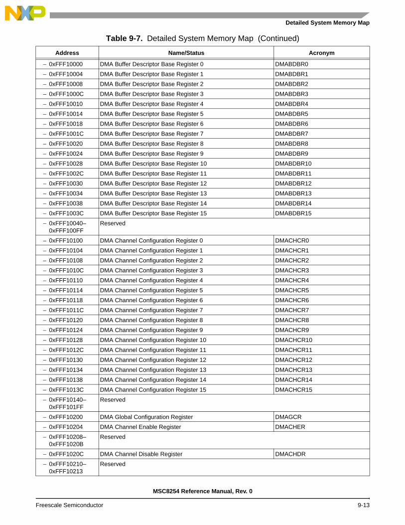
Detailed System Memory Map
− 0xFFF10000 DMA Buffer Descriptor Base Register 0 DMABDBR0
− 0xFFF10004 DMA Buffer Descriptor Base Register 1 DMABDBR1
− 0xFFF10008 DMA Buffer Descriptor Base Register 2 DMABDBR2
− 0xFFF1000C DMA Buffer Descriptor Base Register 3 DMABDBR3
− 0xFFF10010 DMA Buffer Descriptor Base Register 4 DMABDBR4
− 0xFFF10014 DMA Buffer Descriptor Base Register 5 DMABDBR5
− 0xFFF10018 DMA Buffer Descriptor Base Register 6 DMABDBR6
− 0xFFF1001C DMA Buffer Descriptor Base Register 7 DMABDBR7
− 0xFFF10020 DMA Buffer Descriptor Base Register 8 DMABDBR8
− 0xFFF10024 DMA Buffer Descriptor Base Register 9 DMABDBR9
− 0xFFF10028 DMA Buffer Descriptor Base Register 10 DMABDBR10
− 0xFFF1002C DMA Buffer Descriptor Base Register 11 DMABDBR11
− 0xFFF10030 DMA Buffer Descriptor Base Register 12 DMABDBR12
− 0xFFF10034 DMA Buffer Descriptor Base Register 13 DMABDBR13
− 0xFFF10038 DMA Buffer Descriptor Base Register 14 DMABDBR14
− 0xFFF1003C DMA Buffer Descriptor Base Register 15 DMABDBR15
− 0xFFF10040– 0xFFF100FF
Reserved
− 0xFFF10100 DMA Channel Configuration Register 0 DMACHCR0
− 0xFFF10104 DMA Channel Configuration Register 1 DMACHCR1
− 0xFFF10108 DMA Channel Configuration Register 2 DMACHCR2
− 0xFFF1010C DMA Channel Configuration Register 3 DMACHCR3
− 0xFFF10110 DMA Channel Configuration Register 4 DMACHCR4
− 0xFFF10114 DMA Channel Configuration Register 5 DMACHCR5
− 0xFFF10118 DMA Channel Configuration Register 6 DMACHCR6
− 0xFFF1011C DMA Channel Configuration Register 7 DMACHCR7
− 0xFFF10120 DMA Channel Configuration Register 8 DMACHCR8
− 0xFFF10124 DMA Channel Configuration Register 9 DMACHCR9
− 0xFFF10128 DMA Channel Configuration Register 10 DMACHCR10
− 0xFFF1012C DMA Channel Configuration Register 11 DMACHCR11
− 0xFFF10130 DMA Channel Configuration Register 12 DMACHCR12
− 0xFFF10134 DMA Channel Configuration Register 13 DMACHCR13
− 0xFFF10138 DMA Channel Configuration Register 14 DMACHCR14
− 0xFFF1013C DMA Channel Configuration Register 15 DMACHCR15
− 0xFFF10140– 0xFFF101FF
Reserved
− 0xFFF10200 DMA Global Configuration Register DMAGCR
− 0xFFF10204 DMA Channel Enable Register DMACHER
− 0xFFF10208– 0xFFF1020B
Reserved
− 0xFFF1020C DMA Channel Disable Register DMACHDR
− 0xFFF10210– 0xFFF10213
Reserved
Table 9-7. Detailed System Memory Map (Continued)
Address Name/Status Acronym
MSC8254 Reference Manual, Rev. 0
Freescale Semiconductor 9-13

Memory Map
− 0xFFF10214 DMA Channel Freeze Register DMACHFR
− 0xFFF10218– 0xFFF10223
Reserved
− 0xFFF10224 DMA Channel Defrost Register DMACHDFR
− 0xFFF10228– 0xFFF10233
Reserved
− 0xFFF10234 DMA Time-To-Deadline Register 0 DMAEDFTDL0
− 0xFFF10238 DMA Time-To-Deadline Register 1 DMAEDFTDL1
− 0xFFF1023C DMA Time-To-Deadline Register 2 DMAEDFTDL2
− 0xFFF10240 DMA Time-To-Deadline Register 3 DMAEDFTDL3
− 0xFFF10244 DMA Time-To-Deadline Register 4 DMAEDFTDL4
− 0xFFF10248 DMA Time-To-Deadline Register 5 DMAEDFTDL5
− 0xFFF1024C DMA Time-To-Deadline Register 6 DMAEDFTDL6
− 0xFFF10250 DMA Time-To-Deadline Register 7 DMAEDFTDL7
− 0xFFF10254 DMA Time-To-Deadline Register 8 DMAEDFTDL8
− 0xFFF10258 DMA Time-To-Deadline Register 9 DMAEDFTDL9
− 0xFFF1025C DMA Time-To-Deadline Register 10 DMAEDFTDL10
− 0xFFF10260 DMA Time-To-Deadline Register 11 DMAEDFTDL11
− 0xFFF10264 DMA Time-To-Deadline Register 12 DMAEDFTDL12
− 0xFFF10268 DMA Time-To-Deadline Register 13 DMAEDFTDL13
− 0xFFF1026C DMA Time-To-Deadline Register 14 DMAEDFTDL14
− 0xFFF10270 DMA Time-To-Deadline Register 15 DMAEDFTDL15
− 0xFFF10274– 0xFFF10333
Reserved
− 0xFFF10334 DMA EDF Control Register DMAEDFCTRL
− 0xFFF10338 DMA EDF Mask Register DMAEDFMR
− 0xFFF1033C– 0xFFF1033f
Reserved
− 0xFFF10340 DMA EDF Mask Update Register DMAEDFMUR
− 0xFFF10344 DMA EDF Status Register DMAEDFSTR
− 0xFFF10348– 0xFFF1034B
Reserved
− 0xFFF1034C DMA Mask Register DMAMR
− 0xFFF10350– 0xFFF1035B
Reserved
− 0xFFF1035C DMA Mask Update Register DMAMUR
− 0xFFF10360 DMA Status Register DMASTR
− 0xFFF10364– 0xFFF1036F
Reserved
− 0xFFF10370 DMA Error Register DMAERR
− 0xFFF10374 DMA Debug Event Status Register DMADESR
− 0xFFF10378 DMA Local Profiling Configuration Register DMALPCR
− 0xFFF1037C DMA Round Robin Priority Group Update Register DMARRPGUR
Table 9-7. Detailed System Memory Map (Continued)
Address Name/Status Acronym
MSC8254 Reference Manual, Rev. 0
9-14 Freescale Semiconductor

Detailed System Memory Map
− 0xFFF10380 DMA Channel Active Status Register DMACHASTR
− 0xFFF10384– 0xFFF10387
Reserved
− 0xFFF10388 DMA Channel Freeze Status Register DMACHFSTR
− 0xFFF1038C– 0xFFF103FF
reserved
• 0xFFF10400– 0xFFF17FFF
reserved
• 0xFFF18000– 0xFFF18FFF
CLASS
− 0xFFF18000– 0xFFF1801F
Reserved
− 0xFFF18020 CLASS MBus Target Configuration Register 1 C0MTCR1
− 0xFFF18024– 0xFFF1803F
Reserved
− 0xFFF18040 Reserved
− 0xFFF18044– 0xFFF1805F
Reserved
− 0xFFF18060 CLASS MBus Target Configuration Register 3 C0MTCR3
− 0xFFF18064– 0xFFF1807F
Reserved
− 0xFFF18080 CLASS MBus Target Configuration Register 4 C0MTCR4
− 0xFFF18084– 0xFFF1808F
Reserved
− 0xFFF18090 CLASS MBus Target Configuration Register 5 C0MTCR5
− 0xFFF18094– 0xFFF1809F
Reserved
− 0xFFF180A0 CLASS MBus Target Configuration Register 6 C0MTCR6
− 0xFFF180A4– 0xFFF180AF
Reserved
− 0xFFF180B0 CLASS MBus Target Configuration Register 7 C0MTCR7
− 0xFFF180B4– 0xFFF187FF
Reserved
− 0xFFF18800 CLASS Priority Mapping Register 0 C0PMR0
− 0xFFF18804 CLASS Priority Mapping Register 1 C0PMR1
− 0xFFF18808 CLASS Priority Mapping Register 2 C0PMR2
− 0xFFF1880C CLASS Priority Mapping Register 3 C0PMR3
− 0xFFF18810 Reserved
− 0xFFF18814 Reserved
− 0xFFF18818 CLASS Priority Mapping Register 6 C0PMR6
− 0xFFF1881C CLASS Priority Mapping Register 7 C0PMR7
− 0xFFF18820 CLASS Priority Mapping Register 8 C0PMR8
− 0xFFF18824 CLASS Priority Mapping Register 9 C0PMR9
− 0xFFF18828 CLASS Priority Mapping Register 10 C0PMR10
− 0xFFF1882C CLASS Priority Mapping Register 11 C0PMR11
Table 9-7. Detailed System Memory Map (Continued)
Address Name/Status Acronym
MSC8254 Reference Manual, Rev. 0
Freescale Semiconductor 9-15

Memory Map
− 0xFFF18830– 0xFFF1883F
reserved
− 0xFFF18840 CLASS Priority Auto Upgrade Value Register 0 C0PAVR0
− 0xFFF18844 CLASS Priority Auto Upgrade Value Register 1 C0PAVR1
− 0xFFF18848 CLASS Priority Auto Upgrade Value Register 2 C0PAVR2
− 0xFFF1884C CLASS Priority Auto Upgrade Value Register 3 C0PAVR3
− 0xFFF18850 Reserved
− 0xFFF18854 Reserved
− 0xFFF18858 CLASS Priority Auto Upgrade Value Register 6 C0PAVR6
− 0xFFF1885C CLASS Priority Auto Upgrade Value Register 7 C0PAVR7
− 0xFFF18860 CLASS Priority Auto Upgrade Value Register 8 C0PAVR8
− 0xFFF18864 CLASS Priority Auto Upgrade Value Register 9 C0PAVR9
− 0xFFF18868 CLASS Priority Auto Upgrade Value Register 10 C0PAVR10
− 0xFFF1886C CLASS Priority Auto Upgrade Value Register 11 C0PAVR11
− 0xFFF18870– 0xFFF1887F
reserved
− 0xFFF18880 CLASS Priority Auto Upgrade Control Register 0 C0PACR0
− 0xFFF18884 CLASS Priority Auto Upgrade Control Register 1 C0PACR1
− 0xFFF18888 CLASS Priority Auto Upgrade Control Register 2 C0PACR2
− 0xFFF1888C CLASS Priority Auto Upgrade Control Register 3 C0PACR3
− 0xFFF18890 Reserved
− 0xFFF18894 Reserved
− 0xFFF18898 CLASS Priority Auto Upgrade Control Register 6 C0PACR6
− 0xFFF1889C CLASS Priority Auto Upgrade Control Register 7 C0PACR7
− 0xFFF188A0 CLASS Priority Auto Upgrade Control Register 8 C0PACR8
− 0xFFF188A4 CLASS Priority Auto Upgrade Control Register 9 C0PACR9
− 0xFFF188A8 CLASS Priority Auto Upgrade Control Register 10 C0PACR10
− 0xFFF188AC CLASS Priority Auto Upgrade Control Register 11 C0PACR11
− 0xFFF188B0– 0xFFF1897F
reserved
− 0xFFF18980 CLASS Error Address Register 0 C0EAR0
− 0xFFF18984 CLASS Error Address Register 1 C0EAR1
− 0xFFF18988 CLASS Error Address Register 2 C0EAR2
− 0xFFF1898C CLASS Error Address Register 3 C0EAR3
− 0xFFF18990 Reserved
− 0xFFF18994 Reserved
− 0xFFF18998 CLASS Error Address Register 6 C0EAR6
− 0xFFF1899C CLASS Error Address Register 7 C0EAR7
− 0xFFF189A0 CLASS Error Address Register 8 C0EAR8
− 0xFFF189A4 CLASS Error Address Register 9 C0EAR9
− 0xFFF189A8 CLASS Error Address Register 10 C0EAR10
− 0xFFF189AC CLASS Error Address Register 11 C0EAR11
Table 9-7. Detailed System Memory Map (Continued)
Address Name/Status Acronym
MSC8254 Reference Manual, Rev. 0
9-16 Freescale Semiconductor

Detailed System Memory Map
− 0xFFF189B0– 0xFFF189BF
reserved
− 0xFFF189C0 CLASS Error Extended Address Register 0 C0EEAR0
− 0xFFF189C4 CLASS Error Extended Address Register 1 C0EEAR1
− 0xFFF189C8 CLASS Error Extended Address Register 2 C0EEAR2
− 0xFFF189CC CLASS Error Extended Address Register 3 C0EEAR3
− 0xFFF189D0 Reserved
− 0xFFF189D4 Reserved
− 0xFFF189D8 CLASS Error Extended Address Register 6 C0EEAR6
− 0xFFF189DC CLASS Error Extended Address Register 7 C0EEAR7
− 0xFFF189E0 CLASS Error Extended Address Register 8 C0EEAR8
− 0xFFF189E4 CLASS Error Extended Address Register 9 C0EEAR9
− 0xFFF189E8 CLASS Error Extended Address Register 10 C0EEAR10
− 0xFFF189EC CLASS Error Extended Address Register 11 C0EEAR11
− 0xFFF189F0– 0xFFF189FF
reserved
− 0xFFF18A00 CLASS Initiator Profiling Configuration Register 0 C0IPCR0
− 0xFFF18A04 CLASS Initiator Profiling Configuration Register 1 C0IPCR1
− 0xFFF18A08 CLASS Initiator Profiling Configuration Register 2 C0IPCR2
− 0xFFF18A0C CLASS Initiator Profiling Configuration Register 3 C0IPCR3
− 0xFFF18A10 Reserved
− 0xFFF18A14 Reserved
− 0xFFF18A18 CLASS Initiator Profiling Configuration Register 6 C0IPCR6
− 0xFFF18A1C CLASS Initiator Profiling Configuration Register 7 C0IPCR7
− 0xFFF18A20 CLASS Initiator Profiling Configuration Register 8 C0IPCR8
− 0xFFF18A24 CLASS Initiator Profiling Configuration Register 9 C0IPCR9
− 0xFFF18A28 CLASS Initiator Profiling Configuration Register 10 C0IPCR10
− 0xFFF18A2C CLASS Initiator Profiling Configuration Register 11 C0IPCR11
− 0xFFF18A30– 0xFFF18A3F
reserved
− 0xFFF18A40 CLASS Initiator Watch Point Control Register 0 C0IWPCR0
− 0xFFF18A44 CLASS Initiator Watch Point Control Register 1 C0IWPCR1
− 0xFFF18A48 CLASS Initiator Watch Point Control Register 2 C0IWPCR2
− 0xFFF18A4C CLASS Initiator Watch Point Control Register 3 C0IWPCR3
− 0xFFF18A50 Reserved
− 0xFFF18A54 Reserved
− 0xFFF18A58 CLASS Initiator Watch Point Control Register 6 C0IWPCR6
− 0xFFF18A5C CLASS Initiator Watch Point Control Register 7 C0IWPCR7
− 0xFFF18A60 CLASS Initiator Watch Point Control Register 8 C0IWPCR8
− 0xFFF18A64 CLASS Initiator Watch Point Control Register 9 C0IWPCR9
− 0xFFF18A68 CLASS Initiator Watch Point Control Register 10 C0IWPCR10
− 0xFFF18A6C CLASS Initiator Watch Point Control Register 11 C0IWPCR11
Table 9-7. Detailed System Memory Map (Continued)
Address Name/Status Acronym
MSC8254 Reference Manual, Rev. 0
Freescale Semiconductor 9-17

Memory Map
− 0xFFF18A70– 0xFFF18A7F
reserved
− 0xFFF18A80 CLASS Arbitration Weight Register 0 C0AWR0
− 0xFFF18A84 CLASS Arbitration Weight Register 1 C0AWR1
− 0xFFF18A88 CLASS Arbitration Weight Register 2 C0AWR2
− 0xFFF18A8C CLASS Arbitration Weight Register 3 C0AWR3
− 0xFFF18A90 Reserved
− 0xFFF18A94 Reserved
− 0xFFF18A98 CLASS Arbitration Weight Register 6 C0AWR6
− 0xFFF18A9C CLASS Arbitration Weight Register 7 C0AWR7
− 0xFFF18AA0 CLASS Arbitration Weight Register 8 C0AWR8
− 0xFFF18AA4 CLASS Arbitration Weight Register 9 C0AWR9
− 0xFFF18AA8 CLASS Arbitration Weight Register 10 C0AWR10
− 0xFFF18AAC CLASS Arbitration Weight Register 11 C0AWR11
− 0xFFF18AB0– 0xFFF18C13
reserved
− 0xFFF18C14 CLASS Start Address Decoder 5 C0SAD5
− 0xFFF18C18 CLASS Start Address Decoder 6 C0SAD6
− 0xFFF18C1C– 0xFFF18C53
reserved
− 0xFFF18C54 CLASS End Address Decoder 5 C0EAD5
− 0xFFF18C58 CLASS End Address Decoder 6 C0EAD6
− 0xFFF18C5C– 0xFFF18C93
reserved
− 0xFFF18C94 CLASS Attributes Decoder 5 C0ATD5
− 0xFFF18C98 CLASS Attributes Decoder 6 C0ATD6
− 0xFFF18C9C– 0xFFF18D7F
reserved
− 0xFFF18D80 CLASS IRQ Status Register C0ISR
− 0xFFF18D84– 0xFFF18DBF
Reserved
− 0xFFF18DC0 CLASS IRQ Enable Register C0IER
− 0xFFF18DC4– 0xFFF18DFF
Reserved
− 0xFFF18E00 CLASS Target Profiling Configuration Register C0TPCR
− 0xFFF18E04 CLASS Profiling Control Register C0PCR
− 0xFFF18E08 CLASS Watch Point Control Register C0WPCR
− 0xFFF18E0C CLASS Watch Point Access Configuration Register C0WPACR
− 0xFFF18E10 CLASS Watch Point Extended Access Configuration Register C0WPEACR
− 0xFFF18E14 CLASS Watch Point Address Mask Register C0WPAMR
− 0xFFF18E18 CLASS Profiling Time-Out Register C0PTOR
− 0xFFF18E1C CLASS Target Watch Point Control Register C0TWPCR
− 0xFFF18E20 CLASS Profiling IRQ Status Register C0PISR
Table 9-7. Detailed System Memory Map (Continued)
Address Name/Status Acronym
MSC8254 Reference Manual, Rev. 0
9-18 Freescale Semiconductor

Detailed System Memory Map
− 0xFFF18E24 CLASS Profiling IRQ Enable Register C0PIER
− 0xFFF18E28- 0xFFF18E3F
Reserved
− 0xFFF18E40 CLASS Profiling Reference Counter Register C0PRCR
− 0xFFF18E44 CLASS Profiling General Counter Register 0 C0PGCR0
− 0xFFF18E48 CLASS Profiling General Counter Register 1 C0PGCR1
− 0xFFF18E4C CLASS Profiling General Counter Register 2 C0PGCR2
− 0xFFF18E50 CLASS Profiling General Counter Register 3 C0PGCR3
− 0xFFF18E54– 0xFFF18FBF
Reserved
− 0xFFF18FC0 CLASS Arbitration Control Register C0ACR
− 0xFFF18FC4– 0xFFF18FFF
Reserved
• 0xFFF19000– 0xFFF1FFFF
reserved
• 0xFFF20000– 0xFFF21FFF
DDR Controller 1
− 0xFFF20000 Chip Select 0 Bounds M1CS0_BNDS
− 0xFFF20004– 0xFFF20007
reserved
− 0xFFF20008 Chip Select 1 Bounds M1CS1_BNDS
− 0xFFF2000C– 0xFFF2007F
reserved
− 0xFFF20080 Chip Select 0 Configuration M1CS0_CONFIG
− 0xFFF20084 Chip Select 1 Configuration M1CS1_CONFIG
− 0xFFF20088– 0xFFF200BF
reserved
− 0xFFF200C0 Chip Select 0 Configuration 2 M1CS0_CONFIG_2
− 0xFFF200C4 Chip Select 1 Configuration 2 M1CS1_CONFIG_2
− 0xFFF200C8– 0xFFF200FF
reserved
− 0xFFF20100 DDR SDRAM Timing Configuration 3 M1TIMING_CFG_3
− 0xFFF20104 DDR SDRAM Timing Configuration 0 M1TIMING_CFG_0
− 0xFFF20108 DDR SDRAM Timing Configuration 1 M1TIMING_CFG_1
− 0xFFF2010C DDR SCRAM Timing Configuration 2 M1TIMING_CFG_2
− 0xFFF20110 DDR SDRAM Control Configuration M1DDR_SDRAM_CFG
− 0xFFF20114 DDR SDRAM Control Configuration 2 M1DDR_SDRAM_CFG_2
− 0xFFF20118 DDR SDRAM Mode Configuration M1DDR_SDRAM_MODE
− 0xFFF2011C DDR SDRAM Mode Configuration 2 M1DDR_SDRAM_MODE_2
− 0xFFF20120 DDR SDRAM Mode Control M1DDR_SCRAM_MD_CNTL
− 0xFFF20124 DDR SDRAM Interval Configuration M1DDR_SDRAM_INTERVAL
− 0xFFF20128 DDR SDRAM Data Initialization M1DDR_DATA_INIT
− 0xFFF2012C– 0xFFF2012F
reserved
Table 9-7. Detailed System Memory Map (Continued)
Address Name/Status Acronym
MSC8254 Reference Manual, Rev. 0
Freescale Semiconductor 9-19

Memory Map
− 0xFFF20130 DDR SDRAM Clock Control M1DDR_SDRAM_CLK_CNT
− 0xFFF20134– 0xFFF20147
reserved
− 0xFFF20148 DDR SDRAM Initialization Address M1DDR_INIT_ADDRESS
− 0xFFF2014C DDR Initialization Enable Extended Address M1DDR_INIT_ENXT_ADDR
− 0xFFF20150– 0xFFF2015F
reserved
− 0xFFF20160 DDR SDRAM Timing Configuration 4 M1TIMING_CFG_4
− 0xFFF20164 DDR SDRAM Timing Configuration 5 M1TIMING_CFG_5
− 0xFFF20168– 0xFFF2016F
reserved
− 0xFFF20170 DDR ZQ Calibration Control M1DDR_ZQ_CNTL
− 0xFFF20174 DDR Write Leveling Control M1DDR_WRLVL_CNTL
− 0xFFF22178 DDR Pre-Drive Conditioning Control M1DDR_PD_CNTL
− 0xFFF2017C DDR Self Refresh Counter M1DDR_SR_CNTR
− 0xFFF20180 DDR SDRAM Register Control Words 1 M1DDR_SDRAM_RCW_1
− 0xFFF20184 DDR SDRAM Register Control Words 2 M1DDR_SDRAM_RCW_2
− 0xFFF20188– 0xFFF2018F
reserved
− 0xFFF20190 DDR Write Leveling Control 2 M1DDR_WRLVL_CNTL_2
− 0xFFF20194 DDR Write Leveling Control 3 M1DDR_WRLVL_CNTL_3
− 0xFFF20198– 0xFFF20B1F
reserved
− 0xFFF20B20 DDR Debug Status Register 1 M1DDRDSR_1
− 0xFFF20B24 DDR Debug Status Register 2 M1DDRDSR_2
− 0xFFF20B28 DDR Control Driver Register 1 M1DDRCDR_1
− 0xFFF20B2C DDR Control Driver Register 2 M1DDRCDR_2
− 0xFFF20B30– 0xFFF20BF7
reserved
− 0xFFF20BF8 DDR IP Block Revision 1 M1DDR_IP_REV1
− 0xFFF20BFC DDR IP Block Revision 2 M1DDR_IP_REV2
− 0xFFF20C00– 0xFFF20DFF
reserved
− 0xFFF20E00 Memory Data Path Error Injection Mask High M1DDR_ERR_INJECT_HI
− 0xFFF20E04 Memory Data Path Error Injection Mask Low M1DDR_ERR_INJECT_LO
− 0xFFF20E08 Memory Data Path Error Injection Mask ECC M1DDR_ERR_INJECT
− 0xFFF20E0C– 0xFFF20E1F
reserved
− 0xFFF20E20 Memory Data Path Read Capture High M1CAPTURE_DATA_HI
− 0xFFF20E24 Memory Data Path Read Capture Low M1CAPTURE-DATA_LO
− 0xFFF20E28 Memory Data Path Read Capture ECC M1CAPTURE_ECC
− 0xFFF20E2C– 0xFFF20E3F
reserved
− 0xFFF20E40 Memory Error Detect M1ERR_DETECT
Table 9-7. Detailed System Memory Map (Continued)
Address Name/Status Acronym
MSC8254 Reference Manual, Rev. 0
9-20 Freescale Semiconductor

Detailed System Memory Map
− 0xFFF20E44 Memory Error Disable M1ERR_DISABLE
− 0xFFF20E48 Memory Error Interrupt Enable M1ERR_INT_EN
− 0xFFF20E4C Memory Error Attributes Capture M1CAPTURE_ATTRIBUTES
− 0xFFF20E50 Memory Error Address Capture M1CAPTURE_ADDRESS
− 0xFFF20E54– 0xFFF20E57
reserved
− 0xFFF20E58 Single-Bit ECC Memory Error Management M1ERR_SBE
− 0xFFF20E5C– 0xFFF20F03
reserved
− 0xFFF20F04 Debug Register 2 M1DEBUG_2
− 0xFFF20F08– 0xFFF21FFF
reserved
• 0xFFF22000– 0xFFF23FFF
DDR Controller 2
− 0xFFF22000 Chip Select 0 Memory Bounds M2CS0_BNDS
− 0xFFF22004– 0xFFF22007
reserved
− 0xFFF22008 Chip Select 1 Memory Bounds M2CS1_BNDS
− 0xFFF2200C– 0xFFF2207F
reserved
− 0xFFF22080 Chip Select 0 Configuration M2CS0_CONFIG
− 0xFFF22084 Chip Select 1 Configuration M2CS1_CONFIG
− 0xFFF22088– 0xFFF220BF
reserved
− 0xFFF220C0 Chip Select 0 Configuration 2 M2CS0_CONFIG_2
− 0xFFF220C4 Chip Select 1 Configuration 2 M2CS1_CONFIG_2
− 0xFFF220C8– 0xFFF220FF
reserved
− 0xFFF22100 DDR SDRAM Timing Configuration 3 M2TIMING_CFG_3
− 0xFFF22104 DDR SDRAM Timing Configuration 0 M2TIMING_CFG_0
− 0xFFF22108 DDR SDRAM Timing Configuration 1 M2TIMING_CFG_1
− 0xFFF2210C DDR SCRAM Timing Configuration 2 M2TIMING_CFG_2
− 0xFFF22110 DDR SDRAM Control Configuration M2DDR_SDRAM_CFG
− 0xFFF22114 DDR SDRAM Control Configuration 2 M2DDR_SDRAM_CFG_2
− 0xFFF22118 DDR SDRAM Mode Configuration M2DDR_SDRAM_MODE
− 0xFFF2211C DDR SDRAM Mode Configuration 2 M2DDR_SDRAM_MODE_2
− 0xFFF22120 DDR SDRAM Mode Control M2DDR_SCRAM_MD_CNTL
− 0xFFF22124 DDR SDRAM Interval Configuration M2DDR_SDRAM_INTERVAL
− 0xFFF22128 DDR SDRAM Data Initialization M2DDR_DATA_INIT
− 0xFFF2212C– 0xFFF2212F
reserved
− 0xFFF22130 DDR SDRAM Clock Control M2DDR_SDRAM_CLK_CNT
− 0xFFF22134– 0xFFF22147
reserved
Table 9-7. Detailed System Memory Map (Continued)
Address Name/Status Acronym
MSC8254 Reference Manual, Rev. 0
Freescale Semiconductor 9-21

Memory Map
− 0xFFF22148 DDR SDRAM Initialization Address M2DDR_INIT_ADDRESS
− 0xFFF2214C DDR Initialization Enable Extended Address M2DDR_INIT_ENXT_ADDR
− 0xFFF22150– 0xFFF2215F
reserved
− 0xFFF22160 DDR SDRAM Timing Configuration 4 M2TIMING_CFG_4
− 0xFFF22164 DDR SDRAM Timing Configuration 5 M2TIMING_CFG_5
− 0xFFF22168– 0xFFF2216F
reserved
− 0xFFF22170 DDR ZQ Calibration Control M2DDR_ZQ_CNTL
− 0xFFF22174 DDR Write Leveling Control M2DDR_WRLVL_CNTL
− 0xFFF22178 DDR Pre-Drive Conditioning Control M2DDR_PD_CNTL
− 0xFFF2217C DDR Self Refresh Counter M2DDR_SR_CNTR
− 0xFFF22180 DDR SDRAM Register Control Words 1 M2DDR_SDRAM_RCW_1
− 0xFFF22184 DDR SDRAM Register Control Words 2 M2DDR_SDRAM_RCW_2
− 0xFFF22188– 0xFFF2218F
reserved
− 0xFFF22190 DDR Write Leveling Control 2 M2DDR_WRLVL_CNTL_2
− 0xFFF22194 DDR Write Leveling Control 3 M2DDR_WRLVL_CNTL_3
− 0xFFF22198– 0xFFF22B1F
reserved
− 0xFFF22B20 DDR Debug Status Register 1 M2DDRDSR_1
− 0xFFF22B24 DDR Debug Status Register 2 M2DDRDSR_2
− 0xFFF22B28 DDR Control Driver Register 1 M2DDRCDR_1
− 0xFFF22B2C DDR Control Driver Register 2 M2DDRCDR_2
− 0xFFF22B30– 0xFFF22BF7
reserved
− 0xFFF22BF8 DDR IP Block Revision 1 M2DDR_IP_REV1
− 0xFFF22BFC DDR IP Block Revision 2 M2DDR_IP_REV2
− 0xFFF22C00– 0xFFF22DFF
reserved
− 0xFFF22E00 Memory Data Path Error Injection Mask High M2DDR_ERR_INJECT_HI
− 0xFFF22E04 Memory Data Path Error Injection Mask Low M2DDR_ERR_INJECT_LO
− 0xFFF22E08 Memory Data Path Error Injection Mask ECC M2DDR_ERR_INJECT
− 0xFFF22E0C– 0xFFF22E1F
reserved
− 0xFFF22E20 Memory Data Path Read Capture High M2CAPTURE_DATA_HI
− 0xFFF22E24 Memory Data Path Read Capture Low M2CAPTURE-DATA_LO
− 0xFFF22E28 Memory Data Path Read Capture ECC M2CAPTURE_ECC
− 0xFFF22E2C– 0xFFF22E3F
reserved
− 0xFFF22E40 Memory Error Detect M2ERR_DETECT
− 0xFFF22E44 Memory Error Disable M2ERR_DISABLE
− 0xFFF22E48 Memory Error Interrupt Enable M2ERR_INT_EN
− 0xFFF22E4C Memory Error Attributes Capture M2CAPTURE_ATTRIBUTES
Table 9-7. Detailed System Memory Map (Continued)
Address Name/Status Acronym
MSC8254 Reference Manual, Rev. 0
9-22 Freescale Semiconductor

Detailed System Memory Map
− 0xFFF22E50 Memory Error Address Capture M2CAPTURE_ADDRESS
− 0xFFF22E54– 0xFFF22E57
reserved
− 0xFFF22E58 Single-Bit ECC Memory Error Management M2ERR_SBE
− 0xFFF22E5C– 0xFFF22F03
reserved
− 0xFFF22F04 Debug Register 2 M2DEBUG_2
− 0xFFF22F08– 0xFFF23FFF
reserved
• 0xFFF24000– 0xFFF2407F
Clocks
− 0xFFF24000 System Clock Control Register SCCR
− 0xFFF24004 Clock General Purpose Register 0 CLK_GPR0
− 0xFFF24008– 0xFFF2407F
reserved
• 0xFFF24080– 0xFFF247FF
reserved
• 0xFFF24800– 0xFFF248FF
Reset
− 0xFFF24800 Reset Configuration Word Low Register RCWLR
− 0xFFF24804 Reset Configuration Word High Register RCWHR
− 0xFFF24808– 0xFFF2480F
reserved
− 0xFFF24810 Reset Status Register RSR
− 0xFFF24814– 0xFFF24817
reserved
− 0xFFF24818 Reset Protection Register RPR
− 0xFFF2481C Reset Control Register RCR
− 0xFFF24820 Reset Control Enable Register RCER
− 0xFFF24824– 0xFFF248FF
reserved
• 0xFFF24900– 0xFFF24BFF
reserved
• 0xFFF24C00– 0xFFF24CFF
I2C
− 0xFFF24C00 I2C Address Register I2CADR
− 0xFFF24C04 I2C Frequency Divider Register I2CFDR
− 0xFFF24C08 I2C Control Register I2CCR
− 0xFFF24C0C I2C Status Register I2CSR
− 0xFFF24C10 I2C Data Register I2CDR
− 0xFFF24C14 I2C Digital Filter Sampling Rate Register I2CDFSRR
− 0xFFF24C18– 0xFFF24CFF
reserved
• 0xFFF24D00– 0xFFF24FFF
reserved
Table 9-7. Detailed System Memory Map (Continued)
Address Name/Status Acronym
MSC8254 Reference Manual, Rev. 0
Freescale Semiconductor 9-23

Memory Map
• 0xFFF25000– 0xFFF250FF
Watchdog Timer 0
− 0xFFF25000– 0xFFF25003
reserved
− 0xFFF25004 System Watchdog Control Register 0 SWCRR0
− 0xFFF25008 System Watchdog Count Register 0 SWCNR0
− 0xFFF2500C– 0xFFF2500D
reserved
− 0xFFF2500E System Watchdog Service Register 0 SWSRR0
− 0xFFF25010– 0xFFF250FF
reserved
• 0xFFF25100– 0xFFF251FF
Watchdog Timer 1
− 0xFFF25100– 0xFFF25103
reserved
− 0xFFF25104 System Watchdog Control Register 1 SWCRR1
− 0xFFF25108 System Watchdog Count Register 1 SWCNR1
− 0xFFF2510C– 0xFFF2510D
reserved
− 0xFFF2510E System Watchdog Service Register 1 SWSRR1
− 0xFFF25110– 0xFFF251FF
reserved
• 0xFFF25200– 0xFFF252FF
Watchdog Timer 2
− 0xFFF25200– 0xFFF25203
reserved
− 0xFFF25204 System Watchdog Control Register 2 SWCRR2
− 0xFFF25208 System Watchdog Count Register 2 SWCNR2
− 0xFFF2520C– 0xFFF2520D
reserved
− 0xFFF2520E System Watchdog Service Register 2 SWSRR2
− 0xFFF25210– 0xFFF252FF
reserved
• 0xFFF25300– 0xFFF253FF
Watchdog Timer 3
− 0xFFF25300– 0xFFF25303
reserved
− 0xFFF25304 System Watchdog Control Register 3 SWCRR3
− 0xFFF25308 System Watchdog Count Register 3 SWCNR3
− 0xFFF2530C– 0xFFF2530D
reserved
− 0xFFF2530E System Watchdog Service Register 3 SWSRR3
− 0xFFF25310– 0xFFF253FF
reserved
• 0xFFF25400– 0xFFF254FF
Watchdog Timer 4
Table 9-7. Detailed System Memory Map (Continued)
Address Name/Status Acronym
MSC8254 Reference Manual, Rev. 0
9-24 Freescale Semiconductor
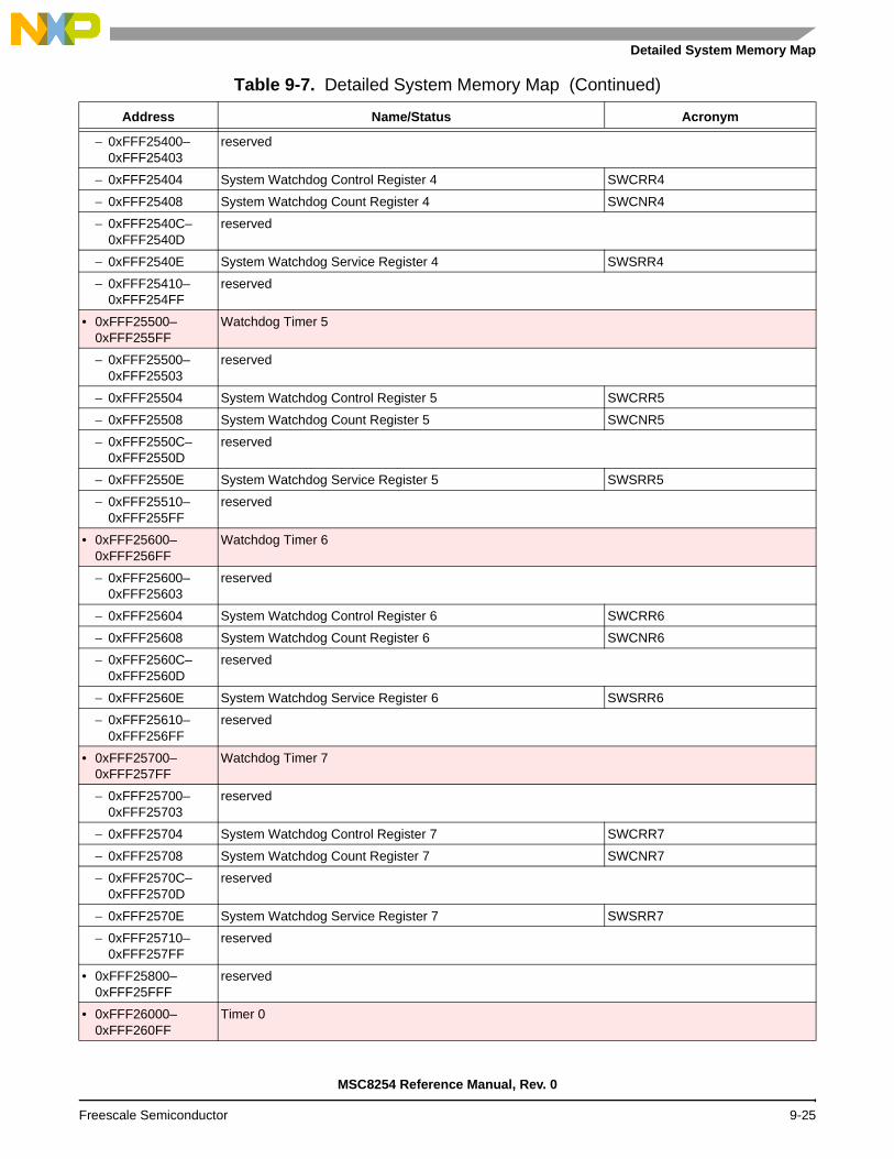
Detailed System Memory Map
− 0xFFF25400– 0xFFF25403
reserved
− 0xFFF25404 System Watchdog Control Register 4 SWCRR4
− 0xFFF25408 System Watchdog Count Register 4 SWCNR4
− 0xFFF2540C– 0xFFF2540D
reserved
− 0xFFF2540E System Watchdog Service Register 4 SWSRR4
− 0xFFF25410– 0xFFF254FF
reserved
• 0xFFF25500– 0xFFF255FF
Watchdog Timer 5
− 0xFFF25500– 0xFFF25503
reserved
− 0xFFF25504 System Watchdog Control Register 5 SWCRR5
− 0xFFF25508 System Watchdog Count Register 5 SWCNR5
− 0xFFF2550C– 0xFFF2550D
reserved
− 0xFFF2550E System Watchdog Service Register 5 SWSRR5
− 0xFFF25510– 0xFFF255FF
reserved
• 0xFFF25600– 0xFFF256FF
Watchdog Timer 6
− 0xFFF25600– 0xFFF25603
reserved
− 0xFFF25604 System Watchdog Control Register 6 SWCRR6
− 0xFFF25608 System Watchdog Count Register 6 SWCNR6
− 0xFFF2560C– 0xFFF2560D
reserved
− 0xFFF2560E System Watchdog Service Register 6 SWSRR6
− 0xFFF25610– 0xFFF256FF
reserved
• 0xFFF25700– 0xFFF257FF
Watchdog Timer 7
− 0xFFF25700– 0xFFF25703
reserved
− 0xFFF25704 System Watchdog Control Register 7 SWCRR7
− 0xFFF25708 System Watchdog Count Register 7 SWCNR7
− 0xFFF2570C– 0xFFF2570D
reserved
− 0xFFF2570E System Watchdog Service Register 7 SWSRR7
− 0xFFF25710– 0xFFF257FF
reserved
• 0xFFF25800– 0xFFF25FFF
reserved
• 0xFFF26000– 0xFFF260FF
Timer 0
Table 9-7. Detailed System Memory Map (Continued)
Address Name/Status Acronym
MSC8254 Reference Manual, Rev. 0
Freescale Semiconductor 9-25

Memory Map
− 0xFFF26000 Timer 0 Channel 0 Compare 1 Register TMR0CMP10
− 0xFFF26004 Timer 0 Channel 0 Compare 2 Register TMR0CMP20
− 0xFFF26008 Timer 0 Channel 0 Capture Register TMR0CAP0
− 0xFFF2600C Timer 0 Channel 0 Load Register TMR0LD0
− 0xFFF26010 Timer 0 Channel 0 Hold Register TMR0HOLD0
− 0xFFF26014 Timer 0 Channel 0 Counter Register TMR0CNTR0
− 0xFFF26018 Timer 0 Channel 0 Control Register TMR0CTL0
− 0xFFF2601C Timer 0 Channel 0 Status and Control Register TMR0SCTL0
− 0xFFF26020 Timer 0 Channel 0 Compare Load 1 Register TMR0CMPLD10
− 0xFFF26024 Timer 0 Channel 0 Compare Load 2 Register TMR0CMPLD20
− 0xFFF26028 Timer 0 Channel 0 Comparator Status and Control Register TMR0COMSC0
− 0xFFF2602C– 0xFFF2603F
reserved
− 0xFFF26040 Timer 0 Channel 1 Compare 1 Register TMR0CMP11
− 0xFFF26044 Timer 0 Channel 1 Compare 2 Register TMR0CMP21
− 0xFFF26048 Timer 0 Channel 1 Capture Register TMR0CAP1
− 0xFFF2604C Timer 0 Channel 1 Load Register TMR0LOAD1
− 0xFFF26050 Timer 0 Channel 1 Hold Register TMR0HOLD1
− 0xFFF26054 Timer 0 Channel 1 Counter Register TMR0CNTR1
− 0xFFF26058 Timer 0 Channel 1 Control Register TMR0CTL1
− 0xFFF2605C Timer 0 Channel 1 Status and Control Register TMR0SCTL1
− 0xFFF26060 Timer 0 Channel 1 Compare Load 1 Register TMR0CMPLD11
− 0xFFF26064 Timer 0 Channel 1 Compare Load 2 Register TMR0CMPLD21
− 0xFFF26068 Timer 0 Channel 1 Comparator Status and Control Register TMR0COMSC1
− 0xFFF2606C– 0xFFF2607F
reserved
− 0xFFF26080 Timer 0 Channel 2 Compare 1 Register TMR0CMP12
− 0xFFF26084 Timer 0 Channel 2 Compare 2 Register TMR0CMP22
− 0xFFF26088 Timer 0 Channel 2 Capture Register TMR0CAP2
− 0xFFF2608C Timer 0 Channel 2 Load Register TMR0LOAD2
− 0xFFF26090 Timer 0 Channel 2 Hold Register TMR0HOLD2
− 0xFFF26094 Timer 0 Channel 2 Counter Register TMR0CNTR2
− 0xFFF26098 Timer 0 Channel 2 Control Register TMR0CTL2
− 0xFFF2609C Timer 0 Channel 2 Status and Control Register TMR0SCTL2
− 0xFFF260A0 Timer 0 Channel 2 Compare Load 1 Register TMR0CMPLD12
− 0xFFF260A4 Timer 0 Channel 2 Compare Load 2 Register TMR0CMPLD22
− 0xFFF260A8 Timer 0 Channel 2 Comparator Status and Control Register TMR0COMSC2
− 0xFFF260AC– 0xFFF260BF
reserved
− 0xFFF260C0 Timer 0 Channel 3 Compare 1 Register TMR0CMP13
− 0xFFF260C4 Timer 0 Channel 3 Compare 2 Register TMR0CMP23
− 0xFFF260C8 Timer 0 Channel 3 Capture Register TMR0CAP3
Table 9-7. Detailed System Memory Map (Continued)
Address Name/Status Acronym
MSC8254 Reference Manual, Rev. 0
9-26 Freescale Semiconductor

Detailed System Memory Map
− 0xFFF260CC Timer 0 Channel 3 Load Register TMR0LOAD3
− 0xFFF260D0 Timer 0 Channel 3 Hold Register TMR0HOLD3
− 0xFFF260D4 Timer 0 Channel 3 Counter Register TMR0CNTR3
− 0xFFF260D8 Timer 0 Channel 3 Control Register TMR0CTL3
− 0xFFF260DC Timer 0 Channel 3 Status and Control Register TMR0SCTL3
− 0xFFF260E0 Timer 0 Channel 3 Compare Load 1 Register TMR0CMPLD13
− 0xFFF260E4 Timer 0 Channel 3 Compare Load 2 Register TMR0CMPLD23
− 0xFFF260E8 Timer 0 Channel 3 Comparator Status and Control Register TMR0COMSC3
− 0xFFF260EC– 0xFFF260FF
reserved
• 0xFFF26100– 0xFFF261FF
Timer 1
− 0xFFF26100 Timer 1 Channel 0 Compare 1 Register TMR1CMP10
− 0xFFF26104 Timer 1 Channel 0 Compare 2 Register TMR1CMP20
− 0xFFF26108 Timer 1 Channel 0 Capture Register TMR1CAP0
− 0xFFF2610C Timer 1 Channel 0 Load Register TMR1LOAD0
− 0xFFF26110 Timer 1 Channel 0 Hold Register TMR1HOLD0
− 0xFFF26114 Timer 1 Channel 0 Counter Register TMR1CNTR0
− 0xFFF26118 Timer 1 Channel 0 Control Register TMR1CTL0
− 0xFFF2611C Timer 1 Channel 0 Status and Control Register TMR1SCTL0
− 0xFFF26120 Timer 1 Channel 0 Compare Load 1 Register TMR1CMPLD10
− 0xFFF26124 Timer 1 Channel 0 Compare Load 2 Register TMR1CMPLD20
− 0xFFF26128 Timer 1 Channel 0 Comparator Status and Control Register TMR1COMSC0
− 0xFFF2612C– 0xFFF2613F
reserved
− 0xFFF26140 Timer 1 Channel 1 Compare 1 Register TMR1CMP11
− 0xFFF26144 Timer 1 Channel 1 Compare 2 Register TMR1CMP21
− 0xFFF26148 Timer 1 Channel 1 Capture Register TMR1CAP1
− 0xFFF2614C Timer 1 Channel 1 Load Register TMR1LOAD1
− 0xFFF26150 Timer 1 Channel 1 Hold Register TMR1HOLD1
− 0xFFF26154 Timer 1 Channel 1 Counter Register TMR1CNTR1
− 0xFFF26158 Timer 1 Channel 1 Control Register TMR1CTL1
− 0xFFF2615C Timer 1 Channel 1 Status and Control Register TMR1SCTL1
− 0xFFF26160 Timer 1 Channel 1 Compare Load 1 Register TMR1CMPLD11
− 0xFFF26164 Timer 1 Channel 1 Compare Load 2 Register TMR1CMPLD21
− 0xFFF26168 Timer 1 Channel 1 Comparator Status and Control Register TMR1COMSC1
− 0xFFF2616C– 0xFFF2617F
reserved
− 0xFFF26180 Timer 1 Channel 2 Compare 1 Register TMR1CMP12
− 0xFFF26184 Timer 1 Channel 2 Compare 2 Register TMR1CMP22
− 0xFFF26188 Timer 1 Channel 2 Capture Register TMR1CAP2
− 0xFFF2618C Timer 1 Channel 2 Load Register TMR1LOAD2
− 0xFFF26190 Timer 1 Channel 2 Hold Register TMR1HOLD2
Table 9-7. Detailed System Memory Map (Continued)
Address Name/Status Acronym
MSC8254 Reference Manual, Rev. 0
Freescale Semiconductor 9-27

Memory Map
− 0xFFF26194 Timer 1 Channel 2 Counter Register TMR1CNTR2
− 0xFFF26198 Timer 1 Channel 2 Control Register TMR1CTL2
− 0xFFF2619C Timer 1 Channel 2 Status and Control Register TMR1SCTL2
− 0xFFF261A0 Timer 1 Channel 2 Compare Load 1 Register TMR1CMPLD12
− 0xFFF261A4 Timer 1 Channel 2 Compare Load 2 Register TMR1CMPLD22
− 0xFFF261A8 Timer 1 Channel 2 Comparator Status and Control Register TMR1COMSC2
− 0xFFF261AC– 0xFFF261BF
reserved
− 0xFFF261C0 Timer 1 Channel 3 Compare 1 Register TMR1CMP13
− 0xFFF261C4 Timer 1 Channel 3 Compare 2 Register TMR1CMP23
− 0xFFF261C8 Timer 1 Channel 3 Capture Register TMR1CAP3
− 0xFFF261CC Timer 1 Channel 3 Load Register TMR1LOAD3
− 0xFFF261D0 Timer 1 Channel 3 Hold Register TMR1HOLD3
− 0xFFF261D4 Timer 1 Channel 3 Counter Register TMR1CNTR3
− 0xFFF261D8 Timer 1 Channel 3 Control Register TMR1CTL3
− 0xFFF261DC Timer 1 Channel 3 Status and Control Register TMR1SCTL3
− 0xFFF261E0 Timer 1 Channel 3 Compare Load 1 Register TMR1CMPLD13
− 0xFFF261E4 Timer 1 Channel 3 Compare Load 2 Register TMR1CMPLD23
− 0xFFF261E8 Timer 1 Channel 3 Comparator Status and Control Register TMR1COMSC3
− 0xFFF261EC– 0xFFF261FF
reserved
• 0xFFF26200– 0xFFF262FF
Timer 2
− 0xFFF26200 Timer 2 Channel 0 Compare 1 Register TMR2CMP10
− 0xFFF26204 Timer 2 Channel 0 Compare 2 Register TMR2CMP20
− 0xFFF26208 Timer 2 Channel 0 Capture Register TMR2CAP0
− 0xFFF2620C Timer 2 Channel 0 Load Register TMR2LOAD0
− 0xFFF26210 Timer 2 Channel 0 Hold Register TMR2HOLD0
− 0xFFF26214 Timer 2 Channel 0 Counter Register TMR2CNTR0
− 0xFFF26218 Timer 2 Channel 0 Control Register TMR2CTL0
− 0xFFF2621C Timer 2 Channel 0 Status and Control Register TMR2SCTL0
− 0xFFF26220 Timer 2 Channel 0 Compare Load 1 Register TMR2CMPLD10
− 0xFFF26224 Timer 2 Channel 0 Compare Load 2 Register TMR2CMPLD20
− 0xFFF26228 Timer 2 Channel 0 Comparator Status and Control Register TMR2COMSC0
− 0xFFF2622C– 0xFFF2623F
reserved
− 0xFFF26240 Timer 2 Channel 1 Compare 1 Register TMR2CMP11
− 0xFFF26244 Timer 2 Channel 1 Compare 2 Register TMR2CMP21
− 0xFFF26248 Timer 2 Channel 1 Capture Register TMR2CAP1
− 0xFFF2624C Timer 2 Channel 1 Load Register TMR2LOAD1
− 0xFFF26250 Timer 2 Channel 1 Hold Register TMR2HOLD1
− 0xFFF26254 Timer 2 Channel 1 Counter Register TMR2CNTR1
− 0xFFF26258 Timer 2 Channel 1 Control Register TMR2CTL1
Table 9-7. Detailed System Memory Map (Continued)
Address Name/Status Acronym
MSC8254 Reference Manual, Rev. 0
9-28 Freescale Semiconductor

Detailed System Memory Map
− 0xFFF2625C Timer 2 Channel 1 Status and Control Register TMR2SCTL1
− 0xFFF26260 Timer 2 Channel 1 Compare Load 1 Register TMR2CMPLD11
− 0xFFF26264 Timer 2 Channel 1 Compare Load 2 Register TMR2CMPLD21
− 0xFFF26268 Timer 2 Channel 1 Comparator Status and Control Register TMR2COMSC1
− 0xFFF2626C– 0xFFF2627F
reserved
− 0xFFF26280 Timer 2 Channel 2 Compare 1 Register TMR2CMP12
− 0xFFF26284 Timer 2 Channel 2 Compare 2 Register TMR2CMP22
− 0xFFF26288 Timer 2 Channel 2 Capture Register TMR2CAP2
− 0xFFF2628C Timer 2 Channel 2 Load Register TMR2LOAD2
− 0xFFF26290 Timer 2 Channel 2 Hold Register TMR2HOLD2
− 0xFFF26294 Timer 2 Channel 2 Counter Register TMR2CNTR2
− 0xFFF26298 Timer 2 Channel 2 Control Register TMR2CTL2
− 0xFFF2629C Timer 2 Channel 2 Status and Control Register TMR2SCTL2
− 0xFFF262A0 Timer 2 Channel 2 Compare Load 1 Register TMR2CMPLD12
− 0xFFF262A4 Timer 2 Channel 2 Compare Load 2 Register TMR2CMPLD22
− 0xFFF262A8 Timer 2 Channel 2 Comparator Status and Control Register TMR2COMSC2
− 0xFFF262AC– 0xFFF262BF
reserved
− 0xFFF262C0 Timer 2 Channel 3 Compare 1 Register TMR2CMP13
− 0xFFF262C4 Timer 2 Channel 3 Compare 2 Register TMR2CMP23
− 0xFFF262C8 Timer 2 Channel 3 Capture Register TMR2CAP3
− 0xFFF262CC Timer 2 Channel 3 Load Register TMR2LOAD3
− 0xFFF262D0 Timer 2 Channel 3 Hold Register TMR2HOLD3
− 0xFFF262D4 Timer 2 Channel 3 Counter Register TMR2CNTR3
− 0xFFF262D8 Timer 2 Channel 3 Control Register TMR2CTL3
− 0xFFF262DC Timer 2 Channel 3 Status and Control Register TMR2SCTL3
− 0xFFF262E0 Timer 2 Channel 3 Compare Load 1 Register TMR2CMPLD13
− 0xFFF262E4 Timer 2 Channel 3 Compare Load 2 Register TMR2CMPLD23
− 0xFFF262E8 Timer 2 Channel 3 Comparator Status and Control Register TMR2COMSC3
− 0xFFF262EC– 0xFFF262FF
reserved
• 0xFFF26300– 0xFFF263FF
Timer 3
− 0xFFF26300 Timer 3 Channel 0 Compare 1 Register TMR3CMP10
− 0xFFF26304 Timer 3 Channel 0 Compare 2 Register TMR3CMP20
− 0xFFF26308 Timer 3 Channel 0 Capture Register TMR3CAP0
− 0xFFF2630C Timer 3 Channel 0 Load Register TMR3LOAD0
− 0xFFF26310 Timer 3 Channel 0 Hold Register TMR3HOLD0
− 0xFFF26314 Timer 3 Channel 0 Counter Register TMR3CNTR0
− 0xFFF26318 Timer 3 Channel 0 Control Register TMR3CTL0
− 0xFFF2631C Timer 3 Channel 0 Status and Control Register TMR3SCTL0
− 0xFFF26320 Timer 3 Channel 0 Load 1 Register TMR3CMPLD10
Table 9-7. Detailed System Memory Map (Continued)
Address Name/Status Acronym
MSC8254 Reference Manual, Rev. 0
Freescale Semiconductor 9-29

Memory Map
− 0xFFF26324 Timer 3 Channel 0 Load 2 Register TMR3CMPLD20
− 0xFFF26328 Timer 3 Channel 0 Comparator Status and Control Register TMR3COMSC0
− 0xFFF2632C– 0xFFF2633F
reserved
− 0xFFF26340 Timer 3 Channel 1 Compare 1 Register TMR3CMP11
− 0xFFF26344 Timer 3 Channel 1 Compare 2 Register TMR3CMP21
− 0xFFF26348 Timer 3 Channel 1 Capture Register TMR3CAP1
− 0xFFF2634C Timer 3 Channel 1 Load Register TMR3LOAD1
− 0xFFF26350 Timer 3 Channel 1 Hold Register TMR3HOLD1
− 0xFFF26354 Timer 3 Channel 1 Counter Register TMR3CNTR1
− 0xFFF26358 Timer 3 Channel 1 Control Register TMR3CTL1
− 0xFFF2635C Timer 3 Channel 1 Status and Control Register TMR3SCTL1
− 0xFFF26360 Timer 3 Channel 1 Load 1 Register TMR3CMPLD11
− 0xFFF26364 Timer 3 Channel 1 Load 2 Register TMR3CMPLD21
− 0xFFF26368 Timer 3 Channel 1 Comparator Status and Control Register TMR3COMSC1
− 0xFFF2636C– 0xFFF2637F
reserved
− 0xFFF26380 Timer 3 Channel 2 Compare 1 Register TMR3CMP12
− 0xFFF26384 Timer 3 Channel 2 Compare 2 Register TMR3CMP22
− 0xFFF26388 Timer 3 Channel 2 Capture Register TMR3CAP2
− 0xFFF2638C Timer 3 Channel 2 Load Register TMR3LOAD2
− 0xFFF26390 Timer 3 Channel 2 Hold Register TMR3HOLD2
− 0xFFF26394 Timer 3 Channel 2 Counter Register TMR3CNTR2
− 0xFFF26398 Timer 3 Channel 2 Control Register TMR3CTL2
− 0xFFF2639C Timer 3 Channel 2 Status and Control Register TMR3SCTL2
− 0xFFF263A0 Timer 3 Channel 2 Load 1 Register TMR3CMPLD12
− 0xFFF263A4 Timer 3 Channel 2 Load 2 Register TMR3CMPLD22
− 0xFFF263A8 Timer 3 Channel 2 Comparator Status and Control Register TMR3COMSC2
− 0xFFF263AC– 0xFFF263BF
reserved
− 0xFFF263C0 Timer 3 Channel 3 Compare 1 Register TMR3CMP13
− 0xFFF263C4 Timer 3 Channel 3 Compare 2 Register TMR3CMP23
− 0xFFF263C8 Timer 3 Channel 3 Capture Register TMR3CAP3
− 0xFFF263CC Timer 3 Channel 3 Load Register TMR3LOAD3
− 0xFFF263D0 Timer 3 Channel 3 Hold Register TMR3HOLD3
− 0xFFF263D4 Timer 3 Channel 3 Counter Register TMR3CNTR3
− 0xFFF263D8 Timer 3 Channel 3 Control Register TMR3CTL3
− 0xFFF263DC Timer 3 Channel 3 Status and Control Register TMR3SCTL3
− 0xFFF263E0 Timer 3 Channel 3 Load 1 Register TMR3CMPLD13
− 0xFFF263E4 Timer 3 Channel 3 Load 2 Register TMR3CMPLD23
− 0xFFF263E8 Timer 3 Channel 3 Comparator Status and Control Register TMR3COMSC3
− 0xFFF263EC– 0xFFF263FF
reserved
Table 9-7. Detailed System Memory Map (Continued)
Address Name/Status Acronym
MSC8254 Reference Manual, Rev. 0
9-30 Freescale Semiconductor

Detailed System Memory Map
• 0xFFF26400– 0xFFF26BFF
reserved
• 0xFFF26C00– 0xFFF26C3F
UART
− 0xFFF26C00 SCI Baud-Rate Register SCIBR
− 0xFFF26C04– 0xFFF26C07
reserved
− 0xFFF26C08 SCI Control Register SCICR
− 0xFFF26C0C– 0xFFF26C0F
reserved
− 0xFFF26C10 SCI Status Register SCISR
− 0xFFF26C14– 0xFFF26C17
reserved
− 0xFFF26C18 SCI Data Register SCIDR
− 0xFFF26C1C– 0xFFF26C27
reserved
− 0xFFF26C28 SCI Data Direction Register SCIDDR
− 0xFFF26C2C– 0xFFF26C3F
reserved
• 0xFFF26C40– 0xFFF26FFF
reserved
• 0xFFF27000– 0xFFF270FF
GIC
− 0xFFF27000 Virtual Interrupt Generation Register VIGR
− 0xFFF27004– 0xFFF27007
reserved
− 0xFFF27008 Virtual Interrupt Status Register VISR
− 0xFFF2700C– 0xFFF270FF
reserved
• 0xFFF27100– 0xFFF271FF
Hardware Semaphores
− 0xFFF27100 Hardware Semaphore Register 0 HSMPR0
− 0xFFF27104– 0xFFF27107
reserved
− 0xFFF27108 Hardware Semaphore Register 1 HSMPR1
− 0xFFF2710C– 0xFFF2710F
reserved
− 0xFFF27110 Hardware Semaphore Register 2 HSMPR2
− 0xFFF27114– 0xFFF27117
reserved
− 0xFFF27118 Hardware Semaphore Register 3 HSMPR3
− 0xFFF2711C– 0xFFF2711F
reserved
− 0xFFF27120 Hardware Semaphore Register 4 HSMPR4
− 0xFFF27124– 0xFFF27127
reserved
Table 9-7. Detailed System Memory Map (Continued)
Address Name/Status Acronym
MSC8254 Reference Manual, Rev. 0
Freescale Semiconductor 9-31

Memory Map
− 0xFFF27128 Hardware Semaphore Register 5 HSMPR5
− 0xFFF2712C– 0xFFF2712F
reserved
− 0xFFF27130 Hardware Semaphore Register 6 HSMPR6
− 0xFFF27134– 0xFFF27137
reserved
− 0xFFF27138 Hardware Semaphore Register 7 HSMPR7
− 0xFFF2713C– 0xFFF271FF
reserved
• 0xFFF27200– 0xFFF272FF
GPIO
− 0xFFF27200 Pin Open-Drain Register PODR
− 0xFFF27204– 0xFFF27207
reserved
− 0xFFF27208 Pin Data Register PDAT
− 0xFFF2720C– 0xFFF2720F
reserved
− 0xFFF27210 Pin Data Direction Register PDIR
− 0xFFF27214– 0xFFF27217
reserved
− 0xFFF27218 Pin Assignment Register PAR
− 0xFFF2721C– 0xFFF2721F
reserved
− 0xFFF27220 Pin Special Options Register PSOR
− 0xFFF27224– 0xFFF272FF
reserved
• 0xFFF27300– 0xFFF27FFF
reserved
• 0xFFF28000– 0xFFF281FF
General Configuration Registers
− 0xFFF28000 General Configuration Register 1 GCR1
− 0xFFF28004 General Configuration Register 2 GCR2
− 0xFFF28008 General Status Register 1 GSR1
− 0xFFF2800C High Speed Serial Interface Status Register HSSI_SR
− 0xFFF28010 DDR General Configuration Register DDR_GCR
− 0xFFF28014 High Speed Serial Interface Control Register 1 HSSI_CR1
− 0xFFF28018 High Speed Serial Interface Control Register 2 HSSI_CR2
− 0xFFF2801C QUICC Engine Control Register QECR
− 0xFFF28020 GPIO Pull-Up Enable Register GPUER
− 0xFFF28024 GPIO Input Enable Register GIER
− 0xFFF28028 System Part and Revision ID Register SPRIDR
− 0xFFF2802C– 0xFFF2802F
reserved
− 0xFFF28030 General Control Register 4 GCR4
− 0xFFF28034 General Control Register 5 GCR5
Table 9-7. Detailed System Memory Map (Continued)
Address Name/Status Acronym
MSC8254 Reference Manual, Rev. 0
9-32 Freescale Semiconductor

Detailed System Memory Map
− 0xFFF28038 General Status Register 2 GSR2
− 0xFFF2803C Core Subsystem Slave Port Priority Control Register TSPPCR
− 0xFFF28040 QUICC Engine First External Request Multiplex Register CPCE1R
− 0xFFF28044 QUICC Engine Second External Request Multiplex Register CPCE2R
− 0xFFF28048 QUICC Engine Third External Request Multiplex Register CPCE3R
− 0xFFF2804C QUICC Engine Fourth External Request Multiplex Register CPCE4R
− 0xFFF28050– 0xFFF28073
reserved
− 0xFFF28074 General Control Register 10 GCR10
− 0xFFF28078– 0xFFF2807F
reserved
− 0xFFF28080 General Interrupt Register 1 GIR1
− 0xFFF28084 General Interrupt Enable Register 1 for Core 0 GIER1_0
− 0xFFF28088 General Interrupt Enable Register 1 for Core 1 GIER1_1
− 0xFFF2808C General Interrupt Enable Register 1 for Core 2 GIER1_2
− 0xFFF28090 General Interrupt Enable Register 1 for Core 3 GIER1_3
− 0xFFF28094 General Interrupt Enable Register 1 for Core 4 GIER1_4
− 0xFFF28098 General Interrupt Enable Register 1 for Core 5 GIER1_5
− 0xFFF2809C– 0xFFF280A3
reserved
− 0xFFF280A4 General Interrupt Register 3 GIR3
− 0xFFF280A8 General Interrupt Enable Register 3 for Core 0 GIER3_0
− 0xFFF280AC General Interrupt Enable Register 3 for Core 1 GIER3_1
− 0xFFF280B0 General Interrupt Enable Register 3 for Core 2 GIER3_2
− 0xFFF280B4 General Interrupt Enable Register 3 for Core 3 GIER3_3
− 0xFFF280B8 General Interrupt Enable Register 3 for Core 4 GIER3_4
− 0xFFF280BC General Interrupt Enable Register 3 for Core 5 GIER3_5
− 0xFFF280C0– 0xFFF280EB
reserved
− 0xFFF280EC General Interrupt Register 5 GIR5
− 0xFFF280F0 General Interrupt Enable Register 5 for Core 0 GIER5_0
− 0xFFF280F4 General Interrupt Enable Register 5 for Core 1 GIER5_1
− 0xFFF280F8 General Interrupt Enable Register 5 for Core 2 GIER5_2
− 0xFFF280FC General Interrupt Enable Register 5 for Core 3 GIER5_3
− 0xFFF28100 General Interrupt Enable Register 5 for Core 4 GIER5_4
− 0xFFF28104 General Interrupt Enable Register 5 for Core 5 GIER5_5
− 0xFFF28108– 0xFFF2810F
reserved
− 0xFFF28110 General Control Register 11 GCR11
− 0xFFF28114 General Control Register 12 GCR12
− 0xFFF28118– 0xFFF2811F
reserved
− 0xFFF28120 DMA Request0 Control Register GCR_DREQ0
Table 9-7. Detailed System Memory Map (Continued)
Address Name/Status Acronym
MSC8254 Reference Manual, Rev. 0
Freescale Semiconductor 9-33

Memory Map
− 0xFFF28124 DMA Request1 Control Register GCR_DREQ1
− 0xFFF28128 DMA Done Control Register GCR_DDONE
− 0xFFF2812C DDR1 General Configuration Register DDR1_GCR
− 0xFFF28130 DDR2 General Configuration Register DDR2_GCR
− 0xFFF28134– 0xFFF28137
reserved
− 0xFFF28138 Core Subsystem Slave Port General Configuration Register CORE_SLV_GCR
− 0xFFF2813C– 0xFFF281FF
reserved
• 0xFFF28200– 0xFFF2FFFF
reserved
• 0xFFF30000– 0xFFF33FFF
TDM0
− 0xFFF30000– 0xFFF307FF
TDM0 Receive Local Memory
− 0xFFF30800– 0xFFF30FFF
reserved
− 0xFFF31000– 0xFFF313FC
TDM0 Receive Channel Parameters Register 0–255 TDM0RCPR[0–255]
− 0xFFF31400– 0xFFF317FF
reserved
− 0xFFF31800– 0xFFF31FFF
TDM0 Transmit Local Memory
− 0xFFF32000– 0xFFF327FF
reserved
− 0xFFF32800– 0xFFF32BFC
TDM0 Transmit Channel Parameters Register 0–255 TDM0TCPR[0–255]
− 0xFFF32C00– 0xFFF33EFF
reserved
− 0xFFF33F00 TDM0 Parity Control Register TDM0PCR
− 0xFFF33F04– 0xFFF33F07
reserved
− 0xFFF33F08 TDM0 Parity Error Register TDM0PER
− 0xFFF33F0C– 0xFFF33F0F
reserved
− 0xFFF33F10 TDM0 Transmit Force Register TDM0TFR
− 0xFFF33F14– 0xFFF33F17
reserved
− 0xFFF33F18 TDM0 Receive Force Register TDM0RFR
− 0xFFF33F1C– 0xFFF33F1F
reserved
− 0xFFF33F20 TDM0 Transmit Status Register TDM0TSR
− 0xFFF33F24– 0xFFF33F27
reserved
− 0xFFF33F28 TDM0 Receive Status Register TDM0RSR
Table 9-7. Detailed System Memory Map (Continued)
Address Name/Status Acronym
MSC8254 Reference Manual, Rev. 0
9-34 Freescale Semiconductor

Detailed System Memory Map
− 0xFFF33F2C– 0xFFF33F2F
reserved
− 0xFFF33F30 TDM0 Adaptation Status Register TDM0ASR
− 0xFFF33F34– 0xFFF33F37
reserved
− 0xFFF33F38 TDM0 Transmit Event Register TDM0TER
− 0xFFF33F3C– 0xFFF33F3F
reserved
− 0xFFF33F40 TDM0 Receive Event Register TDM0RER
− 0xFFF33F44– 0xFFF33F47
reserved
− 0xFFF33F48 TDM0 Transmit Number of Buffers TDM0TNB
− 0xFFF33F4C– 0xFFF33F4F
reserved
− 0xFFF33F50 TDM0 Receive Number of Buffers TDM0RNB
− 0xFFF33F54– 0xFFF33F57
reserved
− 0xFFF33F58 TDM0 Transmit Data Buffer Displacement Register TDM0TDBDR
− 0xFFF33F5C– 0xFFF33F5F
reserved
− 0xFFF33F60 TDM0 Receive Data Buffer Displacement Register TDM0RDBDR
− 0xFFF33F64– 0xFFF33F67
reserved
− 0xFFF33F68 TDM0 Adaptation Sync Distance Register TDM0ASDR
− 0xFFF33F6C– 0xFFF33F6F
reserved
− 0xFFF33F70 TDM0 Transmit Interrupt Enable Register TDM00TIER
− 0xFFF33F74– 0xFFF33F77
reserved
− 0xFFF33F78 TDM0 Receive Interrupt Enable Register TDM0RIER
− 0xFFF33F7C– 0xFFF33F7F
reserved
− 0xFFF33F80 TDM0 Transmit Data Buffer Second Threshold TDM0TDBST
− 0xFFF33F84– 0xFFF33F87
reserved
− 0xFFF33F88 TDM0 Receive Data Buffer Second Threshold TDM0RDBST
− 0xFFF33F8C– 0xFFF33F8F
reserved
− 0xFFF33F90 TDM0 Transmit Data Buffer First Threshold TDM0TDBFT
− 0xFFF33F94– 0xFFF33F97
reserved
− 0xFFF33F98 TDM0 Receive Data Buffer First Threshold TDM0RDBFT
− 0xFFF33F9C– 0xFFF33F9F
reserved
− 0xFFF33FA0 TDM0 Transmit Control Register TDM0TCR
Table 9-7. Detailed System Memory Map (Continued)
Address Name/Status Acronym
MSC8254 Reference Manual, Rev. 0
Freescale Semiconductor 9-35

Memory Map
− 0xFFF33FA4– 0xFFF33FA7
reserved
− 0xFFF33FA8 TDM0 Receive Control Register TDM0RCR
− 0xFFF33FAC– 0xFFF33FAF
reserved
− 0xFFF33FB0 TDM0 Adaptation Control Register TDM0ACR
− 0xFFF33FB4– 0xFFF33FB7
reserved
− 0xFFF33FB8 TDM0 Transmit Global Base Address TDM0TGBA
− 0xFFF33FBC– 0xFFF33FBF
reserved
− 0xFFF33FC0 TDM0 Receive Global Base Address TDM0RGBA
− 0xFFF33FC4– 0xFFF33FC7
reserved
− 0xFFF33FC8 TDM0 Transmit Data Buffer Size TDM0TDBS
− 0xFFF33FCC– 0xFFF33FCF
reserved
− 0xFFF33FD0 TDM0 Receive Data Buffer Size TDM0RDBS
− 0xFFF33FD4– 0xFFF33FD7
reserved
− 0xFFF33FD8 TDM0 Transmit Frame Parameters TDM0TFP
− 0xFFF33FDC– 0xFFF33FDF
reserved
− 0xFFF33FE0 TDM0 Receive Frame Parameters TDM0RFP
− 0xFFF33FE4– 0xFFF33FE7
reserved
− 0xFFF33FE8 TDM0 Transmit Interface Register TDM0TIR
− 0xFFF33FEC– 0xFFF33FEF
reserved
− 0xFFF33FF0 TDM0 Receive Interface Register TDM0RIR
− 0xFFF33FF4– 0xFFF33FF7
reserved
− 0xFFF33FF8 TDM0 General Interface Register TDM0GIR
− 0xFFF33FFC– 0xFFF33FFF
reserved
• 0xFFF34000– 0xFFF37FFF
TDM1
− 0xFFF34000– 0xFFF347FF
TDM1 Receive Local Memory
− 0xFFF34800– 0xFFF34FFF
reserved
− 0xFFF35000– 0xFFF353FC
TDM1 Receive Channel Parameters Register 0–255 TDM1RCPR[0–255]
− 0xFFF35400– 0xFFF357FF
reserved
Table 9-7. Detailed System Memory Map (Continued)
Address Name/Status Acronym
MSC8254 Reference Manual, Rev. 0
9-36 Freescale Semiconductor

Detailed System Memory Map
− 0xFFF35800– 0xFFF35FFF
TDM1 Transmit Local Memory
− 0xFFF36000– 0xFFF367FF
reserved
− 0xFFF36800– 0xFFF36BFC
TDM1 Transmit Channel Parameters Register 0–255 TDM1TCPR[0–255]
− 0xFFF36C00– 0xFFF37EFF
reserved
− 0xFFF37F00 TDM1 Parity Control Register TDM1PCR
− 0xFFF37F04– 0xFFF37F07
reserved
− 0xFFF37F08 TDM1 Parity Error Register TDM1PER
− 0xFFF37F0C– 0xFFF37F0F
reserved
− 0xFFF37F10 TDM1 Transmit Force Register TDM1TFR
− 0xFFF37F14– 0xFFF37F17
reserved
− 0xFFF37F18 TDM1 Receive Force Register TDM1RFR
− 0xFFF37F1C– 0xFFF37F1F
reserved
− 0xFFF37F20 TDM1 Transmit Status Register TDM1TSR
− 0xFFF37F24– 0xFFF37F27
reserved
− 0xFFF37F28 TDM1 Receive Status Register TDM1RSR
− 0xFFF37F2C– 0xFFF37F2F
reserved
− 0xFFF37F30 TDM1 Adaptation Status Register TDM1ASR
− 0xFFF37F34– 0xFFF37F37
reserved
− 0xFFF37F38 TDM1 Transmit Event Register TDM1TER
− 0xFFF37F3C– 0xFFF37F3F
reserved
− 0xFFF37F40 TDM1 Receive Event Register TDM1RER
− 0xFFF37F44– 0xFFF37F47
reserved
− 0xFFF37F48 TDM1 Transmit Number of Buffers TDM1TNB
− 0xFFF37F4C– 0xFFF37F4F
reserved
− 0xFFF37F50 TDM1 Receive Number of Buffers TDM1RNB
− 0xFFF37F54– 0xFFF37F57
reserved
− 0xFFF37F58 TDM1 Transmit Data Buffer Displacement Register TDM1TDBDR
− 0xFFF37F5C– 0xFFF37F5F
reserved
− 0xFFF37F60 TDM1 Receive Data Buffer Displacement Register TDM1RDBDR
Table 9-7. Detailed System Memory Map (Continued)
Address Name/Status Acronym
MSC8254 Reference Manual, Rev. 0
Freescale Semiconductor 9-37

Memory Map
− 0xFFF37F64– 0xFFF37F67
reserved
− 0xFFF37F68 TDM1 Adaptation Sync Distance Register TDM1ASDR
− 0xFFF37F6C– 0xFFF37F6F
reserved
− 0xFFF37F70 TDM1 Transmit Interrupt Enable Register TDM10TIER
− 0xFFF37F74– 0xFFF37F77
reserved
− 0xFFF37F78 TDM1 Receive Interrupt Enable Register TDM1RIER
− 0xFFF37F7C– 0xFFF37F7F
reserved
− 0xFFF37F80 TDM1 Transmit Data Buffer Second Threshold TDM1TDBST
− 0xFFF37F84– 0xFFF37F87
reserved
− 0xFFF37F88 TDM1 Receive Data Buffer Second Threshold TDM1RDBST
− 0xFFF37F8C– 0xFFF37F8F
reserved
− 0xFFF37F90 TDM1 Transmit Data Buffer First Threshold TDM1TDBFT
− 0xFFF37F94– 0xFFF37F97
reserved
− 0xFFF37F98 TDM1 Receive Data Buffer First Threshold TDM1RDBFT
− 0xFFF37F9C– 0xFFF37F9F
reserved
− 0xFFF37FA0 TDM1 Transmit Control Register TDM1TCR
− 0xFFF37FA4– 0xFFF37FA7
reserved
− 0xFFF37FA8 TDM1 Receive Control Register TDM1RCR
− 0xFFF37FAC– 0xFFF37FAF
reserved
− 0xFFF37FB0 TDM1 Adaptation Control Register TDM1ACR
− 0xFFF37FB4– 0xFFF37FB7
reserved
− 0xFFF37FB8 TDM1 Transmit Global Base Address TDM1TGBA
− 0xFFF37FBC– 0xFFF37FBF
reserved
− 0xFFF37FC0 TDM1 Receive Global Base Address TDM1RGBA
− 0xFFF37FC4– 0xFFF37FC7
reserved
− 0xFFF37FC8 TDM1 Transmit Data Buffer Size TDM1TDBS
− 0xFFF37FCC– 0xFFF37FCF
reserved
− 0xFFF37FD0 TDM1 Receive Data Buffer Size TDM1RDBS
− 0xFFF37FD4– 0xFFF37FD7
reserved
− 0xFFF37FD8 TDM1 Transmit Frame Parameters TDM1TFP
Table 9-7. Detailed System Memory Map (Continued)
Address Name/Status Acronym
MSC8254 Reference Manual, Rev. 0
9-38 Freescale Semiconductor
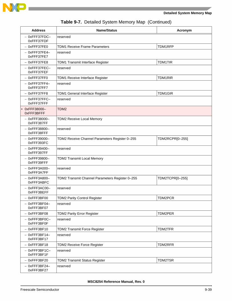
Detailed System Memory Map
− 0xFFF37FDC– 0xFFF37FDF
reserved
− 0xFFF37FE0 TDM1 Receive Frame Parameters TDM1RFP
− 0xFFF37FE4– 0xFFF37FE7
reserved
− 0xFFF37FE8 TDM1 Transmit Interface Register TDM1TIR
− 0xFFF37FEC– 0xFFF37FEF
reserved
− 0xFFF37FF0 TDM1 Receive Interface Register TDM1RIR
− 0xFFF37FF4– 0xFFF37FF7
reserved
− 0xFFF37FF8 TDM1 General Interface Register TDM1GIR
− 0xFFF37FFC– 0xFFF37FFF
reserved
• 0xFFF38000– 0xFFF3BFFF
TDM2
− 0xFFF38000– 0xFFF387FF
TDM2 Receive Local Memory
− 0xFFF38800– 0xFFF38FFF
reserved
− 0xFFF39000– 0xFFF393FC
TDM2 Receive Channel Parameters Register 0–255 TDM2RCPR[0–255]
− 0xFFF39400– 0xFFF397FF
reserved
− 0xFFF39800– 0xFFF39FFF
TDM2 Transmit Local Memory
− 0xFFF3A000– 0xFFF3A7FF
reserved
− 0xFFF3A800– 0xFFF3ABFC
TDM2 Transmit Channel Parameters Register 0–255 TDM2TCPR[0–255]
− 0xFFF3AC00– 0xFFF3BEFF
reserved
− 0xFFF3BF00 TDM2 Parity Control Register TDM2PCR
− 0xFFF3BF04– 0xFFF3BF07
reserved
− 0xFFF3BF08 TDM2 Parity Error Register TDM2PER
− 0xFFF3BF0C– 0xFFF3BF0F
reserved
− 0xFFF3BF10 TDM2 Transmit Force Register TDM2TFR
− 0xFFF3BF14– 0xFFF3BF17
reserved
− 0xFFF3BF18 TDM2 Receive Force Register TDM2RFR
− 0xFFF3BF1C– 0xFFF3BF1F
reserved
− 0xFFF3BF20 TDM2 Transmit Status Register TDM2TSR
− 0xFFF3BF24– 0xFFF3BF27
reserved
Table 9-7. Detailed System Memory Map (Continued)
Address Name/Status Acronym
MSC8254 Reference Manual, Rev. 0
Freescale Semiconductor 9-39

Memory Map
− 0xFFF3BF28 TDM2 Receive Status Register TDM2RSR
− 0xFFF3BF2C– 0xFFF3BF2F
reserved
− 0xFFF3BF30 TDM2 Adaptation Status Register TDM2ASR
− 0xFFF3BF34– 0xFFF38F37
reserved
− 0xFFF3BF38 TDM2 Transmit Event Register TDM2TER
− 0xFFF3BF3C– 0xFFF3BF3F
reserved
− 0xFFF3BF40 TDM2 Receive Event Register TDM2RER
− 0xFFF3BF44– 0xFFF3BF47
reserved
− 0xFFF3BF48 TDM2 Transmit Number of Buffers TDM2TNB
− 0xFFF3BF4C– 0xFFF3BF4F
reserved
− 0xFFF3BF50 TDM2 Receive Number of Buffers TDM2RNB
− 0xFFF3BF54– 0xFFF3BF57
reserved
− 0xFFF3BF58 TDM2 Transmit Data Buffer Displacement Register TDM2TDBDR
− 0xFFF3BF5C– 0xFFF3BF5F
reserved
− 0xFFF3BF60 TDM2 Receive Data Buffer Displacement Register TDM2RDBDR
− 0xFFF3BF64– 0xFFF3BF67
reserved
− 0xFFF3BF68 TDM2 Adaptation Sync Distance Register TDM2ASDR
− 0xFFF3BF6C– 0xFFF3BF6F
reserved
− 0xFFF3BF70 TDM2 Transmit Interrupt Enable Register TDM20TIER
− 0xFFF3BF74– 0xFFF3BF77
reserved
− 0xFFF3BF78 TDM2 Receive Interrupt Enable Register TDM2RIER
− 0xFFF3BF7C– 0xFFF3BF7F
reserved
− 0xFFF3BF80 TDM2 Transmit Data Buffer Second Threshold TDM2TDBST
− 0xFFF3BF84– 0xFFF3BF87
reserved
− 0xFFF3BF88 TDM2 Receive Data Buffer Second Threshold TDM2RDBST
− 0xFFF3BF8C– 0xFFF3BF8F
reserved
− 0xFFF3BF90– 0xFFF38F94
TDM2 Transmit Data Buffer First Threshold TDM2TDBFT
− 0xFFF3BF98 TDM2 Receive Data Buffer First Threshold TDM2RDBFT
− 0xFFF3BF9C– 0xFFF3BF9F
reserved
− 0xFFF3BFA0 TDM2 Transmit Control Register TDM2TCR
Table 9-7. Detailed System Memory Map (Continued)
Address Name/Status Acronym
MSC8254 Reference Manual, Rev. 0
9-40 Freescale Semiconductor

Detailed System Memory Map
− 0xFFF3BFA4– 0xFFF3BFA7
reserved
− 0xFFF3BFA8 TDM2 Receive Control Register TDM2RCR
− 0xFFF3BFAC– 0xFFF3BFAF
reserved
− 0xFFF3BFB0 TDM2 Adaptation Control Register TDM2ACR
− 0xFFF3BFB4– 0xFFF3BFB7
reserved
− 0xFFF3BFB8 TDM2 Transmit Global Base Address TDM2TGBA
− 0xFFF3BFBC– 0xFFF3BFBF
reserved
− 0xFFF3BFC0 TDM2 Receive Global Base Address TDM2RGBA
− 0xFFF3BFC4– 0xFFF3BFC7
reserved
− 0xFFF3BFC8 TDM2 Transmit Data Buffer Size TDM2TDBS
− 0xFFF3BFCC– 0xFFF3BFCF
reserved
− 0xFFF3BFD0 TDM2 Receive Data Buffer Size TDM2RDBS
− 0xFFF3BFD4– 0xFFF3BFD7
reserved
− 0xFFF3BFD8 TDM2 Transmit Frame Parameters TDM2TFP
− 0xFFF3BFDC– 0xFFF3BFDF
reserved
− 0xFFF3BFE0 TDM2 Receive Frame Parameters TDM2RFP
− 0xFFF3BFE4– 0xFFF3BFE7
reserved
− 0xFFF3BFE8 TDM2 Transmit Interface Register TDM2TIR
− 0xFFF3BFEC– 0xFFF3BFEF
reserved
− 0xFFF3BFF0 TDM2 Receive Interface Register TDM2RIR
− 0xFFF3BFF4– 0xFFF3BFF7
reserved
− 0xFFF3BFF8 TDM2 General Interface Register TDM2GIR
− 0xFFF3BFFC– 0xFFF3BFFF
reserved
• 0xFFF3C000– 0xFFF3FFFF
TDM3
− 0xFFF3C000– 0xFFF3C7FF
TDM3 Receive Local Memory
− 0xFFF3C800– 0xFFF3CFFF
reserved
− 0xFFF3D000– 0xFFF3D3FC
TDM3 Receive Channel Parameters Register 0–255 TDM3RCPR[0–255]
− 0xFFF3D400– 0xFFF3D7FF
reserved
Table 9-7. Detailed System Memory Map (Continued)
Address Name/Status Acronym
MSC8254 Reference Manual, Rev. 0
Freescale Semiconductor 9-41
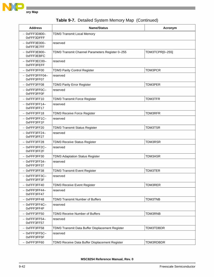
Memory Map
− 0xFFF3D800– 0xFFF3DFFF
TDM3 Transmit Local Memory
− 0xFFF3E000– 0xFFF3E7FF
reserved
− 0xFFF3E800– 0xFFF3EBFC
TDM3 Transmit Channel Parameters Register 0–255 TDM3TCPR[0–255]
− 0xFFF3EC00– 0xFFF3FEFF
reserved
− 0xFFF3FF00 TDM3 Parity Control Register TDM3PCR
− 0xFFF3FFF04– 0xFFF3FF07
reserved
− 0xFFF3FF08 TDM3 Parity Error Register TDM3PER
− 0xFFF3FF0C– 0xFFF3FF0F
reserved
− 0xFFF3FF10 TDM3 Transmit Force Register TDM3TFR
− 0xFFF3FF14– 0xFFF3FF17
reserved
− 0xFFF3FF18 TDM3 Receive Force Register TDM3RFR
− 0xFFF3FF1C– 0xFFF3FF1F
reserved
− 0xFFF3FF20 TDM3 Transmit Status Register TDM3TSR
− 0xFFF3FF24– 0xFFF3FF27
reserved
− 0xFFF3FF28 TDM3 Receive Status Register TDM3RSR
− 0xFFF3FF2C– 0xFFF3FF2F
reserved
− 0xFFF3FF30 TDM3 Adaptation Status Register TDM3ASR
− 0xFFF3FF34– 0xFFF3FF37
reserved
− 0xFFF3FF38 TDM3 Transmit Event Register TDM3TER
− 0xFFF3FF3C– 0xFFF3FF3F
reserved
− 0xFFF3FF40 TDM3 Receive Event Register TDM3RER
− 0xFFF3FF44– 0xFFF3FF47
reserved
− 0xFFF3FF48 TDM3 Transmit Number of Buffers TDM3TNB
− 0xFFF3FF4C– 0xFFF3FF4F
reserved
− 0xFFF3FF50 TDM3 Receive Number of Buffers TDM3RNB
− 0xFFF3FF54– 0xFFF3FF57
reserved
− 0xFFF3FF58 TDM3 Transmit Data Buffer Displacement Register TDM3TDBDR
− 0xFFF3FF5C– 0xFFF3FF5F
reserved
− 0xFFF3FF60 TDM3 Receive Data Buffer Displacement Register TDM3RDBDR
Table 9-7. Detailed System Memory Map (Continued)
Address Name/Status Acronym
MSC8254 Reference Manual, Rev. 0
9-42 Freescale Semiconductor

Detailed System Memory Map
− 0xFFF3FF64– 0xFFF3FF67
reserved
− 0xFFF3FF68 TDM3 Adaptation Sync Distance Register TDM3ASDR
− 0xFFF3FF6C– 0xFFF3FF6F
reserved
− 0xFFF3FF70 TDM3 Transmit Interrupt Enable Register TDM30TIER
− 0xFFF3FF74– 0xFFF3FF77
reserved
− 0xFFF3FF78 TDM3 Receive Interrupt Enable Register TDM3RIER
− 0xFFF3FF7C– 0xFFF3FF7F
reserved
− 0xFFF3FF80 TDM3 Transmit Data Buffer Second Threshold TDM3TDBST
− 0xFFF3FF84– 0xFFF3FF87
reserved
− 0xFFF3FF88 TDM3 Receive Data Buffer Second Threshold TDM3RDBST
− 0xFFF3FF8C– 0xFFF3FF8F
reserved
− 0xFFF3FF90 TDM3 Transmit Data Buffer First Threshold TDM3TDBFT
− 0xFFF3FF94– 0xFFF3FF97
reserved
− 0xFFF3FF98 TDM3 Receive Data Buffer First Threshold TDM3RDBFT
− 0xFFF3FF9C– 0xFFF3FF9F
reserved
− 0xFFF3FFA0 TDM3 Transmit Control Register TDM3TCR
− 0xFFF3FFA4– 0xFFF3FFA7
reserved
− 0xFFF3FFA8 TDM3 Receive Control Register TDM3RCR
− 0xFFF3FFAC– 0xFFF3FFAF
reserved
− 0xFFF3FFB0 TDM3 Adaptation Control Register TDM3ACR
− 0xFFF3FFB4–0xFFF3FFB7
reserved
− 0xFFF3FFB8 TDM3 Transmit Global Base Address TDM3TGBA
− 0xFFF3FFBC– 0xFFF3FFBF
reserved
− 0xFFF3FFC0 TDM3 Receive Global Base Address TDM3RGBA
− 0xFFF3FFC4– 0xFFF3FFC7
reserved
− 0xFFF3FFC8 TDM3 Transmit Data Buffer Size TDM3TDBS
− 0xFFF3FFCC– 0xFFF3FFCF
reserved
− 0xFFF3FFD0 TDM3 Receive Data Buffer Size TDM3RDBS
− 0xFFF3FFD4– 0xFFF3FFD7
reserved
− 0xFFF3FFD8 TDM3 Transmit Frame Parameters TDM3TFP
Table 9-7. Detailed System Memory Map (Continued)
Address Name/Status Acronym
MSC8254 Reference Manual, Rev. 0
Freescale Semiconductor 9-43

Memory Map
− 0xFFF3FFDC– 0xFFF3FFDF
reserved
− 0xFFF3FFE0 TDM3 Receive Frame Parameters TDM3RFP
− 0xFFF3FFE4– 0xFFF3FFE7
reserved
− 0xFFF3FFE8 TDM3 Transmit Interface Register TDM3TIR
− 0xFFF3FFEC– 0xFFF3FFEF
reserved
− 0xFFF3FFF0 TDM3 Receive Interface Register TDM3RIR
− 0xFFF3FFF4– 0xFFF3FFF7
reserved
− 0xFFF3FFF8 TDM3 General Interface Register TDM3GIR
− 0xFFF3FFFC– 0xFFF3FFFF
reserved
• 0xFFF40000– 0xFFF7FFFF
reserved
• 0xFFF80000– 0xFFF9FFFF
RapidIO
− 0xFFF80000 Device Identity Capability Register DIDCAR
− 0xFFF80004 Device Information Capability Register DICAR
− 0xFFF80008 Assembly Identity Capability Register AIDCAR
− 0xFFF8000C Assembly Information Capability Register AICAR
− 0xFFF80010 Processing Element Features Capability Register PEFCAR
− 0xFFF80018 Source Operations Capability Register SOCAR
− 0xFFF8001C Destination Operations Capability Register DOCAR
− 0xFFF80020– 0xFFF8003F
reserved
− 0xFFF80040 Mailbox Command And Status Register MCSR
− 0xFFF80044 Port -Write and Doorbell Command and Status Register PWDCSR
− 0xFFF80048– 0xFFF8004B
reserved
− 0xFFF8004C Processing Element Logical Layer Control Command and Status Register
PELLCCSR
− 0xFFF80050– 0xFFF8005B
reserved
− 0xFFF8005C Local Configuration Space Base Address 1 Command and Status Register
LCSBA1CSR
− 0xFFF80060 Base Device ID Command and Status Register BDIDCSR
− 0xFFF80064– 0xFFF80067
reserved
− 0xFFF80068 Host Base Device ID Lock Command and Status Register HBDIDLCSR
− 0xFFF8006C Component Tag Command and Status Register CTCSR
− 0xFFF80070– 0xFFF800FF
reserved
− 0xFFF80100 Port Maintenance Block Header 0 PMBH0
Table 9-7. Detailed System Memory Map (Continued)
Address Name/Status Acronym
MSC8254 Reference Manual, Rev. 0
9-44 Freescale Semiconductor

Detailed System Memory Map
− 0xFFF80104– 0xFFF8011F
reserved
− 0xFFF80120 Port Link Time-out Control Command and Status Register PLTOCCSR
− 0xFFF80124 Port Response Time-out Control Command and Status Register PRTOCCSR
− 0xFFF80128– 0xFFF8013B
reserved
− 0xFFF8013C Port General Control Command and Status Register PGCCSR
− 0xFFF80140 Port 0 Link Maintenance Request Command and Status Register P0LMREQCSR
− 0xFFF80144 Port 0 Link Maintenance Response Command and Status Register
P0LMRESPCSR
− 0xFFF80148 Port 0 Local ackID Status Command and Status Register P0LASCSR
− 0xFFF8014C– 0xFFF80157
reserved
− 0xFFF80158 Port 0 Error and Status Command and Status Register P0ESCSR
− 0xFFF8015C Port 0 Control Command and Status Register P0CCSR
− 0xFFF80160 Port 1 Link Maintenance Request Command and Status Register P1LMREQCSR
− 0xFFF80164 Port 1 Link Maintenance Response Command and Status Register
P1LMRESPCSR
− 0xFFF80168 Port 1 Local ackID Status Command and Status Register P1LASCSR
− 0xFFF8016C– 0xFFF80177
reserved
− 0xFFF80178 Port 1 Error and Status Command and Status Register P1ESCSR
− 0xFFF8017C Port 1 Control Command and Status Register P1CCSR
− 0xFFF80180– 0xFFF805FF
reserved
− 0xFFF80600 Error Reporting Block Header ERBH
− 0xFFF80604– 0xFFF80607
reserved
− 0xFFF80608 Logical/Transport Layer Error Detect Command and Status Register
LTLEDCSR
− 0xFFF8060C Logical/Transport Layer Error Enable Command and Status Register
LTLEECSR
− 0xFFF80610– 0xFFF80613
reserved
− 0xFFF80614 Logical/Transport Layer Address Capture Command and Status Register
LTLACCSR
− 0xFFF80618 Logical/Transport Layer Device ID Capture Command and Status Register
LTLDIDCCSR
− 0xFFF8061C Logical/Transport Layer Control Capture Command and Status Register
LTLCCCSR
− 0xFFF80620– 0xFFF8063F
reserved
− 0xFFF80640 Port 0 Error Detect Command and Status Register P0EDCSR
− 0xFFF80644 Port 0 Error Rate Enable Command and Status Register P0ERECSR
− 0xFFF80648 Port 0 Error Capture Attributes Command and Status Register P0ECACSR
Table 9-7. Detailed System Memory Map (Continued)
Address Name/Status Acronym
MSC8254 Reference Manual, Rev. 0
Freescale Semiconductor 9-45

Memory Map
− 0xFFF8064C Port 0 Packet/Control Symbol Error Capture Command and Status Register 0
P0PCSECCSR0
− 0xFFF80650 Port 0 Packet Error Capture Command and Status Register 1 P0PECCSR1
− 0xFFF80654 Port 0 Packet Error Capture Command and Status Register 2 P0PECCSR2
− 0xFFF80658 Port 0 Packet Error Capture Command and Status Register 3 P0PECCSR3
− 0xFFF8065C– 0xFFF80667
reserved
− 0xFFF80668 Port 0 Error Rate Command and Status Register P0ERCSR
− 0xFFF8066C Port 0 Error Rate Threshold Command and Status Register P0ERTCSR
− 0xFFF80670– 0xFFF8067F
reserved
− 0xFFF80680 Port 1 Error Detect Command and Status Register P1EDCSR
− 0xFFF80684 Port 1 Error Rate Enable Command and Status Register P1ERECSR
− 0xFFF80688 Port 1 Error Capture Attributes Command and Status Register P1ECACSR
− 0xFFF8068C Port 1 Packet/Control Symbol Error Capture Command and Status Register 0
P1PCSECCSR0
− 0xFFF80690 Port 1 Packet Error Capture Command and Status Register 1 P1PECCSR1
− 0xFFF80694 Port 1 Packet Error Capture Command and Status Register 2 P1PECCSR2
− 0xFFF80698 Port 1 Packet Error Capture Command and Status Register 3 P1PECCSR3
− 0xFFF8069C– 0xFFF806A7
reserved
− 0xFFF806A8 Port 1 Error Rate Command and Status Register P1ERCSR
− 0xFFF806AC Port 1 Error Rate Threshold Command and Status Register P1ERTCSR
− 0xFFF806B0– 0xFFF90003
reserved
− 0xFFF90004 Logical Layer Configuration Register LLCR
− 0xFFF90008– 0xFFF9000F
reserved
− 0xFFF90010 Error/Port-Write Interrupt Status Register EPWISR
− 0xFFF90014– 0xFFF9001F
reserved
− 0xFFF90020 Logical Retry Error Threshold Configuration Register LRETCR
− 0xFFF90024– 0xFFF9007F
reserved
− 0xFFF90080 Physical Retry Error Threshold Configuration Register PRETCR
− 0xFFF90084– 0xFFF900FF
reserved
− 0xFFF90100 Port 0 Alternate Device ID Command and Status Register P0ADIDCSR
− 0xFFF90104– 0xFFF9011F
reserved
− 0xFFF90120 Port 0 Pass-Through Accept-All Configuration Register P0PTAACR
− 0xFFF90124 Port 0 Logical Outbound Packet Time-to-Live Configuration Register
P0LOPTTLCR
− 0xFFF90128– 0xFFF9012F
reserved
Table 9-7. Detailed System Memory Map (Continued)
Address Name/Status Acronym
MSC8254 Reference Manual, Rev. 0
9-46 Freescale Semiconductor

Detailed System Memory Map
− 0xFFF90130 Port 0 Implementation Error Command and Status Register P0IECSR
− 0xFFF90134– 0xFFF9013F
reserved
− 0xFFF90140 Port 0 Physical Configuration Register P0PCR
− 0xFFF90144– 0xFFF90157
reserved
− 0xFFF90158 Port 0 Serial Link Command And Status Register P0SLCSR
− 0xFFF9015C– 0xFFF9015F
reserved
− 0xFFF90160 Port 0 Serial Link Error Injection Configuration Register P0SLEICR
− 0xFFF90164– 0xFFF9017F
reserved
− 0xFFF90180 Port 1 Alternate Device ID Command and Status Register P1ADIDCSR
− 0xFFF90184– 0xFFF9019F
reserved
− 0xFFF901A0 Port 1 Pass-Through Accept-All Configuration Register P1PTAACR
− 0xFFF901A4 Port 1 Logical Outbound Packet Time-to-Live Configuration Register
P1LOPTTLCR
− 0xFFF901A8– 0xFFF901AF
reserved
− 0xFFF901B0 Port 1 Implementation Error Command and Status Register P1IECSR
− 0xFFF901B4– 0xFFF901BF
reserved
− 0xFFF901C0 Port 1 Physical Configuration Register P1PCR
− 0xFFF901C4– 0xFFF901D7
reserved
− 0xFFF901D8 Port 1 Serial Link Command And Status Register P1SLCSR
− 0xFFF901DC– 0xFFF901DF
reserved
− 0xFFF901E0 Port 1 Serial Link Error Injection Configuration Register P1SLEICR
− 0xFFF901E4– 0xFFF90BF7
reserved
− 0xFFF90BF8 IP Block Revision Register 1 IPBRR1
− 0xFFF90BFC IP Block Revision Register 2 IPBRR2
− 0xFFF90C00 Port 0 RapidIO Outbound Window Translation Address Register 0 P0ROWTAR0
− 0xFFF90C04 Port 0 RapidIO Outbound Window Translation Extended Address Register 0
P0ROWTEAR0
− 0xFFF90C08– 0xFFF90C0F
reserved
− 0xFFF90C10 Port 0 RapidIO Outbound Window Attributes Register 0 P0ROWAR0
− 0xFFF90C14– 0xFFF90C1F
reserved
− 0xFFF90C20 Port 0 RapidIO Outbound Window Translation Address Register 1 P0ROWTAR1
− 0xFFF90C24 Port 0 RapidIO Outbound Window Translation Extended Address Register 1
P0ROWTEAR1
Table 9-7. Detailed System Memory Map (Continued)
Address Name/Status Acronym
MSC8254 Reference Manual, Rev. 0
Freescale Semiconductor 9-47

Memory Map
− 0xFFF90C28– 0xFFF90C2F
reserved
− 0xFFF90C30 Port 0 RapidIO Outbound Window Attributes Register 1 P0ROWAR1
− 0xFFF90C34 Port 0 RapidIO Outbound Window Segment 1 Register 1 P0ROWS1R1
− 0xFFF90C38 Port 0 RapidIO Outbound Window Segment 2 Register 1 P0ROWS2R1
− 0xFFF90C3C Port 0 RapidIO Outbound Window Segment 3 Register 1 P0ROWS3R1
− 0xFFF90C40 Port 0 RapidIO Outbound Window Translation Address Register 2 P0ROWTAR2
− 0xFFF90C44 Port 0 RapidIO Outbound Window Translation Extended Address Register 2
P0ROWTEAR2
− 0xFFF90C48 Port 0 RapidIO Outbound Window Base Address Register 2 P0ROWBAR2
− 0xFFF90C4C– 0xFFF90C4F
reserved
− 0xFFF90C50 Port 0 RapidIO Outbound Window Attributes Register 2 P0ROWAR2
− 0xFFF90C54 Port 0 RapidIO Outbound Window Segment 1 Register 2 P0ROWS1R2
− 0xFFF90C58 Port 0 RapidIO Outbound Window Segment 2 Register 2 P0ROWS2R2
− 0xFFF90C5C Port 0 RapidIO Outbound Window Segment 3 Register 2 P0ROWS3R2
− 0xFFF90C60 Port 0 RapidIO Outbound Window Translation Address Register 3 P0ROWTAR3
− 0xFFF90C64 Port 0 RapidIO Outbound Window Translation Extended Address Register 3
P0ROWTEAR3
− 0xFFF90C68 Port 0 RapidIO Outbound Window Base Address Register 3 P0ROWBAR3
− 0xFFF90C6C– 0xFFF90C6F
reserved
− 0xFFF90C70 Port 0 RapidIO Outbound Window Attributes Register 3 P0ROWAR3
− 0xFFF90C74 Port 0 RapidIO Outbound Window Segment 1 Register 3 P0ROWS1R3
− 0xFFF90C78 Port 0 RapidIO Outbound Window Segment 2 Register 3 P0ROWS2R3
− 0xFFF90C7C Port 0 RapidIO Outbound Window Segment 3 Register 3 P0ROWS3R3
− 0xFFF90C80 Port 0 RapidIO Outbound Window Translation Address Register 4 P0ROWTAR4
− 0xFFF90C84 Port 0 RapidIO Outbound Window Translation Extended Address Register 4
P0ROWTEAR4
− 0xFFF90C88 Port 0 RapidIO Outbound Window Base Address Register 4 P0ROWBAR4
− 0xFFF90C8C– 0xFFF90C8F
reserved
− 0xFFF90C90 Port 0 RapidIO Outbound Window Attributes Register 4 P0ROWAR4
− 0xFFF90C94 Port 0 RapidIO Outbound Window Segment 1 Register 4 P0ROWS1R4
− 0xFFF90C98 Port 0 RapidIO Outbound Window Segment 2 Register 4 P0ROWS2R4
− 0xFFF90C9C Port 0 RapidIO Outbound Window Segment 3 Register 4 P0ROWS3R4
− 0xFFF90CA0 Port 0 RapidIO Outbound Window Translation Address Register 5 P0ROWTAR5
− 0xFFF90CA4 Port 0 RapidIO Outbound Window Translation Extended Address Register 5
P0ROWTEAR5
− 0xFFF90CA8 Port 0 RapidIO Outbound Window Base Address Register 5 P0ROWBAR5
− 0xFFF90CAC– 0xFFF90CAF
reserved
− 0xFFF90CB0 Port 0 RapidIO Outbound Window Attributes Register 5 P0ROWAR5
− 0xFFF90CB4 Port 0 RapidIO Outbound Window Segment 1 Register 5 P0ROWS1R5
Table 9-7. Detailed System Memory Map (Continued)
Address Name/Status Acronym
MSC8254 Reference Manual, Rev. 0
9-48 Freescale Semiconductor

Detailed System Memory Map
− 0xFFF90CB8 Port 0 RapidIO Outbound Window Segment 2 Register 5 P0ROWS2R5
− 0xFFF90CBC Port 0 RapidIO Outbound Window Segment 3 Register 5 P0ROWS3R5
− 0xFFF90CC0 Port 0 RapidIO Outbound Window Translation Address Register 6 P0ROWTAR6
− 0xFFF90CC4 Port 0 RapidIO Outbound Window Translation Extended Address Register 6
P0ROWTEAR6
− 0xFFF90CC8 Port 0 RapidIO Outbound Window Base Address Register 6 P0ROWBAR6
− 0xFFF90CCC– 0xFFF90CCF
reserved
− 0xFFF90CD0 Port 0 RapidIO Outbound Window Attributes Register 6 P0ROWAR6
− 0xFFF90CD4 Port 0 RapidIO Outbound Window Segment 1 Register 6 P0ROWS1R6
− 0xFFF90CD8 Port 0 RapidIO Outbound Window Segment 2 Register 6 P0ROWS2R6
− 0xFFF90CDC Port 0 RapidIO Outbound Window Segment 3 Register 6 P0ROWS3R6
− 0xFFF90CE0 Port 0 RapidIO Outbound Window Translation Address Register 7 P0ROWTAR7
− 0xFFF90CE4 Port 0 RapidIO Outbound Window Translation Extended Address Register 7
P0ROWTEAR7
− 0xFFF90CE8 Port 0 RapidIO Outbound Window Base Address Register 7 P0ROWBAR7
− 0xFFF90CEC– 0xFFF90CEF
reserved
− 0xFFF90CF0 Port 0 RapidIO Outbound Window Attributes Register 7 P0ROWAR7
− 0xFFF90CF4 Port 0 RapidIO Outbound Window Segment 1 Register 7 P0ROWS1R7
− 0xFFF90CF8 Port 0 RapidIO Outbound Window Segment 2 Register 7 P0ROWS2R7
− 0xFFF90CFC Port 0 RapidIO Outbound Window Segment 3 Register 7 P0ROWS3R7
− 0xFFF90D00 Port 0 RapidIO Outbound Window Translation Address Register 8 P0ROWTAR8
− 0xFFF90D04 Port 0 RapidIO Outbound Window Translation Extended Address Register 8
P0ROWTEAR8
− 0xFFF90D08 Port 0 RapidIO Outbound Window Base Address Register 8 P0ROWBAR8
− 0xFFF90D0C– 0xFFF90D0F
reserved
− 0xFFF90D10 Port 0 RapidIO Outbound Window Attributes Register 8 P0ROWAR8
− 0xFFF90D14 Port 0 RapidIO Outbound Window Segment 1 Register 8 P0ROWS1R8
− 0xFFF90D18 Port 0 RapidIO Outbound Window Segment 2 Register 8 P0ROWS2R8
− 0xFFF90D1C Port 0 RapidIO Outbound Window Segment 3 Register 8 P0ROWS3R8
− 0xFFF90D20– 0xFFF90D5F
reserved
− 0xFFF90D60 Port 0 RapidIO Inbound Window Translation Address Register 4 P0RIWTAR4
− 0xFFF90D64– 0xFFF90D67
reserved
− 0xFFF90D68 Port 0 RapidIO Inbound Window Base Address Register 4 P0RIWBAR4
− 0xFFF90D6C– 0xFFF90D6F
reserved
− 0xFFF90D70 Port 0 RapidIO Inbound Window Attributes Register 4 P0RIWAR4
− 0xFFF90D74– 0xFFF90D7F
reserved
− 0xFFF90D80 Port 0 RapidIO Inbound Window Translation Address Register 3 P0RIWTAR3
Table 9-7. Detailed System Memory Map (Continued)
Address Name/Status Acronym
MSC8254 Reference Manual, Rev. 0
Freescale Semiconductor 9-49

Memory Map
− 0xFFF90D84– 0xFFF90D87
reserved
− 0xFFF90D88 Port 0 RapidIO Inbound Window Base Address Register 3 P0RIWBAR3
− 0xFFF90D8C– 0xFFF90D8F
reserved
− 0xFFF90D90 Port 0 RapidIO Inbound Window Attributes Register 3 P0RIWAR3
− 0xFFF90D94– 0xFFF90D9F
reserved
− 0xFFF90DA0 Port 0 RapidIO Inbound Window Translation Address Register 2 P0RIWTAR2
− 0xFFF90DA4– 0xFFF90DA7
reserved
− 0xFFF90DA8 Port 0 RapidIO Inbound Window Base Address Register 2 P0RIWBAR2
− 0xFFF90DAC– 0xFFF90DAF
reserved
− 0xFFF90DB0 Port 0 RapidIO inbound window attributes register 2 P0RIWAR2
− 0xFFF90DB4– 0xFFF90DBF
reserved
− 0xFFF90DC0 Port 0 RapidIO Inbound Window Translation Address Register 1 P0RIWTAR1
− 0xFFF90DC4– 0xFFF90DC7
reserved
− 0xFFF90DC8 Port 0 RapidIO Inbound Window Base Address Register 1 P0RIWBAR1
− 0xFFF90DCC– 0xFFF90DCF
reserved
− 0xFFF90DD0 Port 0 RapidIO Inbound Window Attributes Register 1 P0RIWAR1
− 0xFFF90DD4– 0xFFF90DDF
reserved
− 0xFFF90DE0 Port 0 RapidIO Inbound Window Translation Address Register 0 P0RIWTAR0
− 0xFFF90DE4– 0xFFF90DEF
reserved
− 0xFFF90DF0 Port 0 RapidIO Inbound Window Attributes Register 0 P0RIWAR0
− 0xFFF90DF4– 0xFFF92DFF
reserved
− 0xFFF90E00 Port 1 RapidIO Outbound Window Translation Address Register 0 P1ROWTAR0
− 0xFFF90E04 Port 1 RapidIO Outbound Window Translation Extended Address Register 0
P1ROWTEAR0
− 0xFFF90E08 Port 1 RapidIO Outbound Window Base Address Register 0 P1ROWBAR0
− 0xFFF90E0C– 0xFFF90E0F
reserved
− 0xFFF90E10 Port 1 RapidIO Outbound Window Attributes Register 0 P1ROWAR0
− 0xFFF90E14– 0xFFF90E1F
reserved
− 0xFFF90E20 Port 1 RapidIO Outbound Window Translation Address Register 1 P1ROWTAR1
− 0xFFF90E24 Port 1 RapidIO Outbound Window Translation Extended Address Register 1
P1ROWTEAR1
− 0xFFF90E28 Port 1 RapidIO Outbound Window Base Address Register 1 P1ROWBAR1
Table 9-7. Detailed System Memory Map (Continued)
Address Name/Status Acronym
MSC8254 Reference Manual, Rev. 0
9-50 Freescale Semiconductor

Detailed System Memory Map
− 0xFFF90E2C– 0xFFF90E2F
reserved
− 0xFFF90E30 Port 1 RapidIO Outbound Window Attributes Register 1 P1ROWAR1
− 0xFFF90E34 Port 1 RapidIO Outbound Window Segment 1 Register 1 P1ROWS1R1
− 0xFFF90E38 Port 1 RapidIO Outbound Window Segment 2 Register 1 P1ROWS2R1
− 0xFFF90E3C Port 1 RapidIO Outbound Window Segment 3 Register 1 P1ROWS3R1
− 0xFFF90E40 Port 1 RapidIO Outbound Window Translation Address Register 2 P1ROWTAR2
− 0xFFF90E44 Port 1 RapidIO Outbound Window Translation Extended Address Register 2
P1ROWTEAR2
− 0xFFF90E48 Port 1 RapidIO Outbound Window Base Address Register 2 P1ROWBAR2
− 0xFFF90E4C– 0xFFF90E4F
reserved
− 0xFFF90E50 Port 1 RapidIO Outbound Window Attributes Register 2 P1ROWAR2
− 0xFFF90E54 Port 1 RapidIO Outbound Window Segment 1 Register 2 P1ROWS1R2
− 0xFFF90E58 Port 1 RapidIO Outbound Window Segment 2 Register 2 P1ROWS2R2
− 0xFFF90E5C Port 1 RapidIO Outbound Window Segment 3 Register 2 P1ROWS3R2
− 0xFFF90E60 Port 1 RapidIO Outbound Window Translation Address Register 3 P1ROWTAR3
− 0xFFF90E64 Port 1 RapidIO Outbound Window Translation Extended Address Register 3
P1ROWTEAR3
− 0xFFF90E68 Port 1 RapidIO Outbound Window Base Address Register 3 P1ROWBAR3
− 0xFFF90E6C– 0xFFF90E6F
reserved
− 0xFFF90E70 Port 1 RapidIO Outbound Window Attributes Register 3 P1ROWAR3
− 0xFFF90E74 Port 1 RapidIO Outbound Window Segment 1 Register 3 P1ROWS1R3
− 0xFFF90E78 Port 1 RapidIO Outbound Window Segment 2 Register 3 P1ROWS2R3
− 0xFFF90E7C Port 1 RapidIO Outbound Window Segment 3 Register 3 P1ROWS3R3
− 0xFFF90E80 Port 1 RapidIO Outbound Window Translation Address Register 4 P1ROWTAR4
− 0xFFF90E84 Port 1 RapidIO Outbound Window Translation Extended Address Register 4
P1ROWTEAR4
− 0xFFF90E88 Port 1 RapidIO Outbound Window Base Address Register 4 P1ROWBAR4
− 0xFFF90E8C– 0xFFF90E8F
reserved
− 0xFFF90E90 Port 1 RapidIO Outbound Window Attributes Register 4 P1ROWAR4
− 0xFFF90E94 Port 1 RapidIO Outbound Window Segment 1 Register 4 P1ROWS1R4
− 0xFFF90E98 Port 1 RapidIO Outbound Window Segment 2 Register 4 P1ROWS2R4
− 0xFFF90E9C Port 1 RapidIO Outbound Window Segment 3 Register 4 P1ROWS3R4
− 0xFFF90EA0 Port 1 RapidIO Outbound Window Translation Address Register 5 P1ROWTAR5
− 0xFFF90EA4 Port 1 RapidIO Outbound Window Translation Extended Address Register 5
P1ROWTEAR5
− 0xFFF90EA8 Port 1 RapidIO Outbound Window Base Address Register 5 P1ROWBAR5
− 0xFFF90EAC– 0xFFF90EAF
reserved
− 0xFFF90EB0 Port 1 RapidIO Outbound Window Attributes Register 5 P1ROWAR5
− 0xFFF90EB4 Port 1 RapidIO Outbound Window Segment 1 Register 5 P1ROWS1R5
Table 9-7. Detailed System Memory Map (Continued)
Address Name/Status Acronym
MSC8254 Reference Manual, Rev. 0
Freescale Semiconductor 9-51

Memory Map
− 0xFFF90EB8 Port 1 RapidIO Outbound Window Segment 2 Register 5 P1ROWS2R5
− 0xFFF90EBC Port 1 RapidIO Outbound Window Segment 3 Register 5 P1ROWS3R5
− 0xFFF90EC0 Port 1 RapidIO Outbound Window Translation Address Register 6 P1ROWTAR6
− 0xFFF90EC4 Port 1 RapidIO Outbound Window Translation Extended Address Register 6
P1ROWTEAR6
− 0xFFF90EC8 Port 1 RapidIO Outbound Window Base Address Register 6 P1ROWBAR6
− 0xFFF90ECC– 0xFFF90ECF
reserved
− 0xFFF90ED0 Port 1 RapidIO Outbound Window Attributes Register 6 P1ROWAR6
− 0xFFF90ED4 Port 1 RapidIO Outbound Window Segment 1 Register 6 P1ROWS1R6
− 0xFFF90ED8 Port 1 RapidIO Outbound Window Segment 2 Register 6 P1ROWS2R6
− 0xFFF90EDC Port 1 RapidIO Outbound Window Segment 3 Register 6 P1ROWS3R6
− 0xFFF90EE0 Port 1 RapidIO Outbound Window Translation Address Register 7 P1ROWTAR7
− 0xFFF90EE4 Port 1 RapidIO Outbound Window Translation Extended Address Register 7
P1ROWTEAR7
− 0xFFF90EE8 Port 1 RapidIO Outbound Window Base Address Register 7 P1ROWBAR7
− 0xFFF90EEC– 0xFFF90EEF
reserved
− 0xFFF90EF0 Port 1 RapidIO Outbound Window Attributes Register 7 P1ROWAR7
− 0xFFF90EF4 Port 1 RapidIO Outbound Window Segment 1 Register 7 P1ROWS1R7
− 0xFFF90EF8 Port 1 RapidIO Outbound Window Segment 2 Register 7 P1ROWS2R7
− 0xFFF90EFC Port 1 RapidIO Outbound Window Segment 3 Register 7 P1ROWS3R7
− 0xFFF90F00 Port 1 RapidIO Outbound Window Translation Address Register 8 P1ROWTAR8
− 0xFFF90F04 Port 1 RapidIO Outbound Window Translation Extended Address Register 8
P1ROWTEAR8
− 0xFFF90F08 Port 1 RapidIO Outbound Window Base Address Register 8 P1ROWBAR8
− 0xFFF90F0C– 0xFFF90F0F
reserved
− 0xFFF90F10 Port 1 RapidIO Outbound Window Attributes Register 8 P1ROWAR8
− 0xFFF90F14 Port 1 RapidIO Outbound Window Segment 1 Register 8 P1ROWS1R8
− 0xFFF90F18 Port 1 RapidIO Outbound Window Segment 2 Register 8 P1ROWS2R8
− 0xFFF90F1C Port 1 RapidIO Outbound Window Segment 3 Register 8 P1ROWS3R8
− 0xFFF90F20– 0xFFF90F5F
reserved
− 0xFFF90F60 Port 1 RapidIO Inbound Window Translation Address Register 4 P1RIWTAR4
− 0xFFF90F64– 0xFFF90F67
reserved
− 0xFFF90F68 Port 1 RapidIO Inbound Window Base Address Register 4 P1RIWBAR4
− 0xFFF90F6C– 0xFFF90F6F
reserved
− 0xFFF90F70 Port 1 RapidIO Inbound Window Attributes Register 4 P1RIWAR4
− 0xFFF90F74– 0xFFF90F7F
reserved
− 0xFFF90F80 Port 1 RapidIO Inbound Window Translation Address Register 3 P1RIWTAR3
Table 9-7. Detailed System Memory Map (Continued)
Address Name/Status Acronym
MSC8254 Reference Manual, Rev. 0
9-52 Freescale Semiconductor

Detailed System Memory Map
− 0xFFF90F84– 0xFFF90F87
reserved
− 0xFFF90F88 Port 1 RapidIO Inbound Window Base Address Register 3 P1RIWBAR3
− 0xFFF90F8C– 0xFFF90F8F
reserved
− 0xFFF90F90 Port 1 RapidIO Inbound Window Attributes Register 3 P1RIWAR3
− 0xFFF90F94– 0xFFF90F9F
reserved
− 0xFFF90FA0 Port 1 RapidIO Inbound Window Translation Address Register 2 P1RIWTAR2
− 0xFFF90FA4– 0xFFF90FA7
reserved
− 0xFFF90FA8 Port 1 RapidIO Inbound Window Base Address Register 2 P1RIWBAR2
− 0xFFF90FAC– 0xFFF90FAF
reserved
− 0xFFF90FB0 Port 1 RapidIO inbound window attributes register 2 P1RIWAR2
− 0xFFF90FB4– 0xFFF90FBF
reserved
− 0xFFF90FC0 Port 1 RapidIO Inbound Window Translation Address Register 1 P1RIWTAR1
− 0xFFF90FC4– 0xFFF90FC7
reserved
− 0xFFF90FC8 Port 1 RapidIO Inbound Window Base Address Register 1 P1RIWBAR1
− 0xFFF90FCC– 0xFFF90FCF
reserved
− 0xFFF90FD0 Port 1 RapidIO Inbound Window Attributes Register 1 P1RIWAR1
− 0xFFF90FD4– 0xFFF90FDF
reserved
− 0xFFF90FE0 Port 1 RapidIO Inbound Window Translation Address Register 0 P1RIWTAR0
− 0xFFF90FE4– 0xFFF90FE7
reserved
− 0xFFF90FE8 Port 1 RapidIO Inbound Window Base Address Register 1 P1RIWBAR1
− 0xFFF90FEC– 0xFFF90FEF
reserved
− 0xFFF90FF0 Port 1 RapidIO Inbound Window Attributes Register 0 P1RIWAR0
− 0xFFF90FF4– 0xFFF92DFF
reserved
− 0xFFF90FF4– 0xFFF92FFF
reserved
− 0xFFF93000 Outbound Message 0 Mode Register OM0MR
− 0xFFF93004 Outbound Message 0 Status Register OM0SR
− 0xFFF93008– 0xFFF9300B
reserved
− 0xFFF9300C Outbound Message 0 Descriptor Queue Dequeue Pointer Address Register
OM0DQDPAR
− 0xFFF93010– 0xFFF93013
reserved
− 0xFFF93014 Outbound Message 0 Source Address Register OM0SAR
Table 9-7. Detailed System Memory Map (Continued)
Address Name/Status Acronym
MSC8254 Reference Manual, Rev. 0
Freescale Semiconductor 9-53

Memory Map
− 0xFFF93018 Outbound Message 0 Destination Port Register OM0DPR
− 0xFFF9301C Outbound Message 0 Destination Attributes Register OM0DATR
− 0xFFF93020 Outbound Message 0 Double-word Count Register OM0DCR
− 0xFFF93024– 0xFFF93027
reserved
− 0xFFF93028 Outbound Message 0 Descriptor Queue Enqueue Pointer Address Register
OM0DQEPAR
− 0xFFF9302C Outbound Message 0 Retry Error Threshold Configuration Register
OM0RETCR
− 0xFFF93030 Outbound Message 0 Multicast Group Register OM0MGR
− 0xFFF93034 Outbound Message 0 Multicast List Register OM0MLR
− 0xFFF93038– 0xFFF9305F
reserved
− 0xFFF93060 Inbound Message 0 Mode Register IM0MR
− 0xFFF93064 Inbound Message 0 Status Register IM0SR
− 0xFFF93068– 0xFFF9306B
reserved
− 0xFFF9306C Inbound Message 0 Frame Queue Dequeue Pointer Address Register
IM0FQDPAR
− 0xFFF93070– 0xFFF93073
reserved
− 0xFFF93074 Inbound Message 0 Frame Queue Enqueue Pointer Address Register
IM0FQEPAR
− 0xFFF93078 Inbound Message 0 Maximum Interrupt Report Interval Register IM0MIRIR
− 0xFFF9307C– 0xFFF930FF
reserved
− 0xFFF93100 Outbound Message 1 Mode Register OM1MR
− 0xFFF93104 Outbound Message 1 Status Register OM1SR
− 0xFFF93108– 0xFFF9310B
reserved
− 0xFFF9310C Outbound Message 1 Descriptor Queue Dequeue Pointer Address Register
OM1DQDPAR
− 0xFFF93110– 0xFFF93113
reserved
− 0xFFF93114 Outbound Message 1 Source Address Register OM1SAR
− 0xFFF93118 Outbound Message 1 Destination Port Register OM1DPR
− 0xFFF9311C Outbound Message 1 Destination Attributes Register OM1DATR
− 0xFFF93120 Outbound Message 1 Double-word Count Register OM1DCR
− 0xFFF93124– 0xFFF93127
reserved
− 0xFFF93128 Outbound Message 1 Descriptor Queue Enqueue Pointer Address Register
OM1DQEPAR
− 0xFFF9312C Outbound Message 1 Retry Error Threshold Configuration Register
OM1RETCR
− 0xFFF93130 Outbound Message 1 Multicast Group Register OM1MGR
− 0xFFF93134 Outbound Message 1 Multicast List Register OM1MLR
Table 9-7. Detailed System Memory Map (Continued)
Address Name/Status Acronym
MSC8254 Reference Manual, Rev. 0
9-54 Freescale Semiconductor

Detailed System Memory Map
− 0xFFF93138– 0xFFF9315F
reserved
− 0xFFF93160 Inbound Message 1 Mode Register IM1MR
− 0xFFF93164 Inbound Message 1 Status Register IM1SR
− 0xFFF93168– 0xFFF9316B
reserved
− 0xFFF9316C Inbound Message 1 Frame Queue Dequeue Pointer Address Register
IM1FQDPAR
− 0xFFF93170– 0xFFF93173
reserved
− 0xFFF93174 Inbound Message 1 Frame Queue Enqueue Pointer Address Register
IM1FQEPAR
− 0xFFF93178 Inbound Message 1 Maximum Interrupt Report Interval Register IM1MIRIR
− 0xFFF9317C– 0xFFF933FF
reserved
− 0xFFF93400 Outbound Doorbell Mode Register ODMR
− 0xFFF93404 Outbound Doorbell Status Register ODSR
− 0xFFF93408– 0xFFF93417
reserved
− 0xFFF93418 Outbound Doorbell Destination Port Register ODDPR
− 0xFFF9341C Outbound Doorbell Destination Attributes Register ODDATR
− 0xFFF93420– 0xFFF9342B
reserved
− 0xFFF9342C Outbound Doorbell Retry Error Threshold Configuration Register ODRETCR
− 0xFFF93430– 0xFFF9345F
reserved
− 0xFFF93460 Inbound Doorbell Mode Register IDMR
− 0xFFF93464 Inbound Doorbell Status Register IDSR
− 0xFFF93468– 0xFFF9346B
reserved
− 0xFFF9346C Inbound Doorbell Queue Dequeue Pointer Address Register IDQDPAR
− 0xFFF93470– 0xFFF93473
reserved
− 0xFFF93474 Inbound Doorbell Queue Enqueue Pointer Address Register IDQEPAR
− 0xFFF93478 Inbound Doorbell Maximum Interrupt Report Interval Register IDMIRIR
− 0xFFF9347C– 0xFFF934DF
reserved
− 0xFFF934E0 Inbound Port-write Mode Register IPWMR
− 0xFFF934E4 Inbound Port-write Status Register IPWSR
− 0xFFF934EC Inbound Port-write Queue Base Address Register IPWQBAR
− 0xFFF934F0– 0xFFF9FFFF
reserved
• 0xFFFA0000– 0xFFFA0FFF
reserved
• 0xFFFA1000– 0xFFFA103F
HSSI OCN Crossbar Switch to MBus0
Table 9-7. Detailed System Memory Map (Continued)
Address Name/Status Acronym
MSC8254 Reference Manual, Rev. 0
Freescale Semiconductor 9-55

Memory Map
− 0xFFFA1000 OCN-to-MBus Configuration Register 0 O2MCR0
− 0xFFFA1004– 0xFFFA100F
reserved.
− 0xFFFA1010 OCN-to-MBus Error Attribute Register 0 O2MEAR0
− 0xFFFA1014 OCN-to-MBus Error Address Register 0 O2MEADR0
− 0xFFFA1018 OCN-to-MBus Error Status Register 0 O2MESR0
− 0xFFFA101C OCN-to-MBus Interrupt Enable Register 0 O2MIER0
− 0xFFFA1020 OCN-to-MBus Error Capture Enable Register 0 O2MECER0
− 0xFFFA1024– 0xFFFA103F
reserved.
• 0xFFFA1040– 0xFFFA107F
HSSI OCN Crossbar Switch to MBus1
− 0xFFFA1040 OCN-to-MBus Configuration Register 1 O2MCR1
− 0xFFFA1044– 0xFFFA104F
reserved.
− 0xFFFA1040 OCN-to-MBus Error Attribute Register 1 O2MEAR1
− 0xFFFA1044 OCN-to-MBus Error Address Register 1 O2MEADR1
− 0xFFFA1048 OCN-to-MBus Error Status Register 1 O2MESR1
− 0xFFFA104C OCN-to-MBus Interrupt Enable Register 1 O2MIER1
− 0xFFFA1050 OCN-to-MBus Error Capture Enable Register 1 O2MECER1
− 0xFFFA1054– 0xFFFA107F
reserved.
• 0xFFFA1080– 0xFFFA7FFF
reserved
• 0xFFFA8000– 0xFFFA8FFF
HSSI Dedicated DMA Controller 0 Registers
− 0xFFFA8000– 0xFFFA80FF
reserved
− 0xFFFA8100 DMA 0 Mode Register D0MR0
− 0xFFFA8104 DMA 0 Status Register D0SR0
− 0xFFFA8108 DMA 0 Current Link Descriptor Extended Address Register D0ECLNDAR0
− 0xFFFA810C DMA 0 Current Link Descriptor Address Register D0CLNDAR0
− 0xFFFA8110 DMA 0 Source Attributes Register D0SATR0
− 0xFFFA8114 DMA 0 Source Address Register D0SAR0
− 0xFFFA8118 DMA 0 Destination Attributes Register D0DATR0
− 0xFFFA811C DMA 0 Destination Address Register D0DAR0
− 0xFFFA8120 DMA 0 Byte Count Register D0BCR0
− 0xFFFA8124– 0xFFFA8127
reserved
− 0xFFFA8128 DMA 0 Next Link Descriptor Address Register D0NLNDAR0
− 0xFFFA812C– 0xFFFA8133
reserved
− 0xFFFA8134 DMA 0 Current List Descriptor Address Register D0CLSDAR0
− 0xFFFA8138 DMA 0 Extended Next List Descriptor Address Register D0ENLSDAR0
Table 9-7. Detailed System Memory Map (Continued)
Address Name/Status Acronym
MSC8254 Reference Manual, Rev. 0
9-56 Freescale Semiconductor
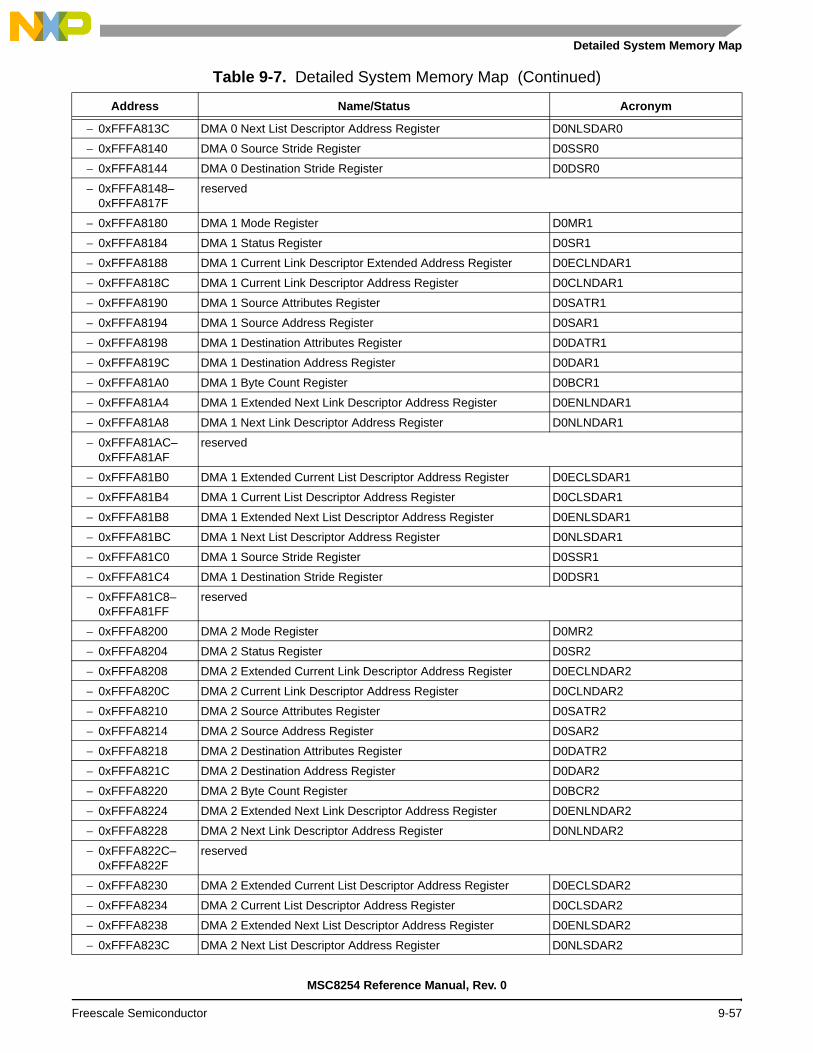
Detailed System Memory Map
− 0xFFFA813C DMA 0 Next List Descriptor Address Register D0NLSDAR0
− 0xFFFA8140 DMA 0 Source Stride Register D0SSR0
− 0xFFFA8144 DMA 0 Destination Stride Register D0DSR0
− 0xFFFA8148– 0xFFFA817F
reserved
− 0xFFFA8180 DMA 1 Mode Register D0MR1
− 0xFFFA8184 DMA 1 Status Register D0SR1
− 0xFFFA8188 DMA 1 Current Link Descriptor Extended Address Register D0ECLNDAR1
− 0xFFFA818C DMA 1 Current Link Descriptor Address Register D0CLNDAR1
− 0xFFFA8190 DMA 1 Source Attributes Register D0SATR1
− 0xFFFA8194 DMA 1 Source Address Register D0SAR1
− 0xFFFA8198 DMA 1 Destination Attributes Register D0DATR1
− 0xFFFA819C DMA 1 Destination Address Register D0DAR1
− 0xFFFA81A0 DMA 1 Byte Count Register D0BCR1
− 0xFFFA81A4 DMA 1 Extended Next Link Descriptor Address Register D0ENLNDAR1
− 0xFFFA81A8 DMA 1 Next Link Descriptor Address Register D0NLNDAR1
− 0xFFFA81AC– 0xFFFA81AF
reserved
− 0xFFFA81B0 DMA 1 Extended Current List Descriptor Address Register D0ECLSDAR1
− 0xFFFA81B4 DMA 1 Current List Descriptor Address Register D0CLSDAR1
− 0xFFFA81B8 DMA 1 Extended Next List Descriptor Address Register D0ENLSDAR1
− 0xFFFA81BC DMA 1 Next List Descriptor Address Register D0NLSDAR1
− 0xFFFA81C0 DMA 1 Source Stride Register D0SSR1
− 0xFFFA81C4 DMA 1 Destination Stride Register D0DSR1
− 0xFFFA81C8– 0xFFFA81FF
reserved
− 0xFFFA8200 DMA 2 Mode Register D0MR2
− 0xFFFA8204 DMA 2 Status Register D0SR2
− 0xFFFA8208 DMA 2 Extended Current Link Descriptor Address Register D0ECLNDAR2
− 0xFFFA820C DMA 2 Current Link Descriptor Address Register D0CLNDAR2
− 0xFFFA8210 DMA 2 Source Attributes Register D0SATR2
− 0xFFFA8214 DMA 2 Source Address Register D0SAR2
− 0xFFFA8218 DMA 2 Destination Attributes Register D0DATR2
− 0xFFFA821C DMA 2 Destination Address Register D0DAR2
− 0xFFFA8220 DMA 2 Byte Count Register D0BCR2
− 0xFFFA8224 DMA 2 Extended Next Link Descriptor Address Register D0ENLNDAR2
− 0xFFFA8228 DMA 2 Next Link Descriptor Address Register D0NLNDAR2
− 0xFFFA822C– 0xFFFA822F
reserved
− 0xFFFA8230 DMA 2 Extended Current List Descriptor Address Register D0ECLSDAR2
− 0xFFFA8234 DMA 2 Current List Descriptor Address Register D0CLSDAR2
− 0xFFFA8238 DMA 2 Extended Next List Descriptor Address Register D0ENLSDAR2
− 0xFFFA823C DMA 2 Next List Descriptor Address Register D0NLSDAR2
Table 9-7. Detailed System Memory Map (Continued)
Address Name/Status Acronym
MSC8254 Reference Manual, Rev. 0
Freescale Semiconductor 9-57
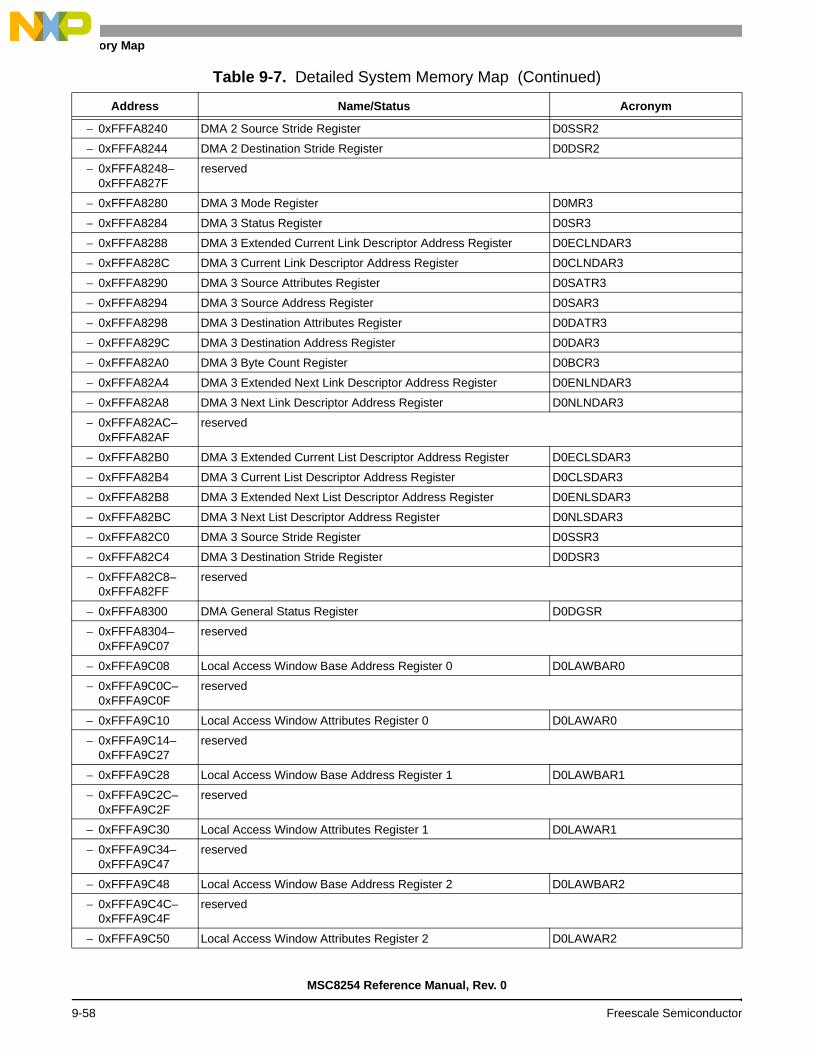
Memory Map
− 0xFFFA8240 DMA 2 Source Stride Register D0SSR2
− 0xFFFA8244 DMA 2 Destination Stride Register D0DSR2
− 0xFFFA8248– 0xFFFA827F
reserved
− 0xFFFA8280 DMA 3 Mode Register D0MR3
− 0xFFFA8284 DMA 3 Status Register D0SR3
− 0xFFFA8288 DMA 3 Extended Current Link Descriptor Address Register D0ECLNDAR3
− 0xFFFA828C DMA 3 Current Link Descriptor Address Register D0CLNDAR3
− 0xFFFA8290 DMA 3 Source Attributes Register D0SATR3
− 0xFFFA8294 DMA 3 Source Address Register D0SAR3
− 0xFFFA8298 DMA 3 Destination Attributes Register D0DATR3
− 0xFFFA829C DMA 3 Destination Address Register D0DAR3
− 0xFFFA82A0 DMA 3 Byte Count Register D0BCR3
− 0xFFFA82A4 DMA 3 Extended Next Link Descriptor Address Register D0ENLNDAR3
− 0xFFFA82A8 DMA 3 Next Link Descriptor Address Register D0NLNDAR3
− 0xFFFA82AC– 0xFFFA82AF
reserved
− 0xFFFA82B0 DMA 3 Extended Current List Descriptor Address Register D0ECLSDAR3
− 0xFFFA82B4 DMA 3 Current List Descriptor Address Register D0CLSDAR3
− 0xFFFA82B8 DMA 3 Extended Next List Descriptor Address Register D0ENLSDAR3
− 0xFFFA82BC DMA 3 Next List Descriptor Address Register D0NLSDAR3
− 0xFFFA82C0 DMA 3 Source Stride Register D0SSR3
− 0xFFFA82C4 DMA 3 Destination Stride Register D0DSR3
− 0xFFFA82C8– 0xFFFA82FF
reserved
− 0xFFFA8300 DMA General Status Register D0DGSR
− 0xFFFA8304– 0xFFFA9C07
reserved
− 0xFFFA9C08 Local Access Window Base Address Register 0 D0LAWBAR0
− 0xFFFA9C0C– 0xFFFA9C0F
reserved
− 0xFFFA9C10 Local Access Window Attributes Register 0 D0LAWAR0
− 0xFFFA9C14– 0xFFFA9C27
reserved
− 0xFFFA9C28 Local Access Window Base Address Register 1 D0LAWBAR1
− 0xFFFA9C2C– 0xFFFA9C2F
reserved
− 0xFFFA9C30 Local Access Window Attributes Register 1 D0LAWAR1
− 0xFFFA9C34– 0xFFFA9C47
reserved
− 0xFFFA9C48 Local Access Window Base Address Register 2 D0LAWBAR2
− 0xFFFA9C4C– 0xFFFA9C4F
reserved
− 0xFFFA9C50 Local Access Window Attributes Register 2 D0LAWAR2
Table 9-7. Detailed System Memory Map (Continued)
Address Name/Status Acronym
MSC8254 Reference Manual, Rev. 0
9-58 Freescale Semiconductor

Detailed System Memory Map
− 0xFFFA9C54– 0xFFFA9C67
reserved
− 0xFFFA9C68 Local Access Window Base Address Register 3 D0LAWBAR3
− 0xFFFA9C6C– 0xFFFA9C6F
reserved
− 0xFFFA9C70 Local Access Window Attributes Register 3 D0LAWAR3
− 0xFFFA9C74– 0xFFFA9C87
reserved
− 0xFFFA9C88 Local Access Window Base Address Register 4 D0LAWBAR4
− 0xFFFA9C8C– 0xFFFA9C8F
reserved
− 0xFFFA9C90 Local Access Window Attributes Register 4 D0LAWAR4
− 0xFFFA9C94– 0xFFFA9CA7
reserved
− 0xFFFA9CA8 Local Access Window Base Address Register 5 D0LAWBAR5
− 0xFFFA9CAC– 0xFFFA9CAF
reserved
− 0xFFFA9CB0 Local Access Window Attributes Register 5 D0LAWAR5
− 0xFFFA9CB4– 0xFFFA9CC7
reserved
− 0xFFFA9CC8 Local Access Window Base Address Register 6 D0LAWBAR6
− 0xFFFA9CCC– 0xFFFA9CCF
reserved
− 0xFFFA9CD0 Local Access Window Attributes Register 6 D0LAWAR6
− 0xFFFA9CD4– 0xFFFA9CE7
reserved
− 0xFFFA9CE8 Local Access Window Base Address Register 7 D0LAWBAR7
− 0xFFFA9CEC– 0xFFFA9CEF
reserved
− 0xFFFA9CF0 Local Access Window Attributes Register 7 D0LAWAR7
− 0xFFFA9CF4– 0xFFFA9D07
reserved
− 0xFFFA9D08 Local Access Window Base Address Register 8 D0LAWBAR8
− 0xFFFA9D0C– 0xFFFA9D0F
reserved
− 0xFFFA9D10 Local Access Window Attributes Register 8 D0LAWAR8
− 0xFFFA9D14– 0xFFFA9D27
reserved
− 0xFFFA9D28 Local Access Window Base Address Register 9 D0LAWBAR9
− 0xFFFA9D2C– 0xFFFA9D2F
reserved
− 0xFFFA9D30 Local Access Window Attributes Register 9 D0LAWAR9
− 0xFFFA9D34– 0xFFFA8FFF
reserved
• 0xFFFA9000– 0xFFFA9FFF
DMA Controller 0 to OCN
Table 9-7. Detailed System Memory Map (Continued)
Address Name/Status Acronym
MSC8254 Reference Manual, Rev. 0
Freescale Semiconductor 9-59

Memory Map
• 0xFFFAA000– 0xFFFAAFFF
Dedicated DMA Controller 1 Registers
− 0xFFFAA000– 0xFFFAA0FF
reserved
− 0xFFFAA100 DMA 0 Mode Register D1MR0
− 0xFFFAA104 DMA 0 Status Register D1SR0
− 0xFFFAA108 DMA 0 Current Link Descriptor Extended Address Register D1ECLNDAR0
− 0xFFFAA10C DMA 0 Current Link Descriptor Address Register D1CLNDAR0
− 0xFFFAA110 DMA 0 Source Attributes Register D1SATR0
− 0xFFFAA114 DMA 0 Source Address Register D1SAR0
− 0xFFFAA118 DMA 0 Destination Attributes Register D1DATR0
− 0xFFFAA11C DMA 0 Destination Address Register D1DAR0
− 0xFFFAA120 DMA 0 Byte Count Register D1BCR0
− 0xFFFAA124– 0xFFFAA127
reserved
− 0xFFFAA128 DMA 0 Next Link Descriptor Address Register D1NLNDAR0
− 0xFFFAA12C– 0xFFFAA133
reserved
− 0xFFFAA134 DMA 0 Current List Descriptor Address Register D1CLSDAR0
− 0xFFFAA138 DMA 0 Next List Descriptor Extended Address Register D1ENLSDAR0
− 0xFFFAA13C DMA 0 Next List Descriptor Address Register D1NLSDAR0
− 0xFFFAA140 DMA 0 Source Stride Register D1SSR0
− 0xFFFAA144 DMA 0 Destination Stride Register D1DSR0
− 0xFFFAA148– 0xFFFAA17F
reserved
− 0xFFFAA180 DMA 1 Mode Register D1MR1
− 0xFFFAA184 DMA 1 Status Register D1SR1
− 0xFFFAA188 DMA 1 Current Link Descriptor Extended Address Register D1ECLNDAR1
− 0xFFFAA18C DMA 1 Current Link Descriptor Address Register D1CLNDAR1
− 0xFFFAA190 DMA 1 Source Attributes Register D1SATR1
− 0xFFFAA194 DMA 1 Source Address Register D1SAR1
− 0xFFFAA198 DMA 1 Destination Attributes Register D1DATR1
− 0xFFFAA19C DMA 1 Destination Address Register D1DAR1
− 0xFFFAA1A0 DMA 1 Byte Count Register D1BCR1
− 0xFFFAA1A4 DMA 1 Next Link Descriptor Extended Address Register D1ENLNDAR1
− 0xFFFAA1A8 DMA 1 Next Link Descriptor Address Register D1NLNDAR1
− 0xFFFAA1AC– 0xFFFAA1AF
reserved
− 0xFFFAA1B0 DMA 1 Current List Descriptor Extended Address Register D1ECLSDAR1
− 0xFFFAA1B4 DMA 1 Current List Descriptor Address Register D1CLSDAR1
− 0xFFFAA1B8 DMA 1 Next List Descriptor Extended Address Register D1ENLSDAR1
− 0xFFFAA1BC DMA 1 Next List Descriptor Address Register D1NLSDAR1
− 0xFFFAA1C0 DMA 1 Source Stride Register D1SSR1
Table 9-7. Detailed System Memory Map (Continued)
Address Name/Status Acronym
MSC8254 Reference Manual, Rev. 0
9-60 Freescale Semiconductor

Detailed System Memory Map
− 0xFFFAA1C4 DMA 1 Destination Stride Register D1DSR1
− 0xFFFAA1C8– 0xFFFAA1FF
reserved
− 0xFFFAA200 DMA 2 Mode Register D1MR2
− 0xFFFAA204 DMA 2 Status Register D1SR2
− 0xFFFAA208 DMA 2 Current Link Descriptor Extended Address Register D1ECLNDAR2
− 0xFFFAA20C DMA 2 Current Link Descriptor Address Register D1CLNDAR2
− 0xFFFAA210 DMA 2 Source Attributes Register D1SATR2
− 0xFFFAA214 DMA 2 Source Address Register D1SAR2
− 0xFFFAA218 DMA 2 Destination Attributes Register D1DATR2
− 0xFFFAA21C DMA 2 Destination Address Register D1DAR2
− 0xFFFAA220 DMA 2 Byte Count Register D1BCR2
− 0xFFFAA224 DMA 2 Next Link Descriptor Extended Address Register D1ENLNDAR2
− 0xFFFAA228 DMA 2 Next Link Descriptor Address Register D1NLNDAR2
− 0xFFFAA22C– 0xFFFAA22F
reserved
− 0xFFFAA230 DMA 2 Current List Descriptor Extended Address Register D1ECLSDAR2
− 0xFFFAA234 DMA 2 Current List Descriptor Address Register D1CLSDAR2
− 0xFFFAA238 DMA 2 Next List Descriptor Extended Address Register D1ENLSDAR2
− 0xFFFAA23C DMA 2 Next List Descriptor Address Register D1NLSDAR2
− 0xFFFAA240 DMA 2 Source Stride Register D1SSR2
− 0xFFFAA244 DMA2 Destination Stride Register D1DSR2
− 0xFFFAA248– 0xFFFAA27F
reserved
− 0xFFFAA280 DMA 3 Mode Register D1MR3
− 0xFFFAA284 DMA 3 Status Register D1SR3
− 0xFFFAA288 DMA 3 Current Link Descriptor Extended Address Register D1ECLNDAR3
− 0xFFFAA28C DMA 3 Current Link Descriptor Address Register D1CLNDAR3
− 0xFFFAA290 DMA 3 Source Attributes Register D1SATR3
− 0xFFFAA294 DMA 3 Source Address Register D1SAR3
− 0xFFFAA298 DMA 3 Destination Attributes Register D1DATR3
− 0xFFFAA29C DMA 3 Destination Address Register D1DAR3
− 0xFFFAA2A0 DMA 3 Byte Count Register D1BCR3
− 0xFFFAA2A4 DMA 3 Next Link Descriptor Extended Address Register D1ENLNDAR3
− 0xFFFAA2A8 DMA 3 Next Link Descriptor Address Register D1NLNDAR3
− 0xFFFAA2AC– 0xFFFAA2AF
reserved
− 0xFFFAA2B0 DMA 3 Current List Descriptor Extended Address Register D1ECLSDAR3
− 0xFFFAA2B4 DMA 3 Current List Descriptor Address Register D1CLSDAR3
− 0xFFFAA2B8 DMA 3 Next List Descriptor Extended Address Register D1ENLSDAR3
− 0xFFFAA2BC DMA 3 Next List Descriptor Address Register D1NLSDAR3
− 0xFFFAA2C0 DMA 3 Source Stride Register D1SSR3
− 0xFFFAA2C4 DMA 3 Destination Stride Register D1DSR3
Table 9-7. Detailed System Memory Map (Continued)
Address Name/Status Acronym
MSC8254 Reference Manual, Rev. 0
Freescale Semiconductor 9-61

Memory Map
− 0xFFFAA2C8– 0xFFFAA2FF
reserved
− 0xFFFAA300 DMA General Status Register D1DGSR
− 0xFFFAA304– 0xFFFABC07
reserved
− 0xFFFABC08 Local Access Window Base Address Register 0 D1LAWBAR0
− 0xFFFABC0C– 0xFFFABC0F
reserved
− 0xFFFABC10 Local Access Window Attributes Register 0 D1LAWAR0
− 0xFFFABC14– 0xFFFABC27
reserved
− 0xFFFABC28 Local Access Window Base Address Register 1 D1LAWBAR1
− 0xFFFABC2C– 0xFFFABC2F
reserved
− 0xFFFABC30 Local Access Window Attributes Register 1 D1LAWAR1
− 0xFFFABC34– 0xFFFABC47
reserved
− 0xFFFABC48 Local Access Window Base Address Register 2 D1LAWBAR2
− 0xFFFABC4C– 0xFFFABC4F
reserved
− 0xFFFABC50 Local Access Window Attributes Register 2 D1LAWAR2
− 0xFFFABC54– 0xFFFABC67
reserved
− 0xFFFABC68 Local Access Window Base Address Register 3 D1LAWBAR3
− 0xFFFABC6C– 0xFFFABC6F
reserved
− 0xFFFABC70 Local Access Window Attributes Register 3 D1LAWAR3
− 0xFFFABC74– 0xFFFABC87
reserved
− 0xFFFABC88 Local Access Window Base Address Register 4 D1LAWBAR4
− 0xFFFABC8C– 0xFFFABC8F
reserved
− 0xFFFABC90 Local Access Window Attributes Register 4 D1LAWAR4
− 0xFFFABC94– 0xFFFABCA7
reserved
− 0xFFFABCA8 Local Access Window Base Address Register 5 D1LAWBAR5
− 0xFFFABCAC– 0xFFFABCAF
reserved
− 0xFFFABCB0 Local Access Window Attributes Register 5 D1LAWAR5
− 0xFFFABCB4– 0xFFFABCC7
reserved
− 0xFFFABCC8 Local Access Window Base Address Register 6 D1LAWBAR6
− 0xFFFABCCC– 0xFFFABCCF
reserved
− 0xFFFABCD0 Local Access Window Attributes Register 6 D1LAWAR6
Table 9-7. Detailed System Memory Map (Continued)
Address Name/Status Acronym
MSC8254 Reference Manual, Rev. 0
9-62 Freescale Semiconductor

Detailed System Memory Map
− 0xFFFABCD4– 0xFFFABCE7
reserved
− 0xFFFABCE8 Local Access Window Base Address Register 7 D1LAWBAR7
− 0xFFFABCEC– 0xFFFABCEF
reserved
− 0xFFFABCF0 Local Access Window Attributes Register 7 D1LAWAR7
− 0xFFFABCF4– 0xFFFABD07
reserved
− 0xFFFABD08 Local Access Window Base Address Register 8 D1LAWBAR8
− 0xFFFABD0C– 0xFFFABD0F
reserved
− 0xFFFABD10 Local Access Window Attributes Register 8 D1LAWAR8
− 0xFFFABD14– 0xFFFABD27
reserved
− 0xFFFABD28 Local Access Window Base Address Register 9 D1LAWBAR9
− 0xFFFABD2C– 0xFFFABD2F
reserved
− 0xFFFABD30 Local Access Window Attributes Register 9 D1LAWAR9
− 0xFFFABD34– 0xFFFA8FFF
reserved
• 0xFFFAB000– 0xFFFABFFF
DMA Controller 1 to OCN
• 0xFFFAC000– 0xFFFAC07F
SerDes PHY 1 Registers
• 0xFFFAC000 SRDS Control Register 0 for SerDes Port 1 SRDS1CR0
• 0xFFFAC004 SRDS Control Register 1 for SerDes Port 1 SRDS1CR1
• 0xFFFAC008 SRDS Control Register 2 for SerDes Port 1 SRDS1CR2
• 0xFFFAC00C SRDS Control Register 3 for SerDes Port 1 SRDS1CR3
• 0xFFFAC010 SRDS Control Register 4 for SerDes Port 1 SRDS1CR4
• 0xFFFAC014 SRDS Control Register 5 for SerDes Port 1 SRDS1CR5
• 0xFFFAC018 SRDS Control Register 6 for SerDes Port 1 SRDS1CR6
• 0xFFFAC0020– 0xFFFACFFF
reserved
• 0xFFFAD000– 0xFFFAD007
SerDes PHY 2 Registers
• 0xFFFAD000 SRDS Control Register 0 for SerDes Port 2 SRDS2CR0
• 0xFFFAD004 SRDS Control Register 1 for SerDes Port 2 SRDS2CR1
• 0xFFFAD008 SRDS Control Register 2 for SerDes Port 2 SRDS2CR2
• 0xFFFAD00C SRDS Control Register 3 for SerDes Port 2 SRDS2CR3
• 0xFFFAD010 SRDS Control Register 4 for SerDes Port 2 SRDS2CR4
• 0xFFFAD014 SRDS Control Register 5 for SerDes Port 2 SRDS2CR5
• 0xFFFAD018 SRDS Control Register 6 for SerDes Port 2 SRDS2CR6
• 0xFFFAD020– 0xFFFB6FFF
reserved
Table 9-7. Detailed System Memory Map (Continued)
Address Name/Status Acronym
MSC8254 Reference Manual, Rev. 0
Freescale Semiconductor 9-63

Memory Map
• 0xFFFB7000– 0xFFFB7FFF
PCI Express Registers
− 0xFFFB7000 PCI Express Configuration Address Register PEX_CONFIG_ADDR
− 0xFFFB7004 PCI Express Configuration Data Register PEX_CONFIG_DATA
− 0xFFFB7008– 0xFFFB700B
reserved
− 0xFFFB700C PCI Express Outbound Completion Timeout Register PEX_OTB_CPL_TOR
− 0xFFFB7010 PCI Express Configuration Retry Timeout Register PEX_CONF_RTY_TOR
− 0xFFFB7014 PCI Express Configuration Register PEX_CONFIG
− 0xFFFB7018– 0xFFFB701F
reserved
− 0xFFFB7020 PCI Express PME and Message Detect Register PEX_PME_MES_DR
− 0xFFFB7024 PCI Express PME and Message Disable Register PEX_PME_MES_DISR
− 0xFFFB7028 PCI Express PME and Message Interrupt Enable Register PEX_PME_MES_IER
− 0xFFFB702C PCI Express Power Management Command Register PEX_PMCR
− 0xFFFB7030– 0xFFFB70FF
reserved
− 0xFFFB7100 PCI Express Link Width Control Register PEX_LWCR
− 0xFFFB7104 PCI Express Link Width Status Register PEX_LWSR
− 0xFFFB7108 PCI Express Link Speed Control Register PEX_LSCR
− 0xFFFB710C PCI Express Link Speed Status Register PEX_LSSR
− 0xFFFB7110– 0xFFFB7BF7
reserved
− 0xFFFB7BF8 IP Block Revision Register 1 PEX_IP_BLK_REV1
− 0xFFFB7BFC IP Block Revision Register 2 PEX_IP_BLK_REV2
− 0xFFFB7C00 PCI Express Outbound Translation Address Register 0 PEXOTAR0
− 0xFFFB7C04 PCI Express Outbound Translation Extended Address Register 0 PEXOTEAR0
− 0xFFFB7C08– 0xFFFB7C0F
reserved
− 0xFFFB7C10 PCI Express Outbound Window Attributes Register 0 PEXOWAR0
− 0xFFFB7C14– 0xFFFB7C1F
reserved
− 0xFFFB7C20 PCI Express Outbound Translation Address Register 1 PEXOTAR1
− 0xFFFB7C24 PCI Express Outbound Translation Extended Address Register 1 PEXOTEAR1
− 0xFFFB7C28 PCI Express Outbound Window Base Address Register 1 PEXOWBAR1
− 0xFFFB7C2C– 0xFFFB7C2F
reserved
− 0xFFFB7C30 PCI Express Outbound Window Attributes Register 1 PEXOWAR1
− 0xFFFB7C34– 0xFFFB7C3F
reserved
− 0xFFFB7C40 PCI Express Outbound Translation Address Register 2 PEXOTAR2
− 0xFFFB7C44 PCI Express Outbound Translation Extended Address Register 2 PEXOTEAR2
− 0xFFFB7C48 PCI Express Outbound Window Base Address Register 2 PEXOWBAR2
Table 9-7. Detailed System Memory Map (Continued)
Address Name/Status Acronym
MSC8254 Reference Manual, Rev. 0
9-64 Freescale Semiconductor

Detailed System Memory Map
− 0xFFFB7C4C– 0xFFFB7C4F
reserved
− 0xFFFB7C50 PCI Express Outbound Window Attributes Register 2 PEXOWAR2
− 0xFFFB7C54– 0xFFFB7C5F
reserved
− 0xFFFB7C60 PCI Express Outbound Translation Address Register 3 PEXOTAR3
− 0xFFFB7C64 PCI Express Outbound Translation Extended Address Register 3 PEXOTEAR3
− 0xFFFB7C68 PCI Express Outbound Window Base Address Register 3 PEXOWBAR3
− 0xFFFB7C6C– 0xFFFB7C6F
reserved
− 0xFFFB7C70 PCI Express Outbound Window Attributes Register 3 PEXOWAR3
− 0xFFFB7C74– 0xFFFB7C7F
reserved
− 0xFFFB7C80 PCI Express Outbound Translation Address Register 4 PEXOTAR4
− 0xFFFB7C84 PCI Express Outbound Translation Extended Address Register 4 PEXOTEAR4
− 0xFFFB7C88 PCI Express Outbound Window Base Address Register 4 PEXOWBAR4
− 0xFFFB7C8C– 0xFFFB7C8F
reserved
− 0xFFFB7C90 PCI Express Outbound Window Attributes Register 4 PEXOWAR4
− 0xFFFB7C94– 0xFFFB7D9F
reserved
− 0xFFFB7DA0 PCI Express Inbound Translation Address Register 3 PEXITAR3
− 0xFFFB7DA4– 0xFFFB7DA7
reserved
− 0xFFFB7DA8 PCI Express Inbound Window Base Address Register 3 PEXIWBAR3
− 0xFFFB7DAC PCI Express Inbound Window Base Extended Address Register 3 PEXIWBEAR3
− 0xFFFB7DB0 PCI Express Inbound Window Attributes Register 3 PEXIWAR3
− 0xFFFB7DB4– 0xFFFB7DBF
reserved
− 0xFFFB7DC0 PCI Express Inbound Translation Address Register 2 PEXITAR2
− 0xFFFB7DC4– 0xFFFB7DC7
reserved
− 0xFFFB7DC8 PCI Express Inbound Window Base Address Register 2 PEXIWBAR2
− 0xFFFB7DCC PCI Express Inbound Window Base Extended Address Register 2 PEXIWBEAR2
− 0xFFFB7DD0 PCI Express Inbound Window Attributes Register 2 PEXIWAR2
− 0xFFFB7DD4– 0xFFFB7DDF
reserved
− 0xFFFB7DE0 PCI Express Inbound Translation Address Register 1 PEXITAR1
− 0xFFFB7DE4– 0xFFFB7DE7
reserved
− 0xFFFB7DE8 PCI Express Inbound Window Base Address Register 1 PEXIWBAR1
− 0xFFFB7DEC– 0xFFFB7DEF
reserved
− 0xFFFB7DF0 PCI Express Inbound Window Attributes Register 1 PEXIWAR1
Table 9-7. Detailed System Memory Map (Continued)
Address Name/Status Acronym
MSC8254 Reference Manual, Rev. 0
Freescale Semiconductor 9-65

Memory Map
− 0xFFFB7DF4– 0xFFFB7DFF
reserved
− 0xFFFB7E00 PCI Express Error Detect Register PEX_ERR_DR
− 0xFFFB7E04– 0xFFFB7E07
reserved
− 0xFFFB7E08 PCI Express Error Interrupt Enable Register PEX_ERR_EN
− 0xFFFB7E0C– 0xFFFB7E0F
reserved
− 0xFFFB7E10 PCI Express Error Disable Register PEX_ERR_DISR
− 0xFFFB7E14– 0xFFFB7E1F
reserved
− 0xFFFB7E20 PCI Express Error Capture Status Register PEX_ERR_CAP_STAT
− 0xFFFB7E24– 0xFFFB7E27
reserved
− 0xFFFB7E28 PCI Express Error Capture Register 0 PEX_ERR_CAP_R0
− 0xFFFB7E2C PCI Express Error Capture Register 1 PEX_ERR_CAP_R1
− 0xFFFB7E30 PCI Express Error Capture Register 2 PEX_ERR_CAP_R2
− 0xFFFB7E34 PCI Express Error Capture Register 3 PEX_ERR_CAP_R3
− 0xFFFB7E38– 0x FFFB7FFF
reserved
• 0xFFFBB000– 0xFFFBB7FF
RapidIO/PCI Express Security Bridge Registers
• 0xFFFBB800– 0xFFFBB8FF
Performance Monitor
− 0xFFFBB800 Performance Monitor Global Control Register PMGCR
− 0xFFFBB804– 0xFFFBB80F
reserved
− 0xFFFBB810 Performance Monitor Local Control Register A0 PMLCA0
− 0xFFFBB814 reserved
− 0xFFFBB818 Performance Monitor Counter 0 PMC0
− 0xFFFBB81C– 0xFFFBB81F
reserved
− 0xFFFBB820 Performance Monitor Local Control Register A1 PMLCA1
− 0xFFFBB824 Performance Monitor Local Control Register B1 PMLCB1
− 0xFFFBB828 Performance Monitor Counter 1 PMC1
− 0xFFFBB82C– 0xFFFBB82F
reserved
− 0xFFFBB830 Performance Monitor Local Control Register A2 PMLCA2
− 0xFFFBB834 Performance Monitor Local Control Register B2 PMLCB2
− 0xFFFBB838 Performance Monitor Counter 2 PMC2
− 0xFFFBB83C– 0xFFFBB83F
reserved
− 0xFFFBB840 Performance Monitor Local Control Register A3 PMLCA3
− 0xFFFBB844 Performance Monitor Local Control Register B3 PMLCB3
− 0xFFFBB848 Performance Monitor Counter 3 PMC3
Table 9-7. Detailed System Memory Map (Continued)
Address Name/Status Acronym
MSC8254 Reference Manual, Rev. 0
9-66 Freescale Semiconductor

Detailed System Memory Map
− 0xFFFBB84C– 0xFFFBB84F
reserved
− 0xFFFBB850 Performance Monitor Local Control Register A4 PMLCA4
− 0xFFFBB854 Performance Monitor Local Control Register B4 PMLCB4
− 0xFFFBB858 Performance Monitor Counter 4 PMC4
− 0xFFFBB85C– 0xFFFBB85F
reserved
− 0xFFFBB860 Performance Monitor Local Control Register A5 PMLCA5
− 0xFFFBB864 Performance Monitor Local Control Register B5 PMLCB5
− 0xFFFBB868 Performance Monitor Counter 5 PMC5
− 0xFFFBB86C– 0xFFFBB86F
reserved
− 0xFFFBB870 Performance Monitor Local Control Register A6 PMLCA6
− 0xFFFBB874 Performance Monitor Local Control Register B6 PMLCB6
− 0xFFFBB878 Performance Monitor Counter 6 PMC6
− 0xFFFBB87C– 0xFFFBB87F
reserved
− 0xFFFBB880 Performance Monitor Local Control Register A7 PMLCA7
− 0xFFFBB884 Performance Monitor Local Control Register B7 PMLCB7
− 0xFFFBB888 Performance Monitor Counter 7 PMC7
− 0xFFFBB88C– 0xFFFBB88F
reserved
− 0xFFFBB890 Performance Monitor Local Control Register A8 PMLCA8
− 0xFFFBB894 Performance Monitor Local Control Register B8 PMLCB8
− 0xFFFBB898 Performance Monitor Counter 8 PMC8
− 0xFFFBB89C– 0xFFFBB8FF
reserved
• 0xFFFBB900– 0xFFFCFFFF
reserved
• 0xFFFD0000– 0xFFFDFFFF
Reserved
• 0xFFFE0000– 0xFFFFEFFF
reserved
0xFFFFF000– 0xFFFFFFFF
reserved
Table 9-7. Detailed System Memory Map (Continued)
Address Name/Status Acronym
MSC8254 Reference Manual, Rev. 0
Freescale Semiconductor 9-67

Memory Map
MSC8254 Reference Manual, Rev. 0
9-68 Freescale Semiconductor

MSC8254 SC3850 DSP Subsystem 10Each SC3850 core is embedded in an DSP subsystem that enhances the power of the SC3850 core and provides a simple interface to each SC3850 core. The DSP core subsystem includes:
SC3850 core.
Instruction channel with a 32-Kbyte instruction cache that supports advanced prefetching.
Data channel built around a 32-Kbyte data cache, which supports advanced prefetching.
Memory management unit (MMU) for task protection and address translation.
Unified 512-Kbyte L2 cache with partitioning support for multitasking reconfigurable in 64-Kbyte partitions as M2 memory.
Write queue that interfaces between the core and the data channel
Dual timer for internal use (such as RTOS).
Extended programmable interrupt controller (EPIC) supporting 256 interrupts.
Real-time debug support with the OCE and a debug and profiling unit (DPU).
Figure 10-1. DSP Core Subsystem
Xa
XbP
6464
128SC3850 Core
OCE
DataChannel
EPIC
DPU
Debug SupportTimer
InstructionChannel MMU
Write Queue
L2 Cache DMA Bridge
M2 DMA Bus (128 bits wide)
Interrupts
222
DMA Bus
128
Master MBus
128
MSC8254 Reference Manual, Rev. 0
Freescale Semiconductor 10-1

MSC8254 SC3850 DSP Subsystem
Note: The SC3850 DSP Core Reference Manual and the MSC8156 SC3850 DSP Core Subsystem Reference Manual have detailed information on the DSP core and core subsystem. Both manuals are available with a signed non-disclosure agreement. Contact your local Freescale dealer or sales representative for more information.
The remainder of this chapter describes each of these DSP core subsystem components.
10.1 SC3850 DSP Core Subsystem Features
The subsystem has the following units and distinctive features:
SC3850 DSP core (see Chapter 2, SC3850 Core Overview for details).
Instruction cache (ICache):
— 32 Kbytes — 8 ways with 16 lines per way — Multi-task support — Real-time support through locking flexible boundaries — Prefetch capability — Software coherency support (‘Sweep’) — PFETCH touch loading instruction support
Data cache (DCache):
— 32 Kbytes — 8 ways with 16 lines per way — Can serve two data accesses in parallel (XA, XB) — Multi-task support — Real-time support through locking flexible boundaries — Software coherency support (Cache ISA or “Sweep”) — Write-back writing policy — Write-through writing policy — Hardware line prefetch capability — Cache performance ISA support (DFETCH touch loading and DMALLOC)
Memory management unit (MMU):
— Virtual to physical address translation — Task protection — Multi-tasking — Defines the memory and access attributes of memory regions
Unified L2 cache:
— 512 KB — 8 ways with 1024 indices — 64-byte line size — Physically addressed
MSC8254 Reference Manual, Rev. 0
10-2 Freescale Semiconductor

SC3850 Core
— Maximum user flexibility for real-time support through address partitioning of the cache
— Rich cache policy support — Multi channel, two dimensional software prefetch support — Software coherency support with seamless transition from L1 cache coherency
operation. — External memory Interface: — MBus unified address separate data bus, with 32-bit address and 128-bit data — Supports asynchronous clock ratio
Debug and profiling:
— On-chip emulator (OCE) for core-related debug and profiling support — Debug and profiling unit (DPU) for subsystem level debug and profiling support — Debug state, single stepping and command insertion from the host debugger — Breakpoints on PC, data address, and data bus values — More than 40 event counting options in 6 parallel counters — Cache debug mode enabling to observe the cache state (cache array, tags, valid and
dirty bits, and so on) and to change the contents of the data cache array. — Real-time tracing of PC, task ID, and profiling information to the main memory
Interrupt handling:
— Extended programmable interrupt controller (EPIC) to handle 256 interrupts, including from internal sources
— Supports 222 interrupts external to the MSC8154 SC3850 DSP subsystem, independently configured as maskable or non-maskable
— 32 priority levels for interrupts — Asynchronous and synchronous interrupts.
Timer. Two general-purpose 32-bit timers for RTOS support
Low-power design modes of operation:
— Wait processing state, where the clocks of the core and caches are gated but peripherals operate.
— Stop processing state for full clock gating
10.2 SC3850 Core
The SC3850 core is an improved superset of the SC3400 architecture that is binary compatible with the previous StarCore architectures, including the SC140/SC140e and SC3400. The SC3850 core is organized the same way as the StarCore architectures. See Chapter 2, SC3850 Core Overview and the SC3850 DSP Core Reference Manual for details on the SC3850 core.
MSC8254 Reference Manual, Rev. 0
Freescale Semiconductor 10-3
MSC8254 SC3850 DSP Subsystem
10.3 Instruction Channel
The instruction channel, which comprises the instruction cache (ICache) and the instruction fetch unit (IFU), provides the core with instructions that are stored in higher-level memory. The ICache operates at core speed and stores recently accessed instructions. Whenever an addressed instruction (from the cacheable memory area) is found in the array, it is immediately made available to the core (ICache hit). When the required address is not found in the array, it is loaded to the ICache from the external (off-subsystem) memory by the IFU (ICache miss). The IFU operates in parallel with the core to implement a HW line prefetching algorithm that loads the ICache with information that has a high probability of being needed soon. This action reduces the number of cache misses. When an instruction is addressed from a non-cacheable area, the IFU fetches it directly to the XP bus of the core without writing it to the cache.
10.3.1 Instruction Cache
The ICache has the following parameters:
A size of 32 Kbytes with 256 bytes per cache line (total of 128 lines in the cache) arranged in an 8 way set-associative structure.
A cache line logically divided into 16 valid bit resolutions (VBRs), each 16 bytes long. This is the resolution for hit or miss detection.
Upon a cache miss, the ICache fetches the required information. A pseudo-LRU replacement algorithm is used to select the line to be replaced when required. The flexible ICache has a locking mechanism that can lock some ways, thus partitioning the cache between tasks. The programmer can flush the full contents of the ICache (meaning, invalidate all tags and VBRs) or selectively flush its contents between programmable address boundaries.
The cache fetches a core instruction for touch loading (PFETCH) by queuing it and initiating it when there is a free slot on the program bus. Using this touch loaded instruction can dramatically reduce the average cache miss penalty. In addition, a programmable HW next line prefetch is used to further reduce the miss ratio for code that is sequential in nature.
The ICache supports real-time and non-real-time debugging and profiling. In real time, it provides information on misses and hits. In non-real-time, it supports access to all its internal information, namely, the tag, the replacement status, and the valid arrays. The cache array itself can be either read or written. This information is accessed through the JTAG interface in Debug processing state.
MSC8254 Reference Manual, Rev. 0
10-4 Freescale Semiconductor

Data Channel
10.3.2 Instruction Fetch Unit
The IFU controls the fetching of instructions from cacheable external memory when a miss indication is received from the ICache. It controls information updates in the ICache. The programmer can control the IFU HW line prefetching to adjust it for better performance for an application. For a request from a non-cacheable area, the information from the external memory is made available directly to the core through the XP bus. To minimize the idle time of the core, the IFU implements critical word first external access and also supports prefetch hit.
10.4 Data Channel
The data channel comprises the data cache (DCache), the data fetch unit (DFU), the data control unit (DCU), the write-back buffer (WBB), and the write-through buffer (WTB). This two-way channel reads and writes information from the core to/from higher-level memory (M2 or L2) and control memory (internal blocks and external peripherals) spaces.
The DCache, which operates at core speed, keeps the recently accessed data. When addressed data (from a cacheable memory area) is found in the array, it is immediately made available to the core (DCache hit) in a read and updated if written to. When the required address is not found in the array, a DCache miss occurs, and the DFU loads the data to the DCache from the external (off-subsystem) memory and drives it to the core. The DFU operates in parallel with the core and implements a HW line prefetch algorithm that loads the DCache with information that has a high probability of being needed soon, thus reducing the number of data cache misses.
The channel differentiates between cacheable and non-cacheable addresses. For cacheable addresses, it supports the write-back allocate and write-through writing policies. The selection is made on an address segment basis, as programmed in the MMU. The data channel supports the arrangement of data in big-endian formats. Core data types can be byte, word, long (4 bytes), or 2 long (8 bytes) wide.
10.4.1 Data Cache
The DCache has the following parameters:
A size of 32 Kbytes with 256 bytes per cache line (total of 128 lines in the cache) arranged in an 8 way set-associative structure.
A cache line logically divided into 16 VBRs, each 16 bytes long. This is the resolution for hit or miss detection. Big-endian byte arrangements are supported.
A data access that is identified as a hit in the DCache is served without freezing the core, with the exception of DCache contention (dual access from two core buses to the same module). If the requested data is not in the cache, the DFU fetches it. If the requested data belongs to a cache line that is not in the cache, the line is allocated at the expense of another line. A pseudo-LRU (PLRU) replacement algorithm selects the line to be replaced. If the line to be replaced contains
MSC8254 Reference Manual, Rev. 0
Freescale Semiconductor 10-5

MSC8254 SC3850 DSP Subsystem
valid and dirty VBRs, it must be written (thrashed) to the external memory. The DCache implements the write-back and write-through writing policies. To speed up the freeing of the cache line, a write is directed to the write-back buffer and later copied from there to the external memory.
The DCache enables the system/software architect to control its operation. A locking mechanism with global locking or partial locking helps reduce the penalty of restoring critical tasks.
A great deal of control flexibility is offered by the sweep command, by which information in the DCache is managed according to its virtual address. The programmer defines a virtual address range and a specific operation to be carried out on cache lines within that range. The operation can involve line invalidation, line synchronization, or line flush. The operation can execute in parallel with core operation. The core can be interrupted at the end of the operation. In addition to sweep, the cache supports SC3850 coherency instructions Flush memory block (DFLUSH) that writes back and invalidates a block of 64 bytes belonging to the specified address and Synchronize memory block (DSYNC) that writes back a block of 64 bytes belonging to the specified address back to memory.
The cache supports touch loading data fetch core instructions (DFETCH) by queuing them and initiating them when there is a free slot on the data bus. Using this instruction can dramatically reduce the average cache miss penalty.
The cache also supports the data memory allocation instruction (DMALLOC), which causes the cache to allocate a line matching the designated address and validating a 64 byte resolution (wrapped on 64-byte boundary) with almost zero overhead without actually fetching the data from memory.
The DCache supports real-time and non-real-time debugging and profiling. In real time, it provides information on misses, hits, and other cache-related events. In non-real time (debug processing state), it enables access to all of its internal information, such as the tag, the PLRU, the valid arrays, and the DCache array. The cache array can be written to as well. This information is accessed through the JTAG interface in debug processing state.
10.4.2 Data Fetch Unit
The DFU controls data fetches from cacheable external memory when it receives a miss indication from the DCache. The unit controls information updates in the DCache. The programmer can control its HW line prefetch to adjust for better performance for an application. For a request from a non-cacheable area, the information from the external memory is made available directly to the core through the requesting bus, WA or WB without updating the cache. The programmer can control the burst size, as well as turn the HW line prefetch mechanism on or off. To minimize the time that the core stalls, the DFU implements critical word first external access and also supports prefetch hit.
MSC8254 Reference Manual, Rev. 0
10-6 Freescale Semiconductor

Data Channel
10.4.3 Write-Back Buffer
The WBB expedites freeing of the DCache to enable fetching of new data with minimal core delay. Modified data from the DCache array is transferred to the WBB, thus freeing the array for additional data fetch from a higher-level memory. This effectively splits the thrashing process into two separate operations. During the first operation, the data to be thrashed is stored in the WBB until after the fetch operation completes. The second operation writes the data to be thrashed out to the higher-level memory.
The WBB has the size of 16 VBRs arranged as 8 entries of 2 VBRs each. It operates as a FIFO buffer. It sends data to the external memory using the QBus protocol through the DCU. It provides the DCU with priority information, either normal or high. Normal priority is used for standard DCache line replacement. High priority is used for the DCache flushing operation.
The WBB also snoops the external core accesses (the physical addresses that are translated from the virtual addresses by the MMU) to detect a hazard situation in which a request is made for a line in the WBB before it gets to the higher-level memory. When such a situation occurs, the WBB is flushed as a high priority request for updating the higher-level memory before fetching from the memory continues. This ensures data coherency.
10.4.4 Write-Through Buffer
The WTB provides a short route for writing data to the data QBus memory space, meaning to external (off-subsystem) memory through the MBus and to internal subsystem registers and external peripherals. The WTB block generates write accesses from the write queue output buses to the devices connected to the data QBus when the application requires a non-cacheable or write-through write access. The WTB also serves write accesses when the cache is disabled, in debug, or missed when in lock. The WTB is arranged as six 64-bit entries. It operates as a FIFO buffer to buffer the latency of the write accesses passing through it from the DSP core.
10.4.5 Data Control Unit
The DCU prioritizes and arbitrates between the various write transactions (from the WBB, the WTB, and the trace writes from the TWB) and the read transactions of the DFU. The DCU transfers the transactions to the data QBus after mastership on the bus is obtained or directly when it accesses the internal subsystem memory-mapped registers.
MSC8254 Reference Manual, Rev. 0
Freescale Semiconductor 10-7
MSC8254 SC3850 DSP Subsystem
10.4.6 Write Queue
The write queue (WRQ) interfaces between the SC3850 core and the data channel. The WRQ stores up to 14 write accesses from both the XA and the XB buses and has the following primary functions:
Bridge the core pipeline gap between the address generation and the data drive.
Enable read accesses to bypass write accesses (unless there is a read after write hazard).
Store write accesses (already with data) until they have an available memory slot, thus freeing the core to execute instructions.
Identify a read-after-write hazard and forward newer write data of pending accessed to replace the older data bytes were read from memory.
Handles core DCache instructions like DFETCH, DSYNC, DMALLOC, and others.
Buffer DFETCH and write-back misses that the system currently can not handle without stalling the core until the WRQ is full.
10.5 Memory Management Unit (MMU)
The MMU performs three main functions:
Memory hardware protection for instruction and data access with two privilege levels (user and supervisor).
High-speed address translation from virtual to physical address to support memory relocation.
Cache and bus controls for advanced memory management
Memory protection increases the reliability of the system so that errant tasks cannot ruin the privileged state and the state of other tasks. Program and data accesses from the core can occur at either the user or supervisor level. The MMU checks each access to determine whether it matches the permissions defined for this task in the memory attributes and translation table (MATT). If it does not, the access is killed and a memory exception is generated.
The MMU performs address translation on external (off-subsystem) addresses, from virtual addresses (used by the software that runs on the core) to physical addresses (used by the system buses). Benefits of address translation include the following:
Enables software to be written without consideration of the physical location of the code in memory, thereby providing a simpler software model that enhances modularity and reuse.
Allows true dynamic code relocation without performance cost or overhead.
The same virtual addresses can be reused between tasks without a need to flush the caches between tasks because the caches store the task ID in their line tags and thus have a unique
MSC8254 Reference Manual, Rev. 0
10-8 Freescale Semiconductor

L2 Cache
memory image per task. Protection and address translation are applied to memory segments defined in the MMU. A segment descriptor (SD) can set cacheable/non-cacheable, prefetch policy, shared/non-shared, and more. The MMU controls up to 20 data and up to 12 program segment descriptors.
The MSC8154 SC3850 DSP subsystem introduces a new programming model for more flexible memory mapping of the SD that reduces previous constraints allowing reduction in the number of descriptors needed and memory waste. For compatibility, the MMU also supports the old programming model.
10.6 L2 Cache
The L2 cache processes data and program accesses to the external M3/DDR memory. Caching the accesses requested by the L1 subsystem reduces the average penalty of accessing the high latency M3. The L2 cache includes a slave arbitration and tag unit, cache logic and arrays, along with a write buffer for write back and write through accesses, fetch logic to fetch data from the off platform memory upon a miss or a non-cacheable access, and a master arbiter that arbitrates between the different internal units.
Features of the L2 cache are as follows:
A size of 512 Kbytes with 64 bytes per cache line (total of 8192 lines in the cache) arranged in an 8 way set-associative structure.
64Byte valid bit resolution (VBR) and dirty bit resolution (DBR). Fetch the whole line at once. Write back the whole line at once when a dirty line is thrashed from the cache.
Physically addressed
Dynamically configurable as a DMA accessible M2 RAM
Software coherency support with seamless transition from L1 cache coherency operation
Multichannel (4) L2 software prefetch for two-dimensional arrays
Cache partitioning by way
Write policies:
— Non-cacheable and non-cacheable on read and write (NC) — Cacheable write-through and cacheable on read non-cacheable on write (WT). Update
the cache on hit. — Cacheable write back; both read and write are cacheable (WB) — Adaptive write policy (AWP). Cacheable WB on hit and NC on miss.
WB composed of eight 32-byte entries
Full ECC support
The main components of the L2 cache are as follows:
MSC8254 Reference Manual, Rev. 0
Freescale Semiconductor 10-9

MSC8254 SC3850 DSP Subsystem
L2 Qbus arbiter (L2Q) to arbitrate the input data QBus, instruction QBus, and the slave port to one output bus (necessary because the cache serves one access per cycle).
Cache logic to manage the cache arrays and state machines
Fetch unit (L2FU) to fetch cacheable accesses from the M3/DDR memory, including L2 SW prefetching of data and instructions not yet requested by the core.
Write buffer (L2WB) to temporarily hold modified (dirty) cache lines thrashed by the cache and also serve as a buffer for non-cacheable memory.
Arbitration unit (L2AU) to arbitrate among the different masters (access generators) of the L2 cache (L2FU and L2WB).
QBus to MBus interface (Q2M) to interface the external memory IF bus asynchronously while maintaining the pipeline.
Register file to hold the L2 cache status and control registers. Mapped to the internal peripherals on bank0.
10.7 On-Chip Emulator and Debug and Profiling Unit
The on-chip emulator (OCE) and the debug and profiling unit (DPU) are hardware blocks for debugging and profiling. The OCE performs the following tasks:
Communicates with the host debugger through the SoC JTAG test access port (TAP) controller
Enables the SC3850 core to enter the debug processing state upon a varied set of conditions to:
— Single step — Execute core commands inserted from the host debugger to upload and download
memory and core registers.
Sets up to six address-related breakpoints on either PC or a data address
Sets a data breakpoint on a data value, optionally combined with a data address
Generates the PC tracing flow, optionally filtered to a subset of events such as only jumps/returns from subroutine, interrupts, and so on.
The DPU has the following characteristics:
Enables parallel counting of subsystem events in six dedicated counters, from more than 40 events
Filters, processes, and adds task ID and profiling information on the OCE PC trace information
MSC8254 Reference Manual, Rev. 0
10-10 Freescale Semiconductor

Extended Programmable Interrupt Controller
10.8 Extended Programmable Interrupt Controller
The internal extended programmable interrupt controller (EPIC) manages internal and external interrupts. The EPIC handles up to 256 interrupts, 222 of which are external subsystem inputs. The rest of the interrupts serve internal subsystem conditions. The external interrupts can be configured as either maskable interrupts or non-maskable interrupts (NMIs). The EPIC can handle 33 levels of interrupt priorities, of which 32 levels are maskable at the core and 1 level is NMI.
10.9 Timer
The timer block includes two 32-bit general-purpose counters with pre-loading capability. It counts clocks at the core frequency. It is intended mainly for operating system use.
10.10 Interfaces
The interfaces transfer data from the subsystem to the rest of the system and vice versa.
10.10.1 QBus to MBus Interface Bridge
The instruction QBus to MBus interface (IQ2MA) bridge translates the bus from the L2 Cache, which uses the proprietary QBus protocol, to the MBus line protocol. The Q2M is placed between two different asynchronous clock domains:
Internal, MSC8154 SC3850 DSP subsystem clock domain
External (out of subsystem) clock domain, which is slower or equal to the internal clock domain.
10.10.2 MBus to DMA Bridge
The MBus to DMA bridge converts the signals coming from the MBus to the protocol used by the L2 Cache slave port. The bridge is placed between two different asynchronous clock domains:
Internal, MSC8154 SC3850 DSP subsystem clock domain
External (out of subsystem) clock domain, which is slower or equal to the internal clock domain.
MSC8254 Reference Manual, Rev. 0
Freescale Semiconductor 10-11
MSC8254 SC3850 DSP Subsystem
10.11 Entering and Exiting Wait and Stop States Safely
The following subsections describe how to enter and exit from the Wait and Stop states safely.
10.11.1 Wait State
The Wait state is described in Section 2.12.4 of the MSC8156 SC3850 DSP Subsystem Reference Manual. The subsystem enters the Wait processing state when the SC3850 core executes the wait instruction. The subsystem exits from the Wait state when an enabled level interrupt request is asserted or the subsystem transfers to the Debug or Reset state. During a Wait state, the subsystem L2/M2 memory is available for access through the slave port. No further steps are required.
10.11.2 Stop State
The Stop state is described in Section 2.12.5 of the MSC8156 SC3850 DSP Subsystem Reference Manual.
10.11.2.1 Procedure for Entering DSP Subsystem Stop State Safely
Note: Before entering the Stop state, terminate any L2 software prefetch activities to reduce the time needed to enter Stop.
Use the following procedure to enter the Stop state:
1. Stop all accesses to the M2/L2 memory in the core subsystem by peripherals and external hosts (if applicable).
2. Close the subsystem slave port window by writing a 1 to the relevant bit in the CORE_SLV_GCR (see Section 8.2.34, Core Subsystem Slave Port General Configuration Register (CORE_SLV_GCR), on page 8-57 for details).
3. Read the CORE_SLV_GCR to make sure that the 1 is written and the bit is set.
Note: After the slave port window is closed, all core accesses will generate an error interrupt to the core.
4. Send a read request from the specified core and subsystem to an adjacent core M2 according to its index, as follows: from Core0 to Core1, from Core1 to Core0, from Core2 to Core3, or from Core3 to Core2.
5. Step 4 generates an address error interrupt. Read GIR5 to make sure that the interrupt is generated by the specified core (see Section 8.2.25, General Interrupt Register 5 (GIR5), on page 8-39 for details).
6. Make sure that the appropriate Stop ACK is asserted in GSR1. If not, assert the bit. (see Section 8.2.3, General Status Register 1 (GSR1), on page 8-5 for details).
MSC8254 Reference Manual, Rev. 0
10-12 Freescale Semiconductor

Entering and Exiting Wait and Stop States Safely
7. Issue a stop command to the specified core.
10.11.2.2 Procedure for Exiting the Stop State Safely
Use the following process to exit from the Stop state:
1. Initiate an enabled level subsystem interrupt. This causes the subsystem to exit the Stop state.
2. The core will open its own slave port window by deasserting the relevant bit in the CORE_SLV_GCR (see Section 8.2.34, Core Subsystem Slave Port General Configuration Register (CORE_SLV_GCR), on page 8-57).
MSC8254 Reference Manual, Rev. 0
Freescale Semiconductor 10-13

MSC8254 SC3850 DSP Subsystem
MSC8254 Reference Manual, Rev. 0
10-14 Freescale Semiconductor

Internal Memory Subsystem 11The internal memory system supports 4.5 MB of internal memory and includes:
Memory management unit (MMU) per core.
Instruction channel with 32 KB L1 ICache per core.
Data channel with 32 KB L1 DCache per core.
512 KB L2 shared unified Cache, configurable in 64 KB blocks as M2 memory, per core.
1 MB + 32 KB 128-bit wide M3 memory connected to three internal memory buses. The 1 MB block can be turned off to reduce power consumption. The M3 memory supports semaphores and the RapidIO mail boxes.
96 KB of boot ROM accessible from the cores.
Note: The MMU, L1 ICache, L1 DCache, and L2 Cache/M2 memory are part of the SC3850 DSP core subsystem. For detailed programming and functional information, refer to the MSC8156 SC3850 DSP Core Reference Manual, available with a signed non-disclosure agreement. Contact your local Freescale dealer or sales representative for more information.
Note: The default burst size for the caches and MMU is 1 VBR, but for most operations, programming the burst size as 4 VBR provides the best performance.
MSC8254 Reference Manual, Rev. 0
Freescale Semiconductor 11-1

Internal Memory Subsystem
11.1 Memory Management Unit (MMU)
The MMU provides a high-speed address translation mechanism to enable memory relocation, and checks access permissions for core instructions and data buses. It also controls hardware task protection and provides cache and bus controls for advanced memory management. The MMU enables better integration of system resources and defines a cleaner software model. For example, programing protected regions, address translation regions, cacheable regions, and so on can be combined. In addition, cache usage can be optimized based on the specific attributes controlled by the MMU programming. For memory protection, the MMU enables the implementation of an RTOS with MMU support, thereby protecting the operating system, task code, and data from errant tasks. Address translation enables implementation of a software model in which the code uses virtual addresses that are translated to physical addresses accessing memory. The MMU provides a virtual memory software model with a hole for the OCE and internal device registers and peripherals. The core generates virtual addresses during its operation. The virtual address together with the task ID from the MMU become the task-extended (TE) virtual address. The MMU translates between virtual and physical addresses during each core access, providing control attributes for each core access per memory segment, such as burst size, prefetch enable, write-policy, cacheability, and so forth.
The MMU has the following functions and features:
A memory attributes and translation table (MATT), composed of 20 data segment descriptors and 12 program segment descriptors.
Each segment descriptor defines a related memory region and its cache and attributes, protection and address translation.
The descriptor related memory space has a long-range variable mapping size. The size is designated in steps as a power of 2, starting from 256 bytes. The mapping size can be between 256 bytes to 4 GB. The base address must be aligned to a segment size.
The memory region dedicated cache and attributes support the following:
— Cacheable access. — A burst size of 1, 2, or 4 for the data fetch unit (DFU) and instruction fetch unit (IFU). — Hardware line prefetch enable. — Hardware next line prefetch enable (instruction only)— System/shared attributes — Write policy for data memory — L2 cache policy
MSC8254 Reference Manual, Rev. 0
11-2 Freescale Semiconductor

Instruction Channel (ICache and IFU)
Hardware data and program access protection is defined for each data/program memory region for two privilege levels: user and supervisor. The MMU provides abort signals for the Xa/Xb/P buses for errant accesses. The MMU provides memory region support, as follows:
— For the program memory region, provides read allowed/not allowed access for both the Supervisor and User levels
— For the data memory region, provides read/write allowed/not allowed for both the Supervisor and User levels
Address translation is defined for each data/program memory region, enabling allocation of a virtual memory region to a valid physical memory space.
Priority mechanism between descriptors, allowing memory regions overlapping.
Stores the program task ID and data task ID for multi-task mechanism. Up to 255 different Program IDs and 255 different data IDs are available.
Subsystem ID register and general-purpose register among its control and status registers.
Access error detection including non-mapped memory access and misaligned memory access.
Captures error status bits and enables a fast error diagnostic.
Precise interrupts allowing handling MMU MATT misses supporting a virtually paged operating system.
Core branch target buffer (BTB) that enables manual and automatic BTB maintenance.
Subsystem error detection code (EDC) recovery scheme.
Enable/disable EDC exception mechanism.
Subsystem master and slave error handling.
Program and data query mechanism.
11.2 Instruction Channel (ICache and IFU)
The Instruction Channel comprises the Instruction Cache (ICache) and the Instruction Fetch Unit (IFU). This channel provides the core with instructions that are stored in higher-level memory. The ICache, which operates at core speed, stores recently accessed instructions. Whenever an addressed instruction (from the cacheable memory area) is found in the array, it is immediately made available to the core (ICache hit). When the required address is not found in the array, it is loaded to the ICache from the external (not part of the DSP core subsystem) memory by the IFU (ICache miss). The IFU operates in parallel to the core to implement a prefetch algorithm that loads the ICache with information that with high probability will be needed soon. This action reduces the number of cache misses. Whenever an instruction is addressed from a non-cacheable area, the IFU fetches it directly to the P bus of the core without writing it to the cache.
MSC8254 Reference Manual, Rev. 0
Freescale Semiconductor 11-3

Internal Memory Subsystem
Instruction channel features include:
Aligned 128-bit XP core accesses.
Concurrent cacheable and non-cacheable accesses, as identified in the MMU based on the address ranges.
Task-extended virtually addressed cache. The 8-bit task ID from the MMU is stored as part of the line tag that allows a task-specific cache image that is not overridden by other tasks that use the same virtual address. This feature can support multi-task mechanism. This extended tag is named the ETAG.
Cacheable shared memory between tasks marked by the MMU according to the memory range, and stored in the cache with TASKID 0.
Cache hit access without wait states (except during memory conflicts).
Issues 128-bit accesses to the higher level memory when a cache miss occurs.
Programmable to issue hardware line prefetch accesses upon cache miss that fetch data to the end of the cache line (256 bytes).
— Hardware line prefetching is aborted in case of a new miss on a burst size boundary. — Programmable burst size of 1, 2, or 4 VBRs.
A miss access identified as a prefetch by the prefetch hit stalls the core to reduce the number of wait states relative to a simple miss.
Automatic hardware next line prefetch on a mis or a hit to a previously fetched line controlled by the MMU.
Supports SC3850 core touch loading PFETCH command that allows the user to prepare specific memory lines in the cache to reduce or remove the penalty for miss accesses.
Pseudo-LRU (PLRU) as the cache line replacement mechanism (LRM).
Partial lock allows locking of a subset of cache lines based on ways boundaries to reduce the cache restoration penalty of a restored task. Instructions can be locked in the cache, preventing the thrashing of instructions that have expected reuse. This mechanism is useful during rapid task switching and prevents a situation in which a task thrashes important instructions associated with other tasks.
Global lock allows locking of all cache lines to reduce the cache restoration penalty of a restored task. In this case, the cache does not serve cache misses.
User-initiated cache sweep operations for coherency support. These operations are performed on each line in a user-specified address range. An invalidate discards the cache line (clears the valid bits).
Cache debug mode in which the cache state (ETAG values, Valid, PLRU state) can be read and the memory array can be read or written.
Dedicated programmable cache control registers that control or reflect its operation.
EDC (error detection) support.
Dedicated exceptions for each of the following events:
MSC8254 Reference Manual, Rev. 0
11-4 Freescale Semiconductor

Data Channel and Write Queue (DCache)
— End of sweep operation. This exception indicates the completion of the sweep operation.
— XP non-cacheable hit access. This exception indicates that an access is a hit access, even though the MMU classifies it as a non-cacheable access. This type of situation can occur if the memory space attributes changed in the MMU without invalidating the appropriate cache lines Assertion of the exception is not guaranteed when the attribute change that led to this error is not performed with SYNCIO as restricted.
— XP double match. This is an error that occurs when a task-shared access has an address that matches a non-shared cache line.
11.3 Data Channel and Write Queue (DCache)
The data channel and write queue is a two-way channel for reading and writing information from the core to/from higher level memory (M2 or L2) and Control Memory (internal blocks and external peripherals) spaces. The DCache, which operates at core speed, keeps the recently accessed data. Whenever addressed data (from a cacheable memory area) is found in the array, it is immediately made available to the core (DCache hit) in a read, and updated if written. When the required address is not found in the array, a DCache miss occurs, and the data is loaded to the DCache from the external (not part of the DSP core subsystem) memory by the DFU, and driven through the write queue to the core.
The data channel is fed by accesses from the write queue buses and not directly from the core XA/XB data buses. Data reads are normally forwarded directly from the write queue, so there is no delay in processing them. On the other hand, data writes can be delayed for extended periods in the write queue. Therefore, they are bypassed by read accesses and their processing in the data channel is completely detached from the core execution flow. The write queue performs the necessary hazard checks and enforces the access order issued by the core.
The DFU operates in parallel with the core and implements a prefetch algorithm to load to the DCache, information that with high probability will be needed soon, thus reducing the number of data cache misses. The channel differentiates between cacheable and non-cacheable addresses as defined by the MMU. For cacheable addresses, it supports the write-back allocate or write-through accesses. Cacheable accesses activate the cache (if the cache is enabled) and respond to the core with no wait states when a hit occurs. For a miss, the data channel issues a fetch request to higher-level memory and typically executes hardware line prefetches limited at most by the end of the cache line. Write-through accesses do not allocate a new line in the cache for a write-miss access.
MSC8254 Reference Manual, Rev. 0
Freescale Semiconductor 11-5

Internal Memory Subsystem
Cacheable write back data writes wait in the cache until a line is flushed, either automatically as part of the replacement policy or when initiated by the user. During flushing, the writes wait in the write back buffer until they are written to higher-level memory. Hardware line prefetching and write backs are issued on the QBus as compact 128-bit transactions, which helps reduce the traffic on the DSP subsystem connection to the higher level memories. Non-cacheable accesses are written through the data channel without changing the cache state. Cacheable write-through accesses, however, are written to the higher level memory, and they update the cache when there is a hit access.
The data channel has the following features:
Handling 2 parallel core accesses WA/WB each with a width of 1, 2, 4 or 8 bytes
Supports both cacheable and non-cacheable accesses concurrently, as identified in the MMU based on their address ranges.
Task-extended virtually addressed cache. The 8-bit task ID from the MMU is stored as part of the line tag, which allows a task-specific cache image that is not overridden by other tasks that use the same virtual address. This feature can support multi-task mechanism. This extended tag is named ETAG.
Supports cacheable shared memory between tasks that is marked by the MMU according to the memory range, and is stored in the cache with task ID 0.
Serves a cache hit access without wait states (except memory conflicts).
Upon a cache miss, issues 128-bit accesses to the higher level memory
Upon a cache miss, could be programmed to issues prefetch accesses that will bring in data until the end of the cache line (256 bytes).
— Hardware line prefetching is aborted when there is a new miss on a burst size boundary.
— Programmable burst size of 1, 2, or 4 VBRs.
Miss access, identified as being hardware line prefetched (prefetch hit), stalls the core for a reduced number of wait states relative to a simple miss.
Supports SC3850 core cache maintenance instructions that are operable for both user and supervisor levels:
— DMALLOC. Allocate a line used later in the code and validate 4 VBRs in the line. Saves time and bus resources need to fetch VBRs from main memory when going to overwrite it.
— DFETCH/W. Allocate a line and fetch the relevant data (at least one memory burst) that is used later in the code. Adding the W indicate to the L2 cache not to allocate the data even if it is cacheable to reduce cache inclusiveness.
— DFLUSH. The DCache writes back and invalidates a cache line belonging to the specified address of the M3 or external memory.
— DSYNC. The DCache writes back a cache line belonging to the specified address of the M3 or external memory.
MSC8254 Reference Manual, Rev. 0
11-6 Freescale Semiconductor

Data Channel and Write Queue (DCache)
Pseudo-LRU (PLRU) as the cache Line Replacement Mechanism (LRM).
Partial lock allows locking of a subset of cache lines based on ways boundaries, to reduce cache restoration penalty of a restored task. Data can be locked in the cache, thus preventing the thrashing of data expected to be used again. This mechanism is useful when rapid task switching is required, thereby preventing a situation in which a task thrashes important data associated with other tasks.
Global lock allows locking of all cache lines to reduce cache restoration penalty of a restored task. Miss accesses are not served by the cache in this case.
Supports user-initiated cache sweep operations for coherency support. These operations are performed on each line in a user-specified address range:
— Synchronize: write back the cache line if it was modified, clearing its “dirty” bit without affecting its validity.
— Flush: write back any cache line (and clear the “dirty” bit), and also invalidate it in the cache (clearing the “valid” bit).
— Invalidate: discard the cache line without writing it back (clear both “dirty” and “valid” bits).
Cache debug mode where the cache state (ETAG values, Valid-Dirty, PLRU state) could be read and the memory array could be read or written.
Dedicated programmable cache control registers that control or reflect its operation.
EDC (error detection) support.
Provides dedicated exceptions for each of the following events:
— End of sweep operation: This exception indicates the completion of the sweep operation.
— WA/WB non-cacheable hit access: This exception indicates that an access is a hit (or prefetch hit) access, although it is indicated by the MMU as a non-cacheable access. This type of situation can occur if the memory space attributes are changed in the MMU without flushing/invalidating the appropriate cache lines Assertion of the exception is not guaranteed if the attribute change that leads to the error was not done with the SYNCIO command as restricted.
— WA/WB double match: This is an error that occurs when a task-shared access has an address that matches a non-shared cache line.
MSC8254 Reference Manual, Rev. 0
Freescale Semiconductor 11-7

Internal Memory Subsystem
11.4 L2 Unified Cache/M2 Memory
Each core subsystem contains a memory region that can be allocated as L2 unified cache or M2 memory. Allocation of M2 memory is done in 64 KB blocks from 0 to 512 KB (the full memory space). Whatever portion is not allocated as M2 memory is used as L2 cache. Allocation can be done dynamically, but must be done when the L2 cache is disabled. The selection of 64 KB blocks is done through address partitioning. After the M2 region is defined, the cache should be flushed and after the flush is completed, the L2 cache controller is enabled and the defined M2 region becomes available for addressing with the remainder of the space available to the L2 cache controller (L2Cache).
The L2Cache is responsible for processing data and program accesses to the M3 and external DDR memory. By caching the accesses requested by the L1 subsystem, the average penalty of accessing the high latency M3/DDR memory is reduced. The L2Cache includes slave arbitration and a Tag unit, cache logic and arrays along with a write buffer for write back and write through accesses, fetch logic that is responsible for fetching data from the M3/DDR memory on a miss or a non-cacheable access, and a master arbiter that arbitrates between the different units.
The main L2Cache components include the following:
Cache logic. Responsible on managing the cache arrays and state machines.
Fetch Unit (L2FU). Responsible for fetching cacheable accesses from the M3/DDR memory, including the rest of the line.
Write Buffer (L2WB). A buffer for temporarily holding modified (dirty) cache lines that were thrashed by the cache and also serving as a buffer for non-cacheable memory.
Control Unit (L2AU). Responsible for arbitration between the different masters (access generators) of the L2Cache (L2FU and L2WB) and interface to the asynchronous bus.
QBus to MBus (Q2M). Enables the interface to the external memory bus asynchronously while maintaining the pipeline.
Register file. Holds the L2Cache status and control registers that are mapped to the internal peripherals on Bank0.
The cache has the following characteristics:
Up to 512 KB cache memory.
8 ways
1024 cache indexes.
64-byte cache line.
64-byte Valid Bit Resolution (VBR) and Dirty Bit Resolution (DBR). Fetches the whole line at once. Writes back the whole line at once when a dirty line is thrashed from the cache.
8192 cache lines (TAGs).
MSC8254 Reference Manual, Rev. 0
11-8 Freescale Semiconductor

L2 Unified Cache/M2 Memory
Physically addressed.
L2WB comprises eight 32-byte entries.
Slave port support.
The L2 Cache Controller is connected to the Data and Instruction QBus. The L2 Cache Controller has a chip select input that signals the access to it. Each access is qualified by the cache policy bits that are linked to the access address, as either a cacheable (CA) access, non-cacheable (NC) access, cacheable write-through (WT), and Adaptive Write Policy (AWP), that is, a CA on a read access or a hit access, and NC on a write miss. Cacheable accesses activate the cache and, in case of a hit, answer after a minimum of five cycles. In case of a miss, the L2 Cache Controller issues fetch requests to the higher-level memory (M3/DDR), and fetches more data than asked for by requesting the whole cache line to reduce the performance impact due to subsequent accesses. In case the access is a WB or AWP hit, the data writes wait in the cache until the line is flushed (automatically as part of the replacement policy or if initiated by the user). Upon flushing, the writes wait in the Write Buffer (L2WB) until they are written to the higher-level memory. Miss fetch and write backs are issued on the MBus as 128-bit transactions, which help reduce the traffic on the platform connection to the higher level memories. NC accesses, WT or AWP miss are written through the L2Cache without changing the cache state via the L2WB. The cache does not calculate hits for NC accesses. To prevent a coherency problem, the cache must be flushed when changing an area from CA policy to NC policy in the MMU MATT descriptors.
The L2 Cache Controller has the following features:
Input ports (DQBus, IQBus, and MBus):
— Handling 2 input QBuses and 1 input MBus, arbitrating them to one internal bus with pipeline support.
— Slave ports (Qbus and MBus) supporting partial bus width accesses of 1, 2, 4, and 8 bytes and full bus bursts of 1, 2, and 4 beats of 128-bit accesses.
— Round-Robin arbitration according to the access type signal and the origin of the access.
— Physically addressed.
Output Port (MBus):
— Interface to the external memory (Master bus) with a bus working in MBus protocol and supporting asynchronous connection.
— The maximum accumulative burst size is 64 bytes. The number of beats in the burst is equal to the burst size divided by the bus size.The maximum accumulative burst size is 64 bytes which is made in 4 beats of 128 bits.
MSC8254 Reference Manual, Rev. 0
Freescale Semiconductor 11-9

Internal Memory Subsystem
Access handling:
— Supports the following cache policies:
• Noncacheable on read and write (NC).
• Cacheable write-through on read noncacheable on write (WT)
• Cacheable write back on both read and write are cacheable (WB)
• Adaptive write policy (AWP). Cacheable WB on read or hit and NC on write miss.
• Adaptive read cacheability according to a read-with-intent-to-write indiction.
• Policy is identified by the cache policy bits (defined by MMU programming) that are part of the accesses attributes signals.
— Supports user-initiated D/PFL2_x commands.— Upon a cache miss, brings the entire line using critical word first and wraps on 64-byte
boundaries.— Identifies data that is being fetched (prefetch hit), which reduces the number of wait
states relative to a simple miss and reduces the external memory bus load.— Detects hazards for reads that use data that was flushed (or noncacheable) and is still in
the L2WB. The access is stalled until the write is completed.— Supports fast write and response request— Issues a transfer acknowledge as soon as the write data is sampled. When response is
high, issues the transfer acknowledge signal when the write access is sampled at the end target.
— Supports core atomic accesses to external memory. Atomic access to L2 cacheable location or to L2 as M2 is not supported (will always succeed)
— Constantly memory maps the cache array to enable read and write to it for debug purposes and also to allow use as M2 with DMA connectivity.
Replacement mechanism:
— Uses random cache line replacement mechanism (LRM).—Partitioning mechanism by ways and address ranges
— Allows assignment of a subset of cache lines to an address range to reduce cache restoration penalty of a restored task. This mechanism is useful when rapid task switching is required, thereby preventing a situation in which a task thrashes important data or instructions associated with other tasks.
ECC is able to fix 1 error in 64 bits. In addition, ECC test mode is supported. This mode enables the user to check the ECC mechanism by initiation of error.
Cache programming:
— Dedicated programmable cache control registers that control or reflect its operation.— Supports reading and writing memory mapped registers through memory mapped
bank0.
Supports user-initiated SW-PF (L2 software prefetch) operation. This operation enables PF of a specific (two-dimensional) address space as programmed in the cache registers.
MSC8254 Reference Manual, Rev. 0
11-10 Freescale Semiconductor

L2 Unified Cache/M2 Memory
Supports SW cache coherency:
— SW initiated DFLUSH/DSYNC operations. These operations are performed in a line resolution.
— SW initiated cache sweep operations for coherency support. These operations are performed on each line in a user-specified address range:
• Synchronize: write back the cache line if it was modified, clearing its dirty bit without affecting its validity.
• Flush: write back any dirty cache line (and clear the dirty bit), and also invalidate it in the cache (clearing the valid bit).
• Invalidate: discard the cache line without writing it back (clear both dirty and valid bits).
Cache debug mode where the cache state (tag, valid, and dirty) could be read through the DQbus slave port.
Provides dedicated interrupts for each of the following events:
— Master port () error: This interrupt indicates that one of the accesses generated by the L2 cache to the off platform memories has failed (that is, non-mapped access).
— End of sweep operation: This interrupt indicates the completion of the sweep operation.
— End of SW-PF operation: This interrupt indicates the completion of a L2 software prefetch operation.
— Noncacheable hit error: This interrupt indicates that an access to a noncacheable area was found to be hit. This indicates user violation of a restriction, which obligates the user to flush the cache before changing descriptors’ attributes.
— Non-aligned non-allocate error: This interrupt indicates that a non-aligned access from the slave port isn’t allocated in the cache and is forwarded to the external memory instead.
— M2 non-mapped access error: This interrupt indicates that an access intended to access the L2 cache as M2, has exceeded the M2 boundaries indicating an issue with memory mapping to M2 configuration.
Disabled on reset. Cannot be disabled after enabled.
MSC8254 Reference Manual, Rev. 0
Freescale Semiconductor 11-11

Internal Memory Subsystem
11.5 M3 Memory
The 1056 KB M3 memory can be used for storing critical program and data shared between the cores and the device peripherals. The M3 memory has a 128-bit wide port and runs at 500 MHz. The M3 memory is ECC protected for soft errors.
The M3 memory uses 64 KB compiled memory banks of SRAM. The memory is divided into three groups, two 512 KB groups and one 32 KB group, each with its own bus controller. The two 512 KB groups of memory are located between addresses 0xC0000000 and 0xC00FFFFF in the MSC8254 memory map. The 32 KB group is located between addresses 0xC0100000 and 0xC0107FFF. To support decreased power consumption, power to the two 512 KB memory groups can be disabled. All of the M3 memory supports semaphores and the RapidIO mail boxes. When the power is removed from the two 512 KB memory groups, the remaining 32 KB group still has power to provide minimal support for the hardware semaphores and the RapidIO mail boxes.
11.6 Internal Boot ROM
The MSC8254 device includes 96 KB of boot ROM accessible from all of the cores. This ROM provides the basic loading programming that allows the device to complete its initialization and load additional configuration and booting from external sources.
MSC8254 Reference Manual, Rev. 0
11-12 Freescale Semiconductor

DDR SDRAM Memory Controller 12The two fully programmable DDR SDRAM memory controllers support most available JEDEC-standard ×8 or ×16 DDR2 and DDR3 memories. In addition, unbuffered and registered DIMMs are supported. However, mixing different memory types or unbuffered and registered DIMMs in the same system is not supported. Built-in error checking and correction (ECC) ensures very low bit-error rates for reliable high-frequency operation. Dynamic power management and auto-precharge modes simplify memory system design. A large set of special features, including ECC error injection, support rapid system debug. Figure 12-1 shows a high-level view of the DDR memory controller with its associated interfaces.
Figure 12-1. DDR SDRAM Memory Controller Simplified Block Diagram
Address from
DDR SDRAM
Data from
Data from
DDR SDRAM
Data Signals
RMW
ECC
Request from
RowPhysical Bank,
FIFO
SDRAM
Address
Row Open
Address
EN
EN
Data Qualifiers
Clocks
To Error
MA[15–0]MBA[2–0]
MCS[0–1]MCASMRASMWEMDM[0–8]MCKE[0–1]
MDQS[0–8]
MDQ[0–63]MECC[0–7]
MCK[0–2]
Decode Control
OpenLogical Bank,Row
TableControl
InputStagingQueue
Memory Array
Memory Control
Initiator
Initiator
SDRAM
Initiator
Management
MCK[0–2]
ECC
Delay Chain
ErrorSignals
SDRAMControl
MDQS[0–8]
ClockControl
MODT[0–1]MDIC[0–1]
MPAR_INMPAR_OUT
Note: Register names in most of the chapter use the generic form shown in this figure. Actual names prepend M1 or M2 for the individual controllers.
MSC8254 Reference Manual, Rev. 0
Freescale Semiconductor 12-1

DDR SDRAM Memory Controller
12.1 Features
Each one of the dual independent DDR memory controllers includes these distinctive features:
Support for DDR2 and DDR3 SDRAM
64-/72-bit or 32-/40-bit SDRAM data bus for DDR2 and DDR3
Programmable settings for meeting all SDRAM timing parameters
The following SDRAM configurations are supported:
— Two physical banks (chip selects), each bank independently addressable— 256-Mbit to 2-Gbit devices depending on internal device configuration with ×8/×16
data ports (no direct ×4 support) — Unbuffered and registered DIMMs
Chip select interleaving support
Partial array self refresh support
Support for data mask signals and read-modify-write for sub-double-word writes. Note that a read-modify-write sequence is only necessary when ECC is enabled.
Support for double-bit error detection and single-bit error correction ECC (8-bit check word across 64-bit data)
Support for address parity for registered DIMMs
Open page management (dedicated entry for each logical bank)
Automatic DRAM initialization sequence or software-controlled initialization sequence
Automatic DRAM data initializationWrite leveling supported for DDR3 memories
Support for up to eight posted refreshes
Memory controller clock frequency of two times the SDRAM clock with support for sleep power management
Support for error injection
The DDR memory controller supports the following modes:
32-byte cache line wrap.
Dynamic power management mode. The DDR memory controller can reduce power consumption by deasserting the SDRAM CKE signal when no transactions are pending to the SDRAM.
Auto-precharge mode. Clearing DDR_SDRAM_INTERVAL[BSTOPRE] causes the memory controller to issue an auto-precharge command with every read or write transaction. Auto-precharge mode can be enabled for separate chip selects by setting CSn_CONFIG[AP_n_EN].
MSC8254 Reference Manual, Rev. 0
12-2 Freescale Semiconductor

Functional Description
12.2 Functional Description
The DDR SDRAM controller controls processor and I/O interactions with system memory. It supports JEDEC-compliant DDR2 and DDR3 SDRAMs. The memory system allows a wide range of memory devices to be mapped to any arbitrary chip select, and support is provided for registered DIMMs and unbuffered DIMMs. However, registered DIMMs cannot be mixed with unbuffered DIMMs. In addition, DDR3 DIMM module specifications allow for vendors to use mirrored DIMMs, where some address and bank address lines are mirrored on the DIMM. The memory controller only supports these if the DDR_SDRAM_MD_CNTL register is used to initialize memory with DDR_SDRAM_CFG[BI] set. However, write leveling is not supported if these DIMMs are used.
Note: A bank is a physical bank specified by a chip select; a logical bank is one of the four or eight sub-banks in each SDRAM chip. A sub-bank is specified by the two or three bits on the memory bank address (MBA) pins during a memory access. Each memory interface supports two physical banks of 64-/72-bit or 32-/40-bit wide memory.
As shown in Figure 12-1, requests are received from the internal mastering device, and the address is decoded to generate the physical bank, logical bank, row, and column addresses. The transaction is compared with values in the row open table to determine if the address maps to an open page. If the transaction does not map to an open page, an active command is issued.
The memory interface supports two physical banks of 64-/72-bit wide or 32-/40bit wide memory. Total memory size can be up to 2 Gbyte while using one or two banks (chip selects).
Programmable parameters allow for a variety of memory organizations and timings. Using optional error checking and correcting (ECC) protection, the DDR memory controller detects and corrects all single-bit errors within the 64-bit or 32-bit data bus, detects all double-bit errors within the 64-bit or 32-bit data bus, and detects all errors within a nibble. The controller allows as many as 16 pages to be opened simultaneously. The amount of time (in clock cycles) the pages remain open is programmed via the DDR_SDRAM_INTERVAL[BSTOPRE] bit (see Table 12-34 on page 12-74).
MSC8254 Reference Manual, Rev. 0
Freescale Semiconductor 12-3

DDR SDRAM Memory Controller
Read and write accesses to memory are burst oriented; accesses start at a selected location and continue for a programmed number of higher locations (four or eight) in a programmed sequence. Accesses to closed pages start with the registration of an ACTIVE command followed by a READ or WRITE. Accessing open pages does not require an ACTIVE command. The address bits registered with the ACTIVATE command specify the logical bank and row to be accessed. The address coincident with the READ or WRITE command specify the logical bank and starting column for the burst access.
The data interface is source synchronous, so the source of the data provides a clocking signal to synchronize data reception. These bidirectional data strobes (MDQS[0–8]) are inputs to the controller during reads and outputs during writes. The DDR SDRAM specification requires the data strobe signals to be centered within the data tenure during writes and to be offset by the controller to the center of the data tenure during reads. These delays are implemented by the DDR SDRAM memory controller for both reads and writes.
When ECC is enabled, 1 clock cycle is added to the read path to check ECC and correct single-bit errors. ECC generation does not add a cycle to the write path.
The address and command interface is also source synchronous, although 1/8 cycle adjustments are provided for adjusting the clock alignment.
Figure 12-2 shows an example DDR SDRAM configuration with four logical banks.
Figure 12-2. Typical Dual Data Rate SDRAM Internal Organization
Logical
Bank 0
Logical
Bank 1
Logical
Bank 2
Logical
Bank 3
Multiplex, Mask,
Read Data Latch
Data-Out Registers Data-In Registers
Data Bus
ADDR
COMMAND–
DQM
BA1,BA0
CKE, MCK, MCK
MCS, MRAS, MCAS, MWE
Control
SDRAM
MSC8254 Reference Manual, Rev. 0
12-4 Freescale Semiconductor

Functional Description
Figure 12-3 shows some typical signal connections.
Figure 12-3. Typical DDR SDRAM Interface Signals
Figure 12-4 shows an example DDR SDRAM configuration with two physical banks, each containing nine 32M × 8 DDR modules for a total of 512 MB of system memory. One of the nine modules is used for the memory ECC checking function. Certain address and control lines software may require buffering. Analysis of the AC timing specifications, desired memory operating frequency, capacitive loads, and board routing loads can assist the system designer in defining signal buffering requirements. The DDR memory controller drives 16 address pins, but in this example the DDR SDRAM devices use only 13 bits.
A[12–0]
Write Enable
DQ[7–0]
DQS
64 M × 1 Byte
CK
CommandBus
512 Mbit
BA[1–0]
Data
Data
8ADDR
MRAS
MCAS
MWE
MCS
DM
CKE
MCK
MCK
13
2SUBBANK ADDR
Strobe
MSC8254 Reference Manual, Rev. 0
Freescale Semiconductor 12-5

DDR SDRAM Memory Controller
Figure 12-4. Example 512 MB DDR SDRAM Configuration With ECC
CAS
CS
RAS
CKECLK
DM
A[0-11]
2Mx8 SDRAM
DQ[0-7]
BA[0-1]CAS
CS
RAS
CKECLK
DM
A[0-11]
2Mx8 SDRAM
DQ[0-7]
BA[0-1]CAS
CS
RAS
CKECLK
DM
A[0-11]
2Mx8 SDRAM
DQ[0-7]
BA[0-1]CAS
CS
RAS
CKECLK
DM
A[0-11]
2Mx8 SDRAM
DQ[0-7]
BA[0-1]CAS
CS
RAS
CKECLK
DM
A(11-0)
2Mx8 SDRAM
DQ(7-0)
BA(1-0)CAS
CS
RAS
CKECLK
DM
A(11-0)
2Mx8 SDRAM
DQ(7-0)
BA(1-0)CAS
CS
RAS
CKECLK
DM
A[0-11]
2Mx8 SDRAM
DQ[0-7]
BA[0-1]CAS
CS
RAS
WECKECK
DM
A[12–0]
32M × 8 SDRAM
DQ[7–0]
BA[1–0]
0
MDQ[0–7]
MDQ[8–15]MDQ[16–23]
MDQ[24–31]
MDQ[32–39]
MDQ[40–47]
MDQ[48–55]
MDQ[56–63]
1234567
0
MDQ[0–7]
1234567
CAS
CS
RAS
CKECK
DM
A[12–0]
32M × 8 SDRAM
DQ[7–0]
BA[1–0]
8
MECC[0–7]
MRAS
MCAS
MWE
MCKE[0:1]
MCK[0–2]
MCS[0–1]
MBA[2–0]
MA[15–0]
MDQ[0–63]
MECC[0–7]
MDM[0–8]
MCS0 MCS1
Bank 18M × 72 (256 Mbytes)
To all SDRAMDevices inCommon
Memory Data Bus and Strobes
Bank 08M × 72 (256 Mbytes)
CAS
CS
RAS
CKECLK
DM
A[0-11]
2Mx8 SDRAM
DQ[0-7]
BA[0-1]CAS
CS
RAS
CKECLK
DM
A[0-11]
2Mx8 SDRAM
DQ[0-7]
BA[0-1]CAS
CS
RAS
CKECLK
DM
A[0-11]
2Mx8 SDRAM
DQ[0-7]
BA[0-1]CAS
CS
RAS
CKECLK
DM
A[0-11]
2Mx8 SDRAM
DQ[0-7]
BA[0-1]CAS
CS
RAS
CKECLK
DM
A(11-0)
2Mx8 SDRAM
DQ(7-0)
BA(1-0)CAS
CS
RAS
CKECLK
DM
A(11-0)
2Mx8 SDRAM
DQ(7-0)
BA(1-0)CAS
CS
RAS
CKECLK
DM
A[0-11]
2Mx8 SDRAM
DQ[0-7]
BA[0-1]CAS
CS
RAS
CKECK
DM
A[12–0]
32M × 8 SDRAM
DQ[7–0]
BA[1–0]
MDQ[8–15]MDQ[16–23]MDQ[24–31]MDQ[32–39]MDQ[40–47]MDQ[48–55]MDQ[56–63]
MDQS[0]MDQS
MDQS[7]
MDQS[8]MDQS
MDQS[0]MDQS
MDQS[7]
MDQS[0–8]
4. MCK[0–2] can be apportioned among all memory devices. Complementary bus is not shown.3. Buffering may be needed if large memory arrays are used.2. Each of the MCS[0–1] signals correspond with a separate physical bank of memory.1. All signals are connected in common (in parallel) except for MCS[0–1], MCK[0–2], MDM[0–8], and the data bus signals.
DDR Controller
CAS
CS
RAS
CKECK
DM
A[12–0]
32M × 8 SDRAM
DQ[7–0]
BA[1–0]
8
MECC[0–7]
MDQS[8]MDQS
MCK[0–2]
WE
WE WE
MODT[0:1]
MSC8254 Reference Manual, Rev. 0
12-6 Freescale Semiconductor

Functional Description
12.2.1 DDR SDRAM Interface Operation
The DDR memory controller supports many different DDR SDRAM configurations. SDRAMs with different sizes can be used in the same system. Sixteen multiplexed address signals MA[15–0] and three logical bank select signals MBA[2–0] support device densities from 256 Mb to 2 Gb. Two chip select signals MCS[0–1] support one double rank DIMM or up to two single rank DIMM. The DDR SDRAM physical banks can be built from standard memory modules or directly-attached memory devices. The data path to individual physical banks is 64 or 32 bits wide (72 or 40 bits with ECC). The DDR memory controller supports physical bank sizes from 32 MB to 2 GB. The physical banks can be constructed using × 8 or ×16 memory devices. Supported memory technologies include 256 Mbits, 512 Mbits, 1 Gbit and 2 Gbits. Nine data qualifier (DQM) signals provide byte selection for memory accesses.
Note: An 8-bit DDR SDRAM device has a DQM signal a pair of differential data strobe signals and eight data signals (DQ[0–7]). A 16-bit DDR SDRAM device has two DQM signals, two pairs of differential data strobe signals associated with specific halves of the 16 data signals (DQ[0–7] and DQ[8–15]).
When ECC is enabled, all memory accesses are performed on 64-bit boundaries (that is, all DQM signals are set simultaneously). However, when ECC is disabled, the memory system uses the DQM signals for byte lane selection. Table 12-1 shows the relationship between data byte lane 0–7, MDM[0–7], MDQS[0–7] and MDQ[0–63] when DDR SDRAM memories are used with × 8 and × 16 devices.
Note: For a 32-bit interface, only data byte lanes 0, 1, 2, 3 and 8 (ECC) are used.
Table 12-1. Byte Lane to Data Relationship
Data Byte Lane Data Bus Mask Data Bus Strobe Data Bus 64-Bit Mode
0 (MSB) MDM0 MDQS0 MDQ[0–7]1 MDM1 MDQS1 MDQ[8–15]2 MDM2 MDQS2 MDQ[16–23]
3 MDM3 MDQS3 MDQ[24–31]4 MDM4 MDQS4 MDQ[32–39]5 MDM5 MDQS5 MDQ[40–47]
6 MDM6 MDQS6 MDQ[48–55]7 (LSB) MDM7 MDQS7 MDQ[56–63]
8 MDM8 MDQS8 MECC[0–7]
MSC8254 Reference Manual, Rev. 0
Freescale Semiconductor 12-7

DDR SDRAM Memory Controller
12.2.2 DDR SDRAM Organization
Although the DDR memory controller multiplexes row and column address bits onto 16 memory address signals MA[15:0] and 3 logical bank select signals MBA[2–0], individual physical banks can contain memory devices with fewer than 31 address bits. Each physical bank can be individually configured to provide from 12 to 16 row address bits plus 2 or 3 logical bank-select bits and from 8–11 column address bits. Table 12-2 and Table 12-3 list the DDR2 and DDR3 SDRAM device configurations supported by the DDR memory controller, respectively.
Note: DDR SDRAM is limited to 31 total address bits.
Note: DDR SDRAM is limited to 31 total address bits.
Table 12-2. Supported DDR2 Device Configurations
SDRAM Device Device ConfigurationRow × Column × Sub-bank Bits
64-Bit Bank Size Two 64-bit Banks of
Memory
256 Mb 32 M × 8 13 × 10 × 2 256 MB 512 MB
256 Mb 16 M × 16 13 × 9 × 2 128 MB 256 MB
512 Mb 64 M × 8 14 × 10 × 2 512 MB 1 GB
512 Mb 32 M × 16 13 × 10 × 2 256 MB 512 MB
1 Gb 128 M × 8 14 × 10 × 3 1 GB 2 GB
1 Gb 64 M × 16 13 × 10 × 3 512 MB 1 GB
2 Gb 256 M x 8 15 x 10 x 3 2 GB NA
2 Gb 128 M × 16 14 × 10 × 3 1 GB 2 GB
Table 12-3. Supported DDR3 SDRAM Device Configurations
SDRAM Device Device ConfigurationRow x Column x Sub-bank Bits
64-Bit Bank SizeTwo 64-bit Banks of
Memory
1 Gb 128 M × 8 14 × 10 × 3 1 GB 2 GB
1 Gb 64 M × 16 13 × 10 × 3 512 MB 1 GB
2 Gb 256 M x 8 15 x 10 x 3 2 GB NA
2 Gb 128 M x 16 14 x 10 x 3 1 GB 2 GB
Table 12-4. Supported DDR2 Device Configurations
SDRAM Device Device ConfigurationRow × Column × Sub-bank Bits
32-Bit Bank Size Two 32-bit Banks of
Memory
256 Mb 32 M × 8 13 × 10 × 2 128 MB 256 MB
256 Mb 16 M × 16 13 × 9 × 2 64 MB 128 MB
512 Mb 64 M × 8 14 × 10 × 2 256 MB 512 MB
512 Mb 32 M × 16 13 × 10 × 2 128 MB 256 MB
1 Gb 128 M × 8 14 × 10 × 3 512 MB 1 GB
MSC8254 Reference Manual, Rev. 0
12-8 Freescale Semiconductor

Functional Description
If a transaction request is issued to the DDR memory controller and the address does not lie within any of the programmed address ranges for an enabled chip select, a memory select error is flagged (see Section 12.6, Error Management, on page 12-35).
If the starting and ending address of a disabled bank overlaps with the address space of an enabled bank, system memory in the overlapping address range can be corrupted. The starting and ending addresses of unused memory banks should be mapped to unused memory space.
Using a memory-polling algorithm at power-on reset or by querying the JEDEC serial presence detect capability of memory modules, system firmware configures the memory-boundary registers to map the size of each bank in memory. The memory controller uses its bank map to assert the appropriate MCSx signal for memory accesses according to the provided bank starting and ending addresses. The memory banks do not have to be mapped to a contiguous address space.
1 Gb 64 M × 16 13 × 10 × 3 256 MB 512 MB
2 Gb 256 M × 8 15 × 10 × 3 1 GB 2 GB
2 Gb 128 M × 16 14 × 10 × 3 512 MB 1 GB
Table 12-5. Supported DDR3 SDRAM Device Configurations
SDRAM Device Device ConfigurationRow x Column x Sub-bank Bits
32-Bit Bank SizeTwo 32-bit Banks of
Memory
1 Gb 128 M × 8 14 × 10 × 3 512 MB 1 GB
1 Gb 64 M × 16 13 × 10 × 3 256 MB 512 MB
2 Gb 256 M × 8 15 × 10 × 3 1 GB 2 GB
2 Gb 128 M × 16 14 × 10 × 3 512 MB 1 GB
Table 12-4. Supported DDR2 Device Configurations
SDRAM Device Device ConfigurationRow × Column × Sub-bank Bits
32-Bit Bank Size Two 32-bit Banks of
Memory
MSC8254 Reference Manual, Rev. 0
Freescale Semiconductor 12-9

DDR SDRAM Memory Controller
12.2.3 DDR SDRAM Address Multiplexing
Table 12-6 and Table 12-7 show the address bit encodings for each DDR SDRAM configuration. The address at the memory controller signals MA[15–0] use MA15 as the MSB and MA0 as the LSB. MA10 is the auto-precharge bit in DDR2/DDR3 modes for reads and writes, so the column address can never use MA10.
Table 12-6. DDR2 Address Multiplexing for 64-bit Data Bus with Interleaving and Partial Array Self Refresh Disabled
Rowx
Col
MSB Address from Core Initiator LSB
31 30 29 28 27 26 25 24 23 22 21 20 19 18 17 16 15 14 13 12 11 10 9 8 7 6 5 4 3 2–0
15x
10 x3
MRAS 14 13 12 11 10 9 8 7 6 5 4 3 2 1 0
MBA 2 1 0
MCAS 9 8 7 6 5 4 3 2 1 0
14x
10 x3
MRAS 13 12 11 10 9 8 7 6 5 4 3 2 1 0
MBA 2 1 0
MCAS 9 8 7 6 5 4 3 2 1 0
14x
10 x2
MRAS 13 12 11 10 9 8 7 6 5 4 3 2 1 0
MBA 1 0
MCAS 9 8 7 6 5 4 3 2 1 0
13x
10x3
MRAS 12 11 10 9 8 7 6 5 4 3 2 1 0
MBA 2 1 0
MCAS 9 8 7 6 5 4 3 2 1 0
13x
10 x2
MRAS 12 11 10 9 8 7 6 5 4 3 2 1 0
MBA 1 0
MCAS 9 8 7 6 5 4 3 2 1 0
13x9x2
MRAS 12 11 10 9 8 7 6 5 4 3 2 1 0
MBA 1 0
MCAS 8 7 6 5 4 3 2 1 0
MSC8254 Reference Manual, Rev. 0
12-10 Freescale Semiconductor

Functional Description
Chip select interleaving is supported for the memory controller, and is programmed in DDR_SDRAM_CFG[BA_INTLV_CTL]. Interleaving is supported between chip selects 0 and 1 When interleaving is enabled, the chip selects being interleaved must use the same size of memory. If two chip selects are interleaved, then 1 extra bit in the address decode is used for the interleaving to determine which chip select to access.
Table 12-8 and Table 12-9 illustrate examples of address decode when interleaving between two chip selects,
Table 12-7. DDR2 Address Multiplexing for 32-bit Data Bus with Interleaving and Partial Array Self Refresh Disabled
Rowx
Col
MSB Address from Core Initiator LSB
30 29 28 27 26 25 24 23 22 21 20 19 18 17 16 15 14 13 12 11 10 9 8 7 6 5 4 3 2 1–0
15x
10 x3
MRAS 14 13 12 11 10 9 8 7 6 5 4 3 2 1 0
MBA 2 1 0
MCAS 9 8 7 6 5 4 3 2 1 0
14x
10 x3
MRAS 13 12 11 10 9 8 7 6 5 4 3 2 1 0
MBA 2 1 0
MCAS 9 8 7 6 5 4 3 2 1 0
14x
10 x2
MRAS 13 12 11 10 9 8 7 6 5 4 3 2 1 0
MBA 1 0
MCAS 9 8 7 6 5 4 3 2 1 0
13x
10x3
MRAS 12 11 10 9 8 7 6 5 4 3 2 1 0
MBA 2 1 0
MCAS 9 8 7 6 5 4 3 2 1 0
13x
10 x2
MRAS 12 11 10 9 8 7 6 5 4 3 2 1 0
MBA 1 0
MCAS 9 8 7 6 5 4 3 2 1 0
13x9x2
MRAS 12 11 10 9 8 7 6 5 4 3 2 1 0
MBA 1 0
MCAS 8 7 6 5 4 3 2 1 0
MSC8254 Reference Manual, Rev. 0
Freescale Semiconductor 12-11

DDR SDRAM Memory Controller
Partial Array Self Refresh (PASR) can be enabled for any chip select using the CSn_CONFIG_2[PASR_CFG] fields. If PASR is enabled for a given chip select, then the sub-bank and row decode are swapped, and the sub-bank is decoded as the most significant portion of the DRAM address, as shown in Table 12-10.
Table 12-8. Example of Address Multiplexing for 64-Bit Data Bus Interleaving BetweenTwo Banks with Partial Array Self Refresh Disabled
Rowx
Col
MSB Address from Core Initiator LSB
31 30 29 28 27 26 25 24 23 22 21 20 19 18 17 16 15 14 13 12 11 10 9 8 7 6 5 4 3 2–0
15 x 10x 3
MRAS 14 13 12 11 10 9 8 7 6 5 4 3 2 1 0CS SEL
MBA
MCAS
14 x 10x 3
MRAS 13 12 11 10 9 8 7 6 5 4 3 2 1 0CS SEL
MBA 2 1 0
MCAS 9 8 7 6 5 4 3 2 1 0
14 x 10x 2
MRAS 13 12 11 10 9 8 7 6 5 4 3 2 1 0CS SEL
MBA 1 0
MCAS 9 8 7 6 5 4 3 2 1 0
13 x 10x 3
MRAS 12 11 10 9 8 7 6 5 4 3 2 1 0
CS SEL
MBA 2 1 0
MCAS 9 8 7 6 5 4 3 2 1 0
13 x 10x 2
MRAS 12 11 10 9 8 7 6 5 4 3 2 1 0
CS SEL
MBA 1 0
MCAS 9 8 7 6 5 4 3 2 1 0
Table 12-9. Example of Address Multiplexing for 32-Bit Data Bus Interleaving Between Two Banks with Partial Array Self Refresh Disabled
Rowx
Col
MSB Address from Core Initiator LSB
31 30 29 28 27 26 25 24 23 22 21 20 19 18 17 16 15 14 13 12 11 10 9 8 7 6 5 4 3 2 1–0
15 x 10x 3
MRAS 14 13 12 11 10 9 8 7 6 5 4 3 2 1 0CS SEL
MBA
MCAS
14 x 10x 3
MRAS 13 12 11 10 9 8 7 6 5 4 3 2 1 0CS SEL
MBA 2 1 0
MCAS 9 8 7 6 5 4 3 2 1 0
14 x 10x 2
MRAS 13 12 11 10 9 8 7 6 5 4 3 2 1 0CS SEL
MBA 1 0
MCAS 9 8 7 6 5 4 3 2 1 0
13 x 10x 3
MRAS 12 11 10 9 8 7 6 5 4 3 2 1 0
CS SEL
MBA 2 1 0
MCAS 9 8 7 6 5 4 3 2 1 0
13 x 10x 2
MRAS 12 11 10 9 8 7 6 5 4 3 2 1 0
CS SEL
MBA 1 0
MCAS 9 8 7 6 5 4 3 2 1 0
MSC8254 Reference Manual, Rev. 0
12-12 Freescale Semiconductor

Functional Description
If chip select interleaving and PASR are enabled simultaneously for a chip select, then the interleaved chip select bit is placed immediately at the top the left of column decode as shown in Table 12-11.
Table 12-10. DDR2 Address Multiplexing with Partial Array Self Refresh Enabled for 32-Bit Data Bus Without Interleaving
Rowx
Col
msb Address from Core Initiator lsb
31 30 29 28 27 26 25 24 23 22 21 20 19 18 17 16 15 14 13 12 11 10 9 8 7 6 5 4 3 2 1–0
15 x 10x 3
MRAS 14 13 12 11 10 9 8 7 6 5 4 3 2 1 0
MBA 2 1 0
MCAS 9 8 7 6 5 4 3 2 1 0
14 x 10x 3
MRAS 13 12 11 10 9 8 7 6 5 4 3 2 1 0
MBA 2 1 0
MCAS 9 8 7 6 5 4 3 2 1 0
14 x 10x 2
MRAS 13 12 11 10 9 8 7 6 5 4 3 2 1 0
MBA 1 0
MCAS 9 8 7 6 5 4 3 2 1 0
13 x 10x 3
MRAS 12 11 10 9 8 7 6 5 4 3 2 1 0
MBA 2 1 0
MCAS 9 8 7 6 5 4 3 2 1 0
13 x 10x 2
MRAS 12 11 10 9 8 7 6 5 4 3 2 1 0
MBA 1 0
MCAS 9 8 7 6 5 4 3 2 1 0
13 x 9x 2
MRAS 12 11 10 9 8 7 6 5 4 3 2 1 0
MBA 1 0
MCAS 8 7 6 5 4 3 2 1 0
Table 12-11. Example of Address Multiplexing for 64-bit Data Bus Interleaving BetweenTwo Banks with Partial Array Self Refresh Enabled
Rowx
Col
msb Address from Core Initiator lsb
31 30 29 28 27 26 25 24 23 22 21 20 19 18 17 16 15 14 13 12 11 10 9 8 7 6 5 4 3 2–0
15 x 10x3
MRAS 14 13 12 11 10 9 8 7 6 5 4 3 2 1 0CS SEL
MBA 2 1 0
MCAS
14 x 10x3
MRAS 13 12 11 10 9 8 7 6 5 4 3 2 1 0CS SEL
MBA 2 1 0
MCAS 9 8 7 6 5 4 3 2 1 0
14 x 10x 2
MRAS 13 12 11 10 9 8 7 6 5 4 3 2 1 0CS SEL
MBA 1 0
MCAS 9 8 7 6 5 4 3 2 1 0
MSC8254 Reference Manual, Rev. 0
Freescale Semiconductor 12-13

DDR SDRAM Memory Controller
13 x 10x 3
MRAS 12 11 10 9 8 7 6 5 4 3 2 1 0
CS SEL
MBA 2 1 0
MCAS 9 8 7 6 5 4 3 2 1 0
13 x 10x 2
MRAS 12 11 10 9 8 7 6 5 4 3 2 1 0
CS SEL
MBA 1 0
MCAS 9 8 7 6 5 4 3 2 1 0
Table 12-11. Example of Address Multiplexing for 64-bit Data Bus Interleaving BetweenTwo Banks with Partial Array Self Refresh Enabled (Continued)
Rowx
Col
msb Address from Core Initiator lsb
31 30 29 28 27 26 25 24 23 22 21 20 19 18 17 16 15 14 13 12 11 10 9 8 7 6 5 4 3 2–0
MSC8254 Reference Manual, Rev. 0
12-14 Freescale Semiconductor

JEDEC Standard DDR SDRAM Interface Commands
12.3 JEDEC Standard DDR SDRAM Interface Commands
This section describes the commands and timings for DDR2 or DDR3 modes. The DDR memory controller performs all read or write accesses to DDR SDRAM using JEDEC standard DDR SDRAM interface commands. The SDRAM device samples command and address inputs on rising edges of the memory clock; data is sampled on both the rising and falling edges of DQS. Data read from the DDR SDRAM is also sampled on both edges of DQS.
Following are the DDR SDRAM interface commands (summarized in Table 12-12 and Table 12-14) provided by the DDR controller. All actions for these commands are described from the perspective of the SDRAM device.
Row activate. Latches row address and initiates memory read of that row. Row data is latched in SDRAM sense amplifiers and must be restored by a precharge command before another row activate occurs.
Precharge. Restores data from the sense amplifiers to the appropriate row. Also initializes the sense amplifiers in preparation for reading another row in the memory array, (performing another activate command). Precharge must occur after read or write, if the row address changes on the next open page mode access.
Read. Latches column address and transfers data from the selected sense amplifier to the output buffer as determined by the column address. During each succeeding clock edge, additional data is driven without additional read commands. The amount of data transferred is determined by the burst size, which defaults to 4.
Write. Latches column address and transfers data from the data pins to the selected sense amplifier as determined by the column address. During each succeeding clock edge, additional data is transferred to the sense amplifiers from the data pins without additional write commands. The amount of data transferred is determined by the data masks and the burst size, which is set to four by the DDR memory controller.
Refresh (similar to MCAS before MRAS). Causes a row to be read in all logical banks (JEDEC SDRAM) as determined by the refresh row address counter. This refresh row address counter is internal to the SDRAM. After it is read, the row is automatically rewritten in the memory array. All logical banks must be in a precharged state before a refresh. The memory controller also supports posted refreshes in which several refreshes execute at once, and the refresh interval can be extended.
MSC8254 Reference Manual, Rev. 0
Freescale Semiconductor 12-15

DDR SDRAM Memory Controller
Mode register set (for configuration). Allows DDR SDRAM options to be set. These options are: MCAS latency, additive latency (for DDR2), write recovery (for DDR2), burst type, and burst length. MCAS latency can be chosen as provided by the preferred SDRAM (some SDRAMs provide MCAS latency {1,2,3}, some provide MCAS latency {1,2,3,4,5}, and so on). Burst type is always sequential. Although some SDRAMs provide burst lengths of 4 and 8, this memory controller supports only a burst length of 4. A burst length of 8 is supported only for DDR3 memory devices. For DDR2 in 32-bit bus mode, all 32-byte burst accesses from the platform are split into two 16-byte (that is, 4 beat) accesses to the SDRAMs in the memory controller. The DDR memory controller executes the mode register set command during system initialization. Parameters such as mode register data, MCAS latency, burst length, and burst type, are set by software in DDR_SDRAM_MODE[SDMODE] and transferred to the SDRAM array by the DDR memory controller after DDR_SDRAM_CFG[MEMEN] is set. If DDR_SDRAM_CFG[BI] is set to bypass the automatic initialization, software can configure the mode registers via the DDR_SDRAM_MD_CNTL register.
Self refresh. For use when the device is in standby for very long periods of time. Automatically generates internal refresh cycles to keep the data in all memory banks refreshed. Before execution of this command, the DDR controller places all logical bank in a precharged state.
MSC8254 Reference Manual, Rev. 0
12-16 Freescale Semiconductor
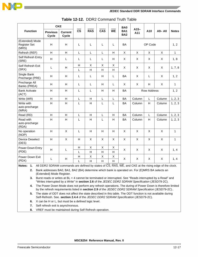
JEDEC Standard DDR SDRAM Interface Commands
Table 12-12. DDR2 Command Truth Table
Function
CKE
CS RAS CAS WEBA0BA1BA2
A15– A11
A10 A9– A0 NotesPrevious Cycle
Current Cycle
(Extended) Mode Register Set (MRS)
H H L L L L BA OP Code 1, 2
Refresh (REF) H H L L L H X X X X 1
Self Refresh Entry (SRE)
H L L L L H X X X X 1, 8
Self Refresh Exit (SRX)
L HH X X X
X X X X 1, 7, 8L H H H
Single Bank Precharge (PRE)
H H L L H L BA X L X 1, 2
Precharge All Banks (PREA)
H H L L H L X X H X 1
Bank Activate (ACT)
H H L L H H BA Row Address 1, 2
Write (WR) H H L H L L BA Column L Column 1, 2, 3
Write with auto-precharge (WRA)
H H L H L L BA Column H Column 1, 2, 3
Read (RD) H H L H L H BA Column L Column 1, 2, 3
Read with auto-precharge (RDA)
H H L H L H BA Column H Column 1, 2, 3
No operation (NOP)
H X L H H H X X X X 1
Device Deselect (DES)
H X H X X X X X X X 1
Power Down Entry (PDE)
H LH X X X
X X X X 1, 4L H H H
Power Down Exit (PDX)
L HH X X X
X X X X 1, 4L H H H
Notes: 1. All DDR2 SDRAM commands are defined by states of CS, RAS, WE, and CKE at the rising edge of the clock.
2. Bank addresses BA0, BA1, BA2 (BA) determine which bank is operated on. For (E)MRS BA selects an (Extended) Mode Register.
3. Burst reads or writes at BL = 4 cannot be terminated or interrupted. See “Reads interrupted by a Read” and “Writes interrupted by a Write” in section 2.6 of the JEDEC DDR2 SDRAM Specification (JESD79-2C).
4. The Power Down Mode does not perform any refresh operations. The during of Power Down is therefore limited by the refresh requirements listed in section 2.9 of the JEDEC DDR2 SDRAM Specification (JESD79-2C)..
5. The state of ODT does not affect the state described in this table. The ODT function is not available during Self-Refresh. See. section 2.4.4 of the JEDEC DDR2 SDRAM Specification (JESD79-2C).
6. X can be H or L, but must be a defined logic level.7. Self refresh exit is asynchronous.
8. VREF must be maintained during Self Refresh operation.
MSC8254 Reference Manual, Rev. 0
Freescale Semiconductor 12-17

DDR SDRAM Memory Controller
Table 12-13. DDR3 Command Truth Table
Function
CKE
CS RAS CAS WEBA0BA1BA2
A15– A13
A12BC
A10A9– A0
A11NotesPrev-
ious Cycle
Cur- rent
Cycle
Mode Register Set (MRS)
H H L L L L BA OP Code
Refresh (REF) H H L L L H V V V V V
Self Refresh Entry (SRE)
H L L L L H V V V V V 7, 9, 12
Self Refresh Exit (SRC)
L HH V V V
V V V V V7, 8, 9,
12L H H H
Single Bank Precharge (PRE)
H H L L H L BA V V L V
Precharge All Banks (PREA)
H H L L H L V V V H V
Bank Activate (ACT)
H H L L H H BA Row Address 1, 2
Write (Fixed BL8 or BC4) (WR)
H H L H L L BA RFU V L CA
Write (BC4, on the Fly) (WRS4)
H H L H L L BA RFU L L CA
Write (BC8, on the Fly) (WRS8)
H H L H L L BA RFU H L CA
Write with auto-precharge (Fixed BL8 or BC4) (WRA)
H H L H L L BA RFU V H CA
Write with auto-precharge (BC4, on the Fly) (WRAS4)
H H L H L L BA RFU L H CA
Write with auto-precharge (BL8) (WRAS8)
H H L H L L BA RFU H H CA
Read (Fixed BL8 or BC4) (RD)
H H L H L H BA RFU V H CA
Read (BC4, on the Fly) (RDS4)
H H L H L H BA RFU L H CA
Read (BL8, on the Fly) (RDS8)
H H L H L H BA RFU H H CA
Read with auto-precharge (Fixed BL8 or BC4) (RDA)
H H L H L H BA RFU V H CA
Read with auto-precharge (BC4, on the Fly) (RDAS4)
H H L H L H BA RFU L H CA
MSC8254 Reference Manual, Rev. 0
12-18 Freescale Semiconductor

JEDEC Standard DDR SDRAM Interface Commands
Read with auto-precharge (BL8, on the Fly) (RDAS8)
H H L H L H BA RFU H H CA
No operation (NOP)
H H L H H H V V V V V 10
Device Deselected (DES)
H H H X X X X X X X X 11
Power Down Entry (PDE)
H LL H H H
V V V V V 6. 12H V V V
Power Down Exit (PDX)
L HL H H H
V V V V V 1, 4H V V V
ZQ Calibration Long (ZQCL)
H H L H H L X X X H X
Notes: 1. All DDR3 SDRAM commands are defined by states of CS, RAS, CAS, WE, and CKE at the rising edge of the clock. The MSB of BA, RA, and CA are device density and configuration dependent.
2. RESET is Low enable command which is only used for asynchronous reset and must be maintained HIGH during any function.
3. Bank addresses BA0, BA1, BA2 (BA) determine which bank is operated on. For (E)MRS BA selects an (Extended) Mode Register.
4. V means H or L, but must be a defined level. X means either defined or undefined (such as floating) logic level.
5. Burst reads or writes cannot be terminated or interrupted. Fixed/on-the-Fly BL is defined by MRS..6. The Power Down Mode does not perform any refresh operations.
7. The state of ODT does not affect the states described in this table. The ODT function is not available during Self-Refresh.
8. Self refresh exit is asynchronous.9. VREF (both VrefDQ and VrefCA) must be maintained during Self-Refresh operation.10. The No Operation command should be used in cases when th DDR3 SDRAM is in an idle or wait state. The
purpose of the NOP command is to prevent the DDR3 SDRAM from registering any unwanted commands between operations. A NOP does not terminate a previous operation that is still executing, such as a burst read or write cycle.
11. The Deselect command perfoms the same function as a NOP.12. Refer to the CKE Truth Table in the JEDEC DDR3 SDRAM Specification (JESD79-3B)for details about CKE
transition.
Table 12-13. DDR3 Command Truth Table (Continued)
Function
CKE
CS RAS CAS WEBA0BA1BA2
A15– A13
A12BC
A10A9– A0
A11NotesPrev-
ious Cycle
Cur- rent
Cycle
MSC8254 Reference Manual, Rev. 0
Freescale Semiconductor 12-19

DDR SDRAM Memory Controller
12.4 DDR SDRAM Clocking and Interface Timing
The DDR memory controller supports four-beat bursts to SDRAM. For single-beat reads, the DDR memory controller performs a four-beat burst read but ignores the last three beats. Single-beat writes are performed by masking the last three beats of the four-beat burst using the data mask MDM[0–8]. If ECC is disabled, writes smaller than the data bus width are performed by appropriately activating the data mask. If ECC is enabled, the controller performs a read-modify write.
Note: If a second read or write is pending, reads shorter than four beats are not terminated early even if some data is irrelevant.
To accommodate available memory technologies across a wide spectrum of operating frequencies, the DDR memory controller allows you to set the timing intervals listed in Table 12-14 with a granularity of 1, 1/2, 1/4, or 1/8 SDRAM clock cycle. The value of these parameters (in whole clock cycles) must be set by application software at system initialization before the DDR controller is enabled and must be kept in the DDR memory controller configuration registers. Any update of the timing parameters should be done while the controller is disabled.
Table 12-14. DDR SDRAM Interface Timing Intervals
Timing Intervals Definition Register/Page
ACTTOACT Activate-to-Activate IntervalThe number of clock cycles from a bank-activate command to another bank-activate command within a physical bank. This interval is listed in the AC specifications of the SDRAM as tRRD.
DDR SDRAM Timing Configuration Register 1 (TIMING_CFG_1)page 12-55
ACTTOPRE Activate-to-Precharge IntervalThe number of clock cycles from an activate command until a precharge command is allowed. This interval is listed in the AC specifications of the SDRAM as tRAS.
ACTTORW Activate-to-Read/Write Interval for SDRAMThe number of clock cycles from an activate command until a read or write command is allowed. This interval is listed in the AC specifications of the SDRAM as tRCD.
BSTOPRE Open Page IntervalThe number of clock cycles to maintain a page open after an access. The page open duration counter is reloaded with BSTOPRE each time the page is accessed (including page hits). When the counter expires, the open page is closed with a SDRAM precharge bank command as soon as possible.
DDR SDRAM Interval Configuration Register (DDR_SDRAM_INTERVAL)page 12-74
CASLAT MCAS Latency from READ CommandUsed in conjunction with additive latency to obtain the READ latency. The number of clock cycles between the registration of a READ command by the SDRAM and the availability of the first piece of output data. If a READ command is registered at clock edge n, and the read latency is m clocks, the data is available nominally coincident with clock edge n + m.
DDR SDRAM Timing Configuration Register 1 (TIMING_CFG_1)page 12-55
PRETOACT Precharge-to-Activate IntervalThe number of clock cycles from a precharge command until an activate or a refresh command is allowed. This interval is listed in the AC specifications of the SDRAM as tRP.
DDR SDRAM Timing Configuration Register 1 (TIMING_CFG_1)page 12-55
MSC8254 Reference Manual, Rev. 0
12-20 Freescale Semiconductor

DDR SDRAM Clocking and Interface Timing
REFINT Refresh IntervalRepresents the number of memory bus clock cycles between refresh cycles. One row is refreshed in each SDRAM bank during each refresh cycle. Depending on DDR_SDRAM_CFG_2[NUM_PR], some number of rows are refreshed in each SDRAM bank during each refresh cycle. The value of REFINT depends on the specific SDRAMs used and the frequency of the interface. This interval is listed in the AC specifications of the SDRAM as tREFI.
DDR SDRAM Interval Configuration Register (DDR_SDRAM_INTERVAL)page 12-74
REFREC Refresh Recovery TimeThe number of clock cycles from the refresh command until an activate command is allowed. This interval is listed in the AC specifications of the SDRAM as tRFC.
DDR SDRAM Timing Configuration Register 1 (TIMING_CFG_1)page 12-55 and DDR SDRAM Timing Configuration Register 3 (TIMING_CFG_3) page 12-50
WR_DATA_DELAY Write Data DelayProvides different options for the timing between a write command and the write data strobe. This allows write data to be sent later than the nominal time to meet the SDRAM timing requirement between the registration of a write command and the reception of a data strobe associated with the write command.The specification dictates that the data strobe may not be received earlier than 75% of a cycle, or laterthan 125% of a cycle, from the registration of a write command. This parameter is not defined in theSDRAM specification. It is implementation-specific,
DDR SDRAM Timing Configuration Register 2 (TIMING_CFG_2)page 12-60
WRREC Write RecoveryThe number of clock cycles from the last beat of a write until a precharge command is allowed. This interval, write recovery time, is listed in the AC specifications of the SDRAM as tWR.
DDR SDRAM Timing Configuration Register 1 (TIMING_CFG_1)page 12-55
WRTORD Last Write Pair to Read Command. Controls the number of clock cycles from the last write data pair to the subsequent read command to the same bank. This interval is listed in the AC specifications of the SDRAM as tWTR.
CLK_ADJUST Clock AdjustAdjusts the MCK timing relative to address/command. The delay is set from the address/command start timing to the MCK rising edge. The resolution is 1/8 SDRAM clock cycle.
DDR SDRAM Clock Control Configuration Register (DDR_SDRAM_CLK_CNTL) page 12-75
ADD_LAT Additive LatencySpecifies the number of clock cycles for a Posted CAS operation until the registered read/write command is issued inside the SDRAM as defined in the JEDEC DDR2 and DDR3 standards.
DDR SDRAM Timing Configuration Register 2 (TIMING_CFG_2) page 12-60
CPO(if automatic
calibration is not selected)
CAS-to-Preamble OverrideSpecifies when the DDR controller starts waiting for the first DQS rising edge from DDR memory during the DQS preamble for read access. The DQS rising edge should occur within 1 clock cycle from the timing defined by this parameter.
DDR SDRAM Timing Configuration Register 2 (TIMING_CFG_2) page 12-60
Table 12-14. DDR SDRAM Interface Timing Intervals (Continued)
Timing Intervals Definition Register/Page
MSC8254 Reference Manual, Rev. 0
Freescale Semiconductor 12-21
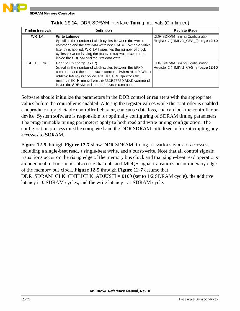
DDR SDRAM Memory Controller
Software should initialize the parameters in the DDR controller registers with the appropriate values before the controller is enabled. Altering the register values while the controller is enabled can produce unpredictable controller behavior, can cause data loss, and can lock the controller or device. System software is responsible for optimally configuring of SDRAM timing parameters. The programmable timing parameters apply to both read and write timing configuration. The configuration process must be completed and the DDR SDRAM initialized before attempting any accesses to SDRAM.
Figure 12-5 through Figure 12-7 show DDR SDRAM timing for various types of accesses, including a single-beat read, a single-beat write, and a burst-write. Note that all control signals transitions occur on the rising edge of the memory bus clock and that single-beat read operations are identical to burst-reads also note that data and MDQS signal transitions occur on every edge of the memory bus clock. Figure 12-5 through Figure 12-7 assume that DDR_SDRAM_CLK_CNTL[CLK_ADJUST] = 0100 (set to 1/2 SDRAM cycle), the additive latency is 0 SDRAM cycles, and the write latency is 1 SDRAM cycle.
WR_LAT Write LatencySpecifies the number of clock cycles between the WRITE command and the first data write when AL = 0. When additive latency is applied, WR_LAT specifies the number of clock cycles between issuing the REGISTERED WRITE command inside the SDRAM and the first data write.
DDR SDRAM Timing Configuration Register 2 (TIMING_CFG_2) page 12-60
RD_TO_PRE Read to Precharge (tRTP)Specifies the number of clock cycles between the READ command and the PRECHARGE command when AL = 0. When additive latency is applied, RD_TO_PRE specifies the minimum tRTP timing from the REGISTERED READ command inside the SDRAM and the PRECHARGE command.
DDR SDRAM Timing Configuration Register 2 (TIMING_CFG_2) page 12-60
Table 12-14. DDR SDRAM Interface Timing Intervals (Continued)
Timing Intervals Definition Register/Page
MSC8254 Reference Manual, Rev. 0
12-22 Freescale Semiconductor

DDR SDRAM Clocking and Interface Timing
ar
Figure 12-5. DDR SDRAM Burst Read Timing: ACTTORW = 3, MCAS Latency = 2
Figure 12-6. DDR SDRAM Single-Beat (32-Bit) Write Timing: ACTTORW = 3
ACTTORW
ROW COL
SDRAM Clock
MCS
MCAS
MA[15–0]
MDQ[0–31]
MWE
MRAS
MDQS
COL
D1 D2 D3 D1 D2D0 D3D0
0 1 2 3 4 5 6 7 8 9 10 11 12
CASLAT
ACTTORW
ROW COL
SDRAM Clock
MCS
MCAS
MA[15–0]
MDQ[0–31]
MWE
MRAS
MDQS
D0 D1 D2 D3
0MDM[0–3]
WRREC
A10=0
PRECHARGE
PRETOACT
ROW
0 1 2 3 4 5 6 7 8 9 10 11 12
FF F
WL=1
MSC8254 Reference Manual, Rev. 0
Freescale Semiconductor 12-23
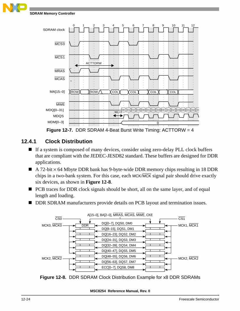
DDR SDRAM Memory Controller
Figure 12-7. DDR SDRAM 4-Beat Burst Write Timing: ACTTORW = 4
12.4.1 Clock DistributionIf a system is composed of many devices, consider using zero-delay PLL clock buffers that are compliant with the JEDEC-JESD82 standard. These buffers are designed for DDR applications.
A 72-bit × 64 Mbyte DDR bank has 9-byte-wide DDR memory chips resulting in 18 DDR chips in a two-bank system. For this case, each MCK/MCK signal pair should drive exactly six devices, as shown in Figure 12-8.
PCB traces for DDR clock signals should be short, all on the same layer, and of equal length and loading.
DDR SDRAM manufacturers provide details on PCB layout and termination issues.
Figure 12-8. DDR SDRAM Clock Distribution Example for x8 DDR SDRAMs
ROW COL
SDRAM clock
MCS0
MCAS
MA[15–0]
MDQ[0–31]
MWE
MRAS
MDQS
MDM[0–3] 0
COL
MCS1
ROW COL COL
D1 D2 D3 D1 D2D0 D3D0 D1 D2 D3 D1 D2D0 D3D0
0 1 2 3 4 5 6 7 8 9 10 11 12
ACTTORW
WL=1
MCK2, MCK2
MCK0, MCK0DQ[0–7], DQS0, DM0
DQ[8–15], DQS1, DM1
DQ[16–23], DQS2, DM2
DQ[24–31], DQS3, DM3
DQ[32–39], DQS4, DM4
DQ[40–47], DQS5, DM5
DQ[48–55], DQS6, DM6
DQ[56–63], DQS7, DM7
ECC[0–7], DQS8, DM8
DDR
CS0A[15–0], BA[2–0], MRAS, MCAS, MWE, CKE
MCK2, MCK2
MCK1, MCK1
CS1
MSC8254 Reference Manual, Rev. 0
12-24 Freescale Semiconductor

DDR SDRAM Clocking and Interface Timing
12.4.2 DDR SDRAM Mode-Set Command Timing
The DDR controller transfers the mode register set commands to the SDRAM array and it uses the setting of TIMING_CFG_0[MRS_CYC] for the Mode Register Set cycle time. Figure 12-9 shows the timing of the mode-set command. The first transfer corresponds to the ESDMODE code; the second corresponds to SDMODE of DDR_SDRAM_MODE in the case of automatic hardware initialization. The Mode Register Set cycle time is set to 2 DRAM cycles in Figure 12-9.
Figure 12-9. DDR SDRAM Mode-Set Command Timing
12.4.3 DDR SDRAM Registered DIMM Mode
To reduce loading, registered DIMMs latch the DDR SDRAM control signals internally before using them to access the array. Setting DDR_SDRAM_CFG[RD_EN] compensates for this delay on the DIMM control bus by delaying the data and data mask writes (on SDRAM buses) by an extra SDRAM clock cycle.
NOTEApplication system board must assert the reset signal on DDR memory devices until software is able to program the DDR memory controller configuration registers, and must deassert the reset signal on DDR memory devices before DDR_SDRAM_CFG[MEM_EN] is set. This ensures that the DDR memory devices are held in reset until a stable clock is provided and, further, that a stable clock is provided before memory devices are released from reset.
Code Code
SDRAM Clock
MCS
MCAS
MAn
MDQn
MWE
MRAS
MDQS
0x4 0x0MBAn
0 1 2 3 4 5 6 7 8 9 10 11 12
MSC8254 Reference Manual, Rev. 0
Freescale Semiconductor 12-25

DDR SDRAM Memory Controller
Figure 12-10 shows the registered DDR SDRAM DIMM single-beat write timing.
12.4.4 DDR SDRAM Write Timing Adjustments
The DDR memory controller facilitates system design flexibility by providing a write timing adjustment parameter, DATA DELAY, configured in TIMING_CFG_2[WR_DATA_DELAY] for data and DQS.
The DDR SDRAM specification requires DQS be received no sooner than 75% of an SDRAM clock period—and no later than 125% of a clock period—from the capturing clock edge of the command/address at the SDRAM. The TIMING_CFG_2[WR_DATA_DELAY] parameter can be used to meet this timing requirement for a variety of system configurations, ranging from a system with one bank of SDRAM devices to a fully populated system. TIMING_CFG_2[WR_DATA_DELAY] specifies how much to delay the launching of DQS and data from the first clock edge occurring one SDRAM clock cycle after the command is launched. The delay increment step sizes are in 1/4 SDRAM clock periods, starting with the default value of 0.
Figure 12-10. Registered DDR SDRAM DIMM Burst Write Timing
ROW COL
SDRAM Clock
MCS
MCAS
MAn
MDQn
MWE
MRAS
MDQS
COL
D1 D2 D3 D1 D2D0 D3D0
0 1 2 3 4 5 6 7 8 9 10 11 12
ACTTORW
00MDMn
MSC8254 Reference Manual, Rev. 0
12-26 Freescale Semiconductor

DDR SDRAM Clocking and Interface Timing
Figure 12-11. Write Timing Adjustments Example for Write Latency = 1 for the Case Where DDR_SDRAM_CLK_CNTL[CLK_ADJUST] = 0100
ACTTORW
ROW COL
SDRAM Clock
MCS
MCAS
MAn
MWE
MRAS
00
MDQn
MDQS
MDMn
1/4 Clock Delay
COL
MDQn
MDQS
MDMn
0 1 2 3 4 5 6 7 8 9 10 11 12
D0 D1 D2 D3 D0 D1 D2 D3
D0 D1 D2 D3 D0 D1 D2 D3
00
associated clock during first write
WR_DATA_DELAY = 001
1/4 clock early from MCKrising edge
WL = 1
1/2 Clock DelayWR_DATA_DELAY = 010
Nominal (no adjust) Timing.No tDQSS skew.
MSC8254 Reference Manual, Rev. 0
Freescale Semiconductor 12-27

DDR SDRAM Memory Controller
12.4.5 DDR SDRAM Refresh
The DDR memory controller supports auto refresh and self refresh. Auto refresh is used during normal operation and is controlled by the DDR_SDRAM_INTERVAL[REFINT] value; self refresh is used only when the DDR memory controller is set to enter a sleep power management state. The REFINT value, which represents the number of memory bus clock cycles between refresh cycles, must allow any outstanding transactions to complete before a refresh request is sent to the memory after the REFINT value is reached. If a memory transaction is in progress when the refresh interval is reached, the refresh cycle waits for the transaction to complete. In the worst case, the refresh cycle must wait the number of bus clock cycles required by the longest programmed access. To ensure that the latency caused by a memory transaction does not violate the device refresh period, it is recommended that the programmed value of REFINT be less than that required by the SDRAM. When a refresh cycle is required, the DDR memory controller does the following:
1. Completes all current memory requests.
2. Closes all open pages with a PRECHARGE ALL command to each DDR SDRAM bank with an open page (as indicated by the row open table).
3. Issues one or more auto-refresh commands to each DDR SDRAM bank (as identified by its chip select) to refresh one row in each logical bank of the selected physical bank.
The auto refresh commands are staggered across the possible banks to reduce instantaneous power requirements. Three sets of auto refresh commands are issued on consecutive cycles. The initial PRECHARGE ALL commands are also staggered in three groups. When the system enters self refresh mode, only one refresh command is issued simultaneously to all physical banks. For the entire refresh sequence, no cycle optimization occurs for the usual case where fewer banks are installed. After the refresh sequence completes, any pending memory request is initiated after an inactive period specified by TIMING_CFG_1[REFREC] and TIMING_CFG_3[EXT_REFREC]. In addition, posted refreshes in DDR_SDRAM_CFG_2[NUM_PR] allow the refresh interval to be set to a larger value.
Note: The MSC8254 initiates three cycles of PRECHARGE ALL commands and three cycles of REFRESH commands although there are only two banks (chip selects) available,
12.4.5.1 DDR SDRAM Refresh Timing
Refresh timing for the DDR SDRAM is controlled by the programmable timing parameter TIMING_CFG_1[REFREC] and TIMING_CFG_3[EXT_REFREC], which specify the number of memory bus clock cycles from the refresh command until a logical bank activate command is allowed. The DDR memory controller implements bank staggering for refreshes, as shown in Figure 12-12 (TIMING_CFG_1[REFREC] = 10 in this example). System software is responsible for optimal configuration of TIMING_CFG_1 [REFREC] and
MSC8254 Reference Manual, Rev. 0
12-28 Freescale Semiconductor
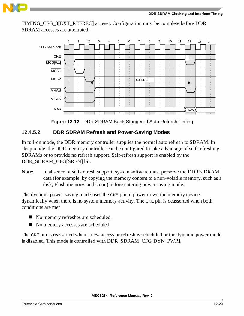
DDR SDRAM Clocking and Interface Timing
TIMING_CFG_3[EXT_REFREC] at reset. Configuration must be complete before DDR SDRAM accesses are attempted.
Figure 12-12. DDR SDRAM Bank Staggered Auto Refresh Timing
12.4.5.2 DDR SDRAM Refresh and Power-Saving Modes
In full-on mode, the DDR memory controller supplies the normal auto refresh to SDRAM. In sleep mode, the DDR memory controller can be configured to take advantage of self-refreshing SDRAMs or to provide no refresh support. Self-refresh support is enabled by the DDR_SDRAM_CFG[SREN] bit.
Note: In absence of self-refresh support, system software must preserve the DDR’s DRAM data (for example, by copying the memory content to a non-volatile memory, such as a disk, Flash memory, and so on) before entering power saving mode.
The dynamic power-saving mode uses the CKE pin to power down the memory device dynamically when there is no system memory activity. The CKE pin is deasserted when both conditions are met
No memory refreshes are scheduled.
No memory accesses are scheduled.
The CKE pin is reasserted when a new access or refresh is scheduled or the dynamic power mode is disabled. This mode is controlled with DDR_SDRAM_CFG[DYN_PWR].
SDRAM clock
MCS[0,1]
MCAS
MRAS
MCS1
MCS2
MAn ROW
CKE
REFREC
0
0 1 2 3 4 5 6 7 8 9 10 11 12 13 14
MSC8254 Reference Manual, Rev. 0
Freescale Semiconductor 12-29

DDR SDRAM Memory Controller
Dynamic power management mode offers tight control of the memory system power consumption by trading power for performance through the use of CKE. Powering up the DDR SDRAM when a new memory reference is scheduled causes an access latency penalty, depending upon whether active or precharge power-down is used, along with the settings of TIMING_CFG_0[ACT_PD_EXIT] and TIMING_CFG_0[PRE_PD_EXIT]. A penalty of one cycle is shown in Figure 12-13.
Figure 12-13. DDR SDRAM Power-Down Mode
The entry and exit timing for self-refreshing SDRAMs in Sleep mode is shown in Figure 12-14 and Figure 12-15.
Figure 12-14. DDR SDRAM Self-Refresh Entry Timing
Memory Bus Clock
NOP NOPCOMMAND ACT
MCKE
SDRAM clock
MCS
MCAS
MAn
MDQn
MWE
MRAS
MDQS
(High Impedance)
MCKE
0 1 2 3 4 5 6 7 8 9 10 11 12
MSC8254 Reference Manual, Rev. 0
12-30 Freescale Semiconductor

DDR SDRAM Clocking and Interface Timing
Figure 12-15. DDR SDRAM Self-Refresh Exit Timing
12.4.6 DDR Data Beat Ordering
Transfers to and from memory are always performed in four- or eight-beat bursts (four beats = 32 bytes for a 64-bit bus). For transfer sizes other than four or eight beats, the data transfers are still in four- or eight-beat bursts. If ECC is enabled and either the access is not 64-bit-aligned or the size is not a multiple of 64 bits, a full read-modify-write is performed for a write to SDRAM. If ECC is disabled or the access is 64-bit-aligned with a size that is a multiple of 64 bits, the data masks MDM[0–8] (MDM[0–3,8] for a 32-bit bus) can be used to prevent the writing of unwanted data to SDRAM. The DDR memory controller also uses data masks to prevent all unintended full 64-bit words from writing to SDRAM. For example, if a write transaction with a size of 8 bytes is desired, then the second, third, and fourth beats of data are not written to SDRAM.
Table 12-15 lists the data beat sequencing to and from the DDR SDRAM and the data queues for each of the possible transfer sizes with each of the possible starting 64-bit offsets. All underlined 64-bit offsets are valid for the transaction.
Table 12-15. Memory Controller–Data Beat Ordering for the 64-Bit Interface
Transfer Size Starting Double-Word Offset Double-Word Sequence to/from DRAM and Queues
8 bytes 0123
0 - 1 - 2 - 31 - 2 - 3 - 02 - 3 - 0 - 13 - 0 - 1 - 2
16 bytes 012
0 - 1 - 2 - 31 - 2 - 3 - 02 - 3 - 0 - 1
(High Impedance)
200 cycles
SDRAM Clock
MCS
MCAS
MAn
MDQn
MWE
MRAS
MDQS
0 1 2 3 4 5 6 7 202 203 204 205 206
MCKE
MSC8254 Reference Manual, Rev. 0
Freescale Semiconductor 12-31

DDR SDRAM Memory Controller
12.4.7 Page Mode and Logical Bank Retention
The DDR memory controller supports an open/closed page mode that allows an open page for each logical bank of DRAM. In closed page mode for DDR SDRAMs, the DDR memory controller uses the auto-precharge feature, which allows the controller to indicate the DDR SDRAM that it must automatically close the page after the read or write access. This is performed by using MA10 of the address during the COMMAND phase of the access to enable auto-precharge. Auto-precharge is non-persistent in that it is either enabled or disabled for each individual READ or WRITE command. However, it can be separately enabled or disabled for each chip select. In open page mode, the DDR memory controller retains the currently active SDRAM page by not issuing a precharge command. The page remains opens until one of the following conditions occurs:
Refresh interval is met.
The user-programmable DDR_SDRAM_INTERVAL[BSTOPRE] value is exceeded.
There is a logical bank row collision with another transaction that must be issued.
Page mode can dramatically reduce access latencies for page hits. Depending on the memory system design and timing parameters, using page mode can save two to three clock cycles for subsequent burst accesses that hit in an active page. Also, better performance can be obtained by using more banks, especially in systems which use many different channels. Page mode is disabled by clearing DDR_SDRAM_INTERVAL[BSTOPRE] or setting CSx_CONFIG[AP_x_EN].
12.5 Error Checking and Correction
The DDR memory controller supports error checking and correcting (ECC) for the data path between the core Initiator and system memory. The DDR memory controller detects all double-bit errors, detects all multi-bit errors within a nibble, and it corrects all single-bit errors. Other errors may be detected, but are not guaranteed to be corrected or detected. Multiple-bit errors are always reported when error reporting is enabled. When a single-bit error occurs, the single-bit error counter register is incremented, its value compared to the single-bit error threshold register. An error is reported when the counter value is equal to the threshold register
24 bytes 01
0 - 1 - 2 - 31 - 2 - 3 - 0
32 bytes 0123
0 - 1 - 2 - 31 - 2 - 3 - 02 - 3 - 0 - 13 - 0 - 1 - 2
Note: All underlined word offsets are valid for the transaction.
Table 12-15. Memory Controller–Data Beat Ordering for the 64-Bit Interface
Transfer Size Starting Double-Word Offset Double-Word Sequence to/from DRAM and Queues
MSC8254 Reference Manual, Rev. 0
12-32 Freescale Semiconductor

Error Checking and Correction
value. The single-bit error registers can be programmed so that minor memory faults are corrected and ignored, but a catastrophic memory failure generates an interrupt.
For writes smaller than 64 bits, the DDR memory controller performs a 64-bit read from system memory of the address for the write (checking for errors), and merges the write data with the data read from memory. Then, a new ECC code is generated for the 64-bit of merged data. The data and ECC code is then written to memory. If a multi-bit error is detected on the read, the transaction completes the read-modify-write to keep the DDR memory controller from hanging. However, the corrupt data is masked on the write, so the original contents in SDRAM remain unchanged.
The syndrome encoding for the ECC code is shown in Table 12-16 and Table 12-17. In 32-bit mode, Table 12-16 is split into 2 halves. The first half, consisting of rows 0–31, is used to calculate the ECC bits for the first 32 data bits of any 64-bit granule of data. This always applies to the odd data beats on the DDR data bus. The second half of the table, consisting of rows 32–63, is used to calculate the ECC bits for the second 32 bits of any 64-bit granule of data. This always applies to the even data beats on the DDR data bus.
Table 12-16. DDR SDRAM ECC Syndrome Encoding
DataBit
Syndrome Bit DataBit
Syndrome Bit
0 1 2 3 4 5 6 7 0 1 2 3 4 5 6 7
0 • • • 32 • • •
1 • • • 33 • • •
2 • • • 34 • • •
3 • • • 35 • • •
4 • • • 36 • • •
5 • • • 37 • • •
6 • • • 38 • • • • •
7 • • • 39 • • • • •
8 • • • 40 • • •
9 • • • 41 • • •
10 • • • 42 • • • • •
11 • • • 43 • • • • •
12 • • • • • 44 • • • • •
13 • • • • • 45 • • • • •
14 • • • • • 46 • • • • •
15 • • • • • 47 • • • • •
16 • • • 48 • • •
17 • • • 49 • • •
18 • • • 50 • • •
19 • • • 51 • • •
MSC8254 Reference Manual, Rev. 0
Freescale Semiconductor 12-33

DDR SDRAM Memory Controller
20 • • • 52 • • •
21 • • • 53 • • •
22 • • • 54 • • •
23 • • • • • 55 • • •
24 • • • 56 • • •
25 • • • 57 • • •
26 • • • 58 • • •
27 • • • • • 59 • • •
28 • • • • • 60 • • •
29 • • • • • 61 • • • • •
30 • • • • • 62 • • • • •
31 • • • • • 63 • • • • •
Table 12-17. DDR SDRAM ECC Syndrome Encoding (Check Bits)
Check Bit
Syndrome Bit
0 1 2 3 4 5 6 7
0 •
1 •
2 •
3 •
4 •
5 •
6 •
7 •
Table 12-16. DDR SDRAM ECC Syndrome Encoding (Continued)
DataBit
Syndrome Bit DataBit
Syndrome Bit
0 1 2 3 4 5 6 7 0 1 2 3 4 5 6 7
MSC8254 Reference Manual, Rev. 0
12-34 Freescale Semiconductor

Error Management
12.6 Error Management
The DDR memory controller detects single-bit, multi-bit, memory select, training errors and address/command parity errors. The following discussion assumes all the relevant error detection, correction, and reporting functions are enabled as described in 12.8.40, DDR SDRAM Memory Error Detect Register (MnERR_DETECT) and 12.8.41, DDR SDRAM Memory Error Disable Register (MnERR_DISABLE).
Single-bit errors are counted and reported based on the ERR_SBE register value (see Table 12-66 on page 12-115). When a single-bit error is detected, the DDR memory controller does the following:
1. Corrects the data.
2. Increments the single-bit error counter ERR_SBE[SBEC].
3. Generates a critical interrupt if the counter value ERR_SBE[SBEC] equals the programmable threshold ERR_SBE[SBET].
4. Completes the transaction normally.
If a multi-bit error is detected for a read, the DDR memory controller logs the error and generates the critical interrupt (if enabled, as described in Table 12-62 on page 12-111).
The DDR memory controller also detects a memory select error, which causes the DDR memory controller to log the error and generate a critical interrupt (if enabled, as described in Table 12-61 on page 12-110). This error is detected if the address from the memory request does not fall into any of the enabled, programmed chip-select address ranges. For all memory select errors, the DDR memory controller does not issue any transactions onto the pins after the first read has returned data strobes. If the DDR memory controller is not using sample points, then a dummy transaction is issued to DDR SDRAM with the first enabled chip select. Table 12-18 describes the errors.
The final error the memory controller detects is the automatic calibration error. This error is set if the memory controller detects an error during its training sequence.
MSC8254 Reference Manual, Rev. 0
Freescale Semiconductor 12-35
DDR SDRAM Memory Controller
The training error the memory controller detects is the automatic calibration error. This error is set if the memory controller detects an error during its training sequence.
12.7 Set-Up and Initialization
System software must configure the DDR memory controller, using a memory polling algorithm at system start-up, to correctly map the size of each bank in memory. The DDR memory controller uses this bank map to assert the appropriate MCSx signal for memory accesses according to the provided bank depths. System software also configures the DDR memory controller at system start-up to multiplex the row and column address bits for each bank (see Table 12-22 on page 12-47). Address multiplexing occurs according to these configuration bits. At system power-up, initialization software (boot code, for example) must set up the programmable parameters in the memory interface configuration registers listed in Table 12-19.
Table 12-18. Memory Controller Errors
Category Error Descriptions Action Detect Register
Notification Single-bit ECC threshold
The number of ECC errors has reached the threshold specified in the ERR_SBE.
The error is reported via critical interrupt if enabled.
The error control register logs only read versus write, not full type
Access Error
Multi-bit ECC error
A multi-bit ECC error is detected during a read, or read-modify-write memory operation.
Memory select error
Read, or write, address does not fall within the address range of any of the memory banks.
Training Calibration error
One of the calibration processes executed during the initialization failed
Parity Address and Command error
The memory device detects that the parity bit calculated by the controller doesn’t correspond to the parity calculated by the memory device.
Table 12-19. Memory Interface Configuration Register Initialization Parameters
Register Parameter Bits Page
Chip-Select Memory Bounds Register (MCSx_BNDS)
Starting Address for Chip Select x (SAx)Ending Address for Chip Select x (EAx)
Table 12-21 on page 12-46
Chip-Select Configuration Register (MCSx_CONFIG)
Chip Select x Enable (CS_x_EN)Chip Select x Auto-Precharge Enable (AP_x_EN)ODT for Reads (ODT_RD_CFG)ODT for Writes (ODT_WR_CFG)Number of Bank Bits (BA_BITS_CS_x)Number of Row Bits (ROW_BITS_CS_x)Number of Column Bits (COL_BITS_CS_x)(INTLV_EN_CTL)
Table 12-22 on page 12-47
Chip Select Configuration 2(MCSx_CONFIG_2)
PASR_CFG Table 12-23 on page 12-49
Extended Timing Parameters for Fields in TIMING_CFG_3 (TIMING_CFG_3)
EXT_REFRECEXT_ACTTOPREEXT_CASLATCNTL_ADJ
Table 12-23 on page 12-49Table 12-24 on page 12-50
MSC8254 Reference Manual, Rev. 0
12-36 Freescale Semiconductor

Set-Up and Initialization
Timing Configuration 0 Register (TIMING_CFG_0)
Read-to-Write Turn-Around (RWT)Write-to-Read Turn-Around (WRT)Read-to-Read Turn-Around (RRT)Write-to-Write Turn-Around (WWT)Active Power-Down Exit Timing (ACT_PD_EXIT)Precharge Power-Down Exit Timing (PRE_PD_EXIT)ODT Power-Down Exit Timing (ODT_PD_EXIT)Mode Register Set Cycle Time (MRS_CYC)
Table 12-25 on page 12-52
Timing Configuration 1 Register (TIMING_CFG_1)
Precharge-to-Activate Interval (PRETOACT)Activate-to-Precharge Interval (ACTTOPRE)Activate to Read/Write Interval for SDRAM (ACTTORW)MCAS Latency from Read Command (CASLAT)Refresh Recovery Time (REFREC)Last Data to Precharge Minimum Interval (WRREC)Activate-to-Activate Interval (ACTTOACT)Last Write Data Pair to Read Interval (WR_TO_RD)
Table 12-26 on page 12-56
Timing Configuration 2 Register (TIMING_CFG_2)
Additive Latency (ADD_LAT)MCAS-to-Preamble Override (CPO)Write Latency (WR_LAT)Read-to-Precharge (RD_TO_PRE)Write Data Delay (WR_DATA_DELAY)Minimum CKE Pulse Width (CKE_PLS)Window for Four Activates (FOUR_ACT)
Table 12-27 on page 12-60
DDR SDRAM Control Configuration Register (DDR_SDRAM_CFG)
Self Refresh Enable (SREN)ECC Enable (ECC_EN)Registereed DIMM Enable (RD_EN)SDRAM Type (SDRAM_Type)Dynamic Power Management Mode (DYN_PWR)32-Bit Bus Enable (32_BE)8-Beat Burst Enable (8_BE)Non-Current Auto Precharge (NCAP)3T Timing Enable (3T_EN)2T Timing Enable (2T_EN)Half-Strength Drive Enable (HSE)Bypass Initialization (BI)
Table 12-28 on page 12-65
DDR SDRAM Control Configuration Register 2 (DDR_SDRAM_CFG_2)
Force Self Refresh (FRC_SR)DLL Reset Disable (DLL_RST_DIS)DQS Configuration (DQS_CFG)ODT Configuration (ODT_CFG)Number of Posted Refreshes (NUM_PR)DRAM Data Initialization (D_INIT)
Table 12-29 on page 12-68
DDR SDRAM Mode Configuration Register (DDR_SDRAM_MODE)
Extended SDRAM Mode (ESDMODE)SDRAM Mode (SDMODE)
Table 12-30 on page 12-70
DDR SDRAM Mode Configuration 2 Register (DDR_SDRAM_MODE_2)
Extended SDRAM Mode 2 (ESDMODE2)Extended SDRAM Mode 3 (ESDMODE3)
Table 12-31 on page 12-71
DDR SDRAM Interval Configuration Register (DDR_SDRAM_INTERVAL)
Refresh Interval (REFINT)Precharge Interval (BSTOPRE)
Table 12-34 on page 12-74
Table 12-19. Memory Interface Configuration Register Initialization Parameters (Continued)
Register Parameter Bits Page
MSC8254 Reference Manual, Rev. 0
Freescale Semiconductor 12-37

DDR SDRAM Memory Controller
DDR SDRAM Data Initialization Register (DDR_DATA_INIT)
Initialization Value (INIT_VALUE) Table 12-35 on page 12-75
DDR SDRAM Clock Control Configuration Register (DDR_SDRAM_CLK_CNTL)
Clock Adjust (CLK_ADJUST) Table 12-36 on page 12-76
DDR SDRAM Initialization Address Register (DDR_INIT_ADDRESS)
Initialization Address (INIT_ADDR) Table 12-37 on page 12-77
DDR Initialization Enable (MDDR_INIT_EN)
Use Initialization Address (UIA) Table 12-38 on page 12-77
DDR SDRAM Timing Configuration 4 Register (TIMING_CFG_4)
Read-to-Write Turnaround for Same Chip Select (RWT)Write-to-Read Turnaround for Same Chip Select (WRT)Read-to-Read Turnaround for Same Chip Select (RRT)Write-to-Write Turnaround for Same Chip Select (WWT)DDR SDRAM DLL Lock Time (DLL_LOCK)
Table 12-39 on page 12-78
DDR SDRAM Timing Configuration 5 Register (TIMING_CFG_5)
Read-to-ODT On (RODT_ON)Read-to-ODT Off (RODT_OFF)Write-to-ODT On (WODT_ON)Write-to-ODT Off (WODT_OFF)
Table 12-40 on page 12-80
DDR ZQ Calibration Control (MDDR_ZQ_CNTL
ZQ Calibration Enable (ZQ_EN)Power-on Reset ZQ Calibration Time (ZQINIT)Normal Operation Full Calibration Time (ZQOPER)Normal Operation Short Calibration Time (ZQCS)
Table 12-41 on page 12-83
DDR Write Leveling Control (MDDR_WRLVL_CNTL)
Write Leveling Enable (WRLVL_EN)First DQS Pulse Rising Edge after Margining Mode Is Programmed (WRLVL_MRD)ODT Delay after Margining Mode Is Programmed (WRLVL_ODTEN)DQS/DQS Delay after Margining Mode Is Programmed (WRLVL_DQSEN)Write Leveling Sample Time (WRLVL_SMPL)Write Leveling Repetition Time (WRLVL_WLR)Write Leveling Start Time (WRLVL_START)
Table 12-42 on page 12-84
DDR Write Leveling Control 2 (MDDR_WRLVL_CNTL_2)
Write Leveling Start Time for DQS1 (WRLVL_START_1)Write Leveling Start Time for DQS2 (WRLVL_START_2)Write Leveling Start Time for DQS3 (WRLVL_START_3)Write Leveling Start Time for DQS4 (WRLVL_START_4)
Table 12-43 on page 12-87
DDR Write Leveling Control 3 (MDDR_WRLVL_CNTL_3)
Write Leveling Start Time for DQS5 (WRLVL_START_5)Write Leveling Start Time for DQS6 (WRLVL_START_6)Write Leveling Start Time for DQS7 (WRLVL_START_7)Write Leveling Start Time for DQS8 (WRLVL_START_8)
Table 12-44 on page 12-90
DDR Self Refresh Counter (MDDR_SR_CNTR)
Self Refresh Idle Threshold (SR_IT) Table 12-46 on page 12-96
Table 12-19. Memory Interface Configuration Register Initialization Parameters (Continued)
Register Parameter Bits Page
MSC8254 Reference Manual, Rev. 0
12-38 Freescale Semiconductor

Set-Up and Initialization
DDR SDRAM Register Control Words 1 (MDDR_SDRAM_RCW_1)
Register Control Word 0 (RCW0)Register Control Word 1 (RCW1)Register Control Word 2 (RCW2)Register Control Word 3 (RCW3)Register Control Word 4 (RCW4)Register Control Word 5 (RCW5)Register Control Word 6 (RCW6)Register Control Word 7 (RCW7)
Table 12-47 on page 12-97
DDR SDRAM Register Control Words 2 (MDDR_SDRAM_RCW_2)
Register Control Word 8 (RCW8)Register Control Word 9 (RCW9)Register Control Word 10 (RCW10)Register Control Word 11 (RCW11)Register Control Word 12 (RCW12)Register Control Word 13 (RCW13)Register Control Word 14 (RCW14)Register Control Word 15 (RCW15)
Table 12-48 on page 12-98
DDR Control Driver Register 1 (MDDRCDR_1)
DDR Driver Hardware Compensation Enable (DHC_EN)Driver Software Override Enable for MDIC (DSO_MDIC_EN)Driver Software Override valeu for MDIC P-Impedance (DSO_MDICPZ)Driver Software Override valeu for MDIC N-Impedance (DSO_MDIC_NZ)Driver Software Override Output Enable for P-Impedance (DSO_MDIC_PZ_OE)Driver Software Override Output Enable for N-Impedance (DSO_MDIC_NZ_OE)ODT Termination Value for I/O (ODT)Driver Software Override Enable for Address/Command (DSO_C_EN)Driver Software Override Enable for Data (DSO_D_EN)DDR Driver Software override value for Command P-Impedance override (DSO_CPZ)DDR Driver Software override value for Command N-Impedance override (DSO_CNZ)DDR Driver Software override value for Data P-Impedance override (DSO_DPZ)DDR Driver Software override value for Data N-Impedance override (DSO_DNZ)
Table 12-51 on page 12-101
DDR Control Driver Register 2 (MDDRCDR_2)
Driver Software Override Enable for Clocks (DSO_CLK_EN)DDR Driver Software override value for Clocks P-Impedance override (DSO_CLKPZ)DDR Driver Software override value for Clocks N-Impedance override (DSO_CLKNZ)ODT Termination Value for I/O (ODT)
Table 12-52 on page 12-104
Table 12-19. Memory Interface Configuration Register Initialization Parameters (Continued)
Register Parameter Bits Page
MSC8254 Reference Manual, Rev. 0
Freescale Semiconductor 12-39

DDR SDRAM Memory Controller
12.7.1 Programming Differences Between Memory Types
Several fields in the configuration registers must be programmed to reflect the characteristics of the DDR memory used in the application. Table 12-20 lists several of the characteristics. Refer to the DDR memory specifications to determine the required settings. Table 12-20 does not list all fields that must be programmed.
Table 12-20. Programming Differences Between Memory Types
Parameter Description Differences
APn_EN Chip Select n Auto Precharge Enable
DDR2 Can be used to place chip select n in auto precharge mode
DDR3 Can be used to place chip select n in auto precharge mode
ODT_RD_CFG Chip Select ODT Read Configuration
DDR2 Can be enabled to assert ODT if desired. This could be set differently depending on system topology. However, systems with only 1 chip select typically does not use ODT when issuing reads to the memory.
DDR3 Can be enabled to assert ODT if desired. This could be set differently depending on system topology. However, systems with only 1 chip select typically does not use ODT when issuing reads to the memory.
ODT_WR_CFG Chip Select ODT Write Configuration
DDR2 Can be enabled to assert ODT if desired. This could be set differently depending on system topology. However, ODT is typically set to assert for the chip select that is getting written to (value would be set to 001).
DDR3 Can be enabled to assert ODT if desired. This could be set differently depending on system topology. However, ODT typically is set to assert for the chip select that is getting written to (value would be set to 001).
ODT_PD_EXIT ODT Powerdown Exit DDR2 Should be set according to the DDR2 specifications for the memory used. The JEDEC parameter this applies to is tAXPD.
DDR3 Should be set to 0001 for DDR3. The powerdown times (tXP and tXPDLL) required for DDR3 are controlled via TIMING_CFG_0[ACT_PD_EXIT] and TIMING_CFG_0[PRE_PD_EXIT].
PRETOACT Precharge to Activate Timing DDR2 Should be set according to the specifications for the memory used (tRP)
DDR3 Should be set according to the specifications for the memory used (tRP)
ACTTOPRE Activate to Precharge Timing DDR2 Should be set, along with the Extended Activate to Precharge Timing, according to the specifications for the memory used (tRAS)
DDR3 Should be set, along with the Extended Activate to Precharge Timing, according to the specifications for the memory used (tRAS)
ACTTORW Activate to Read/Write Timing DDR2 Should be set according to the specifications for the memory used (tRCD)
DDR3 Should be set according to the specifications for the memory used (tRCD)
MSC8254 Reference Manual, Rev. 0
12-40 Freescale Semiconductor

Set-Up and Initialization
CASLAT CAS Latency DDR2 Should be set, along with the Extended CAS Latency, to the desired CAS latency
DDR3 Should be set, along with the Extended CAS Latency, to the desired CAS latency
REFREC Refresh Recovery DDR2 Should be set, along with the Extended Refresh Recovery, to the specifications for the memory used (TRFC)
DDR3 Should be set, along with the Extended Refresh Recovery, to the specifications for the memory used (TRFC)
WRREC Write Recovery DDR2 Should be set according to the specifications for the memory used (tWR)
DDR3 Should be set according to the specifications for the memory used (tWR). If DDR_SDRAM_CFG_2[OBC_CFG] is set, then this should be programmed to tWR + 2 DRAM cycles.
ACTTOACT Activate A to Activate B DDR2 Should be set according to the specifications for the memory used (tRRD)
DDR3 Should be set according to the specifications for the memory used (tRRD)
WRTORD Write to Read Timing DDR2 Should be set according to the specifications for the memory used (tWTR)
DDR3 Should be set according to the specifications for the memory used (tWTR)If DDR_SDRAM_CFG_2[OBC_CFG] is set, then this should be programmed to tWTR + 2 DRAM cycles.
ADD_LAT Additive Latency DDR2 Should be set to the desired additive latency. This must be set to a value less than TIMING_CFG_1[ACTTORW]
DDR3 Should be set to the desired additive latency. This must be set to a value less than TIMING_CFG_1[ACTTORW]
WR_LAT Write Latency DDR2 Should be set to CAS latency – 1 cycle. For example, if the CAS latency if 5 cycles, then this field should be set to 100 (4 cycles).
DDR3 Should be set to the desired write latency. Note that DDR3 SDRAMs do not necessarily require the write latency to equal the CAS latency minus 1 cycle.
RD_TO_PRE Read to Precharge Timing DDR2 Should be set according to the specifications for the memory used (tRTP). Time between read and precharge for non-zero value of additive latency (AL) is a minimum of AL + tRTP cycles.
DDR3 Should be set according to the specifications for the memory used (tRTP). Time between read and precharge for non-zero value of additive latency (AL) is a minimum of AL + tRTP cycles. If DDR_SDRAM_CFG_2[OBC_CFG] is set, then this should be programmed to tRTP + 2 DRAM cycles.
CKE_PLS Minimum CKE Pulse Width DDR2 Should be set according to the specifications for the memory used (tCKE)
DDR3 Should be set according to the specifications for the memory used (tCKE)
Table 12-20. Programming Differences Between Memory Types (Continued)
Parameter Description Differences
MSC8254 Reference Manual, Rev. 0
Freescale Semiconductor 12-41

DDR SDRAM Memory Controller
FOUR_ACT Four Activate Window DDR2 Should be set according to the specifications for the memory used (tFAW). Only applies to eight logical banks.
DDR3 Should be set according to the specifications for the memory used (tFAW).
RD_EN Registered DIMM Enable DDR2 If registered are used, then this field should be set to 1
DDR3 If registered are used, then this field should be set to 1
8_BE 8-beat burst enable DDR2 Should be set to 0
DDR3 If a 64-bit bus is used, this should be set to 0. Otherwise, this should be set to 1. If this is set to 0, then other requirements in TIMING_CFG_4 is needed to ensure tCCD is met.
2T_EN 2T Timing Enable DDR2 In heavily loaded systems, this can be set to 1 to gain extra timing margin on the interface at the cost of address/command bandwidth.
DDR3 In heavily loaded systems, this can be set to 1 to gain extra timing margin on the interface at the cost of address/command bandwidth.
DLL_RST_DIS DLL Reset Disable DDR2 Should typically be set to 0, unless it is desired to bypass the DLL reset when exiting self refresh.
DDR3 Should be set to 1
DQS_CFG DQS Configuration DDR2 Should be set to 01
DDR3 Should be set to 01
ODT_CF ODT Configuration DDR2 Can be set for termination at the IOs according to system topology. Typically, if ODT is enabled, then the internal IOs should be set up for termination only during reads to DRAM.
DDR3 Can be set for termination at the IOs according to system topology. Typically, if ODT is enabled, then the internal IOs should be set up for termination only during reads to DRAM.
OBC_CFG On-The-Fly Burst Chop Configuration
DDR2 Should be set to 0
DDR3 Can be set to 1 if on-the-fly burst chop is used. This is expected to give the best performance in DDR3 mode. This feature can only be used if a 64-bit data bus is used.
RWT Read-to-write turnaround for same chip select (in TIMING_CFG_4)
DDR2 Should typically be set to 0000
DDR3 This can be used to force a longer read-to-write turnaround time when accessing the same chip select. This is useful for burst chop mode, as there are some timing requirements to the same chip select that still must be met.
WRT Write-to-read turnaround for same chip select (in TIMING_CFG_4)
DDR2 Should typically be set to 0000
DDR3 This could be used to force a certain turnaround time between a write and read to the same chip select. This is useful for burst chop mode. However, it is expected that TIMING_CFG_1[WRTORD] is programmed appropriately such that TIMING_CFG_4[WRT] can be set to 0000.
RRT Read-to-read turnaround for same chip select (in TIMING_CFG_4)
DDR2 Should typically be set to 0000
DDR3 Should typically be set to 0100 in burst chop mode (on-the-fly or fixed).
Table 12-20. Programming Differences Between Memory Types (Continued)
Parameter Description Differences
MSC8254 Reference Manual, Rev. 0
12-42 Freescale Semiconductor

Set-Up and Initialization
WWT Write-to-write turnaround for same chip select (in TIMING_CFG_4)
DDR2 Should typically be set to 0000
DDR3 Should typically be set to 0100 in burst chop mode (on-the-fly or fixed).
ZQ_EN ZQ Calibration Enable DDR2 Should be set to 0
DDR3 Should be set to 1. The other fields in DDR_ZQ_CNTL should also be programmed appropriately based on the DRAM specifications.
WRLVL_EN Write Leveling Enable DDR2 Should be set to 0
DDR3 Can be set to 1 if write leveling is desired. Otherwise the value used in TIMING_CFG_2[WR_DATA_DELAY] is used to shift all bytes during writes to DRAM. If write leveling is used, all other fields in DDR_WRLVL_CNTL should be programmed appropriately based on the DRAM specifications.
BSTOPRE Burst To Precharge Interval DDR2 Can be set to any value, depending on the application. Auto precharge can be enabled by setting this field to all 0s.
DDR3 Can be set to any value, depending on the application. Auto precharge can be enabled by setting this field to all 0s.
Table 12-20. Programming Differences Between Memory Types (Continued)
Parameter Description Differences
MSC8254 Reference Manual, Rev. 0
Freescale Semiconductor 12-43

DDR SDRAM Memory Controller
12.7.2 DDR SDRAM Initialization Sequence
After all parameters are configured, system software must set DDR_SDRAM_CFG[MEM_EN] to enable the memory interface. You must allow 200 μs (500 μs for DDR3) to elapse after DRAM clocks are stable (DDR_SDRAM_CLK_CNTL[CLK_ADJUST] is set and any chip select is enabled) before setting MEMEN. Therefore, a delay loop in the initialization code may be necessary if software is enabling the memory controller. If DDR_SDRAM_CFG[BI] bit is not set to bypass initialization, the DDR memory controller conducts an automatic initialization sequence to the memory, which follows the memory specifications. If the bypass initialization mode is used, software can initialize the memory through the DDR_SDRAM_MD_CNTL register.
12.8 Memory Controller Programming Model
In the register figures and field descriptions, the following access definitions apply:
Reserved fields are always ignored for the purposes of determining access type.Read/write, read only, and write only (R/W, R, and W, respectively) indicate that all the non-reserved fields in a register have the same access type.Non-reserved fields that are cleared by writing 1s to them are indicated by w1c.Mixed indicates a combination of access types.Special is used when no other category applies. For special access registers, read the figure and field descriptions very carefully.
The DDR memory controller registers are as follows:
Chip-Select Memory Bounds Register (MnCSx_BNDS), page 12-46.
Chip-Select Configuration Register (MnCSx_CONFIG), page 12-47.
Chip-Select Configuration Register 2 (MnCSx_CONFIG_2), page 12-49DDR SDRAM Timing Configuration 3 (MnTIMING_CFG_3), page 12-50.DDR SDRAM Timing Configuration 0 Register (MnTIMING_CFG_0), page 12-52.DDR SDRAM Timing Configuration 1 Register (MnTIMING_CFG_1), page 12-55.DDR SDRAM Timing Configuration 2 Register (MnTIMING_CFG_2), page 12-60.DDR SDRAM Control Configuration Register (MnDDR_SDRAM_CFG), page 12-65.DDR SDRAM Control Configuration 2 Register (MnDDR_SDRAM_CFG_2), page 12-67.DDR SDRAM Mode Configuration Register (MnDDR_SDRAM_MODE), page 12-70.DDR SDRAM Mode Configuration 2 Register (MnDDR_SDRAM_MODE_2), page 12-71.DDR SDRAM Mode Control Register (MnDDR_SDRAM_MD_CNTL), page 12-71.
MSC8254 Reference Manual, Rev. 0
12-44 Freescale Semiconductor

Memory Controller Programming Model
DDR SDRAM Interval Configuration Register (MnDDR_SDRAM_INTERVAL), page 12-74.DDR SDRAM Data Initialization Register (MnDDR_DATA_INIT), page 12-75.DDR SDRAM Clock Control Configuration Register (MnDDR_SDRAM_CLK_CNTL), page 12-75.DDR Initialization Address Register (MnDDR_INIT_ADDRESS), page 12-76.DDR Initialization Enable Extended Address (MnDDR_INIT_ENXT_ADDR), page 12-77DDR SDRAM Timing Configuration 4 (MnTIMING_CFG_4), page 12-78DDR SDRAM Timing Configuration 5 (MnTIMING_CFG_5), page 12-80DDR ZQ Calibration Control (MnDDR_ZQ_CNTL), page 12-82DDR Write Leveling Control (MnDDR_WRLVL_CNTL), page 12-84DDR Write Leveling Control 2 (MnDDR_WRLVL_CNTL_2), page 12-87DDR Write Leveling Control 3 (MnDDR_WRLVL_CNTL_3), page 12-90DDR Pre-Drive Conditioning Control (MnDDR_PD_CNTL), page 12-93DDR SDRAM Self Refresh Counter (MnDDR_SR_CNTR), page 12-96DDR SDRAM Register Control Words 1 (MnDDR_SDRAM_RCW_1), page 12-97DDR SDRAM Register Control Words 2 (MnDDR_SDRAM_RCW_2), page 12-98DDR Debug Status Register 1 (MnDDRDSR_1), page 12-99DDR Debug Status Register 2 (MnDDRDSR_2), page 12-100DDR Control Driver Register 1 (MnDDRCDR_1), page 12-100DDR Control Driver Register 2 (MnDDRCDR_2), page 12-104DDR IP Block Revision 1 Register (MnDDR_IP_REV1), page 12-105.DDR IP Block Revision 2 Register (MnDDR_IP_REV2), page 12-105.Memory Data Path Error Injection Mask High Register (MnDDR_ERR_INJECT_HI), page 12-106.Memory Data Path Error Injection Mask Low Register (MnDDR_ERR_INJECT_LO), page 12-106.Memory Data Path Error Injection Mask ECC Register (MnDDR_ERR_INJECT), page 12-107Memory Data Path Read Capture High Register (MnCAPTURE_DATA_HI), page 12-108.Memory Data Path Read Capture Low Register (MnCAPTURE_DATA_LO), page 12-108.Memory Data Path Read Capture ECC Register (MnCAPTURE_ECC), page 12-109.Memory Error Detect Register (MnERR_DETECT), page 12-109.Memory Error Disable Register (MnERR_DISABLE), page 12-110.Memory Error Interrupt Enable Register (MnERR_INT_EN), page 12-112.Memory Error Attributes Capture Register (MnCAPTURE_ATTRIBUTES), page 12-113.Memory Error Address Capture Register (MnCAPTURE_ADDRESS), page 12-114.
MSC8254 Reference Manual, Rev. 0
Freescale Semiconductor 12-45

DDR SDRAM Memory Controller
Single-Bit ECC Memory Error Management Register (MnERR_SBE), page 12-114.Debug Register 2 (MnDEBUG_2), page 12-115
Note: DDR1 controller uses base address: 0xFFF20000. DDR2 controller uses base address: 0xFFF22000.
12.8.1 Chip-Select Bounds (MnCSx_BNDS)
CSx_BNDS defines the starting and ending address of the memory space that corresponds to the individual chip selects.
Note: The size specified in CSx_BNDS should equal the size of physical DRAM. Also, note that EAx must be greater than or equal to SAx. The 8 msb of the address is used to define the SAx and EAx.
If chip select interleaving is enabled, all fields in the lower interleaved chip select are used, and the other chip selects bounds registers are not used. For example, if chip selects 0 and 1 are interleaved, all fields in CS0_BNDS are used, and all fields in CS1_BNDS are not used.
CS0_BNDS Chip-Select Bounds Register Offset 0x0000CS1_BNDS 0x0008
Bit 31 30 29 28 27 26 25 24 23 22 21 20 19 18 17 16
— SAxType R R/W
Reset 0 0 0 0 0 0 0 0 0 0 0 0 0 0 0 0
Bit 15 14 13 12 11 10 9 8 7 6 5 4 3 2 1 0
— EAxType R R/WReset 0 0 0 0 0 0 0 0 0 0 0 0 0 0 0 0
Table 12-21. CSx_BNDS Field Descriptions
Bit Reset Description
—31–24
0 Reserved. Cleared to zero for future compatibility.
SAx23–16
0 Starting AddressSpecifies the starting address for chip-select (bank) x. This value is compared against the 8 MSBs of the 32-bit address. See the previous note.
—15–8
0 Reserved. Cleared to zero for future compatibility.
EAx7–0
0 Ending AddressSpecifies the ending address for chip select (bank) x. This value is compared against the 8 MSBs of the 32-bit address. See the previous note.
MSC8254 Reference Manual, Rev. 0
12-46 Freescale Semiconductor

Memory Controller Programming Model
12.8.2 Chip-Select x Configuration Register (MnCSx_CONFIG)
The CSx_CONFIG register enables the DDR chip select x and sets the number of row and column bits used for the chip select. The register should be loaded with the correct number of row and column bits for each SDRAM. Because the ROW_BITS_CS_x and COL_BITS_CS_x fields establish address multiplexing, it is essential to set these values correctly.
If chip select interleaving is enabled, then all fields in the lower interleaved chip select are used, and the other registers’ fields are unused, with the exception of the ODT_RD_CFG and ODT_WR_CFG fields. For example, if chip selects 0 and 1 are interleaved, all fields in CS0_CONFIG are used, but only the ODT_RD_CFG and ODT_WR_CFG fields in CS1_CONFIG are used.
CS0_CONFIG Chip-Select 0 Configuration Register Offset 0x0080CS1_CONFIG Chip-Select 1 Configuration Register Offset 0x0084
Bit 31 30 29 28 27 26 25 24 23 22 21 20 19 18 17 16
CS_x_EN
— AP_x_EN
ODT_RD_CFG — ODT_WR_CFG
Type R/W R/W R R/W R R/WReset 0 0 0 0 0 0 0 0 0 0 0 0 0 0 0 0
Bit 15 14 13 12 11 10 9 8 7 6 5 4 3 2 1 0
BA_BITS_CS_x
— ROW_BITS_CS_x — COL_BITS_CS_x
Type R/W R R/W R R/W
Reset 0 0 0 0 0 0 0 0 0 0 0 0 0 0 0 0
Table 12-22. CSx_CONFIG Field Descriptions
Bit Reset Description Settings
CS_x_EN31
0 Chip Select x EnableEnables/disables chip select.
0 Chip select x is not active.
1 Chip select x is active and assumes the state set in CSx_BNDS.
—30-24
0 Reserved. Write to zero for future compatibility.
AP_x_EN23
0 Chip Select x Auto-Precharge EnableSpecifies when auto-precharged is enabled for chip select x.
0 Chip select x is auto-precharged only if global auto-precharge mode is enabled (DDR_SDRAM_INTERVAL[BSTOPRE] =0).
1 Chip select x always issues an auto-precharge for read and write transactions.
ODT_RD_CFG
22–20
0 On-Die Termination (ODT) for Reads Specifies when ODT is to be asserted for read accesses. Note that CAS latency plus additive latency must be at least 3 cycles for ODT_RD_CFG to be enabled.
000 Never assert ODT for reads.
001 Assert ODT only during reads to CSx.
010 Assert ODT only during reads to other chip selects.
011 Reserved.
100 Assert ODT for all reads.
101–111Reserved.
MSC8254 Reference Manual, Rev. 0
Freescale Semiconductor 12-47

DDR SDRAM Memory Controller
—19
0 Reserved. Write to zero for future compatibility.
ODT_WR_CFG
18–16
0 ODT for WritesSpecifies when ODT is to be asserted for write accesses. Note that write latency plus additive latency must be at least 3 cycles for ODT_WR_CFG to be enabled.
000 Never assert ODT for writes.
001 Assert ODT only during writes to CSx.
010 Assert ODT only during writes to other chip selects.
011 Reserved.
100 Assert ODT for all writes.
101–111Reserved.BA_BITS_
CS_x15–14
0 Number of Bank BitsSpecifies the number of logical bank bits MBA[2–0] for SDRAM on chip select x. See Table 12-6 and Table 12-7 for details
00 2 logical bank bits.
01 3 logical bank bits.
10–11 Reserved
—13–11
0 Reserved. Write to zero for future compatibility.
ROW_ BITS_CS_x
10–8
0 Number of Row BitsSpecifies the number of row bits for SDRAM on chip select x. See Table 12-6 and Table 12-7 for details
000 12 row bits
001 13 row bits
010 14 row bits
011 15 row bits
100 16 row bits
101–111Reserved—
7–30 Reserved. Write to zero for future compatibility.
COL_ BITS_CS_x
2–0
0 Number of Column BitsSpecifies the number of column bits for SDRAM on chip select x. See Table 12-6 and Table 12-7 for details.
000 8 column bits.
001 9 column bits.
010 10 column bits.
011 11 column bits.
100–111Reserved.
Table 12-22. CSx_CONFIG Field Descriptions (Continued)
Bit Reset Description Settings
MSC8254 Reference Manual, Rev. 0
12-48 Freescale Semiconductor
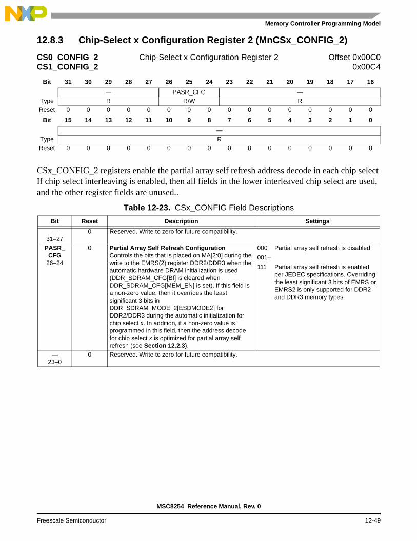
Memory Controller Programming Model
12.8.3 Chip-Select x Configuration Register 2 (MnCSx_CONFIG_2)
CSx_CONFIG_2 registers enable the partial array self refresh address decode in each chip select If chip select interleaving is enabled, then all fields in the lower interleaved chip select are used, and the other register fields are unused..
CS0_CONFIG_2 Chip-Select x Configuration Register 2 Offset 0x00C0CS1_CONFIG_2 0x00C4
Bit 31 30 29 28 27 26 25 24 23 22 21 20 19 18 17 16
— PASR_CFG —Type R R/W R
Reset 0 0 0 0 0 0 0 0 0 0 0 0 0 0 0 0
Bit 15 14 13 12 11 10 9 8 7 6 5 4 3 2 1 0
—Type RReset 0 0 0 0 0 0 0 0 0 0 0 0 0 0 0 0
Table 12-23. CSx_CONFIG Field Descriptions
Bit Reset Description Settings
—31–27
0 Reserved. Write to zero for future compatibility.
PASR_ CFG
26–24
0 Partial Array Self Refresh ConfigurationControls the bits that is placed on MA[2:0] during the write to the EMRS(2) register DDR2/DDR3 when the automatic hardware DRAM initialization is used (DDR_SDRAM_CFG[BI] is cleared when DDR_SDRAM_CFG[MEM_EN] is set). If this field is a non-zero value, then it overrides the least significant 3 bits in DDR_SDRAM_MODE_2[ESDMODE2] for DDR2/DDR3 during the automatic initialization for chip select x. In addition, if a non-zero value is programmed in this field, then the address decode for chip select x is optimized for partial array self refresh (see Section 12.2.3),
000 Partial array self refresh is disabled
001–
111 Partial array self refresh is enabled per JEDEC specifications. Overriding the least significant 3 bits of EMRS or EMRS2 is only supported for DDR2 and DDR3 memory types.
—23–0
0 Reserved. Write to zero for future compatibility.
MSC8254 Reference Manual, Rev. 0
Freescale Semiconductor 12-49

DDR SDRAM Memory Controller
12.8.4 DDR SDRAM Timing Configuration 3 (MnTIMING_CFG_3)
TIMING_CFG_3 sets the extended refresh recovery time, which is combined with TIMING_CFG_1[REFREC] to determine the full refresh recovery time.
TIMING_CFG_3 DDR SDRAM Timing Configuration 3 Register Offset 0x0100
Bit 31 30 29 28 27 26 25 24 23 22 21 20 19 18 17 16
— EXT_ ACTTO
PRE
— EXT_REFREC
Type R R/W R R/WReset 0 0 0 0 0 0 0 0 0 0 0 0 0 0 0 0
Bit 15 14 13 12 11 10 9 8 7 6 5 4 3 2 1 0
— EXT_ CAS LAT
— CNTL_ADJ
Type R R/W R R/WReset 0 0 0 0 0 0 0 0 0 0 0 0 0 0 0 0
Table 12-24. TIMING_CFG_3 Bit Descriptions
Bits Reset Description Setting
—31–25
0 Reserved. Write to zero for future compatibility.
EXT_ACTTOPRE24
0 Extended Activate to precharge interval (tRAS). Determines the number of clock cycles from an activate command until a precharge command is allowed. This field is concatenated with TIMING_CFG_1[ACTTOPRE] to obtain a 5-bit value for the total activate to precharge. Note that a 5-bit value of 0_0000 is the same as a 5-bit value of 1_0000. Both values represent 16 cycles.
0 0 clocks1 16 clocks
—23–20
0 Reserved. Write to zero for future compatibility.
EXT_ REFREC19–16
0 Extended Refresh Recovery Time (tRFC)Controls the number of clock cycles from a refresh command until an activate command is allowed. This field is combined with TIMING_CFG_1[REFREC] to obtain the total refresh recovery time. Note that the minimum value for REFREC is 8 clock cycles.
tRFC = {REFREC | + | EXT_REFREC} min. value = 8 clocks (REFREC = 0x0) + EXT_REFREC = 0x0max. value = 240+ 23 = 263
0000 0 clock cycles.
0001 16 clock cycles.
0010 32 clock cycles.
0011 48 clock cycles.
0100 64 clock cycles.
0101 80 clock cycles.
0110 96 clock cycles.
0111 112 clock cycles
1000 128 clock cycles
1001 144 clock cycles
1010 160 clock cycles
1011 176 clock cycles
1100 192 clock cycles
1101 208 clock cycles
1110 224 clock cycles
1111 240 clock cycles
MSC8254 Reference Manual, Rev. 0
12-50 Freescale Semiconductor

Memory Controller Programming Model
—15–13
0 Reserved. Write to zero for future compatibility.
EXT_CASLAT12
0 Extended MCAS latency from READ command. Number of clock cycles between registration of a READ command by the SDRAM and the availability of the first output data. If a READ command is registered at clock edge n and the latency is m clocks, data is available nominally coincident with clock edge n + m. This field is concatenated with TIMING_CFG_1[CASLAT] to obtain a 5-bit value for the total CAS latency. Note that if this bit is set, then 8 clocks are added to the programmed value in TIMING_CFG_1[CASLAT].
0 0 clocks1 8 clocks
—11–3
0 Reserved. Write to zero for future compatibility.
CNTL_ADJ2-0
0 Control Adjust. Controls the amount of delay to add to the lightly loaded control signals w/ respect to all other DRAM address and command signals. The signals affected by this field are MODT[0:1], MCS[0:1], and MCKE[0:1]
000 MODT[0:1], MCS[0:1], and MCKE[0:1] is launched aligned with the other DRAM address and control signals.
001 MODT[0:1], MCS[0:1], and MCKE[0:1] is launched 1/4 platform cycle later than the other DRAM address and control signals.
010 MODT[0:1], MCS[0:1], and MCKE[0:1] is launched 1/2 platform cycle later than the other DRAM address and control signals.
011 MODT[0:1], MCS[0:1], and MCKE[0:1] is launched 3/4 platform cycles later than the other DRAM address and control signals.
100 MODT[0:1], MCS[0:1], and MCKE[0:1] is launched 1platform cycles later than the other DRAM address and control signals.
101 MODT[0:1], MCS[0:1], and MCKE[0:1] is launched 5/4 platform cycles later than the other DRAM address and control signals.
110-111Reserved
Table 12-24. TIMING_CFG_3 Bit Descriptions (Continued)
Bits Reset Description Setting
MSC8254 Reference Manual, Rev. 0
Freescale Semiconductor 12-51

DDR SDRAM Memory Controller
12.8.5 DDR SDRAM Timing Configuration Register 0 (MnTIMING_CFG_0)
TIMING_CFG_0 sets the number of clock cycles between various SDRAM control commands.
TIMING_CFG_0 DDR SDRAM Timing Configuration Register 0 Offset 0x0104
Bit 31 30 29 28 27 26 25 24 23 22 21 20 19 18 17 16
RWT WRT RRT WWT — ACT_PD_EXIT PRE_PD_EXIT
Type R/W R R/W R/WReset 0 0 0 0 0 0 0 0 0 0 0 1 0 0 0 1
Bit 15 14 13 12 11 10 9 8 7 6 5 4 3 2 1 0
— ODT_PD_EXIT — MRS_CYCType R R/W R R/W
Reset 0 0 0 0 0 0 0 1 0 0 0 0 0 1 0 1
Table 12-25. TIMING_CFG_0 Field Descriptions
Bit Reset Description Settings
RWT31–30
0 Read-to-Write Turn-Around (tRTW)Specifies how many extra cycles to add between a read-to-write turnaround. If 0 clock cycles is chosen, then the DDR controller uses a fixed number based on the CAS latency and write latency. A value other than 0 adds extra cycles to this default calculation. By default, the DDR controller determines the read-to-write turn-around as CL – WL + BL/2 + 2. CL is the CAS latency rounded up to the next integer, WL is the programmed write latency, and BL is the burst length.
00 0 clock cycles.
01 1 clock cycle.
10 2 clock cycles.
11 3 clock cycles.
WRT29–28
0 Write-to-Read Turn-AroundSpecifies how many extra cycles to add between a write-to-read turn-around. If 0 clock cycles is chosen, then the DDR controller uses a fixed number based on the read latency and write latency. A value other than 0 adds extra cycles to this default calculation. By default, the DDR controller determines the write-to-read turn-around as WL – CL + BL/2 + 1. CL is the CAS latency rounded down to the next integer, WL is the programmed write latency, and BL is the burst length.
00 0 clock cycles.
01 1 clock cycle.
10 2 clock cycles.
11 3 clock cycles.
RRT27–26
0 Read-to-Read Turn-AroundSpecifies how many extra cycles to add between reads to different chip selects. By default, 3 cycles are required between read commands to different chip selects. If 00 is selected the DDR Controller uses a predefined value - 3 clocks for the turnaround, selecting a value other than 00 adds extra cycles to this predefined value according to the selectionWhen DDR works in 8 beat burst the default is 5 clock cycles. Note: DDR2 does not support 8-beat bursts.
DDR2:
00 3 clock cycles.
01 4 clock cycle.
10 5 clock cycles.
11 6 clock cycles.
WWT25–24
0 Write-to-Write Turn-AroundSpecifies how many extra cycles to add between writes to different chip selects. By default, 2 cycles are required between write commands to different chip selects.If 00 is selected the DDR Controller uses a predefined value - 2 clocks for the turnaround, selecting a value other than 00 adds extra cycles to this predefined value according to the selectionWhen DDR works in 8 beat burst the default is 4 clock cycles. Note: DDR2 does not support 8-beat bursts.
DDR2:
00 2 clock cycles.
01 3 clock cycle.
10 4 clock cycles.
11 5 clock cycles.
—23
0 Reserved. Write to zero for future compatibility.
MSC8254 Reference Manual, Rev. 0
12-52 Freescale Semiconductor

Memory Controller Programming Model
ACT_PD_ EXIT
22–20
0b001 Active Power-Down Exit Timing (tXARD and tXARDS)Specifies how many clock cycles to wait between exit from active power-down and issuing a command. The default is one clock cycle.
000 Reserved
001 1 clock cycles.
010 2 clock cycles.
011 3 clock cycles.
100 4 clock cycles.
101 5 clock cycles.
110 6 clock cycles.
111 7 clock cyclesPRE_PD_
EXIT19–16
0b0001 Precharge Power-Down Exit Timing (txp)Specifies how many clock cycles to wait after exiting precharge power-down before issuing any command. The default is one clock cycle.
0000 Reserved.
0001 1 clocks.
0010 2 clock cycles.
0011 3 clock cycles.
0100 4 clock cycles.
0101 5 clock cycles.
0110 6 clock cycles.
0111 7 clock cycles
1000 8 clock cycles
1001 9 clock cycle.
1010 10 clock cycles.
1011 11 clock cycles.
1100 12 clock cycles.
1101 13 clock cycles.
1110 14 clock cycles.
1111 15 clock cycles.—
15–120 Reserved. Write to zero for future compatibility.
ODT_PD_ EXIT11–8
0b0001 ODT Power-Down Exit Timing (tAXPD)Specifies how many clock cycles must pass after exit from power-down before ODT can be asserted. The default is 1 clock cycle. Note: For DDR3, ODT_PD_EXIT must be greater than
TIMING_CFG_5[RODT_ON] when using RODT_ON overrides and must be grater than TIMING_CFG_5[WODT_ON] when using WODT_ON overrides.
0000 0 clock
0001 1 clock
0010 2 clock cycles.
0011 3 clock cycles.
0100 4 clock cycles.
0101 5 clock cycles.
0110 6 clock cycles.
0111 7 clock cycles.
1000 8 clock cycles.
1001 9 clock cycles.
1010 10 clock cycles.
1011 11 clock cycles.
1100 12 clock cycles.
1101 13 clock cycles.
1110 14 clock cycles.
1111 15 clock cycles.
—7–4
0 Reserved. Write to zero for future compatibility.
Table 12-25. TIMING_CFG_0 Field Descriptions (Continued)
Bit Reset Description Settings
MSC8254 Reference Manual, Rev. 0
Freescale Semiconductor 12-53
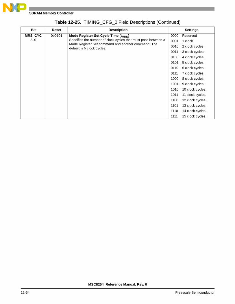
DDR SDRAM Memory Controller
MRS_CYC3–0
0b0101 Mode Register Set Cycle Time (tMRD)Specifies the number of clock cycles that must pass between a Mode Register Set command and another command. The default is 5 clock cycles.
0000 Reserved
0001 1 clock
0010 2 clock cycles.
0011 3 clock cycles.
0100 4 clock cycles.
0101 5 clock cycles.
0110 6 clock cycles.
0111 7 clock cycles.
1000 8 clock cycles.
1001 9 clock cycles.
1010 10 clock cycles.
1011 11 clock cycles.
1100 12 clock cycles.
1101 13 clock cycles.
1110 14 clock cycles.
1111 15 clock cycles.
Table 12-25. TIMING_CFG_0 Field Descriptions (Continued)
Bit Reset Description Settings
MSC8254 Reference Manual, Rev. 0
12-54 Freescale Semiconductor

Memory Controller Programming Model
12.8.6 DDR SDRAM Timing Configuration Register 1 (MnTIMING_CFG_1)
TIMING_CFG_1 DDR SDRAM Timing Configuration Register 1 Offset 0x0108
Bit 31 30 29 28 27 26 25 24 23 22 21 20 19 18 17 16
PRETOACT ACTTOPRE ACTTORW CASLAT
Type R/W R/W R/W R/WReset 0 0 0 0 0 0 0 0 0 0 0 0 0 0 0 0
Bit 15 14 13 12 11 10 9 8 7 6 5 4 3 2 1 0
REFREC WRREC — ACTTOACT — WRTORDType R/W R/W R R/W R R/W
Reset 0 0 0 0 0 0 0 0 0 0 0 0 0 0 0 0
MSC8254 Reference Manual, Rev. 0
Freescale Semiconductor 12-55

DDR SDRAM Memory Controller
TIMING_CFG_1 sets the number of clock cycles between various SDRAM control commands.
Table 12-26. TIMING_CFG_1 Field Descriptions
Bits Reset Description Settings
PRETOACT31–28
0 Precharge-to-Activate Interval (tRP)Specifies the minimum number of clock cycles between a precharge command and an activate or refresh command. This number is calculated from the AC specifications of the SDRAM.This field must be programmed for proper operation of the DDR Controller.
0000 Reserved.
0001 1 clock
0010 2 clock cycles.
0011 3 clock cycles.
0100 4 clock cycles.
0101 5 clock cycles.
0110 6 clock cycles.
0111 7 clock cycles
1000 8 clock cycles.
1001 9 clock cycles.
1010 10 clock cycles.
1011 11 clock cycles.
1100 12 clock cycles.
1101 13 clock cycles.
1110 14 clock cycles.
1111 15 clock cycles.
ACTTOPRE27–24
0 Activate to Precharge Interval (tRAS)Specifies the minimum number of clock cycles between an activate command and a precharge command. This number is calculated from the AC specifications of the SDRAM.This field is concatenated with TIMING_CFG_3[EXT_ACTTOPRE] to obtain a 5-bit value for the total activate to precharge time. Note that the decode of 0000–0011 is equal to 16-19 clocks when TIMING_CFG_3[EXT_ACTTOPRE] = 0, but it is equal to 0-3 clocks when TIMING_CFG_3[EXT_ACTTOPRE] = 1.This field must be programmed for proper operation of the DDR Controller.
0000 16 clock cycles.
0001 17 clock cycles.
0010 18 clock cycles.
0011 19 clock cycles.
0100 4 clock cycles.
0101 5 clock cycles.
0110 6 clock cycles.
0111 7 clock cycles.
1000 8 clock cycles.
1001 9 clock cycles.
1010 10 clock cycles.
1011 11 clock cycles.
1100 12 clock cycles.
1101 13 clock cycles.
1110 14 clock cycles.
1111 15 clock cycles.
MSC8254 Reference Manual, Rev. 0
12-56 Freescale Semiconductor

Memory Controller Programming Model
ACTTORW23–20
0 Activate to Read/Write Interval for SDRAM (tRCD)Specifies the minimum number of clock cycles between an activate command and a read or write command. This interval is calculated from the AC specifications of the SDRAM.This field must be programmed for proper operation of the DDR Controller.
0000 Reserved.
0001 1 clock cycle.
0010 2 clock cycles.
0011 3 clock cycles.
0100 4 clock cycles.
0101 5 clock cycles.
0110 6 clock cycles.
0111 7 clock cycles
1000 8 clock cycles.
1001 9 clock cycles.
1010 10 clock cycles.
1011 11 clock cycles.
1100 12 clock cycles.
1101 13 clock cycles.
1110 14 clock cycles.
1111 15 clock cycles.
CASLAT19–16
0 MCAS Latency from READ CommandSpecifies the number of clock cycles between the time the SDRAM registers a READ command and the availability of the first output data. If a READ command is registered at clock edge n and the latency is m clock cycles., data is available nominally coincident with clock edge n + m. This field is concatenated with TIMING_CFG_3[EXT_CASLAT] to obtain a 5-bit value for the total CAS latency. This value must be programmed at initialization as described in Section 12.8.9, DDR SDRAM Control Configuration Register 2 (MnDDR_SDRAM_CFG_2) on page 12-70.This field must be programmed for proper operation of the DDR Controller.
0000 Reserved.
0001 1 clock cycle.
0010 Reserved.
0011 2 clock cycles.
0100 Reserved.
0101 3 clock cycles.
0110 Reserved.
0111 4 clock cycles.
1000 Reserved.
1001 5 clock cycles.
1010 Reserved.
1011 6 clock cycles.
1100 Reserved.
1101 7 clock cycles.
1110 Reserved.
1111 8 clock cycles.
Table 12-26. TIMING_CFG_1 Field Descriptions (Continued)
Bits Reset Description Settings
MSC8254 Reference Manual, Rev. 0
Freescale Semiconductor 12-57

DDR SDRAM Memory Controller
REFREC15–12
0 Refresh Recovery Time (tRFC)Controls the number of clock cycles from a refresh command until an activate command is allowed. This field is combined with TIMING_CFG_3[EXT_REFREC] to obtain the total refresh recovery time. Note that the minimum value for REFREC is 8 clock cycles.
tRFC = {REFREC || EXT_REFREC} + 8min. value = 8 clocks (REFREC = 0x0) + EXT_REFREC = 0x0max. value = 240 + 15 + 8 = 263
This required value can be calculated by referring to the AC specification of the SDRAM device. The AC specification indicates a minimum refresh to activate interval in nanoseconds.
0000 8 clock cycles.
0001 9 clock cycles.
0010 10 clock cycles.
0011 11 clock cycles.
0100 12 clock cycles.
0101 13 clock cycles.
0110 14 clock cycles.
0111 15 clock cycles.
0000 16 clock cycles.
0001 17 clock cycles.
0010 18 clock cycles.
0011 19 clock cycles.
0100 20 clock cycles.
0101 21 clock cycles.
0110 22 clock cycles.
1111 23 clock cycles.
WRREC11–8
0 Write Recovery (tWR)Specifies the minimum number of clock cycles between the last data associated with a write command and a precharge command. This interval, write recovery time, is calculated from the AC specifications of the SDRAM.If DDR_SDRAM_CFG_2[OBC_CFG] is set, then this field needs to be programmed to (tWR + 2 cycles).This field must be programmed for proper operation of the DDR Controller.
Note: DDR_SDRAM_CFG_2[OBC_CFG] = 1 is the recommended mode.
0000 0 clock cycle.
0001 1 clock cycle.
0010 2 clock cycles.
0011 3 clock cycles.
0100 4 clock cycles.
0101 5 clock cycles.
0110 6 clock cycles.
0111 7 clock cycles
1000 8 clock cycles.
1001 9 clock cycles.
1010 10 clock cycles.
1011 11 clock cycles.
1100 12 clock cycles.
1101 13 clock cycles.
1110 14 clock cycles.
1111 15 clock cycles.
—7
0 Reserved. Write to zero for future compatibility.
ACTTOACT6–4
0 Activate-to-Activate Interval (tRRD)Specifies the minimum number of clock cycles between an activate command and another activate command for a different logical bank in the same physical bank (chip select). This interval is calculated from the AC specifications of the SDRAM.This field must be programmed for proper operation of the DDR Controller.
000 Reserved.
001 1 clock cycle.
010 2 clock cycles.
011 3 clock cycles.
100 4 clock cycles.
101 5 clock cycles.
110 6 clock cycles.
111 7 clock cycles.
Table 12-26. TIMING_CFG_1 Field Descriptions (Continued)
Bits Reset Description Settings
MSC8254 Reference Manual, Rev. 0
12-58 Freescale Semiconductor

Memory Controller Programming Model
—3
0 Reserved. Write to zero for future compatibility.
WRTORD2–0
0 Last Write Data Pair to Read Command Interval (tWTR)Specifies the minimum number of clock cycles between the last write data pair and the subsequent read command to the same physical bank.If DDR_SDRAM_CFG_2[OBC_CFG] is set, then this field needs to be programmed to (tWTR + 2 cycles)This field must be programmed for proper operation of the DDR Controller.
Note: DDR_SDRAM_CFG_2[OBC_CFG] = 1 is the recommended mode.
000 Reserved.
001 1 clock cycle.
010 2 clock cycles.
011 3 clock cycles.
100 4 clock cycles.
101 5 clock cycles.
110 6 clock cycles.
111 7 clock cycles.
Table 12-26. TIMING_CFG_1 Field Descriptions (Continued)
Bits Reset Description Settings
MSC8254 Reference Manual, Rev. 0
Freescale Semiconductor 12-59

DDR SDRAM Memory Controller
12.8.7 DDR SDRAM Timing Configuration Register 2 (MnTIMING_CFG_2)
TIMING_CFG_2 sets the clock delay to data for writes and should be defined according to the system timing. Table 12-28 describes the TIMING_CFG_2 fields.
TIMING_CFG_2 DDR SDRAM Timing Configuration Register 2 Offset 0x010C
Bit 31 30 29 28 27 26 25 24 23 22 21 20 19 18 17 16
ADD_LAT CPO WR_LAT —
Type R/W RReset 0 0 0 0 0 0 0 0 0 0 0 0 0 0 0 0
Bit 15 14 13 12 11 10 9 8 7 6 5 4 3 2 1 0
RD_TO_PRE WR_DATA_ DELAY — CKE_PLS FOUR_ACTType R/W R R/W
Reset 0 0 0 0 0 0 0 0 0 0 0 0 0 0 0 0
Table 12-27. TIMING_CFG_2 Field Descriptions
Bit Reset Description Settings
ADD_LAT31–28
0 Additive LatencySpecifies the number of clock cycles from the Posted CAS operation until the registered read/write command is issued inside the SDRAM as defined in the JEDEC DDR2 and DDR3 standards. The additive latency must be set to a value less than TIMING_CFG_1[ACTTORW].
Note: For DDR2 ADD_LAT can be 0–4.
For DDR3 ADD_LAT can be 0–2.
0000 0 clock cycles.
0001 1 clock cycle.
0010 2 clock cycles.
0011 3 clock cycles.
0100 4 clock cycles.
0101 5 clock cycles
0110 6 clock cycles
0111 7 clock cycles
1000 8 clock cycles.
1001 9 clock cycles.
1010 10 clock cycles.
1011 11 clock cycles.
1100 12 clock cycles.
1101 13 clock cycles.
1110 14 clock cycles.
1111 15 clock cycles.
MSC8254 Reference Manual, Rev. 0
12-60 Freescale Semiconductor
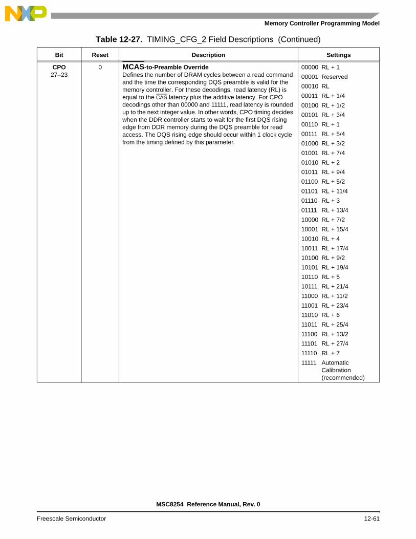
Memory Controller Programming Model
CPO27–23
0 MCAS-to-Preamble OverrideDefines the number of DRAM cycles between a read command and the time the corresponding DQS preamble is valid for the memory controller. For these decodings, read latency (RL) is equal to the CAS latency plus the additive latency. For CPO decodings other than 00000 and 11111, read latency is rounded up to the next integer value. In other words, CPO timing decides when the DDR controller starts to wait for the first DQS rising edge from DDR memory during the DQS preamble for read access. The DQS rising edge should occur within 1 clock cycle from the timing defined by this parameter.
00000 RL + 1
00001 Reserved
00010 RL
00011 RL + 1/4
00100 RL + 1/2
00101 RL + 3/4
00110 RL + 1
00111 RL + 5/4
01000 RL + 3/2
01001 RL + 7/4
01010 RL + 2
01011 RL + 9/4
01100 RL + 5/2
01101 RL + 11/4
01110 RL + 3
01111 RL + 13/4
10000 RL + 7/2
10001 RL + 15/4
10010 RL + 4
10011 RL + 17/4
10100 RL + 9/2
10101 RL + 19/4
10110 RL + 5
10111 RL + 21/4
11000 RL + 11/2
11001 RL + 23/4
11010 RL + 6
11011 RL + 25/4
11100 RL + 13/2
11101 RL + 27/4
11110 RL + 7
11111 Automatic Calibration (recommended)
Table 12-27. TIMING_CFG_2 Field Descriptions (Continued)
Bit Reset Description Settings
MSC8254 Reference Manual, Rev. 0
Freescale Semiconductor 12-61

DDR SDRAM Memory Controller
WR_LAT22–19
0 Write LatencySpecifies the number of clock cycles between the write command and the first data write when AL = 0. When additive latency is applied, WR_LAT specifies the number of clock cycles from when the SDRAM issues the registered write command to the first data write.
This field must be programmed for proper operation of the DDR Controller.
0000 Reserved.
0001 1 clock cycle.
0010 2 clock cycles.
0011 3 clock cycles.
0100 4 clock cycles
0101 5 clock cycles
0110 6 clock cycles
0111 7 clock cycles
1000 8 clock cycles.
1001 9 clock cycles.
1010 10 clock cycles.
1011 11 clock cycles.
1100 12 clock cycles.
1101 13 clock cycles.
1110 14 clock cycles.
1111 15 clock cycles.
—18–16
0 Reserved. Write to zero for future compatibility.
RD_TO_PRE15–13
0 Read to Precharge (tRTP)When AL = 0 then RD_TO_PRE specifies the number of clock cycles between the read command and the precharge command. When additive latency is applied, RD_TO_PRE specifies minimum tRTP timing from the registered read command issued internally by the SDRAM to the precharge command. The interval between the posted read command and the precharge command is ADD_LAT + RD_TO_PRE cycles.If DDR_SDRAM_CFG_2[OBC_CFG] is set, then this field needs to be programmed to (tRTP + 2 cycles)This field must be programmed for proper operation of the DDR Controller.
Note: DDR_SDRAM_CFG_2[OBC_CFG] = 1 is the recommended mode.
000 Reserved.
001 1 clock cycle.
010 2 clock cycles.
011 3 clock cycles.
100 4 clock cycles.
101 5 clock cycle.
110 6 clock cycles.
111 7 clock cycles.
Table 12-27. TIMING_CFG_2 Field Descriptions (Continued)
Bit Reset Description Settings
MSC8254 Reference Manual, Rev. 0
12-62 Freescale Semiconductor

Memory Controller Programming Model
WR_ DATA_ DELAY12–10
0 Write Data DelaySpecifies the adjust timing of DQS and data from its associated clock edge during write cycles. The adjust timing range step sizes are in 1/4 SDRAM clock periods. The tDQSS specification must be within ±25% of the SDRAM clock in the case of DDR2.This parameter is used to meet the tDQSS timing requirement. Using the same clock delay setting for TIMING_CFG_2[WR_DATA_DELAY] and DDR_SDRAM_CLK_CNTL[CLK_ADJUST] ideally results in no tDQSS skew. The write preamble is typically driven high for 1/2 DRAM cycle, and then it is driven low for 1/2 DRAM cycle. However, for WR_DATA_DELAY settings of 0 clocks and 1/4 clocks, the write preamble is driven low for the entire DRAM cycle. If the preamble needs to switch high first (to meet DDR3 specifications), then these values should not be used.Figure 12-11 is an example of the timing definition of WR_DATA_DELAY when using CLK_ADJUST with a 1/2 clock delay.Note: The recommended value for this field is 0b010.
000 0 clock delay
001 1/4 clock delay
010 1/2 clock delay
011 3/4 clock delay
100 1 clock delay
101 5/4 clock delay
110 3/2 clock delay
111 Reserved
—9
0 Reserved. Write to zero for future compatibility.
CKE_PLS8–6
0 Minimum CKE Pulse Width (tCKE)Specifies the minimum clock cycles tCKE that SDRAM must remain in Self-Refresh mode.This field must be programmed for proper operation of the DDR Controller.
000 Reserved.
001 1 clock cycle.
010 2 clock cycles.
011 3 clock cycles.
100 4 clock cycles.
101 5 clock cycle.
110 6 clock cycles.
111 7 clock cycles.
Table 12-27. TIMING_CFG_2 Field Descriptions (Continued)
Bit Reset Description Settings
MSC8254 Reference Manual, Rev. 0
Freescale Semiconductor 12-63

DDR SDRAM Memory Controller
FOUR_ACT5–0
0 Window for Four Activates (tFAW).Specifies the tFAW timing. This is applied to DDR2/DDR3 with eight logical banks only.See Section 2.5 Bank Active Command in JESD79-2C, p. 28.
000000 Reserved.
000001 1 clock cycle.
000010 2 clock cycles.
000011 3 clock cycles.
000100 4 clock cycles.
000101 5 clock cycle.
000110 6 clock cycles.
000111 7clock cycles.
001000 8clock cycles.
001001 9 clock cycle.
001010 10 clock cycles.
001011 11 clock cycles.
001100 12 clock cycles.
001101 13 clock cycle.
001110 14 clock cycles.
001111 15 clock cycles.
010000 16 clock cycles.
010001 17 clock cycle.
010010 18 clock cycles.
010011 19clock cycles.
010100 20clock cycles.
010101 21 clock cycle.
010110 22 clock cycles.
010111 23 clock cycles.
011000 24 clock cycles.
011001 25 clock cycle.
011010 26 clock cycles.
011011 27clock cycles.
011100 28clock cycles.
011101 29 clock cycle.
011110 30 clock cycles.
011111 31 clock cycles.
100000 32 clock cycles.
100001–111111 Reserved.
Table 12-27. TIMING_CFG_2 Field Descriptions (Continued)
Bit Reset Description Settings
MSC8254 Reference Manual, Rev. 0
12-64 Freescale Semiconductor

Memory Controller Programming Model
12.8.8 DDR SDRAM Control Configuration Register (MnDDR_SDRAM_CFG)
DDR_SDRAM_CFG enables the interface logic and specifies certain operating features such as self refreshing, error checking and correcting and dynamic power management.
DDR_SDRAM_CFG DDR SDRAM Control Configuration Register Offset 0x0110
Bit 31 30 29 28 27 26 25 24 23 22 21 20 19 18 17 16
MEM_ EN
SREN ECC_EN
RD_ EN
— SDRAM_TYPE — DYN_ PWR_ MGMT
— 32_BE 8_BE NCAP 3T_EN
Type R/W R R/W R R/W R R/WReset 0 0 0 0 0 0 1 1 0 0 0 0 0 0 0 0
Bit 15 14 13 12 11 10 9 8 7 6 5 4 3 2 1 0
2T_EN BA_INTLV_CTL — HSE — MEM_ HALT
BI
Type R/W R R/W R R/WReset 0 0 0 0 0 0 0 0 0 0 0 0 0 0 0 0
Table 12-28. DDR_SDRAM_CFG Field Descriptions
Bits Reset Description Settings
MEM_EN31
0 DDR SDRAM Interface Logic Enable Enables/disables SDRAM interface logic. This bit must not be set until the initialization code has appropriately configured all other memory configuration parameters.
0 SDRAM interface logic is disabled.
1 SDRAM interface logic is enabled.
SREN30
0 Self Refresh Enable (during sleep)Enables/disables self refresh during sleep. When self refresh is disabled, the system is responsible for preserving the integrity of SDRAM during sleep.
0 SDRAM self refresh is disabled during sleep.
1 SDRAM self refresh is enabled during sleep
ECC_EN29
0 ECC Enable Enables/disables ECC protection mechanism including error reporting and interrupts.
0 No ECC errors are reported. No ECC interrupts are generated.
1 ECC is enabled.RD_EN
280 Registered DIMM Enable
Specifies the type of DIMM used in the system.Note: RD_EN and 2T_EN must not be both set at
the same time.
0 Unbuffered DIMM.or discrete memory devices.
1 Registered DIMM.
—27
0 Reserved. Write to zero for future compatibility.
SDRAM_ TYPE26–24
011 Type of SDRAM DeviceSpecifies the type of device. The default value is 0b011 to designate DDR2 SDRAM.
011 DDR2 SDRAM.
111 DDR3 SDRAM.
All other values reserved.—
23–220 Reserved. Write to zero for future compatibility.
DYN_PWR21
0 Dynamic Power Management ModeEnabled/disables dynamic power management mode. When this bit is set and there is no on-going memory activity, the SDRAM CKE signal is deasserted.
0 Dynamic power management mode is disabled.
1 Dynamic power management mode is enabled.
MSC8254 Reference Manual, Rev. 0
Freescale Semiconductor 12-65

DDR SDRAM Memory Controller
—20
0 Reserved. Write to zero for future compatibility.
32_BE19
0 32-Bit Bus EnableSelects bus size.
0 64-bit bus is used.
1 32-bit bus is used.8_BE
180 8-Beat Burst Enable
Note: DDR2 (SDRAM_TYPE = 011) must use 4-beat bursts, even when using 32-bit bus mode; DDR3 (SDRAM_TYPE = 111) must use 8-beat bursts when using 32-bit bus mode. DDR3 must use 4 beat burst when using 64-bit bus mode.
0 4-beat burst.
1 8-beat burst.
NCAP17
0 Non-Concurrent Auto-PrechargeSome older DDR DRAMs do not support concurrent auto precharge. If one of these devices is used, this bit must be set if auto precharge is used.
0 DRAMs in system support concurrent auto-precharge.
1 DRAMs in system do not support concurrent auto-precharge.
3T_EN16
0 3T Timing EnableEnables/disabled 3T timing. This field cannot be set if DDR_SDRAM_CFG[2T_EN] is also set.This field cannot be used with a 32-bit bus if 4-beat bursts are used.When this bit is cleared, the DRAM command/address are held for only one cycle on the DRAM bus. When this bit is set, the DRAM command/address are held for three full clock cycles. on the DRAM bus for every DRAM transaction. However, the chip select is held only for the third cycle.
0 1T timing is enabled if 2T_EN is also cleared. The DRAM command/address are held for only 1 cycle on the DRAM bus.
1 3T timing is enabled.
2T_EN15
0 2T Timing EnableEnables/disabled 2T timing. This field cannot be used with a 32-bit bus if 4-beat bursts are used.When this bit is cleared, the DRAM command/address are held for only one cycle on the DRAM bus. When this bit is set, the DRAM command/address are held for two full clock cycles. on the DRAM bus for every DRAM transaction. However, the chip select is held only for the second cycle.
0 1T timing is used if 3T_EN is also cleared.
1 2T timing is enabled.
BA_INTLV_CTL14–8
0 Bank (chip select) interleaving control. Set this field only if you wish to use bank interleaving.
0000000 No external memory banks are interleaved
1000000 External memory banks 0 and 1 are interleaved
—7–4
0 Reserved. Write to zero for future compatibility.
HSE3
0 Half-Strength Drive EnableSpecifies whether the I/O drivers are configured to full strength or half strength. This bit applies only when automatic driver compensation is disabled and the software override for the driver strength is not used in DDRCDR1 and 2.
0 I/O drivers are configured to full-strength.
1 IO drivers are configured to half-strength.
—2
0 Reserved. Write to zero for future compatibility.
Table 12-28. DDR_SDRAM_CFG Field Descriptions (Continued)
Bits Reset Description Settings
MSC8254 Reference Manual, Rev. 0
12-66 Freescale Semiconductor

Memory Controller Programming Model
12.8.9 DDR SDRAM Control Configuration Register 2 (MnDDR_SDRAM_CFG_2)
MEM_HALT1
0 DDR Memory Controller HaltWhen this bit is set, the memory controller does not accept any new transactions until the bit is cleared. This bit can be used when initialization is bypassed and the MODE REGISTER SET, EXTENDED MODE REGISTER SET, EXTENDED MODE REGISTER2 SET and EXTENDED MODE REGISTER3 SET commands are forced through software. This bit should be used carefully.Using this MHALT option can create congestion on the system interconnection and can cause hangs of the cores and other initiator.
0 DDR controller accepts new transactions.
1 DDR controller finishes any remaining transactions and then halts until software clears this bit.
BI0
0 Bypass InitializationSpecifies the conditions for initialization. When this bit is set, software is responsible for initializing memory through the DDR_SDRAM_MD_CNTL register. If software is initializing memory, the MEM_HALT bit can be set to prevent the DDR controller from issuing transactions during the initialization sequence. Note: Note that the DDR controller does not issue
a DLL reset to the DRAMs when bypassing the initialization routine, regardless of the value of DDR_SDRAM_CFG[DLL_RST_DIS]. If a DLL reset is required, then the controller should be forced to enter and exit self refresh after the controller is enabled.
For details on avoiding ECC errors in this mode, see the discussion of the DDR SDRAM Initialization Address Register on page 12-76.
0 DDR controller cycles through the initialization routine based on the value of SDRAM_Type.
1 Initialization routine is bypassed.
DDR_SDRAM_CFG_2 DDR SDRAM Control Configuration Register 2 Offset 0x0114
Bit 31 30 29 28 27 26 25 24 23 22 21 20 19 18 17 16
FRC_ SR
— DLL_ RST_ DIS
— DQS_CFG — ODT_CFG —
Type R/W R R/W R R/W R R/W R
Reset 0 0 0 0 0 0 0 0 0 0 0 0 0 0 0 0
Bit 15 14 13 12 11 10 9 8 7 6 5 4 3 2 1 0
NUM_PR — OBC_ CFG
AP_ EN
D_INIT — RCW_ EN
— MD_ EB
Type R/W R R/W R R/W R R/WReset 0 0 0 0 0 0 0 0 0 0 0 0 0 0 0 0
Table 12-28. DDR_SDRAM_CFG Field Descriptions (Continued)
Bits Reset Description Settings
MSC8254 Reference Manual, Rev. 0
Freescale Semiconductor 12-67

DDR SDRAM Memory Controller
DDR_SDRAM_CFG_2 provides control configuration for the DDR controller in addition to that provided by DDR_SDRAM_CFG.
Table 12-29. DDR_SDRAM_CFG_2 Field Descriptions
Bit Reset Description
FRC_SR31
0 Force Self Refresh 0 Normal operating mode.
1 Enter ‘Self Refresh mode.
—30
0 Reserved. Write to zero for future compatibility.
DLL_RST_DIS29
0 DLL Reset DisableThe DDR controller typically issues a DLL reset to the DRAMs when it exists self refresh. However, you can disable this function by setting this bit during initialization.
0 DDR controller issues a DLL reset when exiting self refresh.
1 DDR controller does not issue a DLL reset when exiting self refresh.
—28
0 Reserved. Write to zero for future compatibility.
DQS_CFG27–26
0 DQS ConfigurationThis bit must be programmed for proper operation.
00 Reserved
01 Differential DQS signals are used for DDR2 support.
10 Reserved.
11 Reserved.
—25–23
0 Reserved. Write to zero for future compatibility.
ODT_CFG22–21
0 ODT ConfigurationDefines how ODT is driven to the on-chip I/O.See Table 12-51 and Table 12-52 for the definition of the impedance value that is used.
00 Never assert ODT to internal I/O.
01 Assert ODT to internal I/O only during writes to DRAM.
10 Assert ODT to internal I/O only during reads to DRAM.
11 Always keep ODT asserted to internal I/O.
—20–16
0 Reserved. Write to zero for future compatibility.
NUM_PR15–12
0 Number of Posted RefreshesDetermines how many posted refreshes, if any, can be issued at one time. If posted refreshes are used, this field, along with DDR_SDRAM_INTERVAL[REFINT], must be programmed so that the maximum tras specification cannot be violated. For example, some DDR SDRAMs cannot use more than three posted refreshes because the required refresh interval can exceed the maximum constraint for tras.Note: {TIMING_CFG_1[PRETOACT] + [DDR_SDRAM_CFG_2[NUM_PR] * ({EXT_REFREC || REFREC} + 8 + 2)]} << DDR_SDRAM_INTERVAL[REFINT
0000 Reserved.
0001 1 refresh at a time.
0010 2 refreshes at a time.
0011 3 refreshes at a time.
0100 4 refreshes at a time.
0101 5 refresh at a time.
0110 6 refreshes at a time.
0111 7 refreshes at a time.
1000 8 refreshes at a time.
1001–1111Reserved.
—11–7
0 Reserved. Write to zero for future compatibility.
MSC8254 Reference Manual, Rev. 0
12-68 Freescale Semiconductor

Memory Controller Programming Model
OBC_CFG6
0 On-The-Fly Burst Chop ConfigurationDetermines if on-the-fly Burst Chop is used. This bit should only be set if DDR3 memories are used. If on-the-fly Burst Chop mode is not used with DDR3 memories, then fixed Burst Chop mode may be used if the proper turnaround times are programmed into TIMING_CFG_0 and TIMING_CFG_4. DDR_SDRAM_CFG[8_BE] should be cleared for both on-the-fly Burst Chop mode or fixed Burst Chop mode when using a 64-bit data bus with DDR3 memories.
0 On-the-fly Burst Chop mode is disabled. Fixed burst lengths defined in DDR_SDRAM_CFG[8_BE] are used. If fixed Burst Chop is used (with DDR3 memories), then DDR_SDRAM_CFG[8_BE] should be cleared.
1 On-the-fly Burst Chop mode is used. DDR_SDRAM_CFG[8_BE] should be cleared for on-the-fly Burst Chop mode. DDR_SDRAM_CFG[32-BE] should also be cleared for on-the-fly Burst Chop mode
AP_EN5
0 Address Parity EnableDetermines whether to generate and check address parity for the address and control signals when using registered DIMMs. If address parity is used, the MAPAR_OUT and MAPAR_IN pins are used to drive the parity bit and to receive errors from the open-drain parity error signal. Even parity are used, and parity is generated for the MA[15–0], MBA[2–0], MRAS, MCAS, MWE signals. Parity is not generated for the MCKE[0–1], MODT[0–1], or MCS[0–1] signals.Note: Address parity should not be used for
non-zero values of TIMING_CFG_3[CNTL_ADJ].
0 Address parity not used
1 Address parity used
D_INIT4
0 DRAM Data InitializationThis bit is set by software, and it is cleared by hardware. If software sets this bit before the memory controller is enabled, the controller automatically initializes DRAM after it is enabled. This bit is automatically cleared by hardware once the initialization is completed. This data initialization bit should only be set when the controller is idle..
0 No data initialization, and no data initialization is scheduled.
1 The memory controller initializes memory when it is enabled.
—3
0 Reserved. Write to zero for future compatibility.
RCW_EN2
0 Register Control Word EnableIf DDR3 registered DIMMs are used, it may be necessary to write the register control words before issuing commands to DRAM. If this bit is set, the controller writes the register control words after DDR_SDRAM_CFG[MEM_EN] is set, unless DDR_SDRAM_CFG[BI] is set. The register control words are written with the values in DDR_SDRAM_RCW_1 and DDR_SDRAM_RCW_2.
0 Register control words are not automatically written during DRAM initialization.
1 Register control words are automatically written during DRAM initialization. This bit should only be set if DDR3 registered DIMMs are used, and the default settings need to be modified.
—1
0 Reserved. Write to zero for future compatibility.
Table 12-29. DDR_SDRAM_CFG_2 Field Descriptions (Continued)
Bit Reset Description
MSC8254 Reference Manual, Rev. 0
Freescale Semiconductor 12-69
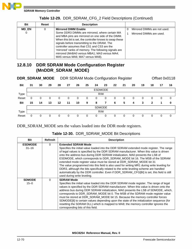
DDR SDRAM Memory Controller
12.8.10 DDR SDRAM Mode Configuration Register (MnDDR_SDRAM_MODE)
DDR_SDRAM_MODE sets the values loaded into the DDR mode registers.
MD_EN0
0 Mirrored DIMM EnableSome DDR3 DIMMs are mirrored, where certain MA and MBA pins are mirrored on one side of the DIMM. When this bit is set, the controller knows to swap these signals before transmitting to the DRAM. The controller assumes that CS1 and CS3 are the ‘mirrored’ ranks of memory. The following signals are mirrored (MnBA0 versus MBA1; MA3 versus MA4; MA5 versus MA6; MA7 versus MA8).
0 Mirrored DIMMs are not used.
1 Mirrored DIMMs are used.
DDR_SDRAM_MODE DDR SDRAM Mode Configuration Register Offset 0x0118
Bit 31 30 29 28 27 26 25 24 23 22 21 20 19 18 17 16
ESDMODE
Type R/WReset 0 0 0 0 0 0 0 0 0 0 0 0 0 0 0 0
Bit 15 14 13 12 11 10 9 8 7 6 5 4 3 2 1 0
SDMODEType R/W
Reset 0 0 0 0 0 0 0 0 0 0 0 0 0 0 0 0
Table 12-30. DDR_SDRAM_MODE Bit Descriptions
Bit Refresh Description
ESDMODE31–16
0 Extended SDRAM ModeSpecifies the initial value loaded into the DDR SDRAM extended mode register. The range of legal values is specified by the DDR SDRAM manufacturer. When this value is driven onto the address bus during DDR SDRAM initialization, MA0 presents the LSB of ESDMODE, which corresponds to DDR_SDRAM_MODE bit 16. The MSB of the SDRAM extended mode register value must be stored at DDR_SDRAM_MODE bit 31The value programmed into this field is also used for writing MR1 during write leveling for DDR3, although the bits specifically related to the write leveling scheme are handled automatically by the DDR controller. Even if DDR_SDRAM_CFG[BI] is set, this field is still used during write leveling.
SDMODE15–0
0 SDRAM ModeSpecifies the initial value loaded into the DDR SDRAM mode register. The range of legal values is specified by the DDR SDRAM manufacturer. When this value is driven onto the address bus during DDR SDRAM initialization, MA0 presents the LSB of SDMODE, which, corresponds to DDR_SDRAM_MODE bit 0. The MSB of the SDRAM mode register value must be stored at DDR_SDRAM_MODE bit 15. Because the memory controller forces SDMODE[8] to certain values depending upon the state of the initialization sequence (for resetting the SDRAM DLL) which is mapped to MA8; the memory controller ignores the corresponding bits of this field.
Table 12-29. DDR_SDRAM_CFG_2 Field Descriptions (Continued)
Bit Reset Description
MSC8254 Reference Manual, Rev. 0
12-70 Freescale Semiconductor

Memory Controller Programming Model
12.8.11 DDR SDRAM Mode Configuration 2 Register (MnDDR_SDRAM_MODE_2)
DDR_SDRAM_MODE_2 sets the values loaded into the DDR extended mode 2 and 3 registers.
12.8.12 DDR SDRAM Mode Control Register (MnDDR_SDRAM_MD_CNTL)
DDR_SDRAM_MD_CNTL allows software to force mode/extended mode register set commands to DRAM, including the following:
DDR_SDRAM_MODE_2 DDR SDRAM Mode Configuration 2 Offset 0x011CRegister
Bit 31 30 29 28 27 26 25 24 23 22 21 20 19 18 17 16
ESDMODE2Type R/WReset 0 0 0 0 0 0 0 0 0 0 0 0 0 0 0 0
Bit 15 14 13 12 11 10 9 8 7 6 5 4 3 2 1 0
ESDMODE3
Type R/WReset 0 0 0 0 0 0 0 0 0 0 0 0 0 0 0 0
Table 12-31. DDR_SDRAM_MODE_2 Bit Descriptions
Bit Reset Description
ESDMODE231–16
0 Extended SDRAM Mode 2Specifies the initial value loaded into the DDR SDRAM Extended 2 Mode Register. The range and meaning of legal values is specified by the DDR SDRAM manufacturer. When this value is driven onto the address bus during the DDR SDRAM initialization sequence, MA0 presents the LSB bit of ESDMODE2, which corresponds to DDR_SDRAM_MODE_2 bit 16. The MSB of the SDRAM extended mode 2 register value must be stored at DDR_SDRAM_MODE_2 bit 31.
ESDMODE315–0
0 Extended SDRAM Mode 3Specifies the initial value loaded into the DDR SDRAM Extended 3 Mode Register. The range of legal values is specified by the DDR SDRAM manufacturer. When this value is driven onto the address bus during DDR SDRAM initialization, MA0 presents the LSB of ESDMODE3, which corresponds to DDR_SDRAM_MODE_2 bit 0. The MSB of the SDRAM extended mode 3 register value must be stored at DDR_SDRAM_MODE_2 bit 15.
DDR_SDRAM_MD_CNTL DDR SDRAM Mode Control Register Offset 0x0120
Bit 31 30 29 28 27 26 25 24 23 22 21 20 19 18 17 16
MD_ EN
— CS_ SEL — MD_SEL SET_ REF
SET_ PRE
CKE_CNTL WRCW
—
Type R/W R R/W R R/W RReset 0 0 0 0 0 0 0 0 0 0 0 0 0 0 0 0
Bit 15 14 13 12 11 10 9 8 7 6 5 4 3 2 1 0
MD_VALUE
Type R/WReset 0 0 0 0 0 0 0 0 0 0 0 0 0 0 0 0
MSC8254 Reference Manual, Rev. 0
Freescale Semiconductor 12-71

DDR SDRAM Memory Controller
Issue a MODE REGISTER SET command to a particular chip select
Issue an immediate REFRESH to a particular chip select
Issue an immediate PRECHARGE or PRECHARGE ALL command to a particular chip select
Force the CKE signals to a specific value
Note: Each command initiated through the DDR_SDRAM_MD_CNTL register should be initiated separately in the order required by the DDR SDRAM. If multiple commands are initiated simultaneously, the execution order is not guarantied and can cause malfunction of the DDR SDRAM.
Table 12-32. DDR_SDRAM_MD_CNTL Bit Descriptions
Bit Reset Description Settings
MD_EN31
0 Mode EnableSetting this bit specifies that valid data in MD_VALUE is ready to be written to DRAM as one of the following commands: • MODE REGISTER SET • EXTENDED MODE REGISTER SET • EXTENDED MODE REGISTER SET 2 • EXTENDED MODE REGISTER SET 3The specific command to be executed is selected by setting MD_SEL. In addition, the chip select must be chosen by setting CS_SEL. MD_EN is set by software and cleared by hardware once the command has been issued.
0 Indicates that no MODE REGISTER SET command needs to be issued.
1 Indicates that valid data contained in the register is ready to be issued as a MODE REGISTER SET command.
—30
0 Reserved. Write to zero for future compatibility.
CS_SEL29–28
0 Select Chip SelectSpecifies the chip select to drive active due to any command forced by software in DDR_SDRAM_MD_CNTL.
00 Chip select 0 is active.
01 Chip select 1 is active.
10 Reserved.
11 Reserved.
—27
0 Reserved. Write to zero for future compatibility.
MD_SEL26–24
000 Mode Register SelectMD_SEL specifies one of the following: • During a mode select command, selects the SDRAM
mode register to be changed • During a precharge command, selects the SDRAM
logical bank to be precharged. A precharge all command ignores this field.
• During a refresh command, this field is ignored.Note that MD_SEL contains the value that is presented onto the memory bank address pins (MBAn) of the DDR controller.000 MR001 EMR010 EMR2011 EMR3
000 MR Mode register
001 EMR Extended Mode Register
010 EMR2 Extended Mode Register 2
011 EMR3 Extended Mode Register 3
SET_REF23
0 Set RefreshForces an immediate refresh to the chip select specified by DDR_SDRAM_MD_CNTL[CS_SEL]. Software sets this bit and hardware clears it when the command is issued.Note: SET_REF, and SET_PRE are mutually exclusive;
they cannot be set at the same time
0 No REFRESH command to issue.1 A REFRESH command is ready to
issue.
MSC8254 Reference Manual, Rev. 0
12-72 Freescale Semiconductor
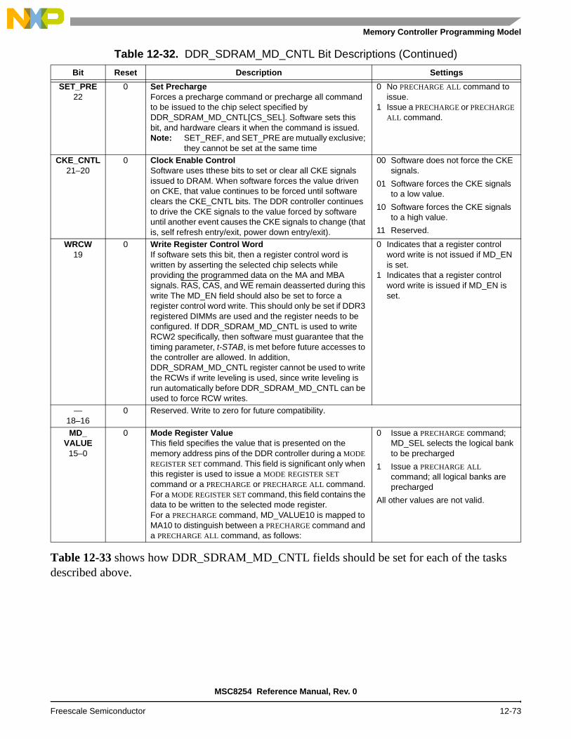
Memory Controller Programming Model
Table 12-33 shows how DDR_SDRAM_MD_CNTL fields should be set for each of the tasks described above.
SET_PRE22
0 Set PrechargeForces a precharge command or precharge all command to be issued to the chip select specified by DDR_SDRAM_MD_CNTL[CS_SEL]. Software sets this bit, and hardware clears it when the command is issued.Note: SET_REF, and SET_PRE are mutually exclusive;
they cannot be set at the same time
0 No PRECHARGE ALL command to issue.
1 Issue a PRECHARGE or PRECHARGE ALL command.
CKE_CNTL21–20
0 Clock Enable ControlSoftware uses tthese bits to set or clear all CKE signals issued to DRAM. When software forces the value driven on CKE, that value continues to be forced until software clears the CKE_CNTL bits. The DDR controller continues to drive the CKE signals to the value forced by software until another event causes the CKE signals to change (that is, self refresh entry/exit, power down entry/exit).
00 Software does not force the CKE signals.
01 Software forces the CKE signals to a low value.
10 Software forces the CKE signals to a high value.
11 Reserved.
WRCW19
0 Write Register Control WordIf software sets this bit, then a register control word is written by asserting the selected chip selects while providing the programmed data on the MA and MBA signals. RAS, CAS, and WE remain deasserted during this write The MD_EN field should also be set to force a register control word write. This should only be set if DDR3 registered DIMMs are used and the register needs to be configured. If DDR_SDRAM_MD_CNTL is used to write RCW2 specifically, then software must guarantee that the timing parameter, t-STAB, is met before future accesses to the controller are allowed. In addition, DDR_SDRAM_MD_CNTL register cannot be used to write the RCWs if write leveling is used, since write leveling is run automatically before DDR_SDRAM_MD_CNTL can be used to force RCW writes.
0 Indicates that a register control word write is not issued if MD_EN is set.
1 Indicates that a register control word write is issued if MD_EN is set.
—18–16
0 Reserved. Write to zero for future compatibility.
MD_ VALUE
15–0
0 Mode Register ValueThis field specifies the value that is presented on the memory address pins of the DDR controller during a MODE REGISTER SET command. This field is significant only when this register is used to issue a MODE REGISTER SET command or a PRECHARGE or PRECHARGE ALL command.For a MODE REGISTER SET command, this field contains the data to be written to the selected mode register.For a PRECHARGE command, MD_VALUE10 is mapped to MA10 to distinguish between a PRECHARGE command and a PRECHARGE ALL command, as follows:
0 Issue a PRECHARGE command; MD_SEL selects the logical bank to be precharged
1 Issue a PRECHARGE ALL command; all logical banks are precharged
All other values are not valid.
Table 12-32. DDR_SDRAM_MD_CNTL Bit Descriptions (Continued)
Bit Reset Description Settings
MSC8254 Reference Manual, Rev. 0
Freescale Semiconductor 12-73

DDR SDRAM Memory Controller
12.8.13 DDR SDRAM Interval Configuration Register (MnDDR_SDRAM_INTERVAL)
DDR_SDRAM_INTERVAL sets the number of DRAM clock cycles between bank refreshes issued to the DDR SDRAMs. In addition, it specifies the number of DRAM cycles that a page is maintained after it is accessed.
Table 12-33. Settings of DDR_SDRAM_MD_CNTL Fields
Field Mode Register Set Refresh PrechargeClock Enable Signals
Control
MD_EN 1 0 0 —
SET_REF 0 1 0 —
SET_PRE 0 0 1 —
CS_SEL Chooses chip select (CS) —
MD_SEL Select mode register. See Table 12-32.
— Selects logical bank —
MD_VALUE Value written to mode register
— Only MD_VALUE10 is significant. See Table 12-32.
—
CKE_CNTL 0 0 0 See Table 12-32.
DDR_SDRAM_INTERVAL DDR SDRAM Interval Configuration Offset 0x0124Register
Bit 31 30 29 28 27 26 25 24 23 22 21 20 19 18 17 16
REFINTType R/WReset 0 0 0 0 0 0 0 0 0 0 0 0 0 0 0 0
Bit 15 14 13 12 11 10 9 8 7 6 5 4 3 2 1 0
— BSTOPRE
Type R/WReset 0 0 0 0 0 0 0 0 0 0 0 0 0 0 0 0
Table 12-34. DDR_SDRAM_INTERVAL Bit Descriptions
Bit Refresh Description
REFINT31–16
0 Refresh IntervalRepresents the number of memory bus clock cycles between refresh cycles. Depending on DDR_SDRAM_CFG_2 [NUM_PR], some number of rows are refreshed in each DDR SDRAM physical bank during each refresh cycle. The value for REFINT depends on the specific SDRAMs used and the interface clock frequency. Refreshes are not issued when REFINT is cleared to all 0s.
MSC8254 Reference Manual, Rev. 0
12-74 Freescale Semiconductor

Memory Controller Programming Model
12.8.14 DDR SDRAM Data Initialization Register (MnDDR_DATA_INIT)
DDR_DATA_INIT provides the value to initialize memory if DDR_SDRAM_CFG_2[D_INIT] is set. When ECC is enabled, initializing all the available memory space can ensure that reads from unwritten addresses does not return ECC errors and interrupts.
12.8.15 DDR SDRAM Clock Control Configuration Register (MnDDR_SDRAM_CLK_CNTL)
—15–14
0 Reserved. Write to zero for future compatibility.
BSTOPRE 13–0
0 Precharge IntervalSpecifies the duration (in memory bus clock cycles) that a page is retained after a DDR SDRAM access. The page open counter is loaded with BSTOPRE each time the page is accessed (including page hits). When the counter expires, the open page is closed with an SDRAM precharge bank command as soon as possible. If BSTOPRE has a value of zero, the DDR memory controller uses auto-precharge read and write commands rather than operating in page mode. This is called global auto-precharge mode.
DDR_DATA_INIT DDR SDRAM Data Initialization Register Offset 0x0128
Bit 31 30 29 28 27 26 25 24 23 22 21 20 19 18 17 16
INIT_VALUE
Type R/WReset 0 0 0 0 0 0 0 0 0 0 0 0 0 0 0 0
Bit 15 14 13 12 11 10 9 8 7 6 5 4 3 2 1 0
INIT_VALUEType R/W
Reset 0 0 0 0 0 0 0 0 0 0 0 0 0 0 0 0
Table 12-35. DDR_DATA_INIT Bit Descriptions
Bits Reset Description
INIT_VALUE31–0
0 Initialization ValueSpecifies the initialization value for the DRAM if DDR_SDRAM_CFG_2[D_INIT] is set.
DDR_SDRAM_CLK_CNTL DDR SDRAM Clock Offset 0x0130 Control Configuration Register
Bit 31 30 29 28 27 26 25 24 23 22 21 20 19 18 17 16
— CLK_ADJUST —
Type R R/W RReset 0 0 0 0 0 0 1 0 0 0 0 0 0 0 0 0
Bit 15 14 13 12 11 10 9 8 7 6 5 4 3 2 1 0
—Type R
Reset 0 0 0 0 0 0 0 0 0 0 0 0 0 0 0 0
Table 12-34. DDR_SDRAM_INTERVAL Bit Descriptions (Continued)
Bit Refresh Description
MSC8254 Reference Manual, Rev. 0
Freescale Semiconductor 12-75

DDR SDRAM Memory Controller
DDR_SDRAM_CLK_CNTL provides a source synchronous option, along with a 1/8 cycle clock adjustment.
12.8.16 DDR SDRAM Initialization Address Register (MnDDR_INIT_ADDR)
DDR_INIT_ADDR provides the address for the data strobe to data skew adjustment and automatic CAS to preamble calibration after setting DDR_SDRAM_CFG[MEM_EN].
Note: After the skew adjustment, this address contains bad ECC data, which is not important at power-on reset because all memory should subsequently be initialized if ECC is enabled either through software or through the use of the DDR_SDRAM_CFG_2[D_INIT] bit. However, if the DSP is reset after the DRAM enters Self-Refresh mode, memory is not initialized. Therefore this address should be written to avoid possible ECC errors when this address is accessed later.
Table 12-36. DDR_SDRAM_CLK_CNTL Bit Descriptions
Bit Reset Description Settings
—31–27
0 Reserved. Write to zero for future compatibility.
CLK_ADJUST26–23
4’b0100 Clock AdjustSpecifies when the clock is launched in relationship to the address/command. Set delay from address/command start timing to MCK rising edge.
Figure 12-5, Figure 12-6, and Figure 12-7 in Section 12.4 show the timing relationships between clock and command for the case of CLK_ADJUST 0100 1/2 clock delay, which means nominal timing. The MCK rising edge is in the center of the address/command period in general.
0000 Clock launched and aligned with address/command.
0001 Clock launched 1/8 applied cycle after address/command.
0010 Clock launched 1/4 applied cycle after address/command.
0011 Clock launched 3/8 applied cycle after address/command.
0100 Clock launched 1/2 applied cycle after address/command.
0101 Clock launched 5/8 applied cycle after address/command.
0110 Clock launched 3/4 applied cycle after address/command.
0111 Clock launched 7/8 applied cycle after address/command.
1000 Clock launched 1 applied cycle after address/command.
1001–1111Reserved.—
22–00 Reserved. Write to zero for future compatibility.
DDR_INIT_ADDR DDR SDRAM Initialization Address Register Offset 0x0148
Bit 31 30 29 28 27 26 25 24 23 22 21 20 19 18 17 16
INIT_ADDRType R/W
Reset 0 0 0 0 0 0 0 0 0 0 0 0 0 0 0 0
Bit 15 14 13 12 11 10 9 8 7 6 5 4 3 2 1 0
INIT_ADDRType R/WReset 0 0 0 0 0 0 0 0 0 0 0 0 0 0 0 0
MSC8254 Reference Manual, Rev. 0
12-76 Freescale Semiconductor

Memory Controller Programming Model
12.8.17 DDR Initialization Enable (MnDDR_INIT_EN)
The DDR SDRAM initialization enable register provides the enable bit to use the address given by DDR_INIT_ADDR[INIT_ADDR] for the data to data strobes deskew calibration and for automatic CAS to preamble calibration during the DDR SDRAM initialization. Table 12-38 describes the DDR_INIT_EN fields.
Table 12-37. DDR_INIT_ADDR Bit Descriptions
Bit Reset Description Settings
INIT_ADDR31–0
0 Initialization AddressProvides the address used for the data to data strobes skew adjustment and automatic CAS to preamble calibration after setting DDR_SDRAM_CFG[MEM_EN].This address is written during the initialization sequence.
DDR_INIT_EN DDR SDRAM Initialization Offset 0x014CEnable
Bit 31 30 29 28 27 26 25 24 23 22 21 20 19 18 17 16
UIA —
Type R/W R
Reset 0 0 0 0 0 0 0 0 0 0 0 0 0 0 0 0
Bit 15 14 13 12 11 10 9 8 7 6 5 4 3 2 1 0
—Type RReset 0 0 0 0 0 0 0 0 0 0 0 0 0 0 0 0
Table 12-38. DDR_INIT_EN Field Descriptions
Bit Reset Description Settings
UIA31
0 Use Initialization AddressIndicates whether to use the initialization address.
0 Use the default address for training sequence as calculated by the controller. This is the first valid address in the first enabled chip select.
1 Use the initialization address programmed in DDR_INIT_ADDR.
—30–0
0 Reserved. Write to zero for future compatibility.
MSC8254 Reference Manual, Rev. 0
Freescale Semiconductor 12-77

DDR SDRAM Memory Controller
12.8.18 DDR SDRAM Timing Configuration 4 (MnTIMING_CFG_4)
The DDR SDRAM timing configuration 4 register provides additional timing fields required to support DDR3 memories. Table 12-39 describes the TIMING_CFG_4 fields.
TIMING_CFG_4 DDR SDRAM Timing Con figuration 4 Offset 0x0160
Bit 31 30 29 28 27 26 25 24 23 22 21 20 19 18 17 16
RWT WRT RRT WWT
Type R/WReset 0 0 0 0 0 0 0 0 0 0 0 0 0 0 0 0
Bit 15 14 13 12 11 10 9 8 7 6 5 4 3 2 1 0
— DLL_LOCKType R/W
Reset 0 0 0 0 0 0 0 0 0 0 0 0 0 0 0 0
Table 12-39. TIMING_CFG_4 Field Descriptions
Bits Reset Description Settings
RWT31–28
0 Read-to-Write Turnaround for Same Chip Select Specifies how many cycles are added between a read to write turnaround for transactions to the same chip select. If a value of 0000 is chosen, then the DDR controller uses the value used for transactions to different chip selects, as defined in TIMING_CFG_0[RWT]. This field can be used to improve performance when operating in burst-chop mode by forcing transactions to the same chip select to use extra cycles, while transaction to different chip selects can utilize the tri-state time on the DRAM interface. Regardless of the value that is set in this field, the value defined by TIMING_CFG_0[RWT] is also met before issuing a write command.
0000 Default0001 1 clock0010 2 clocks0011 3 clocks0100 4 clocks0101 5 clocks0110 6 clocks0111 7 clocks1000 8 clocks1001 9 clocks1010 10 clocks1011 11 clocks1100 12 clocks1101 13 clocks1110 14 clocks1111 15 clocks
WRT27–24
0 Write-to-Read Turnaround for Same Chip Select Specifies how many cycles are added between a write to read turnaround for transactions to the same chip select. If a value of 0000 is chosen, then the DDR controller uses the value used for transactions to different chip selects, as defined in TIMING_CFG_0[WRT]. This field can be used to improve performance when operating in burst-chop mode by forcing transactions to the same chip select to use extra cycles, while transaction to different chip selects can utilize the tri-state time on the DRAM interface. Regardless of the value that is set in this field, the value defined by TIMING_CFG_0[WRT] is also met before issuing a read command.
0000 Default0001 1 clock0010 2 clocks0011 3 clocks0100 4 clocks0101 5 clocks0110 6 clocks0111 7 clocks1000 8 clocks1001 9 clocks1010 10 clocks1011 11 clocks1100 12 clocks1101 13 clocks1110 14 clocks1111 15 clocks
MSC8254 Reference Manual, Rev. 0
12-78 Freescale Semiconductor

Memory Controller Programming Model
RRT23–20
0 Read-to-Read Turnaround for Same Chip Select Specifies how many cycles are added between reads to the same chip select. If a value of 0000 is chosen, then 2 cycles is required between read commands to the same chip select if 4-beat bursts are used (4 cycles are required if 8-beat bursts are used). Note that DDR3 does not support 4-beat bursts. However, this field may be used to add extra cycles when burst-chop mode is used, and the DDR controller must wait 4 cycles for read-to-read transactions to the same chip select.
0000 BL/2 clocks0001 BL/2 + 1 clock0010 BL/2 + 2 clocks0011 BL/2 + 3 clocks0100 BL/2 + 4 clocks0101 BL/2 + 5 clocks0110 BL/2 + 6 clocks0111 BL/2 + 7 clocks1000 BL/2 + 8 clocks1001 BL/2 + 9 clocks1010 BL/2 + 10 clocks1011 BL/2 + 11 clocks1100 BL/2 + 12 clocks1101 BL/2 + 13 clocks1110 BL/2 + 14 clocks1111 BL/2 + 15 clocks
WWT19–16
0 Write-to-Write Turnaround for Same Chip SelectSpecifies how many cycles are added between writes to the same chip select. If a value of 0000 is chosen, then 2 cycles is required between write commands to the same chip select if 4-beat bursts are used (4 cycles are required if 8-beat bursts are used). Note that DDR3 does not support 4-beat bursts. However, this field may be used to add extra cycles when burst-chop mode is used, and the DDR controller must wait 4 cycles for write-to-write transactions to the same chip select.
0000 BL/2 clocks0001 BL/2 + 1 clock0010 BL/2 + 2 clocks0011 BL/2 + 3 clocks0100 BL/2 + 4 clocks0101 BL/2 + 5 clocks0110 BL/2 + 6 clocks0111 BL/2 + 7 clocks1000 BL/2 + 8 clocks1001 BL/2 + 9 clocks1010 BL/2 + 10 clocks1011 BL/2 + 11 clocks1100 BL/2 + 12 clocks1101 BL/2 + 13 clocks1110 BL/2 + 14 clocks1111 BL/2 + 15 clocks
—15–2
0 Reserved. Write to zero for future compatibility.
DLL_LOCK1–0
0 DDR SDRAM DLL Lock TimeThis provides the number of cycles that it takes for the DRAMs DLL to lock at power-on reset and after exiting self refresh. The controller waits the specified number of cycles before issuing any commands after exiting POR or self refresh.
00 200 clocks01 512 clocks10 Reserved11 Reserved
Table 12-39. TIMING_CFG_4 Field Descriptions (Continued)
Bits Reset Description Settings
MSC8254 Reference Manual, Rev. 0
Freescale Semiconductor 12-79

DDR SDRAM Memory Controller
12.8.19 DDR SDRAM Timing Configuration 5 (MnTIMING_CFG_5)
The DDR SDRAM timing configuration 5 register provides additional timing fields required to support DDR3 memories. Table 12-40 describes the TIMING_CFG_5 fields.
TIMING_CFG_5 DDR SDRAM Timing Con figuration 5 Offset 0x0164
Bit 31 30 29 28 27 26 25 24 23 22 21 20 19 18 17 16
— RODT_ON — RODT_OFF — WODT_ON
Type R/W
Reset 0 0 0 0 0 0 0 0 0 0 0 0 0 0 0 0
Bit 15 14 13 12 11 10 9 8 7 6 5 4 3 2 1 0
WODT_ON — WODT_OFF —Type R/WReset 0 0 0 0 0 0 0 0 0 0 0 0 0 0 0 0
Table 12-40. TIMING_CFG_5 Field Descriptions
Bits Reset Description Settings
—31–29
0 Reserved. Write to zero for future compatibility.
RODT_ON28–24
0 Read-to-ODT OnSpecifies the number of cycles that passes from when a read command is placed on the DRAM bus until the assertion of the relevant ODT signal(s). The default case (00000) provides a decode of RL - 3 cycles to support legacy of past products. RL is the read latency, derived from CAS latency + additive latency. If 2T/3T timing is used, one/two extra cycles are automatically added to the value selected in this field.
00000 RL - 3 clocks00001 0 clocks00010 1 clocks00011 2 clocks00100 3 clocks00101 4 clocks00110 5 clocks00111 6 clocks01000 7 clocks01001 8 clocks01010 9 clocks01011 10 clocks01100 11 clocks01101 12 clocks01110 13 clocks.011111 14 clocks10000 15 clocks10001 16 clocks10010 17 clocks10011 18 clocks10100 19 clocks10101 20 clocks10110 21 clocks10111 22 clocks11000 23 clocks11001 24 clocks11010 25 clocks11011 26 clocks11100 27 clocks11101 28 clocks11110 29 clocks.11111 30 clocks
MSC8254 Reference Manual, Rev. 0
12-80 Freescale Semiconductor
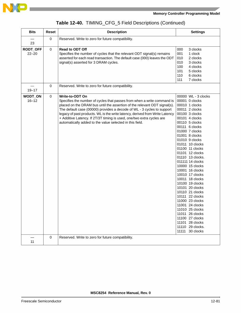
Memory Controller Programming Model
—23
0 Reserved. Write to zero for future compatibility.
RODT_OFF22–20
0 Read to ODT OffSpecifies the number of cycles that the relevant ODT signal(s) remains asserted for each read transaction. The default case (000) leaves the ODT signal(s) asserted for 3 DRAM cycles.
000 3 clocks001 1 clock010 2 clocks010 3 clocks100 4 clocks101 5 clocks110 6 clocks111 7 clocks
—19–17
0 Reserved. Write to zero for future compatibility.
WODT_ON16–12
0 Write-to-ODT OnSpecifies the number of cycles that passes from when a write command is placed on the DRAM bus until the assertion of the relevant ODT signal(s). The default case (00000) provides a decode of WL - 3 cycles to support legacy of past products. WL is the write latency, derived from Write Latency + Additive Latency. If 2T/3T timing is used, one/two extra cycles are automatically added to the value selected in this field.
00000 WL - 3 clocks00001 0 clocks00010 1 clocks00011 2 clocks00100 3 clocks00101 4 clocks00110 5 clocks00111 6 clocks01000 7 clocks01001 8 clocks01010 9 clocks01011 10 clocks01100 11 clocks01101 12 clocks01110 13 clocks.011111 14 clocks10000 15 clocks10001 16 clocks10010 17 clocks10011 18 clocks10100 19 clocks10101 20 clocks10110 21 clocks10111 22 clocks11000 23 clocks11001 24 clocks11010 25 clocks11011 26 clocks11100 27 clocks11101 28 clocks11110 29 clocks.11111 30 clocks
—11
0 Reserved. Write to zero for future compatibility.
Table 12-40. TIMING_CFG_5 Field Descriptions (Continued)
Bits Reset Description Settings
MSC8254 Reference Manual, Rev. 0
Freescale Semiconductor 12-81

DDR SDRAM Memory Controller
12.8.20 DDR ZQ Calibration Control (MnDDR_ZQ_CNTL)
The DDR ZQ Calibration Control register provides the enable and controls required for ZQ calibration when using DDR3 SDRAM devices. There is a limitation for various DRAM timing parameters when ZQ calibration is used. The factors involved in this limitation are DDR_ZQ_CNTL[ZQOPER], DDR_ZQ_CNTL[ZQCS], TIMING_CFG_1[PRETOACT], TIMING_CFG_1[REFREC], DDR_SDRAM_INTERVAL[REFINT], and the number of chip selects enabled. If the following condition is true:
[((DDR_ZQ_CNTL[ZQOPER] + DDR_ZQ_CNTL[ZQCS])* (# enabled chip selects)) +
TIMING_CFG_1[PRETOACT] + TIMING_CFG_1[REFREC] + 2tCK] > (DDR_SDRAM_INTERVAL[REFINT])
it is possible that one refresh is skipped when the controller exits self refresh. If this is an issue, then posted refreshes can be used to extend the refresh interval. Another alternative is to use the DDR_SDRAM_MD_CNTL register to force an extra refresh to each chip select after exiting self refresh mode. However, DDR3 timing parameters for most devices/frequencies do not allow missed refresh cycles. Table 12-41 describes the DDR_ZQ_CNTL fields.
WODT_ OFF10–8
0 Write to ODT OffSpecifies the number of cycles that the relevant ODT signal(s) remains asserted for each write transaction. The default case (000) leaves the ODT signal(s) asserted for 3 DRAM cycles.
000 3 clocks001 1 clock010 2 clocks010 3 clocks100 4 clocks101 5 clocks110 6 clocks111 7 clocks
—7–0
0 Reserved. Write to zero for future compatibility.
DDR_ZQ_ CNTL DDR ZQ Calibration Control Offset 0x0170
Bit 31 30 29 28 27 26 25 24 23 22 21 20 19 18 17 16
ZQ_ EN
— ZQINIT — ZQOPER
Type R/WReset 0 0 0 0 0 0 0 0 0 0 0 0 0 0 0 0
Bit 15 14 13 12 11 10 9 8 7 6 5 4 3 2 1 0
— ZQCS —
Type R/WReset 0 0 0 0 0 0 0 0 0 0 0 0 0 0 0 0
Table 12-40. TIMING_CFG_5 Field Descriptions (Continued)
Bits Reset Description Settings
MSC8254 Reference Manual, Rev. 0
12-82 Freescale Semiconductor

Memory Controller Programming Model
Table 12-41. DDR_ZQ_CNTL Field Descriptions
Bit Reset Description Settings
ZQ_EN31
0 ZQ Calibration EnableThis bit determines whether ZQ calibration is used. This bit should be set only if DDR3 memory is used (DDR_SDRAM_CFG[SDRAM_TYPE] = 0b111).
0 ZQ Calibration is not used.
1 ZQ Calibration is used. A ZQCL command is issued by the DDR controller after power-on reset and anytime the DDR controller exits self refresh. A ZQCS command is issued every 32 refresh sequences to account for VT variations.
—30–28
0 Reserved. Write to zero for future compatibility.
ZQ_INIT27–24
0 Power-on Reset ZQ Calibration Time (tZQinit)Determines the number of cycles that must be allowed for DRAM ZQ calibration at power-on reset. Each chip select is calibrated separately, and this time must elapse after the ZQCL command is issued for each chip select before a separate command can be issued.
0111 128 clocks
1000 256 clocks
1001 512 clocks
1010 1024 clocks
All other values reserved.
—23–20
0 Reserved. Write to zero for future compatibility.
ZQOPER19–16
0 Normal Operation Full Calibration Time (tZQoper)Determines the number of cycles that must be allowed for DRAM ZQ calibration when exiting self refresh. Each chip select is calibrated separately, and this time must elapse after the ZQCL command is issued for each chip select before a separate command may be issued.
0111 128 clocks
1000 256 clocks
1001 512 clocks
1010 1024 clocks
All other values reserved.
—15–12
0 Reserved. Write to zero for future compatibility.
ZQCS11–8
0 Normal Operation Short Calibration Time (tZQCS)Determines the number of cycles that must be allowed for DRAM ZQ calibration during dynamic calibration which is issued every 32 refresh cycles. Each chip select is calibrated separately, and this time must elapse after the ZQCS command is issued for each chip select before a separate command may be issued.
0000 1 clocks
0001 2 clocks
0010 4 clocks
0011 8 clocks
0100 16 clocks
0101 32 clocks
0110 64 clocks
0111 128 clocks
1000 256 clocks
1001 512 clocks
All other values reserved.—
7–00 Reserved. Write to zero for future compatibility.
MSC8254 Reference Manual, Rev. 0
Freescale Semiconductor 12-83
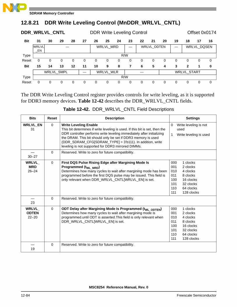
DDR SDRAM Memory Controller
12.8.21 DDR Write Leveling Control (MnDDR_WRLVL_CNTL)
The DDR Write Leveling Control register provides controls for write leveling, as it is supported for DDR3 memory devices. Table 12-42 describes the DDR_WRLVL_CNTL fields.
DDR_WRLVL_CNTL DDR Write Leveling Control Offset 0x0174
Bit 31 30 29 28 27 26 25 24 23 22 21 20 19 18 17 16
WRLVL_EN
— WRLVL_MRD — WRLVL_ODTEN — WRLVL_DQSEN
Type R/WReset 0 0 0 0 0 0 0 0 0 0 0 0 0 0 0 0
Bit 15 14 13 12 11 10 9 8 7 6 5 4 3 2 1 0
WRLVL_SMPL — WRLVL_WLR — WRLVL_STARTType R/W
Reset 0 0 0 0 0 0 0 0 0 0 0 0 0 0 0 0
Table 12-42. DDR_WRLVL_CNTL Field Descriptions
Bits Reset Description Settings
WRLVL_EN31
0 Write Leveling EnableThis bit determines if write leveling is used. If this bit is set, then the DDR controller performs write leveling immediately after initializing the DRAM. This bit should only be set if DDR3 memory is used (DDR_SDRAM_CFG[SDRAM_TYPE] = 3’b111). In addition, write leveling is not supported for DDR3 mirrored DIMMs.
0 Write leveling is not used
1 Write leveling is used
—30–27
0 Reserved. Write to zero for future compatibility.
WRLVL_ MRD26–24
0 First DQS Pulse Rising Edge after Margining Mode Is Programmed (tWL_MRD)Determines how many cycles to wait after margining mode has been programmed before the first DQS pulse may be issued. This field is only relevant when DDR_WRLVL_CNTL[WRLVL_EN] is set.
000 1 clocks001 2 clocks010 4 clocks011 8 clocks100 16 clocks101 32 clocks110 64 clocks111 128 clocks
—23
0 Reserved. Write to zero for future compatibility.
WRLVL_ ODTEN22–20
0 ODT Delay after Margining Mode Is Programmed (tWL_ODTEN)Determines how many cycles to wait after margining mode is programmed.until ODT is asserted.This field is only relevant when DDR_WRLVL_CNTL[WRLVL_EN] is set.
000 1 clocks001 2 clocks010 4 clocks011 8 clocks100 16 clocks101 32 clocks110 64 clocks111 128 clocks
—19
0 Reserved. Write to zero for future compatibility.
MSC8254 Reference Manual, Rev. 0
12-84 Freescale Semiconductor

Memory Controller Programming Model
WRLVL_ DQSEN18–16
0 DQS/DQS Delay after Margining Mode Is Programmed (tWL_DQSEN)Determines how many cycles to wait after margining mode has been programmed until DQS may be actively driven. This field is only relevant when DDR_WRLVL_CNTL[WRLVL_EN] is set.
000 1 clocks001 2 clocks010 4 clocks011 8 clocks100 16 clocks101 32 clocks110 64 clocks111 128 clocks
WRLVL_ SMPL15–12
0 Write Leveling Sample TimeDetermines the number of cycles that must pass before the data signals are sampled after a DQS pulse during margining mode. This field should be programmed at least 6 cycles higher than tWLO to allow enough time for propagation delay and sampling of the prime data bits. This field is only relevant when DDR_WRLVL_CNTL[WRLVL_EN] is set.
0000 Reserved (if DDR_ WRLVL_CNTL[WRLVL_EN] is set)
0001 1 clocks0010 2 clocks0011 3 clocks0100 4 clocks0101 5 clocks1010 6 clocks0111 7 clocks1000 8 clocks1001 9 clocks1010 10 clocks1011 11 clocks1100 12 clocks1101 13 clocks1010 14 clocks1111 15 clocks
—11
0 Reserved. Write to zero for future compatibility.
WRLVL_ WLR10–8
0 Write Leveling Repetition TimeDetermines the number of cycles that must pass between DQS pulses during write leveling. This field is only relevant when DDR_WRLVL_CNTL[WRLVL_EN] is set.
000 1 clocks001 2 clocks010 4 clocks011 8 clocks100 16 clocks101 32 clocks110 64 clocks111 128 clocks
Table 12-42. DDR_WRLVL_CNTL Field Descriptions (Continued)
Bits Reset Description Settings
MSC8254 Reference Manual, Rev. 0
Freescale Semiconductor 12-85

DDR SDRAM Memory Controller
—7–5
0 Reserved. Write to zero for future compatibility.
WRLVL_ START
4–0
0 Write Leveling Start TimeDetermines the value to use for the DQS_ADJUST for the first sample when write leveling is enabled.
00000 0 clock delay00001 1/8 clock delay00010 1/4 clock delay00011 3/8 clock delay00100 1/2 clock delay00101 5/8 clock delay00110 3/4 clock delay00111 7/8 clock delay01000 1 clock delay01001 9/8 clock delay01010 5/4 clock delay01011 11/8 clock delay01100 3/2 clock delay01101 13/8 clock delay01110 7/4 clock delay01111 15/8 clock delay10000 2 clock delay10001 17/8 clock delay10010 9/4 clock delay10011 19/8 clock delay10100 5/2 clock delay10101–11111 Reserved
Table 12-42. DDR_WRLVL_CNTL Field Descriptions (Continued)
Bits Reset Description Settings
MSC8254 Reference Manual, Rev. 0
12-86 Freescale Semiconductor

Memory Controller Programming Model
12.8.22 DDR Write Leveling Control 2 (MnDDR_WRLVL_CNTL_2)
The DDR Write Leveling Control 2 register provides controls for write leveling, as it is supported for DDR3 memory devices. This register specifically defines the starting points for the individual data strobes. Table 12-43 describes the DDR_WRLVL_CNTL_2 fields.
DDR_WRLVL_CNTL_2 DDR Write Leveling Control 2 Offset 0x0190
Bit 31 30 29 28 27 26 25 24 23 22 21 20 19 18 17 16
— WRLVL_START_1 — WRLVL_START_2
Type R/WReset 0 0 0 0 0 0 0 0 0 0 0 0 0 0 0 0
Bit 15 14 13 12 11 10 9 8 7 6 5 4 3 2 1 0
— WRLVL_START_3 — WRLVL_START_4Type R/W
Reset 0 0 0 0 0 0 0 0 0 0 0 0 0 0 0 0
Table 12-43. DDR_WRLVL_CNTL_2 Field Descriptions
Bits Reset Description Settings
—31–29
0 Reserved. Write to zero for future compatibility.
WRLVL_ START_1
28–24
0 Write Leveling Start Time for DQS1Determines the value to use for the DQS_ADJUST for the first sample when write leveling is enabled.
00000 Use value from DDR_WRLVL_CNTL [WRLVL_START]
00001 1/8 clock delay
00010 1/4 clock delay
00011 3/8 clock delay
00100 1/2 clock delay
00101 5/8 clock delay
00110 3/4 clock delay
00111 7/8 clock delay
01000 1 clock delay
01001 9/8 clock delay
01010 5/4 clock delay
01011 11/8 clock delay
01100 3/2 clock delay
01101 13/8 clock delay
01110 7/4 clock delay
01111 15/8 clock delay
10000 2 clock delay
10001 17/8 clock delay
10010 9/4 clock delay
10011 19/8 clock delay
10100 5/2 clock delay
10101–
11111 Reserved
MSC8254 Reference Manual, Rev. 0
Freescale Semiconductor 12-87

DDR SDRAM Memory Controller
—23–21
0 Reserved. Write to zero for future compatibility.
WRLVL_ START_2
20–16
0 Write Leveling Start Time for DQS2Determines the value to use for the DQS_ADJUST for the first sample when write leveling is enabled.
00000 Use value from DDR_WRLVL_CNTL [WRLVL_START]
00001 1/8 clock delay00010 1/4 clock delay00011 3/8 clock delay00100 1/2 clock delay00101 5/8 clock delay00110 3/4 clock delay00111 7/8 clock delay01000 1 clock delay01001 9/8 clock delay01010 5/4 clock delay01011 11/8 clock delay01100 3/2 clock delay01101 13/8 clock delay01110 7/4 clock delay01111 15/8 clock delay10000 2 clock delay10001 17/8 clock delay10010 9/4 clock delay10011 19/8 clock delay10100 5/2 clock delay10101–11111 Reserved
—15–13
0 Reserved. Write to zero for future compatibility.
WRLVL_ START_3
12–8
0 Write Leveling Start Time for DQS3Determines the value to use for the DQS_ADJUST for the first sample when write leveling is enabled.
00000 Use value from DDR_WRLVL_CNTL [WRLVL_START]
00001 1/8 clock delay00010 1/4 clock delay00011 3/8 clock delay00100 1/2 clock delay00101 5/8 clock delay00110 3/4 clock delay00111 7/8 clock delay01000 1 clock delay01001 9/8 clock delay01010 5/4 clock delay01011 11/8 clock delay01100 3/2 clock delay01101 13/8 clock delay01110 7/4 clock delay01111 15/8 clock delay10000 2 clock delay10001 17/8 clock delay10010 9/4 clock delay10011 19/8 clock delay10100 5/2 clock delay10101–11111 Reserved
Table 12-43. DDR_WRLVL_CNTL_2 Field Descriptions (Continued)
Bits Reset Description Settings
MSC8254 Reference Manual, Rev. 0
12-88 Freescale Semiconductor

Memory Controller Programming Model
—7–5
0 Reserved. Write to zero for future compatibility.
WRLVL_ START_4
4–0
0 Write Leveling Start Time for DQS4Determines the value to use for the DQS_ADJUST for the first sample when write leveling is enabled.
00000 Use value from DDR_WRLVL_CNTL [WRLVL_START]
00001 1/8 clock delay00010 1/4 clock delay00011 3/8 clock delay00100 1/2 clock delay00101 5/8 clock delay00110 3/4 clock delay00111 7/8 clock delay01000 1 clock delay01001 9/8 clock delay01010 5/4 clock delay01011 11/8 clock delay01100 3/2 clock delay01101 13/8 clock delay01110 7/4 clock delay01111 15/8 clock delay10000 2 clock delay10001 17/8 clock delay10010 9/4 clock delay10011 19/8 clock delay10100 5/2 clock delay10101–11111 Reserved
Table 12-43. DDR_WRLVL_CNTL_2 Field Descriptions (Continued)
Bits Reset Description Settings
MSC8254 Reference Manual, Rev. 0
Freescale Semiconductor 12-89

DDR SDRAM Memory Controller
12.8.23 DDR Write Leveling Control 3 (MnDDR_WRLVL_CNTL_3)
The DDR Write Leveling Control 3 register provides controls for write leveling, as it is supported for DDR3 memory devices. This register specifically defines the starting points for the individual data strobes. Table 12-43 describes the DDR_WRLVL_CNTL_3 fields.
DDR_WRLVL_CNTL_3 DDR Write Leveling Control 3 Offset 0x0194
Bit 31 30 29 28 27 26 25 24 23 22 21 20 19 18 17 16
— WRLVL_START_5 — WRLVL_START_6
Type R/WReset 0 0 0 0 0 0 0 0 0 0 0 0 0 0 0 0
Bit 15 14 13 12 11 10 9 8 7 6 5 4 3 2 1 0
— WRLVL_START_7 — WRLVL_START_8Type R/W
Reset 0 0 0 0 0 0 0 0 0 0 0 0 0 0 0 0
Table 12-44. DDR_WRLVL_CNTL_3 Field Descriptions
Bits Reset Description Settings
—31–29
0 Reserved. Write to zero for future compatibility.
WRLVL_ START_5
28–24
0 Write Leveling Start Time for DQS5Determines the value to use for the DQS_ADJUST for the first sample when write leveling is enabled.
00000 Use value from DDR_WRLVL_CNTL [WRLVL_START]
00001 1/8 clock delay00010 1/4 clock delay00011 3/8 clock delay00100 1/2 clock delay00101 5/8 clock delay00110 3/4 clock delay00111 7/8 clock delay01000 1 clock delay01001 9/8 clock delay01010 5/4 clock delay01011 11/8 clock delay01100 3/2 clock delay01101 13/8 clock delay01110 7/4 clock delay01111 15/8 clock delay10000 2 clock delay10001 17/8 clock delay10010 9/4 clock delay10011 19/8 clock delay10100 5/2 clock delay10101–11111 Reserved
—23–21
0 Reserved. Write to zero for future compatibility.
MSC8254 Reference Manual, Rev. 0
12-90 Freescale Semiconductor

Memory Controller Programming Model
WRLVL_ START_6
20–16
0 Write Leveling Start Time for DQS6Determines the value to use for the DQS_ADJUST for the first sample when write leveling is enabled.
00000 Use value from DDR_WRLVL_CNTL [WRLVL_START]
00001 1/8 clock delay00010 1/4 clock delay00011 3/8 clock delay00100 1/2 clock delay00101 5/8 clock delay00110 3/4 clock delay00111 7/8 clock delay01000 1 clock delay01001 9/8 clock delay01010 5/4 clock delay01011 11/8 clock delay01100 3/2 clock delay01101 13/8 clock delay01110 7/4 clock delay01111 15/8 clock delay10000 2 clock delay10001 17/8 clock delay10010 9/4 clock delay10011 19/8 clock delay10100 5/2 clock delay10101–11111 Reserved
—15–13
0 Reserved. Write to zero for future compatibility.
WRLVL_ START_7
12–8
0 Write Leveling Start Time for DQS7Determines the value to use for the DQS_ADJUST for the first sample when write leveling is enabled.
00000 Use value from DDR_WRLVL_CNTL [WRLVL_START]
00001 1/8 clock delay00010 1/4 clock delay00011 3/8 clock delay00100 1/2 clock delay00101 5/8 clock delay00110 3/4 clock delay00111 7/8 clock delay01000 1 clock delay01001 9/8 clock delay01010 5/4 clock delay01011 11/8 clock delay01100 3/2 clock delay01101 13/8 clock delay01110 7/4 clock delay01111 15/8 clock delay10000 2 clock delay10001 17/8 clock delay10010 9/4 clock delay10011 19/8 clock delay10100 5/2 clock delay10101–11111 Reserved
Table 12-44. DDR_WRLVL_CNTL_3 Field Descriptions (Continued)
Bits Reset Description Settings
MSC8254 Reference Manual, Rev. 0
Freescale Semiconductor 12-91

DDR SDRAM Memory Controller
—7–5
0 Reserved. Write to zero for future compatibility.
WRLVL_ START_8
4–0
0 Write Leveling Start Time for DQS8Determines the value to use for the DQS_ADJUST for the first sample when write leveling is enabled.
00000 Use value from DDR_WRLVL_CNTL [WRLVL_START]
00001 1/8 clock delay00010 1/4 clock delay00011 3/8 clock delay00100 1/2 clock delay00101 5/8 clock delay00110 3/4 clock delay00111 7/8 clock delay01000 1 clock delay01001 9/8 clock delay01010 5/4 clock delay01011 11/8 clock delay01100 3/2 clock delay01101 13/8 clock delay01110 7/4 clock delay01111 15/8 clock delay10000 2 clock delay10001 17/8 clock delay10010 9/4 clock delay10011 19/8 clock delay10100 5/2 clock delay10101–11111 Reserved
Table 12-44. DDR_WRLVL_CNTL_3 Field Descriptions (Continued)
Bits Reset Description Settings
MSC8254 Reference Manual, Rev. 0
12-92 Freescale Semiconductor

Memory Controller Programming Model
12.8.24 DDR Pre-Drive Conditioning Control (MnDDR_PD_CNTL)
The DDR Pre-Drive Conditioning Control register provides controls for asserting termination at the on-chip I/Os prior to driving DQS/DQ for write commands. Table 12-45 describes the DDR_PD_CNTL fields.
DDR_PD_CNTL DDR Pre_Drive Conditioning Control Offset 0x0178
Bit 31 30 29 28 27 26 25 24 23 22 21 20 19 18 17 16
PD_EN TVPD — PDAR — PDAW
Type R/WReset 0 0 0 0 0 0 0 0 0 0 0 0 0 0 0 0
Bit 15 14 13 12 11 10 9 8 7 6 5 4 3 2 1 0
PDAW — PD_ON — PD_OFFType R/W
Reset 0 0 0 0 0 0 0 0 0 0 0 0 0 0 0 0
Table 12-45. DDR_PD_CNTL Field Descriptions
Bits Reset Description Settings
PD_EN31
0 Pre-Drive Conditioning EnableThis bit determines whether termination is asserted to the on-chip I/Os prior to write commands. This helps bring DRAM/IO terminated signals near VREF before driving an active preamble. The result is a more symmetrical eye with less overshoot on the first rising edge of these signals.
0 Pre-drive conditioning is not used
1 Pre-drive conditioning is used
TVPD30–28
0 Termination Value During Pre-drive ConditioningThis represents the value of the termination that is used during pre-drive conditioning.
000 75 ohms001 60 ohms010 150 ohms011 120 ohms100 46 ohms101 43 ohms110 33 ohms 111 Reserved
—27
0 Reserved. Write to zero for future compatibility.
PDAR26–20
0 Pre-Drive After ReadIf pre-drive conditioning is enabled, it may not be desirable to assert termination to the on-chip IOs immediately after a prior read. This field represents the number of cycles that must pass after a previous read is issue before pre-drive conditioning is available for a future write. Note that the decision to use pre-drive conditioning is made at the time the write command is issued.
0000000 0 clocks0000001 1 clocks0000010 2 clocks...1111111 127 clocks
Note: The value represents the actual number of clocks to use
—19
0 Reserved. Write to zero for future compatibility.
MSC8254 Reference Manual, Rev. 0
Freescale Semiconductor 12-93

DDR SDRAM Memory Controller
PDAW18–12
0 Pre-Drive After WriteIf pre-drive conditioning is enabled, it may not be desirable to assert termination to the on-chip IOs immediately after a prior write. This field represents the number of cycles that must pass after a previous write is issue before pre-drive conditioning is available for a future write. Note that the decision to use pre-drive conditioning is made at the time the write command is issued.
0000000 0 clocks0000001 1 clocks0000010 2 clocks...1111111 127 clocks
Note: The value represents the actual number of clocks to use
—11
0 Reserved. Write to zero for future compatibility.
PD_ON10–6
0 Pre-Drive Conditioning OnSpecifies the number of cycles that passes from when a write command is placed on the DRAM bus until the assertion of termination at the on-chip IOs. Note that DDR_PD_CNTL[PD_ON] + DDR_PD_CNTL[PD_OFF} should not be greater than 31.
00000 Reserved00001 1 clocks00010 2 clocks00011 3 clocks00100 4 clocks00101 5 clocks00110 6 clocks00111 7 clocks01000 8 clocks01001 9 clocks01010 10 clocks01011 11 clocks01100 12 clocks01101 13 clocks01110 14 clocks01111 15 clocks10000 16 clocks10001 17 clocks10010 18 clocks10011 19 clocks10100 20 clocks10101 21 clocks10110 22 clocks10111 23 clocks11000 24 clocks11001 25 clocks11010 26 clocks11011 27 clocks11100 28 clocks11101 29 clocks11110 30 clocks11111 31 clocks
Table 12-45. DDR_PD_CNTL Field Descriptions (Continued)
Bits Reset Description Settings
MSC8254 Reference Manual, Rev. 0
12-94 Freescale Semiconductor

Memory Controller Programming Model
—5
0 Reserved. Write to zero for future compatibility.
PD_OFF4–0
0 Pre-Drive Conditioning OffSpecifies the number of cycles that the termination at the on-chip IOs remains asserted prior to a write transaction. Note that DDR_PD_CNTL[PD_ON] + DDR_PD_CNTL[PD_OFF} should note be greater than 31.
00000 Reserved00001 1 clocks00010 2 clocks00011 3 clocks00100 4 clocks00101 5 clocks00110 6 clocks00111 7 clocks01000 8 clocks01001 9 clocks01010 10 clocks01011 11 clocks01100 12 clocks01101 13 clocks01110 14 clocks01111 15 clocks10000 16 clocks10001 17 clocks10010 18 clocks10011 19 clocks10100 20 clocks10101 21 clocks10110 22 clocks10111 23 clocks11000 24 clocks11001 25 clocks11010 26 clocks11011 27 clocks11100 28 clocks11101 29 clocks11110 30 clocks11111 31 clocks
Table 12-45. DDR_PD_CNTL Field Descriptions (Continued)
Bits Reset Description Settings
MSC8254 Reference Manual, Rev. 0
Freescale Semiconductor 12-95

DDR SDRAM Memory Controller
12.8.25 DDR Self Refresh Counter (MnDDR_SR_CNTR)
DDR_SR_CNTR can be programmed to force the DDR controller to enter self refresh after a predefined period of idle time.
DDR_SR_CNTR DDR Self Refresh Counter Offset 0x017C
Bit 31 30 29 28 27 26 25 24 23 22 21 20 19 18 17 16
— SR_IT
Type R R/WReset 0 0 0 0 0 0 0 0 0 0 0 0 0 0 0 0
Bit 15 14 13 12 11 10 9 8 7 6 5 4 3 2 1 0
—Type R
Reset 0 0 0 0 0 0 0 0 0 0 0 0 0 0 0 0
Table 12-46. DDR_SR_CNTR Bit Descriptions
Bit Reset Description Settings
—31–20
0 Reserved. Write to zero for future compatibility.
SR_IT19–16
0 Self Refresh Idle ThresholdDefines the number of DRAM cycles that must pass while the DDR controller is idle before it enters self refresh. Anytime a transaction is issued to the DDR controller, it resets its internal counter. When a new transaction is received by the DDR controller, it exits self refresh and reset its internal counter. If this field is zero, then the described power savings feature is disabled. In addition, if a non-zero value is programmed into this field, then the DDR controller exits self refresh anytime a transaction is issued to the DDR controller, regardless of the reason self refresh was initially entered.
0000 Automatic self refresh entry disabled
0001 210 DRAM clocks0010 212 DRAM clocks0011 214 DRAM clocks0100 216 DRAM clocks0101 218 DRAM clocks0110 220 DRAM clocks0111 222 DRAM clocks1000 224 DRAM clocks1001 226 DRAM clocks1010 228 DRAM clocks1011 230 DRAM clocks1100-1111 Reserved
—15–0
0 Reserved. Write to zero for future compatibility.
MSC8254 Reference Manual, Rev. 0
12-96 Freescale Semiconductor

Memory Controller Programming Model
12.8.26 DDR SDRAM Register Control Words 1 (MnDDR_SDRAM_RCW_1)
DDR_SDRAM_RCW_1 should be programmed with the intended values of the register control words if DDR_SDRAM_CFG[RCW_EN] is set. Each 4-bit field represents the value that is placed on MA3, MA4, MBA0, and MBA1 during register control word writes.
DDR_SDRAM_RCW_1 DDR SDRAM Register Control Word 1 Offset 0x0180
Bit 31 30 29 28 27 26 25 24 23 22 21 20 19 18 17 16
RCW0 RCW1 RCW2 RCW3
Type R/WReset 0 0 0 0 0 0 0 0 0 0 0 0 0 0 0 0
Bit 15 14 13 12 11 10 9 8 7 6 5 4 3 2 1 0
RCW4 RCW5 RCW6 RCW7
Type R/W
Reset 0 0 0 0 0 0 0 0 0 0 0 0 0 0 0 0
Table 12-47. DDR_SDRAM_RCW_1 Bit Descriptions
Bit Reset Description
RCW031–28
0 Register Control Word 0Represents the value that is placed on MBA[1], MBA[0], MA[4], and MA[3] during writes to register control word 0.
RCW127–24
0 Register Control Word 1Represents the value that is placed on MBA[1], MBA[0], MA[4], and MA[3] during writes to register control word 1.
RCW223–20
0 Register Control Word 2Represents the value that is placed on MBA[1], MBA[0], MA[4], and MA[3] during writes to register control word 2.
RCW319–16
0 Register Control Word 3Represents the value that is placed on MBA[1], MBA[0], MA[4], and MA[3] during writes to register control word 3.
RCW415–12
0 Register Control Word 4Represents the value that is placed on MBA[1], MBA[0], MA[4], and MA[3] during writes to register control word 4.
RCW511–8
0 Register Control Word 5Represents the value that is placed on MBA[1], MBA[0], MA[4], and MA[3] during writes to register control word 5.
RCW67–4
0 Register Control Word 6Represents the value that is placed on MBA[1], MBA[0], MA[4], and MA[3] during writes to register control word 6.
RCW73–0
0 Register Control Word 7Represents the value that is placed on MBA[1], MBA[0], MA[4], and MA[3] during writes to register control word 7.
MSC8254 Reference Manual, Rev. 0
Freescale Semiconductor 12-97

DDR SDRAM Memory Controller
12.8.27 DDR SDRAM Register Control Words 2 (MnDDR_SDRAM_RCW_2)
DDR_SDRAM_RCW_2 should be programmed with the intended values of the register control words if DDR_SDRAM_CFG[RCW_EN] is set. Each 4-bit field represents the value that is placed on MA3, MA4, MBA0, and MBA1 during register control word writes.
DDR_SDRAM_RCW_2 DDR SDRAM Register Control Word 2 Offset 0x0184
Bit 31 30 29 28 27 26 25 24 23 22 21 20 19 18 17 16
RCW8 RCW9 RCW10 RCW11
Type R/WReset 0 0 0 0 0 0 0 0 0 0 0 0 0 0 0 0
Bit 15 14 13 12 11 10 9 8 7 6 5 4 3 2 1 0
RCW12 RCW13 RCW14 RCW15
Type R/W
Reset 0 0 0 0 0 0 0 0 0 0 0 0 0 0 0 0
Table 12-48. DDR_SDRAM_RCW_2 Bit Descriptions
Bit Reset Description
RCW831–28
0 Register Control Word 8Represents the value that is placed on MBA[1], MBA[0], MA[4], and MA[3] during writes to register control word 8.
RCW927–24
0 Register Control Word 9Represents the value that is placed on MBA[1], MBA[0], MA[4], and MA[3] during writes to register control word 9.
RCW1023–20
0 Register Control Word 10Represents the value that is placed on MBA[1], MBA[0], MA[4], and MA[3] during writes to register control word 10.
RCW1119–16
0 Register Control Word 11Represents the value that is placed on MBA[1], MBA[0], MA[4], and MA[3] during writes to register control word 11.
RCW1215–12
0 Register Control Word 12Represents the value that is placed on MBA[1], MBA[0], MA[4], and MA[3] during writes to register control word 12.
RCW1311–8
0 Register Control Word 13Represents the value that is placed on MBA[1], MBA[0], MA[4], and MA[3] during writes to register control word 13.
RCW147–4
0 Register Control Word 14Represents the value that is placed on MBA[1], MBA[0], MA[4], and MA[3] during writes to register control word 14.
RCW153–0
0 Register Control Word 15Represents the value that is placed on MBA[1], MBA[0], MA[4], and MA[3] during writes to register control word 15.
MSC8254 Reference Manual, Rev. 0
12-98 Freescale Semiconductor

Memory Controller Programming Model
12.8.28 DDR Debug Status Register 1 (MnDDRDSR_1)
DDRDSR_1 contains the DDR driver compensation input value and the current settings of the P and N FET impedance for MDICn, command/control, and data. Note: This register is read only
DDRDSR_1 DDR Debug Status Register 1 Offset 0x0B20
Bit 31 30 29 28 27 26 25 24 23 22 21 20 19 18 17 16
DDRDC MDICPZ MDICNZ —
Type RReset 0 0 0 0 0 0 0 0 0 0 0 0 0 0 0 0
Bit 15 14 13 12 11 10 9 8 7 6 5 4 3 2 1 0
CPZ CNZ DPZ DNZType R
Reset 0 0 0 0 0 0 0 0 0 0 0 0 0 0 0 0
Table 12-49. DDRDSR_1 Bit Descriptions
Bit Reset Description
DDRDC31–30
0 DDR Driver Compensation Input Value
MDICPZ29–26
0 Current Setting of PFET Driver MDIC Impedance
MDICNZ25–22
0 Current Setting of NFET Driver MDIC Impedance
—21–16
0 Reserved. Always read as zero
CPZ15–12
0 Current Setting of PFET Driver Command Impedance
CNZ11–8
0 Current Setting of NFET Driver Command Impedance
DPZ7–4
0 Current Setting of PFET Driver Data Impedance
DNZ3–0
0 Current Setting of NFET Driver Data Impedance
MSC8254 Reference Manual, Rev. 0
Freescale Semiconductor 12-99

DDR SDRAM Memory Controller
12.8.29 DDR Debug Status Register 2 (MnDDRDSR_2)
DDRDSR_2 contains the current settings of the P and N FET impedance for the DDR drivers for clocks. Note: This register is read only
12.8.30 DDR Control Driver Register 1 (MnDDRCDR_1)
DDRCDR_1 sets the driver hardware compensation enable, the DDR MDIC driver P/N impedance, ODT termination value for IOs, driver software override enable for MDIC, driver software override enable for address/command, driver software override enable for data, the DDR address/command driver P/N impedance, and the DDR data driver P/N impedance.
DDRDSR_2 DDR Debug Status Register 2 Offset 0x0B24
Bit 31 30 29 28 27 26 25 24 23 22 21 20 19 18 17 16
CLKPZ CLKNZ —
Type RReset 0 0 0 0 0 0 0 0 0 0 0 0 0 0 0 0
Bit 15 14 13 12 11 10 9 8 7 6 5 4 3 2 1 0
—Type R
Reset 0 0 0 0 0 0 0 0 0 0 0 0 0 0 0 0
Table 12-50. DDRDSR_2 Bit Descriptions
Bit Reset Description
CLKPZ31–28
0 Current Setting of PFET Driver Clock Impedance
CLKNZ27–24
0 Current Setting of NFET Driver Clock Impedance
—23–0
0 Reserved. Always read as zero
DDRCDR_1 DDR Control Driver Register 1 Offset 0x0B28
Bit 31 30 29 28 27 26 25 24 23 22 21 20 19 18 17 16
DHC_ EN
DSO_ MDIC_
EN
DSO_MDICPZ DSO_MDICNZ DSO_ MDIC_ PZ_OE
DSO_ MDIC_ NZ_OE
ODT DSO_ C_EN
DSO_ D_EN
Type R/WReset 0 0 0 0 0 0 0 0 0 0 0 0 0 0 0 0
Bit 15 14 13 12 11 10 9 8 7 6 5 4 3 2 1 0
DSO_CPZ DSO_CNZ DSO_DPZ DSO_DNZ
Type R/WReset 0 0 0 0 0 0 0 0 0 0 0 0 0 0 0 0
MSC8254 Reference Manual, Rev. 0
12-100 Freescale Semiconductor
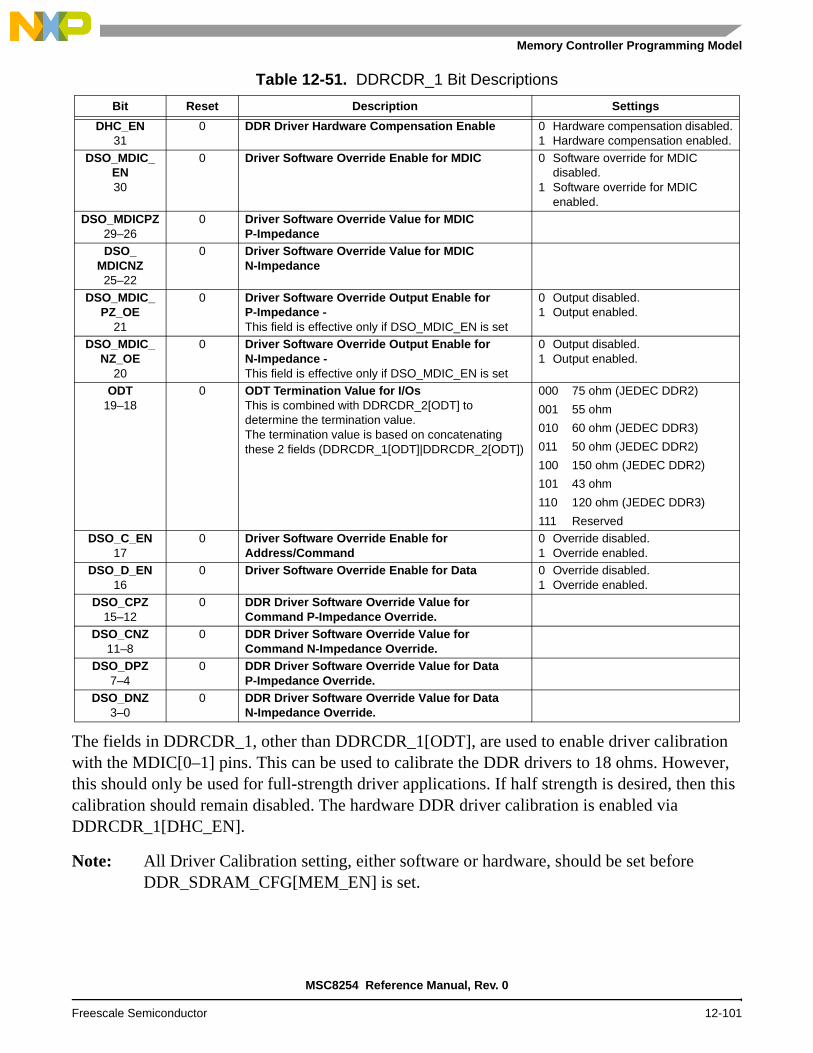
Memory Controller Programming Model
The fields in DDRCDR_1, other than DDRCDR_1[ODT], are used to enable driver calibration with the MDIC[0–1] pins. This can be used to calibrate the DDR drivers to 18 ohms. However, this should only be used for full-strength driver applications. If half strength is desired, then this calibration should remain disabled. The hardware DDR driver calibration is enabled via DDRCDR_1[DHC_EN].
Note: All Driver Calibration setting, either software or hardware, should be set before DDR_SDRAM_CFG[MEM_EN] is set.
Table 12-51. DDRCDR_1 Bit Descriptions
Bit Reset Description Settings
DHC_EN31
0 DDR Driver Hardware Compensation Enable 0 Hardware compensation disabled.1 Hardware compensation enabled.
DSO_MDIC_ EN30
0 Driver Software Override Enable for MDIC 0 Software override for MDIC disabled.
1 Software override for MDIC enabled.
DSO_MDICPZ29–26
0 Driver Software Override Value for MDIC P-Impedance
DSO_ MDICNZ
25–22
0 Driver Software Override Value for MDIC N-Impedance
DSO_MDIC_ PZ_OE
21
0 Driver Software Override Output Enable for P-Impedance - This field is effective only if DSO_MDIC_EN is set
0 Output disabled.1 Output enabled.
DSO_MDIC_ NZ_OE
20
0 Driver Software Override Output Enable for N-Impedance - This field is effective only if DSO_MDIC_EN is set
0 Output disabled.1 Output enabled.
ODT19–18
0 ODT Termination Value for I/OsThis is combined with DDRCDR_2[ODT] to determine the termination value.The termination value is based on concatenating these 2 fields (DDRCDR_1[ODT]|DDRCDR_2[ODT])
000 75 ohm (JEDEC DDR2)
001 55 ohm
010 60 ohm (JEDEC DDR3)
011 50 ohm (JEDEC DDR2)
100 150 ohm (JEDEC DDR2)
101 43 ohm
110 120 ohm (JEDEC DDR3)
111 ReservedDSO_C_EN
170 Driver Software Override Enable for
Address/Command0 Override disabled.1 Override enabled.
DSO_D_EN16
0 Driver Software Override Enable for Data 0 Override disabled.1 Override enabled.
DSO_CPZ15–12
0 DDR Driver Software Override Value for Command P-Impedance Override.
DSO_CNZ11–8
0 DDR Driver Software Override Value for Command N-Impedance Override.
DSO_DPZ7–4
0 DDR Driver Software Override Value for Data P-Impedance Override.
DSO_DNZ3–0
0 DDR Driver Software Override Value for Data N-Impedance Override.
MSC8254 Reference Manual, Rev. 0
Freescale Semiconductor 12-101

DDR SDRAM Memory Controller
Software can be used to calibrate the drivers instead of the automatic hardware calibration. If software calibration is used, the following steps should be taken:
1. Set DDRCDR_1[DSO_MDIC_EN] and ensure that DDRCDR_1[DHC_EN] is cleared
2. Set the highest impedance (value 0000) for DDRCDR_1[DSO_MDICPZ]
3. Set DDRCDR_1[DSO_MDIC_PZ_OE] to enable the output enable for MDIC[0]
4. After at least 4 cycles, read DDRDSR_1[0]. If the value is 0, then use the next lowest impedance, and read DDRDSR_1[0] again. Once a value of 1 is detected, then leave DDRCDR_1[DSO_MDICPZ] at the calibrated value
5. Clear DDRCDR_1[DSO_MDIC_PZ_OE]
6. After DDRCDR_1[DSO_MDICPZ} is calibrated, set a value of 0000 for DDRCDR_1[DSO_MDICNZ]
7. Set DDRCDR_1[DSO_MDIC_NZ_OE] to enable the output enable for MDIC[1]
8. After at least 4 cycles, read DDRDSR_1[1]. If the value is 1, then use the next lowest impedance, and read DDRDSR_1[1] again. Once a value of 0 is detected, then leave DDRCDR_1[DSO_MDICNZ] at the calibrated value
9. Clear DDRCDR_1[DSO_MDIC_NZ_OE]
The legal impedance values (from highest impedance to lowest impedance) for DDR2 (1.8 V) are:
0000 lowest strength/highest impedance
0001
0011
0010
0110
0111 half strength - used when driver calibration is not used by setting DDR_SDRAM_CFG[HSE]
0101
0100
1100
1101
1111
1110
1010
1011 full strength (default)
1001
1000 highest strength/lowest impedance
MSC8254 Reference Manual, Rev. 0
12-102 Freescale Semiconductor

Memory Controller Programming Model
The legal impedance values (from highest impedance to lowest impedance) for DDR3 (1.5 V) are:
0000 lowest strength/highest impedance
0001
0011
0010
0110
0111 half strength - used when driver calibration is not used by setting DDR_SDRAM_CFG[HSE]
0101
0100
1100
1101
1111
1110
1010
1011
1001
1000 highest strength/lowest impedance (default)
Note: Drivers may either be calibrated to full-strength or half-strength
MSC8254 Reference Manual, Rev. 0
Freescale Semiconductor 12-103

DDR SDRAM Memory Controller
12.8.31 DDR Control Driver Register 2 (MnDDRCDR_2)
DDRCDR_2 sets the driver software override enable for clocks, and the DDR clocks driver P/N impedance.
DDRCDR_2 DDR Control Driver Register 2 Offset 0x0B2C
Bit 31 30 29 28 27 26 25 24 23 22 21 20 19 18 17 16
DSO_ CLK_
EN
— DSO_CLKPZ DSO_CLKNZ —
Type R/W R R/W RReset 0 0 0 0 0 0 0 0 0 0 0 0 0 0 0 0
Bit 15 14 13 12 11 10 9 8 7 6 5 4 3 2 1 0
— ODT
Type R R/WReset 0 0 0 0 0 0 0 0 0 0 0 0 0 0 0 0
Table 12-52. DDRCDR_2 Bit Descriptions
Bit Reset Description Settings
DSO_CLK_ EN31
0 Driver Software Override Enable for Clocks 0 Software override disabled.1 Software override enabled.
—30–28
0 Reserved. Write to zero for future compatibility.
DSO_CLKPZ27–24
0 DDR Driver Software Override Value for Clocks P-Impedance Override
DSO_CLKNZ23–20
0 DDR Driver Software Override Value for Clocks N-Impedance Override
—19–1
0 Reserved. Write to zero for future compatibility.
ODT0
0 ODT Termination Value for I/OsThis is combined with DDRCDR_1[ODT] to determine the termination value. The termination value is based on concatenating these 2 fields (DDRCDR_1[ODT]|DDRCDR_2[ODT]).
000 75 ohm (JEDEC DDR2)
001 55 ohm
010 60 ohm (JEDEC DDR3)
011 50 ohm (JEDEC DDR2)
100 150 ohm (JEDEC DDR2)
101 43 ohm
110 120 ohm (JEDEC DDR3)
111 Reserved
MSC8254 Reference Manual, Rev. 0
12-104 Freescale Semiconductor

Memory Controller Programming Model
12.8.32 DDR SDRAM IP Block Revision 1 Register (MnDDR_IP_REV1)
DDR_IP_REV1 provides read-only fields with the IP block ID, along with major and minor revision information.
12.8.33 DDR SDRAM IP Block Revision 2 Register (MnDDR_IP_REV2)
DDR_IP_REV2 provides read-only fields with the IP block integration and configuration options.
DDR_IP_REV1 DDR SDRAM IP Block Revision 1 Register Offset 0x0BF8
Bit 31 30 29 28 27 26 25 24 23 22 21 20 19 18 17 16
IP_ID
Type RReset 0 0 0 0 0 0 0 0 0 0 0 0 0 0 1 0
Bit 15 14 13 12 11 10 9 8 7 6 5 4 3 2 1 0
IP_MJ IP_MNType R
Reset 0 0 0 0 0 1 0 0 0 0 0 0 0 0 0 0
Table 12-53. DDR_IP_REV1 Bit Descriptions
Bit Reset Description
IP_ID31–16
0x0002 IP Block IDFor the DDR controller.
IP_MJ15–8
0x04 Major Revision
IP_MN7–0
0x00 Minor Revision
DDR_IP_REV2 DDR SDRAM IP Block Revision 2 Register Offset 0x0BFC
Bit 31 30 29 28 27 26 25 24 23 22 21 20 19 18 17 16
— IP_INITType RReset 0 0 0 0 0 0 0 0 0 0 0 0 0 0 0 0
Bit 15 14 13 12 11 10 9 8 7 6 5 4 3 2 1 0
— IP_CFG
Type RReset 0 0 0 0 0 0 0 0 0 0 0 0 0 0 0 0
Table 12-54. DDR_IP_REV2 Bit Descriptions
Bit Reset Description
—31–24
0 Reserved. Always read as zero
IP_INT23–16
0 IP Block Integration Options
MSC8254 Reference Manual, Rev. 0
Freescale Semiconductor 12-105

DDR SDRAM Memory Controller
12.8.34 DDR SDRAM Memory Data Path Error Injection Mask High Register (MnDATA_ERR_INJECT_HI)
DATA_ERR_INJECT_HI register is used to inject ECC errors for the 32-msb of a 64-bit SDRAM data bus interfaces.
12.8.35 DDR SDRAM Memory Data Path Error Injection Mask Low Register (MnDATA_ERR_INJECT_LO)
—15–8
0 Reserved. Always read as zero
IP_CFG7–0
0 IP Block Configuration Options
DATA_ERR_INJECT_HI DDR SDRAM Memory Data Path Offset 0x0E00 Error Injection Mask High Register
Bit 31 30 29 28 27 26 25 24 23 22 21 20 19 18 17 16
EIMH
Type R/WReset 0 0 0 0 0 0 0 0 0 0 0 0 0 0 0 0
Bit 15 14 13 12 11 10 9 8 7 6 5 4 3 2 1 0
EIMHType R/W
Reset 0 0 0 0 0 0 0 0 0 0 0 0 0 0 0 0
Table 12-55. DATA_ERR_INJECT_HI Bit Descriptions
Bit Reset Description
EIMH31–0
0 Error Injection Mask High Data PathTests ECC by forcing errors on the highest 32 bits of the data path. When error injection is enabled, setting a bit causes the corresponding data path bit to be inverted during memory bus writes.
DATA_ERR_INJECT_LO DDR SDRAM Memory Data Path Offset 0x0E04Error Injection Mask Low Register
Bit 31 30 29 28 27 26 25 24 23 22 21 20 19 18 17 16
EIML
Type R/WReset 0 0 0 0 0 0 0 0 0 0 0 0 0 0 0 0
Bit 15 14 13 12 11 10 9 8 7 6 5 4 3 2 1 0
EIMLType R/W
Reset 0 0 0 0 0 0 0 0 0 0 0 0 0 0 0 0
Table 12-54. DDR_IP_REV2 Bit Descriptions (Continued)
Bit Reset Description
MSC8254 Reference Manual, Rev. 0
12-106 Freescale Semiconductor

Memory Controller Programming Model
DATA_ERR_INJECT_LO register is used to inject ECC errors for the 32-lsb of a 64-bit SDRAM data bus interfaces.
12.8.36 DDR SDRAM Memory Data Path Error Injection Mask ECC Register (MnERR_INJECT)
ERR_INJECT register sets the ECC mask, enables errors to be written to ECC memory. In addition, a single address parity error can be injected through this register.
Table 12-56. DATA_ERR_INJECT_LO Bit Descriptions
Bit Reset Description
EIML31–0
0 Error Injection Mask Low Data PathTests ECC by forcing errors on the lowest 32 bits of the data path. When the Error Injection is enabled, setting a bit causes the corresponding data path bit to be inverted during memory bus writes.
ERR_INJECT DDR SDRAM Memory Data Path Offset 0x0E08Error Injection Mask ECC Register
Bit 31 30 29 28 27 26 25 24 23 22 21 20 19 18 17 16
— APIEN
Type R R/WReset 0 0 0 0 0 0 0 0 0 0 0 0 0 0 0 0
Bit 15 14 13 12 11 10 9 8 7 6 5 4 3 2 1 0
— EIEN EEIMType R R/W
Reset 0 0 0 0 0 0 0 0 0 0 0 0 0 0 0 0
Table 12-57. ERR_INJECT Bit Descriptions
Bit Reset Description Settings
—31–17
0 Reserved. Write to zero for future compatibility.
APIEN15
0 Address Parity Error Injection Enable. This bit is cleared by hardware after a single address parity error has been injected.
0 Address parity error injection disabled.
1 Address parity error injection enabled.
—15–9
0 Reserved. Write to zero for future compatibility.
EIEN8
0 Error Injection EnableEnables/disables injection of errors.This applies to the data mask bits and to the ECC mask bits.Note: Error injection should not be enabled until the
memory controller has been enabled through DDR_SDRAM_CFG[MEM_EN].
0 Error injection disabled.
1 Error injection enabled.
EEIM7–0
0 ECC Error Injection Mask (0–7)Setting a mask bit causes the corresponding ECC bit to be inverted during memory bus writes.
MSC8254 Reference Manual, Rev. 0
Freescale Semiconductor 12-107

DDR SDRAM Memory Controller
12.8.37 DDR SDRAM Memory Data Path Read Capture Data High Register (MnCAPTURE_DATA_HI)
CAPTURE_DATA_HI stores the high 32 bits of the read data path during error capture.
12.8.38 DDR SDRAM Memory Data Path Read Capture Data Low Register (MnCAPTURE_DATA_LO)
CAPTURE_DATA_LO stores the low 32 bits of the read data path during error capture.
CAPTURE_DATA_HI DDR SDRAM Memory Data Path Offset 0x0E20Read Capture Data High Register
Bit 31 30 29 28 27 26 25 24 23 22 21 20 19 18 17 16
ECHDType R/WReset 0 0 0 0 0 0 0 0 0 0 0 0 0 0 0 0
Bit 15 14 13 12 11 10 9 8 7 6 5 4 3 2 1 0
ECHD
Type R/WReset 0 0 0 0 0 0 0 0 0 0 0 0 0 0 0 0
Table 12-58. CAPTURE_DATA_HI Bit Descriptions
Bit Reset Description
ECHD31–0
0 Error Capture High Data PathCaptures the high 32 bits of the data path when errors are detected.
CAPTURE_DATA_LO DDR SDRAM Memory Data Path Offset 0x0E24 Read Capture Data Low Register
Bit 31 30 29 28 27 26 25 24 23 22 21 20 19 18 17 16
ECLDType R/W
Reset 0 0 0 0 0 0 0 0 0 0 0 0 0 0 0 0
Bit 15 14 13 12 11 10 9 8 7 6 5 4 3 2 1 0
ECLDType R/WReset 0 0 0 0 0 0 0 0 0 0 0 0 0 0 0 0
Table 12-59. CAPTURE_DATA_LO Bit Descriptions
Bit Reset Description
ECLD31–0
0 Error Capture Low Data PathCaptures the low 32 bits of the data path when errors are detected.
MSC8254 Reference Manual, Rev. 0
12-108 Freescale Semiconductor

Memory Controller Programming Model
12.8.39 DDR SDRAM Memory Data Path Read Capture ECC Register (MnCAPTURE_ECC)
CAPTURE_ECC stores the ECC syndrome bits on the data bus when an error is detected.
12.8.40 DDR SDRAM Memory Error Detect Register (MnERR_DETECT)
Note: W1C - Write 0b1 to clear the bit, writing 0b0 as no effect.
ERR_DETECT stores the detection bits for multiple memory errors, single- and multiple-bit ECC errors, calibration error, and memory select errors. Each bit is cleared when software writes a value of 1 to it. System software can determine the type of memory error by examining the
CAPTURE_ECC DDR SDRAM Memory Data Path Read Offset 0x0E28Capture ECC Register
Bit 31 30 29 28 27 26 25 24 23 22 21 20 19 18 17 16
— ECE-32Type R R/WReset 0 0 0 0 0 0 0 0 0 0 0 0 0 0 0 0
Bit 15 14 13 12 11 10 9 8 7 6 5 4 3 2 1 0
— ECE-64
Type R R/WReset 0 0 0 0 0 0 0 0 0 0 0 0 0 0 0 0
Table 12-60. CAPTURE_ECC Bit Descriptions
Bit Reset Description
—31–24
0 Reserved. Write to zero for future compatibility.
ECE-6423–16
0 Error Capture ECCIn 32-bit bus mode, captures the ECC bits of the 1st 32-bits when errors are detected
—15–8
0 Reserved. Write to zero for future compatibility.
ECE-647–0
0 Error Capture ECCIn 64-bit bus mode, captures the ECC bits of entire bus when errors are detected. (0–7)In 32-bit bus mode. captures the ECC bits of the 2nd 32-bits when errors are detected
ERR_DETECT DDR SDRAM Memory Error Detect Register Offset 0x0E40
Bit 31 30 29 28 27 26 25 24 23 22 21 20 19 18 17 16
MME —
Type W1C RReset 0 0 0 0 0 0 0 0 0 0 0 0 0 0 0 0
Bit 15 14 13 12 11 10 9 8 7 6 5 4 3 2 1 0
— APE ACE — MBE SBE — MSEType R W1C W1C R W1C R W1C
Reset 0 0 0 0 0 0 0 0 0 0 0 0 0 0 0 0
MSC8254 Reference Manual, Rev. 0
Freescale Semiconductor 12-109

DDR SDRAM Memory Controller
contents of this register. If an error is disabled with ERR_DISABLE, the corresponding error is never detected or captured in ERR_DETECT.
12.8.41 DDR SDRAM Memory Error Disable Register (MnERR_DISABLE)
ERR_DISABLE selectively disables the DDR controller error detection circuitry. Disabled errors are not detected or reported.
Table 12-61. ERR_DETECT Bit Descriptions
Bit Reset Description Settings
MME31
0 Multiple Memory Errors Indicates whether multiple memory errors of the same type were detected. This bit is cleared by software writing a 1 to it.
0 Multiple memory errors were not detected.
1 Multiple memory errors of the same type were detected.
—30–9
0 Reserved. Write to zero for future compatibility.
APE8
0 Address parity error.Indicates whether an address parity error was detected. This bit is cleared by software writing a 1 to it.
0 An address parity error has not been detected.
1 An address parity error has been detected
ACE7
0 Automatic Calibration ErrorIndicates whether an automatic calibration error was detected. This bit is cleared by software writing a 1 to it.
0 Automatic calibration Error has not been detected.
1 Automatic calibration Error has been detected..
—6–4
0 Reserved. Write to zero for future compatibility.
MBE3
0 Multiple-Bit ErrorIndicates whether a multiple-bit error was detected. This bit is cleared by software writing a 1 to it.
0 Multiple-bit error not detected.
1 Multiple-bit error detected.
SBE2
Single-Bit ECC ErrorIndicates whether the number of single-bit ECC errors detected is equal to the threshold set in ERR_SBE[SBET]. This bit is cleared by software writing a 1 to it.
0 The number of errors is less than the threshold.
1 The number of errors is equal or greater than the threshold.
—1
0 Reserved. Write to zero for future compatibility.
MSE0
0 Memory Select ErrorIndicates whether a memory select error has been detected. This bit is cleared by software writing a 1 to it.
0 Memory select error not detected.
1 Memory select error detected.
ERR_DISABLE DDR SDRAM Memory Error Disable Register Offset 0x0E44
Bit 31 30 29 28 27 26 25 24 23 22 21 20 19 18 17 16
—Type RReset 0 0 0 0 0 0 0 0 0 0 0 0 0 0 0 0
Bit 15 14 13 12 11 10 9 8 7 6 5 4 3 2 1 0
— APED ACED — MBED SBED — MSED
Type R R/W R/W R R/W R R/WReset 0 0 0 0 0 0 0 0 0 0 0 0 0 0 0 0
MSC8254 Reference Manual, Rev. 0
12-110 Freescale Semiconductor
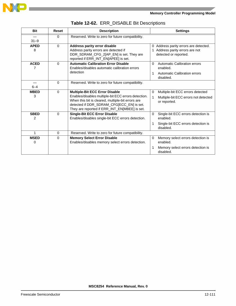
Memory Controller Programming Model
Table 12-62. ERR_DISABLE Bit Descriptions
Bit Reset Description Settings
—31–9
0 Reserved. Write to zero for future compatibility.
APED8
0 Address parity error disableAddress parity errors are detected if DDR_SDRAM_CFG_2[AP_EN] is set. They are reported if ERR_INT_EN[APEE] is set.
0 Address parity errors are detected.1 Address parity errors are not
detected or reported.
ACED7
0 Automatic Calibration Error DisableEnables/disables automatic calibration errors detection
0 Automatic Calibration errors enabled.
1 Automatic Calibration errors disabled.
—6–4
0 Reserved. Write to zero for future compatibility.
MBED3
0 Multiple-Bit ECC Error DisableEnables/disables multiple-bit ECC errors detection. When this bit is cleared, multiple-bit errors are detected if DDR_SDRAM_CFG[ECC_EN] is set. They are reported if ERR_INT_EN[MBEE] is set.
0 Multiple-bit ECC errors detected
1 Multiple-bit ECC errors not detected or reported.
SBED2
0 Single-Bit ECC Error DisableEnables/disables single-bit ECC errors detection.
0 Single-bit ECC errors detection is enabled.
1 Single-bit ECC errors detection is disabled.
1 0 Reserved. Write to zero for future compatibility.MSED
00 Memory Select Error Disable
Enables/disables memory select errors detection.0 Memory select errors detection is
enabled.
1 Memory select errors detection is disabled.
MSC8254 Reference Manual, Rev. 0
Freescale Semiconductor 12-111

DDR SDRAM Memory Controller
12.8.42 DDR SDRAM Memory Error Interrupt Enable Register (MnERR_INT_EN)
ERR_INT_EN enables ECC interrupts, calibration error, address/command parity error or memory select error interrupts. When an enabled interrupt condition occurs, the DDR Controller interrupt request signal is asserted to the embedded programmable interrupt controller (EPIC)
ERR_INT_EN DDR SDRAM Memory Error Interrupt Enable Register Offset 0x0E48
Bit 31 30 29 28 27 26 25 24 23 22 21 20 19 18 17 16
—Type R
Reset 0 0 0 0 0 0 0 0 0 0 0 0 0 0 0 0
Bit 15 14 13 12 11 10 9 8 7 6 5 4 3 2 1 0
— APEE ACEE — MBEE SBEE — MSEEType R R/W R/W R R/W R R/WReset 0 0 0 0 0 0 0 0 0 0 0 0 0 0 0 0
Table 12-63. ERR_INT_EN Bit Descriptions
Bit Reset Description Settings
—31–9
0 Reserved. Write to zero for future compatibility.
APEE8
0 Address parity error interrupt enable 0 Address parity errors cannot generate interrupts.
1 Address parity errors generate interrupts.ACEE
70 Automatic Calibration Error Interrupt Enable
Specifies whether automatic calibration errors generate interrupts.
0 Calibration errors cannot generate interrupts.
1 Calibration errors generate interrupts.—
6–40 Reserved. Write to zero for future compatibility.
MBEE3
0 Multiple-Bit ECC Error Interrupt Enable Specifies whether multiple-bit ECC errors generate interrupts.
0 Multiple-bit ECC errors cannot generate interrupts.
1 Multiple-bit ECC errors generate interrupts.
SBEE2
0 Single-Bit ECC Error Interrupt EnableSpecifies whether single-bit ECC errors generate interrupts.
0 Single-bit ECC errors cannot generate interrupts.
1 Single-bit ECC errors generate interrupts.—1
0 Reserved. Write to zero for future compatibility.
MSEE0
Memory Select Error Interrupt EnableSpecifies whether memory select errors generate interrupts.
0 Memory select errors do not generate interrupts.
1 Memory select errors generate interrupts.
MSC8254 Reference Manual, Rev. 0
12-112 Freescale Semiconductor

Memory Controller Programming Model
12.8.43 DDR SDRAM Memory Error Attributes Capture Register (MnCAPTURE_ATTRIBUTES)
CAPTURE_ATTRIBUTES sets attributes for errors including type, size, source, and so on.
CAPTURE_ATTRIBUTES DDR SDRAM Memory Error Offset 0x0E4CAttributes Capture Register
Bit 31 30 29 28 27 26 25 24 23 22 21 20 19 18 17 16
— BNUM — TSIZ —Type R R/W R R/W RReset 0 0 0 0 0 0 0 0 0 0 0 0 0 0 0 0
Bit 15 14 13 12 11 10 9 8 7 6 5 4 3 2 1 0
— TTYP — VLD
Type R R/W R R/WReset 0 0 0 0 0 0 0 0 0 0 0 0 0 0 0 0
Table 12-64. CAPTURE_ATTRIBUTES Bit Descriptions
Bit Reset Description Settings
—31
0 Reserved. Write to zero for future compatibility.
BNUM30–28
0 Data Beat NumberCaptures the data beat number for the detected error. This bit is relevant only for ECC errors.
—27
0 Reserved. Write to zero for future compatibility.
TSIZ26–24
0 Transaction Size for ErrorCaptures the transaction size in 64-bit increments.
000 4 × 64 bits.
001 1 × 64 bits.
010 2 × 64 bits.
011 3 × 64 bits.
All other values are reserved—
23–140 Reserved. Write to zero for future compatibility.
TTYP13–12
0 Transaction Type for ErrorSpecifies the access type that generates the error.
00 Reserved.
01 Write.
10 Read.
11 Read-modify-write.
—11–1
0 Reserved. Write to zero for future compatibility.
VLD0
0 ValidSet as soon as valid information is captured in the error capture registers.
0 No valid information captured
1 Valid information captured
MSC8254 Reference Manual, Rev. 0
Freescale Semiconductor 12-113

DDR SDRAM Memory Controller
12.8.44 DDR SDRAM Memory Error Address Capture Register (MnCAPTURE_ADDRESS)
CAPTURE_ADDRESS holds the 32-bit of the transaction address when a DDR ECC error is detected.
12.8.45 DDR SDRAM Single-Bit ECC Memory Error Management Register (MnERR_SBE)
ERR_SBE stores the threshold value for reporting single-bit errors and the number of single-bit errors counted since the last error report. When the counter field reaches the threshold, it wraps back to the reset value (0). If necessary, software must clear the counter after it has managed the error.
CAPTURE_ADDRESS DDR SDRAM Memory Error Address Offset 0x0E50Capture Register
Bit 31 30 29 28 27 26 25 24 23 22 21 20 19 18 17 16
CADDRType R/WReset 0 0 0 0 0 0 0 0 0 0 0 0 0 0 0 0
Bit 15 14 13 12 11 10 9 8 7 6 5 4 3 2 1 0
CADDR
Type R/WReset 0 0 0 0 0 0 0 0 0 0 0 0 0 0 0 0
Table 12-65. CAPTURE_ADDRESS Bit Descriptions
Bit Reset Description Settings
CADDR31–0
0 Captured AddressCaptures the 32 bits of the transaction address when an error is detected.
ERR_SBE DDR SDRAM Single-Bit ECC Memory Error Offset 0x0E58Management Register
Bit 31 30 29 28 27 26 25 24 23 22 21 20 19 18 17 16
— SBET
Type R R/WReset 0 0 0 0 0 0 0 0 0 0 0 0 0 0 0 0
Bit 15 14 13 12 11 10 9 8 7 6 5 4 3 2 1 0
— SBECType R R/W
Reset 0 0 0 0 0 0 0 0 0 0 0 0 0 0 0 0
MSC8254 Reference Manual, Rev. 0
12-114 Freescale Semiconductor

Memory Controller Programming Model
12.8.46 Debug Register 2 (MnDEBUG_2)
DEBUG_2 is used to indicate whether the controller is active.
Table 12-66. ERR_SBE Bit Descriptions
Bit Reset Description
—31–24
0 Reserved. Write to zero for future compatibility.
SBET23–16
0 Single-Bit Error ThresholdEstablishes the number of single-bit errors that must be detected before an error condition is reported.
—15–8
0 Reserved. Write to zero for future compatibility.
SBEC7–0
0 Single-Bit Error CounterIndicates the number of single-bit errors detected and corrected since the last error report. If single-bit error reporting is enabled, an error is reported when this value equals the SBET value. SBEC is automatically cleared when the threshold value is reached.
DEBUG_2 Debug Register 2 Offset 0x0F04
Bit 31 30 29 28 27 26 25 24 23 22 21 20 19 18 17 16
—Type R
Reset 0 0 0 0 0 0 0 0 0 0 0 0 0 0 0 0
Bit 15 14 13 12 11 10 9 8 7 6 5 4 3 2 1 0
— IDLE —Type RReset 0 0 0 0 0 0 0 0 0 0 0 0 0 0 1 0
Table 12-67. ERR_SBE Bit Descriptions
Bit Reset Description Settings
—31–2
0 Reserved. Write to zero for future compatibility.
IDLE1
1 IdleThe DDR controller is in idle state.
0 Active
1 Idle—0
0 Reserved. Write to zero for future compatibility.
MSC8254 Reference Manual, Rev. 0
Freescale Semiconductor 12-115

DDR SDRAM Memory Controller
MSC8254 Reference Manual, Rev. 0
12-116 Freescale Semiconductor

Interrupt Handling 13The MSC8254 interrupt system is optimized for a multi-processing environment and performs the following functions:
Routes each of the interrupt sources to each of the extended SC3850 cores thus allowing:
— Flexible resource allocations as well as for a symmetrical or a non-symmetrical application architecture.
— Provides a core-to-core full interrupt mesh.— Provides external host-to-core signaling mechanism by virtual interrupt generation.
Allows for the enabling/disabling of each interrupt source per core.
The MSC8254 supports both internal and external interrupt sources as well as allowing for the generation of an interrupt to external devices.
There are three device level interrupt handlers in the MSC8254:
1. Global interrupt controller. Allows for the generation of virtual interrupt requests (VIRQ) as well as virtual non-maskable interrupts (VNMI) towards the cores as well as generates interrupts to external devices.
2. General configuration block. Concentrates and routes rare and debug interrupts to the SC3400 cores.
3. Embedded programmable interrupt controller (EPIC). Concentrates all the interrupt directed at the associated core and dispatches the highest priority interrupt to the SC3400 core. Although there are various interrupts in the system designated as non-maskable interrupts (NMIs), you must program them to be non-maskable in the EPIC. This is typically done by the boot program.
Note: See the SC3850 DSP Core Subsystem Reference Manual for details about the EPIC. The manual is available with a signed non-disclosure agreement. Contact your local Freescale dealer or sales representative for more information.
Note: The QUICC Engine module also includes an interrupt controller that handles interrupts within the module for the dual-RISC processor system. For details about that interrupt controller and how to program it, refer to Chapter 18, QUICC Engine Subsystem and the QUICC Engine™ Block Reference Manual with Protocol Interworking (QEIWRM).
MSC8254 Reference Manual, Rev. 0
Freescale Semiconductor 13-1

Interrupt Handling
13.1 Global Interrupt Controller (GIC)
The GIC generates 16 VIRQs and 8 VNMIs to the DSP cores by writing to registers in the GIC memory map. The GIC also uses two additional VIRQ slots to generate a non-maskable interrupt NMI_OUT and a maskable interrupt INT_OUT to external devices. A virtual interrupt/VNMI is generated via a write access to the Virtual Interrupt Generation Register (VIGR) by one of the SC3400 cores or an external host CPU. Table 13-1 describes the destination of the supported VIRQs.
The GIC has a status register to indicate whether a virtual interrupt was generated at least once, while not preventing the generation of another interrupt. The core that services the interrupt may clear this status bit by writing a value of one to it, or it may ignore this bit and work locally.
Table 13-1. VIRQ Description
VIRQ Num Destination
VIRQ_0 Connected to Virtual Interrupt 0 at SC3400
VIRQ_1 Connected to Virtual Interrupt 1 at SC3400
VIRQ_2 Connected to Virtual Interrupt 2 at SC3400
VIRQ_3 Connected to Virtual Interrupt 3 at SC3400
VIRQ_4 Connected to Virtual Interrupt 4 at SC3400
VIRQ_5 Connected to Virtual Interrupt 5 at SC3400
VIRQ_6 Connected to Virtual Interrupt 6 at SC3400
VIRQ_7 Connected to Virtual Interrupt 7 at SC3400
VIRQ_8 Connected to Virtual Interrupt 8 at SC3400
VIRQ_9 Connected to Virtual Interrupt 9 at SC3400
VIRQ_10 Connected to Virtual Interrupt 10 at SC3400
VIRQ_11 Connected to Virtual Interrupt 11 at SC3400
VIRQ_12 Connected to Virtual Interrupt 12 at SC3400
VIRQ_13 Connected to Virtual Interrupt 13 at SC3400
VIRQ_14 Connected to Virtual Interrupt 14 at SC3400
VIRQ_15 Connected to Virtual Interrupt 15 at SC3400
VIRQ_16 Connected to VNMI_0
VIRQ_17 Connected to VNMI_1
VIRQ_18 Connected to VNMI_2
VIRQ_19 Connected to VNMI_3
VIRQ_20 Connected to VNMI_4
VIRQ_21 Connected to VNMI_5
VIRQ_22 Connected to VNMI_6
VIRQ_23 Connected to VNMI_7
VIRQ_24 Use to generate INT_OUT (see 13.2.2, External Interrupts)
VIRQ_25 Use to generate NMI_OUT (see 13.2.2, External Interrupts)
MSC8254 Reference Manual, Rev. 0
13-2 Freescale Semiconductor

General Configuration Block
13.2 General Configuration Block
The general configuration block performs services for rare and debug interrupts generated throughout the MSC8254 before they reach the SC3850 EPICs. These services include:
Generating ORed interrupt signals towards the SC3400 cores (see Section 13.2.1).
Providing an interrupt enable bit for each interrupt source for each SC3400 core (see Section 13.5.2, General Interrupt Configuration, on page 13-26).
Providing a status bit for each interrupt source. These bits are shared for all the SC3400 cores (see Section 13.5.2, General Interrupt Configuration, on page 13-26).
13.2.1 Interrupt Groups
The general configuration block generates 5 interrupts based on the groups of ORed interrupts described in Table 13-2.
Table 13-2. General Configuration Block Interrupt Sources
TDM Debug General Watch Dog Timer TDM 0 Rx error CLASS 0 overrun Parity error from TDM[0–3] Watch Dog Timer 0
TDM 0 Tx error CLASS 0 watchpointQUICC Engine module DRAM double soft error
Watch Dog Timer 1
TDM 1 Rx error CLASS 0 errorQUICC Engine module IMEM double soft error
Watch Dog Timer 2
TDM 1 Tx error Performance Monitor all DMA error Watch Dog Timer 3
TDM 2 Rx errorCore subsystems 0 and 1 MEX address error.
DDR1 interrupt Watch Dog Timer 4
TDM 2 Tx errorCore subsystems 2 and 3 MEX address error.
DDR2 interrupt Watch Dog Timer 5
TDM 3 Rx error OCN0 to MBus Watch Dog Timer 6TDM 3 Tx error OCN1 to MBus Watch Dog Timer 7
MSC8254 Reference Manual, Rev. 0
Freescale Semiconductor 13-3

Interrupt Handling
13.2.2 External Interrupts
The MSC8254 allows a number of external interrupt inputs to be multiplexed with the GPIO signals to enable external devices to interrupt the cores (see Chapter 22, GPIO). There are also dedicated external interrupt pins.
Note: All external IRQ signals are multiplexed options of the associated GPIO ports.
Table 13-3 summarizes all the external interrupt inputs in the MSC8254.
INT_OUT is asserted when VIRQ_24 is asserted. NMI_OUT is asserted when VIRQ_25 is asserted.
Table 13-3. MSC8254 External Interrupt Pins
Name GPIO Direction
NMI N/A In
NMI_OUT N/A Out
INT_OUT N/A Out
IRQ0 GPIO0 In
IRQ1 GPIO1 In
IRQ2 GPIO2 In
IRQ3 GPIO3 In
IRQ4 GPIO4 In
IRQ5 GPIO5 In
IRQ6 GPIO6 In
IRQ7 GPIO7 In
IRQ8 GPIO8 In
IRQ9 GPIO9 In
IRQ10 GPIO10 In
IRQ11 GPIO11 In
IRQ12 GPIO12 In
IRQ13 GPIO13 In
IRQ14 GPIO14 In
IRQ15 GPIO15 In
MSC8254 Reference Manual, Rev. 0
13-4 Freescale Semiconductor
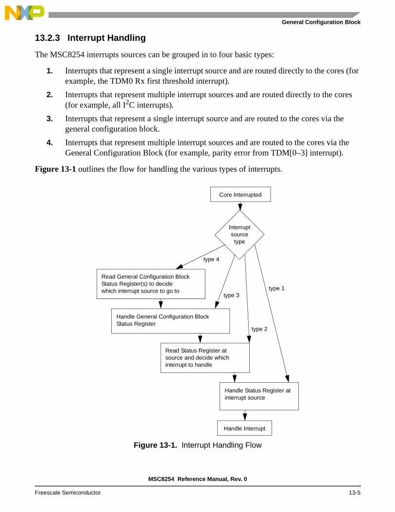
General Configuration Block
13.2.3 Interrupt Handling
The MSC8254 interrupts sources can be grouped in to four basic types:
1. Interrupts that represent a single interrupt source and are routed directly to the cores (for example, the TDM0 Rx first threshold interrupt).
2. Interrupts that represent multiple interrupt sources and are routed directly to the cores (for example, all I2C interrupts).
3. Interrupts that represent a single interrupt source and are routed to the cores via the general configuration block.
4. Interrupts that represent multiple interrupt sources and are routed to the cores via the General Configuration Block (for example, parity error from TDM[0–3] interrupt).
Figure 13-1 outlines the flow for handling the various types of interrupts.
Figure 13-1. Interrupt Handling Flow
Core Interrupted
Interruptsource
type
Read Status Register atsource and decide whichinterrupt to handle
Read General Configuration BlockStatus Register(s) to decidewhich interrupt source to go to
Handle General Configuration BlockStatus Register
Handle Interrupt
Handle Status Register atinterrupt source
type 4
type 3
type 2
type 1
MSC8254 Reference Manual, Rev. 0
Freescale Semiconductor 13-5

Interrupt Handling
As an example of handling a type 4 interrupt, processing of a QUICC Engine interrupt is provided. In Table 13-2, there are two types of QUICC Engine interrupts that are routed through the GCRs:
DRAM double soft error
IMEM double soft error
When enabled and unmasked, both interrupts are concentrated to the GCR general interrupt which is routed to all cores. The GIER1_[0–5] registers allow the user to mask/unmask the interrupts for any or all of the cores.
If the general interrupt from the GCR is received by a core (index 245), the ISR should read GIR1 (GCR offset 0x80) to identify the origin of the general interrupt. Bits 18 and 19 in the register represent DRAM double soft error and IMEM double soft error, respectively. After identifying that the interrupt is coming from the QUICC Engine subsystem, the cores can handle the interrupt in the same way as other QUICC Engine interrupts that are directed to the DSP core subsystems.
There are nine other QUICC Engine interrupts that use indexes 132–141 as indicated in Table 13-4. Details about the QUICC Engine interrupt controller and how to use this interrupts is provided in Section 18.5 and the QUICC Engine™ Block Reference Manual with Interworking (QEIWRM).
13.3 Interrupt Mapping
The EPIC can support up to 256 interrupt sources that can be level-, edge-, or double-edge triggered. The interrupts can have an assigned priority from 1(lowest) to 31 (highest) as well as non-maskable (priority 32). The first 34 interrupt sources are used internally by the SC3850 DSP cores. The core-to-core interrupt mesh uses another 8 interrupts for core-to-core communication. All other interrupts are used by the MSC8254 device. The MSC8254 does not implement all of these possible sources.
Table 13-4 describes the interrupt capabilities (level/edge) and index for each interrupt source. The interrupt default priority at wake up is 0 (all interrupts are ignored). Interrupt sources routed via the general configuration block do not appear in the table because their function is set by the GCR.
Table 13-4. MSC8254 Interrupt Table
Interrupt Description IRQindex Level Edge
Core Subsystem Interrupt Mesh
From Core Subsystem 0 34 + +
From Core Subsystem 0 35 + +
From Core Subsystem 1 36 + +
From Core Subsystem 1 37 + +
MSC8254 Reference Manual, Rev. 0
13-6 Freescale Semiconductor

Interrupt Mapping
From Core Subsystem 2 38 + +
From Core Subsystem 2 39 + +
From Core Subsystem 3 40 + +
From Core Subsystem 3 41 + +
TDM
TDM 0 Rx first threshold 50 + +
TDM 0 Rx second threshold 51 + +
TDM 0 Tx first threshold 52 + +
TDM 0 Tx second threshold 53 + +
TDM 1 Rx first threshold 54 + +
TDM 1 Rx second threshold 55 + +
TDM 1 Tx first threshold 56 + +
TDM 1 Tx second threshold 57 + +
TDM 2 Rx first threshold 58 + +
TDM 2 Rx second threshold 59 + +
TDM 2 Tx first threshold 60 + +
TDM 2 Tx second threshold 61 + +
TDM 3 Rx first threshold 62 + +
TDM 3 Rx second threshold 63 + +
TDM 3 Tx first threshold 64 + +
TDM 3 Tx second threshold 65 + +
Serial RapidIO
Serial RapidIO message in 0 82 + —
Serial RapidIO message in 1 83 + —
Serial RapidIO message out 0 84 + —
Serial RapidIO message out 1 85 + —
Serial RapidIO doorbell inbound 86 + —
Serial RapidIO doorbell outbound 87 + —
Serial RapidIO general error 88 + —
Ethernet 1
Ethernet 1 all 91 + —
Ethernet 1 Rx 0 92 + —
Ethernet 1 Rx 1 93 + —
Ethernet 1 Rx 2 94 + —
Ethernet 1 Rx 3 95 + —
Ethernet 1 Rx 4 96 + —
Ethernet 1 Rx 5 97 + —
Ethernet 1 Rx 6 98 + —
Ethernet 1 Rx 7 99 + —
Table 13-4. MSC8254 Interrupt Table (Continued)
Interrupt Description IRQindex Level Edge
MSC8254 Reference Manual, Rev. 0
Freescale Semiconductor 13-7

Interrupt Handling
Ethernet 1 Tx 0 100 + —
Ethernet 1 Tx 1 101 + —
Ethernet 1 Tx 2 102 + —
Ethernet 1 Tx 3 103 + —
Ethernet 1 Tx 4 104 + —
Ethernet 1 Tx 5 105 + —
Ethernet 1 Tx 6 106 + —
Ethernet 1 Tx 7 107 + —
Ethernet 2
Ethernet 2 all 109 + —
Ethernet 2 Rx 0 110 + —
Ethernet 2 Rx 1 111 + —
Ethernet 2 Rx 2 112 + —
Ethernet 2 Rx 3 113 + —
Ethernet 2 Rx 4 114 + —
Ethernet 2 Rx 5 115 + —
Ethernet 2 Rx 6 116 + —
Ethernet 2 Rx 7 117 + —
Ethernet 2 Tx 0 118 + —
Ethernet 2 Tx 1 119 + —
Ethernet 2 Tx 2 120 + —
Ethernet 2 Tx 3 121 + —
Ethernet 2 Tx 4 122 + —
Ethernet 2 Tx 5 123 + —
Ethernet 2 Tx 6 124 + —
Ethernet 2 Tx 7 125 + —
PCI Express
PCI Express INTA 127 + —
PCI Express INTB 128 + —
PCI Express INTC 129 + —
PCI Express INTD 130 + —
PCI Express general interrupt 131 + —
QUICC Engine Subsystem
QUICC Engine interrupt output 0 132 + —
QUICC Engine interrupt output 1 133 + —
QUICC Engine interrupt output 2 134 + —
QUICC Engine interrupt output 3 135 + —
QUICC Engine interrupt output 4 136 + —
QUICC Engine interrupt output 5 137 + —
Table 13-4. MSC8254 Interrupt Table (Continued)
Interrupt Description IRQindex Level Edge
MSC8254 Reference Manual, Rev. 0
13-8 Freescale Semiconductor

Interrupt Mapping
QUICC Engine interrupt output 6 138 + —
QUICC Engine interrupt output 7 139 + —
QUICC Engine module critical 140 + —
QUICC Engine module regular 141 + —
DMA
DMA channel 0 EOB 144 + —
DMA channel 1 EOB 145 + —
DMA channel 2 EOB 146 + —
DMA channel 3 EOB 147 + —
DMA channel 4 EOB 148 + —
DMA channel 5 EOB 149 + —
DMA channel 6 EOB 150 + —
DMA channel 7 EOB 151 + —
DMA channel 8 EOB 152 + —
DMA channel 9 EOB 153 + —
DMA channel 10 EOB 154 + —
DMA channel 11 EOB 155 + —
DMA channel 12 EOB 156 + —
DMA channel 13 EOB 157 + —
DMA channel 14 EOB 158 + —
DMA channel 15 EOB 159 + —
Timer 0
Timer 0 Channel 0 160 + —
Timer 0 Channel 1 161 + —
Timer 0 Channel 2 162 + —
Timer 0 Channel 3 163 + —
Timer 1
Timer 1 Channel 0 164 + —
Timer 1 Channel 1 165 + —
Timer 1 Channel 2 166 + —
Timer 1 Channel 3 167 + —
Timer 2
Timer 2 Channel 0 168 + —
Timer 2 Channel 1 169 + —
Timer 2 Channel 2 170 + —
Timer 2 Channel 3 171 + —
Timer 3
Timer 3 Channel 0 172 + —
Timer 3 Channel 1 173 + —
Table 13-4. MSC8254 Interrupt Table (Continued)
Interrupt Description IRQindex Level Edge
MSC8254 Reference Manual, Rev. 0
Freescale Semiconductor 13-9

Interrupt Handling
Timer 3 Channel 2 174 + —
Timer 3 Channel 3 175 + —
UART
UART all 176 + —
Global Interrupt Controller
Virtual Interrupt 0 177 — +
Virtual Interrupt 1 178 — +
Virtual Interrupt 2 179 — +
Virtual Interrupt 3 180 — +
Virtual Interrupt 4 181 — +
Virtual Interrupt 5 182 — +
Virtual Interrupt 6 183 — +
Virtual Interrupt 7 184 — +
Virtual Interrupt 8 185 — +
Virtual Interrupt 9 186 — +
Virtual Interrupt 10 187 — +
Virtual Interrupt 11 188 — +
Virtual Interrupt 12 189 — +
Virtual Interrupt 13 190 — +
Virtual Interrupt 14 191 — +
Virtual Interrupt 15 192 — +
Virtual Non Maskable Interrupt 0 193 — +
Virtual Non Maskable Interrupt 1 194 — +
Virtual Non Maskable Interrupt 2 195 — +
Virtual Non Maskable Interrupt 3 196 — +
Virtual Non Maskable Interrupt 4 197 — +
Virtual Non Maskable Interrupt 5 198 — +
Virtual Non Maskable Interrupt 6 199 — +
Virtual Non Maskable Interrupt 7 200 — +
OCNDMA0
Channel 0 Interrupt 203 + —
Channel 1 Interrupt 204 + —
Channel 2 Interrupt 205 + —
Channel 3 Interrupt 206 + —
I2C
I2C all 208 + —
External IRQs
IRQ0 (see note) 226 + +
Table 13-4. MSC8254 Interrupt Table (Continued)
Interrupt Description IRQindex Level Edge
MSC8254 Reference Manual, Rev. 0
13-10 Freescale Semiconductor

Interrupt Mapping
IRQ1 (see note) 227 + +
IRQ2 (see note) 228 + +
IRQ3 (see note) 229 + +
IRQ4 (see note) 230 + +
IRQ5 (see note) 231 + +
IRQ6 (see note) 232 + +
IRQ7 (see note) 233 + +
IRQ8 (see note) 234 + +
IRQ9 (see note) 235 + +
IRQ10 (see note) 236 + +
IRQ11 (see note) 237 + +
IRQ12 (see note) 238 + +
IRQ13 (see note) 239 + +
IRQ14 (see note) 240 + +
IRQ15 (see note) 241 + +
NMI (see note) 242 + +
General Configuration Block
ORed TDM interrupts 243 + —
ORed Debug Interrupts 244 + —
ORed General Interrupts 245 + —
ORed Watch Dog Timer Interrupts 246 + —
OCNDMA1
Channel 0 Interrupt 248 + —
Channel 1 Interrupt 249 + —
Channel 2 Interrupt 250 + —
Channel 3 Interrupt 251 + —
Note: For NMIs and IRQs, when configured as edge-triggered interrupts, assertion of the interrupt is sensed by the cores when the signals are changing state from 1 to 0.
Table 13-4. MSC8254 Interrupt Table (Continued)
Interrupt Description IRQindex Level Edge
MSC8254 Reference Manual, Rev. 0
Freescale Semiconductor 13-11

Interrupt Handling
Table 13-5. Interrupt Summary Reference by Interrupt Indexes and VBA Offset
Name DescriptionInterrupt Index
EPIC Interrupt Index
Offset from VBA
Fetch Set
Dec Hex Dec Hex Dec Hex No. Size
Trap0 Internal exception(generated by a TRAP0 instruction)
0 0x0 — — 0 0x0 1 16 B
Trap1 Internal exception(generated by a TRAP1 instruction)
— — 16 0x10 1 16 B
Trap2 Internal exception(generated by a TRAP2 instruction)
— — 32 0x20 1 16 B
Trap3 Internal exception(generated by a TRAP3 instruction)
— — 48 0x30 1 16 B
Reserved — 1 0x1 — — 64 0x40 4 64 B
ILLEGAL Illegal instruction or set. 2 0x2 — — 128 0x80 4 64 B
DEBUG • Debug exception (OCE)• DEBUG/EV instruction and EDCA are PreciseAfter• EDCD is Precise After (+2 read, +5 write)
3 0x3 — — 192 0xC0 4 64 B
OVERFLOW Overflow exception (DALU).
4 0x4 — — 256 0x100 4 64 B
Reserved — 5 0x5 — — 320 0x140 1 16 B
OCE OCE exception. — — 328 0x148 1 16 B
IMMUAE Instruction MMU address error.
— — 336 0x150 1 16 B
DMMUAE Data MMU address error. — — 344 0x158 1 16 B
Reserved — — — 352 0x160 1 16 B
IEDC Instruction EDC error. — — 360 0x168 1 16 B
DEDC Data EDC error. — — 368 0x170 1 16 B
Reserved — — — 376 0x178 1 16 B
Reserved — 6 0x6 — — 384 0x180 4 64 B
Reserved — 7 0x7 — — 448 0x1C0 4 64 B
I_MIFER Master interface errors from the MMU (NMI)
8 0x8 0 0x0 512 0x200 1 16 B
I_SIFER Slave interface errors from the MMU (NMI)
9 0x9 1 0x1 528 0x210 1 16 B
MSC8254 Reference Manual, Rev. 0
13-12 Freescale Semiconductor

Interrupt Mapping
I_WBBEDC WBB soft data error (NMI)
10 0xA 2 0x2 544 0x220 1 16 B
Reserved Reserved 11 0xB 3 0x3 560 0x230 1 16 B
I_ICDME ICache double match error (NMI)
12 0xC 4 0x4 576 0x240 1 16 B
I_DCDME DCache double match error (NMI)
13 0xD 5 0x5 592 0x250 1 16 B
I_L2NM2 L2 non-mapped M2 access (NMI)
14 0xE 6 0x6 608 0x260 1 16 B
I_L2NAE L2 non-aligned non-allocated access (NMI)
15 0xF 7 0x7 624 0x270 1 16 B
Reserved Reserved for internal DSP subsystem use
16 0x10 8 0x8 640 0x280 1 16 B
I_ICAES ICache end-of-sweep operation exception
17 0x11 9 0x9 656 0x290 1 16 B
I_DCAES DCache end-of-sweep operation exception
18 0x12 10 0xA 672 0x2A0 1 16 B
I_L2AES L2 Cache end-of-sweep operation exception operational in a DSP subsystem with L2 cache
19 0x13 11 0xB 688 0x2B0 1 16 B
I_TM0 Timer 0 interrupt 20 0x14 12 0xC 704 0x2C0 1 16 B
I_TM1 Timer 1 interrupt 21 0x15 13 0xD 720 0x2D0 1 16 B
I_DPUA DPU interrupt A 22 0x16 14 0xE 736 0x2E0 1 16 B
i_DPUB DPU interrupt B 23 0x17 15 0xF 752 0x2F0 1 16 B
I_ICNCH ICache noncacheable hit exception
24 0x18 16 0x10 768 0x300 1 16 B
I_DCNCH DCache noncacheable hit exception
25 0x19 17 0x11 784 0x310 1 16 B
I_L2NCH L2 cache noncacheable hit exception
26 0x1A 18 0x12 800 0x320 1 16 B
I_L2ESP L2 cache end-of-software prefetch
27 0x1B 19 0x13 816 0x330 1 16 B
Reserved — 28 0x1C 20 0x14 832 0x340 1 16 B
Reserved — 29 0x1D 21 0x15 848 0x350 1 16 B
Reserved — 30 0x1E 22 0x16 864 0x360 1 16 B
Reserved — 31 0x1F 23 0x17 880 0x370 1 16 B
Reserved — 32 0x20 24 0x18 896 0x380 1 16 B
Reserved — 33 0x21 25 0x19 912 0x390 1 16 B
Table 13-5. Interrupt Summary Reference by Interrupt Indexes and VBA Offset (Continued)
Name DescriptionInterrupt Index
EPIC Interrupt Index
Offset from VBA
Fetch Set
Dec Hex Dec Hex Dec Hex No. Size
MSC8254 Reference Manual, Rev. 0
Freescale Semiconductor 13-13
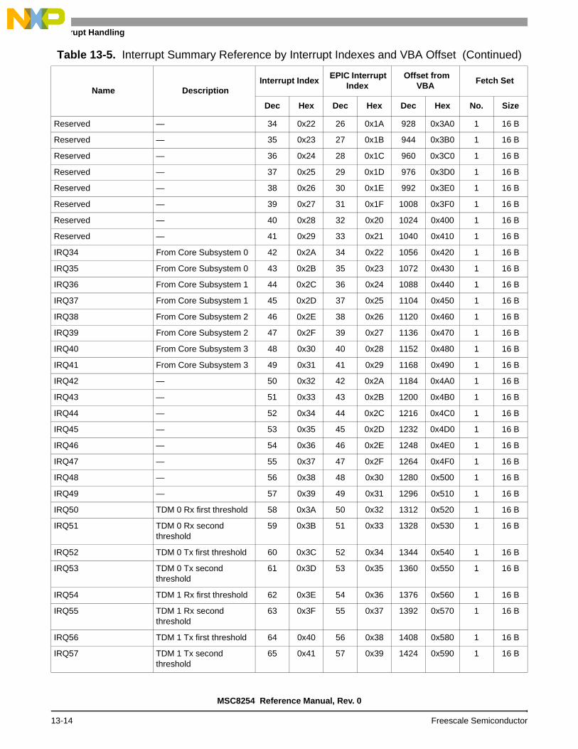
Interrupt Handling
Reserved — 34 0x22 26 0x1A 928 0x3A0 1 16 B
Reserved — 35 0x23 27 0x1B 944 0x3B0 1 16 B
Reserved — 36 0x24 28 0x1C 960 0x3C0 1 16 B
Reserved — 37 0x25 29 0x1D 976 0x3D0 1 16 B
Reserved — 38 0x26 30 0x1E 992 0x3E0 1 16 B
Reserved — 39 0x27 31 0x1F 1008 0x3F0 1 16 B
Reserved — 40 0x28 32 0x20 1024 0x400 1 16 B
Reserved — 41 0x29 33 0x21 1040 0x410 1 16 B
IRQ34 From Core Subsystem 0 42 0x2A 34 0x22 1056 0x420 1 16 B
IRQ35 From Core Subsystem 0 43 0x2B 35 0x23 1072 0x430 1 16 B
IRQ36 From Core Subsystem 1 44 0x2C 36 0x24 1088 0x440 1 16 B
IRQ37 From Core Subsystem 1 45 0x2D 37 0x25 1104 0x450 1 16 B
IRQ38 From Core Subsystem 2 46 0x2E 38 0x26 1120 0x460 1 16 B
IRQ39 From Core Subsystem 2 47 0x2F 39 0x27 1136 0x470 1 16 B
IRQ40 From Core Subsystem 3 48 0x30 40 0x28 1152 0x480 1 16 B
IRQ41 From Core Subsystem 3 49 0x31 41 0x29 1168 0x490 1 16 B
IRQ42 — 50 0x32 42 0x2A 1184 0x4A0 1 16 B
IRQ43 — 51 0x33 43 0x2B 1200 0x4B0 1 16 B
IRQ44 — 52 0x34 44 0x2C 1216 0x4C0 1 16 B
IRQ45 — 53 0x35 45 0x2D 1232 0x4D0 1 16 B
IRQ46 — 54 0x36 46 0x2E 1248 0x4E0 1 16 B
IRQ47 — 55 0x37 47 0x2F 1264 0x4F0 1 16 B
IRQ48 — 56 0x38 48 0x30 1280 0x500 1 16 B
IRQ49 — 57 0x39 49 0x31 1296 0x510 1 16 B
IRQ50 TDM 0 Rx first threshold 58 0x3A 50 0x32 1312 0x520 1 16 B
IRQ51 TDM 0 Rx second threshold
59 0x3B 51 0x33 1328 0x530 1 16 B
IRQ52 TDM 0 Tx first threshold 60 0x3C 52 0x34 1344 0x540 1 16 B
IRQ53 TDM 0 Tx second threshold
61 0x3D 53 0x35 1360 0x550 1 16 B
IRQ54 TDM 1 Rx first threshold 62 0x3E 54 0x36 1376 0x560 1 16 B
IRQ55 TDM 1 Rx second threshold
63 0x3F 55 0x37 1392 0x570 1 16 B
IRQ56 TDM 1 Tx first threshold 64 0x40 56 0x38 1408 0x580 1 16 B
IRQ57 TDM 1 Tx second threshold
65 0x41 57 0x39 1424 0x590 1 16 B
Table 13-5. Interrupt Summary Reference by Interrupt Indexes and VBA Offset (Continued)
Name DescriptionInterrupt Index
EPIC Interrupt Index
Offset from VBA
Fetch Set
Dec Hex Dec Hex Dec Hex No. Size
MSC8254 Reference Manual, Rev. 0
13-14 Freescale Semiconductor

Interrupt Mapping
IRQ58 TDM 2 Rx first threshold 66 0x42 58 0x3A 1440 0x5A0 1 16 B
IRQ59 TDM 2 Rx second threshold
67 0x43 59 0x3B 1456 0x5B0 1 16 B
IRQ60 TDM 2 Tx first threshold 68 0x44 60 0x3C 1472 0x5C0 1 16 B
IRQ61 TDM 2 Tx second threshold
69 0x45 61 0x3D 1488 0x5D0 1 16 B
IRQ62 TDM 3 Rx first threshold 70 0x46 62 0x3E 1504 0x5E0 1 16 B
IRQ63 TDM 3 Rx second threshold
71 0x47 63 0x3F 1520 0x5F0 1 16 B
IRQ64 TDM 3 Tx first threshold 72 0x48 64 0x40 1536 0x600 1 16 B
IRQ65 TDM 3 Tx second threshold
73 0x49 65 0x41 1552 0x610 1 16 B
IRQ66 — 74 0x4A 66 0x42 1568 0x620 1 16 B
IRQ67 — 75 0x4B 67 0x43 1584 0x630 1 16 B
IRQ68 — 76 0x4C 68 0x44 1600 0x640 1 16 B
IRQ69 — 77 0x4D 69 0x45 1616 0x650 1 16 B
IRQ70 — 78 0x4E 70 0x46 1632 0x660 1 16 B
IRQ71 — 79 0x4F 71 0x47 1648 0x670 1 16 B
IRQ72 — 80 0x50 72 0x48 1664 0x680 1 16 B
IRQ73 — 81 0x51 73 0x49 1680 0x690 1 16 B
IRQ74 — 82 0x52 74 0x4A 1696 0x6A0 1 16 B
IRQ75 — 83 0x53 75 0x4B 1712 0x6B0 1 16 B
IRQ76 — 84 0x54 76 0x4C 1728 0x6C0 1 16 B
IRQ77 — 85 0x55 77 0x4D 1744 0x6D0 1 16 B
IRQ78 — 86 0x56 78 0x4E 1760 0x6E0 1 16 B
IRQ79 — 87 0x57 79 0x4F 1776 0x6F0 1 16 B
IRQ80 — 88 0x58 80 0x50 1792 0x700 1 16 B
IRQ81 — 89 0x59 81 0x51 1808 0x710 1 16 B
IRQ82 Serial RapidIO message in 0
90 0x5A 82 0x52 1824 0x720 1 16 B
IRQ83 Serial RapidIO message in 1
91 0x5B 83 0x53 1840 0x730 1 16 B
IRQ84 Serial RapidIO message out 0
92 0x5C 84 0x54 1856 0x740 1 16 B
IRQ85 Serial RapidIO message out 1
93 0x5D 85 0x55 1872 0x750 1 16 B
IRQ86 Serial RapidIO doorbell inbound
94 0x5E 86 0x56 1888 0x760 1 16 B
Table 13-5. Interrupt Summary Reference by Interrupt Indexes and VBA Offset (Continued)
Name DescriptionInterrupt Index
EPIC Interrupt Index
Offset from VBA
Fetch Set
Dec Hex Dec Hex Dec Hex No. Size
MSC8254 Reference Manual, Rev. 0
Freescale Semiconductor 13-15

Interrupt Handling
IRQ87 Serial RapidIO doorbell outbound
95 0x5F 87 0x57 1904 0x770 1 16 B
IRQ88 Serial RapidIO general error
96 0x60 88 0x58 1920 0x780 1 16 B
IRQ89 — 97 0x61 89 0x59 1936 0x790 1 16 B
IRQ90 — 98 0x62 90 0x5A 1952 0x7A0 1 16 B
IRQ91 Ethernet 1 all 99 0x63 91 0x5B 1968 0x7B0 1 16 B
IRQ92 Ethernet 1 Rx 0 100 0x64 92 0x5C 1984 0x7C0 1 16 B
IRQ93 Ethernet 1 Rx 1 101 0x65 93 0x5D 2000 0x7D0 1 16 B
IRQ94 Ethernet 1 Rx 2 102 0x66 94 0x5E 2016 0x7E0 1 16 B
IRQ95 Ethernet 1 Rx 3 103 0x67 95 0x5F 2032 0x7F0 1 16 B
IRQ96 Ethernet 1 Rx 4 104 0x68 96 0x60 2048 0x800 1 16 B
IRQ97 Ethernet 1 Rx 5 105 0x69 97 0x61 2064 0x810 1 16 B
IRQ98 Ethernet 1 Rx 6 106 0x6A 98 0x62 2080 0x820 1 16 B
IRQ99 Ethernet 1 Rx 7 107 0x6B 99 0x63 2096 0x830 1 16 B
IRQ100 Ethernet 1 Tx 0 108 0x6C 100 0x64 2112 0x840 1 16 B
IRQ101 Ethernet 1 Tx 1 109 0x6D 101 0x65 2128 0x850 1 16 B
IRQ102 Ethernet 1 Tx 2 110 0x6E 102 0x66 2144 0x860 1 16 B
IRQ103 Ethernet 1 Tx 3 111 0x6F 103 0x67 2160 0x870 1 16 B
IRQ104 Ethernet 1 Tx 4 112 0x70 104 0x68 2176 0x880 1 16 B
IRQ105 Ethernet 1 Tx 5 113 0x71 105 0x69 2192 0x890 1 16 B
IRQ106 Ethernet 1 Tx 6 114 0x72 106 0x6A 2208 0x8A0 1 16 B
IRQ107 Ethernet 1 Tx 7 115 0x73 107 0x6B 2224 0x8B0 1 16 B
IRQ108 — 116 0x74 108 0x6C 2240 0x8C0 1 16 B
IRQ109 Ethernet 2 all 117 0x75 109 0x6D 2256 0x8D0 1 16 B
IRQ110 Ethernet 2 Rx 0 118 0x76 110 0x6E 2272 0x8E0 1 16 B
IRQ111 Ethernet 2 Rx 1 119 0x77 111 0x6F 2288 0x8F0 1 16 B
IRQ112 Ethernet 2 Rx 2 120 0x78 112 0x70 2304 0x900 1 16 B
IRQ113 Ethernet 2 Rx 3 121 0x79 113 0x71 2320 0x910 1 16 B
IRQ114 Ethernet 2 Rx 4 122 0x7A 114 0x72 2336 0x920 1 16 B
IRQ115 Ethernet 2 Rx 5 123 0x7B 115 0x73 2352 0x930 1 16 B
IRQ116 Ethernet 2 Rx 6 124 0x7C 116 0x74 2368 0x940 1 16 B
IRQ117 Ethernet 2 Rx 7 125 0x7D 117 0x75 2384 0x950 1 16 B
IRQ118 Ethernet 2 Tx 0 126 0x7E 118 0x76 2400 0x960 1 16 B
IRQ119 Ethernet 2 Tx 1 127 0x7F 119 0x77 2416 0x970 1 16 B
Table 13-5. Interrupt Summary Reference by Interrupt Indexes and VBA Offset (Continued)
Name DescriptionInterrupt Index
EPIC Interrupt Index
Offset from VBA
Fetch Set
Dec Hex Dec Hex Dec Hex No. Size
MSC8254 Reference Manual, Rev. 0
13-16 Freescale Semiconductor

Interrupt Mapping
IRQ120 Ethernet 2 Tx 2 128 0x80 120 0x78 2432 0x980 1 16 B
IRQ121 Ethernet 2 Tx 3 129 0x81 121 0x79 2448 0x990 1 16 B
IRQ122 Ethernet 2 Tx 4 130 0x82 122 0x7A 2464 0x9A0 1 16 B
IRQ123 Ethernet 2 Tx 5 131 0x83 123 0x7B 2480 0x9B0 1 16 B
IRQ124 Ethernet 2 Tx 6 132 0x84 124 0x7C 2496 0x9C0 1 16 B
IRQ125 Ethernet 2 Tx 7 133 0x85 125 0x7D 2512 0x9D0 1 16 B
IRQ126 — 134 0x86 126 0x7E 2528 0x9E0 1 16 B
IRQ127 PCI Express INTA 135 0x87 127 0x7F 2544 0x9F0 1 16 B
IRQ128 PCI Express INTB 136 0x88 128 0x80 2560 0xA00 1 16 B
IRQ129 PCI Express INTC 137 0x89 129 0x81 2576 0xA10 1 16 B
IRQ130 PCI Express INTD 138 0x8A 130 0x82 2592 0xA20 1 16 B
IRQ131 PCI Express general interrupt
139 0x8B 131 0x83 2608 0xA30 1 16 B
IRQ132 QUICC Engine interrupt output 0
140 0x8C 132 0x84 2624 0xA40 1 16 B
IRQ133 QUICC Engine interrupt output 1
141 0x8D 133 0x85 2640 0xA50 1 16 B
IRQ134 QUICC Engine interrupt output 2
142 0x8E 134 0x86 2656 0xA60 1 16 B
IRQ135 QUICC Engine interrupt output 3
143 0x8F 135 0x87 2672 0xA70 1 16 B
IRQ136 QUICC Engine interrupt output 4
144 0x90 136 0x88 2688 0xA80 1 16 B
IRQ137 QUICC Engine interrupt output 5
145 0x91 137 0x89 2704 0xA90 1 16 B
IRQ138 QUICC Engine interrupt output 6
146 0x92 138 0x8A 2720 0xAA0 1 16 B
IRQ139 QUICC Engine interrupt output 7
147 0x93 139 0x8B 2736 0xAB0 1 16 B
IRQ140 QUICC Engine module critical
148 0x94 140 0x8C 2752 0xAC0 1 16 B
IRQ141 QUICC Engine module regular
149 0x95 141 0x8D 2768 0xAD0 1 16 B
IRQ142 — 150 0x96 142 0x8E 2784 0xAE0 1 16 B
IRQ143 — 151 0x97 143 0x8F 2800 0xAF0 1 16 B
IRQ144 DMA channel 0 EOB 152 0x98 144 0x90 2816 0xB00 1 16 B
IRQ145 DMA channel 1 EOB 153 0x99 145 0x91 2832 0xB10 1 16 B
IRQ146 DMA channel 2 EOB 154 0x9A 146 0x92 2848 0xB20 1 16 B
IRQ147 DMA channel 3 EOB 155 0x9B 147 0x93 2864 0xB30 1 16 B
Table 13-5. Interrupt Summary Reference by Interrupt Indexes and VBA Offset (Continued)
Name DescriptionInterrupt Index
EPIC Interrupt Index
Offset from VBA
Fetch Set
Dec Hex Dec Hex Dec Hex No. Size
MSC8254 Reference Manual, Rev. 0
Freescale Semiconductor 13-17

Interrupt Handling
IRQ148 DMA channel 4 EOB 156 0x9C 148 0x94 2880 0xB40 1 16 B
IRQ149 DMA channel 5 EOB 157 0x9D 149 0x95 2896 0xB50 1 16 B
IRQ150 DMA channel 6 EOB 158 0x9E 150 0x96 2912 0xB60 1 16 B
IRQ151 DMA channel 7 EOB 159 0x9F 151 0x97 2928 0xB70 1 16 B
IRQ152 DMA channel 8 EOB 160 0xA0 152 0x98 2944 0xB80 1 16 B
IRQ153 DMA channel 9 EOB 161 0xA1 153 0x99 2960 0xB90 1 16 B
IRQ154 DMA channel 10 EOB 162 0xA2 154 0x9A 2976 0xBA0 1 16 B
IRQ155 DMA channel 11 EOB 163 0xA3 155 0x9B 2992 0xBB0 1 16 B
IRQ156 DMA channel 12 EOB 164 0xA4 156 0x9C 3008 0xBC0 1 16 B
IRQ157 DMA channel 13 EOB 165 0xA5 157 0x9D 3024 0xBD0 1 16 B
IRQ158 DMA channel 14 EOB 166 0xA6 158 0x9E 3040 0xBE0 1 16 B
IRQ159 DMA channel 15 EOB 167 0xA7 159 0x9F 3056 0xBF0 1 16 B
IRQ160 Timer 0 Channel 0 168 0xA8 160 0xA0 3072 0xC00 1 16 B
IRQ161 Timer 0 Channel 1 169 0xA9 161 0xA1 3088 0xC10 1 16 B
IRQ162 Timer 0 Channel 2 170 0xAA 162 0xA2 3104 0xC20 1 16 B
IRQ163 Timer 0 Channel 3 171 0xAB 163 0xA3 3120 0xC30 1 16 B
IRQ164 Timer 1 Channel 0 172 0xAC 164 0xA4 3136 0xC40 1 16 B
IRQ165 Timer 1 Channel 1 173 0xAD 165 0xA5 3152 0xC50 1 16 B
IRQ166 Timer 1 Channel 2 174 0xAE 166 0xA6 3168 0xC60 1 16 B
IRQ167 Timer 1 Channel 3 175 0xAF 167 0xA7 3184 0xC70 1 16 B
IRQ168 Timer 2 Channel 0 176 0xB0 168 0xA8 3200 0xC80 1 16 B
IRQ169 Timer 2 Channel 1 177 0xB1 169 0xA9 3216 0xC90 1 16 B
IRQ170 Timer 2 Channel 2 178 0xB2 170 0xAA 3232 0xCA0 1 16 B
IRQ171 Timer 2 Channel 3 179 0xB3 171 0xAB 3248 0xCB0 1 16 B
IRQ172 Timer 3 Channel 0 180 0xB4 172 0xAC 3264 0xCC0 1 16 B
IRQ173 Timer 3 Channel 1 181 0xB5 173 0xAD 3280 0xCD0 1 16 B
IRQ174 Timer 3 Channel 2 182 0xB6 174 0xAE 3296 0xCE0 1 16 B
IRQ175 Timer 3 Channel 3 183 0xB7 175 0xAF 3312 0xCF0 1 16 B
IRQ176 UART all 184 0xB8 176 0xB0 3328 0xD00 1 16 B
IRQ177 Virtual Interrupt 0 185 0xB9 177 0xB1 3344 0xD10 1 16 B
IRQ178 Virtual Interrupt 1 186 0xBA 178 0xB2 3360 0xD20 1 16 B
IRQ179 Virtual Interrupt 2 187 0xBB 179 0xB3 3376 0xD30 1 16 B
IRQ180 Virtual Interrupt 3 188 0xBC 180 0xB4 3392 0xD40 1 16 B
IRQ181 Virtual Interrupt 4 189 0xBD 181 0xB5 3408 0xD50 1 16 B
IRQ182 Virtual Interrupt 5 190 0xBE 182 0xB6 3424 0xD60 1 16 B
Table 13-5. Interrupt Summary Reference by Interrupt Indexes and VBA Offset (Continued)
Name DescriptionInterrupt Index
EPIC Interrupt Index
Offset from VBA
Fetch Set
Dec Hex Dec Hex Dec Hex No. Size
MSC8254 Reference Manual, Rev. 0
13-18 Freescale Semiconductor

Interrupt Mapping
IRQ183 Virtual Interrupt 6 191 0xBF 183 0xB7 3440 0xD70 1 16 B
IRQ184 Virtual Interrupt 7 192 0xC0 184 0xB8 3456 0xD80 1 16 B
IRQ185 Virtual Interrupt 8 193 0xC1 185 0xB9 3472 0xD90 1 16 B
IRQ186 Virtual Interrupt 9 194 0xC2 186 0xBA 3488 0xDA0 1 16 B
IRQ187 Virtual Interrupt 10 195 0xC3 187 0xBB 3504 0xDB0 1 16 B
IRQ188 Virtual Interrupt 11 196 0xC4 188 0xBC 3520 0xDC0 1 16 B
IRQ189 Virtual Interrupt 12 197 0xC5 189 0xBD 3536 0xDD0 1 16 B
IRQ190 Virtual Interrupt 13 198 0xC6 190 0xBE 3552 0xDE0 1 16 B
IRQ191 Virtual Interrupt 14 199 0xC7 191 0xBF 3568 0xDF0 1 16 B
IRQ192 Virtual Interrupt 15 200 0xC8 192 0xC0 3584 0xE00 0.5 8 B
IRQ193 Virtual Non Maskable Interrupt 0
201 0xC9 193 0xC1 3592 0xE08 0.5 8 B
IRQ194 Virtual Non Maskable Interrupt 1
202 0xCA 194 0xC2 3600 0xE10 0.5 8 B
IRQ195 Virtual Non Maskable Interrupt 2
203 0xCB 195 0xC3 3608 0xE18 0.5 8 B
IRQ196 Virtual Non Maskable Interrupt 3
204 0xCC 196 0xC4 3616 0xE20 0.5 8 B
IRQ197 Virtual Non Maskable Interrupt 4
205 0xCD 197 0xC5 3624 0xE28 0.5 8 B
IRQ198 Virtual Non Maskable Interrupt 5
206 0xCE 198 0xC6 3632 0xE30 0.5 8 B
IRQ199 Virtual Non Maskable Interrupt 6
207 0xCF 199 0xC7 3640 0xE38 0.5 8 B
IRQ200 Virtual Non Maskable Interrupt 7
208 0xD0 200 0xC8 3648 0xE40 0.5 8 B
IRQ201 Primary interrupt 209 0xD1 201 0xC9 3656 0xE48 0.5 8 B
IRQ202 Secondary interrupt 210 0xD2 202 0xCA 3664 0xE50 0.5 8 B
IRQ203 Channel 0 Interrupt 211 0xD3 203 0xCB 3672 0xE58 0.5 8 B
IRQ204 Channel 1 Interrupt 212 0xD4 204 0xCC 3680 0xE60 0.5 8 B
IRQ205 Channel 2 Interrupt 213 0xD5 205 0xCD 3688 0xE68 0.5 8 B
IRQ206 Channel 3 Interrupt 214 0xD6 206 0xCE 3696 0xE70 0.5 8 B
IRQ207 — 215 0xD7 207 0xCF 3704 0xE78 0.5 8 B
IRQ208 I2C all 216 0xD8 208 0xD0 3712 0xE80 0.5 8 B
IRQ209 — 217 0xD9 209 0xD1 3720 0xE88 0.5 8 B
IRQ210 — 218 0xDA 210 0xD2 3728 0xE90 0.5 8 B
IRQ211 — 219 0xDB 211 0xD3 3736 0xE98 0.5 8 B
Table 13-5. Interrupt Summary Reference by Interrupt Indexes and VBA Offset (Continued)
Name DescriptionInterrupt Index
EPIC Interrupt Index
Offset from VBA
Fetch Set
Dec Hex Dec Hex Dec Hex No. Size
MSC8254 Reference Manual, Rev. 0
Freescale Semiconductor 13-19

Interrupt Handling
IRQ212 — 220 0xDC 212 0xD4 3744 0xEA0 0.5 8 B
IRQ213 — 221 0xDD 213 0xD5 3752 0xEA8 0.5 8 B
IRQ214 — 222 0xDE 214 0xD6 3760 0xEB0 0.5 8 B
IRQ215 — 223 0xDF 215 0xD7 3768 0xEB8 0.5 8 B
IRQ216 — 224 0xE0 216 0xD8 3776 0xEC0 0.5 8 B
IRQ217 — 225 0xE1 217 0xD9 3784 0xEC8 0.5 8 B
IRQ218 — 226 0xE2 218 0xDA 3792 0xED0 0.5 8 B
IRQ219 — 227 0xE3 219 0xDB 3800 0xED8 0.5 8 B
IRQ220 — 228 0xE4 220 0xDC 3808 0xEE0 0.5 8 B
IRQ221 — 229 0xE5 221 0xDD 3816 0xEE8 0.5 8 B
IRQ222 — 230 0xE6 222 0xDE 3824 0xEF0 0.5 8 B
IRQ223 — 231 0xE7 223 0xDF 3832 0xEF8 0.5 8 B
IRQ224 — 232 0xE8 224 0xE0 3840 0xF00 0.5 8 B
IRQ225 — 233 0xE9 225 0xE1 3848 0xF08 0.5 8 B
IRQ226 IRQ0 234 0xEA 226 0xE2 3856 0xF10 0.5 8 B
IRQ227 IRQ1 235 0xEB 227 0xE3 3864 0xF18 0.5 8 B
IRQ228 IRQ2 236 0xEC 228 0xE4 3872 0xF20 0.5 8 B
IRQ229 IRQ3 237 0xED 229 0xE5 3880 0xF28 0.5 8 B
IRQ230 IRQ4 238 0xEE 230 0xE6 3888 0xF30 0.5 8 B
IRQ231 IRQ5 239 0xEF 231 0xE7 3896 0xF38 0.5 8 B
IRQ232 IRQ6 240 0xF0 232 0xE8 3904 0xF40 0.5 8 B
IRQ233 IRQ7 241 0xF1 233 0xE9 3912 0xF48 0.5 8 B
IRQ234 IRQ8 242 0xF2 234 0xEA 3920 0xF50 0.5 8 B
IRQ235 IRQ9 243 0xF3 235 0xEB 3928 0xF58 0.5 8 B
IRQ236 IRQ10 244 0xF4 236 0xEC 3936 0xF60 0.5 8 B
IRQ237 IRQ11 245 0xF5 237 0xED 3944 0xF68 0.5 8 B
IRQ238 IRQ12 246 0xF6 238 0xEE 3952 0xF70 0.5 8 B
IRQ239 IRQ13 247 0xF7 239 0xEF 3960 0xF78 0.5 8 B
IRQ240 IRQ14 248 0xF8 240 0xF0 3968 0xF80 0.5 8 B
IRQ241 IRQ15 249 0xF9 241 0xF1 3976 0xF88 0.5 8 B
IRQ242 NMI 250 0xFA 242 0xF2 3984 0xF90 0.5 8 B
IRQ243 ORed TDM interrupts 251 0xFB 243 0xF3 3992 0xF98 0.5 8 B
IRQ244 ORed Debug Interrupts 252 0xFC 244 0xF4 4000 0xFA0 0.5 8 B
IRQ245 ORed General Interrupts 253 0xFD 245 0xF5 4008 0xFA8 0.5 8 B
Table 13-5. Interrupt Summary Reference by Interrupt Indexes and VBA Offset (Continued)
Name DescriptionInterrupt Index
EPIC Interrupt Index
Offset from VBA
Fetch Set
Dec Hex Dec Hex Dec Hex No. Size
MSC8254 Reference Manual, Rev. 0
13-20 Freescale Semiconductor

Interrupt Mapping
IRQ246 ORed Watch Dog Timer Interrupts
254 0xFE 246 0xF6 4016 0xFB0 0.5 8 B
IRQ247 — 255 0xFF 247 0xF7 4024 0xFB8 0.5 8 B
IRQ248 Channel 0 Interrupt 256 0x100 248 0xF8 4032 0xFC0 0.5 8 B
IRQ249 Channel 1 Interrupt 257 0x101 249 0xF9 4040 0xFC8 0.5 8 B
IRQ250 Channel 2 Interrupt 258 0x102 250 0xFA 4048 0xFD0 0.5 8 B
IRQ251 Channel 3 Interrupt 259 0x103 251 0xFB 4056 0xFD8 0.5 8 B
IRQ252 — 260 0x104 252 0xFC 4064 0xFE0 0.5 8 B
IRQ253 — 261 0x105 253 0xFD 4072 0xFE8 0.5 8 B
IRQ254 — 262 0x106 254 0xFE 4080 0xFF0 0.5 8 B
IRQ255 — 263 0x107 255 0xFF 4088 0xFF8 0.5 8 B
Table 13-5. Interrupt Summary Reference by Interrupt Indexes and VBA Offset (Continued)
Name DescriptionInterrupt Index
EPIC Interrupt Index
Offset from VBA
Fetch Set
Dec Hex Dec Hex Dec Hex No. Size
MSC8254 Reference Manual, Rev. 0
Freescale Semiconductor 13-21

Interrupt Handling
13.4 Core Interrupt Mesh
To enhance communication between the four SC3850 DSP core subsystems, the MSC8254 has a core interrupt mesh. This mesh is built by connecting two interrupts from each of the SC3850 core subsystems to each of the DSP core subsystems (including itself). Table 13-6 describes the interrupt names connecting the DSP core subsystems. The interrupts mesh
Note: See the SC3850 DSP Core Subsystem Reference Manual for assertion/deassertion of the smmu_gpr signals. As an example of how to use this information, to assert an interrupt from core 1 to core 2, set bit 5 or 4 in M_GPR0 in the core 1 subsystem, which is the sending core.
Table 13-6. Core Interrupt Mesh
From/To Core Subsystem 0 Core Subsystem 1 Core Subsystem 2 Core Subsystem 3
Core Subsystem 0 M_GPR0[1:0] M_GPR0[3:2] M_GPR0[5:4] M_GPR0[7:6]
Core Subsystem 1 M_GPR0[1:0] M_GPR0[3:2] M_GPR0[5:4] M_GPR0[7:6]
Core Subsystem 2 M_GPR0[1:0] M_GPR0[3:2] M_GPR0[5:4] M_GPR0[7:6]
Core Subsystem 3 M_GPR0[1:0] M_GPR0[3:2] M_GPR0[5:4] M_GPR0[7:6]
MSC8254 Reference Manual, Rev. 0
13-22 Freescale Semiconductor

Programming Model
13.5 Programming Model
The MSC8254 interrupt program model includes configuration of the global interrupt controller and the general configuration block interrupt registers.
Note: See the SC3850 DSP Core Subsystem Reference Manual for configuration and programming of the EPIC registers.
13.5.1 Global Interrupt Controller
The virtual interrupt registers reside in a 256-byte address space (for more information see Chapter 9, Memory Map) and include:
Virtual Interrupt Generation Register (VIGR)
Virtual Interrupt status register (VISR)
Note: The GIC registers use a base address of: 0xFFF27000.
13.5.1.1 Virtual Interrupt Generation Register (VIGR)
VIGR generates virtual interrupts according to the written data. The VIRQ generated corresponds to the combination of {VIRQNUM_H, VIRQNUM_L}. A read from VIGR returns all zeros. Notice that the supported values of {VIRQNUM_H, VIRQNUM_L} are 0 to 25.
VIGR Virtual Interrupt Generation Register Offset 0x00
Bit 31 30 29 28 27 26 25 24 23 22 21 20 19 18 17 16
— — — — — — — — — — — — — — — —
Type W
Bit 15 14 13 12 11 10 9 8 7 6 5 4 3 2 1 0
— — — — — — VIRQNUM_H — — — — — VIRQNUM_LType W
Table 13-7. VIGR Bit Descriptions
Name Description Settings
—31–10
Reserved. Write to zero for future compatibility.
VIRQNUM_H9–8
Virtual Interrupt Number (High)The high bits of the virtual interrupt index number.
00 to 11
—7–3
Reserved. Write to zero for future compatibility.
VIRQNUM_L2–0
Virtual Interrupt Number (Low)The low bits of the virtual interrupt index number.
000 to 111
MSC8254 Reference Manual, Rev. 0
Freescale Semiconductor 13-23

Interrupt Handling
13.5.1.2 Virtual Interrupt Status Register (VISR)
Each bit in the VISR corresponds to one virtual interrupt source, selected by proper write access to the VIGR. When the interrupt is generated by this write access, the GIC sets the corresponding status bit. It is the responsibility of the interrupt service routine (ISR) of the destination to clear only the correct status bits by writing ones to them. Writing zeros to status bits has no effect on their status. A set status bit does not block the generation of another virtual interrupt pulse by additional writes to VIGR.
VISR Virtual Interrupt Status Register ‘Offset 0x08
Bit 31 30 29 28 27 26 25 24 23 22 21 20 19 18 17 16
— — — — — — VS25 VS24 VS23 VS22 VS21 VS20 VS19 VS18 VS17 VS16
Type R/WReset 0 0 0 0 0 0 0 0 0 0 0 0 0 0 0 0
Bit 15 14 13 12 11 10 9 8 7 6 5 4 3 2 1 0
VS15 VS14 VS13 VS12 VS11 VS10 VS9 VS8 VS7 VS6 VS5 VS4 VS3 VS2 VS1 VS0Type R/W
Reset 0 0 0 0 0 0 0 0 0 0 0 0 0 0 0 0
Table 13-8. VISR Bit Descriptions
Name Description Settings
—31–26
Reserved. Write to zero for future compatibility.
VS2525
Virtual Interrupt 25 StatusReflects the status of NMI_OUT.
0 Interrupt not asserted
1 Interrupt asserted
VS2424
Virtual Interrupt 24 StatusReflects the status of INT_OUT.
0 Interrupt not asserted
1 Interrupt asserted
VS2323
Virtual Interrupt 23 StatusReflects the status of VNMI_7.
0 Interrupt not asserted
1 Interrupt asserted
VS2222
Virtual Interrupt 22 StatusReflects the status of VNMI_6.
0 Interrupt not asserted
1 Interrupt asserted
VS2121
Virtual Interrupt 21 StatusReflects the status of tVNMI_5.
0 Interrupt not asserted
1 Interrupt asserted
VS2020
Virtual Interrupt 20 StatusReflects the status of VNMI_4.
0 Interrupt not asserted
1 Interrupt asserted
VS1919
Virtual Interrupt 19 StatusReflects the status of VNMI_3.
0 Interrupt not asserted
1 Interrupt asserted
VS1818
Virtual Interrupt 18 StatusReflects the status of VNMI_2.
0 Interrupt not asserted
1 Interrupt asserted
VS1717
Virtual Interrupt 17 StatusReflects the status of VNMI_1.
0 Interrupt not asserted
1 Interrupt asserted
VS1616
Virtual Interrupt 16 StatusReflects the status of VNMI_0.
0 Interrupt not asserted
1 Interrupt asserted
MSC8254 Reference Manual, Rev. 0
13-24 Freescale Semiconductor

Programming Model
VS1515
Virtual Interrupt 15 StatusReflects the status of the core virtual interrupt 15.
0 Interrupt not asserted
1 Interrupt asserted
VS1414
Virtual Interrupt 14 StatusReflects the status of the core virtual interrupt 14.
0 Interrupt not asserted
1 Interrupt asserted
VS1313
Virtual Interrupt 13 StatusReflects the status of the core virtual interrupt 13.
0 Interrupt not asserted
1 Interrupt asserted
VS1212
Virtual Interrupt 12 StatusReflects the status of the core virtual interrupt 12.
0 Interrupt not asserted
1 Interrupt asserted
VS1111
Virtual Interrupt 11 StatusReflects the status of the core virtual interrupt 11.
0 Interrupt not asserted
1 Interrupt asserted
VS1010
Virtual Interrupt 10 StatusReflects the status of the core virtual interrupt 10.
0 Interrupt not asserted
1 Interrupt asserted
VS99
Virtual Interrupt 9 StatusReflects the status of the core virtual interrupt 9.
0 Interrupt not asserted
1 Interrupt asserted
VS88
Virtual Interrupt 8 StatusReflects the status of the core virtual interrupt 8.
0 Interrupt not asserted
1 Interrupt asserted
VS77
Virtual Interrupt 7 StatusReflects the status of the core virtual interrupt 7.
0 Interrupt not asserted
1 Interrupt asserted
VS66
Virtual Interrupt 6 StatusReflects the status of the core virtual interrupt 6.
0 Interrupt not asserted
1 Interrupt asserted
VS55
Virtual Interrupt 5 StatusReflects the status of the core virtual interrupt 5.
0 Interrupt not asserted
1 Interrupt asserted
VS44
Virtual Interrupt 4 StatusReflects the status of the core virtual interrupt 4.
0 Interrupt not asserted
1 Interrupt asserted
VS33
Virtual Interrupt 3 StatusReflects the status of the core virtual interrupt 3.
0 Interrupt not asserted
1 Interrupt asserted
VS22
Virtual Interrupt 2 StatusReflects the status of the core virtual interrupt 2.
0 Interrupt not asserted
1 Interrupt asserted
VS11
Virtual Interrupt 2 StatusReflects the status of the core virtual interrupt 1.
0 Interrupt not asserted
1 Interrupt asserted
VS00
Virtual Interrupt 0 StatusReflects the status of the core virtual interrupt 0.
0 Interrupt not asserted
1 Interrupt asserted
Table 13-8. VISR Bit Descriptions (Continued)
Name Description Settings
MSC8254 Reference Manual, Rev. 0
Freescale Semiconductor 13-25

Interrupt Handling
13.5.2 General Interrupt Configuration
The general configuration block resides in a 128-byte address space (see Chapter 9, Memory Map). These registers are described in detail in Chapter 8, General Configuration Registers, and include the following interrupt configuration registers:
General Interrupt Register 1 (GIR1), see page 8-32General Interrupt Enable Registers 1 for Cores 0–3 (GIER1_[0–3]), see page 8-34General Interrupt Register 3 (GIR3), see page 8-36General Interrupt Enable Registers 3 for Cores 0–3 (GIER3_[0–3]), see page 8-38General Interrupt Register 5 (GIR5), see page 8-39General Interrupt Enable Registers 5 for Cores 0–3 (GIER5_[0–3]), see page 8-40
Note: The general interrupt configuration registers use a base address of: 0xFFF28000.
13.5.3 Programming Restrictions
If a precise interrupt occurs in the SC3850 subsystem, the cause of the interrupt must be resolved before returning from the interrupt handler to normal code execution. If the interrupt is not resolved and cleared, an endless loop can occur and cause a deadlock. For details, see the MSC8156 SC3850 DSP Subsystem Reference Manual, Appendix C: Error Handling.
MSC8254 Reference Manual, Rev. 0
13-26 Freescale Semiconductor

Direct Memory Access (DMA) Controller 14The DMA controller enables data movement and rearrangement while the DSP cores work independently. It can transfer blocks of data to and from the M2 memory, M3 memory, and the DDR SDRAM controllers via the CLASS. It has 16 high-speed bidirectional channels and can be commanded from each of the DSP subsystems, as well as from up to two external initiators through the RapidIO or PCI Express interfaces using buffer descriptors (BDs). All channels are capable of complex data movement and advanced transaction chaining. Operations such as descriptor fetches and block transfers are initiated by each of the sixteen channels. Full duplex operation allows the DMA controller to read data from one target and store it in its internal memory while concurrently writing another buffer to another target. This capability can be used extensively when data is read from the M3 memory and written into the M2 memory. The bidirectional DMA controller reads from one of the CLASS target ports while writing to the second one. The DMA controller supports smart arbitration algorithms such as round-robin and a timer-based mechanism using an earliest deadline first (EDF) algorithm. The DMA controller also supports a Debug mode and profiling for application development and testing. Figure 14-1 shows the VCOP block diagram.
MSC8254 Reference Manual, Rev. 0
Freescale Semiconductor 14-1

Direct Memory Access (DMA) Controller
14.1 Operating Modes
The DMA controller supports to modes of operation:
Functional mode. Each of the data transactions can be executed on each of the MBus ports. The VCOP supports memory to memory data transfers.
Debug mode. The VCOP enters the debug by external debug request. Once the VCOP enters the debug mode, it holds its requests to the MBus ports. The internal logic in the VCOP masks the channels.
— MBus is in debug mode and each of its ports gracefully stops its transaction.— Channel logic in debug mode. The arbitration mechanism masks all channels requests.
The last serviced channel gets is fully serviced.
14.2 Buffer Types
The DMA channel parameter RAM (PRAM) is accessible to the DMA controller and the port interface and includes a parity mechanism. Each channel has one dedicated PRAM line. The external BD is fetched into the PRAM the first time the channel wins during arbitration.
When a buffer is activated, the DMA controller generates a bus transaction with a maximum size as described in the buffer descriptor BTSZ field and decrements BD_SIZE accordingly. The
Figure 14-1. DMA Controller Block Diagram
FIFO
DMA Logic
Channel Logic and Arbitration
Interrupt Bus
Register File
PRAM
MBus
Bus
Interface
Interface
Internal Bus
Debug andProfiling
Peripheral Requests
CLASS
DRQ[0–1]
DDN[0–1]
PeripheralInterface
Block
GCR
ExternalSignals
MSC8156
2
2
32 32 6 62GCR_DDONE
and GCR_DREQinputs
DMAController
MSC8254 Reference Manual, Rev. 0
14-2 Freescale Semiconductor

Buffer Types
address can increment or freeze. When BD_SIZE reaches zero, the channel takes one of the following actions:
Shuts down (simple buffer)
Reinitializes itself (cyclic buffer)
Reinstalls its size (incremental buffer)
Switches to another buffer (chained-buffers)
Any combination of the preceding
Updates the multi-dimension parameters (multi dimension-buffers)
The sections that follow provide examples of several types of buffers. The BD_ATTR fields listed for each example are only those that do not have zero values.
MSC8254 Reference Manual, Rev. 0
Freescale Semiconductor 14-3

Direct Memory Access (DMA) Controller
14.2.1 One-Dimensional Simple Buffer
A simple channel is a buffer that closes when BD_SIZE reaches zero. It is defined by clearing the BD_ATTR[CONT] field to zero (see Table 14-29, BD_ATTR Field Descriptions, on page 14-49). Figure 14-2 shows an example simple buffer.
Figure 14-2. One-Dimensional Simple Buffer
Table 14-1 shows how a simple buffer, designated as BD8, is configured. A 0x200 byte block is read from address 0x1000. The channel closes when the data transfer is complete, and an interrupt is generated. Burst transactions are used on the bus.
Table 14-1. Channel Parameter Values for a Simple Buffer
BD BD Parameters Value Description
8 BD_ADDR 0x1000 External memory buffer current address.
BD_SIZE 0x200 Size of transfer left for this buffer.
BD_BSIZE — Buffer base size of cyclic buffer.
BD_ATTR SST 0x1 Generate interrupt when buffer ends.
CONT 0x0 Non-continuous mode: the buffer closes when the size reaches zero.
CYC 0x0 Increment BD_ADDR when the size reaches zero.
BTSZ 0x7 Maximum transfer size is one burst of 64 bytes.
0x1000
0x11F8 Interrupt
BD8
MSC8254 Reference Manual, Rev. 0
14-4 Freescale Semiconductor

Buffer Types
14.2.2 One-Dimensional Cyclic Buffer
A cyclic buffer is a continuous buffer. When the buffer current address reaches zero, the pointer jumps back to the base address and the buffer executes again. Figure 14-3 shows an example of a cyclic buffer.
Figure 14-3. One-Dimensional Cyclic Buffer
Table 14-2 lists the channel parameters values for channel BD8 when a 0x200 byte block is read from address 0x1000. An interrupt is generated when the buffer size reaches zero, and the transfer restarts from the base address 0x1000.
Table 14-2. Channel Parameter Values for a Cyclic Buffer
BD BD Parameters Value Description
8 BD_ADDR 0x1000 External memory buffer current address.
BD_SIZE 0x200 Size of transfer left for this buffer.
BD_BSIZE 0x200 Buffer base size of cyclic buffer.
BD_ATTR SST 0x1 Generate interrupt when buffer ends.
CONT 0x1 Continuous mode: the buffer is not closed when the size reaches zero.
CYC 0x1 Reinitialize BD_ADDR to original value when the size reaches zero.
BTSZ 0x7 Maximum transfer size is one burst of 64 bytes.
0x1000
0x11F8Interrupt
BD8
MSC8254 Reference Manual, Rev. 0
Freescale Semiconductor 14-5

Direct Memory Access (DMA) Controller
14.2.3 One-Dimensional Chained Buffer
In a chained buffer scheme, when the size of the first buffer reaches zero, the read jumps to the address of the next buffer, which may be another chained buffer or another buffer type (simple, cyclic, or incremental)). Figure 14-4 shows a buffer chained to a simple buffer.
Figure 14-4. One-Dimensional Chained Buffer
There is no constraint on the port used by each chained buffer. However, if the buffers use different ports, the DMA controller masks requests until data is out of the source or in the destination. This operation prevents out-of-sequence transactions at the ports. Table 14-3 lists the channel parameter values associated with a chained buffer (BD0) and a simple buffer (BD1). A 0x20 byte block is read starting from address 0x1000 (buffer 0). When the buffer size is zero, there is a jump to address 0x2000 (buffer 1). 0x200 byte blocks are read and an interrupt is generated.
Table 14-3. Channel Parameter Values for a Chained Buffer and a Simple Buffer
BD BD Parameters Value Description
0 BD_ADDR 0x1000 External memory buffer current address.
BD_SIZE 0x20 Size of transfer left for this buffer.BD_BSIZE 0x20 Buffer base size of cyclic buffer.BD_ATTR CONT 0x1 Continuous mode. Do not close the buffer when size reaches zero.
CYC 0x0 Non-cyclic.NBD 0x1 When size reaches zero, the next request calls buffer 1.BTSZ 0x7 Maximum transfer size is one burst of 64 bytes.
1 BD_ADDR 0x2000 External memory buffer current address.BD_SIZE 0x200 Size of transfer left for this buffer.BD_BSIZE 0x200 Buffer base size of cyclic buffer.
BD_ATTR SST 0x1 Generate interrupt when buffer ends.CONT 0x0 Non-continuous mode. Close the buffer when size reaches zero.CYC 0x0 Non-cyclic mode.
BTSZ 0x7 Maximum transfer size is one burst of 64 bytes.
0x1000
0x1018
Interrupt
0x2000
0x21f8
BD0 BD1
MSC8254 Reference Manual, Rev. 0
14-6 Freescale Semiconductor

Buffer Types
14.2.4 One-Dimensional Incremental Buffer
In an incremental buffer, a data transfer starts at the buffer base address and continues until all data is transferred. An interrupt is generated each time BD_SIZE reaches zero. BD_ATTR[CONT] = 1, so the channel does not close when BD_SIZE reaches zero. BD_ATTR[CYC] = 0, signifying sequential addressing. NBD points to the buffer itself. Figure 14-5 shows an example incremental buffer.
Figure 14-5. One-Dimensional Incremental Buffer
Table 14-4 lists the channel parameter values for an incremental buffer (BD0). Blocks of 0x100 bytes are read, starting at address 0x1000, and an interrupt is generated every 0x100 bytes. The mode is continuous and addressing is sequential. Be aware that in an incremental buffer, memory can be corrupted because of overwriting.
Table 14-4. Channel Parameter Values for an Incremental Buffer
BD BD Parameters Value Description
0 BD_ADDR 0x1000 External memory buffer current address.BD_SIZE 0x100 Size of transfer left for this buffer.
BD_BSIZE 0x100 Buffer base size of cyclic buffer.BD_ATTR SST 0x1 Generate interrupt when buffer ends.
CONT 0x1 Continuous mode. Do not close the buffer when size reaches zero.
CYC 0x0 Increment BD_ADDRESS when size reaches zero.NBD 0x0 Next request calls buffer 0 when size reaches zero.
0x1000
0x10F8
0x1200
0x12F8
Interrupt0x1100
0x11F8 Interrupt
Interrupt
BD0
MSC8254 Reference Manual, Rev. 0
Freescale Semiconductor 14-7

Direct Memory Access (DMA) Controller
14.2.5 One-Dimensional Complex Buffers With Dual Cyclic Buffers
Any combination of the previously described buffers can be used. Dual cyclic buffers, which use two areas in memory to store data, constitute a useful combination of buffer types. While one area of memory is processed, the other receives new data, as shown in Figure 14-6.
Figure 14-6. Dual Cyclic Buffers
Buffer 0 starts at address 0x1000, and transfers 0x200 byte-blocks. Buffer 1 starts at address 0x2000 and transfer size is also 0x200 bytes. Table 14-5 lists the channel parameter values corresponding to dual cyclic buffers.
Table 14-5. Channel Parameter Values for Dual Cyclic Buffers
BD BD Parameters Value Description
0 BD_ADDR 0x1000 External memory buffer current address.
BD_SIZE 0x200 Size of transfer left for this buffer.
BD_BSIZE 0x200 Buffer base size of cyclic buffer.
BD_ATTR CONT 0x1 Continuous mode. Do not shut down the channel when size reaches zero.
CYC 0x1 Reinitialize BD_ADDRESS to original value when size reaches zero.
NBD 0x1 When size reaches zero, next request calls buffer 1.
BTSZ 0x7 Maximum transfer size is one burst of 64 bytes.
1 BD_ADDR 0x2000 External memory buffer current address.
BD_SIZE 0x200 Size of transfer left for this buffer.
BD_BSIZE 0x200 Buffer base size of cyclic buffer.
BD_ATTR SST 0x1 Generate interrupt when buffer ends
CONT 0x1 Continuous mode. Do not shut down the channel when size reaches zero
CYC 0x1 Reinitialize BD_ADDRESS to original value when size reaches zero
NBD 0x0 When size reaches zero, the next request calls buffer 0
BTSZ 0x7 Maximum transfer size is one burst of 64 bytes
0x1000
0x11F8
0x2000
0x21F8
Interrupt
BD0 BD1
MSC8254 Reference Manual, Rev. 0
14-8 Freescale Semiconductor

Buffer Types
14.2.6 Two-Dimensional Simple Buffer
A two-dimensional simple channel is a buffer that closes when BD_SIZE and M2D_COUNT reach zero. This buffer is defined as follows:
BD_ATTR[CONT] = 0
BD_MD_ATTR[BD] = 1
DMACHCR[xMDC] = 1
M2D_COUNT must be set to the two-dimensional parameter and the M2D_OFFSET is set to the next address offset for each two-dimensional loop. The M2D_OFFSET is written in two’s complement. The parameters of the third and fourth dimensions must be set to zero. Figure 14-7 shows an example of a two-dimensional simple buffer.
Figure 14-7. Two-Dimensional Simple Buffer
Table 14-6 lists the configuration of a simple buffer designated as channel BD8. A 0x2000 (0x80 × 0x40) byte two-dimensional block is read from address 0x1000. The first dimension is a line of 0x40 bytes. The second dimension is composed of 0x80 lines of 0x40 bytes each. The offset between each 0x40 byte transaction is 0x1c0. The channel closes when the transfer completes after 0x80 iterations, and an interrupt is generated. Burst transactions are used on the bus.
0x1000
Interrupt
0x11FF
0x1200
0x1040
0x1C0
0x10000
.
BD8
MSC8254 Reference Manual, Rev. 0
Freescale Semiconductor 14-9

Direct Memory Access (DMA) Controller
Table 14-6. Channel Parameter Values for a Two-Dimensional Simple Buffer
BD BD Parameters Value Description
8 BD_ADDR 0x1000 External memory buffer current address.
BD_MD_SIZE 0x40 Size of transfer left for this buffer.
BD_MD_BSIZE 0x40 Buffer base size of continuous buffer.
BD_MD_ATTR SST 0x1 Generate interrupt when buffer ends.
CONT 0x0 Non-continuous mode: the channel closes when the size reaches zero.
CYC 0x0 Increment BD_ADDR when the size reaches zero.
BTSZ 0x7 Maximum transfer size is one burst of 64 bytes.
BD 0x1 Buffer dimension is 2.
SSTD 0x1 Interrupt issued at the end of the second dimension.
CONTD 0x0 Simple buffer.
BD_MD_2D M2D_COUNT 0x80 Second dimension iterations left.
M2D_BCOUNT — Second dimension base number of iterations.
M2D_OFFSET 0x1C0 Second dimension offset between two consecutive iterations.
BD_MD_3D M3D_COUNT 0 Third dimension iterations left.
M3D_BCOUNT 0 Third dimension base number of iterations.
M3D_OFFSET 0 Third dimension offset between two consecutive iterations.
BD_MD_4D M4D_COUNT 0 Fourth dimension iterations left.
M4D_OFFSET 0 Fourth dimension offset between two consecutive iterations.
MSC8254 Reference Manual, Rev. 0
14-10 Freescale Semiconductor

Buffer Types
14.2.7 Three-Dimensional Simple Buffer
A three-dimensional simple channel is a buffer that closes when BD_SIZE, M2D_COUNT, and M3D_COUNT reach zero. It is defined as follows:
BD_ATTR[CONT] = 0
BD_MD_ATTR[BD] = 2
DMACHCR[xMDC] = 1
The M2D_COUNT and M3D_COUNT must be set to each dimension parameter. The M2D_OFFSET and M3D_OFFSET must be set to the next address offset for each dimension loop. The MxD_OFFSET is written in twos-complement form. The parameters of the fourth dimension must be cleared to zero. Figure 14-8 shows a three-dimensional simple buffer.
Table 14-7 shows the configuration of a simple buffer designated as channel BD8. A 0x40000 (0x100 × 10 × 40) three-dimensional block is read from address 0x1000. The basic buffer is 0x40 byte. The offset between each 0x40 byte transaction is 0xF3C0 (0x10400 – 0x1040). The second dimension parameter is 0x10. The offset between each two-dimensional buffers is –0xF4BB0 (0x1090 – 0xE5040). The channel closes when the transfer completes after 0x100 executions of the two-dimensional buffers, and an interrupt is generated. Burst transactions are used on the bus.
Figure 14-8. Three-Dimensional Simple Buffer
0x1000
Interrupt
0x103FF
0x10400
0x1040
M2D_OFFSET = 0xF3C0
0xE5C00
.
0x10D00x1090 0x9FB0
.
0x9F70
0xE5C40
M2D_COUNTtimes
M3D_COUNT times
MSC8254 Reference Manual, Rev. 0
Freescale Semiconductor 14-11

Direct Memory Access (DMA) Controller
14.2.8 Four-Dimensional Simple Buffer
A four-dimensional simple channel is a buffer that closes when BD_SIZE and all MxD_COUNT reach zero. It is defined as follows:
BD_ATTR[CONT] = 0
BD_MD_ATTR[BD] = 3
DMACHCR[xMDC] = 1
All MxD_COUNT must be set to their corresponding dimension parameter. All MxD_OFFSET must be set to the next address offset for the corresponding dimension loop. The MxD_OFFSET is written in twos-complement form. Figure 14-9 shows an example four-dimensional simple buffer.
Table 14-7. Channel Parameter Values for a Three-Dimensional Simple Buffer
BD BD Parameters Value Description
8 BD_ADDR 0x1000 External memory buffer current address.
BD_MD_SIZE 0x40 Size of transfer left for this buffer.
BD_MD_BSIZE 0x40 Buffer base size of continuous buffer.
BD_MD_ATTR SST 0x1 Generate interrupt when buffer ends.
CONT 0x0 Non-continuous mode: the channel is closed when the size reaches zero.
CYC 0x0 Increment BD_ADDR when the size reaches zero.
BTSZ 0x7 Maximum transfer size is one burst of 64 bytes
BD 0x2 Buffer dimension is 3.
SSTD 0x2 Interrupt issued at the end of the third dimension.
CONTD 0x0 Simple buffer.
BD_MD_2D M2D_COUNT 0x10 Second dimension iterations left.
M2D_BCOUNT 0x10 Second dimension base number of iterations.
M2D_OFFSET 0xF3C0 Second dimension offset between two consecutive iterations.
BD_MD_3D M3D_COUNT 0x100 Third dimension iterations left.
M3D_BCOUNT — Third dimension base number of iterations.
M3D_OFFSET –0xE4BB0 Third dimension offset between two consecutive iterations of two-dimensional buffers.
BD_MD_4D M4D_COUNT 0 Fourth dimension iterations left.
M4D_OFFSET 0 Fourth dimension offset between two consecutive iterations.
MSC8254 Reference Manual, Rev. 0
14-12 Freescale Semiconductor

Buffer Types
Figure 14-9. Four-Dimensional Simple Buffer
Table 14-8 lists the configuration of a simple buffer designated as channel BD8. A 0x2000000 (0x80 × 0x100 × 0x10 × 0x40) byte block is read from address 0x1000. The first dimension is a 0x40 byte buffer. The offset between each 0x40 bytes transaction is 0xF3C0. The two-dimensional buffers execute 0x100 times for each fourth dimension iteration. The offset between each two-dimensional buffers is –0xF3FB0 (0x1090 – 0xF5040). The channel closes when the transfer completes after 0x80 iterations of the three-dimensional buffer, and an interrupt is generated. Burst transactions are used on the bus.
0x121000
Interrupt
0x103FF
0x10400
0x1040
0xF3C0
0xF5000
0x11B00x1090 0x8FB00x8F70
0x8CF7840
0x130400
0x216000
0x8C038000x8C12C00
0x8CF7800
0x1000
0xFCFB0
....
BD8
MSC8254 Reference Manual, Rev. 0
Freescale Semiconductor 14-13

Direct Memory Access (DMA) Controller
Table 14-8. Channel Parameter Values for a Four Dimensional Simple Buffer
BD BD Parameters Value Description
8 BD_ADDR 0x1000 External memory buffer current address.
BD_MD_SIZE 0x40 Size of transfer left for this buffer.
BD_MD_BSIZE 0x40 Buffer base size of continuous buffer.
BD_MD_ATTR SST 0x1 Generate interrupt when buffer ends.
CONT 0x0 Non-continuous mode: the channel closes when the size reaches zero.
CYC 0x0 Increment BD_ADDR when the size reaches zero.
BTSZ 0x7 Maximum transfer size is one burst of 64 bytes.
BD 0x3 Buffer dimension is 4.
SSTD 0x3 Interrupt issued at the end of the fourth dimension.
CONTD 0x0 Simple buffer.
BD_MD_2D M2D_COUNT 0x10 Second dimension iterations left.
M2D_BCOUNT 0x10 Second dimension base number of iterations.
M2D_OFFSET 0xF3C0 Second dimension offset between two consecutive iterations.
BD_MD_3D M3D_COUNT 0x100 Third dimension iterations left.
M3D_BCOUNT 0x100 Third dimension base number of iterations.
M3D_OFFSET 0xF3FB0 Third dimension offset between two consecutive iterations.
BD_MD_4D M4D_COUNT 0x80 Fourth dimension iterations left.
M4D_OFFSET 0x24050 Fourth dimension offset between two consecutive iterations.
MSC8254 Reference Manual, Rev. 0
14-14 Freescale Semiconductor

Buffer Types
14.2.9 Multi-Dimensional Chained Buffer
A multi-dimensional chained buffer has two or more multi-dimensional buffers. When the size of the first buffer and all its dimension counters reaches zero, the read jumps to the address of the next buffer, which may be another multi-chained buffer or another type of multi-dimensional buffer types (simple, cyclic, or incremental). The chained multi-dimensional buffers can be of any dimension. Figure 14-10 shows a three-dimensional buffer chained to a four-dimensional simple buffer.
Figure 14-10. Multi-Dimensional Chained Buffer
There is no constraint on the port used by each chained buffer. However, if the buffers use different ports, the DMA logic masks requests until data is out of the source or in the destination. This operation prevents out-of-sequence transactions at the ports. Table 14-9 shows the channel
Interrupt
0x103FF
0x11000
0xF3C0
0x100000
0x11B00x1090 0x8FB00x8F70
0x8CF7840
0x8C038000x8C12C00
0x8CF7800
0x1000
0xFCFB00x1210000x130400
0x216000
0x10000x10400
0xF5000
....
0x1200 0x101600
0x1014000x108200
0x108000
0x1400BD10
BD8
MSC8254 Reference Manual, Rev. 0
Freescale Semiconductor 14-15

Direct Memory Access (DMA) Controller
parameter values associated with a three-dimensional chained buffer (BD8) and a four-dimensional simple buffer (BD10).
Table 14-9. Parameter Values for Multi-Dimensional Chained and Simple Buffers
BD DCPRAM Parameters Value Description
8 BD_ADDR 0x1000 External memory buffer current address.BD_MD_SIZE 0x200 Size of transfer left for this buffer.BD_MD_BSIZE 0x200 Buffer base size of continuous buffer.
BD_MD_ATTR BTSZ 0x5 Basic transfer size is 16 bytes.NBD 0xA Next Buffer descriptor is 10.SST 0x0 Do not generate interrupt when buffer ends.
CONT 0x1 Continuous mode: the channel continues when the size and third dimension counter reach zero. See the CONTD field of the BD_MD_ATTR.
CYC 0x0 Increment BD_ADDR when the size reaches zero.
BD 0x2 Buffer dimension is 3.SSTD 0x0 No interrupt issued.CONTD 0x2 Continuous buffer when size reaches zero at the end of the third
dimension.BD_MD_2D M2D_COUNT 0x10 Second dimension iterations left.
M2D_BCOUNT 0x10 Second dimension base number of iterations.M2D_OFFSET 0xFE00 Second dimension offset between two consecutive iterations.
BD_MD_3D M3D_COUNT 0x8 Third dimension iterations left.
M3D_BCOUNT - Third dimension base number of iterations.M3D_OFFSET 0x1200 Third dimension offset between two consecutive iterations.
BD_MD_4D M4D_COUNT 0 Fourth dimension iterations left.
M4D_OFFSET 0 Fourth dimension offset between two consecutive iterations.10 BD_ADDR 0x1000 External memory buffer current address.
BD_MD_SIZE 0x40 Size of transfer left for this buffer.
BD_MD_BSIZE 0x40 Buffer base size of cyclic buffer.BD_ATTR BTSZ 0x5 Basic transfer size is 16 bytes.
SST 0x1 Generate interrupt when buffer ends.
CONT 0x0 Non-continuous mode: the channel closes when the size reaches zero.
CYC 0x0 Increment BD_ADDR when the size reaches zero.BD_MD_ATTR BD 0x3 Buffer dimension is 4.
SSTD 0x3 Interrupt issued at the end of the fourth dimension.
CONTD 0x0 Simple buffer.BD_MD_2D M2D_COUNT 0x10 Second dimension iterations left.
M2D_BCOUNT 0x10 Second dimension base number of iterations.
M2D_OFFSET 0xF3C0 Second dimension offset between two consecutive iterations.BD_MD_3D M3D_COUNT 0x100 Third dimension iterations left.
M3D_BCOUNT 0x100 Third dimension base number of iterations.
M3D_OFFSET –0xF3FB0 Third dimension offset between two consecutive iterations.BD_MD_4D M4D_COUNT 0x80 Fourth dimension iterations left.
M4D_OFFSET 0x24050 Fourth dimension offset between two consecutive iterations.
MSC8254 Reference Manual, Rev. 0
14-16 Freescale Semiconductor

Buffer Types
14.2.10 Two-Dimensional Cyclic Buffer
A two-dimensional cyclic buffer is a two-dimensional continuous buffer. When the size of the current buffer reaches zero, the pointer jumps back to the base address and the buffer executes again. The third and fourth dimension counters must be cleared to zero. The M3D_OFFSET must be set to the offset between the base address and the last transaction address. Figure 14-11 shows an example cyclic buffer.
Table 14-10 lists the configuration of a two-dimensional cyclic buffer, designated as channel BD8 in this example. A 0x2000 (0x80 × 0x40) byte two dimension block is read from address 0x1000. The first dimension is a line of 0x40 bytes. The second dimension is a 0x80 lines of 0x40 bytes each. The offset between each 0x40 bytes transaction is 0x1C0. The base address is restored when the transfer is complete after 0x80 iterations.
Figure 14-11. Two-Dimensional Cyclic Buffer
Table 14-10. Channel Parameters Values for a Two Dimensions Cyclic Buffer
BD BD Parameters Value Description
8 BD_MD_ADDR 0x1000 External memory buffer current address.BD_MD_SIZE 0x40 Size of transfer left for this buffer.
BD_MD_BSIZE 0x40 Buffer base size of continuous buffer.BD_MD_ATTR SST 0x0 Do not generate interrupt when buffer ends.
CYC 0x1 Cyclic two-dimensional buffer; the third dimension offset is used to restore the base address.
CONT 0x1 Continuous mode. The buffer does not close when BD_MD_BSIZE and M2D_COUNT reach zero.
BTSZ 0x5 Basic transfer size is 16 bytes.
BD 0x1 Buffer dimension is 2.CONTD 0x1 Second dimension continuous.
BD_MD_2D M2D_COUNT 0x80 Second dimension iterations left.
M2D_BCOUNT 0x80 Second dimension base number of iterations.M2D_OFFSET 0x1C0 Second dimension offset between two consecutive iterations.
BD_MD_3D M3D_COUNT 0 Third dimension iterations left.M3D_BCOUNT 0 Third dimension base number of iterations.M3D_OFFSET –0xF040 Third dimension offset between two consecutive iterations.
BD_MD_4D M4D_COUNT 0 Fourth dimension iterations left.M4D_OFFSET 0 Fourth dimension offset between two consecutive iterations.
0x1000
Interrupt
0x11FF
0x1200
0x1040
0x1C0
0x10000
0x10040
BD8
MSC8254 Reference Manual, Rev. 0
Freescale Semiconductor 14-17

Direct Memory Access (DMA) Controller
14.2.11 Three-Dimensional Cyclic Buffer
A three-dimensional cyclic channel is a buffer that continues when BD_SIZE, M2D_COUNT, and M3D_COUNT reach zero. It is defined as follows:
BD_ATTR[CONT] = 0
BD_MD_ATTR[BD] = 2
DMACHCR[xMDC] = 1
M2D_COUNT and M3D_COUNT must be set to each dimension parameter. The M2D_OFFSET and M3D_OFFSET must be set to the next address offset for each dimension loop. The M4D_OFFSET must be set to restore the base address of the channel. The MxD_OFFSET is written in two’s complement. The counters of the fourth dimensions must be cleared to zero. Figure 14-12 shows an example three-dimensional cyclic buffer.
Table 14-11 shows the configuration of a cyclic buffer designated as channel BD8. A 0x40000 (0x100 × 10 × 40) three-dimensional block is read from address 0x1000. The basic buffer is 0x40 byte. The offset between each 0x40 byte transaction is 0xF3C0 (0x10400 – 0x1040). The two-dimensional parameter is 0x10. The offset between each two-dimensional buffer is –0xF3FB0 (0x1090 – 0xF5040). The base address of the channel is restored when the transfer completes after 0x100 executions of the two-dimensional buffers, and an interrupt is generated.
Figure 14-12. Three-Dimensional Cyclic Buffer
0x1000
Interrupt
0x103FF
0x10400
0x1040
0xF3C0
0xF5000
0x11b00x1090 0x8FB00x8F70
0xF50400xFCFB0
BD8
MSC8254 Reference Manual, Rev. 0
14-18 Freescale Semiconductor

Arbitration Types
14.3 Arbitration Types
There are two types of DMA arbitration: round-robin and early-deadline-serve-first (EDF). The type of arbitration is selected via the DGCR[AT] bit (see Table 14-17, DMAGCR Field Descriptions, on page 14-31).
14.3.1 Round-Robin Arbitration
The round-robin arbitration between channels is a least recently used (LRU) schema. Following is a list of the arbitration parameters according to their weight:
DMA port. Each channel is assigned to one DMA port. Each time a channel request is serviced, the channels assigned to its port are masked for three clock cycles. When there are requesting channels for both ports, they are serviced intermittently.
Fixed-priority among round-robin groups. Each channel is assigned to one of the four priority groups as defined by the DCHCRx[RRPG] bit. Each priority group can contain from 0 (empty) to all 16 channels. Pending requests from the highest-priority group are serviced first.
Table 14-11. Parameter Values for a Three-Dimensional Cyclic Buffer
BD BD Parameters Value Description
8 BD_ADDR 0x1000 External memory buffer current address.
BD_MD_SIZE 0x40 Size of transfer left for this buffer.
BD_MD_BSIZE 0x40 Buffer base size of continuous buffer.
BD_MD_ATTR SST 0x1 Generate interrupt when buffer ends.
CONT 0x1 Non-continuous mode: the channel closes when the size reaches zero.
CYC 0x1 Cyclic three dimensions.
BTSZ 0x5 Basic transfer size is 16 bytes.
BD 0x2 Buffer dimension is 3.
SSTD 0x2 Interrupt issued at the end of the third dimension.
CONTD 0x2 Cyclic three-dimensional buffer.
BD_MD_2D M2D_COUNT 0x10 Second dimension iterations left.
M2D_BCOUNT 0x10 Second dimension base number of iterations.
M2D_OFFSET 0xF3C0 Second dimension offset between two consecutive iterations.
BD_MD_3D M3D_COUNT 0x100 Third dimension iterations left.
M3D_BCOUNT 0x100 Third dimension base number of iterations.
M3D_OFFSET –0xF3FB0 Third dimension offset between two consecutive iterations of two dimension buffers.
BD_MD_4D M4D_COUNT 0 Fourth dimension iterations left.
M4D_OFFSET –0xFBFB0 Fourth dimension offset between two consecutive iterations.
MSC8254 Reference Manual, Rev. 0
Freescale Semiconductor 14-19

Direct Memory Access (DMA) Controller
Bandwidth control. Each channel has credit for maximum consecutive grants according to BD_ATTR [TSZ] and BD_ATTR[BTSZ]. If TSZ is greater than BTSZ bytes, the channel wins consecutively in BTSZ byte portions until TSZ is reached. The channel may stop requesting before it is continuously granted the maximum transfer size. The channel keeps its priority until the address is aligned. The channel priority is updated when the buffer or dimension ends.
Least recently used round-robin. A linear queue defines the channel priority. After reset, each channel has a unique priority according to its number. After a channel is serviced, it gets the lowest priority. All the other channels with a priority lower than the winning priority upgrade their priority. All the channels with higher priority on this cycle keep their priority so that they are guaranteed service. Some channels may get the same priority by the time. Table 14-12 lists the priority of the channels for two successive cycles.
14.3.2 EDF Arbitration
EDF arbitration optimizes the DMA transactions in a time domain, simplifying application development. The EDF algorithm assumes that the application needs certain data to be transferred within a certain time. Every channel declares its deadline target, and the DMA controller sorts all channels into four priority groups. The deadline is the time between the current counter value (DMAEDFTDLx[CC]) to the threshold value (DMAEDFTDLx[TH]). See page 14-34 for details. The features of EDF arbitration are as follows:
Round-robin arbitration with channels in the same group.
8-bit counter and base register for each channel.
Counter is enabled/disabled when channel is activated/deactivated.
Two options for continued buffer:
— Continuous mode. Continues the deadline counter and channel with no action by the EDF logic.
— Reset mode. Reloads the counter.
Table 14-12. Round-Robin Arbitration Example
Channel Number Channel Request Clock n Priority Clock n+1 Priority
1 Deasserted 0 (Highest) 0 (Highest)
8 Deasserted 1 1
3 Asserted 2 Channel 3 win 31 (Lowest)
2 Asserted 3 2
6 Asserted 4 3
5 Deasserted 5 4
4 Deasserted 6 5
7 Deasserted 7 (Lowest) 6
MSC8254 Reference Manual, Rev. 0
14-20 Freescale Semiconductor

Arbitration Types
Maskable interrupt for threshold deadline crossing when an active counter crosses the threshold.
Four optional clock sources for the counters and a DMA predivider.
Automatic channel priority group supporting DMA based on EDF algorithm.
The EDF sorts the channels into four priority groups according to their time to deadline value. The arbitration between the groups is fixed-priority (lowest group number has the highest priority). The arbitration among the channels in the same group is round-robin. Pairs of channels with same priority in the same priority group are served according to their channel number, as illustrated in Table 14-13 and Table 14-14.
The first priority parameter is the port, which changes each cycle. The second parameter is the time to deadline, which determines the channel group. The last parameter is the channel number, which gives higher priority to the lower channel number for channels in the same group with the same priority. After each channel is serviced, all priorities are updated on a round-robin basis.
14.3.2.1 Issuing Interrupts
The EDF logic can issue a maskable interrupt request for each counter. The EDF issues its interrupts on the error request line of the DMA controller. There is one source for EDF interrupts: the threshold violation for each counter, as specified in the DMA EDF Status Register (DMAEDFSTR) (see page 14-38). The EDF logic compares each counter value with the threshold value. If a counter value equals the threshold value, EDF logic sets the corresponding sticky bit in the pending register.
14.3.2.2 Counter Control
The EDF field in the source BD_ATTR of the channel defines the EDF logic behavior when source BD_SIZE reached zero.
Table 14-13. Channels Sorted Into Four Priority Groups
Time to Deadline Priority Group
0–1 02–7 1
8–63 2
64–255 3
Table 14-14. Example of Channel Priority Sorting
ChannelCurrent Count
ThresholdTime to
DeadlinePriority Group
Priority (n)Priority (n+1)
Priority (n+2)
Priority (n+3)
0 100 0 100 3 1 0 (winner) 31 30
1 255 80 175 3 2 1 0 (winner) 312 255 80 175 3 2 1 0 0 (winner)3 240 160 80 3 0 (winner) 31 30 29
MSC8254 Reference Manual, Rev. 0
Freescale Semiconductor 14-21

Direct Memory Access (DMA) Controller
14.3.2.3 Clock Source to the Counters
All the counters share the same clock source. There are four clock sources: 3 external (to the DMA) clock sources and the DMA clock divided by 16.
14.4 Interrupts
The DMA controller uses two types of interrupts: maskable and nonmaskable interrupts.
14.4.1 Maskable Interrupts
The DMA controller can issue one maskable interrupt per channel at the end of a buffer or end of a transfer. For multi-dimension buffers, the interrupt may be issued on any of the dimensions. For each maskable interrupt request, a bit in the DMA Status Register (DMASTR) indicates the interrupt source. The interrupt mask is configured via bits in DMA Mask Register (DMAMR). Maskable interrupts are output as 16 individual interrupts, one for each unidirectional destination channel.
Most of the maskable interrupts are issued to request service or indicate that a transfer is available. The exception is EDF threshold violation error interrupt. This interrupt can be masked for each counter.
14.4.2 Nonmaskable Interrupts
Except for the DMA counters threshold violation, nonmaskable interrupts are error interrupts and are all output by one level-error interrupt. The DMA controller issues unmasked interrupts for one of the following sources:
EDF violation (the only maskable source of a DMA error; it can be masked per counter)
Port 0 transfer error
Port 1 transfer error
Any parity error
Buffer size of zero
Note: In some cases in which a PRAM parity error occurs, the BD size zero error may also be set.
For each error source, a bit in the DMA Error Register (DMAERR) indicates the error source. DMAERR also samples the first channel that caused the first bus error and the first channel that caused the first parity error.
MSC8254 Reference Manual, Rev. 0
14-22 Freescale Semiconductor

Profiling
14.5 Profiling
The DMA supports system-level profiling via the Channel Profiled (CHAPRO) and Destination Channel Profiled (DEST) bits of the DMA Local Profiling Configuration Register (DMALPCR) (see Table 14-26, DMALPCR Field Descriptions, on page 14-43). These bits provide the following indications:
DMA channel active.
Arbitration winner.
End of buffer for a DMA channel.
Bus request.
Consecutive grant.
14.6 DMA Peripheral Interface
The DMA peripheral interface supports the handshaking signals that permit up to 2 devices to control the DMA transfers through the RapidIO or PCI Express interfaces using buffer descriptors (BDs). For each interface, the peripheral can generate a request using the DRQ0 or DRQ1 input signal. The DMA controller generates the appropriate DDN0 or DDN1 response to the peripheral device when the transfer is completed. Channel definition is configured via the registers in the GCR block (see Chapter 8, General Configuration Registers for details). Each peripheral can connect to any DMA channel. Internally, the peripheral requests are translated to MBus transactions and the peripheral has an individual request number generated when the DMA generates the transaction on the MBus. The simple asynchronous interface supports all types of buffers and multi-dimensional channels.
14.6.1 Modes of Operation
The DMA peripheral interface supports the following combinations of data transfers:
Peripheral to memory. Source transactions are controlled by the data request (DRQn). After the channel is enabled, the destination BD is fetched. Read data arbitration is sustained until DRQn is asserted. As long as the signal remains asserted, data is read from the source to the DMA internal FIFO. Destination transactions depend only on the data in the DMA internal FIFO and the destination and channel programming. If DRQn is deasserted before the end of the BD, any previously won read transaction arbitrations are executed. Write transactions are executed as long as there is a minimum of 64 bytes of data in the DMA internal FIFO or the FIFO is being flushed due to BD_ATTR[MR] or port switching. Once the channel is closed or BD_ATTR[SST] is set, the done signal is asserted.
Memory to peripheral. Destination transactions are controlled by the data request (DRQn). After the channel is enabled, the source and destination BDs are fetched. Write data
MSC8254 Reference Manual, Rev. 0
Freescale Semiconductor 14-23

Direct Memory Access (DMA) Controller
arbitration is sustained until the done signal is asserted. As long as the signal remains asserted, data is written from the DMA internal FIFO to the destination. Destination transactions depend on the data in the DMA internal FIFO, the state of the done signal, and the destination BD. Source data is arbitrated depending on the source BD, channel programming, and the internal DMA FIFO space. If DRQn is deasserted before the end of the BD, any previously won write transaction arbitrations are executed. Write transactions are arbitrated as long as there is a minimum of 64 bytes of data in the DMA internal FIFO or the FIFO is being flushed due to BD_ATTR[MR] or port switching and the done signal is asserted. Once the channel is closed or BD_ATTR[SST] is set and the BD is finished, the done signal is asserted.
Peripheral to peripheral. Both the source and destination transactions are controlled by DRQn. They can be controlled by the same done signal or by different done signals.
— Same done signal. Do not use this mode. If the associated channel source generates a done signal, then data will be left in FIFO. If the associated channel destination generates the done signal, source data will be fetched after the done is asserted until you flush the FIFO.
— Different done signals. One data request signal is associated with the destination and a different request signal is associated with the source of the channel. This means that after the channel is enabled, the source and destination BDs are fetched. The read data arbitration operates in the same way as for the case of peripheral to memory. The write data arbitration behave in the same way as for the case of memory to peripheral. If the source data request is deasserted before the end of the BD, then previously won read transaction arbitrations are executed. If the destination request is deasserted before the end of the BD, any previously won write transaction arbitrations are executed. However, data may be left in the FIFO because no more write arbitrations can occur until the destination request is asserted again.
14.6.2 Configuration and Control Registers
The operation of DMA peripheral interface is configured using three of the General Configuration Registers:
GCR DMA Request 0 (GCR_DREQ0)
GCR DMA Request 1 (GCR_DREQ1)
GCR DMA Done (GCR_DDONE)
For details about the layout and structure of these registers, see Chapter 8, General Configuration Registers.
MSC8254 Reference Manual, Rev. 0
14-24 Freescale Semiconductor

DMA Peripheral Interface
14.6.3 Functional Description
The DMA peripheral interface block controls the operation of the request and done signals for two peripherals. The following subsections describe the how the signals are handled.
14.6.3.1 Request Signal
The request signals (initiated by the peripheral by asserting the appropriate DRQn input) are synchronized by an internal clock and control the internal associated DMA channel requests. For a source channel, once the DMA channel is enabled and the associated request signal is asserted, the channel reads data from the source. For a destination channel, once the DMA channel is enabled and the associated request signal is asserted, the channel writes data to the destination. The input signal does not enable the channel or the channel logic pulse that sets the channel bit in the DMASTR. However, deasserting the signal disables future arbitration wins for the associated channel. Previously won arbitrations continue to the end even after the request signal is pulled low.
14.6.3.2 Done Signal
The done signals are driven by an internal channel logic pulse width that sets the corresponding channel bit in the DMASTR. You must always set DMA_BD_ATTR[SST] and DMA_BD_ATTR[MR] to enable the generation of the done signal at the end of the BD (or the selected dimension for multi-dimensional channels). When enabled, the interface generates a done signal (which is expressed on the appropriate DDNn output line).
14.6.3.3 Signal Operation
The request and done signal operate under the following conditions:
The done signal is generated when the DMA execution reaches the end of the BD or the channel is closed.
The done signal is driven by one channel only.
Once the done signal is asserted, it is not deasserted as long as the corresponding request signal is asserted.
After the done signal is asserted, additional requests for the channel are ignored until the request signal is deasserted, the done signal is deasserted, and the request signal is reasserted.
MSC8254 Reference Manual, Rev. 0
Freescale Semiconductor 14-25

Direct Memory Access (DMA) Controller
14.6.4 Using the DMA Peripheral Interface Block
To use the DMA peripheral interface block features, you must configure and initialize the block using the following procedures:
1. Program the DMA_BD and other DMA registers for memory-to-memory transactions.
2. Set the corresponding DMA_BD_ATTR[SST] and DMA_BD_ATTR[MR} and, for multidimensional operation BD_MD_ATTR[SSTD] and BD_MD_ATTR[MRD], as required by the peripheral.
3. Because they are multiplexed with GPIO signals, you must configure the GPIO interface to specify the DDN[0–1] and DRQ[0–1] signals. The following list identifies the appropriate GPIO signals to configure:
• GPIO3 must be configured as DRQ1
• GPIO4 must be configured as DDN1
• GPIO14 must be configured as DRQ0
• GPIO15 must be configured as DDN0
See Chapter 22, GPIO for details.
4. You must configure the channels to associate with the signals using GCR_DREQ0, GCR_DREQ1, and GCR_DDONE. See Chapter 8, General Configuration Registers for details.
5. Enable the channel.
After the MSC8254 has set up the DMA controller, the peripheral must perform the following steps:
1. Deassert the DRQn input signal until the peripheral is ready to initiate the transfer.
2. When ready, assert DRQn.
3. Deassert DRQn when DDNn asserts either because it is ready for the next BD or dimension or it has finished the transaction.
4. Reassert DRQn if there is more data to transmit or space to receive the next BD.
5. Continue on in this manner until all transactions are complete.
MSC8254 Reference Manual, Rev. 0
14-26 Freescale Semiconductor

DMA Programming Model
14.7 DMA Programming Model
The DMA controller uses a combination of registers used to configure and report status of the DMA transfers and the Buffer Descriptor tables that control and implement the DMA transfers.
DMA Registers
— DMA Buffer Descriptor Base Registers 0–15 (DMABDBR[0–15], page 14-28— DMA Controller Channel Configuration Registers 0–15 (DMACHCR[0–15]),
page 14-29— DMA Controller Global Configuration Register (DMAGCR), page 14-31— DMA Channel Enable Register (DMACHER), page 14-31— DMA Channel Disable Register (DMACHDR), page 14-32— DMA Channel Freeze Register (DMACHFR), — DMA Channel Defrost Register (DMACHDFR), — DMA EDF Time-to-Dead Line Registers 0–15 (DMAEDFDL[0–15]), page 14-34— DMA EDF Control Register (DMAEDFCTRL), page 14-35— DMA EDF Mask Register (DMAEDFMR), page 14-35— DMA EDF Mask Update Register (DMAEDFMUR), page 14-36— DMA EDF Status Register (DMAEDFSTR), page 14-38— DMA Mask Register (DMAMR), page 14-38— DMA Mask Update Register (DMAMUR), page 14-39— DMA Status Register (DMASTR), page 14-40— DMA Error Register (DMAERR), page 14-41— DMA Debug Event Status Register (DMADESR), page 14-43— DMA Local Profiling Configuration Register (DMALPCR), page 14-43— DMA Round-Robin Priority Group Update Register (DMARRPGUR), page 14-44— DMA Channel Active Status Register (DMACHASTR), page 14-45— DMA Channel Freeze Status Register (DMACHFSTR), page 14-45
DMA Channel Buffer Descriptors
— Buffer Attributes (BD_ATTR), page 14-49— Multi-Dimensional Buffer Attributes (BD_MD_ATTR), page 14-52
Note: The DMA controller registers use a base address of: 0xFFF10000.
Note: If you are using external peripherals, you must configure the DMA peripheral interface block by programming the GPIO block to enable the multiplexing of the handshaking signals and configure the associated channel information in the General Configuration Registers. See Section 14.6.4, Using the DMA Peripheral Interface Block, on page 14-26 for details.
MSC8254 Reference Manual, Rev. 0
Freescale Semiconductor 14-27

Direct Memory Access (DMA) Controller
14.7.1 DMA Buffer Descriptor Base Registers x (DMABDBRx)
Each DMABDBRx holds the user-programmable addresses of the BD tables for DMA channel x. There are two fields: BDTPTR that identifies the base address of the Buffer Descriptor Table and DESO field that identifies the location offset for the destination buffer within the table. All the channel properties should be programmed, including the relevant BD, before the channel is enabled. For more information on BD address calculation, see the discussion in Section 14.7.22, DMA Channel Buffer Descriptors, on page 14-45.
DMABDBR[0–15] DMA Buffer Descriptor Base Registers 0–15 Offset 0x000 + x*0x4
Bit 31 30 29 28 27 26 25 24 23 22 21 20 19 18 17 16
— BDTPTR
Type R/W
Reset 0 0 0 0 0 0 0 0 0 0 0 0 0 0 0 0
Bit 15 14 13 12 11 10 9 8 7 6 5 4 3 2 1 0
BDTPTR DESO
Type R/W
Reset 0 0 0 0 0 0 0 0 0 0 0 0 0 0 0 0
Table 14-15. DMABDBRx Field Descriptions
Bits Reset Description Setting
—31–28
0 Reserved. Write to zero for future compatibility.
BDTPTR27–4
0 Buffer Descriptor Table PointerHolds the 24 most significant bits, out of the 32 bit Buffer Descriptors Table (BDT) address.
DESO3–0
0 Destination OffsetHolds the offset of destination buffer descriptor table from the BTD base (BDTPTR × 256).
0000 Destination table offset is 0x20.
0001 Destination table offset is 0x40.
0010 Destination table offset is 0x80.
0011 Destination table offset is 0x100.
0100 Destination table offset is 0x200.
0101 Destination table offset is 0x400.
0110 Destination table offset is 0x600.
0111 Destination table offset is 0x800.
1000 Destination table offset is 0x1000.
1001 Destination table offset is 0x2000.
1010 Destination table offset is 0x3000.
1011 Destination table offset is 0x4000.
11xx Reserved.
MSC8254 Reference Manual, Rev. 0
14-28 Freescale Semiconductor

DMA Programming Model
14.7.2 DMA Controller Channel Configuration Registers x (DMACHCRx)
DMACHCR[0–15] configure the connection between a VCOP requestor and the corresponding VCOP channel. All the channel properties should be programmed, including the relevant BD, before a channel is enabled. The VCOP logic can modify some fields in these registers while the channel is active. To avoid conflict with the DMA logic, never write these registers while the respective channel is active.
.
DMACHCR[0–15] DMA Controller Channel Configuration Offset 0x100 + x*0x4Registers 0–15
Bit 31 30 29 28 27 26 25 24 23 22 21 20 19 18 17 16
ACTVSPRT DPRT SMDC DMDC — SRCBDPTType R/W
Reset 0 0 0 0 0 0 0 0 0 0 0 0 0 0 0 0
Bit 15 14 13 12 11 10 9 8 7 6 5 4 3 2 1 0
RRPG — DPO — DESBDPTType R/WReset 0 0 0 0 0 0 0 0 0 0 0 0 0 0 0 0
Table 14-16. DMACHCRx Field Descriptions
Bits Reset Description Settings
ACTV31
0 Active VCOP ChannelWhile a channel is disabled, all requests are ignored and any non-serviced request is lost. The DMA controller resets ACTV when the channel task completes. Never write a 0 to this bit when the channel is active. You must use DMACHDR to disable the channel first before disabling the channel. Disabling the channel does not reset its value immediately; the value is reset only when there are no more open requests on the bus interface. See also the DMA Channel Enable Register on page 14-31 and the DMA Channel Disable Register on page 14-32.Written by: User, DMA controller
0 Channel is disabled.
1 Channel is enabled.
SPRT30
0 Source Channel PortSelects the MBus port associated with the source.Written by: User, DMA controller
0 Source is assigned to port 0 of the MBus interface.
1 Source is assigned to port 1 of the MBus interface.
DPRT29
0 Destination Channel PortSelects the MBus interface associated with the destination.Written by: User, DMA controller
0 Destination is assigned to port 0 of the MBus interface.
1 Destination is assigned to port 1 of the MBus interface.
SMDC28
0 Source Multi-Dimensional ChannelThe source can be either one-dimensional or multi-dimensional.Written by: User
0 Source is one-dimensional.
1 Source is multi-dimensional.
DMDC27
0 Destination Multi-Dimensional ChannelThe destination can be either one-dimensional or multi- dimensionalWritten by: User
0 Destination is one-dimensional.
1 Destination is multi-dimensional.
MSC8254 Reference Manual, Rev. 0
Freescale Semiconductor 14-29

Direct Memory Access (DMA) Controller
—26
0 Reserved. Write to zero for future compatibility.
SRCBDPT25–16
0 Source Buffer PointerBD number in the BD table assigned to the source. The maximum number of one-dimensional BDs per source is 1024, and the maximum number of multi-dimensional BDs per source is 512. For details on BD address calculation, see Section 14.7.22, DMA Channel Buffer Descriptors, on page 14-45.Written by: User, DMA controller
RRPG15–13
0 Channel Round-Robin Priority GroupThis field is valid only for round robin arbitration.See Table 14-17 for selecting arbitration mode. For more details about round robin, see 14.3.1, Round-Robin Arbitration. To update this field while the channel is active, use the DMA_RRPGUR register (see page 14-44)Written by: User, DMA controller
000 Highest priority.
011 Lowest priority.
1xx Reserved.
—12
0 Reserved. Write to zero for future compatibility.
DPO11
0 Destination Port OptimizeSpecifies how the destination port is to be optimized.Written by: User
0 Optimize for destination port requests latency.
1 Optimize for destination port requests utilization.
—10
0 Reserved. Write to zero for future compatibility.
DESBDPT9-0
0 Destination Buffer PointerBD number in the BD table assigned to the destination. The maximum number of one-dimensional BDs per destination is 1024. The maximum number of multi-dimensional BDs per destination is 512.For details on BD address calculation, see Section 14.7.22. Written by: User, DMA controller
Table 14-16. DMACHCRx Field Descriptions (Continued)
Bits Reset Description Settings
MSC8254 Reference Manual, Rev. 0
14-30 Freescale Semiconductor

DMA Programming Model
14.7.3 DMA Controller Global Configuration Register (DMAGCR)
DMAGCR defines DMA global parameters.
14.7.4 DMA Channel Enable Register (DMACHER)
DMAGCR DMA Controller Global Configuration Register Offset 0x200
Bit 31 30 29 28 27 26 25 24 23 22 21 20 19 18 17 16
—
Type R/WReset 0 0 0 0 0 0 0 0 0 0 0 0 0 0 0 0
Bit 15 14 13 12 11 10 9 8 7 6 5 4 3 2 1 0
— PSCB PSCA ATType R/W
Reset 0 0 0 0 0 0 0 0 0 0 0 0 0 0 0 0
Table 14-17. DMAGCR Field Descriptions
Bits Reset Description Register Setting—
31–30 Reserved. Write to zero for future compatibility.
PSCB2
0 Port 1 Slow ConfirmationFor debug, the DMA supports slow confirmation for all transactionsWritten by: User
0 Fast confirmation on port 1, when possible.
1 Slow confirmation on port 1.
PSCA1
0 Port 0 Slow ConfirmationFor debug, the DMA supports slow confirmation for all transactionsWritten by: User
0 Fast confirmation on port 0, when possible.
1 Slow confirmation on port 0.
AT0
0 Arbitration TypeEnables the DMA arbitration type. The DMA arbitration type is defined in the DMAGCR. See Section 14.3, Arbitration Types, on page 14-19 for details on arbitration.Written by: User
0 Enable round-robin arbitration.
1 Enable EDF arbitration.
DMACHER DMA Channel Enable Register Offset 0x204
Bit 31 30 29 28 27 26 25 24 23 22 21 20 19 18 17 16
—Type W
Reset 0 0 0 0 0 0 0 0 0 0 0 0 0 0 0 0
Bit 15 14 13 12 11 10 9 8 7 6 5 4 3 2 1 0
EN15 EN14 EN13 EN12 EN11 EN10 EN9 EN8 EN7 EN6 EN5 EN4 EN3 EN2 EN1 EN0Type WReset 0 0 0 0 0 0 0 0 0 0 0 0 0 0 0 0
MSC8254 Reference Manual, Rev. 0
Freescale Semiconductor 14-31

Direct Memory Access (DMA) Controller
Each bit in DMACHER corresponds to DMACHCRx[ACTV]. When an ENx bit is set, it activates channel x. When ENx bit is cleared, it does not affect the channel. DMACHER is cleared at reset, and the user enables a channel request by setting the appropriate bit. The register allows simultaneous activation of channels after they are configured. While channel x is disabled, all requests are ignored and any non-serviced request is lost. The DMA controller logic resets the ENx bit when the channel task completes.
14.7.5 DMA Channel Disable Register (DMACHDR)
Each bit in the DMACHDR corresponds to a channel. Writing a 1 to DISx disables channel x. Writing a 0 to DISx does not affect the channel. DMACHDR is cleared at reset. The register allows simultaneous deactivation of channels during normal operation. While channel x is disabled, all requests are ignored and any non-serviced request is lost. The DISx bit is reset by the DMA logic.
When the user writes either a 1 to DMACHDR[DISx] or a 0 to DMACHCRx[ACTV], the channel is shut down. If more channel requests are pending on the bus interface, the channel is not disabled. The DMACHDR[DISx] and corresponding DMACHER[ENx] and CHCRx[ACTV] are all set until the pending channel transactions are closed. When all transactions are closed, the DMA logic resets the DMACHER[ENx] and DMACHCRx[ACTV] bits. After the channel is disabled, you must poll DMACHASTR to acknowledge that the channel is disabled. The interrupt latency in the system must be considered as well. When you are sure that the channel is disabled and there is no previous pending interrupts, the channel can be activated.
DMACHDR DMA Channel Disable Register Offset 0x20C
Bit 31 30 29 28 27 26 25 24 23 22 21 20 19 18 17 16
—Type W
Reset 0 0 0 0 0 0 0 0 0 0 0 0 0 0 0 0
Bit 15 14 13 12 11 10 9 8 7 6 5 4 3 2 1 0
DIS15DIS14DIS13 DIS12 DIS11 DIS10 DIS9 DIS8 DIS7 DIS6 DIS5 DIS4 DIS3 DIS2 DIS1 DIS0Type WReset 0 0 0 0 0 0 0 0 0 0 0 0 0 0 0 0
MSC8254 Reference Manual, Rev. 0
14-32 Freescale Semiconductor

DMA Programming Model
14.7.6 DMA Channel Freeze Register (DMACHFR)
Setting an Sx bit freezes the corresponding channel source. Setting a Dx bit freezes the corresponding channel destination. When a bit is set, the corresponding channel settings remain valid and new DREQ requests are considered, but the DMA controller does not issue any transactions to the specified channel. This register is write only; writing a 1 to a bit toggles its value (that is, if the value is 0, it sets the bit and if it is 1, it clears the bit). Writing a zero to the bits has no effect. The DMACHFR bits are all cleared by reset. Activating a channel clears the corresponding DMACHFR bits (Sx and Dx). The register allows simultaneous freezing of channels during normal operation
Note: The DMA channels do not freeze immediately; therefore, after a channel freeze is set, the DMA controller can issue new transactions for the channel until its pipeline is cleared.
Note: When the DMA channel becomes frozen, data may be left in the FIFO.
14.7.7 DMA Channel Defrost Register (DMACHDFR).
Setting an Sx bit defrosts the corresponding channel source. Setting a Dx bit defrosts the corresponding channel destination. Defrosting a channel allows it to return to normal functioning. This register is write only; writing a 1 to a bit toggles its value (that is, if the value is 0, it sets the bit and if it is 1, it clears the bit). Writing a zero to the bits has no effect. The DMACHDFR bits
DMACHFR DMA Channel Freeze Register Offset 0x214
Bit 31 30 29 28 27 26 25 24 23 22 21 20 19 18 17 16
D15 S15 D14 S14 D13 S13 D12 S12 D11 S11 D10 S10 D9 S9 D8 S8
Type WReset 0 0 0 0 0 0 0 0 0 0 0 0 0 0 0 0
Bit 15 14 13 12 11 10 9 8 7 6 5 4 3 2 1 0
D7 S7 D6 S6 D5 S5 D4 S4 D3 S3 D2 S2 D1 S1 D0 S0Type W
Reset 0 0 0 0 0 0 0 0 0 0 0 0 0 0 0 0
DMACHDFR DMA Channel Defrost Register Offset 0x224
Bit 31 30 29 28 27 26 25 24 23 22 21 20 19 18 17 16
D15 S15 D14 S14 D13 S13 D12 S12 D11 S11 D10 S10 D9 S9 D8 S8Type WReset 1 1 1 1 1 1 1 1 1 1 1 1 1 1 1 1
Bit 15 14 13 12 11 10 9 8 7 6 5 4 3 2 1 0
D7 S7 D6 S6 D5 S5 D4 S4 D3 S3 D2 S2 D1 S1 D0 S0
Type WReset 1 1 1 1 1 1 1 1 1 1 1 1 1 1 1 1
MSC8254 Reference Manual, Rev. 0
Freescale Semiconductor 14-33

Direct Memory Access (DMA) Controller
are all set by reset. Activating a channel sets the corresponding DMACHDFR bits (Sx and Dx). The register allows simultaneous defrosting of channels
14.7.8 DMA Time-To-Dead Line Registers x (DMAEDFTDLx)
Table 14-18 describes the fields of DMAEDFTDL[0–15].
DMAEDFTDL[0–15] DMA Time-To-Dead Line Registers 0–15 Offset 0x234 + x*0x4
Bit 31 30 29 28 27 26 25 24 23 22 21 20 19 18 17 16
ENC — CURRENT_COUNTType R/W RReset 0 0 0 0 0 0 0 0 0 0 0 0 0 0 0 0
Bit 15 14 13 12 11 10 9 8 7 6 5 4 3 2 1 0
THRESHOLD BASE_COUNT
Type R/WReset 0 0 0 0 0 0 1 0 1 1 1 1 1 1 1 1
Table 14-18. DMAEDFTDL[0–15] Field Descriptions
Bits Reset Write By Description SettingsENC31
0 User ENCThis field enable this counter. The counter will start counting when a task is asserted and this field set.Note: Enabling and disabling the channels change
the counters value. Disabling channels stops the counting and enabling them reloads the counters with their base values.
0 Counter disabled
1 Counter enabled
—30–24
0 Reserved. Write to zero for future compatibility.
CURRENT_ COUNT23–16
0 DMA Current Counter ValueThis field holds the current value of the counter. Upon enabling the channel the counter is loaded with the base value. The counter counts down as long as the channel is enabled. The counter will stop counting when the channel is disabled or when counter reached zero and task is not completed yet. The counter resumes counting when the buffer ends according to the BD_ATTR[EDF].
THRESHOLD15–8
0x02 User Time to Dead Line ThresholdThe threshold defines the value of the counter when the DMA task is due. The maximum threshold value is 0xff and the minimum is 2.Note: The DMA logic sets the priority of the
channels according to counters threshold value.
BASE_COUNT7–0
0xFF User Base Count ValueThe base count value is set by the user before enabling the associated channel. When the DMA reinitializes the counter it reloads the counter with BASE_COUNT. The BASE_COUNT maximum value is 0xff and the minimum is 0.Note: Do not change the base count value of active
channels.
MSC8254 Reference Manual, Rev. 0
14-34 Freescale Semiconductor

DMA Programming Model
14.7.9 DMA EDF Control Register (DMAEDFCTRL)
Table 14-19 describes the fields of the DMAEDFCTRL registers.
14.7.10 DMA EDF Mask Register (DMAEDFMR)
Each bit in the DMAEDFMR corresponds to an interrupt request bit in the DMAEDFSTR. When a bit is set, it enables the generation of an interrupt request of the corresponding counter.
DMAEDFCTRL DMA EDF Control Register Offset 0x334Bit 31 30 29 28 27 26 25 24 23 22 21 20 19 18 17 16
— CLK_SRC
Type R/WReset: 0 0 0 0 0 0 0 0 0 0 0 0 0 0 0 0
Bit 15 14 13 12 11 10 9 8 7 6 5 4 3 2 1 0CLK_DIV
Type R/W
Reset: 0 0 0 0 0 0 0 0 0 0 0 0 0 0 0 1
Table 14-19. DMAEDFCTRL Field Descriptions
Bits Write by Description Setting
—31–18
— Reserved. Write to zero for future compatibility.
CLK_SRC17–16
User Clock SourceThere are four clock sources for the EDF counters.
00: DMA clock divided by 16
01: Source 1
10: Source 2
11: Source 3
CLK_DIV15–0
User Clock DividerDivide the clock source (selected by CLK_SRC) for the EDF counters.The DMAEDFTDLx clock frequency is EDF clock (selected by CLK_SRC) divided by CLK_DIV. The maximum CLK_DIV value is 0xFFFF and the minimum is 1.
DMAEDFMR DMA EDF Mask Register Offset 0x338Bit 31 30 29 28 27 26 25 24 23 22 21 20 19 18 17 16
—Type R/W
Reset: 0 0 0 0 0 0 0 0 0 0 0 0 0 0 0 0
Bit 15 14 13 12 11 10 9 8 7 6 5 4 3 2 1 0M15 M14 M13 M12 M11 M10 M9 M8 M7 M6 M5 M4 M3 M2 M1 M0
Type R/WReset: 0 0 0 0 0 0 0 0 0 0 0 0 0 0 0 0
MSC8254 Reference Manual, Rev. 0
Freescale Semiconductor 14-35

Direct Memory Access (DMA) Controller
DMAEDFMR is cleared at reset, and the user enables a counter interrupt request by setting the appropriate bit.Table 14-20 describes the fields of the DMAEDFMR.
14.7.11 DMA EDF Mask Update Register (DMAEDFMUR).
The DMAEDFMUR enables modifying the DMAEDFMR registers without a read modify write operation. You can modify up to four channels with one action. Table 14-21 describes the fields of the DMAEDFMUR.
Table 14-20. DMAEDFMR Field Descriptions
Bits Write by Description Setting
—31–16
— Reserved. Write to zero for future compatibility.
M[15–0]15–0
User Masks 15–0Each bit corresponds to an interrupt request bit in the DMAEDFSTR. Setting the bit enables generation of the respective interrupt request.
0 Interrupt masked.
1 Interrupt enabled.
DMAEDFMUR DMA EDF Mask Update Register Offset 0x340Bit 31 30 29 28 27 26 25 24 23 22 21 20 19 18 17 16
MASK_CH3 NM3 EN3 MASK_CH2 NM2 EN2Type R/W
Reset: 0 0 0 0 0 0 0 0 0 0 0 0 0 0 0 0
Bit 15 14 13 12 11 10 9 8 7 6 5 4 3 2 1 0MASK_CH1 NM1 EN1 MASK_CH0 NM0 EN0
R/WReset: 0 0 0 0 0 0 0 0 0 0 0 0 0 0 0 0
Table 14-21. DMAEDFMUR Field Descriptions
Bits Write by Description Setting
MASK_CH331–26
User Channel NumberIndicate the channel number of the DMAEDFMR to change.
000000–001111 Channel number.
01xxxx Reserved.1xxxxx Reserved.
NM325
User New Channel Mask ValueStores the new value of DMAEDFMR[MASK_CH3].
0 Not masked.
1 Masked.
EN324
User Enable Mask/Unmask UpdatingWhen set, updates DMAEDFMR[MASK_CH3] according to NM3. When DMAEDFMR[MASK_CH3] is updated, the DMA controller clears this bit.
0 Update occurred.
1 Perform update.
MASK_CH223–18
User Channel NumberIndicate the channel number of the DMAEDFMR to change.
000000–001111 Channel number.
01xxxx Reserved.1xxxxx Reserved.
NM217
User New Channel Mask ValueStores the new value of DMAEDFMR[MASK_CH2].
0 Not masked.
1 Masked.
MSC8254 Reference Manual, Rev. 0
14-36 Freescale Semiconductor

DMA Programming Model
EN216
User Enable Mask/Unmask UpdatingWhen set, updates DMAEDFMR[MASK_CH2] according to NM3. When DMAEDFMR[MASK_CH2] is updated, the DMA controller clears this bit.
0 Update occurred.
1 Perform update.
MASK_CH115–10
User Channel NumberIndicate the channel number of the DMAEDFMR to change.
000000–001111 Channel number.
01xxxx Reserved.1xxxxx Reserved.
NM19
User New Channel Mask ValueStores the new value of DMAEDFMR[MASK_CH1].
0 Not masked.
1 Masked.
EN18
User Enable Mask/Unmask UpdatingWhen set, updates DMAEDFMR[MASK_CH1] according to NM3. When DMAEDFMR[MASK_CH1] is updated, the DMA controller clears this bit.
0 Update occurred.
1 Perform update.
MASK_CH07–2
User Channel NumberIndicate the channel number of the DMAEDFMR to change.
000000–001111 Channel number.
01xxxx Reserved.1xxxxx Reserved.
NM01
User New Channel Mask ValueStores the new value of DMAEDFMR[MASK_CH0].
0 Not masked.
1 Masked.
EN00
User Enable Mask/Unmask UpdatingWhen set, updates DMAEDFMR[MASK_CH0 according to NM3. When DMAEDFMR[MASK_CH0] is updated, the DMA controller clears this bit.
0 Update occurred.
1 Perform update.
Table 14-21. DMAEDFMUR Field Descriptions (Continued) (Continued)
Bits Write by Description Setting
MSC8254 Reference Manual, Rev. 0
Freescale Semiconductor 14-37
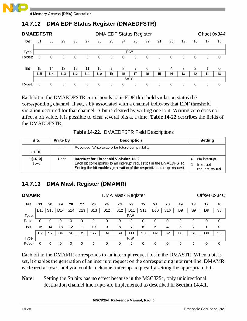
Direct Memory Access (DMA) Controller
14.7.12 DMA EDF Status Register (DMAEDFSTR)
Each bit in the DMAEDFSTR corresponds to an EDF threshold violation status the corresponding channel. If set, a bit associated with a channel indicates that EDF threshold violation occurred for that channel. A bit is cleared by writing one to it. Writing zero does not affect a bit value. It is possible to clear several bits at a time. Table 14-22 describes the fields of the DMAEDFSTR.
14.7.13 DMA Mask Register (DMAMR)
Each bit in the DMAMR corresponds to an interrupt request bit in the DMASTR. When a bit is set, it enables the generation of an interrupt request on the corresponding interrupt line. DMAMR is cleared at reset, and you enable a channel interrupt request by setting the appropriate bit.
Note: Setting the Sn bits has no effect because in the MSC8254, only unidirectional destination channel interrupts are implemented as described in Section 14.4.1.
DMAEDFSTR DMA EDF Status Register Offset 0x344Bit 31 30 29 28 27 26 25 24 23 22 21 20 19 18 17 16
—
Type R/WReset: 0 0 0 0 0 0 0 0 0 0 0 0 0 0 0 0
Bit 15 14 13 12 11 10 9 8 7 6 5 4 3 2 1 0
I15 I14 I13 I12 I11 I10 I9 I8 I7 I6 I5 I4 I3 I2 I1 I0W1C
Reset: 0 0 0 0 0 0 0 0 0 0 0 0 0 0 0 0
Table 14-22. DMAEDFSTR Field Descriptions
Bits Write by Description Setting
—31–16
— Reserved. Write to zero for future compatibility.
I[15–0]15–0
User Interrupt for Threshold Violation 15–0Each bit corresponds to an interrupt request bit in the DMAEDFSTR. Setting the bit enables generation of the respective interrupt request.
0 No interrupt.
1 Interrupt request issued.
DMAMR DMA Mask Register Offset 0x34C
Bit 31 30 29 28 27 26 25 24 23 22 21 20 19 18 17 16
D15 S15 D14 S14 D13 S13 D12 S12 D11 S11 D10 S10 D9 S9 D8 S8Type R/W
Reset 0 0 0 0 0 0 0 0 0 0 0 0 0 0 0 0
Bit 15 14 13 12 11 10 9 8 7 6 5 4 3 2 1 0
D7 S7 D6 S6 D5 S5 D4 S4 D3 S3 D2 S2 D1 S1 D0 S0Type R/WReset 0 0 0 0 0 0 0 0 0 0 0 0 0 0 0 0
MSC8254 Reference Manual, Rev. 0
14-38 Freescale Semiconductor

DMA Programming Model
14.7.14 DMA Mask Update Register (DMAMUR)
DMAMUR is a special register that allows you to modify the DMAMR registers without a read- modify-write operation.
DMAMUR DMA Mask Update Register Offset 0x35C
Bit 31 30 29 28 27 26 25 24 23 22 21 20 19 18 17 16
MASKCH3 DES3 NM3 EN3 MASKCH2 DES2 NM2 EM2
Type RReset 0 0 0 0 0 0 0 0 0 0 0 0 0 0 0 0
Bit 15 14 13 12 11 10 9 8 7 6 5 4 3 2 1 0
MASKCH1 DES1 NM1 EN1 MASKCH0 DES0 NM0 EN0Type R/W
Reset 0 0 0 0 0 0 0 0 0 0 0 0 0 0 0 0
Table 14-23. DMAMUR Field Descriptions
Bits Reset Description Settings
MASKCH331–27
0 Channel NumberThe channel number to which DMAMR should be changed.Written by: User
00000–01111: Channel number.
1xxxx Reserved.
DES326
0 Channel Number DestinationDestination channel number to which DMAMR should be changed.Written by: User
0 Channel number source.
1 Channel number destination.
NM325
0 New Channel Mask valueThe new value of DMAMR[MASKCH3, DES3].Written by: User
0 Unmask.
1 Mask.
EN324
0 Enable MASK/UNMASK UpdateUpdates DMAMR[MASK_CH3, DES3] according to NM3. Then the DMA controller clears this bit.Written by: User, DMA controller
MASKCH223–19
0 Channel NumberThe channel number to which DMAMR should be changed.Written by: User
00000–01111: Channel number.
1xxxx: Reserved.
DES218
0 Channel Number DestinationDestination channel number to which DMAMR should be changed.Written by: User
0 Channel number source.
1 Channel number destination.
NM217
0 New Channel Mask valueThe new value of DMAMR[MASKCH3, DES2].Written by: User
0 Unmask.
1 Mask.
EN216
0 Enable MASK/UNMASK UpdateUpdates the DMAMR[MASKCH2, DES2] according to NM2. Then the DMA controller clears this bit.Written by: User, DMA controller
MASKCH115–11
0 Channel NumberThe channel number to which DMAMR should be changed.Written by: User
00000–01111: Channel number.
1xxxx: Reserved
MSC8254 Reference Manual, Rev. 0
Freescale Semiconductor 14-39

Direct Memory Access (DMA) Controller
14.7.15 DMA Status Register (DMASTR)
Each bit in the DMASTR corresponds to a channel. The source status for each channel is controlled in the BD associated with the channel. If set, a bit associated with a channel indicates that the buffer ends when BD_ATTR[SST] is set or it is the last buffer. A bit is cleared by writing a value of one to it. Writing zero does not affect a bit value. Several bits can be cleared at one time.
Note: You must clear the Dx and Sx bits before enabling the channel.
DES110
0 Channel Number DestinationDestination channel number to which DMAMR should be changed.Written by: User
0 Channel number source.1 Channel Number destination.
NM19
0 New Channel Mask valueThe new value of DMA_MR[MASK_CH1, DES1].Written by: User
0 Unmask.1 Mask.
EN18
0 Enable MASK/UNMASK UpdateUpdates DMAMR[MASKCH0, DES0] according to NM0. Then the DMA controller clears this bit.Written by: User, DMA controller
MASKCH07–3
0 Channel NumberThe channel number to which DMAMR should be changed.Written by: User
00000–01111: Channel number.1xxxx Reserved
DES02
0 Channel Number DestinationDestination channel number to which DMAMR should be changed.Written by: User
0 Channel number source.1 Channel number destination.
NM01
0 New Channel Mask valueThe new value of DMAMR[MASKCH0, DES0].Written by: User
0 Unmask.1 Mask.
EN00
0 Enable MASK/UNMASK UpdateUpdates DMAMR[MASKCH0, DES0] according to NM0. Then the DMA controller clears this bit.Written by: User, DMA controller
DMASTR DMA Status Register Offset 0x360
Bit 31 30 29 28 27 26 25 24 23 22 21 20 19 18 17 16
D15 S15 D14 S14 D13 S13 D12 S12 D11 S11 D10 S10 D9 S9 D8 S8Type R
Reset 0 0 0 0 0 0 0 0 0 0 0 0 0 0 0 0
Bit 15 14 13 12 11 10 9 8 7 6 5 4 3 2 1 0
D7 S7 D6 S6 D5 S5 D4 S4 D3 S3 D2 S2 D1 S1 D0 S0Type RReset 0 0 0 0 0 0 0 0 0 0 0 0 0 0 0 0
Table 14-23. DMAMUR Field Descriptions (Continued)
Bits Reset Description Settings
MSC8254 Reference Manual, Rev. 0
14-40 Freescale Semiconductor

DMA Programming Model
14.7.16 DMA Error Register (DMAERR)
DMAERR holds the source for the error interrupt. The error interrupt output is unmasked in the DMA controller. A bit is cleared by writing a value of one to it. Writing zero does not affect a bit value. Several bits can be cleared at one time. If a port error occurs, all channels assigned to the port enter a freeze state. You must reprogram the channel that caused the error and reactivate it. You may decide to defrost other port assigned channels and continue normally. For a BD size error or parity error, only the channel that caused the error is frozen.
DMAERR DMA Error Register Offset 0x370
Bit 31 30 29 28 27 26 25 24 23 22 21 20 19 18 17 16
BDSZ PACH PADEST — PBCH PBDEST
Type R R/W R R/WReset 0 0 0 0 0 0 0 0 0 0 0 0 0 0 0 0
Bit 15 14 13 12 11 10 9 8 7 6 5 4 3 2 1 0
PAE PBE — THV PRTYPPRTYF PRTYB PRTY — PRTYCH PRTYDType R/W R
Reset 0 0 0 0 0 0 0 0 0 0 0 0 0 0 0 0
Table 14-24. DMAERR Description
Bits Reset Description Settings
BDSZ31
0 Buffer Descriptor SizeIndicates whether the buffer descriptor size is programmed to zero. See also Table 14-28 and Table 14-30.
0 No BD_SIZE or MD_BD_SIZE of 0 detected.
1 BD_SIZE or MD_BD_SIZE of 0 detected.
PACH30–25
0 First Port 0 Channel to Cause Bus ErrorIndicates which channel caused the first error on bus interface port A.
000000 - 001111: channel number
01xxxx: Reserved
10xxxx: ReservedPADEST
240 Error of Port 0 Destination Channel
Indicates whether the last error on port 0 was caused by channel source or destination.
0: Source transaction error.
1: Destination transaction error.
—23
0 Reserved. Write to zero for future compatibility.
PBCH22–17
0 First Port 1 Channel to Cause Bus ErrorIndicates which channel caused the first error on bus interface port B.
000000–001111: channel number.
01xxxx Reserved
10xxxx: ReservedPBDEST
160 Error of Port 1 Destination Channel
Indicates whether the last error on port 1 was caused by a channel source or destination.
0 Source transaction error.
1 Destination transaction error.
PAE15
0 Port 0 Transfer Error IndicationIndicates whether there is an acknowledged transfer error on port 0.
0 No transfer error acknowledged on port 0.
1 Transfer error acknowledged on port 0.
PBE14
0 Port 1 Transfer Error IndicationIndicates whether there is an acknowledged transfer error on port 1.
0 No transfer error acknowledged on port 1.
1 Transfer error acknowledged on port 1.
—13
0 Reserved, write zero for future compatibility.
MSC8254 Reference Manual, Rev. 0
Freescale Semiconductor 14-41

Direct Memory Access (DMA) Controller
THV12
0 Threshold ViolationThe channel that violated the deadline is indicated in the DMA Counter Status Register (DMACNTSTR). THV is set as long as there is a set bit in DMACNTSTR. THV is automatically cleared when all bits in DMACNTSTR are cleared.
0 No deadline violation.
1 Deadline violation.
PRTYP11
0 Parity Error on PRAMIndicates that the parity error occurred in the PRAM.
0 No error indication on the PRAM.
1 PRAM parity error indication.
PRTYF10
0 Parity Error on FIFOsIndicates that the parity error occurred in the FIFOs.
0 No error indication in the FIFO’s.
1 FIFO’s parity error indication.
PRTYB9
0 Parity Error on Bus interfaceIndicates that the parity error occurred in the BI.
0 No error indication in the BI.
1 BI parity error indication.
PRTY8
0 Parity ErrorIndicates any parity error.
0 No error indication.
1 Error indication.
—7
0 Reserved, write zero for future compatibility.
PRTYCH6–1
0 Parity ChannelFirst channel that caused parity errorIndicates by which channel the last parity error was caused.
000000–001111: Channel number.
01xxxx Reserved.
10xxxx Reserved.
PRTYD0
0 Parity Error DestinationIndicates whether the first parity error was caused by a channel source or destination.
0 Source transaction error.
1 Destination transaction error.
Table 14-24. DMAERR Description (Continued)
Bits Reset Description Settings
MSC8254 Reference Manual, Rev. 0
14-42 Freescale Semiconductor
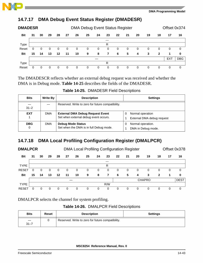
DMA Programming Model
14.7.17 DMA Debug Event Status Register (DMADESR)
The DMADESCR reflects whether an external debug request was received and whether the DMA is in Debug mode. Table 14-25 describes the fields of the DMADESR.
14.7.18 DMA Local Profiling Configuration Register (DMALPCR)
DMALPCR selects the channel for system profiling.
DMADESR DMA Debug Event Status Register Offset 0x374
Bit 31 30 29 28 27 26 25 24 23 22 21 20 19 18 17 16
—
Type RReset 0 0 0 0 0 0 0 0 0 0 0 0 0 0 0 0
Bit 15 14 13 12 11 10 9 8 7 6 5 4 3 2 1 0
— EXT DBGType R
Reset 0 0 0 0 0 0 0 0 0 0 0 0 0 0 0 0
Table 14-25. DMADESR Field Descriptions
Bits Write By Description Settings
—31–2
— Reserved. Write to zero for future compatibility.
EXT1
DMA External DMA Debug Request EventSet when external debug event occurs.
0 Normal operation
1 External DMA debug request
DBG0
DMA Debug Mode StatusSet when the DMA is in full Debug mode.
0 Normal operation.
1 DMA in Debug mode.
DMALPCR DMA Local Profiling Configuration Register Offset 0x378
Bit 31 30 29 28 27 26 25 24 23 22 21 20 19 18 17 16
—TYPE R
RESET 0 0 0 0 0 0 0 0 0 0 0 0 0 0 0 0
Bit 15 14 13 12 11 10 9 8 7 6 5 4 3 2 1 0
— CHAPRO DESTTYPE R/W
RESET 0 0 0 0 0 0 0 0 0 0 0 0 0 0 0 0
Table 14-26. DMALPCR Field Descriptions
Bits Reset Description Settings
—31–7
0 Reserved. Write to zero for future compatibility.
MSC8254 Reference Manual, Rev. 0
Freescale Semiconductor 14-43

Direct Memory Access (DMA) Controller
14.7.19 DMA Round-Robin Priority Group Update Register (DMARRPGUR)
DMARRPGR is a special register that allows you to modify the DMACHCR[RRPG] bit without a read-modify-write operation.
Note: Do not modify this register while the DMA controller is in EDF mode (DMAGCR[AT] is set—see page 14-31).
CHAPRO6–1
0 Channel ProfiledSelects the channel to be profiled.Write by: User
000000–001111: Channel number.
01xxxx Reserved.
10xxxx Reserved.
DEST0
0 Destination Channel ProfiledSpecifies whether source or destination requests are profiled.Write by: User
0 Channel source requests are profiled.
1 Channel destination requests are profiled.
DMARRPGUR DMA Round-Robin Priority Group Update Register Offset 0x37C
Bit 31 30 29 28 27 26 25 24 23 22 21 20 19 18 17 16
—TYPE R
RESET 0 0 0 0 0 0 0 0 0 0 0 0 0 0 0 0
Bit 15 14 13 12 11 10 9 8 7 6 5 4 3 2 1 0
— CH NRRPG ENTYPE R/W
RESET 0 0 0 0 0 0 0 0 0 0 0 0 0 0 0 0
Table 14-27. DMARRPGUR Field Descriptions
Bits Description Settings
—31–10
Reserved. Write to zero for future compatibility.
CH9–4
Channel NumberThe channel number to which DMACHCR[RRPG] should be changed.
000000–001111: Channel number.
01xxxx Reserved.
1xxxxx Reserved.
NRRPG3–1
New Channel Round-Robin Priority GroupThe new value of RRPG to be written to the corresponding CHCR of the channel.
000 Highest priority.
...
011 Lowest priority.
1xx Reserved.
EN0
Enable RRPG UpdateEnables the RRPG update. Then the DMA controller clears this bit
Table 14-26. DMALPCR Field Descriptions (Continued)
Bits Reset Description Settings
MSC8254 Reference Manual, Rev. 0
14-44 Freescale Semiconductor

DMA Programming Model
14.7.20 DMA Channel Active Status Register (DMACHASTR)
Each bit in the DMACHASTR corresponds to the active status of the associated channel. If set, a bit associated with a channel indicates that the channel is still active. A channel can stay active even after DMACHCR[ACTV] is cleared or DMACHDR[DISx] is set. A DMACHASTR bit is reset only when its corresponding channel completes the shutdown procedure.
14.7.21 DMA Channel Freeze Status Register (DMACHFSTR)
Each bit in the DMACHFSTR corresponds to the freeze status of the associated channel. If set, a bit associated with a channel indicates that the channel is still frozen.
Note: The corresponding bits are cleared when a channel is activated.
Note: When a bit is set as a result of BD_ATTR[FRZ] or BD_MD_ATTR[FRZ], it means that the DMA internal logic has finished serving the current BD and will not fetch or process the next BD until the channel is unfrozen. It does not imply that the current BD data or update has reached its destination. To guarantee that data or an updated BD is written to memory, use the interrupt mechanism or poll the channel status register.
14.7.22 DMA Channel Buffer Descriptors
Figure 14-13 shows a diagram of the BD pointer scheme.
DMACHASTR DMA Channel Active Status Register Offset 0x380
Bit 31 30 29 28 27 26 25 24 23 22 21 20 19 18 17 16
—
Type RReset 0 0 0 0 0 0 0 0 0 0 0 0 0 0 0 0
Bit 15 14 13 12 11 10 9 8 7 6 5 4 3 2 1 0
A15 A14 A13 A12 A11 A10 A9 A8 A7 A6 A5 A4 A3 A2 A1 A0Type R
Reset 0 0 0 0 0 0 0 0 0 0 0 0 0 0 0 0
DMACHFSTR DMA Channel Freeze Status Register Offset 0x388
Bit 31 30 29 28 27 26 25 24 23 22 21 20 19 18 17 16
D15 S15 D14 S14 D13 S13 D12 S12 D11 S11 D10 S10 D9 S9 D8 S8
Type RReset 0 0 0 0 0 0 0 0 0 0 0 0 0 0 0 0
Bit 15 14 13 12 11 10 9 8 7 6 5 4 3 2 1 0
D7 S7 D6 S6 D5 S5 D4 S4 D3 S3 D2 S2 D1 S1 D0 S0Type R
Reset 0 0 0 0 0 0 0 0 0 0 0 0 0 0 0 0
MSC8254 Reference Manual, Rev. 0
Freescale Semiconductor 14-45

Direct Memory Access (DMA) Controller
Figure 14-13. Buffer Descriptor Pointers
Following are the actual addresses of the source and destination BDs for any channel:
BDT_BASE = DMABDBR[BDT_PTR] × 256
Source BD = BDT_BASE + DMACHCR[SRCBDPT] × 16 × (DMACHCR[SMDC] + 1)
Destination BD: BDT_BASE + offset + DMACHCR[DESBDPT] × 16 × (DMACHCR[DMDC] + 1)
Offset is the decoded value of DMABDBR[DESO]
The VCOP channel BDs are located in memory outside the VCOP. Each channel has a BD table to hold the BDs for both source and destination buffers. All BDs of all channels must be located in memory connected to MBus interface 0. Figure 14-14 shows the structure of one-dimensional BD, which is a 128-bit entry.
Figure 14-14. DMA Channel BD One-Dimensional Line
BDT_PTR DESO DES_BDPT
DMABDBRx DMACHCRx
BD
BD
SRC_BDPT
{
Note: Memory location can be M2, M3, or DDR.
127
BD_ADDR BD_SIZE BD_ATTR BD_BSIZE
32 Bits 32 Bits 32 Bits 32 Bits
0326496
MSC8254 Reference Manual, Rev. 0
14-46 Freescale Semiconductor

DMA Programming Model
Figure 14-15 shows the structure of a multi-dimensional BD, which is a 256-bit entry.
Figure 14-15. DMA Channel Multi-Dimensional Buffer Descriptor
Table 14-16 shows an example structure for a BD table that holds multi-dimensional read and one-dimensional DMA write tasks. The read channel uses 512 BDs of multi-dimensional BDs, which is the maximum available for multiple dimensions. The write channel uses 1024 one-dimensional BDs, which is the maximum available for one dimension. For details on BD address calculation.
Figure 14-16. Example BD Table with a Mixed Dimensional Structure
The BDs are either one-dimensional or multi-dimensional. One-dimensional BDs are chained only to one-dimensional BDs and multi-dimensional BDs are chained only to multi-dimensional BDs. The types of source and destination BDs are defined in the DMACHCR (see page 14-29). Table 14-28 lists the channel parameters for a one-dimensional BD.
255 0
BD_MD_ADDR BD_MD_BSIZE BD_MD_SIZE BD_MD_ATTR BD_MD_3D BD_MD_4D
32 Bits 16 Bits 16 Bits 48 Bits 52 Bits 52 Bits 40 Bits
BD_MD_2D
4092144192208224
Multi-Dimensional BD 0
One-Dimensional BD 0
Multi-Dimensional BD 1
Multi-Dimensional BD 511
One-Dimensional BD 1
One-Dimensional BD 1023
BDT_BASE Address
MSC8254 Reference Manual, Rev. 0
Freescale Semiconductor 14-47

Direct Memory Access (DMA) Controller
Table 14-28. One-Dimensional BD Field Descriptions
Bits Description
BD_ADDR127–96
Current Buffer AddressHolds the buffer address pointer. This value increments on every transaction the DMA controller issues for this buffer. If the buffer is cyclic, the original address value is restored when the BD_SIZE value reaches zero. For details, refer to Section 14.2.2, One-Dimensional Cyclic Buffer, on page 14-5.
BD_SIZE95–64
Size of Transfer Left for Current BufferContains the remaining size of the buffer. This value decrements by the transfer size each time the DMA controller issues a transaction until it reaches zero. When BD_SIZE reaches zero, the value is restored to the value of BD_BSIZE.Note: The BD_SIZE must not be programmed as zero. A value of zero sets DMAERR[BDSZ] and
freezes the channel. To reactivate the channel, you must disable the channel, reprogram the BDs, and reactivate the channel.
BD_ATTR63–32
Buffer AttributesThis 32-bit parameter describes the attributes of the channel handling this buffer. The fields of the BD_ATTR parameter are described in Table 14-29.
BD_BSIZE31–0
Buffer Base SizeHolds the base size of the buffer.
MSC8254 Reference Manual, Rev. 0
14-48 Freescale Semiconductor

DMA Programming Model
14.7.22.1 Buffer Attributes (BD_ATTR)
BD_ATTR Buffer Attributes
Bit 31 30 29 28 27 26 25 24 23 22 21 20 19 18 17 16
SST CYC CONTNPRTNO_INC — NBDType R/W
Reset Undefined
Bit 15 14 13 12 11 10 9 8 7 6 5 4 3 2 1 0
CNT PP TSZ — FRZ MR — BTSZType R/WReset Undefined
Table 14-29. BD_ATTR Field Descriptions
Bits Description Settings
SST31
Set StatusIndicates whether to set the associated status bit in DMASTR when size reaches zero and the last data transaction ends. Setting this bit in the destination buffer issues a masked interrupt request.
0 Do not set status
1 Set status.
CYC30
Cyclic AddressIndicates the behavior of BD_ADDR when BD_SIZE reaches zero. For details on cyclic buffers, see Section 14.2, Buffer Types, on page 14-2.
0 Sequential address: BD_ADDR increments.
1 Cyclic address: BD_ADDR is restored to the original value for a one-dimensional buffer.
CONT29
Continuous Buffer ModeIndicates whether buffer is to close when BD_SIZE reaches zero.Note: Unlike multidimensional mode, there is no last buffer
indicator in simple mode. If your application is chaining multiple single dimension buffers, you must set this bit for all but the last BD in the chain. The cleared CONT bit in the last BD effectively becomes the last buffer indicator for the chain.
0 Buffer closes.
1 Buffer continues operating.
NPRT28
Next PortWhen size reaches zero and CONT is set, DMACHCR[SPRT] (for source buffers) or DMACHCR[DPRT] (for destination buffers) is updated according to the NPRT field:
0 Next buffer port is MBus port 0.
1 Next buffer port is MBus port 1.
NO_INC27
Increment AddressIndicates the behavior of the buffer address after the request is serviced.Note: When this bit is set, the DMA controller always
issues requests for the same address. It aligns (to the transfer size) on the first transfer as it does for any other first transaction. The DMA controller handles BD_SIZE as if it were a normal buffer, that is, it issues requests with the total byte count size as recorded in the BD_SIZE field.
0 Increment address.
1 Do not increment address.
—26
Reserved. Write to zero for future compatibility.
NBD25–16
Next BufferWhen size reaches zero and CONT is set, the next request calls the buffer to which NBD points.
MSC8254 Reference Manual, Rev. 0
Freescale Semiconductor 14-49

Direct Memory Access (DMA) Controller
CNT15–14
Channel CounterThis field is valid only when the arbitration is time-based. It characterizes the time-based arbitration mechanism for continuous buffers when the buffer size reaches zero and applies only when switching buffers.
00 Continuous: Channel and counter continue working normally.
01 Reserved.
10 Reserved.
11 Resets the channel counter.
PP13–12
Port priorityDefine priority for this buffer. The bus Interface will set priority for this buffer. Note that the user must map the priority in system level.
00 Priority 0 (lowest).
11 Priority 3 (highest).
TSZ11–8
Transfer sizeIndicates the maximum transfer size that the DMA will issue when request is detected.
0000 512 bytes
0001 1 byte.
0010 2 bytes.
0011 4 bytes.
0100 8 bytes.
0101 16 bytes.
0110 32 bytes.
0111 64 bytes.
1000 128 bytes.
1001 256 bytes.
1010 512 bytes.
1011 1024 bytes.
11xx Reserved.
—7
Reserved. Write to zero for future compatibility.
FRZ6
Freeze channelWhen size reaches zero, the channel can be frozen. The already serviced requests continue normally. No further requests are issued for the associated channel until the host defrosts it.
0 Normal operation
1 Freeze channel.
MR5
Mask Requests Until Data Reached DestinationIndicates the behavior of the logic when BD_SIZE reaches zero. Typically, in continuous buffers, the channel should not be masked. However, there is an automatic mask when continuous buffers switch between ports. The DMA controller unmasks the requests when the last data reaches the destination.
0 Normal operation.
1 Mask requests until data reached destination.
—4–3
Reserved. Write to zero for future compatibility.
BTSZ2–0
Basic Transfer SizeThe basic transfer size issued for the request. If BTSZ is greater than TSZ, the DMA controller uses TSZ for the transfer size.
000 64 bytes
001 1 byte
010 2 bytes
011 4 bytes
100 8 bytes
101 16 bytes
110 32 bytes
111 64 bytes
Table 14-29. BD_ATTR Field Descriptions (Continued)
Bits Description Settings
MSC8254 Reference Manual, Rev. 0
14-50 Freescale Semiconductor

DMA Programming Model
Table 14-30 shows the DMA channel parameters for a multi-dimensional buffer.
Table 14-30. Multi-Dimensional BD Field Descriptions
Bits Description
BD_MD_ADDR255–224
Current Buffer AddressHolds the buffer address pointer. This value increments on every transaction the DMA controller issues for this buffer. When BD_MD_SIZE reached zero and the next dimension is active, the next dimension offset is added to the BD_MD_ADDR. For details, see Section 14.2, Buffer Types, on page 14-2.
BD_MD_BSIZE223–208
First Dimension Buffer Base SizeContains the base size for the buffer first dimension.
BD_MD_SIZE207–192
First Dimension Buffer SizeHolds the remaining size for the buffer first dimension. This value is incremented by the transfer size each time the DMA controller issues a transaction, until it reaches zero. When BD_MD_SIZE reaches zero, its value is restored to the value of BD_MD_BSIZE. Note: BD_MD_SIZE must not be programmed to zero. Programming the value to zero sets
DMAERR[BDSZ] and freezes the channel. To reactivate the channel, you must disable the channel, wait for the active status bit to go to clear, reprogram the BDs, and reactivate the channel.
BD_MD_ATTR191–144
Multi-Dimensional Buffer AttributesThis 48-bit parameter describes the multi-dimensional attributes of the channel handling this buffer. The BD_MD_ATTR parameters are described in Table 14-31.
BD_MD_2D143–92
Two-Dimensional Buffer Offset, Bcount, and CountThis 52-bit parameter holds the two-dimensional parameters of the channel handling this buffer. It holds the base count value, current count, and address offset. The Multi Dimension fields are described in Table 14-32, BD_MD_2D Field Descriptions, on page 14-55.
BD_MD_3D91–40
Three-Dimensional Buffer Offset, Bcount, and CountThis 52-bit parameter holds the three-dimension parameters of the channel handling this buffer. It holds the base count value, current count, and address offset. The Multi Dimension fields are described in Table 14-33, BD_MD_3D Field Descriptions, on page 14-55.
BD_MD_4D39–0
Four-Dimensional Buffer Offset and CountThis 40-bit parameter holds the four-dimensional parameters of the channel handling this buffer. It holds the base count value and current count. The multi-dimensional fields are described in Table 14-34, BD_MD_4D Field Descriptions, on page 14-55.
MSC8254 Reference Manual, Rev. 0
Freescale Semiconductor 14-51

Direct Memory Access (DMA) Controller
14.7.22.2 Multi-Dimensional Buffer Attributes (BD_MD_ATTR)
BD_MD_ATTR Multi-Dimensional Buffer Attributes
Bit 47 46 45 44 43 42 41 40 39 38 37 36 35 34 33 32
SST CYC CONTNPRTNO_INC — NBDType R/W
Reset Undefined
Bit 31 30 29 28 27 26 25 24 23 22 21 20 19 18 17 16
CNT PP TSZ — FRZ MR — BTSZType R/WReset Undefined
Bit 15 14 13 12 11 10 9 8 7 6 5 4 3 2 1 0
— LAST BD SSTD FRZD CONTD MRD
Type R/WReset Undefined
Table 14-31. BD_MD_ATTR Field Descriptions
Bits Description Settings
SST47
Set StatusIndicates whether to set the associated status bit in DMASTR when size reaches zero and the last data transaction ends. Setting this bit in the destination buffer issues a masked interrupt request. See also the SSTD bit.
0 Do not set status.
1 Set status when the size of the dimension selected by SSTD reaches zero.
CYC46
Cyclic AddressIndicates the behavior of BD_MD_ADDR when BD dimension count reaches zero. For details on cyclic buffers, see Section 14.2, Buffer Types, on page 14-2.Notes: 1. This field must not be set for four dimensional
buffers.
2. This field is not valid for BD_MD_ATTR[CONTD]<BD_MD+ATTTR[BD].
0 Sequential address: BD_MD_ADDR is incremented.
1 Cyclic address: the next dimension offset is added to BD_MD_ADDR.
CONT45
Continuous Buffer ModeSpecifies whether the buffer closes when CONTD dimension count reaches zero.
0 Buffer closes.
1 Buffer continues operating.
NPRT44
Next PortWhen size reaches zero and CONT is set and the CONTD dimension count reaches zero, DMACHCR[SPRT] (for source buffers) or DMACHCR[DPRT] (for destination buffers) is updated according to the NPRT field.
0 Next buffer port is MBus port 0.
1 Next buffer port is MBus port 1.
NO_INC43
Increment AddressIndicates the behavior of the buffer address after a request is serviced. When a dimension is processed, the DMA adds the next dimension offset to the address, regardless of the status of NO_INC.
0 Increment address.
1 Do not increment address.
—42
Reserved. Write to zero for future compatibility.
MSC8254 Reference Manual, Rev. 0
14-52 Freescale Semiconductor
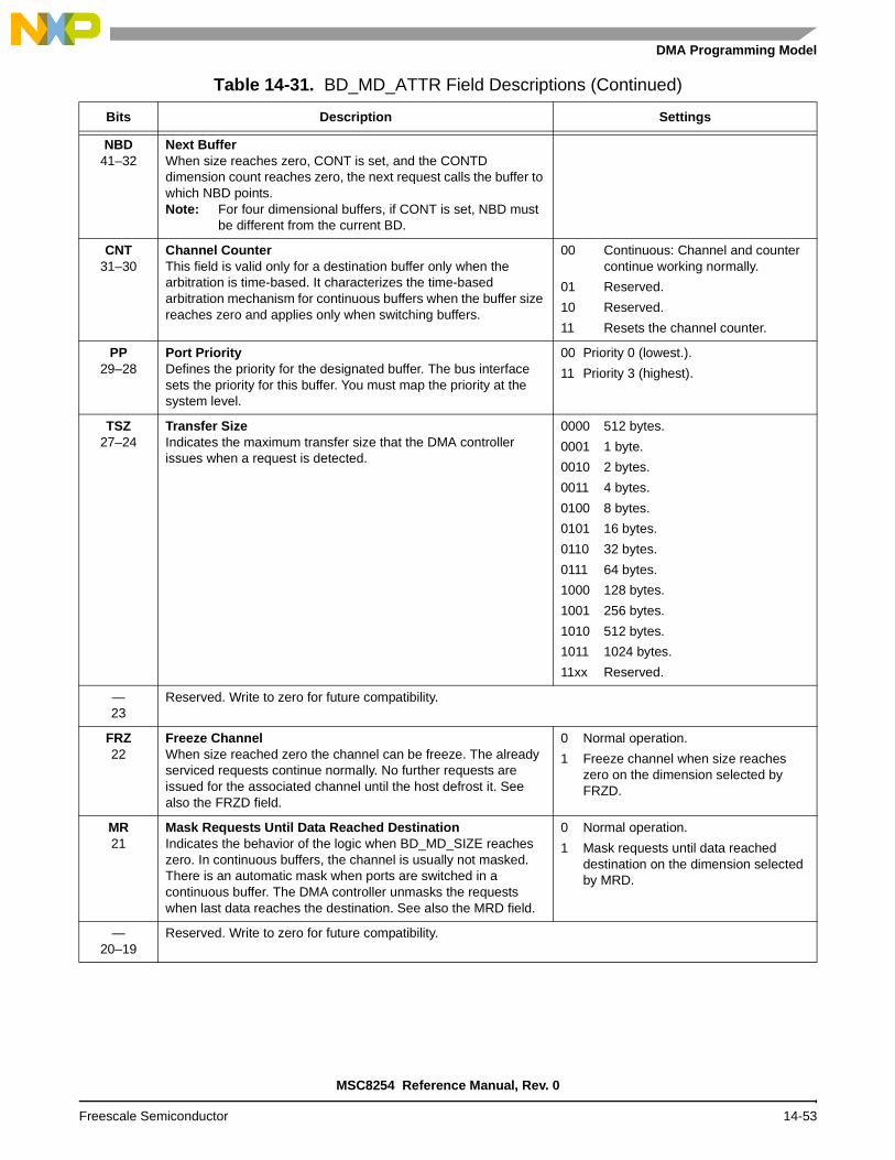
DMA Programming Model
NBD41–32
Next BufferWhen size reaches zero, CONT is set, and the CONTD dimension count reaches zero, the next request calls the buffer to which NBD points.Note: For four dimensional buffers, if CONT is set, NBD must
be different from the current BD.
CNT31–30
Channel CounterThis field is valid only for a destination buffer only when the arbitration is time-based. It characterizes the time-based arbitration mechanism for continuous buffers when the buffer size reaches zero and applies only when switching buffers.
00 Continuous: Channel and counter continue working normally.
01 Reserved.
10 Reserved.
11 Resets the channel counter.
PP29–28
Port PriorityDefines the priority for the designated buffer. The bus interface sets the priority for this buffer. You must map the priority at the system level.
00 Priority 0 (lowest.).
11 Priority 3 (highest).
TSZ27–24
Transfer SizeIndicates the maximum transfer size that the DMA controller issues when a request is detected.
0000 512 bytes.
0001 1 byte.
0010 2 bytes.
0011 4 bytes.
0100 8 bytes.
0101 16 bytes.
0110 32 bytes.
0111 64 bytes.
1000 128 bytes.
1001 256 bytes.
1010 512 bytes.
1011 1024 bytes.
11xx Reserved.
—23
Reserved. Write to zero for future compatibility.
FRZ22
Freeze ChannelWhen size reached zero the channel can be freeze. The already serviced requests continue normally. No further requests are issued for the associated channel until the host defrost it. See also the FRZD field.
0 Normal operation.
1 Freeze channel when size reaches zero on the dimension selected by FRZD.
MR21
Mask Requests Until Data Reached DestinationIndicates the behavior of the logic when BD_MD_SIZE reaches zero. In continuous buffers, the channel is usually not masked. There is an automatic mask when ports are switched in a continuous buffer. The DMA controller unmasks the requests when last data reaches the destination. See also the MRD field.
0 Normal operation.
1 Mask requests until data reached destination on the dimension selected by MRD.
—20–19
Reserved. Write to zero for future compatibility.
Table 14-31. BD_MD_ATTR Field Descriptions (Continued)
Bits Description Settings
MSC8254 Reference Manual, Rev. 0
Freescale Semiconductor 14-53

Direct Memory Access (DMA) Controller
BTSZ18–16
Basic Transfer SizeThe basic transfer size issued by the request. If BTSZ is greater than TSZ, the DMA controller uses the TSZ value.
000 64 bytes.
001 1 byte.
010 2 bytes.
011 4 bytes.
100 8 bytes.
101 16 bytes.
110 32 bytes.
111 64 bytes.
—15–11
Reserved. Write to zero for future compatibility.
LAST10
Last Buffer In ChainSet this bit only to avoid an endless task condition when CONT is set and CONTD is smaller than BD.
0 Not the last buffer in the chain.
1 Last buffer in the chain.
BD9–8
Buffer DimensionIndicates the dimension of the buffer.
00 1 dimension.
01 2 dimensions.
10 3 dimensions.
11 4 dimensions.
SSTD7–6
Set Status DimensionWhen BD_MD_SIZE reaches zero and BD_MD_ATTR[SST] = 1, the status bit is set for the channel in DMASTR. For details, see page 14-40. The SSTD field defines the dimension on which the status bit is set.
00 BD_MD_SIZE reached zero, 1D.
01 M2D_COUNT reached zero, 2D.
10 M3D_COUNT reached zero, 3D.
11 M4D_COUNT reached zero, 4D.
FRZD5–4
Freeze DimensionWhen the selected dimension is processed, the internal logic masks all channel requests and freezes the channel. The host must defrost the channel for further service.This field is valid only if FRZ is set in the BD_MD_ATTR.
00 Mask and freeze channel when first dimension ends.
01 Mask and freeze channel when second dimension ends.
10 Mask and freeze channel when third dimension ends.
11 Mask and freeze channel when fourth dimension ends.
CONTD3–2
Continuous Buffer Mode Dimension SelectIndicates the dimension after which the channel switches to the next multi-dimensional BD. This field is valid only if CONT is set in the BD_MD_ATTR.Notes: 1. The value must not be greater than BD.
2. When NBD is equal to the current BD and CONT is set, CONTD must equal BD.
3. If CONT is set and CONTD < BD, the BD area is updated by the DMA controller. Do not access this area until the DMA task is completed.
4. If CONT is set, CONTD < BD, and NPRT is different from the current port, MR must be set an MRD must be equal to CONTD.
00 Switch to next BD when BD_MD_SIZE reaches zero, 1D
01 Switch to next BD when M2D_COUNT reaches zero, 2D.
10 Switch to next BD when M3D_COUNT reaches zero, 3D.
11 Switch to next BD when M4D_COUNT reaches zero, 4D.
Table 14-31. BD_MD_ATTR Field Descriptions (Continued)
Bits Description Settings
MSC8254 Reference Manual, Rev. 0
14-54 Freescale Semiconductor

DMA Programming Model
MRD1–0
Mask Requests DimensionIndicates the dimension after which the channel masks requests until the data reaches its destination. This field is valid only if MR is set in the BD_MD_ATTR.
00 Mask requests when BD_MD_SIZE reaches zero, 1D.
01 Mask requests when M2D_COUNT reaches zero, 2D.
10 Mask requests when M3D_COUNT reaches zero, 3D.
11 Mask requests when M4D_COUNT reaches zero, 4D.
Table 14-32. BD_MD_2D Field Descriptions
Bits Description
M2D_COUNT51–40
Second Dimension Current CountDecrements each time the BD_MD_SIZE reaches zero. The field is reloaded with the M2D_BCOUNT each time it reaches zero.Note: If the buffer is two dimensional or more, this field cannot be 0.
M2D_BCOUNT39–28
Second Dimension Base CountHolds the second dimension base count.Note: If the buffer is more than two dimensional, this field cannot be 0.
M2D_OFFSET27–0
Second Dimension OffsetWritten in two’s complement. The offset is added to the BD_MD_ADDR each time BD_MD_SIZE reaches zero.
Table 14-33. BD_MD_3D Field Descriptions
Bits Description
M3D_COUNT51–40
Third Dimension Current CountDecrements each time the BD_MD_SIZE and M2D_COUNT reach zero. The field is reloaded with the M3D_BCOUNT each time it reaches zero.Note: If the buffer is three dimensional or more, this field cannot be 0.
M3D_BCOUNT39–28
Third Dimension Base CountHolds the third dimension base count.Note: If the buffer is more than three dimensional, this field cannot be 0.
M3D_OFFSET27–0
Third Dimension OffsetWritten in two’s complement. The offset is added to the BD_MD_ADDR each time BD_MD_SIZE and M2D_COUNT reach zero.
Table 14-34. BD_MD_4D Field Descriptions
Bits Description
M4D_COUNT39–28
Fourth Dimension Current CountDecrements each time BD_MD_SIZE, M2D_COUNT, and M3D_COUNT reach zero. Note: If the buffer is four dimensional, then this field cannot be 0.
M4D_OFFSET27–0
Fourth Dimension OffsetWritten in two’s complement. The offset is added to the BD_MD_ADDR each time BD_MD_SIZE, M2D_COUNT, and M3D_COUNT reach zero.
Table 14-31. BD_MD_ATTR Field Descriptions (Continued)
Bits Description Settings
MSC8254 Reference Manual, Rev. 0
Freescale Semiconductor 14-55

Direct Memory Access (DMA) Controller
MSC8254 Reference Manual, Rev. 0
14-56 Freescale Semiconductor

High Speed Serial Interface (HSSI) Subsystem 15The High Speed Serial Interface (HSSI) is a 8-port serial communication subsystem that supports the following multiplexed serial interface combinations:
Two x1/x4 Serial RapidIO ports
One x1/x4 Serial RapidIO ports, one x1 Serial RapidIO port, and two SGMII ports
One x1/x4 Serial RapidIO port and a PCI Express port
One x1/x4 Serial RapidIO port, two SGMII ports, and a PCI Express port
To support these interfaces, the HSSI includes the following blocks:
One RapidIO controller with two ports and one RapidIO Messaging Unit (RMU)
One PCI Express controller with a bridge to the OCN fabric.
One 8-port OCN fabric with two DMA controllers to connect between the RapidIO and PCI Express controllers and the system CLASS module
Two OCN-to-MBus (O2M) bridges to link the HSSI to the system CLASS module
Two SRIO port controllers to link the RMU and OCN fabric to the SerDes ports.
Two SerDes interfaces to connect to the external signal interface.
These communication interfaces allow the cores to execute the data processing code and be relieved from the data transfer and handling overhead for processing serial data flow.
This chapter describes the communication interface components which include the following:
OCN fabric
DMA controllers
OCN-to-MBus bridges
SRIO interface modules
SerDes interfaces
MSC8254 Reference Manual, Rev. 0
Freescale Semiconductor 15-1

High Speed Serial Interface (HSSI) Subsystem
This chapter includes the interface component programming model, with the exception of the SerDes multiplexing programming, which is done using the S1P and S2P bits in the low half of the reset configuration word (RCW), as described in Chapter 5, Reset. The communication controllers supported within the block are described in Chapter 16, Serial RapidIO Controller and Chapter 17, PCI Express Controller. While the SGMII lines are multiplexed through the SerDes interfaces, they are functionally part of the QUICC Engine subsystem, as described in Chapter 18, QUICC Engine Subsystem.
15.1 HSSI Subsystem Block Diagram
Figure 15-1 shows a block diagram of the HSSI.
Figure 15-1. HSSI Block Diagram
OCN Fabric
Port1
Port 3
Port 2 Port 6Port 5
Port 4Port 0 Port 7
RMU SRIO0 SRIO1 PCI Express
PCI Expressto OCN Bridge
SerDes2 PHY2PHY1SerDes1
OCNDMA0
DMA to OCNBridge
OCNDMA1
DMA to OCNBridge
OCN to MBusBridge 0
OCN to MBusBridge 1
HSSI to MBus Bridge
Serial RapidIO x1/x4 Interfacex1/x2/x4 PCI-Express
Serial RapidIO x1/x4 InterfaceTwo SGMII
QU
ICC
Eng
ine
Sub
syst
em
HSSI
QU
ICC
Engine S
ubsystem
Two SGMII
Notes: 1. The actual signals multiplexed for each PHY is determined by the SerDes configuration field contents in the lower 32 bits of the reset configuration word, which are recorded in RCWLR[S1P] and RCWLR[S2P]. See Chapter 5, Reset for details.
2. You must distribute the access loading between O2M0 (Port 1) and O2M1 (Port 5) for optimal performance. Although the internal OCN arbiters attempt to balance access automatically, these ports can be configured to work specifically with individual RapidIO inbound windows (see Section 16.6.58 for details) and PCI Express inbound windows (see Section 17.4.1.4.13 for details).
MSC8254 Reference Manual, Rev. 0
15-2 Freescale Semiconductor

OCN Fabric
15.2 OCN Fabric
The On-Chip Network (OCN) fabric is a non-blocking high speed interconnect used for embedded system devices. The MSC8156E DSP HSSI uses an 8-port OCN to connect between the Serial RapidIO Controller, the PCI Express controller, the two supporting DMA controllers and the dual x4 SerDes PHYs. The OCN requires no programming and provides a seamless interface for the HSSI.
The OCN arbitration for each OCN target port is based on the following two stages of “least recently used” decisions:
Stage 1 selects the least recently used source from among all different sources with the same priority level. This is done for each of the four possible priority levels, yielding up to four “winners” (one for each priority level).
Stage 2 selects the least recently used source from the four winners of stage 1.
Using this method prevents starvation of a lower priority source, since older source will win over newer source which have a higher priority.
As an example, given a case of two OCN sources (A and B) that are constantly targeting the same OCN port (C), one source (A) is using only priority 0 and the other one (B) is using only priority 1. Each decision cycle, the priority 0 winner is source A, and the priority 1 winner is source B. The next stage winner alternates between A and B. Therefore, the order of the final winners of the arbitration are A, B, A, B, and so on, regardless of the fact that B has the higher priority.
MSC8254 Reference Manual, Rev. 0
Freescale Semiconductor 15-3

High Speed Serial Interface (HSSI) Subsystem
15.3 DMA ControllersThe MSC8254 includes two dedicated DMA controllers that transfer blocks of data between the serial RapidIO controller and the PCI Express controller and the local address space independent from the DSP cores. Figure 15-1 shows the block diagram of each dedicated DMA controller.
Figure 15-2. Interface Dedicated DMA Controller Block Diagram
CHN 0 CHN 1 CHN 2 CHN 3
Arbitration and Bandwidth Control
Source
Controls
Destination
Controls
AddressAddress
Address
ControlsTenure
Data
ControlsTenure
HSSI Data Interface
Dedicated DMA Controllers
Local Space
to Support the RapidIOand PCI Express Interfaces
MSC8254 Reference Manual, Rev. 0
15-4 Freescale Semiconductor

DMA Controllers
15.3.1 Overview
Each dedicated DMA controller has four high-speed DMA channels. Each of the DSP cores can initiate DMA transfers. All channels are capable of complex data movement and advanced transaction chaining. Operations, such as descriptor fetches and block transfers, are initiated by each channel. A channel is selected by the arbitration logic and information is passed to the source and destination control blocks for processing. The source and destination blocks generate read and write requests to the address tenure engine, which manages the DMA master port address interface. After a transaction is accepted by the master port, control is transferred to the data tenure engine that manages the read and write data transfers. A channel remains active in the shared resources for the duration of the data transfer unless the allotted bandwidth per channel is reached.
15.3.2 Features
Each dedicated DMA controller offers the following features:
Four high-speed/high-bandwidth channels accessible by local and remote masters
Basic DMA operation modes (direct, simple chaining)
Extended DMA operation modes (advanced chaining and stride capability)
Cascading descriptor chains
Misaligned transfers
Programmable bandwidth control between channels
Up to 256 bytes for DMA sub-block transfers to maximize performance
Three priority levels supported for source and destination transactions
Interrupt on error and completed segment, list, or link
An Address Translation Management Unit (ATMU) with 10 local access address windows. The ATMU translates a request address into a logical device source/destination.
15.3.3 Modes of Operation
Each MSC8254 dedicated DMA controller has two modes of operation: basic and extended. Basic mode is the DMA legacy mode. It does not support advanced features. Extended mode supports advanced features like striding and flexible descriptor structures.
These two basic modes allow users to initiate and end DMA transfers in various ways. Table 15-1 summarizes the relationship between the modes and the following features:
Direct mode. No descriptors are involved. Software must initialize the required fields as described in Table 15-1 before starting a transfer.
Chaining mode. Software must initialize descriptors in memory and the required fields as described in Table 15-1 before starting a transfer.
MSC8254 Reference Manual, Rev. 0
Freescale Semiconductor 15-5

High Speed Serial Interface (HSSI) Subsystem
Single-write start mode. The DMA process can be started by using a single-write command to either the descriptor address register in one of the chaining modes or the source/destination address registers in one of the direct modes.
External control capability. This allows an external agent to start, pause, and check the status of a DMA transfer that has already been initialized.
Channel continue capability. The channel continue capability allows software the flexibility of having the DMA controller start with descriptors that have already been programmed while software continues to build more descriptors in memory.
Channel abort capability. The software can abort a previously initiated transfer by setting the bit MRn[CA]. The DMA controller terminates all outstanding transfers initiated by the channel without generating any errors before entering an idle state.
(Refer to Section 15.4, Functional Description for details on these modes. Figure 15-3 shows the general DMA operational flow chart.
Figure 15-3. DMA Operational Flow Chart
Table 15-1. Relationship of Modes and Features
Mode Mode with One Additional Feature Mode with Two Additional Features
B (Basic) BD (basic direct) BDS (BD single-write start)BC (basic chaining) BCS (BC single-write start)
Ext (Extended) ExtD (extended direct) ExtDS (ExtD single-write start)ExtC (extended chaining) ExtCS (ExtC single-write start)
Software Sets 1st Link
Process Link
Last Link?Is NY
N
Chain or Extended
Done — DMA Halts
Y
Is
Last List?
N
Y
Advance List
Advance
Mode?
In
Link
MSC8254 Reference Manual, Rev. 0
15-6 Freescale Semiconductor

Functional Description
15.4 Functional Description
This section describes the function of the DMA controller.
15.4.1 DMA Channel Operation
All DMA channels support two different modes of operation, a basic mode (MRn[XFE] = 0) and an extended mode (MRn[XFE] = 1). In both modes, a channel can be activated by clearing and setting MRn[CS] or through the single-write start mode using MRn[CDSM/SWSM] and MRn[SRW].
In basic mode, the channel can be programmed in basic direct mode or basic chaining mode. In extended mode, the channel can be programmed in extended direct mode or extended chaining mode. Extended mode provides more capabilities, such as extended descriptor chaining, striding capabilities, and a more flexible descriptor structure.
The DMA controller supports misaligned transfers for both the source and destination addresses. In order to maximize performance, the source and destination engines issue one or more transactions to reach the desired alignment based on the rules described in Section 15.4.1.1. The DMA always reads/writes the maximum number of bytes for a given transfer as described by the capability inputs of the DMA controller. Using 256 bytes over the RapidIO interface reduces packet overhead that translates to increased bandwidth utilization through the interface.
The DMA controller supports bandwidth control, which prevents a channel from consuming all the data bandwidth in the controller. Each channel is allowed to consume the bandwidth of the shared resources as specified by the bandwidth control value. After the channel uses its allotted bandwidth, the arbiter grants the next channel access to the shared resources. The arbitration is round robin between the channels. This feature is also used to implement the external control pause feature. If the external control start and pause are enabled in the MRn, the channel enters a paused state after transferring the data described in the bandwidth control. External control can restart the channel from a paused state.
The DMA controller is designed to support RapidIO transaction types, including various priority level support. The DMA controller offers reads that can be mapped to non-coherent (NREAD) or maintenance reads. In addition, the writes can be mapped to non-coherent (NWRITE, NWRITE_R, SWRITE) writes and maintenance writes. The DMA programming model permits software to program each DMA engine independently to interrupt on completed segment, chain, or error. It also provides the capability for software to resume the DMA engine from a hardware halted condition by setting the channel continue bit, MRn[CC]. See Table 15-2 for more complete descriptions of the channel states and state transitions.
15.4.1.1 Source/Destination Transaction Size Calculations
The DMA controller may issue smaller transactions from the source and destination address engines in an effort to reach alignment for improved performance. The flow chart in Figure 15-4
MSC8254 Reference Manual, Rev. 0
Freescale Semiconductor 15-7
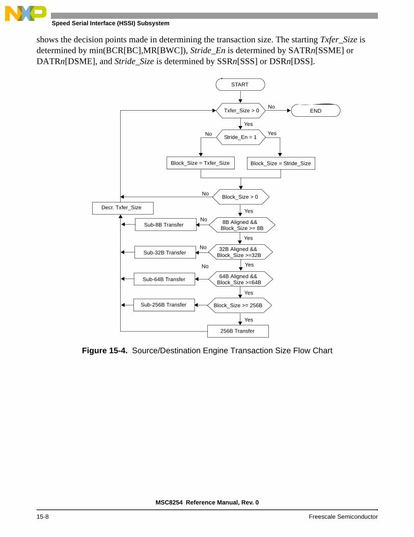
High Speed Serial Interface (HSSI) Subsystem
shows the decision points made in determining the transaction size. The starting Txfer_Size is determined by min(BCR[BC],MR[BWC]), Stride_En is determined by SATRn[SSME] or DATRn[DSME], and Stride_Size is determined by SSRn[SSS] or DSRn[DSS].
Figure 15-4. Source/Destination Engine Transaction Size Flow Chart
START
Txfer_Size > 0
Stride_En = 1
Yes
Block_Size = Txfer_Size Block_Size = Stride_Size
YesNo
Block_Size > 0No
Yes
8B Aligned &&NoSub-8B Transfer
Yes
64B Aligned &&
No
Sub-64B Transfer
Yes
Block_Size >= 256BSub-256B Transfer
Yes
256B Transfer
Block_Size >= 8B
Block_Size >=64B
Decr. Txfer_Size
32B Aligned &&Block_Size >=32B
Yes
NoSub-32B Transfer
ENDNo
MSC8254 Reference Manual, Rev. 0
15-8 Freescale Semiconductor

Functional Description
For example if BCR[BC} = 512 bytes and MR[BWC] = 256 bytes, reading from starting address 0x5D0 will result in the following transaction sizes:
-- Channel Arbitration --0x5D0 - 16 bytes0x5E0 - 32 bytes0x600 - 128 bytes0x680 - 64 bytes0x6C0 - 16 bytes-- Channel Arbitration --0x6D0 - 16 bytes0x6E0 - 32 bytes0x700 - 128 bytes0x780 - 64 bytes0x7C0 - 16 bytes
In this example, the bandwidth control limits the channel from ever reaching the maximum transaction size of 256 bytes. Software should align addresses or increase the available bandwidth for best performance
15.4.1.2 Basic DMA Mode Transfer
This mode is primarily included for backward compatibility with existing DMA controllers which use a simple programming model. This is the default mode out of reset. The different modes of operation under the basic mode are explained in the following sections.
15.4.1.2.1 Basic Direct Mode
In basic direct mode, the DMA controller does not read descriptors from memory, but instead uses the current parameters programmed in the DMA registers to start the DMA transfer. Software is responsible for initializing SARn, SATRn, DARn, DATRn, and BCRn registers. The DMA transfer is started when MRn[CS] is set. Software is expected to program all the appropriate registers before setting MRn[CS] to a 1. The transfer is finished after all the bytes specified in the byte count register have been transferred or if an error condition occurs. The sequence of events to start and complete a transfer in basic direct mode is as follows:
1. Poll the channel state (see Table 15-2), to confirm that the specific DMA channel is idle.
2. Initialize SARn, SATRn, DARn, DATRn and BCRn.
3. Set the mode register channel transfer mode bit, MRn[CTM], to indicate direct mode. Other control parameters may also be initialized in the mode register.
4. Clear then set the mode register channel start bit, MRn[CS], to start the DMA transfer.
5. SRn[CB] is set by the DMA controller to indicate the DMA transfer is in progress.
MSC8254 Reference Manual, Rev. 0
Freescale Semiconductor 15-9

High Speed Serial Interface (HSSI) Subsystem
6. SRn[CB] is automatically cleared by the DMA controller after the transfer is finished, or if the transfer is aborted (MRn[CA] transitions from a 0 to 1), or if a transfer error occurs.
7. End of segment interrupt is generated if MRn[EOSIE] is set.
15.4.1.2.2 Basic Direct Single-Write Start Mode
In basic direct single-write start mode, the DMA controller does not read descriptors from memory, but instead uses the current parameters programmed in the DMA registers to start the DMA transfer. Software is responsible for initializing the SATRn, DATRn, and BCRn registers. Setting MRn[SRW] configures the DMA controller to begin the DMA transfer either when SARn is written or when DARn is written, determined by the state of MRn[CDSM/SWSM]. Writing to SARn initiates the DMA transfer if MRn[CDSM/SWSM] is set. Writing to DARn initiates the DMA transfer if MRn[CDSM/SWSM] is cleared. The DMA controller automatically sets the channel start bit, MRn[CS]. Software is expected to program all the appropriate registers before writing the source or destination address registers. The transfer is finished after all the bytes specified in the byte count register have been transferred or if an error condition occurs. The sequence of events to start and complete a transfer in single-write start basic direct mode is as follows:
1. Poll the channel state (see Table 15-2), to confirm that the specific DMA channel is idle.
2. Initialize the source attributes (SATRn), DATRn, and BCRn registers.
3. Set the mode register channel transfer mode bit, MRn[CTM], and the single-write start direct mode bit, MRn[SRW]. Other control parameters may also be initialized in the mode register. Set MRn[CDSM/SWSM] for transfers started using SARn. Clear MRn[CDSM/SWSM] for transfers started using the DARn.
4. A write to the source or destination address register starts the DMA transfer and automatically sets MRn[CS].
5. SRn[CB] is set by the DMA controller to indicate the DMA transfer is in progress.
6. SRn[CB] is automatically cleared by the DMA controller after the transfer is finished, or if the transfer is aborted (MRn[CA] transitions from a 0 to 1), or if a transfer error occurs.
7. End of segment interrupt is generated if MRn[EOSIE] is set.
15.4.1.2.3 Basic Chaining Mode
In basic chaining mode, software must first build link descriptor segments in memory. Then the current link descriptor address register must be initialized to point to the first descriptor in memory. The DMA controller loads descriptors from memory prior to a DMA transfer. The DMA controller begins the transfer according to the link descriptor information loaded for the
MSC8254 Reference Manual, Rev. 0
15-10 Freescale Semiconductor

Functional Description
segment. After the current segment is finished, the DMA controller reads the next link descriptor from memory and begins another DMA transfer. The transfer is finished if the current link descriptor is the last one in memory or if an error condition occurs. The sequence of events to start and complete a transfer in chaining mode is as follows:
1. Build link descriptor segments in memory.
2. Poll the channel state (see Table 15-2), to confirm that the specific DMA channel is idle.
3. Initialize CLNDARn to point to the first link descriptor in memory.
4. Clear the mode register channel transfer mode bit, MRn[CTM], as well as MRn[XFE], to indicate basic chaining mode. Other control parameters may also be initialized in the mode register.
5. Clear, then set the mode register channel start bit, MRn[CS], to start the DMA transfer.
6. SRn[CB] is set by the DMA controller to indicate the DMA transfer is in progress.
7. SRn[CB] is automatically cleared by the DMA controller after finishing the transfer of the last descriptor segment, or if the transfer is aborted (MRn[CA] transitions from a 0 to 1), or if an error occurs during any of the transfers.
15.4.1.2.4 Basic Chaining Single-Write Start Mode
Basic chaining single-write start mode allows a chain to be started by writing the current link descriptor address register (CLNDARn). Setting MRn[CDSM/SWSM] in the mode register causes MRn[CS] to be automatically set when the current link descriptor address register is written. The sequence of events to start and complete a chain using single-write start mode is as follows:
1. Set the mode register current descriptor start mode bit MRn[CDSM/SWSM]. Clear the extended features enable bit MRn[XFE] and the channel transfer mode bit, MRn[CTM]. This initialization indicates basic chaining and single-write start mode. Also other control parameters may be initialized in the mode register.
2. Build link descriptor segments in memory.
3. Poll the channel state (see Table 15-2), to confirm that the specific DMA channel is idle.
4. Initialize CLNDARn to point to the first descriptor segment in memory. This write automatically causes the DMA controller to begin the link descriptor fetch and set MRn[CS].
5. SRn[CB] is set by the DMA controller to indicate the DMA transfer is in progress.
6. SRn[CB] is automatically cleared by the DMA controller after finishing the transfer of the last descriptor segment, or if the transfer is aborted (MRn[CA] transitions from a 0 to 1), or if an error occurs during any of the transfers.
MSC8254 Reference Manual, Rev. 0
Freescale Semiconductor 15-11

High Speed Serial Interface (HSSI) Subsystem
15.4.1.2.5 Extended DMA Mode Transfer
The extended DMA mode also operates in chaining and direct mode. It offers additional capability over the basic mode by supporting striding and a more flexible descriptor structure. This additional functionality also requires a new and more complex programming model. The extended DMA mode is activated by setting MRn[XFE].
15.4.1.2.6 Extended Direct Mode
Extended direct mode has the same functionality as basic direct mode with the addition of stride capabilities. The bit settings are the same as in direct mode with the exception of the MRn[XFE] being set. Striding on the source address can be accomplished by setting SATRn[SSME] and setting the desired stride size and distance in SSRn. Striding on the destination address can be accomplished by setting DATRn[DSME] and setting the desired stride size and distance in DSRn.
15.4.1.2.7 Extended Direct Single-Write Start Mode
Extended direct single-write start mode has the same functionality as the basic direct single-write start mode with the addition of stride capabilities. The bit settings are also the same with the exception of MRn[XFE] being set. Striding on the source address can be accomplished by setting SATRn[SSME] and setting the desired stride size and distance in SSRn. Striding on the destination address can be accomplished by setting DATRn[DSME] and setting the desired stride size and distance in DSRn.
15.4.1.2.8 Extended Chaining Mode
In extended chaining mode, the software must first build list and link descriptor segments in memory. Then CLSDARn must be initialized to point to the first list descriptor in memory. The DMA controller loads list descriptors and link descriptors from memory prior to a DMA transfer. The DMA controller begins the transfer according to the link descriptor information loaded. Once the current link descriptor is finished, the DMA controller reads the next link descriptor from memory and begins another DMA transfer. If the current link descriptor is the last in the list, the DMA controller reads the next list descriptor in memory. The transfer is finished if the current link descriptor is the last one in the last list in memory or if an error condition occurs. The sequence of events to start and complete a transfer in extended chaining mode is as follows:
1. Build link and list descriptor segments in memory.
2. Poll the channel state (see Table 15-2), to confirm that the specific DMA channel is idle.
3. Initialize CLSDARn to point to the first list descriptor in memory.
MSC8254 Reference Manual, Rev. 0
15-12 Freescale Semiconductor

Functional Description
4. Clear the mode register channel transfer mode bit, MRn[CTM], to indicate chaining mode. MRn[XFE] must be set to indicate extended DMA mode. Other control parameters may also be initialized in the mode register.
5. Clear, then set the mode register channel start bit, MRn[CS], to start the DMA transfer.
6. SRn[CB] is set by the DMA controller to indicate the DMA transfer is in progress.
7. SRn[CB] is automatically cleared by the DMA controller after finishing the transfer of the last descriptor segment, or if the transfer is aborted (MRn[CA] transitions from a 0 to 1), or if an error occurs during any of the transfers.
15.4.1.2.9 Extended Chaining Single-Write Start Mode
In the extended mode, the single-write start feature allows a chain to be started by writing the current list descriptor pointer. Setting MRn[CDSM/SWSM] causes MRn[CS] to be set automatically when CLSDARn is written. The sequence of events to start and complete an extended chain using single-write start mode is as follows:
1. Set MRn[CDSM/SWSM], MRn[CTM], and MRn[XFE] to indicate extended chaining and single-write start mode. Also other control parameters may be initialized in the mode register.
2. Build list and link descriptor segments in local memory.
3. Poll the channel state (see Table 15-2), to confirm that the specific DMA channel is idle.
4. Initialize the current list descriptor address register to point to the first list descriptor segment in memory. This write automatically causes the DMA controller to begin the list descriptor fetch and set MRn[CS].
5. SRn[CB] is set by the DMA controller to indicate the DMA transfer is in progress.
6. SRn[CB] is automatically cleared by the DMA controller after finishing the transfer of the last descriptor segment, or if the transfer is aborted (MRn[CA] transitions from a 0 to 1), or if an error occurs during any of the transfers.
15.4.1.3 Channel Continue Mode for Cascading Transfer Chains
The channel continue mode (enabled when MRn[CC] is set) offers software the flexibility of having the DMA controller get started on descriptors that have already been programmed while software continues to build more descriptors in memory. Software can set the end-of-links descriptor (EOLND) in basic mode, or end-of-lists descriptor (EOLSD) in extended mode, to cause the channel to go into a halted state while software continues to build other descriptors in memory. Software can then set CC to force hardware to continue where it left off. channel continue is only meaningful for chaining modes, not direct mode.
MSC8254 Reference Manual, Rev. 0
Freescale Semiconductor 15-13

High Speed Serial Interface (HSSI) Subsystem
If CC is set by software while the channel is busy with a transfer, the DMA controller finishes all transfers until it reaches the EOLND in basic mode or EOLSD in extended mode. The DMA controller then refetches the last link descriptor in basic mode, or the last list descriptor in extended mode and clears the channel continue bit. If EOLND or EOLSD is still set for their respective modes, the DMA controller remains in the idle state. If EOLND or EOLSD is not set, the DMA controller continues the transfer by refetching the new descriptor.
If CC is set by software while the channel is not busy with a transfer, the DMA controller refetches the last link descriptor in basic mode, or the last list descriptor in extended mode and clears the channel continue bit. If EOLND or EOLSD is still set for their respective modes, the DMA controller remains in the idle state. If the EOLND or EOLSD bits are not set, the DMA controller continues the transfer by refetching the new descriptor.
15.4.1.3.1 Basic Mode
On a channel continue, the descriptor at the current link descriptor address register (CLNDARn) is refetched to get the next link descriptor address field as updated by software. The channel halts if NLNDARn[EOLND] is still set. If EOLND is zero, the next link descriptor address is copied into CLNDARn and the channel continues with another descriptor fetch of the current link descriptor address. As a result, two link descriptor fetches always exist after channel continue before starting the first transfer.
15.4.1.3.2 Extended Mode
On a channel continue, the descriptor at the current list descriptor (CLSDARn) address register is refetched to get the next list descriptor address field as updated by software. The channel halts if NLSDARn[EOLSD] is still set. If not, the next list descriptor address is copied into the CLSDARn register and the channel continues with another descriptor fetch of the current list descriptor address. As a result, two list descriptor fetches always exist after channel continue before the first link descriptor fetch and the first transfer.
15.4.1.4 Channel Abort
Software can abort a previously initiated transfer by setting MRn[CA]. Once the DMA channel controller detects a zero-to-one transition of MRn[CA], it finishes the current sub-block transfer and halts all further activity. The controller then waits for all previously initiated transfers from the specified channel to drain and clears SRn[CB]. Successful completion of a software initiated abort request can be recognized by MRn[CA] being set and SRn[CB] being cleared. Obviously, if the controller was already halted because of an error condition (SRn[TE] is set), or the channel has completed all transfers, then SRn[CB] being cleared may not signify that the controller entered a halt state due to the abort request.
MSC8254 Reference Manual, Rev. 0
15-14 Freescale Semiconductor

Functional Description
15.4.1.5 Bandwidth Control
MRn[BWC] specifies how much data to allow a specific channel to transfer before allowing the next channel to use the shared data transfer hardware. This promotes equitable bandwidth allocation between channels. However, if only one channel is busy, hardware overrides the specified bandwidth control size value. The DMA controller allows a channel to transfer up to 1 Kbyte at a time when no other channel is active. The maximum that any channel will transfer before re-arbitration is 1 Kbyte.
15.4.1.6 Channel State
Table 15-2 defines the state of a channel based on the values of the channel start (MRn[CS]), channel busy (SRn[CB]), transfer error (SRn[TE]), and channel continue (MRn[CC]) bits.
15.4.1.7 Illustration of Stride Size and Stride Distance
If operating in stride mode, the stride size defines the amount of data to transfer before jumping to the next quantity of data as specified by the stride distance. The stride distance is added to the current base address to point to the next quantity of data to be transferred. Figure 15-5 illustrates the stride size and distance parameters. As shown, each time the stride distance is added to the base address, the resulting address becomes the new base address. This sequence repeats until the amount of data transferred equals the transfer size.
Table 15-2. Channel State Table
MRn[CS] SRn[CB] SRn[TE] MRn[CC] Channel State
0 0 0 0 Idle state. This is the state of the bits out of reset.
0 0 0 1 Channel continue unexpected. Channel remains idle
0 0 1 0 Error occurred after software halted the channel.
0 0 1 1 Channel Continue unexpected. Channel remains in error halt state
0 1 0 0 Software halted channel. The channel was busy and software cleared MRn[CS].
0 1 0 1 Channel remains in halt state.
— 1 1 — The channel has encountered an error condition and it is trying to halt.
1 0 0 0 Ready to start a transfer, or transfer completed
1 0 0 1 Continue transfer (only meaningful in chaining mode, not direct mode). In direct mode, the channel continue has no effect.
1 0 1 0 Error occurred during transfer
1 0 1 1 Channel remains in error halt state
1 1 0 0 Transfer in progress
1 1 0 1 Continue after reaching the end of list/link, or the first descriptor fetch after channel continue
MSC8254 Reference Manual, Rev. 0
Freescale Semiconductor 15-15

High Speed Serial Interface (HSSI) Subsystem
Figure 15-5. Stride Size and Stride Distance
15.4.2 DMA Transfer Interfaces
The DMA can be used to achieve data transfers across the entire memory map.
15.4.3 DMA Errors
On a transfer error (address mapping errors, for example), the DMA halts by setting SRn[TE] and generates an interrupt if MRn[EIE] is set. On a programming error, the DMA sets SRn[PE] and generates an interrupt if MRn[EIE] is set. The DMA controller detects the following programming errors:
Transfer started with a byte count of zero
Stride transfer started with a stride size of zero
Transfer started with a priority of three
Illegal type, defined by SATRn[SREADTTYPE] and DATRn[DWRITETTYPE], used for the transfer.
Stride Size
Stride Distance
Base Address New Base Address New Base Address
MSC8254 Reference Manual, Rev. 0
15-16 Freescale Semiconductor

Functional Description
15.4.4 DMA Descriptors
The DMA engine recognizes list descriptors and link descriptors. List descriptors connect lists of link descriptors. Link descriptors describe the DMA activity that is to take place. DMA descriptors are built in either local or remote memory and are connected by the next descriptor fields. Only link descriptors contain information for the DMA controller to transfer data. Software must ensure that each descriptor is 32-byte aligned. The last link descriptor in the last list in memory sets the EOLND bit in the next link descriptor; the next list descriptor fields indicating that these are the last descriptors in memory. Software initializes the current list descriptor address register to point to the first list descriptor in memory. The DMA controller traverses through the descriptor lists until the last link descriptor is met. For each link descriptor in the chain, the DMA controller starts a new DMA transfer with the control parameters specified by that descriptor.
Note: Software must ensure that each descriptor is aligned on a 32-byte boundary.
The last link descriptor in the last list in memory sets NLNDARn[EOLND] in the next link descriptor and NLSDARn[EOLSD] in the next list descriptor fields indicating that these are the last descriptors in memory. Software initializes the current list descriptor address register to point to the first list descriptor in memory. The DMA controller traverses through the descriptor lists until the last link descriptor is met as shown in. For each link descriptor in the chain, the DMA controller starts a new DMA transfer with the control parameters specified by that descriptor.
Table 15-3 summarizes the DMA list descriptors.
Table 15-4 summarizes the DMA link descriptors.
Table 15-3. List DMA Descriptor Summary
Descriptor Field Description
Next list descriptor extended address
Points to the next list descriptor in memory. After the DMA controller reads the descriptor from memory, this field is loaded into the next list descriptor extended address registers.
Next list descriptoraddress
Points to the next list descriptor in memory. After the DMA controller reads the descriptor from memory, this field is loaded into the next list descriptor address registers.
First link descriptor extended address
Points to the first link descriptor in memory for this list. After the DMA controller reads the descriptor from memory, this field is loaded into the current link descriptor extended address registers.
First link descriptor address
Points to the first link descriptor in memory for this list. After the DMA controller reads the descriptor from memory, this field is loaded into the current link descriptor address registers.
Source stride Contains the stride information used for the data source if striding is enabled for a link in the list
Destination stride Contains the stride information used for the data destination if striding is enabled for a link in the list
MSC8254 Reference Manual, Rev. 0
Freescale Semiconductor 15-17

High Speed Serial Interface (HSSI) Subsystem
Figure 15-6 shows the format of the list descriptors for 32-bit devices.
Note: For each channel (DMA controller 0 or 1, channels 0–3), the values written to the mode register determine how the DMA controller executes the data transfers, such as a simple direct transfer, a chain of direct transfers specified by a set of links, or a complex chain involving chained lists, each of which contains pointers to chained link sets (as indicated by Table 15-3 and Table 15-4). Figure 15-6 and Figure 15-7 show the order in which data should be stored in memory (for link descriptors and link descriptors, respectively); the name listed for each field indicates the register format to use for the data written to the specified offset. For example, Next List Descriptor Address refers to the Next List Descriptor Address Register (DnNLSDARx) for the specified DMA controller (n = 0 or 1) and the specific channel (x = 0–3). See the specified register description in Section 15.8, HSSI Programming Model for details.
Table 15-4. Link DMA Descriptor Summary
Descriptor Field Description
Source attributes register Contains source transaction attributes (SATR).
Source address Contains the source address of the DMA transfer. After the DMA controller reads the descriptor from memory, this field is loaded into the Source address register (SAR).
Destination attributes register
Contains destination transaction attributes (DATR).
Destination address Contains the destination address of the DMA transfer. After the DMA controller reads the descriptor from memory, this field is loaded into the destination address register (DAR).
Next link descriptor extended address
Points to the next link descriptor in memory. After the DMA controller reads the link descriptor from memory, this field is loaded into the extended next link descriptor address registers.
Next link descriptor address Points to the next link descriptor in memory. After the DMA controller reads the link descriptor from memory, this field is loaded into the next link descriptor address registers.
Byte count Contains the number of bytes to transfer. After the DMA controller reads the descriptor from memory, this field is loaded into the byte count register (BCR).
Offset Field
0x00 Reserved
0x04 Next List Descriptor Address
0x08 Reserved
0x0c First Link Descriptor Address
0x10 Source Stride
0x14 Destination Stride
0x18 Reserved
0x1c Reserved
Figure 15-6. List Descriptor Format (Used for 32-bit devices)
MSC8254 Reference Manual, Rev. 0
15-18 Freescale Semiconductor

Functional Description
Figure 15-7 shows the format of the link descriptors for 32-bit devices.
15.4.5 Local Access ATMU Registers
The local access ATMU has ten address windows that can map a DMA request to a programmable transaction interface (logical device). The user set up the ATMU windows correctly before enabling translation through the ATMU. In a multiple hit scenario, the first matching window is used. If no hit is detected or if mapping is to a reserved transaction interface, the source/target defaults to local address space.
Note: See Section 15.8.19, Local Access Window Base Address Registers 0–9 (DnLAWBAR[0–9]), on page 15-46 and Section 15.8.20, Local Access Window Attributes Registers 0–9 (DnLAWAR[0–9]), on page 15-47 for details.
15.4.6 Limitations and Restrictions
This section addresses some of the limitations and restrictions of the dedicated DMA controller and is intended to help software maximize the DMA performance and avoid DMA programming errors.
The DMA controller restrictions are as follows:
Due to the limited number of buffers that the DMA controller can use, stride sizes less than 64 bytes should be avoided. Maximum utilization is obtained from strides greater than or equal to 256 bytes. However, small stride sizes can be used for scatter-gather functions.
All interface capabilities from where descriptors are being fetched must support read sizes of 32 bytes or greater.
If MRn[SAHE] is set, the source interface transfer size capability must be greater than or equal to MRn[SAHTS]. The source address must be aligned to a size specified by SAHTS.
Offset Field
0x00 Source Attributes
0x04 Source Address
0x08 Destination Attributes
0x0c Destination Address
0x10 Reserved
0x14 Next Link Descriptor Address
0x18 Byte Count
0x1c Reserved
Figure 15-7. Link Descriptor Format (Used for 32-bit devices
MSC8254 Reference Manual, Rev. 0
Freescale Semiconductor 15-19

High Speed Serial Interface (HSSI) Subsystem
If MRn[DAHE] is set, the destination interface transfer size capability must be greater than or equal to MRn[DAHTS]. The destination address must be aligned to the size specified by DAHTS.
Destination striding is not supported if MRn[DAHE] is set and source striding is not supported if MRn[SAHE] is set.
If the DMA is programmed to send SWRITEs over RapidIO, the programmer must ensure that the destination address is double-word aligned and that the byte count is a double-word multiple.
A single DMA transfer in any of the direct or chaining modes must not cross a 16 GB (34-bit) address boundary.
MSC8254 Reference Manual, Rev. 0
15-20 Freescale Semiconductor

OCN-to-MBus (O2M) Bridges
15.5 OCN-to-MBus (O2M) Bridges
The O2M bridges provide an interface between the OCN fabric and the MBus interfaces that connect internally to the CLASS. The bridges support all mandatory MBus and OCN interface protocol procedures. The bridges provide initiator interfaces to access the target MBus, formats OCN packets, negotiates with the OCN arbiter, and transmits/receives associated transactions. Accesses are configurable as 32-byte or 64-byte transfers using the OCN-to-MBus Control Registers (O2MCR[0–1]) as described in Section 15.8.21.
15.6 SRIO Port Controller Modules (SRIOn)
The SRIO0 and SRIO1 modules provide an interface bridge between the RMU, the two serial RapidIO ports, and the two SerDes PHYs. The units require no programming, but transfers through the SRIO modules can be tracked by the performance monitor. See Section 25.3, Performance Monitor in Chapter 25, Debugging, Profiling, and Performance Monitoring for details.
15.7 SerDes PHY Interfaces
The HSSI includes two 4-port SerDes PHY interfaces that are multiplexed between the two Serial RapidIO ports, the PCI Express port, and the two SGMII ports from the QUICC Engine subsystem. Multiplexing configuration is done using the S1P and S2P fields in the RCWLR. See Section 5.3.1 in Chapter 5, Reset for multiplexing configuration details. Control of the individual lanes is done through the SRDS Control Register 2 described in Section 15.8.29.
15.8 HSSI Programming Model
The following sections describe the dedicated DMA controller 0 and 1 registers and the SerDes PHY interface control registers.
The majority of the DMA controller registers are channel-specific and can be identified by one of the four offsets that describe the register. These registers include the following:
Dn DMA 0–3 Mode Registers (DnMR[0–3]), page 15-24
Dn DMA 0–3 Status Registers (DnSR[0–3]), page 15-27
Dn DMA 0–3 Current Link Descriptor Extended Address Registers (DnECLNDAR[0–3], page 15-29
Dn DMA 0–3 Current Link Descriptor Address Registers (DnCLNDAR[0–3]), page 15-30
Dn DMA 0–3 Source Attributes Registers (DnSATR[0–3]), page 15-31
Dn DMA 0–3 Source Address Registers (DnSAR[0–3]), page 15-32
Dn DMA 0–3 Destination Attributes Registers (DnDATR[0–3]), page 15-33
MSC8254 Reference Manual, Rev. 0
Freescale Semiconductor 15-21

High Speed Serial Interface (HSSI) Subsystem
Dn DMA 0–3 Destination Address Registers (DnDAR[0–3]), page 15-34
Dn DMA 0–3 Byte Count Registers (DnBCR[0–3], page 15-35
Dn DMA 1–3 Next Link Descriptor Extended Address Registers (DnENLNDAR[0–3], page 15-36
Dn DMA 0–3 Next Link Descriptor Address Registers (DnNLNDAR[0–3]), page 15-37
Dn DMA 1–3 Current List Descriptor Extended Address Registers (DnECLSDAR[0–3], page 15-38
Dn DMA 0–3 Current List Descriptor Address Registers (DnCLSDAR[0–3]), page 15-39
Dn DMA 0–3 Next List Descriptor Extended Address Registers (DnENLSDAR[0–3], page 15-40
Dn DMA 0–3 Next List Descriptor Address Registers (DnNLSDAR[0–3]), page 15-41
Dn DMA 0–3 Source Stride Registers (DnSSR[0–3]), page 15-42
Dn DMA 0–3 Destination Stride Registers (DnDSR[0–3]), page 15-43
Dn DMA General Status Register (DnDGSR), page 15-44
Dn Local Access Window Base Address Registers 0–9 (DnLAWBAR[0–9]), page 15-46
Dn Local Access Window Attributes Registers 0–9 (DnLAWAR[0–9]), page 15-47
Note: The dedicated DMA Controller 0 (D0) registers use a base address of 0xFFFA8000. The dedicated DMA Controller 1 (D1) registers use a base address of 0xFFFAA000.
The OCN-to-MBus Control Registers use a set of registers in each bridge to control the data width of the burst transfers. The registers are:
OCN-to-MBus Configuration Registers 0–1 (O2MCR[0–1]), page 15-49
OCN-to-MBus Error Attribute Registers 0–1 (O2MEAR[0–1]), page 15-50
OCN-to-MBus Error Address Registers 0–1 (O2MEADR[0–1]), page 15-52
OCN-to-MBus Error Status Registers 0–1 (O2MESR[0–1]), page 15-53
OCN-to-MBus Interrupt Enable Registers 0–1 (O2MIER[0–1]), page 15-49
OCN-to-MBus Error Capture Enable Registers 0–1 (O2MECER[0–1]), page 15-49
Note: The O2M bridge 0 uses a base address of 0xFFFA1000.The O2M bridge 1 uses a base address of 0xFFFA1040
The SerDes PHYs use control registers in each PHY to control the individual data lanes. The registers are:
SRDSn Control Register 0 for Channel n (SRDSnCR0_[1–2]. page 15-56
SRDSn Control Register 1 for Channel n (SRDSnCR1_[1–2]. page 15-59
SRDSn Control Register 2 for Channel n (SRDSnCR2_[1–2], page 15-62
SRDSn Control Register 3 for Channel n (SRDSnCR3_[1–2]. page 15-63
SRDSn Control Register 4 for Channel n (SRDSnCR4_[1–2].page 15-65
MSC8254 Reference Manual, Rev. 0
15-22 Freescale Semiconductor

HSSI Programming Model
SRDSn Control Register 5 for Channel n (SRDSnCR5_[1–2]. page 15-67
SRDSn Control Register 6 for Channel n (SRDSnCR6_[1–2].page 15-68
Note: SerDes Port 1 uses a base address of 0xFFFAC000. SerDes Port 2 uses a base address of 0xFFFAD000.
There are three general configuration registers used to control and monitor HSSI operation (see Chapter 8, General Configuration Registers for details. These are the following:
High Speed Serial Interface Status Register (HSSI_SR), page 8-7
High Speed Serial Interface Control Register 1 (HSSI_CR1), page 8-12
High Speed Serial Interface Control Register 2 (HSSI_CR2), page 8-15
Note: The base address for the general configuration registers is: 0xFFF28000.
MSC8254 Reference Manual, Rev. 0
Freescale Semiconductor 15-23

High Speed Serial Interface (HSSI) Subsystem
15.8.1 Mode Registers 0–3 (DnMR[0–3]).
The mode register allows software to start a DMA transfer and to control various DMA transfer characteristics. Table 15-5 describes the fields of the DnMR.
DnMR0 Mode Registers 0–3 Offset 0x100DnMR1 Offset 0x180DnMR2 Offset 0x200DnMR3 Offset 0x280
Bit 31 30 29 28 27 26 25 24 23 22 21 20 19 18 17 16— BWC — DAHTS
Type R/WReset: 0 0 0 0 0 0 0 0 0 0 0 0 0 0 0 0
Bit 15 14 13 12 11 10 9 8 7 6 5 4 3 2 1 0SAHTS DAHE SAHE — SRW EOSIE EOLNIEEOLSIE EIE XFE CDSM/
SWSMCA CTM CC CS
R/WReset: 0 0 0 0 0 0 0 0 0 0 0 0 0 0 0 0
Table 15-5. DnMR Field Descriptions
Bits Reset Description Setting
—31–28
0 Reserved. Write to zero for future compatibility.
BWC27–24
0 Bandwidth ControlIf multiple channels are executing transfers concurrently, this value determines how many bytes a channel can transfer before the DMA controller shifts to the next channel. If a single channel is executing, configure this field as 1111 for the channel.
0000 1 byte0001 2 bytes0010 4 bytes0011 8 bytes0100 16 bytes0101 32 bytes0110 64 bytes0111 128 bytes1000 256 bytes1001 512 bytes1010 1024 bytes1011–1110 reserved.1111 Bandwidth sharing disabled;
allows uninterrupted transfers from each channel.
—23–18
0 Reserved. Write to zero for future compatibility.
DAHTS17–16
0 Destination Address Hold Transfer SizeIndicates the transfer size to use while MR[DAHE} is set. The byte count must be in multiples of the size and the destination address must be aligned based on the size. The defined size must be equal to or small than the value of MR[BWC] to avoid undefined behavior.
00 1 byte.01 2 bytes.10 4 bytes. 11 8 bytes.
MSC8254 Reference Manual, Rev. 0
15-24 Freescale Semiconductor

HSSI Programming Model
SATHS15–14
0 Source Address Hold Transfer SizeIndicates the transfer size to use while MR[SAHE} is set. The byte count must be in multiples of the size and the destination address must be aligned based on the size. The defined size must be equal to or small than the value of MR[BWC] to avoid undefined behavior.
00 1 byte.01 2 bytes.10 4 bytes. 11 8 bytes.
DAHE13
0 Destination Address Hold EnableWhen set, allows the DMA controller to hold the destination address of a transfer to the size specified by DATHS. This hardware feature only supports aligned transfers.
0 Destination address hold disabled.1 Destination address hold enabled.
SAHE12
0 Source Address Hold EnableWhen set, allows the DMA controller to hold the destination address of a transfer to the size specified by SATHS. This hardware feature only supports aligned transfers.
0 Source address hold disabled.1 Source address hold enabled.
—11
0 Reserved. Write to zero for future compatibility.
SRW10
0 Single Register Write (CTM = 1 only)The effect of setting this bit in direct mode depends on the value of CDSM/SWSM. Note: This bit is reserved for CTM = 0 (chaining
mode).
CDSM/SWSM = 00 Normal operation.1 A write to the destination address
register sets MR[CS] to initiate a DMA transfer.
CDSM/SWSM = 10 Normal operation.1 A write to the source address
register sets MR[CS] to initiate a DMA transfer.
EOSIE9
0 End-of-Segments interrupt EnableWhen set, generates an interrupt to indicate the completion of a data transfer.Note: When set, the value of this bit overrides
the value of CLNDAR[EOSIE] on a link descriptor basis.
0 No end-of-transfer interrupt generated.
1 End-of-transfer interrupt generated.
EOLNIE8
0 End-of-Links Interrupt EnableWhen set, generates an interrupt at the completion of a list of DMA transfers (that is, sets NLNDAR[EOLND]).
0 No end-of-list interrupt generated.1 End-of-list interrupt generated.
EOLSIE7
0 End-of-Lists Interrupt EnableWhen set, generates an interrupt at the completion of all DMA transfers (that is, sets NLNDAR[EOLND] and NLSDAR[EOLSD]).
0 No end of all transfers interrupt generated.
1 End of all transfers interrupt generated.
EIE6
0 Error Interrupt EnableWhen set, generates an interrupt if a programming or transfer error is detected.
0 No error interrupt generated.1 Error interrupt generated.
XFE5
0 Extended Chaining Enable (CTM = 0 only)When set, enables extended chaining mode.Note: This bit is reserved in direct mode.
0 Extended chaining disabled.1 Extended chaining enabled.
Table 15-5. DnMR Field Descriptions (Continued)
Bits Reset Description Setting
MSC8254 Reference Manual, Rev. 0
Freescale Semiconductor 15-25

High Speed Serial Interface (HSSI) Subsystem
CDSM/SWSM4
0 Current Descriptor Start Mode/Single-Write Start ModeThe function of this bit varies depending on the setting of XFE, CTM, and SRW.Note: This bit must be cleared when SRW is
cleared.
CTM = 0 and XFE = 00 Normal operation.1 Single-write start mode in which a
write to the current link descriptor address register sets MR[CS] to start the DMA transfer.
CTM = 0 and XFE = 10 Normal operation.1 Single-write start mode in which a
write to the current list descriptor address register sets MR[CS] to start the DMA transfer.
CTM = 1 and SRW = 00 Normal operation.1 A write to the current link
descriptor address register sets MR[CS] to initiate a DMA transfer.
CTM = 1 and SRW = 10 A write to the destination address
register sets MR[CS] to initiate a DMA transfer.
1 A write to the source address register sets MR[CS] to initiate a DMA transfer.
CA3
0 Channel AbortWhen set, causes the channel to abort the transfer and clear CB. The channel then remains idle until a new transfer is programmed.
0 No effect.1 Abort current transfer.
CTM2
0 Channel Transfer ModeWhen set, configures the controller in direct mode, which means that software must place all the required parameters into the necessary registers to start the DMA transfer.
0 Chaining mode.1 Direct mode.
CC1
0 Channel Continue (chaining mode only)When set, restarts the transferring process starting at the current descriptor address. This bit is reserved in external master mode. The bit is cleared automatically by hardware after the first descriptor read when continuing a transfer.
0 No effect.1 Restarts the DMA transfer at the
current descriptor address.
CS0
0 Channel StartStops or starts the DMA transfer. This bit is set automatically by hardware during single-write start mode and external master start enable mode.
0 Stops the DMA transfer if the channel is busy (SR[CB] is set), no effect if the channel is idle.
1 Starts the DMA process if the channel is idle (SR[CB] is cleared). Setting the bit while the channel is busy continues the current transfer from the point at which it stopped.
Table 15-5. DnMR Field Descriptions (Continued)
Bits Reset Description Setting
MSC8254 Reference Manual, Rev. 0
15-26 Freescale Semiconductor

HSSI Programming Model
15.8.2 Status Registers (DnSRn)
The status registers report various DMA conditions during and after a DMA transfer. Table 15-6 describes the fields of the DnSR.
DnSR0 Status Registers 0–3 Offset 0x104DnSR1 Offset 0x184DnSR2 Offset 0x204DnSR3 Offset 0x284
Bit 31 30 29 28 27 26 25 24 23 22 21 20 19 18 17 16—
Type R/WReset: 0 0 0 0 0 0 0 0 0 0 0 0 0 0 0 0
Bit 15 14 13 12 11 10 9 8 7 6 5 4 3 2 1 0— TE — CH PE EOLNI CB EOSI EOLSI
R/W W1C R/W R W1C W1C R W1C W1CReset: 0 0 0 0 0 0 0 0 0 0 0 0 0 0 0 0
Table 15-6. DnSR Field Descriptions
Bits Reset Description Setting
—31–8
0 Reserved. Write to zero for future compatibility.
TE7
0 Transfer ErrorIndicates whether an error occurred during the DMA transfer. See Section 15.4.3, DMA Errors, on page 15-16 for details. Note: Write a 1 to this bit to clear it.
0 No error during the DMA transfer.1 Error condition during the DMA
transfer.
—6
0 Reserved. Write to zero for future compatibility.
CH5
0 Channel HaltedIndicates whether the transfer is halted. Attempts to halt a channel that is idle have no effect. If the bit is set, the channel was successfully halted by software and can be restarted.
0 Channel is not halted.1 DMA successfully halted by
software.
PE4
0 Programming ErrorIndicates whether a programming error was detected that prevented the DMA transfer.Note: Write a 1 to this bit to clear it.
0 No programming error detected.1 Programming error detected.
EOLNI3
0 End-of-Links InterruptAfter transferring the last block of data in the last link descriptor. if MR[EOLSIE] is set, then this bit is set and an interrupt is generated.Note: Write a 1 to this bit to clear it.
0 No end-of-links interrupt.1 End-of-links interrupt.
CB2
0 Channel BusyIndicates the current status of the channel.
0 Channel is idle, DMA transfer completed, error occurred, or a channel abort occurred.
1 DMA transfer is in progress.
MSC8254 Reference Manual, Rev. 0
Freescale Semiconductor 15-27

High Speed Serial Interface (HSSI) Subsystem
EOSI1
0 End-of-Segment InterruptIn chaining mode, after finishing a data transfer, if MR[EOLSIE] is set or if CLNDAR[EOSIE} is set, then this bit is set and an interrupt is generated.In direct mode, if MR[EOSIE] is set, then this bit is set and an interrupt is generated.Note: Write a 1 to this bit to clear it.
0 No end-of-segment interrupt.1 End-of-segment interrupt.
EOLSI0
0 End-of-List InterruptAfter transferring the last block of data in the last list descriptor, if MR[EOLSIE] is set, then this bit is set and an interrupt is generated.Note: Write a 1 to this bit to clear it.
0 No end-of-list interrupt.1 End-of-list interrupt.
Table 15-6. DnSR Field Descriptions (Continued)
Bits Reset Description Setting
MSC8254 Reference Manual, Rev. 0
15-28 Freescale Semiconductor

HSSI Programming Model
15.8.3 Current Link Descriptor Extended Address Registers (DnECLNDARn)
The DnECLNDAR contains the extended address of the current link descriptor for the specified channel.
Note: These registers are only used for RapidIO transactions. They are not used for accesses to the internal RapidIO address space.
For RapidIO transactions in basic chaining mode, software must initialize this register and the Current Link Descriptor Address Register (DnCLNDAR) to point to the first link descriptor in memory. After the current descriptor is processed, the DnECLNDAR and DnCLNDAR are loaded from the Next Link Descriptor Extended Address Register (DnENLNDAR) and the Next Link Descriptor Address Register (DnNLNDAR). Then the controller evaluates the DnNLNDARn[EOLND] field. If EOLND is cleared (0), the DMA controller reads in the new current link descriptor for processing. If EOLND is set (1), the last descriptor of the list has completed. If extended chaining mode is not enabled, all DMA transfers are complete and the DMA controller halts.
If extended chaining mode is enabled, the DMA controller examines the state of the EOLSD bit in the next list descriptor address register (DnNLSDAR). If EOLSD is clear, the controller loads the contents of the DnENLSDAR into the Current List Descriptor Extended Address Register (DnECLSDAR) and the contents of the DnNLSDAR into the DnCLSDAR and reads the new list descriptor from memory. If EOLSD is set, all DMA transfers are complete and the DMA controller halts. Table 15-7 describes the DnECLNDAR fields.
DnECLNDAR0 Current Link Descriptor Extended Address Registers 0–3 Offset 0x108DnECLNDAR1 Offset 0x188DnECLNDAR2 Offset 0x208DnECLNDAR3 Offset 0x288
Bit 31 30 29 28 27 26 25 24 23 22 21 20 19 18 17 16
—Type R/W
Reset 0 0 0 0 0 0 0 0 0 0 0 0 0 0 0 0
Bit 15 14 13 12 11 10 9 8 7 6 5 4 3 2 1 0
— ECLNDAType R/WReset 0 0 0 0 0 0 0 0 0 0 0 0 0 0 0 0
Table 15-7. DnECLNDAR Field Descriptions
Bits Reset Description Setting—
31–40 Reserved. Write to zero for future compatibility.
MSC8254 Reference Manual, Rev. 0
Freescale Semiconductor 15-29

High Speed Serial Interface (HSSI) Subsystem
15.8.4 Current Link Descriptor Address Registers (DnCLNDARn):
The DnCLNDAR contains the address of the current link descriptor for the specified channel. In basic chaining mode, software must initialize this register to point to the first link descriptors in memory. After the current descriptor is processed, the CLDAR is loaded from the NLNDAR and the NLNDARn[EOLND] field in the DnNLNDAR is examined. If EOLND is zero, the DMA controller reads in the new current link descriptor for processing. If EOLND is set, the last descriptor of the list was just completed. If extended chaining mode is not enabled, all DMA transfers are complete and the DMA controller halts. If extended chaining mode is enabled, the DMA controller examines the state of DnNLSDARn[EOLSD] in the DnNLSDAR. If EOLSD is clear, the controller loads the contents of the DnNLSDAR into the DnCLNDAR and reads the new list descriptor from memory. If EOLSD is set, all DMA transfers are complete and the DMA controller halts. Table 15-8 describes the DnCLNDAR fields.
ECLNDA3–0
0 Current Link Descriptor Extended AddressContains the most significant 4 bits of the 36-bit address used with RapidIO transactions only.Note: This field is not used for local
transactions.
DnCLNDAR0 Current Link Descriptor Address Registers 0–3 Offset 0x10CDnCLNDAR1 Offset 0x18CDnCLNDAR2 Offset 0x20CDnCLNDAR3 Offset 0x28C
Bit 31 30 29 28 27 26 25 24 23 22 21 20 19 18 17 16
CLNDAType R/W
Reset 0 0 0 0 0 0 0 0 0 0 0 0 0 0 0 0
Bit 15 14 13 12 11 10 9 8 7 6 5 4 3 2 1 0
CLNDA EOSIE —Type R/WReset 0 0 0 0 0 0 0 0 0 0 0 0 0 0 0 0
Table 15-8. DnCLNDAR Field Descriptions
Bits Reset Description SettingCLNDA
31–40 Current Link Descriptor Address
Holds the current descriptor address of the buffer descriptor in memory. The descriptor must be 32-byte aligned.Note: This field is used for all transfers. For
RapidIO transactions, it is the lower portion of the 36-bit address formed by combining with the ECLNDA for use with RapidIO transaction types.
Table 15-7. DnECLNDAR Field Descriptions (Continued)
Bits Reset Description Setting
MSC8254 Reference Manual, Rev. 0
15-30 Freescale Semiconductor
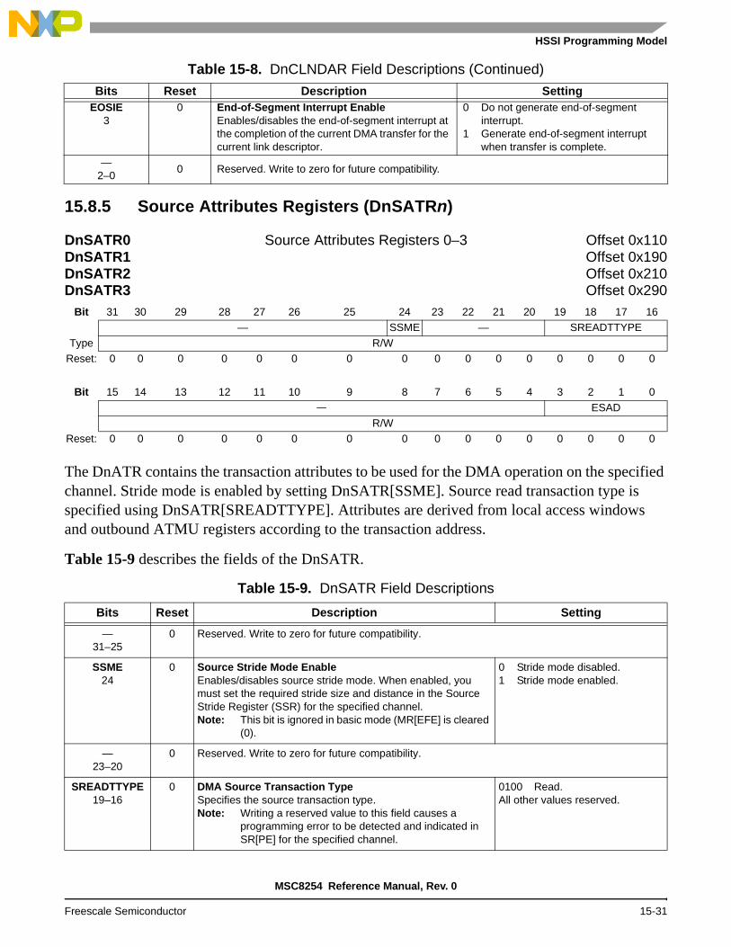
HSSI Programming Model
15.8.5 Source Attributes Registers (DnSATRn).
The DnATR contains the transaction attributes to be used for the DMA operation on the specified channel. Stride mode is enabled by setting DnSATR[SSME]. Source read transaction type is specified using DnSATR[SREADTTYPE]. Attributes are derived from local access windows and outbound ATMU registers according to the transaction address.
Table 15-9 describes the fields of the DnSATR.
EOSIE3
0 End-of-Segment Interrupt EnableEnables/disables the end-of-segment interrupt at the completion of the current DMA transfer for the current link descriptor.
0 Do not generate end-of-segment interrupt.
1 Generate end-of-segment interrupt when transfer is complete.
—2–0
0 Reserved. Write to zero for future compatibility.
DnSATR0 Source Attributes Registers 0–3 Offset 0x110DnSATR1 Offset 0x190DnSATR2 Offset 0x210DnSATR3 Offset 0x290
Bit 31 30 29 28 27 26 25 24 23 22 21 20 19 18 17 16— SSME — SREADTTYPE
Type R/WReset: 0 0 0 0 0 0 0 0 0 0 0 0 0 0 0 0
Bit 15 14 13 12 11 10 9 8 7 6 5 4 3 2 1 0— ESAD
R/WReset: 0 0 0 0 0 0 0 0 0 0 0 0 0 0 0 0
Table 15-9. DnSATR Field Descriptions
Bits Reset Description Setting
—31–25
0 Reserved. Write to zero for future compatibility.
SSME24
0 Source Stride Mode EnableEnables/disables source stride mode. When enabled, you must set the required stride size and distance in the Source Stride Register (SSR) for the specified channel.Note: This bit is ignored in basic mode (MR[EFE] is cleared
(0).
0 Stride mode disabled.1 Stride mode enabled.
—23–20
0 Reserved. Write to zero for future compatibility.
SREADTTYPE19–16
0 DMA Source Transaction TypeSpecifies the source transaction type.Note: Writing a reserved value to this field causes a
programming error to be detected and indicated in SR[PE] for the specified channel.
0100 Read.All other values reserved.
Table 15-8. DnCLNDAR Field Descriptions (Continued)
Bits Reset Description Setting
MSC8254 Reference Manual, Rev. 0
Freescale Semiconductor 15-31

High Speed Serial Interface (HSSI) Subsystem
15.8.6 Source Address Registers (DnSARn)
The SAR contains the address from which the DMA controller reads data for the specified channel. In direct mode, if DnMR[CDSM/SWSM] and DnMR[SRW] are set, a write to this register simultaneously sets DnMR[CS], starting a DMA transfer. Software must ensure that this is a valid address. Table 15-10 describes the DnSAR fields.
—15–4
0 Reserved. Write to zero for future compatibility.
ESAD3–0
0 Extended Source AddressRepresents the most significant 4 bits of the 36-bit source address of the DMA transfer with SARx.
DnSAR0 Source Address Registers 0–3 Offset 0x114DnSAR1 Offset 0x194DnSAR2 Offset 0x214DnSAR3 Offset 0x294
Bit 31 30 29 28 27 26 25 24 23 22 21 20 19 18 17 16
Local SAD
Type R/W
Reset 0 0 0 0 0 0 0 0 0 0 0 0 0 0 0 0
Bit 15 14 13 12 11 10 9 8 7 6 5 4 3 2 1 0
Local SAD
Type R/W
Reset 0 0 0 0 0 0 0 0 0 0 0 0 0 0 0 0
Table 15-10. DnSAR Field Descriptions
Bits Reset DescriptionLocal Source
SAD31–0
0 Source AddressContains least significant 32 bits of the 36-bit source address of the DMA transfer. The contents are updated after every DMA write operation unless the final stride of a striding operation is less than the stride size, it which case it remains equal to the address from with the last stride began.
Table 15-9. DnSATR Field Descriptions (Continued)
Bits Reset Description Setting
MSC8254 Reference Manual, Rev. 0
15-32 Freescale Semiconductor

HSSI Programming Model
15.8.7 Destination Attributes Registers (DnDATRn).
The destination attributes registers contain the transaction attributes for the DMA operation. Stride mode is enabled by setting DnDATR[DSME] for the specified channel. Destination write transaction type is specified using the DnDATR[DWRITETTYPE] field.
The target interface is derived from the local access ATMU mapping and the transaction is obtained from the value specified in DnDATR[DWRITETTYPE] using the local address space category.
Table 15-11 describes the fields of the DATR.
DnDATR0 Destination Attributes Registers 0–3 Offset 0x118DnDATR1 Offset 0x198DnDATR2 Offset 0x218DnDATR3 Offset 0x298
Bit 31 30 29 28 27 26 25 24 23 22 21 20 19 18 17 16— NLWR — DSME — DWRITETTYPE
Type R/WReset: 0 0 0 0 0 0 0 0 0 0 0 0 0 0 0 0
Bit 15 14 13 12 11 10 9 8 7 6 5 4 3 2 1 0— EDAD
R/WReset: 0 0 0 0 0 0 0 0 0 0 0 0 0 0 0 0
Table 15-11. DnDATR Field Descriptions
Bits Reset Description Setting
—31
0 Reserved. Write to zero for future compatibility.
NLWR30
0 No Last Write With ResponseUsed to indicate whether the last write requires a target response. The ROWARx[WRTYP] value selects the write transaction type. If NLWR is cleared, then the last write transaction is NWRITE_R instead of SWRITE or NWRITE, depending on the value of ROWARx[WRTYP]. If NLWR is set, the last write transaction is performed as specified by the value of ROWARx[WRTYP].
0 Last write transfer is a write with target response.
1 Last write transfer is a write without target response.
—20–25
0 Reserved. Write to zero for future compatibility.
DSME24
0 Destination Stride Mode EnableEnables/disables destination stride mode. When enabled, you must set the required stride size and distance in the Destination Stride Register (DSR) for the specified channel.Note: This bit is ignored in basic mode (MR[EFE] is cleared
(0).
0 Stride mode disabled.1 Stride mode enabled.
—23–20
0 Reserved. Write to zero for future compatibility.
MSC8254 Reference Manual, Rev. 0
Freescale Semiconductor 15-33

High Speed Serial Interface (HSSI) Subsystem
15.8.8 Destination Address Registers (DnDARn)
The DnDAR contains the address to which the DMA controller writes data for the specified channel. In direct mode, if DnMR[CDSM/SWSM] is cleared and DnMR[SRW] is set, a write to this register simultaneously sets DnMR[CS], starting a DMA transfer. Software must ensure that this is a valid address.
Table 15-12 describes the DnDAR fields.
DWRITETTYPE19–16
0 DMA Destination Transaction TypeSpecifies the destination transaction type.Note: Writing a reserved value to this field causes a
programming error to be detected and indicated in SR[PE] for the specified channel.
0100 Write.All other values reserved.
—15–4
0 Reserved. Write to zero for future compatibility.
EDAD3–0
0 Extended Destination AddressRepresents the most significant 4 bits of the 36-bit destination address of the DMA transfer with DARx.
DnDAR0 Destination Address Registers 0–3 Offset 0x11CDnDAR1 Offset 0x19CDnDAR2 Offset 0x21CDnDAR3 Offset 0x29C
Bit 31 30 29 28 27 26 25 24 23 22 21 20 19 18 17 16
Local DAD
Type R/W
Reset 0 0 0 0 0 0 0 0 0 0 0 0 0 0 0 0
Bit 15 14 13 12 11 10 9 8 7 6 5 4 3 2 1 0
Local DAD
Type R/W
Reset 0 0 0 0 0 0 0 0 0 0 0 0 0 0 0 0
Table 15-12. DnDAR Field Descriptions
Bits Reset DescriptionLocal Source
DAD31–0
0 Destination AddressContains the least significant 32 bits of the 36-bit destination address of the DMA transfer. The contents are updated after every DMA write operation unless the final stride of a striding operation is less than the stride size, it which case it remains equal to the address from with the last stride began.
Table 15-11. DnDATR Field Descriptions (Continued)
Bits Reset Description Setting
MSC8254 Reference Manual, Rev. 0
15-34 Freescale Semiconductor

HSSI Programming Model
15.8.9 Byte Count Registers (DnBCRn).
The byte count register contains the number of bytes to transfer. Table 15-13 describes the fields of the DnBCR.
DnBCR0 Byte Count Registers 0–3 Offset 0x120DnBCR1 Offset 0x1A0DnBCR2 Offset 0x220DnBCR3 Offset 0x2A0
Bit 31 30 29 28 27 26 25 24 23 22 21 20 19 18 17 16— BC
Type R/WReset: 0 0 0 0 0 0 0 0 0 0 0 0 0 0 0 0
Bit 15 14 13 12 11 10 9 8 7 6 5 4 3 2 1 0
BCR/W
Reset: 0 0 0 0 0 0 0 0 0 0 0 0 0 0 0 0
Table 15-13. DnBCR Field Descriptions
Bits Reset Description
—31–26
0 Reserved. Write to zero for future compatibility.
BC25–0
0 Byte CountContains the number of bytes to transfer. The value in this field is decremented after each DMA read operation. The maximum transfer size is 226 – 1 bytes.
MSC8254 Reference Manual, Rev. 0
Freescale Semiconductor 15-35

High Speed Serial Interface (HSSI) Subsystem
15.8.10 Extended Next Link Descriptor Address Registers (DnENLNDARn)
The DnENLNDAR contains the extended address of the next link descriptor for the specified channel.
Note: These registers are only used for RapidIO transactions. They are not used for accesses to the internal RapidIO address space.
For RapidIO transactions in basic chaining mode, software must initialize this register and the NLNDAR to point to the next link descriptor in memory. After the current descriptor is processed, the ECLNDAR and CLNDAR are loaded from the ENLNDAR and the NLNDAR. Then the controller evaluates the NLNDARn[EOLND] field. If EOLND is cleared (0), the DMA controller reads in the new current link descriptor for processing. If EOLND is set (1), the last descriptor of the list has completed. If extended chaining mode is not enabled, all DMA transfers are complete and the DMA controller halts.
If extended chaining mode is enabled, the DMA controller examines the state of the EOLSD bit in the next list descriptor address register (NLSDAR). If EOLSD is clear, the controller loads the contents of the ENLSDAR into the ECLSDAR and the contents of the NLSDAR into the CLSDAR and reads the new list descriptor from memory. If EOLSD is set, all DMA transfers are complete and the DMA controller halts. Table 15-14 describes the ENLNDAR fields.
DnENLNDAR1 Extended Next Link Descriptor Address Registers 1–3 Offset 0x1A4DnENLNDAR2 Offset 0x224DnENLNDAR3 Offset 0x2A4
Bit 31 30 29 28 27 26 25 24 23 22 21 20 19 18 17 16
—Type R/WReset 0 0 0 0 0 0 0 0 0 0 0 0 0 0 0 0
Bit 15 14 13 12 11 10 9 8 7 6 5 4 3 2 1 0
— ENLNDA
Type R/WReset 0 0 0 0 0 0 0 0 0 0 0 0 0 0 0 0
Table 15-14. DnENLNDAR Field Descriptions
Bits Reset Description Setting—
31–40 Reserved. Write to zero for future compatibility.
ENLNDA3–0
0 Next Link Descriptor Extended AddressContains the most significant 4 bits of the 36-bit address used with RapidIO transactions only.Note: This field is not used for local
transactions.
MSC8254 Reference Manual, Rev. 0
15-36 Freescale Semiconductor

HSSI Programming Model
15.8.11 Next Link Descriptor Address Registers (DnNLNDARn)
The DnNLNDAR contains the address of the next link descriptor for the specified channel. In basic chaining mode, software must initialize this register to point to the first link descriptors in memory. After the current descriptor is processed, the CLDAR is loaded from the DnNLNDAR and the DnNLNDARn[EOLND] field in the DnNLNDAR is examined. If EOLND is zero, the DMA controller reads in the new current link descriptor for processing. If EOLND is set, the last descriptor of the list was just completed. If extended chaining mode is not enabled, all DMA transfers are complete and the DMA controller halts. If extended chaining mode is enabled, the DMA controller examines the state of DnNLSDARn[EOLSD] in the DnNLSDAR. If EOLSD is clear, the controller loads the contents of the NLSDAR into the CLNDAR and reads the new list descriptor from memory. If EOLSD is set, all DMA transfers are complete and the DMA controller halts. Table 15-15 describes the DnNLNDAR fields.
DnNLNDAR0 Next Link Descriptor Address Registers 0–3 Offset 0x128DnNLNDAR1 Offset 0x1A8DnNLNDAR2 Offset 0x228DnNLNDAR3 Offset 0x2A8
Bit 31 30 29 28 27 26 25 24 23 22 21 20 19 18 17 16
NLNDA
Type R/WReset 0 0 0 0 0 0 0 0 0 0 0 0 0 0 0 0
Bit 15 14 13 12 11 10 9 8 7 6 5 4 3 2 1 0
NLNDA — NDEOSIE — EOLNDType R/W
Reset 0 0 0 0 0 0 0 0 0 0 0 0 0 0 0 0
Table 15-15. DnNLNDAR Field Descriptions
Bits Reset Description SettingNLNDA
31–50 Next Link Descriptor Address
Holds the descriptor address of the next buffer descriptor in memory. The descriptor must be 32-byte aligned.Note: This field is used for all transfers. For
RapidIO transactions, it is the lower portion of the 36-bit address formed by combining with the ENLNDA for use with RapidIO transaction types.
—4
0 Reserved. Write to zero for future compatibility.
NDEOSIE3
0 Next Descriptor End-of-Segment Interrupt EnableEnables/disables the next descriptor end-of-segment interrupt when the current DMA transfer for the current link descriptor completes.
0 Do not generate next descriptor end-of-segment interrupt.
1 Generate next descriptor end-of-segment interrupt when transfer is complete.
—2–1
0 Reserved. Write to zero for future compatibility.
MSC8254 Reference Manual, Rev. 0
Freescale Semiconductor 15-37

High Speed Serial Interface (HSSI) Subsystem
15.8.12 Extended Current List Descriptor Address Registers (DnECLSDARn)
The DnECLSDAR contains the extended address of the current address of the list descriptor in memory in extended chaining mode for the specified channel.
Note: These registers are only used for RapidIO transaction types. They are not used for accesses to the internal RapidIO address space.
In extended chaining mode, software must initialize this register and DnCLSDAR to point to the first list descriptor in memory. After finishing the last link descriptor in the current list, the DMA controller loads the contents of the DnENLNDAR and the DnNLNDAR. Then the controller evaluates the DnNLSDARn[EOLSD] field. If EOLSD is cleared (0), the DMA controller reads in the new current list descriptor for processing. If EOLND is set (1) and the last link of the current list is finished, all DMA transfers are complete. Table 15-16 describes the DnECLSDAR fields.
EOLND0
0 End-of-Links DescriptorIndicates whether the descriptor is the last descriptor in memory for this list.Note: This bit is ignored in direct mode.
0 Not the last descriptor for this list.1 Last descriptor for this list.
DnECLSDAR1 Extended Current List Descriptor Address Registers 0–3 Offset 0x1B0DnECLSDAR2 Offset 0x230DnECLSDAR3 Offset 0x2B0
Bit 31 30 29 28 27 26 25 24 23 22 21 20 19 18 17 16
—
Type R/WReset 0 0 0 0 0 0 0 0 0 0 0 0 0 0 0 0
Bit 15 14 13 12 11 10 9 8 7 6 5 4 3 2 1 0
— ECLSDAType R/W
Reset 0 0 0 0 0 0 0 0 0 0 0 0 0 0 0 0
Table 15-16. DnECLSDAR Field Descriptions
Bits Reset Description Setting—
31–40 Reserved. Write to zero for future compatibility.
ECLSDA3–0
0 Current List Descriptor Extended AddressContains the most significant 4 bits of the 36-bit address used with RapidIO transactions only.Note: This field is not used for local
transactions.
Table 15-15. DnNLNDAR Field Descriptions (Continued)
Bits Reset Description Setting
MSC8254 Reference Manual, Rev. 0
15-38 Freescale Semiconductor

HSSI Programming Model
15.8.13 Current List Descriptor Address Registers (DnCLSDARn)
The DnCLSDAR contains the address of the current list descriptor for the specified channel. In extended chaining mode, software must initialize this register to point to the first list descriptor in memory. After finishing the last link descriptor in the current list, the DMA controller loads the contents of the DnENLSDAR and the DnNLSDAR. Then the controller evaluates the DnNLSDARn[EOLSD] field. If EOLSD is cleared (0), the DMA controller reads in the new current list descriptor for processing. If EOLND is set (1) and the last link of the current list is finished, all DMA transfers are complete. Table 15-17 describes the DnCLSDAR fields.
DnCLSDAR0 Current List Descriptor Address Registers 0–3 Offset 0x134DnCLSDAR1 Offset 0x1B4DnCLSDAR2 Offset 0x234DnCLSDAR3 Offset 0x2B4
Bit 31 30 29 28 27 26 25 24 23 22 21 20 19 18 17 16
CLSDA
Type R/WReset 0 0 0 0 0 0 0 0 0 0 0 0 0 0 0 0
Bit 15 14 13 12 11 10 9 8 7 6 5 4 3 2 1 0
CLSDA —Type R/W
Reset 0 0 0 0 0 0 0 0 0 0 0 0 0 0 0 0
Table 15-17. DnCLSDAR Field Descriptions
Bits Reset Description SettingCLSDA
31–50 Current List Descriptor Address
Holds the current list descriptor address of the buffer descriptor in memory. The descriptor must be 32-byte aligned.Note: This field is used for all transfers. For
RapidIO transactions, it is the lower portion of the 36-bit address formed by combining with the ECLSDA for use with RapidIO transaction types.
—4–0
0 Reserved. Write to zero for future compatibility.
MSC8254 Reference Manual, Rev. 0
Freescale Semiconductor 15-39

High Speed Serial Interface (HSSI) Subsystem
15.8.14 Extended Next List Descriptor Address Registers (DnENLSDARn)
The DnENLSDAR contains the extended address of the next address of the list descriptor in memory. If the contents are transferred to the current list descriptor address register, they become effective for the current transfer in extended chaining mode for the specified channel.
Note: These registers are only used for RapidIO transaction types. They are not used for accesses to the internal RapidIO address space.
Table 15-18 describes the DnENLSDAR fields.
DnENLSDAR0 Extended Next List Descriptor Address Registers 0–3 Offset 0x138DnENLSDAR1 Offset 0x1B8DnENLSDAR2 Offset 0x238DnENLSDAR3 Offset 0x2B8
Bit 31 30 29 28 27 26 25 24 23 22 21 20 19 18 17 16
—
Type R/WReset 0 0 0 0 0 0 0 0 0 0 0 0 0 0 0 0
Bit 15 14 13 12 11 10 9 8 7 6 5 4 3 2 1 0
— ENLSDAType R/W
Reset 0 0 0 0 0 0 0 0 0 0 0 0 0 0 0 0
Table 15-18. DnENLSDAR Field Descriptions
Bits Reset Description Setting—
31–40 Reserved. Write to zero for future compatibility.
ENLSDA3–0
0 Next List Descriptor Extended AddressContains the most significant 4 bits of the 36-bit address used with RapidIO transactions only.Note: This field is not used for local
transactions.
MSC8254 Reference Manual, Rev. 0
15-40 Freescale Semiconductor

HSSI Programming Model
15.8.15 Next List Descriptor Address Registers (DnNLSDARn)
The DnNLSDAR contains the address of the next address of the list descriptor in memory. If the contents are transferred to the current list descriptor address register, they become effective for the current transfer in extended chaining mode for the specified channel. Table 15-19 describes the DnNLSDAR fields.
DnNLSDAR0 Next List Descriptor Address Registers 0–3 Offset 0x13CDnNLSDAR1 Offset 0x1BCDnNLSDAR2 Offset 0x23CDnNLSDAR3 Offset 0x2BC
Bit 31 30 29 28 27 26 25 24 23 22 21 20 19 18 17 16
NLSDA
Type R/WReset 0 0 0 0 0 0 0 0 0 0 0 0 0 0 0 0
Bit 15 14 13 12 11 10 9 8 7 6 5 4 3 2 1 0
NLSDA — EOLSDType R/W
Reset 0 0 0 0 0 0 0 0 0 0 0 0 0 0 0 0
Table 15-19. DnNLSDAR Field Descriptions
Bits Reset Description SettingNLSDA
31–50 Next List Descriptor Address
Holds the next list descriptor address of the buffer descriptor in memory. The descriptor must be 32-byte aligned.Note: This field is used for all transfers. For
RapidIO transactions, it is the lower portion of the 36-bit address formed by combining with the ENLSDA for use with RapidIO transaction types.
—4–1
0 Reserved. Write to zero for future compatibility.
EOLSD0
0 End-of-Lists DescriptorIndicates whether the descriptor is the last list descriptor in memory. When the bit is set, the DMA controller halts after the last link descriptor transaction finishes.Note: This bit is ignored in direct mode.
0 Not the last list descriptor in memory.1 Last list descriptor in memory.
MSC8254 Reference Manual, Rev. 0
Freescale Semiconductor 15-41

High Speed Serial Interface (HSSI) Subsystem
15.8.16 Source Stride Registers (DnSSRn)
The DnSSR contains the source stride size and distance. Note that the source stride information is loaded when a new list descriptor is read from memory. Therefore, the DnSSR applies for all link descriptors in the new list. Changing the source stride information for a link requires that a new list be generated. Table 15-19 describes the DnSSR fields.
DnSSR0 Source Stride Registers 0–3 Offset 0x140DnSSR1 Offset 0x1C0DnSSR2 Offset 0x240DnSSR3 Offset 0x2C0
Bit 31 30 29 28 27 26 25 24 23 22 21 20 19 18 17 16
— SSS
Type R/WReset 0 0 0 0 0 0 0 0 0 0 0 0 0 0 0 0
Bit 15 14 13 12 11 10 9 8 7 6 5 4 3 2 1 0
SSS SSDType R/W
Reset 0 0 0 0 0 0 0 0 0 0 0 0 0 0 0 0
Table 15-20. DnSSR Field Descriptions
Bits Reset Description—
31–240 Reserved. Write to zero for future compatibility.
SSS23–12
0 Source Stride SizeHolds the number of bytes to transfer before jumping to the next address as specified in the source stride distance field.
SSD11–0
0 Source Stride DistanceThe source stride distance in bytes from the start byte to the end byte.
MSC8254 Reference Manual, Rev. 0
15-42 Freescale Semiconductor

HSSI Programming Model
15.8.17 Destination Stride Registers (DnDSRn)
The DnDSR contains the destination stride size and distance. Note that the destination stride information is loaded when a new list descriptor is read from memory. Therefore, the DnDSR applies for all link descriptors in the new list. Changing the destination stride information for a link requires that a new list be generated. Table 15-21 describes the DnDSR fields.
DnDSR0 Destination Stride Registers 0–3 Offset 0x144DnDSR1 Offset 0x1C4DnDSR2 Offset 0x244DnDSR3 Offset 0x2C4
Bit 31 30 29 28 27 26 25 24 23 22 21 20 19 18 17 16
— DSS
Type R/WReset 0 0 0 0 0 0 0 0 0 0 0 0 0 0 0 0
Bit 15 14 13 12 11 10 9 8 7 6 5 4 3 2 1 0
DSS DSDType R/W
Reset 0 0 0 0 0 0 0 0 0 0 0 0 0 0 0 0
Table 15-21. DnDSR Field Descriptions
Bits Reset Description—
31–240 Reserved. Write to zero for future compatibility.
DSS23–12
0 Destination Stride SizeHolds the number of bytes to transfer before jumping to the next address as specified in the destination stride distance field.
DSD11–0
0 Destination Stride DistanceThe destination stride distance in bytes from the start byte to the end byte.
MSC8254 Reference Manual, Rev. 0
Freescale Semiconductor 15-43

High Speed Serial Interface (HSSI) Subsystem
15.8.18 DMA General Status Register (DnDGSR))
The DMA general status register combines all of the status bits from each channel into one register. This register is read-only. Table 15-22 describes the fields of the DnDGSR.
DnDGSR DMA General Status Register Offset 0x300
Bit 31 30 29 28 27 26 25 24 23 22 21 20 19 18 17 16
TE0 — CH0 PE0 EOLNI0 CB0 EOSI0 EOLSI0 TE1 — CH1 PE1 EOLNI1 CB1 EOSI1 EOLSI1
Type RReset 0 0 0 0 0 0 0 0 0 0 0 0 0 0 0 0
Bit 15 14 13 12 11 10 9 8 7 6 5 4 3 2 1 0
TE2 — CH2 PE2 EOLNI2 CB2 EOSI2 EOLSI2 TE3 — CH3 PE3 EOLNI3 CB3 EOSI3 EOLSI3Type R
Reset 0 0 0 0 0 0 0 0 0 0 0 0 0 0 0 0
Table 15-22. DnDGSR Field Descriptions
Bits Reset Description SettingTE031
0 Channel 0 Transfer ErrorIndicates whether a transfer error occurred.
0 Normal operation.1 Error condition occurred during DMA
transfer.—30
0 Reserved. Write to zero for future compatibility.
CH029
0 Channel 0 HaltedIndicates whether the channel halted.
0 Channel not halted.1 Channel halted.
PE028
0 Channel 0 Programming Error DetectedIndicates whether a programming error was detected.
0 Normal operation.1 Programming error detected.
EOLNI027
0 Channel 0 End-of-Links InterruptIndicates whether an end-of-links interrupt occurred.
0 Normal operation.1 End-of-links interrupt occurred.
CB026
0 Channel 0 BusyIndicates whether the channel is busy.
0 Channel not busy.1 Channel busy.
EOSI025
0 Channel 0 End-of-Segment InterruptIndicates whether an end-of-segment interrupt occurred.
0 Normal operation.1 End-of-segment interrupt occurred.
EOLSI024
0 Channel 0 End-of-Lists/Direct InterruptIndicates whether an end-of lists/direct interrupt occurred.
0 Normal operation.1 End-of-list/direct interrupt occurred.
TE123
0 Channel 1 Transfer ErrorIndicates whether a transfer error occurred.
0 Normal operation.1 Error condition occurred during DMA
transfer.
—22
0 Reserved. Write to zero for future compatibility.
CH121
0 Channel 1 HaltedIndicates whether the channel halted.
0 Channel not halted.1 Channel halted.
PE120
0 Channel 1 Programming Error DetectedIndicates whether a programming error was detected.
0 Normal operation.1 Programming error detected.
EOLNI119
0 Channel 1 End-of-Links InterruptIndicates whether an end-of-links interrupt occurred.
0 Normal operation.1 End-of-links interrupt occurred.
MSC8254 Reference Manual, Rev. 0
15-44 Freescale Semiconductor

HSSI Programming Model
CB118
0 Channel 1 BusyIndicates whether the channel is busy.
0 Channel not busy.1 Channel busy.
EOSI117
0 Channel 1 End-of-Segment InterruptIndicates whether an end-of-segment interrupt occurred.
0 Normal operation.1 End-of-segment interrupt occurred.
EOLSI116
0 Channel 1 End-of-Lists/Direct InterruptIndicates whether an end-of lists/direct interrupt occurred.
0 Normal operation.1 End-of-list/direct interrupt occurred.
TE215
0 Channel 2 Transfer ErrorIndicates whether a transfer error occurred.
0 Normal operation.1 Error condition occurred during DMA
transfer.—14
0 Reserved. Write to zero for future compatibility.
CH213
0 Channel 2 HaltedIndicates whether the channel halted.
0 Channel not halted.1 Channel halted.
PE212
0 Channel 2 Programming Error DetectedIndicates whether a programming error was detected.
0 Normal operation.1 Programming error detected.
EOLNI211
0 Channel 2 End-of-Links InterruptIndicates whether an end-of-links interrupt occurred.
0 Normal operation.1 End-of-links interrupt occurred.
CB210
0 Channel 2 BusyIndicates whether the channel is busy.
0 Channel not busy.1 Channel busy.
EOSI29
0 Channel 2 End-of-Segment InterruptIndicates whether an end-of-segment interrupt occurred.
0 Normal operation.1 End-of-segment interrupt occurred.
EOLSI28
0 Channel 2 End-of-Lists/Direct InterruptIndicates whether an end-of lists/direct interrupt occurred.
0 Normal operation.1 End-of-list/direct interrupt occurred.
TE37
0 Channel 3 Transfer ErrorIndicates whether a transfer error occurred.
0 Normal operation.1 Error condition occurred during DMA
transfer.—6
0 Reserved. Write to zero for future compatibility.
CH35
0 Channel 3 HaltedIndicates whether the channel halted.
0 Channel not halted.1 Channel halted.
PE34
0 Channel 3 Programming Error DetectedIndicates whether a programming error was detected.
0 Normal operation.1 Programming error detected.
EOLNI33
0 Channel 3 End-of-Links InterruptIndicates whether an end-of-links interrupt occurred.
0 Normal operation.1 End-of-links interrupt occurred.
CB32
0 Channel 3 BusyIndicates whether the channel is busy.
0 Channel not busy.1 Channel busy.
EOSI31
0 Channel 3 End-of-Segment InterruptIndicates whether an end-of-segment interrupt occurred.
0 Normal operation.1 End-of-segment interrupt occurred.
EOLSI30
0 Channel 3 End-of-Lists/Direct InterruptIndicates whether an end-of lists/direct interrupt occurred.
0 Normal operation.1 End-of-list/direct interrupt occurred.
Table 15-22. DnDGSR Field Descriptions (Continued)
Bits Reset Description Setting
MSC8254 Reference Manual, Rev. 0
Freescale Semiconductor 15-45

High Speed Serial Interface (HSSI) Subsystem
15.8.19 Local Access Window Base Address Registers 0–9 (DnLAWBAR[0–9])
DnLAWBARx holds 24 most significant bits of the window base address. The least significant byte is always 0s. Table 15-23 describes the DnLAWBARx fields.
DnLAWBAR0 Local Access Window Base Address Registers 0–9 Offset 0x1C08DnLAWBAR1 Offset 0x1C28DnLAWBAR2 Offset 0x1C48DnLAWBAR3 Offset 0x1C68DnLAWBAR4 Offset 0x1C88DnLAWBAR5 Offset 0x1CA8DnLAWBAR6 Offset 0x1CC8DnLAWBAR7 Offset 0x1CE8DnLAWBAR8 Offset 0x1D08DnLAWBAR9 Offset 0x1D28
Bit 31 30 29 28 27 26 25 24 23 22 21 20 19 18 17 16
— BA
Type R R/W
Reset 0 0 0 0 0 0 0 0 0 0 0 0 0 0 0 0
Bit 15 14 13 12 11 10 9 8 7 6 5 4 3 2 1 0
BA
Type R/W
Reset 0 0 0 0 0 0 0 0 0 0 0 0 0 0 0 0
Table 15-23. DnLAWBARx Field Descriptions
Bits Reset Description Setting
—31–24
0 Reserved. Write to zero for future compatibility.
BA23–0
0 Base AddressHolds the 24 most significant bits of the 36-bit window base address.• Bits 23–20 correspond to the value of
SATRx[ESAD]/DATRx[EDAD]• Bits 19–0 correspond to bits 31–12 of
SARx[SAD]/DARx[DAD]Note: For local transactions, the most
significant 4 bits in this field must be 0s.
MSC8254 Reference Manual, Rev. 0
15-46 Freescale Semiconductor

HSSI Programming Model
15.8.20 Local Access Window Attributes Registers 0–9 (DnLAWAR[0–9])
DnLAWARx contains the transaction interface for a request mapped to this window. Table 15-24 describes the DnLAWARx fields.
DnLAWAR0 Local Access Window Attributes Registers 0–9 Offset 0x1C10DnLAWAR1 Offset 0x1C30DnLAWAR2 Offset 0x1C50DnLAWAR3 Offset 0x1C70DnLAWAR4 Offset 0x1C90DnLAWAR5 Offset 0x1CB0DnLAWAR6 Offset 0x1CD0DnLAWAR7 Offset 0x1CF0DnLAWAR8 Offset 0x1D10DnLAWAR9 Offset 0x1D30
Bit 31 30 29 28 27 26 25 24 23 22 21 20 19 18 17 16
EN — TRANS_INT —
Type R/W R R/W R
Reset 0 0 0 0 0 0 0 0 0 0 0 0 0 0 0 0
Bit 15 14 13 12 11 10 9 8 7 6 5 4 3 2 1 0
— SIZE
Type R/W
Reset 0 0 0 0 0 0 0 0 0 0 0 0 0 0 0 0
Table 15-24. DnLAWARx Field Descriptions
Bits Reset Description Settings
EN31
0 Enable Enables/disables the local access window (LAW) and all other LAWAR and LAWBAR fields. When the LAW is enabled, the LAWAR and LAWBAR fields combine to define the address range for this window.
0 Local access window disabled.1 Local access window enabled.
—30–24
0 Reserved. Write to zero for future compatibility.
TRANS_INT23–20
0 Transaction InterfaceSpecifies the logical destination/target of the transaction mapped to this window. A reserved value defaults to local address space.
0001 PCI Express1011 OCN to MBus Bridge 0 for local
space1100 SRIO Port 01101 SRIO Port 11111 OCN to MBus Bridge 1 for local
space.All others reserved.
—19–6
0 Reserved. Write to zero for future compatibility.
MSC8254 Reference Manual, Rev. 0
Freescale Semiconductor 15-47

High Speed Serial Interface (HSSI) Subsystem
SIZE5–0
0 Local Access Window SizeThis value determines the local access window, which is computed using the formula 2(SIZE + 1).
The minimum size is 4K. The maximum size is 64G.
001011 4K
001100 8K
001101 16K
001110 32K
001111 64K
010000 128K
010001 256K
010010 512K
010011 1M
010100 2M
010101 4M
010110 8M
010111 16M
011000 32M
011001 64M
011010 128M
011011 256M
011100 512M
011101 1G
011110 2G
011111 4G
100000 8G
100001 16G
100010 32G
100011 64G
All others reserved.
Table 15-24. DnLAWARx Field Descriptions (Continued)
Bits Reset Description Settings
MSC8254 Reference Manual, Rev. 0
15-48 Freescale Semiconductor

HSSI Programming Model
15.8.21 OCN-to-MBus Configuration Registers (O2MCR[0–1])
O2MCRn is used to control the size of the burst transactions between the OCN and the MBus.
Note: The O2M bridge 0 uses a base address of 0xFFFA1000.The O2M bridge 1 uses a base address of 0xFFFA1040.
Table 15-33 describes the O2MCRn fields.
O2MCR0 OCN-to-MBus Configuration Registers 0–1 Offset 0x00O2MCR1 Offset 0x00
Bit 31 30 29 28 27 26 25 24 23 22 21 20 19 18 17 16
— MBSType R/W
Reset 0 0 0 0 0 0 0 1 0 0 0 0 0 1 0 1
Bit 15 14 13 12 11 10 9 8 7 6 5 4 3 2 1 0
—Type R/WReset 0 0 0 0 0 0 0 0 0 0 0 0 0 0 0 0
Table 15-25. O2MCRn Field Descriptions
Bits Reset Description Settings
—31–19
0b0000000100000 Reserved. All bits in this field are set by default and must not be changed.
MBS18–16
101 Maximum Burst SizeDetermines the maximum burst width for MBus transactions.
101 64 bytes.110 128 bytes.111 256 bytesAll other values reserved.
—15–0
0x0 Reserved. Write to zero for future compatibility.
MSC8254 Reference Manual, Rev. 0
Freescale Semiconductor 15-49

High Speed Serial Interface (HSSI) Subsystem
15.8.22 OCN-to-MBus Error Attribute Registers (O2MEAR[0–1])
O2MEARn locks the attributes of an incorrect transaction, such as the ID of the source that initiates the transaction and the request type. The capture of a specific error attribute is performed only if the corresponding it in the Error Capture Enable Register is set. Once the capture occurs, the register is locked. You can release the register to capture another error by clearing the corresponding status bit in the O2MESR through a register write.
Note: The O2M bridge 0 uses a base address of 0xFFFA1000.The O2M bridge 1 uses a base address of 0xFFFA1040.
Table 15-33 describes the O2MEARn fields.
O2MEAR0 OCN-to-MBus Error Attribute Registers 0–1 Offset 0x10O2MEAR1 Offset 0x10
Bit 31 30 29 28 27 26 25 24 23 22 21 20 19 18 17 16
ERR_ADDR ERR_ID — WR RWBType R
Reset 0 0 0 0 0 0 0 1 0 0 0 0 0 0 0 0
Bit 15 14 13 12 11 10 9 8 7 6 5 4 3 2 1 0
— REQ_TYPE — ERR_SRCType RReset 0 0 0 0 0 0 0 0 0 0 0 0 0 0 0 0
Table 15-26. O2MEARn Field Descriptions
Bits Reset Description Settings
ERR_ADDR30–28
0 Error AddressFour most significant bits of the captured address. These are used with the 32 least significant bits captured O2MEADRn to derive the full 36-bit address of the erroneous transaction.
ERR_ ID
27–24
0 Error IdentificationThis field is used to identify the type of error captured.
0000 No error attributes captured.0001 DE, transfer error, OCN arbiter
timeout.0010 TE, Early EOP error.0011 EE, Transaction Type error.0100 TT, OCN data error.0101 MD, MBus data error.0110 ME, MBus EOT errorAll other values reserved.
—23–18
0 Reserved. Always write zeros to these bits for future compatibility.
WR17
0 With ResponseIndicates whether the OCN request packet is with or without response.
0 Without response.1 With response.
RWB16
0 Read/WriteIndicates the type of access (read/write).
0 Write access executed.1 Read access executed.
—15–13
0 Reserved. Write to zero for future compatibility.
MSC8254 Reference Manual, Rev. 0
15-50 Freescale Semiconductor

HSSI Programming Model
REQ_TYPE12–8
0 Transaction Request TypeIndicates the request type of the incorrect transaction.
00000 Write with no response (if WR=0) or write with response (if WR=1).
00001 Read with response (WR=1)00010 Configuration write with
response (WR=1)00011 Configuring read with response
(WR=1)00100 Message with response (WR=1)00101 Doorbell with response (WR=1)00110 User defined transaction with no
response (WR=0) or User-defined transaction with response (WR=1)
01100 Read and post increment with response (WR=1)
01101 Read and post decrement with response (WR=1)
01110 Read and set to all 1s with response (WR=1)
01111 Read and clear to all 0x with response (WR=1)
All other values reserved.
—7–6
0x0 Reserved. Write to zero for future compatibility.
ERR_SRC5–0
0 Error Source IDThe unique ID of the OCN initiator that performs the error-causing transaction.
Table 15-26. O2MEARn Field Descriptions (Continued)
Bits Reset Description Settings
MSC8254 Reference Manual, Rev. 0
Freescale Semiconductor 15-51

High Speed Serial Interface (HSSI) Subsystem
15.8.23 OCN-to-MBus Error Address Registers (O2MEADR[0–1])
O2MEADRn indicates the least significant bits of the captured address of the incorrect transaction. These 32 bits are combined with the 4 most significant bits in the O2MEARn to yield the 36-bit address. The register contents are locked once the address is captured and can only be cleared by writing to the corresponding status bit in the O2MESRn.
Note: The O2M bridge 0 uses a base address of 0xFFFA1000.The O2M bridge 1 uses a base address of 0xFFFA1040.
Table 15-33 describes the O2MEADRn fields.
O2MEADR0 OCN-to-MBus Error Address Registers 0–1 Offset 0x14O2MEADR1 Offset 0x14
Bit 31 30 29 28 27 26 25 24 23 22 21 20 19 18 17 16
ERR_ADDRType R
Reset 0 0 0 0 0 0 0 1 0 0 0 0 0 0 0 0
Bit 15 14 13 12 11 10 9 8 7 6 5 4 3 2 1 0
ERR_ADDRType RReset 0 0 0 0 0 0 0 0 0 0 0 0 0 0 0 0
Table 15-27. O2MEADRn Field Descriptions
Bits Reset Description Settings
ERR_ADDR31–0
0 Erroneous Transaction AddressContains the least significant 32 bits of the captured transaction address.
MSC8254 Reference Manual, Rev. 0
15-52 Freescale Semiconductor
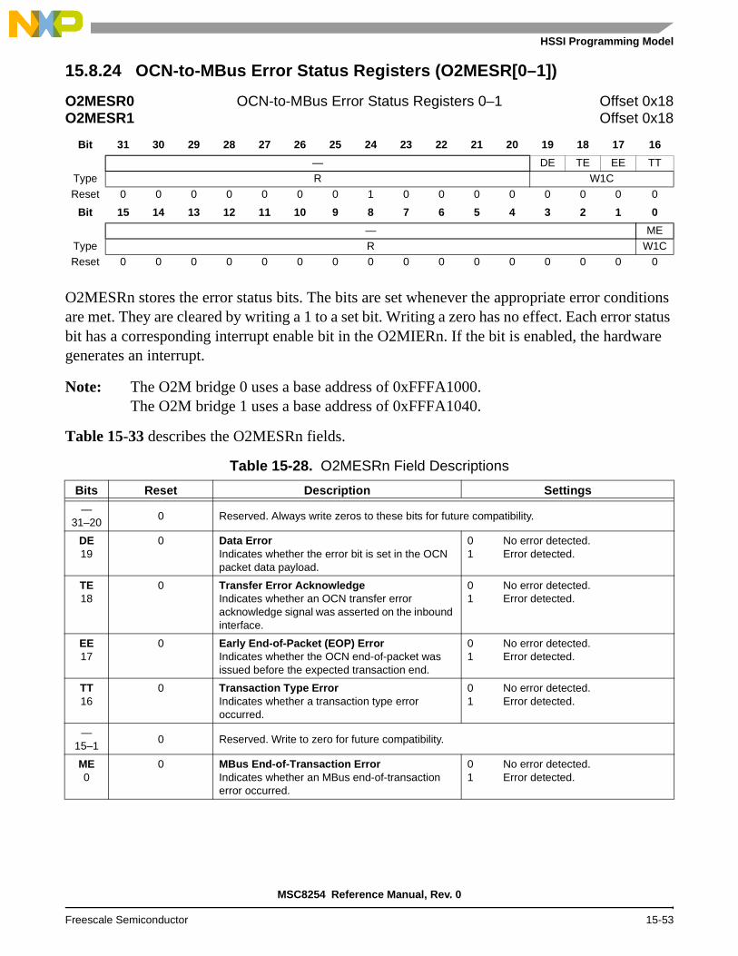
HSSI Programming Model
15.8.24 OCN-to-MBus Error Status Registers (O2MESR[0–1])
O2MESRn stores the error status bits. The bits are set whenever the appropriate error conditions are met. They are cleared by writing a 1 to a set bit. Writing a zero has no effect. Each error status bit has a corresponding interrupt enable bit in the O2MIERn. If the bit is enabled, the hardware generates an interrupt.
Note: The O2M bridge 0 uses a base address of 0xFFFA1000.The O2M bridge 1 uses a base address of 0xFFFA1040.
Table 15-33 describes the O2MESRn fields.
O2MESR0 OCN-to-MBus Error Status Registers 0–1 Offset 0x18O2MESR1 Offset 0x18
Bit 31 30 29 28 27 26 25 24 23 22 21 20 19 18 17 16
— DE TE EE TTType R W1C
Reset 0 0 0 0 0 0 0 1 0 0 0 0 0 0 0 0
Bit 15 14 13 12 11 10 9 8 7 6 5 4 3 2 1 0
— METype R W1CReset 0 0 0 0 0 0 0 0 0 0 0 0 0 0 0 0
Table 15-28. O2MESRn Field Descriptions
Bits Reset Description Settings
—31–20
0 Reserved. Always write zeros to these bits for future compatibility.
DE19
0 Data ErrorIndicates whether the error bit is set in the OCN packet data payload.
0 No error detected.1 Error detected.
TE18
0 Transfer Error AcknowledgeIndicates whether an OCN transfer error acknowledge signal was asserted on the inbound interface.
0 No error detected.1 Error detected.
EE17
0 Early End-of-Packet (EOP) ErrorIndicates whether the OCN end-of-packet was issued before the expected transaction end.
0 No error detected.1 Error detected.
TT16
0 Transaction Type ErrorIndicates whether a transaction type error occurred.
0 No error detected.1 Error detected.
—15–1
0 Reserved. Write to zero for future compatibility.
ME0
0 MBus End-of-Transaction ErrorIndicates whether an MBus end-of-transaction error occurred.
0 No error detected.1 Error detected.
MSC8254 Reference Manual, Rev. 0
Freescale Semiconductor 15-53
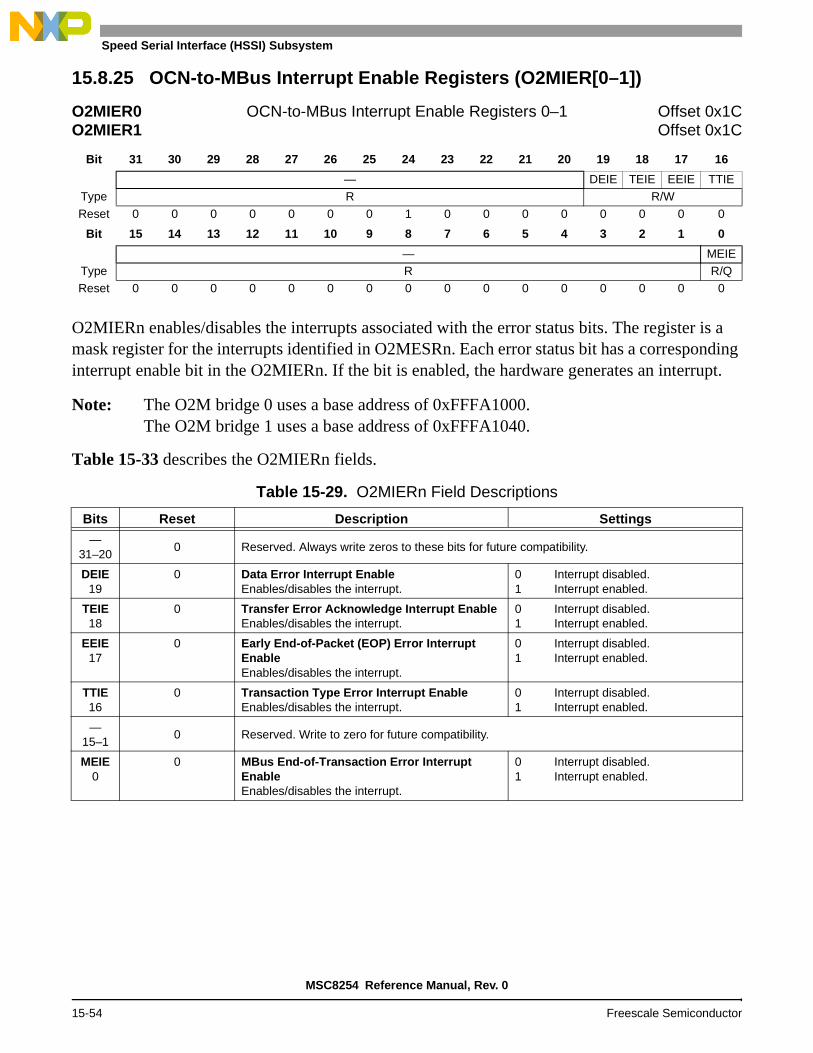
High Speed Serial Interface (HSSI) Subsystem
15.8.25 OCN-to-MBus Interrupt Enable Registers (O2MIER[0–1])
O2MIERn enables/disables the interrupts associated with the error status bits. The register is a mask register for the interrupts identified in O2MESRn. Each error status bit has a corresponding interrupt enable bit in the O2MIERn. If the bit is enabled, the hardware generates an interrupt.
Note: The O2M bridge 0 uses a base address of 0xFFFA1000.The O2M bridge 1 uses a base address of 0xFFFA1040.
Table 15-33 describes the O2MIERn fields.
O2MIER0 OCN-to-MBus Interrupt Enable Registers 0–1 Offset 0x1CO2MIER1 Offset 0x1C
Bit 31 30 29 28 27 26 25 24 23 22 21 20 19 18 17 16
— DEIE TEIE EEIE TTIEType R R/W
Reset 0 0 0 0 0 0 0 1 0 0 0 0 0 0 0 0
Bit 15 14 13 12 11 10 9 8 7 6 5 4 3 2 1 0
— MEIEType R R/QReset 0 0 0 0 0 0 0 0 0 0 0 0 0 0 0 0
Table 15-29. O2MIERn Field Descriptions
Bits Reset Description Settings
—31–20
0 Reserved. Always write zeros to these bits for future compatibility.
DEIE19
0 Data Error Interrupt EnableEnables/disables the interrupt.
0 Interrupt disabled.1 Interrupt enabled.
TEIE18
0 Transfer Error Acknowledge Interrupt EnableEnables/disables the interrupt.
0 Interrupt disabled.1 Interrupt enabled.
EEIE17
0 Early End-of-Packet (EOP) Error Interrupt EnableEnables/disables the interrupt.
0 Interrupt disabled.1 Interrupt enabled.
TTIE16
0 Transaction Type Error Interrupt EnableEnables/disables the interrupt.
0 Interrupt disabled.1 Interrupt enabled.
—15–1
0 Reserved. Write to zero for future compatibility.
MEIE0
0 MBus End-of-Transaction Error Interrupt EnableEnables/disables the interrupt.
0 Interrupt disabled.1 Interrupt enabled.
MSC8254 Reference Manual, Rev. 0
15-54 Freescale Semiconductor

HSSI Programming Model
15.8.26 OCN-to-MBus Error Capture Enable Registers (O2MECER[0–1])
O2MECERn enables/disables capturing the address associated with a detected error. Each error status bit has a corresponding capture enable bit in the O2MECERn. If the bit is enabled, the hardware performs an address capture for the error.
Note: The O2M bridge 0 uses a base address of 0xFFFA1000.The O2M bridge 1 uses a base address of 0xFFFA1040.
Table 15-33 describes the O2MECERn fields.
O2MECER0 OCN-to-MBus Error Capture Enable Registers 0–1 Offset 0x20O2MECER1 Offset 0x20
Bit 31 30 29 28 27 26 25 24 23 22 21 20 19 18 17 16
— DECE TECE EECE TTCEType R R/W
Reset 0 0 0 0 0 0 0 1 0 0 0 0 0 0 0 0
Bit 15 14 13 12 11 10 9 8 7 6 5 4 3 2 1 0
— MECEType R R/QReset 0 0 0 0 0 0 0 0 0 0 0 0 0 0 0 0
Table 15-30. O2MECERn Field Descriptions
Bits Reset Description Settings
—31–20
0 Reserved. Always write zeros to these bits for future compatibility.
DECE19
0 Data Error Capture EnableEnables/disables address capture.
0 Capture disabled.1 Capture enabled.
TECE18
0 Transfer Error Acknowledge Capture EnableEnables/disables address capture.
0 Capture disabled.1 Capture enabled.
EECE17
0 Early End-of-Packet (EOP) Error Capture EnableEnables/disables address capture.
0 Capture disabled.1 Capture enabled.
TTCE16
0 Transaction Type Error Capture EnableEnables/disables address capture.
0 Capture disabled.1 Capture enabled.
—15–1
0 Reserved. Write to zero for future compatibility.
MECE0
0 MBus End-of-Transaction Error Capture EnableEnables/disables address capture.
0 Capture disabled.1 Capture enabled.
MSC8254 Reference Manual, Rev. 0
Freescale Semiconductor 15-55
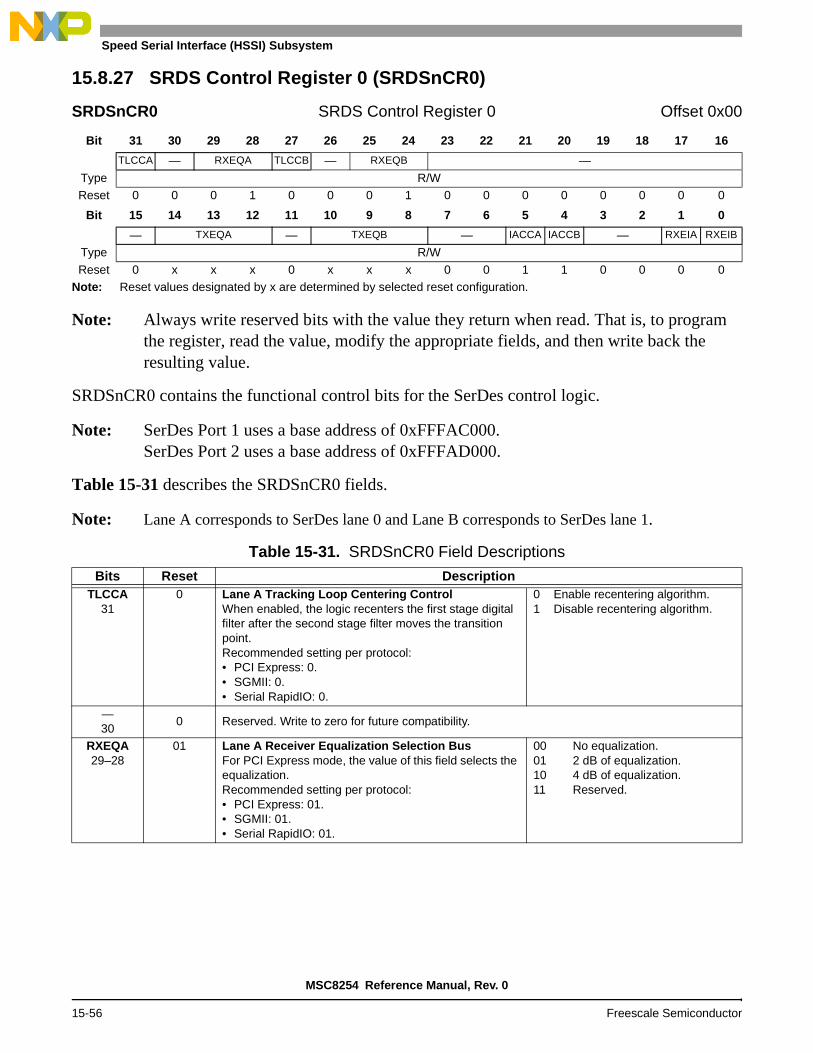
High Speed Serial Interface (HSSI) Subsystem
15.8.27 SRDS Control Register 0 (SRDSnCR0)
Note: Always write reserved bits with the value they return when read. That is, to program the register, read the value, modify the appropriate fields, and then write back the resulting value.
SRDSnCR0 contains the functional control bits for the SerDes control logic.
Note: SerDes Port 1 uses a base address of 0xFFFAC000. SerDes Port 2 uses a base address of 0xFFFAD000.
Table 15-31 describes the SRDSnCR0 fields.
Note: Lane A corresponds to SerDes lane 0 and Lane B corresponds to SerDes lane 1.
SRDSnCR0 SRDS Control Register 0 Offset 0x00
Bit 31 30 29 28 27 26 25 24 23 22 21 20 19 18 17 16
TLCCA — RXEQA TLCCB — RXEQB —
Type R/WReset 0 0 0 1 0 0 0 1 0 0 0 0 0 0 0 0
Bit 15 14 13 12 11 10 9 8 7 6 5 4 3 2 1 0
— TXEQA — TXEQB — IACCA IACCB — RXEIA RXEIB
Type R/W
Reset 0 x x x 0 x x x 0 0 1 1 0 0 0 0Note: Reset values designated by x are determined by selected reset configuration.
Table 15-31. SRDSnCR0 Field Descriptions
Bits Reset DescriptionTLCCA
310 Lane A Tracking Loop Centering Control
When enabled, the logic recenters the first stage digital filter after the second stage filter moves the transition point.Recommended setting per protocol:• PCI Express: 0.• SGMII: 0.• Serial RapidIO: 0.
0 Enable recentering algorithm.1 Disable recentering algorithm.
—30
0 Reserved. Write to zero for future compatibility.
RXEQA29–28
01 Lane A Receiver Equalization Selection BusFor PCI Express mode, the value of this field selects the equalization.Recommended setting per protocol:• PCI Express: 01.• SGMII: 01.• Serial RapidIO: 01.
00 No equalization.01 2 dB of equalization.10 4 dB of equalization.11 Reserved.
MSC8254 Reference Manual, Rev. 0
15-56 Freescale Semiconductor
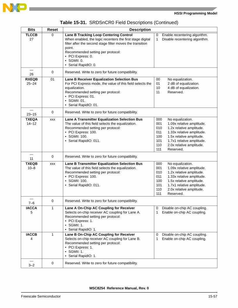
HSSI Programming Model
TLCCB27
0 Lane B Tracking Loop Centering ControlWhen enabled, the logic recenters the first stage digital filter after the second stage filter moves the transition point.Recommended setting per protocol:• PCI Express: 0.• SGMII: 0.• Serial RapidIO: 0.
0 Enable recentering algorithm.1 Disable recentering algorithm.
—26
0 Reserved. Write to zero for future compatibility.
RXEQB25–24
01 Lane B Receiver Equalization Selection BusFor PCI Express mode, the value of this field selects the equalization.Recommended setting per protocol:• PCI Express: 01.• SGMII: 01.• Serial RapidIO: 01.
00 No equalization.01 2 dB of equalization.10 4 dB of equalization.11 Reserved.
—23–15
0 Reserved. Write to zero for future compatibility.
TXEQA14–12
xxx Lane A Transmitter Equalization Selection BusThe value of this field selects the equalization.Recommended setting per protocol:• PCI Express: 100.• SGMII: 100.• Serial RapidIO: 011.
000 No equalization.001 1.09x relative amplitude.010 1.2x relative amplitude.011 1.33x relative amplitude.100 1.5x relative amplitude.101 1.7x1 relative amplitude.110 2.0x relative amplitude.111 Reserved.
—11
0 Reserved. Write to zero for future compatibility.
TXEQB10–8
xxx Lane B Transmitter Equalization Selection BusThe value of this field selects the equalization.Recommended setting per protocol:• PCI Express: 100.• SGMII: 100.• Serial RapidIO: 011.
000 No equalization.001 1.09x relative amplitude.010 1.2x relative amplitude.011 1.33x relative amplitude.100 1.5x relative amplitude.101 1.7x1 relative amplitude.110 2.0x relative amplitude.111 Reserved.
—7–6
0 Reserved. Write to zero for future compatibility.
IACCA5
1 Lane A On-Chip AC Coupling for ReceiverSelects on-chip receiver AC coupling for Lane A.Recommended setting per protocol:• PCI Express: 1.• SGMII: 1.• Serial RapidIO: 1.
0 Disable on-chip AC coupling.1 Enable on-chip AC coupling.
IACCB4
1 Lane B On-Chip AC Coupling for ReceiverSelects on-chip receiver AC coupling for Lane B.Recommended setting per protocol:• PCI Express: 1.• SGMII: 1.• Serial RapidIO: 1.
0 Disable on-chip AC coupling.1 Enable on-chip AC coupling.
—3–2
0 Reserved. Write to zero for future compatibility.
Table 15-31. SRDSnCR0 Field Descriptions (Continued)
Bits Reset Description
MSC8254 Reference Manual, Rev. 0
Freescale Semiconductor 15-57

High Speed Serial Interface (HSSI) Subsystem
RXEIA1
0 Lane A Receiver Electrical Idle StateSetting this bit forces the lane into an electrical idle state.• PCI Express: 0.• SGMII: 0.• Serial RapidIO: 0.
0 Lane not forced into an electrical idle state.
1 Lane forced into an electrical idle state.
RXEIB0
0 Lane B Receiver Electrical Idle StateSetting this bit forces the lane into an electrical idle state.• PCI Express: 0.• SGMII: 0.• Serial RapidIO: 0.
0 Lane not forced into an electrical idle state.
1 Lane forced into an electrical idle state.
Table 15-31. SRDSnCR0 Field Descriptions (Continued)
Bits Reset Description
MSC8254 Reference Manual, Rev. 0
15-58 Freescale Semiconductor

HSSI Programming Model
15.8.28 SRDS Control Register 1 (SRDSnCR1)
Note: Always write reserved bits with the value they return when read. That is, to program the register, read the value, modify the appropriate fields, and then write back the resulting value.
SRDSnCR1 contains the functional control bits for the SerDes control logic.
Note: SerDes Port 1 uses a base address of 0xFFFAC000. SerDes Port 2 uses a base address of 0xFFFAD000.
Table 15-32 describes the SRDSnCR1 fields.
Note: Lane E corresponds to SerDes lane 2 and Lane F corresponds to SerDes lane 3.
SRDSnCR1 SRDS Control Register 1 Offset 0x04
Bit 31 30 29 28 27 26 25 24 23 22 21 20 19 18 17 16
TLCCE — RXEQE TLCCF — RXEQF —
Type R/WReset 0 0 0 1 0 0 0 1 0 0 0 0 0 0 0 0
Bit 15 14 13 12 11 10 9 8 7 6 5 4 3 2 1 0
— TXEQE — TXEQF — IACCE IACCF — RXEIE RXEIF
Type R/W
Reset 0 x x x 0 x x x 0 0 1 1 0 0 0 0Note: Reset values designated by x are determined by selected reset configuration.
Table 15-32. SRDSnCR1 Field Descriptions
Bits Reset DescriptionTLCCE
310 Lane E Tracking Loop Centering Control
When enabled, the logic recenters the first stage digital filter after the second stage filter moves the transition point.Recommended setting per protocol:• PCI Express: 0.• SGMII: 0.• Serial RapidIO: 0.
0 Enable recentering algorithm.1 Disable recentering algorithm.
—30
0 Reserved. Write to zero for future compatibility.
RXEQE29–28
01 Lane E Receiver Equalization Selection BusFor PCI Express mode, the value of this field selects the equalization.Recommended setting per protocol:• PCI Express: 01.• SGMII: 01.• Serial RapidIO: 01.
00 No equalization.01 2 dB of equalization.10 4 dB of equalization.11 Reserved.
MSC8254 Reference Manual, Rev. 0
Freescale Semiconductor 15-59

High Speed Serial Interface (HSSI) Subsystem
TLCCF27
0 Lane F Tracking Loop Centering ControlWhen enabled, the logic recenters the first stage digital filter after the second stage filter moves the transition point.Recommended setting per protocol:• PCI Express: 0.• SGMII: 0.• Serial RapidIO: 0.
0 Enable recentering algorithm.1 Disable recentering algorithm.
—26
0 Reserved. Write to zero for future compatibility.
RXEQF25–24
01 Lane F Receiver Equalization Selection BusFor PCI Express mode, the value of this field selects the equalization.Recommended setting per protocol:• PCI Express: 01.• SGMII: 01.• Serial RapidIO: 01.
00 No equalization.01 2 dB of equalization.10 4 dB of equalization.11 Reserved.
—23–15
0 Reserved. Write to zero for future compatibility.
TXEQE14–12
xxx Lane E Transmitter Equalization Selection BusThe value of this field selects the equalization.Recommended setting per protocol:• PCI Express: 100.• SGMII: 100.• Serial RapidIO: 011.
000 No equalization.001 1.09x relative amplitude.010 1.2x relative amplitude.011 1.33x relative amplitude.100 1.5x relative amplitude.101 1.7x1 relative amplitude.110 2.0x relative amplitude.111 Reserved.
—11
0 Reserved. Write to zero for future compatibility.
TXEQF10–8
xxx Lane F Transmitter Equalization Selection BusThe value of this field selects the equalization.Recommended setting per protocol:• PCI Express: 100.• SGMII: 100.• Serial RapidIO: 011.
000 No equalization.001 1.09x relative amplitude.010 1.2x relative amplitude.011 1.33x relative amplitude.100 1.5x relative amplitude.101 1.7x1 relative amplitude.110 2.0x relative amplitude.111 Reserved.
—7–6
0 Reserved. Write to zero for future compatibility.
IACCE5
1 Lane E On-Chip AC Coupling for ReceiverSelects on-chip receiver AC coupling for Lane E.Recommended setting per protocol:• PCI Express: 1.• SGMII: 1.• Serial RapidIO: 1.
0 Disable on-chip AC coupling.1 Enable on-chip AC coupling.
IACCF4
1 Lane F On-Chip AC Coupling for ReceiverSelects on-chip receiver AC coupling for Lane F.Recommended setting per protocol:• PCI Express: 1.• SGMII: 1.• Serial RapidIO: 1.
0 Disable on-chip AC coupling.1 Enable on-chip AC coupling.
—3–2
0 Reserved. Write to zero for future compatibility.
Table 15-32. SRDSnCR1 Field Descriptions (Continued)
Bits Reset Description
MSC8254 Reference Manual, Rev. 0
15-60 Freescale Semiconductor

HSSI Programming Model
RXEIE1
0 Lane E Receiver Electrical Idle StateSetting this bit forces the lane into an electrical idle state.• PCI Express: 0.• SGMII: 0.• Serial RapidIO: 0.
0 Lane not forced into an electrical idle state.
1 Lane forced into an electrical idle state.
RXEIF0
0 Lane F Receiver Electrical Idle StateSetting this bit forces the lane into an electrical idle state.• PCI Express: 0.• SGMII: 0.• Serial RapidIO: 0.
0 Lane not forced into an electrical idle state.
1 Lane forced into an electrical idle state.
Table 15-32. SRDSnCR1 Field Descriptions (Continued)
Bits Reset Description
MSC8254 Reference Manual, Rev. 0
Freescale Semiconductor 15-61

High Speed Serial Interface (HSSI) Subsystem
15.8.29 SRDS Control Register 2 (SRDSnCR2)
Note: Always write reserved bits with the value they return when read. That is, to program the register, read the value, modify the appropriate fields, and then write back the resulting value.
SRDSnCR2 is used to enable the signal lanes and select the operating mode of the SerDes interface lanes.
Note: SerDes Port 1 uses a base address of 0xFFFAC000. SerDes Port 2 uses a base address of 0xFFFAD000.
Table 15-33 describes the SRDSnCR2 fields.
Note: Lane A corresponds to SerDes lane 0, Lane B corresponds to SerDes lane 1, Lane E corresponds to SerDes lane 2, and Lane F corresponds to SerDes lane 3.
SRDSnCR2 SRDS Control Register 2 Offset 0x08
Bit 31 30 29 28 27 26 25 24 23 22 21 20 19 18 17 16
— X3SA X3SB — X3SE X3SF
Type R/WReset 0 0 0 0 0 0 0 0 1 0 0 0 0 0 0 0
Bit 15 14 13 12 11 10 9 8 7 6 5 4 3 2 1 0
— LBSEL PLLBW —Type R/W
Reset 0 0 1 0 0 0 0 0 0 1 0 0 0 0 0 0Note: Reset values designated by x are determined by selected reset configuration.
Table 15-33. SRDSnCR2 Field Descriptions
Bits Reset Description—
31–220000000010 Reserved. Write to 0b0000000010 for future compatibility.
X3SA21
0 Lane A Transmitter Tri-StateWhen set, this bit disables the Lane A transmitter and puts the output into a tri-state (high impedance) condition. Lane A corresponds to channel 0 of the SerDes port.
0 Normal.1 Lane A transmitter output is
disabled and lane is tri-stated.
X3SB20
0 Lane B Transmitter Tri-StateWhen set, this bit disables the Lane B transmitter and puts the output into a tri-state (high impedance) condition. Lane B corresponds to channel 1 of the SerDes port.
0 Normal.1 Lane B transmitter output is
disabled and lane is tri-stated.
—19–18
0 Reserved. Write to zero for future compatibility.
X3SE17
0 Lane E Transmitter Tri-StateWhen set, this bit disables the Lane E transmitter and puts the output into a tri-state (high impedance) condition. Lane E corresponds to channel 2 of the SerDes port.
0 Normal.1 Lane E transmitter output is
disabled and lane is tri-stated.
X3SF16
0 Lane F Transmitter Tri-StateWhen set, this bit disables the Lane F transmitter and puts the output into a tri-state (high impedance) condition. Lane F corresponds to channel 3 of the SerDes port.
0 Normal.1 Lane F transmitter output is
disabled and lane is tri-stated.
MSC8254 Reference Manual, Rev. 0
15-62 Freescale Semiconductor

HSSI Programming Model
15.8.30 SRDS Control Register 3 (SRDSnCR3)
Note: Always write reserved bits with the value they return when read. That is, to program the register, read the value, modify the appropriate fields, and then write back the resulting value.
SRDSnCR3 contains functional control bits used by the SerDes logic.
Note: SerDes Port 1 uses a base address of 0xFFFAC000. SerDes Port 2 uses a base address of 0xFFFAD000.
Table 15-34 describes the SRDSnCR3 fields.
Note: Lane A corresponds to SerDes lane 0 and Lane B corresponds to SerDes lane 1.
—15–11
00100 Reserved. Write to 0b00100 for future compatibility.
LBSEL10–7
0 Selects Loop-Back TypeThis field selects the loop-back mode for the SerDes port.
0000 Normal operation, no loopback.
0001 Digital loopback mode in both lanes.
All other values are reserved.PLLBW
61 SerDes PLL Bandwidth
Selects the PLL bandwidth.0 ~4 MHz bandwidth (SGMII
and Serial RapidIO protocols).
1 ~8 MHz bandwidth (PCI Express).
—5–0
0 Reserved. Write to zero for future compatibility.
SRDSnCR3 SRDS Control Register 3 Offset 0x0C
Bit 31 30 29 28 27 26 25 24 23 22 21 20 19 18 17 16
—Type R/W
Reset 0 0 0 0 x x 0 0 0 0 0 0 0 0 0 0
Bit 15 14 13 12 11 10 9 8 7 6 5 4 3 2 1 0
— EICA — EICBType R/WReset 0 0 0 0 0 0 0 0 0 0 0 0 0 0 0 0
Note: Reset values designated by x are determined by selected reset configuration.
Table 15-34. SRDSnCR3 Field Descriptions
Bits Reset Description
—31–13
0000xx0000000000
000Reserved. Write to zero for future compatibility.
Table 15-33. SRDSnCR2 Field Descriptions (Continued)
Bits Reset Description
MSC8254 Reference Manual, Rev. 0
Freescale Semiconductor 15-63

High Speed Serial Interface (HSSI) Subsystem
EICA12–8
0 Lane A Receiver Idle Detection ControlThe field is broken into two subfields. The highest order 3 bits set the general detection level. The lowest order 2 bits control exit from idle for the PCI Express interface.Recommended setting per protocol:• PCI Express: 10000.• SGMII: 00100.• Serial RapidIO: 00000.
EICA[12–10]:000 Loss of signal detect function disabled.001 Default SGMII levels (Low = 30 mV, High =
100 mV)010 Intermediate level (Low =38 mV, High = 120
mV)011 Intermediate level (Low = 50 mV, High 150
mV)100 Default PCI Express levels (Low = 65 mV,
High = 175 mV)101 Low = 75 mV, High = 200 mV110 Intermediate level (Low = 88 mV, High = 225
mV)111 Intermediate level (Low = 100 mV, High =
250 mV)EICA[9–8]:00 Exit from Idle ~88 UI and Unexpected Idle
Detect ~1 µs (application mode).01 Exit from Idle ~88 UI and Unexpected Idle
Detect ~10 µs10 Exit from Idle ~88 UI and Unexpected Idle
Detect ~1 µs11 Bypass
—7–5
0 Reserved. Write to zero for future compatibility.
EICB4–0
0 Lane B Receiver Idle Detection ControlThe field is broken into two subfields. The highest order 3 bits set the general detection level. The lowest order 2 bits control exit from idle for the PCI Express interface.Recommended setting per protocol:• PCI Express: 10000.• SGMII: 00100.• Serial RapidIO: 00000.
EICB[4–2]:000 Loss of signal detect function disabled.001 Default SGMII levels (Low = 30 mV, High =
100 mV)010 Intermediate level (Low =38 mV, High = 120
mV)011 Intermediate level (Low = 50 mV, High 150
mV)100 Default PCI Express levels (Low = 65 mV,
High = 175 mV)101 Low = 75 mV, High = 200 mV110 Intermediate level (Low = 88 mV, High = 225
mV)111 Intermediate level (Low = 100 mV, High =
250 mV)EICA[1–0]:00 Exit from Idle ~88 UI and Unexpected Idle
Detect ~1 µs (application mode).01 Exit from Idle ~88 UI and Unexpected Idle
Detect ~10 µs10 Exit from Idle ~88 UI and Unexpected Idle
Detect ~1 µs11 Bypass
Table 15-34. SRDSnCR3 Field Descriptions (Continued)
Bits Reset Description
MSC8254 Reference Manual, Rev. 0
15-64 Freescale Semiconductor

HSSI Programming Model
15.8.31 SRDS Control Register 4 (SRDSnCR4)
Note: Always write reserved bits with the value they return when read. That is, to program the register, read the value, modify the appropriate fields, and then write back the resulting value.
SRDSnCR4 contains functional control bits used by the SerDes logic.
Note: SerDes Port 1 uses a base address of 0xFFFAC000. SerDes Port 2 uses a base address of 0xFFFAD000.
Table 15-35 describes the SRDSnCR4 fields.
Note: Lane E corresponds to SerDes lane 2 and Lane F corresponds to SerDes lane 3.
SRDSnCR4 SRDS Control Register 4 Offset 0x10
Bit 31 30 29 28 27 26 25 24 23 22 21 20 19 18 17 16
—
Type R/WReset 0 0 0 0 x x 0 0 0 0 0 0 0 0 0 0
Bit 15 14 13 12 11 10 9 8 7 6 5 4 3 2 1 0
— EICE — EICFType R/W
Reset 0 0 0 0 0 0 0 0 0 0 0 0 0 0 0 0Note: Reset values designated by x are determined by selected reset configuration.
Table 15-35. SRDSnCR4 Field Descriptions
Bits Reset Description
—31–13
0000xx0000000000
000Reserved. Write to zero for future compatibility.
MSC8254 Reference Manual, Rev. 0
Freescale Semiconductor 15-65

High Speed Serial Interface (HSSI) Subsystem
EICE12–8
0 Lane E Receiver Idle Detection ControlThe field is broken into two subfields. The highest order 3 bits set the general detection level. The lowest order 2 bits control exit from idle for the PCI Express interface.Recommended setting per protocol:• PCI Express: 10000.• SGMII: 00100.• Serial RapidIO: 00000.
EICE[12–10]:000 Loss of signal detect function disabled.001 Default SGMII levels (Low = 30 mV, High =
100 mV)010 Intermediate level (Low =38 mV, High = 120
mV)011 Intermediate level (Low = 50 mV, High 150
mV)100 Default PCI Express levels (Low = 65 mV,
High = 175 mV)101 Low = 75 mV, High = 200 mV110 Intermediate level (Low = 88 mV, High = 225
mV)111 Intermediate level (Low = 100 mV, High =
250 mV)EICE9–8]:00 Exit from Idle ~88 UI and Unexpected Idle
Detect ~1 µs (application mode).01 Exit from Idle ~88 UI and Unexpected Idle
Detect ~10 µs10 Exit from Idle ~88 UI and Unexpected Idle
Detect ~1 µs11 Bypass
—7–5
0 Reserved. Write to zero for future compatibility.
EICF4–0
0 Lane F Receiver Idle Detection ControlThe field is broken into two subfields. The highest order 3 bits set the general detection level. The lowest order 2 bits control exit from idle for the PCI Express interface.Recommended setting per protocol:• PCI Express: 10000.• SGMII: 00100.• Serial RapidIO: 00000.
EICF[4–2]:000 Loss of signal detect function disabled.001 Default SGMII levels (Low = 30 mV, High =
100 mV)010 Intermediate level (Low =38 mV, High = 120
mV)011 Intermediate level (Low = 50 mV, High 150
mV)100 Default PCI Express levels (Low = 65 mV,
High = 175 mV)101 Low = 75 mV, High = 200 mV110 Intermediate level (Low = 88 mV, High = 225
mV)111 Intermediate level (Low = 100 mV, High =
250 mV)EICF[1–0]:00 Exit from Idle ~88 UI and Unexpected Idle
Detect ~1 µs (application mode).01 Exit from Idle ~88 UI and Unexpected Idle
Detect ~10 µs10 Exit from Idle ~88 UI and Unexpected Idle
Detect ~1 µs11 Bypass
Table 15-35. SRDSnCR4 Field Descriptions (Continued)
Bits Reset Description
MSC8254 Reference Manual, Rev. 0
15-66 Freescale Semiconductor

HSSI Programming Model
15.8.32 SRDS Control Register 5 (SRDSnCR5)
Note: Always write reserved bits with the value they return when read. That is, to program the register, read the value, modify the appropriate fields, and then write back the resulting value.
SRDSnCR5 contains functional control bits for the SerDes interface logic.
Note: SerDes Port 1 uses a base address of 0xFFFAC000. SerDes Port 2 uses a base address of 0xFFFAD000.
Table 15-36 describes the SRDSnCR5 fields.
Note: Lane A corresponds to SerDes lane 0 and Lane B corresponds to SerDes lane 1.
SRDSnCR5 SRDS Control Register 5 Offset 0x14
Bit 31 30 29 28 27 26 25 24 23 22 21 20 19 18 17 16
— SDFMA — SDFMB
Type R/WReset 0 0 0 0 0 0 x x 0 0 0 0 0 0 x x
Bit 15 14 13 12 11 10 9 8 7 6 5 4 3 2 1 0
— SDTXLA — SDTXLBType R/W
Reset 0 0 0 0 0 0 0 0 0 0 0 0 0 0 0 0Note: Reset values designated by x are determined by selected reset configuration.
Table 15-36. SRDSnCR5 Field Descriptions
Bits Reset Description—
31–260 Reserved. Write to zero for future compatibility.
SDFMA25–24
xx Lane A Digital Filter BandwidthSets the bandwidth of the digital filter that optimizes for a given frequency offset.Recommended setting per protocol:• PCI Express: 01.• SGMII: 00.• Serial RapidIO: 00.
00 200 ppm (SGMII or Serial RapidIO protocol)
01 600 ppm (PCI Express)10 Reserved.11 Reserved.
—23–18
0 Reserved. Write to zero for future compatibility.
SDFMB17–16
0000xx Lane B Digital Filter BandwidthSets the bandwidth of the digital filter that optimizes for a given frequency offset.Recommended setting per protocol:• PCI Express: 01.• SGMII: 00.• Serial RapidIO: 00.
00 200 ppm (SGMII or Serial RapidIO protocol)
01 600 ppm (PCI Express)10 Reserved.11 Reserved.
—15–11
0 Reserved. Write to zero for future compatibility.
MSC8254 Reference Manual, Rev. 0
Freescale Semiconductor 15-67

High Speed Serial Interface (HSSI) Subsystem
15.8.33 SRDS Control Register 6 (SRDSnCR6)
Note: Always write reserved bits with the value they return when read. That is, to program the register, read the value, modify the appropriate fields, and then write back the resulting value.
SRDSnCR6 contains functional control bits for the SerDes interface logic.
Note: SerDes Port 1 uses a base address of 0xFFFAC000. SerDes Port 2 uses a base address of 0xFFFAD000.
Table 15-37 describes the SRDSnCR6 fields.
Note: Lane E corresponds to SerDes lane 2 and Lane F corresponds to SerDes lane 3.
SDTXLA10–8
0 Lane A Transmitter Amplitude LevelsControls transmitter amplitude levels.Recommended setting per protocol:• PCI Express: 000.• SGMII: 000.• Serial RapidIO: 000.
000 No amplitude reduction.001 0.916 full swing.010 0.833 full swing.011 0.750 full swing.100 0.666 full swing.101 0.583 full swing.110 0.500 full swing.111 Reserved.
—7–3
0 Reserved. Write to zero for future compatibility.
SDTXLB2–0
0 Lane B Transmitter Amplitude LevelsControls transmitter amplitude levels.Recommended setting per protocol:• PCI Express: 000.• SGMII: 000.• Serial RapidIO: 000.
000 No amplitude reduction.001 0.916 full swing.010 0.833 full swing.011 0.750 full swing.100 0.666 full swing.101 0.583 full swing.110 0.500 full swing.111 Reserved.
SRDSnCR6 SRDS Control Register 6 Offset 0x18
Bit 31 30 29 28 27 26 25 24 23 22 21 20 19 18 17 16
— SDFME — SDFMFType R/W
Reset 0 0 0 0 0 0 x x 0 0 0 0 0 0 x x
Bit 15 14 13 12 11 10 9 8 7 6 5 4 3 2 1 0
— SDTXLE — SDTXLFType R/WReset 0 0 0 0 0 0 0 0 0 0 0 0 0 0 0 0
Note: Reset values designated by x are determined by selected reset configuration.
Table 15-37. SRDSnCR6 Field Descriptions
Bits Reset Description—
31–260 Reserved. Write to zero for future compatibility.
Table 15-36. SRDSnCR5 Field Descriptions (Continued)
Bits Reset Description
MSC8254 Reference Manual, Rev. 0
15-68 Freescale Semiconductor

HSSI Programming Model
SDFME25–24
xx Lane E Digital Filter BandwidthSets the bandwidth of the digital filter that optimizes for a given frequency offset.Recommended setting per protocol:• PCI Express: 01.• SGMII: 00.• Serial RapidIO: 00.
00 200 ppm (SGMII or Serial RapidIO protocol)
01 600 ppm (PCI Express)10 Reserved.11 Reserved.
—23–18
0 Reserved. Write to zero for future compatibility.
SDFMF17–16
0000xx Lane F Digital Filter BandwidthSets the bandwidth of the digital filter that optimizes for a given frequency offset.Recommended setting per protocol:• PCI Express: 01.• SGMII: 00.• Serial RapidIO: 00.
00 200 ppm (SGMII or Serial RapidIO protocol)
01 600 ppm (PCI Express)10 Reserved.11 Reserved.
—15–11
0 Reserved. Write to zero for future compatibility.
SDTXLE10–8
0 Lane E Transmitter Amplitude LevelsControls transmitter amplitude levels.Recommended setting per protocol:• PCI Express: 000.• SGMII: 000.• Serial RapidIO: 000.
000 No amplitude reduction.001 0.916 full swing.010 0.833 full swing.011 0.750 full swing.100 0.666 full swing.101 0.583 full swing.110 0.500 full swing.111 Reserved.
—7–3
0 Reserved. Write to zero for future compatibility.
SDTXLF2–0
0 Lane F Transmitter Amplitude LevelsControls transmitter amplitude levels.Recommended setting per protocol:• PCI Express: 000.• SGMII: 000.• Serial RapidIO: 000.
000 No amplitude reduction.001 0.916 full swing.010 0.833 full swing.011 0.750 full swing.100 0.666 full swing.101 0.583 full swing.110 0.500 full swing.111 Reserved.
Table 15-37. SRDSnCR6 Field Descriptions (Continued)
Bits Reset Description
MSC8254 Reference Manual, Rev. 0
Freescale Semiconductor 15-69

High Speed Serial Interface (HSSI) Subsystem
MSC8254 Reference Manual, Rev. 0
15-70 Freescale Semiconductor

Serial RapidIO Controller 16The RapidIO controller supports a high-performance, point-to-point, low-pin-count, packet-switched system-level interconnect that can be used in a variety of applications as an open standard. The RapidIO architecture provides a rich variety of features, including high data bandwidth, low-latency capability, and support for high-performance I/O devices. RapidIO technology provides message passing and software-managed programming models. The MSC8254 includes a serial RapidIO subsystem that supports two ports and a RapidIO message unit (RMU) that comply with the RapidIO Interconnect Specification, Revision 1.2 (see Figure 16-1). The MSC8254 device can connect directly to a host, another MSC8254 device, or a serial RapidIO switch. Each port in the switch is point-to-point connected to the MSC8254 device through a serial RapidIO link that typically carries packets in both directions. Packets ready for processing are transported from the host to the MSC8254, and the processed packets are transported from the MSC8254 device back to the host.
The Serial RapidIO controller directs the traffic flow between the MSC8254 and any other RapidIO device through the RMU for messages and doorbells and through the RapidIO DMA channels for NWRITEs, NWRITE_Rs, NREADs, and SWRITEs.
The two serial RapidIO ports connect through an OCN interconnect fabric in the HSSI (see Chapter 15, High Speed Serial Interface (HSSI) Subsystem). This connectivity enables the two ports to perform pass-through operations between them. Pass-through mode allows RapidIO packets to be forwarded to the next device connected to the second RapidIO port. a packet is forwarded if the packet destination device ID does not match the current RapidIO port device ID (base and alternative, if enabled).
The host and the MSC8254 communicate as follows:
The host sends messages to the destination MSC8254 device, which are sent back to the host after processing along with a short doorbell interrupt.
Messages eliminate the latency of read accesses. The host writes to the MSC8254 and the MSC8254 writes to the host. In addition, messages can be used in applications where the host does not know the internal memory structure of the target DSP.
The host can directly access the data in the MSC8254 memory for both reads and writes. It handshakes with the software running on a DSP core through buffer descriptors (BDs) that are messaged from the DSP core to the host.
MSC8254 Reference Manual, Rev. 0
Freescale Semiconductor 16-1

Serial RapidIO Controller
The host can put all the data buffers into its memory and have the MSC8254 access the data.
Any initiator on the RapidIO system can access any internal memory space as well as the DDR SDRAM using NREAD, NWRITE, MESSAGE, and DOORBELLS. In addition, it can configure the RapidIO messaging and configuration unit using maintenance packets.
The MSC8254 can perform NREAD, NWRITE, NWRITE_R, SWRITE, or MAINTENANCE accesses to any device directly connected to it, or to any other device that is part of the RapidIO interconnection through RapidIO switches. This capability is in addition to the MESSAGES and DOORBELL transactions already described.
Figure 16-1. RapidIO Controller and RMU
OCN Fabric
OCN-to MBusBridge 1
SerDesMultiplexer
Block 1
RapidIOPhysical
RapidIOLogical
RapidIO Configuration
RapidIO Configuration
Message UnitLogical
SRIO0
Message Unit
SerDesMultiplexer
Block 2
RapidIOPhysical
RapidIOLogical
RapidIO Configuration
SRIO1
PCIExpress
Controller
DMAC0and
Bridge
DMAC1and
Bridge
Two SGMIIfrom QUICCEngine Subsystem
1 5
2
OCN-to MBusBridge 0
0
46
73
Note: See Chapter 15 High Speed Serial Interface Unit for details on the OCN fabric, bridges, and DMA operation.
MSC8254 Reference Manual, Rev. 0
16-2 Freescale Semiconductor
Introduction
16.1 Introduction
This section summarizes the Serial RapidIO controller features, operating modes, and signal functionality.
16.1.1 Features
The RapidIO port incorporates the following features of the RapidIO Interconnect Specification, Revision 1.2:
Small or large size transport information field.
34-bit addressing.
Up to 256-byte data payload.
Up to eight outstanding unacknowledged RapidIO transactions.
Hardware recovery only.
All transaction flows and all priorities.
Register and register bit extensions as described in the RapidIO Interconnect Specification, Revision 1.2, Part VIII: Error Management Extensions Specification.
Packet types as defined in the RapidIO Interconnect Specification, Revision 1.2, Part II: Message Passing Logical Specification. Type 10 (send a short message) and Type 11 (send a message).
NWRITE, SWRITE, and NWRITE_R write operations.
Receiver-controlled flow control only.
External message passing unit can handle inbound and outbound message passing, inbound and outbound doorbells, and inbound maintenance port-write operations.
Inbound transactions to the configuration registers are limited to 32-bit accesses.
Accepts and generates packet types as defined in the RapidIO Interconnect Specification, Revision 1.2, Part II: Message Passing Logical Specification. Specifically: Type 10 (send/receive a short message), and Type 11 (send/receive a message).
Accepts and generates NREAD, NWRITE, SWRITE, and NWRITE_R, and MAINTENANCE read and write operations.
Outbound maintenance transactions can be any valid size.
The RMU incorporates the following features of the RapidIO Interconnect Specification, Revision 1.2:
Two outbound message controllers.
Two inbound message controllers.
One outbound doorbell controller.
One inbound doorbell controller.
One inbound port-write controller.
MSC8254 Reference Manual, Rev. 0
Freescale Semiconductor 16-3

Serial RapidIO Controller
The RMU incorporates the following general features of the RapidIO specification:
Small or large size transport information field.
All transaction flows and all priorities.
Register and register bit extensions as described in Part VIII: Error Management Extensions Specification of the RapidIO Interconnect Specification, Revision 1.2.
The RMU supports the following user-defined features:
Performance monitor interface.
The RapidIO endpoint incorporates the following user-defined features:
Nine outbound ATMU windows.
Five inbound ATMU windows.
Logical outbound packet time-to-live counter to prevent local processor from hanging when the RapidIO interface fails.
Accept-all mode of operation for failover support.
RapidIO random bit error injection.
Performance monitor interface for selected events.
RapidIO endpoint does not support or has limited support for the following features of the RapidIO Interconnect Specification, Revision 1.2:
50-bit and 66-bit addressing.
Software assisted error recovery.
ATOMIC transaction in either direction.
Coherent (CC-NUMA) transactions.
Transmitter-controlled flow control.
No support for multicast event control symbols.
The RapidIO endpoint incorporates the following features of RapidIO 1x/4x LP-serial interfaces:
Both 1x and 4x LP-serial link interfaces.
Transmission rates of 1.25, 2.5, and 3.125 Gbaud (data rates of 1.0, 2.0, and 2.5 Gbps, respectively).
Auto detection of 1x and 4x mode operation during port initialization.
Error detection for packets and control symbols.
Link initialization, synchronization, error recovery, and time-out.
RapidIO endpoint does not support the following features of RapidIO 1x/4x operation:
RapidIO endpoint cannot be configured as four 1x ports.
MSC8254 Reference Manual, Rev. 0
16-4 Freescale Semiconductor

Introduction
16.1.2 Operating Modes
The main operating modes of the RapidIO ports are as follows:
1x or 4x LP-Serial link interfaces.
Transmission rates of 1.25. 2.5, and 3.125 Gbaud (data rates of 1.0, 2.0, and 2.5 Gbps, respectively).
Small or large size transport information field.
Accept-all mode of operation; all packets are accepted regardless of the target ID.
The main operating modes of the message unit are as follows:
Outbound message controllers:
— Direct mode. There are no descriptors, and software must initialize the required fields before starting a transfer.
— Chaining mode. Software must initialize descriptors in memory and the required fields before starting a transfer.
— Multicast mode. Single-segment messages can be transferred up to 32 destinations.
Inbound message controllers:
— Direct mode. There are no descriptors, and software must initialize the required fields before starting a transfer.
16.1.3 1x/4x LP-Serial Signals
Table 16-1 describes the serial RapidIO signal functionality. For details on electrical characteristics, refer to the RapidIO Interconnect Specification, Revision 1.2.
Table 16-1. Serial Rapid I/O Interface Signals
Port Name Description System Connection I/OActive State
Reset
SD_TX[0–3]/SD_TX[0–3]
Transmit DataSerial data output for the 1x or 4x link. One differential pair output per link. This implementation supports data rates of 1.25, 2.5, or 3.125 Gbaud.
Primary output pads. Asynchronous outputs.
O — x
SD_RX[0–3]/SD_RX[0–3]
Receive DataSerial data input for 1x or 4x link. One differential pair input per link. This implementation supports data rates of 1.25, 2.5, or 3.125 Gbaud.
Primary input pads. Asynchronous inputs.
I — x
MSC8254 Reference Manual, Rev. 0
Freescale Semiconductor 16-5

Serial RapidIO Controller
16.1.4 RapidIO Interface Activation
There are two basic activation scenarios:
Boot over the Serial RapidIO interface
Non-boot operation
16.1.4.1 Initialization for Booting the MSC8254 DSP
When the RapidIO interface is use to boot the MSC8254, the serial RapidIO master device waits for the boot program to complete the default initialization and then initializes the interface by loading code and data into the device memory. For details, see Section 6.2.4, Serial RapidIO Interconnect, on page 6-21. In this scenario, the boot operation opens the lanes before the 4x sync sequence ends and the master device can begin accessing the RapidIO interface.
16.1.4.2 Initialization for Non-Boot Operation
When used for non-boot operations, the interface is connected to a serial RapidIO transmitting device, such as an MSBA8100, MSC8144, or another MSC8254, for example. Sync signals are received over the Rx lines, although the Tx lines remain tri-stated. The device is unable to sync in 4x mode and times out because the Tx lines are tri-stated, and the interface syncs on 1x mode. To sync on 4x mode, the device must be disabled, by writing 0x50E00001 to it, which activates the lines, removing them from tri-state, and reactivates the device in 4x mode.
16.2 RapidIO Interface Basics
This section summarizes the RapidIO transactions, packet format, and control symbols. It also discusses how the configuration registers are accessed via the RapidIO packets and the operation of the ATMU translation windows for translating RapidIO addresses to local physical addresses and vice versa.
MSC8254 Reference Manual, Rev. 0
16-6 Freescale Semiconductor

RapidIO Interface Basics
16.2.1 RapidIO Transactions
The RapidIO endpoint supports limited inbound and outbound RapidIO transactions and all RapidIO message passing transactions, as listed in Table 16-2.
Table 16-3 summarizes the RapidIO message passing transactions of the RapidIO endpoint
.
Table 16-2. RapidIO I/O Inbound Transactions
RapidIO Transaction ftype ttype Status Description
NREAD 0010 0100 NA Read
NWRITE 0101 0100 Write with no response
NWRITE_R 0101 Write with response
SWRITE 0110 N/A Streaming-Write
MAINT read 1000 0000 Maintenance read
MAINT write 0001 Maintenance write
MAINT read response 0010 0000 Done maintenance read response
0111 Error response
MAINT write response 0011 0000 Done maintenance write response
0111 Error response
MAINT port-write 0100 NA Maintenance port-write1
RESPONSE without data 1101 0000 0000 I/O done response
0111 I/O error response
RESPONSE with data 1000 0000 I/O done response with data
Notes: 1. Limited to inbound RapidIO packets only.
Table 16-3. RapidIO Message Passing Transactions
Message Transaction ftype ttype Status Description
DOORBELL 1010 NA NA Doorbell
MESSAGE 1011 Message
RESPONSE without data 1101 0000 0000 Doorbell done response
0011 Doorbell retry response
0111 Doorbell error response
0001 0000 Message done response
0011 Message retry response
0111 Message error response
MSC8254 Reference Manual, Rev. 0
Freescale Semiconductor 16-7

Serial RapidIO Controller
16.2.2 RapidIO Packet Format
Table 16-4 summarizes the small transport field packet formats of RapidIO transaction types for LP-Serial operation.
Note: RapidIO endpoint limits configuration read and write requests to 32-bit data accesses. The large transport field packet format extends the destination and source IDs to 16-bits each. The MSC8254 supports small and large transport fields (large at default), so, for large transport, the destination and source IDs are 16-bits wide according to the direction of the transaction.
Table 16-4. RapidIO Small Transport Field Packet Format
Transaction
Bits
32 32 16
645 3 2 2 4 8 8 4 4 8 8 8
13
1 2
NREAD ackIDrsv=0
prio tt ftypedest ID
src ID
ttype
rdsize src TID addrwdptr
xambs
NA
NWRITE_R, ackIDrsv=0
prio tt ftypedest ID
src ID
ttype
wrsize
src TID addrwdptr
xambs
dword 0 →
dword n
NWRITE ackIDrsv=0
prio tt ftypedest ID
src ID
ttype
wrsize
don’t care addrwdptr
xambs
dword 0 →
dword n
SWRITE ackIDrsv=0
prio tt ftypedest ID
src ID
addr(29), rsv(1)=0, xambs(2) dword 0 -> dword n
MAINT read ackIDrsv=0
prio tt ftypedest ID
src ID
ttype
rd/wrsize
src TIDhop cnt
cfg offsetwdptr
rsv=0
NA
MAINT write ackIDrsv=0
prio tt ftypedest ID
src ID
ttype
rd/wrsize
src TIDhop cnt
cfg offsetwdptr
rsv=0
dword 0
(32-bit)
MAINT port-write
ackIDrsv= 0
prio tt ftypedest ID
src ID
ttype
rd/wrsize
rsv=0hop cnt
rsv=0wdptr
rsv=0
dword 0 →
dword n
MAINT response
without dataackID
rsv= 0
prio tt ftypedest ID
src ID
ttype
status tar TIDhop cnt
rsv=0 NA
MSC8254 Reference Manual, Rev. 0
16-8 Freescale Semiconductor

RapidIO Interface Basics
16.2.3 RapidIO Control Symbol Summary
Table 16-5 summarizes the 1x/4x LP-Serial control symbols and their format. Refer to the RapidIO Interconnect Specification, Revision 1.2 Part VI: Physical Layer 1x/4x LP-Serial Specifications, Chapter 4 PCS and PMA Layers for 8B/10B data and special (/PD/, /SC/, idle, sync, skip, align) characters. The 32-bit LP-Serial control symbol is composed of the 8-bit special character and the 24-bit control symbol format.
MAINT responsewith data
ackIDrsv= 0
prio tt ftypedest ID
src ID
ttype
status tar TIDhop cnt
rsv=0dword
0(32-bit)
RESPONSE without data
ackIDrsv= 0
prio tt ftypedest ID
src ID
ttype
status tar TID NA
RESPONSE without data for message
ackIDrsv= 0
prio tt ftypedest ID
src ID
ttype
statusletter(2), mbox(2),
msgseg(4)NA
RESPONSE with data
ackIDrsv=0
prio tt ftypedest ID
src ID
ttype
status tar TID dword 0 -> dword n
DOORBELL ackIDrsv=0
prio tt ftypedes tID
src ID
rsv=0 src TIDInfo-msb
Info-
lsbNA
MESSAGE ackIDrsv=0
prio tt ftypedest ID
src ID
msglen(4), ssize(4), letter(2), mbox(2),
msgseg(4)dword 0 -> dword n
Table 16-5. 1x/4x LP-Serial Control Symbol Format
Bits
Description24
stype0 param0 param1 stype1 cmd CRC
3 5 5 3 3 5
000 pkt_ackID buf_stat — crc Packet accepted
001 pkt_ackID buf_stat — crc Packet retry
Table 16-4. RapidIO Small Transport Field Packet Format (Continued)
Transaction
Bits
32 32 16
645 3 2 2 4 8 8 4 4 8 8 8
13
1 2
MSC8254 Reference Manual, Rev. 0
Freescale Semiconductor 16-9

Serial RapidIO Controller
010 pkt_ackID cause — crc Packet not acceptedCause:
00001 Received unexpected ackID on packet.
00010 Received a control symbol with bad CRC.
00011 Non-maintenance packet reception is stopped.
00100 Received packet with bad CRC.
00101 Received invalid character or a valid but illegal character.
11111 General error.
100 ackID_stat buf_stat — crc StatusackID_stat:
00000 Expecting ackID 0
00001 Expecting ackID 1
00010 Expecting ackID 2
00011 Expecting ackID 3
00100 Expecting ackID 4
00101 Expecting ackID 5
00110 Expecting ackID 6
00111 Expecting ackID 7
110 ackID_stat port_stat — crc Link-responseackID_stat:
00000 Expecting ackID 0
00001 Expecting ackID 1
00010 Expecting ackID 2
00011 Expecting ackID 3
00100 Expecting ackID 4
00010 Expecting ackID 5
00110 Expecting ackID 6
00111 Expecting ackID 7
port_stat:
00010 Error; unrecoverable
00100 Retry stopped
00101 Error stopped
10000 OK
— 000 000 crc Start of packet
— 001 000 crc Stomp
— 010 000 crc End of packet
— 011 000 crc Restart from retry
Table 16-5. 1x/4x LP-Serial Control Symbol Format (Continued)
Bits
Description24
stype0 param0 param1 stype1 cmd CRC
3 5 5 3 3 5
MSC8254 Reference Manual, Rev. 0
16-10 Freescale Semiconductor

RapidIO Interface Basics
16.2.4 Accessing Configuration Registers via RapidIO Packets
The RapidIO endpoint limits requests to configuration register space to 32-bit data accesses. If the order of completion is important, inbound configuration accesses should be assumed incomplete until an appropriate response is received. There should be only one outstanding configuration request at a time to ensure that requests complete in the intended order.
16.2.4.1 Inbound Maintenance Accesses
There are two recommended methods by which RapidIO transactions can target RapidIO configuration register space in local memory.
One method is based on RapidIO NREAD and NWRITE_R requests hitting a RapidIO address window defined by the Local Configuration Space Base Address Command and Status Register (LCSxBA1CSR), which is described on page 16-143. If external configuration accesses are disabled (LLCR[ECRAB] = 1; see page 16-174), any configuration access through the LCSxBA1CSR window is denied. A 32-bit data payload of all zeros is returned for a non-maintenance configuration read.
Note: Only NWRITE_R requests can access the entire internal CCSR address space. Any other write transaction is denied and does not alter the registers.
The second method is based on RapidIO MAINT requests. This method allows an external device limited access to local RapidIO configuration register space. Any maintenance access beyond the first 64 KB of RapidIO configuration register space is denied (lower 64 KB contains RapidIO architecture registers; upper 64 KB contains RapidIO implementation registers). A 32-bit data payload of all zeros is returned for a read response.
A third method that uses an inbound ATMU window to translate RapidIO NREAD and NWRITE_R requests to configuration accesses is not recommended because it does not support
— 100 cmd crc Link requestcmd:
011 Reset the receiving device
100 Return input port status; functions as a restart-from-error control symbol under error conditions
— 111 000 crc NOP (ignore)
Table 16-5. 1x/4x LP-Serial Control Symbol Format (Continued)
Bits
Description24
stype0 param0 param1 stype1 cmd CRC
3 5 5 3 3 5
MSC8254 Reference Manual, Rev. 0
Freescale Semiconductor 16-11

Serial RapidIO Controller
the configuration access protection features offered by the LCSBA1CSR window and RapidIO MAINT requests.
16.2.4.2 RapidIO Non-Maintenance Accesses Using LCSBA1CSR
NREAD and NWRITE_R requests can be used to access RapidIO configuration register space by matching RapidIO address[0–13] with the 14-bit value of the LCSBA1CSR[LCSBA], which is described on page 16-143. Inbound requests with RapidIO addresses that fall within the window defined by LCSBA1CSR are translated to the local address range indicated by the CCSR base address. The LCSBA1CSR hit definition and RapidIO address translation depend on the size of the configuration register space, which is fixed at 1 MB.
The LCSBA1CSR hit definition is:
— A window hit is defined as LCSBA1CSR[30–17] matching RapidIO address [0–13].— The accessed RapidIO register offset is derived the RapidIO address[14–30].
If the NREAD/NWRITE_R access hits an inbound ATMU window as well, the LCSBA1CSR window has priority in determining the RapidIO address translation. If an NWRITE/SWRITE request hits the LCSBA1CSR window, an illegal transaction decode error is generated and logged.
16.2.4.3 RapidIO Maintenance Accesses
MAINT requests can be used to access RapidIO configuration register space via the 21-bit configuration offset field (config_offset) from the RapidIO maintenance packet. The index into RapidIO configuration register space is represented by config_offset[8–20] only; bits for config_offset[0–7] are ignored.
16.2.4.3.1 Guidelines
The RapidIO endpoint limits configuration register space requests to 32-bit data accesses. If the order of completion is important, assume that inbound configuration accesses are incomplete until an appropriate response is received. It is suggested that only one outstanding configuration request be active at a time to ensure that requests are completed in the intended order. For inbound configuration write results that are immediately used by another transaction, perform an inbound configuration read immediately after the configuration write to ensure that the transaction uses the updated value of the accessed configuration register.
16.2.4.3.2 Outbound Maintenance Accesses
Outbound NREAD_R or NWRITE requests can be translated to a RapidIO maintenance request if the internal generated address falls within the bounds of an outbound ATMU window that is setup for generating a maintenance request. The ATMU window specifies the configuration offset, hop count, source and destination ID, and priority for the outbound RapidIO packet.
MSC8254 Reference Manual, Rev. 0
16-12 Freescale Semiconductor

RapidIO Interface Basics
16.2.5 RapidIO ATMU Implementation
The ATMU uses a set of registers to translate RapidIO packets to internal packets on inbound and to translate internal packets to RapidIO packets on outbound. ATMU window misses use the window 0 register set by default, and overlapping window hits result in the use of the lowest number window register set hit. For both inbound and outbound translation, the smallest window size is 4 K and the largest window size is 16 G for inbound translation and 64 G for outbound translation.
The default window register set causes no translation of the transaction address for inbound transactions because the RapidIO address space has 34 bits and the internal interconnect address space has 36 bits. For outbound transactions, the default window maps each of the four 16 G windows to the RapidIO 16 G address space.
The inbound and outbound translation windows must be aligned based on the granularity selected by the size fields. The packet device ID fields are not used in the inbound translation process, only the address field. The RapidIO endpoint implementation allows up to a 34-bit (0–33) RapidIO address and a 36-bit (0–35) internal interconnection address. The MSC8254 is confined to 32-bit internal addresses, therefore the top 4 bits (0–3) of the Inbound translation address and the outbound base address should be set to all 0; setting any of these bits results in undefined behavior.
As with all registers, an external processor writing the ATMU registers should never assume that the write is completed until a response is received.
Note: Booting from a serial RapidIO must always use outbound ATMU window 0.
16.2.5.1 RapidIO Outbound ATMU
All outbound windows have the capability to have 2 or 4 segments, all of which are equal in size, numbered 0–1, or 0–3, respectively. Each segment assigns attributes and the target deviceID for an outbound transaction. All segments of a window translate to the same translation address in the target. Additionally, each segment can be set up with 2, 4, or 8 subsegments, all of which are equal in size. These subsegments allow a single segment to target a number of numerically adjacent target device IDs, and, again, they all translate to the same translation address in the targets. For example, a segment with 8 subsegments can be configured to generate a transaction with the same set of attributes to target deviceIDs 0, 1, 2, 3, 4, 5, 6, or 7, depending on which subsegment is addressed.
Note: Subsegments are only supported when multiple segments are chosen.
This allows a window to be configured so that aliases can be created to the same offset within the target device so that a single window can be used to generate different transaction types. Without segmented windows, achieving the equivalent behavior would require multiple windows. Figure 16-2 shows an example of this capability. A window is defined to be 4 Kbyte in size, and is
MSC8254 Reference Manual, Rev. 0
Freescale Semiconductor 16-13

Serial RapidIO Controller
defined to have 4 segments and no subsegments. Each segment is assigned to target deviceID 0x05, and each segment is given a different write transaction type attribute - segment 0 is assigned NWRITE, segment 1 is assigned SWRITE, segment 2 is assigned NWRITE_R, and segment 3 is assigned FLUSH. Since all of the segments are assigned to target the same device, by writing to the same offset in each segment, a different write transaction can be generated to the target to the same offset in the target.
So, writing to offset 0x0 in segment 0 is translated (as defined in the translation address registers) and generates a NWRITE transaction to offset 0x0 in a 1KB window in the target with deviceID = 0x05. A write to offset 0x0 in segment 2 is also translated, to the same offset in the target device as the write to segment 0, but this time a NWRITE_R transaction is generated.
Another use is that the same window can be used to target multiple devices with the same translation offset. Without segmented (and subsegmented) windows, achieving the equivalent behavior would require multiple windows. Figure 16-3 shows an example of this multi-targeting. For example, a 4kB window is set up with 2 segments of 2 subsegments. Each segment is assigned a write type of NWRITE, but each segment and subsegment has a different target deviceID. Segments 0 and 1 are assigned target deviceIDs 4 and 5, and 8 and 9, respectively.
Figure 16-2. Single Target Example
1 Kbyte
1 Kbyte
1 Kbyte
1 Kbyte
1 Kbyte
4 K
byte
target deviceID = 0x00000101write ftype = NWRITE
target deviceID = 0x00000101write ftype = FLUSH
target deviceID = 0x00000101write ftype = SWRITE
target deviceID = 0x00000101write ftype = NWRITE_R
4 Kbyte window with 4 segments
target deviceID = 0x00000101
MSC8254 Reference Manual, Rev. 0
16-14 Freescale Semiconductor

RapidIO Interface Basics
In this example, a write to offset 0x0 in segment 0 is translated as defined, and a NWRITE transaction is generated targeted to deviceID 4. A corresponding write to segment 1 to offset 0x400 is also translated but also using the assigned deviceID instead of the translation address bits [22–29]. The generated NWRITE transaction has the same target device offset as the write to segment 0, but is instead targeted to deviceID 9. Combinations of aliasing and multi-targeting are also possible for a window.
16.2.5.2 Outbound Windows
RapidIO Endpoint implements nine outbound ATMU translation windows for translating local physical address to RapidIO address.
Port n RapidIO Outbound Window Translation Address Registers 0–8 define the starting point for the RapidIO address translation and specify the RapidIO destination ID for the transaction.
Port n RapidIO Outbound Window Attributes Registers 0–8 define the translation window size and specify the RapidIO transaction type and priority for the transaction.
Port n RapidIO Outbound Window Segment 1–3 Registers 1–8 are used if the ATMU is segmented.
There are eight comparison windows.
Port n RapidIO Outbound Window Base Address Register 1–8 represents the base address for each of the eight ATMU windows. The base address for each window must be aligned based on the translation window size specified in the Port n RapidIO Outbound Window Attributes Register 1–8.
Figure 16-3. Multi-Targeting Example
1 Kbyte
1 Kbyte
1 Kbyte
1 Kbyte
1 Kbyte
4 K
byte
4 Kbyte window with 2 segments of 2 subsegments
target deviceID = 0x00000100
1 Kbyte
target deviceID = 0x00000101
1 Kbyte
target deviceID = 0x00001000
1 Kbyte
target deviceID = 0x00001001
target deviceID = 0x0000010xwrite ftype = NWRITE
target deviceID = 0x0000100xwrite ftype = NWRITE
x = 0
x = 1
x = 0
x = 1
MSC8254 Reference Manual, Rev. 0
Freescale Semiconductor 16-15
Serial RapidIO Controller
Port n RapidIO Outbound Window Translation Address Register 0 and Port n RapidIO Outbound Window Attributes Register 0 are the translation registers for the default ATMU window. It is used only if an NREAD, NWRITE, or NWRITE_R request misses all eight ATMU comparison windows.
16.2.5.3 Window Size and Segmented Windows
For the following discussion, RapidIO address[0–30] consists of xambs[0–1] and address[0–28] fields as defined in the RapidIO request packet format. RapidIO address is a 31-bit double-word physical address (or 34-bit byte address). Internal address[0–32] is a 33-bit double-word physical address (or 36-bit byte address).
The ATMU window hit definition and RapidIO address translation are as follows:
1. 4K window size (smallest window size)
— A window hit is defined as {BEXADD[0–3], BADD[0–19]} matching internal address [0–23]
— RapidIO addr[0–30] = {TREXAD[8–9], TRAD[0–19], internal address[24–32]}2. 8K window size
— A window hit is defined as {BEXADD[0–3], BADD[0–18]} matching internal address [0–22]
— RapidIO addr[0–30] = {TREXAD[8–9], TRAD[0–18], internal address[23–32]}3. 16K window size
— A window hit is defined as {BEXADD[0–3], BADD[0–17]} matching internal address [0–21]
— RapidIO addr[0–30] = {TREXAD[8–9], TRAD[0–17], internal address[22–32]}4. Window sizes 32 K, 64 K, 128 K, 256 K, 512 K, 1 M, 2 M, 4 M, 8 M, 16 M, 32 M,
64 M, 128 M, 256 M, 512 M, 1 G, and 2 G are not shown
5. 4G window size
— A window hit is defined as {BEXADD[0–3]} matching internal address [0–3]— RapidIO addr[0–30] = {TREXAD[8–9], internal address[4–32]}
6. 8G window size
— A window hit is defined as {BEXADD[0–2]} matching internal address [0–2]— RapidIO addr[0–30] = {TREXAD[8], internal address[3–32]}
7. 16 G window size
— A window hit is defined as {BEXADD[0–1]} matching internal address [0–1]— RapidIO addr[0–30] = {internal address[2–32]}
A window can be defined to be non-segmented or segmented depending on the NSEG field definition in the Port n RapidIO Outbound Window Attributes Register.
MSC8254 Reference Manual, Rev. 0
16-16 Freescale Semiconductor

RapidIO Interface Basics
A non-segmented window uses the specified RapidIO transaction type (RDTYP, WRTYP) and designated target ID (TGTID) without additional internal address comparison.
A segmented window divides the specified window size into smaller sub-windows. A segmented window can be further divided into sub-segments as defined by the NSSEG field definition. The use of segmented and sub-segmented windows requires additional internal address comparison. There are two reasons for using a segmented ATMU window: allow a single ATMU window to generate different transactions types; allow a single ATMU window to generate multiple RapidIO target IDs.
Table 16-6 lists the various combination options.
Table 16-6. Outbound ATMU Window Segments
Desired ConfigurationRegisters That Need
ConfigurationTarget ID
Transaction Type# of Segments
(NSEG)
# of Sub- Segments (NSSEG)
Segment Index (1–8
Subsegment Index (1–8)
Small Transport
(7–0)
Large Transport
(15–0)
1 0 1 NA PnROWTAR0 [TREXAD]
PnROWTAR0 [TREXAD]
PnROWAR0
2 0 1 NA [7–0] = PnROWTAR0 {TREXAD]
[15–10] = PnROWTEAR0 [LTGTID],[9–8] = PnROWTAR0 [LTGTID],[7–0] = PnROWTAR0 [TREXAD]
PnROWAR0
2 NA [7–0] = PnROWS1R1 [SGTGTDID]
[15–10] = PnROWTEAR0 [LTGTID],[9–8] = PnROWTAR0 [LTGTID],[7–0] = PnROWS1R1 [SGTGTDID]
PnROWS1R1
MSC8254 Reference Manual, Rev. 0
Freescale Semiconductor 16-17

Serial RapidIO Controller
4 0 1 NA [7–0] = PnROWTAR0 [TREXAD]
[15–10] = PnROWTEAR0 [LTGTID], [9:8] = PnROWTAR0 [LTGTID],[7–0] = PnROWTAR0 [TREXAD]
PnROWAR0
2 NA [7–0] = PnROWS1R1 [SGTGTDID]
[15–10] = PnROWTEAR0 [LTGTID], [9:8] = PnROWTAR0 [LTGTID],[7–0] = PnROWS1R1 [SGTGTDID]
PnROWS1R1
3 NA [7–0] = PnROWS2R1 [SGTGTDID]
[15–10] = PnROWTEAR0 [LTGTID], [9:8] = PnROWTAR0 [LTGTID],[7–0] = PnROWS2R1 [SGTGTDID]
PnROWS2R1
4 NA [7–0] = PnROWS3R1 [SGTGTDID]
[15–10] = PnROWTEAR0 [LTGTID], [9:8] = PnROWTAR0 [LTGTID],[7–0] = PnROWS3R1 [SGTGTDID]
PnROWS3R1
1 2 Not supported Not supported Not supported Not supported Not supported
Table 16-6. Outbound ATMU Window Segments (Continued)
Desired ConfigurationRegisters That Need
ConfigurationTarget ID
Transaction Type# of Segments
(NSEG)
# of Sub- Segments (NSSEG)
Segment Index (1–8
Subsegment Index (1–8)
Small Transport
(7–0)
Large Transport
(15–0)
MSC8254 Reference Manual, Rev. 0
16-18 Freescale Semiconductor

RapidIO Interface Basics
2 2 1 1 [7–1] = PnROWTAR0 [TREXAD],0 = 0b0
[15–10] = PnROWTEAR0 [LTGTID],[9–8] = PnROWTAR0 [LTGTID],[7–1] = PnROWTAR0 [TREXAD],0 = 0b0
PnROWAR0
2 [7–1] = PnROWTAR0 [TREXAD],0 = 0b1
[15–10] = PnROWTEAR0 [LTGTID],[9–8] = PnROWTAR0 [LTGTID],[7–1] = PnROWTAR0 [TREXAD],0 = 0b1
2 1 [7–1] = PnROWS1R1 [SGTGTDID],0 = 0b0
[15–10] = PnROWTEAR0 [LTGTID],[9–8] = PnROWTAR0 [LTGTID],[7–1] = PnROWS1R1 [SGTGTDID],0 = 0b0
PnROWS1R1
2 [7–1] = PnROWS1R1 [SGTGTDID],0 = 0b1
[15–10] = PnROWTEAR0 [LTGTID],[9–8] = PnROWTAR0 [LTGTID],[7–1] = PnROWS1R1 [SGTGTDID],0 = 0b1
Table 16-6. Outbound ATMU Window Segments (Continued)
Desired ConfigurationRegisters That Need
ConfigurationTarget ID
Transaction Type# of Segments
(NSEG)
# of Sub- Segments (NSSEG)
Segment Index (1–8
Subsegment Index (1–8)
Small Transport
(7–0)
Large Transport
(15–0)
MSC8254 Reference Manual, Rev. 0
Freescale Semiconductor 16-19

Serial RapidIO Controller
2 4 1 1 [7–2] = PnROWTAR0 [TREXAD],[1–0] = 0b00
[15–10] = PnROWTEAR0 [LTGTID],[9–8] = PnROWTAR0 [LTGTID],[7–2] = PnROWTAR0 [TREXAD],[1–0] = 0b00
PnROWAR0
2 [7–2] = PnROWTAR0 [TREXAD],[1–0] = 0b01
[15–10] = PnROWTEAR0 [LTGTID],[9–8] = PnROWTAR0 [LTGTID],[7–2] = PnROWTAR0 [TREXAD],[1–0] = 0b01
3 [7–2] = PnROWTAR0 [TREXAD],[1–0] = 0b10
[15–10] = PnROWTEAR0 [LTGTID],[9–8] = PnROWTAR0 [LTGTID],[7–2] = PnROWTAR0 [TREXAD],[1–0] = 0b10
4 [7–2] = PnROWTAR0 [TREXAD],[1–0] = 0b11
[15–10] = PnROWTEAR0 [LTGTID],[9–8] = PnROWTAR0 [LTGTID],[7–2] = PnROWTAR0 [TREXAD],[1–0] = 0b11
Table 16-6. Outbound ATMU Window Segments (Continued)
Desired ConfigurationRegisters That Need
ConfigurationTarget ID
Transaction Type# of Segments
(NSEG)
# of Sub- Segments (NSSEG)
Segment Index (1–8
Subsegment Index (1–8)
Small Transport
(7–0)
Large Transport
(15–0)
MSC8254 Reference Manual, Rev. 0
16-20 Freescale Semiconductor

RapidIO Interface Basics
2 4 2 1 [7–2] = PnROWS1R1 [SGTGTDID],0 = 0b00
[15–10] = PnROWTEAR0 [LTGTID],[9–8] = PnROWTAR0 [LTGTID],[7–2] = PnROWS1R1 [SGTGTDID],0 = 0b00
PnROWS1R1
2 [7–2] = PnROWS1R1 [SGTGTDID],0 = 0b01
[15–10] = PnROWTEAR0 [LTGTID],[9–8] = PnROWTAR0 [LTGTID],[7–2] = PnROWS1R1 [SGTGTDID],0 = 0b01
3 [7–2] = PnROWS1R1 [SGTGTDID],0 = 0b10
[15–10] = PnROWTEAR0 [LTGTID],[9–8] = PnROWTAR0 [LTGTID],[7–2] = PnROWS1R1 [SGTGTDID],0 = 0b10
4 [7–2] = PnROWS1R1 [SGTGTDID],0 = 0b11
[15–10] = PnROWTEAR0 [LTGTID],[9–8] = PnROWTAR0 [LTGTID],[7–2] = PnROWS1R1 [SGTGTDID],0 = 0b11
Table 16-6. Outbound ATMU Window Segments (Continued)
Desired ConfigurationRegisters That Need
ConfigurationTarget ID
Transaction Type# of Segments
(NSEG)
# of Sub- Segments (NSSEG)
Segment Index (1–8
Subsegment Index (1–8)
Small Transport
(7–0)
Large Transport
(15–0)
MSC8254 Reference Manual, Rev. 0
Freescale Semiconductor 16-21

Serial RapidIO Controller
2 8 1 1 [7–3] = PnROWTAR0 [TREXAD],0 = 0b000
[15–10] = PnROWTEAR0 [LTGTID],[9–8] = PnROWTAR0 [LTGTID],[7–3] = PnROWTAR0 [TREXAD],0 = 0b000
PnROWAR0
2 [7–3] = PnROWTAR0 [TREXAD],0 = 0b001
[15–10] = PnROWTEAR0 [LTGTID],[9–8] = PnROWTAR0 [LTGTID],[7–3] = PnROWTAR0 [TREXAD],0 = 0b001
3 [7–3] = PnROWTAR0 [TREXAD],0 = 0b010
[15–10] = PnROWTEAR0 [LTGTID],[9–8] = PnROWTAR0 [LTGTID],[7–3] = PnROWTAR0 [TREXAD],0 = 0b010
4 [7–3] = PnROWTAR0 [TREXAD],0 = 0b011
[15–10] = PnROWTEAR0 [LTGTID],[9–8] = PnROWTAR0 [LTGTID],[7–3] = PnROWTAR0 [TREXAD],0 = 0b011
Table 16-6. Outbound ATMU Window Segments (Continued)
Desired ConfigurationRegisters That Need
ConfigurationTarget ID
Transaction Type# of Segments
(NSEG)
# of Sub- Segments (NSSEG)
Segment Index (1–8
Subsegment Index (1–8)
Small Transport
(7–0)
Large Transport
(15–0)
MSC8254 Reference Manual, Rev. 0
16-22 Freescale Semiconductor

RapidIO Interface Basics
2 8 1 5 [7–3] = PnROWTAR0 [TREXAD],0 = 0b100
[15–10] = PnROWTEAR0 [LTGTID],[9–8] = PnROWTAR0 [LTGTID],[7–3] = PnROWTAR0 [TREXAD],0 = 0b100
PnROWAR0
6 [7–3] = PnROWTAR0 [TREXAD],0 = 0b101
[15–10] = PnROWTEAR0 [LTGTID],[9–8] = PnROWTAR0 [LTGTID],[7–3] = PnROWTAR0 [TREXAD],0 = 0b101
7 [7–3] = PnROWTAR0 [TREXAD],0 = 0b110
[15–10] = PnROWTEAR0 [LTGTID],[9–8] = PnROWTAR0 [LTGTID],[7–3] = PnROWTAR0 [TREXAD],0 = 0b110
8 [7–3] = PnROWTAR0 [TREXAD],0 = 0b111
[15–10] = PnROWTEAR0 [LTGTID],[9–8] = PnROWTAR0 [LTGTID],[7–3] = PnROWTAR0 [TREXAD],0 = 0b111
Table 16-6. Outbound ATMU Window Segments (Continued)
Desired ConfigurationRegisters That Need
ConfigurationTarget ID
Transaction Type# of Segments
(NSEG)
# of Sub- Segments (NSSEG)
Segment Index (1–8
Subsegment Index (1–8)
Small Transport
(7–0)
Large Transport
(15–0)
MSC8254 Reference Manual, Rev. 0
Freescale Semiconductor 16-23

Serial RapidIO Controller
2 8 2 1 [7–3] = PnROWS1R1 [SGTGTDID],0 = 0b000
[15–10] = PnROWTEAR0 [LTGTID],[9–8] = PnROWTAR0 [LTGTID],[7–3] = PnROWS1R1 [SGTGTDID],0 = 0b000
PnROWS1R1
2 [7–3] = PnROWS1R1 [SGTGTDID],0 = 0b001
[15–10] = PnROWTEAR0 [LTGTID],[9–8] = PnROWTAR0 [LTGTID],[7–3] = PnROWS1R1 [SGTGTDID],0 = 0b001
3 [7–3] = PnROWS1R1 [SGTGTDID],0 = 0b010
[15–10] = PnROWTEAR0 [LTGTID],[9–8] = PnROWTAR0 [LTGTID],[7–3] = PnROWS1R1 [SGTGTDID],0 = 0b010
4 [7–3] = PnROWS1R1 [SGTGTDID],0 = 0b011
[15–10] = PnROWTEAR0 [LTGTID],[9–8] = PnROWTAR0 [LTGTID],[7–3] = PnROWS1R1 [SGTGTDID],0 = 0b011
Table 16-6. Outbound ATMU Window Segments (Continued)
Desired ConfigurationRegisters That Need
ConfigurationTarget ID
Transaction Type# of Segments
(NSEG)
# of Sub- Segments (NSSEG)
Segment Index (1–8
Subsegment Index (1–8)
Small Transport
(7–0)
Large Transport
(15–0)
MSC8254 Reference Manual, Rev. 0
16-24 Freescale Semiconductor

RapidIO Interface Basics
2 8 2 5 [7–3] = PnROWS1R1 [SGTGTDID],0 = 0b100
[15–10] = PnROWTEAR0 [LTGTID],[9–8] = PnROWTAR0 [LTGTID],[7–3] = PnROWS1R1 [SGTGTDID],0 = 0b100
PnROWS1R1
6 [7–3] = PnROWS1R1 [SGTGTDID],0 = 0b101
[15–10] = PnROWTEAR0 [LTGTID],[9–8] = PnROWTAR0 [LTGTID],[7–3] = PnROWS1R1 [SGTGTDID],0 = 0b101
7 [7–3] = PnROWS1R1 [SGTGTDID],0 = 0b110
[15–10] = PnROWTEAR0 [LTGTID],[9–8] = PnROWTAR0 [LTGTID],[7–3] = PnROWS1R1 [SGTGTDID],0 = 0b110
8 [7–3] = PnROWS1R1 [SGTGTDID],0 = 0b111
[15–10] = PnROWTEAR0 [LTGTID],[9–8] = PnROWTAR0 [LTGTID],[7–3] = PnROWS1R1 [SGTGTDID],0 = 0b111
Table 16-6. Outbound ATMU Window Segments (Continued)
Desired ConfigurationRegisters That Need
ConfigurationTarget ID
Transaction Type# of Segments
(NSEG)
# of Sub- Segments (NSSEG)
Segment Index (1–8
Subsegment Index (1–8)
Small Transport
(7–0)
Large Transport
(15–0)
MSC8254 Reference Manual, Rev. 0
Freescale Semiconductor 16-25

Serial RapidIO Controller
4 2 1 1 [7–1] = PnROWTAR0 [TREXAD],0 = 0b0
[15–10] = PnROWTEAR0 [LTGTID],[9–8] = PnROWTAR0 [LTGTID],[7–1] = PnROWTAR0 [TREXAD],0 = 0b0
PnROWAR0
2 [7–1] = PnROWTAR0 [TREXAD],0 = 0b1
[15–10] = PnROWTEAR0 [LTGTID],[9–8] = PnROWTAR0 [LTGTID],[7–1] = PnROWTAR0 [TREXAD],0 = 0b1
2 1 [7–1] = PnROWS1R1 [SGTGTDID],0 = 0b0
[15–10] = PnROWTEAR0 [LTGTID],[9–8] = PnROWTAR0 [LTGTID],[7–1] = PnROWS1R1 [SGTGTDID],0 = 0b0
PnROWS1R1
2 [7–1] = PnROWS1R1 [SGTGTDID],0 = 0b1
[15–10] = PnROWTEAR0 [LTGTID],[9–8] = PnROWTAR0 [LTGTID],[7–1] = PnROWS1R1 [SGTGTDID],0 = 0b1
Table 16-6. Outbound ATMU Window Segments (Continued)
Desired ConfigurationRegisters That Need
ConfigurationTarget ID
Transaction Type# of Segments
(NSEG)
# of Sub- Segments (NSSEG)
Segment Index (1–8
Subsegment Index (1–8)
Small Transport
(7–0)
Large Transport
(15–0)
MSC8254 Reference Manual, Rev. 0
16-26 Freescale Semiconductor

RapidIO Interface Basics
4 2 3 1 [7–1] = PnROWS2R1 [SGTGTDID],0 = 0b0
[15–10] = PnROWTEAR0 [LTGTID],[9–8] = PnROWTAR0 [LTGTID],[7–1] = PnROWS2R1 [SGTGTDID],0 = 0b0
PnROWS2R1
2 [7–1] = PnROWS2R1 [SGTGTDID],0 = 0b1
[15–10] = PnROWTEAR0 [LTGTID],[9–8] = PnROWTAR0 [LTGTID],[7–1] = PnROWS2R1 [SGTGTDID],0 = 0b1
4 1 [7–1] = PnROWS3R1 [SGTGTDID],0 = 0b0
[15–10] = PnROWTEAR0 [LTGTID],[9–8] = PnROWTAR0 [LTGTID],[7–1] = PnROWS3R1 [SGTGTDID],0 = 0b0
PnROWS3R1
2 [7–1] = PnROWS3R1 [SGTGTDID],0 = 0b1
[15–10] = PnROWTEAR0 [LTGTID],[9–8] = PnROWTAR0 [LTGTID],[7–1] = PnROWS3R1 [SGTGTDID],0 = 0b1
Table 16-6. Outbound ATMU Window Segments (Continued)
Desired ConfigurationRegisters That Need
ConfigurationTarget ID
Transaction Type# of Segments
(NSEG)
# of Sub- Segments (NSSEG)
Segment Index (1–8
Subsegment Index (1–8)
Small Transport
(7–0)
Large Transport
(15–0)
MSC8254 Reference Manual, Rev. 0
Freescale Semiconductor 16-27

Serial RapidIO Controller
4 4 1 1 [7–2] = PnROWTAR0 [TREXAD],[1–0] = 0b00
[15–10] = PnROWTEAR0 [LTGTID],[9–8] = PnROWTAR0 [LTGTID],[7–2] = PnROWTAR0 [TREXAD],[1–0] = 0b00
PnROWAR0
2 [7–2] = PnROWTAR0 [TREXAD],[1–0] = 0b01
[15–10] = PnROWTEAR0 [LTGTID],[9–8] = PnROWTAR0 [LTGTID],[7–2] = PnROWTAR0 [TREXAD],[1–0] = 0b01
3 [7–2] = PnROWTAR0 [TREXAD],[1–0] = 0b10
[15–10] = PnROWTEAR0 [LTGTID],[9–8] = PnROWTAR0 [LTGTID],[7–2] = PnROWTAR0 [TREXAD],[1–0] = 0b10
4 [7–2] = PnROWTAR0 [TREXAD],[1–0] = 0b11
[15–10] = PnROWTEAR0 [LTGTID],[9–8] = PnROWTAR0 [LTGTID],[7–2] = PnROWTAR0 [TREXAD],[1–0] = 0b11
Table 16-6. Outbound ATMU Window Segments (Continued)
Desired ConfigurationRegisters That Need
ConfigurationTarget ID
Transaction Type# of Segments
(NSEG)
# of Sub- Segments (NSSEG)
Segment Index (1–8
Subsegment Index (1–8)
Small Transport
(7–0)
Large Transport
(15–0)
MSC8254 Reference Manual, Rev. 0
16-28 Freescale Semiconductor

RapidIO Interface Basics
4 4 2 1 [7–2] = PnROWS1R1 [SGTGTDID],0 = 0b00
[15–10] = PnROWTEAR0 [LTGTID],[9–8] = PnROWTAR0 [LTGTID],[7–2] = PnROWS1R1 [SGTGTDID],0 = 0b00
PnROWS1R1
2 [7–2] = PnROWS1R1 [SGTGTDID],0 = 0b01
[15–10] = PnROWTEAR0 [LTGTID],[9–8] = PnROWTAR0 [LTGTID],[7–2] = PnROWS1R1 [SGTGTDID],0 = 0b01
3 [7–2] = PnROWS1R1 [SGTGTDID],0 = 0b10
[15–10] = PnROWTEAR0 [LTGTID],[9–8] = PnROWTAR0 [LTGTID],[7–2] = PnROWS1R1 [SGTGTDID],0 = 0b10
4 [7–2] = PnROWS1R1 [SGTGTDID],0 = 0b11
[15–10] = PnROWTEAR0 [LTGTID],[9–8] = PnROWTAR0 [LTGTID],[7–2] = PnROWS1R1 [SGTGTDID],0 = 0b11
Table 16-6. Outbound ATMU Window Segments (Continued)
Desired ConfigurationRegisters That Need
ConfigurationTarget ID
Transaction Type# of Segments
(NSEG)
# of Sub- Segments (NSSEG)
Segment Index (1–8
Subsegment Index (1–8)
Small Transport
(7–0)
Large Transport
(15–0)
MSC8254 Reference Manual, Rev. 0
Freescale Semiconductor 16-29

Serial RapidIO Controller
4 4 3 1 [7–2] = PnROWS2R1 [SGTGTDID],0 = 0b00
[15–10] = PnROWTEAR0 [LTGTID],[9–8] = PnROWTAR0 [LTGTID],[7–2] = PnROWS2R1 [SGTGTDID],0 = 0b00
PnROWS2R1
2 [7–2] = PnROWS2R1 [SGTGTDID],0 = 0b01
[15–10] = PnROWTEAR0 [LTGTID],[9–8] = PnROWTAR0 [LTGTID],[7–2] = PnROWS2R1 [SGTGTDID],0 = 0b01
3 [7–2] = PnROWS2R1 [SGTGTDID],0 = 0b10
[15–10] = PnROWTEAR0 [LTGTID],[9–8] = PnROWTAR0 [LTGTID],[7–2] = PnROWS2R1 [SGTGTDID],0 = 0b10
4 [7–2] = PnROWS2R1 [SGTGTDID],0 = 0b11
[15–10] = PnROWTEAR0 [LTGTID],[9–8] = PnROWTAR0 [LTGTID],[7–2] = PnROWS2R1 [SGTGTDID],0 = 0b11
Table 16-6. Outbound ATMU Window Segments (Continued)
Desired ConfigurationRegisters That Need
ConfigurationTarget ID
Transaction Type# of Segments
(NSEG)
# of Sub- Segments (NSSEG)
Segment Index (1–8
Subsegment Index (1–8)
Small Transport
(7–0)
Large Transport
(15–0)
MSC8254 Reference Manual, Rev. 0
16-30 Freescale Semiconductor

RapidIO Interface Basics
4 4 4 1 [7–2] = PnROWS3R1 [SGTGTDID],0 = 0b00
[15–10] = PnROWTEAR0 [LTGTID],[9–8] = PnROWTAR0 [LTGTID],[7–2] = PnROWS3R1 [SGTGTDID],0 = 0b00
PnROWS3R1
2 [7–2] = PnROWS3R1 [SGTGTDID],0 = 0b01
[15–10] = PnROWTEAR0 [LTGTID],[9–8] = PnROWTAR0 [LTGTID],[7–2] = PnROWS3R1 [SGTGTDID],0 = 0b01
3 [7–2] = PnROWS3R1 [SGTGTDID],0 = 0b10
[15–10] = PnROWTEAR0 [LTGTID],[9–8] = PnROWTAR0 [LTGTID],[7–2] = PnROWS3R1 [SGTGTDID],0 = 0b10
4 [7–2] = PnROWS3R1 [SGTGTDID],0 = 0b11
[15–10] = PnROWTEAR0 [LTGTID],[9–8] = PnROWTAR0 [LTGTID],[7–2] = PnROWS3R1 [SGTGTDID],0 = 0b11
Table 16-6. Outbound ATMU Window Segments (Continued)
Desired ConfigurationRegisters That Need
ConfigurationTarget ID
Transaction Type# of Segments
(NSEG)
# of Sub- Segments (NSSEG)
Segment Index (1–8
Subsegment Index (1–8)
Small Transport
(7–0)
Large Transport
(15–0)
MSC8254 Reference Manual, Rev. 0
Freescale Semiconductor 16-31

Serial RapidIO Controller
4 8 1 1 [7–3] = PnROWTAR0 [TREXAD],0 = 0b000
[15–10] = PnROWTEAR0 [LTGTID],[9–8] = PnROWTAR0 [LTGTID],[7–3] = PnROWTAR0 [TREXAD],0 = 0b000
PnROWAR0
2 [7–3] = PnROWTAR0 [TREXAD],0 = 0b001
[15–10] = PnROWTEAR0 [LTGTID],[9–8] = PnROWTAR0 [LTGTID],[7–3] = PnROWTAR0 [TREXAD],0 = 0b001
3 [7–3] = PnROWTAR0 [TREXAD],0 = 0b010
[15–10] = PnROWTEAR0 [LTGTID],[9–8] = PnROWTAR0 [LTGTID],[7–3] = PnROWTAR0 [TREXAD],0 = 0b010
4 [7–3] = PnROWTAR0 [TREXAD],0 = 0b011
[15–10] = PnROWTEAR0 [LTGTID],[9–8] = PnROWTAR0 [LTGTID],[7–3] = PnROWTAR0 [TREXAD],0 = 0b011
Table 16-6. Outbound ATMU Window Segments (Continued)
Desired ConfigurationRegisters That Need
ConfigurationTarget ID
Transaction Type# of Segments
(NSEG)
# of Sub- Segments (NSSEG)
Segment Index (1–8
Subsegment Index (1–8)
Small Transport
(7–0)
Large Transport
(15–0)
MSC8254 Reference Manual, Rev. 0
16-32 Freescale Semiconductor

RapidIO Interface Basics
4 8 1 5 [7–3] = PnROWTAR0 [TREXAD],0 = 0b100
[15–10] = PnROWTEAR0 [LTGTID],[9–8] = PnROWTAR0 [LTGTID],[7–3] = PnROWTAR0 [TREXAD],0 = 0b100
PnROWAR0
6 [7–3] = PnROWTAR0 [TREXAD],0 = 0b101
[15–10] = PnROWTEAR0 [LTGTID],[9–8] = PnROWTAR0 [LTGTID],[7–3] = PnROWTAR0 [TREXAD],0 = 0b101
7 [7–3] = PnROWTAR0 [TREXAD],0 = 0b110
[15–10] = PnROWTEAR0 [LTGTID],[9–8] = PnROWTAR0 [LTGTID],[7–3] = PnROWTAR0 [TREXAD],0 = 0b110
8 [7–3] = PnROWTAR0 [TREXAD],0 = 0b111
[15–10] = PnROWTEAR0 [LTGTID],[9–8] = PnROWTAR0 [LTGTID],[7–3] = PnROWTAR0 [TREXAD],0 = 0b111
Table 16-6. Outbound ATMU Window Segments (Continued)
Desired ConfigurationRegisters That Need
ConfigurationTarget ID
Transaction Type# of Segments
(NSEG)
# of Sub- Segments (NSSEG)
Segment Index (1–8
Subsegment Index (1–8)
Small Transport
(7–0)
Large Transport
(15–0)
MSC8254 Reference Manual, Rev. 0
Freescale Semiconductor 16-33

Serial RapidIO Controller
4 8 2 1 [7–3] = PnROWS1R1 [SGTGTDID],0 = 0b000
[15–10] = PnROWTEAR0 [LTGTID],[9–8] = PnROWTAR0 [LTGTID],[7–3] = PnROWS1R1 [SGTGTDID],0 = 0b000
PnROWS1R1
2 [7–3] = PnROWS1R1 [SGTGTDID],0 = 0b001
[15–10] = PnROWTEAR0 [LTGTID],[9–8] = PnROWTAR0 [LTGTID],[7–3] = PnROWS1R1 [SGTGTDID],0 = 0b001
3 [7–3] = PnROWS1R1 [SGTGTDID],0 = 0b010
[15–10] = PnROWTEAR0 [LTGTID],[9–8] = PnROWTAR0 [LTGTID],[7–3] = PnROWS1R1 [SGTGTDID],0 = 0b010
4 [7–3] = PnROWS1R1 [SGTGTDID],0 = 0b011
[15–10] = PnROWTEAR0 [LTGTID],[9–8] = PnROWTAR0 [LTGTID],[7–3] = PnROWS1R1 [SGTGTDID],0 = 0b011
Table 16-6. Outbound ATMU Window Segments (Continued)
Desired ConfigurationRegisters That Need
ConfigurationTarget ID
Transaction Type# of Segments
(NSEG)
# of Sub- Segments (NSSEG)
Segment Index (1–8
Subsegment Index (1–8)
Small Transport
(7–0)
Large Transport
(15–0)
MSC8254 Reference Manual, Rev. 0
16-34 Freescale Semiconductor

RapidIO Interface Basics
4 8 2 5 [7–3] = PnROWS1R1 [SGTGTDID],0 = 0b100
[15–10] = PnROWTEAR0 [LTGTID],[9–8] = PnROWTAR0 [LTGTID],[7–3] = PnROWS1R1 [SGTGTDID],0 = 0b100
PnROWS1R1
6 [7–3] = PnROWS1R1 [SGTGTDID],0 = 0b101
[15–10] = PnROWTEAR0 [LTGTID],[9–8] = PnROWTAR0 [LTGTID],[7–3] = PnROWS1R1 [SGTGTDID],0 = 0b101
7 [7–3] = PnROWS1R1 [SGTGTDID],0 = 0b110
[15–10] = PnROWTEAR0 [LTGTID],[9–8] = PnROWTAR0 [LTGTID],[7–3] = PnROWS1R1 [SGTGTDID],0 = 0b110
8 [7–3] = PnROWS1R1 [SGTGTDID],0 = 0b111
[15–10] = PnROWTEAR0 [LTGTID],[9–8] = PnROWTAR0 [LTGTID],[7–3] = PnROWS1R1 [SGTGTDID],0 = 0b111
Table 16-6. Outbound ATMU Window Segments (Continued)
Desired ConfigurationRegisters That Need
ConfigurationTarget ID
Transaction Type# of Segments
(NSEG)
# of Sub- Segments (NSSEG)
Segment Index (1–8
Subsegment Index (1–8)
Small Transport
(7–0)
Large Transport
(15–0)
MSC8254 Reference Manual, Rev. 0
Freescale Semiconductor 16-35

Serial RapidIO Controller
4 8 3 1 [7–3] = PnROWS2R1 [SGTGTDID],0 = 0b000
[15–10] = PnROWTEAR0 [LTGTID],[9–8] = PnROWTAR0 [LTGTID],[7–3] = PnROWS2R1 [SGTGTDID],0 = 0b000
PnROWS2R1
2 [7–3] = PnROWS2R1 [SGTGTDID],0 = 0b001
[15–10] = PnROWTEAR0 [LTGTID],[9–8] = PnROWTAR0 [LTGTID],[7–3] = PnROWS2R1 [SGTGTDID],0 = 0b001
3 [7–3] = PnROWS2R1 [SGTGTDID],0 = 0b010
[15–10] = PnROWTEAR0 [LTGTID],[9–8] = PnROWTAR0 [LTGTID],[7–3] = PnROWS2R1 [SGTGTDID],0 = 0b010
4 [7–3] = PnROWS2R1 [SGTGTDID],0 = 0b011
[15–10] = PnROWTEAR0 [LTGTID],[9–8] = PnROWTAR0 [LTGTID],[7–3] = PnROWS2R1 [SGTGTDID],0 = 0b011
Table 16-6. Outbound ATMU Window Segments (Continued)
Desired ConfigurationRegisters That Need
ConfigurationTarget ID
Transaction Type# of Segments
(NSEG)
# of Sub- Segments (NSSEG)
Segment Index (1–8
Subsegment Index (1–8)
Small Transport
(7–0)
Large Transport
(15–0)
MSC8254 Reference Manual, Rev. 0
16-36 Freescale Semiconductor

RapidIO Interface Basics
4 8 3 5 [7–3] = PnROWS2R1 [SGTGTDID],0 = 0b100
[15–10] = PnROWTEAR0 [LTGTID],[9–8] = PnROWTAR0 [LTGTID],[7–3] = PnROWS2R1 [SGTGTDID],0 = 0b100
PnROWS2R1
6 [7–3] = PnROWS2R1 [SGTGTDID],0 = 0b101
[15–10] = PnROWTEAR0 [LTGTID],[9–8] = PnROWTAR0 [LTGTID],[7–3] = PnROWS2R1 [SGTGTDID],0 = 0b101
7 [7–3] = PnROWS2R1 [SGTGTDID],0 = 0b110
[15–10] = PnROWTEAR0 [LTGTID],[9–8] = PnROWTAR0 [LTGTID],[7–3] = PnROWS2R1 [SGTGTDID],0 = 0b110
8 [7–3] = PnROWS2R1 [SGTGTDID],0 = 0b111
[15–10] = PnROWTEAR0 [LTGTID],[9–8] = PnROWTAR0 [LTGTID],[7–3] = PnROWS2R1 [SGTGTDID],0 = 0b111
Table 16-6. Outbound ATMU Window Segments (Continued)
Desired ConfigurationRegisters That Need
ConfigurationTarget ID
Transaction Type# of Segments
(NSEG)
# of Sub- Segments (NSSEG)
Segment Index (1–8
Subsegment Index (1–8)
Small Transport
(7–0)
Large Transport
(15–0)
MSC8254 Reference Manual, Rev. 0
Freescale Semiconductor 16-37

Serial RapidIO Controller
4 8 4 1 [7–3] = PnROWS3R1 [SGTGTDID],0 = 0b000
[15–10] = PnROWTEAR0 [LTGTID],[9–8] = PnROWTAR0 [LTGTID],[7–3] = PnROWS3R1 [SGTGTDID],0 = 0b000
PnROWS3R1
2 [7–3] = PnROWS3R1 [SGTGTDID],0 = 0b001
[15–10] = PnROWTEAR0 [LTGTID],[9–8] = PnROWTAR0 [LTGTID],[7–3] = PnROWS3R1 [SGTGTDID],0 = 0b001
3 [7–3] = PnROWS3R1 [SGTGTDID],0 = 0b010
[15–10] = PnROWTEAR0 [LTGTID],[9–8] = PnROWTAR0 [LTGTID],[7–3] = PnROWS3R1 [SGTGTDID],0 = 0b010
4 [7–3] = PnROWS3R1 [SGTGTDID],0 = 0b011
[15–10] = PnROWTEAR0 [LTGTID],[9–8] = PnROWTAR0 [LTGTID],[7–3] = PnROWS3R1 [SGTGTDID],0 = 0b011
Table 16-6. Outbound ATMU Window Segments (Continued)
Desired ConfigurationRegisters That Need
ConfigurationTarget ID
Transaction Type# of Segments
(NSEG)
# of Sub- Segments (NSSEG)
Segment Index (1–8
Subsegment Index (1–8)
Small Transport
(7–0)
Large Transport
(15–0)
MSC8254 Reference Manual, Rev. 0
16-38 Freescale Semiconductor

RapidIO Interface Basics
The use of segmented windows impacts only the RapidIO transaction type or the destination ID. The internal address translation is a function of the Port n Outbound Window Translation Address Register and the translation window size.
4 8 4 5 [7–3] = PnROWS3R1 [SGTGTDID],0 = 0b100
[15–10] = PnROWTEAR0 [LTGTID],[9–8] = PnROWTAR0 [LTGTID],[7–3] = PnROWS3R1 [SGTGTDID],0 = 0b100
PnROWS3R1
6 [7–3] = PnROWS3R1 [SGTGTDID],0 = 0b101
[15–10] = PnROWTEAR0 [LTGTID],[9–8] = PnROWTAR0 [LTGTID],[7–3] = PnROWS3R1 [SGTGTDID],0 = 0b101
7 [7–3] = PnROWS3R1 [SGTGTDID],0 = 0b110
[15–10] = PnROWTEAR0 [LTGTID],[9–8] = PnROWTAR0 [LTGTID],[7–3] = PnROWS3R1 [SGTGTDID],0 = 0b110
8 [7–3] = PnROWS3R1 [SGTGTDID],0 = 0b111
[15–10] = PnROWTEAR0 [LTGTID],[9–8] = PnROWTAR0 [LTGTID],[7–3] = PnROWS3R1 [SGTGTDID],0 = 0b111
Table 16-6. Outbound ATMU Window Segments (Continued)
Desired ConfigurationRegisters That Need
ConfigurationTarget ID
Transaction Type# of Segments
(NSEG)
# of Sub- Segments (NSSEG)
Segment Index (1–8
Subsegment Index (1–8)
Small Transport
(7–0)
Large Transport
(15–0)
MSC8254 Reference Manual, Rev. 0
Freescale Semiconductor 16-39

Serial RapidIO Controller
16.2.5.3.1 Valid Hits to Multiple ATMU Windows
If a request hits multiple ATMU windows, window 1 has the highest priority of the nine outbound ATMU windows (windows 1–8, default). Window 2 is given the next highest priority and is followed by windows 3 through 8. The default window has the lowest priority. If a request hits (base address match) multiple ATMU windows and the transaction end address is contained within the boundary of each hit window and does not extend into another ATMU window, the translation window is the highest priority window that is hit.
If a lower priority window is programmed to lie entirely within a higher priority window, then it is possible for a transaction to cross window boundaries. Although not a practical programming application, the RapidIO endpoint handles this as follows:
1. If a request hits (base address match) an ATMU window (1–8) and the transaction end address extends into another ATMU window with lower priority but is still contained within the boundary of the hit window, the translation window is the hit window.
2. If a request hits (base address match) multiple ATMU windows (1–8) and the transaction end address extends beyond the boundary of a lower priority hit window but is still contained within the boundary of a higher priority hit window, the translation window is the highest priority window that is hit.
Figure 16-4. Valid Hit that Extends Into a Lower Priority Window
Figure 16-5. Valid Hit that Extends Beyond the Window Boundary
Window #1
Window #2
Transaction start address
Transaction end address
Window #1
Window #2
Transaction start address
Transaction end address
MSC8254 Reference Manual, Rev. 0
16-40 Freescale Semiconductor

RapidIO Interface Basics
16.2.5.3.2 Window Boundary Crossing Errors
If a higher priority window is programmed to lie entirely within a lower priority window, then it is possible for a transaction to cross window boundaries. The RapidIO endpoint handles this as follows:
1. If a request hits (base address match) an ATMU window (1–8, default) and the transaction end address extends into another ATMU window with higher priority, an ATMU crossed boundary error is generated and logged. The outbound request is discarded.
2. If a request hits multiple ATMU windows (1–8, default) and transaction end address extends beyond the boundary of a higher priority hit window, an outbound ATMU crossed boundary error is generated and logged. The outbound request is discarded.
Figure 16-6. Boundary Crossing Error Due to Extension Into a Higher Priority Window
Figure 16-7. Boundary Crossing Error Due to Extension Beyond the Higher Priority Window Boundary
Window #3
Window #2
Transaction start address
Transaction end address
Window #3
Window #2
Transaction start address
Transaction end address
MSC8254 Reference Manual, Rev. 0
Freescale Semiconductor 16-41

Serial RapidIO Controller
3. If a request hits (base address match) an ATMU window (1–8) and the transaction end address exceeds the size of the window, an outbound ATMU crossed boundary error is generated and logged. The outbound request is discarded.
An internal error response is generated for internal requests that require a response. Boundary crossing errors (outbound ATMU boundary crossing, segment boundary crossing, and sub-segment boundary crossing) are logged in the LTLEDCSR[OACB] configuration register field. If a request misses all ATMU windows (1–8) and the transaction's end address exceeds the maximum size of the default window, an outbound ATMU crossed boundary error is not generated. The outbound request is forwarded to the RapidIO target device.
16.2.5.4 RapidIO Inbound ATMU
The RapidIO endpoint has five inbound ATMU translation windows for translating RapidIO addresses to local physical addresses. ATMU registers are used for inbound transactions. Their purpose is to translate RapidIO packets to on-device interconnect packets. ATMU window misses use the window 0 register set by default, and overlapping window matches result in the use of the lowest-number window register set in the match. For inbound translation, the smallest window size is 4 KB and the largest window size is 16G. The default window register set causes no translation of the transaction address for inbound transactions. The inbound translation windows must be aligned on the basis of the granularity selected by the size fields. The packet device ID fields are not used in the inbound translation process, only the address field.
The RapidIO endpoint implementation allows up to a 34-bit (0–33) RapidIO address and a 36-bit (0–35) internal addressing. The MSC8254 device is confined to 32-bit addresses, so the top 4 bits (0–3) of the inbound translation address should be set to all 0s. Other settings result in undefined behavior. An external processor should not assume that a write to any ATMU register is complete until a response is received. Table 16-7 describes the registers for configuring the window parameters, along with the number of the page where each register is described in detail.
Figure 16-8. Boundary Crossing Error Due to Transaction Size Exceeding the Window Size
Window #0 (default window)
Window #2
Transaction start address
Transaction end address
MSC8254 Reference Manual, Rev. 0
16-42 Freescale Semiconductor
RapidIO Interface Basics
For the following discussion, RapidIO address[0–30] consists of xambs[0–1] and the address[0–28] fields as defined in the RapidIO request packet format. The RapidIO address is a 31-bit double-word physical address (or a 34-bit byte address). The ATMU translated address[0–32] is a 33-bit double-word physical address (or 36-bit byte address).
The ATMU window hit definition and RapidIO address translation are as follows:
4 KB window size (smallest window size):
— A window hit is defined as {BEXADD[0–1], BADD[0–19]} matching RapidIO address [0–21].
— Internal interconnection addr[0–32] = {TREXAD[0–3], TRAD[0–19], RapidIO address[22–30]}.
8 KB window size:
— A window hit is defined as {BEXADD[0–1], BADD[0–18]} matching RapidIO address [0–20].
— Internal interconnection addr[0–32] = {TREXAD[0–3], TRAD[0–18], RapidIO address[21–30]}.
16 KB window size:
— A window hit is defined as {BEXADD[0–1], BADD[0–17]} matching RapidIO address [0–19].
— Internal interconnection addr[0–32] = {TREXAD[0–3], TRAD[0–17], RapidIO address[20–30]}.
Table 16-7. ATMU Registers for Configuring Window Parameters
ATMU Registers Acronym Description Page
Port 0–1 RapidIO Inbound Window Translation Address Registers 1–4
PnRIWTAR[1–4] Define the starting-point for the RapidIO address translation.
page 16-191
Port 0–1 RapidIO Inbound Window Attributes Registers 1–4
PnRIWAR[1–4] Define the translation window size and specify the internal priority, attributes, and the internal target port for the transaction.
page 16-193
Configuring the Four Comparison Windows
The Port 0–1 RapidIO Inbound Window Base Address Registers 1–4
PnRIWBAR [1–4]
Represent the base address for each ATMU window. The base address must be aligned based on the translation window size specified in PnRIWAR 1–4
page 16-193
Port 0–1 RapidIO Inbound Window Translation Address Registers 0
PnRIWTAR0 Translation registers for ATMU window 0 (default window). Used for the following conditions:• NREAD, NWRITE_R request misses all four
ATMU comparison windows and the LCSBA1CSR window.
• NWRITE, SWRITE request misses all four comparison windows.
page 16-191
Port 0–1 RapidIO Inbound Window Attributes Register 0
PnRIWAR0 page 16-193
MSC8254 Reference Manual, Rev. 0
Freescale Semiconductor 16-43

Serial RapidIO Controller
Window sizes 32 KB, 64 KB, 128 KB, 256 KB, 512 KB, 1 MB, 2 MB, 4 MB, 8 MB, 16 MB, 32 MB, 64 MB, 128 MB, 256 MB, 512 MB, 1GB, 2 GB are not shown.
4 GB window size:
— A window hit is defined as {BEXADD[0–1]} matching RapidIO address [0–1].— Internal interconnection addr[0–32] = {TREXAD[0–3], RapidIO address[2–30]}.
8 GB window size:
— A window hit is defined as {BEXADD[0]} matching RapidIO address0.— Internal interconnection addr[0–32] = {TREXAD[0–2], RapidIO address[1–30]}.
16 GB window size (largest size):
— A window hit is defined as any RapidIO address.— Internal interconnection addr[0–32] = {TREXAD[0–1], RapidIO address[0–30]}.
16.2.5.4.1 Hits to Multiple ATMU Windows
If a request hits multiple ATMU windows, window 1 has the highest priority of the five inbound ATMU windows (windows 1–4, default). Window 2 has the next highest priority, followed by windows 3 and 4. The default window has the lowest priority.
If a request hits (base address match) multiple ATMU windows and the transaction end address is contained within the boundary of each hit window and does not extend into another ATMU window, the translation window is the highest-priority window.
If a lower-priority window is programmed to lie entirely within a higher-priority window, then it is possible for a transaction to cross window boundaries. Although this is not a practical programming application, RapidIO Endpoint handles it as follows:
If a request hits (base address match) an ATMU window (1–4) and the transaction end address extends into another ATMU window with a lower priority but contained within the boundary of the hit window, the translation window is the hit window.
If a request hits (base address match) multiple ATMU windows (1–4) and the transaction end address extends beyond the boundary of a lower-priority hit window but is still contained within the boundary of a higher-priority hit window, the translation window is the highest priority window.
16.2.5.4.2 Window Boundary Crossing Errors
If a higher-priority window is programmed to lie entirely within a lower-priority window, then it is possible for a transaction to cross window boundaries. The RapidIO endpoint handles this situation as follows:
If a request hits (base address match) an ATMU window (1–4, default) and the transaction end address extends into another ATMU window with a higher priority, an ATMU crossed boundary error is generated and logged.
MSC8254 Reference Manual, Rev. 0
16-44 Freescale Semiconductor
RapidIO Interface Basics
If a request hits multiple ATMU windows (1–4, default) and the transaction end address extends beyond the boundary of a higher priority hit window, an inbound ATMU crossed boundary error is generated and logged.
Other window boundary crossing errors are as follows:
If a request hits (base address match) an ATMU window (1–4) and the transaction end address exceeds the size of the window, an inbound ATMU crossed boundary error is generated and logged.
If a NREAD/NWRITE_R/NWRITE/SWRITE request hits (base address match) an ATMU window (1–4, default) and the transaction end address extends into the region defined as the local configuration space window, an inbound ATMU crossed boundary error is generated and logged.
A RapidIO error response is generated for RapidIO requests that require a response. RapidIO requests that do not require a response are dropped. Inbound ATMU boundary crossing errors are logged in the LTLEDCSR[IACB] configuration register. If a request misses all ATMU windows (1–4) and the transaction end address exceeds the maximum size of the default window, an inbound ATMU crossed boundary error is not generated.
16.2.6 Generating Link-Request/Reset-Device
In LP-Serial mode, the link partner cannot be reliably reset using the link-request/reset-device control symbols because the input port receiver cannot be disabled independently of the output port driver. The input port driver must be disabled to prevent non-idle control symbols from being transmitted between the four link-request/reset-device control symbols. For example, if a packet is received on the inbound side after one of the four link-request/reset-device control symbols is sent outbound, the required sequence of four link-request/reset-device symbols is interrupted with the packet acknowledgement (packet accept, packet retry, or packet not accept).
One method to reset the link partner is as follows.
1. Disable packet reception and transmission by setting the Port Lockout bit (PL bit = 1 in the Port n Control Command and Status Register).
2. Wait the appropriate amount of time for all outstanding packets transmitted on the link to be either retried, accepted or timed-out
3. Discard all outbound packets (OBDEN = 1 in Port n Physical Configuration Register) and clear all errors
4. Disable the input port receiver (IPD bit = 1 in the Port n Control Command and Status Register). This will allow the four consecutive link-request/reset-device control symbols to be generated with only idle control symbols between the link-request/reset-device control symbols.
MSC8254 Reference Manual, Rev. 0
Freescale Semiconductor 16-45

Serial RapidIO Controller
5. Generate four link-request/reset-device control symbol using the Port n Link Maintenance Request register. Note that the link partner does not generate a link-response control symbol for a link-request/reset-device control symbol.
6. The link partner will expects the inbound and outbound Ack IDs to be 0 after being reset. Set the inbound and outbound Ack IDs to 0 (IA and OBA) by writing 0s to these fields in the Port n Local AckID Status Command and Status Register (PnLASCSR).
7. After the link partner has completed initialization indicated by the PO bit of Port n Error and Status Command and Status Register (PnESCSR), enable packets to be received and transmitted by clearing the Port Lockout bit (PL) in the Port n Control Command and Status Register (PnCCSR).
16.2.7 Outbound Drain Mode
The RapidIO port is placed into Drain mode when one of the following occurs:
PnPCR[OBDEN] is set.
he Failed Threshold has been encountered and the PnCCSR[SPF] and PnCCSR[DPE] are both set
The packet time-to-live counter expires causing PnPCR[OBDEN] to be set
When the RapidIO port is placed into Drain mode, the RapidIO port discards all packets in the outgoing data stream. Since the data stream is invalid, the RapidIO port also puts its outbound port back to normal state. Any received acknowledgements and link-responses are considered invalid during this period (because the RapidIO port has cleared out all acknowledgement history).
The RapidIO port's outbound and outstanding ackID shows that all outstanding packets at the time Drain mode was entered were accepted, whether they were accepted or not. If the outbound ackID is not acceptable, then software should change it prior to taking the RapidIO port out of Drain mode. Also, if the link-partner needs to be returned to the inbound OK state, software should send a link-request/input-status. The recommended sequence for recovering from Drain mode is given in Section 16.2.9, Software Assisted Error Recovery Register Support, on page 16-47.
Setting PnPCR[OBDEN] also causes any queued packet acknowledgements to be discarded if the port is uninitialized; the RapidIO port allows them be transferred if the port is initialized. Drain mode due to Failed Threshold does not cause any packet acknowledgements to be dropped.
If a discarded packet in the outgoing data stream requires a logical response, a packet response time-out will occur if the packet response timer is enabled (PRTOCCSR is non 0).
MSC8254 Reference Manual, Rev. 0
16-46 Freescale Semiconductor

RapidIO Interface Basics
16.2.8 Input Port Disable Mode
When PnCCSR[PD] is set, the RapidIO port is placed into Input Port Disable mode. This mode causes the following to occur:
The RapidIO port discards all incoming data streams.
Because the incoming stream is invalid, the RapidIO port returns it inbound port to the normal state. If an incoming packet is in progress when the RapidIO port is placed into Input Port Disable mode, the RapidIO port physical layer aborts the packet to the logical layer.
The RapidIO port ends any packet capture that is in progress when the mode is invoked.
The RapidIO port clears the link-request/reset-device count.
The RapidIO port inbound ackID shows that all packets successfully received by the port before it entered Input Port Disable mode were accepted. If the outbound port entered Output Port Disable mode at the same time, however, some packet acknowledgements may be discarded by the RapidIO port. If the inbound ackID is not accepted, software should change it before taking the RapidIO port out of Input Port Disable mode.
16.2.9 Software Assisted Error Recovery Register Support
PnLMREQCSR is only supported for recovery from Drain mode. Therefore, software should only write to this register when the port is in Drain mode. The proper sequence for recovering from Drain mode is as follows:
1. Software ensures that link activity is stopped. This should include:
a. Software polls for Port OK bit to be set
b. Software waits longer than the link time-out value
2. Software generates a link-request/input-status to obtain the link-partner's inbound ackID value.
3. Software changes the RapidIO port's outbound ackID to this value (if necessary).
4. If the link-partner was hot-inserted, software changes the RapidIO port's inbound ackID to zero.
Note: If software can guarantee that the link-partner will not attempt to forward any packets to this RapidIO port, then software can write the outbound ackID of the link-partner to match the inbound ackID of this RapidIO port. However, if the link-partner attempts to forward another packet while this write is still outstanding, and the ackIDs is already lined up, then the write actually causes the ackIDs not to match, and the link is not recovered.
MSC8254 Reference Manual, Rev. 0
Freescale Semiconductor 16-47

Serial RapidIO Controller
5. Software should cause the link-partner to send a link-request/input-status to ensure that the RapidIO inbound port is operating normally.
6. Software clears the Failed Encountered bit or the Output Buffer Drain Enable bit; whichever one caused the Drain mode (thus clearing Drain mode).
Software is responsible for timing software generated link-requests. If the response valid bit is not set in some reasonable period of time, the software should write another request in the register.
When software writes PnLMREQCSR, software should make sure that PnLMRESPCSR successfully reads as set; otherwise, software may read a stale ackID status/link status later.
Note: When the RapidIO port's outbound ackID is written by software using PnLASCSR, the inbound ackID is also written. Care must be taken to ensure that the inbound ackID is not written to an incorrect value. For example, PnCCSR[PL] could be set to prevent the inbound ackID from changing before PnLASCSR is written.
16.2.10 Errors and Error Handling
This section describes how the logical and physical layers detect RapidIO errors and respond to them. For details on the action of the SC3850 core when it is notified of any of these errors, see the RapidIO Interconnect Specification, Revision 1.2, part VII (Error Management Extensions Specifications).
16.2.10.1 RapidIO Error Description
RapidIO errors are classified under three categories: recoverable errors, notification errors, and fatal errors.
Recoverable errors. Non-fatal transmission errors, such as a corrupt packet or corrupt control symbols and general protocol errors, for which there is hardware detection and recovery as described in the RapidIO Interconnect Specification, Revision 1.2. In these cases, the appropriate bit is set in the Port 0–1 Error Detect CSR. Only the packet containing the first detected recoverable error that is enabled for error capture (by the Port 0–1 Error Enable CSR) is captured in the Port 0–1 Error Capture CSRs. No interrupt is generated or actions required for a recoverable error. Recoverable errors are detected only in the physical layer.
MSC8254 Reference Manual, Rev. 0
16-48 Freescale Semiconductor

RapidIO Interface Basics
Notification errors. Non-recoverable non-fatal errors detected by RapidIO, such as degraded threshold, port-write received, and all logical/transport layer (LTL) errors captured. Because they are non-recoverable and in some cases have caused a packet to be dropped, notification by interrupt is available. However, because they are non-fatal, a response to the interrupt is not crucial to port performance. The port is still functional. When a notification error is detected, the appropriate bit is set in the error-specific register, an interrupt is generated, and in some cases, the error is captured. In all cases, the RapidIO port continues operating. Notification errors are detected in both the physical and logical layers.
Fatal errors. There are two types of fatal errors:
— Exceeded failed threshold. The port fails because its recoverable error rate has exceeded a predefined failed threshold. RapidIO sets the Output Failed-encountered bit in the Port0 Error and Status CSR; the RapidIO output hardware may or may not stop (based on Stop-on-Port-Failed-Encounter-Enable and Drop-Packet-Enable bits).
— Exceeded consecutive retry. The port fails because it has received too many packet retries in a row. The RapidIO controller sets the Retry Counter Threshold Trigger Exceeded bit in the Port 0–1 Implementation Error CSR; the RapidIO hardware continues to operate.
In both cases, an interrupt is generated, and while the port continues operating at least partially, a system-level fix (such as reset) is recommended to clean up the RapidIO controller internal queues and resume normal operation. Fatal errors are detected only in the physical layer.
MSC8254 Reference Manual, Rev. 0
Freescale Semiconductor 16-49

Serial RapidIO Controller
16.2.10.2 Physical Layer RapidIO Errors
Table 16-8 lists all the RapidIO link errors detected by the RapidIO endpoint physical layer and the actions taken by the RapidIO endpoint. The Error Enable column lists the control bits that can disable the error checking associated with a particular error. If this column is blank, error checking cannot be disabled. The Cause Field column indicates which cause field is used with the associated packet-not-accept control symbol for input error recovery. The EME Error Enable/Detect column indicates which bit of the PnERECSR (see page 16-165) allows the error to increment the error rate counter and lock the Port 0–1 Error Capture registers—and also which PnEDCSR bit is set when the error is detected (see page 16-164).
Table 16-9 shows the RapidIO endpoint behavior after certain preset limits are exceeded (degraded threshold, failed threshold, retry threshold). Table 16-10 shows the threshold response.
Table 16-8. Physical RapidIO Errors Detected
LevelError
ErrorEnable
RapidIO Endpoint Action
Cause FieldEME Error
Type
EME Error
Enable/ Detect
Recoverable Errors
1a Received character has a disparity error.
Enter input error stopped. Enter output error stopped.
5: Received invalid/illegal character
Delineation Error
DE
1a Received an invalid character or valid but illegal character.
Enter input error stopped. Enter output error stopped.
5: Received invalid/illegal character
1b The four control character bits associated with the received symbol do not make sense (not 0000, 1000, 1111).
Enter input error stopped. Enter output error stopped.
5: Received invalid/illegal character
1b Control symbol does not begin with an /SC/ or /PD/ control character.
Enter input error stopped. Enter output error stopped.
5: Received invalid/illegal character
1c Received a packet with embedded idles.
Enter input error stopped.
5: Received invalid/illegal character
1d Received a control symbol with a bad CRC.
PnPCR[CCC] enables detect.
Enter input error stopped. Enter output error stopped.
2: Received a control symbol with bad CRC
Received corrupt control symbol
CCS
MSC8254 Reference Manual, Rev. 0
16-50 Freescale Semiconductor

RapidIO Interface Basics
1d Missing start:Packet data received without previous SOP control symbol.
Enter input error stopped.
7/31: General error
Protocol Error(unexpected packet/control symbol received)
PE
1e Received packet that is < 64 bits.
Enter input error stopped.
7/31: General error
1e Received an EOP control symbol when no packet is received.
Enter input error stopped.
7/31: General error
1e Received a stomp control symbol when no packet is received.
Enter input error stopped.
7/31: General error
2a Received a restart-from-retry control symbol when in the OK state.
Enter input error stopped
7/31: General error
Protocol Error(unexpected packet/control symbol received)
PE
2a Received packet with a bad CRC value.
PnPCR[CCP] enables detect.
Enter input error stopped.
4: bad CRC on packet.
Received packet with bad CRC
CRC
2a Received packet which exceeds the maximum allowed size by the RapidIO spec.
Enter input error stopped.
7/31: General error
Received packet exceeds 276 Bytes
EM
2b Received packet with unexpected ackID value (out-of-sequence ACKID)
Enter input error stopped.
1: Received unexpected ACKID on packet
Received packet with unexpected ackID
UA
2c Received a non-maintenance packet when non-maintenance packet reception is stopped
Non-maint. packet reception stops when Input Port Enable = 0.
Enter input error stopped.
3: Non-maintenance packet reception stops
Not Captured
2d Any packet received while Port Lockout bit is set
All packet reception stops when Port Lockout bit is set.
Enter input error stopped.
3: Non-maintenance packet reception stops
Not Captured
— Received a Link request control symbol before servicing previous link request.
Not detected.
2a Received packet-not-accepted ACK control symbol.
Enter output error stopped.
Received packet-not-accepted symbol
PNA
Table 16-8. Physical RapidIO Errors Detected (Continued)
LevelError
ErrorEnable
RapidIO Endpoint Action
Cause FieldEME Error
Type
EME Error
Enable/ Detect
MSC8254 Reference Manual, Rev. 0
Freescale Semiconductor 16-51

Serial RapidIO Controller
2b Received an ACK (accepted, or retry) control symbol when there are no outstanding packets
Enter output error stopped.
Unsolicited ACK symbol
UCS
2b Received packet ACK (accepted) for a packet whose transmission has not finished
Enter output error stopped.
2b Received a Link response control symbol when no outstanding request.
Enter output error stopped.
2c Received an ACK (accepted or retry) control symbol with an unexpected ACKID.
Enter output error stopped.
Received ack. control symbol with unexpected ackID
AUA
2c Link_response received with an ackID that is not outstanding
Re-enter Output Error Stopped.
Non-outstanding ackID
NOA
2d An ACK control symbol is not received within the specified time-out interval.
PLTOCCSR[TV] > 0 enables detect.
Enter output error stopped.
Link time-out LTO
2d A Link response is not received within the specified time-out interval
PLTOCCSR[TV] > 0 enables detect.
(re-) Enter output error stopped.
Table 16-9. Physical RapidIO Threshold Response
ErrorError
EnableRapidIO Endpoint Action
EME Error Type
Error DetectInterrupt
Clear*
Notification Errors
Error rate counter exceeded the degraded threshold.
PnERTCSR[ERDTT] > 0 and any bit in PnERCSR enables detect and interrupt generation.
Generate interrupt.Continue to operate normally.
Degraded threshold
PnESCSR[ODE] Write 1 to PnESCSR[ODE]
Fatal Errors
Consecutive retry counter exceeded the retry counter threshold trigger
PRETCR[RET] > 0 enables detect and interrupt generation
Generate interrupt. Port is in priority order.
Consecutive retry threshold
PnIECSR[RETE] Write 1 to PnIECSR[RETE]
Table 16-8. Physical RapidIO Errors Detected (Continued)
LevelError
ErrorEnable
RapidIO Endpoint Action
Cause FieldEME Error
Type
EME Error
Enable/ Detect
MSC8254 Reference Manual, Rev. 0
16-52 Freescale Semiconductor

RapidIO Interface Basics
16.2.10.3 Logical Layer RapidIO Errors
This section describes how the logical layer detects and responds to RapidIO errors. The action of the core processor when it is notified of these errors is minimally described. For details, see the interrupt generation reference in the RapidIO Interconnect Specification, Revision 1.2, part VII (Error Management Extensions Specifications).
Table 16-10 through Table 16-23 list all the errors detected by the RapidIO endpoint logical layer and the actions taken. Error responses are sent as follows:
When the RapidIO endpoint action includes sending an error response to the system or the RapidIO interconnect, an error response is sent only if the original transaction is a request requiring a response. Otherwise, no error response is sent.
For multiple errors, a discard of a packet has a higher priority than an error response.
For misaligned transactions, the error management extension registers are updated with each child.
Error rate counter exceeded the failed threshold.
PnERTCSR[ERFTT] > 0 and any bit in PnERCSR enables detect and interrupt generation.
Generate Interrupt. Port behavior depends on PnCCSR[SPF] andPnCCSR[DPE]. Port can continue transmitting packets or stop sending output packets, keeping or dropping them.
Failed threshold
PnESCSR[OFE] Write 1 to PnESCSR[OFE]
Note: Information given here is minimal for clearing the interrupt. More detailed steps should be taken to find the cause of the interrupt, as described in the interrupt generation reference of the RapidIO Interconnect Specification, Revision 1.2 Part VII (Error Management Extensions Specifications).
Table 16-10. Hardware Errors For NREAD Transaction
Error Interrupt Status Bit Set Error
ResponseComments
PriorityPriority of read transaction is 3.
Yes if LTLEECSR[ITD] is set
LTLEDCSR[ITD] No RapidIO packet is dropped.
TransportTypeReceived reserved TT
Yes if LTLEECSR[TSE] is set
LTLEDCSR[TSE] No RapidIO packet is dropped.
Received TT that is not enabled. Error valid is when passthrough is disabled and accept_all is disabled or when accept_all is enabled.
Yes if LTLEECSR[TSE] is set
LTLEDCSR[TSE] No RapidIO packet is dropped.
DestIDDestID does not match this port DeviceID if Alternate DeviceID is disabled or DestId does not match either Alternate DeviceID or DeviceId if Alternate DeviceID is enabled. Error valid when (pass_through | accept_all) is false.
Yes if LTLEECSR[ITTE] is set
LTLEDCSR[ITTE] Yes
Table 16-9. Physical RapidIO Threshold Response (Continued)
ErrorError
EnableRapidIO Endpoint Action
EME Error Type
Error DetectInterrupt
Clear*
MSC8254 Reference Manual, Rev. 0
Freescale Semiconductor 16-53

Serial RapidIO Controller
SourceIDNot Checked for error.
TransactionTypeReceived RapidIO packet with reserved TType for this ftype.
Yes if LTLEECSR[ITD] is set
LTLEDCSR[ITD] Yes
RdSizeNot checked for error.SrcTIDNot checked for error.Address:WdPtr:XambsRead request hits overlapping ATMU windowsRefer to Section 16.2.5.4.2, Window Boundary Crossing Errors, on page 16-44.
Yes if LTLEECSR[IACB] is set
LTLEDCSR[IACB] Yes
Address:WdPtr:XambsRequest hits a protected ATMU window or the local configuration space window.
Yes if LTLEECSR[ITD] is set
LTLEDCSR[ITD] Yes
Address:WdPtr:XambsBeginning address matches LCSBA1CSR with no 32-bit read request. Performed only when ttype == 4’b0100.
Yes if LTLEECSR[ITD] is set
LTLEDCSR[ITD] Yes
Header SizeHeader size is not 12 bytes for small transport packet or not 16 bytes for large transport packet. Large transport packet has 14 valid bytes and two bytes of padding of 0s. Padding of 0s is not checked.
Yes if LTLEECSR[ITD] is set
LTLEDCSR[ITD] Yes
PayloadSizeNot Applicable.The Logical/Transport Layer Address Capture Command and Status Register described on page 16-161 uses the incoming RapidIO packet for a small transport packet as follows:• LTLACCSR[XA] gets packet bits 78–79.• LTLACCSR[A] gets packet bits 48–76.• LTLDIDCCSR[DIDMSB] gets 0s.• LTLDIDCCSR[DID] gets packet bits 16–23.• LTLDIDCCSR[SIDMSB] gets 0s.• LTLDIDCCSR[SID] gets packet bits 24–31.• LTLCCCSR[FT] gets packet bits 12–15.• LTLCCCSR[TT] gets packet bits 32–35.• LTLCCCSR[MI] gets 0s.The Logical/Transport Layer Address Capture Command and Status Register uses the incoming RapidIO packet for a large transport packet as follows:• LTLACCSR[XA] gets packet bits 94–95.• LTLACCSR[A] gets packet bits 64–92.• LTLDIDCCSR[DIDMSB] gets packet bits 16–23.• LTLDIDCCSR[DID] gets packet bits 24–31.• LTLDIDCCSR[SIDMSB] gets bits 32–39.• LTLDIDCCSR[SID] gets packet bits 40–47.• LTLCCCSR[FT] gets packet bits 12–15.• LTLCCCSR[TT] gets packet bits 48–51.• LTLCCCSR[MI] gets 0s.
Table 16-10. Hardware Errors For NREAD Transaction (Continued)
Error Interrupt Status Bit Set Error
ResponseComments
MSC8254 Reference Manual, Rev. 0
16-54 Freescale Semiconductor

RapidIO Interface Basics
Table 16-11. Hardware Errors For Maintenance READ/WRITE Request Transaction
Error Interrupt Status Bit SetError
ResponseComments
PriorityPriority of maintenance read or write request transaction is 3.
Yes if LTLEECSR[ITD] is set
LTLEDCSR[ITD] No RapidIO packet is dropped.
TransportTypeReceived reserved TT.
Yes LTLEDCSR[TSE] No RapidIO packet is dropped.
Received TT that is not enabled. Error is valid when passthrough is disabled and accept_all is disabled or when accept_all is enabled.
Yes if LTLEECSR[TSE] is set
LTLEDCSR[TSE] No RapidIO packet is dropped.
DestIDDestID does not match this port DeviceID if Alternate DeviceID is disabled or DestId does not match either Alternate DeviceID or DeviceId if Alternate DeviceID is enabled. Error valid when (passthrough | accept_all) is false.
Yes if LTLEECSR[ITTE] is set
LTLEDCSR[ITTE] Yes
SourceIDNot Checked for error.
TransactionTypeReserved transaction type for this ftype
Yes if LTLEECSR[ITD] is set.
LTLEDCSR[ITD] Yes RapidIO packet is dropped.
RdSizeRead/Write request size is not for 4 bytes.
Yes if LTLEECSR[ITD] is set.
LTLEDCSR[ITD] Yes
SrcTIDNot checked for error.HopCountNot checked for error.Config OffsetNot checked for error.Header SizeMaintenance Read requestHeader size is not 12 bytes for a small transport packet or not 16 bytes for large transport packet.
Maintenance Write requestTotal header size is not 12 bytes for a small transport packet or not 16 bytes for a large transport packet. Padding of 0s in last two bytes of large transport packet is not checked.
Yes if LTLEECSR[ITD] is set.
LTLEDCSR[ITD] Yes
PayloadSizeWrite request with payload not equal to 8 bytes.Read request with payload not 0 bytes
Yes if LTLEECSR[ITD] is set.
LTLEDCSR[ITD] Yes
MSC8254 Reference Manual, Rev. 0
Freescale Semiconductor 16-55
Serial RapidIO Controller
The Logical/Transport Layer Address Capture Command and Status Register described on page 16-161 uses the incoming RapidIO packet for a small transport packet as follows:• LTLACCSR[XA] gets packet bits 78–79.• LTLACCSR[A] gets packet bits 48–76.• LTLDIDCCSR[DIDMSB] gets 0s.• LTLDIDCCSR[DID] gets packet bits 16–23.• LTLDIDCCSR[SIDMSB] gets 0s.• LTLDIDCCSR[SID] gets packet bits 24–31.• LTLCCCSR[FT] gets packet bits 12–15.• LTLCCCSR[TT] gets packet bits 32–35.• LTLCCCSR[MI] gets 0s.The Logical/Transport Layer Address Capture Command and Status Register uses the incoming RapidIO packet for a large transport packet as follows:• LTLACCSR[XA] gets packet bits 94–95.• LTLACCSR[A] gets packet bits 64–92.• LTLDIDCCSR[DIDMSB] gets packet bits 16–23.• LTLDIDCCSR[DID] gets packet bits 24–31.• LTLDIDCCSR[SIDMSB] gets bits 32–39.• LTLDIDCCSR[SID] gets packet bits 40–47.• LTLCCCSR[FT] gets packet bits 12–15.• LTLCCCSR[TT] gets packet bits 48–51.• LTLCCCSR[MI] gets 0s.
Table 16-11. Hardware Errors For Maintenance READ/WRITE Request Transaction
Error Interrupt Status Bit SetError
ResponseComments
MSC8254 Reference Manual, Rev. 0
16-56 Freescale Semiconductor

RapidIO Interface Basics
Table 16-12. Hardware Errors For NWRITE, NWRITE_R
Error Interrupt Status Bit SetError
Response Comments
PriorityNot UT
Yes if LTLEECSR[ITD] is set.
LTLEDCSR[ITD] No RapidIO packet is dropped.
TransportTypeReceived reserved TT.
Yes. LTLEDCSR[TSE] No RapidIO packet is dropped.
Received TT that is not enabled. Error is valid when passthroughis disabled and accept_all is disabled or when accept_all is enabled.
Yes if LTLEECSR[TSE] is set.
LTLEDCSR[TSE] No RapidIO packet is dropped.
DestIDDestID does not match this port DeviceID if Alternate DeviceID is disabled or DestId does not match either Alternate DeviceID or DeviceId if Alternate DeviceID is enabled. Error is valid when (passthrough | accept_all) is false.
Yes if LTLEECSR[ITTE] is set.
LTLEDCSR[ITTE] Yes for NWRITE_R.
No for NWRITE.
RapidIO packet is dropped for NWRITE.
SourceIDNot applicable.
TransactionType Yes if LTLEECSR[UT] is set.
LTLEDCSR[UT] Yes
TransactionTypeReceived RapidIO packet with reserved TType for this ftype. Packet is treated as Nwrite Transaction.
Yes if LTLEECSR[ITD] is set.
LTLEDCSR[ITD] Yes for NWRITE_R.
No for NWRITE
RapidIO packet is dropped.
WrSizeNot unsupported transactionWrSize request is for one of reserved sizes.
Yes if LTLEECSR[ITD] is set.
LTLEDCSR[ITD] Yes for NWRITE_R.
No for NWRITE.
RapidIO packet is dropped for NWRITE.
Address:WdPtr:XambsNot unsupported transactionNWRITE request hits LCSBA1CSR.
Yes if LTLEECSR[ITD] is set.
LTLEDCSR[ITD] No for NWRITE.
RapidIO packet is dropped for NWRITE.
Address:WdPtr:XambsNot unsupported transactionRequest hits a protected ATMU window or the local configuration space window.
Yes if LTLEECSR[ITD] is set.
LTLEDCSR[ITD] Yes for NWRITE_R.
No for NWRITE.
RapidIO packet is dropped for NWRITE.
Address:WdPtr:XambsWrite request hits overlapping ATMU windows. Refer to Section 16.2.5.4.2, Window Boundary Crossing Errors, on page 16-44.
Yes if LTLEECSR[IACB] is set.
LTLEDCSR[IACB] Yes for NWRITE_R.
No for NWRITE.
RapidIO packet is dropped for NWRITE.
SrcTIDNot Checked for error.
Address:WdPtr:XambsNWRITE_R address matches LCSBA1CSR with a request that is not a 32-bit read.Performed only for NWRITE_R packet.
Yes if LTLEECSR[ITD] is set.
LTLEDCSR[ITD] Yes for NWRITE_R.
MSC8254 Reference Manual, Rev. 0
Freescale Semiconductor 16-57

Serial RapidIO Controller
Header SizeNot unsupported transaction.Header size is less than 12 bytes for small transport packet or less than 16 bytes for large transport packet; that is, no payload is present.
Large transport packet has 14 valid bytes and two bytes of padding of 0s. Padding of 0s is not checked.
Yes if LTLEECSR[ITD] is set.
LTLEDCSR[ITD] Yes for NWRITE_R.
No for NWRITE.
RapidIO packet is dropped for NWRITE.
PayloadSizeNot unsupported transaction.Payload is greater than that indicated by the {wdptr:wrsize} field. Payload is not double word aligned or does not have any payload.
Yes if LTLEECSR[ITD] is set.
LTLEDCSR[ITD] Yes for NWRITE_R.
No for NWRITE.
RapidIO packet is dropped for NWRITE.
The Logical/Transport Layer Address Capture Command and Status Register uses the incoming RapidIO packet for a small transport packet as follows:• LTLACCSR[XA] gets packet bits 78–79.• LTLACCSR[A] gets packet bits 48–76.• LTLDIDCCSR[DIDMSB] gets 0s.• LTLDIDCCSR[DID] gets packet bits 16–23.• LTLDIDCCSR[SIDMSB] gets 0s.• LTLDIDCCSR[SID] gets packet bits 24–31.• LTLCCCSR[FT] gets packet bits 12–15.• LTLCCCSR[TT] gets packet bits 32–35.• LTLCCCSR[MI] gets 0s.The Logical/Transport Layer Address Capture Command and Status Register uses the incoming RapidIO packet for a large transport packet as follows:• LTLACCSR[XA] gets packet bits 94–95.• LTLACCSR[A] gets packet bits 64–92.• LTLDIDCCSR[DIDMSB] gets packet bits 16–23.• LTLDIDCCSR[DID] gets packet bits 24–31.• LTLDIDCCSR[SIDMSB] gets packet bits 32–39.• LTLDIDCCSR[SID] gets packet bits 40–47.• LTLCCCSR[FT] gets packet bits 12–15.• LTLCCCSR[TT] gets packet bits 48–51.• LTLCCCSR[MI] gets 0s.
Table 16-12. Hardware Errors For NWRITE, NWRITE_R (Continued)
Error Interrupt Status Bit SetError
Response Comments
MSC8254 Reference Manual, Rev. 0
16-58 Freescale Semiconductor

RapidIO Interface Basics
Table 16-13. Hardware Errors For SWRITE Transactions
Error Interrupt Status Bit SetError
ResponseComments
PrioritySwrite transaction priority is 3.
Yes if LTLEECSR[ITD] is set. LTLEDCSR[ITD] No RapidIO packet is dropped.
TransportTypeReceived reserved TT.
Yes if LTLEECSR[TSE] is set. LTLEDCSR[TSE] No RapidIO packet is dropped.
Received TT that is not enabled. Error is valid when passthroughis disabled and accept_all is disabled or when accept_all is enabled.
Yes if LTLEECSR[TSE] is set. LTLEDCSR[TSE] No RapidIO packet is dropped.
DestIDDestID does not match this port DeviceID if Alternate DeviceID is disabled or DestId does not match either Alternate DeviceID or DeviceId if Alternate DeviceID is enabled. Error is valid when (passthrough | accept_all) is false.
Yes if LTLEECSR[ITTE] is set. LTLEDCSR[ITTE] No RapidIO packet is dropped.
SourceIDNot checked for error.
Address:WdPtr:XambsSWRITE request hits overlapping ATMU windows. See Section 16.2.5.4.2, Window Boundary Crossing Errors, on page 16-44.
Yes if LTLEECSR[IACB] is set. LTLEDCSR[IACB] No RapidIO packet is dropped.
Address:WdPtr:XambsRequest hits a protected ATMU window or the local configuration space window.
Yes if LTLEECSR[ITD] is set. LTLEDCSR[ITD] No RapidIO packet is dropped.
MSC8254 Reference Manual, Rev. 0
Freescale Semiconductor 16-59

Serial RapidIO Controller
PayloadSizePayload size is not in DWs, has exceeded 256 bytes, or has no payload.
Yes if LTLEECSR[ITD] is set. LTLEDCSR[ITD] No RapidIO packet is dropped.
The Logical/Transport Layer Address Capture Command and Status Register uses the incoming RapidIO packet for a small transport packet as follows:• LTLACCSR[XA] gets packet bits 62–63.• LTLACCSR[A] gets packet bits 32–60.• LTLDIDCCSR[DIDMSB] gets 0s.• LTLDIDCCSR[DID] gets packet bits 16–23.• LTLDIDCCSR[SIDMSB] gets 0s.• LTLDIDCCSR[SID] gets packet bits 24–31.• LTLCCCSR[FT] gets packet bits 12–15.• LTLCCCSR[TT] gets packet bits 32–35.• LTLCCCSR[MI] gets 0s.The Logical/Transport Layer Address Capture Command and Status Register uses the incoming RapidIO packet for a large transport packet as follows:• LTLACCSR[XA] gets packet bits 78–79.• LTLACCSR[A] gets packet bits 46–76.• LTLDIDCCSR[DIDMSB] gets packet bits 16–23.• LTLDIDCCSR[DID] gets packet bits 24–31.• LTLDIDCCSR[SIDMSB] gets packet bits 32–39.• LTLDIDCCSR[SID] gets packet bits 40–47.• LTLCCCSR[FT] gets packet bits 12–15.• LTLCCCSR[TT] gets packet bits 48–51.• LTLCCCSR[MI] gets 0s.
Table 16-13. Hardware Errors For SWRITE Transactions (Continued)
Error Interrupt Status Bit SetError
ResponseComments
MSC8254 Reference Manual, Rev. 0
16-60 Freescale Semiconductor

RapidIO Interface Basics
Table 16-14. Hardware Errors For Maintenance Response Transactions
Error Interrupt Status Bit SetError
ResponseComments
PriorityNot unsupported response.Response priority is not higher than the RapidIO maintenance priority.
Yes if LTLEECSR[ITD] is set. LTLEDCSR[ITD] No RapidIO packet is dropped and ignored.
TransportTypeReceived reserved TT.
Yes if LTLEECSR[TSE] is set. LTLEDCSR[TSE] No RapidIO packet is dropped and ignored.
Received TT that is not enabled. Error is valid when passthroughis disabled and accept_all is disabled or when accept_all is enabled.
Yes if LTLEECSR[TSE] is set. LTLEDCSR[TSE] No RapidIO packet is dropped and ignored.
DestIDDestID does not match this port DeviceID if Alternate DeviceID is disabled or DestId does not match either Alternate DeviceID or DeviceId if Alternate DeviceID is enabled. Error is valid when (passthrough | accept_all) is false.
Yes if LTLEECSR[ITTE] is set. LTLEDCSR[ITTE] No RapidIO packet is dropped and ignored.
SourceIDDoes not match the request DestID.
Yes if LTLEECSR[UR] is set. LTLEDCSR[UR] No RapidIO packet is dropped and ignored.
Transaction Type.Not unsupported transaction.Received RapidIO packet with reserved TType for the FType.
Yes if LTLEECSR[ITD] is set. LTLEDCSR[ITD] No RapidIO packet is dropped and ignored.
Not unsupported response.Maintenance read/write response does not correspond to an outstanding valid message read/write request.
Yes if LTLEECSR[ITD] is set. LTLEDCSR[ITD] No RapidIO packet is dropped and ignored.
HopCountNot checked for error.
— — — —
StatusNot unsupported response.Is not “Done” or “Error”Not “Done” status for “read_response” transaction type with payload “Error” status with payload.
Yes if LTLEECSR[ITD] is set. LTLEDCSR[ITD] No RapidIO packet is dropped and ignored.
StatusNot unsupported responseError Response.
Yes if LTLEECSR[IER] is set. LTLEDCSR[IER] Yes OCN error response is generated to requestor
TargetTIDNo outstanding transaction for this TargetTID
Yes if LTLEECSR[UR] is set. LTLEDCSR[UR] No RapidIO packet is dropped and ignored.
Header SizeNot unsupported responseMaintenance Read response—total payload size with “Done” status is not greater than 4 bytes.Maintenance Write response—total header size is less than 12 bytes for small transport packet or is less than 16 bytes for large transport packet.Padding of 0s for small or large transport packet is not verified.
Yes if LTLEECSR[ITD] is set. LTLEDCSR[TID] No RapidIO packet is dropped and ignored.
MSC8254 Reference Manual, Rev. 0
Freescale Semiconductor 16-61
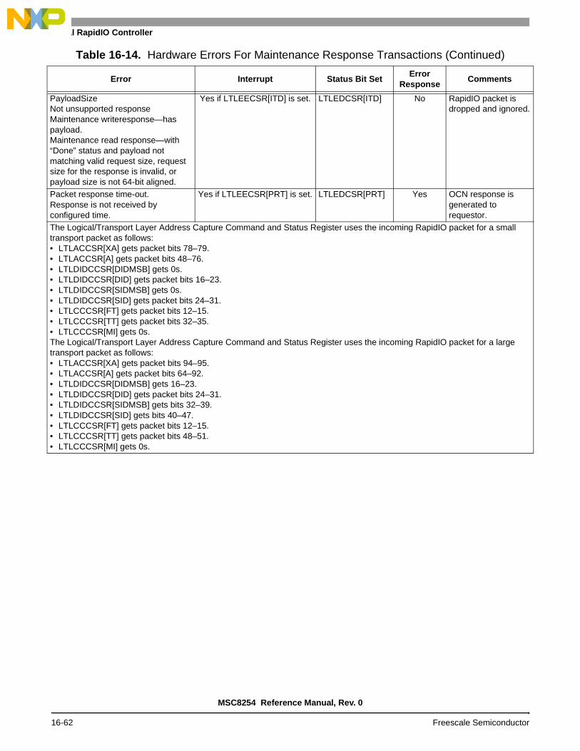
Serial RapidIO Controller
PayloadSizeNot unsupported responseMaintenance writeresponse—has payload.Maintenance read response—with “Done” status and payload not matching valid request size, request size for the response is invalid, or payload size is not 64-bit aligned.
Yes if LTLEECSR[ITD] is set. LTLEDCSR[ITD] No RapidIO packet is dropped and ignored.
Packet response time-out.Response is not received by configured time.
Yes if LTLEECSR[PRT] is set. LTLEDCSR[PRT] Yes OCN response is generated to requestor.
The Logical/Transport Layer Address Capture Command and Status Register uses the incoming RapidIO packet for a small transport packet as follows:• LTLACCSR[XA] gets packet bits 78–79. • LTLACCSR[A] gets packet bits 48–76.• LTLDIDCCSR[DIDMSB] gets 0s.• LTLDIDCCSR[DID] gets packet bits 16–23.• LTLDIDCCSR[SIDMSB] gets 0s.• LTLDIDCCSR[SID] gets packet bits 24–31.• LTLCCCSR[FT] gets packet bits 12–15.• LTLCCCSR[TT] gets packet bits 32–35.• LTLCCCSR[MI] gets 0s.The Logical/Transport Layer Address Capture Command and Status Register uses the incoming RapidIO packet for a large transport packet as follows:• LTLACCSR[XA] gets packet bits 94–95.• LTLACCSR[A] gets packet bits 64–92.• LTLDIDCCSR[DIDMSB] gets 16–23.• LTLDIDCCSR[DID] gets packet bits 24–31.• LTLDIDCCSR[SIDMSB] gets bits 32–39.• LTLDIDCCSR[SID] gets bits 40–47.• LTLCCCSR[FT] gets packet bits 12–15.• LTLCCCSR[TT] gets packet bits 48–51.• LTLCCCSR[MI] gets 0s.
Table 16-14. Hardware Errors For Maintenance Response Transactions (Continued)
Error Interrupt Status Bit SetError
ResponseComments
MSC8254 Reference Manual, Rev. 0
16-62 Freescale Semiconductor

RapidIO Interface Basics
Table 16-15. Hardware Errors For IO Response Transactions (Not Maintenance)
ErrorInterrupt
GeneratedStatus Bit
Set
OCN Error Response Generated
Logical/Transport Layer Capture Register
Comments
PriorityNot URResponse priority is not higher than RapidIO request priority
Yes if LTLEECSR[ITD] is set
LTLEDCSR[ITD]
No Using the incoming RapidIO packet, for Small Transport type packets, LTLACCSR[XA] gets packet bits 78–79 (if available), LTLACCSR[A] gets packet bits 48–76 (if available), LTLDIDCCSR[DIDMSB] gets 0’s, LTLDIDCCSR[DID] gets packet bits 16–23, LTLDIDCCSR[SIDMSB] gets 0’s, LTLDIDCCSR[SID] gets packet bits 24–31, LTLCCCSR[FT] gets packet bits 12–15, LTLCCCSR[TT] gets packet bits 32–35, LTLCCCSR[MI] gets 0’s
For Large Transport type packets. LTLACCSR[XA] gets packet bits 94-95 (if available), LTLACCSR[A] gets packet bits 64-92 (if available), LTLTLTLDIDCCSR[DIDMSB] gets 16-23, LTLDIDCCSR[DID] gets packet bits 24–31, LTLDIDCCSR[SIDMSB] gets bits 32-39, LTLDIDCCSR[SID] gets bits 40-47, LTLCCCSR[FT] gets packet bits 12–15, LTLCCCSR[TT] gets packet bits 48–51, LTLCCCSR[MI] gets 0’s
RapidIO packet is dropped and ignored
TransportTypeReceived reserved TT for this ftype
Yes if LTLEECSR[TSE] is set
LTLEDCSR[TSE]
No Same as first entry RapidIO packet is dropped and ignored
Received TT which is not enabled. - Error valid when passthroughis disabled and accept_all is disabled Or when accept_all is enabled.
Yes if LTLEECSR[TSE] is set
LTLEDCSR[TSE]
No Same as first entry RapidIO packet is dropped and ignored
DestIDDestID does not match this port’s DeviceID if Alternate DeviceID is disabled or DestId does not match either Alternate DeviceID or DeviceId if Alternate DeviceID is enabled.Error valid when (passthrough or accept_all) is false
Yes if LTLEECSR[ITTE] is set
LTLEDCSR[ITTE]
No Same as first entry RapidIO packet is dropped and ignored
SourceIDDoes not match the request’s DestID
Yes if LTLEECSR[
UR] is set
LTLEDCSR[UR]
No Same as first entry RapidIO packet is dropped and ignored
TransactionTypeNot URReceived RapidIO packet with reserved TType
Yes if LTLEECSR[ITD] is set
LTLEDCSR[ITD]
No Same as first entry RapidIO packet is dropped and ignored
MSC8254 Reference Manual, Rev. 0
Freescale Semiconductor 16-63

Serial RapidIO Controller
Not URIO read response does not correspond to an outstanding valid IO read request. IO write response does not correspond to an outstanding valid IO write request.
Yes if LTLEECSR[ITD] is set
LTLEDCSR[ITD]
No Same as first entry RapidIO packet is dropped and ignored
StatusNot URIO transaction - Is not “Done” or “Error” GSM transaction IO_Read_Home Is not “Done - Data-Only”, “Done - Done-Intervention”, “Done”, “Retry” or “Error”.Flush_w_Data response is not “Done”, “Retry” or “Error”Transaction type of “Response_with_data” and status is not done
Yes if LTLEECSR[ITD] is set
LTLEDCSR[ITD]
No Same as first entry RapidIO packet is dropped and ignored.
StatusNot URGSM Error response
Yes if LTLEECSR[GER] is set
LTLEDCSR[GER]
Yes if data is not
received for this
request.
Same as first entry except error capture is done from original request packet.
OCN error response is generated to requestor if data is not forwarded to it. Else the RapidIO packet is dropped.
StatusNot URIO Error Response
Yes if LTLEECSR[IER] is set
LTLEDCSR[IER]
Yes Same as first entry except error capture is done from original request packet.
OCN error response is generated to requestor.
TargetTIDNo outstanding transaction for this TargetTID
Yes if LTLEECSR[
UR] is set
LTLEDCSR[UR]
No Same as first entry RapidIO packet is dropped and ignored.
Table 16-15. Hardware Errors For IO Response Transactions (Not Maintenance) (Continued)
ErrorInterrupt
GeneratedStatus Bit
Set
OCN Error Response Generated
Logical/Transport Layer Capture Register
Comments
MSC8254 Reference Manual, Rev. 0
16-64 Freescale Semiconductor

RapidIO Interface Basics
Packet SizeNot UR(All non-maintenance and non-message)Write response - Header size is not 8 Bytes for Small Transport packet or not 12 Bytes for Large Transport packetGSM - “Done” response packet size to “Flush” is not 8 Bytes for Small Transport packet or not 12 Bytes for Large Transport packet.“Done-Intervention” is not 8 Bytes for Small Transport and 12 Bytes for Large Transport field.Two byte padding of 0’s in Large Transport field packet is not checked.
Yes if LTLEECSR[ITD] is set
LTLEDCSR[ITD]
No Same as first entry RapidIO packet is dropped and ignored.
Payload SizeNot URIO - Read Response - total payload is not of the size requested.“Done” or “Done-Data_Only” response to IO_Read_Home with incorrect payload size.Response with transaction type “response_with_no_data” has payload
Yes if LTLEECSR[ITD] is set
LTLEDCSR[ITD]
No Same as first entry RapidIO packet is dropped and ignored.
Retry Not URGSM request has had one more than configured number of retries for non misaligned request. The misaligned GSM request has had one to four (cumulative for the corresponding child requests) more than configured number of retries.
Yes if LTLEECSR[
RETE] is set
LTLEDCSR[RETE]
Yes Same as first entry except error capture is done from original request.
OCN error response is generated to requestor.
Table 16-15. Hardware Errors For IO Response Transactions (Not Maintenance) (Continued)
ErrorInterrupt
GeneratedStatus Bit
Set
OCN Error Response Generated
Logical/Transport Layer Capture Register
Comments
MSC8254 Reference Manual, Rev. 0
Freescale Semiconductor 16-65

Serial RapidIO Controller
Packet response time-outResponse is not received by configured time for packets requiring RapidIO response.“GSM - IO_Read_Home” - Done_With_Data is not received in configured time when Done_Intervention is received for non misaligned request or last child of misaligned request.Done response is not received in configured time for non misaligned request or last child of misaligned request. EME capture occurs for each child packet response time-out.
Yes if LTLEECSR[PRT] is set
LTLEDCSR[PRT]
Yes Same as first entry except error capture is done from original request.
OCN error response is generated to requestor.
Packet response time-outResponse is not received by configured time for packets requiring RapidIO response.“GSM - IO_Read_Home” - Done_Intervention is not received in configured time when Done_With_Data is received. This is true for both non misaligned or misaligned requests.
Yes if LTLEECSR[PRT] is set
LTLEDCSR[PRT]
No Same as first entry except error capture is done from original request.
An OCN done response is generated when the Done_With_Data is received for non misaligned requests or the last child of a misaligned request. Therefore, an error response cannot be sent when the packet response time-out occurs.
GSM - IO_Read_HomeNot URDone response, Retry response, or Error response is after Done_Intervention response or Data_only is received.
Yes if LTLEECSR[ITD] is set
LTLEDCSR[ITD]
No Same as first entry RapidIO packet is dropped and ignored.
Table 16-15. Hardware Errors For IO Response Transactions (Not Maintenance) (Continued)
ErrorInterrupt
GeneratedStatus Bit
Set
OCN Error Response Generated
Logical/Transport Layer Capture Register
Comments
MSC8254 Reference Manual, Rev. 0
16-66 Freescale Semiconductor

RapidIO Interface Basics
Not URResponse for OCN packets not requiring response, but converted to “response” type packet by ATMU receives Error response. For example, NWrite converted to NWrite_r received “Error” response
Yes if LTLEECSR[IER]/[GER]/[RETE] is
set
LTLEDCSR[IER]/[GER]/[RETE]
No Same as first entry except error capture is done from original request.
RapidIO packet is dropped and ignored.
Response for OCN packets not requiring response, but converted to “response” type packet by ATMU is not received by configured time.
Yes if LTLEECSR[PRT] is set
LTLEDCSR[PRT]
No Same as first entry except error capture is done from original request.
No error response is generated.
Table 16-15. Hardware Errors For IO Response Transactions (Not Maintenance) (Continued)
ErrorInterrupt
GeneratedStatus Bit
Set
OCN Error Response Generated
Logical/Transport Layer Capture Register
Comments
MSC8254 Reference Manual, Rev. 0
Freescale Semiconductor 16-67

Serial RapidIO Controller
Table 16-16. Hardware Errors For Message Request Transactions
Error Interrupt Status Bit Set Error
ResponseComments
PriorityNot applicable.TransportType
Received reserved TT.
Yes if LTLEECSR[TSE] is set.
LTLEDCSR[TSE] No RapidIO packet is dropped.
Received TT that is not enabled. Error is valid when passthrough is disabled and accept_all is disabled or when accept_all is enabled.
Yes if LTLEECSR[TSE] is set.
LTLEDCSR[TSE] No RapidIO packet is dropped.
DestIDDestID does not match this port DeviceID if Alternate DeviceID is disabled or DestId does not match either Alternate DeviceID or DeviceId if Alternate DeviceID is enabled.Error valid when (passthrough | accept_all) is false.
Yes if LTLEECSR[ITTE] is set.
LTLEDCSR[ITTE] Yes if priority is not 3. Else packet is dropped.
If priority is 3, packet is dropped.
SourceIDNot checked for error.
MsgLen,Ssize,Ltr,Mbox,MsgSegNot checked for error.
PayloadSizeMessage payload size is larger than the specified ssize or is of size 0 when seg_len == msg_len, or message payload size is not equal to specified ssize when seg_len!= msg_len.
Yes if LTLEECSR[MFE] is set.
LTLEDCSR[MFE] Yes if priority is not 3. Else packet is dropped.
If priority is 3, packet is dropped.
Reserved ssize field. Yes if LTLEECSR[MFE] is set.
LTLEDCSR[MFE] Yes if priority is not 3. Else packet is dropped.
If priority is 3, packet is dropped.
MSC8254 Reference Manual, Rev. 0
16-68 Freescale Semiconductor

RapidIO Interface Basics
OtherReceived message request with SOCAR[M] disabled.
Yes if LTLEECSR[UT] is set.
LTLEDCSR[UT] Yes if priority is not 3. Else packet is dropped.
If priority is 3, packet is dropped.
The Logical/Transport Layer Address Capture Command and Status Register uses the incoming RapidIO packet for a small transport packet as follows:• LTLACCSR[XA] gets packet bits 78–79.• LTLACCSR[A] gets packet bits 48–76.• LTLDIDCCSR[DIDMSB] gets 0s.• LTLDIDCCSR[DID] gets packet bits 16–23.• LTLDIDCCSR[SIDMSB] gets 0s.• LTLDIDCCSR[SID] gets bits 24–31.• LTLCCCSR[FT] gets packet bits 12–15.• LTLCCCSR[TT] gets packet bits 32–35.• LTLCCCSR[MI] gets 0s.The Logical/Transport Layer Address Capture Command and Status Register uses the incoming RapidIO packet for a large transport packet as follows:• LTLACCSR[XA] gets packet bits 94–95.• LTLACCSR[A] gets packet bits 64–92.• LTLDIDCCSR[DIDMSB] gets packet bits 16–23.• LTLDIDCCSR[DID] gets packet bits 24–31.• LTLDIDCCSR[SIDMSB] gets packet bits 32–39.• LTLDIDCCSR[SID] gets packet bits 40–47.• LTLCCCSR[FT] gets packet bits 12–15.• LTLCCCSR[TT] gets packet bits 48–51.• LTLCCCSR[MI] gets packet bits 56–63.
Table 16-16. Hardware Errors For Message Request Transactions (Continued)
Error Interrupt Status Bit Set Error
ResponseComments
MSC8254 Reference Manual, Rev. 0
Freescale Semiconductor 16-69

Serial RapidIO Controller
Table 16-17. Hardware Errors For Message Response Transactions
Error Interrupt Status Bit SetOCN Error Response
Comments
PriorityNot checked for error.TransportTypeReceive reserved TT.
Yes if LTLEECSR[TSE] is set.
LTLEDCSR[TSE] No RapidIO packet is dropped and ignored.
Received TT that is not enabled. Error is valid when passthrough is disabled and accept_all is disabled or when accept_all is enabled.
Yes if LTLEECSR[TSE] is set.
LTLEDCSR[TSE] No RapidIO packet is dropped and ignored.
DestID(All non-maintenance)DestID does not match this port DeviceID if Alternate DeviceID is disabled or DestId does not match either Alternate DeviceID or DeviceId if Alternate DeviceID is enabled. Error valid when (passthrough | accept_all) is false.
Yes if LTLEECSR[ITTE] is set.
LTLEDCSR[ITTE] No RapidIO packet is dropped and ignored.
SourceIDNot Checked for error.StatusNot checked for error.OtherReceived message response with SOCAR[M] disabled.
Yes if LTLEECSR[UR] is set.
LTLEDCSR[UR] No RapidIO packet is dropped and ignored.
The Logical/Transport Layer Address Capture Command and Status Register uses the incoming RapidIO packet for a small transport packet as follows:• LTLACCSR[XA] gets packet bits 78–79.• LTLACCSR[A] gets packet bits 48–76.• LTLDIDCCSR[DIDMSB] gets 0s.• LTLDIDCCSR[DID] gets packet bits 16–23.• LTLDIDCCSR[SIDMSB] gets 0s.• LTLDIDCCSR[SID] gets bits 24–31.• LTLCCCSR[FT] gets packet bits 12–15.• LTLCCCSR[TT] gets packet bits 32–35.• LTLCCCSR[MI] gets 0s.The Logical/Transport Layer Address Capture Command and Status Register uses the incoming RapidIO packet for a large transport packet as follows:• LTLACCSR[XA] gets packet bits 94–95.• LTLACCSR[A] gets packet bits 64–92.• LTLDIDCCSR[DIDMSB] gets packet bits 16–23.• LTLDIDCCSR[DID] gets packet bits 24–31.• LTLDIDCCSR[SIDMSB] gets packet bits 32–39.• LTLDIDCCSR[SID] gets packet bits 40–47.• LTLCCCSR[FT] gets packet bits 12–15.• LTLCCCSR[TT] gets packet bits 48–51.• LTLCCCSR[MI] gets packet bits 56–63.For all entries except the first, the capture registers are loaded from the response RapidIO packet.
MSC8254 Reference Manual, Rev. 0
16-70 Freescale Semiconductor

RapidIO Interface Basics
Table 16-18. Hardware Errors For Doorbell Request Transaction
Error Interrupt Status Bit SetError
ResponseComments
PriorityNot applicable.TransportTypeReceived reserved TT.
Yes if LTLEECSR[TSE] is set.
LTLEDCSR[TSE] No. RapidIO packet is dropped.
Received TT that is not enabled. Error is valid when passthrough is disabled and accept_all is disabled or when accept_all is enabled.
Yes if LTLEECSR[TSE] is set.
LTLEDCSR[TSE] No. RapidIO packet is dropped.
DestIDDestID does not match this port DeviceID if Alternate DeviceID is disabled or DestId does not match either Alternate DeviceID or DeviceId if Alternate DeviceID is enabled. Error is valid when (passthrough | accept_all) is false.
Yes if LTLEECSR[ITTE] is set.
LTLEDCSR[ITTE] Yes if priority is not 3. Else packet is dropped.
SourceIDNot checked for error.SrcTIDNot checked for error.OtherReceived doorbell request with DOCAR[D] disabled.
Yes if LTLEECSR[UT] is set.
LTLEDCSR[UT] Yes if priority is not 3. Else packet is dropped.
The Logical/Transport Layer Address Capture Command and Status Register uses the incoming RapidIO packet for a small transport packet as follows:• LTLACCSR[XA] gets packet bits 78–79.• LTLACCSR[A] gets packet bits 48–76.• LTLDIDCCSR[DIDMSB] gets 0s.• LTLDIDCCSR[DID] gets packet bits 16–23.• LTLDIDCCSR[SIDMSB] gets 0s.• LTLDIDCCSR[SID] gets bits 24–31.• LTLCCCSR[FT] gets packet bits 12–15.• LTLCCCSR[TT] gets packet bits 32–35.• LTLCCCSR[MI] gets 0s.The Logical/Transport Layer Address Capture Command and Status Register uses the incoming RapidIO packet for a large transport packet as follows for all entries but the blank ones:• LTLACCSR[XA] gets packet bits 94–95.• LTLACCSR[A] gets packet bits 64–92.• LTLDIDCCSR[DIDMSB] gets packet bits 16–23.• LTLDIDCCSR[DID] gets packet bits 24–31.• LTLDIDCCSR[SIDMSB] gets packet bits 32–39.• LTLDIDCCSR[SID] gets packet bits 40–47.• LTLCCCSR[FT] gets packet bits 12–15.• LTLCCCSR[TT] gets packet bits 48–51.• LTLCCCSR[MI] gets 0s.
MSC8254 Reference Manual, Rev. 0
Freescale Semiconductor 16-71

Serial RapidIO Controller
Table 16-19. Hardware Errors For Doorbell Response Transactions
Error Interrupt Status Bit SetOCN Error
ResponseComments
PriorityNot UR or UTResponse priority is not higher than RapidIO request priority.
Yes if LTLEECSR[ITD] is set.
LTLEDCSR[ITD] No RapidIO packet is dropped and ignored.
TransportTypeReceived reserved TT.
Yes if LTLEECSR[TSE] is set.
LTLEDCSR[TSE] No RapidIO packet is dropped and ignored.
Received TT Error is valid when passthrough is disabled and accept_all is disabled or when accept_all is enabled.
Yes if LTLEECSR[TSE] is set.
LTLEDCSR[TSE] No RapidIO packet is dropped and ignored.
DestIDDestID does not match this port DeviceID if Alternate DeviceID is disabled or DestId does not match either Alternate DeviceID or DeviceId if Alternate DeviceID is enabled. Error is valid when (passthrough | accept_all) is false.
Yes if LTLEECSR[ITTE] is set.
LTLEDCSR[ITTE] No RapidIO packet is dropped and ignored.
SourceIDDoes not match the request’s DestID.
Yes if LTLEECSR[UR] is set.
LTLEDCSR[UR] No RapidIO packet is dropped and ignored.
StatusNot UR or UTNot one of Done/Error/Retry.
Yes if LTLEECSR[ITD] is set.
LTLEDCSR[ITD] No RapidIO packet is dropped and ignored.
TransactionTypeNot UR or UTAnything other than Done_No_Data.
Yes if LTLEECSR[ITD] is set.
LTLEDCSR[ITD] No RapidIO packet is dropped and ignored.
TargetTIDNo outstanding transaction for this TargetTID.
Yes if LTLEECSR[UR] is set.
LTLEDCSR[UR] No RapidIO packet is dropped and ignored.
Packet SizeNot UR or UTDMA response. Header size is not 8 bytes for small transport packet or not 12 bytes for large transport packet. Two byte padding of 0s in a large transport field packet is not checked.
Yes if LTLEECSR[ITD] is set.
LTLEDCSR[ITD] No RapidIO packet is dropped and ignored.
MSC8254 Reference Manual, Rev. 0
16-72 Freescale Semiconductor

RapidIO Interface Basics
Packet response time-outResponse is not received by configured time.
Yes if LTLEECSR[PRT] is set.
LTLEDCSR[PRT] Yes
The Logical/Transport Layer Address Capture Command and Status Register uses the incoming RapidIO packet for a small transport packet as follows:• LTLACCSR[XA] gets packet bits 78–79.• LTLACCSR[A] gets packet bits 48–76.• LTLDIDCCSR[DIDMSB] gets 0s.• LTLDIDCCSR[DID] gets packet bits 16–23.• LTLDIDCCSR[SIDMSB] gets 0s.• LTLDIDCCSR[SID] gets bits 24–31.• LTLCCCSR[FT] gets packet bits 12–15.• LTLCCCSR[TT] gets packet bits 32–35.• LTLCCCSR[MI] gets 0s.The Logical/Transport Layer Address Capture Command and Status Register uses the incoming RapidIO packet for a large transport packet as follows for all entries but the last one, in which the capture registers are loaded from original request RapidIO packet:• LTLACCSR[XA] gets packet bits 94–95.• LTLACCSR[A] gets packet bits 64–92.• LTLDIDCCSR[DIDMSB] gets packet bit 16–23.• LTLDIDCCSR[DID] gets packet bits 24–31.• LTLDIDCCSR[SIDMSB] gets packet bits 32–39.• LTLDIDCCSR[SID] gets packet bits 40–47.• LTLCCCSR[FT] gets packet bits 12–15.• LTLCCCSR[TT] gets packet bits 48–51.• LTLCCCSR[MI] gets 0s.
Table 16-19. Hardware Errors For Doorbell Response Transactions
Error Interrupt Status Bit SetOCN Error
ResponseComments
MSC8254 Reference Manual, Rev. 0
Freescale Semiconductor 16-73

Serial RapidIO Controller
Table 16-20. Hardware Errors for Port-Write Transaction
Error Interrupt Status Bit SetError
Response Comments
PriorityNot applicable.TransportType
Received reserved TT.
Yes if LTLEECSR[TSE] is set.
LTLEDCSR[TSE] No RapidIO packet is dropped.
Received TT which is not enabled. - Error valid when passthrough is disabled and accept_all is disabled Or when accept_all is enabled.
Yes if LTLEECSR[TSE] is set.
LTLEDCSR[TSE] No RapidIO packet is dropped.
DestID
DestID does not match this port’s DeviceID if Alternate DeviceID is disabled or DestId does not match either Alternate DeviceID or DeviceId if Alternate DeviceID is enabled. Error valid when (passthrough | accept_all) is false.
Yes if LTLEECSR[ITTE] is set.
LTLEDCSR[ITTE] No RapidIO packet is dropped.
SourceIDNot checked for error.TransactionTypeNot checked for error.WrSizeNot UTIs one of reserved sizes or less than 4 bytes.
Yes if LTLEECSR[ITD] is set.
LTLEDCSR[ITD] No RapidIO packet is dropped.
SrcTIDNot checked for error.
HopCountNot checked for error.
ConfigOffsetNot checked for error.
PayloadSizeNot UTAn incorrect port-write wr_size encoding (not 4, 8, 16, 24, 32, 40, 48, 56, or 64 bytes). Payload size is greater than the value defined by wr_size. Payload size is not 64-bit aligned when the wr_size is not 4 bytes.
Yes if LTLEECSR[ITD] is set.
LTLEDCSR[ITD] No RapidIO packet is dropped.
MSC8254 Reference Manual, Rev. 0
16-74 Freescale Semiconductor

RapidIO Interface Basics
OtherReceived PortWrite transaction with DOCAR[PW] disabled.
Yes if LTLEECSR[UT] is set.
LTLEDCSR[UT] No RapidIO packet is dropped.
In Table 16-20, the Logical/Transport Layer Address Capture Command and Status Register uses the incoming RapidIO packet for a small transport packet as follows:• LTLACCSR[XA] gets packet bits 78–79.• LTLACCSR[A] gets packet bits 48–76.• LTLDIDCCSR[DIDMSB] gets 0s.• LTLDIDCCSR[DID] gets packet bits 16–23.• LTLDIDCCSR[SIDMSB] gets 0s.• LTLDIDCCSR[SID] gets bits 24–31.• LTLCCCSR[FT] gets packet bits 12–15.• LTLCCCSR[TT] gets packet bits 32–35.• LTLCCCSR[MI] gets 0s.In Table 16-20, the Logical/Transport Layer Address Capture Command and Status Register uses the incoming RapidIO packet for a large transport packet as follows for all entries but the blank ones:• LTLACCSR[XA] gets packet bits 94-95• LTLACCSR[A] gets packet bits 64–92.• LTLDIDCCSR[DIDMSB] gets packet bit 16–23.• LTLDIDCCSR[DID] gets packet bits 24–31.• LTLDIDCCSR[SIDMSB] gets packet bits 32–39.• LTLDIDCCSR[SID] gets packet bits 40–47.• LTLCCCSR[FT] gets packet bits 12–15.• LTLCCCSR[TT] gets packet bits 48–51.• LTLCCCSR[MI] gets 0s.
Table 16-20. Hardware Errors for Port-Write Transaction (Continued)
Error Interrupt Status Bit SetError
Response Comments
MSC8254 Reference Manual, Rev. 0
Freescale Semiconductor 16-75

Serial RapidIO Controller
Table 16-21. Hardware Errors for Outbound Transaction Crossed ATMU Boundary
Error Interrupt Status Bit SetOCN Error Response Generated
Comments
OCN Address and payload size OCN address range for Outbound RapidIO transaction hits multiple ATMU windows.
Yes if LTLEECSR[IACB] is set and/or LTLEDCSR[PRT] is set
LTLEDCSR[OACB]LTLEDCSR[PRT]
Yes if original request requires a response.
OCN error response is generated if the request requires a response. Otherwise, the OCN packet is dropped.
The Logical/Transport Layer Address Capture Command and Status Register uses the original RapidIO packet sent out by outbound. For a small transport packet, it uses the following:• LTLACCSR[XA] gets packet bits 78–79.• LTLACCSR[A] gets packet bits 48–76.• LTLDIDCCSR[DIDMSB] gets 0s.• LTLDIDCCSR[DID] gets packet bits 16–23.• LTLDIDCCSR[SIDMSB] gets 0s.• LTLDIDCCSR[SID] gets bits 24–31.• LTLCCCSR[FT] gets packet bits 12–15.• LTLCCCSR[TT] gets packet bits 32–35.• LTLCCCSR[MI] gets 0s.For a large transport packet, it uses the following:• LTLACCSR[XA] gets packet bits 94–95.• LTLACCSR[A] gets packet bits 64–92.• LTLDIDCCSR[DIDMSB] gets packet bits 16–23.• LTLDIDCCSR[DID] gets packet bits 24–31.• LTLDIDCCSR[SIDMSB] gets packet bits 32–39.• LTLDIDCCSR[SID] gets packet bits 40–47.• LTLCCCSR[FT] gets packet bits 12–15.• LTLCCCSR[TT] gets packet bits 48–51.• LTLCCCSR[MI] gets 0s.
MSC8254 Reference Manual, Rev. 0
16-76 Freescale Semiconductor

RapidIO Interface Basics
Table 16-22. Hardware Errors for Outbound Packet Time-to-Live Errors
Error Interrupt Status Bit SetOCN Error Response Generated
Comments
Packet time-to-live error. Yes if LTLEECSR[PTTL] is set
LTLEDCSR[PTTL] Yes if original request requires a response.
OCN error response is generated if the request requires a response. Otherwise, the OCN packet is dropped.
The Logical/Transport Layer Address Capture Command and Status Register uses the RapidIO packet attempted to send outbound. For a small transport packet, it uses the following:• LTLACCSR[XA] gets packet bits 78–79.• LTLACCSR[A] gets packet bits 48–76.• LTLDIDCCSR[DIDMSB] gets 0s.• LTLDIDCCSR[DID] gets packet bits 16–23.• LTLDIDCCSR[SIDMSB] gets 0s.• LTLDIDCCSR[SID] gets bits 24–31.• LTLCCCSR[FT] gets packet bits 12–15.• LTLCCCSR[TT] gets packet bits 32–35.• LTLCCCSR[MI] gets 0s.For a large transport packet, it uses the following:• LTLACCSR[XA] gets packet bits 94–95.• LTLACCSR[A] gets packet bits 64–92.• LTLDIDCCSR[DIDMSB] gets packet bits 16–23.• LTLDIDCCSR[DID] gets packet bits 24–31.• LTLDIDCCSR[SIDMSB] gets packet bits 32–39.• LTLDIDCCSR[SID] gets packet bits 40–47.• LTLCCCSR[FT] gets packet bits 12–15.• LTLCCCSR[TT] gets packet bits 48–51.• LTLCCCSR[MI] gets 0s.
MSC8254 Reference Manual, Rev. 0
Freescale Semiconductor 16-77

Serial RapidIO Controller
Table 16-23. Hardware Errors for Reserved Ftype
Error Interrupt GeneratedStatus Bit Set if Corresponding Bit is Enabled
Error Response
Comments
FtypeFtype is not IO Read, IO Write, SWrite, Maintenance request, Maintenance Response, Response (Ftype 13), Doorbell or Message class and it is not a passthrough transaction. (passthrough is not enabled | accept_all is enabled | transaction is addressed to this port).
Yes if LTLEECSR[UT] is set.
LTLEDCSR[UT] No RapidIO packet is dropped.
TransportTypeReceived reserved TT.
Yes if LTLEECSR[TSE] is set.
LTLEDCSR[TSE] No RapidIO packet is dropped.
Received TT that is not enabled.Error is valid when passthrough is disabled and accept_all is disabled or when accept_all is enabled.
Yes if LTLEECSR[TSE] is set.
LTLEDCSR[TSE] No RapidIO packet is dropped.
DestIDDestID does not match this port’s DeviceID if Alternate DeviceID is disabled or DestId does not match either Alternate DeviceID or DeviceId if Alternate DeviceID is enabled. Error valid when (passthrough | accept_all) is false.
Yes if LTLEECSR[ITTE] is set.
LTLEDCSR[ITTE] No RapidIO packet is dropped.
Address:WdPtr:XambsSwrite request hits overlapping ATMU windows. Refer to Section 16.2.5.4.2, Window Boundary Crossing Errors, on page 16-44. Packet is checked as a non-SWRITE packet.
Yes if LTLEECSR[IACB] is set.
LTLEDCSR[IACB] No RapidIO packet is dropped.
Address:WdPtr:XambsNot UTRequest hits a protected ATMU window or the local configuration space window. Packet is checked as non-Swrite packet.
Yes if LTLEECSR[ITD] is set.
LTLEDCSR[ITD] No RapidIO packet is dropped.
The Logical/Transport Layer Address Capture Command and Status Register uses the incoming RapidIO packet for a small transport packet as follows:• LTLACCSR[XA] gets packet bits 78–79.• LTLACCSR[A] gets packet bits 48–76.• LTLDIDCCSR[DIDMSB] gets 0s.• LTLDIDCCSR[DID] gets packet bits 16–23.• LTLDIDCCSR[SIDMSB] gets 0s.• LTLDIDCCSR[SID] gets bits 24–31.• LTLCCCSR[FT] gets packet bits 12–15.• LTLCCCSR[TT] gets packet bits 32–35.• LTLCCCSR[MI] gets 0s.The Logical/Transport Layer Address Capture Command and Status Register uses the incoming RapidIO packet for a large transport packet as follows for all entries:• LTLACCSR[XA] gets packet bits 94–95.• LTLACCSR[A] gets packet bits 64–92.• LTLDIDCCSR[DIDMSB] gets packet bits 16–23.• LTLDIDCCSR[DID] gets packet bits 24–31.• LTLDIDCCSR[SIDMSB] gets packet bits 32–39.• LTLDIDCCSR[SID] gets packet bits 40–47.• LTLCCCSR[FT] gets packet bits 12–15.• LTLCCCSR[TT] gets packet bits 48–51.• LTLCCCSR[MI] gets 0s.• LTLCCCSR[MI] gets 0s.
MSC8254 Reference Manual, Rev. 0
16-78 Freescale Semiconductor

RapidIO Message Unit
16.3 RapidIO Message Unit
The RapidIO message unit handles multicast and non-multicast single-segment messages and non-multicast multiple-segment messages. The RapidIO controller has two inbound and two outbound message controllers.
The message passing programming model for inter-processor and inter-device communication enables a producer to send a message across the interconnect fabric to the message hardware of a consumer, called a mailbox. The receiving mailbox hardware places the message into a queue located in local memory. A message consists of one to sixteen segments. When a configured number of messages is received, an interrupt is generated (if enabled) to the interrupt controller for the processor to process the messages. Messages can be queued for transmission in the producer memory, and the message hardware processes them sequentially. Messages can also be queued in consumer memory while software processes them sequentially. Software can configure the depths of the queues in the producer and consumer memories. A multicast function allows single-segment messages to be sent to multiple consumers.
The message unit is compliant with the message passing logical specification in the RapidIO Interconnect Specification, Revision 1.2. The message passing model is most commonly used in systems in which a processing element is allowed to access only memory that is local to itself, processing elements communicate with each other through message passing, and communication is address independent.
Each inbound message controller has a dedicated interrupt to notify software that a configured number of messages have been received. Similarly, each outbound message controller has a dedicated interrupt to notify software that there are no more messages for the outbound mailbox controller. The message controller is managed through a set of run-time registers.
16.3.1 Features
The message unit supports two outbound message controllers with the following features:
Chaining and direct modes.
Multicast up to 32 RapidIO destinations for single-segment messages.
Transmission to any mailbox for a single-segment message.
Transmission to any mailbox for a multi-segment message.
Segment size up to 256 bytes.
Up to 16 segment messages with a total payload of up to 4 KB.
One entire message with up to a 16 message segments can be transmitted before a response is received.
One entire single-segment message to all multicast destinations (up to 32) can be transmitted before a response is received.
MSC8254 Reference Manual, Rev. 0
Freescale Semiconductor 16-79

Serial RapidIO Controller
All message segment transfers for a message transaction must complete before the next message transaction begins.
Pipelined transmission of a full message in each message controller but all responses must be received before the next message can be transmitted.
In Chaining mode, the next descriptor can be fetched before the current message completes (descriptor prefetching).
The message unit supports two inbound message controllers with the following features:
Reception of any mailbox and letter for a single- or multi-segment message.
Segment size up to 256 bytes.
Up to sixteen segment messages with a total payload of up to 4 KB.
Full inbound line rate performance.
Back-to-back message reception of the same or lower priority.
Out-of-order message segment reception.
Concurrent inbound message controller operation.
16.3.2 Outbound Message Controller Operation
The outbound message controller sends messages stored in local memory, and it can operate in three different modes:
Direct mode. Software programs the necessary registers to point to the beginning of the message in memory.
Chaining mode. Software programs the necessary registers to point to the beginning of the first valid descriptor in memory. The descriptor provides all the necessary registers to start the message transfer.
Multicast mode. A single-segment message can be sent to multiple destinations. Multicast mode is supported in Direct or Chaining mode.
Each outbound message controller uses a unique identifying number. For example, if there are two outbound message controllers, message controller 0 uses number 0 and message controller 1 uses number 1.
16.3.2.1 Direct Mode
In Direct mode (OMxMR[MUTM] = 1; see page 16-194) the outbound message controller does not read descriptors from memory. Instead, it uses the parameters programmed in the outbound message controller registers to start the transfer. Software initializes all the parameters to start the message transmission. The message transfer starts when the outbound message controller start bit, OMxMR[MUS] changes from 0 to 1 and the outbound message controller is not busy. If it is busy, OMxMR[MUS] the transition from 0 to 1 is ignored. Software should program all the appropriate registers before setting OMxMR[MUS].
MSC8254 Reference Manual, Rev. 0
16-80 Freescale Semiconductor

RapidIO Message Unit
There are many ways in which software can interact with the message controller. One example sequence of events to start and complete a transfer in Direct mode is as follows:
1. Poll the OMxSR[MUB] bit to ensure that the outbound message controller is not busy.
2. Clear the following OMxSR status bits (see Table 16-104, OMxSR Field Descriptions, on page 16-197):
• MER
• RETE
• PRT]
• TE
• QOI
• QFI
• EOMI
• QEI
3. Initialize the following registers:
• Source address (OMxSAR)
• Destination port (OMxDPR)
• Destination attributes (OMxDATR)
• Retry error threshold (OMxRETCR)
• Double-word count (OMxDCR).
If multicast mode is enabled (OMxMR[MM]), initialize the multicast group and list in OMxMGR and OMxMLR.
4. Initialize the outbound message mode register message unit transfer mode bit, OMxMR[MUTM] = 1, to indicate direct mode. Other control parameters must also be initialized in the mode register.
5. Clear and then set the mode register message unit start bit, OMxMR[MUS], to start the message transfer.
6. The outbound message controller sets the OMxSR[MUB] bit to indicate that the message transfer is in progress.
7. The outbound message controller reads a message segment from local memory using the source address register (OMxSAR).
8. If a message has multiple segments, the outbound message controller reads the other message segments from local memory.
9. After the message read to local memory completes, the message is sent.
MSC8254 Reference Manual, Rev. 0
Freescale Semiconductor 16-81

Serial RapidIO Controller
10. The outbound message controller clears OMxSR[MUB]. A non-multicast message transfer completes after all message segments complete. A multicast message transfer completes after all message segments complete for each destination. A message segment completes when one of the following occurs:
• Done response received
• Error response
• Packet response time-out received
• Retry error threshold exceeded
• An internal error occurs during the local memory access
11. After the outbound message operation completes, the outbound message interrupt is generated if the end of message outbound message interrupt event is enabled (OMnDATR[EOMIE]).
In Direct mode, the outbound message interrupt is generated after a message operation completes if OMxDATR[EOMIE] =1.
The event causing this interrupt is indicated by OMxSR[EOMI]. The interrupt is held until the OMxSR[EOMI] bit is cleared by writing a 1 to it.
In Direct mode, the Error/Port-Write interrupt is generated for the following reasons:
• A message error response is received and this interrupt event is enabled (OMxMR[EIE]).
• A packet response time-out occurs and this interrupt event is enabled (OMxMR[EIE]).
• A retry threshold exceeded error occurs and this interrupt event is enabled (OMxMR[EIE]).
• An internal error response is received and this interrupt event is enabled (OMxMR[EIE]).
Table 16-24 describes each of these error types.
Table 16-24. Error Types In Outbound Message Controller Direct Mode
Error Type Message Controller Response to Error
Message Error Response • Sets the message error response status bit (OMxSR[MER]).• Generates a serial RapidIO error/write-port interrupt if OMxMR[EIE] is
set. • Stops after the message operation completes (indicated by
OMxSR[MUB]).
MSC8254 Reference Manual, Rev. 0
16-82 Freescale Semiconductor

RapidIO Message Unit
16.3.2.2 Software Error Handling
When an error occurs and the Serial RapidIO error/write-port interrupt is generated, software takes the following actions:
1. Determines the cause of the interrupt and processes the error.
2. Verifies that the message controller has stopped operation by polling OMxSR[MUB].
3. Disables the message controller by clearing OMxMR[MUS].
4. Clears the error by writing a 1 to the corresponding OMxSR status bit (see Table 16-104, OMxSR Field Descriptions, on page 16-197):
• MER
• PRT
• RETE
• TE
When an error occurs and the Serial RapidIO error/write-port interrupt is not enabled, software takes the following actions:
1. Determines that an error has occurred by polling the status bits OMxSR status bit (see Table 16-104, OMxSR Field Descriptions, on page 16-197):
• MER
Packet Response Time-Out • Sets the packet response time-out status bit (OMxSR[PRT]).• Generates a serial RapidIO error/write-port interrupt if OMxMR[EIE] is
set.• Stops after the message operation completes (indicated by
OMxSR[MUB]).
Retry Error Threshold Exceeded • Sets the retry threshold exceed status bit (OMxSR[RETE]).• Generates a Serial RapidIO error/write-port interrupt if OMxMR[EIE] is
set.• Stops after the message operation completes (indicated by
OMxSR[MUB]).
Internal Error During Local Memory Read • Sets the transaction error bit (OMxSR[TE]) • Does not send message segments with an internal error because the
message data is not available• Does not transfer memory reads generated before the internal error.• Generates but does not transfer additional memory reads for the same
message operation.• Does not transfer all subsequent message segments for the same
message operation, including retried message segments.• Stops after the message operation completes (indicated by
OMxSR[MUB]).• Generates the Serial RapidIO error/write-port interrupt if OMxMR[EIE] is
set.
Table 16-24. Error Types In Outbound Message Controller Direct Mode (Continued)
Error Type Message Controller Response to Error
MSC8254 Reference Manual, Rev. 0
Freescale Semiconductor 16-83
Serial RapidIO Controller
• PRT
• RETE
• TE
2. Verifies that the message controller has stopped operation by polling OMxSR[MUB].
3. Disables the message controller by clearing OMxMR[MUS].
4. Clears the error by writing a 1 to the corresponding status bit (listed in step 1).
16.3.2.3 Disabling and Enabling the Message Controller
Once the message controller is started, it cannot be stopped except by loss of power or reset.
16.3.2.4 Hardware Error Handling
Table 16-25 describes Direct mode hardware errors. The error checking level indicates the order in which errors are checked. Multiple errors can be checked at an error checking level. When an error is detected, no additional error checking beyond the current level is performed. The first error detected in the processing pipeline updates the error management extensions registers. These error condition checks are provided by the messaging unit in addition to the error condition checks provided by the RapidIO port described in Section 16.2.10, Errors and Error Handling, on page 16-48.
Table 16-25. Outbound Message Direct Mode Hardware Errors
Transaction Error Description
Message request
Internal error during a read of the message segment from local memory
Error checking level: 1Interrupt generated: Serial RapidIO error/write-port if OMxMR[EIE] setStatus bit set: Transaction error in the outbound message status register (OMxSR[TE]). Message failed in the mailbox CSR (MCSR[FA]).Message segment sent: NoLogical/Transport Layer Capture Register:Comments: Message controller stops after the current message operation completes. The descriptor dequeue pointer is not incremented in chaining mode.
Message request
Internal error for an earlier message segment local memory read. An internal error for a subsequent message segment local memory read for the same message may or may not occur.
Error checking level: 2Interrupt generated:Status bit set: NoneMessage segment sent: YesLogical/Transport Layer Capture Register:
Undefined packet
Reserved ftype encoding1
Error checking level: 3Interrupt generated: Serial RapidIO error/write-port if LTLEECSR[UT] is setStatus bit set: Unsupported transaction in the Logical/Transport Layer Error Detect CSR LTLEDCSR[UT]Message segment sent: YesLogical/Transport Layer Capture Register: Updated with the packet.2
Comments: Packet is ignored and discarded.
MSC8254 Reference Manual, Rev. 0
16-84 Freescale Semiconductor

RapidIO Message Unit
Message response
Reserved tt encoding1
Error checking level: 3Interrupt generated: Serial RapidIO error/write-port if LTLEECSR[TSE] is setStatus bit set: Illegal transaction target in the Logical/Transport Layer Error Detect CSR LTLEDCSR[ITTE]. Transport size error in the Logical/Transport Layer Error Detect CSR LTLEDCSR[TSE].Message segment sent: YesLogical/Transport Layer Capture Register: Updated with the packet.2
Comments: Packet is ignored and discarded.Message response
Large transport size when operating in small transport size or small transport size when operating in large transport size1
Error checking level: 3Interrupt generated: Serial RapidIO error/write-port if LTLEECSR[TSE] is setStatus bit set: Transport size error in the Logical/Transport Layer Error Detect CSR LTLEDCSR[TSE].Message segment sent: YesLogical/Transport Layer Capture Register: Updated with the packet.2
Comments: Packet is ignored and discarded. An error or illegal transaction target error response is not generated.
Message response
Illegal destination ID1
Error checking level: 3Interrupt generated: Serial RapidIO error/write-port if LTLEECSR[ITTE] is setStatus bit set: Illegal transaction target in the Logical/Transport Layer Error Detect CSR LTLEDCSR[ITTE].Message segment sent: YesLogical/Transport Layer Capture Register: Updated with the packet.2
Comments: Packet is ignored and discarded.Message response
ttype (transaction field) is not message response1
Error checking level: 3Interrupt generated: Serial RapidIO error/write-port if LTLEECSR[ITD] is setStatus bit set: Illegal transaction decode in the Logical/Transport Layer Error Detect CSR LTLEDCSR[ITD].Message segment sent: YesLogical/Transport Layer Capture Register: Updated with the packet.2
Comments: Packet is ignored and discarded.
Message response
Message response received and no outbound mailboxes are supported1
Error checking level: 3Interrupt generated: Serial RapidIO error/write-port if LTLEECSR[UR] is setStatus bit set: Unsupported transaction in the Logical/Transport Layer Error Detect CSR LTLEDCSR[UR].Message segment sent: NoLogical/Transport Layer Capture Register: Updated with the packet.2
Comments: Packet is ignored and discarded.Message response
Reserved response status (not done, retry, or error)
Error checking level: 4aInterrupt generated: Serial RapidIO error/write-port if LTLEECSR[ITD] is set.Status bit set: Illegal transaction decode in the Logical/Transport Layer Error Detect CSR LTLEDCSR[ITD].Message segment sent: YesLogical/Transport Layer Capture Register: Updated with the packet.2
Comments: Packet is ignored and discarded.Message response
Message response packet size is incorrect
Error checking level: 4aInterrupt generated: Serial RapidIO error/write-port if LTLEECSR[ITD] is set.Status bit set: Message format error in the Logical/Transport Layer Error Detect CSR LTLEDCSR[ITD].Message segment sent: YesLogical/Transport Layer Capture Register: Updated with the packet.2
Comments: Packet is ignored and discarded.
Table 16-25. Outbound Message Direct Mode Hardware Errors
Transaction Error Description
MSC8254 Reference Manual, Rev. 0
Freescale Semiconductor 16-85
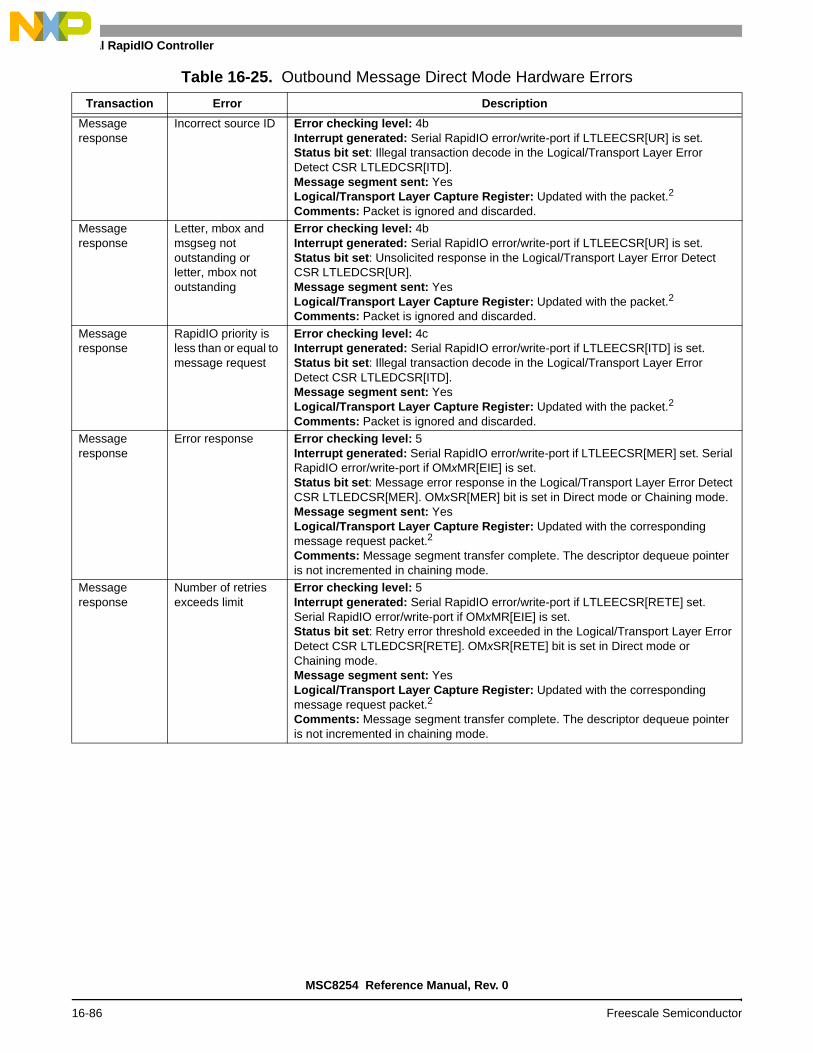
Serial RapidIO Controller
Message response
Incorrect source ID Error checking level: 4bInterrupt generated: Serial RapidIO error/write-port if LTLEECSR[UR] is set.Status bit set: Illegal transaction decode in the Logical/Transport Layer Error Detect CSR LTLEDCSR[ITD].Message segment sent: YesLogical/Transport Layer Capture Register: Updated with the packet.2
Comments: Packet is ignored and discarded.Message response
Letter, mbox and msgseg not outstanding or letter, mbox not outstanding
Error checking level: 4bInterrupt generated: Serial RapidIO error/write-port if LTLEECSR[UR] is set.Status bit set: Unsolicited response in the Logical/Transport Layer Error Detect CSR LTLEDCSR[UR].Message segment sent: YesLogical/Transport Layer Capture Register: Updated with the packet.2
Comments: Packet is ignored and discarded.
Message response
RapidIO priority is less than or equal to message request
Error checking level: 4cInterrupt generated: Serial RapidIO error/write-port if LTLEECSR[ITD] is set.Status bit set: Illegal transaction decode in the Logical/Transport Layer Error Detect CSR LTLEDCSR[ITD].Message segment sent: YesLogical/Transport Layer Capture Register: Updated with the packet.2
Comments: Packet is ignored and discarded.Message response
Error response Error checking level: 5Interrupt generated: Serial RapidIO error/write-port if LTLEECSR[MER] set. Serial RapidIO error/write-port if OMxMR[EIE] is set.Status bit set: Message error response in the Logical/Transport Layer Error Detect CSR LTLEDCSR[MER]. OMxSR[MER] bit is set in Direct mode or Chaining mode. Message segment sent: YesLogical/Transport Layer Capture Register: Updated with the corresponding message request packet.2
Comments: Message segment transfer complete. The descriptor dequeue pointer is not incremented in chaining mode.
Message response
Number of retries exceeds limit
Error checking level: 5Interrupt generated: Serial RapidIO error/write-port if LTLEECSR[RETE] set. Serial RapidIO error/write-port if OMxMR[EIE] is set.Status bit set: Retry error threshold exceeded in the Logical/Transport Layer Error Detect CSR LTLEDCSR[RETE]. OMxSR[RETE] bit is set in Direct mode or Chaining mode.Message segment sent: YesLogical/Transport Layer Capture Register: Updated with the corresponding message request packet.2
Comments: Message segment transfer complete. The descriptor dequeue pointer is not incremented in chaining mode.
Table 16-25. Outbound Message Direct Mode Hardware Errors
Transaction Error Description
MSC8254 Reference Manual, Rev. 0
16-86 Freescale Semiconductor

RapidIO Message Unit
Table 16-26 lists programming errors that result in undefined or undesired hardware operation.
Message response
Packet response time-out
Error checking level: UnrelatedInterrupt generated: Serial RapidIO error/write-port if LTLEECSR[PRT] set. Serial RapidIO error/write-port if OMxMR[EIE].Status bit set: Packet response time-out in the Logical/Transport Layer Error Detect CSR LTLEDCSR[PRT]. OMxSR[PRT] bit is set in Direct mode or Chaining mode.Message segment sent: YesLogical/Transport Layer Capture Register: Updated with the corresponding message request packet.2 The LTLDIDCCSR[SIDMSB] and LTLDIDCCSR[SID] field has a value of 0..
Comments: Message segment transfer complete. The descriptor dequeue pointer is not incremented in chaining mode.
Notes: 1. Notes: 1. These error types are actually detected in the RapidIO port, not in the message controller.
2. In small transport size configuration using the packet, the following allocations are made:
• LTLACCSR[XA] gets the extended address (packet bits 78–79).• LTLACCSR[A] gets the address (packet bits 48–76).• LTLDIDCCSR[MDID] gets 0.• LTLDIDCCSR[DID] gets the least significant byte of the destination ID (packet bits 16–23).• LTLDIDCCSR[MSID] gets 0.• LTLDIDCCSR[SID] gets the least significant byte of the source ID (packet bits 24–31).• LTLCCCSR[FT] gets the ftype (packet bits 12–15).• LTLCCCSR[TT] gets the ttype (packet bits 32–35).• LTLCCCSR[MI] gets the msg info (packet bits 40–47)
In large transport size configuration using the packet, the following allocations are made:
• LTLACCSR[XA] gets the extended address (packet bits 94–95).• LTLACCSR[A] gets the address (packet bits 64–92).• LTLDIDCCSR[MDID] gets the most significant byte of the destination ID (packet bits
16–23).• LTLDIDCCSR[DID] gets the least significant byte of the destination ID (packet bits 24–31).• LTLDIDCCSR[MSID] gets the most significant byte of the source ID (packet bits 32–39).• LTLDIDCCSR[SID] gets the least significant byte of the source ID (packet bits 40–47).• LTLCCCSR[FT] gets the ftype (packet bits 12–15).• LTLCCCSR[TT] gets the ttype (packet bits 48–51) if the message request packet is
captured or 0 if the message response packet is captured.• LTLCCCSR[MI] gets the message information (packet bits 56–63).
Table 16-26. Outbound Message Direct Mode Programming Errors
ErrorInterrupt
GeneratedStatus Bit Set Comments
Double word count greater than 256 bytes when multi-cast mode selected
No None Undefined operation
Double word count set to a reserved value No None Undefined operation Transaction flow level set to 3 No None Undefined operation Target interface set to an invalid RapidIO port No None Undefined operation
Source address for message read is invalid No No Local memory captures the transaction and generates an interrupt.
Register values changed during operation No No Undefined operation.
Table 16-25. Outbound Message Direct Mode Hardware Errors
Transaction Error Description
MSC8254 Reference Manual, Rev. 0
Freescale Semiconductor 16-87

Serial RapidIO Controller
16.3.2.5 Chaining Mode
In Chaining mode, OMxMR[MUTM] = 0, message descriptors are built in local memory in a circular queue. Several options are available to the programmer. Software can build one or more descriptors before initializing the outbound message controller registers, or it can initialize the outbound message controller registers and then build the descriptors. Software maintains the enqueue pointer (OMxDQEPAR). The outbound message controller dequeues descriptors, processes them, and increments the dequeue pointer (OMxDQDPAR) to point to the next descriptor in the queue. Figure 16-9 depicts a sample structure of the outbound portion of the message controller and a descriptor queue, with each valid descriptor queue entry pointing to a valid message. The descriptor queue has eight entries, four of which are valid. The local processor enqueues descriptors and the outbound message controller dequeues the descriptors.
Figure 16-9. Outbound Frame Queue Structure
One of several ways software can initialize the message controller in Chaining mode is as follows:
1. Poll the status register message unit busy bit, OMxSR[MUB], to verify that the outbound message controller is not busy.
2. Clear the message unit start bit (OMxMR[MUS]).
3. Initialize the descriptor queue dequeue pointer address registers (OMxDQDPAR; see page 16-198) and the enqueue pointer address registers (OMxDQEPAR; see page 16-203) to the same value for proper operation.
Outbound
MessageData
MessageData
MessageData
Descriptor
Descriptor
Descriptor
Descriptor
Enqueue Pointer
Dequeue Pointer
Outbound
Message
Controller
Local Memory
Local Memory
Packets to
MessageData
Local Processor
Enqueue and Dequeue
RapidIOInterface
Pointers
Descriptor List
Queue
MSC8254 Reference Manual, Rev. 0
16-88 Freescale Semiconductor

RapidIO Message Unit
These registers must also be queue size aligned on a boundary equal to the number of queue entries × 32 bytes (the size of each queue descriptor). For example, there are 16 entries in the queue, the register must be 512-byte aligned.
The number of queue entries is set in OMnMR[CIRQ_SIZ]. See Section 16.6.59, Outbound Message x Mode Registers (OMxMR), on page 16-194.
4. Initialize the retry error threshold in the outbound message retry error threshold configuration register (OMxRETCR; see page 16-204).
5. Clear OMxMR[MUTM] for Chaining mode.
6. If you are using single-segment multicast mode, set OMxMR[MM].
7. Configure the other control parameters in the mode register (OMxMR).
8. Clear OMxSR[MER, PRT, RETE, TE, QOI, QFI, EOMI, and QEI]. If OMxSR[MER, PRT, RETE, TE, or QOI] are not cleared, the message controller does not start a new message operation. Incorrect status is indicated if the other status bits are not cleared.
9. Set the message unit start (OMxMR[MUS]) to enable the outbound message controller and cause the descriptor queue dequeue pointer (OMxDQDPAR) to be saved as the base address of the descriptor queue.
The method to start and complete transfers by adding descriptors after initializing the message unit is as follows:
1. Create one or more descriptors in local memory starting at the address to which the descriptor queue enqueue pointer address register (OMxDQEPAR) is pointing.
2. Either increment the enqueue pointer address registers (OMxDQEPAR) by setting OMxMR[MUI] for each descriptor entry added or directly change the enqueue pointer address register (OMxDQEPAR). If software sets OMxMR[MUI], the message controller clears this bit after successfully incrementing the enqueue pointer.
3. When the descriptor queue is not empty, the message controller reads the descriptor from local memory using the address to which the dequeue pointer (OMxDQDPAR) is pointing and sets the busy bit (OMxSR[MUB]).
4. The message controller reads the next descriptor from local memory, if available, using the address to which the dequeue pointer (OMxDQDPAR) is pointing. The message controller does not prefetch more than one descriptor.
5. The message controller sets OMxSR[MUB] to indicate that the message transfer is in progress. OMxSR[MUB] remains set until the descriptor queue is empty or a transaction error occurs.
MSC8254 Reference Manual, Rev. 0
Freescale Semiconductor 16-89

Serial RapidIO Controller
6. Software can create and enqueue additional descriptors while the message controller is busy (OMxSR[MUB]). Software can continue adding descriptors as long as the descriptor queue is not full. If software adds descriptors using the OMxMR[MUI] bit, overflowing the queue can be prevented by polling the queue full bit (OMxSR[QF]) before creating and enqueueing the next descriptor.
7. After the descriptor memory read completes, the corresponding message segment is read from local memory.
8. If a message has multiple segments, the outbound message controller reads the other message segments from local memory.
9. After the message read to local memory completes, the message is sent.
10. If multi-cast is enabled, all the indicated targets are sent the same message.
11. A non-multicast message transfer completes after all message segments complete. A multi-cast message transfer completes after all message segments complete for each destination. A message segment completes when one of the following occurs:
• Done response received
• Error response received
• Packet response time-out
• Retry error threshold exceeded
• Internal error during the descriptor (all message segments complete) or message read of local memory
12. When processing for the current descriptor completes and another descriptor is available, the preceding steps are repeated.
13. If a RapidIO error response is received, the message error response bit is set (OMxSR[MER]) and the outbound message controller operation stops after all message segments complete. If OMxMR[EIE] is set, the interrupt Serial RapidIO error/write-port is generated.
14. If a packet response time-out occurs, the packet response time-out bit is set (OMxSR[PRT]). If OMxMR[EIE] is set, the interrupt Serial RapidIO error/write-port is generated.
15. If the retry error threshold value is exceeded for a specific segment, the retry error threshold exceeded bit is set (OMxSR[RETE]) and outbound message controller operation stops after all message segments complete. If OMxMR[EIE] is set, the interrupt Serial RapidIO error/write-port is generated.
16. If an internal error occurs while local memory is read, the transaction error bit is set (OMxSR[TE]) and outbound message controller operation stops after all message segments complete. If OMxMR[EIE] is set, the interrupt Serial RapidIO error/write-port is generated.
MSC8254 Reference Manual, Rev. 0
16-90 Freescale Semiconductor

RapidIO Message Unit
This process continues until the descriptor queue is empty (dequeue pointer equals the enqueue pointer).
17. The message unit clears OMxSR[MUB] after it processes the last descriptor or a transaction error occurs.
18. If an error occurs, the message unit must be disabled, reinitialized, and reenabled before another message can be sent.
16.3.2.5.1 Changing Descriptor Queues in Chaining Mode
When software switches to another descriptor queue in local memory, it must wait for the processing of the current queue to complete, as indicated by the busy bit (OMxSR[MUB]). Software then disables the message controller by clearing OMxMR[MUS], changes the enqueue and dequeue descriptor pointers (OMxDQEPAR and OMxDQDPAR), and reenables the message unit by setting OMxMR[MUS].
16.3.2.5.2 Preventing Queue Overflow in Chaining Mode
Software must guarantee that descriptors are not added to an already full queue. When the increment bit is used (OMxMR[MUI]), software can poll the queue full bit (OMxSR[QF]) before enqueueing another descriptor. When software sets the enqueue pointer directly, software is responsible for not overflowing the descriptor queue.
16.3.2.5.3 Switching Between Direct and Chaining Modes
The message unit architecture allows switching from Direct mode to Chaining mode and vice versa after all required parameters are initialized in the appropriate registers and the message unit is not busy, as indicated by clearing of the OMxSR[MUB]. If OMxMR[MUS] is cleared and then set during a switch from Direct mode to Chaining mode, the message unit is reinitialized in Chaining mode and the outbound message descriptor dequeue pointer address is saved as the new base address of the circular queue in memory. During a switch from Chaining mode to Direct mode, OMxMR[MUS] must also be cleared and set.
MSC8254 Reference Manual, Rev. 0
Freescale Semiconductor 16-91

Serial RapidIO Controller
16.3.2.5.4 Chaining Mode Descriptor Format
The descriptor contains information the message unit controller needs to transfer data. Software must ensure that each descriptor is aligned on a 32-byte boundary and that the descriptor queue is on a queue boundary, that is, on a boundary equal to the number of queue entries × 32 byte (the size of each queue descriptor). For each descriptor in the queue, the message unit controller starts a new message operation with the control parameters specified by the descriptor, as shown in Table 16-27.
Figure 16-10 depicts the queue dequeue pointer and an associated descriptor. The descriptor is valid only if the enqueue and dequeue pointers are not equal.
Figure 16-10. Descriptor Dequeue Pointer and Descriptor
Table 16-27. Outbound Message Unit Descriptor Summary
Descriptor Field Description
Reserved —
Source address Source address of the message operation. After the message controller reads the descriptor from memory, this field is loaded into the Source Address Register.
Destination port Destination port of the message operation. After the message controller reads the descriptor from memory, this field is loaded into the Destination Port Register.
Destination attributes Transaction attributes of the message operation. After the message controller reads the descriptor from memory, this field is loaded into the Destination Attributes Register.
Multicast group Logical multi-cast group. Groups are defined as a list of 32 numerically consecutive destinations by deviceID.
Multi-cast list Bit vector list of consecutive destinations by deviceID.
Double-word count Number of double-words for the message operation. After the message controller reads the descriptor from memory, this field is loaded into the Double-Word Count Register.
Reserved —
Descriptor Dequeue Pointer Address Register
Descriptor
310
0x00
0x08
0x18
0x10
0x04
Destination Port
Reserved
Double-word Count
Multicast Group
Local MemoryOffset
0x14
Source Address
0x0C
Multicast List
310
0x1C
Destination Attributes
Reserved
MSC8254 Reference Manual, Rev. 0
16-92 Freescale Semiconductor

RapidIO Message Unit
16.3.2.5.5 Chaining Mode Controller Interrupts
An outbound message interrupt can be generated for one of the following reasons.
Queue Empty. The queue goes empty and the interrupt event is enabled (OMxMR[QEIE] = 1). The event causing the outbound message interrupt is indicated by OMxSR[QEI]. The interrupt is held until the queue is not empty and the OMxSR[QEI] bit is cleared by writing a value of 1 to it.
Queue Full. The queue is full and the interrupt event is enabled (OMxMR[QFIE] = 1). The event causing the outbound message interrupt is indicated by OMxSR[QFI]. The interrupt is held until the queue is not full and the OMxSR[QFI] bit is cleared by writing a value of 1 to it.
Queue Overflow. The queue is full, the increment bit is set (OMnMR[MUI]), and the interrupt event is enabled (OMxMR[QOIE] = 1). The event causing the outbound message interrupt is indicated by OMxSR[QOI]. The message unit must be reinitialized. The interrupt is held until the OMxSR[QOI] bit his cleared by writing a value of 1 to it. This interrupt is also generated if the enqueue pointer is directly written and causes an overflow.
End-Of-Message. The message completed and the interrupt event is enabled (OMxDATR[EOMIE] = 1). The event causing this interrupt is indicated by OMxSR[EOMI]. The interrupt is held until the OMxSR[EOMI] bit is cleared by writing a value of 1 to it. This allows an interrupt to be generated after a particular descriptor is processed.
An error/port-write interrupt can be generated for the following reasons in Chaining mode.
Message error response. Message error response is received and this interrupt event is enabled (OMxMR[EIE])
Packet response time-out. A packet response time-out occurs and this interrupt event is enabled (OMxMR[EIE]).
Retry error threshold exceeded. A retry threshold exceeded error occurs and this interrupt event is enabled (OMxMR[EIE]).
Transaction error. A message error response is received and this interrupt event is enabled (OMxMR[EIE]).
MSC8254 Reference Manual, Rev. 0
Freescale Semiconductor 16-93

Serial RapidIO Controller
Table 16-24 describes each of these error types.
16.3.2.6 Software Error Handling
When an error occurs and the Serial RapidIO error/write-port interrupt is generated, software takes the following actions:
1. Determines the cause of the interrupt and processes the error.
2. Verifies that the message controller has stopped operation by polling OMxSR[MUB].
3. Disables the message controller by clearing OMxMR[MUS].
4. Clears the error by writing a 1 to the corresponding OMxSR status bit (MER, PRT, RETE, or TE).
When an error occurs and the Serial RapidIO error/write-port interrupt is not enabled, software takes the following actions:
Table 16-28. Error Types In Outbound Message Controller Direct Mode
Error Type Message Controller Response to Error
Message Error Response • Sets the message error response status bit (OMxSR[MER]).• Generates the Serial RapidIO error/write-port if OMxMR[EIE] is set.• Stops after the message operation completes (indicated by
OMxSR[MUB]).
Packet Response Time-Out • Sets the packet response time-out status bit (OMxSR[PRT]). • Generates the Serial RapidIO error/write-port interrupt if OMxMR[EIE] is
set.• Stops after the message operation completes (indicated by
OMxSR[MUB]).
Retry Error Threshold Exceeded • Sets the retry threshold exceed status bit (OMxSR[RETE]) • Generates the Serial RapidIO error/write-port interrupt if OMxMR[EIE] is
set.• Stops after the message operation completes (indicated by
OMxSR[MUB]).
Transaction error • Sets the transaction error bit (OMxSR[TE]).• Does not generate message segment reads and sends no message
segments if the internal error occurs while the memory controller reads descriptor memory.
• Does not sent message segments with an internal error because the message data is not available.
• Does not transfer memory reads generated before the internal error.• Generates additional memory reads for the same message operation but
does not transfer them.• Does not transfer subsequent message segments for the same message
operation. This includes retried message segments.• Stops after the message operation completes (indicated by
OMxSR[MUB]).• Generates the Serial RapidIO error/write-port interrupt if OMxMR[EIE] is
set.
MSC8254 Reference Manual, Rev. 0
16-94 Freescale Semiconductor

RapidIO Message Unit
1. Determines that an error has occurred by polling the following OMxSR status bits (see Table 16-104, OMxSR Field Descriptions, on page 16-197:
• MER
• PRT
• RETE
• TE
2. Verifies that the message controller has stopped by polling OMxSR[MUB].
3. Disables the message controller by clearing OMxMR[MUS].
4. Clears the error by writing a 1 to the corresponding OMxSR status bit (listed in step 1).
16.3.2.7 Hardware Error Handling
Table 16-29 shows error conditions in addition to those for Direct mode. All the errors listed in Table 16-25, Outbound Message Direct Mode Hardware Errors, on page 16-84 can also occur. The error checking level indicates the order in which errors are checked. Multiple errors can be checked at an error checking level. When an error is detected no additional error checking beyond the current level is performed. The first error detected in the processing pipeline updates the error management extensions registers. The messaging unit provides these error condition checks in addition to the error condition checks provided by the RapidIO port and described in Section 16.2.10, Errors and Error Handling, on page 16-48.
Table 16-30 lists programming errors that result in undefined or undesired hardware operation. These errors are in addition to those listed in Table 16-26, Outbound Message Direct Mode Programming Errors, on page 16-87.
Table 16-29. Additional Hardware Error Conditions
Transaction Error Description
Message request
Internal error during a read of the descriptor from local memory
Error checking level: 0Interrupt generated: Serial RapidIO error/write-port if OMxMR[EIE] is set.Status bit set: Transaction error in the outbound message status register (OMxSR[TE]). Message Failed in the Mailbox CSR (MCSR[FA]).Message segment sent: NoLogical/Transport Layer Capture Register: Comments: Message controller stops. Note that the descriptor dequeue pointer is not incremented.
MSC8254 Reference Manual, Rev. 0
Freescale Semiconductor 16-95

Serial RapidIO Controller
16.3.2.8 Outbound Message Controller Arbitration
There are two ways to define the order in which each message controller sends messages from its message queues when both outbound message controllers are enabled:
Fixed priority. The lowest numbered message unit has the highest priority. Message unit 0 has the highest priority.
Rotating priority. The message units take turns sending messages in round-robin (message units 0, 1, 0, 1 and so on). A message controller can send 1–64 messages.
OMxMR[SCNTL] (see page 16-194) configures the message units for the fixed or rotating modes of arbitration.
In fixed-priority arbitration, all message segments for message unit 0 must complete before message unit 1 can start. However, in rotating priority arbitration, the other message unit can start processing a message as soon as all message segments are transmitted. Also, in fixed-priority arbitration when a message unit other than message unit 0 is processing a message, message unit 0 can start processing a message as soon as all message segments are transmitted.
Table 16-30. Outbound Message Chaining Mode Programming Errors
ErrorInterrupt
GeneratedStatus Bit Set Comments
Enqueued descriptor address is invalid No No Local memory captures the transaction and generates an interrupt.
Address for descriptor enqueue address pointer is invalid No No Local memory captures the transaction and generates an interrupt.
Descriptor enqueue and dequeue pointers are not initialized to the same value
No No Undefined operation
Descriptor queue size set to a reserved value No No Undefined operation
Address of descriptor enqueue pointer set to a value outside of queue
No No Undefined operation
Enqueueing of descriptors causes descriptor queue overflow
Outbound message interrupt enable set
(OMxMR[QOIE])
Queue overflow (OMxSR[QOI])
Message controller stops.
Queue misaligned No No May result in duplicate messages being sent.
MSC8254 Reference Manual, Rev. 0
16-96 Freescale Semiconductor

RapidIO Message Unit
16.3.3 Inbound Message Controller Operation
The inbound message controller receives messages and places them in a circular frame queue in local memory. It can receive segments of a message in any order. The address to which a message is to be written is computed as: Base address + (msgseg × ssize in double-words). In contrast to the outbound message controller for which software controls the enqueue pointer and hardware controls the dequeue pointer, the inbound message controller controls the enqueue pointer and the software controls the dequeue pointer.
Figure 16-11 depicts a sample structure of the inbound message frames and the frame pointers. In this example, the frame queue has eight entries, three of which are currently valid. The inbound controller controls the enqueue pointer and the software controls the dequeue pointer. After a configured number of messages is received, an interrupt is generated to the processor. After processing a received message, the local processor can either write the inbound message mode register mailbox increment bit (IMxMR[MI]]), causing the dequeue pointer to point to the next message frame in the queue, or wait until all received messages are processed and write to the dequeue pointer.
Figure 16-11. Inbound Message Structure
MessageFrame
MessageFrame
MessageFrame
Enqueue Pointer
Dequeue Pointer
Dequeue Pointer
Local ProcessorRead
InboundMailbox
Port
Local Memory
Packets fromRapidIO Interface
MSC8254 Reference Manual, Rev. 0
Freescale Semiconductor 16-97

Serial RapidIO Controller
16.3.3.1 Inbound Message Controller Initialization
The sequence of events to initialize the inbound message controller is as follows:
1. Initialize the frame queue dequeue pointer address registers (IMxFQDPAR) and the frame queue enqueue pointer address registers (IMxFQEPAR) to the same value for proper operation. These registers must also be queue size aligned, that is, they must be aligned on a boundary equal to the number of queue entries × frame size in byte. For example, if there are eight entries in the queue and the frame size is 128 bytes, the register must be 1024-byte aligned.
2. Clear the status register (IMxSR).
3. In the inbound message mode register (IMxMR), set the mailbox enable bit (IMxMR[ME]) along with the other control parameters (frame queue size, message-in-queue threshold, frame size, snoop enable, and the various interrupt enables).
16.3.3.2 Inbound Controller Operation
There are many ways in which software can interact with the message controller. One method is as follows:
1. The inbound message controller receives a message segment request from the RapidIO port. If the inbound message controller is enabled (IMxMR[ME] =1), the inbound message controller has received all the segments for the previous message, and the frame queue is not full then the message segment is accepted.
2. The inbound message controller computes the address for each segment of the message (up to 16 segments per message) using the value of the inbound message frame queue enqueue pointer address registers and the segment number.
3. The inbound message controller writes each segment to the circular queue in local memory at the computed address.
4. When the entire message is received and all message segments are written, the inbound message controller increments the enqueue pointer to point to the next message frame in local memory. A message operation completes after all message segments for the message are complete. A message segment is complete when one of the following occurs:
• The memory write completes (either successfully or with an internal error).
• A message request time-out occurs (all message segments not yet received are now complete).
MSC8254 Reference Manual, Rev. 0
16-98 Freescale Semiconductor

RapidIO Message Unit
5. The message segments of one message can immediately be followed by the message segments of another message under the following conditions:
• If a message segment of a new message arrives before all memory writes complete for the previous message and the RapidIO priority (PRIO field value in the message packet) of the new message is equal to or lower than that of all previous messages, the message controller processes the message and a memory write is generated to the appropriate frame queue entry.
• If the RapidIO priority of the new message is higher than that of any previous message memory writes not yet complete, the message controller generates a retry.
• If a message segment arrives before all previous message memory writes for the same message complete and the new message segment has a higher priority than the previous message segments, the message controller generates a retry.
The message controller clears the IMxSR[MB] bit when all message operations complete.
6. An inbound message interrupt is generated to the local processor if the number of messages in the queue is greater than or equal to the configured message-in-queue threshold (IMxMR[MIQ_THRESH) and this event is enabled to generate the interrupt (IMxMR[MIQIE]).
7. By reading the inbound message status register (IMxSR[MIQI]), software detects that the message-in-queue interrupt bit is set and determines that the message-in-queue event caused the interrupt.
8. Software processes the frame queue entry to which the frame dequeue pointer address registers (IMxFQDPAR) are pointing.
9. Software increments the dequeue pointer address registers (IMxFQDPAR) by setting the message increment bit (IMxMR[MI]). Software determines whether there are any more messages to process by reading the queue empty bit (IMxSR[QE]). If the queue is not empty, the previous two steps are repeated.
10. Optionally, software reads the enqueue pointer address registers (IMxFQEPAR) and processes all the received messages. After message processing is complete, the dequeue pointer address registers (IMxFQDPAR) are written.
11. Software clears the message-in-queue interrupt bit (IMxSR[MIQI]) by writing a 1 to the IMxSR[MIQI] bit.
MSC8254 Reference Manual, Rev. 0
Freescale Semiconductor 16-99

Serial RapidIO Controller
16.3.3.3 Message Steering
Messages are forwarded to the inbound message controllers as follows:
Messages directed to mailbox 0 are forwarded to message controller 0.
Messages directed to mailbox 1, 2, or 3 are forwarded to message controller 1.
16.3.3.4 Retry Response Conditions
The conditions to generate a logical layer retry (response retry) are as follows:
The local memory circular queue is full and a message is received.
The inbound message controller has received at least one segment of a multiple-segment message but has not received all message segments (as determined by a different RapidIO source ID, RapidIO destination ID, or mailbox).
A message is received with a higher priority than all previous messages being written to memory, but it has not completed.
Note: If all inbound messages have the same RapidIO priority, this condition for generating a retry does not occur.
16.3.3.5 Inbound Message Controller Interrupts
The inbound message controller generates the inbound message interrupt for several different events. Each event can be individually enabled:
Message-In-Queue interrupt is generated under one of the following conditions:
— The circular queue has accumulated the specified number of messages, and this interrupt event is enabled (IMxMR[MIQIE]). The event causing this interrupt is indicated by IMxSR[MIQI]. The interrupt is held until the dequeue and enqueue pointers indicate that the specified number of messages is not in the frame queue and the IMxSR[MIQI] bit is cleared by writing a 1 to it.
— The circular queue contains one or more messages, the specified number of messages has not accumulated, a message has not been dequeued for the maximum interrupt report interval, and this interrupt event is enabled (IMxSR[MIQIE]). The event causing this interrupt is indicated by IMxSR[MIQI]. The interrupt is held until the IMxSR[MIQI] bit is cleared by writing a 1 to it.
Queue Full interrupt is generated when the circular queue becomes full and this interrupt event is enabled (IMxSR[QFIE]). The event causing this interrupt is indicated by IMxSR[QFI]. The interrupt is held until the queue is not full and the IMxSR[QFI] bit is cleared by writing a 1 to it.
MSC8254 Reference Manual, Rev. 0
16-100 Freescale Semiconductor

RapidIO Message Unit
The error/port-write interrupt is generated for the following reasons.
An interrupt is generated after a message request time-out and this interrupt event is enabled (IMxMR[EIE]). The message request time-out counter starts after the first valid segment of a multi-segment message is received and the time-out counter is enabled.
A transaction error interrupt is generated after an internal error response is received and this interrupt event is enabled (IMxMR[EIE]).
Table 16-31 describes each of these error types.
16.3.3.6 Software Error Handling
When an error occurs and the Serial RapidIO error/write-port interrupt is generated, software takes the following actions:
1. Determines the cause of the interrupt and processes the error
2. Verifies that the message controller has stopped operation by polling IMxSR[MB].
3. Clears the error by writing a 1 to the corresponding status bit (IMxSR[MRT] and/or IMxSR[TE]).
4. Disables, reinitializes, and reenables the message unit before another message can be received.
5. Reinitializes and re-enables the message controller.
Table 16-31. Error Types In the Inbound Message Controller
Error Type Message Controller Response to Error
Message Request Time-Out • Sets the message request time-out status bit (IMxSR[MRT]).• Treats as complete all message segments not yet received.• Generates the Serial RapidIO error/write-port interrupt if IMxMR[EIE] is
set.• Stops after all message segments complete (indicated by IMxSR[MB]).
Transaction Error • Sets the transaction error bit (IMxSR[TE]) and enters the error state.• Returns an error response. Memory writes already generated before the
internal error also return an error response.• Stops after the message operation completes (indicated by IMxSR[MB]).• Generates the Serial RapidIO error/write-port interrupt if IMxMR[EIE] is
set.
MSC8254 Reference Manual, Rev. 0
Freescale Semiconductor 16-101

Serial RapidIO Controller
When an error occurs and the Serial RapidIO error/write-port interrupt is not enabled, software takes the following actions (see Table 16-115, IMxSR Field Descriptions, on page 16-209):
1. Determines that an error has occurred by polling the status bits (IMxSR[MRT] and/or IMxSR[TE]).
2. Verifies that the message controller has stopped operation by polling IMxSR[MB].
3. Disables the message controller by clearing IMxMR[ME].
4. Clears the error by writing a 1 to the corresponding status bit (IMxSR[MRT] and/or IMxSR[TE])
16.3.3.7 Hardware Error Handling
Table 16-32 lists the hardware error conditions. The error checking level indicates the order in which errors are checked. Multiple errors can be checked at an error checking level. After an error is detected, no additional error checking beyond the current level is performed. Note that messages are processed in a pipeline. The first error detected in the processing pipeline updates the error management extensions registers. These error condition checks are provided by the messaging unit. These check are in addition to the error condition checks provided by the RapidIO port and described in Section 16.2.10, Errors and Error Handling, on page 16-48.
Table 16-32. Inbound Message Hardware Errors
Error Description
Reserved ftype1 Error checking level: 1Interrupt generated: Serial RapidIO error/write-port if LTLEECSR[TSE] is set.Status bit set: Unsupported transaction in the Logical/Transport Layer Error Detect CSR LTLEDCSR[UT].Queue entry written in local memory: NoResponse status: No responseLogical/Transport Layer Capture Register: Updated with the packet.Comments: Packet is ignored and discarded.
Reserved tt encoding1 Error checking level: 1Interrupt generated: Serial RapidIO error/write-port if LTLEECSR[TSE] is setStatus bit set: Transport size error in the Logical/Transport Layer Error Detect CSR LTLEDCSR[TSE]. Queue entry written in local memory: NoResponse status: No responseLogical/Transport Layer Capture Register: Updated with the packet.Comments: Packet is ignored and discarded.
Large transport size when operating in small transport size or small transport size when operating in large transport size1
Error checking level: 1Interrupt generated: Serial RapidIO error/write-port if LTLEECSR[TSE] is set.Status bit set: Transport size error in the Logical/Transport Layer Error Detect CSR LTLEDCSR[TSE].Queue entry written in local memory: NoResponse status: No responseLogical/Transport Layer Capture Register: Updated with the packet.Comments: Packet is ignored and discarded. An error or illegal transaction target error response is not generated.
MSC8254 Reference Manual, Rev. 0
16-102 Freescale Semiconductor

RapidIO Message Unit
Illegal destination ID1 Error checking level: 1Interrupt generated: Serial RapidIO error/write-port if LTLEECSR[ITTE] is set.Status bit set: Illegal transaction target in the Logical/Transport Layer Error Detect CSR LTLEDCSR[ITTE].Queue entry written in local memory: NoResponse status: ErrorLogical/Transport Layer Capture Register: Updated with the packet.Comments: Packet is ignored and discarded.
Incorrect message packet size1
Payload is not the specified ssize except for the last segment. The last segment payload can be less than or equal to the segment size but not 0. Note: Payload sizes are 64-bit
multiples.
Error checking level: 1Interrupt generated: Serial RapidIO error/write-port if LTLEECSR[MFE] is set.Status bit set: Message Format error in the Logical/Transport Layer Error Detect CSR LTLEDCSR[MFE].Queue entry written in local memory: NoResponse status: ErrorLogical/Transport Layer Capture Register: Updated with the packet.Comments: Packet is ignored and discarded.
Reserved ssize field1 Error checking level: 1Interrupt generated: Serial RapidIO error/write-port if LTLEECSR[MFE] is set.Status bit set: Message Format error in the Logical/Transport Layer Error Detect CSR LTLEDCSR[MFE].Queue entry written in local memory: NoResponse status: ErrorLogical/Transport Layer Capture Register: Updated with the packetComments: Packet is ignored and discarded.
Message received and no mailboxes are supported as indicated by DOCAR[M]1
Error checking level: 1Interrupt generated: Serial RapidIO error/write-port if LTLEECSR[UT] is set.Status bit set: Unsupported transaction in the Logical/Transport Layer Error Detect CSR LTLEDCSR[UT].Queue entry written in local memory: NoResponse status: ErrorLogical/Transport Layer Capture Register: Updated with the packet.Comments: Packet is ignored and discarded.
Message packet size larger than the configured frame size and message controller is enabled
Error checking level: 2Interrupt generated: Serial RapidIO error/write-port if LTLEECSR[MFE] is set.Status bit set: Message Format error in the Logical/Transport Layer Error Detect CSR LTLEDCSR[MFE].Queue entry written in local memory: NoResponse status: ErrorLogical/Transport Layer Capture Register: Updated with the packet.Comments: Packet is ignored and discarded.
Inbound message packet with a RapidIO priority of 3
Error checking level: 2Interrupt generated: Serial RapidIO error/write-port if LTLEECSR[ITD] is set.Status bit set: Illegal transaction decode in the Logical/Transport Layer Error Detect CSR LTLEDCSR[ITD].Queue entry written in local memory: NoResponse status: No responseLogical/Transport Layer Capture Register: Updated with the packet.Comments: Packet is ignored and discarded.
Table 16-32. Inbound Message Hardware Errors
Error Description
MSC8254 Reference Manual, Rev. 0
Freescale Semiconductor 16-103
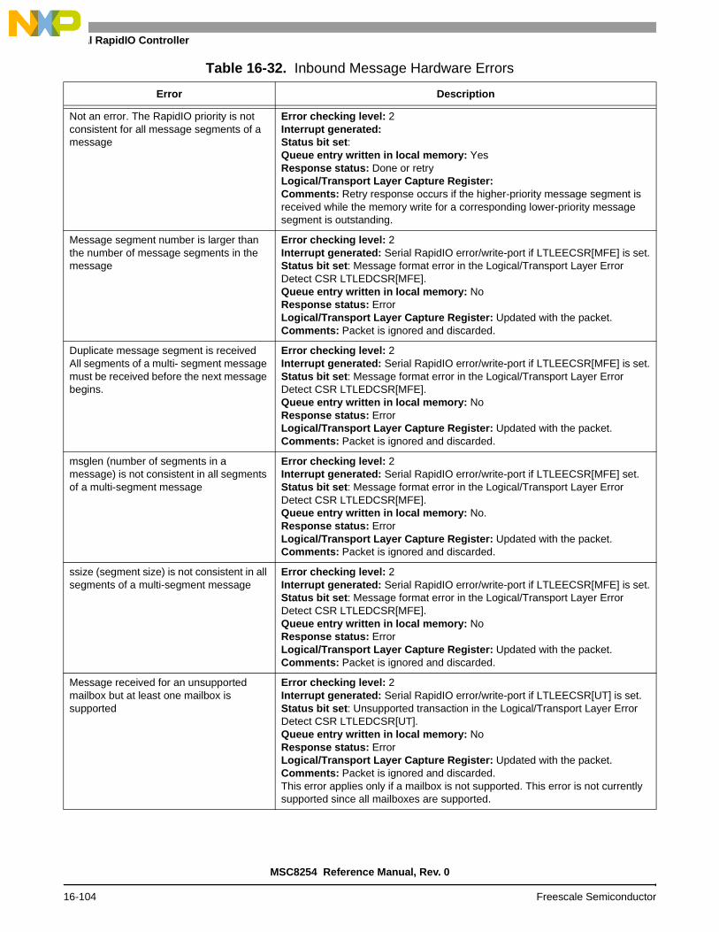
Serial RapidIO Controller
Not an error. The RapidIO priority is not consistent for all message segments of a message
Error checking level: 2Interrupt generated:Status bit set:Queue entry written in local memory: YesResponse status: Done or retryLogical/Transport Layer Capture Register:Comments: Retry response occurs if the higher-priority message segment is received while the memory write for a corresponding lower-priority message segment is outstanding.
Message segment number is larger than the number of message segments in the message
Error checking level: 2Interrupt generated: Serial RapidIO error/write-port if LTLEECSR[MFE] is set.Status bit set: Message format error in the Logical/Transport Layer Error Detect CSR LTLEDCSR[MFE].Queue entry written in local memory: NoResponse status: ErrorLogical/Transport Layer Capture Register: Updated with the packet.Comments: Packet is ignored and discarded.
Duplicate message segment is receivedAll segments of a multi- segment message must be received before the next message begins.
Error checking level: 2Interrupt generated: Serial RapidIO error/write-port if LTLEECSR[MFE] is set.Status bit set: Message format error in the Logical/Transport Layer Error Detect CSR LTLEDCSR[MFE].Queue entry written in local memory: NoResponse status: ErrorLogical/Transport Layer Capture Register: Updated with the packet.Comments: Packet is ignored and discarded.
msglen (number of segments in a message) is not consistent in all segments of a multi-segment message
Error checking level: 2Interrupt generated: Serial RapidIO error/write-port if LTLEECSR[MFE] set.Status bit set: Message format error in the Logical/Transport Layer Error Detect CSR LTLEDCSR[MFE].Queue entry written in local memory: No.Response status: ErrorLogical/Transport Layer Capture Register: Updated with the packet.Comments: Packet is ignored and discarded.
ssize (segment size) is not consistent in all segments of a multi-segment message
Error checking level: 2Interrupt generated: Serial RapidIO error/write-port if LTLEECSR[MFE] is set.Status bit set: Message format error in the Logical/Transport Layer Error Detect CSR LTLEDCSR[MFE].Queue entry written in local memory: NoResponse status: ErrorLogical/Transport Layer Capture Register: Updated with the packet.Comments: Packet is ignored and discarded.
Message received for an unsupported mailbox but at least one mailbox is supported
Error checking level: 2Interrupt generated: Serial RapidIO error/write-port if LTLEECSR[UT] is set.Status bit set: Unsupported transaction in the Logical/Transport Layer Error Detect CSR LTLEDCSR[UT].Queue entry written in local memory: NoResponse status: ErrorLogical/Transport Layer Capture Register: Updated with the packet.Comments: Packet is ignored and discarded.This error applies only if a mailbox is not supported. This error is not currently supported since all mailboxes are supported.
Table 16-32. Inbound Message Hardware Errors
Error Description
MSC8254 Reference Manual, Rev. 0
16-104 Freescale Semiconductor
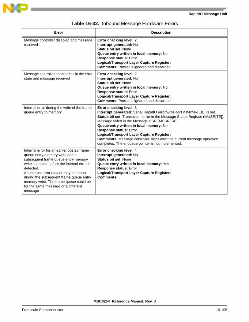
RapidIO Message Unit
Message controller disabled and message received
Error checking level: 2Interrupt generated: NoStatus bit set: NoneQueue entry written in local memory: NoResponse status: ErrorLogical/Transport Layer Capture Register:Comments: Packet is ignored and discarded.
Message controller enabled but in the error state and message received
Error checking level: 2Interrupt generated: NoStatus bit set: NoneQueue entry written in local memory: NoResponse status: ErrorLogical/Transport Layer Capture Register:Comments: Packet is ignored and discarded.
Internal error during the write of the frame queue entry to memory
Error checking level: 3Interrupt generated: Serial RapidIO error/write-port if IMxMR[EIE] is set.Status bit set: Transaction error in the Message Status Register (IMxSR[TE]). Message failed in the Message CSR (MCSR[FA]).Queue entry written in local memory: NoResponse status: ErrorLogical/Transport Layer Capture Register:Comments: Message controller stops after the current message operation completes. The enqueue pointer is not incremented.
Internal error for an earlier posted frame queue entry memory write and a subsequent frame queue entry memory write is posted before the internal error is detected.An internal error may or may not occur during the subsequent frame queue entry memory write. The frame queue could be for the same message or a different message
Error checking level: 4Interrupt generated: NoStatus bit set: NoneQueue entry written in local memory: YesResponse status: ErrorLogical/Transport Layer Capture Register:Comments:
Table 16-32. Inbound Message Hardware Errors
Error Description
MSC8254 Reference Manual, Rev. 0
Freescale Semiconductor 16-105

Serial RapidIO Controller
Message request to request time-out for multi-segment messages
Error checking level: UnrelatedInterrupt generated: Serial RapidIO error/write-port if LTLEECSR[MRT] set. Serial RapidIO error/write-port if IMxMR[EIE] is set.Status bit set: Message request time-out in the Logical/Transport Layer Error Detect CSR LTLEDCSR[MRT]. IMxSR[MRT] bit is set.Queue entry written in local memory: NoResponse status: NoLogical/Transport Layer Capture Register: Updated with the previous message request packet except that the message segment field (bits 4–7 of LTLCCCSR[MI]) is updated with the lowest message segment number not yet received.2
Comments: All message segments received before the time-out update memory. The enqueue pointer is not incremented. The message operation completes.
Notes: 1. These error types are actually detected in the RapidIO port, not in the message controller.
2. In small transport size configuration using the packet, the following allocations are made:• LTLACCSR[XA] gets the extended address (packet bits 78–79).• LTLACCSR[A] gets the address (packet bits 48–76).• LTLDIDCCSR[MDID] gets 0.• LTLDIDCCSR[DID] gets the least significant byte of the destination ID (packet bits 16–23).• LTLDIDCCSR[MSID] gets 0.• LTLDIDCCSR[SID] gets the least significant byte of the source ID (packet bits 24–31).• LTLCCCSR[FT] gets the ftype (packet bits 12–15).• LTLCCCSR[TT] gets the ttype (packet bits 32–35).• LTLCCCSR[MI] gets the msg info (packet bits 40–47).
In large transport size configuration using the packet, the following allocations are made:• LTLACCSR[XA] gets the extended address (packet bits 94–95)• LTLACCSR[A] gets the address (packet bits 64–92)• LTLDIDCCSR[MDID] gets the most significant byte of the destination ID (packet bits 16–23)• LTLDIDCCSR[DID] gets the least significant byte of the destination ID (packet bits 24–31)• LTLDIDCCSR[MSID] gets the most significant byte of the source ID (packet bits 32–39)• LTLDIDCCSR[SID] gets the least significant byte of the source ID (packet bits 40–47)• LTLCCCSR[FT] gets the ftype (packet bits 12–15)• LTLCCCSR[TT] gets the ttype (packet bits 48–51)• LTLCCCSR[MI] gets the msg info (packet bits 56–63).
Table 16-32. Inbound Message Hardware Errors
Error Description
MSC8254 Reference Manual, Rev. 0
16-106 Freescale Semiconductor

RapidIO Message Unit
16.3.3.8 Programming Errors
Table 16-33 shows a partial list of programming errors that result in undefined or undesired hardware operation.
16.3.3.9 Disabling and Enabling the Inbound Message Controller
When the message controller is disabled by clearing IMxMR[ME] the following occurs (see Table 16-115, IMxSR Field Descriptions, on page 16-209):
1. Queue full clears the IMxSR[QF] bit.
2. Message-in-queue clears the IMxSR[MIQ] bit.
3. Queue empty is set via the IMxSR[QE] bit.
4. Message busy clears the IMxSR[MB] bit after all pending frame queue entry writes complete.
Once the message controller is disabled, an error response is generated for all new message packets. If the message controller is disabled before all of the message segments for a multisegment message are received, a message request time-out must occurs and all pending frame queue writes must complete before message busy clears (IMxSR[MB]).
Table 16-33. Inbound Message Programming Errors
Error Interrupt Status Bit Set Comments
Reserved value of the message in queue threshold (IMxMR[MIQ_THRESH]) or reserved value of the circular frame queue size (IMxMR[CIRQ_SIZE])
No No Undefined operation results
The message in-queue threshold is equal to the frame queue size
No No Message in queue interrupt occurs when queue is full
The message in-queue threshold is greater than the frame queue size
No No Message in queue interrupt never occurs
Frame queue entry written to non-existent memory No No Memory controller will cause the interrupt and update capture registers. IMxSR[TE] will be set due to the internal error.
Message enqueue and dequeue pointers are not initialized to the same value
No No Undefined operation results
The dequeue frame pointer register is set incorrectly. No No Undefined operation results
Queue misaligned. No No Undefined operation results.
MSC8254 Reference Manual, Rev. 0
Freescale Semiconductor 16-107

Serial RapidIO Controller
Before the message controller is reenabled, the message busy bit must be clear (IMxSR[MB = 0) and the (IMxMR[ME]), frame queue dequeue pointer address registers (IMxFQDPAR), and frame queue enqueue pointer address registers (IMxFQEPAR) must be initialized to the same value for proper message controller operation.
16.3.4 RapidIO Message Passing Logical Specification Register Bits
The Mailbox Command and Status Register (MCSR; see page 16-139) provides the status for the two inbound and the two outbound controllers. These read-only status bits indicate the state of each of the message controllers, as described in Table 16-34.
16.4 RapidIO Doorbell
This section describes the operation of the doorbell controllers, which are part of the RapidIO message unit. The doorbell controllers are designed to comply with the message passing logical specification contained in the RapidIO Interconnect Specification, Revision 1.2. The doorbell controller generates and receives doorbells.
The doorbell controllers are controlled through a set of run-time registers.
16.4.1 FeaturesSupport for one outbound doorbell controllers
Support for one inbound doorbell controllers
The doorbell controller can sustain back-to-back inbound doorbells
Table 16-34. MCSR Bits to Indicate Status of Inbound and Outbound Controllers
MCSR Bit Description
Available (A) Indicates the following:• The inbound message controller is enabled (IMxMR[ME]).• The inbound message controller is not in the internal error state (IMxSR[TE] = 0).• The inbound message controller did not detect a message request time-out (IMxSR[MRT] = 0).
Full (FU) Reflects the inbound message controller queue full status.
Empty (EM) Reflects the state of the outbound message controller message empty status.
Busy (B) Reflects the state of the inbound message controller busy bit IMxSR[MB].
Failed (FA) Set if any of the following bits are set:• Inbound message controller transaction error status bit IMxSR[TE].• Inbound message controller message request time-out status bit IMxSR[MRT].• Outbound message controller transaction error status bit OMxSR[TE].• Outbound message controller packet response time-out bit OMxSR[PRT].• Outbound message controller message error response received status bit OMxSR[MER].• Outbound message controller retry error threshold exceeded status bit OMxSR[RETE].
Error (ERR) Always has a value of 0.
MSC8254 Reference Manual, Rev. 0
16-108 Freescale Semiconductor

RapidIO Doorbell
16.4.2 Doorbell Controller
The RapidIO architecture specification defines a doorbell type with no data payload that is transferred using inbound and outbound doorbell controllers. The MSC8254 RapidIO interconnect doorbell unit supports both inbound and outbound doorbells. The doorbell entry size is fixed at 64 bits because doorbell packets only pass a small amount of information, making the enqueue and dequeue pointers double-word addresses.
Inbound doorbells are handled by the doorbell controller similar to the way the message controller handles inbound data messages. The doorbell controller receives the doorbells and places them in a circular queue located in local memory. Additional doorbells can be received and forwarded to memory before the previous doorbell memory write completes as long as the RapidIO priority is the same or lower than the previous doorbell. The doorbell is retried if the RapidIO priority is higher than the previous doorbell.
Table 16-12 depicts an example of the structure of the inbound doorbell queue and pointers. The doorbell queue has eight entries, three of which are currently valid. The doorbell controller enqueues doorbells and the local processor dequeues doorbells.Each inbound doorbell controller has a dedicated interrupt to notify software that there are incoming doorbells.
Outbound doorbells are generated through a memory-mapped write port rather than a queue. An outbound doorbell must complete before another outbound doorbell can be generated. The outbound doorbell controller has a dedicated interrupt used to notify software that a doorbell was sent.
Figure 16-12. Inbound Doorbell Queue and Pointer Structure
DoorbellEntry
DoorbellEntry
DoorbellEntry
Enqueue Pointer
Dequeue Pointer
Dequeue Pointer
Local Processor Read
InboundDoorbell
Controller
Local Memory
Packets from
RapidIO interface
MSC8254 Reference Manual, Rev. 0
Freescale Semiconductor 16-109

Serial RapidIO Controller
16.4.3 Outbound Doorbell Controller
The outbound doorbell controller generates doorbells. Software initializes all parameters in the necessary registers to start the doorbell transmission. The doorbell transfer starts when the doorbell start bit, DUS, in the Outbound Doorbell Mode Register (ODMR) transitions from 0 to 1 (see Table 16-119, ODMR Field Descriptions, on page 16-214) and the doorbell controller is not busy. Software should program all appropriate registers before setting ODMR[DUS].
Software can interact with the doorbell controller in many ways. One example method for generating a doorbell is as follows:
1. Poll the status register doorbell unit busy bit, ODSR[DUB], to ensure that the outbox is not busy (see Table 16-120, ODSR Field Descriptions, on page 16-215).
2. Clear the following ODSR status bits:
• MER
• RETE
• PRT
• EODI]
3. Initialize the following registers:
• Destination port (ODDPR; see page 16-216)
• Destination attributes (ODDATR; see page 16-217)
• Retry error threshold (ODRETCR; see page 16-218)
4. To start the doorbell transfer, clear and then set the doorbell start bit, ODMR[DUS].
5. ODSR[DUB] is set when ODMR[DUS] transitions from 0 to 1 to indicate that the doorbell transfer is in progress.
6. The outbound doorbell controller sends the doorbell.
7. The outbound doorbell controller clears the ODSR[DUB] bit after the doorbell operation completes. A doorbell completes when one of the following events occurs:
• Done response received.
• Error response received.
• Packet response time-out.
• Retry limit exceeded.
8. The outbound doorbell interrupt is generated if the end of doorbell outbound doorbell interrupt event is enabled (ODDATR[EODIE]).
MSC8254 Reference Manual, Rev. 0
16-110 Freescale Semiconductor

RapidIO Doorbell
16.4.3.1 Interrupts
The outbound doorbell controller interrupt is generated after the completion of a doorbell (done, error, packet response time-out, or retry limit exceeded) if this interrupt event is enabled (ODDATR[EODIE] =1). The event causing this interrupt is indicated by ODSR[EODI]. The interrupt is held until the ODSR[EODI] bit is cleared by writing a 1 to it.
Table 16-35 describes each of these error types.
16.4.3.2 Software Error Handling
When an error occurs and the Serial RapidIO error/write-port interrupt is generated, software takes the following actions:
1. Determines the cause of the interrupt and processes the error.
2. Verifies that the doorbell controller has stopped operation by polling ODSR[DUB].
3. Disables the doorbell controller by clearing ODMR[DUS].
4. Clears the error by writing a 1 to the corresponding ODSR status bit (see Table 16-120, ODSR Field Descriptions, on page 16-215):
• MER
• PRT
• RETE
When an error occurs and the Serial RapidIO error/write-port interrupt is not enabled, software takes the following actions:
1. Determines that an error has occurred by polling the ODSR status bits (MER, PRT, and/or RETE).
2. Verifies that the doorbell controller has stopped operation by polling ODSR[DUB].
3. Disables the doorbell controller by clearing ODMR[DUS].
4. Clears the error by writing a 1 to the corresponding ODSR status bit (listed in step 1).
Note: Once the doorbell controller starts, it cannot be stopped.
Table 16-35. Error Types In the Outbound Doorbell Controller
Error Type Doorbell Controller Response to Error
Error Response Error • Sets the message error response status bit (ODSR[MER]).• Stops after the doorbell operation completes (indicated by ODSR[DUB]).
Packet Response Time-Out Error • Sets the packet response time-out status bit (ODSR[PRT]).• Stops after the doorbell operation completes (indicated by ODSR[DUB]).
Retry Error Threshold Exceeded Error • Sets the retry threshold exceed status bit (ODSR[RETE]).• Stops after the doorbell operation completes (indicated by ODSR[DUB]).
MSC8254 Reference Manual, Rev. 0
Freescale Semiconductor 16-111

Serial RapidIO Controller
16.4.3.3 Hardware Error Handling
Table 16-36 lists possible error conditions for outbound doorbells and how they are handled. The error checking level indicates the order in which errors are checked. Multiple errors can be checked at an error checking level. When an error is detected, no additional error checking beyond the current level is performed. Note that outbound doorbell responses are processed in a pipeline. The first error detected in the processing pipeline updates the error management extensions registers.
These error condition checks are provided by the messaging unit. These check are in addition to the error condition checks provided by the RapidIO port as discussed in Section 16.2.10, Errors and Error Handling, on page 16-48.
Table 16-36. Outbound Doorbell Hardware Errors
Transaction Error Description
Undefined packet
Reserved ftype encoding1
Error checking level: 1Interrupt generated: Serial RapidIO error/write-port if LTLEECSR[UT] is set.Status bit set: Unsupported transaction in the Logical/Transport Layer Error Detect CSR LTLEDCSR[UT] (see page 16-159).Doorbell sent: YesLogical/Transport Layer Capture Register: Updated with the packet.2
Comments: Packet is ignored and discarded.
Doorbell response
Reserved tt encoding1
Error checking level: 1Interrupt generated: Serial RapidIO error/write-port if LTLEECSR[TSE] is set.Status bit set: Transport size error in the Logical/Transport Layer Error Detect CSR LTLEDCSR[TSE] (see page 16-159). Doorbell sent: Yes.Logical/Transport Layer Capture Register: Updated with the packet.2
Comments: Packet is ignored and discarded.
Doorbell response
Large transport size in small transport mode or small transport size in large transport mode.1
Error checking level: 1Interrupt generated: Serial RapidIO error/write-port if LTLEECSR[TSE] set.Status bit set: Transport size error in the Logical/Transport Layer Error Detect CSR LTLEDCSR[TSE] (see page 16-159). Doorbell sent: YesLogical/Transport Layer Capture Register: Updated with the packet.2
Comments: Packet is ignored and discarded. An error or illegal transaction target error response is not generated.
Doorbell response
Illegal Destination ID1
Error checking level: 1Interrupt generated: Serial RapidIO error/write-port if LTLEECSR[ITTE] is set.Status bit set: Illegal transaction target in the Logical/Transport Layer Error Detect CSR LTLEDCSR[ITTE] (see page 16-159).Doorbell sent: YesLogical/Transport Layer Capture Register: Updated with the packet.2
Comments: Packet is ignored and discarded.
Doorbell response
Doorbell not outstanding1
Error checking level: 1Interrupt generated: Serial RapidIO error/write-port if LTLEECSR[UR] is set.Status bit set: Unsolicited response in the Logical/Transport Layer Error Detect CSR LTLEDCSR[UR] (see page 16-159).Doorbell sent: YesLogical/Transport Layer Capture Register: Updated with the packet.2
Comments: Packet is ignored and discarded.
MSC8254 Reference Manual, Rev. 0
16-112 Freescale Semiconductor

RapidIO Doorbell
Doorbell response
ttype (transaction field) is not doorbell response1
Error checking level: 1Interrupt generated: Serial RapidIO error/write-port if LTLEECSR[ITD] is set.Status bit set: Illegal transaction decode in the Logical/Transport Layer Error Detect CSR LTLEDCSR[ITD] (see page 16-159).Doorbell sent: YesLogical/Transport Layer Capture Register: Updated with the packet.2
Comments: Packet is ignored and discarded.
Doorbell response
RapidIO priority is less than or equal to outbound request1
Error checking level: 2Interrupt generated: Serial RapidIO error/write-port if LTLEECSR[ITD] is set (see page 16-160).Status bit set: Illegal transaction decode in the Logical/Transport Layer Error Detect CSR LTLEDCSR[ITD] (see page 16-159).Doorbell sent: YesLogical/Transport Layer Capture Register: Updated with the packet.2
Comments: Packet is ignored and discarded.
Doorbell response
Incorrect Source ID1
Error checking level: 2Interrupt generated: Serial RapidIO error/write-port if LTLEECSR[ITD] set (see page 16-160).Status bit set: Illegal transaction decode in the Logical/Transport Layer Error Detect CSR LTLEDCSR[ITD] (see page 16-159).Doorbell sent: YesLogical/Transport Layer Capture Register: Updated with the packet.2
Comments: Packet is ignored and discarded.
Doorbell response
Reserved response status1
Error checking level: 2Interrupt generated: Serial RapidIO error/write-port if LTLEECSR[ITD] is set (see page 16-160).Status bit set: Illegal transaction decode in the Logical/Transport Layer Error Detect CSR LTLEDCSR[ITD] (see page 16-159).Doorbell sent: YesLogical/Transport Layer Capture Register: Updated with the packet.2
Comments: Packet is ignored and discarded.
Doorbell response
Doorbell response packet size is incorrect1
Error checking level: 2Interrupt generated: Serial RapidIO error/write-port if LTLEECSR[MFE] is set (see page 16-160).Status bit set: Message Format error in the Logical/Transport Layer Error Detect CSR LTLEDCSR[MFE] (see page 16-159).Doorbell sent: YesLogical/Transport Layer Capture Register: Updated with the packet.2
Comments: Packet is ignored and discarded.
Doorbell response
Error response Error checking level: 3Interrupt generated: Serial RapidIO error/write-port if LTLEECSR[MER] is set (see page 16-160).Status bit set: Message error response in the Logical/Transport Layer Error Detect CSR LTLEDCSR[MER] (see page 16-159). ODSR[MER] bit set (see page 16-214).Doorbell sent: YesLogical/Transport Layer Capture Register: Updated with the corresponding doorbell request packet.2
Comments: Doorbell transfer complete.
Table 16-36. Outbound Doorbell Hardware Errors (Continued)
Transaction Error Description
MSC8254 Reference Manual, Rev. 0
Freescale Semiconductor 16-113

Serial RapidIO Controller
16.4.3.4 Programming Errors
Table 16-37 lists programming errors that result in undefined or undesired hardware operation.
Doorbell response
Number of retries exceeds limit
Error checking level: 3Interrupt generated: Serial RapidIO error/write-port if LTLEECSR[RETE] is set (see page 16-160). Status bit set: Retry limit exceeded in the Logical/Transport Layer Error Detect CSR LTLEDCSR[RETE] (see page 16-159). ODSR[RETE] bit is set (see page 16-215).Doorbell sent: YesLogical/Transport Layer Capture Register: Updated with the corresponding doorbell request packet.2
Comments: Doorbell transfer complete.
Doorbell response
Packet response time-out1
Error checking level: UnrelatedInterrupt generated: Serial RapidIO error/write-port if LTLEECSR[PRT] is set (see page 16-160).Status bit set: Packet response time-out in the Logical/Transport Layer Error Detect CSR LTLEDCSR[PRT] in RapidIO endpoint (see page 16-159). ODSR[PRT] bit is set (see page 16-215).Doorbell sent: YesLogical/Transport Layer Capture Register: Updated with the doorbell request packet in RapidIO endpoint.2
Comments: Doorbell transfer complete. Note that RapidIO endpoint sends a special priority 3 packet indicating a doorbell time-out.
Notes: 1. Notes: 1. These error types are actually detected in the RapidIO port, not in the doorbell controller.
2. In small transport size configuration using the packet, the following allocations are made:• LTLACCSR[XA] gets the extended address (packet bits 78–79).• LTLACCSR[A] gets the address (packet bits 48–76)• LTLDIDCCSR[MDID] gets 0.• LTLDIDCCSR[DID] gets the least significant byte of the destination ID (packet bits 16–23).• LTLDIDCCSR[MSID] gets 0.• LTLDIDCCSR[SID] gets the least significant byte of the source ID (packet bits 24–31).• LTLCCCSR[FT] gets the ftype (packet bits 12–15).• LTLCCCSR[TT] gets the ttype (packet bits 32–35).• LTLCCCSR[MI] gets 0
In large transport size configuration using the packet, the following allocations are made:• LTLACCSR[XA] gets the extended address (packet bits 94–95).• LTLACCSR[A] gets the address (packet bits 64–92).• LTLDIDCCSR[MDID] gets the most significant byte of the destination ID (packet bits
16–23).• LTLDIDCCSR[DID] gets the least significant byte of the destination ID (packet bits 24–31).• LTLDIDCCSR[MSID] gets the most significant byte of the source ID (packet bits 32–39).• LTLDIDCCSR[SID] gets the least significant byte of the source ID (packet bits 40–47).• LTLCCCSR[FT] gets the ftype (packet bits 12–15).• LTLCCCSR[TT] gets the ttype (packet bits 48–51).• LTLCCCSR[MI] gets 0.
Table 16-36. Outbound Doorbell Hardware Errors (Continued)
Transaction Error Description
MSC8254 Reference Manual, Rev. 0
16-114 Freescale Semiconductor

RapidIO Doorbell
16.4.4 Inbound Doorbell Controller
The inbound doorbell controller receives doorbells and places them in a circular doorbell queue in local memory. The inbound controller controls the enqueue pointer and software controls the dequeue pointer. After a configured number of doorbells are received, an interrupt is generated to the processor. After processing a received doorbell, the local processor can either write the doorbell mode register increment bit (IDMR[DI]]) causing the dequeue pointer to point to the next doorbell in the queue or wait until all the received doorbells are processed and write the dequeue pointer.
There are many ways in which software can interact with the doorbell controllers. One method of initializing the inbound doorbell controller follows:
1. Initialize the doorbell queue dequeue pointer address registers IDQDPAR (see page 16-222) and IDQEPAR (see page 16-223) and the doorbell queue enqueue pointer address register (DQEPAR). These registers must be initialized to the same value for proper operation. They also must be queue size aligned.
2. Clear the status register (IDSR; see page 16-221).
3. Set the doorbell enable bit IDMR[DE] along with the other control parameters (doorbell queue size, doorbell-in-queue threshold, and various interrupt enables) in the doorbell mode register (IDMR; see Table 16-124, IDMR Field Descriptions, on page 16-219).
Another method follows:
1. The doorbell controller receives a doorbell. If the inbound doorbell controller is enabled (IDMR[DE] =1) and the doorbell queue is not full, then the doorbell is accepted.
2. The doorbell controller stores the 16-bit information field and the RapidIO source and destination IDs in local memory using the value of the doorbell queue enqueue pointer address register (DQEPAR).
3. When the memory write completes, the enqueue pointer is incremented to point to the next doorbell queue entry in local memory.
4. If another doorbell arrives before all previous doorbell memory writes complete and the RapidIO priority of the doorbell is equal to or lower than the priority of all previous doorbells, the doorbell controller processes the doorbell and generates a memory write
Table 16-37. Outbound Doorbell Programming Errors
ErrorInterrupt
GeneratedStatus Bit Set Comments
Transaction flow level set to 3 No None Undefined operation.
Target interface set to an invalid RapidIO port No None Undefined operation.
Register values changed during operation No No Undefined operation.
MSC8254 Reference Manual, Rev. 0
Freescale Semiconductor 16-115

Serial RapidIO Controller
to the appropriate doorbell queue entry. If the priority of the new doorbell is higher than that of the previous doorbell memory writes that have not completed, the doorbell controller generates a retry.
5. An inbound doorbell interrupt is generated to the local processor because the number of doorbells in the queue is greater than or equal to the configured doorbell-in-queue threshold (IDMR[DIQ_THRESH) and this event is enabled to generate the interrupt (IDMR[DIQIE]).
6. Software determines that the doorbell-in-queue event caused the interrupt by detecting that the doorbell-in-queue interrupt bit is set in the doorbell status register (IDSR[DIQI]).
7. Software processes the doorbell queue entry to which the doorbell queue dequeue pointer address register (DQDPAR) is pointing.
8. Software increments the dequeue pointer address register (DQDPAR) by setting the doorbell increment bit (IDMR[DI]).
9. Software determines whether there are more doorbells to process by reading the queue empty bit (IDSR[QE]). If the queue is not empty, the previous two steps are repeated.
10. Software clears the doorbell-in-queue interrupt bit (IDSR[DIQI]) by writing a 1 to it.
16.4.4.1 Doorbell Queue Entry Format
Each doorbell entry in the queue has two 32-bit words, one for target information (see Table 16-38) and one for source information (see Table 16-39). The target information is stored because a RapidIO port can be configured to accept packets from any destination. When there are multiple RapidIO ports on one device, each port can be configured with a different destination ID. For the MSC8254, the target information is identical for all received doorbell entries.
Table 16-38. Inbound Doorbell Target Info Definition
Bit Name Description
31–16 — Reserved.
15–8 ETID Extended target ID in Large Transport mode.Reserved for Small Transport mode.
7–0 TID Target ID field from the received doorbell packet.
Table 16-39. Source Info Definition
Bit Name Description
31–24 ESID Extended source ID in Large Transport mode.Reserved fir Small Transport mode.
23–16 SID Source ID field from the received doorbell packet.
15–8 INFO MSB Most significant byte of the info field from the received doorbell packet.
7–0 INFO LSB Least significant byte of the info field from the received doorbell packet.
MSC8254 Reference Manual, Rev. 0
16-116 Freescale Semiconductor

RapidIO Doorbell
Figure 16-13 depicts the doorbell queue entry fields and their related offsets.
Figure 16-13. Doorbell Entry Format
16.4.4.2 Retry Response Conditions
There are two conditions in which a doorbell is retried at the logical layer (Response Retry):
A doorbell is received and there are no entries in the doorbell queue.
A doorbell is received with a higher priority than all previous doorbells being written to memory. If all inbound doorbells have the same priority, this condition does not occur.
16.4.4.3 Doorbell Controller Interrupts
There is one doorbell controller interrupt per inbound doorbell controller. The following events can generate the interrupt:
Doorbell-in-queue:
— The circular queue has accumulated the number of doorbells specified by the doorbell-in-queue threshold (IDMR[DIQ_THRESH) and this interrupt event is enabled (IDMR[DIQIE]). The event causing this interrupt is indicated by IDSR[DIQI]. The interrupt is held until the dequeue and enqueue pointers indicate that the specified number of doorbells is not in the doorbell queue and the IDSR[DIQI] bit is cleared by writing a 1 to it.
— The circular queue contains one or more doorbells, the specified number of doorbells has not accumulated, a doorbell has not been dequeued for the maximum interrupt report interval, and this interrupt event is enabled (IDMR[DIQIE]). The event causing this interrupt is indicated by IDSR[DIQI]. The interrupt is held until either IDMR[DI] is set or DQDPAR[DQDPA] is written and IDSR[DIQI] is cleared by writing a 1 to it.
Queue Full. An interrupt is generated each time the circular queue becomes full and this interrupt event is enabled (IDSR[QFIE]). The event causing this interrupt is indicated by IDSR[QFI]. The interrupt is held until the queue is not full and the IDSR[QFI] bit is cleared by writing a 1 to it.
The error/port-write interrupt can be generated after an internal error response is received and this interrupt event is enabled (IDMR[EIE]).
0b000
0b100
Target Info
Local MemoryOffset
Source Info
031
MSC8254 Reference Manual, Rev. 0
Freescale Semiconductor 16-117

Serial RapidIO Controller
16.4.4.4 Transaction Errors
When an internal error occurs while the doorbell controller is writing to local memory the doorbell controller responds as follows:
1. Sets the transaction error bit (IDSR[TE]) and enters the error state.
2. Returns an error response.
3. Generates the Serial RapidIO error/write-port interrupt if IDMR[EIE] is set.
16.4.4.5 Software Error Handling
When an error occurs and the Serial RapidIO error/write-port interrupt is generated, software performs the following actions.
1. Determines the cause of the interrupt and processes the error.
2. Verifies that the doorbell controller has stopped operation by polling IDSR[DB].
3. Clears the error by writing a 1 to the corresponding status bit (IDSR[TE]).
4. Disables, reinitializes, and reenables the doorbell unit before another doorbell can be received.
16.4.4.6 Hardware Error Handling
Table 16-40 describes the hardware error conditions and how they are handled. The error checking level indicates the order in which errors are checked. Multiple errors can be checked at an error checking level. When an error is detected, no additional error checking beyond the current level is performed. Doorbells are processed in a pipeline. The first error detected in the processing pipeline updates the error management extensions registers. These error condition checks are provided by the messaging unit. These checks are in addition to the error condition checks provided by the RapidIO port as discussed in Section 16.2.10, Errors and Error Handling, on page 16-48.
MSC8254 Reference Manual, Rev. 0
16-118 Freescale Semiconductor
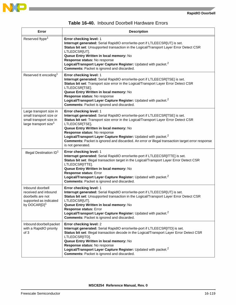
RapidIO Doorbell
Table 16-40. Inbound Doorbell Hardware Errors
Error Description
Reserved ftype1 Error checking level: 1Interrupt generated: Serial RapidIO error/write-port if LTLEECSR[UT] is set.Status bit set: Unsupported transaction in the Logical/Transport Layer Error Detect CSR LTLEDCSR[UT].Queue Entry Written in local memory: NoResponse status: No responseLogical/Transport Layer Capture Register: Updated with packet.2
Comments: Packet is ignored and discarded.
Reserved tt encoding1 Error checking level: 1Interrupt generated: Serial RapidIO error/write-port if LTLEECSR[TSE] is set.Status bit set: Transport size error in the Logical/Transport Layer Error Detect CSR LTLEDCSR[TSE].Queue Entry Written in local memory: NoResponse status: No responseLogical/Transport Layer Capture Register: Updated with packet.2
Comments: Packet is ignored and discarded.
Large transport size in small transport size or small transport size in large transport size1
Error checking level: 1Interrupt generated: Serial RapidIO error/write-port if LTLEECSR[TSE] is set.Status bit set: Transport size error in the Logical/Transport Layer Error Detect CSR LTLEDCSR[TSE]. Queue Entry Written in local memory: NoResponse status: No responseLogical/Transport Layer Capture Register: Updated with packet.2
Comments: Packet is ignored and discarded. An error or illegal transaction target error response is not generated.
Illegal Destination ID1 Error checking level: 1Interrupt generated: Serial RapidIO error/write-port if LTLEECSR[ITTE] is set.Status bit set: Illegal transaction target in the Logical/Transport Layer Error Detect CSR LTLEDCSR[ITTE].Queue Entry Written in local memory: NoResponse status: ErrorLogical/Transport Layer Capture Register: Updated with packet.2
Comments: Packet is ignored and discarded.
Inbound doorbell received and inbound doorbells are not supported as indicated by DOCAR[D]1
Error checking level: 1Interrupt generated: Serial RapidIO error/write-port if LTLEECSR[UT] is set.Status bit set: Unsupported transaction in the Logical/Transport Layer Error Detect CSR LTLEDCSR[UT].Queue Entry Written in local memory: NoResponse status: ErrorLogical/Transport Layer Capture Register: Updated with packet.2
Comments: Packet is ignored and discarded.
Inbound doorbell packet with a RapidIO priority of 3
Error checking level: 2Interrupt generated: Serial RapidIO error/write-port if LTLEECSR[ITD] is set.Status bit set: Illegal transaction decode in the Logical/Transport Layer Error Detect CSR LTLEDCSR[ITD].Queue Entry Written in local memory: NoResponse status: No responseLogical/Transport Layer Capture Register: Updated with packet.2
Comments: Packet is ignored and discarded.
MSC8254 Reference Manual, Rev. 0
Freescale Semiconductor 16-119

Serial RapidIO Controller
Incorrect doorbell packet size (not one datum in small transport mode or not two datums in large transport mode)
Error checking level: 2Interrupt generated: Serial RapidIO error/write-port if LTLEECSR[MFE] is set.Status bit set: Message Format error in the Logical/Transport Layer Error Detect CSR LTLEDCSR[MFE].Queue Entry Written in local memory: NoResponse status: ErrorLogical/Transport Layer Capture Register: Updated with packet.2
Comments: Packet is ignored and discarded.
Doorbell controller disabled and doorbell received
Error checking level: 3Interrupt generated: NoStatus bit set: NoneQueue Entry Written in local memory: NoResponse status: ErrorLogical/Transport Layer Capture RegisterComments: Packet is ignored and discarded.
Doorbell controller enabled but in the error state and doorbell received
Error checking level: 3Interrupt generated: NoStatus bit set: NoneQueue Entry Written in local memory: NoResponse status: ErrorLogical/Transport Layer Capture RegisterComments: Packet is ignored and discarded.
Internal error during the write of the doorbell queue entry to memory
Error checking level: 4Interrupt generated: Serial RapidIO error/write-port if IDMR[EIE] is set.Status bit set: Transaction error in the Doorbell status register (IDSR[TE]). Doorbell Failed in the Port-write and Doorbell CSR (PWDCSR[FA]).Queue Entry Written in local memory: NoResponse status: ErrorLogical/Transport Layer Capture RegisterComments: Doorbell controller stops after the current doorbell operation completes.The enqueue pointer is not incremented.
Table 16-40. Inbound Doorbell Hardware Errors
Error Description
MSC8254 Reference Manual, Rev. 0
16-120 Freescale Semiconductor

RapidIO Doorbell
16.4.4.7 Programming Errors
Table 16-41 lists the programming errors that result in undefined or undesired hardware operation.
An internal error occurred for an earlier posted write of a doorbell queue entry to memory and a subsequent write of a doorbell queue entry to memory is posted before the internal error is detected.
Error checking level: 5Interrupt generated: NoStatus bit set: NoneQueue Entry Written in local memory: YesResponse status: ErrorLogical/Transport Layer Capture RegisterComments: An internal error may or may not occur during the subsequent write of a doorbell queue entry to memory.
Notes: 1. These error types are actually detected in the RapidIO port, not in the doorbell controller.
2. In small transport size configuration using the packet, the following allocations are made:
• LTLACCSR[XA] gets the extended address (packet bits 78–79).• LTLACCSR[A] gets the address (packet bits 48–76).• LTLDIDCCSR[MDID] gets 0.• LTLDIDCCSR[DID] gets the least significant byte of the destination ID (packet bits 16–23).• LTLDIDCCSR[MSID] gets 0.• LTLDIDCCSR[SID] gets the least significant byte of the source ID (packet bits 24–31).• LTLCCCSR[FT] gets the ftype (packet bits 12–15).• LTLCCCSR[TT] gets the ttype (packet bits 32–35).• LTLCCCSR[MI] gets 0.
In large transport size configuration using the packet, the following allocations are made:
• LTLACCSR[XA] gets the extended address (packet bits 94–95).• LTLACCSR[A] gets the address (packet bits 64–92).• LTLDIDCCSR[MDID] gets the most significant byte of the destination ID (packet bits 16–23).• LTLDIDCCSR[DID] gets the least significant byte of the destination ID (packet bits 24–31).• LTLDIDCCSR[MSID] gets the most significant byte of the source ID (packet bits 32–39).• LTLDIDCCSR[SID] gets the least significant byte of the source ID (packet bits 40–47).• LTLCCCSR[FT] gets the ftype (packet bits 12–15).• LTLCCCSR[TT] gets the ttype (packet bits 48–51).• LTLCCCSR[MI] gets 0.
Table 16-41. Inbound Doorbell Programming Errors
ErrorInterrupt
GeneratedStatus Bit Set Comments
Reserved value of the doorbell in queue threshold (IDxMR[DIQ_THRESH]) or reserved value of the circular doorbell queue size (IDxMR[CIRQ_SIZ]); see Table 16-124, IDMR Field Descriptions, on page 16-219.
No No Undefined operation results
The doorbell in-queue threshold is equal to the doorbell queue size.
No No Doorbell in queue interrupt when queue is full
The doorbell in-queue threshold is greater than the doorbell queue size.
No No Doorbell in queue interrupt never occurs
Table 16-40. Inbound Doorbell Hardware Errors
Error Description
MSC8254 Reference Manual, Rev. 0
Freescale Semiconductor 16-121

Serial RapidIO Controller
16.4.4.8 Disabling and Enabling the Doorbell Controller
When the doorbell controller is disabled by clearing IDMR[DE] the following occurs in the IDSR (see Table 16-125, IDSR Field Descriptions, on page 16-221):
1. Queue full clears (QF).
2. Doorbell-in-queue clears (DIQ).
3. Queue empty is set (QE)
4. Doorbell busy clears (DUB) after all pending doorbell queue entry writes to local memory complete.
Before the doorbell controller is reenabled, the doorbell busy bit must be clear (IDSR[DB) and the doorbell dequeue pointer address register (DQDPAR) and the doorbell queue enqueue pointer address register (DQEPAR) must be initialized to the same value for proper doorbell controller operation.
16.4.4.9 RapidIO Message Passing Logical Specification Registers
The port-write and doorbell command and status register (PWDCSR) includes several doorbell controller status bits. See Section 16.6.9, Port Write and Doorbell Command and Status Register (PWDCSR), on page 16-141 for details.
These read-only status bits indicate the state of doorbell controller 0.
Available (PWDCSR[A]). Indicates that the inbound doorbell controller is enabled (IDMR[DE]) and the doorbell controller is not in the internal error state (IDnSR[TE] = 0)
Full (PWDCSR[FU]). This bit reflects the inbound doorbell controller queue full status bit (IDSR[QF])
Empty (PWDCSR[EM]). This bit reflects the inverted state of the outbound doorbell busy bit (ODSR[DUB] = 0)
Busy (PWDCSR[B]). This bit reflects the state of the inbound doorbell controller busy bit IDSR[DUB]
Doorbell queue entry written to non-existent memory. No No Memory controller causes the interrupt and updates the capture registers
Doorbell enqueue and dequeue pointers are not initialized to the same value.
No No Undefined operation
The dequeue pointer register is set incorrectly. No No Undefined operation
Table 16-41. Inbound Doorbell Programming Errors (Continued)
ErrorInterrupt
GeneratedStatus Bit Set Comments
MSC8254 Reference Manual, Rev. 0
16-122 Freescale Semiconductor

Port-Write Controller
Failed (PWDCSR[FA]). This bit reflects the state of the transaction error status bit IDSR[TE]
Error (PWDCSR[ERR]). This bit is always a 0
16.5 Port-Write Controller
The implementation of the port-write controller is very similar to the inbound message and doorbell controllers except that only one queue entry is supported. The port write is an error reporting mechanism for a device that has no end-point to communicate with a control processor or other system host. Figure 16-14 shows the structure of the inbound queue and pointer. The port-write queue only contains one entry with a fixed size of 64 bytes and is aligned to a cache line boundary. The port-write controller uses the error/port-write interrupt for the RapidIO error/write-port to indicate incoming port-writes.
Figure 16-14. Inbound Port-Write Structure
16.5.1 Port-Write Controller Initialization
There are many ways in which software can interact with the port-write controller. One method to initialize the port-write controller is as follows:
1. Initialize the port-write queue base address registers (IPWQBAR; see Table 16-131, IPWQBAR Field Descriptions, on page 16-227).
2. Clear the status register (IPWSR; see Table 16-130, IPWSR Field Descriptions, on page 16-226).
3. Set the port-write enable bit IPWMR[PWE] along with the interrupt enable) in the inbound port-write mode register (IPWMR; see Table 16-129, IPWMR Field Descriptions, on page 16-225).
Port-Write64-Byte Entry
Pointer
Pointer
Local ProcessorRead
InboundPort-writeController
Local Memory
Port-Write Packets fromRapidIO interface
Port Write Queue
MSC8254 Reference Manual, Rev. 0
Freescale Semiconductor 16-123

Serial RapidIO Controller
16.5.2 Port-Write Controller Operation
There are several ways in which software can interact with the port-write controller. One method is as follows:
1. The port-write controller receives a port-write from the RapidIO port. If the inbound port-write controller is enabled (IPWMR[PWE] =1) and the port-write queue is not full, the port-write is accepted.
2. The port-write controller stores 64 bytes of payload in local memory using the value of the port-write queue base address registers (IPWQBAR). Valid payload sizes include 4, 8, 16, 24, 32, 40, 48, 56, or 64 bytes. Note that 64 bytes are always written to memory. If the actual payload size is less than 64 bytes, the non payload data is undefined.
3. If the queue full interrupt enable bit is set (IPWMR[QFIE]) after the memory write completes, the port-write controller generates the error/port-write interrupt.
4. An inbound error/port-write interrupt is generated to the local processor because a port-write is received and this event is enabled to generate the interrupt (IPWMR[QFIE]). Note that the RMU actually generates the Serial RapidIO error/write-port output, which is combined with the error interrupt to generate the error/port-write interrupt.
5. Software reads the queue full bit (IPWSR[QFI]) and determines that the queue full event caused the interrupt. Many events that can generate this interrupt. Software must read several registers to determine that the interrupt is due to a port-write.
6. Software processes the port-write queue entry to which the port-write base address registers (IPWQBAR) are pointing.
7. Software sets the clear queue bit (IPWMR[CQ]) to reenable the hardware to receive another port-write.
8. Software clears the queue full interrupt bit (IPWSR[QFI]) by setting IPWSR[QFI].
16.5.3 Port-Write Controller Interrupts
The error/port-write interrupt is used by the port-write controller. This interrupt is used to notify the processor that some type of error event has occurred in a RapidIO port, message controller, doorbell controller or port-write controller. There are many events that can generate this interrupt. For example, the error management extensions use this interrupt to notify that error events have occurred. In the port-write controller the following event can generate this interrupt.
Queue Full. This interrupt event is enabled (IPWMR[QFIE]) and a port-write is received and written to memory. The event causing this interrupt is indicated by IPWSR[QFI]. The interrupt is held until the queue is not full and the IPWSR[QFI] bit is cleared by writing a value of 1 to it.
MSC8254 Reference Manual, Rev. 0
16-124 Freescale Semiconductor

Port-Write Controller
Transaction Error. An internal error response is received and this interrupt event is enabled (IPWMR[EIE]).
16.5.4 Discarding Port-Writes
While the queue full bit is set or a port-write is being written to memory but has not completed, all received port-writes are discarded. When a port-write is discarded for one of these reasons, the controller sets the port write discarded bit (IPWSR[PWD]). Note that the port-write busy bit (IPWSR[PWB]) indicates that a port-write is being written to memory but has not completed.
16.5.5 Transaction Errors
When an internal error occurs while the port-write controller is writing data to local memory, the controller takes the following actions:
1. Sets the transaction error bit (IPWSR[TE]) and enters the error state.
2. Generates the Serial RapidIO error/write-port interrupt if IPWMR[EIE] is set.
16.5.6 Software Error Handling
When an error occurs and the Serial RapidIO error/write-port interrupt is generated, software takes the following actions:
1. Determines the cause of the interrupt and processes the error.
2. Polls IPWSR[PWB] to verify that the port-write controller has stopped operation.
3. Disables the port-write controller by clearing IPWMR[PWE].
4. Clears the error by writing a 1 to the corresponding status bit (IPWSR[TE]).
5. Disables, reinitializes, and reenables the port-write unit before another maintenance port-write can be received.
When an error occurs and the Serial RapidIO error/write-port interrupt is not enabled, software takes the following actions:
1. Polls the status bits (IPWSR[TE]) to determines that an error has occurred.
2. Polls IPWSR[PWB] to verify that the port-write controller has stopped operation.
3. Clears IPWMR[PWE] to disable the port-write controller.
4. Clears the error by writing a 1 to the corresponding status bit (IPWSR[TE]).
16.5.7 Hardware Error Handling
Table 16-42 describes the possible hardware error conditions and what occurs when they are detected. The error checking level indicates the order in which errors are checked. Multiple errors can be checked at an error checking level. When an error is detected, no additional error checking
MSC8254 Reference Manual, Rev. 0
Freescale Semiconductor 16-125
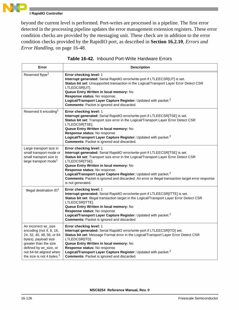
Serial RapidIO Controller
beyond the current level is performed. Port-writes are processed in a pipeline. The first error detected in the processing pipeline updates the error management extension registers. These error condition checks are provided by the messaging unit. These check are in addition to the error condition checks provided by the RapidIO port, as described in Section 16.2.10, Errors and Error Handling, on page 16-48.
Table 16-42. Inbound Port-Write Hardware Errors
Error Description
Reserved ftype1 Error checking level: 1Interrupt generated: Serial RapidIO error/write-port if LTLEECSR[UT] is set.Status bit set: Unsupported transaction in the Logical/Transport Layer Error Detect CSR LTLEDCSR[UT].Queue Entry Written in local memory: NoResponse status: No response.Logical/Transport Layer Capture Register: Updated with packet.2
Comments: Packet is ignored and discarded.
Reserved tt encoding1 Error checking level: 1Interrupt generated: Serial RapidIO error/write-port if LTLEECSR[TSE] is set.Status bit set: Transport size error in the Logical/Transport Layer Error Detect CSR LTLEDCSR[TSE].Queue Entry Written in local memory: NoResponse status: No responseLogical/Transport Layer Capture Register: Updated with packet.2
Comments: Packet is ignored and discarded.
Large transport size in small transport mode or small transport size in large transport mode1
Error checking level: 1Interrupt generated: Serial RapidIO error/write-port if LTLEECSR[TSE] is set.Status bit set: Transport size error in the Logical/Transport Layer Error Detect CSR LTLEDCSR[TSE]. Queue Entry Written in local memory: NoResponse status: No response.Logical/Transport Layer Capture Register: Updated with packet.2
Comments: Packet is ignored and discarded. An error or illegal transaction target error response is not generated.
Illegal destination ID1 Error checking level: 1Interrupt generated: Serial RapidIO error/write-port if LTLEECSR[ITTE] is set.Status bit set: Illegal transaction target in the Logical/Transport Layer Error Detect CSR LTLEDCSR[ITTE].Queue Entry Written in local memory: NoResponse status: No responseLogical/Transport Layer Capture Register: Updated with packet.2
Comments: Packet is ignored and discarded.
An incorrect wr_size encoding (not 4, 8, 16, 24, 32, 40, 48, 56, or 64 bytes), payload size greater than the size defined by wr_size, or not 64-bit aligned when the size is not 4 bytes.1
Error checking level: 1Interrupt generated: Serial RapidIO error/write-port if LTLEECSR[ITD] set.Status bit set: Message Format error in the Logical/Transport Layer Error Detect CSR LTLEDCSR[ITD].Queue Entry Written in local memory: NoResponse status: No responseLogical/Transport Layer Capture Register: Updated with packet.2
Comments: Packet is ignored and discarded.
MSC8254 Reference Manual, Rev. 0
16-126 Freescale Semiconductor
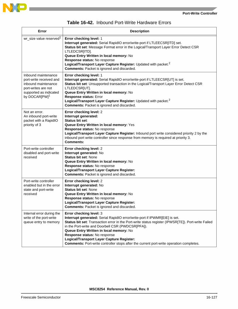
Port-Write Controller
wr_size value reserved1 Error checking level: 1Interrupt generated: Serial RapidIO error/write-port if LTLEECSR[ITD] set.Status bit set: Message Format error in the Logical/Transport Layer Error Detect CSR LTLEDCSR[ITD].Queue Entry Written in local memory: NoResponse status: No responseLogical/Transport Layer Capture Register: Updated with packet.2
Comments: Packet is ignored and discarded.
Inbound maintenance port-write received and inbound maintenance port-writes are not supported as indicated by DOCAR[PW]1
Error checking level: 1Interrupt generated: Serial RapidIO error/write-port if LTLEECSR[UT] is set.Status bit set: Unsupported transaction in the Logical/Transport Layer Error Detect CSR LTLEDCSR[UT].Queue Entry Written in local memory: NoResponse status: ErrorLogical/Transport Layer Capture Register: Updated with packet.2
Comments: Packet is ignored and discarded.
Not an error. An inbound port-write packet with a RapidIO priority of 3
Error checking level: 2Interrupt generated: Status bit set: Queue Entry Written in local memory: YesResponse status: No responseLogical/Transport Layer Capture Register: Inbound port write considered priority 2 by the inbound port write controller since response from memory is required at priority 3.Comments:
Port-write controller disabled and port-write received
Error checking level: 2Interrupt generated: NoStatus bit set: NoneQueue Entry Written in local memory: NoResponse status: No responseLogical/Transport Layer Capture Register:Comments: Packet is ignored and discarded.
Port-write controller enabled but in the error state and port-write received
Error checking level: 2Interrupt generated: NoStatus bit set: NoneQueue Entry Written in local memory: NoResponse status: No responseLogical/Transport Layer Capture Register: Comments: Packet is ignored and discarded.
Internal error during the write of the port-write queue entry to memory
Error checking level: 3Interrupt generated: Serial RapidIO error/write-port if IPWMR[EIE] is set.Status bit set: Transaction error in the Port-write status register (IPWSR[TE]). Port-write Failed in the Port-write and Doorbell CSR (PWDCSR[PFA]).Queue Entry Written in local memory: NoResponse status: No responseLogical/Transport Layer Capture Register: Comments: Port-write controller stops after the current port-write operation completes.
Table 16-42. Inbound Port-Write Hardware Errors
Error Description
MSC8254 Reference Manual, Rev. 0
Freescale Semiconductor 16-127

Serial RapidIO Controller
Table 16-43 lists the port-write programming errors.
16.5.8 Disabling and Enabling the Port-Write Controller
When the port-write controller is disabled by clearing IPWMR[PWE], the following actions are taken:
1. Queue full clears (IPWSR[QF]).
2. Port-write busy (IPWSR[PWB]) clears after a pending port-write queue entry write completes.
Before the port-write controller is reenabled (IPWMR[PWE]), the port-write busy bit (IPWSR[PWB]) must be cleared.
Notes: 1. These error types are actually detected in the RapidIO port, not in the port-write controller.
2. In small transport size configuration using the packet, the following allocations are made:• LTLACCSR[XA] gets the extended address (packet bits 78–79).• LTLACCSR[A] gets the address (packet bits 48–76).• LTLDIDCCSR[MDID] gets 0.• LTLDIDCCSR[DID] gets the least significant byte of the destination ID (packet bits 16–23).• LTLDIDCCSR[MSID] gets 0.• LTLDIDCCSR[SID] gets the least significant byte of the source ID (packet bits 24–31).• LTLCCCSR[FT] gets the ftype (packet bits 12–15).• LTLCCCSR[TT] gets the ttype (packet bits 32–35).• LTLCCCSR[MI] gets 0.
In large transport size configuration using the packet, the following allocations are made:• LTLACCSR[XA] gets the extended address (packet bits 94–95).• LTLACCSR[A] gets the address (packet bits 64– 92).• LTLDIDCCSR[MDID] gets the most significant byte of the destination ID (packet bits 16–23).• LTLDIDCCSR[DID] gets the least significant byte of the destination ID (packet bits 24–31).• LTLDIDCCSR[MSID] gets the most significant byte of the source ID (packet bits 32–39).• LTLDIDCCSR[SID] gets the least significant byte of the source ID (packet bits 40–47).• LTLCCCSR[FT] gets the ftype (packet bits 12–15).• LTLCCCSR[TT] gets the ttype (packet bits 48 –51).• LTLCCCSR[MI] gets 0.
Table 16-43. Inbound Port-Write Programming Errors
ErrorInterrupt
GeneratedStatus Bit Set Comments
Port-write queue entry written to non-existent memory
No No When a write to memory occurs, the memory controller causes its own interrupt and update its own capture registers. An internal error response is returned. When the port-write controller receives the error response it sets the transaction error bit (IPWSR[TE]) and enters the error state.
Table 16-42. Inbound Port-Write Hardware Errors
Error Description
MSC8254 Reference Manual, Rev. 0
16-128 Freescale Semiconductor

RapidIO Programming Model
16.5.9 RapidIO Message Passing Logical Specification Registers
The port-write and doorbell command and status register (PWDCSR) includes several port-write controller status bits. These read-only status bits only indicate the state of the port-write controller. See Section 16.6.9, Port Write and Doorbell Command and Status Register (PWDCSR), on page 16-141 for details.
Available (PWDCSR[PA]). Indicates that the port-write controller is enabled (IPWnMR[PWE]), the only port-write queue entry is available to be written (IPWnSR[QF]) = 0 and the port-write controller is not in the internal error state (IPWnSR[TE] = 0)
Full (PWDCSR[PFU]). This bit reflects the state of the queue full status bit (IPWnSR[QF])
Empty (PWDCSR[PEM]). This bit always a 1 since a port-write cannot be generated
Busy (PWDCSR[PB]). This bit reflects the state of the busy bit IPWnSR[PWB]
Failed (PWDCSR[PFA]). This bit reflects the state of the transaction error status bit IPWnSR[TE]
Error (PWDCSR[PE]). This bit is always a 0
16.6 RapidIO Programming Model
The RapidIO registers are listed in Table 16-44.
Table 16-44. RapidIO Registers
Group Register Offset Acronym Page
Architectural Registers:
Device Identity Capability Register 0x00000 DIDCAR page 16-133Device Information Capability Register 0x00004 DICAR page 16-133Assembly Identity Capability Register 0x00008 AIDCAR page 16-134Assembly Information Capability Register 0x0000C AICAR page 16-134Processing Element Features Capability Register 0x00010 PEFCAR page 16-135Source Operations Capability Register 0x00018 SOCAR page 16-136Destination Operations Capability Register 0x0001C DOCAR page 16-138Mailbox Command and Status Register 0x00040 MCSR page 16-139Port -Write and Doorbell Command and Status Register 0x00044 PWDCSR page 16-141Processing Element Logical Layer Control Command and Status Register
0x0004C PELLCCSR page 16-142
Local Configuration Space Base Address 1 Command and Status Register
0x0005C LCSBA1CSR page 16-143
Base Device ID Command and Status Register 0x00060 BDIDCSR page 16-144Host Base Device ID Lock Command and Status Register 0x00068 HBDIDLCSR page 16-145Component Tag Command and Status Register 0x0006C CTCSR page 16-146
MSC8254 Reference Manual, Rev. 0
Freescale Semiconductor 16-129

Serial RapidIO Controller
Extended Features Space: 1x/4x LP-Serial
Port Maintenance Block Header 0 (0) 0x00100 PMBH0 page 16-147Port Link Time-Out Control Command and Status Register ()
0x00120 PLTOCCSR page 16-148
Port Response Time-out Control Command and Status Register ()
0x00124 PRTOCCSR page 16-149
Port General Control Command and Status Register 0x0013C PGCCSR page 16-150Port 0–1 Link Maintenance Request Command and Status Register
0x001400x00160
PnLMREQCSR page 16-151
Port 0–1 Link Maintenance Response Command and Status Register
0x001440x00164
PnLMRESPCSR page 16-152
Port 0–1 Local ackID Status Command and Status Register
0x001480x00168
PnLASCR page 16-153
Port 0–1 Error and Status Command and Status Register 0x001580x00178
PnESCSR page 16-154
Port 0–1 Control Command and Status Register 0x0015C0x0017C
PnCCSR) page 16-156
Extended Features Space: Error Reporting (Logical)
Error Reporting Block Header 0x00600 ERBH page 16-158Logical/Transport Layer Error Detect Command and Status Register
0x00608 LTLEDCSR page 16-158
Logical/Transport Layer Error Enable Command and Status Register
0x0060C LTLEECSR page 16-160
Logical/Transport Layer Address Capture Command and Status Register
0x00614 LTLACCSR page 16-161
Logical/Transport Layer Device ID Capture Command and Status Register
0x00618 LTLDIDCCSR page 16-162
Logical/Transport Layer Control Capture Command and Status Register
0x0061C LTLCCCSR page 16-163
Extended Features Space: Error Reporting
(Physical)
Port 0–1 Error Detect Command and Status Register 0x006400x00680
PnEDCSR page 16-164
Port 0–1 Error Rate Enable Command and Status Register
0x006440x00684
PnERECSR page 16-165
Port 0–1 Error Capture Attributes Command and Status Register
0x006480x00688
PnECACSR page 16-166
Port 0–1 Packet/Control Symbol Error Capture Command and Status Register
0x0064C0x0068C
PnPCSECCSR0 page 16-168
Port 0–1 Packet Error Capture Command and Status Register 1
0x006500x00690
PnPECCSR1 page 16-169
Port 0–1 Packet Error Capture Command and Status Register 2
0x006540x00694
PnPECCSR2 page 16-170
Port 0–1 Packet Error Capture Command and Status Register 3
0x006580x00698
PnPECCSR3 page 16-171
Port 0–1 Error Rate Command and Status Register 0x006680x006A8
PnERCSR page 16-172
Port 0–1 Error Rate Threshold Command and Status Register
0x0066C0x006AC
PnERTCSR page 16-173
Table 16-44. RapidIO Registers (Continued)
Group Register Offset Acronym Page
MSC8254 Reference Manual, Rev. 0
16-130 Freescale Semiconductor

RapidIO Programming Model
Implementation Space: General
Logical Layer Configuration Register 0x10004 LLCR page 16-174Error /Port-write Interrupt Status Register 0x10010 EPWISR page 16-175Logical Retry Error Threshold Configuration Register 0x10020 LRETCR page 16-176Physical Retry Error Threshold Configuration Register () 0x10080 PRETCR page 16-177Port 0–1 Alternate Device ID Command and Status Register
0x101000x10180
PnADIDCSR page 16-178
Port 0–1 Pass-Through Accept-All Configuration Register 0x101200x101A0
PnPTAACR page 16-179
Port 0–1 Logical Outbound Packet Time-to-Live Configuration Register ()
0x101240x101A4
PnLOPTTLCR page 16-180
Port 0–1 Implementation Error Command and Status Register
0x101300x101B0
PnIECSR page 16-181
Port 0–1 Serial Link Command and Status Register 0x101580x101D8
PnSLCSR page 16-182
Port 0–1 Serial Link Error Injection Configuration Register 0x101600x101E0
PnSLEICR page 16-183
Implementation Space: Revision Control
IP Block Revision Register 1 0x10BF8 IPBRR1 page 16-184IP Block Revision Register 2 0x10BFC IPBRR2 page 16-184
Outbound ATMU
Port 0–1 RapidIO Outbound Window Translation Address Register x (offset is x*0x20)
0x10C000x10E00
PnROWTARx page 16-185
Port 0–1 RapidIO Outbound Window Translation Extended Address Register x (offset is x*0x20)
0x10C040x10E04
PnROWTEARx page 16-186
Port 0–1 RapidIO Outbound Window Base Address Register x (offset is x*0x20)
0x10C080x10E08
PnROWBARx page 16-187
Port 0–1 RapidIO Outbound Window Attributes Register x (offset is x*0x20)
0x10C100x10E10
PnROWARx page 16-188
Port 0–1 RapidIO Outbound Window Segment x (1–3) Registers y (1–8) (offset is (x –1)*0x20 + (y – 1)*0x20)
0x10C340x10E34
PnROWSxRy page 16-190
Inbound ATMU Port 0–1 RapidIO Inbound Window Translation Address Registers x (offset is (4 – x)*0x20);
0x10D600x10F60
PnRIWTARx page 16-191
Port 0–1 RapidIO Inbound Window Base Address Registers x (offset is (4 – x)*0x20)
0x10D680x10F68
PnRIWBARx page 16-192
Port 0–1 RapidIO Inbound Window Attributes Registers x (offset is (4 – x)*0x20)
0x10D700x10F70
PnRIWARx page 16-193
Table 16-44. RapidIO Registers (Continued)
Group Register Offset Acronym Page
MSC8254 Reference Manual, Rev. 0
Freescale Semiconductor 16-131

Serial RapidIO Controller
Note: The base address for the RapidIO registers is: 0xFFF80000.
Outbound Message Unit Registers
Outbound Message x Mode Registers (offset is x*0x100) 0x13000 OMxMR page 16-194Outbound Message x Status Registers (offset is x*0x100) 0x13004 OMxSR page 16-196Outbound Message x Descriptor Queue Dequeue Pointer Address Registers (offset is x*0x100)
0x1300C OMxDQDPAR page 16-198
Outbound Message x Source Address Registers (offset is x*0x100)
0x13014 OMxSAR page 16-199
Outbound Message x Destination Port Registers (offset is x*0x100)
0x13018 OMxDPR page 16-200
Outbound Message x Destination Attributes Registers (offset is x*0x100)
0x1301C OMxDATR page 16-201
Outbound Message x Double-Word Count Registers (offset is x*0x100)
0x13020 OMxDCR page 16-202
Outbound Message x Descriptor Queue Enqueue Pointer (offset is x*0x100) Address Registers (offset is x*0x100)
0x13028 OMxDQEPAR page 16-203
Outbound Message x Retry Error Threshold (offset is x*0x100) Configuration Registers
0x1302C OMxRETCR page 16-204
Outbound Message x Multicast Group Registers (offset is x*0x100)
0x13030 OMxMGR page 16-205
Outbound Message x Multicast List Registers (offset is x*0x100)
0x13034 OMxMLR page 16-206
Inbound Message Unit Registers
Inbound Message x Mode Registers (offset is x*0x100) 0x13060 IMxMR page 16-207Inbound Message x Status Registers (offset is x*0x100) 0x13064 IMxSR page 16-209Inbound Message x Frame Queue Dequeue Pointer Address Registers (offset is x*0x100)
0x1306C IMxFQDPAR page 16-211
Inbound Message x Frame Queue Enqueue Pointer Address Registers (offset is x*0x100)
0x13074 IMxFQEPAR page 16-212
Inbound Message x Maximum Interrupt Report Interval Registers (offset is x*0x100)
0x13078 IMxMIRIR page 16-213
Outbound Doorbell Unit Registers
Outbound Doorbell Mode Register 0x13400 ODMR page 16-214Outbound Doorbell Status Register 0x13404 ODSR page 16-215Outbound Doorbell Destination Port Register 0x13418 ODDPR page 16-216Outbound Doorbell Destination Attributes Register 0x1341C ODDATR page 16-217Outbound Doorbell Retry Error Threshold Configuration Register
0x1342C ODRETCR page 16-218
Inbound Doorbell Unit Registers
Inbound Doorbell Mode Register 0x13460 IDMR page 16-219Inbound Doorbell Status Register 0x13464 IDSR page 16-221Inbound Doorbell Queue Dequeue Pointer Address Register
0x1346C IDQDPAR page 16-222
Inbound Doorbell Queue Enqueue Pointer Address Register
0x13474 IDQEPAR page 16-223
Inbound Doorbell Maximum Interrupt Report Interval Register
0x13478 IDMIRIR page 16-224
Port-Write Registers
Inbound Port-Write Mode Register 0x134E0 IPWMR page 16-225Inbound Port-Write Status Register 0x134E4 IPWSR page 16-226Inbound Port-Write Queue Base Address Register 0x134EC IPWQBAR page 16-227
Table 16-44. RapidIO Registers (Continued)
Group Register Offset Acronym Page
MSC8254 Reference Manual, Rev. 0
16-132 Freescale Semiconductor

RapidIO Programming Model
16.6.1 Device Identity Capability Register (DIDCAR)
16.6.2 Device Information Capability Register (DICAR)
DIDCAR Device Identity Capability Register Offset 0x00000
Bit 31 30 29 28 27 26 25 24 23 22 21 20 19 18 17 16
DI
TYPE RRESET 0 0 0 1 1 0 0 0 0 0 0 1 0 0 0 0
Bit 15 14 13 12 11 10 9 8 7 6 5 4 3 2 1 0
DVITYPE R
RESET 0 0 0 0 0 0 0 0 0 0 0 0 0 0 1 0
Table 16-45. DIDCAR Field Descriptions
Bits Reset Description
DI31–16
0x1810 Device Identity Uniquely identifies the type of device from the vendor specified by DVI. The values for DI are assigned and managed by the respective vendor. The value for the MSC8254 = 0x1810.
DVI15–0
0x0002 Device Vendor IdentityIdentifies the vendor that manufactures the device containing the processing element. A value for DVI is uniquely assigned to a device vendor by the registration authority of the RapidIO Trade Association. The value for Freescale Semiconductor, Inc. is 0x0002.
DICAR Device Information Capability Register Offset 0x00004
Bit 31 30 29 28 27 26 25 24 23 22 21 20 19 18 17 16
DRTYPE R
RESET 0 0 0 0 0 0 0 0 0 0 0 0 0 0 0 0
Bit 15 14 13 12 11 10 9 8 7 6 5 4 3 2 1 0
DR
TYPE RRESET 0 0 0 0 0 0 0 0 0 0 0 0 0 0 0 0
Table 16-46. DICAR Field Descriptions
Bit Reset Description
DR31–0
0x00000000 Device RevisionIdentifies the revision level of the device. The value for DR is assigned and managed by the vendor specified by DIDCAR[DVI].
MSC8254 Reference Manual, Rev. 0
Freescale Semiconductor 16-133

Serial RapidIO Controller
16.6.3 Assembly Identity Capability Register (AIDCAR)
16.6.4 Assembly Information Capability Register (AICAR)
AICAR contains additional information on the assembly and the pointer to the first entry in the extended features list.
AIDCAR Assembly Identity Capability Register Offset 0x00008
Bit 31 30 29 28 27 26 25 24 23 22 21 20 19 18 17 16
AI
TYPE RRESET 0 0 0 0 0 0 0 0 0 0 0 0 0 0 0 0
Bit 15 14 13 12 11 10 9 8 7 6 5 4 3 2 1 0
AVITYPE R
RESET 0 0 0 0 0 0 0 0 0 0 0 0 0 0 0 0
Table 16-47. AIDCAR Field Descriptions
Bit Name Description
AI31–16
0x0000 Assembly IdentityUniquely identifies the type of assembly from the vendor specified by AVI. The values for AI are assigned and managed by the respective vendor.
AVI15–0
0x0000 Assembly Vendor Identity Identifies the vendor that manufactures the assembly or subsystem containing the device. A value for AVI is uniquely assigned to an assembly vendor by the registration authority of the RapidIO Trade Association.
AICAR Assembly Information Capability Register Offset 0x0000C
Bit 31 30 29 28 27 26 25 24 23 22 21 20 19 18 17 16
AR
TYPE RRESET 0 0 0 0 0 0 0 0 0 0 0 0 0 0 0 0
Bit 15 14 13 12 11 10 9 8 7 6 5 4 3 2 1 0
EFPTYPE R
RESET 0 0 0 0 0 0 0 1 0 0 0 0 0 0 0 0
Table 16-48. AICAR Field Descriptions
Bit Reset Description
AR31–16
0x0000 Assembly Revision
EFP15–0
0x0100 Extended Features Pointer
MSC8254 Reference Manual, Rev. 0
16-134 Freescale Semiconductor

RapidIO Programming Model
16.6.5 Processing Element Features Capability Register (PEFCAR)
PEFCAR identifies the major functionality provided by the processing element.
PEFCAR Processing Element Features Capability Register Offset 0x00010
Bit 31 30 29 28 27 26 25 24 23 22 21 20 19 18 17 16
BR MEM PROC SW — MB DB —
TYPE RRESET 1 1 1 0 0 0 0 0 1 1 1 1 1 0 0 0
Bit 15 14 13 12 11 10 9 8 7 6 5 4 3 2 1 0
— CTLS EF EASTYPE R
RESET 0 0 0 0 0 0 0 0 0 0 0 1 1 0 0 1
Table 16-49. PEFCAR Field Descriptions
Bit Reset Description Settings
BR31
1 BridgeSpecifies whether the MSC8254 can bridge to another interface.
MEM30
1 MemorySpecifies whether the MSC8254 has physically addressable local address space and can be accessed as an endpoint through non-maintenance operations.
PROC29
1 ProcessorSpecifies whether the MSC8254 contains a local processor that executes code.
SW28
0 SwitchThe MSC8254 does not bridge to another external RapidIO interface. (SW=0)
—27–24
0 Reserved. Write to zero for future compatibility.
MB23–20
0b1111 MailboxSpecifies the inbound mailboxes supported by the MSC8254.
1000 Mailbox 0, supported by MSC8254.
0100 Mailbox 1, supported by MSC8254.
0010 Mailbox 2, supported by MSC8254.
0001 Mailbox 3, supported by MSC8254.
1111 Mailboxes 0–3.
DB19
1 DoorbellSpecifies whether the RapidIO Controller supports inbound Doorbells.
—18–5
0 Reserved. Write to zero for future compatibility.
CTLS4
1 Common Transport Large SystemsSpecifies whether the RapidIO Controller supports large systems.This is configured at power-up through the reset configuration word.
0 Only common transport small systems (up to 256 devices).
1 Large systems up to 65,536 devices.
MSC8254 Reference Manual, Rev. 0
Freescale Semiconductor 16-135

Serial RapidIO Controller
16.6.6 Source Operations Capability Register (SOCAR)
SOCAR defines the set of RapidIO logical operations that can be issued by the MSC8254.
EF3
1 Extended FeaturesSpecifies whether the extended features pointer is valid.
EAS2–0
0b001 Extended Address SupportIndicates the number of address bits supported by the RapidIO controller both as a source and target of an operation.
000 Reserved.
010 Reserved.
001 34-bit addresses.
SOCAR Source Operations Capability Register 0x00018
Bit 31 30 29 28 27 26 25 24 23 22 21 20 19 18 17 16
R IR RO DCI C F IOR ICI TIE TIES —
TYPE RRESET 0 0 0 0 0 0 0 0 0 0 0 0 0 0 0 0
Bit 15 14 13 12 11 10 9 8 7 6 5 4 3 2 1 0
NR NW SW NWR M D — ATS AI AD AS AC — PW —TYPE R
RESET 1 1 1 1 1 1 0 0 0 0 0 0 0 0 0 0
Table 16-50. SOCAR Field Descriptions
Bit Reset Description
R31
0 Read OperationMSC8254 does not support.
IR30
0 IRead OperationMSC8254 does not support.
RO29
0 Read-to-Own OperationMSC8254 does not support.
DCI28
0 Data Cache Invalidate OperationMSC8254 does not support.
C27
0 Castout OperationMSC8254 does not support.
F26
0 Flush OperationMSC8254 does not support.
IOR25
0 I/O-Read OperationMSC8254 does not support.
ICI24
0 Instruction Cache Invalidate OperationMSC8254 does not support.
TIE23
0 TLBIE OperationMSC8254 does not support.
TIES22
0 TLBSYNC OperationMSC8254 does not support.
—21–16
0 Reserved. Write to zero for future compatibility.
NR15
1 NREAD OperationMSC8254 supports operation.
Table 16-49. PEFCAR Field Descriptions
Bit Reset Description Settings
MSC8254 Reference Manual, Rev. 0
16-136 Freescale Semiconductor
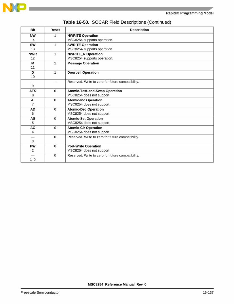
RapidIO Programming Model
NW14
1 NWRITE OperationMSC8254 supports operation.
SW13
1 SWRITE OperationMSC8254 supports operation.
NWR12
1 NWRITE_R OperationMSC8254 supports operation.
M11
1 Message Operation
D10
1 Doorbell Operation
—9
— Reserved. Write to zero for future compatibility.
ATS8
0 Atomic-Test-and-Swap OperationMSC8254 does not support.
AI7
0 Atomic-Inc OperationMSC8254 does not support.
AD6
0 Atomic-Dec OperationMSC8254 does not support.
AS5
0 Atomic-Set OperationMSC8254 does not support.
AC4
0 Atomic-Clr OperationMSC8254 does not support.
—3
0 Reserved. Write to zero for future compatibility.
PW2
0 Port-Write OperationMSC8254 does not support.
—1–0
0 Reserved. Write to zero for future compatibility.
Table 16-50. SOCAR Field Descriptions (Continued)
Bit Reset Description
MSC8254 Reference Manual, Rev. 0
Freescale Semiconductor 16-137
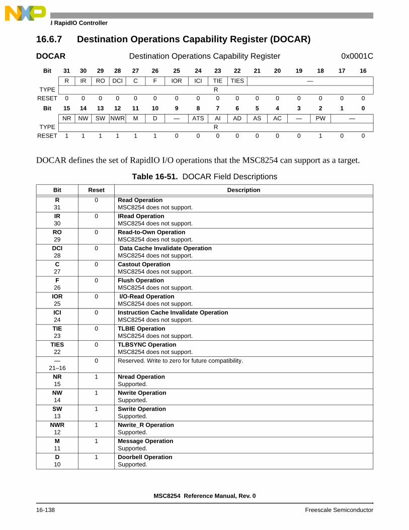
Serial RapidIO Controller
16.6.7 Destination Operations Capability Register (DOCAR)
DOCAR defines the set of RapidIO I/O operations that the MSC8254 can support as a target.
DOCAR Destination Operations Capability Register 0x0001C
Bit 31 30 29 28 27 26 25 24 23 22 21 20 19 18 17 16
R IR RO DCI C F IOR ICI TIE TIES —
TYPE RRESET 0 0 0 0 0 0 0 0 0 0 0 0 0 0 0 0
Bit 15 14 13 12 11 10 9 8 7 6 5 4 3 2 1 0
NR NW SW NWR M D — ATS AI AD AS AC — PW —TYPE R
RESET 1 1 1 1 1 1 0 0 0 0 0 0 0 1 0 0
Table 16-51. DOCAR Field Descriptions
Bit Reset Description
R31
0 Read OperationMSC8254 does not support.
IR30
0 IRead OperationMSC8254 does not support.
RO29
0 Read-to-Own OperationMSC8254 does not support.
DCI28
0 Data Cache Invalidate OperationMSC8254 does not support.
C27
0 Castout OperationMSC8254 does not support.
F26
0 Flush OperationMSC8254 does not support.
IOR25
0 I/O-Read OperationMSC8254 does not support.
ICI24
0 Instruction Cache Invalidate OperationMSC8254 does not support.
TIE23
0 TLBIE OperationMSC8254 does not support.
TIES22
0 TLBSYNC OperationMSC8254 does not support.
—21–16
0 Reserved. Write to zero for future compatibility.
NR15
1 Nread OperationSupported.
NW14
1 Nwrite OperationSupported.
SW13
1 Swrite OperationSupported.
NWR12
1 Nwrite_R OperationSupported.
M11
1 Message OperationSupported.
D10
1 Doorbell OperationSupported.
MSC8254 Reference Manual, Rev. 0
16-138 Freescale Semiconductor

RapidIO Programming Model
16.6.8 Mailbox Command and Status Register (MCSR)
MCSR reflects the status of the RapidIO message controllers.
—9
— Reserved. Write to zero for future compatibility.
ATS8
0 Atomic-Test-and-Swap OperationMSC8254 does not support.
AI7
0 Atomic-Inc OperationMSC8254 does not support.
AD6
0 Atomic-Dec OperationMSC8254 does not support.
AS5
0 Atomic-Set OperationMSC8254 does not support.
AC4
0 Atomic-Clr OperationMSC8254 does not support.
—3
0 Reserved. Write to zero for future compatibility.
PW2
1 Port-Write OperationSupported.
—1–0
0 Reserved. Write to zero for future compatibility.
MCSR Mailbox Command and Status Register 0x00040
Bit 31 30 29 28 27 26 25 24 23 22 21 20 19 18 17 16
A0 FU0 EM0 B0 FA0 ERR0 — A1 FU1 EM1 B1 FA1 ERR1 —TYPE R
RESET 0 0 1 0 0 0 0 0 0 0 1 0 0 0 0 0
Bit 15 14 13 12 11 10 9 8 7 6 5 4 3 2 1 0
—TYPE R
RESET 0 0 0 0 0 0 0 0 0 0 0 0 0 0 0 0
Table 16-52. MCSR Field Definitions
Bits Reset Description Settings
A031
0 AvailableSpecifies whether message controller 0 is initialized and ready to accept messages. When this bit is cleared, all incoming message transactions to message controller 0 return error responses.
0 Not ready.
1 Ready.
FU030
0 FullSpecifies whether message controller 0 is full. When FU0 is set, new messages to message controller 0 are retried.
0 Not full.
1 Full.
EM029
1 EmptySpecifies whether message controller 0 contains outstanding messages.
0 Contains outstanding messages.
1 Contains no outstanding messages.
Table 16-51. DOCAR Field Descriptions (Continued)
Bit Reset Description
MSC8254 Reference Manual, Rev. 0
Freescale Semiconductor 16-139

Serial RapidIO Controller
B028
0 BusySpecifies whether message controller 0 is busy processing a message. When this bit is set, new message operations to message controller 0 return retry responses.
0 Not busy.
1 Busy.
FA027
0 FailureSpecifies whether message controller 0 has encountered an internal error and is awaiting assistance. When this bit is set, all incoming message transactions to message controller 0 return error responses.
0 No internal error.
1 Internal fault or error condition encountered.
ERR026
0 ErrorThis field always returns a value of 0.
—25–24
0 Reserved. Write to zero for future compatibility.
A123
0 AvailableSpecifies whether message controller 1 is initialized and ready to accept messages. When this bit is cleared, all incoming message transactions to message controller 1 return error responses.
0 Not ready.
1 Ready.
FU122
0 FullSpecifies whether message controller 1 is full. When FU0 is set, new messages to message controller 1 are retried.
0 Not full.
1 Full.
EM121
1 EmptySpecifies whether message controller 1 contains outstanding messages.
0 Contains outstanding messages.
1 Contains no outstanding messages.
B120
0 BusySpecifies whether message controller 1 is busy processing a message. When this bit is set, new message operations to message controller 1 return retry responses.
0 Not busy.
1 Busy.
FA119
0 FailureSpecifies whether message controller 1 has encountered an internal error and is awaiting assistance. When this bit is set, all incoming message transactions to message controller 1 return error responses.
0 No internal error.
1 Internal fault or error condition encountered.
ERR118
0 ErrorThis field always returns a value of 0.
—17–0
0 Reserved. Write to zero for future compatibility.
Table 16-52. MCSR Field Definitions (Continued)
Bits Reset Description Settings
MSC8254 Reference Manual, Rev. 0
16-140 Freescale Semiconductor

RapidIO Programming Model
16.6.9 Port Write and Doorbell Command and Status Register (PWDCSR)
PWDCSR reflects the status of the RapidIO doorbell and port-write hardware. For details, refer to the RapidIO Interconnect Specification, Revision 1.2 in sections “Doorbell CSR” and “Write Port CSR.”:
PWDCSR Port-Write and Doorbell Command and Status Register Offset 0x00044
Bit 31 30 29 28 27 26 25 24 23 22 21 20 19 18 17 16
A FU EM B FA ERR —
TYPE RRESET 0 0 1 0 0 0 0 0 0 0 0 0 0 0 0 0
Bit 15 14 13 12 11 10 9 8 7 6 5 4 3 2 1 0
— PA PFU PEM PB PFA PE —TYPE R
RESET 0 0 0 0 0 0 0 0 0 0 1 0 0 0 0 0
Table 16-53. PWDCSR Field Descriptions
Bits Reset Description Settings
A31
0 AvailableSpecifies whether the doorbell unit is available and ready to accept doorbell messages. When this bit is cleared, all incoming doorbell transactions return error responses.
0 Not ready.
1 Ready.
FU30
0 FullSpecifies whether the doorbell unit is full. When this bit is set, new doorbell messages are retried.
0 Not full.
1 Full.
EM29
1 EmptySpecifies whether the doorbell unit has outstanding doorbell messages.
0 Outstanding doorbell messages.
1 No outstanding doorbell messages.
B28
0 BusySpecifies whether the doorbell unit is busy processing a doorbell message. When this bit is set, incoming transactions are not retried.
0 Not busy.
1 Busy.
FA27
0 FailureSpecifies whether the doorbell unit has encountered an internal fault or error condition and is awaiting assistance. When this bit is set, all incoming doorbell transactions return error responses.
0 No internal error.
1 Internal fault or error condition encountered.
ERR26
0 ErrorThis field always returns a value of 0.
—25–8
0 Reserved. Write to zero for future compatibility.
PA7
0 Port-Write Unit AvailableSpecifies whether the port-write unit is available and ready to accept a port-write packet. When this bit is cleared, all incoming port-write packets are discarded.
0 Not available.
1 Ready.
PFU6
0 Port-Write Unit FullSpecifies whether the port-write unit is full. When this bit is set, all incoming port-write packets are discarded.
0 Not full.
1 Full.
PEM5
1 Port-Write Unit EmptyThis field always returns a value of 1.
MSC8254 Reference Manual, Rev. 0
Freescale Semiconductor 16-141
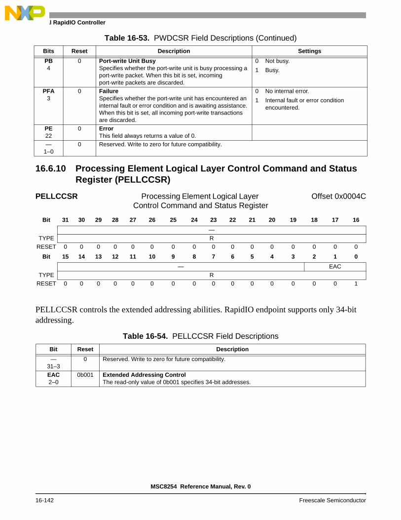
Serial RapidIO Controller
16.6.10 Processing Element Logical Layer Control Command and Status Register (PELLCCSR)
PELLCCSR controls the extended addressing abilities. RapidIO endpoint supports only 34-bit addressing.
PB4
0 Port-write Unit BusySpecifies whether the port-write unit is busy processing a port-write packet. When this bit is set, incoming port-write packets are discarded.
0 Not busy.
1 Busy.
PFA3
0 FailureSpecifies whether the port-write unit has encountered an internal fault or error condition and is awaiting assistance. When this bit is set, all incoming port-write transactions are discarded.
0 No internal error.
1 Internal fault or error condition encountered.
PE22
0 ErrorThis field always returns a value of 0.
—1–0
0 Reserved. Write to zero for future compatibility.
PELLCCSR Processing Element Logical Layer Offset 0x0004CControl Command and Status Register
Bit 31 30 29 28 27 26 25 24 23 22 21 20 19 18 17 16
—TYPE R
RESET 0 0 0 0 0 0 0 0 0 0 0 0 0 0 0 0
Bit 15 14 13 12 11 10 9 8 7 6 5 4 3 2 1 0
— EAC
TYPE RRESET 0 0 0 0 0 0 0 0 0 0 0 0 0 0 0 1
Table 16-54. PELLCCSR Field Descriptions
Bit Reset Description
—31–3
0 Reserved. Write to zero for future compatibility.
EAC2–0
0b001 Extended Addressing ControlThe read-only value of 0b001 specifies 34-bit addresses.
Table 16-53. PWDCSR Field Descriptions (Continued)
Bits Reset Description Settings
MSC8254 Reference Manual, Rev. 0
16-142 Freescale Semiconductor

RapidIO Programming Model
16.6.11 Local Configuration Space Base Address 1 Command and Status Register (LCSBA1CSR)
LCSBA1CSR specifies the most significant bits of the local physical address double-word offset for the MSC8254 configuration register space allowing the configuration register space to be physically mapped in the processing element. This register allows configuration and maintenance of an MSC8254 through regular read and write operations rather than maintenance operations. The double-word offset is right justified in the register. This window has priority over all ATMU windows. As with all registers, an external processor writing to LCSBA1CSR should not assume that the write occurs until a response is received.
LCSBA1CSR Local Configuration Space Base Address 1 Offset 0x0005CCommand and Status Register
Bit 31 30 29 28 27 26 25 24 23 22 21 20 19 18 17 16
— LCSBA —TYPE R/W
RESET 0 0 1 1 1 1 1 1 1 1 1 1 1 1 0 0
Bit 15 14 13 12 11 10 9 8 7 6 5 4 3 2 1 0
—
TYPE RRESET 0 0 0 0 0 0 0 0 0 0 0 0 0 0 0 0
Table 16-55. LCSBA1CSR Field Descriptions
Bit Reset Description
—31
0 Reserved. Write to zero for future compatibility.
LCSBA30–17
0x1FFE Local configuration space base address. These bits correspond to the highest 14 bits of the 34-bit RapidIO address space.
—16–0
0 Reserved. Write to zero for future compatibility.
MSC8254 Reference Manual, Rev. 0
Freescale Semiconductor 16-143

Serial RapidIO Controller
16.6.12 Base Device ID Command and Status Register (BDIDCSR)
BDIDCSR contains the base device ID values for the processing element.
BDIDCSR Base Device ID Command and Status Register Offset 0x00060
Bit 31 30 29 28 27 26 25 24 23 22 21 20 19 18 17 16
— BDID
TYPE R R/WRESET 0 0 0 0 0 0 0 0 1 1 1 1 1 1 1 1
Bit 15 14 13 12 11 10 9 8 7 6 5 4 3 2 1 0
LBDIDTYPE R/W
RESET 1 1 1 1 1 1 1 1 1 1 1 1 1 1 1 1
Table 16-56. BDIDCSR Field Descriptions
Bit Reset Description
—31–24
0 Reserved. Write to zero for future compatibility.
BDID23–16
0xFF Base Device ID in Small Common Transport System (RapidIO Device ID)Valid only if PEFCAR[CTLS] is cleared. If the RapidIO controller is configured as a host, the highest 5 bits of BDID are cleared and the lowest 3 bits are equal to the lowest three bits of the RCWHR[DEVID] field (see Section 5.3.2, Reset Configuration Word High Register (RCWHR), on page 5-19). If the RapidIO controller is configured as an agent, BDID = 0xFF.
LBDID15–0
0xFFFF Large Base Device ID in Large Common Transport SystemValid only if PEFCAR[CTLS] is set. If the RapidIO controller is configured as a host, the highest 13 bits of LBDID are cleared and the lowest 3 bits are equal to the lowest three bits of the RCWHR[DEVID] field (see Section 5.3.2, Reset Configuration Word High Register (RCWHR), on page 5-19). If the RapidIO controller is configured as an agent, LBDID = 0xFFFF.
MSC8254 Reference Manual, Rev. 0
16-144 Freescale Semiconductor

RapidIO Programming Model
16.6.13 Host Base Device ID Lock Command and Status Register (HBDIDLCSR)
HBDIDLCSR contains the base device ID value for the processing element in the system that initializes this device. The HBDID field is a write-once/resettable field with a lock function. When HBDID is written, all subsequent writes to the field are ignored, except when the value written matches the value in the field. Then, the register is reinitialized to 0xFFFF. After HBDID is written, the processing element must read the host base device ID lock CSR to verify that it owns the lock before it attempts to initialize the device.
HBDIDLCSR Host Base Device ID Lock Command and Status Offset 0x00068Register
Bit 31 30 29 28 27 26 25 24 23 22 21 20 19 18 17 16
—TYPE R
RESET 0 0 0 0 0 0 0 0 0 0 0 0 0 0 0 0
Bit 15 14 13 12 11 10 9 8 7 6 5 4 3 2 1 0
HBDID
TYPE RRESET 1 1 1 1 1 1 1 1 1 1 1 1 1 1 1 1
Table 16-57. HBDIDLCSR Field Descriptions
Bit Reset Description
—31–16
0 Reserved. Write to zero for future compatibility.
HBDID15–0
0xFFFF Host Base Device IDThe host base device ID for the processing element that initializes this device. Only the first write to this field is accepted; all other writes are ignored, except when the value written matches the value contained in the field. In this case, the register is reinitialized to 0xFFFF.
MSC8254 Reference Manual, Rev. 0
Freescale Semiconductor 16-145

Serial RapidIO Controller
16.6.14 Component Tag Command and Status Register (CTCSR)
CTCSR contains a component tag value for the processing element that software can assign when the device is initialized. It is unused internally in RapidIO Endpoint.
CTCSR Component Tag Command and Status Register Offset 0x0006C
Bit 31 30 29 28 27 26 25 24 23 22 21 20 19 18 17 16
CT
TYPE R/WRESET 0 0 0 0 0 0 0 0 0 0 0 0 0 0 0 0
Bit 15 14 13 12 11 10 9 8 7 6 5 4 3 2 1 0
CTTYPE R/W
RESET 0 0 0 0 0 0 0 0 0 0 0 0 0 0 0 0
Table 16-58. CTCSR Field Descriptions
Bit Reset Description
CT31–0
0 Component Tag
MSC8254 Reference Manual, Rev. 0
16-146 Freescale Semiconductor

RapidIO Programming Model
16.6.15 Port Maintenance Block Header 0 (PMBH0)
PMBH0 contains a pointer (EFPTR) to the next extended features space, error management block, extended features block (EFBLK), and the EFID that identifies it as the generic endpoint port maintenance block header. While registers defined by software-assisted error recovery are supported, software-assisted error recovery is not. Therefore, the RapidIO Endpoint is defined here as not supporting software-assisted error recovery.
PMBH0 Port Maintenance Block Offset 0x00100Header 0
Bit 31 30 29 28 27 26 25 24 23 22 21 20 19 18 17 16
EFPTRTYPE R
RESET 0 0 0 0 0 1 1 0 0 0 0 0 0 0 0 0
Bit 15 14 13 12 11 10 9 8 7 6 5 4 3 2 1 0
EFIDTYPE R
RESET 0 0 0 0 0 0 0 0 0 0 0 0 0 0 0 1
Table 16-59. PMBH0 Field Descriptions
Bit Reset Description
EFPTR31–15
0x0600 Extended Features Pointer
EFID16–31
0x0001 Extended Features ID
MSC8254 Reference Manual, Rev. 0
Freescale Semiconductor 16-147

Serial RapidIO Controller
16.6.16 Port Link Time-Out Control Command and Status Register (PLTOCCSR)
PLTOCCSR contains the link time-out value for all ports. This time-out is for link events such as sending a packet to receive the corresponding acknowledge and sending a link-request to receive the corresponding link-response. The reset value is the maximum time-out interval and represents between 3 and 5 seconds.
The time-out increment unit is a function of the OCN bus clock frequency (the HSSI clock frequency) and the value given in the RapidIO prescaler field (CLK_GPR0[RPTE]) and is within the range of 255 ns (±5 ns). The exact formula to calculate this value is:
For example, if the OCN clock frequency = 333 MHz (RCWLR[MODCK] = 0) and CLK_GPR0[RPTE] = 41, the timer resolution is 252 ns.
PLTOCCSR Port Link Time-Out Control Command and Status Offset 0x00120Register
Bit 31 30 29 28 27 26 25 24 23 22 21 20 19 18 17 16
TVTYPE R/W
RESET 1 1 1 1 1 1 1 1 1 1 1 1 1 1 1 1
Bit 15 14 13 12 11 10 9 8 7 6 5 4 3 2 1 0
TV —
TYPE R/W RRESET 1 1 1 1 1 1 1 1 0 0 0 0 0 0 0 1
Table 16-60. PLTOCCSR Field Descriptions
Bit Reset Description
TV31–8
0xFFFFFF Time-Out ValueClearing this field to all zeros disables the link time-out timer. This value is loaded each time the link time-out timer starts.
—7–0
0x01 Reserved. Write to 0x01 for future compatibility.
Timer_Resolution 2 RPTE 1+( ) ocn_clk_freq⁄×=
where ocn_clk_freq HSSI clock frequency=
RPTE Decimal value of CLK_GPR0[RPTE]=
MSC8254 Reference Manual, Rev. 0
16-148 Freescale Semiconductor
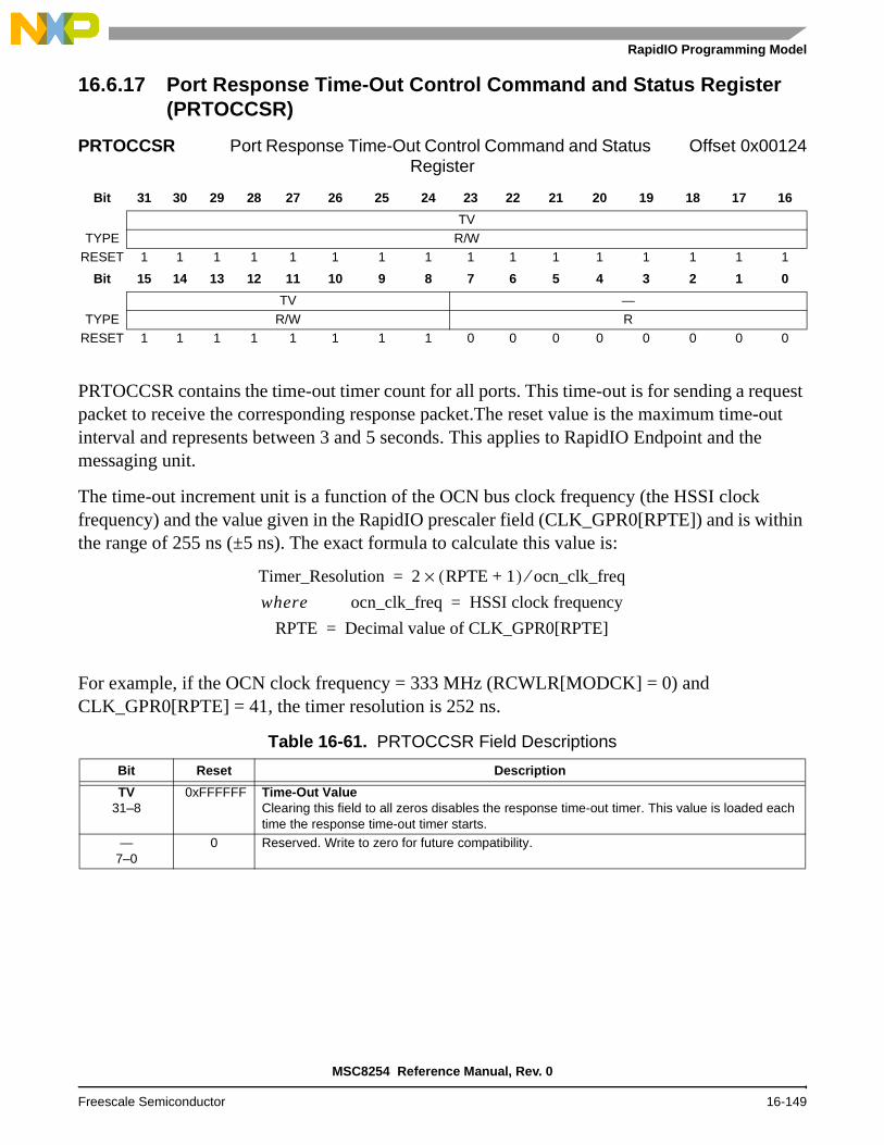
RapidIO Programming Model
16.6.17 Port Response Time-Out Control Command and Status Register (PRTOCCSR)
PRTOCCSR contains the time-out timer count for all ports. This time-out is for sending a request packet to receive the corresponding response packet.The reset value is the maximum time-out interval and represents between 3 and 5 seconds. This applies to RapidIO Endpoint and the messaging unit.
The time-out increment unit is a function of the OCN bus clock frequency (the HSSI clock frequency) and the value given in the RapidIO prescaler field (CLK_GPR0[RPTE]) and is within the range of 255 ns (±5 ns). The exact formula to calculate this value is:
For example, if the OCN clock frequency = 333 MHz (RCWLR[MODCK] = 0) and CLK_GPR0[RPTE] = 41, the timer resolution is 252 ns.
PRTOCCSR Port Response Time-Out Control Command and Status Offset 0x00124Register
Bit 31 30 29 28 27 26 25 24 23 22 21 20 19 18 17 16
TVTYPE R/W
RESET 1 1 1 1 1 1 1 1 1 1 1 1 1 1 1 1
Bit 15 14 13 12 11 10 9 8 7 6 5 4 3 2 1 0
TV —
TYPE R/W RRESET 1 1 1 1 1 1 1 1 0 0 0 0 0 0 0 0
Table 16-61. PRTOCCSR Field Descriptions
Bit Reset Description
TV31–8
0xFFFFFF Time-Out ValueClearing this field to all zeros disables the response time-out timer. This value is loaded each time the response time-out timer starts.
—7–0
0 Reserved. Write to zero for future compatibility.
Timer_Resolution 2 RPTE 1+( ) ocn_clk_freq⁄×=
where ocn_clk_freq HSSI clock frequency=
RPTE Decimal value of CLK_GPR0[RPTE]=
MSC8254 Reference Manual, Rev. 0
Freescale Semiconductor 16-149
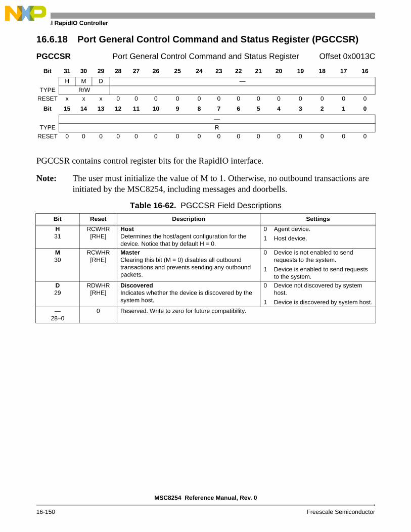
Serial RapidIO Controller
16.6.18 Port General Control Command and Status Register (PGCCSR)
PGCCSR contains control register bits for the RapidIO interface.
Note: The user must initialize the value of M to 1. Otherwise, no outbound transactions are initiated by the MSC8254, including messages and doorbells.
PGCCSR Port General Control Command and Status Register Offset 0x0013C
Bit 31 30 29 28 27 26 25 24 23 22 21 20 19 18 17 16
H M D —
TYPE R/WRESET x x x 0 0 0 0 0 0 0 0 0 0 0 0 0
Bit 15 14 13 12 11 10 9 8 7 6 5 4 3 2 1 0
—TYPE R
RESET 0 0 0 0 0 0 0 0 0 0 0 0 0 0 0 0
Table 16-62. PGCCSR Field Descriptions
Bit Reset Description Settings
H31
RCWHR [RHE]
HostDetermines the host/agent configuration for the device. Notice that by default H = 0.
0 Agent device.
1 Host device.
M30
RCWHR [RHE]
MasterClearing this bit (M = 0) disables all outbound transactions and prevents sending any outbound packets.
0 Device is not enabled to send requests to the system.
1 Device is enabled to send requests to the system.
D29
RDWHR [RHE]
DiscoveredIndicates whether the device is discovered by the system host.
0 Device not discovered by system host.
1 Device is discovered by system host.—
28–00 Reserved. Write to zero for future compatibility.
MSC8254 Reference Manual, Rev. 0
16-150 Freescale Semiconductor
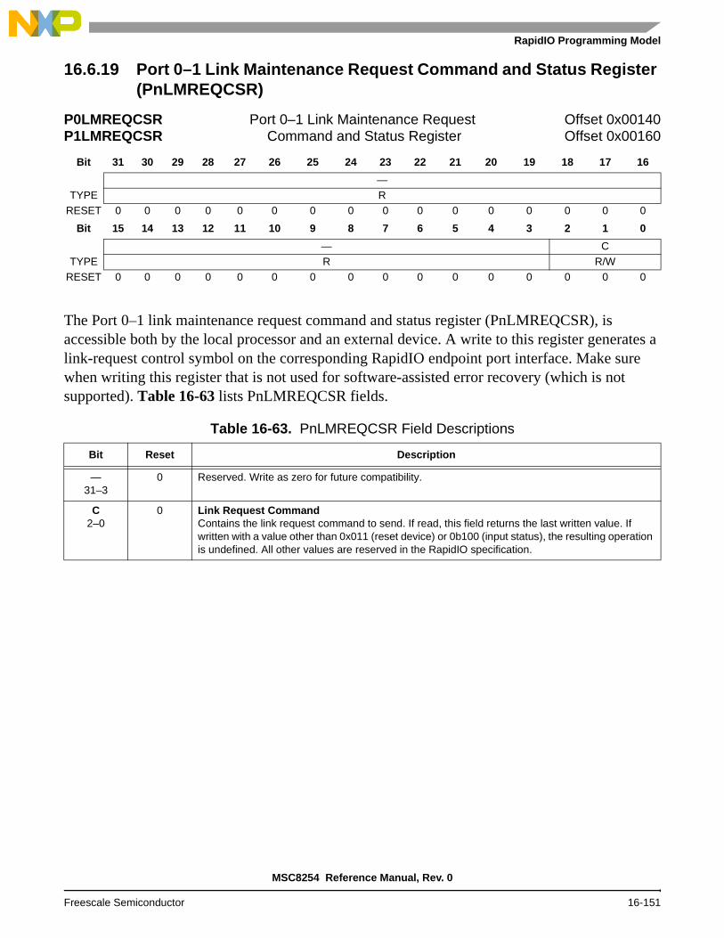
RapidIO Programming Model
16.6.19 Port 0–1 Link Maintenance Request Command and Status Register (PnLMREQCSR)
The Port 0–1 link maintenance request command and status register (PnLMREQCSR), is accessible both by the local processor and an external device. A write to this register generates a link-request control symbol on the corresponding RapidIO endpoint port interface. Make sure when writing this register that is not used for software-assisted error recovery (which is not supported). Table 16-63 lists PnLMREQCSR fields.
P0LMREQCSR Port 0–1 Link Maintenance Request Offset 0x00140P1LMREQCSR Command and Status Register Offset 0x00160
Bit 31 30 29 28 27 26 25 24 23 22 21 20 19 18 17 16
—TYPE R
RESET 0 0 0 0 0 0 0 0 0 0 0 0 0 0 0 0
Bit 15 14 13 12 11 10 9 8 7 6 5 4 3 2 1 0
— C
TYPE R R/WRESET 0 0 0 0 0 0 0 0 0 0 0 0 0 0 0 0
Table 16-63. PnLMREQCSR Field Descriptions
Bit Reset Description
—31–3
0 Reserved. Write as zero for future compatibility.
C2–0
0 Link Request CommandContains the link request command to send. If read, this field returns the last written value. If written with a value other than 0x011 (reset device) or 0b100 (input status), the resulting operation is undefined. All other values are reserved in the RapidIO specification.
MSC8254 Reference Manual, Rev. 0
Freescale Semiconductor 16-151

Serial RapidIO Controller
16.6.20 Port 0–1 Link Maintenance Response Command and Status Register (PnLMRESPCSR)
The Port 0–1 link maintenance response command and status register (PnLMRESPCSR), is accessible both by the local processor and an external device. A read to this register returns the status received in a link-response control symbol. This register is read-only. Table 16-64 lists PnLMRESPCSR fields.
P0LMRESPCSR Port 0–1 Link Maintenance Response Offset 0x00144P0LMRESPCSR Command and Status Register Offset 0x00164
Bit 31 30 29 28 27 26 25 24 23 22 21 20 19 18 17 16
RV —TYPE R
RESET 0 0 0 0 0 0 0 0 0 0 0 0 0 0 0 0
Bit 15 14 13 12 11 10 9 8 7 6 5 4 3 2 1 0
— AS LS
TYPE RRESET 0 0 0 0 0 0 0 0 0 0 0 0 0 0 0 0
Table 16-64. PnLMRESPCSR Field Descriptions
Bit Reset Description Settings
RV31
0 Response ValidThis bit indicates one of two conditions:• If the link-request causes a link-response, a set bit indicates that the
link-response was received and the status fields are valid.• If the link-request did not cause a link-response, a set bit indicates
that the link-request was transmitted.Note: This bit clears on read.
0 Link response not received, link response not valid, or link request was not transmitted.
1 Link response received with valid status bits or link request was transmitted.
—30–10
0 Reserved. Write as zero for future compatibility.
AS9–5
0 AckID_StatusThis field holds the AckID status field from the link response.
LS4–0
0 Link StatusThis field holds the link status field from the link response.
MSC8254 Reference Manual, Rev. 0
16-152 Freescale Semiconductor

RapidIO Programming Model
16.6.21 Port 0–1 Local ackID Command and Status Register (PnLASCR)
The Port 0–1 local ackID status command and status register (PnLASCSR) is accessible both by the core processor and an external device. A read to this register returns the local ackID status for both the output and input ports of the device. Care should be taken not to use this register for software error management. Table 16-65 lists PnLASCSR fields.
P0LASCSR Port 0–1 Local ackID Command and Status Register Offset 0x00148P1LASCSR Offset 0x00168
Bit 31 30 29 28 27 26 25 24 23 22 21 20 19 18 17 16
— IA —TYPE R R/W R
RESET 0 0 0 0 0 0 0 0 0 0 0 0 0 0 0 0
Bit 15 14 13 12 11 10 9 8 7 6 5 4 3 2 1 0
— OUTA — OBATYPE R R/W
RESET 0 0 0 0 0 0 0 0 0 0 0 0 0 0 0 0
Table 16-65. PnLASCSR Field Descriptions
Bit Reset Description
—31–29
0 Reserved. Write as zero for future compatibility.
IA28–24
0 Input ackIDThe value of the next expected Input port ackID.
23–13 0 Reserved. Write as zero for future compatibility.
OUTA12–8
0 Outstanding Port Unacknowledged ackID StatusNext expected acknowledge control symbol ackID field that indicates the ackID value expected in the next received acknowledge control symbol. Note that this value is read only even though RapidIO specification allows for it to be writable.
—7–5
0 Reserved. Write as zero for future compatibility.
OBA4–0
0 Outbound ackID Output Port Next Transmitted ackID ValueThis can be written by software but only if there are no outstanding unacknowledged packets. If there are, a newly-written value will be ignored
MSC8254 Reference Manual, Rev. 0
Freescale Semiconductor 16-153

Serial RapidIO Controller
16.6.22 Port 0–1 Error and Status Command and Status Register (PnESCSR)
PnESCSR is accessed when a local master or an external device needs to examine the port error and status information.
P0ESCSR Port 0 Error Command and Status Register Offset 0x00158P1ESCSR Offset 0x00178
Bit 31 30 29 28 27 26 25 24 23 22 21 20 19 18 17 16
— OPD OFE ODE — ORE OR ORS OEE OESTYPE R W1C W1C W1C W1C R W1C R
RESET 0 0 0 0 0 0 0 0 0 0 0 0 0 0 0 0
Bit 15 14 13 12 11 10 9 8 7 6 5 4 3 2 1 0
— IRS IEE IES — PWP — PE PO PU
TYPE R W1C R W1C RRESET 0 0 0 0 0 0 0 0 0 0 0 0 0 0 0 1
Table 16-66. PnESCSR Field Descriptions
Bit Reset Description
—31–27
0 Reserved. Write to zero for future compatibility.
OPD26
0 Output Packet-DroppedOutput port has discarded a packet. A packet is discarded if: • It is received while OFE is set and PnCCSR[DPE] (drop packet enable) is set and
PnCCSR[SPF] (stop on port failed) is set.• It is received while PnPCR[OBDEN] (output buffer drain enable) is set.• The link-partner does not accept it while the PnERTCSR[ERFTT] (error rate failed
threshold trigger) is met or exceeded, PnCCSR[DPE] is set, and PnCCSR[SPF] is not set (and link-response returns the expected ID acknowledge).
When OPD is set, it remains set until it is written with a logic 1 to clear it.OFE25
0 Output Fail EncounteredThe output port has encountered a failed condition because the error rate counter (PnEERCSR[ERC]) has met or exceeded the port failed error threshold (PnERTCSR[ERFTT]). OFE remains set until it is written with a logic 1 to clear it. When it is cleared, it does not assert again unless the error rate counter dips below the port failed error threshold and then meets or exceeds it again.
ODE24
0 Output Degraded Condition EncounteredThe output port has encountered a degraded condition because the error rate counter (PnEERCSR[ERC]) has met or exceeded the port degraded error threshold (PnERTCSR[ERDTT]). ODE remains set until it is written with a logic 1 to clear it. When it is cleared, it does not assert again unless the error rate counter dips below the port degraded error threshold and then meets or exceeds it again.
—23–21
0 Reserved. Write to zero for future compatibility.
ORE20
0 Output Retry Condition EncounteredThe output port has encountered a retry condition. This bit is set when ORS is set. ORE remains set until it is written with a logic 1 to clear it.
OR19
0 Output RetryThe output port has received a packet retry control symbol and cannot make forward progress. OR is set when ORS is set and cleared when a packet-accepted or packet-not-accepted control symbol is received. Read only.
MSC8254 Reference Manual, Rev. 0
16-154 Freescale Semiconductor

RapidIO Programming Model
ORS18
0 Output StopThe output port stops due to a retry. Read only.
OEE17
0 Output Error EncounterThe output port encountered (and possibly recovered from) a transmission error. OEE is set when OES is set. It remains set until it is written with a logic 1 to clear it.
OES16
0 Output Error StopThe output port is stopped due to a transmission error. Read only.
—15–11
0 Reserved. Write to zero for future compatibility.
IRS10
0 Input Retry StopThe input port is stopped due to a retry. Read only.
IEE9
0 Input Error EncounterThe input port encountered (and possibly recovered from) a transmission error. IEE is set when IES is set. It remains set until it is written with a logic 1 to clear it.
IES8
0 Input Error StopThe input port is stopped due to a transmission error. Read only.
—7–5
0 Reserved. Write to zero for future compatibility.
PWP4
0 Port Write Port has encountered a condition requiring it to initiate a maintenance port-write operation. PWP is valid only if the device can issue a maintenance port-write transaction. RapidIO Endpoint cannot issue port-writes. This bit is hard-wired to 0. Read only.
—3
0 Reserved
PE2
0 Port ErrorThe input or output port has encountered an error from which hardware could not recover. PE remains set until it is written with a logic 1 to clear it. PE indicates that OFE is set while CCSR[SPF] is set. That is, reaching the failed threshold has caused the output port to stop transmitting packets.
PO1
0 Ports OperatingThe input and output ports are initialized and the port is exchanging error-free control symbols with the attached device. Read only.
PU0
1 Ports UninitializedInput and output ports are not initialized. This bit and PO are mutually exclusive. Read only.
Table 16-66. PnESCSR Field Descriptions (Continued)
Bit Reset Description
MSC8254 Reference Manual, Rev. 0
Freescale Semiconductor 16-155

Serial RapidIO Controller
16.6.23 Port 0–1 Control Command and Status Register (PnCCSR)
PnCCSR contains control register bits for the RapidIO port. This register is for serial implementation only.
P0CCSR Port 0–1 Control Command and Status Register Offset 0x0015CP1CCSR Offset 0x0017C
Bit 31 30 29 28 27 26 25 24 23 22 21 20 19 18 17 16
PW IPW PWO PD OPE IPE ECD MEP —TYPE R R/W R
RESET 0 1 0 1 0 0 0 0 0 1 1 0 0 0 0 0
Bit 15 14 13 12 11 10 9 8 7 6 5 4 3 2 1 0
— SPF DPE PL PTTYPE R R/W R
RESET 0 0 0 0 0 0 0 0 0 0 0 0 0 0 0 1
Table 16-67. PnCCSR Field Descriptions
Bit Reset Description Settings
PW31–30
0b01 Port WidthSpecifies the hardware width of the port. Read only.
00 Single-lane port.
01 Four-lane port (the default).
10–11 Reserved.IPW
29–270b010 Initialized Port Width
Specifies the width of the ports after they are initialized. Read only. If the port degrades to 1x, the value changes to 0b000. In single lane mode, the RapidIO block can synchronize on lane 0 or lane 2. Programming the PWO field to 010 forces the controller to synchronize on lane 0.
000 Single-lane port, lane 0 or 2.
001 Reserved.
010 Four-lane port (the default).
011–111 Reserved.
PWO26–24
0b000 Port Width OverrideSoft port configuration to override the hardware size.Change PWO only when the port is uninitialized. First disable the RapidIO port. Then change PWO to any valid value. Finally, re-enable the RapidIO port.
000 No override (the default).
001 Reserved.
010 Force single lane, lane 0.
011–111 Reserved.
PD23
0 Port DisableWhen this bit is set, the port does not accept or transmit any transaction. The output will congest if packets are sent to a disabled port.
0 Port receiver/drivers are enabled.
1 Port receiver/drivers are disabled and are unable to receive or transmit.
OPE22
1 Output Port Transmit EnableSpecifies whether the port is enabled to issue packets. When OPE is cleared, the port routes or responds to I/O logical maintenance packets. Control symbols are not affected and are sent normally.The initial value of OPE is read from configuration pins.
0 Port is stopped and not enabled to issue packets.
1 Port is enabled to issue packets.
MSC8254 Reference Manual, Rev. 0
16-156 Freescale Semiconductor

RapidIO Programming Model
IPE21
1 Input port Receive EnableSpecifies whether the port is enable to respond to packets. When IPE is cleared, the port can only route or respond to I/O logical maintenance packets. Other packets generate packet-not-accepted control symbols to force an error condition to be signaled by the sending device. Control symbols are not affected and are received and handled normally.The value of IPE must equal the value of OPE for the RapidIO controller to function properly. The initial value of IPE is read from configuration pins.
0 Port is stopped and not enabled to respond to packets.
1 Port is enabled to respond to packets.
ECD20
0 Error Checking DisableDisables all RapidIO transmission error checking. This bit is hard-wired to 0.
0 Error checking and recovery is enabled.
1 Error checking and recovery is disabled.
MEP19
0 Multicast Event ParticipantThis bit is hard-wired to 0. The MSC8254 does not participate in multicast events.
—18–4
0 Reserved. Write to zero for future compatibility.
SPF3
0 Stop on Port Failed Encounter EnableUsed with the DPE bit to force certain behavior when the error rate failed threshold is met or exceeded.
0 Stop on port failed disabled.
1 Stop on port failed enabled.
DPE2
0 Drop Packet EnableUsed with the SPF bit to force certain behavior when the error rate failed threshold is met or exceeded.
PL1
0 Port LockoutStops the port so that is cannot issue or receive packets. The input port can still follow the training procedure and can still send and respond to link requests. All received packets return packet-not-accepted control symbols to force the sending device to signal an error condition.
0 Packets that can be received and issued are controlled by the state of the OPE and IPE bits.
1 The port is stopped and not enabled to issue or receive packets.
PT0
1 Port TypeHard-wired to 1.
0 Reserved.
1 Serial port.
Table 16-67. PnCCSR Field Descriptions (Continued)
Bit Reset Description Settings
MSC8254 Reference Manual, Rev. 0
Freescale Semiconductor 16-157

Serial RapidIO Controller
16.6.24 Error Reporting Block Header (ERBH)
ERBH contains the EFPTR to the next EFBLK. The next EFPTR is 0x0000 since this is the last set of registers in the extended features space. ERBH also contains EFID that identifies this as the error reporting block header.
16.6.25 Logical/Transport Layer Error Detect Command and Status Register (LTLEDCSR)
LTLEDCSR indicates the error that was detected by the logical or transport logic layer. Software writes this register with all 0s to clear the detected error and unlock the capture registers. Error information that corresponds to two or more different error events is not captured on the same clock cycle. However, one error event such as a corrupted inbound packet can cause multiple bits to be set. The priority of errors is PRT and all other errors. An error that is not enabled sets the detect bit in this register as long as a capture has not yet occurred. You can program fields in this
ERBH Error Reporting Block Header Offset 0x00600
Bit 31 30 29 28 27 26 25 24 23 22 21 20 19 18 17 16
EFPTR
TYPE RRESET 0 0 0 0 0 0 0 0 0 0 0 0 0 0 0 0
Bit 15 14 13 12 11 10 9 8 7 6 5 4 3 2 1 0
EFIDTYPE R
RESET 0 0 0 0 0 0 0 0 0 0 0 0 0 1 1 1
Table 16-68. ERBH Field Descriptions
Bit Reset Description
EFPTR31–16
0 Extended Features PointerPoints to the next EFBLK.
EFID15–0
0x0007 Extended Features IDIdentifies this as the error reporting block header.
LTLEDCSR Logical/Transport Layer Error Detect Command Offset 0x00608and Status Register
Bit 31 30 29 28 27 26 25 24 23 22 21 20 19 18 17 16
IER MER — MFE ITD ITTE MRT PRT UR UT —TYPE R/W R R/W R
RESET 0 0 0 0 0 0 0 0 0 0 0 0 0 0 0 0
Bit 15 14 13 12 11 10 9 8 7 6 5 4 3 2 1 0
— IACB OACB — RETE TSE PTTL —
TYPE R R/W R R/W RRESET 0 0 0 0 0 0 0 0 0 0 0 0 0 0 0 0
MSC8254 Reference Manual, Rev. 0
16-158 Freescale Semiconductor

RapidIO Programming Model
register to emulate a hardware error during software development. Undefined results occur if fields in this register are set while an actual Logical/Transport Layer error is detected. Note that this register can be written with an invalid combination of bits set, and care should be taken to avoid this.
Table 16-69. LTLEDCSR Field Descriptions
Bit Name Description
IER31
0 I/O Error ResponseIndicates an error response for an I/O logical layer request.
MER30
0 Message Error ResponseIndicates an error response for an MSG logical layer request. The error is detected and captured in the message unit.
—29
0 Reserved. Write to zero for future compatibility.
MFE28
0 Message Format ErrorIndicates a MESSAGE packet data payload with an invalid size or segment. The error is detected and captured in the message unit.
ITD27
0 Illegal Transaction DecodeIndicates received illegal fields in the request/response packet for a supportedtransaction (IO/MSG logical)
ITTE26
0 Illegal Transaction Target ErrorIndicates a packet containing a destination ID that is not defined for this end point when accept-all is not enabled.
MRT25
0 Message Request Time-OutIndicates that a required message request has not been received within the specified time-out interval. The error is detected and captured in message unit.
PRT24
0 Packet Response Time-OutIndicates that a required response was not received within the specified time-out interval (IO/MSG logical)
UR23
0 Unsolicited ResponseIndicates that an unsolicited/unexpected response packet was received (IO/MSG logical).
UT22
0 Unsupported TransactionIndicates a received transaction that is not supported in the destination operations CAR.
—21–8
0 Reserved. Write to zero for future compatibility.
IACB7
0 Inbound ATMU Crossed BoundaryIndicates a received transaction that crosses an Inbound ATMU boundary.
OACB6
0 Outbound ATMU Crossed BoundaryIndicates a received transaction that crosses an outbound ATMU boundary, a segment boundary, or a subsegmented boundary.
—5
0 Reserved. Write to zero for future compatibility.
RETE4
0 Retry Error Threshold ExceededIndicates that the allowed number of logical retries (given by LRETCR[RET]) has been exceeded. The message unit also drives RETE when the allowed number of message retries is exceeded.
TSE3
0 Transport Size ErrorThe tt field is not consistent with bit 27 of the processing element features CAR (that is, the tt value is reserved or indicates a common transport system unsupported by this device).
PTTL2
0 Packet Time-to-Live ErrorIndicates that a packet time-to-live error occurred (that is, a packet could not be successfully transmitted before the packet time-to-live counter expired).
—1–0
0 Reserved. Write to zero for future compatibility.
MSC8254 Reference Manual, Rev. 0
Freescale Semiconductor 16-159

Serial RapidIO Controller
16.6.26 Logical/Transport Layer Error Enable Command and Status Register (LTLEECSR)
LTLEECSR contains the bits that control whether an error condition locks the logical/transport layer error detect and capture registers and is reported to the system host. LTLEECSR is stored in all ports and the message unit.
LTLEECSR Logical/Transport Layer Error Enable Command and Offset 0x0060CStatus Register
Bit 31 30 29 28 27 26 25 24 23 22 21 20 19 18 17 16
IER MER — MFE ITD ITTE MRT PRT UR UT —TYPE R/W R R/W R
RESET 0 0 0 0 0 0 0 0 0 0 0 0 0 0 0 0
Bit 15 14 13 12 11 10 9 8 7 6 5 4 3 2 1 0
— IACB OACB — RETE TSE PTTL —
TYPE R R/W R R/W R/W RRESET 0 0 0 0 0 0 0 0 0 0 0 0 0 0 0 0
Table 16-70. LTLEECSR Field Descriptions
Bit Name Description
IER31
0 I/O Error Response EnableEnables reporting of an I/O error response. It captures and locks the error.
MER30
0 Message Error Response EnableEnables reporting of a message error response. It captures and locks the error. Capture done in message unit.
—29
0 Reserved. Write to zero for future compatibility.
MFE28
0 Message Format Error EnableEnables reporting of a message format error. It captures and locks the error. Capture done in messaging unit.
ITD27
0 Illegal Transaction Decode Error EnableEnables reporting of an illegal transaction decode error. It captures and locks the error.
ITTE26
0 Illegal Transaction Target Error EnableEnables reporting of an illegal transaction target error. It captures and locks the error.
MRT25
0 Message Request Time-Out Error EnableEnables reporting of a message request time-out error. It captures and locks the error. Capture done in messaging unit.
PRT24
0 Packet Response Time-Out Error EnableEnables reporting of a packet response time-out error. It captures and locks the error.
UR23
0 Unsolicited Response Error EnableEnables reporting of an unsolicited response error. It captures and locks the error.
UT22
0 Unsupported Transaction Error EnableEnables reporting of an unsupported transaction error. It captures and locks the error.
—21–8
0 Reserved. Write to zero for future compatibility.
IACB7
0 Inbound ATMU Crossed Boundary Error EnableEnables reporting of a received transaction that crosses an inbound ATMU boundary. It captures and locks the error.
OACB6
0 Outbound ATMU Crossed BoundaryIndicates a received transaction that crosses an outbound ATMU boundary, a segment boundary, or a subsegmented boundary.
MSC8254 Reference Manual, Rev. 0
16-160 Freescale Semiconductor

RapidIO Programming Model
16.6.27 Logical/Transport Layer Address Capture Command and Status Register (LTLACCSR)
LTLACCSR contains error information. It is locked when a logical/transport error is detected and the corresponding enable bit is set. LTLACCSR is stored in the port and in the message unit, although the values in this register can differ between the port and the message unit. The message unit LTLACCSR cannot lock if the port is locked; the port LTLACCSR cannot lock if the message unit is locked.
Note: Fields in this register can be set by writing to the register. You can use this to emulate a hardware error during software development. Undefined results occur if fields in the register are changed while an actual Logical/Transport error is being detected.
—5
0 Reserved. Write to zero for future compatibility.
RETE4
0 Retry Error Threshold Exceeded EnableEnables reporting when the allowed number of logical retries is exceeded.
TSE3
0 Transport Size Error EnableEnables error reporting when the field is not consistent with the CTLS bit of the processing element features CAR (that is, the tt value is reserved or indicates a common transport system unsupported by this device).
PTTL2
0 Packet Time-to-Live Error EnableEnables reporting of a packet time-to-live error. Capture and lock the result.
—2–0
0 Reserved. Write to zero for future compatibility.
LTLACCSR Logical/Transport Layer Address Capture Command and Offset 0x00614Status Register
Bit 31 30 29 28 27 26 25 24 23 22 21 20 19 18 17 16
ATYPE R/W
RESET 0 0 0 0 0 0 0 0 0 0 0 0 0 0 0 0
Bit 15 14 13 12 11 10 9 8 7 6 5 4 3 2 1 0
A — XA
TYPE R/W R R/WRESET 0 0 0 0 0 0 0 0 0 0 0 0 0 0 0 0
Table 16-71. LTLACCSR Field Descriptions
Bit Reset Description
A31–3
0 AddressNormally, the least significant 29 bits of the address associated with the error (for requests, for responses, if available). For details, see Section 16.2.10.3, Logical Layer RapidIO Errors, on page 16-53.
Table 16-70. LTLEECSR Field Descriptions (Continued)
Bit Name Description
MSC8254 Reference Manual, Rev. 0
Freescale Semiconductor 16-161

Serial RapidIO Controller
16.6.28 Logical/Transport Layer Device ID Capture Command and Status Register (LTLDIDCCSR)
LTLDIDCCSR contains error information. It is locked when a logical/transport error is detected and the corresponding enable bit is set. LTLDIDCCSR is stored in the port and in the message unit, although the values in this register can differ between the port and the message unit. The message unit LTLDIDCCSR cannot lock if the port is locked; the port LTLDIDCCSR cannot lock if the message unit is locked.
Note: Fields in this register can be set by writing to the register. You can use this to emulate a hardware error during software development. Undefined results occur if fields in the register are changed while an actual Logical/Transport error is being detected.
—2
0 Reserved. Write to zero for future compatibility.
XA1–0
0 Extended Address MSBsNormally the extended address bits of the address associated with the error (for requests, responses, if available). For details, see Section 16.2.10.3, Logical Layer RapidIO Errors, on page 16-53.
LTLDIDCCSR Logical/Transport Layer Device ID Capture Command Offset 0x00618and Status Register
Bit 31 30 29 28 27 26 25 24 23 22 21 20 19 18 17 16
DIDMSB DIDTYPE R/W
RESET 0 0 0 0 0 0 0 0 0 0 0 0 0 0 0 0
Bit 15 14 13 12 11 10 9 8 7 6 5 4 3 2 1 0
SIDMSB SID
TYPE R/WRESET 0 0 0 0 0 0 0 0 0 0 0 0 0 0 0 0
Table 16-72. LTLDIDCCSR Field Descriptions
Bit Reset Description
DIDMSB31–24
0 Destination ID MSBNormally, the most significant byte of the destination ID associated with the error. This field is valid only if the CTLS bit of the Processing Element Features CAR is set (large transport systems only). For details, see Section 16.2.10.3, Logical Layer RapidIO Errors, on page 16-53.
DID23–16
0 Destination IDNormally, the destination ID (or least significant byte of the destination ID if large transport system) associated with the error. For details, see Section 16.2.10.3, Logical Layer RapidIO Errors, on page 16-53.
Table 16-71. LTLACCSR Field Descriptions
Bit Reset Description
MSC8254 Reference Manual, Rev. 0
16-162 Freescale Semiconductor
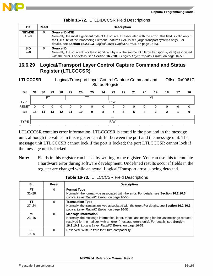
RapidIO Programming Model
16.6.29 Logical/Transport Layer Control Capture Command and Status Register (LTLCCCSR)
LTLCCCSR contains error information. LTLCCCSR is stored in the port and in the message unit, although the values in this register can differ between the port and the message unit. The message unit LTLCCCSR cannot lock if the port is locked; the port LTLCCCSR cannot lock if the message unit is locked.
Note: Fields in this register can be set by writing to the register. You can use this to emulate a hardware error during software development. Undefined results occur if fields in the register are changed while an actual Logical/Transport error is being detected.
SIDMSB15–8
0 Source ID MSBNormally, the most significant byte of the source ID associated with the error. This field is valid only if the CTLS bit of the Processing Element Features CAR is set (large transport systems only). For details, see Section 16.2.10.3, Logical Layer RapidIO Errors, on page 16-53.
SID7–0
0 Source IDNormally, the source ID (or least significant byte of the source ID if large transport system) associated with the error. For details, see Section 16.2.10.3, Logical Layer RapidIO Errors, on page 16-53.
LTLCCCSR Logical/Transport Layer Control Capture Command and Offset 0x0061CStatus Register
Bit 31 30 29 28 27 26 25 24 23 22 21 20 19 18 17 16
FT TT MI
TYPE R/WRESET 0 0 0 0 0 0 0 0 0 0 0 0 0 0 0 0
Bit 15 14 13 12 11 10 9 8 7 6 5 4 3 2 1 0
—TYPE R/W
RESET 0 0 0 0 0 0 0 0 0 0 0 0 0 0 0 0
Table 16-73. LTLCCCSR Field Descriptions
Bit Reset Description
FT31–28
0 Format TypeNormally, the format type associated with the error. For details, see Section 16.2.10.3, Logical Layer RapidIO Errors, on page 16-53.
TT27–24
0 Transaction TypeNormally, the transaction type associated with the error. For details, see Section 16.2.10.3, Logical Layer RapidIO Errors, on page 16-53.
MI23–16
0 Message InformationNormally, the message information: letter, mbox, and msgseg for the last message request received for the mailbox with an error (message errors only). For details, see Section 16.2.10.3, Logical Layer RapidIO Errors, on page 16-53.
—15–0
0 Reserved. Write to zero for future compatibility.
Table 16-72. LTLDIDCCSR Field Descriptions
Bit Reset Description
MSC8254 Reference Manual, Rev. 0
Freescale Semiconductor 16-163

Serial RapidIO Controller
16.6.30 Port 0–1 Error Detect Command and Status Register (PnEDCSR)
PnEDCSR indicates transmission errors detected by the hardware. Software can write bits in this register with a value of 1 to increment the error rate counter. Undefined results occur if this register is written while actual physical layer errors are detected by the port
Port
P0EDCSR Port 0–1 Error Detect Command and Status Register Offset 0x00640P1EDCSR Offset 0x00680
Bit 31 30 29 28 27 26 25 24 23 22 21 20 19 18 17 16
— CCS AUA PNA UA CRC EM —TYPE R/W
RESET 0 0 0 0 0 0 0 0 0 0 0 0 0 0 0 0
Bit 15 14 13 12 11 10 9 8 7 6 5 4 3 2 1 0
— NOA PE — DE UCS LTOTYPE R/W
RESET 0 0 0 0 0 0 0 0 0 0 0 0 0 0 0 0
Table 16-74. PnEDCSR Field Descriptions
Bit Reset Description
—31–23
0 Reserved. Write to zero for future compatibility.
CCS22
0 CRC Control SymbolReceived a control symbol with a bad CRC value.
AUA21
0 Acknowledge Control With Unexpected Acknowledge IDReceived an acknowledge control symbol with an unexpected acknowledge ID (packet-accepted or packet-retry).
PNA20
0 Packet Not AcceptedReceived packet-not-accepted acknowledge control symbol.
UA19
0 Unexpected Acknowledge IDReceived packet with unexpected ackID value.
CRC18
0 Bad CRCReceived a packet with a bad CRC value.
EM17
0 Exceed MaximumReceived packet which exceed the maximum allowed size (276 bytes).
—16–6
0 Reserved. Write to zero for future compatibility.
NOA5
0 Not Outstanding AcknowledgeLink-response received with an ackID that is not outstanding.
PE4
0 Protocol ErrorAn unexpected packet or control symbol was received.
—3
0 Reserved. Write to zero for future compatibility.
DE2
0 Delineation ErrorReceived unaligned /SC/ or /PD/ or undefined code-group.
UCS1
0 Unsolicited Control SymbolAn unsolicited acknowledge control symbol was received.
LTO0
0 Link Time-OutAn acknowledge or link-response control symbol is not received within the specified time-out interval.
MSC8254 Reference Manual, Rev. 0
16-164 Freescale Semiconductor

RapidIO Programming Model
16.6.31 Port 0–1 Error Rate Enable Command and Status Register (PnERECSR)
PnERECSR contains the bits that control when an error condition is allowed to increment the error rate counter in the Port 0–1 error rate threshold register and lock the Port 0–1 error capture registers.
P0ERECSR Port 0–1 Error Rate Enable Command and Status Register Offset 0x00644P1ERECSR Offset 0x00684
Bit 31 30 29 28 27 26 25 24 23 22 21 20 19 18 17 16
— CCS AUA PNA UA CRC EM —TYPE R/W
RESET 0 0 0 0 0 0 0 0 0 0 0 0 0 0 0 0
Bit 15 14 13 12 11 10 9 8 7 6 5 4 3 2 1 0
— NOA PE — DE UCS LTO
TYPE R/WRESET 0 0 0 0 0 0 0 0 0 0 0 0 0 0 0 0
Table 16-75. PnERECSR Field Descriptions
Bit Reset Description
—31–23
0 Reserved. Write to zero for future compatibility.
CCS22
0 CRC Control Symbol EnableEnable error counting of a corrupt control symbol.
AUA21
0 Acknowledge Control With Unexpected Acknowledge ID EnableEnable error rate counting of an acknowledge control symbol with an unexpected acknowledge ID.
PNA20
0 Packet Not Accepted EnableEnable error rate counting of packet-not-accepted acknowledge control symbols.
UA19
0 Unexpected Acknowledge ID EnableEnable error rate counting of packets with an unexpected ackID value.
CRC18
0 Bad CRC EnableEnable error rate counting of packets with a bad CRC value.
EM17
0 Exceed Maximum EnableEnable error rate counting of packets that exceed the maximum allowed size (276 bytes).
—16–6
0 Reserved. Write to zero for future compatibility.
NOA5
0 Not Outstanding AcknowledgeEnable error rate counting of ink-responses received with an acknowledge ID that is not outstanding.
PE4
0 Protocol ErrorEnable error rate counting of protocol errors.
—3
0 Reserved. Write to zero for future compatibility.
DE2
0 Delineation ErrorsEnable error rate counting of delineation errors.
MSC8254 Reference Manual, Rev. 0
Freescale Semiconductor 16-165

Serial RapidIO Controller
16.6.32 Port 0–1 Error Capture Attributes Command and Status Register (PnECACSR)
PnECACSR indicates the type of information contained in the Port 0–1 error capture registers. For multiple errors detected during the same clock cycle, one of the errors must be reflected in the error type field. Undefined results occur if this register is written while actual physical layer errors are detected by the port. Before the capture registers are read, software should verify that the PnECACSR[CVI] bit is set to ensure that the error is properly captured.
UCS1
0 Unsolicited Control SymbolEnable error rate counting of unexpected acknowledge control symbols.
LTO0
0 Link Time-OutEnable error rate counting of an acknowledge or link-response control symbol not received within the specified time-out interval.
P0ECACSR Port 0–1 Error Capture Attributes Command Offset 0x00648P1ECACSR and Status Register Offset 0x00688
Bit 31 30 29 28 27 26 25 24 23 22 21 20 19 18 17 16
IT — ET ECI15 ECI14 ECI13 ECI12 ECI11 ECI10 ECI9 ECI8
TYPE R/W R R/W
RESET 0 0 0 0 0 0 0 0 0 0 0 0 0 0 0 0
Bit 15 14 13 12 11 10 9 8 7 6 5 4 3 2 1 0
ECI7 ECI6 ECI5 ECI4 ECI3 ECI2 ECI1 ECI0 — CVI
TYPE R/W R R/W
RESET 0 0 0 0 0 0 0 0 0 0 0 0 0 0 0 0
Table 16-76. PnECACSR Field Descriptions
Bit Reset Description Settings
IT31–30
0 Information TypeType of information logged.
00 Packet. Error capture registers hold the first 4 words of the packet or the entire packet if it is less than four words long.
01 Control symbol. Only the error capture register 0 is valid.
10 Reserved.
11 Undefined. Not clearly a control symbol or packet error. Error capture registers hold the symbol that caused the error and the next thee symbols.
—29
0 Reserved. Write to zero for future compatibility.
Table 16-75. PnERECSR Field Descriptions (Continued)
Bit Reset Description
MSC8254 Reference Manual, Rev. 0
16-166 Freescale Semiconductor

RapidIO Programming Model
ET28–24
0 ErrorThe encoded value of the bit in the Port 0–1 error detect CSR that describes the error captured in the Port 0–1 error capture CSRs.
ECI23–8
0 Extended Capture InformationECI contains the control/data character signal corresponding to each byte of captured data.
ECI15] Associated with PnPCSECCSR0[31–24].
ECI14 Associated with PnPCSECCSR0[23–16].
ECI13 Associated with PnPCSECCSR00[15–8].
ECI12 Associated with PnPCSECCSR0[7–0].
ECI11 Associated with PnPECCSR1[31–24].
ECI10 Associated with PnPECCSR1[25–16].
...
ECI1 Associated with PnPECCSR3[15–8].
ECI0 Associated with PnPECCSR3[7–0].
—7–1
0 Reserved. Write to zero for future compatibility.
CVI0
Contain Valid InformationHardware sets CVI to indicate that the packet/control symbol capture registers contain valid information. For control symbols, only capture register 0 contains meaningful information.
Table 16-76. PnECACSR Field Descriptions
Bit Reset Description Settings
MSC8254 Reference Manual, Rev. 0
Freescale Semiconductor 16-167

Serial RapidIO Controller
16.6.33 Port 0–1 Packet/Control Symbol Error Capture Command and Status Register (PnPCSECCSR)
PnPCSECCSR0 contains the first 4 bytes of captured packet symbol information or a control character and control symbol. Undefined results occur if this register is written while actual physical layer errors are detected by the port. Software should verify that the PnECACSR[CVI] bit is set before reading the capture registers to ensure that the error is properly captured.
P0PCSECCSR Port 0–1 Packet/Control Symbol Error Capture Command Offset 0x0064CP1PCSECCSR and Status Register Offset 0x0068C
Bit 31 30 29 28 27 26 25 24 23 22 21 20 19 18 17 16
C0TYPE R/W
RESET 0 0 0 0 0 0 0 0 0 0 0 0 0 0 0 0
Bit 15 14 13 12 11 10 9 8 7 6 5 4 3 2 1 0
C0
TYPE R/WRESET 0 0 0 0 0 0 0 0 0 0 0 0 0 0 0 0
Table 16-77. PnPCSECCSR0 Field Descriptions
Bit Reset Description
C031–0
0 Capture 0Control character and control symbol or bytes 0–3 of the packet header.
MSC8254 Reference Manual, Rev. 0
16-168 Freescale Semiconductor

RapidIO Programming Model
16.6.34 Port 0–1 Packet Error Capture Command and Status Register 1 (PnPECCSR1)
PnPECCSR1 contains bytes 4–7 of the packet header. Undefined results occur if this register is written while actual physical layer errors are detected by the port. Software should verify that the PnECACSR[CVI] bit is set before reading the capture registers to ensure that the error is properly captured.
P0PECCSR1 Port 0–1 Packet Error Capture Command and Offset 0x00650P1PECCSR1 Status Register 1 Offset 0x00690
Bit 31 30 29 28 27 26 25 24 23 22 21 20 19 18 17 16
C1TYPE R/W
RESET 0 0 0 0 0 0 0 0 0 0 0 0 0 0 0 0
Bit 15 14 13 12 11 10 9 8 7 6 5 4 3 2 1 0
C1
TYPE R/WRESET 0 0 0 0 0 0 0 0 0 0 0 0 0 0 0 0
Table 16-78. PnPECCSR1 Field Descriptions
Bit Reset Description
C131–0
0 Capture 1Contains bytes 4–7 of the packet header.
MSC8254 Reference Manual, Rev. 0
Freescale Semiconductor 16-169

Serial RapidIO Controller
16.6.35 Port 0–1 Packet Error Capture Command and Status Register 2 (PnPECCSR2)
PnPECCSR2 contains bytes 8–11 of the packet header. Undefined results occur if this register is written while actual physical layer errors are detected by the port. Software should verify that the PnECACSR[CVI] bit is set before reading the capture registers to ensure that the error is properly captured.
P0PECCSR2 Port 0–1 Packet Error Capture Command Offset 0x00654P1PECCSR2 and Status Register 2 Offset 0x00694
Bit 31 30 29 28 27 26 25 24 23 22 21 20 19 18 17 16
C2TYPE R/W
RESET 0 0 0 0 0 0 0 0 0 0 0 0 0 0 0 0
Bit 15 14 13 12 11 10 9 8 7 6 5 4 3 2 1 0
C2
TYPE R/WRESET 0 0 0 0 0 0 0 0 0 0 0 0 0 0 0 0
Table 16-79. PECCSR2 Field Descriptions
Bit Reset Description
C231–0
0 Capture 2Bytes 8 to 11 of the packet header
MSC8254 Reference Manual, Rev. 0
16-170 Freescale Semiconductor

RapidIO Programming Model
16.6.36 Port 0–1 Packet Error Capture Command and Status Register 3 (PnPECCSR3)
PnPECCSR3 contains bytes 12–15 of the packet header. Undefined results occur if this register is written while actual physical layer errors are detected by the port. Software should verify that the PnECACSR[CVI] bit is set before reading the capture registers to ensure that the error has been properly captured.
P0PECCSR3 Port 0–1 Packet Error Capture Command and Offset 0x00658P1PECCSR3 Status Register 3 Offset 0x00698
Bit 31 30 29 28 27 26 25 24 23 22 21 20 19 18 17 16
C3TYPE R/W
RESET 0 0 0 0 0 0 0 0 0 0 0 0 0 0 0 0
Bit 15 14 13 12 11 10 9 8 7 6 5 4 3 2 1 0
C3
TYPE R/WRESET 0 0 0 0 0 0 0 0 0 0 0 0 0 0 0 0
Table 16-80. PnPECCSR3 Field Descriptions
Bit Reset Description
C331–0
0 Capture 3Bytes 12–15 of the packet header.
MSC8254 Reference Manual, Rev. 0
Freescale Semiconductor 16-171

Serial RapidIO Controller
16.6.37 Port 0–1 Error Rate Command and Status Register (PnERCSR)
PnERCSR is used with the Port0 Error Rate Threshold Command and Status Register (PnERTCSR) to monitor and control the reporting of transmission errors.
P0ERCSR Port 0–1 Error Rate Command and Status Register Offset 0x00668P1ERCSR Offset 0x006A8
Bit 31 30 29 28 27 26 25 24 23 22 21 20 19 18 17 16
ERB — ERRTYPE R/W R R/W
RESET 1 0 0 0 0 0 0 0 0 0 0 0 0 0 0 0
Bit 15 14 13 12 11 10 9 8 7 6 5 4 3 2 1 0
PER ERCTYPE R/W
RESET 0 0 0 0 0 0 0 0 0 0 0 0 0 0 0 0
Table 16-81. PnERCSR Field Descriptions
Bit Reset Description Setting
ERB31–24
0b1000_0000
Error Rate BiasProvides the error rate bias value.
0x00 Do not decrement the error rate counter.
0x01 Decrement every 1 ms (±34%).
0x02 Decrement every 10 ms (±34%).
0x04 Decrement every 100 ms (±34%).
0x08 Decrement every 1 s (±34%).
0x10 Decrement every 10 s (±34%).
0x20 Decrement every 100 s (±34%).
0x40 Decrement every 1000 s (±34%).
0x80 Decrement every 10000 s (±34%).
Other values are reserved and cause undefined operation.
—23–18
0 Reserved. Write to zero for future compatibility.
ERR17–16
0 Error RateLimits increments of the error rate counter above the failed threshold trigger. This counter never increments above 0xFF, even if the combined settings of ERR and the failed threshold trigger imply that it would.
0b00 Count only 2 errors above.
0b01 Count only 4 errors above.
0b10 Count only 16 error above.
0b11 Do not limit increments above the error rate count.
PER15–8
0 Peak Error RateContains the peak value attained by the error rate counter.
ERC7–0
0 Error Rate CounterCounts the number of transmission errors detected by the port, decremented by the error rate bias, to create an indication of the link error rate. Software should not attempt to write to ERC a value higher than the failed threshold trigger plus the number of errors specified in the ERR field (the maximum ERC value).
MSC8254 Reference Manual, Rev. 0
16-172 Freescale Semiconductor

RapidIO Programming Model
16.6.38 Port 0–1 Error Rate Threshold Command and Status Register (PnERTCSR)
PnERTCSR controls reporting of the link status to the system host.
P0ERTCSR Port 0–1 Error Rate Threshold Command and Status Offset 0x0066CP1ERTCSR ‘Register Offset 0x006AC
Bit 31 30 29 28 27 26 25 24 23 22 21 20 19 18 17 16
ERFTT ERDTTTYPE R/W
RESET 1 1 1 1 1 1 1 1 1 1 1 1 1 1 1 1
Bit 15 14 13 12 11 10 9 8 7 6 5 4 3 2 1 0
—
TYPE RRESET 0 0 0 0 0 0 0 0 0 0 0 0 0 0 0 0
Table 16-82. PnERTCSR Field Descriptions
Bit Reset Description Settings
ERFTT31–24
0xFF Error Rate Failed Threshold TriggerProvides the threshold value for reporting an error condition due to a possibly broken link. The PnESCSR[OFE] bit is set if PnERCSR[ERC] meets or exceeds the ERFTT value (that is, PnERCSR[ERC] ≥ ERFTT).
0x00 Disable the error rate failed threshold trigger.
0x01 Set the error reporting threshold to 1.
0x02 Set the error reporting threshold to 2.
...
0xFF Set the error reporting threshold to 255.
ERDTT23–16
0xFF Error Rate Degraded Threshold TriggerProvides the threshold value for reporting an error condition due to a degrading link. The PnESCSR[ODE] bit is set if PnERCSR[ERC] meets or exceeds the ERDTT value (that is, PnERCSR[ERC] ≥ ERFTT).
0x00 Disable the error rate degraded threshold trigger.
0x01 Set the error reporting threshold to 1.
0x02 Set the error reporting threshold to 2.
...
0xFF Set the error reporting threshold to 255.
—15–0
0 Reserved. Write to zero for future compatibility.
MSC8254 Reference Manual, Rev. 0
Freescale Semiconductor 16-173

Serial RapidIO Controller
16.6.39 Logical Layer Configuration Register (LLCR)
LLCR contains general port-common logical layer mode enables.
LLCR Logical Layer Configuration Register Offset 0x10004
Bit 31 30 29 28 27 26 25 24 23 22 21 20 19 18 17 16
— ECRAB —
TYPE R/W RRESET 0 0 0 0 0 0 0 0 0 0 0 0 0 0 0 0
Bit 15 14 13 12 11 10 9 8 7 6 5 4 3 2 1 0
—TYPE R
RESET 0 0 0 0 0 0 0 0 0 0 0 0 0 0 0 0
Table 16-83. LLCR Field Descriptions
Bit Reset Description
—31–30
0 Reserved. Write to zero for future compatibility.
ECRAB29
0 External Configuration Register Access BlockBlocks all maintenance requests and accesses to LCSBA1CSR. Reads return all 0s, and writes are ignored (both return a done response). When ECRAB is cleared, any external RapidIO device can access the registers.
—28–0
0 Reserved. Write to zero for future compatibility.
MSC8254 Reference Manual, Rev. 0
16-174 Freescale Semiconductor

RapidIO Programming Model
16.6.40 Error/Port-Write Status Register (EPWISR)
EPWISR contains status bits of the interrupts generated by the port or the message unit for physical or logical/transport layer errors or inbound port-writes. Because errors from the port are reported to the SC3850 core with one interrupt signal, this register provides the core with quick access to where the error occurred. This register is read-only and stored in the port and the message unit as a logically equivalent copy.
EPWISR Error/Port-Write Interrupt Status Register Offset 0x10010
Bit 31 30 29 28 27 26 25 24 23 22 21 20 19 18 17 16
PINT0 PINT1 —
TYPE RRESET 0 0 0 0 0 0 0 0 0 0 0 0 0 0 0 0
Bit 15 14 13 12 11 10 9 8 7 6 5 4 3 2 1 0
— MU PWTYPE R
RESET 0 0 0 0 0 0 0 0 0 0 0 0 0 0 0 0
Table 16-84. EPWISR Field Descriptions
Bit Reset Description
PINT031
0 Physical or Logical/Transport Error Interrupt Port 0Indicates a physical or logical transport error interrupt was generated by port 0.
PINT130
0 Physical or Logical/Transport Error Interrupt Port 1Indicates a physical or logical transport error interrupt was generated by port 1
—29–2
0 Reserved. Can be used to indicate errors on more ports if they exist.
MU1
0 Message Unit Logical/Transport Layer Error InterruptIndicates a logical/transport layer error interrupt was generated by the message unit.
PW0
0 Port WriteIndicates an inbound port-write was received.
MSC8254 Reference Manual, Rev. 0
Freescale Semiconductor 16-175

Serial RapidIO Controller
16.6.41 Logical Retry Error Threshold Configuration Register (LRETCR)
LRETCR contains the retry error threshold for the logical layer. When the number of consecutive logical retries for a given packet is greater than this value, an error interrupt is generated. Notice that the number of retries must be greater than the threshold value, which is not the case for other registers that define a retry threshold.
LRETCR Logical Retry Error Threshold Configuration Register Offset 0x10020
Bit 31 30 29 28 27 26 25 24 23 22 21 20 19 18 17 16
—
TYPE R/WRESET 0 0 0 0 0 0 0 0 0 0 0 0 0 0 0 0
Bit 15 14 13 12 11 10 9 8 7 6 5 4 3 2 1 0
— RETTYPE R/W
RESET 0 0 0 0 0 0 0 0 1 1 1 1 1 1 1 1
Table 16-85. LRETCR Field Descriptions
Bit Reset Description
—31–8
0 Reserved. Write to zero for future compatibility.
RET7–0
0xFF Retry Error ThresholdThe threshold value for the number of consecutive logical retries received for a given packet that causes the RAPIDIO ENDPOINT to report an error condition.
0x00 Disable the retry threshold.
0x01 Set the error reporting threshold to 1.
...
0xFF Set the error reporting threshold to 255.
MSC8254 Reference Manual, Rev. 0
16-176 Freescale Semiconductor

RapidIO Programming Model
16.6.42 Physical Retry Error Threshold Configuration Register (PRETCR)
PRETCR contains the retry error threshold for the physical layer. When the number of consecutive acknowledge-retries is greater than or equal to this value, an error interrupt is generated.
PRETCR Physical Retry Error Threshold Configuration Register Offset 0x10080
Bit 31 30 29 28 27 26 25 24 23 22 21 20 19 18 17 16
—
TYPE RRESET 0 0 0 0 0 0 0 0 0 0 0 0 0 0 0 0
Bit 15 14 13 12 11 10 9 8 7 6 5 4 3 2 1 0
— RETTYPE R R/W
RESET 0 0 0 0 0 0 0 0 1 1 1 1 1 1 1 1
Table 16-86. PRETCR Field Descriptions
Bit Reset Description Settings
—31–8
0 Reserved. Write to zero for future compatibility.
RET7–0
0xFF Retry Error ThresholdThe threshold value for the number of consecutive acknowledge-retries received that cause the RAPIDIO ENDPOINT to report an error condition.
0x00 Disable the retry threshold.
0x01 Set the error reporting threshold to 1.
...
0xFF Set the error reporting threshold to 255.
MSC8254 Reference Manual, Rev. 0
Freescale Semiconductor 16-177

Serial RapidIO Controller
16.6.43 Port 0–1 Alternate Device ID Command and Status Register (PnADIDCSR)
PnADIDCSR contains an alternate device ID. This register should be enabled before the initiator enabled bit of the PGCCSR is set (see Table 16-62, PGCCSR Field Descriptions, on page 16-150). Therefore, when the PGCCSR bit is enabled, all other devices in the RapidIO system (including switches) send and receive packets from the device ID in PnADIDCSR instead of the device ID in BDIDCSR. When the alternate deviceID is enabled, inbound RapidIO endpoint accepts only packets sent with the device ID in PnADIDCSR or the deviceID in BDIDCSR. An exception is Accept All mode, in which the inbound RapidIO Endpoint accept packets using the same common transport system. The outbound RapidIO endpoint generates requests using only the device ID in PnADIDCSR. It generates responses with the deviceID in the original request packet (either from PnADIDCSR or BDIDCSR). The selection between a large or small transport system is done during the power-up sequence by using the CTLS bit in the RCW.
P0ADIDCSR Port 0–1 Alternate Device ID Command and Status Register Offset 0x10100P1ADIDCSR Offset 0x10180
Bit 31 30 29 28 27 26 25 24 23 22 21 20 19 18 17 16
ADE — ADIDTYPE R/W R R/W
RESET 0 0 0 0 0 0 0 0 0 0 0 0 0 0 0 0
Bit 15 14 13 12 11 10 9 8 7 6 5 4 3 2 1 0
LADID
TYPE R/WRESET 0 0 0 0 0 0 0 0 0 0 0 0 0 0 0 0
Table 16-87. PnADIDCSR Field Descriptions
Bit Reset Description
ADE31
0 Alternate Device ID EnableCauses the port to use the device ID specified in this register instead of the device ID specified in BDIDCSR.
—30–24
0 Reserved. Write to zero for future compatibility.
ADID23–16
0 Alternate Device IDAlternate device ID in a small transport system.
LADID15–0
0 Large Alternate Device IDAlternate device ID for the device in a large transport system.
MSC8254 Reference Manual, Rev. 0
16-178 Freescale Semiconductor

RapidIO Programming Model
16.6.44 Port 0–1 Pass-Through Accept-All Configuration Register (PnPTAACR)
PnPTAACR contains information on accept-all mode.
P0PTAACR Port 0–1 Pass-Through Accept-All Configuration Register Offset 0x10120P1PTAACR Offset 0x101A0
Bit 31 30 29 28 27 26 25 24 23 22 21 20 19 18 17 16
PTPN —TYPE R/W
RESET x x x x 0 0 0 0 0 0 0 0 0 0 0 0
Bit 15 14 13 12 11 10 9 8 7 6 5 4 3 2 1 0
— PTE AA
TYPE R/WRESET 0 0 0 0 0 0 0 0 0 0 0 0 0 0 x x
Table 16-88. PnPTAACR Field Descriptions
Bit Reset Description Settings
PTPN31–28
Port 0 = 1
Port 1 = 0
Pass-Through RapidIO Port NumberThe RapidIO port to which to send pass-through packets. The SRIO unit in the HSSI uses this value to map the RapidIO port number (0 or 1) to the OCN port number (0 or 4).
—27–2
0 Reserved. Write to zero for future compatibility.
PTE1
RCWHR[RPT] Pass-Through Mode EnableEnables/disables pass-through mode.Note: AA has priority over PTE; when AA
is set, the value of PTE is ignored.
0 Packets whose target ID does not match the device ID are not sent out to another SRIO port. An error occurs if the AA bit is not set (to select accept all mode).
1 Packet whose target ID does not match the device ID (base or alternate, if enabled) or whose transport size does not match the device transport size (defined by the common transport large system bit in the high part of the Reset Configuration Word (RCWH[CTLS]).is sent out through the OCN to another SRIO port designated by the value of the PTPN field.
AA0
Port 0 = RCWHR[R1A]
Port 1 = RCWHR[R2A]
Accept AllSpecifies whether packet acceptance is based on a target ID. When this bit is set, the tt field value must be consistent with the common transport system specified by the CTLS bit of the processing element features CAR.
0 Normal RapidIO acceptance based on target ID.
1 All packets are accepted without checking the target ID.
MSC8254 Reference Manual, Rev. 0
Freescale Semiconductor 16-179
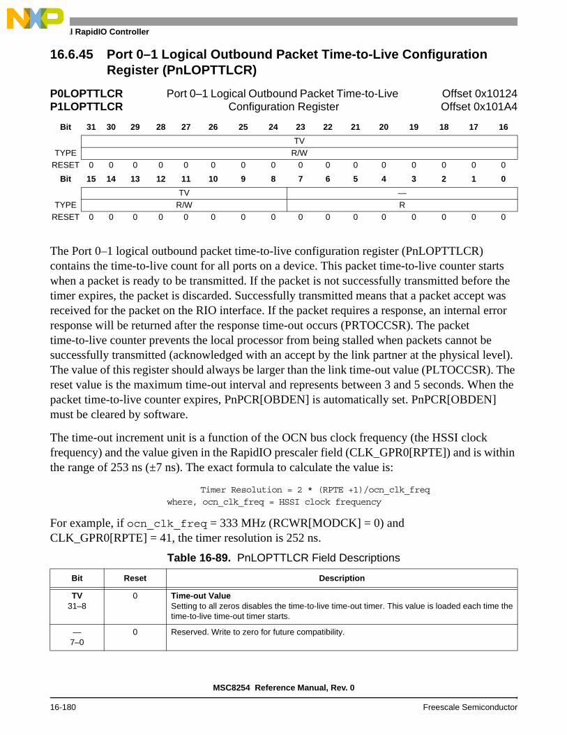
Serial RapidIO Controller
16.6.45 Port 0–1 Logical Outbound Packet Time-to-Live Configuration Register (PnLOPTTLCR)
The Port 0–1 logical outbound packet time-to-live configuration register (PnLOPTTLCR) contains the time-to-live count for all ports on a device. This packet time-to-live counter starts when a packet is ready to be transmitted. If the packet is not successfully transmitted before the timer expires, the packet is discarded. Successfully transmitted means that a packet accept was received for the packet on the RIO interface. If the packet requires a response, an internal error response will be returned after the response time-out occurs (PRTOCCSR). The packet time-to-live counter prevents the local processor from being stalled when packets cannot be successfully transmitted (acknowledged with an accept by the link partner at the physical level). The value of this register should always be larger than the link time-out value (PLTOCCSR). The reset value is the maximum time-out interval and represents between 3 and 5 seconds. When the packet time-to-live counter expires, PnPCR[OBDEN] is automatically set. PnPCR[OBDEN] must be cleared by software.
The time-out increment unit is a function of the OCN bus clock frequency (the HSSI clock frequency) and the value given in the RapidIO prescaler field (CLK_GPR0[RPTE]) and is within the range of 253 ns (±7 ns). The exact formula to calculate the value is:
Timer Resolution = 2 * (RPTE +1)/ocn_clk_freqwhere, ocn_clk_freq = HSSI clock frequency
For example, if ocn_clk_freq = 333 MHz (RCWR[MODCK] = 0) and CLK_GPR0[RPTE] = 41, the timer resolution is 252 ns.
P0LOPTTLCR Port 0–1 Logical Outbound Packet Time-to-Live Offset 0x10124P1LOPTTLCR Configuration Register Offset 0x101A4
Bit 31 30 29 28 27 26 25 24 23 22 21 20 19 18 17 16
TVTYPE R/W
RESET 0 0 0 0 0 0 0 0 0 0 0 0 0 0 0 0
Bit 15 14 13 12 11 10 9 8 7 6 5 4 3 2 1 0
TV —
TYPE R/W RRESET 0 0 0 0 0 0 0 0 0 0 0 0 0 0 0 0
Table 16-89. PnLOPTTLCR Field Descriptions
Bit Reset Description
TV31–8
0 Time-out ValueSetting to all zeros disables the time-to-live time-out timer. This value is loaded each time thetime-to-live time-out timer starts.
—7–0
0 Reserved. Write to zero for future compatibility.
MSC8254 Reference Manual, Rev. 0
16-180 Freescale Semiconductor

RapidIO Programming Model
16.6.46 Port 0–1 Implementation Error Command and Status Register (PnIECSR)
PnIECSR contains status bits that are asserted when an implementation-defined error occurs.
P0IECSR Port 0–1 Implementation Error Command and Offset 0x10130P1IECSR Status Register Offset 0x101B0
Bit 31 30 29 28 27 26 25 24 23 22 21 20 19 18 17 16
RETE —TYPE W1C R
RESET 0 0 0 0 0 0 0 0 0 0 0 0 0 0 0 0
Bit 15 14 13 12 11 10 9 8 7 6 5 4 3 2 1 0
—
TYPE RRESET 0 0 0 0 0 0 0 0 0 0 0 0 0 0 0 0
Table 16-90. PnIECSR Field Descriptions
Bit Reset Description
RETE31
0 Retry Error Threshold ExceededSet when the number of consecutive retries reaches the retry error threshold in the Physical Retry Error Threshold Configuration Register (PRETCR). RETE is cleared by writing a value of 1 to it. This bit is set again if another retry is received and the number of consecutive retries continues to exceed the retry error threshold.
—30–0
0 Reserved. Write to zero for future compatibility.
MSC8254 Reference Manual, Rev. 0
Freescale Semiconductor 16-181

Serial RapidIO Controller
16.6.47 Port 0–1 Serial Link Command and Status Register (PnSLCSR)
PnSLCSR contains status of the of the serial physical link.
P0SLCSR Port 0–1 Serial Link Command and Status Register Offset 0x10158P1SLCSR Offset 0x101D8
Bit 31 30 29 28 27 26 25 24 23 22 21 20 19 18 17 16
LS0 LS1 LS2 LS3 — LA —TYPE W1C W1C W1C W1C R W1C R
RESET 0 0 0 0 0 0 0 0 0 0 0 0 0 0 0 0
Bit 15 14 13 12 11 10 9 8 7 6 5 4 3 2 1 0
—TYPE R
RESET 0 0 0 0 0 0 0 0 0 0 0 0 0 0 0 0
Table 16-91. PnSLCSR Field Descriptions
Bit Reset Description
LS031
0 Lane Sync Achieved for Lane 0Write with 1 to clear
LS130
0 Lane Sync Achieved for Lane 1Write with 1 to clear
LS229
0 Lane Sync Achieved for Lane 2Write with 1 to clear
LS328
0 Lane Sync Achieved for Lane 3Write with 1 to clear
—27–24
0 Reserved. Write to zero for future compatibility.
LA23
0 Lane Alignment AchievedWrite with 1 to clear.
—22–0
0 Reserved. Write to zero for future compatibility.
MSC8254 Reference Manual, Rev. 0
16-182 Freescale Semiconductor

RapidIO Programming Model
16.6.48 Port 0–1 Serial Link Error Injection Configuration Register (PnSLEICR)
PnSLEICR controls the injection of bit errors into the transmit bit stream and is used to generate pseudo-random errors into the outbound serial RapidIO data stream. If the EIC field is non-zero, error injection is enabled and, at pseudo-random intervals, an error is injected by inverting a single bit in the outgoing data stream. The range of the pseudo-random value (delay between injected errors) is controlled by the EIR field. That is, the value of EIR, multiplied by 32, determines the maximum number of character times between injected errors.
P0SLEICR Port 0–1 Serial Link Error Injection Configuration Register Offset 0x10160P1SLEICR Offset 0x101E0
Bit 31 30 29 28 27 26 25 24 23 22 21 20 19 18 17 16
EIC — EIRTYPE R/W R R/W
RESET 0 0 0 0 0 0 0 0 0 0 0 0 0 0 0 0
Bit 15 14 13 12 11 10 9 8 7 6 5 4 3 2 1 0
EIR
TYPE R/WRESET 0 0 0 0 0 0 0 0 0 0 0 0 0 0 0 0
Table 16-92. PnSLEICR Field Descriptions
Bit Reset Description Settings
EIC31–27
0 Error Injection ControlEnables and controls serial link error injection as follows.
00000 Error injection is disabled.
10000 Error injection, lane 0 only.
01000 Error injection, lane 1 only
00100 Error injection, lane 2 only
00010 Error injection, lane 3 only
11110 Error injection, all lanes simultaneously
11111 Error injection, randomly distributed over all 4 lanes
All other values reserved.
—26–20
0 Reserved. Write to zero for future compatibility.
EIR19–0
0 Error Injection RangeThe value of EIR × 32 determines the maximum value of the pseudo-random delay between errors. For example, a value of 0x1 indicates a maximum delay of 32 character times. The value within this register should be right-justified.
MSC8254 Reference Manual, Rev. 0
Freescale Semiconductor 16-183

Serial RapidIO Controller
16.6.49 IP Block Revision Register 1 (IPBRR1)
IPBRR1 tracks changes and revisions of the RapidIO endpoint.
16.6.50 IP Block Revision Register 2 (IPBRR2)
IPBRR2 track changes and revisions of the RapidIO endpoint.
IPBRR1 IP Block Revision Register 1 Offset 0x10BF8
Bit 31 30 29 28 27 26 25 24 23 22 21 20 19 18 17 16
IPID
TYPE RRESET 0 0 0 0 0 0 0 1 1 1 0 0 0 0 0 0
Bit 15 14 13 12 11 10 9 8 7 6 5 4 3 2 1 0
IPMJ IPMNTYPE R
RESET 0 0 0 0 0 0 0 1 0 0 0 0 0 0 1 0
Table 16-93. IPBRR1 Field Descriptions
Bit Reset Description
IPID31–16
0x01C0 IP block ID = 0x01C0
IPMJ15–8
0x01 Major revision of the IP block = 0x01
IPMN7–0
0x00 Minor revision of the IP block = 0x02
IPBRR2 IP Block Revision Register 2 Offset 0x10BFC
Bit 31 30 29 28 27 26 25 24 23 22 21 20 19 18 17 16
— IPINT
TYPE R
RESET 0 0 0 0 0 0 0 0 0 0 0 0 0 0 0 0
Bit 15 14 13 12 11 10 9 8 7 6 5 4 3 2 1 0
— IPCFG
TYPE R
RESET 0 0 0 0 0 0 0 0 0 0 0 0 0 0 0 1
Table 16-94. IPBRR2 Field Descriptions
Bit Reset Description
—31–24
0 Reserved. Write to zero for future compatibility.
IPINT23–16
0 IP block Integration options = 0x0.
—15–8
0 Reserved. Write to zero for future compatibility.
IPCFG7–0
0x01 IP Block Configuration Options = 0x01.
MSC8254 Reference Manual, Rev. 0
16-184 Freescale Semiconductor

RapidIO Programming Model
16.6.51 Port 0–1 RapidIO Outbound Window Translation Address Registers x (PnROWTARx)
PnROWTARx points to the starting addresses in the RapidIO address space for window hits within the outbound translation windows. The new translated address is created by concatenating the transaction offset to this translation address.
P0ROWTAR[0–8] Port 0–1 RapidIO Outbound Window Offset 0x10C00 + x*0x20P1ROWTAR[0–8] Translation Address Registers 0–8 Offset 0x10E00 + x*0x20
Bit 31 30 29 28 27 26 25 24 23 22 21 20 19 18 17 16
LTGTID TREXAD TRADTYPE R/WReset
0 0 0 0 0 0 0 0 0 1 0 0 0 0 0 0 01–8 0 0 0 0 0 0 0 0 0 0 0 0 0 0 0 0
Bit 15 14 13 12 11 10 9 8 7 6 5 4 3 2 1 0
TRADTYPE R/W
Reset0 0 0 0 0 0 0 0 0 0 0 0 0 0 0 0 0
1–8 0 0 0 0 0 0 0 0 0 0 0 0 0 0 0 0
Table 16-95. PnROWTARx Field Descriptions
Bit Reset Description
LTGTID31–30
0 Large Transport System Target AddressLTGTID corresponds to bits 6–7 of the targetID for a large transport system. This field is valid only if the PEFCAR[CTLS] bit is set (see Section 16.6.5, Processing Element Features Capability Register (PEFCAR), on page 16-135). Bits 0–5 of the target ID are specified in the PnROWTEARX (see Section 16.6.52, Port 0–1 RapidIO Outbound Window Translation Extended Address Registers x (PnROWTEARx), on page 16-186
TREXAD29–20
Reg. 0:0x008
Reg. 1–8:0
Translation Extended AddressTREXAD[0–7] corresponds to the target ID for a small transport system or the least significant byte (bits 8–15) of the target ID for a large transport system. TREXAD[8–9] correspond to bits 0–1 of a 34-bit RapidIO translation address. For maintenance transactions and default window 0, TREXAD[8–9] are reserved.
TRAD19–0
0 Translation AddressSystem address that represents the starting point of the outbound translated address. The translation address must be aligned based on the field size. This corresponds to bits 2–21 of the 34-bit RapidIO translation address. For maintenance transactions, the hop count is formed from TRAD[0–7] and the upper 12 bits of the maintenance offset is formed from TRAD[8–19]. The rest of the maintenance offset is reserved for default window 0.
MSC8254 Reference Manual, Rev. 0
Freescale Semiconductor 16-185

Serial RapidIO Controller
16.6.52 Port 0–1 RapidIO Outbound Window Translation Extended Address Registers x (PnROWTEARx)
PnROWTEARx points to the starting addresses in the RapidIO address space for window hits within the outbound translation windows. The new translated address is created by concatenating the transaction offset to this translation address.
P0ROWTEAR[0–8] Port 0–1 RapidIO Outbound Offset 0x10C04 + x*0x20P1ROWTEAR[0–8] Window Translation Extended Offset 0x10E04 + x*0x20
Address Registers 0–8
Bit 31 30 29 28 27 26 25 24 23 22 21 20 19 18 17 16
—
TYPE R/WReset
0 0 0 0 0 0 0 0 0 0 0 0 0 0 0 0 0
1–8 0 0 0 0 0 0 0 0 0 0 0 0 0 0 0 0
Bit 15 14 13 12 11 10 9 8 7 6 5 4 3 2 1 0
— LTGTIDTYPE R/WReset
0 0 0 0 0 0 0 0 0 0 0 1 1 1 1 1 11–8 0 0 0 0 0 0 0 0 0 0 0 0 0 0 0 0
Table 16-96. PnROWTEARx Field Descriptions
Bit Reset Description
—31–6
0 Reserved. Write to zero for future compatibility.
LTGTID5–0
Reg. 0:111111
Reg. 1–8:000000
Large Transport System Target IDCorresponds to bits 0–5 of the target ID for a large transport system. This field is valid only if the PEFCAR[CTLS] bit is set (see Section 16.6.5, Processing Element Features Capability Register (PEFCAR), on page 16-135). Bits 6–7 of the target ID are specified in the corresponding PnROWTARx.
MSC8254 Reference Manual, Rev. 0
16-186 Freescale Semiconductor

RapidIO Programming Model
16.6.53 Port 0–1 RapidIO Outbound Window Base Address Registers x (PnROWBARx)
PnROWBARx selects the base address for the windows that are translated to an alternate target address space. Addresses for outbound transactions are compared with the addresses of these windows. If such a transaction does not fall within one of these spaces, it is forwarded to the interior of the device using the default window. For information on transactions that cross more than one window, see Section 16.2.5.4.2, Window Boundary Crossing Errors, on page 16-44.
P0ROWBAR[1–8] Port 0–1 RapidIO Outbound Offset 0x10C08 + x*0x20P1ROWBAR[1–8] Window Base Address Registers 1–8 Offset 0x10E08 + x*0x20
Bit 31 30 29 28 27 26 25 24 23 22 21 20 19 18 17 16
— BEXAD BADDTYPE R R/W
RESET 0 0 0 0 0 0 0 0 0 0 0 0 0 0 0 0
Bit 15 14 13 12 11 10 9 8 7 6 5 4 3 2 1 0
BADD
TYPE R/WRESET 0 0 0 0 0 0 0 0 0 0 0 0 0 0 0 0
Table 16-97. PnROWBARx Field Descriptions
Bit Reset Description
—31–24
0 Reserved. Write to zero for future compatibility.
BEXAD23–20
0 Base Extended AddressBits 0–3 of the 36-bit RapidIO base address.Note: Bit 0 is the most significant bit.
BADD19–0
0 Base AddressA system address that is the starting-point for the outbound translation window. The window must be aligned on the basis of the size selected in the window size bits. This corresponds to bits 4–23 of the 36-bit RapidIO base address.Note: Bit 0 is the most significant bit.
MSC8254 Reference Manual, Rev. 0
Freescale Semiconductor 16-187

Serial RapidIO Controller
16.6.54 Port 0–1 RapidIO Outbound Window Attributes Registers x (PnROWARx)
The RapidIO outbound window attributes registers define the window sizes to translate and other attributes of the translations. The largest window size allowed is 64 GB. For a segmented window, these attributes are used for segment 0. The PCI window bit applies for all segments.
P0ROWARx Port 0–1 RapidIO Outbound Offset 0x10C10 + x*0x20P1ROWARx Window Attributes Registers 0–8 Offset 0x10E10 + x*0x20
Bit 31 30 29 28 27 26 25 24 23 22 21 20 19 18 17 16
EN — TFLOWLV PCI — NSEG NSSEG RDTYPType R/W R R/W R R/W
Reset:
0 1 0 0 0 0 0 0 0 0 0 0 0 0 1 0 01–8 0 0 0 0 0 0 0 0 0 0 0 0 0 1 0 0
Bit 15 14 13 12 11 10 9 8 7 6 5 4 3 2 1 0
WRTYP — SIZEType R/W R R/W (R for default window 0)
Reset:0 0 1 0 0 0 0 0 0 0 0 1 0 0 0 1 1
1–8 0 1 0 0 0 0 0 0 0 0 1 0 0 0 1 1
Table 16-98. PnROWARx Field Descriptions
Bit Reset Description Settings
EN31
Reg. 0:1
Reg. 1–8:0
Enable Address TranslationFor default window 0 only, this bit is set to 1 and read-only.
0 Window disabled.
1 Window enabled.
—30–28
000 Reserved. Write to zero for future compatibility.
TFLOWLV27–26
00 Transaction Flow LevelSelects the transaction flow priority level. This field must be cleared (00) if the PCI bit is set. Also, the RapidIO priority given by this field must always be greater than or equal to the internal priority or a deadlock can occur. Normally, the internal priority of all packets is 0.
00 Lowest priority transaction request flow.
01 Medium priority transaction request flow.
10 Highest priority transaction request flow.
11 Reserved.PCI25
0 PCI WindowIf set, this window follows PCI ordering rules as defined in the RapidIO Inter-operability specification. The TFLOWLV field must be 00 if this bit is set causing reads to have RapidIO priority 0 and writes to have RapidIO priority 1.
0 Non-PCI window rules.
1 PCI window rules.
—24
0 Reserved. Write to zero for future compatibility.
NSEG23–22
00 Number of SegmentsNumber of segments for this window.Note: This field is reserved for default window 0.
00 One segment (normal)
01 Two segments (half-size aliasing window)
10 Four segments (quarter-size aliasing window)
11 Reserved.
MSC8254 Reference Manual, Rev. 0
16-188 Freescale Semiconductor

RapidIO Programming Model
NSSEG21–20
00 Number of Subsegments per SegmentDefines the number of segments to use with each segment.Notes: 1. This field is reserved for default window 0.
2. This field is valid only if NSEG = 1 or 2.
00 One target deviceID per segment
01 Two target deviceIDs per segment.
10 Four target deviceIDs per segment.
11 Eight target deviceIDs per segment.
RDTYP19–16
0100 Read TypeTransaction type to run on the RapidIO interface if the access is a read.
0100 Read.
0111 Maintenance Read.
All other values are reserved.
WRTYP15–12
0100 Write TypeTransaction type to run on the RapidIO interface if access is a write.A write-requiring-response sent from an internal source must generate a write-requiring-response to the RapidIO interface. Therefore, if an internal write-requiring-response request hits a window with WRTYP = SWRITE or NWRITE, the RapidIO endpoint generates an NWRITE_R instead.
0011 SWRITE.
0100 NWRITE.
0101 NWRITE_R.
0111 Maintenance Write
All other values are reserved.
—11–6
000000 Reserved. Write to zero for future compatibility.
SIZE5–0
000011 Window SizeOutbound translation window size N, which is the encoded 2^(N+1) byte window size. The smallest window size is 4 Kbyte. Note: This field is read-only for default window 0.
000000 Reserved.
...
001011 4 KB window size.
001100 8 KB window size.
...
011111 4 GB window size.
100000 8 GB window size.
100001 16 GB window size.
100010 32 GB window size.
100011 64 GB window size.
100100 Reserved
...
111111 Reserved.
Table 16-98. PnROWARx Field Descriptions (Continued)
Bit Reset Description Settings
MSC8254 Reference Manual, Rev. 0
Freescale Semiconductor 16-189

Serial RapidIO Controller
16.6.55 Port 0–1 RapidIO Outbound Window Segment 1–3 Registers 1–8 (PnROWSxRy)
PnROWSxRy define the attributes and target device ID to use for a transaction that hits in the segment rather than the primary attributes and target deviceID.There is a segment register for each segment except segment 0.
Port 0–1 RapidIO Outbound Window Segment 1–3 Registers 1–8P0ROWS[1–3]R[1–8] Offset 0x10C34 + (x–1)*0x4 + (y–1)*0x20P1ROWS[1–3]R[1–8] Offset 0x10E34 + (x–1)*0x4 + (y–1)*0x20
Bit 31 30 29 28 27 26 25 24 23 22 21 20 19 18 17 16
— TFLOWLV — RDTYP WRTYP
TYPE R R/W R R/WRESET 0 0 0 0 0 0 0 0 0 1 0 0 0 1 0 0
Bit 15 14 13 12 11 10 9 8 7 6 5 4 3 2 1 0
— SGTGTDIDTYPE R R/W
RESET 0 0 0 0 0 0 0 0 0 0 0 0 0 0 0 0
Table 16-99. PnROWSxRn Field Descriptions
Bit Description Settings
—31–28
Reserved. Write to zero for future compatibility.
TFLOWLY27–26
Transaction Flow LevelSelects the transaction flow priority level.
Note: This field must be set to 00 if the PCI bit is set.
00 Lowest priority transaction request flow.
01 Next highest priority transaction request flow.
10 Highest priority transaction request flow.
11 Reserved.
—25–24
Reserved. Write to zero for future compatibility.
RDTYP23–20
Read TypeTransaction type to run on the RapidIO interface if the access is a read.
0100 NREAD.
0111 Maintenance read.
All other values are reserved.WRTYP19–16
Write TypeTransaction type to run on the RapidIO interface if access is a write.
0011 SWRITE.
0100 NWRITE.
0101 NWRITE_R.
0111 Maintenance Write.
All other values are reserved.—
15–8Reserved. Write to zero for future compatibility.
SGTGTDID7–0
Segment Target DeviceIDStores the Target DeviceID as follows:• SGTGTDID[7–3]: Bits 0–4 for small transport or bits 8–12 for large transport.• SGTGTDID2: Bit 5 for small transport or bit 13 for large transport; reserved for 8 target subsegments.• SBTGTDID1: Bit 6 for small transport or bit 14 for large transport; reserved for 8 or 4 target subsegments.• SBTGTDID0: Bit 7 for small transport or bit 15 for large transport; reserved for 8, 4, or 2 target
subsegments.
MSC8254 Reference Manual, Rev. 0
16-190 Freescale Semiconductor

RapidIO Programming Model
16.6.56 Port 0–1 RapidIO Inbound Window Translation Address Registers x (PnRIWTARx)
PnRIWTARx points to the starting addresses in the RapidIO address space for window hits within the inbound translation windows. The new translated address is created by concatenating the transaction offset to this translation address.
P0RIWTAR[0–4] Port 0–1 RapidIO Inbound Offset 0x10D60 + (4–x)*0x20P1RIWTAR[0–4] Window Translation Offset 0x10F60 + (4–x)*0x20
Address Registers 0–4
Bit 31 30 29 28 27 26 25 24 23 22 21 20 19 18 17 16
— TRAD
TYPE R/WRESET 0 0 0 0 0 0 0 0 0 0 0 0 0 0 0 0
Bit 15 14 13 12 11 10 9 8 7 6 5 4 3 2 1 0
TRADTYPE R/W
RESET 0 0 0 0 0 0 0 0 0 0 0 0 0 0 0 0
Table 16-100. PnRIWTARx Field Descriptions
Bit Reset Description
—31–20
0 Reserved. Write to zero for future compatibility.
TRAD19–0
0 Translation AddressTarget address to indicate the starting point of the inbound translated address. The translation address must be aligned on the basis of the size field. TRAD is reserved for default window 0.
MSC8254 Reference Manual, Rev. 0
Freescale Semiconductor 16-191

Serial RapidIO Controller
16.6.57 Port 0–1 RapidIO Inbound Window Base Address Registers x (PnRIWBARx)
PnRIWBARx selects the base address for the windows that are translated to an alternate target address space. Addresses for inbound transactions are compared with the addresses of these windows. If such a transaction does not fall within one of these spaces, it is forwarded to the interior of the device using the default window. For information on transactions that cross more than one window, see Section 16.2.5.4.2, Window Boundary Crossing Errors, on page 16-44.
P0RIWBAR[1–4] Port 0–1 RapidIO Inbound Offset 0x10D68 + (4–x)*0x20P1RIWBAR[1–4] Window Base Offset 0x10F68 + (4–x)*0x20
Address Registers 1–4
Bit 31 30 29 28 27 26 25 24 23 22 21 20 19 18 17 16
— BEXAD BADD
TYPE R R/WRESET 0 0 0 0 0 0 0 0 0 0 0 0 0 0 0 0
Bit 15 14 13 12 11 10 9 8 7 6 5 4 3 2 1 0
BADDTYPE R/W
RESET 0 0 0 0 0 0 0 0 0 0 0 0 0 0 0 0
Table 16-101. PnRIWBARx Field Descriptions
Bit Reset Description
—31–22
0 Reserved. Write to zero for future compatibility.
BEXAD21–20
0 Base Extended AddressBits 0–1 of the 34-bit RapidIO base address.Note: Bit 0 is the most significant bit.
BADD19–0
0 Base AddressA system address that is the starting-point for the inbound translation window. The window must be aligned on the basis of the size selected in the window size bits. This corresponds to bits 2–21 of the 34-bit RapidIO base address.Note: Bit 0 is the most significant bit.
MSC8254 Reference Manual, Rev. 0
16-192 Freescale Semiconductor
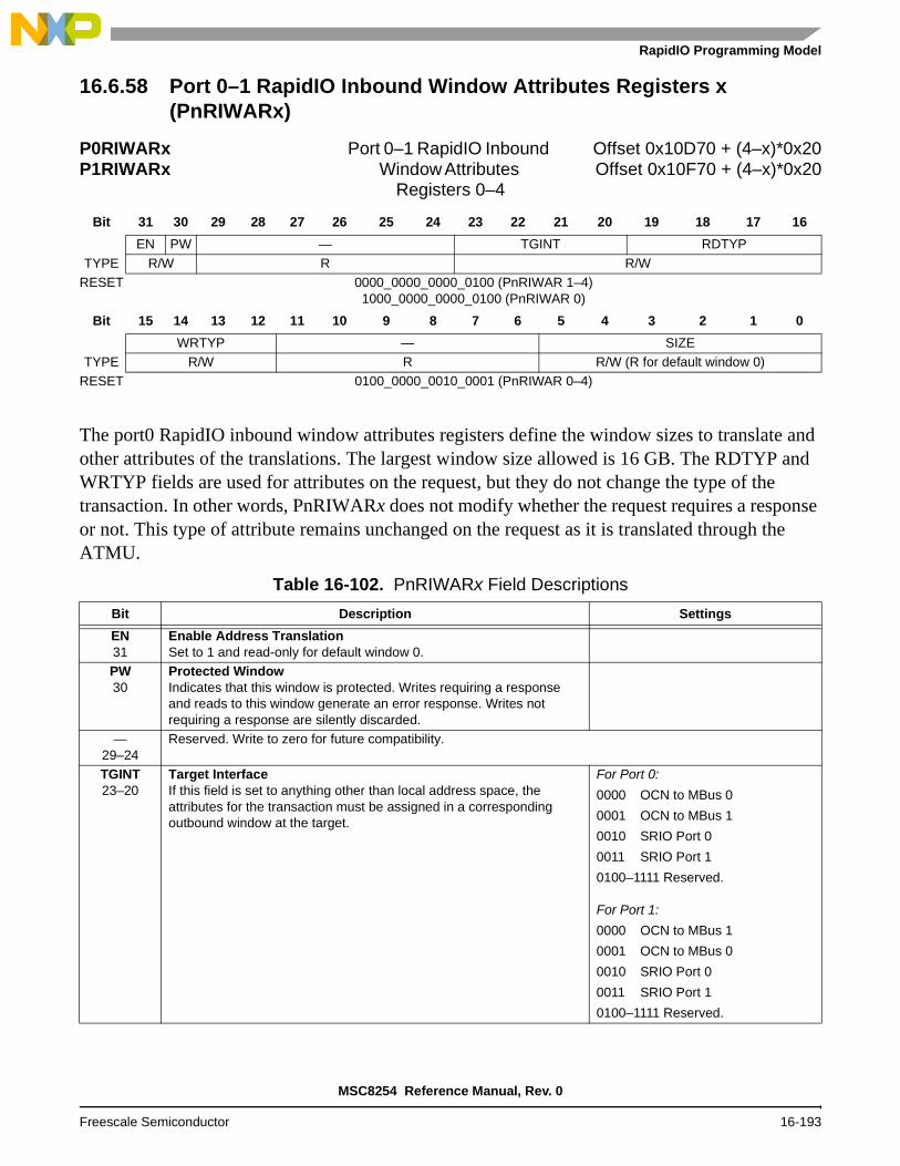
RapidIO Programming Model
16.6.58 Port 0–1 RapidIO Inbound Window Attributes Registers x (PnRIWARx)
The port0 RapidIO inbound window attributes registers define the window sizes to translate and other attributes of the translations. The largest window size allowed is 16 GB. The RDTYP and WRTYP fields are used for attributes on the request, but they do not change the type of the transaction. In other words, PnRIWARx does not modify whether the request requires a response or not. This type of attribute remains unchanged on the request as it is translated through the ATMU.
P0RIWARx Port 0–1 RapidIO Inbound Offset 0x10D70 + (4–x)*0x20P1RIWARx Window Attributes Offset 0x10F70 + (4–x)*0x20
Registers 0–4
Bit 31 30 29 28 27 26 25 24 23 22 21 20 19 18 17 16
EN PW — TGINT RDTYP
TYPE R/W R R/WRESET 0000_0000_0000_0100 (PnRIWAR 1–4)
1000_0000_0000_0100 (PnRIWAR 0)
Bit 15 14 13 12 11 10 9 8 7 6 5 4 3 2 1 0
WRTYP — SIZETYPE R/W R R/W (R for default window 0)
RESET 0100_0000_0010_0001 (PnRIWAR 0–4)
Table 16-102. PnRIWARx Field Descriptions
Bit Description Settings
EN31
Enable Address TranslationSet to 1 and read-only for default window 0.
PW30
Protected WindowIndicates that this window is protected. Writes requiring a response and reads to this window generate an error response. Writes not requiring a response are silently discarded.
—29–24
Reserved. Write to zero for future compatibility.
TGINT23–20
Target InterfaceIf this field is set to anything other than local address space, the attributes for the transaction must be assigned in a corresponding outbound window at the target.
For Port 0:
0000 OCN to MBus 0
0001 OCN to MBus 1
0010 SRIO Port 0
0011 SRIO Port 1
0100–1111 Reserved.
For Port 1:
0000 OCN to MBus 1
0001 OCN to MBus 0
0010 SRIO Port 0
0011 SRIO Port 1
0100–1111 Reserved.
MSC8254 Reference Manual, Rev. 0
Freescale Semiconductor 16-193

Serial RapidIO Controller
16.6.59 Outbound Message x Mode Registers (OMxMR)
OMxMR allows software to start a message operation and to control various message operation characteristics.
RDTYP19–16
Read TypeTransaction type to run on the local memory if the access is a read.
0000 Reserved.
...
0011 Reserved.
0100 Read.
0101 Reserved.
...
1111 Reserved.WRTYP15–12
Transaction type to run on local memory if access is a write. 0000 Reserved....
0011 Reserved.
0100 Write.
0101 Reserved.
...
1111 Reserved.
—11–6
Reserved. Write to zero for future compatibility.
SIZE5–0
Window SizeInbound translation window size N, which is the encoded 2^(N+1) byte window size. The smallest window size is 4 KB. This field is read-only for default window 0.
000000 Reserved.
...
001011 4 KB window size.
001100 8 KB window size.
...
011111 4 GB window size.
100000 8 GB window size.
100001 16 GB window size.
100010 Reserved.
...
111111 Reserved.
OM[0–1]MR Outbound Message 0–1 Mode Registers Offset 0x13000 + x*0x100
Bit 31 30 29 28 27 26 25 24 23 22 21 20 19 18 17 16
— SCTL —TYPE R R/W R
RESET 0 0 0 0 0 0 0 0 0 0 0 0 0 0 0 0
Bit 15 14 13 12 11 10 9 8 7 6 5 4 3 2 1 0
CIRQ_SIZ — QOIE QFIE — QEIE EIE — MUTM MUI MUS
TYPE R/W R R/W R R/W R R/WRESET 0 0 0 0 0 0 0 0 0 0 0 0 0 0 0 0
Table 16-102. PnRIWARx Field Descriptions (Continued)
Bit Description Settings
MSC8254 Reference Manual, Rev. 0
16-194 Freescale Semiconductor

RapidIO Programming Model
Table 16-103. OMxMR Field Descriptions
Bits Reset Description
—31–28
0 Reserved. Write to zero for future compatibility.
SCTL27–25
0 Service ControlDetermines the number of descriptors to process before the next queue is serviced. Note that if one queue has SCTL set to fixed priority, all SCTL values in other queues are ignored. For example, of the two outbound message units and the service control value for unit 1 is set to 0b000, a fixed priority is set and unit 0 handles the highest priority results. If a queue is in direct mode, only one message operation is serviced before the next queue is serviced. For proper operation, this field should be modified only when the outbound message controller is not enabled. The value of this field cannot be changed unless both units are disabled.
000 Fixed priority based on outbound message unit number.
001 1 descriptor.
010 2 descriptors.
011 4 descriptors.
100 8 descriptors.
101 16 descriptors.
110 32 descriptors.
111 64 descriptors.
—24–16
0 Reserved. Write to zero for future compatibility.
CIRQ_SIZ15–12
0 Circular Descriptor Queue SizeDetermines the number of descriptors that can be placed on the circular queue without overflow. For proper operation, this field should be modified only when the outbound message controller is not enabled
0000 2.
0001 4.
0010 8.
0011 16.
0100 32.
0101 64.
0110 128.
0111 256.
1000 512.
1001 1024.
1010 2048.
1011—
1111 Reserved.
—11–10
0 Reserved. Write to zero for future compatibility.
QOIE9
0 Queue Overflow Interrupt EnableEnables an interrupt when a queue overflow is detected. That is, the enqueue and dequeue pointers are no longer equal after the processor increments the enqueue pointer while the queue is full. This bit is applicable only in chaining mode. No queue overflow interrupt is generated if this bit is cleared. If this bit is not set and the queue overflows, the result is undefined.
QFIE8
0 Queue Full Interrupt EnableEnables an interrupt when the queue transitions to full. That is, the enqueue and dequeue pointers are equal after the processor increments the enqueue pointer. No QF interrupt is generated if this bit is cleared. If this bit is set and OMxSR[QF] is set, OMxSR[QFI] becomes set.
—7
0 Reserved. Write to zero for future compatibility.
MSC8254 Reference Manual, Rev. 0
Freescale Semiconductor 16-195

Serial RapidIO Controller
16.6.60 Outbound Message x Status Registers (OMxSR)
OMxSR reports various message unit conditions during and after a message operation. Writing a 1 to the corresponding set bit clears the bit.
QEIE6
0 Queue Empty Interrupt EnableEnables an interrupt at the completion of all outstanding message operations. That is, the enqueue and dequeue pointers are equal after an increment by the message unit controller. No Queue Empty interrupt is generated if this bit is cleared. For proper operation, this field should be modified only when the outbound message controller is not enabled
0 No interrupt.
1 Queue empty interrupt.
EIE5
0 Error Interrupt EnableEnables a port-write/error interrupt when a transfer error (OMxSR[TE]), a message error response (OMxSR[MER]), a packet response time-out (OMxSR[PRT]), or a retry threshold event exceeded (OMxSR[RETE]) event occurs. No port-write/error interrupt is generated if this bit is cleared.
0 No port-write/error interrupt.
1 Generate a port-write/error interrupt.
—4–3
0 Reserved. Write to zero for future compatibility.
MUTM2
0 Message unit Transfer ModePuts the message unit into direct mode so that software is responsible for placing all the required parameters into registers to start the message transmission. Clearing this bit configures the message unit in chaining mode.
0 Chaining mode.
1 Direct mode.
MUI1
0 Message Unit IncrementSoftware sets this bit after writing a descriptor to memory. Hardware then increments the OMxDQEPAR and clears this bit. MUI always reads as 0 when MUS is set.
MUS0
0 Message Unit StartIn Direct mode, a 0 to 1 transition when the message unit is not busy (MUB bit is 0) starts the message unit. A 1 to 0 transition has no effect. If this bit is set in Chaining mode, the message unit starts when the enqueue and dequeue pointers are not equal.
OM[0–1]SR Outbound Message 0–1 Status Registers Offset 0x13004 + x*0x100
Bit 31 30 29 28 27 26 25 24 23 22 21 20 19 18 17 16
— QF —TYPE R
RESET 0 0 0 0 0 0 0 0 0 0 0 0 0 0 0 0
Bit 15 14 13 12 11 10 9 8 7 6 5 4 3 2 1 0
— MER RETE PRT — TE — QOI QFI — MUB EOMI QEITYPE R W1C W1C W1C R W1C R W1C W1C R W1C W1C
RESET 0 0 0 0 0 0 0 0 0 0 0 0 0 0 0 0
Table 16-103. OMxMR Field Descriptions (Continued)
Bits Reset Description
MSC8254 Reference Manual, Rev. 0
16-196 Freescale Semiconductor

RapidIO Programming Model
Table 16-104. OMxSR Field Descriptions
Bits Reset Description
—31–21
0 Reserved. Write to zero for future compatibility.
QF20
0 Queue FullIf the queue becomes full, this bit is set. Read only.
—19–13
0 Reserved. Write to zero for future compatibility.
MER12
0 Message Error ResponseSet when an ERROR response is received from the message target. The error response received field indicates the value of the error response status bits when an error response is received. This bit is cleared by writing a value of 1 to it.
RETE11
0 Retry Error Threshold ExceededSet when the message unit is unable to complete a message operation because the retry error threshold value is exceeded due to a RapidIO retry response. This bit is cleared by writing a value of 1 to it.
PRT10
0 Packet Response Time-OutSet when the message unit has been unable to complete a message operation and a packet response time-out occurred. This bit is cleared by writing a 1.
—9–8
0 Reserved. Write to zero for future compatibility.
TE7
0 Transaction ErrorSet when an internal error condition occurs during the message operation. This bit is cleared by writing a value of 1 to it. For proper operation, this field should be modified only when the outbound message controller is not enabled
—6
0 Reserved. Write to zero for future compatibility.
QOI5
0 Queue Overflow InterruptSet when a queue overflow condition is detected. This bit is cleared by writing a value of 1 to it. QOI is applicable only to chaining mode.
QFI4
0 Queue Full InterruptIf the queue becomes full and the QFIE bit in the Mode Register is set, this bit is set and an interrupt is generated. This bit is cleared by writing a value of 1 to it.
—3
0 Reserved. Write to zero for future compatibility.
MUB2
0 Message Unit BusyIndicates that a message operation is currently in progress. This bit is cleared when an error occurs or the message operation completes. Read only.
EOMI1
0 End-Of-Message InterruptWhen the message operation completes and the EOMIE bit in the Destination Attributes Register is set, EOMI is set and an interrupt is generated. This bit is cleared by writing a value of 1 to it.
QEI0
0 Queue Empty InterruptWhen the last message operation in the outbound descriptor queue is finished and the QEIE bit in the Mode Register is set, this bit is set and an interrupt is generated. Otherwise, no interrupt is generated. This bit is cleared by writing a value of 1 to it.
MSC8254 Reference Manual, Rev. 0
Freescale Semiconductor 16-197

Serial RapidIO Controller
16.6.61 Outbound Message x Descriptor Queue Dequeue Pointer Address Registers (DMxDQDPAR)
OMxDQDPAR contain the address of the first descriptor in memory to be processed. Software must initialize this register to point to the first descriptor in memory. After the descriptor is processed, the message unit controller increments the outbound message descriptor queue dequeue pointer address in OMxDQDPAR to point to the next descriptor. If the outbound message descriptor queue enqueue pointer and the outbound message descriptor queue dequeue pointer are not equal (indicating that the queue is not empty), the message unit controller reads the next descriptor from memory for processing. If the enqueue and dequeue pointers are equal after the message unit controller increments the dequeue pointer, the queue is empty and the message unit halts until the processor increments the enqueue pointer. Incrementing the pointer indicates that a new descriptor was added to the queue and is ready for processing. If the queue becomes empty and OMxMR[QEIE] is set, OMxSR[QEI] is set and an interrupt is generated.
When software initializes these registers, they must be aligned on a boundary equal to the number of queue entries × 32 bytes (the size of each queue descriptor).For example, if there are eight entries in the queue, the register must be 256-byte aligned. The number of queue entries is set in OMnMR[CIRQ_SIZ].
OM[0–1]DQDPAR Outbound Message 0–1 Descriptor Offset 0x1300C + x*0x100Queue Dequeue Pointer Address Registers
Bit 31 30 29 28 27 26 25 24 23 22 21 20 19 18 17 16
DQDPATYPE R/W
RESET 0 0 0 0 0 0 0 0 0 0 0 0 0 0 0 0
Bit 15 14 13 12 11 10 9 8 7 6 5 4 3 2 1 0
DQDPA —
TYPE R/W RRESET 0 0 0 0 0 0 0 0 0 0 0 0 0 0 0 0
Table 16-105. OMxDQDPAR Field Descriptions
Bits Reset Description
DQDPA31–5
0 Descriptor Dequeue Pointer AddressContains the address of the first descriptor in memory to process. The descriptor must be aligned to a 32-byte boundary. For proper operation, this field should be modified only when the outbound message controller is not enabled.
—4–0
0 Reserved. Write to zero for future compatibility.
MSC8254 Reference Manual, Rev. 0
16-198 Freescale Semiconductor

RapidIO Programming Model
16.6.62 Outbound Message x Source Address Registers (OMxSAR)
OMxSAR indicates the address from which the message unit controller is to read data. Software must ensure that this is a valid local memory address. The source address must be aligned to a double-word boundary, so the least significant three bits are reserved.
OM[0–1]SAR Outbound Message 0–1 Source Offset 0x13014 + x*0x100Address Registers
Bit 31 30 29 28 27 26 25 24 23 22 21 20 19 18 17 16
SADTYPE R/W
RESET 0 0 0 0 0 0 0 0 0 0 0 0 0 0 0 0
Bit 15 14 13 12 11 10 9 8 7 6 5 4 3 2 1 0
SAD —TYPE R/W R
RESET 0 0 0 0 0 0 0 0 0 0 0 0 0 0 0 0
Table 16-106. OMxSAR Field Descriptions
Bits Reset Description
SAD31–3
0 Source AddressThe source address of the message operation. The contents are updated after every memory read operation. For proper operation, this field should be modified only when the outbound message controller is not enabled
—2–0
0 Reserved. Write to zero for future compatibility.
MSC8254 Reference Manual, Rev. 0
Freescale Semiconductor 16-199

Serial RapidIO Controller
16.6.63 Outbound Message x Destination Port Register (OMxDPR)
OMxDPR indicates the RapidIO destination ID and mailbox to which the message unit controller is to send data. The software must ensure that this is a valid port in the receiving device.
OM[0–1]DPR Outbound Message 0–1 Destination Offset 0x13018 + x*0x100Port Registers
Bit 31 30 29 28 27 26 25 24 23 22 21 20 19 18 17 16
EDGTROUTE DTGTROUTETYPE R/W
RESET 0 0 0 0 0 0 0 0 0 0 0 0 0 0 0 0
Bit 15 14 13 12 11 10 9 8 7 6 5 4 3 2 1 0
— MAILBTYPE R R/W
RESET 0 0 0 0 0 0 0 0 0 0 0 0 0 0 0 0
Table 16-107. OMxDPR Field Descriptions
Bits Reset Description
EDGTROUTE31–24
0 Extended Destination Target RouteMost significant byte of a 16-bit target route when activated in Large Transport mode. Reserved when operated in Small Transport mode. For proper operation, this field should be modified only when the outbound message controller is not enabled
DTGTROUTE23–16
0 Destination Target RouteContains the target route field of the transaction (device ID of the target). This value is overridden by the multicast group and list if Multicast mode is enabled. When an error occurs while Multicast mode is enabled, this field is loaded with the destination of the failed operation. For proper operation, this field should be modified only when the outbound message controller is not enabled
—15–2
0 Reserved. Write to zero for future compatibility.
MAILB1–0
0 Value for MBOX Field in MESSAGE PacketFor proper operation, this field should be modified only when the outbound message controller is not enabled
MSC8254 Reference Manual, Rev. 0
16-200 Freescale Semiconductor

RapidIO Programming Model
16.6.64 Outbound Message x Destination Attributes Register (OMxDATR)
OMxDATR contains the transaction attributes to be used for the message operation.
OM[0–1]DATR Outbound Message 0–1 Destination Offset 0x1301C + x*0x100Attributes Registers
Bit 31 30 29 28 27 26 25 24 23 22 21 20 19 18 17 16
MM — EOMIE — DTFLOWLVL — DTGTINT —TYPE R/W R R/W R R/W R R/W R
RESET 0 0 0 0 0 0 0 0 0 0 0 0 0 0 0 0
Bit 15 14 13 12 11 10 9 8 7 6 5 4 3 2 1 0
—TYPE R
RESET 0 0 0 0 0 0 0 0 0 0 0 0 0 0 0 0
Table 16-108. OMxDATR Field Descriptions
Bits Reset Description
MM31
0 Multicast ModeWhen set, sends the message operation to all targets indicated by the multicast group and list. Messages are limited to one segment and 256 bytes or less.
0 Normal operation.
1 Multicast mode.
—30
0 Reserved. Write to zero for future compatibility.
EOMIE29
0 End-of-Message Interrupt EnableWhen set, generates an interrupt when the current message operation finishes. For proper operation, this field should be modified only when the outbound message controller is not enabled.
—28
0 Reserved. Write to zero for future compatibility.
DTFLOWLVL27–26
0 Transaction Flow LevelFor proper operation, this field should be modified only when the outbound message controller is not enabled
00 Lowest priority transaction request flow.
01 Next highest priority transaction request flow.
10 Highest priority transaction request flow.
11 Reserved.
—25–24
0 Reserved. Write to zero for future compatibility.
DTGTINT23–20
0 Target InterfaceSelects the target interface.
0000 SRIO Port 0
0001 SRIO Port 1
All other values reserved.
—19–0
0 Reserved. Write to zero for future compatibility.
MSC8254 Reference Manual, Rev. 0
Freescale Semiconductor 16-201

Serial RapidIO Controller
16.6.65 Outbound Message x Double-Word Count Register (DMxDCR)
OMxDCR contains the number of double-words for the message operation. The maximum message operation size is 4 KB and the minimum is 8 bytes.
OM[0–1]DCR Outbound Message 0–1 Double-Word Offset 0x13020 + x*0x100 Count Registers
Bit 31 30 29 28 27 26 25 24 23 22 21 20 19 18 17 16
—TYPE R
RESET 0 0 0 0 0 0 0 0 0 0 0 0 0 0 0 0
Bit 15 14 13 12 11 10 9 8 7 6 5 4 3 2 1 0
— DCR —TYPE R R/W R
RESET 0 0 0 0 0 0 0 0 0 0 0 0 0 0 0 0
Table 16-109. OMxDCR Field Descriptions
Bits Reset Description Settings
—31–13
0 Reserved. Write to zero for future compatibility.
DCR12–3
0 Transfer Count RegisterContains the number of bytes for the message operation.For proper operation, this field should be modified only when the outbound message controller is not enabled. The values with an asterisk (*) apply only in Multi-Segment mode.
Note: The value in this register represents the number of double words to transfer and not the byte count; that is, the DCR value = the number of bytes/8.
00 0000 0000 Reserved.
00 0000 0001 8 bytes.
00 0000 0010 16 bytes.
00 0000 0100 32 bytes.
00 0000 1000 64 bytes.
00 0001 0000 128 bytes.
00 0010 0000 256 bytes.
00 0100 0000 512 bytes*.
00 1000 0000 1024 bytes*.
01 0000 0000 2048 bytes*.
10 0000 0000 4096 bytes*.All other values yield undefined behavior.
—2–0
0 Reserved. Write to zero for future compatibility.
MSC8254 Reference Manual, Rev. 0
16-202 Freescale Semiconductor

RapidIO Programming Model
16.6.66 Outbound Message x Descriptor Queue Enqueue Pointer Address Registers (OMxDQEPAR)
OMxDQEPAR contains the address for the next descriptor in memory to be added to the queue. Software must initialize this register to match the outbound message descriptor queue dequeue pointer address. When a message is ready to be sent, the processor writes a descriptor to the next location in the queue (indicated by the address in OMxDQEPAR ), and then either writes the OMxDQEPAR to point to the next descriptor location in memory or sets OMxMR[MUI]. This can result in a number of actions:
If the enqueue and dequeue pointers match, the queue is now full. If the OMxMR[QFIE] bit is set, then the OMxSR[QFI] bit is set, and an interrupt is generated.
If the enqueue and dequeue pointers no longer match after the enqueue pointer is incremented and the queue is full, then the queue overflows, and the message unit stops. If OMxMR[QOIE] is set, then the controller sets OMxSR[QOI] and generates an interrupt. OMxMR[MUS] must change from a 1 to a 0 to clear this error condition. If the enqueue pointer is written directly, the queue overflow condition is not detected.
If the enqueue and dequeue pointers were the same before the register is incremented, the message unit controller will start, if enabled.
Note: When software initializes these registers, they must be aligned on a boundary equal to the number of queue entries × 32 bytes (the size of each queue descriptor). For example, if there are eight entries in the queue, the register must be 256-byte aligned. The number of queue entries is set in OMxMR[CIRQ_SIZ].
OM[0–1]DQEPAR Outbound Message x Descriptor Offset 0x13028 + x*0x100Queue Enqueue Pointer Address Registers
Bit 31 30 29 28 27 26 25 24 23 22 21 20 19 18 17 16
DQEPATYPE R/W
RESET 0 0 0 0 0 0 0 0 0 0 0 0 0 0 0 0
Bit 15 14 13 12 11 10 9 8 7 6 5 4 3 2 1 0
DQEPA —
TYPE R/W RRESET 0 0 0 0 0 0 0 0 0 0 0 0 0 0 0 0
Table 16-110. OMxDQEPAR Field Descriptions
Bits Reset Description
DQEPA31–5
0 Descriptor Enqueue Pointer AddressContains the address of the next free descriptor location. The descriptor must be aligned to a 32-byte boundary and a descriptor queue boundary.
—4–0
0 Reserved. Write to zero for future compatibility.
MSC8254 Reference Manual, Rev. 0
Freescale Semiconductor 16-203

Serial RapidIO Controller
16.6.67 Outbound Message x Retry Error Threshold Configuration Register (OMxRETCR)
OMxRETCR controls the number of times the message unit can attempt to transfer a message segment to a specific destination before reporting an error. A message segment is retransmitted if a RETRY response is received from the target.
OM[0–1]RETCR Outbound Message 0–1 Retry Error Offset 0x1302C + x*0x100Threshold Configuration Registers
Bit 31 30 29 28 27 26 25 24 23 22 21 20 19 18 17 16
—TYPE R
RESET 0 0 0 0 0 0 0 0 0 0 0 0 0 0 0 0
Bit 15 14 13 12 11 10 9 8 7 6 5 4 3 2 1 0
— RET
TYPE R R/WRESET 0 0 0 0 0 0 0 0 0 0 0 0 0 0 0 0
Table 16-111. OMxRETCR Field Descriptions
Bits Reset Description Settings
—31–8
0 Reserved. Write to zero for future compatibility.
RET7–0
0 Retry Error ThresholdThe number of times the message unit can attempt to transmit a message segment to a specific target. For proper operation, this field should be modified only when the outbound message controller is not enabled
0x00 Disabled.
0x01 Message segment transmitted only 1 time.
0x02 Message segment transmitted up to 2 times.
...
0xFF Message segment transmitted up to 255 times.
MSC8254 Reference Manual, Rev. 0
16-204 Freescale Semiconductor

RapidIO Programming Model
16.6.68 Outbound Message x Multicast Group Registers (OMxMGR)
OMxMGR contains a multicast group (MG) value and extended multicast group number (EMG) which, in combination with the multicast list register and the multicast enable (OMxMR[MM] described in Table 16-103, OMxMR Field Descriptions, on page 16-195), indicates which device IDs are targets of a multicast operation. The multicast group represents the most significant three bits (bits[7–5]) of the RapidIO device IDs that are destinations of the message operation. The multicast list indicates a list of targets within that group. Each individual bit, when encoded, determines the least significant five bits of the RapidIO device IDs (bits[4–0]) that are targets of the message operation. Therefore, multicast group 0 (MG = 0) contains target device IDs (0, 1, ..., 31), multicast group 1 (MG = 1) contains target device IDs (32, 33, ... 63), and so on.
In large transport mode, the extended multicast group represents the eight most significant bits (bits[15–8]), the multicast group represents the next three bits (bits[7–5]) and the multicast list indicates a list of targets within that group.
If multicast is enabled, this information in the multicast group and mask register is used to determine the target of the message operation instead of the DTGTROUTE and EDTGTROUTE fields in the Outbound Message Destination Port Register (see Table 16-107, OMxDPR Field Descriptions, on page 16-200).
OM[0–1]MGR Outbound Message 0–1 Multicast Group Offset 0x13030 + x*0x100Registers
Bit 31 30 29 28 27 26 25 24 23 22 21 20 19 18 17 16
—TYPE R
RESET 0 0 0 0 0 0 0 0 0 0 0 0 0 0 0 0
Bit 15 14 13 12 11 10 9 8 7 6 5 4 3 2 1 0
— EMG MGTYPE R R/W
RESET 0 0 0 0 0 0 0 0 0 0 0 0 0 0 0 0
Table 16-112. OMxMGR Field Descriptions
Bits Name Description
—31–11
0 Reserved. Write to zero for future compatibility.
MSC8254 Reference Manual, Rev. 0
Freescale Semiconductor 16-205

Serial RapidIO Controller
16.6.69 Outbound Message x Multicast List Registers (OMxMLR)
See Section 16.6.68, Outbound Message x Multicast Group Registers (OMxMGR), on page 16-205 for more information.
EMG10–3
0 Extended Multi-Cast GroupThe most significant eight bits of the target device IDs for the multicast operation in Large Transport mode. For proper operation, this field should be modified only when the outbound message controller is not enabled
MG2–0
0 Multi-Cast GroupThe most significant three bits of the target device IDs for the multicast operation. In Large Transport mode, these are the most significant bits of the least significant byte of the Target Device ID. For proper operation, this field should be modified only when the outbound message controller is not enabled
OM[0–1]MLR Outbound Message 0–1 Multicast List Offset 0x13034 + x*0x100Registers
Bit 31 30 29 28 27 26 25 24 23 22 21 20 19 18 17 16
MLTYPE R/W
RESET 0 0 0 0 0 0 0 0 0 0 0 0 0 0 0 0
Bit 15 14 13 12 11 10 9 8 7 6 5 4 3 2 1 0
ML
TYPE R/WRESET 0 0 0 0 0 0 0 0 0 0 0 0 0 0 0 0
Table 16-113. OMxMLR Field Descriptions
Bits Reset Description
ML31–0
0 Multicast ListThe group target list for the message operation. Depending upon the value of the multicast group value, bit 31 corresponds to device ID 0, 32, 64, 96, and so on. Bit 30 corresponds to device ID 1, 33, 65, 97, and so on. If none of the bits are set, bit 31 is assumed to be set. For proper operation, this field should be modified only when the outbound message controller is not enabled.
Table 16-112. OMxMGR Field Descriptions (Continued)
Bits Name Description
MSC8254 Reference Manual, Rev. 0
16-206 Freescale Semiconductor

RapidIO Programming Model
16.6.70 Inbound Message x Mode Registers (IMxMR)
IMxMR allows software to enable the mailbox controller and to control various characteristics of the message operation.
IM[0–1]MR Inbound Message 0–1 Mode Registers Offset 0x13060 + x*0x100
Bit 31 30 29 28 27 26 25 24 23 22 21 20 19 18 17 16
MIQ_THRESH — FRM_SIZ
TYPE R/W R R/WRESET 0 0 0 0 0 0 0 0 0 0 0 0 0 0 0 0
Bit 15 14 13 12 11 10 9 8 7 6 5 4 3 2 1 0
CIRQ_SIZ — QFIE — MIQIE EIE — MI METYPE R/W R R/W R R/W R R/W
RESET 0 0 0 0 0 0 0 0 0 0 0 0 0 0 0 0
Table 16-114. IMxMR Field Descriptions
Bits Reset Description Settings
MIQ_THRESH31–28
0 Message in Queue ThresholdDetermines the number of message frames to be accumulated in the frame queue before Message In Queue is signaled. Results are undefined if the message in queue threshold is greater than or equal to the message queue size (IMxMR[CIRQ_SIZ]). For proper operation, this field should be modified only when the inbound message controller is not enabled.
0000 1.
0001 2.
0010 4.
0011 8.
0100 16.
0101 32.
0110 64.
0111 128.
1000 256.
1001 512.
1010 1024.
1011–
1111 Reserved.—
27–200 Reserved. Write to zero for future compatibility.
FRM_SIZ19–16
0 Message Frame SizeDetermines the maximum message size the mailbox can accept without error. Combined with IMxMR[CIRQ_SIZ], this parameter determines the maximum contiguous memory space allocated to the mailbox. For proper operation, this field should be modified only when the inbound message controller is not enabled.
0000–
0001 Reserved.
0010 8 bytes.
0011 16 bytes.
0100 32 bytes.
0101 64 bytes.
0110 128 bytes.
0111 256 bytes.
1000 512 bytes.
1001 1024 bytes.
1010 2048 bytes.
1011 4096 bytes.
1100–
1111 Reserved.
MSC8254 Reference Manual, Rev. 0
Freescale Semiconductor 16-207

Serial RapidIO Controller
CIRQ_SIZ15–12
0 Circular Frame Queue SizeDetermines the number of message frames that can be placed on the circular queue without overflow. Combined with IMxMR[FRM_SIZ], this parameter determines the maximum contiguous memory space allocated to the mailbox. This field should be modified only when the inbound message controller is not enabled.
0000 2.
0001 4.
0010 8.
0011 16.
0100 32.
0101 64.
0110 128.
0111 256.
1000 512.
1001 1024.
1010 2048.
1011–
1111 Reserved.—
11–90 Reserved. Write to zero for future compatibility.
QFIE8
0 Queue Full Interrupt EnableWhen set, the controller generates an interrupt when the queue is full (that is, the enqueue and dequeue pointers are equal after the mailbox controller increments the dequeue pointer). No QFI interrupt is generated if this if this bit is cleared. If this bit is set and IMxSR[QF] = 1, IMxSR[QFI] is set.
0 No interrupt is generated.
1 Interrupt generaated on queue full.
—7
0 Reserved. Write to zero for future compatibility.
MIQIE6
0 Message in Queue Interrupt EnableWhen set, the controller enerates an interrupt when the queue has accumulated the number of messages specified by the IMxMR[MIQ_THRESH]. No MIQ interrupt is generated if this bit is cleared. If this bit is set and IMxSR[MIQ] = 1, IMxSR[MIQI] is set. If this bit is set and IMxMR[MI] is also set simultaneously, IMxSR[MIQI] reflects the value of MIQ after the increment.
0 No interrupt is generated.
1 Interrupt generaated on message in queue event.
EIE5
0 Error Interrupt EnableWhen set, the controller generates a port-write/error interrupt when a transfer error (IMxSR[TE]) or a message request time-out (IMxSR[MRT]) event occurs. No port-write/error interrupt is generated if this bit is cleared.
0 No interrupt is generated.
1 Interrupt generaated on error.
—4–2
0 Reserved. Write to zero for future compatibility.
MI1
0 Mailbox IncrementSoftware sets this bit after processing an inbound message. Hardware increments the IMxFQDPAR and clears this bit. MI always reads as 0.
ME0
0 Mailbox EnableSet when the mailbox is initialized and can service incoming message operations. If this bit is cleared after the first segment of a multi-segment message arrives, a message request time-out results (IMxSR[MRT]). The busy bit (IMxSR[MB]) clears if the port response timer value (PRTOCCSR[TV]) is not set to the disabled value. If it is set to the disabled value, the busy bit does not clear.
Table 16-114. IMxMR Field Descriptions (Continued)
Bits Reset Description Settings
MSC8254 Reference Manual, Rev. 0
16-208 Freescale Semiconductor

RapidIO Programming Model
16.6.71 Inbound Message x Status Registers (IMxSR)
IMxSR reports various mailbox conditions during and after a message operation. Writing a value of 1 to the corresponding set bit clears the bit.
IM[0–1]SR Inbound Message 0–1 Status Registers Offset 0x13064 + x*0x100
Bit 31 30 29 28 27 26 25 24 23 22 21 20 19 18 17 16
— QF — MIQ
TYPE R
RESET 0 0 0 0 0 0 0 0 0 0 0 0 0 0 0 0
Bit 15 14 13 12 11 10 9 8 7 6 5 4 3 2 1 0
— MRT — TE — QFI — MB QE MIQI
TYPE R W1C R W1C R W1C R W1C
RESET 0 0 0 0 0 0 0 0 0 0 0 0 0 0 1 0
Table 16-115. IMxSR Field Descriptions
Bits Reset Description
—31–21
0 Reserved. Write to zero for future compatibility.
QF20
0 Queue FullIf the queue becomes full, this bit is set. QF is cleared when the queue is not full and if the message controller is disabled. Read only.
—19–17
0 Reserved. Write to zero for future compatibility.
MIQ16
0 Message-In-QueueIf the queue has accumulated the number of messages specified by the IMxMR[MIQTH], this bit is set. MIQ is cleared when the number of message in the queue is less than the number specified by IMxMR[MIQ_THRESH] and if the message controller is disabled. Read only.
—15–11
0 Reserved. Write to zero for future compatibility.
MRT10
0 Message Request Time-OutSet when the message unit has not received another message segment for a multi-segment message and a time-out occurs. This bit is cleared by writing a 1 to it.For proper operation, this bit should be modified only when the inbound message controller is not enabled.
—9–8
0 Reserved. Write to zero for future compatibility.
TE7
0 Transaction ErrorSet when an internal error condition occurs during the message operation. TE is cleared by writing a 1 to it. For proper operation, this bit should be modified only when the inbound message controller is not enabled.
—6–5
0 Reserved. Write to zero for future compatibility.
MSC8254 Reference Manual, Rev. 0
Freescale Semiconductor 16-209

Serial RapidIO Controller
QFI4
0 Queue Full InterruptIf the queue is full and the IMxMR[QFIE] bit is set, QFI is set and an interrupt is generated. QFI s cleared by writing a 1 to it.
—3
0 Reserved. Write to zero for future compatibility.
MB2
0 Mailbox BusyIndicates that a message operation is in progress. MB is cleared when an error occurs or the message operation finishes. Read only.
QE1
1 Queue EmptyIf the queue is empty, this bit is set. QE is also set if the message controller is disabled. Read only.
MIQI0
0 Message-In-Queue InterruptIf the queue has accumulated the number of messages specified by the IMxMR[MIQ_THRESH] and the IMxMR[MIQIE] bit is set, this bit is set and an interrupt is generated. This bit is cleared by writing a 1 to it.
Table 16-115. IMxSR Field Descriptions (Continued)
Bits Reset Description
MSC8254 Reference Manual, Rev. 0
16-210 Freescale Semiconductor
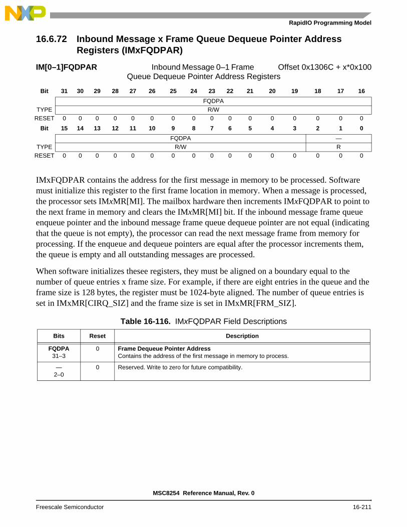
RapidIO Programming Model
16.6.72 Inbound Message x Frame Queue Dequeue Pointer Address Registers (IMxFQDPAR)
IMxFQDPAR contains the address for the first message in memory to be processed. Software must initialize this register to the first frame location in memory. When a message is processed, the processor sets IMxMR[MI]. The mailbox hardware then increments IMxFQDPAR to point to the next frame in memory and clears the IMxMR[MI] bit. If the inbound message frame queue enqueue pointer and the inbound message frame queue dequeue pointer are not equal (indicating that the queue is not empty), the processor can read the next message frame from memory for processing. If the enqueue and dequeue pointers are equal after the processor increments them, the queue is empty and all outstanding messages are processed.
When software initializes thesee registers, they must be aligned on a boundary equal to the number of queue entries x frame size. For example, if there are eight entries in the queue and the frame size is 128 bytes, the register must be 1024-byte aligned. The number of queue entries is set in IMxMR[CIRQ_SIZ] and the frame size is set in IMxMR[FRM_SIZ].
IM[0–1]FQDPAR Inbound Message 0–1 Frame Offset 0x1306C + x*0x100Queue Dequeue Pointer Address Registers
Bit 31 30 29 28 27 26 25 24 23 22 21 20 19 18 17 16
FQDPATYPE R/W
RESET 0 0 0 0 0 0 0 0 0 0 0 0 0 0 0 0
Bit 15 14 13 12 11 10 9 8 7 6 5 4 3 2 1 0
FQDPA —
TYPE R/W RRESET 0 0 0 0 0 0 0 0 0 0 0 0 0 0 0 0
Table 16-116. IMxFQDPAR Field Descriptions
Bits Reset Description
FQDPA31–3
0 Frame Dequeue Pointer AddressContains the address of the first message in memory to process.
—2–0
0 Reserved. Write to zero for future compatibility.
MSC8254 Reference Manual, Rev. 0
Freescale Semiconductor 16-211

Serial RapidIO Controller
16.6.73 Inbound Message x Frame Queue Enqueue Pointer Address Registers (IMxFQEPAR)
IMxFQEPAR contains the address for the next message frame in memory to be added to the queue. Software must initialize this register to match the frame queue dequeue pointer address. When the mailbox controller receives a message, it writes the message data to the next location in the queue (indicated by the address in IMxFQEPAR) and then increments IMxFQEPAR to point to the next frame location in memory. This can result in a number of actions:
If the enqueue and dequeue pointers match, the queue is full and the mailbox controller does not accept any more incoming messages, returning RETRY responses to the sending devices until the queue is no longer full. If the IMxMR[QFIE] bit is set, the IMxMR[QFI] bit is set and an interrupt is generated.
If the enqueue and dequeue pointers are the same before the register is incrememted, the queue has changed from empty to not empty. If IMxMR[MIQIE] is set, IMxSR[MIQI] is set, and an interrupt is generated.
When software initializes these registers, they must be aligned on a boundary equal to the number of queue entries x frame size. For example, if there are eight entries in the queue and the frame size is 128 bytes, the register must be 1024-byte aligned. The number of queues is set in IMxMR[CIRQ_SIZ] and the frame size is set in IMxMR[FRM_SIZ].
IM[0–1]FQEPAR Inbound Message x Frame Offset 0x13074 + x*0x100Queue Enqueue Pointer Address Registers
Bit 31 30 29 28 27 26 25 24 23 22 21 20 19 18 17 16
FQEPATYPE R/W
RESET 0 0 0 0 0 0 0 0 0 0 0 0 0 0 0 0
Bit 15 14 13 12 11 10 9 8 7 6 5 4 3 2 1 0
FQEPA —
TYPE R/W RRESET 0 0 0 0 0 0 0 0 0 0 0 0 0 0 0 0
Table 16-117. IMxFQEPAR Field Descriptions
Bits Reset Description
FQEPA31–3
0 Frame Queue Enqueue Pointer AddressContains the address of the next message frame to be added to the queue. For proper operation, this field should be modified only when the inbound message controller is not enabled.
—2–0
0 Reserved. Write to zero for future compatibility.
MSC8254 Reference Manual, Rev. 0
16-212 Freescale Semiconductor

RapidIO Programming Model
16.6.74 Inbound Message x Maximum Interrupt Report Interval Registers (IMxMIRIR)
IMxMIRIR contains a time-out timer value to define the maximum amount of time that the mailbox controller is to wait after transitioning from not empty before signaling an interrupt to the local processor (if enabled) if the IMxMR[MIQ_THRESH] limit is not reached. The reset value is the maximum time-out interval, and represents between 3 and 5 seconds.
IM[0–1]MIRIR Inbound Message 0–1 Maximum Offsert 0x13078 + x*0x100Interrupt Report Interval Registers
Bit 31 30 29 28 27 26 25 24 23 22 21 20 19 18 17 16
MIRITYPE R/W
RESET 1 1 1 1 1 1 1 1 1 1 1 1 1 1 1 1
Bit 15 14 13 12 11 10 9 8 7 6 5 4 3 2 1 0
MIRI —
TYPE R/W RRESET 1 1 1 1 1 1 1 1 0 0 0 0 0 0 0 0
Table 16-118. IMxMIRIR Field Descriptions
Bits Reset Description
MIRI31–8
0xFFFFFF Maximum Interrupt Report IntervalMaximum interval between receiving the first message and setting IMxSR[IMIQ]. A value of 0 disables the time-out timer.For proper operation, this field should be modified only when the inbound message controller is not enabled.
—7–0
0 Reserved. Write to zero for future compatibility.
MSC8254 Reference Manual, Rev. 0
Freescale Semiconductor 16-213

Serial RapidIO Controller
16.6.75 Outbound Doorbell Mode Register (ODMR)
ODMR allows software to start a doorbell operation and to control the characteristics of various doorbell operations.
ODMR Outbound Doorbell Mode Register Offset 0x13400
Bit 31 30 29 28 27 26 25 24 23 22 21 20 19 18 17 16
—
TYPE RRESET 0 0 0 0 0 0 0 0 0 0 0 0 0 0 0 0
Bit 15 14 13 12 11 10 9 8 7 6 5 4 3 2 1 0
— DUSTYPE R
RESET 0 0 0 0 0 0 0 0 0 0 0 0 0 0 0 0
Table 16-119. ODMR Field Descriptions
Bits Reset Description
—31–1
0 Reserved. Write to zero for future compatibility.
DUS0
0 Doorbell Unit StartA 0-to-1 transition when the doorbell unit is not busy (ODSR[DUB] bit has a value of 0) starts the doorbell unit. A 1-to-0 transition has no effect.
MSC8254 Reference Manual, Rev. 0
16-214 Freescale Semiconductor

RapidIO Programming Model
16.6.76 Outbound Doorbell Status Register (ODSR)
ODSR reports various doorbell conditions during and after a doorbell operation. Writing a 1 to the corresponding set bit clears the bit.
ODSR Outbound Doorbell Status Register Offset 0x13404
Bit 31 30 29 28 27 26 25 24 23 22 21 20 19 18 17 16
—
TYPE RRESET 0 0 0 0 0 0 0 0 0 0 0 0 0 0 0 0
Bit 15 14 13 12 11 10 9 8 7 6 5 4 3 2 1 0
— MER RETE PRT — DUB EODI —TYPE R W1C R R W1C R
RESET 0 0 0 0 0 0 0 0 0 0 0 0 0 0 0 0
Table 16-120. ODSR Field Descriptions
Bits Reset Description
—31–13
0 Reserved. Write to zero for future compatibility.
MER12
0 Message Error ResponseSet when an error response is received from the doorbell target. The error response reserved field indicates the value of the error response status bits when an error response is received. MER is cleared by writing a 1 to it. For proper operation, this bit should be cleared only when a doorbell operation is not in progress.
RETE11
0 Retry Error Threshold ExceededSet when the doorbell unit cannot complete a doorbell operation because the retry error threshold value has been exceeded due to a RapidIO retry response. RETE is cleared by writing a 1 to it. For proper operation, this bit should be cleared only when a doorbell operation is not in progress.
PRT10
0 Packet Response Time-OutSet when the doorbell unit cannot complete a doorbell operation and a packet response time-out occurs. PRT is cleared by writing a 1 to it. For proper operation, this bit should be cleared only when a doorbell operation is not in progress.
—9–3
0 Reserved. Write to zero for future compatibility.
DUB2
0 Doorbell Unit BusyIndicates that a doorbell operation is in progress. DUB is cleared when an error occurs or the doorbell operation is finishes. Read only.
EODI1
0 End-of-Doorbell InterruptWhen a doorbell operation finishes and the ODDATR[EODIE] bit is set, this bit is set and an interrupt is generated. EODI is cleared by writing a 1 to it. For proper operation, this bit should be cleared only when a doorbell operation is not in progress.
—0
0 Reserved. Write to zero for future compatibility.
MSC8254 Reference Manual, Rev. 0
Freescale Semiconductor 16-215

Serial RapidIO Controller
16.6.77 Outbound Doorbell Destination Port Register (ODDPR)
ODDPR indicates the RapidIO destination device ID to which the doorbell unit controller is to send data. Software must ensure that this is a valid port in the receiving device.
ODDPR Outbound Doorbell Destination Port Register Offset 0x13418
Bit 31 30 29 28 27 26 25 24 23 22 21 20 19 18 17 16
EDTGROUTE DTGTROUTE
TYPE R/WRESET 0 0 0 0 0 0 0 0 0 0 0 0 0 0 0 0
Bit 15 14 13 12 11 10 9 8 7 6 5 4 3 2 1 0
—TYPE R
RESET 0 0 0 0 0 0 0 0 0 0 0 0 0 0 0 0
Table 16-121. ODDPR Field Descriptions
Bits Reset Description
EDTROUTE31–24
0 Extended Destination Target RouteMost significant byte of a 16-bit target route (device ID of the target) in Large Transport mode. In Small Transport mode, this bit is reserved. For proper operation, this field should be modified only when a doorbell operation is not in progress.
DTROUTE23–16
0 Destination Target RouteContains the target route field of the transaction (device ID of the target). For proper operation, this field should be modified only when a doorbell operation is not in progress.
—15–0
0 Reserved. Write to zero for future compatibility.
MSC8254 Reference Manual, Rev. 0
16-216 Freescale Semiconductor

RapidIO Programming Model
16.6.78 Outbound Doorbell Destination Attributes Register (ODDATR)
ODDATR contains the transaction attributes to be used for the doorbell operation.
ODDATR Outbound Doorbell Destination Attributes Register Offset 0x1341C
Bit 31 30 29 28 27 26 25 24 23 22 21 20 19 18 17 16
— EODIE — DTFLOWLVL — TGINT —
TYPE R/W
RESET 0 0 0 0 0 0 0 0 0 0 0 0 0 0 0 0
Bit 15 14 13 12 11 10 9 8 7 6 5 4 3 2 1 0
INFO_MSB INFO_LSB
TYPE R/W
RESET 0 0 0 0 0 0 0 0 0 0 0 0 0 0 0 0
Table 16-122. ODDATR Field Descriptions
Bits Reset Description Settings
—31–30
0 Reserved. Write to zero for future compatibility. Bit 30 is hardwired to 0.
EODIE29
0 End-of-Doorbell Interrupt EnableGenerates an interrupt when the current doorbell operation finishes. This field should be modified only when a doorbell operation is not in progress.
—28
0 Reserved. Write to zero for future compatibility.
DTFLOWLVL27–26
0 Transaction Flow LevelSpecifies the transaction flow level. This field should be modified only when a doorbell operation is not in progress.
00 Lowest-priority transaction flow.
01 Next highest priority transaction flow.
10 Highest-priority transaction flow.
11 Reserved.
—25–24
0 Reserved. Write to zero for future compatibility.
TGINT23–20
0 Target InterfaceSelects the target interface.
0000 SRIO Port 0
0001 SRIO Port 1
All other values reserved.
—19–16
0 Reserved. Write to zero for future compatibility.
INFO_MSB15–8
0 MSB of Doorbell INFOMost significant byte of the doorbell INFO field. This field should be modified only when a doorbell operation is not in progress.
INFO_LSB7–0
0 LSB of Doorbell INFOLeast significant byte of the doorbell INFO field. This field should be modified onlyy when a doorbell operation is not in progress.
MSC8254 Reference Manual, Rev. 0
Freescale Semiconductor 16-217

Serial RapidIO Controller
16.6.79 Outbound Doorbell Retry Error Threshold Configuration Register (ODRETCR)
ODRETCR controls the number of times the doorbell unit attempts to complete a doorbell operation before reporting an error and moving on to the next task, if available. Failures to complete an operation are indicated when the doorbell unit receives a RapidIO logical layer RETRY response from the target. If the programmed count is exceeded, the ODSR[RETE] bit is set.
ODRETCR Outbound Doorbell Retry Error Threshold Configuration Offset 0x1342CRegister
Bit 31 30 29 28 27 26 25 24 23 22 21 20 19 18 17 16
—TYPE R
RESET 0 0 0 0 0 0 0 0 0 0 0 0 0 0 0 0
Bit 15 14 13 12 11 10 9 8 7 6 5 4 3 2 1 0
— RET
TYPE R R/WRESET 0 0 0 0 0 0 0 0 0 0 0 0 0 0 0 0
Table 16-123. ODRETCR Field Descriptions
Bits Name Description Settings
—31–8
0 Reserved. Write to zero for future compatibility.
RET7–0
0 Retry Error ThresholdSpecifies the number of times the doorbell unit attempts to transmit a doorbell message. This field should be modified only when a doorbell operation is not in progress.
0x00 Disabled.
0x01 Doorbell transmitted only 1 time.
0x02 Doorbell transmitted up to 2 times
...
0xFF - Doorbell transmitted up to 255 times.
MSC8254 Reference Manual, Rev. 0
16-218 Freescale Semiconductor

RapidIO Programming Model
16.6.80 Inbound Doorbell Mode Registers (IDMR)
IDMR allows software to enable the inbound doorbell controller and to control the characteristics of various doorbell operations.
IDMR Inbound Doorbell Mode Register Offset 0x13460
Bit 31 30 29 28 27 26 25 24 23 22 21 20 19 18 17 16
DIQ_THRESH —
TYPE R/W RRESET 0 0 0 0 0 0 0 0 0 0 0 0 0 0 0 0
Bit 15 14 13 12 11 10 9 8 7 6 5 4 3 2 1 0
CIRQ_SIZ — QFIE — DIQIE EIE — DI DETYPE R/W R R/W R R/W R R/W
RESET 0 0 0 0 0 0 0 0 0 0 0 0 0 0 0 0
Table 16-124. IDMR Field Descriptions
Bits Reset Description Settings
DIQ_THRESH31–28
0 Doorbell-in-Queue ThresholdDetermines the number of doorbells to accumulate in the doorbell queue before the doorbell-in-queue bit is set (IDSR[DIQ]). Undefined operation results if the actual number of entries in the doorbell-in-queue threshold is set as greater than or equal to the actual size of the doorbell queue. For proper operation, this field should be modified only when the doorbell controller is not enabled.
0000 1.
0001 2.
0010 4.
0011 8.
0100 16.
0101 32.
0110 64.
0111 128.
1000 256.
1001 512.
1010 1024.
1011–
1111 Reserved.
—27–16
0 Reserved. Write to zero for future compatibility.
CIRQ_SIZ15–12
0 Circular Doorbell Queue SizeDetermines the number of doorbell entries that can be placed in the circular queue. CIRQ_SIZ × 8 bytes determine the maximum contiguous memory space allocated to the doorbell unit. For proper operation, this field should be modified only when the doorbell controller is not enabled.
0000 2.
0001 4.
0010 8.
0011 16.
0100 32.
0101 64.
0110 128.
0111 256.
1000 512 (4 KB page boundary).
1001 1024.
1010 2048.
1011–
1111 Reserved.
MSC8254 Reference Manual, Rev. 0
Freescale Semiconductor 16-219

Serial RapidIO Controller
—11–9
0 Reserved. Write to zero for future compatibility.
QFIE8
0 Queue Full Interrupt EnableWhen set, enables the queue full interrupt. The queue is full when the enqueue and dequeue pointers are equal after the doorbell controller increments the dequeue pointer, the controller genrates the Queue Full interrupt. That is, if this bit is set and IDSR[QF] = 1, IDSR[QFI] is set.For proper operation, this field should only be modified when the inbound doorbell controller is not enabled.
0 No QF interrupt is generated.
1 Generates an interrupt when the queue is full .
—7
0 Reserved. Write to zero for future compatibility.
DIQIE6
0 Doorbell in Queue Interrupt EnableWhen set, enables the doorbell in queue interrupt. The interrupt cannot be asserted if this bit is cleared.If this bit is set and IDSR[DIQ] = 1, IDSR[DIQI] is set. If this bit is set and IDMR[DI] is set simultaneously, IDSR[DIQI] reflects the value of DIQ after the increment.For proper operation, this field should only be modified when the inbound doorbell controller is not enabled.
0 No DIQ interrupt is generated.
1 Generates an interrupt when IDSR[DIQ] = 1.
EIE5
0 Error Interrupt EnableWhen set, enables the port-write/error interrupt when a transfer error (IDSR[TE]) event occurs. No port-write/error interrupt is generated if this bit is cleared. For proper operation, this field should only be modified when the inbound doorbell controller is not enabled.
—4–2
0 Reserved Reserved. Write to zero for future compatibility.
DI1
0 Doorbell IncrementSoftware sets this bit after an inbound doorbell is processed. Hardware then increments the IDQDPAR and clears this bit. DI always reads as 0.
DE0
0 Doorbell EnableEnabled/disables the inbound doorbell operations.
0 Inbound doorbell disabled.
1 The inbound doorbell is initialized and can service incoming doorbell operations.
Table 16-124. IDMR Field Descriptions (Continued)
Bits Reset Description Settings
MSC8254 Reference Manual, Rev. 0
16-220 Freescale Semiconductor
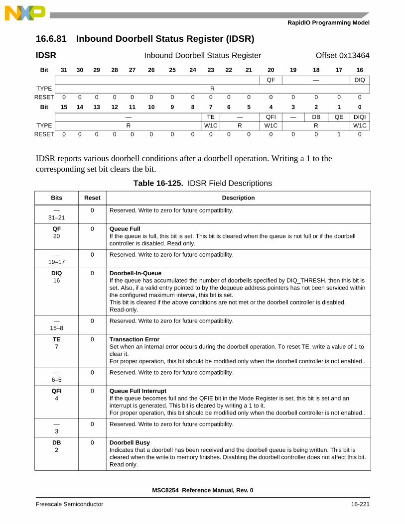
RapidIO Programming Model
16.6.81 Inbound Doorbell Status Register (IDSR)
IDSR reports various doorbell conditions after a doorbell operation. Writing a 1 to the corresponding set bit clears the bit.
IDSR Inbound Doorbell Status Register Offset 0x13464
Bit 31 30 29 28 27 26 25 24 23 22 21 20 19 18 17 16
QF — DIQ
TYPE RRESET 0 0 0 0 0 0 0 0 0 0 0 0 0 0 0 0
Bit 15 14 13 12 11 10 9 8 7 6 5 4 3 2 1 0
— TE — QFI — DB QE DIQITYPE R W1C R W1C R W1C
RESET 0 0 0 0 0 0 0 0 0 0 0 0 0 0 1 0
Table 16-125. IDSR Field Descriptions
Bits Reset Description
—31–21
0 Reserved. Write to zero for future compatibility.
QF20
0 Queue FullIf the queue is full, this bit is set. This bit is cleared when the queue is not full or if the doorbell controller is disabled. Read only.
—19–17
0 Reserved. Write to zero for future compatibility.
DIQ16
0 Doorbell-In-QueueIf the queue has accumulated the number of doorbells specified by DIQ_THRESH, then this bit is set. Also, if a valid entry pointed to by the dequeue address pointers has not been serviced within the configured maximum interval, this bit is set. This bit is cleared if the above conditions are not met or the doorbell controller is disabled. Read-only.
—15–8
0 Reserved. Write to zero for future compatibility.
TE7
0 Transaction ErrorSet when an internal error occurs during the doorbell operation. To reset TE, write a value of 1 to clear it. For proper operation, this bit should be modified only when the doorbell controller is not enabled..
—6–5
0 Reserved. Write to zero for future compatibility.
QFI4
0 Queue Full InterruptIf the queue becomes full and the QFIE bit in the Mode Register is set, this bit is set and an interrupt is generated. This bit is cleared by writing a 1 to it. For proper operation, this bit should be modified only when the doorbell controller is not enabled..
—3
0 Reserved. Write to zero for future compatibility.
DB2
0 Doorbell BusyIndicates that a doorbell has been received and the doorbell queue is being written. This bit is cleared when the write to memory finishes. Disabling the doorbell controller does not affect this bit. Read only.
MSC8254 Reference Manual, Rev. 0
Freescale Semiconductor 16-221

Serial RapidIO Controller
16.6.82 Inbound Doorbell Queue Dequeue Pointer Address Register (IDQDPAR)
IDQDPAR contains the double-word address for the first doorbell in memory to be processed. Software must initialize this register to the first doorbell entry location in memory. After a doorbell is processed, the processor sets IDMR[DI]. Then the doorbell queue dequeue pointer address register is incremented by hardware to point to the next doorbell entry in memory and IDMR[DI] is cleared.
When processing multiple doorbells, the processor can write this register directly instead of setting IDMR[DI] for each doorbell. If the enqueue pointer and the dequeue pointer are not equal (indicating that the queue is not empty), the processor can read the next doorbell from memory for processing. If the enqueue and dequeue pointers are equal after the processor increments the IDQDPAR, the queue is empty, and all outstanding doorbells have been processed.
QE1
1 Queue EmptyIf the queue is empty, then this bit is set. This bit will also be set if the doorbell controller is disabled. Read only.
DIQI0
0 Doorbell-In-Queue InterruptIf DIQ is set and IDMR[DIQIE} is set, the controller sets this bit and generates an interrupt. This bit is cleared by writing a 1 to it.
IDQDPAR Inbound Doorbell Queue Dequeue Pointer Address Registers Offset 0x1346C
Bit 31 30 29 28 27 26 25 24 23 22 21 20 19 18 17 16
DQDPATYPE R/W
RESET 0 0 0 0 0 0 0 0 0 0 0 0 0 0 0 0
Bit 15 14 13 12 11 10 9 8 7 6 5 4 3 2 1 0
DQDPA —TYPE R R
RESET 0 0 0 0 0 0 0 0 0 0 0 0 0 0 0 0
Table 16-126. IDQDPAR Field Descriptions
Bits Reset Description
DQDPA31–3
0 Doorbell Dequeue Pointer AddressContains the double-word address of the first doorbell in memory to process.
—2–0
0 Reserved. Write to zero for future compatibility.
Table 16-125. IDSR Field Descriptions (Continued)
Bits Reset Description
MSC8254 Reference Manual, Rev. 0
16-222 Freescale Semiconductor

RapidIO Programming Model
16.6.83 Inbound Doorbell Queue Enqueue Pointer Address Registers (IDQEPAR)
IDQEPAR contains the double-word address for the next doorbell entry in memory to be added to the queue. Software must initialize IDQEPAR to match the doorbell queue dequeue pointer address. When a doorbell packet is received by the doorbell controller, it writes the doorbell information to the next location in the queue (indicated by the address in IDQEPAR) and then increments IDQEPAR to point to the next doorbell location in memory. This can result in a number of actions:
If the enqueue and dequeue pointers match, then the queue is now full and the doorbell controller will not accept any more incoming doorbell packets, returning RETRY responses to the sending devices until the queue is no longer full. If the IDMR[QFIE] bit is set, then the IDSR[QFI] is set and the interrupt is generated.
If the enqueue and dequeue pointers were the same before receiving the doorbell, the queue has changed from empty to not empty. When the number of doorbells received matches the configured threshold, the IDSR[DIQ] bit is set. If the IDMR[DIQIE] bit is set, then the IDSR[DIQI] bit is also set and the inbound doorbell interrupt is generated.
IDQEPAR Inbound Doorbell Queue Enqueue Pointer Address Registers Offset 0x13474
Bit 31 30 29 28 27 26 25 24 23 22 21 20 19 18 17 16
DQEPATYPE R/W
RESET 0 0 0 0 0 0 0 0 0 0 0 0 0 0 0 0
Bit 15 14 13 12 11 10 9 8 7 6 5 4 3 2 1 0
DQEPA —TYPE R R
RESET 0 0 0 0 0 0 0 0 0 0 0 0 0 0 0 0
Table 16-127. IDQEPAR Field Descriptions
Bits Name Description
DQEPA31–3
0 Doorbell Queue Enqueue Pointer AddressContains the double-word address of the next doorbell location to be added to the queue. For proper operation, this field should be written only when the doorbell controller is disabled.
—2–0
0 Reserved. Write to zero for future compatibility.
MSC8254 Reference Manual, Rev. 0
Freescale Semiconductor 16-223

Serial RapidIO Controller
16.6.84 Inbound Doorbell Maximum Interrupt Report Interval Register (IDMIRIR)
IDMIRIR contains a time-out timer value to define the maximum amount of time that a doorbell entry can be at the head of the doorbell queue before generating an interrupt if the IDMR[DIQ_THRESH] limit is not reached. The reset value is the maximum time-out interval and represents 3–6 seconds.
IDMIRIR Inbound Doorbell Maximum Interrupt Report Offset 0x13478Interval Register
Bit 31 30 29 28 27 26 25 24 23 22 21 20 19 18 17 16
MIRITYPE R/W
RESET 1 1 1 1 1 1 1 1 1 1 1 1 1 1 1 1
Bit 15 14 13 12 11 10 9 8 7 6 5 4 3 2 1 0
MIRI —
TYPE R/W RRESET 1 1 1 1 1 1 1 1 0 0 0 0 0 0 0 0
Table 16-128. IDMIRIR Field Descriptions
Bits Reset Description
MIRI31–8
0xFFFFFF Maximum Interrupt Report IntervalMaximum interval between the time a doorbell message goes into the queue until an interrupt is generated. A value of 0 disables the timer. This field should be written only when the doorbell controller is disabled.
—7–0
0 Reserved. Write to zero for future compatibility.
MSC8254 Reference Manual, Rev. 0
16-224 Freescale Semiconductor

RapidIO Programming Model
16.6.85 Inbound Port-Write Mode Register (IPWMR)
IPWMR allows software to enable the port-write controller and to control various characteristics of port-write operations.
IPWMR Inbound Port-Write Mode Register Offset 0x134E0
Bit 31 30 29 28 27 26 25 24 23 22 21 20 19 18 17 16
—
TYPE RRESET 0 0 0 0 0 0 0 0 0 0 0 0 0 0 0 0
Bit 15 14 13 12 11 10 9 8 7 6 5 4 3 2 1 0
— QFIE — EIE — CQ PWETYPE R R/W R R/W R R/W
RESET 0 0 0 0 0 0 0 0 0 0 0 0 0 0 0 0
Table 16-129. IPWMR Field Descriptions
Bits Reset Description
—31–9
0 Reserved. Write to zero for future compatibility.
QFIE8
0 Queue Full Interrupt EnableWhen set, enable a error/port-write interrupt when the queue is full; that is, the controller has written the port-write data payload into memory. No interrupt is generated if this if this bit is cleared. For proper operation, this field should be modified only when the port-write controller is not enabled.
—7–6
0 Reserved. Write to zero for future compatibility.
EIE5
0 Error Interrupt EnableWhen set, enables a port-write/error interrupt when a transfer error (IPW0SR[TE]) event occurs. No interrupt is generated if this bit is cleared. For proper operation, this field should be modified only when the port-write controller is not enabled.
—4–2
0 Reserved. Write to zero for future compatibility.
CQ1
0 Clear QueueSoftware sets this bit after processing an inbound port-write operation. Hardware clears the queue full bit (IPWSR[QF]), clears this bit, and allows another port-write to be received. This bit is always read as a 0.
PWE0
0 Port Write EnableIf this bit is set the port-write controller is initialized and can service an incoming operation.
MSC8254 Reference Manual, Rev. 0
Freescale Semiconductor 16-225

Serial RapidIO Controller
16.6.86 Inbound Port-Write Status Register (IPWSR)
IPWSR reports various port-write conditions.
IPWSR Inbound Port-Write Status Register Offset 0x134E4
Bit 31 30 29 28 27 26 25 24 23 22 21 20 19 18 17 16
— QF —
TYPE RRESET 0 0 0 0 0 0 0 0 0 0 0 0 0 0 0 0
Bit 15 14 13 12 11 10 9 8 7 6 5 4 3 2 1 0
— TE — QFI PWD PWB —TYPE R W1C R W1C R
RESET 0 0 0 0 0 0 0 0 0 0 0 0 0 0 0 0
Table 16-130. IPWSR Field Descriptions
Bits Reset Description Settings
—31–21
0 Reserved. Write to zero for future compatibility.
QF20
0 Queue FullSet when the queue becomes full. QF is cleared when the clear queue bit is set (IPWMR[CQ]) and the queue is not full. This bit is cleared when the queue is not full or if the port-write controller is disabled. Read only.
—19–16
0 Reserved. Write to zero for future compatibility.
TE15
0 Transaction ErrorSet when an internal error condition occurs during the port-write operation. Write a value of 1 to TE to clear it. This bit should be modified only when the port-write controller is not enabled.
—6–5
0 Reserved. Write to zero for future compatibility.
QFI4
0 Queue Full InterruptIf the queue is full and the IPWMR[QFIE] bit is set, this bit is set and an interrupt generated. This bit is cleared by writing a 1 to it.
PWD3
0 Port-Write DiscardedSet when a port-write is discarded while the port-write controller is enabled but busy. This bit is cleared by writing a 1 to it.
PWB2
0 Port-Write BusyIndicates a port-write busy condition. Disabling the port-write controller does not affect this bit. Read only.
0 Port-write payload has been written to memory.
1 A port-write has been received and the port-write payload is being written to memory.
—1–0
0 Reserved. Write to zero for future compatibility.
MSC8254 Reference Manual, Rev. 0
16-226 Freescale Semiconductor

RapidIO Programming Model
16.6.87 Inbound Port-Write Queue Base Address Register (IPWQBAR)
IPWQBAR contains the 64-byte cache line address for the port-write data payload. Software must initialize this register to the desired location in memory.
IPWQBAR Inbound Port-Write Queue Base Address Register Offset 134EC
Bit 31 30 29 28 27 26 25 24 23 22 21 20 19 18 17 16
PWQBA
TYPE R/WRESET 0 0 0 0 0 0 0 0 0 0 0 0 0 0 0 0
Bit 15 14 13 12 11 10 9 8 7 6 5 4 3 2 1 0
PWQBA —TYPE R/W R
RESET 0 0 0 0 0 0 0 0 0 0 0 0 0 0 0 0
Table 16-131. IPWQBAR Field Descriptions
Bits Reset Description
PWQBA31–6
0 Port-Write Queue Base AddressContains the address of the port-write data payload. This field should be written only when the port-write controller is disabled
—5–0
0 Reserved. Write to zero for future compatibility.
MSC8254 Reference Manual, Rev. 0
Freescale Semiconductor 16-227

Serial RapidIO Controller
MSC8254 Reference Manual, Rev. 0
16-228 Freescale Semiconductor

PCI Express Controller 17The PCI Express controller supports communication with PCI Express devices connected to the MSC8254 device. The PCI Express interface is designed to comply with the PCI Express™ Base Specification, Revision 1.0a (available from http://www.pcisig.org). This chapter describes the PCI Express controller and provides a basic description of the PCI Express protocol. Designers of systems incorporating PCI Express devices should refer to the specification for a thorough description of PCI Express structure and functionality.
17.1 Overview
The PCI Express controller connects the MSC8254 device through the High Speed Serial Interface (HSSI) to a 2.5-GHz serial interface configurable for up to a x4 interface. As both an initiator and a target device, the PCI Express interface is capable of high-bandwidth data transfer and is designed to support next generation I/O devices. When selected and enabled by the device configuration, the PCI Express interface performs link width negotiation and exchanges flow control credits with its link partner after it completes its reset sequence. Once link autonegotiation is successful, the controller is available to transfer data. In x4 mode only, the controller permits lanes to be reversed between the transmitting and the receiving device (that is, transmitter lanes 0-1-2-3 are swapped to 3-2-1-0 of the receiver).
Note: See Chapter 15, High Speed Serial Interface (HSSI) Subsystem for details on signal multiplexing and data communications with the MSC8254 cores, memory, and internal peripherals.
MSC8254 Reference Manual, Rev. 0
Freescale Semiconductor 17-1

PCI Express Controller
Internally, the design contains queues to keep track of inbound and outbound transactions. Control logic handles buffer management, bus protocol, transaction spawning and tag generation. In addition, memory blocks store inbound and outbound data. Figure 17-1 is a high-level block diagram of the PCI Express controller.
The PCI Express controller can be configured to operate as either a PCI Express root complex (RC) or an endpoint (EP) device. An RC device connects the core processor/memory subsystem to I/O devices while an EP device typically denotes a peripheral or I/O device. In RC mode, a PCI Express type 1 configuration header is used; in EP mode, a PCI Express type 0 configuration header is used.
As an initiator, the PCI Express controller supports memory read and write operations with a maximum transaction size of 256 bytes. In RC mode, the controller also supports configuration and I/O transactions. As a target interface, the PCI Express controller accepts read and write operations to local memory space. When configured as an EP device, the PCI Express controller accepts configuration transactions to the internal PCI Express configuration registers. Message generation and acceptance are supported in both RC and EP modes. Locked transactions and inbound I/O transactions are not supported.
17.1.1 Outbound Transactions
Outbound internal platform transactions to PCI Express are first mapped to a translation window to determine what PCI Express transactions are to be issued. A transaction from the internal platform can become a PCI Express Memory, I/O, Message, or Configuration transaction depending on the window attributes.
Figure 17-1. PCI Express Controller Block Diagram
Internal Interface Signals
Transaction LayerRX TX
Data Link LayerRX TX
MAC LayerRX TX
Con
figur
atio
n R
egis
ters
Messaging Interface
SerDes Signals
MSC8254 Reference Manual, Rev. 0
17-2 Freescale Semiconductor

Overview
A transaction may be broken up into smaller sized transactions depending on the original request size, transaction type, and either the PCI Express device control register [MAX_PAYLOAD_SIZE] field for write requests or the PCI Express device control register [MAX_READ_SIZE] field for read requests. The controller performs PCI Express ordering rule checking to determine which transaction is to be sent on the PCI Express link.
In general, transactions are serviced in the order that they are received. Only when there is a stalled condition does the controller apply PCI Express ordering rules to outstanding transactions. For posted write transactions, once all data has been received, the data is forwarded to the PCI Express link and the transaction is considered as done. For non-posted write transactions, the controller waits for the completion packets to return before considering the transaction finished. For non-posted read transactions, the controller waits for all completion packets to return and then forwards all data back to the internal platform before terminating the transaction.
Note: After reset or when recovering from a link down condition, external transactions should not be attempted until the link has successfully trained. Software can poll the LTSSM state status register (PEX_LTSSM_STAT) to check the status of link training before issuing external requests.
17.1.2 Inbound Transactions
Inbound PCI Express transactions to internal platform are first mapped to a translation window to determine what internal platform transactions are to be issued. A transaction may be broken up into smaller sized transactions when sending to the internal platform depending on the original request size, byte enables and starting/ending addresses. The controller performs PCI Express ordering rule checking to determine what transaction to send next to the internal interface.
In general, transactions are serviced in the order that they are received from the PCI Express link. Only when there is a stalled condition does the controller apply PCI Express ordering to outstanding transactions. For posted write transactions, once all data has been received from the PCI Express link, the data is forwarded to the internal platform and the transaction is considered as done. For non-posted read transactions, the controller forwards internal platform data back to the PCI Express link.
Note: The controller splits transactions at the crossing of every 256-byte-aligned boundary when sending data back to the PCI Express link.
MSC8254 Reference Manual, Rev. 0
Freescale Semiconductor 17-3

PCI Express Controller
17.2 Features
The PCI Express controller includes the following features:
Designed to comply with the PCI Express™ Base Specification, Revision 1.0a.
Supports root complex (RC) and endpoint (EP) configurations.
32- and 64-bit address support.
x4, x2, or x1 link support.
Supports accesses to all PCI Express memory and I/O address spaces (requestor only).
Supports posting of processor-to-PCI Express and PCI Express-to-memory writes.
Supports strong and relaxed transaction ordering rules.
PCI Express configuration registers (type 0 in EP mode, type 1 in RC mode).
Baseline and advanced error reporting support.
One virtual channel (VC0).
256-byte maximum payload size (MAX_PAYLOAD_SIZE).
Supports three inbound general-purpose translation windows and one configuration window.
Supports four outbound translation windows and one default window.
Supports eight non-posted and four posted PCI Express transactions.
Supports up to six priority 0 internal platform reads and eight priority 0 to 2 internal platform writes. The maximum number of outstanding transactions at any given time is eight.
Credit-based flow control management.
Supports PCI Express messages and interrupts.
Accepts up to 256-byte transactions.
MSC8254 Reference Manual, Rev. 0
17-4 Freescale Semiconductor
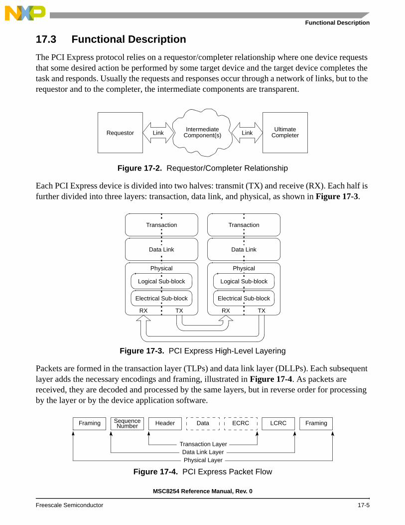
Functional Description
17.3 Functional Description
The PCI Express protocol relies on a requestor/completer relationship where one device requests that some desired action be performed by some target device and the target device completes the task and responds. Usually the requests and responses occur through a network of links, but to the requestor and to the completer, the intermediate components are transparent.
Figure 17-2. Requestor/Completer Relationship
Each PCI Express device is divided into two halves: transmit (TX) and receive (RX). Each half is further divided into three layers: transaction, data link, and physical, as shown in Figure 17-3.
Figure 17-3. PCI Express High-Level Layering
Packets are formed in the transaction layer (TLPs) and data link layer (DLLPs). Each subsequent layer adds the necessary encodings and framing, illustrated in Figure 17-4. As packets are received, they are decoded and processed by the same layers, but in reverse order for processing by the layer or by the device application software.
Figure 17-4. PCI Express Packet Flow
RequestorIntermediate
Component(s)LinkUltimate
CompleterLink
RX TX RX TX
Transaction Transaction
Data Link Data Link
Physical Physical
Logical Sub-block Logical Sub-block
Electrical Sub-block Electrical Sub-block
Framing FramingHeader Data ECRC LCRCSequenceNumber
Transaction LayerData Link LayerPhysical Layer
MSC8254 Reference Manual, Rev. 0
Freescale Semiconductor 17-5

PCI Express Controller
17.3.1 Modes of Operation
The PCI Express controller can function as either a root complex (RC) or an endpoint (EP) on the PCI Express link. The mode and port width are selected by reset configuration signals (see Chapter 5, Reset for details.
17.3.2 PCI Express Transactions
Table 17-1 lists the transactions that the PCI Express controller supports as an initiator and a target.
Table 17-1. PCI Express Transactions
PCI ExpressTransaction
Supported asan Initiator
Supported asa Target
Definition
Mrd Yes Yes Memory Read Request
MRdLk No No Memory Read Lock. As a target, CplLk with UR status is returned.
MWr Yes Yes Memory Write Request to memory-mapped PCI-Express space
IORd Yes (RC only) No I/O Read request. As a target, Cpl with UR status is returned
IOWr Yes (RC only) No I/O Write Request. As a target, Cpl with UR status is returned
CfgRd0 Yes (RC only Yes Configuration Read Type 0
CfgWr0 Yes (RC only) Yes Configuration Write Type 0
CfgRd1 Yes (RC only) No Configuration Read Type 1. As a target, Cpl with UR status is returned.
CfgWr1 Yes (RC only) No Configuration Write Type 1. As a target, Cpl with UR status is returned.
Msg Yes Yes Message Request
MsgD Yes (RC only) Yes (EP only) Message Request with Data payload. Note that Set_Slot_Power_Limit is the only message with data that is supported and then only when the controller is an initiator and in RC mode or a target and in EP mode.
Cpl Yes Yes Completion without Data
CplD Yes Yes Completion with Data
CplLk No Yes Completion for Locked Memory Read without Data. The only time that CplLk is returned with UR status is when the controller receives a MRdLk command.
CplDLk No No Completion for Locked Memory Read with Data
MSC8254 Reference Manual, Rev. 0
17-6 Freescale Semiconductor

Functional Description
17.3.2.1 Byte Ordering
Whenever data must cross a bridge between two buses, the byte ordering of data on the source and destination buses must be considered. The internal platform bus of this device is inherently big endian and the PCI Express bus interface is inherently little endian.
There are two methods to handle ordering of data as it crosses a bridge—address invariance and data invariance. Address invariance preserves the addressing of bytes within a scalar data element, but not the relative significance of the bytes within that scalar. Conversely, data invariance preserves the relative significance of bytes within a scalar, but not the addressing of the individual bytes that make up a scalar.
This device uses address invariance as its byte ordering policy.
As stated above, address invariance preserves the byte address of each byte on an I/O interface as it is placed in memory or moved into a register. This policy can have the effect of reversing the significance order of bytes (most significant to least significant and vice versa), but it has the benefit of preserving the format of general data structures. Provided that software is aware of the endianness and format of the data structure, it can correctly interpret the data on either side of the bridge.
Figure 17-5 shows the transfer of a 4-byte scalar, 0x4142_4344, from a big endian source across an address invariant bridge to a little endian destination.
Note: Although the significance of the bytes within the scalar has changed, the address of the individual bytes that make up the scalar has not changed. As long as software is aware that the source of the data used a big endian format, the data can be interpreted correctly.
Figure 17-6 shows data flowing the other way, from a little endian source to a big endian destination.
Big endian source bus
Little endian destination bus
Byte lane 0 1 2 3 3 2 1 0
Address lsbs 000 001 010 011 011 010 001 000
Data 41 42 43 44 š 44 43 42 41
Significance MSB LSB MSB LSB
Figure 17-5. Address Invariant Byte Ordering—4 bytes Outbound
MSC8254 Reference Manual, Rev. 0
Freescale Semiconductor 17-7

PCI Express Controller
Figure 17-7 shows an outbound transfer of an 8-byte scalar, 0x5455_1617_CDCE_2728, using address invariance.
Figure 17-8 shows an inbound transfer of a 2-byte scalar, 0x5837, using address invariance.
Note: In all of these examples, the original addresses of the individual bytes within the scalars (as created by the source) are preserved.
Little endian source bus
Big endian destination bus
Byte lane 3 2 1 0 0 1 2 3
Address lsbs 011 010 001 000 000 001 010 011
Data 41 42 43 44 š 44 43 42 41
Significance MSB LSB MSB LSB
Figure 17-6. Address Invariant Byte Ordering—4 bytes Inbound
Big endian source bus Little endian destination bus
Byte lane 0 1 2 3 4 5 6 7 7 6 5 4 3 2 1 0
Address lsbs 000 001 010 011 100 101 110 111 111 110 101 100 011 010 001 000
Data 54 55 16 17 CD CE 27 28 š 28 27 CE CD 17 16 55 54
Significance MSB
LSB MSB
LSB
Figure 17-7. Address Invariant Byte Ordering—8 bytes Outbound
Little endian source bus
Big endian destination bus
Byte lane 3 2 1 0 0 1 2 3
Address lsbs 011 010 001 000 000 001 010 011
Data — — 58 37 š 37 58 — —
Significance MSB LSB MSB LSB
Figure 17-8. Address Invariant Byte Ordering—2 bytes Inbound
MSC8254 Reference Manual, Rev. 0
17-8 Freescale Semiconductor
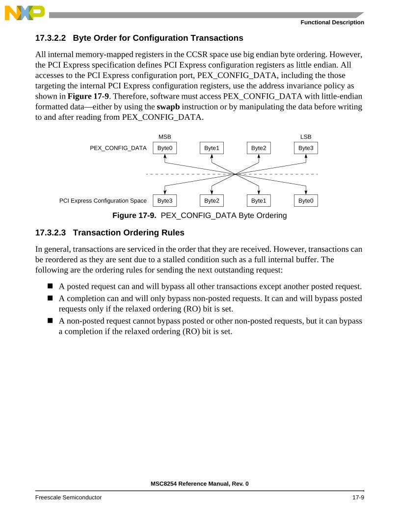
Functional Description
17.3.2.2 Byte Order for Configuration Transactions
All internal memory-mapped registers in the CCSR space use big endian byte ordering. However, the PCI Express specification defines PCI Express configuration registers as little endian. All accesses to the PCI Express configuration port, PEX_CONFIG_DATA, including the those targeting the internal PCI Express configuration registers, use the address invariance policy as shown in Figure 17-9. Therefore, software must access PEX_CONFIG_DATA with little-endian formatted data—either by using the swapb instruction or by manipulating the data before writing to and after reading from PEX_CONFIG_DATA.
Figure 17-9. PEX_CONFIG_DATA Byte Ordering
17.3.2.3 Transaction Ordering Rules
In general, transactions are serviced in the order that they are received. However, transactions can be reordered as they are sent due to a stalled condition such as a full internal buffer. The following are the ordering rules for sending the next outstanding request:
A posted request can and will bypass all other transactions except another posted request.
A completion can and will only bypass non-posted requests. It can and will bypass posted requests only if the relaxed ordering (RO) bit is set.
A non-posted request cannot bypass posted or other non-posted requests, but it can bypass a completion if the relaxed ordering (RO) bit is set.
PEX_CONFIG_DATA
MSB LSB
Byte0 Byte1 Byte2 Byte3
PCI Express Configuration Space Byte3 Byte2 Byte1 Byte0
MSC8254 Reference Manual, Rev. 0
Freescale Semiconductor 17-9

PCI Express Controller
17.3.2.4 Memory Space Addressing
A PCI Express memory transaction can address a 32- or 64-bit memory space. Table 17-2 describes the Fmt and Type field contents in the PCI Express TLP header for memory transactions.
As an initiator, the controller is capable of sending 32- or 64-bit memory packets. Any transaction from the internal platform that (after passing through the translation mechanism) has a translated address greater than 4G is sent as a 64-bit memory packet. Otherwise, a 32-bit memory packet is sent. As a target device, the controller is capable of decoding 32- or 64-bit memory packets. This is done through two 32-bit inbound windows and two 64-bit inbound windows. All inbound addresses are translated to 36-bit internal platform addresses.
17.3.2.5 I/O Space Addressing
The controller does not support I/O transactions as a target. As an initiator, the controller can send I/O transactions in RC mode only by programming one of the outbound translation window attributes to send I/O transactions. All I/O transactions only access 32-bit address I/O space. Table 17-3 describes the Fmt and Type field contents in the PCI Express TLP header for I/O transactions.
Table 17-2. TLP Header Type and Format Field Definitions for Memory Transactions
Request Fmt[1–0] Type[4–0]
Mem read (32-bit) 00 00000
Mem read (64-bit) 01 00000
Mem write (32-bit) 10 00000
Mem write (64-bit) 11 00000
Table 17-3. TLP Header Type and Format Field Definitions for I/O Transactions
Request Fmt[1–0] Type[4–0]
I/O read (32-bit) 00 00010
I/O write (32-bit) 10 00010
MSC8254 Reference Manual, Rev. 0
17-10 Freescale Semiconductor

Functional Description
17.3.2.6 Configuration Space Addressing
As an initiator, the controller supports both type 0 and type 1 configuration cycles when configured in RC mode. There are two methods of generating a configuration transaction; refer to Section 17.4.1.6, PCI Express Configuration Space Access, on page 17-65, for more information. A configuration transaction can hit into the controller internal configuration space, it can be sent out on the PCI Express link, or it can be internally terminated. Table 17-4 describes the Fmt and Type field contents in the PCI Express TLP header for configuration transactions.
Note that all configuration transactions sent on PCI Express require a response regardless whether they are read or a write configuration transactions. The controller does not generate configuration transactions in EP mode. Only inbound configuration transactions are supported in EP mode.
17.3.2.7 Serialization of Configuration and I/O Writes
Configuration and I/O writes originating from the PCI Express outbound ATMUs are serialized by the controller. The logic after issuing a configuration write or IO write will not issue any new transactions until the outstanding configuration or I/O write is finished. This means that an acknowledgement packet from the link partner in the form of a CpL TLP packet must be seen or the transaction has timed out. If the CpL packet contains a CRS status, then the logic will re-issue the configuration write transaction. It will keep retrying the request until either a status other than CRS is returned or the transaction times out. Note that configuration writes originating from the PCI Express configuration access registers (PEX_CONFIG_ADDR/PEX_CONFIG_DATA) are not serialized.
Note: It is possible for outbound configuration read request to be requeued and be placed at the end of the request queue due to CRS condition.
17.3.3 Messages
Software message generation is supported in both RC and EP modes.
Table 17-4. TLP Header Type and Format Field Definitions for Configuration Transactions
Request Fmt[1–0] Type[4–0]
Config Type 0 read 00 00100
Config Type 0 write 10 00100
Config Type 1 read 00 00101
Config Type 1 write 10 00101
MSC8254 Reference Manual, Rev. 0
Freescale Semiconductor 17-11

PCI Express Controller
17.3.3.1 Outbound ATMU Message Generation
Software can choose to send a message by programming PEXOWARn[WTT] = 0x5. A message is sent by writing a 4-byte transaction in big-endian format that hits in an outbound window configured to send messages. Part of the 4-byte data is used to store information such as message code and routing information. Table 17-5 describes the message data format.
In addition to the outbound ATMU, the PEX PM Command register also provides the capability to send PME_Turn_Off message or PM_PME message by setting bits 31 or 29. See Section 17.4.1.2.4, PCI Express Power Management Command Register (PEX_PMCR), on page 17-36 for more information.
Table 17-6 provides a complete list of supported outbound messages depending on whether RC or EP is configured.
Table 17-5. Internal Platform (OCN) Message Data Format
Bits Name Reset Value Description
0–15 — — Reserved
16–18 Routing x Routing mechanism. Contains the message’s routing information19–23 — — Reserved24–31 Code x Message code. Contains the actual message type to be sent.
Table 17-6. PCI Express ATMU Outbound Messages
Name Code[7–0] Routing[2–0] RC EP Description
PM_Active_State_Nak 0001 0100 100 Yes N/A Terminate at receiverPM_PME 0001 1000 000 N/A Yes Sent Upstream by PME-requesting
componentPME_Turn_Off 0001 1001 011 Yes N/A Broadcast DownstreamPM_TO_Ack 0001 1011 101 N/A Yes Sent Upstream by Endpoint
ERR_COR 0011 0000 000 N/A Yes Sent by component when it detects a correctable error
ERR_NONFATAL 0011 0001 000 N/A Yes Sent by component when it detects a Non-fatal, uncorrectable error
ERR_FATAL 0011 0011 000 N/A Yes Sent by component when it detects a Fatal, uncorrectable error
Unlock 0000 0000 000 No N/A Not supportedSet_Slot_Power_Limit 0101 0000 100 Yes N/A Set Slot Power Limit in Upstream PortVendor_Defined Type 0 0111 1110 No No Not supported
Vendor_Defined Type 1 0111 1111 No No Not supportedAttention_Indicator_On 0100 0001 100 Yes N/A Hot-plug messageAttention_Indicator_Blink 0100 0011 100 Yes N/A Hot-plug message
Attention_Indicator_Off 0100 0000 100 Yes N/A Hot-plug messagePower_Indicator_On 0100 0101 100 Yes N/A Hot-plug messagePower_Indicator_Blink 0100 0111 100 Yes N/A Hot-plug message
Power_Indicator_Off 0100 0100 100 Yes N/A Hot-plug messageAttention_Button_Pressed 0100 1000 100 Yes N/A Hot-plug message
MSC8254 Reference Manual, Rev. 0
17-12 Freescale Semiconductor

Functional Description
17.3.3.2 Inbound Messages
Table 17-7 provides a complete list of supported inbound messages in RC mode.
Table 17-8 provides a complete list of supported inbound messages in EP mode.
Table 17-7. PCI Express RC Inbound Message Handling
Name Code[7–0] Routing[2–0] Action
Assert_INTA 0010 0000 100 Send to interrupt controller
Assert_INTB 0010 0001 100 Send to interrupt controllerAssert_INTC 0010 0010 100 Send to interrupt controllerAssert_INTD 0010 0011 100 Send to interrupt controller
Deassert_INTA 0010 0100 100 Send to interrupt controllerDeassert_INTB 0010 0101 100 Send to interrupt controllerDeassert_INTC 0010 0110 100 Send to interrupt controller
Deassert_INTD 0010 0111 100 Send to interrupt controllerPM_Active_State_Nak 0001 0100 100 No action takenPM_PME 0001 1000 000 Generate interrupt to interrupt controller if enabled
PME_Turn_Off 0001 1001 011 No action takenPME_TO_Ack 0001 1011 101 Set PEX_PME_MES_DR[ENL23] bit and generate
interrupt to interrupt controller if enabledERR_COR 0011 0000 000 Generate interrupt to interrupt controller if enabledERR_NONFATAL 0011 0001 000 Generate interrupt to interrupt controller if enabled
ERR_FATAL 0011 0011 000 Generate interrupt to interrupt controller if enabledUnlock 0000 0000 000 No action takenSet_Slot_Power_Limit 0101 0000 100 No action taken
Vendor_Defined Type 0 0111 1110 — No action takenVendor_Defined Type 1 0111 1111 — No action takenAttention_Indicator_On 0100 0001 100 No action taken
Attention_Indicator_Blink 0100 0011 100 No action takenAttention_Indicator_Off 0100 0000 100 No action takenPower_Indicator_On 0100 0101 100 No action taken
Power_Indicator_Blink 0100 0111 100 No action takenPower_Indicator_Off 0100 0100 100 No action takenAttention_Button_Pressed 0100 1000 100 Set PEX_PME_MES_DR[ABP] bit and send interrupt if
enabled.
Table 17-8. PCI Express EP Inbound Message Handling
Name Code[7–0] Routing[2–0] Action
Assert_INTA 0010 0000 100 No action takenAssert_INTB 0010 0001 100 No action takenAssert_INTC 0010 0010 100 No action taken
Assert_INTD 0010 0011 100 No action takenDeassert_INTA 0010 0100 100 No action takenDeassert_INTB 0010 0101 100 No action taken
Deassert_INTC 0010 0110 100 No action takenDeassert_INTD 0010 0111 100 No action takenPM_Active_State_Nak 0001 0100 100 No action taken
PM_PME 0001 1000 000 No action taken
MSC8254 Reference Manual, Rev. 0
Freescale Semiconductor 17-13

PCI Express Controller
PME_Turn_Off 0001 1001 011 Set PEX_PME_MES_DR[PTO] bit. Send interrupt if enabled.
PM_TO_Ack 0001 1011 101 No action takenERR_COR 0011 0000 000 No action taken
ERR_NONFATAL 0011 0001 000 No action takenERR_FATAL 0011 0011 000 No action takenUnlock 0000 0000 000 No action taken
Set_Slot_Power_Limit 0101 0000 100 Update power value in PCI Express device capability register in configuration space.
Vendor_Defined Type 0 0111 1110 — No action takenVendor_Defined Type 1 0111 1111 — No action takenAttention_Indicator_On 0100 0001 100 Set PEX_PME_MES_DR[AION] bit. Send interrupt if
enabled.Attention_Indicator_Blink 0100 0011 100 Set PEX_PME_MES_DR[AIB] bit. Send interrupt if
enabled.Attention_Indicator_Off 0100 0000 100 Set PEX_PME_MES_DR[AIOF] bit. Send interrupt if
enabled.Power_Indicator_On 0100 0101 100 Set PEX_PME_MES_DR[PION] bit. Send interrupt if
enabled.Power_Indicator_Blink 0100 0111 100 Set PEX_PME_MES_DR[PIB] bit. Send interrupt if
enabled.Power_Indicator_Off 0100 0100 100 Set PEX_PME_MES_DR[PIOF] bit. Send interrupt if
enabled.Attention_Button_Pressed 0100 1000 100 No action taken
Table 17-8. PCI Express EP Inbound Message Handling (Continued)
Name Code[7–0] Routing[2–0] Action
MSC8254 Reference Manual, Rev. 0
17-14 Freescale Semiconductor

Functional Description
17.3.4 Error Handling
The PCI Express specification classifies errors as correctable and uncorrectable. Correctable errors result in degraded performance, but uncorrectable errors generally result in functional failures. As shown in Figure 17-10 uncorrectable errors can further be classified as fatal or non-fatal.
Figure 17-10. PCI Express Error Classification
17.3.4.1 PCI Express Error Logging and Signaling
Figure 17-11 shows the PCI Express-defined sequence of operations related to signaling and logging of errors detected by a device. Note that the PCI Express controller on this device supports the advanced error handling capabilities shown within the dotted lines.
Physical
Data Link Transaction
Correctable Errors
ERR_COR
Physical
Transaction
Uncorrectable Errors
ERR_NONFATAL
Data Link
ERR_FATAL
Fatal
MSC8254 Reference Manual, Rev. 0
Freescale Semiconductor 17-15

PCI Express Controller
Figure 17-11. PCI Express Device Error Signaling Flowchart
If First Error Pointer not valid,update First Error Pointerand Header Log Registers
Set corresponding bit inUncorrectable Error
Status Register
Masked inUncorrectable
Error MaskRegister
?
Set Fatal/Non_FatalError Detected bit in
Device Status Register
Adjust severity accordingto Uncorrectable Error
Severity Register
UncorrectableError Reporting Enabled
in Device ControlRegister
?
Is severity Fatal?
Send ERR_NONFATALMessage (See Note)
Send ERR_FATALMessage (See Note)
End
End
End
Send ERR_CORMessage (See Note)
CorrectableError Reporting Enabled
in Device ControlRegister
?
Masked inCorrectableError Mask
Register?
End
Set corresponding bit inCorrectable ErrorStatus Register
Set CorrectableError Detected bit in
Device Status Register
End
End
Correctable?
Error Detected
NOTE: If error is detected by theRoot Port, the error message is notactually sent, but is processedinternally by the Root Port (i.e. raising interrupt).
End
YesNo
Yes
No
Yes
No
Yes
No
Yes
No
No
Yes
Advanced ErrorHandling Only
MSC8254 Reference Manual, Rev. 0
17-16 Freescale Semiconductor

Functional Description
17.3.4.2 PCI Express Controller Internal Interrupt Sources
Table 17-9 describes the sources of the PCI Express controller internal interrupt to the EPIC and the preconditions for signaling the interrupt.
Table 17-9. PCI Express Internal Controller Interrupt Sources
Status Register Bit Preconditions
Any bit in PEX_PME_MES_DR set The corresponding interrupt enable bits must be set in PEX_PME_MES_IER
Any bit in PEX_ERR_DR set The corresponding interrupt enable bits must be set in PEX_ERR_EN.PCI Express Root Status Register[16] (PME status) is set
PCI Express Root Control Register [3] (PME interrupt enable) is set
PCI Express Root Error Status Register[6] (fatal error messages received) is set
PCI Express Root Error Command Register [2] (fatal error reporting enable) is set orPCI Express Root Control Register [2] (system error on fatal error enable) is set
PCI Express Root Error Status Register [5] (non-fatal error messages received) is set
PCI Express Root Error Command Register [1] (non-fatal error reporting enable) is set or PCI Express Root Control Register [1] (system error on non-fatal error enable) is set
PCI Express Root Error Status Register[0] (correctable error messages received) is set
PCI Express Root Error Command Register[0] (correctable error reporting enable) is setor PCI Express Root Control Register[0] (system error on correctable error enable) is set.
Any correctable error status bit in PCI Express Correctable Error Status Register is set
The corresponding error mask bit in PCI Express Correctable Error Mask Register is clear and PCI Express Root Error Command Register[0] (correctable error reporting enable) is set
Any fatal uncorrectable error status bit in PCI Express Uncorrectable Error Status Register is set. (The corresponding error is classified as fatal based on the severity setting in PCI Express Uncorrectable Error Severity Register.)
The corresponding error mask bit in PCI Express Uncorrectable Error Mask Register is clear and either PCI Express Device Control Register[2] (fatal error reporting) is set or PCI Express Command Register[8] (SERR) is set.
Any non-fatal uncorrectable error status bit in PCI Express Uncorrectable Error Status Register is set. (The corresponding error is classified as non-fatal based on the severity setting in PCI Express Uncorrectable Error Severity Register.)
The corresponding error mask bit in PCI Express Uncorrectable Error Mask Register is clear and either PCI Express Device Control Register[1] (non-fatal error reporting) is set or PCI Express Command Register[8] (SERR) is set.
PCI Express Secondary Status Register[8] (master data parity error) is set.
PCI Express Secondary Status Interrupt Mask Register[0] (mask master data parity error) is cleared and PCI Express Command Register[6] (parity error response) is set.
PCI Express Secondary Status Register[11] (signaled target abort) is set
PCI Express Secondary Status Interrupt Mask Register[1] (mask signaled target abort) is cleared.
PCI Express Secondary Status Register[12] (received target abort) is set
PCI Express Secondary Status Interrupt Mask Register[2] (mask received target abort) is cleared.
PCI Express Secondary Status Register[13] (received master abort) is set
PCI Express Secondary Status Interrupt Mask Register[3] (mask received master abort) is cleared.
PCI Express Secondary Status Register[14] (signaled system error) is set.
PCI Express Secondary Status Interrupt Mask Register[4] (mask signaled system error) is cleared.
PCI Express Secondary Status Register[15] (detected parity error) is set
PCI Express Secondary Status Interrupt Mask Register[5] (mask detected parity error) is cleared.
MSC8254 Reference Manual, Rev. 0
Freescale Semiconductor 17-17

PCI Express Controller
17.3.4.3 Error Conditions
Table 17-10 describes specific error types and the action taken for various transaction types.
PCI Express Slot Status Register[0] (attention button pressed) is set
PCI Express Slot Control Register[0] (attention button pressed enable) is set and PCI Express Slot Control Register[5] (hot plug interrupt enable) is set and either PCI Express PM Control Register[1–0] = 00 (the function power state is D0) or PCI Express PM Control Register[8] (PME enable) is set.
PCI Express Slot Status Register[1] (power fault detected) is set
PCI Express Slot Control Register[1] (power fault detected enable) is set and PCI Express Slot Control Register[5] (hot plug interrupt enable) is set and either PCI Express PM Control Register[1–0] = 00 (the function power state is D0) or PCI Express PM Control Register[8] (PME enable) is set.
PCI Express Slot Status Register[2] (MRL sensor changed) is set
PCI Express Slot Control Register[2] (MRL sensor changed enable) is set and PCI Express Slot Control Register[5] (hot plug interrupt enable) is set and either PCI Express PM Control Register[1–0] = 00 (the function power state is D0) or PCI Express PM Control Register[8] (PME enable) is set.
PCI Express Slot Status Register[3] (presence detect changed) is set
PCI Express Slot Control Register[3] (presence detect changed enable) is set and PCI Express Slot Control Register[5] (hot plug interrupt enable) is set and either PCI Express PM Control Register[1–0] = 00 (the function power state is D0) or PCI Express PM Control Register[8] (PME enable) is set.
PCI Express Slot Status Register[4] (command completed) is set
PCI Express Slot Control Register[4] (command completed interrupt enable) is set and PCI Express Slot Control Register[5] (hot plug interrupt enable) is set.
Table 17-10. Error Conditions
Transaction Type
Error Type Action
Inbound response
PEX response time out. This case happens when the internal platform sends a non-posted request that did not get a response back after a specific amount of time specified in the outbound completion timeout register (PEX_OTB_CPL_TOR)
Log error (PEX_ERR_DR[PCT]) and send interrupt to PIC, if enabled.
Inbound response
Unexpected PEX response. This can happen if, after the response times out and the internal queue entry is deallocated, the response comes back.
Log unexpected completion error (PCI Express Uncorrectable Status Register[16]) and send interrupt to PIC, if enabled.
Table 17-9. PCI Express Internal Controller Interrupt Sources (Continued)
Status Register Bit Preconditions
MSC8254 Reference Manual, Rev. 0
17-18 Freescale Semiconductor

Functional Description
Inbound response
Unsupported request (UR) response status
Depending upon whether the initial internal request was broken up, the error is not sent until all responses come back for all portions of the internal request. Log the error (PEX_ERR_DR[CDNSC] and PCI Express Uncorrectable Status Register[20]) and send interrupt to PIC, if enabled.
Inbound response
Completer abort (CA) response status
Depending upon whether the initial internal request was broken up, the error is not sent until all responses come back for all portions of the internal request. Log the error (PEX_ERR_DR[PCAC, CDNSC] and PCI Express Uncorrectable Status Register[15] and send interrupt to PIC, if enabled.
Inbound response
Poisoned TLP (EP=1) Depending upon whether the initial internal request was broken up, the error is not sent until all responses come back for all portions of the internal request. Log the error (PCI Express Uncorrectable Status Register[12]) and send interrupt to PIC, if enabled.
Inbound response
ECRC error Depending upon whether the initial internal request was broken up, the error is not sent until all responses come back for all portions of the internal request. Log the error (PCI Express Uncorrectable Status Register[19]) and send interrupt to PIC, if enabled.
Inbound response
Configuration Request Retry Status (CRS) timeout for a configuration transaction that originates from PEX_CONFIG_ADDR/PEX_CONFIG_DATA
1.The controller always retries the transaction as soon as possible until a status other than CRS is returned. However, if a CRS status is returned after the configuration retry timeout (PEXCONF_RTY_TOR) timer expires, then the controller aborts the transaction and sends all 1s (0xFFFF_FFFF) data back to requester. 2. Log the error (PEX_ERR_DR[PCT]) and send interrupt to the PIC, if enabled.
Inbound response
UR response for configuration transaction that originates from PEX_CONFIG_ADDR/PEX_CONFIG_DATA
1. Send back all 1s (0xFFFF_FFFF) data.2. Log the error (PEX_ERR_DR[CDNSC] and PCI Express Uncorrectable Status Register[20]) and send interrupt to PIC, if enabled.
Inbound response
CA response for Configuration transaction that originates from PEX_CONFIG_ADDR/PEX_CONFIG_DATA
1. Send back all 1s (0xFFFF_FFFF) data.2. Log the error (PEX_ERR_DR[PCAC, CDNSC] and PCI Express Uncorrectable Status Register[15]) and send interrupt to PIC, if enabled.
Inbound response
Poisoned TLP (EP=1) response for Configuration transaction that originates from PEX_CONFIG_ADDR/PEX_CONFIG_DATA
1. Send back all 1s (0xFFFF_FFFF) data.2. Log the error (PCI Express Uncorrectable Status Register[12]) and send interrupt to PIC, if enabled.
Inbound response
ECRC error response for Configuration transaction that originates from PEX_CONFIG_ADDR/PEX_CONFIG_DATA
1. Send back all 1s (0xFFFF_FFFF) data.2. Log the error (PCI Express Uncorrectable Status Register[19]) and send interrupt to PIC, if enabled.
Inbound response
Configuration Request Retry Status (CRS) response for Configuration transaction that originates from ATMU
1.The controller always retries the transaction as soon as possible until a status other than CRS is returned. However, if a CRS status is returned after the configuration retry timeout (PEXCONF_RTY_TOR) timer expires, then the controller aborts the transaction. 2. Log the error (PEX_ERR_DR[CRST]) and send interrupt to the PIC, if enabled.
Table 17-10. Error Conditions (Continued)
Transaction Type
Error Type Action
MSC8254 Reference Manual, Rev. 0
Freescale Semiconductor 17-19

PCI Express Controller
Inbound response
UR response for Configuration transaction that originates from ATMU
Log the error (PEX_ERR_DR[CDNSC] and PCI Express Uncorrectable Status Register[20]) and send interrupt to PIC, if enabled.
Inbound response
CA response for Configuration transaction that originates from ATMU
Log the error (PEX_ERR_DR[PCAC, CDNSC] and PCI Express Uncorrectable Status Register[15]) and send interrupt to PIC, if enabled.
Inbound response
Malformed TLP response PCI Express controller does not pass the response back to the core. Therefore, a completion timeout error eventually occurs.
Inbound request
Poisoned TLP (EP=1) 1. If it is a posted transaction, the controller drops it. 2. If it is a non-posted transaction, the controller returns a completion with UR status.3. Release the proper credits
Inbound request
ECRC error 1. If it is a posted transaction, the controller drops it. 2. If it is a non-posted transaction, the controller returns a completion with UR status.3. Release the proper credits
Inbound request
PCI Express nullified request The packet is dropped.
Outbound request
Outbound ATMU crossing Log the error (PEX_ERR_DR[OAC]). The transaction is not sent out on the link.
Outbound request
Illegal message size Log the error (PEX_ERR_DR[MIS]). The transaction is not sent out on the link.
Outbound request
Illegal I/O size Log the error (PEX_ERR_DR[IOIS]). The transaction is not sent out on the link.
Outbound request
Illegal I/O address Log the error (PEX_ERR_DR[IOIA]). The transaction is not sent out on the link.
Outbound request
Illegal configuration size Log the error (PEX_ERR_DR[CIS]). The transaction is not sent out on the link.
Outbound request
Internal platform memory write/read requests that do not hit either Memory Base/Limit or Pref Memory Base/Limit register.
Log the error in error detect register. The controller will drop the transaction.
Outbound request
Internal platform I/O write/read requests that do not hit either Memory Base/Limit or Pref Memory Base/Limit register.
Log the error in error detect register. The controller will drop the transaction.
Outbound response
Internal platform response with error (for example, an ECC error on a DDR read or the transaction maps to unknown address space).
Send poisoned TLP (EP=1) completion(s) for data that are known bad. If the response is the final response, then deallocate resource. If the response is not the final response, wait for all responses to come back before deallocate resource.If the poison data happens in the middle of the packet, the rest of the response packet(s) is also poisoned.
Link speed change request
1. Auto request with Auto speed disable bit set or2. Link partner incapable of 5.0 Gb/s and request speed is 5.0 Gb/s
Clear link speed request and set interrupt in PME Message Detect register. Additionally, log error in link speed status register.
Link width change request
1. Auto request with Auto width disable bit set or2. Upconfiguration not capable and request was to size-up the width or3. Not enough detected lanes for a given request
Clear link width request and set interrupt in PME Message Detect register. Additionally, log error in link width status register.
Table 17-10. Error Conditions (Continued)
Transaction Type
Error Type Action
MSC8254 Reference Manual, Rev. 0
17-20 Freescale Semiconductor

Functional Description
17.3.5 Interrupts
Handling of INTx and message signaled interrupts (MSI) depends on whether the PCI Express controller is configured as an RC or EP device. As an RC device, the PCI Express controller responds to interrupts from the system. As a CP device, the controller can generate interrupt signals. Table 17-11 and Table 17-12 summarize the interrupt functionality for CP and RC devices, respectively.
Link speed change request
1. Auto request with Auto speed disable bit set or2. Link partner incapable of 5.0 Gb/s and request speed is 5.0 Gb/s
Clear link speed request and set interrupt in PME Message Detect register. Additionally, log error in link speed status register.
Link width change request
1. Auto request with Auto width disable bit set or2. Upconfiguration not capable and request was to size-up the width or3. Not enough detected lanes for a given request
Clear link width request and set interrupt in PME Message Detect register. Additionally, log error in link width status register.
Table 17-11. EP Device INTx and MSI Handling
Interrupt Action
EP Device
INTx Message Generation• Hardware Not supported.
• Software Not supported.MSI Generation• Hardware: When configured to handle this operation, the PCI Express controller can generate MSI transactions
automatically to the RC. The PCI Express controller uses the GCR5[PEX_IRQ_OUT] bit (see Chapter 8, General Configuration Registers for details). to trigger the generation of the MSI. The remote RC must set up the MSI capability structure for all endpoints during system initialization by writing the appropriate values to the Message Address and Message Data registers and setting the MSIE bit in the MSI Message Control register. When configured properly, the PCI Express controller detects when the GCR5[PEX_IRQQ_OUT] bit sets (= 1) and generates a PCI Express memory write transaction to the address specified in the MSI Message Address register (and MSI Message Upper Address register) with a data payload as specified in the MSI Message Data register (with leading zeros appended).
• Software The core must set up the MSI capability registers to enable MSI mode, and write the correct values to the MSI address and data register. Then, local software must read the MSI address in the MSI capability register and configure the outbound ATMU window to map the translated address to the MSI address (see Chapter 8, General Configuration Registers for details on programming the ATMU window). Software must determine the number of allocated messages in the MSI capability register and allocate the appropriate data values to use. A write to the ATMU window containing the MSI address with the appropriate data value generates the desired MSI transaction to the remote RC.
Table 17-10. Error Conditions (Continued)
Transaction Type
Error Type Action
MSC8254 Reference Manual, Rev. 0
Freescale Semiconductor 17-21

PCI Express Controller
17.3.6 Initial Credit Advertisement
To prevent overflowing of the receiver buffers and for ordering-compliance purposes, the transmitter cannot send transactions unless it has enough flow control (FC) credits to send. Each device maintains an FC credit pool. The FC information is conveyed between the two link partners by DLLPs during link training (initial credit advertisement). The transaction layer performs the FC accounting functions. One FC unit is four DWs (16-bytes) of data.
17.3.7 Power Management
All device power states are supported with the exception of D3cold with Vaux. In addition, all link power states are supported with the exception of L2 states. Only L0s ASPM mode is supported if enabled by configuring the Link Control register’s bits 1–0 in configuration space. Note that there is no power saving in the controller when the device is put into a non-D0 state. The only power saving is the I/O drivers when the controller is put into a non-L0 link state.
Table 17-12. RC Device INTx and MSI Handling
Interrupt Action
RC Device
INTx Message MSIs are the preferred interrupt signaling mechanism for PCI Express. However, in RC mode, the PCI Express controller supports the INTx virtual-wire interrupt signaling mechanism (as described in the PCI Express specification). Whenever the controller receives an inbound INTx (INTA, INTB, INTC, or INTD) asserted or deasserted message, it asserts or deasserts an equivalent internal INTx signal (inta, intb, intc, or intd) to the EPIC in each core. If a PCI Express INTx interrupt is used, then the EPIC must be configured so that these interrupts are level-sensitive (see Chapter 13, Interrupt Handling).
MSI An inbound MSI should be handled by using one of the virtual interrupts or virtual NMIs (see Chapter 13, Interrupt Handling).Note: It is the responsibility of the host software to configure the EP MSI capability registers such that an
MSI cycle generated from the EP device generates an appropriate interrupt to the DSP cores.
Table 17-13. Initial credit advertisement
Credit Type Initial Credit Advertisement
PH (Memory Write, Message Write) 4
PD (Memory Write, Message Write) (256/16) x 4 = 64
NPH (Memory Read, IO Read, Cfg Read, Cfg Write) 8
NPD (IO Write, Cfg Write) 2
CPLH (Memory Read Completion, IO R/W Completion, Cfg R/W Completion) Infinite
CPLD (Memory Read Completion, IO Read Completion, Cfg Read Completion) Infinite
MSC8254 Reference Manual, Rev. 0
17-22 Freescale Semiconductor

Functional Description
17.3.8 L2/L3 Ready Link State
The L2/L3 Ready link state is entered after the EP device is put into a D3hot state followed by a PME_Turn_Off/PME_TO_Ack message handshake protocol. Exiting this state requires a POR reset or a WAKE signal from the EP device. The PCI Express controller (in EP mode) does not support the generation of beacon; therefore, the device can use one of the GPIO signals as an enable to an external tristate buffer to generate a WAKE signal, shown in Figure 17-12.
Figure 17-12. WAKE Generation Example
In RC mode, the WAKE signal from the EP device can be connected to one of the external interrupt inputs to service the WAKE request.
17.3.9 Hot Reset
When a hot reset condition occurs, the controller (in both RC and EP mode) initiates a clean-up of all outstanding transactions and returns to an idle state. All non-sticky configuration register bits are cleared. Link training then occurs. The device can generate a hot reset condition on the bus when it is configured as an RC device by setting the “Secondary Bus Reset” bit in the Bridge
Table 17-14. Power Management State Supported
Component D-State
Permissible Interconnect
StateAction
D0 L0, L0s In full operation.D1 L0, L0s, L1 All outbound traffics are stalled. All inbound traffics will be thrown away. The only
exceptions are PME messages and configuration transactions. If the device is in RC mode, it is permissible to send a PM_Turn_Off message via the PEX Power Management Command register.
D2 L0, L0s, L1 All outbound traffics are stalled. All inbound traffics will be thrown away. The only exceptions are PME messages and configuration transactions. If the device is in RC mode, it is permissible to send a PM_Turn_Off message via the PEX Power Management Command register.
D3hot L0, L0s, L1, L2/L3 Ready
All outbound traffics are stalled. All inbound traffics will be thrown away. The only exceptions are PME messages and configuration transactions. If the device is in RC mode, it is permissible to send a PM_Turn_Off message via the PEX Power Management Command register. Note that if a transition of D3hot->D0 occurs, a reset is performed to the controller’s configuration space. In addition, link training will restart.
D3cold L3 Completely off.
GPIOn
WAKE
PCI Express controller in EP mode
MSC8254 Reference Manual, Rev. 0
Freescale Semiconductor 17-23

PCI Express Controller
Control Register in the configuration space. As an EP device, it cannot generate a hot reset condition; it can only detect a hot reset condition and initiate the appropriate clean-up procedure.
17.3.10 Link Down
Typically, a link down condition occurs after a hot reset event; however, it is possible for the link to go down unexpectedly without a hot reset event. When this occurs, a link down condition is detected (PEX_PME_MSG_DR[LDD]=1). Link down is treated similarly to a hot reset condition.
Subsequently, while the link is down, all new posted outbound transactions are discarded. All new non-posted ATMU transactions are errored out. Non-posted configuration transactions issued using PEX_CONFIG_ADDR/PEX_CONFIG_DATA toward the link returns 0xFFFF_FFFF (all 1s). As soon as the link is up again, the sending of transaction resumes.
Note: In EP mode, a link down condition causes the controller to reset all non-sticky bits in its PCI Express configuration registers as if it had been hot reset.
17.3.11 Initialization/Application Information
In normal boot mode (RCWHR[PRDY] = 0), the DSP cores are expected to boot and configure the device. During this time, the PCI Express interface will retry all inbound PCI Express configuration transactions. When the core has configured the device to a state where it can accept inbound PCI Express configuration transactions, the boot code should set the CFG_READY bit in the PEX_CFG_READY register after which inbound PCI Express configuration transactions are accepted. Refer to Section 17.4.1.9.20, Configuration Ready Register—0x4B0, on page 17-119 for more information about the CFG_READY bit.
In PCI Express ready mode (RCWHR[PRDY] = 1), the PCI Express interface accepts all inbound PCI Express configuration transactions which allows an external host/RC to configure the device with DSP core intervention.
17.4 Programming Model
The PCI Express interface supports the following register types:
Memory-mapped registers—these registers control PCI Express address translation, PCI error management, and PCI Express configuration register access. These registers are described in Section 17.4.1, PCI Express Memory Mapped Registers, on page 17-25, and its subsections.
PCI Express configuration registers contained within the PCI Express configuration space—these registers are specified by the PCI Express specification for every PCI Express device. These registers are described in Section 17.4.1.6, PCI Express Configuration Space Access and its subsections.
MSC8254 Reference Manual, Rev. 0
17-24 Freescale Semiconductor

Programming Model
17.4.1 PCI Express Memory Mapped Registers
The PCI Express memory mapped registers are accessed by reading and writing to an address comprised of the base address (specified by the CCSR on the local side or the PEXCSRBAR on the PCI Express side) plus the block base address, plus the offset of the specific register to be accessed. Note that all memory-mapped registers (except the PCI Express configuration data register, PEX_CONFIG_DATA) must only be accessed as 32-bit quantities.
Table 17-15 lists the memory-mapped registers. In this table and in the register figures and field descriptions, the following access definitions apply:
Reserved fields are always ignored for the purposes of determining access type.
R/W, R, and W (read/write, read only, and write only) indicate that all the non-reserved fields in a register have the same access type.
w1c indicates that all of the non-reserved fields in a register are cleared by writing ones to them.
Mixed indicates a combination of access types.
Special is used when no other category applies. In this case the register figure and field description table should be read carefully.
Table 17-15. PCI Express Memory-Mapped Register Map
Offset Register Access Reset Page
PCI Express Controller Memory-Mapped Registers—Block Base Address 0x0A000 PCI Express Configuration Access Registers
0x000 PEX_CONFIG_ADDR—PCI Express configuration address register R/W 0x0000_0000 page 17-270x004 PEX_CONFIG_DATA—PCI Express configuration data register R/W 0x0000_0000 page 17-280x00C PEX_OTB_CPL_TOR—PCI Express outbound completion timeout
registerR/W 0x0010_FFFF page 17-29
0x010 PEX_CONF_RTY_TOR—PCI Express configuration retry timeout register
R/W 0x0400_FFFF page 17-30
0x014 PEX_CONFIG—PCI Express configuration register R/W 0x0000_0000 page 17-30PCI Express Power Management Event & Message Registers
0x020 PEX_PME_MES_DR—PCI Express PME & message detect register w1c 0x0000_0000 page 17-310x024 PEX_PME_MES_DISR—PCI Express PME & message disable
registerR/W 0x0000_0000 page 17-33
0x028 PEX_PME_MES_IER—PCI Express PME & message interrupt enable register
R/W 0x0000_0000 page 17-34
0x02C PEX_PMCR—PCI Express power management command register R/W 0x0000_0000 page 17-36PCI Express IP Block Revision Registers
0xBF8 IP block revision register 1 (PEX_IP_BLK_REV1) R 0x0208_0101 page 17-410xBFC IP block revision register 2 (PEX_IP_BLK_REV2) R 0x0000_0000 page 17-41
PCI Express ATMU RegistersOutbound Window 0 (Default)
0xC00 PEXOTAR0—PCI Express outbound translation address register 0 (default)
R/W 0x0000_0000 page 17-42
0xC04 PEXOTEAR0—PCI Express outbound translation extended address register 0 (default)
R/W 0x0000_0000 page 17-43
MSC8254 Reference Manual, Rev. 0
Freescale Semiconductor 17-25

PCI Express Controller
0xC10 PEXOWAR0—PCI Express outbound window attributes register 0 (default)
Mixed 0x8004_4023 page 17-45
Outbound Window 10xC20 PEXOTAR1—PCI Express outbound translation address register 1 R/W 0x0000_0000 page 17-420xC24 PEXOTEAR1—PCI Express outbound translation extended address
register 1R/W 0x0000_0000 page 17-43
0xC28 PEXOWBAR1—PCI Express outbound window base address register 1
R/W 0x0000_0000 page 17-44
0xC30 PEXOWAR1—PCI Express outbound window attributes register 1 R/W 0x0004_4023 page 17-45Outbound Window 2
0xC40 PEXOTAR2—PCI Express outbound translation address register 2 R/W 0x0000_0000 page 17-420xC44 PEXOTEAR2—PCI Express outbound translation extended address
register 2R/W 0x0000_0000 page 17-43
0xC48 PEXOWBAR2—PCI Express outbound window base address register 2
R/W 0x0000_0000 page 17-44
0xC50 PEXOWAR2—PCI Express outbound window attributes register 2 R/W 0x0004_4023 page 17-45Outbound Window 3
0xC60 PEXOTAR3—PCI Express outbound translation address register 3 R/W 0x0000_0000 page 17-420xC64 PEXOTEAR3—PCI Express outbound translation extended address
register 3R/W 0x0000_0000 page 17-43
0xC68 PEXOWBAR3—PCI Express outbound window base address register 3
R/W 0x0000_0000 page 17-44
0xC70 PEXOWAR3—PCI Express outbound window attributes register 3 R/W 0x0004_4023 page 17-45Outbound Window 4
0xC80 PEXOTAR4—PCI Express outbound translation address register 4 R/W 0x0000_0000 page 17-420xC84 PEXOTEAR4—PCI Express outbound translation extended address
register 4R/W 0x0000_0000 page 17-43
0xC88 PEXOWBAR4—PCI Express outbound window base address register 4
R/W 0x0000_0000 page 17-44
0xC90 PEXOWAR4—PCI Express outbound window attributes register 4 R/W 0x0004_4023 page 17-45Inbound Window 3
0xDA0 PEXITAR3—PCI Express inbound translation address register 3 R/W 0x0000_0000 page 17-480xDA8 PEXIWBAR3—PCI Express inbound window base address register 3 R/W 0x0000_0000 page 17-490xDAC PEXIWBEAR3—PCI Express inbound window base extended address
register 3R/W 0x0000_0000 page 17-51
0xDB0 PEXIWAR3—PCI Express inbound window attributes register 3 R/W 0x20F4_4023 page 17-52Inbound Window 2
0xDC0 PEXITAR2—PCI Express inbound translation address register 2 R/W 0x0000_0000 page 17-480xDC8 PEXIWBAR2—PCI Express inbound window base address register 2 R/W 0x0000_0000 page 17-490xDCC PEXIWBEAR2—PCI Express inbound window base extended address
register 2R/W 0x0000_0000 page 17-51
0xDD0 PEXIWAR2—PCI Express inbound window attributes register 2 R/W 0x20F4_4023 page 17-52Inbound Window 1
0xDE0 PEXITAR1—PCI Express inbound translation address register 1 R/W 0x0000_0000 page 17-480xDE8 PEXIWBAR1—PCI Express inbound window base address register 1 R/W 0x0000_0000 page 17-490xDF0 PEXIWAR1—PCI Express inbound window attributes register 1 R/W 0x20F4_4023 page 17-52
PCI Express Error Management Registers0xE00 PEX_ERR_DR—PCI Express error detect register w1c 0x0000_0000 page 17-540xE08 PEX_ERR_EN—PCI Express error interrupt enable register R/W 0x0000_0000 page 17-560xE10 PEX_ERR_DISR—PCI Express error disable register R/W 0x0000_0000 page 17-58
Table 17-15. PCI Express Memory-Mapped Register Map (Continued)
Offset Register Access Reset Page
MSC8254 Reference Manual, Rev. 0
17-26 Freescale Semiconductor

Programming Model
17.4.1.1 PCI Express Configuration Access Registers
17.4.1.1.1 PCI Express Configuration Address Register (PEX_CONFIG_ADDR)
The PCI Express configuration address register contains address information for accesses to PCI Express internal and external configuration registers. Both root complex (RC) and endpoint (EP) configuration headers contain 4096 bytes of address space. To access a register within the header, both the extended register number and the register number fields are concatenated to form the 4-byte aligned address of the register. That is, the register address is:
extended register number || register number || 0b00.
The fields of the PCI Express configuration address register are described in Table 17-17.
0xE20 PEX_ERR_CAP_STAT—PCI Express error capture status register Mixed 0x0000_0000 page 17-590xE28 PEX_ERR_CAP_R0—PCI Express error capture register 0 R/W 0x0000_0000 page 17-600xE2C PEX_ERR_CAP_R1—PCI Express error capture register 1 R/W 0x0000_0000 page 17-610xE30 PEX_ERR_CAP_R2—PCI Express error capture register 2 R/W 0x0000_0000 page 17-630xE34 PEX_ERR_CAP_R3—PCI Express error capture register 3 R/W 0x0000_0000 page 17-64
0xE38–0xFFC
Reserved — —
PEX_CONFIG_ADDR PCI Express Configuration Address Register Offset 0x00000
Bit 31 30 29 28 27 26 25 24 23 22 21 20 19 18 17 16
EN — EXTREGN BUSNTYPE R/W R RW
RESET 0 0 0 0 0 0 0 0 0 0 0 0 0 0 0 0
Bit 15 14 13 12 11 10 9 8 7 6 5 4 3 2 1 0
DEVN FUNCN REGN —
TYPE R/W RRESET 0 0 0 0 0 0 0 0 0 0 0 0 0 0 0 0
Table 17-16. PEX_CONFIG_ADDR Field Descriptions
Bits Reset Description Settings
EN31
0 EnableThis bit allows a PCI Express configuration access when PEX_CONFIG_DATA is accessed.
0 Writing to PEX_CONFIG_DATA has no effect and reading PEX_CONFIG_DATA returns unknown data.
1 PCI Express configuration access allowed when PEX_CONFIG_DATA is accessed.
—30–28
0 Reserved. Write to zero for future compatibility.
EXTREGN27–24
0 Extended Register NumberThis field allows access to extended PCI Express configuration space (that is, the registers in the offset range from 0x100 to 0xFFF).
Table 17-15. PCI Express Memory-Mapped Register Map (Continued)
Offset Register Access Reset Page
MSC8254 Reference Manual, Rev. 0
Freescale Semiconductor 17-27

PCI Express Controller
17.4.1.1.2 PCI Express Configuration Data Register (PEX_CONFIG_DATA)
The PCI Express configuration data register, show in Figure 17-1, is a 32-bit port for internal and external configuration access. Note that accesses of 1, 2, or 4 bytes to the PCI Express configuration data register are allowed. Also note that accesses to the little-endian PCI Express configuration space must be properly formatted. See Section 17.3.2.2, Byte Order for Configuration Transactions, on page 17-9 for more information.
The fields of the PCI Express configuration data register are described in Table 17-18.
BUSN23–16
0 BUS NumberPCI bus number to access.
DEVN15–11
0 Device NumberDevice number to access on specified bus.
FUNCN10–8
0 Function NumberFunction to access within specified device.
REGN7–2
0 Register Number32-bit register to access within specified device
—1–0
0 Reserved. Write to zero for future compatibility.
Table 17-17. PEX_CONFIG_ADDR Field Descriptions
Bits Name Description
1–3 — Reserved
4–7 EXTREGN Extended register number. This field allows access to extended PCI Express configuration space (that is, the registers in the offset range from 0x100 to 0xFFF).
8–15 BUSN Bus number. PCI bus number to access
16–20 DEVN Device number. Device number to access on specified bus
21–23 FUNCN Function number. Function to access within specified device
24–29 REGN
Offset 0x004 Access: Read/Write
31 0
RData
W
Reset All zeros
Figure 17-13. PCI Express Configuration Data Register (PEX_CONFIG_DATA)
Table 17-18. PEX_CONFIG_DATA Field Descriptions
Bits Name Description
310 Data A read or write to this register starts a PCI Express configuration cycle if the PEX_CONFIG_ADDR enable bit is set (PEX_CONFIG_ADDR[EN] = 1).
Table 17-16. PEX_CONFIG_ADDR Field Descriptions (Continued)
Bits Reset Description Settings
MSC8254 Reference Manual, Rev. 0
17-28 Freescale Semiconductor

Programming Model
17.4.1.1.3 PCI Express Outbound Completion Timeout Register(PEX_OTB_CPL_TOR)
The PCI Express outbound completion timeout register, shown in Figure 17-2, contains the maximum wait time for a response to come back as a result of an outbound non-posted request before a timeout condition occurs. The outbound completion timeout register (see <Cross Refs>Figure 17-14) is a programmable register that represents 1/8 timeout period of a response from PCI Express. The logic uses this register’s programmed value as an input to a running counter. This counter gets loaded with the timeout counter value every time a non-posted request is scheduled to PCI Express. While waiting for the response to come back, the counter gets decremented. If the response did not come back when the timer expires, then a timeout error has occurred. The specification requires a minimum of 10 ms and a maximum of 50 ms before timeout.
The fields of the PCI Express outbound completion timeout register are described in Table 17-19.
Offset 0x00C Access: Read/Write
31 30 24 23 0
RTD
—TC
W
Reset 0 0 0 0 0 0 0 0 0 0 0 1 0 0 0 0 1 1 1 1 1 1 1 1 1 1 1 1 1 1 1 1
Figure 17-14. PCI Express Outbound Completion Timeout Register (PEX_OTB_CPL_TOR)
Table 17-19. PEX_OTB_CPL_TOR Field Descriptions
Bits Name Description
31 TD Timeout disable. This bit controls the enabling/disabling of the timeout function.0 Enable completion timeout1 Disable completion timeout
30–24 — Reserved
23–0 TC Timeout counter. This is the value that is used to load the response counter of the completion timeout. One TC unit is 24 ns at 333 MHz and 30 ns at 260 MHz.Timeout period based on different TC settings:0x00_0000 Reserved0x10_FFFF 26.72 ms at 333.33 MHz platform clock0xFF_FFFF 446.94 ms at 333.33 MHz platform clock
MSC8254 Reference Manual, Rev. 0
Freescale Semiconductor 17-29

PCI Express Controller
17.4.1.1.4 PCI Express Configuration Retry Timeout Register(PEX_CONF_RTY_TOR)
The PCI Express configuration retry timeout register, shown in Figure 17-3, contains the maximum time period during which retries of configuration transactions which resulted in a CRS response occur.
The fields of the PCI Express configuration retry timeout register are described in Table 17-20.
17.4.1.1.5 PCI Express Configuration Register (PEX_CONFIG)
The PCI Express configuration register, shown in Figure 17-4, contains various control switches for the controller.
The fields of the PCI Express configuration register are described in Table 17-21.
Offset 0x010 Access: Read/Write
31 30 28 27 0
RRD
—TC
W
Reset 0 0 0 0 0 1 0 0 0 0 0 0 0 0 0 0 1 1 1 1 1 1 1 1 1 1 1 1 1 1 1 1
Figure 17-15. PCI Express Configuration Retry Timeout Register (PEX_CONF_RTY_TOR)
Table 17-20. PEX_CONF_RTY_TOR Field Descriptions
Bits Name Description
31 RD Retry disable. This bit disables the retry of a configuration transaction that receives a CRS status response packet.0 Enable retry of a configuration transaction in response to receiving a CRS status response until the timeout
counter (defined by the PEX_CONF_RTY_TOR[TC] field) has expired.1 Disable retry of a configuration transaction regardless of receiving a CRS status response.
30–28 — Reserved
27–0 TC Timeout counter. This is the value that is used to load the CRS response counter. One TC unit is 24 ns at 333 MHz and 30 ns at 260 MHz.Timeout period based on different TC settings:0x000_0000 Reserved0x400_FFFF 1.612 seconds at 333.33 MHz platform clock0xFFF_FFFF 7.12 seconds at 333.33 MHz platform clock
Offset 0x014 Access: Read/Write
31 13 5 4 3 2 1 0
R —OB_CK SAC
—SP SCC
W
Reset all zeros
Figure 17-16. PCI Express Configuration Register (PEX_CONFIG)
MSC8254 Reference Manual, Rev. 0
17-30 Freescale Semiconductor

Programming Model
17.4.1.2 PCI Express Power Management Event and Message Registers
17.4.1.2.1 PCI Express PME and Message Detect Register (PEX_PME_MES_DR)
The PCI Express PME and message detect register, shown in Figure 17-5, logs inbound messages and PME events that are detected by the PCI Express controller. This register is a write-1-to-clear type register.
The fields of the PCI Express PME and message detect register are described in Table 17-22.
Table 17-21. PEX_CONFIG Field Descriptions
Bits Name Description
31–14 — Reserved
13 OB_CK Outbound transaction address checking enable.0 Disable checking for all outbound transaction addresses (memory and I/O) against the base/limit registers.
There is no checking of outbound addresses. This setting is compatible with the previous generation PCI Express controller behavior.
1 Enable checking for all outbound addresses (memory and I/O) against the base/limit registers. If an outbound transaction address does not hit into the base/limit registers, it will cause an error.
12–5 — Reserved
4 SAC Sense ASPM Control. This bit controls the default value of ASPM of PEX Link Control Register’s bit 0. See Section 17.4.1.8.11, PCI Express Link Control Register—0x5C, on page 17-96 for more information.
3–2 — Reserved1 SP Slot Present. This bit controls the default value of the PCI Express capabilities register [slot] bit. See Section
17.4.1.8.6, PCI Express Capabilities Register—0x4E, on page 17-93 for more information.0 SCC Slot Clock Configuration. This bit controls the default value of the PCI Express link status register [SCC] bit.
See Section 17.4.1.8.12, PCI Express Link Status Register—0x5E, on page 17-97 for more information.
Offset 0x020 Access: w1c
31 16 15 14 13 12 11 10 9 8 7 6 5 4 3 2 1 0
R—
PTO PTAT ENL23 EXL23—
HRD LDD—
AION AIB AIOF PION PIB PIOF ABP
W w1c w1c w1c w1c w1c w1c w1c w1c w1c w1c w1c w1c w1c
Reset All zeros
Figure 17-17. PCI Express PME and Message Detect Register (PEX_PME_MES_DR)
Table 17-22. PEX_PME_MES_DR Field Descriptions
Bits Name Description
31–16 — Reserved
15 PTO PME turn off. This bit indicates the detection of a PME_Turn_Off message. This bit is only valid in EP mode.1 A PME_Turn_Off_message is detected0 No PME_Turn_Off message detected
14 PTAT PME to ack time-out. This bit indicates the detection of a PME_to_ack time-out condition. This bit is only valid in RC mode.1 A PME_TO_Ack time-out condition is detected0 No PME_TO_Ack time-out condition detected
13 ENL23 Entered L2/L3 ready state. This bit indicates that the PCI Express controller has entered L2/L3 state. This is only valid in RC mode.1 L2/L3 ready state has been entered0 L2/L3 ready state has not been entered
MSC8254 Reference Manual, Rev. 0
Freescale Semiconductor 17-31

PCI Express Controller
12 EXL23 Exit L2/L3 ready state. This bit indicates that the PCI Express controller has exited the L2/L3 state. This is only valid in RC mode.1 Exit L2/L3 state has been detected0 Exit L2/L3 state not detected
11 — Reserved. Note that during normal operation, this bit may be set (falsely). The bit may be ignored and cleared (w1c) without consequence.
10 HRD Hot reset detected. This bit indicates that the PCI Express controller has detected a hot reset condition on the link. The controller will be reset and will clean up all outstanding transactions. Link retraining will take place once hot reset state is exited. This is valid only in EP mode.1 Hot reset request has been detected0 Hot reset request not detected
9 LDD Link down detected. This bit indicates that a link down condition has been detected. The controller will be reset and then will clean up all outstanding transactions. Link retraining will take place once the controller has cleaned itself up.1 Link down has been detected0 Link down not detected
8–7 — Reserved6 AION Attention indicator on. This bit indicates the detection of an Attention_Indicator_On message. This bit is only
valid in EP mode.1 Attention indicator on message is detected0 No attention indicator on message detected
5 AIB Attention indicator blink. This bit indicates the detection of an Attention_Indicator_Blink message. This bit is only valid in EP mode.1 Attention indicator blink message is detected0 No attention indicator blink message detected
4 AIOF Attention indicator off. This bit indicates the detection of an Attention_Indicator_Off message. This bit is only valid in EP mode.1 Attention indicator off message is detected0 No attention indicator off message detected
3 PION Power indicator on. This bit indicates the detection of a Power_Indicator_On message. This bit is only valid in EP mode.1 Power indicator on message is detected0 No power indicator on message detected
2 PIB Power indicator blink. This bit indicates the detection of an Power_Indicator_Blink message. This bit is only valid in EP mode.1 Power indicator blink message is detected0 No power indicator blink message detected
1 PIOF Power indicator off. This bit indicates the detection of an Power_Indicator_Off message. This bit is only valid in EP mode.1 Power indicator off message is detected0 No power indicator off message detected
0 ABP Attention button pressed. This bit indicates the detection of an Attention_Button_Pressed message. This bit is only valid in EP mode.1 Attention button press message is detected0 No attention button press message detected
Table 17-22. PEX_PME_MES_DR Field Descriptions (Continued)
Bits Name Description
MSC8254 Reference Manual, Rev. 0
17-32 Freescale Semiconductor

Programming Model
17.4.1.2.2 PCI Express PME and Message Disable Register(PEX_PME_MES_DISR)
The PCI Express PME and message disable register, shown in Figure 17-6, when set, prevents the detection of the corresponding bits in the PCI Express PME and message detect register.
The fields of the PCI Express PME and message disable register are described in Table 17-23.
Offset 0x024 Access: Read/Write
31 16
R —
W
Reset All zeros
15 14 13 12 11 10 9 8 7 6 5 4 3 2 1 0
RPTOD PTATD ENL23D EXL23D
—HRDD LDDD
—AIOND AIBD AIOFD PIOND PIBD PIOFD ABPD
W
Reset All zeros
Figure 17-18. PCI Express PME and Message Disable Register (PEX_PME_MES_DISR)
Table 17-23. PEX_PME_MES_DISR Field Descriptions
Bits Name Description
31–16 — Reserved15 PTOD PME turn off disable. When set will disable the setting of PEX_PME_MES_DR[PTO] bit.
1 Disable PME_Turn_Off_message detection0 Enable PME_Turn_Off message detection
14 PTATD PME to ack time-out disable. When set will disable the setting of PEX_PME_MES_DR[PTAT] bit.1 Disable PME_TO_Ack time-out detection0 Enable PME_TO_Ack time-out detection
13 ENL23D Entered_L2/L3 ready disable. When set will disable the setting of PEX_PME_MES_DR[ENL23] bit.1 Disable Entered_L2/L3 ready state detection0 Enable Entered_L2/L3 ready state detection
12 EXL23D Exited_L2/L3 ready disable. When set will disable the setting of PEX_PME_MES_DR[EXL23] bit. 1 Disable Exited_L2/L3 ready state detection0 Enable Exited_L2/L3 ready state detection
11 — Reserved10 HRDD Hot reset detected disable. When set will disable the setting of PEX_PME_MES_DR[HRD] bit.
1 Disable hot reset state detection0 Enable hot reset state detection
9 LDDD Link down detected disable. When set will disable the setting of PEX_PME_MES_DR[LDD] bit.1 Disable link down state detection0 Enable link down state detection
8–7 — Reserved6 AIOND Attention indicator on disable. When set will disable the setting of PEX_PME_MES_DR[AION] bit.
1 Disable attention indicator on message detection0 Enable attention indicator on message detection
5 AIBD Attention indicator blink disable. When set will disable the setting of PEX_PME_MES_DR[AIB] bit.1 Disable attention indicator blink message detection0 Enable attention indicator blink message detection
4 AIOFD Attention indicator off disable. When set will disable the setting of PEX_PME_MES_DR[AIOF] bit.1 Disable attention indicator off message detection0 Enable attention indicator off message detection
MSC8254 Reference Manual, Rev. 0
Freescale Semiconductor 17-33

PCI Express Controller
17.4.1.2.3 PCI Express PME and Message Interrupt Enable Register(PEX_PME_MES_IER)
The PCI Express PME and message interrupt enable register, shown in Figure 17-7, allows for the detection of a message or a PME event to generate an interrupt, provided that the corresponding bit in the PCI Express PME and message detect register is set.
Table 17-24 shows the fields of the PCI Express PME and message interrupt enable register.
3 PIOND Power indicator on disable. When set will disable the setting of PEX_PME_MES_DR[PION] bit.1 Disable power indicator on message detection0 Enable power indicator on message detection
2 PIBD Power indicator blink disable. When set will disable the setting of PEX_PME_MES_DR[PIB] bit.1 Disable power indicator blink message detection0 Enable power indicator blink message detection
1 PIOFD Power indicator off disable. When set will disable the setting of PEX_PME_MES_DR[PIOF] bit.1 Disable power indicator off message detection0 Enable power indicator off message detection
0 ABPD Attention button pressed disable. When set will disable the setting of PEX_PME_MES_DR[ABP] bit.1 Disable attention button press message detection0 Enable attention button press message detection
Offset 0x028 Access: Read/Write
31 16
R —
WReset All zeros
15 14 13 12 11 10 9 8 7 6 5 4 3 2 1 0
RPTOIE PTATIE
ENL23IE
EXL23IE
—HRDIE LDDIE
—AIONIE AIBIE AIOFIE PIONIE PIBIE PIOFIE ABPIE
WReset All zeros
Figure 17-19. PCI Express PME and Message Interrupt Enable Register (PEX_PME_MES_IER)
Table 17-24. PEX_PME_MES_IER Field Descriptions
Bits Name Description
31–16 — Reserved15 PTOIE PME turn off interrupt enable. When set and PEX_PME_MES_DR[PTO]=1 will generate an interrupt.
1 Enable PME_Turn_Off_message interrupt generation0 Disable PME_Turn_Off message interrupt generation
14 PTATIE PME To ack time-out interrupt enable. When set and PEX_PME_MES_DR[PTAT]=1 will generate an interrupt.1 Enable PME_TO_Ack time-out interrupt generation0 Disable PME_TO_Ack time-out interrupt generation
13 ENL23IE Entered L2/L3 ready interrupt enable. When set and PEX_PME_MES_DR[ENL23]=1 will generate an interrupt.1 Enable Entered_L2/L3 ready state interrupt generation0 Disable Entered_L2/L3 ready state interrupt generation
Table 17-23. PEX_PME_MES_DISR Field Descriptions (Continued)
Bits Name Description
MSC8254 Reference Manual, Rev. 0
17-34 Freescale Semiconductor

Programming Model
12 EXL23IE Exited L2/L3 ready interrupt enable. When set and PEX_PME_MES_DR[EXL23]=1 will generate an interrupt.1 Enable Exited_L2/L3 ready state interrupt generation0 Disable Exited_L2/L3 ready state interrupt generation
11 — Reserved10 HRDIE Hot reset detected interrupt enable. When set and PEX_PME_MES_DR[HRD]=1 will generate an
interrupt.1 Enable hot reset state interrupt generation0 Disable hot reset state interrupt generation
9 LDDIE Link down detected interrupt enable. When set and PEX_PME_MES_DR[LDD]=1 will generate an interrupt.1 Enable link down state interrupt generation0 Disable link down state interrupt generation
8–7 — Reserved6 AIONIE Attention indicator on interrupt enable. When set and PEX_PME_MES_DR[AION]=1 will generate an
interrupt.1 Enable attention indicator on message interrupt generation0 Disable attention indicator on message interrupt generation
5 AIBIE Attention indicator blink interrupt enable. When set and PEX_PME_MES_DR[AIB]=1 will generate an interrupt.1 Enable attention indicator blink message interrupt generation0 Disable attention indicator blink message interrupt generation
4 AIOFIE Attention indicator off interrupt enable. When set and PEX_PME_MES_DR[AIOF]=1 will generate an interrupt.1 Enable attention indicator off message interrupt generation0 Disable attention indicator off message interrupt generation
3 PIONIE Power indicator on interrupt enable. When set and PEX_PME_MES_DR[PION]=1 will generate an interrupt.1 Enable power indicator on message interrupt generation0 Disable power indicator on message interrupt generation
2 PIBIE Power indicator blink interrupt enable. When set and PEX_PME_MES_DR[PIB]=1 will generate an interrupt.1 Enable power indicator blink message interrupt generation0 Disable power indicator blink message interrupt generation
1 PIOFIE Power indicator off interrupt enable. When set and PEX_PME_MES_DR[PIOF]=1 will generate an interrupt.1 Enable power indicator off message interrupt generation0 Disable power indicator off message interrupt generation
0 ABPIE Attention button pressed interrupt enable. When set and PEX_PME_MES_DR[ABP]=1 will generate an interrupt.1 Enable attention button press message interrupt generation0 Disable attention button press message interrupt generation
Table 17-24. PEX_PME_MES_IER Field Descriptions (Continued)
Bits Name Description
MSC8254 Reference Manual, Rev. 0
Freescale Semiconductor 17-35

PCI Express Controller
17.4.1.2.4 PCI Express Power Management Command Register (PEX_PMCR)
The PCI Express power management command register, shown in Figure 17-8, provides software a mechanism to allow the PCI Express controller to get back to L0 link state.
The fields of the PCI Express power management command register are described in Table 17-25.
Offset 0x02C Access: Read/Write
31 3 2 1 0
R —SPMES EXL2S PTOMR
W
Reset All zeros
Figure 17-20. PCI Express Power Management Command Register (PEX_PMCR)
Table 17-25. PEX_PMCR Field Descriptions
Bits Name Description
31–3 — Reserved
2 SPMES Set PME status. This will set the PME status bit and if PME is enabled (see Section 17.4.1.8.3, PCI Express Power Management Status and Control Register—0x48, on page 17-92 for more information) it will transmit a PM_PME message upstream. This bit should not be used when in RC mode. This bit is self-clearing.
1 EXL2S Exit L2 state. When set will exit the link state out of L2/L3 ready state in order to send new requests. The request is only made when entered_L2/L3 ready state is active. This bit is self-clearing. When the link has exited L2/L3 ready state, the status bit Exit_L2/L3 ready state will be set. This bit should not be used when in EP mode.
0 PTOMR PME_Turn_Off message request. When set will broadcast a PME turn_off message. This bit should not be used when in EP mode. This bit is self-clearing
MSC8254 Reference Manual, Rev. 0
17-36 Freescale Semiconductor

Programming Model
17.4.1.2.5 PCI Express Link Width Control Register (PEX_LWCR)
The PCI Express link width control register, shown in Figure 17-21, provides software a mechanism to dynamically changing the link width.
The fields of the PCI Express link width control register are described in Table 17-26.
Offset 0x100 Access: Read/Write
31 16 15 10 9 5 4 3 1 0
R— LWRS — LWA — LWR
W
Reset 0 0 0 0 0 0 0 0 0 0 0 0 0 0 0 0 n n n n n n 0 0 0 0 0 0 0 0 0 0
Figure 17-21. PCI Express Link Width Control Register (PEX_LWCR)
Table 17-26. PEX_LWCR Field Descriptions
Bits Name Description
31–16 — Reserved
15-10 LWRS Link width request size. These bits indicate the size of the link width request. Software should first read the PEX_LWSR[LD] bits to determine what are the valid lanes to request before initializing this field.000001 - x1 link000010 - x2 link000100 - x4 linkAll other encodings are reserved and should not be used.
9–5 — Reserved
4 LWA Link width auto. This bit is set by software.
3–1 — Reserved
0 LWR Link width request. This bit when set by software will initiate a change in link width as indicated by LWRS. Once the link width operation finishes, this bit is cleared by hardware.
MSC8254 Reference Manual, Rev. 0
Freescale Semiconductor 17-37

PCI Express Controller
17.4.1.2.6 PCI Express Link Width Status Register (PEX_LWSR)
The PCI Express link width status register, shown in Figure 17-22, provides software a mechanism to dynamically changing the link width.
The fields of the PCI Express link width status register are described in Table 17-27.
Offset 0x104 Access: Mixed
31 16 15 8 7 5 4 3 1 0
R—
LD — LWE —LWRU
W w1c
Reset 0 0 0 0 0 0 0 0 0 0 0 0 0 0 0 0 0 0 0 0 0 0 0 0 0 0 0 0 0 0 0
Figure 17-22. PCI Express Link Width Status Register (PEX_LWCR)
Table 17-27. PEX_LWSR Field Descriptions
Bits Name Description
31–16 — Reserved
15-8 LD Lane detected. Each bit indicates a corresponding lane was detected when coming out of the Detect state. For example, a value of 00000001 means only one lane was detected; a value of 00000011 means 2 lanes were detected.
7–5 — Reserved
4 LWE Link width error. An error has been detected when making a link width change request.0 no error1 error has been detected. The following conditions will cause an error to be detected. • PEX_LWCR[LWR]=1 and PEX_LWCR[LWA]=1 and Hardware Autonomous Width Disable bit is set in
Link Control 2 register • PEX_LWCR[LWR] = 1 and PEX_LWCR[LWRS] > current link width and not upconfiguration capable • PEX_LWCR[LWR] = 1 and PEX_LWCR[LWRS] width is not to available lanes • PEX_PME_MES_DR[LWD]=1 and current width != PEX_LWCR[LWRS]
3–1 — Reserved
0 LWU Link width upconfiguration capable. It means that the link is capable of a size up request.
MSC8254 Reference Manual, Rev. 0
17-38 Freescale Semiconductor

Programming Model
17.4.1.2.7 PCI Express Link Speed Control Register (PEX_LSCR)
The PCI Express link speed control register, shown in Figure 17-23, provides software a mechanism to dynamically changing the link speed.
The fields of the PCI Express link speed control register are described in Table 17-28.
Offset 0x108 Access: Read/Write
31 16 15 12 11 5 4 3 2 1 0
R— LSRS — LSA — LSM LSR
W
Reset 0 0 0 0 0 0 0 0 0 0 0 0 0 0 0 0 n n n n 0 0 0 0 0 0 0 0 0 0 n 0
Figure 17-23. PCI Express Link Speed Control Register (PEX_LSCR)
Table 17-28. PEX_LSCR Field Descriptions
Bits Name Description
31–16 — Reserved
15-12 LSRS Link speed request size. These bits indicate the size of the link speed request. Software should first determine the link partner’s speed by reading PEX_LSSR[LPAS] bits before initializing these bits.0001 - 2.5 Gb/s speed0010 - 5.0 Gb/s speedAll other encodings are reserved and should not be used.
11–5 — Reserved
4 LSA Link speed auto. This bit is set by software. It is gated with the Hardware Autonomous Speed Disable bit.
3-2 — Reserved
1 LSM Link speed mask. This bit when set indicates that 5.0 Gb/s speed is not supported.
0 LSR Link speed request. This bit when set by software will initiate a change in link speed as indicated by LSRS. Once the link speed operation finishes, this bit is cleared by hardware.
MSC8254 Reference Manual, Rev. 0
Freescale Semiconductor 17-39

PCI Express Controller
17.4.1.2.8 PCI Express Link Speed Status Register (PEX_LSSR)
The PCI Express link speed request status register, shown in Figure 17-20, provides software status of the link speed request.
The fields of the PCI Express link speed status register are described in 17-25.
Offset 0x10C Access: Read only
31 16 15 8 5 4 3 2 1 0
R — LSRA — LSE DAS LPAS
W w1c
Reset All zeros 0 n n n n
Figure 17-24. PCI Express Link Speed Status Register (PEX_LSSR)
Table 17-29. PEX_LSSR Field Descriptions
Bits Name Description
31–16 — Reserved
15–8 LSRA Link speed request attempt. These bits indicate the number of times that the link speed has been changed (or attempt to change)
7–5 — Reserved
4 LSE Link speed error. When set indicates that there was an error with the link speed request.0 no error1 error has been detected. The following conditions will cause an error to be detected. • PEX_LSCR[LSR]=1 and PEX_LSCR[LSA]=1 and Hardware Autonomous Speed Disable bit is set in Link
Control 2 register • PEX_LSCR[LSR] = 1 and PEX_LWCR[LSRS] = 4’b0010 and PEX_LSSR[LPAS] = 2’b01 • PEX_PMS_MES_DR[LSD]=1 and current speed != PEX_LWCR[LSRS]
3–2 DAS Device advertised speed.00 Reserved01 2.5 Gb/s10 5.0 Gb/s11 Reserved
1–0 LPAS Link partner advertised speed. Its default value is set by the link partner’s speed.00 Reserved01 2.5 Gb/s10 5.0 Gb/s11 Reserved
MSC8254 Reference Manual, Rev. 0
17-40 Freescale Semiconductor

Programming Model
17.4.1.3 PCI Express IP Block Revision Registers
17.4.1.3.1 IP Block Revision Register 1 (PEX_IP_BLK_REV1)
The IP block revision register 1 is shown in Figure 17-9.
Table 17-30 contains descriptions of the fields of the IP block revision register 1. This read-only register indicates the identification and revision of the source IP used in the device design.
17.4.1.3.2 IP Block Revision Register 2 (PEX_IP_BLK_REV2)
The IP block revision register 2 is shown in Figure 17-12.
Table 17-31 contains descriptions of the fields of the IP block revision register 2. This read-only register indicates the identification and revision of the source IP used in the device design.
Offset 0xBF8 Access: Read only
31 16 15 8 7 0
R IP_ID IP_MJ IP_MN
W
Reset 0 0 0 0 0 0 1 0 0 0 0 0 1 0 0 0 0 0 0 0 0 0 0 1 0 0 0 0 0 0 0 1
Figure 17-25. IP Block Revision Register 1
Table 17-30. PCI Express IP Block Revision Register 1 Field Descriptions
Bits Name Description
31–16 IP_ID Block ID
15–8 IP_MJ Block Major Revision
7–0 IP_MN Block Minor Revision
Offset 0xBFC Access: Read only
31 24 23 16 15 8 7 0
R IP_INT IP_CFG
W
Reset All zeros
Figure 17-26. IP Block Revision Register 2
Table 17-31. PCI Express IP Block Revision Register 2 Field Descriptions
Bits Name Description
31–24 — Reserved
23–16 IP_INT Block integration option
15–8 — Reserved
7–0 IP_CFG Block configuration option
MSC8254 Reference Manual, Rev. 0
Freescale Semiconductor 17-41

PCI Express Controller
17.4.1.4 PCI Express ATMU Registers
17.4.1.4.1 PCI Express Outbound ATMU Registers
The outbound address translation windows must be aligned based on the granularity selected by the size fields. Outbound window misses use the default outbound register set (outbound ATMU window 0). Overlapping outbound windows are not supported and will cause undefined behavior. Note that for RC mode, all outbound transactions post ATMU must hit either into the memory base/limit range or the prefetchable memory base/limit range defined in the PCI Express type 1 header. For EP mode, there is no such requirement.
Note that in RC mode, there is no checking on whether the translated address actually hits into the memory base/limit range. It will just pass it through as is.
Figure 17-27 shows the outbound transaction flow.
Figure 17-27. RC Outbound Transaction Flow
17.4.1.4.2 PCI Express Outbound Translation Address Registers (PEXOTARn)
The PCI Express outbound translation address registers, shown in Figure 17-28, select the starting addresses in the system address space for window hits within the PCI Express outbound address translation windows. The new translated address is created by concatenating the transaction offset to this translation address.
Primary Side Secondary Side
Memory or IO Base
Memory or IO Limit
Prefetchable
Prefetchable Memory Limit
Outbound ATMUs
From Memory
Memory Base
MSC8254 Reference Manual, Rev. 0
17-42 Freescale Semiconductor

Programming Model
Table 17-32 describes the fields of the PCI Express outbound translation address registers.
17.4.1.4.3 PCI Express Outbound Translation Extended Address Registers(PEXOTEARn)
The PCI Express outbound translation extended address registers, shown in Figure 17-29, contain the most-significant bits of a 64 bit translation address.
Table 17-33 describes the fields of the PCI Express outbound translation extended address registers.
Offset Window 0: 0xC00Window 1: 0xC20Window 2: 0xC40Window 3: 0xC60Window 4: 0xC80
Access: Read/Write
31 20 19 0
RTEA TA
W
Reset All zeros
Figure 17-28. PCI Express Outbound Translation Address Registers (PEXOTARn)
Table 17-32. PEXOTARn Field Descriptions
Bits Name Description
31–20 TEA Translation extended address. System address which indicates the starting point of the outbound translated address. The translation address must be aligned based on the size field. Corresponds to PCI Express address bits [43:32] (bit 32 is the lsb).
19–0 TA Translation address. System address which indicates the starting point of the outbound translated address. The translation address must be aligned based on the size field. This corresponds to PCI Express address bits [31:12].
Offset Window 0: 0xC04Window 1: 0xC24Window 2: 0xC44Window 3: 0xC64Window 4: 0xC84
Access: Read/Write
31 20 19 0
R —TEA
W
Reset All zeros
Figure 17-29. PCI Express Outbound Translation Extended Address Registers (PEXOTEARn)
MSC8254 Reference Manual, Rev. 0
Freescale Semiconductor 17-43

PCI Express Controller
17.4.1.4.4 PCI Express Outbound Window Base Address Registers(PEXOWBARn)
The PCI Express outbound window base address registers, shown in Figure 17-30, select the base address for the windows which are translated to the external address space. Addresses for outbound transactions are compared to these windows. If such a transaction does not fall within one of these spaces the transaction is forwarded through a default register set.
Table 17-34 describes the fields of the PCI Express outbound window base address registers.
Table 17-33. PCI Express Outbound Extended Address Translation Register n Field Descriptions
Bits Name Description
31–20 — Reserved
19–0 TEA Translation extended address. System address which indicates the starting point of the outbound translated address. The translation address must be aligned based on the size field. Corresponds to PCI Express address bits [63:44].
Offset Window 1: 0xC28Window 2: 0xC48Window 3: 0xC68Window 4: 0xC88
Access: Read/Write
31 24 23 20 19 0
R —WBEA WBA
W
Reset All zeros
Figure 17-30. PCI Express Outbound Window Base Address Registers (PEXOWBARn)
Table 17-34. PCI Express Outbound Window Base Address Register n Field Descriptions
Bits Name Description
31–24 — Reserved
23–20 WBEA Window base extended address. Source address which is the starting point for the outbound translation window. The window must be aligned based on the size selected in the window size bits. Correspond to internal platform address bits [0:3]. (where 0 is the msb of the internal platform address)
19–0 WBA Window base address. Source address which is the starting point for the outbound translation window. The window must be aligned based on the size selected in the window size bits. This corresponds to internal platform address bits [4:23].
MSC8254 Reference Manual, Rev. 0
17-44 Freescale Semiconductor

Programming Model
17.4.1.4.5 PCI Express Outbound Window Attributes Registers (PEXOWARn)
The PCI Express outbound window attributes registers, shown in Figure 17-31 and Figure 17-32, define the window sizes to translate and other attributes for the translations. 64 Gbytes is the largest window size allowed. Figure 17-31 shows the outbound window attributes register 0 (PEXOWAR0).
Figure 17-32 shows the PCI Express outbound window attributes registers 1–4 (PEXOWARn).
Table 17-35 describes the fields of the PCI Express outbound window attributes registers.
Offset 0xC10 Access: Mixed
31 30 29 28 27 26 25 24 23 22 21 20 19 18 17 16 15 12 11 6 5 0
R ENROE NS
—TC
—RTT WTT
—OWS
W
Reset 1 0 0 0 0 0 0 0 0 0 0 0 0 1 0 0 0 1 0 0 0 0 0 0 0 0 1 0 0 0 1 1
Figure 17-31. PCI Express Outbound Window Attributes Register 0 (PEXOWAR0)
Offset Window 1: 0xC30Window 2: 0xC50Window 3: 0xC70Window 4: 0xC90
Access: Read/Write
31 30 29 28 27 26 24 23 21 20 19 16 15 12 11 6 5 0
REN ROE NS TC RTT WTT
—OWS
W
Reset 0 0 0 0 0 0 0 0 0 0 0 0 0 1 0 0 0 1 0 0 0 0 0 0 0 0 1 0 0 0 1 1
Figure 17-32. PCI Express Outbound Window Attributes Registers 1–4 (PEXOWARn)
Table 17-35. PEXOWARn Field Descriptions
Bits Name Description
31 EN Enable. This bit enables this address translation window. For the default window, this bit is read-only and always hardwired to 1.0 Disable outbound translation window1 Enable outbound translation window
30–29 — Reserved28 ROE Relaxed ordering enable. This bit when set and the PCI Express device control register[Enable Relaxed] bit
is set will enable the Relaxed Ordering bit for the packet. This bit only applies to memory transactions.0 Default ordering1 Relaxed ordering
27 NS No snoop enable. This bit when set and the PCI Express device control register[Enable No Snoop] bit is set will enable the no snoop bit for the packet. This bit only applies to memory transactions.0 Snoopable1 No snoop
26–24 — Reserved
MSC8254 Reference Manual, Rev. 0
Freescale Semiconductor 17-45

PCI Express Controller
23–21 TC Traffic class. This field indicates the traffic class of the outbound packet. This field only applies to memory transaction. All other transaction types should set the TC field to 0.000 TC0001 TC1010 TC2011 TC3100 TC4101 TC5110 TC6111 TC7Note: Traffic class settings are passed through to the PCI Express link, but no specific actions are taken in
the device based on traffic class.20 — Reserved
19–16 RTT Read transaction type. Read transaction type to run on the PCI Express link0000 Reserved0000 Reserved0010 Configuration read. Supported only when in RC mode and size of less than or equal to 4 bytes and not
crossing 4-byte address boundary.0100 Memory read... Reserved1000 IO read. Supported only when in RC mode and size of less than or equal to 4 bytes and not crossing
4-byte address boundary.... Reserved1111 Reserved
15–12 WTT Write transaction type. Write transaction type to run on the PCI Express link. 0000 Reserved0001 Reserved0010 Configuration write. Supported only when in RC mode and size of less than or equal to 4 bytes and not
crossing 4-byte address boundary. 0100 Memory write0101 Message write. Only support 4-byte size access on a 4-byte address boundary.... Reserved1000 IO Write. Supported only when in RC mode and size of less than or equal to 4 bytes and not crossing
4-byte address boundary. ... Reserved1111 Reserved
11–6 — Reserved
5–0 OWS Outbound window size. Outbound translation window size N which is the encoded 2(N + 1)-byte window size. The smallest window size is 4 Kbytes. Note that for the default window (window 0), the outbound window size may be programmed less than the 64-Gbyte maximum. However, accesses that miss all other windows and hit outside the default window will be aliased to the default window.000000 Reserved...001011 4-Kbyte window size001100 8-Kbyte window size...011111 4-Gbyte window size100000 8-Gbyte window size100001 16-Gbyte window size100010 32-Gbyte window size100011 64-Gbyte window size100100 Reserved...111111 Reserved
Table 17-35. PEXOWARn Field Descriptions (Continued)
Bits Name Description
MSC8254 Reference Manual, Rev. 0
17-46 Freescale Semiconductor

Programming Model
17.4.1.4.6 PCI Express Inbound ATMU Registers
There are differences between RC and EP implementations of inbound ATMU registers as described in the following sections.
17.4.1.4.7 EP Inbound ATMU Implementation
All base address registers (BARs) reside in the PCI Express type 0 configuration header space which is accessible via PEX_CONFIG_ADDR/PEX_CONFIG_DATA mechanism. Note that host software must program these BAR using configuration type 0 cycles. There are 4 inbound BARs.
Default inbound window BAR0 at configuration address 0x10 (32-bit). Also known as PEXCSRBAR. This is a fixed 1-Mbyte window used for inbound memory transactions that access memory-mapped registers.
Inbound window BAR1 at configuration address 0x14 (32-bit)
Inbound window BAR2 at configuration address 0x18-0x1c (64-bit)
Inbound window BAR3 at configuration address 0x20-0x24 (64-bit)
The PCI Express controller does not implement a shadow of the inbound BARs in the memory-mapped register set. However, when there is a hit to the BAR(s), the PCI Express controller uses the corresponding translation and attribute registers in the memory-mapped register set for the translation. If the transaction hits multiple BARs, then the lowest-numbered BAR will be used.
17.4.1.4.8 RC Inbound ATMU Implementation
In RC mode, the PEXIWBAR[1–3] registers reside outside of the type 1 header; PEXIWBAR0 is the only inbound BAR that resides in the Type 1 header (at offset 0x10).
If the transaction hits any window, the translation is performed and then the transaction is sent to memory. If there is no hit to any one of the BARs, then a UR completion will be returned for non-posted transactions. All posted transactions with no BAR hit are ignored.
Figure 17-33 shows the inbound transaction flow in RC mode.
MSC8254 Reference Manual, Rev. 0
Freescale Semiconductor 17-47

PCI Express Controller
Figure 17-33. RC Inbound Transaction Flow
17.4.1.4.9 PCI Express Inbound Translation Address Registers (PEXITARn)
The PCI Express inbound translation address registers, shown in Figure 17-34, contain the translated internal platform address to be used. Note that PEXITAR0 does not exist in the memory-mapped space; it is a fixed 1-Mbyte translation to the internal configuration (CCSR) space.
Table 17-36 describes the fields of the PCI Express inbound translation address registers.
Offset Window 1: 0xDE0Window 2: 0xDC0Window 3: 0xDA0
Access: Read/Write
31 24 23 20 19 0
R —TEA TA
W
Reset All zeros
Figure 17-34. PCI Express Inbound Translation Address Registers (PEXITARn)
Table 17-36. PCI Express Inbound Translation Address Registers Field Descriptions
Bits Name Description
31–24 — Reserved
23–20 TEA Translation extended address. Target address which indicates the starting point of the inbound translated address. The translation address must be aligned based on the size field. Corresponds to internal platform address bits [0:3] where bit 0 is the msb of the internal platform address.
19–0 TA Translation address. Target address which indicates the starting point of the inbound translated address. The translation address must be aligned based on the size field. This corresponds to internal platform address bits [4:23].
Primary Side Secondary Side
Memory or IO Base
Memory or IO Limit
Prefetchable
Prefetchable
Inbound ATMUs
To Memory
Memory Base
Memory Limit
MSC8254 Reference Manual, Rev. 0
17-48 Freescale Semiconductor

Programming Model
17.4.1.4.10 PCI Express Inbound Window Base Address Register 1 (PEXIWBAR1)
The PCI Express inbound window base address register 1 selects the base address for the window that is translated to an alternate target address space. In root complex (RC) mode, addresses for inbound transactions are compared to the PEXIWBAR windows. In RC mode, PEXIWBAR0 is located in the PCI Express type 1 configuration header space and PEXIWBAR[1–3] registers are implemented as described in this section. In endpoint (EP) mode, these registers are not implemented in the memory-mapped space. Reading these registers in EP mode returns all zeros and writing to these offsets has no effect. All base address registers in EP are located in the PCI Express type 0 configuration header space. Note that PEXIWBAR1 only supports 32-bit PCI Express address space.
Table 17-37 describes the fields of the PCI Express inbound window base address registers.
PEXIWBAR1 PCI Express Inbound Window Base Address Register 1 Offset 0xDE8
Bit 31 30 29 28 27 26 25 24 23 22 21 20 19 18 17 16
— WBA
TYPE R R/WRESET 0 0 0 0 0 0 0 0 0 0 0 0 0 0 0 0
Bit 15 14 13 12 11 10 9 8 7 6 5 4 3 2 1 0
WBATYPE R/W
RESET 0 0 0 0 0 0 0 0 0 0 0 0 0 0 0 0
Table 17-37. PEXIWBARx Field Descriptions
Bit Reset Description
—31–20
0 Reserved. Write to zero for future compatibility.
WBA19–0
0 Window Base AddressSource address that is the starting-point for the inbound translation window. The window must be aligned on the basis of the size selected in the window size bits. This corresponds to PCI Express address bits 31–12.
MSC8254 Reference Manual, Rev. 0
Freescale Semiconductor 17-49

PCI Express Controller
17.4.1.4.11 PCI Express Inbound Window Base Address Registers (PEXIWBARn)
The PCI Express inbound window base address registers select the base address for the windows that are translated to an alternate target address space. In root complex (RC) mode, addresses for inbound transactions are compared to these windows. In RC mode, PEXIWBAR0 is located in the PCI Express type 1 configuration header space and PEXIWBAR[1–3] registers are implemented as described in this section. In endpoint (EP) mode, these registers are not implemented in the memory-mapped space. Reading these registers in EP mode returns all zeros and writing to these offsets has no effect. All base address registers in EP are located in the PCI Express type 0 configuration header space. Note that PEXIWBAR1 only supports 32-bit PCI Express address space.
Table 17-38 describes the fields of the PCI Express inbound window base address registers.
PEXIWBAR2 PCI Express Inbound Offset 0xDC8PEXIWBAR3 Window Base Offset 0xDA8
Address Registers 2–3
Bit 31 30 29 28 27 26 25 24 23 22 21 20 19 18 17 16
WBEA WBA
TYPE R/WRESET 0 0 0 0 0 0 0 0 0 0 0 0 0 0 0 0
Bit 15 14 13 12 11 10 9 8 7 6 5 4 3 2 1 0
WBATYPE R/W
RESET 0 0 0 0 0 0 0 0 0 0 0 0 0 0 0 0
Table 17-38. PEXIWBARx Field Descriptions
Bit Reset Description
WBEA31–20
0 Window Base Extended AddressThis field corresponds to PCI Express address bits [43–32].
WBA19–0
0 Window Base AddressSource address that is the starting-point for the inbound translation window. The window must be aligned on the basis of the size selected in the window size bits. This corresponds to PCI Express address bits 31–12.
MSC8254 Reference Manual, Rev. 0
17-50 Freescale Semiconductor

Programming Model
17.4.1.4.12 PCI Express Inbound Window Base Extended Address Registers (PEXIWBEARn)
The PCI Express inbound window base extended address registers contain the most-significant bits of a 64 bit base address. Table 17-39 describes the fields of the PCI Express inbound window base extended address registers.
PEXIWBEAR2 PCI Express Inbound Offset 0xDCCPEXIWBEAR3 Window Base Extended Offset 0xDAC
Address Registers 2–3
Bit 31 30 29 28 27 26 25 24 23 22 21 20 19 18 17 16
— WBEATYPE R R/W
RESET 0 0 0 0 0 0 0 0 0 0 0 0 0 0 0 0
Bit 15 14 13 12 11 10 9 8 7 6 5 4 3 2 1 0
WBEA
TYPE R/WRESET 0 0 0 0 0 0 0 0 0 0 0 0 0 0 0 0
Table 17-39. PEXIWBARx Field Descriptions
Bit Reset Description
—31–20
0 Reserved. Write to zero for future compatibility.
WBEA19–0
0 Window Base Extended AddressThis field corresponds to PCI Express address bits [63:44]
MSC8254 Reference Manual, Rev. 0
Freescale Semiconductor 17-51

PCI Express Controller
17.4.1.4.13 PCI Express Inbound Window Attributes Registers (PEXIWARn)
The PCI Express inbound window attributes registers define the window sizes to translate and other attributes for the translations. 64 Gbytes is the largest window size allowed. Table 17-40 describes the fields of the PCI Express inbound window attributes registers.
PEXIWAR1 PCI Express Inbound Offset 0xDF0PEXIWAR2 Window Attributes Offset 0xDD0PEXIWAR3 Registers 1–3 Offset 0xDB0
Bit 31 30 29 28 27 26 25 24 23 22 21 20 19 18 17 16
EN — PF — TRGT RTT
TYPE R/W R R/WRESET 0 0 1 0 0 0 0 0 1 1 1 1 0 1 0 0
Bit 15 14 13 12 11 10 9 8 7 6 5 4 3 2 1 0
WTT — IWSTYPE R/W R R/W
RESET 0 1 0 0 0 0 0 0 0 0 1 0 0 0 1 1
Table 17-40. PEXIWARx Field Descriptions
Bit Description Settings
EN31
Enable Address TranslationSet to 1 and read-only for default window 0.
0 Disable inbound window translation.
1 Enable inbound window translation.
—30
Reserved. Write to zero for future compatibility.
PW29
PrefetchableThis bit indicates that the address space is prefetchable. This bit corresponds to the prefetchable bit in the BAR in the PCI Express type 0 header. This bit drives the BAR prefetchable bit in EP mode.
0 Not prefetchable
1 Prefetchable
—28–24
Reserved. Write to zero for future compatibility.
TRGT23–20
Target InterfaceThis field selects the interface to which the inbound transaction is sent. See Section 15.1 for information about the OCN-to-MBus bridges.
0000 OCN-to-MBus Bridge 0
1111 OCN-to-MBus Bridge 1
All others reserved.
RTT19–16
Read Transaction TypeTransaction type to run on the local memory if the access is a read.
Not a local memory space access:
0100 Read.
All others reserved.WTT
15–12Write Transaction TypeTransaction type to run on local memory if access is a write.
Not a local memory space access:
0100 Write
All others reserved.
MSC8254 Reference Manual, Rev. 0
17-52 Freescale Semiconductor

Programming Model
—11–6
Reserved. Write to zero for future compatibility.
IWS5–0
Window Size
Inbound translation window size N which is the encoded 2(N + 1)-bytes window size. The smallest window size is 4 Kbytes. For EP mode, this field directly controls the size of the BARs.
001011 4-Kbyte window size
001100 8-Kbyte window size
to in 4-Kbyte increments
011111 4-Gbyte window size
100000 8-Gbyte window size
100001 16-Gbyte window size
100010 32-Gbyte window size
100011 64-Gbyte window size
All others reserved.
Table 17-40. PEXIWARx Field Descriptions (Continued)
Bit Description Settings
MSC8254 Reference Manual, Rev. 0
Freescale Semiconductor 17-53

PCI Express Controller
17.4.1.5 PCI Express Error Management Registers
17.4.1.5.1 PCI Express Error Detect Register (PEX_ERR_DR)
The PCI Express error detect register, shown in Figure 17-35, contains error status bits that are detected by hardware.The detected error bits are write-1-to-clear type registers. Reading from these registers occurs normally; however, write operations can clear but not set bits. A bit is cleared whenever the register is written, and the data in the corresponding bit location is a 1. For example, to clear bit 6 and not affect any other bits in the register, the value 0b0200_0000 is written to the register. When an error is detected the appropriate error bit is set. Subsequent errors will set the appropriate error bits in the error detection registers, but only the first error for a particular unit will have any relevant information captured. The interrupt enable bits are used to allow or block the error reporting to the interrupt mechanism while the disable bits are used to prevent or allow the setting of the status bits.
Table 17-41 describes the fields of the PCI Express error detect register.
Offset 0xE00 Access: w1c
31 30 24 23 22 21 20 19 18 17 16
R ME — PCT — PCAC PNM CDNSC CRSNC ICCA IACA
W w1c w1c w1c w1c w1c w1c w1c w1c
Reset All zeros
15 14 13 12 11 10 9 8 7 0
R CRST MIS IOIS CIS CIEP IOIEP OAC IOIA —
W w1c w1c w1c w1c w1c w1c w1c w1c
Reset All zeros
Figure 17-35. PCI Express Error Detect Register (PEX_ERR_DR)
Table 17-41. PCI Express Error Detect Register Field Descriptions
Bits Name Description
31 ME Multiple errors. Detecting multiple errors of the same type. An error is considered as multiple error when its detect bit is set and the same error is occurring again. Note that this bit does not track the ordering of when the error occurs.1 Multiple errors were detected.0 Multiple errors were not detected.
30–24 — Reserved
23 PCT PCI Express completion time-out. A completion time-out condition was detected for a non-posted, outbound PCI Express transaction. An error response is sent back to the requestor. Note that a completion timeout counter only starts when the non-posted request was able to send to the link partner.1 A completion time-out on the PCI Express link was detected. Note that a completion timeout error is a fatal
error. If a completion timeout error is detected, the system has become unstable. Hot reset is recommended to restore stability of the system
0 No completion time-out on the PCI Express link detected.
22 — Reserved
21 PCAC PCI Express completer abort (CA) completion. A completion with CA status was received.1 A completion with CA status was detected.0 No completion with CA status detected.
MSC8254 Reference Manual, Rev. 0
17-54 Freescale Semiconductor

Programming Model
20 PNM PCI Express no map. Detect an inbound transaction that was not mapped to any inbound windows. In RC mode, a completion without data (CPL) packet with a UR completion status is sent back to the requester and this bit is set. For EP mode, a CPL packet with a UR completion status is sent back to the requester but will not set this bit. 1 A no-map transaction was detected in RC mode.0 No no-map transaction detected.
19 CDNSC Completion with data not successful. A completion with data packet was received with a non successful status (i.e. UR, CA or CRS status). 1 Completion with data non successful packet was detected.0 No completion with data non successful packet detected.
18 CRSNC CRS non configuration. A completion was detected for a non configuration cycle and with CRS status. 1 CRS non configuration packet was detected.0 No CRS non configuration packet detected.
17 ICCA Invalid PEX_CONFIG_ADDR/PEX_CONFIG_DATA configuration access. Access to an illegal configuration space from PEX_CONFIG_ADDR/PEX_CONFIG_DATA was detected. 1 Invalid CONFIG_ADDR/PEX_CONFIG_DATA access detected0 No invalid PEX_CONFIG_ADDR/PEX_CONFIG_DATA access detected
16 IACA Invalid ATMU configuration access. Access to an illegal configuration space from an ATMU window was detected. 1 Invalid ATMU configuration access was detected0 No invalid ATMU configuration access detected
15 CRST CRS thresholded. An outbound configuration transaction was retried and thresholded due to a CRS completion status. An error response is sent back to the requestor. See Section 17.4.1.1.4, PCI Express Configuration Retry Timeout Register (PEX_CONF_RTY_TOR), on page 17-30 for more information.1 A CRS threshold condition was detected for an outbound configuration transaction0 No CRS threshold condition detected
14 MIS Message invalid size. An outbound message transaction that is greater than 4 bytes or crosses a 4-byte boundary was detected. See Section 17.3.3.1, Outbound ATMU Message Generation, on page 17-12 for more information.1 An invalid size outbound message transaction was detected0 No invalid size outbound message transaction detected
13 IOIS I/O invalid size. An outbound I/O transaction that is greater than 4 bytes or crosses a 4-byte boundary was detected.1 an invalid size outbound I/O transaction was detected0 no invalid size outbound I/O transaction detected
12 CIS Configuration invalid size. An outbound configuration transaction that is greater than 4 bytes or crosses a 4-byte boundary was detected.1 An invalid size outbound configuration transaction was detected0 No invalid size outbound configuration transaction detected
11 CIEP Configuration invalid EP. An outbound ATMU configuration transaction request was seen when in EP mode.1 An outbound configuration transaction while in EP was detected0 No outbound configuration transaction in EP detected
Table 17-41. PCI Express Error Detect Register Field Descriptions (Continued)
Bits Name Description
MSC8254 Reference Manual, Rev. 0
Freescale Semiconductor 17-55

PCI Express Controller
17.4.1.5.2 PCI Express Error Interrupt Enable Register (PEX_ERR_EN)
The PCI Express error interrupt enable register, shown in Figure 17-36, allows interrupts to be generated when the corresponding PCI Express error detect register bits are set.
Table 17-42 describes the fields of the PCI Express error interrupt enable register.
10 IOIEP I/O invalid EP. An outbound I/O transaction request was seen when in EP mode.1 An outbound I/O transaction while in EP was detected0 No outbound I/O transaction in EP detected
9 OAC Outbound ATMU crossing. An outbound crossing ATMU transaction was detected.1 An outbound transaction that hits in one window and crosses overing it was detected0 No outbound ATMU crossing condition detected
8 IOIA I/O invalid address. An outbound I/O transaction with a translated address of greater than 4 Gbytes was detected.1 A greater than 4-Gbyte I/O address was detected0 No greater than 4-Gbyte I/O address detected
7–0 — Reserved
Offset 0xE08 Access: Read/Write
31 24 23 22 21 20 19 18 17 16
R —PCTIE
—PCACIE PNMIE CDNSCIE CRSNCIE
ICCAIE
IACAIEW
Reset All zeros
15 14 13 12 11 10 9 8 7 0
RCRSTIE MISIE IOISIE CISIE CIEPIE IOIEPIE OACIE IOIAIE
—
W
Reset All zeros
Figure 17-36. PCI Express Error Interrupt Enable Register (PEX_ERR_EN)
Table 17-42. PCI Express Error Interrupt Enable Register Field Descriptions
Bits Name Description
31–24 — Reserved
23 PCTIE PCI Express completion time-out interrupt enable. When set and PEX_ERR_DR[PCT]=1 will generate an interrupt.1 Enable PCI Express completion time-out interrupt generation0 Disable PCI Express completion time-out interrupt generation
22 — Reserved
21 PCACIE PCI Express CA completion interrupt enable. When set and PEX_ERR_DR[PCAC]=1 will generate an interrupt.1 Enable completion with CA status interrupt generation0 Disable completion with CA status interrupt generation
20 PNMIE PCI Express no map interrupt enable. When set and PEX_ERR_DR[PNM]=1 will generate an interrupt.1 Enable no map PCI Express packet interrupt generation0 Disable no map PCI Express packet interrupt generation
Table 17-41. PCI Express Error Detect Register Field Descriptions (Continued)
Bits Name Description
MSC8254 Reference Manual, Rev. 0
17-56 Freescale Semiconductor

Programming Model
19 CDNSCIE Completion with data not successful interrupt enable. When this bit is set and PEX_ERR_DR[CDNSC] = 1 will generate an interrupt. 1 Enable completion with data non successful interrupt generation0 Disable completion with data non successful interrupt generation
18 CRSNCIE CRS non configuration interrupt enable. When this bit is set and PEX_ERR_DR[CRSNC] = 1 will generate an interrupt. 1 Enable CRS non configuration interrupt generation0 Disable CRS non configuration interrupt generation
17 ICCAIE Invalid PEX_CONFIG_ADDR/PEX_CONFIG_DATA configuration access interrupt enable. When set and PEX_ERR_DR[ICCA]=1 will generate an interrupt. 1 Enable invalid PEX_CONFIG_ADDR/PEX_CONFIG_DATA access interrupt generation0 Disable invalid PEX_CONFIG_ADDR/PEX_CONFIG_DATA access interrupt generation.
16 IACAIE Invalid ATMU configuration access. When set and PEX_ERR_DR[IACA]=1 will generate an interrupt. 1 Enable invalid ATMU configuration access interrupt generation0 Disable invalid ATMU configuration access interrupt generation
15 CRSTIE CRS thresholded interrupt enable. When set and PEX_ERR_DR[CRST]=1 will generate an interrupt.1 Enable CRS threshold interrupt generation0 Disable CRS threshold interrupt generation
14 MISIE Message invalid size interrupt enable. When set and PEX_ERR_DR[MIS]=1 will generate an interrupt.1 Enable invalid outbound message size interrupt generation0 Disable invalid outbound message size interrupt generation
13 IOISIE I/O invalid size interrupt enable. When set and PEX_ERR_DR[IOIS]=1 will generate an interrupt.1 Enable invalid outbound I/O size interrupt generation0 Disable invalid outbound I/O size interrupt generation
12 CISIE Configuration invalid size interrupt enable. When set and PEX_ERR_DR[CIS]=1 will generate an interrupt.1 Enable invalid outbound configuration size interrupt generation0 Disable invalid outbound configuration size interrupt generation
11 CIEPIE Configuration invalid EP interrupt enable. When set and PEX_ERR_DR[CIEP]=1 will generate an interrupt.1 Enable outbound configuration transaction while in EP mode interrupt generation0 Disable outbound configuration transaction in EP mode interrupt generation
10 IOIEPIE I/O invalid EP interrupt enable. When set and PEX_ERR_DR[IOIEP]=1 will generate an interrupt. 1 Enable outbound I/O transaction EP mode interrupt generation0 Disable outbound I/O transaction EP mode interrupt generation
9 OACIE Outbound ATMU crossing interrupt enable. When set and PEX_ERR_DR[OAC]=1 will generate an interrupt. 1 Enable outbound crossing ATMU interrupt generation0 Disable outbound crossing ATMU interrupt generation
8 IOIAIE I/O address invalid enable. When set and PEX_ERR_DR[IOIA]=1 will generate an interrupt.1 Enable greater than 4G I/O address interrupt generation0 Disable greater than 4G I/O address interrupt generation
7–0 — Reserved
Table 17-42. PCI Express Error Interrupt Enable Register Field Descriptions (Continued)
Bits Name Description
MSC8254 Reference Manual, Rev. 0
Freescale Semiconductor 17-57

PCI Express Controller
17.4.1.5.3 PCI Express Error Disable Register (PEX_ERR_DISR)
The PCI Express error disable register, shown in Figure 17-37, controls the setting of the PCI Express error detect register’s bits.
Table 17-43 describes the fields of the PCI Express error disable register.
Offset 0xE10 Access: Read/Write
31 30 24 23 22 21 20 19 18 17 16
RMED
—PCTD
—PCACD PNMD CDNSCD CRSNCD ICCAD IACAD
W
Reset All zeros
15 14 13 12 11 10 9 8 7 0
RCRSTD MISD IOISD CISD CIEPD IOIEPD OACD IOIAD
—
W
Reset All zeros
Figure 17-37. PCI Express Error Disable Register (PEX_ERR_DISR)
Table 17-43. PCI Express Error Disable Register Field Descriptions
Bits Name Description
31 MED Multiple errors disable. When set will disable the setting of PEX_ERR_DR[ME] bit.1 Disable multiple errors detection0 Enable multiple errors detection
30–24 — Reserved23 PCTD PCI Express completion time-out disable. When set will disable the setting of PEX_ERR_DR[PET] bit.
1 Disable PCI Express completion time-out detection0 Enable PCI Express completion time-out detection
22 — Reserved
21 PCACD PCI Express CA completion disable. When set will disable the setting of PEX_ERR_DR[PCAC] bit.1 Disable completion with CA status detection0 Enable completion with CA status detection
20 PNMD PCI Express no map disable. When set will disable the setting of PEX_ERR_DR[PNM] bit.1 Disable no map PCI Express packet detection0 Enable no map PCI Express packet detection
19 CDNSCD Completion with data not successful disable. When set will disable the setting of PEX_ERR_DR[CDNSC] bit. 1 Disable completion with data not successful detection0 Enable completion with data not successful detection
18 CRSNCD CRS non configuration disable. When set will disable the setting of PEX_ERR_DR[CRSNC] bit. 1 Disable CRS non configuration detection0 Enable CRS non configuration detection
17 ICCAD Invalid PEX_CONFIG_ADDR/PEX_CONFIG_DATA configuration access disable. When set will disable the setting of PEX_ERR_DR[ICCA] bit. 1 Disable invalid PEX_CONFIG_ADDR/PEX_CONFIG_DATA access detection0 Enable invalid PEX_CONFIG_ADDR/PEX_CONFIG_DATA access detection
16 IACAD Invalid ATMU configuration access. When set will disable the setting of PEX_ERR_DR[IACA] bit. 1 Disable invalid ATMU configuration access detection0 Enable invalid ATMU configuration access detection
15 CRSTD CRS thresholded disable. When set will disable the setting of PEX_ERR_DR[CRST] bit.1 Disable CRS threshold detection0 Enable CRS threshold detection
MSC8254 Reference Manual, Rev. 0
17-58 Freescale Semiconductor

Programming Model
17.4.1.5.4 PCI Express Error Capture Status Register (PEX_ERR_CAP_STAT)
The PCI Express error capture status register, shown in Figure 17-38, allows vital error information to be captured when an error occurs. Note that no further error capturing is performed until the ECV bit is cleared.
Table 17-44 describes the fields of the PCI Express error capture status register.
14 MISD Message invalid size disable. When set will disable the setting of PEX_ERR_DR[MIS] bit.1 Disable invalid outbound message size detection0 Enable invalid outbound message size detection
13 IOISD I/O invalid size disable. When set will disable the setting of PEX_ERR_DR[IOIS] bit. 1 Disable invalid outbound I/O size detection0 Enable invalid outbound I/O size detection
12 CISD Configuration invalid size disable. When set will disable the setting of PEX_ERR_DR[CIS] bit.1 Disable invalid outbound configuration size detection0 Enable invalid outbound configuration size detection
11 CIEPD Configuration invalid EP disable. When set will disable the setting of PEX_ERR_DR[CIEP] bit.1 Disable outbound configuration transaction EP mode detection0 Enable outbound configuration transaction EP mode detection
10 IOIEPD I/O invalid EP disable. When set will disable the setting of PEX_ERR_DR[IOEP] bit.1 Disable outbound I/O transaction EP mode detection0 Enable outbound I/O transaction EP mode detection
9 OACD Outbound ATMU crossing disable. When set will disable the setting of PEX_ERR_DR[OAC] bit.1 Disable outbound crossing ATMU detection0 Enable outbound crossing ATMU detection
8 IOIAD I/O invalid address disable. When set will disable the setting of PEX_ERR_DR[IOIA] bit.1 Disable greater than 4G I/O address detection0 Enable greater than 4G I/O address detection
7–0 — Reserved
Offset 0xE20 Access: Mixed
31 7 6 5 1 0
R —TO
— ECV
W w1c
Reset All zeros
Figure 17-38. PCI Express Error Capture Status Register (PEX_ERR_CAP_STAT)
Table 17-44. PCI Express Error Capture Status Register Field Descriptions
Bits Name Description
0–24 — Reserved6 TO Transaction originator. This field Indicates whether the originator of the transaction is from
PEX_CONFIG_ADDR/PEX_CONFIG_DATA.1 Transaction originated from PEX_CONFIG_ADDR/PEX_CONFIG_DATA.0 Transaction not originated from PEX_CONFIG_ADDR/PEX_CONFIG_DATA.
5–1 — Reserved
0 ECV Error capture valid. This bit indicates that the capture registers 0-3 contain valid info. This bit when set indicates that the captured registers contain valid capturing information. No new capturing will be done unless this bit is cleared by writing a 1 to it.
Table 17-43. PCI Express Error Disable Register Field Descriptions (Continued)
Bits Name Description
MSC8254 Reference Manual, Rev. 0
Freescale Semiconductor 17-59

PCI Express Controller
17.4.1.5.5 PCI Express Error Capture Register 0 (PEX_ERR_CAP_R0)
Together with the other PCI Express error capture registers, PEX_ERR_CAP_R0 allows vital error information to be captured when an error occurs. Different error information is reported depending on whether the error source is from an outbound transaction from an internal source or from an inbound transaction from an external source; the source of the captured error is reflected in PEX_ERR_CAP_STAT[GSID]. Note that after the initial error is captured, no further capturing is performed until the PEX_ERR_CAP_STAT[ECV] bit is clear.
PEX_ERR_CAP_R0 for the case when the error is caused by an outbound transaction from an internal source (that is, PEX_ERR_CAP_STAT[GSID] ≠ 0h02), is shown in Figure 17-39.
Table 17-45 describes the fields of the PCI Express error capture register 0 for the case when the error is caused by an outbound transaction from an internal source.
PEX_ERR_CAP_R0 for the case when the error is caused by an inbound transaction from an external source (that is, PEX_ERR_CAP_STAT[GSID] = 0h02 for controller 1), is shown in Figure 17-40.
Offset 0xE28 Access: Read/Write
31 16 15 14 13 9 8 0
R —FMT TYPE
—
W
Reset All zeros
Figure 17-39. PCI Express Error Capture Register 0 (PEX_ERR_CAP_R0)Internal Source, Outbound Transaction
Table 17-45. PCI Express Error Capture Register 0 Field Descriptions Internal Source, Outbound Transaction
Bits Name Description
31–16 — Reserved
15–14 FMT PCI Express format. This field indicates the PCI Express packet format. See PCI Express Spec 1.0a for more information on 3 or 4 DW (4-byte) header format.
13–9 TYPE PCI Express type. This field indicates the PCI express packet type. See PCI Express Spec 1.0a for more information on 3 or 4 DW (4-byte) header format.
8–0 — Reserved
Offset 0xE28 Access: Read/Write
31 0
RGH0
W
Reset All zeros
Figure 17-40. PCI Express Error Capture Register 0 (PEX_ERR_CAP_R0)External Source, Inbound Transaction
MSC8254 Reference Manual, Rev. 0
17-60 Freescale Semiconductor

Programming Model
Table 17-46 describes the fields of PEX_ERR_CAP_R0 for the case when the error is caused by an inbound transaction from an external source.
17.4.1.5.6 PCI Express Error Capture Register 1 (PEX_ERR_CAP_R1)
Together with the other PCI Express error capture registers, PEX_ERR_CAP_R1 allows vital error information to be captured when an error occurs. Different error information is reported depending on whether the error source is from an outbound transaction from an internal source or from an inbound transaction from an external source; the source of the captured error is reflected in PEX_ERR_CAP_STAT[GSID]. Note that after the initial error is captured, no further capturing is performed until the PEX_ERR_CAP_STAT[ECV] bit is clear.
PEX_ERR_CAP_R1 for the case when the error is caused by an outbound transaction from an internal source (that is, PEX_ERR_CAP_STAT[GSID] ≠ 0h02), is shown in Figure 17-41.
Table 17-47 describes the fields of PEX_ERR_CAP_R1 for the case when the error is caused by an outbound transaction from an internal source.
Table 17-46. PCI Express Error Capture Register 0 Field DescriptionsExternal Source, Inbound Transaction
Bits Name Description
31–0 GH0 PCI Express 1st DW (4-byte) header. This field contains the PCI Express error packet’s 1st DW (4-byte) header. 27–31 type26–26 fmt20–24 Rsv17–19 TC16 Rsv14–15 length[9:8]12–13 Rsv10–11 Attr9 EP8 TD0–7 length[7:0]
Offset 0xE2C Access: Read/Write
31 8 7 0
R —OD0
W
Reset All zeros
Figure 17-41. PCI Express Error Capture Register 1 (PEX_ERR_CAP_R1)Internal Source, Outbound Transaction
MSC8254 Reference Manual, Rev. 0
Freescale Semiconductor 17-61

PCI Express Controller
PEX_ERR_CAP_R1 for the case when the error is caused by an inbound transaction from an external source (that is, PEX_ERR_CAP_STAT[GSID] = 0h02 for controller 1), is shown in Figure 17-42.
Table 17-48 describes the fields of PEX_ERR_CAP_R1 for the case when the error is caused by an inbound transaction from an external source.
Table 17-47. PCI Express Error Capture Register 1 Field DescriptionsInternal Source, Outbound Transaction
Bits Name Description
31–8 — Reserved
7–0 OD0 Internal platform transaction information. Reserved for factory debug.
Offset 0xE2C Access: Read/Write
31 0
RGH1
W
Reset All zeros
Figure 17-42. PCI Express Error Capture Register 1 (PEX_ERR_CAP_R1)External Source, Inbound Transaction
Table 17-48. PCI Express Error Capture Register 1 Field DescriptionsExternal Source, Inbound Transaction
Bits Name Description
31–0 GH1 PEX 2nd DW (4-byte) header. This field contains the PCI Express error packet’s 2nd DW (4-byte) header. 24–31 Comp ID[15:8]16–23 Comp ID[7:0]13–15 Comp Status12 BCM8–11 Byte Count[11:8]0–7 Byte Count[7:0]
MSC8254 Reference Manual, Rev. 0
17-62 Freescale Semiconductor

Programming Model
17.4.1.5.7 PCI Express Error Capture Register 2 (PEX_ERR_CAP_R2)
Together with the other PCI Express error capture registers, PEX_ERR_CAP_R2 allows vital error information to be captured when an error occurs. Different error information is reported depending on whether the error source is from an outbound transaction from an internal source or from an inbound transaction from an external source; the source of the captured error is reflected in PEX_ERR_CAP_STAT[GSID]. Note that after the initial error is captured, no further capturing is performed until the PEX_ERR_CAP_STAT[ECV] bit is clear.
PEX_ERR_CAP_R2 for the case when the error is caused by an outbound transaction from an internal source (that is, PEX_ERR_CAP_STAT[GSID] ≠ 0h02), is shown in Figure 17-43.
Table 17-47 describes the fields of PEX_ERR_CAP_R2 for the case when the error is caused by an outbound transaction from an internal source.
PEX_ERR_CAP_R2 for the case when the error is caused by an inbound transaction from an external source (that is, PEX_ERR_CAP_STAT[GSID] = 0h02 for controller 1), is shown in Figure 17-42.
Table 17-48 describes the fields of PEX_ERR_CAP_R2 for the case when the error is caused by an inbound transaction from an external source.
Offset 0xE30 Access: Read/Write
31 0
ROD1
W
Reset All zeros
Figure 17-43. PCI Express Error Capture Register 2 (PEX_ERR_CAP_R2)Internal Source, Outbound Transaction
Table 17-49. PCI Express Error Capture Register 2 Field DescriptionsInternal Source, Outbound Transaction
Bit Name Description
31–0 OD1 Internal platform transaction information. Reserved for factory debug.
Offset 0xE30 Access: Read/Write
31 0
RGH2
W
Reset All zeros
Figure 17-44. PCI Express Error Capture Register 2 (PEX_ERR_CAP_R2)External Source, Inbound Transaction
MSC8254 Reference Manual, Rev. 0
Freescale Semiconductor 17-63

PCI Express Controller
17.4.1.5.8 PCI Express Error Capture Register 3 (PEX_ERR_CAP_R3)
Together with the other PCI Express error capture registers, PEX_ERR_CAP_R3 allows vital error information to be captured when an error occurs. Different error information is reported depending on whether the error source is from an outbound transaction from an internal source or from an inbound transaction from an external source; the source of the captured error is reflected in PEX_ERR_CAP_STAT[GSID]. Note that after the initial error is captured, no further capturing is performed until the PEX_ERR_CAP_STAT[ECV] bit is clear.
PEX_ERR_CAP_R3 for the case when the error is caused by an outbound transaction from an internal source (that is, PEX_ERR_CAP_STAT[GSID] ≠ 0h02), is shown in Figure 17-45.
Table 17-47 describes the fields of PEX_ERR_CAP_R3 for the case when the error is caused by an outbound transaction from an internal source.
PEX_ERR_CAP_R3 for the case when the error is caused by an inbound transaction from an external source (that is, PEX_ERR_CAP_STAT[GSID] = 0h02 for controller 1), is shown in Figure 17-42.
Table 17-50. PCI Express Error Capture Register 2 Field DescriptionsExternal Source, Inbound Transaction
Bits Name Description
31–0 GH2 PCI Express 3rd DW (4-byte) header. This field contains the PCI Express error packet’s 3rd DW (4-byte) header. 24–31 Req ID[15:8]16–23 Req ID[7:0]8–15 Tag[7:0]1–7 Lower Address[6:0]0 Rsv
Offset 0xE34 Access: Read/Write
31 0
ROD2
W
Reset All zeros
Figure 17-45. PCI Express Error Capture Register 3 (PEX_ERR_CAP_R3)Internal Source, Outbound Transaction
Table 17-51. PCI Express Error Capture Register 3 Field DescriptionsInternal Source, Outbound Transaction
Bits Name Description
31–0 OD2 Internal platform transaction information. Reserved for factory debug.
MSC8254 Reference Manual, Rev. 0
17-64 Freescale Semiconductor

Programming Model
Table 17-48 describes the fields of PEX_ERR_CAP_R3 for the case when the error is caused by an inbound transaction from an external source.
17.4.1.6 PCI Express Configuration Space Access
There are two methods of accessing the PCI Express configuration header:
PCI Express outbound ATMU window
PCI Express configuration access registers (PEX_CONFIG_ADDR/PEX_CONFIG_DATA)
17.4.1.6.1 RC Configuration Register Access
To access internal configuration space, software must rely on the PCI Express configuration access register (PEX_CONFIG_ADDR/ PEX_CONFIG_DATA) mechanism. To access external configuration space, software can either use configuration access registers or the outbound ATMU mechanism. For the configuration access register method, a value must be written to the PEX_CONFIG_ADDR register that specifies the PCI Express bus, the device on that bus, the function within the device, and the configuration register in that device that should be accessed. The PCI Express controller’s bus number is obtained from the PCI Express configuration header (type 1). Then either a write or a read to the PEX_CONFIG_DATA register triggers the actual write or read cycle to the configuration space. Note that accesses to the little-endian PCI Express configuration space must be properly formatted. See Section 17.3.2.2, Byte Order for Configuration Transactions, on page 17-9 for more information.
Note that external configuration transactions should not be attempted until the link has successfully trained. Software can poll the LTSSM state status register (PEX_LTSSM_STAT) to check the status of link training before issuing external configuration requests.
Offset 0xE34 Access: Read/Write
31 0
RGH3
W
Reset All zeros
Figure 17-46. PCI Express Error Capture Register 3 (PEX_ERR_CAP_R3)External Source, Inbound Transaction
Table 17-52. PEX Error Capture Register 3 Field DescriptionsExternal Source, Inbound Transaction
Bits Name Description
31–0 GH3 PEX 4th DW (4-byte) header. This field is a don’t care.
MSC8254 Reference Manual, Rev. 0
Freescale Semiconductor 17-65
PCI Express Controller
17.4.1.6.2 PCI Express Configuration Access Register Mechanism
There are two types of configuration transactions (Type 0 and Type 1) needed to support hierarchical bridges.
If the bus number, and device number equal to the PCI Express controller’s bus number and device number, and the function number is zero, then an internal PCI Express configuration cycle access is performed.
If the bus number does not equal the PCI Express controller’s bus number, but does equal the secondary bus number (from the type 1 header) and the device number is 0, then a Type 0 configuration transaction is sent to the PCI Express link.
If the bus number does not equal the PCI Express controller’s bus number, and does not equal the secondary bus number (from the type 1 header), and the bus number is less than or equal to the subordinate bus number (from the type 1 header), then a Type 1 configuration transaction is sent to the PCI Express link.
If none of the above conditions occur, then the PCI Express controller returns all 1s for reads and ignores writes.
17.4.1.6.3 Outbound ATMU Configuration Mechanism (RC-Only)
Software can also program one of the outbound ATMU windows to perform a configuration access. This is accomplished by programming the ReadTType or WriteTType field of the desired PEXOWAR to 0x2. Software must only issue 4-byte or less access to the ATMU configuration window and the access cannot cross a 4-byte boundary. The bus number, device number, function number, register, and extended register number sent are decoded from the outbound translated PCI Express address.
bus number[7:0] = PCI Express address[27:20]
device number[4:0] = PCI Express address[19:15]
function number[2:0] = PCI Express address[14:12]
extended register number[3:0] = PCI Express address[11:8]
register number[5:0] = PCI Express address[7:2]
A Type 0 configuration cycle is sent to the link if the bus number equals the secondary bus number (from the type 1 header) and device number is 0. A Type 1 configuration cycle is sent to the link if bus number does not equal primary bus and secondary bus numbers and it is less than or equal to the subordinate bus number (from the type 1 header). For all other cases, the PCI Express controller squashes the write and read will result in a response with error returned.
Note that the PCI Express controller does not support access to its internal configuration registers using the outbound ATMU mechanism. That is, the outbound ATMU mechanism must not be used to program the internal registers.
MSC8254 Reference Manual, Rev. 0
17-66 Freescale Semiconductor

Programming Model
17.4.1.6.4 EP Configuration Register Access
When the PCI Express controller is configured as an EP device it responds to remote host generated configuration cycles. This is indicated by decoding the configuration command along with type 0 access in the packet. A remote host can access up to 4096 bytes of the PCI Express configuration area. While in EP mode, the PCI Express controller does not support generating configuration accesses as a master. The PCI Express Controller Internal CSR registers are not accessible by inbound PCI Express configuration transactions. Attempts to access these registers return all zeros.
All accesses to PEX_CONFIG_ADDR/PEX_CONFIG_DATA cause the device to access the internal configuration registers regardless of the bus number or device number programmed in the PEX_CONFIG_ADDR register. There is no configuration mechanism supported in EP mode using the ATMU window. If the outbound ATMU window is configured to issue a configuration transaction, all posted transactions hitting this window are ignored and all non-posted transactions will get a response with an error.
17.4.1.7 PCI Compatible Configuration Headers
The first 64 bytes of the 256-byte PCI compatible configuration space consists of a predefined header that every PCI Express device must support. The first 16 bytes of the predefined header are defined the same for all PCI Express devices. These common registers are shown in Figure 17-47.
The remaining 48 bytes of the header may have differing layouts depending on the function of the device. There are two header types applicable to PCI Express. Type 0 headers are typically used by endpoints; Type 1 headers are used by root complexes and switches/bridges.
17.4.1.7.1 Common PCI Compatible Configuration Header Registers
This section details the registers that are common to both type 0 and type 1 configuration headers.
ReservedAddress
Offset (Hex)
Device ID Vendor ID 00Status Command 04
Class Code Revision ID 08
BIST Header Type Latency Timer Cache Line Size 0C
Figure 17-47. PCI Express PCI-Compatible Configuration Header Common Registers
MSC8254 Reference Manual, Rev. 0
Freescale Semiconductor 17-67

PCI Express Controller
17.4.1.7.2 PCI Express Vendor ID Register—Offset 0x00
The vendor ID register, shown in Figure 17-48, is used to identify the manufacturer of the device.
Table 17-53 describes the vendor ID register fields.
17.4.1.7.3 PCI Express Device ID Register—Offset 0x02
The device ID register, shown in Figure 17-49, is used to identify the device.
Table 17-54 describes the device ID register fields.
17.4.1.7.4 PCI Express Command Register—Offset 0x04
The command register, shown in Figure 17-50, provides control over the ability to generate and respond to PCI Express cycles.
Offset 0x00 Access: Read-only
15 0
R Vendor ID
WReset 0 0 0 1 1 0 0 1 0 1 0 1 0 1 1 1
Figure 17-48. PCI Express Vendor ID Register
Table 17-53. PCI Express Vendor ID Register Field Description
Bits Name Description
15–0 Vendor ID 0x1957 (Freescale)
Offset 0x02 Access: Read-only
15 0
R Device IDW
Reset Device-specific; see field description
Figure 17-49. PCI Express Device ID Register
Table 17-54. PCI Express Device ID Register Field Description
Bits Name Description
15–0 Device ID Value is 0x1810.
Offset 0x04 Access: Mixed
15 11 10 9 8 7 6 5 3 2 1 0
R — InterruptDisable
—SERR
— Parity errorresponse
—Bus master
Memoryspace
I/O space
W
Reset All zeros
Figure 17-50. PCI Express Command Register
MSC8254 Reference Manual, Rev. 0
17-68 Freescale Semiconductor

Programming Model
Table 17-55 describes the bits of the command register.
Table 17-55. PCI Express Command Register Field Descriptions
Bits Name Description
15–11 — Reserved10 Interrupt
DisableControls the ability to generate INTx interrupt messages.0 Enables INTx interrupt messages1 Disables INTx interrupt messagesAny INTx emulation interrupts already asserted by this device must be deasserted when this bit is set.
9 — Reserved
8 SERR Controls the reporting of fatal and non-fatal errors detected by the device to the root complex. 0 Disables reporting1 Enables reportingNote: The error control and status bits in the command and status registers control PCI-compatible error
reporting. PCI Express advanced error reporting is controlled by the PCI Express device control register described in Section 17.4.1.8.8, PCI Express Device Control Register—0x54, on page 17-95 and the advance error reporting capability structure described in Section 17.4.1.9.1 through Section 17.4.1.9.12.
7 — Reserved6 Parity error
responseControls whether this PCI Express controller responds to parity errors. 0 Parity errors are ignored and normal operation continues.1 Parity errors cause the appropriate bit in the PCI Express status register to be set. However, note that
errors are reported based on the values set in the PCI Express error enable and detection registers.Note: The error control and status bits in the command and status registers control PCI-compatible error
reporting. PCI Express advanced error reporting is controlled by the PCI Express device control register described in Section 17.4.1.8.8, PCI Express Device Control Register—0x54, on page 17-95 and the advance error reporting capability structure described in Section 17.4.1.9.1 through Section 17.4.1.9.12.
5–3 — Reserved2 Bus master Indicates whether this PCI Express device is configured as a master.
0 Disables the ability to generate PCI Express accesses1 Enables this PCI Express controller to behave as a PCI Express bus masterEP mode: Clearing this bit prevent the device from issuing any memory or I/O transactions. Because MSI interrupts are effectively memory writes, clearing this bit also disables the ability of the device to issue MSI interrupts.RC mode: Clearing this bit disables the ability of the device to forward memory transactions upstream. This causes any inbound memory transaction to be treated as an unsupported request.
1 Memory space
Controls whether this PCI Express device (as a target) responds to memory accesses.0 This PCI Express device does not respond to PCI Express memory space accesses. 1 This PCI Express device responds to PCI Express memory space accesses. EP mode: Clearing this bit will prevent the device from accepting any memory transaction.RC mode: This bit is ignored. It does not affect outbound memory transaction
0 I/O space I/O space. 0 This PCI Express device (as a target) does not respond to PCI Express I/O space accesses. 1 This PCI Express device (as a target) does respond to PCI Express I/O space accesses. EP mode: Clearing this bit will prevent the device from accepting any IO transaction. Note that this bit is
a don’t care in EP mode since the device does not support IO transaction.RC mode: This bit is ignored. It does not affect outbound IO transaction.
MSC8254 Reference Manual, Rev. 0
Freescale Semiconductor 17-69

PCI Express Controller
17.4.1.7.5 PCI Express Status Register—Offset 0x06
The status register, shown in Figure 17-51, is used to record status information for PCI Express related events.
. The definition of each bit is given in Table 17-56.
Offset 0x06 Access: Mixed
15 14 13 12 11 10 9 8
R Detected parity error
Signaledsystem error
Received master-abort
Received target-abort
Signaledtarget-abort
—Master dataparity error
W w1c w1c w1c w1c w1c w1c
Reset All zeros
7 6 5 4 3 2 0
R— — —
Capabilities list
Interrupt Status
—
W
Reset 0 0 0 1 0 0 0 0
Figure 17-51. PCI Express Status Register
Table 17-56. PCI Express Status Register Field Descriptions
Bits Name Description
15 Detected parity error1
1. The error control and status bits in the command and status registers control PCI-compatible error reporting. PCI Express advanced error reporting is controlled by the PCI Express device control register described in Section 17.4.1.8.8, PCI Express Device Control Register—0x54, on page 17-95 and the advance error reporting capability structure described in Section 17.4.1.9.1 through Section 17.4.1.9.12.
Set whenever a device receives a poisoned TLP regardless of the state of bit 6 in the command register.
14 Signaled system error1
Set whenever a device sends a ERR_FATAL or ERR_NONFATAL message and the SERR enable bit in the command register is set.
13 Received master-abort1
Set whenever a requestor receives a completion with unsupported request completion status.
12 Received target-abort1
Set whenever a device receives a completion with completer abort completion status.
11 Signaled target-abort1
Set whenever a device completes a request using completer abort completion status.
10–9 — Reserved8 Master data parity
error detected1Set by the requestor (primary side for Type1 headers) when either the requestor receives a completion marked poisoned or the requestor poisons a write request. Note that the parity error enable bit (bit 6) in the command register must be set for this bit to be set.
7–5 — Reserved4 Capabilities List All PCI Express devices are required to implement the PCI Express capability structure.
3 Interrupt Status Set when an INTx interrupt message is pending internally to the device.Note that this bit is associated with INTx messages and not Message Signaled Interrupts.
2–0 — Reserved
MSC8254 Reference Manual, Rev. 0
17-70 Freescale Semiconductor

Programming Model
17.4.1.7.6 PCI Express Revision ID Register—Offset 0x08
The revision ID register, shown in Figure 17-52, is used to identify the revision of the device.
. Table 17-57 describes the revision ID register fields.
17.4.1.7.7 PCI Express Class Code Register—Offset 0x09
The class code register, shown in Figure 17-53, is comprised of three single-byte fields—base class (offset 0x0B), sub-class (offset 0x0A), and programming interface (offset 0x09)—that indicate the basic functionality of the function.
. Table 17-58 describes the class code register fields.
Offset 0x08 Access: Read-only
7 0
R Revision ID
WReset Revision specific
Figure 17-52. PCI Express Revision ID Register
Table 17-57. PCI Express Revision ID Register Field Descriptions
Bits Name Description
7–0 Revision ID Revision specific.
Offset 0x09 Access: Mixed
23 16
R Base Class
W
Reset 0 0 0 0 1 0 1 1
15 8
R Sub-Class
W
Reset 0 0 1 0 0 0 0 0
7 0
R Programming Interface
W
Reset 0x00 RC mode0x01 EP mode
Figure 17-53. PCI Express Class Code Register
Table 17-58. PCI Express Class Code Register Field Descriptions
Bits Name Description
23–16 Base Class 0x0B—Processor
15–8 Sub-Class 0x20—PowerPC7–0 Programming
Interface0x00—RC mode0x01—EP mode
MSC8254 Reference Manual, Rev. 0
Freescale Semiconductor 17-71
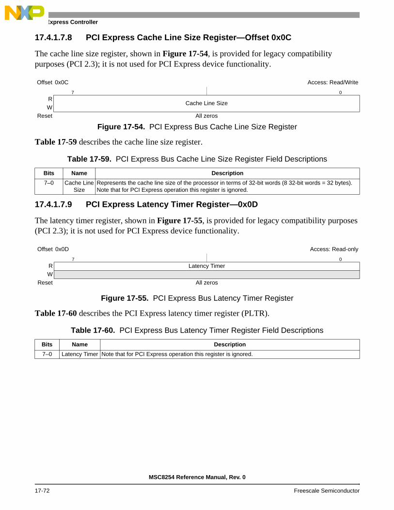
PCI Express Controller
17.4.1.7.8 PCI Express Cache Line Size Register—Offset 0x0C
The cache line size register, shown in Figure 17-54, is provided for legacy compatibility purposes (PCI 2.3); it is not used for PCI Express device functionality.
Table 17-59 describes the cache line size register.
17.4.1.7.9 PCI Express Latency Timer Register—0x0D
The latency timer register, shown in Figure 17-55, is provided for legacy compatibility purposes (PCI 2.3); it is not used for PCI Express device functionality.
Table 17-60 describes the PCI Express latency timer register (PLTR).
Offset 0x0C Access: Read/Write
7 0
RCache Line Size
WReset All zeros
Figure 17-54. PCI Express Bus Cache Line Size Register
Table 17-59. PCI Express Bus Cache Line Size Register Field Descriptions
Bits Name Description
7–0 Cache LineSize
Represents the cache line size of the processor in terms of 32-bit words (8 32-bit words = 32 bytes). Note that for PCI Express operation this register is ignored.
Offset 0x0D Access: Read-only
7 0
R Latency TimerW
Reset All zeros
Figure 17-55. PCI Express Bus Latency Timer Register
Table 17-60. PCI Express Bus Latency Timer Register Field Descriptions
Bits Name Description
7–0 Latency Timer Note that for PCI Express operation this register is ignored.
MSC8254 Reference Manual, Rev. 0
17-72 Freescale Semiconductor
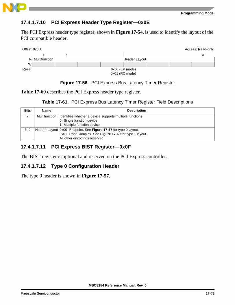
Programming Model
17.4.1.7.10 PCI Express Header Type Register—0x0E
The PCI Express header type register, shown in Figure 17-54, is used to identify the layout of the PCI compatible header.
Table 17-60 describes the PCI Express header type register.
17.4.1.7.11 PCI Express BIST Register—0x0F
The BIST register is optional and reserved on the PCI Express controller.
17.4.1.7.12 Type 0 Configuration Header
The type 0 header is shown in Figure 17-57.
Offset 0x0D Access: Read-only
7 6 0
R Multifunction Header Layout
WReset 0x00 (EP mode)
0x01 (RC mode)
Figure 17-56. PCI Express Bus Latency Timer Register
Table 17-61. PCI Express Bus Latency Timer Register Field Descriptions
Bits Name Description
7 Multifunction Identifies whether a device supports multiple functions0 Single function device1 Multiple function device
6–0 Header Layout 0x00 Endpoint. See Figure 17-57 for type 0 layout.0x01 Root Complex. See Figure 17-69 for type 1 layout.All other encodings reserved.
MSC8254 Reference Manual, Rev. 0
Freescale Semiconductor 17-73
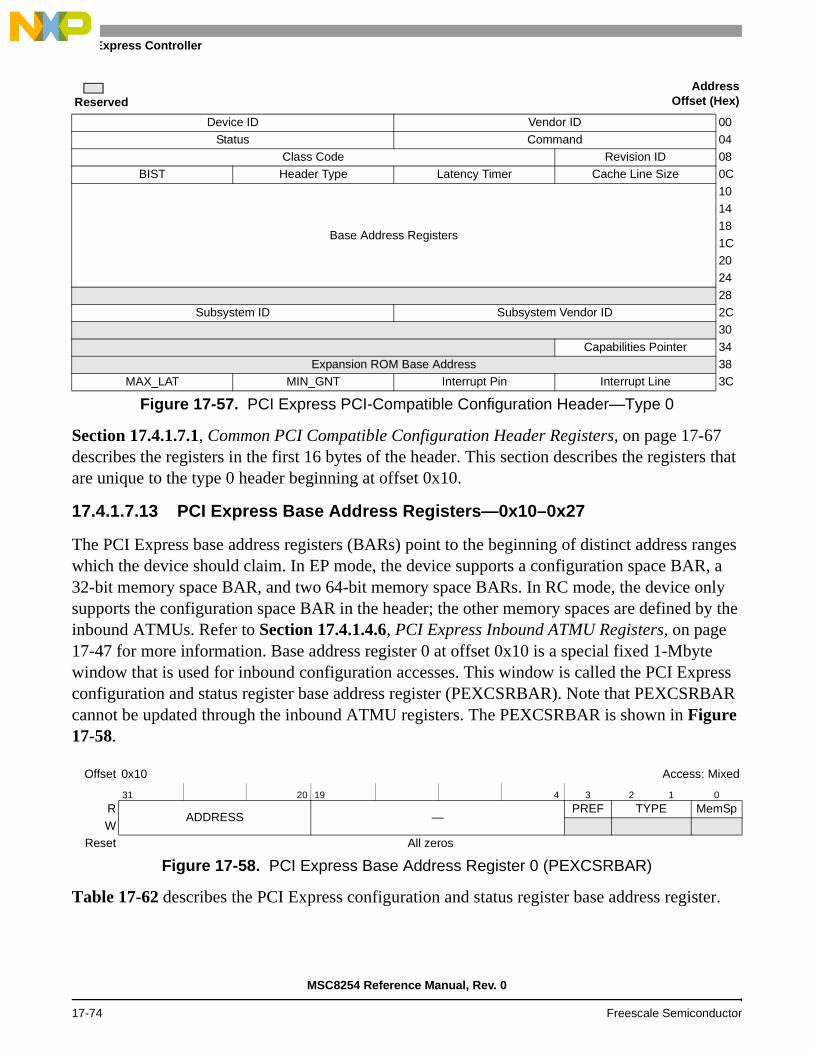
PCI Express Controller
Section 17.4.1.7.1, Common PCI Compatible Configuration Header Registers, on page 17-67 describes the registers in the first 16 bytes of the header. This section describes the registers that are unique to the type 0 header beginning at offset 0x10.
17.4.1.7.13 PCI Express Base Address Registers—0x10–0x27
The PCI Express base address registers (BARs) point to the beginning of distinct address ranges which the device should claim. In EP mode, the device supports a configuration space BAR, a 32-bit memory space BAR, and two 64-bit memory space BARs. In RC mode, the device only supports the configuration space BAR in the header; the other memory spaces are defined by the inbound ATMUs. Refer to Section 17.4.1.4.6, PCI Express Inbound ATMU Registers, on page 17-47 for more information. Base address register 0 at offset 0x10 is a special fixed 1-Mbyte window that is used for inbound configuration accesses. This window is called the PCI Express configuration and status register base address register (PEXCSRBAR). Note that PEXCSRBAR cannot be updated through the inbound ATMU registers. The PEXCSRBAR is shown in Figure 17-58.
Table 17-62 describes the PCI Express configuration and status register base address register.
ReservedAddress
Offset (Hex)
Device ID Vendor ID 00
Status Command 04Class Code Revision ID 08
BIST Header Type Latency Timer Cache Line Size 0C
Base Address Registers
101418
1C2024
28Subsystem ID Subsystem Vendor ID 2C
30
Capabilities Pointer 34Expansion ROM Base Address 38
MAX_LAT MIN_GNT Interrupt Pin Interrupt Line 3C
Figure 17-57. PCI Express PCI-Compatible Configuration Header—Type 0
Offset 0x10 Access: Mixed
31 20 19 4 3 2 1 0
RADDRESS —
PREF TYPE MemSpW
Reset All zeros
Figure 17-58. PCI Express Base Address Register 0 (PEXCSRBAR)
MSC8254 Reference Manual, Rev. 0
17-74 Freescale Semiconductor

Programming Model
d
p
Base address register 1 at offset 0x14 is used to define the inbound memory window in the 32-bit memory space. The 32-bit memory BAR is shown in Figure 17-59.
Table 17-63 describes the PCI Express 32-bit memory BAR fields.
Base address register 2 at offset 0x18 and base address register 4 at offset 0x20 are used to define the lower portion of the 64-bit inbound memory windows. The 64-bit low memory BARs are shown in Figure 17-60.
Table 17-64 describes the PCI Express 64-bit low memory BAR fields.
Table 17-62. PEXCSRBAR Field Descriptions
Bits Name Description
31–20 ADDRESS Indicates the base address that the inbound configuration window occupies. This window is fixed at 1 Mbyte.
19–4 — Reserved
3 PREF Prefetchable2–1 TYPE Type.
00 Locate anywhere in 32-bit address space. 0 MemSp Memory space indicator
Offset 0x14 (EP-mode only) Access: Mixed
31 12 11 4 3 2 1 0
RADDRESS —
PREF TYPE MemSp
W
Reset 0 0 0 0 0 0 0 0 0 0 0 0 0 0 0 0 0 0 0 0 0 0 0 0 0 0 0 0 1 0 0 0
Figure 17-59. 32-Bit Memory Base Address Register (BAR1)
Table 17-63. 32-Bit Memory Base Address Register (BAR1) Field Descriptions
Bits Name Description
31–12 ADDRESS Indicates the base address where the inbound memory window begins. The number of upper bits that the device allows to be writable is selected through the inbound window size in the inbound window attributes register (PEXIWAR1).
11–4 — Reserved. The device allows a 4 Kbyte window minimum.3 PREF Prefetchable. This bit is determined by PEXIWAR1[PF].
2–1 TYPE Type.00 Locate anywhere in 32-bit address space.
0 MemSp Memory space indicator.
Offset 0x18 (EP-mode only)0x20 (EP-mode only)
Access: Mixe
31 12 11 4 3 2 1 0
RADDRESS —
PREF TYPE MemS
W
Reset 0 0 0 0 0 0 0 0 0 0 0 0 0 0 0 0 0 0 0 0 0 0 0 0 0 0 0 0 1 1 0 0
Figure 17-60. 64-Bit Low Memory Base Address Register
MSC8254 Reference Manual, Rev. 0
Freescale Semiconductor 17-75

PCI Express Controller
Base address register 3 at offset 0x1C and base address register 5 at offset 0x24 are used to define the upper portion of the 64-bit inbound memory windows. The 64-bit high memory BARs are shown in Figure 17-61.
Table 17-65 describes the PCI Express 64-bit low memory BAR fields.
17.4.1.7.14 PCI Express Subsystem Vendor ID Register (EP-Mode Only)—0x2C
The PCI Express subsystem vendor ID register is used to identify the subsystem.
Table 17-64. 64-Bit Low Memory Base Address Register Field Descriptions
Bits Name Description
31–12 ADDRESS Indicates the lower portion of the base address where the inbound memory window begins. The number of bits that the device allows to be writable is selected through the inbound window size in the inbound window attributes registers (PEXIWAR2 for offset 0x18 and PEXIWAR3 for offset 0x20).
11–4 — Reserved. The device allows a 4 Kbyte window minimum.3 PREF Prefetchable. This bit is determined by PEXIWARn[2].
2–1 TYPE Type.0b10 Locate anywhere in 64-bit address space.
0 MemSp Memory space indicator
Offset 0x1C (EP-mode only)0x24 (EP-mode only)
Access: Read/Write
31 0
RADDRESS
W
Reset All zeros
Figure 17-61. 64-Bit High Memory Base Address Register
Table 17-65. Bit Setting for 64-Bit High Memory Base Address Register
Bits Name Description
31–0 ADDRESS Indicates the upper portion of the base address where the inbound memory window begins. The number of bits that the device allows to be writable is selected through the inbound window size in the inbound window attributes registers (PEXIWAR2 for offset 0x1C and PEXIWAR3 for offset 0x24). If no access to local memory is to be permitted by external requestors, then all bits are programmed.
Offset 0x2C (EP-mode only) Access: Read-only
15 0
R Subsystem Vendor ID
W
Reset Value taken from PEX_SSVID_UPDATE[SSV_ID]
Figure 17-62. PCI Express Subsystem Vendor ID Register
MSC8254 Reference Manual, Rev. 0
17-76 Freescale Semiconductor

Programming Model
17.4.1.7.15 PCI Express Subsystem ID Register (EP-Mode Only)—0x2E
The PCI Express subsystem ID register is used to identify the subsystem.
17.4.1.7.16 Capabilities Pointer Register—0x34
The capabilities pointer identifies additional functionality supported by the device.
Table 17-66. PCI Express Subsystem Vendor ID Register Field Description
Bits Name Description
15–0 Subsystem Vendor ID The value for subsystem vendor ID is determined by the PCI Express subsystem vendor ID update register. See Section 17.4.1.9.19, PCI Express Subsystem Vendor ID Update Register (EP Mode Only)—0x478, on page 17-119 for more information.
Offset 0x2E (EP-mode only) Access: Read-only
15 0
R Subsystem ID
W
Reset Value taken from PEX_SSVID_UPDATE[SSV_ID]
Figure 17-63. PCI Express Subsystem ID Register
Table 17-67. PCI Express Subsystem ID Register Field Description
Bits Name Description
15–0 Subsystem ID The value for subsystem ID is determined by the PCI Express subsystem vendor ID update register. See Section 17.4.1.9.19, PCI Express Subsystem Vendor ID Update Register (EP Mode Only)—0x478, on page 17-119 for more information.
Offset 0x34 Access: Read-only
7 0
R Capabilities Pointer
W
Reset 0 1 0 0 0 1 0 0
Figure 17-64. Capabilities Pointer Register
Table 17-68. Capabilities Pointer Register Field Description
Bits Name Description
7–0 Capabilities Pointer The capabilities pointer provides the offset (0x44) for additional PCI-compatible registers above the common 64-byte header. Refer to Section 17.4.1.8, PCI Compatible Device-Specific Configuration Space, on page 17-90 for more information.
MSC8254 Reference Manual, Rev. 0
Freescale Semiconductor 17-77

PCI Express Controller
17.4.1.7.17 PCI Express Interrupt Line Register (EP-Mode Only)—0x3C
The interrupt line register is used by device drivers and OS software to communicate interrupt line routing information. Values in this register are programmed by system software and are system specific.
17.4.1.7.18 PCI Express Interrupt Pin Register—0x3D
The interrupt pin register identifies the legacy interrupt (INTx) messages the device (or function) uses.
17.4.1.7.19 PCI Express Minimum Grant Register (EP-Mode Only)—0x3E
This register does not apply to PCI Express. It is present for legacy purposes.
Offset 0x3C (EP-mode only) Access: Read/Write
7 0
RInterrupt Line
WReset All zeros
Figure 17-65. PCI Express Interrupt Line Register
Table 17-69. PCI Express Interrupt Line Register Field Description
Bits Name Description
7–0 Interrupt Line Used to communicate interrupt line routing information.
Offset 0x3D Access: Read-only
7 0
R Interrupt PinW
Reset 0 0 0 0 0 0 0 1
Figure 17-66. PCI Express Interrupt Pin Register
Table 17-70. PCI Express Interrupt Pin Register Field Description
Bits Name Description
7–0 Interrupt pin Legacy INTx message used by this device.0x00 This device does not use legacy interrupt (INTx) messages.0x01 INTA 0x02 INTB0x03 INTC0x04 INTDall others Reserved.
Offset 0x3E (EP-mode only) Access: Read-only
7 0
R MIN_GNTW
Reset All zeros
Figure 17-67. PCI Express Maximum Grant Register (MAX_GNT)
MSC8254 Reference Manual, Rev. 0
17-78 Freescale Semiconductor

Programming Model
17.4.1.7.20 PCI Express Maximum Latency Register (EP-Mode Only)—0x3F
This register does not apply to PCI Express. It is present for legacy purposes.
17.4.1.7.21 Type 1 Configuration Header
The type 1 header is shown in Figure 17-69.
Section 17.4.1.7.1, Common PCI Compatible Configuration Header Registers, on page 17-67 describes the registers in the first 16 bytes of the header. This section describes the registers that are unique to the type 1 header beginning at offset 0x10.
Table 17-71. PCI Express Maximum Grant Register Field Description
Bits Name Description
7–0 MIN_GNT Does not apply for PCI Express.
Offset 0x3F (EP-mode only) Access: Read-only
7 0
R MAX_LAT
WReset All zeros
Figure 17-68. PCI Express Maximum Latency Register (MAX_LAT)
Table 17-72. PCI Express Maximum Latency Register Field Description
Bits Name Description
7–0 MAX_LAT Does not apply for PCI Express.
ReservedAddress
Offset (Hex)
Device ID Vendor ID 00
Status Command 04Class Code Revision ID 08
BIST Header Type Latency Timer Cache Line Size 0C
Base Address Register 0 1014
Secondary Latency Timer Subordinate Bus Number Secondary Bus Number Primary Bus Number 18
Secondary Status I/O Limit I/O Base 1CMemory Limit Memory Base 20
Prefetchable Memory Limit Prefetchable Memory Base 24
Prefetchable Base Upper 32 Bits 28Prefetchable Limit Upper 32 Bits 2C
I/O Limit Upper 16 Bits I/O Base Upper 16 Bits 30
Capabilities Pointer 34Bridge Control Interrupt Pin Interrupt Line 3C
Figure 17-69. PCI Express PCI-Compatible Configuration Header—Type 1
MSC8254 Reference Manual, Rev. 0
Freescale Semiconductor 17-79

PCI Express Controller
17.4.1.7.22 PCI Express Base Address Register 0—0x10
Base address register 0 at offset 0x10 is a special fixed 1-Mbyte window that is used for inbound configuration accesses. This window is called the PCI Express configuration and status register base address register (PEXCSRBAR). Note that PEXCSRBAR cannot be updated through the inbound ATMU registers. The PEXCSRBAR is shown in Figure 17-58.
Table 17-62 describes the PCI Express configuration and status register base address register.
17.4.1.7.23 PCI Express Primary Bus Number Register—Offset 0x18
The primary bus number register is shown in Figure 17-71.
Table 17-74 describes the primary bus number register fields.
Offset 0x10 Access: Mixed
31 20 19 4 3 2 1 0
RADDRESS —
PREF TYPE MemSp
W
Reset All zeros
Figure 17-70. PCI Express Base Address Register 0 (PEXCSRBAR)
Table 17-73. PEXCSRBAR Field Descriptions
Bits Name Description
31–20 ADDRESS Indicates the base address that the inbound configuration window occupies. This window is fixed at 1 Mbyte.
19–4 — Reserved
3 PREF Prefetchable
2–1 TYPE Type.00 Locate anywhere in 32-bit address space.
0 MemSp Memory space indicator
Offset 0x18 Access: Read/Write
7 0
RPrimary Bus Number
W
Reset All zeros
Figure 17-71. PCI Express Primary Bus Number Register
Table 17-74. PCI Express Primary Bus Number Register Field Description
Bits Name Description
7–0 Primary Bus Number Bus that is connected to the upstream interface. Note that this register is programmed during system enumeration; in RC mode this register should remain 0x00.
MSC8254 Reference Manual, Rev. 0
17-80 Freescale Semiconductor

Programming Model
17.4.1.7.24 PCI Express Secondary Bus Number Register—Offset 0x19
The secondary bus number register is shown in Figure 17-72.
Table 17-75 describes the secondary bus number register fields.
17.4.1.7.25 PCI Express Subordinate Bus Number Register—Offset 0x1A
The subordinate bus number register is shown in Figure 17-73.
Table 17-76 describes the subordinate bus number register fields.
17.4.1.7.26 PCI Express Secondary Latency Timer Register—0x1B
The secondary latency timer register does not apply to PCI Express. It must be read-only and return all zeros when read.
Offset 0x19 Access: Read/Write
7 0
RSecondary Bus Number
W
Reset All zeros
Figure 17-72. PCI Express Secondary Bus Number Register
Table 17-75. PCI Express Secondary Bus Number Register Field Description
Bits Name Description
7–0 Secondary Bus Number Bus that is directly connected to the downstream interface. Note that this register is programmed during system enumeration; in RC mode, this register is typically programmed to 0x01.
Offset 0x1A Access: Read/Write
7 0
RSubordinate Bus Number
W
Reset All zeros
Figure 17-73. PCI Express Subordinate Bus Number Register
Table 17-76. PCI Express Subordinate Bus Number Register Field Description
Bits Name Description
7–0 Subordinate Bus Number Highest bus number that is on the downstream interface.
MSC8254 Reference Manual, Rev. 0
Freescale Semiconductor 17-81

PCI Express Controller
17.4.1.7.27 PCI Express I/O Base Register—0x1C
Note that this device does not support inbound I/O transactions. The I/O base register is shown in Figure 17-73.
Table 17-76 describes the I/O base register fields.
17.4.1.7.28 PCI Express I/O Limit Register—0x1D
Note that this device does not support inbound I/O transactions. The I/O limit register is shown in Figure 17-73.
Table 17-76 describes the I/O limit register fields.
Offset 0x1C Access: Read-only
7 4 3 0
R I/O Start Address Address Decode Type
W
Reset All zeros
Figure 17-74. PCI Express I/O Base Register
Table 17-77. PCI Express I/O Base Register Field Description
Bits Name Description
7–4 I/O Start Address Specifies bits 15:12 of the I/O space start address
3–0 Address Decode Type Specifies the number of I/O address bits.0x00 16-bit I/O address decode0x01 32-bit I/O address decodeAll other settings reserved.
Offset 0x1D Access: Read-only
7 4 3 0
R I/O Limit Address Address Decode Type
W
Reset All zeros
Figure 17-75. PCI Express I/O Limit Register
Table 17-78. PCI Express I/O Limit Register Field Description
Bits Name Description
7–4 I/O Limit Address Specifies bits 15:12 of the I/O space ending address
3–0 Address Decode Type Specifies the number of I/O address bits.0x00 16-bit I/O address decode0x01 32-bit I/O address decodeAll other settings reserved.
MSC8254 Reference Manual, Rev. 0
17-82 Freescale Semiconductor

Programming Model
17.4.1.7.29 PCI Express Secondary Status Register—0x1E
The PCI Express secondary status register is shown in Figure 17-76. Note that the errors in this register may be masked by corresponding bits in the secondary status interrupt mask register (PEX_SS_INTR_MASK) and that by default all of the errors are masked. See Section 17.4.1.9.22, Secondary Status Interrupt Mask Register (RC-Mode Only)—0x5A0, on page 17-121 for more information.
Table 17-79 describes the PCI Express secondary status register fields.
Offset 0x1E Access: Mixed
15 14 13 12 11 10 9 8 7 0
R DPE SSE RMA RTA STA — MDPE —
W w1c w1c w1c w1c w1c w1c
Reset All zeros
Figure 17-76. PCI Express Secondary Status Register
Table 17-79. PCI Express Secondary Status Register Field Description
Bits Name Description
15 DPE Detected parity error. This bit is set whenever the secondary side receives a poisoned TLP regardless of the state of the parity error response bit.
14 SSE Signaled system error. This bit is set when a device sends a ERR_FATAL or ERR_NONFATAL message, provided the SERR enable bit in the command register is set to enable reporting.
13 RMA Received master abort. This bit is set when the secondary side receives an unsupported request (UR) completion.
12 RTA Received target abort. This bit is set when the secondary side receives a completer abort (CA) completion.
11 STA Signaled target abort. This bit is set when the secondary side issues a CA completion.
10–9 — Reserved
8 MDPE Master data parity error. This bit is set when the parity error response bit is set and the secondary side requestor receives a poisoned completion or poisons a write request. If the parity error response bit is cleared, this bit is never set.
7–0 — Reserved
MSC8254 Reference Manual, Rev. 0
Freescale Semiconductor 17-83

PCI Express Controller
17.4.1.7.30 PCI Express Memory Base Register—0x20
The memory base register is shown in Figure 17-77.
Table 17-80 describes the memory base register fields.
17.4.1.7.31 PCI Express Memory Limit Register—0x22
The memory limit register is shown in Figure 17-78.
Table 17-81 describes the memory base register fields.
Offset 0x20 Access: Read/Write
15 4 3 0
RMemory Base
—
W
Reset All zeros
Figure 17-77. PCI Express Memory Base Register
Table 17-80. PCI Express Memory Base Register Field Description
Bits Name Description
15–4 Memory Base Specifies bits 31:20 of the non-prefetchable memory space start address. Typically used for specifying memory-mapped I/O space. Note: Inbound posted transactions hitting into the mem base/limit range are ignored; inbound non-posted
transactions hitting into the mem base/limit range results in an unsupported request response.
3–0 — Reserved
Offset 0x22 Access: Read/Write
15 4 3 0
RMemory Limit
—
W
Reset All zeros
Figure 17-78. PCI Express Memory Limit Register
Table 17-81. PCI Express Memory Limit Register Field Description
Bits Name Description
15–4 Memory Limit Specifies bits 31:20 of the non-prefetchable memory space ending address. Typically used for specifying memory-mapped I/O space. Note: Inbound posted transactions hitting into the mem base/limit range are ignored; inbound non-posted
transactions hitting into the mem base/limit range will result in unsupported request response.
3–0 — Reserved
MSC8254 Reference Manual, Rev. 0
17-84 Freescale Semiconductor

Programming Model
17.4.1.7.32 PCI Express Prefetchable Memory Base Register—0x24
The prefetchable memory base register is shown in Figure 17-79.
Table 17-82 describes the prefetchable memory base register fields.
17.4.1.7.33 PCI Express Prefetchable Memory Limit Register—0x26
The prefetchable memory limit register is shown in Figure 17-80.
Table 17-83 describes the prefetchable memory limit register fields.
Offset 0x24 Access: Read/Write
15 4 3 0
RPF Memory Base
Address Decode Type
W
Reset All zeros
Figure 17-79. PCI Express Prefetchable Memory Base Register
Table 17-82. PCI Express Prefetchable Memory Base Register Field Description
Bits Name Description
15–4 PF Memory Base Specifies bits 31:20 of the prefetchable memory space start address.
3–0 Address Decode Type Specifies the number of prefetchable memory address bits.0x00 32-bit memory address decode0x01 64-bit memory address decodeAll other settings reserved.
Offset 0x26 Access: Read/Write
15 4 3 0
RPF Memory Limit
Address Decode Type
W
Reset All zeros
Figure 17-80. PCI Express Prefetchable Memory Limit Register
Table 17-83. PCI Express Prefetchable Memory Limit Register Field Description
Bits Name Description
15–4 PF Memory Limit Specifies bits 31:20 of the prefetchable memory space ending address.
3–0 Address Decode Type Specifies the number of prefetchable memory address bits.0x00 32-bit memory address decode0x01 64-bit memory address decodeAll other settings reserved.
MSC8254 Reference Manual, Rev. 0
Freescale Semiconductor 17-85
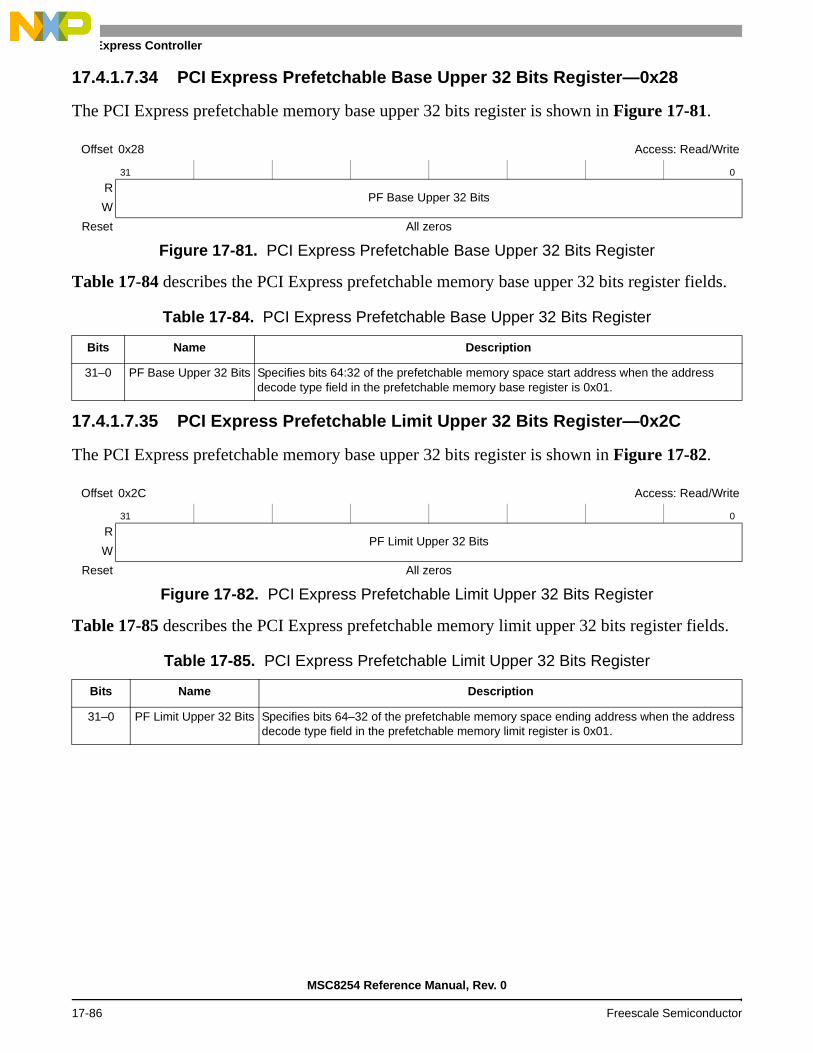
PCI Express Controller
17.4.1.7.34 PCI Express Prefetchable Base Upper 32 Bits Register—0x28
The PCI Express prefetchable memory base upper 32 bits register is shown in Figure 17-81.
Table 17-84 describes the PCI Express prefetchable memory base upper 32 bits register fields.
17.4.1.7.35 PCI Express Prefetchable Limit Upper 32 Bits Register—0x2C
The PCI Express prefetchable memory base upper 32 bits register is shown in Figure 17-82.
Table 17-85 describes the PCI Express prefetchable memory limit upper 32 bits register fields.
Offset 0x28 Access: Read/Write
31 0
RPF Base Upper 32 Bits
W
Reset All zeros
Figure 17-81. PCI Express Prefetchable Base Upper 32 Bits Register
Table 17-84. PCI Express Prefetchable Base Upper 32 Bits Register
Bits Name Description
31–0 PF Base Upper 32 Bits Specifies bits 64:32 of the prefetchable memory space start address when the address decode type field in the prefetchable memory base register is 0x01.
Offset 0x2C Access: Read/Write
31 0
RPF Limit Upper 32 Bits
W
Reset All zeros
Figure 17-82. PCI Express Prefetchable Limit Upper 32 Bits Register
Table 17-85. PCI Express Prefetchable Limit Upper 32 Bits Register
Bits Name Description
31–0 PF Limit Upper 32 Bits Specifies bits 64–32 of the prefetchable memory space ending address when the address decode type field in the prefetchable memory limit register is 0x01.
MSC8254 Reference Manual, Rev. 0
17-86 Freescale Semiconductor

Programming Model
17.4.1.7.36 PCI Express I/O Base Upper 16 Bits Register—0x30
Note that this device does not support inbound I/O transactions. The I/O base upper 16 bits register is shown in Figure 17-83.
Table 17-86 describes the I/O base upper 16 bits register fields.
17.4.1.7.37 PCI Express I/O Limit Upper 16 Bits Register—0x32
Note that this device does not support inbound I/O transactions. The I/O limit upper 16 bits register is shown in Figure 17-84.
Table 17-87 describes the I/O limit upper 16 bits register fields.
Offset 0x30 Access: Read-only
15 0
R I/O Base Upper 16 Bits
W
Reset All zeros
Figure 17-83. PCI Express I/O Base Upper 16 Bits Register
Table 17-86. PCI Express I/O Base Upper 16 Bits Register Field Description
Bits Name Description
15–0 I/O Base Upper 16 Bits Specifies bits 31–16 of the I/O space start address when the address decode type field in the I/O base register is 0x01.
Offset 0x32 Access: Read-only
15 0
R I/O Limit Upper 16 Bits
W
Reset All zeros
Figure 17-84. PCI Express I/O Limit Upper 16 Bits Register
Table 17-87. PCI Express I/O Limit Upper 16 Bits Register Field Description
Bits Name Description
15–0 I/O Limit Upper 16 Bits Specifies bits 31–16 of the I/O space ending address when the address decode type field in the I/O limit register is 0x01.
MSC8254 Reference Manual, Rev. 0
Freescale Semiconductor 17-87

PCI Express Controller
17.4.1.7.38 Capabilities Pointer Register—0x34
The capabilities pointer identifies additional functionality supported by the device.
17.4.1.7.39 PCI Express Interrupt Line Register—0x3C
The interrupt line register is used by device drivers and OS software to communicate interrupt line routing information. Values in this register are programmed by system software and are system specific.
17.4.1.7.40 PCI Express Interrupt Pin Register—0x3D
The interrupt pin register identifies the legacy interrupt (INTx) messages the device (or function) uses.
Offset 0x34 Access: Read-only
7 0
R Capabilities PointerW
Reset 0 1 0 0 0 1 0 0
Figure 17-85. Capabilities Pointer Register
Table 17-88. Capabilities Pointer Register Field Description
Bits Name Description
7–0 Capabilities Pointer The capabilities pointer provides the offset (0x44) for additional PCI-compatible registers above the common 64-byte header. Refer to Section 17.4.1.8, PCI Compatible Device-Specific Configuration Space, on page 17-90,” for more information.
Offset 0x3C Access: Read/Write
7 0
RInterrupt Line
W
Reset All zeros
Figure 17-86. PCI Express Interrupt Line Register
Table 17-89. PCI Express Interrupt Line Register Field Description
Bits Name Description
7–0 Interrupt Line Used to communicate interrupt line routing information.
Offset 0x3D Access: Read-only
7 0
R Interrupt Pin
WReset 0 0 0 0 0 0 0 1
Figure 17-87. PCI Express Interrupt Pin Register
MSC8254 Reference Manual, Rev. 0
17-88 Freescale Semiconductor

Programming Model
17.4.1.7.41 PCI Express Bridge Control Register—0x3E
The PCI Express bridge control register is shown in Figure 17-88.
Table 17-91 describes the PCI Express bridge control register fields.
Table 17-90. PCI Express Interrupt Pin Register Field Description
Bits Name Description
7–0 Interrupt pin Legacy INTx message used by this device.0x00 This device does not use legacy interrupt (INTx) messages.0x01 INTA 0x02 INTB0x03 INTC0x04 INTDall others Reserved.
Offset 0x3E Access: Read/Write
15 7 6 5 4 3 2 1 0
R— Scnd_RST — VGA_EN ISA_EN SERR_EN PER
W
Reset All zeros
Figure 17-88. PCI Express Bridge Control Register
Table 17-91. PCI Express Bridge Control Register Field Description
Bits Name Description
15–7 — Reserved6 Scnd_RST Secondary bus reset
5–4 — Reserved3 VGA_EN VGA enable
2 ISA_EN ISA enable1 SERR_EN SERR enable. This bit controls the propagation of ERR_COR, ERR_NONFATAL, and ERR_FATAL
responses received on the secondary side.0 PER Parity error response.
MSC8254 Reference Manual, Rev. 0
Freescale Semiconductor 17-89

PCI Express Controller
17.4.1.8 PCI Compatible Device-Specific Configuration Space
The PCI compatible device-specific configuration space is a PCI compatible configuration space from 0x40 to 0xFF (just above the 64-byte PCI-compatible configuration header).
ReservedAddress
Offset (Hex)
PCI-Compatible Configuration Header(See Section 17.4.1.7, PCI Compatible Configuration Headers for more information.)
00
3F
40Power Mgmt Capabilities Next Pointer (0x4C) Power Mgmt Capability ID 44
Data Power Management Status & Control 48
PCI Express Capabilities Next Pointer(0x70 — EP mode)(NULL — RC mode)
PCI Express Capability ID 4C
Device Capabilities 50
Device Status Device Control 54Link Capabilities 58
Link Status Link Control 5C
Slot Capabilities 60Slot Status Slot Control 64
Root Control (RC mode only) 68
Root Status 6CMSI Message Control Next Pointer (NULL) MSI Message Capability ID 70
MSI Message Address 74
MSI Upper Message Address 78MSI Message Data 7C
80
FF
Figure 17-89. PCI Compatible Device-Specific Configuration Space
MSC8254 Reference Manual, Rev. 0
17-90 Freescale Semiconductor

Programming Model
17.4.1.8.1 PCI Express Power Management Capability ID Register—0x44
The PCI Express power management capability ID register is shown in Figure 17-90.
17.4.1.8.2 PCI Express Power Management Capabilities Register—0x46
The PCI Express power management capabilities register is shown in Figure 17-91.
Offset 0x44 Access: Read-only
7 0
R Power Mgmt Capability ID
W
Reset 0 0 0 0 0 0 0 1
Figure 17-90. PCI Express Power Management Capability ID Register
Table 17-92. PCI Express Power Management Capability ID Register Field Description
Bits Name Description
7–0 Power Mgmt Capability ID Power Management = 0x01
Offset 0x46 Access: Read-only
15 11 10 9 8 6 5 4 3 2 0
R PME Support D2 D1 AUX Curr DSI — PME CLK Version
W
Reset 0 1 1 1 1 1 1 0 0 0 0 0 0 0 1 0
Figure 17-91. PCI Express Power Management Capabilities Register
Table 17-93. PCI Express Power Management Capabilities Register Field Description
Bits Name Description
15–11 PME Support Indicates the power states that this device supports
10 D2 D2 Support
9 D1 D1 Support
8–6 AUX Curr AUX Current
5 DSI Device Specific Initialization
4 — Reserved
3 PME CLK Does not apply to PCI Express.
2–0 Version Version 1.0a
MSC8254 Reference Manual, Rev. 0
Freescale Semiconductor 17-91

PCI Express Controller
17.4.1.8.3 PCI Express Power Management Status and Control Register—0x48
The PCI Express power management status and control register is shown in Figure 17-92.
17.4.1.8.4 PCI Express Power Management Data Register—0x4B
The PCI Express power management data register is shown in Figure 17-93.
Offset 0x48 Access: Mixed
15 14 13 12 9 8 7 2 1 0
R PME_STAT Data ScaleData Select
PME_EN —Power State
W w1c Sticky
Reset All zeros
Figure 17-92. PCI Express Power Management Status and Control Register
Table 17-94. PCI Express Status and Control Register Field Description
Bits Name Description
15 PME_STAT PME Status
14–13 Data Scale Obtained directly from PCI Express™ Base Specification, Revision 1.0a
12–9 Data Select Obtained directly from PCI Express™ Base Specification, Revision 1.0a
8 PME_EN PME Enable
7–2 — Reserved
1–0 Power State Power state. Indicates the current power state of the function.0x00 D00x01 D1 0x02 D20x03 D3
Offset 0x4B Access: Read-only
7 0
R Data
W
Reset All zeros
Figure 17-93. PCI Express Power Management Data Register
Table 17-95. PCI Express Power Management Data Register Field Description
Bits Name Description
7–0 Data Obtained from PCI Express™ Base Specification, Revision 1.0a
MSC8254 Reference Manual, Rev. 0
17-92 Freescale Semiconductor
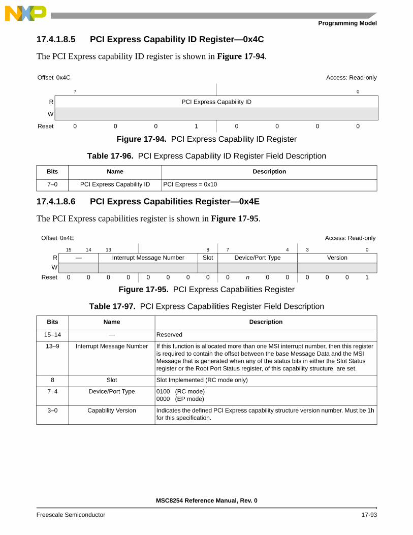
Programming Model
17.4.1.8.5 PCI Express Capability ID Register—0x4C
The PCI Express capability ID register is shown in Figure 17-94.
17.4.1.8.6 PCI Express Capabilities Register—0x4E
The PCI Express capabilities register is shown in Figure 17-95.
Offset 0x4C Access: Read-only
7 0
R PCI Express Capability ID
W
Reset 0 0 0 1 0 0 0 0
Figure 17-94. PCI Express Capability ID Register
Table 17-96. PCI Express Capability ID Register Field Description
Bits Name Description
7–0 PCI Express Capability ID PCI Express = 0x10
Offset 0x4E Access: Read-only
15 14 13 8 7 4 3 0
R — Interrupt Message Number Slot Device/Port Type Version
W
Reset 0 0 0 0 0 0 0 0 0 n 0 0 0 0 0 1
Figure 17-95. PCI Express Capabilities Register
Table 17-97. PCI Express Capabilities Register Field Description
Bits Name Description
15–14 — Reserved
13–9 Interrupt Message Number If this function is allocated more than one MSI interrupt number, then this register is required to contain the offset between the base Message Data and the MSI Message that is generated when any of the status bits in either the Slot Status register or the Root Port Status register, of this capability structure, are set.
8 Slot Slot Implemented (RC mode only)
7–4 Device/Port Type 0100 (RC mode)0000 (EP mode)
3–0 Capability Version Indicates the defined PCI Express capability structure version number. Must be 1h for this specification.
MSC8254 Reference Manual, Rev. 0
Freescale Semiconductor 17-93
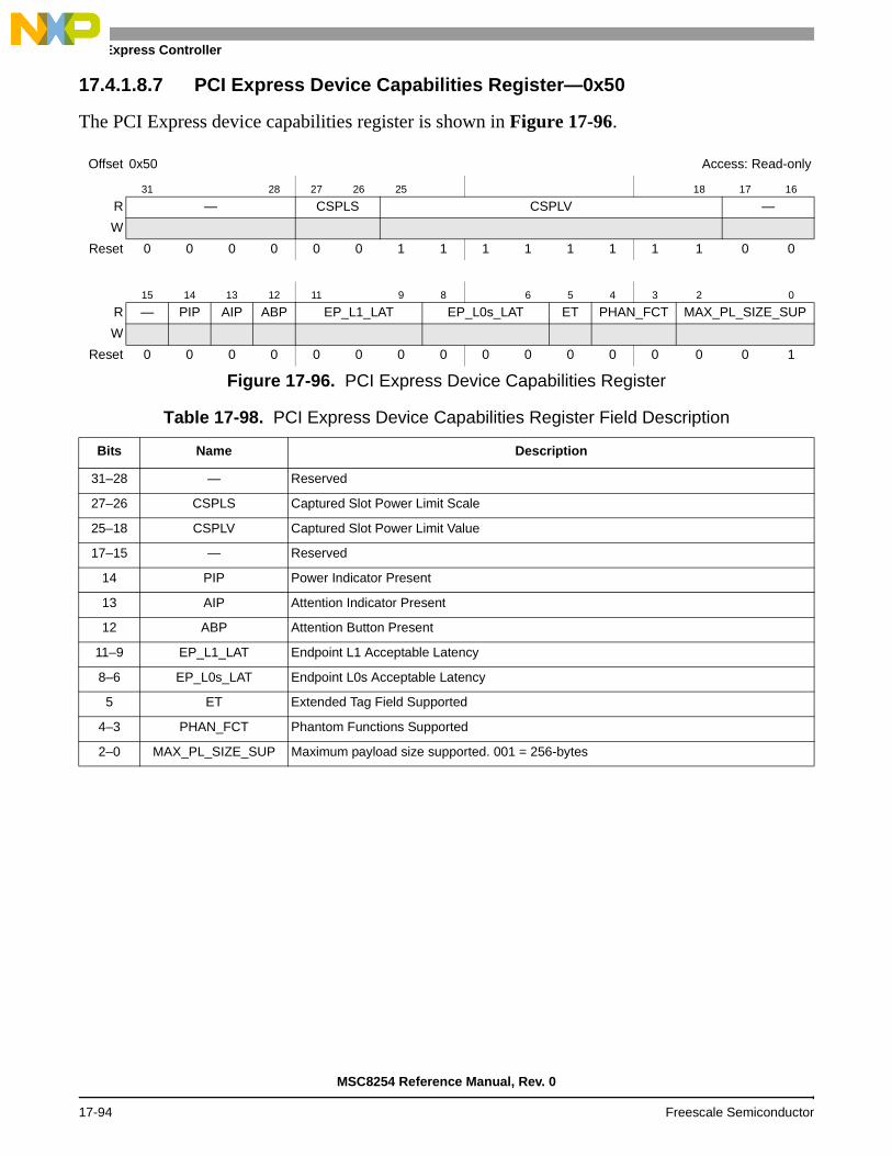
PCI Express Controller
17.4.1.8.7 PCI Express Device Capabilities Register—0x50
The PCI Express device capabilities register is shown in Figure 17-96.
Offset 0x50 Access: Read-only
31 28 27 26 25 18 17 16
R — CSPLS CSPLV —
W
Reset 0 0 0 0 0 0 1 1 1 1 1 1 1 1 0 0
15 14 13 12 11 9 8 6 5 4 3 2 0
R — PIP AIP ABP EP_L1_LAT EP_L0s_LAT ET PHAN_FCT MAX_PL_SIZE_SUP
W
Reset 0 0 0 0 0 0 0 0 0 0 0 0 0 0 0 1
Figure 17-96. PCI Express Device Capabilities Register
Table 17-98. PCI Express Device Capabilities Register Field Description
Bits Name Description
31–28 — Reserved
27–26 CSPLS Captured Slot Power Limit Scale
25–18 CSPLV Captured Slot Power Limit Value
17–15 — Reserved
14 PIP Power Indicator Present
13 AIP Attention Indicator Present
12 ABP Attention Button Present
11–9 EP_L1_LAT Endpoint L1 Acceptable Latency
8–6 EP_L0s_LAT Endpoint L0s Acceptable Latency
5 ET Extended Tag Field Supported
4–3 PHAN_FCT Phantom Functions Supported
2–0 MAX_PL_SIZE_SUP Maximum payload size supported. 001 = 256-bytes
MSC8254 Reference Manual, Rev. 0
17-94 Freescale Semiconductor

Programming Model
17.4.1.8.8 PCI Express Device Control Register—0x54
The PCI Express device control register is shown in Figure 17-97.
17.4.1.8.9 PCI Express Device Status Register—0x56
The PCI Express device status register is shown in Figure 17-98.
Offset 0x54 Access: Read/write
15 14 12 11 10 9 8 7 5 4 3 2 1 0
R— MAX_READ_SIZE NSE APE PFE ETE MAX_PAYLOAD_SIZE RO URR FER NFER CER
W
Reset 0 0 1 0 1 0 0 0 0 0 0 1 0 0 0 0
Figure 17-97. PCI Express Device Control Register
Table 17-99. PCI Express Device Control Register Field Description
Bits Name Description
15 — Reserved14–12 MAX_READ_SIZE Maximum read request size
11 NSE No snoop enable10 APE AUX power PM enable9 PFE Phantom functions enable
8 ETE Extended tag field enable7–5 MAX_PAYLOAD_SIZE Maximum payload size4 RO Relaxed ordering
3 URR Unsupported request reporting2 FER Fatal error reporting1 NFER Non-fatal error reporting
0 CER Correctable error reporting
Offset 0x56 Access: Mixed
15 6 5 4 3 2 1 0
R—
TP APD URD FED NFED CED
W w1c w1c w1c w1c
Reset All zeros
Figure 17-98. PCI Express Device Status Register
Table 17-100. PCI Express Device Status Register Field Description
Bits Name Description
15–6 — Reserved
5 TP Transactions pending4 APD AUX power detected3 URD Unsupported request detected
2 FED Fatal error detected1 NFED Non-fatal error detected0 CED Correctable error detected
MSC8254 Reference Manual, Rev. 0
Freescale Semiconductor 17-95

PCI Express Controller
17.4.1.8.10 PCI Express Link Capabilities Register—0x58
The PCI Express link capabilities register is shown in Figure 17-99.
17.4.1.8.11 PCI Express Link Control Register—0x5C
The PCI Express link control register is shown in Figure 17-100.
Offset 0x58 Access: Read-only
31 24 23 18 17 16
R Port Number — L1_EX_LAT...W
Reset 0 0 0 0 0 0 0 0 0 0 0 0 0 0 1 1
15 14 12 11 10 9 4 3 0
R ... L0s_EX_LAT ASPM MAX_LINK_W MAX_LINK_SPW
Reset 1 0 1 1 0 1 0 0 1 0 0 0 0 0 0 1
Figure 17-99. PCI Express Link Capabilities Register
Table 17-101. PCI Express Link Capabilities Register Field Description
Bits Name Description
31–24 Port Number23–18 — Reserved17–15 L1_EX_LAT L1 exit latency
14–12 L0s_EX_LAT L0s exit latency11–10 ASPM Active state power management (ASPM) Support9–4 MAX_LINK_W Maximum link width
3–0 MAX_LINK_SP Maximum link speed
Offset 0x5C Access: Read/Write
15 8 7 6 5 4 3 2 1 0
R— EXT_SYNC CCC RL LD RCB — ASPM_CTL
WReset All zeros
Figure 17-100. PCI Express Link Control Register
Table 17-102. PCI Express Link Control Register Field Description
Bits Name Description
15–8 — Reserved7 EXT_SYNC Extended synch6 CCC Common clock configuration
5 RL Retrain link (Reserved for EP devices). In RC mode, setting this bit initiates link retraining by directing the Physical Layer LTSSM to the Recovery state; reads of this bit always return 0.
4 LD Link disable
3 RCB Read completion boundary2 — Reserved
1–0 ASPM_CTL Active state power management (ASPM) control
MSC8254 Reference Manual, Rev. 0
17-96 Freescale Semiconductor

Programming Model
17.4.1.8.12 PCI Express Link Status Register—0x5E
The PCI Express link status register is shown in Figure 17-101.
17.4.1.8.13 PCI Express Slot Capabilities Register—0x60
The PCI Express slot capabilities register is shown in Figure 17-102.
Offset 0x5E Access: Read-only
15 13 12 11 10 9 4 3 0
R — SCC LT — NEG_LINK_W LINK_SPW
Reset 0 0 0 0 0 0 0 0 0 0 0 1 0 0 0 1
Figure 17-101. PCI Express Link Status Register
Table 17-103. PCI Express Link Status Register Field Description
Bits Name Description
15–13 — Reserved12 SCC Slot clock configuration
11 LT Link training10 — Reserved.
9–4 NEG_LINK_W Negotiated link width
3–0 LINK_SP Link speed
Offset 0x60 Access: Read-only
31 19 18 17 16
R Physical Slot Number — SPLSW
Reset All zeros
15 14 7 6 5 4 3 2 1 0
R SPLS SPLV HPC HPS PIP AIP MRLSP PCP ABP
WReset All zeros
Figure 17-102. PCI Express Slot Capabilities Register
Table 17-104. PCI Express Slot Capabilities Register Field Description
Bits Name Description
31–19 Physical Slot Number This hardware initialized field indicates the physical slot number attached to this Port. This field must be hardware initialized to a value that assigns a slot number that is globally unique within the chassis. These registers should be initialized to 0 for Ports connected to devices that are either integrated on the system board or integrated within the same silicon as the Switch device or Root Port.
18–17 — Reserved
16–15 SPLS Slot power limit scale.14–7 SPLV Slot power limit value.
6 HPD Hot plug capable.
5 HPS Hot plug surprise.4 PIP Power indicator present.
MSC8254 Reference Manual, Rev. 0
Freescale Semiconductor 17-97

PCI Express Controller
17.4.1.8.14 PCI Express Slot Control Register—0x64
The PCI Express slot control register is shown in Figure 17-103.
3 AIP Attention indicator present.2 MRLSP MRL sensor present.1 PCP Power controller present.
0 ABP Attention button present.
Offset 0x64 Access: Read/Write
15 11 10 9 8 7 6 5 4 3 2 1 0
R— PCC PIC AIC HPIE CCIE
PDCE
MRLSCE PFDE ABPEW
Reset All zeros
Figure 17-103. PCI Express Slot Control Register
Table 17-105. PCI Express Slot Control Register Field Description
Bits Name Description
15–11 — Reserved
10 PCC Power controller control.
9–8 PIC Power indicator control.
7–6 AIC Attention indicator control.
5 HPIE Hot plug interrupt enable.
4 CCIE Command completed interrupt enable.
3 PDCE Presence detect changed enable.
2 MRLSCE MRL sensor changed enable.
1 PFDE Power fault detected enable.
0 ABPE Attention button pressed enable.
Table 17-104. PCI Express Slot Capabilities Register Field Description (Continued)
Bits Name Description
MSC8254 Reference Manual, Rev. 0
17-98 Freescale Semiconductor

Programming Model
17.4.1.8.15 PCI Express Slot Status Register—0x66
The PCI Express slot status register is shown in Figure 17-104.
17.4.1.8.16 PCI Express Root Control Register (RC Mode Only)—0x68
The PCI Express root control register is shown in Figure 17-105.
Offset 0x66 Access: Mixed
15 7 6 5 4 3 2 1 0
R — PDS MRLSS CC PDC MRLSC PFD ABP
W w1c w1c w1c w1c w1c
Reset 0 0 0 0 0 0 0 0 0 1 0 0 0 0 0 0
Figure 17-104. PCI Express Slot Status Register
Table 17-106. PCI Express Slot Status Register Field Descriptions
Bits Name Description
15–7 — Reserved
6 PDS Presence detect state. This bit indicates the presence of a card in the slot.0 Slot empty1 Card is present
5 MRLSS MRL sensor state.0 MRL closed1 MRL open
4 CC Command completed.
3 PDC Presence detect changed.
2 MRLSC MRL sensor changed.
1 PFD Power fault detected.
0 ABP Attention button pressed.
Offset 0x68 Access: Read/Write
15 4 3 2 1 0
R— PMEIE SEFEE SENFEE SECEE
W
Reset All zeros
Figure 17-105. PCI Express Root Control Register
Table 17-107. PCI Express Root Control Register Field Description
Bits Name Description
15–4 — Reserved
3 PMEIE PME interrupt enable.
2 SEFEE System error on fatal error enable.
1 SENFEE System error on non-fatal error enable.
0 SECEE System error on correctable error enable.
MSC8254 Reference Manual, Rev. 0
Freescale Semiconductor 17-99

PCI Express Controller
17.4.1.8.17 PCI Express Root Status Register (RC Mode Only)—0x6C
The PCI Express root status register is shown in Figure 17-106.
17.4.1.8.18 PCI Express MSI Message Capability ID Register(EP Mode Only)—0x70
The PCI Express MSI message capability ID register is shown in Figure 17-107.
Offset 0x6C Access: Mixed
31 18 17 16
R — PMEP PMES
W w1c
Reset All zeros
15 0
R PME Requestor ID
W
Reset All zeros
Figure 17-106. PCI Express Root Status Register
Table 17-108. PCI Express Root Status Register Field Description
Bits Name Description
31–18 — Reserved
17 PMEP PME pending.
16 PMES PME status.
15–0 PME Requestor ID PME requestor ID.
Offset 0x70 Access: Read-only
7 0
R MSI Message Capability ID
W
Reset 0 0 0 0 0 1 0 1
Figure 17-107. PCI Express Capability ID Register
Table 17-109. PCI Express Capability ID Register Field Description
Bits Name Description
7–0 MSI Message Capability ID MSI Message = 0x05
MSC8254 Reference Manual, Rev. 0
17-100 Freescale Semiconductor

Programming Model
17.4.1.8.19 PCI Express MSI Message Control Register (EP Mode Only)—0x72
The PCI Express MSI message control register is shown in Figure 17-108.
17.4.1.8.20 PCI Express MSI Message Address Register (EP Mode Only)—0x74
The PCI Express MSI message address register is shown in Figure 17-109.
Offset 0x72 Access: Mixed
15 8 7 6 4 3 1 0
R—
64ACMME
MMCMSIE
W
Reset 0 0 0 0 0 0 0 0 1 0 0 0 1 0 0 0
Figure 17-108. PCI Express MSI Message Control Register
Table 17-110. PCI Express MSI Message Control Register Field Description
Bits Name Description
15–8 — Reserved
7 64AC 64-bit address capable.
6–4 MME Multiple message enable.
3–1 MMC Multiple message capable.
0 MSIE MSI enable.
Offset 0x74 Access: Read/Write
31 2 1 0
RMessage Address
00
W
Reset All zeros
Figure 17-109. PCI Express MSI Message Address Register
Table 17-111. PCI Express MSI Message Address Register Field Description
Bits Name Description
31–2 Message Address System-specified message address
1–0 00 Always returns 00 on reads; write operations have no effect.
MSC8254 Reference Manual, Rev. 0
Freescale Semiconductor 17-101

PCI Express Controller
17.4.1.8.21 PCI Express MSI Message Upper Address Register(EP Mode Only)—0x78
The PCI Express MSI message upper address register is shown in Figure 17-110.
17.4.1.8.22 PCI Express MSI Message Data Register (EP Mode Only)—0x7C
The PCI Express MSI message data register is shown in Figure 17-111.
Offset 0x78 Access: Read/Write
31 0
RMessage Upper Address
W
Reset All zeros
Figure 17-110. PCI Express MSI Message Upper Address Register
Table 17-112. PCI Express MSI Message Upper Address Register Field Description
Bits Name Description
31–0 Message Upper Address System-specified message upper address
Offset 0x7C Access: Read/Write
15 0
RMessage Data
W
Reset All zeros
Figure 17-111. PCI Express MSI Message Data Register
Table 17-113. PCI Express MSI Message Data Register Field Description
Bits Name Description
15–0 Message Data System-specified message.
MSC8254 Reference Manual, Rev. 0
17-102 Freescale Semiconductor

Programming Model
17.4.1.9 PCI Express Extended Configuration Space
ReservedAddress
Offset (Hex)
PCI Compatible Configuration Header(See Section 17.4.1.7, PCI Compatible Configuration Headers for more information.)
000
03F
PCI-Compatible Device-Specific Configuration Space(See Section 17.4.1.8, PCI Compatible Device-Specific Configuration Space for more information.)
040
0FF
Next Capability Offset (NULL)/Capability Version Advanced Error Reporting Capability ID 100
Uncorrectable Error Status 104
Uncorrectable Error Mask 108
Uncorrectable Error Severity 10C
Correctable Error Status 110
Correctable Error Mask 114
Advanced Error Capabilities and Control 118
Header Log
11C
120
124
128
Root Error Command 12C
Root Error Status 130
Error Source ID Correctable Error Source ID 134
138
3FF
PCI Express Controller Internal CSRs
400
6FF
700
FFF
Note: The PCI Express Controller Internal CSRs are not accessible by inbound PCI Express configuration transactions. Attempts to access these registers returns all 0s.
Figure 17-112. PCI Express Extended Configuration Space
MSC8254 Reference Manual, Rev. 0
Freescale Semiconductor 17-103

PCI Express Controller
17.4.1.9.1 PCI Express Advanced Error Reporting Capability ID Register—0x100
The PCI Express advanced error reporting capability ID register is shown in Figure 17-113.
17.4.1.9.2 PCI Express Uncorrectable Error Status Register—0x104
The PCI Express uncorrectable error status register is shown in Figure 17-114.
Offset 0x100 Access: Read-only
15 0
R Capability ID
WReset 0 0 0 0 0 0 0 0 0 0 0 0 0 0 0 1
Figure 17-113. PCI Express Advanced Error Reporting Capability ID Register
Table 17-114. PCI Express Advanced Error Reporting Capability ID Register Field Description
Bits Name Description
15–0 Capability ID Advanced error reporting capability = 0x0001
Offset 0x104 Access: Read/Write
31 21 20 19 18 17 16
R—
URE ECRCE MTLP RXO UC
W w1c w1c w1c w1c w1cReset All zeros
15 14 13 12 11 5 4 3 1 0
R CA CTO FCPE PTLP—
DLPE—
TEW w1c w1c w1c w1c w1c w1c
Reset All zeros
Figure 17-114. PCI Express Uncorrectable Error Status Register
Table 17-115. PCI Express Uncorrectable Error Status Register Field Description
Bits Name Description
31–21 — Reserved20 URE Unsupported request error status.
19 ECRCE ECRC error status.18 MTLP Malformed TLP status.17 RXO Receiver overflow status.
16 UC Unexpected completion status.15 CA Completer abort status.14 CTO Completion timeout status. Note that a completion timeout error is a fatal error. If a
completion timeout error is detected, the system has become unstable. Hot reset is recommended to restore stability of the system.
13 FCPE Flow control protocol error status.12 PTLP Poisoned TLP status.
MSC8254 Reference Manual, Rev. 0
17-104 Freescale Semiconductor

Programming Model
17.4.1.9.3 PCI Express Uncorrectable Error Mask Register—0x108
The PCI Express uncorrectable error mask register is shown in Figure 17-115.
11–5 — Reserved4 DLPE Data link protocol error status.
3–1 — Reserved
0 TE Training error status.
Offset 0x108 Access: Read/Write
31 21 20 19 18 17 16
R— UREM ECRCEM MTLPM RXOM UCM
W
Reset All zeros
15 14 13 12 11 5 4 3 1 0
RCAM CTOM FCPEM PTLPM — DLPEM — TEM
W
Reset All zeros
Figure 17-115. PCI Express Uncorrectable Error Mask Register
Table 17-116. PCI Express Uncorrectable Error Mask Register Field Description
Bits Name Description
31–21 — Reserved
20 UREM Unsupported request error mask.
19 ECRCEM ECRC error mask.
18 MTLPM Malformed TLP mask.
17 RXOM Receiver overflow mask.
16 UCM Unexpected completion mask.
15 CAM Completer abort mask.
14 CTOM Completion timeout mask.
13 FCPEM Flow control protocol error mask.
12 PTLPM Poisoned TLP mask.
11–5 — Reserved
4 DLPEM Data link protocol error mask.
3–1 — Reserved
0 TEM Training error mask.
Table 17-115. PCI Express Uncorrectable Error Status Register Field Description (Continued)
Bits Name Description
MSC8254 Reference Manual, Rev. 0
Freescale Semiconductor 17-105

PCI Express Controller
17.4.1.9.4 PCI Express Uncorrectable Error Severity Register—0x10C
The PCI Express uncorrectable error severity register is shown in Figure 17-116.
Offset 0x10C Access: Read/Write
31 21 20 19 18 17 16
R— URES ECRCES MTLPS RXOS UCS
W
Reset 0 0 0 0 0 0 0 0 0 0 0 0 0 1 1 0
15 14 13 12 11 5 4 3 1 0
RCAS CTOS FCPES PTLPS — DLPES — TES
W
Reset 0 0 1 0 0 0 0 0 0 0 0 1 0 0 0 1
Figure 17-116. PCI Express Uncorrectable Error Severity Register
Table 17-117. PCI Express Uncorrectable Error Severity Register Field Description
Bits Name Description
31–21 — Reserved
20 URES Unsupported request error severity.
19 ECRCES ECRC error severity.
18 MTLPS Malformed TLP severity.
17 RXOS Receiver overflow severity.
16 UCS Unexpected completion severity.
15 CAS Completer abort severity.
14 CTOS Completion timeout severity.
13 FCPES Flow control protocol error severity.
12 PTLPS Poisoned TLP severity.
11–5 — Reserved
4 DLPES Data link protocol error severity.
3–1 — Reserved
0 TES Training error severity.
MSC8254 Reference Manual, Rev. 0
17-106 Freescale Semiconductor

Programming Model
17.4.1.9.5 PCI Express Correctable Error Status Register—0x110
The PCI Express correctable error status register is shown in Figure 17-117.
Offset 0x110 Access: Read/Write
31 16
R—
W
Reset All zeros
15 13 12 11 9 8 7 6 5 1 0
R—
RTTO—
RNR BDLLP BTLP—
RXE
W w1c w1c w1c w1c w1c
Reset All zeros
Figure 17-117. PCI Express Correctable Error Status Register
Table 17-118. PCI Express Correctable Error Status Register Field Description
Bits Name Description
31–13 — Reserved
12 RTTO Replay timer timeout status
11–9 — Reserved
8 RNR REPLAY_NUM Rollover status
7 BDLLP Bad DLLP status
6 BTLP Bad TLP status
5–1 — Reserved
0 RXE Receiver error status
MSC8254 Reference Manual, Rev. 0
Freescale Semiconductor 17-107

PCI Express Controller
17.4.1.9.6 PCI Express Correctable Error Mask Register—0x114
The PCI Express correctable error mask register is shown in Figure 17-118.
Offset 0x114 Access: Read/Write
31 16
R—
W
Reset All zeros
15 13 12 11 9 8 7 6 5 1 0
R— RTTOM — RNRM BDLLPM BTLPM — RXEM
W
Reset All zeros
Figure 17-118. PCI Express Correctable Error Mask Register
Table 17-119. PCI Express Correctable Error Mask Register Field Description
Bits Name Description
31–13 — Reserved
12 RTTOM Replay timer timeout mask
11–9 — Reserved
8 RNRM REPLAY_NUM Rollover mask
7 BDLLPM Bad DLLP mask
6 BTLPM Bad TLP mask
5–1 — Reserved
0 RXEM Receiver error mask
MSC8254 Reference Manual, Rev. 0
17-108 Freescale Semiconductor

Programming Model
17.4.1.9.7 PCI Express Advanced Error Capabilities and Control Register—0x118
The PCI Express advanced error capabilities and control register is shown in Figure 17-119.
Offset 0x118 Access: Read/Write
31 16
R—
W
Reset 0 0 0 0 0 0 0 0 0 0 0 0 0 0 0 0
15 9 8 7 6 5 4 0
R— ECRCCE
ECRCCCECRCGE
ECRCGC First Error Pointer
W
Reset 0 0 0 0 0 0 0 0 1 0 1 0 0 0 0 0
Figure 17-119. PCI Express Advanced Error Capabilities and Control Register
Table 17-120. PCI Express Advanced Error Capabilities and Control Register Field Description
Bits Name Description
31–9 — Reserved.
8 ECRCCE ECRC checking enable.
7 ECRCCC ECRC checking capable.
6 ECRCGE ECRC generation enable.
5 ECRCGC ECRC generation capable.
4–0 First Error Pointer The First Error Pointer is a read-only register that identifies the bit position of the first error reported in the Uncorrectable Error Status register.
MSC8254 Reference Manual, Rev. 0
Freescale Semiconductor 17-109

PCI Express Controller
17.4.1.9.8 PCI Express Header Log Register—0x11C–0x12B
The PCI Express header log register is shown in Figure 17-120.
Offset 0x11C Access: Read-only
31 24 23 16 15 8 7 0
R Byte 0 Byte 1 Byte 2 Byte 3
W
Reset All zeros
Offset 0x120 Access: Read-only
31 24 23 16 15 8 7 0
R Byte 4 Byte 5 Byte 6 Byte 7
W
Reset All zeros
Offset 0x124 Access: Read-only
31 24 23 16 15 8 7 0
R Byte 8 Byte 9 Byte A Byte B
W
Reset All zeros
Offset 0x128 Access: Read-only
31 24 23 16 15 8 7 0
R Byte C Byte D Byte E Byte F
W
Reset All zeros
Figure 17-120. PCI Express Header Log Register
Table 17-121. PCI Express Header Log Register Field Description
Bits Name Description
127–0 Header Log Header of TLP associated with error.
MSC8254 Reference Manual, Rev. 0
17-110 Freescale Semiconductor

Programming Model
17.4.1.9.9 PCI Express Root Error Command Register—0x12C
The PCI Express root error command register is shown in Figure 17-121.
17.4.1.9.10 PCI Express Root Error Status Register—0x130
The PCI Express root error status register is shown in Figure 17-122.
Offset 0x12C Access: Read/Write
31 16
R—
W
Reset All zeros
15 3 2 1 0
R— FERE NFERE CERE
W
Reset All zeros
Figure 17-121. PCI Express Root Error Command Register
Table 17-122. PCI Express Root Error Command Register Field Description
Bits Name Description
31–3 — Reserved
2 FERE Fatal error reporting enable.
1 NFERE Non-fatal error reporting enable
0 CERE Correctable error reporting enable
Offset 0x12C Access: Mixed
31 27 26 16
R AEIMN—
W
Reset All zeros
15 7 6 5 4 3 2 1 0
R—
FEMR NFEMR FUF MEFNFR EFNFR MECR ECR
W w1c w1c w1c w1c w1c w1c w1c
Reset All zeros
Figure 17-122. PCI Express Root Error Command Register
MSC8254 Reference Manual, Rev. 0
Freescale Semiconductor 17-111

PCI Express Controller
17.4.1.9.11 PCI Express Correctable Error Source ID Register—0x134
The PCI Express correctable error source ID register is shown in Figure 17-123.
17.4.1.9.12 PCI Express Error Source ID Register—0x136
The PCI Express error source ID register is shown in Figure 17-124.
Table 17-123. PCI Express Root Error Command Register Field Description
Bits Name Description
31–27 AEIMN Advanced error interrupt message number.
26–7 — Reserved
6 FEMR Fatal error messages received.
5 NFEMR Non-fatal error messages received.
4 FUF First uncorrectable fatal.
3 MEFNFR Multiple ERR_FATAL/NONFATAL received.
2 EFNFR ERR_FATAL/NONFATAL received.
1 MECR Multiple ERR_COR received.
0 ECR ERR_COR received.
Offset 0x134 Access: Read-only
15 0
R ERR_COR Source ID
W
Reset All zeros
Figure 17-123. PCI Express Correctable Error Source ID Register
Table 17-124. PCI Express Correctable Error Source ID Register Field Description
Bits Name Description
15–0 ERR_COR Source ID Loaded with the Requestor ID indicated in the received ERR_COR Message when the ERR_COR Received register is not already set. Default value of this field is 0.
Offset 0x134 Access: Read-only
15 0
R Error Source ID
W
Reset All zeros
Figure 17-124. PCI Express Correctable Error Source ID Register
Table 17-125. PCI Express Correctable Error Source ID Register Field Description
Bits Name Description
15–0 Error Source ID ERR_FATAL/NONFATAL source ID
MSC8254 Reference Manual, Rev. 0
17-112 Freescale Semiconductor

Programming Model
17.4.1.9.13 LTSSM State Control Register—0x400
The PCI Express link training and status state machine (LTSSM) state control register, shown in Figure 17-125, is used to control the state transitions of the LTSSM in the MAC layer. This register is useful for debugging link training failures. During normal operation, all the bits of this register (except BYP_RXDET) must be cleared. The BYP_RXDET bit may be set as a temporary solution if there are issues with receiver detection in the PHY layer.
The fields of the PCI Express LTSSM state control register are described in Table 17-126.
Offset 0x400 Access: Mixed
31 6 5 4 3 2 0
R — BYP_RXDET
DIS_LC DIS_SR—
W
Reset All zeros
Figure 17-125. PCI Express LTSSM State Control Register (PEX_LTSSM_CONTROL)
Table 17-126. PEX_LTSSM_CONTROL Field Descriptions
Bits Name Description
31–6 — Reserved
5 BYP_RXDET Bypass receiver detect.
1 Receiver detect LTSSM state is bypassed. Useful if the receiver detection mechanism in the PHY layer has any issues during operation.
0 Normal operation.Note: This bit must be programmed before the PCI Express controller comes out of reset
4 DIS_LC Disable LTSSM control.
1 Link training is skipped; the link comes up immediately. Useful when conducting loopback testing. This bit must be set to enabled bypass training, which allows the controller to perform lane reversal (transmitter lanes 0-1-2-3 connect to receiver lanes 3-2-1-0) if required; lane reversal is only valid for x4 mode.
0 Normal operation.Note: This bit must be programmed before the PCI Express controller comes out of reset.
3 DIS_SR Disable scramble request.
1 Disable scramble request.
0 Normal operation.Note: This bit must be programmed before the PCI Express controller comes out of reset.
2–0 — Reserved
MSC8254 Reference Manual, Rev. 0
Freescale Semiconductor 17-113

PCI Express Controller
17.4.1.9.14 LTSSM State Status Register—0x404
The PCI Express link training and status state machine (LTSSM) state status register, shown in Figure 17-126, provides detailed information about link training status. This register is useful for debugging link training failures.
The fields of the PCI Express LTSSM state status register are described in Table 17-127.
Table 17-128 provides the encodings for the status code field of the PEX_LTSSM_STAT register.
Offset 0x404 Access: Read-only
31 7 6 0
R — Status Code
W
Reset All zeros
Figure 17-126. PCI Express LTSSM State Status Register (PEX_LTSSM_STAT)
Table 17-127. PEX_LTSSM_STAT Field Descriptions
Bits Name Description
31–7 — Reserved
6–0 Status code Status code. See Table 17-128 for encodings.
Table 17-128. PEX_LTSSM_STAT Status Codes
Status Code (Hex)
LTSSM State DescriptionStatus Code
(Hex)LTSSM State Description
00 Detect quiet 27 TX L0s FTS; RX L0s FTS
01 Detect active (0) 28 L0 to L1 (0)
02 Detect active (1) 29 L0 to L1 (1)
03 Detect active (2) 2A L1 entry
04 Polling active (0) 2B L1 idle (0)
05 Polling active (1) 2C L1 idle (1)
06 Polling config (0) 2D L0 to L2 (0)
07 Polling config (1) 2E L0 to L2 (1)
08 Polling compliance 2F L2 entry
09 Configuration link width start (0) 30 L2 idle (0)
0A Configuration link width start (1) 31 L2 idle (1)
0B Configuration link width accept (0) 32 Recovery lock (0)
0C Configuration link width accept (1) 33 Recovery lock (1)
0D Configuration lane number wait (0) 34 Recovery lock (2)
0E Configuration lane number wait (1) 35 Recovery cfg (0)
0F Configuration lane number wait (2) 36 Recovery cfg (1)
MSC8254 Reference Manual, Rev. 0
17-114 Freescale Semiconductor

Programming Model
10 Configuration lane number wait (3) 37 Recovery idle (0)
11 Configuration lane number accept 38 Recovery idle (1)
12 Configuration complete (0) 39 Recovery to configuration
13 Configuration complete (1) 3A Recovery cfg to configuration
14 Configuration idle (0) 3F L0 no training
15 Configuration idle (1) 7F Detect quiet EI
16 L0 49 Configuration link width start—RC
17 TX L0; RX L0s entry 4A Configuration link width accept—RC
18 TX L0; RX L0s idle 4B Configuration lane number wait—RC
19 TX L0; RX L0s fast training sequence (FTS) 4C Configuration lane number accept—RC
1A TX L0s entry (0); RX L0 60 Loopback slave active (0)
1B TX L0s entry (0); RX L0s idle 61 Loopback slave active (1)
1C TX L0s entry (0); RX L0s FTS 62 Loopback slave exit
1D TX L0s entry (1); RX L0 68 Hot reset (0)
1E TX L0s entry (1); RX L0s idle 69 Hot reset (1)
1F TX L0s entry (1); RX L0s FTS 6A Hot reset (0)—RC
20 TX L0s idle; RX L0 6B Hot reset (1)—RC
21 TX L0s idle; RX L0s entry 75 Disabled (0)
22 TX L0s idle; RX L0s idle 71 Disabled (1)
23 TX L0s idle; RX L0s FTS 72 Disabled (2)
24 TX L0s FTS; RX L0 73 Disabled (3)
25 TX L0s FTS; RX L0s entry 74 Disabled (4)
26 TX L0s FTS; RX L0s idle 78 L0 to L1/L2—RC
Table 17-128. PEX_LTSSM_STAT Status Codes (Continued)
Status Code (Hex)
LTSSM State DescriptionStatus Code
(Hex)LTSSM State Description
MSC8254 Reference Manual, Rev. 0
Freescale Semiconductor 17-115

PCI Express Controller
17.4.1.9.15 PCI Express ACK Replay Timeout Register (PEX_ACK_REPLAY_TIMEOUT)—0x434
The fields of the PCI Express ACK replay timeout register are described in Table 17-130.
This register is used to program timeout values for ACK DLLP transmission and reception in DLL. ACK receive timeout is termed Replay timeout because TLPs are re-transmitted after this timeout. Both values should be in terms of CORE clk cycles and must be set based on Max-Payload-size and operating link width as specified in the protocol (P-140 and P149). ACK time-out also depends upon ASPM L0s enabling for the Tx link of the device.
The CSR implements a look-up table for automatic updating of ACK and replay time-out values, based on max-payload size, link_width, and ASPM L0s enabled information. So, the reset value of this register is difficult to check. The automatic update of these values is disabled upon the first write to this register by UL because it is assumed that UL takes care of the update based on the above factors. The macros related to the look-up table are available in the include file gpex_csr.vh in the include directory. This file is generated by VPP parsing gpex_csr.vhpp file.
Offset 0x434 Access: R/W
31 28 27 13 12 0
R— Replay Timeout Value ACK Latency Timeout Value
W
Reset 0 0 0 0 0 0 0 0 0 0 0 0 0 0 0 0 0 0 0 0 0 0 0 0 0 0 0 1 0 0 0 0
Figure 17-127. PCI Express ACK Replay Timeout Register (PEX_ACK_REPLAY_TIMEOUT)
Table 17-129. PEX_ACK_REPLAY_TIMEOUT Field Descriptions
Bits Name Description
31–28 — Reserved
27–13 Replay_ Timeout_Value
Timeout value to wait for reception of ACK DLLP from link side by DLL before re-transmitting TLPs. Protocol specifies this value in symbol times for various combinations of max-payload size and negotiated linkwidth . Appropriate value should be chosen and programmed into this register. This value can be calculated as (Symbol_time * CORE_CLK in MHz /250+ Rx L0s adjustment offset in terms of core clk cycles).
12–0 ACK_ Latency_
Timeout_Value
Timeout value to force transmission of ACK DLLP by DLL after a TLP is received. Protocol specifies this value in symbol times for various combinations of max-payload size and negotiated linkwidth. Appropriate value should be chosen and programmed into this register. This value can be calculated as (Symbol_time * CORE_CLK in MHz /250 + Tx L0s adjustment offset in terms of core clk cycles).
MSC8254 Reference Manual, Rev. 0
17-116 Freescale Semiconductor

Programming Model
17.4.1.9.16 PCI Express Controller Core Clock Ratio Register—0x440
The PCI Express controller core clock ratio register, shown in Figure 17-128, is used to program the ratio of the actual PCI Express controller clock frequency to the default controller core frequency (333 MHz). This is required only when a PCI Express controller clock frequency other than the default 333 MHz has to be used.
The fields of the PCI Express IP block core clock ratio register are described in Table 17-130.
As an example of programming PEX_GCLK_RATIO, consider the case where the actual PCI Express controller clock is 250 MHz, the ratio of the actual clock to the default clock (333 MHz) is 3:4. that is, the default core clock has to be multiplied by the ratio (3/4, which is equivalent to 12/16). So the register has to be programmed with the decimal numerator value 12 or 0x0000_000C.
17.4.1.9.17 PCI Express Power Management Timer Register—0x450
The PCI Express power management timer register, shown in Figure 17-129, is used to program the time-in values for entering L0s and L1 power management states.
The fields of the PCI Express power management timer register are described in Table 17-131.
Offset 0x440 Access: Mixed
31 6 5 0
R — Clock Ratio NumeratorW
Reset 0 0 0 0 0 0 0 0 0 0 0 0 0 0 0 0 0 0 0 0 0 0 0 0 0 0 0 1 0 0 0 0
Figure 17-128. PCI Express IP Block Core Clock Ratio Register (PEX_GCLK_RATIO)
Table 17-130. PEX_GCLK_RATIO Field Descriptions
Bits Name Description
31–6 — Reserved
5–0 Clock Ratio Numerator
The numerator of the ratio of the actual PCI Express controller clock frequency used to the default core clock frequency of 333 MHz. The denominator of the ratio is fixed at 16. The default value of this register is 0x10 (16 decimal), which corresponds to a ratio of 1:1 (or 16/16)
Offset 0x450 Access: Mixed
31 24 23 12 11 0
R —L1_WAIT_PERIOD L0s_TIME_IN
W
Reset 0 0 0 0 0 0 0 0 0 0 0 1 0 1 0 0 1 1 0 1 0 1 1 1 1 1 0 0 1 1 1 0
Figure 17-129. PCI Express Power Management Timer Register (PEX_PM_TIMER)
MSC8254 Reference Manual, Rev. 0
Freescale Semiconductor 17-117

PCI Express Controller
17.4.1.9.18 PCI Express PME Time-Out Register (EP-Mode Only)—0x454
The PCI Express PME time-out register, shown in Figure 17-130, is used to program the time-out value that the controller uses before re-sending a PME message to the host. If PME is requested by a function and the host does not clear the associated PME_STAT bit even after this time-out has expired, the PME message is sent again to the host by the PCI Express controller. This register is supported only for EP mode.
The fields of the PCI Express PME time-out register are described in Table 17-131.
Table 17-131. PEX_PM_TIMER Field Descriptions
Bits Name Description
31–24 — Reserved
23–12 L1_WAIT_PERIOD Wait period (in PCI Express controller core clock cycles) before entering L1 power state after all functions are in a non-D0 power state. The value is calculated as:
Time (in µsec) × PCI Express controller core clock frequency (in MHz)The time value must be less than 2 µs; the default value (0x14D) is 1 µs for the default clock frequency of 333 MHz.
11–0 L0s_TIME_IN Time in value (in PCI Express controller core clock cycles) for entering L0s power state. The value is calculated as:
Time (in µsec) × PCI Express controller core clock frequency (in MHz)The maximum time value is 7 µs; the default value (0x7CE) is 6 µs for the default clock frequency of 333 MHz.
Offset 0x454 (EP-mode only) Access: Mixed
31 26 25 0
R —PME_TIMEOUT
W
Reset 0 0 0 0 0 0 0 1 1 1 1 1 1 1 0 0 0 0 0 1 1 1 1 0 0 0 1 0 0 0 0 0
Figure 17-130. PCI Express PME Time-Out Register (PEX_PME_TIMEOUT)
Table 17-132. PEX_PME_TIMEOUT Field Descriptions
Bits Name Description
31–26 — Reserved
25–0 PME_TIMEOUT The PME time-out value specifies the interval before PME messages are resent by the controller, provided the PME_STAT bit in the PCI Express power management status and control register (offset 0x48) is not cleared by the host. The value for PME_TIMEOUT is specified in terms of PCI Express controller core clock cycles. The value is calculated as:
Time (in µsec) × PCI Express controller core clock frequency (in MHz)The minimum time value is 100 ms; the default value (0x1FC1E20) is 100 ms for the default clock frequency of 333 MHz.
MSC8254 Reference Manual, Rev. 0
17-118 Freescale Semiconductor
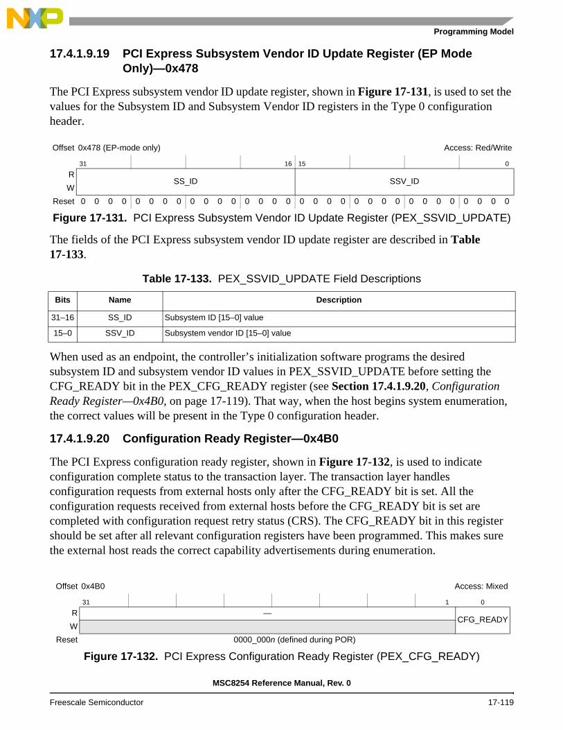
Programming Model
17.4.1.9.19 PCI Express Subsystem Vendor ID Update Register (EP Mode Only)—0x478
The PCI Express subsystem vendor ID update register, shown in Figure 17-131, is used to set the values for the Subsystem ID and Subsystem Vendor ID registers in the Type 0 configuration header.
The fields of the PCI Express subsystem vendor ID update register are described in Table 17-133.
When used as an endpoint, the controller’s initialization software programs the desired subsystem ID and subsystem vendor ID values in PEX_SSVID_UPDATE before setting the CFG_READY bit in the PEX_CFG_READY register (see Section 17.4.1.9.20, Configuration Ready Register—0x4B0, on page 17-119). That way, when the host begins system enumeration, the correct values will be present in the Type 0 configuration header.
17.4.1.9.20 Configuration Ready Register—0x4B0
The PCI Express configuration ready register, shown in Figure 17-132, is used to indicate configuration complete status to the transaction layer. The transaction layer handles configuration requests from external hosts only after the CFG_READY bit is set. All the configuration requests received from external hosts before the CFG_READY bit is set are completed with configuration request retry status (CRS). The CFG_READY bit in this register should be set after all relevant configuration registers have been programmed. This makes sure the external host reads the correct capability advertisements during enumeration.
Offset 0x478 (EP-mode only) Access: Red/Write
31 16 15 0
RSS_ID SSV_ID
W
Reset 0 0 0 0 0 0 0 0 0 0 0 0 0 0 0 0 0 0 0 0 0 0 0 0 0 0 0 0 0 0 0 0
Figure 17-131. PCI Express Subsystem Vendor ID Update Register (PEX_SSVID_UPDATE)
Table 17-133. PEX_SSVID_UPDATE Field Descriptions
Bits Name Description
31–16 SS_ID Subsystem ID [15–0] value
15–0 SSV_ID Subsystem vendor ID [15–0] value
Offset 0x4B0 Access: Mixed
31 1 0
R —CFG_READY
W
Reset 0000_000n (defined during POR)
Figure 17-132. PCI Express Configuration Ready Register (PEX_CFG_READY)
MSC8254 Reference Manual, Rev. 0
Freescale Semiconductor 17-119

PCI Express Controller
The fields of the PCI Express configuration ready register are described in Table 17-134.
17.4.1.9.21 PME_To_Ack Timeout Register (RC-Mode Only)—0x590
The PCI Express PME_To_Ack timeout register, shown in Figure 17-133, is used to program the timeout value for a PME_To_Ack message response in terms of PCI Express controller core clock cycles.
The fields of the PCI Express PME_To_Ack timeout register are described in Table 17-135.
Table 17-134. PEX_CFG_READY Field Descriptions
Bits Name Description
31–1 — Reserved
0 CFG_READY Configuration ready1 The transaction layer will accept inbound configuration requests.0 The transaction layer will respond to all inbound configuration requests with retry (CRS)Note that the reset state of this bit is determined during POR.
Offset 0x590 (RC-mode only) Access: Mixed
31 22 21 0
R —PME_TO_ACK_TIMEOUT
W
Reset 1 0 0 0 0 0 0 0 0 0 0 0 0 0 0 1 0 0 0 0 0 1 0 0 0 0 1 0 1 0 0 0
Figure 17-133. PCI Express PME_To_Ack Timeout Register (PEX_PME_TO_ACK_TOR)
Table 17-135. PEX_PME_TO_ACK_TOR Field Descriptions
Bits Name Description
31–22 — Reserved
21–0 PME_TO_ACK_TIMEOUT
After a PME_Turn_Off message is broadcast by the RC, the power management module waits for the duration of the PME_To_Ack timeout interval to receive a PME_To_Ack message from the downstream device. If the Ack message is not received within this interval, the power manager indicates that it is safe to switch off power, since timeout has occurred.The value is calculated as:
Time (in µsec) × PCI Express controller core clock frequency (in MHz)The recommended timeout duration is 1 ms to 10 ms to make sure that the downstream devices get enough time to prepare for power-off condition.
MSC8254 Reference Manual, Rev. 0
17-120 Freescale Semiconductor

Programming Model
17.4.1.9.22 Secondary Status Interrupt Mask Register (RC-Mode Only)—0x5A0
The PCI Express secondary status interrupt mask register, shown in Figure 17-134, can be used to disable sideband interrupt generation when error bits in the PCI Express secondary status register are set. See Section 17.4.1.7.29, PCI Express Secondary Status Register—0x1E, on page 17-83 for more information. By default, interrupt generation due to secondary status errors is disabled.
The fields of the PCI Express secondary status interrupt mask register are described in Table 17-136.
Offset 0x5A0 (RC-mode only) Access: Mixed
31 6 5 4 3 2 1 0
R— M_DPE M_SSE M_RMA M_RTA
M_STA
M_MDPE
W
Reset 0 0 0 0 0 0 0 0 0 0 0 0 0 0 0 0 0 0 0 0 0 0 0 0 0 0 1 1 1 1 1 1
Figure 17-134. PCI Express PCI Interrupt Mask Register (PEX_SS_INTR_MASK)
Table 17-136. PEX_SS_INTR_MASK Field Descriptions
Bits Name Description
31–6 — Reserved
5 M_DPE Mask detected parity error
4 M_SSE Mask signaled system error
3 M_RMA Mask received master abort
2 M_RTA Mask received target abort
1 M_STA Mask signaled target abort
0 M_MDPE Mask master data parity error
MSC8254 Reference Manual, Rev. 0
Freescale Semiconductor 17-121

PCI Express Controller
17.4.1.9.23 Gen2 Control Register
The PEX Gen2 control register, shown in Figure 17-135, can be used to control the MAC in Gen2 device.
The fields of the PEX Gen2 control register are described in Table 17-137.
Offset 0x640 Access: Read/Write
31 21 20 16
R— RxEI_FWH
W
Reset All zeros
15 14 9 8 7 4 3 2 1 0
R RxEI_FWH
RxEI_FWLRxEI Inf_E
S_LS SDEF SDEPHWLW
UETx_S
W
Reset 0 0 0 0 0 0 0 1 0 0 1 0 0 0 1 0
Figure 17-135. PEX Gen2 Control Register (PEX_GEN2_CONTROL)
Table 17-137. PEX_GEN2_CONTROL Field Descriptions
Bits Name Description
31–21 — Reserved
20–15 RxEI_FWH RxEI filter width high
14–9 RxEI_FWL RxEI filter width low
8 RxEI_Inf_E RxEI inferring enable
7–4 S_LS Supported link speeds
3 SDEF Select de-emphasis forced
2 SDEP Select de-emphasis preferred
1 HWLWUE Hardware link width upconfiguration enable
0 Tx_S Transmit swing
MSC8254 Reference Manual, Rev. 0
17-122 Freescale Semiconductor

QUICC Engine Subsystem 18The QUICC Engine subsystem is a versatile RISC-based communication processor that supports multiple external interfaces and protocols independently from the core processor(s) in an integrated processing device. This allows the cores to execute the data processing code and be relieved from the data transfer and handling overhead. This chapter provides an overview of the QUICC Engine subsystem components used in the MSC8254, which include the following:
Dual RISC engines with
— Internal interfaces to the core and peripherals— Parameter RAM— Buffer descriptors— Multithreading operation— Serial numbers (SNUMs)— Instruction RAM (IRAM)
Serial DMA controller
Clocking
— Signal multiplexing— Baud-rate generation
Dedicated interrupt controller
Two programmable Unified Communication Controllers (UCCs), each of which provides dedicated support for an Ethernet controller for RGMII/SGMII interfaces
Serial peripheral interface (SPI)
Note: Detailed information about QUICC Engine functionality and programming is provided in the QUICC Engine Block Reference Manual with Protocol Interworking (QEIWRM). Refer to that manual for all the functional and programming details
Note: If the QUICC Engine subsystem is not used for booting, the user must clear the QUICC Engine DRAM before using it to ensure correct operation.
MSC8254 Reference Manual, Rev. 0
Freescale Semiconductor 18-1
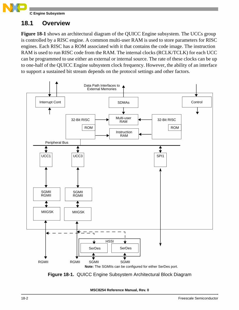
QUICC Engine Subsystem
18.1 Overview
Figure 18-1 shows an architectural diagram of the QUICC Engine subsystem. The UCCs group is controlled by a RISC engine. A common multi-user RAM is used to store parameters for RISC engines. Each RISC has a ROM associated with it that contains the code image. The instruction RAM is used to run RISC code from the RAM. The internal clocks (RCLK/TCLK) for each UCC can be programmed to use either an external or internal source. The rate of these clocks can be up to one-half of the QUICC Engine subsystem clock frequency. However, the ability of an interface to support a sustained bit stream depends on the protocol settings and other factors.
Figure 18-1. QUICC Engine Subsystem Architectural Block Diagram
UCC1 UCC3 SPI1
32-Bit RISC Multi-userRAM
SGMIIRGMII
Peripheral Bus
SDMAs
ROM
32-Bit RISC
ROM
Data Path Interfaces toExternal Memories
InstructionRAM
Interrupt Cont Control
SGMIIRGMII
MIIGSKMIIGSK
SerDesSerDes
SGMIISGMIIRGMII RGMII
HSSI
Note: The SGMIIs can be configured for either SerDes port.
MSC8254 Reference Manual, Rev. 0
18-2 Freescale Semiconductor

RISC Processors
18.2 RISC Processors
The two 32-bit RISC processors reside on a bus separate from the SC3850 cores, and can, therefore, perform tasks independently from the DSP cores. The RISC processors handle lower-layer communications tasks and DMA control, freeing the DSP cores to handle higher-layer activities. The RISC processors work with the UCCs to implement user-programmable protocols and manage the serial DMA (SDMA) channels that transfer data between the I/O channels and memory. The RISC processor architecture and instruction set are optimized for data communications and data processing required by many wire-line and wireless communications standards. The SC3850 DSP cores issues commands to the RISC processors by writing to the QUICC Engine Command Register (CECR), which is described in Section 18.9. The RISC processors execute the commands to ensure synchronization with other tasks running on the QUICC Engine subsystem. The DSP core sets the CECR[FLG] bit when it issues a command, and the QUICC Engine subsystem clears the FLG after execution, indicating to the DSP core that it is ready for the next command. Subsequent commands to the CECR can be given only after FLG is clear. The software reset command may be issued by setting RST even if the FLG bit is set. The CECR rarely needs to be accessed. For example, to terminate the transmission of a frame without waiting until the end, a STOP TX command is issued through the CECR. The worst-case command execution latency is 200 clocks and the typical command execution latency is about 40 clocks. The RISC processors give SDMA commands to the SDMA. RISC processor features include:
One QUICC Engine clock cycle per instruction
32-bit instruction object code
Code execution from internal ROM or RAM
32-bit ALU data path
64-bit multi-port RAM access
Optimized for communications processing
DMA bursting of serial data to/from external memory
18.2.1 SC3850 Core Interface
The RISC processors communicate with the SC3850 cores in several ways:
Many parameters are exchanged through the multi-port RAM. The RISC processors can execute special commands issued by the SC3850 cores. These commands should be issued only in special situations such as exceptions or error recovery. The RISC processor generates interrupts through the interrupt controller. The SC3850 cores can read the QUICC Engine subsystem status/event registers at any time.
MSC8254 Reference Manual, Rev. 0
Freescale Semiconductor 18-3

QUICC Engine Subsystem
18.2.2 Peripheral Interface
The RISC processors use the peripheral bus to communicate with all of its UCCs. Each controller has separate receive and transmit 192-byte FIFOs.
18.2.3 Parameter RAM
The QUICC Engine subsystem maintains a section in the multi-user RAM that contains the associated parameter values for the operation of the UCCs and SPI. Each peripheral has an associated page in the parameter RAM. The exact definition of the parameter RAM for each peripheral is in the protocol descriptions in the QUICC Engine Block Reference Manual with Protocol Interworking (QEIWRM). The size of the parameter RAM page differs from protocol to protocol. The minimum size of the parameter RAM page assigned to any protocol is 64 bytes. The base address of the parameter RAM page must be aligned to 64 bytes.
Some parameter RAM values must be initialized before the UCC is enabled. The QUICC Engine subsystem initializes or writes other values. Once initialized, most parameter RAM values need not be accessed by user software, because most activity centers around the TxBDs and RxBDs rather than the parameter RAM. However, if the parameter RAM is accessed, note the following:
You can read the parameter RAM at any time.
You can write to the Tx parameter RAM only when the transmitter is disabled (that is, after a STOP TRANSMIT command or after the buffer/frame finishes transmitting after a GRACEFUL STOP TRANSMIT command and before a RESTART TRANSMIT command).
You can write to the Rx parameter RAM only when the receiver is disabled. The CLOSE RX
BD command does not stop reception, but it does allow the user to extract data from a partially full Rx buffer.
After reset, the QUICC Engine subsystem initializes the base addresses of the parameter RAM pages for all the UCCs to default values. You can override the default values by issuing the ASSIGN PAGE command to the QUICC Engine subsystem. The advantage of using the ASSIGN PAGE command is that you can arrange the parameter RAM area efficiently (with no unused areas) according to the specific peripherals/protocols used in your system.
Table 18-1 lists the default values of the parameter RAM pages base addresses assigned by the QUICC Engine subsystem to the different peripherals.
Table 18-1. Default Parameter RAM Base Addresses
Address Offset PeripheralSize
(Bytes)
0x8400 UCC 1 (Rx and Tx) 256
0x8600 UCC 3 (Rx and Tx) 256
0x8900 SPI (Rx and Tx) 128
MSC8254 Reference Manual, Rev. 0
18-4 Freescale Semiconductor

RISC Processors
18.2.4 Buffer Descriptors (BDs)
If you are programming the UCCs, you need to know how the controllers use buffer descriptors to define buffer allocation. A buffer descriptor (BD) contains the essential information about each buffer in memory. Each buffer is referenced by a BD that can reside anywhere in system memory. These BDs are split between all UCCs.
Each 64-bit BD has the structure shown in Figure 18-2. This structure is common to all UCCs. A receive buffer descriptor (RxBD) table and a transmit buffer descriptor (TxBD) table are associated with each controller. Each table can have multiple BDs.
In this discussion, the BD and field values use the following convention:
BD.field
Table 18-2 shows the possible BD and field naming conventions. Bit names in RxBD.bd_cstat and TxBD.bd_cstat use the following convention:
BD.bd_cstat.bit
The structural elements of a buffer descriptor are defined as follows:
Status and control. The 16-bit value at offset+0x0, which contains status and control bits that control and report status information on the data transfer. The RISC processor updates the status bits after the buffer is sent or received. Only this field differs for each protocol. Refer to the relevant chapter in this manual for each protocol RxBD.bd_cstat and TxBD.bd_cstat bit description.Data length. The 16-bit value at offset+0x2, which contains the number of bytes sent or received.
Offset 15 14 13 12 11 10 9 8 7 6 5 4 3 2 1 0
0x0 Status and Control
0x2 Data Length
0x4 High-Order Buffer Pointer
0x6 Low-Order Buffer Pointer
Figure 18-2. Buffer Descriptor Structure
Table 18-2. Buffer Descriptor Name Convention
BD Field Example
RxBD/TxBD bd_cstat TxBD.bd_cstat.R refers to the ready bit in the TxBD’s status and control field.
bd_length RxBD.bd_length refers to RxBD data length field.bd_addr RxBD.bd_addr refers to RxBD buffer pointer field.
MSC8254 Reference Manual, Rev. 0
Freescale Semiconductor 18-5

QUICC Engine Subsystem
RxBD data length. The number of bytes the RISC processor writes into the RxBD buffer once the BD closes. The RISC processor updates this field after the received data is placed into the buffer and the buffer is closed. You do not need to initialize this field. In frame-based protocols, RxBD.bd_length contains the total frame length including CRC bytes. If a received frame length, including CRC, is an exact multiple of the parameter RAM maximum receive buffer length MRBLR, the last buffer holds no actual data but the associated BD contains the total frame length.TxBD data length. The number of data bytes the controller needs to transmit from its buffer. The RISC processor never modifies this field. This field needs to be initialized by the user.Buffer pointer. The 32-bit data at offset+0x4, which points to the beginning of the buffer in internal or external memory.RxBD buffer pointer. The buffer pointer value must be a multiple of four to be word-aligned.TxBD buffer pointer. The buffer pointer value can be even or odd.
18.2.5 Multithreading
The Ethernet Controllers are able to processes frames or cells at high bit rates (gigabit Ethernet and above OC-3 nominal rates). In order to achieve these bit rates the UCC receiver and the UCC transmitter are able to process multiple frames/cells simultaneously at any given time. This is implemented with the multithreading mechanism. Each thread processes a different frame/cell. The multithreading processing mechanism comprises three components: Distributor, Threads and in some cases Terminator. Figure 18-3 shows a high-level diagram of the multithreading architecture.
Each one of the components (distributor, threads and terminator) has an ID number associated with it, referred to as its Serial Number (SNUM). The distributor SNUM is always the SNUM of the UCC receiving or transmitting the data. Each one of the transmitter and receiver threads has its own parameter RAM located in the multi-port RAM. The user software initializes the values for the SNUM and the pointer of the parameter RAM base address at initialization time.
Note: See the QUICC Engine Block Reference Manual with Protocol Interworking (QEIWRM).for specific interface configuration details.
Figure 18-3. Multi-Threading Processing Mechanism
DistributorThread1
Thread2
Thread3
Terminator
MSC8254 Reference Manual, Rev. 0
18-6 Freescale Semiconductor

RISC Processors
18.2.6 Serial Numbers (SNUMs)
Each peripheral has a unique serial number (SNUM) associated with it. Threads, which are used by the multithreading mechanisms described in Section 18.2.5, Multithreading also have a unique serial number. There are two cases for which you should specify the SNUM:
1. When issuing the ASSIGN PAGE command.
2. When initializing the multithreading mechanism.
Table 18-3 lists the Serial Numbers (SNUMs) used to program the multithreading options in the UCCs for the Ethernet controllers. The component column indicates the peripheral or thread name for each SNUM.
Table 18-3. SNUM Table
SNUM Component SNUM Component SNUM Component SNUM Component
0x00 UCC1 TX 0x40 — 0x80 0xC0 Reserved0x01 UCC1 RX 0x41 — 0x81 0xC1 Reserved
0x04 Thread16 0x44 — 0x84 — 0xC4 —0x05 Thread17 0x45 — 0x85 — 0xC5 —0x08 — 0x48 0x88 Thread0 0xC8 Thread8
0x09 — 0x49 0x89 Thread1 0xC9 Thread90x0C Thread18 0x4C — 0x8C — 0xCC —0x0D Thread19 0x4D — 0x8D — 0xCD —
0x10 Reserved 0x50 Reserved 0x90 Reserved 0xD0 —0x11 Reserved 0x51 Reserved 0x91 Reserved 0xD1 —0x14 Thread20 0x54 — 0x94 — 0xD4 —
0x15 Thread21 0x55 — 0x95 — 0xD5 —0x18 — 0x58 — 0x98 Thread2 0xD8 Thread100x19 — 0x59 — 0x99 Thread3 0xD9 Thread11
0x1C Thread22 0x5C — 0x9C — 0xDC —0x1D Thread23 0x5D — 0x9D — 0xDD —0x20 UCC3 TX 0x60 Reserved 0xA0 Reserved 0xE0
0x21 UCC3 RX 0x61 Reserved 0xA1 Reserved 0xE10x24 Thread24 0x64 — 0xA4 — 0xE4 —0x25 Thread25 0x65 — 0xA5 — 0xE5 —
0x28 — 0x68 — 0xA8 Thread4 0xE8 Thread120x29 — 0x69 — 0xA9 Thread5 0xE9 Thread130x2C Thread26 0x6C — 0xAC — 0xEC —
0x2D Thread27 0x6d — 0xAD — 0xED —0x30 Reserved 0x70 Reserved 0xB0 Reserved 0xF0 TIMER0x31 Reserved 0x71 Reserved 0xB1 Reserved 0xF1 Lowest
0x34 Thread28 0x74 — 0xB4 — 0xF4 —0x35 Thread29 0x75 — 0xB5 — 0xF5 —0x38 — 0x78 — 0xB8 Thread6 0xF8 Reserved
0x39 — 0x79 — 0xB9 Thread7 0xF9 Reserved0x3C Reserved 0x7C — 0xBC — 0xFC —0x3D Reserved 0x7D — 0xBD — 0xFD —
Note: See the QUICC Engine Block Reference Manual with Protocol Interworking (QEIWRM) for details on how to use the SNUM with the ASSIGN PAGE command.
MSC8254 Reference Manual, Rev. 0
Freescale Semiconductor 18-7

QUICC Engine Subsystem
18.2.7 IRAM
The QUICC Engine subsystem includes 48 KB of IRAM that can be used to store processing code for the RISC processors. The IRAM can be split into two 24-KB areas assigned individually to each of the two RISC processors, or it can be shared by both processors as one contiguous 48-KB memory space. Access is through the IRAM address register (IADDR) using the IRAM data register (IDR). See the QUICC Engine Block Reference Manual with Protocol Interworking (QEIWRM) for details.
18.3 Serial DMA Controller
The QUICC Engine subsystem has one physical serial DMA (SDMA) channel that interfaces with the internal MBus. The QUICC Engine subsystem implements two dedicated virtual SDMA channels for each peripheral, one for the receiver and one for the transmitter. Additional virtual channels are available for general purpose accesses.
18.3.1 Data Paths
Figure 18-4 is a simplified block diagram that shows the data paths in the MSC8254. The MSC8254 may be implemented with one DDR bus (32 or 64 bit data).
The CLASS is responsible for distribution of MBus transactions to the various possible targets (for example, RapidIO or DDR memory controller) based on the transaction address. See Chapter 4, Chip-Level Arbitration and Switching System (CLASS) for details.
Figure 18-4. MSC8254 Data Paths
QBusSC3850
SDMAMulti-User
RAM
UCC3UCC1
ComplexRISC
QUICC Engine (QUICC Engine Subsystem)
ExternalDDR
External System
(32 or 64 bit data) DDR Bus
DDRMEMC
CLASSRapidIO
Controller
SerDes Interface
DSPCores
M3Memory
MSC8254 Reference Manual, Rev. 0
18-8 Freescale Semiconductor

Serial DMA Controller
18.3.2 SDMA and Bus Error
If a bus error occurs on an SDMA access from the QUICC Engine subsystem, the following occurs:
1. The QUICC Engine subsystem generates a unique maskable interrupt in the SDMA status register (SDSR),
2. The DSP core uses an interrupt service routine (ISR) to read the SDSR to determine which bus generated the error.
3. System recovery depends on how you configure the SDMR[SBER_1] bit. One of the following occurs:
— The QUICC Engine subsystem disables the peripheral or thread associated with the bus error and continues to operate as usual on all other peripherals (default). The recovery sequence in this mode is based on re-initialization of the peripheral associated with the error, or
— The QUICC Engine subsystem stops all activity, and must be reset through the reset command to the QUICC Engine Command Register (CECR).
In general, it should be noted that the DSP core, depending on how it is programmed, may read the SDMA address register (SDTA) to determine the address at which the bus error occurred, and the SDMA SNUM register (SDTM) to determine which peripheral or thread was being serviced by the SDMA virtual channel. See Table 18-3 for the list of SNUMs.
The SDTA and the SDTM registers store information related to accesses to the MBus. These two registers are not updated with the address and SNUM of subsequent transactions as long as the event bit in the SDSR is set.
18.3.2.1 Simple Recovery from Bus Error
The simplest recovery from a bus error is a QUICC Engine subsystem reset followed by an overall QUICC Engine subsystem re-initialization procedure, regardless of the peripheral that has actually caused the error. The reasoning is that for some applications, stopping one peripheral leads to a chain reaction that ultimately disrupts the correct interworking operation of the QUICC Engine subsystem. For debug purposes, it is valuable to observe continued operation, but a selective recovery does not provide any added value. This non-distinctive procedure also reduces the complexity of the recovery flow.
MSC8254 Reference Manual, Rev. 0
Freescale Semiconductor 18-9

QUICC Engine Subsystem
18.3.2.2 Selective Peripheral Recovery Procedure
Selective recovery can be a complex procedure due to the following:
The Ethernet controllers are multi-thread controllers and SNUM to peripheral/controller translation requires maintaining association tables.
Status for multiple bus errors is not maintained, so in theory there might be additional non-reported bus errors and the recovery will not be complete.
For these reason, a full reset and re-initialization are recommended.
18.3.3 SDMA and Reset
When the QUICC Engine subsystem is reset through the CECR[RST] bit, the SDMA continues to process outstanding transactions in its FIFOs although the data related to these transactions may be corrupted. During system reset (SRESET or HRESET), all SDMA FIFOs are flushed and all outstanding transactions are stopped.
18.3.4 MBus Access
The SDMA requests the bus from the CLASS at two possible priority levels. When the SDMA is in normal state, it requests the bus at priority level programmed by the user in the SDMR[EBPR] bit field. When the SDMA is in emergency state, it requests the bus at the highest priority level that the CLASS supports; the QUICC Engine subsystem is assigned an arbitration weight through a field in GCR11 (see Section 8.2.27, General Control Register 11 (GCR11), on page 8-41 for details). SDTR and SDHY program the threshold and hysteresis values that affect the conditions for SDMA normal and emergency states. It is possible to mask the emergency state priority requests globally in SDMR[EBMSK] and enforce the priority set in SDMR[EBPR] regardless of the SDMA state.
The SDMA asserts the highest priority request (emergency state) for any one of the following reasons:
When one of the FIFOs in the QUICC Engine subsystem reaches an emergency state (too full on Rx or too empty in the middle of a frame during Tx)
When the internal SDMA data buffers are filled beyond a certain level (programmed in SDTR/SDHY registers).
When the internal SDMA command queue is filled beyond a certain level (programmed in SDTR/SDHY registers).
A priority request to the multi-user RAM is also asserted by the SDMA, if needed, for the same reasons. It is possible to mask the high priority request globally in SDMR[ERMSK].
MSC8254 Reference Manual, Rev. 0
18-10 Freescale Semiconductor

Clocking
18.3.5 SDMA Internal Resource
The SDMA requires temporary buffering for some data in the multi-user RAM. The base address for the SDMA temporary buffer is programmed in the SDEBCR. The base address must be aligned to a 4-KB boundary. The size of the multi-user RAM needed for this buffering is programmable via the STBSZ bit field in the SDMR. The size the temporary buffer that must be allocated ranges from a minimum of 512 bytes to maximum of 3 KB in the multi-user RAM. See the QUICC Engine Block Reference Manual with Protocol Interworking (QEIWRM) for details.
18.4 Clocking
The QUICC Engine subsystem uses a programmable multiplexing system to route the various clocks used to transfer data through the external interfaces. Depending on the application and interface used, these signals can be supplied externally or taken from the internal programmable baud-rate generators. The following subsections describe the multiplexing unit and the internal baud-rate generators.
18.4.1 Multiplexer Logic
The QUICC Engine subsystem multiplexing logic routes clocks and connects the physical interfaces to the QUICC Engine subsystem peripherals, including the two UCCs. The multiplexer logic routes clocks to all the QUICC Engine subsystem peripherals from a bank of internal clocks (BRG[5–8]) and a bank of external clocks.
Physical signal connections are also configured using the clock route registers. However, because these signal lines are multiplexed with other functions at the I/O lines, you must make sure that the lines are also enabled through the GPIO registers and initial mode selection pins. Figure 18-5 shows a block diagram of the QUICC Engine subsystem multiplexing logic.
Figure 18-5. QUICC Engine Multiplexing Logic Block Diagram
Parallel I/O
CLKIN xMII
DataClocks
UCC1 UCC3 QUICC Engine Peripherals
Multiplexing and Timing Logic
ClockMultiplexing
Configuration
DataMultiplexer
ClockMultiplexer
Bank of ExternalClocks
MSC8254 Reference Manual, Rev. 0
Freescale Semiconductor 18-11

QUICC Engine Subsystem
The multiplexing logic is primarily used for clock assignment for UCC1 and UCC3. The clocks are derived from a bank of internal BRGs and external clock inputs as shown in Figure 18-6. The clock routing options are described in Table 18-4 and Table 18-5. The bank of clocks selection logic applies an available clock to a peripheral that requires a clock. Because the peripheral is not directly connected to a specific clock source, peripherals can share the same clock. There are two main advantages to the bank-of-clocks approach. First, a peripheral is not forced to choose a serial device clock from a predefined input or BRG. Second, peripheral receivers and transmitters that need the same clock rate can share the same source. This configuration leaves additional signal lines for other functions and minimizes potential skew between multiple clock sources.
Figure 18-6. Bank of Clocks
Table 18-4. Clock Source Options Using External Clock Signals
ClockExternal CLK
GE1_RX_CLK GE1_TX_CLK GE2_RX_CLK GE2_TX_CLK
UCC1 Rx VUCC1 Tx VUCC3 Rx V
UCC3 Tx VTime Stamp 1 V VTime Stamp 2 V V
Bank of ClocksSelection Logic
GE1_TX_CLKGE1_RX_CLK
(Partially filled cross-switch logic programmed in the multiplex
UCC1Tx
Rx
Time stamps 1,2
UCC3Tx
Rx
GE2_RX_CLKGE2_TX_CLK
BRG5 BRG6 BRG7 BRG8
logic registers.)
MSC8254 Reference Manual, Rev. 0
18-12 Freescale Semiconductor

Clocking
18.4.2 Baud-Rate Generators (BRGs)
The QUICC Engine subsystem contains four independent, identical baud-rate generators (BRGs) that can be used with the UCCs. The clocks produced by the BRGs are sent to the bank-of-clocks selection logic, where they can be routed to the controllers. Each BRG can be routed to one or more UCCs. Figure 18-7 shows the block diagram for a BRG.
All BRGs can use BRGCLK as its source clock, or the external clock input selected by the value of BRGCx[EXTC]. The BRGCLK is an internal signal generated in the clock synthesizer. The external source option allows flexible baud-rate frequency generation, independent of the system frequency. Additionally, the external source option allows a single external frequency to be the source for more than one BRG. The external source signals are not synchronized internally before being used by the BRG. The BRG provides a divide-by-16 option (BRGCx[DIV16]) and a 12-bit prescaler (BRGCx[CD]) to divide the source clock frequency. The combined source-clock divide factor can be changed on-the-fly, except when changing to or from a CD value of 1, 2, or 3. For these values, disable the BRG and reset it before you program the new value. In addition, you should not make two changes within two source clock periods. If the BRG divides the clock by an even value, the transitions of BRGOn always occur on the rising edge of the source clock. If the divide factor is odd, the transitions alternate between the falling and rising edges of the source clock. The output of the BRG can be sent to the autobaud control block.
Table 18-5. Clock Source Options - Internal Clock Generators
ClockBRG Number
5 6 7 8
UCC1 Rx V
UCC1 Tx VUCC3 Rx VUCC3 Tx V
Figure 18-7. Baud-Rate Generator (BRG) Block Diagram
ClockSourceMUX
Divide by1 or 16
Prescaler12-Bit Counter
1–4,096
DIV 16 CD[5–8]
BRGOn Clock
BRGCLK
EXTC
ControlRXDn
ToBank of Clocks
BRGn
Ext. Clock
MSC8254 Reference Manual, Rev. 0
Freescale Semiconductor 18-13

QUICC Engine Subsystem
18.5 Interrupt Controller
The QUICC Engine subsystem interrupt controller sends general interrupts to the DSP cores in the MSC8254 device. The core must then initiate the correct interrupt service routine to handle the interrupt. Typically, this routine must read the interrupt status registers in the QUICC Engine subsystem to determine the appropriate action to take. For some specific interrupts, the MSC8254 uses five general configuration registers to expedite some interrupt responses:
Four external request registers (CPE1R, CPE2R, CPE3R, and CPE4R) record events reported to the QUICC Engine subsystem directly by another MSC8254 peripheral (see Section 8.2.16, QUICC Engine First External Request Multiplex Register (CPCE1R), on page 8-27 through Section 8.2.19, QUICC Engine Fourth External Request Multiplex Register (CPCE4R), on page 8-30 for details).
GIR1 includes two fields to specify whether an ECC error occurred for the QUICC Engine IRAM or DRAM (see Section 8.2.21, General Interrupt Register 1 (GIR1), on page 8-32). These fields are maskable for each core individually using the corresponding fields in GIER1_x (see Section 8.2.22, General Interrupt Enable Register 1 (GIER1_x), on page 8-34).
Note: See the QUICC Engine Block Reference Manual with Protocol Interworking (QEIWRM) for details about configuring the QUICC Engine interrupt system.
18.6 UCCs
The QUICC Engine subsystem UCCs implement the Ethernet protocols. This section provides a general overview of the UCCs. For a detailed description of the feature set and the protocol-specific programming model, refer to the QUICC Engine Block Reference Manual with Protocol Interworking (QEIWRM). The key features of the UCCs include:
Supports 1000 Mbps, full-duplex Ethernet/IEEE 802.3x/VLAN through RGMII/SGMII.
UCC clock can be derived from a internal clock or an external signal.
Uses bursts to improve bus usage.
Multibuffer data structure for received and transmitted data.
Buffers and buffer descriptors (BDs) may reside anywhere in system memory.
Programmable size-virtual FIFO buffers.
Echo and local loopback modes for testing.
MSC8254 Reference Manual, Rev. 0
18-14 Freescale Semiconductor

UCCs
The UCC block diagram is shown in Figure 18-8.
High-speed protocols require large FIFO depth. Sufficient FIFO size is important for increasing the QUICC Engine subsystem performance by eliminating overrun and underrun bottlenecks. Each protocol has an optimized FIFO size that depends not only on the bit rate, but also on other parameters such as packet or frame size. The UCC, when configured for high-speed protocols, extends the hardware FIFO into the QUICC Engine subsystem internal RAM. This extension is called virtual FIFO or VFIFO, because its size and location within the RAM are programmable according to the specific protocol. The FIFO as shown in Figure 18-8 is constructed using a real hardware FIFO embedded in the UCC and its extension to a virtual FIFOs in the QUICC Engine subsystem RAM. This flexible FIFO structure enables the QUICC Engine subsystem to sustain wire speed frame or cell bursts by allocating larger FIFO memory when required. The size of the virtual FIFO is user-programmable. The actual size that is needed depends on a number of factors, especially the following:
Maximum packet size
Protocols running on the UCC
Memory bus latency
Figure 18-8. UCC Block Diagram
Control and StatusRegisters
ClockGenerator
MAC RxControl
Unit
MAC TxControl
Unit
ReceiveData and
Status FIFOTransmitData and
Status FIFOL1 Interface (I/O)
CLASS Bus
Serial Bus
TCLK
RCLK
Internal Clocks
L1 Interface (I/O)
Interrupts
** **
** The size of the FIFO is user-programmable.
MSC8254 Reference Manual, Rev. 0
Freescale Semiconductor 18-15
QUICC Engine Subsystem
18.7 Ethernet Controllers
The Ethernet interface is a widely-used local area network (LAN) that is based on the carrier-sense, multiple access, collision detect (CSMA/CD) approach. The IEEE 802.3 standard was developed to codify the requirements of such a system to insure interoperability between devices operating on the LAN. Because Ethernet and the IEEE protocols are similar and can coexist on the same LAN, this manual uses the generic term Ethernet unless otherwise noted. The MSC8254 uses two UCC Gigabit Ethernet Controllers (UECs) coordinated through the QUICC Engine subsystem. Each controller supports several standard MAC-PHY interfaces to connect to an external Ethernet transceiver. Supported interfaces include:
1000 Mbps RGMII interface
1000 Mbps SGMII interface.
The gigabit Ethernet modes were developed as individual company standards. As an alternative to the IEEE 802.3z (GMII) Ethernet standard that discuss general Ethernet interfacing, the RGMII Specification Reduced Pin-count Interface for Gigabit Ethernet Physical Layer Devices provides a method for Gigabit throughput while saving pins/board space. The RGMII Specification is managed by Broadcom, Marvell, and Hewlett-Packard, and is available on the Hewlett-Packard website at:
http://www.hp.com/rnd/pdfs/RGMIIv2_0_final_hp.pdf
To maintain Gigabit speed while reducing the data signals in half, the RGMI specification makes use of both the positive and negative edges of the clock. Because of this, meeting the RGMII specification requires careful attention to timing and delays.
A second protocol that uses an even lower pin count was developed by Cisco Systems. The Serial-GMH Specification defines a serial gigabit interface for Ethernet. The specification is available from the Cisco website at:
ftp://ftp-eng.cisco.com/smii/sgmii.pdf
The MSC8254 implements the SGMII through a SerDes interface managed by the HSSI (see Chapter 15, High Speed Serial Interface (HSSI) Subsystem for details.
Refer to the QUICC Engine Block Reference Manual with Protocol Interworking (QEIWRM) for complete functional and programming details.
Figure 18-9 illustrates the block diagram of the UCC Ethernet controller.
MSC8254 Reference Manual, Rev. 0
18-16 Freescale Semiconductor

Ethernet Controllers
Figure 18-9. UCC Ethernet Controller Block Diagram
G/MII MAC Layer
Hostinterface
TBI
RMONCounters
TransmitDataFIFO
ReceiveDataFIFO
Peripheral Bus
ClocksGenerator
MIIGSK
RGMII
SerDes
RGMII SGMII MII Mgmt
MSC8254 Reference Manual, Rev. 0
Freescale Semiconductor 18-17

QUICC Engine Subsystem
18.7.1 Operating Modes
Each Ethernet controller can be configured to use RGMII or SGMII mode. Two fields in the QUICC Engine Control Register allow programming of each controller independently (see Section 8.2.8, QUICC Engine Control Register (QECR), on page 8-16 for details).
18.7.1.1 RGMII Mode
The RGMII is intended to be an alternative to the IEEE 802.3u MII, the IEEE 802.3z GMII, and TBI standards. The principle objective is to reduce the number of pins required to interconnect the MAC and the PHY from a maximum of 28 pins (TBI) to 12 pins in a cost effective and technology independent manner. In order to accomplish this objective, the data paths and all associated control signals are reduced and control signals are multiplexed together and both edges of the clock are used. For Gigabit operation, the clocks operate at 125 MHz.
18.7.1.2 SGMII Mode
The Serial Gigabit Media Independent Interface (SGMII) is designed to satisfy the following requirements:
Convey network data and port speed between a 1000 PHY and a MAC with significantly less signal pins than required for GMII.
Operate in full duplex.
In the MSC8254, SGMII is implemented used the SerDes interface.
Note: The internal ten-bit interface (TBI) circuitry is used to serialize/deserialize the Ethernet frame data. The TBI must be configured to perform this function. See the QUICC Engine Block Reference Manual with Protocol Interworking (QEIWRM) for programming details.
18.7.2 Ethernet Physical Interfaces
You can program the physical interfaces by configuring the PSMR and MACCFG2 registers. See the QUICC Engine Block Reference Manual with Protocol Interworking (QEIWRM) for details.
Table 18-6 lists the external signal properties of the shared Management Data lines.Chapter 3, External Signals describes the assignment of the signals to the device pins.
Table 18-6. Management Data Signal Properties
Name Function I/O
MDC Management Data Clock for all Ethernet interfacesThe MDIO signal clock reference (2.5 MHz clock).
Output
MDIO Management Data Input/Output for all Ethernet interfacesTransfers control signals between the PHY layer and the manger entity.
Input/Output
MSC8254 Reference Manual, Rev. 0
18-18 Freescale Semiconductor

Ethernet Controllers
The following subsections give details on the RGMII and SGMII signals.
18.7.2.1 Reduced Gigabit Media-Independent Interface (RGMII) Signals
The RGMII data paths and all associated control signals are reduced, control signals are multiplexed, and both edges of the clock are used. Figure 18-10 shows the RGMII connections between the Ethernet controller and a PHY.
18.7.2.1.1 RGMII Signals
Table 18-7 lists the RGMII signals.
Figure 18-10. RGMII MAC-PHY Interface
Table 18-7. RGMII Signals
Consortium Name
I/O Size FunctionReference
Clock
GTX_CLK O 1 Transmit Reference Clock125 MHz
—
TX_CLK I 1 Transmit Clock GTX_CLK
TX_CTL O 1 Transmit ControlTX_EN on clock positive edge.TX_ER on clock negative edge.
TXC
Tx Data O 4 Transmit DataTXD[0–3] on clock positive edge.TXD[4–7] on clock negative edge.
TXC
TXD[3–0]
RXD[3–0]
RX_CTL
RGMII
RX_CLK
TX_CTL
DSP
TX Data CLK
PHY
125 MHz Clock
GEn_TX_CLK
GEn_GTX_CLK
GEn_TX_CTL
GEn_TD[0–3]
GEn_RX_CLK
GEn_RX_CTL
GEn_RD[0–3]
GTX_CLK
TX_EN
TD[0–3]
RX_CLK
RX_CTL
RD[0–3]
MSC8254 Reference Manual, Rev. 0
Freescale Semiconductor 18-19

QUICC Engine Subsystem
18.7.2.1.2 RGMII Signal Configuration
The RGMII signals are multiplexed with the TDM signals (see Chapter 3, External Signals). Ethernet controller 1 is multiplexed with TDM2 and TDM3 signals and Ethernet controller 2 is multiplexed with TDM0 and TDM1 signals. Selection is done at reset by the value of the GE1 and GE2 fields in the Reset Configuration Word High (see Section 5.3.2, Reset Configuration Word High Register (RCWHR), on page 5-19 for details). If the value of field is 0 (low), the TDM signals are selected; if the value of the field is 1 (high), the Ethernet signals are selected. In addition, the appropriate field in the QUICC Engine Control Register (ENET_SGMII_MODE1 for GE2 or ENET_SGMII_MODE0 for GE1) must be configured for RGMII (the field must be 0) (see Section 8.2.8, QUICC Engine Control Register (QECR), on page 8-16 for details).
Note: The MSC8254 allows adjustment of the transmission delays for the RGMII signal lines using GCR4 (see Section 8.2.12, General Control Register 4 (GCR4), on page 8-20 for register details). Recommended settings are listed in the MSC8254 data sheet. Guidelines for adjusting these numbers in individual designs is provided in Using GCR4 to Adjust Ethernet Timing in MSC8144 DSPs (AN3811), available at www.freescale.com. The adjustment recommendations are applicable for the MSC8254 DSP.
18.7.2.2 Serial Gigabit Media-Independent Interface (SGMII) Signals
The SGMII is an alternative to the RGMII interface that further reduces the number of pins required to interconnect the MAC and PHY by using a SerDes 4 interface. It does not support auto-negotiation. The Ethernet controller SGMII interface uses the UEC ten-bit interface (TBI) connection internally, which connects to the SerDes block that serializes the transmitted data and deserializes the received data to/from the SGMII interface.
RX_CTL I 1 Receive ControlRX_DV on clock positive edge.RX_ER on clock negative edge.
RXC
Rx Data I 4 Receive DataRXD[0–3] on clock posedge RXD[4–7] on clock negedge
RXC
MDIO I/O 1 Management Data I/OTransfers control signals between the PHY layer and the manager entity.
MDC
MDC O 1 Management Data ClockThe MDIO signal clock reference (2.5 MHz clock).
—
RX_CLK I 1 Continuous Receive Reference Clock 125 MHz
—
Table 18-7. RGMII Signals (Continued)
Consortium Name
I/O Size FunctionReference
Clock
MSC8254 Reference Manual, Rev. 0
18-20 Freescale Semiconductor

Ethernet Controllers
18.7.2.2.1 SGMII Signals
The SGMII physical interface transmits and receives data using two data signals and a clock signals to convey frame data and link rate information between a 1000 Mbps PHY and an Ethernet MAC. The data signals operate at 1.25 Gbaud. Due to the speed of operation, each of these signals (including the clock signal) is realized as a differential pair thus providing signal integrity while minimizing system noise. Therefore, each data and clock signal path uses two physical signal lines (the differential pair). Table 18-8 lists the SGMII signals.
18.7.2.2.2 SGMII Signal Configuration
The SGMII signals are multiplexed with the serial RapidIO and PCI Express signals (see Chapter 3, External Signals and Chapter 15, High Speed Serial Interface (HSSI) Subsystem). Either signal can be routed through SerDes port 1 or 2, depending on the selected multiplex configuration. Selection is done at reset by the value of the S2P and S1P fields in the Reset Configuration Word Low (see Section 5.3.1, Reset Configuration Word Low Register (RCWLR), on page 5-17 for details). The values of these fields determine which lanes of the SerDes ports are assigned to the SGMII signals. In addition, the appropriate field in the QUICC Engine Control Register (ENET_SGMII_MODE1 for GE2 or ENET_SGMII_MODE0 for GE1) must be configured for SGMII (the field must be 1) (see Section 8.2.8, QUICC Engine Control Register (QECR), on page 8-16 for details).
Table 18-8. SGMII Signals
Signal Name I/O Size FunctionReference
Clock
SRIO_REF_CLK
SRIO_REF_CLK
I
I
2 Reference Clock125 MHz differential pair.
—
SG1_TX
SG1_TX
O
O
2 Transmit Data 1Differential pair for Ethernet 1 controller.
SRIO_REF_CLKSRIO_REF_CLK
SG2_TX
SG2_TX
O
O
2 Transmit Data 2Differential pair for Ethernet 2 controller.
SRIO_REF_CLKSRIO_REF_CLK
SG1_RX
SG1_RX
I
I
2 Receive Data 1Differential pair for Ethernet 1 controller.
SRIO_REF_CLKSRIO_REF_CLK
SG2_RX
SG2_RX
I
I
2 Receive Data 2Differential pair for Ethernet 2 controller.
SRIO_REF_CLKSRIO_REF_CLK
MDIO I/O 1 Management Data I/OTransfers control signals between the PHY layer and the manager entity.
MDC
MDC I 1 Management Data ClockThe MDIO signal clock reference (25 MHz clock).
—
MSC8254 Reference Manual, Rev. 0
Freescale Semiconductor 18-21

QUICC Engine Subsystem
18.7.3 Controlling PHY Links (Management Interface)
The support for MII Ethernet Management can be done by the SPI or by one UCC that can be selected using CMXGCR[SMI]. Control and status to and from the PHY is provided via the two-wire MII management interface described in the IEEE 802.3u standard. The MII management registers (MII management configuration, command, address, control, status, and indicator registers) exercise this interface between a host processor and one or more PHY devices.
The UEC MII registers support continuous read cycles (called a scan cycle); even through scan cycles are not explicitly defined in the standard. If requested (by setting MIIMCOM[scan cycle]), the controller performs repetitive read cycles of the PHY status register, for example. This allows you to monitor link characteristics more efficiently. The different fields in the MII management indicator register (scan, not valid, and busy) indicate availability of each read of the scan cycle to the host via MIIMSTAT[PHY scan] bit field.
The length of the MII management interface preamble can also be modified through the MII registers. After establishing that a PHY supports preamble suppression, the host may configure the UEC to suppress the preamble. When enabled, the length of MII management frames are reduced from 64 to 32 clocks. This effectively doubles the efficiency of the interface.
18.7.4 Ethernet Controller Initialization
After the Ethernet Controller completes the reset sequence, software must initialize certain UEC registers and the required parameters in the parameter RAM. Based on system requirements, other optional registers and parameters can also be initialized at the same time.
Table 18-9 lists the minimum steps required for register and parameter initialization
Table 18-9. Minimum Register Initialization
Initialization Step Registers
Configure the UCC to Fast protocols URMODE,UTMODE
Set the Tx Global Parameter RAM
Set the Rx Global Parameter RAMSet CMXUCR1 Select UCC1, UCC3 RxClk and TxClkInitialize the MAC Station address MACSTNADDR1 and MACSTNADDR2Initialize the Media media access control configuration register and the UCC protocol specific mode register
This MACCFG2 together with UPSMR register adjust frame length and preamble length, specifies various CRC/pad combinations, specifies Full/Half Duplex and operating mode
Initialize the Fast Protocol Fifo Configuration registers URFB, URFET, URFS, URFSET, UTFB, UTFS, UTFET, UTFTT, URTRY
UCC event register, Fast UCCE Initialize interrupts to prepare for interrupt eventsUCC mask register, Fast UCCM Initialize the interrupt mask to prepare for interrupt
events
Activate The Ethernet Controller
MSC8254 Reference Manual, Rev. 0
18-22 Freescale Semiconductor
Serial Peripheral Interface (SPI)
After initializing the registers, you must complete the following steps to bring the Ethernet Controller into a functional state:
1. To transmit Ethernet frames, build the TxBDs in memory, link them together as a ring, and point to the ring. A minimum of two TxBDs per ring is required.
2. To receive Ethernet frames, link the RxBDs together as a ring and point the corresponding registers to them. Both transmit and receive can be gracefully stopped after transmission and reception begins.
For SGMII mode, in addition to the minimum initialization steps, based on your system requirements, you must configure the QUICC Engine Control Register (QECR) to work in SGMII mode. See Section 8.2.8, QUICC Engine Control Register (QECR) on page 8-16 for details. You must also configure the TBI MII registers. See the QUICC Engine Block Reference Manual with Protocol Interworking (QEIWRM) for details.
18.8 Serial Peripheral Interface (SPI)
The serial peripheral interface (SPI) allows the exchange of data with other devices containing an SPI. The SPI also communicates with peripheral devices such as EEPROMs, real-time clocks, A/D converters, and ISDN devices. The SPI is a full-duplex, synchronous, character-oriented channel that supports a four-wire interface (receive, transmit, clock, and slave select). The SPI block consists of transmitter and receiver sections, an independent baud-rate generator, and a control unit. The transmitter and receiver sections use the same clock, which is derived from the SPI baud rate generator in master mode and generated externally in slave mode. During an SPI transfer, data is sent and received simultaneously. The SPI receiver and transmitter are double-buffered, as shown in Figure 18-11, giving an effective FIFO size (latency) of 2 characters. When the SPI is disabled in the SPI mode register (SPMODE[EN] = 0), it consumes little power.
Initialize the InitEnet parameter CECDR Initialize the Tx and Rx parameters of UCC1 ethernet. CECR
Enable the Ethernet Controller MAC TX and RX MACCFG1Note: See the QUICC Engine Block Reference Manual with Protocol Interworking (QEIWRM) for register addressing,
structure, and programming details.
Table 18-9. Minimum Register Initialization (Continued)
Initialization Step Registers
MSC8254 Reference Manual, Rev. 0
Freescale Semiconductor 18-23

QUICC Engine Subsystem
18.8.1 SPI Operating Modes
The SPI can be programmed to work in a single- or multiple-master environment. This section describes the SPI master and slave operation in a single-master configuration and then discusses the multi-master environment. The following sections present a summary of the main modes of operation which the SPI supports.
18.8.1.1 SPI as a Master Device
In master mode, the SPI sends a message to the slave peripheral, which sends back a simultaneous reply. A single-master device with multiple slaves can use general-purpose parallel I/O signals to selectively enable slaves, as shown in Figure 18-12. To eliminate the multi-master error in a single-master environment, the master SPI_SL input can be forced inactive by selecting SPI_SL for general-purpose I/O.
Figure 18-11. SPI Block Diagram
SPI Mode Register Transmit_Register Receive_Register
Counter Shift_Register
SPIBRGPins InterfaceQUICC Engine clk/2
SPI_MOSISPI_SL SPI_MISO SPI_CK
TxDRxD IN_CLK
Peripheral Bus/Serial Bus
Transmit_Buffer Receive_Buffer
Peripheral Bus
MSC8254 Reference Manual, Rev. 0
18-24 Freescale Semiconductor

Serial Peripheral Interface (SPI)
To start exchanging data, the QUICC Engine subsystem writes the data to be sent into a buffer, configures a TxBD with TxBD[R] set, and configures one or more RxBDs. The QUICC Engine subsystem then sets SPCOM[STR] in the SPI command register to start sending data, which starts once the SDMA channel loads the Tx FIFO with data.
The SPI then generates programmable clock pulses on SPI_CK for each character and simultaneously shifts Tx data out on SPI_MOSI and Rx data in on SPI_MISO. Received data is written into a Rx buffer using the next available RxBD. The SPI keeps sending and receiving characters until the whole buffer is sent or an error occurs. The QUICC Engine subsystem then clears TxBD[R] and RxBD[E] and issues a maskable interrupt to the interrupt controller.
When multiple TxBDs are ready, TxBD[L] determines whether the SPI keeps transmitting without SPCOM[STR] being set again. If the current TxBD[L] is cleared, the next TxBD is processed after data from the current buffer is sent. Typically, there is no delay on SPI_MOSI between buffers. If the current TxBD[L] is set, sending stops after the current buffer is sent. In addition, the RxBD is closed after transmission stops, even if the Rx buffer is not full; therefore, Rx buffers need not be the same length as Tx buffers.
Figure 18-12. Single-Master/Multi-Slave Configuration
SPI_MOSI
SPI_MISO
SPI_CK
SPI_SL
Slave 0
SPI_MISO
SPI_CK
SPI_SL
Slave 1
Slave 2
Master SPI
SPI_MOSI
SPI_MISO
SPI_CK
SPI_SL
SPI_MOSI
SPI_SL
SPI_CK
SPI_MISO
SPI_MOSI
Decoder can beEither Internal orExternal Logic
MSC8254 Reference Manual, Rev. 0
Freescale Semiconductor 18-25

QUICC Engine Subsystem
18.8.1.2 SPI as a Slave Device
In slave mode, the SPI receives messages from an SPI master and sends a simultaneous reply. The slave’s SPI_SL must be asserted before Rx clocks are recognized; once SPI_SL is asserted, SPI_CK becomes an input from the master to the slave. SPI_CK can be any frequency from DC to QUICC Engine clk/4.
To prepare for data transfers, the slave’s core processor writes data to be sent into a buffer, configures a TxBD with TxBD[R] set, and configures one or more RxBDs. The core processor then sets SPCOM[STR] to activate the SPI. Once SPI_SL is asserted, the slave shifts data out from SPI_MISO and in through SPI_MOSI. A maskable interrupt is issued when a full buffer finishes receiving and sending or after an error. The SPI uses successive RxBDs in the table to continue reception until it runs out of Rx buffers or SPI_SL is deasserted.
Transmission continues until no more data is available or SPI_SL is deasserted. If it is deasserted before all data is sent, it stops but the TxBD stays open. Transmission continues once SPI_SL is reasserted and SPI_CK begins toggling. After the characters in the buffer are sent, the SPI sends ones as long as SPI_SL remains asserted.
Note: When enabling the SPI or changing parameters in SPI Mode Register (like CP,CI), SPI_SL must remain deasserted for at least 2 QUICC Engine clk/2 clocks afterwards. Also if SPI_SL is deasserted between transfers, its deassertion time should be at least 2 QUICC Engine clk/2 clocks.
18.8.2 SPI in Multi-Master Operation
The SPI can operate in a multi-master environment in which SPI devices are connected to the same bus. In this configuration, the SPI_MOSI, SPI_MISO, and SPI_CK signals of all SPIs are shared; the SPI_SL inputs are connected separately, as shown in Figure 18-13. Only one SPI device at a time can act as a master—all others must be slaves. When an SPI is configured as a master and its SPI_SL input is asserted, a multi master error occurs because more than one SPI device is a bus master. The SPI sets SPIE[MME] in the SPI event register and a maskable interrupt is issued to the QUICC Engine subsystem. It also disables SPI operation and the output drivers of SPI signals. The core processor must clear SPMODE[EN] before the SPI is used again. After correcting the problems, clear SPIE[MME] and re-enable the SPI.
The maximum sustained data rate that the SPI supports is QUICC Engine clk/50. However, the SPI can transfer a single character at much higher rates—QUICC Engine clk/8 in master mode and QUICC Engine clk/4 in slave mode. Gaps should be inserted between multiple characters to keep from exceeding the maximum sustained data rate.
MSC8254 Reference Manual, Rev. 0
18-26 Freescale Semiconductor

Serial Peripheral Interface (SPI)
Figure 18-13. Multimaster Configuration
SPI #2
SPI_MISOSPI_MOSI
SELOUT1SPI_SLSPI_CK
SELOUT3SELOUT2
SPI #1
SPI #0
Notes:• All signals are open-drain • For a multi-master QUICC Engine subsystem with more than two masters, SPI_SL and SPIE[MME]
• It is the responsibility of the software to arbitrate for the SPI bus (with token passing,will not detect all possible conflicts.
• SPI_SLx signals are implemented in the software with general-purpose I/O signals.
SP
I_S
L1S
PI_
SL0
SP
I_S
L3S
PI_
SL2
SPI #3
for example).
SPI_MISOSPI_MOSI
SELOUT0SPI_SLSPI_CK
SELOUT3SELOUT2
SPI_MISOSPI_MOSI
SELOUT0SPI_SLSPI_CK
SELOUT3SELOUT1
SPI_MISOSPI_MOSI
SELOUT0SPI_SLSPI_CK
SELOUT2SELOUT1
MSC8254 Reference Manual, Rev. 0
Freescale Semiconductor 18-27
QUICC Engine Subsystem
18.8.3 External Signal Configuration
The SPI supports a four-wire interface—transmit, receive, clock, and slave select. See Figure 3-1 for detailed signal descriptions. After reset, the signals are assigned as GPIO17 to GPIO20. They must be configured as SPI signals by writing the correct values to the GPIO configuration registers. Refer to Table 3-9 SPI Signals on page 3-20 and Chapter 22, GPIO for programming information.
The SPI can be configured as a slave or as a master in single- or multiple-master environments. The master SPI generates the transfer clock SPI_CK, using the SPI baud rate generator (BRG). The SPI BRG input is QUICC Engine clk /2. The selection as slave or master determines the signal direction (input or output) to select when configuring the signals using the GPIO configuration registers.
SPI_CK is a gated clock, active only during data transfers. Four combinations of SPI_CK phase and polarity can be configured by using SPMODE[CI, CP]. SPI signals can also be configured as open-drain to support a multimaster configuration in which a shared SPI signal is driven by the processor or an external SPI device.
The SPI master-in slave-out SPI_MISO signal acts as an input for master devices and as an output for slave devices. Conversely, the master-out slave-in SPI_MOSI signal is an output for master devices. The dual functionality of these signals allows the SPIs in a multimaster environment to communicate with one another using a common hardware configuration.
When the SPI is a master, SPI_CK is the clock output signal that shifts received data in from SPI_MISO and transmitted data out to SPI_MOSI. SPI masters must output a slave select signal to enable SPI slave devices by using a separate general-purpose I/O signal. Assertion of SPI_SL while it is a master causes an error.
When the SPI is a slave, SPI_CK is the clock input that shifts received data in from SPI_MOSI and transmitted data out through SPI_MISO. SPI_SL is the input enable to the SPI slave. In a multi-master environment, SPI_SL (always an input) is also used to detect an error when more than one master is operating.
18.8.4 SPI Transmission and Reception Process
Because the SPI is a character-oriented communication unit, the core processor must pack and unpack the receive/transmit frames. A frame consists of all of the characters transmitted or received during a completed SPI transmission session, from the first character written to the internal SPI transmit data register (SPITD) to the last character transmitted following the setting of the LST bit in the SPI command (SPCOM) register.
The core processor receives data by reading the SPI receive data register (SPIRD) when the SPI event register (SPIE) not-empty bit (SPIE[NE]) is set. The core processor transmits data by writing it into the SPITD. When the next character to transmit is the final one in the current
MSC8254 Reference Manual, Rev. 0
18-28 Freescale Semiconductor
Programming Model
frame, the core processor sets the last (SPCOM[LST]) bit and then writes the final character to SPITD. The SPI sets the not-full (SPIE[NF]) bit whenever its transmit FIFO is not full. It clears the bit when the last character is written to SPITD and resets it after sending the last data.
The SPI-core processor handshake protocol can use a polling or interrupt mechanism. When using polling, the core processor reads the SPIE at a predefined frequency and acts according to the value of the SPIE bits. The polling frequency depends on the SPI serial channel frequency. When using the interrupt mechanism, setting either SPIE[NF] or SPIE[NE] causes an interrupt to the core processor. The core processor then reads the SPIE and acts accordingly. There are three basic modes of operation for transmitting and receiving: master, slave, and multimaster.
18.9 Programming Model
This section provides a summary list of the MSC8254 QUICC Engine subsystem, Ethernet controller, and SPI registers with their offsets.
Note: The QUICC Engine registers use a base address of 0xFEE00000.
Table 18-10. MSC8254 QUICC Engine Register Summary
Register Name Acronym Offset
IRAM Registers
IRAM Address Register IADD 0x0000
IRAM Data Register IDATA. 0x0004
Interrupt Controller Registers
QUICC Engine System Interrupt Configuration Register CICR. 0x0080
QUICC Engine Interrupt Vector Register CIVEC. 0x0084
QUICC Engine RISC Interrupt Pending Register CRIPNR. 0x0088
QUICC Engine System Interrupt Pending Register CIPNR. 0x008C
QUICC Engine Interrupt Priority Register—XCC Peripherals CIPXCC. 0x0090
QUICC Engine Interrupt Priority Register—WCC Peripherals CIPWCC. 0x0098
QUICC Engine Interrupt Priority Register—ZCC Peripherals CIPZCC. 0x009C
QUICC Engine System Interrupt Mask Register CIMR. 0x00A0
QUICC Engine RISC Interrupt Mask Register CRIMR. 0x00A4
QUICC Engine System Interrupt Control Register CICNR. 0x00A8
QUICC Engine Interrupt Priority Register for RISC Tasks A CIPRTA. 0x00B0
QUICC Engine System RISC Interrupt Control Register CRICR. 0x00BC
QUICC Engine High System Interrupt Vector Register CHIVEC. 0x00E0
QUICC Engine System
QUICC Engine Command Register CECR 0x0100
QUICC Engine Command Data Register CECDR 0x0108
MSC8254 Reference Manual, Rev. 0
Freescale Semiconductor 18-29

QUICC Engine Subsystem
QUICC Engine Time-Stamp Control Register CETSCR 0x011C
QUICC Engine Virtual Tasks Event Register CEVTER 0x0130
QUICC Engine Virtual Tasks Mask Register CEVTMR 0x0134
QUICC Engine RAM Control Register CERCR 0x0138
QUICC Engine Microcode Revision Number CEURNR 0x01B8
QUICC Engine Multiplexer Registers
CMX General Clock Route Register CMXGCR 0x0400
UCC Clock Route Register 1 CMXUCR1. 0x0410
SPI registers
SPI Mode Register SPMODE. 0x04E0
SPI Event Register SPIE. 0x04E4
SPI Mask Register SPIM. 0x04E8
SPI Command Register SPCOM. 0x04EC
Baud Rate Generators
Baud-Rate Generator Configuration Registers 5 BRGCR5 0x0650
Baud-Rate Generator Configuration Registers 6 BRGCR6 0x0654
Baud-Rate Generator Configuration Registers 7 BRGCR7 0x0658
Baud-Rate Generator Configuration Registers 8 BRGCR8 0x065C
UCC Registers
UCC1 General Mode Register GUMR1. 0x2000
UCC1 Protocol-Specific Mode Register UPSMR1. 0x2004
UCC1 Transmit On Demand Register UTODR1. 0x2008
UCC1 Event Register UCCE1. 0x2010
UCC1 Mask Register UCCM1. 0x2014
UCC1 Ethernet Transmitter Status Register UCCS1 0x2018
UCC1 Receive FIFO Base URFB1. 0x2020
UCC1 Receive FIFO Size URFS1. 0x2024
UCC1 Receive FIFO Emergency Threshold URFET1. 0x2028
UCC1 Receive FIFO Special Emergency Threshold URFSET1. 0x202A
UCC1 Transmit FIFO Base UTFB1. 0x202C
UCC1 Transmit FIFO Size UTFS1 0x2030
UCC1 Transmit FIFO Emergency Threshold UTFET1. 0x2034
UCC1 Transmit FIFO Transmit Threshold UTFTT1. 0x2038
UCC1 Transmit Polling Timer UFPT1 0x203C
UCC1 Retry Counter URTRY1. 0x2040
UCC1 General Extended Mode Register GUEMR1. 0x2090
Table 18-10. MSC8254 QUICC Engine Register Summary (Continued)
Register Name Acronym Offset
MSC8254 Reference Manual, Rev. 0
18-30 Freescale Semiconductor

Programming Model
Ethernet 1 MAC Configuration 1 Register E1MACCFG1 0x2100
Ethernet 1 MAC Configuration 2 Register E1MACCFG2 0x2104
Ethernet 1 Interframe Gap Register E1PGFG 0x2108
Ethernet 1 Half Duplex Register HAFDUP1 0x210C
Ethernet 1 MII Management Configuration Register MIIMCFG1 0x2120
Ethernet 1 MII Management Command Register MIIMCOM1 0x2124
Ethernet 1 MII Management Address Register MIIMADD1 0x2128
Ethernet 1 MII Management Control Register MIIMCON1 0x212C
Ethernet 1 MII Management Status Register MIIMSTAT1 0x2130
Ethernet 1 MII Management Indicator Register MIIMIND1 0x2134
Ethernet 1 Interface Status Register IFSTAT1 0x213C
Ethernet 1 Station Address Part 1 Register E1MACSTNADDR1 0x2140
Ethernet 1 Station Address Part 2 Register E1MACSTNADDR2 0x2144
Ethernet 1 MAC Parameter Register UEMPR1 0x2150
Ethernet 1 Ten-Bit Interface Physical Address Register UTBIPAR1 0x2154
Ethernet 1 Statistics Control Register UESCR1 0x2158
Ethernet 1 Tx 64-byte Frames E1TX64 0x2180
Ethernet 1 Tx 65- to 127-byte Frames E1TX127 0x2184
Ethernet 1 Tx 128- to 255-byte Frames E1TX255 0x2188
Ethernet 1 Rx 64-byte Frames E1RX64 0x218C
Ethernet 1 Rx 65- to 127-byte Frames E1RX127 0x2190
Ethernet 1 Rx 128- to 255-byte Frames E1RX255 0x2194
Ethernet 1 Octet Transmitted OK E1TXOK 0x2198
Ethernet 1 Tx Pause Frames E1TXCF 0x219C
Ethernet 1 Multicast Frame Transmitted OK E1TMCA 0x21A0
Ethernet 1 Broadcast Frames Transmitted OK E1TBCA 0x21A4
Ethernet 1 Number of Frames Received OK E1RXFOK 0x21A8
Ethernet 1 Rx Octets OK E1RBYT 0x21AC
Ethernet 1 Rx Octets E1RXBOK 0x21B0
Ethernet 1 Multicast Frame Received OK E1RMCA 0x21B4
Ethernet 1 Broadcast Frames Received OK E1RBCA 0x21B8
Ethernet 1 Statistic Counters Carry Register E1SCAR 0x21BC
Ethernet 1 Statistic Counters Carry Mask Register E1SCAM 0x21C0
UCC3 General Mode Register GUMR3. 0x2200
UCC3 Protocol-Specific Mode Register UPSMR3. 0x2204
UCC3 Transmit On Demand Register UTODR3. 0x2208
UCC3 Event Register UCCE3. 0x2210
Table 18-10. MSC8254 QUICC Engine Register Summary (Continued)
Register Name Acronym Offset
MSC8254 Reference Manual, Rev. 0
Freescale Semiconductor 18-31

QUICC Engine Subsystem
UCC3 Mask Register UCCM3. 0x2214
UCC3 Ethernet Transmitter Status Register UCCS3 0x2218
UCC3 Receive FIFO Base URFB3. 0x2220
UCC3 Receive FIFO Size URFS3. 0x2224
UCC3 Receive FIFO Emergency Threshold URFET3 0x2228
UCC3 Receive FIFO Special Emergency Threshold URFSET3 0x222A
UCC3 Transmit FIFO Base UTFB3. 0x222C
UCC3 Transmit FIFO Size UTFS3 0x2230
UCC3 Transmit FIFO Emergency Threshold UTFET3 0x2234
UCC3 Transmit FIFO Transmit Threshold UTFTT3. 0x2238
UCC3 Transmit Polling Timer UFPT3 0x223C
UCC3 Retry Counter URTRY3. 0x2240
UCC3 General Extended Mode Register GUEMR3 0x2290
Ethernet 2 MAC Configuration 1 Register E2MACCFG1 0x2300
Ethernet 2 MAC Configuration 2 Register E2MACCFG2 0x2304
Ethernet 2 Interframe Gap Register E2PGFG 0x2308
Ethernet 2 Half Duplex Register HAFDUP2 0x230C
Ethernet 2 MII Management Configuration Register MIIMCFG2 0x2320
Ethernet 2 MII Management Command Register MIIMCOM2 0x2324
Ethernet 2 MII Management Address Register MIIMADD2 0x2328
Ethernet 2 MII Management Control Register MIIMCON2 0x232C
Ethernet 2 MII Management Status Register MIIMSTAT2 0x2330
Ethernet 2 MII Management Indicator Register MIIMIND2 0x2334
Ethernet 2 Interface Status Register IFSTAT2 0x233C
Ethernet 2 Station Address Part 1 Register E2MACSTNADDR1 0x2340
Ethernet 2 Station Address Part 2 Register E2MACSTNADDR2 0x2344
Ethernet 2 MAC Parameter Register UEMPR2 0x2350
Ethernet 2 Ten-Bit Interface Physical Address Register UTBIPAR2 0x2354
Ethernet 2 Statistics Control Register UESCR2 0x2358
Ethernet 2 Tx 64-byte Frames E2TX64 0x2380
Ethernet 2 Tx 65- to 127-byte Frames E2TX127 0x2384
Ethernet 2 Tx 128- to 255-byte Frames E2TX255 0x2388
Ethernet 2 Rx 64-byte Frames E2RX64 0x238C
Ethernet 2 Rx 65- to 127-byte Frames E2RX127 0x2390
Ethernet 2 Rx 128- to 255-byte Frames E2RX255 0x2394
Ethernet 2 Octet Transmitted OK E2TXOK 0x2398
Ethernet 2 Tx Pause Frames E2TXCF 0x239C
Table 18-10. MSC8254 QUICC Engine Register Summary (Continued)
Register Name Acronym Offset
MSC8254 Reference Manual, Rev. 0
18-32 Freescale Semiconductor

Programming Model
Ethernet 2 Multicast Frame Transmitted OK E2TMCA 0x23A0
Ethernet 2 Broadcast Frames Transmitted OK E2TBCA 0x23A4
Ethernet 2 Number of Frames Received OK E2RXFOK 0x23A8
Ethernet 2 Rx Octets OK E2RBYT 0x23AC
Ethernet 2 Rx Octets E2RXBOK 0x23B0
Ethernet 2 Multicast Frame Received OK E2RMCA 0x23B4
Ethernet 2 Broadcast Frames Received OK E2RBCA 0x23B8
Ethernet 2 Statistic Counters Carry Register E2SCAR 0x23BC
Ethernet 2 Statistic Counters Carry Mask Register E2SCAM 0x23C0
MIIGSK1 Enable Register MIIGSK1_ENR 0x2808
MIIGSK2 Enable Register MIIGSK2_ENR 0x2A08
SDMA Registers
Serial DMA Status Register SDSR 0x4000
Serial DMA Mode Register SDMR 0x4004
Serial DMA Threshold Register SDTR 0x4008
Serial DMA Hysteresis Register SDHY 0x4010
Serial DMA Transfer Address Register SDTA 0x4018
Serial DMA Transfer Channel Number Register SDTM 0x4020
Serial DMA Address Qualify Register SDAQR 0x4038
Serial DMA Address Qualify Mask Register SDAQMR. 0x403C
Serial DMA Temporary Buffer Base in Multi-User RAM Value SDEBCR 0x4044
Table 18-10. MSC8254 QUICC Engine Register Summary (Continued)
Register Name Acronym Offset
MSC8254 Reference Manual, Rev. 0
Freescale Semiconductor 18-33

QUICC Engine Subsystem
MSC8254 Reference Manual, Rev. 0
18-34 Freescale Semiconductor
TDM Interface 19The MSC8254 Time-Division Multiplexing (TDM) interface enables communication among many devices over a single bus. Traffic is managed according to a time-division multiplexing method in which only one device drives the bus (transmit) for each channel. Each device drives its active transmit channels and samples its active receive channels when its channel is active. It is the system designer’s responsibility to guarantee that there is no conflict in transmit channel allocation.
The TDM interface is composed of four identical and independent TDM modules, each supporting 256 bidirectional channels (256 transmit and 256 receive channels) running at up to 62.5 Mbps with 2-, 4-, 8-, and 16-bit word size. The TDM bus connects gluelessly to most T1 /E1 framers as well as to common buses such as the ST-Bus. Each TDM module operates in independent or shared mode when receiving or transmitting data:
In independent mode, there are different sync, clock, and data links for receive and transmit.
In shared sync and clock mode, the clock and the sync are shared between the transmit and receive with different data links for the receive and transmit.
In shared data link mode, the receive and transmit share sync, clock, and full duplex data links between the transmit and receive. The clock and the sync signals can also be shared between the TDM modules.
MSC8254 Reference Manual, Rev. 0
Freescale Semiconductor 19-1
TDM Interface
At any time, each channel is individually set to active or inactive. An on-the-fly hardware A-law/μ−law conversion is supported for 8-bit channels. A channel is transparent or A-law/μ−law. Its data is collected in its own buffer location independently from other channel buffers. Memory space size is 16 MB for transparent channels and 32 MB for A-law/μ−law channels.
The direction of the bits in the channel (MSB first/LSB first) is configured globally for each TDM module. The direction of TSN is set to input or output. The polarity of the clock (sample/drive at clock rise or fall) is independently configured for the receiver and transmitter. The polarity of TSN/RSN/FSYN is configured to positive or negative.
The four TDM modules have an I/O matrix that routes the clock and sync signals between the TDM modules and the MSC8254 signal lines. The TDM may be configured by all six SC3850 cores (see Figure 19-1), as well as by an external host. Data is received and transmitted from the TDM modules to the channel buffers through the internal MBus. Figure 19-2 shows the TDM block diagram and the receive and transmit data flows. The dashed line depicts the transmit data flow from the system I/F to the I/O matrix; the solid line depicts the receive data flow from the I/O matrix to the receive buffers on the system I/F.
Serial data received from the I/O matrix is packed and stored in the TDM local memory buffer. From the local memory buffer, the data is converted according to A/μ transformation (if needed) and re-packed for transaction to the system I/F. Data transmission occurs in a similar way but in reverse order. The channel data is transferred from the transmit data buffers being converted by the A/μ logic and stored in the TDM local memory buffer. Then the data is transmitted to the transmit serial block and to the I/O matrix.
MSC8254 Reference Manual, Rev. 0
19-2 Freescale Semiconductor

Figure 19-1. General TDM Module Interface
TD
M0R
SN
TD
M0R
CK
TD
M0R
DT
TD
M0T
SN
TD
M0T
CK
TD
M0T
DT
TD
M1R
SN
TD
M1R
CK
TD
M1R
DT
TD
M1T
SY
TD
M1T
CK
TD
M01D
AT
TD
M2R
SN
TD
M2R
CK
TD
M2R
DT
TD
M2T
SN
TD
M2T
CK
TD
M2T
DT
TD
M3R
CK
TD
M3R
DT
TD
M3T
SN
TD
M3T
DT
Configuration I/F Multiplex
Interrupts Interrupts Interrupts Interrupts 64
System I/F
32
4
TDM I/O Matrix
44
tdm2_rdata_a-d
tdm2_rsync
tdm2_tdata_a-d
tdm2_tsync
tdm2_tclk
tdm2_rclk
44
tdm3_rdata_a-d
tdm3_rsync
tdm3_tdata_a-d
tdm3_tclk
tdm3_rclk
44
6
_
TD
M3T
CK
tdm3_tsync
TDM 3
3Rx error int0, Rxthreshold1 int0, Rxthreshold2 int0
1
1
2 Rx error int1, Rx threshold1 int1, Rx threshold2 int1
2
Rx error int2, Rx threshold1 int2,Rx threshold2 int2
3
4 Rx error int3, Rx threshold1 int7, Rx threshold2 int3
4
TDM 1 TDM 2
tdm1_rdata_a-d
tdm1_rsync
tdm1_rclk
tdm1_tdata_a-d
tdm1_tsync
tdm1_tclk
TDM 0
tdm0_rdata_a-d
tdm0_rsync
tdm0_tdata_a-d
tdm0_tsync
tdm0_tclk
tdm0_rclk
4
tdm0_sync_out
tdm1_sync_out
tdm2_sync_out
tdm3_sync_out
6 6 6
Tx error int0, Txthreshold1 int0, Txthreshold2 int0
Tx error int1, Tx threshold1 int1, Tx threshold2 int1
Tx error int2, Tx threshold1 int2,Tx threshold2 int2
Tx error int3, Tx threshold1 int7, Tx threshold2 int3
Configuration I/F
TDM Arbiter
TD
M3R
SN
MSC8254 Reference Manual, Rev. 0
Freescale Semiconductor 19-3

TDM Interface
Figure 19-2. TDM Block Diagram
Receive SerialMachine
Transmit Serial
Machine
TDM Local Memory
ReceivedData
TransmitData
TDM DMA
To internal MBus Interface
To IPBus Multiplex
tdmx_rdata_a
tdmx_rdata_b
tdmx_rdata_c
tdmx_rdata_d
tdmx_rsync
tdmx_rclk
64
IP logic
Status Registers
Control Registers
Configuration Registers
32
From I/O Matrix To I/O Matrix
TDM(x) Machine
32
Notes: X is the TDM number (0–3).
A/m Law DataConversion
64
64
128
Transmit data out
Receive data flow: Transmit data flow:
tdmx_tdata_a
tdmx_tdata_b
tdmx_tdata_c
tdmx_tdata_d
tdmx_tsync
tdmx_tclk
ReceiveData In
16
1616
tdmx_sync_out
MSC8254 Reference Manual, Rev. 0
19-4 Freescale Semiconductor

Typical Configurations
19.1 Typical Configurations
The TDM connects in various configurations. Figure 19-3 shows two MSC8254 devices that connect point-to-point. Data transmits from the device on the left to the device on the right or vice versa.
Figure 19-4 depicts a TDM point to multi-point configuration. Multiple MSC8254 devices connect on the same TDM bus, which connects to the network through a framer.
Figure 19-3. TDM Point-to-Point Configuration
Figure 19-4. TDM Point-to-Multi-Point Configuration
TDMxTDT
TDMxTSN
TDMxTCK
TDMxRDT
TDMxRSN
TDMxRCK
TDMxRDT
TDMxRSN
TDMxRCK
TDMxTDT
TDMxTSN
TDMxTCK
On-Board Clock Generator
On-Board Clock Generator
MS
C8254
MS
C8254
TD
MxT
DT
TD
MxT
CK
TD
MxT
SN
TD
MxR
DT
TD
MxR
CK
TD
MxR
SN
From ReceiverClock Generator
From transmitter Clock Generator
From ExternalSync Generator
TD
MxT
DT
TD
MxT
CK
TD
MxT
SN
TD
MxR
DT
TD
MxR
CK
TD
MxR
SN
TD
MxT
DT
TD
MxT
CK
TD
MxT
SN
TD
MxR
DT
TD
MxR
CK
TD
MxR
SN
TD
MxT
DT
TD
MxT
CK
TD
MxT
SN
TD
MxR
DT
TD
MxR
CK
TD
MxR
SN
MSC8254 MSC8254 MSC8254 MSC8254
MSC8254 Reference Manual, Rev. 0
Freescale Semiconductor 19-5

TDM Interface
Figure 19-5 depicts an application in which all the TDM modules share the sync and the clock (see Figure 19-11). Therefore, each TDM module supports one or two active links. In this example, 16 receive link and 16 transmit links connect to two MSC8254 devices.
19.2 TDM Basics
Multiple TDM channels are transferred sequentially in a structure called a frame. The frame start is identified by a frame sync signal that is briefly asserted at the beginning of every frame. Each of the four TDM modules can receive or transmit up to 256 channels at a granularity of two. The number of receive channels is determined by the RNCF field in the TDMx Receive Frame Parameters Register (TDMxRFP) (see page 19-47). The number of transmit channels is determined by the TNCF field in the TDMx Transmit Frame Parameters Register (TDMxTFP) (see page 19-50).
The size of all the channels (for each TDM module) is unified and it can be 2-, 4-, 8-, and 16 bits. The receive channel size is determined by the RCS field in the TDMxRFP; the transmit channel size is determined by the TCS field in the TDMxTFP (refer to page 19-50).
When the TDM connects to a T1 framer, the RT1 field in the TDMx Receive Frame Parameters Register (TDMxRFP) (see page 19-47) and the TT1 field in the TDMx Transmit Frame Parameters Register (TDMxTFP) (see page 19-50) should be set. The T1 frame contains 193 bits (24 channels of 8 bits each) when the first bit of the frame is a Frame Alignment bit that is not used by the TDM. At the T1 received frame, the Frame Alignment bit is removed and does not transfer to the main memory. At the transmit T1 frame, the bit is not driven out.
Figure 19-5. Common Frame Sync and Clock
TDM0
FCLK
FSYN
RD
TA 0
RD
TA 1
TD
TA 0
TD
TA 1
TDM1 TDM2 TDM0 TDM1 TDM2 TDM3
RD
TA 2
RD
TA 3
TD
TA 2
TD
TA 3
RD
TA 4
RD
TA 5
TD
TA 4
TD
TA 5
RD
TA 1
4R
DTA
15
TD
TA 1
4T
DTA
15
RD
TA16
RD
TA 1
7T
DTA
16
TD
TA 1
7
RD
TA 1
8R
DTA
19
TD
TA 1
8T
DTA
19
RD
TA 2
0R
DTA
21
TD
TA 2
0T
DTA
21
RD
TA 3
0R
DTA
31
TD
TA 3
0T
DTA
31
MSC8254 MSC8254
TDM3
MSC8254 Reference Manual, Rev. 0
19-6 Freescale Semiconductor

TDM Basics
Figure 19-6 shows an example of TDMx frames. The receive frame contains two 2-bit channels. The transmit frame contains four 4-bit channels. Figure 19-7 shows an example of T1 frame. In T1 mode, the first bit of the frame is not used by the TDM.
Figure 19-6. TDM Frames
Figure 19-7. T1 Frame
TDMxRCK(Receive clock)
TDMxRSNC(receive sync)
TDMxRDT (receive data) Channel 0 Channel 1 Channel 0 Channel 1 Channel0
TDMxTCK(transmit clock)
TDMxTSNC(transmit sync)
TDMxTDT channel 0 channel 1 Channel 2 Channel 3 Channel 0
Receive Frame parameters: RNCF[3–0] = 0x1 (2 channels), RCS = 0x1 (2 bits) and RT1 = 0 (nonT1).
TNCF[3–0]= 0x3 (4 channels), TCS = 0x3 (4 bits). and TT1 = 0 (non T1)Transmit Frame parameters:
Channel size
Frame Size
TDMxT/RCK
TDMxT/RSN
TDMxT/RDT FA D0 D1 D7 D0 D7 FAD6
193 bits, 125 ms
channel 0
Receive Frame parameters: RNCF[3–0] = 0x17 (24 channels), RCS = 0x7 (8 bits) and RT1 = 1 (T1 mode).
TNCF[3–0] = 0x23 (24 channels), TCS = 0x7 (8 bits) and TT1 = 1 (T1 mode)Transmit Frame parameters:
MSC8254 Reference Manual, Rev. 0
Freescale Semiconductor 19-7

TDM Interface
19.2.1 Common Signals for the TDM Modules
The sync and clock signals can be shared among the TDM modules or separate for each TDM module. When the CTS bit of the TDMx General Interface Register (see page 19-36) is equal to 1, the TDM modules share sync and clock signals. In this mode, the common signals connect to the following signal lines:
In non-independent mode, connect the shared sync to TDM0TSN (receive and transmit of all TDM modules share the same sync signal).
In non-independent mode, connect the shared clock to TDM0TCK (receive and transmit of all TDM modules share the same clock signal).
In independent mode, connect the transmit shared sync to TDM0TSNC (transmit of all TDM modules share the same sync signal). Connect the receive shared sync to TDM1TSNC (receive of all TDM modules share the same sync signal)
In independent mode, connect the transmit shared clock to TDM0TCK (transmit of all TDM modules share the same clock signal). Connect the receive shared clock to TDM1TCK (receive of all TDM modules share the same clock signal).
When the TDMxTIR[TSO] bit is set to a value of 1 (see page 19-45), the sync out signal drives out through TDM0TSN.
The configuration registers (see page 19-36) should be identical for the TDM modules that share signals. There are only seven possibilities for sharing TDMs:
TDM0 and TDM1.
TDM0, TDM1, and TDM2.
TDM0, TDM1, TDM2 and TDM3.
Figure 19-8 illustrates a common receive sync, receive clock, transmit sync, and transmit clock for TDM0 and TDM1. When the CTS bit of the TDMx General Interface Register (see page 19-36) is cleared, the TDM modules do not share signals. In Figure 19-8, TDM2–TDM3 do not share signals with the other TDM modules
MSC8254 Reference Manual, Rev. 0
19-8 Freescale Semiconductor

TDM Basics
In Figure 19-9, all four TDM modules share the same receive clock and sync and the same transmit clock and sync. The receive clock connects to the TDM1TCK port. The transmit clock connects to TDM0TCK, the receive sync connects to TDM1TSN, and the transmit sync connects to TDM0TSNC. Each module has two active data links. Notice that TDMxTSN, TDMxTCK when 2 ≤ x ≤ 3
are not used.
Figure 19-8. TDM Modules Model
Figure 19-9. Shared Receive Sync and Clock and Transmit Sync and Clock
TDM0 TDM1 TDM2 TDM3
TD
M0R
DT
Rxdata 0
TD
M0R
SN
Rxdata 1
TD
M0R
CK
Txdata 1
TD
M0T
DT
Txdata 0
TD
M0T
SN
Txsync (com
mon)
TD
M0T
CK
Txclk (com
mon)
TD
M1R
DT
Rxdata 2
TD
M1R
SN
Rxdata 3
TD
M1R
CK
Txdata 2
TD
M1T
DT
Txdata 3
TD
M1T
SN
Rxsync (com
mon)
TD
M1T
CK
Rxclk (com
mon)
TD
M2R
DT
R2data 0
TD
M2R
SN
R2sync
TD
M2R
CK
R2clk
TD
M2T
DT
T2data0
TD
M2T
SN
T2sync
TD
M2T
CK
T2clk
TD
M3R
DT
R3data 0
TD
M3R
SN
R3sync
TD
M3R
CK
R3clk
TD
M3T
DT
T3data0
TD
M3T
SN
T3sync
TD
M3T
CK
T3clk
RTSAL[3–0] = 0001CTS = 1
RTSAL[3–0] = 0001CTS = 1
RTSAL[3–0] = 0000CTS = 0
RTSAL[3–0] = 0000CTS = 0
TDM0 TDM1 TDM2 TDM3
TD
M0R
DT
Rxdata 0
TD
M0R
SN
Rxdata 1
TD
M0R
CK
Txdata 1
TD
M0T
DT
Txdata 0
TD
M0T
SN
Txsync (com
mon)
TD
M0T
CK
Txclk (com
mon)
TD
M1R
DT
Rxdata 2
TD
M1R
SN
Rxdata 3
TD
M1R
CK
Txdata 2
TD
M1T
DT
Txdata 3
TD
M1T
SN
CR
xsync (comm
on)
TD
M1T
CK
Rxclk (com
mon)
TD
M2R
DT
Rxdata 4
TD
M2R
SN
TD
M2R
CK
Txdata 5
TD
M2T
DT
Txdata 4
TD
M2T
SN
TD
M2T
CK
TD
M3R
DT
Rxdata 14
TD
M3R
SN
Rxdata 15
TD
M3R
CK
Txdata 15
TD
M3T
DT
Tx data 14
TD
M3T
SN
TD
M3T
CK
RTSAL[3–0] = 0001CTS = 1
RTSAL[3–0] = 0001CTS = 1
RTSAL[3–0] = 0001CTS = 1
RTSAL[3–0] = 0001CTS = 1
Rxdata 5
MSC8254 Reference Manual, Rev. 0
Freescale Semiconductor 19-9

TDM Interface
In Figure 19-10, all four TDM modules share the same frame sync, clock, and data links. Notice that TDMxTCK and TDMxTSN when 1 ≤ x ≤ 3 are not used.
19.2.2 Receiver and Transmitter Independent or Shared Operation
The TDM operates with the transmit and receive operations running either independently or shared, as illustrated in Figure 19-11. When the two most significant bits of the RTSAL field (RTSAL[3–2]) in the TDMx General Interface Register (see page 19-36) equal 0b00, the receive and the transmit are independent as illustrated on the left side of Figure 19-11. In this mode, there is one input receive data link and one output transmit data link. If the TDM shares signals with other TDM modules (CTS = 1), it can receive two data links and it can output two data links.
When the RTSAL[3–2] in the TDMx General Interface Register (see page 19-36) equal 0b01, the receive and transmit are shared as illustrated in the middle of Figure 19-11. The transmit and the receive share the Frame Sync (FSYN) and the Frame Clock (FCLK) signals. The number of receive and the transmit active links can be one or two. The direction of the receive links is input, and the direction of the transmit links is output.
When RTSAL[3–2] in the TDMx General Interface Register (see page 19-36) equal 0b11, the receive and the transmit are shared as illustrated on the right side of Figure 19-11. The transmit and the receive share the Frame Sync (FSYN), the Frame Clock (FCLK), and the data signals. In this mode, the data links are full duplex and are used for both transmit and receive, so the number of active links can be 1, 2, or 4.
Figure 19-10. Shared Frame Sync, Clock, and Data Links
TDM0 TDM1 TDM2 TDM3
TD
M1R
DT
Fxdata 4
TD
M1R
SN
Fxdata 5
TD
M1R
CK
Fxdata 6
TD
M1T
DT
Fxdata 7
TD
M1T
SN
C
TD
M1T
CK
TD
M2R
DT
Fxdata 8
TD
M2R
SN
TD
M2R
CK
Fxdata 10
TD
M2T
DT
Fxdata 11
TD
M2T
SN
TD
M2T
CK
TD
M3R
DT
Fxdata 12
TD
M3R
SN
Fxdata 13
TD
M3R
CK
Fxdata 14
TD
M3T
DT
Fx data 15
TD
M3T
SN
TD
M3T
CK
RTSAL[3–0] = 1111CTS = 1
RTSAL[3–0] = 1111CTS = 1
RTSAL[3–0] = 1111CTS = 1
RTSAL[3–0] = 1111CTS = 1
Fxdata 9
TD
M0R
DT
Fxdata 0
TD
M0R
SN
Fxdata 1
TD
M0R
CK
Fxdata 2
TD
M0T
DT
Fxdata 3
TD
M0T
SN
Fxsync (com
mon)
TD
M0T
CK
Fxclk (com
mon)
MSC8254 Reference Manual, Rev. 0
19-10 Freescale Semiconductor

TDM Basics
When RTSAL [1–0] equals 0b11, there are four active links: DATA_A, DATA_B, DATA_C, and DATA_D. When RTSAL[1–0] equals 0b01, there are two active links: DATA_A and DATA_B. When RTSAL[1–0] equals 0b00, there is one active link, DATA_A.
Figure 19-12 describes the TDM interface when the receive and transmit are totally independent (TDMxGIR[RTSAL] = 0b0000). The TDMxRCK is not synchronized to the TDMxTCK. They differ according to the sync location relative to the beginning of the frame and the number of bits.
Figure 19-11. TDM Module Sharing Modes
Figure 19-12. Receive and Transmit Totally Independent
TDM Module
TDMxRDT
TDMxRSN
TDMxRCK
TDMxTDT
TDMxTSN
TDMxTCK
TDMxRDT
TDMxRSN
TDMxRCK
TDMxTDT
TDMxTSN
TDMxTCK
Independent Receive Shared Data
x Defines the TDM number.
TDMxRDT
TDMxRSN
TDMxRCK
TDMxTDT
TDMxTSN
TDMxTCK
and Transmit Shared Clock and Frame Sync
TDM Module TDM Module
FSYNC (frame sync) specifies that the receiver and transmitter share the same sync.FCLK (frame clock) specifies that the receiver and transmitter share the same clock.
rdata_a
rsync/rdata_b
rclk/tdata_b
tdata_a
tsync
tclk
rdata_a
rdata_b
tdata_b
tdata_a
fsync
fclk
data_a
data_b
data_d
data_c
fsync
fclk
TDMxRCK
TDMxRSN
TDMxRDT Channel N–1 Channel 0 Channel 1 Channel 2
TDMxTCK
TDMxTSN
TDMxTDT Channel M – 1 Channel 0 Channel 1 Channel 2
X The TDM number.N The number of channel in the receive TDM frame.M The number of channels in the transmit TDM frame.
MSC8254 Reference Manual, Rev. 0
Freescale Semiconductor 19-11

TDM Interface
Figure 19-13 describes the TDM timing interface when TDMxGIR[RTSAL] = 0b0101. The frame sync and the clock is shared between the receive and transmit, and links A and links B are active. RDT and RSN are used as received data links, and TDT and RCK are used as transmit data links. Channels are organized in pairs: channel i and channel i+1 are always received/transmitted on the same link, one after another.
Figure 19-14 shows the TDM timing interface when the RTSAL field is set to 0b1111.The frame sync, the clock, and the data links are common. All four data links are active and are used for both transmit and receive.
Figure 19-13. Shared Sync and Clock (Two Active Data Links)
Figure 19-14. Receive and Transmit Share Sync, Clock, and Data (Four Active Links)
TDMxTCK (FCLK)
TDMxTSN (FSYN)
TDMxRDT (RDATA_A) Channel(N–3) Channel 0 Channel 1 Channel 4 Channel 5 Channel 8 Channel 9
TDMxRSN (RDATA_B) Channel(N–1) Channel 2 Channel 3 Channel 6 Channel 7 Channel 10 Channel 11
x The TDM number.
N The number of channels in a TDM frame.
Channel(N–3) Channel 0 Channel 1 Channel 4 Channel 5 Channel 8 Channel 9
Channel(N–1) Channel 2 Channel 3 Channel 6 Channel 7 Channel 10 Channel 11
TDMxTDT (TDATA_A)
TDMxRCK (TDATA_B)
TDMxTCK (FCLK)
TDMxTSN (FSYN)
TDMxRDT (DATA_A) Channel(N–7) Channel 0 Channel 1 Channel 8 Channel 9 Channel 16 Channel17
TDMxRSN (DATA_B) Channel (N–5) Channel 2 Channel 3 Channel 10 Channel 11 Channel 18 Channel19
TDMxRCK (DATA_C) Channel(N–3) Channel 4 Channel 5 Channel 12 Channel13 Channel 20 Channel21
TDMxTDT (DATA_D) Channel N–1 Channel 6 Channel 7 Channel 14 Channel 15 Channel 22 Channel23
x The TDM number.
N Number of channels in a TDM frame.
The data links are bidirectional.
The clock and the sync are common.
MSC8254 Reference Manual, Rev. 0
19-12 Freescale Semiconductor

TDM Basics
Note: The number of channels in a frame must be a multiple of 2 × the number of data links.
Table 19-1 shows the number of channels each active link supports.
The TDM bit rate depends on:
System bus clock. The TDM processes the data using the CLASS clock rate divided by 2, so the maximum data bit rate is limited to one half of the rate of the CLASS clock.
Number of active links. The total bit rate is shared by all active links, so one active link supports the highest bit rate.
Channel width. When there are more bits per channel, there are fewer channels per second, so higher bit rates can be processed per second.
Table 19-2 describes the maximum bit rate as a function of these parameters. Factors other than the width of the channel can affect the bit rate, such as the memory system load, for example.
Note: In addition to the limits defined in Table 19-2, the maximum serial frequency is limited to 62.5 MHz.
19.2.3 TDM Data Structures
TDM data structures are stored in transmit and receive local memory, as follows:
TDM receive local memory. Received data is stored in 256 8-byte entries located in addresses between 0x0000–0x07FF, which is offset from the TDMx receive local memory (see Chapter 9, Memory Map). This memory contains 1, 2, 4, 8, 16, or 32 indexed buffers starting at 0. Each buffer contains multiple frames. The number of buffers used to store the received data is indicated in the RNB field of the TDMx Receive Number of Buffers Register (TDMxRNB) (discussed on page 19-67). Channel C in buffer B is the 8 bytes starting at (256 / (RNB + 1) × B + C) × 8.
Table 19-1. Maximum Number of Channels Per Active Link
Number of Active Links 1 Active Link 2 Active Links 4 Active Links
Maximum channel number per active link in one TDM module
256 128 64
Table 19-2. Factors Affecting Maximum Bit Rate
Channel Width (Bits)
1 Active Link 2 Active Links 4 Active Links
2 (half the CLASS frequency)/8 (half the CLASS frequency)/12 (half the CLASS frequency)/20
4 (half the CLASS frequency)/4 (half the CLASS frequency)/6 (half the CLASS frequency)/10
8 (half the CLASS frequency)/2 (half the CLASS frequency)/3 (half the CLASS frequency)/5
16 (half the CLASS frequency)/2 (half the CLASS frequency)/2 (half the CLASS frequency)/2.5
MSC8254 Reference Manual, Rev. 0
Freescale Semiconductor 19-13

TDM InterfaceTDM transmit local memory. Transmit data is located in the TDM local memory before it is transmitted externally. The data is stored in 256 8-byte entries in addresses between 0x1800– 0x1FFF, which is offset from the TDMx receive local memory (see Chapter 9, Memory Map). This memory can contain 1, 2, 4, 8, 16, or 32 indexed buffers starting at 0. Each buffer contains multiple frames. The number of buffers used to store the transmitted data is indicated in the TNB field of the TDMx Transmitter Number of Buffers Register (TDMxTNB). Channel C in buffer B is the 8 bytes starting at (256 / (TNB + 1) × B + C) × 8.
Figure 19-15 shows an example of TDM local memory that contains four transmit buffers and one receive buffer. Up to 32 transmit bytes of channel 2 are located in four buffers (TNB = 3). Only 8 receive bytes of channel 2 are located in one buffer (RNB = 0). Each buffer contains 8 bytes per channel.
When the TDM transmit local memory is accessed using addresses with 8-byte alignment, data is written to the 4 LSB of the memory row. Figure 19-16 describes the TDMx local memory after write access of 0x01234567 to address 0x1800 (offset from TDMx Receive Local Memory) and 0x89ABCDEF to address 0x1804 (offset from TDMx Receive Local Memory). If TDMxTIR[TBOR] = 1, the 0x89ABCDEF data is transmitted before the 0x01234567 data.
Figure 19-15. TDM Local Buffer (Receive and Transmit)
Figure 19-16. TDMx Local Memory Write Example
256
row
s
8 Bytes25
6 ro
ws8 Bytes
Buffer 0
Buffer 1
Buffer 2
Buffer 3
255
Channel 2
Channel 2
Channel 2
Channel 2
0x0000 (offset from TDMx receive local memory) 0x1800 (offset from TDMx receive local memory)
TDMx Receive Local Buffer TDMx Transmit Local Buffer
Channel 2
0x1800
8 Bytes
1 2 3 4 5 6 78 9 A B C D E F 0
MSC8254 Reference Manual, Rev. 0
19-14 Freescale Semiconductor

TDM Basics
When the TDM receive local memory is accessed using addresses with 8-byte alignment, data is read from the 4 LSB of the memory row. Figure 19-17 describes a row in the TDMx local memory, in which the 0x00112233 data is received before the 0x44556677 data (if TDMxRIR[RBOR] = 1). In this example, the data to be read from address 0x1000 (offset from TDMx Receive Local Memory) is 0x44556677, and the data to be read from address 0x1004 (offset from TDMx Receive Local Memory) is 0x00112233.
19.2.4 Serial Interface
This section covers issues related to the serial interface, such as how to configure the frame sync and how to control the data order of the bits in the channel.
19.2.4.1 Sync Out Configuration
TDMxTSN is programmed as either an input or output by writing 1 to the TSO bit in the Transmit Interface Register (TDMxTIR) (see page 19-45). When the TSO bit value is equal to 1, the sync_out signal connects to the sync out signal in the TDM I/O matrix and is output via TDMxTSN. When the TDM modules share a sync and clock signals (the CTS bit is set), then the TDMx[TSO] bits should be equal for all the TDM modules and they determine whether the sync arrives from the board or is generated by the TDM0 transmitter. Configuring the sync out signal involves the parameters listed in Table 19-3.
Figure 19-17. TDMx Local Memory Read Example
Table 19-3. Parameters in Configuring the Frame Sync (TDMxTIR[TSO] = 1)
Task Register
Control the length of the sync_out signal.If the SOL bit is clear then the sync_out width is one transmit bit, else the sync_out length is one transmit channel.
TDMxTIR[SOL], page 19-45
Control the transmit clock edge on which the sync_out is driven out. If the SOE bit is clear, the sync_out is driven out on the rising edge of the transmit clock.
TDMxTIR[SOE], page 19-45
Control the sync_out level.The sync out level must be identical to the transmit sync. It is determined by the TSL configuration field.
TDMxTIR[TSL], page 19-45
Control the sync_out distance. The distance between two consecutive sync out events is constant and equal to one transmit frame. The transmit frame length is determined by the transmitter configuration fields TCS,TNCF, TT1 and RTSAL[1–0]. The distance is = (TCS + 1) × (TNCF + 1) / (RTSAL[1–0] + 1) + TT1.
TDMxTFP[TNCF], page 19-50TDMxTFP[TCS], page 19-50TDMxTFP[TT1], page 19-50TDMxGIR[RTSAL], page 19-36
0x1000
8 Bytes
4 5 5 6 6 7 70 0 1 1 2 2 3 3 4
MSC8254 Reference Manual, Rev. 0
Freescale Semiconductor 19-15

TDM Interface
19.2.4.2 Sync In Configuration
TDMxRSN is an input that identifies the beginning of the received frame. TDMxTSN can be an input or output from the TDM, but the transmitter refers to the transmit sync as an input because the connection between the sync_out signal and the transmit sync (tsync) occurs only in the TDM I/O matrix. Figure 19-19 illustrates the relation between the data, the sync, and the clock for various configurations. The receive data and frame sync are sampled with the rising or falling edge of the receive clock. The transmit frame sync is sampled with the rising or falling edge of the transmit clock. The transmit data drives out at the rising or falling edge of the transmit clock. The delay between the first data bit of the frame and the sync is referred to as the rising edge of the sync. Table 19-4 lists the frame sync controls.
The receive delay when the receive sync and the receive data are not sampled at the same clock edge is RFSD + 0.5. The transmit data can be driven out before the transmit sync sample. Therefore, the transmit delay when the transmit sync and transmit data are sampled/driven out at the same clock edge is (TFSD – 1). And when the sync and the data sampled/driven out at different clock edge is (TFSD – 1 + 0.5).
Figure 19-18. Sync Length Selection
Table 19-4. Transmit and Receive Frame Configuration
Control Register
Which receive clock edge samples the receive frame sync. If RFSE is clear, the receive frame sync is sampled on the rising edge of the receive clock.
TDMxRIR[RFSE] bit, page 19-43.
Which transmit clock edge samples the transmit frame sync. If TFSE is clear, the transmit frame sync is sampled on the rising edge of the transmit clock.
TDMxTIR[TFSE] bit, page 19-45
Which receive clock samples the receive data. If RDE is clear, the receive data is sampled on the rising edge of the receive clock.
TDMxRIR[RDE] bit, page 19-43
Which transmit clock edge drives out the data. If TDE is clear, then the transmit data is driven out on the rising edge of the transmit clock.
TDMxTIR[TDE] bit, page 19-45
Determines the receive sync level. If RSL is clear the receive sync level is high. TDMxRIR[RSL] bit, page 19-43Determines the transmit sync level. If TSL is clear the transmit sync level is high. TDMxTIR[TSL] bit, page 19-45Determines the timing of the receive frame sync signal relative to the first data bit of the receive frame.
TDMxRIR[RFSD] field, page 19-43
Determines the timing of the transmit frame sync signal relative to the first data bit of the transmit frame.
TDMxTIR[TFSD] field, page 19-45
TDMx(R/T)CLK
TDMxTSN (sync_out)
TDMxTDT N – 1 Channel 0 Channel 1
TDMx(R/T)CLK
TDMxTSN(sync_out)
TDMxTDT Channel 0 Channel 1
Four Bits
One-Bit Length:SOL = 0
Word Length: SOL = 1
MSC8254 Reference Manual, Rev. 0
19-16 Freescale Semiconductor

TDM Basics
Figure 19-19. Frame Sync Configurations
TDMxRCK
TDMxRSN
TDMxRDT D3 D0 D1 D2 D3 D0 D1 D2 D3
Channel number Channel N–1 Channel 0 Channel 1
TDMxTCK
TDMxTSN
TDMxTDT D2 D3 D0 D1 D2 D3 D0 D1 D2
Channel number channel 0 Channel 1
TDMxRCK
TDMxRDT D(n–2) D(n–1) Dn D0 D1 D2
TDMxRSN
Channel number Channel 0
Start of the frame
No sync delayRDE=0, RFSE=0 RFSD=00
Half–bit delay (The data and the sync drive/sample at the different edges)TDE=1, TFSE=0 TFSD=00
Start of the frame
–0.5 bit delay (data driven out 0.5 bits before the sync is sampled)
(The data and the sync sample with the same edge)
Two-bit delay (The data and the sync sample with different edges)
RDE=1 RFSE=0 RFSD=10
Start of the frame
2.5 bit delay
TDMxTCK
TDMxTSN
TDMxTDT D3 D0 D1 D2 D3 D0 D1 D2 D3 D0 D1 D2 D3 D0 D1
Channel number Channel 0 Channel 1 Channel 2
No-bit delay (The data and the sync drive/sample at the same edge)--
TDE=1, TFSE=1, TFSD=01
Start of the frame0 bit delay
data sampledsync sample
data drivesync sample
data sampledsync sample
data drivesync sample
MSC8254 Reference Manual, Rev. 0
Freescale Semiconductor 19-17

TDM Interface
Figure 19-21 illustrates how the polarity of the receive sync and the transmit sync signals is controlled by the TDMxRIR[RSL] and the TDMxTIR[TSL] bits.
19.2.4.3 Serial Interface Synchronization
The TDM module enables communication among many devices over a single bus. The receive and transmit of each TDM frame is identified by a frame sync signal that is asserted at the beginning of every frame. The frame sync synchronization is necessary when more than one device drives the bus. Figure 19-22 shows the state diagram of the frame sync synchronization.
Figure 19-20. Frame Sync Configuration At T1 Mode
Figure 19-21. Frame Sync Polarity
TDMxRCK
TDMxRSN
TDMxRDT D0 D1 D7 D0 D7 FAD6
Start of the Frame
No sync delay (The data and the sync sample with the same edge)
RDE=0, RFE=0, RFSD=00
data samplesync sample
FA
TDMx(R/T)CLK
TDMx(R/T)SYN
TDMx(R/T)DAT Channel N – 1 Channel 0 Channel 1
TDMx(R/T)CLK
TDMx(R/T)SYN
TDMx(R/T)DAT Channel N-1 Channel 0 channel 1
Sync Level Active High (RSL/TSL=0)
Sync Level Active Low (RSL/TSL=1)
MSC8254 Reference Manual, Rev. 0
19-18 Freescale Semiconductor

TDM Basics
The details of the state diagram are as follows:
HUNT (0b00). A sync event is constantly sought. As soon the sync event is detected, the state machine changes to a WAIT state. During the Hunt state, data is neither received nor transmitted.
WAIT (0b01). At least one sync has been detected. The next sync event is accepted after one TDM frame. If the sync appears in the correct position, the state changes to the PRESYNC state (0b11). If the sync does not appear, the state returns to the hunt state. During the WAIT state, data is neither received nor transmitted.
PRESYNC (0b11). Two sync events have been detected and the distance between the syncs is one TDM frame. If the sync event is recognized early, the state returns to the WAIT state. Otherwise, the machine transfers to the SYNC state at the last bit of the TDM frame. During PRESYNC state, data is neither received nor transmitted.
SYNC (0b10). At least one sync event has appeared exactly where it was expected. This state is maintained as long as the sync event continues to appear where expected. If a sync is missed or a sync event is recognized early, the state changes to the HUNT state (0b00). During the SYNC state, data is both received and transferred.
Figure 19-22. Frame Sync Synchronization State Diagram
HUNT
00
PRESYNC
SYNC WAIT
Sync event found atthe expected position
orSync event found no atthe expected position
01
11
10
Sync event found not at the expected
sync event found
No sync event foundat the expected position
position
Last bit of the frame
No sync event foundat the expected position
Sync error:
TDM reset or disable
Sync event found not at the expectedposition
MSC8254 Reference Manual, Rev. 0
Freescale Semiconductor 19-19

TDM Interface
The TDM receiver synchronizes on the receive frame sync (rsync). The state of the receive frame sync synchronization is indicated by the TDMxRSR[RSSS] field (see page 19-71). During the HUNT, WAIT, and PRESYNC states, the received data is not transferred to the buffers in the main memory for processing. When the receive sync synchronization is lost, the state transfers from SYNC to HUNT (the TDMxRER[RSE] bit is asserted) (see page 19-68). If the TDMxRIER[RSEEE] bit (see page 19-63) is also set, a receive error interrupt is generated. The interrupt service routine (ISR) should clear the TDMxRER[RSE] bit by writing a 1 to the bit before clearing the related status bit in the EPIC and before returning from the ISR.
The transmit frame sync synchronization state is indicated by the TDMxTSR[TSSS] field (see page 19-72). During the HUNT, WAIT, and PRESYNC states, new data is not driven out. If the Transmit Always Out (TDMxTIR[TAO]) field (see page 19-45) is set, then the last data is driven out until the frame sync synchronization state returns to SYNC state. If the TDMxTIR[TAO] bit is clear, data is not driven out and TDMxTDT is tri-stated. When the transmit sync synchronization is lost, the TDMxTER[TSE] bit (see page 19-69) is asserted. If the TDMxTIER[TSEIE] bit (see page 19-64) is also set, a transmit error interrupt is generated. The ISR should clear the TDMxTER[TSE] bit by writing a 1 to the bit before clearing the related status bit in the EPIC and before returning from the ISR.
The frame sync synchronization state can identify different problems. In the initial design stages, the frame sync summarization state indicates whether the TDM programming matches the actual TDM stream. During operation, the synchronization state and the error interrupts may indicate errors in the TDM module signal processing.
19.2.4.4 Reverse Data Order
Figure 19-23 illustrates how the bit order of the stored data relates to the bit order of the receive or the transmit data. The TDMxRIR[RRDO] bit defines how the receive channel data is stored in memory. If TDMxRIR[RRDO] is clear, the first bit of the received channel data is stored as the most significant bit. The TDMxTIR[TRDO] bit selects the transmit data bits order. If TDMxTIR[TRDO] is clear, the most significant bit of the memory is transmitted as the first transmit data.
MSC8254 Reference Manual, Rev. 0
19-20 Freescale Semiconductor

TDM Basics
Figure 19-23. Reserve Bit Order
TDMxCLK (receive/transmit)
TDMxDAT (receive/transmit) D0 D1 D2 D3 D4 D5 D6 D7 D0
Channel N
Row in Memory (Channel N)
LSBMSB
D1D2D3D4D5D6D7 D0 D1D2D3D4D5D6D7 D0
Reverse Data Bit Order: RRDO/TRDO = 1
TDMxCLK (receive/transmit)
TDMxDAT (receive/transmit) D0 D1 D2 D3 D4 D5 D6 D7 D0
Channel N
Row in Memory (Channel N)
D6D5D4D3D2D1D0 D7 D6D5D4D3D2D1D0 D7
Reverse Data Bit Order: RRDO/TRDO = 0
LSBMSB
MSC8254 Reference Manual, Rev. 0
Freescale Semiconductor 19-21

TDM Interface
19.2.5 TDM Local Memory
Received data is temporarily stored in the TDM receive local memory until it is transferred to the receive buffers mapped on the system I/F. A single data transfer from TDM local memory to a memory-mapped region on the system I/F transfers at least 64 bits of data. Each channel can store more than 64 bits before the data is written to the buffers mapped on the system I/F. The TDMxRFP[RCDBL] field (see page 19-47) provides an upper boundary on the number of receive bits that can be stored in the TDM local memory. The receive data latency is defined as the time between receiving data and the time when it is available for processing by an SC3850 core. Reducing the TDMxRFP[RCDBL] value reduces the receive data latency. However, reading the TDM local memory imposes more strict latency requirements on the system I/F. The maximum receive data latency is calculated as follows: RCDBL /RCS × receive frame time.
When the amount of received data exceeds the size of the TDM receive local memory, the TDMxRER[OLBE] bit is set (see page 19-68). If the TDMxRIER[OLBEE] bit is also set, an error interrupt is generated. This error should not occur during normal operation. It indicates that the TDM has not received enough bandwidth on the system I/F and therefore cannot write the data into the destination memory (the data buffer).
Data transmitted from memories mapped on the system I/F is temporarily stored in the TDM transmit local memory until it is transferred externally. A single data transfer from the system I/F to TDM local memory transfers at least 64 bits of data. Each channel can store more than 64 bits before it is transmitted externally. The TDMxTFP[TCDBL] field provides an upper boundary on the number of transmit bits that can be stored in TDM local memory. The transmit data latency is defined as the time between when the data is read from the buffers mapped to the system I/F and when it is transmitted externally. Reducing the TDMxTFP[TCDBL] value reduces the transmit data latency. However, writing the TDM local memory imposes more strict latency requirements on the internal MBus. The maximum transmit data latency is calculated as follows: TCDBL / TCS × transmit frame time.
When the TDM cannot transfer data from data buffers to TDM local memory, an underrun occurs. When the TDM transmit local memory is empty, the TDMxTER[ULBE] bit (see page 19-69) is set and the TDMxTIER[ULBEE] bit is also set, an error interrupt is generated. This error should not occur during normal operation. It indicates that the TDM has not received enough bandwidth on the system I/F and therefore cannot read the data from the source memory into TDM transmit local memory. The minimum latency is achieved when the RCDBL/TCDBL field is clear (only 64 bits are stored in the TDM local memory). For example, the minimum latency for a T1 application with 8 bits per channel and a frame length of 125 μs is equal to 1 ms. T1 minimum latency= 64/8 × 125 μs.
MSC8254 Reference Manual, Rev. 0
19-22 Freescale Semiconductor

TDM Basics
19.2.6 Buffers Mapped on System Memory
Each receive or transmit data channel is stored in a different buffer mapped on the internal system memory. This buffer can be located in any of the internal memories (such as the M2 or M3 memory) that are shared by all the SC3850 cores.
19.2.6.1 Data Buffer Size and A/μ-law Channels
Data buffer size is identical for all receive channels belonging to a TDM module and is indicated in the TDMxRDBS[RDBS] field. Data buffer size is also identical for all the transmit data buffers and is indicated in the TDMxTDBS[TDBS] field (see page 19-53). An exception is the A/μ-law channels (buffer size × 2). When the TDMxRCPRn[RCONV] field (see page 19-61) indicates that a channel is an A-law channel, the received 8 bits are converted into a 13-bit PCM sample padded with three zeros on the right. This channel therefore occupies 16 bits per 8 received bits, essentially occupying double the size. When the TDMxRCPRn[RCONV] field indicates that a channel is a μ-law channel, the received 8 bits are converted into a 14-bit PCM sample padded with two zeros on the right. This channel also occupies 16 bits per 8 received bits, essentially occupying double the size.
When the TDMxTCPRn[TCONV] field (see page 19-62) indicates that a channel is an A-law channel, the transmitted 13 bits are converted into an 8-bit PCM sample. This channel therefore occupies 16 bits (13 bits padded with three zeros at the right) per 8 transmit bits, essentially occupying double the size. When the TDMxTCPRn[TCONV] field indicates that a channel is a μ-law channel, the received 14 bits are converted into an 8-bit PCM sample. This channel also occupies 16 bits (14 bits padded with two zeros at the right) per 8 transmit bits, essentially occupying double the size. The A/μ-law conversion is performed according to the ITU-T recommendation G.711.
Note: The minimum buffer size for both transmit and receive is 16 bytes (that is, the RDBS/TDBS value is 0x00000F). The maximum buffer size for both transmit and receive is 16 MB (that is, the RDBS/TDBS value is 0xFFFFFF), but it can be further limited by the main memory size according to the number of channels in the frame.
Figure 19-24 shows how the samples are stored in the receive main data buffer (if the receive channel is A/μ law and TDMxRIR[RBOR] = 1) or the transmit main data buffer (if the transmit channel is A/μ law and TDMxTIR[TBOR] = 1).
Figure 19-24. Receive/Transmit Main Data Buffer For A-Law/μ-Law Channel
smp #0 smp #1 smp #2 smp #3
smp #4 smp #5 smp #6 smp #7
smp #8 smp #9 smp #A smp #B
smp #C smp #D smp #E smp #F
16 bit
MSC8254 Reference Manual, Rev. 0
Freescale Semiconductor 19-23

TDM Interface
19.2.6.2 Data Buffer Address
The address of a receive buffer is a function of the following:
Receive Global Base Address. TDMxRGBA[RGBA], page 19-53.
Receive Channel Data Base Address. TDMxRCPRn[RCDBA] field, page 19-61. RGBA << 16 + RCDBA points to the first byte of receive data buffer n. The four lsbs of RCDBA must be 0000.
Receive Data Buffer Displacement. TDMxRDBDR[RDBD] field, page 19-66. Adding this field to the first byte of receive data buffer n indicates the location to which the TDM will write next: The address is calculated as follows: RGBA << 16 + RCDBA + RDBD. The RDBD can be used to show that data is written to the buffer and can be processed.
The address of a transmit buffer is a function of the following:
Transmit Global Base Address. TDMxTGBA[TGBA] field, page 19-54.
Transmit Channel Data Base Address. TDMxTCPRn[TCDBA] field, page 19-62. TGBA << 16 + TCDBA points to the first byte of transmit data buffer n. The four lsbs of TCDBA must be 0000.
Transmit Data Buffer Displacement. TDMxTDBDR[TDBD] field, page 19-66. Adding this field to the first byte of transmit data buffer n indicates the location to which the TDM will read next: The address is calculated as follows: TGBA << 16 + TCDBA + TDBD. The TDBD can be used to show which data is already read from the buffer so that the buffer can be filled with new data.
Note: For A/μ-law channels the RDBD and the TDBD fields should be doubled before use.
MSC8254 Reference Manual, Rev. 0
19-24 Freescale Semiconductor

TDM Basics
Figure 19-25 illustrates the pointers associated with receive and transmit buffers that are mapped on the system I/F.
Figure 19-25. Data Buffer Location in Main Memory
Receive Global Base Address
data
buf
fer
k ba
se a
ddre
ss
TDMxRGBA << 16
Receive Data Buffer
Memory Map
8 bytes
channel k
(A/μ law active)
(transparent channel)
transparent channel
Receive Data Buffer i RDBS Bytes
RDBSx2Bytes
RCPRk[RCDBA]
Transmit Global Base AddressTDMxTGBA << 16
Transmit Data Bufferchannel m
(A/μ law active)
Bytes
TDBSBytes
TDBSx2
RCPRi[RCDBA]
Transmit data buffer lTCPRl[TCDBA]
TCPRm[TCDBA]
0000RCDBA RCPRx
RGBARGBA
Receive data buffer i base address
0323 31 16
0000TCDBA TCPRx
TGBATGBA
Transmit data buffer i base address
0323 31 16
MSC8254 Reference Manual, Rev. 0
Freescale Semiconductor 19-25
TDM Interface
19.2.6.3 Threshold Pointers and Interrupts
The receive data buffers share two threshold levels. The TDM notifies the SC3850 core each time it fills the receive buffer up to a threshold level. An example use of thresholds is the implementation of double buffering with the first threshold in the middle of a buffer and the second at the last eight bytes of the buffer.
When the TDM receiver fills the receive buffer through the system interface to an offset defined by the first threshold, which is the TDMxRDBFT[RDBFT] field (see page 19-58), the TDMxRER[RFTE] bit is set. If the TDMxRIER[RFTEE] bit is also set, a first threshold interrupt is generated. The interrupt can be generated as pulse or level, as determined by the TDMxRIR[RFTL] bit. If the interrupt is level, the ISR should clear the TDMxRER[RFTE] bit by writing a 1 to it. If the interrupt is pulse, then there is no need to clear the status bit. When the interrupt is asserted in the EPIC, then the SC3850 core can read all the receive buffers from their beginning up to the byte to which the first threshold (RDBFT) points. Meanwhile, the TDM keeps writing new data to the second part of the buffer.
When the TDM receiver fills the receive buffer through the system interface up to an offset defined by the second threshold, which is the TDMxRDBST[RDBST] field (see page 19-60), the TDMxRER[RSTE] bit is set. If the TDMxRIER[RSEEE] bit is also set, a second threshold interrupt is generated. The second threshold interrupt can generate as pulse or level, as determined by the TDMxRIR[RSTL] bit. If the interrupt is level, the ISR should clear the TDMxRER[RSTE] bit by writing a 1 to it. If the interrupt is pulse, there is no need to clear the status bit. When the interrupt is asserted in the EPIC, then the SC3850 core can read all the receive buffers up to the byte to which the second threshold (TDMxRDBST[RDBST]) points. Meanwhile, the TDM keeps writing new data to the first part of the buffer.
The transmit data buffers also share two threshold levels. The TDM notifies the SC3850 core each time it reads from the transmit buffer to a threshold level. When the TDM transmitter reads the transmit buffer through the system interface to an offset defined by the first threshold, which is the TDMxTDBFT[TDBFT] field, the TDMxTER[TFTE] bit is set. If the TDMxTIER[TFTEE] bit is also set, a first threshold interrupt is generated. The interrupt can generate as pulse or level, as determined by the TDMxTIR[TFTL] bit. If the interrupt is level, then the ISR should clear the TDMxTER[TFTE] bit by writing a 1 to it. If the interrupt is pulse, there is no need to clear the status bit. When the interrupt is asserted in the EPIC, then the SC3850 core can fill all the transmit buffers from their beginning up to the byte to which the first threshold (TDBFT) points. Meanwhile, the TDM continues reading new data from the second part of the buffer.
When the TDM transmitter reads the transmit buffer through the system interface up to an offset defined by the second threshold, which is the TDMxTDBST[TDBST] field, the TDMxTER[TSTE] bit is set. If the TDMxTEIR[TSTEE] bit is also set, a second threshold interrupt is generated. The second threshold interrupt can generate as pulse or level, as determined by the TDMxTIR[TSTL] bit. If the interrupt is level, the ISR should clear the TDMxTER[TSTE] bit by writing a 1 to it. If the interrupt is pulse, then there is no need to clear
MSC8254 Reference Manual, Rev. 0
19-26 Freescale Semiconductor

TDM Basics
the status bit. When the interrupt is asserted in the EPIC, then the SC3850 core can fill all the transmit buffers from their beginnings to the byte to which the second threshold (TDBST) points. Meanwhile, the TDM keeps reading new data from the buffer.
Figure 19-26 shows the threshold pointers for transparent and A/μ law channels.
The TDMxRDBFT[RDBFT], TDMxRDBST[RDBST], TDMxTDBFT[TDBFT], and TDMxTDBST[TDBST] fields are control fields and can therefore be updated while the TDM is active. For example, to invoke an interrupt for each 64 bits written to the system I/F memory, the interrupt routine that handles the receive first threshold interrupt should include:
If (TDMxRDBFT[RDBFT] == (TDMxRDBS[RDBS] - 0xF))then TDMxRDBFT[RDBFT] = 0x0
else if (TDMxRDBFT[RDBFT] == (TDMxRDBS[RDBS] - 0x7))then TDMxRDBFT[RDBFT] = 0x8
else TDMxRDBFT[RDBFT] = TDMxRDBFT[RDBFT] + 0x10
The interrupt routine that handles the receive second threshold interrupt should include:
If (TDMxRDBST[RDBST] == (TDMxRDBS[RDBS] - 0xF))then TDMxRDBST[RDBST] = 0x0
else if (TDMxRDBST[RDBST] == (TDMxRDBS[RDBS] - 0x7))then TDMxRDBST[RDBST] = 0x8
else TDMxRDBST[RDBST] = TDMxRDBST[RDBST] + 0x10
Figure 19-26. Main Memory Buffers Threshold Pointers
Transparent Channel A/μ Law Channel
Buf
fer
Siz
e
RD
BS
/TD
BS
First Threshold
Second Threshold
First Threshold
(RDBFT/TDBFT) × 2
Second Threshold
(RDBST/TDBST) × 2
Buf
fer
Siz
e
2 ×
RD
BS
/ 2
× T
DB
S
Displacement
RDBFT/TDBFT
RDBST/TDBST
TDBDR/RDBDRDisplacement
(TDBDR/RDBDR) × 2
Data Buffer of Data Buffer of
MSC8254 Reference Manual, Rev. 0
Freescale Semiconductor 19-27

TDM Interface
19.2.6.4 Unified Buffer Mode
When the TDMxRFP[RUBM] bit is set (see page 19-47), all receive channels are directed to one buffer through the system interface. The number of active links must be one (RTSAL = 0b0000 or 0b0100 or 0b1100). The channel parameters of all the receive channels are located in the TDMxRCPR0 register. Unified Buffer mode essentially creates a one-channel link that is typically used in point-to-point connections. When TDMxTFP[TUBM] =1, data is transmitted from one buffer into all the transmit channels.
Note: When TDMxTFP[TUBM] = 1, the first block of data that was initialized for transmission in the memory is not transmitted. The size (number of bits) of the non-transmitted block is determined by the following equation:
For example, if the transmit number of channels (that is, TDMxTFP[TNCF] + 1) is 32 and the transmit channel size (that is, TDMxTFP[TCS] + 1) is 8 bits, then the number of non transmitted bits is 480. Note that those bits (that are not be transmitted) are located either in the TDM local memory and/or in the device level memory (M2, M3, DDR, and so on).
Figure 19-27 describes the transmit data flow in independent data buffers mode (TDMxTFP[TUBM] = 0). Each data channel transfers data from an independent data buffer to the TDM local memory, and transmit data is read out serially from the local memory.
Figure 19-27. Transmit Data Buffer in Independent Data Buffer Mode (TUBM=0)
2 TDMxTFP[TNCF] 1–( ) TDMxTFP[TCS] 1+( )××
Notes: 1. Channel 0 is a transparent channel.
2. Channel 1 is a transparent channel RCPR1[RCONV]=00.3. Channel k is an A/μ law channel RCPRk[RCONV]=10.
channel (N – 1) channel 0 channel 1 channel 2 channel 3 channel k channel k + 1
Transmit Data Buffer 0
Transmit data Buffer
k
Transmit Data Buffer
1
TDBS
TDBS x 2
TDBS
TDMxTFSYN
TDMxTDT
TGBA
TCPR0[TCDBA]
TCPRk[TCDBA]
TCPR1[TCDBA]
(A/m law channel)
MSC8254 Reference Manual, Rev. 0
19-28 Freescale Semiconductor

TDM Basics
Figure 19-28 illustrates the receive data flow in receive unified buffer mode. All the received channels are stored in the TDM local memory and then written into their unified buffer through the system I/F.
Note: When the receiver is configured as Unified Buffer Mode, the RRDO bit in the TDMxRIR should be cleared. When the transmitter is configured as Unified Buffer Mode, the TRDO bit in the TDMxTIR should be cleared.
Figure 19-28. Receive Unified Buffer Mode (RUBM = 1)
TDMxRSN
TDMxRDT
TDM Local Memory
Unified Data Buffer RCPR0[RCDBA]
RGBA
channel 0 channel 1 channel 2 channel 3 ... channel N-1 channel 0
MSC8254 Reference Manual, Rev. 0
Freescale Semiconductor 19-29

TDM Interface
19.2.7 Adaptation Machine
Each TDM module has an Adaptation Machine that counts the number of bits between frame SYNCs. This module can be used to determine the frame size in bits.
Figure 19-29 shows the Adaptation Machine block diagram. The Adaptation Machine can work with either the transmit or receive frame. The LTS bit in the TDMx Adaptation Control Register (TDMxACR) defines whether the Adaptation Machine is fed with the transmit or with the receive frame sync and clock. The Adaptation Machine samples the sync only at the rising edge of the associated clock. When enabled, the Adaptation Machine detects a frame sync, stores the Bit Counter in the ASD field in the TDMx Adaptation Sync Distance Register (TDMxASDR), resets the Bit Counter, and sets the AMS bit in the TDMx Adaptation Status Register (TDMxASR).
The following steps define how to use the Adaptation Machine:
1. Configure the LTS bit to define whether the Adaptation Machine is fed with the Transmit or with the receive frame sync and clock. (See page 19-56).
2. Set the AME bit in the TDMxACR to enable the Adaptation Machine.
3. Wait for AMS bit in the TDMxASR to be set to 1. (See the TDMx Adaptation Status Register on page 19-70).
Figure 19-29. Adaptation Machine Block Diagram
TDMxACR[LTS]
RxSYNC
TxSYNC
RxCLK
TxCLK
Adaptation Machine Clock
0
1
RiseDetector Bit Counter
AMS
set
TDMxASR[AMS]
Write “1”
clear
TDMxASDR[ASD]
reset
0
1
TDMxACR[AME]en
en
ASDload
MSC8254 Reference Manual, Rev. 0
19-30 Freescale Semiconductor

TDM Power Saving
4. Read the value of the ASD field in the TDMxASDR. (See the TDMxASDR indicates the number of receive/transmit bits between the last two consecutive receive/transmit sync events. The register value updates each time the TDMxASR[AMS] bit is set. on page 19-70).
5. Clear the AMS bit by writing a 1 to the AMS bit in the TDMxASR.
6. Repeat steps 3–5 until you read the same value from the ASD field for 20 consecutive times. At this time the ASD value is valid and can be used to configure the TDM receiver or transmitter.
7. Clear the AME bit in the TDMxACR to disable the Adaptation Machine.
8. Configure the receiver or transmitter according to the following parameters:
— ASD value.
— Number of active links.
— Channel size.
— SYN
19.3 TDM Power Saving
The MSC8254 TDMs use the stop mode of different clocks to save power. Each TDM has three clock domains: transmit serial, receive serial, and the system clock (CLASS clock/2). The transmit serial clock is not supplied to the TDM module when the transmitter is disabled, that is, the TDMxTCR[TEN] bit and the TDMxTSR[TENS] are both clear. The receive serial clock is not supplied to the TDM module when the receiver is disabled, TDMxRCR[REN] bit and TDMxRSR[RENS] bit are both clear. The system clock automatically stops when the TDM is disabled, that is, both transmitter and receiver are disabled. In addition, the TDM registers get the system clock only at reset or during an access.
19.4 Channel Activation
The TACT and RACT bits in the Transmit/Receive Channel Parameter n Registers (see page 19-61 and page 19-62) are enabled during the receiver/transmitter operation to control the channel activation. If the TACT/RACT bit is clear, the channel is not active. Otherwise, it is active. The procedure for activating an inactive receive channel (C) is as follows:
1. Verify that the active (RACT) bit of the channel is clear.
2. Write the initialization value to the channel locations in the receive TDM local memory.
The receive local memory contains 1, 2, 4, 8, 16, or 32 buffers so that each buffer contains 8 bytes per channel. The location of channel C in buffer B is the 8 bytes that start at (256 / (RNB + 1) × B + C) × 8. (See Section 19.2.3, TDM Data Structures, on page 19-13). For example, if the number of buffers is four, the SC3850 core should write the
MSC8254 Reference Manual, Rev. 0
Freescale Semiconductor 19-31

TDM Interface
initialization value to all four receive buffers. Initializing the receive TDM local memory prevents invalid data from being received by the channel buffer in the main memory.
3. Set the TDMxRCPRC[RACT] bit (C indicates the channel number).
The procedure for activating an inactive transmit channel (C) is as follows:
1. Verify that the active (TACT) bit of the channel is clear.
2. Write the initialization value to the channel locations in the transmit TDM local memory.
The transmit local memory contains 1, 2, 4, 8, 16, or 32 buffers so that each buffer contains 8 bytes per channel. The location of channel C in buffer B is the 8 bytes that start at (256 / (TNB + 1) × B + C) × 8. (See Section 19.2.3, TDM Data Structures, on page 19-13). Initializing the transmit TDM local memory prevents invalid data from being transmitted out.
3. Set the TDMxTCPRC[TACT] bit (C indicates the channel number).
For example, if the SC3850 core needs to activate receive channel 2 and the number of receive buffers is 4 (RNB[3–0] = 0011), it should write the initialization value to the following addresses (which are offsets from the TDMx receive local memory, see Chapter 9, Memory Map):
— 0x0010–0x0017 (the channel location in buffer 0).— 0x0210–0x0217 (the channel location in buffer 1).— 0x0410–0x0417 (the channel location in buffer 2). — 0x0610–0x0617 (the channel location in buffer 3).
19.5 Loopback Support
In Loopback Test mode, the receiver receives the same data that is transmitted. The frame clock should supply to the TDM, and the frame sync can be generated internally or supplied externally. The receiver and transmitter share the frame sync, frame clock, and data links (RTSAL[3–2] = 0b11). The number of data links can be 1, 2, or 4 and is determined by the RTSAL[1–0] bits. All the receive and transmit frame channels are active. The procedure for loopback is as follows:
1. Configure the RTSAL field in the GIR register (see page 19-36) to shared data links mode- RTSAL[3–2] = 0b11. The number of data links can be 1, 2, or 4.
2. Configure the receive and transmit frame parameters to be the same. The configuration of the RFP register should be identical to that of the TFP register (see page 19-47 and page 19-50).
3. Configure the TDMx Transmit Interface Register (TDMxTIR) and the TDMx Receive Interface Register (TDMxRIR) according to the following instructions:
— Set the Transmit Sync Out (TSO) bit to 1. The transmit sync is generated by the TDM.
MSC8254 Reference Manual, Rev. 0
19-32 Freescale Semiconductor

TDM Initialization
— Set the Receive Frame Sync Delay field to 0x00 and the Transmit Frame Sync Delay field to 0x01.
— Set both the Receive Frame Sync Edge (RFSE) bit and the Transmit Frame Sync Edge (TFSE) bits to 1. The sync samples at the negative edge.
— The value of the Receive Sync level bit should be identical to that of the Transmit Sync Level field (RSL = TSL).
— Clear the Receive Data Edge bit (RDE = 0x0), so that the receive data is sampled on the positive edge.
— Set the Transmit Data Edge bit (TDE = 0x1) to transmit data driven at the negative edge.
4. Set the receive active RACT bit of all the channels to 1.
5. Set the transmit active TACT bit of all the channels to 1.
6. Set the TDMxTCR[TEN] bit.
7. Set the TDMxRCR[REN] bit.
19.6 TDM Initialization
After reset, all TDM registers are reset. Table 19-5 describes the TDM signal direction after reset.
The TDMxRCR[REN] bit (see page 19-57) enables the receiver part of the TDM module. When TDMxRCR[REN] is clear, the receive TDM is disabled, but all the registers retain their values except for the TDMx Receive Data Buffers Displacement Register (TDMxRDBDR). The TDMxTCR[TEN] bit (see page 19-58) enables the transmit part of the TDM module. When TDMxTCR[TEN] is clear, the transmit TDM is disabled, but all the registers retain their values except for the TDMx Transmit Data Buffers Displacement Register (TDMxTDBDR).
The correct flow for initializing the TDM is as follows:
1. Perform a hardware reset to disable the receiver and the transmitter.
2. Program all the configuration registers. Program all the control registers, except the TDMx Receive Control Register (TDMxRCR) and the TDMx Transmit Control Register (TDMxTCR).
Table 19-5. TDM Signal Direction at Reset
TDM Signal Signal Direction
TDMXRCK input
TDMxRDT inputTDMxRSN inputTDMxTCK input
TDMxTDT inputTDMxTSN input
MSC8254 Reference Manual, Rev. 0
Freescale Semiconductor 19-33
TDM Interface
3. Fill the sync data in all the TDM receive local memory.
The received data is stored in 256 entries of 8 bytes each located in the addresses between 0x0000–0x07FF. This memory contains 1, 2, 4, 8, 16, or 32 indexed buffers, starting at 0. Each buffer contains multiple frames. The number of buffers used to store the received data is indicated in the RNB field of the TDMx Receive number of Buffers Register (TDMxRNB) (see page 19-67). Channel C in buffer B is the 8 bytes starting at (256 / (RNB + 1) × B + C) × 8. (Refer to Section 19.2.3, TDM Data Structures, on page 19-13 for details)
4. Fill the sync data in all the TDM transmit local memory.
Transmit data is located in the TDM local memory before it is transmitted externally. The data is stored in 256 8-byte entries in addresses between 0x1800–0x27FF. This memory can contain 1, 2, 4, 8, 16, or 32 indexed buffers starting at 0. Each buffer contains multiple frames. The number of buffers used to store the transmitted data is indicated in the TNB field of the TDMx Transmitter Number of Buffers Register (TDMxTNB). Channel C in buffer B is the 8 bytes starting at (256/(TNB+1) × B+C) × 8.
5. Clear the TDMxRER and TDMxTER event registers by writing a value of 0xF to each of them.
6. Set the TDMxRCR[REN] bit and/or the TDMxTCR[TEN] bit.
19.7 TDM Programming Model
The handshake between the TDM module and the SC3850 core occurs via a set of registers, data structures in the memory, and interrupts. All TDM registers are mapped into the CCSR address space. See Chapter 9, Memory Map for details on CCSR addressing. There are four modules (TDM 0–3), each with its own region in the CCSR address space. Within the module address space, the area is divided into spaces for configuration registers, control registers, and status registers as follows:
Configuration registers. Set the operation modes and provide indications for all channels. They are set before the TDM is enabled and should not be changed while the TDM is active.
Control registers. Set the channel specific parameters individually for each channel and the threshold pointers. These registers can be changed during operation.
Status registers. Read-only registers that can be accessed any time.
MSC8254 Reference Manual, Rev. 0
19-34 Freescale Semiconductor

TDM Programming Model
This section describes the TDM module registers, which are listed as follows:
TDMx General Interface Register (TDMxGIR), page 19-36.TDMx Receive Interface Register (TDMxRIR), page 19-43.TDMx Transmit Interface Register (TDMxTIR), page 19-45.TDMx Receive Frame Parameters (TDMxRFP), page 19-47.TDMx Transmit Frame Parameters (TDMxTFP), page 19-50.TDMx Receive Data Buffer Size (TDMxRDBS), page 19-52.TDMx Transmit Data Buffer Size (TDMxTDBS), page 19-53.TDMx Receive Global Base Address (TDMxRGBA), page 19-53.TDMx Transmit Global Base Address (TDMxTGBA), page 19-54.
TDMx Transmit Force Register (TDMxTFR), page 19-54
TDMx Receive Force Register (TDMxRFR), page 19-55
TDMx Parity Control Register (TDMxPCR), page 19-56
TDMx Adaptation Control Register (TDMxACR), page 19-56.TDMx Receive Control Register (TDMxRCR), page 19-57.TDMx Transmit Control Register (TDMxTCR), page 19-58.TDMx Receive Data Buffers First Threshold (TDMxRDBFT), page 19-58.TDMx Transmit Data Buffers First Threshold (TDMxTDBFT), page 19-59.TDMX Receive Data Buffers Second Threshold (TDMxRDBST), page 19-60.TDMx Transmit Data Buffers Second Threshold (TDMxTDBST), page 19-60.TDMx Receive Channel Parameter Register 0–255 (TDMxRCPR[0–255]), page 19-61.TDMx Transmit Channel Parameter Register 0–255 (TDMxTCPR[0–255]), page 19-62.TDMx Receive Interrupt Enable Register (TDMxRIER), page 19-63.TDMx Transmit Interrupt Enable Register (TDMxTIER), page 19-64.TDMx Adaptation Sync Distance Register (TDMxASDR), page 19-65.TDMx Receive Data Buffers Displacement Register (TDMxRDBDR), page 19-66TDMx Transmit Data Buffers Displacement Register (TDMxTDBDR), page 19-66.TDMx Receive Number of Buffers (TDMxRNB), page 19-67.TDMx Transmitter Number of Buffers (TDMxTNB), page 19-68.TDMx Receive Event Register (TDMxRER), page 19-68.TDMx Transmit Event Register (TDMxTER), page 19-69.TDMx Adaptation Status Register (TDMxASR), page 19-70.TDMx Receive Status Register (TDMxRSR), page 19-71.TDMx Transmit Status Register (TDMxTSR), page 19-72.
TDMx Parity Error Register (TDMxPER), page 19-73.
MSC8254 Reference Manual, Rev. 0
Freescale Semiconductor 19-35

TDM Interface
Note: The base addresses for the TDM registers are as follows:
TDM0 = 0xFFF30000
TDM1 = 0xFFF34000
TDM2 = 0xFFF38000
TDM3 = 0xFFF3C000
19.7.1 Configuration Registers
The following sections describe the configuration registers.
19.7.1.1 TDMx General Interface Register (TDMxGIR)
TDMxGIR defines the TDMx interface operation mode.
TDMxGIR TDMx General Interface Register Offset 0x3FF8
Bit 31 30 29 28 27 26 25 24 23 22 21 20 19 18 17 16
—
Type R/WReset 0 0 0 0 0 0 0 0 0 0 0 0 0 0 0 0
Bit 15 14 13 12 11 10 9 8 7 6 5 4 3 2 1 0
— SYNC_MODE
CTS RTSAL
Type R/W
Reset 0 0 0 0 0 0 0 0 0 0 0 0 0 0 0 0
Table 19-6. TDMxGIR Bit Descriptions
Name Reset Description Settings
—31–6
0 Reserved. Write to zero for future compatibility.
SYNC_MODE5
0 Sync ModeUsed to synchronize the start of each TDM receiver/transmitter with enabling the TDM0 transmitter. In this mode, the TDM0 transmitter should be the last to operate.
0 Non-sync mode.
1 Sync mode.
CTS4
0 Common TDM SignalsDefines whether the TDM shares sync and clock signals with other TDM modules. The four TDMs can share signals as follows:
TDM[0–3] do not share signals. (TDMxCTS = 0 for 0 ≤ x ≤ 3)TDM0 and TDM1 share signals, but TDM[2–3] do not share signals with the other TDM modules. (TDMxCTS = 1for 0 ≤ x ≤ 1, TDMyCTS=0 for 2 ≤ y ≤ 3)TDM[0–2] share signals, but TDM[3] does not share signals with the other TDM modules. (TDMxCTS=1for 0 ≤ x ≤ 2, TDMyCTS=0 for 3 = y)TDM[0–3] share signals (TDMxCTS=1for 0 ≤ x ≤ 3)
Table 19-7 on page 19-38 describes the functionality of the TDM signals as a function of the RTSAL field.Note: If the TDM modules share sync and clock signals, then the
RFP, TFP,RIR, and TIR registers should be configured the same way for all the TDM modules.
0 The TDM does not share signals with other TDM modules
1 The TDM shares sync and clock signals with other TDM modules.
Refer to Table 19-7.
MSC8254 Reference Manual, Rev. 0
19-36 Freescale Semiconductor
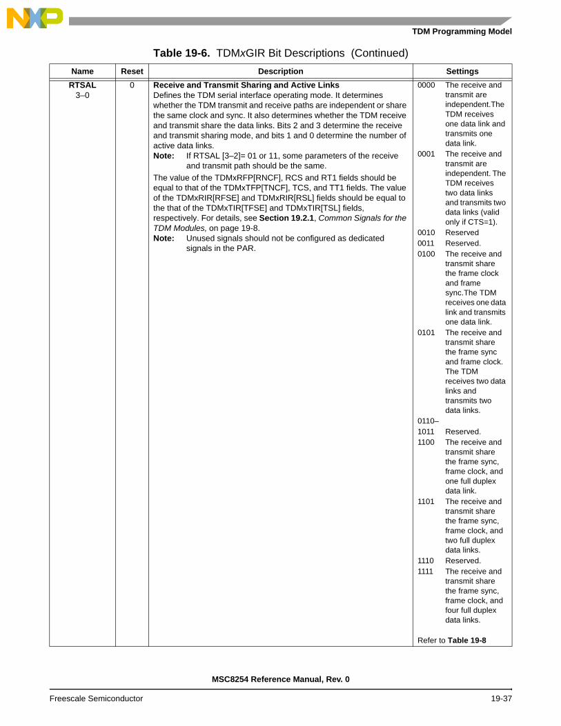
TDM Programming Model
RTSAL3–0
0 Receive and Transmit Sharing and Active LinksDefines the TDM serial interface operating mode. It determines whether the TDM transmit and receive paths are independent or share the same clock and sync. It also determines whether the TDM receive and transmit share the data links. Bits 2 and 3 determine the receive and transmit sharing mode, and bits 1 and 0 determine the number of active data links.Note: If RTSAL [3–2]= 01 or 11, some parameters of the receive
and transmit path should be the same.
The value of the TDMxRFP[RNCF], RCS and RT1 fields should be equal to that of the TDMxTFP[TNCF], TCS, and TT1 fields. The value of the TDMxRIR[RFSE] and TDMxRIR[RSL] fields should be equal to the that of the TDMxTIR[TFSE] and TDMxTIR[TSL] fields, respectively. For details, see Section 19.2.1, Common Signals for the TDM Modules, on page 19-8.Note: Unused signals should not be configured as dedicated
signals in the PAR.
0000 The receive and transmit are independent.The TDM receives one data link and transmits one data link.
0001 The receive and transmit are independent. The TDM receives two data links and transmits two data links (valid only if CTS=1).
0010 Reserved0011 Reserved.0100 The receive and
transmit share the frame clock and frame sync.The TDM receives one data link and transmits one data link.
0101 The receive and transmit share the frame sync and frame clock. The TDM receives two data links and transmits two data links.
0110–1011 Reserved.1100 The receive and
transmit share the frame sync, frame clock, and one full duplex data link.
1101 The receive and transmit share the frame sync, frame clock, and two full duplex data links.
1110 Reserved.1111 The receive and
transmit share the frame sync, frame clock, and four full duplex data links.
Refer to Table 19-8
Table 19-6. TDMxGIR Bit Descriptions (Continued)
Name Reset Description Settings
MSC8254 Reference Manual, Rev. 0
Freescale Semiconductor 19-37

TDM Interface
Table 19-7. TDM Signal Configuration When TDM Modules Share Signals
RTSAL[3–0] Field Value
Description
0000 Receive clock: TDM1TCKTransmit clock: TDM0TCKReceive sync: TDM1TSNTransmit sync: TDM0TSNReceive data links: TDMxRDTTransmit data links: TDMxTDTUnused signals: TDMxRCK, TDMxRSN.Note: The x specifies the TDM number of TDMs that share signals. For example if TDM0, TDM1,
and TDM2 share signals, then x is equal to 0,1, and 2 and the receive data links are TDM0RDT, TDM1RDT, and TDM2RDT.
0001 Receive clock: TDM1TCKTransmit clock: TDM0TCKReceive sync: TDM1TSNTransmit sync: TDM0TSNReceive data links: TDMxRDT, TDMxRSN.Transmit data links: TDMxTDT, TDMxRCLk.Note: The x specifies the number of the TDM and any one of the shared TDM modules.
0100 Frame clock (receive and transmit share the same clock): TDM0TCKFrame sync (receive and transmit share the same sync): TDM0TSNReceive data links: TDMxRDTTransmit data links: TDMxTDTUnused signals: TDMxRCK, TDMxRSN, TDMyTCK, TDMyTSN
TDMx specifies the TDM number and any one of the shared TDM modules. TDMy specifies the TDM number and any one of the shared TDM modules except TDM0. For example, if TDM0 and TDM1 share signals, the unused signals are TDM0RCK, TDM1RCK, TDM0RSN, TDM1RSN, TDM1TCK, and TDM1TSN.
0101 Frame clock (receive and transmit share the same clock): TDM0TCKFrame sync (receive and transmit share the same sync): TDM0TSNReceive data links: TDMxRDT, TDMxRSNTransmit data links: TDMxTDT, TDMxRCKUnused signals: TDMyTCK, TDMyTSN
TDMx specifies the TDM number and any one of the shared TDM modules. TDMy specifies the TDM number and any one of the shared TDM modules except TDM0. For example, if TDM0 and TDM1 share signals, the unused signals are TDM1TCK and TDM1TSN.
1100 Frame clock (receive and transmit share the same clock): TDM0TCKFrame sync (receive and transmit share the same sync): TDM0TSNFull duplex data links (the data link is inout and is used for receive and transmit) TDMxRDT.Unused signals: TDMyTCK, TDMyTSN, TDMxRCK, TDMxRSN, and TDMxTDT.
TDMx specifies the TDM number and any one of the shared TDM modules. TDMy specifies the TDM number and any one of the shared TDM modules except TDM0. For example, if TDM0 and TDM1 share signals, the unused signals are TDM0RCK, TDM1RCK, TDM0RSN, TDM1RSN, TDM0TDT, TDM1TDT, TDM1TCK, and TDM1TSN.
1101 Frame clock (receive and transmit share the same clock): TDM0TCKFrame sync (receive and transmit share the same sync): TDM0TSNFull duplex data links (the data link is inout it and it is used for receive and transmit): TDMxRDT, TDMxRSNUnused signals: TDMyTCK, TDMyTSN, TDMxRCK, TDMxTDT.
TDMx specifies the TDM number and any one of the shared TDM modules. TDMy specifies the TDM number and any one of the shared TDM modules except of TDM0. for example if TDM0 and TDM1 shared signals then the unused signals are TDM0RCK, TDM1RCK, TDM0TDT, TDM1TDT, TDM1TCK, and TDM1TSN.
MSC8254 Reference Manual, Rev. 0
19-38 Freescale Semiconductor
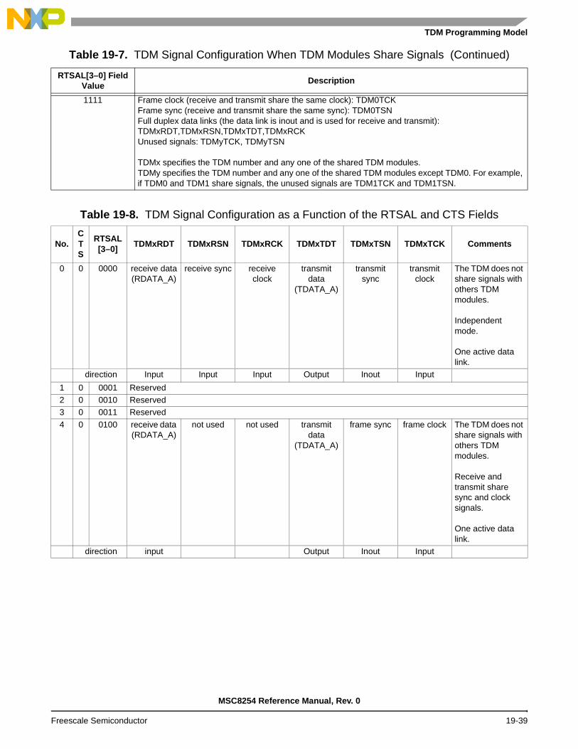
TDM Programming Model
1111 Frame clock (receive and transmit share the same clock): TDM0TCKFrame sync (receive and transmit share the same sync): TDM0TSNFull duplex data links (the data link is inout and is used for receive and transmit): TDMxRDT,TDMxRSN,TDMxTDT,TDMxRCKUnused signals: TDMyTCK, TDMyTSN
TDMx specifies the TDM number and any one of the shared TDM modules. TDMy specifies the TDM number and any one of the shared TDM modules except TDM0. For example, if TDM0 and TDM1 share signals, the unused signals are TDM1TCK and TDM1TSN.
Table 19-8. TDM Signal Configuration as a Function of the RTSAL and CTS Fields
No.CTS
RTSAL[3–0]
TDMxRDT TDMxRSN TDMxRCK TDMxTDT TDMxTSN TDMxTCK Comments
0 0 0000 receive data(RDATA_A)
receive sync receive clock
transmit data
(TDATA_A)
transmit sync
transmit clock
The TDM does not share signals with others TDM modules.
Independent mode.
One active data link.
direction Input Input Input Output Inout Input
1 0 0001 Reserved 2 0 0010 Reserved 3 0 0011 Reserved
4 0 0100 receive data (RDATA_A)
not used not used transmit data
(TDATA_A)
frame sync frame clock The TDM does not share signals with others TDM modules.
Receive and transmit share sync and clock signals.
One active data link.
direction input Output Inout Input
Table 19-7. TDM Signal Configuration When TDM Modules Share Signals (Continued)
RTSAL[3–0] Field Value
Description
MSC8254 Reference Manual, Rev. 0
Freescale Semiconductor 19-39

TDM Interface
5 0 0101 receive data(RDATA_A)
receive data(RDATA_B)
transmit data
(TDATA_B)
transmit data
(TDATA_A)
frame sync frame clock The TDM does not share signals with other TDM modules.
Receive and transmit share sync and clock signals.
Two active data links.
direction Input Input Output Output Inout Input6 0 0110 Reserved
7 0 0111 Reserved 8 0 1100 data link
(DATA_A)not used not used not used frame sync frame clock The TDM does not
share signals with other TDM modules.
Receive and transmit share the sync, clock, and data signals.
One full duplex active data link.
direction Inout Inout Input9 0 1101 data link
(DATA_A)data link
(DATA_B)not used not used frame sync frame clock The TDM does not
share signals with other TDM modules.
Receive and transmit share the sync, clock, and data signals.
Two full duplex active data links.
direction Inout Inout Inout Input10 0 1110 Reserved
Table 19-8. TDM Signal Configuration as a Function of the RTSAL and CTS Fields (Continued)
No.CTS
RTSAL[3–0]
TDMxRDT TDMxRSN TDMxRCK TDMxTDT TDMxTSN TDMxTCK Comments
MSC8254 Reference Manual, Rev. 0
19-40 Freescale Semiconductor

TDM Programming Model
11 0 1111 data link (DATA_A)
data link (DATA_B)
data link (DATA_D)
data link(DATA_C)
frame sync frame clock The TDM does not share signals with other TDM modules.
Receive and transmit share the sync, clock, and data signals.
Four full duplex active data links.
direction Inout Inout Inout Inout Inout Input12 1 0000 receive data
(RDATA_A)not used not used transmit
data(TDATA_A)
receive sync/
transmit sync/
not used
receive clock/
transmit clock/
not used
The TDM shares receive sync and clock and transmit sync and clock with other TDM modules.
Independent mode.
One active data link.
direction Input Output Inout Input13 1 0001 receive data
(RDATA_A)receive data(RDATA_B)
transmit data
(TDATA_B)
transmit data
(TDATA_A)
receive sync/
transmit sync/
not used
receive clock/
transmit clock/
not used
The TDM shares receive sync and clock and transmit sync and clock with other TDM modules.
Independent mode.
Two active data links.
direction Input Input Output Output Inout Input14 1 0010 Reserved
15 1 0011 Reserved 16 1 0100 receive data
(RDATA_A)not used not used transmit
data (TDATA_A)
frame sync/ not used
frame clock/ not used
The TDM shares the frame sync and frame clock with other TDM modules. Receive and transmit shared sync and clock signals.
One active data link.
direction input Output Inout Input
Table 19-8. TDM Signal Configuration as a Function of the RTSAL and CTS Fields (Continued)
No.CTS
RTSAL[3–0]
TDMxRDT TDMxRSN TDMxRCK TDMxTDT TDMxTSN TDMxTCK Comments
MSC8254 Reference Manual, Rev. 0
Freescale Semiconductor 19-41

TDM Interface
17 1 0101 receive dataRDATA_A
receive dataRDATA_B
transmit data
(TDATA_B)
transmit data
(TDATA_A)
frame sync/ not used
frame clock/ not used
The TDM shares the frame sync and frame clock with other TDM modules.
Receive and transmit share the sync and clock signals.
Two active data links.
direction Input Input Output Output Inout Input18 10 0110 Reserved 19 1 0111 Reserved
20 1 1100 data link (DATA_A)
not used not used not used frame sync/ not used
frame clock/not used
The TDM shares the frame sync and frame clock with other TDM modules.
Receive and transmit share the sync, clock, and data signals.
One full duplex active data link.
direction Inout Inout Input21 1 1101 data link
(DATA_A)data link
(DATA_B)not used not used frame sync/
not usedframe clock/
not used The TDM share the frame sync and frame clock with other TDM modules.
Receive and transmit share the sync, clock, and data signals.
Two full duplex active data links.
direction Inout Inout Inout Input22 1 1110 Reserved
Table 19-8. TDM Signal Configuration as a Function of the RTSAL and CTS Fields (Continued)
No.CTS
RTSAL[3–0]
TDMxRDT TDMxRSN TDMxRCK TDMxTDT TDMxTSN TDMxTCK Comments
MSC8254 Reference Manual, Rev. 0
19-42 Freescale Semiconductor

TDM Programming Model
19.7.1.2 TDMx Receive Interface Register (TDMxRIR)
TDMxRIR defines the TDMx receiver interface operation.
23 1 1111 data link (DATA_A)
data link (DATA_B)
data link(DATA_D)
data link (DATA_C)
frame sync/ not used
frame clock/not used
The TDM shares the frame sync and frame clock with other TDM modules.
Receive and transmit share the sync, clock, and data signals.
Four full duplex active data links.
direction Inout Inout Inout Inout Inout InputNote: Frame sync specifies that the receiver and transmitter use the same sync. Frame clock specifies that the receiver
and transmitter use the same clock. If data link specifies that the direction is inout, the signal is used for receive and transmit.
TDMxRIR TDMx Receive Interface Register Offset 0x3FF0
Bit 31 30 29 28 27 26 25 24 23 22 21 20 19 18 17 16
— RBOR
Type R/WReset 0 0 0 0 0 0 0 0 0 0 0 0 0 0 0 1
Boot 0 0 0 0 0 0 0 0 0 0 0 0 0 0 0 1
Bit 15 14 13 12 11 10 9 8 7 6 5 4 3 2 1 0
RFTL RSTL — RFSD RSL RDE RFSE RRDOType R/W
Reset 0 0 0 0 0 0 0 0 0 0 0 0 0 0 0 0Boot 0 0 0 0 0 0 0 0 0 0 0 0 0 0 0 0
Table 19-9. TDMxRIR Bit Descriptions
Name Reset Description Settings
—31–17
0 Reserved. Write to zero for future compatibility.
RBOR16
1 Receive Byte OrderIndicates the location of the receive data in the receive external memory buffer. The boot program writes a 1 to this bit.
0 First receive data is at the high address.
1 First receive data is at the low address.
RFTL15
0 Receive First Threshold LevelDetermines whether the receive first threshold interrupt is pulse or level. For details, see Section 19.2.6.3.
0 Receive first threshold interrupt is pulse.
1 Receive first threshold interrupt is level.
Table 19-8. TDM Signal Configuration as a Function of the RTSAL and CTS Fields (Continued)
No.CTS
RTSAL[3–0]
TDMxRDT TDMxRSN TDMxRCK TDMxTDT TDMxTSN TDMxTCK Comments
MSC8254 Reference Manual, Rev. 0
Freescale Semiconductor 19-43

TDM Interface
RSTL14
0 Receive Second Threshold LevelDetermines whether the receive second threshold interrupt is pulse or level. For details, see Section 19.2.6.3.
0 Receive second threshold interrupt is pulse.
1 Receive second threshold interrupt is level.
—13–6
0 Reserved. Write to zero for future compatibility.
RFSD5–4
0 Receive Frame Sync DelayWith the RDE and the RFSE bits, determines the number of clocks between the receive sync signal and the first data bit of the receive frame.
Refer to Table 19-10.Note: If the receive channel size is 2
(RCS = 0x1), then the RFSD field value can be only 0 or 1.
RSL3
0 Receive Sync Level Determines the polarity of the receive sync signal.For details, see Figure 19-21.
0 Receive sync is active on logic 1.
1 Receive sync is active on logic 0.
RDE2
0 Receive Data EdgeDetermines whether the receive data signal is sampled on the rising or falling edge of the receive clock. For details see Section 19.2.4.2.
0 The receive data signal is sampled on the rising edge of the receive clock.
1 The receive data signal is sampled on the falling edge of the receive clock.
RFSE1
0 Receive Frame Sync EdgeDetermines whether the receive frame sync signal is sampled on the rising or falling edge of the receive clock. For details, see Section 19.2.4.2.
0 The receive frame sync signal is sampled with the rising edge of the receive clock.
1 The receive frame sync signal is sampled on the falling edge of the receive clock.
RRDO0
0 Receive Reversed Data OrderFor examples, see Section 19.2.4.2.
0 The first bit of a received channel is stored as the most significant bit in the internal memory.
1 The first bit of a received channel is stored as the least significant bit in the internal memory
Table 19-9. TDMxRIR Bit Descriptions (Continued)
Name Reset Description Settings
MSC8254 Reference Manual, Rev. 0
19-44 Freescale Semiconductor
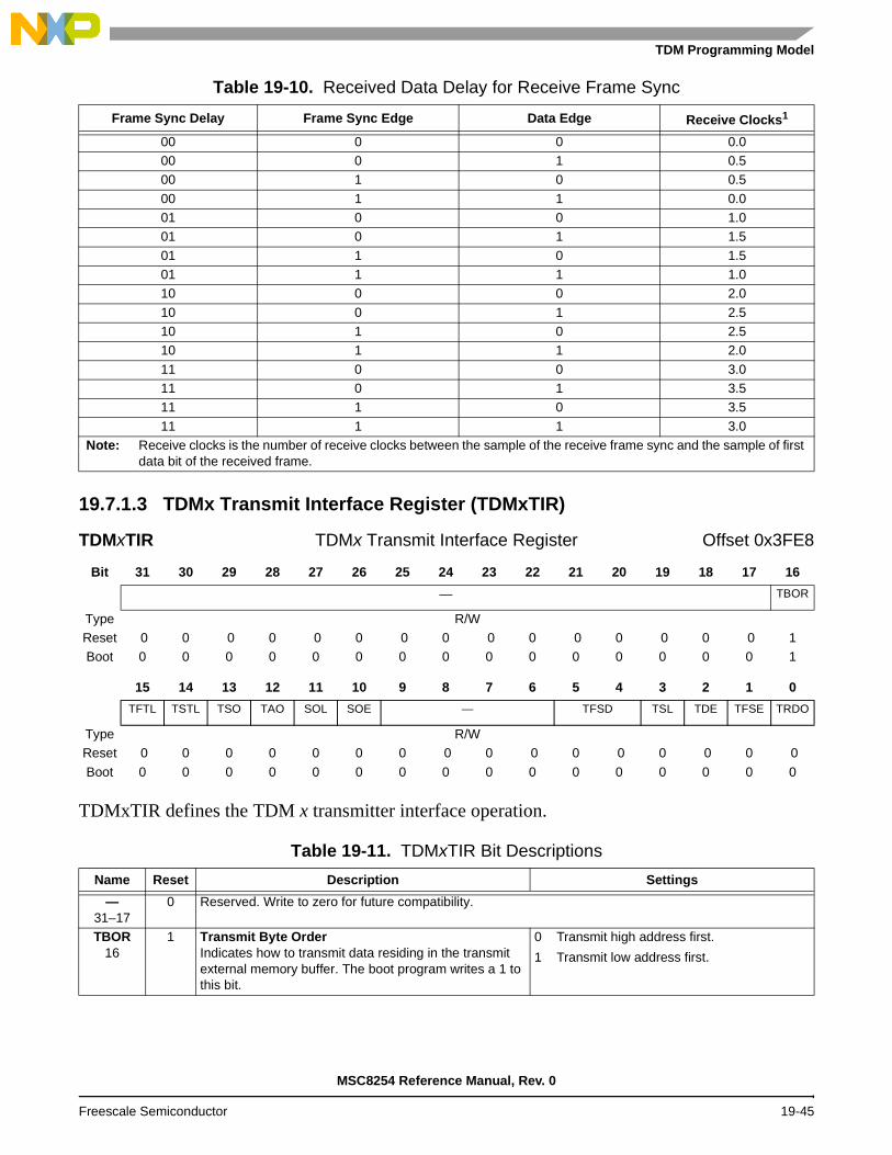
TDM Programming Model
19.7.1.3 TDMx Transmit Interface Register (TDMxTIR)
TDMxTIR defines the TDM x transmitter interface operation.
Table 19-10. Received Data Delay for Receive Frame Sync
Frame Sync Delay Frame Sync Edge Data Edge Receive Clocks1
00 0 0 0.000 0 1 0.500 1 0 0.5
00 1 1 0.001 0 0 1.001 0 1 1.5
01 1 0 1.501 1 1 1.010 0 0 2.0
10 0 1 2.510 1 0 2.510 1 1 2.0
11 0 0 3.011 0 1 3.511 1 0 3.5
11 1 1 3.0Note: Receive clocks is the number of receive clocks between the sample of the receive frame sync and the sample of first
data bit of the received frame.
TDMxTIR TDMx Transmit Interface Register Offset 0x3FE8
Bit 31 30 29 28 27 26 25 24 23 22 21 20 19 18 17 16
— TBOR
Type R/WReset 0 0 0 0 0 0 0 0 0 0 0 0 0 0 0 1Boot 0 0 0 0 0 0 0 0 0 0 0 0 0 0 0 1
15 14 13 12 11 10 9 8 7 6 5 4 3 2 1 0
TFTL TSTL TSO TAO SOL SOE — TFSD TSL TDE TFSE TRDO
Type R/WReset 0 0 0 0 0 0 0 0 0 0 0 0 0 0 0 0
Boot 0 0 0 0 0 0 0 0 0 0 0 0 0 0 0 0
Table 19-11. TDMxTIR Bit Descriptions
Name Reset Description Settings
—31–17
0 Reserved. Write to zero for future compatibility.
TBOR16
1 Transmit Byte OrderIndicates how to transmit data residing in the transmit external memory buffer. The boot program writes a 1 to this bit.
0 Transmit high address first.
1 Transmit low address first.
MSC8254 Reference Manual, Rev. 0
Freescale Semiconductor 19-45

TDM Interface
TFTL15
0 Transmit First Threshold LevelDetermines whether the Transmit first threshold interrupt is pulse or level. For details, see Section 19.2.6.3.
0 Transmit first threshold interrupt is pulse.
1 Transmit first threshold interrupt is level.
TSTL14
0 Transmit Second Threshold LevelDetermines whether the Transmit second threshold interrupt is pulse or level. For details, see Section 19.2.6.3.
0 Transmit second threshold interrupt is pulse.
1 Transmit second threshold interrupt is level.
TSO13
0 Transmit Sync OutputDetermines whether the transmit sync is driven out by the TDM transmitter or it input to the TDM transmitter. For details, see Section 19.2.4.1
0 Transmit sync is input.
1 Transmit sync is output.
TAO12
0 Transmit Always OutputDetermines whether the TDM transmitter drives TDMxDAT for the inactive channels.
0 The TDM transmitter does not drive the TDMxDAT for inactive channels.
1 The TDM transmitter drives the TDMxDAT regardless of whether the channel is active.
SOL11
0 Sync Out LengthIndicates whether the TDMxTSN is asserted for one cycle of TDMxTCK or is asserted for the duration of the first channel in the frame. For details, see Section 19.2.4.1.
0 The sync_out width is one bit.
1 The sync_out width is equal to the channel width.
SOE10
0 Sync Out EdgeDetermines whether the sync out signal is driven out with the rising or falling edge of the transmit clock. For details, see Section 19.2.4.1.
0 The transmit frame sync signal is driven out on the rising edge of the transmit clock.
1 The transmit frame sync signal is driven out on the falling edge of the transmit clock.
—9–6
0 Reserved. Write to zero for future compatibility.
TFSD5–4
0 Transmit Frame Sync DelayWith the TDE and the TFSE bits, determines the number of clocks between the transmit sync signal and the first data bit of the transmit frame. For examples, see Section 19.2.4.2.
Refer to Table 19-12 on page 47. Note: If the transmit channel size is 2
(TCS = 0x1) then the TFSD field value can be only 0 or 1.
TSL3
0 Transmit Sync Level Determines the polarity of the transmit sync signal. For details, see Section 19.2.4.2.
0 Transmit sync is active on logic 1.
1 Transmit sync is active on logic 0.
TDE2
0 Transmit Data EdgeDetermines whether the transmit data is driven out on the rising or falling edge of the transmit clock. For details, see Section 19.2.4.2.
0 The transmit data is driven out on the rising edge of the transmit clock.
1 The transmit data is driven out on the falling edge of the transmit clock.
TFSE1
0 Transmit Frame Sync EdgeDetermines whether the transmit frame sync signal is sampled with the rising or falling edge of the transmit clock. For details, see Section 19.2.4.2.
0 The transmit frame sync signal is sampled with the rising edge of the transmit clock.
1 The transmit frame sync signal is sampled with the falling edge of the transmit clock.
TRDO0
0 Transmit Reversed Data OrderFor examples, see Section 19.2.4.4.
0 The most significant bit of the memory is sent out at the first transmit data bit.
1 The least significant bit of the memory is sent out at the first transmit data bit.
Table 19-11. TDMxTIR Bit Descriptions (Continued)
Name Reset Description Settings
MSC8254 Reference Manual, Rev. 0
19-46 Freescale Semiconductor

TDM Programming Model
19.7.1.4 TDMx Receive Frame Parameters (TDMxRFP)
Table 19-12. Transmit Data Delay for Transmit Frame Sync
Frame Sync Delay Frame Sync Edge Data Edge Transmit Clocks1
00 0 0 –1 2
00 0 1 –0.5 2
00 1 0 –0.5 2
00 1 1 –1 2
01 0 0 0
01 0 1 0.5
01 1 0 0.5
01 1 1 0
10 0 0 1
10 0 1 1.5
10 1 0 1.5
10 1 1 1
11 0 0 2
11 0 1 2.5
11 1 0 2.5
11 1 1 2
Notes: 1. Transmit clocks is the number of transmit clocks between the first transmit frame sync sample and the first data bit of the frame that is driven out.
2. The field value is negative because the data is driven out before the transmit frame sync sample.
TDMxRFP TDMx Receive Frame Parameters Offset 0x3FE0
Bit 31 30 29 28 27 26 25 24 23 22 21 20 19 18 17 16
— RNCFType R/W
Reset 0 0 0 0 0 0 0 0 0 0 0 0 0 0 0 0
Bit 15 14 13 12 11 10 9 8 7 6 5 4 3 2 1 0
— RCDBL — RCS RT1 RUBMType R/WReset 0 0 0 0 0 0 0 0 0 0 0 0 0 0 0 0
MSC8254 Reference Manual, Rev. 0
Freescale Semiconductor 19-47

TDM Interface
TDMxRFP defines the TDMx receive frame parameters.
Table 19-13. TDMxRFP Bit Descriptions
Name Reset Description Settings
—31–24
0 Reserved. Write to zero for future compatibility.
RNCF23–16
0 Receive Number of Channels in a TDM FrameSpecifies the total number of channels that are received in the TDM modules. One TDM frame can contain 2–256 channels at a granularity of two.Notes: 1. RNCF[8-15] = (number of channels that
received on one active link) × (number of active data links) – 1, the number of active data links is specified in the RTSAL field.
2. If RCDBL field is clear, then the minimum number of channels is limit. The minimum receive number of channels is 128 / (receive channel size) + 2. For example, if the channel size is 4 bits, then the receive TDM frame should contain at least 34 channels.
Table 19-14 describes the RNCF valid value as a function of the RTSAL field (Receive and Transmit Sharing and Active Links). For details, see Section 19.2.5.
0x00 Reserved.0x01 2 received channels.0x02 Reserved.0x03 4 received channels.0x04 Reserved.
.
.
.
0xFD 254 received channels.0xFE Reserved.0xFF 256 received channels.Note: The even values are
reserved.
—15–11
0 Reserved. Write to zero for future compatibility.
RCDBL10–8
0 Receive Channel Data Bits LatencyDefines the maximum amount of receive channel bits stored in the TDM local memory before they are transferred for processing. RCDBL determines the maximum data latency in the following way: Maximum data latency= (RCDBL)/RCS × (receive frame duration). For details, see Section 19.2.6.Notes: 1. The maximum data latency is the latency at the
worst case when the bus is very loaded. Typically the latency it much smaller.
2. RCS is field at RFP register defines the channel size.
3. The minimum number of receive channel is limited if the RCDBL field is clear.The minimum receive number of channels is 128/(receive channel size) + 2.
000 Maximum 64 channel bits. 001 Maximum 128 channel bits. 010 Maximum 256 channel bits. 011 Maximum 512 channel bits. 100 Maximum 1024 channel bits. 101 Maximum 2048 channel bits.110 Reserved.111 Reserved.
—7–6
0 Reserved. Write to zero for future compatibility.
RCS5–2
0 Receive Channel SizeDetermines the receiver channel size – 1. For details, see Section 19.2.6.
0000 Reserved.0001 The receiver channel size is 2
bits. 0010 Reserved.0011 The receiver channel size is 4
bits. 0100–0110 Reserved.0111 Receiver channel size is 8 bits. 1000–1110 Reserved.1111 Receiver channel size is 16
bits.
MSC8254 Reference Manual, Rev. 0
19-48 Freescale Semiconductor
TDM Programming Model
Table 19-14 describes the RNCF valid value as a function of the RTSAL[0–1] field.
RT11
0 Receive T1 frame Determines whether the receive frame is T1 frame or non T1.Note: In T1 mode the channel size must be 8 bits
(RCS = 0x7) and the number of channels must be 24 × (number of links). For example, if the number of link is 2 (RTSAL[1–0] = 01), the number of channels should be 48 (RNCF = 0x2F). For details, see Section 19.2.
0 The receive frame is non T1 frame.
1 The receive frame is T1 frame.
RUBM0
0 Receive Unified Buffer ModeIndicates that all the received data is directed to one buffer. When RUBM is set, the number of active links must be 1 (RTSAL = 0b0000 or RTSAL = 0100). The channel parameters of all the receive channels are located in the TDMxRCPR0 (See page 19-61). For details, see Section 19.2.6.4.Note: When this bit is set, the TDMxRIR[RRDO] bit should
be cleared.
0 Each channel is written to a different data buffer in the internal MBus.
1 All the channels are written to the same data buffer in the internal MBus.
Table 19-14. RNCF[3–0] Valid Values
RTSAL[1–0]Number of
Active LinksRNCF[3–0]
SuffixValid Value of RNCF
00 1 xxxxxxx1 The total number of channels must have a granularity of two.
01 2 xxxxxx11 The total number of channels must have a granularity of four.
10 Reserved.
11 4 xxxxx111 The total number of channels must have a granularity of eight.
Table 19-13. TDMxRFP Bit Descriptions (Continued)
Name Reset Description Settings
MSC8254 Reference Manual, Rev. 0
Freescale Semiconductor 19-49

TDM Interface
19.7.1.5 TDMx Transmit Frame Parameters (TDMxTFP)
TDMxTFP defines the TDMx transmit frame parameters.
TDMxTFP TDMx Transmit Frame Parameters Offset 0x3FD8
Bit 31 30 29 28 27 26 25 24 23 22 21 20 19 18 17 16
— TNCF
Type R/WReset 0 0 0 0 0 0 0 0 0 0 0 0 0 0 0 0
Bit 15 14 13 12 11 10 9 8 7 6 5 4 3 2 1 0
— TCDBL — TCS TT1 TUBM
Type R/WReset 0 0 0 0 0 0 0 0 0 0 0 0 0 0 0 0
Table 19-15. TDMxTFP Bit Descriptions
Name Reset Description Settings
—31–24
0 Reserved. Write to zero for future compatibility.
TNCF23–16
0 Transmit Number of Channels in a TDM FrameSpecifies the total number of channels that are transmitted in the TDM modules. One TDM frame contains 2–256 channels.Notes: 1. TNCF[8–15] = (number of channels that
transmit on one active link) × (number of active data links) – 1. the number of active data links is specified in the RTSAL field.
2. If TCDBL field is cleared, the minimum number of channels is limit. The minimum transmit number of channels is 128 / (transmit channel size) + 2. for example if the transmit channel size is 16 bits then the transmit TDM frame should contain at least 10 channels.
The number of active data links is specified in the RTSAL field. Table 19-16 describes the TNCF valid value as a function of the TDMxGIR[RTSAL] field (Receive and Transmit Sharing and Active Links). For details, see Section 19.2.5.
0x00 Reserved.0x01 2 Transmit channels.0x02 Reserved.0x03 4 Transmit channels.0x04 Reserved....0xFE Reserved.0xFF 256 Transmit channels. The even values are reserved.
—15–11
0 Reserved. Write to zero for future compatibility.
MSC8254 Reference Manual, Rev. 0
19-50 Freescale Semiconductor

TDM Programming Model
TCDBL10–8
0 Transmit Channel Data Bits LatencyDefines the maximum transmit channel bits that can be stored in the TDM local memory before it transfers output. TCDBL determines the maximum data latency in the following way: Maximum data latency = (TCDBL) / TCS × (transmit frame duration). See Section 19.2.6.Notes: 1. The maximum data latency is the latency at the
worst case when the bus is very loaded. Typically, actual latency is much smaller.
2. TDMxTFP[TCS] defines the transmit channel size.
3. The minimum number of transmit channel is limit if the RCDBL field is clear. The minimum transmit number of channels is 128 / (transmit channel size) + 2.For example see TNCF field.
000 Maximum 64 channel bits.001 Maximum 128 channel bits.010 Maximum 256 channel bits.011 Maximum 512 channel bits.100 Maximum 1024 channel bits.101 Maximum 2048 channel bits. 110 Reserved.111 Reserved.
—7–6
0 Reserved. Write to zero for future compatibility.
TCS5–2
0 Transmit Channel SizeDetermines the transmitter channel size – 1. For details, see Section 19.2.5.
0000 Reserved0001 The transmitter channel
size is 2 bits. 0010 Reserved0011 The transmitter channel
size is 4 bits. 0100 Reserved.0101 Reserved.0110 Reserved.0111 The transmitter channel
size is 8 bits. 1000–1110 Reserved1111 The transmitter channel
size is 16 bits.
TT11
0 Transmit T1 Frame Determines whether the TDM transmitter drives a T1 frame or non T1 frame.Note: In T1 mode, the channel size must be 8 (TCS = 0x7)
and the number of channels 24 × (number of links). For example, if the number of links is 1 (RTSAL[1–0] = 00, the number of channels should be 24 (TNCF = 0x17). For details, see Section 19.2.
0 Transmit frame is non T1 frame.
1 Transmit frame is T1 frame.
TUBM0
0 Transmit Unified Buffer ModeIndicates that all the transmit data is transferred from one buffer. When TUBM is set, the number of active links must be 1 (RTSAL = 0b0000 or 0b0100). The parameters of all transmit channels are located in TDMxTCPR0. For details, see Section 19.2.6.4.Note: When this bit is set, the TDMxTIR[TRDO] bit should
be cleared.
0 Each channel is read from a different data buffer in the internal MBus.
1 All the channels are read from the same data buffer in the internal MBus.
Table 19-15. TDMxTFP Bit Descriptions (Continued)
Name Reset Description Settings
MSC8254 Reference Manual, Rev. 0
Freescale Semiconductor 19-51

TDM Interface
Table 19-16 describes the TNCF valid value as function of the RTSAL field.
19.7.1.6 TDMx Receive Data Buffer Size (TDMxRDBS)
TDMxRDBS defines the receive data buffers size in bytes.The buffers for A/μ-law channels are double size.
Table 19-16. TNCF[3–0] Valid Values
RTSAL[2–0]Number of
Active LinksTNCF[3–0]
SuffixValid Value of TNCF
00 1 xxxxxxx1 The total number of channels must have a granularity of two.
01 2 xxxxxx11 The total number of channels must have a granularity of four.
10 Reserved
11 4 xxxxx111 The total number of channels must have a granularity of eight.
TDMxRDBS TDMx Receive Data Buffer Size Offset 0x3FD0
Bit 31 30 29 28 27 26 25 24 23 22 21 20 19 18 17 16
— RDBS
Type R/W
Reset 0 0 0 0 0 0 0 0 0 0 0 0 0 0 0 0
Bit 15 14 13 12 11 10 9 8 7 6 5 4 3 2 1 0
RDBSType R/W
Reset 0 0 0 0 0 0 0 0 0 0 0 0 0 0 0 0
Table 19-17. TDMxRDBS Bit Descriptions
Name Reset Description Settings
—31–24
0 Reserved. Write to zero for future compatibility.
RDBS23–0
0 Receive Data Buffers SizeReceive data buffers size equals the receive data buffer size in bytes minus 1. The buffer size is aligned to 8 bytes, so bits 0–2 must be set to “111”. For details, see Section 19.2.6.1, Data Buffer Size and A/m-law Channels, on page 19-23.Note: The minimum buffer size is 16 bytes.
0x00000F to 0xFFFFFF
MSC8254 Reference Manual, Rev. 0
19-52 Freescale Semiconductor

TDM Programming Model
19.7.1.7 TDMx Transmit Data Buffer Size (TDMxTDBS)
TDMxTDBS defines the transmit data buffer size in bytes. The buffers for A/μ channels are double size.
19.7.1.8 TDMx Receive Global Base Address
TDMxRGBA determines the 16 most significant bits global base address of the receiver data buffers. The actual address of each receive data buffer is RCDBA + (RGBA << 16). See Section 19.2.6.2.
TDMxTDBS TDMx Transmit Data Buffer Size Offset 0x3FC8
Bit 31 30 29 28 27 26 25 24 23 22 21 20 19 18 17 16
— TDBSType R/W
Reset 0 0 0 0 0 0 0 0 0 0 0 0 0 0 0 0
Bit 15 14 13 12 11 10 9 8 7 6 5 4 3 2 1 0
TDBSType R/W
Reset 0 0 0 0 0 0 0 0 0 0 0 0 0 0 0 0
Table 19-18. TDMxTDBS Bit Descriptions
Name Reset Description Settings
—31–24
0 Reserved. Write to zero for future compatibility.
TDBS23–0
0 Transmit Data Buffers SizeTransmit data buffers size equals the transmit data buffer size in bytes minus 1. The buffer size is aligned to 8 bytes, so bits 29–31 must be set to “111.” For details, see Section 19.2.6.1.Note: The minimum buffer size is 16 bytes.
0x00000F to 0xFFFFFF
TDMxRGBA TDMx Receive Global Base Address Offset 0x3FC0
Bit 31 30 29 28 27 26 25 24 23 22 21 20 19 18 17 16
—Type R/W
Reset 0 0 0 0 0 0 0 0 0 0 0 0 0 0 0 0
Bit 15 14 13 12 11 10 9 8 7 6 5 4 3 2 1 0
RGBAType R/WReset 0 0 0 0 0 0 0 0 0 0 0 0 0 0 0 0
Table 19-19. TDMxRGBA Bit Descriptions
Name Reset Description
—31–16
0 Reserved. Write to zero for future compatibility.
MSC8254 Reference Manual, Rev. 0
Freescale Semiconductor 19-53

TDM Interface
19.7.1.9 TDMx Transmit Global Base Address
TDMxTGBA determines the 16 most significant bits global base address of the transmitter data buffers. The actual address of each transmit data buffer is TCDBA + (TGBA << 16). See Section 19.2.6.2.
19.7.1.10 TDMx Transmit Force Register (TDMxTFR)
RGBA15–0
0 Receive Global Base AddressDetermines the global base address of the receiver data buffers. It is added to the channel data buffer address and to the current receive displacement to generate the actual data address.
TDMxTGBA TDMx Transmit Global Base Address Offset 0x3FB8
Bit 31 30 29 28 27 26 25 24 23 22 21 20 19 18 17 16
—Type R/W
Reset 0 0 0 0 0 0 0 0 0 0 0 0 0 0 0 0
Bit 15 14 13 12 11 10 9 8 7 6 5 4 3 2 1 0
TGBAType R/WReset 0 0 0 0 0 0 0 0 0 0 0 0 0 0 0 0
Table 19-20. TDMxTGBA Bit Descriptions
Name Reset Description
—31–16
0 Reserved. Write to zero for future compatibility.
TGBA15–0
0 Transmit Global Base AddressDetermines the global base address of the transmit data buffers. It is added to channel data buffer address and to the current transmit displacement to generate the actual address.
TDMxTFR TDMx Transmit Force Register 0x3F10
Bit 31 30 29 28 27 26 25 24 23 22 21 20 19 18 17 16
—
Type R/WReset 0 0 0 0 0 0 0 0 0 0 0 0 0 0 0 0
Bit 15 14 13 12 11 10 9 8 7 6 5 4 3 2 1 0
PUVType R/W
Reset 0 0 0 0 0 0 0 0 0 0 0 0 0 0 0 0
Table 19-19. TDMxRGBA Bit Descriptions
Name Reset Description
MSC8254 Reference Manual, Rev. 0
19-54 Freescale Semiconductor

TDM Programming Model
TDMxTFR sets the priority upgrade value for the transmit channels.
19.7.1.11 TDMx Receive Force Register (TDMxRFR)
TDMxRFR sets the priority upgrade value for the transmit channels.
Table 19-21. TDMxTFR Bit Descriptions
Name Reset Description
—31–16
0 Reserved. Write to zero for future compatibility.
PUV15–0
0 Priority Upgrade ValueDetermines the threshold value for which the TDM transmitter upgrades its system priority. The value is used to avoid an underrun condition. If the value is 0x0000 (reset value), the priority is not upgraded and remains low. The maximum value, which causes the priority always to be high, depends on the value stored in TDMxTFP[TCDBL]. If TDMxTFP[TCDBL] = 0x000, achieve the maximum value is achieved by setting PUV = TDMxTFP[TNCF]. If TDMxTFP[TCDBL] is not 0x000, set the PUV using: PUV = 64/TDMxTFP[TCS] × TDMxTNB[TNB]. See page 19-50 for TDMxTFP details and page 19-68 for TDMxTNB details.
TDMxRFR TDMx Receive Force Register0x3F18
Bit 31 30 29 28 27 26 25 24 23 22 21 20 19 18 17 16
—
Type R/WReset 0 0 0 0 0 0 0 0 0 0 0 0 0 0 0 0
Bit 15 14 13 12 11 10 9 8 7 6 5 4 3 2 1 0
PUVType R/W
Reset 0 0 0 0 0 0 0 0 0 0 0 0 0 0 0 0
Table 19-22. TDMxRFR Bit Descriptions
Name Reset Description
—31–16
0 Reserved. Write to zero for future compatibility.
PUV15–0
0 Priority Upgrade ValueDetermines the threshold value for which the TDM receiver upgrades its system priority. The value is used to avoid an overrun condition. If the value is 0x0000 (reset value), the priority is not upgraded and remains low. The maximum value, which causes the priority always to be high, depends on the value stored in TDMxRFPx[RCDBL]. If TDMxRFP[RCDBL] = 0x000, achieve the maximum value by setting PUV = TDMxRFP[RNCF]. If TDMxRFP[RCDBL] is not 0x000, set the PUV using PUV = 64/TDMxRFP[RCS] × RNBx[RNB]. See page 19-47 for TDMxRFP details and page 19-67 for TDMxRNB details.
MSC8254 Reference Manual, Rev. 0
Freescale Semiconductor 19-55

TDM Interface
19.7.1.12 TDMx Parity Control Register (TDMxPCR)
TDMxPCR controls the parity check operation.
19.7.2 Control Registers
The following sections describe the TDM control registers.
19.7.2.1 TDMx Adaptation Control Register
TDMxPCR TDMx Parity Control Register Offset 0x3F00
Bit 31 30 29 28 27 26 25 24 23 22 21 20 19 18 17 16
—Type R/W
Reset 0 0 0 0 0 0 0 0 0 0 0 0 0 0 0 0
Bit 15 14 13 12 11 10 9 8 7 6 5 4 3 2 1 0
— PC PIE PILType R/WReset 0 0 0 0 0 0 0 0 0 0 0 0 0 0 0 0
Table 19-23. TDMxPCR Bit Descriptions
Name Reset Description Settings
—31–3
0 Reserved. Write to zero for future compatibility.
PC2
0 Parity CheckEnables the parity check mechanism. When the bit is set, you can write to TDMxRCPRn[27–24] or TDMxTCPRn[27–24].
0 Parity check is disabled.
1 Parity check is enabled
PIE1
0 Parity Interrupt Enable
Enables/disables the parity interrupt.
0 Parity interrupt is disabled.
1 Parity interrupt is enabled
PIL0
0 Parity Interrupt Level
Selects the trigger type for the parity interrupt.
0 Parity interrupt is level-triggered.
1 Parity interrupt is edge-triggered.
TDMxACR TDMx Adaptation Control Register Offset 0x3FB0
Bit 31 30 29 28 27 26 25 24 23 22 21 20 19 18 17 16
—Type R/W
Reset 0 0 0 0 0 0 0 0 0 0 0 0 0 0 0 0
Bit 15 14 13 12 11 10 9 8 7 6 5 4 3 2 1 0
— LTS AMEType R/WReset 0 0 0 0 0 0 0 0 0 0 0 0 0 0 0 0
MSC8254 Reference Manual, Rev. 0
19-56 Freescale Semiconductor

TDM Programming Model
TDMxACR controls the activation/deactivation of the TDMx adaptation machine. The propagation of the enable/disable to the adaptation machine is delayed because is clocked by the serial clock.
19.7.2.2 TDMx Receive Control Register
TDMxRCR controls the activation/deactivation of the TDMx Receiver. Receiver activation is valid only when the RENS bit is clear.
Table 19-25. TDMxACR Bit Descriptions
Name Reset Description Settings
—31–2
0 Reserved. Write to zero for future compatibility.
AME1
0 Adaptation Machine EnableDetermines whether the adaptation machine is
enabled or disabled.
0 Adaptation machine is disabled.
1 Adaptation machine is enabled
LTS0
0 Learn Transmit SyncDetermines whether the adaptation machine
learns the transmit sync or the receive sync.
0 Adaptation machine learn the receive sync.
1 Adaptation machine learn the transmit sync.
TDMxRCR TDMx Receive Control Register Offset 0x3FA8
Reg 31 30 29 28 27 26 25 24 23 22 21 20 19 18 17 16
—Type R/WReset 0 0 0 0 0 0 0 0 0 0 0 0 0 0 0 0
Reg 15 14 13 12 11 10 9 8 7 6 5 4 3 2 1 0
— REN
Type R/WReset 0 0 0 0 0 0 0 0 0 0 0 0 0 0 0 0
Table 19-26. TDMxRCR Bit Descriptions
Name Reset Description Settings
—31–1
0 Reserved. Write to zero for future compatibility.
REN0
0 Receive EnableDetermines whether the receive TDM is enabled or disabled.Note: Setting this bit is the last step in initializing the
receiver.
0 Receiver is disabled.
1 Receiver is enabled.
MSC8254 Reference Manual, Rev. 0
Freescale Semiconductor 19-57

TDM Interface
19.7.2.3 TDMx Transmit Control Register (TDMxTCR)
TDMxTCR controls the activation/deactivation of the TDMx Transmitter. Transmitter activation is valid only when the TENS bit is clear.
19.7.2.4 TDMx Receive Data Buffer First Threshold (TDMxRDBFT)
TDMxRDBFT determines the first threshold of the receive data buffers. When the receive buffers are filled up to the first threshold defined by this field—the TDMx Receive Data Buffers Displacement Register (TDMxRDBDR) = TDMx Receive Data Buffers First Threshold (TDMxRDBFT) + 8—the RFTE bit in the TDMx Receive Event Register (TDMx RER) is set. If the associated enable bit is also set, an interrupt is generated. This register can be updated at any time, even when the TDMx receiver is enabled. For details, see Section 19.2.6.3.
TDMxTCR TDMx Transmit Control Register Offset 0x3FA0
Bit 31 30 29 28 27 26 25 24 23 22 21 20 19 18 17 16
—
Type R/WReset 0 0 0 0 0 0 0 0 0 0 0 0 0 0 0 0
Bit 15 14 13 12 11 10 9 8 7 6 5 4 3 2 1 0
Reserved TEN
Type R/WReset 0 0 0 0 0 0 0 0 0 0 0 0 0 0 0 0
Table 19-27. TDMxTCR Bit Descriptions
Name Reset Description Settings
—31–1
0 Reserved. Write to zero for future compatibility.
TEN0
0 Transmit EnableDetermines whether the transmit TDM is enabled or disabled. Setting this bit is the last step in initializing the transmitter.
0 Transmitter is disabled.
1 Transmitter is enabled.
TDMxRDBFT TDMx Receive Data Buffer First Threshold Offset 0x3F98
Bit 31 30 29 28 27 26 25 24 23 22 21 20 19 18 17 16
— RDBFT
Type R/W
Reset 0 0 0 0 0 0 0 0 0 0 0 0 0 0 0 0
Bit 15 14 13 12 11 10 9 8 7 6 5 4 3 2 1 0
RDBFT
Type R/W
Reset 0 0 0 0 0 0 0 0 0 0 0 0 0 0 0 0
MSC8254 Reference Manual, Rev. 0
19-58 Freescale Semiconductor

TDM Programming Model
19.7.2.5 TDMx Transmit Data Buffer First Threshold
TDMxTDBFT determines the first threshold of the transmit data buffers. When the transmit buffers are emptied up to the first threshold defined by this field—the TDMx Transmit Data Buffers Displacement Register (TDMxTDBDR) = the TDMx Transmit Data Buffers First Threshold (TDMxTDBFT) + 8—the TFTE bit in the TDMx Transmit Event Register (TDMxTER) is set. If the associated enable bit is also set, an interrupt is generated. This register can be updated any time, even when the TDMx transmitter is enabled. For details, see Section 19.2.6.3.
Table 19-28. TDMxRDBFT Bit Descriptions
Name Reset Description Settings
—31–24
0 Reserved. Write to zero for future compatibility.
RDBFT23–0
0 Receive Data Buffer First ThresholdDetermines the location of the first threshold in the receive data buffers. The register value has a granularity of 8 bytes; that is, the three LSBits are always clear.
0x000000 to (RDBS – 7)
TDMxTDBFT TDMx Transmit Data Buffer First Threshold Offset 0x3F90
Bit 31 30 29 28 27 26 25 24 23 22 21 20 19 18 17 16
— TDBFT
Type R/W
Reset 0 0 0 0 0 0 0 0 0 0 0 0 0 0 0 0
Bit 15 14 13 12 11 10 9 8 7 6 5 4 3 2 1 0
TDBFT
Type R/W
Reset 0 0 0 0 0 0 0 0 0 0 0 0 0 0 0 0
Table 19-29. TDMxTDBFT Bit Descriptions
Name Reset Description Settings
—31–24
0 Reserved. Write to zero for future compatibility.
TDBFT23–0
0 Transmit Data Buffer First ThresholdDetermines the location of the first threshold in the transmit data buffers. The register value has a granularity of eight bytes; that is, the three LSBits are always clear.
0x000000 to (TDBS – 7)
MSC8254 Reference Manual, Rev. 0
Freescale Semiconductor 19-59

TDM Interface
19.7.2.6 TDMx Receive Data Buffer Second Threshold
TDMxRDBST determines the second threshold of the receive data buffers. When the receive buffers are filled up to the second threshold defined by this field—the Receive Data Buffers Displacement Register (TDMxRDBDR) = the Receive Data Buffers Second Threshold (TDMxRDBST) + 8—the RSTE bit in the TDMx Receive Event Register (TDMxRER) is set. If the associated enable bit is also set, an interrupt is generated. This register can be updated any time, even when the TDMx receiver is enabled. For details, see Section 19.2.6.3.
19.7.2.7 TDMx Transmit Data Buffer Second Threshold
TDMxTDBST determines the second threshold of the transmit data buffers. When the transmit buffers are emptied up to the second threshold defined by this field—the Transmit Data Buffers Displacement Register (TDMxTDBDR) = the Transmit Data Buffers Second Threshold (TDMxTDBST) + 8—then the TSTE bit in the TDMx Transmit Register (TDMxTER) is set. If
TDMxRDBST TDMx Receive Data Buffer Second Threshold Offset 0x3F88
Bit 31 30 29 28 27 26 25 24 23 22 21 20 19 18 17 16
Reserved RDBSTType R/W
Reset 0 0 0 0 0 0 0 0 0 0 0 0 0 0 0 0
Bit 15 14 13 12 11 10 9 8 7 6 5 4 3 2 1 0
RDBSTType R/WReset 0 0 0 0 0 0 0 0 0 0 0 0 0 0 0 0
Table 19-30. TDMxRDBFT Bit Descriptions
Name Reset Description Settings
—31–24
0 Reserved. Write to zero for future compatibility.
RDBST23–0
0 Receive Data Buffer Second ThresholdDetermines the location of the second threshold in the receive data buffers. The register value has a granularity of eight bytes; that is, the three LSBits are always clear.
0x000000 to (RDBS – 7)
TDMxTDBST TDMx Transmit Data Buffer Second Threshold Offset 0x3F80
Bit 31 30 29 28 27 26 25 24 23 22 21 20 19 18 17 16
— TDBSTType R/W
Reset 0 0 0 0 0 0 0 0 0 0 0 0 0 0 0 0
15 14 13 12 11 10 9 8 7 6 5 4 3 2 1 0
TDBSTType R/WReset 0 0 0 0 0 0 0 0 0 0 0 0 0 0 0 0
MSC8254 Reference Manual, Rev. 0
19-60 Freescale Semiconductor

TDM Programming Model
the associated enable bit is also set, an interrupt is generated. This register can be updated at any time, even when the TDMx transmitter is enabled. For details, see Section 19.2.6.3.
19.7.2.8 TDMx Receive Channel Parameter Register n
Note: The value n is reported in decimal. Convert the value to hexidecimal before multiplying to compute the offset value for a specific register location.
TDMxRCPRn determines the parameters for channel 0 to channel 255. The TDMxRCPRn[RACT] bit can be changed at any time during the receiver operation. All other fields can only be changed when TDMxRCPRn[RACT] is cleared. The read/write access to TDMxRCPRn registers can done only to 32 bits, write or read of byte or word is not valid. The register reset value is unknown.
Note: All TDMxRCPRn with an index number (n) less than or equal to the TDMxRFP[RNCF] bit (see page 19-47) should be valid when setting the corresponding TDMxRCR[REN] bit (see page 19-57).
The TDMxRCPRn registers are implemented using a compiled memory, and include support of parity mechanisms that allows detection and correction of one soft error using an interrupt (see TDMxPCR on page 19-56).
Table 19-31. TDMxTDBST Bit Descriptions
Name Reset Description Settings
—31–24
0 Reserved. Write to zero for future compatibility.
TDBST23–0
0 Transmit Data Buffer Second ThresholdDetermines the location of the second threshold in the transmit data buffers. The register value has a granularity of 8 bytes; that is, the three LSBits are always clear.
0x000000 to (TDBS – 7)
TDMxRCPRn TDMx Receive Channel Parameter Register n Offset 0x1000 + n*0x4
Bit 31 30 29 28 27 26 25 24 23 22 21 20 19 18 17 16
RACT RCONV — Reserved RCDBAType R/WReset — — — — — — — — — — — — — — — —
Bit 15 14 13 12 11 10 9 8 7 6 5 4 3 2 1 0
RCDBA
Type R/WReset — — — — — — — — — — — — — — — —
Table 19-32. TDMxRCPRn Bit Descriptions
Name Reset Description Settings
RACT31
— Receive Channel ActiveSet when the receive channel n is active.
0 The channel is non-active.
1 The channel is active.
MSC8254 Reference Manual, Rev. 0
Freescale Semiconductor 19-61

TDM Interface
19.7.2.9 TDMx Transmit Channel Parameter Register n
Note: The value n is reported in decimal. Convert the value to hexidecimal before multiplying to compute the offset value for a specific register location.
The TDMxTCPRn registers determine the parameters for channel 0 to channel 255. The registers can change any time during the transmitter operation. The TDMxTCPRn[TACT] bit can be changed at any time during the transmitter operation. All other fields can only be changed when TDMxTCPRn[TACT] is cleared. The read/write access to TDMxTCPRn registers can done only as a 32-bit access. A write or read of a byte or a word is not valid.The register reset value is indeterminate.
Note: All TDMxTCPRn with an index number (n) less than or equal to the TDMxTFP[TNCF] bit (see page 19-50) should be valid when setting the corresponding TDMxTCR[TEN] bit (see page 19-58).
RCONV30–29
— Receive Channel ConvertDetermines the type of the incoming channel n: Transparent, A-law, or μ-Law.
00 Receive channel n is a transparent channel.
01 Receive channel n is a μ-Law channel.
10 Receive channel n is an A-Law channel.
11 Reserved.
—28
— Reserved. Write to zero for future compatibility.
—27–24
— These bits are used for parity protection.
RCDBA23–0
— Receive Channel Data Buffer Base AddressDetermines the offset of the data buffer n base address from the Receive Global Base Address (RGBA).The RCDBA value should be 16 byte aligned; that is, the four LSB should be 0. For details, see Section 19.2.6.2.
0x000000–0xFFFFF0.
TDMxTCPRn TDMx Transmit Channel Parameter Register n Offset 0x2800 + n*0x4
Bit 31 30 29 28 27 26 25 24 23 22 21 20 19 18 17 16
TACT TCONV — Reserved TCDBAType R/WReset — — — — — — — — — — — — — — — —
Bit 15 14 13 12 11 10 9 8 7 6 5 4 3 2 1 0
TCDBA
Type R/WReset — — — — — — — — — — — — — — — —
Table 19-32. TDMxRCPRn Bit Descriptions (Continued)
Name Reset Description Settings
MSC8254 Reference Manual, Rev. 0
19-62 Freescale Semiconductor

TDM Programming Model
The TDMxTCPRn registers are implemented using a compiled memory, and include support of a parity mechanism that allows detection and correction of one soft error using an interrupt (see TDMxPCR on page 19-56).
19.7.2.10 TDMx Receive Interrupt Enable Register (TDMXRIER)
TDMxRIER has the same bit format as the TDMxRER registers. If an RIER bit is clear, the corresponding event in the TDMxRER registers is masked (see page 19-68).
Table 19-33. TDMxTCPRn Bit Descriptions
Name Reset Description Settings
TACT31
— Transmit Channel ActiveSet when the transmit channel n is active.
0 The channel is non-active.
1 The channel is active.
TCONV30–29
— Transmit Channel ConvertDetermines the type of the transmit channel n: Transparent, A-law, or μ-Law.
00 Transmit channel n is a transparent channel.
01 Transmit channel n is a μ-Law channel.
10 Transmit channel n is an A-Law channel.
11 Reserved.
—28
— Reserved. Write to zero for future compatibility.
—27–24
— These bits are used for parity protection.
TCDBA23–0
— Transmit Channel Data Buffer Base AddressDetermines the offset of the transmit data buffer n base address from the Transmit Global Base Address (TGBA). The TCDBA value should be 16 byte aligned; that is, the four LSB should be clear. For details, see Section 19.2.6.2.
0x000000–0xFFFFF0.
TDMxRIER TDMx Receive Interrupt Enable Register Offset 0x3F78
Bit 31 30 29 28 27 26 25 24 23 22 21 20 19 18 17 16
—
Type R/WReset 0 0 0 0 0 0 0 0 0 0 0 0 0 0 0 0
Bit 15 14 13 12 11 10 9 8 7 6 5 4 3 2 1 0
— RSEEE OLBEE RFTEE RSTEE
Type R/WReset 0 0 0 0 0 0 0 0 0 0 0 0 0 0 0 0
Table 19-34. TDMxRIER Bit Descriptions
Name Reset Description Settings
—31–4
0 Reserved. Write to zero for future compatibility.
RSEEE3
0 Receive Sync Error Event EnableEnable assertion of the receive error interrupt when the Receive Sync Error (RSE) bit is set (see page 19-68).
0 Receive sync error is masked.
1 Receive sync error is enabled.
MSC8254 Reference Manual, Rev. 0
Freescale Semiconductor 19-63

TDM Interface
19.7.2.11 TDMx Transmit Interrupt Enable Register (TDMxTIER)
TDMxTIER has the same bit format as the TDMxTER registers. If a TDMxTIER bit is clear, the corresponding event in the TDMxTER is masked (see page 19-69).
OLBEE2
0 Overrun Local Buffer Event EnableEnable assertion of an interrupt when the Overrun Local Buffer Event (OLBE) bit is set (see page 19-68).
0 Overrun Local buffer event is masked.
1 Overrun Local buffer event is enabled.
RFTEE1
0 Receive First Threshold Event EnableEnable assertion of the receive first threshold interrupt when the Receive First threshold Event (RFTE) bit is set (see page 19-68).
0 Receive first threshold interrupt is disabled.
1 Receive first threshold interrupt is enabled.
RSTEE0
0 Receive Second Threshold Event EnabledEnable assertion of the receive second threshold interrupt when the Receive Second Threshold Event (RSTE) bit is set (see page 19-68).
0 Receive second threshold interrupt is disabled.
1 Receive second threshold interrupt is enabled
TDMxTIER TDMx Transmit Interrupt Enable Register Offset 0x3F70
Bit 31 30 29 28 27 26 25 24 23 22 21 20 19 18 17 16
—
Type R/W
Reset 0 0 0 0 0 0 0 0 0 0 0 0 0 0 0 0
Bit 15 14 13 12 11 10 9 8 7 6 5 4 3 2 1 0
— TSEIE ULBEETFTEETSTEEType R/WReset 0 0 0 0 0 0 0 0 0 0 0 0 0 0 0 0
Table 19-35. TDMxTIER Bit Descriptions
Name Reset Description Settings
—31–4
0 Reserved. Write to zero for future compatibility.
TSEIE3
0 Transmit Sync Error Event EnabledEnable assertion of the transmit error interrupt when the Transmit Sync Error (TSE) bit is set. See page 19-69.
0 Transmit sync error interrupt is disabled.
1 Transmit sync error interrupt is enabled.
ULBEE2
0 Underrun Local Buffer Event EnabledEnable assertion of an interrupt when the Underrun Local Buffer Event (ULBE) bit is set. See page 19-69.
0 Underrun Local buffer event is masked.
1 Underrun Local buffer event is enabled.
TFTEE1
0 Transmit First Threshold Event EnabledEnable assertion of the transmit first threshold interrupt when the Transmit First Threshold Event (TSTE) bit is set. See page 19-69.
0 Transmit first threshold interrupt is disabled.
1 Transmit first threshold interrupt is enabled.
Table 19-34. TDMxRIER Bit Descriptions (Continued)
Name Reset Description Settings
MSC8254 Reference Manual, Rev. 0
19-64 Freescale Semiconductor

TDM Programming Model
19.7.3 Status Registers
The following sections describe the TDM status registers.
19.7.3.1 TDMx Adaptation Sync Distance Register (TDMxASDR)
TDMxASDR indicates the number of receive/transmit bits between the last two consecutive receive/transmit sync events. The register value updates each time the TDMxASR[AMS] bit is set.
TSTEE0
0 Transmit Second Threshold Event EnabledEnable assertion of the transmit second threshold interrupt when the Transmit second Threshold Event (TSTE) bit is set.
0 Transmit second threshold interrupt is disabled.
1 Transmit second threshold interrupt is enabled.
TDMxASDR TDMx Adaptation Sync Distance Register Offset 0x3F68
Bit 31 30 29 28 27 26 25 24 23 22 21 20 19 18 17 16
— —
Type RReset 0 0 0 0 0 0 0 0 0 0 0 0 0 0 0 0
Bit 15 14 13 12 11 10 9 8 7 6 5 4 3 2 1 0
— ASDType R
Reset 0 0 0 0 0 0 0 0 0 0 0 0 0 0 0 0
Table 19-36. TDMxASDR Bit Descriptions
Name Reset Description Settings
—31–11
0 Reserved. Write to zero for future compatibility.
ASD10–0
0 Adaptation Sync DistanceIndicate the number of bits between the last two consecutive sync events.
If the TDMxACR[LTS] bit is set, the ASD field indicates the number of transmit bits between the last two transmit sync events. If the LTS bit is clear, the value indicates the number of receive bits between the last two receive sync events.
0x000 The number of bits between the last two sync events is 1.
0x001 The number of bits between the last two sync events is 2.
.
.
.
0x7FF The number of bits between the last two sync events is 2048.
Table 19-35. TDMxTIER Bit Descriptions
Name Reset Description Settings
MSC8254 Reference Manual, Rev. 0
Freescale Semiconductor 19-65

TDM Interface
19.7.3.2 TDMx Receive Data Buffers Displacement Register (TDMxRDBDR)
TDMxRDBDR points to the current displacement in the receive data buffers where the received data should be written by the TDM DMA. For details, see Section 19.2.6.2, Data Buffer Address, on page 19-24.
19.7.3.3 TDMx Transmit Data Buffer Displacement Register (TDMxTDBDR)
TDMxRDBDR TDMx Receive Data Buffers Displacement Register Offset 0x3F60
Bit 31 30 29 28 27 26 25 24 23 22 21 20 19 18 17 16
— RDBD
Type R
Reset 0 0 0 0 0 0 0 0 0 0 0 0 0 0 0 0
Bit 15 14 13 12 11 10 9 8 7 6 5 4 3 2 1 0
RDBD
Type R
Reset 0 0 0 0 0 0 0 0 0 0 0 0 0 0 0 0
Table 19-37. TDMxRDBDR Bit Descriptions
Name Reset Description Settings
—31–24
0 Reserved. Write to zero for future compatibility.
RDBD23–0
0 Receive Data Buffer DisplacementPoints to the current displacement of the received data in the data buffers. The value is unified to all the transparent channels and is doubled for A/μ law channels.
0 to (RDBS – 7) = Receive Data Buffer Size.
TDMxTDBDR TDMx Transmit Data Buffer Displacement Register Offset 0x3F58
Bit 31 30 29 28 27 26 25 24 23 22 21 20 19 18 17 16
— TDBD
Type RReset 0 0 0 0 0 0 0 0 0 0 0 0 0 0 0 0
Bit 15 14 13 12 11 10 9 8 7 6 5 4 3 2 1 0
TDBDType R
Reset 0 0 0 0 0 0 0 0 0 0 0 0 0 0 0 0
MSC8254 Reference Manual, Rev. 0
19-66 Freescale Semiconductor

TDM Programming Model
TDMxTDBDR points to the current displacement in the transmit data buffers of the data that should be read by the TDM DMA. For details, see Section 19.2.6.2, Data Buffer Address, on page 19-24.
19.7.3.4 TDMx Receive Number of Buffers (TDMxRNB)
TDMxRNB holds the number of buffers in the TDM receive local buffer. Using this register, you can calculate the location of all the bytes belonging to any channel in the TDM local memory.
Table 19-38. TDMxTDBDR Bit Descriptions
Name Reset Description Settings
—31–24
0 Reserved. Write to zero for future compatibility.
TDBD23–0
0 Transmit Data Buffer DisplacementPoints to the current displacement of the transmit data in the transmit data buffers. The value is unified to all the transparent channels and is doubled for A/μ law channels.
The register value can range from 0x000000 to the Transmit Data Buffer (TDBS – 7).
TDMxRNB TDMx Receive Number of Buffers Offset 0x3F50
Bit 31 30 29 28 27 26 25 24 23 22 21 20 19 18 17 16
—
Type RReset 0 0 0 0 0 0 0 0 0 0 0 0 0 0 0 0
Bit 15 14 13 12 11 10 9 8 7 6 5 4 3 2 1 0
— RNBType R
Reset 0 0 0 0 0 0 0 0 0 0 0 0 0 0 0 0
Table 19-39. TDMxRNB Bit Descriptions
Name Reset Description Settings
—31–5
0 Reserved. Write to zero for future compatibility.
RNB4–0
0 Receive Number of BuffersHolds the number of buffers in the TDM receive local buffer. For details, see Section 19.2.5, TDM Local Memory, on page 19-22.Notes: 1. The number of receive buffers equals
RNB + 1.
2. If TDMxRFP[RUBM] = 1, the RNB value is determined by the value of TDMxRFP[RCDBL].
0x00 1 buffer.
0x01 2 buffers.
0x03 4 buffers.
0x07 8 buffers.
0x0F 16 buffers.
0x1F 32 buffers.
The other values are reserved.
MSC8254 Reference Manual, Rev. 0
Freescale Semiconductor 19-67

TDM Interface
19.7.3.5 TDMx Transmitter Number of Buffers (TDMxTNB)
TDMxTNB holds the number of transmit buffers in the TDM transmit local buffer.
19.7.3.6 TDMx Receive Event Register (TDMxRER)
TDMxRER contains the status of the receive data buffers and general receive events. The register can be read at any time. Bits 3–0 are cleared by writing ones to them; writing zero has no effect.
TDMxTNB TDMx Transmitter Number of Buffers Offset 0x3F48
Bit 31 30 29 28 27 26 25 24 23 22 21 20 19 18 17 16
—Type R
Reset 0 0 0 0 0 0 0 0 0 0 0 0 0 0 0 0
Bit 15 14 13 12 11 10 9 8 7 6 5 4 3 2 1 0
— TNBType RReset 0 0 0 0 0 0 0 0 0 0 0 0 0 0 0 0
Table 19-40. TDMxTNB Bit Descriptions
Name Reset Description Settings
—31–5
0 Reserved. Write to zero for future compatibility.
TNB4–0
0 Transmit Number of BuffersHolds the number of buffers in the TDM transmit local buffer.Notes: 1. The number of transmit buffers equals
TNB + 1.
2. If TDMxTFP[TUBM] = 1, the TNB value is determined by the value of TDMxTFP[TCDBL].
0x00 1 buffer.
0x01 2 buffers.
0x03 4 buffers.
0x07 8 buffers.
0x0F 16 buffers.
0x1F 32 buffers.
The other values are reserved.
TDMxRER TDMx Receive Event Register Offset 0x3F40
Bit 31 30 29 28 27 26 25 24 23 22 21 20 19 18 17 16
—
Type R/WReset 0 0 0 0 0 0 0 0 0 0 0 0 0 0 0 0
Bit 15 14 13 12 11 10 9 8 7 6 5 4 3 2 1 0
— RFSTI RSE OLBE RFTE RSTEType R/W
Reset 0 0 0 0 0 0 0 0 0 0 0 0 0 0 0 0
Table 19-41. TDMxRER Bit Descriptions
Name Reset Description Settings
—31–5
0 Reserved. Write to zero for future compatibility.
MSC8254 Reference Manual, Rev. 0
19-68 Freescale Semiconductor

TDM Programming Model
19.7.3.7 TDMx Transmit Event Register (TDMxTER)
TDMxTER contains the status of the transmit data buffers and general transmit events.The register can be read at any time. Bits 3–0 are cleared by writing ones to them; writing zero has no effect.
RFSTI4
0 Receive First or Second Threshold Interrupt IndicationIndicates whether the last receive threshold interrupt is the first or second threshold.
0 Second threshold interrupt.
1 First threshold interrupt.
RSE3
0 Receive Sync ErrorIndicates whether a sync error has occurred. RSE is set when the receive frame synchronization is lost (the synchronization state change from SYNC to HUNT state) because that a frame sync arrive early or it not recognized at the expected position. During operation, this bit indicates errors on the receive signals of the TDM module. For details, see Section 19.2.4.3
0 Normal operation. No receive error has occurred.
1 Receive sync error has occurred.
OLBE2
0 Overrun Local Buffer EventIndicates whether an overrun event has occurred in TDM local memory. This error should not occur during normal operation. It indicates that the TDM has not received enough bandwidth on the internal MBus and therefore cannot write the data into the destination memory (data buffer). For details, see Section 19.2.6.
0 No overrun event has occurred in the TDM local memory.
1 An overrun event has occurred in the TDM local memory.
RFTE1
0 Receive First Threshold EventThis field is set when the first thresholds of all the received data buffers are filled with received data. The first threshold pointer is determined by the Receive Data Buffer First Threshold field (RDBFT). For details, see Section 19.2.6.3.
0 No receive first threshold event has occurred.
1 A receive first threshold event has occurred.
RSTE0
0 Receive Second Threshold EventThis field is set when the second thresholds of all the receive data buffers are filled with received data. The second threshold pointer is determined by the Receive Data Buffer Second Threshold. (RDBST) field. For details, see Section 19.2.6
0 No receive second threshold event has occurred.
1 A receive second threshold event has occurred.
TDMxTER TDMx Transmit Event Register Offset 0x3F38
Bit 31 30 29 28 27 26 25 24 23 22 21 20 19 18 17 16
—
Type R/WReset 0 0 0 0 0 0 0 0 0 0 0 0 0 0 0 0
Bit 15 14 13 12 11 10 9 8 7 6 5 4 3 2 1 0
— TFSTI TSE ULBE TFTE TSTEType R/W
Reset 0 0 0 0 0 0 0 0 0 0 0 0 0 0 0 0
Table 19-41. TDMxRER Bit Descriptions (Continued)
Name Reset Description Settings
MSC8254 Reference Manual, Rev. 0
Freescale Semiconductor 19-69

TDM Interface
19.7.3.8 TDMx Adaptation Status Register (TDMxASR)
Table 19-42. TDMxTER Bit Descriptions
Name Reset Description Settings
—31–5
0 Reserved. Write to zero for future compatibility.
TFSTI4
0 Transmit First or Second Threshold Interrupt IndicationIndicates whether the last receive threshold interrupt is the first or second threshold.
0 Second threshold interrupt.
1 First threshold interrupt.
TSE3
0 Transmit Sync ErrorIndicates whether a sync error has occurred. TSE is set when the transmit frame synchronization is lost (the synchronization state change from SYNC to HUNT state) because that a transmit frame sync arrive early or it not recognized at the expected position. During operation, this bit indicates errors on the transmit signals of the TDM module. For details, see Section 19.2.4.3
0 Normal operation. No transmit sync error has occurred.
1 A transmit sync error has occurred.
ULBE2
0 Underrun Local Buffer EventIndicates whether an underrun event has occurred in the TDM local buffer. This error should not occur during normal operation. It indicates that the TDM has not received enough bandwidth on the internal MBus and therefore cannot read the data from the data buffers to the TDM local memory. For details, see Section 19.2.6.
0 No underrun event has occurred in the TDM local memory.
1 An underrun event has occurred in the TDM local memory.
TFTE1
0 Transmit First Threshold EventIndicates whether a first threshold event has occurred. TFTE is set when the first threshold of all the transmit data buffers is empty. The first threshold pointer is determined by the Transmit First Threshold Register (TDMxTFTR). For details, see Section 19.2.6.3.
0 No transmit first threshold event has occurred.
1 A transmit first threshold event has occurred.
TSTE0
0 Transmit Second Threshold EventIndicates whether a transmit second threshold event has occurred. TSTE is set when the second threshold of all the transmit data buffers is empty. The second threshold pointer is determined by the transmit Second Threshold Register (TDMxTSTR). For details, see Section 19.2.6.3.
0 No transmit second threshold event has occurred.
1 A transmit second threshold event has occurred.
TDMxASR TDMx Adaptation Status Register Offset 0x3F30
Bit 31 30 29 28 27 26 25 24 23 22 21 20 19 18 17 16
—
Type R/W
Reset 0 0 0 0 0 0 0 0 0 0 0 0 0 0 0 0
Bit 15 14 13 12 11 10 9 8 7 6 5 4 3 2 1 0
— AMS
Type R/W
Reset 0 0 0 0 0 0 0 0 0 0 0 0 0 0 0 0
MSC8254 Reference Manual, Rev. 0
19-70 Freescale Semiconductor

TDM Programming Model
TDMxASR contains the status of the adaptation machine. The register can be read at any time. Bits are cleared by writing ones to them; writing zero has no effect.
19.7.3.9 TDMx Receive Status Register (TDMxRSR)
TDMxRSR contains the receiver statues. It indicates whether the receiver is synchronized on the receive sync and the receiver is enabled or disabled.
NameRese
tDescription Settings
—31–1
0 Reserved. Write to zero for future compatibility.
AMS0
0 Adaptation Machine StatusIndicates the status of the adaptation machine. If the bit is set, new sync arrive and the Adaptation Sync Distance Register (TDMxASDR) loads the new value.
0 No sync arrives and TDMxASDR does not contain a new value.
1 New sync arrives and the TDMxASDR register contains a new value that the SC3850 core should read.
TDMxRSR TDMx Receive Status Register Offset 0x3F28
Bit 31 30 29 28 27 26 25 24 23 22 21 20 19 18 17 16
—
Type R
Reset 0 0 0 0 0 0 0 0 0 0 0 0 0 0 0 0
Bit 15 14 13 12 11 10 9 8 7 6 5 4 3 2 1 0
— RSSS RENS
Type R
Reset 0 0 0 0 0 0 0 0 0 0 0 0 0 0 0 0
Table 19-43. TDMxRSR Bit Descriptions
Name Reset Description Settings
—31–3
0 Reserved. Write to zero for future compatibility.
RSSS2–1
0 Receive Sync Synchronization StatusIndicates the status of the receive sync synchronization. When the synchronization state is SYNC, the serial part synchronized on the received sync and the received data transfer to the buffer in main memory for processing.Note: For details, see Section 19.2.4.3.
00 HUNT state.
01 WAIT state.
11 PRESYNC state.
10 SYNC state.
RENS0
0 Receive Enable Status Indicates whether all the receiver parts are enabled/disabled. The propagation of the enable/disable may be delayed because of the different clocks domains.
0 The receiver machine is disabled.
1 The receiver machine is enabled.
MSC8254 Reference Manual, Rev. 0
Freescale Semiconductor 19-71

TDM Interface
19.7.3.10 TDMx Transmit Status Register (TDMxTSR)
TDMxTSR contains the status of the transmitter. It indicates whether the transmitter is synchronized on the transmit sync and whether it is enabled or disabled.
TDMxTSR TDMx Transmit Status Register Offset 0x3F20
Bit 31 30 29 28 27 26 25 24 23 22 21 20 19 18 17 16
—
Type R
Reset 0 0 0 0 0 0 0 0 0 0 0 0 0 0 0 0
Bit 15 14 13 12 11 10 9 8 7 6 5 4 3 2 1 0
— TSSS TENS
Type R
Reset 0 0 0 0 0 0 0 0 0 0 0 0 0 0 0 0
Table 19-44. TDMxTSR Bit Descriptions
Name Reset Description Settings
—31–3
0 Reserved. Write to zero for future compatibility.
TSSS2–1
0 Transmit Sync Synchronization StatusIndicates the transmit sync synchronization status. When the synchronization state is SYNC, the serial part is synchronized on the transmit sync and new transit data is driven out. For details, see Section 19.2.4.3.
00 HUNT state.
01 WAIT state.
11 PRESYNC state.
10 SYNC state.
TENS0
0 Transmit Enable Status Indicates whether all the transmitter parts are enabled/disabled. The propagation of the enable/disable may be delayed because of the different clock domains.
0 The transmit machine is disabled.
1 The transmit machine is enabled.
MSC8254 Reference Manual, Rev. 0
19-72 Freescale Semiconductor

TDM Programming Model
19.7.3.11 TDMx Parity Error Register (TDMxPER)
TDMxPER contains the parity error status information. It indicates whether a parity error has occurred, whether multiple errors have occurred, and the address of the last error. Table 19-45 lists the bit field definitions.
TDMxPER TDMx Parity Error Register Offset 0x3F08
Bit 31 30 29 28 27 26 25 24 23 22 21 20 19 18 17 16
— PME PERR
Type R
Reset 0 0 0 0 0 0 0 0 0 0 0 0 0 0 0 0
Bit 15 14 13 12 11 10 9 8 7 6 5 4 3 2 1 0
— PEA
Type R
Reset 0 0 0 0 0 0 0 0 0 0 0 0 0 0 0 0
Table 19-45. TDMxPER Bit Descriptions
Name Reset Description Settings
—31–18
0 Reserved. Write to zero for future compatibility.
PME17
0 Parity Multiple ErrorIndicates whether multiple parity errors occurred before clearing the PERR field. Clearing the PERR field clears this bit.
0 < 2 parity errors occurred.
1 2 or more parity errors occurred.
PERR16
0 Parity ErrorIndicates whether a parity error occurred. The bit is cleared by writing a 1 to it. Writing a zero has no effect. The parity error is calculated in row resolution (2 channel parameters). Thus, even when accessing a channel parameter with no parity error, this bit indicates a parity error if the other channel has a parity error. Moreover, the parity error is indicated even if a channel is non-active.
0 No parity error occurred.
1 Parity error occurred.
—15–10
0 Reserved. Write to zero for future compatibility.
PEA9–0
0 Parity Error AddressInternal memory address where the last parity error occurred. The field is cleared when the TDMxPER[PERR] field is cleared. Receive parameter addresses fall in the range 0x100–0x17F and transmit parameter addresses fall in the range 0x280–0x2FF. Each address represents two channels. For example, address 0x100 indicates receive channels 0 and 1; address 0x280 indicates transmit channels 0 and 1.
MSC8254 Reference Manual, Rev. 0
Freescale Semiconductor 19-73

TDM Interface
MSC8254 Reference Manual, Rev. 0
19-74 Freescale Semiconductor
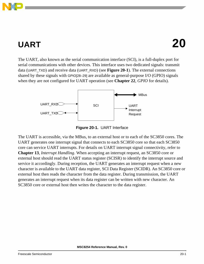
UART 20The UART, also known as the serial communication interface (SCI), is a full-duplex port for serial communications with other devices. This interface uses two dedicated signals: transmit data (UART_TXD) and receive data (UART_RXD) (see Figure 20-1). The external connections shared by these signals with GPIO[28–29] are available as general-purpose I/O (GPIO) signals when they are not configured for UART operation (see Chapter 22, GPIO for details).
The UART is accessible, via the MBus, to an external host or to each of the SC3850 cores. The UART generates one interrupt signal that connects to each SC3850 core so that each SC3850 core can service UART interrupts. For details on UART interrupt signal connectivity, refer to Chapter 13, Interrupt Handling. When accepting an interrupt request, an SC3850 core or external host should read the UART status register (SCISR) to identify the interrupt source and service it accordingly. During reception, the UART generates an interrupt request when a new character is available to the UART data register, SCI Data Register (SCIDR). An SC3850 core or external host then reads the character from the data register. During transmission, the UART generates an interrupt request when its data register can be written with new character. An SC3850 core or external host then writes the character to the data register.
Figure 20-1. UART Interface
SCIUART_RXD
UART_TXD
UART Interrupt Request
MBus
MSC8254 Reference Manual, Rev. 0
Freescale Semiconductor 20-1

UART
As Figure 20-2 shows, the UART allows full duplex, asynchronous, non-return-to-zero (NRZ) serial communication between the MSC8254 and remote devices, including other MSC8254 devices. The UART transmitter and receiver operate independently, although they use the same baud-rate generator and same character length. An SC3850 core monitors the status of the UART, writes the data to be transmitted, and processes received data.
Figure 20-3 shows the full duplex UART system in which the MSC8254 UART transmits and receives simultaneously. A higher-level protocol should handle the full duplex communication to guarantee that no more than one target UART transmits to the UART_RXD signal of the initiator at a given time. Receiver wake-up can obtain such a protocol (see Section 21.2.7, Receiver Wake-Up). The UART UART_TXD signal can be configured with full CMOS drive or with open-drain drive (see Chapter 22, GPIO). In both cases, the external pull-up resistor is needed to avoid floating input at the UART_RXD of the initiator.
Figure 20-2. UART Block Diagram
SCI Data
ReceiveShift Register
SCI Data Register
TransmitShift Register
Register
Baud-RateGenerator
SBR[12–0]
UART_RXD
UART_TXD
Sys
tem Transmit
Control³16
Receiveand Wake-Up
Data FormatControl
Control
T8
PF
FE
NF
RDRF
IDLE
TIE
OR
TCIE
TDRE
TC
R8
RAFRWU
RE
PE
ILT
PT
WAKE
M
Clo
ck
UART
ILIE
RIE
Interrupt
SBK
TE
Request
LoopLOOPS
RSRCControl
UART_TXD
From Transmitter
R[7–0]
T[7–0]
MSC8254 Reference Manual, Rev. 0
20-2 Freescale Semiconductor

Figure 20-3. Full Duplex Multiple UART System
UART-Rx
Chip ID =n1
UART-TxUART_TXD
UART_RXD
UART-Rx
Chip ID =n3
UART-TxUART_TXD
UART_RXD
UART-Rx
Chip ID =n2
UART-TxUART_TXD
UART_RXD
Initiator Device
UART_RXD
TxD
Note: The RC value on the MultiPoint TxD may limit system baud rate.
R
MSC8254
MSC8254 Reference Manual, Rev. 0
Freescale Semiconductor 20-3

UART
Figure 20-4 shows the UART on a single-wire connection of a half duplex system. The UART_TXD signal must be configured with open-drain drive (see Chapter 22, GPIO) and an external pull-up resistor. For details on single-wire, see Section 20.4.2, Single-Wire Operation, on page 20-22.
Figure 20-4. Single-Wire Connection
UART-Rx
Chip ID =n1
UART-TxTxD
UART-Rx
Chip ID =n3
UART-TxTxD
UART-Rx
Chip ID =n2
UART-TxTxD
Note: The RC value on the MultiPoint UART_TXD might limit system baud rate.
R Initiator device
RXD
MSC8254
MSC8254 Reference Manual, Rev. 0
20-4 Freescale Semiconductor

The UART uses the standard NRZ mark/space data format illustrated in Figure 20-5.
Each data character is contained in a frame that includes a start bit, eight or nine data bits, and a stop bit. Clearing the M bit in SCI Control Register 1 (SCICR) configures the SCI for 8-bit data characters. A frame with eight data bits has a total of 10 bits, including a start bit and a stop bit.
Setting the M bit configures the UART for nine-bit data characters. When the UART is configured for 9-bit data characters, the ninth data bit is the T8 or R8 bit in the SCIDR. T8 remains unchanged after transmission and can be used repeatedly without rewriting it. A frame with nine data bits has a total of 11 bits, including a start bit and a stop bit.
Figure 20-5. UART Data Formats
Table 20-1. Examples of 8-Bit Data Format
Start Bit Data Bits Address Bits Parity Bits Stop Bit
1 8 0 0 1
1 7 0 1 1
1 7 1 0 1
Note: The address bit identifies the frame as an address character. The address bit is bit 7 (M = 0) or bit 8 (M = 1) See Section 21.2.7, Receiver Wake-Up.
Table 20-2. Example of 9-Bit Data Format
Start Bit Data Bits Address Bits Parity Bits Stop Bit
1 9 0 0 1
1 8 0 1 1
1 8 1 0 1
Note: The address bit identifies the frame as an address character. The address bit is bit 7 (M = 0) or bit 8 (M = 1). See Section 21.2.7, Receiver Wake-Up.
Bit 5
StartBit Bit 0 Bit 1
Next
StopBit
StartBit
9-Bit Data Format
Bit 2 Bit 3 Bit 4 Bit 6 Bit 7
Parityor Data
Bit
Parityor Data
Bit
Bit M in SCICR Set
8-Bit Data Format
Bit M in SCICR Clear
Bit 5Bit 0 Bit 1 Bit 2 Bit 3 Bit 4 Bit 6 Bit 7 Bit 8 StopBit
NextStartBit
StartBit
MSC8254 Reference Manual, Rev. 0
Freescale Semiconductor 20-5

UART
A 13-bit modulus counter in the baud-rate generator derives the baud rate for both the receiver and the transmitter. A value ranging from 1 to 8191 is written to the SBR[12–0] bits to determine the CLASS clock/2 clock divisor. Writing a 0 to SBR[12–0] disables the baud-rate generator. The SBR bits are in the SCI Baud-Rate Register (SCIBR). The baud-rate clock is synchronized with the bus clock and drives the receiver. The baud-rate clock divided by 16 drives the transmitter. The receiver has an acquisition rate of 16 samples per bit time. Baud-rate generation is subject to two sources of error:
Integer division of the CLASS clock/2 may not give the exact target frequency.
Synchronization with the bus clock can cause phase shift.
Refer to Section 21.2.2, Data Sampling, for details on adjusting to the received baud rate at the receiver.
Table 20-3 lists some examples of achieving target baud rates with a CLASS clock/2 frequency of 250 MHz, using the following formula:
20.1 Transmitter
The UART transmitter accommodates either 8-bit or 9-bit data characters. The state of the M bit in the SCI Control Register (SCICR) determines the length of the data characters. When 9-bit data is transmitted, bit T8 in the SCIDR is the ninth bit (bit 8).
Table 20-3. Baud Rates (CLASS clock/2 = 250 MHz)
Bits SBR Receiver Clock (Hz) Transmitter Clock (Hz) Target Baud Rate Error (Percentage)
34 7,352,941 459,559 460,000 0.096
68 3,676,471 229,779 230,000 0.096
136 1,838,235 114,890 115,000 0.096
244 1,024,590 64,037 64,000 0.058
407 614,251 38,391 38,400 0.024
814 307,125 19,195 19,200 0.024
1628 153,563 9598 9600 0.024
3255 76,805 4800 4800 0.006
6510 38,402 2400 2400 0.006
Not supported 1200 —
Note: The error relates only to the first source error. Although typically, the CLASS frequency is 500 MHz, it may be reconfigured as indicated in the Clock Modes Table 7-1 in the Clocks chapter. The divider values must be recomputed for a different CLASS frequency.
UART baud rate System clock 16 SCIBR 12– 0[ ]×( )⁄=
MSC8254 Reference Manual, Rev. 0
20-6 Freescale Semiconductor

Transmitter
20.1.1 Character Transmission
To transmit data, one of the SC3850 cores or an external host writes the data character to the SCI Data Register (SCIDR), which is then transferred to the transmitter shift register. The transmitter shift register then shifts out the data bits on the UART_TXD signal, after it prefaces them with a start bit and appends them with a stop bit. The SCI data register is the write-only buffer between the MBus and the transmit shift register.
The UART also sets a flag, the transmit data register empty flag (TDRE), every time it transfers data from the buffer (SCIDR) to the transmitter shift register. If the Transmit Interrupt Enable (TIE) bit in the SCICR is set, the TDRE flag asserts a UART interrupt request. The transmit interrupt service routine responds to this flag by writing another character to the transmitter buffer (SCIDR), while the shift register is still shifting out the first character. If the TDRE flag is set and no new data or break character transferred to the shift register, the UART sets a flag, transmit complete (TC) and UART_TXD becomes idle.
Figure 20-6. Transmitter Block Diagram
PE
PT
H 8 7 6 5 4 3 2 1 0 L
11-Bit Transmit Shift RegisterSto
p
Sta
rt
T8
TDRE
TIE
TCIE
SBK
TC
ParityGeneration
MS
B
SCI Data Register T[7–0]
Load
Fro
m S
CID
R
Shi
ft E
nabl
e
Pre
ambl
e (A
ll O
nes)
Bre
ak (
All
0s)
M
SBR[12–0]
Baud-Rate ³ 16
UART_TXD
TDRE Interrupt Source
TC Interrupt Source
CLASS clock/2
Loop
LOOPS
RSRC
TE
ToControl Receiver
GeneratorTransmitter Control
MBus
MSC8254 Reference Manual, Rev. 0
Freescale Semiconductor 20-7

UART
Begin a UART transmission as follows:
1. Configure the UART:
a. Select a baud rate. Write the appropriate value to the SCIBR to start the baud-rate generator. Note that the baud-rate generator is disabled when the baud rate is zero. Writing to the 5 MSB (SBR[12–8]) bits of the SCIBR has no effect without also writing to the 8 LSB of SCIBR (SBR[7–0]).
b. Configure GPIO29 for UART UART_TXD (see Chapter 22, GPIO):
• Select the UART transmit signal for the GPIO29 external connection via the GPIO29 configuration registers.
• Set the direction bit for the GPIO29 port to select output.c. Write to the SCICR to configure data length, parity, and other configuration bits (LOOPS,
RSRC, M, WAKE, ILT, PE, PT) and enable the transmit and receive interrupts as required (TIE, TCIE, RIE, ILIE, TE, RE, RWU, and SBK). A preamble character is now shifted out of the transmitter shift register.
2. Perform the transmit procedure for each character:
d. Poll the TDRE flag by reading the SCISR or responding to the UART interrupt. Keep in mind that the TDRE reset value is one.
e. If the TDRE flag is set, write the data to be transmitted to SCIDR, where the ninth bit is written to the T8 bit in SCIDR if the UART is in 9-bit data format. Reading TDRE bit in the SCISR and then writing new data to T[7–0] in the SCIDR clears the TDRE flag. Otherwise, the last data transmitted and then UART_TXD goes to idle condition, that is, a logic 1 (high).
3. Repeat step 2 for each subsequent transmission.
Note: The TDRE flag is set when the shift register is loaded with the next data to be transmitted from SCIDR, which occurs 9/16ths of a bit time after the start of the stop bit of the previous frame.
Note: When the shift register is empty (the TC and TDRE flags are set), transmission starts no more than one bit time after the data register is written. If only the TC interrupt source is enabled (SCICR[TCIE] = 1, SCICR[TIE] = 0), then you must ensure at least one bit time interval between successive writes to the SCIDR to enable the transmitter software to write twice to the SCIDR per interrupt.
Setting the Transmitter Enable (SCICR[TE]) bit to 1 automatically loads the transmit shift register with a preamble of 10 logic 1s (if M = 0) or 11 logic 1s (if M = 1). After the preamble shifts out, control logic transfers the data from the SCIDR into the transmit shift register. A logic 0 start bit automatically goes into the least significant bit position of the transmit shift register. A logic 1 stop bit goes into the most significant bit position.
Hardware supports odd or even parity. When parity is enabled, the most significant bit (msb) of the data character is the parity bit.
MSC8254 Reference Manual, Rev. 0
20-8 Freescale Semiconductor

Transmitter
When the transmit shift register is not transmitting a character, UART_TXD goes to the idle condition, logic 1. When software clears the SCICR[TE] bit, the transmitter relinquishes control of UART_TXD.
Note: If SCIDDR[DDRTX] is set, UART_TXD is driven by a logic 0 (pulled down). Otherwise, if SCIDDR[DDRTX] is cleared, the UART_TXD signal is not driven. See Chapter 22, GPIO for details about configuring this signal.
If software clears SCICR[TE] while a transmission is in progress (TC = 0), the frame in the transmit shift register continues to shift out. Then the transmitter relinquishes control of UART_TXD even if there is data pending in the SCI data register. To avoid accidentally cutting off the last frame in a message, always wait for TDRE to go high after the last frame before clearing SCICR[TE].
To separate messages with preambles with minimum idle line time, use the following sequence between messages (see also Figure 20-7, Queuing an Idle Character):
1. Write the last character of the first message to the SCIDR.
2. Wait for the TDRE flag to go high, indicating the transfer of the last frame to the transmit shift register.
3. Insert a preamble by clearing and then setting the SCICR[TE] bit.
4. Write the first character of the second message to the SCIDR.
Another way to separate messages with idle line is to wait until the TC flag is set after writing the last character of the first message to SCIDR, indicating this character has already been transmitted. When TC is set, UART_TXD goes idle. Then, after some idle line time, write the first character of the second message to SCIDR.
20.1.2 Break Characters
Setting the send break bit (SCICR[SBK]) to a value of 1 loads the transmit shift register with a break character. A break character contains all logic 0s and has no start, stop, or parity bit. Break character is ten logic 0s (if M = 0) or eleven logic 0s (if M = 1). As long as SCICR[SBK] is at logic 1, transmitter logic continuously loads break characters into the transmit shift register. After software clears the SBK bit, the shift register finishes transmitting the last break character and then transmits at least one logic 1. The automatic logic 1 at the end of a break character guarantees the recognition of the start bit of the next frame.
MSC8254 Reference Manual, Rev. 0
Freescale Semiconductor 20-9

UART
20.1.3 Idle Characters
An idle character contains all logic 1s and has no start, stop, or parity bit. The length of idle characters depends on the M bit in SCICR. The preamble is a synchronizing idle character that begins the first transmission initiated after the SCICR[TE] bit is written from 0 to 1. Clearing and then setting the SCICR[TE] bit during a transmission queues an idle character to be sent after the frame currently being transmitted.
Note: When queuing an idle character, return the SCICR[TE] bit to logic 1 before the stop bit of the current frame shifts out to UART_TXD. Setting SCICR[TE] after the stop bit appears on UART_TXD discards data previously written to the SCI data register. Toggle the SCICR[TE] bit for a queued idle character while the TDRE flag is set and immediately before writing the next character to the SCI data register. See Figure 20-7, Queuing an Idle Character.
20.1.4 Parity Bit Generation
The UART can be configured to enable parity bit generation by the parity enable bit (SCICR[PE]). The parity type bit (SCICR[PT]) determines whether to place even or odd parity at T8 (if M = 1) or at T7 (if M = 0) bits of SCIDR.
20.2 Receiver
The SCI receiver can accommodate either 8-bit or 9-bit data characters. The state of the SCICR[M] bit determines the length of data characters. When receiving 9-bit data, bit R8 in the SCIDR is the ninth bit (bit 8).
Figure 20-7. Queuing an Idle Character
StartBit Stop
BitStartBit
StopBitCharacter
Next DataCharacter
IdleUART_TXD StopBit
TDRE flagis set
ToggleTE bit
Write nextdata character
to SCIDR
Character
Current Data
MSC8254 Reference Manual, Rev. 0
20-10 Freescale Semiconductor

Receiver
20.2.1 Character Reception
During a UART reception, the receive shift register shifts a frame in through UART_RXD. The SCI data register is the read-only buffer between the MBus and the receive shift register. After a complete frame shifts into the receive shift register, the data portion of the frame (the character) is transferred to the SCI data register. The receive data register full flag, RDRF, in SCISR is set, indicating that the received character can be read.
The overrun flag, OR, is set when software fails to read the SCIDR before the receive shift register receives the next character. If the receive interrupt enable bit (SCICR[RIE]) is also set, the Receive Data Register Full (RDRF) or the OR flags generate an interrupt request.
Begin an SCI reception as follows:
1. Configure the SCI:
f. Select the target baud rate and write the appropriate value to the SCI Baud Rate Register (SCIBR). Note that the baud-rate generator is disabled when the baud rate is zero. Writing to 5 MSB bits of SCIBR (SBR[12–8]) has no effect without also writing to 7 LSB of SCIBR (SBR[7–0]).
g. Configure GPIO28 for UART UART_RXD (see Chapter 22, GPIO):
— Select the UART UART_RXD signal as the external connection via the GPIO port 20 configuration registers.
— Clear the direction bit for GPIO28 in the direction register to select input.h. Write to the SCICR to configure data length, parity, and other configuration bits (LOOPS,
RSRC, M, WAKE, ILT, PE, PT) and enable the transmitter, interrupts, receive, and wake up as required (TIE, TCIE, RIE, ILIE, TE, RE, RWU, and SBK).If the SBK bit is set, the receiver wakes up if there are particular conditions on the UART_RXD signal according to the WAKE control bit. Refer to Section 21.2.7, Receiver Wake-Up.
2. Perform the reception procedure for each character:
i. Poll the RDRF flag by reading the SCISR or responding to the UART interrupt.
j. If the RDRF flag is set, read the data to be received from SCIDR, where the ninth bit is read from R8 bit in SCIDR if the SCI is in 9-bit data format. Reading RDRF bit at SCISR and then reading new data from SCIDR clears RDRF flag.
3. Repeat step 2 for each subsequent reception.
MSC8254 Reference Manual, Rev. 0
Freescale Semiconductor 20-11

UART
20.2.2 Data Sampling
The receiver samples UART_RXD at the RT clock rate. The RT clock is an internal signal with a frequency 16 times the baud rate. To adjust for baud rate mismatch between the baud rate generated by RT clock and the target baud rate, the RT clock (see Figure 20-9) is re-synchronized:
After every start bit.
After the receiver detects a data bit change from logic 1 to logic 0 (after the majority of data bit samples at RT8, RT9, and RT10 returns a valid logic 1 and the majority of the next RT8, RT9, and RT10 samples returns a valid logic 0).
To locate the start bit, data sampling logic searches for a logic 0 preceded by three logic 1s. When the falling edge of a possible start bit occurs, the RT clock logic begins to count to 16.
Figure 20-8. UART Receiver Block Diagram
All
One
s
M
WAKE
ILT
PE
PT
RE
H 8 7 6 5 4 3 2 1 0 L
11-Bit Receive Shift RegisterSto
p bi
t
Sta
rt b
it
Data
Wake-up
ParityChecking
MS
B
SCI Data Register R[7–0]
R8
RIE
ILIE
RWU
RDRF
OR
NFFE
PF
UART_RXD
System
Idle Interrupt Source
RDRF Interrupt Source
SBR[12–0]
Baud-Rate
From UART_TXDOR Transmitter
Clock
IDLE
RAF
Sampling
Logic
OR Interrupt Source
Generator
sam
ple
sam
ple
Loop
LOOPS
RSRC
Control
MBus
MSC8254 Reference Manual, Rev. 0
20-12 Freescale Semiconductor

Receiver
To verify the start bit and to detect noise, data sampling logic takes samples at RT3 and RT5. If both samples are logic 1 the RT counter is reset and a new search for a start bit begins, else also RT7 sample is taken. If at least two samples (from RT3, RT5, and RT7) are logic 0 then the start bit is perceived. The noise flag, NF, is set if two samples are logic 0 and one is logic 1. Table 20-4 summarizes the results of the start bit verification samples.
If start bit verification is not successful, the RT counter is reset and a new search for a start bit begins. To determine the value of a data bit and to detect noise, sample logic takes samples at RT8, RT9, and RT10. The data bit value is determined by the majority of the samples. The noise flag, NF, is set if not all samples have the same logical value. Table 20-5 summarizes the results of the data bit samples.
Figure 20-9. Receiver Data Sampling
Table 20-4. Start Bit Verification
RT3, RT5, and RT7 Samples Start Bit Verification Noise Flag
000 Yes 0001 Yes 1010 Yes 1
011 No 0100 Yes 1101 No 0
11 (RT7 sample is not taken) No 0
Table 20-5. Data Bit Recovery
RT8, RT9, and RT10 Samples Data Bit Determination Noise Flag
000 0 0001 0 1
010 0 1011 1 1100 0 1
101 1 1110 1 1111 1 0
Reset RT Clock
RT
1R
T1
RT
1R
T1
RT
1R
T1
RT
1R
T1
RT
1R
T2
RT
3R
T4
RT
5
RT
8R
T7
RT
6
RT
11R
T10
RT
9
RT
15R
T14
RT
13R
T12
RT
16R
T1
RT
2R
T3
RT
4
Samples
RT Clock
RT Clock Count
Start BitUART_RXD
Start BitQualification
Start Bit DataSampling
1 111111 1 0 0 0 000 0
LSB
Verification
MSC8254 Reference Manual, Rev. 0
Freescale Semiconductor 20-13

UART
Note: The RT8, RT9, and RT10 samples do not affect start bit verification. If any or all of the RT8, RT9, and RT10 start bit samples are logic 1s following a successful start bit verification, the noise flag (NF) is set and the receiver assumes that the bit is a start bit (logic 0).
To verify a stop bit and to detect noise, sample logic takes samples at RT8, RT9, and RT10. The noise flag, NF, is set if not all samples have the same logical value (the same as for data bit sampling). If the majority of the samples are logic 0 framing error flag, FE, is set. Table 20-6 summarizes the results of the stop bit samples.
In Figure 20-10 the start bit verification samples RT3 and RT5 determine that the first logic 0 detected is noise and not the beginning of a start bit. The RT counter is reset and the start bit search resumes. The noise flag is not set because the noise occurred before the start bit was found.
Table 20-6. Stop Bit Recovery
RT8, RT9, and RT10 Samples Framing Error Flag Noise Flag
000 1 0
001 1 1
010 1 1
011 0 1
100 1 1
101 0 1
110 0 1
111 0 0
Figure 20-10. Start Bit Search Example 1
Reset RT Counter
RT
1R
T1
RT
1R
T1
RT
2R
T3
RT
4R
T5
RT
1R
T1
RT
2R
T3
RT
4
RT
7R
T6
RT
5
RT
10R
T9
RT
8
RT
14R
T13
RT
12R
T11
RT
15R
T16
RT
1R
T2
RT
3Samples
RT Clock
RT Clock Count
Start Bit
UART_RXD
1 1011 1 1 0 0 00 0
LSB
0 0
MSC8254 Reference Manual, Rev. 0
20-14 Freescale Semiconductor

Receiver
In Figure 20-11, the verification sample at RT3 is high. The RT3 sample sets the noise flag. Although the perceived bit time is misaligned, the data samples RT8, RT9, and RT10 of the next bit are within the bit time and data recovery is successful.
In Figure 20-12 the first start bit verification is a case similar to that in Figure 20-10, Start Bit Search Example 1, but this time the first logic 0 detected is the real beginning of start bit. The noise is at samples R3 and R5 which causes the RT counter to reset and the start bit search begins again. Although the perceived bit time is misaligned, the data samples RT8, RT9, and RT10 of the next bit are within the bit time and data recovery is successful. For this case the noise and framing error flags are not set.
Figure 20-11. Start Bit Search Example 2
Figure 20-12. Start Bit Search Example 3
RT
1R
T1
RT
1R
T1
RT
1R
T1
RT
2R
T3
RT
4R
T5
RT
6R
T7
RT
8
RT
11R
T10
RT
9
RT
14R
T13
RT
12
RT
2R
T1
RT
16R
T15
RT
3R
T4
RT
5R
T6
RT
7
Actual Start Bit
1 1111 1 0 0 00
LSB
00
Perceived Start Bit
Reset RT Counter
Samples
RT Clock
RT Clock Count
UART_RXD
Reset RT Counter
RT
1R
T1
RT
1R
T1
RT
2R
T3
RT
4R
T5
RT
1R
T2
RT
3R
T4
RT
5
RT
8R
T7
RT
6
RT
11R
T10
RT
9
RT
15R
T14
RT
13R
T12
RT
16R
T1
RT
2R
T3
RT
4
Samples
RT Clock
RT Clock Count
Actual Start Bit
UART_RXD
1 011 1 0 0
LSB
1
Perceived Start Bit
0 0 0
RT
5R
T6
RT
7R
T8
RT
9R
T10
0 0 0
MSC8254 Reference Manual, Rev. 0
Freescale Semiconductor 20-15

UART
In Figure 20-13, a large burst of noise is perceived as the beginning of a start bit, although the test sample at RT5 is high. The RT5 sample sets the noise flag. Although this is a worst-case misalignment of perceived bit time, the RT8, RT9, and RT10 data samples of the next bit are within the bit time, and data recovery is successful.
Figure 20-14 shows the effect of noise early in the start bit time. Although this noise does not affect proper synchronization with the start bit time, it does set the noise flag.
Figure 20-15 shows a burst of noise near the beginning of the start bit that causes the start bit not to be found and resets the RT counter. The sample after the reset is low but is not preceded by three high samples that would qualify as a falling edge. Depending on the timing of the start bit search and on the data, the frame may be missed entirely or it may set the framing error flag.
Figure 20-13. Start Bit Search Example 4
Figure 20-14. Start Bit Search Example 5
Reset RT Counter
RT
1
RT
1
RT
1
RT
1
RT
2
RT
3
RT
4
RT
5
RT
6
RT
7
RT
8
RT
9
RT
10
RT
13
RT
12
RT
11
RT
16
RT
15
RT
14
RT
4
RT
3
RT
2
RT
1
RT
5
RT
6
RT
7
RT
8
RT
9
Samples
RT Clock
RT Clock Count
Actual Start BitUART_RXD
1 011 1 0 0 00
LSB
0
Perceived Start BitR
T1
RT
1R
T1
RT
1R
T1
RT
1R
T1
RT
1
RT
1R
T1
RT
2R
T3
RT
4
RT
7R
T6
RT
5
RT
10
RT
9R
T8
RT
14R
T13
RT
12
RT
11
RT
15R
T16
RT
1R
T2
RT
3
Perceived and Actual Start Bit
1 111 1 0 01
LSB
11 1 1
Reset RT Counter
Samples
RT Clock
RT Clock Count
UART_RXD
MSC8254 Reference Manual, Rev. 0
20-16 Freescale Semiconductor

Receiver
In Figure 20-16, a noise burst makes the majority of data samples RT8, RT9, and RT10 high. This sets the noise flag but does not reset the RT counter. In the start bits only, the RT8, RT9, and RT10 data samples are not used for determining bit value.
20.2.3 Framing Error
If the data sampling logic does not detect a logic 1 where the stop bit should be in an incoming frame, it sets the framing error flag, SCISR[FE]. A break character also sets the FE flag because a break character has no stop bit. The FE flag is set at the same time that the RDRF flag is set. FE inhibits further data reception until it is cleared. Clear SCISR[FE] by reading SCISR and then reading the SCIDR.
Figure 20-15. Start Bit Search Example 6
Figure 20-16. Start Bit Search Example 7
RT
1
RT
1
RT
1
RT
1
RT
1
RT
1
RT
1
RT
1
RT
1
RT
1
RT
2
RT
3
RT
4
RT
7
RT
6
RT
5
RT
1
RT
1
RT
1
RT
1
RT
1
RT
1
RT
1
RT
1
RT
1
RT
1
RT
1
RT
1
Start Bit
1 111 1 0 10
LSB
11 1 1 1 0 000 000 0
No Start Bit Found
Reset RT Counter
Samples
RT Clock
RT Clock Count
UART_RXD
RT
1
RT
1R
T1
RT
1R
T1
RT
1R
T1
RT
1R
T1
RT
1R
T2
RT
3R
T4
RT
7
RT
6R
T5
RT
10
RT
9
RT
8
RT
14
RT
13R
T12
RT
11
RT
15
RT
16R
T1
RT
2R
T3
Start Bit
1 111 1 0 00
LSB
11 1 1 0 1 10
Reset RT Counter
Samples
RT Clock
RT Clock Count
UART_RXD
MSC8254 Reference Manual, Rev. 0
Freescale Semiconductor 20-17

UART
20.2.4 Parity Error
The UART can be configured to enable parity check via the Parity Enable (PE) bit in the SCICR. The parity type (SCICR[PT]) determines whether to check for even or odd parity. The Parity Error Flag, SCISR[PF], is set when the parity enable bit is set and the parity of the received character does not match the PT bit. Clear SCISR[PF] by reading the SCISR and then reading SCIDR.
20.2.5 Break Characters
The UART recognizes a break character as a start bit followed by 8 or 9logic 0 data bits and a logic 0 stop bit. Receiving a break character has the following effects on UART registers:
1. The framing error flag (SCISR[FE]) is set.
2. The receive data register full flag (SCISR[RDRF]) is set.
Note: Once the RDRF flag is cleared after being set by a break character, a valid frame must set the RDRF flag again before another break character can set it again.
3. The SCIDR is cleared.
4. The overrun flag (OR), noise flag (NF), parity error flag (PF), or the receiver active flag (RAF) is set (see the discussion in Section 20.6).
20.2.6 Baud-Rate Tolerance
A transmitting device may be operating at a baud rate below or above the receiver baud rate. Accumulated bit time misalignment can cause one of the three stop bit data samples (RT8, RT9, and RT10) to fall outside the actual stop bit. A noise error occurs if the RT8, RT9, and RT10 samples are not all the same logical values. A framing error occurs if the receiver clock is misaligned so that the majority of the RT8, RT9, and RT10 stop bit samples are a logic zero. In most applications, the baud-rate tolerance is much more than the degree of misalignment that is likely to occur.
As the receiver samples an incoming frame, it resynchronizes the RT clock on any valid falling edge within the frame. Resynchronization within frames corrects a misalignment between transmitter bit times and receiver bit times.
MSC8254 Reference Manual, Rev. 0
20-18 Freescale Semiconductor
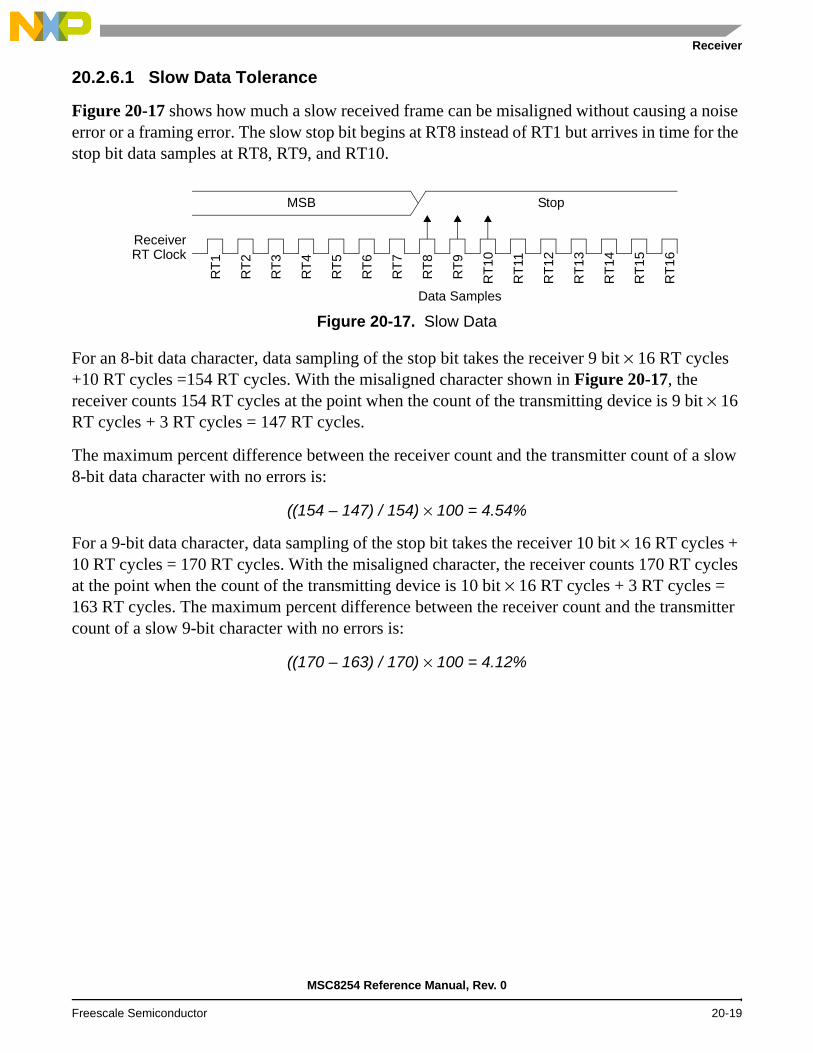
Receiver
20.2.6.1 Slow Data Tolerance
Figure 20-17 shows how much a slow received frame can be misaligned without causing a noise error or a framing error. The slow stop bit begins at RT8 instead of RT1 but arrives in time for the stop bit data samples at RT8, RT9, and RT10.
For an 8-bit data character, data sampling of the stop bit takes the receiver 9 bit × 16 RT cycles +10 RT cycles =154 RT cycles. With the misaligned character shown in Figure 20-17, the receiver counts 154 RT cycles at the point when the count of the transmitting device is 9 bit × 16 RT cycles + 3 RT cycles = 147 RT cycles.
The maximum percent difference between the receiver count and the transmitter count of a slow 8-bit data character with no errors is:
((154 – 147) / 154) × 100 = 4.54%
For a 9-bit data character, data sampling of the stop bit takes the receiver 10 bit × 16 RT cycles + 10 RT cycles = 170 RT cycles. With the misaligned character, the receiver counts 170 RT cycles at the point when the count of the transmitting device is 10 bit × 16 RT cycles + 3 RT cycles = 163 RT cycles. The maximum percent difference between the receiver count and the transmitter count of a slow 9-bit character with no errors is:
((170 – 163) / 170) × 100 = 4.12%
Figure 20-17. Slow Data
MSB StopR
T1
RT
2
RT
3
RT
4
RT
5
RT
6
RT
7
RT
8
RT
9
RT
10
RT
11
RT
12
RT
13
RT
14
RT
15
RT
16
Data Samples
Receiver RT Clock
MSC8254 Reference Manual, Rev. 0
Freescale Semiconductor 20-19

UART
20.2.6.2 Fast Data Tolerance
Figure 20-18 shows how much a fast received frame can be misaligned without causing a noise error or a framing error. The fast stop bit ends at RT10 instead of RT16, but it is still sampled at RT8, RT9, and RT10.
For an 8-bit data character, data sampling of the stop bit takes the receiver 9 bit times × 16 RT cycles + 10 RT cycles = 154 RT cycles. With the misaligned character shown in Figure 20-18, the receiver counts 154 RT cycles at the point when the count of the transmitting device is 10 bit times × 16 RT cycles = 160 RT cycles.
The maximum percent difference between the receiver count and the transmitter count of a fast 8-bit character with no errors is:
((154 – 160) / 154) × 100 = 3.90%
For a 9-bit data character, data sampling of the stop bit takes the receiver 10 bit × 16 RT cycles + 10 RT cycles = 170 RT cycles. With the misaligned character, the receiver counts 170 RT cycles at the point when the count of the transmitting device is 11 bit × 16 RT cycles = 176 RT cycles. The maximum percent difference between the receiver count and the transmitter count of a fast 9-bit character with no errors is:
((170 – 176) / 170) × 100 = 3.53%
20.2.7 Receiver Wake-Up
The receiver can be put into a standby state, so that the UART (SCI) can ignore transmissions intended only for other receivers in multiple-receiver systems. This is sometimes called putting the receiver to sleep. Setting the receiver wake-up (RWU) bit in the SCICR puts the receiver into a standby state during which receiver interrupts are disabled. The SCI still loads the receive data into the SCIDR, but it does not set the SCISR[RDRF] flag or any other flag. The transmitting device can address messages to selected receivers by including addressing information in the initial frame or frames of each message. Once the receiver is asleep, there must be a wake-up procedure to allow it to respond to messages addressed to it. The SCICR[WAKE] bit determines how the SCI is brought out of the standby state to process an incoming message. This wake bit enables either idle line wake-up or address mark wake-up.
Figure 20-18. Fast Data
Idle or Next FrameStopR
T1
RT
2
RT
3
RT
4
RT
5
RT
6
RT
7
RT
8
RT
9
RT
10
RT
11
RT
12
RT
13
RT
14
RT
15
RT
16
DataSamples
Receiver RT Clock
MSC8254 Reference Manual, Rev. 0
20-20 Freescale Semiconductor

Reset Initialization
20.2.7.1 Idle Input Line Wake-Up (WAKE = 0)
In idle input line wake-up, an idle condition on UART_RXD (all logic 1s) clears the SCICR[RWU] bit and wakes up the SCI. The initial frame or frames of every message contain addressing information. All receiver software evaluate the addressing information, and receivers for which the message is addressed process the frames that follow. Any receiver for which a message is not addressed can set its SCICR[RWU] bit and return to the standby state. The RWU bit remains set and the receiver remains on standby until another idle character appears on UART_RXD.
Idle line wake-up requires that messages be separated by at least one idle character and that no message contain idle characters. The idle character that wakes a receiver does not set the receiver idle bit, IDLE, or the receive data register full flag, SCISR[RDRF]. The idle line type bit, SCICR[ILT], determines whether the receiver begins counting logic 1s as idle character bits after the start bit or after the stop bit.
Note: With the WAKE bit clear, setting the SCICR[RWU] bit after UART_RXD has been idle can cause the receiver to wake up immediately.
20.2.7.2 Address Mark Wake-Up (WAKE = 1)
In address mark wake-up, a logic 1 in the MSB position of a frame clears the SCICR[RWU] bit and wakes up the SCI. This frame is considered to contain an address character. Hence, all data characters should have their MSB at zero. Each receiver software evaluates the addressing information when awakened and compares it to its own address. If the addresses match, the receiver(s) process the frames that follow. If the addresses do not match, the receiver software puts the receiver to sleep by setting the SCICR[RWU] bit. The RWU bit remains set and the receiver remains on standby until another address frame appears on UART_RXD.
The logic 1 in the MSB of an address character clears the receiver RWU bit before the stop bit is received and sets the SCISR[RDRF] interrupt flag. Address mark wake-up allows messages to contain idle characters but requires that the MSB be reserved for use in address frames.
20.3 Reset Initialization
After reset the UART transmitter and receiver are disabled and UART_TXD and UART_RXD are not driven. For information on initializing the transmitter, refer to Section 20.1.1. For information on initializing the receiver, refer to Section 20.2.1.
MSC8254 Reference Manual, Rev. 0
Freescale Semiconductor 20-21

UART
20.4 Modes of Operation
The following sections summarize the UART modes of operation.
20.4.1 Run Mode
Run mode is the normal mode of operation.
20.4.2 Single-Wire Operation
Normally, the UART (SCI) uses two signals for transmitting and receiving data. In single-wire operation, UART_RXD is disconnected from the UART and is available as a GPIO signal (see Chapter 22, GPIO). The UART uses UART_TXD for both receiving and transmitting data. Setting the data direction bit for UART_TXD, SCIDDR[DDRTX], configures UART_TXD as the output for transmitted data. Clearing the data direction bit, SCIDDR[DDRTX], disables the transmitter to drive UART_TXD.
Enable single-wire operation by setting the SCICR[LOOPS] bit and the receiver source bit, SCICR[RSRC]. Setting the SCICR[LOOPS] bit disables the path from UART_RXD to the receiver. Setting the SCICR[RSRC] bit connects the receiver input to the output of UART_TXD. Both the transmitter and receiver must be enabled (SCICR[TE] = 1 and SCICR[RE] = 1). You can configure UART_TXD (see Chapter 22, GPIO) for full CMOS drive or for open-drain drive. The configuration bit controls UART_TXD in both normal operation and single-wire operation. The configuration bit also allows the UART_TXD outputs to be tied together in a multiple-transmitter system, which allows the UART_TXD signals of nonactive transmitters to follow the logic level of an active one. External pull-up resistors are necessary when using open-drain outputs.
Figure 20-19. Single-Wire Operation (LOOPS = 1, RSRC = 1)
UART_TXD
UART_RXD
Transmitter
General-Purpose I/O
Receiver
SCIDDR[DDRTX]
GPIOUART
MSC8254 Reference Manual, Rev. 0
20-22 Freescale Semiconductor

Modes of Operation
20.4.3 Loop Operation
To help isolate system problems, the Loop mode is sometimes used to check software without changing the physical connections in the external system. In Loop mode, the transmitter output is connected to the receiver input internally. The UART_RXD signal is disconnected from the external connection which then becomes available for use as a GPIO signal. Clearing the data direction bit of UART_TXD disconnects the transmitter output from the external connection.
To enable loop operation, set the SCICR[LOOPS] bit and clear SCICR[RSRC]. Setting the SCICR[LOOPS] bit disables the path from UART_RXD to the external output connection. Clearing the SCICR[RSRC] bit connects the transmitter output to the receiver input. Both the transmitter and receiver must be enabled (SCICR[TE] = 1 and SCICR[RE] = 1) for loop operation.
20.4.4 Stop Mode
The UART stops its clock to provide reduced power consumption when the GCR1[UART_STC] bit is set (see Section 8.2.1, General Configuration Register 1 (GCR1), on page 8-2). When the UART enters Stop mode, the states of the UART registers are unaffected. The UART registers cannot be accessed during Stop mode. When the UART_STC bit is cleared, UART operation resumes. Entering Stop mode during a transmission or reception results in invalid data. Therefore, disable the receiver and transmitter (SCICR[TE] = 0, SCICR[RE] = 0) before entering Stop mode.
20.4.5 Receiver Standby Mode
Refer to Section 21.2.7, Receiver Wake-Up.
Figure 20-20. Loop Operation (LOOPS = 1, RSRC = 0)
UART_TXD
UART_RXDGeneral-Purpose I/O
Transmitter
Receiver
SCIDDR[DDRTX]
GPIOUART
MSC8254 Reference Manual, Rev. 0
Freescale Semiconductor 20-23

UART
20.5 Interrupt Operation
Table 20-7 lists the five interrupts generated by the UART to communicate with an SC3850 core or external host.The UART outputs only one signal, which can be activated by each of the five interrupt sources (refer to Figure 20-1, UART Interface, on page 20-1). Receiver interrupts are disabled when the receiver is in standby state (RWU is set).
The UART (SCI) only originates interrupt requests. An interrupt source flag (see Table 20-7) generates interrupt request if its associated interrupt enable bit is set. The interrupt vector offset and interrupt number are chip dependent.
20.6 UART Programming Model
All UART registers are mapped into the MBus address space. This section describes the UART (SCI) module registers, which are listed as follows:
SCI Baud-Rate Register (SCIBR), on page 20-25.
SCI Control Register (SCICR), on page 20-26.
SCI Status Register (SCISR), on page 20-29.
SCI Data Register (SCIDR), on page 20-31.
SCI Data Direction Register (SCIDDR), on page 20-32.
Note: The UART register use a base address of: 0xFFF26C00.
Table 20-7. UART Interrupt Sources
SourceTransmitter/
ReceiverInterrupt Enable Bit
Flag at StatusRegister
Description
TDRE T TIE:SCICR[7] TDRE:SCISR[15] Indicates that a character was transferred from SCIDR to the transmit shift register.
TC T TCIE:SCICR[6] TC:SCISR[14] Indicates that a transmit is complete.
RDRF R RIE:SCICR[5] RDRF:SCISR[13] Indicates that received data is available in SCIDR.
OR R RIE:SCICR[5] OR:SCISR[11] Indicates an overrun condition.
IDLE R ILIE:SCICR[4] IDLE:SCISR[12] Indicates that receiver input has become idle.
Note: For details, refer to SCI Status Register (SCISR), on page 20-29
MSC8254 Reference Manual, Rev. 0
20-24 Freescale Semiconductor

UART Programming Model
20.6.1 SCI Baud-Rate Register (SCIBR)
SCIBR determines the SCI baud rate. A write to SCIBR[12–8] has no effect without a write to SCIBR[7–0], since writing to SCIBR[12–8] puts the data in a temporary location until SCIBR[7–0] is written.
Note: The formula for calculating the baud rate is: SCI baud rate = (CLASS clock/2)/(16 × BR).
Note: The baud-rate generator is disabled until the SCICR[TE] bit or the SCICR[RE] bit is set for the first time after reset. The baud-rate generator is disabled when BR = 0.
SCIBR SCI Baud-Rate Register Offset 0x00
Bit 31 30 29 28 27 26 25 24 23 22 21 20 19 18 17 16
—
Type R/WReset 0 0 0 0 0 0 0 0 0 0 0 0 0 0 0 0
Bit 15 14 13 12 11 10 9 8 7 6 5 4 3 2 1 0
— SBR12SBR11SBR10 SBR9 SBR8 SBR7 SBR6 SBR5 SBR4 SBR3 SBR2 SBR1 SBR0Type R/W
Reset 0 0 0 0 0 0 0 0 0 0 0 0 0 1 0 0
Table 20-8. SCIBR Bit Descriptions
Name Reset Description Settings
—31-13
0 Reserved. Write to zero for future compatibility.
SBR[12–0]12-0
4 SCI Baud RateThe baud-rate register used by the counter to determine the baud rate of the SCI.
Can contain a value from 1 to 8191.
MSC8254 Reference Manual, Rev. 0
Freescale Semiconductor 20-25
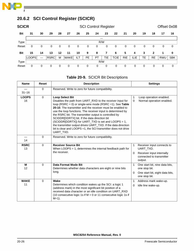
UART
20.6.2 SCI Control Register (SCICR)
SCICR SCI Control Register Offset 0x08
Bit 31 30 29 28 27 26 25 24 23 22 21 20 19 18 17 16
—
Type R/W
Reset 0 0 0 0 0 0 0 0 0 0 0 0 0 0 0 0
Bit 15 14 13 12 11 10 9 8 7 6 5 4 3 2 1 0
LOOPS — RSRC M WAKE ILT PE PT TIE TCIE RIE ILIE TE RE RWU SBKType R/WReset 0 0 0 0 0 0 0 0 0 0 0 0 0 0 0 0
Table 20-9. SCICR Bit Descriptions
Name Reset Description Settings
—31–16
0 Reserved. Write to zero for future compatibility.
LOOPS 16
0 Loop Select Bit Disables the path from UART_RXD to the receiver input for loop (RSRC = 0) or single-wire mode (RSRC =1). See Table 20-10. The transmitter and the receiver must be enabled to use the loop functions. The receiver input is determined by the RSRC bit. The transmitter output is controlled by SCIDDR[DDRTX] bit. If the data direction bit (SCIDDR[DDRTX]) for UART_TXD is set and LOOPS = 1, the transmitter output drives UART_TXD. If the data direction bit is clear and LOOPS =1, the SCI transmitter does not drive UART_TXD.
1 Loop operation enabled.0 Normal operation enabled.
—14
0 Reserved. Write to zero for future compatibility.
RSRC13
0 Receiver Source BitWhen LOOPS = 1, determines the internal feedback path for the receiver.
1 Receiver input connects to UART_TXD.
0 Receiver input internally connected to transmitter output.
M12
0 Data Format Mode BitDetermines whether data characters are eight or nine bits long.
1 One start bit, nine data bits, one stop bit.
0 One start bit, eight data bits, one stop bit.
WAKE11
0 WakeDetermines which condition wakes up the SCI: a logic 1 (address mark) in the most significant bit position of a received data character or an idle condition on UART_RXD (10 consecutive logic 1s if M = 0 or 11 consecutive logic 1s if M=1).
1 Address mark wake-up.
0 Idle line wake-up.
MSC8254 Reference Manual, Rev. 0
20-26 Freescale Semiconductor

UART Programming Model
ILT10
0 Idle Line Type BitDetermines when the receiver starts counting logic 1s as idle character bits. The counting begins either after the start bit or after the stop bit. If the count begins after the start bit, then a string of logic 1s preceding the stop bit may cause false recognition of an idle character. Beginning the count after the stop bit avoids false idle character recognition, but requires properly synchronized transmissions.
1 Idle character bit count begins after stop bit.
0 Idle character bit count begins after start bit.
PE9
0 Parity Enable BitEnables the parity function. When enabled, the parity function inserts (when transmitter enabled) and checks (when receiver enabled) a parity bit at the most significant bit position.
1 Parity function enabled.
0 Parity function disabled.
PT8
0 Parity Type BitDetermines whether the SCI generates and checks for even parity or odd parity. With even parity, an even number of 1s clears the parity bit and an odd number of 1s sets the parity bit. With odd parity, an odd number of 1s clears the parity bit and an even number of 1s sets the parity bit.
1 Odd parity.
0 Even parity.
TIE7
0 Transmitter Interrupt EnableEnables the transmit data register empty flag, TDRE, to generate interrupt requests.Note: Since SCISR[TDRE] reset value is 1, setting TIE
immediately after reset results in a UART interrupt request, regardless of SCICR[TE].
1 TDRE interrupt source enabled.
0 TDRE interrupt source disabled.
TCIE6
0 Transmission Complete Interrupt Enable Enables the transmission complete flag, TC, to generate interrupt requests.Note: Since the SCISR[TC] reset value is 1, setting TCIE
immediately after reset results in a UART interrupt request, regardless of SCICR[TE].
1 TC interrupt source enabled.
0 TC interrupt source disabled.
RIE5
0 Receiver Full Interrupt EnableEnables the receive data register full flag, RDRF, and the overrun flag, OR, to generate interrupt requests.
1 RDRF and OR interrupt sources enabled.
0 RDRF and OR interrupt sources disabled.
ILIE4
0 Idle Line Interrupt EnableEnables the idle line flag, IDLE, to generate interrupt requests.
1 IDLE interrupt source enabled.
0 IDLE interrupt source disabled.
TE3
0 Transmitter EnableEnables the SCI transmitter. The TE bit can be used to queue an idle preamble.
1 Transmitter enabled.
0 Transmitter disabled.
RE2
0 Receiver EnableEnables the SCI receiver.
1 Receiver enabled.
0 Receiver disabled.
Table 20-9. SCICR Bit Descriptions (Continued)
Name Reset Description Settings
MSC8254 Reference Manual, Rev. 0
Freescale Semiconductor 20-27
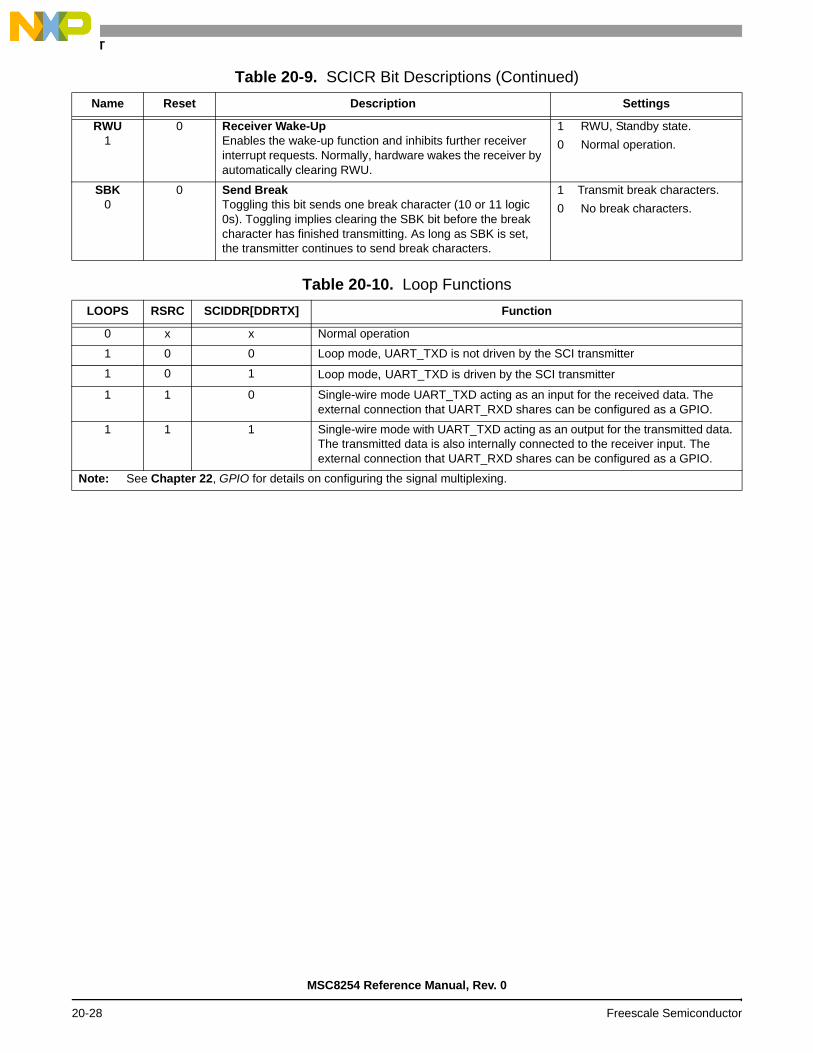
UART
RWU1
0 Receiver Wake-UpEnables the wake-up function and inhibits further receiver interrupt requests. Normally, hardware wakes the receiver by automatically clearing RWU.
1 RWU, Standby state.
0 Normal operation.
SBK0
0 Send BreakToggling this bit sends one break character (10 or 11 logic 0s). Toggling implies clearing the SBK bit before the break character has finished transmitting. As long as SBK is set, the transmitter continues to send break characters.
1 Transmit break characters.
0 No break characters.
Table 20-10. Loop Functions
LOOPS RSRC SCIDDR[DDRTX] Function
0 x x Normal operation
1 0 0 Loop mode, UART_TXD is not driven by the SCI transmitter
1 0 1 Loop mode, UART_TXD is driven by the SCI transmitter
1 1 0 Single-wire mode UART_TXD acting as an input for the received data. The external connection that UART_RXD shares can be configured as a GPIO.
1 1 1 Single-wire mode with UART_TXD acting as an output for the transmitted data. The transmitted data is also internally connected to the receiver input. The external connection that UART_RXD shares can be configured as a GPIO.
Note: See Chapter 22, GPIO for details on configuring the signal multiplexing.
Table 20-9. SCICR Bit Descriptions (Continued)
Name Reset Description Settings
MSC8254 Reference Manual, Rev. 0
20-28 Freescale Semiconductor

UART Programming Model
20.6.3 SCI Status Register (SCISR)
SCISR can be read any time. A write has no meaning or effect.
SCISR SCI Status Register Offset 0x10
Bit 31 30 29 28 27 26 25 24 23 22 21 20 19 18 17 16
—
Type R/W
Reset 0 0 0 0 0 0 0 0 0 0 0 0 0 0 0 0
Bit 15 14 13 12 11 10 9 8 7 6 5 4 3 2 1 0
TDRE TC RDRF IDLE OR NF FE PF — RAFType R R/W R
Reset 1 1 0 0 0 0 0 0 0 0 0 0 0 0 0 0
Table 20-11. SCISR Bit Descriptions
Name Reset Description Settings
—31–16
0 Reserved. Write to zero for future compatibility.
TDRE15
1 Transmit Data Register Empty FlagSet when the transmit shift register receives a character from the SCI data register. When TDRE is 1, the transmit data register (SCIDR) is empty and can receive a new value to transmit. This flag can generate an interrupt request (refer to Section 20.5).
Clear TDRE by reading TDRE and then writing to T[7–0] in the SCIDR.
1 Character transferred to transmit shift register; transmit data register empty.
0 No character transferred to transmit shift register.
TC14
1 Transmit Complete FlagSet low when there is a transmission in progress or when a preamble or break character is loaded. TC is set high when the TDRE flag is set and no data, preamble, or break character is being transmitted. When TC is set, UART_TXD becomes idle (logic 1). This flag can generate an interrupt request (refer to Section 20.5).
Clear TC by reading TC and then writing to T[7–0] in the SCIDR. TC is cleared automatically when data, preamble, or break is queued and ready to be sent. Also, TC is cleared in the event of a simultaneous set and clear of the TC flag (transmission not complete).
1 No transmission in progress.
0 Transmission in progress.
RDRF13
0 Receive Data Register Full FlagSet when the data in the receive shift register transfers to the SCI data register. This flag can generate an interrupt request (refer to Section 20.5).
Clear RDRF by reading RDRF bit at SCISR and then reading R[7–0] in the SCIDR.Note: Once the RDRF flag is cleared, after it is set by a
break or idle character, a valid frame must set the RDRF flag before another break or idle character can set it again.
1 Received data available in SCI data register.
0 Data not available in SCI data register.
MSC8254 Reference Manual, Rev. 0
Freescale Semiconductor 20-29

UART
IDLE12
0 Idle Line FlagSet when 10 consecutive logic 1s (if M = 0) or 11 consecutive logic 1s (if M = 1) appear on the receiver input. Once the IDLE flag is cleared, a valid frame must again set the RDRF flag before an idle condition can set the IDLE flag.This flag can generate an interrupt request (refer to Section 20.5).
Clear IDLE by reading IDLE and then reading R[7–0] in the SCIDR.Note: When the receiver wake-up bit (RWU) is set, an idle
line condition does not set the IDLE flag.
1 Receiver input has become idle.
0 Receiver input is either active now or has never become active since the IDLE flag was last cleared.
OR11
0 Overrun FlagSet when software fails to read the SCI data register before the receive shift register receives the next frame. The OR bit is set immediately after the stop bit has been completely received for the second frame. The data in the shift register is lost, but the data already in the SCI data registers is not affected. This flag can generate an interrupt request (refer to Section 20.5).
Clear OR by reading OR then reading R[7–0] in the SCIDR.
1 Overrun.
0 No overrun.
NF10
0 Noise FlagSet when the SCI detects noise on the receiver input. NF is set during the same cycle as the RDRF flag but is not set for an overrun.
Clear NF by reading NF and then reading R[7–0] in the SCIDR.
1 Noise.
0 No noise.
FE9
0 Framing Error Flag Set when a logic 0 is accepted as the stop bit. FE is set during the same cycle as the RDRF flag but is not set for an overrun. FE inhibits further data reception until it is cleared.
Clear FE by reading FE and then reading R[7–0] in the SCIDR.
1 Framing error.
0 No framing error.
PF8
0 Parity Error FlagSet when the parity enable bit, PE, is set and the parity of the received data does not match its parity bit.
Clear PF by reading PF and then reading R[7–0] in the SCIDR.
1 Parity error.
0 No parity error.
—7–1
0 Reserved. Write to zero for future compatibility.
RAF0
0 Receiver Active FlagSet when the receiver detects a logic 0 during the RT1 time period of the start bit search.
RAF is cleared when the receiver detects an idle character.
1 Reception in progress.
0 No reception in progress.
Table 20-11. SCISR Bit Descriptions (Continued)
Name Reset Description Settings
MSC8254 Reference Manual, Rev. 0
20-30 Freescale Semiconductor

UART Programming Model
20.6.4 SCI Data Register (SCIDR)
Note: In the SCIDR, writing affects only T[8–0]; writing to R[8–0] has no effect.
SCIDR SCI Data Register Offset 0x18
Bit 31 30 29 28 27 26 25 24 23 22 21 20 19 18 17 16
—
Type R/W
Reset 0 0 0 0 0 0 0 0 0 0 0 0 0 0 0 0
Bit 15 14 13 12 11 10 9 8 7 6 5 4 3 2 1 0
R8 T8 — R7/T7 R6/T6 R5/T5 R4/T4 R3/T3 R2/T2 R1/T1 R0/T0Type R R/W R/W R[7–0] is R
T[7–0] is WReset 0 0 0 0 0 0 0 0 0 0 0 0 0 0 0 0
Table 20-12. SCIDR Bit Descriptions
Name Reset Description Settings
—31–16
0 Reserved. Write to zero for future compatibility.
R815
0 Received Bit 8The ninth data bit received when the SCI is configured for 9-bit data format (M = 1).
T814
0 Transmit Bit 8The ninth data bit transmitted when the SCI is configured for 9-bit data format (M = 1).
—13–8
0 Reserved. Write to zero for future compatibility.
7–0 R[7–0] 0 Received Bits 7–0Received bits seven through zero for 9-bit or 8-bit data formats.
T[7–0] Transmit Bits 7–0Transmit bits seven through zero for 9-bit or 8-bit formats.
Notes: 1. If the value of T8 is the same as in the previous transmission, T8 does not have to be rewritten. The same value is transmitted until T8 is rewritten.
2. In 8-bit data format, only SCIDR[7–9] need to be accessed.3. When transmitting in 9-bit data format, write to SCIDR[15–0] (one access). Otherwise, write first to T8 and then
to the low byte (SCIDR[7–0]).
MSC8254 Reference Manual, Rev. 0
Freescale Semiconductor 20-31

UART
20.6.5 SCI Data Direction Register (SCIDDR)
When LOOPS is cleared and TE is set, UART_TXD is an output regardless of the state of SCIDDR[DDRTX].
SCIDDR SCI Data Direction Register Offset 0x28
Bit 31 30 29 28 27 26 25 24 23 22 21 20 19 18 17 16
—
Type R/WReset 0 0 0 0 0 0 0 0 0 0 0 0 0 0 0 0
Bit 15 14 13 12 11 10 9 8 7 6 5 4 3 2 1 0
— DDRTX —Type R/W
Reset 0 0 0 0 0 0 0 0 0 0 0 0 0 0 0 0
Table 20-13. SCIDDR Bit Descriptions
Name Reset Description Settings
—31–10
0 Reserved. Write to zero for future compatibility.
DDRTX9
0 Data Direction Bit TXControls the TX signal direction in single-wire mode (refer to Section 20.4.2).
1 If TE=1, TX is driven by the transmitter. Otherwise, if TE=0, UART_TXD is driven by logic 0.
0 UART_TXD is not driven when the transmitter is disabled (TE=0) or when LOOPS=1.
—8–0
0 Reserved. Write to zero for future compatibility.
Note: The setting descriptions assume that the UART_TXD signal is configured for UART operation.
MSC8254 Reference Manual, Rev. 0
20-32 Freescale Semiconductor

Timers 21The MSC8254 device includes 3 types of timers:
Device-level timers. Each MSC8254 device contains a total of 16 device timers. Each can be used by any of the DSP cores within MSC8254 as well as by an external host. See Section 21.1 for details.
SC3850 DSP core subsystem timers. Each of the SC3850 DSP core subsystems contain two timers used by the specific DSP core for any required operating system purpose. For details, see the MSC8156 SC3850 DSP Core Subsystem Reference Manual available with a signed non-disclosure agreement. Contact your Freescale representative or distributor for details.
Software watchdog timers. The MSC8254 device includes 8 software watchdog timers. Each of the software watchdog timers can be used by any of the cores within MSC8254 as well as by an external host. For details, see Section 21.3.
21.1 Device-Level Timers
There are four identical quad timer modules in the MSC8254 device. Each quad timer module contains four identical timer groups that serve as frequency dividers, clock generators, and event counters. Each 16-bit timer group contains a prescaler, a counter, a load register, a hold register, a capture register, two compare registers, and two status and control registers. The timers interface with the MSC8254 inputs/outputs as listed in Table 21-1. This document uses the term timer to refer to the four internal timers in each module and quad timer to refer to each of the timer modules. The term channel is used in register naming for clarity.
Table 21-1. Device-Level Timers Connectivity
Timer Module Timer Channel External Input External Output
0
0 TMR0 —
1 TMR1 TMR02 CLKIN —3 TDM0TCK TMR1
1
0 TMR0 —1 TMR2 —2 CLKIN —
3 TDM0TCK TMR2
MSC8254 Reference Manual, Rev. 0
Freescale Semiconductor 21-1

Timers
21.1.1 Features
Features of the timers include:
Counters support the following operations:
— Cascade.— Preloading.— Count once or continuously.— Share input pins.— Do capture and compare.— Count up or down.
Count modulo is programmable.
Maximum count rate is the CLASS clock/2 rate when the timer input signals are not in use.
Maximum count rate is half the CLASS clock/2 rate when the timer input signals are in use.
Each counter has a separate prescaler.
21.1.2 Timer Module Architecture
Each quad timer module contains four timers. The block diagram of one timer within a quad timer module is shown in Figure 21-1. As the figure shows, the primary clock selector contains a prescaler, primary clock multiplex, and an optional invert. It selects and optionally inverts a clock source for the primary clock. The primary clock can be selected from any of the following:
Normal clocking:
— CLASS clock/2— (CLASS clock/2) divided by the prescaler: /1, /2, /4, ..., /128.
Clocking from external events through a timer input signal.
2
0 TMR0 —1 TMR3 —
2 CLKIN —3 TDM0TCK TMR3
3
0 TMR0 —
1 TMR4 —2 CLKIN —3 TDM0TCK TMR4
Note: The external inputs list the external signal line connected to the specified timer input. The external outputs connect to the specified timer output. Most of the timer outputs do not connect to an external signal line. Even for cases in which a connection is indicated, the output is not valid unless the output is enabled by the TMRnSCTL[OEN] bit for the timer (see Section 21.4.1.2). Inputs and outputs for the TMRn signal lines are multiplexed.
Table 21-1. Device-Level Timers Connectivity (Continued)
Timer Module Timer Channel External Input External Output
MSC8254 Reference Manual, Rev. 0
21-2 Freescale Semiconductor
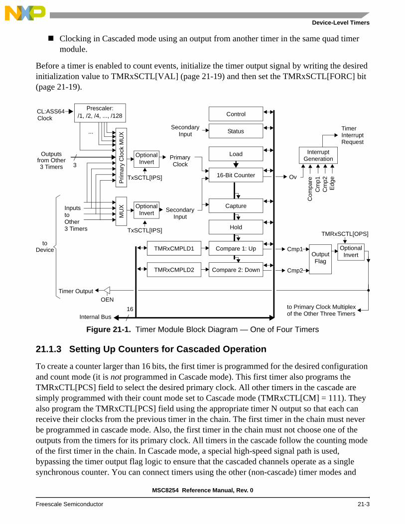
Device-Level Timers
Clocking in Cascaded mode using an output from another timer in the same quad timer module.
Before a timer is enabled to count events, initialize the timer output signal by writing the desired initialization value to TMRxSCTL[VAL] (page 21-19) and then set the TMRxSCTL[FORC] bit (page 21-19).
21.1.3 Setting Up Counters for Cascaded Operation
To create a counter larger than 16 bits, the first timer is programmed for the desired configuration and count mode (it is not programmed in Cascade mode). This first timer also programs the TMRxCTL[PCS] field to select the desired primary clock. All other timers in the cascade are simply programmed with their count mode set to Cascade mode (TMRxCTL[CM] = 111). They also program the TMRxCTL[PCS] field using the appropriate timer N output so that each can receive their clocks from the previous timer in the chain. The first timer in the chain must never be programmed in cascade mode. Also, the first timer in the chain must not choose one of the outputs from the timers for its primary clock. All timers in the cascade follow the counting mode of the first timer in the chain. In Cascade mode, a special high-speed signal path is used, bypassing the timer output flag logic to ensure that the cascaded channels operate as a single synchronous counter. You can connect timers using the other (non-cascade) timer modes and
Figure 21-1. Timer Module Block Diagram — One of Four Timers
Prescaler:/1, /2, /4, ..., /128
CL:ASS64
Prim
ary
Clo
ck M
UX...
Outputsfrom Other
MU
XInputs
OptionalInvert
TMRxSCTL[OPS]TxSCTL[IPS]
Primary
SecondaryInput
Clock
16-Bit Counter
Load
Clock
Capture
Hold
Compare 1: Up
Compare 2: Down
Internal Bus
Control
Status
Output
InterruptGeneration
Ov
Cmp1
Cmp2
OptionalInvert
TxSCTL[IPS]
Cm
p1C
mp2
Edg
e
Timer Output
to Primary Clock Multiplex
TimerInterrupt
TMRxCMPLD1
TMRxCMPLD2
16C
ompa
re
OEN
toDevice
3
of the Other Three Timers
3 Timers
SecondaryInput
Request
OptionalInvertto
Flag
Other3 Timers
MSC8254 Reference Manual, Rev. 0
Freescale Semiconductor 21-3

Timers
selecting the outputs of other timers as a clock source. In this case, the timers operate in a ripple mode, in which higher-order counters transition a clock later than in a purely synchronous design. This is not the typical use for cascaded counters.
21.1.3.1 Operation of the Cascaded Timer
If the first timer in a cascaded chain is counting up and it encounters a compare event, the timer connected to it is incremented. If the first timer in the chain is counting down and it encounters a compare event, the timer is decremented. You can correctly read all 16-bit portions of a cascaded timer as follows using the TMRxHOLD registers:
1. Read any 16-bit portion of the cascaded timer from its TMRxCNTR register. You can do this at any time.
2. When any TMRxCNTR register in the module is read, all other timers simultaneously load their values into their hold registers.
3. Read the 16-bit portions of all other timers in the cascade from their TMRxHOLD registers.
21.1.3.2 Cascading Restrictions
To ensure that there are no feedback loops in a cascade, there are restrictions on which timers can be cascaded. The timer with the lowest number must always be the first in the cascade, the timer with the second lowest number must be second, and so on. The timer with the highest number must always be last in the cascade. Table 21-2 summarizes the cascading restrictions.
Table 21-2. Restrictions On Cascading Timers
Timer NumberValid Cascade
Inputs
Legal Values for Cascading using TMRxCTL[PCS]
Description
Timer 0 None None Timer 0 can only be the first timer in a cascaded timer. It cannot receive another timer’s output for cascaded operation. Timer 0 must always be the first timer in the cascade.
Timer 1 Timer 0 output 0100: Timer 0 Timer 1 can be cascaded with Timer 0, with Timer 0 as the first timer in the chain.
Timer 2 Timer 0 outputTimer 1 output
0100: Timer 00101: Timer 1
Timer 2 can be cascaded with Timer 0 or Timer 1 when Timer 2 is not the first timer in the cascade.
Timer 3 Timer 0 outputTimer 1 outputTimer 2 output
0100: Timer 00101: Timer 10110: Timer 2
Timer 3 can be cascaded with Timer 0, Timer 1, or Timer 3. Timer 3 must always be the last timer in a cascade.
MSC8254 Reference Manual, Rev. 0
21-4 Freescale Semiconductor

Device-Level Timers
21.1.4 Timer Operating Modes
The timer operates in two modes:
Count the CLASS clock/2 or external events via the timer input using the primary clock.
Count the CLASS clock/2 or external events via the timer input using the primary clock while a second input signal, the secondary clock, is asserted, thus timing the width of the secondary clock signal.
Each timer can be configured in the following ways:
to count the rising, falling, or both edges of the selected input pin.
to decode and count quadrature encoded input signals.
to count up and down using dual inputs in a count with direction format.
program the timer terminal count value (modulo).
program the value loaded into the timer after it reaches its terminal count.
program the timer to count repeatedly or to stop after completing one count cycle.
program the timer to count to a programmed value (using the compare functionality)and then immediately reinitialize or to count through the compare value until the count rolls over to zero.
The counting modes define the different modes for clocking the timers. The count mode is selected in the TMRxCTL[CM] field (page 21-17). If a timer is programmed to count to a specific value and then stop, the TMRCTL[CM] bit is cleared when the count terminates. Table 21-3 summarizes the counting modes.
Table 21-3. Summary of Timer Counting Modes
Counting Mode CM Bits Description Primary ClockSecondary
Clock
Disabled 000 Timer not active. — —
Count 001 Counts the rising edges of the selected clock source(falling edges if TxSCTL[IPS] is set).This mode is useful for generating periodic interrupts for timing purposes or for counting external events.
Clock* —
Dual-Edge Count 010 Counts both edges of a timer Input signal.This mode is useful for counting the changes in the external environment. When this mode is selected, TMRxCTL[PCS] must not be set to any value between 1000 and 1111; that is, it must not set to the input clock or any scaled version of the input clock.
Clock —
MSC8254 Reference Manual, Rev. 0
Freescale Semiconductor 21-5

Timers
Figure 21-2. Quadrature Incremental Position Encoder
Gated Count 011 Counts primary clock edges while the secondary input is high (low if TxSCTL[IPS] is set). This mode is used to time the duration of external events when the primary clock is set to the input clock and the secondary input is set to use one of the timer input signals. It can also be used to count the number of external events that occur on one of the timer input signals, set as the primary clock, while a second timer input signal, connected to the secondary Input signal, is asserted.
Clock Gate*
Quadrature Count
100 Counts using quadrature encoded signals.The quadrature signals are square waves, 90 degrees out of phase. The decoding of quadrature signal provides both count and direction information. A timing diagram illustrating the basic operation of a quadrature incremental position encoder is provided in Figure 21-2.
Quadraturesignal
Quadraturesignal
Signed Count 101 Counts the primary clock source while a secondary input provides the count direction (up or down) for each recognized count.
Clock to count Count direction
Triggered Count 110 Counts the primary clock source only after a rising edge is detected on the secondary input (falling edge if TxSCTL[IPS] is set). The counting continues until a compare event occurs or another positive input transition is detected. If a second input transition occurs before a terminal count is reached, counting stops. Subsequent odd-numbered edges of the secondary input restart the counting, and even numbered edges stop counting. This process continues until a compare event occurs.
Clock to count Enable/disabletimer*
Cascade Count 111 Cascades multiple timers. Cascade mode is used for creating timers larger than 16-bits. Up to four timers may be cascaded together to create a 64-bit wide timer. The Cascaded Timer mode is synchronous. See Section 21.1.4.2.
Clock to count Triggers timer
Note: * This input can be inverted by the TxSCTL[IPS] bit.
Table 21-3. Summary of Timer Counting Modes
Counting Mode CM Bits Description Primary ClockSecondary
Clock
-1 -1 -1 -1 -1 -1 -1
PHASEA
COUNT
PHASEB
UP/DOWN
+1 +1 +1 +1 +1 +1 +1 +1
MSC8254 Reference Manual, Rev. 0
21-6 Freescale Semiconductor
Device-Level Timers
Other count modes derived as special cases of the modes described in Table 21-3 are described in the remainder of this section.
21.1.4.1 One-Shot Mode
One-Shot mode is a variation on Triggered Count mode if the timer is set up as follows:
TMRxCTL[CM] = 110 to count the rising and falling edges of the primary source
(see Table 21-5).
The Count Length bit, TMRxCTL[LEN] = 1.
Output Flag mode, TMRxCTL[OFLM] = 101 to select set on compare, cleared on secondary input signal edge.
The Count Once bit, TMRxCTL[ONCE] = 1 to count till a compare and then stop.
An external event causes the timer to count. When terminal count is reached, the timer output flag is asserted. This delayed output assertion can be used to provide timing delays.
21.1.4.2 Pulse Output Mode
In Pulse Output mode, a variation on Count mode, the timer outputs a stream of pulses with the same frequency as the selected clock source (cannot be the (CLASS clock/2)/1) if the timer is set up as follows:
TMRxCTL[CM] = 001 to count the rising edges of the primary source.(see Table 21-5TMR[0–3]SCTL[0–3] Bit Descriptions, on page 21>-19).
The Output Flag Mode, TMRxCTL[OFLM], = 111 to enable gated clock output while the timer is active.
The Count Once bit, TMRxCTL[ONCE], = 1 to count till a compare and then stop.
The number of output pulses is equal to the compare value minus the initial value. The primary count source must be set to one of the timer outputs for gated clock output mode.
21.1.4.3 Fixed Frequency PWM Mode
Fixed Frequency Pulse Width Modulated (PWM) mode is a subset of Count mode. The timer is set up as follows:
TMRxCTL[CM] = 001 to count the rising edges of the primary source.
The Count Length bit, TMRxCTL[LEN], = 0 so that the timer continues counting past the compare value (binary roll-over).
The Count Once bit, TMRxCTL[ONCE], = 0 to count repeatedly.
The Output Flag Mode, TMRxCTL[OFLM], = 110 so that the output flag is set when a compare occurs.
MSC8254 Reference Manual, Rev. 0
Freescale Semiconductor 21-7

Timers
The timer output yields a PWM signal with:
a frequency equal to the count clock frequency divided by 65,536.
a pulse width duty cycle equal to the compare value divided by 65,536.
21.1.4.4 Variable Frequency PWM Mode
The timer output yields a PWM signal with a frequency and pulse width determined by the values programmed into the TMRxCMP1 and TMRxCMP2 registers and the input clock frequency if the timer is set up as follows:
TMRxCTL[CM] = 001 TMRxCTL[CM] = 001 to count the rising edges of the primary source (see Table 21-5).
The Count Length bit, TMRxCTL[LEN], = 1 so that the timer counts to the compare value and then reinitializes.
The Count Once bit, TMRxCTL[ONCE], = 0 to count repeatedly.
The Output Flag Mode, TMRxCTL[OFLM], = 100 to toggle the timer output flag using alternating compare registers.
This method of PWM generation has the advantage of allowing almost any desired PWM frequency and/or constant on or off periods. The TMRxCMPLD1 and TMRxCMPLD2 registers are especially useful for this mode because they give you time to calculate values for the next PWM cycle during the PWM current cycle.
To set up the timer to run in Variable Frequency PWM mode with compare preload, use the set up described here for the desired timer. During set-up, update the TMRxCTL register last because the timer starts counting if the count mode changes to any value other than 000. Set up the Timer Control (TMRxCTL) register bits as follows:
Count Mode (CM) = 001 to count the rising edges of the primary source.
Primary Count Source (PCS) = 1000 to specify the best granularity for waveform timing; prescaler (CLASS clock/2)/1.
Secondary Count Source (SCS) = Any value because the bits are ignored in this mode.
Count Once (ONCE) = 0 to count repeatedly.
Count Length (LEN) = 1 so that the timer counts till it reaches a compare and then reinitializes the timer register.
Direction (DIR) = Count up (0) or count down (1). The compare register values must be chosen carefully to account for roll-under and so on.
External Initialization (EIN) = 0 so that another timer cannot force a reinitialization of this timer. However, you can set this bit if you need the functionality.
Output Mode (OFLM) = 100 to toggle the timer output flag using alternating compare registers.
MSC8254 Reference Manual, Rev. 0
21-8 Freescale Semiconductor

Device-Level Timers
Set up the Timer Status and Control Register (TMRxSCTL) bits as follows:
Output Polarity Select (OPS) = Your choice, true (0) or inverted (1).
Output Enable (OEN) = 1 to enable the timer output to be put on an external pin. Set this bit as needed.
Ensure that the rest of the TMRxSCTL bits are cleared. Interrupts are enabled in the Timer Comparator Status and Control Register (TMRxCOMSC) instead of in this register.
Set up the Timer Comparator Status and Control Register (TMRxCOMSC) bits as follows:
Timer Compare 2 Interrupt Enable (TCF2EN) = 1 to allow an interrupt to be issued when TCF2 is set).
Timer Compare1 Interrupt Enable (TCF1EN) = 0 so that an interrupt cannot be issued when TCF1 is set.
Timer Compare 1 Interrupt Source (TCF1) = 0 to clear the timer compare 1 interrupt source flag. This bit is set when a successful comparison of the timer and the TMRxCMP1 register occurs.
Timer Compare 2 Interrupt Source (TCF2) = 0 to clear the timer compare 2 interrupt source flag. This bit is set when a successful comparison of the timer and the TMRxCMP2 register occurs.
Compare Load Control 1 (CL1) = 10 to load the compare register when TCF2 is set.
Compare Load Control 2 (CL2) = 01 to load the compare register when TCF1 is set.
To service the TCF2 interrupts generated by the Timer, the interrupt controller must be configured to enable the interrupts for the timer being used. Additionally, you must write an interrupt service routine to do at least the following:
Clear the TCF2 and TCF1 flags.
Calculate and write new values for TMRxCMPLD1[15–0] and TMRxCMPLD2[15–0].
Figure 21-3 shows the timing for the compare preload cycle, which begins when a compare event on TMRxCMP2 causes TCF2 to be set. TMRxCMP1 is loaded with the value in the TMRxCMPLD1 one internal bus clock later. In addition, the timer asserts an interrupt, and the interrupt service routine executes while both comparator load registers are updated with new values. When TCF1 is set, TMRxCMP2 is loaded with the value of the CLV2 bits in TMRxCMPLD2. During the subsequent TCF2 event, TMRxCMP1 is loaded with the value of the TMRxCMPLD1[CLV1] bits. The cycle starts over again as an interrupt is asserted and the interrupt service routine clears TCF1 and TCF2 and calculates new values for TMRxCMPLD1 and TMRxCMPLD2.
MSC8254 Reference Manual, Rev. 0
Freescale Semiconductor 21-9

Timers
Figure 21-3. Compare Preload Timing
21.1.5 Timer Compare Functionality
The compare registers (TMRxCMP1 and TMRxCMP2) provide a bidirectional modulo count capability. TMRxCMP1 is used when the timer is counting up. Program it with the desired maximum count value or to 0xFFFF to indicate the maximum un signed value prior to roll-over. TMRxCMP2 is used when the timer is counting down. Program it with the maximum negative count value or to 0x0000 to indicate the minimum unsigned value prior to roll-under. The only exception occurs when the timer is operating with alternating compare registers.
When TMRxCTL[OFLM] = 100, alternating values of TMRxCMP1 and TMRxCMP2 are used to generate successful compares, and the output flag toggles while using alternating compare registers. For example, when TMRxCTL[OFLM] = 100, the timer is programmed to count upwards. It counts until the TMRxCMP1 value is reached, reinitializes, then counts until the TMRxCMP2 value is reached, reinitializes, then counts until the TMRxCMP1 value is reached, and so on. In this Variable Frequency PWM mode, the TMRxCMP2 value defines the desired pulse width of the on-time, and the TMRxCMP1 register defines the off-time. The Variable Frequency PWM mode is defined for positive counting only. See Section 21.1.4.4, Variable Frequency PWM Mode, on page 21-8.
Use caution when changing TMRxCMP1 and TMRxCMP2 while the timer is active. If the timer has already passed the new value, it counts to 0xFFFF or 0x0000, rolls over/under, and then begins counting toward the new value. The check is for Count = TMRxCMPx, not Count > = TMRxCMP1 or Count < = TMRxCMP2). Use of the preload registers addresses this problem.
1 Compare Preload Cycle 3
ci1-1 ci1 0 1 c0-n c0-1 c0 0 1 c2-1 c2 0
ci0 c0 c1
ci1 c2
c0 c1
ci1 c2
Internal Bus Clock
Counter[15–0]
TMRxCMP1[15–0]
TMRxCMP2[15–0]
TCF1
TCF2
TMRxCMPLD1[15–0]
TMRxCMPLD2[15–0]
Output Flag
MSC8254 Reference Manual, Rev. 0
21-10 Freescale Semiconductor

Device-Level Timers
21.1.5.1 Compare Preload Registers
The TMRxCMPLD1, TMRxCMPLD2 and TMRxCOMSC registers offer a high degree of flexibility for loading compare registers with user-defined values on different compare events. To ensure correct functionality, use the loading method described in this section.
The compare preload feature speeds updating of the compare registers. The compare preload feature allows you to calculate new compare values and store them into the comparator preload registers. When a compare event occurs, the new compare values in the comparator preload registers are directly written to the compare registers, eliminating the use of software to do this.
The compare preload feature is used in variable frequency PWM mode. See Section 21.1.4.4, Variable Frequency PWM Mode, on page 21-8. The TMRxCMP1 register determines the pulse width for the logic low part of the timer output, and TMRxCMP2 determines the pulse width for the logic high part of the timer output. The period of the waveform is determined by the TMRxCMP1 and TMRxCMP2 values and the frequency of the primary clock source. See Figure 21-4.
Figure 21-4. Variable PWM Waveform
To update the duty cycle or period of the waveform, update the TMRxCMP1 and TMRxCMP2 values using the compare preload feature.
21.1.5.2 Capture Register Use
The capture register, TMRxCAP (page 21-23), stores a copy of the timer value when an input edge (positive, negative, or both) on the secondary input signal is detected. The capture mode, programmable via TMRxSCTL[CM] (page 21-19), is one of the following:
CM = 00. Disabled.
CM = 01. Load the capture register on the rising edge of the signal.
CM = 10. Load the capture register on the falling edge of the signal.
CM = 11. Load the capture register on either edge of the signal.
When a capture event occurs, there are no further updates of TMRxCAP until the input edge flag (IEF) is cleared by writing a value of 0 to the TMRxSCTL[IEF] bit (page 21-19).
TMRxCMP1
TMRxCMP2
PWM Period
MSC8254 Reference Manual, Rev. 0
Freescale Semiconductor 21-11
Timers
21.1.5.3 Broadcast from an Initiator Timer
Any timer can be assigned as an initiator. An initiator compares signal can be broadcast to the other timers within the module. The other timers can be configured as follows to reinitialize their timers and/or force their output to predetermined values when an initiator timer compare event occurs:
Select one timer as the initiator timer by setting the TMRxSCTL[MSTR] bit.
Program the other timers to perform an action when a compare event occurs on the initiator timer as follows:
— The other timer is reinitialized if its TMRxCTL[EIN] bit is set.— The other timer forces its output flag signal if its TMRxSCTL[EEOF] bit is set.
21.1.6 Resets and Interrupts
The timers reset conditions are shown in Chapter 5, Reset. This reset forces all registers to their reset state and clears the output flag signal if it is asserted. The timer is turned off until the settings in the control register are changed. Each timer in a quad timer module can be programmed for interrupts. The available types of interrupts are as follows:
Timer compare
Timer compare 1
Timer compare 2
Timer overflow
Timer input edge
Each of these different types is ORed together within each timer to generate a single interrupt request signal to the interrupt controller.
21.1.6.1 Timer Compare Interrupts
Interrupt requests are generated when a successful compare occurs between a timer and its compare registers while the Timer Compare Flag Interrupt Enable bit, TMRxSCTL[TCFIE], is set. These interrupt requests are cleared by writing a zero to the appropriate TMRxSCTL[TCF] bit. When a timer compare interrupt is set in the TMRxSCTL and the compare preload registers are available, one of the following two interrupts is also asserted:
Timer compare 1 interrupt
Timer compare 2 interrupt
Timer compare 1 interrupts are generated when a successful compare occurs between a timer and its TMRxCMP1 register while the Timer Compare 1 Interrupt Enable (TCF1EN) is set in the TMRxCOMSC register. These interrupts are cleared by writing a zero to the TMRxCOMSC[TCF1] bit. Timer compare 2 interrupts are generated when a successful compare
MSC8254 Reference Manual, Rev. 0
21-12 Freescale Semiconductor

SC3850 DSP Core Subsystem Timers
occurs between a timer and its TMRxCMP2 register while the Timer Compare 2 Interrupt Enable (TCF2EN) bit is set in the TMRxCOMSC register. These interrupts are cleared by writing a zero to the TCF2 bit in the TMRxCOMSC.
21.1.6.2 Timer Overflow Interrupts
Timer overflow interrupts are generated when a timer rolls over its maximum value while the TCFIE bit is set in the TMRxSCTL register. These interrupts are cleared by writing a zero to the Timer Overflow Flag (TOF) bit of the appropriate TMRxSCTL.
21.1.6.3 Timer Input Edge Interrupts
Timer input edge interrupts are generated by a transition of the input signal (either positive or negative, depending on TMRxSCTL[IPS] setting) while the Input Edge Flag Interrupt Enable (IEFIE) bit is set in the TMRxSCTL. These interrupts are cleared by writing a zero to the appropriate TMRxSCTL[IEF] bit.
21.2 SC3850 DSP Core Subsystem Timers
For a detailed description of the core subsystem timers, see the MSC8156 SC3850 DSP Core Subsystem Reference Manual.
21.3 Software Watchdog Timers
There are total of eight identical software watchdog timers (WDTs). Typically, one is used per core and the remainder are used for external hosts. However, you can allocate the WDTs in any manner to meet your system requirements.
The WDT is responsible for asserting a hardware reset or machine-check interrupt (MCP) if the software fails to service the software watchdog timer for a certain period of time (for example, because software is lost or trapped in a loop with no controlled exit). Each WDT is a free-running down-counter that generates a reset or a non-maskable interrupt on underflow. To prevent a reset, software must periodically restart the countdown. Watchdog timer operations are configured in the system watchdog control register (SWCRR). See Section 21.4.3.1 for details.
Note: If any of the watchdog timers generate a reset, it resets all of the SC3850 core subsystems in the MSC8254 device.
MSC8254 Reference Manual, Rev. 0
Freescale Semiconductor 21-13

Timers
The software watchdog timer is enabled after reset to cause a hard reset or non-maskable interrupt (MCP) if it times out. If the software WDT is not needed, you must clear SWCRR[SWEN] to disable it. If it is used, the software WDT requires a special service sequence that executes periodically. Without this periodic servicing, the software watchdog timer times out and issues a reset or a nonmaskable interrupt, as programmed in SWCRR[SWRI]. Once software writes SWRI, the state of SWEN cannot be changed. Figure 21-1 shows the high level WDT block diagram.
Figure 21-1. Software Watchdog Timer High Level Block Diagram
21.3.1 Features
The key features of the WDT include the following:
Based on 16-bit prescaler and 16-bit down-counter.
Provide a selectable range for the time-out period.
Provide ~8.59 s maximum software time-out delay for 500 MHz input clock.
21.3.2 Modes of Operation
The WDT unit can operate in the following modes:
WDT enable/disable mode:
If the software watchdog timer is not needed, user can disable it. SWCRR[SWEN] bit enables the watchdog timer. It should be cleared by software after a system reset to disable the software watchdog timer. When the watchdog timer is disabled, the watchdog counter and prescaler counter are held in a stopped state.
— WDT enable mode (SWCRR[SWEN] = 1)This is the default value after soft reset.
— WDT disable mode (SWCRR[SWEN] = 0)If the software watchdog timer is not needed, the user must clear SWCRR[SWEN] to disable it.
WDT reset/interrupt output mode
Without software periodic servicing, the software watchdog timer times out and issues a reset or a nonmaskable interrupt (MCP), programmed in SWCRR[SWRI].
According to SWCRR[SWRI] programming, WDT timer causes a hard reset or machine check interrupt to the core.
Software Reset or MCP
SystemWatchdog
Register Interface
clockTimer
MSC8254 Reference Manual, Rev. 0
21-14 Freescale Semiconductor

Software Watchdog Timers
— Reset mode (SWCRR[SWRI] = 1)Software watchdog timer causes a hard reset (this is the default value after soft reset).
— Interrupt mode (SWCRR[SWRI] = 0)Software watchdog timer causes a machine check interrupt to the core.
WDT prescaled/non-prescaled clock mode
The WDT counter clock can be prescaled by programming CRR[SWPR] bit that controls the divide-by-65536 of WDT counter.
— Prescale mode (CRR[SWPR] = 1)The WDT clock is prescaled.
— Non-prescale mode (CRR[SWPR] = 0)The WDT clock is not prescaled.
21.3.3 Software WDT Servicing
The software watchdog timer service sequence consists of the following two steps:
Write 0x556C to the System Watchdog Service Register (SWSRR)
Write 0xAA39 to SWSRR
The service sequence reloads the watchdog timer and the timing process begins again. If a value other than 0x556C or 0xAA39 is written to the SWSRR, the entire sequence must start over. Although the writes must occur in the correct order before a time-out, any number of instructions can be executed between the writes. This allows interrupts and exceptions to occur between the two writes when necessary. Figure 21-5 shows a state diagram for the watchdog timer.
Figure 21-5. Software Watchdog Timer Service State Diagram
Although most software disciplines permit or even encourage the watchdog concept, some systems require a selection of time-out periods. For this reason, the software watchdog timer
0x556C / Don’t reloadReset
0xAA39 / Reload
State 0Waiting for 0x556C
State 1Waiting for 0xAA39
Not 0xAA39 / Don’t reloadNot 0x556C / Don’t reload
MSC8254 Reference Manual, Rev. 0
Freescale Semiconductor 21-15

Timers
must provide a selectable range for the time-out period. Figure 21-6 shows how to handle this need.
Figure 21-6. Software Watchdog Timer Functional Block Diagram
In Figure 21-6, the range is determined by SWCRR[SWTC]. The value in SWTC is then loaded into a 16-bit decrementer clocked by the CLASS clock/2. An additional divide-by-65536 prescaler value is used when needed.
The decrementer begins counting when loaded with a value from SWTC. After the timer reaches 0x0, a software watchdog expiration request is issued to the reset or MCP (machine check processor) control logic. Upon reset, SWTC is set to the maximum value and is again loaded into the System Watchdog Service Register (SWSRR), starting the process over. When a new value is loaded into SWTC, the software watchdog timer is not updated until the servicing sequence is written to the SWSRR. If SWCRR[SWEN] is loaded with 0, the modulus counter does not count.
21.4 Timers Programming Model
Because they are programmed differently, the device-level, SC3850 DSP core platform level, and software watchdog timers are described in separate subsections.
21.4.1 Device-Level Timers
This section describes the device-level timers. For a complete listing of all registers in all modules with their memory locations, see Chapter 9, Memory Map. The device-level timer registers are listed as follows, along with the pages on which the registers are discussed:
Timer Channel Control Registers (TMR[0–3]CTL[0–3], page 21-17.
Timer Channel Status and Control Registers (TMR[0–3]SCTL[0–3]), page 21-19.
Timer Channel Compare Register 1 (TMR[0–3]CMP1[0–3]), page 21-21.
Timer Channel Compare Register 2 (TMR[0–3]CMP2[0–3]), page 21-21.
Time-outSWCNR
Reload
SWCRR[SWEN]
CLASSClock/2
SWCRR[SWPR]
65536Divider
ClockDisable
SWSRR[WS]
SWCRR[SWTC]
Service
SWCRR[SWRI]
16-Bit DecrementerEventLogic
Reset or MCP
MSC8254 Reference Manual, Rev. 0
21-16 Freescale Semiconductor

Timers Programming Model
Timer Channel Compare Load Register 1 (TMR[0–3]CMPLD1[0–3]), page 21-22.
Timer Channel Compare Load Register 2 (TMR[0–3]CMPLD2[0–3]), page 21-22.
Timer Channel Comparator Status and Control Registers (TMR[0–3]COMSC[0–3]), page 21-22.
Timer Channel Capture Register (TMR[0–3]CAP[0–3]), page 21-22.
Timer Channel Load Register (TMR[0–3]LOAD[0–3]), page 21-24.
Timer Channel Hold Registers (TMR[0–3]HOLD[0–3]), page 21-24.
Timer Channel Counter Register (TMR[0–3]CNTR[0–3]), page 21-24.
Note: The base addresses for the device level timer modules are as follows:
Timer 0 = 0xFFF26000
Timer 1 = 0xFFF26100
Timer 2 = 0xFFF26200
Timer 3 =- 0xFFF26300
21.4.1.1 Timer Channel Control Registers (TMRnCTLx)
TMR[0–3]CTL[0–3] Timer Control Registers Offset 0x18 + x*0x40
Bit 15 14 13 12 11 10 9 8 7 6 5 4 3 2 1 0
CM PCS SC ONCE LEN DIR EIN OFLM
Type R/W
Reset 0 0 0 0 0 0 0 0 0 0 0 0 0 0 0 0
Table 21-4. TMR[0–3]CTL[0–3] Bit Descriptions
Name Reset Description Settings
CM15–13
0 Count ModeControl the basic counting behavior of the counter. Rising edges are counted only when TxSCTL[IPS] = 0. Falling edges are counted only when TxSCTL[IPS] = 1.
When count mode 010 is selected, the PCS bits must not be set to 1000–1111.
When count mode 111 is selected, the PCS bits must be set to one of the “Timer N output” selections.
000 No operation. Disabled.
001 Count rising edges of the primary source.
010 Count rising and falling edges of the primary source.
011 Count rising edges of the primary source while the secondary input is high active.
100 Quadrature count mode, uses primary clock and secondary input.
101 Count rising edges of the primary clock; secondary input specifies direction (1 = minus).
110 Edge of the secondary input triggers primary count until a compare occurs.
111 Cascaded timer mode (up/down).
MSC8254 Reference Manual, Rev. 0
Freescale Semiconductor 21-17

Timers
PCS12–9
0 Primary Count SourceSelect the primary count source. A timer selecting its own output for input is not a legal choice. The result is no counting.
0000 Timer 0 input signal.
0001 Timer 1 input signal.
0010 Timer 2 input signal.
0011 Timer 3 input signal.
0100 Timer 0 output for cascaded timer operation.
0101 Timer 1 output for cascaded timer operation.
0110 Timer 2 output for cascaded timer operation.
0111 Timer 3 output for cascaded timer operation.
1000 Prescaler ((CLASS clock/2)/1).
1001 Prescaler ((CLASS clock/2)/2).
1010 Prescaler ((CLASS clock/2)/4).
1011 Prescaler ((CLASS clock/2)/ 8).
1100 Prescaler ((CLASS clock/2)/16).
1101 Prescaler ((CLASS clock/2)/32).
1110 Prescaler ((CLASS clock/2)/64).
1111 Prescaler ((CLASS clock/2)/128).
SC8–7
0 Secondary Count SourceProvides additional information, such as direction, used for counting. These bits also define the source used by both the Capture mode bits and the input Edge Flag in the Timer Channel Status and Control register. The Timer n input signals are inputs of the timers in the quad timer module.
00 Timer 0 input signal.
01 Timer 1 input signal.
10 Timer 2 input signal.
11 Timer 3 input signal.
ONCE6
0 Count OnceSelects continuous or one-shot counting. If counting up, a successful compare occurs when the timer reaches TMRxCMP1 value. If counting down, a successful compare occurs when a timer reaches TMRxCMP2 value.
0 Count repeatedly.
1 Count to the compare value and then stop.
LEN5
0 Count LengthDetermines whether the timer counts to the compare value and then reinitializes itself, or the timer continues counting past the compare value (binary roll-over). If counting up, a successful compare occurs when the timer reaches the TMRxCMP1 value. If counting down, a successful compare occurs when the timer reaches the TMRxCMP2 value.
0 Roll-over.
1 Count to the compare value and then reinitialize.
DIR4
0 Count DirectionSelects either the normal count up direction, or the reverse down direction.
0 Count up.
1 Count down.
Table 21-4. TMR[0–3]CTL[0–3] Bit Descriptions (Continued)
Name Reset Description Settings
MSC8254 Reference Manual, Rev. 0
21-18 Freescale Semiconductor
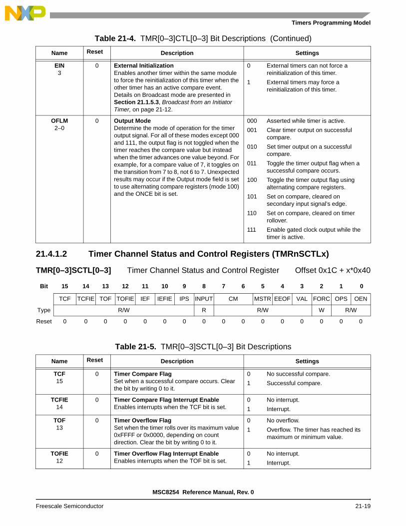
Timers Programming Model
21.4.1.2 Timer Channel Status and Control Registers (TMRnSCTLx)
EIN3
0 External InitializationEnables another timer within the same module to force the reinitialization of this timer when the other timer has an active compare event. Details on Broadcast mode are presented in Section 21.1.5.3, Broadcast from an Initiator Timer, on page 21-12.
0 External timers can not force a reinitialization of this timer.
1 External timers may force a reinitialization of this timer.
OFLM2–0
0 Output ModeDetermine the mode of operation for the timer output signal. For all of these modes except 000 and 111, the output flag is not toggled when the timer reaches the compare value but instead when the timer advances one value beyond. For example, for a compare value of 7, it toggles on the transition from 7 to 8, not 6 to 7. Unexpected results may occur if the Output mode field is set to use alternating compare registers (mode 100) and the ONCE bit is set.
000 Asserted while timer is active.
001 Clear timer output on successful compare.
010 Set timer output on a successful compare.
011 Toggle the timer output flag when a successful compare occurs.
100 Toggle the timer output flag using alternating compare registers.
101 Set on compare, cleared on secondary input signal’s edge.
110 Set on compare, cleared on timer rollover.
111 Enable gated clock output while the timer is active.
TMR[0–3]SCTL[0–3] Timer Channel Status and Control Register Offset 0x1C + x*0x40
Bit 15 14 13 12 11 10 9 8 7 6 5 4 3 2 1 0
TCF TCFIE TOF TOFIE IEF IEFIE IPS INPUT CM MSTR EEOF VAL FORC OPS OEN
Type R/W R R/W W R/W
Reset 0 0 0 0 0 0 0 0 0 0 0 0 0 0 0 0
Table 21-5. TMR[0–3]SCTL[0–3] Bit Descriptions
Name Reset Description Settings
TCF15
0 Timer Compare FlagSet when a successful compare occurs. Clear the bit by writing 0 to it.
0 No successful compare.
1 Successful compare.
TCFIE14
0 Timer Compare Flag Interrupt EnableEnables interrupts when the TCF bit is set.
0 No interrupt.
1 Interrupt.
TOF13
0 Timer Overflow FlagSet when the timer rolls over its maximum value 0xFFFF or 0x0000, depending on count direction. Clear the bit by writing 0 to it.
0 No overflow.
1 Overflow. The timer has reached its maximum or minimum value.
TOFIE12
0 Timer Overflow Flag Interrupt EnableEnables interrupts when the TOF bit is set.
0 No interrupt.
1 Interrupt.
Table 21-4. TMR[0–3]CTL[0–3] Bit Descriptions (Continued)
Name Reset Description Settings
MSC8254 Reference Manual, Rev. 0
Freescale Semiconductor 21-19

Timers
IEF11
0 Input Edge FlagSet when a positive input transition occurs while the timer is enabled. Clear the bit by writing a 0 to it. Setting the input polarity select (TxSCTL[IPS]) bit enables the detection of negative input edge transitions. Also, the control register secondary count source determines which external input pin is monitored by the detection circuitry.
0 No action.
1 Positive input transition while timer enabled.
IEFIE10
0 Input Edge Flag Interrupt EnableEnables interrupts when the IEF bit is set.
0 No action.
1 Interrupts enabled.
IPS9
0 Input Polarity SelectInverts the input signal polarity.
0 No action.
1 Invert signal polarity.
INPUT8
0 Secondary Input SignalReflects the current state of the secondary Input signal.
00 Capture function disabled.
01 Load capture register on rising edge of the secondary count source input.
10 Load capture register on falling edge of the secondary count source input.
11 Load capture register on any edge of the secondary count source input.
CM7–6
0 Input Capture ModeSpecifies the operation of the capture register as well as the operation of the input edge flag.
00 Capture function is disabled.
01 Load capture register on the rising edge of the secondary count source input.
10 Load capture register on the falling edge of the secondary count source input.
11 Load capture register on any edge of the secondary count source input.
MSTR5
0 Initiator ModeEnables the compare function output to broadcast to the other timers in the module. This identifies a timer as the initiator timer in Broadcast mode. This signal is used to reinitialize the other timers and/or force their outputs. For details on Broadcast mode, see Section 21.1.5.3, Broadcast from an Initiator Timer, on page 21-12.
0 No action.
1 Broadcast mode.
EEOF4
0 Enable External Output ForceEnables the compare from another timer configured as the initiator to force the state of this timer output signal. For details on Broadcast mode, see Section 21.1.5.3, Broadcast from an Initiator Timer, on page 21-12.
o No action.
1 Other timer can force this timer’s output flag signal.
VAL3
0 Forced Output Flag ValueDetermines the value of the timer output flag signal when a software-triggered FORCE command occurs.
Table 21-5. TMR[0–3]SCTL[0–3] Bit Descriptions (Continued)
Name Reset Description Settings
MSC8254 Reference Manual, Rev. 0
21-20 Freescale Semiconductor

Timers Programming Model
21.4.1.3 Timer Channel Compare 1 Registers (TMRnCMP1x)
TMR[0–3]CMP1[0–3] store the comparison value (CV) for comparison with the timer value.
21.4.1.4 Timer Channel Compare 2 Registers (TMRnCMP2x)
TMR[0–3]CMP2[0–3] store the comparison value (CV) for comparison with the timer value.
FORC2
0 Force OutputForces the current value of the VAL bit to be written to the timer output. Always read this bit as a 0. The VAL and FORCE bits can be written simultaneously in a single write operation. Write to the FORCE bit only if the timer is disabled. Setting this bit while the timer is enabled may yield unpredictable results.
0 No action.
1 Forces the current value of the VAL bit to be written to timer output.
OPS1
0 Output Polarity SelectDetermines the polarity of the output signal.
0 True polarity.
1 Inverted polarity.
OEN0
0 Output EnableEnables the timer output. The OPS bit determines the polarity of the output.
0 Timer output not enabled.
1 Timer output enabled.
TMR[0–3]CMP1[0–3] Timer Channel Compare 1 Registers Offset x*0x40
Bit 15 14 13 12 11 10 9 8 7 6 5 4 3 2 1 0
CV
Type R/W
Reset 0 0 0 0 0 0 0 0 0 0 0 0 0 0 0 0
TMR[0–3]CMP2[0–3] Timer Channel Compare 2 Registers Offset 0x04 + x*0x40
Bit 15 14 13 12 11 10 9 8 7 6 5 4 3 2 1 0
CV
Type R/W
Reset 0 0 0 0 0 0 0 0 0 0 0 0 0 0 0 0
Table 21-5. TMR[0–3]SCTL[0–3] Bit Descriptions (Continued)
Name Reset Description Settings
MSC8254 Reference Manual, Rev. 0
Freescale Semiconductor 21-21

Timers
21.4.1.5 Timer Channel Compare Load 1 Registers (TMRnCMPLD1x)
TMR[0–3]CMPLD1[0–3] store the preload value for the TMR[0–3]CMP1[0–3].
21.4.1.6 Timer Channel Compare Load 2 Registers (TMRnCMPLD2x)
TMR[0–3]CMPLD2[0–3] store the preload value for the TMR[0–3]CMP2[0–3].
21.4.1.7 Timer Channel Comparator Status and Control Registers (TMRnCOMSCx)
TMR[0–3]COMSC[0–3] store the preload values used for the TMR[0–3]CMP2[0–3] registers.
TMR[0–3]CMPLD1[0–3] Timer Channel Compare Load 1 Registers Offset 0x20 + x*0x40
Bit 15 14 13 12 11 10 9 8 7 6 5 4 3 2 1 0
CLV1
Type R/W
Reset 0 0 0 0 0 0 0 0 0 0 0 0 0 0 0 0
TMR[0–3]CMPLD2[0–3] Timer Channel Compare Load 2 Registers Offset 0x24 + x*0x40
Bit 15 14 13 12 11 10 9 8 7 6 5 4 3 2 1 0
CLV2
Type R/W
Reset 0 0 0 0 0 0 0 0 0 0 0 0 0 0 0 0
TMR[0–3]COMSC[0–3] Timer Channel Comparator Status and Offset 0x28 + x*0x40Control Registers
Bit 15 14 13 12 11 10 9 8 7 6 5 4 3 2 1 0
— TCF2EN TCF1EN TCF2 TCF1 CL2 CL1
Type R R/W
Reset 0 0 0 0 0 0 0 0 0 0 0 0 0 0 0 0
Table 21-6. TMR[0–3]COMSC[0–3] Bit Descriptions
Name Reset Description Settings
—15–8
0 Reserved. Write to 0 for future compatibility.
TCF2EN7
0 Timer Compare 2 Interrupt EnableEnables the compare 2 interrupt. An interrupt is issued when both this bit and the TCF2 bit are set.
0 No action.
1 Enable compare 2 interrupt.
MSC8254 Reference Manual, Rev. 0
21-22 Freescale Semiconductor

Timers Programming Model
21.4.1.8 Timer Channel Capture Registers (TMRnCAPx)
TMR[0–3]CAP[0–3] store the values captured from the timers.
TCF1EN6
0 Timer Compare 1 Interrupt EnableEnables the compare 1 interrupt. An interrupt is issued when both this bit and the TCF1 bit are set.
0 No action.
1 Enable compare 1 interrupt.
TCF25
0 Timer Compare 2 Interrupt SourceIndicates a successful comparison of the timer and the TMRxCMP2. This bit is sticky and remains set until it is explicitly cleared by writing a zero to this bit location.
0 Normal operation.
1 Successful compare 2.
TCF14
0 Timer Compare 1 Interrupt SourceIndicates a successful comparison of the timer and the TMRxCMP1. This bit is sticky and remains set until it is explicitly cleared by writing a zero to this bit location.
0 Normal operation.
1 Successful compare 1.
CL23–2
0 Compare Load Control 2Control when TMRxCMP2 is preloaded with the value from TMRxCMPLD2.
00 Never preload.
01 Load upon successful compare with the value in TMRxCMP1.
10 Load upon successful compare with the value in TMRxCMP2.
11 Reserved.
CL11–0
0 Compare Load Control 1Control when TMRxCMP1 is preloaded with the value from TMRxCMPLD1.
00 Never preload.
01 Load upon successful compare with the value in TMRxCMP1.
10 Load upon successful compare with the value in TMRxCMP2.
11 Reserved.
TMR[0–3]CAP[0–3] Timer Channel Capture Registers Offset 0x08 + x*0x40
Bit 15 14 13 12 11 10 9 8 7 6 5 4 3 2 1 0
CAPV
Type R/W
Reset 0 0 0 0 0 0 0 0 0 0 0 0 0 0 0 0
Table 21-6. TMR[0–3]COMSC[0–3] Bit Descriptions (Continued)
Name Reset Description Settings
MSC8254 Reference Manual, Rev. 0
Freescale Semiconductor 21-23

Timers
21.4.1.9 Timer Channel Load Registers (TMRnLOADx)
TMR[0–3]LOAD[0–3] store the value used to load the timer.
21.4.1.10 Timer Channel Hold Registers (TMRnHOLDx)
TMR[0–3]HOLD[0–3] store the value whenever any timer is read.
21.4.1.11 Timer Channel Counter Registers (TMRnCNTRx)
TMR[0–3]CNTR[0–3] are counters.
21.4.2 SC3850 DSP Core Subsystem Timers
For a detailed information about programming the core subsystem timers, see the MSC8156 SC3850 DSP Core Subsystem Reference Manual.
TMR[0–3]LOAD[0–3] Timer Channel Load Registers Offset 0x0C + x*0x40
Bit 15 14 13 12 11 10 9 8 7 6 5 4 3 2 1 0
LDV
Type R/W
Reset 0 0 0 0 0 0 0 0 0 0 0 0 0 0 0 0
TMR[0–3]HOLD[0–3] Timer Channel Hold Registers Offset 0x10 + x*0x40
Bit 15 14 13 12 11 10 9 8 7 6 5 4 3 2 1 0
HDV
Type R/W
Reset 0 0 0 0 0 0 0 0 0 0 0 0 0 0 0 0
TMR[0–3]CNTR[0–3] Timer Channel Counter Registers Offset 0x14 + x*0x40
Bit 15 14 13 12 11 10 9 8 7 6 5 4 3 2 1 0
HDV
Type R/W
Reset 0 0 0 0 0 0 0 0 0 0 0 0 0 0 0 0
MSC8254 Reference Manual, Rev. 0
21-24 Freescale Semiconductor

Timers Programming Model
21.4.3 Software Watchdog Timers
This section describes the software WDT registers, which include:
System Watchdog Control Register 0–7 (SWCRR[0–7]), see page 21-26.
System Watchdog Count Register 0–7 (SWCNR[0–7]), see page 21-27.
System Watchdog Service Register 0–7 (SWSRR[0–7]), see page 21-27.
Note: The watchdog timers use the following base addresses:
System Watchdog Timer 0 = 0xFFF25000
System Watchdog Timer 1 = 0xFFF25100
System Watchdog Timer 2 = 0xFFF25200
System Watchdog Timer 3 = 0xFFF25300
System Watchdog Timer 4 = 0xFFF25400
System Watchdog Timer 5 = 0xFFF25500
System Watchdog Timer 6 = 0xFFF25600
System Watchdog Timer 7 = 0xFFF25700
MSC8254 Reference Manual, Rev. 0
Freescale Semiconductor 21-25

Timers
21.4.3.1 System Watchdog Control Register 0–7 (SWCRR[0–7])
SWCRR[0–7] control the software watchdog timer period and configure WDT operation. SWCRR can be read at any time but can be written only once after system reset. Table 21-7 defines the SWCRR[0–7] bit fields.
SWCRR[0–7] System Watchdog Control Register 0–7 Offset 0x04
Bit 31 30 29 28 27 26 25 24 23 22 21 20 19 18 17 16
SWTCType R/W
Reset 0 0 0 0 0 0 0 0 0 0 0 0 0 0 0 0
Bit 15 14 13 12 11 10 9 8 7 6 5 4 3 2 1 0
SWTC— SWEN SWRI SWPR
Type R/W
Reset 0 0 0 0 0 0 0 0 0 0 0 0 0 0 0 0
Table 21-7. SWCRR[0–7] Bit Descriptions
Name Reset Description Settings
SWTC31–16
0xFFFF Software Watchdog Time CountThe SWTC field contains the modulus that is reloaded into the watchdog counter by a service sequence. When a new value is loaded into SWCRR[SWTC], the software watchdog timer is not updated until the servicing sequence is written to the SWSRR. If SWCRR[SWEN] is loaded with 0, the modulus counter does not count. The new value is also used at the next and all subsequent reloads. Reading the SWCRR register returns the value in the System Watchdog Control Register. Reset initializes the SWCRR[SWTC] field to $FFFF.
Note: The prescaler counter is reset anytime a new value is loaded into the watchdog counter and also during reset.
—15–3
0 Reserved. Write to zero for future compatibility.
SWEN2
0 Watchdog EnableSWCRR[SWEN] bit enables the watchdog timer. It should be cleared by software after a system reset to disable the software watchdog timer. When the watchdog timer is disabled, the watchdog counter and prescaler counter are held in a stopped state.
0 Watchdog timer disabled.
1 Watchdog timer enabled.
SWRI1
0 Software Watchdog Reset/Interrupt Select Depending on the SWCRR[SWRI] programming, WDT timer causes a hard reset or machine check interrupt to the core.
0 Software watchdog timer causes a machine check interrupt to the core.
1 Software watchdog timer causes a hard reset (this is the default value after soft reset).
SWPR0
0 Software Watchdog Counter PrescaleControls the divide-by-65536 WDT counter prescaler.
0 The WDT counter is not prescaled.
1 The WDT counter clock is prescaled.
MSC8254 Reference Manual, Rev. 0
21-26 Freescale Semiconductor

Timers Programming Model
21.4.3.2 System Watchdog Count Register 0–7 (SWCNR[0–7])
SWCNR[0–7] provide visibility to the WDT counter values. Writes to SWCNR have no effect and terminate without transfer error exception.
21.4.3.3 System Watchdog Service Register 0–7 (SWSRR[0–7])
When the WDT is enabled, writing 0x556C followed by 0xAA39 to the SWSRR register before the WDT times out prevents a reset. If SWSRR is not serviced before the time-out, the watchdog timer sends a signal to the reset or interrupt controller module. Both writes must occur before the time-out in the order listed, but any number of instructions can be executed between the two writes. Reset initializes the SWSRR[WS] field to 0x0000. SWSRR can be written at any time, but returns all zeros when read. Table 21-9 defines the bit fields of SWSRR.
SWCNR[0–7] System Watchdog Count Register 0–7 Offset 0x08
Bit 31 30 29 28 27 26 25 24 23 22 21 20 19 18 17 16
—Type R
Reset 1 1 1 1 1 1 1 1 1 1 1 1 1 1 1 1
Bit 15 14 13 12 11 10 9 8 7 6 5 4 3 2 1 0
SWCNType RReset 0 0 0 0 0 0 0 0 0 0 0 0 0 0 0 0
Table 21-8. SWCNR[0–7] Bit Descriptions
Name Reset Description
—31–16
0 Reserved. Write to zero for future compatibility.
SWCN15–0
0xFFFF Software Watchdog Count FieldThe read-only SWCNR[SWCN] field reflects the current value in the watchdog counter. Writing to the SWCNR register has no effect, and write cycles are terminated normally. Reset initializes the SWCNR[SWCN] field to $FFFF. Reading the 16 LS bits of 32-bit SWCNR register with two 8-bit reads is not guaranteed to return a coherent value.
SWSRR[0–7] System Watchdog Service Register 0–7 Offset 0x0E
Bit 15 14 13 12 11 10 9 8 7 6 5 4 3 2 1 0
WS
Type WReset 0 0 0 0 0 0 0 0 0 0 0 0 0 0 0 0
Table 21-9. SWSRR[0–7] Bit Descriptions
Name Reset Description
WS15–0
0 Software Watchdog Service FieldWrite 0x556C followed by 0xAA39 to this register to prevent software watchdog timer time-out. SWSRR[WS] can be written at any time, but returns all zeros when read. Writing any other value resets the servicing sequence.
MSC8254 Reference Manual, Rev. 0
Freescale Semiconductor 21-27

Timers
MSC8254 Reference Manual, Rev. 0
21-28 Freescale Semiconductor

GPIO 22The MSC8254 device has 32 general-purpose I/O (GPIO) ports, 17 of which are multiplexed as either GPIO ports or dedicated peripheral interface ports. In addition, sixteen of the GPIOs can be configured as external maskable interrupt inputs. As GPIOs, each port is configured as an input or output (with a register for data output that is read or written at any time). If configured as output, the GPIO ports can also be configured as open-drain (that is, configured in an active low wired-OR configuration on the board). In this mode, an output drives a zero voltage but goes to tri-state when driving a high voltage. GPIO ports have configurable internal pull-up resistors. These resistors are enabled by default. They can be disabled by programming the GPIO Pull-Up Enable Register (GPUER); see the Chapter 8, General Configuration Registers for details. The dedicated MSC8254 peripheral functions multiplexed with the GPIO ports are grouped to maximize the usefulness of the ports in the greatest number of MSC8254 applications.
Note: To understand the port assignment capability described in this chapter, you must also understand the operation of the SPI, timers, UART, I2C, and DMA peripherals.
22.1 Features
Following are the key features of the GPIO ports:
32 GPIO ports.
All ports are bidirectional.
Seventeen ports have alternate on-device peripheral functions.
At system reset, all 32 port inputs and outputs are disabled and the pull-up resistors are enabled.
All port values can be read while the port is connected to an internal peripheral.
All ports have open-drain output capability.
Sixteen of the GPIOs can function as interrupt inputs.
Four of the GPIOs can function as SPI signals.
Five of the GPIOs can function as timer signals.
Two of the GPIOs can function as a UART port.
Two of the GPIOs can function as an I2C interface.
Four of the GPIOs can function as external DMA control signals.
MSC8254 Reference Manual, Rev. 0
Freescale Semiconductor 22-1

GPIO
22.2 GPIO Block Diagram
Figure 22-1 shows a GPIO functional block diagram.
Figure 22-1. Port Functional Operation
Register Name 0 1 Description
PARx General-purpose Dedicated Port Assignment Registers
PSORx Dedicated 1 Dedicated 2 Port Special Options Registers
PDIRx Input Output Port Data Direction Registers
PODRx Regular Open drain Port Open-Drain Registers
PDATx 0 (data) 1 (data) Port Data Registers
Note: In addition to these registers, you must set each the ports as inputs using the General Input Enable (GIER) register. See 8.2.10, GPIO Input Enable Register (GIER) for details.
Port Control Register Bits
Pin
PDATx
DefaultInput IN1
DefaultInput IN2
To DED IN1
To DED IN2
From DED OUT2
PDATx Read
0
1
0
1PAR
Open-Drain (OD)0Reg.
From DED OUT1
PSOR
1
0
1
PDATx Write
To/from internal bus
PAR
Synchronizer
Notes: 1. Force Output may be asserted high by dedicated peripheral 2 direction control, only when
PODRxReg.
PDIR
Force Output1
Output Enable (OE)Data Out (D)
OD D OE Pin
x x 0 Z0 d 1 d1 0 1 01 1 1 Z
PAR = 1 and PSOR = 1 (selects this peripheral) and PDIR = 0 (input). It is used for bidirectionaloperation allowing the peripheral to dynamically control the port direction.
Force Tri-state 2
2. Force Tri-state may be asserted low by dedicated peripheral 1 output enable, only whenPAR = 1 and PSOR = 0 (selects this peripheral) and PDIR = 1 (output). It is used for tri-state outputoperation, allowing the peripheral to control the port drive dynamically.
PSORPDIR
PARPSORPDIR
MSC8254 Reference Manual, Rev. 0
22-2 Freescale Semiconductor

GPIO Connection Functions
22.3 GPIO Connection Functions
This section describes the GPIO port when it has GPIO or dedicated functionality, which depends on the settings in the Pin Assignment Register (PAR), as follows:
Each port is independently configured as a GPIO if the corresponding PAR bit is cleared. A port is configured as an input if the corresponding control bit in the Pin Data Direction Register (PDIR) is cleared; it is configured as an output if the corresponding PDIR bit is set.
Each port is configured as a dedicated on-device peripheral port if the corresponding PAR bit is set.
All PAR and PDIR bits are cleared on total system reset, which disables the output direction of the GPIO ports.
Data transfer is done through the Pin Data Register (PDAT). Data written to the PDAT is stored in an output register. If a GPIO is configured as an output, the output register data is gated onto the GPIO port. If a GPIO is configured as an input and the port is enabled by the appropriate bit in the GIER, a read of PDATx is actually a read of the GPIO port itself. Data written to PDAT when the GPIO is configured as an input is still stored in the output register, but it is prevented from reaching the external port.
When a multiplexed GPIO port is not configured as a GPIO, it has a dedicated functionality, as described in Table 22-1. If an input to a peripheral is not supplied externally, a default value is supplied to the internal peripheral as listed in the right-most column.
Table 22-1 describes the functionality of the GPIO ports according to the configuration of the port registers (PAR, PSOR, and PDIR). Each port can be configured as a GPIO (input, regular output, or open-drain output), one of two dedicated outputs, or one of two dedicated inputs. A route of one GPIO-dedicated output to another GPIO-dedicated input gives even more flexibility. The implemented routing is described in Table 22-1 as primary and secondary input.
Table 22-1. GPIO Dedicated Assignment (PARx = 1)
GPIO
Port Function
PSORx = 0 PSORx = 1
PDIRx = 1(Output, Unless
Tri-State Option is Specified)
PDIRx = 0(Input)
Default Input
PDIRx = 1(Output)
PDIRx = 0(Input, UnlessInout Option is
Specified)
DefaultInput
0 — IRQ0 1 — — 0
1 — IRQ1 1 — — 0
2 — IRQ2 1 — — 0
3 — IRQ3 1 — DRQ1 0
4 — IRQ4 1 DDN1 — 0
MSC8254 Reference Manual, Rev. 0
Freescale Semiconductor 22-3

GPIO
5 — IRQ5 1 — — 0
6 — IRQ6 1 — — 0
7 — IRQ7 1 — — 0
8 — IRQ8 1 — — 0
9 — IRQ9 1 — — 0
10 — IRQ10 1 — — 0
11 — IRQ11 1 — — 0
12 — IRQ12 1 — — 0
13 — IRQ13 1 — — 0
14 — IRQ14 1 — DRQ0 0
15 — IRQ15 1 DDN0 — 0
16 — — 0 — — 0
17 — — 0 SPI_SCK SPI_SCK 0
18 — — 0 SPI_MOSI SPI_MOSI 0
19 — — 0 SPI_MISO SPI_MISO 0
20 — — 0 SPI_SL SPI_SL 1
21 — — 0 — — 0
22 — — 0 — — 0
23 — — 0 TMR0 TMR0 0
24 — — 0 TMR1 TMR1 0
25 — — 0 TMR2 TMR2 0
26 — — 0 TMR3 TMR3 0
27 — — 0 TMR4 TMR4 0
28 — — 0 UART_RXD UART_RXD 1
29 — — 0 UART_TXD UART_TXD 0
30 — — 0 I2C_SCL I2C_SCL 0
31 — — 0 I2C_SDA I2C_SDA 0
Note: You must enable the port to use it as an input. See 8.2.10, GPIO Input Enable Register (GIER) for details.
Table 22-1. GPIO Dedicated Assignment (PARx = 1) (Continued)
GPIO
Port Function
PSORx = 0 PSORx = 1
PDIRx = 1(Output, Unless
Tri-State Option is Specified)
PDIRx = 0(Input)
Default Input
PDIRx = 1(Output)
PDIRx = 0(Input, UnlessInout Option is
Specified)
DefaultInput
MSC8254 Reference Manual, Rev. 0
22-4 Freescale Semiconductor

GPIO Programming Model
22.4 GPIO Programming Model
The GPIO registers reside on a 256 KB address space. The GPIO block has five memory-mapped, read/write, 32-bit control registers. This section describes these registers in detail. Following is a list of the GPIO registers:
Pin Open-Drain Register (PODR), page 22-6Pin Data Register (PDAT), page 22-7Pin Data Direction Registers (PDIR), page 22-8Pin Assignment Register (PAR), page 22-9Pin Special Options Registers (PSOR), page 22-10
Note: The GPIO registers use a base address of: 0xFFF27200.
If the corresponding PAR[DDx] bit is 1 (configured as a dedicated peripheral function port) before a PSOR or PDIR bit is programmed, an external connection may function for a short period as an unwanted dedicated function and cause unpredictable behavior. Thus, it is recommended that you program the GPIO in the following sequence: PSOR, PODR, PDIR, PAR.
In addition to the GPIO registers, there are two registers in the set of General Configuration Registers (GCRs) that control GPIO operation. These are as follows:
GPIO Pull-Up Enable Register (GPUER), see Section 8.2.9, GPIO Pull-Up Enable Register (GPUER), on page 8-17.
GPIO Input Enable Register (GIER), see Section 8.2.10, GPIO Input Enable Register (GIER), on page 8-18. To be used as an input line, a port must be enabled by this register.
Note: The base address for the general configuration registers is: 0xFFF28000.
MSC8254 Reference Manual, Rev. 0
Freescale Semiconductor 22-5

GPIO
22.4.1 Pin Open-Drain Register (PODR)
PODR indicates a normal or active low open drain mode for wired-OR configuration of the outputs.
Note: The GPIO registers use a base address of: 0xFFF27200.
PODR Pin Open-Drain Register Offset 0x00
Bit 31 30 29 28 27 26 25 24 23 22 21 20 19 18 17 16
OD31 OD30 OD29 OD28 OD27 OD26 OD25 OD24 OD23 OD22 OD21 OD20 OD19 OD18 OD17 OD16
Type R/WReset 0 0 0 0 0 0 0 0 0 0 0 0 0 0 0 0
Bit 15 14 13 12 11 10 9 8 7 6 5 4 3 2 1 0
OD15 OD14 OD13 OD12 OD11 OD10 OD9 OD8 OD7 OD6 OD5 OD4 OD3 OD2 OD1 OD0Type R/W
Reset 0 0 0 0 0 0 0 0 0 0 0 0 0 0 0 0
Table 22-2. PODR Bit Descriptions
Name Reset Description Settings
OD[31–0]31–0
0 Open-Drain ConfigurationDetermines whether the corresponding port is actively driven as an output or is an open-drain driver. As an open-drain driver, the port is driven active-low. Otherwise, it is tri-stated (high impedance).
0 The I/O port is actively driven as an output.
1 The I/O port is an open-drain driver.
MSC8254 Reference Manual, Rev. 0
22-6 Freescale Semiconductor

GPIO Programming Model
22.4.2 Pin Data Register (PDAT)
A read of a PDAT register returns the data at the pin if the input line is enabled by the correct bit in the GIER, independently of whether the port is defined as an input or output. Thus, output conflicts at the pin can be detected by comparing the written data with the data on the pin. A write to the PDATx is sampled in a register bit, and if the equivalent PDIR bit is configured as an output, the value sampled for that bit is driven onto its respective pin. PDAT can be read or written at any time.
If a pin is selected as GPIO, it is accessed through the PDAT. Data written to the PDAT register is stored in an output register. If a port is configured as an output, the output register data is gated onto the pin. When PDAT is read, the GPIO pin itself is read. If a GPIO port is configured as an input and enabled by the correct bit in the GIER, data written to the PDAT register is still stored in the output register, but it is prevented from reaching the actual pin. When the PDAT register is read and enabled as an input, the state of the actual pin is read.
Note: The GPIO registers use a base address of: 0xFFF27200.
PDAT Pin Data Register Offset 0x08
Bit 31 30 29 28 27 26 25 24 23 22 21 20 19 18 17 16
D31 D30 D29 D28 D27 D26 D25 D24 D23 D22 D21 D20 D19 D18 D17 D16
Type R/WReset 0 0 0 0 0 0 0 0 0 0 0 0 0 0 0 0
Bit 15 14 13 12 11 10 9 8 7 6 5 4 3 2 1 0
D15 D14 D13 D12 D11 D10 D9 D8 D7 D6 D5 D4 D3 D2 D1 D0Type R/W
Reset 0 0 0 0 0 0 0 0 0 0 0 0 0 0 0 0
MSC8254 Reference Manual, Rev. 0
Freescale Semiconductor 22-7

GPIO
22.4.3 Pin Data Direction Register (PDIR)
PDIR is cleared at system reset.
Note: The GPIO registers use a base address of: 0xFFF27200.
PDIR Pin Data Direction Register Offset 0x10
Bit 31 30 29 28 27 26 25 24 23 22 21 20 19 18 17 16
DR31 DR30 DR29 DR28 DR27 DR26 DR25 DR24 DR23 DR22 DR21 DR20 DR19 DR18 DR17 DR16
Type R/WReset 0 0 0 0 0 0 0 0 0 0 0 0 0 0 0 0
Bit 15 14 13 12 11 10 9 8 7 6 5 4 3 2 1 0
DR15 DR14 DR13 DR12 DR11 DR10 DR9 DR8 DR7 DR6 DR5 DR4 DR3 DR2 DR1 DR0Type R/W
Reset 0 0 0 0 0 0 0 0 0 0 0 0 0 0 0 0
Table 22-3. PDIR Bit Descriptions
Name Reset Description Settings
DR31–0
0 DirectionIndicates whether a port is an input or an output.
0 The corresponding port is an input.
1 The corresponding port is an output.
Note: This register sets the direction of the selected port, but you must enable the port using the General Input Enable Register (GIER) to use it. See Section 8.2.10, GPIO Input Enable Register (GIER), on page 8-18 for details.
MSC8254 Reference Manual, Rev. 0
22-8 Freescale Semiconductor

GPIO Programming Model
22.4.4 Pin Assignment Register (PAR)
PAR is cleared at system reset.
Note: The GPIO registers use a base address of: 0xFFF27200.
PAR Pin Assignment Register Offset 0x18
Bit 31 30 29 28 27 26 25 24 23 22 21 20 19 18 17 16
DD31 DD30 DD29 DD28 DD27 DD26 DD25 DD24 DD23 DD22 DD21 DD20 DD19 DD18 DD17 DD16
Type R/WReset 0 0 0 0 0 0 0 0 0 0 0 0 0 0 0 0
Bit 15 14 13 12 11 10 9 8 7 6 5 4 3 2 1 0
DD15 DD14 DD13 DD12 DD11 DD10 DD9 DD8 DD7 DD6 DD5 DD4 DD3 DD2 DD1 DD0Type R/W
Reset 0 0 0 0 0 0 0 0 0 0 0 0 0 0 0 0
Table 22-4. PAR Bit Descriptions
Name Reset Description Bit Settings
DD[31–0]31–0
0 Dedicated EnableIndicates whether a pin is a GPIO or a dedicated peripheral port. As a dedicated peripheral function, the pin is used by the internal module. The internal peripheral function to which it is dedicated can be determined by other bits, such as those in the PSOR.
0 GPIO. The peripheral functions of the pin are not used.
1 Dedicated peripheral function.
MSC8254 Reference Manual, Rev. 0
Freescale Semiconductor 22-9

GPIO
22.4.5 Pin Special Options Register (PSOR)
PSOR bits are effective only if the corresponding PAR[DDx] bit is 1 (a dedicated peripheral function).
Note: The GPIO registers use a base address of: 0xFFF27200.
PSOR Pin Special Options Register Offset 0x20
Bit 31 30 29 28 27 26 25 24 23 22 21 20 19 18 17 16
SO31 SO30 SO29 SO28 SO27 SO26 SO25 SO24 SO23 SO22 SO21 SO20 SO19 SO18 SO17 SO16
Type R/WReset 0 0 0 0 0 0 0 0 0 0 0 0 0 0 0 0
Bit 15 14 13 12 11 10 9 8 7 6 5 4 3 2 1 0
SO15 SO14 SO13 SO12 SO11 SO10 SO9 SO8 SO7 SO6 SO5 SO4 SO3 SO2 SO1 SO0Type R/W
Reset 0 0 0 0 0 0 0 0 0 0 0 0 0 0 0 0
Table 22-5. PSOR Bit Descriptions
Name Reset Description Settings
SO[31–0]31–0
0 Special-OptionDetermines whether an external connection configured for a dedicated function (PAR[DD] = 1) uses option 1 or option 2. See Table 22-1.
0 Dedicated peripheral function. Option 1.
1 Dedicated peripheral function. Option 2.
MSC8254 Reference Manual, Rev. 0
22-10 Freescale Semiconductor

Hardware Semaphores 23The MSC8254 hardware semaphores (HS) hold eight coded hardware semaphores. A coded hardware semaphore provides a simple way to achieve a “lock” operation via a single write access, eliminating the need for such sophisticated read-modify-write mechanisms as the reservation. Using the hardware semaphores, external hosts and on-device bus initiators can protect internal and external shared resources and ensure coherency in any sequence of operations on these resources. Each coded hardware semaphore is an eight-bit register with a selective write mechanism, as follows (see Figure 23-1):
The semaphore is free if its value is zero.
The semaphore is locked if its value is non-zero and its value is the lock code. Each processor/task that needs the lock capability of the semaphore must have a unique non-zero eight-bit code for locking the semaphore for correct protocol operation.
A write of a non-zero value (lock code) is successful only if the current value of the semaphore is zero (free). This write is defined as a successful lock operation, and the written value is the lock code.
A write of a non-zero value (lock code) is ignored if the current value of the semaphore is non-zero (locked). This write is defined as a failed lock operation, since the coded semaphore is considered locked with the non-zero code it holds.
To maintain the protocol coherency, only the initiator that successfully locked the semaphore is allowed (and obligated) to free it. A write of zero is always successful and is defined as a free operation.
When a processor/task must lock an unlocked semaphore to its unique code, it writes its unique lock code to the semaphore register. It then reads back the semaphore value, and if it matches its lock code, the lock operation is successful. A value mismatch (a different non-zero code or zero) indicates to the initiator that the lock operation failed and must be retried. After a successful lock operation, the initiator can do any coherent operation associated with this semaphore and then it must free the semaphore (write zero).
MSC8254 Reference Manual, Rev. 0
Freescale Semiconductor 23-1

Hardware Semaphores
The hardware semaphore registers reside in the CCSR address space and have a constant offset. They are accessed through the MBus. The addresses of the hardware semaphore registers are presented in Chapter 9, Memory Map. The registers use a base address of 0xFFF27100.
Figure 23-1. Hardware Semaphore Block Diagram
HSMPR[0–7] Hardware Semaphore Register n Offset n*0x8
Bit 31 30 29 28 27 26 25 24 23 22 21 20 19 18 17 16
—
Type R
Reset 0 0 0 0 0 0 0 0 0 0 0 0 0 0 0 0
Bit 15 14 13 12 11 10 9 8 7 6 5 4 3 2 1 0
— SMPVAL
Type R R/W
Reset 0 0 0 0 0 0 0 0 0 0 0 0 0 0 0 0
Table 23-1. HSMPRx Bit Descriptions
Name Reset Description Settings
—31–8
0 Reserved. Write to zero for future compatibility.
SMPVAL7–0
0 Semaphore ValueThe eight-bit coded semaphore value. It holds the current semaphore value. A non-zero value indicates the current lock code.
0 Semaphore is free. It is writable to any value.
≠ 0 Semaphore is locked with lock code indicated by its current value. It is writable only to zero.
(=0)Write Value
Write Control
1
0
1
0
SM
PV
AL
Clock
88
8
8
ReadValue
Free
(=0)Free
MSC8254 Reference Manual, Rev. 0
23-2 Freescale Semiconductor

I2C 24The inter-integrated circuit (IIC or I2C) bus is a two-wire—serial data (I2C_SDA) and serial clock (I2C_SCL)— bidirectional serial bus that provides a simple efficient method of data exchange between the system and other devices, such as microcontrollers, EEPROMs, real-time clock devices, A/D converters, and LCDs. The two-wire bus minimizes the interconnections between devices. The synchronous, multi-initiator I2C bus allows the connection of additional devices to the bus for expansion and system development. The bus includes collision detection and arbitration that prevent data corruption if two or more initiators attempt to control the bus simultaneously. In the MSC8254 device, the maximum I2C_SCL frequency is 400 kHz. Figure 24-1 is a block diagram of the I2C block.
Figure 24-1. I2C Controller Block Diagram
I2CADR I2CFDR I2CCR I2CSR I2CDR
Addr Decode
AddressCompareInput Sync
In/Out DataShift Register
Clock Divide
Control
I2C_SDA
Interrupt
andDigital Filter
START/STOP/restart
andArbitration
Control
and
I2C_SCL
I2CDFSRR
Core Processor
MSC8254 Reference Manual, Rev. 0
Freescale Semiconductor 24-1

I2C
24.1 Features
The I2C interface includes the following features:
Two-wire interface
Multi-initiator operation
Arbitration lost interrupt with automatic mode switching from initiator to target
Calling address identification interrupt
START and STOP signal generation/detection
Acknowledge bit generation/detection
Bus busy detection
Software-programmable clock frequency
Software-selectable acknowledge bit
On-chip filtering for spikes on the bus
24.2 Modes of Operation
The following modes of operation are supported by the I2C controller:
Initiator mode. The I2C is the driver of the I2C_ line. It cannot use its own target address as a calling address. The I2C cannot be an initiator and a target simultaneously. The initiator device initiates the data transfer by generating a START condition.
The module must be enabled before a START condition from a I2C initiator is detected.
START condition. This condition denotes the beginning of a new data transfer (each data transfer contains several bytes of data) and awakens all targets. This mode is I2C-specific.
Repeated START condition. A START condition that is generated without a STOP condition to terminate the previous transfer. This mode is I2C-specific.
STOP condition. The initiator can terminate the transfer by generating a STOP condition to free the bus. This mode is I2C-specific.
Interrupt-driven byte-to-byte data transfer. When successful target addressing is achieved (and I2C_SCL returns to zero), the data transfer can proceed on a byte-to-byte basis in the direction specified by the R/W bit sent by the calling initiator. Each byte of data must be followed by an acknowledge bit, which is signalled from the receiving device. Several bytes can be transferred during a data transfer session.
Boot sequencer mode. Used only for loading the reset configuration word (RCW) only. See Chapter 5, Reset.
MSC8254 Reference Manual, Rev. 0
24-2 Freescale Semiconductor

I2C Module Functional Blocks
24.3 I2C Module Functional Blocks
The I2C module includes the following blocks:
Clock control
Input synchronization
Digital input filter
Transaction monitoring
Arbitration control
Transfer control
In/out data shift register
Address compare
24.3.1 Clock Control
The clock control block handles requests from clock for transferring and controlling data for multiple tasks. A 9-cycle data transfer (8-bit data plus the ACK bit) clock is requested for the following conditions:
Initiator mode
— transmit target address after START condition— transmit target address after restart condition— transmit data— receive data
Target mode
— transmit data— receive data— receive target address after START or restart condition
24.3.2 Input Synchronization
The input synchronization block synchronizes the input I2C_SCL and I2C_SDA signals to the [CLASS clock/2] and detects transitions of these signals.
24.3.3 Digital Input Filter
The I2C_SCL and I2C_SDA signal inputs are filtered to eliminate noise. Three consecutive signal samples are compared using a pre-determined sampling rate. If they are all high, the filter output is high. If they are all low, the output is low. For any high/low combination, the filter output is the value of the previous clock cycle. The sampling rate is the binary value stored in the frequency register. The sampling cycle duration is controlled by a down counter that sets a signal at the end of the count. This allows software to write to the frequency register to control the
MSC8254 Reference Manual, Rev. 0
Freescale Semiconductor 24-3
I2C
filtered sampling rate. The value written to the I2CDFSRR should be defined by the system noise and the I2CFDR value. I2CDFSRR must be less than six times the division factor defined by I2CFDR. Note that the division factor stands for a I2CDFSRR value of 1.
24.3.4 Transaction Monitoring
The different conditions of the I2C data transfers are monitored as follows:
START conditions are detected when an I2C_SDA fall occurs while I2C_SCL is high.
STOP conditions are detected when and I2C_SDA rise occurs while I2C_SCL is high.
Data transfers in progress are canceled when a STOP condition is detected or if there is a target address mismatch. Cancellation of data transactions resets the clock module
The bus state is busy beginning with the detection of a START condition, and idle when a STOP condition is detected.
24.3.5 Arbitration Control
The arbitration control block controls the arbitration procedure of the initiator mode. A loss of arbitration occurs whenever the initiator detects a 0 on the external I2C_SDA line while attempting to drive a 1, tries to generate a START or restart at an inappropriate time, or detects an unexpected STOP request on the line. Arbitration by the initiator in initiator mode is lost under the following conditions:
Low detected when high expected (transmit)
Ack bit, low detected when high expected (receive)
A START condition is attempted when the bus is busy
A START condition is attempted when the bus is nearly busy (the I2C controller does not yet recognize the bus as busy, but the bus is set to Initiator mode and I2C_SDA samples low).
A start condition is attempted when the requesting device is not the bus owner
Unexpected STOP condition detected
24.3.6 Transfer Control
The I2C contains logic that controls the output to the serial data (I2C_SDA) and serial clock (I2C_SCL) lines of the I2C. The I2C_SCL output is pulled low as determined by the internal clock generated in the clock module. The I2C_SDA output can only change at the midpoint of a low cycle of the I2C_SCL, unless performing a START, STOP, or restart condition. Otherwise, the I2C_SDA output is held constant. The I2C_SDA signal is pulled low when one or more of the following conditions are true in either initiator or target mode:
Initiator mode
— data bit (transmit)
MSC8254 Reference Manual, Rev. 0
24-4 Freescale Semiconductor

I2C Module Functional Blocks
— ack bit (receive)— START condition— STOP condition— Restart condition
Target mode
— acknowledging address match— data bit (transmit)— ack bit (receive)
The I2C_SCL signal corresponds to the internal I2C_SCL signal when one or more of the following conditions are true in either initiator or target mode:
Initiator mode
— bus owner— lost arbitration— START condition— STOP condition— Restart condition begin— Restart condition end
Target mode
— address cycle— transmit cycle— ack cycle
24.3.7 In/Out Data Shift Register
This block controls the interface between the serial data line and the data register, both transmitting data to and receiving data from the I2C. In transmit mode, a write to I2CCR[MTX] sets the direction to transmit. The contents of the parallel register are loaded into a shift register, which are then shifted on the I2C_SDA line.
24.3.8 Address Compare
The address compare block determines whether a target has been properly addressed and whether a specific action is required. The four performed address comparisons are described as follows:
The address sent by the current initiator matches the general broadcast address (addresses all targets)
The address matches the target address
A broadcast message to update the I2CSR was received
A message was addressed via the target address to update the I2CSR and to generate an interrupt
MSC8254 Reference Manual, Rev. 0
Freescale Semiconductor 24-5

I2C
24.4 Functional Description
The reset state of the I2C is the boot sequencer mode. After the boot sequencer has completed, the I2C interface performs as a target receiver. The I2C unit always performs as a target receiver as a default, unless explicitly programmed to be an initiator or target transmitter address.
A standard I2C transfer consists of the following:
• START condition
• Target target address transmission (7-bit calling address plus the read/write bit)
• Data transfer
• STOP condition
Figure 24-2 shows the interaction of these four parts with the calling address, data byte, and new calling address components of the I2C protocol. The details of the protocol are described in the following subsections.
24.4.1 START Condition
When the I2C bus is not engaged (both I2C_SDA and I2C_SCL lines are at logic high), an initiator can initiate a transfer by sending a START condition. As shown in Figure 24-2, a START condition is defined as a high-to-low transition of I2C_SDA while I2C_SCL is high. This condition denotes the beginning of a new data transfer. Each data transfer can contain several bytes and awakens all targets. The START condition is initiated by a software write that sets the I2CCR[MSTA].
Figure 24-2. I2C Interface Transaction Protocol
1 2 3 4 5 6 7 8 9 1 2 3 4 5 6 7 8 9
A7 A6 A5 A4 A3 A2 A1 R/W
A7 A6 A5 A4 A3 A2 A1 R/W
D7 D6 D5 D4 D3 D2 D1 D0XXXX
I2C_SCL
I2C_SDA
START STOPackno ack
read/write
calling address data byte
1 2 3 4 5 6 7 8 9 1 2 3 4 5 6 7 8 9
A7 A6 A5 A4 A3 A2 A1 R/W
I2C_SCL
I2C_SDA
START STOPackno ack
read/write
calling address new calling address
repeatSTART
MSC8254 Reference Manual, Rev. 0
24-6 Freescale Semiconductor

Functional Description
24.4.2 Target Address Transmission
The first byte of data is transferred by the initiator immediately after the START condition is the target address. This is a seven-bit calling address followed by a R/W bit, which indicates the direction of the data being transferred to the target. Each target in the system has a unique address. In addition, when the I2C module is operating as an initiator, it must not transmit an address that is the same as its target address. An I2C device cannot be initiator and target at the same time. Only the target with a calling address that matches the one transmitted by the initiator responds by returning an acknowledge bit (pulling the I2C_SDA signal low at the 9th clock) as shown in Figure 24-2. If no target acknowledges the address, the initiator should generate a STOP condition or a repeated START condition. When target addressing is successful (and I2C_SCL returns to zero), the data transfer can proceed on a byte-to-byte basis in the direction specified by the R/W bit sent by the calling initiator.
The I2C module responds to a general call (broadcast) command when I2CCR[BCST] is set. See the Philips I2C specification for details. A broadcast address is always zero, however the I2C module does not check the R/W bit. The second byte of the broadcast message is the initiator device ID. Because the second byte is automatically acknowledged by hardware, the receiver device software must verify that the broadcast message is intended for itself by reading the second byte of the message. If the device ID is for another receiver device and the third byte is a write command, then software can ignore the third byte during the broadcast. If the device ID is for another receiver device and the third byte is a read command, software must write 0xFF to I2CDR with I2CCR[TXAK] = 1, so that it does not interfere with the data written from the addressed device. Each data byte is 8 bits long. Data bits can be changed only while I2C_SCL is low and must be held stable while I2C_SCL is high, as shown in Figure 24-2. There is one clock pulse on I2C_SCL for each data bit, and the most significant bit (msb) is transmitted first. Each byte of data must be followed by an acknowledge bit, which is signaled from the receiving device by pulling the I2C_SDA line low at the ninth clock. Therefore, one complete data byte transfer takes nine clock pulses. Several bytes can be transferred during a data transfer session. If the target receiver does not acknowledge the initiator, the I2C_SDA line must be left high by the target. The initiator can then generate a stop condition to abort the data transfer or a START condition (repeated START) to begin a new calling. If the initiator receiver does not acknowledge the target transmitter after a byte of transmission, the target interprets that the end-of-data has been reached. Then the target releases the I2C_SDA line for the initiator to generate a STOP or a START condition.
24.4.3 Repeated START Condition
Figure 24-2 shows a repeated START condition, which is generated without a STOP condition that can terminate the previous transfer. The initiator uses this method to communicate with another target or with the same target in a different mode (transmit/receive mode) without releasing the bus.
MSC8254 Reference Manual, Rev. 0
Freescale Semiconductor 24-7

I2C
24.4.4 STOP Condition
The initiator can terminate the transfer by generating a STOP condition to free the bus. A STOP condition is defined as a low-to-high transition of the I2C_SDA signal while I2C_SCL is high. For more information, see Figure 24-2. Note that an initiator can generate a STOP even if the target has transmitted an acknowledge bit, at which point the target must release the bus. The STOP condition is initiated by a software write that clears I2CCR[MSTA]. As described in Section 24.4.3, the initiator can generate a START condition followed by a calling address without generating a STOP condition for the previous transfer. This is called a repeated START condition.
24.4.5 Arbitration Procedure
The I2C interface is a true multiple initiator bus that allows more than one initiator device to be connected on it. If two or more initiators simultaneously try to control the bus, each initiator’s (including the I2C module) clock synchronization procedure determines the bus clock—the low period is equal to the longest clock low period and the high is equal to the shortest one among the initiators. A bus initiator loses arbitration if it transmits a logic 1 on I2C_SDA while another initiator transmits a logic 0. The losing initiators immediately switch to target-receive mode and stop driving the I2C_SDA line. In this case, the transition from initiator to target mode does not generate a STOP condition. Meanwhile, the I2C unit sets the I2CSR[MAL] status bit to indicate the loss of arbitration and, as a target, services the transaction if it is directed to itself.
Arbitration is lost (and I2CSR[MAL] is set) in the following circumstances:
I2C_SDA sampled as low when the initiator drives a high during address or data-transmit cycle.
I2C_SDA sampled as low when the initiator drives a high during the acknowledge bit of a data-receive cycle.
A START condition is attempted when the bus is busy.
A repeated START condition is requested in target mode.
The I2C module does not automatically retry a failed transfer attempt. If the I2C module is enabled in the middle of an ongoing byte transfer, the interface behaves as follows:
Target mode—the I2C module ignores the current transfer on the bus and starts operating whenever a subsequent START condition is detected. If ICCR[MEN] is set and ICCR[RX] is cleared while the I2C_SDA signal is low and I2C_SCL is high, a false start condition is detected. If in this case, the data bits match the I2C target address, then I2CSR[MAAS] is set. The application must correct the condition to release the I2C_SCL bus.
MSC8254 Reference Manual, Rev. 0
24-8 Freescale Semiconductor

Initialization/Application Information
Initiator mode—the I2C module cannot tell whether the bus is busy; therefore, if a START condition is initiated, the current bus cycle can be corrupted. This ultimately results in the current bus initiator of the I2C interface losing arbitration, after which bus operations return to normal.
24.4.6 Clock Synchronization
Due to the wire AND logic on the I2C_SCL line, a high-to-low transition on the I2C_SCL line affects all devices connected on the bus. The devices begin counting their low period when the initiator drives the I2C_SCL line low. After a device has driven I2C_SCL low, it holds the I2C_SCL line low until the clock high state is reached. However, the change of low-to-high in a device clock may not change the state of the I2C_SCL line if another device is still within its low period. Therefore, synchronized clock I2C_SCL is held low by the device with the longest low period. Devices with shorter low periods enter a high wait state during this time. When all devices concerned have counted off their low period, the synchronized I2C_SCL line is released and pulled high. Then there is no difference between the device clocks and the state of the I2C_SCL line, and all the devices begin counting their high periods. The first device to complete its high period pulls the I2C_SCL line low again.
24.4.7 Handshaking
The clock synchronization mechanism can be used as a handshake in data transfer. Target devices can hold the I2C_SCL low after completion of a 1-byte transfer (9 bits). In such cases, it halts the bus clock and forces the initiator clock into wait states until the target releases the I2C_SCL line.
24.4.8 Clock Stretching
Targets can use the clock synchronization mechanism to slow down the transfer bit rate. After the initiator has driven the I2C_SCL line low, the target can drive I2C_SCL low for the required period and then release it. If the target I2C_SCL low period is greater than the initiator I2C_SCL low period, then the resulting I2C_SCL bus signal low period is stretched.
24.5 Initialization/Application Information
This section describes some programming guidelines recommended for the I2C interface. It also includes Figure 24-3, a recommended flowchart for the I2C interrupt service routines. The I2C registers in this chapter are shown in big-endian format. If the system is in little-endian mode, software must swap the bytes appropriately. The I2C controller does not guarantee its recovery from all illegal I2C bus activity. In addition, a malfunctioning device may hold the bus captive. A good programming practice is for software to rely on a watchdog timer to help recover from I2C bus hangs. The recovery routine should also handle the case when the status bits returned after an interrupt are not consistent with what was expected due to illegal I2C bus protocol behavior.
MSC8254 Reference Manual, Rev. 0
Freescale Semiconductor 24-9

I2C
24.5.1 Initialization Sequence
A hard reset initializes all the I2C registers to their default states. The following initialization sequence initializes the I2C unit:
All I2C registers must be located in a cache-inhibited page, that is the register locations must be defined as non-cacheable by the memory management units (MMUs).
The GPIO registers must be configured to select the I2C signal multiplexing options. See Chapter 22, GPIO for details.
Update I2CFDR[FDR] and select the required division ratio to obtain the I2C_SCL frequency from the [CLASS clock/2] clock.
Update I2CADR to define the target address for this device.
Modify I2CCR to select initiator/target mode, transmit/receive mode, and interrupt-enable or disable.
Set the I2CCR[MEN] to enable the I2C interface.
24.5.2 Generation of START
After initialization, the following sequence can be used to generate START:
If the device is connected to a multiinitiator I2C system, test the state of I2CSR[MBB] to check whether the serial bus is free (I2CSR[MBB] = 0) before switching to initiator mode.
Select initiator mode (set I2CCR[MSTA]) to transmit serial data and select transmit mode (set I2CCR[MTX]) for the address cycle.
Write the target address being called into the data register (I2CDR). The data written to I2CDR[7–1] comprises the target calling address. I2CCR[MTX] indicates the direction of transfer (transmit/receive) required from the target.
The scenario above assumes that the I2C interrupt bit (I2CSR[MIF]) is cleared. If I2CSR[MIF] = 1 at any time, the I2C interrupt handler should immediately handle the interrupt.
24.5.3 Post-Transfer Software Response
Transmission or reception of a byte automatically sets the data transferring bit (I2CSR[MCF]), which indicates that one byte has been transferred. The I2C interrupt bit (I2CSR[MIF]) is also set; an interrupt is generated to the processor if the interrupt function is enabled during the initialization sequence (I2CCR[MIEN] = 1). In the interrupt handler, software must do the following:
Clear I2CSR[MIF]
Read the contents of the I2C data register (I2CDR) in receive mode or write to I2CDR in transmit mode. Note that this causes I2CSR[MCF] to be cleared. See Section 24.5.10 for details.
MSC8254 Reference Manual, Rev. 0
24-10 Freescale Semiconductor

Initialization/Application Information
When an interrupt occurs at the end of the address cycle, the initiator remains in transmit mode. If initiator receive mode is required, I2CCR[MTX] should be toggled at this stage. See Section 24.5.10, “Interrupt Service Routine Flowchart.” If the interrupt function is disabled, software can service the I2CDR in the main program by monitoring I2CSR[MIF]. In this case, I2CSR[MIF] should be polled rather than I2CSR[MCF] because MCF behaves differently when arbitration is lost. Note that interrupt or other bus conditions may be detected before the I2C signals have time to settle. Thus, when polling I2CSR[MIF] (or any other I2CSR bits), software delays may be needed (in order to give the I2C signals sufficient time to settle). During target-mode address cycles (I2CSR[MAAS] = 1), I2CSR[SRW] should be read to determine the direction of the subsequent transfer and I2CCR[MTX] should be programmed accordingly. For target-mode data cycles (I2CSR[MAAS] = 0), I2CSR[SRW] is not valid and I2CCR[MTX] should be read to determine the direction of the current transfer. See Section 24.5.10 for details.
24.5.4 Generation of STOP
A data transfer ends with a STOP condition generated by the initiator device. An initiator transmitter can generate a STOP condition after all the data has been transmitted. If an initiator receiver wants to terminate a data transfer, it must inform the target transmitter by not acknowledging the last byte of data, which is done by setting the transmit acknowledge (I2CCR[TXAK]) bit before reading the next-to-last byte of data At this time, the next-to-last byte of data has already been transferred on the I2C interface, so the last byte will not receive the data acknowledge when I2CCR[TXAK] is set. For 1-byte transfers, a dummy read should be performed by the interrupt service routine. (See Section 24.5.10, “Interrupt Service Routine Flowchart.”) Before the interrupt service routine reads the last byte of data, a STOP condition must first be generated. Eventually, I2CCR[TXAK] must be cleared again for subsequent I2C transactions. This can be accomplished when setting up the I2CCR for the next transfer.
24.5.5 Generation of Repeated START
At the end of a data transfer, if the initiator still wants to communicate on the bus, it can generate another START condition followed by another target address without first generating a STOP condition by setting I2CCR[RSTA].
24.5.6 Generation of I2C_SCL When I2C_SDA Low
In some cases it is necessary to force the I2C module to become the I2C bus initiator out of reset and drive the I2C_SCL signal (even though I2C_SDA may already be driven, which indicates that the bus is busy). This can occur when a system reset does not cause all I2C devices to be reset. Thus, the I2C_SDA signal can be driven low by another I2C device while the I2C module is coming out of reset and will stay low indefinitely. The following procedure can be used to force the I2C module to generate I2C_SCL so that the device driving I2C_SDA can finish its transaction:
MSC8254 Reference Manual, Rev. 0
Freescale Semiconductor 24-11

I2C
Disable the I2C and set the initiator bit by setting I2CCR to 0x20.
Enable the I2C by setting I2CCR to 0xA0.
Read the I2CDR.
Return the I2C module to target mode by setting I2CCR to 0x80.
24.5.7 Target Mode Interrupt Service Routine
In the target interrupt service routine, the module addressed as a target should be tested to check if a calling of its own address has been received. If I2CSR[MAAS] = 1, software should set the transmit/receive mode select bit (I2CCR[MTX]) according to the R/W command bit (I2CSR[SRW]). Writing to I2CCR clears I2CSR[MAAS] automatically. The only time I2CSR[MAAS] is read as set is from the interrupt handler at the end of that address cycle where an address match occurred; interrupts resulting from subsequent data transfers will have I2CSR[MAAS] = 0. A data transfer can then be initiated by writing to I2CDR for target transmits or dummy reading from I2CDR in target-receive mode. The target drives I2C_SCL low between byte transfers. I2C_SCL is released when the I2CDR is accessed in the required mode.
24.5.8 Target Transmitter and Received Acknowledge
In the target transmitter routine, the received acknowledge bit (I2CSR[RXAK]) must be tested before sending the next byte of data. The initiator signals an end-of-data by not acknowledging the data transfer from the target. When no acknowledge is received (I2CSR[RXAK] = 1), the target transmitter interrupt routine must clear I2CCR[MTX] to switch the target from transmitter to receiver mode. A dummy read of I2CDR then releases I2C_SCL so that the initiator can generate a STOP condition. See Section 24.5.10, “Interrupt Service Routine Flowchart.”
24.5.9 Loss of Arbitration and Forcing of Target Mode
When an initiator loses arbitration the following conditions all occur—
I2CSR[MAL] is set
I2CCR[MSTA] is cleared (changing the initiator to target mode)
An interrupt occurs (if enabled) at the falling edge of the 9th clock of this transfer.
Thus, the target interrupt service routine should test I2CSR[MAL] first, and the software should clear I2CSR[MAL] if it is set. See Section 24.3.5, for details.
24.5.10 Interrupt Service Routine Flowchart
Figure 24-3 shows an example algorithm for an I2C interrupt service routine. Deviation from the flowchart may result in unpredictable I2C bus behavior. However, in the target receive mode (not shown in the flowchart), the interrupt service routine may need to set I2CCR[TXAK] when the
MSC8254 Reference Manual, Rev. 0
24-12 Freescale Semiconductor

Initialization/Application Information
next-to-last byte is to be accepted. It is recommended that a sync instruction follow each I2C register read or write to guarantee in-order instruction execution.
Figure 24-3. Example I2C Interrupt Service Routine Flowchart
Clear I2CSR[MIF]
I2CCR[MSTA] == 0== 1
I2CSR[MAL]
I2CCR[MTX]
== 1== 1 == 0
Clear I2CSR[MAL]
EOI
I2CSR[MAAS]
I2CSR[SRW]
Set I2CCR[MTX]
== 0
Clear I2CCR[MTX]
Write I2CDR dummy read
EOI
== 1
Target Addr. Phase
Target Data CycleI2CCR[MTX]
== 1 == 0
Target XmitI2CSR[RXAK]== 1
== 0
Write next byte to I2CDR
EOI
Target Received
Read I2CDR and store
All doneY
N
Set I2CCR[TXAK]
Read I2CDR (dummy read)
YNLast byte
Next-to-lastGenerate
Read I2CDRand store
EOI
Y N
Set
Initiator Rcv
STOP
I2CCR[TXAK]
byte
Last byteY N
I2CSR[RXAK]== 1
Write next byte to I2CDR
== 0
EOI
Generate
Initiator Xmit
STOP
B
== 0
== 1
A== 0
A B
I2CSR[MAAS] B
== 0
== 1
Clear I2CCR[MTX]
End of address phase forinitiator receive mode?
N
Only one byteto receive?
Y
Y
SetI2CCR[TXAK]
Read I2CDR (dummy read)
Clear I2CCR[MTX]
N
MSC8254 Reference Manual, Rev. 0
Freescale Semiconductor 24-13

I2C
24.6 Programming Model
The registers covered in this section are as follows:
I2C Address Register (I2CADR), page 24-14
I2C Frequency Divider Register (I2CFDR), page 24-15
I2C Control Register (I2CCR), page 24-16
I2C Status Register (I2CSR), page 24-17
I2C Data Register (I2CDR), page 24-19
Digital Filter Sampling Rate Register (I2CDFSRR), page 24-19
Note: Reserved bits should always be written with the value they returned when read. In other words, the register should be programmed by reading the value, modifying the appropriate fields, and writing back the value. The return value of the reserved fields should not be assumed, even though the reserved fields return zero. This note does not apply to the I2C data register (I2CDR).
Note: The I2C registers use a base address of: 0xFFF24C00. Accesses to the I2C registers should be 1 byte in size and to addresses using the specified register offset.
24.6.1 I2C Address Register (I2CADR)
I2CADR contains the address to which the I2C interface responds when addressed as a target. This is not the address sent on the bus during the address-calling cycle when the I2C module is in initiator mode. Table 24-1 describes the I2CADR fields.
I2CADR I2C Address Register Offset 0x00
Bit 7 6 5 4 3 2 1 0
ADDR —Type R/W
Reset 0 0 0 0 0 0 0 0
Table 24-1. I2CADR Bit Descriptions
Name Reset Description
ADDR7–1
0 Target AddressContains the specific target address used by the I2C interface. The default mode of the I2C interface is target mode for an address match.
—0
0 Reserved. Write to zero for future compatibility.
MSC8254 Reference Manual, Rev. 0
24-14 Freescale Semiconductor

Programming Model
24.6.2 I2C Frequency Divider Register (I2CFDR)
Table 24-2 describes the I2CFDR fields. It also maps the I2CFDR[FDR] field to the clock divider values.
I2CFDR I2C Frequency Divider Register Offset 0x04
Bit 7 6 5 4 3 2 1 0
— FDR
Type R/W
Reset 0 0 0 0 0 0 0 0
Table 24-2. I2CFDR Bit Descriptions
Name Reset Description Settings
—7–6
0 Reserved. Write to zero for future compatibility.
FDR5–0
0 Frequency Divider RatioUsed to prescale the clock for bit rate selection. The serial bit clock frequency of I2C_SCL is equal to the [CLASS clock/2] clock divided by the divider. The frequency divider value can be changed at any point in a program.
FDR Divider (Decimal) FDR Divider (Decimal)0x00 — 0x20 —0x01 — 0x21 —0x02 — 0x22 —0x03 — 0x23 —0x04 44 0x24 —0x05 52 0x25 —0x06 60 0x26 320x07 64 0x27 360x08 72 0x28 320x09 88 0x29 400x0A 104 0x2A 480x0B 112 0x2B 560x0C 128 0x2C 480x0D 160 0x2D 640x0E 192 0x2E 800x0F 208 0x2F 960x10 224 0x30 640x11 288 0x31 960x12 352 0x32 1280x13 384 0x33 1600x14 448 0x34 1280x15 576 0x35 1920x16 704 0x36 2560x17 768 0x37 3200x18 896 0x38 2560x19 1152 0x39 3840x1A 1408 0x3A 5120x1B 1536 0x3B 6400x1C 1792 0x3C 5120x1D 2304 0x3D 7680x1E 2816 0x3E 10240x1F 3072 0x3F 1280
MSC8254 Reference Manual, Rev. 0
Freescale Semiconductor 24-15

I2C
24.6.3 I2C Control Register (I2CCR)
Table 24-3 describes the I2CCR fields.
I2CCR I2C Control Register Offset 0x08
Bit 7 6 5 4 3 2 1 0
MEN MIEN MSTA MTX TXAK RSTA — BCST
Type R/W R/W W R/W R/W W R/W R/W
Reset 0 0 0 0 0 0 0 0
Table 24-3. I2CCR Bit Descriptions
Name Reset Description Settings
MEN7
0 Module EnableThis bit controls the software reset of the I2C module. When cleared, the interface is held in reset but the registers can still be accessed. This bit must be set before any other control register bits have any effect. All I2C registers for target receive or initiator START can be initialized before setting this bit.
0 The module is reset and disabled.
1 The I2C module is enabled.
MIEN6
0 Module Interrupt EnableEnables/disables interrupts from the I2C module. Clearing the bit does not clear any pending interrupts. When set, the interrupt occurs only if I2CSR[MIF] is also set.
0 Interrupts are disabled.
1 Interrupts are enabled.
MSTA5
0 Initiator/Target Mode STARTIssues a STOP and changes to Target mode or a START and changes to Initiator mode. It the initiator loses arbitration, the bit is cleared without generating a STOP condition on the bus.
0 Issues a STOP condition and changes mode from initiator to target.
1 Issues a START condition and initiator mode is selected.
MTX4
0 Transmit/Receive Mode SelectThis bit selects the direction of the initiator and target transfers. When configured as a target, this bit should be set by software according to I2CSR[SRW]. In initiator mode, the bit should be set according to the type of transfer required. Therefore, for address cycles, this bit will always be high. The MTX bit is cleared when the initiator loses arbitration.
0 Receive mode.
1 Transmit mode.
TXAK3
0 Transfer AcknowledgeThis bit specifies the value driven onto the I2C_SDA line during acknowledge cycles for both initiator and target receivers. The value of this bit only applies when the I2C module is configured as a receiver, not a transmitter. It also does not apply to address cycles; when the core is addressed as a target, an acknowledge is always sent.
0 An acknowledge signal (I2C_SDA low) is sent to the bus on the 9th clock after receiving one byte of data.
1 No acknowledge signal response is sent (I2C_SDA high).
RSTA2
0 Repeat STARTSetting this bit always generates a repeated START condition on the bus and provides the core with the current bus initiator. Attempting a repeated START at the wrong time (or if the bus is owned by another initiator), results in loss of arbitration.
0 No START condition generated.
1 Generates repeat START condition.
MSC8254 Reference Manual, Rev. 0
24-16 Freescale Semiconductor

Programming Model
24.6.4 I2C Status Register (I2CSR)
Table 24-4 describes the I2CSR fields.
—1
0 Reserved. Write to zero for future compatibility.
BCST0
0 Broadcast Enables/disables the I2C module to accept broadcast messages at address zero.
0 Broadcast disabled.
1 Broadcast enabled.
I2CSR I2C Status Register Offset 0x0C
Bit 7 6 5 4 3 2 1 0
MCF MAAS MBB MAL BCSTM SRW MIF RXAK
Type R R R R/W R R R/W R
Reset 1 0 0 0 0 0 0 1
Table 24-4. I2CSR Bit Descriptions
Name Reset Description Settings
MCF7
1 Module Data Transfer CompleteWhen one byte of data is being transferred, the bit is cleared. It is set by the falling edge of the 9th clock of the byte transfer.
0 Byte transfer in progress. MCF is cleared under either of the following conditions: a. When I2CSR is read in receive mode or written in transmit mode, or b. after a START sequence is recognized by the I2C controller in target mode.
1 Byte transfer is completed.
MAAS6
0 Module Address as TargetWhen the value in I2CDR matches the calling address, or the calling address matches the broadcast address (if broadcast mode is enabled), this bit is set. The processor is interrupted if I2CCR[MIEN] is set. Next, the processor must check the SRW bit and set I2CCR[MTX] accordingly. Writing to the I2CCR automatically clears this bit.
0 Not addressed as target.
1 Addressed as target.
MBB5
0 Module Bus BusyIndicates the status of the bus. When a START condition is detected, MBB is set. If a STOP condition is detected, it is cleared.
0 I2C bus is idle.
1 I2C bus is busy.
MAL4
0 Module Arbitration LostAutomatically set when the arbitration procedure is lost. The core does not automatically retry a failed transfer attempt. This bit can only be cleared by software.
0 Arbitration is not lost.
1 Arbitration is lost.
Table 24-3. I2CCR Bit Descriptions (Continued)
Name Reset Description Settings
MSC8254 Reference Manual, Rev. 0
Freescale Semiconductor 24-17

I2C
BCSTM3
0 Broadcast MatchWriting to the I2CCR automatically clears this bit.
0 No broadcast match.
1 Calling address matches the broadcast address instead of the programmed target address, or the I2C initiator drove an address of all 0s.
SRW2
0 Target Read/WriteWhen MAAS is set, SRW indicates the value of the R/W command bit of the calling address, which is sent from the initiator. This bit is valid only when both of the following conditions are true:• A complete transfer occurred and no other transfers have
been initiated.• The I2C interface is configured as a target and has an
address match.By checking this bit, the processor can select target transmit/receive mode according to the command of the initiator.
0 Target receive, initiator writing to target.
1 Target transmit, initiator reading from target.
MIF1
0 Module InterruptThe MIF bit is set when an interrupt is pending, causing a processor interrupt request if I2CCR[MIEN] is set. MIF is set when one of the following events occurs:• One byte of data is transferred (set at the falling edge of
the 9th clock).• The value in I2CADR matches with the calling address in
target-receive mode.• Arbitration is lost.The bit can only be cleared by software.
0 No interrupt pending.
1 Interrupt pending.
RXAK0
1 Received AcknowledgeThe value of I2C_SDA during the reception of acknowledge bit of a bus cycle.
0 Acknowledge received after completion of 8-bit transmission on the bus.
1 No acknowledge detected on the ninth clock.
Table 24-4. I2CSR Bit Descriptions (Continued)
Name Reset Description Settings
MSC8254 Reference Manual, Rev. 0
24-18 Freescale Semiconductor

Programming Model
24.6.5 I2C Data Register (I2CDR)
Table 24-5 describes the I2CDR fields.
24.6.6 Digital Filter Sampling Rate Register (I2CDFSRR)
Table 24-6 describes the I2CDFSRR fields.
I2CDR I2C Data Register Offset 0x10
Bit 7 6 5 4 3 2 1 0
DATAType R/W
Reset 0 0 0 0 0 0 0 0
Table 24-5. I2CDR Bit Descriptions
Name Reset Description
DATA7–0
0 Data Transmission starts when an address and the R/W bit are written to the data register and the I2C interface performs as the initiator. A data transfer is initiated when data is written to the I2CDR. The most significant bit is sent first in both cases. In the initiator receive mode, reading the data register allows the read to occur, but also allows the I2C module to receive the next byte of data on the I2C interface. In target mode, the same function is available after it is addressed.
I2CDFSRR Digital Filter Sampling Rate Register Offset 0x14
Bit 7 6 5 4 3 2 1 0
— DFSR
Type R/W
Reset 0 0 0 1 0 0 0 0
Table 24-6. I2CDFSRR Bit Descriptions
Name Reset Description
—7–6
0 Reserved. Write to zero for future compatibility.
DFSR5–0
010000 Digital Filter Sampling Rate To assist in filtering out signal noise, the sample rate is programmed. This field is used to prescale the frequency at which the digital filter takes samples from the I2C bus. The resulting sampling rate is calculated by dividing the system frequency by the non-zero value of DFSR. If I2CDFSRR is set to zero, the I2C bus sample points default to the reset divisor 0x10. The value of DFSR should be defined by the system noise and the I2CFDR[FDR] value. DFSR must be less than six times the division factor defined by I2CFDR[FDR].
MSC8254 Reference Manual, Rev. 0
Freescale Semiconductor 24-19

I2C
MSC8254 Reference Manual, Rev. 0
24-20 Freescale Semiconductor

Debugging, Profiling, and Performance Monitoring 25The MSC8254 device includes a number of mechanisms to evaluate and debug system operation. These features include:
JTAG test access port (TAP) and boundary scan architecture
On-chip emulator (OCE) module in each core
Special debug and profiling elements in the device that permit:
— Event counting— Entering debug mode after detection of a predefined state— Special trace modes in the QUICC Engine module and DSP core subsystems— Special debug errors— Host reads and writes of all registers in debug mode
Performance monitoring of events occurring within internal modules including the DMA controller and RapidIO controller.
25.1 TAP, Boundary Scan, and OCE
The dedicated user-accessible test access port (TAP) is designed to be compatible with the IEEE Std. 1149.1 test access port and boundary scan architecture. Problems associated with testing high-density circuit boards led to development of this standard under the sponsorship of the test technology committee of IEEE and the joint test action group (JTAG). The MSC8254 supports circuit-board test strategies based on this standard. This section covers aspects of JTAG that are specific to the MSC8254. It includes the items that the standard requires to be defined, with additional information specific to the MSC8254 device. For details on the standard, refer to the IEEE Std. 1149.1 documentation.
The JTAG port also provides access to the on-chip emulator (OCE) module, a dedicated block for debugging applications. Therefore, this section includes information on registers and functionality of the OCE module that are specific to the MSC8254. For details on the OCE module functionality, see the MSC8156 SC3850 DSP Core Subsystem Reference Manual.
The SC3850 core OCE module interfaces with the SC3850 core and its peripherals non-intrusively so that you can examine registers, memory, or on-device peripherals, thus facilitating hardware and software development on the SC3850 core-based devices. Special
MSC8254 Reference Manual, Rev. 0
Freescale Semiconductor 25-1

Debugging, Profiling, and Performance Monitoring
circuits and dedicated signals on the SC3850 core avoid sacrificing user-accessible internal resource. As the DSP applications grow in both size and complexity, the OCE module provides many features of the breakpoints, conditional breakpoints, breakpoints on data-bus values, and event detection that offer the user non-destructive access to peripherals, variety in profiling, a program tracing buffer, and real-time access to memory.
Note: There are some restrictions about using data breakpoints with some multi-variable move instructions. Multi-variable move instructions utilize the wide memory data bus to move several data elements in one access. For example, MOVE.2W transfers two 16-bit items as one 32-bit access. When the OCE data event detection channel (EDCD) is configured to detect a byte, word, or long reference data value and the core performs a multi-variable move, the reference value is searched in the positions on the bus where the variable could appear. In the MOVE.2W example, an EDCD search for a 16-bit value should be performed on bits 15–0 and 31–16 of the bus concurrently. However, for some SC3850 multi-variable byte move instructions, the EDCD does not check for the reference value in all optional positions of a byte. Therefore, it is possible that the EDCD byte breakpoints can be missed in these cases. The affected instructions include: MOVE2.2B, MOVE2.4B, MOVE2.8B, MOVEU2.2B, MOVEU2.4B, and MOVEU.8B.
25.1.1 Overview
The MSC8254 TAP consists of five dedicated signal lines, a 16-state TAP controller, and three test data registers. A Boundary Scan Register (BSR) links most of the device signal connections into a single shift register. The test logic, which uses static logic design, is independent of the device system logic. The MSC8254 JTAG can do the following:
Perform boundary scan operations to check circuit-board electrical continuity.
Bypass the MSC8254 for a given circuit-board test by effectively reducing the Boundary Scan Register (BSR) to a single cell.
Sample the MSC8254 system connections during operation and transparently shift out the result in the BSR. Preload values to outputs prior to circuit board testing.
Disable the drive to outputs during circuit board testing.
Access the OCE controller and circuits to control a target system.
Give entry to Debug mode.
Query identification information (manufacturer, part number and version) from an MSC8254-based device.
Force test data onto the outputs of an MSC8254-based device while replacing its BSR in the serial data path with a single-bit register.
Note: Precautions must be taken to ensure that the IEEE Std. 1149.1-like test logic does not interfere with non-test operation.
MSC8254 Reference Manual, Rev. 0
25-2 Freescale Semiconductor

TAP, Boundary Scan, and OCE
To access the JTAG registers, shift the appropriate command into the JTAG instruction register and then shift the required value into the register. See Section 25.1.3 for a discussion of the JTAG instructions. Figure 25-1 shows the MSC8254 JTAG 5-bit instruction register and the following test registers:
Boundary Scan Register (BSR). Regarding the length of the BSR, The boundary scan bit definitions vary according to the specific chip implementation of the MSC8254 and are described by the BSDL file on the product website
1-bit Bypass Register
32-bit Identification Register (ID)
32 × 32-bit General-Purpose Register Bank (GSBI)
Test port access register
Table 25-1 lists the test access port (TAP) signals.
Figure 25-1. Test Logic Block Diagram
Table 25-1. TAP Signals
Signal Description
TCK A test clock input to synchronize the test logic.
TMS A test mode select input (with an internal pull-up resistor) that is sampled on the rising edge of TCK to sequence the TAP controller state machine.
TDI A test data input (with an internal pull-up resistor) that is sampled on the rising edge of TCK.
8-Bit Instruction Register
TDO
TDI
TMS
TCK TAP Controller
Boundary Scan Register
Bypass Register
Identification Register
8
MUX
General-Purpose Registerultiplex
Parallel-Input Register
Instruction Apply and Decode
OCE Module Logic
M
er
TRST
MSC8254 Reference Manual, Rev. 0
Freescale Semiconductor 25-3
Debugging, Profiling, and Performance Monitoring
TDO A data output that can be tri-stated and actively driven in the SHIFT-IR and SHIFT-DR controller states. TDO changes on the falling edge of TCK.
TRST An asynchronous reset (with an internal pull-up resistor) that provides initialization of the TAP controller and other logic required by the standard.
Table 25-1. TAP Signals (Continued)
Signal Description
MSC8254 Reference Manual, Rev. 0
25-4 Freescale Semiconductor

TAP, Boundary Scan, and OCE
25.1.2 TAP Controller
The TAP controller interprets the sequence of logical values on the TMS signal. This synchronous state machine controls the operation of the JTAG logic. The value adjacent to each arc in Figure 25-2 represents the value of the TMS signal sampled on the rising edge of the TCK signal. For a description of the TAP controller states, refer to the IEEE Std. 1149.1 documentation.
Figure 25-2. TAP Controller State Machine
Test LogicReset
Run-Test/Idle Select-DR_SCAN
Capture-DR
Shift-DR
Exit1-DR
Pause-DR
Exit2-DR
Update-DR
Select-IR_SCAN
Capture-IR
Shift-IR
Exit1-IR
Pause-IR
Exit2-IR
Update-IR
0 0
0
0
1
1
1
0 0
0
0
1
111
1
0
0
1
1
11
1
0
1
0
0 0
0
0
1
MSC8254 Reference Manual, Rev. 0
Freescale Semiconductor 25-5

Debugging, Profiling, and Performance Monitoring
25.1.3 Instruction Decoding
The MSC8254 includes the three mandatory public instructions EXTEST, SAMPLE/PRELOAD, and BYPASS and also supports the optional CLAMP and HIGHZ instructions defined by IEEE Std. 1149.1. The following public instructions perform key functions:
READ_STATUS enables the JTAG port to query the status of the OCE circuitry.
ENABLE_ONCE enables the JTAG port to communicate with the OCE circuitry.
DEBUG_REQUEST enables the JTAG port to force the MSC8254 into Debug mode.
CHOOSE_ONCE allows the operation of multiple OCE devices. This instruction should always execute before the first ENABLE_ONCE instruction and should shift a 1 to the SC3850 OCE module choose cells for each module that you want to enable. Since there are six internal OCE modules, you must shift 6 bits to the choose cells. For details, see Section 25.1.4.
The MSC8254 includes an 8-bit instruction register without parity, consisting of a shift register with eight parallel outputs. Data is transferred from the shift register to the parallel outputs during the UPDATE-IR controller state. The eight bits decode to the unique instructions listed in Table 25-3. All other encoding, with the exception of the manufacturer private instructions, is reserved for future enhancements and is decoded as BYPASS.
The parallel output of the Instruction Register is reset to 0xF3 in the test-logic-reset controller state, which is equivalent to the IDCODE instruction. During the CAPTURE-IR controller state, the parallel inputs to the instruction shift register are loaded with the code 01 in the least significant bits, as required by the standard. Two bits of the GPR are configured to select an SC3850 core, whose status is output from the multiplexer. Therefore, the status of all SC3850 cores can be viewed serially by updating the GPR between each SC3850 core status reading. Alternatively, all six SC3850 cores can be viewed simultaneously from the PIREG. For details on core states, refer to the SC3850 StarCore DSP Reference Manual.
Table 25-2. Instruction Register Capture and SC3850 Core Status Values
Name/bits Description Settings
FBiST_Done7
FBIST DoneField built-in self test completed.
0 FBIST not complete.
1 FBIST completed
MBIST_Failed6
MBIST FailedIndicates an MBIST failure.
0 No MBIST failure.
1 MBIST failed
MBIST_Done5
MBIST DoneIndicates that the MBIST is completed.
0 Either an activated MBIST is still running or no MBIST was initiated by the last HRESET
1 All active MBISTs are complete
—4
Reserved. Always 0.
clock_end_ count
3
Clock End CountIndicates that the counter in the clock block completed its count.
0 Clock block done signal not asserted
1 Clock block done signal asserted
MSC8254 Reference Manual, Rev. 0
25-6 Freescale Semiconductor

TAP, Boundary Scan, and OCE
Table 25-3 describes the 8-bit instructions coded in the Instruction Register.
retention- stopped
2
Retention StoppedIndicates whether all of the activated MBISTs in retention mode have stopped. This bit is cleared by assertion of HRESET or MBIST initiation.
0 An activated MBIST in retention mode has not stopped, or no MBIST retention stop was performed since the last HRESET assertion
1 All activated MBISTs in retention mode stopped.
—1–0
Contains value (01) required by the JTAG standard Read-only
Figure 25-3. Instruction Register (IR) Configuration
Table 25-3. Instruction Decoding
Opcode Instruction Updates IR Description
Standard Instructions
0x00 EXTEST Yes Selects the Boundary Scan Register (BSR). EXTEST also asserts internal reset for the MSC8254 system logic to force a predictable internal state while external boundary scan operations are performed. By using the TAP, the register can: • Scan user-defined values into the output buffers• Capture values presented to inputs• Control the direction of bidirectional signals• Control the output drive of tri-statable outputs For details on the function and use of EXTEST, refer to the IEEE Std. 1149.1 documentation. Although the latest specification recommends not using all zeroes, it was mandated by earlier versions of the specification and is retained for backward compatibility.
0xF0 SAMPLE Yes SAMPLE provides a means to obtain a snapshot of system data and control signals.
0xF0 PRELOAD Yes Initializes the BSR output cells prior to the selection of EXTEST. This initialization ensures that known data appears on the outputs when an EXTEST instruction is entered.
Table 25-2. Instruction Register Capture and SC3850 Core Status Values
Name/bits Description Settings
Parallel
From TDI Clock-IR
C
D1
1MUX
G1
C
D
ParallelInput
Update-IR
Shift-IR
Output
To next cell or TDO
MSC8254 Reference Manual, Rev. 0
Freescale Semiconductor 25-7

Debugging, Profiling, and Performance Monitoring
0xF1 CLAMP Yes Optional in the IEEE Std. 1149.1. This public instruction selects the one-bit Bypass Register as the serial path between TDI and TDO, while allowing signals driven from the component to be determined from the Boundary Scan Register. During testing of ICs on PCBs, it may be necessary to place static guarding values on signals that control logic operations not involved in the test. The EXTEST instruction can be used for this purpose, but since it selects the BSR, the required guarding signals would be loaded as part of the complete serial data stream shifted in, both at the start of the test and each time a new test pattern is entered. Since the CLAMP instruction allows guarding values to be applied using the BSR of the appropriate ICs while selecting their Bypass Registers, it allows much faster testing than EXTEST. Data in the boundary scan cell remains unchanged until a new instruction is shifted in. Note: The CLAMP instruction also asserts internal reset for the
MSC8254 system logic to force a predictable internal state while external boundary scan operations are performed.
0xF2 HIGHZ Yes Optional in the IEEE Std. 1149.1. It is a manufacturer’s public instruction to prevent back-drive of the outputs during circuit-board testing. When HIGHZ is invoked, all output drivers, including the two-state drivers, are turned off (that is, high impedance). The HIGHZ instruction selects the Bypass Register. It also asserts internal reset for the MSC8254 system logic to force a predictable internal state while external boundary scan operations are performed.
0xF3 IDCODE Yes Selects the ID Register. This instruction is a public instruction to allow the manufacturer, part number and version of a component to be determined through the TAP. The ID Register configuration is as follows:• Bits 31–28: Version Information• Bits 27–12: Customer Part Number• Bits 11–1: Manufacturer IdentityOne application of the ID Register is to distinguish the manufacturer(s) of components on a board when multiple sourcing is used. included in the design.
As required by the IEEE Std. 1149.1, the operation of the test logic has no effect on the operation of the internal system logic when the IDCODE instruction is selected. The value for the MSC8254 is 0x0189501D.
0xFE STATUS Yes Private instruction that allows the user to scan out STATUS from the Instruction Register without changing the Instruction Update Register.
0xFF BYPASS Yes Selects the single-bit Bypass Register. This creates a shift-register path from TDI to the Bypass Register and, finally, to TDO, circumventing the 573-bit BSR register. This instruction enhances test efficiency when a component other than the MSC8254-based device is the device under test. When the current instruction selects the Bypass Register, the shift-register stage is set to a logic zero on the rising edge of TCK in the CAPTURE-DR controller state. Therefore, the first bit to be shifted out after the Bypass Register is selected is always a logic zero.
Clocking Control
0x05 FREEZE Yes Private instruction that stops the clocks. The instructions causes all device clocks to stop. Resuming execution from this stopped state is not possible.
Table 25-3. Instruction Decoding (Continued)
Opcode Instruction Updates IR Description
MSC8254 Reference Manual, Rev. 0
25-8 Freescale Semiconductor

TAP, Boundary Scan, and OCE
TLM
0x03 TLM_SELECT Yes Private instruction that provides access to the TAP Linking Module.
0x04 TLM_HOLD No Private instruction that provides access to a TAP Linking Module. The most recent instruction that updated the Instruction Register is not overwritten by this instruction. Both the TLM Update Register and whatever else is selected by the instruction in the IR receive the TDI, but only the TLM Shift Register sends data to TDO.
OCE Instructions
0xA0 ENABLE_ONCE Yes Not included in the IEEE Std. 1149.1. This public instruction allows you to perform system debug functions. When the ENABLE_ONCE instruction is decoded, TDI and TDO connect directly to the OCE registers. The OCE controller selects the specific OCE register connected between TDI and TDO, depending on the OCE instruction being executed. All communication with the OCE controller is through the SELECT-DR-SCAN path of the JTAG TAP Controller. Before the ENABLE_ONCE instruction is selected, the CHOOSE_ONCE instruction should be executed to define which OCE is to be activated.Note: This instruction is valid only if the core processor is running.
0xA1 DEBUG_REQUEST Yes Not included in the IEEE Std. 1149.1. This public instruction allows you to generate a debug request signal to the MSC8254. When the DEBUG_REQUEST instruction is decoded, TDI and TDO connect to the OCE registers. In addition, ENABLE_ONCE is active and forced to request Debug mode from the MSC8254 to perform system debug functions. Before the DEBUG_REQUEST instruction is selected, the CHOOSE_ONCE instruction should be executed to define which OCE module is to be selected for DEBUG_REQUEST. Note: Issuing this instruction does not ensure that the SC3850 core
enters the debug state. Monitor the core status to make sure that it has stopped.
0xA2 CHOOSE_ONCE Yes Not included in the IEEE Std. 1149.1. This instruction enables selected SC3850 OCE modules. All instructions executed after this one target only the selected OCE set. Therefore, this instruction always executes, regardless of the selected OCE set.
0xA3 RD_STATUS Yes The status of the OCE can be read from a dedicated status register inside the OCE by the JTAG instruction, RD_STATUS.
Table 25-3. Instruction Decoding (Continued)
Opcode Instruction Updates IR Description
MSC8254 Reference Manual, Rev. 0
Freescale Semiconductor 25-9

Debugging, Profiling, and Performance Monitoring
25.1.4 Multi-Core JTAG and OCE Module Concept
The MSC8254 uses JTAG TAP for standard defined testing compatibilities and for multi-core OCE module control and OCE module interconnection control. The MSC8254 has an internal OCE module per SC3850 core. The OCE modules interconnect in a chain and are configured and directed by the JTAG TAP controller. Each of the MSC8254 OCE modules has an interface to a JTAG port. The interface is active even when a reset signal to the SC3850 core is asserted. However, system reset must be deasserted to allow a proper interface with the cores. This interface is synchronized with the internal clocks derived from the JTAG TCK clock. Each OCE module includes an OCE controller, an event counter, an event detector unit, a synchronizer, an event selector, and a trace unit.
Note: For details on the OCE module features, consult the MSC8156 SC3850 DSP Core Subsystem Reference Manual.
The JTAG port performs the following tasks via the JTAG-OCE module interface:
Chooses one or more OCE module blocks (CHOOSE_ONCE)
Issues a debug request to the OCE module (DEBUG_REQUEST)
Writes an OCE command to the OCE Command Register (DEBUG_REQUEST or ENABLE_ONCE)
Reads and writes to internal OCE registers (DEBUG_REQUEST or ENABLE_ONCE)
Queries the status of the OCE block (RD_STATUS)
25.1.5 Enabling the OCE Module
The CHOOSE_ONCE mechanism integrates multiple cores and thus multiple OCE modules on the same device. Using the CHOOSE_ONCE instruction, you can selectively activate one or more of the OCE modules on the MSC8254. The OCE modules selected by the CHOOSE_ONCE instruction are cascaded as shown in Figure 25-4. Only selected OCE modules
MSC8254 Reference Manual, Rev. 0
25-10 Freescale Semiconductor

TAP, Boundary Scan, and OCE
respond to ENABLE_ONCE and DEBUG_REQUEST instructions from the JTAG. All OCE modules are deselected after reset.
Since all the OCE modules are cascaded, the selection procedure is performed serially. The sequence is:
1. Select the CHOOSE_ONCE instruction.
2. Enter at Shift_DR state the serial stream that specifies the modules to be selected (1 = selected, 0 = not selected).
The number of bits in this stream, that is, the number of clocks in this state, is equal to the number of selected SC3850 cores in the cascade, which is six. This state is indicated by the CHOOSE_CLOCK_DR signal. For example, for the six SC3850 cores on the MSC8254, to activate the sixth core in the cascade, which is the closest to TDO and the farthest from TDI, the data is 1,0,0,0,0,0 (first a one, then five zeros). If the data is 0,0,1,0,1,0, then both the second and the fourth cells are selected.
Only the OCE command register (ECR) should be accessed in cascaded mode. To do this, first enter the CHOOSE_ONCE instruction and set ENABLE_ONCE to 1 for all cores. Then shift in the cascaded value for all ECRs in series. When the shift is ended and the controller issues a SHIFT_UPDATE, all registers are updated in parallel. However, it is not guaranteed that this occurs in the same SC3850 clock cycle for all cores.
25.1.6 DEBUG_REQUEST and ENABLE_ONCE Commands
After completing the CHOOSE_ONCE instruction, you can execute DEBUG_REQUEST and ENABLE_ONCE instructions. More than one such instruction can execute, and other instructions can be placed between them, as well as between them and the CHOOSE_ONCE instruction. The OCE modules selected in the CHOOSE_ONCE instruction remain selected until the next CHOOSE_ONCE instruction. The DEBUG_REQUEST or ENABLE_ONCE instruction is shifted in during the SHIFT-IR state, as are all JTAG instructions.
Figure 25-4. Cascading Multiple OCE Modules
CHOOSETDI
Controls
JTAG
Core 0
to TDOOCE Module
SC3850SC3850
CHOOSE
Core 3
OCE Module
MSC8254 Reference Manual, Rev. 0
Freescale Semiconductor 25-11

Debugging, Profiling, and Performance Monitoring
25.1.7 RD_STATUS Command
In the OCE, the status bits are no longer shifted out when shifting in any JTAG instruction. Instead, there is a special instruction which will return the status of selected core(s). Figure 25-5 shows an example of CORE_CMD and RD_STATUS instructions.
25.1.8 Reading/Writing OCE Registers Through JTAG
An external host can read or write almost every OCE register through the JTAG interface by performing the following steps:
1. Execute the CHOOSE_ONCE command in the JTAG.
2. Send the data showing which OCE module is chosen. This command enables the JTAG to manage multiple OCE modules in a device.
3. Execute the ENABLE_ONCE command in the JTAG.
Figure 25-5. CORE_CMD and RD_STATUS Flow
Wait for core to enter debug or
Execute a DEBUG_REQUEST instruction.
Issue RD_STATUS JTAG command
Execute choose_EONCE instruction and enable_ONCE in JTAG
.
Continue as required.
Shift out RD_STATUS register
Issue ENABLE_ONCE JTAG command
Execute the CORE_CMD
Is thesystem idle?
Is theSYS IDLE needed?
No Yes
SYS IDLErequired?
Yes
No
needanother
CORE_CMD?
No
MSC8254 Reference Manual, Rev. 0
25-12 Freescale Semiconductor

TAP, Boundary Scan, and OCE
4. Write the OCE command into the ECR; that is, enter the JTAG TAP state machine into the SHIFT-DR state and then give the required command on the TDI input signal.
After the command is shifted in, the JTAG TAP state machine must enter the UPDATE-DR state. The data shifted via the TDI is sampled into the ECR. If, for example, the command written into the ECR is Write EDCA0_CTRL, then the host must again enter the JTAG into SHIFT-DR and shift the required data, which is to be written into the EDCA0_CTRL, via TDI. If the command is read some register, then the DR chain must be passed again and the contents of the register are shifted out through the TDO output signal. When JTAG shifts data to the OCE module, the lsb of the data is shifted first. See Figure 25-6.
25.1.9 Signalling a Debug Request
The EE[0–1] signals connect to each of the MSC8254 OCE modules. EE0 is an input that signals a debug request; EE1 is an output signal that acknowledges the request or acts as an output of event detector 1.
Note: Asserting EE0 does not guarantee that the cores enter debug mode.The signal can be masked internally. Monitor the core status by shifting out the contents of PIREG or by issuing an instruction and observing the TDO value shifted out.
Figure 25-6. Reading and Writing OCE Registers Via the JTAG TAP
OCE module is connected to the TDO.OCE module is ready to get command in ECR.
Write command into ECR register via shift-dr or update-dr
Execute CHOOSE_ONCE instruction in JTAG
.
Execute ENABLE_ONCE instruction in JTAG
The chosen register is selected.
Write/read data into the chosen register via shift-dr or update-dr.
The chosen register is written/read.
Bits 0–6 = address of the chosen register.Bits 7–8 = 00
Bit 9 = 0 for a write command, and 1 for a read command
Write JTAG data to choose the OCE module
MSC8254 Reference Manual, Rev. 0
Freescale Semiconductor 25-13

Debugging, Profiling, and Performance Monitoring
25.1.10 EE_CTRL Modifications for the MSC8254
The relevant paragraph from the OCE module chapter of the SC3850 DSP Core Reference Manual is reproduced here with the appropriate amendments. See Figure 7-20 in that manual for details.
The modes for EE[0–2] are restricted as follows:
The EE0DEF bits program EE0, either to enable Address Event Detection Channel 0 by providing an input to the OCE module in the event detection unit and the event selector to or to generate an OCE event. EE0 can be programmed to enter the SC3850 core into Debug mode (the default) right after the SC3850 core is reset. Holding EE0 at logic value 1 during and after the reset puts the SC3850 core into Debug mode before the first dispatch occurs. In this mode, asserting EE0 also causes an exit from the STOP or WAIT processing states of the SC3850 core. If you want some SC3850 cores running and others in Debug mode, you must disable either the inputs of the running SC3850 cores or the outputs of the stopped SC3850 cores. To block EE0, set it as an input and mask the EE0 event in the event selector mask register (see the next section on programming the ESEL_DM Register).
The EE1DEF bits program EE1. The signal can be programmed as an output of the OCE module to indicate detection by Address Event Detection Channel 1 (working as a toggle) or to indicate
EE_CTRL EE Control Register
Bit 15 14 13 12 11 10 9 8 7 6 5 4 3 2 1 0
— EE1DEF EE0DEF
Type R/WReset 1 1 1 1 1 1 1 1 1 1 1 1 1 1 1 1
Table 25-4. EE0 Definition (EE0DEF), Bits 1–0
EE0DEF EE0 Definition
0 0 Reserved
0 1 Reserved
1 0 Input
1 1 Input: Debug Request
Table 25-5. EE1 Definition (EE1DEF), Bits 3–2
EE1DEF EE1 Definition
0 0 Output: Detection by EDCA1
0 1 Output: Debug Acknowledge
1 0 Reserved
1 1 Reserved
MSC8254 Reference Manual, Rev. 0
25-14 Freescale Semiconductor

TAP, Boundary Scan, and OCE
that the DSP has entered Debug mode (Debug Acknowledge). To disable EE1, EDCA1 must be disabled and the mode set to 00.
Note: If the boot code is not executed, you must initialize the EE1DEF bits to 01 (output debug acknowledge) to activate EE1 as debug acknowledge. The default value (11) does not activate EE1 as debug acknowledge. If the EE1DEF bits are not initialized correctly, EE1 as a core output will always be 0, meaning that no debug acknowledge is sent to the other cores (as a signal to enter Debug mode) or to the EE1 output. Therefore, if the boot code is bypassed, the user must initialize EE1DEF correctly to use the debug acknowledge.
25.1.11 ESEL_DM and EDCA_CTRL Register Programming
The Event Selector Mask Debug Mode (ESEL_DM) register in the OCE programs the event selectors for the debug events. From the EE pins, the MSC8254 only supports EE0 and EE1
signals. Also, there is a requirement to block triggering from EE0 if only some SC3850 cores must enter Debug mode. The EE_CTRL register can be used to enable the use of EE1 as the debug indicator. See the MSC8156 SC3850 DSP Core Subsystem Reference Manual for more information.
25.1.12 Real-Time Debug Request
All the SC3850 cores can enter Debug mode in several ways. The EE0 debug input request of all six SC3850 cores is wired to the output of an “OR” gate that sums the state of all EE1 outputs of the other SC3850 cores and the external EE0 signal (see Figure 25-7). Therefore, if any one SC3850 core sets its EE1 output (that is, enters Debug mode) or EE0 is asserted, the debug request input on all SC3850 cores is asserted. EE1 is activated when at least one of the SC3850 cores enters Debug mode.
MSC8254 Reference Manual, Rev. 0
Freescale Semiconductor 25-15

Debugging, Profiling, and Performance Monitoring
Note: The EE0 input initiates Debug mode, and the EE1 output is the debug acknowledge indication.
25.1.13 Exiting Debug Mode
When an SC3850 core enters Debug mode (this is checked by OCE module status bits through JTAG as shown in Table 25-2), the EE0 internal signal of that SC3850 core OCE module is masked, preventing any more debug requests. When all the SC3850 cores exit Debug mode, the EE0 internal signals of all SC3850 cores are unmasked, enabling further debug requests. To restart the SC3850 cores, a go instruction is scanned into all six SC3850 cores. When the scan completes, the update launches all six SC3850 cores.
Figure 25-7. Selected SC3850 Core Issues a Debug Request to All Other SC3850 Cores
Figure 25-8. Board EE Signal Interconnectivity
EE0 EE1
MSC8156
EE0
EE1
EE0
EE1
EE0
EE1
EE0
EE1
EE0
EE1
EE0
EE1
SC3850core
EE1 EE0 EE0EE0 EE1EE1
MSC8156 MSC8156 MSC8156
Board
MSC8254 Reference Manual, Rev. 0
25-16 Freescale Semiconductor

TAP, Boundary Scan, and OCE
Note: When multiple cores are in Debug mode, issuing simultaneous go instructions to such cores does not guarantee that the cores exit Debug mode on the same clock cycle.
No retriggering occurs through EE0. For stepping, the same arrangement is used with the step instruction. All SC3850 cores are enabled via the CHOOSE_ONCE command, and then a step instruction is scanned into all six SC3850 cores. When the scan is done, the update launches all six SC3850 cores simultaneously. No retriggering occurs through EE0.
25.1.14 General JTAG Mode Restrictions
The control afforded by the output enable signals using the bsr and the extest instruction requires a compatible circuit-board test environment to avoid device-destructive configurations. You must avoid situations in which the MSC8254 output drivers are enabled into actively driven networks. There are two constraints on the JTAG interface.
The TCK input does not include an internal pull-up resistor. To preclude mid-level input effects, do not leave this line unconnected.
To ensure that the JTAG logic does not conflict with the system logic, always force the TAP into the test-logic-reset controller state by asserting the TRST input during power-up.
To save power when JTAG is not in use, the MSC8254 should be in the following state:
To enter or to remain in the Low-Power Stop mode, the TAP controller must be in the test-logic-reset state. Leaving the TAP controller test-logic-reset state negates the ability to achieve low power but does not otherwise affect device functionality.
The TCK input is not blocked in Low-Power Stop mode. To consume minimal power, the TCK input should externally connect to VCC or ground.
TMS and TDI include internal pull-up resistors. In Low-Power Stop mode, these two signals should remain either unconnected or connected to VCC to achieve minimal power consumption.
25.1.15 JTAG and OCE Module Programming Model
25.1.15.1 Identification Register
The JTAG ID register is a 32-bit read-only factory-programmed register that distinguishes the component on a board according to the IEEE Std. 1149.1. The fields are defined as follows:
JTAGID JTAG Identification (ID) Register JTAG port access only
Bit 31 30 29 28 27 26 25 24 23 22 21 20 19 18 17 16 15 14 13 12 11 10 9 8 7 6 5 4 3 2 1 0
0 0 0 0 0 0 0 1 1 0 0 0 1 0 0 1 0 0 0 0 0 0 0 0 0 0 0 1 1 1 0 1
Version Design Center Sequence Number Manufacturer identity 1
MSC8254 Reference Manual, Rev. 0
Freescale Semiconductor 25-17

Debugging, Profiling, and Performance Monitoring
Version information corresponds to the revision number. The MSC8254 first mask set is 0b0000.
Design Center number is 0b000110.
Sequence Number for the MSC8254 is 0b0010010100.
Manufacture identity is 0b00000001110.
The final 1 is required by the IEEE Std. 1149.1.
Note: The hexadecimal value stored in this register is 0x0189501D.
Later mask sets will have a different number. Refer to the website listed on the back cover of this manual for the information about the contents of this register for current device revisions.
25.1.15.2 Boundary Scan Register (BSR)
The MSC8254 BSR contains bits for most device signals and control signals. All MSC8254 bidirectional signals have two registers for boundary scan data and are controlled by an associated control bit in the BSR. The boundary scan bit definitions vary according to the specific chip implementation of the MSC8254 and are described by the BSDL file on the product website. Figure 25-9 through Figure 25-12 show various BSR cell types.
Figure 25-9. Output Signal Cell (O.PIN)
1
1MUX
1
1MUX
G1
C
D
CD
From Last Cell Clock DR Update DR
Shift DR1 — EXTEST or CLAMP
Data fromTo Output
Buffer
0 — Otherwise
LogicSystem
To Next Cell
G1
MSC8254 Reference Manual, Rev. 0
25-18 Freescale Semiconductor

TAP, Boundary Scan, and OCE
Figure 25-10. Observe-Only Input Signal Cell (I.OBS)
Figure 25-11. Output Control Cell (IO.CTL)
1
1MUX
G1
CD
From Last Cell
Clock DR
Data toSystemLogic
InputPin
Shift DR
To Next Cell
1
1MUX
G1
1
1MUX
G1
C
D
CD
From Last Cell Clock DR Update DR
Shift DR1 — EXTEST or CLAMP
To OutputBuffer
0 — Otherwise
To Next Cell
Output Control
Logicfrom System
MSC8254 Reference Manual, Rev. 0
Freescale Semiconductor 25-19

Debugging, Profiling, and Performance Monitoring
The control bit value controls the output function of the bidirectional signal. One or more bidirectional data cells can be serially connected to a control cell. Bidirectional signals include two scan cells for data (IO.Cell) as shown in Figure 25-12, and these bits are controlled by the cell shown in Figure 25-11. It is important to know the boundary scan bit order and signals that are associated with them. The BSDL file on the product website describes the boundary sca serial string. The three MSC8254 cell types described in this file are depicted in Figure 25-9 through Figure 25-11, which describe the cell structure for each type.
25.1.15.3 Shift Registers
The shift registers include the Bypass Register, General-Purpose Register (GPR), BSR, Identification Register, and Parallel Input register.
25.1.15.4 Bypass Register
The Bypass Register is a single-bit shift register (see Figure 25-13). When selected, it creates a shift-register path of one bit from TDI to TDO. When the Bypass Register is selected, the shift-register stage is set to a logic zero on the rising edge of TCK in the CAPTURE-DR controller state.
Figure 25-12. General Arrangement of Bidirectional Signal Cells
Figure 25-13. Bypass Register Configuration
I/OPin
From Last Cell
Output Data
Input Data
Output Enable
I.OBS
EN
from System Logic
O.PIN
I/O.CTL
To Next Pin PairTo Next Cell
1
1MUX
G1
CD To TDO
From TDI
0
Shift-DR
Clock-DR
MSC8254 Reference Manual, Rev. 0
25-20 Freescale Semiconductor

TAP, Boundary Scan, and OCE
25.1.15.5 Identification Register
When the Identification Register is selected, the shift-register stage is set to a logic value equal to IDCODE on the rising edge of TCK in the CAPTURE-DR controller state. It can then be shifted out in the SHIFT-DR controller state. See Figure 25-14.
Figure 25-14. Identification Register Configuration (ID)
1
1
MUX
C
D
G
Parallel Input
Serial Input
Serial Output
Clock-DR
Shift-DR
MSC8254 Reference Manual, Rev. 0
Freescale Semiconductor 25-21

Debugging, Profiling, and Performance Monitoring
25.2 Debug and Profiling
The main debugging and profiling purposes are:
Parallel counting of different events characterizing the operation of the MSC8254 device.
Support for entering Debug mode upon detecting a predefined state of the MSC8254 device, for example, when counting a predefined number of events (watchpoint monitors).
Support for tracing of various modes in the QUICC Engine module and DSP core subsystem.
Debug errors (for example, a transaction request with an illegal address or peripherals errors).
Support of reading and writing all MSC8254 registers and memories in debug mode by a host processor.
25.2.1 Features
Table 25-6 describes MSC8254 device debug and profiling features
Table 25-6. MSC8254 Debug and Profiling Features
Block NameNumber of Blocks in MSC8254
Supports Internal Debug
Supports Internal Profiling
Supports Profiling by PM
Block
Supports Profiling and Debug by a
CLASS Module
DSP core subsystem 6 + + + +
DMA 1 + — + +
QUICC Engine subsystem 1 + + — +
Class 2 + + — +
TDM 4 + — — +
PCI 1 + — — +
RapidIO complex 1 + — + +
L2/M2 memory 6 — — — +
M3 memory 1 — — — +
DDR memory 1 — — — +
MSC8254 Reference Manual, Rev. 0
25-22 Freescale Semiconductor

Debug and Profiling
Other features:
The performance monitor block supports counting of RapidIO and DMA specific events.
The watchdog timer (WDT) option prevents system lock if software becomes trapped in a loop operation with no controlled exit.
JTAG port
— Support multiple core OCE control and interconnection for the DSP core subsystems.— Supports QUICC Engine module debug control. — Provides access to all shared and CCSR memory space.
The MSC8254 provides access for all peripherals (QUICC Engine subsystem, RapidIO, PCI Express, TDM, DMA, and UART) to all shared and CCSR memory space.
25.2.2 Entering Debug Mode
The individual modules have their own Debug state, which can be entered as follows:
DSP core subsystem. Enters the Debug state when one of the following events occur:— Assertion of dedicated input signals (normally connected to the debugging agent) — Execution of the DEBUG or DEBUGEV instructions by the core. — A DPU event (depends on the configuration of the DPU and OCE).— Initiator or peripheral writes a certain value to the GCR2 control register. L1 ICache and DCache and L2 Cache. Activated only when the DSP core subsystem is in the Debug state and certain values are written to their respective control registers. In this mode, the internal state of the caches (tags, valid bits, PLRU table and cache array) can be read with JTAG-inserted core commands.
Note: See SC3850 DSP Core Reference Manual and MSC8156 SC3850 DSP Core Subsystem Reference Manual for details. Both are available under NDA. Contact your local Freescale sales office or representative for details.
25.2.3 Exiting Debug mode
The modules with a Debug mode exit that mode as follows:
1. The ICache, DCache and L2 Cache blocks exit the Debug state when certain values are written to their respective control registers through the JTAG port or a reset signal is asserted.
2. The SC3850 DSP core subsystems exit the Debug state when they receive the proper transaction from the external debugging agent through the JTAG port, or a reset signal is asserted.
MSC8254 Reference Manual, Rev. 0
Freescale Semiconductor 25-23

Debugging, Profiling, and Performance Monitoring
25.2.4 SC3850 Debug and Profiling
The MSC8254 device contains six extended DSP cores. Each DSP core subsystem supports the debug and profiling capabilities. When the DSP core subsystem is in the Debug state, the SC3850 core enters its Debug processing state, and instruction processing is halted. After a delay, all subsequent DSP core subsystem activity ceases (as reflected in the BUSY bit in the JTAG accessible OCE register RD_STATUS). In this state, a debugging agent external to the DSP core subsystem can access various internal DSP core subsystem registers and memory locations to develop and debug applications. The DSP core subsystem enters Debug state after one of the following occurs:
Assertion of dedicated input signals (normally connected to the debugging agent).
Execution of the DEBUG or DEBUGEV instruction by the core.
An event is detected by the DPU (depending on the configuration of the DPU and OCE).
An initiator or peripheral device writes a certain value to GCR2 control register.
Note: See the MSC8156 SC3850 DSP Core Subsystem Reference Manual for details.
The DSP core subsystem exits the Debug state when it receives the proper transaction from the external debugging agent through the JTAG port or a reset signal is asserted.
25.2.5 L1 ICache and DCache Debug and Profiling
The L1 ICache and DCache L2 Cache/M2 blocks in each DSP core subsystem have block-specific Debug modes that are ctivated only when the DSP core subsystem is in the Debug state and certain values are written to their respective control registers. In this mode, the internal state of the caches (tags, valid bits, PLRU table and cache array) can be read with JTAG-inserted core commands.
Note: See the MSC8254 MSC3850 Core Subsystem Reference Manual for details.
25.2.6 DMA Controller Debug and Profiling
The DMA controller can enter debug mode only as the result of an external debug request. When this occurs, the channel logic masks all channel requests generated towards the bus interface and finishes all pipelined requests in the bus interface and M bus. In this state, a debugging agent external to the MSC8254 can access the DMA controller PRAM through JTAG bus.
25.2.6.1 Debug Errors
The DMA support debugging errors and indications, such as:
BD_SIZE, MD_BD_SIZE programmed with a value of zero
Channel information that causes an illegal addresses on bus interface ports A/B.
Early Dead Line serve First Violation.
MSC8254 Reference Manual, Rev. 0
25-24 Freescale Semiconductor
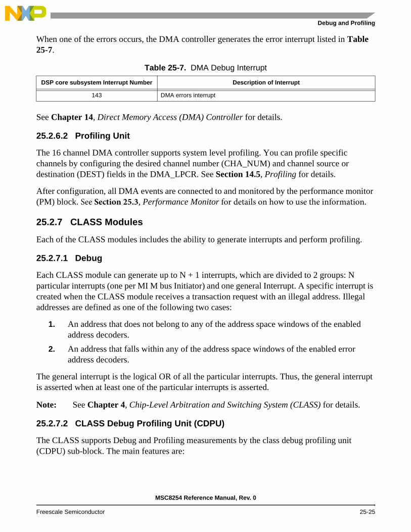
Debug and Profiling
When one of the errors occurs, the DMA controller generates the error interrupt listed in Table 25-7.
See Chapter 14, Direct Memory Access (DMA) Controller for details.
25.2.6.2 Profiling Unit
The 16 channel DMA controller supports system level profiling. You can profile specific channels by configuring the desired channel number (CHA_NUM) and channel source or destination (DEST) fields in the DMA_LPCR. See Section 14.5, Profiling for details.
After configuration, all DMA events are connected to and monitored by the performance monitor (PM) block. See Section 25.3, Performance Monitor for details on how to use the information.
25.2.7 CLASS Modules
Each of the CLASS modules includes the ability to generate interrupts and perform profiling.
25.2.7.1 Debug
Each CLASS module can generate up to N + 1 interrupts, which are divided to 2 groups: N particular interrupts (one per MI M bus Initiator) and one general Interrupt. A specific interrupt is created when the CLASS module receives a transaction request with an illegal address. Illegal addresses are defined as one of the following two cases:
1. An address that does not belong to any of the address space windows of the enabled address decoders.
2. An address that falls within any of the address space windows of the enabled error address decoders.
The general interrupt is the logical OR of all the particular interrupts. Thus, the general interrupt is asserted when at least one of the particular interrupts is asserted.
Note: See Chapter 4, Chip-Level Arbitration and Switching System (CLASS) for details.
25.2.7.2 CLASS Debug Profiling Unit (CDPU)
The CLASS supports Debug and Profiling measurements by the class debug profiling unit (CDPU) sub-block. The main features are:
Table 25-7. DMA Debug Interrupt
DSP core subsystem Interrupt Number Description of Interrupt
143 DMA errors interrupt
MSC8254 Reference Manual, Rev. 0
Freescale Semiconductor 25-25

Debugging, Profiling, and Performance Monitoring
Time-out mechanism. This mechanism does not generate an interrupt. The host must poll certain a bit in the respective CLASS register.
Watch point mechanism profiling unit. The CLASS profiling unit provides the following profiling information:
— Data acknowledges of write accesses. — Data acknowledges of read accesses. — Acknowledged accesses (req and req_ack). — Stall cycles due to write-after-read. — Cycles of non-acknowledged accesses. — Acknowledged supervisor accesses. — Acknowledged non-supervisor accesses. — Cycles when priority = 0. — Cycles when priority = 1. — Cycles when priority = 2. — Cycles when priority = 3. — Priority upgrades. — Cycles for which the priority was not upgraded because the upgradeable signal was
low. — Acknowledged read accesses. — Acknowledged write with confirm accesses. — Acknowledged write without confirm accesses.
Over-flow mechanism.
Chapter 4, Chip-Level Arbitration and Switching System (CLASS) and Chapter 8, General Configuration Registers for details.
Table 25-8. Class0 Debug Interrupts
DSP Core Subsystem Interrupt Description of Interrupt
Routed through General Interrupt Register 3 (GIR3) Class0 watch point mechanism interrupt
Routed through General Interrupt Register 3 (GIR3) Class0 over flow mechanism interrupt
Routed through General Interrupt Register 3 (GIR3) Class0 error interrupt
MSC8254 Reference Manual, Rev. 0
25-26 Freescale Semiconductor

Debug and Profiling
25.2.8 QUICC Engine Debug and Profiling
The QUICC Engine module has several means to debug and profile its operation as described in the following sections.
25.2.8.1 Trace Buffer
The QUICC Engine module provides chip-level testing capability through the trace buffer block (TRB). The TRB provides means of tracing the code ran by the CP (communication processor) in real time (through storing it non-intrusively) and reporting several internal CP/TRB events. The QUICC Engine module RISC has 4 kinds of breakpoints for on chip software debugging
Instruction breakpoint
Software breakpoint
Data breakpoint
External breakpoint
Note: See Section 18.2, RISC Processors for details.
25.2.8.2 Loopback Modes
SGMII supports an internal Loopback mode in the TBI MAC layer. RGMII supports internal Loopback mode in the MAC layer. The communication controllers support Diagnostic modes, including local and external loopback (transmitter-to-receiver) and normal operation. See QUICC Engine Block Reference Manual with Protocol Interworking (QEIWRM) for details.
The Serial RapidIO controller supports analog and digital loopback mode. See Chapter 16, Serial RapidIO Controller for details.
MSC8254 Reference Manual, Rev. 0
Freescale Semiconductor 25-27

Debugging, Profiling, and Performance Monitoring
25.2.9 TDM Debug and Profiling
The TDM modules provide a set of debug interrupts and loopback support for debugging.
25.2.9.1 Debug
The TDM complex in the MSC8254 device consists of four TDM modules. Each TDM module supports transmit sync error and receive sync error interrupts. Table 25-9 lists the TDM debug interrupts.
See Chapter 19, TDM Interface and Chapter 8, General Configuration Registers for details.
25.2.9.2 TDM Loopback Support
The TDM modules support loopback test mode in which the receiver receives the same data that is transmitted out. See Section 19.5, Loopback Support for details.
25.2.10 RapidIO Debug and Profiling
The RapidIO system debugging system includes an error interrupt and the ability to connect to the profiling unit.
25.2.10.1 Debug Errors
The RapidIO system asserts the error interrupt listed in Table 25-10 when a system error is detected.
See Chapter 16, Serial RapidIO Controller for details.
Table 25-9. TDM Debug Interrupts
DSP core subsystem Interrupt Number Description of Interrupt
Routed through General Interrupt Register 1 (GIR1) RX sync error interrupt
Routed through General Interrupt Register 1 (GIR1) TX sync error interrupt
Routed through General Interrupt Register 1 (GIR1) RX sync error interrupt
Routed through General Interrupt Register 1 (GIR1) TX sync error interrupt
Routed through General Interrupt Register 1 (GIR1) RX sync error interrupt
Routed through General Interrupt Register 1 (GIR1) TX sync error interrupt
Routed through General Interrupt Register 1 (GIR1) RX sync error interrupt
Routed through General Interrupt Register 1 (GIR1) TX sync error interrupt
Table 25-10. RapidIO Debug Interrupt
DSP core subsystem Interrupt Number Description of Interrupt
90 RapidIO Errors interrupt
MSC8254 Reference Manual, Rev. 0
25-28 Freescale Semiconductor

Debug and Profiling
25.2.10.2 Profiling Unit
All RapidIO events can connect to Performance monitor (PM) block. See Section 25.3, Performance Monitor for details. The RapidIO PM uses the RapidIO clock.
25.2.11 Software Watchdog (SWT)
The watchdog timer (WDT) option prevents system lockup in cases where the software becomes trapped in a loop with no controlled exit. Watchdog timer operations are configured in the System Watchdog Control Register (SWCRR). See Chapter 8, General Configuration Registers for details.
25.2.12 Profiling Unit Programming Model
All DPU registers are memory-mapped and can be written or read by the core in Execution mode or through the OCE Core Command in Debug mode. Only one access per execution set to a DPU register is allowed in order to assure that the programming of the DPU registers occurs in a deterministic order. Reserved or unused bits in all registers should be written as zeros and the read value should be masked. Writing to unimplemented or read-only registers has no effect, and should be avoided for future software compatibility. Reading from unimplemented or write-only registers is illegal and produces undefined results.
Writing and reading of the DPU registers is done via the QBus. The DPU registers are located in Bank 0. This means that there are a number of cycles until the value is actually written to the DPU registers. In case DPU register synchronization is important, then the programming of the last DPU register should have a SYNCIO instruction in parallel. Code following this action can assume that the DPU registers written earlier were actually written. All registers are 32 bits with 16-bit accesses, which enable the use of bit-mask operations. When a 16-bit access is used on the 32-bit registers, the software address offset to the MSB part of the registers is equal to the software address offset of the LSB part + 2. The LSB part of the address is as shown in the registers memory map, and is not influenced by whether the system is Big Endian or Little Endian.) Any other access type other than word or long (such as byte, 2 long) should be avoided, and will result in an undefined result. When accessing the counter value registers, the 31 LSBs of the bus are written to the 31 LSBs of the register. Bit 31 of these registers is reserved.
General Registers
— DPU Control Register (DP_CR) — DPU Status Register (DP_SR) — DPU Monitor Register (DP_MR) — DPU PID Detection Reference Value Register (DP_RPID) — DPU DID Detection Reference Value Register (DP_RDID)
General Counters
— DPU Counter Triad A Control Register (DP_TAC)
MSC8254 Reference Manual, Rev. 0
Freescale Semiconductor 25-29

Debugging, Profiling, and Performance Monitoring
— DPU Counter Triad B Control Register (DP_TBC) — DPU Counter A0 Control Register (DP_CA0C) — DPU Counter A0 Value Register (DP_CA0V) — DPU Counter A1 Control Register (DP_CA1C) — DPU Counter A1 Value Register (DP_CA1V) — DPU Counter A2 Control Register (DP_CA2C) — DPU Counter A2 Value Register (DP_CA2V) — DPU Counter B0 Control Register (DP_CB0C) — DPU Counter B0 Value Register (DP_CB0V) — DPU Counter B1 Control Register (DP_CB1C) — DPU Counter B1 Value Register (DP_CB1V) — DPU Counter B2 Control Register (DP_CB2C) — DPU Counter B2 Value Register (DP_CB2V)
Trace Buffer Registers
— DPU Trace Control Register (DP_TC) — DPU VTB Start Address Register (DP_TSA) — DPU VTB End Address Register (DP_TEA) — DPU Trace Event Request Register (DP_TER) — DPU Trace Write Pointer Register (DP_TW) — DPU Trace Data Register (DP_TD)
Note: The DPU registers use the base address: 0xFFF0A000.
25.2.12.1 DPU Control Register (DP_CR)
The DP_CR register is a 32-bit register responsible for controlling the debug logic of the DPU and the task ID comparator. Table 25-11 defines the DP_CR bit fields.
DP_CR DPU Control Register Offset 0x00
Bit 31 30 29 28 27 26 25 24 23 22 21 20 19 18 17 16
— TIDCM ISEDCA5 ISEDCA4 ISEDCA3 ISEDCA2 ISEDCA1 ISEDCA0
Type R/WReset 0 0 0 0 0 0 0 0 0 0 0 0 0 0 0 0
Bit 15 14 13 12 11 10 9 8 7 6 5 4 3 2 1 0
— EIS DETB DECB2 DECB1 DECB0 DECA2 DECA1 DECA0
Type R/WReset 0 0 0 0 0 0 0 0 0 0 0 0 0 0 0 0
Table 25-11. DP_CR Bit Descriptions
Name Reset Description Settings
—31–30
0 Reserved. Write to zero for future compatibility.
MSC8254 Reference Manual, Rev. 0
25-30 Freescale Semiconductor

Debug and Profiling
TIDCM29–28
0 Task ID Comparator MaskControls the operation of the task ID comparator, deciding which part takes part in the comparison. The reference program and data ID values are written in the DP_RPID and DP_RDID registers.
00 Neither the data task ID or the program task ID participate in the comparison. The comparison result is always 1.
01 The data task ID does not participate in the comparison (masked).
10 The program task ID does not participate in the comparison (masked).
11 Both the program task ID and the data task ID participate in the comparison.
ISEDCA527–26
0 Interrupt Selector EDCA5An event generated by the EDCA5 channel of the OCE causes interrupt Debug A or Debug B to the EPIC.
00 Does not cause an interrupt
01 reserved
10 Generates Debug A interrupt to the EPIC
11 Generates Debug B interrupt to the EPIC
ISEDCA425–24
0 Interrupt Selector EDCA4An event generated by the EDCA4 channel of the OCE causes interrupt Debug A or Debug B to the EPIC.
00 Does not cause an interrupt
01 reserved
10 Generates Debug A interrupt to the EPIC
11 Generates Debug B interrupt to the EPIC
ISEDCA323–22
0 Interrupt Selector EDCA3An event generated by the EDCA3 channel of the OCE causes interrupt Debug A or Debug B to the EPIC.
00 Does not cause an interrupt
01 reserved
10 Generates Debug A interrupt to the EPIC
11 Generates Debug B interrupt to the EPIC
ISEDCA221–20
0 Interrupt Selector EDCA2An event generated by the EDCA2 channel of the OCE causes interrupt Debug A or Debug B to the EPIC.
00 Does not cause an interrupt
01 reserved
10 Generates Debug A interrupt to the EPIC
11 Generates Debug B interrupt to the EPIC
ISEDCA119–18
0 Interrupt Selector EDCA1An event generated by the EDCA1 channel of the OCE causes interrupt Debug A or Debug B to the EPIC.
00 Does not cause an interrupt
01 reserved
10 Generates Debug A interrupt to the EPIC
11 Generates Debug B interrupt to the EPIC
ISEDCA017–16
0 Interrupt Selector EDCA0An event generated by the EDCA0 channel of the OCE causes interrupt Debug A or Debug B to the EPIC.
00 Does not cause an interrupt
01 reserved
10 Generates Debug A interrupt to the EPIC
11 Generates Debug B interrupt to the EPIC
—15
0 Reserved. Write to zero for future compatibility.
EIS14
0 OCE Interrupt SelectorA maskable interrupt generated by the OCE is directed either to interrupt Debug A or Debug B.
0 A maskable interrupt generates Debug A
1 A maskable interrupt generates Debug B
DETB13–12
0 Trace Buffer Debug Request/Interrupt EnableAn event generated by the trace logic of the DPU causes a debug request to the OCE or an interrupt to the EPIC.
00 Does not cause an interrupt
01 reserved
10 Generates Debug A interrupt to the EPIC
11 Generates Debug B interrupt to the EPIC
Table 25-11. DP_CR Bit Descriptions (Continued)
Name Reset Description Settings
MSC8254 Reference Manual, Rev. 0
Freescale Semiconductor 25-31

Debugging, Profiling, and Performance Monitoring
25.2.12.2 DPU Status Register (DP_SR)
The DP_SR is a 32-bit register that reflects the status of the DPU counters and if a trace write buffer (TWB) flush is in progress. All the bits are sticky status bits, and are read-only. Only the 6 lsb bits are used to enable the execution of bit-mask instructions.
DECB211–10
0 Counter B2 Debug Request/Interrupt EnableAn event generated by counter B2 of the DPU causes a debug request to the OCE or an interrupt to the EPIC.
00 Does not cause an interrupt
01 reserved
10 Generates Debug A interrupt to the EPIC
11 Generates Debug B interrupt to the EPIC
DECB19–8
0 Counter B1 Debug Request/Interrupt EnableAn event generated by counter B1 of the DPU causes a debug request to the OCE or an interrupt to the EPIC.
00 Does not cause an interrupt
01 reserved
10 Generates Debug A interrupt to the EPIC
11 Generates Debug B interrupt to the EPIC
DECB07–6
0 Counter B0 Debug Request/Interrupt EnableAn event generated by counter B0 of the DPU causes a debug request to the OCE or an interrupt to the EPIC.
00 Does not cause an interrupt
01 reserved
10 Generates Debug A interrupt to the EPIC
11 Generates Debug B interrupt to the EPIC
DECA25–4
0 Counter A2 Debug Request/Interrupt EnableAn event generated by counter A2 of the DPU causes a debug request to the OCE or an interrupt to the EPIC.
00 Does not cause an interrupt
01 reserved
10 Generates Debug A interrupt to the EPIC
11 Generates Debug B interrupt to the EPIC
DECA13–2
0 Counter A1 Debug Request/Interrupt EnableAn event generated by counter A1 of the DPU causes a debug request to the OCE or an interrupt to the EPIC.
00 Does not cause an interrupt
01 reserved
10 Generates Debug A interrupt to the EPIC
11 Generates Debug B interrupt to the EPIC
DECA01–9
0 Counter A0 Debug Request/Interrupt EnableAn event generated by counter A0 of the DPU causes a debug request to the OCE or an interrupt to the EPIC.
00 Does not cause an interrupt
01 reserved
10 Generates Debug A interrupt to the EPIC
11 Generates Debug B interrupt to the EPIC
DP_SR DPU Status Register Offset 0x04
Bit 31 30 29 28 27 26 25 24 23 22 21 20 19 18 17 16
—
Type RReset 0 0 0 0 0 0 0 0 0 0 0 0 0 0 0 0
Bit 15 14 13 12 11 10 9 8 7 6 5 4 3 2 1 0
— TWBA ENCB2 ENCB ENCB0 ENCA2 ENCA1 ENCA0
Type RReset 0 0 0 0 0 0 0 0 0 0 0 0 0 0 0 0
Table 25-11. DP_CR Bit Descriptions (Continued)
Name Reset Description Settings
MSC8254 Reference Manual, Rev. 0
25-32 Freescale Semiconductor

Debug and Profiling
Note: The ENCA and ENCB bits are used whenever the counter is enabled or disabled by events that occur after the DPU is initialized (for example, an EDCA0 event enables the counter and the DEBUGEV instruction disables it).
Table 25-12 defines the DP_SR bit fields.
25.2.12.3 DPU Monitor Register (DP_MR)
The DP_MR is a 32-bit register that reflects information about an event generated by a counter or the trace buffer. All the bits are sticky bits, and can be only cleared by writing 1 to the appropriate bit(s).
Table 25-12. DP_SR Bit Descriptions
Name Reset Description Settings
—31–7
0 Reserved. Write to zero for future compatibility.
TWBA6
0 Trace Write Buffer ActiveThe user can poll this bit to determine whether to disable tracing by setting the DP_TC[TMPDIS] bit or by clearing the DP_TC[EN] bit.
0 Trace Write Buffer flush is complete.
1 Flush sent to Trace Write Buffer.
ENCB25
0 Counter B2 EnableIndicates whether the counter is disabled or enabled.
0 Disabled.
1 Enabled.
ENCB14
0 Counter B1 EnableIndicates whether the counter is disabled or enabled.
0 Disabled.
1 Enabled.
ENCB03
0 Counter B0 EnableIndicates whether the counter is disabled or enabled.
0 Disabled.
1 Enabled.
ENCA22
0 Counter A2 EnableIndicates whether the counter is disabled or enabled.
0 Disabled.
1 Enabled.
ENCA11
0 Counter A1 EnableIndicates whether the counter is disabled or enabled.
0 Disabled.
1 Enabled.
ENCA00
0 Counter A0 EnableIndicates whether the counter is disabled or enabled.
0 Disabled.
1 Enabled.
DP_MR DPU Status Register Offset 0x08
Bit 31 30 29 28 27 26 25 24 23 22 21 20 19 18 17 16
—
Type R
Reset 0 0 0 0 0 0 0 0 0 0 0 0 0 0 0 0
Bit 15 14 13 12 11 10 9 8 7 6 5 4 3 2 1 0
— TBF DRA — DRTB DRCB2 DRCB1‘ BRCB0 DRCA2 DRCA1 DRCA0
Type R W1C
Reset 0 0 0 0 0 0 0 0 0 0 0 0 0 0 0 0
MSC8254 Reference Manual, Rev. 0
Freescale Semiconductor 25-33

Debugging, Profiling, and Performance Monitoring
Only the 16 lsbs are used to enable the execution of bit-mask instructions. Table 25-13 defines the DP_SR bit fields.
Table 25-13. DP_MR Bit Descriptions
Name Reset Description Settings
—31–10
0 Reserved. Write to zero for future compatibility.
TBF9
0 Trace Buffer FinishedIndicates whether the trace buffer has written the last entry in the VTB.
0 Trace buffer has not written the last entry to the VTB.
1 Trace buffer has written the last entry to the VTB.
DRA8
0 Debug is External Asynchronous Debug RequestIndicates whether an external synchronous debug request.
0 No external synchronous debug request.
1 External synchronous debug request.
—7
0 Reserved. Write to zero for future compatibility.
DRTB6
0 Debug/Interrupt Reason is Trace BufferIndicates a trace buffer event debug request.
0 No trace buffer event debug request.
1 Trace buffer event debug request.
DRCB25
0 Debug/Interrupt Reason is Counter B2 EventIndicates a counter B2 Event debug request.
0 No counter B2 event debug request.
1 Counter B2 event debug request.
DRCB14
0 Debug/Interrupt Reason is Counter B1 EventIndicates a counter B1 Event debug request.
0 No counter B1 event debug request.
1 Counter B1 event debug request.
DRCB03
0 Debug/Interrupt Reason is Counter B0 EventIndicates a counter B0 Event debug request.
0 No counter B0 event debug request.
1 Counter B0 event debug request.
DRCA22
0 Debug/Interrupt Reason is Counter A2 EventIndicates a counter A2 Event debug request.
0 No counter A2 event debug request.
1 Counter A2 event debug request.
DRCA11
0 Debug/Interrupt Reason is Counter A1 EventIndicates a counter A1 Event debug request.
0 No counter A1 event debug request.
1 Counter A1 event debug request.
DRCA00
0 Debug/Interrupt Reason is Counter A0 EventIndicates a counter A0 Event debug request.
0 No counter A0 event debug request.
1 Counter A0 event debug request.
MSC8254 Reference Manual, Rev. 0
25-34 Freescale Semiconductor

Debug and Profiling
25.2.12.4 DPU PID Detection Reference Value Register (DP_RPID)
The DP_RPID is a 32-bit register containing the reference program ID value for the task ID comparator. The DPU Control register controls the operation mode of the comparator. Table 25-14 defines the DP_RPID bit fields.
25.2.12.5 DPU DID Detection Reference Value Register (DP_RDID)
The DP_RDID is a 32- bit register containing the reference data ID value for the task ID comparator. The DPU Control register controls the operation mode of the comparator. Table 25-15 defines the DP_RDID bit fields.
DP_RPID DPU PID Detection Reference Value Registers Offset 0x0C
Bit 31 30 29 28 27 26 25 24 23 22 21 20 19 18 17 16
—
Type R/WReset 0 0 0 0 0 0 0 0 0 0 0 0 0 0 0 0
Bit 15 14 13 12 11 10 9 8 7 6 5 4 3 2 1 0
— RPID
Type R/WReset 0 0 0 0 0 0 0 0 0 0 0 0 0 0 0 0
Table 25-14. DP_RPID Bit Descriptions
Name Reset Description Settings
—31–8
0 Reserved. Write to zero for future compatibility.
RPID7–0
0 Reference Program ID ValueStores the value of the reference program ID.
DP_RDID DPU DID Detection Reference Value Registers Offset 0x10
Bit 31 30 29 28 27 26 25 24 23 22 21 20 19 18 17 16
—
Type R/WReset 0 0 0 0 0 0 0 0 0 0 0 0 0 0 0 0
Bit 15 14 13 12 11 10 9 8 7 6 5 4 3 2 1 0
— RDID
Type R/WReset 0 0 0 0 0 0 0 0 0 0 0 0 0 0 0 0
Table 25-15. DP_RDID Bit Descriptions
Name Reset Description Settings
—31–8
0 Reserved. Write to zero for future compatibility.
MSC8254 Reference Manual, Rev. 0
Freescale Semiconductor 25-35

Debugging, Profiling, and Performance Monitoring
25.2.12.6 DPU Counter Triad A Control Register (DP_TAC)
The DP_TAC register is a 32-bit register that controls the operation of the DPU counter triad A, including what events and when they are counted. If the TCEN bit in the DP_TAC register is set, the appropriate counters are controlled by this register and ignore the programming of their own control register. When the TCEN bit is cleared, each counter is controlled individually by its own control register. Table 25-19 defines the DP_TAC bit fields.
RDID7–0
0 Reference Data Task ID ValueStores the value of the reference data task ID.
DP_TAC DPU Triad A Control Register Offset 0x20
Bit 31 30 29 28 27 26 25 24 23 22 21 20 19 18 17 16
— TDMP TDM — TENMP TENM
Type R/WReset 0 0 0 0 0 0 0 0 0 0 0 0 0 0 0 0
Bit 15 14 13 12 11 10 9 8 7 6 5 4 3 2 1 0
— CEGP — CEG — CMODE TCEN
Type R/WReset 0 0 0 0 0 0 0 0 0 0 0 0 0 0 0 0
Table 25-16. DP_TAC Bit Descriptions
Name Reset Description Settings
—31–30
0 Reserved. Write to zero for future compatibility.
TDMP29–28
0 Triad Disable Mode Privilege LevelThe event disabling the counters belongs to the task described by these bits. If the DEBUGEV instruction disables the counters, all the programming options mentioned here can be chosen. For EDCA events the privilege level can be filtered inside the EDCA itself.
00 The disabling event belongs to any task.
01 The disabling event is the result of a user task detected under the control of DP_CR[TIDCM].
10 The disabling event belongs to a supervisor level task.
11 The disabling event is the result of a supervisor level task detected under the control of DP_CR[TIDCM].
TDM27–24
0 Triad Disable ModeThe event that disables the counters in the triad.
0000 No disabling event.
0001 DEBUGEV instruction.
0010 Event generated by EDCA0 in the OCE.
0011 Event generated by EDCA1 in the OCE.
0100 Event generated by EDCA2 in the OCE.
0101 Event generated by EDCA3 in the OCE.
0110 Event generated by EDCA4 in the OCE.
0111 Event generated by EDCA5 in the OCE.
1000–
1111 reserved
Table 25-15. DP_RDID Bit Descriptions (Continued)
Name Reset Description Settings
MSC8254 Reference Manual, Rev. 0
25-36 Freescale Semiconductor

Debug and Profiling
—23–22
0 Reserved. Write to zero for future compatibility.
TENMP21–20
0 Triad Enable Mode Privilege LevelThe event enabling the counters belongs to the task described by these bits. If the MARK instruction enables the counters, all the programming options mentioned here can be chosen. For EDCA events the privilege level can be filtered inside the EDCA itself.
00 The enabling event belongs to any task.
01 The enabling event is the result of a user task detected under the control of DP_CR[TIDCM].
10 The enabling event belongs to a supervisor level task.
11 The enabling event is the result of a supervisor level task detected under the control of DP_CR[TIDCM].
TENM19–16
0 Triad Enable ModeThe event that enables the counters.
0000 The counter is disabled.
0001 MARK instruction.
0010 Event generated by EDCA0 in the OCE.
0011 Event generated by EDCA1 in the OCE.
0100 Event generated by EDCA2 in the OCE.
0101 Event generated by EDCA3 in the OCE.
0110 Event generated by EDCA4 in the OCE.
0111 Event generated by EDCA5 in the OCE.
1000–
1110 reserved
1111 The counter is enabled.
—15–14
0 Reserved. Write to zero for future compatibility.
CEGP13–12
0 Counted Event Group Privilege LevelThe source counted by the counter belongs to the task described by these bits.
00 The counter counts events that belong to any task.
01 The counter only counts events belonging to user tasks detected under the control of DP_CR[TIDCM].
10 The counter counts event that belong to a supervisor level task.
11 The counter counts events belonging to supervisor level task detected under the control of DP_CR[TIDCM].
—11–9
0 Reserved. Write to zero for future compatibility.
CEG8–4
0 Counted Event GroupThe source counted by the counter.
See Table 25-17 for details.
—3
0 Reserved. Write to zero for future compatibility.
CMODE2–1
0 Triad Counters ModeSpecifies the mode of the counter
00 One shot. Each counters in the triad generates an event when it reaches 0, stops counting, and disables itself.
01 Trace mode. Each counter in the triad has its value saved in a shadow register whenever required by the trace buffer. The counter continues to count and generates an event when it reaches 0.
10–
11 reserved.
Table 25-16. DP_TAC Bit Descriptions (Continued)
Name Reset Description Settings
MSC8254 Reference Manual, Rev. 0
Freescale Semiconductor 25-37

Debugging, Profiling, and Performance Monitoring
TCEN0
0 Triad Control EnableDetermines whether the three counters in the triad are controlled by this control register or their individual control counters.
0 Each counter is controlled independently.
1 The three counters are controlled by this register and the individual register settings have no effect.
Table 25-17. Counted Event Group
CEG Value
Group Name Counter 0 Counts Counter 1 Counts Counter 2 Counts
00000 ICache hit-miss ICache misses (without prefetch hits)
ICache hits ICache prefetch hits
00001 DCache hit-miss DCache misses (without prefetch hits)
DCache hits DCache prefetch hits
00010 Core wait state Clock cycles (non-debug)
Wait processing-state cycles
Not used
00011 Breakdown of application cycles - Group 1
Application cycles (non-debug, non-wait, non-stop)
No bubble Bubble due to COF or interrupt
00100 Breakdown of application cycles - Group 2
Bubble due to starvation (no instructions in the prefetch/dispatch buffer)
Bubble due to core resource conflicts
Bubble due to data memory holds
00101 Not implemented in the MSC8254
00110 Not implemented in the MSC8254
00111 Hold associated with debug
Hold due to VTB writes Hold due to Nexus freeze not used
01000 Hold due to WRQ or WTB
Hold due to WRQ flush or atomic operation
Hold due to WRQ hazard Hold due to WRQ or WTB full
01010 Hold due to Dcache system
Hold due to cacheable access (read, write-back miss or write-trough prefetch hit).
Hold due to non-cacheable access (read)
not used
01011 Not implemented in the MSC8254
01100 Master bus No. 1 load (See Section 10.2.1.8.8)
Master bus No. 1 bus cycles
Instruction transfer cycles on Master bus No. 1
Data transfer cycles on Master bus No. 1
01101 Master bus No. 2 load (See Section 10.2.1.8.8)
Master bus No. 2 bus cycles
Instruction transfer cycles on Master bus No. 2
Data transfer cycles on Master bus No. 2
01110 Bus load due to VTB write
Master bus No. 1 bus cycles
Data transfer to the VTB (TWB write accesses)
Master bus No. 2 bus cycles
10000 Instruction accesses to L2 subsystem
L2 instruction access miss
L2 instruction access hit Total L2 instruction accesses
10001 Data accesses to L2 subsystem
L2 data access miss L2 data access hit Total L2 data accesses
Table 25-16. DP_TAC Bit Descriptions (Continued)
Name Reset Description Settings
MSC8254 Reference Manual, Rev. 0
25-38 Freescale Semiconductor

Debug and Profiling
25.2.12.7 DPU Counter Triad B Control Register (DP_TBC)
The DP_TBC register is a 32-bit register that controls the operation of the DPU counter triad B, including what events and when they are counted. If the TCEN bit in the DP_TBC register is set, the appropriate counters are controlled by this register and ignore the programming of their own control register. When the TCEN bit is cleared, each counter is controlled individually by its own control register. Table 25-19 defines the DP_TBC bit fields.
10010 M2 RAM contentions (if L2 subsystem exists)
Contentions between IQ DQ accesses
Contentions between Q (IQ or DQ) and DMA accesses
not used
10011 M2 ROM contentions (if L2 subsystem exists)
Contentions between IQ DQ accesses
Contentions between Q (IQ or DQ) and DMA accesses
not used
10100 BTB Characterization Group 1
Total number of execution sets
Sequentially executed execution sets.
BTB-able instructions correctly predicted
10101 BTB Characterization Group 2
BTB-able instructions not in the BTB, wrongly predicted.
BTB-able instructions, in the BTB, wrongly predicted.
Not BTB-able instructions
Note: Other combinations reserved
DP_TBC DPU Triad B Control Register Offset 0x24
Bit 31 30 29 28 27 26 25 24 23 22 21 20 19 18 17 16
— TDMP TDM — TENMP TENM
Type R/W
Reset 0 0 0 0 0 0 0 0 0 0 0 0 0 0 0 0
Bit 15 14 13 12 11 10 9 8 7 6 5 4 3 2 1 0
— CEGP — CEG — CMODE TCEN
Type R/W
Reset 0 0 0 0 0 0 0 0 0 0 0 0 0 0 0 0
Table 25-18. DP_TBC Bit Descriptions
Name Reset Description Settings
—31–30
0 Reserved. Write to zero for future compatibility.
Table 25-17. Counted Event Group (Continued)
CEG Value
Group Name Counter 0 Counts Counter 1 Counts Counter 2 Counts
MSC8254 Reference Manual, Rev. 0
Freescale Semiconductor 25-39

Debugging, Profiling, and Performance Monitoring
TDMP29–28
0 Triad Disable Mode Privilege LevelThe event disabling the counters belongs to the task described by these bits. If the DEBUGEV instruction disables the counters, all the programming options mentioned here can be chosen. For EDCA events the privilege level can be filtered inside the EDCA itself.
00 The disabling event belongs to any task.
01 The disabling event is the result of a user task detected under the control of DP_CR[TIDCM].
10 The disabling event belongs to a supervisor level task.
11 The disabling event is the result of a supervisor level task detected under the control of DP_CR[TIDCM].
TDM27–24
0 Triad Disable ModeThe event that disables the counters in the triad.
0000 No disabling event.
0001 DEBUGEV instruction.
0010 Event generated by EDCA0 in the OCE.
0011 Event generated by EDCA1 in the OCE.
0100 Event generated by EDCA2 in the OCE.
0101 Event generated by EDCA3 in the OCE.
0110 Event generated by EDCA4 in the OCE.
0111 Event generated by EDCA5 in the OCE.
1000–
1111 reserved—
23–220 Reserved. Write to zero for future compatibility.
TENMP21–20
0 Triad Enable Mode Privilege LevelThe event enabling the counters belongs to the task described by these bits. If the MARK instruction enables the counters, all the programming options mentioned here can be chosen. For EDCA events the privilege level can be filtered inside the EDCA itself.
00 The enabling event belongs to any task.
01 The enabling event is the result of a user task detected under the control of DP_CR[TIDCM].
10 The enabling event belongs to a supervisor level task.
11 The enabling event is the result of a supervisor level task detected under the control of DP_CR[TIDCM].
TENM19–16
0 Triad Enable ModeThe event that enables the counters.
0000 The counter is disabled.
0001 MARK instruction.
0010 Event generated by EDCA0 in the OCE.
0011 Event generated by EDCA1 in the OCE.
0100 Event generated by EDCA2 in the OCE.
0101 Event generated by EDCA3 in the OCE.
0110 Event generated by EDCA4 in the OCE.
0111 Event generated by EDCA5 in the OCE.
1000–
1110 reserved
1111 The counter is enabled.
—15–14
0 Reserved. Write to zero for future compatibility.
Table 25-18. DP_TBC Bit Descriptions (Continued)
Name Reset Description Settings
MSC8254 Reference Manual, Rev. 0
25-40 Freescale Semiconductor

Debug and Profiling
25.2.12.8 DPU Counter A0 Control Register (DP_CA0C)
The DP_CA0C is a 32-bit register that controls the operation of the DPU Extension Support Counter A0, including what events and when they are counted. Table 25-19 defines the DP_CA0C bit fields.
CEGP13–12
0 Counted Event Group Privilege LevelThe source counted by the counter belongs to the task described by these bits.
00 The counter counts events that belong to any task.
01 The counter only counts events belonging to user tasks detected under the control of DP_CR[TIDCM].
10 The counter counts event that belong to a supervisor level task.
11 The counter counts events belonging to supervisor level task detected under the control of DP_CR[TIDCM].
—11–9
0 Reserved. Write to zero for future compatibility.
CEG8–4
0 Counted Event GroupThe source counted by the counter.
See Table 25-17 for details.
—3
0 Reserved. Write to zero for future compatibility.
CMODE2–1
0 Triad Counters ModeSpecifies the mode of the counter
00 One shot. Each counters in the triad generates an event when it reaches 0, stops counting, and disables itself.
01 Trace mode. Each counter in the triad has its value saved in a shadow register whenever required by the trace buffer. The counter continues to count and generates an event when it reaches 0.
10–
11 reserved.
TCEN0
0 Triad Control EnableDetermines whether the three counters in the triad are controlled by this control register or their individual control counters.
0 Each counter is controlled independently.
1 The three counters are controlled by this register and the individual register settings have no effect.
DP_CA0C DPU Counter A0 Control Register Offset 0x2C
Bit 31 30 29 28 27 26 25 24 23 22 21 20 19 18 17 16
— CDMP CDM — CENMP CENM
Type R/W
Reset 0 0 0 0 0 0 0 0 0 0 0 0 0 0 0 0
Bit 15 14 13 12 11 10 9 8 7 6 5 4 3 2 1 0
— CEP — CE — CMODE —
Type R/W
Reset 0 0 0 0 0 0 0 0 0 0 0 0 0 0 0 0
Table 25-18. DP_TBC Bit Descriptions (Continued)
Name Reset Description Settings
MSC8254 Reference Manual, Rev. 0
Freescale Semiconductor 25-41

Debugging, Profiling, and Performance Monitoring
Table 25-19. DP_CA0C Bit Descriptions
Name Reset Description Settings
—31–30
0 Reserved. Write to zero for future compatibility.
CDMP29–28
0 Counter Disable Mode Privilege LevelThe event disabling the counter belongs to the task described by these bits. If the DEBUGEV instruction disables the counters, all the programming options mentioned here can be chosen. For EDCA events the privilege level can be filtered inside the EDCA itself.
00 The disabling event belongs to any task.
01 The disabling event is the result of a user task detected under the control of DP_CR[TIDCM].
10 The disabling event belongs to a supervisor level task.
11 The disabling event is the result of a supervisor level task detected under the control of DP_CR[TIDCM].
CDM27–24
0 Counter Disable ModeThe event that disables the counter.
0000 No disabling event.
0001 DEBUGEV instruction.
0010 Event generated by EDCA0 in the OCE.
0011 Event generated by EDCA1 in the OCE.
0100 Event generated by EDCA2 in the OCE.
0101 Event generated by EDCA3 in the OCE.
0110 Event generated by EDCA4 in the OCE.
0111 Event generated by EDCA5 in the OCE.
1000–
1111 reserved
—23–22
0 Reserved. Write to zero for future compatibility.
CENMP21–20
0 Counter Enable Mode Privilege LevelThe event enabling the counter belongs to the task described by these bits. If the MARK instruction enables the counter, all the programming options mentioned here can be chosen. For EDCA events the privilege level can be filtered inside the EDCA itself.
00 The enabling event belongs to any task.
01 The enabling event is the result of a user task detected under the control of DP_CR[TIDCM].
10 The enabling event belongs to a supervisor level task.
11 The enabling event is the result of a supervisor level task detected under the control of DP_CR[TIDCM].
CENM19–16
0 Counter Enable ModeThe event that enables the counter.
0000 The counter is disabled.
0001 MARK instruction.
0010 Event generated by EDCA0 in the OCE.
0011 Event generated by EDCA1 in the OCE.
0100 Event generated by EDCA2 in the OCE.
0101 Event generated by EDCA3 in the OCE.
0110 Event generated by EDCA4 in the OCE.
0111 Event generated by EDCA5 in the OCE.
1000–
1110 reserved
1111 The counter is enabled.—
15–140 Reserved. Write to zero for future compatibility.
MSC8254 Reference Manual, Rev. 0
25-42 Freescale Semiconductor

Debug and Profiling
CEP13–12
0 Counted Event Privilege LevelThe source counted by the counter belongs to the task described by these bits.
00 The counter counts events that belong to any task.
01 The counter only counts events belonging to user tasks detected under the control of DP_CR[TIDCM].
10 The counter counts event that belong to a supervisor level task.
11 The counter counts events belonging to supervisor level task detected under the control of DP_CR[TIDCM].
—11–9
0 Reserved. Write to zero for future compatibility.
CE8–4
0 Counted EventThe source counted by the counter.
00000 Clock cycles (non-debug)
00001 Application cycles (non-wait, non-stop, non-debug
00010 Number of events generated by the EDCA0 of the OCE (CEP bits can be 00 or 01)
00011 Number of interrupts
00100 Number of ICache thrashes due to miss.
00101–
11111 reserved—3
0 Reserved. Write to zero for future compatibility.
CMODE2–1
0 Counter ModeSpecifies the mode of the counter
00 One shot. The counter generates an event when it reaches 0, stops counting, and disables itself.
01 Trace mode. The counter value is saved in a shadow register whenever required by the trace buffer. The counter continues to count and generates an event when it reaches 0.
10–
11 reserved.
—0
0 Reserved. Write to zero for future compatibility.
Table 25-19. DP_CA0C Bit Descriptions (Continued)
Name Reset Description Settings
MSC8254 Reference Manual, Rev. 0
Freescale Semiconductor 25-43

Debugging, Profiling, and Performance Monitoring
25.2.12.9 DPU Counter A0 Value Register (DP_CA0V)
DP_CA0V is a 32-bit register containing the specified counter value. Table 25-20 defines the counter bit fields.
25.2.12.10 DPU Counter A1 Control Register (DP_CA1C)
The DP_CA1C is a 32-bit register that controls the operation of the DPU Extension Support Counter A1, including what events and when they are counted. Table 25-21 defines the DP_CA1C bit fields.
DP_CA0V DPU Counter A0 Value Registers Offset 0x30
Bit 31 30 29 28 27 26 25 24 23 22 21 20 19 18 17 16
— CV
Type R/WReset 0 0 0 0 0 0 0 0 0 0 0 0 0 0 0 0
Bit 15 14 13 12 11 10 9 8 7 6 5 4 3 2 1 0
CV
Type R/WReset 0 0 0 0 0 0 0 0 0 0 0 0 0 0 0 0
Table 25-20. DP_CA0V Bit Descriptions
Name Reset Description Settings
—31
0 Reserved. Write to zero for future compatibility.
CV30–0
0 Counter ValueStores the value of the counter.
DP_CA1C DPU Counter A1 Control Register Offset 0x34
Bit 31 30 29 28 27 26 25 24 23 22 21 20 19 18 17 16
— CDMP CDM — CENMP CENM
Type R/W
Reset 0 0 0 0 0 0 0 0 0 0 0 0 0 0 0 0
Bit 15 14 13 12 11 10 9 8 7 6 5 4 3 2 1 0
— CEP — CE — CMODE —
Type R/W
Reset 0 0 0 0 0 0 0 0 0 0 0 0 0 0 0 0
Table 25-21. DP_CA1C Bit Descriptions
Name Reset Description Settings
—31–30
0 Reserved. Write to zero for future compatibility.
MSC8254 Reference Manual, Rev. 0
25-44 Freescale Semiconductor

Debug and Profiling
CDMP29–28
0 Counter Disable Mode Privilege LevelThe event disabling the counter belongs to the task described by these bits. If the DEBUGEV instruction disables the counters, all the programming options mentioned here can be chosen. For EDCA events the privilege level can be filtered inside the EDCA itself.
00 The disabling event belongs to any task.
01 The disabling event is the result of a user task detected under the control of DP_CR[TIDCM].
10 The disabling event belongs to a supervisor level task.
11 The disabling event is the result of a supervisor level task detected under the control of DP_CR[TIDCM].
CDM27–24
0 Counter Disable ModeThe event that disables the counter.
0000 No disabling event.
0001 DEBUGEV instruction.
0010 Event generated by EDCA0 in the OCE.
0011 Event generated by EDCA1 in the OCE.
0100 Event generated by EDCA2 in the OCE.
0101 Event generated by EDCA3 in the OCE.
0110 Event generated by EDCA4 in the OCE.
0111 Event generated by EDCA5 in the OCE.
1000–
1111 reserved—
23–220 Reserved. Write to zero for future compatibility.
CENMP21–20
0 Counter Enable Mode Privilege LevelThe event enabling the counter belongs to the task described by these bits. If the MARK instruction enables the counter, all the programming options mentioned here can be chosen. For EDCA events the privilege level can be filtered inside the EDCA itself.
00 The enabling event belongs to any task.
01 The enabling event is the result of a user task detected under the control of DP_CR[TIDCM].
10 The enabling event belongs to a supervisor level task.
11 The enabling event is the result of a supervisor level task detected under the control of DP_CR[TIDCM].
CENM19–16
0 Counter Enable ModeThe event that enables the counter.
0000 The counter is disabled.
0001 MARK instruction.
0010 Event generated by EDCA0 in the OCE.
0011 Event generated by EDCA1 in the OCE.
0100 Event generated by EDCA2 in the OCE.
0101 Event generated by EDCA3 in the OCE.
0110 Event generated by EDCA4 in the OCE.
0111 Event generated by EDCA5 in the OCE.
1000–
1110 reserved
1111 The counter is enabled.
—15–14
0 Reserved. Write to zero for future compatibility.
Table 25-21. DP_CA1C Bit Descriptions (Continued)
Name Reset Description Settings
MSC8254 Reference Manual, Rev. 0
Freescale Semiconductor 25-45

Debugging, Profiling, and Performance Monitoring
CEP13–12
0 Counted Event Privilege LevelThe source counted by the counter belongs to the task described by these bits.
00 The counter counts events that belong to any task.
01 The counter only counts events belonging to user tasks detected under the control of DP_CR[TIDCM].
10 The counter counts event that belong to a supervisor level task.
11 The counter counts events belonging to supervisor level task detected under the control of DP_CR[TIDCM].
—11–9
0 Reserved. Write to zero for future compatibility.
CE8–4
0 Counted EventThe source counted by the counter.
00000 Clock cycles (non-debug)
00001 Application cycles (non-wait, non-stop, non-debug
00010 Number of events generated by the EDCA1 of the OCE (CEP bits can be 00 or 01)
00011 Number of rollovers by counter A2 (CEP bits must be 00).
00100 Number of DCache thrashes due to miss.
00101–
11111 reserved—3
0 Reserved. Write to zero for future compatibility.
CMODE2–1
0 Counter ModeSpecifies the mode of the counter
00 One shot. The counter generates an event when it reaches 0, stops counting, and disables itself.
01 Trace mode. The counter value is saved in a shadow register whenever required by the trace buffer. The counter continues to count and generates an event when it reaches 0.
10–
11 reserved.—0
0 Reserved. Write to zero for future compatibility.
Table 25-21. DP_CA1C Bit Descriptions (Continued)
Name Reset Description Settings
MSC8254 Reference Manual, Rev. 0
25-46 Freescale Semiconductor

Debug and Profiling
25.2.12.11 DPU Counter A1 Value Registers (DP_CA1V)
DP_CA1V is a 32-bit register containing the specified counter value. Table 25-20 defines the counter bit fields.
25.2.12.12 DPU Counter A2 Control Register (DP_CA2C)
The DP_CA2C is a 32-bit register that controls the operation of the DPU Extension Support Counter A2, including what events and when they are counted. Table 25-23 defines the DP_CA2C bit fields.
DP_CA1V DPU Counter A1 Value Registers Offset 0x38
Bit 31 30 29 28 27 26 25 24 23 22 21 20 19 18 17 16
— CV
Type R/WReset 0 0 0 0 0 0 0 0 0 0 0 0 0 0 0 0
Bit 15 14 13 12 11 10 9 8 7 6 5 4 3 2 1 0
CV
Type R/WReset 0 0 0 0 0 0 0 0 0 0 0 0 0 0 0 0
Table 25-22. DP_CA1V Bit Descriptions
Name Reset Description Settings
—31
0 Reserved. Write to zero for future compatibility.
CV30–0
0 Counter ValueStores the value of the counter.
DP_CA2C DPU Counter A2 Control Register Offset 0x3C
Bit 31 30 29 28 27 26 25 24 23 22 21 20 19 18 17 16
— CDMP CDM — CENMP CENM
Type R/WReset 0 0 0 0 0 0 0 0 0 0 0 0 0 0 0 0
Bit 15 14 13 12 11 10 9 8 7 6 5 4 3 2 1 0
— CEP — CE — CMODE —
Type R/WReset 0 0 0 0 0 0 0 0 0 0 0 0 0 0 0 0
Table 25-23. DP_CA2C Bit Descriptions
Name Reset Description Settings
—31–30
0 Reserved. Write to zero for future compatibility.
MSC8254 Reference Manual, Rev. 0
Freescale Semiconductor 25-47
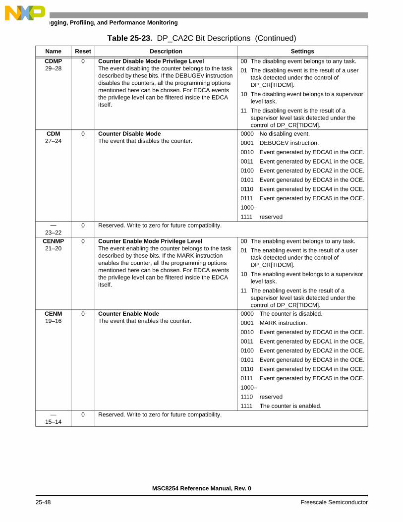
Debugging, Profiling, and Performance Monitoring
CDMP29–28
0 Counter Disable Mode Privilege LevelThe event disabling the counter belongs to the task described by these bits. If the DEBUGEV instruction disables the counters, all the programming options mentioned here can be chosen. For EDCA events the privilege level can be filtered inside the EDCA itself.
00 The disabling event belongs to any task.
01 The disabling event is the result of a user task detected under the control of DP_CR[TIDCM].
10 The disabling event belongs to a supervisor level task.
11 The disabling event is the result of a supervisor level task detected under the control of DP_CR[TIDCM].
CDM27–24
0 Counter Disable ModeThe event that disables the counter.
0000 No disabling event.
0001 DEBUGEV instruction.
0010 Event generated by EDCA0 in the OCE.
0011 Event generated by EDCA1 in the OCE.
0100 Event generated by EDCA2 in the OCE.
0101 Event generated by EDCA3 in the OCE.
0110 Event generated by EDCA4 in the OCE.
0111 Event generated by EDCA5 in the OCE.
1000–
1111 reserved—
23–220 Reserved. Write to zero for future compatibility.
CENMP21–20
0 Counter Enable Mode Privilege LevelThe event enabling the counter belongs to the task described by these bits. If the MARK instruction enables the counter, all the programming options mentioned here can be chosen. For EDCA events the privilege level can be filtered inside the EDCA itself.
00 The enabling event belongs to any task.
01 The enabling event is the result of a user task detected under the control of DP_CR[TIDCM].
10 The enabling event belongs to a supervisor level task.
11 The enabling event is the result of a supervisor level task detected under the control of DP_CR[TIDCM].
CENM19–16
0 Counter Enable ModeThe event that enables the counter.
0000 The counter is disabled.
0001 MARK instruction.
0010 Event generated by EDCA0 in the OCE.
0011 Event generated by EDCA1 in the OCE.
0100 Event generated by EDCA2 in the OCE.
0101 Event generated by EDCA3 in the OCE.
0110 Event generated by EDCA4 in the OCE.
0111 Event generated by EDCA5 in the OCE.
1000–
1110 reserved
1111 The counter is enabled.
—15–14
0 Reserved. Write to zero for future compatibility.
Table 25-23. DP_CA2C Bit Descriptions (Continued)
Name Reset Description Settings
MSC8254 Reference Manual, Rev. 0
25-48 Freescale Semiconductor

Debug and Profiling
CEP13–12
0 Counted Event Privilege LevelThe source counted by the counter belongs to the task described by these bits.
00 The counter counts events that belong to any task.
01 The counter only counts events belonging to user tasks detected under the control of DP_CR[TIDCM].
10 The counter counts event that belong to a supervisor level task.
11 The counter counts events belonging to supervisor level task detected under the control of DP_CR[TIDCM].
—11–9
0 Reserved. Write to zero for future compatibility.
CE8–4
0 Counted EventThe source counted by the counter.
00000 Clock cycles (non-debug)
00001 Application cycles (non-wait, non-stop, non-debug
00010 Number of events generated by the EDCA2 of the OCE (CEP bits can be 00 or 01)
00011 Number of task switches; includes the number of times the service of a task started including the first time (CEP bits must be 00).
00100–
11111 reserved—3
0 Reserved. Write to zero for future compatibility.
CMODE2–1
0 Counter ModeSpecifies the mode of the counter
00 One shot. The counter generates an event when it reaches 0, stops counting, and disables itself.
01 Trace mode. The counter value is saved in a shadow register whenever required by the trace buffer. The counter continues to count and generates an event when it reaches 0.
10 Extension mode. The counter rolls over when it reaches 0 and continues to count. Counter A1 can be programmed to count the number of overflows. In this case, counter A1 must operate in one-shot mode.
11 reserved.—0
0 Reserved. Write to zero for future compatibility.
Table 25-23. DP_CA2C Bit Descriptions (Continued)
Name Reset Description Settings
MSC8254 Reference Manual, Rev. 0
Freescale Semiconductor 25-49

Debugging, Profiling, and Performance Monitoring
25.2.12.13 DPU Counter A2 Value Registers (DP_CA2V)
DP_CA2V is a 32-bit register containing the specified counter value. Table 25-20 defines the counter bit fields.
25.2.12.14 DPU Counter B0 Control Register (DP_CB0C)
The DP_CB0C is a 32-bit register that controls the operation of the DPU Extension Support Counter B0, including what events and when they are counted. Table 25-27 defines the DP_CB0C bit fields.
DP_CA2V DPU Counter A2 Value Registers Offset 0x40
Bit 31 30 29 28 27 26 25 24 23 22 21 20 19 18 17 16
— CV
Type R/WReset 0 0 0 0 0 0 0 0 0 0 0 0 0 0 0 0
Bit 15 14 13 12 11 10 9 8 7 6 5 4 3 2 1 0
CV
Type R/WReset 0 0 0 0 0 0 0 0 0 0 0 0 0 0 0 0
Table 25-24. DP_CA2V Bit Descriptions
Name Reset Description Settings
—31
0 Reserved. Write to zero for future compatibility.
CV30–0
0 Counter ValueStores the value of the counter.
DP_CB0C DPU Counter B0 Control Register Offset 0x54
Bit 31 30 29 28 27 26 25 24 23 22 21 20 19 18 17 16
— CDMP CDM — CENMP CENM
Type R/WReset 0 0 0 0 0 0 0 0 0 0 0 0 0 0 0 0
Bit 15 14 13 12 11 10 9 8 7 6 5 4 3 2 1 0
— CEP — CE — CMODE —
Type R/WReset 0 0 0 0 0 0 0 0 0 0 0 0 0 0 0 0
Table 25-25. DP_CB0C Bit Descriptions
Name Reset Description Settings
—31–30
0 Reserved. Write to zero for future compatibility.
MSC8254 Reference Manual, Rev. 0
25-50 Freescale Semiconductor

Debug and Profiling
CDMP29–28
0 Counter Disable Mode Privilege LevelThe event disabling the counter belongs to the task described by these bits. If the DEBUGEV instruction disables the counters, all the programming options mentioned here can be chosen. For EDCA events the privilege level can be filtered inside the EDCA itself.
00 The disabling event belongs to any task.
01 The disabling event is the result of a user task detected under the control of DP_CR[TIDCM].
10 The disabling event belongs to a supervisor level task.
11 The disabling event is the result of a supervisor level task detected under the control of DP_CR[TIDCM].
CDM27–24
0 Counter Disable ModeThe event that disables the counter.
0000 No disabling event.
0001 DEBUGEV instruction.
0010 Event generated by EDCA0 in the OCE.
0011 Event generated by EDCA1 in the OCE.
0100 Event generated by EDCA2 in the OCE.
0101 Event generated by EDCA3 in the OCE.
0110 Event generated by EDCA4 in the OCE.
0111 Event generated by EDCA5 in the OCE.
1000–
1111 reserved—
23–220 Reserved. Write to zero for future compatibility.
CENMP21–20
0 Counter Enable Mode Privilege LevelThe event enabling the counter belongs to the task described by these bits. If the MARK instruction enables the counter, all the programming options mentioned here can be chosen. For EDCA events the privilege level can be filtered inside the EDCA itself.
00 The enabling event belongs to any task.
01 The enabling event is the result of a user task detected under the control of DP_CR[TIDCM].
10 The enabling event belongs to a supervisor level task.
11 The enabling event is the result of a supervisor level task detected under the control of DP_CR[TIDCM].
CENM19–16
0 Counter Enable ModeThe event that enables the counter.
0000 The counter is disabled.
0001 MARK instruction.
0010 Event generated by EDCA0 in the OCE.
0011 Event generated by EDCA1 in the OCE.
0100 Event generated by EDCA2 in the OCE.
0101 Event generated by EDCA3 in the OCE.
0110 Event generated by EDCA4 in the OCE.
0111 Event generated by EDCA5 in the OCE.
1000–
1110 reserved
1111 The counter is enabled.
—15–14
0 Reserved. Write to zero for future compatibility.
Table 25-25. DP_CB0C Bit Descriptions (Continued)
Name Reset Description Settings
MSC8254 Reference Manual, Rev. 0
Freescale Semiconductor 25-51

Debugging, Profiling, and Performance Monitoring
CEP13–12
0 Counted Event Privilege LevelThe source counted by the counter belongs to the task described by these bits.
00 The counter counts events that belong to any task.
01 The counter only counts events belonging to user tasks detected under the control of DP_CR[TIDCM].
10 The counter counts event that belong to a supervisor level task.
11 The counter counts events belonging to supervisor level task detected under the control of DP_CR[TIDCM].
—11–9
0 Reserved. Write to zero for future compatibility.
CE8–4
0 Counted EventThe source counted by the counter.
00000 Clock cycles (non-debug)
00001 Application cycles (non-wait, non-stop, non-debug
00010 Number of events generated by the EDCA3 of the OCE (CEP bits can be 00 or 01)
00011 Number of interrupts
00100 Number of ICache thrashes due to miss.
00101–
11111 reserved—3
0 Reserved. Write to zero for future compatibility.
CMODE2–1
0 Counter ModeSpecifies the mode of the counter
00 One shot. The counter generates an event when it reaches 0, stops counting, and disables itself.
01 Trace mode. The counter value is saved in a shadow register whenever required by the trace buffer. The counter continues to count and generates an event when it reaches 0.
10–
11 reserved.
—0
0 Reserved. Write to zero for future compatibility.
Table 25-25. DP_CB0C Bit Descriptions (Continued)
Name Reset Description Settings
MSC8254 Reference Manual, Rev. 0
25-52 Freescale Semiconductor

Debug and Profiling
25.2.12.15 DPU Counter B0 Value Registers (DP_CB0V)
DP_CB0V is a 32-bit register containing the specified counter value. Table 25-20 defines the counter bit fields.
25.2.12.16 DPU Counter B1 Control Register (DP_CB1C)
The DP_CB1C is a 32-bit register that controls the operation of the DPU Extension Support Counter B1, including what events and when they are counted. Table 25-27 defines the DP_CB1C bit fields.
DP_CB0V DPU Counter B0 Value Registers Offset 0x58
Bit 31 30 29 28 27 26 25 24 23 22 21 20 19 18 17 16
— CV
Type R/WReset 0 0 0 0 0 0 0 0 0 0 0 0 0 0 0 0
Bit 15 14 13 12 11 10 9 8 7 6 5 4 3 2 1 0
CV
Type R/WReset 0 0 0 0 0 0 0 0 0 0 0 0 0 0 0 0
Table 25-26. DP_CB0V Bit Descriptions
Name Reset Description Settings
—31
0 Reserved. Write to zero for future compatibility.
CV30–0
0 Counter ValueStores the value of the counter.
DP_CB1C DPU Counter B1 Control Register Offset 0x5C
Bit 31 30 29 28 27 26 25 24 23 22 21 20 19 18 17 16
— CDMP CDM — CENMP CENM
Type R/WReset 0 0 0 0 0 0 0 0 0 0 0 0 0 0 0 0
Bit 15 14 13 12 11 10 9 8 7 6 5 4 3 2 1 0
— CEP — CE — CMODE —
Type R/WReset 0 0 0 0 0 0 0 0 0 0 0 0 0 0 0 0
Table 25-27. DP_CB1C Bit Descriptions
Name Reset Description Settings
—31–30
0 Reserved. Write to zero for future compatibility.
MSC8254 Reference Manual, Rev. 0
Freescale Semiconductor 25-53

Debugging, Profiling, and Performance Monitoring
CDMP29–28
0 Counter Disable Mode Privilege LevelThe event disabling the counter belongs to the task described by these bits. If the DEBUGEV instruction disables the counters, all the programming options mentioned here can be chosen. For EDCA events the privilege level can be filtered inside the EDCA itself.
00 The disabling event belongs to any task.
01 The disabling event is the result of a user task detected under the control of DP_CR[TIDCM].
10 The disabling event belongs to a supervisor level task.
11 The disabling event is the result of a supervisor level task detected under the control of DP_CR[TIDCM].
CDM27–24
0 Counter Disable ModeThe event that disables the counter.
0000 No disabling event.
0001 DEBUGEV instruction.
0010 Event generated by EDCA0 in the OCE.
0011 Event generated by EDCA1 in the OCE.
0100 Event generated by EDCA2 in the OCE.
0101 Event generated by EDCA3 in the OCE.
0110 Event generated by EDCA4 in the OCE.
0111 Event generated by EDCA5 in the OCE.
1000–
1111 reserved—
23–220 Reserved. Write to zero for future compatibility.
CENMP21–20
0 Counter Enable Mode Privilege LevelThe event enabling the counter belongs to the task described by these bits. If the MARK instruction enables the counter, all the programming options mentioned here can be chosen. For EDCA events the privilege level can be filtered inside the EDCA itself.
00 The enabling event belongs to any task.
01 The enabling event is the result of a user task detected under the control of DP_CR[TIDCM].
10 The enabling event belongs to a supervisor level task.
11 The enabling event is the result of a supervisor level task detected under the control of DP_CR[TIDCM].
CENM19–16
0 Counter Enable ModeThe event that enables the counter.
0000 The counter is disabled.
0001 MARK instruction.
0010 Event generated by EDCA0 in the OCE.
0011 Event generated by EDCA1 in the OCE.
0100 Event generated by EDCA2 in the OCE.
0101 Event generated by EDCA3 in the OCE.
0110 Event generated by EDCA4 in the OCE.
0111 Event generated by EDCA5 in the OCE.
1000–
1110 reserved
1111 The counter is enabled.
—15–14
0 Reserved. Write to zero for future compatibility.
Table 25-27. DP_CB1C Bit Descriptions (Continued)
Name Reset Description Settings
MSC8254 Reference Manual, Rev. 0
25-54 Freescale Semiconductor

Debug and Profiling
CEP13–12
0 Counted Event Privilege LevelThe source counted by the counter belongs to the task described by these bits.
00 The counter counts events that belong to any task.
01 The counter only counts events belonging to user tasks detected under the control of DP_CR[TIDCM].
10 The counter counts event that belong to a supervisor level task.
11 The counter counts events belonging to supervisor level task detected under the control of DP_CR[TIDCM].
—11–9
0 Reserved. Write to zero for future compatibility.
CE8–4
0 Counted EventThe source counted by the counter.
00000 Clock cycles (non-debug)
00001 Application cycles (non-wait, non-stop, non-debug
00010 Number of events generated by the EDCA4 of the OCE (CEP bits can be 00 or 01)
00011 Number of rollovers by counter B2 (CEP bits must be 00).
00100 Number of DCache thrashes due to miss.
00101–
11111 reserved—3
0 Reserved. Write to zero for future compatibility.
CMODE2–1
0 Counter ModeSpecifies the mode of the counter
00 One shot. The counter generates an event when it reaches 0, stops counting, and disables itself.
01 Trace mode. The counter value is saved in a shadow register whenever required by the trace buffer. The counter continues to count and generates an event when it reaches 0.
10–
11 reserved.—0
0 Reserved. Write to zero for future compatibility.
Table 25-27. DP_CB1C Bit Descriptions (Continued)
Name Reset Description Settings
MSC8254 Reference Manual, Rev. 0
Freescale Semiconductor 25-55

Debugging, Profiling, and Performance Monitoring
25.2.12.17 DPU Counter B1 Value Registers (DP_CB1V)
DP_CB1V is a 32-bit register containing the specified counter value. Table 25-28 defines the counter bit fields.
25.2.12.18 DPU Counter B2 Control Register (DP_CB2C)
The DP_CB2C is a 32-bit register that controls the operation of the DPU Extension Support Counter B2, including what events and when they are counted. Table 25-29 defines the DP_CB2C bit fields.
DP_CB1V DPU Counter B1 Value Registers Offset 0x60
Bit 31 30 29 28 27 26 25 24 23 22 21 20 19 18 17 16
— CV
Type R/WReset 0 0 0 0 0 0 0 0 0 0 0 0 0 0 0 0
Bit 15 14 13 12 11 10 9 8 7 6 5 4 3 2 1 0
CV
Type R/WReset 0 0 0 0 0 0 0 0 0 0 0 0 0 0 0 0
Table 25-28. DP_CB1V Bit Descriptions
Name Reset Description Settings
—31
0 Reserved. Write to zero for future compatibility.
CV30–0
0 Counter ValueStores the value of the counter.
DP_CB2C DPU Counter B2 Control Register Offset 0x64
Bit 31 30 29 28 27 26 25 24 23 22 21 20 19 18 17 16
— CDMP CDM — CENMP CENM
Type R/WReset 0 0 0 0 0 0 0 0 0 0 0 0 0 0 0 0
Bit 15 14 13 12 11 10 9 8 7 6 5 4 3 2 1 0
— CEP — CE — CMODE —
Type R/WReset 0 0 0 0 0 0 0 0 0 0 0 0 0 0 0 0
Table 25-29. DP_CB2C Bit Descriptions
Name Reset Description Settings
—31–30
0 Reserved. Write to zero for future compatibility.
MSC8254 Reference Manual, Rev. 0
25-56 Freescale Semiconductor

Debug and Profiling
CDMP29–28
0 Counter Disable Mode Privilege LevelThe event disabling the counter belongs to the task described by these bits. If the DEBUGEV instruction disables the counters, all the programming options mentioned here can be chosen. For EDCA events the privilege level can be filtered inside the EDCA itself.
00 The disabling event belongs to any task.
01 The disabling event is the result of a user task detected under the control of DP_CR[TIDCM].
10 The disabling event belongs to a supervisor level task.
11 The disabling event is the result of a supervisor level task detected under the control of DP_CR[TIDCM].
CDM27–24
0 Counter Disable ModeThe event that disables the counter.
0000 No disabling event.
0001 DEBUGEV instruction.
0010 Event generated by EDCA0 in the OCE.
0011 Event generated by EDCA1 in the OCE.
0100 Event generated by EDCA2 in the OCE.
0101 Event generated by EDCA3 in the OCE.
0110 Event generated by EDCA4 in the OCE.
0111 Event generated by EDCA5 in the OCE.
1000–
1111 reserved—
23–220 Reserved. Write to zero for future compatibility.
CENMP21–20
0 Counter Enable Mode Privilege LevelThe event enabling the counter belongs to the task described by these bits. If the MARK instruction enables the counter, all the programming options mentioned here can be chosen. For EDCA events the privilege level can be filtered inside the EDCA itself.
00 The enabling event belongs to any task.
01 The enabling event is the result of a user task detected under the control of DP_CR[TIDCM].
10 The enabling event belongs to a supervisor level task.
11 The enabling event is the result of a supervisor level task detected under the control of DP_CR[TIDCM].
CENM19–16
0 Counter Enable ModeThe event that enables the counter.
0000 The counter is disabled.
0001 MARK instruction.
0010 Event generated by EDCA0 in the OCE.
0011 Event generated by EDCA1 in the OCE.
0100 Event generated by EDCA2 in the OCE.
0101 Event generated by EDCA3 in the OCE.
0110 Event generated by EDCA4 in the OCE.
0111 Event generated by EDCA5 in the OCE.
1000–
1110 reserved
1111 The counter is enabled.
—15–14
0 Reserved. Write to zero for future compatibility.
Table 25-29. DP_CB2C Bit Descriptions (Continued)
Name Reset Description Settings
MSC8254 Reference Manual, Rev. 0
Freescale Semiconductor 25-57

Debugging, Profiling, and Performance Monitoring
CEP13–12
0 Counted Event Privilege LevelThe source counted by the counter belongs to the task described by these bits.
00 The counter counts events that belong to any task.
01 The counter only counts events belonging to user tasks detected under the control of DP_CR[TIDCM].
10 The counter counts event that belong to a supervisor level task.
11 The counter counts events belonging to supervisor level task detected under the control of DP_CR[TIDCM].
—11–9
0 Reserved. Write to zero for future compatibility.
CE8–4
0 Counted EventThe source counted by the counter.
00000 Clock cycles (non-debug)
00001 Application cycles (non-wait, non-stop, non-debug
00010 Number of events generated by the EDCA5 of the OCE (CEP bits can be 00 or 01)
00011 Number of task switches; includes the number of times the service of a task started including the first time (CEP bits must be 00).
00100–
11111 reserved—3
0 Reserved. Write to zero for future compatibility.
CMODE2–1
0 Counter ModeSpecifies the mode of the counter
00 One shot. The counter generates an event when it reaches 0, stops counting, and disables itself.
01 Trace mode. The counter value is saved in a shadow register whenever required by the trace buffer. The counter continues to count and generates an event when it reaches 0.
10 Extension mode. The counter rolls over when it reaches 0 and continues to count. Counter B1 can be programmed to count the number of overflows. In this case, counter B1 must operate in one-shot mode.
11 reserved.—0
0 Reserved. Write to zero for future compatibility.
Table 25-29. DP_CB2C Bit Descriptions (Continued)
Name Reset Description Settings
MSC8254 Reference Manual, Rev. 0
25-58 Freescale Semiconductor

Debug and Profiling
25.2.12.19 DPU Counter B2 Value Registers (DP_CB2V)
DP_CB2V is a 32-bit registers containing the specified counter value. Table 25-30 defines the counter bit fields.
25.2.12.20 DPU Trace Control Register (DP_TC)
The DP_TC is a 32-bit register responsible that controls the VTB memory. Table 25-31 defines the DP_TC bit fields.
DP_CB2V DPU Counter B2 Value Registers Offset 0x68
Bit 31 30 29 28 27 26 25 24 23 22 21 20 19 18 17 16
— CV
Type R/WReset 0 0 0 0 0 0 0 0 0 0 0 0 0 0 0 0
Bit 15 14 13 12 11 10 9 8 7 6 5 4 3 2 1 0
CV
Type R/WReset 0 0 0 0 0 0 0 0 0 0 0 0 0 0 0 0
Table 25-30. DP_CA[0–2]V and DP_CB[0–2]V Bit Descriptions
Name Reset Description Settings
—31
0 Reserved. Write to zero for future compatibility.
CV30–0
0 Counter ValueStores the value of the counter.
DP_TC DPU Trace Control Register Offset 0x7C
Bit 31 30 29 28 27 26 25 24 23 22 21 20 19 18 17 16
— SHARE — CSS — PRIV GLOBAL BURST_SIZE
Type R/WReset 0 0 0 0 0 0 0 0 0 0 0 0 0 0 0 0
Bit 15 14 13 12 11 10 9 8 7 6 5 4 3 2 1 0
— TMPDIS — VTBWM — SAMPLE — TMODE EN
Type R/WReset 0 0 0 0 0 0 0 0 0 0 0 0 0 0 0 0
Table 25-31. DP_TC Bit Descriptions
Name Reset Description Settings
—31–27
0 Reserved. Write to zero for future compatibility.
MSC8254 Reference Manual, Rev. 0
Freescale Semiconductor 25-59
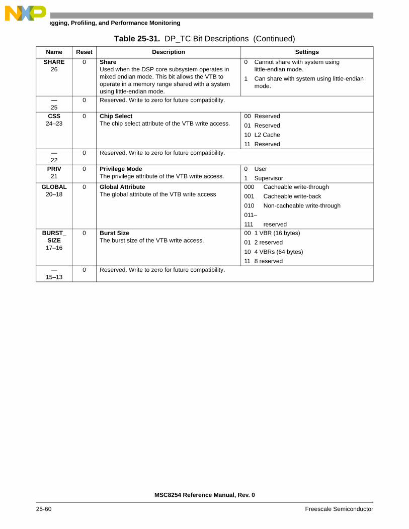
Debugging, Profiling, and Performance Monitoring
SHARE26
0 ShareUsed when the DSP core subsystem operates in mixed endian mode. This bit allows the VTB to operate in a memory range shared with a system using little-endian mode.
0 Cannot share with system using little-endian mode.
1 Can share with system using little-endian mode.
—25
0 Reserved. Write to zero for future compatibility.
CSS24–23
0 Chip SelectThe chip select attribute of the VTB write access.
00 Reserved
01 Reserved
10 L2 Cache
11 Reserved—22
0 Reserved. Write to zero for future compatibility.
PRIV21
0 Privilege ModeThe privilege attribute of the VTB write access.
0 User
1 SupervisorGLOBAL
20–180 Global Attribute
The global attribute of the VTB write access000 Cacheable write-through
001 Cacheable write-back
010 Non-cacheable write-through
011–
111 reservedBURST_
SIZE17–16
0 Burst SizeThe burst size of the VTB write access.
00 1 VBR (16 bytes)
01 2 reserved
10 4 VBRs (64 bytes)
11 8 reserved
—15–13
0 Reserved. Write to zero for future compatibility.
Table 25-31. DP_TC Bit Descriptions (Continued)
Name Reset Description Settings
MSC8254 Reference Manual, Rev. 0
25-60 Freescale Semiconductor

Debug and Profiling
TMPDIS12
0 Temporary DisableTo verify that all traced information arrived at the VTB, a flush can be generated that is similar to the flush generated when tracing is disabled. The only difference is that when tracing is disabled by setting the TMPDIS bit, when tracing is re -enabled by resetting this bit, the value of the Start Address is not sampled at the TB Write Pointer. The TB Write Pointer saves its previous value, thereby enabling tracing to be continued from the point where it was interrupted. If the tracing is enabled, TMPDIS bit must not be changed in debug mode by Core Command. The TMPDIS bit must not be set together with the EN bit. When the tracing is disabled by resetting the EN bit, the TMPDIS bit should not be set. When the TMPDIS bit is set, its resetting should not be done in the 16 VLES after the setting. Before the tracing is disabled by setting TMPDIS bit, the user has to wait until the TWB finishes the previous flush that can be initiated by a previous trace disabling or by entering wait or stop states. (Bit TWBA in the DP_SR register indicates if the TWB is in the middle of a flush operation.) In order not to lose information, serving an interrupt between the checking of the TWBA bit and the disabling should be avoided. (It can be done by disabling the interrupts before the checking of the TWBA bit and enabling them after the disabling.) When the TMPDIS bit is set, the trace logic disregards further inputs.
0 Trace logic enabled
1 Trace logic disabled
—11–10
0 Reserved. Write to zero for future compatibility.
VTBWM9–8
0 Virtual Trace Buffer Write ModeSpecifies the manner in which the VTB is written.
00 Overwrite mode. The DPU writes all the time. After writing to the End Address, the write pointer wraps to the first address and starts to overwrite the first entries. When disabled, it contains the last the entries leading to the disable point. (The TBF bit in the DP_MR register shows that the VTB was full at least once.)
01 One address mode. The DPU always writes to the same address (described by the Start Address).
10 Trace event request mode. When the write access is generated to the address equal to the value in the Trace Event Request, then depending on the programming of the DETB bit in the DP_CR register, either an interrupt to the EPIC or a debug request to the core (to the OCE) is generated. The debug request to the core may become an internal debug exception according to the programming of the OCE.
11 reserved—7
0 Reserved. Write to zero for future compatibility.
Table 25-31. DP_TC Bit Descriptions (Continued)
Name Reset Description Settings
MSC8254 Reference Manual, Rev. 0
Freescale Semiconductor 25-61

Debugging, Profiling, and Performance Monitoring
SAMPLE6
0 SampleA bit that can only be set. When set, the counter values are sampled to the trace buffer. This bit is only relevant when the TMODE bits are 0100. This bit is cleared by the DPU after writing the information to the trace buffer.
0 No action
1 Counter values are added to the trace buffer.
—5
0 Reserved. Write to zero for future compatibility.
TMODE4–1
0 Trace ModeIdentifies the source that is written to the trace buffer.
0000 Information generated by the OCE. Data compression is off.
0001 Information generated by the OCE after compression and adding task ID flags.
0010 Depending on the OCE programming, the data transferred at a task switch is either the first and last PC of the tasks together with a task flag and all six counter values; or, for a jump to a subroutine, a jump to an interrupt routine, or a return from either, the task ID and the values of all six counters.
0011 reserved
0100 When the SAMPLE bit in the Trace Buffer Control register is set by software at specified points during the application execution, the task ID and all six counters.
1010 The value written to the Trace Buffer Data register every time a new value is written.
0110 The task ID and the value of all six counters when EDCA5 generates an event that belongs to the task described by the task ID comparator. When the task is a user task, the task ID comparator must be programmed accordingly by the TIDCM bits in the DP_CR register. When the task is a supervisor level task or any task, the TIDCM bits in the DP_CR register must be 00.
0111–
1000 reserved
Table 25-31. DP_TC Bit Descriptions (Continued)
Name Reset Description Settings
MSC8254 Reference Manual, Rev. 0
25-62 Freescale Semiconductor

Debug and Profiling
25.2.12.21 DPU VTB Start Address Register (DP_TSA)
The DP_TSA is a 32-bit register that contains the start address of the VTB (physical address). The VTB can be located only in Bank 3 (between addresses 0x00000000–0xFF000000). Alignment depends on the burst size:
For a burst size of 1 VBR, TER must be aligned to the value: 32 × Burst Size (programmed in the DP_TC register).
For a burst size of 4 VBRs, the value of TER can be 32 × (2 × n – 1), where n is a positive integer.
Note: Bits 4–0 must be written as zeros and are read as zeros.
Table 25-33 defines the DP_TSA bit fields.
EN0
0 EnableThis bit is used to enable/disable the trace buffer. Use the following guidelines to enable/disable the trace buffer:• Always wait until any current flush operations are
completed before disabling a trace operation. Poll the DP_SR[TWBA] bit to determine the flush status.
• To prevent any interrupt servicing that may occur between reading the DP_SR[TWBA] bit and disabling the trace buffer, always disable the interrupts before reading the DP_SR[TWBA] bit and enable them only after disabling the trace buffer.
• Never change the configuration of a trace operation during execution. Always disable the trace buffer first and then change the configuration.
0 Trace buffer disabled.
1 Trace buffer enabled
DP_TSA DPU VTB Start Address Register Offset 0x80
Bit 31 30 29 28 27 26 25 24 23 22 21 20 19 18 17 16
SA
Type R/WReset 0 0 0 0 0 0 0 0 0 0 0 0 0 0 0 0
Bit 15 14 13 12 11 10 9 8 7 6 5 4 3 2 1 0
SA —
Type R/WReset 0 0 0 0 0 0 0 0 0 0 0 0 0 0 0 0
Table 25-31. DP_TC Bit Descriptions (Continued)
Name Reset Description Settings
MSC8254 Reference Manual, Rev. 0
Freescale Semiconductor 25-63

Debugging, Profiling, and Performance Monitoring
25.2.12.22 DPU VTB End Address Register (DP_TEA)
The DP_TEA is a 32-bit register that contains the end address of the VTB (physical address). The VTB can be located only in Bank 3 (between addresses 0x00000000–0xFF000000). Alignment depends on the burst size:
For a burst size of 1 VBR, TER must be aligned to the value: 32 × Burst Size (programmed in the DP_TC register).
For a burst size of 4 VBRs, the value of TER can be 32 × (2 × n – 1), where n is a positive integer.
Note: Bits 4–0 must be written as zeros and are read as zeros.
Table 25-33 defines the DP_TEA bit fields.
Table 25-32. DP_TSA Bit Descriptions
Name Reset Description Settings
SA31–5
0 Start AddressSpecifies the end address of the VTB address range.
—4–0
0 Reserved. Write to zero for future compatibility.
DP_TEA DPU VTB End Address Register Offset 0x84
Bit 31 30 29 28 27 26 25 24 23 22 21 20 19 18 17 16
EA
Type R/WReset 0 0 0 0 0 0 0 0 0 0 0 0 0 0 0 0
Bit 15 14 13 12 11 10 9 8 7 6 5 4 3 2 1 0
EA —
Type R/WReset 0 0 0 0 0 0 0 0 0 0 0 0 0 0 0 0
Table 25-33. DP_TEA Bit Descriptions
Name Reset Description Settings
EA31–5
0 End AddressSpecifies the end address of the VTB address range.
—4–0
0 Reserved. Write to zero for future compatibility.
MSC8254 Reference Manual, Rev. 0
25-64 Freescale Semiconductor

Debug and Profiling
25.2.12.23 DPU Trace Event Request Register (DP_TER)
The DP_TER is a 32-bit register that is used when the VTB is written in Trace Event Request mode (programmed in the DP_TC[TMODE] field). The DP_TER register contains the address within the range of the VTB where an interrupt or debug request should be generated (depending on the programming of the DETB bit in the DP_CR register). Alignment depends on the burst size:
For a burst size of 1 VBR, TER must be aligned to the value: 32 × Burst Size (programmed in the DP_TC register).
For a burst size of 4 VBRs, the value of TER can be 32 × (2 × n – 1), where n is a positive integer.
Note: Bits 4–0 must be written as zeros and are read as zeros.
Table 25-36 defines the DP_TER bit fields.
DP_TER DPU Trace Event Request Register Offset 0x88
Bit 31 30 29 28 27 26 25 24 23 22 21 20 19 18 17 16
TER
Type R/WReset 0 0 0 0 0 0 0 0 0 0 0 0 0 0 0 0
Bit 15 14 13 12 11 10 9 8 7 6 5 4 3 2 1 0
TER —
Type R/WReset 0 0 0 0 0 0 0 0 0 0 0 0 0 0 0 0
Table 25-34. DP_TER Bit Descriptions
Name Reset Description Settings
TER31–5
0 Trace Event RequestSpecifies the address within the VTB address range where the interrupt or debug request is generated.
—4–0
0 Reserved. Write to zero for future compatibility.
MSC8254 Reference Manual, Rev. 0
Freescale Semiconductor 25-65

Debugging, Profiling, and Performance Monitoring
25.2.12.24 DPU Trace Write Pointer Register (DP_TW)
The DP_TW is a 32-bit register that contains the pointer to the location in the VTB where the last entry was written by the DPU. When tracing is enabled (by setting the DP_TC[EN] bit), the value of the VTB Start Address register is sampled to it. When tracing is re-enabled (by resetting the DP_TC[TMPDIS] bit), the value of the TB Write Pointer does not change. If it is written by the user, its value must be aligned to the value “32 × Burst Size” programmed in the DP_TC register.
Note: Before changing the value of the DP_TW register, you must generate a flush by setting the DP_TC[TMPDIS] bit.
Table 25-36 defines the DP_TW bit fields.
DP_TW DPU Trace Write Pointer Register Offset 0x8C
Bit 31 30 29 28 27 26 25 24 23 22 21 20 19 18 17 16
WP
Type R/WReset 0 0 0 0 0 0 0 0 0 0 0 0 0 0 0 0
Bit 15 14 13 12 11 10 9 8 7 6 5 4 3 2 1 0
WP —
Type R/WReset 0 0 0 0 0 0 0 0 0 0 0 0 0 0 0 0
Table 25-35. DP_TW Bit Descriptions
Name Reset Description Settings
WP31–5
0 Write PointerStores the pointer to the last entry written by the DPU to the VTB.
—4–0
0 Reserved. Write to zero for future compatibility.
MSC8254 Reference Manual, Rev. 0
25-66 Freescale Semiconductor

Performance Monitor
25.2.12.25 DPU Trace Data Register (DP_TD)
The DP_TD is a 32-bit register containing the value to be written to the TB. This value is only relevant when the MODE bits in the DP_TC register are 1010.
Table 25-36 defines the DP_TD bit fields.
25.3 Performance Monitor
The MSC8254 includes a performance monitor facility that can be used to monitor and record selected behaviors of the integrated device. Section 25.3.1.5 briefly describes the events that can be monitored. Refer to the individual module chapters for a better understanding of these events. Performance monitor up-counters (PMC0–PMC8) count events selected by the performance monitor local control registers. PMC0 is a 64-bit up-counter specifically designated to count cycles. PMC1–PMC8 are 32-bit counters that can monitor 64 specific events in addition to counting 64 reference events. Each counter is associated with two local control registers (A and B) that configure the events counted. In addition, there is a global control register that can be used to enable/disable all the counters at one time.
The benefits of an internal performance monitor are numerous, and include the following:
Because some systems or software environments are not easily characterized by signal traces or benchmarks, the performance monitor can be used to understand the MSC8254 device behavior in any system or software environment.
The performance monitor facility can be used to aid system developers when bringing up and debugging systems.
DP_TD DPU Trace Data Register Offset 0x90
Bit 31 30 29 28 27 26 25 24 23 22 21 20 19 18 17 16
TBD
Type R/WReset 0 0 0 0 0 0 0 0 0 0 0 0 0 0 0 0
Bit 15 14 13 12 11 10 9 8 7 6 5 4 3 2 1 0
TBD
Type R/WReset 0 0 0 0 0 0 0 0 0 0 0 0 0 0 0 0
Table 25-36. DP_TD Bit Descriptions
Name Reset Description Settings
TBD31–0
0 Trace Buffer DataStores the data to write to the Trace Buffer.
MSC8254 Reference Manual, Rev. 0
Freescale Semiconductor 25-67

Debugging, Profiling, and Performance Monitoring
System performance can be increased by monitoring memory hierarchy behavior. This can help to optimize algorithms used to schedule or partition tasks and to refine the data structures and distribution used by each task.
Figure 25-15 is a high-level block diagram of the performance monitor. The module consists of a global control register (PMGC), one 64-bit counter (PMC0), eight 32-bit counters, and two control registers per counter. The global control register PMGC affects all counters and takes priority over local control registers. The local control registers are divided into two groups, as follows:
Local control A registers control counter freezing, overflow condition enable, and event selection. Local control register PMLCA0, which controls counter PMC0, does not contain event selection because PMC0 counts only cycles.
Local control B registers contain the counters’ threshold values. Local control register PMLCB0 is not used.
Performance monitor events are signalled by the functional blocks in the integrated device and are selectively recorded in the PMCs. Sixty-four of these events are referred to as reference events, which can be counted on any of the eight counters. Counter-specific events can be counted only on the counter for which the event is defined.
Figure 25-15. Performance Monitor Block Diagram
Counters
Global Control Register
PMGC
PMLCA3 PMLCB3PMLCA2 PMLCB2PMLCA1 PMLCB1PMLCA0 —
PMC1PMC2PMC3...
Control Logic
Counters and Registers
Performance Monitor
Event 1
Event 2
Event 8
Event 3
Event 4
...
Event Signals
Interrupt (int)
Read Data
Output Signals
PMC8
PMLCA8 PMLCB8
Event 0
PMC0 (upper) PMC0 (lower)
32-bit
Local Control Registers
......
MSC8254 Reference Manual, Rev. 0
25-68 Freescale Semiconductor

Performance Monitor
The performance monitor can generate an interrupt on overflow. Several control registers specify how a performance monitor interrupt is signalled. The PMCs can also be programmed to freeze when an interrupt is generated.
25.3.1 Functional Description
The MSC8254 performance monitor offers a rich set of features that permits a complete performance characterization of the implementation. These features include:
One 64-bit counter exclusively dedicated to counting cycles.Eight 32-bit counters that count the occurrence of selected events.One global control register (all counters) and two local control registers per counter. Counts up to 64 reference events on any of the eight 32-bit counters.Ability to count up to 512 counter-specific events.chaining capability. Quantity threshold counting.
Ability to generate an interrupt on overflow.
The performance monitor does not drive any signals externally, but it does assert the internal interrupt signal when a monitored event or other interrupt condition occurs.
25.3.1.1 Performance Monitor Interrupts
The PMCs can generate an interrupt on an overflow when the msb of a counter changes from 0 to 1. For the interrupt to be signalled, the condition enable bit (PMLCAn[CE]) and performance monitor interrupt enable bit (PMGC[PMIE]) must be set. When an interrupt is signalled and the freeze-counters-on-enabled-condition-or-event bit (PMGC[FCECE]) is set, PMGC[FAC] is set by hardware and all of the registers are frozen. Software can clear the interrupt condition by resetting the performance monitor and clearing the most significant bit of the counter that generated the overflow.
25.3.1.2 Event Counting
Using the control registers described in Section 25.3.2, the nine PMCs can count the occurrences of specific events. The 64-bit PMC0 is design to count only clock cycles. However, to provide flexibility, a total of 64 reference events can be counted on any of the 32-bit PMCs (PMC1–PMC8). Additionally, up to 64 unique events can be counted on each 32-bit counter. The performance monitor must be reset before event counting sequences. The performance monitor can be reset by first freezing one or more counters and then clearing the freeze condition to allow the counters to count according to the settings in the performance monitor registers. Counters can be frozen individually by setting PMLCAn[FC] bits, or simultaneously by setting PMGC[FAC]. Simply clearing these freeze bits will then allow the performance monitor to begin counting based on the register settings.
MSC8254 Reference Manual, Rev. 0
Freescale Semiconductor 25-69

Debugging, Profiling, and Performance Monitoring
Note: Using PMLCAn[FC] resets only the specified counter. Performance monitor registers can be configured through reads or writes while the counters are frozen as long as freeze bits are not cleared by the register accesses.
25.3.1.3 Threshold Events
The quantity threshold event sequences the performance monitor counter is only incremented when the specified threshold event exceeds the threshold value. Threshold event is generally used to monitor the usage of buffers and queues. For example, the usage of a specific queue can be characterized by measuring the amount of time the queue is completely full or partially full. For this example the threshold field would be used to specify how many entries are required to be valid in the queue for that event to be counted.A timing diagram for quantity threshold event counting is shown in Figure 25-16.
25.3.1.4 Chaining
By configuring one counter to increment each time another counter overflows, several counters can be chained together to provide event counts larger than 32 bits. Each counter in a chain adds 32 bits to the maximum count. The register chaining sequence is not arbitrary and is specified indirectly by selecting the register overflow event to be counted. Selecting an event has the effect of selecting a source register because all available chaining events, as shown in Table 25-37, are dedicated to specific registers.
Note: The chaining overflow event occurs when the counter reaches its maximum value and wraps, not when the register msb is set. For this overflow to occur, PMLCAn[CE] should be cleared to avoid signalling an interrupt when the counter most significant bit
Figure 25-16. Quantity Threshold Event Sequence Timing Diagram
1 2 3 4 5 6 7 8 9 10 11 12
2
2PMLCBn[THRESHOLD]
thresh_value
0 1 2 3 4 5 6
0_entries_in_queue
1_entry_in_queue
2_entries_in_queue
3_entries_in_queue
4_entries_in_queue
counter_increment
perfmon_counter
Note: For this example a threshold value of two indicates the user wishes to count the number of cycles. There are at least two valid entries in a particular queue.
MSC8254 Reference Manual, Rev. 0
25-70 Freescale Semiconductor

Performance Monitor
is set. Several cycles may be required for the chained counters to reflect the true count because of the internal delay between when an overflow occurs and a counter increments.
25.3.1.5 Performance Monitor Events
Table 25-37 lists performance monitor events specified in PMLCA[1–8]. The event assignment column indicates the event type and number, using the following formats:
Ref:#—Reference events are shared across counters PMC1–PMC8. The number indicates the event. For example, Ref:6 means that PMC1–PMC8 share reference event 6.
C[0–8]:#—Counter-specific events. C8 indicates an event assigned to PMC8. Thus C8:62 means PMC8 is assigned event 62 (RapidIO DMA1 Channel 2 Write DW).
Note: With counter-specific events, an offset of 64 must be used when programming the field, because counter-specific events occupy the bottom 64 values of the 7-bit event field where events are numbered. For example, to specify counter-specific event 0, the event field must be programmed to 64.
Counter events not specified in Table 25-37 are reserved.
Note: The DMA event frequency is different from the PM frequency. Therefore, these events pass through a synchronizer before entering the PM.
Table 25-37. Performance Monitor Events Performance
Event Counted Number Description of Event Counted
General Events
Nothing Ref:0 Register counter holds current value
System cycles C0 CCB HSSI clock cycles
System DMA Events
MSC8254 Reference Manual, Rev. 0
Freescale Semiconductor 25-71

Debugging, Profiling, and Performance Monitoring
Asserted for every cycle DMA specific channel is active C5:3 This event counts the number of cycles a specific DMA channel is active. It is insufficient to enable the C5:3 event. Three additional parameters must be defined in the DMA:• en_profiling. Enables/disables DMA
profiling.− 0 = Disable DMA profiling− 1 = Enable DMA profiling
• channel_number. Selects the DMA channel to profile.− 000000–001111 = Channel number− 01xxxx = Reserved− 10xxxx = Reserved
• dest_ch_profiler. Specifies whether to profile the source or destination requests.− 0 = Source− 1 = Destination
For detaila about DMA profiling, see Section 14.5, Profiling, on page 14-23.
RapidIO RMU EVENTS
Packet received of any priority C1:5
Packet received of priority 0 C2:5
Packet received of priority 1 C3:5
Packet received of priority 2 C4:5
Packet received of priority 3 C5:5
Clock cycle occurred in which the inbound buffer is full to any priority. Event asserted for as many clock cycles as this is true.
C1:46
Clock cycle occurred in which the inbound buffer is full to priority 0. Event asserted for as many clock cycles as this is true.
C2:46
Clock cycle occurred in which the inbound buffer is full to priority 1. Event asserted for as many clock cycles as this is true.
C3:46
Clock cycle occurred in which the inbound buffer is full to priority 2. Event asserted for as many clock cycles as this is true.
C4:46
Clock cycle occurred in which the inbound buffer is full to priority 3. Event asserted for as many clock cycles as this is true.
C5:46
Table 25-37. Performance Monitor Events Performance
Event Counted Number Description of Event Counted
MSC8254 Reference Manual, Rev. 0
25-72 Freescale Semiconductor

Performance Monitor
SRIO0 Events
A received packet has been sent to OCN for passthrough C2:2
Packet sent to RapidIO C4:2
Packet was retried C6:2
Packet was reordered
C8:2 Packet was reordered on Outbound. After an outbound request is retried, the Serial RapidIO controller preferentially tries to send the oldest next higher priority packet.
Packet sent to RapidIO of priority 0 C5:8
Packet sent to RapidIO of priority 1 C6:8
Packet sent to RapidIO of priority 2 C7:8
Packet sent to RapidIO of priority 3 C8:8
Clock cycle occurred in which the outbound buffer is full to any priority. Event asserted for as many clock cycles as this is true.
C4:15 Outbound logical buffer in the Serial RapidIO controller.
Clock cycle occurred in which the outbound buffer is full to priority 0. Event asserted for as many clock cycles as this is true.
C5:15
Clock cycle occurred in which the outbound buffer is full to priority 1. Event asserted for as many clock cycles as this is true.
C6:15
Clock cycle occurred in which the outbound buffer is full to priority 2. Event asserted for as many clock cycles as this is true.
C7:15
Clock cycle occurred in which the outbound buffer is full to priority 3. Event asserted for as many clock cycles as this is true.
C8:15
Packet accepted on RapidIO C5:2
Packet accepted from RapidIO of priority 0 C6:9
Packet accepted from RapidIO of priority 1 C7:9
Packet accepted from RapidIO of priority 2 C8:9
Packet accepted from RapidIO of priority 3 C1:9
Packet retry occurred due to inbound buffer limitations for any priority
C7:2
Packet retry occurred due to inbound buffer limitations, priority 0 C8:60
Packet retry occurred due to inbound buffer limitations, priority 1 C1:60
Packet retry occurred due to inbound buffer limitations, priority 2 C2:60
Packet retry occurred due to inbound buffer limitations, priority 3 C3:60
Clock cycle occurred in which the inbound buffer is full to any priority. Event asserted for as many clock cycles as this is true.
C2:13
Clock cycle occurred in which the inbound buffer is full to priority 0. Event asserted for as many clock cycles as this is true.
C3:13
Table 25-37. Performance Monitor Events Performance
Event Counted Number Description of Event Counted
MSC8254 Reference Manual, Rev. 0
Freescale Semiconductor 25-73

Debugging, Profiling, and Performance Monitoring
Clock cycle occurred in which the inbound buffer is full to priority 1. Event asserted for as many clock cycles as this is true.
C4:13
Clock cycle occurred in which the inbound buffer is full to priority 2. Event asserted for as many clock cycles as this is true.
C5:13
Clock cycle occurred in which the inbound buffer is full to priority 3. Event asserted for as many clock cycles as this is true.
C6:13
RapidIO DMA0 Events
DMA Channel 0 Read request C1:0 OCNDMA data read only.
DMA Channel 1 Read request C2:0 OCNDMA data read only.
DMA Channel 2 Read request C3:0 OCNDMA data read only.
DMA Channel 3 Read request C4:0 OCNDMA data read only.
DMA Channel 0 Write request C6:53 OCNDMA write.
DMA Channel 1 Write request C7:53 OCNDMA write.
DMA Channel 2 Write request C8:53 OCNDMA write.
DMA Channel 3 Write request C5:53 OCNDMA write.
DMA Channel 0 Descriptor request C7:54
DMA Channel 1 Descriptor request C8:54
DMA Channel 2 Descriptor request C5:54
DMA Channel 3 Descriptor request C6:54
Channel 0 Read DW C8:61 OCNDMA descriptor read only. DW = 8 bytes
Channel 1 Read DW C5:61 OCNDMA descriptor read only. DW = 8 bytes
Channel 2 Read DW C6:61 OCNDMA descriptor read only. DW = 8 bytes
Channel 3 Read DW C7:61 OCNDMA descriptor read only. DW = 8 bytes
Channel 0 Write DW C2:62 OCNDMA descriptor write DW = 8 bytes
Channel 1 Write DW C3:62 OCNDMA descriptor write DW = 8 bytes
Channel 2 Write DW C4:62 OCNDMA descriptor write DW = 8 bytes
Channel 3 Write DW C1:62 OCNDMA descriptor write DW = 8 bytes
SRIO1 Events
A received packet has been sent to OCN for passthrough C3:1
Packet sent to RapidIO C7:1
Packet was retried C4:1
Table 25-37. Performance Monitor Events Performance
Event Counted Number Description of Event Counted
MSC8254 Reference Manual, Rev. 0
25-74 Freescale Semiconductor

Performance Monitor
Packet was reordered
C1:1 Packet was reordered Outbound. After an outbound request gets retried, the Serial RapidIO controller preferentially tries to send the oldest next higher priority packet.
Packet sent to RapidIO of priority 0 C8:11
Packet sent to RapidIO of priority 1 C1:11
Packet sent to RapidIO of priority 2 C2:11
Packet sent to RapidIO of priority 3 C3:11
Clock cycle occurred in which the outbound buffer is full to any priority. Event asserted for as many clock cycles as this is true.
C5:16 Outbound logical buffer in the Serial RapidIO controller.
Clock cycle occurred in which the outbound buffer is full to priority 0. Event asserted for as many clock cycles as this is true.
C6:16
Clock cycle occurred in which the outbound buffer is full to priority 1. Event asserted for as many clock cycles as this is true.
C7:16
Clock cycle occurred in which the outbound buffer is full to priority 2. Event asserted for as many clock cycles as this is true.
C8:16
Clock cycle occurred in which the outbound buffer is full to priority 3. Event asserted for as many clock cycles as this is true.
C1:16
Packet accepted on RapidIO C8:1
Packet accepted from RapidIO of priority 0 C1:12
Packet accepted from RapidIO of priority 1 C2:12
Packet accepted from RapidIO of priority 2 C3:12
Packet accepted from RapidIO of priority 3 C4:12
Packet retry occurred due to inbound buffer limitations for any priority
C5:1
Packet retry occurred due to inbound buffer limitations, priority 0 C6:59
Packet retry occurred due to inbound buffer limitations, priority 1 C7:59
Packet retry occurred due to inbound buffer limitations, priority 2 C8:59
Packet retry occurred due to inbound buffer limitations, priority 3 C1:59
Clock cycle occurred in which the inbound buffer is full to any priority. Event asserted for as many clock cycles as this is true.
C3:14
Clock cycle occurred in which the inbound buffer is full to priority 0. Event asserted for as many clock cycles as this is true.
C4:14
Clock cycle occurred in which the inbound buffer is full to priority 1. Event asserted for as many clock cycles as this is true.
C5:14
Clock cycle occurred in which the inbound buffer is full to priority 2. Event asserted for as many clock cycles as this is true.
C6:14
Table 25-37. Performance Monitor Events Performance
Event Counted Number Description of Event Counted
MSC8254 Reference Manual, Rev. 0
Freescale Semiconductor 25-75

Debugging, Profiling, and Performance Monitoring
Clock cycle occurred in which the inbound buffer is full to priority 3. Event asserted for as many clock cycles as this is true.
C7:14
RapidIO DMA1 Events
DMA Channel 0 Read request C5:0 OCNDMA data read only.
DMA Channel 1 Read request C6:0 OCNDMA data read only.
DMA Channel 2 Read request C7:0 OCNDMA data read only.
DMA Channel 3 Read request C8:0 OCNDMA data read only.
DMA Channel 0 Write request C2:53 OCNDMA write.
DMA Channel 1 Write request C3:53 OCNDMA write.
DMA Channel 2 Write request C4:53 OCNDMA write.
DMA Channel 3 Write request C1:53 OCNDMA write.
DMA Channel 0 descriptor request C3:54
DMA Channel 1 descriptor request C4:54
DMA Channel 2 descriptor request C1:54
DMA Channel 3 descriptor request C2:54
Channel 0 Read DW C4:61 OCNDMA descriptor read only. DW = 8 bytes
Channel 1 Read DW C1:61 OCNDMA descriptor read only. DW = 8 bytes
Channel 2 Read DW C2:61 OCNDMA descriptor read only. DW = 8 bytes
Channel 3 Read DW C3:61 OCNDMA descriptor read only. DW = 8 bytes
Channel 0 Write DW C6:62 OCNDMA descriptor write DW = 8 bytes
Channel 1 Write DW C7:62 OCNDMA descriptor write DW = 8 bytes
Channel 2 Write DW C8:62 OCNDMA descriptor write DW = 8 bytes
Channel 3 Write DW C5:62 OCNDMA descriptor write DW = 8 bytes
PCI Express Events
PM inbound OCN read request. Indicates that the bridge has request an OCN read.
C1:32
PM inbound OCN write request. Indicates that the bridge has request an OCN write.
C2:32
PM inbound OCN data valid. Indicates that the bridge has valid data to send. This is true for write.
C5:30
PM outbound OCN read request. When asserted indicates that the bridge has received an OCN read packet.
C8:32
Table 25-37. Performance Monitor Events Performance
Event Counted Number Description of Event Counted
MSC8254 Reference Manual, Rev. 0
25-76 Freescale Semiconductor

Performance Monitor
25.3.1.6 Performance Monitor Examples
Table 25-39 contains sample register settings for the three supported modes.
Simple event performance monitoring example
Threshold event performance monitoring example
The settings in Table 25-38 are identical for all three examples.
For simple event counting, a non-threshold event is selected in PMLCAn[EVENT] and all other features are disabled by clearing all register fields except for CE.
PM outbound OCN write request. When asserted indicates that the bridge has received an OCN write packet.
C3:31
PM outbound OCN data valid. When asserted indicates that the bridge has received OCN write data.
C4:31
Chaining Events
PMC0 carry-out Ref:1 PMC0[63] 1-to-0 transitions.
PMC1 carry-out Ref:2 PMC1[63] 1-to-0 transitions. Reserved for PMC1.
PMC2 carry-out Ref:3 PMC2[63] 1-to-0 transitions. Reserved for PMC2.
PMC3 carry-out Ref:4 PMC3[63] 1-to-0 transitions. Reserved for PMC3.
PMC4 carry-out Ref:5 PMC4[63] 1-to-0 transitions. Reserved for PMC4.
PMC5 carry-out Ref:6 PMC5[63] 1-to-0 transitions. Reserved for PMC5.
PMC6 carry-out Ref:7 PMC6[63] 1-to-0 transitions. Reserved for PMC6.
PMC7 carry-out Ref:8 PMC7[63] 1-to-0 transitions. Reserved for PMC7.
PMC8 carry-out Ref:9 PMC8[63] 1-to-0 transitions. Reserved for PMC8.
Table 25-38. PMGC and PMLCAn Settings
Field Setting Reason
PMGC[FAC] 0 Counters must not be frozen.
PMGC[PMIE] 1 Performance monitor interrupts are enabled
PMGC[FCECE] 1 Counters should be frozen when an interrupt is signalled.
PMLCAn[FC] 0 Counters cannot be frozen for counting.
PMLCAn[CE] 1 Overflow condition enable is required to allow interrupt signalling.
Table 25-37. Performance Monitor Events Performance
Event Counted Number Description of Event Counted
MSC8254 Reference Manual, Rev. 0
Freescale Semiconductor 25-77

Debugging, Profiling, and Performance Monitoring
For threshold counting, a threshold event must be specified in PMLCAn[EVENT] and threshold value in PMLCBn[THRESHOLD].
The performance monitor must be reset before event counting sequences. The performance monitor can be reset by first freezing one or more counters and then clearing the freeze condition to allow the counters to count according to the settings in the performance monitor registers. Counters can be frozen individually by setting PMLCAn[FC] bits, or simultaneously by setting PMGC[FAC]. Simply clearing these freeze bits will then allow the performance monitor to begin counting based on the register settings.
Note that using PMLCAn[FC] to reset the performance monitor resets only the specified counter. Performance monitor registers can be configured through reads or writes while the counters are frozen as long as freeze bits are not cleared by the register accesses.
Table 25-39. Register Settings for Counting Examples
Register Register Field Simple Event Threshold
PMGC FAC 0 0
PMIE 1 1
FCECE 1 1
PMLCAn FC 0 0
CE 1 1
EVENT 121 33
PMLCBn TRIGONSEL 0 0
TRIGOFFSEL 0 0
TRIGONCNTL 0 0
TRIGOFFCNTL 0 0
THRESHOLD 0 3
MSC8254 Reference Manual, Rev. 0
25-78 Freescale Semiconductor

Performance Monitor
25.3.2 Performance Monitor Programming Model
The performance monitor system includes the following registers:
Performance Monitor Global Control Register (PMGC), see page 25-80.
Performance Monitor Local Control Register A0 (PMLCA0), see page 25-81.
Performance Monitor Local Control Register A[1–8] (PMLCA[1–8]), see page 25-82.
Performance Monitor Local Control Register B[1–8] (PMLCB[1–8]), see page 25-83.
Performance Monitor Counter 0 (PMC0), see page 25-84.
Performance Monitor Counter 1–8 (PMC[1–8]), see page 25-85.
Note: Because accessing a PMC manually has priority over counter incrementation by the counted event, reading or writing a PMC while it is counting may affect the count. Likewise, accessing a performance monitor control register while its target counter is counting may also affect the count.
Note: The Performance Monitor block uses the base address: 0xFFFBB800.
MSC8254 Reference Manual, Rev. 0
Freescale Semiconductor 25-79

Debugging, Profiling, and Performance Monitoring
25.3.2.1 Performance Monitor Global Control Register (PMGC)
PMGC globally configures the PMC operation. Table 25-40 defines the PMGC bit fields.
PMGC Performance Monitor Global Control Register Offset 0x00
Bit 31 30 29 28 27 26 25 24 23 22 21 20 19 18 17 16
FAC PMIE FCECE —
Type R/WReset 0 0 0 0 0 0 0 0 0 0 0 0 0 0 0 0
Bit 15 14 13 12 11 10 9 8 7 6 5 4 3 2 1 0
—
Type R/WReset 0 0 0 0 0 0 0 0 0 0 0 0 0 0 0 0
Table 25-40. PMGC Bit Descriptions
Name Reset Description Settings
FAC31
0 Freeze All CountersEnables or freezes all counters. This bit is set by hardware when a performance monitor interrupt occurs and the FCECE bit is set.
0 PMCs increment if permitted by other control bits
1 PMCs do not increment.
PMIE30
0 Performance Monitor Interrupt EnableEnables/disables the performance monitor interrupt. When enabled, the interrupt is asserted when a PMC overflows.
0 Interrupts disabled.
1 Interrupts enabled.
FCECE29
0 Freeze Counters on Enabled Condition or EventDetermines whether a PMC can continue increment if permitted by other control bits, or freezes when an enabled condition or event occurs.
0 PMCs increment.
1 PMCs freeze when the enabled condition or event occurs.
—28–0
0 Reserved. Write to zero for future compatibility.
MSC8254 Reference Manual, Rev. 0
25-80 Freescale Semiconductor

Performance Monitor
25.3.2.2 Performance Monitor Local Control A0 Register (PMLCA0)
PMLCA0 configures the PMC0 operation. Table 25-41 defines the PMLCA0 bit fields.
PMLCA0 Performance Monitor Local Control A0 Offset 0x10
Bit 31 30 29 28 27 26 25 24 23 22 21 20 19 18 17 16
FC — CE —
Type R/WReset 0 0 0 0 0 0 0 0 0 0 0 0 0 0 0 0
Bit 15 14 13 12 11 10 9 8 7 6 5 4 3 2 1 0
—
Type R/WReset 0 0 0 0 0 0 0 0 0 0 0 0 0 0 0 0
Table 25-41. PMLCA0 Bit Descriptions
Name Reset Description Settings
FC31
0 Freeze Counter 0Enables or freezes PMC0.
0 PMC0 increments if permitted by other control bits.
1 PMC0 disabled and does not increment.
—30–27
0 Reserved. Write to zero for future compatibility.
CE26
0 Condition EnableControls the counter 0 overflow condition. This bit should be cleared when PMC0 is selected for chaining.An overflow condition occurs when PMC0[msb] is set
0 Overflow cannot occur. PMC0 cannot cause interrupts or freeze counters.
1 Overflow conditions are enabled and can generate interrupts and freeze counters.
—25–0
0 Reserved. Write to zero for future compatibility.
MSC8254 Reference Manual, Rev. 0
Freescale Semiconductor 25-81

Debugging, Profiling, and Performance Monitoring
25.3.2.3 Performance Monitor Local Control A[1–8] (PMLCA[1–8])
PMLCA[1–8], along with PMLCB[1–8], configure the respective PMC[1–8] operation. Table 25-42 defines the PMLCA[1–8] bit fields.
PMLCA[1–8] Performance Monitor Local Control A[1–8] Offset 0x10 + n*0x10
Bit 31 30 29 28 27 26 25 24 23 22 21 20 19 18 17 16
FC — CE — EVENT
Type R/WReset 0 0 0 0 0 0 0 0 0 0 0 0 0 0 0 0
Bit 15 14 13 12 11 10 9 8 7 6 5 4 3 2 1 0
—
Type R/WReset 0 0 0 0 0 0 0 0 0 0 0 0 0 0 0 0
Table 25-42. PMLCA[1–8] Bit Descriptions
Name Reset Description Settings
FC31
0 Freeze CounterEnables or freezes PMCn.
0 PMCn increments if permitted by other control bits.
1 PMCn disabled and does not increment.
—30–27
0 Reserved. Write to zero for future compatibility.
CE26
0 Condition EnableControls the counter n overflow condition. This bit should be cleared when PMCn is selected for chaining.Note: An overflow condition occurs when PMCn[msb] is set.
0 Overflow cannot occur. PMCn cannot cause interrupts or freeze counters.
1 Overflow conditions are enabled and can generate interrupts and freeze counters.
—25–23
0 Reserved. Write to zero for future compatibility.
EVENT22–16
0 Event SelectorSelects the event to count.
Bit 22 is always set (1). This is because of the required offset of 64. See the first note in Section 25.3.1.5.
The definitions for Bits [21:16] values 0x00 to 0x3F are Event Numbers defined in Table 25-37.
—15–0
0 Reserved. Write to zero for future compatibility.
MSC8254 Reference Manual, Rev. 0
25-82 Freescale Semiconductor

Performance Monitor
25.3.2.4 Performance Monitor Local Control B[1–8] (PMLCB[1–8])
PMLCB[1–8], along with PMLCA[1–8], configure the respective PMC[1–8] operation. Table 25-43 defines the PMLCB[1–8] bit fields.
PMLCB[1–8] Performance Monitor Local Control B[1–8] Offset 0x14 + n*0x10
Bit 31 30 29 28 27 26 25 24 23 22 21 20 19 18 17 16
—
Type R/WReset 0 0 0 0 0 0 0 0 0 0 0 0 0 0 0 0
Bit 15 14 13 12 11 10 9 8 7 6 5 4 3 2 1 0
— THRESHOLD
Type R/WReset 0 0 0 0 0 0 0 0 0 0 0 0 0 0 0 0
Table 25-43. PMLCB[1–8] Bit Descriptions
Name Reset Description Settings
—31–6
0 Reserved. Write to zero for future compatibility.
THRESHOLD5–0
0 ThresholdSets the counting threshold level. Only event with a number of occurrence greater than this number are counted.
MSC8254 Reference Manual, Rev. 0
Freescale Semiconductor 25-83

Debugging, Profiling, and Performance Monitoring
25.3.2.5 Performance Monitor Counter 0 (PMC0)
PMC0 is only used to count clock cycles for events specified by PMLCA0. Table 25-44 defines the PMC0 bit fields.
PMC0 Performance Monitor Counter 0 Offset 0x18
Bit 63 62 61 60 59 58 57 56 55 54 53 52 51 50 49 48
PMC0
Type R/WReset 0 0 0 0 0 0 0 0 0 0 0 0 0 0 0 0
Bit 47 46 45 44 43 42 41 40 39 38 37 36 35 34 33 32
PMC0
Type R/WReset 0 0 0 0 0 0 0 0 0 0 0 0 0 0 0 0
Bit 31 30 29 28 27 26 25 24 23 22 21 20 19 18 17 16
PMC0
Type R/WReset 0 0 0 0 0 0 0 0 0 0 0 0 0 0 0 0
Bit 15 14 13 12 11 10 9 8 7 6 5 4 3 2 1 0
PMC0
Type R/WReset 0 0 0 0 0 0 0 0 0 0 0 0 0 0 0 0
Table 25-44. PMC0 Bit Descriptions
Name Reset Description Settings
PMC063–0
0 Performance Monitor Counter 0Contains the current PMC0 count.
MSC8254 Reference Manual, Rev. 0
25-84 Freescale Semiconductor
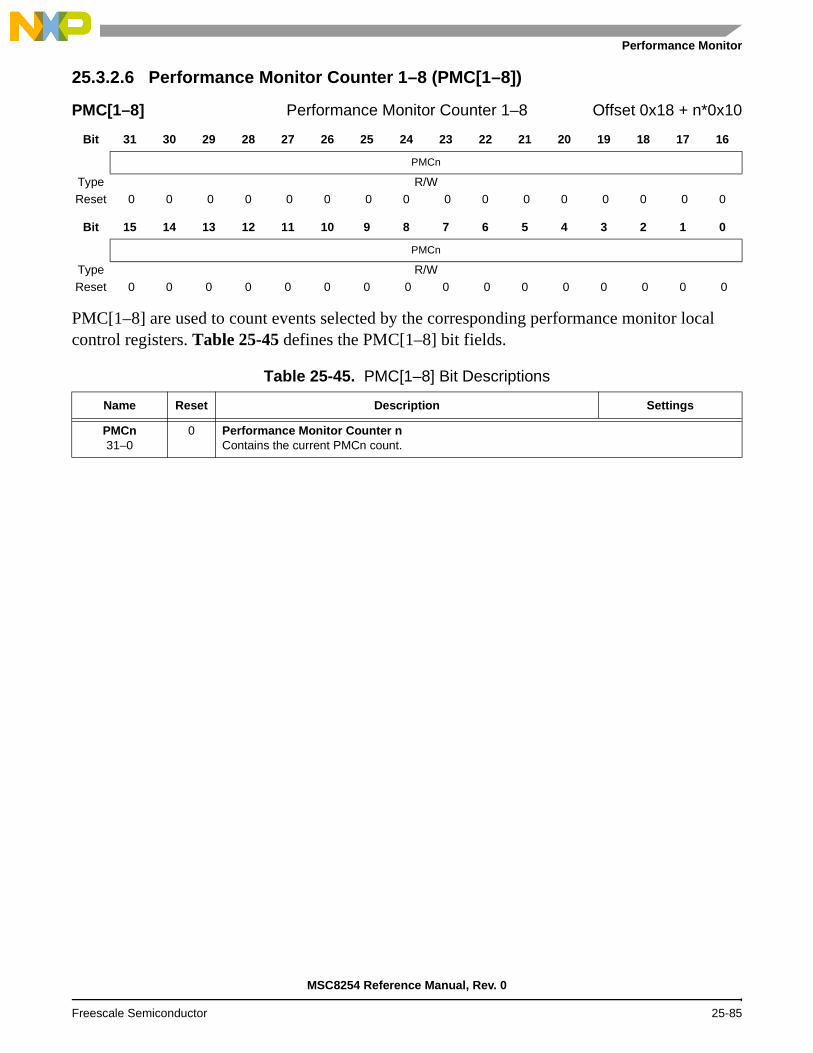
Performance Monitor
25.3.2.6 Performance Monitor Counter 1–8 (PMC[1–8])
PMC[1–8] are used to count events selected by the corresponding performance monitor local control registers. Table 25-45 defines the PMC[1–8] bit fields.
PMC[1–8] Performance Monitor Counter 1–8 Offset 0x18 + n*0x10
Bit 31 30 29 28 27 26 25 24 23 22 21 20 19 18 17 16
PMCn
Type R/WReset 0 0 0 0 0 0 0 0 0 0 0 0 0 0 0 0
Bit 15 14 13 12 11 10 9 8 7 6 5 4 3 2 1 0
PMCn
Type R/WReset 0 0 0 0 0 0 0 0 0 0 0 0 0 0 0 0
Table 25-45. PMC[1–8] Bit Descriptions
Name Reset Description Settings
PMCn31–0
0 Performance Monitor Counter nContains the current PMCn count.
MSC8254 Reference Manual, Rev. 0
Freescale Semiconductor 25-85

Debugging, Profiling, and Performance Monitoring
MSC8254 Reference Manual, Rev. 0
25-86 Freescale Semiconductor