LPC553x data sheet - NXP
161
1. General description The LPC553x is an ARM Cortex-M33 based microcontroller for embedded applications. These devices include up to 256 KB on-chip flash, up to 128 KB of on-chip SRAM, FlexSPI with cache, USB Full-Speed device with crystal-less operation, USB Full-Speed Host, CAN FD, five general-purpose timers, one SCTimer/PWM, one RTC/alarm timer, one 24-bit Multi-Rate Timer (MRT), a Windowed Watchdog Timer (WWDT), Code Watchdog Timer, one OS Timer, one Micro-tick timer, eight flexible serial communication peripherals (Flexcomm Interfaces - which can be configured as a USART, SPI, high speed SPI, I2C, or I2S interface), one DMIC, one I3C interface, four 16-bit 2.0 Msamples/sec (four 12-bit 3.2 Msamples/sec) ADC capable of four simultaneous conversions, four comparators, two temperature sensors, three 12-bit 1 Msample/sec DAC, 3 OpAmps, two FlexPWM timers, and two QEIs. 2. Features and benefits ARM Cortex-M33 core (r0p4): Running at a frequency of up to 150 MHz. Integrated digital signal processing (DSP) instructions. Floating Point Unit (FPU) and Memory Protection Unit (MPU). ARM Cortex M33 built-in Nested Vectored Interrupt Controller (NVIC). Non-maskable Interrupt (NMI) input with a selection of sources. Serial Wire Debug with eight breakpoints and four watch points. Includes Serial Wire Output for enhanced debug capabilities and trace (ETM). System tick timer. A hardware DSP accelerator for fixed and floating point DSP functions (PowerQuad). PowerQuad uses a bank of four dedicated 4 KB SRAMs On-chip memory: Up to 256 KB on-chip flash program memory, with flash accelerator and 512 byte page erase and write, coupled with 8 KB Low Power Cache to enhance system performance. Up to 128 KB total SRAM consisting of 16 KB SRAM on Code Bus, 112 KB SRAM on System Bus (112 KB is contiguous). Parity support on all RAM banks except RAM1 bank. ECC support available only on RAM1 bank. OTP eFuse programmable memory. LPC553x 32-bit Arm Cortex ® -M33, 128 KB SRAM; 256 KB flash, FlexSPI with cache, USB FS, Flexcomm Interface, CAN FD, 32-bit counter/ timers, SCTimer/PWM, 16-bit 2.0 Msamples/sec ADC, Comparator, 12-bit DAC, OpAmp, FlexPWM Timer, QEI, Temperature Sensor, CRC Rev. 1.0 — 04/2022 Product data sheet
-
Upload
khangminh22 -
Category
Documents
-
view
1 -
download
0
Transcript of LPC553x data sheet - NXP

1. General description
The LPC553x is an ARM Cortex-M33 based microcontroller for embedded applications. These devices include up to 256 KB on-chip flash, up to 128 KB of on-chip SRAM, FlexSPI with cache, USB Full-Speed device with crystal-less operation, USB Full-Speed Host, CAN FD, five general-purpose timers, one SCTimer/PWM, one RTC/alarm timer, one 24-bit Multi-Rate Timer (MRT), a Windowed Watchdog Timer (WWDT), Code Watchdog Timer, one OS Timer, one Micro-tick timer, eight flexible serial communication peripherals (Flexcomm Interfaces - which can be configured as a USART, SPI, high speed SPI, I2C, or I2S interface), one DMIC, one I3C interface, four 16-bit 2.0 Msamples/sec (four 12-bit 3.2 Msamples/sec) ADC capable of four simultaneous conversions, four comparators, two temperature sensors, three 12-bit 1 Msample/sec DAC, 3 OpAmps, two FlexPWM timers, and two QEIs.
2. Features and benefits
ARM Cortex-M33 core (r0p4):
Running at a frequency of up to 150 MHz.
Integrated digital signal processing (DSP) instructions.
Floating Point Unit (FPU) and Memory Protection Unit (MPU).
ARM Cortex M33 built-in Nested Vectored Interrupt Controller (NVIC).
Non-maskable Interrupt (NMI) input with a selection of sources.
Serial Wire Debug with eight breakpoints and four watch points. Includes Serial Wire Output for enhanced debug capabilities and trace (ETM).
System tick timer.
A hardware DSP accelerator for fixed and floating point DSP functions (PowerQuad). PowerQuad uses a bank of four dedicated 4 KB SRAMs
On-chip memory:
Up to 256 KB on-chip flash program memory, with flash accelerator and 512 byte page erase and write, coupled with 8 KB Low Power Cache to enhance system performance.
Up to 128 KB total SRAM consisting of 16 KB SRAM on Code Bus, 112 KB SRAM on System Bus (112 KB is contiguous).
Parity support on all RAM banks except RAM1 bank. ECC support available only on RAM1 bank.
OTP eFuse programmable memory.
LPC553x32-bit Arm Cortex®-M33, 128 KB SRAM; 256 KB flash, FlexSPI with cache, USB FS, Flexcomm Interface, CAN FD, 32-bit counter/ timers, SCTimer/PWM, 16-bit 2.0 Msamples/sec ADC, Comparator, 12-bit DAC, OpAmp, FlexPWM Timer, QEI, Temperature Sensor, CRCRev. 1.0 — 04/2022 Product data sheet

NXP Semiconductors LPC553x32-bit ARM Cortex-M33 microcontroller
On-chip ROM bootloader supports:
Booting of images from on-chip flash and external flash.
CRC32 image integrity checking.
Flash programming through In System Programming (ISP) commands over following interfaces: USB0 interfaces using HID Class device, UART interface (Flexcomm 0) with auto baud, High-Speed SPI slave interfaces (Flexcomm 8) using mode 3 (CPOL = 1 and CPHA = 1), I2C slave interface (Flexcomm 1), and CAN-FD ISP.
ROM API functions:Flash programming API and OTP eFuse programming API.
Dual images (boot latest version) from on-chip flash using re-map feature.
Loading image to RAM from external Octal/QuadSPI device.
Booting Execute-in-Place (XIP) images present on Octal/QuadSPI devices.
Dual Execute-in-Place (XIP) images in Octal/QuadSPI flash through flash address remap feature.
Load-to-RAM boot mode from 1-bit SPI flash devices connected to Flexcomm (selectable by PFR) as normal boot option and recovery boot option.
USB Device DFU Connection (Device only).
Code Read protection (CRP) on non-secure devices.
Crystal-less USB ISP Device mode.
Serial interfaces:
Flexcomm Interface contains up to eight serial peripherals (Flexcomm Interface 0-7). Each Flexcomm Interface can be selected by software to be a USART, SPI, I2C, and I2S interface. Each Flexcomm Interface includes a FIFO that supports USART, SPI, and I2S. A variety of clocking options are available to each Flexcomm Interface, including a shared fractional baud-rate generator, and time-out feature.Flexcomm interfaces 0 to 5 each provide one channel pair of I2S and Flexcomm interfaces 6 to 7 each provide four channel pairs of I2S.
I2C-bus interfaces support Fast-mode and Fast-mode Plus with data rates of up to 1Mbit/s and with multiple address recognition and monitor mode. Two sets of true I2C pads also support high-speed Mode (3.4 Mbit/s) as a slave.
High Speed SPI (Flexcomm 8, 50MHz for both master and slave).
A digital microphone interface supporting up to two channels with associated decimators and Voice Activation Detect. One pair of channels can be streamed directly to I2S. The DMIC supports DMA.
One I3C bus interface.
One CAN FD module with dedicated DMA controller.
USB 2.0 full speed host/device controller with on-chip PHY and dedicated DMA controller supporting crystal-less operation in device mode using software library example in Application Note (AN13527, LPC55S3x/LPC553x Crystal-Less USB Solution).
Digital peripherals:
DMA0 controller with 52 channels and up to 53 programmable triggers, able to access all memories and DMA-capable peripherals.
DMA1 controller with 16 channels and up to 25 programmable triggers, able to access all memories and DMA-capable peripherals.
LPC553x All information provided in this document is subject to legal disclaimers. © NXP Semiconductors B.V. 2022. All rights reserved.
Product data sheet Rev. 1.0 — 04/2022 2 of 158

NXP Semiconductors LPC553x32-bit ARM Cortex-M33 microcontroller
CRC engine block can calculate a CRC on supplied data using one of three standard polynomials with DMA support. Supports programmable CRC polynomial.
Up to 66 General-Purpose Input/Output (GPIO) pins.
GPIO registers are located on the AHB for fast access. The DMA supports GPIO ports.
Up to eight GPIOs can be selected as pin interrupts (PINT), triggered by rising,
falling or both input edges.
A group of up to 8 GPIO pins can be selected for boolean pattern matching, which can generate interrupts and/or drive a pattern-match output.
Two GPIO grouped interrupts (GINT) enable an interrupt based on a logical
(AND/OR) combination of input states.
I/O pin configuration with support for up to 16 signal options.
FlexSPI flash interface for external flash with 8 KB cache for execute-in-place and supports DMA. The FlexSPI includes 1 port: high speed
channel A which supports quad or octal operation. Support dual image via address remapping.
Two AOI (AND/OR/Invert) combinatorial logic modules with dedicated set of input and output signals. Each AOI has 4 outputs that feed to different peripheral muxes to individual peripherals.
128 bit unique device serial number for identification (UUID).
Timers:
Five 32-bit standard general purpose asynchronous timers/counters, which support up to four capture inputs and four compare outputs, PWM mode, and external count input. Specific timer events can be selected to generate DMA requests.
One SCTimer/PWM with 8 input and 10 output functions (16 capture and match registers). Inputs and outputs can be routed to or from external pins and internally to or from selected peripherals. Internally, the SCTimer/PWM supports 16 captures/matches, 16 events, 32 states, and a Dither engine for improved average resolution of pulse edges.
32-bit Real-time clock (RTC) with calendar feature and 1 s resolution running in the always-on power domain. Another timer in the RTC can be used for wake-up from all low power modes including deep power-down, with 1 ms resolution. The RTC is clocked by the 32 kHz FRO or 32.768 kHz external crystal.
Multiple-channel multi-rate 24-bit timer (MRT) for repetitive interrupt generation at up to four programmable, fixed rates.
Windowed Watchdog Timer (WWDT) with FRO 1 MHz as clock source.
The Micro-Tick Timer running from the watchdog oscillator can be used to wake-up the device from sleep and deep-sleep modes. Includes 4 capture registers with pin inputs.
42-bit free running OS Timer as continuous time-base for the system, available in any reduced power modes. It has a selectable clock source. When a 32 kHz clock is selected, allows a count period of more than 4 years.
Motor Control Subsystem: 2x FlexPWM with 4 sub-modules, providing 24 PWM outputs (it supports two 3-phase motors), and 2 Quadrature Encoder/Decoder (QEI).
Analog peripherals:
LPC553x All information provided in this document is subject to legal disclaimers. © NXP Semiconductors B.V. 2022. All rights reserved.
Product data sheet Rev. 1.0 — 04/2022 3 of 158

NXP Semiconductors LPC553x32-bit ARM Cortex-M33 microcontroller
Four single-ended 16-bit or two differential input ADCs (selectable) with sample rate of 2.0 Msamples/sec in 16-bit mode and 3.2 Msamples/sec in 12-bit mode. Eight differential channel pairs, (or 16 single-ended channels), with multiple internal and external trigger inputs. The ADC supports four simultaneous conversions, under the control of two independent sequences.
Integrated temperature sensor connected to both ADCs.
One comparator in always-on domain with up to four input pins and internal reference voltage. Can be used as a wake-up source from low power modes.
Three High Speed Comparators with up to five input pins and internal reference voltage.
Three 12-bit DACs with sample rates of up to 1.0 MSample/sec.
Three OpAmps with programmable VREF.
Clock generation:
Internal Free Running Oscillator (FRO). This oscillator provides a selectable 96 MHz output, and a 12 MHz output (divided down from the selected higher frequency) that can be used as a system clock. The FRO is trimmed to +/- 1% accuracy over the entire voltage and 0 C to 85 C. The FRO is trimmed to +/- 2% accuracy over the entire voltage and -40 C to 105 C.
32 kHz Internal Free Running Oscillator FRO. The FRO is trimmed to +/- 2% accuracy over the entire voltage and temperature range.
Internal low power oscillator (FRO 1 MHz) trimmed to +/- 15% accuracy over the entire voltage and temperature range.
Crystal oscillator with an operating frequency of 12 MHz to 32 MHz. Option for external clock input (bypass mode) for clock frequencies of up to 25 MHz.
Crystal oscillator with 32.768 kHz operating frequency.
PLL0 and PLL1 allows CPU operation up to the maximum CPU rate without the need for a high-frequency external clock. PLL0 and PLL1 can run from the internal FRO 12 MHz output, the external oscillator, internal FRO 1 MHz output, or the 32.768 kHz RTC oscillator.
Clock output function with divider to monitor internal clocks.
Frequency measurement unit for measuring the frequency of any on-chip or off-chip clock signal.
Each crystal oscillator has one embedded capacitor bank, where each can be used as an integrated load capacitor for the crystal oscillators. Using APIs, the capacitor banks on each crystal pin can tune the frequency for crystals with a Capacitive Load (CL) leading to conserving board space and reducing costs.
Power-saving modes and wake-up:
Integrated PMU (Power Management Unit) to minimize power consumption.
Low power modes: Sleep, Deep-sleep with RAM retention, power-down with RAM retention and CPU retention, and deep power-down with RAM retention.
Configurable wake-up options from peripherals interrupts.
The Micro-Tick Timer running from the watchdog oscillator can be used to wake-up the device from sleep and deep-sleep modes.
The Real-Time Clock (RTC) running from the 32.768 kHz clock can be used to wake-up the device from sleep, deep-sleep, power-down, and deep power-down modes.
Power-On Reset (POR) (trip low-level of 0.705 V and trip high-level of 0.87 V).
LPC553x All information provided in this document is subject to legal disclaimers. © NXP Semiconductors B.V. 2022. All rights reserved.
Product data sheet Rev. 1.0 — 04/2022 4 of 158

NXP Semiconductors LPC553x32-bit ARM Cortex-M33 microcontroller
Brown-Out Detectors (BOD) for external VDD_MAIN and internal VDD_CORE with separate thresholds for forced reset.
Operating from internal DC-DC converter or selectable LDO such that DC-DC converter can be bypassed.
On-chip LDO core 1.8 V to 3.6 V.
DC-DC power supply 1.8 V to 3.6 V.
Two Main IO supplies (VDDIO_1: 1.8 V to 3.6 V, VDDIO_2: 1.08 v to 3.6 V).
Separate VBAT supply 1.71 V to 3.6 V.
JTAG boundary scan supported.
Operating temperature range 40 °C to +105 °C.
Available in HLQFP100, HTQFP64, and HVQFN48 packages.
LPC553x All information provided in this document is subject to legal disclaimers. © NXP Semiconductors B.V. 2022. All rights reserved.
Product data sheet Rev. 1.0 — 04/2022 5 of 158

NXP Semiconductors LPC553x32-bit ARM Cortex-M33 microcontroller
3. Ordering information
[1] E = Single TrayK = Multi Trays (5 +1 cover tray)MP = Tape & Reel
3.1 Ordering options
The last18 Remark: The last 18 pages (10 KB) are reserved on the 256 KB flash devices resulting in 246 KB internal flash memory.
Table 1. Ordering information
Type number Part Order Number[1] Package
Name Description Version
LPC5536JBD100 LPC5536JBD100ELPC5536JBD100KLPC5536JBD100MP
HLQFP100 plastic low profile quad flat package; 100 leads; body 14 14 0.5mm pitch
SOT1570-3
LPC5536JBD64 LPC5536JBD64ELPC5536JBD64KLPC5536JBD64MP
HTQFP64 plastic low profile quad flat package; 64 leads; body 10 10 0.5mm pitch
SOT 855-5
LPC5534JBD100 LPC5534JBD100ELPC5534JBD100KLPC5534JBD100MP
HLQFP100 plastic low profile quad flat package; 100 leads; body 14 14 0.5mm pitch
SOT1570-3
LPC5534JBD64 LPC5534JBD64ELPC5534JBD64KLPC5534JBD64MP
HTQFP64 plastic low profile quad flat package; 64 leads; body 10 10 0.5mm pitch
SOT 855-5
LPC5534JHI48 LPC5534JHI48/00ELPC5534JHI48/00KLPC5534JHI48/00MP
HVQFN48 plastic thermal enhanced very thin quad flat package; no leads; 48 terminals; body 7 x7 x 0.85 mm
SOT619-1
LPC5536JHI48 LPC5536JHI48/00ELPC5536JHI48/00KLPC5536JHI48/00MP
HVQFN48 plastic thermal enhanced very thin quad flat package; no leads; 48 terminals; body 7 x7 x 0.85 mm
SOT619-1
Table 2. Ordering options
Type number
Fla
sh
/KB
Tota
l SR
AM
/KB
CA
N F
D
US
B
GP
IO
Fle
x S
PI
AD
C C
han
nel
s
DA
C O
utp
uts
Inte
rnal
DA
C
Co
mp
arat
or
Tam
per
Pin
s
OP
Am
p
CR
P1/
2/3
DM
IC
LPC5536JBD100 256 128 y FS 66 y 23 2 1 4 4 3 y y
LPC5536JBD64 256 128 y - 39 y 13 1 2 4 2 3 y y
LPC5534JBD100 128 96 y FS 66 y 23 2 1 4 4 3 y y
LPC5534JBD64 128 96 y - 39 y 13 1 2 4 2 3 y y
LPC5534JHI48 128 96 y - 32 y 10 - 1 4 2 3 y y
LPC5536JHI48 256 128 y - 32 y 10 - 1 4 2 3 y y
LPC553x All information provided in this document is subject to legal disclaimers. © NXP Semiconductors B.V. 2022. All rights reserved.
Product data sheet Rev. 1.0 — 04/2022 6 of 158

NXP Semiconductors LPC553x32-bit ARM Cortex-M33 microcontroller
4. Marking
The HLQFP100 package has the following top-side marking:
The HTQFP64 package has the following top-side marking:
Fig 1. HLQFP100 package marking
1
n
Terminal 1 index areaaaa-011231
First line: LPC553x
Second line: xxxxxxx
Third line:
zzzyywwxR
– yyww: Date code with yy = year and ww = week
– xR: Device revision A
First line: LPC553x
Second line: JBD64
Third line: xxxx
Forth line: xxxx
Fifth line:
zzzyywwxR
– yyww: Date code with yy = year and ww = week
– xR: Device revision A
LPC553x All information provided in this document is subject to legal disclaimers. © NXP Semiconductors B.V. 2022. All rights reserved.
Product data sheet Rev. 1.0 — 04/2022 7 of 158

NXP Semiconductors LPC553x32-bit ARM Cortex-M33 microcontroller
The HVQFN48 package has the following top-side marking:
First line: LPC553x
Second line: JHI48
Third line: xxxxxxxx
Forth line: xxxx
Fifth line:
zzzyywwxR
– yyww: Date code with yy = year and ww = week
– xR: Device revision A
LPC553x All information provided in this document is subject to legal disclaimers. © NXP Semiconductors B.V. 2022. All rights reserved.
Product data sheet Rev. 1.0 — 04/2022 8 of 158

NXP Semiconductors LPC553x32-bit ARM Cortex-M33 microcontroller
5. Block diagram
Fig 2. LPC553x Block diagram (Non-secure)
Notes: [1] : each FlexComm includes USART, SPI, and I2C. Flexcomms 6 and 7 include 4 channel-pairs of I2S, Flexcomms 0-5 each include 1 channel-pair of I2S.
Multilayer AHB Matrix
Coprocessor interface with math function
JTAG boundary scan
Serial Wire Debug
Code
SCTimer / PWMHS GPIO
CLKINCRYSTAL CLKOUT
Syste
m
Clocks, Power control, DC-DC Converter, LDOs,system functions
PoR
PLL
BoDFRO
Debug Interface
RST_NLx
DMA0Power QuadARM
Cortex M33
CAN
Inter
face
USB-FS
USB
Phy
Powe
r
Flexcomm 0-4 [1]
Flexcomm 5-7 [1]
DMA1 CAN FD
SRAMX16 KB SRAM 0
4x 4KBSRAM 116 KB
SRAM 332 KB
SRAM 232 KB
SRAM 4 4 x 4 KB
HS SPI (Flexcomm 8)
System Functions
Host
Devic
e
I/O configurationOTP eFuse Controller
Frequency Measurement Unit
Multi-rate Timer PMC & ACMP Flash Controller registersI3C
GPIO group interrupts 0, 1 (GINT)Peripheral input muxes
2x 32-bit timer (CTIMER0, 1)
LPCAC (8k)
Flash Mem Ctrl
Flash 256 KB
ROM
USB-FS Device regs
DMA0 registers
DMIC regs
Debug Mailbox
CRC engine
CAN-FD registers
USB-FS Host regs
Power Quad
DMA1 registers
FlexSPI regs
FlexPWM (0, 1)AOI (0, 1)
ADC1DAC (0, 1, 2)
OpAmp (0, 1, 2)HSCMP (0, 1, 2)
APB bridge 0 APB bridge 1
Cache64(8k)
3x 32-bit timer (CTIMER2, 3, 4)
VDD
Flex-SPI
In AO Power Domain
Real Time Clock & Wake Timer
32 kHz clk (FRO/
XTAL)
RTC Subsec Counter
OS_Event_Timer
ENC (0, 1)
ADC0
MPUDSP FPU
Analog Control
WD_Osc (FRO1M)
MicroTick TimerWindowed Watchdog
GPIO Pin Interrupts (PINT)
Code Watchdog
LPC553x All information provided in this document is subject to legal disclaimers. © NXP Semiconductors B.V. 2022. All rights reserved.
Product data sheet Rev. 1.0 — 04/2022 9 of 158

NXP Semiconductors LPC553x32-bit ARM Cortex-M33 microcontroller
6. Pinning information
6.1 Pin description
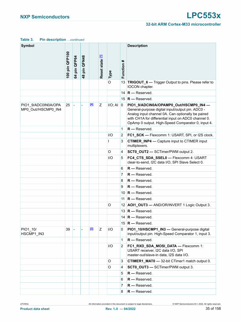
Table 4 shows the pin functions available on each pin, and for each package. These functions are selectable using the IOCON control registers.
Some functions, such as ADC or comparator inputs, are available only on specific pins when digital functions are disabled on those pins. By default, the GPIO function is selected except on pins PIO0_0 an PIO0_9, which are the serial wire debug pins. This allows debug to operate through reset.
All pins have all pull-ups, pull-downs, and inputs turned off at reset except PIO0_0, PIO0_2, PIO0_5, PIO0_9, PIO0_13 and PIO0_14 pins. This prevents power loss through pins prior to software configuration. Due to special pin functions, some pins have a different reset configuration. PIO0_5 and PIO0_12 pins have internal pull-up enabled by default, and PIO0_0, PIO0_2, PIO0_3, and PIO0_4 have internal pull-down enabled by default. PIO0_13 and PIO0_14 are true open drain pins. Refer to pin description table for default reset configuration.
The state of port pin PIO0_5 and PIO0_7 at Reset determines the boot source of the part or if the handler is invoked.
The external reset pin or wake-up pins can trigger a wake-up from deep power-down mode. For the wake-up pins, do not assign any function to this pin if it will be used as a wake-up input when using deep power-down mode. If not in deep power-down mode, a function can be assigned to this pin. If the pin is used for wake-up, it should be pulled HIGH externally before entering deep power-down mode. A LOW-going pulse as short as 50 ns causes the chip to exit deep power-down mode wakes up the part.
The JTAG functions TRST, TCK, TMS, TDI, and TDO, are selected on pins PIO0_2 to PIO0_6 by hardware when the part is in boundary scan mode. The JTAG functions cannot be used for debug mode.To perform boundary scan testing refer to Application Note: How to Perform Boundary Scan for LPC55(S)xx.
Table 3. Pin description
Symbol
100
pin
QF
P10
0
64 p
in Q
FP
64
48 p
in Q
FN
48
Res
et
sta
te [1
]
Typ
e
Fu
nc
tio
n #
Description
PIO0_0/ACMP0_A
54 36 26 [4] Z I/O; AI 0 PIO0_0/ACMP0_A — General-purpose digital input/output pin. Comparator 0, input A if the DIGIMODE bit is set to 0 and ANAMODE is set to 1 in the IOCON register for this pin.
1 R — Reserved.
I/O 2 FC3_SCK — Flexcomm 3: USART, SPI, or I2S clock.
O 3 CTIMER0_MAT0 — 32-bit CTimer0 match output 0.
I 4 SCT0_GPI0 — Pin input 0 to SCTimer/PWM.
LPC553x All information provided in this document is subject to legal disclaimers. © NXP Semiconductors B.V. 2022. All rights reserved.
Product data sheet Rev. 1.0 — 04/2022 10 of 158

NXP Semiconductors LPC553x32-bit ARM Cortex-M33 microcontroller
I 5 PDM_DATA0 — PDM data input for DMIC channel 0.
6 R — Reserved.
7 R — Reserved.
8 R — Reserved.
O 9 SWCLK — Serial Wire Debug clock. This is the default function after booting. Since the internal pull-ups are disabled by default, connect external pull-up or pull-down resistor (~10 Kohm) on SWCLK pin to comply with the ARM SWD interface spec.
10 R — Reserved.
I/O 11 PWM1_B2 — FlexPWM1 PWMB output of SubModule2.
12 R — Reserved.
I 13 EXTTRIG_IN8 — Input Mux. Trigger input to selected on-chip peripherals. Please refer to INPUT MUX chapter.
14 R — Reserved.
15 R — Reserved.
PIO0_1/ADC1IN2B
5 3 2 [2] Z I/O 0 PIO0_1/ADC1IN2B — General-purpose digital input/output pin. ADC1 - Analog input channel 2B. Can optionally be paired with CH2A for differential input on ADC1 channel 2.
1 R — Reserved.
I/O 2 FC3_CTS_SDA_SSEL0 — Flexcomm 3: USART clear-to-send, I2C data I/O, SPI Slave Select 0.
I 3 CTIMER_INP0 — Capture input to CTIMER input muxes.
I 4 SCT0_GPI1 — Pin input 1 to SCTimer/PWM.
O 5 PDM_CLK0 — PDM clock output for DMIC channel 0.
6 R — Reserved
O 7 ACMP0_OUT — Analog comparator 0 output.
8 R — Reserved.
9 R — Reserved.
10 R — Reserved.
11 R — Reserved.
O 12 AOI0_OUT1 — AND/OR/INVERT 0 Logic Output 1.
13 R — Reserved.
14 R — Reserved.
15 R — Reserved.
Table 3. Pin description …continued
Symbol
100
pin
QF
P1
00
64 p
in Q
FP
64
48 p
in Q
FN
48
Res
et
sta
te [1
]
Typ
e
Fu
nc
tio
n #
Description
LPC553x All information provided in this document is subject to legal disclaimers. © NXP Semiconductors B.V. 2022. All rights reserved.
Product data sheet Rev. 1.0 — 04/2022 11 of 158

NXP Semiconductors LPC553x32-bit ARM Cortex-M33 microcontroller
PIO0_2/TRST
81 52 38 [2] PD I/O 0 PIO0_2/TRST — General-purpose digital input/output pin. In boundary scan mode: TRST (Test Reset).
I/O 1 FC3_TXD_SCL_MISO_WS — Flexcomm 3: USART transmitter, I2C clock, SPI master-in/slave-out data I/O, I2S word select/frame.
I 2 CTIMER_INP1 — Capture input to CTIMER input multiplexers.
O 3 SCT0_OUT0 — SCTimer/PWM output 0.
I 4 SCT0_GPI2 — Pin input 2 to SCTimer/PWM.
I/O 5 FLEXSPI0_DATA3 — Data bit 3 for the FlexSPI interface.
6 R — Reserved.
7 R — Reserved.
8 R — Reserved.
9 R — Reserved.
10 R — Reserved.
I/O 11 PWM0_A2 — FlexPWM0 PWMA output 2.
O 12 TRIGOUT_3 — Trigger Output to pins. Please refer to IOCON chapter.
I 13 EXTTRIG_IN4 — Input Mux. Trigger input to selected on-chip peripherals. Please refer to INPUT MUX chapter.
14 R — Reserved.
15 R — Reserved.
PIO0_3/TCK 84 55 40 [2] PD I/O 0 PIO0_3 — General-purpose digital input/output pin. In boundary scan mode: TCK (Test Clock In).
I/O 1 FC3_RXD_SDA_MOSI_DATA — Flexcomm 3: USART receiver, I2C data I/O, SPI master-out/slave-in data, I2S data I/O.
O 2 CTIMER0_MAT1 — 32-bit CTimer0 match output 1.
O 3 SCT0_OUT1 — SCTimer/PWM output 1.
I 4 SCT0_GPI3 — Pin input 3 to SCTimer/PWM.
I/O 5 FLEXSPI0_DATA2 — Data bit 2 for the FlexSPI interface.
6 R — Reserved.
7 R — Reserved.
8 R — Reserved.
9 R — Reserved.
10 R — Reserved.
Table 3. Pin description …continued
Symbol
100
pin
QF
P1
00
64 p
in Q
FP
64
48 p
in Q
FN
48
Res
et
sta
te [1
]
Typ
e
Fu
nc
tio
n #
Description
LPC553x All information provided in this document is subject to legal disclaimers. © NXP Semiconductors B.V. 2022. All rights reserved.
Product data sheet Rev. 1.0 — 04/2022 12 of 158

NXP Semiconductors LPC553x32-bit ARM Cortex-M33 microcontroller
I/O 11 PWM1_B0 — FlexPWM1 PWMB output of SubModule0.
12 R — Reserved.
13 R — Reserved.
14 R — Reserved.
15 R — Reserved.
PIO0_4/TMS 87 57 42 [2] PD I/O 0 PIO0_4 — General-purpose digital input/output pin. In boundary scan mode: TMS (Test Mode Select).
I 1 CAN0_RD — Receiver input for CAN 0.
I/O 2 FC4_SCK — Flexcomm 4: USART, SPI, or I2S clock.
I 3 CTIMER_INP12 — Capture input to CTIMER input multiplexers.
I 4 SCT0_GPI4 — Pin input 4 to SCTimer/PWM.
I/O 5 FLEXSPI0_DATA1 — Data bit 1 for the FlexSPI interface.
6 R — Reserved.
7 R — Reserved.
I/O 8 FC3_CTS_SDA_SSEL0 — Flexcomm 3: USART clear-to-send, I2C data I/O, SPI Slave Select 0.
I/O 9 FC7_TXD_SCL_MISO_WS — Flexcomm 7: USART transmitter, I2C clock, SPI master-in/slave-out data I/O, I2S word select/frame.
10 R — Reserved.
I/O 11 PWM0_B3 — FlexPWM0 PWMB output of SubModule3.
12 R — Reserved.
I 13 EXTTRIG_IN2 — Input Mux. Trigger input to selected on-chip peripherals. Please refer to INPUT MUX chapter.
14 R — Reserved.
15 R — Reserved.
PIO0_5/TDI 90 60 44 [2] PU I/O 0 PIO0_5 — General-purpose digital input/output pin. In boundary scan mode: TDI (Test Data In).
Remark: The state of this pin along with PIO0_7 at Reset determines the boot source for the part of if ISP handler is invoked. See the Boot Process chapter in the Reference Manual for more details.
O 1 CAN0_TD — Transmitter output for CAN 0.
Table 3. Pin description …continued
Symbol
100
pin
QF
P1
00
64 p
in Q
FP
64
48 p
in Q
FN
48
Res
et
sta
te [1
]
Typ
e
Fu
nc
tio
n #
Description
LPC553x All information provided in this document is subject to legal disclaimers. © NXP Semiconductors B.V. 2022. All rights reserved.
Product data sheet Rev. 1.0 — 04/2022 13 of 158

NXP Semiconductors LPC553x32-bit ARM Cortex-M33 microcontroller
I/O 2 FC4_RXD_SDA_MOSI_DATA — Flexcomm 4: USART receiver, I2C data I/O, SPI master-out/slave-in data, I2S data I/O.
O 3 CTIMER3_MAT0 — 32-bit CTimer3 match output 0.
I 4 SCT0_GPI5 — Pin input 5 to SCTimer/PWM.
5 R — Reserved.
6 R — Reserved.
7 R — Reserved.
I/O 8 FC3_RTS_SCL_SSEL1 — Flexcomm 3: USART request-to-send, I2C clock, SPI slave select 1.
I/O 9 MCLK — MCLK input or output for I2S.
10 R — Reserved.
I/O 11 PWM0_A0 — FlexPWM0 PWMA output 0.
12 R — Reserved.
I 13 EXTTRIG_IN5 — Input Mux. Trigger input to selected on-chip peripherals. Please refer to INPUT MUX chapter.
14 R — Reserved.
15 R — Reserved.
PIO0_6/TDO 89 59 43 [2] Z I/O 0 PIO0_6 — General-purpose digital input/output pin. In boundary scan mode: TDO (Test Data Out).
I/O 1 FC3_SCK — Flexcomm 3: USART, SPI, or I2S clock.
I 2 CTIMER_INP13 — Capture input to CTIMER input multiplexers.
O 3 CTIMER4_MAT0 — 32-bit CTimer4 match output 0.
I 4 SCT0_GPI6 — Pin input 6 to SCTimer/PWM.
I/O 5 FLEXSPI0_DATA0 — Data bit 0 for the FlexSPI interface.
6 R — Reserved.
7 R — Reserved.
O 8 SCT0_OUT6 — SCTimer/PWM output 6.
I/O 9 FC7_RXD_SDA_MOSI_DATA — Flexcomm 7: USART receiver, I2C data I/O, SPI master-out/slave-in data, I2S data I/O.
10 R — Reserved.
I/O 11 PWM0_B0 — FlexPWM0 PWMB output of SubModule0.
12 R — Reserved.
Table 3. Pin description …continued
Symbol
100
pin
QF
P1
00
64 p
in Q
FP
64
48 p
in Q
FN
48
Res
et
sta
te [1
]
Typ
e
Fu
nc
tio
n #
Description
LPC553x All information provided in this document is subject to legal disclaimers. © NXP Semiconductors B.V. 2022. All rights reserved.
Product data sheet Rev. 1.0 — 04/2022 14 of 158

NXP Semiconductors LPC553x32-bit ARM Cortex-M33 microcontroller
I 13 EXTTRIG_IN1 — Input Mux. Trigger input to selected on-chip peripherals. Please refer to INPUT MUX chapter of the Reference Manual.
14 R — Reserved.
15 R — Reserved.
PIO0_7/HSCMP1_IN0
42 27 20 [2] Z I/O 0 PIO0_7/HSCMPIN0 — General-purpose digital input/output pin. High-Speed Comparator 1, input 0.Remark: The state of this pin along with PIO0_5 at Reset determines the boot source for the part of if ISP handler is invoked. See the Boot Process chapter in the Reference Manual for more details.
I/O 1 FC3_RTS_SCL_SSEL1 — Flexcomm 3: USART request-to-send, I2C clock, SPI slave select 1.
2 R — Reserved.
I/O 3 FC5_SCK — Flexcomm 5: USART, SPI, or I2S clock.
I/O 4 FC1_SCK — Flexcomm 1: USART, SPI, or I2S clock.
O 5 PDM_CLK0 — PDM clock output for DMIC channel 0.
6 R — Reserved.
7 R — Reserved.
I 8 MCLK — MCLK input or output for I2S and/or digital microphone.
9 R — Reserved.
10 R — Reserved.
I/O 11 PWM0_B0 — FlexPWM0 PWMB output of SubModule0.
O 12 TRIGOUT_6 — Trigger Output to pins. Please refer to IOCON chapter.Input Mux.
O 13 HSCMP2_OUT — High-Speed Comparator 2 output.
14 R — Reserved.
15 R — Reserved.
PIO0_8/OPAMP0_INP
26 17 13 [2] Z I/O 0 PIO0_8/OPAMP_INP — General-purpose digital input/output pin. Op Amp 0 positive input.
I/O 1 FC3_SSEL3 — Flexcomm 3: SPI slave select 3.
2 R — Reserved.
I/O 3 FC5_RXD_SDA_MOSI_DATA — Flexcomm 5: USART receiver, I2C data I/O, SPI master-out/slave-in data, I2S data I/O.
O 4 SWO — Serial Wire Debug trace output.
I/O 5 PDM_DATA1 — PDM data input for DMIC channel 1.
6 R — Reserved.
Table 3. Pin description …continued
Symbol
100
pin
QF
P1
00
64 p
in Q
FP
64
48 p
in Q
FN
48
Res
et
sta
te [1
]
Typ
e
Fu
nc
tio
n #
Description
LPC553x All information provided in this document is subject to legal disclaimers. © NXP Semiconductors B.V. 2022. All rights reserved.
Product data sheet Rev. 1.0 — 04/2022 15 of 158

NXP Semiconductors LPC553x32-bit ARM Cortex-M33 microcontroller
7 R — Reserved.
8 R — Reserved.
9 R — Reserved.
10 R — Reserved.
11 R — Reserved.
12 R — Reserved.
13 R — Reserved.
14 R — Reserved.
15 R — Reserved.
PIO0_9/ACMP0_B
55 37 27 [4] Z I/O; AI 0 PIO0_9/ACMP0_B — General-purpose digital input/output pin. Comparator 0, input B if the DIGIMODE bit is set to 0 and ANAMODE is set to 1 in the IOCON register for this pin.
I/O 1 FC3_SSEL2 — Flexcomm 3: SPI slave select 2.
2 R — Reserved.
I/O 3 FC5_TXD_SCL_MISO_WS — Flexcomm 5: USART transmitter, I2C clock, SPI master-in/slave-out data I/O, I2S word-select/frame.
4 R — Reserved.
5 R — Reserved.
6 R — Reserved.
I/O 7 I3C0_SCL — Clock for I3C master or slave.
8 R — Reserved.
I/O 9 SWDIO — Serial Wire Debug I/O. This is the default function after booting. Since the internal pull-ups are disabled by default, connect external pull-up resistor (~10 Kohm) on the SWDIO pin to comply with the ARM SWD interface spec.
10 R — Reserved.
O 11 PWM1_A2 — FlexPWM1 PWMA output 2.
12 R — Reserved.
O 13 TRIGOUT_2 — Trigger Output to pins. Please refer to IOCON chapter.Input Mux.
14 R — Reserved.
15 R — Reserved.
PIO0_10/ADC0IN1A
21 14 11 [4] Z I/O; AI 0 PIO0_10/ADC0IN1A — General-purpose digital input/output pin. ADC0 - Analog input channel 1A.
I/O 1 FC6_SCK — Flexcomm 6: USART, SPI, or I2S clock.
Table 3. Pin description …continued
Symbol
100
pin
QF
P1
00
64 p
in Q
FP
64
48 p
in Q
FN
48
Res
et
sta
te [1
]
Typ
e
Fu
nc
tio
n #
Description
LPC553x All information provided in this document is subject to legal disclaimers. © NXP Semiconductors B.V. 2022. All rights reserved.
Product data sheet Rev. 1.0 — 04/2022 16 of 158

NXP Semiconductors LPC553x32-bit ARM Cortex-M33 microcontroller
I 2 CTIMER_INP10 — Capture input to CTIMER input multiplexers.
O 3 CTIMER2_MAT0 — 32-bit CTimer2 match output 0.
I/O 4 FC1_TXD_SCL_MISO_WS — Flexcomm 1: USART transmitter, I2C clock, SPI master-in/slave-out data I/O, I2S word-select/frame.
O 5 SCT0_OUT2 — SCTimer/PWM output 2.
6 R — Reserved.
7 R — Reserved.
8 R — Reserved.
9 R — Reserved.
10 R — Reserved.
11 R — Reserved.
12 R — Reserved.
13 R — Reserved.
14 R — Reserved.
15 R — Reserved.
PIO0_11/ADC1IN2A
9 7 4 [4] PD I/O; AI 0 PIO0_11/ADC1IN2A — General-purpose digital input/output pin. ADC1 - Analog input channel 2A. Can optionally be paired with CH2B fordifferential input on ADC1 channel 2.
I/O 1 FC6_RXD_SDA_MOSI_DATA — Flexcomm 6: USART receiver, I2C data I/O, SPI master-out/slave-in data, I2S data I/O.
O 2 CTIMER2_MAT2 — 32-bit CTimer2 match output 2.
I 3 FREQME_GPIO_CLK_A — Frequency Measure pin clock input A.
4 R — Reserved.
5 R — Reserved.
6 R — Reserved.
7 R — Reserved.
8 R — Reserved.
9 R — Reserved.
10 R — Reserved.
11 R — Reserved.
O 12 AOI1_OUT2 — AND/OR/INVERT 1 Logic Output 2.
13 R — Reserved.
14 R — Reserved.
Table 3. Pin description …continued
Symbol
100
pin
QF
P1
00
64 p
in Q
FP
64
48 p
in Q
FN
48
Res
et
sta
te [1
]
Typ
e
Fu
nc
tio
n #
Description
LPC553x All information provided in this document is subject to legal disclaimers. © NXP Semiconductors B.V. 2022. All rights reserved.
Product data sheet Rev. 1.0 — 04/2022 17 of 158

NXP Semiconductors LPC553x32-bit ARM Cortex-M33 microcontroller
15 R — Reserved.
PIO0_12/ADC1IN3A
10 - - [4] PU I/O; AI 0 PIO0_12/ADC1IN3A — ADC1 - Analog input channel 3A. Can optionally be paired with CH3B for differential input on ADC1 channel 3.
I/O 1 FC3_TXD_SCL_MISO_WS — Flexcomm 3: USART transmitter, I2C clock, SPI master-in/slave-out data I/O, I2S word-select/frame.
2 R — Reserved.
I 3 FREQME_GPIO_CLK_B — Frequency Measure pin clock input B.
I 4 SCT0_GPI7 — Pin input 7 to SCTimer/PWM.
5 R — Reserved.
6 R — Reserved.
I/O 7 FC6_TXD_SCL_MISO_WS — Flexcomm 6: USART transmitter, I2C clock, SPI master-in/slave-out data I/O, I2S word-select/frame.
8 R — Reserved.
9 R — Reserved.
10 R — Reserved.
11 R — Reserved.
O 12 AOI1_OUT1 — AND/OR/INVERT 1 Logic Output 1.
13 R — Reserved.
14 R — Reserved.
15 R — Reserved.
PIO0_13 70 46 34 [3] Z I/O 0 PIO0_13 — General-purpose digital input/output pin.
Remark: In ISP mode, this pin is set to the Flexcomm 1 I2C SDA function.
I/O 1 FC1_CTS_SDA_SSEL0 — Flexcomm 1: USART clear-to-send, I2C data I/O, SPI Slave Select 0.
I 2 UTICK_CAP0 — Micro-tick timer capture input 0.
I 3 CTIMER_INP0 — Capture input to CTIMER input multiplexers.
I 4 SCT0_GPI0 — Pin input 0 to SCTimer/PWM.
I/O 5 FC1_RXD_SDA_MOSI_DATA — Flexcomm 1: USART receiver, I2C data I/O, SPI master-out/slave-in data, I2S data I/O.
6 R — Reserved.
7 R — Reserved.
8 R — Reserved.
Table 3. Pin description …continued
Symbol
100
pin
QF
P1
00
64 p
in Q
FP
64
48 p
in Q
FN
48
Res
et
sta
te [1
]
Typ
e
Fu
nc
tio
n #
Description
LPC553x All information provided in this document is subject to legal disclaimers. © NXP Semiconductors B.V. 2022. All rights reserved.
Product data sheet Rev. 1.0 — 04/2022 18 of 158

NXP Semiconductors LPC553x32-bit ARM Cortex-M33 microcontroller
9 R — Reserved.
10 R — Reserved.
11 R — Reserved.
12 R — Reserved.
I 13 EXTTRIG_IN3 — Input Mux. Trigger input to selected on-chip peripherals. Please refer to INPUT MUX chapter.
14 R — Reserved.
15 R — Reserved.
PIO0_14 71 47 35 [3] Z I/O 0 PIO0_14 — General-purpose digital input/output pin.
Remark: In ISP mode, this pin is set to the Flexcomm 1 I2C SCL function.
I/O 1 FC1_RTS_SCL_SSEL1 — Flexcomm 1: USART request-to-send, I2C clock, SPI slave select 1.
I 2 UTICK_CAP1 — Micro-tick timer capture input 1.
I 3 CTIMER_INP1 — Capture input to CTIMER input multiplexers.
I 4 SCT0_GPI1 — Pin input 1 to SCTimer/PWM.
5 R — Reserved.
I/O 6 FC1_TXD_SCL_MISO_WS — Flexcomm 1: USART transmitter, I2C clock, SPI master-in/slave-out data I/O, I2S word-select/frame.
7 R — Reserved.
8 R — Reserved.
9 R — Reserved.
10 R — Reserved.
11 R — Reserved.
12 R — Reserved.
I 13 EXTTRIG_IN2 — Input Mux. Trigger input to selected on-chip peripherals. Please refer to INPUT MUX chapter.
14 R — Reserved.
15 R — Reserved.
PIO0_15/ADC0IN3A
22 15 12 [4] Z I/O; AI 0 PIO0_15/ADC0IN3A — General-purpose digital input/output pin. ADC0 - Analog input channel 3A. Can optionally be paired with CH3B for differential input on ADC0 channel 3.
I/O 1 FC6_CTS_SDA_SSEL0 — Flexcomm 6: USART clear-to-send, I2C data I/O, SPI Slave Select 0.
Table 3. Pin description …continued
Symbol
100
pin
QF
P1
00
64 p
in Q
FP
64
48 p
in Q
FN
48
Res
et
sta
te [1
]
Typ
e
Fu
nc
tio
n #
Description
LPC553x All information provided in this document is subject to legal disclaimers. © NXP Semiconductors B.V. 2022. All rights reserved.
Product data sheet Rev. 1.0 — 04/2022 19 of 158

NXP Semiconductors LPC553x32-bit ARM Cortex-M33 microcontroller
I 2 UTICK_CAP2 — Micro-tick timer capture input 2.
I 3 CTIMER_INP16 — Capture input to CTIMER input multiplexers.
O 4 SCT0_OUT2 — SCTimer/PWM output 2.
5 R — Reserved.
6 R — Reserved.
7 R — Reserved.
8 R — Reserved.
9 R — Reserved.
10 R — Reserved.
11 R — Reserved.
12 R — Reserved.
13 R — Reserved.
14 R — Reserved.
15 R — Reserved.
PIO0_16/ADC0IN3B
20 13 10 [4] Z I/O; AI 0 PIO0_16/ADC0IN3B — ADC0 - Analog input channel 3B. Can optionally be paired with CH3A for differential input on ADC0 channel 3.
I/O 1 FC4_TXD_SCL_MISO_WS — Flexcomm 4: USART transmitter, I2C clock, SPI master-in/slave-out data I/O, I2S word-select/frame.
O 2 CLKOUT — Output of the CLKOUT function.
I 3 CTIMER_INP4 — Capture input to CTIMER input multiplexers.
4 R — Reserved.
5 R — Reserved.
6 R — Reserved.
7 R — Reserved.
8 R — Reserved.
9 R — Reserved.
10 R — Reserved.
11 R — Reserved.
O 12 AOI0_OUT3 — AND/OR/INVERT 0 Logic Output 3.
13 R — Reserved.
14 R — Reserved.
15 R — Reserved.
PIO0_17/HSCMP2_IN0
41 26 19 [2] Z I/O 0 PIO0_17/HSCMP2_IN0 — General-purpose digital input/output pin. High-Speed Comparator 2, input 0.
Table 3. Pin description …continued
Symbol
100
pin
QF
P1
00
64 p
in Q
FP
64
48 p
in Q
FN
48
Res
et
sta
te [1
]
Typ
e
Fu
nc
tio
n #
Description
LPC553x All information provided in this document is subject to legal disclaimers. © NXP Semiconductors B.V. 2022. All rights reserved.
Product data sheet Rev. 1.0 — 04/2022 20 of 158

NXP Semiconductors LPC553x32-bit ARM Cortex-M33 microcontroller
I/O 1 FC4_SSEL2 — Flexcomm 4: SPI slave select 2.
2 R — Reserved.
I 3 SCT0_GPI7 — Pin input 7 to SCTimer/PWM.
O 4 SCT0_OUT0 — SCTimer/PWM output 0.
5 R — Reserved.
6 R — Reserved.
7 R — Reserved.
I/O 8 FC5_RXD_SDA_MOSI_DATA — — Flexcomm 5: USART receiver, I2C data I/O, SPI master-out/slave-in data, I2S data I/O.
9 R — Reserved.
10 R — Reserved.
11 R — Reserved.
O 12 TRIGOUT_7 — Trigger Output to pins. Please refer to IOCON chapter.
O 13 HSCMP1_OUT — High-Speed Comparator 1 Output.
14 R — Reserved.
15 R — Reserved.
PIO0_18/ACMP0_C
56 38 28 [4] Z I/O; AI 0 PIO0_18/ACMP0_C — General-purpose digital input/output pin. Comparator 0, input C if the DIGIMODE bit is set to 0 and ANAMODE is set to 1 in the IOCON register for this pin.
I/O 1 FC4_CTS_SDA_SSEL0 — Flexcomm 4: USART clear-to-send, I2C data I/O, SPI Slave Select 0.
2 R — Reserved.
O 3 CTIMER1_MAT0 — 32-bit CTimer1 match output 0.
O 4 SCT0_OUT1 — SCTimer/PWM output 1.
I/O 5 FC5_RXD_SDA_MOSI_DATA — Flexcomm 5: USART receiver, I2C data I/O, SPI master-out/slave-in data, I2S data I/O.
6 R — Reserved.
7 R — Reserved.
O 8 SWO — Serial Wire Debug trace output.
9 R — Reserved.
10 R — Reserved.
I/O 11 PWM1_A0 — FlexPWM1 PWMA output 0.
Table 3. Pin description …continued
Symbol
100
pin
QF
P1
00
64 p
in Q
FP
64
48 p
in Q
FN
48
Res
et
sta
te [1
]
Typ
e
Fu
nc
tio
n #
Description
LPC553x All information provided in this document is subject to legal disclaimers. © NXP Semiconductors B.V. 2022. All rights reserved.
Product data sheet Rev. 1.0 — 04/2022 21 of 158

NXP Semiconductors LPC553x32-bit ARM Cortex-M33 microcontroller
12 R — Reserved.
O 13 TRIGOUT_7 — Trigger Output to pins. Please refer to IOCON chapter.
14 R — Reserved.
15 R — Reserved.
PIO0_19 83 54 39 [2] Z I/O 0 PIO0_19 — General-purpose digital input/output pin.
I/O 1 FC4_RTS_SCL_SSEL1 — Flexcomm 4: USART request-to-send, I2C clock, SPI slave select 1.
I 2 UTICK_CAP0 — Micro-tick timer capture input 0.
O 3 CTIMER0_MAT2 — 32-bit CTimer0 match output 2.
O 4 SCT0_OUT2 — SCTimer/PWM output 2.
O 5 FLEXSPI0_SCLK — Clock output for the FlexSPI interface.
6 R — Reserved.
I/O 7 FC7_TXD_SCL_MISO_WS — Flexcomm 7: USART transmitter, I2C clock, SPI master-in/slave-out data I/O, I2S word-select/frame.
8 R — Reserved.
I 9 FC7_SCK — Flexcomm 7: USART, SPI, or I2S clock.
10 R — Reserved.
I/O 11 PWM0_B1 — FlexPWM0 PWMB output of SubModule0.
O 12 TRIGOUT_5 — Trigger Output to pins. Please refer to IOCON chapter.
I 13 EXTTRIG_IN0 — Input Mux. Trigger input to selected on-chip peripherals. Please refer to INPUT MUX chapter.
14 R — Reserved.
15 R — Reserved.
PIO0_20 73 48 36 [2] Z I/O 0 PIO0_20 — General-purpose digital input/output pin.
I/O 1 FC3_CTS_SDA_SSEL0 — Flexcomm 3: USART clear-to-send, I2C data I/O, SPI Slave Select 0.
O 2 CTIMER1_MAT1 — 32-bit CTimer1 match output 1.
I 3 CTIMER_INP15 — Capture input to CTIMER input multiplexers.
I 4 SCT0_GPI2 — Pin input 2 to SCTimer/PWM.
5 R — Reserved.
6 R — Reserved.
Table 3. Pin description …continued
Symbol
100
pin
QF
P1
00
64 p
in Q
FP
64
48 p
in Q
FN
48
Res
et
sta
te [1
]
Typ
e
Fu
nc
tio
n #
Description
LPC553x All information provided in this document is subject to legal disclaimers. © NXP Semiconductors B.V. 2022. All rights reserved.
Product data sheet Rev. 1.0 — 04/2022 22 of 158

NXP Semiconductors LPC553x32-bit ARM Cortex-M33 microcontroller
I/O 7 FC7_RXD_SDA_MOSI_DATA — Flexcomm 7: USART receiver, I2C data I/O, SPI master-out/slave-in data, I2S data I/O.
I/O 8 HS_SPI_SSEL0 — Slave Select 0 for high speed SPI.
9 R — Reserved.
10 R — Reserved.
I/O 11 FC4_TXD_SCL_MISO_WS — Flexcomm 4: USART transmitter, I2C clock, SPI master-in/slave-out data I/O, I2S word-select/frame.
12 R — Reserved.
I/O 13 PWM1_X2 — FlexPWM1 PWMX output 2.
14 R — Reserved.
15 R — Reserved.
PIO0_21 76 49 37 [2] Z I/O 0 PIO0_21 — General-purpose digital input/output pin.
I/O 1 FC3_RTS_SCL_SSEL1 — Flexcomm 3: USART request-to-send, I2C clock, SPI slave select 1.
I 2 UTICK_CAP3 — Micro-tick timer capture input 3.
O 3 CTIMER3_MAT3 — 32-bit CTimer3 match output 3.
I 4 SCT0_GPI3 — Pin input 3 to SCTimer/PWM.
O 5 SCT0_OUT7 — SCTimer/PWM output 7.
O 6 FLEXSPI0_SS0_N — Active low slave select 0 for the FlexSPI interface.
I/O 7 FC7_SCK — Flexcomm 7: USART, SPI, or I2S clock.
I/O 8 HS_SPI_SSEL3 — Slave Select 3 for high speed SPI.
I 9 FC7_CTS_SDA_SSEL0 — Flexcomm 7: USART clear-to-send, I2C data I/O,
SPI Slave Select 0.
10 R — Reserved.
I/O 11 PWM1_B1 — FlexPWM1 PWMB output of SubModule1.
O 12 TRIGOUT_4 — Trigger Output to pins. Please refer to IOCON chapter.
I 13 EXTTRIG_IN7 — Input Mux. Trigger input to selected on-chip peripherals. Please refer to INPUT MUX chapter.
14 R — Reserved.
15 R — Reserved.
Table 3. Pin description …continued
Symbol
100
pin
QF
P1
00
64 p
in Q
FP
64
48 p
in Q
FN
48
Res
et
sta
te [1
]
Typ
e
Fu
nc
tio
n #
Description
LPC553x All information provided in this document is subject to legal disclaimers. © NXP Semiconductors B.V. 2022. All rights reserved.
Product data sheet Rev. 1.0 — 04/2022 23 of 158

NXP Semiconductors LPC553x32-bit ARM Cortex-M33 microcontroller
PIO0_22 78 50 - [2][8] Z I/O 0 PIO0_22 — General-purpose digital input/output pin.
I/O 1 FC6_TXD_SCL_MISO_WS — Flexcomm 6: USART transmitter, I2C clock, SPI master-in/slave-out data I/O, I2S word-select/frame.
I 2 UTICK_CAP1 — Micro-tick timer capture input 1.
I 3 CTIMER_INP15 — Capture input to CTIMER input multiplexers.
O 4 SCT0_OUT3 — SCTimer/PWM output 3.
O 5 FLEXSPI0_SCLK_N — Inverted clock output for the FlexSPI interface.
O 6 FLEXSPI0_SS1_N — Active low slave select 1 for the FlexSPI interface.
I 7 USB0_VBUS — Monitors the presence of USB0 bus power.
8 R — Reserved.
I/O 9 FC7_RTS_SCL_SSEL1 — Flexcomm 7: USART
request-to-send, I2C clock, SPI slave select 1.
10 R — Reserved.
I/O 11 PWM1_X0 — FlexPWM1 PWMX output 0.
12 R — Reserved.
I 13 EXTTRIG_IN5 — Input Mux. Trigger input to selected on-chip peripherals. Please refer to INPUT MUX chapter.
14 R — Reserved.
15 R — Reserved.
PIO0_23/ADC0IN8B
19 - - [4] Z I/O; AI 0 PIO0_23/ADC0IN8B — General-purpose digital input/output pin. ADC0 - Analog input channel 8B. Can optionally be paired with CH8A for differential input on ADC0 channel 8.
I/O 1 MCLK — MCLK input or output for I2S.
O 2 CTIMER1_MAT2 — 32-bit CTimer1 match output 2.
O 3 CTIMER3_MAT3 — 32-bit CTimer3 match output 3.
O 4 SCT0_OUT4 — SCTimer/PWM output 4.
I/O 5 FC0_CTS_SDA_SSEL0 — Flexcomm 0: USART clear-to-send, I2C data I/O, SPI Slave Select 0.
6 R — Reserved.
7 R — Reserved.
8 R — Reserved.
9 R — Reserved.
Table 3. Pin description …continued
Symbol
100
pin
QF
P1
00
64 p
in Q
FP
64
48 p
in Q
FN
48
Res
et
sta
te [1
]
Typ
e
Fu
nc
tio
n #
Description
LPC553x All information provided in this document is subject to legal disclaimers. © NXP Semiconductors B.V. 2022. All rights reserved.
Product data sheet Rev. 1.0 — 04/2022 24 of 158

NXP Semiconductors LPC553x32-bit ARM Cortex-M33 microcontroller
10 R — Reserved.
11 R — Reserved.
12 R — Reserved.
13 R — Reserved.
14 R — Reserved.
15 R — Reserved.
PIO0_24/HSCMP0_IN0
69 45 33 [2] Z I/O 0 PIO0_24/HSCMP0_IN0 — General-purpose digital input/output pin. High-Speed Comparator 0, input 0.
I/O 1 FC0_RXD_SDA_MOSI_DATA — Flexcomm 0: USART receiver, I2C data I/O, SPI master-out/slave-in data, I2S data I/O.
2 R — Reserved.
I 3 CTIMER_INP8 — Capture input to CTIMER input multiplexers.
I 4 SCT0_GPI0 — Pin input 0 to SCTimer/PWM.
I/O 5 I3C0_SDA — Data for I3C master or slave.
O 6 TRACEDATA[0] — Trace data bit 0.
7 R — Reserved.
8 R — Reserved.
9 R — Reserved.
10 R — Reserved.
I/O 11 PWM0_A1 — FlexPWM0 PWMA output 1.
12 R — Reserved.
I/O 13 PWM0_X0 — FlexPWM0 PWMX output 0.
14 R — Reserved.
15 R — Reserved.
PIO0_25 79 51 - [2] Z I/O 0 PIO0_25 — General-purpose digital input/output pin.
I/O 1 FC0_TXD_SCL_MISO_WS — Flexcomm 0: USART transmitter, I2C clock, SPI master-in/slave-out data I/O, I2S word-select/frame.
2 R — Reserved.
I 3 CTIMER_INP9 — Capture input to CTIMER input multiplexers.
I 4 SCT0_GPI1 — Pin input 1 to SCTimer/PWM.
O 5 R — Reserved.
O 6 FLEXSPI0_DQS — Data strobe output for the FlexSPI interface.
Table 3. Pin description …continued
Symbol
100
pin
QF
P1
00
64 p
in Q
FP
64
48 p
in Q
FN
48
Res
et
sta
te [1
]
Typ
e
Fu
nc
tio
n #
Description
LPC553x All information provided in this document is subject to legal disclaimers. © NXP Semiconductors B.V. 2022. All rights reserved.
Product data sheet Rev. 1.0 — 04/2022 25 of 158

NXP Semiconductors LPC553x32-bit ARM Cortex-M33 microcontroller
O 7 HSCMP0_OUT — High-Speed Comparator 0 Output.
8 R — Reserved.
9 R — Reserved.
10 R — Reserved.
I/O 11 PWM0_A0 — FlexPWM0 PWMA output 0.
12 R — Reserved.
I 13 EXTTRIG_IN6 — Input Mux. Trigger input to selected on-chip peripherals. Please refer to INPUT MUX chapter.
14 R — Reserved.
15 R — Reserved.
PIO0_26/WAKEUP4/TAMPER2
60 41 30 [2][8] Z I/O 0 PIO0_26/WAKEUP4/TAMPER2 — General-purpose digital input/output pin. This pin can trigger a wake-up from deep power-down mode, can be configured as rising or falling edge. This pin can also be used to trigger Tamper Event recorder block.
Remark: In ISP mode, this pin is set to the HS SPI MOSI function (Flexcomm 8).
I/O 1 FC2_RXD_SDA_MOSI_DATA — Flexcomm 2: USART receiver, I2C data I/O, SPI master-out/slave-in data, I2S data I/O.
O 2 CLKOUT — Output of the CLKOUT function.
I 3 CTIMER_INP14 — Capture input to CTIMER input multiplexers.
O 4 SCT0_OUT5 — SCTimer/PWM output 5.
O 5 PDM_CLK0 — PDM clock output for DMIC channel 0.
6 R — Reserved.
I 7 USB0_IDVALUE — Indicates to the transceiver whether connected as an A-device (USB0_ID LOW) or B-device (USB0_ID HIGH).
I/O 8 FC0_SCK — Flexcomm 0: USART, SPI, or I2S clock.
I/O 9 HS_SPI_MOSI — Master-out/slave-in data for high speed SPI.
10 R — Reserved.
I/O 11 PWM0_B1 — FlexPWM0 PWMB output of SubModule1.
12 R — Reserved.
13 R — Reserved.
14 R — Reserved.
Table 3. Pin description …continued
Symbol
100
pin
QF
P1
00
64 p
in Q
FP
64
48 p
in Q
FN
48
Res
et
sta
te [1
]
Typ
e
Fu
nc
tio
n #
Description
LPC553x All information provided in this document is subject to legal disclaimers. © NXP Semiconductors B.V. 2022. All rights reserved.
Product data sheet Rev. 1.0 — 04/2022 26 of 158

NXP Semiconductors LPC553x32-bit ARM Cortex-M33 microcontroller
15 R — Reserved.
PIO0_27/OPAMP1_INP
28 19 15 [2] Z I/O 0 PIO0_27/OPAMP1_INP — General-purpose digital input/output pin. Op Amp 1 positive input.
I/O 1 FC2_TXD_SCL_MISO_WS — Flexcomm 2: USART transmitter, I2C clock, SPI master-in/slave-out data I/O, I2S word-select/frame.
2 R — Reserved.
O 3 CTIMER3_MAT2 — 32-bit CTimer3 match output 2.
O 4 SCT0_OUT6 — SCTimer/PWM output 6.
I 5 PDM_DATA0 — PDM data input for DMIC channel 0.
6 R — Reserved.
I/O 7 FC7_RXD_SDA_MOSI_DATA — Flexcomm 7: USART receiver, I2C data I/O, SPI master-out/slave-in data, I2S data I/O.
8 R — Reserved.
9 R — Reserved.
10 R — Reserved.
11 R — Reserved.
12 R — Reserved.
13 R — Reserved.
14 R — Reserved.
15 R — Reserved.
PIO0_28/ WAKEUP1/TAMPER1
66 - - [2][8] Z I/O 0 PIO0_28/WAKEUP1/TAMPER1 — General-purpose digital input/output pin. This pin can trigger a wake-up from deep power-down mode and can be configured as rising or falling edge. This pin can also be used to trigger Tamper Event recorder block.
I/O 1 FC0_SCK — Flexcomm 0: USART, SPI, or I2S clock.
2 R — Reserved.
I 3 CTIMER_INP11 — Capture input to CTIMER input multiplexers.
O 4 SCT0_OUT7 — SCTimer/PWM output 7.
O 5 TRACEDATA[3] — Trace data bit 3.
6 R — Reserved.
I 7 USB0_OVERCURRENTN — USB0 bus overcurrent indicator (active low).
Table 3. Pin description …continued
Symbol
100
pin
QF
P1
00
64 p
in Q
FP
64
48 p
in Q
FN
48
Res
et
sta
te [1
]
Typ
e
Fu
nc
tio
n #
Description
LPC553x All information provided in this document is subject to legal disclaimers. © NXP Semiconductors B.V. 2022. All rights reserved.
Product data sheet Rev. 1.0 — 04/2022 27 of 158

NXP Semiconductors LPC553x32-bit ARM Cortex-M33 microcontroller
O 8 I3C0_PUR — Pullup resistor control for I3C master. The I3C0_PUR function controls the SDA pull-up. It is intended to be connected to one end of an external low-value pull-up resistor (e.g., 1KOhm), with the other end connected to the SDA line. If there is no external high weak bus keeper on SDA, then add an additional external weak (e.g., 100KOhm or even 500KOhm) always-on pull-up on this line.
9 R — Reserved.
10 R — Reserved.
I/O 11 PWM0_A2 — FlexPWM0 PWMA output 2.
12 R — Reserved.
13 R — Reserved.
14 R — Reserved.
15 R — Reserved.
PIO0_29 93 61 45 [2] Z I/O 0 PIO0_29 — General-purpose digital input/output pin.
Remark: In ISP mode, this pin is set to the Flexcomm 0 USART RXD function or CAN0_RD function using ISP auto-detect.
I/O 1 FC0_RXD_SDA_MOSI_DATA — Flexcomm 0: USART receiver, I2C data I/O, SPI master-out/slave-in data, I2S data I/O.
2 R — Reserved.
O 3 CTIMER2_MAT3 — 32-bit CTimer2 match output 3.
O 4 SCT0_OUT8 — SCTimer/PWM output 8.
O 5 TRACEDATA[2] — Trace data bit 2.
I/O 6 FC6_RXD_SDA_MOSI_DATA — Flexcomm 6: USART receiver, I2C data I/O, SPI master-out/slave-in data, I2S data I/O.
O 7 ACMP0_OUT — Analog comparator 0 output.
8 R — Reserved.
9 R — Reserved.
10 R — Reserved.
I/O 11 PWM0_A1 — FlexPWM0 PWMA output 1.
12 R — Reserved.
I 13 EXTTRIG_IN3 — Input Mux. Trigger input to selected on-chip peripherals. Please refer to INPUT MUX chapter.
14 R — Reserved.
15 R — Reserved.
Table 3. Pin description …continued
Symbol
100
pin
QF
P1
00
64 p
in Q
FP
64
48 p
in Q
FN
48
Res
et
sta
te [1
]
Typ
e
Fu
nc
tio
n #
Description
LPC553x All information provided in this document is subject to legal disclaimers. © NXP Semiconductors B.V. 2022. All rights reserved.
Product data sheet Rev. 1.0 — 04/2022 28 of 158

NXP Semiconductors LPC553x32-bit ARM Cortex-M33 microcontroller
PIO0_30 95 63 47 [2] Z I/O 0 PIO0_30 — General-purpose digital input/output pin.
Remark: In ISP mode, this pin is set to the Flexcomm 0 USART TXD function or CAN0_TD function using ISP auto-detect.
I/O 1 FC0_TXD_SCL_MISO_WS — Flexcomm 0: USART transmitter, I2C clock, SPI master-in/slave-out data I/O, I2S word-select/frame.
2 R — Reserved.
O 3 CTIMER0_MAT0 — 32-bit CTimer0 match output 0.
O 4 SCT0_OUT9 — SCTimer/PWM output 9.
O 5 TRACEDATA[1] — Trace data bit 1.
O 6 CAN0_TD — Transmitter output for CAN 0.
7 R — Reserved.
8 R — Reserved.
I/O 9 FC6_TXD_SCL_MISO_WS — Flexcomm 6: USART transmitter, I2C clock, SPI master-in/slave-out data I/O, I2S word-select/frame.
10 R — Reserved.
I/O 11 PWM1_A1 — FlexPWM1 PWMA output 1.
O 12 AOI1_OUT0 — AND/OR/INVERT 1 Logic Output 0.
13 R — Reserved.
14 R — Reserved.
15 R — Reserved.
PIO0_31/ADC0IN8A
23 16 - [4] Z I/O; AI 0 PIO0_31/ADC0IN8A — General-purpose digital input/output pin. ADC0 - Analog input channel 8A. Can optionally be paired with CH8B for differential input on ADC0 channel 8.
I/O 1 FC0_CTS_SDA_SSEL0 — Flexcomm 0: USART clear-to-send, I2C data I/O, SPI Slave Select 0.
2 R — Reserved.
O 3 CTIMER0_MAT1 — 32-bit CTimer0 match output 1.
O 4 SCT0_OUT3 — SCTimer/PWM output 3.
5 R — Reserved.
6 R — Reserved.
7 R — Reserved.
8 R — Reserved.
9 R — Reserved.
10 R — Reserved.
11 R — Reserved.
Table 3. Pin description …continued
Symbol
100
pin
QF
P1
00
64 p
in Q
FP
64
48 p
in Q
FN
48
Res
et
sta
te [1
]
Typ
e
Fu
nc
tio
n #
Description
LPC553x All information provided in this document is subject to legal disclaimers. © NXP Semiconductors B.V. 2022. All rights reserved.
Product data sheet Rev. 1.0 — 04/2022 29 of 158

NXP Semiconductors LPC553x32-bit ARM Cortex-M33 microcontroller
O 12 AOI0_OUT0 — AND/OR/INVERT 0 Logic Output 0.
13 R — Reserved.
14 R — Reserved.
15 R — Reserved.
PIO1_0/ADC1IN0B
6 4 3 [4] Z I/O; AI 0 PIO1_0/ADC1IN0B — General-purpose digital input/output pin. ADC1 - Analog input channel 0B. Can optionally be paired with CH0A for differential input on ADC1 channel 0.
I/O 1 FC0_RTS_SCL_SSEL1 — Flexcomm 0: USART request-to-send, I2C clock, SPI slave select 1.
2 R — Reserved.
I 3 CTIMER_INP2 — Capture input to CTIMER input multiplexers.
I 4 SCT0_GPI4 — Pin input 4 to SCTimer/PWM.
5 R — Reserved.
6 R — Reserved.
7 R — Reserved.
8 R — Reserved.
9 R — Reserved.
11 R — Reserved.
O 12 AO1_OUT0 — AND/OR/INVERT 1 Logic Output 0.
13 R — Reserved.
14 R — Reserved.
15 R — Reserved.
PIO1_1/ WAKEUP0/TAMPER0
59 40 29 [2] Z I/O 0 PIO1_1/WAKEUP0/TAMPER0 — General-purpose digital input/output pin. This pin can trigger a wake-up from deep power-down mode. WAKEUP pin can be configured as rising or falling edge. This pin can also be used to trigger Tamper Event recorder block.
Remark: In ISP mode, this pin is set to the High Speed SPI SSEL1 function (Flexcomm 8).
I/O 1 FC3_RXD_SDA_MOSI_DATA — Flexcomm 3: USART receiver, I2C data I/O, SPI master-out/slave-in data, I2S data I/O.
2 R — Reserved.
I 3 CTIMER_INP3 — Capture input to CTIMER input multiplexers.
I 4 SCT0_GPI5 — Pin input 5 to SCTimer/PWM.
I/O 5 HS_SPI_SSEL1 — Slave Select 1 for high speed SPI.
Table 3. Pin description …continued
Symbol
100
pin
QF
P1
00
64 p
in Q
FP
64
48 p
in Q
FN
48
Res
et
sta
te [1
]
Typ
e
Fu
nc
tio
n #
Description
LPC553x All information provided in this document is subject to legal disclaimers. © NXP Semiconductors B.V. 2022. All rights reserved.
Product data sheet Rev. 1.0 — 04/2022 30 of 158

NXP Semiconductors LPC553x32-bit ARM Cortex-M33 microcontroller
O 6 TRACECLK — Trace clock.
7 R — Reserved.
8 R — Reserved.
9 R — Reserved.
O 10 RTC_ALARMOUT — RTC controlled output.
I/O 11 PWM0_B2 — FlexPWM0 PWMB output of SubModule2.
12 R — Reserved.
13 R — Reserved.
14 R — Reserved.
15 R — Reserved.
PIO1_2 61 42 31 [2] Z I/O 0 PIO1_2 — General-purpose digital input/output pin.
Remark: In ISP mode, this pin is set to the High Speed SPI SCK function (Flexcomm 8).
O 1 CAN0_TD — Transmitter output for CAN 0.
2 R — Reserved.
O 3 CTIMER0_MAT3 — 32-bit CTimer0 match output 3.
I 4 SCT0_GPI6 — Pin input 6 to SCTimer/PWM.
O 5 PDM_CLK1 — PDM clock output for DMIC channel 1.
I/O 6 HS_SPI_SCK — Clock for high speed SPI.
7 R — Reserved.
8 R — Reserved.
9 R — Reserved.
10 R — Reserved.
I/O 11 PWM0_B0 — FlexPWM0 PWMB output of SubModule0.
O 12 AOI0_OUT0 — AND/OR/INVERT 0 Logic Output 0.
13 R — Reserved.
14 R — Reserved.
15 R — Reserved.
PIO1_3 62 43 32 [2] Z I/O 0 PIO1_3 — General-purpose digital input/output pin.
Remark: In ISP mode, this pin is set to the High Speed SPI MISO function (Flexcomm 8).
I 1 CAN0_RD — Receiver input for CAN 0.
2 R — Reserved.
I/O 3 FC2_TXD_SCL_MISO_WS — Flexcomm 2: USART transmitter, I2C clock, SPI master-in/slave-out data I/O, I2S word select/frame.
Table 3. Pin description …continued
Symbol
100
pin
QF
P1
00
64 p
in Q
FP
64
48 p
in Q
FN
48
Res
et
sta
te [1
]
Typ
e
Fu
nc
tio
n #
Description
LPC553x All information provided in this document is subject to legal disclaimers. © NXP Semiconductors B.V. 2022. All rights reserved.
Product data sheet Rev. 1.0 — 04/2022 31 of 158

NXP Semiconductors LPC553x32-bit ARM Cortex-M33 microcontroller
O 4 SCT0_OUT4 — SCTimer/PWM output 4.
I 5 PDM_DATA1 — PDM data input for DMIC channel 1.
I/O 6 HS_SPI_MISO — Master-in/slave-out data for high speed SPI.
O 7 USB0_PORTPWRN — USB0 VBUS drive indicator (Indicates VBUS must be driven).
8 R — Reserved.
9 R — Reserved.
10 R — Reserved.
I/O 11 PWM0_A3 — FlexPWM0 PWMA output 3.
12 R — Reserved.
13 R — Reserved.
14 R — Reserved.
15 R — Reserved.
PIO1_4 75 - - [2] Z I/O 0 PIO1_4 — General-purpose digital input/output pin.
I/O 1 FC0_SCK — Flexcomm 0: USART, SPI, or I2S clock.
2 R — Reserved.
O 3 CTIMER2_MAT1 — 32-bit CTimer2 match output 1.
O 4 SCT0_OUT0 — SCTimer/PWM output 0.
I 5 FREQME_GPIO_CLK_A — Frequency Measure pin clock input A.
6 R — Reserved.
I/O 7 FC4_TXD_SCL_MISO_WS — Flexcomm 0: USART transmitter, I2C clock, SPI master-in/slave-out data I/O, I2S word select/frame.
8 R — Reserved.
9 R — Reserved.
10 R — Reserved.
O 11 PWM0_B2 — FlexPWM0 PWMB output of SubModule2.
O 12 TRIGOUT_7 — Trigger Output to pins. Please refer to IOCON chapter.
I 13 EXTTRIG_IN8 — Input Mux. Trigger input to selected on-chip peripherals. Please refer to INPUT MUX chapter.
14 R — Reserved.
15 R — Reserved.
Table 3. Pin description …continued
Symbol
100
pin
QF
P1
00
64 p
in Q
FP
64
48 p
in Q
FN
48
Res
et
sta
te [1
]
Typ
e
Fu
nc
tio
n #
Description
LPC553x All information provided in this document is subject to legal disclaimers. © NXP Semiconductors B.V. 2022. All rights reserved.
Product data sheet Rev. 1.0 — 04/2022 32 of 158

NXP Semiconductors LPC553x32-bit ARM Cortex-M33 microcontroller
PIO1_5/HSCMP0_IN3 35 - - [2] Z I/O 0 PIO1_5/HSCMP0_IN3 — General-purpose digital input/output pin. High-Speed Comparator 0, input 3.
I/O 1 FC0_RXD_SDA_MOSI_DATA — Flexcomm 0: USART receiver, I2C data I/O, SPI master-out/slave-in data, I2S data I/O.
2 R — Reserved.
O 3 CTIMER2_MAT0 — 32-bit CTimer2 match output 0.
I 4 SCT0_GPI0 — Pin input 0 to SCTimer/PWM.
5 R — Reserved.
6 R — Reserved.
7 R — Reserved.
8 R — Reserved.
9 R — Reserved.
10 R — Reserved.
I/O 11 PWM1_A3 — FlexPWM1 PWMA output 3.
O 12 TRIGOUT_0 — Trigger Output to pins. Please refer to IOCON chapter.
13 R — Reserved.
14 R — Reserved.
15 R — Reserved.
PIO1_6 50 - - [2] Z I/O 0 PIO1_6 — General-purpose digital input/output pin.
I/O 1 FC0_TXD_SCL_MISO_WS — Flexcomm 0: USART transmitter, I2C clock, SPI master-in/slave-out data I/O, I2S word-select/frame.
2 R — Reserved.
O 3 CTIMER2_MAT1 — 32-bit CTimer2 match output 1.
I 4 SCT0_GPI3 — Pin input 3 to SCTimer/PWM.
5 R — Reserved.
6 R — Reserved.
7 R — Reserved.
8 R — Reserved.
9 R — Reserved.
10 R — Reserved.
I/O 11 PWM0_A1 — FlexPWM0 PWMA output 1.
O 12 TRIGOUT_5 — Trigger Output to pins. Please refer to IOCON chapter.
O 13 HSCMP0_OUT — High-Speed Comparator 0 output.
14 R — Reserved.
Table 3. Pin description …continued
Symbol
100
pin
QF
P1
00
64 p
in Q
FP
64
48 p
in Q
FN
48
Res
et
sta
te [1
]
Typ
e
Fu
nc
tio
n #
Description
LPC553x All information provided in this document is subject to legal disclaimers. © NXP Semiconductors B.V. 2022. All rights reserved.
Product data sheet Rev. 1.0 — 04/2022 33 of 158

NXP Semiconductors LPC553x32-bit ARM Cortex-M33 microcontroller
15 R — Reserved.
PIO1_7/ADC1IN3B 4 - - [2] Z I/O 0 PIO1_7/ADC1IN3B — General-purpose digital input/output pin. ADC1 - Analoginput channel 3B. Can optionally be paired with CH3A for differential input on
ADC1 channel 3.
I/O 1 FC0_RTS_SCL_SSEL1 — Flexcomm 0: USART request-to-send, I2C clock, SPI slave select 1.
2 R — Reserved.
O 3 CTIMER2_MAT2 — 32-bit CTimer2 match output 2.
I 4 SCT0_GPI4 — Pin input 4 to SCTimer/PWM.
5 R — Reserved.
6 R — Reserved.
7 R — Reserved.
8 R — Reserved.
9 R — Reserved.
10 R — Reserved.
11 R — Reserved.
O 12 AOI1_OUT3 — AND/OR/INVERT 1 Logic Output 3.
13 R — Reserved.
14 R — Reserved.
15 R — Reserved.
PIO1_8 36 - - [4] Z I/O; AI 0 PIO1_8 — General-purpose digital input/output pin.
I/O 1 FC0_CTS_SDA_SSEL0 — Flexcomm 0: USART clear-to-send, I2C data I/O, SPI Slave Select 0.
2 R — Reserved.
3 R — Reserved.
O 4 SCT0_OUT1 — SCTimer/PWM output 1.
I/O 5 FC4_SSEL2 — Flexcomm 4: SPI slave select 2.
6 R — Reserved.
I/O 7 FC1_SCK — Flexcomm 1: USART, SPI, or I2S clock.
8 R — Reserved.
9 R — Reserved.
10 R — Reserved.
I/O 11 PWM0_A2 — FlexPWM0 PWMA output 2.
O 12 AOI1_OUT2 — AND/OR/INVERT 1 Logic Output 2.
Table 3. Pin description …continued
Symbol
100
pin
QF
P1
00
64 p
in Q
FP
64
48 p
in Q
FN
48
Res
et
sta
te [1
]
Typ
e
Fu
nc
tio
n #
Description
LPC553x All information provided in this document is subject to legal disclaimers. © NXP Semiconductors B.V. 2022. All rights reserved.
Product data sheet Rev. 1.0 — 04/2022 34 of 158
NXP Semiconductors LPC553x32-bit ARM Cortex-M33 microcontroller
O 13 TRIGOUT_6 — Trigger Output to pins. Please refer to IOCON chapter.
14 R — Reserved.
15 R — Reserved.
PIO1_9/ADC0IN0A/OPAMP0_Out//HSCMP0_IN4
25 - - [4] Z I/O; AI 0 PIO1_9/ADCIN0A/OPAMP0_Out/HSCMP0_IN4 — General-purpose digital input/output pin. ADC0 - Analog input channel 0A. Can optionally be paired with CH1A for differential input on ADC0 channel 0. OpAmp 0 output. High-Speed Comparator 0, input 4.
1 R — Reserved.
I/O 2 FC1_SCK — Flexcomm 1: USART, SPI, or I2S clock.
I 3 CTIMER_INP4 — Capture input to CTIMER input multiplexers.
O 4 SCT0_OUT2 — SCTimer/PWM output 2.
I/O 5 FC4_CTS_SDA_SSEL0 — Flexcomm 4: USART clear-to-send, I2C data I/O, SPI Slave Select 0.
6 R — Reserved.
7 R — Reserved.
8 R — Reserved.
9 R — Reserved.
10 R — Reserved.
11 R — Reserved.
O 12 AOI1_OUT3 — AND/OR/INVERT 1 Logic Output 3.
13 R — Reserved.
14 R — Reserved.
15 R — Reserved.
PIO1_10/HSCMP1_IN3
39 - - [2] Z I/O 0 PIO1_10/HSCMP1_IN3 — General-purpose digital input/output pin. High-Speed Comparator 1, input 3.
1 R — Reserved.
I/O 2 FC1_RXD_SDA_MOSI_DATA — Flexcomm 1: USART receiver, I2C data I/O, SPI master-out/slave-in data, I2S data I/O.
O 3 CTIMER1_MAT0 — 32-bit CTimer1 match output 0.
O 4 SCT0_OUT3 — SCTimer/PWM output 3.
5 R — Reserved.
6 R — Reserved.
7 R — Reserved.
8 R — Reserved.
Table 3. Pin description …continued
Symbol
100
pin
QF
P1
00
64 p
in Q
FP
64
48 p
in Q
FN
48
Res
et
sta
te [1
]
Typ
e
Fu
nc
tio
n #
Description
LPC553x All information provided in this document is subject to legal disclaimers. © NXP Semiconductors B.V. 2022. All rights reserved.
Product data sheet Rev. 1.0 — 04/2022 35 of 158

NXP Semiconductors LPC553x32-bit ARM Cortex-M33 microcontroller
9 R — Reserved.
10 R — Reserved.
I/O 11 PWM0_X1 — FlexPWM0 PWMX output 1.
O 12 TRIGOUT_3 — Trigger Output to pins. Please refer to the IOCON chapter.
O 13 HSCMP2_OUT — High-Speed Comparator 2 output.
14 R — Reserved.
15 R — Reserved.
PIO1_11 94 62 46 [2][8] Z I/O 0 PIO1_11 — General-purpose digital input/output pin.
1 R — Reserved.
I/O 2 FC1_TXD_SCL_MISO_WS — Flexcomm 1: USART transmitter, I2C clock, SPI master-in/slave-out data I/O, I2S word-select/frame.
I 3 CTIMER_INP5 — Capture input to CTIMER input multiplexers.
I 4 USB0_VBUS — Monitors the presence of USB0 bus power.
5 R — Reserved.
6 R — Reserved.
I/O 7 HS_SPI_SSEL0 — Slave Select 0 for high speed SPI.
8 R — Reserved.
9 R — Reserved.
I/O 10 FC6_SCK — Flexcomm 6: USART, SPI, or I2S clock.
I/O 11 PWM0_A0 — FlexPWM0 PWMA output 0.
12 R — Reserved.
I 13 EXTTRIG_IN8 — Input Mux. Trigger input to selected on-chip peripherals. Please refer to INPUT MUX chapter.
14 R — Reserved.
15 R — Reserved.
PIO1_12/HSCMP0_IN1
67 - - [2][8] Z I/O 0 PIO1_12/HSCMP0_IN1 — General-purpose digital input/output pin.
High-Speed Comparator 0, input 1.
1 R — Reserved.
I/O 2 FC6_SCK — Flexcomm 6: USART, SPI, or I2S clock.
O 3 CTIMER1_MAT1 — 32-bit CTimer1 match output 1.
O 4 USB0_PORTPWRN — USB0 VBUS drive indicator (Indicates VBUS must be driven).
Table 3. Pin description …continued
Symbol
100
pin
QF
P1
00
64 p
in Q
FP
64
48 p
in Q
FN
48
Res
et
sta
te [1
]
Typ
e
Fu
nc
tio
n #
Description
LPC553x All information provided in this document is subject to legal disclaimers. © NXP Semiconductors B.V. 2022. All rights reserved.
Product data sheet Rev. 1.0 — 04/2022 36 of 158

NXP Semiconductors LPC553x32-bit ARM Cortex-M33 microcontroller
I/O 5 HS_SPI_SSEL2 — Slave Select 2 for high speed SPI.
6 R — Reserved.
7 R — Reserved.
8 R — Reserved.
9 R — Reserved.
10 R — Reserved.
I/O 11 PWM0_A3 — FlexPWM0 PWMA output 3.
O 12 AOI0_OUT1 — AND/OR/INVERT 0 Logic Output 1.
I 13 EXTTRIG_IN9 — Input Mux. Trigger input to selected on-chip peripherals. Please refer to INPUT MUX chapter.
14 R — Reserved.
15 R — Reserved.
PIO1_13/ACMP0VREF 58 39 - [2][8] Z I/O 0 PIO1_13/ACMP0VREF — General-purpose digital input/output pin. Alternate reference voltage for the analog comparator.
1 R — Reserved.
I/O 2 FC6_RXD_SDA_MOSI_DATA — Flexcomm 6: USART receiver, I2C data I/O, SPI master-out/slave-in data, I2S data I/O.
I 3 CTIMER_INP6 — Capture input to CTIMER input multiplexers.
I 4 USB0_OVERCURRENTN — USB0 bus overcurrent indicator (active low).
O 5 USB0_FRAME — USB0 frame toggle signal.
6 R — Reserved.
7 R — Reserved.
O 8 SCT0_OUT8 — SCTimer/PWM output 8.
9 R — Reserved.
10 R — Reserved.
I/O 11 PWM1_X1 — FlexPWM1 PWMX output 1.
O 12 AOI0_OUT2 — AND/OR/INVERT 0 Logic Output 2.
13 R — Reserved.
14 R — Reserved.
15 R — Reserved.
Table 3. Pin description …continued
Symbol
100
pin
QF
P1
00
64 p
in Q
FP
64
48 p
in Q
FN
48
Res
et
sta
te [1
]
Typ
e
Fu
nc
tio
n #
Description
LPC553x All information provided in this document is subject to legal disclaimers. © NXP Semiconductors B.V. 2022. All rights reserved.
Product data sheet Rev. 1.0 — 04/2022 37 of 158

NXP Semiconductors LPC553x32-bit ARM Cortex-M33 microcontroller
PIO1_14/ACMP0_D
57 - - [4][8] Z I/O; AI 0 PIO1_14/ACMP0_D — General-purpose digital input/output pin. Comparator 0, input D if the DIGIMODE bit is set to 0 and ANAMODE is set to 1 in the IOCON register for this pin.
1 R — Reserved.
I 2 UTICK_CAP2 — Micro-tick timer capture input 2.
O 3 CTIMER1_MAT2 — 32-bit CTimer1 match output 2.
I/O 4 FC5_CTS_SDA_SSEL0 — Flexcomm 5: USART clear-to-send, I2C data I/O, SPI Slave Select 0.
O 5 USB0_LEDN — USB0-configured LED indicator (active low).
6 R — Reserved.
7 R — Reserved.
8 R — Reserved.
9 R — Reserved.
10 R — Reserved.
I/O 11 PWM0_B3 — FlexPWM0 PWMB output of SubModule3.
12 R — Reserved.
I 13 EXTTRIG_IN9 — Input Mux. Trigger input to selected on-chip peripherals. Please refer to INPUT MUX chapter.
14 R — Reserved.
15 R — Reserved.
PIO1_15 82 53 - [2] Z I/O 0 PIO1_15 — General-purpose digital input/output pin.
1 R — Reserved.
I 2 UTICK_CAP3 — Micro-tick timer capture input 3.
I 3 CTIMER_INP7 — Capture input to CTIMER input multiplexers.
I/O 4 FC5_RTS_SCL_SSEL1 — Flexcomm 5: USART request-to-send, I2C clock, SPI slave select 1.
I/O 5 FC4_RTS_SCL_SSEL1 — Flexcomm 4: USART request-to-send, I2C clock, SPI slave select 1.
6 R — Reserved.
7 R — Reserved.
I/O 8 FLEXSPI0_DATA5 — Data bit 5 for the FlexSPI interface.
I/O 9 FC1_SCK — Flexcomm 1: USART, SPI, or I2S clock.
10 R — Reserved.
Table 3. Pin description …continued
Symbol
100
pin
QF
P1
00
64 p
in Q
FP
64
48 p
in Q
FN
48
Res
et
sta
te [1
]
Typ
e
Fu
nc
tio
n #
Description
LPC553x All information provided in this document is subject to legal disclaimers. © NXP Semiconductors B.V. 2022. All rights reserved.
Product data sheet Rev. 1.0 — 04/2022 38 of 158

NXP Semiconductors LPC553x32-bit ARM Cortex-M33 microcontroller
I/O 11 PWM0_B0 — FlexPWM0 PWMB output of SubModule0.
12 R — Reserved.
I 13 EXTTRIG_IN8 — Input Mux. Trigger input to selected on-chip peripherals. Please refer to INPUT MUX chapter.
14 R — Reserved.
15 R — Reserved.
PIO1_16 88 58 - [2] Z I/O 0 PIO1_16 — General-purpose digital input/output pin.
1 R — Reserved.
I/O 2 FC6_TXD_SCL_MISO_WS — Flexcomm 6: USART transmitter, I2C clock, SPI master-in/slave-out data I/O, I2S word-select/frame.
O 3 CTIMER1_MAT3 — 32-bit CTimer1 match output 3.
4 R — Reserved.
5 R — Reserved.
6 R — Reserved.
7 R — Reserved.
I/O 8 FLEXSPI0_DATA4 — Data bit 4 for the FlexSPI interface.
I/O 9 FC1_RXD_SDA_MOSI_DATA — Flexcomm 1: USART receiver, I2C data I/O, SPI master-out/slave-in data, I2S data I/O.
10 R — Reserved.
I/O 11 PWM0_B2 — FlexPWM0 PWMB output of SubModule2.
12 R — Reserved.
I 13 EXTTRIG_IN7 — Input Mux. Trigger input to selected on-chip peripherals. Please refer to INPUT MUX chapter.
14 R — Reserved.
15 R — Reserved.
PIO1_17 91 - - [2] Z I/O 0 PIO1_17 — General-purpose digital input/output pin.
1 R — Reserved.
2 R — Reserved.
I/O 3 FC6_RTS_SCL_SSEL1 — Flexcomm 6: USART request-to-send, I2C clock, SPI slave select 1.
O 4 SCT0_OUT4 — SCTimer/PWM output 4.
5 R — Reserved.
Table 3. Pin description …continued
Symbol
100
pin
QF
P1
00
64 p
in Q
FP
64
48 p
in Q
FN
48
Res
et
sta
te [1
]
Typ
e
Fu
nc
tio
n #
Description
LPC553x All information provided in this document is subject to legal disclaimers. © NXP Semiconductors B.V. 2022. All rights reserved.
Product data sheet Rev. 1.0 — 04/2022 39 of 158

NXP Semiconductors LPC553x32-bit ARM Cortex-M33 microcontroller
6 R — Reserved.
7 R — Reserved.
8 R — Reserved.
9 R — Reserved.
10 R — Reserved.
I/O 11 PWM0_B0 — FlexPWM0 PWMB output of SubModule0.
O 12 AOI1_OUT3 — AND/OR/INVERT 1 Logic Output 3.
13 R — Reserved.
14 R — Reserved.
15 R — Reserved.
PIO1_18/ WAKEUP2/TAMPER3
64 - - [2] Z I/O 0 PIO1_18/WAKEUP2/TAMPER3 — General-purpose digital input/output pin. This pin can trigger a wake-up from deep power-down mode. WAKEUP pin can be configured as rising or falling edge. This pin can also be used to trigger Tamper Event recorder block.
1 R — Reserved.
2 R — Reserved.
3 R — Reserved.
O 4 SCT0_OUT5 — SCTimer/PWM output 5.
5 R — Reserved.
6 R — Reserved.
7 R — Reserved.
O 8 RTC_ALARMOUT — RTC controlled output.
9 R — Reserved.
10 R — Reserved.
I/O 11 PWM0_A2 — FlexPWM0 PWMA output 2.
12 R — Reserved.
O 13 HSCMP2_OUT — High-Speed Comparator 2 Output.
14 R — Reserved.
15 R — Reserved.
PIO1_19/DAC1_OUT/ADC0IN4B/HSCMP1_IN5
30 - - [4] Z I/O; AI 0 PIO1_19/DAC1_OUT/ADC0IN4B/HSCMP1_IN5 — General-purpose digital input/output pin. DAC1 Output. ADC0 - Analog input channel 4B. Can optionally be paired with CH4A for differential input on ADC0 channel 4. High-Speed Comparator 0, input 5.
1 R — Reserved.
O 2 SCT0_OUT7 — SCTimer/PWM output 7.
Table 3. Pin description …continued
Symbol
100
pin
QF
P1
00
64 p
in Q
FP
64
48 p
in Q
FN
48
Res
et
sta
te [1
]
Typ
e
Fu
nc
tio
n #
Description
LPC553x All information provided in this document is subject to legal disclaimers. © NXP Semiconductors B.V. 2022. All rights reserved.
Product data sheet Rev. 1.0 — 04/2022 40 of 158

NXP Semiconductors LPC553x32-bit ARM Cortex-M33 microcontroller
O 3 CTIMER3_MAT1 — 32-bit CTimer3 match output 1.
I 4 SCT0_GPI7 — Pin input 7 to SCTimer/PWM.
I/O 5 FC4_SCK — Flexcomm 4: USART, SPI, or I2S clock.
6 R — Reserved.
7 R — Reserved.
8 R — Reserved.
9 R — Reserved.
10 R — Reserved.
11 R — Reserved.
12 R — Reserved.
O 13 AOI1_OUT2 — AND/OR/INVERT 1 Logic Output 2.
14 R — Reserved.
15 R — Reserved.
PIO1_20/ADC1IN8A 11 - - [2] Z I/O 0 PIO1_20/ADC1IN8A — General-purpose digital input/output pin. Analog input channel 8A. Can optionally be paired with CH8B for differential input on ADC1 channel 8.
I/O 1 FC7_RTS_SCL_SSEL1 — Flexcomm 7: USART request-to-send, I2C clock, SPI slave select 1.
2 R — Reserved.
I 3 CTIMER_INP14 — Capture input to CTIMER input multiplexers.
4 R — Reserved.
I/O 5 FC4_TXD_SCL_MISO_WS — Flexcomm 4: USART transmitter, I2C clock, SPI master-in/slave-out data I/O, I2S word-select/frame.
6 R — Reserved.
7 R — Reserved.
8 R — Reserved.
9 R — Reserved.
10 R — Reserved.
O 11 PWM0_A0 — FlexPWM0 PWMA output 0.
O 12 AOI0_OUT1 — AND/OR/INVERT 0 Logic Output 1.
13 R — Reserved.
14 R — Reserved.
15 R — Reserved.
PIO1_21 37 - - [2] Z I/O 0 PIO1_21 — General-purpose digital input/output pin.
Table 3. Pin description …continued
Symbol
100
pin
QF
P1
00
64 p
in Q
FP
64
48 p
in Q
FN
48
Res
et
sta
te [1
]
Typ
e
Fu
nc
tio
n #
Description
LPC553x All information provided in this document is subject to legal disclaimers. © NXP Semiconductors B.V. 2022. All rights reserved.
Product data sheet Rev. 1.0 — 04/2022 41 of 158

NXP Semiconductors LPC553x32-bit ARM Cortex-M33 microcontroller
I/O 1 FC7_CTS_SDA_SSEL0 — Flexcomm 7: USART clear-to-send, I2C data I/O, SPI Slave Select 0.
2 R — Reserved.
O 3 CTIMER3_MAT2 — 32-bit CTimer3 match output 2.
4 R — Reserved.
I/O 5 FC4_RXD_SDA_MOSI_DATA — Flexcomm 4: USART receiver, I2C data I/O, SPI master-out/slave-in data, I2S data I/O.
6 R — Reserved.
7 R — Reserved.
8 R — Reserved.
9 R — Reserved.
10 R — Reserved.
I/O 11 PWM1_A0 — FlexPWM1 PWMA output 0.
O 12 TRIGOUT_1 — Trigger Output to pins. Please refer to IOCON chapter.
13 R — Reserved.
14 R — Reserved.
15 R — Reserved.
PIO1_22/HSCMP1_IN1/DAC0_OUT
40 25 - [2] Z I/O 0 PIO1_22/HSCMP1_IN1/DAC0_OUT — General-purpose digital input/output pin. High-Speed Comparator 1 input 1. DAC0 output.
1 R — Reserved.
2 R — Reserved.
O 3 CTIMER2_MAT3 — 32-bit CTimer2 match output 3.
I 4 SCT0_GPI5 — Pin input 5 to SCTimer/PWM.
I/O 5 FC4_SSEL3 — Flexcomm 4: SPI slave select 3.
6 R — Reserved.
7 R — Reserved.
8 R — Reserved.
I 9 CAN0_RD — Receiver input for CAN 0.
10 R — Reserved.
I/O 11 PWM0_B1 — FlexPWM0 PWMB output of SubModule1.
O 12 TRIGOUT_2 — Trigger Output to pins. Please refer to IOCON chapter.
13 R — Reserved.
14 R — Reserved.
Table 3. Pin description …continued
Symbol
100
pin
QF
P1
00
64 p
in Q
FP
64
48 p
in Q
FN
48
Res
et
sta
te [1
]
Typ
e
Fu
nc
tio
n #
Description
LPC553x All information provided in this document is subject to legal disclaimers. © NXP Semiconductors B.V. 2022. All rights reserved.
Product data sheet Rev. 1.0 — 04/2022 42 of 158

NXP Semiconductors LPC553x32-bit ARM Cortex-M33 microcontroller
15 R — Reserved.
PIO1_23/HSCMP2_IN1 49 - - [2] Z I/O 0 PIO1_23/HSCMP2_IN1 — General-purpose digital input/output pin.
High-Speed Comparator 2 input 1.
I/O 1 FC2_SCK — Flexcomm 2: USART, SPI, or I2S clock.
O 2 SCT0_OUT0 — SCTimer/PWM output 0.
3 R — Reserved.
4 R — Reserved.
I/O 5 FC3_SSEL2 — Flexcomm 3: SPI slave select 2.
6 R — Reserved.
7 R — Reserved.
8 R — Reserved.
9 R — Reserved.
10 R — Reserved.
I/O 11 PWM1_A1 — FlexPWM1 PWMA output 1
O 12 TRIGOUT_4 — Trigger Output to pins. Please refer to IOCON chapter.
13 R — Reserved.
14 R — Reserved.
15 R — Reserved.
PIO1_24/ADC1IN8B 3 - - [2] Z I/O 0 PIO1_24/ADC1IN8B — General-purpose digital input/output pin. Analog input channel 8B. Can optionally be paired with CH8A for differential input on ADC1 channel 8.
I/O 1 FC2_RXD_SDA_MOSI_DATA — Flexcomm 2: USART receiver, I2C data I/O, SPI master-out/slave-in data, I2S data I/O.
O 2 SCT0_OUT1 — SCTimer/PWM output 1.
3 R — Reserved.
4 R — Reserved.
I/O 5 FC3_SSEL3 — Flexcomm 3: SPI slave select 3.
6 R — Reserved.
7 R — Reserved.
8 R — Reserved.
9 R — Reserved.
10 R — Reserved.
11 R — Reserved.
O 12 AOI0_OUT2 — AND/OR/INVERT 0 Logic Output 2.
Table 3. Pin description …continued
Symbol
100
pin
QF
P1
00
64 p
in Q
FP
64
48 p
in Q
FN
48
Res
et
sta
te [1
]
Typ
e
Fu
nc
tio
n #
Description
LPC553x All information provided in this document is subject to legal disclaimers. © NXP Semiconductors B.V. 2022. All rights reserved.
Product data sheet Rev. 1.0 — 04/2022 43 of 158

NXP Semiconductors LPC553x32-bit ARM Cortex-M33 microcontroller
13 R — Reserved.
14 R — Reserved.
15 R — Reserved.
PIO1_25 77 - - [2] Z I/O 0 PIO1_25 — General-purpose digital input/output pin.
I/O 1 FC2_TXD_SCL_MISO_WS — Flexcomm 2: USART transmitter, I2C clock, SPI master-in/slave-out data I/O, I2S word-select/frame.
O 2 SCT0_OUT2 — SCTimer/PWM output 2.
3 R — Reserved.
I 4 UTICK_CAP0 — Micro-tick timer capture input 0.
5 R — Reserved.
6 R — Reserved.
7 R — Reserved.
8 R — Reserved.
9 R — Reserved.
10 R — Reserved.
I/O 11 PWM1_A2 — FlexPWM1 PWMA output 2.
12 R — Reserved.
O 13 AOI0_OUT3 — AND/OR/INVERT 0 Logic Output 3.
14 R — Reserved.
15 R — Reserved.
PIO1_26 68 - - [2] Z I/O 0 PIO1_26 — General-purpose digital input/output pin.
I/O 1 FC2_CTS_SDA_SSEL0 — Flexcomm 2: USART clear-to-send, I2C data I/O, SPI Slave Select 0.
O 2 SCT0_OUT3 — SCTimer/PWM output 3.
I 3 CTIMER_INP3 — Capture input to CTIMER input multiplexers.
I 4 UTICK_CAP1 — Micro-tick timer capture input 1.
I/O 5 HS_SPI_SSEL3 — Slave Select 3 for high speed SPI.
6 R — Reserved.
7 R — Reserved.
8 R — Reserved.
9 R — Reserved.
10 R — Reserved.
I/O 11 PWM0_A1 — FlexPWM0 PWMA output 1.
12 R — Reserved.
Table 3. Pin description …continued
Symbol
100
pin
QF
P1
00
64 p
in Q
FP
64
48 p
in Q
FN
48
Res
et
sta
te [1
]
Typ
e
Fu
nc
tio
n #
Description
LPC553x All information provided in this document is subject to legal disclaimers. © NXP Semiconductors B.V. 2022. All rights reserved.
Product data sheet Rev. 1.0 — 04/2022 44 of 158

NXP Semiconductors LPC553x32-bit ARM Cortex-M33 microcontroller
O 13 AOI1_OUT2 — AND/OR/INVERT 1 Logic Output 2.
14 R — Reserved.
15 R — Reserved.
PIO1_27 86 - - [2] Z I/O 0 PIO1_27 — General-purpose digital input/output pin.
I/O 1 FC2_RTS_SCL_SSEL1 — Flexcomm 2: USART request-to-send, I2C clock, SPI slave select 1.
2 R — Reserved.
O 3 CTIMER0_MAT3 — 32-bit CTimer0 match output 3.
O 4 CLKOUT — Output of the CLKOUT function.
5 R — Reserved.
6 R — Reserved.
7 R — Reserved.
I/O 8 FLEXSPI0_DATA6 — Data bit 6 for the FlexSPI interface.
O 9 CAN0_TD — Transmitter output for CAN 0.
10 R — Reserved.
I/O 11 PWM1_B2 — FlexPWM1 PWMB output of SubModule2.
12 R — Reserved.
13 R — Reserved.
14 R — Reserved.
15 R — Reserved.
PIO1_28 72 - - [2] Z I/O 0 PIO1_28 — General-purpose digital input/output pin.
I/O 1 FC7_SCK — Flexcomm 7: USART, SPI, or I2S clock.
I/O 2 R — Reserved.
I 3 CTIMER_INP2 — Capture input to CTIMER input multiplexers.
4 R — Reserved.
5 R — Reserved.
6 R — Reserved.
7 R — Reserved.
8 R — Reserved.
9 R — Reserved.
O 10 TRIGOUT_4 — Trigger Output to pins. Please refer to IOCON chapter.
I/O 11 PWM1_X3 — FlexPWM1 PWMX output 3.
12 R — Reserved.
Table 3. Pin description …continued
Symbol
100
pin
QF
P1
00
64 p
in Q
FP
64
48 p
in Q
FN
48
Res
et
sta
te [1
]
Typ
e
Fu
nc
tio
n #
Description
LPC553x All information provided in this document is subject to legal disclaimers. © NXP Semiconductors B.V. 2022. All rights reserved.
Product data sheet Rev. 1.0 — 04/2022 45 of 158

NXP Semiconductors LPC553x32-bit ARM Cortex-M33 microcontroller
O 13 HSCMP1_OUT — High-Speed Comparator 1 Output.
14 R — Reserved.
15 R — Reserved.
PIO1_29 80 - - [2][8] Z I/O 0 PIO1_29 — General-purpose digital input/output pin.
I/O 1 FC7_RXD_SDA_MOSI_DATA — Flexcomm 7: USART receiver, I2C data I/O, SPI master-out/slave-in data, I2S data I/O.
2 R — Reserved.
I 3 SCT0_GPI6 — Pin input 6 to SCTimer/PWM.
4 R — Reserved.
5 R — Reserved.
6 R — Reserved.
7 R — Reserved.
I/O 8 FLEXSPI0_DATA7 — Data bit 7 for the FlexSPI interface.
9 R — Reserved.
10 R — Reserved.
I/O 11 PWM0_X2 — FlexPWM0 PWMX output 2.
12 R — Reserved.
I 13 EXTTRIG_IN9 — Input Mux. Trigger input to selected on-chip peripherals. Please refer to INPUT MUX chapter.
14 R — Reserved.
15 R — Reserved.
PIO1_30/WAKEUP3
65 - - [2] Z I/O 0 PIO1_30/WAKEUP3 — General-purpose digital input/output pin.This pin can trigger a wake-up from deep power-down mode. WAKEUP pin can be configured as rising or falling edge.
I/O 1 FC7_TXD_SCL_MISO_WS — Flexcomm 7: USART transmitter, I2C clock, SPI master-in/slave-out data I/O, I2S word-select/frame.
2 R — Reserved.
I 3 SCT0_GPI7 — Pin input 7 to SCTimer/PWM.
4 R — Reserved.
5 R — Reserved.
6 R — Reserved.
7 R — Reserved.
8 R — Reserved.
Table 3. Pin description …continued
Symbol
100
pin
QF
P1
00
64 p
in Q
FP
64
48 p
in Q
FN
48
Res
et
sta
te [1
]
Typ
e
Fu
nc
tio
n #
Description
LPC553x All information provided in this document is subject to legal disclaimers. © NXP Semiconductors B.V. 2022. All rights reserved.
Product data sheet Rev. 1.0 — 04/2022 46 of 158

NXP Semiconductors LPC553x32-bit ARM Cortex-M33 microcontroller
9 R — Reserved.
10 R — Reserved.
I/O 11 PWM0_X3 — FlexPWM0 PWMX output 3.
O 12 AOI1_OUT3 — AND/OR/INVERT 1 Logic Output 3.
O 13 HSCMP0_OUT — High-Speed Comparator Output 0.
14 R — Reserved.
15 R — Reserved.
PIO1_31 92 - - [2] Z I/O 0 PIO1_31 — General-purpose digital input/output pin.
I/O 1 MCLK — MCLK input or output for I2S.
O 2 R — Reserved.
O 3 CTIMER0_MAT2 — 32-bit CTimer0 match output 2.
O 4 SCT0_OUT6 — SCTimer/PWM output 6.
5 R — Reserved.
6 R — Reserved.
I 7 USB0_VBUS — Monitors the presence of USB0 bus power.
8 R — Reserved.
9 R — Reserved.
10 R — Reserved.
I/O 11 PWM1_B2 — FlexPWM1 PWMB output of SubModule2.
12 R — Reserved.
I 13 EXTTRIG_IN2 — Input Mux. Trigger input to selected on-chip peripherals. Please refer to INPUT MUX chapter.
14 R — Reserved.
15 R — Reserved.
PIO2_0/ADC0IN9A
24 - - [2] Z I/O 0 PIO2_0/ADC0IN9A — General-purpose digital input/output pin. Analog input channel 9A. Can optionally be paired with CH9B for
differential input on ADC0 channel 9.
1 R — Reserved.
I/O 2 FC0_RXD_SDA_MOSI_DATA — Flexcomm 0: USART receiver, I2C data I/O, SPI master-out/slave-in data, I2S data I/O.
3 R — Reserved.
I 4 CTIMER_INP4 — Capture input to CTIMER input multiplexers.
Table 3. Pin description …continued
Symbol
100
pin
QF
P1
00
64 p
in Q
FP
64
48 p
in Q
FN
48
Res
et
sta
te [1
]
Typ
e
Fu
nc
tio
n #
Description
LPC553x All information provided in this document is subject to legal disclaimers. © NXP Semiconductors B.V. 2022. All rights reserved.
Product data sheet Rev. 1.0 — 04/2022 47 of 158

NXP Semiconductors LPC553x32-bit ARM Cortex-M33 microcontroller
I 5 I3C0_PUR — Pullup resistor control for I3C master. The I3C0_PUR function controls the SDA pull-up. It is intended to be connected to one end of an external low-value pull-up resistor (e.g.,1KOhm), with the other end connected to the SDA line. If there is no external high weak bus keeper on SDA, then add an additional external weak (e.g.,100KR or even 500KR) always-on pull-up on this line.
6 R — Reserved.
7 R — Reserved.
8 R — Reserved.
9 R — Reserved.
10 R — Reserved.
11 R — Reserved.
O 12 AOI0_OUT0 — AND/OR/INVERT 0 Logic Output 0.
13 R — Reserved.
14 R — Reserved.
15 R — Reserved.
PIO2_1/OPAMP2_INP
1 1 48 [2] Z I/O 0 PIO2_1/OPAMP2_INP — General-purpose digital input/output pin. Op Amp 2 positive input.
1 R — Reserved.
I/O 2 FC0_TXD_SCL_MISO_WS — Flexcomm 0: USART transmitter, I2C clock, SPI master-in/slave-out data I/O, I2S word select/frame.
3 R — Reserved.
O 4 CTIMER1_MAT0 — 32-bit CTimer1 match output 0.
I/O 5 I3C0_SDA — Data for I3C master or slave.
6 R — Reserved.
7 R — Reserved.
8 R — Reserved.
9 R — Reserved.
10 R — Reserved.
11 R — Reserved.
O 12 AOI0_OUT2 — AND/OR/INVERT 0 Logic Output 2.
13 R — Reserved.
14 R — Reserved.
15 R — Reserved.
LX 46 31 23 - - DC-DC converter power stage output.
Table 3. Pin description …continued
Symbol
100
pin
QF
P1
00
64 p
in Q
FP
64
48 p
in Q
FN
48
Res
et
sta
te [1
]
Typ
e
Fu
nc
tio
n #
Description
LPC553x All information provided in this document is subject to legal disclaimers. © NXP Semiconductors B.V. 2022. All rights reserved.
Product data sheet Rev. 1.0 — 04/2022 48 of 158
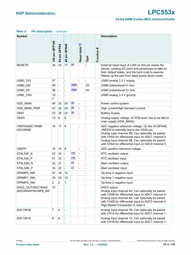
NXP Semiconductors LPC553x32-bit ARM Cortex-M33 microcontroller
RESETN 34 23 17 [5] - I External reset input: A LOW on this pin resets the device, causing I/O ports and peripherals to take on their default states, and the boot code to execute. Wakes up the part from deep power-down mode.
USB0_3V3 97 - - - - USB0 analog 3.3 V supply.
USB0_DM 99 - - [6][8] I/O USB0 bidirectional D- line.
USB0_DP 98 - - [6][8] I/O USB0 bidirectional D+ line.
USB0_VSS 100
- - USB0 analog 3.3 V ground.
VDD_MAIN 48 32 24 [9] - - Power control system.
VDD_MAIN_PWR 47 32 24 [9] - - High current/High transient current.
VBAT 53 35 25 [9] - - Battery Supply.
VDDA 13 8 6 - - Analog supply voltage. At PCB level, has to be tied to main supply (VDD_MAIN)
VREFN/ADC1IN5B/ADC0IN5B
16 11 9 - - ADC negative reference voltage. On the HVQFN48, VREFN is internally tied to the VSSA pin. Analog input channel 5B. Can optionally be paired with CH5A for differential input on ADC1 channel 5.Analog input channel 5B. Can optionally be paired with CH5A for differential input on ADC0 channel 5
VREFP 15 10 8 - - ADC positive reference voltage.
XTAL32K_N 52 34 - [10] - - RTC oscillator output.
XTAL32K_P 51 33 - [10] - - RTC oscillator input.
XTAL32M_N 32 21 - [7] - - Main oscillator output.
XTAL32M_P 33 22 - [7] - - Main oscillator input.
OPAMP0_INN 27 18 14 Op Amp 0 negative input.
OPAMP1_INN 29 20 16 Op Amp 1 negative input.
OPAMP2_INN 2 2 1 Op Amp 2 negative input.
DAC0_OUT/ADC1IN4A/ADC0IN4A/HSCMP0_IN5
31 - DAC0 output. Analog input channel 4A. Can optionally be paired with CH4B for differential input on ADC1 channel 4.Analog input channel 4A. Can optionally be paired with CH4B for differential input on ADC0 channel 4.High-Speed Comparator 0, input 5.
ADC1IN1B 7 5 - Analog input channel 1B. Can optionally be paired with CH1A for differential input on ADC1 channel 1.
ADC1IN1A 8 6 - Analog input channel 1A. Can optionally be paired with CH1B for differential input on ADC1 channel 1.
Table 3. Pin description …continued
Symbol
100
pin
QF
P1
00
64 p
in Q
FP
64
48 p
in Q
FN
48
Res
et
sta
te [1
]
Typ
e
Fu
nc
tio
n #
Description
LPC553x All information provided in this document is subject to legal disclaimers. © NXP Semiconductors B.V. 2022. All rights reserved.
Product data sheet Rev. 1.0 — 04/2022 49 of 158

NXP Semiconductors LPC553x32-bit ARM Cortex-M33 microcontroller
[1] PU = input mode, pull-up enabled (pull-up resistor pulls pin up towards VDD). PD = input mode, pull-down enabled (pull-down resistor pulls pin down towards VSS). Z = high impedance; pull-up, pull-down, and input disabled. AI = analog input. I = input. O = output. I/O = input/output. Reset state reflects the pin state at reset without boot code operation. For termination on unused pins, see Section 6.1.2 "Termination of unused pins".
[2] Pad with programmable glitch filter; provides digital I/O functions with TTL levels and hysteresis; normal drive strength. Pulse width of spikes or glitches suppressed by input filter is from 3 ns to 16 ns (simulated value).
[3] True open-drain pin. I2C-bus pins compliant with the I2C-bus specification for I2C standard mode, I2C Fast-mode, and I2C Fast-mode Plus. The pin requires an external pull-up to provide output functionality. When power is switched off, this pin is floating and does not disturb the I2C lines. Open-drain configuration applies to all functions on this pin.
[4] Pin providing standard digital I/O functions with configurable modes, configurable hysteresis, and analog input. When configured as an analog input, the digital section of the pin is disabled.
[5] Reset pad with glitch filter and hysteresis. Pulse width of spikes or glitches suppressed by input filter is from 3 ns to 20 ns (simulated value)
[6] Transparent analog pad.
[7] Optional bypass mode is supported, xtal32M_P can be driven by an external clock with restrictions in terms of drive level. See: Section 13. "Application information".
[8] The corresponding VBUS must be connected to supply voltage when using the USB peripheral. USB0_VBUS is not 5V tolerant.
[9] Main battery supply: Star connection at application level (PCB).
VREF_OUT/ADC1IN5A/ADC0IN5A
14 9 7 Output of the on-chip precision voltage reference from the VREG module. Can be 1.0 to 2.1V in 100mV steps. External capacitor (220 nF) is required. Analog input channel 5A. Can optionally be paired with CH5B for differential input on ADC1 channel 5.Analog input channel 5A. Can optionally be paired with CH5B for differential input on ADC0 channel 5
VSS exposed pad Ground for IOs
VSSA 17, 18
12 9 Analog ground. On the HVQFN48, ADC negative reference voltage.
VSS_MAIN_PWR 44 29 22 Star ground connection is managed to PCB ground plane.
VSS_MAIN 45 30 22 Star ground connection is managed to PCB ground plane.
VDDA 13 8 6 Analog supply voltage. At PCB level, has to be tied to main supply (VDD_MAIN).
VDD_CORE 38 24 18 Supply of DC-DC output stage. DC-DC core supply (references and regulation stages).
VDDIO_1 12, 43
8, 28
21, 5
Supply of Digital/Analog I/Os. Must be equal to VDD_MAIN.
VDDIO_2 63, 74, 85, 96
44, 56, 64
41 Supply of Digital I/Os/Analog I/Os. For Digital functions, voltage can be less than or equal to VDD_MAIN. For Analog functions, voltage must be equal to VDD_MAIN.
Table 3. Pin description …continued
Symbol
100
pin
QF
P1
00
64 p
in Q
FP
64
48 p
in Q
FN
48
Res
et
sta
te [1
]
Typ
e
Fu
nc
tio
n #
Description
LPC553x All information provided in this document is subject to legal disclaimers. © NXP Semiconductors B.V. 2022. All rights reserved.
Product data sheet Rev. 1.0 — 04/2022 50 of 158

NXP Semiconductors LPC553x32-bit ARM Cortex-M33 microcontroller
[10] Optional bypass mode is supported, xtal32K_P can be driven by an external clock with restrictions in terms of drive level See: Section 13. "Application information".
LPC553x All information provided in this document is subject to legal disclaimers. © NXP Semiconductors B.V. 2022. All rights reserved.
Product data sheet Rev. 1.0 — 04/2022 51 of 158

NXP Semiconductors LPC553x32-bit ARM Cortex-M33 microcontroller
6.1.1 Power Supply for pins
Table 4 shows the GPIOs belonging to the specific VDDIO groups domain. VDDIO_1 must be equal to VDD_MAIN. VDDIO_2 can be less than or equal to VDD_MAIN.
Table 4. Power Supply for pins
Pin GPIO pins
VDDIO_1 PIO0_1
PIO0_7 to PIO0_8
PIO0_10 to PIO0_12
PIO0_15 to PIO0_17
PIO0_23
PIO0_27
PIO0_31
PIO1_0
PIO1_5 to PIO1_10
PIO1_19 to PIO1_24
PIO2_0 to PIO2_1
RESETN
VDDIO_2 P0_0
P0_2 to P0_6
P0_9
P0_13 to P0_14
P0_18 to P0_22
P0_24 to P0_26
P0_28 to P0_30
P1_1 to P1_4
P1_11 to P1_18
P1_25 to P1_31
LPC553x All information provided in this document is subject to legal disclaimers. © NXP Semiconductors B.V. 2022. All rights reserved.
Product data sheet Rev. 1.0 — 04/2022 52 of 158

NXP Semiconductors LPC553x32-bit ARM Cortex-M33 microcontroller
6.1.2 Termination of unused pins
Table 5 shows how to terminate pins that are not used in the application. In many cases, unused pins should be connected externally or configured correctly by software to minimize the overall power consumption of the part.
Unused pins with GPIO function should be configured as outputs set to LOW with their internal pull-up disabled. To configure a GPIO pin as output and drive it LOW, select the GPIO function in the IOCON register, select output in the GPIO DIR register, and write a 0 to the GPIO PORT register for that pin. Disable the pull-up in the pin’s IOCON register.
In addition, it is recommended to configure all GPIO pins that are not bonded out on smaller packages as outputs driven LOW with their internal pull-up disabled.
[1] I = Input, IA = Inactive (no pull-up/pull-down enabled), PU = Pull-Up enabled
Table 5. Termination of unused pins
Pin Default state[1]
Recommended termination of unused pins
RESET I; PU The RESET pin can be left unconnected if the application does not use it.
all PIOn_m (not open-drain) I; PU Can be left unconnected if driven LOW and configured as GPIO output with pull-up or pull-down disabled by software.
PIOn_m (I2C open-drain) IA Can be left unconnected if driven LOW and configured as GPIO output by software.
XTAL32K_P - Connect to ground. When grounded, the RTC oscillator is disabled.
XTAL32K_N - Can be left unconnected.
XTAL32M_P - Connect to ground. When grounded, the RTC oscillator is disabled.
XTAL32M_N - Can be left unconnected.
VREFP - Tie to VDD_MAIN.
VREFN - Tie to VSS.
VDDA - Tie to VDD_MAIN.
VSSA - Tie to VSS.
USBn_DP F Can be left unconnected.
USBn_DM F Can be left unconnected.
USBn_3V3 F Tie to VDD_MAIN. If not using USB and using 1.8 V supply, USBn_3V3 can be connected to 1.8 V.
USBn_VSS F Tie to VSS.
USB0_VBUS F Tie to VDD_MAIN.
LPC553x All information provided in this document is subject to legal disclaimers. © NXP Semiconductors B.V. 2022. All rights reserved.
Product data sheet Rev. 1.0 — 04/2022 53 of 158

NXP Semiconductors LPC553x32-bit ARM Cortex-M33 microcontroller
6.1.3 Using Internal DC-DC converter
Fig 3. Using internal LDO
LPC55xx
C2
VDD_MAINVDD_CORE
VDD_MAIN_PWR
C3
C4 C1
22uF
100n
F
47pF 4.7u
F
VSS_MAIN_PWRVSS_MAIN
Fig 4. Using internal DC-DC converter
LPC55xx
C2
VDD_MAINVDD_CORE
LX
VDD_MAIN_PWR
C3
C4 C1L1
22uF
100n
F
47pF 4u7H 22uF
VSS_MAIN_PWRVSS_MAIN
LPC553x All information provided in this document is subject to legal disclaimers. © NXP Semiconductors B.V. 2022. All rights reserved.
Product data sheet Rev. 1.0 — 04/2022 54 of 158

NXP Semiconductors LPC553x32-bit ARM Cortex-M33 microcontroller
7. Functional description
7.1 Architectural overview
The Arm Cortex M33 includes two AHB-Lite buses, one system bus and one code bus. The Code AHB (C-AHB) interface is used for any instruction fetch and data access to the Code region of the ARMv8-M memory map ([0x00000000 - 0x1FFFFFFF]). The System AHB (S-AHB) interface is used for instruction fetch and data access to all other regions of the ARMv8-M memory map ([0x20000000 - 0xFFFFFFFF]).
The chip uses a multi-layer AHB matrix to connect the ARM Cortex-M33 buses and other bus masters to peripherals in a flexible manner that optimizes performance by allowing peripherals that are on different slave ports of the matrix to be accessed simultaneously by different bus masters. Section 5. "Block diagram" shows details of the available matrix connections.
7.2 Arm Cortex-M33 processor
The ARM Cortex-M33 is based on the ARMv8-M architecture that offers systems enhancements, such as ARM TrustZone® security, single-cycle digital signal processing, low power consumption, enhanced debug features, and a high level of support block integration. The ARM Cortex-M33 CPU employs a 3-stage instruction pipe and includes an internal prefetch unit that supports speculative branching. A hardware floating-point processor is integrated into the core. On the chip, the Cortex-M33 is augmented with two hardware co-processors providing accelerated support for additional DSP algorithms and cryptography.
The Arm Cortex M33 provides a security foundation, offering isolation to protect valuable IP and data with TrustZone technology. It simplifies the design and software development of digital signal control systems with the integrated digital signal processing (DSP) instructions.
7.3 Arm Cortex-M33 integrated Floating Point Unit (FPU)
The FPU fully supports single-precision add, subtract, multiply, divide, multiply and accumulate, and square root operations. It also provides conversions between fixed-point and floating-point data formats, and floating-point constant instructions.
The FPU provides floating-point computation functionality that is compliant with the ANSI/IEEE Std 754-2008, IEEE Standard for Binary Floating-Point Arithmetic, referred to as the IEEE 754 standard.
7.4 Memory Protection Unit (MPU)
The Cortex-M33 processor includes a Memory Protection Unit (MPU). The MPU provides fine grain memory control, enabling applications to implement security privilege levels, separating code, data, and stack on a task-by-task basis.
The MPU allows separating processing tasks by disabling access to memory regions, allowing memory regions to be defined as read-only, and detecting unexpected memory accesses.
LPC553x All information provided in this document is subject to legal disclaimers. © NXP Semiconductors B.V. 2022. All rights reserved.
Product data sheet Rev. 1.0 — 04/2022 55 of 158

NXP Semiconductors LPC553x32-bit ARM Cortex-M33 microcontroller
The MPU separates the memory into distinct regions and implements protection by preventing disallowed accesses. The MPU supports up to eight regions each of which can be divided into eight subregions. Accesses to memory locations that are not defined in the MPU regions, or not permitted by the region’s setting cause a Memory Management Fault exception.
The MPU register interface is located on the CPU private peripheral bus and is described in detail in Ref 1 “Cortex-M33 DEBUG”.
7.5 Nested Vectored Interrupt Controller (NVIC) for Cortex-M33
The NVIC is an integral part of the Cortex-M33. The tight coupling to the CPU allows for low interrupt latency and efficient processing of late arriving interrupts.
7.5.1 Features
• Controls system exceptions and peripheral interrupts.
• 118 vectored interrupts.
• Eight programmable interrupt priority levels, with hardware priority level masking.
• Relocatable vector table using Vector Table Offset Register (VTOR).
• Non-Maskable Interrupt (NMI).
• Software interrupt generation.
7.5.2 Interrupt sources
Each peripheral device has one interrupt line connected to the NVIC but may have several interrupt flags.
7.6 System Tick timer (SysTick)
The ARM Cortex-M33 core include a system tick timer (SysTick) that is intended to generate a dedicated SYSTICK exception. The clock source for the SysTick can be the system clock or the SYSTICK clock.
7.7 PowerQuad Hardware Accelerator
The chip has a PowerQuad hardware accelerator for CMSIS DSP functions (fixed and floating point unit) with support of SDK software API faster execution of ARM CMSIS instruction set. The PowerQuad is a hardware accelerator targeting common calculations in DSP applications. With the assistance of the PowerQuad, the Cortex-M33 can be freed to perform other tasks. While the PowerQuad is executing the assigned computation task, the CM33 can prepare the next PowerQuad task, resulting in a pipeline of PowerQuad tasks.
7.8 On-chip static RAM
The chip supports up to 128 kB SRAM with separate bus master access for higher throughput and individual power control for low-power operation.
Parity support on all RAM banks except RAM1 bank. ECC support available only on RAM1 bank.
LPC553x All information provided in this document is subject to legal disclaimers. © NXP Semiconductors B.V. 2022. All rights reserved.
Product data sheet Rev. 1.0 — 04/2022 56 of 158

NXP Semiconductors LPC553x32-bit ARM Cortex-M33 microcontroller
7.8.1 RAM partitions
Remark:RAM0 has 4 banks - RAM_00, RAM_01, RAM_02, RAM_03. In Power-down mode, RAM_00 is reserved for CPU state retention. RAM_01 can be used for stack.RAM1 has 1 bank - RAM_10.RAM2 has 1 bank - RAM_20.RAM3 has 1 bank - RAM_30.RAM4 has 4 banks - RAM_40, RAM_41, RAM_42, RAM_43. RAM4 is dedicated for PowerQuad use. If PowerQuad is not used, RAM4 can be used for general purpose.
Please refer to the Reference Manual (memory map) for further details.
7.9 On-chip flash
The chip supports up to 256 kB of on-chip flash memory.Remark: The last 18 pages (10 KB) are reserved on the 256 KB flash devices resulting in 246 KB internal flash memory.
7.10 On-chip ROM
The on-chip ROM contains the bootloader and the following features:
• Booting of images from on-chip flash
• Supports CRC32 image integrity checking.
• Supports flash programming through In System Programming (ISP) commands over following interfaces: USB0 interfaces using HID Class device, UART interface (Flexcomm 0) with auto baud, High-speed SPI slave interfaces using mode 3 (CPOL = 1 and CPHA = 1), I2C slave interface (Flexcomm 1), and CAN-FD ISP.
• ROM API functions: Flash programming API, Power control API, OTP eFuse programming API
• Support dual images (boot latest version) from on-chip flash using re-map feature.
• Support loading image to RAM from external Octal/QuadSPI device.
• Support booting XIP images present on Octal/QuadSPI devices.
• Support dual Execute-in-Place (XIP) images in Octal/QSPI flash through flash address remap feature.
• Support load-to-RAM boot mode from 1-bit SPI flash devices connected to Flexcomm (selectable by PFR) as normal boot option and recovery boot option.
• USB Device DFU Connection (Device only).
• Code Read protection (CRP) on non-secure devices.
• Crystal-less USB ISP mode.
Table 6. RAM Partition Table (Non-secure)
Type Number
Total SRAM (KB) (RAMX + RAM0 + RAM1 + RAM3 + RAM4)
RAMX
(16 KB)RAM0 (4x4 KB)
RAM1
(1x16 KB)
RAM2
(1x32 KB)
RAM3
(1x32 KB)RAM4 (4x4 KB)
LPC5534 96 16 16 16 32 - 16
LPC5536 128 16 16 16 32 32 16
LPC553x All information provided in this document is subject to legal disclaimers. © NXP Semiconductors B.V. 2022. All rights reserved.
Product data sheet Rev. 1.0 — 04/2022 57 of 158

NXP Semiconductors LPC553x32-bit ARM Cortex-M33 microcontroller
7.10.1 FlexSPI Flash Interface
The Flexible Serial Peripheral Interface (FlexSPI) host controller supports one port and up to 2 external devices. FlexSPI supports Single/Dual/Quad/Octal mode data transfer (1/2/4/8 bidirectional data lines).
FlexSPI flash interface with 8 KB cache with CACHE64 controller for execute-in-place and supports DMA.
Remark: HVQFN 48 pin package devices support FlexSPI boot only in Quad mode (4 data pins) flash devices. Due to no availability of upper data pins, Hyperflash and Octal mode flash devices are not supported.
7.10.1.1 Features
• FlexSPI complies with JEDEC’s JESD151 v1.0 for xSPI standard specification.
• Flexible sequence engine (LUT table) to support various vendor devices.
– Serial NOR Flash: XccelaFLash, HyperFlash, EcoXiP Flash, Octa Flash, and all QSPI flash devices
– Serial NAND Flash
– Serial pSRAM: HyperRAM, Xccela RAM (IoTRAM)
– FPGA device
• Flash access mode
– Single/Dual/Quad/Octal mode
– SDR/DDR mode
– Individual/Parallel mode
• Support sampling clock mode:
– Internal dummy read strobe looped back internally
– Internal dummy read strobe looped back from pad
– Flash provided read strobe
• Automatic Data Learning to select correct sample clock phase
• Memory mapped read/write access by AHB Bus
– AHB RX Buffer implemented to reduce read latency. Total AHB RX Buffer size: 256 * 64 Bits
– 16 AHB masters supported with priority for read access
– 8 flexible and configurable buffers in AHB RX Buffer
– AHB TX Buffer implemented to buffer all write data from one AHB burst. AHB TX Buffer size: 8 * 64 Bits
– All AHB masters share this AHB TX Buffer. No AHB master number limitation for Write Access.
• Software triggered Flash read/write access by IP Bus
– IP RX FIFO implemented to buffer all read data from External device. FIFO size: 64 * 64 Bits
– IP TX FIFO implemented to buffer all Write data to External device. FIFO size: 128 * 64 Bits
LPC553x All information provided in this document is subject to legal disclaimers. © NXP Semiconductors B.V. 2022. All rights reserved.
Product data sheet Rev. 1.0 — 04/2022 58 of 158

NXP Semiconductors LPC553x32-bit ARM Cortex-M33 microcontroller
– DMA support to fill IP TX FIFO
– DMA support to read IP RX FIFO
– SCLK stopped when reading flash data and IP RX FIFO is full
– SCLK stopped when writing flash data and IP TX FIFO is empty
7.11 Protected Flash Region (PFR)
The protected flash region is available to configure read UUID and user-defined fields available for specific data storage.
7.12 OTP eFuse
The One Time Programmable Memory (OTP) is used for device configuration. An additional 6 bytes of OTP memory is available for user application. The OTP eFuse also contains pre-programmed factory configuration data such as on-chip oscillator calibration values, among other things. It may also be used by customer applications to configure some details of device operation, and enforce ECDSA signature check aspects of device.
7.13 Memory mapping
Please refer to the Reference Manual for memory map overview and descriptions.
7.14 AHB multilayer matrix
The device uses a multi-layer AHB matrix to connect the CPU buses and other bus masters to peripherals in a flexible manner that optimizes performance by allowing peripherals that are on different slave ports of the matrix to be accessed simultaneously by different bus masters. The device block diagram in Section 5. "Block diagram" shows details of the available matrix connections.
7.15 System control
7.15.1 Clock sources
The device supports 2 external and 3 internal clock sources:
• Internal Free Running Oscillator (FRO). This oscillator provides a selectable 96 MHz output, and a 12 MHz output (divided down from the selected higher frequency) that can be used as a system clock. The FRO is trimmed to +/- 1% accuracy over the entire voltage and 0 C to 85 C. The FRO is trimmed to +/- 2% accuracy over the entire voltage and -40 C to 105 C. The FRO 12 MHz oscillator provides the default clock at reset and provides a clean system clock shortly after the supply pins reach operating voltage. On power-up, the chip boots up using FRO high-speed output at 96 MHz.
• 32 kHz Internal Free Running Oscillator FRO. The FRO is trimmed to +/- 2% accuracy over the entire voltage and temperature range.
• Internal low power oscillator (FRO 1 MHz). The FRO is trimmed to +/- 15% accuracy over the entire voltage and temperature range.
• Crystal oscillator with an operating frequency of 12 MHz to 25 MHz. Option for external clock input (bypass mode) for clock frequencies of up to 25 MHz
• Crystal oscillator with 32.768 kHz operating frequency.
LPC553x All information provided in this document is subject to legal disclaimers. © NXP Semiconductors B.V. 2022. All rights reserved.Product data sheet Rev. 1.0 — 04/2022 59 of 158

NXP Semiconductors LPC553x32-bit ARM Cortex-M33 microcontroller
Each crystal oscillator has one embedded capacitor bank, where each can be used as an integrated load capacitor for the crystal oscillators. Using APIs, the capacitor banks on each crystal pin can tune the frequency for crystals with a Capacitive Load (CL) leading to conserving board space and reducing costs. See: Section 13. "Application information".
7.15.2 PLL (PLL0 and PLL1)
PLL0 and PLL1 allows CPU operation up to the maximum CPU rate without the need for a high-frequency external clock. PLL0 and PLL1 can run from the internal FRO 12 MHz output, the external oscillator, internal FRO 1 MHz output, or the 32.768 kHz RTC oscillator.
The system PLL accepts an input clock frequency in the range of 2 kHz - 150 MHz. The input frequency is multiplied up to a high frequency with a Current Controlled Oscillator (CCO). The PLL can be enabled or disabled by software.
7.15.3 Clock generation
The system control block facilitates the clock generation. Many clocking variations are possible. Figure 5 gives an overview of potential clock options. Figure 7 describes signals on the clocking diagram. The maximum clock frequency is 150 MHz.
Remark: The indicated clock multiplexers shown in Figure 5 are synchronized. In order to operate, the currently selected clock must be running, and the clock to be switched to must also be running. This is so that the multiplexer can gracefully switch between the two clocks without glitches. Other clock multiplexers are not synchronized. The output divider can be stopped and restarted gracefully during switching if a glitch-free output is needed.
The low-power oscillator provides a frequency in the range of 1 MHz. The accuracy of this clock is limited to +/- 15% over temperature, voltage, and silicon processing variations after trimming made during assembly. To determine the actual watchdog oscillator output, use the frequency measure block.
The part contains one system PLL that can be configured to use a number of clock inputs and produce an output clock in the range of 1.2 MHz up to the maximum chip frequency, and can be used to run most on-chip functions. The output of the PLL can be monitored through the CLKOUT pin.
For 1.8 V operation CLKOUT limitation is 50 MHz (SLEW rate setting = 1) and for 3.3 V operation, limitation is 90 MHz (SLEW rate setting = 1).
Table 7. Clocking diagram signal name descriptions
Name Description
32k_osc The 32 kHz output of the RTC oscillator. The 32 kHz clock must be enabled in the RTCOSCCTRL register.
clk_in This is the internal clock that comes from the external oscillator.
frg_clk The output of each Fractional Rate Generator to Flexcomm clock. Each FRG and its source selection is shown in Figure 5.
fro_12m 12 MHz divided down from the currently selected on-chip FRO oscillator.
fro_hf The currently selected FRO high speed output at 96 MHz.
main_clk The main clock used by the CPU and AHB bus, and potentially many others. The main clock and its source selection are shown in Figure 5.
mclk_in The MCLK input function, when it is connected to a pin by selecting it in the IOCON block.
pll0_clk The output of the PLL0. The PLL0 and its source selection is shown in Figure 5.
LPC553x All information provided in this document is subject to legal disclaimers. © NXP Semiconductors B.V. 2022. All rights reserved.
Product data sheet Rev. 1.0 — 04/2022 60 of 158

NXP Semiconductors LPC553x32-bit ARM Cortex-M33 microcontroller
pll1_clk The output of the PLL1. The PLL1 and its source selection is shown in Figure 5.
fro_1m The output of the low power oscillator.
“none” A tied-off source that should be selected to save power when the output of the related multiplexer is not used.
Table 7. Clocking diagram signal name descriptions
Name Description
LPC553x All information provided in this document is subject to legal disclaimers. © NXP Semiconductors B.V. 2022. All rights reserved.
Product data sheet Rev. 1.0 — 04/2022 61 of 158

NXP Semiconductors LPC553x32-bit ARM Cortex-M33 microcontroller
Fig 5. Clock generation (Part 1 of 3)
FROHFDIV
fro_hf_divFRO_HF Divider
fro_hf
clk_in
Main clock select AMAINCLKSELA[1:0]
fro_1m
fro_12m
fro_hf
*
: synchronized multiplexer*
11
0110
00
xtalout
XO32M_CTRL
xtalinMain crystal
oscillatorxtal32MHz_freqme
Systick Clock Select SYSTICKCLKSEL0[2:0]
to System Tick Timer
fro_1m32k_osc"none"
111
001010
000
SYSTICKCLKDIV
Systick Clock Divider
main clk
Trace Clock Select TRACECLKSEL[2:0]
to Trace Clock for SWO
fro_1m32k_osc"none"
111
001010
000
TRACECLKDIV
Trace Clock Divider
main clk
clk_in
32k_osc
PLL0 clock select PLL0CLKSEL[2:0]
fro_1m
fro_12m
PLL0 settings
PLL0
"none"011
001010
000
111
pll0_clk
01 32k_osc
Flexcomm 32K Clock Select FC32KCLKSEL
01
XTAL32KFRO32K
RTC Clock Select PMC.RTCOSC32K
to RTC, Wake Timer, Subsecond counter
Main clock select B MAINCLKSELB[1:0]
main clkpll0_clk
32k_osc
*111
001010
000
pll1_clk
AHBCLKDIV
CPU Clock Divider to CPU, AHB bus,
Sync APB, etc.
MCLK Clock Select MCLKCLKSEL[2:0]
MCLKDIV
MCLK Divider
MCLK pin (output)pll0_clk
fro_hf
"none"001111
000
pll_clk_divPLL Clock Divider
pll0_clk
001111
000pll1_clknone
PLL select PLLCLKDIVSEL[2:0]
PLL1 Settings
PLL1pll1_clkfro_1m
fro_12m
011
001010
000
111
clk_in
32k_osc“none”
PLL1 clock select PLL1CLKSEL[2:0]
AHB_clk
CLOCK_CTRL
xo_to_adc_clk
clk_inenables
PLLCLKDIV(for Flexcomms)
LPC553x All information provided in this document is subject to legal disclaimers. © NXP Semiconductors B.V. 2022. All rights reserved.
Product data sheet Rev. 1.0 — 04/2022 62 of 158

NXP Semiconductors LPC553x32-bit ARM Cortex-M33 microcontroller
Fig 6. Clock generation (Part 2 of 3)
FRGCTRL[15:0]FRG clock select
FRGCLKSELn[2:0]
pll_clk_divfro_hf_div
main clk
Fractional Rate Divider (FRG)
1x instance per Flexcomm 0 through 7(mclk_in only connected if I2S is present in Flexcomm config)
to FCLK of Flexcomm[n]
Flexcomm clock select FCCLKSELn[2:0]
fro_12mfro_hf_div
main clk
fro_1m
32k_osc
011
001010
000
100101110111
mclk_in
111
001010
000
none
FLEXCOMMnCLKDIV
Flexcomm Clock Divider
"none"
USB0 clock select USB0CLKSEL[2:0]
USB0CLKDIV
FS USB Clock Divider
to FS USB
‘0’
‘0’
‘0’fro_hf
main clkpll0_clk
"none"
011
001010
000
100101110111
pll1_clk
FLEXSPI clock select FLEXSPICLKSEL[2:0]
FLEXSPICLKDIV
FlexSPI Divider
to FlexSPI function clock
‘0’
‘0’
‘0’fro_hf
main clkpll0_clk
"none"
011
001010
000
100101110111
pll1_clk
pll_clk_divfro_12mfro_hf_div
main clk
fro_1m
32k_osc
to FCLK of HS-SPI011
001010
000
100101110111
"none"
‘0’
001111
000main clkfro_hf_div"none"
I3CFCLKSEL [2:0]
I3CFCLKDIV
I3C FCLK Divider
fro_1m I3C TCLK Divider
I3CTCCLKDIVI3CFCLKSTCDIV[2:0]
To I3C0/1 FCLK
To I3C0/1 CLK_SLOW_TC
10
fro_1m I3C Slow clock Divider
To I3C0/1 CLK_SLOW
I3CFCLKSDIV
HS_SPI clock select HSSPICLKSEL[2:0]
LPC553x All information provided in this document is subject to legal disclaimers. © NXP Semiconductors B.V. 2022. All rights reserved.
Product data sheet Rev. 1.0 — 04/2022 63 of 158

NXP Semiconductors LPC553x32-bit ARM Cortex-M33 microcontroller
7.15.4 Brownout detection
The chip includes two Brown-out detectors to monitor the voltage of VDD_MAIN and VDD_CORE. If the voltage falls below one of the selected voltages, the BOD asserts an interrupt to the NVIC or issues a reset.
7.16 Power control
The chip supports a variety of power control features. In Active mode, when the chip is running, power and clocks to selected peripherals can be adjusted for power consumption. In addition, there are four special modes of processor power reduction with different peripherals running: sleep mode, deep-sleep mode, power-down mode, and deep power-down mode which can be activated by the power mode configure API.
Fig 7. Clock generation (Part 3 of 3)
CLKOUT selectCLKOUTSEL[2:0]
CLKOUTDIV
CLKOUT Divider
pll1_clk32k_osc
fro_1mfro_hf
main clkpll0_clk
"none"
011
001010
000
100101110111
CLKOUT
clk_in
SCT clock select SCTCLKSEL[2:0]
SCTCLKDIV
SCTimer/PWM Clock Divider
to SCTimer/PWM input clock 7
‘0’
clk_infro_hf
main clkpll0_clk
"none"
011
001010
000
100101110111
mclk_inpll1_clk
1x instance per DAC
DAC n clock selectDACnCLKSEL[2:0]
main_clk
fro_hf
"none"
pll0_clk
fro_12m011
001010
000
100101110111
DACnCLKDIV
DAC Divider
to DAC
pll1_clkfro_1m
‘0’
DMIC clock select DMICCLKSEL[2:0]
DMICCLKDIV
DMIC Clock Divider
to DMIC subsys
‘0’
clk_infro_hf
pll0_clk
"none"
011
001010
000
100101110111
mclk_inpll1_clk
main clk
1x instance per ADC
CTimer clock select nCTIMERCLKSELn[2:0]
to CTIMER n
main_clk
mclk_in
fro_hf
"none"
pll0_clk
1x instance per CTimer
fro_1m
32k_osc
011
001010
000
100101110111
pll1_clk
CTIMERnCLKDIV
CTIMER Divider
wdt_clkfro_1m WDT Divider
WDTCLKDIV [5:0]OS Event Timer clock select PMC.OSEVENTTIMER[4:3]
to OSTimer
111
001010
00032k_oscfro_1m
FRO32K
AHB_clk
pll0_clk
ADCnCLKDIV
ADC Clock Divider
to ADCfro_hf
main clk
"none"
ADC n clock selectADCnCLKSEL[2:0]
100
001010
000
111
xo_to_adc_clk
LPC553x All information provided in this document is subject to legal disclaimers. © NXP Semiconductors B.V. 2022. All rights reserved.
Product data sheet Rev. 1.0 — 04/2022 64 of 158

NXP Semiconductors LPC553x32-bit ARM Cortex-M33 microcontroller
7.16.1 DC-DC Buck Converter and Low Drop-Out (LDO)
The chip has an internal DC-DC Buck Converter and an internal Low Drop-Out (LDO) regulator where either can be selected as a supply source to the Core Logic and System Power domains. Both on-chip regulators convert input supply voltage (ranging from1.8 V to 3.6 V via VDD_MAIN pin) to a fixed output voltage. The optimum internal output voltage is automatically set up when calling the POWER_SetVoltageForFrequency API function. To switch between the DC-DC and the LDO_CORE use the POWER_SetCorePowerSource power API function.
7.16.2 Sleep mode
In Sleep mode, the system clock to the CPU is stopped and execution of instructions is suspended until either a reset or interrupt occurs. Peripheral functions, if selected to be clocked can continue operation during Sleep mode and may generate interrupts to cause the processor to resume execution. Sleep mode eliminates dynamic power used by the processor itself, memory systems and related controllers, internal buses, and unused peripherals.
7.16.3 Deep-sleep mode
In Deep-sleep mode, the flash is powered down. The system clock to the CPU is stopped and if not configured, the peripherals receives no clocks. Through the power profiles API, selected peripherals such as USB0, Flexcomm interfaces 0 to 7 (SPI, I2C, USART, I2S), Flexcomm interface 8 (High Speed SPI), Micro-tick, WWDT, RTC, OSTimer, Standard Timers, comparator, and BOD can be left running in Deep-sleep mode. Clock sources such as FRO 12 MHz, FRO 32 kHz, FRO 1 MHz, the 32.768 kHz RTC clock, and the external oscillator can be enabled or disabled via software.
The chip can wake up from Deep-sleep mode via a reset, digital pins selected as inputs to the pin interrupt block and group interrupt block, OS Timer, Standard Timers, Micro-tick, RTC alarm, a watchdog timer interrupt/reset, BOD interrupt/reset, an interrupt from the USB0, SPI, I2C, I2S, USART, and comparator. Some peripherals can have DMA service during Deep-sleep mode without waking up entire device.
In Deep-sleep mode, all SRAM, logic state, and registers maintain their internal states. All SRAM instances that are not configured to enter in ‘retention state’ will stay in active state. Deep-sleep mode allows for very low quiescent power and fast wake-up options.
7.16.4 Power-down mode
In Power-down mode, nearly all on-chip power consumption is turned off by shutting down the internal DC-DC converter. The flash is powered down. The system clock to the CPU is stopped and if not configured, the peripherals receives no clocks. Through the power profiles API, selected peripherals such as Flexcomm interfaces 3 (SPI, I2C, USART, I2S), RTC, OS Timer, and comparator can be left running in power-down mode. Clock sources such as FRO 32 kHz, and the 32.768 kHz RTC clock can be enabled or disabled via software.
The chip can wake up from Power-down mode via a reset, digital pins selected as inputs to the group interrupt block, OS Timer, RTC alarm, an interrupt from the Flexcomm Interface 3 (SPI, I2C, I2S, USART), and comparator.
In Power-down mode, the CPU processor state is retained to allow resumption of code execution when a wake-up event occurs.
LPC553x All information provided in this document is subject to legal disclaimers. © NXP Semiconductors B.V. 2022. All rights reserved.
Product data sheet Rev. 1.0 — 04/2022 65 of 158

NXP Semiconductors LPC553x32-bit ARM Cortex-M33 microcontroller
All SRAM, logic state, and registers maintain their internal states. All SRAM instances that are not configured to enter in ‘retention state’ will enter in ‘shutdown’ state.
7.16.5 Deep Power-down mode
In Deep Power-down mode, power is shut off to the entire chip except for the RTC power domain, the RESET pin, 4 Wake-up pins, and the OT Timer if enabled. Clock sources such as FRO 32 kHz, and the 32.768 kHz RTC clock can be enabled or disabled via software. The chip can wake up from Deep Power-down mode via the RESET pin, the RTC alarm, four special wake-up pins, or without an external signal, by using the time-out of the OS Timer. The ALARM1HZ flag in RTC control register generates an RTC wake-up interrupt request, which can wake up the part. SRAM can maintain their internal states. All SRAM instances that are not configured to enter in ‘retention state’ will enter in ‘shutdown’ state. In Deep Power-down mode all functional pins are in tri-state.
7.17 General Purpose I/O (GPIO)
The chip provides GPIO ports 0 and 1 with a total of up to 64 GPIO pins.
Device pins that are not connected to a specific peripheral function are controlled by the GPIO registers. Pins may be dynamically configured as inputs or outputs. Separate registers allow setting or clearing any number of outputs simultaneously. The current level of a port pin can be read back no matter what peripheral is selected for that pin.
See Table 5 for the default state on reset.
7.17.1 Features
• Accelerated GPIO functions:
– GPIO registers are located on the AHB so that the fastest possible I/O timing can be achieved.
– Mask registers allow treating sets of port bits as a group, leaving other bits unchanged.
– All GPIO registers are byte and half-word addressable.
– Entire port value can be written in one instruction.
• Bit-level set, clear, and toggle registers allow a single instruction set, clear or toggle of any number of bits in one port.
• Direction control of individual bits.
• All I/O default to inputs after reset.
• All GPIO pins can be selected to create an edge or level-sensitive GPIO interrupt request.
• Two GPIO group interrupts can be triggered by a combination of any pin or pins to reflect two distinct interrupt patterns.
• The grouped interrupts can wake up the part from sleep, deep-sleep, and power-down modes.
LPC553x All information provided in this document is subject to legal disclaimers. © NXP Semiconductors B.V. 2022. All rights reserved.
Product data sheet Rev. 1.0 — 04/2022 66 of 158

NXP Semiconductors LPC553x32-bit ARM Cortex-M33 microcontroller
7.18 Pin interrupt/pattern engine
The pin interrupt block configures up to eight pins from all digital pins for providing eight external interrupts connected to the NVIC. The pattern match engine can be used in conjunction with software to create complex state machines based on pin inputs. Any digital pin, independent of the function selected through the switch matrix can be configured through the SYSCON block as an input to the pin interrupt or pattern match engine. The registers that control the pin interrupt or pattern match engine are located on the I/O+ bus for fast single-cycle access.
7.18.1 Features
• Pin interrupts:
– Up to eight pins can be selected from all GPIO pins on ports 0 and 1 as edge-sensitive or level-sensitive interrupt requests. Each request creates a separate interrupt in the NVIC.
– Edge-sensitive interrupt pins can interrupt on rising or falling edges or both.
– Level-sensitive interrupt pins can be HIGH-active or LOW-active.
– Level-sensitive interrupt pins can be HIGH-active or LOW-active.
– Pin interrupts can wake up the device from sleep mode, and deep-sleep mode.
• Pattern match engine:
– Up to eight pins can be selected from all digital pins on ports 0 and 1 to contribute to a boolean expression. The boolean expression consists of specified levels and/or transitions on various combinations of these pins.
– Each bit slice minterm (product term) comprising of the specified boolean expression can generate its own, dedicated interrupt request.
– Any occurrence of a pattern match can also be programmed to generate an RXEV notification to the CPU. The RXEV signal can be connected to a pin.
– Pattern match can be used in conjunction with software to create complex state machines based on pin inputs.
– Pattern match engine facilities wake-up only from active and sleep modes.
7.19 Communication peripherals
7.19.1 Full-speed USB Host/Device Interface (USB0)
The USB is a 4-wire bus that supports communication between ahost and one or more (up to 127) peripherals. The host controller allocates the USBbandwidth to attached devices through a token-based protocol. The bus supports hotplugging and dynamic configuration of the devices. All transactions are initiated by the host controller.
7.19.1.1 USB0 device controller
The device controller enables 12 Mbit/s data exchange with a USB host controller. Itconsists of a register interface, serial interface engine, endpoint buffer memory. The serialinterface engine decodes the USB data stream and writes data to the appropriateendpoint buffer. The status of a completed USB transfer or error condition is indicated via status registers. An interrupt is also generated if enabled.
LPC553x All information provided in this document is subject to legal disclaimers. © NXP Semiconductors B.V. 2022. All rights reserved.
Product data sheet Rev. 1.0 — 04/2022 67 of 158

NXP Semiconductors LPC553x32-bit ARM Cortex-M33 microcontroller
Features
• USB2.0 full-speed device controller supporting crystal-less operation in device mode using software library example in technical note.
• Supports ten physical (five logical) endpoints including one control endpoint.
• Single and double-buffering supported.
• Each non-control endpoint supports bulk, interrupt, or isochronous endpoint types.
• Supports wake-up from Deep-sleep mode on USB activity and remote wake-up.
• Supports SoftConnect.
• Link Power Management (LPM) supported.
7.19.1.2 USB0 host controller
The host controller enables full- and low-speed data exchange with USB devices attachedto the bus. It consists of register interface, serial interface engine and DMA controller. The register interface complies with the Open Host Controller Interface (OHCI) specification.
Features
• OHCI compliant.
• Two downstream ports.
7.19.2 Flexcomm Interface serial communication
Each Flexcomm Interface provides a choice of peripheral functions, one of which must be chosen by the user before the function can be configured and used.
7.19.2.1 Features
• USART with asynchronous operation or synchronous master or slave operation.
• SPI master or slave with up to 4 slave selects.
• I2C, including separate master, slave, and monitor functions.
• Flexcomm interfaces 0 to 5 each provide one channel pair of I2S and Flexcomm interfaces 6 to 7 each provide four channel pairs of I2S.
• Data for USART, SPI, and I2S traffic uses the Flexcomm FIFO. The I2C function does not use the FIFO.
7.19.2.2 SPI serial I/O (SPIO) controller
Features
Maximum supported bit rate for SPI master mode (transmit/receive) is 50 Mbit/s. The maximum supported bit rate for SPI slave receive mode is 20 Mbit/s (100 MHz ≤ CPU clock ≤ 150 MHz) / 12.5 Mbit/s (CPU clock < 100 MHz) and for SPI slave transmit mode is 50 Mbits/s.
• Master and slave operation.
• Data frames of 4 to 16 bits supported directly. Larger frames supported by software.
• The SPI function supports separate transmit and receive FIFOs with eight entries each.
LPC553x All information provided in this document is subject to legal disclaimers. © NXP Semiconductors B.V. 2022. All rights reserved.
Product data sheet Rev. 1.0 — 04/2022 68 of 158

NXP Semiconductors LPC553x32-bit ARM Cortex-M33 microcontroller
• Supports DMA transfers: SPIn transmit and receive functions can operated with the system DMA controller.
• Data can be transmitted to a slave without the need to read incoming data. This can be useful while setting up an SPI memory.
• Up to Four Slave Select input/outputs with selectable polarity and flexible usage.
7.19.2.3 I2C-bus interface
The I2C-bus is bidirectional for inter-IC control using only two wires: a serial clock line (SCL) and a serial data line (SDA). Each device is recognized by a unique address and can operate as either a receiver-only device (for example, an LCD driver) or a transmitter with the capability to both receive and send information (such as memory). Transmitters and/or receivers can operate in either master or slave mode, depending on whether the chip has to initiate a data transfer or is only addressed. The I2C is a multi-master bus and can be controlled by more than one bus master connected to it.
Features
• Support standard, Fast-mode, and Fast-mode Plus (specific I2C pins) with data rates of up to 1 Mbit/s.
• Support high-speed slave mode with data rates of up to 3.4 Mbit/s (specific I2C pins).
• Independent Master, Slave, and Monitor functions.
• Supports both Multi-master and Multi-master with Slave functions.
• Multiple I2C slave addresses supported in hardware.
• One slave address can be selectively qualified with a bit mask or an address range in order to respond to multiple I2C-bus addresses.
• 10-bit addressing supported with software assist.
• Supports SMBus.
• Separate DMA requests for master, slave, and monitor functions.
• No chip clocks are required in order to receive and compare an address as a slave, so this event can wake-up the device from deep-sleep mode.
• Automatic modes optionally allow less software overhead for some use cases.
7.19.2.4 USART
Features
• Maximum bit rates of 10 Mbit/s in asynchronous mode and 12 Mbit/s in synchronous mode for USART functions.
• 7, 8, or 9 data bits and 1 or 2 stop bits.
• Synchronous mode with master or slave operation. Includes data phase selection and continuous clock option.
• Multiprocessor/multidrop (9-bit) mode with software address compare.
• RS-485 transceiver output enable.
• Autobaud mode for automatic baud rate detection
• Parity generation and checking: odd, even, or none.
• Software selectable oversampling from 5 to 16 clocks in asynchronous mode.
LPC553x All information provided in this document is subject to legal disclaimers. © NXP Semiconductors B.V. 2022. All rights reserved.
Product data sheet Rev. 1.0 — 04/2022 69 of 158

NXP Semiconductors LPC553x32-bit ARM Cortex-M33 microcontroller
• One transmit and one receive data buffer.
• RTS/CTS for hardware signaling for automatic flow control. Software flow control can be performed using Delta CTS detect, Transmit Disable control, and any GPIO as an RTS output.
• Received data and status can optionally be read from a single register
• Break generation and detection.
• Receive data is 2 of 3 sample "voting". Status flag set when one sample differs.
• Built-in Baud Rate Generator with auto-baud function.
• A fractional rate divider is shared among all USARTs.
• Interrupts available for Receiver Ready, Transmitter Ready, Receiver Idle, change in receiver break detect, Framing error, Parity error, Overrun, Underrun, Delta CTS detect, and receiver sample noise detected.
• Loopback mode for testing of data and flow control.
• In synchronous slave mode, wakes up the part from deep-sleep and deep-sleep2 modes.
• Special operating mode allows operation at up to 9600 baud using the 32.768 kHz RTC oscillator as the UART clock. This mode can be used while the device is in deep-sleep and can wake-up the device when a character is received.
• USART transmit and receive functions work with the system DMA controller.
• The USART function supports separate transmit and receive FIFO with 16 entries each.
7.19.2.5 I2S-bus interface
The I2S bus provides a standard communication interface for streaming data transfer applications such as digital audio or data collection. The I2S bus specification defines a 3-wire serial bus with one data, one clock, and one word select/frame trigger signal, providing single or dual (mono or stereo) audio data transfer in addition to other configurations. Each Flexcomm Interface (0 to 5) implements one I2S channel pair and each Flexcomm Interface (6 to 7) implement four I2S channel pairs.
The I2S interface within one Flexcomm Interface provides one channel pair that can be configured as a master or a slave. Other channel pairs, if present, always operate as slaves. All of the channel pairs within one Flexcomm Interface share one set of I2S signals, and are configured together for either transmit or receive operation, using the same mode, same data configuration, and frame configuration. All such channel pairs can participate in a Time Division Multiplexing (TDM) arrangement. For cases requiring an MCLK input and/or output, this is handled outside of the I2S block in the system level clocking scheme.
Features
• A Flexcomm Interface can implement one or more I2S channel pairs, the first of which could be a master or a slave, and the rest would be slaves. All channel pairs are configured together for either transmit or receive and other shared attributes.
• Flexcomm interfaces 0 to 5 each provide one channel pair of I2S function. Other channel pairs, if present, always operate as slaves.
LPC553x All information provided in this document is subject to legal disclaimers. © NXP Semiconductors B.V. 2022. All rights reserved.
Product data sheet Rev. 1.0 — 04/2022 70 of 158

NXP Semiconductors LPC553x32-bit ARM Cortex-M33 microcontroller
• Configurable data size for all channels within one Flexcomm Interface, from 4 bits to 32 bits. Each channel pair can also be configured independently to act as a single channel (mono as opposed to stereo operation).
• All channel pairs within one Flexcomm Interface share a single bit clock (SCK) and word select/frame trigger (WS), and data line (SDA).
• Data for all I2S traffic within one Flexcomm Interface uses the Flexcomm FIFO. The FIFO depth is 8 entries.
• Left justified and right justified data modes.
• DMA support using FIFO level triggering.
• TDM with a several stereo slots and/or mono slots is supported. Each channel pair can act as any data slot. Multiple channel pairs can participate as different slots on one TDM data line.
• The bit clock and WS can be selectively inverted.
• Sampling frequencies supported depends on the specific device configuration and applications constraints (For example, system clock frequency and PLL availability) but generally supports standard audio data rates.
7.19.3 High-Speed SPI serial I/O (SPIO controller)
7.19.3.1 Features
• Master and slave operation.
• Excluding delays introduced by external device and PCB, the maximum supported bit rate for SPI master mode (transmit/receive) is 50 Mbit/s. Excluding delays introduced by external device and PCB, the maximum supported bit rate for SPI slave receive mode is 50 Mbit/s and for SPI slave transmit mode is 30 Mbit/s (100 MHz ≤ CPU clock ≤ 150 MHz) and 25 Mbit/s (CPU clock < 100 MHz).
• Data frames of 4 to 16 bits supported directly. Larger frames supported by software.
• The SPI function supports separate transmit and receive FIFOs with eight entries each.
• Supports DMA transfers: SPIn transmit and receive functions can operated with the system DMA controller.
• Data can be transmitted to a slave without the need to read incoming data. This can be useful while setting up an SPI memory.
• Up to Four Slave Select input/outputs with selectable polarity and flexible usage.
7.19.4 I3C interface
The MIPI Alliance Improved Inter-Integrated Circuit (MIPI I3C) brings major improvementsin use and power over I2C, and provides an alternative to SPI for mid-speedapplications.The I3C bus is designed to support future sensor interface architectures,widely expected in Internet-of-Things applications. The I3C bus is intended to be used by microcontrollers (MCU) and application processors (AP) to connect to sensors, actuators, and other MCUs (as slaves). Connecting an MCU to other MCUs and connecting an AP to an MCU are considered to be the major use cases.
LPC553x All information provided in this document is subject to legal disclaimers. © NXP Semiconductors B.V. 2022. All rights reserved.
Product data sheet Rev. 1.0 — 04/2022 71 of 158

NXP Semiconductors LPC553x32-bit ARM Cortex-M33 microcontroller
7.19.4.1 Features
• In-band interrupts: interrupts can go from Slave to Master without extra wires, such that the Master knows which Slave sent the interrupt.
• In-band command codes (Common Command Codes (CCC)).
• Dynamic addressing.
• Multi-master / multi-drop.
• Hot-Join.
• I2C compatibility. Note that I2C compatibility has limitations. Please refer to Reference Manual for further details.
7.20 CAN Flexible Data (CAN FD) interface
The chip contains a CAN FD interface.
7.20.1 Features
• Conforms with CAN protocol version 2.0 part A, B and ISO 11898-1.
• CAN FD with up to 64 data bytes supported.
• CAN Error Logging.
• AUTOSAR support.
• SAE J1939 support.
• Improved acceptance filtering.
7.21 Standard counter/timers (CT32B0 to 4)
The chip includes five general-purpose 32-bit timer/counters.
The timer/counter is designed to count cycles of the system derived clock or an externally-supplied clock. It can optionally generate interrupts, generate timed DMA requests, or perform other actions at specified timer values, based on four match registers. Each timer/counter also includes two capture inputs to trap the timer value when an input signal transitions, optionally generating an interrupt.
7.21.1 Features
• A 32-bit timer/counter with a programmable 32-bit prescaler.
• Counter or timer operation.
• Up to four 32-bit capture channels per timer, that can take a snapshot of the timer value when an input signal transitions. A capture event may also generate an interrupt.
• The timer and prescaler may be configured to be cleared on a designated capture
event. This feature permits easy pulse width measurement by clearing the timer on
the leading edge of an input pulse and capturing the timer value on the trailing edge.
• Four 32-bit match registers that allow:
– Continuous operation with optional interrupt generation on match.
– Stop timer on match with optional interrupt generation.
LPC553x All information provided in this document is subject to legal disclaimers. © NXP Semiconductors B.V. 2022. All rights reserved.
Product data sheet Rev. 1.0 — 04/2022 72 of 158

NXP Semiconductors LPC553x32-bit ARM Cortex-M33 microcontroller
– Reset timer on match with optional interrupt generation.
• Up to four external outputs per timer corresponding to match registers with the following capabilities:
– Set LOW on match.
– Set HIGH on match.
– Toggle on match.
– Do nothing on match.
• Up to two match registers can be used to generate timed DMA requests.
• Up to 4 match registers can be configured for PWM operation, allowing up to 3 single edged controlled PWM outputs.WM mode using up to three match channels for PWM output.
7.22 SCTimer/PWM subsystem
The SCTimer/PWM is a flexible timer module capable of creating complex PWM waveforms and performing other advanced timing and control operations with minimal or no CPU intervention.
The SCTimer/PWM can operate as a single 32-bit counter or as two independent, 16-bit counters in uni-directional or bi-directional mode. It supports a selection of match registers against which the count value can be compared, and capture registers where the current count value can be recorded when some pre-defined condition is detected.
The SCTimer/PWM module supports multiple separate events that can be defined by the user based on some combination of parameters including a match on one of the match registers, and/or a transition on one of the SCTimer/PWM inputs or outputs, the direction of count, and other factors.
Every action that the SCTimer/PWM block can perform occurs in direct response to one of these user-defined events without any software overhead. Any event can be enabled to:
• Start, stop, or halt the counter.
• Limit the counter which means to clear the counter in unidirectional mode or change its direction in bi-directional mode.
• Set, clear, or toggle any SCTimer/PWM output.
• Force a capture of the count value into any capture registers.
• Generate an interrupt of DMA request.
7.22.1 Features
• The SCTimer/PWM Supports:
– Eight inputs.
– Ten outputs.
– Sixteen match/capture registers.
– Sixteen events.
– Thirty two states.
– Match register 0 to 5 support a fractional component for the dither engine .
LPC553x All information provided in this document is subject to legal disclaimers. © NXP Semiconductors B.V. 2022. All rights reserved.
Product data sheet Rev. 1.0 — 04/2022 73 of 158

NXP Semiconductors LPC553x32-bit ARM Cortex-M33 microcontroller
• Counter/timer features:
– Each SCTimer/PWM is configurable as two 16-bit counters or one 32-bit counter.
– Counters clocked by system clock or selected input.
– Configurable number of match and capture registers. Up to sixteen match and capture registers total.
– Sixteen events.
– Thirty two states.
– Upon match and/or an input or output transition create the following events: interrupt; stop, limit, halt the timer or change counting direction; toggle outputs; change the state.
– Counter value can be loaded into capture register triggered by a match or input/output toggle.
• PWM features:
– Counters can be used in conjunction with match registers to toggle outputs and create time-proportioned PWM signals.
– Up to ten single-edge or eight dual-edge PWM outputs with independent duty cycle and common PWM cycle length.
• Event creation features:
– The following conditions define an event: a counter match condition, an input (or output) condition such as an rising or falling edge or level, a combination of match and/or input/output condition.
– Selected events can limit, halt, start, or stop a counter or change its direction.
– Events trigger state changes, output toggles, interrupts, and DMA transactions.
– Match register 0 can be used as an automatic limit.
– In bi-directional mode, events can be enabled based on the count direction.
– Match events can be held until another qualifying event occurs.
• State control features:
– A state is defined by events that can happen in the state while the counter is running.
– A state changes into another state as a result of an event.
– Each event can be assigned to one or more states.
– State variable allows sequencing across multiple counter cycles.
– Dither engine for improved average resolution of pulse edges.
7.23 Windowed Watchdog Timer (WWDT)
The purpose of the Watchdog Timer is to reset or interrupt the microcontroller within a programmable time if it enters an erroneous state. When enabled, a watchdog reset is generated if the user program fails to feed (reload) the Watchdog within a predetermined amount of time.
7.23.1 Features
• Internally resets chip if not reloaded during the programmable time-out period.
LPC553x All information provided in this document is subject to legal disclaimers. © NXP Semiconductors B.V. 2022. All rights reserved.
Product data sheet Rev. 1.0 — 04/2022 74 of 158

NXP Semiconductors LPC553x32-bit ARM Cortex-M33 microcontroller
• Optional windowed operation requires reload to occur between a minimum and maximum time period, both programmable.
• Optional warning interrupt can be generated at a programmable time prior to watchdog time-out.
• Programmable 24-bit timer with internal fixed pre-scaler.
• Selectable time period from 1,024 watchdog clocks (TWDCLK × 256 × 4) to over 67 million watchdog clocks (TWDCLK × 224 × 4) in increments of four watchdog clocks.
• “Safe” watchdog operation. Once enabled, requires a hardware reset or a Watchdog reset to be disabled.
• Incorrect feed sequence causes immediate watchdog event if enabled.
• The watchdog reload value can optionally be protected such that it can only be changed after the “warning interrupt” time is reached.
• Flag to indicate Watchdog reset.
• The watchdog clock (WDCLK) is generated from always on FRO_1MHz clock which can be divided by WDT clock divider register. The accuracy of this clock is limited to +/- 15% over temperature, voltage, and silicon processing variations.
• The Watchdog timer can be configured to run in Deep-sleep mode.
• Debug mode.
7.24 Code Watchdog Timer (CDOG)
Code Watchdog Timer for detecting code flow integrity.
7.24.1 Features
• Secure Counter (SEC_CNT) to detect altered software in the execution flow.
• Instruction Timer (INST_TIMER) which places a hard upper-limit on the interval between checks of the secure counter.
7.25 RTC timer
The RTC block can be used to count seconds and generate an alarm interrupt to the processor whenever the counter value equals the value programmed into the associated 32-bit match register.
7.25.1 Features
• The RTC resides in a separate “always-on” voltage domain with battery backup. It utilizes an independent oscillator which is also in the “always-on” domain.
• The RTC oscillator has the following clock outputs: 32.768 kHz clock (named as 32 kHz clock in rest of this chapter) 32 kHz clock, selectable for system clock and CLKOUT pin, 1 Hz clock for RTC timing, and 1024 Hz clock (named as 1 kHz clock in rest of this chapter) for high-resolution RTC timing.
• 32-bit, 1 Hz RTC counter and associated match register for alarm generation.
• 15-bit, 32kHz sub-second counter (not in always-on domain).
• Separate 16-bit high-resolution/wake-up timer clocked at 1 kHz for 1 ms resolution with a more that one minute maximum time-out period.
LPC553x All information provided in this document is subject to legal disclaimers. © NXP Semiconductors B.V. 2022. All rights reserved.
Product data sheet Rev. 1.0 — 04/2022 75 of 158

NXP Semiconductors LPC553x32-bit ARM Cortex-M33 microcontroller
• RTC alarm and high-resolution/wake-up timer time-out each generate independent interrupt requests that go to one NVIC channel. Either time-out can wake up the part from any of the low power modes, including deep power-down.
• Eight 32-bit general purpose registers can retain data in deep power-down or in the event of a power failure, provided there is battery backup.
• Calendar Feature.
7.26 Multi-Rate Timer (MRT)
The Multi-Rate Timer (MRT) provides a repetitive interrupt timer with four channels. Each channel can be programmed with an independent time interval, and each channel operates independently from the other channels.
7.26.1 Features
• 24-bit interrupt timer.
• Four channels independently counting down from individually set values.
• Repeat interrupt, one-shot interrupt, and one-shot bus stall modes.
7.27 OS Timer
42-bit free running timer with individual match/capture and interrupt generation logic used as continuous time-base for the system, available in any reduced power modes. It runs on 32kHz clock source, allowing a count period of more than 4 years.
7.27.1 Features
• Central 42-bit, free-running gray-code event/timestamp timer.
• Match registers compared to the main counter to generate an interrupt and/or wake-up event.
• Capture registers triggered by CPU command, readable via the AHB/IPS bus.
• APB interface for register access.
• IRQ and wake-up.
• Reads of gray-encoded timers are accomplished with no synchronization latency.
7.28 Micro-tick timer (UTICK)
The ultra-low power Micro-tick Timer, running from the Watchdog oscillator, can be used to wake up the device from Sleep and Deep-sleep modes.
7.28.1 Features
• Ultra simple timer.
• Write once to start.
• Interrupt or software polling.
• Four capture registers that can be triggered by external pin transitions.
7.29 Motor Control Subsystem
The following motor control subsystems are provided.
LPC553x All information provided in this document is subject to legal disclaimers. © NXP Semiconductors B.V. 2022. All rights reserved.
Product data sheet Rev. 1.0 — 04/2022 76 of 158

NXP Semiconductors LPC553x32-bit ARM Cortex-M33 microcontroller
7.29.1 FlexPWM
Two FlexPWMs with 4 sub-modules, providing 24 PWM outputs, supporting two 3-phase motors..
7.29.1.1 Features
• Supports Velocity and Position control of BLDC & PMSM motors.
• Implements Field Orient Control (FOC) using Back EMF to improve motor efficiency.
• Programmable supports to place PWM outputs in inactive state during Stop, Wait, Debug states.
• Enable dither support (FRAC=0).
7.29.2 QEI
Two Quadrature Encoder/Decoders (QEIs) are available.
The enhanced quadrature Encoder/ decoder module provides interfacing capability to position/speed sensors used in industrial motor control applications. It has five input signals: PHASEA, PHASEB, INDEX, TRIGGER, and HOME. This module is used to decode shaft position, revolution count and speed.
7.29.3 OpAmps
Three OpAmps with programmable VREF are available on the chip.
7.29.4 Comparators
Four analog comparators (One comparator in the always On domain and three high speed comparators in the Core domain) can compare voltage levels on external pins and internal voltages.
7.29.4.1 Features
• Selectable external inputs can be used as either the positive or negative input of the comparator.
• Voltage ladder source selectable between the supply, multiplexing between internal VDD_MAIN and ACMP0VREF.
• 32-stage voltage ladder can be used as either the positive or negative input of the comparator.
• Supports standard and low power modes
• Interrupt capability.
7.30 Digital peripherals
7.30.1 DMA controller
The DMA controller allows peripheral-to memory, memory-to-peripheral, and memory-to-memory transactions. Each DMA stream provides unidirectional DMA transfers for a single source and destination.
Two identical DMA controllers are provided on the chip.
LPC553x All information provided in this document is subject to legal disclaimers. © NXP Semiconductors B.V. 2022. All rights reserved.
Product data sheet Rev. 1.0 — 04/2022 77 of 158

NXP Semiconductors LPC553x32-bit ARM Cortex-M33 microcontroller
7.30.1.1 Features
• DMA0: 52 channels, 45 of which are connected to peripheral DMA requests. These come from the Flexcomm (USART, SPI, I2C, and I2S), high-speed SPI interface, ADC, AES, and SHA interfaces. 53 trigger sources are available.
• DMA1: 16 channels, 12 of which are connected to peripheral DMA requests. These come from the Flexcomm Interfaces, high-speed SPI interface, AES, and SHA interfaces. 25 trigger sources are available.
• DMA operations can be triggered by on-chip or off-chip events.
• Priority is user selectable for each channel (up to eight priority levels).
• Continuous priority arbitration.
• Address cache with four entries.
• Efficient use of data bus.
• Supports single transfers up to 1,024 words.
• Address increment options allow packing and/or unpacking data.
7.30.2 DMIC subsystem
The DMIC subsystem, including the dual-channel digital PDM microphone interface (DMIC) and hardware voice activity detector (HWVAD), is available.
7.30.2.1 Features
• Pulse-Density Modulation (PDM) data input for 2-left and/or 2-right channels (four in total) on 1 or 2 buses (Total: 2 channels).
• Flexible decimation.
• 16 entry FIFO for each channel.
• DC blocking or unaltered DC bias can be selected.
7.30.3 CRC engine
The Cyclic Redundancy Check (CRC) generator with programmable polynomial settings supports several CRC standards commonly used. To save system power and bus bandwidth, the CRC engine supports DMA transfers.
7.30.3.1 Features
• Supports three common polynomials CRC-CCITT, CRC-16, and CRC-32.
– CRC-CCITT: x16 + x12 + x5 + 1
– CRC-16: x16 + x15 + x2 + 1
– CRC-32: x32 + x26 + x23 + x22 + x16 + x12 + x11 + x10 + x8 + x7 + x5 + x4 + x2 + x + 1
• Bit order reverse and 1’s complement programmable setting for input data and CRC sum.
• Programmable seed number setting.
• Supports CPU PIO or DMA back-to-back transfer.
• Accept any size of data width per write: 8, 16 or 32-bit.
– 8-bit write: 1-cycle operation.
– 16-bit write: 2-cycle operation (8-bit x 2-cycle).
LPC553x All information provided in this document is subject to legal disclaimers. © NXP Semiconductors B.V. 2022. All rights reserved.
Product data sheet Rev. 1.0 — 04/2022 78 of 158

NXP Semiconductors LPC553x32-bit ARM Cortex-M33 microcontroller
– 32-bit write: 4-cycle operation (8-bit x 4-cycle).
• Supports programmable CRC polynomial.
7.31 Analog peripherals
7.31.1 16-bit Analog-to-Digital Converters (ADC)
Four single-ended 16-bit or two differential input ADCs (selectable) with sample rate of 2.0 Msamples/sec in 16-bit mode and 3.2 Msamples/sec in 12-bit mode. Eight differential channel pairs, (or 16 single-ended channels), with multiple internal and external trigger inputs. The ADC supports four simultaneous conversions, under the control of two independent sequences.
7.31.1.1 Features
• 16-bit Linear successive approximation algorithm.
• Differential operation with 16-bit or 13-bit resolution.
• Single-ended operation with 16-bit or 12-bit resolution.
• Depending on the package, provides channel support for up to 23 analog input channels for conversion of external pin and from internal sources.
• Select external pin inputs paired for conversion as differential channel input.
• Measurement of on-chip analog sources such as DAC, temperature sensor or bandgap.
• Configurable analog input sample time.
• Configurable speed options to accommodate operation in low power modes of SoC.
• Trigger detect with up to 16 trigger sources with priority level configuration. Software or hardware trigger option for each.
• Fifteen command buffers allow independent options selection and channel sequence scanning.
• Automatic compare for less-than, greater-than, within range, or out-of-range with "store on true" and "repeat until true" options.
• Two independent result FIFOs each contains 16 entries. Each FIFO has configurable watermark and overflow detection.
• Interrupt, DMA, or polled operation.
• Linearity and gain offset calibration logic.
7.31.2 12-DAC Digital-to-Analog Converter (DAC)
Three 12-bit DAC with sample rates of up to 1.0 MSample/sec are available on the chip.
7.31.3 Temperature sensors
The ADC has dedicated input channels for on-chip temperature sensors that are mapped on channels 26.
7.32 Universally Unique Identifier (UUID)
Each device consists of a unique 128-bit IETF RFC4122 compliant non-sequential UUID. The UUID can be read from the device using ffr_get_uuid API.
LPC553x All information provided in this document is subject to legal disclaimers. © NXP Semiconductors B.V. 2022. All rights reserved.
Product data sheet Rev. 1.0 — 04/2022 79 of 158

NXP Semiconductors LPC553x32-bit ARM Cortex-M33 microcontroller
7.33 Code Watchdog Timer (CDOG)
The Code Watchdog Timer (CDOG) module helps protect the integrity of software by detecting unexpected changes (faults) in code execution flow. The CDOG module can be configured to reset or interrupt the processor core when the module detects a fault. The CDOG includes the following code flow and data integrity checking:
• Faults and flags configurable to generate a system reset, interrupts, or nothing
• Counters for statistics on code behavior patterns for fault types
7.34 Code Read Protection
Code Read Protection is a mechanism that allows users to enable different levels of security in the system so they can protect both their software code and hardware. LPC553x devices have five different active security levels: CPR0, CRP1, CRP2, CRP3 and CRP4. Each mode increases the security level, with CRP4 restricting any access to the device only using Debug Mailbox command.
7.35 Emulation and debugging
Debug and trace functions are integrated into the Arm Cortex-M33 Serial wire debug and trace function (Serial Wire Output) are supported. Eight breakpoints and four watch points are supported. In addition, JTAG boundary scan mode is provided.
The Arm SYSREQ reset is supported and causes the processor to reset the peripherals, execute the boot code, restart from address 0x0000 0000, and break at the user entry point.
The SWD pins are multiplexed with other digital I/O pins. On reset, the pins assume the SWD functions by default.
ETM support is also available.
LPC553x All information provided in this document is subject to legal disclaimers. © NXP Semiconductors B.V. 2022. All rights reserved.
Product data sheet Rev. 1.0 — 04/2022 80 of 158

NXP Semiconductors LPC553x32-bit ARM Cortex-M33 microcontroller
8. Limiting values
Table 8. Limiting values
In accordance with the Absolute Maximum Rating System (IEC 60134).[1]
Symbol Parameter Conditions Min Max Unit
VDD Main IO supply [2] -0.3 3.96 V
VDDIO_1 Supply of Digital/Analog I/Os. Must be equal to VDD_MAIN.
[2] -0.3 3.96 V
VDDIO_2 Supply of Digital I/Os/Analog I/Os. For Digital functions, voltage can be less than or equal to VDD_MAIN. For Analog functions, voltage must be equal to VDD_MAIN.
[2] -0.3 3.96 V
VDD_MAIN Power control system. [2] -0.3 3.96 V
VDD_MAIN_PWR High current/High transient current.
[2] -0.3 3.96 V
VBAT Battery Supply. [2] -0.3 3.96 V
VDD_CORE Analog supply for Core. DC-DC output
[2] -0.3 1.26 V
USB0_3V3 USB0 analog 3.3 V supply.
[2] -0.3 3.96 V
VDDA Analog supply voltage for ADC
[2] -0.3 3.96 V
Vrefp ADC positive reference voltage
[2] -0.3 3.96 V
VBAT Battery supply voltage [2] 0.3 3.96 V
VI input voltage only valid when the VDD ≥ 1.8 V [5] 0.5 VDD + 0.5 V
VI input voltage on I2C open-drain pins 0.5 VDD + 0.5 V
USB_DM,
USB_DP pins
0.3 USB_3V3 + 0.5
V
VIA analog input voltage on digital pins configured for an analog function
[6][7] -0.3 3.96 V
IDD total supply current per supply pin (HLQFP100, HTQFP64, HVQFN48)
- 256 mA
ISS total ground current per ground pin (HLQFP100, HTQFP64, HVQFN48)
- 256 mA
Ilatch I/O latch-up current (0.5VDD) < VI < (1.5VDD);
Tj < 125 C
- 100 mA
LPC553x All information provided in this document is subject to legal disclaimers. © NXP Semiconductors B.V. 2022. All rights reserved.
Product data sheet Rev. 1.0 — 04/2022 81 of 158

NXP Semiconductors LPC553x32-bit ARM Cortex-M33 microcontroller
[1] The following applies to the limiting values:
a) This product includes circuitry specifically designed for the protection of its internal devices from the damaging effects of excessive static charge. Nonetheless, it is suggested that conventional precautions be taken to avoid applying greater than the rated maximum.
b) Parameters are valid over operating temperature range unless otherwise specified. All voltages are with respect to VSS unless otherwise noted.
c) The limiting values are stress ratings only and operating the part at these values is not recommended and proper operation is not guaranteed. The conditions for functional operation are specified in Table 20.
[2] Maximum/minimum voltage above the maximum operating voltage (see Table 20) and below ground that can be applied for a short time (< 10 ms) to a device without leading to irrecoverable failure. Failure includes the loss of reliability and shorter lifetime of the device.
[3] Human body model: equivalent to discharging a 100 pF capacitor through a 1.5 k series resistor.
[4] VDD present or not present. Compliant with the I2C-bus standard. 5.5 V can be applied to this pin when VDD is powered down.
[5] Including the voltage on outputs in 3-state mode.
[6] An ADC input voltage above 3.6 V can be applied for a short time without leading to immediate, unrecoverable failure. Accumulated exposure to elevated voltages at 4.6 V must be less than 106 s total over the lifetime of the device. Applying an elevated voltage to the ADC inputs for a long time affects the reliability of the device and reduces its lifetime.
[7] It is recommended to connect an overvoltage protection diode between the analog input pin and the voltage supply pin.
Tstg storage temperature -65 +150 C
VESD electrostatic discharge voltage
human body model; all pins [3] 2000 V
VESD electrostatic discharge voltage
charge device model; all pins [3] 500 V
Table 8. Limiting values …continued
In accordance with the Absolute Maximum Rating System (IEC 60134).[1]
Symbol Parameter Conditions Min Max Unit
LPC553x All information provided in this document is subject to legal disclaimers. © NXP Semiconductors B.V. 2022. All rights reserved.
Product data sheet Rev. 1.0 — 04/2022 82 of 158

NXP Semiconductors LPC553x32-bit ARM Cortex-M33 microcontroller
9. Thermal characteristics
The average chip junction temperature, Tj (C), can be calculated using the following equation:
(1)
• Tamb = ambient temperature (C),
• Rth(j-a) = the package junction-to-ambient thermal resistance (C/W)
• PD = sum of internal and I/O power dissipation
The internal power dissipation is the product of IDD and VDD. The I/O power dissipation of the I/O pins is often small and many times can be negligible. However it can be significant in some applications.
[1] Determined in accordance to JEDEC JESD51-2A natural convection environment. Thermal resistance data in this report is solely for a thermal performance comparison of one package to another in a standardized specified environment. It is not meant to predict the performance of a package in an application-specific environment
[2] Thermal test board meets JEDEC specification for this package (JESD51-9).
[3] Junction-to-Case thermal resistance determined using an isothermal cold plate. Case is defined as the bottom of the packages (exposed pad)
Tj Tamb PD Rth j a– +=
Table 9. Thermal resistance
Symbol Parameter Conditions Max/Min Unit
HLQFP100 Package
Rth(j-a) thermal resistance from junction to ambient [1]
JESD51-9, 2s2p[2] 26.7 C/W
Rth(j-c) thermal resistance from junction to case [3]
JESD51-9[2] 2.4 C/W
HTQFP 64 Package
Rth(j-a) thermal resistance from junction to ambient [1]
JESD51-9, 2s2p[2] 27.9 C/W
Rth(j-c) thermal resistance from junction to case [3]
JESD51-9[2] 2.3 C/W
HVQFN48 Package
Rth(j-a) thermal resistance from junction to ambient [1]
JESD51-9, 2s2p[2] 26.0 C/W
Rth(j-c) thermal resistance from junction to case [3]
JESD51-9[2] 1.5 C/W
Table 10. Maximum Junction Temperature
Symbol Parameter Conditions Max Unit
Tjmax maximum junction temperature + 107 C
LPC553x All information provided in this document is subject to legal disclaimers. © NXP Semiconductors B.V. 2022. All rights reserved.
Product data sheet Rev. 1.0 — 04/2022 83 of 158

NXP Semiconductors LPC553x32-bit ARM Cortex-M33 microcontroller
10. Static characteristics
10.1 General operating conditions
[1] Typical ratings are not guaranteed. The values listed are for room temperature (25 C), nominal supply voltages.
[2] Power library in SDK sets the DC-DC output or LDO output based on the frequency selected. For frequencies 100 MHz or below, DC-DC output or LDO output is set between 1.025 V to 1.075 V, for frequencies between 101 MHz to 130 MHz, DC-DC output or LDO output is set between 1.1 V to 1.175 V and for frequencies above 130 MHz, DC-DC output or LDO output is set between 1.150 V to 1.2 V. Typical default DC-DC output or LDO output is 1.1 V.
[3] See: Section 13. "Application information".
Table 11. General operating conditions
Tamb = -40 °C to +105 °C, unless otherwise specified.
Symbol Parameter Conditions Min Typ[1] Max Unit
fclk clock frequency internal CPU/system clock - - 150 MHz
fclk clock frequency For USB full-speed device and
host operations
12 - 150 MHz
VDDIO_1 Supply of Digital/Analog I/Os. Must be equal to VDD_MAIN.
1.8 - 3.6 V
VDDIO_2 Supply of Digital I/Os/Analog I/Os. For Digital functions, voltage can be less than or equal to VDD_MAIN. For Analog functions, voltage must be equal to VDD_MAIN.
1.08 - 3.6 V
VDD_MAIN Power control system 1.8 - 3.6 V
VDD_MAIN_PWR High current/High transient current.
1.8 - 3.6 V
VDD_CORE[2] Analog supply for Core. DC-DC output
1.0 - 1.2 V
USB0_3V3 USB0 analog 3.3 V supply. 3.0 - 3.6 V
VDDA Analog supply voltage for ADC
1.8 - 3.6 V
Vrefp ADC positive reference voltage
0.985 - VDDA V
VBAT Battery supply voltage 1.71 - 3.6 V
LPC553x All information provided in this document is subject to legal disclaimers. © NXP Semiconductors B.V. 2022. All rights reserved.
Product data sheet Rev. 1.0 — 04/2022 84 of 158

NXP Semiconductors LPC553x32-bit ARM Cortex-M33 microcontroller
10.2 CoreMark data
[1] Clock source FRO (12 MHz/96 MHz output FRO) PLL disabled
[2] Characterized through bench measurements using typical samples.
[3] Compiler settings: IAR v9.10, optimization level 3, optimized for time on.
[4] See the FMCCR (FLASHTIM bits) in the Reference Manual for system clock flash access time settings.
[5] PLL enabled
[6] Power library in SDK sets the DC-DC output or LDO output based on the frequency selected. For frequencies 100 MHz or below, DC-DC output or LDO output is set between 1.025 V to 1.075 V, for frequencies between 101 MHz to 130 MHz, DC-DC output or LDO output is set between 1.1 V to 1.175 V and for frequencies above 130 MHz, DC-DC output or LDO output is set between 1.150 V to 1.2 V. Typical default DC-DC output or LDO output is 1.1 V.
Table 12. CoreMark score [6]
Tamb = 25°C, VDD_MAIN = VDD = 3.0 V
Parameter Conditions Typ [2] Unit
ARM Cortex-M33 in active mode
CoreMark score CoreMark code executed from SRAMX;
CCLK = 12 MHz [1][3] 4.0 (Iterations/s) / MHz
CCLK = 48 MHz [1][3] 4.0 (Iterations/s) / MHz
CCLK = 60 MHz [1][3] 4.0 (Iterations/s) / MHz
CCLK = 96 MHz [1][3] 4.0 (Iterations/s) / MHz
CCLK = 100 MHz [3][5] 4.0 (Iterations/s) / MHz
CCLK = 150 MHz [3][5] 4.0 (Iterations/s) / MHz
CoreMark score CoreMark code executed from flash; cache enabled
CCLK = 12 MHz; 2 system clock flash access time. [1][3][4] 4.0 (Iterations/s) / MHz
CCLK = 48 MHz, 5 system clock flash access time.
[1][3][4] 4.0 (Iterations/s) / MHz
CCLK = 96 MHz, 9 system clock flash access time.
[1][3][4] 4.0 (Iterations/s) / MHz
CCLK = 100 MHz, 9 system clock flash access time.
[3][4][5] 4.0 (Iterations/s) / MHz
CCLK = 150 MHz, 13 system clock flash access time.
[3][4][5] 4.0 (Iterations/s) / MHz
CoreMark score CoreMark code executed from flash; cache disabled
CCLK = 12 MHz; 2 system clock flash access time. [1][3][4] 3.8 (Iterations/s) / MHz
CCLK = 48 MHz, 5 system clock flash access time.
[1][3][4] 3.0 (Iterations/s) / MHz
CCLK = 96 MHz, 9 system clock flash access time.
[1][3][4] 2.4 (Iterations/s) / MHz
CCLK = 100 MHz, 9 system clock flash access time.
[3][4][5] 2.3 (Iterations/s) / MHz
CCLK = 150 MHz, 13 system clock flash access time.
[3][4][5] 1.9 (Iterations/s) / MHz
LPC553x All information provided in this document is subject to legal disclaimers. © NXP Semiconductors B.V. 2022. All rights reserved.
Product data sheet Rev. 1.0 — 04/2022 85 of 158

NXP Semiconductors LPC553x32-bit ARM Cortex-M33 microcontroller
10.3 Power consumption
[1] Typical ratings are not guaranteed. Typical values listed are at room temperature (25 C). Characterized through bench measurements using typical samples.
[2] Clock source FRO (12 MHz/96 MHz output FRO) enabled. PLL disabled
[3] Compiler settings: IAR v9.10, optimization level 0, optimized for time off.
[4] PLL enabled
[5] Power library in SDK sets the internal LDO output based on the frequency selected. For frequencies 100 MHz or below, internal LDO output is set between 1.025 V to 1.075 V, for frequencies between 101 MHz to 130 MHz, internal LDO output is set between 1.1 V to 1.175 V and for frequencies above 130 MHz, internal LDO output is set between 1.150 V to 1.2 V. Typical default internal LDO output is 1.1 V.
[6] See the FMCCR (FLASHTIM bits) in the Reference Manual for system clock flash access time settings.
Table 13. Static characteristics LDO output: Power consumption in active mode [5]
Tamb = 40 C to +105 C, unless otherwise specified.
Symbol Parameter Conditions Min Typ[1] Typ[1] Max Unit
(VDD_MAIN = 1.8 V) (VDD_MAIN = 3.0 V)
ARM Cortex-M33 in active mode
IDD supply current CoreMark code executed from SRAMX; flash powered down.
CCLK = 12 MHz [2][3] - 1.6 1.8 - mA
CCLK = 48 MHz [2][3] - 5.0 5.6 - mA
CCLK = 96 MHz [2][3] - 8.0 9.0 - mA
CCLK = 100 MHz [3][4] - 8.9 10.0 - mA
CCLK = 150 MHz [3][4] - 13.0 15.0 - mA
IDD supply current CoreMark code executed from flash; cache enabled
CCLK = 12 MHz; 2 system clock flash access time. [2][3][6] - 1.7 1.8 - mA
CCLK = 48 MHz; 5 system clock flash access time. [2][3][6] - 5.5 5.5 - mA
CCLK = 96 MHz, 9 system clock flash access time.
[2][3][6]
- 9.1 9.2 - mA
CCLK = 100 MHz, 9 system clock flash access time.
[3][4][6]
- 10.0 10.1 - mA
CCLK = 150 MHz, 13 system clock flash access time.
[3][4][6]
- 14.7 15.0 - mA
Table 14. Static characteristics DC-DC output: Power consumption in active mode [5]
Tamb = -40 °C to +105 °C, unless otherwise specified.
Symbol Parameter Conditions Min Typ[1] Typ[1] Max Unit
( VDD_MAIN = 1.8 V ) ( VDD_MAIN = 3.0 V )
ARM Cortex-M33 in active mode
IDD supply current
CoreMark code executed from SRAMX; flash powered down.
CCLK = 12 MHz [2][3] - 1.4 1.0 - mA
CCLK = 48 MHz [2][3] 4.4 2.8 - mA
CCLK = 96 MHz [2][3] - 7.1 4.5 - mA
CCLK = 100 MHz [3][4] - 7.8 4.9 - mA
CCLK = 150 MHz [3][4] - 15.0 10.0 - mA
LPC553x All information provided in this document is subject to legal disclaimers. © NXP Semiconductors B.V. 2022. All rights reserved.
Product data sheet Rev. 1.0 — 04/2022 86 of 158

NXP Semiconductors LPC553x32-bit ARM Cortex-M33 microcontroller
[1] Typical ratings are not guaranteed. Typical values listed are at room temperature (25 C). Characterized through bench measurements using typical samples.
[2] Clock source FRO (12 MHz/96 MHz output FRO). PLL disabled
[3] Compiler settings: IAR v9.10, optimization level 0, optimized for time off.
[4] PLL enabled
[5] Power library in SDK sets the DC-DC output based on the frequency selected. For frequencies 100 MHz or below, DC-DC output is set between 1.025 V to 1.075 V, for frequencies between 101 MHz to 130 MHz, DC-DC output is set between 1.1 V to 1.175 V and for frequencies above 130 MHz, DC-DC output is set between 1.150 V to 1.2 V. Typical default DC-DC output is 1.1 V.
[6] See the FMCCR (FLASHTIM bits) in the Reference Manual for system clock flash access time settings.
[1] Typical ratings are not guaranteed. Typical values listed are at room temperature (25 C)
[2] Clock source FRO. PLL disabled
IDD supply current
CoreMark code executed from flash; cache enable
CCLK = 12 MHz, 2 system clock flash access time.
[2][3][6]
- 1.6 0.98 - mA
CCLK = 48 MHz, 5 system clock flash access time.
[2][3][6]
- 4.9 2.7 - mA
CCLK = 96 MHz, 9 system clock flash access time.
[2][3][6]
- 8.0 4.4 - mA
CCLK = 100 MHz, 9 system clock flash access time.
[3][4][6]
- 8.7 4.8 - mA
CCLK = 150 MHz, 13 system clock flash access time.
[3][4][6]
- 17.1 9.9 - mA
Table 14. Static characteristics DC-DC output: Power consumption in active mode [5] …continued
Tamb = -40 °C to +105 °C, unless otherwise specified.
Symbol Parameter Conditions Min Typ[1] Typ[1] Max Unit
( VDD_MAIN = 1.8 V ) ( VDD_MAIN = 3.0 V )
Table 15. Static characteristics: Power consumption in Sleep mode
Tamb = -40 °C to +105 °C, unless otherwise specified. VDD_MAIN = VDD = 3.0 V
Symbol Parameter Conditions Min Typ[1] Max Unit
ARM Cortex-M33 in Sleep mode
IDD supply current CCLK = 12 MHz, PLL disabled [1][2] - 1.3 - mA
CCLK = 96 MHz, PLL disabled [2] - 5.0 - mA
Table 16. Static characteristics: Power consumption in Deep-sleep, Power-down, and Deep Power-down modes
Tamb = 40 C to +105 C; unless otherwise specified. IDD is total current from VDD_MAIN, VDDA, and VDD supply domain. VSUPPLY = VDD_MAIN + VDD_MAIN_PWR + VDDA + VDDIO_n
Symbol Parameter Conditions Min Typ[1][2] Max[3] Unit
IDD supply current
Deep-sleep mode: all SRAM on (128 KB)
Tamb = 25 °C, VSUPPLY = 3.0 V [2] - 100 146 A
Tamb = 105 °C, VSUPPLY = 3.0 V [2] - 1870 3094 A
LPC553x All information provided in this document is subject to legal disclaimers. © NXP Semiconductors B.V. 2022. All rights reserved.
Product data sheet Rev. 1.0 — 04/2022 87 of 158

NXP Semiconductors LPC553x32-bit ARM Cortex-M33 microcontroller
IDD supply current
Power-down mode:
CPU state retainedSRAM_00/01 powered (8 KB) Tamb = 25 °C, VSUPPLY = 3.0 V - 8 - A
CPU state retainedSRAM_00/01 powered (8 KB) Tamb = 105 °C, VSUPPLY = 3.0 V - 135 - A
CPU state retainedRAM_X0, RAM00, RAM01 retained (24 KB) Tamb = 25 °C, VSUPPLY = 3.0 V - 9 12 A
CPU state retainedRAM_X0, RAM00, RAM01 retained (24 KB) Tamb = 105 °C, VSUPPLY = 3.0 V - 162 252 A
CPU state retained128 KB full retentionTamb = 25 °C, VSUPPLY = 3.0 V - 13 - A
CPU state retained128 KB full retentionTamb = 105 °C, VSUPPLY = 3.0 V - 260 - A
Table 16. Static characteristics: Power consumption in Deep-sleep, Power-down, and Deep Power-down modes …continued
Tamb = 40 C to +105 C; unless otherwise specified. IDD is total current from VDD_MAIN, VDDA, and VDD supply domain.
Symbol Parameter Conditions Min Typ[1][2] Max[3] Unit
LPC553x All information provided in this document is subject to legal disclaimers. © NXP Semiconductors B.V. 2022. All rights reserved.
Product data sheet Rev. 1.0 — 04/2022 88 of 158

NXP Semiconductors LPC553x32-bit ARM Cortex-M33 microcontroller
[1] Typical ratings are not guaranteed. Typical values listed are at room temperature (25 C).
[2] Characterized through bench measurements using typical samples.
[3] The maximum values represent characterized results equivalent to the mean plus three times the standard deviation (mean + 3 sigma).
IDD supply current
Deep Power-down mode:
RTC disabled (RTC oscillator input grounded), 4 KB, SRAM_00 disabled)Tamb = 25 °C, VSUPPLY = 3.0 V, VBAT = 0 V - 2.4 3.2 A
RTC disabled (RTC oscillator input grounded), 4 KB, SRAM_00 disabled)Tamb = 105 °C, VSUPPLY = 3.0 V, VBAT = 0 V - 24 28 A
RTC oscillator running with external crystal
(4 KB SRAM_00 disabled)Tamb = 25 °C, VSUPPLY= 3.0 V, VBAT = 0 V - 2.6 - A
RTC oscillator running with external crystal
(4 KB SRAM_00 enabled)Tamb = 25 °C, VSUPPLY= 3.0 V, VBAT = 0 V - 2.5 - A
Ibat Supply current
RTC disabled (RTC oscillator input grounded), 4 KB, SRAM_00 disabled Tamb = 25 C, VBAT = 3.0 V, VSUPPLY = 0 V
- 2.2 3 A
RTC disabled (RTC oscillator input grounded), 4 KB, SRAM_00 disabled Tamb = 105 C, VBAT = 3.0 V,VSUPPLY = 0 V
- 10.6 13.2 A
Table 16. Static characteristics: Power consumption in Deep-sleep, Power-down, and Deep Power-down modes …continued
Tamb = 40 C to +105 C; unless otherwise specified. IDD is total current from VDD_MAIN, VDDA, and VDD supply domain.
Symbol Parameter Conditions Min Typ[1][2] Max[3] Unit
LPC553x All information provided in this document is subject to legal disclaimers. © NXP Semiconductors B.V. 2022. All rights reserved.
Product data sheet Rev. 1.0 — 04/2022 89 of 158

NXP Semiconductors LPC553x32-bit ARM Cortex-M33 microcontroller
[1] Typical ratings are not guaranteed. Typical values listed are at room temperature (25 °C), 3.0 V.
Table 17. Static characteristics: ADC Power consumption
Tamb = -40 °C to +105 °C, unless otherwise specified.0.985 V VREFP VDDA V; 1.8 V VDDA 3.6 V.
Symbol Parameter Conditions Min Typ[1] Max Unit
IDDA analog supply current ADC in low power mode (PWRSEL = 0) Idle mode (analog blocks pre-enabled, inc ADC Bias)
- 0.2 - mA
ADC in low power mode (PWRSEL = 0) Sampling/ SE Conversion mode (analog blocks ON)
f_adc = 24 MHz
- 0.7 - mA
ADC in high power mode (PWRSEL = 3) Idle mode (analog blocks pre-enabled)
- 0.2 - mA
ADC in high power mode (PWRSEL = 3) Sampling/ SE Conversion mode (analog blocks ON) f_adc = 48 MHz
- 1.4 - mA
ADC in high power mode (PWRSEL = 3) PWRSEL = 3 Sampling/ DIFF or Dual SE Conversion mode (analog blocks ON) f_adc = 48 MHz
- 2.1 - mA
Temperature sensor (inc ADC Bias)
- 60 - µA
IDDA Analog supply Current Deep Sleep mode, ADC OFF - 10 - nA
Power-down mode, ADC OFF - 6 - nA
Deep Power-down mode, ADC OFF
- 5 - nA
IDD(VREFP) VREFP supply current ADC Idle mode (analog blocks pre_enabled)
- 5 - nA
Sampling/ SE Conversion mode (analog blocks ON)
f_adc = 48 MHz
- 50 - µA
Sampling/DIFF or Dual SE Conversion mode (analog blocks ON)
f_adc = 48 MHz
- 100 - µA
LPC553x All information provided in this document is subject to legal disclaimers. © NXP Semiconductors B.V. 2022. All rights reserved.
Product data sheet Rev. 1.0 — 04/2022 90 of 158

NXP Semiconductors LPC553x32-bit ARM Cortex-M33 microcontroller
Fig 8. VDD_MAIN/VDD_MAIN_PWR power consumption in Deep-sleep mode (all SRAM on, 128 KB, 1.8 V, 3.0 V)
aaa-045915
-40 -10 20 50 80 1100
400
800
1200
1600
2000
Temperature (°C)
CurrentCurrentCurrent(μA)(μA)(μA)
1.8 V same curve1.8 V same curve1.8 V same curve3.0 V3.0 V3.0 V
Fig 9. VDD_MAIN/VDD_MAIN_PWR power consumption in Power-down mode (CPU state retained, SRAM_00/01 powered (8 KB), 1.8V, 3.0 V)
aaa-045916
-40 -10 20 50 80 1100
30
60
90
120
150
Temperature (°C)
CurrentCurrentCurrent(μA)(μA)(μA)
1.8 V same curve1.8 V same curve1.8 V same curve3.0 V3.0 V3.0 V
LPC553x All information provided in this document is subject to legal disclaimers. © NXP Semiconductors B.V. 2022. All rights reserved.
Product data sheet Rev. 1.0 — 04/2022 91 of 158

NXP Semiconductors LPC553x32-bit ARM Cortex-M33 microcontroller
10.3.1 Peripheral Power Consumption
Table 19 shows the typical peripheral power consumption measured on a typical sample at Tamb = 25 °C and VDD_MAIN = 3.3 V. The supply current per peripheral is measured as the difference in supply current between the peripheral block enabled and the peripheral block disabled using AHB clock control and PDRUNCFG registers. All other blocks are disabled and no code accessing the peripheral is executed.
The supply currents are shown for system clock frequencies of 12 MHz, 96 MHz, and 150 MHz.
Fig 10. VDD_MAIN/VDD_MAIN_PWR power consumption in Deep-power Down mode, RTC disabled (RTC oscillator input grounded), 4 KB, SRAM_00 disabled, VDD_MAIN/VDD_MAIN_PWR = 1.8 V, 3.0 V, VBAT = 0V
aaa-045910
-40 -10 20 50 80 1100
4
8
12
16
20
Temperature (°C)
CurrentCurrentCurrent(μA)(μA)(μA)
1.8 V1.8 V1.8 V
3.0 V3.0 V3.0 V
Fig 11. VBAT power consumption in Deep-power Down mode, RTC disabled (RTC oscillator input grounded), 4 KB, SRAM_00 disabled, VBAT = 1.8V, 3.0 V VDD_MAIN/VDD_MAIN_PWR = 0 V
aaa-045909
-40 -10 20 50 80 1100
2
4
6
8
10
12
Temperature (°C)
CurrentCurrentCurrent(μA)(μA)(μA)
1.8 V1.8 V1.8 V
3.0 V3.0 V3.0 V
LPC553x All information provided in this document is subject to legal disclaimers. © NXP Semiconductors B.V. 2022. All rights reserved.
Product data sheet Rev. 1.0 — 04/2022 92 of 158

NXP Semiconductors LPC553x32-bit ARM Cortex-M33 microcontroller
Table 18. Typical peripheral power consumption
VDD_MAIN = 3.3 V; T = 25 °C
Peripheral IDD (A)
FRO (96 MHz) 778
FRO (12 MHz) 115
FRO (1 MHz) 45
FRO (32 kHz) 0.9
System OSC 46
32.768 kHz OSC 0.7
BOD_VDDMAIN 1.3
BOD_CORE 1.4
Table 19. Typical peripheral power consumption
VDD_MAIN = 3.3 V; T = 25 °C
Peripheral IDD in A/MHz IDD in A/MHz IDD in A/MHz
CPU: 12 MHz CPU: 96 MHz CPU: 150 MHz
ADC0 5.13 4.85 5.37
ADC1 5.27 4.84 5.40
Analog Comparator 0.60 0.75 0.82
AOI0 0.55 0.63 0.72
AOI1 0.55 0.69 0.72
CAN-FD 6.17 6.25 7.04
CodeWatchdog Timer 0.22 0.28 0.26
CRC 0.96 1.01 1.07
DAC0 0.11 0.82 1.01
DAC1 0.07 0.81 0.97
DAC2 0.47 0.94 1.11
DMA0 6.81 6.95 7.71
DMA1 2.87 2.99 3.28
DMIC 2.31 2.68 2.94
ENC0 1.41 1.54 1.65
ENC1 1.31 1.48 1.57
FLASH 2.71 2.71 2.97
Flexcomm Interface 0 1.70 1.79 1.98
Flexcomm Interface 1 1.64 1.89 2.89
Flexcomm Interface 2 2.89 3.25 3.65
Flexcomm Interface 3 1.57 2.19 2.48
Flexcomm Interface 4 2.74 3.23 3.65
Flexcomm Interface 5 3.13 3.64 4.10
Flexcomm Interface 6 3.37 3.83 4.28
Flexcomm Interface 7 3.03 3.38 3.79
FlexSPI 12.62 12.73 14.20
LPC553x All information provided in this document is subject to legal disclaimers. © NXP Semiconductors B.V. 2022. All rights reserved.
Product data sheet Rev. 1.0 — 04/2022 93 of 158

NXP Semiconductors LPC553x32-bit ARM Cortex-M33 microcontroller
FMC 4.63 4.52 5.08
Frequency monitor (Freqme) 0.40 0.55 0.54
FTM0 0.22 0.31 0.29
GINT 0.53 0.62 0.67
GPIO0 1.27 1.34 1.44
GPIO1 1.21 1.32 1.43
GPIO2 1.27 1.30 1.45
High-Speed comparator0 0.35 0.42 0.44
High-Speed comparator1 0.31 0.39 0.47
High-Speed comparator2 0.33 0.40 0.48
HS SPI 0.01 1.43 1.96
I3C 2.64 2.75 3.12
INPUTMUX 3.42 3.55 3.90
IOCON 1.14 1.25 1.39
Mailbox 0.34 0.42 0.43
MRT 0.85 0.94 1.03
OPAMP0 0.22 0.27 0.34
OPAMP1 0.23 0.30 0.34
OPAMP2 0.19 0.28 0.31
OS Timer 0.84 1.01 1.09
OTP 0.42 0.55 0.54
Peripheral Input Mux 1 0.37 0.53 0.57
PINT 0.97 1.10 1.19
PowerQuad 1.98 2.13 2.29
PWM0 1.92 2.34 2.64
PWM1 2.21 2.66 2.98
ROM 2.07 2.22 2.38
RTC 1.20 1.30 1.41
SCTimer/PWM 3.70 4.10 4.61
Timer0 2.42 2.88 3.22
Timer1 2.30 2.69 3.04
Timer2 2.29 2.80 3.16
Timer3 2.33 2.66 3.04
Timer4 2.32 2.70 3.01
USB0 FS Device 5.86 6.50 7.23
USB FS Host Slave 4.71 5.38 5.90
USB FS Host Master 5.06 5.76 6.34
Table 19. Typical peripheral power consumption …continued
VDD_MAIN = 3.3 V; T = 25 °C
Peripheral IDD in A/MHz IDD in A/MHz IDD in A/MHz
CPU: 12 MHz CPU: 96 MHz CPU: 150 MHz
LPC553x All information provided in this document is subject to legal disclaimers. © NXP Semiconductors B.V. 2022. All rights reserved.
Product data sheet Rev. 1.0 — 04/2022 94 of 158

NXP Semiconductors LPC553x32-bit ARM Cortex-M33 microcontroller
[1] Turn off the peripheral when the configuration is done.
UTICK 0.42 0.58 0.55
VREF 0.24 0.41 0.39
WWDT 0.52 0.68 0.69
Table 19. Typical peripheral power consumption …continued
VDD_MAIN = 3.3 V; T = 25 °C
Peripheral IDD in A/MHz IDD in A/MHz IDD in A/MHz
CPU: 12 MHz CPU: 96 MHz CPU: 150 MHz
LPC553x All information provided in this document is subject to legal disclaimers. © NXP Semiconductors B.V. 2022. All rights reserved.
Product data sheet Rev. 1.0 — 04/2022 95 of 158

NXP Semiconductors LPC553x32-bit ARM Cortex-M33 microcontroller
10.4 Pin characteristics
Table 20. Static characteristics: pin characteristics
Tamb = -40 °C to +105 °C, unless otherwise specified. 1.8 V VDDIO_1 3.6 V; 1.8 V VDDIO_2 3.6; V unless otherwise specified. Values tested in production unless otherwise specified.
Symbol Parameter Conditions Min Typ[1]
Max Unit
Standard I/O pins, RESET pin
Input characteristics
IIL LOW-level input current
VI = 0 V; on-chip pull-up resistor disabled
- 2 200 nA
IIH HIGH-level input current
VI = VDD; on-chip pull-down resistor disabled
- 2 200 nA
VI input voltage pin configured to provide a digital function;
VDDIO_x ≥ 1.8 V
[2]
0 - 3.6 V
VIH HIGH-level input voltage
0.7 x VDDIO_x - VDDIO_x V
VIL LOW-level input voltage
- 0.3 - 0.3 x VDDIO_x V
Vhys hysteresis voltage - 0.4 - V
Output characteristics
VOH HIGH-level output voltage
IOH = 4 mA;
1.8 V VDDIO_x < 2.7 V
VDDIO_x - 0.5 - - V
IOH = 4 mA;
2.7 V VDDIO_x 3.6 V
VDDIO_x - 0.4 - - V
VOL LOW-level output voltage
IOL = 4 mA;
1.8 V VDDIO_x < 2.7 V
- - 0.4 V
IOL = 4 mA; 2.7 V VDDIO_x 3.6 V - - 0.4 V
Weak input pull-up/pull-down characteristics
Rpd pull-down resistance VI = 0 40 50 62 kΩ
Rpu pull-up resistance VI = VDDIO_x 40 50 62 kΩ
LPC553x All information provided in this document is subject to legal disclaimers. © NXP Semiconductors B.V. 2022. All rights reserved.
Product data sheet Rev. 1.0 — 04/2022 96 of 158

NXP Semiconductors LPC553x32-bit ARM Cortex-M33 microcontroller
[1] Typical ratings are not guaranteed. The values listed are at room temperature (25 C), 3.0 V.
[2] With respect to ground.
[3] The value specified is a simulated value, excluding package/bondwire capacitance.
[4] The values specified are simulated and absolute values, including package/bondwire capacitance.
Pin capacitance
Cio input/output capacitance
I2C-bus pins [3] - - 4.5 pF
pins with digital functions only [4] - - 2.5 pF
Pins with digital and analog functions [4] - - 3.0 pF
Table 20. Static characteristics: pin characteristics …continued
Tamb = -40 °C to +105 °C, unless otherwise specified. 1.8 V VDDIO_1 3.6 V; 1.8 V VDDIO_2 3.6; V unless otherwise specified. Values tested in production unless otherwise specified.
Symbol Parameter Conditions Min Typ[1]
Max Unit
Table 21. Static characteristics: pin characteristics
Based on simulation, typical silicon, 25 °C, VDDIO_2 = 1.2 V, not tested in production.
Symbol Parameter Conditions Min Typ[1] Max Unit
Standard I/O pins, RESET pin
Input characteristics
IIL LOW-level input current VI = 0 V; on-chip pull-up resistor disabled
- 2 200 nA
IIH HIGH-level input current VI = VDD; on-chip pull-down resistor disabled
- 2 200 nA
VI input voltage pin configured to provide a digital function;
VDDIO_2 ≥ 1.08 V
[2]
0 - 3.6 V
VIH HIGH-level input voltage 0.7 x VDDIO_2 - VDDIO_2 V
VIL LOW-level input voltage - 0.3 - 0.3 x VDDIO_2 V
Vhys hysteresis voltage - 0.4 - V
Output characteristics
VOH HIGH-level output voltage IOH = 2 mA VDDIO_2 - 0.5 - - V
VOL LOW-level output voltage IOL = 2 mA - - 0.4 V
Weak input pull-up/pull-down characteristics
Rpd pull-down resistance VI = 0 40 50 62 kΩ
Rpu pull-up resistance VI = VDDIO_2 40 50 62 kΩ
LPC553x All information provided in this document is subject to legal disclaimers. © NXP Semiconductors B.V. 2022. All rights reserved.
Product data sheet Rev. 1.0 — 04/2022 97 of 158

NXP Semiconductors LPC553x32-bit ARM Cortex-M33 microcontroller
[1] Typical ratings are not guaranteed. The values listed are at room temperature (25 C), 1.2 V.
[2] With respect to ground.
[3] The value specified is a simulated value, excluding package/bondwire capacitance.
[4] The values specified are simulated and absolute values, including package/bondwire capacitance.
Pin capacitance
Cio input/output capacitance I2C-bus pins [3] - - 4.5 pF
pins with digital functions only [4] - - 2.5 pF
Pins with digital and analog functions
[4] - - 3.0 pF
Table 21. Static characteristics: pin characteristics …continued
Based on simulation, typical silicon, 25 °C, VDDIO_2 = 1.2 V, not tested in production.
Symbol Parameter Conditions Min Typ[1] Max Unit
Fig 12. Pin input/output current measurement
aaa-010819
+ -pin PIO0_n
IOHIpu
- +pin PIO0_n
IOLIpd
VDD
A
A
LPC553x All information provided in this document is subject to legal disclaimers. © NXP Semiconductors B.V. 2022. All rights reserved.
Product data sheet Rev. 1.0 — 04/2022 98 of 158

NXP Semiconductors LPC553x32-bit ARM Cortex-M33 microcontroller
11. Dynamic characteristics
11.1 Flash memory
[1] Number of erase/program cycles.
[2] Temperature = 25°C.
11.2 I/O pins
[1] Based on characterized, not tested in production
[2] Rise and fall times measured between 90% and 10% of the full input signal level.
[3] The slew rate is configured in the IOCON block the SLEW bit. See the Reference Manual.
Table 22. Flash characteristics
Tamb = -40 °C to +105 °C
Symbol Parameter Conditions Min Typ [2] Max Unit
Nendu endurance Page erase/program, Tamb = 40 C to +85 C [1] 100000 - - cycles
Mass erase/program, Tamb = 40 C to +85 C 100000 - - cycles
Page erase/program Tamb = 40 C to +105 C, 100000 - - cycles
Mass erase/program Tamb = 40 C to +105 C, 100000 - - cycles
tret retention time < 1k erase/program cycles 25 - - years
≥ 1k erase/program cycles 15 - - years
ter erase time 1 page or multiple pages - 2.0 - ms
tprog programming time - 1.09 - ms
Nupdates number of page updates
1 page or multiple pages - - 50 million
Table 23. Dynamic characteristic: I/O pins[1]
Tamb = -40 °C to +105 °C; 1.8 V VDDIO_x 3.6 V
Symbol Parameter Conditions Min Typ Max Unit
Standard I/O pins - normal drive strength
tr rise time pin configured as output; SLEW = 1 [2][3] 3 - 8 ns
tf fall time pin configured as output; SLEW = 1 [2][3] 3 - 9 ns
tr rise time pin configured as output; SLEW = 0 [2][3] 7 - 15 ns
tf fall time pin configured as output; SLEW = 0 [2][3] 7 - 14 ns
I2C I/O pins - normal drive strength
tr rise time pin configured as output; SLEW = 1 [2][3] 3.0 - 11.0 ns
tf fall time pin configured as output; SLEW = 1 [2][3] 3.0 - 7.0 ns
tr rise time pin configured as output; SLEW = 0 [2][3] 21.5 - 39.0 ns
tf fall time pin configured as output; SLEW = 0 [2][3] 29.8 - 36.0 ns
LPC553x All information provided in this document is subject to legal disclaimers. © NXP Semiconductors B.V. 2022. All rights reserved.
Product data sheet Rev. 1.0 — 04/2022 99 of 158

NXP Semiconductors LPC553x32-bit ARM Cortex-M33 microcontroller
[4] Rise and fall times measured between 90% and 10% of the full input signal level.
[5] The slew rate is configured in the IOCON block the SLEW bit. See Reference Manual.
11.3 Wake-up process
[1] Typical ratings are not guaranteed. The values listed are at room temperature (25 C), nominal supply voltages.
[2] The wake-up time measured is the time between when a GPIO input pin is triggered to wake the device up from the low power modes and from when a GPIO output pin is set in the interrupt service routine (ISR) wake-up handler.
[3] FRO enabled, all peripherals off.
[4] RTC disabled. Wake-up from deep power-down causes the part to go through entire reset process. The wake-up time measured is the time between when the RESET pin is triggered to wake the device up and when a GPIO output pin is set in the reset handler. Wake-up time for non-secure mode.
[5] Compiler settings: IAR v8.40, High optimization
11.4 FRO (12 MHz/96 MHz) (extended temperature)
[1] Typical ratings are not guaranteed. The values listed are at room temperature (25 °C), nominal supply voltages.
Table 24. Dynamic characteristic: I/O pins
Based on simulation, typical silicon, 25 °C, VDDIO_2 = 1.2 V, not tested in production.
Symbol Parameter Conditions Min Typ Max Unit
Standard I/O pins - normal drive strength
tr rise time pin configured as output; SLEW = 1 [4][5] 3.1 - 8.2 ns
tf fall time pin configured as output; SLEW = 1 [4][5] 3.1 - 8.6 ns
tr rise time pin configured as output; SLEW = 0 [4][5] 7.1 - 14.6 ns
tf fall time pin configured as output; SLEW = 0 [4][5] 6.5 - 13.7 ns
Table 25. Dynamic characteristic: Typical wake-up times from low power modes
VDD_MAIN = VDD = 3.3 V;Tamb = 25 °C; using FRO as the system clock.
Symbol Parameter Conditions Min Typ[1][2] Max Unit
twake wake-up time from Sleep mode, 96 MHz, No PRIMASK backup and restore
[2][3] - 3.2 - s
from Deep-sleep mode with full SRAM retention (128 KB) [2] - 76 - s
from Power-down mode with CPU retention and 8KB/24KB/128KB retained
[2] - 405 - s
from deep power-down mode; 0KB/4KB retained, RTC disabled; using RESET or WAKEUP pins.
[2] - 2.9 - s
Table 26. Dynamic characteristic: FRO
Tamb = -40 °C to +105 °C; 1.8 V VDD_MAIN 3.6 V.
Symbol Parameter Conditions Min Typ[1] Max Unit
fosc(RC) FRO clock frequency - 11.76 12 12.24 MHz
fosc(RC) FRO clock frequency - 94.08 96 97.92 MHz
LPC553x All information provided in this document is subject to legal disclaimers. © NXP Semiconductors B.V. 2022. All rights reserved.
Product data sheet Rev. 1.0 — 04/2022 100 of 158

NXP Semiconductors LPC553x32-bit ARM Cortex-M33 microcontroller
11.5 FRO (12 MHz/96 MHz)
[1] Typical ratings are not guaranteed. The values listed are at room temperature (25 °C), nominal supply voltages.
11.6 FRO (1 MHz)
[1] Typical ratings are not guaranteed. The values listed are at room temperature (25 C), nominal supply voltages.
11.7 FRO (32 kHz)
[1] Typical ratings are not guaranteed. The values listed are at room temperature (25 C), nominal supply voltages.
11.8 RTC oscillator
See Section 13.3 "RTC oscillator" for connecting the RTC oscillator to an external clock source.
[1] Parameters are valid over operating temperature range unless otherwise specified.
11.9 I2C-bus
Table 27. Dynamic characteristic: FRO
Tamb = 0 °C to +85 °C; 1.8 V VDD_MAIN 3.6 V.
Symbol Parameter Conditions Min Typ[1] Max Unit
fosc(RC) FRO clock frequency - 11.88 12 12.12 MHz
fosc(RC) FRO clock frequency - 95.04 96 96.96 MHz
Table 28. Dynamic characteristic: FRO
Tamb = -40 °C to +105 °C; 1.8 V VDD_MAIN 3.6 V.
Symbol Parameter Conditions Min Typ[1] Max Unit
fosc(RC) FRO clock frequency - 0.85 1 1.15 MHz
Table 29. Dynamic characteristic: FRO
Tamb = -40 °C to +105 °C; 1.8 V VDD_MAIN 3.6 V.
Symbol Parameter Conditions Min Typ[1] Max Unit
fosc(RC) FRO clock frequency - 32.11 32.768 33.42 kHz
Table 30. Dynamic characteristic: RTC oscillator
Tamb = -40 °C to +105 °C; 1.8 VDD_MAIN 3.6[1]
Symbol Parameter Conditions Min Typ[1] Max Unit
fi input frequency - - 32.768 kHz
Table 31. Dynamic characteristic: I2C-bus pins[1]
Tamb = -40 °C to +105 °C; 1.8 V VDD_MAIN 3.6 V; 1.8 V VDDIO_1 3.6 V[2]
Symbol Parameter Conditions Min Max Unit
fSCL SCL clock frequency Standard-mode 0 100 kHz
Fast-mode 0 400 kHz
Fast-mode Plus 0 1 MHz
LPC553x All information provided in this document is subject to legal disclaimers. © NXP Semiconductors B.V. 2022. All rights reserved.
Product data sheet Rev. 1.0 — 04/2022 101 of 158

NXP Semiconductors LPC553x32-bit ARM Cortex-M33 microcontroller
[1] Guaranteed by design. No tested in production.
[2] Parameters are valid over operating temperature range unless otherwise specified. See the I2C-bus specification UM10204 for details.
[3] tHD;DAT is the data hold time that is measured from the falling edge of SCL; applies to data in transmission and the acknowledge.
[4] A device must internally provide a hold time of at least 300 ns for the SDA signal (with respect to the VIH(min) of the SCL signal) to bridge the undefined region of the falling edge of SCL.
[5] Cb = total capacitance of one bus line in pF. If mixed with Hs-mode devices, faster fall times are allowed.
[6] The maximum tf for the SDA and SCL bus lines is specified at 300 ns. The maximum fall time for the SDA output stage tf is specified at
250 ns. This allows series protection resistors to be connected in between the SDA and the SCL pins and the SDA/SCL bus lines
without exceeding the maximum specified tf.
[7] In Fast-mode Plus, fall time is specified the same for both output stage and bus timing. If series resistors are used, designers should
allow for this when considering bus timing.
[8] The maximum tHD;DAT could be 3.45 s and 0.9 s for Standard-mode and Fast-mode but must be less than the maximum of tVD;DAT or tVD;ACK by a transition time. This maximum must only be met if the device does not stretch the LOW period (tLOW) of the SCL signal. If the clock stretches the SCL, the data must be valid by the set-up time before it releases the clock.
[9] tSU;DAT is the data set-up time that is measured with respect to the rising edge of SCL; applies to data in transmission and the acknowledge.
[10] A Fast-mode I2C-bus device can be used in a Standard-mode I2C-bus system but the requirement tSU;DAT = 250 ns must then be met. This will automatically be the case if the device does not stretch the LOW period of the SCL signal. If such a device does stretch the LOW period of the SCL signal, it must output the next data bit to the SDA line tr(max) + tSU;DAT = 1000 + 250 = 1250 ns (according to the Standard-mode I2C-bus specification) before the SCL line is released. Also the acknowledge timing must meet this set-up time.
tf fall time [4][5][6][7] of both SDA and SCL signals
Standard-mode
- 300 ns
Fast-mode - 300 ns
Fast-mode Plus - 120 ns
tLOW LOW period of the SCL clock Standard-mode 4.7 - s
Fast-mode 1.3 - s
Fast-mode Plus 0.5 - s
tHIGH HIGH period of the SCL clock Standard-mode 4.0 - s
Fast-mode 0.6 - s
Fast-mode Plus 0.26 - s
tHD;DAT data hold time [3][4][8] Standard-mode 0 - s
Fast-mode 0 - s
Fast-mode Plus 0 - s
tSU;DAT data set-up time
[9][10] Standard-mode 250 - ns
Fast-mode 100 - ns
Fast-mode Plus 50 - ns
Table 31. Dynamic characteristic: I2C-bus pins[1]
Tamb = -40 °C to +105 °C; 1.8 V VDD_MAIN 3.6 V; 1.8 V VDDIO_1 3.6 V[2]
Symbol Parameter Conditions Min Max Unit
LPC553x All information provided in this document is subject to legal disclaimers. © NXP Semiconductors B.V. 2022. All rights reserved.
Product data sheet Rev. 1.0 — 04/2022 102 of 158

NXP Semiconductors LPC553x32-bit ARM Cortex-M33 microcontroller
Fig 13. I2C-bus pins clock timing
002aaf425
tf
70 %30 %SDA
tf
70 %30 %
S
70 %30 %
70 %30 %
tHD;DAT
SCL
1 / fSCL
70 %30 %
70 %30 %
tVD;DAT
tHIGH
tLOW
tSU;DAT
LPC553x All information provided in this document is subject to legal disclaimers. © NXP Semiconductors B.V. 2022. All rights reserved.
Product data sheet Rev. 1.0 — 04/2022 103 of 158

NXP Semiconductors LPC553x32-bit ARM Cortex-M33 microcontroller
11.10 MIPI I3C interface
Unless otherwise specified, MIPI I3C specifications are timed to/from the VIH and /or VIL signal points.
[1] Cb = total capacitance of the one bus line in pF.
Table 32. MIPI I3C specifications when communication with legacy I2C devices
Symbol Characteristic 400 kHz/Fast mode 1 MHz/ Fast+ mode Unit
Min Max Min Max
fSCL SCL Clock Frequency 0 0.4 0 1 MHz
tSU_STA Set-up time for a repeated START condition 600 - 260 - ns
Hold time(repeated)START condition
tHD; STA 600 - 260 - ns
tLOW LOW period of the SCL clock 1300 - 500 - ns
tHIGH HIGH period of the SCL clock 600 - 260 - ns
tSU_DAT Data set-up time 100 - 50 - ns
tHD_DAT Data hold time for I2C bus devices - - - - ns
tf Fall time of SDA and SCL signals 20*(Vdd/5.5 v) 300 20*(Vdd/5.5 v) 120 ns
tr Rise time of SDA and SCL signals 20 300 - 120 ns
tSU_STO Set-up time for STOP condition 600 260 - ns
tBUF Bus free time between STOP and START condition
1.3 0.5 - s
tSP Pulse width of spikes that must be suppressed by the input filter
0 50 0 50 ns
Table 33. MIPI I3C open drain mode specifications
Symbol Characteristic Min Max Unit Notes
tLOW_OD LOW period of the SCL clock 200 - ns
tDIG_OD_L tLOW_OD + tfDA_OD(min) - ns
tHIGH HIGH period of the SCL clock - 41 ns
tfDA_OD Fall time of SDA signal tCF 12 ns [1]
tSU_OD Data set-up time during open drain mode 3 - ns
tCAS Clock after START (S) Condition
ENTAS0 38.4 n 1 s
ENTAS1 100 s
ENTAS2 2 m s
ENTAS3 50 m s
tCBP Clock before STOP (P) condition tCAS(min)/2 - s
tMMOverlap Current master to secondary master overlap time during hand off
tDIG_OD_L - ns
tAVAL Bus available condition 1 - s
tIDLE Bus idle condition 1 - ms
tMMLock Time internal where new master not driving SDA low
tAVAL - s
LPC553x All information provided in this document is subject to legal disclaimers. © NXP Semiconductors B.V. 2022. All rights reserved.
Product data sheet Rev. 1.0 — 04/2022 104 of 158

NXP Semiconductors LPC553x32-bit ARM Cortex-M33 microcontroller
[1] When communication with an I3C Device on a mixed Bus, the tDIG_H period must be constrained in order to make sure that I2C devices do not interpret I3C signaling as valid I2C signaling.
Fig 14. Timing definition for devices on the I2C bus
Table 34. MIPI I3C push-pull specifications for SDR and HDR-DDR modes
Symbol Characteristic Min Typ Max Unit Notes
fSCL SCL Clock Frequency 0.01 12.5 13 MHz
tLOW LOW period of the SCL clock 24 - - ns
tDIG_L 32 - - ns
tHIGH_MIXED High period of the SCL clock for a mixed bus
24 - - ns
tDIG_H_MIXED 32 - 45 ns [1]
tHIGH HIGH period of the SCL clock 24 - - ns
tDIG_H 32 - - ns
tSCO Clock in to data out for a slave - - 12 ns
tCR SCL clock rise time - - 150 * 1/ fSCL
(capped at 60)
ns
tCF SCL clock fall time - - 150 * 1/ fSCL
(capped at 60)
ns
tHD_PP SDA signal data hold
Master modetCR + 3 andtCF + 3
- - ns
Slave mode 0 - - ns
tSU_PP SDA signal setup 3 - - ns
tCASr Clock after repeated START (Sr) tCAS(min) - - ns
tCBSr Clock before repeated START (Sr) tCAS(min)/2 - - ns
Cb Capacitive load per bus line - - 50 pF
LPC553x All information provided in this document is subject to legal disclaimers. © NXP Semiconductors B.V. 2022. All rights reserved.
Product data sheet Rev. 1.0 — 04/2022 105 of 158

NXP Semiconductors LPC553x32-bit ARM Cortex-M33 microcontroller
11.11 I2S-bus interface
Excluding delays introduced by external device and PCB, the maximum supported bit rate for I2S master mode (transmit/receive) is 24.58 Mbit/s (100 MHz ≤ CPU clock ≤ 150 MHz) and the maximum supported bit rate for I2S slave mode (transmit/receive) is 24.58 Mbit/s (100 MHz ≤ CPU clock ≤ 150 MHz).
Excluding delays introduced by external device and PCB, the maximum supported bit rate for I2S master transmit mode is 20 Mbit/s (CPU clock < 100 MHz) and I2S master receive mode is 15 Mbit/s (CPU clock < 100 MHz). The maximum supported bit rate for I2S slave receive mode is 20 Mbit/s (CPU clock < 100 MHz) and I2S slave receive mode is 15 Mbit/s (CPU clock < 100 MHz).
Table 35. Dynamic characteristics: I2S-bus interface pins [1][3]
Tamb = -40 °C to 105 °C; 1.8 V VDD_MAIN 3.6 V;1.8 V VDDIO_1 3.6 V;1.08 V VDDIO_2 3.6 V; CL = 10 pF balanced loading on all pins; Input slew = 1.0 ns, SLEW setting = fast mode for all pins; Parameters sampled at the 50% level of the rising or falling edge.
Symbol Parameter Conditions Min Typ Max Unit
Common to master and slave
tWH pulse width HIGH on pins I2Sx_TX_SCK and I2Sx_RX_SCK[4]
45% - 55% Tcyc
tWL pulse width LOW on pins I2Sx_TX_SCK and I2Sx_RX_SCK[4]
45% - 55% Tcyc
Master
tv(Q) data output valid time on pin I2Sx_TX_SDA
CPU clock < 100 MHz [2] 0 - 20 ns
100 MHz ≤ CPU clock ≤ 150 MHz [2] 0 - 15 ns
on pin I2Sx_WS
CPU clock < 100 MHz [2] 0 - 20 ns
100 MHz ≤ CPU clock ≤ 150 MHz [2] 0 - 15 ns
tsu(D) data input set-up time on pin I2Sx_RX_SDA
CPU clock < 100 MHz [2] 30 - - ns
100 MHz ≤ CPU clock ≤ 150 MHz [2] 16 - - ns
th(D) data input hold time on pin I2Sx_RX_SDA[2] 0 - - ns
Slave
tv(Q) data output valid time on pin I2Sx_TX_SDA [2]
CPU clock < 100 MHz 0 - 20 ns
100 MHz ≤ CPU clock ≤ 150 MHz 0 - 15 ns
tsu(D) data input set-up time on pin I2Sx_RX_SDA [2]
CPU clock < 100 MHz 30 - - ns
100 MHz ≤ CPU clock ≤ 150 MHz 16 - - ns
on pin I2Sx_WS
CPU clock < 100 MHz 15 - - ns
100 MHz ≤ CPU clock ≤ 150 MHz 10 - - ns
LPC553x All information provided in this document is subject to legal disclaimers. © NXP Semiconductors B.V. 2022. All rights reserved.
Product data sheet Rev. 1.0 — 04/2022 106 of 158

NXP Semiconductors LPC553x32-bit ARM Cortex-M33 microcontroller
[1] Based on simulation; not tested in production.
[2] Clock Divider register (DIV) = 0x0.
[3] The Flexcomm Interface function clock frequency should not be above 48 MHz. See the data rates section in the I2S chapter of the Reference Manual to calculate clock and sample rates.
[4] Based on simulation. Not tested in production.
th(D) data input hold time on pin I2Sx_RX_SDA [2]
0 - - ns
on pin I2Sx_WS
0 - - ns
Table 35. Dynamic characteristics: I2S-bus interface pins [1][3]
Tamb = -40 °C to 105 °C; 1.8 V VDD_MAIN 3.6 V;1.8 V VDDIO_1 3.6 V;1.08 V VDDIO_2 3.6 V; CL = 10 pF balanced loading on all pins; Input slew = 1.0 ns, SLEW setting = fast mode for all pins; Parameters sampled at the 50% level of the rising or falling edge.
Symbol Parameter Conditions Min Typ Max Unit
Fig 15. I2S-bus timing (master)
aaa-026799
I2Sx_SCK
I2Sx_TX_SDA
I2Sx_WS
Tcy(clk) tf tr
tWH tWL
tv(Q)
tv(Q)
tsu(D) th(D)
I2Sx_RX_SDA
LPC553x All information provided in this document is subject to legal disclaimers. © NXP Semiconductors B.V. 2022. All rights reserved.
Product data sheet Rev. 1.0 — 04/2022 107 of 158

NXP Semiconductors LPC553x32-bit ARM Cortex-M33 microcontroller
Fig 16. I2S-bus timing (slave)
aaa-026800
Tcy(clk) tf tr
tWH
tsu(D) th(D)
tsu(D) th(D)
tWL
I2Sx_SCK
I2Sx_RX_SDA
I2Sx_WS
I2Sx_TX_SDA
tv(Q)
LPC553x All information provided in this document is subject to legal disclaimers. © NXP Semiconductors B.V. 2022. All rights reserved.
Product data sheet Rev. 1.0 — 04/2022 108 of 158

NXP Semiconductors LPC553x32-bit ARM Cortex-M33 microcontroller
11.12 SPI interface (Flexcomm Interfaces 0 - 7)
The actual SPI bit rate depends on the delays introduced by the external trace, the external device, system clock (CCLK), and capacitive loading.
Excluding delays introduced by external device and PCB, the maximum supported bit rate for SPI master mode (transmit/receive) is 50 Mbit/s.
Excluding delays introduced by external device and PCB, the maximum supported bit rate for SPI slave receive mode is 50 Mbit/s and for slave transmit mode is 20 Mbit/s (100 MHz ≤ CPU clock ≤ 150 MHz) and 12.5 Mbit/s (CPU clock < 100 MHz).
[1] Based on simulated values. Not tested in production
Table 36. SPI dynamic characteristics[1]
Tamb = -40 °C to 105 °C; 1.8 V VDD_MAIN 3.6 V; 1.8 V VDDIO_1 3.6 V; 1.08 V VDDIO_2 3.6 V; CL = 10 pF balanced loading on all pins; Input slew = 1 ns, SLEW setting = fast mode for all pins;. Parameters sampled at the 50% level of the rising or falling edge.
Symbol Parameter Conditions Min Typ Max Unit
SPI master
tDS data set-up time 4 - - ns
tDH data hold time 0 - - ns
tv(Q) data output valid time 0 - 8 ns
SPI slave
tDS data set-up time 5 - - ns
tDH data hold time 0 - - ns
tv(Q) data output valid time CPU clock < 100 MHz 0 - 30 ns
100 MHz ≤ CPU clock ≤ 150 MHz 0 - 20 ns
LPC553x All information provided in this document is subject to legal disclaimers. © NXP Semiconductors B.V. 2022. All rights reserved.
Product data sheet Rev. 1.0 — 04/2022 109 of 158

NXP Semiconductors LPC553x32-bit ARM Cortex-M33 microcontroller
Tcy(clk) = CCLK/DIVVAL with CCLK = system clock frequency. DIVVAL is the SPI clock divider. See the chip Reference Manual.
Fig 17. SPI master timing
SCK (CPOL = 0)
MOSI (CPHA = 1)
SSEL
MISO (CPHA = 1)
Tcy(clk)
tDS tDH
tv(Q)
DATA VALID (LSB) DATA VALID
tv(Q)
SCK (CPOL = 1)
DATA VALID (LSB) DATA VALID
MOSI (CPHA = 0)
MISO (CPHA = 0) tDS tDH
DATA VALID (MSB) DATA VALID (MSB)DATA VALID
DATA VALID (LSB)
DATA VALID (LSB)
tv(Q)
DATA VALID (MSB) DATA VALID
tv(Q)
aaa-014969
DATA VALID (MSB)
DATA VALID (MSB)
DATA VALID (MSB)
DATA VALID (MSB) IDLE
IDLE
IDLE
IDLE
DATA VALID (MSB)
LPC553x All information provided in this document is subject to legal disclaimers. © NXP Semiconductors B.V. 2022. All rights reserved.
Product data sheet Rev. 1.0 — 04/2022 110 of 158

NXP Semiconductors LPC553x32-bit ARM Cortex-M33 microcontroller
Fig 18. SPI slave timing
SCK (CPOL = 0)
MISO (CPHA = 1)
SSEL
MOSI (CPHA = 1)
Tcy(clk)
tDS tDH
tv(Q)
DATA VALID (LSB) DATA VALID
tv(Q)
SCK (CPOL = 1)
DATA VALID (LSB) DATA VALID
MISO (CPHA = 0)
MOSI (CPHA = 0) tDS tDH
DATA VALID (MSB) DATA VALID (MSB)DATA VALID
DATA VALID (LSB)
DATA VALID (LSB)
tv(Q)
DATA VALID (MSB) DATA VALID
tv(Q)
aaa-014970
DATA VALID (MSB)
DATA VALID (MSB)
DATA VALID (MSB)
DATA VALID (MSB)
IDLE
IDLE
IDLE
IDLE
DATA VALID (MSB)
LPC553x All information provided in this document is subject to legal disclaimers. © NXP Semiconductors B.V. 2022. All rights reserved.
Product data sheet Rev. 1.0 — 04/2022 111 of 158

NXP Semiconductors LPC553x32-bit ARM Cortex-M33 microcontroller
11.13 High-Speed SPI interface (Flexcomm Interface 8)
The actual SPI bit rate depends on the delays introduced by the external trace, the external device, system clock (CCLK), and capacitive loading. Excluding delays introduced by external device and PCB, the maximum supported bit rate for SPI master mode (transmit/receive) is 50 Mbit/s. Excluding delays introduced by external device and PCB, the maximum supported bit rate for SPI slave receive mode is 50 Mbit/s and for SPI slave transmit mode is 30 Mbit/s (100 MHz ≤ CPU clock ≤ 150 MHz) and 25 Mbit/s (CPU clock < 100 MHz).
[1] Based on simulated values. Not tested in production.
Table 37. SPI dynamic characteristics[1]
Tamb = -40 °C to 105 °C; Tamb = -40 °C to 105 °C; 1.8 V VDD_MAIN 3.6 V; 1.8 V VDDIO_1 3.6 V; 1.08 V VDDIO_2 3.6 V; CL = 10 pF balanced loading on all pins; Input slew = 1 ns, SLEW setting = fast mode for all pins;. Parameters sampled at the 50% level of the rising or falling edge.
Symbol Parameter Conditions Min Typ Max Unit
SPI master
tDS data set-up time 3 - - ns
tDH data hold time 0 - - ns
tv(Q) data output valid time 0 - 4 ns
SPI slave
tDS data set-up time 3 - - ns
tDH data hold time 0 - - ns
tv(Q) data output valid time CPU clock < 100 MHz 0 - 16 ns
100 MHz ≤ CPU clock ≤ 150 MHz 0 - 10 ns
LPC553x All information provided in this document is subject to legal disclaimers. © NXP Semiconductors B.V. 2022. All rights reserved.
Product data sheet Rev. 1.0 — 04/2022 112 of 158

NXP Semiconductors LPC553x32-bit ARM Cortex-M33 microcontroller
Tcy(clk) = CCLK/DIVVAL with CCLK = system clock frequency. DIVVAL is the SPI clock divider. See the chip Reference Manual.
Fig 19. SPI master timing
SCK (CPOL = 0)
MOSI (CPHA = 1)
SSEL
MISO (CPHA = 1)
Tcy(clk)
tDS tDH
tv(Q)
DATA VALID (LSB) DATA VALID
tv(Q)
SCK (CPOL = 1)
DATA VALID (LSB) DATA VALID
MOSI (CPHA = 0)
MISO (CPHA = 0) tDS tDH
DATA VALID (MSB) DATA VALID (MSB)DATA VALID
DATA VALID (LSB)
DATA VALID (LSB)
tv(Q)
DATA VALID (MSB) DATA VALID
tv(Q)
aaa-014969
DATA VALID (MSB)
DATA VALID (MSB)
DATA VALID (MSB)
DATA VALID (MSB) IDLE
IDLE
IDLE
IDLE
DATA VALID (MSB)
LPC553x All information provided in this document is subject to legal disclaimers. © NXP Semiconductors B.V. 2022. All rights reserved.
Product data sheet Rev. 1.0 — 04/2022 113 of 158

NXP Semiconductors LPC553x32-bit ARM Cortex-M33 microcontroller
Fig 20. SPI slave timing
SCK (CPOL = 0)
MISO (CPHA = 1)
SSEL
MOSI (CPHA = 1)
Tcy(clk)
tDS tDH
tv(Q)
DATA VALID (LSB) DATA VALID
tv(Q)
SCK (CPOL = 1)
DATA VALID (LSB) DATA VALID
MISO (CPHA = 0)
MOSI (CPHA = 0) tDS tDH
DATA VALID (MSB) DATA VALID (MSB)DATA VALID
DATA VALID (LSB)
DATA VALID (LSB)
tv(Q)
DATA VALID (MSB) DATA VALID
tv(Q)
aaa-014970
DATA VALID (MSB)
DATA VALID (MSB)
DATA VALID (MSB)
DATA VALID (MSB)
IDLE
IDLE
IDLE
IDLE
DATA VALID (MSB)
LPC553x All information provided in this document is subject to legal disclaimers. © NXP Semiconductors B.V. 2022. All rights reserved.
Product data sheet Rev. 1.0 — 04/2022 114 of 158

NXP Semiconductors LPC553x32-bit ARM Cortex-M33 microcontroller
11.14 USART interface
The actual USART bit rate depends on the delays introduced by the external trace, the external device, system clock (CCLK), and capacitive loading. Excluding delays introduced by external device and PCB, the maximum supported bit rate for USART master and slave synchronous mode is 12 Mbit/s. Excluding delays introduced by external device and PCB, the maximum supported bit rate for USART master and slave asynchronous mode is 10 Mbit/s.
[1] Based on simulated values. Not tested in production.
Table 38. USART dynamic characteristics[1]
Tamb = -40 °C to 105 °C; Tamb = -40 °C to 105 °C; 1.8 V VDD_MAIN 3.6 V; 1.8 V VDDIO_1 3.6 V; 1.08V VDDIO_2 3.6 V; CL = 10 pF balanced loading on all pins; Input slew = 1 ns, SLEW setting = fast-mode for all pins; Parameters sampled at the 50% level of the rising or falling edge.
Symbol Parameter Conditions Min Typ Max Unit
USART master (in synchronous mode)
tsu(D) data input set-up time CPU clock < 100 MHz 30 - - ns
100 MHz ≤ CPU clock ≤ 150 MHz
20 - ns
th(D) data input hold time 0 - - ns
tv(Q) data output valid time 0 - 10 ns
USART slave (in synchronous mode)
tsu(D) data input set-up time 10 - - ns
th(D) data input hold time 0 - - ns
tv(Q) data output valid time CPU clock < 100 MHz 0 - 35 ns
100 MHz ≤ CPU clock ≤ 150 MHz
0 - 20 ns
Fig 21. USART timing
Un_SCLK (CLKPOL = 0)
TXD
RXD
Tcy(clk)
tsu(D) th(D)
tv(Q)
START BIT0
tvQ)
Un_SCLK (CLKPOL = 1)
START BIT0 BIT1
BIT1
aaa-015074
LPC553x All information provided in this document is subject to legal disclaimers. © NXP Semiconductors B.V. 2022. All rights reserved.
Product data sheet Rev. 1.0 — 04/2022 115 of 158

NXP Semiconductors LPC553x32-bit ARM Cortex-M33 microcontroller
11.15 FlexSPI flash interface
[1] Based on simulation; not tested in production.
[2] DLLACR register [6:3] = 8, MISCCR2 register [1:0] = 2.
Table 39. Dynamic characteristics: FlexSPI flash interface [1]
Tamb = -40 °C to +105 °C, 1.8 V VDD_MAIN 3.6 V; 1.8 V VDDIO_1 3.6 V; 1.08 V VDDIO_2 3.6 V; CL = 10 pF balanced loading on all pins; Full Drive Mode on all pins, Input slew = 1 ns, SLEW setting = standard mode for all pins; Parameters sampled at the 50% level of the rising or falling edge.
Symbol Parameter Conditions Min Typ Max Unit
SDR Mode
fclk clock frequency Transmit - - 100 MHz
RX clock source = 0 - - 100 MHz
RX clock source = 3 - - 100 MHz
tDS data set-up time RX clock source = 0 (internal dummy read strobe and loopbacked internally)
6 - - ns
source = 3 (external DQS, Flash provides read strobe)
2 - - ns
tDH data hold time RX clock source = 0 (internal dummy read strobe and loopbacked internally)
0 - - ns
source = 3 (external DQS, Flash provides read strobe)
0 - - ns
tv(Q) data output valid time 0 - 4 ns
DDR Mode (with and without DQS)
fclk clock frequency Transmit - - 75[2] MHz
RX clock source = 0 - - 50 MHz
RX clock source = 3, with external DQS.
- - 50 MHz
tDS data set-up time RX clock source = 0 (internal dummy read strobe and loopbacked internally)
12 - - ns
source = 3 (external DQS, Flash provides read strobe)
3 - - ns
tDH data hold time RX clock source = 0 (internal dummy read strobe and loopbacked internally)
0 - - ns
source = 3 (external DQS, Flash provides read strobe)
0 - - ns
tv(Q) data output valid time 0 - 4 ns
LPC553x All information provided in this document is subject to legal disclaimers. © NXP Semiconductors B.V. 2022. All rights reserved.
Product data sheet Rev. 1.0 — 04/2022 116 of 158

NXP Semiconductors LPC553x32-bit ARM Cortex-M33 microcontroller
Fig 22. SDR mode (input timing, mode 0 and 1)
TIS TIH
SCK
SIO[0:7]
TIS TIH
Internal Sample Clock
Fig 23. SDR mode (input timing, mode 3)
TIS TIH
DQS
SIO[0:7]
TIS TIH
Internal Sample Clock
Fig 24. SDR mode (output timing, mode 0 and 1)
T CK
Tv(q) max
Tv(q) min
Tv(q) max
Tv(q) min
SCK
SIO[0:7]
Fig 25. SDR mode (output timing, mode 3)
T CK
Tv(q) max
Tv(q) min
Tv(q) max
Tv(q) min
DQS
SIO[0:7]
LPC553x All information provided in this document is subject to legal disclaimers. © NXP Semiconductors B.V. 2022. All rights reserved.
Product data sheet Rev. 1.0 — 04/2022 117 of 158

NXP Semiconductors LPC553x32-bit ARM Cortex-M33 microcontroller
Fig 26. DDR mode (input timing, mode 0 and 1)
TIS TIH TIS TIH
SCLK
SIO[0:7]
Internal Sample Clock
Fig 27. DDR mode (input timing, mode 3)
TIS TIH TIS TIH
DQS
SIO[0:7]
Internal Sample Clock
Fig 28. DDR mode (output timing, mode 0 and 1)
T CK
T
Tv(q) min
Tv(q) max
Tv(q) min
SCK
SIO[0:7]
v(q) max
Fig 29. DDR mode (output timing, mode 3)
T CK
T v(q) max
Tv(q) min
Tv(q) max
Tv(q) min
DQS
SIO[0:7]
LPC553x All information provided in this document is subject to legal disclaimers. © NXP Semiconductors B.V. 2022. All rights reserved.
Product data sheet Rev. 1.0 — 04/2022 118 of 158

NXP Semiconductors LPC553x32-bit ARM Cortex-M33 microcontroller
11.16 DMIC subsystem
[1] Based on simulated values. Not tested in production.
11.17 SCTimer/PWM output timing
11.18 FlexPWM output timing
Table 40. Dynamic characteristics[1]
Tamb = -40°C to 105 °C; 1.8 V VDD_MAIN 3.6 V; 1.8 V VDDIO_1 3.6 V; 1.08 V VDDIO_2 3.6 V; CL = 10 pF balanced loading on all pins; Input slew = 1 ns, SLEW set to standard mode for all pins; Bypass bit = 0 (PDM data in bypass mode); Parameters sampled at the 50% level of the rising or falling edge
Symbol Parameter Conditions Min Typ Max Unit
tDS data set-up time CPU clock < 100 MHz 40 - - ns
100 MHz ≤ CPU clock ≤ 150 MHz 25 - - ns
tDH data hold time 0 - - ns
Fig 30. DMIC timing diagram
aaa-017025
CLOCK
DATA
tSUtDH
Table 41. SCTimer/PWM output dynamic characteristics
Tamb = -40 °C to +105 °C, 1.8 V VDD_MAIN 3.6 V; 1.8 V VDDIO_1 3.6 V; 1.08 V VDDIO_2 3.6 V; CL = 10 pF. Simulated skew (over process, voltage, and temperature) of any two SCT fixed-pin output signals; sampled at the 50% level of the rising or falling edge; based on simulated values. Not tested in production.
Symbol Parameter Conditions Min Typ Max Unit
tsk(o) output skew time CPU clock < 100 MHz 0 - 15 ns
100 MHz ≤ CPU clock ≤ 150 MHz
0 - 11 ns
Table 42. FlexPWM output dynamic characteristics
Tamb = -40 C to 105 C °C, 1.8 V VDD_MAIN 3.6 V; 1.8 V VDDIO_1 3.6 V; 1.08 V VDDIO_2 3.6 V.
Symbol Parameter Conditions Min Typ Max Unit
pwmp resolution FlexPWM Freq = 150 MHz (6.7 ns),
Dithering (5-bit resolution)
- 208 - ns
LPC553x All information provided in this document is subject to legal disclaimers. © NXP Semiconductors B.V. 2022. All rights reserved.
Product data sheet Rev. 1.0 — 04/2022 119 of 158

NXP Semiconductors LPC553x32-bit ARM Cortex-M33 microcontroller
12. Analog characteristics
12.1 BOD
Brown-out detector to monitor the voltage of VDD_MAIN/VDD_MAIN_PWR and VDD_CORE. If the voltage falls below one of the selected voltages, the BOD asserts an interrupt to the NVIC or issues a reset. Single low threshold detection level (programmable trip low level) is used for either BOD interrupt or BOD reset. Hysteresis control on the BOD is programmable. Please refer to chip Reference Manual for further details on how to program the desired BOD trigger level.
Table 43. BOD static characteristics (VDD_MAIN/VDD_MAIN_PWR)
Tamb = 25 °C; based on characterization; not tested in production.
Symbol Parameter Conditions Min Typ Max Unit
Vth threshold voltage (TRIGLVL)
- 1.75 - V
- 1.80 - V
- 1.90 - V
- 2.00 - V
- 2.10 - V
- 2.20 - V
- 2.30 - V
- 2.40 - V
- 2.50 - V
- 2.60 - V
- 2.70 - V
- 2.80 - V
- 2.90 - V
- 3.00 - V
- 3.10 - V
- 3.20 - V
- 3.30 - V
LPC553x All information provided in this document is subject to legal disclaimers. © NXP Semiconductors B.V. 2022. All rights reserved.
Product data sheet Rev. 1.0 — 04/2022 120 of 158

NXP Semiconductors LPC553x32-bit ARM Cortex-M33 microcontroller
12.2 16-bit ADC characteristics
Fig 31. BOD
BOD
Vth + hyst
Trip_Low
VDD_MAIN
Trip_High
3 V
0 V
3 V
0 V
<<0>> <<0>>
<<1>>
t
t
BOD_VDDMAIN_VAL flag
Vth
BOD_VDDMAIN_VAL flag
<<digital>> flag
Reset threshold voltage
Table 44. BOD static characteristics (VDD_CORE)
Tamb = 25 °C; based on characterization; not tested in production.
Symbol Parameter Conditions Min Typ Max Unit
Vth threshold voltage (TRIGLVL)
- 0.90 - V
- 0.95 - V
Table 45. 16-bit ADC static characteristics[9]
Tamb = -40 °C to +105 °C; VDDA = 1.8 V to 3.6 V; ADC calibrated at T = 25 °C.
Symbol Parameter Conditions Min[2] Typ[2] Max[2] Unit
VIA analog input voltage
0 - VDDA V
Cia input capacitance - 4 - pF
fclk(ADC) ADC input clock frequency
Low Power Mode (PWRSEL=00) 4 24 MHz
High Speed Mode (PWRSEL=11) 4 60 MHz
fs sampling frequency
12-bit, MODE=0. ADCK =60MHz, AVG=1,STS=3,PWRSEL=3
- - 3.2 Msamples/s
16-bit, MODE=1. ADCK =48MHz, AVG=1,STS=3,PWRSEL=3
- - 2.0 Msamples/s
ED differential linearity error
16-bit differential mode, CTYPE = 2 [1][2][3] -0.94 -0.5/+0.6 5.58 LSB
16-bit single ended mode, CTYPE = 0 [1][2][3] -2.23 -1/+2.6 4.82 LSB
EL(adj) integral non-linearity
16-bit differential mode, CTYPE = 2 [1][2][4] -20.96 +/-2.0 17.01 LSB
16-bit single ended mode, CTYPE = 0 [1][2][4] -7.51 +/-2.8 8.96 LSB
EO offset error Calibrated, 16-bit single ended modeVDDA = VREFP = 3 V
[1][5] - 1 - LSB
Verr(FS) full-scale error voltage
Calibrated, 16-bit single ended modeVDDA = VREFP = 3 V
[1][6] - 11 - LSB
ED differential linearity error
12-bit differential mode, CTYPE = 2 [1][2][3] -1 -1/+2 3.01 LSB
12-bit single ended mode, CTYPE = 0 [1][2][3] -1 -1/+0.6 1.6 LSB
LPC553x All information provided in this document is subject to legal disclaimers. © NXP Semiconductors B.V. 2022. All rights reserved.
Product data sheet Rev. 1.0 — 04/2022 121 of 158

NXP Semiconductors LPC553x32-bit ARM Cortex-M33 microcontroller
EL(adj) integral non-linearity
12-bit differential mode, CTYPE = 2 [1][2][4] -2.93 +/-2.0 2.48 LSB
12-bit single ended mode, CTYPE = 0 [1][2][4] -1.01 -1/+0.6 1.13 LSB
EO offset error Calibrated, 12-bit single ended modeVDDA = VREFP = 3 V
[1][5] - 0.065 - LSB
Verr(FS) full-scale error voltage
Calibrated, 12-bit single ended modeVDDA = VREFP = 3 V
[1][6] - 0.5 - LSB
ENOB [L:] Effective number of bits
16-bit differential mode, CTYPE = 2 [7] - 13.2 - bits
16-bit single ended mode, CTYPE = 0,1
[7] - 12.5 - bits
16-bit differential mode, CTYPE = 2 [8] - 12.4 - bits
16-bit single ended mode, CTYPE = 0,1
[8] - 11.8 - bits
12-bit differential mode, CTYPE = 2 [7] - 11.87 - bits
12-bit single ended mode, CTYPE = 0,1
[7] - 11.28 - bits
12-bit differential mode, CTYPE = 2 [8] - 10.12 - bits
12-bit single ended mode, CTYPE = 0,1
[8] - 10.01 - bits
THD [L:] Total Harmonic Distortion
16-bit differential mode, CTYPE = 2 [7] - 92 - dB
16-bit single ended mode, CTYPE = 0,1
[7] - 88.1 - dB
16-bit differential mode, CTYPE = 2 [8] - 88.8 - dB
16-bit single ended mode, CTYPE = 0,1
[8] - 80.8 - dB
12-bit differential mode, CTYPE = 2 [7] - 87.4 - dB
12-bit single ended mode, CTYPE = 0,1
[7] - 80.4 - dB
12-bit differential mode, CTYPE = 2 [8] - 87.3 - dB
12-bit single ended mode, CTYPE = 0,1
[8] - 81.5 - dB
SFDR [L:] Spurious Free Dynamic Range
16-bit differential mode, CTYPE = 2 [7] - 94.6 - dB
16-bit single ended mode, CTYPE = 0,1
[7] - 89.9 - dB
16-bit differential mode, CTYPE = 2 [8] - 93.7 - dB
16-bit single ended mode, CTYPE = 0,1
[8] - 88.4 - dB
12-bit differential mode, CTYPE = 2 [7] - 62.2 - dB
12-bit single ended mode, CTYPE = 0,1
[7] - 62.2 - dB
12-bit differential mode, CTYPE = 2 [8] - 68.2 - dB
12-bit single ended mode, CTYPE = 0,1
[8] - 68.2 - dB
Table 45. 16-bit ADC static characteristics[9] …continued
Tamb = -40 °C to +105 °C; VDDA = 1.8 V to 3.6 V; ADC calibrated at T = 25 °C.
Symbol Parameter Conditions Min[2] Typ[2] Max[2] Unit
LPC553x All information provided in this document is subject to legal disclaimers. © NXP Semiconductors B.V. 2022. All rights reserved.
Product data sheet Rev. 1.0 — 04/2022 122 of 158

NXP Semiconductors LPC553x32-bit ARM Cortex-M33 microcontroller
[1] Linear data collected using a linear histogram technique.
[2] The values listed are typical values (VDDA = VREFP = 3.0 V) and are not guaranteed. Based on characterization. Not tested in production. If VREFP is less than VDDA, then voltage inputs greater than VREFP but less than VDDA are allowed but result in a full scale conversion result.
[3] The differential linearity error (ED) is the difference between the actual step width and the ideal step width.
[4] The integral non-linearity (EL(adj)) is the peak difference between the center of the steps of the actual and the ideal transfer curve after appropriate adjustment of gain and offset errors.
[5] The offset error (EO) is the absolute difference between the straight line which fits the actual curve and the straight line which fits the ideal curve VDDA =VREFP = 3.0 V.
[6] The full-scale error voltage or gain error (EG) is the difference between the straight-line fitting the actual transfer curve after removing offset error, and the straight line which fits the ideal transfer curve.
[7] Input data is 1kHz sine wave, ADC conversion clock 24 MHz, Power Select = 3, Average setting = 1, STS = 3.
[8] Input data is 1kHz sine wave, ADC conversion clock 48 MHz, Power Select = 3, Average setting = 1, STS = 3.
[9] For 16-bit mode: Sampling frequency = 48 MHz / (20.5 (conversion cycles) + sample cycles (STS bit in CMDH register)).So for minimum sample time of 3 ADCK cycles, the ADC conversion time = fclk (ADC) /(20.5 + sample_cycles) = 48 MHz /(20.5 + 3.5) = 2.0 Msamples/s.For 12-bit mode:Sampling frequency = 60 MHz / (15.5 (conversion cycles) + sample cycles (STS bit in CMDH register)).So for minimum sample time of 3 ADCK cycles, the ADC conversion time = 60 /(15.5 + 3.5) = 3.2 Msamples/s.
SNR Signal to Noise Ratio
16-bit differential mode, CTYPE = 2 [7] - 81.5 - dB
16-bit single ended mode, CTYPE = 0,1
[7] - 77.6 - dB
16-bit differential mode, CTYPE = 2 [8] - 76.2 - dB
16-bit single ended mode, CTYPE = 0,1
[8] - 73.1 - dB
12-bit differential mode, CTYPE = 2 [7] - 57.1 - dB
12-bit single ended mode, CTYPE = 0,1
[7] - 56.9 - dB
12-bit differential mode, CTYPE = 2 [8] - 62.8 - dB
12-bit single ended mode, CTYPE = 0,1
[8] - 62.1 - dB
Table 45. 16-bit ADC static characteristics[9] …continued
Tamb = -40 °C to +105 °C; VDDA = 1.8 V to 3.6 V; ADC calibrated at T = 25 °C.
Symbol Parameter Conditions Min[2] Typ[2] Max[2] Unit
LPC553x All information provided in this document is subject to legal disclaimers. © NXP Semiconductors B.V. 2022. All rights reserved.
Product data sheet Rev. 1.0 — 04/2022 123 of 158

NXP Semiconductors LPC553x32-bit ARM Cortex-M33 microcontroller
12.2.1 ADC input resistance
[1] Based on simulation, not tested, characterized, or tested in production.
12.3 Temperature sensors
[1] Absolute temperature accuracy. Based on characterization, not tested in production.
[2] Typical values are derived from nominal simulation.
[3] To use temperature sensors, the maximum fclk(ADC) frequency is 6 MHz.
Table 46. ADC input resistance[1]
Tamb = -40 °C to +105 °C (Please refer to ADC Inputs Selection & ADC programming table in the Reference Manual).
Symbol Parameter Conditions Min Typ Max Unit
RI input resistance Fast/Muxed ADC Input Channels (PIO0_1. PIO0_10. PIO0_11. PIO0_12, PIO0_15, PIO0_16, PIO01_0. PIO1_7)
VDDA = 1.8 V - - 1.6 k
VDDA = 3.0 V - - 1.1 k
Fast/Muxed/Internal ADC Input Channels(PIO1_9)
VDDA = 1.8 V - - 1.87 k
VDDA = 3.0 V - - 1.1 k
Standard/Muxed ADC Input Channels(PIO0_23, PIO0_31, PIO1_19. PIO1_20, PIO1_24, PIO2_0)
VDDA = 1.8 V - - 3.2 k
VDDA = 3.0 V - - 1.8 k
Fast/Dedicated ADC Input Channels(ADC1IN1A, ADC1IN1B)
VDDA = 1.8 V - - 0.3 k
VDDA = 3.0 V - - 0.3 k
Standard/Dedicated ADC Input Channels(ADC0IN4A, ADC0IN5A, ADC0IN5B, ADC1IN4A, ADC1IN5A, ADC1IN5B)
VDDA = 1.8 V - - 0.3 k
VDDA = 3.0 V - - 0.3 k
Table 47. Temperature sensors static and dynamic characteristics [3]
1.8 V VDD_MAIN 3.6 V; 1.8 V VDDIO_1 3.6 V; 1.08 V VDDIO_2 3.6 V
Symbol Parameter Conditions Min Typ Max Unit
DTsen sensor temperature accuracy
Tamb = 40 C to +105 C [1] - +/- 2 +/- 2.5 C
ts(pu) power-up settling time
[2] - 5 - s
LPC553x All information provided in this document is subject to legal disclaimers. © NXP Semiconductors B.V. 2022. All rights reserved.
Product data sheet Rev. 1.0 — 04/2022 124 of 158

NXP Semiconductors LPC553x32-bit ARM Cortex-M33 microcontroller
12.4 Comparators
Table 48. Comparator characteristics (in always-on domain)
Tamb = -40 °C to +105 °C unless noted otherwise; VDDA = ACMP0VREF = 1.8 V to 3.6 V.
Symbol Parameter Conditions Min Typ[1] Max Unit
Static characteristics
IDD supply current Low Power Mode - 2.5 - A
Fast Mode - 5 - A
VIC common-mode input voltage Propagation delay; Vcm_min = 0.1 V to VDD_MAIN-0.1 V
0 - VDD_MAIN V
Voffset offset voltage Common mode input voltage < VDD_MAIN - 0.2 V
0 - 10 mV
Voffset offset voltage Common mode input voltage (Range: VDD_MAIN - 0.2 V:VDD_MAIN - 0.1 V)
0 - 20 mV
Dynamic characteristics
tstartup start-up time nominal process; VDD_MAIN = 3.3 V; Tamb = 25 °C, Max overdrive with reference at mid-supply
- 3.3 - s
tdelay propagation delay timeLow Power Modenegative input = VDD_MAIN/2
V_overdrive = 50 mV - 3100 - ns
V_overdrive = max[2] - 900 3000 ns
propagation delay timeLow Power Modenegative input =
VDD_MAIN - 0.1 V
V_overdrive = 50 mV - 6000 - ns
V_overdrive = max[2] - 4400 - ns
propagation delay timeLow Power Modenegative input = 0.1 V
V_overdrive = 50 mV - 2300 - ns
V_overdrive = max[2] - 50 200 ns
propagation delay timeHigh Speed Modenegative input = VDD_MAIN/2
V_overdrive = 50 mV - 520 - ns
V_overdrive = max[2] - 210 300 ns
propagation delay timeHigh Speed Modenegative input =
VDD_MAIN - 0.1 V
V_overdrive = 50 mV - 1150 - ns
V_overdrive = max[2] - 790 - ns
propagation delay timeHigh Speed Modenegative input = 0.1 V
V_overdrive = 50 mV - 405 - ns
V_overdrive = max[2] - 40 100 ns
LPC553x All information provided in this document is subject to legal disclaimers. © NXP Semiconductors B.V. 2022. All rights reserved.
Product data sheet Rev. 1.0 — 04/2022 125 of 158

NXP Semiconductors LPC553x32-bit ARM Cortex-M33 microcontroller
[1] Characterized on typical samples, not tested in production; Tamb = 25 °C
[2] Max is the difference between VDD_MAIN and negative voltage level
Vhys hysteresis voltage(VHYST_P - VHSYT_N)
Common Mode Input Voltages in [VDD_MAIN-300 mV: VDD_MAIN-200 mV] range (See Vin_N in Figure 32)
- 150 300
mV
Common Mode Input Voltages in [200 mV: Vbat - 300mV] range (See Vin_N in Figure 32)
- 100 200
mV
Rlad ladder resistance Resistive ladder, Divider ratio programmed with 5-bit control word. Entry point is either PIO1_19 or internal VDD_MAIN
- 1.27 - M
Table 48. Comparator characteristics (in always-on domain) …continued
Tamb = -40 °C to +105 °C unless noted otherwise; VDDA = ACMP0VREF = 1.8 V to 3.6 V.
Symbol Parameter Conditions Min Typ[1] Max Unit
Table 49. High-speed comparator and 8-bit DAC characteristics
Tamb = -40 °C to +105 °C unless noted otherwise; VDDA = ACMP0VREF = 1.8 V to 3.6 V.
Symbol Parameter Conditions Min Typ[1] Max Unit
Static characteristics
IDD supply current Low Power Mode - 10 - A
Fast Mode - 200 - A
VIC common-mode input voltage Propagation delay; Vcm_min = 0.1 V to VDD_MAIN - 0.1 V
0.1 - VDD_MAIN - 0.1
V
Voffset offset voltage Normal and High Speed mode - - 20 mV
Dynamic characteristics
tstartup start-up time nominal process; VDD_MAIN = 3.3 V; Tamb = 25 °C, Max overdrive with reference at mid-supply
- 40 - s
LPC553x All information provided in this document is subject to legal disclaimers. © NXP Semiconductors B.V. 2022. All rights reserved.
Product data sheet Rev. 1.0 — 04/2022 126 of 158

NXP Semiconductors LPC553x32-bit ARM Cortex-M33 microcontroller
[1] Characterized on typical samples, not tested in production; Tamb = 25 °C
tdelay
propagation delay timeLow Power Modenegative input = VDD_MAIN/2
V_overdrive = 30 mV - - 300 ns
propagation delay timeLow Power Modenegative input =
VDD_MAIN - 0.1 V
V_overdrive = 30 mV - - 400 ns
propagation delay timeLow Power Modenegative input = 0.1 V
V_overdrive = 30 mV - - 400 ns
propagation delay timeHigh Speed Modenegative input = VDD_MAIN/2
V_overdrive = 30 mV - - 50 ns
V_overdrive = 100 mV - - 25 ns
propagation delay timeHigh Speed Modenegative input = VDD_MAIN-0.1 V
V_overdrive = 30 mV - - 50 ns
V_overdrive = 100 mV - - 25 ns
propagation delay timeHigh Speed Modenegative input = 0.1 V
V_overdrive = 30 mV - - 50 ns
V_overdrive = 100 mV - - 25 ns
Vhys hysteresis voltage (See Vin_N in Figure 32)
[HYSTCTR] = 1 - 10 - mV
[HYSTCTR] = 2 - 20 - mV
[HYSTCTR] = 3 30 - mV
Rlad ladder resistance Resistive ladder
Low Power mode 3.6 M
High Speed mode 0.45 M
IDAC8b 8-bit DAC current
Low Power mode 1 A
High Speed mode 10 A
INL Integral Non-linearity
Low Power mode -1 +1 LSB
High Speed mode -1 +1 LSB
DNL Differential Non-linearity
Low Power mode -1 +1 LSB
High Speed mode -1 +1 LSB
Table 49. High-speed comparator and 8-bit DAC characteristics …continued
Tamb = -40 °C to +105 °C unless noted otherwise; VDDA = ACMP0VREF = 1.8 V to 3.6 V.
Symbol Parameter Conditions Min Typ[1] Max Unit
LPC553x All information provided in this document is subject to legal disclaimers. © NXP Semiconductors B.V. 2022. All rights reserved.
Product data sheet Rev. 1.0 — 04/2022 127 of 158

NXP Semiconductors LPC553x32-bit ARM Cortex-M33 microcontroller
Fig 32. Comparator Hysteresis
Comparator Hysteresis
Vin_N Vhyst_P
Vin_P
Vhyst_N
3 V
0 V
3 V
0 V
<<0>> <<0>>
<<1>>
Comparator output
t
t
LPC553x All information provided in this document is subject to legal disclaimers. © NXP Semiconductors B.V. 2022. All rights reserved.
Product data sheet Rev. 1.0 — 04/2022 128 of 158

NXP Semiconductors LPC553x32-bit ARM Cortex-M33 microcontroller
12.5 Voltage reference electrical specifications
[1] CL must be connected to VREF_OUT if the VREF_OUT functionality is being used for either an internal or external reference.
[1] See the chip's Reference Manual for the appropriate settings of the VREF Status and Control registers.
[2] Vvrefo max is also VDDA - 0.6 V.
[3] Trimmed value in default configuration (1.2 V).
[4] Load regulation voltage is the difference between the VREF_OUT voltage with no load v.s. voltage with defined load.
[5] (Vmax-Vmin)/Vmin for all step of 100mV.
[6] Based on characterization, not tested in production.
[7] Typical silicon, 25°C, VDDA = 3.0 V.
Table 50. VREF operating requirements
Symbol Description Min Typ Max Unit
VDDA Supply voltage 1.8 3.0 3.6 V
CL[1] Output load capacitance 130 220 1000 nF
Table 51. VREF operating behaviors[6]
Tamb = -40 °C to +105 °C and VDDA = 1.8 V to 3.6 V unless noted otherwise.
Symbol Description Min Typ[7] Max Unit
Low power bandgap
Vvrefo_lpbg [1] [2] Voltage reference output - LP bandgap 0.95 1.0 1.05 V
lq_lpbg Quiescent current - LP bandgap - 1.6 - A
lout_lpbg Output current - LP bandgap - ±10 - A
tst_lpbg Start-up time - LP bandgap - 6 20 s
Voltage reference
Vvrefo Voltage reference output 1.0 2.1[2] V
Vstep Fine trim step - 0.5 x Vvrefo (V) - mV
lq Quiescent current (active mode) - 750 - A
lout Output current ±1 - - mA
ΔVLOAD [4] Load regulation Iout of +/-1mA min - 100 200 V/mA
Vacc[3] Absolute voltage accuracy (25C) - ±1.5 ±5 mV
Vdev[5] Voltage deviation over temperature (-40C
→ 105C)- 0.22 0.3 %
Vdev[5] Voltage deviation over temperature (-20C
→ 70C)- 0.15 0.2 %
tst Start-up time - 400 s
LPC553x All information provided in this document is subject to legal disclaimers. © NXP Semiconductors B.V. 2022. All rights reserved.
Product data sheet Rev. 1.0 — 04/2022 129 of 158

NXP Semiconductors LPC553x32-bit ARM Cortex-M33 microcontroller
12.6 DAC specifications
Table 52. DAC specifications[1]
Tamb = -40 °C to +105 °C and VDDA = 1.8 V to 3.6 V unless noted otherwise.
Symbol Description Min Typ[2] Max Unit Footnotes
VDACR DAC reference voltage 0.97 - VDDA V The DAC reference can be selected to be VDDA or VREFH
CL Output load capacitance - 50 100 pF
IL Output load current -1 1 mA
Idd_dac DAC operating current - Low-power mode
- 150 200 A DAC Enable, LOW POWER MODE. INPUT CODE: 800h no loading
DAC operating current - Normal mode
- 500 700 A DAC Enable, NORMAL POWER MODE. INPUT CODE: 800h no loading
IDIS DAC disabled current - 10 - nA
DNL Differential non-linearity - ±0.5 ±1 LSB Calculated through the difference between two successive analog outputs given by two successive digital inputs in a ramp. DAC enable, BUFFER MODE ON, INPUT CODE: 100h to F00h
INL Integral non-linearity - ±1.5 ±3.0 LSB Calculated non linearity through the difference between the measured output value and the ideal one DAC enable, BUFFER MODE ON, INPUT CODE: 100h to F00h
EOFFSET OFFSET Error / Temperature OFFSET Error
- ±0.15 ±0.5 % DAC enable, BUFFER MODE ON, INPUT CODE: 100h
EGAIN GAIN Error / Temperature GAIN Error for Vref<1.8V
- ±0.6 - %FSR DAC enable, BUFFER MODE ON, INPUT CODE: F00h
GAIN Error / Temperature GAIN Error for Vref>1.8V
- ±0.3 - %FSR DAC enable, BUFFER MODE ON, INPUT CODE: F00h
TCO Temperature coefficient offset voltage
- ± 10 - V/°C
TGE Temperature coefficient gain error
- 10 - ppm of FSR/°C
SRLP Slew Rate - Low-power mode
- 0.5 - V/s Slope measurement during an output code switch in LOW POWER MODE. DAC enable, BUFFER MODE ON, LOW POWER MODE ON, INPUT CODE: 100h to F00h or F00h to 100h.
SRHP Slew Rate - Normal mode - 3.0 - V/s Slope measurement during an output code switch in NORMAL POWER MODE. DAC enable, BUFFER MODE ON, NORMAL POWER MODE ON, INPUT CODE: 100h to F00h or F00h to 100h.
LPC553x All information provided in this document is subject to legal disclaimers. © NXP Semiconductors B.V. 2022. All rights reserved.
Product data sheet Rev. 1.0 — 04/2022 130 of 158

NXP Semiconductors LPC553x32-bit ARM Cortex-M33 microcontroller
[1] Based on characterization, not tested in production.
[2] Typical silicon, 25°C, VDDA = 3.0 V.
12.7 Op-Amp specifications
TCCDACLP Code-to-code settling time (low power mode).
- 2 4 s DAC Enable, BUFFER MODE ON, LOW POWER MODE. INPUT CODE: BF8h to C08h.
TCCDACHP Code-to-code settling time, (Normal mode).
- 1 2 s DAC Enable, BUFFER MODE ON, NORMAL POWER MODE. INPUT CODE: BF8h to C08h
TfsLP FULL SCALE rising / falling settling time in LOW power mode
- 5 8 s Measure the time takes by the DAC to reach and remain in a given band error whose center coincide with the final value in LOW POWER MODE. DAC enable, BUFFER MODE ON, LOW POWER MODE ON, INPUT CODE: 100h to F00h
TfsHP FULL SCALE rising / falling settling time in NORMAL mode
- 2.5 3 s Measure the time takes by the DAC to reach and remain in a given band error whose center coincide with the final value in NORMAL POWER MODE. DAC enable, BUFFER MODE ON, NORMAL POWER MODE ON, INPUT CODE: 100h to F00h
PSRR Power supply rejection ratio
30 70 - dB ΔVout resulting in a ΔVin of 30mV. DAC enable, INPUT CODE: 800h no loading
CT Cross Talk - - -80 dB Between DACs, if two DACs are used and share the same VREFH.
Table 52. DAC specifications[1] …continued
Tamb = -40 °C to +105 °C and VDDA = 1.8 V to 3.6 V unless noted otherwise.
Symbol Description Min Typ[2] Max Unit Footnotes
Table 53. Op-Amp specifications
Characteristic Min Typ Max Unit Footnotes
Operating temperature -40 - 105 C
Operating voltage 1.8 - 3.6 V
Supply Current (IOUT=0mA, CL=50pF, low noise)
- 250 - A [1]
Supply Current (IOUT=0mA, CL=0pF, highspeed)
- 450 - A Only connect to SAR ADC internally [1]
Input offset voltage -5 - 5 mV [1]
Input offset voltage Temperature Coefficient
- 5 - V/C [1]
Input Common Mode Voltage Low 0 - - V
Input Common Mode Voltage High - - VDDA V
Input Common Mode Rejection Ratio (Open Loop)
- 80 - dB [1]
LPC553x All information provided in this document is subject to legal disclaimers. © NXP Semiconductors B.V. 2022. All rights reserved.
Product data sheet Rev. 1.0 — 04/2022 131 of 158

NXP Semiconductors LPC553x32-bit ARM Cortex-M33 microcontroller
[1] Based on characterization, not tested in production.
[2] Based on simulation, not tested in production.
Power Supply Rejection Ration @ DC - 80 - dB [1]
Slew Rate (ΔVIN=1V, low noise mode) - 2 - V/s 50P//10Kohm [1]
Slew Rate (ΔVIN=1V, high speed mode) - 5.5 - V/s Connect to ADC, no load on output [1]
Unity Gain Bandwidth (low noise mode) - 3 - MHz [2]
Unity Gain Bandwidth (high speed mode) CL=0pF
- 15 - MHz [2]
DC Open Loop Voltage Gain - 110 - dB [2]
Load Capacitance Driving Capability(Low noise mode)
- - 50 pF [2]
Load Capacitance Driving Capability (High speed mode)
- - 5 pF [2]
Load resistance 2K - - ohm [2]
Phase Margin 45 60 - deg [1]
Voltage noise density @1kHz input = VDDA/2
- 50 - nv/sqrtHz
Low noise mode
Voltage output swing from supply rails (RL = 10 kΩ)
- 150 - mV [2]
Settling time (low noise mode) - 900 - ns Setup:Invert gain = 4, input = 10mV, with +/- 150mV settling accuracy. [2]
Settling time (high speed mode) - 650 - ns Setup:
Invert gain = 4, input = 10mV, with +/- 150V settling accuracy.[2]
Input Capacitance - 5 - pF [2]
Startup Time (buffer with input 1V) - 5 - s [1]
Table 53. Op-Amp specifications …continued
Characteristic Min Typ Max Unit Footnotes
Table 54. Op-Amp specifications with PGA characteristics
Symbol Description Conditions Min Typ[2] Max Unit Notes
G Gain[3]
PGAG = 1 0.95 1 1.05 +/- 5% variation
RAS<100[1]PGAG = 2 1.9 2 2.1
PGAG = 3 3.8 4 4.2
PGAG = 4 7.6 8 8.4
PGAG = 5 15.2 16 16.6
PGAG = 6 31.2 32.9 34.5
PGAG = 7 60.6 63.8 67.0
BW Input signal bandwidth low noise mode - 3/Gain - MHz [1]
high speed mode - 15/Gain - MHz [1]
LPC553x All information provided in this document is subject to legal disclaimers. © NXP Semiconductors B.V. 2022. All rights reserved.
Product data sheet Rev. 1.0 — 04/2022 132 of 158

NXP Semiconductors LPC553x32-bit ARM Cortex-M33 microcontroller
[1] Based on characterization, not tested in production.
[2] Typical values assume VDDA = 3.0V, Temp = 25 °C, fADCK = 12MHz unless otherwise stated.
[3] Gain = 2PGAG
[4] Limit the input signal swing so that the PGA does not saturate during operation. Input signal swing is dependent on the PGA reference voltage and gain setting.
[5] Based on simulation, not tested in production.
PSRR Power supply rejection ratio
Gain = 1 - 80 - dB VDDA = 3V ±100mV, fVDDA = 50Hz,60Hz [2], [5]
CMRR Common mode rejection ratio
Gain = 1 - 78.31 - dB VCM = 500mVpp
fVCM = 50Hz,100Hz [2], [5]Gain = 64 - 87.58 - dB
VPP, DIFF Maximum differential input signal swing
V [4]
Table 54. Op-Amp specifications with PGA characteristics …continued
Symbol Description Conditions Min Typ[2] Max Unit Notes
min Vref VDDA Vref– 0.2– offset Gain– 4Gain
--------------------------------------------------------------------------------------------------------------------------
LPC553x All information provided in this document is subject to legal disclaimers. © NXP Semiconductors B.V. 2022. All rights reserved.
Product data sheet Rev. 1.0 — 04/2022 133 of 158

NXP Semiconductors LPC553x32-bit ARM Cortex-M33 microcontroller
13. Application information
13.1 I/O power consumption
I/O pins are contributing to the overall dynamic and static power consumption of the part. If pins are configured as digital inputs, a static current can flow depending on the voltage level at the pin and the setting of the internal pull-up and pull-down resistors. This current can be calculated using the parameters Rpu and Rpd given in Table 20 for a given input voltage VI. For pins set to output, the current drive strength is given by parameters IOH and IOL in Table 20, but for calculating the total static current, you also need to consider any external loads connected to the pin.
I/O pins also contribute to the dynamic power consumption when the pins are switching because the VDD supply provides the current to charge and discharge all internal and external capacitive loads connected to the pin in addition to powering the I/O circuitry.
The contribution from the I/O switching current Isw can be calculated as follows for any given switching frequency fsw if the external capacitive load (Cext) is known (see Table 20 for the internal I/O capacitance):
Isw = VDD x fsw x (Cio + Cext)
13.2 Crystal oscillator
The crystal oscillator has an embedded capacitor bank that can be used as an integrated load capacitor for the crystal oscillators. The capacitor banks on each crystal pin can tune the frequency for crystals with a Capacitive Load (CL) between 6 to 10pF (IEC equivalent). Simple APIs can be used to configure the capacitor banks based on the crystal Capacitive Load (CL) and measured PCB parasitic capacitances on the XIN and XOUT pins.
In the crystal oscillator circuit, only the crystal (XTAL) needs to be connected while the CX1 and CX2 on XTAL32M_P and XTAL32M_N pins can also optionally be connected. No additional capacitance needs to be added to the PCB unless the computation of the required Capacitance Load is less than 20 pF (10 pF equivalent IEC) and greater than 20 pF (10 pF equivalent IEC), in which case, additional capacitance is required. Please refer to the Cap Bank API chapter in the Reference Manual.
In bypass mode, an external clock (maximum frequency of up to 25 MHz) can also be connected to XTAL32M_P if XTAL32M_N is left open. External [0 – VH] square signal can be applied on the XTAL32M_P pin from 0 V to 850 mV.
LPC553x All information provided in this document is subject to legal disclaimers. © NXP Semiconductors B.V. 2022. All rights reserved.
Product data sheet Rev. 1.0 — 04/2022 134 of 158

NXP Semiconductors LPC553x32-bit ARM Cortex-M33 microcontroller
For best results, it is very critical to select a matching crystal for the on-chip oscillator. Load capacitance (CL), series resistance (RS), and drive level (DL) are important parameters to consider while choosing the crystal.
13.2.1 Crystal Printed Circuit Board (PCB) design guidelines
• Connect the crystal and external load capacitors on the PCB as close as possible to the oscillator input and output pins of the chip.
• The length of traces in the oscillation circuit should be as short as possible and must not cross other signal lines.
• Ensure that the load capacitors have a common ground plane.
• Loops must be made as small as possible to minimize the noise coupled in through the PCB and to keep the parasitics as small as possible.
• Lay out the ground (GND) pattern under crystal unit.
• Do not lay out other signal lines under crystal unit for multi-layered PCB.
13.3 RTC oscillator
The crystal oscillator has an embedded capacitor bank that can be used as an integrated load capacitor for the crystal oscillators. The capacitor banks on each crystal pin can tune the frequency for crystals with a Capacitive Load (CL) between 6 to 10pF (IEC equivalent). Simple APIs can be used to configure the capacitor banks based on the crystal Capacitive Load (CL) and measured PCB parasitic capacitances on the XIN and XOUT pins.
In the crystal oscillator circuit, only the crystal (XTAL) needs to be connected while the CX1 and CX2 on XTAL32K_P and XTAL32K_N pins can also optionally be connected. No additional capacitance needs to be added to the PCB unless the computation of the required Capacitance Load is less than 20 pF (10 pF equivalent IEC) and greater than 20 pF (10 pF equivalent IEC), in which case, additional capacitance is required. Please refer to the Cap Bank API chapter in the Reference Manual.
Fig 33. Crystal oscillator components
aaa-018147-x
LPC
XTAL32M_P XTAL32M_N
CX2CX1
XTAL
= CL CP
RS
L
LPC553x All information provided in this document is subject to legal disclaimers. © NXP Semiconductors B.V. 2022. All rights reserved.
Product data sheet Rev. 1.0 — 04/2022 135 of 158

NXP Semiconductors LPC553x32-bit ARM Cortex-M33 microcontroller
In bypass mode, an external clock (maximum frequency of up to 100 kHz) can also be connected to XTAL32K_P if XTAL32K_N which is left open. An external [0 – VH] square signal can be applied on the XTAL32K_P pin with 1.1 V +/-10%.
A external signal below 1.0 V or above 1.2 V cannot be applied.
For best results, it is very critical to select a matching crystal for the on-chip oscillator. Load capacitance (CL), series resistance (RS), and drive level (DL) are important parameters to consider while choosing the crystal.
13.3.1 RTC Printed Circuit Board (PCB) design guidelines
• Connect the crystal and external load capacitors on the PCB as close as possible to the oscillator input and output pins of the chip.
• The length of traces in the oscillation circuit should be as short as possible and must not cross other signal lines.
• Ensure that the load capacitors CX1, CX2, and CX3, in case of third overtone crystal usage, have a common ground plane.
• Loops must be made as small as possible to minimize the noise coupled in through the PCB and to keep the parasitics as small as possible.
• Lay out the ground (GND) pattern under crystal unit.
• Do not lay out other signal lines under crystal unit for multi-layered PCB.
13.4 Suggested USB Full-speed interface solutions
The USB device can be connected to the USB as self-powered device (see Figure 35) or bus-powered device (see Figure 36).
The USB_VBUS pin is 5 V tolerant only when VDD is applied and at operating voltage level. Therefore, if the USB_VBUS function is connected to the USB connector and the device is self-powered, the USB_VBUS pin must be protected for situations when VDD = 0 V.
Fig 34. RTC oscillator components
aaa-0181472-x
LPC
XTAL32K_P XTAL32K_N
CX2CX1
XTAL
= CL CP
RS
L
LPC553x All information provided in this document is subject to legal disclaimers. © NXP Semiconductors B.V. 2022. All rights reserved.
Product data sheet Rev. 1.0 — 04/2022 136 of 158

NXP Semiconductors LPC553x32-bit ARM Cortex-M33 microcontroller
If VDD is always at operating level while VBUS = 5 V, the USB_VBUS pin can be connected directly to the VBUS pin on the USB connector. For such USB applications, the internal pull-down on the GPIO/VBUS pad must be enabled on pins P0_22, P1_31, or P1_11 when attaching/de-attaching in the USB application. Enable the internal pull-downs with user software. For USB ISP mode, the internal resistor pull-down is not enabled on the P0_22 or P1_31 pins where the VBUS pin can be floating. USB enumeration may still occur when VBUS is not connected.
For systems where VDD can be 0 V and VBUS is directly applied to the VBUS pin, precautions must be taken to reduce the voltage to below 3.6 V, which is the maximum allowable voltage on the USB_VBUS pin in this case.
One method is to use a voltage divider to connect the USB_VBUS pin to the VBUS on the USB connector. The voltage divider ratio should be such that the USB_VBUS pin is greater than 0.7 VDD to indicate a logic HIGH while below the 3.6 V allowable maximum voltage.
For the following operating conditions:
VBUSmax = 5.25 V
VDD = 3.6 V
the voltage divider should provide a reduction of 3.6 V/5.25 V or ~0.686 V.
Fig 35. USB interface on a self-powered device where USB_VBUS = 5 V
The internal pull-up (1.5 k) can be enabled by setting the DCON bit in the DEVCMDSTAT register to prevent the USB from timing out when there is a significant delay between power-up and handling USB traffic. External circuitry is not required.
LPCxxxxVDD
R11.5 kΩ
aaa-023996
USB-Bconnector
USB_DP
USB_DM
USB_VBUS
VSS
RS = 33 Ω
RS = 33 Ω
USB
R2
R3
D+D-
LPC553x All information provided in this document is subject to legal disclaimers. © NXP Semiconductors B.V. 2022. All rights reserved.
Product data sheet Rev. 1.0 — 04/2022 137 of 158

NXP Semiconductors LPC553x32-bit ARM Cortex-M33 microcontroller
Two options exist for connecting VBUS to the USB_VBUS pin:
(1) Connect the regulator output to USB_VBUS. In this case, the USB_VBUS signal is HIGH whenever the part is powered.
(2) Connect the VBUS signal directly from the connector to the USB_VBUS pin. In this case, 5 V are applied to the USB_VBUS pin while the regulator is ramping up to supply VDD. Since the USB_VBUS pin is only 5 V tolerant when VDD is at operating level, this connection can degrade the performance of the part over its lifetime. Simulation shows that lifetime is reduced to 15 years at Tamb = 45 °C and 8 years at Tamb = 55 °C assuming that USB_VBUS = 5 V is applied continuously while VDD = 0 V.
Fig 36. USB interface on a bus-powered device
REGULATOR
VBUS
LPCxxxxVDD
R11.5 kΩ
aaa-023997
USB-Bconnector
USB_DP
USB_DMVSS
USB_VBUS(2)USB_VBUS(1)
USB
D-RS = 33 Ω
RS = 33 Ω
D+
LPC553x All information provided in this document is subject to legal disclaimers. © NXP Semiconductors B.V. 2022. All rights reserved.
Product data sheet Rev. 1.0 — 04/2022 138 of 158

NXP Semiconductors LPC553x32-bit ARM Cortex-M33 microcontroller
14. Package outline
Fig 37. HLQFP100 Package outline 1
LPC553x All information provided in this document is subject to legal disclaimers. © NXP Semiconductors B.V. 2022. All rights reserved.
Product data sheet Rev. 1.0 — 04/2022 139 of 158

NXP Semiconductors LPC553x32-bit ARM Cortex-M33 microcontroller
Fig 38. HLQFP100 Package outline 2
LPC553x All information provided in this document is subject to legal disclaimers. © NXP Semiconductors B.V. 2022. All rights reserved.
Product data sheet Rev. 1.0 — 04/2022 140 of 158

NXP Semiconductors LPC553x32-bit ARM Cortex-M33 microcontroller
Fig 39. HTQFP64 Package outline 1
LPC553x All information provided in this document is subject to legal disclaimers. © NXP Semiconductors B.V. 2022. All rights reserved.
Product data sheet Rev. 1.0 — 04/2022 141 of 158

NXP Semiconductors LPC553x32-bit ARM Cortex-M33 microcontroller
Fig 40. HTQFP64 Package outline 2
LPC553x All information provided in this document is subject to legal disclaimers. © NXP Semiconductors B.V. 2022. All rights reserved.
Product data sheet Rev. 1.0 — 04/2022 142 of 158

NXP Semiconductors LPC553x32-bit ARM Cortex-M33 microcontroller
Fig 41. HVQFN48 Package outline
ReferencesOutlineversion
Europeanprojection Issue date
IEC JEDEC JEITA
SOT619-1 MO-220
sot619-1_po
02-10-1812-11-22
Unit(1)
mmmaxnommin
1.000.850.80
0.050.020.00
0.27.17.06.9
5.255.104.95
5.255.104.95
7.17.06.9
0.50.40.3
0.5 5.5 0.1
A
Dimensions (mm are the original dimensions)
Note1. Plastic or metal protrusions of 0.075 mm maximum per side are not included
HVQFN48: plastic thermal enhanced very thin quad flat package; no leads;48 terminals; body 7 x 7 x 0.85 mm SOT619-1
A1 b
0.300.210.18
C D Dh E Eh e e1 e2
5.5
L v
0.1
w
0.05
y
0.05
y1
0 2.5 5 mm
scale
A A1c
detail X
L
Eh
Dh
b
13 24
48 37
36
2512
1
D
E
terminal 1index area
terminal 1index area
1/2 e
AC Bvw C
B
C
A
y
e1
e2
1/2 e Cy1e
X
e
LPC553x All information provided in this document is subject to legal disclaimers. © NXP Semiconductors B.V. 2022. All rights reserved.
Product data sheet Rev. 1.0 — 04/2022 143 of 158

NXP Semiconductors LPC553x32-bit ARM Cortex-M33 microcontroller
15. Soldering
Fig 42. HLQFP100 Soldering footprint part 1
LPC553x All information provided in this document is subject to legal disclaimers. © NXP Semiconductors B.V. 2022. All rights reserved.
Product data sheet Rev. 1.0 — 04/2022 144 of 158

NXP Semiconductors LPC553x32-bit ARM Cortex-M33 microcontroller
Fig 43. HLQFP100 Soldering footprint part 2
LPC553x All information provided in this document is subject to legal disclaimers. © NXP Semiconductors B.V. 2022. All rights reserved.
Product data sheet Rev. 1.0 — 04/2022 145 of 158

NXP Semiconductors LPC553x32-bit ARM Cortex-M33 microcontroller
Fig 44. HLQFP100 Soldering footprint part 3
LPC553x All information provided in this document is subject to legal disclaimers. © NXP Semiconductors B.V. 2022. All rights reserved.
Product data sheet Rev. 1.0 — 04/2022 146 of 158

NXP Semiconductors LPC553x32-bit ARM Cortex-M33 microcontroller
Fig 45. HLQFP100 Soldering footprint 4
LPC553x All information provided in this document is subject to legal disclaimers. © NXP Semiconductors B.V. 2022. All rights reserved.
Product data sheet Rev. 1.0 — 04/2022 147 of 158

NXP Semiconductors LPC553x32-bit ARM Cortex-M33 microcontroller
Fig 46. HTQFP64 Soldering footprint part 1
LPC553x All information provided in this document is subject to legal disclaimers. © NXP Semiconductors B.V. 2022. All rights reserved.
Product data sheet Rev. 1.0 — 04/2022 148 of 158

NXP Semiconductors LPC553x32-bit ARM Cortex-M33 microcontroller
Fig 47. HTQFP64 Soldering footprint part 2
LPC553x All information provided in this document is subject to legal disclaimers. © NXP Semiconductors B.V. 2022. All rights reserved.
Product data sheet Rev. 1.0 — 04/2022 149 of 158

NXP Semiconductors LPC553x32-bit ARM Cortex-M33 microcontroller
Fig 48. HTQFP64 Soldering footprint part 3
LPC553x All information provided in this document is subject to legal disclaimers. © NXP Semiconductors B.V. 2022. All rights reserved.
Product data sheet Rev. 1.0 — 04/2022 150 of 158

NXP Semiconductors LPC553x32-bit ARM Cortex-M33 microcontroller
Fig 49. HTQFP64 Soldering footprint 4
LPC553x All information provided in this document is subject to legal disclaimers. © NXP Semiconductors B.V. 2022. All rights reserved.
Product data sheet Rev. 1.0 — 04/2022 151 of 158

NXP Semiconductors LPC553x32-bit ARM Cortex-M33 microcontroller
Fig 50. Reflow soldering of the HVQFN48 package (7 x7) 1 of 3
LPC553x All information provided in this document is subject to legal disclaimers. © NXP Semiconductors B.V. 2022. All rights reserved.
Product data sheet Rev. 1.0 — 04/2022 152 of 158

NXP Semiconductors LPC553x32-bit ARM Cortex-M33 microcontroller
Fig 51. Reflow soldering of the HVQFN48 package (7 x7) 2 of 3
LPC553x All information provided in this document is subject to legal disclaimers. © NXP Semiconductors B.V. 2022. All rights reserved.
Product data sheet Rev. 1.0 — 04/2022 153 of 158

NXP Semiconductors LPC553x32-bit ARM Cortex-M33 microcontroller
Fig 52. Reflow soldering of the HVQFN48 package (7 x7) 3 of 3
LPC553x All information provided in this document is subject to legal disclaimers. © NXP Semiconductors B.V. 2022. All rights reserved.
Product data sheet Rev. 1.0 — 04/2022 154 of 158
NXP Semiconductors LPC553x32-bit ARM Cortex-M33 microcontroller
16. Abbreviations
Table 55. Abbreviations
Acronym Description
AHB Advanced High-performance Bus
APB Advanced Peripheral Bus
API Application Programming Interface
DMA Direct Memory Access
FRO oscillator Internal Free-Running Oscillator, tuned to the factory specified frequency
GPIO General Purpose Input/Output
FRO Free Running Oscillator
LSB Least Significant Bit
MCU MicroController Unit
PDM Pulse Density Modulation
PLL Phase-Locked Loop
SPI Serial Peripheral Interface
TCP/IP Transmission Control Protocol/Internet Protocol
TTL Transistor-Transistor Logic
USART Universal Asynchronous Receiver/Transmitter
LPC553x All information provided in this document is subject to legal disclaimers. © NXP Semiconductors B.V. 2022. All rights reserved.
Product data sheet Rev. 1.0 — 04/2022 155 of 158

NXP Semiconductors LPC553x32-bit ARM Cortex-M33 microcontroller
17. Revision history
Table 56. Revision History
Revision Release date
1.0 2022-04-04 Initial release
LPC553x All information provided in this document is subject to legal disclaimers. © NXP Semiconductors B.V. 2022. All rights reserved.
Product data sheet Rev. 1.0 — 04/2022 156 of 158

NXP Semiconductors LPC553x32-bit ARM Cortex-M33 microcontroller
18. Contents
1. General description . . . . . . . . . . . . . . . . . . . . . . 1
2. Features and benefits . . . . . . . . . . . . . . . . . . . . 1
3. Ordering information. . . . . . . . . . . . . . . . . . . . . 63.1 Ordering options . . . . . . . . . . . . . . . . . . . . . . . . 6
4. Marking . . . . . . . . . . . . . . . . . . . . . . . . . . . . . . . . 75. Block diagram 96. Pinning information 106.1 Pin description . . . . . . . . . . . . . . . . . . . . . . . . 106.1.1 Power Supply for pins. . . . . . . . . . . . . . . . . . . 526.1.2 Termination of unused pins. . . . . . . . . . . . . . . 536.1.3 Using Internal DC-DC converter . . . . . . . . . . . 54
7. Functional description . . . . . . . . . . . . . . . . . . 557.1 Architectural overview . . . . . . . . . . . . . . . . . . 557.2 Arm Cortex-M33 processor. . . . . . . . . . . . . . . 557.3 Arm Cortex-M33 integrated Floating Point Unit
(FPU) . . . . . . . . . . . . . . . . . . . . . . . . . . . . . . . 557.4 Memory Protection Unit (MPU). . . . . . . . . . . . 557.5 Nested Vectored Interrupt Controller (NVIC) for
Cortex-M33. . . . . . . . . . . . . . . . . . . . . . . . . . . 567.5.1 Features . . . . . . . . . . . . . . . . . . . . . . . . . . . . . 567.5.2 Interrupt sources. . . . . . . . . . . . . . . . . . . . . . . 567.6 System Tick timer (SysTick) . . . . . . . . . . . . . . 567.7 PowerQuad Hardware Accelerator . . . . . . . . . 567.8 On-chip static RAM. . . . . . . . . . . . . . . . . . . . . 567.8.1 RAM partitions . . . . . . . . . . . . . . . . . . . . . . . . 577.9 On-chip flash . . . . . . . . . . . . . . . . . . . . . . . . . 577.10 On-chip ROM . . . . . . . . . . . . . . . . . . . . . . . . . 577.10.1 FlexSPI Flash Interface . . . . . . . . . . . . . . . . . 587.10.1.1 Features . . . . . . . . . . . . . . . . . . . . . . . . . . . . . 587.11 Protected Flash Region (PFR) . . . . . . . . . . . . 597.12 OTP eFuse . . . . . . . . . . . . . . . . . . . . . . . . . . . 597.13 Memory mapping . . . . . . . . . . . . . . . . . . . . . . 597.14 AHB multilayer matrix . . . . . . . . . . . . . . . . . . . 597.15 System control . . . . . . . . . . . . . . . . . . . . . . . . 597.15.1 Clock sources . . . . . . . . . . . . . . . . . . . . . . . . . 597.15.2 PLL (PLL0 and PLL1) . . . . . . . . . . . . . . . . . . . 607.15.3 Clock generation. . . . . . . . . . . . . . . . . . . . . . . 607.15.4 Brownout detection. . . . . . . . . . . . . . . . . . . . . 647.16 Power control . . . . . . . . . . . . . . . . . . . . . . . . . 647.16.1 DC-DC Buck Converter and Low Drop-Out (LDO)
657.16.2 Sleep mode . . . . . . . . . . . . . . . . . . . . . . . . . . 657.16.3 Deep-sleep mode . . . . . . . . . . . . . . . . . . . . . . 657.16.4 Power-down mode . . . . . . . . . . . . . . . . . . . . . 657.16.5 Deep Power-down mode . . . . . . . . . . . . . . . . 667.17 General Purpose I/O (GPIO) . . . . . . . . . . . . . 667.17.1 Features . . . . . . . . . . . . . . . . . . . . . . . . . . . . . 66
7.18 Pin interrupt/pattern engine . . . . . . . . . . . . . . 677.18.1 Features. . . . . . . . . . . . . . . . . . . . . . . . . . . . . 677.19 Communication peripherals . . . . . . . . . . . . . . 677.19.1 Full-speed USB Host/Device Interface (USB0) 677.19.1.1 USB0 device controller . . . . . . . . . . . . . . . . . 677.19.1.2 USB0 host controller . . . . . . . . . . . . . . . . . . . 687.19.2 Flexcomm Interface serial communication. . . 687.19.2.1 Features. . . . . . . . . . . . . . . . . . . . . . . . . . . . . 687.19.2.2 SPI serial I/O (SPIO) controller . . . . . . . . . . . 687.19.2.3 I2C-bus interface . . . . . . . . . . . . . . . . . . . . . . 697.19.2.4 USART. . . . . . . . . . . . . . . . . . . . . . . . . . . . . . 697.19.2.5 I2S-bus interface . . . . . . . . . . . . . . . . . . . . . . 707.19.3 High-Speed SPI serial I/O (SPIO controller) . 717.19.3.1 Features. . . . . . . . . . . . . . . . . . . . . . . . . . . . . 717.19.4 I3C interface. . . . . . . . . . . . . . . . . . . . . . . . . . 717.19.4.1 Features. . . . . . . . . . . . . . . . . . . . . . . . . . . . . 727.20 CAN Flexible Data (CAN FD) interface . . . . . 727.20.1 Features. . . . . . . . . . . . . . . . . . . . . . . . . . . . . 727.21 Standard counter/timers (CT32B0 to 4) . . . . . 727.21.1 Features. . . . . . . . . . . . . . . . . . . . . . . . . . . . . 727.22 SCTimer/PWM subsystem. . . . . . . . . . . . . . . 737.22.1 Features. . . . . . . . . . . . . . . . . . . . . . . . . . . . . 737.23 Windowed Watchdog Timer (WWDT) . . . . . . 747.23.1 Features. . . . . . . . . . . . . . . . . . . . . . . . . . . . . 747.24 Code Watchdog Timer (CDOG) . . . . . . . . . . . 757.24.1 Features. . . . . . . . . . . . . . . . . . . . . . . . . . . . . 757.25 RTC timer. . . . . . . . . . . . . . . . . . . . . . . . . . . . 757.25.1 Features. . . . . . . . . . . . . . . . . . . . . . . . . . . . . 757.26 Multi-Rate Timer (MRT) . . . . . . . . . . . . . . . . . 767.26.1 Features. . . . . . . . . . . . . . . . . . . . . . . . . . . . . 767.27 OS Timer . . . . . . . . . . . . . . . . . . . . . . . . . . . . 767.27.1 Features. . . . . . . . . . . . . . . . . . . . . . . . . . . . . 767.28 Micro-tick timer (UTICK) . . . . . . . . . . . . . . . . 767.28.1 Features. . . . . . . . . . . . . . . . . . . . . . . . . . . . . 767.29 Motor Control Subsystem . . . . . . . . . . . . . . . 767.29.1 FlexPWM . . . . . . . . . . . . . . . . . . . . . . . . . . . . 777.29.1.1 Features. . . . . . . . . . . . . . . . . . . . . . . . . . . . . 777.29.2 QEI. . . . . . . . . . . . . . . . . . . . . . . . . . . . . . . . . 777.29.3 OpAmps . . . . . . . . . . . . . . . . . . . . . . . . . . . . . 777.29.4 Comparators . . . . . . . . . . . . . . . . . . . . . . . . . 777.29.4.1 Features. . . . . . . . . . . . . . . . . . . . . . . . . . . . . 777.30 Digital peripherals . . . . . . . . . . . . . . . . . . . . . 777.30.1 DMA controller . . . . . . . . . . . . . . . . . . . . . . . . 777.30.1.1 Features. . . . . . . . . . . . . . . . . . . . . . . . . . . . . 787.30.2 DMIC subsystem . . . . . . . . . . . . . . . . . . . . . . 787.30.2.1 Features. . . . . . . . . . . . . . . . . . . . . . . . . . . . . 787.30.3 CRC engine . . . . . . . . . . . . . . . . . . . . . . . . . . 787.30.3.1 Features. . . . . . . . . . . . . . . . . . . . . . . . . . . . . 78
LPC553x All information provided in this document is subject to legal disclaimers. © NXP Semiconductors B.V. 2022. All rights reserved.
Product data sheet Rev. 1.0 — 04/2022 157 of 158
continued >>

NXP Semiconductors LPC553x32-bit ARM Cortex-M33 microcontroller
7.31 Analog peripherals . . . . . . . . . . . . . . . . . . . . . 797.31.1 16-bit Analog-to-Digital Converters (ADC) . . . 797.31.1.1 Features . . . . . . . . . . . . . . . . . . . . . . . . . . . . . 797.31.2 12-DAC Digital-to-Analog Converter (DAC) . . 797.31.3 Temperature sensors . . . . . . . . . . . . . . . . . . . 797.32 Universally Unique Identifier (UUID). . . . . . . . 797.33 Code Watchdog Timer (CDOG) . . . . . . . . . . . 807.34 Code Read Protection . . . . . . . . . . . . . . . . . . 807.35 Emulation and debugging. . . . . . . . . . . . . . . . 80
8. Limiting values. . . . . . . . . . . . . . . . . . . . . . . . . 81
9. Thermal characteristics . . . . . . . . . . . . . . . . . 83
10. Static characteristics. . . . . . . . . . . . . . . . . . . . 8410.1 General operating conditions . . . . . . . . . . . . . 8410.2 CoreMark data . . . . . . . . . . . . . . . . . . . . . . . . 8510.3 Power consumption . . . . . . . . . . . . . . . . . . . . 8610.3.1 Peripheral Power Consumption . . . . . . . . . . . 9210.4 Pin characteristics . . . . . . . . . . . . . . . . . . . . . 96
11. Dynamic characteristics . . . . . . . . . . . . . . . . . 9911.1 Flash memory. . . . . . . . . . . . . . . . . . . . . . . . . 9911.2 I/O pins . . . . . . . . . . . . . . . . . . . . . . . . . . . . . . 9911.3 Wake-up process . . . . . . . . . . . . . . . . . . . . . 10011.4 FRO (12 MHz/96 MHz) (extended temperature) .
10011.5 FRO (12 MHz/96 MHz) . . . . . . . . . . . . . . . . . 10111.6 FRO (1 MHz) . . . . . . . . . . . . . . . . . . . . . . . . 10111.7 FRO (32 kHz) . . . . . . . . . . . . . . . . . . . . . . . . 10111.8 RTC oscillator . . . . . . . . . . . . . . . . . . . . . . . . 10111.9 I2C-bus . . . . . . . . . . . . . . . . . . . . . . . . . . . . . 10111.11 I2S-bus interface . . . . . . . . . . . . . . . . . . . . . . 10611.12 SPI interface (Flexcomm Interfaces 0 - 7) . . 10911.13 High-Speed SPI interface (Flexcomm Interface 8)
11211.14 USART interface. . . . . . . . . . . . . . . . . . . . . . 11511.15 FlexSPI flash interface . . . . . . . . . . . . . . . . . 11611.16 DMIC subsystem . . . . . . . . . . . . . . . . . . . . . 11911.17 SCTimer/PWM output timing . . . . . . . . . . . . 11911.18 FlexPWM output timing . . . . . . . . . . . . . . . . 119
12. Analog characteristics . . . . . . . . . . . . . . . . . 12012.1 BOD . . . . . . . . . . . . . . . . . . . . . . . . . . . . . . . 12012.2 16-bit ADC characteristics . . . . . . . . . . . . . . 12112.2.1 ADC input resistance . . . . . . . . . . . . . . . . . . 12412.3 Temperature sensors . . . . . . . . . . . . . . . . . . 12412.4 Comparators. . . . . . . . . . . . . . . . . . . . . . . . . 12512.5 Voltage reference electrical specifications . . 12912.6 DAC specifications . . . . . . . . . . . . . . . . . . . . 13012.7 Op-Amp specifications . . . . . . . . . . . . . . . . . 131
13. Application information. . . . . . . . . . . . . . . . . 13413.1 I/O power consumption. . . . . . . . . . . . . . . . . 13413.2 Crystal oscillator . . . . . . . . . . . . . . . . . . . . . . 13413.2.1 Crystal Printed Circuit Board (PCB) design
guidelines . . . . . . . . . . . . . . . . . . . . . . . . . . . 13513.3 RTC oscillator . . . . . . . . . . . . . . . . . . . . . . . . 13513.3.1 RTC Printed Circuit Board (PCB) design
guidelines . . . . . . . . . . . . . . . . . . . . . . . . . . . 136
14. Package outline . . . . . . . . . . . . . . . . . . . . . . . 139
15. Soldering . . . . . . . . . . . . . . . . . . . . . . . . . . . . 144
16. Abbreviations . . . . . . . . . . . . . . . . . . . . . . . . 155
17. Revision history . . . . . . . . . . . . . . . . . . . . . . 156
18. Contents. . . . . . . . . . . . . . . . . . . . . . . . . . . . . 157
LPC553x All information provided in this document is subject to legal disclaimers. © NXP Semiconductors B.V. 2022. All rights reserved.
Product data sheet Rev. 1.0 — 04/2022 158 of 158

Legal information
Data sheet statusDocument status[1][2] Product status[3] Definition
Objective [short] data sheet Development This document contains data from the objective specification for product development.
Preliminary [short] data sheet Qualification This document contains data from the preliminary specification.
Product [short] data sheet Production This document contains the product specification.
[1] Please consult the most recently issued document before initiating or completing a design.[2] The term 'short data sheet' is explained in section "Definitions".[3] The product status of device(s) described in this document may have changed since this document was published and may differ in case of multiple devices.
The latest product status information is available on the Internet at URL http://www.nxp.com.
DefinitionsDraft — A draft status on a document indicates that the content is still under internal review and subject to formal approval, which may result in modifications or additions. NXP Semiconductors does not give any representations or warranties as to the accuracy or completeness of information included in a draft version of a document and shall have no liability for the consequences of use of such information.
Short data sheet — A short data sheet is an extract from a full data sheet with the same product type number(s) and title. A short data sheet is intended for quick reference only and should not be relied upon to contain detailed and full information. For detailed and full information see the relevant full data sheet, which is available on request via the local NXP Semiconductors sales office. In case of any inconsistency or conflict with the short data sheet, the full data sheet shall prevail.
Product specification — The information and data provided in a Product data sheet shall define the specification of the product as agreed between NXP Semiconductors and its customer, unless NXP Semiconductors and customer have explicitly agreed otherwise in writing. In no event however, shall an agreement be valid in which the NXP Semiconductors product is deemed to offer functions and qualities beyond those described in the Product data sheet.
DisclaimersLimited warranty and liability — Information in this document is believed to be accurate and reliable. However, NXP Semiconductors does not give any representations or warranties, expressed or implied, as to the accuracy or completeness of such information and shall have no liability for the consequences of use of such information. NXP Semiconductors takes no responsibility for the content in this document if provided by an information source outside of NXP Semiconductors.
In no event shall NXP Semiconductors be liable for any indirect, incidental, punitive, special or consequential damages (including - without limitation - lost profits, lost savings, business interruption, costs related to the removal or replacement of any products or rework charges) whether or not such damages are based on tort (including negligence), warranty, breach of contract or any other legal theory.
Notwithstanding any damages that customer might incur for any reason whatsoever, NXP Semiconductors’ aggregate and cumulative liability towards customer for the products described herein shall be limited in accordance with the Terms and conditions of commercial sale of NXP Semiconductors.
Right to make changes — NXP Semiconductors reserves the right to make changes to information published in this document, including without limitation specifications and product descriptions, at any time and without notice. This document supersedes and replaces all information supplied prior to the publication hereof.
Suitability for use — NXP Semiconductors products are not designed, authorized or warranted to be suitable for use in life support, life-critical or safety-critical systems or equipment, nor in applications where failure or malfunction of an NXP Semiconductors product can reasonably be expected to result in personal injury, death or severe property or environmental damage. NXP Semiconductors and its suppliers accept no liability for inclusion and/or use of NXP Semiconductors products in such equipment or applications and therefore such inclusion and/or use is at the customer’s own risk.
NXP SemiconductorsLegal information
LPC553x, Rev. 1.0, 04/2022Data Sheet: Technical Data

Applications — Applications that are described herein for any of these products are for illustrative purposes only. NXP Semiconductors makes no representation or warranty that such applications will be suitable for the specified use without further testing or modification.
Customers are responsible for the design and operation of their applications and products using NXP Semiconductors products, and NXP Semiconductors accepts no liability for any assistance with applications or customer product design. It is customer’s sole responsibility to determine whether the NXP Semiconductors product is suitable and fit for the customer’s applications and products planned, as well as for the planned application and use of customer’s third party customer(s). Customers should provide appropriate design and operating safeguards to minimize the risks associated with their applications and products.
NXP Semiconductors does not accept any liability related to any default, damage, costs or problem which is based on any weakness or default in the customer’s applications or products, or the application or use by customer’s third party customer(s). Customer is responsible for doing all necessary testing for the customer’s applications and products using NXP Semiconductors products in order to avoid a default of the applications and the products or of the application or use by customer’s third party customer(s). NXP does not accept any liability in this respect.
Limiting values — Stress above one or more limiting values (as defined in the Absolute Maximum Ratings System of IEC 60134) will cause permanent damage to the device. Limiting values are stress ratings only and (proper) operation of the device at these or any other conditions above those given in the Recommended operating conditions section (if present) or the Characteristics sections of this document is not warranted. Constant or repeated exposure to limiting values will permanently and irreversibly affect the quality and reliability of the device.
Terms and conditions of commercial sale — NXP Semiconductors products are sold subject to the general terms and conditions of commercial sale, as published at http://www.nxp.com/profile/terms, unless otherwise agreed in a valid written individual agreement. In case an individual agreement is concluded only the terms and conditions of the respective agreement shall apply. NXP Semiconductors hereby expressly objects to applying the customer’s general terms and conditions with regard to the purchase of NXP Semiconductors products by customer.
No offer to sell or license — Nothing in this document may be interpreted or construed as an offer to sell products that is open for acceptance or the grant, conveyance or implication of any license under any copyrights, patents or other industrial or intellectual property rights.
Export control — This document as well as the item(s) described herein may be subject to export control regulations. Export might require a prior authorization from competent authorities.
Suitability for use in non-automotive qualified products — Unless this data sheet expressly states that this specific NXP Semiconductors product is automotive qualified, the product is not suitable for automotive use. It is neither qualified nor tested in accordance with automotive testing or application requirements. NXP Semiconductors accepts no liability for inclusion and/or use of non-automotive qualified products in automotive equipment or applications.
In the event that customer uses the product for design-in and use in automotive applications to automotive specifications and standards, customer (a) shall use the product without NXP Semiconductors’ warranty of the product for such automotive applications, use and specifications, and (b) whenever customer uses the product for automotive applications beyond NXP Semiconductors’ specifications such use shall be solely at customer’s own risk, and (c) customer fully indemnifies NXP Semiconductors for any liability, damages or failed product claims resulting from customer design and use of the product for automotive applications beyond NXP Semiconductors’ standard warranty and NXP Semiconductors’ product specifications.
Security — Customer understands that all NXP products may be subject to unidentified vulnerabilities or may support established security standards or specifications with known limitations. Customer is responsible for the design and operation of its applications and products throughout their lifecycles to reduce the effect of these vulnerabilities on customer’s applications and products. Customer’s responsibility also extends to other open and/or proprietary technologies supported by NXP products for use in customer’s applications. NXP accepts no liability for any vulnerability. Customer should regularly check security updates from NXP and follow up appropriately.
Customer shall select products with security features that best meet rules, regulations, and standards of the intended application and make the ultimate design decisions regarding its products and is solely responsible for compliance with all legal, regulatory, and security related requirements concerning its products, regardless of any information or support that may be provided by NXP.
NXP has a Product Security Incident Response Team (PSIRT) (reachable at [email protected]) that manages the investigation, reporting, and solution release to security vulnerabilities of NXP products.
TrademarksNotice: All referenced brands, product names, service names, and trademarks are the property of their respective owners.
NXP — wordmark and logo are trademarks of NXP B.V.
AMBA, Arm, Arm7, Arm7TDMI, Arm9, Arm11, Artisan, big.LITTLE, Cordio, CoreLink, CoreSight, Cortex, DesignStart, DynamIQ, Jazelle, Keil, Mali, Mbed, Mbed Enabled, NEON, POP, RealView, SecurCore, Socrates, Thumb, TrustZone, ULINK, ULINK2, ULINK-ME, ULINK-PLUS, ULINKpro, μVision, Versatile — are trademarks or registered trademarks of Arm Limited (or its subsidiaries) in the US and/or elsewhere. The related technology may be protected by any or all of patents, copyrights, designs and trade secrets. All rights reserved.
I2C-bus — logo is a trademark of NXP B.V.
NXP SemiconductorsLegal information
LPC553x, Rev. 1.0, 04/2022Data Sheet: Technical Data

Please be aware that important notices concerning this document and the product(s) described herein, have been included in section 'Legal information'.
© NXP B.V. 2022. All rights reserved.
For more information, please visit: http://www.nxp.comFor sales office addresses, please send an email to: [email protected]
Date of release: 04/2022Document identifier: LPC553x