5 V PCM Codec-Filter MC145484 - NXP
28
The MC145484 is a general purpose per channel PCM Codec–Filter with pin selectable Mu–Law or A–Law companding, and is offered in 20–pin SOG, SSOP, and TSSOP packages. This device performs the voice digitization and reconstruction as well as the band limiting and smoothing required for PCM systems. This device is designed to operate in both synchronous and asynchronous applications and contains an on–chip precision reference voltage. This device has an input operational amplifier whose output is the input to the encoder section. The encoder section immediately low–pass filters the analog signal with an active R–C filter to eliminate very high frequency noise from being modulated down to the passband by the switched capacitor filter. From the active R–C filter, the analog signal is converted to a differential signal. From this point, all analog signal processing is done differentially. This allows processing of an analog signal that is twice the amplitude allowed by a single–ended design, which reduces the significance of noise to both the inverted and non–inverted signal paths. Another advantage of this differential design is that noise injected via the power supplies is a common–mode signal that is cancelled when the inverted and non–inverted signals are recombined. This dramatically improves the power supply rejection ratio. After the differential converter, a differential switched capacitor filter band– passes the analog signal from 200 Hz to 3400 Hz before the signal is digitized by the differential compressing A/D converter. The decoder accepts PCM data and expands it using a differential D/A converter. The output of the D/A is low–pass filtered at 3400 Hz and sinX/X compensated by a differential switched capacitor filter. The signal is then filtered by an active R–C filter to eliminate the out–of–band energy of the switched capacitor filter. The MC145484 PCM Codec–Filter has a high impedance V AG reference pin which allows for decoupling of the internal circuitry that generates the mid–supply V AG reference voltage, to the V SS power supply ground. This reduces clock noise on the analog circuitry when external analog signals are referenced to the power supply ground. This device is optimal for electronic SLIC interfaces. The MC145484 PCM Codec–Filter accepts a variety of clock formats, including Short Frame Sync, Long Frame Sync, IDL, and GCI timing environments. This device also maintains compatibility with Motorola’s family of Telecommunication products, including the MC14LC5472 and MC145572 U–Interface Transceivers, MC145474/75 and MC145574 S/T–Interface Trans- ceivers, MC145532 ADPCM Transcoder, MC145422/26 UDLT–1, MC145421/25 UDLT–2, and MC3419/MC33120 SLICs. The MC145484 PCM Codec–Filter utilizes CMOS due to its reliable low–power performance and proven capability for complex analog/digital VLSI functions. • Single 5 V Power Supply • Typical Power Dissipation of 15 mW, Power–Down of 0.01 mW • Fully–Differential Analog Circuit Design for Lowest Noise • Transmit Band–Pass and Receive Low–Pass Filters On–Chip • Active R–C Pre–Filtering and Post–Filtering • Mu–Law and A–Law Companding by Pin Selection • On–Chip Precision Reference Voltage of 1.575 V for a – 0 dBm TLP @ 600 Ω • Push–Pull 300 Ω Power Drivers with External Gain Adjust • MC14LC5480EVK is the Evaluation Kit for This Device Order this document by MC145484/D SEMICONDUCTOR TECHNICAL DATA PIN ASSIGNMENT DW SUFFIX SOG PACKAGE CASE 751D ORDERING INFORMATION MC145484DW SOG Package MC145484SD SSOP MC145484DT TSSOP 20 1 SD SUFFIX SSOP CASE 940C 20 1 20 1 DT SUFFIX TSSOP CASE 948E Motorola, Inc. 1998 REV 2 3/98 TN98031100 Freescale Semiconductor, I Freescale Semiconductor, Inc. For More Information On This Product, Go to: www.freescale.com nc... ARCHIVED BY FREESCALE SEMICONDUCTOR, INC.
-
Upload
khangminh22 -
Category
Documents
-
view
3 -
download
0
Transcript of 5 V PCM Codec-Filter MC145484 - NXP

MC145484MOTOROLA1
The MC145484 is a general purpose per channel PCM Codec–Filter with pinselectable Mu–Law or A–Law companding, and is offered in 20–pin SOG,SSOP, and TSSOP packages. This device performs the voice digitization andreconstruction as well as the band limiting and smoothing required for PCMsystems. This device is designed to operate in both synchronous andasynchronous applications and contains an on–chip precision referencevoltage.
This device has an input operational amplifier whose output is the input to theencoder section. The encoder section immediately low–pass filters the analogsignal with an active R–C filter to eliminate very high frequency noise from beingmodulated down to the passband by the switched capacitor filter. From theactive R–C filter, the analog signal is converted to a differential signal. From thispoint, all analog signal processing is done differentially. This allows processingof an analog signal that is twice the amplitude allowed by a single–endeddesign, which reduces the significance of noise to both the inverted andnon–inverted signal paths. Another advantage of this differential design is thatnoise injected via the power supplies is a common–mode signal that iscancelled when the inverted and non–inverted signals are recombined. Thisdramatically improves the power supply rejection ratio.
After the differential converter, a differential switched capacitor filter band–passes the analog signal from 200 Hz to 3400 Hz before the signal is digitizedby the differential compressing A/D converter.
The decoder accepts PCM data and expands it using a differential D/Aconverter. The output of the D/A is low–pass filtered at 3400 Hz and sinX/Xcompensated by a differential switched capacitor filter. The signal is then filteredby an active R–C filter to eliminate the out–of–band energy of the switchedcapacitor filter.
The MC145484 PCM Codec–Filter has a high impedance VAG reference pinwhich allows for decoupling of the internal circuitry that generates themid–supply VAG reference voltage, to the VSS power supply ground. Thisreduces clock noise on the analog circuitry when external analog signals arereferenced to the power supply ground. This device is optimal for electronicSLIC interfaces.
The MC145484 PCM Codec–Filter accepts a variety of clock formats,including Short Frame Sync, Long Frame Sync, IDL, and GCI timingenvironments. This device also maintains compatibility with Motorola’s familyof Telecommunication products, including the MC14LC5472 and MC145572U–Interface Transceivers, MC145474/75 and MC145574 S/T–Interface Trans-ce ivers , MC145532 ADPCM Transcoder, MC145422/26 UDLT–1,MC145421/25 UDLT–2, and MC3419/MC33120 SLICs.
The MC145484 PCM Codec–Filter utilizes CMOS due to its reliablelow–power performance and proven capability for complex analog/digital VLSIfunctions.
• Single 5 V Power Supply• Typical Power Dissipation of 15 mW, Power–Down of 0.01 mW• Fully–Differential Analog Circuit Design for Lowest Noise• Transmit Band–Pass and Receive Low–Pass Filters On–Chip• Active R–C Pre–Filtering and Post–Filtering• Mu–Law and A–Law Companding by Pin Selection• On–Chip Precision Reference Voltage of 1.575 V for a – 0 dBm TLP @ 600 Ω• Push–Pull 300 Ω Power Drivers with External Gain Adjust• MC14LC5480EVK is the Evaluation Kit for This Device
Order this documentby MC145484/D
SEMICONDUCTOR TECHNICAL DATA
PIN ASSIGNMENT
DW SUFFIXSOG PACKAGE
CASE 751D
ORDERING INFORMATION
MC145484DW SOG PackageMC145484SD SSOPMC145484DT TSSOP
20
1
!
SD SUFFIXSSOP
CASE 940C20
1
20
1
DT SUFFIXTSSOP
CASE 948E
Motorola, Inc. 1998
REV 23/98 TN98031100
Fre
esc
ale
Se
mic
on
du
cto
r, I
Freescale Semiconductor, Inc.
For More Information On This Product, Go to: www.freescale.com
nc
...
ARCHIVED BY FREESCALE SEMICONDUCTOR, INC.
MC145484 MOTOROLA2
!
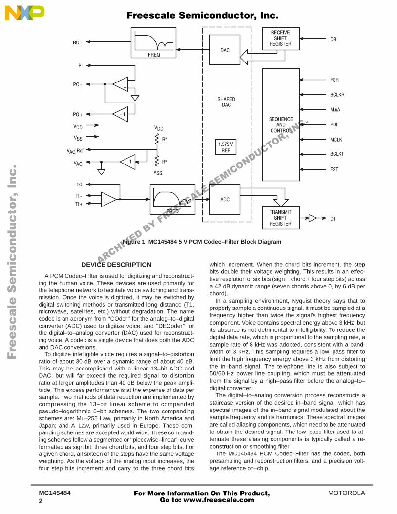
Figure 1. MC145484 5 V PCM Codec–Filter Block Diagram
DEVICE DESCRIPTION
A PCM Codec–Filter is used for digitizing and reconstruct-ing the human voice. These devices are used primarily forthe telephone network to facilitate voice switching and trans-mission. Once the voice is digitized, it may be switched bydigital switching methods or transmitted long distance (T1,microwave, satellites, etc.) without degradation. The namecodec is an acronym from ‘‘COder’’ for the analog–to–digitalconverter (ADC) used to digitize voice, and ‘‘DECoder’’ forthe digital–to–analog converter (DAC) used for reconstruct-ing voice. A codec is a single device that does both the ADCand DAC conversions.
To digitize intelligible voice requires a signal–to–distortionratio of about 30 dB over a dynamic range of about 40 dB.This may be accomplished with a linear 13–bit ADC andDAC, but will far exceed the required signal–to–distortionratio at larger amplitudes than 40 dB below the peak ampli-tude. This excess performance is at the expense of data persample. Two methods of data reduction are implemented bycompressing the 13–bit linear scheme to compandedpseudo–logarithmic 8–bit schemes. The two compandingschemes are: Mu–255 Law, primarily in North America andJapan; and A–Law, primarily used in Europe. These com-panding schemes are accepted world wide. These compand-ing schemes follow a segmented or ‘‘piecewise–linear’’ curveformatted as sign bit, three chord bits, and four step bits. Fora given chord, all sixteen of the steps have the same voltageweighting. As the voltage of the analog input increases, thefour step bits increment and carry to the three chord bits
which increment. When the chord bits increment, the stepbits double their voltage weighting. This results in an effec-tive resolution of six bits (sign + chord + four step bits) acrossa 42 dB dynamic range (seven chords above 0, by 6 dB perchord).
In a sampling environment, Nyquist theory says that toproperly sample a continuous signal, it must be sampled at afrequency higher than twice the signal’s highest frequencycomponent. Voice contains spectral energy above 3 kHz, butits absence is not detrimental to intelligibility. To reduce thedigital data rate, which is proportional to the sampling rate, asample rate of 8 kHz was adopted, consistent with a band-width of 3 kHz. This sampling requires a low–pass filter tolimit the high frequency energy above 3 kHz from distortingthe in–band signal. The telephone line is also subject to50/60 Hz power line coupling, which must be attenuatedfrom the signal by a high–pass filter before the analog–to–digital converter.
The digital–to–analog conversion process reconstructs astaircase version of the desired in–band signal, which hasspectral images of the in–band signal modulated about thesample frequency and its harmonics. These spectral imagesare called aliasing components, which need to be attenuatedto obtain the desired signal. The low–pass filter used to at-tenuate these aliasing components is typically called a re-construction or smoothing filter.
The MC145484 PCM Codec–Filter has the codec, bothpresampling and reconstruction filters, and a precision volt-age reference on–chip.
Fre
esc
ale
Se
mic
on
du
cto
r, I
Freescale Semiconductor, Inc.
For More Information On This Product, Go to: www.freescale.com
nc
...
ARCHIVED BY FREESCALE SEMICONDUCTOR, INC.
MC145484MOTOROLA3
PIN DESCRIPTIONS
POWER SUPPLY
VDDPositive Power Supply (Pin 6)
This is the most positive power supply and is typically con-nected to + 5 V. This pin should be decoupled to VSS with a0.1 µF ceramic capacitor.
VSSNegative Power Supply (Pin 15)
This is the most negative power supply and is typicallyconnected to 0 V.
VAGAnalog Ground Output (Pin 20)
This output pin provides a mid–supply analog ground. Thispin should be decoupled to VSS with a 0.01 µF ceramiccapacitor. All analog signal processing within this device isreferenced to this pin. If the audio signals to be processedare referenced to VSS, then special precautions must beutilized to avoid noise between VSS and the VAG pin. Refer tothe applications information in this document for more in-formation. The VAG pin becomes high impedance when thisdevice is in the powered–down mode.
VAG RefAnalog Ground Reference Bypass (Pin 1)
This pin is used to capacitively bypass the on–chip cir-cuitry that generates the mid–supply voltage for the VAG out-put pin. This pin should be bypassed to VSS with a 0.1 µFceramic capacitor using short, low inductance traces. TheVAG Ref pin is only used for generating the reference voltagefor the VAG pin. Nothing is to be connected to this pin in addi-tion to the bypass capacitor. All analog signal processingwithin this device is referenced to the VAG pin. If the audiosignals to be processed are referenced to VSS, then specialprecautions must be utilized to avoid noise between VSS andthe VAG pin. Refer to the applications information in thisdocument for more information. When this device is in thepowered–down mode, the VAG Ref pin is pulled to the VDDpower supply with a non–linear, high–impedance circuit.
CONTROL
Mu/AMu/A Law Select (Pin 16)
This pin controls the compression for the encoder and theexpansion for the decoder. Mu–Law companding is selectedwhen this pin is connected to VDD and A–Law companding isselected when this pin is connected to VSS.
PDIPower–Down Input (Pin 10)
This pin puts the device into a low power dissipation modewhen a logic 0 is applied. When this device is powered down,all of the clocks are gated off and all bias currents are turnedoff, which causes RO–, PO–, PO+, TG, VAG, and DT to
become high impedance and the VAG Ref pin is pulled to theVDD power supply with a non–linear, high–impedance circuit.The device will operate normally when a logic 1 is applied tothis pin. The device goes through a power–up sequencewhen this pin is taken to a logic 1 state, which prevents theDT PCM output from going low impedance for at least twoFST cycles. The VAG and VAG Ref circuits and the signal pro-cessing filters must settle out before the DT PCM output orthe RO– receive analog output will represent a valid analogsignal.
ANALOG INTERFACE
TI+Transmit Analog Input (Non–Inverting) (Pin 19)
This is the non–inverting input of the transmit input gainsetting operational amplifier. This pin accommodates a differ-ential to single–ended circuit for the input gain setting opamp. This allows input signals that are referenced to the VSSpin to be level shifted to the VAG pin with minimum noise.This pin may be connected to the VAG pin for an invertingamplifier configuration if the input signal is already refer-enced to the VAG pin. The common mode range of the TI+and TI– pins is from 1.2 V, to VDD minus 1.2 V. This is an FETgate input.
The TI+ pin also serves as a digital input control for thetransmit input multiplexer. Connecting the TI+ pin to VDD willplace this amplifier’s output (TG) into a high–impedancestate, and selects the TG pin to serve as a high–impedanceinput to the transmit filter. Connecting the TI+ pin to VSS willalso place this amplifier’s output (TG) into a high–impedancestate, and selects the TI– pin to serve as a high–impedanceinput to the transmit filter.
TI–Transmit Analog Input (Inverting) (Pin 18)
This is the inverting input of the transmit gain setting op-erational amplifier. Gain setting resistors are usually con-nected from this pin to TG and from this pin to the analogsignal source. The common mode range of the TI+ and TI–pins is from 1.2 V to VDD – 1.2 V. This is an FET gate input.
The TI– pin also serves as one of the transmit input multi-plexer pins when the TI+ pin is connected to VSS. When TI+is connected to VDD, this pin is ignored. See the pin descrip-tions for the TI+ and the TG pins for more information.
TGTransmit Gain (Pin 17)
This is the output of the transmit gain setting operationalamplifier and the input to the transmit band–pass filter. Thisop amp is capable of driving a 2 kΩ load. Connecting the TI+pin to VDD will place the TG pin into a high–impedance state,and selects the TG pin to serve as a high–impedance input tothe transmit filter. All signals at this pin are referenced to theVAG pin. When TI+ is connected to VSS, this pin is ignored.See the pin descriptions for the TI+ and TI– pins for more in-formation. This pin is high impedance when the device is inthe powered–down mode.
Fre
esc
ale
Se
mic
on
du
cto
r, I
Freescale Semiconductor, Inc.
For More Information On This Product, Go to: www.freescale.com
nc
...
ARCHIVED BY FREESCALE SEMICONDUCTOR, INC.
MC145484 MOTOROLA4
RO–Receive Analog Output (Inverting) (Pin 2)
This is the inverting output of the receive smoothing filterfrom the digital–to–analog converter. This output is capableof driving a 2 kΩ load to 1.575 V peak referenced to the VAGpin. If the device is operated half–channel with the FST pinclocking and FSR pin held low, the receive filter input will beconencted to the VAG voltage. This minimizes transients atthe RO– pin when full–channel operation is resumed byclocking the FSR pin. This pin is high impedance when thedevice is in the powered–down mode.
PIPower Amplifier Input (Pin 3)
This is the inverting input to the PO– amplifier. The non–inverting input to the PO– amplifier is internally tied to theVAG pin. The PI and PO– pins are used with external resis-tors in an inverting op amp gain circuit to set the gain of thePO+ and PO– push–pull power amplifier outputs. Connect-ing PI to VDD will power down the power driver amplifiers andthe PO+ and PO– outputs will be high impedance.
PO–Power Amplifier Output (Inverting) (Pin 4)
This is the inverting power amplifier output, which is usedto provide a feedback signal to the PI pin to set the gain ofthe push–pull power amplifier outputs. This pin is capable ofdriving a 300 Ω load to PO+. The PO+ and PO– outputs aredifferential (push–pull) and capable of driving a 300 Ω load to3.15 V peak, which is 6.3 V peak–to–peak. The bias voltageand signal reference of this output is the VAG pin. The VAGpin cannot source or sink as much current as this pin, andtherefore low impedance loads must be between PO+ andPO–. The PO+ and PO– differential drivers are also capableof driving a 100 Ω resistive load or a 100 nF Piezoelectrictransducer in series with a 20 Ω resister with a small increasein distortion. These drivers may be used to drive resistiveloads of ≥ 32 Ω when the gain of PO– is set to 1/4 or less.Connecting PI to VDD will power down the power driver am-plifiers and the PO+ and PO– outputs will be high imped-ance. This pin is also high impedance when the device ispowered down by the PDI pin.
PO+Power Amplifier Output (Non–Inverting) (Pin 5)
This is the non–inverting power amplifier output, which isan inverted version of the signal at PO–. This pin is capableof driving a 300 Ω load to PO–. Connecting PI to VDD willpower down the power driver amplifiers and the PO+ andPO– outputs will be high impedance. This pin is also high im-pedance when the device is powered down by the PDI pin.See PI and PO– for more information.
DIGITAL INTERFACE
MCLKMaster Clock (Pin 11)
This is the master clock input pin. The clock signal appliedto this pin is used to generate the internal 256 kHz clock andsequencing signals for the switched–capacitor filters, ADC,and DAC. The internal prescaler logic compares the clock on
this pin to the clock at FST (8 kHz) and will automaticallyaccept 256, 512, 1536, 1544, 2048, 2560, or 4096 kHz. ForMCLK frequencies of 256 and 512 kHz, MCLK must be syn-chronous and approximately rising edge aligned to FST. Foroptimum performance at frequencies of 1.536 MHz andhigher, MCLK should be synchronous and approximately ris-ing edge aligned to the rising edge of FST. In many ap-plications, MCLK may be tied to the BCLKT pin.
FSTFrame Sync, Transmit (Pin 14)
This pin accepts an 8 kHz clock that synchronizes the out-put of the serial PCM data at the DT pin. This input is com-patible with various standards including IDL, Long FrameSync, Short Frame Sync, and GCI formats. If both FST andFSR are held low for several 8 kHz frames, the device willpower down.
BCLKTBit Clock, Transmit (Pin 12)
This pin controls the transfer rate of transmit PCM data. Inthe IDL and GCI modes it also controls the transfer rate ofthe receive PCM data. This pin can accept any bit clock fre-quency from 64 to 4096 kHz for Long Frame Sync and ShortFrame Sync timing. This pin can accept clock frequenciesfrom 256 kHz to 4.096 MHz in IDL mode, and from 512 kHzto 6.176 MHz for GCI timing mode.
DTData, Transmit (Pin 13)
This pin is controlled by FST and BCLKT and is high im-pedance except when outputting PCM data. When operatingin the IDL or GCI mode, data is output in either the B1 or B2channel as selected by FSR. This pin is high impedancewhen the device is in the powered down mode.
FSRFrame Sync, Receive (Pin 7)
When used in the Long Frame Sync or Short Frame Syncmode, this pin accepts an 8 kHz clock, which synchronizesthe input of the serial PCM data at the DR pin. FSR can beasynchronous to FST in the Long Frame Sync or ShortFrame Sync modes. When an ISDN mode (IDL or GCI) hasbeen selected with BCLKR, this pin selects either B1 (logic 0)or B2 (logic 1) as the active data channel.
BCLKRBit Clock, Receive (Pin 9)
When used in the Long Frame Sync or Short Frame Syncmode, this pin accepts any bit clock frequency from 64 to4096 kHz. When this pin is held at a logic 1, FST, BCLKT, DT,and DR become IDL Interface compatible. When this pin isheld at a logic 0, FST, BCLKT, DT, and DR become GCI Inter-face compatible.
DRData, Receive (Pin 8)
This pin is the PCM data input, and when in a Long FrameSync or Short Frame Sync mode is controlled by FSR andBCLKR. When in the IDL or GCI mode, this data transfer iscontrolled by FST and BCLKT. FSR and BCLKR select theB channel and ISDN mode, respectively.
Fre
esc
ale
Se
mic
on
du
cto
r, I
Freescale Semiconductor, Inc.
For More Information On This Product, Go to: www.freescale.com
nc
...
ARCHIVED BY FREESCALE SEMICONDUCTOR, INC.
MC145484MOTOROLA5
FUNCTIONAL DESCRIPTION
ANALOG INTERFACE AND SIGNAL PATH
The transmit portion of this device includes a low–noise,three–terminal op amp capable of driving a 2 kΩ load. Thisop amp has inputs of TI+ (Pin 19) and TI– (Pin 18) and itsoutput is TG (Pin 17). This op amp is intended to be confi-gured in an inverting gain circuit. The analog signal may beapplied directly to the TG pin if this transmit op amp is inde-pendently powered down by connecting the TI+ input to theVDD power supply. The TG pin becomes high impedancewhen the transmit op amp is powered down. The TG pin isinternally connected to a 3–pole anti–aliasing pre–filter. Thispre–filter incorporates a 2–pole Butterworth active low–passfilter, followed by a single passive pole. This pre–filter is fol-lowed by a single–ended to differential converter that isclocked at 512 kHz. All subsequent analog processing uti-lizes fully–differential circuitry. The next section is a fully–differential, 5–pole switched–capacitor low–pass filter witha 3.4 kHz frequency cutoff. After this filter is a 3–poleswitched–capacitor high–pass filter having a cutoff fre-quency of about 200 Hz. This high–pass stage has a trans-mission zero at dc that eliminates any dc coming from theanalog input or from accumulated op amp offsets in the pre-ceding filter stages. The last stage of the high–pass filter isan autozeroed sample and hold amplifier.
One bandgap voltage reference generator and digital–to–analog converter (DAC) are shared by the transmit and re-ceive sections. The autozeroed, switched–capacitorbandgap reference generates precise positive and negativereference voltages that are virtually independent of tempera-ture and power supply voltage. A binary–weighted capacitorarray (CDAC) forms the chords of the companding structure,while a resistor string (RDAC) implements the linear stepswithin each chord. The encode process uses the DAC, thevoltage reference, and a frame–by–frame autozeroedcomparator to implement a successive–approximation con-version algorithm. All of the analog circuitry involved in thedata conversion (the voltage reference, RDAC, CDAC, andcomparator) are implemented with a differential architecture.
The receive section includes the DAC described above, asample and hold amplifier, a 5–pole, 3400 Hz switched ca-pacitor low–pass filter with sinX/X correction, and a 2–poleactive smoothing filter to reduce the spectral components ofthe switched capacitor filter. The output of the smoothing fil-ter is buffered by an amplifier, which is output at the RO– pin.This output is capable of driving a 2 kΩ load to the VAG pin.The MC145484 also has a pair of power amplifiers that areconnected in a push–pull configuration. The PI pin is the in-verting input to the PO– power amplifier. The non–invertinginput is internally tied to the VAG pin. This allows this amplifierto be used in an inverting gain circuit with two external resis-
tors. The PO+ amplifier has a gain of minus one, and is in-ternally connected to the PO– output. This complete poweramplifier circuit is a differential (push–pull) amplifier with ad-justable gain that is capable of driving a 300 Ω load to+ 12 dBm. The power amplifier may be powered down inde-pendently of the rest of the chip by connecting the PI pin toVDD.
POWER–DOWN
There are two methods of putting this device into a lowpower consumption mode, which makes the device nonfunc-tional and consumes virtually no power. PDI is the power–down input pin which, when taken low, powers down thedevice. Another way to power the device down is to hold boththe FST and FSR pins low while the BCLKT and MCLK pinsare clocked. When the chip is powered down, the VAG, TG,RO–, PO+, PO–, and DT outputs are high impedance andthe VAG Ref pin is pulled to the VDD power supply with a non–linear, high–impedance circuit. To return the chip to the pow-er–up state, PDI must be high and the FST frame sync pulsemust be present while the BCLKT and MCLK pins areclocked. The DT output will remain in a high–impedancestate for at least two 8 kHz FST pulses after power–up.
MASTER CLOCK
Since this codec–filter design has a single DAC architec-ture, the MCLK pin is used as the master clock for all analogsignal processing including analog–to–digital conversion,digital–to–analog conversion, and for transmit and receive fil-tering functions of this device. The clock frequency applied tothe MCLK pin may be 256 kHz, 512 kHz, 1.536 MHz,1.544 MHz, 2.048 MHz, 2.56 MHz, or 4.096 MHz. This de-vice has a prescaler that automatically determines the properdivide ratio to use for the MCLK input, which achieves the re-quired 256 kHz internal sequencing clock. The clocking re-quirements of the MCLK input are independent of the PCMdata transfer mode (i.e., Long Frame Sync, Short FrameSync, IDL mode, or GCI mode).
DIGITAL I/O
The MC145484 is pin selectable for Mu–Law or A–Law.Table 1 shows the 8–bit data word format for positive andnegative zero and full scale for both companding schemes.Table 2 shows the series of eight PCM words for both Mu–Law and A–Law that correspond to a digital milliwatt. Thedigital mW is the 1 kHz calibration signal reconstructed bythe DAC that defines the absolute gain or 0 dBm0 Transmis-sion Level Point (TLP) of the DAC. The timing for the PCMdata transfer is independent of the companding scheme se-lected. Refer to Figure 2 for a summary and comparison ofthe four PCM data interface modes of this device.
Fre
esc
ale
Se
mic
on
du
cto
r, I
Freescale Semiconductor, Inc.
For More Information On This Product, Go to: www.freescale.com
nc
...
ARCHIVED BY FREESCALE SEMICONDUCTOR, INC.
MC145484 MOTOROLA6
Table 1. PCM Codes for Zero and Full Scale
Mu–Law A–Law
Level Sign Bit Chord Bits Step Bits Sign Bit Chord Bits Step Bits
+ Full Scale 1 0 0 0 0 0 0 0 1 0 1 0 1 0 1 0
+ Zero 1 1 1 1 1 1 1 1 1 1 0 1 0 1 0 1
– Zero 0 1 1 1 1 1 1 1 0 1 0 1 0 1 0 1
– Full Scale 0 0 0 0 0 0 0 0 0 0 1 0 1 0 1 0
Table 2. PCM Codes for Digital mW
Mu–Law A–Law
Phase Sign Bit Chord Bits Step Bits Sign Bit Chord Bits Step Bits
π/8 0 0 0 1 1 1 1 0 0 0 1 1 0 1 0 0
3π/8 0 0 0 0 1 0 1 1 0 0 1 0 0 0 0 1
5π/8 0 0 0 0 1 0 1 1 0 0 1 0 0 0 0 1
7π/8 0 0 0 1 1 1 1 0 0 0 1 1 0 1 0 0
9π/8 1 0 0 1 1 1 1 0 1 0 1 1 0 1 0 0
11π/8 1 0 0 0 1 0 1 1 1 0 1 0 0 0 0 1
13π/8 1 0 0 0 1 0 1 1 1 0 1 0 0 0 0 1
15π/8 1 0 0 1 1 1 1 0 1 0 1 1 0 1 0 0
Fre
esc
ale
Se
mic
on
du
cto
r, I
Freescale Semiconductor, Inc.
For More Information On This Product, Go to: www.freescale.com
nc
...
ARCHIVED BY FREESCALE SEMICONDUCTOR, INC.
MC145484MOTOROLA7
Figure 2a. Long Frame Sync (Transmit and Receive Have Individual Clocking)
Figure 2b. Short Frame Sync (Transmit and Receive Have Individual Clocking)
Figure 2c. IDL Interface — BCLKR = 1 (Transmit and Receive Have Common Clocking)
Figure 2d. GCI Interface — BCLKR = 0 (Transmit and Receive Have Common Clocking)
!"
#%$
Figure 2. Digital Timing Modes for the PCM Data Interface
Fre
esc
ale
Se
mic
on
du
cto
r, I
Freescale Semiconductor, Inc.
For More Information On This Product, Go to: www.freescale.com
nc
...
ARCHIVED BY FREESCALE SEMICONDUCTOR, INC.

MC145484 MOTOROLA8
Long Frame Sync
Long Frame Sync is the industry name for one type ofclocking format that controls the transfer of the PCM datawords. (Refer to Figure 2a.) The ‘‘Frame Sync’’ or ‘‘Enable’’ isused for two specific synchronizing functions. The first is tosynchronize the PCM data word transfer, and the second isto control the internal analog–to–digital and digital–to–analogconversions. The term ‘‘Sync’’ refers to the function of syn-chronizing the PCM data word onto or off of the multiplexedserial PCM data bus, which is also known as a PCM high-way. The term ‘‘Long’’ comes from the duration of the framesync measured in PCM data clock cycles. Long Frame Synctiming occurs when the frame sync is used directly as thePCM data output driver enable. This results in the PCM out-put going low impedance with the rising edge of the transmitframe sync, and remaining low impedance for the duration ofthe transmit frame sync.
The implementation of Long Frame Sync has maintainedcompatibility and been optimized for external clocking sim-plicity. This optimization includes the PCM data output goinglow impedance with the logical AND of the transmit framesync (FST) with the transmit data bit clock (BCLKT). The op-timization also includes the PCM data output (DT) remaininglow impedance until the middle of the LSB (seven and a halfPCM data clock cycles) or until the FST pin is taken low,whichever occurs last. This requires the frame sync to beapproximately rising edge aligned with the initiation of thePCM data word transfer, but the frame sync does not have aprecise timing requirement for the end of the PCM data wordtransfer. The device recognizes Long Frame Sync clockingwhen the frame sync is held high for two consecutive fallingedges of the transmit data clock. The transmit logic decideson each frame sync whether it should interpret the nextframe sync pulse as a Long or a Short Frame Sync. This de-cision is used for receive circuitry also. The device is de-signed to prevent PCM bus contention by not allowing thePCM data output to go low impedance for at least two framesync cycles after power is applied or when coming out of thepowered down mode.
The receive side of the device is designed to accept thesame frame sync and data clock as the transmit side and tobe able to latch its own transmit PCM data word. Thus thePCM digital switch needs to be able to generate only onetype of frame sync for use by both transmit and receive sec-tions of the device.
The logical AND of the receive frame sync with the receivedata clock tells the device to start latching the 8–bit serialword into the receive data input on the falling edges of thereceive data clock. The internal receive logic counts the re-ceive data clock cycles and transfers the PCM data word tothe digital–to–analog converter sequencer on the ninth dataclock rising edge.
This device is compatible with four digital interface modes.To ensure that this device does not reprogram itself for a dif-ferent timing mode, the BCLKR pin must change logic stateno less than every 125 µs. The minimum PCM data bit clockfrequency of 64 kHz satisfies this requirement.
Short Frame Sync
Short Frame Sync is the industry name for the type ofclocking format that controls the transfer of the PCM datawords (refer to Figure 2b). The ‘‘Frame Sync’’ or ‘‘Enable’’ is
used for two specific synchronizing functions. The first is tosynchronize the PCM data word transfer, and the second isto control the internal analog–to–digital and digital–to–analogconversions. The term ‘‘Sync’’ refers to the function of syn-chronizing the PCM data word onto or off of the multiplexedserial PCM data bus, which is also known as a PCM high-way. The term ‘‘Short’’ comes from the duration of the framesync measured in PCM data clock cycles. Short Frame Synctiming occurs when the frame sync is used as a ‘‘pre–syn-chronization’’ pulse that is used to tell the internal logic toclock out the PCM data word under complete control of thedata clock. The Short Frame Sync is held high for one fallingdata clock edge. The device outputs the PCM data word be-ginning with the following rising edge of the data clock. Thisresults in the PCM output going low impedance with the ris-ing edge of the transmit data clock, and remaining low im-pedance until the middle of the LSB (seven and a half PCMdata clock cycles).
The device recognizes Short Frame Sync clocking whenthe frame sync is held high for one and only one falling edgeof the transmit data clock. The transmit logic decides on eachframe sync whether it should interpret the next frame syncpulse as a Long or a Short Frame Sync. This decision is usedfor receive circuitry also. The device is designed to preventPCM bus contention by not allowing the PCM data output togo low impedance for at least two frame sync cycles afterpower is applied or when coming out of the powered downmode.
The receive side of the device is designed to accept thesame frame sync and data clock as the transmit side and tobe able to latch its own transmit PCM data word. Thus thePCM digital switch needs to be able to generate only onetype of frame sync for use by both transmit and receive sec-tions of the device.
The falling edge of the receive data clock latching a highlogic level at the receive frame sync input tells the device tostart latching the 8–bit serial word into the receive data inputon the following eight falling edges of the receive data clock.The internal receive logic counts the receive data clockcycles and transfers the PCM data word to the digital–to–analog converter sequencer on the rising data clock edge af-ter the LSB has been latched into the device.
This device is compatible with four digital interface modes.To ensure that this device does not reprogram itself for a dif-ferent timing mode, the BCLKR pin must change logic stateno less than every 125 µs. The minimum PCM data bit clockfrequency of 64 kHz satisfies this requirement.
Interchip Digital Link (IDL)
The Interchip Digital Link (IDL) Interface is one of twostandard synchronous 2B+D ISDN timing interface modeswith which this device is compatible. In the IDL mode, the de-vice can communicate in either of the two 64 kbps B chan-nels (refer to Figure 2c for sample timing). The IDL mode isselected when the BCLKR pin is held high for two or moreFST (IDL SYNC) rising edges. The digital pins that controlthe transmit and receive PCM word transfers are repro-grammed to accommodate this mode. The pins affected areFST, FSR, BCLKT, DT, and DR. The IDL Interface consists offour pins: IDL SYNC (FST), IDL CLK (BCLKT), IDL TX (DT),and IDL RX (DR). The IDL interface mode provides access toboth the transmit and receive PCM data words with commoncontrol clocks of IDL Sync and IDL Clock. In this mode, the
Fre
esc
ale
Se
mic
on
du
cto
r, I
Freescale Semiconductor, Inc.
For More Information On This Product, Go to: www.freescale.com
nc
...
ARCHIVED BY FREESCALE SEMICONDUCTOR, INC.
MC145484MOTOROLA9
FSR pin controls whether the B1 channel or the B2 channelis used for both transmit and receive PCM data word trans-fers. When the FSR pin is low, the transmit and receive PCMwords are transferred in the B1 channel, and for FSR highthe B2 channel is selected. The start of the B2 channel is tenIDL CLK cycles after the start of the B1 channel.
The IDL SYNC (FST, Pin 14) is the input for the IDL framesynchronization signal. The signal at this pin is nominallyhigh for one cycle of the IDL Clock signal and is rising edgealigned with the IDL Clock signal. (Refer to Figure 4 and theIDL Timing specifications for more details.) This event identi-fies the beginning of the IDL frame. The frequency of the IDLSync signal is 8 kHz. The rising edge of the IDL SYNC (FST)should be aligned approximately with the rising edge ofMCLK. MCLK must be one of the clock frequencies specifiedin the Digital Switching Characteristics table, and is typicallytied to IDL CLK (BCLKT).
The IDL CLK (BCLKT, Pin 12) is the input for the PCMdata clock. All IDL PCM transfers and data control sequenc-ing are controlled by this clock following the IDL SYNC. Thispin accepts an IDL data clock frequency of 256 kHz to4.096 MHz.
The IDL TX (DT, Pin 13) is the output for the transmit PCMdata word. Data bits are output for the B1 channel on se-quential rising edges of the IDL CLK signal beginning afterthe IDL SYNC pulse. If the B2 channel is selected, then thePCM word transfer starts on the eleventh IDL CLK risingedge after the IDL SYNC pulse. The IDL TX pin will remainlow impedance for the duration of the PCM word until theLSB after the falling edge of IDL CLK. The IDL TX pin will re-main in a high impedance state when not outputting PCMdata or when a valid IDL Sync signal is missing.
The IDL RX (DR, Pin 8) is the input for the receive PCMdata word. Data bits are input for the B1 channel on sequen-tial falling edges of the IDL CLK signal beginning after theIDL SYNC pulse. If the B2 channel is selected, then the PCMword is latched in starting on the eleventh IDL CLK fallingedge after the IDL SYNC pulse.
General Circuit Interface (GCI)
The General Circuit Interface (GCI) is the second of twostandard synchronous 2B+D ISDN timing interface modeswith which this device is compatible. In the GCI mode, thedevice can communicate in either of the two 64 kbps B–channels. (Refer to Figure 2d for sample timing.) The GCImode is selected when the BCLKR pin is held low for two ormore FST (FSC) rising edges. The digital pins that controlthe transmit and receive PCM word transfers are repro-grammed to accommodate this mode. The pins affected areFST, FSR, BCLKT, DT, and DR. The GCI Interface consistsof four pins: FSC (FST), DCL (BCLKT), Dout (DT), and Din(DR). The GCI interface mode provides access to both thetransmit and receive PCM data words with common controlclocks of FSC (frame synchronization clock) and DCL (dataclock). In this mode, the FSR pin controls whether the B1channel or the B2 channel is used for both transmit and re-ceive PCM data word transfers. When the FSR pin is low, thetransmit and receive PCM words are transferred in the B1channel, and for FSR high the B2 channel is selected. Thestart of the B2 channel is 16 DCL cycles after the start of theB1 channel.
The FSC (FST, Pin 14) is the input for the GCI frame syn-chronization signal. The signal at this pin is nominally risingedge aligned with the DCL clock signal. (Refer to Figure 6and the GCI Timing specifications for more details.) Thisevent identifies the beginning of the GCI frame. The frequen-cy of the FSC synchronization signal is 8 kHz. The risingedge of the FSC (FST) should be aligned approximately withthe rising edge of MCLK. MCLK must be one of the clock fre-quencies specified in the Digital Switching Characteristicstable, and is typically tied to DCL (BCLKT).
The DCL (BCLKT, Pin 12) is the input for the clock thatcontrols the PCM data transfers. The clock applied at theDCL input is twice the actual PCM data rate. The GCI framebegins with the logical AND of the FSC with the DCL. Thisevent initiates the PCM data word transfers for both transmitand receive. This pin accepts a GCI data clock frequency of512 kHz to 6.176 MHz for PCM data rates of 256 kHz to3.088 MHz.
The GCI Dout (DT, Pin 13) is the output for the transmitPCM data word. Data bits are output for the B1 channel onalternate rising edges of the DCL clock signal, beginning withthe FSC pulse. If the B2 channel is selected, then the PCMword transfer starts on the seventeenth DCL rising edge afterthe FSC rising edge. The Dout pin will remain low impedancefor 15–1/2 DCL clock cycles. The Dout pin becomes highimpedance after the second falling edge of the DCL clockduring the LSB of the PCM word. The Dout pin will remain ina high–impedance state when not outputting PCM data orwhen a valid FSC signal is missing.
The Din (DR, Pin 8) is the input for the receive PCM dataword. Data bits are latched in for the B1 channel on alternaterising edges of the DCL clock signal, beginning with the se-cond DCL clock after the rising edge of the FSC pulse. If theB2 channel is selected then the PCM word is latched in start-ing on the eighteenth DCL rising edge after the FSC risingedge.
PRINTED CIRCUIT BOARD LAYOUTCONSIDERATIONS
The MC145484 is manufactured using high–speed CMOSVLSI technology to implement the complex analog signalprocessing functions of a PCM Codec–Filter. The fully–differ-ential analog circuit design techniques used for this deviceresult in superior performance for the switched capacitor fil-ters, the analog–to–digital converter (ADC) and the digital–to–analog converter (DAC). Special attention was given tothe design of this device to reduce the sensitivities of noise,including power supply rejection and susceptibility to radiofrequency noise. This special attention to design includes afifth order low–pass filter, followed by a third order high–passfilter whose output is converted to a digital signal with greaterthan 75 dB of dynamic range, all operating on a single 5 Vpower supply. This results in an LSB size for small audio sig-nals of about 386 µV. The typical idle channel noise level ofthis device is less than one LSB. In addition to the dynamicrange of the codec–filter function of this device, the inputgain–setting op amp has the capability of greater than 35 dBof gain intended for an electret microphone interface.
This device was designed for ease of implementation, butdue to the large dynamic range and the noisy nature ofthe environment for this device (digital switches, radio
Fre
esc
ale
Se
mic
on
du
cto
r, I
Freescale Semiconductor, Inc.
For More Information On This Product, Go to: www.freescale.com
nc
...
ARCHIVED BY FREESCALE SEMICONDUCTOR, INC.
MC145484 MOTOROLA10
telephones, DSP front–end, etc.) special care must be takento assure optimum analog transmission performance.
PC BOARD MOUNTING
It is recommended that the device be soldered to the PCboard for optimum noise performance. If the device is to beused in a socket, it should be placed in a low parasitic pininductance (generally, low–profile) socket.
POWER SUPPLY, GROUND, AND NOISECONSIDERATIONS
This device is intended to be used in switching applica-tions which often require plugging the PC board into a rackwith power applied. This is known as ‘‘hot–rack insertion.’’ Inthese applications care should be taken to limit the voltageon any pin from going positive of the VDD pins, or negative ofthe VSS pins. One method is to extend the ground and powercontacts of the PCB connector. The device has input protec-tion on all pins and may source or sink a limited amount ofcurrent without damage. Current limiting may be accom-plished by series resistors between the signal pins and theconnector contacts.
The most important considerations for PCB layout dealwith noise. This includes noise on the power supply, noisegenerated by the digital circuitry on the device, and crosscoupling digital or radio frequency signals into the audio sig-nals of this device. The best way to prevent noise is to:
1. Keep digital signals as far away from audio signals aspossible.
2. Keep radio frequency signals as far away from the audiosignals as possible.
3. Use short, low inductance traces for the audio circuitryto reduce inductive, capacitive, and radio frequencynoise sensitivities.
4. Use short, low inductance traces for digital and RFcircuitry to reduce inductive, capacitive, and radiofrequency radiated noise.
5. Bypass capacitors should be connected from the VDD,VAG Ref, and VAG pins to VSS with minimal tracelength. Ceramic monolithic capacitors of about 0.1 µFare acceptable for the VDD and VAG Ref pins to decouplethe device from its own noise. The VDD capacitor helpssupply the instantaneous currents of the digital circuitryin addition to decoupling the noise which may begenerated by other sections of the device or othercircuitry on the power supply. The VAG Ref decouplingcapacitor is effecting a low–pass filter to isolate themid–supply voltage from the power supply noise gener-ated on–chip as well as external to the device. The VAGdecoupling capacitor should be about 0.01 µF. Thishelps to reduce the inpedance of the VAG pin to VSS atfrequencies above the bandwidth of the VAG generator,which reduces the susceptibility to RF noise.
6. Use a short, wide, low inductance trace to connect theVSS ground pin to the power supply ground. The VSSpin is the digital ground and the most negative powersupply pin for the analog circuitry. All analog signalprocessing is referenced to the VAG pin, but becausedigital and RF circuitry will probably be powered by thissame ground, care must be taken to minimize highfrequency noise in the VSS trace. Depending on theapplication, a double–sided PCB with a VSS groundplane connecting all of the digital and analog VSS pinstogether would be a good grounding method. A multi-layer PC board with a ground plane connecting all of thedigital and analog VSS pins together would be the optimalground configuration. These methods will result in thelowest resistance and the lowest inductance in theground circuit. This is important to reduce voltage spikesin the ground circuit resulting from the high speed digitalcurrent spikes. The magnitude of digitally inducedvoltage spikes may be hundreds of times larger than theanalog signal the device is required to digitize.
7. Use a short, wide, low inductance trace to connect theVDD power supply pin to the 5 V power supply.Depending on the application, a double–sided PCB withVDD bypass capacitors to the VSS ground plane, asdescribed above, may complete the low impedancecoupling for the power supply. For a multilayer PC boardwith a power plane, connecting all of the VDD pins to thepower plane would be the optimal power distributionmethod. The integrated circuit layout and packagingconsiderations for the 5 V VDD power circuit areessentially the same as for the VSS ground circuit.
8. The VAG pin is the reference for all analog signalprocessing. In some applications the audio signal to bedigitized may be referenced to the VSS ground. Toreduce the susceptibility to noise at the input of the ADCsection, the three–terminal op amp may be used in adifferential to single–ended circuit to provide levelconversion from the VSS ground to the VAG ground withnoise cancellation. The op amp may be used for morethan 35 dB of gain in microphone interface circuits, whichwill require a compact layout with minimum trace lengthsas well as isolation from noise sources. It is recom-mended that the layout be as symmetrical as possible toavoid any imbalances which would reduce the noisecancelling benefits of this differential op amp circuit.Refer to the application schematics for examples of thiscircuitry.If possible, reference audio signals to the VAG pininstead of to the VSS pin. Handset receivers and tele-phone line interface circuits using transformers may beaudio signal referenced completely to the VAG pin. Re-fer to the application schematics for examples of thiscircuitry. The VAG pin cannot be used for ESD or lineprotection.
Fre
esc
ale
Se
mic
on
du
cto
r, I
Freescale Semiconductor, Inc.
For More Information On This Product, Go to: www.freescale.com
nc
...
ARCHIVED BY FREESCALE SEMICONDUCTOR, INC.
MC145484MOTOROLA11
MAXIMUM RATINGS (Voltages Referenced to VSS Pin)
Rating Symbol Value Unit
DC Supply Voltage VDD – 0.5 to 6 V
Voltage on Any Analog Input or Output Pin VSS – 0.3 to VDD + 0.3 V
Voltage on Any Digital Input or Output Pin VSS – 0.3 to VDD + 0.3 V
Operating Temperature Range TA – 40 to + 85 °C
Storage Temperature Range Tstg – 85 to +150 °C
POWER SUPPLY (TA = – 40 to + 85°C)
Characteristics Min Typ Max Unit
DC Supply Voltage 4.5 5.0 5.5 V
Active Power Dissipation (VDD = 5 V) (No Load, PI ≥ VDD – 0.5 V)(No Load, PI ≤ VDD – 1.5 V)
——
33
4.85.0
mA
Power–Down Dissipation (VIH for Logic Levels Must be ≥ 3.0 V) PDI = VSSFST and FSR = VSS, PDI = VDD
——
0.0020.01
0.10.2
mA
DIGITAL LEVELS (VDD = + 5 V ± 10%, VSS = 0 V, TA = – 40 to + 85°C)
Characteristics Symbol Min Max Unit
Input Low Voltage VIL — 0.6 V
Input High Voltage VIH 2.4 — V
Output Low Voltage (DT Pin, IOL= 2.5 mA) VOL — 0.4 V
Output High Voltage (DT Pin, IOH = – 2.5 mA) VOH VDD – 0.5 — V
Input Low Current (VSS ≤ Vin ≤ VDD) IIL – 10 + 10 µA
Input High Current (VSS ≤ Vin ≤ VDD) IIH – 10 + 10 µA
Output Current in High Impedance State (VSS ≤ DT ≤ VDD) IOZ – 10 + 10 µA
Input Capacitance of Digital Pins (Except DT) Cin — 10 pF
Input Capacitance of DT Pin when High–Z Cout — 15 pF
Fre
esc
ale
Se
mic
on
du
cto
r, I
Freescale Semiconductor, Inc.
For More Information On This Product, Go to: www.freescale.com
nc
...
ARCHIVED BY FREESCALE SEMICONDUCTOR, INC.
MC145484 MOTOROLA12
ANALOG ELECTRICAL CHARACTERISTICS (VDD = + 5 V ± 10%, VSS = 0 V, TA = – 40 to + 85°C)
Characteristics Min Typ Max Unit
Input Current TI+, TI– — ± 0.1 ± 1.0 µA
Input Resistance to VAG (VAG – 0.5 V ≤ Vin ≤ VAG + 0.5 V) TI+, TI– 10 — — MΩ
Input Capacitance TI+, TI– — — 10 pF
Input Offset Voltage of TG Op Amp TI+, TI– — — ± 5 mV
Input Common Mode Voltage Range TI+, TI– 1.2 VDD – 2.0 V
Input Common Mode Rejection Ratio TI+, TI– — 60 — dB
Gain Bandwidth Product (10 kHz) of TG Op Amp (RL ≥ 10 kΩ) — 3000 — kHz
DC Open Loop Gain of TG Op Amp (RL ≥ 10 kΩ) — 95 — dB
Equivalent Input Noise (C–Message) Between TI+ and TI– at TG — – 30 — dBrnC
Output Load Capacitance for TG Op Amp 0 — 100 pF
Output Voltage Range for TG(RL = 10 kΩ to VAG)(RL = 2 kΩ to VAG)
0.51.0
——
VDD – 0.5VDD – 1.0
V
Output Current (0.5 V ≤ Vout ≤ VDD – 0.5 V) TG, RO– ± 1.0 — — mA
Output Load Resistance to VAG TG, RO– 2 — — kΩ
Output Impedance (0 to 3.4 kHz) RO– — 1 — Ω
Output Load Capacitance RO– 0 — 500 pF
DC Output Offset Voltage of or RO– Referenced to VAG — — ± 25 mV
VAG Output Voltage Referenced to VSS (No Load) VDD/2 – 0.1 VDD/2 VDD/2 + 0.1 V
VAG Output Current with ± 25 mV Change in Output Voltage ± 2.0 ± 10 — mA
Power Supply Rejection Ratio Transmit(0 to 100 kHz @100 mVrms Applied to VDD, ReceiveC–Message Weighting, All Analog SignalsReferenced to VAG Pin)
5050
8075
——
dBC
Power Drivers PI, PO+, PO–
Input Current (VAG – 0.5 V ≤ PI ≤ VAG + 0.5 V) PI — ± 0.05 ± 1.0 µA
Input Resistance (VAG – 0.5 V ≤ PI ≤ VAG + 0.5 V) PI 10 — — MΩ
Input Offset Voltage PI — — ± 20 mV
Output Offset Voltage of PO+ Relative to PO– (Inverted Unity Gain for PO–) — — ± 50 mV
Output Current (VSS + 0.7 V ≤ PO+ or PO– ≤ VDD – 0.7 V) ± 10 — — mA
PO+ or PO– Output Resistance (Inverted Unity Gain for PO–) — 1 — Ω
Gain Bandwidth Product (10 kHz, Open Loop for PO–) — 1000 — kHz
Load Capacitance (PO+ or PO– to VAG, or PO+ to PO–) 0 — 1000 pF
Gain of PO+ Relative to PO– (RL = 300 Ω, + 3 dBm0, 1 kHz) – 0.2 0 + 0.2 dB
Total Signal to Distortion at PO+ and PO– with a Differential Load of: 300 Ω100 nF in series with ≥ 20 Ω
≥ 100 Ω
45——
604040
———
dBC
Power Supply Rejection Ratio 0 to 4 kHz(0 to 25 kHz @ 100 mVrms Applied to VDD. 4 to 25 kHzPO– Connected to PI. Differential or MeasuredReferenced to VAG Pin.)
40—
5540
——
dB
Fre
esc
ale
Se
mic
on
du
cto
r, I
Freescale Semiconductor, Inc.
For More Information On This Product, Go to: www.freescale.com
nc
...
ARCHIVED BY FREESCALE SEMICONDUCTOR, INC.

MC145484MOTOROLA13
ANALOG TRANSMISSION PERFORMANCE(VDD = + 5 V ± 10%, VSS = 0 V, All Analog Signals Referenced to VAG, 0 dBm0 = 0.775 Vrms = + 0 dBm @ 600 Ω, FST = FSR = 8 kHz,BCLKT = MCLK = 2.048 MHz Synchronous Operation, TA = – 40 to + 85°C, Unless Otherwise Noted)
A/D D/A
Characteristics Min Typ Max Min Typ Max Units
Peak Single Frequency Tone Amplitude without Clipping Tmax — 1.575 — — 1.575 — Vpk
Absolute Gain (0 dBm0 @ 1.02 kHz, TA = 25°C, VDD = 5.0 V) – 0.25 — + 0.25 – 0.25 — + 0.25 dB
Absolute Gain Variation with Temperature 0 to + 70°C(Referenced to 25°C) – 40 to + 85°C
——
——
± 0.03± 0.05
——
——
± 0.03± 0.05
dB
Absolute Gain Variation with Power Supply (TA = 25°C) — — ± 0.03 — — ± 0.03 dB
Gain vs Level Tone (Mu–Law, Relative to – 10 dBm0, 1.02 kHz)+ 3 to – 40 dBm0
– 40 to – 50 dBm0– 50 to – 55 dBm0
– 0.20– 0.4– 0.8
———
+ 0.20+ 0.40+ 0.80
– 0.20– 0.40– 0.80
———
+ 0.20+ 0.40+ 0.80
dB
Gain vs Level Pseudo Noise, CCITT G.712 – 10 to – 40 dBm0(A–Law, Relative to – 10 dBm0) – 40 to – 50 dBm0
– 50 to – 55 dBm0
– 0.25– 0.30– 0.45
———
+ 0.25+ 0.30+ 0.45
– 0.25– 0.30– 0.45
———
+ 0.25+ 0.30+ 0.45
dB
Total Distortion, 1.02 kHz Tone + 3 dBm0(Mu–Law, C–Message Weighting) 0 to – 30 dBm0
– 40 dBm0– 45 dBm0
34363025
————
————
34363025
————
————
dBC
Total Distortion, Pseudo Noise, CCITT G.714 (A–Law) – 3 dBm0– 6 to – 27 dBm0
– 34 dBm0– 40 dBm0– 50 dBm0– 55 dBm0
303634291914
——————
——————
303635302015
——————
——————
dB
Idle Channel Noise (For End–to–End and A/D, See Note 1)(Mu–Law, C–Message Weighted)(A–Law, Psophometric Weighted)
——
——
17– 69
——
——
11– 79
dBrnc0dBm0p
Frequency Response (Relative to 1.02 kHz @ 0 dBm0) 15 Hz50 Hz60 Hz
165 Hz200 Hz
300 to 3000 Hz3000 to 3200 Hz
3300 Hz3400 Hz3600 Hz4000 Hz
4600 Hz to 100 kHz
————
– 1.0– 0.20– 0.20– 0.35– 0.8
———
———
– 3.0—————
– 3.0——
– 40– 30– 26—
– 0.4+ 0.15+ 0.20+ 0.15
0—
– 14– 32
– 0.5– 0.5– 0.5– 0.5– 0.5– 0.15– 0.20– 0.35– 0.85
———
—————————
– 3.0——
00000
+ 0.15+ 0.20+ 0.15
0—
– 1430
dB
In–Band Spurious (1.02 kHz @ 0 dBm0, Transmit and Receive)300 to 3400 Hz — — – 48 — — – 48
dB
Out–of–Band Spurious at RO+ (300 to 3400 Hz @ 0 dBm0 in)4600 to 7600 Hz7600 to 8400 Hz
8400 to 100,000 Hz
———
———
———
———
———
– 30– 40– 30
dB
Idle Channel Noise Selective (8 kHz, Input = VAG, 30 Hz Bandwidth) — — — — — – 70 dBm0
Absolute Delay (1600 Hz) — — 315 — — 205 µs
Group Delay Referenced to 1600 Hz 500 to 600 Hz600 to 800 Hz
800 to 1000 Hz1000 to 1600 Hz1600 to 2600 Hz2600 to 2800 Hz2800 to 3000 Hz
———————
———————
21013070357095145
– 40– 40– 40– 30———
———————
————85110175
µs
Crosstalk of 1020 Hz @ 0 dBm0 from A/D or D/A (Note 2) — — – 75 — — – 75 dB
Intermodulation Distortion of Two Frequencies of Amplitudes(– 4 to – 21 dBm0 from the Range 300 to 3400 Hz) — — – 41 — — – 41
dB
NOTES:1. Extrapolated from a 1020 Hz @ – 50 dBm0 distortion measurement to correct for encoder enhancement.2. Selectively measured while stimulated with 2667 Hz @ – 50 dBm0.
Fre
esc
ale
Se
mic
on
du
cto
r, I
Freescale Semiconductor, Inc.
For More Information On This Product, Go to: www.freescale.com
nc
...
ARCHIVED BY FREESCALE SEMICONDUCTOR, INC.
MC145484 MOTOROLA14
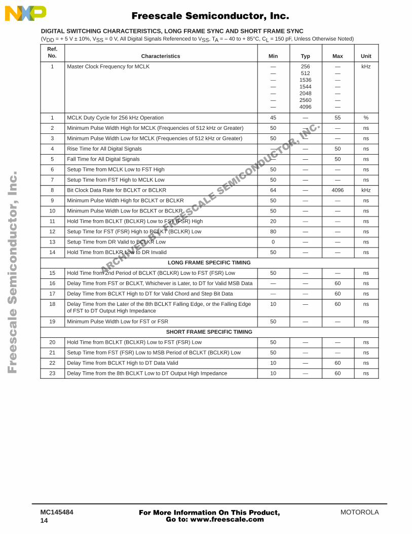
DIGITAL SWITCHING CHARACTERISTICS, LONG FRAME SYNC AND SHORT FRAME SYNC (VDD = + 5 V ± 10%, VSS = 0 V, All Digital Signals Referenced to VSS, TA = – 40 to + 85°C, CL = 150 pF, Unless Otherwise Noted)
Ref.No. Characteristics Min Typ Max Unit
1 Master Clock Frequency for MCLK ———————
25651215361544204825604096
———————
kHz
1 MCLK Duty Cycle for 256 kHz Operation 45 — 55 %
2 Minimum Pulse Width High for MCLK (Frequencies of 512 kHz or Greater) 50 — — ns
3 Minimum Pulse Width Low for MCLK (Frequencies of 512 kHz or Greater) 50 — — ns
4 Rise Time for All Digital Signals — — 50 ns
5 Fall Time for All Digital Signals — — 50 ns
6 Setup Time from MCLK Low to FST High 50 — — ns
7 Setup Time from FST High to MCLK Low 50 — — ns
8 Bit Clock Data Rate for BCLKT or BCLKR 64 — 4096 kHz
9 Minimum Pulse Width High for BCLKT or BCLKR 50 — — ns
10 Minimum Pulse Width Low for BCLKT or BCLKR 50 — — ns
11 Hold Time from BCLKT (BCLKR) Low to FST (FSR) High 20 — — ns
12 Setup Time for FST (FSR) High to BCLKT (BCLKR) Low 80 — — ns
13 Setup Time from DR Valid to BCLKR Low 0 — — ns
14 Hold Time from BCLKR Low to DR Invalid 50 — — ns
LONG FRAME SPECIFIC TIMING
15 Hold Time from 2nd Period of BCLKT (BCLKR) Low to FST (FSR) Low 50 — — ns
16 Delay Time from FST or BCLKT, Whichever is Later, to DT for Valid MSB Data — — 60 ns
17 Delay Time from BCLKT High to DT for Valid Chord and Step Bit Data — — 60 ns
18 Delay Time from the Later of the 8th BCLKT Falling Edge, or the Falling Edgeof FST to DT Output High Impedance
10 — 60 ns
19 Minimum Pulse Width Low for FST or FSR 50 — — ns
SHORT FRAME SPECIFIC TIMING
20 Hold Time from BCLKT (BCLKR) Low to FST (FSR) Low 50 — — ns
21 Setup Time from FST (FSR) Low to MSB Period of BCLKT (BCLKR) Low 50 — — ns
22 Delay Time from BCLKT High to DT Data Valid 10 — 60 ns
23 Delay Time from the 8th BCLKT Low to DT Output High Impedance 10 — 60 ns
Fre
esc
ale
Se
mic
on
du
cto
r, I
Freescale Semiconductor, Inc.
For More Information On This Product, Go to: www.freescale.com
nc
...
ARCHIVED BY FREESCALE SEMICONDUCTOR, INC.
MC145484MOTOROLA15
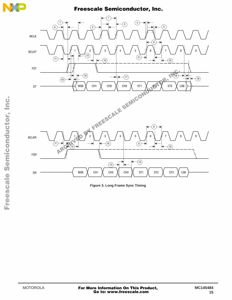
Figure 3. Long Frame Sync Timing
Fre
esc
ale
Se
mic
on
du
cto
r, I
Freescale Semiconductor, Inc.
For More Information On This Product, Go to: www.freescale.com
nc
...
ARCHIVED BY FREESCALE SEMICONDUCTOR, INC.
MC145484 MOTOROLA16
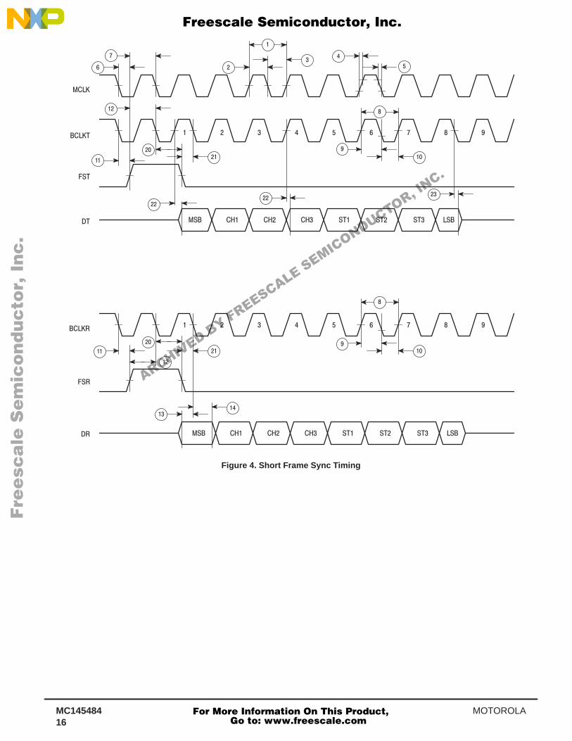
Figure 4. Short Frame Sync Timing
Fre
esc
ale
Se
mic
on
du
cto
r, I
Freescale Semiconductor, Inc.
For More Information On This Product, Go to: www.freescale.com
nc
...
ARCHIVED BY FREESCALE SEMICONDUCTOR, INC.
MC145484MOTOROLA17
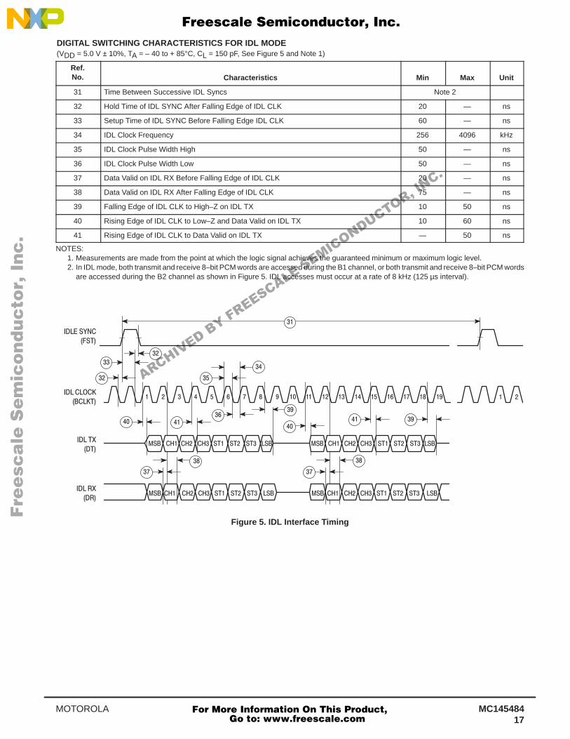
DIGITAL SWITCHING CHARACTERISTICS FOR IDL MODE (VDD = 5.0 V ± 10%, TA = – 40 to + 85°C, CL = 150 pF, See Figure 5 and Note 1)
Ref.No. Characteristics Min Max Unit
31 Time Between Successive IDL Syncs Note 2
32 Hold Time of IDL SYNC After Falling Edge of IDL CLK 20 — ns
33 Setup Time of IDL SYNC Before Falling Edge IDL CLK 60 — ns
34 IDL Clock Frequency 256 4096 kHz
35 IDL Clock Pulse Width High 50 — ns
36 IDL Clock Pulse Width Low 50 — ns
37 Data Valid on IDL RX Before Falling Edge of IDL CLK 20 — ns
38 Data Valid on IDL RX After Falling Edge of IDL CLK 75 — ns
39 Falling Edge of IDL CLK to High–Z on IDL TX 10 50 ns
40 Rising Edge of IDL CLK to Low–Z and Data Valid on IDL TX 10 60 ns
41 Rising Edge of IDL CLK to Data Valid on IDL TX — 50 ns
NOTES:1. Measurements are made from the point at which the logic signal achieves the guaranteed minimum or maximum logic level.2. In IDL mode, both transmit and receive 8–bit PCM words are accessed during the B1 channel, or both transmit and receive 8–bit PCM words
are accessed during the B2 channel as shown in Figure 5. IDL accesses must occur at a rate of 8 kHz (125 µs interval).
Figure 5. IDL Interface Timing
Fre
esc
ale
Se
mic
on
du
cto
r, I
Freescale Semiconductor, Inc.
For More Information On This Product, Go to: www.freescale.com
nc
...
ARCHIVED BY FREESCALE SEMICONDUCTOR, INC.
MC145484 MOTOROLA18
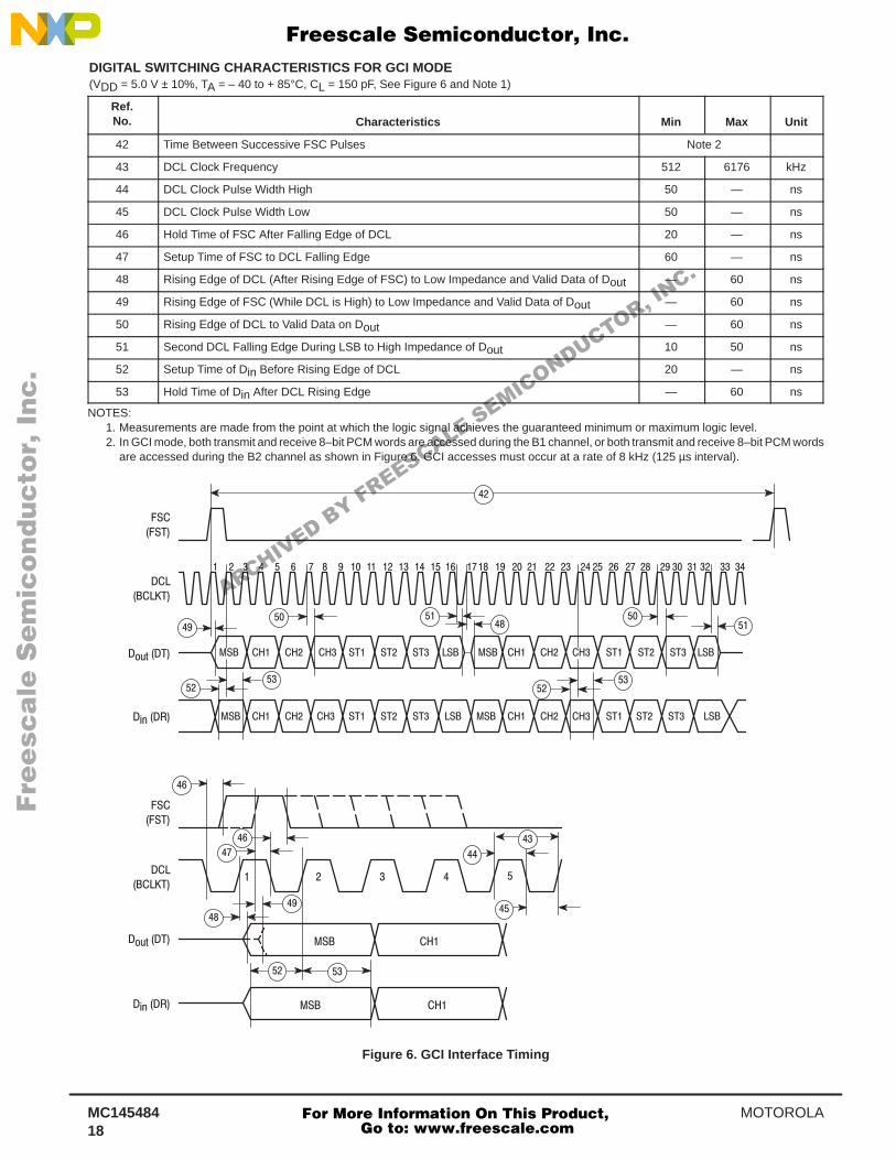
DIGITAL SWITCHING CHARACTERISTICS FOR GCI MODE(VDD = 5.0 V ± 10%, TA = – 40 to + 85°C, CL = 150 pF, See Figure 6 and Note 1)
Ref.No. Characteristics Min Max Unit
42 Time Between Successive FSC Pulses Note 2
43 DCL Clock Frequency 512 6176 kHz
44 DCL Clock Pulse Width High 50 — ns
45 DCL Clock Pulse Width Low 50 — ns
46 Hold Time of FSC After Falling Edge of DCL 20 — ns
47 Setup Time of FSC to DCL Falling Edge 60 — ns
48 Rising Edge of DCL (After Rising Edge of FSC) to Low Impedance and Valid Data of Dout — 60 ns
49 Rising Edge of FSC (While DCL is High) to Low Impedance and Valid Data of Dout — 60 ns
50 Rising Edge of DCL to Valid Data on Dout — 60 ns
51 Second DCL Falling Edge During LSB to High Impedance of Dout 10 50 ns
52 Setup Time of Din Before Rising Edge of DCL 20 — ns
53 Hold Time of Din After DCL Rising Edge — 60 ns
NOTES:1. Measurements are made from the point at which the logic signal achieves the guaranteed minimum or maximum logic level.2. In GCI mode, both transmit and receive 8–bit PCM words are accessed during the B1 channel, or both transmit and receive 8–bit PCM words
are accessed during the B2 channel as shown in Figure 6. GCI accesses must occur at a rate of 8 kHz (125 µs interval).
Figure 6. GCI Interface Timing
Fre
esc
ale
Se
mic
on
du
cto
r, I
Freescale Semiconductor, Inc.
For More Information On This Product, Go to: www.freescale.com
nc
...
ARCHIVED BY FREESCALE SEMICONDUCTOR, INC.

MC145484MOTOROLA19
'
!
%'
"
µ
! !
"
µ
µ %Ω
"
" #$
&
"
"
%Ω
%Ω
%Ω
µ
µ %
%
Figure 7. MC145484 Test Circuit — Signals Referenced to V AG Pin
µ
'
!
%'
"
µ ≥ %Ω! !
"
µ
µ
%Ω %Ω
%Ω %Ω
%Ω µ
≥ Ω! !
"
" #$
&
"
"
%
µ
%
Figure 8. MC145484 Test Circuit — Signals Referenced to V SS
Fre
esc
ale
Se
mic
on
du
cto
r, I
Freescale Semiconductor, Inc.
For More Information On This Product, Go to: www.freescale.com
nc
...
ARCHIVED BY FREESCALE SEMICONDUCTOR, INC.
MC145484 MOTOROLA20
+.
.
µ
Ω , ,
.
%& %$
& $
+.
.
$ !%!'&
!%!'&
!%
(
# #
(
(
(
#
$#
#
( Ω
#$
Figure 9. Long Frame Sync Clock Circuit for 2.048 MHz
%&!
,
,
$
µ
(
"
.
" !'&
+.
(
µ
(
µ
µ
+Ω
+Ω +Ω
"
$!
"
"!
"!
$
$
%$
(
( $)*
-
&
&
%&
&
&
&
(
(%%
µ
+Ω
+Ω
+Ω µ
Figure 10. MC145484 Analog Interface to Handset
Fre
esc
ale
Se
mic
on
du
cto
r, I
Freescale Semiconductor, Inc.
For More Information On This Product, Go to: www.freescale.com
nc
...
ARCHIVED BY FREESCALE SEMICONDUCTOR, INC.
MC145484MOTOROLA21
- #
- #
Ω
!
&(
- ,
)+*
- ',
#
µ
#
µ
'Ω
µ 'Ω
+
!
!
!
!
!
!
#
#
#
# $%
'Ω 'Ω
µ
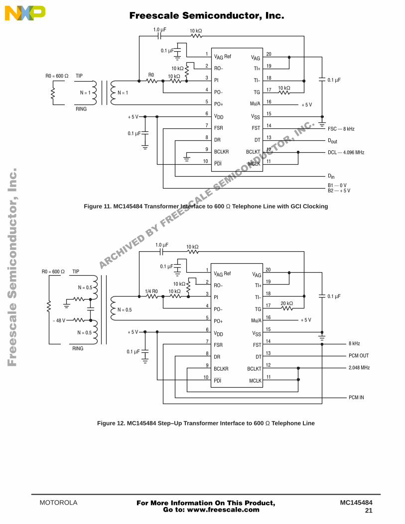
Figure 11. MC145484 Transformer Interface to 600 Ω Telephone Line with GCI Clocking
#
Ω
!
,
"!
',
µ
#
'Ω
#
# $%
+
!
!
!
!
!
!
#
#
'Ω
µ
'Ω
#
µ
µ
'Ω
Figure 12. MC145484 Step–Up Transformer Interface to 600 Ω Telephone Line
Fre
esc
ale
Se
mic
on
du
cto
r, I
Freescale Semiconductor, Inc.
For More Information On This Product, Go to: www.freescale.com
nc
...
ARCHIVED BY FREESCALE SEMICONDUCTOR, INC.
MC145484 MOTOROLA22
)
#
&'
)
)
%"
%4
'4"
)
#
%&
#
!
)
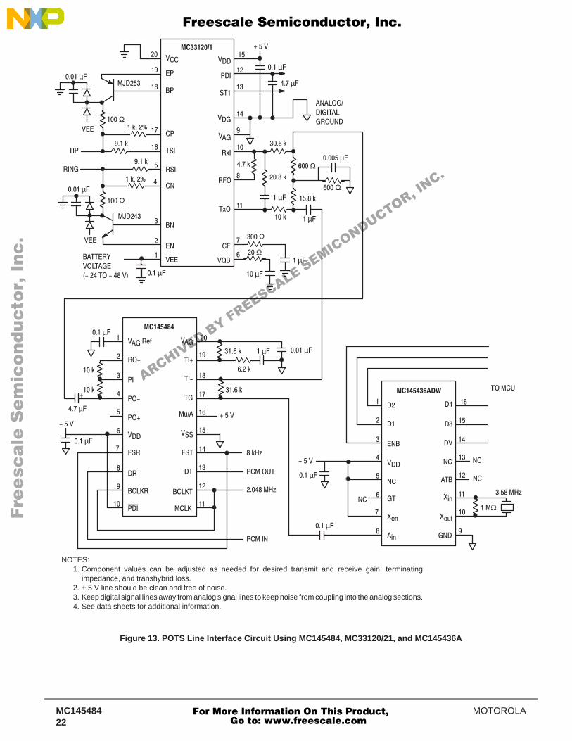
NOTES:1. Component values can be adjusted as needed for desired transmit and receive gain, terminating
impedance, and transhybrid loss.2. + 5 V line should be clean and free of noise.3. Keep digital signal lines away from analog signal lines to keep noise from coupling into the analog sections.4. See data sheets for additional information.
)$
#
'&
!
!
'#
/
/
/
/
Ω)
µ
%!
Ω
)
µ
µ
''%+
)"'
'" )
)
'
'
3
)&&
&'
'
) %,-
%"
#"
#
&%
%
'
'
#"
)
#
%
)
µ
µ
Ω
Ω
µ
µ
Ω
/
/
/
/
/
µ
µ
Ω
µ
!"
'
%"(!
µ
/
/
µ
)
µ
)
# !
/5
# "('
5
/
/
/
µ µ
)
'
*.0
*132
!
!
!
*,0
!
)
'
.0
'" (
Ω
5
µ
!
)
µ
!
!
Figure 13. POTS Line Interface Circuit Using MC145484, MC33120/21, and MC145436A
Fre
esc
ale
Se
mic
on
du
cto
r, I
Freescale Semiconductor, Inc.
For More Information On This Product, Go to: www.freescale.com
nc
...
ARCHIVED BY FREESCALE SEMICONDUCTOR, INC.

MC145484MOTOROLA23
Table 3. Mu–Law Encode–Decode Characteristics
Chord Number Step Decision DecodeNumber of Steps Size Levels Sign Chord Chord Chord Step Step Step Step Levels
NormalizedEncode Normalized
1 2 3 4 5 6 7 8
Digital Code
81591 0 0 0 0 0 0 0 8031
79038 16 256 … … …
43191 0 0 0 1 1 1 1 4191
4063
… … …
7 16 128 21431 0 0 1 1 1 1 1 2079
2015… … …
6 16 64 10551 0 1 0 1 1 1 1 1023
991
… … …
5 16 32 5111 0 1 1 1 1 1 1 495
479
… … …
4 16 16 2391 1 0 0 1 1 1 1 231
223
… … …
3 16 8 1031 1 0 1 1 1 1 1 99
95
… … …
2 16 4 351 1 1 0 1 1 1 1 33
31
… … …
1 15 2 31 1 1 1 1 1 1 0 2
11 1 1 1 1 1 1 1 1 1 0
0
NOTES:1. Characteristics are symmetrical about analog zero with sign bit = 0 for negative analog values.2. Digital code includes inversion of all magnitude bits.
Fre
esc
ale
Se
mic
on
du
cto
r, I
Freescale Semiconductor, Inc.
For More Information On This Product, Go to: www.freescale.com
nc
...
ARCHIVED BY FREESCALE SEMICONDUCTOR, INC.
MC145484 MOTOROLA24
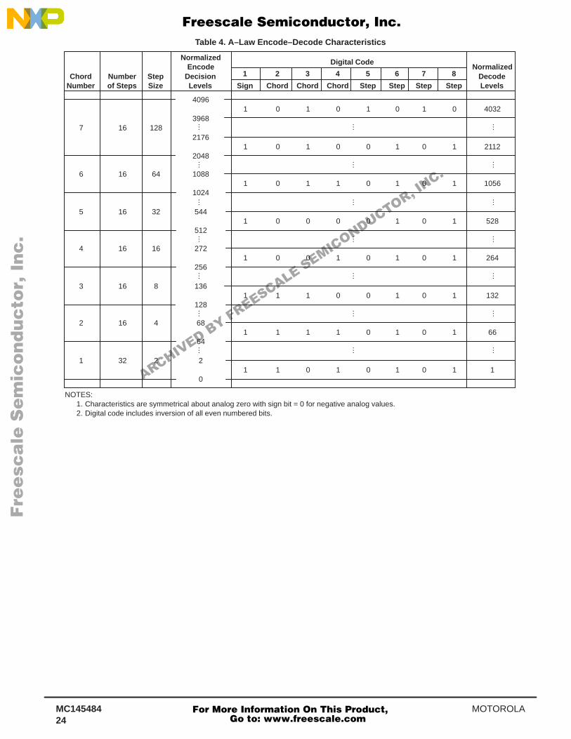
Table 4. A–Law Encode–Decode Characteristics
Chord Number Step Decision DecodeNumber of Steps Size Levels Sign Chord Chord Chord Step Step Step Step Levels
NormalizedEncode Normalized
1 2 3 4 5 6 7 8
Digital Code
40961 0 1 0 1 0 1 0 4032
39687 16 128 … … …
21761 0 1 0 0 1 0 1 2112
2048
… … …
6 16 64 10881 0 1 1 0 1 0 1 1056
1024… … …
5 16 32 5441 0 0 0 0 1 0 1 528
512
… … …
4 16 16 2721 0 0 1 0 1 0 1 264
256
… … …
3 16 8 1361 1 1 0 0 1 0 1 132
128
… … …
2 16 4 681 1 1 1 0 1 0 1 66
64
… … …
1 32 2 21 1 0 1 0 1 0 1 1
0
NOTES:1. Characteristics are symmetrical about analog zero with sign bit = 0 for negative analog values.2. Digital code includes inversion of all even numbered bits.
Fre
esc
ale
Se
mic
on
du
cto
r, I
Freescale Semiconductor, Inc.
For More Information On This Product, Go to: www.freescale.com
nc
...
ARCHIVED BY FREESCALE SEMICONDUCTOR, INC.
MC145484MOTOROLA25
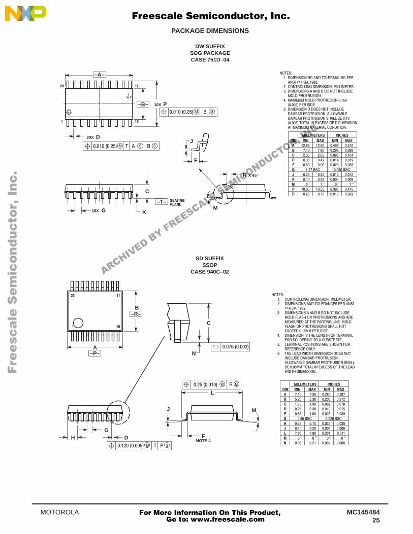
PACKAGE DIMENSIONS
DW SUFFIXSOG PACKAGECASE 751D–04
! ! %
! ! ! " !"
$" !"
! " !" # !" !! $ ! $" ! !
–A–
–B–
!
D20X
P10X
J
F
G18X K
C
–T–
M
R X 45
SD SUFFIXSSOP
CASE 940C–02
H
A
B
–P–
–R–
! ! ! !
% ! "
!" " ! ! ! !" !$
! ! ! ! " !!
! ! # %
! #! !" !" # !" !! $ ! #!
GD
!
N
C
L
J
F
M
NOTE 4
Fre
esc
ale
Se
mic
on
du
cto
r, I
Freescale Semiconductor, Inc.
For More Information On This Product, Go to: www.freescale.com
nc
...
ARCHIVED BY FREESCALE SEMICONDUCTOR, INC.
MC145484 MOTOROLA26
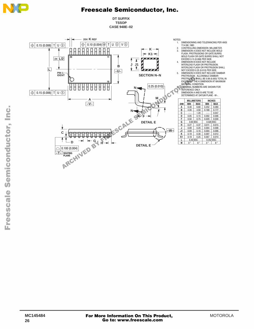
DT SUFFIXTSSOP
CASE 948E–02
" "
" "
#" " #! ! "
( #! " #! " " # $
" !#!$"" ! # $!!" " ! # $!!" " #' ! "
" " # $#! " ! !#!$"#! " ! !#!$" "# ' ! "
" " # $ ! !#!$" & ! !#!$" " ## '"" # " # '$#! #
#! $!" ! "& !!! (
" ! # #! # #$ &
ÍÍÍÍÍÍÍÍÍ
PIN 1IDENT
A
B
–T–
C
D GH
SECTION N–N
KK1
J J1
N
N
M
F
–W–
–V–
–U–
"$ % "#
20X REFK
L
L/22X
"$ #
DETAIL E
DETAIL E
"$ #
Fre
esc
ale
Se
mic
on
du
cto
r, I
Freescale Semiconductor, Inc.
For More Information On This Product, Go to: www.freescale.com
nc
...
ARCHIVED BY FREESCALE SEMICONDUCTOR, INC.
MC145484MOTOROLA27
This page intentionally left blank.
Fre
esc
ale
Se
mic
on
du
cto
r, I
Freescale Semiconductor, Inc.
For More Information On This Product, Go to: www.freescale.com
nc
...
ARCHIVED BY FREESCALE SEMICONDUCTOR, INC.
MC145484 MOTOROLA28
Motorola reserves the right to make changes without further notice to any products herein. Motorola makes no warranty, representation or guarantee regardingthe suitability of its products for any particular purpose, nor does Motorola assume any liability arising out of the application or use of any product or circuit, andspecifically disclaims any and all liability, including without limitation consequential or incidental damages. “Typical” parameters which may be provided in Motoroladata sheets and/or specifications can and do vary in different applications and actual performance may vary over time. All operating parameters, including “Typicals”must be validated for each customer application by customer’s technical experts. Motorola does not convey any license under its patent rights nor the rights ofothers. Motorola products are not designed, intended, or authorized for use as components in systems intended for surgical implant into the body, or otherapplications intended to support or sustain life, or for any other application in which the failure of the Motorola product could create a situation where personal injuryor death may occur. Should Buyer purchase or use Motorola products for any such unintended or unauthorized application, Buyer shall indemnify and hold Motorolaand its officers, employees, subsidiaries, affiliates, and distributors harmless against all claims, costs, damages, and expenses, and reasonable attorney feesarising out of, directly or indirectly, any claim of personal injury or death associated with such unintended or unauthorized use, even if such claim alleges thatMotorola was negligent regarding the design or manufacture of the part. Motorola and are registered trademarks of Motorola, Inc. Motorola, Inc. is an EqualOpportunity/Affirmative Action Employer.
Mfax is a trademark of Motorola, Inc.How to reach us:USA/EUROPE/Locations Not Listed : Motorola Literature Distribution; JAPAN : Nippon Motorola Ltd.: SPD, Strategic Planning Office, 141,P.O. Box 5405, Denver, Colorado 80217. 1–303–675–2140 or 1–800–441–2447 4–32–1 Nishi–Gotanda, Shagawa–ku, Tokyo, Japan. 03–5487–8488
Mfax : [email protected] – TOUCHTONE 1–602–244–6609 ASIA/PACIFIC : Motorola Semiconductors H.K. Ltd.; 8B Tai Ping Industrial Park,Motorola Fax Back System – US & Canada ONLY 1–800–774–1848 51 Ting Kok Road, Tai Po, N.T., Hong Kong. 852–26629298
– http://sps.motorola.com/mfax/HOME PAGE: http://motorola.com/sps/ CUSTOMER FOCUS CENTER: 1–800–521–6274
MC145484/D◊
Fre
esc
ale
Se
mic
on
du
cto
r, I
Freescale Semiconductor, Inc.
For More Information On This Product, Go to: www.freescale.com
nc
...
ARCHIVED BY FREESCALE SEMICONDUCTOR, INC.