MC68HC05K1.pdf - NXP
154
MC68HC05K1/D Rev. 2.0 MC68HC05K0 MC68HCL05K0 MC68HSC05K0 MC68HC05K1 HCMOS Microcontroller Unit TECHNICAL DATA HC 5 Freescale Semiconductor, I Freescale Semiconductor, Inc. For More Information On This Product, Go to: www.freescale.com nc...
-
Upload
khangminh22 -
Category
Documents
-
view
3 -
download
0
Transcript of MC68HC05K1.pdf - NXP

MC68HC05K1/DRev. 2.0
MC68HC05K0MC68HCL05K0MC68HSC05K0MC68HC05K1
HCMOS Microcontroller Unit
TECHNICAL DATA
HC 5
Fre
esc
ale
Se
mic
on
du
cto
r, I
Freescale Semiconductor, Inc.
For More Information On This Product, Go to: www.freescale.com
nc
...

Technical Data MC68HC05K0 • MC68HC05K1 — Rev. 2.0
Technical Data
Fre
esc
ale
Se
mic
on
du
cto
r, I
Freescale Semiconductor, Inc.
For More Information On This Product, Go to: www.freescale.com
nc
...

F
ree
sca
le S
em
ico
nd
uc
tor,
IFreescale Semiconductor, Inc.
nc
...
Technical Data — MC68HC05K0 • MC68HC05K1
List of Sections
Section 1. General Description . . . . . . . . . . . . . . . . . . . .17
Section 2. Memory . . . . . . . . . . . . . . . . . . . . . . . . . . . . . .29
Section 3. Central Processor Unit (CPU) . . . . . . . . . . . .35
Section 4. Interrupts . . . . . . . . . . . . . . . . . . . . . . . . . . . . .43
Section 5. Resets . . . . . . . . . . . . . . . . . . . . . . . . . . . . . . .53
Section 6. Low-Power Modes. . . . . . . . . . . . . . . . . . . . . .59
Section 7. Parallel Input/Output (I/O). . . . . . . . . . . . . . . .65
Section 8. Multifunction Timer. . . . . . . . . . . . . . . . . . . . .77
Section 9. Personality EPROM (MC68HC05K1 Only) . . .85
Section 10. Instruction Set . . . . . . . . . . . . . . . . . . . . . . . .93
Section 11. Electrical Specifications. . . . . . . . . . . . . . .111
Section 12. Mechanical Specifications . . . . . . . . . . . . .127
Section 13. Ordering Information . . . . . . . . . . . . . . . . .129
Appendix A. MC68HCL05K0. . . . . . . . . . . . . . . . . . . . . .135
Appendix B. MC68HSC05K0 . . . . . . . . . . . . . . . . . . . . .141
Index. . . . . . . . . . . . . . . . . . . . . . . . . . . . . . . . . . . . . . . . 145
MC68HC05K0 • MC68HC05K1 — Rev. 2.0 Technical Data
List of Sections For More Information On This Product,
Go to: www.freescale.com

Technical Data
F
ree
sca
le S
em
ico
nd
uc
tor,
I
Freescale Semiconductor, Inc.n
c..
.
Technical Data MC68HC05K0 • MC68HC05K1 — Rev. 2.0
List of Sections For More Information On This Product,
Go to: www.freescale.com

F
ree
sca
le S
em
ico
nd
uc
tor,
IFreescale Semiconductor, Inc.
nc
...
Technical Data — MC68HC05K0 • MC68HC05K1
Table of Contents
Section 1. General Description
1.1 Contents . . . . . . . . . . . . . . . . . . . . . . . . . . . . . . . . . . . . . . . . . .17
1.2 Introduction . . . . . . . . . . . . . . . . . . . . . . . . . . . . . . . . . . . . . . . .18
1.3 Features . . . . . . . . . . . . . . . . . . . . . . . . . . . . . . . . . . . . . . . . . .18
1.4 Mask Options . . . . . . . . . . . . . . . . . . . . . . . . . . . . . . . . . . . . . .19
1.5 MCU Structure . . . . . . . . . . . . . . . . . . . . . . . . . . . . . . . . . . . . .20
1.6 Pin Assignments . . . . . . . . . . . . . . . . . . . . . . . . . . . . . . . . . . . .211.6.1 VDD and VSS. . . . . . . . . . . . . . . . . . . . . . . . . . . . . . . . . . . . .221.6.2 OSC1, OSC2, and PB1/OSC3 . . . . . . . . . . . . . . . . . . . . . . .221.6.2.1 Crystal . . . . . . . . . . . . . . . . . . . . . . . . . . . . . . . . . . . . . . .231.6.2.2 Ceramic Resonator . . . . . . . . . . . . . . . . . . . . . . . . . . . . .241.6.2.3 2-Pin Resistor-Capacitor (RC) Combination . . . . . . . . . .251.6.2.4 3-Pin RC Oscillator. . . . . . . . . . . . . . . . . . . . . . . . . . . . . .261.6.2.5 External Clock Signal . . . . . . . . . . . . . . . . . . . . . . . . . . . .271.6.3 RESET . . . . . . . . . . . . . . . . . . . . . . . . . . . . . . . . . . . . . . . . .271.6.4 IRQ/VPP . . . . . . . . . . . . . . . . . . . . . . . . . . . . . . . . . . . . . . . .271.6.5 PA7–PA0 . . . . . . . . . . . . . . . . . . . . . . . . . . . . . . . . . . . . . . .271.6.6 PB1/OSC3 and PB0 . . . . . . . . . . . . . . . . . . . . . . . . . . . . . . .28
Section 2. Memory
2.1 Contents . . . . . . . . . . . . . . . . . . . . . . . . . . . . . . . . . . . . . . . . . .29
2.2 Introduction . . . . . . . . . . . . . . . . . . . . . . . . . . . . . . . . . . . . . . . .29
2.3 Input/Output Section . . . . . . . . . . . . . . . . . . . . . . . . . . . . . . . . .30
2.4 RAM . . . . . . . . . . . . . . . . . . . . . . . . . . . . . . . . . . . . . . . . . . . . .30
MC68HC05K0 • MC68HC05K1 — Rev. 2.0 Technical Data
Table of Contents For More Information On This Product,
Go to: www.freescale.com

Technical Data
F
ree
sca
le S
em
ico
nd
uc
tor,
I
Freescale Semiconductor, Inc.n
c..
.
2.5 ROM . . . . . . . . . . . . . . . . . . . . . . . . . . . . . . . . . . . . . . . . . . . . .34
2.6 Personality EPROM (MC68HC05K1 Only). . . . . . . . . . . . . . . .34
Section 3. Central Processor Unit (CPU)
3.1 Contents . . . . . . . . . . . . . . . . . . . . . . . . . . . . . . . . . . . . . . . . . .35
3.2 Introduction . . . . . . . . . . . . . . . . . . . . . . . . . . . . . . . . . . . . . . . .35
3.3 CPU Registers . . . . . . . . . . . . . . . . . . . . . . . . . . . . . . . . . . . . .363.3.1 Accumulator . . . . . . . . . . . . . . . . . . . . . . . . . . . . . . . . . . . . .373.3.2 Index Register . . . . . . . . . . . . . . . . . . . . . . . . . . . . . . . . . . .373.3.3 Stack Pointer . . . . . . . . . . . . . . . . . . . . . . . . . . . . . . . . . . . .383.3.4 Program Counter . . . . . . . . . . . . . . . . . . . . . . . . . . . . . . . . .393.3.5 Condition Code Register . . . . . . . . . . . . . . . . . . . . . . . . . . .40
3.4 Arithmetic/Logic Unit (ALU) . . . . . . . . . . . . . . . . . . . . . . . . . . .41
Section 4. Interrupts
4.1 Contents . . . . . . . . . . . . . . . . . . . . . . . . . . . . . . . . . . . . . . . . . .43
4.2 Introduction . . . . . . . . . . . . . . . . . . . . . . . . . . . . . . . . . . . . . . . .43
4.3 Interrupt Types . . . . . . . . . . . . . . . . . . . . . . . . . . . . . . . . . . . . .444.3.1 Software Interrupt. . . . . . . . . . . . . . . . . . . . . . . . . . . . . . . . .444.3.2 External Interrupts . . . . . . . . . . . . . . . . . . . . . . . . . . . . . . . .444.3.2.1 IRQ/VPP Pin . . . . . . . . . . . . . . . . . . . . . . . . . . . . . . . . . . .454.3.2.2 PA3–PA0 Pins . . . . . . . . . . . . . . . . . . . . . . . . . . . . . . . . .464.3.2.3 IRQ Status and Control Register . . . . . . . . . . . . . . . . . . .484.3.3 Timer Interrupts . . . . . . . . . . . . . . . . . . . . . . . . . . . . . . . . . .494.3.3.1 Timer Overflow Interrupt . . . . . . . . . . . . . . . . . . . . . . . . .494.3.3.2 Real-Time Interrupt . . . . . . . . . . . . . . . . . . . . . . . . . . . . .49
4.4 Interrupt Processing . . . . . . . . . . . . . . . . . . . . . . . . . . . . . . . . .50
Section 5. Resets
5.1 Contents . . . . . . . . . . . . . . . . . . . . . . . . . . . . . . . . . . . . . . . . . .53
5.2 Introduction . . . . . . . . . . . . . . . . . . . . . . . . . . . . . . . . . . . . . . . .53
5.3 Reset Types . . . . . . . . . . . . . . . . . . . . . . . . . . . . . . . . . . . . . . .54
Technical Data MC68HC05K0 • MC68HC05K1 — Rev. 2.0
Table of Contents For More Information On This Product,
Go to: www.freescale.com

Table of Contents
F
ree
sca
le S
em
ico
nd
uc
tor,
I
Freescale Semiconductor, Inc.n
c..
.
5.3.1 Power-On Reset. . . . . . . . . . . . . . . . . . . . . . . . . . . . . . . . . .545.3.2 External Reset . . . . . . . . . . . . . . . . . . . . . . . . . . . . . . . . . . .555.3.3 Computer Operating Properly (COP) Reset. . . . . . . . . . . . .565.3.4 Illegal Address Reset . . . . . . . . . . . . . . . . . . . . . . . . . . . . . .565.3.5 Low-Voltage Reset . . . . . . . . . . . . . . . . . . . . . . . . . . . . . . . .57
5.4 Reset States . . . . . . . . . . . . . . . . . . . . . . . . . . . . . . . . . . . . . . .575.4.1 CPU . . . . . . . . . . . . . . . . . . . . . . . . . . . . . . . . . . . . . . . . . . .575.4.2 I/O Port Registers. . . . . . . . . . . . . . . . . . . . . . . . . . . . . . . . .585.4.3 Timer . . . . . . . . . . . . . . . . . . . . . . . . . . . . . . . . . . . . . . . . . .585.4.4 COP Watchdog . . . . . . . . . . . . . . . . . . . . . . . . . . . . . . . . . .58
Section 6. Low-Power Modes
6.1 Contents . . . . . . . . . . . . . . . . . . . . . . . . . . . . . . . . . . . . . . . . . .59
6.2 Introduction . . . . . . . . . . . . . . . . . . . . . . . . . . . . . . . . . . . . . . . .59
6.3 Stop Mode . . . . . . . . . . . . . . . . . . . . . . . . . . . . . . . . . . . . . . . .60
6.4 Wait Mode. . . . . . . . . . . . . . . . . . . . . . . . . . . . . . . . . . . . . . . . .61
6.5 Halt Mode . . . . . . . . . . . . . . . . . . . . . . . . . . . . . . . . . . . . . . . . .62
6.6 Data-Retention Mode . . . . . . . . . . . . . . . . . . . . . . . . . . . . . . . .62
Section 7. Parallel Input/Output (I/O)
7.1 Contents . . . . . . . . . . . . . . . . . . . . . . . . . . . . . . . . . . . . . . . . . .65
7.2 Introduction . . . . . . . . . . . . . . . . . . . . . . . . . . . . . . . . . . . . . . . .65
7.3 Port A . . . . . . . . . . . . . . . . . . . . . . . . . . . . . . . . . . . . . . . . . . . .667.3.1 Port A Data Register . . . . . . . . . . . . . . . . . . . . . . . . . . . . . .667.3.2 Data Direction Register A . . . . . . . . . . . . . . . . . . . . . . . . . .677.3.3 Pulldown Register A . . . . . . . . . . . . . . . . . . . . . . . . . . . . . .687.3.4 Port A External Interrupts . . . . . . . . . . . . . . . . . . . . . . . . . . .697.3.5 Port A Logic . . . . . . . . . . . . . . . . . . . . . . . . . . . . . . . . . . . . .69
MC68HC05K0 • MC68HC05K1 — Rev. 2.0 Technical Data
Table of Contents For More Information On This Product,
Go to: www.freescale.com

Technical Data
F
ree
sca
le S
em
ico
nd
uc
tor,
I
Freescale Semiconductor, Inc.n
c..
.
7.4 Port B . . . . . . . . . . . . . . . . . . . . . . . . . . . . . . . . . . . . . . . . . . . .707.4.1 Port B Data Register . . . . . . . . . . . . . . . . . . . . . . . . . . . . . .707.4.2 Data Direction Register B. . . . . . . . . . . . . . . . . . . . . . . . . . .727.4.3 Pulldown Register B . . . . . . . . . . . . . . . . . . . . . . . . . . . . . . .737.4.4 Port B Logic . . . . . . . . . . . . . . . . . . . . . . . . . . . . . . . . . . . . .74
Section 8. Multifunction Timer
8.1 Contents . . . . . . . . . . . . . . . . . . . . . . . . . . . . . . . . . . . . . . . . . .77
8.2 Introduction . . . . . . . . . . . . . . . . . . . . . . . . . . . . . . . . . . . . . . . .77
8.3 Timer Status and Control Register . . . . . . . . . . . . . . . . . . . . .78
8.4 Timer Counter Register . . . . . . . . . . . . . . . . . . . . . . . . . . . . . .81
8.5 COP Watchdog. . . . . . . . . . . . . . . . . . . . . . . . . . . . . . . . . . . . .82
Section 9. Personality EPROM (MC68HC05K1 Only)
9.1 Contents . . . . . . . . . . . . . . . . . . . . . . . . . . . . . . . . . . . . . . . . . .85
9.2 Introduction . . . . . . . . . . . . . . . . . . . . . . . . . . . . . . . . . . . . . . . .85
9.3 PEPROM Registers . . . . . . . . . . . . . . . . . . . . . . . . . . . . . . . . .879.3.1 PEPROM Bit Select Register . . . . . . . . . . . . . . . . . . . . . . .879.3.2 PEPROM Status and Control Register . . . . . . . . . . . . . . . .89
9.4 PEPROM Programming . . . . . . . . . . . . . . . . . . . . . . . . . . . . . .90
9.5 PEPROM Reading . . . . . . . . . . . . . . . . . . . . . . . . . . . . . . . . . .92
Section 10. Instruction Set
10.1 Contents . . . . . . . . . . . . . . . . . . . . . . . . . . . . . . . . . . . . . . . . . .93
10.2 Introduction . . . . . . . . . . . . . . . . . . . . . . . . . . . . . . . . . . . . . . . .94
10.3 Addressing Modes . . . . . . . . . . . . . . . . . . . . . . . . . . . . . . . . . .9410.3.1 Inherent . . . . . . . . . . . . . . . . . . . . . . . . . . . . . . . . . . . . . . . .9510.3.2 Immediate. . . . . . . . . . . . . . . . . . . . . . . . . . . . . . . . . . . . . . .9510.3.3 Direct . . . . . . . . . . . . . . . . . . . . . . . . . . . . . . . . . . . . . . . . . .9510.3.4 Extended . . . . . . . . . . . . . . . . . . . . . . . . . . . . . . . . . . . . . . .9510.3.5 Indexed, No Offset . . . . . . . . . . . . . . . . . . . . . . . . . . . . . . . .9610.3.6 Indexed, 8-Bit Offset. . . . . . . . . . . . . . . . . . . . . . . . . . . . . . .96
Technical Data MC68HC05K0 • MC68HC05K1 — Rev. 2.0
Table of Contents For More Information On This Product,
Go to: www.freescale.com

Table of Contents
F
ree
sca
le S
em
ico
nd
uc
tor,
I
Freescale Semiconductor, Inc.n
c..
.
10.3.7 Indexed, 16-Bit Offset. . . . . . . . . . . . . . . . . . . . . . . . . . . . . .9610.3.8 Relative . . . . . . . . . . . . . . . . . . . . . . . . . . . . . . . . . . . . . . . .97
10.4 Instruction Types . . . . . . . . . . . . . . . . . . . . . . . . . . . . . . . . . . .9710.4.1 Register/Memory Instructions. . . . . . . . . . . . . . . . . . . . . . . .9810.4.2 Read-Modify-Write Instructions . . . . . . . . . . . . . . . . . . . . . .9910.4.3 Jump/Branch Instructions. . . . . . . . . . . . . . . . . . . . . . . . . .10010.4.4 Bit Manipulation Instructions . . . . . . . . . . . . . . . . . . . . . . .10210.4.5 Control Instructions . . . . . . . . . . . . . . . . . . . . . . . . . . . . . .103
10.5 Instruction Set Summary . . . . . . . . . . . . . . . . . . . . . . . . . . . .104
10.6 Opcode Map . . . . . . . . . . . . . . . . . . . . . . . . . . . . . . . . . . . . . .109
Section 11. Electrical Specifications
11.1 Contents . . . . . . . . . . . . . . . . . . . . . . . . . . . . . . . . . . . . . . . . .111
11.2 Introduction . . . . . . . . . . . . . . . . . . . . . . . . . . . . . . . . . . . . . . .111
11.3 Maximum Ratings . . . . . . . . . . . . . . . . . . . . . . . . . . . . . . . . . .112
11.4 Equivalent Pin Loading . . . . . . . . . . . . . . . . . . . . . . . . . . . . . .112
11.5 Operating Temperature Range. . . . . . . . . . . . . . . . . . . . . . . .113
11.6 Thermal Characteristics . . . . . . . . . . . . . . . . . . . . . . . . . . . . .113
11.7 Power Considerations. . . . . . . . . . . . . . . . . . . . . . . . . . . . . . .114
11.8 5.0-Volt DC Electrical Characteristics . . . . . . . . . . . . . . . . . .115
11.9 3.3-Volt DC Electrical Specifications . . . . . . . . . . . . . . . . . . .116
11.10 5.0-Volt Control Timing . . . . . . . . . . . . . . . . . . . . . . . . . . . . .120
11.11 3.3-Volt Control Timing . . . . . . . . . . . . . . . . . . . . . . . . . . . . . .121
11.12 Typical Oscillator Characteristics . . . . . . . . . . . . . . . . . . . . . .124
MC68HC05K0 • MC68HC05K1 — Rev. 2.0 Technical Data
Table of Contents For More Information On This Product,
Go to: www.freescale.com

Technical Data
F
ree
sca
le S
em
ico
nd
uc
tor,
I
Freescale Semiconductor, Inc.n
c..
.
Section 12. Mechanical Specifications
12.1 Contents . . . . . . . . . . . . . . . . . . . . . . . . . . . . . . . . . . . . . . . . .127
12.2 Introduction . . . . . . . . . . . . . . . . . . . . . . . . . . . . . . . . . . . . . . .127
12.3 MC68HC05K0/MC68HC05K1P (PDIP) . . . . . . . . . . . . . . . . .128
12.4 MC68HC05K0/MC68HC05K1DW (SOIC) . . . . . . . . . . . . . . .128
Section 13. Ordering Information
13.1 Contents . . . . . . . . . . . . . . . . . . . . . . . . . . . . . . . . . . . . . . . . .129
13.2 Introduction . . . . . . . . . . . . . . . . . . . . . . . . . . . . . . . . . . . . . . .129
13.3 MCU Ordering Forms . . . . . . . . . . . . . . . . . . . . . . . . . . . . . . .130
13.4 Application Program Media. . . . . . . . . . . . . . . . . . . . . . . . . . .13013.4.1 Diskettes. . . . . . . . . . . . . . . . . . . . . . . . . . . . . . . . . . . . . . .13113.4.2 EPROMs . . . . . . . . . . . . . . . . . . . . . . . . . . . . . . . . . . . . . .132
13.5 ROM Program Verification . . . . . . . . . . . . . . . . . . . . . . . . . . .132
13.6 ROM Verification Units (RVUs). . . . . . . . . . . . . . . . . . . . . . . .133
13.7 MCU Order Numbers . . . . . . . . . . . . . . . . . . . . . . . . . . . . . . .134
Appendix A. MC68HCL05K0
A.1 Contents . . . . . . . . . . . . . . . . . . . . . . . . . . . . . . . . . . . . . . . . .135
A.2 Introduction . . . . . . . . . . . . . . . . . . . . . . . . . . . . . . . . . . . . . . .135
A.3 1.8–2.4-Volt DC Electrical Characteristics . . . . . . . . . . . . . . .136
A.4 2.5–3.6-Volt DC Electrical Characteristics . . . . . . . . . . . . . . .136
A.5 Low-Power Supply Current. . . . . . . . . . . . . . . . . . . . . . . . . . .137
A.6 Low-Power Pulldown Current . . . . . . . . . . . . . . . . . . . . . . . . .138
A.7 Ordering Information. . . . . . . . . . . . . . . . . . . . . . . . . . . . . . . .139
Technical Data MC68HC05K0 • MC68HC05K1 — Rev. 2.0
Table of Contents For More Information On This Product,
Go to: www.freescale.com

Table of Contents
F
ree
sca
le S
em
ico
nd
uc
tor,
I
Freescale Semiconductor, Inc.n
c..
.
Appendix B. MC68HSC05K0
B.1 Contents . . . . . . . . . . . . . . . . . . . . . . . . . . . . . . . . . . . . . . . . .141
B.2 Introduction . . . . . . . . . . . . . . . . . . . . . . . . . . . . . . . . . . . . . . .141
B.3 High-Speed Supply Current . . . . . . . . . . . . . . . . . . . . . . . . . .142
B.4 5.0-Volt Control Timing . . . . . . . . . . . . . . . . . . . . . . . . . . . . . .143
B.5 3.3-Volt Control Timing . . . . . . . . . . . . . . . . . . . . . . . . . . . . . .144
B.6 Ordering Information. . . . . . . . . . . . . . . . . . . . . . . . . . . . . . . .144
Index
Index . . . . . . . . . . . . . . . . . . . . . . . . . . . . . . . . . . . . . . . . . . . .145
MC68HC05K0 • MC68HC05K1 — Rev. 2.0 Technical Data
Table of Contents For More Information On This Product,
Go to: www.freescale.com

Technical Data
F
ree
sca
le S
em
ico
nd
uc
tor,
I
Freescale Semiconductor, Inc.n
c..
.
Technical Data MC68HC05K0 • MC68HC05K1 — Rev. 2.0
Table of Contents For More Information On This Product,
Go to: www.freescale.com

F
ree
sca
le S
em
ico
nd
uc
tor,
IFreescale Semiconductor, Inc.
nc
...
Technical Data — MC68HC05K0 • MC68HC05K1
List of Figures
Figure Title Page
1-1 MC68HC05K0 and MC68HC05K1 Block Diagram. . . . . . . .201-2 Pin Assignments. . . . . . . . . . . . . . . . . . . . . . . . . . . . . . . . . .211-3 Bypassing Layout Recommendation . . . . . . . . . . . . . . . . . .221-4 Crystal Connections . . . . . . . . . . . . . . . . . . . . . . . . . . . . . . .231-5 2-Pin Ceramic Resonator Connections . . . . . . . . . . . . . . . .241-6 3-Pin Ceramic Resonator Connections . . . . . . . . . . . . . . . .241-7 2-Pin RC Oscillator Connections . . . . . . . . . . . . . . . . . . . . .251-8 3-Pin RC Oscillator Connections . . . . . . . . . . . . . . . . . . . . .261-9 External Clock Connections . . . . . . . . . . . . . . . . . . . . . . . . .27
2-1 Memory Map . . . . . . . . . . . . . . . . . . . . . . . . . . . . . . . . . . . .312-2 Control, Status, and Data Registers. . . . . . . . . . . . . . . . . . .32
3-1 Programming Model . . . . . . . . . . . . . . . . . . . . . . . . . . . . . . .363-2 Accumulator (A) . . . . . . . . . . . . . . . . . . . . . . . . . . . . . . . . . .373-3 Index Register (X) . . . . . . . . . . . . . . . . . . . . . . . . . . . . . . . .373-4 Stack Pointer (SP) . . . . . . . . . . . . . . . . . . . . . . . . . . . . . . . .383-5 Program Counter . . . . . . . . . . . . . . . . . . . . . . . . . . . . . . . . .393-6 Condition Code Register (CCR) . . . . . . . . . . . . . . . . . . . . . .40
4-1 External Interrupt Logic . . . . . . . . . . . . . . . . . . . . . . . . . . . .464-2 IRQ Status and Control Register (ISCR) . . . . . . . . . . . . . . .484-3 Interrupt Stacking Order . . . . . . . . . . . . . . . . . . . . . . . . . . . .504-4 Interrupt Flowchart . . . . . . . . . . . . . . . . . . . . . . . . . . . . . . . .52
5-1 Reset Sources . . . . . . . . . . . . . . . . . . . . . . . . . . . . . . . . . . .555-2 COP Register (COPR) . . . . . . . . . . . . . . . . . . . . . . . . . . . . .56
6-1 Stop/Wait/Halt Flowchart . . . . . . . . . . . . . . . . . . . . . . . . . . .63
7-1 Port A Data Register (PORTA). . . . . . . . . . . . . . . . . . . . . . .66
MC68HC05K0 • MC68HC05K1 — Rev. 2.0 Technical Data
List of Figures For More Information On This Product,
Go to: www.freescale.com

Technical Data
F
ree
sca
le S
em
ico
nd
uc
tor,
I
Freescale Semiconductor, Inc.n
c..
.
Figure Title Page
7-2 Data Direction Register A (DDRA) . . . . . . . . . . . . . . . . . . . .677-3 Pulldown Register A (PDRA) . . . . . . . . . . . . . . . . . . . . . . . .687-4 Port A I/O Circuit . . . . . . . . . . . . . . . . . . . . . . . . . . . . . . . . .697-5 Port B Data Register (PORTB). . . . . . . . . . . . . . . . . . . . . . .717-6 Data Direction Register B (DDRB) . . . . . . . . . . . . . . . . . . . .727-7 Pulldown Register B (PDRB) . . . . . . . . . . . . . . . . . . . . . . . .737-8 Port B I/O Circuit . . . . . . . . . . . . . . . . . . . . . . . . . . . . . . . . .74
8-1 Multifunction Timer Block Diagram. . . . . . . . . . . . . . . . . . . .788-2 Timer Status and Control Register (TSCR) . . . . . . . . . . . . .798-3 Timer Counter Register (TCNTR) . . . . . . . . . . . . . . . . . . . .818-4 COP Register (COPR) . . . . . . . . . . . . . . . . . . . . . . . . . . . . .82
9-1 PEPROM Block Diagram . . . . . . . . . . . . . . . . . . . . . . . . . . .869-2 PEPROM Bit Select Register (PEBSR) . . . . . . . . . . . . . . . .879-3 PEPROM Status and Control Register (PESCR). . . . . . . . .899-4 Programming Circuit. . . . . . . . . . . . . . . . . . . . . . . . . . . . . . .91
11-1 Equivalent Test Load . . . . . . . . . . . . . . . . . . . . . . . . . . . . .11211-2 Typical High-Side Driver Characteristics . . . . . . . . . . . . . .11711-3 Typical Low-Side Driver Characteristics. . . . . . . . . . . . . . .11711-4 Typical Run IDD versus Internal Clock Frequency . . . . . . .11811-5 Typical Wait IDD versus Internal Clock Frequency . . . . . . .11811-6 Typical Stop IDD versus Temperature . . . . . . . . . . . . . . . .11911-7 External Interrupt Timing . . . . . . . . . . . . . . . . . . . . . . . . . .12211-8 Stop Mode Recovery Timing . . . . . . . . . . . . . . . . . . . . . . .12211-9 Power-On Reset Timing . . . . . . . . . . . . . . . . . . . . . . . . . . .12311-10 External Reset Timing . . . . . . . . . . . . . . . . . . . . . . . . . . . .12311-11 2-Pin RC Oscillator R versus Frequency
(VDD = 5.0 V) . . . . . . . . . . . . . . . . . . . . . . . . . . . . . . . . .12511-12 3-Pin RC Oscillator R versus Frequency
(VDD = 5.0 V) . . . . . . . . . . . . . . . . . . . . . . . . . . . . . . . . .12511-13 2-Pin Oscillator R versus Frequency (VDD = 3.0 V) . . . . . .12611-14 3-Pin Oscillator R versus Frequency (VDD = 3.0 V) . . . . . .126
13-1 Maximum Run Mode IDD versus Frequency. . . . . . . . . . . .13813-2 Maximum Wait Mode IDD versus Frequency . . . . . . . . . . .139
Technical Data MC68HC05K0 • MC68HC05K1 — Rev. 2.0
List of Figures For More Information On This Product,
Go to: www.freescale.com
F
ree
sca
le S
em
ico
nd
uc
tor,
IFreescale Semiconductor, Inc.
nc
...
Technical Data — MC68HC05K0 • MC68HC05K1
List of Tables
Table Title Page
1-1 Mask Options . . . . . . . . . . . . . . . . . . . . . . . . . . . . . . . . . . . . .19
4-1 Reset/Interrupt Vector Addresses . . . . . . . . . . . . . . . . . . . . .51
7-1 Port A Pin Functions. . . . . . . . . . . . . . . . . . . . . . . . . . . . . . . .707-2 PB0 Pin Functions . . . . . . . . . . . . . . . . . . . . . . . . . . . . . . . . .757-3 PB1/OSC3 Pin Functions . . . . . . . . . . . . . . . . . . . . . . . . . . . .75
8-1 Real-Time Interrupt Rate Selection . . . . . . . . . . . . . . . . . . . .808-2 COP Watchdog Recommendations . . . . . . . . . . . . . . . . . . . .83
9-1 PEPROM Bit Selection . . . . . . . . . . . . . . . . . . . . . . . . . . . . . .88
10-1 Register/Memory Instructions. . . . . . . . . . . . . . . . . . . . . . . . .9810-2 Read-Modify-Write Instructions . . . . . . . . . . . . . . . . . . . . . . .9910-3 Jump and Branch Instructions . . . . . . . . . . . . . . . . . . . . . . .10110-4 Bit Manipulation Instructions. . . . . . . . . . . . . . . . . . . . . . . . .10210-5 Control Instructions. . . . . . . . . . . . . . . . . . . . . . . . . . . . . . . .10310-6 Instruction Set Summary . . . . . . . . . . . . . . . . . . . . . . . . . . .10410-7 Opcode Map . . . . . . . . . . . . . . . . . . . . . . . . . . . . . . . . . . . . .110
13-1 MCU Order Numbers . . . . . . . . . . . . . . . . . . . . . . . . . . . . . .134
A-1 MC68HCL05K0 Order Numbers. . . . . . . . . . . . . . . . . . . . . .139
B-1 MC68HSC05K0 Order Numbers . . . . . . . . . . . . . . . . . . . . .144
MC68HC05K0 • MC68HC05K1 — Rev. 2.0 Technical Data
List of Tables For More Information On This Product,
Go to: www.freescale.com

Technical Data
F
ree
sca
le S
em
ico
nd
uc
tor,
I
Freescale Semiconductor, Inc.n
c..
.
Technical Data MC68HC05K0 • MC68HC05K1 — Rev. 2.0
List of Tables For More Information On This Product,
Go to: www.freescale.com

F
ree
sca
le S
em
ico
nd
uc
tor,
IFreescale Semiconductor, Inc.
nc
...
Technical Data — MC68HC05K0 • MC68HC05K1
Section 1. General Description
1.1 Contents
1.2 Introduction . . . . . . . . . . . . . . . . . . . . . . . . . . . . . . . . . . . . . . . .18
1.3 Features . . . . . . . . . . . . . . . . . . . . . . . . . . . . . . . . . . . . . . . . . .18
1.4 Mask Options . . . . . . . . . . . . . . . . . . . . . . . . . . . . . . . . . . . . . .19
1.5 MCU Structure . . . . . . . . . . . . . . . . . . . . . . . . . . . . . . . . . . . . .20
1.6 Pin Assignments . . . . . . . . . . . . . . . . . . . . . . . . . . . . . . . . . . . .211.6.1 VDD and VSS. . . . . . . . . . . . . . . . . . . . . . . . . . . . . . . . . . . . .221.6.2 OSC1, OSC2, and PB1/OSC3 . . . . . . . . . . . . . . . . . . . . . . .221.6.2.1 Crystal . . . . . . . . . . . . . . . . . . . . . . . . . . . . . . . . . . . . . . .231.6.2.2 Ceramic Resonator . . . . . . . . . . . . . . . . . . . . . . . . . . . . .241.6.2.3 2-Pin Resistor-Capacitor (RC) Combination . . . . . . . . . .251.6.2.4 3-Pin RC Oscillator. . . . . . . . . . . . . . . . . . . . . . . . . . . . . .261.6.2.5 External Clock Signal . . . . . . . . . . . . . . . . . . . . . . . . . . . .271.6.3 RESET . . . . . . . . . . . . . . . . . . . . . . . . . . . . . . . . . . . . . . . . .271.6.4 IRQ/VPP . . . . . . . . . . . . . . . . . . . . . . . . . . . . . . . . . . . . . . . .271.6.5 PA7–PA0 . . . . . . . . . . . . . . . . . . . . . . . . . . . . . . . . . . . . . . .271.6.6 PB1/OSC3 and PB0 . . . . . . . . . . . . . . . . . . . . . . . . . . . . . . .28
MC68HC05K0 • MC68HC05K1 — Rev. 2.0 Technical Data
General Description For More Information On This Product,
Go to: www.freescale.com

Technical Data
F
ree
sca
le S
em
ico
nd
uc
tor,
I
Freescale Semiconductor, Inc.n
c..
.
1.2 Introduction
The MC68HC05K1 and MC68HC05K0 are members of Motorola’slow-cost, high-performance M68HC05 Family of 8-bit microcontrollerunits (MCU). The M68HC05 Family is based on the customer-specifiedintegrated circuit (CSIC) design strategy. All MCUs in the family use thepopular M68HC05 central processor unit (CPU) and are available with avariety of subsystems, memory sizes and types, and package types.
On-chip memory includes 504 bytes of user read-only memory (ROM)and 32 bytes of user random-access memory (RAM).
The MC68HC05K1 has an additional 64-bit personality, erasable,programmable, read-only memory (PEPROM). In an MC68HC05K1MCU, the PEPROM cannot be erased and serves as a 64-bit array ofone-time programmable ROM (OTPROM).
Appendix A. MC68HCL05K0 introduces the MC68HCL05K0, alow-power version of the MC68HC05K0.
Appendix B. MC68HSC05K0 introduces the MC68HSC05K0, ahigh-speed version of the MC68HC05K0.
1.3 Features
Features of the MC68HC05K0 and MC68HC05K1 include:
• M68HC05 CPU
• Memory-mapped input/output (I/O) registers
• 504 bytes of ROM including eight user vector locations
• 32 bytes of user RAM
• 64-bit PEPROM/OTPROM (MC68HC05K1 only)
• 10 bidirectional input/output (I/O) pins with these features:
– Software programmable pulldown devices
– Four I/O pins with 8-mA current sinking capability
– Four I/O pins with maskable external interrupt capability
Technical Data MC68HC05K0 • MC68HC05K1 — Rev. 2.0
General Description For More Information On This Product,
Go to: www.freescale.com

General DescriptionMask Options
F
ree
sca
le S
em
ico
nd
uc
tor,
I
Freescale Semiconductor, Inc.n
c..
.
• Hardware mask and flag for external interrupts
• Fully static operation with no minimum clock speed
• On-chip oscillator with connections for a crystal/ceramic resonatoror for a mask-optional 2-pin or 3-pin resistor-capacitor (RC)oscillator
• Computer operating properly (COP) watchdog
• 15-bit multifunction timer with real-time interrupt circuit
• Power-saving stop, wait/halt, and data-retention modes
• 8 × 8 unsigned multiply instruction
• Illegal address reset
• Low-voltage reset
• 16-pin plastic dual in-line package (PDIP)
• 16-pin small outline integrated circuit package (SOIC)
1.4 Mask Options
Table 1-1 shows the available mask options.
Table 1-1. Mask Options
Feature Mask Options
COP watchdog Enabled Disabled
External interrupt pin triggeringEdge triggered
onlyEdge and
level triggered
Port A external interrupt function Enabled Disabled
Low-voltage reset function Enabled Disabled
STOP instruction Enabled Convert to halt
Oscillator typeCrystal/ceramic
resonator
Resistor-capacitor
2-pin 3-pin
Port A and port B pulldown devices Software control Disabled
MC68HC05K0 • MC68HC05K1 — Rev. 2.0 Technical Data
General Description For More Information On This Product,
Go to: www.freescale.com

Technical Data
F
ree
sca
le S
em
ico
nd
uc
tor,
I
Freescale Semiconductor, Inc.n
c..
.
1.5 MCU Structure
Figure 1-1 shows the structure of the MC68HC05K0 andMC68HC05K1.
Figure 1-1. MC68HC05K0 and MC68HC05K1 Block Diagram
DATA
DIR
ECTI
ON
REG
ISTE
R B
PORT
B
PB1/OSC3
PB0
0 0 0 0 0 0 0 0 1 1
CPU CONTROL ARITHMETIC/LOGICUNIT
ACCUMULATOR
REGISTER
STACK POINTER
0 0 0
PROGRAM COUNTER
0 0
M68HC05MCU
RESET
CONDITION CODE REGISTER
1 1 1 H I N C Z
DATA
DIR
ECTI
ON
REG
ISTE
R A
PORT
A
PA7*
PA6*
PA5*
PA4*
PA3**
PA2**
PA1**
PA0**
*8-mA sink capability**External interrupt capability
COP WATCHDOGAND
INTERNALOSCILLATOR
DIVIDEBY TWO
MULTIFUNCTIONTIMER
ILLEGAL ADDRESSDETECT
LOW-VOLTAGE
IRQ/VPP
VDD
VSS
OSC1
OSC2
PERSONALITY EPROM/OTPROM— 64 BITS
USER RAM — 32 BYTES
USER ROM — 504 BYTES
1
0
(MC68HC05K1 ONLY)VPP
CPU
CLO
CK
TIM
ERC
LOC
K
DETECT
fosc fop
RESET
OSC3
Technical Data MC68HC05K0 • MC68HC05K1 — Rev. 2.0
General Description For More Information On This Product,
Go to: www.freescale.com

General DescriptionPin Assignments
F
ree
sca
le S
em
ico
nd
uc
tor,
I
Freescale Semiconductor, Inc.n
c..
.
1.6 Pin Assignments
Figure 1-2 shows the MC68HC05K0 and MC68HC05K1 pinassignments.
Figure 1-2. Pin Assignments
RESET OSC1
OSC2
VSS
VDD
PA7
PA6
PA5
PA4
1
2
3
4
5
6
7
8
16
15
14
13
12
11
10
9
PB1/OSC3
PB0
IRQ/VPP
PA0
PA1
PA2
PA3
MC68HC05K0 • MC68HC05K1 — Rev. 2.0 Technical Data
General Description For More Information On This Product,
Go to: www.freescale.com

Technical Data
F
ree
sca
le S
em
ico
nd
uc
tor,
I
Freescale Semiconductor, Inc.n
c..
.
1.6.1 VDD and VSS
VDD and VSS are the power supply and ground pins. The MCU operatesfrom a single 3.0-V to 6.0-V power supply.
Very fast signal transitions occur on the MCU pins, placing highshort-duration current demands on the power supply. To prevent noiseproblems, take special care to provide good power supply bypassing atthe MCU. Place bypass capacitors as close to the MCU as possible, asFigure 1-3 shows.
Figure 1-3. Bypassing Layout Recommendation
1.6.2 OSC1, OSC2, and PB1/OSC3
The OSC1, OSC2, and PB1/OSC3 pins are the control connections forthe 2-pin or 3-pin on-chip oscillator. The oscillator can be driven by anyof these:
• Crystal
• Ceramic resonator
• Resistor-capacitor (RC) combination
• External clock signal
The frequency of the internal oscillator is fosc. The MCU divides theinternal oscillator output by two to produce the internal clock with afrequency of fop.
VDD
VSS
C1
MCU C2
VDD
VSS
+C1
OSC1
OSC2
C2
Note:Actual layout varies according to component dimensions.
Technical Data MC68HC05K0 • MC68HC05K1 — Rev. 2.0
General Description For More Information On This Product,
Go to: www.freescale.com

General DescriptionPin Assignments
F
ree
sca
le S
em
ico
nd
uc
tor,
I
Freescale Semiconductor, Inc.n
c..
.
1.6.2.1 Crystal
The circuit in Figure 1-4 shows a typical crystal oscillator circuit for anAT-cut, parallel resonant crystal. Follow the crystal supplier’srecommendations, as the crystal parameters determine the externalcomponent values required to provide reliable startup and maximumstability. The load capacitance values used in the oscillator circuit designshould account for all stray layout capacitances. To minimize outputdistortion, mount the crystal and capacitors as close as possible to thepins.
Figure 1-4. Crystal Connections
NOTE: Use an AT-cut crystal and not a strip or tuning fork crystal. The MCU mayoverdrive or have the incorrect characteristic impedance for a strip ortuning fork crystal.
To use the crystal-driven oscillator, select the crystal/ceramic resonatormask option when ordering the MCU. The crystal/ceramic resonatormask option connects an internal 2-MΩ startup resistor between OSC1and OSC2.
MCU
VDD
VSS
OSC1
OSC2
XTAL
VSS
OSC1 OSC2
XTAL
27 pF 27 pF
2 MΩ
C1 C2
C4
C3(MASK OPTION)
C3 C4
MC68HC05K0 • MC68HC05K1 — Rev. 2.0 Technical Data
General Description For More Information On This Product,
Go to: www.freescale.com

Technical Data
F
ree
sca
le S
em
ico
nd
uc
tor,
I
Freescale Semiconductor, Inc.n
c..
.
1.6.2.2 Ceramic Resonator
To reduce cost, use a ceramic resonator in place of the crystal. Use thecircuit in Figure 1-5 for a 2-pin ceramic resonator or Figure 1-6 for a3-pin ceramic resonator and follow the resonator manufacturer’srecommendations.
Figure 1-5. 2-Pin Ceramic Resonator Connections
Figure 1-6. 3-Pin Ceramic Resonator Connections
The external component values required for maximum stability andreliable starting depend upon the resonator parameters. The loadcapacitance values used in the oscillator circuit design should accountfor all stray layout capacitances. To minimize output distortion, mountthe resonator and capacitors as close as possible to the pins.
MCU
VDD
VSS
OSC1
OSC2
CER.
VSS
OSC
1
OSC
2CERAMIC
27 pF 27 pFC1 C2
C4
C3
RES.
RESONATOR
VDD
2 MΩ(MASK OPTION)
C3 C4
MCU
VDD
VSS
OSC1
OSC2
CER.
VSS
OSC
1
OSC
2
CERAMIC C1 C2
RES.
RESONATOR VDD
2 MΩ(MASK OPTION)
Technical Data MC68HC05K0 • MC68HC05K1 — Rev. 2.0
General Description For More Information On This Product,
Go to: www.freescale.com

General DescriptionPin Assignments
F
ree
sca
le S
em
ico
nd
uc
tor,
I
Freescale Semiconductor, Inc.n
c..
.
To use the resonator-driven oscillator, select the crystal/ceramicresonator mask option when ordering the MCU. The crystal/ceramicresonator mask option connects an internal 2-MΩ startup resistorbetween OSC1 and OSC2.
1.6.2.3 2-Pin Resistor-Capacitor (RC) Combination
For maximum cost reduction, use the 2-pin RC oscillator configurationshown in Figure 1-7. The OSC2 signal is a square-type wave, and thesignal on OSC1 is a triangular-type wave. The optimum frequency forthe 2-pin oscillator configuration is 2 MHz.
Figure 1-7. 2-Pin RC Oscillator Connections
To use the 2-pin RC oscillator configuration, select the 2-pin RCoscillator mask option when ordering the MCU.
MCU
OSC
1
OSC
2
R
VDD
VSS
OSC1
OSC2
VSS
C1 C2
C3R
C3
VDD
MC68HC05K0 • MC68HC05K1 — Rev. 2.0 Technical Data
General Description For More Information On This Product,
Go to: www.freescale.com

Technical Data
F
ree
sca
le S
em
ico
nd
uc
tor,
I
Freescale Semiconductor, Inc.n
c..
.
1.6.2.4 3-Pin RC Oscillator
Another low-cost option is the 3-pin RC oscillator configuration shown inFigure 1-8. The 3-pin oscillator is more stable than the 2-pin oscillator.The OSC2 and PB1/OSC3 signals are square-type waves, and thesignal on OSC1 is a triangular-type wave. Short the OSC1 pin to the sideof resistor R, which is connected to capacitor C3. The 3-pin RC oscillatorconfiguration is recommended for frequencies of 1 MHz down to100 kHz.
Figure 1-8. 3-Pin RC Oscillator Connections
To use the 3-pin RC oscillator configuration, select the 3-pin RCoscillator mask option when ordering the MCU.
NOTE: In the 3-pin RC oscillator configuration the PEPROM of theMC68HC05K1 cannot be programmed by user software. If the voltageon IRQ/VPP is raised above VDD, the oscillator will revert to a 2-pinoscillator configuration and device operation will be disrupted.
PB1/
OSC
3
MCU
OSC
1
OSC
2
R
VDD
VSS
OSC1
OSC2
VSS
C1 C2
R
C3+
PB1/OSC3
C3
VDD
Technical Data MC68HC05K0 • MC68HC05K1 — Rev. 2.0
General Description For More Information On This Product,
Go to: www.freescale.com

General DescriptionPin Assignments
F
ree
sca
le S
em
ico
nd
uc
tor,
I
Freescale Semiconductor, Inc.n
c..
.
1.6.2.5 External Clock Signal
An external clock from another complementary metal oxidesemiconductor (CMOS)-compatible device can drive the OSC1 input,with the OSC2 pin unconnected, as Figure 1-9 shows.
Figure 1-9. External Clock Connections
1.6.3 RESET
A logic 0 on the RESET pin forces the MCU to a known startup state.See 5.3 Reset Types.
1.6.4 IRQ/VPP
The IRQ/VPP pin has these functions:
• Applying asynchronous external interrupt signals.See 4.3 Interrupt Types.
• Applying the personality EPROM programming voltage(MC68HC05K1 only). See 9.3 PEPROM Registers.
1.6.5 PA7–PA0
PA7–PA0 are the pins of port A, a general-purpose, bidirectional I/Oport. See 7.3 Port A.
All port A pins have mask-optional pulldown devices that sinkapproximately 100 µA. See 7.3.3 Pulldown Register A. If the mask
MCU
OSC
1
OSC
2
EXTERNALCMOS CLOCK
MC68HC05K0 • MC68HC05K1 — Rev. 2.0 Technical Data
General Description For More Information On This Product,
Go to: www.freescale.com

Technical Data
F
ree
sca
le S
em
ico
nd
uc
tor,
I
Freescale Semiconductor, Inc.n
c..
.
option for port A external interrupts is selected, PA3-PA0 serve asexternal interrupt pins. See 7.3.4 Port A External Interrupts.
1.6.6 PB1/OSC3 and PB0
PB1/OSC3 and PB0 are the pins of port B, a general-purpose,bidirectional I/O port. See 7.4 Port B.
PB1 is the oscillator output for the 3-pin resistor/capacitor (RC) oscillatormask option. See 1.6.2 OSC1, OSC2, and PB1/OSC3. PB1 and PB0have mask-optional pulldown devices that sink approximately 100 µA.See 7.4.3 Pulldown Register B.
Technical Data MC68HC05K0 • MC68HC05K1 — Rev. 2.0
General Description For More Information On This Product,
Go to: www.freescale.com

F
ree
sca
le S
em
ico
nd
uc
tor,
IFreescale Semiconductor, Inc.
nc
...
Technical Data — MC68HC05K0 • MC68HC05K1
Section 2. Memory
2.1 Contents
2.2 Introduction . . . . . . . . . . . . . . . . . . . . . . . . . . . . . . . . . . . . . . . .29
2.3 Input/Output Section . . . . . . . . . . . . . . . . . . . . . . . . . . . . . . . . .30
2.4 RAM . . . . . . . . . . . . . . . . . . . . . . . . . . . . . . . . . . . . . . . . . . . . .30
2.5 ROM . . . . . . . . . . . . . . . . . . . . . . . . . . . . . . . . . . . . . . . . . . . . .34
2.6 Personality EPROM (MC68HC05K1 Only). . . . . . . . . . . . . . . .34
2.2 Introduction
The central processor unit (CPU) can address 1 Kbyte of memory space.The program counter typically advances one address at a time throughthe memory, reading the program instructions and data. The read-onlymemory (ROM) portion of memory holds the program instructions, fixeddata, user-defined vectors, and interrupt service routines. Therandom-access memory (RAM) portion of memory holds variable data.Input/output (I/O) registers are memory-mapped so that the CPU canaccess their locations in the same way that it accesses all other memorylocations.
Figure 2-1 is a memory map of the microcontroller unit (MCU).
MC68HC05K0 • MC68HC05K1 — Rev. 2.0 Technical Data
Memory For More Information On This Product,
Go to: www.freescale.com

Technical Data
F
ree
sca
le S
em
ico
nd
uc
tor,
I
Freescale Semiconductor, Inc.n
c..
.
2.3 Input/Output Section
The first 32 addresses of the memory space, $0000–$001F, are the I/Osection. These are the addresses of the I/O control registers, statusregisters, and data registers. Figure 2-2 is a register map of the I/Osection.
2.4 RAM
The 32 addresses from $00E0 to $00FF serve as both the user RAM andthe stack RAM. The CPU uses five RAM bytes to save all CPU registercontents before processing an interrupt. During a subroutine call, theCPU uses two bytes to store the return address. The stack pointerdecrements during pushes and increments during pulls.
NOTE: Be careful when using nested subroutines or multiple interrupt levels.The CPU may overwrite data in the RAM during a subroutine or duringthe interrupt stacking operation.
Technical Data MC68HC05K0 • MC68HC05K1 — Rev. 2.0
Memory For More Information On This Product,
Go to: www.freescale.com

MemoryRAM
F
ree
sca
le S
em
ico
nd
uc
tor,
I
Freescale Semiconductor, Inc.n
c..
.
Figure 2-1. Memory Map
$0000I/O
32 BYTES
PORT A DATA REGISTER $0000PORT B DATA REGISTER $0001
$001F UNUSED $0002$0020
USER ROM192 BYTES
UNUSED $0003PORT A DATA DIRECTION REGISTER $0004PORT B DATA DIRECTION REGISTER $0005
UNUSED $0006$00DF UNUSED $0007$00E0 TIMER STATUS & CONTROL REGISTER $0008
TIMER COUNTER REGISTER $0009IRQ STATUS & CONTROL REGISTER $000A
UNUSED $000BUNUSED $000C
$00FF UNUSED $000D$0100
UNUSED256 BYTES
PEPROM SELECT REGISTER(1)
1. MC68HC05K1 only
$000EPEPROM STATUS & CONTROL REGISTER(1) $000F
PULLDOWN REGISTER A $0000PULLDOWN REGISTER B $0011
UNUSED $0012UNUSED $0013UNUSED $0014UNUSED $0015UNUSED $0016
$01FF UNUSED $0017$0200
USER ROM496 BYTES
UNUSED $0018UNUSED $0019UNUSED $001AUNUSED $001BUNUSED $001CUNUSED $001DUNUSED $001E
RESERVED $001F
COP REGISTER(2)
2. Writing a 0 to bit 0 of $03F0 clears the COP watchdog. Reading $03F0 returns ROM data.
$03F0RESERVED $03F1RESERVED $03F2RESERVED $03F3
$03EF RESERVED $03F4$03F0
INTERNAL TEST ROMAND COP REGISTER
8 BYTES
RESERVED $03F5RESERVED $03F6RESERVED $03F7
TIMER VECTOR (HIGH) $03F8TIMER VECTOR (LOW) $03F9IRQ VECTOR (HIGH) $03FAIRQ VECTOR (LOW) $03FB
$03F7 SWI VECTOR (HIGH) $03FC$03F8
USER VECTORS8 BYTES
SWI VECTOR (LOW) $03FDRESET VECTOR (HIGH BYTE) $03FE
$03FF RESET VECTOR (LOW BYTE) $03FF
STACK AND RAM32 BYTES
MC68HC05K0 • MC68HC05K1 — Rev. 2.0 Technical Data
Memory For More Information On This Product,
Go to: www.freescale.com

Technical Data
F
ree
sca
le S
em
ico
nd
uc
tor,
I
Freescale Semiconductor, Inc.n
c..
.
Addr. Register Name Bit 7 6 5 4 3 2 1 Bit 0
$0000Port A Data Register
(PORTA)See page 66.
Read:PA7 PA6 PA5 PA4 PA3 PA2 PA1 PA0
Write:
Reset: Unaffected by reset
$0001Port B Data Register
(PORTB)See page 71.
Read: 0 0 0 0 0 0PB1 PB0
Write:
Reset: Unaffected by reset
$0002 Unimplemented
$0003 Unimplemented
$0004Data Direction Register A
(DDRA)See page 67.
Read:DDRA7 DDRA6 DDRA5 DDRA4 DDRA3 DDRA2 DDRA1 DDRA0
Write:
Reset: 0 0 0 0 0 0 0 0
$0005Data Direction Register B
(DDRB)See page 72.
Read: 0 0 0 0 0 0DDRB1 DDRB0
Write:
Reset: 0 0 0 0 0 0 0 0
$0006 Unimplemented
$0007 Unimplemented
$0008Timer Status and Control
Register (TSCR)See page 79.
Read: TOF RTIFTOIE RTIE
0 0RT1 RT0
Write: TOFR RTIFR
Reset: 0 0 0 0 0 0 1 1
$0009Timer Counter Register
(TCNTR)See page 81.
Read: TCR7 TCR6 TCR5 TCR4 TCR3 TCR2 TCR1 TCR0
Write:
Reset: 0 0 0 0 0 0 0 0
$000AIRQ Status and Control
Register (ISCR)See page 48.
Read:IRQE
0 0 0 IRQF 0 0 0
Write: IRQR
Reset: 1 0 0 0 0 0 U 0
= Unimplemented R = Reserved U = Unaffected
Figure 2-2. Control, Status, and Data Registers (Sheet 1 of 2)
Technical Data MC68HC05K0 • MC68HC05K1 — Rev. 2.0
Memory For More Information On This Product,
Go to: www.freescale.com

MemoryRAM
F
ree
sca
le S
em
ico
nd
uc
tor,
I
Freescale Semiconductor, Inc.n
c..
.
$000B Unimplemented
↓
$000D Unimplemented
$000EPEPROM Bit Select Register
(PEBSR)See page 87.
Read:PEB7 PEB6 PEB5 PEB4 PEB3 PEB2 PEB1 PEB0
Write:
Reset: 0 0 0 0 0 0 0 0
$000FPEPROM Status and Control
Register (PESCR)See page 89.
Read: PEDATA 0PEPGM
0 0 0 0 PEPRZF
Write:
Reset: U 0 0 0 0 0 0 1
$0010Pulldown Register A
(PDRA)See page 68.
Read:
Write: PDIA7 PDIA6 PDIA5 PDIA4 PDIA3 PDIA2 PDIA1 PDIA0
Reset: 0 0 0 0 0 0 0 0
$0011Pulldown Register B
(PDRB)See page 73.
Read:
Write: PDIB1 PDIB0
Reset: U U U U U U 0 0
$0012 Unimplemented
↓
$001E Unimplemented
$001FReserved
Read:R R R R R R R R
Write:
Reset: Unaffected by reset
$03F0
COP Register(COPR)
See page 56.
Read: 0 0 0 0 0 0 1 0
Write: COPC
Reset: U U U U U U U 0
Addr. Register Name Bit 7 6 5 4 3 2 1 Bit 0
= Unimplemented R = Reserved U = Unaffected
Figure 2-2. Control, Status, and Data Registers (Sheet 2 of 2)
MC68HC05K0 • MC68HC05K1 — Rev. 2.0 Technical Data
Memory For More Information On This Product,
Go to: www.freescale.com

Technical Data
F
ree
sca
le S
em
ico
nd
uc
tor,
I
Freescale Semiconductor, Inc.n
c..
.
2.5 ROM
Addresses $0200–$03EF contain 496 bytes of user ROM. The eightaddresses from $03F8 to $03FF are user ROM locations reserved forinterrupt vectors and reset vectors.
2.6 Personality EPROM (MC68HC05K1 Only)
In an MC68HC05K1 MCU, the personality EPROM cannot be erasedand serves as a 64-bit array of one-time programmable ROM(OTPROM).
Technical Data MC68HC05K0 • MC68HC05K1 — Rev. 2.0
Memory For More Information On This Product,
Go to: www.freescale.com

F
ree
sca
le S
em
ico
nd
uc
tor,
IFreescale Semiconductor, Inc.
nc
...
Technical Data — MC68HC05K0 • MC68HC05K1
Section 3. Central Processor Unit (CPU)
3.1 Contents
3.2 Introduction . . . . . . . . . . . . . . . . . . . . . . . . . . . . . . . . . . . . . . . .35
3.3 CPU Registers . . . . . . . . . . . . . . . . . . . . . . . . . . . . . . . . . . . . .363.3.1 Accumulator . . . . . . . . . . . . . . . . . . . . . . . . . . . . . . . . . . . . .373.3.2 Index Register . . . . . . . . . . . . . . . . . . . . . . . . . . . . . . . . . . .373.3.3 Stack Pointer . . . . . . . . . . . . . . . . . . . . . . . . . . . . . . . . . . . .383.3.4 Program Counter . . . . . . . . . . . . . . . . . . . . . . . . . . . . . . . . .393.3.5 Condition Code Register . . . . . . . . . . . . . . . . . . . . . . . . . . .40
3.4 Arithmetic/Logic Unit (ALU) . . . . . . . . . . . . . . . . . . . . . . . . . . .41
3.2 Introduction
The central processor unit (CPU) contains five registers and anarithmetic/logic unit (ALU).
MC68HC05K0 • MC68HC05K1 — Rev. 2.0 Technical Data
Central Processor Unit (CPU) For More Information On This Product,
Go to: www.freescale.com

Technical Data
F
ree
sca
le S
em
ico
nd
uc
tor,
I
Freescale Semiconductor, Inc.n
c..
.
3.3 CPU Registers
Figure 3-1 shows the five CPU registers. CPU registers are not part ofthe memory map.
Figure 3-1. Programming Model
ACCUMULATOR (A)
INDEX REGISTER (X)
1 10 00 0 00 00
0 00 00
Z CI N1 H1 1
047 5
CONDITION CODE
PROGRAM
STACK POINTER (SP)
HALF-CARRY FLAG
INTERRUPT MASK
NEGATIVE FLAG
ZERO FLAG
CARRY/BORROW FLAG
0
1
6 3 2 1
047 56 3 2 1
047 56 3 2 1
047 56 3 2 1
047 56 3 2 1
81215 1314 11 10 9
81215 1314 11 10 9
REGISTER (CCR)
COUNTER (PC)
Technical Data MC68HC05K0 • MC68HC05K1 — Rev. 2.0
Central Processor Unit (CPU) For More Information On This Product,
Go to: www.freescale.com

Central Processor Unit (CPU)CPU Registers
F
ree
sca
le S
em
ico
nd
uc
tor,
I
Freescale Semiconductor, Inc.n
c..
.
3.3.1 Accumulator
The accumulator (A) shown in Figure 3-2 is a general-purpose 8-bitregister. The accumulator holds operands and results of arithmetic andnon-arithmetic operations.
3.3.2 Index Register
In the indexed addressing modes, the CPU uses the byte in the indexregister (X) to determine the effective address of the operand. (See10.3.5 Indexed, No Offset, 10.3.6 Indexed, 8-Bit Offset, 10.3.7Indexed, 16-Bit Offset.) The 8-bit index register shown in Figure 3-3can also serve as a temporary data storage location.
Bit 7 6 5 4 3 2 1 Bit 0
Read:
Write:
Reset: Unaffected by reset
Figure 3-2. Accumulator (A)
Bit 7 6 5 4 3 2 1 Bit 0
Read:
Write:
Reset: Unaffected by reset
Figure 3-3. Index Register (X)
MC68HC05K0 • MC68HC05K1 — Rev. 2.0 Technical Data
Central Processor Unit (CPU) For More Information On This Product,
Go to: www.freescale.com

Technical Data
F
ree
sca
le S
em
ico
nd
uc
tor,
I
Freescale Semiconductor, Inc.n
c..
.
3.3.3 Stack Pointer
The stack pointer (SP) shown in Figure 3-4 is a 16-bit register thatcontains the address of the next location on the stack. During a reset orafter the reset stack pointer (RSP) instruction, the stack pointer initializesto $00FF. The address in the stack pointer decrements as data ispushed onto the stack and increments as data is pulled from the stack.
The 11 most significant bits of the stack pointer are permanently fixed at00000000111, so the stack pointer produces addresses from $00FF to$00E0. If subroutines and interrupts use more than 32 stack locations,the stack pointer wraps around to address $00FF and begins writingover the previously stored data. A subroutine call uses two stacklocations; an interrupt uses five locations.
Bit 15 14 13 12 11 10 9 8 7 6 5 4 3 2 1 Bit 0
Read:0 0 0 0 0 0 0 0 1 1 1
Write:
Reset: 0 0 0 0 0 0 0 0 1 1 1 1 1 1 1 1
Figure 3-4. Stack Pointer (SP)
Technical Data MC68HC05K0 • MC68HC05K1 — Rev. 2.0
Central Processor Unit (CPU) For More Information On This Product,
Go to: www.freescale.com

Central Processor Unit (CPU)CPU Registers
F
ree
sca
le S
em
ico
nd
uc
tor,
I
Freescale Semiconductor, Inc.n
c..
.
3.3.4 Program Counter
The program counter (PC) shown in Figure 3-5 is a 16-bit register thatcontains the address of the next instruction or operand to be fetched.The six most significant bits of the program counter are ignored internallyand appear as 000000 when stacked.
Normally, the address in the program counter automatically incrementsto the next sequential memory location every time an instruction oroperand is fetched. Jump, branch, and interrupt operations load theprogram counter with an address other than that of the next sequentiallocation.
Figure 3-5. Program Counter
Bit 15 14 13 12 11 10 9 8 7 6 5 4 3 2 1 Bit 0
Read:0 0 0 0 0 0
Write:
Reset: Loaded with vector from $03FE and $03FF
MC68HC05K0 • MC68HC05K1 — Rev. 2.0 Technical Data
Central Processor Unit (CPU) For More Information On This Product,
Go to: www.freescale.com

Technical Data
F
ree
sca
le S
em
ico
nd
uc
tor,
I
Freescale Semiconductor, Inc.n
c..
.
3.3.5 Condition Code Register
The condition code register (CCR) shown in Figure 3-6 is an 8-bitregister whose three most significant bits are permanently fixed at 111.The condition code register contains the interrupt mask and four flagsthat indicate the results of prior instructions.
Bits 7–5
Bits 7–5 always read as logic 1.
H — Half-Carry Flag
The CPU sets the half-carry flag when a carry occurs between bits 3and 4 of the accumulator during an add without carry (ADD) or addwith carry (ADC) operation. The half-carry bit is required forbinary-coded decimal (BCD) arithmetic operations. Reset has noeffect on the half-carry flag.
I — Interrupt Mask Bit
Setting the interrupt mask (I) disables interrupts. If an interruptrequest occurs while the interrupt mask is a logic 0, the CPU savesthe CPU registers on the stack, sets the interrupt mask, and thenfetches the interrupt vector. If an interrupt request occurs while theinterrupt mask is set, the interrupt request is latched. The CPUprocesses the latched interrupt as soon as the interrupt mask iscleared again.
A return-from-interrupt (RTI) instruction pulls the CPU registers fromthe stack, restoring the interrupt mask to its cleared state. After areset, the interrupt mask is set and can be cleared only by a clearinterrupt mask bit (CLI), STOP, or WAIT instruction.
7 6 5 4 3 2 1 0
Read:1 1 1 H I N Z C
Write:
Reset: 1 1 1 U 1 U U U
U = Unaffected
Figure 3-6. Condition Code Register (CCR)
Technical Data MC68HC05K0 • MC68HC05K1 — Rev. 2.0
Central Processor Unit (CPU) For More Information On This Product,
Go to: www.freescale.com

Central Processor Unit (CPU)Arithmetic/Logic Unit (ALU)
F
ree
sca
le S
em
ico
nd
uc
tor,
I
Freescale Semiconductor, Inc.n
c..
.
N — Negative Flag
The CPU sets the negative flag when an arithmetic operation, logicaloperation, or data manipulation produces a negative result. Reset hasno effect on the negative flag.
Z — Zero Flag
The CPU sets the zero flag when an arithmetic operation, logicaloperation, or data manipulation produces a result of $00. Reset hasno effect on the zero flag.
C — Carry/Borrow Flag
The CPU sets the carry/borrow flag when an addition operationproduces a carry out of bit 7 of the accumulator or when a subtractionoperation requires a borrow. Some logical operations and datamanipulation instructions also clear or set the carry/borrow flag. Resethas no effect on the carry/borrow flag.
3.4 Arithmetic/Logic Unit (ALU)
The ALU performs the arithmetic and logical operations defined by theinstruction set. The binary arithmetic circuits decode instructions and setup the ALU for the selected operation.
MC68HC05K0 • MC68HC05K1 — Rev. 2.0 Technical Data
Central Processor Unit (CPU) For More Information On This Product,
Go to: www.freescale.com

Technical Data
F
ree
sca
le S
em
ico
nd
uc
tor,
I
Freescale Semiconductor, Inc.n
c..
.
Technical Data MC68HC05K0 • MC68HC05K1 — Rev. 2.0
Central Processor Unit (CPU) For More Information On This Product,
Go to: www.freescale.com

F
ree
sca
le S
em
ico
nd
uc
tor,
IFreescale Semiconductor, Inc.
nc
...
Technical Data — MC68HC05K0 • MC68HC05K1
Section 4. Interrupts
4.1 Contents
4.2 Introduction . . . . . . . . . . . . . . . . . . . . . . . . . . . . . . . . . . . . . . . .43
4.3 Interrupt Types . . . . . . . . . . . . . . . . . . . . . . . . . . . . . . . . . . . . .444.3.1 Software Interrupt. . . . . . . . . . . . . . . . . . . . . . . . . . . . . . . . .444.3.2 External Interrupts . . . . . . . . . . . . . . . . . . . . . . . . . . . . . . . .444.3.2.1 IRQ/VPP Pin . . . . . . . . . . . . . . . . . . . . . . . . . . . . . . . . . . .454.3.2.2 PA3–PA0 Pins . . . . . . . . . . . . . . . . . . . . . . . . . . . . . . . . .464.3.2.3 IRQ Status and Control Register . . . . . . . . . . . . . . . . . . .484.3.3 Timer Interrupts . . . . . . . . . . . . . . . . . . . . . . . . . . . . . . . . . .494.3.3.1 Timer Overflow Interrupt . . . . . . . . . . . . . . . . . . . . . . . . .494.3.3.2 Real-Time Interrupt . . . . . . . . . . . . . . . . . . . . . . . . . . . . .49
4.4 Interrupt Processing . . . . . . . . . . . . . . . . . . . . . . . . . . . . . . . . .50
4.2 Introduction
This section describes how interrupts temporarily change the processingsequence.
MC68HC05K0 • MC68HC05K1 — Rev. 2.0 Technical Data
Interrupts For More Information On This Product,
Go to: www.freescale.com

Technical Data
F
ree
sca
le S
em
ico
nd
uc
tor,
I
Freescale Semiconductor, Inc.n
c..
.
4.3 Interrupt Types
These conditions generate interrupts:
• SWI instruction (software interrupt)
• A logic 0 applied to the IRQ/VPP pin (external interrupt)
• A logic 1 applied to one of the PA3–PA0 pins if the port A externalinterrupt mask option is selected (external interrupt)
• A timer overflow (timer interrupt)
• Expiration of the real-time interrupt period (timer interrupt)
An interrupt temporarily suspends normal program execution to processa particular event. An interrupt does not stop the execution of theinstruction in progress, but takes effect when the current instructioncompletes its execution. Interrupt processing automatically saves thecentral processor unit (CPU) registers on the stack and loads theprogram counter with a user-defined vector address.
4.3.1 Software Interrupt
The software interrupt (SWI) instruction causes a non-maskableinterrupt.
4.3.2 External Interrupts
These sources can generate external interrupts:
• IRQ/VPP pin
• PA3–PA0 pins if the port A external interrupts mask option isselected
Setting the I bit in the condition code register or clearing the IRQE bit inthe interrupt status and control register disables external interrupts.See Figure 4-2.
Technical Data MC68HC05K0 • MC68HC05K1 — Rev. 2.0
Interrupts For More Information On This Product,
Go to: www.freescale.com

InterruptsInterrupt Types
F
ree
sca
le S
em
ico
nd
uc
tor,
I
Freescale Semiconductor, Inc.n
c..
.
4.3.2.1 IRQ/VPP Pin
An interrupt signal on the IRQ/VPP pin latches an external interrupt
request. The IRQ/VPP pin contains an internal Schmitt trigger as part of
its input to improve noise immunity. After completing the currentinstruction, the CPU tests these bits:
• IRQF bit in the interrupt status and control register
• IRQE bit in the interrupt status and control register
• I bit in the condition code register
If both the IRQF bit and the IRQE bit are set, and the I bit is clear, theCPU then begins the interrupt sequence. The CPU clears the IRQF bitwhile it fetches the interrupt vector, so that another external interruptrequest can be latched during the interrupt service routine. As soon asthe I bit is cleared during the return from interrupt, the CPU canrecognize the new interrupt request. Figure 4-1 shows the logic forexternal interrupts.
The IRQ/VPP pin is negative-edge triggered only or negative-edge andlow-level triggered, depending on the mask option selected.
When the edge- and level-sensitive trigger mask option is selected:
• A falling edge or a low level on the IRQ/VPP pin latches an externalinterrupt request.
• As long as the IRQ/VPP pin is low, an external interrupt request ispresent, and the CPU continues to execute the interrupt serviceroutine. The edge- and level-sensitive trigger option allowsconnection to the IRQ/VPP pin to multiple wired-OR interruptsources.
When the edge-sensitive only trigger mask option is selected:
• A falling edge of the IRQ/VPP pin latches an external interruptrequest.
• A subsequent interrupt request can be latched only after thevoltage level on the IRQ/VPP pin returns to logic 1 and then fallsagain to logic 0.
NOTE: If the IRQ/VPP pin is not in use, connect it to the VDD pin.
MC68HC05K0 • MC68HC05K1 — Rev. 2.0 Technical Data
Interrupts For More Information On This Product,
Go to: www.freescale.com

Technical Data
F
ree
sca
le S
em
ico
nd
uc
tor,
I
Freescale Semiconductor, Inc.n
c..
.
Figure 4-1. External Interrupt Logic
4.3.2.2 PA3–PA0 Pins
The mask option for port A external interrupts enables pins PA3–PA0 toserve as additional external interrupt sources. The PA3–PA0 pins do notcontain internal Schmitt triggers. An interrupt signal on one of thePA3–PA0 pins latches an external interrupt request. After completingthe current instruction, the CPU tests these bits:
• IRQF bit (IRQ latch)
• IRQE bit in the interrupt status and control register
• I bit in the condition code register
If both the IRQ latch and the IRQE bit are set and the I bit is clear, theCPU then begins the interrupt sequence. The CPU clears the IRQ latchwhile it fetches the interrupt vector, so that another external interruptrequest can be latched during the interrupt service routine. As soon as
LEVEL-SENSITIVE TRIGGER
PA3
PA2
PA1
IRQ
PA0
IRQLATCH
VDD
(MASK OPTION)
RSTIRQ VECTOR FETCH
IRQ STATUS AND CONTROL REGISTER
EXTERNALINTERRUPTREQUEST
IRQ
E
IRQ
F
IRQ
R
PORT AEXTERNAL INTERRUPTS
ENABLED
(MASK OPTION)
INTERNAL DATA BUS
TO BIH & BILINSTRUCTIONPROCESSING
R
Technical Data MC68HC05K0 • MC68HC05K1 — Rev. 2.0
Interrupts For More Information On This Product,
Go to: www.freescale.com

InterruptsInterrupt Types
F
ree
sca
le S
em
ico
nd
uc
tor,
I
Freescale Semiconductor, Inc.n
c..
.
the I bit is cleared during the return from interrupt, the CPU canrecognize the new interrupt request.
The PA3–PA0 pins are positive edge triggered only or positive-edge andhigh- level triggered, depending on the mask option selected.
When the positive edge and high level-sensitive trigger mask option isselected:
• A rising edge or a high level on a PA3–PA0 pin latches an externalinterrupt request if and only if all other PA3–PA0 pins are low andthe IRQ/VPP pin is high.
• A falling edge or a low level on the IRQ/VPP pin latches an externalinterrupt request if and only if all of the PA3–PA0 pins are low.
• As long as any PA3–PA0 pin is high or the IRQ/VPP pin is low, anexternal interrupt request is present, and the CPU continues toexecute the interrupt service routine.
Edge- and level-sensitive triggering allows multiple external interruptsources to be wire-ORed to any of the PA3–PA0 pins. As long as anysource is holding a PA3–PA0 pin high, an external interrupt request islatched, and the CPU continues to execute the interrupt service routine.
When the positive edge-sensitive-only trigger mask option is selected:
• A rising edge on any one of the PA3–PA0 pins latches an externalinterrupt request if all other PA3–PA0 pins are low and theIRQ/VPP pin is high.
• A falling edge on the IRQ/VPP pin latches an external interruptrequest if and only if all of the PA3–PA0 pins are low.
• A subsequent PA3–PA0 pin interrupt request can be latched onlyafter the voltage level of the previous PA3–PA0 interrupt signalreturns to a logic 0 and then rises again to a logic 1.
• A subsequent IRQ/VPP pin interrupt request can be latched onlyafter the voltage level of the previous IRQ/VPP interrupt signalreturns to a logic 1 and then falls again to a logic 0.
MC68HC05K0 • MC68HC05K1 — Rev. 2.0 Technical Data
Interrupts For More Information On This Product,
Go to: www.freescale.com

Technical Data
F
ree
sca
le S
em
ico
nd
uc
tor,
I
Freescale Semiconductor, Inc.n
c..
.
4.3.2.3 IRQ Status and Control Register
The IRQ status and control register (ISCR), shown in Figure 4-2,contains an external interrupt mask, an external interrupt flag, and a flagreset bit. Unused bits read as logic 0s.
IRQE — External Interrupt Request Enable Bit
This read/write bit enables external interrupts. Reset sets the IRQEbit.
1 = External interrupt processing enabled0 = External interrupt processing disabled
IRQF — External Interrupt Request Flag
The IRQF bit (IRQ latch) is a clearable, read-only bit that is set whenan external interrupt request is pending. Reset clears the IRQF bit.
1 = Interrupt request pending0 = No interrupt request pending
These conditions set the IRQF bit:
– An external interrupt signal on the IRQ/VPP pin
– An external interrupt signal on pin PA3, PA2, PA1, or PA0 ifPA3–PA0 are enabled by mask option to serve as externalinterrupt sources
The CPU clears the IRQF bit when fetching the interrupt vector.Writing to the IRQF bit has no effect. Writing a logic 1 to the IRQR bitclears the IRQF bit.
Address: $000A
Bit 7 6 5 4 3 2 1 Bit 0
Read:IRQE
0 0 0 IRQF 0 0 0
Write: IRQR
Reset: 1 0 0 0 0 0 U 0
= Unimplemented U = Unaffected
Figure 4-2. IRQ Status and Control Register (ISCR)
Technical Data MC68HC05K0 • MC68HC05K1 — Rev. 2.0
Interrupts For More Information On This Product,
Go to: www.freescale.com
InterruptsInterrupt Types
F
ree
sca
le S
em
ico
nd
uc
tor,
I
Freescale Semiconductor, Inc.n
c..
.
IRQR — Interrupt Request Reset Bit
Writing a logic 1 to this write-only bit clears the IRQF bit. Writing alogic 0 to IRQR has no effect. Reset has no effect on IRQR.
1 = IRQF bit cleared0 = No effect
4.3.3 Timer Interrupts
The multifunction timer can generate these interrupts:
• Timer overflow interrupt
• Real-time interrupt
Setting the I bit in the condition code register disables all timer interrupts.
4.3.3.1 Timer Overflow Interrupt
A timer overflow interrupt request occurs if the timer overflow flag (TOF)becomes set while the timer overflow interrupt enable bit (TOIE) is alsoset. See 8.3 Timer Status and Control Register.
4.3.3.2 Real-Time Interrupt
A real-time interrupt request occurs if the real-time interrupt flag, RTIF,becomes set while the real-time interrupt enable bit, RTIE, is also set.See 8.3 Timer Status and Control Register.
MC68HC05K0 • MC68HC05K1 — Rev. 2.0 Technical Data
Interrupts For More Information On This Product,
Go to: www.freescale.com

Technical Data
F
ree
sca
le S
em
ico
nd
uc
tor,
I
Freescale Semiconductor, Inc.n
c..
.
4.4 Interrupt Processing
To begin servicing an interrupt, the CPU:
• Stores the CPU registers on the stack in the order shown inFigure 4-3
• Sets the I bit in the condition code register to prevent furtherinterrupts
• Loads the program counter with the contents of the appropriateinterrupt vector locations:
– $03FC and $03FD (software interrupt vector)
– $03FA and $03FB (external interrupt vector)
– $03F8 and $03F9 (timer interrupt vector)
The return-from-interrupt (RTI) instruction causes the CPU to recoverthe CPU registers from the stack as shown in Figure 4-3.
Figure 4-3. Interrupt Stacking Order
CONDITION CODE REGISTER
$00E0 (BOTTOM OF STACK)
$00E1
$00E2
•••
ACCUMULATOR
INDEX REGISTER
PROGRAM COUNTER (HIGH BYTE)
PROGRAM COUNTER (LOW BYTE)
•••
•••
•••
$00FD
$00FE
$00FF (TOP OF STACK)
1
2
3
4
5
5
4
3
2
1
UNSTACKINGORDER
STACKINGORDER
Technical Data MC68HC05K0 • MC68HC05K1 — Rev. 2.0
Interrupts For More Information On This Product,
Go to: www.freescale.com

InterruptsInterrupt Processing
F
ree
sca
le S
em
ico
nd
uc
tor,
I
Freescale Semiconductor, Inc.n
c..
.
Table 4-1 summarizes the reset and interrupt sources and vectorassignments.
NOTE: If more than one interrupt request is pending, the CPU fetches the vectorof the higher priority interrupt first. A higher priority interrupt does notinterrupt a lower priority interrupt service routine unless the lower priorityinterrupt service routine clears the I bit.
Table 4-1. Reset/Interrupt Vector Addresses
Function SourceLocalMask
GlobalMask
Priority(1 = Highest)
Vector Address
Reset
Power-onlogic
None None 1 $03FE–$03FF
RESET pin
COP
watchdog(1)
1. The computer operating properly (COP) watchdog is a mask option.
Low-voltage
detect(2)
2. The low-voltage reset function is a mask option.
Illegaladdress
logic
Softwareinterrupt
(SWI)User code None None
Same priorityas instruction
$03FC–$03FD
Externalinterrupts
IRQ/VPP pin
IRQE bit I bit 2 $03FA–$03FB
PA3 pin(3)
3. Port A interrupt capability is a mask option.
PA2 pin(3)
PA1 pin(3)
PA0 pin(3)
Timerinterrupts
TOF bit TOIE bitI bit 3 $03F8–$03F9
RTIF bit RTIE bit
MC68HC05K0 • MC68HC05K1 — Rev. 2.0 Technical Data
Interrupts For More Information On This Product,
Go to: www.freescale.com

Technical Data
F
ree
sca
le S
em
ico
nd
uc
tor,
I
Freescale Semiconductor, Inc.n
c..
.
Figure 4-4 shows the sequence of events caused by an interrupt.
Figure 4-4. Interrupt Flowchart
EXTERNALINTERRUPT?
I BIT SET?
FROMRESET
TIMERINTERRUPT?
FETCH NEXTINSTRUCTION
SWIINSTRUCTION?
RTIINSTRUCTION?
STACK PC, X, A, CCRSET I BIT
LOAD PC WITH INTERRUPT VECTOR
YES
YES
YES
YES
YESUNSTACK CCR, A, X, PC
EXECUTE INSTRUCTION
CLEAR IRQF BIT
NO
NO
NO
NO
NO
Technical Data MC68HC05K0 • MC68HC05K1 — Rev. 2.0
Interrupts For More Information On This Product,
Go to: www.freescale.com

F
ree
sca
le S
em
ico
nd
uc
tor,
IFreescale Semiconductor, Inc.
nc
...
Technical Data — MC68HC05K0 • MC68HC05K1
Section 5. Resets
5.1 Contents
5.2 Introduction . . . . . . . . . . . . . . . . . . . . . . . . . . . . . . . . . . . . . . . .53
5.3 Reset Types . . . . . . . . . . . . . . . . . . . . . . . . . . . . . . . . . . . . . . .545.3.1 Power-On Reset. . . . . . . . . . . . . . . . . . . . . . . . . . . . . . . . . .545.3.2 External Reset . . . . . . . . . . . . . . . . . . . . . . . . . . . . . . . . . . .555.3.3 Computer Operating Properly (COP) Reset. . . . . . . . . . . . .565.3.4 Illegal Address Reset . . . . . . . . . . . . . . . . . . . . . . . . . . . . . .565.3.5 Low-Voltage Reset . . . . . . . . . . . . . . . . . . . . . . . . . . . . . . . .57
5.4 Reset States . . . . . . . . . . . . . . . . . . . . . . . . . . . . . . . . . . . . . . .575.4.1 CPU . . . . . . . . . . . . . . . . . . . . . . . . . . . . . . . . . . . . . . . . . . .575.4.2 I/O Port Registers. . . . . . . . . . . . . . . . . . . . . . . . . . . . . . . . .585.4.3 Timer . . . . . . . . . . . . . . . . . . . . . . . . . . . . . . . . . . . . . . . . . .585.4.4 COP Watchdog . . . . . . . . . . . . . . . . . . . . . . . . . . . . . . . . . .58
5.2 Introduction
This section describes the five reset sources and how they initialize themicrocontroller unit (MCU).
MC68HC05K0 • MC68HC05K1 — Rev. 2.0 Technical Data
Resets For More Information On This Product,
Go to: www.freescale.com

Technical Data
F
ree
sca
le S
em
ico
nd
uc
tor,
I
Freescale Semiconductor, Inc.n
c..
.
5.3 Reset Types
A reset immediately stops the operation of the instruction beingexecuted, initializes certain control bits, and loads the program counterwith a user-defined reset vector address.
These conditions produce a reset:
• Initial power-up (power-on reset)
• A logic 0 applied to the RESET pin (external reset)
• Timeout of the mask-optional computer operating properly (COP)watchdog (COP reset)
• An opcode fetch from an address not in the read-only memory(ROM) or random-access memory (RAM) (illegal address reset)
• VDD voltage below LVR trip point (mask-optional low-voltagereset)
Figure 5-1 is a block diagram of the reset sources.
5.3.1 Power-On Reset
A positive transition on the VDD pin generates a power-on reset. Thepower-on reset is strictly for power-up conditions and cannot be used todetect drops in power supply voltage.
A 4064 tcyc (internal clock cycle) delay after the oscillator becomesactive allows the clock generator to stabilize. If the RESET pin is at alogic 0 at the end of 4064 tcyc, the MCU remains in the reset conditionuntil the signal on the RESET pin goes to a logic 1.
Technical Data MC68HC05K0 • MC68HC05K1 — Rev. 2.0
Resets For More Information On This Product,
Go to: www.freescale.com

ResetsReset Types
F
ree
sca
le S
em
ico
nd
uc
tor,
I
Freescale Semiconductor, Inc.n
c..
.
5.3.2 External Reset
An external reset is generated by applying a logic 0 for 1 1/2 tcyc to theRESET pin. A Schmitt trigger senses the logic level at the RESET pin.
A COP reset or an illegal address reset pulls the RESET pin low for oneinternal clock cycle. A low-voltage reset pulls the RESET pin low for aslong as the low-voltage condition exists.
NOTE: To avoid overloading some power supply designs, do not connect theRESET pin directly to VDD. Use a pullup resistor of 10 kΩ or more.
Figure 5-1. Reset Sources
VDD
RESETRESETLATCH
R
COP WATCHDOG
LOW-VOLTAGE RESET
POWER-ON RESET
ILLEGAL ADDRESS RESET
INTERNAL ADDRESS BUS
D
INTERNALCLOCK
S
(MASK OPTION)
RST TO CPU ANDSUBSYSTEMS
(MASK OPTION)
MC68HC05K0 • MC68HC05K1 — Rev. 2.0 Technical Data
Resets For More Information On This Product,
Go to: www.freescale.com

Technical Data
F
ree
sca
le S
em
ico
nd
uc
tor,
I
Freescale Semiconductor, Inc.n
c..
.
5.3.3 Computer Operating Properly (COP) Reset
A timeout of the computer operating properly (COP) watchdoggenerates a COP reset. The COP watchdog is part of a software errordetection system and must be cleared periodically to start a new timeoutperiod. To clear the COP watchdog and prevent a COP reset, write alogic 0 to bit 0 (COPC) of the COP register at location $03F0.See 8.5 COP Watchdog.
The COP register, shown in Figure 5-2, is a write-only register thatreturns the contents of a ROM location when read.
The COP watchdog function is a mask option.
COPC — COP Clear Bit
COPC is a write-only bit. Periodically writing a logic 0 to COPCprevents the COP watchdog from resetting the MCU. Writing a logic 1has no effect. Reset clears the COPC bit.
5.3.4 Illegal Address Reset
An opcode fetch from an address that is not in the ROM (locations$0200–$03FF) or the RAM (locations $00E0–$00FF) generates anillegal address reset. An illegal address reset pulls the RESET pin lowfor one cycle of the internal clock.
Address: $03F0
Bit 7 6 5 4 3 2 1 Bit 0
Read: 0 0 0 0 0 0 1 0
Write: COPC
Reset: U U U U U U U 0
= Unimplemented U = Unaffected
Figure 5-2. COP Register (COPR)
Technical Data MC68HC05K0 • MC68HC05K1 — Rev. 2.0
Resets For More Information On This Product,
Go to: www.freescale.com

ResetsReset States
F
ree
sca
le S
em
ico
nd
uc
tor,
I
Freescale Semiconductor, Inc.n
c..
.
5.3.5 Low-Voltage Reset
The low-voltage reset circuit is a mask option that generates a resetsignal if the voltage on the VDD pin falls below the LVR trip point. VDDmust be set at 5 V ±10% if the mask option enabling the low-voltagereset circuit is selected.
A low-voltage reset pulls the RESET pin low for as long as thelow-voltage condition exists.
NOTE: When the low-voltage reset is enabled, use a pullup resistor on RESETbecause low-voltage reset shorts RESET to ground when it detects alow VDD. If there is no pullup to limit current, low-voltage reset will shortVDD to ground, causing the chip to possibly remain in reset due to VDDbeing pulled down by the short. VDD may also pull current andpermanently damage the chip.
5.4 Reset States
This subsection describes how resets initialize the MCU.
5.4.1 CPU
A reset has these effects on the CPU:
• Loads the stack pointer with $FF
• Sets the I bit in the condition code register, inhibiting interrupts
• Sets the IRQE bit in the interrupt status and control register
• Loads the program counter with the user-defined reset vector fromlocations $03FE and $03FF
• Clears the IRQF bit (IRQ latch)
• Clears the stop latch, enabling the CPU clock, or exiting the haltmode
• Clears the wait latch, waking the CPU from wait mode
MC68HC05K0 • MC68HC05K1 — Rev. 2.0 Technical Data
Resets For More Information On This Product,
Go to: www.freescale.com

Technical Data
F
ree
sca
le S
em
ico
nd
uc
tor,
I
Freescale Semiconductor, Inc.n
c..
.
5.4.2 I/O Port Registers
A reset has these effects on input/output (I/O) port registers:
• Clears bits DDRA7–DDRA0 in data direction register A so thatport A pins are inputs
• Clears bits PDIA7–PDIA0 in pulldown register A, turning on port Apulldown devices (if pulldown devices are enabled by maskoption)
• Clears bits DDRB1 and DDRB0 in data direction register B so thatport B pins are inputs
• Clears bits PDIB1 and PDIB0 in pulldown register B, turning onport B pulldown devices (if pulldown devices are enabled by maskoption)
• Has no effect on port A or port B data registers
5.4.3 Timer
A reset has these effects on the multifunction timer:
• Clears the timer status and control register
• Clears the timer counter register
5.4.4 COP Watchdog
A reset clears the COP watchdog timeout counter.
Technical Data MC68HC05K0 • MC68HC05K1 — Rev. 2.0
Resets For More Information On This Product,
Go to: www.freescale.com

F
ree
sca
le S
em
ico
nd
uc
tor,
IFreescale Semiconductor, Inc.
nc
...
Technical Data — MC68HC05K0 • MC68HC05K1
Section 6. Low-Power Modes
6.1 Contents
6.2 Introduction . . . . . . . . . . . . . . . . . . . . . . . . . . . . . . . . . . . . . . . .59
6.3 Stop Mode . . . . . . . . . . . . . . . . . . . . . . . . . . . . . . . . . . . . . . . .60
6.4 Wait Mode. . . . . . . . . . . . . . . . . . . . . . . . . . . . . . . . . . . . . . . . .61
6.5 Halt Mode . . . . . . . . . . . . . . . . . . . . . . . . . . . . . . . . . . . . . . . . .62
6.6 Data-Retention Mode . . . . . . . . . . . . . . . . . . . . . . . . . . . . . . . .62
6.2 Introduction
This section describes the four low-power modes:
• Stop mode
• Wait mode
• Halt mode
• Data-retention mode
MC68HC05K0 • MC68HC05K1 — Rev. 2.0 Technical Data
Low-Power Modes For More Information On This Product,
Go to: www.freescale.com
Technical Data
F
ree
sca
le S
em
ico
nd
uc
tor,
I
Freescale Semiconductor, Inc.n
c..
.
6.3 Stop Mode
The STOP instruction puts the microcontroller unit (MCU) in its lowestpower-consumption mode and has these effects on the MCU:
• Clears TOF and RTIF, the timer interrupt flags in the timer statusand control register, removing any pending timer interrupts
• Clears TOIE and RTIE, the timer interrupt enable bits in the timerstatus and control register, disabling further timer interrupts
• Clears the multifunction timer counter register
• Sets the IRQE bit in the IRQ status and control register to enableexternal interrupts
• Clears the I bit in the condition code register, enabling interrupts
• Stops the internal oscillator, turning off the central processor unit(CPU) clock and the timer clock, including the computer operatingproperly (COP) watchdog, and holds OSC2 at a logic 1
The STOP instruction does not affect any other registers or anyinput/output (I/O) lines.
These conditions bring the MCU out of stop mode:
• An external interrupt signal on the IRQ/VPP pin — A high-to-lowtransition on the IRQ/VPP pin loads the program counter with thecontents of locations $03FA and $03FB.
• An external interrupt signal on a port A external interrupt pin — Ifthe mask option for the port A external interrupt function isselected, a low-to-high transition on a PA3–PA0 pin loads theprogram counter with the contents of locations $03FA and $03FB.
• Low-voltage reset — A low-voltage detect resets the MCU andloads the program counter with the contents of locations $03FEand $03FF (if this mask option is selected).
• External reset — A logic 0 on the RESET pin resets the MCU andloads the program counter with the contents of locations $03FEand $03FF.
When the MCU exits stop mode, processing resumes after astabilization delay of 4064 oscillator cycles.
Technical Data MC68HC05K0 • MC68HC05K1 — Rev. 2.0
Low-Power Modes For More Information On This Product,
Go to: www.freescale.com
Low-Power ModesWait Mode
F
ree
sca
le S
em
ico
nd
uc
tor,
I
Freescale Semiconductor, Inc.n
c..
.
6.4 Wait Mode
The WAIT instruction puts the MCU in an intermediatepower-consumption mode and has these effects on the MCU:
• Clears the I bit in the condition code register, enabling interrupts
• Sets the IRQE bit in the IRQ status and control register, enablingexternal interrupts
• Stops the CPU clock, but allows the internal oscillator and timerclock to continue to run
The WAIT instruction does not affect any other registers or any I/O lines.
These conditions restart the CPU clock and bring the MCU out of waitmode:
• An external interrupt signal on the IRQ/VPP pin — A high-to-lowtransition on the IRQ/VPP pin loads the program counter with thecontents of locations $03FA and $03FB.
• An external interrupt signal on a port A external interrupt pin — Ifthe mask option for the port A external interrupt function isselected, a low-to-high transition on a PA3–PA0 pin loads theprogram counter with the contents of locations $03FA and $03FB.
• A timer interrupt — A timer overflow or a real-time interrupt requestloads the program counter with the contents of locations $03F8and $03F9.
• A COP watchdog reset — A timeout of the mask-optional COPwatchdog resets the MCU and loads the program counter with thecontents of locations $03FE and $03FF. Software can enablereal-time interrupts so that the MCU can periodically exit waitmode to reset the COP watchdog.
• Low-voltage reset — A low-voltage detect resets the MCU andloads the program counter with the contents of locations $03FEand $03FF (if this mask option is selected).
• External reset — A logic 0 on the RESET pin resets the MCU andloads the program counter with the contents of locations $03FEand $03FF.
MC68HC05K0 • MC68HC05K1 — Rev. 2.0 Technical Data
Low-Power Modes For More Information On This Product,
Go to: www.freescale.com

Technical Data
F
ree
sca
le S
em
ico
nd
uc
tor,
I
Freescale Semiconductor, Inc.n
c..
.
6.5 Halt Mode
If the mask option to disable the STOP instruction is selected, a STOPinstruction puts the MCU in halt mode. Halt mode is identical to waitmode, except that a recovery delay of from 1 to 4064 internal clockcycles occurs when the MCU exits halt mode. If the mask option todisable the STOP instruction is selected, the COP watchdog cannot beturned off inadvertently by a STOP instruction.
Figure 6-1 shows the sequence of events in stop, wait, and halt modes.
6.6 Data-Retention Mode
In data-retention mode, the MCU retains random-access memory (RAM)contents and CPU register contents at VDD voltages as low as 2.0 Vdc.The data-retention feature allows the MCU to remain in a lowpower-consumption state during which it retains data, but the CPUcannot execute instructions.
To put the MCU in data-retention mode:
1. Drive the RESET pin to a logic 0.
2. Lower the VDD voltage. The RESET pin must remain lowcontinuously during data-retention mode.
To take the MCU out of data-retention mode:
1. Return VDD to normal operating voltage.
2. Return the RESET pin to a logic 1.
Technical Data MC68HC05K0 • MC68HC05K1 — Rev. 2.0
Low-Power Modes For More Information On This Product,
Go to: www.freescale.com

Low-Power ModesData-Retention Mode
F
ree
sca
le S
em
ico
nd
uc
tor,
I
Freescale Semiconductor, Inc.n
c..
.
Figure 6-1. Stop/Wait/Halt Flowchart
STOP
STOPDISABLED?
CLEAR I BIT IN CCRSET IRQE BIT IN ISCR
CLEAR TOF, RTIF, TOIE, AND RTIE BITS IN TSCRTURN OFF INTERNAL OSCILLATOR
EXTERNALRESET?
EXTERNALINTERRUPT?
NO
NO
NO
TURN ON INTERNAL OSCILLATORSTART STABILIZATION DELAY
YES
YES
HALTYES
END OFSTABILIZATION
DELAY?
YES
NO
YES
NO
NO
NO
COPRESET?
TIMERINTERRUPT?
EXTERNALINTERRUPT?
EXTERNALRESET?
CLEAR I BIT IN CCRSET IRQE BIT IN ISCR
TURN OFF CPU CLOCKTIMER CLOCK ACTIVE
YES
YES
YES
WAIT
YES
NO
NO
NO
COPRESET?
TIMERINTERRUPT?
EXTERNALINTERRUPT?
EXTERNALRESET?
CLEAR I BIT IN CCRSET IRQE BIT IN ISCR
TURN OFF CPU CLOCKTIMER CLOCK ACTIVE
YES
YES
YES
NO NO
TURN ON CPU CLOCK
1. LOAD PC WITH RESET VECTOROR
2. SERVICE INTERRUPTa. SAVE CPU REGISTERS ON STACKb. SET I BIT IN CCRc. LOAD PC WITH INTERRUPT VECTOR
LVRENABLED?
LVR?YES
NO
YES
NO
LVRENABLED?
LVRENABLED?
LVR? LVR?
YES YES
NO NO
NONO
YES YES
MC68HC05K0 • MC68HC05K1 — Rev. 2.0 Technical Data
Low-Power Modes For More Information On This Product,
Go to: www.freescale.com
Technical Data
F
ree
sca
le S
em
ico
nd
uc
tor,
I
Freescale Semiconductor, Inc.n
c..
.
Technical Data MC68HC05K0 • MC68HC05K1 — Rev. 2.0
Low-Power Modes For More Information On This Product,
Go to: www.freescale.com

F
ree
sca
le S
em
ico
nd
uc
tor,
IFreescale Semiconductor, Inc.
nc
...
Technical Data — MC68HC05K0 • MC68HC05K1
Section 7. Parallel Input/Output (I/O)
7.1 Contents
7.2 Introduction . . . . . . . . . . . . . . . . . . . . . . . . . . . . . . . . . . . . . . . .65
7.3 Port A . . . . . . . . . . . . . . . . . . . . . . . . . . . . . . . . . . . . . . . . . . . .667.3.1 Port A Data Register . . . . . . . . . . . . . . . . . . . . . . . . . . . . . .667.3.2 Data Direction Register A. . . . . . . . . . . . . . . . . . . . . . . . . . .677.3.3 Pulldown Register A . . . . . . . . . . . . . . . . . . . . . . . . . . . . . . .687.3.4 Port A External Interrupts . . . . . . . . . . . . . . . . . . . . . . . . . . .697.3.5 Port A Logic . . . . . . . . . . . . . . . . . . . . . . . . . . . . . . . . . . . . .69
7.4 Port B . . . . . . . . . . . . . . . . . . . . . . . . . . . . . . . . . . . . . . . . . . . .707.4.1 Port B Data Register . . . . . . . . . . . . . . . . . . . . . . . . . . . . . .707.4.2 Data Direction Register B. . . . . . . . . . . . . . . . . . . . . . . . . . .727.4.3 Pulldown Register B . . . . . . . . . . . . . . . . . . . . . . . . . . . . . .737.4.4 Port B Logic . . . . . . . . . . . . . . . . . . . . . . . . . . . . . . . . . . . . .74
7.2 Introduction
The 10 bidirectional input/output (I/O) pins form two parallel I/O ports.Each I/O pin is programmable as an input or an output. The contents ofthe data direction registers determine the data direction of each I/O pin.
All 10 I/O pins have mask-optional pulldown devices.
MC68HC05K0 • MC68HC05K1 — Rev. 2.0 Technical Data
Parallel Input/Output (I/O) For More Information On This Product,
Go to: www.freescale.com

Technical Data
F
ree
sca
le S
em
ico
nd
uc
tor,
I
Freescale Semiconductor, Inc.n
c..
.
7.3 Port A
Port A is an 8-bit, general-purpose, bidirectional I/O port with thesefeatures:
• Programmable pulldown devices (mask option)
• 8-mA current sinking capability (pins PA7–PA4)
• External interrupt capability (pins PA3–PA0) (mask option)
7.3.1 Port A Data Register
The port A data register (PORTA), shown in Figure 7-1, contains a bitfor each of the port A pins. When a port A pin is programmed to be anoutput, the state of its data register bit determines the state of the outputpin. When a port A pin is programmed to be an input, reading the port Adata register returns the logic state of the pin. The port A data registermay be written to while the port is either an input or an output.
PA7–PA0 — Port A Data Bits
These read/write bits are software-programmable. Data direction ofeach bit is under the control of the corresponding bit in data directionregister A. Reset has no effect on port A data.
Address: $0000
Bit 7 6 5 4 3 2 1 Bit 0
Read:PA7 PA6 PA5 PA4 PA3 PA2 PA1 PA0
Write:
Reset: Unaffected by reset
Figure 7-1. Port A Data Register (PORTA)
Technical Data MC68HC05K0 • MC68HC05K1 — Rev. 2.0
Parallel Input/Output (I/O) For More Information On This Product,
Go to: www.freescale.com

Parallel Input/Output (I/O)Port A
F
ree
sca
le S
em
ico
nd
uc
tor,
I
Freescale Semiconductor, Inc.n
c..
.
7.3.2 Data Direction Register A
The contents of data direction register A (DDRA), shown in Figure 7-2,determine whether each port A pin is an input or an output. Writing alogic 1 to a DDRA bit enables the output buffer for the associated port Apin; a logic 0 disables the output buffer. A reset initializes all DDRA bitsto logic 0s, configuring all port A pins as inputs. If the pulldown devicesare enabled by mask option, setting a DDRA bit to a logic 1 turns off thepulldown device for that pin.
DDRA7–DDRA0 — Port A Data Direction Bits
These read/write bits control port A data direction. Reset clears bitsDDRA7–DDRA0.
1 = Corresponding port A pin configured as output0 = Corresponding port A pin configured as input
NOTE: Avoid glitches on port A pins by writing to the port A data register beforechanging DDRA bits from logic 0 to logic 1.
Address: $0004
Bit 7 6 5 4 3 2 1 Bit 0
Read:DDRA7 DDRA6 DDRA5 DDRA4 DDRA3 DDRA2 DDRA1 DDRA0
Write:
Reset: 0 0 0 0 0 0 0 0
Figure 7-2. Data Direction Register A (DDRA)
MC68HC05K0 • MC68HC05K1 — Rev. 2.0 Technical Data
Parallel Input/Output (I/O) For More Information On This Product,
Go to: www.freescale.com

Technical Data
F
ree
sca
le S
em
ico
nd
uc
tor,
I
Freescale Semiconductor, Inc.n
c..
.
7.3.3 Pulldown Register A
Port A pins have mask-optional pulldown devices that sinkapproximately 100 µA. Clearing the PDIA7–PDIA0 bits in pulldownregister A turns on the port A pulldown devices. Pulldown register A,shown in Figure 7-3, can turn on a port A pulldown device only when theport A pin is an input.
If the pulldown mask option is selected, reset initializes all port A and portB pins as inputs with pulldown devices turned on.
PDIA7–PDIA0 — Port A Pulldown Inhibit Bits 7–0
Writing logic 0s to these write-only bits turns on the port A pulldowndevices. Reading pulldown register A returns undefined data. Resetclears bits PDIA7–PDIA0.
1 = Corresponding port A pin pulldown device turned off0 = Corresponding port A pin pulldown device turned on
NOTE: To avoid excessive current draw, connect all unused input pins to VDDor VSS. Or change I/O pins to outputs by writing to DDRA in userinitialization code. Avoid a floating port A input by clearing its pulldownregister bit before changing its DDRA bit from logic 1 to logic 0.
Because pulldown register A is a write-only register, using theread-modify-write instruction may result in inadvertently turning bits onor off.
Address: $0010
Bit 7 6 5 4 3 2 1 Bit 0
Read:
Write: PDIA7 PDIA6 PDIA5 PDIA4 PDIA3 PDIA2 PDIA1 PDIA0
Reset: 0 0 0 0 0 0 0 0
= Unimplemented
Figure 7-3. Pulldown Register A (PDRA)
Technical Data MC68HC05K0 • MC68HC05K1 — Rev. 2.0
Parallel Input/Output (I/O) For More Information On This Product,
Go to: www.freescale.com

Parallel Input/Output (I/O)Port A
F
ree
sca
le S
em
ico
nd
uc
tor,
I
Freescale Semiconductor, Inc.n
c..
.
7.3.4 Port A External Interrupts
If the mask option for port A external interrupts is selected, the PA3–PA0pins serve as external interrupt pins in addition to the IRQ/VPP pin.External interrupts can be positive edge-triggered or positive edge- andhigh level-triggered.
NOTE: When testing for external interrupts, the BIH and BIL instructions test thevoltage on the IRQ/VPP pin, not the state of the internal IRQ signal.Therefore, BIH and BIL do not test the port A external interrupt pins.
Port A interrupts are not sensitive to the direction of the port pins. Drivinga logic 1 on PA0–PA3 while port interrupts are enabled will cause aninterrupt, even if PA0–PA3 are set to outputs.
7.3.5 Port A Logic
Figure 7-4 shows the port A I/O logic.
Figure 7-4. Port A I/O Circuit
PAx
EXTERNALINTERRUPTREQUEST
DATA DIRECTIONREGISTER ABIT DDRAx
PORT A DATAREGISTER
BIT PAx
PULLDOWNREGISTER A
BIT PDIAx
READ $0004
WRITE $0000
READ $0000
WRITE $0010
100-mAPULLDOWNDEVICERESET
INTE
RN
AL D
ATA
BUS
8-mA SINKCAPABILITY
(PINS PA7–PA4)
(PINS PA3–PA0)
WRITE $0004
PULLDOWNS ENABLED (ACTIVE LOW)
(MASK OPTION)
MC68HC05K0 • MC68HC05K1 — Rev. 2.0 Technical Data
Parallel Input/Output (I/O) For More Information On This Product,
Go to: www.freescale.com

Technical Data
F
ree
sca
le S
em
ico
nd
uc
tor,
I
Freescale Semiconductor, Inc.n
c..
.
When a port A pin is programmed as an output, reading the port bitactually reads the value of the data latch and not the voltage on the pinitself. When a port A pin is programmed as an input, reading the port bitreads the voltage level on the pin. The data latch can always be written,regardless of the state of its DDR bit. Table 7-1 summarizes theoperations of the port A pins.
7.4 Port B
Port B is a 2-bit, general-purpose, bidirectional I/O port with thesefeatures:
• Programmable pulldown devices (mask option)
• Oscillator output for 3-pin resistor-capacitor (RC) oscillator maskoption
7.4.1 Port B Data Register
The port B data register (PORTB), shown in Figure 7-5, contains a bitfor each of the port B pins. When a port B pin is programmed to be anoutput, the state of its data register bit determines the state of the outputpin. When a port B pin is programmed to be an input, reading the port B
Table 7-1. Port A Pin Functions
PulldownMask
Option
Control BitsI/O Pin Mode
Accessesto PDRA
Accessesto DDRA
Accessesto PORTA
PDIAx DDRAx Read Write Read/Write Read Write
No X 0 Input, hi-z U PDIA7–PDIA0 DDRA7–DDRA0 Pin PA0–PA7
No X 1 Output U PDIA7–PDIA0 DDRA7–DDRA0 PA0–PA7 PA0–PA7
Yes 0 0Input,
pulldown onU PDIA7–PDIA0 DDRA7–DDRA0 Pin PA0–PA7
Yes 0 1 Output U PDIA7–PDIA0 DDRA7–DDRA0 PA0–PA7 PA0–PA7
Yes 1 0 Input, hi-z U PDIA7–PDIA0 DDRA7–DDRA0 Pin PA0–PA7
Yes 1 1 Output U PDIA7–PDIA0 DDRA7–DDRA0 PA0–PA7 PA0–PA7
X = Don’t careU = Undefined
Technical Data MC68HC05K0 • MC68HC05K1 — Rev. 2.0
Parallel Input/Output (I/O) For More Information On This Product,
Go to: www.freescale.com

Parallel Input/Output (I/O)Port B
F
ree
sca
le S
em
ico
nd
uc
tor,
I
Freescale Semiconductor, Inc.n
c..
.
data register returns the logic state of the pin. Reset has no effect on portB data.
PB1/OSC3 — Port B Data Bit 1
This read/write bit is software programmable. Data direction of PB1 isunder the control of the DDRB1 bit in data direction register B.
When the 3-pin RC oscillator mask option is selected, PB1/OSC3 isused as an oscillator output. Using the 3-pin RC oscillatorconfiguration affects port B in these ways:
• Bit PB1 can be used as a read/write storage location withoutaffecting the oscillator. Reset has no effect on bit PB1.
• Bit DDRB1 in data direction register B can be used as a read/writestorage location without affecting the oscillator. Reset clearsDDRB1.
• The PB1/OSC3 pulldown device is disabled.
PB0 — Port B Data Bit 0
This read/write bit is software-programmable. Data direction of PB0 isunder the control of the DDRB0 bit in data direction register B.
Bits 7–2 — Not used
Bits 7–2 always read as logic 0s.
Address: $0001
Bit 7 6 5 4 3 2 1 Bit 0
Read: 0 0 0 0 0 0PB1 PB0
Write:
Reset: Unaffected by reset
AlternateFunction:
OSC3
= Unimplemented
Figure 7-5. Port B Data Register (PORTB)
MC68HC05K0 • MC68HC05K1 — Rev. 2.0 Technical Data
Parallel Input/Output (I/O) For More Information On This Product,
Go to: www.freescale.com

Technical Data
F
ree
sca
le S
em
ico
nd
uc
tor,
I
Freescale Semiconductor, Inc.n
c..
.
7.4.2 Data Direction Register B
The contents of data direction register B (DDRB) determine whethereach port B pin is an input or an output (see Figure 7-6). Writing a logic 1to a DDRB bit enables the output buffer for the associated port B pin; alogic 0 disables the output buffer. A reset initializes all DDRB bits tologic 0, configuring all port B pins as inputs. Setting a DDRB bit to alogic 1 turns off the pulldown device for that pin.
DDRB1 and DDRB0 — Data Direction Bits 1 and 0
These read/write bits control port B data direction.1 = Corresponding port B pin configured as output0 = Corresponding port B pin configured as input
Bit 7–2 — Not used
Bits 7–2 always read as logic 0s. Writes to these bits have no effect.
NOTE: Avoid glitches on port B pins by writing to the port B data register beforechanging DDRB bits from logic 0 to logic 1.
Address: $0005
Bit 7 6 5 4 3 2 1 Bit 0
Read: 0 0 0 0 0 0DDRB1 DDRB0
Write:
Reset: 0 0 0 0 0 0 0 0
= Unimplemented
Figure 7-6. Data Direction Register B (DDRB)
Technical Data MC68HC05K0 • MC68HC05K1 — Rev. 2.0
Parallel Input/Output (I/O) For More Information On This Product,
Go to: www.freescale.com

Parallel Input/Output (I/O)Port B
F
ree
sca
le S
em
ico
nd
uc
tor,
I
Freescale Semiconductor, Inc.n
c..
.
7.4.3 Pulldown Register B
Port B pins have mask-optional pulldown devices that sinkapproximately 100 µA. Clearing the PDIB1 and PDIB0 bits in pulldownregister B turns on the port B pulldown devices. Pulldown register B canturn on a port B pulldown device only when the port B pin is an input. SeeFigure 7-7.
If the pulldown mask option is selected, reset initializes all port A andport B pins as inputs with pulldown devices turned on.
PDIB1 and PDIB0 — Port B Pulldown Inhibit Bits 1 and 0
Writing logic 0s to these write-only bits turns on the port B pulldowndevices. Reading pulldown register B returns undefined data. Resetclears PDIB1 and PDIB0.
1 = Corresponding port B pin pulldown device turned off0 = Corresponding port B pin pulldown device turned on
Bits 7–2 — Not used
Bits 7–2 always read as logic 0s.
NOTE: To avoid excessive current draw, connect all unused input pins to VDDor VSS. Or change I/O pins to outputs by writing to DDRB in userinitialization code. Avoid a floating port B input by clearing its pulldownregister bit before changing its DDRB bit from logic 1 to logic 0.
Because pulldown register B is a write-only register, using theread-modify-write instruction may result in inadvertently turning bits onor off.
Address: $0011
Bit 7 6 5 4 3 2 1 Bit 0
Read:
Write: PDIB1 PDIB0
Reset: U U U U U U 0 0
= Unimplemented U = Unaffected
Figure 7-7. Pulldown Register B (PDRB)
MC68HC05K0 • MC68HC05K1 — Rev. 2.0 Technical Data
Parallel Input/Output (I/O) For More Information On This Product,
Go to: www.freescale.com

Technical Data
F
ree
sca
le S
em
ico
nd
uc
tor,
I
Freescale Semiconductor, Inc.n
c..
.
7.4.4 Port B Logic
Figure 7-8 shows the port B I/O logic.
Figure 7-8. Port B I/O Circuit
PB1/
DATA DIRECTIONREGISTER BBIT (DDRB1)
PORT B DATAREGISTERBIT (PB1)
PULLDOWNREGISTER BBIT (PDIB1)
READ $0005
WRITE $0005
WRITE $0001
READ $0001
WRITE $0011100-mAPULLDOWNDEVICE
RESET
INTE
RN
AL D
ATA
BUS
OSC3
PB0
DATA DIRECTIONREGISTER BBIT (DDRB0)
PORT B DATAREGISTERBIT (PB0)
PULLDOWNREGISTER BBIT (PDIB0)
READ $0005
WRITE $0005
WRITE $0001
READ $0001
WRITE $0011 100-mAPULLDOWNDEVICE
TO 3-PINOSCILLATOR
PULLDOWNS ENABLED(MASK OPTION)
3-PIN RC OSCILLATOR(MASK OPTION)
RC OSCILLATOR(MASK OPTION)
(ACTIVE LOW)
Technical Data MC68HC05K0 • MC68HC05K1 — Rev. 2.0
Parallel Input/Output (I/O) For More Information On This Product,
Go to: www.freescale.com

Parallel Input/Output (I/O)Port B
F
ree
sca
le S
em
ico
nd
uc
tor,
I
Freescale Semiconductor, Inc.n
c..
.
When a port B pin is programmed as an output, reading the port bit readsthe value of the data latch and not the voltage on the pin itself. When aport B pin is programmed as an input, reading the port bit reads thevoltage level on the pin. The data latch can always be written, regardlessof the state of its DDR bit. Table 7-2 and Table 7-3 summarize theoperation of the port B pins.
Table 7-2. PB0 Pin Functions
Pulldown Mask
Option
Control Bits PB0Pin Mode
Accessesto PDRB
Accessesto DDRB
Accessesto PORTB
PDIB0 DDRB0 Read Write Read/Write Read Write
No X 0 Input, hi-z U PDIB0 DDRB0 Pin PB0
No X 1 Output U PDIB0 DDRB0 PB0 PB0
Yes 0 0Input,
pulldown onU PDIB0 DDRB0 Pin PB0
Yes 0 1 Output U PDIB0 DDRB0 PB0 PB0
Yes 1 0 Input, hi-z U PDIB0 DDRB0 Pin PB0
Yes 1 1 Output U PDIB0 DDRB0 PB0 PB0
X = Don’t careU = Undefined
Table 7-3. PB1/OSC3 Pin Functions
Mask Options Control Bits PB1/OSC3Pin Mode
Accessesto PDRB
Accessesto DDRB
Accessesto PORTB
3-Pin Osc. Pulldowns PDIB1 DDRB1 Read Write Read/Write Read Write
No No X 0 Input, hi-z U PDIB1 DDRB1 Pin PB1
No No X 1 Output U PDIB1 DDRB1 PB1 PB1
No Yes 0 0Input,
pulldown onU PDIB1 DDRB1 Pin PB1
No Yes 0 1 Output U PDIB1 DDRB1 PB1 PB1
No Yes 1 0 Input, hi-z U PDIB1 DDRB1 Pin PB1
No Yes 1 1 Output U PDIB1 DDRB1 PB1 PB1
X = Don’t careU = Undefined
MC68HC05K0 • MC68HC05K1 — Rev. 2.0 Technical Data
Parallel Input/Output (I/O) For More Information On This Product,
Go to: www.freescale.com

Technical Data
F
ree
sca
le S
em
ico
nd
uc
tor,
I
Freescale Semiconductor, Inc.n
c..
.
Technical Data MC68HC05K0 • MC68HC05K1 — Rev. 2.0
Parallel Input/Output (I/O) For More Information On This Product,
Go to: www.freescale.com

F
ree
sca
le S
em
ico
nd
uc
tor,
IFreescale Semiconductor, Inc.
nc
...
Technical Data — MC68HC05K0 • MC68HC05K1
Section 8. Multifunction Timer
8.1 Contents
8.2 Introduction . . . . . . . . . . . . . . . . . . . . . . . . . . . . . . . . . . . . . . . .77
8.3 Timer Status and Control Register . . . . . . . . . . . . . . . . . . . . .78
8.4 Timer Counter Register . . . . . . . . . . . . . . . . . . . . . . . . . . . . . .81
8.5 COP Watchdog. . . . . . . . . . . . . . . . . . . . . . . . . . . . . . . . . . . . .82
8.2 Introduction
This section describes the operation of the multifunction timer and thecomputer operating properly (COP) watchdog. Figure 8-1 shows theorganization of the timer subsystem.
MC68HC05K0 • MC68HC05K1 — Rev. 2.0 Technical Data
Multifunction Timer For More Information On This Product,
Go to: www.freescale.com

Technical Data
F
ree
sca
le S
em
ico
nd
uc
tor,
I
Freescale Semiconductor, Inc.n
c..
.
Figure 8-1. Multifunction Timer Block Diagram
8.3 Timer Status and Control Register
The timer status and control register (TSCR), shown in Figure 8-2,contains these bits:
• Timer interrupt enable bits
• Timer interrupt flags
• Timer interrupt flag reset bits
• Timer interrupt rate select bits
TIMER COUNTER REGISTER÷ 4TIMER CLOCK (fOP)
(fOSC ÷ 2)
Q S
INTERRUPT
COP RESET
fOP ÷ 22
7-BIT COUNTERfOP ÷ 210
RTIRATE
SELECT
fOP ÷ 214
fOP ÷ 215
fOP ÷ 216
fOP ÷ 217
RT0
RT1
TOF
RTIF
÷ 2 ÷ 2÷ 2
fOP ÷ 212
TOIE
RTIE
REQUEST
R
POR
COP CLEARRESET
Technical Data MC68HC05K0 • MC68HC05K1 — Rev. 2.0
Multifunction Timer For More Information On This Product,
Go to: www.freescale.com

Multifunction TimerTimer Status and Control Register
F
ree
sca
le S
em
ico
nd
uc
tor,
I
Freescale Semiconductor, Inc.n
c..
.
TOF — Timer Overflow FlagThis read-only flag becomes set when the first eight stages of thecounter roll over from $FF to $00. TOF generates a timer overflowinterrupt request if TOIE is also set. Clear TOF by writing a logic 1 tothe TOFR bit. Writing to TOF has no effect. Reset clears TOF.
RTIF — Real-Time Interrupt Flag
This read-only flag becomes set when the selected real-time interrupt(RTI) output becomes active. RTIF generates a real-time interruptrequest if RTIE is also set. Clear RTIF by writing a logic 1 to theRTIFR bit. Writing to RTIF has no effect. Reset clears RTIF.
TOIE — Timer Overflow Interrupt Enable Bit
This read/write bit enables timer overflow interrupts. Reset clearsTOIE.
1 = Timer overflow interrupts enabled0 = Timer overflow interrupts disabled
RTIE — Real-Time Interrupt Enable Bit
This read/write bit enables real-time interrupts. Reset clears RTIE.1 = Real-time interrupts enabled0 = Real-time interrupts disabled
TOFR — Timer Overflow Flag Reset Bit
Writing a logic 1 to this write-only bit clears the TOF bit. TOFR alwaysreads as a logic 0. Reset does not affect TOFR.
Address: $0008
Bit 7 6 5 4 3 2 1 Bit 0
Read: TOF RTIFTOIE RTIE
0 0RT1 RT0
Write: TOFR RTIFR
Reset: 0 0 0 0 0 0 1 1
= Unimplemented
Figure 8-2. Timer Status and Control Register (TSCR)
MC68HC05K0 • MC68HC05K1 — Rev. 2.0 Technical Data
Multifunction Timer For More Information On This Product,
Go to: www.freescale.com
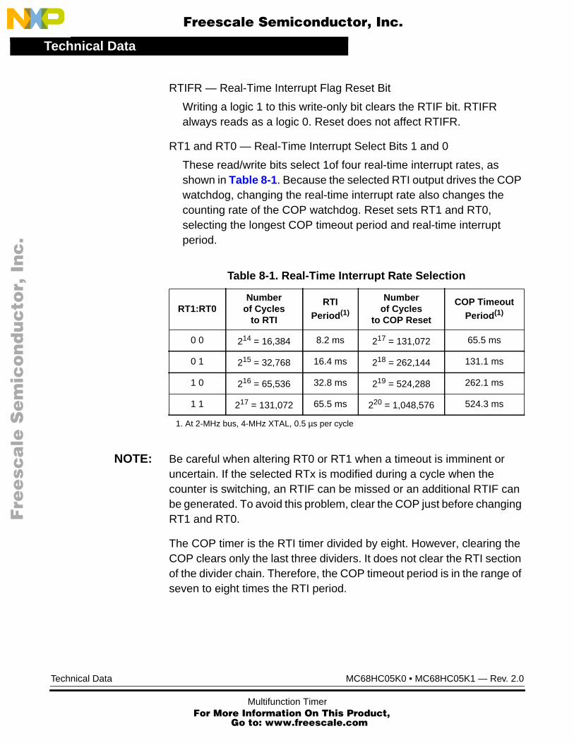
Technical Data
F
ree
sca
le S
em
ico
nd
uc
tor,
I
Freescale Semiconductor, Inc.n
c..
.
RTIFR — Real-Time Interrupt Flag Reset Bit
Writing a logic 1 to this write-only bit clears the RTIF bit. RTIFRalways reads as a logic 0. Reset does not affect RTIFR.
RT1 and RT0 — Real-Time Interrupt Select Bits 1 and 0
These read/write bits select 1of four real-time interrupt rates, asshown in Table 8-1. Because the selected RTI output drives the COPwatchdog, changing the real-time interrupt rate also changes thecounting rate of the COP watchdog. Reset sets RT1 and RT0,selecting the longest COP timeout period and real-time interruptperiod.
NOTE: Be careful when altering RT0 or RT1 when a timeout is imminent oruncertain. If the selected RTx is modified during a cycle when thecounter is switching, an RTIF can be missed or an additional RTIF canbe generated. To avoid this problem, clear the COP just before changingRT1 and RT0.
The COP timer is the RTI timer divided by eight. However, clearing theCOP clears only the last three dividers. It does not clear the RTI sectionof the divider chain. Therefore, the COP timeout period is in the range ofseven to eight times the RTI period.
Table 8-1. Real-Time Interrupt Rate Selection
RT1:RT0Number
of Cyclesto RTI
RTIPeriod(1)
1. At 2-MHz bus, 4-MHz XTAL, 0.5 µs per cycle
Numberof Cycles
to COP Reset
COP TimeoutPeriod(1)
0 0 214 = 16,384 8.2 ms 217 = 131,072 65.5 ms
0 1 215 = 32,768 16.4 ms 218 = 262,144 131.1 ms
1 0 216 = 65,536 32.8 ms 219 = 524,288 262.1 ms
1 1 217 = 131,072 65.5 ms 220 = 1,048,576 524.3 ms
Technical Data MC68HC05K0 • MC68HC05K1 — Rev. 2.0
Multifunction Timer For More Information On This Product,
Go to: www.freescale.com

Multifunction TimerTimer Counter Register
F
ree
sca
le S
em
ico
nd
uc
tor,
I
Freescale Semiconductor, Inc.n
c..
.
8.4 Timer Counter Register
A 15-stage ripple counter is the core of the timer. The value of the firsteight stages is readable at any time from the read-only timer counterregister shown in Figure 8-3.
Power-on clears the entire counter chain and begins clocking thecounter. After 4064 cycles, the power-on reset circuit is released,clearing the counter again and allowing the MCU to come out of reset.
A timer overflow function at the eighth counter stage allows a timerinterrupt every 1024 internal clock cycles.
Each count of the timer counter register takes eight oscillator cycles orfour cycles of the internal clock.
Address: $0009
Bit 7 6 5 4 3 2 1 Bit 0
Read: TCR7 TCR6 TCR5 TCR4 TCR3 TCR2 TCR1 TCR0
Write:
Reset: 0 0 0 0 0 0 0 0
= Unimplemented
Figure 8-3. Timer Counter Register (TCNTR)
MC68HC05K0 • MC68HC05K1 — Rev. 2.0 Technical Data
Multifunction Timer For More Information On This Product,
Go to: www.freescale.com

Technical Data
F
ree
sca
le S
em
ico
nd
uc
tor,
I
Freescale Semiconductor, Inc.n
c..
.
8.5 COP Watchdog
Three counter stages at the end of the timer make up the mask optionalcomputer operating properly (COP) watchdog (see Figure 8-1). TheCOP watchdog is a software error detection system that automaticallytimes out and resets the MCU if not cleared periodically by a programsequence. Writing a logic 0 to bit 0 of the COP register, shown inFigure 8-4, clears the COP watchdog and prevents a COP reset.
COPC — COP Clear Bit
This write-only bit resets the COP watchdog. Reading address $03F0returns the ROM data at that address.
The COP watchdog is active in the run, wait, and halt modes ofoperation. The STOP instruction disables the COP watchdog by clearingthe counter and turning off its clock source. In applications that dependon the COP watchdog, the STOP instruction can be disabled (convertedto halt) by a mask option.
In applications that have wait cycles longer than the COP timeout period,the COP watchdog can be disabled by a mask option.
NOTE: If the voltage on the IRQ/VPP pin exceeds a nominal 1.5 × VDD, the COPwatchdog turns off and remains off until the IRQ/VPP voltage falls below2 × VDD.
Address: $03F0
Bit 7 6 5 4 3 2 1 Bit 0
Read: 0 0 0 0 0 0 1 0
Write: COPC
Reset: U U U U U U U 0
= Unimplemented U = Unaffected
Figure 8-4. COP Register (COPR)
Technical Data MC68HC05K0 • MC68HC05K1 — Rev. 2.0
Multifunction Timer For More Information On This Product,
Go to: www.freescale.com

Multifunction TimerCOP Watchdog
F
ree
sca
le S
em
ico
nd
uc
tor,
I
Freescale Semiconductor, Inc.n
c..
.
Table 8-2 summarizes recommended conditions for enabling anddisabling the COP watchdog.
Table 8-2. COP Watchdog Recommendations
STOPInstruction
(Mask Option)Wait/Halt Time
RecommendedCOP Watchdog Condition
Disabled Less than COP timeout period Enabled(1)
1. Reset the COP watchdog immediately before executing the WAIT/HALT instruction.
Disabled Greater than COP timeout period Disabled
MC68HC05K0 • MC68HC05K1 — Rev. 2.0 Technical Data
Multifunction Timer For More Information On This Product,
Go to: www.freescale.com

Technical Data
F
ree
sca
le S
em
ico
nd
uc
tor,
I
Freescale Semiconductor, Inc.n
c..
.
Technical Data MC68HC05K0 • MC68HC05K1 — Rev. 2.0
Multifunction Timer For More Information On This Product,
Go to: www.freescale.com

F
ree
sca
le S
em
ico
nd
uc
tor,
IFreescale Semiconductor, Inc.
nc
...
Technical Data — MC68HC05K0 • MC68HC05K1
Section 9. Personality EPROM (MC68HC05K1 Only)
9.1 Contents
9.2 Introduction . . . . . . . . . . . . . . . . . . . . . . . . . . . . . . . . . . . . . . . .85
9.3 PEPROM Registers . . . . . . . . . . . . . . . . . . . . . . . . . . . . . . . . .879.3.1 PEPROM Bit Select Register (PEBSR) . . . . . . . . . . . . . . . .879.3.2 PEPROM Status and Control Register (PESCR). . . . . . . . .89
9.4 PEPROM Programming . . . . . . . . . . . . . . . . . . . . . . . . . . . . . .90
9.5 PEPROM Reading . . . . . . . . . . . . . . . . . . . . . . . . . . . . . . . . . .92
9.2 Introduction
This section describes how to program the 64-bit personality erasable,programmable read-only memory (PEPROM) on the MC68HC05K1only. Figure 9-1 shows the structure of the PEPROM subsystem.
NOTE: The PEPROM cannot be erased in parts offered without the windowedpackage.
MC68HC05K0 • MC68HC05K1 — Rev. 2.0 Technical Data
Personality EPROM (MC68HC05K1 Only) For More Information On This Product,
Go to: www.freescale.com

Technical Data
F
ree
sca
le S
em
ico
nd
uc
tor,
I
Freescale Semiconductor, Inc.n
c..
.
Figure 9-1. PEPROM Block Diagram
PEPROM STATUS/CONTROL REGISTER
SINGLESENSE
AMPLIFIERPE
DATA
0 0 0 0 0
PEPG
M
PEPR
ZF
8-TO-1 COLUMN DECODERAND MULTIPLEXER
8-TO-1 ROW DECODERAND MULTIPLEXER
CO
L 0
CO
L 1
CO
L 2
CO
L 3
CO
L 4
CO
L 5
CO
L 6
CO
L 7
ROW 0
ROW 1
ROW 2
ROW 3
ROW 4
ROW 5
ROW 6
ROW 7
VPP SWITCH VPP SWITCH
PEPROM STATUS/CONTROL REGISTER
0 0 PEB5
PEB4
PEB3
PEB2
PEB1
PEB0
ROW ZERODECODER
INTERNAL DATA BUS
INTERNAL DATA BUS
VPP
RESET
RESET
Technical Data MC68HC05K0 • MC68HC05K1 — Rev. 2.0
Personality EPROM (MC68HC05K1 Only) For More Information On This Product,
Go to: www.freescale.com

Personality EPROM (MC68HC05K1 Only)PEPROM Registers
F
ree
sca
le S
em
ico
nd
uc
tor,
I
Freescale Semiconductor, Inc.n
c..
.
9.3 PEPROM Registers
Two input/output (I/O) registers control programming and reading of thePEPROM:
• PEPROM bit select register (PEBSR)
• PEPROM status and control register (PESCR)
9.3.1 PEPROM Bit Select Register
The PEPROM bit select register (PEBSR), shown in Figure 9-2, selectsone of 64 bits in the PEPROM array. Reset clears all the bits in thePEPROM bit select register.
PEB7 and PEB6 — Not Connected to the PEPROM Array
These read/write bits are available as storage locations. Reset clearsPEB7 and PEB6.
PEB5–PEB0 — PEPROM Bit Select Bits
These read/write bits select one of 64 bits in the PEPROM as shownin Table 9-1. Bits PEB2–PEB0 select the PEPROM row, and bitsPEB5–PEB3 select the PEPROM column. Reset clears PEB5–PEB0,selecting the PEPROM bit in row zero, column zero.
Address: $000E
Bit 7 6 5 4 3 2 1 Bit 0
Read:PEB7 PEB6 PEB5 PEB4 PEB3 PEB2 PEB1 PEB0
Write:
Reset: 0 0 0 0 0 0 0 0
Figure 9-2. PEPROM Bit Select Register (PEBSR)
MC68HC05K0 • MC68HC05K1 — Rev. 2.0 Technical Data
Personality EPROM (MC68HC05K1 Only) For More Information On This Product,
Go to: www.freescale.com

Technical Data
F
ree
sca
le S
em
ico
nd
uc
tor,
I
Freescale Semiconductor, Inc.n
c..
.
Table 9-1. PEPROM Bit Selection
PEBSR PEPROM Bit Selected
$00 Row 0 Column 0
$01 Row 1 Column 0
$02 Row 2 Column 0
$07 Row 7 Column 0
$08 Row 0 Column 1
$09 Row 1 Column 1
$0A Row 2 Column 1
$0F Row 7 Column 1
$10 Row 0 Column 2
$11 Row 1 Column 2
$12 Row 2 Column 2
$37 Row 7 Column 6
$38 Row 0 Column 7
$39 Row 1 Column 7
$3A Row 2 Column 7
$3B Row 3 Column 7
$3C Row 4 Column 7
$3D Row 5 Column 7
$3E Row 6 Column 7
$3F Row 7 Column 7
Technical Data MC68HC05K0 • MC68HC05K1 — Rev. 2.0
Personality EPROM (MC68HC05K1 Only) For More Information On This Product,
Go to: www.freescale.com

Personality EPROM (MC68HC05K1 Only)PEPROM Registers
F
ree
sca
le S
em
ico
nd
uc
tor,
I
Freescale Semiconductor, Inc.n
c..
.
9.3.2 PEPROM Status and Control Register
The PEPROM status and control register (PESCR), shown inFigure 9-3, controls the PEPROM programming voltage. This registeralso transfers the PEPROM bits to the internal data bus and contains arow zero flag.
PEDATA — PEPROM Data Bit
This read-only bit is the state of the PEPROM sense amplifier andshows the state of the currently selected bit. Reset does not affect thePEDATA bit.
1 = PEPROM data logic 10 = PEPROM data logic 0
PEPGM — PEPROM Program Control Bit
This read/write bit controls the switches that apply the programmingvoltage, VPP, to the selected PEPROM cell. Reset clears PEPGM.
1 = Programming voltage applied0 = Programming voltage not applied
PEPRZF — PEPROM Row Zero Flag
This read-only bit is set when the PEPROM bit select register selectsthe first row (row zero) of the PEPROM array. Selecting any other rowclears PEPRZF. Monitoring PEPRZF can reduce the code needed toaccess one byte of PEPROM. Reset sets PEPRZF.
1 = Row zero selected0 = Row zero not selected
Address: $000F
Bit 7 6 5 4 3 2 1 Bit 0
Read: PEDATA 0PEPGM
0 0 0 0 PEPRZF
Write:
Reset: U 0 0 0 0 0 0 1
= Unimplemented U = Unaffected
Figure 9-3. PEPROM Status and Control Register (PESCR)
MC68HC05K0 • MC68HC05K1 — Rev. 2.0 Technical Data
Personality EPROM (MC68HC05K1 Only) For More Information On This Product,
Go to: www.freescale.com

Technical Data
F
ree
sca
le S
em
ico
nd
uc
tor,
I
Freescale Semiconductor, Inc.n
c..
.
9.4 PEPROM Programming
Factory-provided software for programming the PEPROM is availablethrough the Motorola Web site at:
htt://mcu.motsps.com
The circuit shown in Figure 9-4 can be used to program the PEPROMwith the factory-provided programming software.
NOTE: The personality EPROM cannot be erased in parts offered without thewindowed package.
To program the PEPROM, VDD must be greater than 4.5 Vdc.
The PEPROM also can be programmed by user software with VPPapplied to the IRQ/VPP pin. This sequence shows how to program eachPEPROM bit:
1. Select a PEPROM bit by writing to PEBSR.
2. Set the PEPGM bit in PESCR.
3. Wait 3 ms.
4. Clear the PEPGM bit.
NOTE: While the PEPGM bit is set and VPP is applied to the IRQ/VPP pin, do notaccess bits that are to be left unprogrammed (erased).
In the 3-pin RC oscillator configuration, the PEPROM cannot beprogrammed by user software. If the voltage on IRQ/VPP is raised aboveVDD, the oscillator will revert to a 2-pin oscillator configuration anddevice operation will be disrupted. The 2-pin RC and crystalconfigurations are not affected.
Technical Data MC68HC05K0 • MC68HC05K1 — Rev. 2.0
Personality EPROM (MC68HC05K1 Only) For More Information On This Product,
Go to: www.freescale.com

Personality EPROM (MC68HC05K1 Only)PEPROM Programming
F
ree
sca
le S
em
ico
nd
uc
tor,
I
Freescale Semiconductor, Inc.n
c..
.
Figure 9-4. Programming Circuit
141
215
316
417
5
618
197
208
219
2210231124122513
STROBE
D0
D1INITD2
D3
D4
D5
D6
D7
ACK
PE
MC68HC05K1
RESETPB1PB0IRQ/VPPPA0PA1PA2PA3
OSC112345678
161514131211109
OSC2VSSVDDPA7PA6PA5PA4
2.2 kΩ
2.2 kΩ
220 Ω
0.1 µF
VCC
VCC
0.1µF
+ +
+
10 µH
VCC
DR COLSENSEVCCCOMPARE
SW COLSW EMIT
CAPGND
MC34063
8765
1234
IN5817
100 pF0.1 µF
330 Ω
10 µF
4.7 Ω
1.5 kΩ
100 Ω
S1
5 V
VPP
S2
100 Ω
0.1 µF10 µF 0.1 µF
OPTIONAL VPP GENERATOR
170 µH
VCC
+
5 kΩ
10 µF
15 kΩ
10 µF
MC68HC05K0 • MC68HC05K1 — Rev. 2.0 Technical Data
Personality EPROM (MC68HC05K1 Only) For More Information On This Product,
Go to: www.freescale.com

Technical Data
F
ree
sca
le S
em
ico
nd
uc
tor,
I
Freescale Semiconductor, Inc.n
c..
.
9.5 PEPROM Reading
This sequence shows how to read the PEPROM:
1. Select a bit by writing to PEBSR.
2. Read the PEDATA bit in PESCR.
3. Store the PEDATA bit in RAM or in a register.
4. Select another bit by changing PEBSR.
5. Continue reading and storing the PEDATA bits until the requiredpersonality EPROM data is stored.
Reading the PEPROM is easiest when each PEPROM column containsone byte. Selecting a row-0 bit selects the first bit, and incrementing thePEPROM bit select register (PEBSR) selects the next row-1 bit from thesame column. Incrementing PEBSR seven more times selects theremaining bits of the column and selects the row-0 bit of the next column,setting the row-0 flag, PEPRZF.
A PEPROM byte that has been read can be transferred to thepersonality EPROM bit select register (PEBSR) so that subsequentreads of the PEBSR quickly yield that PEPROM byte.
Technical Data MC68HC05K0 • MC68HC05K1 — Rev. 2.0
Personality EPROM (MC68HC05K1 Only) For More Information On This Product,
Go to: www.freescale.com

F
ree
sca
le S
em
ico
nd
uc
tor,
IFreescale Semiconductor, Inc.
nc
...
Technical Data — MC68HC05K0 • MC68HC05K1
Section 10. Instruction Set
10.1 Contents
10.2 Introduction . . . . . . . . . . . . . . . . . . . . . . . . . . . . . . . . . . . . . . . .94
10.3 Addressing Modes . . . . . . . . . . . . . . . . . . . . . . . . . . . . . . . . . .9410.3.1 Inherent . . . . . . . . . . . . . . . . . . . . . . . . . . . . . . . . . . . . . . . .9510.3.2 Immediate. . . . . . . . . . . . . . . . . . . . . . . . . . . . . . . . . . . . . . .9510.3.3 Direct . . . . . . . . . . . . . . . . . . . . . . . . . . . . . . . . . . . . . . . . . .9510.3.4 Extended . . . . . . . . . . . . . . . . . . . . . . . . . . . . . . . . . . . . . . .9510.3.5 Indexed, No Offset . . . . . . . . . . . . . . . . . . . . . . . . . . . . . . . .9610.3.6 Indexed, 8-Bit Offset. . . . . . . . . . . . . . . . . . . . . . . . . . . . . . .9610.3.7 Indexed, 16-Bit Offset. . . . . . . . . . . . . . . . . . . . . . . . . . . . . .9610.3.8 Relative . . . . . . . . . . . . . . . . . . . . . . . . . . . . . . . . . . . . . . . .97
10.4 Instruction Types . . . . . . . . . . . . . . . . . . . . . . . . . . . . . . . . . . .9710.4.1 Register/Memory Instructions. . . . . . . . . . . . . . . . . . . . . . . .9810.4.2 Read-Modify-Write Instructions . . . . . . . . . . . . . . . . . . . . . .9910.4.3 Jump/Branch Instructions. . . . . . . . . . . . . . . . . . . . . . . . . .10010.4.4 Bit Manipulation Instructions . . . . . . . . . . . . . . . . . . . . . . .10210.4.5 Control Instructions . . . . . . . . . . . . . . . . . . . . . . . . . . . . . .103
10.5 Instruction Set Summary . . . . . . . . . . . . . . . . . . . . . . . . . . . .104
10.6 Opcode Map . . . . . . . . . . . . . . . . . . . . . . . . . . . . . . . . . . . . . .109
MC68HC05K0 • MC68HC05K1 — Rev. 2.0 Technical Data
Instruction Set For More Information On This Product,
Go to: www.freescale.com

Technical Data
F
ree
sca
le S
em
ico
nd
uc
tor,
I
Freescale Semiconductor, Inc.n
c..
.
10.2 Introduction
The microcontroller unit (MCU) instruction set has 62 instructions anduses eight addressing modes. The instructions include all those of theM146805 complementary metal oxide semiconductor (CMOS) Familyplus one more: the unsigned multiply (MUL) instruction. The MULinstruction allows unsigned multiplication of the contents of theaccumulator (A) and the index register (X). The high-order product isstored in the index register, and the low-order product is stored in theaccumulator.
10.3 Addressing Modes
The central processor unit (CPU) uses eight addressing modes forflexibility in accessing data. The addressing modes provide eightdifferent ways for the CPU to find the data required to execute aninstruction.
The eight addressing modes are:
• Inherent
• Immediate
• Direct
• Extended
• Indexed, no offset
• Indexed, 8-bit offset
• Indexed, 16-bit offset
• Relative
Technical Data MC68HC05K0 • MC68HC05K1 — Rev. 2.0
Instruction Set For More Information On This Product,
Go to: www.freescale.com

Instruction SetAddressing Modes
F
ree
sca
le S
em
ico
nd
uc
tor,
I
Freescale Semiconductor, Inc.n
c..
.
10.3.1 Inherent
Inherent instructions are those that have no operand, such as returnfrom interrupt (RTI) and stop (STOP). Some of the inherent instructionsact on data in the CPU registers, such as set carry flag (SEC) andincrement accumulator (INCA). Inherent instructions require no operandaddress and are one byte long.
10.3.2 Immediate
Immediate instructions are those that contain a value to be used in anoperation with the value in the accumulator or index register. Immediateinstructions require no operand address and are two bytes long. Theopcode is the first byte, and the immediate data value is the second byte.
10.3.3 Direct
Direct instructions can access any of the first 256 memory locations withtwo bytes. The first byte is the opcode, and the second is the low byte ofthe operand address. In direct addressing, the CPU automatically uses$00 as the high byte of the operand address.
10.3.4 Extended
Extended instructions use three bytes and can access any address inmemory. The first byte is the opcode; the second and third bytes are thehigh and low bytes of the operand address.
When using the Motorola assembler, the programmer does not need tospecify whether an instruction is direct or extended. The assemblerautomatically selects the shortest form of the instruction.
MC68HC05K0 • MC68HC05K1 — Rev. 2.0 Technical Data
Instruction Set For More Information On This Product,
Go to: www.freescale.com

Technical Data
F
ree
sca
le S
em
ico
nd
uc
tor,
I
Freescale Semiconductor, Inc.n
c..
.
10.3.5 Indexed, No Offset
Indexed instructions with no offset are 1-byte instructions that canaccess data with variable addresses within the first 256 memorylocations. The index register contains the low byte of the effectiveaddress of the operand. The CPU automatically uses $00 as the highbyte, so these instructions can address locations $0000–$00FF.
Indexed, no offset instructions are often used to move a pointer througha table or to hold the address of a frequently used random-accessmemory (RAM) or input/output (I/O) location.
10.3.6 Indexed, 8-Bit Offset
Indexed, 8-bit offset instructions are 2-byte instructions that can accessdata with variable addresses within the first 511 memory locations. TheCPU adds the unsigned byte in the index register to the unsigned bytefollowing the opcode. The sum is the effective address of the operand.These instructions can access locations $0000–$01FE.
Indexed 8-bit offset instructions are useful for selecting the kth elementin an n-element table. The table can begin anywhere within the first 256memory locations and could extend as far as location 510 ($01FE). Thek value is typically in the index register, and the address of the beginningof the table is in the byte following the opcode.
10.3.7 Indexed, 16-Bit Offset
Indexed, 16-bit offset instructions are 3-byte instructions that can accessdata with variable addresses at any location in memory. The CPU addsthe unsigned byte in the index register to the two unsigned bytesfollowing the opcode. The sum is the effective address of the operand.The first byte after the opcode is the high byte of the 16-bit offset; thesecond byte is the low byte of the offset.
Indexed, 16-bit offset instructions are useful for selecting the kth elementin an n-element table anywhere in memory.
Technical Data MC68HC05K0 • MC68HC05K1 — Rev. 2.0
Instruction Set For More Information On This Product,
Go to: www.freescale.com

Instruction SetInstruction Types
F
ree
sca
le S
em
ico
nd
uc
tor,
I
Freescale Semiconductor, Inc.n
c..
.
As with direct and extended addressing, the Motorola assemblerdetermines the shortest form of indexed addressing.
10.3.8 Relative
Relative addressing is only for branch instructions. If the branchcondition is true, the CPU finds the effective branch destination byadding the signed byte following the opcode to the contents of theprogram counter. If the branch condition is not true, the CPU goes to thenext instruction. The offset is a signed, two’s complement byte that givesa branching range of –128 to +127 bytes from the address of the nextlocation after the branch instruction.
When using the Motorola assembler, the programmer does not need tocalculate the offset, because the assembler determines the proper offsetand verifies that it is within the span of the branch.
10.4 Instruction Types
The MCU instructions fall into five categories:
• Register/memory instructions
• Read-modify-write instructions
• Jump/branch instructions
• Bit manipulation instructions
• Control instructions
MC68HC05K0 • MC68HC05K1 — Rev. 2.0 Technical Data
Instruction Set For More Information On This Product,
Go to: www.freescale.com

Technical Data
F
ree
sca
le S
em
ico
nd
uc
tor,
I
Freescale Semiconductor, Inc.n
c..
.
10.4.1 Register/Memory Instructions
These instructions operate on CPU registers and memory locations.Most of them use two operands. One operand is in either theaccumulator or the index register. The CPU finds the other operand inmemory.
Table 10-1. Register/Memory Instructions
Instruction Mnemonic
Add memory byte and carry bit to accumulator ADC
Add memory byte to accumulator ADD
AND memory byte with accumulator AND
Bit test accumulator BIT
Compare accumulator CMP
Compare index register with memory byte CPX
Exclusive OR accumulator with memory byte EOR
Load accumulator with memory byte LDA
Load Index register with memory byte LDX
Multiply MUL
OR accumulator with memory byte ORA
Subtract memory byte and carry bit fromaccumulator
SBC
Store accumulator in memory STA
Store index register in memory STX
Subtract memory byte from accumulator SUB
Technical Data MC68HC05K0 • MC68HC05K1 — Rev. 2.0
Instruction Set For More Information On This Product,
Go to: www.freescale.com

Instruction SetInstruction Types
F
ree
sca
le S
em
ico
nd
uc
tor,
I
Freescale Semiconductor, Inc.n
c..
.
10.4.2 Read-Modify-Write Instructions
These instructions read a memory location or a register, modify itscontents, and write the modified value back to the memory location or tothe register.
NOTE: Do not use read-modify-write operations on write-only registers.
Table 10-2. Read-Modify-Write Instructions
Instruction Mnemonic
Arithmetic shift left (same as LSL) ASL
Arithmetic shift right ASR
Bit clear BCLR(1)
1. Unlike other read-modify-write instructions, BCLR and BSET useonly direct addressing.
Bit set BSET(1)
Clear register CLR
Complement (one’s complement) COM
Decrement DEC
Increment INC
Logical shift left (same as ASL) LSL
Logical shift right LSR
Negate (two’s complement) NEG
Rotate left through carry bit ROL
Rotate right through carry bit ROR
Test for negative or zero TST(2)
2. TST is an exception to the read-modify-write sequence because itdoes not write a replacement value.
MC68HC05K0 • MC68HC05K1 — Rev. 2.0 Technical Data
Instruction Set For More Information On This Product,
Go to: www.freescale.com

Technical Data
F
ree
sca
le S
em
ico
nd
uc
tor,
I
Freescale Semiconductor, Inc.n
c..
.
10.4.3 Jump/Branch Instructions
Jump instructions allow the CPU to interrupt the normal sequence of theprogram counter. The unconditional jump instruction (JMP) and thejump-to-subroutine instruction (JSR) have no register operand. Branchinstructions allow the CPU to interrupt the normal sequence of theprogram counter when a test condition is met. If the test condition is notmet, the branch is not performed.
The BRCLR and BRSET instructions cause a branch based on the stateof any readable bit in the first 256 memory locations. These 3-byteinstructions use a combination of direct addressing and relativeaddressing. The direct address of the byte to be tested is in the bytefollowing the opcode. The third byte is the signed offset byte. The CPUfinds the effective branch destination by adding the third byte to theprogram counter if the specified bit tests true. The bit to be tested and itscondition (set or clear) is part of the opcode. The span of branching isfrom –128 to +127 from the address of the next location after the branchinstruction. The CPU also transfers the tested bit to the carry/borrow bitof the condition code register.
Technical Data MC68HC05K0 • MC68HC05K1 — Rev. 2.0
Instruction Set For More Information On This Product,
Go to: www.freescale.com

Instruction SetInstruction Types
F
ree
sca
le S
em
ico
nd
uc
tor,
I
Freescale Semiconductor, Inc.n
c..
.
Table 10-3. Jump and Branch Instructions
Instruction Mnemonic
Branch if carry bit clear BCC
Branch if carry bit set BCS
Branch if equal BEQ
Branch if half-carry bit clear BHCC
Branch if half-carry bit set BHCS
Branch if higher BHI
Branch if higher or same BHS
Branch if IRQ pin high BIH
Branch if IRQ pin low BIL
Branch if lower BLO
Branch if lower or same BLS
Branch if interrupt mask clear BMC
Branch if minus BMI
Branch if interrupt mask set BMS
Branch if not equal BNE
Branch if plus BPL
Branch always BRA
Branch if bit clear BRCLR
Branch never BRN
Branch if bit set BRSET
Branch to subroutine BSR
Unconditional jump JMP
Jump to subroutine JSR
MC68HC05K0 • MC68HC05K1 — Rev. 2.0 Technical Data
Instruction Set For More Information On This Product,
Go to: www.freescale.com

Technical Data
F
ree
sca
le S
em
ico
nd
uc
tor,
I
Freescale Semiconductor, Inc.n
c..
.
10.4.4 Bit Manipulation Instructions
The CPU can set or clear any writable bit in the first 256 bytes ofmemory, which includes I/O registers and on-chip RAM locations. TheCPU can also test and branch based on the state of any bit in any of thefirst 256 memory locations.
Table 10-4. Bit Manipulation Instructions
Instruction Mnemonic
Bit clear BCLR
Branch if bit clear BRCLR
Branch if bit set BRSET
Bit set BSET
Technical Data MC68HC05K0 • MC68HC05K1 — Rev. 2.0
Instruction Set For More Information On This Product,
Go to: www.freescale.com

Instruction SetInstruction Types
F
ree
sca
le S
em
ico
nd
uc
tor,
I
Freescale Semiconductor, Inc.n
c..
.
10.4.5 Control Instructions
These instructions act on CPU registers and control CPU operationduring program execution.
Table 10-5. Control Instructions
Instruction Mnemonic
Clear carry bit CLC
Clear interrupt mask CLI
No operation NOP
Reset stack pointer RSP
Return from interrupt RTI
Return from subroutine RTS
Set carry bit SEC
Set interrupt mask SEI
Stop oscillator and enable IRQ pin STOP
Software interrupt SWI
Transfer accumulator to index register TAX
Transfer index register to accumulator TXA
Stop CPU clock and enable interrupts WAIT
MC68HC05K0 • MC68HC05K1 — Rev. 2.0 Technical Data
Instruction Set For More Information On This Product,
Go to: www.freescale.com

Technical Data
F
ree
sca
le S
em
ico
nd
uc
tor,
I
Freescale Semiconductor, Inc.n
c..
.
10.5 Instruction Set Summary
Table 10-6. Instruction Set Summary (Sheet 1 of 6)
SourceForm Operation Description
Effecton CCR
Ad
dre
ssM
od
e
Op
cod
e
Op
eran
d
Cyc
les
H I N Z C
ADC #oprADC oprADC oprADC opr,XADC opr,XADC ,X
Add with Carry A ← (A) + (M) + (C) —
IMMDIREXTIX2IX1IX
A9B9C9D9E9F9
iidd
hh llee ff
ff
234543
ADD #oprADD oprADD oprADD opr,XADD opr,XADD ,X
Add without Carry A ← (A) + (M) —
IMMDIREXTIX2IX1IX
ABBBCBDBEBFB
iidd
hh llee ff
ff
234543
AND #oprAND oprAND oprAND opr,XAND opr,XAND ,X
Logical AND A ← (A) ∧ (M) — — —
IMMDIREXTIX2IX1IX
A4B4C4D4E4F4
iidd
hh llee ff
ff
234543
ASL oprASLAASLXASL opr,XASL ,X
Arithmetic Shift Left (Same as LSL) — —
DIRINHINHIX1IX
3848586878
dd
ff
53365
ASR oprASRAASRXASR opr,XASR ,X
Arithmetic Shift Right — —
DIRINHINHIX1IX
3747576777
dd
ff
53365
BCC rel Branch if Carry Bit Clear PC ← (PC) + 2 + rel ? C = 0 — — — — — REL 24 rr 3
BCLR n opr Clear Bit n Mn ← 0 — — — — —
DIR (b0)DIR (b1)DIR (b2)DIR (b3)DIR (b4)DIR (b5)DIR (b6)DIR (b7)
11131517191B1D1F
dddddddddddddddd
55555555
BCS rel Branch if Carry Bit Set (Same as BLO) PC ← (PC) + 2 + rel ? C = 1 — — — — — REL 25 rr 3
BEQ rel Branch if Equal PC ← (PC) + 2 + rel ? Z = 1 — — — — — REL 27 rr 3
BHCC rel Branch if Half-Carry Bit Clear PC ← (PC) + 2 + rel ? H = 0 — — — — — REL 28 rr 3
BHCS rel Branch if Half-Carry Bit Set PC ← (PC) + 2 + rel ? H = 1 — — — — — REL 29 rr 3
BHI rel Branch if Higher PC ← (PC) + 2 + rel ? C ∨ Z = 0 — — — — — REL 22 rr 3
BHS rel Branch if Higher or Same PC ← (PC) + 2 + rel ? C = 0 — — — — — REL 24 rr 3
C
b0b7
0
b0b7
C
Technical Data MC68HC05K0 • MC68HC05K1 — Rev. 2.0
Instruction Set For More Information On This Product,
Go to: www.freescale.com

Instruction SetInstruction Set Summary
F
ree
sca
le S
em
ico
nd
uc
tor,
I
Freescale Semiconductor, Inc.n
c..
.
BIH rel Branch if IRQ Pin High PC ← (PC) + 2 + rel ? IRQ = 1 — — — — — REL 2F rr 3
BIL rel Branch if IRQ Pin Low PC ← (PC) + 2 + rel ? IRQ = 0 — — — — — REL 2E rr 3
BIT #oprBIT oprBIT oprBIT opr,XBIT opr,XBIT ,X
Bit Test Accumulator with Memory Byte (A) ∧ (M) — — —
IMMDIREXTIX2IX1IX
A5B5C5D5E5F5
iidd
hh llee ff
ff
234543
BLO rel Branch if Lower (Same as BCS) PC ← (PC) + 2 + rel ? C = 1 — — — — — REL 25 rr 3
BLS rel Branch if Lower or Same PC ← (PC) + 2 + rel ? C ∨ Z = 1 — — — — — REL 23 rr 3
BMC rel Branch if Interrupt Mask Clear PC ← (PC) + 2 + rel ? I = 0 — — — — — REL 2C rr 3
BMI rel Branch if Minus PC ← (PC) + 2 + rel ? N = 1 — — — — — REL 2B rr 3
BMS rel Branch if Interrupt Mask Set PC ← (PC) + 2 + rel ? I = 1 — — — — — REL 2D rr 3
BNE rel Branch if Not Equal PC ← (PC) + 2 + rel ? Z = 0 — — — — — REL 26 rr 3
BPL rel Branch if Plus PC ← (PC) + 2 + rel ? N = 0 — — — — — REL 2A rr 3
BRA rel Branch Always PC ← (PC) + 2 + rel ? 1 = 1 — — — — — REL 20 rr 3
BRCLR n opr rel Branch if Bit n Clear PC ← (PC) + 2 + rel ? Mn = 0 — — — —
DIR (b0)DIR (b1)DIR (b2)DIR (b3)DIR (b4)DIR (b5)DIR (b6)DIR (b7)
01030507090B0D0F
dd rrdd rrdd rrdd rrdd rrdd rrdd rrdd rr
55555555
BRN rel Branch Never PC ← (PC) + 2 + rel ? 1 = 0 — — — — — REL 21 rr 3
BRSET n opr rel Branch if Bit n Set PC ← (PC) + 2 + rel ? Mn = 1 — — — —
DIR (b0)DIR (b1)DIR (b2)DIR (b3)DIR (b4)DIR (b5)DIR (b6)DIR (b7)
00020406080A0C0E
dd rrdd rrdd rrdd rrdd rrdd rrdd rrdd rr
55555555
BSET n opr Set Bit n Mn ← 1 — — — — —
DIR (b0)DIR (b1)DIR (b2)DIR (b3)DIR (b4)DIR (b5)DIR (b6)DIR (b7)
10121416181A1C1E
dddddddddddddddd
55555555
BSR rel Branch to Subroutine
PC ← (PC) + 2; push (PCL)SP ← (SP) – 1; push (PCH)
SP ← (SP) – 1PC ← (PC) + rel
— — — — — REL AD rr 6
CLC Clear Carry Bit C ← 0 — — — — 0 INH 98 2
CLI Clear Interrupt Mask I ← 0 — 0 — — — INH 9A 2
Table 10-6. Instruction Set Summary (Sheet 2 of 6)
SourceForm Operation Description
Effecton CCR
Ad
dre
ssM
od
e
Op
cod
e
Op
eran
d
Cyc
les
H I N Z C
MC68HC05K0 • MC68HC05K1 — Rev. 2.0 Technical Data
Instruction Set For More Information On This Product,
Go to: www.freescale.com

Technical Data
F
ree
sca
le S
em
ico
nd
uc
tor,
I
Freescale Semiconductor, Inc.n
c..
.
CLR oprCLRACLRXCLR opr,XCLR ,X
Clear Byte
M ← $00A ← $00X ← $00M ← $00M ← $00
— — 0 1 —
DIRINHINHIX1IX
3F4F5F6F7F
dd
ff
53365
CMP #oprCMP oprCMP oprCMP opr,XCMP opr,XCMP ,X
Compare Accumulator with Memory Byte (A) – (M) — —
IMMDIREXTIX2IX1IX
A1B1C1D1E1F1
iidd
hh llee ff
ff
234543
COM oprCOMACOMXCOM opr,XCOM ,X
Complement Byte (One’s Complement)
M ← (M) = $FF – (M)A ← (A) = $FF – (A)X ← (X) = $FF – (X)M ← (M) = $FF – (M)M ← (M) = $FF – (M)
— — 1
DIRINHINHIX1IX
3343536373
dd
ff
53365
CPX #oprCPX oprCPX oprCPX opr,XCPX opr,XCPX ,X
Compare Index Register with Memory Byte (X) – (M) — —
IMMDIREXTIX2IX1IX
A3B3C3D3E3F3
iidd
hh llee ff
ff
234543
DEC oprDECADECXDEC opr,XDEC ,X
Decrement Byte
M ← (M) – 1A ← (A) – 1X ← (X) – 1M ← (M) – 1M ← (M) – 1
— — —
DIRINHINHIX1IX
3A4A5A6A7A
dd
ff
53365
EOR #oprEOR oprEOR oprEOR opr,XEOR opr,XEOR ,X
EXCLUSIVE OR Accumulator with MemoryByte
A ← (A) ⊕ (M) — — —
IMMDIREXTIX2IX1IX
A8B8C8D8E8F8
iidd
hh llee ff
ff
234543
INC oprINCAINCXINC opr,XINC ,X
Increment Byte
M ← (M) + 1A ← (A) + 1X ← (X) + 1M ← (M) + 1M ← (M) + 1
— — —
DIRINHINHIX1IX
3C4C5C6C7C
dd
ff
53365
JMP oprJMP oprJMP opr,XJMP opr,XJMP ,X
Unconditional Jump PC ← Jump Address — — — — —
DIREXTIX2IX1IX
BCCCDCECFC
ddhh llee ff
ff
23432
Table 10-6. Instruction Set Summary (Sheet 3 of 6)
SourceForm Operation Description
Effecton CCR
Ad
dre
ssM
od
e
Op
cod
e
Op
eran
d
Cyc
les
H I N Z C
Technical Data MC68HC05K0 • MC68HC05K1 — Rev. 2.0
Instruction Set For More Information On This Product,
Go to: www.freescale.com

Instruction SetInstruction Set Summary
F
ree
sca
le S
em
ico
nd
uc
tor,
I
Freescale Semiconductor, Inc.n
c..
.
JSR oprJSR oprJSR opr,XJSR opr,XJSR ,X
Jump to Subroutine
PC ← (PC) + n (n = 1, 2, or 3)Push (PCL); SP ← (SP) – 1Push (PCH); SP ← (SP) – 1
PC ← Effective Address
— — — — —
DIREXTIX2IX1IX
BDCDDDEDFD
ddhh llee ff
ff
56765
LDA #oprLDA oprLDA oprLDA opr,XLDA opr,XLDA ,X
Load Accumulator with Memory Byte A ← (M) — — —
IMMDIREXTIX2IX1IX
A6B6C6D6E6F6
iidd
hh llee ff
ff
234543
LDX #oprLDX oprLDX oprLDX opr,XLDX opr,XLDX ,X
Load Index Register with Memory Byte X ← (M) — — —
IMMDIREXTIX2IX1IX
AEBECEDEEEFE
iidd
hh llee ff
ff
234543
LSL oprLSLALSLXLSL opr,XLSL ,X
Logical Shift Left (Same as ASL) — —
DIRINHINHIX1IX
3848586878
dd
ff
53365
LSR oprLSRALSRXLSR opr,XLSR ,X
Logical Shift Right — — 0
DIRINHINHIX1IX
3444546474
dd
ff
53365
MUL Unsigned Multiply X : A ← (X) × (A) 0 — — — 0 INH 4211
NEG oprNEGANEGXNEG opr,XNEG ,X
Negate Byte (Two’s Complement)
M ← –(M) = $00 – (M)A ← –(A) = $00 – (A)X ← –(X) = $00 – (X)M ← –(M) = $00 – (M)M ← –(M) = $00 – (M)
— —
DIRINHINHIX1IX
3040506070
dd
ff
53365
NOP No Operation — — — — — INH 9D 2
ORA #oprORA oprORA oprORA opr,XORA opr,XORA ,X
Logical OR Accumulator with Memory A ← (A) ∨ (M) — — —
IMMDIREXTIX2IX1IX
AABACADAEAFA
iidd
hh llee ff
ff
234543
ROL oprROLAROLXROL opr,XROL ,X
Rotate Byte Left through Carry Bit — —
DIRINHINHIX1IX
3949596979
dd
ff
53365
Table 10-6. Instruction Set Summary (Sheet 4 of 6)
SourceForm Operation Description
Effecton CCR
Ad
dre
ssM
od
e
Op
cod
e
Op
eran
d
Cyc
les
H I N Z C
C
b0b7
0
b0b7
C0
C
b0b7
MC68HC05K0 • MC68HC05K1 — Rev. 2.0 Technical Data
Instruction Set For More Information On This Product,
Go to: www.freescale.com

Technical Data
F
ree
sca
le S
em
ico
nd
uc
tor,
I
Freescale Semiconductor, Inc.n
c..
.
ROR oprRORARORXROR opr,XROR ,X
Rotate Byte Right through Carry Bit — —
DIRINHINHIX1IX
3646566676
dd
ff
53365
RSP Reset Stack Pointer SP ← $00FF — — — — — INH 9C 2
RTI Return from Interrupt
SP ← (SP) + 1; Pull (CCR)SP ← (SP) + 1; Pull (A)SP ← (SP) + 1; Pull (X)
SP ← (SP) + 1; Pull (PCH)SP ← (SP) + 1; Pull (PCL)
INH 80 9
RTS Return from SubroutineSP ← (SP) + 1; Pull (PCH)SP ← (SP) + 1; Pull (PCL)
— — — — — INH 81 6
SBC #oprSBC oprSBC oprSBC opr,XSBC opr,XSBC ,X
Subtract Memory Byte and Carry Bit fromAccumulator
A ← (A) – (M) – (C) — —
IMMDIREXTIX2IX1IX
A2B2C2D2E2F2
iidd
hh llee ff
ff
234543
SEC Set Carry Bit C ← 1 — — — — 1 INH 99 2
SEI Set Interrupt Mask I ← 1 — 1 — — — INH 9B 2
STA oprSTA oprSTA opr,XSTA opr,XSTA ,X
Store Accumulator in Memory M ← (A) — — —
DIREXTIX2IX1IX
B7C7D7E7F7
ddhh llee ff
ff
45654
STOP Stop Oscillator and Enable IRQ Pin — 0 — — — INH 8E 2
STX oprSTX oprSTX opr,XSTX opr,XSTX ,X
Store Index Register In Memory M ← (X) — — —
DIREXTIX2IX1IX
BFCFDFEFFF
ddhh llee ff
ff
45654
SUB #oprSUB oprSUB oprSUB opr,XSUB opr,XSUB ,X
Subtract Memory Byte from Accumulator A ← (A) – (M) — —
IMMDIREXTIX2IX1IX
A0B0C0D0E0F0
iidd
hh llee ff
ff
234543
SWI Software Interrupt
PC ← (PC) + 1; Push (PCL)SP ← (SP) – 1; Push (PCH)
SP ← (SP) – 1; Push (X)SP ← (SP) – 1; Push (A)
SP ← (SP) – 1; Push (CCR)SP ← (SP) – 1; I ← 1
PCH ← Interrupt Vector High BytePCL ← Interrupt Vector Low Byte
— 1 — — — INH 8310
TAX Transfer Accumulator to Index Register X ← (A) — — — — — INH 97 2
Table 10-6. Instruction Set Summary (Sheet 5 of 6)
SourceForm Operation Description
Effecton CCR
Ad
dre
ssM
od
e
Op
cod
e
Op
eran
d
Cyc
les
H I N Z C
b0b7
C
Technical Data MC68HC05K0 • MC68HC05K1 — Rev. 2.0
Instruction Set For More Information On This Product,
Go to: www.freescale.com

Instruction SetOpcode Map
F
ree
sca
le S
em
ico
nd
uc
tor,
I
Freescale Semiconductor, Inc.n
c..
.
10.6 Opcode Map
See Table 10-7.
TST oprTSTATSTXTST opr,XTST ,X
Test Memory Byte for Negative or Zero (M) – $00 — — —
DIRINHINHIX1IX
3D4D5D6D7D
dd
ff
43354
TXA Transfer Index Register to Accumulator A ← (X) — — — — — INH 9F 2
WAIT Stop CPU Clock and Enable Interrupts — 0 — — — INH 8F 2
A Accumulator opr Operand (one or two bytes)C Carry/borrow flag PC Program counterCCR Condition code register PCH Program counter high bytedd Direct address of operand PCL Program counter low bytedd rr Direct address of operand and relative offset of branch instruction REL Relative addressing modeDIR Direct addressing mode rel Relative program counter offset byteee ff High and low bytes of offset in indexed, 16-bit offset addressing rr Relative program counter offset byteEXT Extended addressing mode SP Stack pointerff Offset byte in indexed, 8-bit offset addressing X Index registerH Half-carry flag Z Zero flaghh ll High and low bytes of operand address in extended addressing # Immediate valueI Interrupt mask ∧ Logical ANDii Immediate operand byte ∨ Logical ORIMM Immediate addressing mode ⊕ Logical EXCLUSIVE ORINH Inherent addressing mode ( ) Contents ofIX Indexed, no offset addressing mode –( ) Negation (two’s complement)IX1 Indexed, 8-bit offset addressing mode ← Loaded withIX2 Indexed, 16-bit offset addressing mode ? IfM Memory location : Concatenated withN Negative flag Set or clearedn Any bit — Not affected
Table 10-6. Instruction Set Summary (Sheet 6 of 6)
SourceForm Operation Description
Effecton CCR
Ad
dre
ssM
od
e
Op
cod
e
Op
eran
d
Cyc
les
H I N Z C
MC68HC05K0 • MC68HC05K1 — Rev. 2.0 Technical Data
Instruction Set For More Information On This Product,
Go to: www.freescale.com

Instruction Set
SB
F
ree
sca
le S
em
ico
nd
uc
tor,
I
Freescale Semiconductor, Inc.n
c..
.
Tab
le 1
0-7.
Op
cod
e M
ap
Bit
Man
ipu
lati
on
Bra
nch
Rea
d-M
od
ify-
Wri
teC
on
tro
lR
egis
ter/
Mem
ory
DIR
DIR
RE
LD
IRIN
HIN
HIX
1IX
INH
INH
IMM
DIR
EX
TIX
2IX
1IX
01
23
45
67
89
AB
CD
EF
05
BR
SE
T0
3D
IR
5B
SE
T0
2D
IR
3B
RA
2R
EL
5N
EG
2D
IR
3N
EG
A1
INH
3N
EG
X1
INH
6N
EG
2IX
1
5N
EG
1I X
9R
TI
1IN
H
2S
UB
2IM
M
3S
UB
2D
IR
4S
UB
3E
XT
5S
UB
3IX
2
4S
UB
2IX
1
3S
UB
1I X
0
15
BR
CLR
03
DIR
5B
CLR
02
DIR
3B
RN
2R
EL
6R
TS
1IN
H
2C
MP
2IM
M
3C
MP
2D
IR
4C
MP
3E
XT
5C
MP
3IX
2
4C
MP
2IX
1
3C
MP
1I X
1
25
BR
SE
T1
3D
IR
5B
SE
T1
2D
IR
3B
HI
2R
EL
11M
UL
1IN
H
2S
BC
2IM
M
3S
BC
2D
IR
4S
BC
3E
XT
5S
BC
3IX
2
4S
BC
2IX
1
3S
BC
1I X
2
35
BR
CLR
13
DIR
5B
CLR
12
DIR
3B
LS2
RE
L
5C
OM
2D
IR
3C
OM
A1
INH
3C
OM
X1
INH
6C
OM
2IX
1
5C
OM
1I X
10S
WI
1IN
H
2C
PX
2IM
M
3C
PX
2D
IR
4C
PX
3E
XT
5C
PX
3IX
2
4C
PX
2IX
1
3C
PX
1I X
3
45
BR
SE
T2
3D
IR
5B
SE
T2
2D
IR
3B
CC
2R
EL
5LS
R2
DIR
3LS
RA
1IN
H
3LS
RX
1IN
H
6LS
R2
IX1
5LS
R1
I X
2A
ND
2IM
M
3A
ND
2D
IR
4A
ND
3E
XT
5A
ND
3IX
2
4A
ND
2IX
1
3A
ND
1I X
4
55
BR
CLR
23
DIR
5B
CLR
22
DIR
3B
CS
/BLO
2R
EL
2B
IT2
IMM
3B
IT2
DIR
4B
IT3
EX
T
5B
IT3
IX2
4B
IT2
IX1
3B
IT1
IX5
65
BR
SE
T3
3D
IR
5B
SE
T3
2D
IR
3B
NE
2R
EL
5R
OR
2D
IR
3R
OR
A1
INH
3R
OR
X1
INH
6R
OR
2IX
1
5R
OR
1IX
2LD
A2
IMM
3LD
A2
DIR
4LD
A3
EX
T
5LD
A3
IX2
4LD
A2
IX1
3LD
A1
IX6
75
BR
CLR
33
DIR
5B
CLR
32
DIR
3B
EQ
2R
EL
5A
SR
2D
IR
3A
SR
A1
INH
3A
SR
X1
INH
6A
SR
2IX
1
5A
SR
1IX
2TA
X1
INH
4S
TA2
DIR
5S
TA3
EX
T
6S
TA3
IX2
5S
TA2
IX1
4S
TA1
IX7
85
BR
SE
T4
3D
IR
5B
SE
T4
2D
IR
3B
HC
C2
RE
L
5A
SL/
LSL
2D
IR
3A
SLA
/LS
LA1
INH
3A
SLX
/LS
LX1
INH
6A
SL/
LSL
2IX
1
5A
SL/
LSL
1IX
2C
LC1
INH
2E
OR
2IM
M
3E
OR
2D
IR
4E
OR
3E
XT
5E
OR
3IX
2
4E
OR
2IX
1
3E
OR
1IX
8
95
BR
CLR
43
DIR
5B
CLR
42
DIR
3B
HC
S2
RE
L
5R
OL
2D
IR
3R
OLA
1IN
H
3R
OLX
1IN
H
6R
OL
2IX
1
5R
OL
1IX
2S
EC
1IN
H
2A
DC
2IM
M
3A
DC
2D
IR
4A
DC
3E
XT
5A
DC
3IX
2
4A
DC
2IX
1
3A
DC
1IX
9
A5
BR
SE
T5
3D
IR
5B
SE
T5
2D
IR
3B
PL
2R
EL
5D
EC
2D
IR
3D
EC
A1
INH
3D
EC
X1
INH
6D
EC
2IX
1
5D
EC
1IX
2C
LI1
INH
2O
RA
2IM
M
3O
RA
2D
IR
4O
RA
3E
XT
5O
RA
3IX
2
4O
RA
2IX
1
3O
RA
1IX
A
B5
BR
CLR
53
DIR
5B
CLR
52
DIR
3B
MI
2R
EL
2S
EI
1IN
H
2A
DD
2IM
M
3A
DD
2D
IR
4A
DD
3E
XT
5A
DD
3IX
2
4A
DD
2IX
1
3A
DD
1IX
B
C5
BR
SE
T6
3D
IR
5B
SE
T6
2D
IR
3B
MC
2R
EL
5IN
C2
DIR
3IN
CA
1IN
H
3IN
CX
1IN
H
6IN
C2
IX1
5IN
C1
IX
2R
SP
1IN
H
2JM
P2
DIR
3JM
P3
EX
T
4JM
P3
IX2
3JM
P2
IX1
2JM
P1
IXC
D5
BR
CLR
63
DIR
5B
CLR
62
DIR
3B
MS
2R
EL
4T
ST
2D
IR
3T
STA
1IN
H
3T
ST
X1
INH
5T
ST
2IX
1
4T
ST
1IX
2N
OP
1IN
H
6B
SR
2R
EL
5JS
R2
DIR
6JS
R3
EX
T
7JS
R3
IX2
6JS
R2
IX1
5JS
R1
IXD
E5
BR
SE
T7
3D
IR
5B
SE
T7
2D
IR
3B
IL2
RE
L
2S
TOP
1IN
H
2LD
X2
IMM
3LD
X2
DIR
4LD
X3
EX
T
5LD
X3
IX2
4LD
X2
IX1
3LD
X1
IXE
F5
BR
CLR
73
DIR
5B
CLR
72
DIR
3B
IH2
RE
L
5C
LR2
DIR
3C
LRA
1IN
H
3C
LRX
1IN
H
6C
LR2
IX1
5C
LR1
IX
2W
AIT
1IN
H
2T
XA
1IN
H
4S
TX
2D
IR
5S
TX
3E
XT
6S
TX
3IX
2
5S
TX
2IX
1
4S
TX
1IX
F
INH
= In
here
ntR
EL
= R
elat
ive
IMM
= Im
med
iate
IX =
Inde
xed,
No
Offs
etD
IR =
Dire
ctIX
1 =
Inde
xed,
8-B
it O
ffset
EX
T =
Ext
ende
dIX
2 =
Inde
xed,
16-
Bit
Offs
et
0M
SB
of O
pcod
e in
Hex
adec
imal
LSB
of O
pcod
e in
Hex
adec
imal
05
BR
SE
T0
3D
IR
Num
ber
of C
ycle
sO
pcod
e M
nem
onic
Num
ber
of B
ytes
/Add
ress
ing
Mod
e
SBM
SB
LM
SB
LSB
MS
B
Technical Data MC68HC05K0 • MC68HC05K1 — Rev. 2.0
Instruction Set
L
For More Information On This Product,
Go to: www.freescale.com

F
ree
sca
le S
em
ico
nd
uc
tor,
IFreescale Semiconductor, Inc.
nc
...
Technical Data — MC68HC05K0 • MC68HC05K1
Section 11. Electrical Specifications
11.1 Contents
11.2 Introduction . . . . . . . . . . . . . . . . . . . . . . . . . . . . . . . . . . . . . . .111
11.3 Maximum Ratings . . . . . . . . . . . . . . . . . . . . . . . . . . . . . . . . . .112
11.4 Equivalent Pin Loading . . . . . . . . . . . . . . . . . . . . . . . . . . . . . .112
11.5 Operating Temperature Range. . . . . . . . . . . . . . . . . . . . . . . .113
11.6 Thermal Characteristics . . . . . . . . . . . . . . . . . . . . . . . . . . . . .113
11.7 Power Considerations. . . . . . . . . . . . . . . . . . . . . . . . . . . . . . .114
11.8 5.0-Volt DC Electrical Characteristics . . . . . . . . . . . . . . . . . .115
11.9 3.3-Volt DC Electrical Specifications . . . . . . . . . . . . . . . . . . .116
11.10 5.0-Volt Control Timing . . . . . . . . . . . . . . . . . . . . . . . . . . . . .120
11.11 3.3-Volt Control Timing . . . . . . . . . . . . . . . . . . . . . . . . . . . . . .121
11.12 Typical Oscillator Characteristics . . . . . . . . . . . . . . . . . . . . . .124
11.2 Introduction
This section contains electrical and timing specifications.
MC68HC05K0 • MC68HC05K1 — Rev. 2.0 Technical Data
Electrical Specifications For More Information On This Product,
Go to: www.freescale.com

Technical Data
F
ree
sca
le S
em
ico
nd
uc
tor,
I
Freescale Semiconductor, Inc.n
c..
.
11.3 Maximum Ratings
Maximum ratings are the extreme limits to which the MCU can beexposed without permanently damaging it.
The MCU contains circuitry to protect the inputs against damage fromhigh static voltages; however, do not apply voltages higher than thoseshown in the table here. Keep VIn and VOut within the rangeVSS ≤ (VIn or VOut) ≤ VDD. Connect unused inputs to the appropriatevoltage level, either VSS or VDD.
NOTE: This device is not guaranteed to operate properly at the maximumratings. Refer to 11.8 5.0-Volt DC Electrical Characteristics and11.9 3.3-Volt DC Electrical Specifications for guaranteed operatingconditions.
11.4 Equivalent Pin Loading
Figure 11-1 shows the equivalent input/output (I/O) pin loading for testpurposes.
Figure 11-1. Equivalent Test Load
Rating(1)
1. Maximum values are not guaranteed operating values.
Symbol Value Unit
Supply voltage VDD –0.3 to +7.0 V
Current drain per pin excludingVDD and VSS
I 25 mA
Storage temperature range TSTG –65 to +150 °C
VDD
C
R2
R1
TEST
PINS
PA3–PA0, PB1–PB0
PA7–PA4
PA3–PA0, PB1–PB0
VDD
4.5 V
3.0 V
R1
3.26 kΩ
470 Ω
10.91 kΩ
R2
2.38 kΩ
2.38 kΩ
6.32 kΩ
C
50 pF
50 pF
50 pF
POINT
Technical Data MC68HC05K0 • MC68HC05K1 — Rev. 2.0
Electrical Specifications For More Information On This Product,
Go to: www.freescale.com

Electrical SpecificationsOperating Temperature Range
F
ree
sca
le S
em
ico
nd
uc
tor,
I
Freescale Semiconductor, Inc.n
c..
.
11.5 Operating Temperature Range
11.6 Thermal Characteristics
Rating Symbol Value Unit
Operating temperature range
MC68HC05K0/K1P(1), DW(2)
MC68HC05K0/K1C(3)P, CDW
MC68HC05K0/K1V(4)P, VDW
1. P = Plastic dual in-line package (PDIP)2. DW = Small outline integrated circuit (SOIC)3. C = Extended temperature range (–40°C to +85°C)4. V = Automotive temperature range (–40°C to +105°C)
TA0 to +70
–40 to +85–40 to +105
°C
Characteristic Symbol Value Unit
Maximum junction temperature TJ 150 °C
Thermal resistance
MC68HC05K0/K1P(1)
MC68HC05K0/K1DW(2)
1. P = Plastic dual in-line package (PDIP)2. DW = Small outline integrated circuit (SOIC)
θJA 100140
°C/W
MC68HC05K0 • MC68HC05K1 — Rev. 2.0 Technical Data
Electrical Specifications For More Information On This Product,
Go to: www.freescale.com

Technical Data
F
ree
sca
le S
em
ico
nd
uc
tor,
I
Freescale Semiconductor, Inc.n
c..
.
11.7 Power Considerations
The average chip junction temperature, TJ, in °C can be obtained from:
TJ = TA + (PD x θJA) (1)
Where:TA = ambient temperature in °CθJA = package thermal resistance, junction to ambient in °C/WPD = PINT + PI/OPINT = ICC × VCC = chip internal power dissipationPI/O = power dissipation on input and output pins (user-determined)
For most applications, PI/O < PINT and can be neglected.
Ignoring PI/O, the relationship between PD and TJ is approximately:
(2)
Solving equations (1) and (2) for K gives:
= PD x (TA + 273°C) + θJA x (PD)2 (3)
where K is a constant pertaining to the particular part. K can bedetermined from equation (3) by measuring PD (at equilibrium) for aknown TA. Using this value of K, the values of PD and TJ can be obtainedby solving equations (1) and (2) iteratively for any value of TA.
PD =TJ + 273°C
K
Technical Data MC68HC05K0 • MC68HC05K1 — Rev. 2.0
Electrical Specifications For More Information On This Product,
Go to: www.freescale.com

Electrical Specifications5.0-Volt DC Electrical Characteristics
F
ree
sca
le S
em
ico
nd
uc
tor,
I
Freescale Semiconductor, Inc.n
c..
.
11.8 5.0-Volt DC Electrical Characteristics
Characteristic(1)
1. VDD = 5.0 V ±10%, typical values reflect average measurements at midpoint of voltage range at 25°C
Symbol Min Typ Max Unit
Output voltageILoad = 10.0 µAILoad = –10.0 µA
VOLVOH
—VDD –0.1
——
0.1—
V
Output high voltage (ILoad = –0.8 mA)PA7–PA0, PB1/OSC3, PB0
VOH VDD – 0.8 — — V
Output low voltagePA3–PA0, PB1/OSC3, PB0 (ILoad = 1.6 mA)PA7–PA4 (ILoad = 8.0 mA)
VOL ——
——
0.40.4
V
Input high voltagePA7–PA0, PB1/OSC3, PB0, IRQ/VPP, RESET, OSC1
VIH 0.7 × VDD — VDD V
Input low voltagePA7–PA0, PB1/OSC3, PB0, IRQ/VPP, RESET, OSC1
VIL VSS — 0.3 × VDD V
Supply current
Run(2)
Wait(3)
Stop(4)
25°C0°C to +70°C (Standard)–40°C to +85°C (Extended)
LVR enabled (25°C)LVR disabled (25°C)
2. Run (operating) IDD measured using external square wave clock source (fosc = 4.2 MHz). All inputs 0.2 V from rail. No dcloads. Less than 50 pF on all outputs. CL = 20 pF on OSC2. OSC2 capacitance linearly affects run IDD.
3. Wait IDD measured using external square wave clock source (fosc = 4.2 MHz) All inputs 0.2 V from rail. No dc loads. Lessthan 50 pF on all outputs. CL = 20 pF on OSC2. All ports configured as inputs. VIL = 0.2 V, VIH = VDD – 0.2 V. OSC2 ca-pacitance linearly affects wait IDD.
4. Stop IDD measured with OSC1 = VDD. All ports configured as inputs. VIL = 0.2 V, VIH = VDD – 0.2 V.
IDD
——
—————
2.00.4
0.20.71450.2
74
10101010010
mAmA
µAµAµAµAµA
I/O ports hi-z leakage currentPA7–PA0, PB1/OSC3, PB0 (pulldown devices off)
IOZ — — ±10 µA
Input pulldown currentPA7–PA0, PB1/OSC3, PB0 (pulldown devices on)
IIL 50 75 200 µA
Input currentIRQ/VPP, OSC1RESET (pulldown device off)RESET (pulldown device on)
IIn——1.0
——4.0
±1±18.0
µAµAmA
CapacitancePorts (input or output)RESET, IRQ/VPP
COutCIn
——
——
128
pF
Low-voltage reset threshold VLVR 2.8 3.5 4.5 V
Oscillator internal resistor (OSC1 to OSC2) ROSC 1.0 2.0 3.0 MΩ
PEPROM programming voltage(5)
5. Programming voltage measured at IRQ/VPP pin
VPP 17.0 17.5 18.0 V
PEPROM programming current IPP — 5 10 mA
MC68HC05K0 • MC68HC05K1 — Rev. 2.0 Technical Data
Electrical Specifications For More Information On This Product,
Go to: www.freescale.com

Technical Data
F
ree
sca
le S
em
ico
nd
uc
tor,
I
Freescale Semiconductor, Inc.n
c..
.
11.9 3.3-Volt DC Electrical Specifications
Characteristic Symbol Min Typ(1)
1. VDD = 3.3 V ±0.3 V, typical values reflect average measurements at midpoint of voltage range at 25°C
Max Unit
Output voltageILoad = 10.0 µAILoad = –10.0 µA
VOLVOH
—VDD – 0.1
——
0.1—
V
Output high voltage (ILoad = –0.4 mA)PA7–PA0, PB1/OSC3, PB0
VOH VDD – 0.3 — — V
Output low voltagePA3–PA0, PB1/OSC3, PB0 (ILoad = 0.4 mA)PA7–PA4 (ILoad = 3.0 mA)
VOL ——
——
0.30.3
VV
Input high voltagePA7–PA0, PB1/OSC3, PB0, IRQ/VPP, RESET, OSC1
VIH 0.7 × VDD — VDD V
Input low voltagePA7–PA0, PB1/OSC3, PB0, IRQ/VPP, RESET, OSC1
VIL VSS — 0.2 × VDD V
Supply current
Run(2)
Wait(3)
Stop(4)
25°C0°C to 70°C (standard)–40°C to +85°C (extended)
2. Run (operating) IDD measured using external square wave clock source (fosc = 2.0 MHz) with all inputs 0.2 V from rail; nodc loads; less than 50 pF on all outputs; CL = 20 pF on OSC2. OSC2 capacitance linearly affects run IDD.
3. Wait IDD measured using external square wave clock source (fosc = 2.0 MHz). All inputs 0.2 V from rail. No dc loads. Lessthan 50 pF on all outputs. CL = 20 pF on OSC2. All ports configured as inputs. VIL = 0.2 V, VIH = VDD – 0.2 V. OSC2 ca-pacitance linearly affects wait IDD.
4. Stop IDD measured with OSC1 = VDD. Low-voltage reset disabled. All ports configured as inputs. VIL = 0.2 V,VIH = VDD – 0.2 V.
IDD
——
———
0.80.3
0.050.51
2.51.0
555
mAmA
µAµAµA
I/O ports hi-z leakage currentPA7–PA0, PB1/OSC3, PB0 (pulldown devices off)
IOZ — — ±10 µA
Input pulldown currentPA7–PA0, PB1/OSC3, PB0 (pulldown devices on)
IIL 10 20 100 µA
Input currentIRQ/VPP, OSC1RESET (pulldown devices off)RESET (pulldown devices on)
IIn——0.2
——2.0
±1±14.0
µAµAmA
CapacitancePorts (input or output)RESET, IRQ/VPP
COutCIn
——
——
128
pF
Oscillator internal resistor (OSC1 to OSC2) ROSC 1.0 2.0 3.0 MΩ
Technical Data MC68HC05K0 • MC68HC05K1 — Rev. 2.0
Electrical Specifications For More Information On This Product,
Go to: www.freescale.com

Electrical Specifications3.3-Volt DC Electrical Specifications
F
ree
sca
le S
em
ico
nd
uc
tor,
I
Freescale Semiconductor, Inc.n
c..
.
Figure 11-2. Typical High-Side Driver Characteristics
Figure 11-3. Typical Low-Side Driver Characteristics
0.8
0.7
0.6
0.5
0.4
0.3
0.2
0.1
00 –1.0 –2.0 –3.0 –4.0 –5.0
IOH (mA)
0.8
0.7
0.6
0.5
0.4
0.3
0.2
0.1
0
V DD
– V
OH
(V)
0 –1.0 –2.0 –3.0 –4.0 –5.0
IOH (mA)
V DD
– V
OH
(V)
Notes:1. Shaded area indicates variation in driver characteristics due to changes in temperature and for normal processing tolerances.
Within the limited range of values shown, V versus I curves are approximately straight lines.2. At VDD = 5.0 V, devices are specified and tested for VOH ≥ VDD – 800 mV @ IOH = –0.8 mA.
3. At VDD = 3.3 V, devices are specified and tested for VOH ≥ VDD – 300 mV @ IOH = –0.2 mA.
(NOTE 3)
(NOTE 2)
VDD = 5.0 V VDD = 3.3 V
0.40
0.35
0.30
0.25
0.20
0.15
0.10
0.05
00 2.0 4.0 6.0 8.0 10.0
IOL (mA)
0.40
0.35
0.30
0.25
0.20
0.15
0.10
0.05
0
V OL
(V)
0 2.0 4.0 6.0 8.0 10.0
IOL (mA)
(NOTE 3)
(NOTE 2)
VDD = 5.0 V VDD = 3.3 V
V OL
(V)
Notes:1. Shaded area indicates variation in driver characteristics due to changes in temperature and for normal processing tolerances.
Within the limited range of values shown, V versus. I curves are approximately straight lines.2. At VDD = 5.0 V, devices are specified and tested for VOL ≤ 400 mV @ IOL = 1.6 mA.
3. At VDD = 3.3 V, devices are specified and tested for VOL ≤ 300 mV @ IOL = 0.4 mA.
MC68HC05K0 • MC68HC05K1 — Rev. 2.0 Technical Data
Electrical Specifications For More Information On This Product,
Go to: www.freescale.com

Technical Data
F
ree
sca
le S
em
ico
nd
uc
tor,
I
Freescale Semiconductor, Inc.n
c..
.
Figure 11-4. Typical Run IDD versus Internal Clock Frequency
Figure 11-5. Typical Wait IDD versus Internal Clock Frequency
0
0.5
1.0
1.5
2.0
2.5
3.0
0 1.5 2.00.5 1.0
INTERNAL CLOCK FREQUENCY (MHz)
SUPP
LY C
UR
REN
T (m
A)
5.5 V
4.5 V
3.6 V
T = 25°C
3.0 V
0
100
200
400
600
800
900
0 1.5 2.00.5 1.0
INTERNAL CLOCK FREQUENCY (MHz)
SUPP
LY C
UR
REN
T (m
A)
5.5 V
4.5 V
3.6 V
T = 25°C
3.0 V
700
500
300
Technical Data MC68HC05K0 • MC68HC05K1 — Rev. 2.0
Electrical Specifications For More Information On This Product,
Go to: www.freescale.com

Electrical Specifications3.3-Volt DC Electrical Specifications
F
ree
sca
le S
em
ico
nd
uc
tor,
I
Freescale Semiconductor, Inc.n
c..
.
Figure 11-6. Typical Stop IDD versus Temperature
1000
500
1000
1500
2000
2500
0 60 8020 40
TEMPERATURE (°C)
SUPP
LY C
UR
REN
T (n
A)
5.5 V
4.5 V
3.6 V
3.0 V
MC68HC05K0 • MC68HC05K1 — Rev. 2.0 Technical Data
Electrical Specifications For More Information On This Product,
Go to: www.freescale.com

Technical Data
F
ree
sca
le S
em
ico
nd
uc
tor,
I
Freescale Semiconductor, Inc.n
c..
.
11.10 5.0-Volt Control Timing
Characteristic(1)
1. VDD = 5.0 Vdc ±10%
Symbol Min Max Unit
Oscillator frequency3-pin RC oscillator2-pin RC oscillator
Crystal(2)/ceramic resonatorExternal clock
2. Use only AT-cut crystals.
fosc
0.1(3)
0.1(2)
0.500dc
3. Minimum oscillator frequency with RC oscillator option is limited only by size of external R and C and leakage of external C.
1.22.44.04.0
MHz
Internal operating frequency (fosc ÷ 2)3-pin RC oscillator2-pin RC oscillator
Crystal(1)/ceramic resonatorExternal clock
fop
0.05(2)
0.05(2)
0.250dc
0.61.22.02.0
MHz
2-pin RC oscillator frequency combined stability(4)
fosc = 2.0 MHz; VDD = 5.0 Vdc ±10%; TA = –40°C to +85°Cfosc = 2.0 MHz; VDD = 5.0 Vdc ±10%; TA = 0°C to +40°C
4. Includes processing tolerances and variations in temperature and supply voltage; excludes tolerances of external R and C.
∆fosc ——
±25±15
%
3-pin RC oscillator frequency combined stability(3)
fosc = 1.0 MHz; VDD = 5.0 Vdc ±10%; TA = –40°C to +85°Cfosc = 1.0 MHz; VDD = 5.0 Vdc ±10%; TA = 0°C to +40°C
∆fosc ——
±15±7
%
Cycle time (1 ÷ fop) tcyc 500 — ns
RC oscillator stabilization time tRCON — 1 ms
Crystal oscillator startup time tOXOV — 100 ms
Stop recovery startup time tILCH — 100 ms
RESET pulse width low tRL 1.5 — tcyc
Timer resolution(5)
5. The 2-bit timer prescaler is the limiting factor in determining timer resolution.
tRESL 4.0 — tcyc
IRQ interrupt pulse width low (edge-triggered) tILIH 250 — ns
IRQ interrupt pulse period tILIL Note(6)
6. The minimum period, tILIL or tIHIH, should not be less than the number of cycles it takes to execute the interrupt serviceroutine plus 19 tcyc.
— tcyc
PA3–PA0 interrupt pulse width high (edge-triggered) tIHIL 250 — ns
PA3–PA0 interrupt pulse period tIHIH Note(5) — tcyc
OSC1 pulse width tOH, tOL 200 — ns
PEPROM programming time per byte(7)
7. Programming time per byte is tEPGM which may be accumulated during multiple programming passes.
tEPGM 10 15 ms
Technical Data MC68HC05K0 • MC68HC05K1 — Rev. 2.0
Electrical Specifications For More Information On This Product,
Go to: www.freescale.com

Electrical Specifications3.3-Volt Control Timing
F
ree
sca
le S
em
ico
nd
uc
tor,
I
Freescale Semiconductor, Inc.n
c..
.
11.11 3.3-Volt Control Timing
Characteristic(1)
1. VDD = 3.3 Vdc ±10%
Symbol Min Max Unit
Oscillator frequency3-pin RC oscillator2-pin RC oscillator
Crystal(2)/ceramic resonatorExternal clock
2. Use only AT-cut crystals.
fosc
0.1(3)
0.1(2)
0.500dc
3. Minimum oscillator frequency with RC oscillator option is limited only by size of external R and C and leakage of external C.
1.22.02.02.0
MHz
Internal operating frequency (fosc ÷ 2)3-pin RC oscillator2-pin RC oscillator
Crystal(1)/ceramic resonatorExternal clock
fop
0.05(2)
0.05(2)
0.250dc
0.61.01.01.0
MHz
2-pin RC oscillator frequency combined stability(4)
fosc = 2.0 MHz; VDD = 3.3 Vdc ±0.3 V; TA = –40°C to +85°Cfosc = 2.0 MHz; VDD = 3.3 Vdc ±0.3 V; TA = 0°C to +40°C
4. Includes processing tolerances and variations in temperature and supply voltage; excludes tolerances of external R and C.
∆fosc ——
±35±20
%
3-pin RC oscillator frequency combined stability(3)
fosc = 1.0 MHz; VDD = 3.3 Vdc ± 0.3 V; TA = –40°C to +85°Cfosc = 1.0 MHz; VDD = 3.3 Vdc ± 0.3 V; TA = 0°C to +40°C
∆fosc ——
±15±10
%
Cycle time (1 ÷ fop) tcyc 1000 — ns
RC oscillator stabilization time tRCON — 1 ms
Crystal oscillator startup time tOXOV — 100 ms
Stop recovery startup time tILCH — 100 ms
RESET pulse width low tRL 1.5 — tcyc
Timer resolution(5)
5. The 2-bit timer prescaler is the limiting factor in determining timer resolution.
tRESL 4.0 — tcyc
IRQ interrupt pulse width low (edge-triggered) tILIH 250 — ns
IRQ interrupt pulse period tILIL Note(6)
6. The minimum period, tILIL or tIHIH, should not be less than the number of cycles it takes to execute the interrupt serviceroutine plus 19 tcyc.
— tcyc
PA3–PA0 interrupt pulse width high (edge-triggered) tIHIL 250 — ns
PA3–PA0 interrupt pulse period tIHIH Note(5) — tcyc
OSC1 pulse width tOH, tOL 200 — ns
MC68HC05K0 • MC68HC05K1 — Rev. 2.0 Technical Data
Electrical Specifications For More Information On This Product,
Go to: www.freescale.com

Technical Data
F
ree
sca
le S
em
ico
nd
uc
tor,
I
Freescale Semiconductor, Inc.n
c..
.
Figure 11-7. External Interrupt Timing
Figure 11-8. Stop Mode Recovery Timing
IRQ (INTERNAL)
tILIH
tILIL
tILIH
IRQ/VPP PIN
IRQ1
IRQn
.
.
.
tILIH
4064 tCYC
OSC (NOTE 1)
tRL
RESET
IRQ/VPP (NOTE 2)
IRQ/VPP (NOTE 3)
INTERNALCLOCK
INTERNALADDRESS BUS
Notes:1. Internal clocking from OSC1 pin2. Edge-triggered external interrupt mask option3. Edge- and level-triggered external interrupt mask option4. Reset vector shown as example
RESET OR INTERRUPTVECTOR FETCH
03FE03FE 03FE 03FE 03FE 03FF(NOTE 4)
Technical Data MC68HC05K0 • MC68HC05K1 — Rev. 2.0
Electrical Specifications For More Information On This Product,
Go to: www.freescale.com
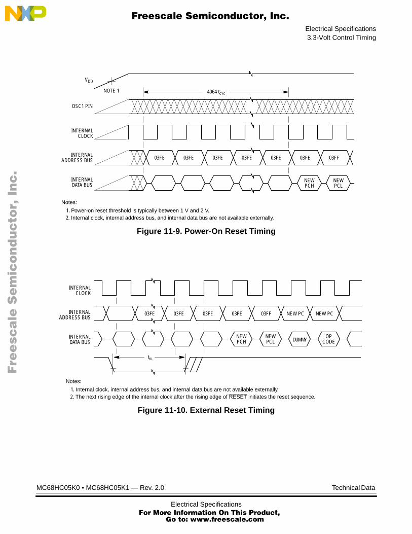
Electrical Specifications3.3-Volt Control Timing
F
ree
sca
le S
em
ico
nd
uc
tor,
I
Freescale Semiconductor, Inc.n
c..
.
Figure 11-9. Power-On Reset Timing
Figure 11-10. External Reset Timing
03FE
4064 tCYC
VDD
OSC1 PIN
INTERNALCLOCK
INTERNALADDRESS BUS
Notes:
INTERNALDATA BUS
03FE 03FE 03FE 03FE 03FE 03FF
NOTE 1
1. Power-on reset threshold is typically between 1 V and 2 V.2. Internal clock, internal address bus, and internal data bus are not available externally.
NEWPCH
NEWPCL
INTERNALCLOCK
INTERNALADDRESS BUS
Notes:
INTERNALDATA BUS
03FE 03FE 03FE 03FE 03FF NEW PC
1. Internal clock, internal address bus, and internal data bus are not available externally.2. The next rising edge of the internal clock after the rising edge of RESET initiates the reset sequence.
NEWPCH
tRL
NEW PC
NEWPCL DUMMY
OPCODE
MC68HC05K0 • MC68HC05K1 — Rev. 2.0 Technical Data
Electrical Specifications For More Information On This Product,
Go to: www.freescale.com

Technical Data
F
ree
sca
le S
em
ico
nd
uc
tor,
I
Freescale Semiconductor, Inc.n
c..
.
11.12 Typical Oscillator Characteristics
ParameterVDD = 3.0 V VDD = 5.0 V Units
Oscillator Type Nominal Frequency
Frequency Variation(Part-to-Part)
2-pin RC oscillator 2 MHz ±12 ±7%
3-pin RC oscillator 1 MHz ±5 ±4
Frequency Variationwith Temperature
2-pin RC oscillator 2 MHz –2100 –1600ppm/°C
3-pin RC oscillator 1 MHz –1100 –1100
Frequency Variationwith Supply Voltage
2-pin RC oscillator 2 MHz ±1.0 ±0.2%f/%V
3-pin RC oscillator 1 MHz ±0.3 ±0.1
Cumulative FrequencyVariations(1)
1. VDD ±10%; TA = –40°C to +85°C
2-pin RC oscillator 2 MHz ±36 ±20%
3-pin RC oscillator 1 MHz ±16 ±13
Technical Data MC68HC05K0 • MC68HC05K1 — Rev. 2.0
Electrical Specifications For More Information On This Product,
Go to: www.freescale.com

Electrical SpecificationsTypical Oscillator Characteristics
F
ree
sca
le S
em
ico
nd
uc
tor,
I
Freescale Semiconductor, Inc.n
c..
.
Figure 11-11. 2-Pin RC Oscillator R versus Frequency (VDD = 5.0 V)
Figure 11-12. 3-Pin RC Oscillator R versus Frequency (VDD = 5.0 V)
000.0 E+0
1.0 E+6
2.0 E+6
3.0 E+6
4.0 E+6
30 kΩ5 kΩ
RESISTANCE
EXTE
RN
AL F
REQ
UEN
CY
10 kΩ 40 kΩ20 kΩ
500.0 E+3
1.5 E+6
2.5 E+6
3.5 E+6
15 pF
20 pF
30 pF
39 pF
50 pF
30 kΩ5 kΩ
RESISTANCE
10 kΩ 20 kΩ000.0 E+0
1.0 E+6
2.0 E+6
EXTE
RN
AL F
REQ
UEN
CY
500.0 E+3
1.5 E+6
2.5 E+615 pF
20 pF
30 pF
39 pF
50 pF
MC68HC05K0 • MC68HC05K1 — Rev. 2.0 Technical Data
Electrical Specifications For More Information On This Product,
Go to: www.freescale.com

Technical Data
F
ree
sca
le S
em
ico
nd
uc
tor,
I
Freescale Semiconductor, Inc.n
c..
.
Figure 11-13. 2-Pin Oscillator R versus Frequency (VDD = 3.0 V)
Figure 11-14. 3-Pin Oscillator R versus Frequency (VDD = 3.0 V)
000.0 E+0
1.0 E+6
2.0 E+6
3.0 E+6
30 kΩ5 kΩRESISTANCE
EXTE
RN
AL F
REQ
UEN
CY
10 kΩ 40 kΩ20 kΩ
500.0 E+3
1.5 E+6
2.5 E+6
15 pF
20 pF
30 pF
39 pF
50 pF
30 kΩ5 kΩRESISTANCE
10 kΩ 20 kΩ000.0 E+0
1.0 E+6
2.0 E+6
3.0 E+6
EXTE
RN
AL F
REQ
UEN
CY
500.0 E+3
1.5 E+6
2.5 E+6
15 pF
20 pF
30 pF
39 pF
50 pF
Technical Data MC68HC05K0 • MC68HC05K1 — Rev. 2.0
Electrical Specifications For More Information On This Product,
Go to: www.freescale.com

F
ree
sca
le S
em
ico
nd
uc
tor,
IFreescale Semiconductor, Inc.
nc
...
Technical Data — MC68HC05K0 • MC68HC05K1
Section 12. Mechanical Specifications
12.1 Contents
12.2 Introduction . . . . . . . . . . . . . . . . . . . . . . . . . . . . . . . . . . . . . . .127
12.3 MC68HC05K0/MC68HC05K1P (PDIP) . . . . . . . . . . . . . . . . .128
12.4 MC68HC05K0/MC68HC05K1DW (SOIC) . . . . . . . . . . . . . . .128
12.2 Introduction
Package dimensions available at the time of this publication areprovided in this section. The packages are:
• 16-pin plastic dual-in-line package (PDIP)
• 16-pin small outline integrated circuit (SOIC)
To make sure that you have the latest case outline specifications,contact one of these:
• Local Motorola sales office
• Motorola Mfax
– Phone 602-244-6609
– EMAIL [email protected]
• World Wide Web (wwweb) at http://www.mcu.motsps.com
Follow Mfax or wwweb on-line instructions to retrieve the currentmechanical specifications.
MC68HC05K0 • MC68HC05K1 — Rev. 2.0 Technical Data
Mechanical Specifications For More Information On This Product,
Go to: www.freescale.com

Technical Data
F
ree
sca
le S
em
ico
nd
uc
tor,
I
Freescale Semiconductor, Inc.n
c..
.
12.3 MC68HC05K0/MC68HC05K1P (PDIP)
12.4 MC68HC05K0/MC68HC05K1DW (SOIC)
-A-
B
F C
S
HG
D 16 PL
J
L
M
SEATINGPLANE
1 8
916
K
-T-
MAM0.25 (0.010) T
DIM MIN MAX MIN MAX
MILLIMETERSINCHES
A 0.740 0.770 18.80 19.55B 0.250 0.270 6.35 6.85C 0.145 0.175 3.69 4.44D 0.015 0.021 0.39 0.53F 0.040 0.70 1.02 1.77G 0.100 BSC 2.54 BSCH 0.050 BSC 1.27 BSCJ 0.008 0.015 0.21 0.38K 0.110 0.130 2.80 3.30L 0.295 0.305 7.50 7.74M 0° 10° 0° 10°S 0.020 0.040 0.51 1.01
F
J
DIM MIN MAX MIN MAX
INCHESMILLIMETERS
A 10.15 10.45 0.400 0.411
B 7.40 7.60 0.292 0.299
C 2.35 2.65 0.093 0.104
D 0.35 0.49 0.014 0.019
F 0.50 0.90 0.020 0.035
G 1.27 BSC 0.050 BSC
J 0.25 0.32 0.010 0.012
K 0.10 0.25 0.004 0.009
M 0° 7° 0° 7°P 10.05 10.55 0.395 0.415
R 0.25 0.75 0.010 0.029
MBM0.010 (0.25)
-A-
-B- P8X
G 14X
D 16X
SEATINGPLANE
-T-
SAM0.010 (0.25) B ST
16 9
81
R X 45
M
C
K
Technical Data MC68HC05K0 • MC68HC05K1 — Rev. 2.0
Mechanical Specifications For More Information On This Product,
Go to: www.freescale.com

F
ree
sca
le S
em
ico
nd
uc
tor,
IFreescale Semiconductor, Inc.
nc
...
Technical Data — MC68HC05K0 • MC68HC05K1
Section 13. Ordering Information
13.1 Contents
13.2 Introduction . . . . . . . . . . . . . . . . . . . . . . . . . . . . . . . . . . . . . . .129
13.3 MCU Ordering Forms . . . . . . . . . . . . . . . . . . . . . . . . . . . . . . .130
13.4 Application Program Media. . . . . . . . . . . . . . . . . . . . . . . . . . .13013.4.1 Diskettes. . . . . . . . . . . . . . . . . . . . . . . . . . . . . . . . . . . . . . .13113.4.2 EPROMs . . . . . . . . . . . . . . . . . . . . . . . . . . . . . . . . . . . . . .132
13.5 ROM Program Verification . . . . . . . . . . . . . . . . . . . . . . . . . . .132
13.6 ROM Verification Units (RVUs). . . . . . . . . . . . . . . . . . . . . . . .133
13.7 MCU Order Numbers . . . . . . . . . . . . . . . . . . . . . . . . . . . . . . .134
13.2 Introduction
This section contains instructions for ordering custom-masked read-onlymemory (ROM) microcontroller units (MCU).
MC68HC05K0 • MC68HC05K1 — Rev. 2.0 Technical Data
Ordering Information For More Information On This Product,
Go to: www.freescale.com

Technical Data
F
ree
sca
le S
em
ico
nd
uc
tor,
I
Freescale Semiconductor, Inc.n
c..
.
13.3 MCU Ordering Forms
To initiate an order for a ROM-based MCU, first obtain the currentordering form for the MCU from a Motorola representative. Submit theseitems when ordering MCUs:
• A current MCU ordering form that is completely filled out.Contact a Motorola sales office for assistance.
• A copy of the customer specification if the customer specificationdeviates from the Motorola specification for the MCU
• Customer’s application program on one of the media listed in13.4 Application Program Media
The current MCU ordering form is also available through the World WideWeb (wwweb) at http://www.mcu.motsps.com
13.4 Application Program Media
Deliver the application program to Motorola in one of these media:
• Macintosh®1 3 1/2-inch diskette (double-sided double-density800 Kbytes or double-sided high-density 1.4 Mbytes)
• MS-DOS®2 or PC-DOS®3 3 1/2-inch diskette (double-sideddouble-density 720 Kbytes or double-sided high-density1.44 Mbytes)
• MS-DOS® or PC-DOS® 5 1/4-inch diskette (double-sideddouble-density 360 Kbytes or double-sided high-density1.2 Mbytes)
• Erasable, programmable read-only memory(s) (EPROM) 2716,2732, 2764, 27,128, 27,256, or 27,512 (depending on the size ofthe memory map of the MCU)
Use positive logic for data and addresses.
1. Macintosh is a registered trademark of Apple Computer, Inc.2. MS-DOS is a registered trademark of Microsoft, Inc.3. PC-DOS is a registered trademark of International Business Machines Corporation.
Technical Data MC68HC05K0 • MC68HC05K1 — Rev. 2.0
Ordering Information For More Information On This Product,
Go to: www.freescale.com

Ordering InformationApplication Program Media
F
ree
sca
le S
em
ico
nd
uc
tor,
I
Freescale Semiconductor, Inc.n
c..
.
13.4.1 Diskettes
If submitting the application program on a diskette, clearly label thediskette with this information:
• Customer name
• Customer part number
• Project or product name
• Filename of object code
• Date
• Name of operating system that formatted diskette
• Formatted capacity of diskette
On diskettes, the application program must be in Motorola’s S-recordformat (S1 and S9 records), a character-based object file formatgenerated by M6805 cross assemblers and linkers.
NOTE: Begin the application program at the first user ROM location. Programaddresses must correspond exactly to the available on-chip user ROMaddresses as shown in the memory map. Write $00 in all non-user ROMlocations or leave all non-user ROM locations blank. See the currentMCU ordering form for additional requirements.
If the memory map has two user ROM areas with the same addresses,then write the two areas in separate files on the diskette. Label thediskette with both filenames.
In addition to the object code, a file containing the source code can beincluded. Motorola keeps this code confidential and uses it only toexpedite ROM pattern generation in case of any difficulty with the objectcode. Label the diskette with the filename of the source code.
MC68HC05K0 • MC68HC05K1 — Rev. 2.0 Technical Data
Ordering Information For More Information On This Product,
Go to: www.freescale.com

Technical Data
F
ree
sca
le S
em
ico
nd
uc
tor,
I
Freescale Semiconductor, Inc.n
c..
.
13.4.2 EPROMs
If submitting the application program in an EPROM, clearly label theEPROM with this information:
• Customer name
• Customer part number
• Checksum
• Project or product name
• Date
NOTE: Begin the application program at the first user ROM location. Programaddresses must correspond exactly to the available on-chip user ROMaddresses as shown in the memory map. Write $00 in all non-user ROMlocations. See the current MCU ordering form for additionalrequirements.
Submit the application program in one EPROM large enough to containthe entire memory map. If the memory map has two user ROM areaswith the same addresses, then write the two areas on separateEPROMs. Label the EPROMs with the addresses they contain.
Pack EPROMs securely in a conductive IC carrier for shipment. Do notuse Styrofoam®1.
13.5 ROM Program Verification
The primary use for the on-chip ROM is to hold the customer’sapplication program. The customer develops and debugs the applicationprogram and then submits the MCU order along with the applicationprogram.
Motorola inputs the customer’s application program code into acomputer program that generates a listing verify file. The listing verify filerepresents the memory map of the MCU. The listing verify file containsthe user ROM code and may also contain non-user ROM code, such as
1. Styrofoam is a registered trademark of The Dow Chemical Company.
Technical Data MC68HC05K0 • MC68HC05K1 — Rev. 2.0
Ordering Information For More Information On This Product,
Go to: www.freescale.com

Ordering InformationROM Verification Units (RVUs)
F
ree
sca
le S
em
ico
nd
uc
tor,
I
Freescale Semiconductor, Inc.n
c..
.
self-check code. Motorola sends the customer a computer printout of thelisting verify file along with a listing verify form.
To aid the customer in checking the listing verify file, Motorola willprogram the listing verify file into customer-supplied blank EPROMs orpreformatted Macintosh or DOS disks. All original pattern media are filedfor contractual purposes and are not returned.
Check the listing verify file thoroughly, then complete and sign the listingverify form and return the listing verify form to Motorola. The signedlisting verify form constitutes the contractual agreement for the creationof the custom mask.
13.6 ROM Verification Units (RVUs)
After receiving the signed listing verify form, Motorola manufactures acustom photographic mask. The mask contains the customer’sapplication program and is used to process silicon wafers. Theapplication program cannot be changed after the manufacture of themask begins. Motorola then produces 10 MCUs, called RVUs, andsends the RVUs to the customer. RVUs are usually packaged inunmarked ceramic and tested to 5 Vdc at room temperature. RVUs arenot tested to environmental extremes because their sole purpose is todemonstrate that the customer’s user ROM pattern was properlyimplemented. The 10 RVUs are free of charge with the minimum orderquantity but are not production parts. RVUs are not guaranteed byMotorola Quality Assurance.
MC68HC05K0 • MC68HC05K1 — Rev. 2.0 Technical Data
Ordering Information For More Information On This Product,
Go to: www.freescale.com
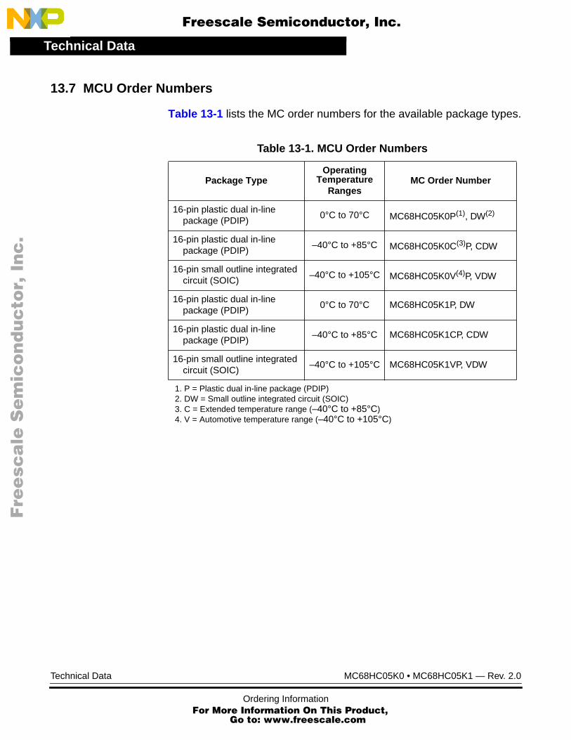
Technical Data
F
ree
sca
le S
em
ico
nd
uc
tor,
I
Freescale Semiconductor, Inc.n
c..
.
13.7 MCU Order Numbers
Table 13-1 lists the MC order numbers for the available package types.
Table 13-1. MCU Order Numbers
Package TypeOperating
TemperatureRanges
MC Order Number
16-pin plastic dual in-linepackage (PDIP)
0°C to 70°C MC68HC05K0P(1), DW(2)
1. P = Plastic dual in-line package (PDIP)2. DW = Small outline integrated circuit (SOIC)
16-pin plastic dual in-linepackage (PDIP)
–40°C to +85°C MC68HC05K0C(3)P, CDW
3. C = Extended temperature range (–40°C to +85°C)
16-pin small outline integratedcircuit (SOIC)
–40°C to +105°C MC68HC05K0V(4)P, VDW
4. V = Automotive temperature range (–40°C to +105°C)
16-pin plastic dual in-linepackage (PDIP)
0°C to 70°C MC68HC05K1P, DW
16-pin plastic dual in-linepackage (PDIP)
–40°C to +85°C MC68HC05K1CP, CDW
16-pin small outline integratedcircuit (SOIC)
–40°C to +105°C MC68HC05K1VP, VDW
Technical Data MC68HC05K0 • MC68HC05K1 — Rev. 2.0
Ordering Information For More Information On This Product,
Go to: www.freescale.com

F
ree
sca
le S
em
ico
nd
uc
tor,
IFreescale Semiconductor, Inc.
nc
...
Technical Data — MC68HC05K0 • MC68HC05K1
Appendix A. MC68HCL05K0
A.1 Contents
A.2 Introduction . . . . . . . . . . . . . . . . . . . . . . . . . . . . . . . . . . . . . . .135
A.3 1.8–2.4-Volt DC Electrical Characteristics . . . . . . . . . . . . . . .136
A.4 2.5–3.6-Volt DC Electrical Characteristics . . . . . . . . . . . . . . .136
A.5 Low-Power Supply Current. . . . . . . . . . . . . . . . . . . . . . . . . . .137
A.6 Low-Power Pulldown Current . . . . . . . . . . . . . . . . . . . . . . . . .138
A.7 Ordering Information. . . . . . . . . . . . . . . . . . . . . . . . . . . . . . . .139
A.2 Introduction
This appendix introduces the MC68HCL05K0, a low-power version ofthe MC68HC05K0. All of the information in this manual applies to theMC68HCL05K0 with the exceptions given in this appendix.
MC68HC05K0 • MC68HC05K1 — Rev. 2.0 Technical Data
MC68HCL05K0 For More Information On This Product,
Go to: www.freescale.com

Technical Data
F
ree
sca
le S
em
ico
nd
uc
tor,
I
Freescale Semiconductor, Inc.n
c..
.
A.3 1.8–2.4-Volt DC Electrical Characteristics
A.4 2.5–3.6-Volt DC Electrical Characteristics
Characteristic(1) Symbol Min Typ Max Unit
Output high voltageILoad = –0.1 mA
PA7–PA0, PBB1/OSC3, PB0VOH VDD – 0.3 — — V
Output low voltageILoad = 0.2 mA
PPA3–PA0, PB1/OSC3, PB0ILoad = 2.0 mA
PPA7–PA4
VOL —
—
—
—
0.3
0.3
V
1. VDD = 1.8–2.4 Vdc
Characteristic(1) Symbol Min Typ Max Unit
Output high voltageILoad = –0.2 mA
PA7–PA0, PBB1/OSC3, PB0VOH VDD – 0.3 — — V
Output low voltageILoad = 0.4 mA
PA3–PA0ILoad = 5.0 mA
PA7–PA4
VOL —
—
—
—
0.3
0.3
V
1. VDD = 2.5–3.6 Vdc
Technical Data MC68HC05K0 • MC68HC05K1 — Rev. 2.0
MC68HCL05K0 For More Information On This Product,
Go to: www.freescale.com

MC68HCL05K0Low-Power Supply Current
F
ree
sca
le S
em
ico
nd
uc
tor,
I
Freescale Semiconductor, Inc.n
c..
.
A.5 Low-Power Supply Current
Characteristic Symbol Min Typ(1) Max Unit
Supply current (VDD = 4.5–5.5 Vdc, fop = 2.1 MHz)
Run(2)
Wait(3)
Stop(4)
25°C0°C to 70°C (standard)
IDD
——
——
3.01.6
0.22.0
4.02.5
1020
mAmA
µAµA
Supply current (VDD = 2.5–3.6 Vdc, fop = 1.0 MHz)
Run(2)
Wait(3)
Stop(4)
25°C0°C to 70°C (standard)
IDD
——
——
1.00.5
0.11.0
2.01.0
5.010.0
mAmA
µAµA
Supply current (VDD = 2.5–3.6 Vdc, fop = 500 kHz)
Run(2)
Wait(3)
Stop(4)
25°C0°C to 70°C (standard)
IDD
——
——
0.5250
0.051.0
1.0500
5.010.0
mAµA
µAµA
Supply current (VDD = 1.8–2.4 Vdc, fop = 500 kHz)
Run(2)
Wait(3)
Stop(4)
25°C0°C to 70°C (standard)
IDD
——
——
300150
0.050.5
700400
2.05.0
µAµA
µAµA
1. Typical values reflect average measurements at midpoint of voltage range at 25°C.2. Run (operating) IDD measured using external square wave clock source with all inputs 0.2 V from rail. No dc loads. Less
than 50 pF on all outputs. CL = 20 pF on OSC2. OSC2 capacitance linearly affects run IDD.3. Wait IDD measured using external square wave clock source with all inputs 0.2 V from rail. No dc loads. Less than 50 pF
on all outputs. CL = 20 pF on OSC2. All ports configured as inputs. VIL = 0.2 V, VIH = VDD – 0.2 V. OSC2 capacitancelinearly affects wait IDD.
4. Stop IDD measured with OSC1 = VDD. All ports configured as inputs. VIL = 0.2 V, VIH = VDD – 0.2 V.
MC68HC05K0 • MC68HC05K1 — Rev. 2.0 Technical Data
MC68HCL05K0 For More Information On This Product,
Go to: www.freescale.com

Technical Data
F
ree
sca
le S
em
ico
nd
uc
tor,
I
Freescale Semiconductor, Inc.n
c..
.
A.6 Low-Power Pulldown Current
Figure 13-1. Maximum Run Mode IDD versus Frequency
Characteristic Symbol Min Typ(1) Max Unit
Pulldown current (VDD = 4.5–5.5 Vdc, fop = 2.1 MHz)PA7–PA0, PB1/OSC3, PB0 (pulldown device on)
IIL 50 100 200 µA
Pulldown current (VDD = 2.5–3.6 Vdc, fop = 1.0 MHz)PA7–PA0, PB1/OSC3, PB0 (pulldown device on)
IIL 8 30 100 µA
Pulldown current (VDD = 2.5–3.6 Vdc, fop = 500 kHz)PA7–PA0, PB1/OSC3, PB0 (pulldown device on)
IIL 3 10 50 µA
Pulldown current (VDD = 1.8–2.4 Vdc, fop = 500 kHz)PA7–PA0, PB1/OSC3, PB0 (pulldown device on)
IIL 3 10 50 µA
1. Typical values reflect average measurements at midpoint of voltage range at 25°C.
RUN
I DD
(mA)
INTERNAL CLOCK FREQUENCY (MHz)
2.0
1.8
1.6
1.4
1.2
1.0
0.8
0.6
0.4
0.2
0
0 0.1 0.2 0.3 0.4 0.5 0.6 0.8 0.9 1.00.7
VDD = 3.6 V
VDD = 2.4 V
Technical Data MC68HC05K0 • MC68HC05K1 — Rev. 2.0
MC68HCL05K0 For More Information On This Product,
Go to: www.freescale.com

MC68HCL05K0Ordering Information
F
ree
sca
le S
em
ico
nd
uc
tor,
I
Freescale Semiconductor, Inc.n
c..
.
Figure 13-2. Maximum Wait Mode IDD versus Frequency
A.7 Ordering Information
Table A-1 lists order numbers for the available package types.
WAI
T I D
D (m
A)
INTERNAL CLOCK FREQUENCY (MHz)
1.0
0.9
0.8
0.7
0.6
0.5
0.4
0.1
0
0 0.1 0.2 0.3 0.4 0.5 0.6 0.8 0.9 1.00.7
VDD = 3.6 V
VDD = 2.4 V
0.3
0.2
Table A-1. MC68HCL05K0 Order Numbers
Package TypeOperating
Temperature RangeOrder Number
16-pin plastic dual in-line package (PDIP) 0°C to 70°C MC68HCL05K0P(1)
16-pin small outline integrated circuit (SOIC) 0°C to 70°C MC68HCL05K0DW(2)
1. P = Plastic dual in-line package (PDIP)2. DW = Small outline integrated circuit (SOIC)
MC68HC05K0 • MC68HC05K1 — Rev. 2.0 Technical Data
MC68HCL05K0 For More Information On This Product,
Go to: www.freescale.com

Technical Data
F
ree
sca
le S
em
ico
nd
uc
tor,
I
Freescale Semiconductor, Inc.n
c..
.
Technical Data MC68HC05K0 • MC68HC05K1 — Rev. 2.0
MC68HCL05K0 For More Information On This Product,
Go to: www.freescale.com

F
ree
sca
le S
em
ico
nd
uc
tor,
IFreescale Semiconductor, Inc.
nc
...
Technical Data — MC68HC05K0 • MC68HC05K1
Appendix B. MC68HSC05K0
B.1 Contents
B.2 Introduction . . . . . . . . . . . . . . . . . . . . . . . . . . . . . . . . . . . . . . .141
B.3 High-Speed Supply Current . . . . . . . . . . . . . . . . . . . . . . . . . .142
B.4 5.0-Volt Control Timing . . . . . . . . . . . . . . . . . . . . . . . . . . . . . .143
B.5 3.3-Volt Control Timing . . . . . . . . . . . . . . . . . . . . . . . . . . . . . .144
B.6 Ordering Information. . . . . . . . . . . . . . . . . . . . . . . . . . . . . . . .144
B.2 Introduction
This appendix introduces the MC68HSC05K0, a high-speed version ofthe MC68HC05K0. All of the information in this manual applies to theMC68HSC05K0 with the exceptions given in this appendix.
MC68HC05K0 • MC68HC05K1 — Rev. 2.0 Technical Data
MC68HSC05K0 For More Information On This Product,
Go to: www.freescale.com

Technical Data
F
ree
sca
le S
em
ico
nd
uc
tor,
I
Freescale Semiconductor, Inc.n
c..
.
B.3 High-Speed Supply Current
Characteristic Symbol Min Typ(1) Max Unit
Supply current (VDD = 4.5–5.5 Vdc, fop = 4.0 MHz)
Run(2)
Wait(3)
Stop(4)
25°C–40°C to +85°C
IDD
——
——
4.52.5
0.22.0
6.03.25
1020
mAmA
µAµA
Supply current (VDD = 3.0–3.6 Vdc, fop = 2.1 MHz)RunWaitStop
25°C–40°C to +85°C
IDD
——
——
2.01.0
0.11.0
4.02.0
5.010.0
mAmA
µAµA
1. Typical values at midpoint of voltage range, 25°C only.2. Run (operating) IDD measured using external square wave clock source with all inputs 0.2 V from rail. No dc loads. Less
than 50 pF on all outputs. CL = 20 pF on OSC2. OSC2 capacitance linearly affects run IDD.3. Wait IDD measured using external square wave clock source with all inputs 0.2 V from rail. No dc loads. Less than 50 pF
on all outputs. CL = 20 pF on OSC2. All ports configured as inputs. VIL = 0.2 V, VIH = VDD – 0.2 V. OSC2 capacitance lin-early affects wait IDD.
4. Stop IDD measured with OSC1 = VDD. All ports configured as inputs. VIL = 0.2 V, VIH = VDD – 0.2 V.
Technical Data MC68HC05K0 • MC68HC05K1 — Rev. 2.0
MC68HSC05K0 For More Information On This Product,
Go to: www.freescale.com

MC68HSC05K05.0-Volt Control Timing
F
ree
sca
le S
em
ico
nd
uc
tor,
I
Freescale Semiconductor, Inc.n
c..
.
B.4 5.0-Volt Control Timing
Characteristic(1) Symbol Min Max Unit
Oscillator frequency3-pin RC oscillator2-pin RC oscillator
Crystal oscillator(2)
External clock
fosc
0.020.20.2dc
2.04.08.08.0
MHz
Internal operating frequency (fosc ÷ 2)3-pin RC oscillator2-pin RC oscillator
Crystal oscillator(2)
External clock
fop
———dc
1.02.04.04.0
MHz
Internal clock cycle time (1 ÷ fop)3-pin RC oscillator2-pin RC oscillator
Crystal oscillator(2)
External clock
tcyc
1.0500250250
————
µsnsnsns
RC oscillator stabilization time tRCON — 500 µs
Crystal oscillator startup time tOXOV — 50 ms
STOP recovery time tILCH — 50 ms
IRQ pulse width low (edge-triggered) tILIH 125 — ns
PA3–PA0 interrupt pulse width high (edge-triggered) tIHIL 125 — ns
OSC1 pulse width tOH or tOL 45 — ns
1. VDD = 5.0 Vdc ±10%; VSS = 0 Vdc; TA = TL to TH2. Use only AT-cut crystals.
MC68HC05K0 • MC68HC05K1 — Rev. 2.0 Technical Data
MC68HSC05K0 For More Information On This Product,
Go to: www.freescale.com

Technical Data
F
ree
sca
le S
em
ico
nd
uc
tor,
I
Freescale Semiconductor, Inc.n
c..
.
B.5 3.3-Volt Control Timing
B.6 Ordering Information
Table B-1 lists order numbers for the available package types.
Characteristic(1) Symbol Min Max Unit
Oscillator frequency3-pin RC oscillator2-pin RC oscillator
Crystal oscillator(2)
External clock
fosc
0.020.20.2dc
1.04.04.04.0
MHz
Internal operating frequency (fosc ÷ 2)3-pin RC oscillator2-pin RC oscillator
Crystal oscillator(2)
External clock
fop
———dc
1.02.02.02.0
MHz
Internal clock cycle time (1 ÷ fop)3-pin RC oscillator2-pin RC oscillator
Crystal oscillator(2)
External clock
tcyc
1.0500500500
————
µsnsnsns
RC oscillator stabilization time tRCON — 1.0 ms
Crystal oscillator startup time tOXOV — 100 ms
STOP recovery time tILCH — 100 ms
IRQ pulse width low (edge-triggered) tILIH 250 — ns
PA3–PA0 interrupt pulse width high (edge-triggered) tIHIL 250 — ns
OSC1 pulse width tOH or tOL 100 — ns
1. VDD = 3.3 Vdc ±10%; VSS = 0 Vdc; TA = TL to TH.2. Use only AT-cut crystals.
Table B-1. MC68HSC05K0 Order Numbers
Package TypeOperating
Temperature RangeOrder Number
16-pin plastic dual in-line package (PDIP) 0°C to +70°C MC68HSC05K0P(1)
16-pin small outline integrated circuit (SOIC) 0°C to +70°C MC68HSC05K0DW(2)
1. P = Plastic dual in-line pachage (PDIP)2. DW = Small outline integrated circuit (SOIC)
Technical Data MC68HC05K0 • MC68HC05K1 — Rev. 2.0
MC68HSC05K0 For More Information On This Product,
Go to: www.freescale.com

F
ree
sca
le S
em
ico
nd
uc
tor,
IFreescale Semiconductor, Inc.
nc
...
Technical Data — MC68HC05K0 • MC68HC05K1
Index
Aaccumulator (A) . . . . . . . . . . . . . . . . . . . . . . . . . . . . . . . . . . .94, 95, 98addressing modes . . . . . . . . . . . . . . . . . . . . . . . . . . . . . . . . . . . . . . .94arithmetic logic unit (ALU) . . . . . . . . . . . . . . . . . . . . . . . . . . . . . . . . .41
Bblock diagram . . . . . . . . . . . . . . . . . . . . . . . . . . . . . . . . . . . . . . . . . .20
CC bit . . . . . . . . . . . . . . . . . . . . . . . . . . . . . . . . . . . . . . . . . . . . . . . . .100central processor unit (CPU) . . . . . . . . . . . . . . . . . . . . . . . . . . . . . . .35condition code register (CCR) . . . . . . . . . . . . . . . . . . . . . . . . . . . . .100COP watchdog . . . . . . . . . . . . . . . . . . . . . . . . . . . . . . . . . . . . . . . . . .82
COP enabling/disabling recommendations . . . . . . . . . . . . . . . . .83mask options . . . . . . . . . . . . . . . . . . . . . . . . . . . . . . . . . . . . . . . .19
CPUaccumulator (A) . . . . . . . . . . . . . . . . . . . . . . . . . . . . . . . . . . . . . .37condition code register (CCR) . . . . . . . . . . . . . . . . . . . . . . . . . . .40index register (X) . . . . . . . . . . . . . . . . . . . . . . . . . . . . . . . . . . . . .37instruction set summary . . . . . . . . . . . . . . . . . . . . . . . . . . . . . . .104instruction types . . . . . . . . . . . . . . . . . . . . . . . . . . . . . . . . . . . . . .97opcode map . . . . . . . . . . . . . . . . . . . . . . . . . . . . . . . . . . . . . . . .110program counter (PC) . . . . . . . . . . . . . . . . . . . . . . . . . . . . . . . . . .39programming model . . . . . . . . . . . . . . . . . . . . . . . . . . . . . . . . . . .36registers . . . . . . . . . . . . . . . . . . . . . . . . . . . . . . . . . . . . . . . . . . . .36stack pointer (SP) . . . . . . . . . . . . . . . . . . . . . . . . . . . . . . . . . . . . .38
CPU registers . . . . . . . . . . . . . . . . . . . . . . . . . . . . . . . . . . .95, 98, 103accumulator (A) . . . . . . . . . . . . . . . . . . . . . . . . . . . . . . . .94, 95, 98condition code register (CCR) . . . . . . . . . . . . . . . . . . . . . . . . . .100index register (X) . . . . . . . . . . . . . . . . . . . . . . . . . . . .94, 95, 96, 98program counter (PC) . . . . . . . . . . . . . . . . . . . . . . . . . . . . . .97, 100
MC68HC05K0 • MC68HC05K1 — Rev. 2.0 Technical Data
Index For More Information On This Product,
Go to: www.freescale.com

Technical Data
F
ree
sca
le S
em
ico
nd
uc
tor,
I
Freescale Semiconductor, Inc.n
c..
.
Ddata-retention mode . . . . . . . . . . . . . . . . . . . . . . . . . . . . . . . . . . . . . .62
Eelectrical specifications . . . . . . . . . . . . . . . . . . . . . . . . . . . . . . . . . .111
control timing . . . . . . . . . . . . . . . . . . . . . . . . . . . . . . . . . . . . . . .120electrical characteristics . . . . . . . . . . . . . . . . . . . . . . . . . . . . . . .115oscillator characteristics . . . . . . . . . . . . . . . . . . . . . . . . . . . . . . .124power considerations . . . . . . . . . . . . . . . . . . . . . . . . . . . . . . . . .114
EPROM (personality EPROM (PEPROM))bit selection . . . . . . . . . . . . . . . . . . . . . . . . . . . . . . . . . . . . . . . . .88block diagram . . . . . . . . . . . . . . . . . . . . . . . . . . . . . . . . . . . . . . . .86PEPROM bit select register (PEBSR) . . . . . . . . . . . . . . . . . . . . .87PEPROM reading . . . . . . . . . . . . . . . . . . . . . . . . . . . . . . . . . . . . .92PEPROM status and control register (PESCR) . . . . . . . . . . . . . .89programming . . . . . . . . . . . . . . . . . . . . . . . . . . . . . . . . . . . . . . . .90programming circuit . . . . . . . . . . . . . . . . . . . . . . . . . . . . . . . . . . .91
EPROM (personality)/OTPROM . . . . . . . . . . . . . . . . . . . . . . . . . . . .34programming voltage . . . . . . . . . . . . . . . . . . . . . . . . . . . . . . . . . .27
Ffeatures . . . . . . . . . . . . . . . . . . . . . . . . . . . . . . . . . . . . . . . . . . . . . . .18
Hhalt mode . . . . . . . . . . . . . . . . . . . . . . . . . . . . . . . . . . . . . . . . . . . . . .62high-speed MC68HSC05K0
control timing . . . . . . . . . . . . . . . . . . . . . . . . . . . . . . . . . . . . . . .143ordering information . . . . . . . . . . . . . . . . . . . . . . . . . . . . . . . . . .144
II/O (input/output) . . . . . . . . . . . . . . . . . . . . . . . . . . . . . . . . . . . . . . . .30
port A . . . . . . . . . . . . . . . . . . . . . . . . . . . . . . . . . . . . . . . . . . . . . .66port B . . . . . . . . . . . . . . . . . . . . . . . . . . . . . . . . . . . . . . . . . . . . . .70
I/O bitsC bit . . . . . . . . . . . . . . . . . . . . . . . . . . . . . . . . . . . . . . . . . . . . . .100
index register (X) . . . . . . . . . . . . . . . . . . . . . . . . . . . . . . .94, 95, 96, 98
Technical Data MC68HC05K0 • MC68HC05K1 — Rev. 2.0
Index For More Information On This Product,
Go to: www.freescale.com

Index
F
ree
sca
le S
em
ico
nd
uc
tor,
I
Freescale Semiconductor, Inc.n
c..
.
instruction set . . . . . . . . . . . . . . . . . . . . . . . . . . . . . . . . . . . . . . . . . . .93addressing modes . . . . . . . . . . . . . . . . . . . . . . . . . . . . . . . . . . . .94instruction set summary . . . . . . . . . . . . . . . . . . . . . . . . . . . . . . .104instruction types . . . . . . . . . . . . . . . . . . . . . . . . . . . . . . . . . . . . . .97opcode map . . . . . . . . . . . . . . . . . . . . . . . . . . . . . . . . . . . . . . . .110
interrupts . . . . . . . . . . . . . . . . . . . . . . . . . . . . . . . . . . . . . . . . . . . . . .43external . . . . . . . . . . . . . . . . . . . . . . . . . . . . . . . . . . . . . . . . . . . . .27external interrupt logic . . . . . . . . . . . . . . . . . . . . . . . . . . . . . . . . .46external interrupt pin triggering mask options . . . . . . . . . . . . . . .19interrupt flowchart . . . . . . . . . . . . . . . . . . . . . . . . . . . . . . . . . . . . .52interrupt processing . . . . . . . . . . . . . . . . . . . . . . . . . . . . . . . . . . .50interrupt stacking order . . . . . . . . . . . . . . . . . . . . . . . . . . . . . . . . .50interrupt types . . . . . . . . . . . . . . . . . . . . . . . . . . . . . . . . . . . . . . . .44IRQ status and control register (ISCR) . . . . . . . . . . . . . . . . . . . . .48IRQ/VPP pin . . . . . . . . . . . . . . . . . . . . . . . . . . . . . . . . . . . . . . . . . .45PA3–PA0 pins . . . . . . . . . . . . . . . . . . . . . . . . . . . . . . . . . . . . . . .46port A external interrupt function mask options . . . . . . . . . . . . . .19port A external interrupts . . . . . . . . . . . . . . . . . . . . . . . . . . . . . . .69reset/interrupt vector addresses . . . . . . . . . . . . . . . . . . . . . . . . . .51software interrupt . . . . . . . . . . . . . . . . . . . . . . . . . . . . . . . . . . . . .44timer interrupts . . . . . . . . . . . . . . . . . . . . . . . . . . . . . . . . . . . . . . .49
IRQ/VPP pin . . . . . . . . . . . . . . . . . . . . . . . . . . . . . . . . . . . . . . . . . . . .44functions . . . . . . . . . . . . . . . . . . . . . . . . . . . . . . . . . . . . . . . . . . . .27
Jjunction temperature . . . . . . . . . . . . . . . . . . . . . . . . . . . . . . . . . . . .114
Llow-power MC68HCL05K0
DC electrical characteristics . . . . . . . . . . . . . . . . . . . . . . . . . . . .136ordering information . . . . . . . . . . . . . . . . . . . . . . . . . . . . . . . . . .139
low-power modes . . . . . . . . . . . . . . . . . . . . . . . . . . . . . . . . . . . . . . . .59data retention . . . . . . . . . . . . . . . . . . . . . . . . . . . . . . . . . . . . . . . .62flowchart . . . . . . . . . . . . . . . . . . . . . . . . . . . . . . . . . . . . . . . . . . . .63halt . . . . . . . . . . . . . . . . . . . . . . . . . . . . . . . . . . . . . . . . . . . . . . . .62stop . . . . . . . . . . . . . . . . . . . . . . . . . . . . . . . . . . . . . . . . . . . . . . . .60wait . . . . . . . . . . . . . . . . . . . . . . . . . . . . . . . . . . . . . . . . . . . . . . . .61
low-voltage resetmask options . . . . . . . . . . . . . . . . . . . . . . . . . . . . . . . . . . . . . . . .19
MC68HC05K0 • MC68HC05K1 — Rev. 2.0 Technical Data
Index For More Information On This Product,
Go to: www.freescale.com

Technical Data
F
ree
sca
le S
em
ico
nd
uc
tor,
I
Freescale Semiconductor, Inc.n
c..
.
Mmask option . . . . . . . . . . . . . . . . . . . . . . . . . . . . . . . . . . . . . . . . . . . .19mechanical specifications . . . . . . . . . . . . . . . . . . . . . . . . . . . . . . . .127
PDIP . . . . . . . . . . . . . . . . . . . . . . . . . . . . . . . . . . . . . . . . . . . . . .128SOIC . . . . . . . . . . . . . . . . . . . . . . . . . . . . . . . . . . . . . . . . . . . . . .128
memory . . . . . . . . . . . . . . . . . . . . . . . . . . . . . . . . . . . . . . . . . . . . . . .29I/O (input/output) . . . . . . . . . . . . . . . . . . . . . . . . . . . . . . . . . . . . .30personality EPROM/OTPROM . . . . . . . . . . . . . . . . . . . . . . . . . . .34RAM . . . . . . . . . . . . . . . . . . . . . . . . . . . . . . . . . . . . . . . . . . . . . . .30ROM . . . . . . . . . . . . . . . . . . . . . . . . . . . . . . . . . . . . . . . . . . . . . . .34
multifunction timer . . . . . . . . . . . . . . . . . . . . . . . . . . . . . . . . . . . . . . .77
Oopcode map . . . . . . . . . . . . . . . . . . . . . . . . . . . . . . . . . . . . . . . . . . .110ordering information . . . . . . . . . . . . . . . . . . . . . . . . . . . . . . . . . . . . .129
MCU order numbers . . . . . . . . . . . . . . . . . . . . . . . . . . . . . . . . . .134ordering information (high-speed part)
MCU order numbers . . . . . . . . . . . . . . . . . . . . . . . . . . . . . . . . . .144ordering information (low-power part)
MCU order numbers . . . . . . . . . . . . . . . . . . . . . . . . . . . . . . . . . .139OSC1 . . . . . . . . . . . . . . . . . . . . . . . . . . . . . . . . . . . . . . . . . . . . . . . . .22OSC2 . . . . . . . . . . . . . . . . . . . . . . . . . . . . . . . . . . . . . . . . . . . . . . . . .22oscillator
ceramic . . . . . . . . . . . . . . . . . . . . . . . . . . . . . . . . . . . . . . . . . . . . .24crystal . . . . . . . . . . . . . . . . . . . . . . . . . . . . . . . . . . . . . . . . . . . . . .23external clock signal . . . . . . . . . . . . . . . . . . . . . . . . . . . . . . . . . . .27frequency . . . . . . . . . . . . . . . . . . . . . . . . . . . . . . . . . . . . . . . . . . .22mask options . . . . . . . . . . . . . . . . . . . . . . . . . . . . . . . . . . . . . . . .19oscillator characteristics . . . . . . . . . . . . . . . . . . . . . . . . . . . . . . .124resistor-capacitor (RC) combination . . . . . . . . . . . . . . . . . . . . . . .25
PPA7–PA0
pins . . . . . . . . . . . . . . . . . . . . . . . . . . . . . . . . . . . . . . . . . . . . . . . .27parallel input/output (I/O) . . . . . . . . . . . . . . . . . . . . . . . . . . . . . . . . . .65PB1/OSC3 . . . . . . . . . . . . . . . . . . . . . . . . . . . . . . . . . . . . . . . . . . . . .22PB1/OSC3 and PB0 pins . . . . . . . . . . . . . . . . . . . . . . . . . . . . . . . . . .28personality EPROM . . . . . . . . . . . . . . . . . . . . . . . . . . . . . . . . . . . . . .85pin assignments . . . . . . . . . . . . . . . . . . . . . . . . . . . . . . . . . . . . . . . . .21
Technical Data MC68HC05K0 • MC68HC05K1 — Rev. 2.0
Index For More Information On This Product,
Go to: www.freescale.com

Index
F
ree
sca
le S
em
ico
nd
uc
tor,
I
Freescale Semiconductor, Inc.n
c..
.
port A . . . . . . . . . . . . . . . . . . . . . . . . . . . . . . . . . . . . . . . . . . . . . . . . .66data direction register A (DDRA) . . . . . . . . . . . . . . . . . . . . . . . . .67external interrupts . . . . . . . . . . . . . . . . . . . . . . . . . . . . . . . . . . . . .27I/O logic circuit . . . . . . . . . . . . . . . . . . . . . . . . . . . . . . . . . . . . . . .69pin functions . . . . . . . . . . . . . . . . . . . . . . . . . . . . . . . . . . . . . . . . .70pins . . . . . . . . . . . . . . . . . . . . . . . . . . . . . . . . . . . . . . . . . . . . . . . .27port A data register (PORTA) . . . . . . . . . . . . . . . . . . . . . . . . . . . .66port A external interrupts . . . . . . . . . . . . . . . . . . . . . . . . . . . . . . .69pulldown devices . . . . . . . . . . . . . . . . . . . . . . . . . . . . . . . . . . . . .27pulldown register A (PDRA) . . . . . . . . . . . . . . . . . . . . . . . . . . . . .68
port B . . . . . . . . . . . . . . . . . . . . . . . . . . . . . . . . . . . . . . . . . . . . . . . . .70data direction register B (DDRB) . . . . . . . . . . . . . . . . . . . . . . . . .72I/O logic circuit . . . . . . . . . . . . . . . . . . . . . . . . . . . . . . . . . . . . . . .74PB1/OSC3 pin functions . . . . . . . . . . . . . . . . . . . . . . . . . . . . . . . .75pin functions . . . . . . . . . . . . . . . . . . . . . . . . . . . . . . . . . . . . . . . . .75pins . . . . . . . . . . . . . . . . . . . . . . . . . . . . . . . . . . . . . . . . . . . . . . . .28port B data register (PORTB) . . . . . . . . . . . . . . . . . . . . . . . . . . . .70pulldown devices . . . . . . . . . . . . . . . . . . . . . . . . . . . . . . . . . . . . .28pulldown register B (PDRB) . . . . . . . . . . . . . . . . . . . . . . . . . . . . .73
power dissipation . . . . . . . . . . . . . . . . . . . . . . . . . . . . . . . . . . . . . . .114program counter (PC) . . . . . . . . . . . . . . . . . . . . . . . . . . . . . . . .97, 100pulldown devices
mask options . . . . . . . . . . . . . . . . . . . . . . . . . . . . . . . . . . . . . . . .19pulldown register A (PDRA) . . . . . . . . . . . . . . . . . . . . . . . . . . . . .68pulldown register B (PDRB) . . . . . . . . . . . . . . . . . . . . . . . . . . . . .73
RRAM . . . . . . . . . . . . . . . . . . . . . . . . . . . . . . . . . . . . . . . . . . . . . . . . . .30registers
CPU . . . . . . . . . . . . . . . . . . . . . . . . . . . . . . . . . . . . . . . . . . . . . . .36reset
interrupt flowchart . . . . . . . . . . . . . . . . . . . . . . . . . . . . . . . . . . . . .52pin . . . . . . . . . . . . . . . . . . . . . . . . . . . . . . . . . . . . . . . . . . . . . . . . .27
resets . . . . . . . . . . . . . . . . . . . . . . . . . . . . . . . . . . . . . . . . . . . . . . . . .53computer operating properly (COP) . . . . . . . . . . . . . . . . . . . . . . .56effect on COP watchdog . . . . . . . . . . . . . . . . . . . . . . . . . . . . . . .58effect on CPU . . . . . . . . . . . . . . . . . . . . . . . . . . . . . . . . . . . . . . . .57effect on I/O port registers . . . . . . . . . . . . . . . . . . . . . . . . . . . . . .58
MC68HC05K0 • MC68HC05K1 — Rev. 2.0 Technical Data
Index For More Information On This Product,
Go to: www.freescale.com

Technical Data
F
ree
sca
le S
em
ico
nd
uc
tor,
I
Freescale Semiconductor, Inc.n
c..
.
effect on timer . . . . . . . . . . . . . . . . . . . . . . . . . . . . . . . . . . . . . . . .58illegal address . . . . . . . . . . . . . . . . . . . . . . . . . . . . . . . . . . . . . . .56low-voltage . . . . . . . . . . . . . . . . . . . . . . . . . . . . . . . . . . . . . . . . . .57power-on . . . . . . . . . . . . . . . . . . . . . . . . . . . . . . . . . . . . . . . . . . .54reset states . . . . . . . . . . . . . . . . . . . . . . . . . . . . . . . . . . . . . . . . . .57reset/interrupt vector addresses . . . . . . . . . . . . . . . . . . . . . . . . . .51sources diagram . . . . . . . . . . . . . . . . . . . . . . . . . . . . . . . . . . . . . .55types . . . . . . . . . . . . . . . . . . . . . . . . . . . . . . . . . . . . . . . . . . . . . . .54
ROM . . . . . . . . . . . . . . . . . . . . . . . . . . . . . . . . . . . . . . . . . . . . . . . . .34
SSTOP instruction
mask options . . . . . . . . . . . . . . . . . . . . . . . . . . . . . . . . . . . . . . . .19stop mode . . . . . . . . . . . . . . . . . . . . . . . . . . . . . . . . . . . . . . . . . . . . .60
Tthermal resistance . . . . . . . . . . . . . . . . . . . . . . . . . . . . . . . . . . . . . .114timer
block diagram . . . . . . . . . . . . . . . . . . . . . . . . . . . . . . . . . . . . . . . .78COP enabling/disabling recommendations . . . . . . . . . . . . . . . . .83COP watchdog . . . . . . . . . . . . . . . . . . . . . . . . . . . . . . . . . . . . . . .82timer counter register (TCNTR) . . . . . . . . . . . . . . . . . . . . . . . . . .81timer status and control register (TSCR) . . . . . . . . . . . . . . . . . . .78
VVDD and VSS . . . . . . . . . . . . . . . . . . . . . . . . . . . . . . . . . . . . . . . . . . . .22
Wwait mode . . . . . . . . . . . . . . . . . . . . . . . . . . . . . . . . . . . . . . . . . . . . .61
Technical Data MC68HC05K0 • MC68HC05K1 — Rev. 2.0
Index For More Information On This Product,
Go to: www.freescale.com

MC68HC05K0/K1 Rev. 2 TECHNICAL DATA
1
2
3
4
5
6
7
8
9
10
11
12
13
14
15
16
17
18
19
F
ree
sca
le S
em
ico
nd
uc
tor,
I
Freescale Semiconductor, Inc.n
c..
.
CUSTOMER RESPONSE SURVEYTo make M68HC05 documentation as clear, complete, and easy to use as possible, we need yourcomments. Please complete this form and return it by mail, or FAX it to 512-891-3236.
1. How do you rate the quality of this document?
2. What is your intended use for this document?
3. Does this document help you perform your job?
4. Are you able to find the information you need easily?
5. Does each section of the document provide you with enough information?
High Low High LowOrganization Tables
Readability Table of contents
Accuracy Page size/binding
Figures Overall impression
Comments:
Device selection for new application Other Please specify:
System design
Training
Yes NoComments:
Yes No
Comments:
Yes No Yes NoSEC. 1: GEN. DESCRIPTION SEC. 10: INSTR. SET
SEC. 2: MEMORY SEC. 11: ELECTRICAL
SEC. 3: CPU SEC. 12: MECHANICAL
SEC. 4: INTERRUPTS SEC. 13: ORDERING
SEC. 5: RESETS APP. A MC68HCL05K0
SEC. 6: LOW-POWER MODES APP. B MC68HSC05K0
SEC. 7: PARALLEL I/O INDEX
SEC. 8: TIMER
SEC. 9: EPROM
6. What would you do to improve this document?
For More Information On This Product,
Go to: www.freescale.com

Fir
st:
cut
alo
ng
th
is li
ne
to r
emo
ve
Freescale Semiconductor, Inc.
Motorola6501 William Cannon Drive WestMail Stop OE17Austin, Texas 78735-8598
Attn: MMD Publications Department
Second: fold back along this line
Please supply the following information (optional).
Name: ___________________________________________________
Company Name: ___________________________________________
Title: ____________________________________________________
Address: _________________________________________________
City: _____________________________State: _____Zip:__________
Phone Number: ____________________________________________
Fre
esc
ale
Se
mic
on
du
cto
r, I
nc
...
For More Information On This Product,
Go to: www.freescale.com

Fre
esc
ale
Se
mic
on
du
cto
r, I
Freescale Semiconductor, Inc.
For More Information On This Product, Go to: www.freescale.com
nc
...

MC68HC05K1/D
Fre
esc
ale
Se
mic
on
du
cto
r, I
Freescale Semiconductor, Inc.
For More Information On This Product, Go to: www.freescale.com
nc
...
RXZB30
hibbertleft
RXZB30
disclaimer
RXZB30
rohstext
RXZB30
logo