
A2I25D025N.pdf - NXP
19
RF LDMOS Wideband Integrated Power Amplifiers The A2I25D025N wideband integrated circuit is designed with on--chip matching that makes it usable from 2100 to 2900 MHz. This multi--stage structure is rated for 26 to 32 V operation and covers all typical cellular base station modulation formats. Typical Single--Carrier W--CDMA Characterization Performance: V DD = 28 Vdc, I DQ1(A+B) = 56 mA, I DQ2(A+B) = 136 mA, P out = 3.2 W Avg., Input Signal PAR = 9.9 dB @ 0.01% Probability on CCDF. (1) Frequency G ps (dB) PAE (%) ACPR (dBc) 2300 MHz 32.0 19.0 –46.7 2350 MHz 31.8 19.0 –47.1 2400 MHz 31.7 19.1 –47.5 2496 MHz 31.7 19.3 –47.3 2600 MHz 32.0 19.5 –47.1 2690 MHz 32.5 20.0 –46.8 Features On--Chip Matching (50 Ohm Input, DC Blocked) Integrated Quiescent Current Temperature Compensation with Enable/Disable Function (2) Designed for Digital Predistortion Error Correction Systems Optimized for Doherty Applications Figure 1. Functional Block Diagram Figure 2. Pin Connections Note: Exposed backside of the package is the source terminal for the transistors. Quiescent Current Temperature Compensation (2) V DS1A RF inA V GS1A RF out1 /V DS2A V GS2A Quiescent Current Temperature Compensation (2) V DS1B RF inB V GS1B RF out2 /V DS2B V GS2B V DS1A RF inA GND RF inB RF out1 /V DS2A 1 2 3 4 7 8 15 V GS1B 9 10 11 V GS2A V GS1A N.C. N.C. V GS2B GND V DS1B RF out2 /V DS2B 13 6 12 (Top View) 5 14 GND 16 17 VBW A VBW B 1. All data measured in fixture with device soldered to heatsink. 2. Refer to AN1977, Quiescent Current Thermal Tracking Circuit in the RF Integrated Circuit Family , and to AN1987, Quiescent Current Control for the RF Integrated Circuit Device Family . Go to http://www.freescale.com/rf . Select Documentation/Application Notes -- AN1977 or AN1987. Document Number: A2I25D025N Rev. 0, 3/2015 Freescale Semiconductor Technical Data 2100–2900 MHz, 3.2 W AVG., 28 V AIRFAST RF LDMOS WIDEBAND INTEGRATED POWER AMPLIFIERS A2I25D025NR1 A2I25D025GNR1 TO--270WB--17 PLASTIC A2I25D025NR1 TO--270WBG--17 PLASTIC A2I25D025GNR1 Freescale Semiconductor, Inc., 2015. All rights reserved.
-
Upload
khangminh22 -
Category
Documents
-
view
4 -
download
0
Transcript of A2I25D025N.pdf - NXP

A2I25D025NR1 A2I25D025GNR1
1RF Device DataFreescale Semiconductor, Inc.
RF LDMOS Wideband IntegratedPower AmplifiersThe A2I25D025N wideband integrated circuit is designed with on--chip
matching that makes it usable from 2100 to 2900 MHz. This multi--stagestructure is rated for 26 to 32 V operation and covers all typical cellular basestation modulation formats.
Typical Single--Carrier W--CDMA Characterization Performance:VDD = 28 Vdc, IDQ1(A+B) = 56 mA, IDQ2(A+B) = 136 mA, Pout = 3.2 W Avg.,Input Signal PAR = 9.9 dB @ 0.01% Probability on CCDF. (1)
FrequencyGps(dB)
PAE(%)
ACPR(dBc)
2300 MHz 32.0 19.0 –46.7
2350 MHz 31.8 19.0 –47.1
2400 MHz 31.7 19.1 –47.5
2496 MHz 31.7 19.3 –47.3
2600 MHz 32.0 19.5 –47.1
2690 MHz 32.5 20.0 –46.8
Features
On--Chip Matching (50 Ohm Input, DC Blocked) Integrated Quiescent Current Temperature Compensation with
Enable/Disable Function (2)
Designed for Digital Predistortion Error Correction Systems Optimized for Doherty Applications
Figure 1. Functional Block Diagram Figure 2. Pin Connections
Note: Exposed backside of the package isthe source terminal for the transistors.
Quiescent CurrentTemperature Compensation (2)
VDS1A
RFinA
VGS1A
RFout1/VDS2A
VGS2A
Quiescent CurrentTemperature Compensation (2)
VDS1B
RFinB
VGS1B
RFout2/VDS2B
VGS2B
VDS1A
RFinA
GND
RFinB
RFout1/VDS2A
1234
78
15
VGS1B91011
VGS2AVGS1A
N.C.
N.C.
VGS2B
GND
VDS1B
RFout2/VDS2B
13
6
12
(Top View)
5
14
GND
16
17 VBWA
VBWB
1. All data measured in fixture with device soldered to heatsink.2. Refer to AN1977,Quiescent Current Thermal Tracking Circuit in the RF Integrated Circuit Family, and to AN1987,Quiescent Current Control
for theRF IntegratedCircuit Device Family. Go to http://www.freescale.com/rf. Select Documentation/ApplicationNotes -- AN1977 or AN1987.
Document Number: A2I25D025NRev. 0, 3/2015
Freescale SemiconductorTechnical Data
2100–2900 MHz, 3.2 W AVG., 28 VAIRFAST RF LDMOS WIDEBAND
INTEGRATED POWER AMPLIFIERS
A2I25D025NR1A2I25D025GNR1
TO--270WB--17PLASTIC
A2I25D025NR1
TO--270WBG--17PLASTIC
A2I25D025GNR1
Freescale Semiconductor, Inc., 2015. All rights reserved.

2RF Device Data
Freescale Semiconductor, Inc.
A2I25D025NR1 A2I25D025GNR1
Table 1. Maximum Ratings
Rating Symbol Value Unit
Drain--Source Voltage VDSS –0.5, +65 Vdc
Gate--Source Voltage VGS –0.5, +10 Vdc
Operating Voltage VDD 32, +0 Vdc
Storage Temperature Range Tstg –65 to +150 C
Case Operating Temperature Range TC –40 to +150 C
Operating Junction Temperature Range (1,2) TJ –40 to +225 C
Input Power Pin 20 dBm
Table 2. Thermal Characteristics
Characteristic Symbol Value (2,3) Unit
Thermal Resistance, Junction to CaseCase Temperature 74C, 3.2 W, 2496 MHzStage 1, 28 Vdc, IDQ1(A+B) = 56 mAStage 2, 28 Vdc, IDQ2(A+B) = 136 mA
RJC
6.31.8
C/W
Table 3. ESD Protection Characteristics
Test Methodology Class
Human Body Model (per JESD22--A114) 1B
Machine Model (per EIA/JESD22--A115) A
Charge Device Model (per JESD22--C101) II
Table 4. Moisture Sensitivity Level
Test Methodology Rating Package Peak Temperature Unit
Per JESD22--A113, IPC/JEDEC J--STD--020 3 260 C
Table 5. Electrical Characteristics (TA = 25C unless otherwise noted)
Characteristic Symbol Min Typ Max Unit
Stage 1 -- Off Characteristics (4)
Zero Gate Voltage Drain Leakage Current(VDS = 65 Vdc, VGS = 0 Vdc)
IDSS — — 10 Adc
Zero Gate Voltage Drain Leakage Current(VDS = 32 Vdc, VGS = 0 Vdc)
IDSS — — 1 Adc
Gate--Source Leakage Current(VGS = 1.0 Vdc, VDS = 0 Vdc)
IGSS — — 1 Adc
Stage 1 -- On Characteristics
Gate Threshold Voltage (4)
(VDS = 10 Vdc, ID = 2.5 Adc)VGS(th) 0.8 1.2 1.6 Vdc
Gate Quiescent Voltage(VDS = 28 Vdc, IDQ1(A+B) = 59 mAdc)
VGS(Q) — 2.0 — Vdc
Fixture Gate Quiescent Voltage(VDD = 28 Vdc, IDQ1(A+B) = 59 mAdc, Measured in Functional Test)
VGG(Q) 4.6 5.3 6.1 Vdc
1. Continuous use at maximum temperature will affect MTTF.2. MTTF calculator available at http://www.freescale.com/rf. Select Software & Tools/Development Tools/Calculators to access MTTF
calculators by product.3. Refer to AN1955, Thermal Measurement Methodology of RF Power Amplifiers. Go to http://www.freescale.com/rf. Select
Documentation/Application Notes -- AN1955.4. Each side of device measured separately.
(continued)

A2I25D025NR1 A2I25D025GNR1
3RF Device DataFreescale Semiconductor, Inc.
Table 5. Electrical Characteristics (TA = 25C unless otherwise noted) (continued)
Characteristic Symbol Min Typ Max Unit
Stage 2 -- Off Characteristics (1)
Zero Gate Voltage Drain Leakage Current(VDS = 65 Vdc, VGS = 0 Vdc)
IDSS — — 10 Adc
Zero Gate Voltage Drain Leakage Current(VDS = 32 Vdc, VGS = 0 Vdc)
IDSS — — 1 Adc
Gate--Source Leakage Current(VGS = 1.0 Vdc, VDS = 0 Vdc)
IGSS — — 1 Adc
Stage 2 -- On Characteristics
Gate Threshold Voltage (1)
(VDS = 10 Vdc, ID = 16 Adc)VGS(th) 0.8 1.2 1.6 Vdc
Gate Quiescent Voltage(VDS = 28 Vdc, IDQ2(A+B) = 157 mAdc)
VGS(Q) — 1.9 — Vdc
Fixture Gate Quiescent Voltage(VDD = 28 Vdc, IDQ2(A+B) = 157 mAdc, Measured in Functional Test)
VGG(Q) 4.3 5.0 5.8 Vdc
Drain--Source On--Voltage (1)
(VGS = 10 Vdc, ID = 200 mAdc)VDS(on) 0.1 0.22 1.5 Vdc
Functional Tests (2,3) (In Freescale Production Test Fixture, 50 ohm system) VDD = 28 Vdc, IDQ1(A+B) = 59 mA, IDQ2(A+B) = 157 mA,Pout = 3.2 W Avg., f = 2690 MHz, Single--Carrier W--CDMA, IQ Magnitude Clipping, Input Signal PAR = 9.9 dB @ 0.01% Probability onCCDF. ACPR measured in 3.84 MHz Channel Bandwidth @ 5 MHz Offset.
Power Gain Gps 30.5 31.9 34.5 dB
Power Added Efficiency PAE 18.0 19.7 — %
Load Mismatch (In Freescale Production Test Fixture, 50 ohm system) IDQ1(A+B) = 59 mA, IDQ2(A+B) = 157 mA, f = 2600 MHz
VSWR 10:1 at 32 Vdc, 36.3 W CW Output Power(3 dB Input Overdrive from 25 W CW Rated Power)
No Device Degradation
Typical Performance (4) (In Freescale Characterization Test Fixture, 50 ohm system) VDD = 28 Vdc, IDQ1(A+B) = 56 mA, IDQ2(A+B) = 136 mA,2300–2690 MHz Bandwidth
Pout @ 1 dB Compression Point, CW P1dB — 24 — W
Pout @ 3 dB Compression Point, CW (5) P3dB — 35.5 — W
AM/PM(Maximum value measured at the P3dB compression point acrossthe 2300–2690 MHz frequency range.)
— –9.0 —
VBW Resonance Point(IMD Third Order Intermodulation Inflection Point)
VBWres — 170 — MHz
Quiescent Current Accuracy over Temperature (6)
with 4.7 k Gate Feed Resistors (–30 to 85C) Stage 1with 4.7 k Gate Feed Resistors (–30 to 85C) Stage 2
IQT——
2.431.13
——
%
Gain Flatness in 390 MHz Bandwidth @ Pout = 3.2 W Avg. GF — 0.8 — dB
Gain Variation over Temperature(–30C to +85C)
G — 0.036 — dB/C
Output Power Variation over Temperature(–30C to +85C)
P1dB — 0.004 — dB/C
Table 6. Ordering Information
Device Tape and Reel Information Package
A2I25D025NR1R1 Suffix = 500 Units, 44 mm Tape Width, 13--inch Reel
TO--270WB--17
A2I25D025GNR1 TO--270WBG--17
1. Each side of device measured separately.2. Part internally input and output matched.3. Measurements made with device in straight lead configuration before any lead forming operation is applied. Lead forming is used for gull
wing (GN) parts.4. All data measured in fixture with device soldered to heatsink.5. P3dB = Pavg + 7.0 dB where Pavg is the average output power measured using an unclipped W--CDMA single--carrier input signal where
output PAR is compressed to 7.0 dB @ 0.01% probability on CCDF.6. Refer to AN1977, Quiescent Current Thermal Tracking Circuit in the RF Integrated Circuit Family, and to AN1987, Quiescent Current Control
for the RF Integrated Circuit Device Family. Go to http://www.freescale.com/rf. Select Documentation/Application Notes -- AN1977 or AN1987.

4RF Device Data
Freescale Semiconductor, Inc.
A2I25D025NR1 A2I25D025GNR1
Figure 3. A2I25D025NR1 Production Test Circuit Component Layout
VDD2A A2I25D025NRev. P1
D62771
VDD2B
VDD1B
VGG2B
VGG1B
VGG1A
VGG2AVDD1A
Z1 Z2
R1
R2
R5
R3
R4
C1C2
C7
C8
C9
C10
C11C13
C14C12
C17
C18
C3
C4
C15
C16
C19 C21
C20 C22
C5
C6R6
CUTOUTAREA
Table 7. A2I25D025NR1 Production Test Circuit Component Designations and ValuesPart Description Part Number Manufacturer
C1, C2 0.9 pF Chip Capacitors ATC600F0R9BT250XT ATC
C3, C4 15 pF Chip Capacitors ATC600F150JT250XT ATC
C5, C6 30 pF Chip Capacitors ATC600F300JT250XT ATC
C7, C8, C9, C10, C15, C16,C19, C20
4.7 F Chip Capacitors GRM31CR71H475KA12L Murata
C11, C12, C17, C18, C21,C22
10 F Chip Capacitors GRM31CR61H106KA12L Murata
C13, C14 1 F Chip Capacitors GRM31MR71H105KA88L Murata
R1, R4 4.7 K Chip Resistors CRCW12064K70FKEA Vishay
R2, R3 2.2 k, 1/4 W Chip Resistors CRCW12062K20FKEA Vishay
R5, R6 50 , 10 W Chip Resistors 060120A15Z50--2 Anaren
Z1, Z2 2300–2900 MHz Band, 3 dB Hybrid Couplers X3C26P1-03S Anaren
PCB Rogers RO4350B, 0.020, r = 3.66 D62771 MTL
A2I25D025NR1 A2I25D025GNR1
5RF Device DataFreescale Semiconductor, Inc.
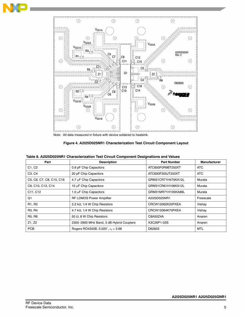
Figure 4. A2I25D025NR1 Characterization Test Circuit Component Layout
VDD2A
A2I25D025NRev. 2
D62833
Q1
VDD2B
VDD1B
VGG2B
VGG1B
VGG1A
VGG2A
VDD1A
R1
R3
R5Z1 Z2
R2
R4
C1
C2
C5C7 C9
C11
C6C8
C12C10
C13C15
C14C16
C3
C4 R6
Note: All data measured in fixture with device soldered to heatsink.
Table 8. A2I25D025NR1 Characterization Test Circuit Component Designations and ValuesPart Description Part Number Manufacturer
C1, C2 0.9 pF Chip Capacitors ATC600F0R9BT250XT ATC
C3, C4 20 pF Chip Capacitors ATC600F200JT250XT ATC
C5, C6, C7, C8, C15, C16 4.7 F Chip Capacitors GRM31CR71H475KA12L Murata
C9, C10, C13, C14 10 F Chip Capacitors GRM31CR61H106KA12L Murata
C11, C12 1.0 F Chip Capacitors GRM31MR71H105KA88L Murata
Q1 RF LDMOS Power Amplifier A2I25D025NR1 Freescale
R1, R2 2.2 k, 1/4 W Chip Resistors CRCW12062K20FKEA Vishay
R3, R4 4.7 k, 1/4 W Chip Resistors CRCW12064K70FKEA Vishay
R5, R6 50 , 8 W Chip Resistors C8A50Z4A Anaren
Z1, Z2 2300–2900 MHz Band, 3 dB Hybrid Couplers X3C26P1-03S Anaren
PCB Rogers RO4350B, 0.020, r = 3.66 D62833 MTL

6RF Device Data
Freescale Semiconductor, Inc.
A2I25D025NR1 A2I25D025GNR1
TYPICAL CHARACTERISTICS
PARC(dB)
--0.8
--0.4
--0.5
--0.6
--0.7
--0.92300
f, FREQUENCY (MHz)
Figure 5. Single--Carrier Output Peak--to--Average Ratio Compression(PARC) Broadband Performance @ Pout = 3.2 Watts Avg.
31
33
32.8
32.6
--48
20.5
20
19.5
19
--45.5
--46
--46.5
--47
PAE,POWER
ADDED
EFFICIENCY(%)
Gps,POWER
GAIN(dB) 32.4
32.2
32
31.8
31.6
31.4
31.2
2350 2400 2450 2500 2550 2600 2650 2700
18.5
--47.5
ACPR
(dBc)
Figure 6. Intermodulation Distortion Productsversus Two--Tone Spacing
TWO--TONE SPACING (MHz)
10--70
--10
--20
--30
--50
1 300
IMD,INTERMODULATIONDISTORTION(dBc)
--40
Figure 7. Output Peak--to--Average RatioCompression (PARC) versus Output Power
Pout, OUTPUT POWER (WATTS)
--1
--3
4
0
--2
--4
OUTPUTCOMPRESSIONAT
0.01%
PROBABILITY
ONCCDF(dB)
2 6 8 1210
40
35
30
25
20
15
PAE,POWER
ADDED
EFFICIENCY(%)
10
ACPR
PARC
ACPR
(dBc)
--50
--20
--25
--30
--40
--35
--45
32.2
Gps,POWER
GAIN(dB)
32
31.8
31.6
31.4
31.2
31
Gps
--5
1
ACPR
PARC
Gps
IM7--LIM7--U
IM3--L
100
--1 dB = 3.6 W --2 dB = 5.4 W
--3 dB = 7.2 W
IM3--U
VDD = 28 Vdc, IDQ1(A+B) = 56 mA, IDQ2(A+B) = 136 mAf = 2590 MHz, Single--Carrier W--CDMA
3.84 MHz Channel Bandwidth, Input SignalPAR = 9.9 dB @ 0.01% Probability on CCDF
VDD = 28 Vdc, Pout = 3.2 W (Avg.), IDQ1(A+B) = 56 mAIDQ2(A+B) = 136 mA, Single--Carrier W--CDMA3.84 MHz Channel Bandwidth PAE
PAE
VDD = 28 Vdc, Pout = 13.5 W (PEP), IDQ1(A+B) = 56 mAIDQ2(A+B) = 136 mA, Two--Tone Measurements(f1 + f2)/2 = Center Frequency of 2590 MHz
IM5--UIM5--L
--60
Input Signal PAR = 9.9 dB @ 0.01%Probability on CCDF

A2I25D025NR1 A2I25D025GNR1
7RF Device DataFreescale Semiconductor, Inc.
TYPICAL CHARACTERISTICS
1
Pout, OUTPUT POWER (WATTS) AVG.
Figure 8. Single--Carrier W--CDMA Power Gain, Power AddedEfficiency and ACPR versus Output Power — 2496–2690 MHz
--10
--20
24
36
0
60
50
40
30
20
Gps,POWER
GAIN(dB)
34
32
10 50
10
--60
ACPR
(dBc)
30
28
26
0
--30
--40
--50
ACPR2590 MHz
VDD = 28 Vdc, IDQ1(A+B) = 56 mA, IDQ2(A+B) = 136 mASingle--Carrier W--CDMA, 3.84 MHz Channel BandwidthInput Signal PAR = 9.9 dB @ 0.01% Probability on CCDF
Gps
2690 MHz
2690 MHz2590 MHz
2496 MHz
2496 MHz
2590 MHz2690 MHz
PAE
PAE,POWER
ADDED
EFFICIENCY(%)
2496 MHz
1
Pout, OUTPUT POWER (WATTS) AVG.
Figure 9. Single--Carrier W--CDMA Power Gain, Power AddedEfficiency and ACPR versus Output Power — 2300–2400 MHz
--10
--20
24
36
0
60
50
40
30
20
Gps,POWER
GAIN(dB)
34
32
10 50
10
--60
ACPR
(dBc)
30
28
26
0
--30
--40
--50
ACPR
Gps
PAE
PAE,POWER
ADDED
EFFICIENCY(%)
2400 MHz2350 MHz 2300 MHz
VDD = 28 Vdc, IDQ1(A+B) = 56 mA, IDQ2(A+B) = 136 mASingle--Carrier W--CDMA, 3.84 MHz ChannelBandwidth, Input Signal PAR = 9.9 dB @ 0.01%Probability on CCDF
2300 MHz
2400 MHz
2350 MHz
2300 MHz
2350 MHz 2400 MHz
Figure 10. Broadband Frequency Response
24
36
f, FREQUENCY (MHz)
VDD = 28 VdcPin = 0 dBmIDQ1(A+B) = 56 mAIDQ2(A+B) = 136 mA
32
30
28
GAIN(dB)
34
26
1500 1750 2000 2250 2500 2750 3500
Gain
3000 3250
Note: Frequency response at band edges limited by hybrid couplers.
8RF Device Data
Freescale Semiconductor, Inc.
A2I25D025NR1 A2I25D025GNR1
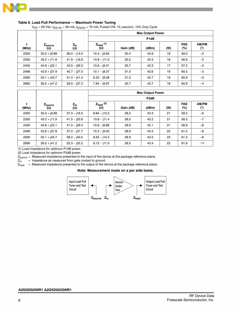
Table 9. Load Pull Performance — Maximum Power TuningVDD = 28 Vdc, IDQ1(A) = 29 mA, IDQ2(A) = 75 mA, Pulsed CW, 10 sec(on), 10% Duty Cycle
f(MHz)
Zsource()
Zin()
Max Output Power
P1dB
Zload (1)
() Gain (dB) (dBm) (W)PAE(%)
AM/PM()
2300 35.0 + j9.89 36.0 – j13.0 10.4 – j9.63 30.4 42.6 18 59.0 –2
2350 43.2 + j11.9 41.9 – j16.8 10.8 – j11.0 30.5 42.5 18 56.9 –2
2400 45.8 + j23.1 43.5 – j26.0 10.6 – j8.31 30.7 42.3 17 57.2 –3
2496 43.9 + j37.9 40.7 – j37.0 10.1 – j8.37 31.0 42.6 18 60.5 –3
2590 33.1 + j43.7 31.4 – j41.4 9.32 – j9.38 31.0 42.7 19 60.9 –3
2690 29.5 + j41.2 28.0 – j37.3 7.84 – j9.97 30.7 42.7 18 60.8 –4
f(MHz)
Zsource()
Zin()
Max Output Power
P3dB
Zload (2)
() Gain (dB) (dBm) (W)PAE(%)
AM/PM()
2300 35.0 + j9.89 37.3 – j16.5 9.84 – j10.3 28.2 43.3 21 59.2 –6
2350 43.2 + j11.9 41.5 – j20.9 10.6 – j11.4 28.5 43.2 21 58.3 –7
2400 45.8 + j23.1 41.0 – j29.4 10.6 – j8.89 28.6 43.1 21 58.9 –8
2496 43.9 + j37.9 37.0 – j37.7 10.3 – j9.50 28.8 43.4 22 61.4 –8
2590 33.1 + j43.7 28.2 – j40.5 9.50 – j10.2 28.9 43.5 23 61.3 –8
2690 29.5 + j41.2 25.3 – j35.2 8.12 – j11.0 28.5 43.4 22 61.6 –11
(1) Load impedance for optimum P1dB power.(2) Load impedance for optimum P3dB power.Zsource = Measured impedance presented to the input of the device at the package reference plane.Zin = Impedance as measured from gate contact to ground.Zload = Measured impedance presented to the output of the device at the package reference plane.
Note: Measurement made on a per side basis.
Input Load PullTuner and TestCircuit
DeviceUnderTest
Zsource Zin Zload
Output Load PullTuner and TestCircuit

A2I25D025NR1 A2I25D025GNR1
9RF Device DataFreescale Semiconductor, Inc.
Table 10. Load Pull Performance — Maximum Power Added Efficiency TuningVDD = 28 Vdc, IDQ1(A) = 29 mA, IDQ2(A) = 75 mA, Pulsed CW, 10 sec(on), 10% Duty Cycle
f(MHz)
Zsource()
Zin()
Max Power Added Efficiency
P1dB
Zload (1)
() Gain (dB) (dBm) (W)PAE(%)
AM/PM()
2300 35.0 + j9.89 38.0 – j10.9 18.2 – j1.09 31.8 40.8 12 67.0 –6
2350 43.2 + j11.9 45.1 – j14.7 16.1 – j0.71 31.9 40.9 12 64.2 –6
2400 45.8 + j23.1 46.9 – j26.5 14.9 – j0.56 31.9 41.1 13 65.4 –5
2496 43.9 + j37.9 42.8 – j38.7 12.1 – j2.47 31.9 41.6 14 67.5 –6
2590 33.1 + j43.7 32.9 – j44.4 9.72 – j2.39 32.1 41.3 14 68.8 –7
2690 29.5 + j41.2 28.3 – j41.3 7.82 – j4.78 31.8 41.4 14 67.9 –9
f(MHz)
Zsource()
Zin()
Max Power Added Efficiency
P3dB
Zload (2)
() Gain (dB) (dBm) (W)PAE(%)
AM/PM()
2300 35.0 + j9.89 38.7 – j13.1 17.2 – j2.23 29.7 41.7 15 66.7 –11
2350 43.2 + j11.9 44.6 – j17.7 15.8 – j2.22 29.8 41.9 15 64.7 –9
2400 45.8 + j23.1 45.2 – j28.8 14.2 – j0.88 29.9 41.9 15 65.7 –10
2496 43.9 + j37.9 40.4 – j39.4 11.9 – j2.47 29.9 42.3 17 67.9 –11
2590 33.1 + j43.7 30.3 – j43.9 9.68 – j2.97 30.0 42.1 16 68.5 –12
2690 29.5 + j41.2 25.7 – j39.0 7.97 – j5.65 29.7 42.4 17 67.4 –15
(1) Load impedance for optimum P1dB efficiency.(2) Load impedance for optimum P3dB efficiency.Zsource = Measured impedance presented to the input of the device at the package reference plane.Zin = Impedance as measured from gate contact to ground.Zload = Measured impedance presented to the output of the device at the package reference plane.
Note: Measurement made on a per side basis.
Input Load PullTuner and TestCircuit
DeviceUnderTest
Zsource Zin Zload
Output Load PullTuner and TestCircuit
10RF Device Data
Freescale Semiconductor, Inc.
A2I25D025NR1 A2I25D025GNR1
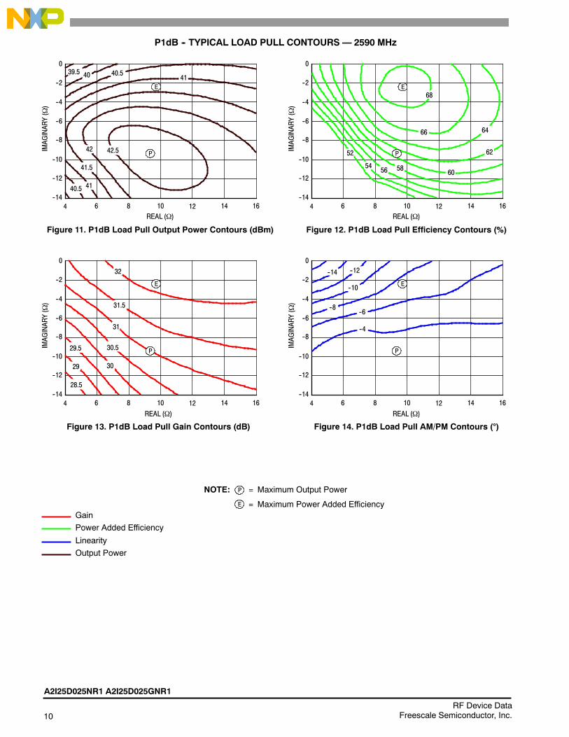
P1dB -- TYPICAL LOAD PULL CONTOURS — 2590 MHz
Figure 11. P1dB Load Pull Output Power Contours (dBm)
REAL ()
--14
0
--4
IMAGINARY()
8 10 124 16
--2
--8
--10
6 14
--6
NOTE: = Maximum Output Power
= Maximum Power Added Efficiency
P
E
Gain
Power Added Efficiency
Linearity
Output Power
Figure 12. P1dB Load Pull Efficiency Contours (%)
REAL ()
Figure 13. P1dB Load Pull Gain Contours (dB)
REAL ()
Figure 14. P1dB Load Pull AM/PM Contours ()
REAL ()
--12
--14
0
--4
IMAGINARY()
8 10 124 16
--2
--8
--10
6 14
--6
--12
--14
0
--4
IMAGINARY()
8 10 124 16
--2
--8
--10
6 14
--6
--12
--14
0
--4IMAGINARY()
8 10 124 16
--2
--8
--10
6 14
--6
--12
40.5 41
P
E
41.5
42 42.5
4140.54039.5
P
E
52
5654 58
60
62
6466
68
29
29.5 P
E
30
30.5
31
31.5
32
28.5
--10
--12--14
--4
--6--8
P
E

A2I25D025NR1 A2I25D025GNR1
11RF Device DataFreescale Semiconductor, Inc.
P3dB -- TYPICAL LOAD PULL CONTOURS — 2590 MHz
Figure 15. P3dB Load Pull Output Power Contours (dBm)
REAL ()
--14
0
--4
IMAGINARY()
8 10 124 16
--2
--8
--10
6 14
--6
NOTE: = Maximum Output Power
= Maximum Power Added Efficiency
P
E
Gain
Power Added Efficiency
Linearity
Output Power
Figure 16. P3dB Load Pull Efficiency Contours (%)
REAL ()
Figure 17. P3dB Load Pull Gain Contours (dB)
REAL ()
Figure 18. P3dB Load Pull AM/PM Contours ()
REAL ()
--12
--14
0
--4
IMAGINARY()
8 10 124 16
--2
--8
--10
6 14
--6
--12
--14
0
--4
IMAGINARY()
8 10 124 16
--2
--8
--10
6 14
--6
--12
--14
0
--4IMAGINARY()
8 10 124 16
--2
--8
--10
6 14
--6
--12
P
E
40.540 41 41.5
42
42.5
43
43.5P
E
52
54
56
58
60
62
64
66
68
27.5
27P
E
26.5
28
28.5
29
29.5
30
P
E
--6
--10
--8
--12--14
--16
--18
--20
--22

12RF Device Data
Freescale Semiconductor, Inc.
A2I25D025NR1 A2I25D025GNR1
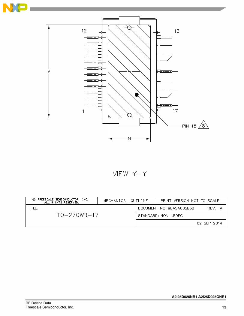
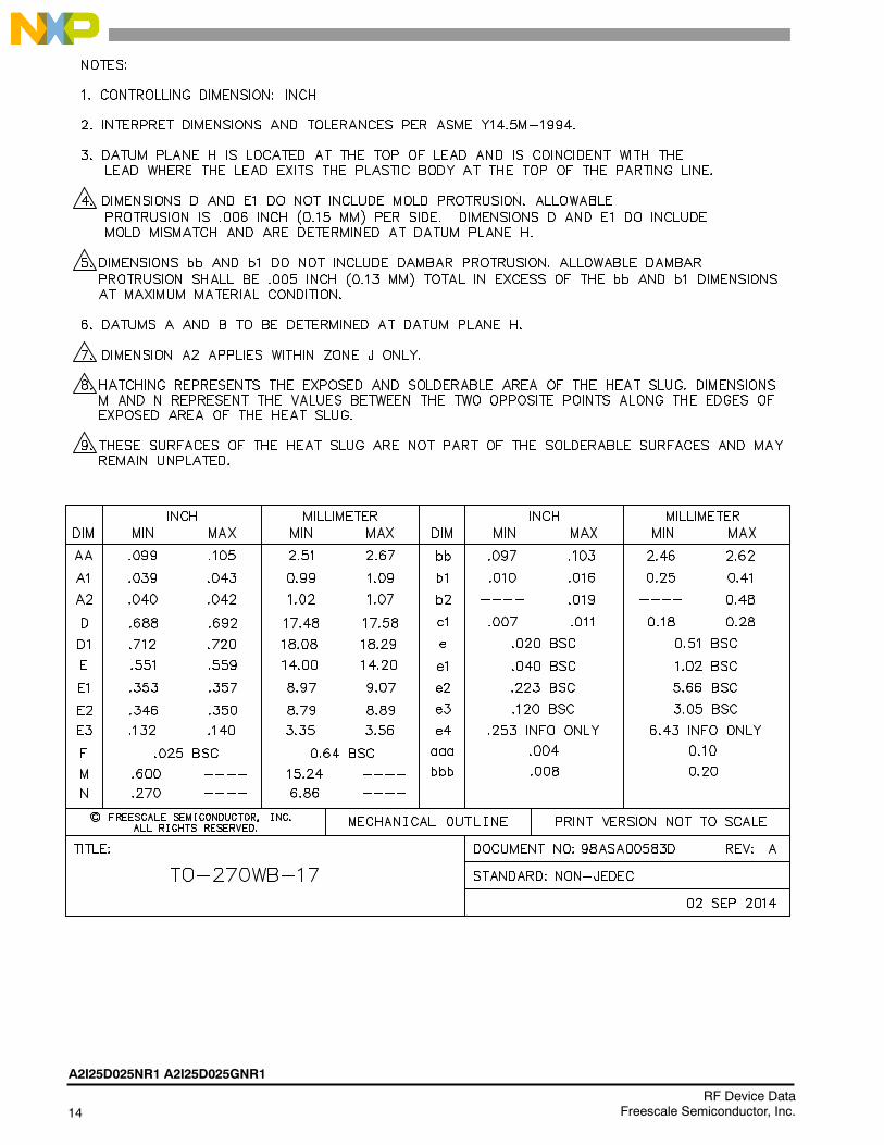
PACKAGE DIMENSIONS
A2I25D025NR1 A2I25D025GNR1
13RF Device DataFreescale Semiconductor, Inc.
14RF Device Data
Freescale Semiconductor, Inc.
A2I25D025NR1 A2I25D025GNR1

A2I25D025NR1 A2I25D025GNR1
15RF Device DataFreescale Semiconductor, Inc.

16RF Device Data
Freescale Semiconductor, Inc.
A2I25D025NR1 A2I25D025GNR1

A2I25D025NR1 A2I25D025GNR1
17RF Device DataFreescale Semiconductor, Inc.

18RF Device Data
Freescale Semiconductor, Inc.
A2I25D025NR1 A2I25D025GNR1
PRODUCT DOCUMENTATION, SOFTWARE AND TOOLS
Refer to the following resources to aid your design process.
Application Notes AN1955: Thermal Measurement Methodology of RF Power Amplifiers AN1977: Quiescent Current Thermal Tracking Circuit in the RF Integrated Circuit Family AN1987: Quiescent Current Control for the RF Integrated Circuit Device Family
Engineering Bulletins EB212: Using Data Sheet Impedances for RF LDMOS Devices
Software Electromigration MTTF Calculator
RF High Power Model
.s2p File
Development Tools Printed Circuit Boards
For Software and Tools, do a Part Number search at http://www.freescale.com, and select the “Part Number” link. Go toSoftware & Tools on the part’s Product Summary page to download the respective tool.
REVISION HISTORY
The following table summarizes revisions to this document.
Revision Date Description
0 Mar. 2015 Initial release of data sheet

A2I25D025NR1 A2I25D025GNR1
19RF Device DataFreescale Semiconductor, Inc.
Information in this document is provided solely to enable system and softwareimplementers to use Freescale products. There are no express or implied copyrightlicenses granted hereunder to design or fabricate any integrated circuits based on theinformation in this document.
Freescale reserves the right to make changes without further notice to any productsherein. Freescale makes no warranty, representation, or guarantee regarding thesuitability of its products for any particular purpose, nor does Freescale assume anyliability arising out of the application or use of any product or circuit, and specificallydisclaims any and all liability, including without limitation consequential or incidentaldamages. “Typical” parameters that may be provided in Freescale data sheets and/orspecifications can and do vary in different applications, and actual performance mayvary over time. All operating parameters, including “typicals,” must be validated foreach customer application by customer’s technical experts. Freescale does not conveyany license under its patent rights nor the rights of others. Freescale sells productspursuant to standard terms and conditions of sale, which can be found at the followingaddress: freescale.com/SalesTermsandConditions.
Freescale and the Freescale logo are trademarks of Freescale Semiconductor, Inc.,Reg. U.S. Pat. & Tm. Off. Airfast is a trademark of Freescale Semiconductor, Inc. Allother product or service names are the property of their respective owners.E 2015 Freescale Semiconductor, Inc.
How to Reach Us:
Home Page:freescale.com
Web Support:freescale.com/support
Document Number: A2I25D025NRev. 0, 3/2015