MRF6522-70.pdf - NXP
10
ARCHIVE INFORMATION ARCHIVE INFORMATION RF Power Field Effect Transistor N--Channel Enhancement--Mode Lateral MOSFET Designed for GSM 900 frequency band, the high gain and broadband performance of this device make it ideal for large--signal, common source amplifier applications in 26 volt base station equipment. • Specified Performance @ 940 MHz, 26 Volts Output Power, P1dB 80 Watts (Typ) Power Gain @ P1dB 16 dB (Typ) Efficiency @ P1dB 58% (Typ) • Capable of Handling 5:1 VSWR, @ 26 Vdc, 945 MHz, 50 Watts CW Output Power • RoHS Compliant • In Tape and Reel. R3 Suffix = 250 Units per 32 mm, 13 inch Reel. Table 1. Maximum Ratings Rating Symbol Value Unit Drain--Source Voltage V DSS --0.5, +65 Vdc Gate--Source Voltage V GS ± 20 Vdc Drain Current Continuous I D 7 Adc Total Device Dissipation @ T C = 25°C Derate above 25°C P D 159 0.9 W W/°C Storage Temperature Range T stg --65 to +150 °C Case Operating Temperature T C 150 °C Operating Junction Temperature T J 200 °C Table 2. Thermal Characteristics Characteristic Symbol Value Unit Thermal Resistance, Junction to Case R θJC 1.1 °C/W NOTE -- CAUTION -- MOS devices are susceptible to damage from electrostatic charge. Reasonable precautions in handling and packaging MOS devices should be observed. Document Number: MRF6522--70 Rev. 9, 10/2008 Freescale Semiconductor Technical Data MRF6522--70R3 920--960 MHz, 70 W, 26 V LATERAL N--CHANNEL RF POWER MOSFET CASE 465D--05, STYLE 1 NI--600 © Freescale Semiconductor, Inc., 2008, 2010. All rights reserved.
-
Upload
khangminh22 -
Category
Documents
-
view
4 -
download
0
Transcript of MRF6522-70.pdf - NXP

ARCHIVEINFORMATION
ARCHIVEINFORMATION
MRF6522--70R3
1RF Device DataFreescale Semiconductor
RF Power Field Effect TransistorN--Channel Enhancement--Mode Lateral MOSFETDesigned for GSM 900 frequency band, the high gain and broadband
performance of this device make it ideal for large--signal, common sourceamplifier applications in 26 volt base station equipment.
• Specified Performance @ 940 MHz, 26 VoltsOutput Power, P1dB 80 Watts (Typ)Power Gain @ P1dB 16 dB (Typ)Efficiency @ P1dB 58% (Typ)
• Capable of Handling 5:1 VSWR, @ 26 Vdc, 945 MHz, 50 Watts CW OutputPower
• RoHS Compliant• In Tape and Reel. R3 Suffix = 250 Units per 32 mm, 13 inch Reel.
Table 1. Maximum Ratings
Rating Symbol Value Unit
Drain--Source Voltage VDSS --0.5, +65 Vdc
Gate--Source Voltage VGS ±20 Vdc
Drain Current Continuous ID 7 Adc
Total Device Dissipation @ TC = 25°CDerate above 25°C
PD 1590.9
WW/°C
Storage Temperature Range Tstg -- 65 to +150 °C
Case Operating Temperature TC 150 °C
Operating Junction Temperature TJ 200 °C
Table 2. Thermal Characteristics
Characteristic Symbol Value Unit
Thermal Resistance, Junction to Case RθJC 1.1 °C/W
NOTE -- CAUTION -- MOS devices are susceptible to damage from electrostatic charge. Reasonable precautions in handling andpackaging MOS devices should be observed.
Document Number: MRF6522--70Rev. 9, 10/2008
Freescale SemiconductorTechnical Data
MRF6522--70R3
920--960 MHz, 70 W, 26 VLATERAL N--CHANNELRF POWER MOSFET
CASE 465D--05, STYLE 1NI--600
© Freescale Semiconductor, Inc., 2008, 2010. All rights reserved.

ARCHIVEINFORMATION
ARCHIVEINFORMATION
2RF Device Data
Freescale Semiconductor
MRF6522--70R3
Table 3. Electrical Characteristics (TC = 25°C unless otherwise noted)
Characteristic Symbol Min Typ Max Unit
Off Characteristics
Drain--Source Breakdown Voltage(VGS = 0 Vdc, ID = 20 μAdc)
V(BR)DSS 65 Vdc
Zero Gate Voltage Drain Current(VDS = 28 Vdc, VGS = 0 Vdc)
IDSS 10 μAdc
Gate--Source Leakage Current(VGS = 20 Vdc, VDS = 0 Vdc)
IGSS 1 μAdc
On Characteristics
Gate Threshold Voltage(VDS = 10 Vdc, ID = 300 μAdc)
VGS(th) 2 3 4 Vdc
Gate Quiescent Voltage(VDS = 26 Vdc, ID = 400 mAdc)
VGS(Q) 3 4 5 Vdc
Drain--Source On--Voltage(VGS = 10 Vdc, ID = 1 Adc)
VDS(on) 0.15 0.6 Vdc
Forward Transconductance(VDS = 10 Vdc, ID = 2 Adc)
gfs 2 3 S
Dynamic Characteristics
Input Capacitance (1)
(VDS = 26 Vdc, VGS = 0, f = 1 MHz)Ciss 130 pF
Output Capacitance(VDS = 26 Vdc, VGS = 0, f = 1 MHz)
Coss 41 47 52 pF
Reverse Transfer Capacitance(VDS = 26 Vdc, VGS = 0, f = 1 MHz)
Crss 2.4 3 3.4 pF
Functional Tests (In Freescale Test Fixture)
Output Power(VDD = 26 Vdc, IDQ = 400 mA, f = 940 MHz)
P1dB 73 80 W
Common--Source Amplifier Power Gain @ P1dB (Min)(VDD = 26 Vdc, IDQ = 400 mA, f = 940 MHz)
Gps 14 16 18 dB
Drain Efficiency @ Pout = 50 W(VDD = 26 Vdc, IDQ = 400 mA, f = 940 MHz)
η1 47 51 %
Drain Efficiency @ P1dB(VDD = 26 Vdc, IDQ = 400 mA, f = 940 MHz)
η2 58 %
Input Return Loss @ Pout = 50 W(VDD = 26 Vdc, IDQ = 400 mA, f = 940 MHz)
IRL -- 15 dB
1. Value excludes the input matching.
ARCHIVEINFORMATION
ARCHIVEINFORMATION
MRF6522--70R3
3RF Device DataFreescale Semiconductor
Figure 1. MRF6522--70 Test Circuit Schematic
R6R2
R1
C6
C5
C13
C11C9C8
C14
C2
Q1
C10
VSUPPLY
RF Output
C12C3
C4C7
RF Input
R3
R4
T2
C1VBIAS
Vreg
T1Gnd
VinVout
C1 1.0 μF Chip Capacitor (0805)C2 10 μF, 35 Vdc Tantalum CapacitorC3 100 nF Chip CapacitorC4, C6, C14 22 pF Chip Capacitors, ACCU--P (0805)C5 2.7 pF Chip Capacitor, ACCU--P (0805)C7, C8, C13 4.7 pF Chip Capacitors, ACCU--P (0805)C9, C10 8.2 pF Chip Capacitors, ACCU--P (0805)C11, C12 2.2 pF Chip Capacitors, ACCU--P (0805)R1 10 Ω Chip Resistor (0805)R2 1.0 kΩ Chip Resistor (0805)
R3 1.2 kΩ Chip Resistor (0805)R4 2.2 kΩ Chip Resistor (0805)R5 220 Ω Chip Resistor (0805)R6 5.0 kΩ SMD Potentiometer
T1 LP2951 Micro--8T2 BC847 SOT--23
SUBSTRATE GI180 0.8 mm
R5
+
Figure 2. MRF6522--70 Test Circuit Component Layout
R6
C1
R2
R1
C3
C4
C7
R5
C6
C5 C8C9
C10
C11
C12
C13
C2
T2
STRAP
VGroundV
R4C14
R3
T1
MRF6522
--70
Q1
SUPPLYBIAS
Freescale has begun the transition of marking Printed Circuit Boards (PCBs) with the Freescale Semiconductor signature/-logo. PCBs may have either Motorola or Freescale markings during the transition period. These changes will have no impacton form, fit or function of the current product.

ARCHIVEINFORMATION
ARCHIVEINFORMATION
4RF Device Data
Freescale Semiconductor
MRF6522--70R3
TYPICAL CHARACTERISTICS
Pout, OUTPUT POWER (WATTS)Pout, OUTPUT POWER (WATTS)
17.5
15.0
Figure 3. Power Gain versus Output Power
10
15.5
16.0
Figure 4. Power Gain versus Output Power
10010
18.0
17.6
16.2
16.6
17.4
16.0
16.5
17.0
100
Gps,POWER
GAIN(dB)
VDS = 26 Vdcf = 921 MHz
Figure 5. Output Power versus Supply Voltage Figure 6. Output Power versus Supply Voltage
Figure 7. Efficiency and Output Powerversus Input Power
200 mA 300 mA400 mA
500 mA
IDQ = 600 mA
16.4
16.8
17.2
17.0
17.8
VDS = 26 Vdcf = 960 MHz
200 mA
300 mA
400 mA
500 mA
IDQ = 600 mA
Gps,POWER
GAIN(dB)
VDD, SUPPLY VOLTAGE (VOLTS)
115
4518
55
75
85
105
28
P out,OUTPUTPOWER
(WATTS)
20 22 24 26
65
95
IDQ = 400 mAf = 921 MHz
Pin = 5.0 W
3.0 W
4.0 W
2.0 W
VDD, SUPPLY VOLTAGE (VOLTS)
105
18
55
75
85
95
28
P out,OUTPUTPOWER
(WATTS)
20 22 24 26
45
65
IDQ = 400 mAf = 960 MHz
Pin = 5.0 W
3.0 W4.0 W
2.0 W
35
η
Pin, INPUT POWER (WATTS)
80
0
20
40
50
70
2.0
η,EFFICIENCY(%)
0.5 1.0 1.5
10
30
60
VDS = 26 VdcIDQ = 400 mAf = 921 MHz
0
80
70
60
50
40
30
20
10
0
P out,OUTPUTPOWER
(WATTS)
Pout
19 21 23 25 27 2719 21 23 25

ARCHIVEINFORMATION
ARCHIVEINFORMATION
MRF6522--70R3
5RF Device DataFreescale Semiconductor
TYPICAL CHARACTERISTICS
η
Pin, INPUT POWER (WATTS)
Figure 8. Efficiency and Output Powerversus Input Power
0
Figure 9. Power Gain and Efficiencyversus Input Power
70
10
30
Figure 10. Power Gain and Efficiencyversus Input Power
20
40
50
60
20
19
η,EFFICIENCY(%)
Gps,POWER
GAIN(dB) 18
17
16
15
14
13
VDS = 26 Vdcf = 921 MHz
η
Gps
Pin, INPUT POWER (WATTS)
80
0
20
40
50
70
2.0
η,EFFICIENCY(%)
0.5 1.0 1.5
10
30
60
VDS = 26 VdcIDQ = 400 mAf = 960 MHz
0
80
70
60
50
40
30
20
10
0P out,OUTPUTPOWER
(WATTS) Pout
3.962.261.260.700.380.210.120.060.030.02
Pin, INPUT POWER (WATTS)
0
70
10
30
20
40
50
60
20
19
η,EFFICIENCY(%)
Gps,POWER
GAIN(dB) 18
17
16
15
14
13
VDS = 26 Vdcf = 960 MHz
η
Gps
3.702.141.150.620.340.180.100.050.030.02

ARCHIVEINFORMATION
ARCHIVEINFORMATION
6RF Device Data
Freescale Semiconductor
MRF6522--70R3
TYPICAL CHARACTERISTICS
Figure 11. Performance in Broadband Circuit (at Small Signal)
f, FREQUENCY (MHz)
--10
--25910
--20
--15
970
VDS = 26 VdcIDQ = 400 mA
920 950 960
IRL,INPUTRETURNLOSS
(dB)
17
16
15
Gps,GAIN(dB)
18
930 940
IRL
Gps
ARCHIVEINFORMATION
ARCHIVEINFORMATION
MRF6522--70R3
7RF Device DataFreescale Semiconductor
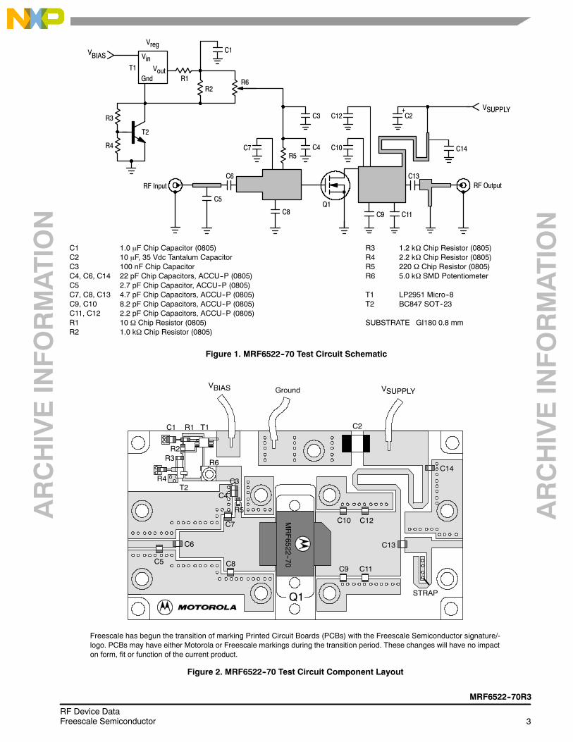
Figure 12. Series Equivalent Source and Load Impedance
fMHz
ZsourceΩ
ZloadΩ
925
940
960
2.65 -- j2.53
2.85 -- j1.87
2.67 -- j2.14
1.62 + j0.2
1.56 + j0.34
1.55 + j0.2
VSUPPLY = 26 Vdc, IBIAS = 400 mA, CW = Room Temperature
Zo = 5Ω
f = 925 MHz
f = 925 MHz960 MHz
Zsource = Test circuit impedance as measured fromgate to ground.
Zload = Test circuit impedance as measuredfrom drain to ground.
Zsource Z load
InputMatchingNetwork
DeviceUnder Test
OutputMatchingNetwork
Zsource
Zload
960 MHz
ARCHIVEINFORMATION
ARCHIVEINFORMATION
8RF Device Data
Freescale Semiconductor
MRF6522--70R3
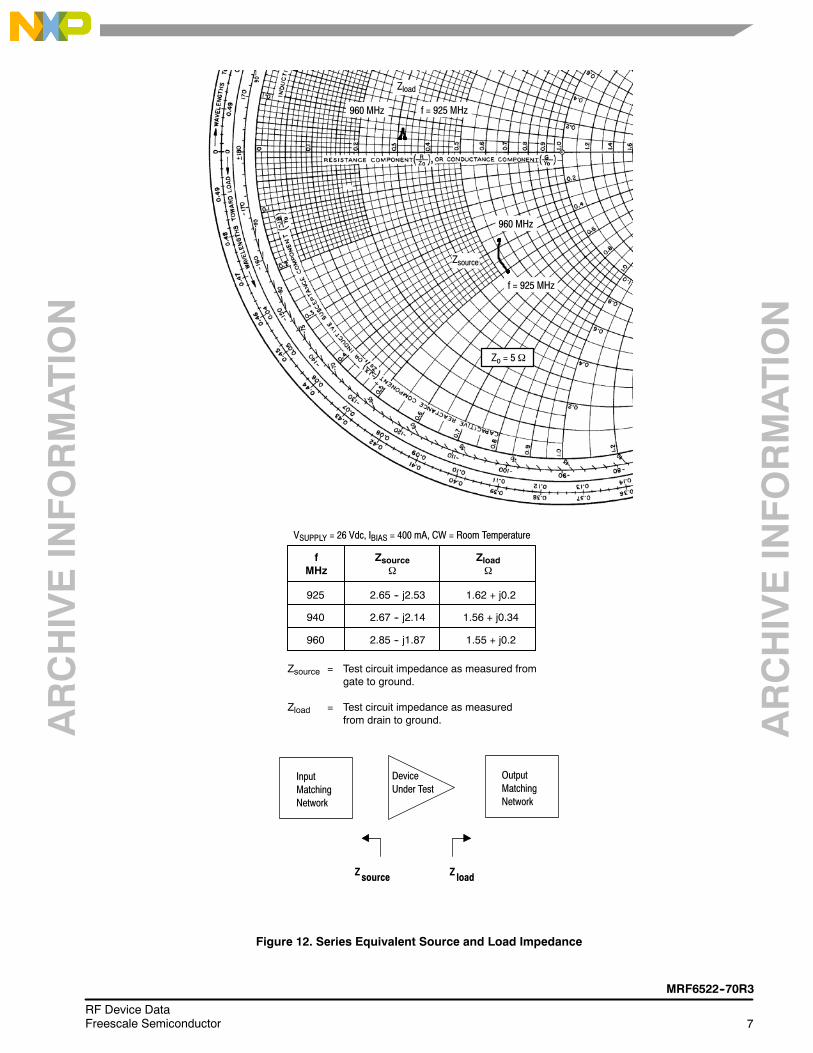
PACKAGE DIMENSIONS
CASE 465D--05ISSUE DNI--600
D
G
1
2
3
K
A
C
HE SEATING
PLANE
F
NOTES:1. INTERPRET DIMENSIONS AND TOLERANCES
PER ANSI Y14.5M--1994.2. CONTROLLING DIMENSION: INCH.3. DIMENSION H IS MEASURED 0.030 (0.762) AWAY
FROM PACKAGE BODY.
DIM MIN MAX MIN MAXMILLIMETERSINCHES
A 1.065 1.075 27.05 27.30B 0.380 0.390 9.65 9.91C 0.160 0.205 4.06 5.21D 0.425 0.435 10.80 11.05E 0.060 0.070 1.52 1.78F 0.004 0.006 0.10 0.15G 0.870 BSC 22.10 BSCH 0.096 0.106 2.44 2.69K 0.190 0.223 4.83 5.66M 0.594 0.606 15.09 15.39
Q 0.124 0.130 3.15 3.30R 0.394 0.404 10.01 10.26
STYLE 1:PIN 1. DRAIN
2. GATE3. SOURCE
Q2X
MAMbbb B MT
MAMbbb B MT
B
B(FLANGE)
MAMccc B MT
MAMbbb B MT
A
T
N (LID)
M (INSULATOR)
S
MAMaaa B MT
(INSULATOR)
R
MAMccc B MT
(LID)
S 0.395 0.405 10.03 10.29
N 0.591 0.601 15.01 15.27
aaa 0.005 REF 0.13 REFbbb 0.010 REF 0.25 REFccc 0.015 REF 0.38 REF

ARCHIVEINFORMATION
ARCHIVEINFORMATION
MRF6522--70R3
9RF Device DataFreescale Semiconductor
PRODUCT DOCUMENTATION
Refer to the following documents to aid your design process.
Engineering Bulletins• EB212: Using Data Sheet Impedances for RF LDMOS Devices
REVISION HISTORY
The following table summarizes revisions to this document.
Revision Date Description
9 Oct. 2008 • Modified data sheet to reflect RF Test Reduction described in Product and Process Change Notificationnumber, PCN12779, p. 1, 2
• Added Product Documentation and Revision History, p. 9
Dec. 2010 • Data sheet archived. Part no longer manufactured.
ARCHIVEINFORMATION
ARCHIVEINFORMATION
10RF Device Data
Freescale Semiconductor
MRF6522--70R3
Information in this document is provided solely to enable system and softwareimplementers to use Freescale Semiconductor products. There are no express orimplied copyright licenses granted hereunder to design or fabricate any integratedcircuits or integrated circuits based on the information in this document.
Freescale Semiconductor reserves the right to make changes without further notice toany products herein. Freescale Semiconductor makes no warranty, representation orguarantee regarding the suitability of its products for any particular purpose, nor doesFreescale Semiconductor assume any liability arising out of the application or use ofany product or circuit, and specifically disclaims any and all liability, including withoutlimitation consequential or incidental damages. Typical parameters that may beprovided in Freescale Semiconductor data sheets and/or specifications can and dovary in different applications and actual performance may vary over time. All operatingparameters, including Typicals, must be validated for each customer application bycustomers technical experts. Freescale Semiconductor does not convey any licenseunder its patent rights nor the rights of others. Freescale Semiconductor products arenot designed, intended, or authorized for use as components in systems intended forsurgical implant into the body, or other applications intended to support or sustain life,or for any other application in which the failure of the Freescale Semiconductor productcould create a situation where personal injury or death may occur. Should Buyerpurchase or use Freescale Semiconductor products for any such unintended orunauthorized application, Buyer shall indemnify and hold Freescale Semiconductorand its officers, employees, subsidiaries, affiliates, and distributors harmless against allclaims, costs, damages, and expenses, and reasonable attorney fees arising out of,directly or indirectly, any claim of personal injury or death associated with suchunintended or unauthorized use, even if such claim alleges that FreescaleSemiconductor was negligent regarding the design or manufacture of the part.
Freescalet and the Freescale logo are trademarks of Freescale Semiconductor, Inc.All other product or service names are the property of their respective owners.© Freescale Semiconductor, Inc. 2008, 2010. All rights reserved.
How to Reach Us:
Home Page:www.freescale.com
Web Support:http://www.freescale.com/support
USA/Europe or Locations Not Listed:Freescale Semiconductor, Inc.Technical Information Center, EL5162100 East Elliot RoadTempe, Arizona 852841--800--521--6274 or +1--480--768--2130www.freescale.com/support
Europe, Middle East, and Africa:Freescale Halbleiter Deutschland GmbHTechnical Information CenterSchatzbogen 781829 Muenchen, Germany+44 1296 380 456 (English)+46 8 52200080 (English)+49 89 92103 559 (German)+33 1 69 35 48 48 (French)www.freescale.com/support
Japan:Freescale Semiconductor Japan Ltd.HeadquartersARCO Tower 15F1--8--1, Shimo--Meguro, Meguro--ku,Tokyo 153--0064Japan0120 191014 or +81 3 5437 [email protected]
Asia/Pacific:Freescale Semiconductor China Ltd.Exchange Building 23FNo. 118 Jianguo RoadChaoyang DistrictBeijing 100022China+86 10 5879 [email protected]
For Literature Requests Only:Freescale Semiconductor Literature Distribution CenterP.O. Box 5405Denver, Colorado 802171--800--441--2447 or +1--303--675--2140Fax: [email protected]
Document Number: MRF6522--70Rev. 9, 10/2008