
Low Power Wireless Sensor Applications - CiteSeerX
110
Low Power Wireless Sensor Applications Steve, Chi Lap YUEN A Thesis Submitted in Partial Fulfillment of the Requirements for the Degree of Master of Philosophy in Department of Computer Science & Engineering c The Chinese University of Hong Kong June, 2004 The Chinese University of Hong Kong holds the copyright of this thesis. Any person(s) intending to use a part or the whole of the materials in this thesis in a proposed publication must seek copyright release from the Dean of the Graduate School.
-
Upload
khangminh22 -
Category
Documents
-
view
0 -
download
0
Transcript of Low Power Wireless Sensor Applications - CiteSeerX

Low Power Wireless Sensor Applications
Steve, Chi Lap YUEN
A Thesis Submitted in Partial Fulfillment
of the Requirements for the Degree of
Master of Philosophy
in
Department of Computer Science & Engineering
c©The Chinese University of Hong Kong
June, 2004
The Chinese University of Hong Kong holds the copyright of this thesis.
Any person(s) intending to use a part or the whole of the materials in this
thesis in a proposed publication must seek copyright release from the Dean of
the Graduate School.

Low Power Wireless Sensor Applications
submitted by
Steve, Chi Lap YUEN
for the degree of Master of Philosophy
at the Chinese University of Hong Hong
Abstract
Energy harvesting is becoming a popular technique for pervasive computing.
It is possible to extract ambient power from sunshine, wind, waves, vibrations,
etc. Although vibrational to electrical power conversion is a well-studied topic,
recent advances in low power electronics make it possible to miniaturize vibra-
tion powered systems to sizes that were previously intractable.
In this work, two key areas related to vibration powered systems were
studied, namely improving the efficiency of the energy conversion process, and
the development of applications which can use this type of energy source.
A micro power generator (MPG) resulted in this project generates 120 µW
with maximum output voltage 2.4 V . A voltage multiplier (part of the power
management circuit) incorporated in the MPG was estimated to be 53 % ef-
ficient for input power around 100 µW . The converted energy is stored in
storage capacitor (1 mF ) and can be used as required.
A long-term temperature monitoring system was implemented. In this
system, data is transmitted via radio frequency to a host computer. The
time taken for one temperature measurement is roughly 1.4 s and the system
energy consumption was 212.62 µJ . For first time activation, the MPG takes 32
seconds to produce sufficient energy to drive the wireless RF thermometer with
input acceleration 4.63 m/s2 and frequency 80 Hz. 18 seconds are required
i

for later measurements.
A battery powered 2D input ring was also implemented. It illustrated how
one could control electronic devices using finger motion and wireless technol-
ogy. Based on this technology, gesture-based inputs from a small wearable
device can be used to control almost any electronic system including com-
puters, portable digital assistants (PDAs), mobile phones, televisions and air
conditioners. Future research could lead to vibration based versions of this
ring.
ii

低功率無線傳感器應用
袁志立
香港中文大學
計算機科學與工程學課程
哲學碩士論文
2004年6月
摘要
能量收集是濔漫計算中一項普遍的技術。這項技術可於四周環境中,如:陽
光、風力、海浪、震動等提取能量。雖然,把震動力轉換成電能已是廣泛研習的
課題,但是在如何縮小震動力發電系統的題目上,一直沒有方案。然而,除著近
期低功耗電子學的發展,以上問題可望解決。
本文對於震動力發電系統研習了兩個主要的地方,即改進能量轉換過程的效
率和發展應用這類型能源的用途。
在計畫中,我們製成了一台微型發電機 (MPG),它能產生 120微瓦 電力,最大
輸出電壓為 2.4伏特。這個微型發電機拼入了一個電壓增益器(電力管理電路的一部
份)。當輸入能量為 100微瓦 時,此電壓增益器的效能為 53%。而轉換所得的能量
均存於存貯電容器 (1毫法拉),以供有需要時使用。
我們實現了一個長時期溫度監測系統作為微型發電機的應用例子。這個系統
透過射頻傳送數據到主計算機。單一次的測量,系統耗時約 1.4秒 ,耗電 212.62微
焦耳。在輸入加速率為 每平方秒4.63米 與輸入頻率為 80赫茲 下,微型發電機首次
啟動耗時 32秒,用以產生足夠能量來推動無線射頻溫度計。其後每次激活間距為
18秒。
我們亦實現了一個電池推動的二維空間輸入指環。它說明了如何利用手指的
動作和無線技術來操控電子裝置。基於此項技術,一個細小、可佩帶的裝置能夠
透過手的姿勢與動作來操控大部份的電子裝置,包括:電子計算機、便攜式數字
助理 (PDAs)、流動電話、電視和空氣調節器。未來的研究將可達成以震動力推動
的輸入指環。
iii

Acknowledgments
This thesis would not be completed without the help of many people.
I would like to thank my final year project and Master Degree supervisor,
Professor Leong Heng Wai Philip, for his guidance in the past three years. He
provided me valuable ideas for my research work and led me to finish the ITF
micro power generator (MPG) project.
I would like to thank Professor Li Wen Jung who is the PI of ITF micro
power generator project which provided me the RA position for the past two
years. A number of discussions with him led me towards new and successful
applications for MPG project.
I would like to thank Professor Lee Kin Hong and Professor Young Fung
Yu Evangeline for suggestions and comments for improving this work.
I would like to thank Mr Lee Ming Ho for providing the micro power
transducers and their experimental results.
I would like to thank Mr Lam Hiu Fung for sharing idea on the prototpye
of the 2D input ring.
I would like to thank Mr Wong Ming Yee and Mr Ma Chung King for
technical support.
I would like to thank my colleages, Mr Sham Chi Wing, Mr Cheung Yu
Hoi, Mr Tsoi Kuen Hung, Mr Lam Yuet Ming, Mr Ho Chun Hok, Mr Wu
Fei, Mr Yu Chiu Man, Mr Tong Ka Yau, Miss Lam Ka Man, Miss Li Xiao
Qi and Miss Jiang Ming Fei for their support to my research and bring me a
comfortable working atmosphere.
iv

Last but no means least, I thank my parents and Sammi for their love and
care.
v

Contents
1 Introduction 1
1.1 Motivation . . . . . . . . . . . . . . . . . . . . . . . . . . . . . . 1
1.2 Aims . . . . . . . . . . . . . . . . . . . . . . . . . . . . . . . . . 2
1.3 Contributions . . . . . . . . . . . . . . . . . . . . . . . . . . . . 3
1.4 Thesis Organization . . . . . . . . . . . . . . . . . . . . . . . . . 4
2 Background and Literature Review 5
2.1 Introduction . . . . . . . . . . . . . . . . . . . . . . . . . . . . . 5
2.2 Vibration-to-Electrical Transducer . . . . . . . . . . . . . . . . . 6
2.2.1 Electromagnetic (Inductive) Power Conversion . . . . . . 6
2.2.2 Electrostatic(Capacitive) Power Conversion . . . . . . . 8
2.2.3 Piezoelectric Power Conversion . . . . . . . . . . . . . . 9
2.3 Wireless Sensor Platform Examples . . . . . . . . . . . . . . . . 11
2.3.1 MICA[14] from UC Berkeley[49] . . . . . . . . . . . . . . 11
2.3.2 WINS[48] from UCLA[51] . . . . . . . . . . . . . . . . . 12
2.3.3 Wong’s Infrared System[5] . . . . . . . . . . . . . . . . . 12
2.4 Summary . . . . . . . . . . . . . . . . . . . . . . . . . . . . . . 14
3 Micro Power Generator 16
3.1 Introduction . . . . . . . . . . . . . . . . . . . . . . . . . . . . . 16
3.2 MEMS Resonator . . . . . . . . . . . . . . . . . . . . . . . . . . 18
3.2.1 Laser-machinery . . . . . . . . . . . . . . . . . . . . . . . 18
vi
3.2.2 Electroplating Fabrication . . . . . . . . . . . . . . . . . 18
3.3 Voltage Multiplier . . . . . . . . . . . . . . . . . . . . . . . . . . 19
3.4 Modeling, Simulations and Measurements . . . . . . . . . . . . . 21
3.5 Summary . . . . . . . . . . . . . . . . . . . . . . . . . . . . . . 30
4 Low Power Wireless Sensor Platform 37
4.1 Introduction . . . . . . . . . . . . . . . . . . . . . . . . . . . . . 37
4.2 Generic Platform . . . . . . . . . . . . . . . . . . . . . . . . . . 37
4.2.1 Startup Module and Power Management . . . . . . . . . 38
4.2.2 Control Unit . . . . . . . . . . . . . . . . . . . . . . . . . 44
4.2.3 Input Units (Sensor Peripherals) . . . . . . . . . . . . . . 46
4.2.4 Output Units (Wireless Transmitters) . . . . . . . . . . . 47
4.3 Summary . . . . . . . . . . . . . . . . . . . . . . . . . . . . . . 57
5 Application I - Wireless RF Thermometer 58
5.1 Overview . . . . . . . . . . . . . . . . . . . . . . . . . . . . . . . 58
5.2 Implementation . . . . . . . . . . . . . . . . . . . . . . . . . . . 59
5.2.1 Prototype 1 . . . . . . . . . . . . . . . . . . . . . . . . . 59
5.2.2 Prototype 2 . . . . . . . . . . . . . . . . . . . . . . . . . 59
5.2.3 Prototype 3 . . . . . . . . . . . . . . . . . . . . . . . . . 61
5.2.4 Prototype 4 . . . . . . . . . . . . . . . . . . . . . . . . . 62
5.3 Results . . . . . . . . . . . . . . . . . . . . . . . . . . . . . . . . 63
5.4 Summary . . . . . . . . . . . . . . . . . . . . . . . . . . . . . . 66
6 Application II - 2D Input Ring 69
6.1 Overview . . . . . . . . . . . . . . . . . . . . . . . . . . . . . . . 69
6.2 Architecture . . . . . . . . . . . . . . . . . . . . . . . . . . . . . 69
6.3 Software Implementation . . . . . . . . . . . . . . . . . . . . . . 71
6.3.1 Methodology . . . . . . . . . . . . . . . . . . . . . . . . 71
6.3.2 Error Control Code . . . . . . . . . . . . . . . . . . . . . 72
vii

6.3.3 Peripheral Control Protocol . . . . . . . . . . . . . . . . 74
6.4 Results . . . . . . . . . . . . . . . . . . . . . . . . . . . . . . . . 76
6.5 Summary . . . . . . . . . . . . . . . . . . . . . . . . . . . . . . 80
7 Conclusion 82
7.1 Micro power generator . . . . . . . . . . . . . . . . . . . . . . . 82
7.2 Low power wireless sensor applications . . . . . . . . . . . . . . 83
7.2.1 Wireless thermometer . . . . . . . . . . . . . . . . . . . 83
7.2.2 2D input ring . . . . . . . . . . . . . . . . . . . . . . . . 84
7.3 Further development . . . . . . . . . . . . . . . . . . . . . . . . 84
Bibliography 86
A Schematics 94
viii

List of Figures
2.1 A simple circuit illustrates the idea of electrostatic power conversion
[40]. . . . . . . . . . . . . . . . . . . . . . . . . . . . . . . . . . . 9
2.2 Photograph of Roundy’s macro-scale electrostatic converter [40]. Photo
courtesy of Shad Roundy . . . . . . . . . . . . . . . . . . . . . . . 9
2.3 Photograph of Roundy’s piezoelectric generator (Design 1) [40]. Photo
courtesy of Shad Roundy . . . . . . . . . . . . . . . . . . . . . . . 10
2.4 Photograph of Roundy’s piezoelectric generator (Design 3) [40]. Photo
courtesy of Shad Roundy . . . . . . . . . . . . . . . . . . . . . . . 10
2.5 Photograph of power circuit of piezoelectric generator [40]. Photo
courtesy of Shad Roundy . . . . . . . . . . . . . . . . . . . . . . . 11
2.6 Block diagram of MICA node [14] . . . . . . . . . . . . . . . . . . 12
2.7 Photograph of MICA node [40] . . . . . . . . . . . . . . . . . . . . 13
2.8 WINS node architecture [48] . . . . . . . . . . . . . . . . . . . . . 13
2.9 Wong’s Infrared system block diagram [5] . . . . . . . . . . . . . . 14
3.1 Illustrations of: (a) Inner structure of the micro power generator;
(b) the AA-size micro power generator which is integrated with a
power-management circuit. Photo courtesy of Johnny M. H. Lee . . 17
3.2 SEM pictures of: (a) a laser-micromachined copper spring with di-
ameter of 5 mm, (b)close-up of the copper spring; width of spring is
∼ 100 µm. Photo courtesy of Johnny M. H. Lee. . . . . . . . . . . 19
ix

3.3 Copper spring fabrication process. Photo courtesy of Johnny M. H.
Lee . . . . . . . . . . . . . . . . . . . . . . . . . . . . . . . . . . 20
3.4 The schematics of voltage doubler, tripler and quadrupler [15] . . . . 21
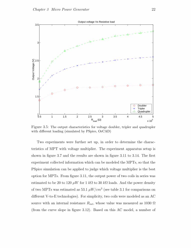
3.5 The output characteristics for voltage doubler, tripler and quadru-
pler with different loading (simulated by PSpice, OrCAD) . . . . . . 22
3.6 PSpice simulation for voltage doubler with C = 10 µF and Rload =
350 kΩ . . . . . . . . . . . . . . . . . . . . . . . . . . . . . . . . 23
3.9 Illustrative drawing for micro power generator. Photo courtesy of
Johnny M. H. Lee . . . . . . . . . . . . . . . . . . . . . . . . . . 24
3.10 MPG (left) weighs less than the normal AA-size battery (right).
Photo courtesy of Johnny M. H. Lee . . . . . . . . . . . . . . . . . 24
3.7 The experiment apparatus for measuring MPG coils characteristics. . 25
3.8 Vibration drum. Photo courtesy of Johnny M. H. Lee . . . . . . . . 25
3.11 Output power versus load resistance for two MPG coils in series
stimulated at 70.5Hz . . . . . . . . . . . . . . . . . . . . . . . . . 26
3.12 Load voltage versus load current for two MPG coils in series stimu-
lated at 70.5Hz . . . . . . . . . . . . . . . . . . . . . . . . . . . . 27
3.13 Output power versus load voltage of two MPG coils in series stimu-
lated at 70.5Hz . . . . . . . . . . . . . . . . . . . . . . . . . . . . 28
3.14 Output power versus input voltage of tripler . . . . . . . . . . . . . 29
3.15 Average input power versus resistive load for Vth(H) = 1.4 V and
Vth(L) = 1.0 V (simulated by PSpice) . . . . . . . . . . . . . . . . 30
3.16 Average input power versus resistive load for Vth(H) = 1.8 V and
Vth(L) = 1.4 V (simulated by PSpice) . . . . . . . . . . . . . . . . 31
3.17 Average input power versus resistive load for Vth(H) = 2.2 V and
Vth(L) = 1.8 V (simulated by PSpice) . . . . . . . . . . . . . . . . 32
3.18 Energy efficiency versus resistive load for Vth(H) = 1.4 V and Vth(L) =
1.0 V (simulated by PSpice) . . . . . . . . . . . . . . . . . . . . . 32
x

3.19 Energy efficiency versus resistive load for Vth(H) = 1.8 V and Vth(L) =
1.4 V (simulated by PSpice) . . . . . . . . . . . . . . . . . . . . . 33
3.20 Energy efficiency versus resistive load for Vth(H) = 2.2 V and Vth(L) =
1.8 V (simulated by PSpice) . . . . . . . . . . . . . . . . . . . . . 33
3.21 Startup time versus resistive load for Vth(H) = 1.4 V (simulated by
PSpice) . . . . . . . . . . . . . . . . . . . . . . . . . . . . . . . . 34
3.22 Startup time versus resistive load for Vth(H) = 1.8 V (simulated by
PSpice) . . . . . . . . . . . . . . . . . . . . . . . . . . . . . . . . 34
3.23 Startup time versus resistive load for Vth(H) = 2.2 V (simulated by
PSpice) . . . . . . . . . . . . . . . . . . . . . . . . . . . . . . . . 35
3.24 Recharge time versus resistive load for Vth(H) = 1.4 V and Vth(L) =
1.0 V (simulated by PSpice) . . . . . . . . . . . . . . . . . . . . . 35
3.25 Recharge time versus resistive load for Vth(H) = 1.8 V and Vth(L) =
1.4 V (simulated by PSpice) . . . . . . . . . . . . . . . . . . . . . 36
3.26 Recharge time versus resistive load for Vth(H) = 2.2 V and Vth(L) =
1.8 V (simulated by PSpice) . . . . . . . . . . . . . . . . . . . . . 36
4.1 Generic platform block diagram . . . . . . . . . . . . . . . . . . . 39
4.2 System supply stuck at Vth(On) without startup module . . . . . . 41
4.3 Output characteristics of startup module and system supply . . . . 41
4.4 Schematic of startup module . . . . . . . . . . . . . . . . . . . . . 42
4.5 Voltage multipliers: tripler, quadrupler and doubler . . . . . . . . . 43
4.6 Simple boost converter [33] . . . . . . . . . . . . . . . . . . . . . . 44
4.7 Programmable System on Chip has built-in switching regulator [26] . 44
4.8 These essential components illustrate the mechanics of charge-pump
operation. [34] . . . . . . . . . . . . . . . . . . . . . . . . . . . . 45
4.9 Schematic of LC-based radio frequency transmitter . . . . . . . . . 51
4.10 System block diagram of PLL with crystal . . . . . . . . . . . . . . 52
4.11 Schematic of SAW-based On-Off Keying RF transmitter [36] . . . . 53
xi

5.1 System block diagram . . . . . . . . . . . . . . . . . . . . . . . . 58
5.2 Photograph of prototype 1 . . . . . . . . . . . . . . . . . . . . . . 60
5.3 Photograph of prototype 2 . . . . . . . . . . . . . . . . . . . . . . 61
5.4 Photograph of prototype 3 . . . . . . . . . . . . . . . . . . . . . . 62
5.5 Photograph of prototype 4 . . . . . . . . . . . . . . . . . . . . . . 64
5.6 Operating flow chart of prototype 4 . . . . . . . . . . . . . . . . . 65
5.7 CRO screen capture for system startup . . . . . . . . . . . . . . . 67
5.8 Setup for measuring power consumption of the startup and applica-
tion circuit . . . . . . . . . . . . . . . . . . . . . . . . . . . . . . 68
5.9 Average power consumption of the system in each stage . . . . . . . 68
6.1 Illustrative drawing of 2D ring . . . . . . . . . . . . . . . . . . . . 70
6.2 Photograph of ring board (top view) . . . . . . . . . . . . . . . . . 70
6.3 Photograph of ring board (bottom view) . . . . . . . . . . . . . . . 70
6.4 Rapid prototype of 2D Ring boards . . . . . . . . . . . . . . . . . 71
6.5 The operation details of 2D ring . . . . . . . . . . . . . . . . . . . 71
6.6 State diagram explains Manchester encoding . . . . . . . . . . . . . 74
6.7 Timing diagram 1 explains Manchester decoding . . . . . . . . . . . 75
6.8 Data packet format for wireless transmission . . . . . . . . . . . . . 75
6.9 Data packet format for MS mouse protocol [10, 13] . . . . . . . . . 76
6.10 Space code example for Pentax camera remote control . . . . . . . . 77
6.11 CRO screen capture of Pentax remote control data word . . . . . . 78
6.15 Photograph of 2D ring modules . . . . . . . . . . . . . . . . . . . 78
6.16 Photograph of 2D ring receiver . . . . . . . . . . . . . . . . . . . . 78
6.12 Photograph of 2D remote control ring . . . . . . . . . . . . . . . . 80
6.17 Photograph of 2D ring demo kit (top view) . . . . . . . . . . . . . 80
6.18 Photograph of 2D ring demo kit (side view) . . . . . . . . . . . . . 80
6.13 Transmission power of the 2D ring at 1 cm . . . . . . . . . . . . . 81
6.14 Transmission power of the 2D ring at 3 m . . . . . . . . . . . . . . 81
xii

List of Tables
3.1 Comparisons between different vibration-to-electrical transducers . . 24
3.2 The relationship between threshold voltages and ASE . . . . . . . . 30
4.1 Antenna length from [18] . . . . . . . . . . . . . . . . . . . . . . . 56
4.2 Antenna diameter and transmission range . . . . . . . . . . . . . . 57
5.1 The summary of prototype 1, 2 and 4 . . . . . . . . . . . . . . . . 66
5.2 Energy consumption statistics for startup and application circuit at
each stage . . . . . . . . . . . . . . . . . . . . . . . . . . . . . . 67
6.1 Design summary of 2D input ring . . . . . . . . . . . . . . . . . . 79
6.2 Comparisons between Lam’s MIDS and 2D input ring . . . . . . . . 79
xiii

Chapter 1
Introduction
1.1 Motivation
Energy can be scavenged from vibrations.
Most modern portable electronic devices are powered by electrochemical bat-
teries which require replacement or charging once consumed. Obviously, alter-
native non-exhaustive power sources would be more convenient. Vibrational
energy is an option which is readily available. However, mechanical energy
(from vibrations) has not been often used since the power which can be gener-
ated from a miniature vibration-based generator is very small. Improvements
in integrated circuit technology has been steadily reducing the power con-
sumption required by portable systems and miniaturized vibrational powered
systems are now a reality.
Self-powered wireless sensors are poised to have a very important role in
the future. Engineers can attach them to the building to test their structural
behavior (such as bridge) under vibrations caused by strong wind or earthquake
[4]. Scientists can monitor plants, trees and animals to better understand their
physiology. The sensor can report real-time information, even in dangerous
environments.
1

Chapter 1 Introduction 2
Sensor networks can improve living standards and life style.
With the system-on-chip technology and MEMS processes, an integrated cir-
cuit which is self-powered by vibrations for controlling smart appliances wire-
lessly can be fit into a very small volume, such as a ring. Wearing the device,
people can record their habits and interact with other computerized devices
more conveniently. If a large group of sensors are used to form an ad hoc
network at home, they can be embedded in the furniture and under the floor
to observe their activities, which can be used to monitor the elderly [28]. It is
very likely that sensor networks will become as common as the Internet today.
1.2 Aims
The objective of this research was to develop low power sensor applications
which can be powered by batteries or non-exhaustive sources, since information
from the environment and transmit the data via a wireless communications
link. Therefore, the sensor applications developed under our scheme have small
geometries, wireless communication ability and long operating time with single
or no battery. The detailed research aims were:
• Develop a generic platform (GP) which combines sensors and wireless
transmission and can be used for both battery sources and vibration
powered sources. For long-term monitoring, the scientists, based on GP,
can design its own applications without the knowledge of low power
integrated circuit design.
• Optimize the electronics for a miniature, vibration-to-electrical power
transducer. Although it does not need to be recharged, the power output
of the transducer is extremely low and unable to directly drive off-the-
shelf circuits.
Chapter 1 Introduction 3
• Develop an application which uses both the vibration-based generator
(VBG) and GP to implement a wireless temperature monitoring system.
This illustrates how to integrate an application circuit with a power
generator and provides a functional test for the VBG.
• Develop a wireless ring input device which can be used as a general
computer interface. In this system, a battery power is used. It illustrates
GP can be applied to other power sources. Also, the wireless ring input
device can be applied to stroke or gesture recognition which introduces
a novel communication interface between human and the electronics.
1.3 Contributions
The main contributions of this dissertation are as follows:
• The issue of developing the power conversion circuitry for an AA-sized
micro power generator was considered. As the size of a micro power
generator (MPG) is reduced, it is a challenge to develop power manage-
ment circuit with trade-offs between size, static power consumption and
efficiency. An optimized power management circuit was designed and
implemented. This involved step-up conversion of the AC micro power
transducer (MPT) 1 circuit to a DC value, a startup circuit and a thor-
ough analysis of the efficiency of the design. To the best of author’s
knowledge, this is the first practical AA-sized MPG with DC output.
• A generic low power wireless sensor platform (GLPWSP) which can be
used for a wide range of applications was developed. Applications de-
rived from GLPWSP inherits all its nice features: low power, wireless
1The MPT was developed by Johnny Ming Ho Lee, Neil N. H. Ching and Dr. Wen J. Lifrom the ACAE department of the Chinese University of Hong Kong.

Chapter 1 Introduction 4
connectivity, ease integration with sensors, high signal processing power
and long period self timing.
• A completely self powered wireless thermometer system was developed
and it is the first such work (self powered and start-up system) reported.
• A battery powered 2D input ring, based on GLPWSP, was implemented.
This ring was designed to control personal computer and appliances. It
has an IrDA transceiver which can communicate with most of portable
consumer electronics, such as portable digital assistant (PDA), Hi-Fi,
etc. The 2D input ring can emulate the computer mouse via an RF link
as well as control a camera. This application demonstrates an example
of a new application which is made possible by low power wireless sensor
systems and to the best of the author’s knowledge, is the first example
of a ring based generic input device with no moving parts.
1.4 Thesis Organization
In chapter 2, a review of related work on vibration-to-electrical conversion and
sensor circuits is given. Chapter 3 introduces the power management circuit
for the micro power generator (MPG) and chapter 4 presents the architecture
of the generic low power wireless sensor platform and the operational details of
the startup module. In chapter 5 a practical micro power generator application,
namely an RF temperature sensor is presented. In chapter 6, a battery powered
2D input ring is presented to demonstrate a novel input method which uses
finger motion. Finally, the conclusion and suggestions for future work are
presented in chapter 7.

Chapter 2
Background and Literature
Review
2.1 Introduction
Energy enables bodies to do work and energy conversions occur around us
every day. Humans intake food to gain power to move and work. This is a
living example of how chemical energy (in food) can be converted to mechanical
energy (movement).
Energy can be classified into renewable and non-renewable sources. Non-
renewable energy sources include crude oil, coal, natural gas and nuclear. Once
consumed, the resulting work products are discarded. Portable electronics,
such as mobile phone, PDAs, etc., are powered by electrochemical batteries.
An electrochemical battery is a non-renewable power source, requiring recharg-
ing or replacement when exhausted. Renewable energy sources include solar
energy, tidal energy, wind energy, etc. This chapter aims to give readers some
background information on power sources which are commonly used for sensor
systems or portable electronics. A review of previous wireless sensor systems
will also be given.
5

Chapter 2 Background and Literature Review 6
2.2 Vibration-to-Electrical Transducer
Thanks to advances in silicon fabrication process and System-on-Chip (SoC)
technology, modern electronic appliances are getting smaller, requires less
power, yet achieve greater functionality. Most of them are directly powered
by electrochemical cells. Electrochemical cells have the advantages of high
energy capacity, are able to provide large instantaneous output current, yet
have a compact size. However, batteries are not the ideal power source for
long term monitoring applications because they require replacement. Turning
ambient vibrational energy into electrical energy is an alternative renewable
power source. Vibration-to-electrical converting methods can be classified into
three categories [40]: electromagnetic (inductive), electrostatic (capacitive),
and piezoelectric. Challenges for designing vibration-to-electrical transducer
are to:
1. model the methodology in mathematically and optimize the model by
simulation; Fortunately, Mitechson et al. [27] published a journal pa-
per which discussed the architectures for vibration-driven micropower
generators in mathematics, interest parties may refer to [27].
2. improve the efficiency of the energy conversion;
3. convert AC power to DC power as electronic components normally op-
erate on DC.
Those converting methodologies will be reviewed in this section. AC to DC
and DC to DC power conversion techniques will be explained in section 4.2.1.
2.2.1 Electromagnetic (Inductive) Power Conversion
Electromagnetic power conversion is the most well-known method which gen-
erates power using a spring, coil and a magnet. Its principle comes from Fara-
day’s law: when the coils cut the magnet’s field, an AC current is induced.

Chapter 2 Background and Literature Review 7
A mathematical model was constructed to model electromagnetic conversion
system by Williams et al [55]. A simplified version is presented in chapter 3.
Several research groups [55, 2] have developed electromagnetic converters.
Williams [55] developed a general second order linear model. He also devel-
oped an electromagnetic generator which was 1 mm thick, and thus the power
density of the system was 10 − 15 µW/cm3. However, Roundy [40] criticized
that the output voltage and current for that device were too low to be rectified
because its output voltage was much lower than a diode’s forward bias voltage.
Amirtharajah and Chandrakasan [2] designed an electromagnetic converter.
The electromagnetic converter was designed for vibrations generated by a per-
son walking, using a vibration magnitude of about 2 cm at about 2 Hz. The
maximum system output power was reported to be 400 µW with measured
voltage output of 180 mV . Its size was 4 cm × 4 cm × 10 cm and the power
density was 2.5 µW/cm3.
Li et al [31] developed methods to improve the efficiency of springs for
vibrational-to-electrical transducers. The main idea is to control the spiral,
thickness and nature of materials for the spring, so that the quality factor Q
of spring is optimized (becomes sharp) at particular frequencies. Therefore,
at the desired frequency, the spring is resonant and it converts most of energy
from vibration to electrical form. In 2000, Li et al [24] had demonstrated a
magnet-based generator with total volume of 4.7 cm3 which was able to drive
an off-the-shelf circuit from vibrations with amplitude ∼ 150 µm and frequency
105 Hz. Its power output was measured as 830 µW and its power density was
calculated as 176.59 µW/cm3.

Chapter 2 Background and Literature Review 8
2.2.2 Electrostatic(Capacitive) Power Conversion
Others have proposed to generate power from two precharged metal plates
under vibration. The simple circuit in figure 2.1 illustrates the idea of electro-
static power conversion. When two precharged metal plates are separated by
distance d, they form a capacitor. The voltage, capacitance and energy stored
at the capacitor are given by equations 2.1.
V =Qd
ε0lw
C =Q
V
E =Q2
2C(2.1)
where Q is the charge on the plates, V is the voltage across the capacitor, E
is the stored energy at capacitor, l is the length of the plate, w is the width
of the plate, and ε0 is the dielectric constant of free space. Imagined that two
metal plates are vibrated by external force (separation d varies), the voltage
across two metal plates varies if the plates’ charges are kept constant. If the
voltage across output capacitor and vibrated capacitor are the same initially,
the voltage across the output capacitor will be charged to the maximum voltage
output of the vibrated capacitor (assuming an ideal diode). Therefore, the
vibrational energy is converted to energy stored on the output capacitor.
Meninger et al [25] proposed to fabricate two comb-like metal plates inside
a chip. For first time usage, metal plates are precharged. AC current is
induced during vibration. The predicted power output was 8.6 µW for volume
of 1.5 cm × 0.5 cm × 1 mm from a vibration source at 2.52 kHz, giving a
predicted power density of 114.6 µW/cm3.
Roundy [40] reported a macro-scale electrostatic converter was as shown
in figure 2.2. At an operation frequency of 100 Hz, the output power was
measured to be 1 nW for a 9 V DC source which was used to maintain the
charges on the plates.

Chapter 2 Background and Literature Review 9
+ + + + + +
- - - - - -
Output
Vout(init)=Vinit
Vout(finial)=Vmax
Vibrated
V(init)=Vinit
V(min)=Vmin
V(max)=Vmax
Figure 2.1: A simple circuit illustrates the idea of electrostatic power conversion[40].
Figure 2.2: Photograph of Roundy’s macro-scale electrostatic converter [40]. Photocourtesy of Shad Roundy
2.2.3 Piezoelectric Power Conversion
Piezoelectric material, ie. polycrystalline ceramic can produce electrical charges
when mechanically deformed. The material is processed in a large electrical
field which orients its crystalline structure in the direction of the external field.
The processed polycrystalline ceramic can vary its voltage if it is elongated or
compressed by an external force. The equations for a piezoelectric materials
are given in equations 2.2.
δ =σ
Y+ dE
D = εE + dσ (2.2)

Chapter 2 Background and Literature Review 10
where δ is mechanical strain, σ is mechanical stress, Y is the modulus of
elasticity (Young’s Modulus), d is the piezoelectric strain coefficient, E is the
electric field, D is the electrical displacement (charge density), ε is the dielectric
constant of the piezoelectric material.
Roundy [40] implemented three piezoelectric generators. Two are shown
in figures 2.3 (Roundy’s design 1) and 2.4 (Roundy’s design 3). For input
vibration at 85Hz and 2.25 m/s2, the maximum power output was reported
as 207 µW and 90 µW for a resistive load and capacitive load respectively.
Roundy’s design 1 was regulated by a piezoelectric circuit (shown in figure
2.5) to power a wireless transmitter at 1% duty cycle. The piezoelectric cir-
cuit contains a full-wave rectifier and a inductor-based step-down regulator.
The full-wave rectifier changes the AC input to DC (2 − 12 V ). Then the
rectified input is down converted to 1.5 V or 3 V DC by a switch mode regu-
lator. Roundy’s design 3 was a large version of design 1. Its maximum power
output was measured to be 1700 µW . It was tested to drive the MICA node
shown in figure 2.7. The maximum demonstrated power densities of Roundy’s
piezoelectric generators were 207 µW/cm3 and 335 µW/cm3 for design 1 and
design 3 respectively.
Figure 2.3: Photograph of Roundy’s
piezoelectric generator (Design 1)
[40]. Photo courtesy of Shad Roundy
Figure 2.4: Photograph of Roundy’s
piezoelectric generator (Design 3)
[40]. Photo courtesy of Shad Roundy

Chapter 2 Background and Literature Review 11
Figure 2.5: Photograph of power circuit of piezoelectric generator [40]. Photocourtesy of Shad Roundy
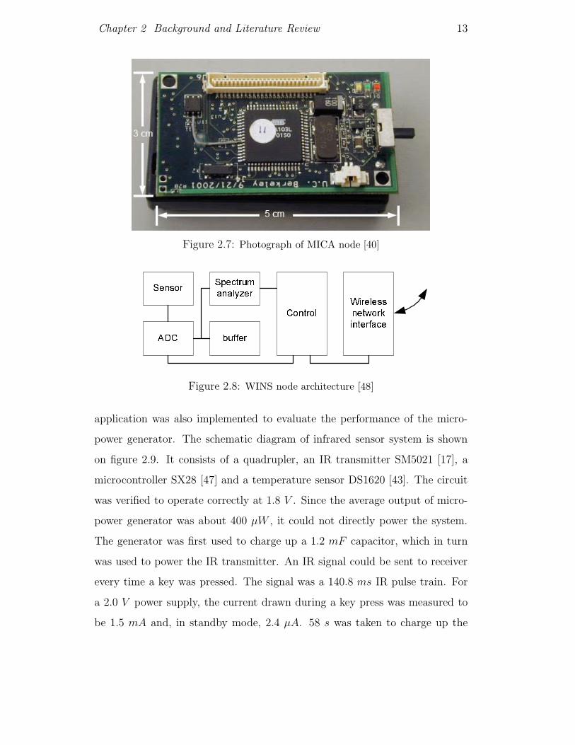
2.3 Wireless Sensor Platform Examples
2.3.1 MICA[14] from UC Berkeley[49]
Hill and Culler reported a wireless platform for deeply embedded networks
called MICA. MICA is a small and low-cost wireless sensor. It consists of a
TR1000 radio transceiver, ATEMGA 103 microcontroller, FPGA hardware ac-
celerators, DS2401 unique ID tag, 4-Mbit flash and a power regulator MAX1678.
The block diagram and photograph of MICA node are shown in figures 2.6 and
2.7 respectively. The MICA node is controlled by a software operating system,
TinyOS [50], designed for networked sensor applications. The operation of a
MICA is as follows: For power saving, MICA activates itself every five minutes
(programmable). It then measures the environment via its sensor. A MICA
node has an analog-to-digital converter (ADC), for interface to the sensor.
MICA has a microcontroller as well as control unit. Hardware FPGA accel-
erator which can be programmed to do any kind of digital signal processing
to process the input data. The RF transceiver provides a wireless medium to

Chapter 2 Background and Literature Review 12
communicate with other nodes in an ad hoc networking manner. The devel-
opers of the MICA system had put the whole system into an ASIC to further
reduce the size and power.
51-pi I/O expansion connector
Digital I/OEight analog
I/Os
Eight
programming
lines
Atmega103 microcontroller
Transmission
power control
Hardware
accelerators
TR1000 radio transceiver
Coprocessor
4-Mbit external flash
Power regulation MAX1678(3V)
DS2401 unique ID
Figure 2.6: Block diagram of MICA node [14]
2.3.2 WINS[48] from UCLA[51]
The Wireless Integrated Network Sensors (WINS) project started at UCLA
in 1993. WINS is an ASIC version of MICA without operating system. The
measured power consumption was 110 µA with 3 V supply and multi-hop
communication. Figure 2.8 shows WINS node architecture. The size of chip
was 2160 × 2554 µm2 in a 0.6 µm CMOS process [54].
2.3.3 Wong’s Infrared System[5]
An external-triggered infrared system developed at the Chinese University
of Hong Kong used a quadrupler circuit as the voltage step up circuit for
the micro-power generator mentioned before. An infrared temperature sensor
Chapter 2 Background and Literature Review 13
Figure 2.7: Photograph of MICA node [40]
Sensor
ADC
Spectrum
analyzer
buffer
Control
Wireless
network
interface
Figure 2.8: WINS node architecture [48]
application was also implemented to evaluate the performance of the micro-
power generator. The schematic diagram of infrared sensor system is shown
on figure 2.9. It consists of a quadrupler, an IR transmitter SM5021 [17], a
microcontroller SX28 [47] and a temperature sensor DS1620 [43]. The circuit
was verified to operate correctly at 1.8 V . Since the average output of micro-
power generator was about 400 µW , it could not directly power the system.
The generator was first used to charge up a 1.2 mF capacitor, which in turn
was used to power the IR transmitter. An IR signal could be sent to receiver
every time a key was pressed. The signal was a 140.8 ms IR pulse train. For
a 2.0 V power supply, the current drawn during a key press was measured to
be 1.5 mA and, in standby mode, 2.4 µA. 58 s was taken to charge up the

Chapter 2 Background and Literature Review 14
capacitor for the first activation, and 30 s was required to recharge the system
in subsequent activations.
4
1
2
3
8
5
6
7
13
16
15
14
9
12
11
10
C1
K2/MODE
K4/TIMER
C2
Vss
K1/OFF
K5/SWING
K3/SPEED
VDD
K7
LED0
OSC2
OSC1
DOUT
K8
LIGHT/K6
R2 4.7RIR LED
Q1 BC548
455k
R1
1KR
C3
100pF
C2
100pF
Q2
BC548
SM5021
DC output
from
voltage
multiplierC1
1.12mF
Figure 2.9: Wong’s Infrared system block diagram [5]
2.4 Summary
In this chapter, vibrational-to-electrical converting methodologies and some
low power wireless sensor platforms were covered. They are divided into three
categories: electromagnetic, electrostatic and piezoelectric. For electrostatic
conversion, Meninger et al created a SoC solution with simulated power density
of 114.6 µW/cm3. Li et al implemented an electromagnetic generator which
was able to drive a thermometer circuit with infrared transmission link. Its
measured power density was 176.59 µW/cm3. Roundy [40] demonstrated a
piezoelectric generator with power density of 207 µW/cm3 which was able to
power a 1.5 V wireless transmitter, and thus, this generator has the highest
rating on power density.
For low power wireless sensors, MICA [14] and WINS [48] both are well-
known. MICA designed by UC Berkeley, is a commercial sensor node which
can form a multi-hop network to monitor a region. It was estimated to have
a 10 years battery life using with 2 AA-size alkaline batteries. MICA has an

Chapter 2 Background and Literature Review 15
component-based operating system which reduces the code size and software
development time. WINS designed by UCLA, is like an ASIC version of MICA
without operating system. It was measured to consume 110 µA at 3 V supply.

Chapter 3
Micro Power Generator
3.1 Introduction
In this chapter, AA-size Micro Power Generator (MPG) is presented. The in-
formation provided is a summary of two papers co-published by the ACAE [29]
and CSE [30] departments of the Chinese University of Hong Kong (CUHK).
Interested parties should refer to the original references [23, 5].
The AA-size MPG consists of a tripler and two Micro Power Transducers
(MPT). Both MPTs can be connected in series or in parallel. To provide
large drive current, MPTs should be connected in parallel, otherwise, serial
connection would give higher output voltage. The MPT is the key component
to convert ambient mechanical energy (from vibration) into electrical energy. It
consists of an inner housing, a MEMS spring with designable spring constant k,
a N45 grading rare earth permanent magnet which has mass m and magnetic
field strength B, copper coil of length l. The inner housing is to secure the
spring with magnet attached on. In figure 3.1, the illustrative drawing shows
the orientation of outer and inner housing, magnet and the resonating spring
of MPT.
MPT generates AC power when the whole system is vibrated. When the
generator housing is vibrated with an amplitude Yt, the magnet will then
vibrate with an amplitude Zt. This relative movement causes magnetic flux to
16
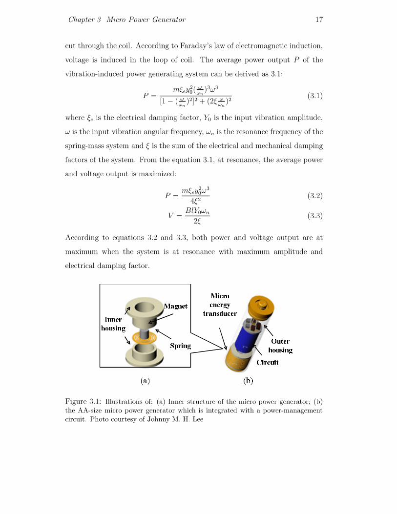
Chapter 3 Micro Power Generator 17
cut through the coil. According to Faraday’s law of electromagnetic induction,
voltage is induced in the loop of coil. The average power output P of the
vibration-induced power generating system can be derived as 3.1:
P =mξey
20(
ωωn
)3ω3
[1 − ( ωωn
)2]2 + (2ξ ωωn
)2(3.1)
where ξe is the electrical damping factor, Y0 is the input vibration amplitude,
ω is the input vibration angular frequency, ωn is the resonance frequency of the
spring-mass system and ξ is the sum of the electrical and mechanical damping
factors of the system. From the equation 3.1, at resonance, the average power
and voltage output is maximized:
P =mξey
20ω
3
4ξ2(3.2)
V =BlY0ωn
2ξ(3.3)
According to equations 3.2 and 3.3, both power and voltage output are at
maximum when the system is at resonance with maximum amplitude and
electrical damping factor.
Magnet
Spring
Inner
housing
Micro
energy
transducer
Outer
housing
Circuit
(a) (b)
Figure 3.1: Illustrations of: (a) Inner structure of the micro power generator; (b)the AA-size micro power generator which is integrated with a power-managementcircuit. Photo courtesy of Johnny M. H. Lee

Chapter 3 Micro Power Generator 18
3.2 MEMS Resonator
The key design issue for the MPT is to fabricate a spring with controllable
resonance frequency. A variety of materials were studied, and copper found to
be the best material for the spring, since it has relatively low Young’s modulus
and high yield stress compared to silicon. Brass, titanium and 55-Ni-45-Ti may
be alternatives for special operating environment. For example, 55-Ni-45-Ti
can be used in situations where low resonance frequency is required.
Currently, two MEMS techniques were explored to obtain the spiral res-
onating spring: laser-micromachinery and lithographic electroplating.
3.2.1 Laser-machinery
A Q-switch (Nd:YAG 1.06 µm wavelength) laser was used to micromachine the
spiral resonating spring. The SEM photo of resulted spring is shown in figure
3.2. A copper spring with diameter of 8 mm and 0.1 mm thickness was used
for first generation of AA-size MPG. Using a laser to cut the spring out from
a copper disc provides accurate control of the spiral of the spring. However,
the thickness of spring cannot be controlled and the cutting edge is not very
smooth as shown in figure 3.2.
3.2.2 Electroplating Fabrication
Instead of shaping the spring with a laser, lithographic techniques can be used
to fabricate the spring with controllable spiral dimensions and thickness. A
1 µm thickness can be achieved using this process. The fabrication process is
illustrated in figure 3.3. First, a gold layer is put on the substrate. The gold
layer acts as a conducting seed for the copper ions. Second, lithographic tech-
niques are used to secure a SU-8 negative PR mask on the gold layer. Third,
copper is electroplated. Fourth, the spring is separated from the substrate. The
springs produced by lithographic electroplating can be thinner with smoother

Chapter 3 Micro Power Generator 19
(a) (b)
Figure 3.2: SEM pictures of: (a) a laser-micromachined copper spring with diameterof 5 mm, (b)close-up of the copper spring; width of spring is ∼ 100 µm. Photocourtesy of Johnny M. H. Lee.
edges than those produced via laser cutting, resulting in a lower resonance
frequency. This process is also more suitable for mass production since many
springs can be made in a single batch.
3.3 Voltage Multiplier
The AC output voltage (Vrms = 450 mV ) supplied by the MPT is not suit-
able for driving a conventional digital circuit. A Voltage Multiplier (VM)
was introduced to step up and rectify the AC output of two MPTs to pro-
duce a DC voltage. The circuits shown in figure 3.4 are a voltage doubler,
tripler and quadrupler. The output characteristics of a quadrupler compared
with a tripler and doubler are shown in figure 3.5. As can be seen, voltage
quadrupler is made by cascading two voltage doublers. The principle of the
voltage doubler is first explained. The doubler contains two diodes and two
capacitors. The number describes a node label eg. V(2,1) means the voltage
of capacitor C1. VAC represents the amplitude of input sine-wave and are two
half-wave rectifier circuits in series. Observe its behavior for sine wave input
on first stage rectifier. The positive half cycles bring the voltage of node 1

Chapter 3 Micro Power Generator 20
(1) Sputter Au layer on
substrate
(2) Coat SU-8 negative
PR
(3) Expose SU-8
negative PR
(4) Develop SU-8
negative PR
(5) Electroplate
Copper
(6) Strip SU-8 and
substrate
UV
Figure 3.3: Copper spring fabrication process. Photo courtesy of Johnny M. H. Lee
from ground to VAC . The negative half cycles charge up C1 by introducing
current from ground terminal of diode D1. By superposition, V2, with respect
to ground, is a sine-wave offset to VAC . The second stage rectifies this offset
sine-wave. Thus, a doubled output voltage is produced. A voltage quadrupler
can be thought as two voltage doublers DB1 and DB2. DB1 doubles the Vref
of DB2 with respect to VAC . Based on Vref , DB2 quadruples and rectifies the
input. The PSpice simulation in figure 3.6 shows that time is required for the
voltage multiplier to achieve the final output, mainly due to the charging up
time of capacitor C1 and output capacitor C3. The prototype circuit was built
using KEMET type T491 10 µF , 10 V capacitors and Toshiba 1SS374 silicon
epitaxial schottky barrier Type diodes. The 1SS374 diode was chosen as it has
relatively low forward voltage (0.23 V ) which allows an increase in efficiency
of the quadrupler. KEMET T491 tantalum capacitors are used because these

Chapter 3 Micro Power Generator 21
make the rectifying circuit compact and have lower leakage. A capacitor of
1.0 mF is connected with the quadrupler and acts as a reservoir to store the
electrical energy generated by the MPG. The reservoir capacitor also acts as
a decoupling capacitor to smooth the output of voltage multiplier.
C2
D3
D4
C4
Vout
AC input
C1
D2
D1 C3
Quadrupler
DB1
DB2C1
D1
D2
C2
Vout
AC
input
1 2 3
0
Doubler
C2
D2
D3
C3
Vout
AC
inputD1
C1
Tripler
Figure 3.4: The schematics of voltage doubler, tripler and quadrupler [15]
3.4 Modeling, Simulations and Measurements
The micro power generator was integrated as shown in figure 3.9 and tested
using a vibration drum (shown in figure 3.8) and signal generator. The input
acceleration was measured as 4.63 m/s2 with an accelerometer attached on
vibration drum. Figure 3.10 shows the photo of the MPG. Our MPG weighs
10.5 gram about half the weight of a typical alkaline cell. Two transducers
were observed using a stroboscope and oscilloscope. They were vibrated in 3
different modes X, Y and Z. The experiment showed that the spring delivers
more energy when the mass experiences translational and rotational vibration,
rather than horizontal vibration. It is because the former vibration mode
provides higher rate of change in magnetic flux than the latter.
Chapter 3 Micro Power Generator 22
0.5 1 1.5 2 2.5 3 3.5 4 4.5 5
x 105
1
1.5
2
2.5
3
3.5Output voltage Vs Resistive load
Rload
(Ω)
Out
put V
olta
ge (
V)
DoublerTriplerQuadrupler
Figure 3.5: The output characteristics for voltage doubler, tripler and quadruplerwith different loading (simulated by PSpice, OrCAD)
Two experiments were further set up, in order to determine the charac-
teristics of MPT with voltage multiplier. The experiment apparatus setup is
shown in figure 3.7 and the results are shown in figure 3.11 to 3.14. The first
experiment collected information which can be modeled the MPTs, so that the
PSpice simulation can be applied to judge which voltage multiplier is the best
option for MPTs. From figure 3.11, the output power of two coils in series was
estimated to be 20 to 120 µW for 1 kΩ to 30 kΩ loads. And the power density
of two MPTs was estimated as 53.1 µW/cm3 (see table 3.1 for comparisons on
different V-to-E technologies). For simplicity, two coils were modeled as an AC
source with an internal resistance Rint, whose value was measured as 1030 Ω
(from the curve slope in figure 3.12). Based on this AC model, a number of

Chapter 3 Micro Power Generator 23
Date/Time run: 04/10/04 Temperature: 27.0
Date: April 10, 2004 Page 1 Time: 17:46:47
(A) bias (active)
Time
40.0ms 80.0ms 120.0ms 160.0ms 200.0ms 240.0ms3.4msV(3) V(2,1) V(2) V(1)
-1.0V
0V
1.0V
1.8V
Figure 3.6: PSpice simulation for voltage doubler with C = 10 µF and Rload =350 kΩ
PSpice simulations were performed on voltage multipliers (doubler, tripler and
quadrupler). Tripler was selected from other VMs to test with MPTs since it
outperformed others in PSpice simulations. From figure 3.13 and 3.14 show the
relationship between power input/output and the input voltage of the tripler.

Chapter 3 Micro Power Generator 24
Inputacceleration Power Output Size (H , Power density(Ampl. or (Power, Vout) (L, W ) or D) (µW/cm3)accel., f)
Williams [55] - - - 10 − 15Amirtharajah and 2 cm, 400 µW , 4 cm × 4 cmChandrakasan [2] 2 Hz 180 mVrms ×10 cm
2.5
150 µm, 830 µW , 1.5 cmLi [24] 105 Hz 1.414 Vrms ×(1)2π cm2 176.59
Meninger [25] - 8.6 µW 1 mm×2.52 kHz - 1.5 cm × 0.5 cm
114.6
Roundy [40] 2.25 m/s2, 207 µWdesign 1 85 Hz 12 Vdc
1 cm3 207
Roundy [40] 2.25 m/s2, 1700 µWdesign 3 85 Hz 12 Vdc
5.1 cm3 335
Two MPTs 4.63 m/s2, 120 µW 2 cm×in series 80 Hz 2.4 Vrms (0.6)2π cm2 53
Table 3.1: Comparisons between different vibration-to-electrical transducers
Figure 3.9: Illustrative drawing
for micro power generator. Photo
courtesy of Johnny M. H. Lee
Figure 3.10: MPG (left) weighs less than
the normal AA-size battery (right). Photo
courtesy of Johnny M. H. Lee
Voltage multiplier is a device to convert AC to DC power. Some performance

Chapter 3 Micro Power Generator 25
AC
Rint
Rload
CROAC coils
AC coilsVoltage
multiplierRload
CRO
Figure 3.7: The experiment apparatus for measuring MPG coils characteristics.
Figure 3.8: Vibration drum. Photo courtesy of Johnny M. H. Lee
metrics are introduced to quantify the performance of the converters.
Available stored energy The MPG is too weak to power off-the-shelf circuit
in a continuous manner. Input energy will be stored into a storage capac-
itor and released in bursts as required. This method is the so-called Duty
Cycle Approach (DCA). The MPG can be applied to any off-the-shelf
circuit with startup module (its details are covered in chapter 4). Startup
module controls the amount of energy stored in storage capacitor Cstorage
with voltages across Cstorage, Vth(H) and Vth(L). Available Stored En-
ergy (ASE) is defined as stored energy in capacitor which can be released
at once after each charging finished, in the other words, the energy flows

Chapter 3 Micro Power Generator 26
0 1 2 3 4 5 6
x 104
0
0.2
0.4
0.6
0.8
1
1.2
1.4x 10
−4
Load Resistance (Ω)
Pow
er (
Wat
t)
P−R characteristic for two coils in series at 70.5Hz
Figure 3.11: Output power versus load resistance for two MPG coils in series stim-ulated at 70.5Hz
into Cstorage from Vstorage cap = Vth(L) rising to Vstorage cap = Vth(H). In
mathematically, ASE = 12× (Vth(H)2 − Vth(L)2).
Startup time (ST) is defined as the elapsed time required to charge the po-
tential of storage capacitor from zero to Vth(H) via the MPG.
Recharge time (RT) is defined as the elapsed time required to charge the
storage capacitor from Vth(L) to Vth(H) via the MPG.
Average input power Input Energy (IE) is required to charge Cstorage from
a low threshold voltage Vth(L) to a high threshold voltage Vth(H). Aver-
age Input Power (AIP) is defined as input energy per unit charge time.
Mathematically, AIP = IERT
. Higher rating on AIP means poor perfor-
mance.
Energy efficiency This term is to measure the efficiency of a device from
the view of energy. Energy Efficiency (EE) is defined as available stored

Chapter 3 Micro Power Generator 27
0 0.2 0.4 0.6 0.8 1 1.2 1.4 1.6 1.8
x 10−4
0.6
0.65
0.7
0.75
0.8
Load Current (A)
Load
Vol
tage
(V
)
V−I characteristic for two coils in series at 70.5Hz
Figure 3.12: Load voltage versus load current for two MPG coils in series stimulatedat 70.5Hz
energy per unit input energy. In mathematically, EE = ASEIE
× 100%.
Higher rating on EE means better performance.
Output load (Capacitive and Resistive) The output of VM will be con-
nected to a storage capacitor and a resistive load. Because duty cy-
cle approach requires a large storage capacitor, typically 1 mF , so the
output capacitance will dominate the resistive load. The resistive load
represents the loading from startup module and application circuit in
shutdown/sleep mode. Therefore, resistive load in simulation are typi-
cally small, in range of 50 kΩ to 500 kΩ (equivalent loading of startup
module). Energy dissipated on resistive load don’t consider as useful
energy, so it won’t be included to the calculation of output power. The
useful energy refers to energy stored in capacitor, ASE.
A proposed simulation circuit contained a test VM, a resistor (Rint) and
a AC source (Vp−p = 2.4, f = 70.6 Hz). The storage capacitor of VM is

Chapter 3 Micro Power Generator 28
0.66 0.68 0.7 0.72 0.74 0.76 0.780
1
2
3
4
5
6
7
8x 10
−5 P−V characteristic of two coils in series at 70.5Hz
Load Voltage rms (V)
Pow
er (
W)
Figure 3.13: Output power versus load voltage of two MPG coils in series stimulatedat 70.5Hz
1 mF . They were connected in series. Three predefined groups of threshold
voltages (Vth(L), Vth(H)) and corresponding ASE were used. Table 3.2 shows
the relationship between threshold voltages and ASE. The criteria for choosing
threshold voltages were based on the minimum input voltage requirement of
DC-DC converters and startup module used in proposed low power wireless
sensor system in chapter 4. VMs were evaluated with average input power,
energy efficiency, startup time and recharge time on different resistive load.
The simulation results are shown in figures 3.15 to 3.26. From figures 3.15 to
3.17, low order VM works better than higher order VM in the view of average
input power required. Doubler takes less power to store a particular amount
of energy than tripler does. And tripler takes less than quadrupler. However,
doubler is not able to store energy at the groups Vth(H) ≥ 1.8 V because
the output of fairly loaded doubler can’t achieve ≥ 1.8 V . From figures 3.18
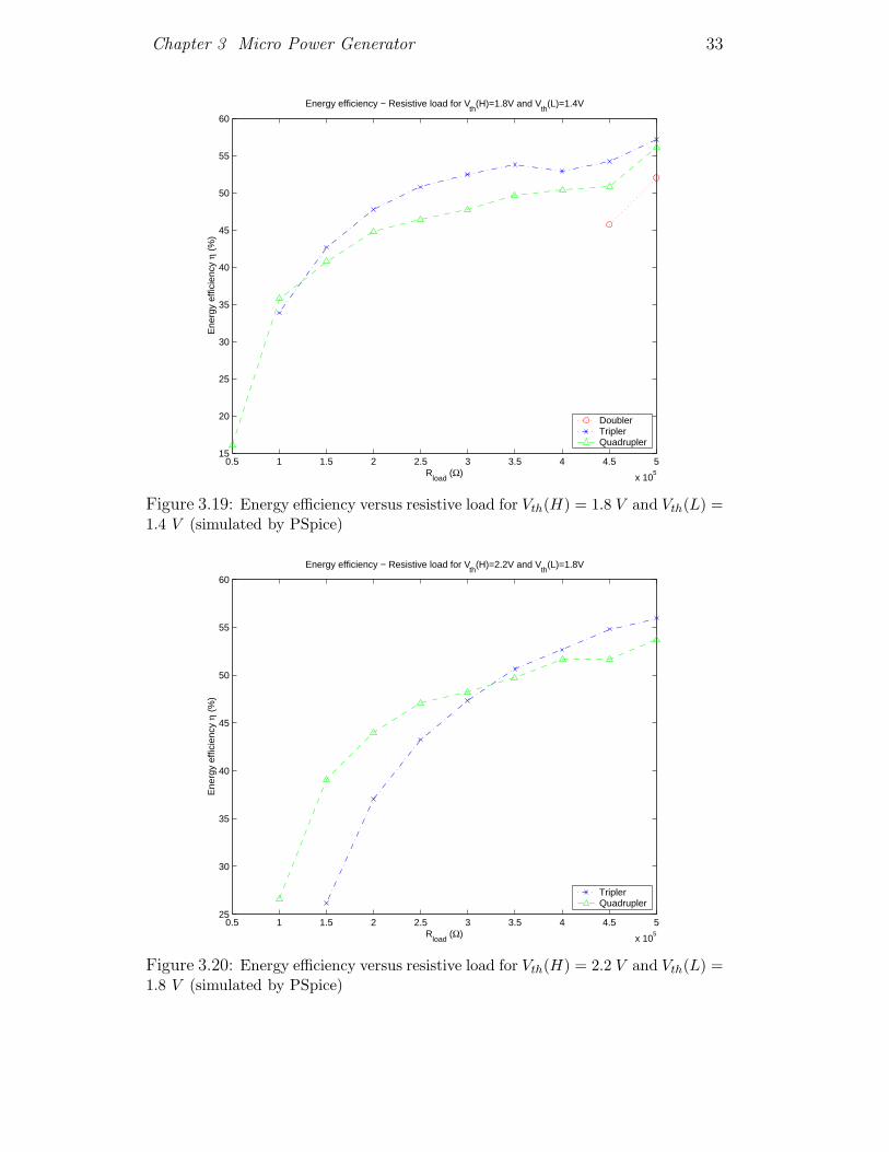
to 3.20, tripler is more efficient than the quadrupler for converting power.

Chapter 3 Micro Power Generator 29
0.55 0.6 0.65 0.7 0.75 0.8−1
0
1
2
3
4
5
6x 10
−5 P−Vin
Characterstic of Tripler
Input Voltage in rms (V)
Out
put P
ower
(W
)
Figure 3.14: Output power versus input voltage of tripler
From figures 3.21 to 3.26, tripler takes more time to startup or recharge than
quadrupler generally. Tripler was chosen to incorporated into MPG because
its overall performance is fine at (Vth(H) = 1.8 V, Vth(L) = 1.4 V ). Its AIG is
around 100µJs−1 which is the maximum power output of two MPGs nearly.
Also, it got the modest rating at full range of tested load (50 kΩ to 500 kΩ)
for charging voltage level from Vth(L) = 1.4 V to Vth(H) = 1.8 V . The
comparison of VMs is mainly concentrated on energy efficiency and average
input power at charging voltage level (Vth(L) = 1.4, Vth(H) = 1.8) because the
minimum switch threshold low for startup circuit is 1.35 V . Energy stored at
the capacitor below this voltage can not be used by application circuit directly.
The startup time of tripler was estimated to 32 seconds. The recharge time
was estimated to 18 seconds. And the energy efficiency was estimated to 53%,
with average input power below 100µW .

Chapter 3 Micro Power Generator 30
(Vth(L), Vth(H)) ASE
(1.0 V, 1.4 V ) 0.48 mJ(1.4 V, 1.8 V ) 0.64 mJ(1.8 V, 2.2 V ) 0.8 mJ
Table 3.2: The relationship between threshold voltages and ASE
0.5 1 1.5 2 2.5 3 3.5 4 4.5 5
x 105
0.6
0.8
1
1.2
1.4
1.6
1.8x 10
−4
Rload
(Ω)
Ave
rage
inpu
t pow
er (
(J/s
)
Average input power − load for Vth
(H)=1.4V and Vth
(L)=1.0V
DoublerTriplerQuadrupler
Figure 3.15: Average input power versus resistive load for Vth(H) = 1.4 V andVth(L) = 1.0 V (simulated by PSpice)
3.5 Summary
Vibration-to-electrical transducers were not a new research topic in 2004.
Many researchers used classic techniques to convert the vibration into elec-
trical power. The MPG outperforms other techniques in energy-to-density
because MPT contains a high Q spring, which was made by lithographic elec-
troplating on accurate mathematical model. The other useful feature of our
MPG is that it can power any off-the-shelf circuits. In section 4.2.1, the startup
module and its duty-cycle operating mechanism will be discussed.

Chapter 3 Micro Power Generator 31
0.5 1 1.5 2 2.5 3 3.5 4 4.5 5
x 105
0
0.5
1
1.5x 10
−4
Rload
(Ω)
Ave
rage
inpu
t pow
er (
(J/s
)
Average input power − load for Vth
(H)=1.8V and Vth
(L)=1.4V
DoublerTriplerQuadrupler
Figure 3.16: Average input power versus resistive load for Vth(H) = 1.8 V andVth(L) = 1.4 V (simulated by PSpice)
Finally, two evaluation metrics were introduced to quantify the perfor-
mance of different VMs. A tripler was chosen for the MPG because of its
overall performance. The metrics can be applied to evaluate any duty cycled
AC-DC power converters.

Chapter 3 Micro Power Generator 32
1 1.5 2 2.5 3 3.5 4 4.5 5
x 105
5
6
7
8
9
10
11
12
13x 10
−5
Rload
(Ω)
Ave
rage
inpu
t pow
er (
(J/s
)
Average input power − load for Vth
(H)=2.2V and Vth
(L)=1.8V
TriplerQuadrupler
Figure 3.17: Average input power versus resistive load for Vth(H) = 2.2 V andVth(L) = 1.8 V (simulated by PSpice)
0.5 1 1.5 2 2.5 3 3.5 4 4.5 5
x 105
25
30
35
40
45
50
55
60
Energy efficiency − Resistive load for Vth
(H)=1.4V and Vth
(L)=1.0V
Rload
(Ω)
Ene
rgy
effic
ienc
y η
(%)
DoublerTriplerQuadrupler
Figure 3.18: Energy efficiency versus resistive load for Vth(H) = 1.4 V and Vth(L) =1.0 V (simulated by PSpice)
Chapter 3 Micro Power Generator 33
0.5 1 1.5 2 2.5 3 3.5 4 4.5 5
x 105
15
20
25
30
35
40
45
50
55
60
Energy efficiency − Resistive load for Vth
(H)=1.8V and Vth
(L)=1.4V
Rload
(Ω)
Ene
rgy
effic
ienc
y η
(%)
DoublerTriplerQuadrupler
Figure 3.19: Energy efficiency versus resistive load for Vth(H) = 1.8 V and Vth(L) =1.4 V (simulated by PSpice)
0.5 1 1.5 2 2.5 3 3.5 4 4.5 5
x 105
25
30
35
40
45
50
55
60
Energy efficiency − Resistive load for Vth
(H)=2.2V and Vth
(L)=1.8V
Rload
(Ω)
Ene
rgy
effic
ienc
y η
(%)
TriplerQuadrupler
Figure 3.20: Energy efficiency versus resistive load for Vth(H) = 2.2 V and Vth(L) =1.8 V (simulated by PSpice)

Chapter 3 Micro Power Generator 34
0.5 1 1.5 2 2.5 3 3.5 4 4.5 5
x 105
17
18
19
20
21
22
23
24
25
Rload
(Ω)
Sta
rtup
tim
e (s
)
Startup time vs Resistive load for Vth
(H)=1.4V
DoublerTriplerQuadrupler
Figure 3.21: Startup time versus resistive load for Vth(H) = 1.4 V (simulated byPSpice)
0.5 1 1.5 2 2.5 3 3.5 4 4.5 5
x 105
20
30
40
50
60
70
80
90
Rload
(Ω)
Sta
rtup
tim
e (s
)
Startup time vs Resistive load for Vth
(H)=1.8V
DoublerTriplerQuadrupler
Figure 3.22: Startup time versus resistive load for Vth(H) = 1.8 V (simulated byPSpice)

Chapter 3 Micro Power Generator 35
0.5 1 1.5 2 2.5 3 3.5 4 4.5 5
x 105
35
40
45
50
55
60
65
70
75
80
85
Rload
(Ω)
Sta
rtup
tim
e (s
)
Startup time vs Resistive load for Vth
(H)=2.2V
TriplerQuadrupler
Figure 3.23: Startup time versus resistive load for Vth(H) = 2.2 V (simulated byPSpice)
0.5 1 1.5 2 2.5 3 3.5 4 4.5 5
x 105
6
7
8
9
10
11
12
13
14
Rload
(Ω)
Rec
harg
e tim
e (s
)
Recharge time vs Resistive load for Vth
(H)=1.4V and Vth
(L)=1.0V
DoublerTriplerQuadrupler
Figure 3.24: Recharge time versus resistive load for Vth(H) = 1.4 V and Vth(L) =1.0 V (simulated by PSpice)

Chapter 3 Micro Power Generator 36
0.5 1 1.5 2 2.5 3 3.5 4 4.5 5
x 105
0
10
20
30
40
50
60
70
80
Rload
(Ω)
Rec
harg
e tim
e (s
)
Recharge time vs Resistive load for Vth
(H)=1.8V and Vth
(L)=1.4V
DoublerTriplerQuadrupler
Figure 3.25: Recharge time versus resistive load for Vth(H) = 1.8 V and Vth(L) =1.4 V (simulated by PSpice)
0.5 1 1.5 2 2.5 3 3.5 4 4.5 5
x 105
10
15
20
25
30
35
40
45
50
55
Rload
(Ω)
Rec
harg
e tim
e (s
)
Recharge time vs Resistive load for Vth
(H)=1.8V and Vth
(L)=1.4V
TriplerQuadrupler
Figure 3.26: Recharge time versus resistive load for Vth(H) = 2.2 V and Vth(L) =1.8 V (simulated by PSpice)

Chapter 4
Low Power Wireless Sensor
Platform
4.1 Introduction
For long-term monitoring applications, vibrational-to-electrical power trans-
ducers are a good power source option because they provide a non-exhaustive
supply. However, in many applications, the transducer must be small, typi-
cally of same order of magnitude to sensor circuit and this limits the power
generated to a range of few hundred micro-watts if the volume is constrained
to 1 cm3 to 3 cm3. Besides power considerations, designing wireless sensors in-
volves many tradeoffs. In this chapter, the architecture of a low power wireless
sensor will be covered.
4.2 Generic Platform
A Generic Platform (GP) is proposed to fulfill the requirements of general
monitoring applications. The block diagram of the GP is shown in figure 4.1.
The GP will be powered by a battery or a micropower generator as described
in chapter 3. The power source is connected to a power management circuit
which consists of a startup module and power regulator. The startup module
37

Chapter 4 Low Power Wireless Sensor Platform 38
acts as an active switch between the application circuit and power source. It
will monitor the voltage level of power source and activate the application
circuit only when the stored energy is sufficient. Because the output voltage
level of power source will vary within a defined range, a power regulator is
introduced to step up/down the voltage so that a stable supply voltage can be
presented to the application circuit.
The application circuit consists of a microprocessor, an Analog-to-Digital
Converter (ADC), secondary storage, long period timer and some sensor pe-
ripherals. The microprocessor controls the system’s peripherals and the data
communication between them. The microprocessor must have General Purpose
Input Output pins which connect and exchange data with the digital sensors.
For sensor with analog output, an ADC acts as a voltage interface which digi-
tizes the analog output of the sensors. The secondary storage is a non-volatile
device which stores system information and post-processed data from the mi-
croprocessor. The long period timer should be driven by a crystal operated at
low frequency. It can trigger the microprocessor with a pre-programmed pe-
riod to wake the system from sleep mode or to make a time record. The sensor
peripherals monitor or measure the behaviors or changes of the environment.
The GP can communicate with other GPs or computing hosts via its wireless
RF transmitter (one-way) or Infrared transceiver (two-ways).
4.2.1 Startup Module and Power Management
Startup Module
The startup circuit is not a part of the MPG. However, it is essential for
the MPG because it guarantees that the application circuit (loading of MPG)
activates at the right time. The startup module only applies power to the
application circuit when the voltage at the output of the tripler exceeds a
fixed threshold, Vth(H). Without the startup module, the application circuit

Chapter 4 Low Power Wireless Sensor Platform 39
Microprocessor
ADCLong period
timer
Non-volatile
Storage
Sensor
peripherals
Radio
frequency
Wireless
transmitter
Infrared
host
Analog
Digital
Startup
module
Power
Reg
Power
Management
Battery/
MPG
Figure 4.1: Generic platform block diagram
will begin to operate well before the minimum voltage required for correct
operation is reached, a large current consumption. This results in a situation
in which the voltage at the output of the tripler cannot continue to rise as
shown in figure 4.2. The schematic of the startup module is shown in figure
4.4. Three resistors connected to positive input of comparator set the hysteresis
of the startup module, i.e. the value of Vth(H) and Vth(L). Equation 4.1 shows
the calculation [32] to determine the resistor values shown in figure 4.4. The
output of startup circuit is active-high. It will switch on the NMOS transistor
when the supply voltage is higher than Vth(H) and will switch off the NMOS
when the supply voltage drops lower than Vth(L). Thus, the NMOS switch
acts as a power switch for the application circuit. When the NMOS turns on,
a return path between system ground of application circuit and power ground
is provided. Figure 4.3 shows the output characteristics of startup module and
system supply. The input capacitor of startup module must be large enough
to provide sufficient energy for one time activation of the application circuit.
For example, the wireless RF thermometer, described in chapter 5 consumes
212.62 µJ per activation. Therefore a 1 mF capacitor is sufficient. Equation
4.2 shows the amount of energy available in a charged 1 mF capacitor with
Vth(L) = 1.4 V and Vth(H) = 1.9 V .

Chapter 4 Low Power Wireless Sensor Platform 40
Select R3 = 1.2 MΩ
Choose the hysteresis band, VHB = 1.9 − 1.35
= 550 mV
Calculate R1 = 1.2 M × (550 mV
1.9 V)
= 347 kΩ
Vth(H) > 1.25 × 347 k + 1.2 M
1.2 M
1.9 V > 1.61145 V√
R2 = 1/[Vth(H)
Vref × R1− 1
R1− 1
R3]
= 1/[1.9
1.25 × 347 k− 1
347 k− 1
1.2 M]
= 1.5032 MΩ
R1 = 349 kΩ, R2 = 1.5 MΩ, R3 = 1.2 MΩ
were selected for stock available.
Verify the trip voltage, Vth(H) = Vref × R1 × (1
R1+
1
R2+
1
R3)
= 1.904375 V√
Vth(L) = Vth(H) − R1 × 1.9
R3
= 1.35179 V√
Hysteresis = Vth(H) − Vth(L)
= 552.585 mV√
(4.1)
Available Energy, E for 1.0 mF = C × ∆V × V
= C × (Vth(H) − Vth(L)) × Vth(H) + Vth(L)
2
= 1 m × (1.9 − 1.4) × 1.9 − 1.4
2
= 825 µJ (4.2)

Chapter 4 Low Power Wireless Sensor Platform 41
Vth(On)
Figure 4.2: System supply stuck at Vth(On) without startup module
Vth(H)
Vth(L)
Vth(On)
Usage cycle Charging cycle
Voltage
across
capacitor
Startup
circuit output
1st charging cycle Usage cycle Charging cycle
Figure 4.3: Output characteristics of startup module and system supply
Conversion Technique
Conventional vibration-to-electrical transducers produce AC power. Neither
voltage nor current is easy to store in AC form. The most common way is to
convert the AC output to DC and store the energy in a capacitor or battery.
The former is preferred since capacitors suffer less from self-discharge (in the
µA range).
AC-DC For AC-DC conversion, a voltage multiplier [15] provides the simplest
solution. It is constructed entirely from diodes and capacitors, and hence
does not need a DC voltage supply to operate. Three types of voltage
multipliers, described earlier in section 3.3, are shown in figure 4.5.

Chapter 4 Low Power Wireless Sensor Platform 42
349K
1.5M
Ref
1mF
Tripler output
1.2M
1.8M
BSH103
Application
Circuit
1.2M
Figure 4.4: Schematic of startup module
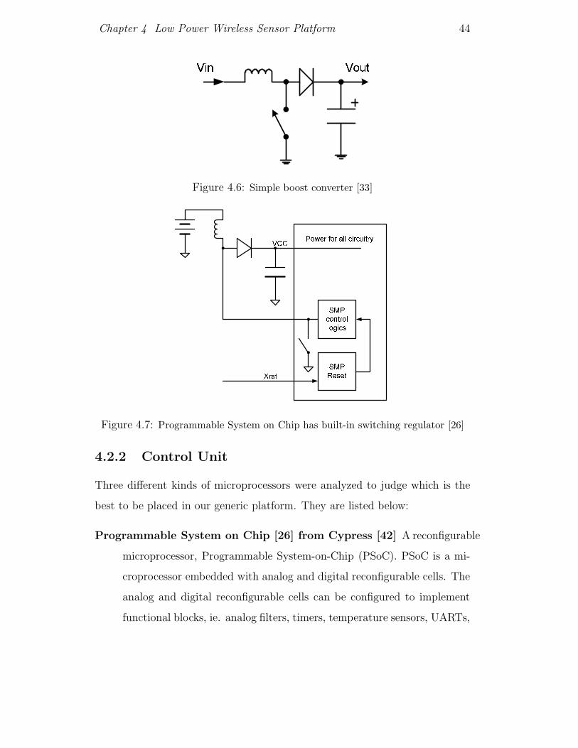
DC-DC(Inductor-based Switching Regulator) A simple boost regulator
is shown [33] is shown in figure 4.6. Imagine that the switch has been
open for a long time. Assuming no load, the voltage at the output ca-
pacitor is Vin −Vdiode drop. Once the switch is closed, one end of inductor
shortens to ground. The diode prevents a backward current and thus
voltage at the output is unchanged. The inductor current increases be-
fore being saturated and develops a field on the inductor. When the
switch is open, the end of inductor (originally shorted to ground) will
virtually short to the output because the output diode is forward-biased.
The stored energy in the magnetic field of the inductor will be released
to maintain the current which flows out to the output before the stored
energy vanishes. The voltage across the inductor is greater than the out-
put voltage (VL > Vout), and charge is transferred to the capacitor. To
maintain a desired output voltage level, the switching process must not
be interrupted. To achieve high efficiency, switching on/off time must

Chapter 4 Low Power Wireless Sensor Platform 43
be tuned, so that the inductor is nearly but not saturated. Microproces-
sors with built-in inductor-based switching regulators are available [26].
In figure 4.7, a simplified schematic diagram of the internal switching
regulator of the PSoC chip from Cypress [42] is shown.
DC-DC(Capacitor-based Voltage Converter) Capacitor-based voltage con-
verters use capacitors to store and transfer energy. Since the capacitor
can’t change voltage levels abruptly, multiple capacitors and switches
are required to step up/down input voltage. Also, the maximum drive
current for capacitor-based voltage converters is low, but clean (less rip-
ple). A good introduction to capacitor-pump voltage converters can be
found in [34]. Capacitive voltage conversion is achieved by switching a
capacitor periodically. In figure 4.8, a circuit demonstrates the genera-
tion of −V+ from a supply voltage V+. Two pairs of switches (S1,S3)
and (S2,S4) are turned on/off alternatively. For the positive input cycle,
(S1,S3) are closed and C1 is charged to V+. For the zero input cycle,
(S1,S3) are opened and (S2,S4) are closed and charges sharing occurs be-
tween C1 and C2. Thus, a voltage −V+ is developed at Vout. A voltage
of 2 V+ can be achieved by connecting the load between V+ and Vout.
Figure 4.5: Voltage multipliers: tripler, quadrupler and doubler
Chapter 4 Low Power Wireless Sensor Platform 44
Vin Vout
Figure 4.6: Simple boost converter [33]
VCC
SMP
control
logics
SMP
ResetXrst
Power for all circuitry
Figure 4.7: Programmable System on Chip has built-in switching regulator [26]
4.2.2 Control Unit
Three different kinds of microprocessors were analyzed to judge which is the
best to be placed in our generic platform. They are listed below:
Programmable System on Chip [26] from Cypress [42] A reconfigurable
microprocessor, Programmable System-on-Chip (PSoC). PSoC is a mi-
croprocessor embedded with analog and digital reconfigurable cells. The
analog and digital reconfigurable cells can be configured to implement
functional blocks, ie. analog filters, timers, temperature sensors, UARTs,

Chapter 4 Low Power Wireless Sensor Platform 45
V+
C1
C2
Vout=-(V+)
S1 S2
S3 S4
Figure 4.8: These essential components illustrate the mechanics of charge-pumpoperation. [34]
ADCs, etc. via a module library. There are two types of analog reconfig-
urable blocks. Both are based on switch capacitor circuits to minimize
mismatch effects. Besides the reconfigurable ability, the PSoC has many
nice features. It has a sleep timer with 1 s period, a built-in switch
mode pump designed for stepping up a battery input (≥ 1.2 V ) to pre-
programmed supply voltage (say 3.3 V ) with 50 % efficiency. Figure 4.7
shows the schematic diagram of the switch mode pump in the PSoC.
Microcontroller with integrated PLL - Atmel Smart RF [7] This wire-
less data microtransmitter was designed for Remote Keyless Entry sys-
tems (RKE). It has a built-in Phase Lock Loop (PLL) and Power am-
plifier (PA), so that only an external inductor and a crystal are required
for the wireless transmission. The Intermediate Frequency (IF) can be
selected from 264 − 456 MHz. The IF is controlled by the natural fre-
quency of the crystal (for Atmel Smart RF, fIF = 24 × fcrystal). Atmel
Smart RF implements On-Off Keying (OOK) modulation or Frequency
Shift Keying (FSK) modulation by changing the configuration of inter-
nal capacitor arrays. To improve transmission rate, an internal timer
(bit timer) is used to control, pulse/space encoding. Atmel Smart RF
has 128 Bytes of non-volatile storage and six I/O pins. Finally, it is

Chapter 4 Low Power Wireless Sensor Platform 46
worthwhile to mention that it can be programmed with a couple of pins
in I2C format.
Ultra-low power microcontroller - TI MSP430 [21] This 16−bit Micro
Control Unit (MCU) was designed for ultralow power applications. It
has five power modes and interval timers. In power mode 3, the power
consumption of the MCU is as small as 2 µA with 3 V supply. The
interval timer sourced by a 32 kHz crystal can wake up the system from
power mode 3 6 s intervals. This MCU has GPIO pins which can cause
individual of interrupts. Some versions of the MSP430 have built-in
modules such as ADCs and DACs for analog peripherals. This MCU
also has flash memory for storage.
These MCUs have tradeoffs, and are evaluated in chapter 5.
4.2.3 Input Units (Sensor Peripherals)
In this section, three kinds of sensors are introduced which enable the generic
platform to measure temperature, sense motion and measure the sound level.
Temperature sensor TMP100 [20]
There are many ways to measure temperature. The simplest way is to measure
the voltage across a thermistor which connects with resistor and voltage source
in series. However, this may require an ADC to translate the analog voltage
level into digital form for the MCU. Texas Instructment’s (TI) TMP100 is
a digital temperature sensor which provides a digital output, simplifying its
interface. The TMP100 takes at most 75 ms to make a 9 − bit temperature
conversion with current consumption of 70 µA at 3 V . It can be shut down
with a very low quiescent current consumption, typically 0.1−1 µA and comes
in a 3 mm × 3 mm × 1.45 mm package.

Chapter 4 Low Power Wireless Sensor Platform 47
iMEMS accelerometer [16]
The iMEMS accelerometer is a 5 mm × 5 mm × 2 mm monolithic IC from
Analog Device, Inc. It measures both dynamic and static acceleration for
single or double axis. The outputs are analog voltage or digital signals whose
duty cycles (ratio of pulsewidth to period) are proportional to acceleration.
An ADC or a counter can be used to decode the output of the accelerometer,
the period being set by an external resistor. The accelerometer can achieve
2 mg resolution at 60 Hz bandwidth. It operates at supply voltage 3−5.25 V
with supply current < 0.6 mA.
Digital microphone from BSE [9] and National [44]
A microphone is a pressure-to-electrical transducer. It converts sound to small
analog signal. A conventional Electret Condenser Microphone (ECM) contains
a JFET preamplifier. Conventional ECMs have low noise immunity due to its
analog output. Aire van Rhijn [52] reported that a digital ECM to improve
Signal-to-Noise Ratio (SNR) compared to an analog ECM. The idea is to re-
place the JFET by a preamplifier and a sigma-delta modulator. Therefore the
output becomes digital. The digital ECM has four pins: Vcc (power), Clock-
in, Data-out and Vss (ground) and is easily interfaced. The sound level can be
acquired by averaging the accumulated output of the sigma delta modulator.
4.2.4 Output Units (Wireless Transmitters)
Infrared and radio frequencies are two common mediums for wireless trans-
mission. Their details are covered below:
Infrared
Infrared transmission requires line-of-sight, although reflection is allowed at
a smooth surface, ie. metal plate, mirror, etc. It is commonly adopted in

Chapter 4 Low Power Wireless Sensor Platform 48
remote controls, RKE system where short range and low transmission rates
are acceptable. An infrared Light Emitting Diode (LED) is sufficient to form
an infrared transmitter. Modern portable electronics use infrared transceivers
to form short range communication links.
Radio Frequency
Radio Frequency (RF) transmitters do not require line-of-sight. RF transmit-
ter can be constructed by LC circuits (LC), PLLs or Surface Accoustic Wave
(SAW) components.
LC A single-transistor FM transmitter was built to test its performance [11].
The schematic of FM transmitter is shown in figure 4.9. The FM trans-
mitter was designed to work in the commercial FM radio band 88 −108 MHz with a 2 V supply. Data in digital form can be input to the
circuit. C1 and C2 forms a potential divider to reduce the AC signal
to 1/10 of its original value. Q1 acts as a common base oscillator, with
feedback provided by C4. R1 provides the bias for the transistor, and R2
provides emitter bias. A 2N2222A VHF transistor was chosen for the
oscillator. Any NPN transistor operating at 500 MHz or above should
work with different modulation characteristics. The tank circuit L1 and
C3, along with stray circuit and transistor collector-to-base capacitances,
determine the frequency of oscillation. The collector-to-base capacitance
is a function of collector-base voltage, and this voltage is modulated
by the input voltage from C1, causing direct frequency modulation of
the oscillator frequency. Because the oscillator power output also varies
with collector voltage, some AM components will also be present. The
FM broadcast is approximately at a 3-meter wavelength (100 MHz)
approximately. C3 is approximately 8 pf and the transistor and stray
capacitances are approximately 2 − 5 pf . L1 is 0.25 µH . C5 is used

Chapter 4 Low Power Wireless Sensor Platform 49
as a DC-blocking capacitor and is generally around the same value as
the tank-tuning capacitor for optimal performance. As for antenna, it
is usually made about one-forth of a wavelength and for 100 MHz, is
about 70 cm. However, for short ranges, up to 7.5 meters, radiation from
the circuit or coupling on supply rails is adequate for transmission. An
experimental transmitter was implemented and it consumed ≈ 300 µA
with 2.3 V supply in continuous transmission mode. Its transmission
range was about 1.5 meters. The calculation of power consumption and
transmission range is presented in equations 4.3 and 4.4.
Assume that the supply voltage is 2 V , current consumption is 300 µA,
transistor Q1 is a 2N2222A which has gain β = 40 and forward voltage
Vf = 0.6 V , commercial radio’s sensitivity is 0.01 mW . No antenna is
required which reduces the transmission power to 30 %. The steps for
calculation are listed below [12]:
1. Define the input swing, here it is 0 V to 3 V at the input of C1.
The input is coupled to node between C1 and Q2 and reduces the
maximum input voltage to 0.3 V .
2. Calculate voltage VE across resistor on emitter of Q1.
3. Use current gain equation to calculate IB.
4. Calculate base resistor of Q1, RB.
5. Calculate emitter resistor of Q1, RE.
6. Calculate output power of transistor Q1.
7. Calculate ideal transmission range.
8. Calculate effective transmission range when there is no antenna and
obstacle between transmitter and emitter.

Chapter 4 Low Power Wireless Sensor Platform 50
Vbias =2 − 0.6
2+ 0.6
= 1.3 V
VE =2 − 0.6
2
= 0.7 V
IB =IB
β + 1
=300 µ
40 + 1
= 7.317 µA
RB =2 − 1.3
7.317 µ
= 95.67 kΩ
RE = (2 − 0.6
2)/300 µ
= 2.3 kΩ
Ptransistor = (2 − 2 − 0.6
2) × 300 µ
= 0.39 mW (4.3)
Tx Distanceideal =
√0.39 m
0.01 m
=√
39
= 6.24 meters
Tx Distanceeffective = 6.24 × 30%
= 1.873 meters (4.4)
PLL with crystal To provide a wide frequency-tunability and high frequency-
stability, a crystal-based frequency synthesizer using a Phase-Locked
Loop (PLL) [53] can be used. Figure 4.10 is a simplified diagram of
a common single-loop PLL synthesizer. It takes a low-frequency crystal
oscillator as a reference clock. The clock signal is fed into the R divider,

Chapter 4 Low Power Wireless Sensor Platform 51
Digital Data Input
Antenna
(FM output)
C1
10nF
C2
100nFR2
2.3kR
C4
5.6pF
C3
5p-50pF
R1
95.6kR C5
27p
L1
250nH
Q1
2N2222A
Figure 4.9: Schematic of LC-based radio frequency transmitter
which decreases the reference frequency via an adjustable frequency di-
vider. The frequency output of the R divider is further inserted into the
phase comparator, which compares the phase of the R divider to that of
the adjustable N frequency divider. The phase comparator determines
the phase difference between the outputs of divider R and divider N .
For a charge pump type PLL, its output is in duty-cycle format which
is further rectified into a DC correction voltage for the VCO by the loop
filter. The negative feedback loop makes the desire frequency lock with
reference clock frequency from crystal oscillator, fvco = fref × NR
. A
crystal-based PLL transmitter combines a crystal-based PLL oscillator
with a Power Amplifier.
Both On-Off Keying (OOK) and Frequency Modulation (FM) can be
implemented using a PLL. For OOK, an Intermediate Frequency (IF) is
generated by feeding crystal signal into the PLL. By-passing the IF to
the output denotes 1 and shortening the output to ground denotes 0.
For FM, two different frequencies can be generated by changing the RN
ratio slightly. The drawbacks of the PLL are:

Chapter 4 Low Power Wireless Sensor Platform 52
1. complex, since the design of loop filter is very critical.
2. large power consumption. The PLL involves many components and
they are ON for transmission of both 0 ’s or 1 ’s.
N divider
R divider
Phase
comparatorLoop filter VCO PA
Matching
NetworkCrystal-
based
Oscillator
Figure 4.10: System block diagram of PLL with crystal
SAW-stabilized Figure 4.11 shows a schematic diagram of SAW-stabilized
ASK transmitter [37] which is similar to the LINX LC series transmit-
ter [46]. The Surface Acoustic Wave (SAW) resonator combines with a
wideband RF transistor to form a SAW oscillator and PA. When data is
applied on the input switch, the oscillator is tuned on and off according
to the input data stream. This input sequence will be amplified and
send to matching network at output stage, then the signal will radiate
out via antenna. The SAW-stabilized ASK transmitter is an OOK trans-
mitter which is also known as Carrier Present Carrier Absent modulation
(CPCA) [41]. The SAW-stabilized ASK transmitter outperforms either
LC or PLL for low power wireless sensor applications because it has good
immunity to noise and low power consumption, since it consumes little
power when sending 0.
Modulation and Coding Schemes
This section gives a brief introduction to modulation and coding schemes. For
more details, please refer to Sayre [41].

Chapter 4 Low Power Wireless Sensor Platform 53
L1
C1
L2
C4
C1
C3
C6
Q1
BFR540
R1
R2
SAW
resonator C2
Q2
BFR540R3
C2
Data In
Tx
Enable
Figure 4.11: Schematic of SAW-based On-Off Keying RF transmitter [36]
The earliest radio station broadcasted using Amplitude Modulation (AM).
Modulation is a scheme to insert baseband information (ie. voice digital data,
analog audio/video, etc.) into RF carrier wave. AM is a modulation scheme
which embeds the information into the envelope of the carrier wave. Frequency
Modulation (FM) is now more widely used because of its higher fidelity com-
pared to AM. An FM signal can be generated by altering the frequency of the
carrier according to the amplitude variation of the baseband input or changing
the phase of the carrier. The transmitter shown in figure 4.9 is an example of
the former. Both AM and FM are classified as being analog modulation.
Modern wireless communication adopts Digital Modulation (DM) because
it provides higher data rates and noise immunity within constrained band-
widths and noisy channels. DM involves mathematics which beyond the scope
of this section, therefore, only the idea will be presented.

Chapter 4 Low Power Wireless Sensor Platform 54
The most common DM schemes for low-power short range data transmis-
sion are On-Off Keying (OOK) and Frequency Shifting Keying (FSK). OOK
is a type of amplitude shift keying modulation. It represents 1 s and 0 s by
turning on and off the RF carrier frequency. FSK is another DM scheme which
represents 1 s and 0 s by two different non-harmonic frequencies, called mark
and space.
For infrared remote control [38], the information bitstream is modulated
with a ∼ 40 kHz frequency. The types listed below are the common codings
for an infrared remote control:
Pulse code varies the length of the pulses. 1 s is coded with longer pulse
and 0 s is coded with short pulse.
Space code varies the space between the pulses. The length of space repre-
sents the coding.
Shift code alters the order of pulse space. A space+pulse represents 1 and a
pulse+space represents 0.
Transmitting data via RF is different from the media of wire. The RF
bitstream is bit serial and must be encoded with a clock. Due to the on-off
time of the oscillator, the duty cycle width of OOK for sending 0 and 1 may
not be 50/50. Therefore, Manchester codes are used. Referring to Federal
Standard 1037C [1], the definition of Manchester code is:
“A code in which (a) data and clock signals are combined to form a
single self-synchronizing data stream (b) each encoded bit contains
a transition at the midpoint of a bit period, (c) the direction of
transition determines wheterh the bit is a 0 or a 1, and (d) the first
half is the true bit value and the second half is the complement of
the true bit value.”
The implementation of a Manchester code is covered in chapter 6.

Chapter 4 Low Power Wireless Sensor Platform 55
Antenna
Antenna is a device designed for radiating energy efficiently from one media
to another. Different shapes and geometries of antenna have different charac-
teristics. To evaluate an antenna, terms, such as antenna diversity, antenna
pattern, return loss, VSWR, beamwidth, etc. are used. Standard procedures
to design and evaluate an antenna are as follows:
1. According to the nature and geometry of application, the antenna type
is chosen.
2. The design is drawn and simulated with high frequency synthesis tools,
such as Ansoft HFSS [6], aiming to optimize the quality factor and min-
imize the return loss of the antenna at the carrier frequency.
3. The design is fabricated and balun is placed. The impedance and S-
parameter of the antenna output are matched by network analyzer with
Smith chart.
4. Output matching network is built. The matched antenna is incorporated
to the transmitter. Further testing is required for transmission power and
output spectrum in order to fulfill the regulations of FCC.
Interest parties should refer to Setian’s book [45].
Application note [19] provides a good introduction for compact antenna
design. The common antenna types are listed below:
1/4 wavelength A tin-plated copper wire between 22 to 32 gauge with a
quarter wavelength of carrier frequency long is the simplest antenna.
Table 4.1 shows the length of antenna corresponding to carrier frequen-
cies, 315 MHz−916 MHz. For 433 MHz, the length of 1/4 wavelength
monopole is 6.5 inches which is too long for a portable device. There-
fore, people shorten the height of the monopole by winding its lower end,
which is called a Short Whip.

Chapter 4 Low Power Wireless Sensor Platform 56
Frequency inMHz
315 418 434 868 916
1/4 Wave ininches
8.91 6.72 6.48 3.24 3.07
Table 4.1: Antenna length from [18]
Spiral To further cut the size of a whip, the wire can be coiled up to form
a flattened coil of wire or directly fabricate on PCB as spiral trace. A
planner antenna can be fit into a square, 19 mm × 19 mm. However, a
groundplate must be placed to enhance the performance of the planner
spiral antenna. The size and the location of the groundplate must be
carefully designed, otherwise, the performance of the antenna is reduced.
It is worthwhile to mention that the quality factor of a spiral antenna
is very high, therefore, it can only be optimized for particular carrier
frequency. In the other words, it can’t be a wideband antenna.
Helix The helical antenna is similar to a spiral, but it is not flattened. The
wire size, coil diameter, turn spacing and number of turns are the factors
to judge the characteristics of helical antenna. The problem with this
antenna are its bulk size and it is easily detuned by nearby objects.
A fairly good matched antenna can be achieved by the following procedures:
1. Calculate the transmission range from the power of transmitter (shown
in equations 4.3 and 4.4.).
2. Cut a tin-plated copper wire or plastic-coated copper wire with > 1/4
wavelength and connect to the transmitter.
3. Move the transmitter away from the receiver as far as possible until
receiver can’t receive correct data.
4. Cut a little bit of the antenna and repeat step 3 to see whether longer

Chapter 4 Low Power Wireless Sensor Platform 57
Diameter Transmission range
1.5 mm 8 meters1 mm 3 meterswire wrap wire 1.5 meters
Table 4.2: Antenna diameter and transmission range
transmission distance can achieve. Halt the process if shorter transmis-
sion distance resulted.
5. Record the wire length which have the longest transmission range.
These procedures were used for evaluating different wire diameters for a 433 MHz
SAW-based transmitter and receiver. The antenna was wound in a helix form
(with 4 turns and turn diameter = 1.3 cm). The results are shown in table
4.2.
4.3 Summary
In this chapter, a generic platform for low power wireless sensor application is
introduced. A low power startup module was designed to interface between a
GP and micropower generator. Beside a power management circuit, the GP
consists of an MCU, long-period self-wakeup timer, non-volatile storage, GPIO
and ADC, wireless transmitters (RF and infrared) and sensor peripherals. The
usage and operating details of each these modules were explained. Up-to-date
commercial products for each GP modules are also presented.

Chapter 5
Application I - Wireless RF
Thermometer
5.1 Overview
A wireless thermometer is presented which provides a practical application for
the MPG described in chapter 3. The wireless thermometer is based on the low
power wireless sensor platform stated in chapter 4. The system block diagram
is shown in figure 5.1. Implementation details are described in this chapter.
Voltage
Multiplier Startup
Module
PwrReg
uP RF Tx
TMP
Sensor
Coil DATA
PWR
DATA
SYSTEM.PWR
SYSTEM.GND
AA-size MPG Startup module and application circuit
Figure 5.1: System block diagram
58

Chapter 5 Application I - Wireless RF Thermometer 59
5.2 Implementation
Four prototypes of wireless RF thermometers were built. Different kinds of
MCUs, temperature sensors, RF transmitter and power regulators were tested
and their tradeoffs were evaluated.
5.2.1 Prototype 1
Prototype 1 has the similar setup to Wong’s system described in section 2.3.3
with the main difference being that it uses an analog LC transmitter instead of
an infrared LED. This eliminates the line-of-sight transmission problem. The
photograph of prototype 1 is shown in figure 5.2. The transmitted data is
received by a commercial radio and displayed on a CRO. The disadvantages
of prototype 1 are:
1. The system must be powered by 3 V directly since there is no voltage
regulator.
2. The system requires external intervention. The system has no self-timer,
therefore it can’t wake up itself.
3. The LC transmitter is easily influenced by proximity to conducting ob-
jects and temperature-drift.
5.2.2 Prototype 2
Due to low accuracy, temperature-drift and slow startup time of prototype 1,
a commercial LINX chip whose carrier frequency is 433 MHz was used in the
second prototype to replace the analog transmitter. The transmitter was tested
with a data rate 5 kbit (with proper coding) and 91.4 meters transmission
range. Besides a SAW transmitter, prototype 2 used the PSoC micro control
unit (MCU). The PSoC MCU has a built-in voltage regulator which steps-up
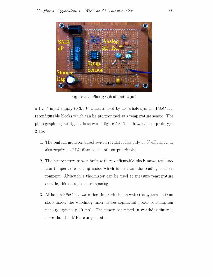
Chapter 5 Application I - Wireless RF Thermometer 60
Figure 5.2: Photograph of prototype 1
a 1.2 V input supply to 3.3 V which is used by the whole system. PSoC has
reconfigurable blocks which can be programmed as a temperature sensor. The
photograph of prototype 2 is shown in figure 5.3. The drawbacks of prototype
2 are:
1. The built-in inductor-based switch regulator has only 50 % efficiency. It
also requires a RLC filter to smooth output ripples.
2. The temperature sensor built with reconfigurable block measures junc-
tion temperature of chip inside which is far from the reading of envi-
ronment. Although a thermistor can be used to measure temperature
outside, this occupies extra spacing.
3. Although PSoC has watchdog timer which can wake the system up from
sleep mode, the watchdog timer causes significant power consumption
penalty (typically 10 µA). The power consumed in watchdog timer is
more than the MPG can generate.

Chapter 5 Application I - Wireless RF Thermometer 61
Figure 5.3: Photograph of prototype 2
5.2.3 Prototype 3
Sacrificing a little in power consumption, a special focus on component counts
and size was made for prototype 3. Prototype 3 uses an Atmel Smart RF
MCU as the central processing unit because it has integrated RF transmitter.
In figure 5.4, a photograph of prototype 3 is shown. The MCU is a 8-bit pro-
cessor and runs at 3−5 MHz. Prototype 3 contains an inductor-based switch
regulator (MAX1724 [35]), temperature sensor and accelerometer. MAX1724
can step up an input voltage from > 0.9 V to 3.0 V with 90 % efficiency and
1.5 µA quiescent current consumption. A TMP100 temperature sensor is used
because of its accuracy and small size. The drawbacks of this system are:
1. It has no timing module to wake the system up after the system entered
sleep mode.
2. The antenna output of Smart RF requires 3 V bias. However, the output
of switching regulator is very noisy and the noise will couple to the
antenna.
3. To solve problem 2, a large capacitor Cout and inductor can smooth
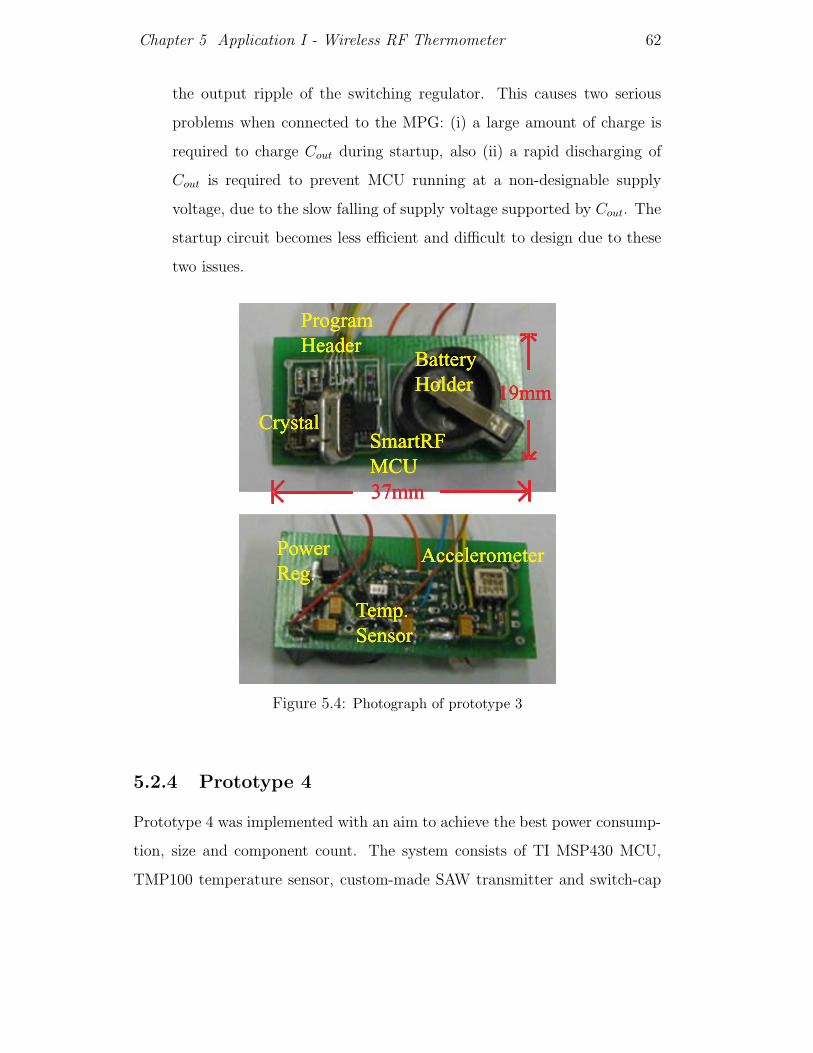
Chapter 5 Application I - Wireless RF Thermometer 62
the output ripple of the switching regulator. This causes two serious
problems when connected to the MPG: (i) a large amount of charge is
required to charge Cout during startup, also (ii) a rapid discharging of
Cout is required to prevent MCU running at a non-designable supply
voltage, due to the slow falling of supply voltage supported by Cout. The
startup circuit becomes less efficient and difficult to design due to these
two issues.
Figure 5.4: Photograph of prototype 3
5.2.4 Prototype 4
Prototype 4 was implemented with an aim to achieve the best power consump-
tion, size and component count. The system consists of TI MSP430 MCU,
TMP100 temperature sensor, custom-made SAW transmitter and switch-cap

Chapter 5 Application I - Wireless RF Thermometer 63
regulator. MSP430 is a 16-bit MCU designed for ultra-low power applica-
tions. It has long period (3.67 s) timer clocked with a low frequency crystal
(76.8 kHz). Its GPIO pin is connected with the TMP100 to collect tempera-
ture readings. A custom-made SAW transmitter gives high degree of flexibility
for controlling the transmission power and matching antenna impedance. A
Switch-cap power regulator has up to 90 % efficiency with 2 µA quiescent
current consumption. It also has less output ripple than an inductor-based
design, typically 30 mV . Prototype 4 was built with a startup module, so that
the MPG can connect directly with it. The flow chart in figure 5.6 shows the
operating sequence of startup module and application circuit. The operating
sequence is listed below:
1. When the system is vibrated, the MPG charges up the output storage
capacitor Cout. The charges inside Cout are assumed to be initially zero.
2. The startup module switches off the application circuit until the voltage
across Cout rises higher than Vth(H) at which point the application circuit
is allowed to operate.
3. The application circuit performs, MCU initialization, temperature con-
version and data transmission.
4. After the application is done, the circuit sleeps for a preprogrammed
period and waits for next activation if energy is sufficient. Otherwise, it
will wait for next charge-up of Cout above Vth(H).
The photograph of prototype 4 is shown in figure 5.5.
5.3 Results
The main features of prototypes 1, 2 and 4 are summarized in table 5.1. Un-
fortunately, prototype 3 could not transmit since the noise from the power

Chapter 5 Application I - Wireless RF Thermometer 64
Figure 5.5: Photograph of prototype 4
regulator coupled to the antenna via the supply biasing.
Prototype 4 is the only one (out of 4 prototypes) which can be powered
by the MPG. The startup module was verified to provide stable operation for
fifty transmission cycles by applying vibration to the system randomly. One of
these experiments was recorded and a CRO screen capture is shown in figure
5.7. In the figure, the middle trace shows the voltage of comparator output,
the comparator is used to switch on/off the application circuit. The bottom
trace shows the voltage level of the system supply. The top trace shows the
signal pin of the MCU (it is asserted when the MCU turns on). The startup
time of power regulator was measured as 600 µs. The startup time of MCU
was measured as 545.4 µs.
The power consumption of prototype 4 was measured and analyzed with
the experiment setup shown in figure 5.8. A 2.0 V voltage supply is in series
with a 22 kΩ resistor to emulate the MPG by limiting current entering the
1 mF storage capacitor to 27 µA (at 1.4 V to 2.0 V ). The instantaneous cur-
rent consumption can be acquired by measuring the voltage across 3 Ω resistor,
thus, the instantaneous power consumption is calculated by multiplying the
current across the resistor and the voltage across the storage capacitor. Ta-
ble 5.2 shows the measurement and the graphical representation is shown in
figure 5.9. The total energy consumed for a single activation was measured
as 212.62 µJ . 30 % of the total energy is consumed in the regulator startup

Chapter 5 Application I - Wireless RF Thermometer 65
Start
Initialization
Send Temperature
Conversion CMD
Read Temperature
Conversion
End
Transmit data to
host via
RF 433MHz
Sleep 853ms
Power good is
asserted?
Sleep 30s
Yes
No
Application circuit
C(stored)
charged up to
Vth(H)?
Switch on and app.
Circuit runs
C(stored) falls to
Vth(L)?
Switch off and
application halts
No
Yes
Yes
No
Startup module
Figure 5.6: Operating flow chart of prototype 4
and MCU initialization. This consumption can be avoided for consecutive
temperature measurements if the MPG generates more power than the appli-
cation circuit consumes in sleep mode (22.38 µW ). 17 % of the total energy
is consumed in temperature conversion. Wireless transmission consumed most
of energy, 53 %. It takes 1.42 s for single measurement. During charging up
by the MPG, the system has a 4.5 µA current consumption which is consid-
ered as the minimum overhead of the startup module. Therefore, the MPG
must provide more than 4.5 µA supply current in order to keep the circuit in
continuous operation.
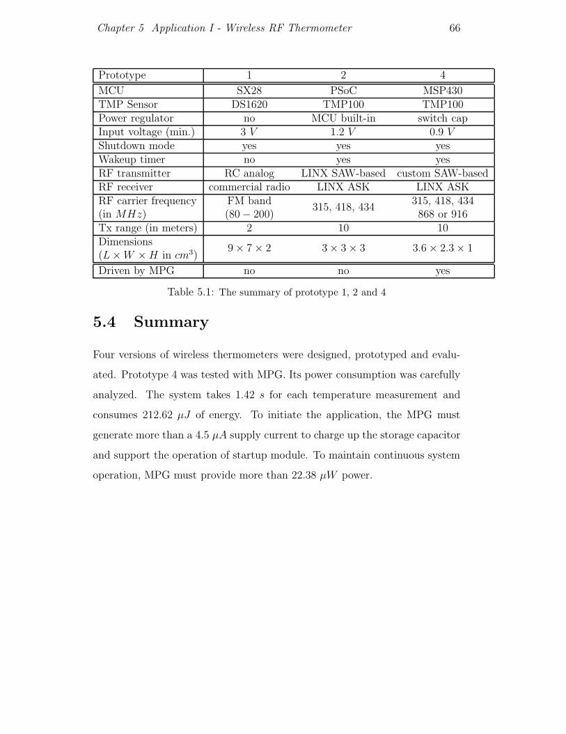
Chapter 5 Application I - Wireless RF Thermometer 66
Prototype 1 2 4
MCU SX28 PSoC MSP430TMP Sensor DS1620 TMP100 TMP100Power regulator no MCU built-in switch capInput voltage (min.) 3 V 1.2 V 0.9 VShutdown mode yes yes yesWakeup timer no yes yesRF transmitter RC analog LINX SAW-based custom SAW-basedRF receiver commercial radio LINX ASK LINX ASKRF carrier frequency FM band 315, 418, 434(in MHz) (80 − 200)
315, 418, 434868 or 916
Tx range (in meters) 2 10 10Dimensions(L × W × H in cm3)
9 × 7 × 2 3 × 3 × 3 3.6 × 2.3 × 1
Driven by MPG no no yes
Table 5.1: The summary of prototype 1, 2 and 4
5.4 Summary
Four versions of wireless thermometers were designed, prototyped and evalu-
ated. Prototype 4 was tested with MPG. Its power consumption was carefully
analyzed. The system takes 1.42 s for each temperature measurement and
consumes 212.62 µJ of energy. To initiate the application, the MPG must
generate more than a 4.5 µA supply current to charge up the storage capacitor
and support the operation of startup module. To maintain continuous system
operation, MPG must provide more than 22.38 µW power.

Chapter 5 Application I - Wireless RF Thermometer 67
PowerTime
Energy Consumptionconsumption
taken MeasuredEstimated
(+Corrected)Calculated
Reg. 49.01 µJ + 0.006 µJstartup
600 µs n/a= 49.02 µJ
81.70 mW
uP 14.944 µJ + 0.0928 µJstartup
545.4 µs n/a= 15.0368 µJ
27.57 mW
Temp 18.855 µJ + 17.195 µJconv.
1.4109 s 33.1875 µJ= 36.05 µJ
25.55 µW
Wireless 112.447 µJ + 0.06107 µJtx
4.167 ms 109.431 µJ= 112.509 µJ
27.00 mW
Sleep t 20t µJ 22.38t µJ 22.38 µW
Total (212.62 + 22.38t) µJ
Table 5.2: Energy consumption statistics for startup and application circuit at eachstage
Figure 5.7: CRO screen capture for system startup

Chapter 5 Application I - Wireless RF Thermometer 68
1mF Startup Application
22k
2.0V
3R
Figure 5.8: Setup for measuring power consumption of the startup and applicationcircuit
81.7mW
27.57mW 27mW
25.55uW
22.38uW
time
Average power
consumption
600us 545.4us 1.4109s 4.167ms
4.5uW minimum
overhead
Reg startup
uP init.
Temp conv.
RF tx.
Sleep
*figure is not in scale
ts
Figure 5.9: Average power consumption of the system in each stage

Chapter 6
Application II - 2D Input Ring
6.1 Overview
A 2D input ring was implemented to demonstrate the utility of the GP de-
scribed in chapter 4. The ring is a device for ubiquitous computing, such
as controlling a Personal Computer (PC). The current prototype is able to
emulate computer mouse via RF RS232 port. It is also able to control home
appliances and portable electronics equipped with infrared or IrDA transceiver.
6.2 Architecture
The hardware architecture of the 2D input ring is based on a low power wireless
sensor platform (excluding startup module). A battery is used to support
continuous operation. In order to detect the finger motion, an accelerometer
(iMEMS ADXL202E) is installed. The illustrative drawing of the 2D/3D ring
is shown in figure 6.1. The 2D ring consists of two 2 cm × 2 cm PCB boards
which communicate via a connector. Photographs of both boards are shown
in figures 6.2 and 6.3. Besides two axis the accelerometer, the 2D ring consists
of a MSP430 microcontroller, power management circuit, RF transmitter, a
program socket, 2 buttons (B1, B2) and a LED indicator. The program socket
has two functions: to connect to host a computer for MCU programming; to
69

Chapter 6 Application II - 2D Input Ring 70
connect interface add-on modules, such as IrDA [3] transceiver, Liquid Crystal
Display (LCD) and external flash storage, etc. Figure 6.4 shows the prototype
PCB which was made using a PCB rapid prototype machine. The prototype
PCB was used to verify the spacing and width of the tracks and pads before
fabrication.
Wire bonding two boards
Programmable socket
MicroprocessorLED
indicator
TOP VIEW SIDE VIEW
Accelerometer
RF transmitter
Button/Accelerometer and
Power management circuit uP and programmable socket
Figure 6.1: Illustrative drawing of 2D ring
Figure 6.2: Photograph of ring board
(top view)
Figure 6.3: Photograph of ring board
(bottom view)
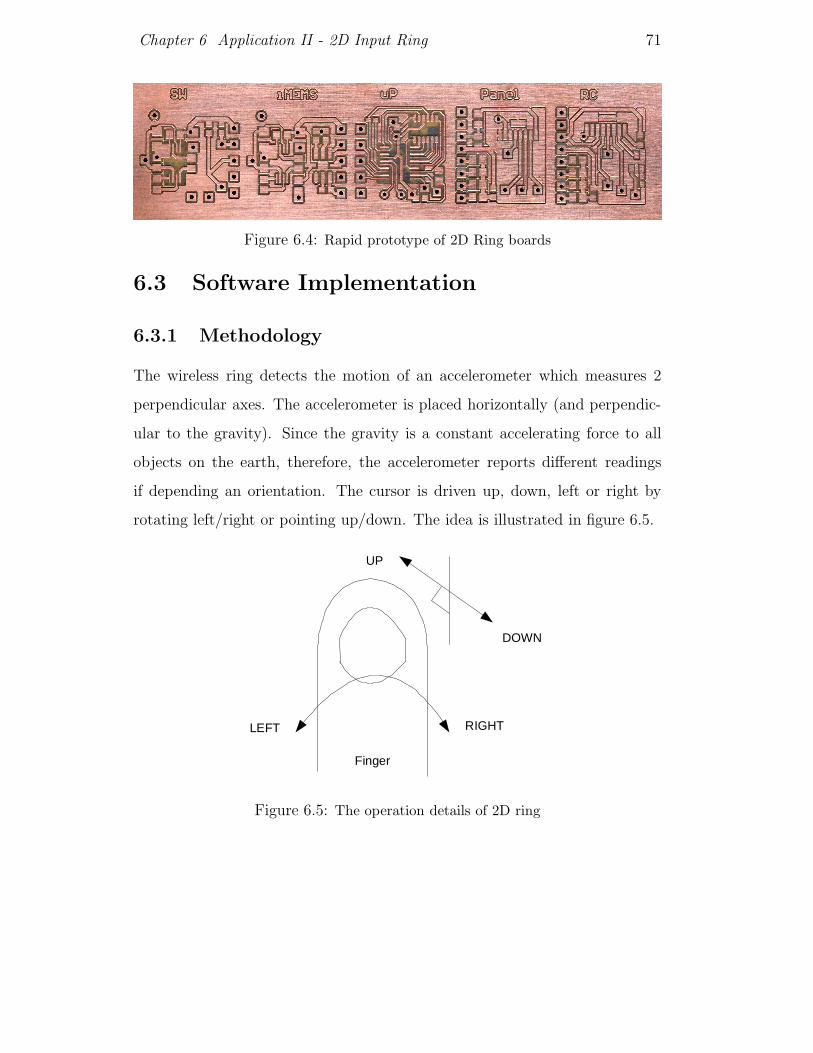
Chapter 6 Application II - 2D Input Ring 71
Figure 6.4: Rapid prototype of 2D Ring boards
6.3 Software Implementation
6.3.1 Methodology
The wireless ring detects the motion of an accelerometer which measures 2
perpendicular axes. The accelerometer is placed horizontally (and perpendic-
ular to the gravity). Since the gravity is a constant accelerating force to all
objects on the earth, therefore, the accelerometer reports different readings
if depending an orientation. The cursor is driven up, down, left or right by
rotating left/right or pointing up/down. The idea is illustrated in figure 6.5.
UP
DOWN
RIGHTLEFT
Finger
Figure 6.5: The operation details of 2D ring

Chapter 6 Application II - 2D Input Ring 72
6.3.2 Error Control Code
An error control code is used to maintain data integrity from one system
to another via the noisy wireless channel. There are many kinds of error
control coding schemes, some of them detect errors and some of them detect
and correct errors, ie. hamming codes, turbo codes, etc. Sometimes, errors
may not relate to the transmission channel but to the architecture itself. For
example, to save power, the SAW RF transmitter turns off its oscillator when
transmitting 0. However, the SAW oscillator’s startup time and turn-off time
is not the same. This non-symmetrical property limits the data rate. To
overcome this problem, a Manchester code is introduced. The Manchester code
represents binary data with edge transitions, the so-called biphase code. It
improves the data rate of a SAW RF transmitter from 2.4 kbit/s to 4.8 kbit/s.
The ring system is not only protected by an outer code (Manchester code),
but also by an inner code (XOR check sum). Both techniques are used to
detect errors, and detected faulty packets will be discarded. Compared to
error correction codes, an error detection code is more suitable for a ring
system because:
1. error detection code is simple and consumes less computation time to,
therefore faster response time is achieved;
2. for the computer mouse application, numerous data is generated to de-
scribe the trajectory of the cursor. Loss of packets are not terribly im-
portant (assuming no burst error), since the errors caused by missing
packet can be corrected almost subconsciously by the user.
In figure 6.6, the diagram explains Manchester encoding on the transmitter
side. Data words to be transmitted are buffered in a 16-bit register and they
are clocked out sequentially by interrupt timer. When data is ready, 8-bits
of data is stored into the low byte of a data buffer, and the high byte of

Chapter 6 Application II - 2D Input Ring 73
the data buffer is used to store the 8-bit data’s complement. For 4800 bit/s,
a 9600 Hz timing interrupt is required. When MCU is interrupted by the
timer, the LSB of data buffer is transmitted. Then the complement and data
byte are swapped. The complement bit (now the data byte) will be clocked
out on the next interrupt arrived. A 16-bit data register will be shifted after
both bits are sent. The send and shift process repeats until 8-bits of data are
processed. The transmitted byte ends up in the low byte of the data buffer
as a by-product. For the receiver side, a GPIO pin, a timer and a register are
used to decode data. A GPIO pin detects edge transitions and a timer records
the elapsed time between two consecutive transitions. A register is used to
store the received data. Figure 6.7 gives the nature of Manchester coded bits.
The figure shows two consecutive received bits: the previous bit and current
bit. R-R/F-F denotes a rising/falling edge is followed by a rising/falling edge.
R-F/F-R denotes a rising/falling edge is followed by a falling/rising edge. If
the previous bit is known, the current bit value can be extracted by observing
elapsed time between previous and current edges. Rather than measure the
precise of rise and fall time, Nbound, Sbound and Bbound are used to check
whether time measured is in accepted range. It is worthwhile to mention
that Manchester code requires tight alignment of data. Figure 6.8 shows the
packet format which enables independent alignment of each packet. Each
packet contains a PREAMBLE, CMD, three data bytes (D1, D2, D3 ) and
CHKSUM. PREAMBLE is to align each packet. CMD byte is reserved for
control signals. CHKSUM verifies the correctness of three data bytes (D1, D2,
D3).

Chapter 6 Application II - 2D Input Ring 74
Data ByteComplement Byte
Fill data
Tx
Swap
Idle
Timer interrupt
Data bit sent
Data rdy
Buffer Empty
16-bit data buffer
0 1 1 0
=”0" =”1"
Shift Comp. bit sent
Figure 6.6: State diagram explains Manchester encoding
6.3.3 Peripheral Control Protocol
MS Serial Computer Mouse
Microsoft [8] (MS) serial computer mouse protocol was implemented, based on
[10, 13], so that the 2D ring can be directly used on any PC OS with generic
mouse support. The data packet format for the MS mouse protocol is shown
in figure 6.9. Three bytes are used to describe the displacement of the cursor.
The first byte describes the status of the mouse’s left and right buttons. It also
stores the two most significant bits of the X and Y displacement. The second
and third bytes store the remaining data bits of the X and Y displacement.
For the receiver side, a minimal handshaking was implemented to acknowledge
the host via the RS232 port, so that the computer mouse client is recognized
by the host computer.

Chapter 6 Application II - 2D Input Ring 75
Nbound
Sbound
R-R: Nbound
R-F: Sbound
Transition Edge
represents data
Previous Bit Current Bit
Nbound
Bbound
F-R: Bbound
F-F: Nbound
Figure 6.7: Timing diagram 1 explains Manchester decoding
CMD D1 D2 D3 CHKSUMPREAMBLE
Figure 6.8: Data packet format for wireless transmission
Protocol for Smart Appliances and PDAs
For controlling the portable electronics remotely, infrared was the first carrier
widely used. Many electronic devices, including MP3 players, TV, HiFi, etc.,
come with an infrared remote control. Infrared has advantages over other
wireless carriers in that it is low cost and simple to implement. For short range
and low data rate transmission, many data coding methods exist (different
manufacturers use different coding schemes) and their operating details were
explained in section 4.2.4.
To illustrate the remote control ability, a 2D input ring was programmed
to be a 2-button remote control pad for a film camera. The coding scheme of
film camera was recovered by observation of the infrared signals using an IrDA
transceiver and digital oscilloscope. The data word format was recognized as a
space code and is shown in figure 6.10. Each data packet is formed by a pream-
ble and 7-bit data. In each packet, high is represented by a 38.46 kHz signal

Chapter 6 Application II - 2D Input Ring 76
- 1 ? ? Y Y X X - 0 X X X X X X - 0 Y Y Y Y Y Y
1st byte 2nd byte 3rd byte
Left Button
Right ButtonX X X X X X X X Y Y Y Y Y Y Y Y
X displacement Y displacement
Figure 6.9: Data packet format for MS mouse protocol [10, 13]
train (38/62 duty cycle) and low is represented by a ground level. A pream-
ble is constructed by sending high for 12.945 ms and then low for 3.032 ms.
7-bit data is coded by the space width between two consecutive signal high.
1 ms space width represents 0 and 3 ms space width represents 1. Figure
6.11 shows the CRO screen capture of two data words from the Pentax film
camera’s remote control. The top trace shows the data word of key 1 in com-
plement manner (from the view of receiver). The middle trace shows the data
word of key 2 in complement. The bottom trace shows the data word of key 2
emulated by the ring (transmitter output). The remote control protocol was
implemented on the 2D ring and it was verified using the camera. Figure 6.12
shows the photograph of the 2D remote control ring.
6.4 Results
The 2D ring was successfully tested as a computer mouse. The basic function
such as move, button click, and button drag and drop were implemented and
verified. A fully charged NiMH battery (rated at 2.4 V and 15 mAhr) can

Chapter 6 Application II - 2D Input Ring 77
Preamble Data
12.94545ms3.03245ms
10
1ms 1ms 3ms 1ms10us 16.3635us
Figure 6.10: Space code example for Pentax camera remote control
support the 2D ring for 1.5 hour continuous operation (an average power con-
sumption of 24 mW ). The transmission range was tested for 3 meters with
transmission power of −58.33 dBm. Figures 6.13 and 6.14 show the measure-
ments of transmission power with spectrum analyzer and a 1/4 wavelength
monopole antenna. Table 6.1 gives a summary of the 2D ring. The output
voltage ripple on the system supply rail was measured to be 12.4 mV . The out-
put precision of the accelerometer was measured to be 7-bit. Table 6.2 shows
the comparison between Lam’s MIDS ring [22] and the 2D ring. The 2D ring
outperforms the MIDS ring in terms of power consumption and output accu-
racy of the accelerometer (the accelerometer’s output noise was measured as
low as 0.29%, 7-bit) because special attention was paid in choosing the voltage
regulator (to reduce output ripple and achieve higher efficiency) and inserting

Chapter 6 Application II - 2D Input Ring 78
Figure 6.11: CRO screen capture of Pentax remote control data word
decoupling capacitors (to minimize noise generated by the RF transmitter be-
ing coupled to the accelerometer). Figures 6.15 to 6.18 show photographs of
the 2D ring (TX/RX) modules and the 2D ring demo kit.
Figure 6.15: Photograph of 2D
ring modules
Figure 6.16: Photograph of 2D ring re-
ceiver
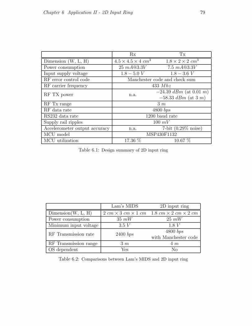
Chapter 6 Application II - 2D Input Ring 79
Rx Tx
Dimension (W, L, H) 4.5 × 4.5 × 4 cm3 1.8 × 2 × 2 cm3
Power consumption 25 [email protected] 7.5 [email protected] supply voltage 1.8 − 5.0 V 1.8 − 3.6 VRF error control code Manchester code and check sumRF carrier frequency 433 Mhz
−24.39 dBm (at 0.01 m)RF TX power n.a. −58.33 dBm (at 3 m)RF Tx range 3 mRF data rate 4800 bpsRS232 data rate 1200 baud rateSupply rail ripples 100 mVAccelerometer output accuracy n.a. 7-bit (0.29% noise)MCU model MSP430F1132MCU utilization 17.36 % 10.67 %
Table 6.1: Design summary of 2D input ring
Lam’s MIDS 2D input ring
Dimension(W, L, H) 2 cm × 3 cm × 1 cm 1.8 cm × 2 cm × 2 cmPower consumption 35 mW 25 mWMinimum input voltage 3.5 V 1.8 V
4800 bpsRF Transmission rate 2400 bps
with Manchester codeRF Transmission range 3 m 4 mOS dependent Yes No
Table 6.2: Comparisons between Lam’s MIDS and 2D input ring

Chapter 6 Application II - 2D Input Ring 80
Figure 6.12: Photograph of 2D remote control ring
Figure 6.17: Photograph of 2D
ring demo kit (top view)
Figure 6.18: Photograph of 2D ring
demo kit (side view)
6.5 Summary
In this chapter, a 2D input ring based on a generic low power wireless sensor
platform (GLPWSP) was presented. This GLPWSP is useful in ubiquitous
computing because it introduces an alternative use interface. The 2D input
ring also outperforms Lam’s MIDS (wireless version) in terms of power con-
sumption and software portability because the ring requires no custom software
driver installation, and thus, is not operating system (OS) dependent.

Chapter 6 Application II - 2D Input Ring 81
Figure 6.13: Transmission power of the 2D ring at 1 cm
Figure 6.14: Transmission power of the 2D ring at 3 m

Chapter 7
Conclusion
A generic system for low power wireless sensor applications was presented.
It consists of a vibration-to-electrical transducer, power management circuit
and generic sensor platform. The whole system is divided into two parts: a
micro power generator (MPG) and generic low power wireless sensor platform
(GLPWSP). The MPG contains a vibration-to-electrical transducer and power
management circuit. The GLPWSP contains sensor peripherals and a startup
circuit.
7.1 Micro power generator
An AA-size micro power generator (MPG) was introduced. It is a battery
replacement for low power wireless sensor applications. The MPG converts
ambient vibration to electrical energy and is a non-exhaustive power source.
It has a power management circuit which consists of a voltage multiplier (VM)
and regulator which converts AC to a regulated DC voltage at a level usable by
standard integrated circuits. VMs were evaluated by PSpice simulations and
two evaluation metrics: average input power (AIP) and energy efficiency (EE)
suggested. These metrics can also be used to evaluate other duty cycled AC-
DC power converters. The voltage tripler had the best performance, achieving
53 % energy efficiency. With input acceleration 4.63 m/s2, the measured
82
Chapter 7 Conclusion 83
power density of the MPG was 53.1 µW/cm3. Maximum output voltage was
measured to be 2.4 V . The MPG was measured to take 32 seconds for charging
reservoir capacitor (1 mF ) from 0 V to 1.8 V . The recharge time was measured
to be 18 seconds for charging 1 mF capacitor from 1.4 V to 1.8 V .
7.2 Low power wireless sensor applications
A generic platform (GP) was also presented for low power wireless sensor appli-
cations. It can be used to measure the properties of environment and transmit
data via a radio frequency (RF) channel. The GP is multi-functional and can
measure temperature, acceleration, humidity or sound level with an appropri-
ate sensor. Besides sending information to the host via RF, GP can store the
information in non-volatile memory (flash memory). Two applications were
presented to show its utility.
7.2.1 Wireless thermometer
A wireless thermometer was designed and tested using the AA-size MPG as
a power source. Equipped with a startup module, the wireless thermometer
consumes only 4.5 µW in the idle state. The startup module turns on the
wireless thermometer when the storage capacitor is charged to a predefined
voltage (1.8 V ). The wireless thermometer then takes 1.42 s to measure and
transmit the temperature reading. The whole process consumes 212.62 µJ of
energy, 30 % of the total energy being consumed in the regulator startup and
MCU initialization. Wireless transmission consumes most of energy 53 % of
the energy. The wireless thermometer with MPG is the first reported sensor
system which can be both self powered and startup.

Chapter 7 Conclusion 84
7.2.2 2D input ring
The 2D input battery powered ring is a miniature device for ubiquitous com-
puting. It also demonstrated that the GLPWSP, can be used for battery
powered application, which require similar features to the VBG based appli-
cations, ie. low power, small, wireless and easy to integrate with different
sensors. The 2D input ring can be used as a mouse and control a personal
computer. Besides RF communications, the 2D input ring can control other
appliances via the IrDA module is loaded. As an example, the 2D input ring
was programmed to be a remote control pad which can operate with Pentax
camera (zoom and shoot).
Instead of mechanical buttons, the 2D ring can recognize strokes or gestures
and send commands to other devices via infrared or radio frequency channels.
This introduces an alternative user interface which can be worn at all times
and serve as an interface to multiple appliances.
Compared to Lam’s MIDS [22], the 2D input ring has lower power con-
sumption and higher output resolution.
7.3 Further development
The 2D input ring can be upgraded to detect 3D motion and be powered
by vibration-based micro power generator. The input ring can be completely
shielded by metal case with caved antenna. The ring requires no batteries
because it is self-powered by vibrations.
Many applications can be derived for the input ring. A more robust al-
gorithm can be developed in order to recognize finger stroke or gesture. A
well-known speech algorithm, namely the Hidden Markov Model (HMM), can
be applied to with slightly modifications. With proper data set training and
vector quantization, a compactly coded HMM system should fit on the ring.
Equipped with recognition ability, the ring acts as a communication interface

Chapter 7 Conclusion 85
between electronic appliances and human. In the future, computer users need
not to put their hands on keyboard or computer mouse. Instead of being con-
fined to working on a surface, their finger can be used to write freely in the air
to command other devices via an ad hoc network (similar to the idea of pico
net in Bluetooth).
The 2D input ring is a good example of GLPWSP, however it is not the
only one. Based on GLPWSP, scientists can design different kinds of sensor
nodes to monitor different quantities. They can monitor the environmental fac-
tors (humidity, temperature, sunshine) of natural places, such as wetlands. A
group of modified sensor nodes (equipped with RFID [39]) can be placed in the
commercial center to track buying habits of consumers. GPs which contains
MEMS sensor, microprocessor and wireless transceiver have nice properties:
low power and small size and is likely to become standard for pervastive com-
puting. As technologies advance, miniature wireless sensor systems become
feasible and many new applications will emerge.

Bibliography
[1] Federal Standard 1037C. Manchester code.
http://www.its.bldrdoc.gov/fs-1037/dir-022/ 3206.htm.
[2] R Amirtharajah and A.P. Chandrakasan. Self-powered signal processing
using vibration-based power generation. In IEEE Journal of Solid-State
Circuits, volume 33, May 1998.
[3] The Infrared Data Association. Official homepage of IrDA.
http://www.irda.org.
[4] Marshall Brain. Howstuffworks “how motes work”.
http://computer.howstuffworks.com/mote2.htm.
[5] Neil N.H. Ching, H.Y. Wong, Wen J.Li, and Philip H.W. Leong. A laser-
micromachined vibrational to electrical power transducer for wireless sens-
ing systems. In the 11th International Conference on Solid-State Sensors
and Actuators, volume A: Physical, Munich, Germany, 2001.
[6] Ansoft Corporation. HFSS official product homepage.
http://www.ansoft.com/products/hf/hfss/.
[7] Atmel Corporation. Smart RF Wireless Data Microtransmitter, 2003.
http://www.atmel.com/dyn/resources/prod documents/doc1424.
pdf.
86

[8] Microsoft Corporation. Microsoft Official Homepage.
http://www.microsoft.com.
[9] Best Sound Electronics. Official homepage of BSE, 2003.
http://www.bsecm.com/e index.asp.
[10] Tomi Engdahl. PC mouse information.
http://www.hut.fi/∼then/mytexts/mouse.html.
[11] Rudolf F Graf and William Sheets. Build Your Own Low-Power Transmi-
iter - Projects for the Electronics Experimenter. 225 Wildwood Avenue,
Woburn MA 01801-2041, 2001.
[12] Rudolf F. Graf and William Sheets. Build Your Own Low-Power Trans-
mitters - Projects for the Electronics Experimenter. 2001.
[13] Gruime. Mouse Protocol.
http://wwww.everything2.com/?node=Mouse+protocol.
[14] Jason L. Hill and David E. Cullier. A wireless platform for deeply
embedded networks. IEEE mico magazine, 22(6), 2002.
http://www.cs.berkeley.edu/∼culler/cs294-f03/papers/
micaarch.pdf.
[15] Horowitz and Hill. The Art of Electronics. Cambridge, The Edinburgh
Building, Cambridge CB2 2RU, UK, 1999.
[16] Analog Devices Inc. Low-Cost ±2 g Dual-Axis Accelerometer With Duty
Cycle Output Data Sheet (Rev. A, 10/00), 2000.
http://www.analog.com/UploadedFiles/Data Sheets/
567227477ADXL202E a.pdf.
87

[17] Nippon Precision Circuits INC. SM5021 series crystal oscillator module
ICS, 1999.
ftp://ftp.npc.co.jp/pub/pdf e/nc9903ae.pdf.
[18] RF Monolithics Inc. Antenna Lenghts.
http://www.rfm.com/products/apnotes/antennalengths.pdf.
[19] RF Monolithics Inc. Antennas for Low Power Applications.
http://www.rfm.com/corp/appdata/antenna.pdf.
[20] Texas Instruments Incorporated. Digital Temperature Sensor with i2c
Interface, 2003.
http://www-s.ti.com/sc/ds/tmp100.pdf.
[21] Texas Instruments Incorporated. MSP430x1xx Family User’s Guild
(Rev.D), 2004.
http://focus.ti.com/lit/ug/slau049d/slau049d.pdf.
[22] Alan H. F. Lam. Micro Input Devices System MIDS: Using MEMS sensors
and wireless technology for generalized computer interface functions. In
Proceedings of the 4th ACM Postgraduate Research Day 2003, Hong Kong,
2003.
[23] Johnny M.H. Lee, Steve C.L. Yuen, Wen J. Li, and Philip H.W. Leong.
Development of an AA size energy transducer with micro resonators. In
Proceedings of IEEEE/ICECS, 2002.
[24] W.J. Li, Z.Y. Wen, P.K. Wong, G.M.H. Chan, and P.H.W. Leong. A
micromachined vibration-induced power generator for low power sensors
of robotic systems. In Proc. of the World Automation Congress, Hawaii,
USA, 2002.
[25] Scott Meninger, Jose Oscar Mur-Miranda, Rajeevan Amirtharajah, Anan-
tha P. Chandrakasan, and Jeffrey H. Lang. Vibration-to-electric energy
88

conversion. In IEEE transaction on Very Large Scale Integration System,
volume 9, Feb 2001.
[26] Cypress MicroSystem. Datasheet of PSoC, 2003.
http://www.cypress.com/cfuploads/img/products/CY8C26443.pdf.
[27] Paul D. Mitcheson, Tim C. Green, Eric M. Yeatman, and Andrew S.
Holmes. Architectures for vibration-driven micropower generators. In
Journal of Microelectromechanical Systems, volume 13, Jun 2004.
[28] Elizabeth D. Mynatt, Anne-Sophie Melenhorst, Arthur D. Fisk, and
Wendy A. Rogers. Aware Technologies for Aging in Place: Understand-
ing User Needs and Attitudes. In IEEE Pervasive Computing, volume 3,
April-June 2004.
[29] Department of Automation and Computer-Aided Engineering. ACAE
official homepage.
http://www.acae.cuhk.edu.hk.
[30] Department of Computer Science and Engineering. CSE official home-
page.
http://www.cse.cuhk.edu.hk.
[31] The Chinese University of Hong Kong. CUHK official homepage.
http://www.cse.cuhk.edu.hk.
[32] Maxim Integrated Products. SOT23, 1.8V, Nanopower, Beyong-the-Rails
Comparators With/Without Reference, 1999.
http://pdfserv.maxim-ic.com/en/ds/MAX917-MAX920.pdf.
[33] Maxim Integrated Products. DC-DC Convertor Tutorial, 2000.
http://pdfserv.maxim-ic.com/en/an/AN710.pdf.
89

[34] Maxim Integrated Products. DC/DC Conversion without Inductors,
2000.
http://pdfserv.maxim-ic.com/en/an/AN725.pdf.
[35] Maxim Integrated Products. 1.5µa iQ, Step-Up DC-DC Converters, 2001.
http://pdfserv.maxim-ic.com/en/ds/MAX1722-MAX1724.pdf.
[36] Bob Nelson RFM. High Data Rate SAW-Stabilized ASK Transmitter,
2003.
http://www.rfm.com/products/apnotes/highdataratesaw.pdf.
[37] Jie Nie RFM. SAW Based Transmitter Design Notes, 2003.
http://www.rfm.com/products/apnotes/sawbasedtransmitter.pdf.
[38] Bjorn Rhoads. a general remote control program ver3.4, 1995.
http://www.rhoads.nu/bjorn/hp48/remote/remote.html.
[39] Mark Roberti. RFID Journal.
http://www.rfidjournal.com/.
[40] S.J. Roundy. Energy Scavenging for Wireless Sensor Nodes with a Focus
on Vibration to Electricity Conversion. PhD thesis, May. 2003.
http://engnet.anu.edu.au/DEpeople/Shad.Roundy/paper/
ShadThesis.pdf.
[41] Cotter W. Sayre. Complete Wireless Design. 2001.
[42] Cypress Semiconductor. Cypress Microsystems homepage, 2003.
http://www.cypressmicro.com.
[43] DALLAS Semiconductor. DS1620 digital thermometer and thermostat,
1999.
http://pdfserv.maxim-ic.com/arpdf/DS1620.pdf.
90

[44] National Semiconductor. National’s New Revolutionary Microphone Am-
plifiers.
http://www.national.com/appinfo/amps/microphone.html.
[45] Leo Setian. Practical Communication Antenna with Wireless Applica-
tions. 1998.
[46] LINX technologies Ltd. LINX LC series transmitter datasheet, 1999.
http://www.rfdigital.com/pdf/rfd24003.pdf.
[47] UBICOM. SX20AC/SX28AC configurable communications controllers
with EE/FLASH program memory, in-system programming capability
and on-chip debug, 2001.
http://www.ubicom.com/pdfs/products/sx/processor/
SX-DDS-SX2028AC-16.pdf.
[48] UCLA. WINS wireless integrated network sensors, 1993-1999.
http://www.janet.ucla.edu/WINS.
[49] Berkeley Univerisity of California. UC Berkeley Homepage, 2003.
http://www.berkeley.edu/.
[50] Berkeley University of California. Tiny OS, a component-based OS for
the networked sensor regime, 2003.
http://webs.cs.berkeley.edu/tos/.
[51] LA University of California. UCLA homepage, 2003.
http://www.ucla.edu.
[52] Arie van Rhijn. Digital Microphones - Applications and System Parti-
tioning, 2003.
http://www.national.com/nationaledge/apr03/article.html.
91

[53] Tony van Roon. Phase-Locked Loop Tutorial, 2001.
http://www.uoguelph.ca/∼antoon/gadgets/pll/pll.html.
[54] S. Vardhan, M. Wilczynski, G.J. Portie, and W.J. Kaiser. Wireless inte-
grated network sensors (wins): distributed in situ sensing for mission and
flight systems. In Aerospace Conference Proceedings, volume 7, March
2000.
[55] C.B. Williams, C. Shearwood, M.A Harradinem, P.H. Meller, T.S. Birch,
and R.B. Yates. Development of an electromagnetic microgenerator. In
Circuits, Devices and System, IEE proceedings, volume 148, Dec. 2001.
92

Publications
Full length conference paper
Johnny M. H. Lee, Steve C. L. Yuen, Wen J. Li, and Philip H. W. Leong, “De-
velopment of an AA-Size Energy Transducer with Micro Resonators”, IEEE
Int. Symp. on Circuit and Systems (ISCAS), Bangkok, Thailand, May 2003
93

Appendix A
Schematics
1. 2D input ring (transmitter section)
2. 2D input ring (receiver section)
94
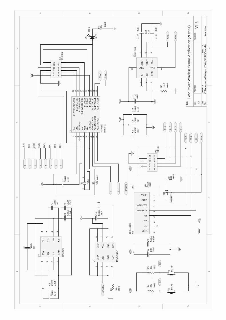
11
22
33
44
DD
CC
BB
AA
Title
Num
ber
Rev
ision
Size A
4
Dat
e:20
04/6
/16
Shee
t o
f Fi
le:
C:\D
ocum
ents
and
Set
tings
\..\2
Drin
g.SC
HD
OCD
raw
n B
y:
0.1u
FC
0603
C7
P2.3
/TA
1/A
311
P2.4
/TA
2/A
412
P1.0
/TA
CLK
13P1
.1/T
A0
14P1
.2/T
A1
15P1
.3/T
A2
16P1
.4/S
MCL
K/T
CK17
P1.5
/TA
0/TM
S18
P1.6
/TA
1/TD
I19
P1.7
/TA
2/TD
O/T
DI
20Te
st1
VCC
2
P2.5
/Ros
c3
Vss
4
Xou
t5
Xin
6
_RST
/NM
I7
P2.0
/AC
LK/A
08
P2.1
/IN
CLK
/A1
9
P2.2
/TA
0/A
210
MSP
1132
TSSO
P-20
U1
VCC
12
7680
0
Y1
68k
0402
R2
10k 06
03
R5
LED
2
080
5
DS1
B2
B1
LIN
XTX
123456
789
101112
CLE
106
JP1
XFI
LT
7
YFI
LT
6
Xou
t5
VDD8
ST1
T2
2
CO
M3
Yout 4
AD
XL2
02E
U2
0603
0.1u
F C12 06
030.
1uFC
13
0603
0.1u
FC
11
VD
D
t
1M2
0603
R3
Xou
t1
You
t1
Xou
t1
You
t1
VD
D
10uF
C12
10C
8
1uF
C06
03C
9
0.1
uFC
0603
C10
C2+
8
C1+
7
Vin
6
C1-
5G
ND
4
C2-
3
EN2
Vou
t1
TPS
6024
0
U2
1uF
C08
05C
4
1uF
C08
05
C3
2.2u
FC
1206
C2
2.2
uFC
0805
C5
2.2
uFC
0805
C1
t
20k
0603
R5
t
20k
0603
R4
B1
B2
VD
D SW-P
BS1
SW-P
BS2
GN
D1
DIN
2
GN
D3
LA
DJ
4
GN
D8
VCC
7
GN
D6
RFO
5
TXM
-433
-LC
U4
VCC
10uF
C12
06C
14
t
100
0603
R1
LIN
XT
X
Low
Pow
er W
irele
ss S
esno
r A
pplic
atio
n (2
D ri
ng) V1.
8
Stev
e Y
uen
2.2u
FC
1206
C6
NC7
Vcc 6
SD 5
GND8
RXD(IrDA) 4
TXD(IrDA) 3
V(RC) 2
LEDA1
HSD
L-30
02U
3
VCC
123456
789
101112
FTE
106
JP2
MO
SFE
T-NQ1
0R 0603
R7
3.3R
060
3
R6
VD
D
P1.2
P1.3
P1.1
P1.0
VD
DV
DD 6.8u
FT4
91C
8
0.47
uFC
0805
C9
P1.4
P1.5
P1.6
P1.7
VC
C
0 1 2 3 4 5 6 7
Test
VD
D
GN
D
TDO
TDI
TMS
TCK
_RST

11
22
33
44
DD
CC
BB
AA
Title
Num
ber
Rev
ision
Size A
4
Dat
e:20
04/6
/16
Shee
t o
f Fi
le:
C:\D
ocum
ents
and
Set
tings
\..\T
IR1.
SCH
DO
CD
raw
n B
y:
8
EN111
FORC
EOFF
16
9
FOR
CEO
N1213
INVA
LID
10
C1+
2
C2+
5
GN
D14
C1-
4V
CC15
C2-
6
V-
7
V+
3
MA
X32
21C
AE
U1
0.1u
FC
0603
C1
0.1u
FC
0603
C2
0.1
uFC
0603
C3
0.1
uFC
0603
C4
0.1
uFC
0603
C6
0.1u
FC
0603
C6
VCC
1 2 3 4 56 7 8 9
11 10
D C
onne
ctor
9
J1
100 06
03
R1
P2.3
/TA
1/A
311
P2.4
/TA
2/A
412
P1.0
/TA
CLK
13P1
.1/T
A0
14P1
.2/T
A1
15P1
.3/T
A2
16P1
.4/S
MCL
K/T
CK17
P1.5
/TA
0/TM
S18
P1.6
/TA
1/TD
I19
P1.
7/TA
2/TD
O/T
DI
20Te
st1
VCC
2
P2.5
/Ros
c3
Vss
4
Xou
t5
Xin
6
_RST
/NM
I7
P2.0
/AC
LK
/A0
8
P2.1
/IN
CLK
/A1
9
P2.2
/TA
0/A
210
MSP
1132
TSSO
P-20
U2
VCC
VCC
12
7680
0
Y1
68k
0402
R2
10k 06
03
R3
LED
2
0805
DS1
RS2
32
MA
CK
MA
CK
RS2
32
LIN
XR
XLI
NX
RX
123456
789
101112
CLE
106
JP1
NC
1
NC
2
NC
3
GN
D4
VCC
5
PDN
6
NC
7
DA
TA8
NC
9N
C10
NC
11N
C12
NC
13N
C14
GN
D15
AN
T16
LIN
XR
F
U3
VC
C
1uF
C06
03C
8
LIN
XR
X
AN
TEN
NA
NC
1
Enab
le2
Vin
3
GN
D4
PGN
D5
C-
6C
+7
Vou
t8
REG
711
U4
2.2
uFC
0805
C9
0.2
2uF
C06
03
C10
10uF
C12
06C
11
VCC
Bat
t in.
Low
Pow
er W
irel
ess
Sens
or A
pplic
atio
n (R
ecei
ver s
ectio
n)
Stev
e Y
uenv1
.8
10uF
C12
06C
7