
Nonlinear second order equations with applications to partial differential equations
Upload
independentCategory
view
2download
0
Light-opals interaction modelingby direct numerical solution
of Maxwell’s equations
Alessandro Vaccari,1,∗ Antonino Cala Lesina,2,3,8 Luca Cristoforetti,4Andrea Chiappini,5 Luigi Crema,1 Lucia Calliari,6 Lora Ramunno,2,3
Pierre Berini,2,3,7 and Maurizio Ferrari51FBK (Fondazione Bruno Kessler), Centro Materiali e Microsistemi, Unita ARES, 38123
Trento, Italy2Department of Physics, University of Ottawa, Ottawa, Ontario, K1N6N5, Canada
3Centre for Research in Photonics, University of Ottawa, Ottawa, Ontario, K1N6N5, Canada4Provincia Autonoma di Trento, Dipartimento della Conoscenza, 38122 Trento, Italy
5IFN-CNR, Istituto per la Fotonica e le Nanotecnologie, Laboratorio CSMFO, 38123 Trento,Italy
6FBK (Fondazione Bruno Kessler), Centro Materiali e Microsistemi, Unita LISC, 38123Trento, Italy
7School of Electrical Engineering and Computer Science, University of Ottawa, Ottawa,Ontario, K1N6N5, Canada
[email protected]∗[email protected]
Abstract: This work describes a 3-D Finite-Difference Time-Domain(FDTD) computational approach for the optical characterization of an opalphotonic crystal. To fully validate the approach we compare the computedtransmittance of a crystal model with the transmittance of an actual crystalsample, as measured over the 400÷ 750 nm wavelength range. The opalphotonic crystal considered has a face-centered cubic (FCC) lattice struc-ture of spherical particles made of polystyrene (a non-absorptive materialwith constant relative dielectric permittivity). Light-matter interaction isdescribed by numerically solving Maxwell’s equations via a parallelizedFDTD code. Periodic boundary conditions (PBCs) at the outer edges of thecrystal are used to effectively enforce an infinite lateral extension of thesample. A method to study the propagating Bloch modes inside the crystalbulk is also proposed, which allows the reconstruction of the ω-k dispersioncurve for k sweeping discretely the Brillouin zone of the crystal.
© 2014 Optical Society of America
OCIS codes: (160.5298) Photonic crystals; (160.5293) Photonic bandgap materials;(050.1755) Computational electromagnetic methods; (290.4210) Multiple scattering.
References and links1. K. S. Yee, “Numerical solution of initial boundary value problems involving Maxwell’s equations in isotropic
media,” IEEE Trans. Antennas Propag. 14, 302–307 (1966).2. A. Taflove and S. C. Hagness, Computational Electrodynamics: The Finite-Difference Time-Domain Method, 3rd
ed. (Artech House, 2005).3. A. Vaccari, L. Cristoforetti, A. Cala Lesina, L. Ramunno, A. Chiappini, F. Prudenzano, A. Bozzoli, and L.
Calliari, “Parallel FDTD modeling of an opal photonic crystal,” Opt. Eng. 53(7), 071809 (2014).4. J. D. Joannopoulos, S. G. Johnson, J. N. Winn, and R. D. Meade, Photonic Crystals. Molding the Flow of Light,
2nd ed. (Princeton University, 2008), Appendix B.
#217506 - $15.00 USD Received 3 Sep 2014; revised 19 Oct 2014; accepted 20 Oct 2014; published 31 Oct 2014(C) 2014 OSA 3 November 2014 | Vol. 22, No. 22 | DOI:10.1364/OE.22.027739 | OPTICS EXPRESS 27739

5. J. A. Stratton, Electromagnetic Theory (McGraw-Hill, 1941), Chap. VIII.6. J. D. Jackson, Classical Electrodynamics, 3rd ed. (Wiley, 1998), Chap. 9.7. W. Gropp, E. L. Lusk, and A. Skjellum, Using MPI. Portable Parallel Programming With the Message Passing
Interface, 2nd ed. (MIT, 1999).8. W. Gropp, E. L. Lusk, and R. Thakur, Using MPI-2. Advanced Features in the Message Passing Interface (MIT,
1999).9. P. Pacheco, Parallel Programming with MPI (Morgan Kaufmann, 1997).
10. A. Taflove and M. E. Brodwin, “Numerical solution of steady-state electromagnetic scattering problems usingthe time-dependent Maxwell’s equations,” IEEE Trans. Microwave Theory Tech. 23, 623–630 (1975).
11. J. A. Roden and S. D. Gedney, “Convolution PML (CPML): An efficient FDTD implementation of the CFS-PMLfor arbitrary media,” Microw. Opt. Tech. Lett. 27(5), 334–339 (2000).
12. R. Pontalti, L. Cristoforetti, and L. Cescatti, “The frequency dependent FD-TD method for multi-frequencyresults in microwave hypertermia treatment simulation,” Phys. Med. Biol. 38, 1283–1298 (1993).
13. R. Pontalti, J. Nadobny, P. Wust, A. Vaccari, and D. Sullivan, “Investigation of static and quasi-static fieldsinherent to the pulsed FDTD method,” IEEE Trans. Microwave Theory Tech. 50(8), (2002).
14. A. Vaccari, R. Pontalti, C. Malacarne, and L. Cristoforetti, “A robust and efficient subgridding algorithm forfinite-difference time-domain simulations of Maxwell’s equations,” J. Comput. Phys. 194, 117–139 (2004).
15. A. Chiappini, C. Armellini, A. Chiasera, M. Ferrari, L. Fortes, M. C. Goncalves, R. Guider, Y. Jestin, R. Retoux,G. N. Conti, S. Pelli, R. M. Almeida, and G. C. Righini, “An alternative method to obtain direct opal photoniccrystal structures,” J. Non-Cryst. Solids 355, 1167–1170 (2009).
1. Introduction
The Finite-Difference Time-Domain (or simply FDTD) method [1,2] is a technique in Compu-tational Electromagnetics which solves Maxwell’s equations directly in the time-domain witha minimum of numerical complexity and computer resources. In this method a 3-D mesh ofsampling points in space and a discrete sampling of the time axis for the electric and magneticvector component values is used, thus getting a space-time grid. A characteristic staggered po-sitioning of the electric and magnetic fields on the grid (i.e. in both space and time) providessecond-order accuracy in the partial derivatives, allowing an explicit updating scheme of thefield values at any instant of time, resulting in a complete description of their time evolution,starting from a zero field initial configuration. Frequency-domain data are easily obtained byperforming an in-line discrete Fourier transform (DFT) of the fields, if the excitation of thesystem is done by means of signals of finite duration.
In a previous paper [3] we used the FDTD method to characterize the optical behavior of anopal photonic crystal (PC) at a fundamental level, by numerically solving Maxwell’s equationsfully accounting for the electromagnetic interaction with its material structure on a macro-scopic scale. In that article we considered a small finite crystal sample made of face-centeredcubic (FCC) packed polystyrene spheres, illuminated with a light beam impinging perpendic-ularly to its (1,1,1) reticular planes, where use is made here of the Miller indices notationcharacterizing a given family of planes [4]. The impinging light beam was simulated througha linearly polarized plane wave pulse, injected on the FDTD grid by means of the so calledtotal-field/scattered-field (TF/SF) method. A special boundary is constructed in space on theFDTD mesh and field corrections are applied at any instant of time to the field components onthis boundary to maintain the contrast between the interior (total-field region) and the exterior(scattered-field only region) of the boundary.
Analyzing the scattered far-field obtained by means of the Kirchhoff formula [5, 6] appliedto the time Fourier transformed near-field data on a surface surrounding the sample, we nu-merically determined its transmittance intensity spectrum and traced out the bandgap arisingfrom the crystal symmetry and the refractive index of the polystyrene spheres from which itis assembled. Due to edge effects of the small sample used and to the low dielectric contrast,although the numerical data compared fairly well with the experimental ones for what con-cerns the wavelength occurrence of the bandgap, this was reproduced with a very small depth.To get a well indented transmittance spectrum a lot of (1,1,1) reticular planes along the im-
#217506 - $15.00 USD Received 3 Sep 2014; revised 19 Oct 2014; accepted 20 Oct 2014; published 31 Oct 2014(C) 2014 OSA 3 November 2014 | Vol. 22, No. 22 | DOI:10.1364/OE.22.027739 | OPTICS EXPRESS 27740

pinging direction have to be stacked in the numerical model, similarly to what happens in theexperimental situation in which a macroscopic crystal sample is used. Actually, it is likely thatsecondary irradiation from the lateral sample surfaces bends the planar wavefronts thus pre-venting a full Bragg destructive interference in the forward direction. However, increasing thenumber of modeled reticular planes requires a lot of computational resources. One of the mostefficient solutions consists in the use of periodic boundary conditions (PBCs) [2] on surfaceswith normals perpendicular to the beam propagation direction, allowing the modelization of anideal crystal slab of infinite extension and of given thickness. Moreover, to evaluate its trans-mittance and reflectance it is sufficient to perform a Poynting vector integration on parallelsurfaces before and after the slab (at a sufficient distance to neglect the actual discontinuouscrystal structure) of the time Fourier transformed data without the need of a near-to-far-fieldstep.
In the present paper we are thus able to numerically reproduce, simulating the basic principlesof the crystal interaction with the light electromagnetic field, the optical behavior of an opal PCas a function of the wavelength in the 400÷ 750 nm range in a very satisfactory agreementwith experimental measurements. Thanks to the FDTD data results on the crystal bulk andby using spatial Fourier transforms, we are also able to reconstruct quantitatively parts of theω− k crystal dispersion curve, a generalizable result which cannot be obtained analytically forarbitrary structures.
For the present work we wrote and used a parallelized version of an in-house FDTD codebased on the Message Passing Interface (MPI) library [7–9]. All the calculations where per-formed on the BGQ, a Southern Ontario Smart Computing Innovation Platform (SOSCIP)BlueGene/Q supercomputer, located at the University of Toronto’s SciNet HPC facility.
The rest of the paper is organized as follows. In Section 2 we give details of the crystalmodel and on the FDTD simulations. In particular, we describe the way in which paralleliza-tion is achieved. In Section 3 we give examples of the calculated field distributions inside thecrystal, both in the time and frequency domains. We also compare reflectance and transmittancenumerically calculated spectra with a corresponding experimental measurement. In Section 4we describe the procedure we introduce to reconstruct the dispersion curve of the crystal andshow a graph of it. Finally, we summarize our work in Section 5.
2. Modeling and simulation
The crystal model is made of polystyrene spheres of relative dielectric permittivity εr = 2.4which are assumed non-absorptive (σ = 0 Siemens/m). The cell edge of the FCC packing isa = 333.75 nm and the spheres’ radius is R = 118 nm. This gives a structure with a maximalfilling factor of 0.74 (i.e., the ratio of the void to the filled space). In the (1,1,1) planes thecenters of the spheres lie at the vertices of equilateral triangles of edge length ` = a/
√2 and
height h =√
3`/2. The FCC packing is obtained by stacking a sequence ABCABC ... of suchplanes along the y axis. The (1,1,1) planes are then parallel to the xz Cartesian coordinatesystem. In each plane the triangles are incrementally shifted by a vertical distance of d = h/3(in B planes the triangles are also laterally shifted by `/2). The various (1,1,1) planes areat a distance D = a/
√3 apart from each other. Fig. 1 depicts examples of sectional views of
the crystal in the xy, yz (lateral) and xz (front) coordinate planes, to convey an idea of how thestacking of reticular (1,1,1) planes creates the final 3-D structure of the crystal sample modeled.
For the simulation we use cubic Yee unit cells [1, 2] of edge size δ = 2 nm and a timestep δ t = δ/2co, to satisfy the Courant-Friedrichs-Lewy stability condition [10], co being thevacuum light velocity. The computational domain truncation is got by means of convolutionalperfectly matched layers (CPML) absorbing boundary conditions [11]. However, these are ap-plied only to the upstream and downstream external faces, with respect of the impinging beam
#217506 - $15.00 USD Received 3 Sep 2014; revised 19 Oct 2014; accepted 20 Oct 2014; published 31 Oct 2014(C) 2014 OSA 3 November 2014 | Vol. 22, No. 22 | DOI:10.1364/OE.22.027739 | OPTICS EXPRESS 27741

0 500 1000 1500 2000
y−axis [nm]
0
200
400
600
800
x−axis
[nm
]
0 500 1000 1500 2000
y−axis [nm]
0
100
200
300
400
500
600
700
800
z−axis
[nm
]
0 200 400 600 800
x−axis [nm]
0
100
200
300
400
500
600
700
800
z−axis
[nm
]
Fig. 1. Lateral xy (top), yz (bottom-left) and front xz (bottom-right) sections of the FCClattice as modeled in the FDTD code.
propagation direction. On the lateral faces PBCs are applied, which consist in reinjecting thefield values in a wraparound fashion. To this end, the interacting crystal structure has to berepresented in a consistent manner: the part left out at one side must be mirrored at the otheropposite side. To excite the system, we used a “raised cosine” plane wave pulse type with a timeprofile having compact support like the ones described in [12–14]. The “plane wave injector”no more has lateral and ending guiding surfaces, but only the starting one (the vertical dashedline in Fig. 2). Behind it only the reflected field is present. In that region, if sufficiently far
Incident field
Total field
Sca/ered field only
Periodic boundary condi5on
Periodic boundary condi5on
CPML boundary condi5on
CPML boundary condi5on
y
Fig. 2. Two-dimensional scheme of the FDTD modeling with PBCs.
from the crystal slab, reflectance can be evaluated by integrating the real part of the complexPoynting normal vector. The transmittance can be similarly evaluated by considering down-stream planes beyond the crystal slab in the total field region (incident plus transmitted ones).By means of the PBCs, the numerical solution obtained is the one corresponding to an infiniteextension of the slab in planes perpendicular to the impinging beam. Frequency domain field
Yee FDTD cell
x
y
z
x
y
z
𝛿𝑥
𝛿𝑦
𝛿𝑧
Ez
Ex
Ey
Hz
Hx Hy
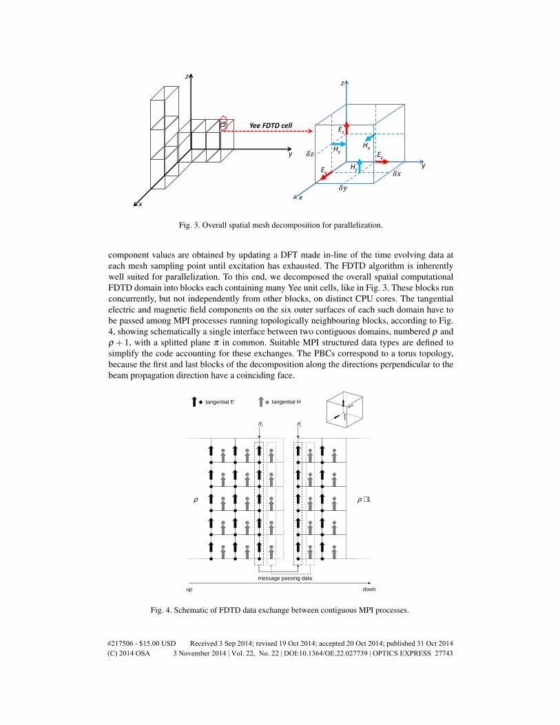
Fig. 3. Overall spatial mesh decomposition for parallelization.
component values are obtained by updating a DFT made in-line of the time evolving data ateach mesh sampling point until excitation has exhausted. The FDTD algorithm is inherentlywell suited for parallelization. To this end, we decomposed the overall spatial computationalFDTD domain into blocks each containing many Yee unit cells, like in Fig. 3. These blocks runconcurrently, but not independently from other blocks, on distinct CPU cores. The tangentialelectric and magnetic field components on the six outer surfaces of each such domain have tobe passed among MPI processes running topologically neighbouring blocks, according to Fig.4, showing schematically a single interface between two contiguous domains, numbered ρ andρ + 1, with a splitted plane π in common. Suitable MPI structured data types are defined tosimplify the code accounting for these exchanges. The PBCs correspond to a torus topology,because the first and last blocks of the decomposition along the directions perpendicular to thebeam propagation direction have a coinciding face.
up down
ρ ρ +1
tangential E tangential H
π+ π−
message passing data
Fig. 4. Schematic of FDTD data exchange between contiguous MPI processes.
#217506 - $15.00 USD Received 3 Sep 2014; revised 19 Oct 2014; accepted 20 Oct 2014; published 31 Oct 2014(C) 2014 OSA 3 November 2014 | Vol. 22, No. 22 | DOI:10.1364/OE.22.027739 | OPTICS EXPRESS 27743
3. Results
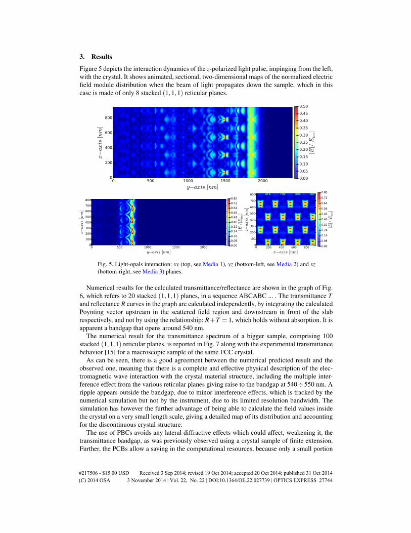
Figure 5 depicts the interaction dynamics of the z-polarized light pulse, impinging from the left,with the crystal. It shows animated, sectional, two-dimensional maps of the normalized electricfield module distribution when the beam of light propagates down the sample, which in thiscase is made of only 8 stacked (1,1,1) reticular planes.
0 500 1000 1500 2000
y−axis [nm]
0
200
400
600
800
x−axis
[nm
]
0.00
0.05
0.10
0.15
0.20
0.25
0.30
0.35
0.40
0.45
0.50
|E|/|E
inc|
0 500 1000 1500 2000
y−axis [nm]
0
100
200
300
400
500
600
700
800
z−axis
[nm
]
0.00
0.08
0.16
0.24
0.32
0.40
0.48
0.56
0.64
0.72
0.80
|E|/|E
inc|
0 200 400 600 800
x−axis [nm]
0
100
200
300
400
500
600
700
800
z−axis
[nm
]0.00
0.08
0.16
0.24
0.32
0.40
0.48
0.56
0.64
0.72
0.80
|E|/|E
inc|
Fig. 5. Light-opals interaction: xy (top, see Media 1), yz (bottom-left, see Media 2) and xz(bottom-right, see Media 3) planes.
Numerical results for the calculated transmittance/reflectance are shown in the graph of Fig.6, which refers to 20 stacked (1,1,1) planes, in a sequence ABCABC ... . The transmittance Tand reflectance R curves in the graph are calculated independently, by integrating the calculatedPoynting vector upstream in the scattered field region and downstream in front of the slabrespectively, and not by using the relationship: R+T = 1, which holds without absorption. It isapparent a bandgap that opens around 540 nm.
The numerical result for the transmittance spectrum of a bigger sample, comprising 100stacked (1,1,1) reticular planes, is reported in Fig. 7 along with the experimental transmittancebehavior [15] for a macroscopic sample of the same FCC crystal.
As can be seen, there is a good agreement between the numerical predicted result and theobserved one, meaning that there is a complete and effective physical description of the elec-tromagnetic wave interaction with the crystal material structure, including the multiple inter-ference effect from the various reticular planes giving raise to the bandgap at 540÷550 nm. Aripple appears outside the bandgap, due to minor interference effects, which is tracked by thenumerical simulation but not by the instrument, due to its limited resolution bandwidth. Thesimulation has however the further advantage of being able to calculate the field values insidethe crystal on a very small length scale, giving a detailed map of its distribution and accountingfor the discontinuous crystal structure.
The use of PBCs avoids any lateral diffractive effects which could affect, weakening it, thetransmittance bandgap, as was previously observed using a crystal sample of finite extension.Further, the PCBs allow a saving in the computational resources, because only a small portion
#217506 - $15.00 USD Received 3 Sep 2014; revised 19 Oct 2014; accepted 20 Oct 2014; published 31 Oct 2014(C) 2014 OSA 3 November 2014 | Vol. 22, No. 22 | DOI:10.1364/OE.22.027739 | OPTICS EXPRESS 27744

0.0
0.2
0.4
0.6
0.8
1.0
400 450 500 550 600 650 700 750
Re
fle
cta
nc
e/T
ran
sm
itta
nc
e
vacuum wavelength (nm)
Fig. 6. Numerical transmittance (top curve) and reflectance (bottom curve) for a crystalslab made of 20 stacked (1,1,1) planes.
0.0
0.2
0.4
0.6
0.8
1.0
400 450 500 550 600 650 700 750
Tra
ns
mit
tan
ce
vacuum wavelength (nm)
Fig. 7. Numerical transmittance for a crystal slab made of 100 stacked (1,1,1) planes (topcurve) compared with an experimental result (bottom curve) for a macroscopic sample ofthe same FCC crystal.
in planes perpendicular to the impinging direction has to be considered. We used the minimumtransverse extension which could be periodically prolonged. Larger extensions did not giveappreciable different results even if they are used in the maps for illustrative purposes. Usingthe minimum transverse dimensions, in fact, allows time saving.
We also tried the two different linear polarization orientations in the (1,1,1) reticular planes(here the x and z axes) without observing changes in the response, as confirmed also by experi-mental observations.
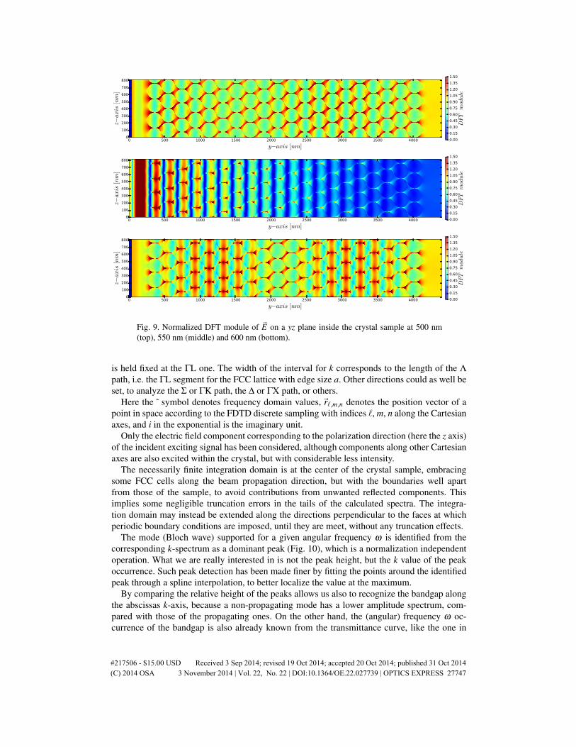
Figures 8 and 9 depict sectional, two-dimensional maps, extracted from inside the crystalstructure, of the Fourier transformed ~E field distribution. The Fourier transforms have beenobtained by means of a DFT on all the spatial values, at the angular frequencies corresponding
#217506 - $15.00 USD Received 3 Sep 2014; revised 19 Oct 2014; accepted 20 Oct 2014; published 31 Oct 2014(C) 2014 OSA 3 November 2014 | Vol. 22, No. 22 | DOI:10.1364/OE.22.027739 | OPTICS EXPRESS 27745
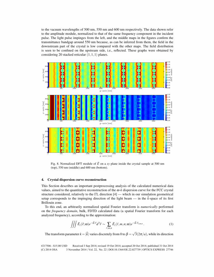
to the vacuum wavelengths of 500 nm, 550 nm and 600 nm respectively. The data shown referto the amplitude module, normalized to that of the same frequency component in the incidentpulse. The light pulse impinges from the left, and the middle maps in the figures confirm thetransmittance bandgap around 550 nm because, as can be inferred from them, the field in thedownstream part of the crystal is low compared with the other maps. The field distributionis seen to be confined on the upstream side, i.e., reflected. These graphs were obtained byconsidering 20 stacked reticular (1,1,1) planes.
0 500 1000 1500 2000 2500 3000 3500 4000
y−axis [nm]
0
200
400
600
800
x−axis
[nm
]
0.00
0.15
0.30
0.45
0.60
0.75
0.90
1.05
1.20
1.35
1.50
DFTmodule
0 500 1000 1500 2000 2500 3000 3500 4000
y−axis [nm]
0
200
400
600
800
x−axis
[nm
]
0.00
0.15
0.30
0.45
0.60
0.75
0.90
1.05
1.20
1.35
1.50
DFTmodule
0 500 1000 1500 2000 2500 3000 3500 4000
y−axis [nm]
0
200
400
600
800
x−axis
[nm
]
0.00
0.15
0.30
0.45
0.60
0.75
0.90
1.05
1.20
1.35
1.50
DFTmodule
Fig. 8. Normalized DFT module of ~E on a xy plane inside the crystal sample at 500 nm(top), 550 nm (middle) and 600 nm (bottom).
4. Crystal dispersion curve reconstruction
This Section describes an important postprocessing analysis of the calculated numerical datavalues, aimed to the quantitative reconstruction of the ω-k dispersion curve for the FCC crystalstructure considered, relatively to the ΓL direction [4] — which in our simulation geometricalsetup corresponds to the impinging direction of the light beam — in the ~k-space of its firstBrillouin zone.
To this end, an arbitrarily normalized spatial Fourier transform is numerically performedon the frequency domain, bulk, FDTD calculated data (a spatial Fourier transform for eachanalyzed frequency), according to the approximation:∫∫∫
Ez(~r;ω)e−i~k·~rd3~r ∼ ∑`,m,n
Ez(`,m,n;ω)e−i~k·~r`,m,n . (1)
The transform parameter k= |~k| varies discretely from 0 to β =√
3(2π/a), while its direction
#217506 - $15.00 USD Received 3 Sep 2014; revised 19 Oct 2014; accepted 20 Oct 2014; published 31 Oct 2014(C) 2014 OSA 3 November 2014 | Vol. 22, No. 22 | DOI:10.1364/OE.22.027739 | OPTICS EXPRESS 27746
0 500 1000 1500 2000 2500 3000 3500 4000
y−axis [nm]
0
100
200
300
400
500
600
700
800
z−axis
[nm
]
0.00
0.15
0.30
0.45
0.60
0.75
0.90
1.05
1.20
1.35
1.50
DFTmodule
0 500 1000 1500 2000 2500 3000 3500 4000
y−axis [nm]
0
100
200
300
400
500
600
700
800
z−axis
[nm
]
0.00
0.15
0.30
0.45
0.60
0.75
0.90
1.05
1.20
1.35
1.50
DFTmodule
0 500 1000 1500 2000 2500 3000 3500 4000
y−axis [nm]
0
100
200
300
400
500
600
700
800
z−axis
[nm
]
0.00
0.15
0.30
0.45
0.60
0.75
0.90
1.05
1.20
1.35
1.50
DFTmodule
Fig. 9. Normalized DFT module of ~E on a yz plane inside the crystal sample at 500 nm(top), 550 nm (middle) and 600 nm (bottom).
is held fixed at the ΓL one. The width of the interval for k corresponds to the length of the Λ
path, i.e. the ΓL segment for the FCC lattice with edge size a. Other directions could as well beset, to analyze the Σ or ΓK path, the ∆ or ΓX path, or others.
Here the ˜ symbol denotes frequency domain values,~r`,m,n denotes the position vector of apoint in space according to the FDTD discrete sampling with indices `, m, n along the Cartesianaxes, and i in the exponential is the imaginary unit.
Only the electric field component corresponding to the polarization direction (here the z axis)of the incident exciting signal has been considered, although components along other Cartesianaxes are also excited within the crystal, but with considerable less intensity.
The necessarily finite integration domain is at the center of the crystal sample, embracingsome FCC cells along the beam propagation direction, but with the boundaries well apartfrom those of the sample, to avoid contributions from unwanted reflected components. Thisimplies some negligible truncation errors in the tails of the calculated spectra. The integra-tion domain may instead be extended along the directions perpendicular to the faces at whichperiodic boundary conditions are imposed, until they are meet, without any truncation effects.
The mode (Bloch wave) supported for a given angular frequency ω is identified from thecorresponding k-spectrum as a dominant peak (Fig. 10), which is a normalization independentoperation. What we are really interested in is not the peak height, but the k value of the peakoccurrence. Such peak detection has been made finer by fitting the points around the identifiedpeak through a spline interpolation, to better localize the value at the maximum.
By comparing the relative height of the peaks allows us also to recognize the bandgap alongthe abscissas k-axis, because a non-propagating mode has a lower amplitude spectrum, com-pared with those of the propagating ones. On the other hand, the (angular) frequency ω oc-currence of the bandgap is also already known from the transmittance curve, like the one in
#217506 - $15.00 USD Received 3 Sep 2014; revised 19 Oct 2014; accepted 20 Oct 2014; published 31 Oct 2014(C) 2014 OSA 3 November 2014 | Vol. 22, No. 22 | DOI:10.1364/OE.22.027739 | OPTICS EXPRESS 27747

Fig. 6 or Fig. 7. There, the abscissas are labelled as vacuum wavelengths for more practicalinsight, but actually correspond univocally to frequency domain data: ω = 2πc/λ . Examplesof numerically calculated amplitude k-spectra are given in Fig. 10 and Fig. 11, the latter show-ing together the graphs of the previous one. Note that, as expected, at the angular frequencycorresponding to λ = 540 nm (the middle graph), i.e. the frequency of the first bandgap (seeFig. 6), the magnitude of the peak is less than one half the magnitudes of the other peaks (leftand right graphs in the figure) which correspond to fully propagated modes.
0.0E+00
5.0E+04
1.0E+05
1.5E+05
2.0E+05
2.5E+05
3.0E+05
0.2 0.3 0.4 0.5 0.6 0.7 0.8 0.9 1
Arb
itra
ry U
nit
s
k [normalized]
0.0E+00
2.0E+04
4.0E+04
6.0E+04
8.0E+04
1.0E+05
1.2E+05
0.2 0.3 0.4 0.5 0.6 0.7 0.8 0.9 1
Arb
itra
ry U
nit
s
k [normalized]
0.0E+00
5.0E+04
1.0E+05
1.5E+05
2.0E+05
2.5E+05
3.0E+05
0.2 0.3 0.4 0.5 0.6 0.7 0.8 0.9 1
Arb
itra
ry U
nit
s
k [normalized]
Fig. 10. Examples of numerically calculated spatial spectra for ω = 2πc/λ , with λ = 400nm (top-left), 540 nm (top-right) and 700 nm (bottom).
0.0E+00
5.0E+04
1.0E+05
1.5E+05
2.0E+05
2.5E+05
3.0E+05
0.2 0.3 0.4 0.5 0.6 0.7 0.8 0.9 1
Arb
itra
ry U
nit
s
k [normalized]
Fig. 11. Numerical amplitude spatial spectra of Ez(~r;ω) for ω = 2πc/λ , with λ = 700 nm(left curve), 540 nm (middle curve) and 400 nm (right curve).
We eventually end up with a sequence of (k,ω) pairs which, when graphed, allows the quan-
#217506 - $15.00 USD Received 3 Sep 2014; revised 19 Oct 2014; accepted 20 Oct 2014; published 31 Oct 2014(C) 2014 OSA 3 November 2014 | Vol. 22, No. 22 | DOI:10.1364/OE.22.027739 | OPTICS EXPRESS 27748

titative reconstruction of the dispersion curve searched for. That in Fig. 12 is for a stack of 20reticular (1,1,1) planes, in a sequence ABCABC ... . The k and ω axes of the graph are normal-ized: the horizontal one corresponds to k/β values, the vertical one to ωa/2πc values. To getthe second branch of the curve above the first bandgap (the so called “air-line”), the relevant kdata obtained by means of the spatial Fourier transforms have been mirrored in the vertical linethrough the value kbg = 0.499β corresponding to the first bandgap.
It is apparent from the figure that the slope flattens at the interval extrema on the k-axis —except at the origin — as expected. The four dots standing at the most right position in thegraph of Fig. 12 correspond to the bandgap and should be neglected. The width of the bandgaphere corresponds to that of Fig. 6.
0
0,2
0,4
0,6
0,8
1
1,2
0 0,1 0,2 0,3 0,4 0,5
ω [
no
rmalize
d]
k [normalized]
Fig. 12. Quantitative reconstruction of the dispersion curve of an opal FCC photonic crystal.
The behavior of the curve toward the origin is, from a linear regression analysis, that of astraight line with zero intercept. The slope of the straight line allows to calculate the effectiverefractive index of the crystal. We get a numerically predicted value of ne f f = 1.393; the exper-imental value of ne f f = 1.436 reported by [15] and that of ne f f = 1.427 from geometric meanconsideration in effective medium approximation there cited are in fairly good accordance withours.
This is a general procedure usable for different packing geometries and which may be alsoextended to the higher branches of the dispersion curve and for the entire Brillouin zone.
5. Conclusion
In this paper we demonstrate the effectiveness and robustness of a parallel FDTD code with pe-riodic boundary conditions, which we developed to characterize numerically the optical physi-cal behavior of an opal photonic crystal. In particular, we applied this analysis to the quantitativereconstruction of the dispersion curve, a task which cannot be accomplished analytically. Thedescribed procedure can be generalized and we are confident, in future, to apply this simulationtool also to the random close packing sphere configuration for the analysis of photonic glasses.
Acknowledgments
This work is supported by IBM Canada Research and Development Center.
#217506 - $15.00 USD Received 3 Sep 2014; revised 19 Oct 2014; accepted 20 Oct 2014; published 31 Oct 2014(C) 2014 OSA 3 November 2014 | Vol. 22, No. 22 | DOI:10.1364/OE.22.027739 | OPTICS EXPRESS 27749
Copyright © 2022 FDOKUMEN