LBI-38998 - MONOGRAM SERIES PORTABLE RADIO ...
20
Mobile Communications Monogram Series Portable Radio Model MHP 300 30-50 MHz LBI-38998 Maintenance Manual Printed in U.S.A.
-
Upload
khangminh22 -
Category
Documents
-
view
1 -
download
0
Transcript of LBI-38998 - MONOGRAM SERIES PORTABLE RADIO ...

Mobile Communications
Monogram Series
Portable RadioModel MHP 300 30-50 MHz
LBI-38998
Maintenance Manual
Printed in U.S.A.

Copyright© January 1994, Ericsson GE Mobile Communications Inc.
TABLE OF CONTENTS
Page
SPECIFICATIONS . . . . . . . . . . . . . . . . . . . . . . . . . . . . . . . . . . . . . . . . . . . . . . . . . . 1
General . . . . . . . . . . . . . . . . . . . . . . . . . . . . . . . . . . . . . . . . . . . . . . . . . . . . . . 1
Transmitter . . . . . . . . . . . . . . . . . . . . . . . . . . . . . . . . . . . . . . . . . . . . . . . . . . . . 2
Receiver . . . . . . . . . . . . . . . . . . . . . . . . . . . . . . . . . . . . . . . . . . . . . . . . . . . . . 2
Accessories . . . . . . . . . . . . . . . . . . . . . . . . . . . . . . . . . . . . . . . . . . . . . . . . . . . 2
DESCRIPTION . . . . . . . . . . . . . . . . . . . . . . . . . . . . . . . . . . . . . . . . . . . . . . . . . . . . 2
OPTIONS AND ACCESSORIES . . . . . . . . . . . . . . . . . . . . . . . . . . . . . . . . . . . . . . . . . . . 2
Programmable Functions . . . . . . . . . . . . . . . . . . . . . . . . . . . . . . . . . . . . . . . . . . . . 3
Controls And Indicators . . . . . . . . . . . . . . . . . . . . . . . . . . . . . . . . . . . . . . . . . . . . . 3
Controls . . . . . . . . . . . . . . . . . . . . . . . . . . . . . . . . . . . . . . . . . . . . . . . . . . . . . 3
Indicators . . . . . . . . . . . . . . . . . . . . . . . . . . . . . . . . . . . . . . . . . . . . . . . . . . . . 3
Alert Tones . . . . . . . . . . . . . . . . . . . . . . . . . . . . . . . . . . . . . . . . . . . . . . . . . . . . 3
Radio On/off . . . . . . . . . . . . . . . . . . . . . . . . . . . . . . . . . . . . . . . . . . . . . . . . . . . 3
To Receive Messages . . . . . . . . . . . . . . . . . . . . . . . . . . . . . . . . . . . . . . . . . . . . . . 3
To Transmit A Message . . . . . . . . . . . . . . . . . . . . . . . . . . . . . . . . . . . . . . . . . . . . . 3
CIRCUIT ANALYSIS . . . . . . . . . . . . . . . . . . . . . . . . . . . . . . . . . . . . . . . . . . . . . . . . . 3
Microprocessor Control . . . . . . . . . . . . . . . . . . . . . . . . . . . . . . . . . . . . . . . . . . . . . 3
Frequency Synthesizer . . . . . . . . . . . . . . . . . . . . . . . . . . . . . . . . . . . . . . . . . . . . . . 4
Transmitter . . . . . . . . . . . . . . . . . . . . . . . . . . . . . . . . . . . . . . . . . . . . . . . . . . . . 5
Receiver . . . . . . . . . . . . . . . . . . . . . . . . . . . . . . . . . . . . . . . . . . . . . . . . . . . . . 6
SERVICE SECTION . . . . . . . . . . . . . . . . . . . . . . . . . . . . . . . . . . . . . . . . . . . . . . . . . 6
Care Of Equipment . . . . . . . . . . . . . . . . . . . . . . . . . . . . . . . . . . . . . . . . . . . . . . . 7
Radio Identification . . . . . . . . . . . . . . . . . . . . . . . . . . . . . . . . . . . . . . . . . . . . . . . 7
Electrostatic Devices . . . . . . . . . . . . . . . . . . . . . . . . . . . . . . . . . . . . . . . . . . . . . . . 7
Removal And Replacement . . . . . . . . . . . . . . . . . . . . . . . . . . . . . . . . . . . . . . . . . . . 7
EEPROM Programming . . . . . . . . . . . . . . . . . . . . . . . . . . . . . . . . . . . . . . . . . . . . . 8
Transmitter Alignment . . . . . . . . . . . . . . . . . . . . . . . . . . . . . . . . . . . . . . . . . . . . . . 9
Transmitter Performance Tests . . . . . . . . . . . . . . . . . . . . . . . . . . . . . . . . . . . . . . . . . 10
Receiver Alignment . . . . . . . . . . . . . . . . . . . . . . . . . . . . . . . . . . . . . . . . . . . . . . . 11
Receiver Performance Tests . . . . . . . . . . . . . . . . . . . . . . . . . . . . . . . . . . . . . . . . . . . 11
SERVICING THE BATTERY . . . . . . . . . . . . . . . . . . . . . . . . . . . . . . . . . . . . . . . . . . . . . 11
Battery Charging And Care . . . . . . . . . . . . . . . . . . . . . . . . . . . . . . . . . . . . . . . . . . . 11
Dual Rate Charger . . . . . . . . . . . . . . . . . . . . . . . . . . . . . . . . . . . . . . . . . . . . . . . . 11
SPECIFICATIONS*
GENERAL
FCC DOC
Radio Identification30-35 MHz F3JSP5050B 287 194 1001P35-42 MHz F3JSP5050C 287 194 1001P42-50 MHz F3JSP5050D 287 194 1001P
Frequency Range 30-50 MHz
Number of Channels 6 TX/RX
ImpedanceAntenna 50 ohms unbalancedSpeaker 8 ohmsMicrophone 1.5k ohms
Microphone Sensitivity > 90 dB S.P.L.
Power (battery) Rechargeable Nickel-Cadmium, 10.8 Vdc nominal (600 mA)Input Voltage 10.8 Vdc
Current Drain (maximum)Standby 40 mA.Receive 180 mA @ 500 mA audio outputTransmit 0.3 A. @ 5 watts
WeightRadio (with battery) 18 oz.
EnvironmentalTemperature Range -30º C To +60º C (-22º F to 140º F)Relative Humidity 0% @ 40º C Non-condensing
Dimensions (mm)Radio 5.6" X 2.8" X 1.9" (143 mm x 70 mm x 48 mm)
LBI-38998 LBI-38998
1

DESCRIPTION
The Ericsson GE Monogram Series Personal radio is small,lightweight, yet ruggedly constructed 5 watt two way FM radiooperating on the 30-50 MHz frequency band. This multichan-nel radio offers both simplex and semi-duplex operations witha wide range of options and accessories available.
Advanced state-of-the-art technology is used in the designand manufacture of this synthesized radio to provide flexibility,capability, and adaptability. Up to six channels are availablewith CTCSS tones (optional) programmable on a per channelbasis to satisfy customer requirements.
This unit is packaged in a durable Noryl housing for indus-trial use. The 600 mAh NI-CAD battery pack, in combinationwith the efficient TX power amp and low stand-by currentmaximizes the in-service time. Batteries are recharged in singleor multiple drop-in chargers or a wall charger that plugs intothe top panel external charge jack.
Channel frequency coding information is stored in a plug-in EEPROM (Electrically Erasable Programmable Read OnlyMemory) that requires no battery backup to retain data. TheEEPROM data is dealer programmable using the MHTS3Rprogrammer. Programming new channels is accomplished byreprogramming or replacing the EEPROM (Some minor tune-up may be required).
A plug-in interface circuit board facilitates customizing theradio’s performance by the addition of optional accessories.CTCSS is offered as a simple plug-in circuit board. Individualchannel CTCSS tones are programmable to provide any com-bination of tones in transmit or receive modes. Sub audible
CTCSS tones allow users to hear only the messages intendedfor them and, unless the monitor button is pressed, blocks outall other communications
OPTIONS AND ACCESSORIES
MHNC3R Antenna, 30-35 MHz (349A9730P11)
MHNC3S Antenna, 35-42 MHz (349A9730P12)
MHNC3S Antenna, 42-50 MHz (349A9730P13)
MHAE3J Speaker/Microphone (349A9730P21)
MHHC5W Leather Case Assembly (use with 600 mAhbattery) (349A9730P28)
MHPA5P 600 mAh Battery, Nickel-Cadmium battery(344A9730P22)
MHCH3V Standard Dual Rate Charger (349A9730P25)
MHCH3W Rapid Multicharger (344A209P21)Wall Charger (349A9730P24)Belt Clip (349A9730P23)
MHTS3R Radio Programmer (349A9730P30)(LBI-39008)
SPECIFICATIONS* (CONT’D)
TRANSMITTER
Allowable spread 2.0 MHz (with degradation)
RF Output Power 5 watts minimum
Frequency Stability ±0.002%
FM Hum & Noise <45 dB
Spurious EmissionsConducted 60 dBcRadiated 60 dBc
Audio Distortion <3%
AF Response +1, -4.5 dB 300-3000 Hz
Modulation Limiting 5 kHz 300-3000 Hz
Channel Spacing 20 kHz
Carrier Attack Time <100 ms
RECEIVER
Allowable spread 2.0 MHz (with degradation)
Sensitivity12 dB SINAD 0.25 µV20 dB 0.5 µV
Adjacent Channel Selectivity -70 dB
Intermodulation Rejection -70 Db
Spurious Response Rejection -70 dB
Frequency Stability ±0.002%
Channel Spacing 20 kHz
Modulation Acceptance Bandwidth 7.5 kHz
Squelch Blocking > 5 kHz
Hum and Noise (unsquelched) 45 dB
Conducted Spurious 70 dB min
Frequency Response +2 to -8 dB 1000 Hz reference 6 dB octave de-emphasized 300 Hzto 3000 Hz.
Audio Power Output 0.5 watts minimum
Audio Distortion < 3%
ACCESSORIES
Dual Rate Charger (3 hr & 14 hr)Input 120 Vac, 60 Hz, 18 W.Output 11 Vdc, 200 mA
*These specifications are intended primarily for use by the service technician. Refer to the appropriate Specification Sheet for complete information.
LBI-38998 LBI-38998
2

PROGRAMMABLE FUNCTIONS
All programmable functions are controlled by the micro-controller. The microcontroller reads specific channel informa-tion from an EEPROM. Refer to the programming manualprovided with the programmer for instructions. The followingfeatures are programmable on a per channel basis:
• Channel transmit frequencies
• Channel receive frequencies
• CTCSS tone frequencies (per channel basis)Transmit/Receive
• Transmit only channels
• Receive only channels
CONTROLS AND INDICATORS
Operating controls, indicators, accessory jacks and antennareceptacle are located on the top panel. The monitor and PTTbuttons are located on the left hand side of the radio chassis.The microphone is behind the grill on the front of the radio.The battery is internal to the case assembly. Figure 1 shows thelocation of the controls and indicators.
CONTROLS
1. VOLumeControl
Turns the radio on and off and adjusts thevolume level.
2. AntennaReceptacle
Connects the antenna to the radio, 1/4 inchUNEF socket.
3. EARPHONEJack
For use with optional Speaker Microphoneor Vox unit. May be used with an external 8ohm speaker or an earphone.
4. EXT MIC/PTT/CH
For use with optional Speaker Microphoneor Vox unit. This jack is also used to chargethe battery pack (using the wall charger sup-plied with the portable). NOTE: If the op-tional Speaker Microphone is attached,unplug it and insert the wall charger pluginto this jack. Then connect the charger to anac outlet Be Sure The Radio Is Turned Off.Full charge will take about 14 hours.
5. ChannelSelectorSwitch
Rotary switch, used to select one of up to 6preprogrammed channels.
6. SQuelchControl
The squelch control will silence the receiverwhen no signal is being received. Rotate thesquelch control to the tone (detent) positionwhen tone coded options are installed.
8. Microphone Located behind the speaker grille. To trans-mit clear messages, speak about two inchesaway from the microphone in a normal voicelevel.
9. MonitorButton
Located above the PTT bar. This is a squelchdefeat switch. When pressed, it unsquelchesthe receiver to allow the user to monitor theselected channel.
10. PTT Bar Pressing the PTT bar keys the transmitterand activates the radio CTCSS encoderWhen released, the radio operates in the "re-ceive" mode.
INDICATORS
7. BT/TX Red LED - ON when the transmitter iskeyed. The LED dims or goes out when thebattery voltage is low. Recharge or replacethe battery to restore optimum performance.
ALERT TONES
PLL Unlock A repeated double beep tone (1000 Hz)sounds when the PLL becomes unlocked.It may also indicate an unprogrammedchannel.
RADIO ON/OFF
1. Turn the radio ON by rotating the VOLume controlfully clockwise (to the right) until you hear a click.
2. Turn the radio OFF by rotating the VOLume con-trol fully counterclockwise until you hear a clickand feel the switch enter the detente position.
TO RECEIVE MESSAGES
1. Turn the radio ON and set the channel selectorswitch to the desired channel.
2. Unsquelch the radio by pressing the monitor switchon the side of the radio and adjust the VOLumecontrol for the desired listening level.
TO TRANSMIT A MESSAGE
1. Before making a call always press the monitor but-ton to be sure the channel is not in use. Do not keythe transmitter while a message is being received.
2. Press and hold the PTT switch. The status indicatorglows red to indicate the transmitter is keyed.
3. Place the microphone 2.5 to 10 cm from the mouthand speak clearly in a normal voice.
4. Release the PTT switch to listen.
5. Turn the radio off by rotating the on/off VOLumecontrol fully counterclockwise.
CIRCUIT ANALYSIS
The radio contains three printed circuit boards (PCB):Main, VCO, and Top Panel. The Main PCB contains thetransmitter, receiver, and synthesizer circuitry excluding theVCO (located on a separate PCB). The Top Panel PCB ac-commodates the user interface functions: channel selectorswitch, volume control, squelch control, accessory jacks, an-tenna connector, and transmit/battery indicator.
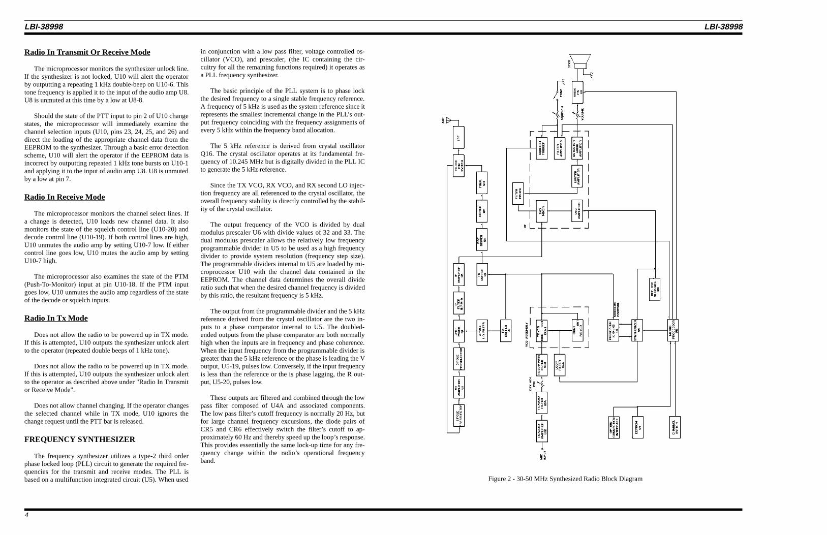
Functionally, the radio transceiver is divided into five ar-eas consisting of the Microprocessor/Control, FrequencySynthesizer, Transmitter, Receiver, and Voltage Regulatorsand Power Distribution. A block diagram is shown in Figure2.
MICROPROCESSOR CONTROL
Microprocessor U10 performs the various policing andcontrol functions required to ensure the radio is set to per-form as desired by the operator’s inputs. An internallymasked program determines the sequence and timing ofthese control functions. The following discussion describesthe various control functions that U9 performs.
Figure 1 - Location of Controls And Indicators
When CTCSS is programmed, only calls codedwith the radio’s assigned code are heard. In nor-mal operation the speaker is muted until the cor-rect CTCSS code is received. The receiveropens and the call is heard.
NOTE
When making a call on channels programmedwith CTCSS , only calls with that channel’s pro-grammed tone are heard. In normal operationthe speaker will remain quiet until the correcttone is received.
The RED TX indicator is "on" continuouslywhen the PTT bar is pressed, indicating the ra-dio transmitter is keyed.
Recharge or replace the battery if the TX/BT in-dicator is dimly lit or fades rapidly.
NOTES
Operating the transmitter without a proper antennainstalled may result in permanent damage to the ra-dio.
CAUTION
LBI-38998 LBI-38998
3
Radio In Transmit Or Receive Mode
The microprocessor monitors the synthesizer unlock line.If the synthesizer is not locked, U10 will alert the operatorby outputting a repeating 1 kHz double-beep on U10-6. Thistone frequency is applied it to the input of the audio amp U8.U8 is unmuted at this time by a low at U8-8.
Should the state of the PTT input to pin 2 of U10 changestates, the microprocessor will immediately examine thechannel selection inputs (U10, pins 23, 24, 25, and 26) anddirect the loading of the appropriate channel data from theEEPROM to the synthesizer. Through a basic error detectionscheme, U10 will alert the operator if the EEPROM data isincorrect by outputting repeated 1 kHz tone bursts on U10-1and applying it to the input of audio amp U8. U8 is unmutedby a low at pin 7.
Radio In Receive Mode
The microprocessor monitors the channel select lines. Ifa change is detected, U10 loads new channel data. It alsomonitors the state of the squelch control line (U10-20) anddecode control line (U10-19). If both control lines are high,U10 unmutes the audio amp by setting U10-7 low. If eithercontrol line goes low, U10 mutes the audio amp by settingU10-7 high.
The microprocessor also examines the state of the PTM(Push-To-Monitor) input at pin U10-18. If the PTM inputgoes low, U10 unmutes the audio amp regardless of the stateof the decode or squelch inputs.
Radio In Tx Mode
Does not allow the radio to be powered up in TX mode.If this is attempted, U10 outputs the synthesizer unlock alertto the operator (repeated double beeps of 1 kHz tone).
Does not allow the radio to be powered up in TX mode.If this is attempted, U10 outputs the synthesizer unlock alertto the operator as described above under "Radio In Transmitor Receive Mode".
Does not allow channel changing. If the operator changesthe selected channel while in TX mode, U10 ignores thechange request until the PTT bar is released.
FREQUENCY SYNTHESIZER
The frequency synthesizer utilizes a type-2 third orderphase locked loop (PLL) circuit to generate the required fre-quencies for the transmit and receive modes. The PLL isbased on a multifunction integrated circuit (U5). When used
in conjunction with a low pass filter, voltage controlled os-cillator (VCO), and prescaler, (the IC containing the cir-cuitry for all the remaining functions required) it operates asa PLL frequency synthesizer.
The basic principle of the PLL system is to phase lockthe desired frequency to a single stable frequency reference.A frequency of 5 kHz is used as the system reference since itrepresents the smallest incremental change in the PLL’s out-put frequency coinciding with the frequency assignments ofevery 5 kHz within the frequency band allocation.
The 5 kHz reference is derived from crystal oscillatorQ16. The crystal oscillator operates at its fundamental fre-quency of 10.245 MHz but is digitally divided in the PLL ICto generate the 5 kHz reference.
Since the TX VCO, RX VCO, and RX second LO injec-tion frequency are all referenced to the crystal oscillator, theoverall frequency stability is directly controlled by the stabil-ity of the crystal oscillator.
The output frequency of the VCO is divided by dualmodulus prescaler U6 with divide values of 32 and 33. Thedual modulus prescaler allows the relatively low frequencyprogrammable divider in U5 to be used as a high frequencydivider to provide system resolution (frequency step size).The programmable dividers internal to U5 are loaded by mi-croprocessor U10 with the channel data contained in theEEPROM. The channel data determines the overall divideratio such that when the desired channel frequency is dividedby this ratio, the resultant frequency is 5 kHz.
The output from the programmable divider and the 5 kHzreference derived from the crystal oscillator are the two in-puts to a phase comparator internal to U5. The doubled-ended outputs from the phase comparator are both normallyhigh when the inputs are in frequency and phase coherence.When the input frequency from the programmable divider isgreater than the 5 kHz reference or the phase is leading the Voutput, U5-19, pulses low. Conversely, if the input frequencyis less than the reference or the is phase lagging, the R out-put, U5-20, pulses low.
These outputs are filtered and combined through the lowpass filter composed of U4A and associated components.The low pass filter’s cutoff frequency is normally 20 Hz, butfor large channel frequency excursions, the diode pairs ofCR5 and CR6 effectively switch the filter’s cutoff to ap-proximately 60 Hz and thereby speed up the loop’s response.This provides essentially the same lock-up time for any fre-quency change within the radio’s operational frequencyband.
Figure 2 - 30-50 MHz Synthesized Radio Block Diagram
LBI-38998 LBI-38998
4

The output from the low pass filter is connected directly tothe VCO tuning varactor and is composed of a DC voltage witha small AC signal (error voltage) riding on the DC. The level ofthe DC voltage coarse tunes the VCO to the correct frequencyand the error voltage acts as a continuous fine tune to maintainphase tracking with the 5 kHz reference.
A lock detect circuit consisting of Q15 and its associatedcomponents is provided as an indication to the microprocessorof the operational state of the PLL. The lock output from syn-thesizer U5-9 is a series of negative going pulses where the in-dividual pulse width is a direct measure of the closeness offrequency and/or phase coherence of the VCO to the 5 kHz ref-erence. R67 and C78 form an integrator with the time constantselected so that Q15 will turn off whenever the pulse widthsappearing at U5-9 narrow to the width that represents the VCObeing within the allowable frequency tolerance of programmedoutput frequency.
As the PLL achieves lock, the transition between Q15 con-ducting (out-of-lock indication) and turning off (valid lock in-dication) typically results in a short period where Q15 will berapidly turning on and off. R66 and C77 are provided to filterout this "chatter" so that the indication to the microprocessor(U10-21) is a steady lock or unlock condition.
Transmit/Receive VCO’S
The synthesized radio uses two VCO’s to generate thetransmit channel frequencies and the receiver’s first LO injec-tion frequency. Both oscillators use the same Colpitts topologywith the receiver oscillator offset in frequency by the 10.7MHz, the first IF. The receive VCO consists of Q201 and asso-ciated circuitry and the transmit VCO consists of Q202 and as-sociated circuitry. Refer to the VCO schematic diagram.
The oscillators are both grounded gate JFET designs thatare varactor controlled to be DC voltage tuneable through arange of approximately 7 MHz. The VCO frequencies are setby monitoring the VCO Test Point on the VCO board, settingthe channel selector for the center programmed frequency, andadjusting the appropriate capacitor (C205 receive & C212transmit) for 4.5 ± 0.1 Vdc. The test point is located near thecenter of the board just above R206. The TX VCO has a sec-ond varactor tapped into the oscillator tank circuit of Q202 toallow direct FM modulation.
The transmit or receive VCO is enabled by switching the 8Vdc supply to the appropriate oscillator depending on whetherthe radio is operating in the transmit or receive mode. The ac-tive oscillator is determined by the presence of 8 Vdc at pin 1(transmit) or pin 2 (receive) of the VCO board.
TRANSMITTER
The transmitter operates in a frequency range of 30 to 50MHz and delivers 5 watts RF output power to the antenna. Theoperating frequencies are established by preprogramming theradio and may be programmed by the dealer using theMHTS3R Radio Programmer. The transmitter consists of themicrophone audio circuit, power amplifier, harmonic filter,automatic power control, and frequency synthesizer.
When the PTT bar is pressed the transmitter is keyed, themicrophone audio circuitry is powered up via Q11, and Q12 isturned on. The open collector output of Q12 represents the ra-dio’s PTT function and switches the receiver VCO off and thetransmit VCO on via Q13 and Q14. Q12 also provides a re-quest to transmit signal, via J1-1 to the microprocessor at U10-2. The microprocessor then directs the transmit channel codesbe loaded into synthesizer U5 from the information stored inEEPROM U9. Once the synthesizer loop has achieved lockwith the selected transmit frequency, the synthesizer, via Q15,signals microprocessor U10-21 with a logic low. The micro-processor then outputs a logic high (TX ENABLE) on pin 8 toturn on power control transistor Q5 and enable the transmitterpower amplifier circuits through dc power switch Q6.
To initiate transmit operation a positive base voltage fromthe microprocessor must first turn on power control transistorQ5. When Q5 is turned on its collector drops low, enabling itto:
• Complete the current path to illuminate the TX LED,CR302.
• Provide base current to turn on dc switching transistorQ6, providing dc power to the power amplifier circuits,RF pre-driver Q7 and drivers Q8 and Q9 respectively.
Microphone Audio Circuit
The Monogram radio operates using direct frequencymodulation by applying the modulating signals to a modula-tion varactor diode that is lightly coupled to the transmit VCOtank circuit. Deviation limiting and occupied bandwidth arecontrolled by an instantaneous peak limiter and audio low passfilter respectively.
Voice modulation may be applied either through the inter-nal electret microphone (MP301) or externally by an optionalspeaker/mic through J301. The internal electret is enabled bypressing the hand-held PTT switch. If the external speaker/micis used, the external PTT switch controls the radio and the in-ternal mic remains disabled.
DC bias for the microphone is supplied through R30 whenthe PTT bar is pressed. The resulting current through R30
causes Q11 to turn on supplying 8 Vdc to the op-amp pair ofU3 and also to Q12 through R33. Q12 is turned on. Theopen collector output of Q12 represents the radio’s PTTfunction. The active low PTT output from Q12 switches Q14off, removing the receiver VCO voltage causing it to be dis-abled and also switches Q13 on, applying 8V to the trans-mitter VCO, enabling it.
The audio frequencies from the microphone are ampli-fied and filtered by the active two-pole high pass filter con-sisting of U3B and its associated components. The filteroperates with a cutoff frequency of 270 Hz and provides ap-proximately 17 dB of voltage gain. The amplified outputfrom U3B is passed through a 6 dB/octave pre-emphasis net-work composed of C61 and R43 to the input of limiting am-plifier U3A. U3A has a voltage gain of approximately 40 dBat 1 kHz. This amplifier is driven into limiting to providepeak clipping. Deviation symmetry while in limiting is setby the reference voltage divider of R42 and R46, supplyingU3. The combined gain of U3A and U3B establishes the mi-crophone sensitivity and is optimized to provide the besttrade off between maximum deviation with low distortionversus the tendency to pick up background noise.
The limited output of U3A is coupled through a resistivedivider network consisting of R48, R49, and R50, optionconnector J1, and coupling capacitor C71 to the input of anactive 3-pole low pass filter. The filter, consisting of U4 Band associated components has a cutoff frequency of 3 kHzto roll off the harmonics of the clipped signal and thereforeestablish the spectral distribution of the modulated RF sig-nal. The output of this LPF is coupled directly to the modu-lating varactor diode in the transmit VCO.
The connection point in the transmit audio path is at op-tion connector J1. This provides a summing point for the ac-cessories that modulate the transmitter, such as, CTCSSencoding, DTMF encoding, etc. Resistors R48 and R49, be-sides being part of the voltage divider to reduce the ampli-tude of the modulating signal to a level compatible with theinput of the LPF, provide for minimal loading of the signalsources to be summed.
Power Amplifier And Harmonic Filter
RF transistors Q7 - Q1O are the active devices in thetransmit power chain and are controlled by the microproces-sor through power control transistor Q5 and dc power switchQ6.
Transmitter pre-amp Q7 is located within the synthesizershield to prevent stray RF pickup from transmitted highpower RF fields. It therefore acts as a buffer to isolate thetransmit VCO from the subsequent transmitter power stages.
This isolation minimizes VCO pulling by controlling theload changes seen by the transmit VCO.
Q7 is biased Class "A" by resistive divider R53-R54 andemitter resistor R56. The emitter resistor provides ac and dcdegeneration for amplifier stability. The collector output isdc shunt fed by L18 and has approximately 12 dB of powergain. C70 and L18 form an impedance matching "L" net-work that drives a 50 ohm RF pad consisting of R57- R59.The padded RF output is then applied to the emitter of am-plifier Q8.
Q8 is also biased Class "A" by resistive divider R21-R22and collector resistor R24. The output of Q8 is then matchedinto the base of Q9 by an "L" network composed of L9 andC33.
The last two stages, Q9 and Q10, are biased Class "C".These stages are driven into saturation to provide RF powerstability (flatness) over the extremes of operating tempera-ture and voltage. Another "L" network consisting of L11 andC34 is utilized to form a broad band impedance matchingnetwork between the collector of Q9 and the base of Q10.Driver transistor Q9 supplies sufficient RF power to saturatepower amplifier Q10.
Dc to the collector of Q9 is shunt fed by parallel circuitL13-R28 that acts as a low Q RF choke to the RF outputpower. The amplifier output is matched to 50 ohms by a "T"network consisting of L14, C41, C42, and L15. RF powerthen passes through pin diode CR3, coupling capacitor C43,and an elliptic Low Pass Filter (LPF) to reach the antenna.The LPF is a 50 ohm input-output design to reject harmon-ics. Together, the "T" network and the LPF pass the carrierwith low loss while effectively suppressing harmonics. C42is adjustable to provide 5 watts to the antenna output.
Receiver Protection Circuit
During transmit, the receiver protection circuit, L17, isactive. The protection circuit consists of "T" network L17,L16, and C44 terminated by pin diode CR2, which is turnedon, and parallel capacitors C39 and C40. The capacitors andCR2 act as an RF short at the receiver input to protect itfrom transmitted energy. The loading presented to the trans-mitter consists of a parallel resonant circuit composed ofL16 and C44. The impedance of this circuit is high with re-spect to 50 ohms, therefore, transmitter power loss is mini-mal within the usable bandwidth of the transmitter.
LBI-38998 LBI-38998
5

RECEIVER
The FM receiver is a dual conversion superheterodynewith a first IF of 10.7 MHz and a second IF of 455 kHz. Thelow band radio uses high side injection for the 1st LO injec-tion.
The received signal from antenna jack J303 passesthrough an elliptic LPF (Low Pass Filter) and through cou-pling capacitor C43 to the receiver protection circuit. In thereceive mode, both pin diodes, CR2 and CR3, are off, dis-abling the receive input protection scheme. With the pin di-odes off, circuit components L16, L17 and C44 form abroadly tuned low-loss BPF that connects the elliptic LPF tothe receive input stage.
Receiver Input Stage Q1
Receiver input stage Q1 is a low noise bipolar amplifier.The preselector band pass filter on it’s input is a double-tuned (L1 and L2) filter featuring low insertion loss and anapproximate bandwidth of 2 MHz. The preselector is cou-pled to the input of RF amplifier Q1. The output from Q1 isloaded by a triple pole RF band pass filter is tuned by induc-tors L3, L4, and L5. Receiver noise figure is established pri-marily by the preselector insertion loss while the image andother out-of-band spurious responses are determined by thestopband attenuation of both the preselector and output bandpass filters. The output from the triple-tuned RF filter is cou-pled through C13 and C15 to the mixer input.
JFET Mixer Q2
Mixer Q2 is a JFET transistor that provides excellent in-termodulation characteristics for the receiver. Capacitor C13matches the impedance of the RF filter output to the lowerimpedance FET source while C15 acts as a shorting path forthe RF signal. Resistor R6 provides dc self-bias for themixer operating point and L6 provides the required dc returnfor JFET current without loading the RF signal.
The LO is injected into the gate of Q2 through a wideband tuned circuit to enhance receiver performance. The LOsignal is generated by the synthesizer receive VCO and is accoupled through C65 to the source input of buffer Q3. Q3 isa grounded gate JFET amplifier whose output load is thetuned mixer gate circuit. The tuned circuit consists of induc-tors L7 and L8 resonating with capacitors C18, C16, andC17. The gate LO injection controls mixer FET conductionto provide mixing of the RF frequency on the source and theLO frequency on the gate. The drain output transformer T1is tuned to 10.7 MHz to select the difference frequencywhile rejecting other mixer outputs. T1 also performs an im-pedance transformation to match the output impedance of
the mixer to the input impedance of crystal filter pair, FL1and FL2.
Crystal Filters FL1 And FL2
Filters FL1 and FL2 are two-pole monolithic crystal fil-ters having a center frequency of 10.7 MHz. Together thetwo filters yield four poles of IF selectivity with a bandwidthof 15 kHz to attenuate undesired 1st mixer products and es-tablish 2nd image rejection. The filters are connected in cas-cade with C22 optimized for minimum ripple within the 15kHz IF bandwidth. IF transformer T2 is used to match theimpedance of the filter output termination to the input of IFpre-amplifier Q4.
The function of Q4 is to provide first IF system gain tominimize contributions to the receiver noise figure by sub-sequent stages. Q4 is an RC coupled amplifier whose outputappears at collector resistor R13. This output is coupledthrough C25 to the mixer input of integrated circuit U7.
Mixer/IF Ampl/FM Detector/Noise Squelch
Multipurpose IC U7 incorporates a mixer, IF amplifer,FM detector, and noise squelch functions within a singlepackage. This package contains the active circuit devices thatare linked by external components to complete the circuitswithin the IC.
The initial stage of U7 is a mixer to down convert the10.7 MHz frequency to 455 kHz. Pin 16 is the mixer inputand pin 1 is the LO injection from the 10.245 MHz REFOSC Q16. The mixer output is taken from pin 3 of U7 and isfed through ceramic filter FL3 to select the difference fre-quency of 455 kHz. FL3 provides second IF selectivity andimproves adjacent channel rejection. The output of FL3 isreturned to pin 5 of U7 as the input to a limiting 455 kHz IFamplifier.
The 455 kHz IF amplifier provides AM rejection andhigh gain at the low IF frequency. The limiting output is fedto a quadrature detector circuit. The quadrature circuit con-sists of an internal capacitor plus external coil L19 to de-velop the 90 degree phase shifted signal required by thedetector. The quadrature detector recovers the FM modula-tion from the IF signal and provides an amplified audio out-put at U7-9.
The recovered audio signal is directed through an RC cir-cuit (R84-C98) that attenuates the 455 kHz IF while preserv-ing audio and noise frequencies within the bandwidth of thereceiver. From U7-9, the audio branches in two directions.R84 and C99 couple the signal to a squelch-controlled audio
output stage U8 while R83 passes the higher frequency noisespectrum to a BPF noise amplifier.
Since FM receivers noise quiet during reception, channelnoise is typically utilized to mute audio until the receiver signalto noise ratio becomes acceptable. To perform this task, re-ceiver noise is bandpassed, rectified, and used as a noisethreshold control for muting the output audio amplifier.
The squelch noise amplifier is a MFB (multiple feedbackbandpass) design with its input at U7-10 and output at U7-11.In this bandpass amplifier, resistors R82, R83, and R80 in con-junction with capacitors C95 and C96 are the essential compo-nents that determine the gain and center frequency.
C97, in conjunction with R82, is a high pass filter to rejectvoice components.
The output of the noise amplifier is converted to a dc levelrepresenting the average receiver noise by voltage doubling de-tector CR7. The detector output load consists of the series/par-allel combination of R76, R77, and RT1 in parallel with C91 tosmooth the variations in noise
levels. The rectified dc operates the squelch input at U7-12.An operator controlled dc voltage is summed with the rectifiednoise output to allow the user to control the squelch point.
U7-12 is the input to an internal switching circuit config-ured to provide approximately 50 mV of hysteresis on theswitch trigger point. Additional external hysteresis is providedby loading the dc voltage summed with the noise detector out-put through R78 to ground provided by U7-14.
Hysteresis or positive feedback effectively performs twouseful functions. First, it increases switching speed due to re-generation and further, it shifts the threshold point slightly toeliminate squelch chatter.
When a positive dc signal (caused by the detected RX noiseduring low RF signal conditions) greater than 0.7 Vdc is ap-plied to U7- 12, the switching circuit outputs at U7-13 (Scan)and U7-14 (Mute) change states. U7-14 reflects an open circuitcondition effectively providing the previously mentioned exter-nal hysteresis by removing the load on the input by R78. TheSCAN output at pin 13 goes low and represents a request formicroprocessor U10 to mute the audio output stage. U10 re-sponds by outputting a logic high at U10-7 to mute audio am-plifier U8.
Audio Amplifier, U8
Audio amplifier U8 is the final receiver stage; the stage thatprovides power amplification and mutes the audio. A positivedc level at U8-8 mutes the amplifier. The input audio to U8 is
controlled by the volume control. The volume control input iseither the received output (noise and signal) or a pulsating 1.0kHz alarm indicating synthesizer unlock.
Basically, U8 is a power op amp with the input coupledthrough C100 to non-inverting (+) input pin 1. Input resistorR87, returned to voltage divider R88-89, sets the dc referencefor the amplifier operating point. R90, returned to the same ref-erence divider, is a speaker pop eliminator. Negative feedbackcomponents C108, R92, R91, and C107 determine the ampli-fier gain and its frequency response. The parallel combinationof R92-C108 forms a de-emphasis circuit that attenuates audioat 6 dB per octave rate at frequencies above the cutoff fre-quency. C107 in conjunction R91, causes low frequency roll-off.
Processed audio output is coupled through C109 to internalspeaker SP301 or to an external speaker via jack J302. RC cir-cuit R93-C110 prevents high frequency oscillations by severelyloading the amplifier at the very high frequencies. R94 is resis-tive speaker loading to suppress speaker resonances.
SERVICE SECTION
The Service Section contains information to assist you inidentifying problem areas and in tuning and adjusting the radiofor optimum performance. Care of the radio, Removal and Re-placement Procedures, Radio Alignment, Performance Testsand Antenna Tuning procedures are included.
Verify that the user’s operating configuration is pro-grammed into the EEPROM and the transmit and receive sec-tions of the radio are adjusted for optimum performance. Ifnew frequencies be programmed into the radio, that are outsidethe current bandwidth or frequency sensitive components re-placed, realign the radio and verify proper operation by doingthe Performance Tests. If the optional Channel Guard tone en-coder/decoder is installed and the radio programmed for Chan-nel Guard operation, the Channel Guard deviation and noisesquelch must also be adjusted prior to returning the radio toservice.
The alignment and performance checks can be very helpfulin localizing a problem when trouble shooting the radio. If anyfrequency sensitive components are replaced, the performancechecks should be run to verify proper operation and, if indi-cated, the realignment may be required. If alignment is re-quired, run the performance procedures again to assure properoperation.
Voltage charts, located on the service outlines, are providedfor both the component and solder side of the main PCB.
LBI-38998 LBI-38998
6

In some radios, a VCO out-of-lock indication is givenwhile switching between channels or when an unprogrammedchannel is selected. The unlock indication is recognized by re-peated two short beeps sounded from the speaker. This in noway inhibits or restricts the operation of the radio and lasts foronly a very short time. A solution to the unprogrammed chan-nel problem is to program all unused channels with a receivefrequency. Refer to the programmer instruction manual.
CARE OF EQUIPMENT
1. Keep the exterior of the radio clean. Use a soft dampcloth.
2. To ensure efficient power transfer from battery to ra-dio, wipe the contacts of the battery and radio to re-move dirt or grease. Use a soft dry cloth.
3. When the accessories connector is not in use, coverthe connector with a protective dust cap to prevent thebuild up of dust or water particles.
RADIO IDENTIFICATION
The Monogram Series Portable operates on one of threefrequency splits:
Freq. Split Model
30-35 MHz35-42 MHz42-50 MHz
344A9730P11344A9730P12344A9730P13
ELECTROSTATIC DEVICES
REMOVAL AND REPLACEMENT
Antenna Removal And Replacement
A high quality molded antenna is supplied to match the op-erating frequency split of each radio. Each antenna must betuned for the frequency split for which it will be operating.Should an antenna, tuned to the wrong frequency split be in-stalled, the performance of the radio will be degraded.
1. To remove the antenna, turn the antenna counterclock-wise.
2. To install the antenna, turn the antenna clockwise un-til it is firmly seated. do not over tighten.
Battery Removal and Replacement
1. To remove the battery, use a screwdriver or coin to un-latch the back cover screw, located at the bottom ofthe rear cover. Rotate the screw counterclockwise torelease.
2. Pull up on the cloth strap attached to the battery andremove the battery.
3. To replace the battery, insert it in compartment so thecontacts mate and replace battery cover.
Main PCB & Option Interface Board Removaland Replacement
1. Remove the battery as instructed above
2. Using a posi drive screw driver, remove the fourmachine screws from the bottom cover (batterycompartment) and separate the bottom from the ra-dio assembly and unplug the Option Interfaceboard.
3. On each side of the radio near the top, remove thetwo posi drive screws securing the bottom covercasting to the top panel casting. One of thesescrews is located just above the monitor switch.
4. Hold the radio with the battery compartment facingup and the thumbs positioned on the side of the ra-dio (on the front cover and the metal casting), sepa-rate the front cover from the metal casting.
5. Unplug the option interface or Channel Guardboard located just below the top panel.
6. Remove the two retaining screws securing the mainPCB to the top panel.
7. Unsolder the connections to the volume control,squelch control, and the BT/RX indicator.
8. Unsolder the ten remaining wires, including the an-tenna wire, that interconnect the main PCB and thetop panel PCB.
9. Disconnect the 3-pin PTT/monitor connector formthe main PCB and remove board.
10. Reassemble the radio in reverse order.
Condenser Mic & Speaker Removal AndReplacement
Condenser Microphone
1. Separate the radio covers by performing steps 1-4of Main PCB board removal above.
2. Unsolder the gray and brown microphone wiresfrom the main PCB and remove the microphone.
3. Reassemble radio in reverse order.
Speaker
1. Separate radio covers by performing steps 1-4 ofMain PCB board removal above.
2. Unsolder the black and white speaker wires fromthe top panel PCB (located near top center) and re-move the speaker.
3. Reassemble radio in reverse order.
Top Panel Removal and Replacement
1. Remove the main PCB and speaker as describedabove.
2. To remove the top panel PCB board unsolder allconnections to the top panel controls and accessoryjacks.
3. Reassemble the radio in reverse order.
PTT and Monitor Switch Removal AndReplacement
1. Separate radio covers by performing steps 1-4 ofMain PCB board removal above.
2. Unplug the 3-pin connector used to interconnect thePTT and monitor controls to the main PCB.
3. Remove the retaining screw securing the PTT bar tothe metal casting.
4. Unsolder controls as necessary.
5. Reassemble the radio in reverse order.
SMD Component Removal & Replacement
When removing and replacing the surface mounted com-ponents, SMD, follow the procedures given below using asoldering iron and a solder sucker.
Removing SMD components
1. Unsolder the component by heating one pad andusing a solder sucker to remove the solder. Then ap-ply heat to the other pad and lift the componentfrom the board.
Do not carry or hold the radio by the antenna.
Do not use chemical cleaners, aerosol sprays orpetroleum based products. They may damage theradio housing.
CAUTION
Integrated Circuit devices used inthis equipment can be destroyedby static discharges. Before han-dling one of these devices, theservice person should dischargehimself by touching the case of a
bench test instrument that has a 3-prong power cordconnected to an outlet with a known good earthground. When soldering or desoldering a CMOS de-vice, the soldering iron should also have a 3-prongpower cord connected to an outlet with a knowngood earth ground. A battery operated soldering ironmay be used in place of the regular soldering iron.
CAUTION
Any repairs or adjustments should be made by aqualified service technician or an authorizedservice center.
WARNING
LBI-38998 LBI-38998
7

Replacing SMD Components
With the PCB appropriately held in the best position forrepair:
1. Ensure that all excess solder and old glue is re-moved from the board and the pads on the printedcircuit board and component solder pads are me-chanically clean.
2. Centrally locate the component between the printedcircuit board pads.
3. Using the soldering iron apply sufficient heat to theSMD component pads and the corresponding PCBpads to set the component in position.
EEPROM PROGRAMMING
Before alignment, the radio must be programmed to theuser’s transmit and receive frequencies as well as the op-tional Channel Guard tone frequencies. This programmed in-formation is stored in a plug-in EEPROM inside the radiounit. Refer to the Programmers Manual to program theEEPROM with the operating information. The followingprocedure is used for removing and re-installing theEEPROM.
1. Use a screwdriver or coin to unlatch the back coverscrew, located on the bottom of the back cover ofthe radio. Remove the battery cover. Rotate latchscrew counterclockwise to release.
2. Remove the battery pack and the insulating materialfrom the battery compartment.
3. Locate and remove the four screws in the batterycompartment securing the front and rear covers.
4. Remove the two top screws from the metal castingon either side of the radio. One screw secures thetop of the PTT bar.
5. With the battery compartment facing up, snap thecase halves apart.
6. Locate and carefully remove the optional ChannelGuard printed circuit board (see Figure 3 for loca-tion).
7. Locate and carefully remove the EEPROM.
8 Program the EEPROM to the user’s operating con-figuration.
9. Carefully re-install the EEPROM and reassemblethe radio in the reverse order.
Table 1 - Transistor Voltage Chart
Component Side
TRANSISTOR MODE E B C
Q1 TX 0.00 0.00 0.00
RX 0.00 0.76 5.36
SQ 0.00 0.76 5.36
Q3 FET TX 8.0 S 7.2 B 7.93 D
RX 8.0 S 7.72 B 0.85 D
SQ 8.0 S 7.72 B 0.85 D
Q6 TX 10.6 9.8 10.5
RX 10.8 10.8 0.00
SQ 10.8 10.8 0.00
Q9 TX 0.00 0.00 10.3
RX 0.00 0.00 0.00
SQ 0.00 0.00 0.00
Q10 TX 0.00 0.00 10.4
RX 0.00 0.00 10.82
SQ 0.00 0.00 10.82
Q12 TX 0.00 0.8 0.15
RX 0.00 0.00 0.76
SQ 0.00 0.00 0.76
Q13 TX 8.0 7.0 8.0
RX 8.0 7.95 1.8
SQ 8.0 7.95 1.8
Q14 TX 7.94 8.0 0.00
RX 8.0 7.2 7.95
SQ 8.0 7.2 7.95
Chip Component Side
TRANSISTOR MODE E B C
Q2 TX 0.00 S 0.00 G 0.00 D
RX 2.4 S 0.00 G 7.42 D
SQ 2.4 S 0.00 G 7.42 D
Q4 TX 0.00 0.00 0.00
RX 0.18 0.89 3.9
SQ 0.18 0.89 3.9
Q5 TX 0.16 0.96 0.16
RX 7.6 0.09 10.8
SQ 7.6 0.09 10.8
Q7 TX 1.23 1.93 7.9
RX 0.00 0.28 0.85
SQ 0.00 0.28 0.85
Q8 TX 0.00 0.52 6.25
RX 0.00 0.00 0.00
SQ 0.00 0.00 0.00
Q11 TX 8.0 7.3 7.9
RX 8.0 8.0 0.00
SQ 8.0 8.0 0.00
Q16 TX 4.5 5.0 7.9
RX 4.5 5.0 0.00
SQ 4.5 5.0 0.00
Do not allow the soldering iron to come in contactwith the body of the replacement SMD component.
Avoid prolonged application of heat to the pads ofthe replacement component. Damage to the compo-nent may result.
Do not use SMD components that do not accept sol-der properly. They may not function as required orthe working life of the component may be reduceddue to chemical contamination.
CAUTION
Figure 3 - EEPROM Removal
LBI-38998 LBI-38998
8
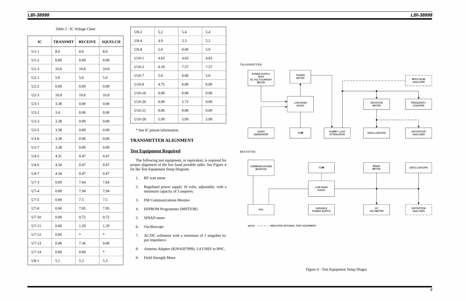
Table 2 - IC Voltage Chart
IC TRANSMIT RECEIVE SQUELCH
U1-1 8.0 8.0 8.0
U1-2 0.00 0.00 0.00
U1-3 10.8 10.8 10.8
U2-1 5.0 5.0 5.0
U2-2 0.00 0.00 0.00
U2-3 10.8 10.8 10.8
U3-1 3.38 0.00 0.00
U3-2 3.4 0.00 0.00
U3-3 3.38 0.00 0.00
U3-5 3.38 0.00 0.00
U3-6 3.38 0.00 0.00
U3-7 3.38 0.00 0.00
U4-5 4.31 0.47 0.47
U4-6 4.34 0.47 0.47
U4-7 4.34 0.47 0.47
U7-3 0.00 7.64 7.64
U7-4 0.00 7.94 7.94
U7-5 0.00 7.5 7.5
U7-8 0.00 7.95 7.95
U7-10 0.00 0.72 0.72
U7-11 0.00 1.29 1.29
U7-12 0.00 * *
U7-13 0.00 7.36 0.00
U7-14 0.00 0.00 *
U8-1 5.1 5.3 5.3
U8-2 5.2 5.4 5.4
U8-4 4.9 5.3 5.2
U8-8 5.0 0.00 5.0
U10-1 4.63 4.63 4.63
U10-2 0.19 7.57 7.57
U10-7 5.0 0.00 5.0
U10-8 4.75 0.00 0.00
U10-16 0.00 0.00 0.00
U10-20 0.00 5.72 0.00
U10-21 0.00 0.00 0.00
U10-28 5.09 5.09 5.09
* See IC pinout information
TRANSMITTER ALIGNMENT
Test Equipment Required
The following test equipment, or equivalent, is required forproper alignment of the low band portable radio. See Figure 4for the Test Equipment Setup Diagram.
1. RF watt meter
2. Regulated power supply 16 volts, adjustable; with aminimum capacity of 3 amperes.
3. FM Communications Monitor
4. EEPROM Programmer (MHTS3R)
5. SINAD meter
6. Oscilloscope
7. AC/DC voltmeter with a minimum of 1 megohm in-put impedance
8. Antenna Adaptor (R29/4207999), 1/4 UNEF to BNC.
9. Field Strength Meter
Figure 4 - Test Equipment Setup Diagra
LBI-38998 LBI-38998
9

Pre-Alignment Notes
1. The transmit frequencies should be within a 2 MHzrange.
2. The receive frequencies should be within a 2 MHzrange.
3. There is no constraint on the relationship betweenthe transmit frequencies and the receive frequenciesexcept that they lie within the limits of the radioband (i.e., 30-35, 35-42 or 42-50 MHz).
Antenna Tuning
Refer to Figure 5 for tuning capacitor settings for thevarious frequencies. To tune the antenna perform the follow-ing steps
1. Remove slotted set screw from coil cover of an-tenna to uncover the tuning capacitor.
2. Select the radio channel that represents the centerof the frequencies programmed.
3. Hold the radio upright and press the PTT bar to keythe transmitter on the selected channel.
4. With a field strength meter in the same polarizationplane as the radio antenna, use a non-conductive
tuning tool to adjust the tuning capacitor for maxi-mum field strength.
5. After tuning, carefully re-install the set screw intothe coil cover until it is flush with the outside of thecover. DO NOT OVER TIGHTEN .
Alignment Procedure.
3. Select the middle programmed transmit channel.Key the transmitter and adjust C212 on the VCOPCB for 4.5 ± 0.1 Vdc at the control voltage testpoint on the VCO PCB.
4. Select a programmed mid-frequency transmit chan-nel. Connect a frequency counter to the output ofthe power attenuator. Key the transmitter and adjust
C122 for the correct channel frequency with a maxi-mum error of ± 100 Hz.
5. Key the transmitter and adjust C41 for maximum RFoutput power. Switch the radio between the lowestand highest transmit frequencies and adjust C41 toobtain the smallest power output variation across thetransmit frequency range.
6. Connect an audio generator with a source impedanceof 600 ohms or less to the external microphone jackJ301 on the top panel.
7. Set the audio frequency to 1 kHz at an output level of300 mVrms. Key the transmitter and adjust R50 for±4.5 kHz deviation. Maintain the input from 300 Hzto 3 kHz and readjust R50 if necessary to ensure thatthe deviation does not exceed ± 5.0 kHz.
8. Check all programmed transmit channels and readjustR50, if necessary, to ensure that the deviation does notexceed ± 5.0 kHz on any channel.
TRANSMITTER PERFORMANCE TESTS
Power Output
Power output should be in excess of 5 watts with a powersupply input voltage of 11 volts and total dc current of 1.5 am-pere or less. Reducing the supply voltage to 9 volts should pro-duce a minimum power output of 2.5 watts.
Audio Response
Connect an audio generator to the EXT MIC jack. Set theoutput for 1 kHz modulation and press the PTT switch. Adjustthe generator output level to produce 1 kHz of deviation on thedeviation meter. Reset the generator modulation to 500 Hz.The deviation should be approximately 500 Hz. Set the gener-ator modulation to 2 kHz. The deviation should now be ap-proximately 2 kHz.
Limiting Test
Adjust the audio generator output level for 1 kHz deviationwith 3 kHz modulation. Increase the generator output by 20 dBand sweep the frequency band from 300 to 3000 Hz. The de-viation should not exceed ± 5 kHz. at any frequency within thisband.
Splatter Filter Test
With the test equipment set up for the Limiting Test, notethe reading of the ac vtvm connected across the audio output ofthe deviation meter at 3 kHz deviation. Set the audio generatorto 6 kHz. The ac vtvm reading should decrease more than 18dB.
Spectrum Test
With the input attenuator of the spectrum analyzer pro-tected by 40 to 60 dB of attenuation, all spurious and harmon-ics should be down more than 60 dB.
Figure 5 - Antenna Tuning Capacitor Settings VsFrequencies
Be sure the radio is programmed to customer specifi-cations, otherwise use a test EEPROM programmedwith low, center, and high Tx/Rx frequencies for thesplit being used prior to aligning the radio. WhenChannel Guard is required use the CG frequencieslisted below for test operation.
Low Tx/Rx channel - 67.0 HzCenter Tx/Rx channel - 151.4 HzHigh TxRx channel - 250.3 Hz
NOTE
To avoid damage to the radio, observe proper powersupply polarity.
• Connect the power supply to the battery terminalsof the radio (battery removed). As you proceedwith the alignment procedure, ensure that thepower supply voltage remains at 10.8 Vdc meas-ured at the radio, not the power supply. Refer toFigure 6 for location of adjustment and tuning con-trols.
• Connect an RF Wattmeter (5 watt scale) and PowerAttenuator/dummy load to the antenna jack usingan antenna adapter, 1/4 x 32 x 3/16 thread to BNC,part number R29/4207999.
CAUTION
Figure 6 - Location of Controls and Adjustments.
LBI-38998 LBI-38998
10

Antenna Test
Reassemble the radio and install a fully-charged batterypack. Insert the radio into its case. Connect a properly trimmed(to frequency) flexible antenna to the antenna connector on thetop panel. Key to transmit and check the frequency, deviationand spectral purity. All should be the same as tested with the 50ohm dummy load.
RECEIVER ALIGNMENT
1. Select the middle programmed receive channel andadjust C205 on the VCO PCB for 4.5 ± 0.1 Vdc at theVCO control voltage test point on the VCO PCB.
2. Turn the Squelch control fully counter-clockwisewithout switching into the tone (detent) position.
3. Connect an oscilloscope (and distortion analyzer ifavailable) across the speaker terminals
4. Select a programmed mid-frequency channel. Con-nect an RF signal generator or communications moni-tor to the antenna jack. Set the RF frequency to thecorrect channel frequency. The generator should beset for 3 kHz with 1 kHz modulation. The RF outputlevel should be 1 mV.
5. Adjust the discriminator coil (L19) for maximum sinewave amplitude at the speaker terminals. Adjust theVOLume control if necessary to avoid clipping. If asine wave is not visible (only noise), proceed withstep 8 and return to this step.
6. Adjust T1, T2, and L19 for lowest audio distortion atthe speaker terminals as observed on the oscilloscopeor distortion analyzer.
7. Connect a SINAD meter across the speaker terminals.Adjust the VOLume control to the proper level for theSINAD meter and the signal generator output level toproduce 12 dB SINAD on the SINAD meter.
8. Adjust L1, L2, L3, L4, L5, L7, L8, and T1 for the bestsensitivity, readjusting the RF signal generator levelas necessary to keep the SINAD meter reading near12 dB.
9. Repeat step 8 at the lowest and highest programmedreceive channels, if necessary, to give the best sensi-tivity across the entire receive band.
RECEIVER PERFORMANCE TESTS
SINAD Sensitivity
Adjust the signal generator output for 12 dB SINAD. Thesignal generator output should be less than 0.28 µV.
Noise Quieting Sensitivity
With the signal generator disconnected from the radio andthe squelch open, adjust the VOLume control to obtain a noisereading of 1 V rms. Couple the signal generator to radio withno modulation and adjust the RF output so that a noise readingof 0.1 V rms is obtained. This is the 20 dB quieting point. Thesignal generator output level should be 0.5 µV maximum.
Squelch Sensitivity
With the signal generator set for the 1 kHz modulation, 3kHz deviation and the RF attenuator at minimum, adjust thesquelch control to its threshold. The squelch should open as theoutput of the signal generator is increased to 0.20 µV. Set thesquelch control to its maximum clockwise position. Increasethe RF attenuator setting until the squelch opens. The point ofopening should be 10 to 20 dB greater than for the 0.20 µV at-tenuator setting.
Audio Output
With the generator set at 1000 µV RF output, adjust the ra-dio’s volume control to display a clean sinewave on the oscillo-scope just below the point at which clipping occurs. The acvtvm connected across the speaker leads should read 2V (500mW at 1 kHz into an 8 ohm load). The distortion analyzershould display less than 10% THD.
Standby Current
Squelch the receiver and connect a VOM (0-100 mA range)in series with one of the supply leads. The meter readingshould be less than 40 mA at a supply voltage of 11 volts.
SERVICING THE BATTERY
BATTERY CHARGING AND CARE
To insure peak performance from your radio, the batterypack must be fully charged. Proper care and charging will pro-vide maximum performance and life of your battery pack.
New batteries or batteries that have been stored for along period of time, should be fully charged before being in-stalled in a radio. The battery should be recharged or re-placed if the charge state is in doubt.
If the charging battery is sparingly or seldom used and isleft on continuous charge for one or two months at a time, itcould experience reduced capacity. This would severely re-duce the life of the battery between charges.
The rechargeable nickel-cadmium battery packs may berecharged using the MONOGRAM Dual Rate Charger344A9730P25 (LBI-39009), separately or with the radio in-serted. The battery should be recharged when the chargestate is in doubt. To recharge a battery insert the battery pack(or radio) into the charger.
DUAL RATE CHARGER
The charger operates from a 110/120 Vac source andshould be installed with a 150 mA 125 Vac fuse inserted inthe charger fuse holder. The unit is capable of continuousoperation; however, it should be disconnected from thepower source when not in use. To operate the Dual RateCharger, plug the charger into the power source and insertthe battery or radio into the appropriate section of the
charger. When the radio is inserted into the charger (rear sec-tion), it initially operates on fast charge until the battery isfully charged and then reverts to "slow" charge to maintainfull battery capacity. The battery will charge fully in about 3hours. When the battery (only) is inserted into the front sec-tion of the charger, the battery is charged at the slow rate andwill be fully charged in about 14 hours. The appropriate fastor slow charge indicator will light indicating the rate atwhich the battery is being charged.
• If the charge indicator does not light, check to seethat the battery has been inserted properly.
• Do not charge the battery when the battery tem-perature is below 10ºC or above 40ºC (50ºF or104ºF). Usable life of the battery may be reduced.
• Do not use the charger if it is wet or damaged inany way.
• Do not toss batteries into a fire; they may explode.
CAUTION
LBI-38998 LBI-38998
11

TRANSISTOR & IC PINOUT INFORMATION
Q1Q4, Q7, Q8, Q16Q5 ,Q12Q11, Q13, Q14, Q15
- R29/200-003-5- R29/203-109-3- R29/218-018-2- R29/18-017-1
Q2, Q3, Q201, Q202 - R29/203-116-9
Q6 - R29/203-054-6
Q9 - R29/203-176-3
Q10 - R29/203-043-6
CR5-CR7 - R29/249-006-5
U1 - 8-VOLT REGULATOR R29/229-358-7
U2 - 5-VOLT REGULATOR R29/223-119-8
U3, U4 - DUAL OP AMP R29/231-124-2
U5 - SYNTHESIZER R29/223-145-1
U6 - DUAL MODULUS PRESCALER R29/223-403-4
U7 - IF AMPL/FM DET/NOISE SQ. R29/223-116-5
U8 - AUDIO AMPLIFIER R29/229-080-5
U9 - EEPROM R29/229-063-0
U10 - MICROPROCESSOR CONTROLLER
LBI-38998 LBI-38998
12

OUTLINE DIAGRAM
Main Printed Circuit Board(R29/404-049-A)
SOLDER SIDECOMPONENT SIDE TOP PANEL PCB VCO PCB
LBI-38998 LBI-38998
13
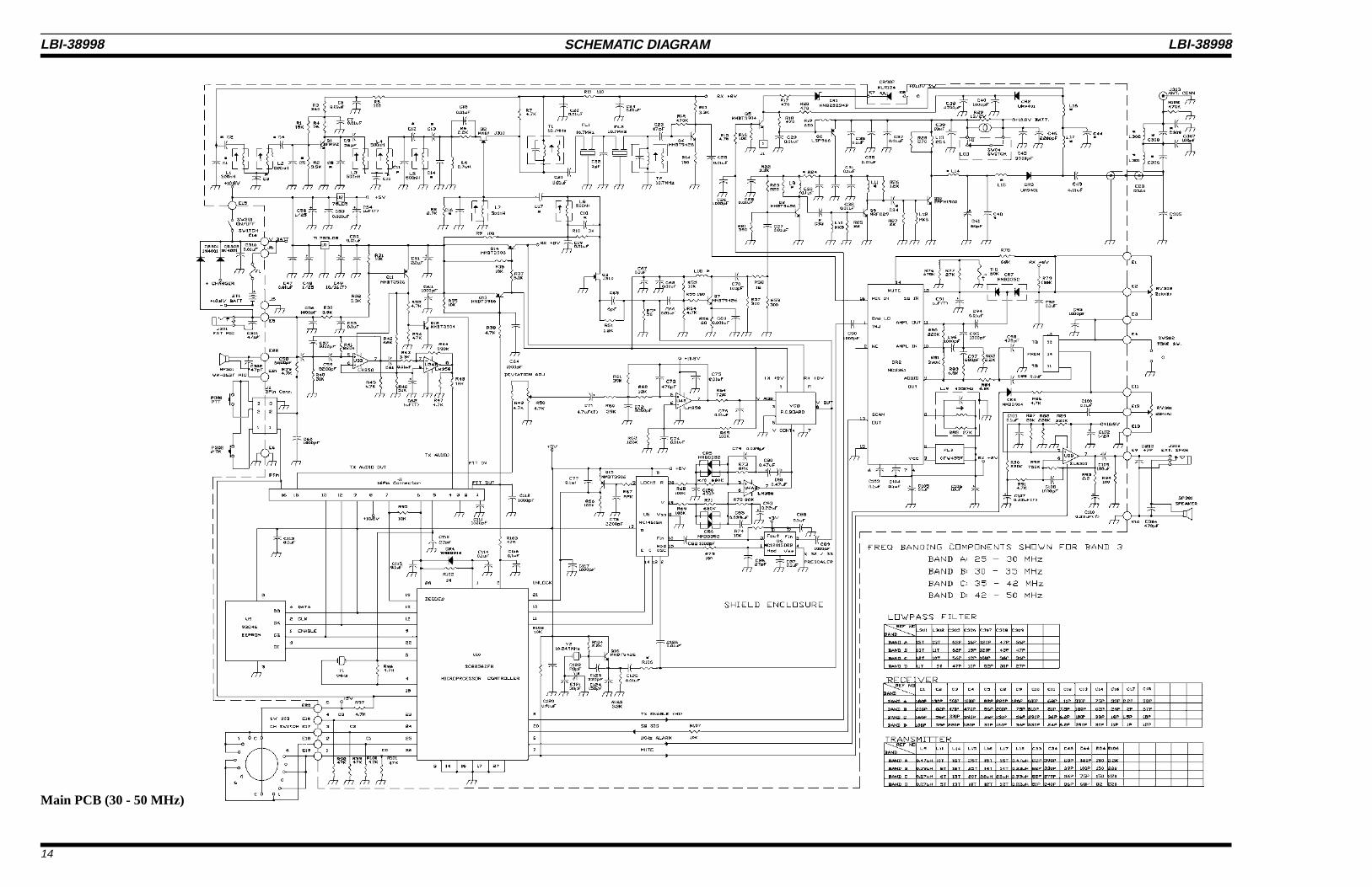
SCHEMATIC DIAGRAM
Main PCB (30 - 50 MHz)
LBI-38998 LBI-38998
14

Top Panel & VCO PCBR29/406-977-A
SCHEMATIC DIAGRAM
Main Board/Top Panel VCO
LBI-38998 LBI-38998
15
Main PCB & Top Panel Interconnect DiagramVCO Diagram
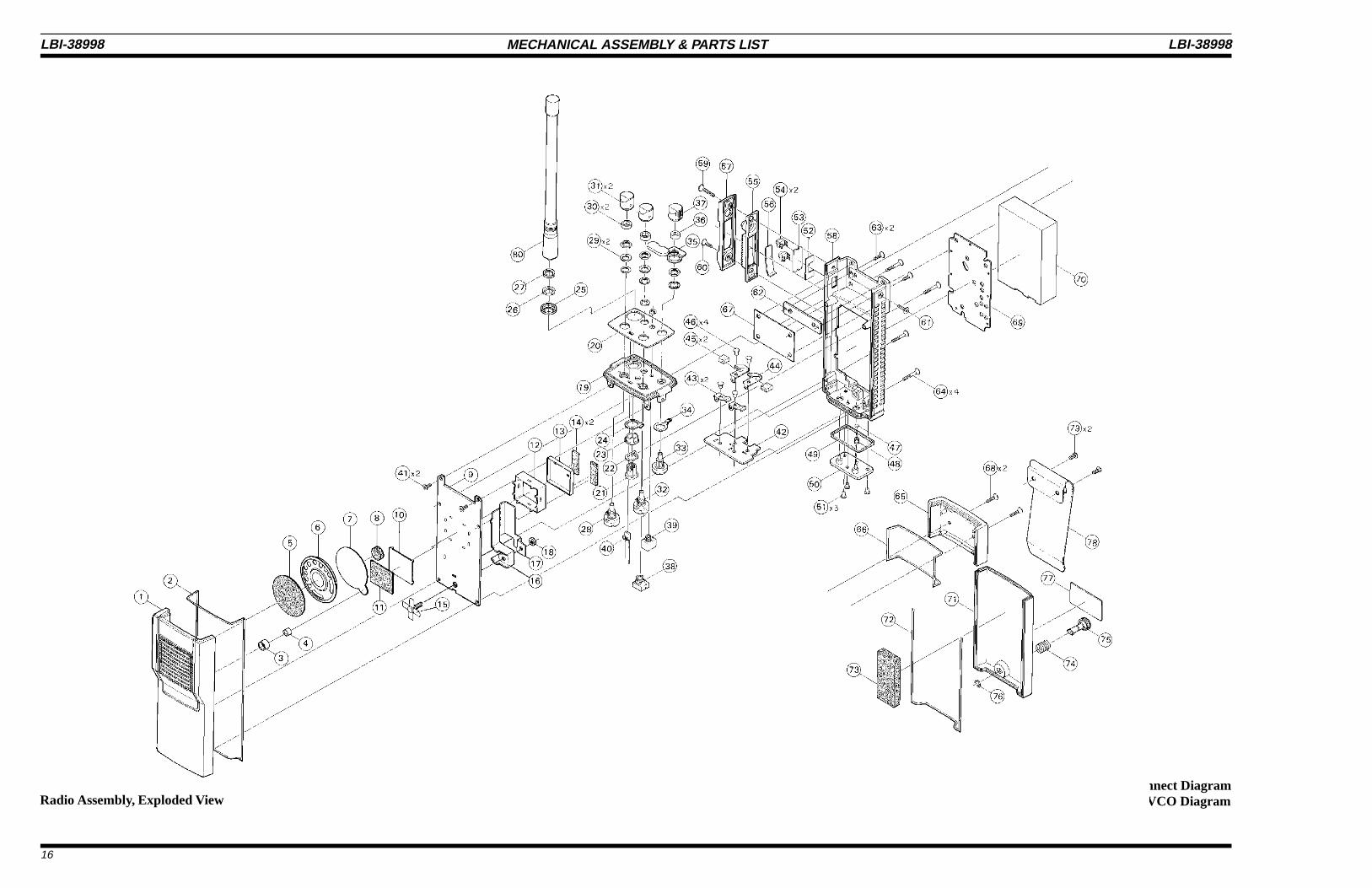
MECHANICAL ASSEMBLY & PARTS LIST
Radio Assembly, Exploded View
LBI-38998 LBI-38998
16

PARTS LIST
SYMBOL PART NO. DESCRIPTION
1 R29/718-088-AA Cover Upper Assembly, Lexan 141-2032
2 R29/891-370 Gasket, Sili (Rubber/blk) (Included in cover upper assem-bly)
3 R29/850-924 Bushing MIC (Included in cover upper assembly)
4 R29/999-113-7 Condenser MIC assembly
5 R29/906-070 Felt (ø40 x t0.2 blk) (Included in cover upper asesembly)
6 R29/420-167-8 Speaker (45-8B-03 400 Hz)
7 Insulation Plate (Fiber Sticker)
8 R29/892-111 Rubber sponge sticker (Sticker blk)
9 Main PCB
10 Shield Plate
11 R29/894-592 Cushon, (Rubber sponge sticker)
12 Shield Case
13 Shield cover
14 R29/894-557 Cushon, (Rubber sponge sticker)
15 R29/203-043-6 Transistor
16 Heat Sink
17 Top Panel Assembly
18 R29/650-047 Nut
19 R29/718-075 Top Panel (Included in top panel assembly)
20 R29/795-083 Overlay (Included in top panel assembly)
21 R29/732-535 Holder (Ant) (Included in top panel assembly)
22 Washer (Ant) (Included in top panel assembly)
23 R29/852-761 Bushing (Ant P.C. Blk) (Included in top panel assembly)
24 Washer (ground) (Included in top panel assembly)
25 R29/8520765 Ring (Ant mtg) (Included in top panel assembly)
26 R29/905-481 Washer (P.C. clear) (Included in top panel assembly)
27 R29/650-295 Nut (Ant) (Included in top panel assembly)
28 R29/450-517-0 V12M4-1 (6x5) S (SJ) 12R-B20K VR (Squelch) (Includedin top panel assembly)
29 R29/660-770 Washer (BSBM) (Included in top panel assembly)
30 R29/851-990 Bushing (CR-Blk) (Included in top panel assembly)
31 R29/821-470 Control Knob (Included in top panel assembly)
32 R29/450-516-9 V12M4-1 (6x5) S (SJ) 12R-150A20K VR (Volume) (In-cluded in top panel assembly)
33 R29/430-029-0 JRE2-6 Rotary Sw. (Channel Select) (Included in toppanel assembly)
34 Lug Terminal (Included in top panel assembly)
35 R29/894-514 Rubber Cap (Blk) (Included in top panel assembly)
36 Bushing (NEPO. Blk) (Included in top panel assembly)
37 R29/825-630 Knob (Channel) (Included in top panel assembly)
38 R29/420-717-5 Connector Jack (HCY3505 w/nut) (Included in top panelassembly)
39 R29/420-718-5 Connector Jack (HCY2505 w/nut) (Included in top panelassembly)
40 R29/251-016-7 L.E.D. Lamp (SLB) (Included in top panel assembly)
41 R29/611-230 (+) Machinea Screw
42 P.C.B. Battery (Included in Battery Contact Assembly)
43 R29/880-540 Spring Terminal (Included in Battery Contact Assembly)
44 R29/880-530 Spring battery (Included in Battery Contact Assembly)
45 R29/894-535 Cushon, (Sponge Sticker) (Included in Battery Contact As-sembly)
46 Rivet (Terminal) (Included in Battery Contact Assembly)
47 R29/750-447 Ball Bearing (Included in frame assembly)
48 R29/881-481 Spring (Included in frame assembly)
49 Gasket (Spacer/rubber Blk) (Included in frame assembly)
50 Spacer (Battery terminal) (Included in frame assembly)
51 (+) Machine screw (B.H.) (Included in frame assembly)
52 R29/906-192 Installation Plate (Mylar sticker) (Included in PTT assem-bly)
53 P.C.B.PTT (Included in PTT assembly)
SYMBOL PART NO. DESCRIPTION
54 R29/434-007-0 Touch S.W. (SKHHAR 018A) (Included in PTT assembly)
55 R29/894-502 Gasket (PTT rubber Blk) (Included in PTT assembly)
56 R29/881-481 Spring (PTT rubber mtg.) (Included in PTT assembly)
57 R29/732-720 Holder, PTT (Included in PTT assembly)
58 R29/718-070-A Frame (Included in frame assembly)
59 R29/613-761 (+) Machine screw (F.H.) Blk
60 R29/613-570 (+) Machine screw (F.H.) Blk
61 R29/613-217 (+) Machine screw (F.H.) Blk (Included in frame assembly)
62 R29/732-731 Holder Frame mtg)
63 (+) Machine screw (F.H.) 2.6 x 4 (Included in frame assem-bly)
64 (+) Machine screw (F.H.) 2.6 x 15
65 R29/718-087 Cover Bottom
66 R29/891-370 Gasket (Sili rubber Blk)
67 R29/903-680 Insulation Plate (Fiber sticker)
68 R29/613-192 (+) Machine screw (F.H.) Blk
69 Shield plate (Included in frame assembly)
70 Cover battery assembly
71 R29/718-090-A Cover battery (Included in cover battery assembly)
72 R29/891-370 Gasket (Sili rubber Blk) (Included in cover battery assem-bly)
73 Cushion (Sponge sicker gray) (Included in cover batteryassembly)
74 R29/881-462 Spring (locking) (Included in cover battery assembly)
75 R29/852-932 Shaft, locking (Included in cover battery assembly)
76 R29/665-110 "E" Ring, locking (Included in cover battery assembly)
77 R29/959-670-BA Name Plate
78 R29/721-821-B Belt Loop
79 R29/613-590 (+) Maching screw (B.H.)
80 Option Antenna
81 R29/958-671-A Clear overlay for nameplate (Not shown) Frame Assembly
MONOGRAM Series Personal RadioMPG 300
PARTS LISTMAIN PRINTED CIRCUIT BOARD
R29/406-049-ANote, when ordering parts the prefix "R29/" must precede all part numbers
SYMBOL PART NO. DESCRIPTION
C1 131-811-1Z Capacitor, Ceramic 180 pF, COG (Band A)
C1 Capacitor, Ceramic 220 pF, COG (Band B)
C1 Capacitor, Ceramic 160 pF, COG (Band C)
C1 131-027-0Z Capacitor, Ceramic 100 pF, COG (Band D)
C2 Capacitor, Ceramic 130 pF, COG (Band A)
C2 138-210-3 Capacitor, Ceramic 82 pF, COG (Band B)
C2 135-613-9Z Capacitor, Ceramic 56 pF, COG (Band C)
C2 Capacitor, Ceramic 39 pF, COG (Band D)
C3 Capacitor, Ceramic 560 pF, COG (Band A)
C3 134-761-4Z Capacitor, Ceramic 470 pF, COG (Band B)
C3 Capacitor, Ceramic 330 pF, COG (Band C)
C3 Capacitor, Ceramic 220 pF, COG (Band D)
C4 130-A17-6Z Capacitor, Ceramic 1000 pF, COG (Band A)
C4 134-726-3 Capacitor, Ceramic 470 pF, COG (Band B)
C4 133-925-1Z Capacitor, Ceramic 390 pF, COG (Band C)
C4 Capacitor, Ceramic 120 pF, COG (Band D)
C5 138-210-3 Capacitor, Ceramic 82 pF, COG (Band A)
C5 Capacitor, Ceramic 56 pF, COG (Band B)
C5 Capacitor, Ceramic 36 pF, COG (Band C)
C5 133-010-4Z Capacitor, Ceramic 30 pF, COG (Band D)
C6 130-172-2Z Capacitor, Ceramic .01 µF, X7R
C7 130-172-2Z Capacitor, Ceramic .01 µF, X7R
C8 132-220-2Z Capacitor, Ceramic 220 pF, COG (Band A)
C8 Capacitor, Ceramic 200 pF, COG (Band B)
C8 131-529-7Z Capacitor, Ceramic 150 pF, COG (Band C)
C8 131-107-9Z Capacitor, Ceramic 120 pF, COG (Band D)
C9 131-211-9 Capacitor, Ceramic 120 pF, COG (Band A)
C9 137-504-4Z Capacitor, Ceramic 75 pF, COG (Band B)
C9 135-613-9Z Capacitor, Ceramic 56 pF, COG (Band C)
C9 Capacitor, Ceramic 36 pF, COG (Band D)
C10 136-811-6Z Capacitor, Ceramic 680 pF, COG (Band A)
C10 Capacitor, Ceramic 510 pF, COG (Band B)
C10 133-925-1Z Capacitor, Ceramic 390 pF, COG (Band C)
C10 Capacitor, Ceramic 330 pF, COG (Band D)
C11 136-811 Capacitor, Ceramic 68 pF, COG (Band A)
C11 135-103-5Z Capacitor, Ceramic 51 pF, COG (Band B)
C11 Capacitor, Ceramic 36 pF, COG (Band C)
C11 132-407-5Z Capacitor, Ceramic 24 pF, COG (Band D)
C12 Capacitor, Ceramic 11 pF, COG (Band A)
C12 Capacitor, Ceramic 7.5 pF, COG (Band B)
C12 Capacitor, Ceramic 6.2 pF, COG (Band C & D)
C13 Capacitor, Ceramic 330 pF, COG (Band A)
C13 131-811-1Z Capacitor, Ceramic 180 pF, COG (Band B)
C13 131-811-1Z Capacitor, Ceramic 180 pF, COG (Band C)
C13 133-925-1Z Capacitor, Ceramic 390 pF, COG (Band D)
C14 137-504-4Z Capacitor, Ceramic 75 pF, COG (Band A)
C14 Capacitor, Ceramic 62 pF, COG (Band B)
C14 133-932-7 Capacitor, Ceramic 39 pF, COG (Band C)
C14 133-010-4Z Capacitor, Ceramic 30 pF, COG (Band D)
C15 130-172-2Z Capacitor, Ceramic .01 µF, X7R
C16 133-306-2Z Capacitor, Ceramic 33 pF, COG (Band A)
C16 132-407-5Z Capacitor, Ceramic 24 pF, COG (Band B)
C16 Capacitor, Ceramic 18 pF, COG (Band C)
C16 Capacitor, Ceramic 11 pF, COG (Band D)
C17 132-247-7 Capacitor, Ceramic 2.2 pF, COG (Band A)
C17 132-011-0Z Capacitor, Ceramic 2 pF, COG (Band B)
C17 131-559-4Z Capacitor, Ceramic 1.5 pF, COG (Band C)
SYMBOL PART NO. DESCRIPTION
C17 131-030-2Z Capacitor, Ceramic 1 pF, COG (Band D)
C18 133-306-2Z Capacitor, Ceramic 33 pF, COG (Band A)
C18 132-714-2Z Capacitor, Ceramic 27 pF, COG (Band B)
C18 Capacitor, Ceramic 18 pF, COG (Band C)
C18 131-208-7Z Capacitor, Ceramic 12 pF, COG (Band D)
C19 130-172-2Z Capacitor, Ceramic .01 µF, X7R
C20 130-172-2Z Capacitor, Ceramic .01 µF, X7R
C21 130-172-2Z Capacitor, Ceramic .01 µF, X7R
C22 133-014-8Z Capacitor, Ceramic 3 pF, COG
C23 134-722-1Z Capacitor, Ceramic 47 pF, COG
C24 130-172-2Z Capacitor, Ceramic .01 µF, X7R
C25 130-172-2Z Capacitor, Ceramic .01 µF, X7R
C26 130-A17-6Z Capacitor, Ceramic .001 µF, X7R
C27 130-172-2Z Capacitor, Ceramic .01 µF, X7R
C28 130-172-2Z Capacitor, Ceramic .01 µF, X7R
C29 130-172-2Z Capacitor, Ceramic .01 µF, X7R
C30 Capacitor, Ceramic .1 µF, Y5V
C31 Capacitor, Ceramic .1 µF, Y5V
C32 130-172-2Z Capacitor, Ceramic .01 µF, X7R
C33 138-210-3 Capacitor, Ceramic 82 pF, COG (Band A, B & C)
C33 135-103-5Z Capacitor, Ceramic 51 pF, COG (Band D)
C34A 133-925-1Z Capacitor, Ceramic 390 pF
C34 133-339-2Z Capacitor, Ceramic 330 pF, COG (Band A & B)
C34 132-710-8Z Capacitor, Ceramic 270 pF, COG (Band C)
C34 132-411-8 Capacitor, Ceramic 240 pF, COG (Band D)
C35 130-170-0Z Capacitor, Ceramic .1 µF, Y5V
C36 130-172-2Z Capacitor, Ceramic .01 µF, X7R
C37 130-172-2Z Capacitor, Ceramic .01 µF, X7R
C38 101-043-5 Capacitor, Electrolytic 10 µF, 16V
C39 130-719-7Z Capacitor, Ceramic 4700 pF, X7R
C40 130-A17-6Z Capacitor, Ceramic .001 µF, X7R
C41 175-007-2 Capacitor, Trimmer 50 pF,
C42 136-816-5Z Capacitor, Ceramic 68 pF, COG (Band A)
C42 Capacitor, Ceramic 39 pF, COG (Band B)
C42 135-613-9Z Capacitor, Ceramic 56 pF, COG (Band C)
C42 Capacitor, Ceramic 36 pF, COG (Band D)
C43 130-172-2Z Capacitor, Ceramic .01 µF, X7R
C44 Capacitor, Ceramic 120 pF, COG (Band A)
C44 139-101-3 Capacitor, Ceramic 100 pF, COG (Band B)
C44 137-504-4Z Capacitor, Ceramic 75 pF, COG (Band C)
C44 136-816-5Z Capacitor, Ceramic 68 pF, COG (Band D)
C45 Capacitor, Ceramic 3900 pF, X7R
C46 130-239-0Z Capacitor, Ceramic 2200 pF, X7R
C47 130-172-2Z Capacitor, Ceramic .01 µF, X7R
C48 Capacitor, Tantalum 1 µF, 16V
C49 141-004-2 Capacitor, Tamtalum 10 µF, 16V
C50 130-172-2Z Capacitor, Ceramic .01 µF, X7R
C51 102-246-7 Capacitor, Electrolytic 22 µF, 16V
C52 Capacitor, Tantalum 1 µF, 16V
C53 130-A17-6Z Capacitor, Ceramic .001 µF, X7R
C54 141-027-3Z Capacitor, Tantalum 1 µF, 16V
C55 Capacitor, Ceramic .1 µF, Y5V
C56 130-A17-6Z Capacitor, Ceramic .001 µF, X7R
C57 130-A17-6Z Capacitor, Ceramic .001 µF, X7R
C58 130-602-4Z Capacitor, Ceramic 6800 pF, X7R
C59 130-804-0 Capacitor, Ceramic 8200 pF, X7R
C60 130-A17-6Z Capacitor, Ceramic .001 µF, X7R
C61 130-172-2Z Capacitor, Ceramic .01 µF, X7R
C62 141-008-6Z Capacitor, Tantalum 1 µF, 16V
C63 130-A17-6Z Capacitor, Ceramic .001 µF, X7R
C64 130-A17-6Z Capacitor, Ceramic .001 µF, X7R
C65 Capacitor, Ceramic 6 pF, COG
LBI-38998 LBI-38998
17

PARTS LIST
SYMBOL PART NO. DESCRIPTION
C66 130-172-2Z Capacitor, Ceramic .01 µF, X7R
C67 Capacitor, Ceramic .1 µF, Y5V
C68 130-172-2Z Capacitor, Ceramic .01 µF, X7R
C69 130-A17-6Z Capacitor, Ceramic .001 µF, X7R
C70 131-027-0Z Capacitor, Ceramic 100 pF
C71 144-702-4Z Capacitor, Tantalum 4.7 µF, 16V
C72 130-804-0 Capacitor, Ceramic 8200 pF, X7R
C73 134-761-4Z Capacitor, Ceramic 470 pF, COG
C74 130-172-2Z Capacitor, Ceramic .01 µF, X7R
C75 130-172-2Z Capacitor, Ceramic .01 µF, X7R
C76 130-172-2Z Capacitor, Ceramic .01 µF, X7R
C77 Capacitor, Ceramic .1 µF, Y5V
C78 130-239-0Z Capacitor, Ceramic 2200 pF, X7R
C79 Capacitor, Ceramic .039 µF, X7R
C80 Capacitor, Tantalum .47 µF
C81 Capacitor, Tantalum .47 µF
C82 130-A17-6Z Capacitor, Ceramic .001 µF, X7R
C83 140-204-1Z Capacitor, Tantalum .22 µF
C84 NOT USED
C85 Capacitor, Ceramic .039 µF, X7R
C86 132-714-2Z Capacitor, Ceramic 27 pF, COG
C87 Capacitor, Ceramic .1 µF, Y5V
C88 Capacitor, Ceramic .1 µF, Y5V
C89 130-A17-6Z Capacitor, Ceramic .001 µF, X7R
C90 130-A17-6Z Capacitor, Ceramic .001 µF, X7R
C91 141-027-3Z Capacitor, Tantalum 1 µF, 16V
C92 Capacitor, Ceramic .1 µF, Y5V
C93 130-A17-6Z Capacitor, Ceramic .001 µF, X7R
C94 130-172-2Z Capacitor, Ceramic .01 µF, X7R
C95 130-A17-6Z Capacitor, Ceramic .001 µF, X7R
C96 130-A17-6Z Capacitor, Ceramic .001 µF, X7R
C97 136-811-6Z Capacitor, Ceramic 680 pF, COG
C98 134-761-4Z Capacitor, Ceramic 470 pF, COG
C99 Capacitor, Ceramic .1 µF, Y5V
C100 Capacitor, Ceramic .1 µF, Y5V
C101 Capacitor, Ceramic .1 µF, Y5V
C102 Capacitor, Tantalnm 1 µF, 16V
C103 Capacitor, Ceramic .1 µF, Y5V
C104 Capacitor, Ceramic .1 µF, Y5V
C105 141-012-9Z Capacitor, Electrolytic 10 µF, 16V
C106 101-043-5 Capacitor, Electrolytic 10 µF, 16V
C107 143-302-1Z Capacitor, Tantalum .33 µF, 16V
C108 130-A17-6Z Capacitor, Ceramic .001 µF, X7R
C109 101-093-0 Capacitor, Electrolytic 100 µF, 16V
C110 143-302-1Z Capacitor, Tantalum .33 µF, 16V
C111 130-A17-6Z Capacitor, Ceramic .001 µF, X7R
C112 130-A17-6Z Capacitor, Ceramic .001 µF, X7R
C113 Capacitor, Ceramic .1 µF, Y5V
C114 Capacitor, Ceramic .1 µF, Y5V
C115 Capacitor, Ceramic .1 µF, Y5V
C116 Capacitor, Ceramic .1 µF, Y5V
C117 130-A17-6Z Capacitor, Ceramic .001 µF, X7R
C118 132-216-9Z Capacitor, Ceramic 22 pF, COG
C119 132-216-9Z Capacitor, Ceramic 22 pF, COG
C120 130-172-2Z Capacitor, Ceramic .01 µF, X7R
C121 133-010-4Z Capacitor, Ceramic 30 pF
C122 172-017-8 Capacitor, Trimmer 20 pF
C123 Capacitor, Ceramic 330 pF, COG
C124 131-529-7Z Capacitor, Ceramic 150 pF, COG
C125 130-172-2Z Capacitor, Ceramic .01 µF, X7R
C126 130-172-2Z Capacitor, Ceramic .01 µF, X7R
SYMBOL PART NO. DESCRIPTION
C127-C200
NOT USED
C201 Capacitor, Ceramic .1 µF, Y5V
C202 130-172-2Z Capacitor, Ceramic .01 µF, X7R
C203 136-816-5Z Capacitor, Ceramic 68 pF, COG
C204 131-811-1Z Capacitor, Ceramic 180 pF, COG
C205 Capacitor, Trimmer 20 pF
C206 135-010-4Z Capacitor, Ceramic 5 pF, COG
C207 135-010-4Z Capacitor, Ceramic 5 pF, COG
C208 130-172-2Z Capacitor, Ceramic .01 µF, X7R
C209 Capacitor, Ceramic .1 µF, Y5V
C210 131-027-0Z Capacitor, Ceramic 91 pF, COG (Bands A,B,D)
C210 131-052-2 Capacitor, Ceramic 100pF, COG (Band C)
C211 131-811-1 Capacitor, Ceramic 180 pF, COG
C212 Capacitor, Trimmer 20 pF
C213 133-014-8Z Capacitor, Ceramic 3 pF, X7R
C214 130-A17-6Z Capacitor, Ceramic .001 µF, X7R
C215 Capacitor, Tantalum .1 µF, (T)
C216-C300
NOT USED
C301 134-722-1Z Capacitor, Ceramic 47 pF, COG
C302 134-761-4Z Capacitor, Ceramic 470 pF, COG
C303 134-722-1Z Capacitor, Ceramic 47 pF, COG
C304 Capacitor, Ceramic 470 pF, COG
C305 Capacitor, Ceramic 62 pF. COG (Band A & B)
C305 135-613--9Z Capacitor, Ceramic 56 pF. COG (Band C)
C305 134-722-1Z Capacitor, Ceramic 47 pF. COG (Band D)
C306 131-511-0Z Capacitor, Ceramic 16 pF. COG (Band A)
C306 131-511-0Z Capacitor, Ceramic 16 pF. COG (Band B)
C306 131-208-7Z Capacitor, Ceramic 12 pF. COG (Band C)
C306 131-039-1Z Capacitor, Ceramic 10 pF. COG (Band D)
C307 131-107-9Z Capacitor, Ceramic 120 pF. COG (Band A)
C307 131-107-9Z Capacitor, Ceramic 120 pF. COG (Band B)
C307 131-027-0Z Capacitor, Ceramic 100 pF. COG (Band C)
C307 138-210-3Z Capacitor, Ceramic 82 pF. COG (Band D)
C308 134-722-1Z Capacitor, Ceramic 47 pF, COG (Band A)
C308 Capacitor, Ceramic 43 pF, COG (Band B)
C308 Capacitor, Ceramic 36 pF, COG (Band C)
C308 133-010-4Z Capacitor, Ceramic 30 pF, COG (Band D)
C309 135-613-9Z Capacitor, Ceramic 56 pF, COG (Band A)
C309 134-722-1 Capacitor, Ceramic 47 pF, COG (Band B)
C309 Capacitor, Ceramic 36 pF, COG (Band C)
C309 132-714-2Z Capacitor, Ceramic 27 pF, COG (Band D)
C310 130-188-8 Capacitor, Ceramic .01 µF, X7R
CR1 Diode, Zener MMBZ5234B-T1(8J)
CR2 243-016-4 Diode, Pin UM9401
CR3 243-016-4 Diode, Pin UM9401
CR4 243-052-6 Diode, Silicon MMBD914-LT1(5D)
CR5 249-006-5 Diode, Schottkey MMBD352-LT1(5G)
CR6 249-006-5 Diode, Schottkey MMBD352-LTI(5G)
CR7 249-006-5 Diode, Schottkey MMBD352-LTI(5G)
CR8 243-052-6 Diode, Silicon MMBD914-LTI(5D)
CR201 Diode, MMBV6O9L
CR202 Diode, MMBV609L
CR203 Diode, MMBV609L
CR301 Diode, 1N4001
CR302 251-016-7 Diode, LED Lamp (KLR124)
CR303 Diode, 1N4001
F1 280-089-7 Fuse, 3A
FL1 Filter, Crystal 10M15B
FL2 Filter, Crystal 10M15B
FL3 270-027-8Z Filter, ceramic CFW455F
J1 TDH Connector TDH-16SG
SYMBOL PART NO. DESCRIPTION
J2 422-027-5 Molex Connector 5267-03A
J3 421-607-4 R. I. C. Socket DIS-8DR
J4 504-508 7 Pin IC Socket
J6 422-228-0 Interconnection Header Pin
J301 420-718-6 Jack Connector HCY2505 (MPS)
J302 420-717-5 Jack Connector w/nut HCY3505
J303 732-535 Antenna Stud Mount Connector
L1 Coil, 500 nH 12T
L2 Coil, 500 nH 12T
L3 Coil, 500 nH 12T
L4 Coil, 500 nH 12T
L5 Coil, 500 nH 12T
L6 Coil, Chip 2.7 uH
L7 Coil, 500 nH 12T
L8 Coil, 500 nH 12T
L9 Coil, .47 uH (Band A)
L9 Coil, .39 uH (Band B)
L9 Coil, .27 uH (Band C, D)
L10 310-085-3 Coil, Choke MK8
L11 Coil, 10T .125 ID #24 AWG (Band A)
L11 Coil, 8T .125 ID #24 AWG (Band B)
L11 Coil, 6T .125 ID #24 AWG (Band C)
L11 Coil, 5T .125 ID #24 AWG (Band D)
L12 10-085-3 Coil, Choke MK8
L13 Coil, 25T #28 AWG on T25-12 Core
L14 Coil, 18T #28 AWG on T25-12 Core (Band A,B)
L14 Coil, 13T #24 AWG on T25-12 Core (Band C,D)
L15 Coil, 25T #28 AWG on T25-12 Core (Band A,B)
L15 Coil, 20T #28 AWG on T25-12 Core (Band C)
L15 Coil, 18T #28 AWG on T25-12 Core (Band D)
L16 Coil, 15T #24 AWG on T25-12 Core (Band A)
L16 Coil, 14T #24 AWG on T25-12 Core (Band B)
L16 Coil, 13T #24 AWG on T25-12 Core (Band C)
L16 Coil, 12T #24 AWG on T25-12 Core (Band D)
L17 Coil, 15T #24 AWG on T25-12 Core (Band A)
L17 Coil, 14T #24 AWG on T25-12 Core (Band B)
L17 Coil, 13T #24 AWG on T25-12 Core (Band C)
L17 Coil, 12T #24 AWG on T25-12 Core (Band D)
L18 Coil, Chip .47 uH (Band A)
L18 Coil, Chip .33 uH (Band B & C)
L18 310-392-0 Coil, Chip .22 uH (Band D)
L19 320-232-2 Coil, 455 KHz Detector
L201 Coil, Chip 220 nH (Band A)
L201 Coil, Chip 220 nH (Band B)
L201 310-392-0 Coil, Chip 220 nH (Band C)
L201 310-647-1 Coil, Chip 220 nH (Band D)
L202 310-607-5 Coil, Chip 22 uH
L203 310-607-5 Coil, Chip 22 uH
L204 Coil, Chip 330 nH (Band A)
L204 Coil, Chip 330 nH (Band B)
L204 Coil, Chip 330 nH (Band C)
L204 310-392-0 Coil, Chip 220 nH (Band D)
L205 310-607-5 Coil, Chip 22 uH
L206 310-607-5 Coil, Chip 22 uH
L207 310-607-5 Coil, Chip 22 uH
L301 Coil, 15T #24 AWG on T25-12 Core (Band A)
L301 Coil, 13T #24 AWG on T25-12 Core (Band B)
L301 Coil, 12T #24 AWG on T25-12 Core (Band C)
L301 Coil, 11T #24 AWG on T25-12 Core (Band D)
L302 Coil, 13T #24 AWG on T25-12 Core (Band A)
L302 Coil, 11T #24 AWG on T25-12 Core (Band B)
L302 Coil, 10T #24 AWG on T25-12 Core (Band C)
SYMBOL PART NO. DESCRIPTION
L302 Coil, 9T #24 AWG on T25-12 Core (Band C)
P4 422-247-7 Interconnection Header Pin GDH-16DBC 4.7 mm
Q1 200-003-5 Transistor, BFR92A
Q2 203-116-9 Transistor, MMBFJ31O (6T)
Q3 203-116-9 Transistor, MMBFJ310 (6T)
Q4 203-109-3 Transistor, MMBR9426-LT1
Q5 218-018-2 Transistor, MMBT3904 (1A)
Q6 203-054-6 Transistor, L8P966
Q7 203-109-3 Transistor, MMBR9426-LT1
Q8 203-109-3 Transistor, MMBR9426-LT1
Q9 203-176-3 Transistor, MRF229
Q10 203-043-6 Transistor, SRFH1900
Q11 218-017-1 Transistor, MMBT3906 (2A)
Q12 218-018-2 Transistor, MMBT3904 (1A)
Q13 218-017-1 Transistor, MMBT3906 (2A)
Q14 218-017-1 Transistor, MMBT3906 (2A)
Q15 218-017-1 Transistor, MMBT3906 (2A)
Q16 203-109-3 Transistor, MMBR9426-LT1
Q201 203-116-9 Transistor, MMBFJ310 (6T)
Q202 203-116-9 Transistor, MMBFJ310 (6T)
R1 060-153-3Z Resistor, Chip 15k ohm 1/10W 5%
R2 060-392-2Z Resistor, Chip 3.9k ohm 1/10W 5%
R3 Resistor, Chip 360 ohm 1/10W 5%
R4 060-560-7Z Resistor, Chip 56 ohm 1/10W 5%
R5 060-101-6Z Resistor, Chip 100 ohm 1/10W 5%
R6 060-222-2Z Resistor, Chip 2.2k ohm 1/10W 5%
R7 060-472-1Z Resistor, Chip 4.7k ohm 1/10W 5%
R8 060-272-7Z Resistor, Chip 2.7k ohm 1/10W 5%
R9 060-101-6Z Resistor, Chip 100 ohm 1/10W 5%
R10 060-302-1Z Resistor, Chip 3k ohm 1/10W 5%
R11 060-101-6Z Resistor, Chip 100 ohm 1/10W 5%
R12 060-474-3Z Resistor, Chip 470k ohm 1/10W 5%
R13 060-332-8Z Resistor, Chip 3.3k ohm 1/10W 5%
R14 060-151-1Z Resistor, Chip 150 ohm 1/10W 5%
R15 060-472-1Z Resistor, Chip 4.7k ohm 1/10W 5%
R16 060-103-8Z Resistor, Chip 10k ohm 1/10W 5%
R17 060-471-0Z Resistor, Chip 470 ohm 1/10W 5%
R18 060-471-0Z Resistor, Chip 470 ohm 1/10W 5%
R19 060-681-3Z Resistor, Chip 680 ohm 1/10W 5%
R20 060-471-0Z Resistor, Chip 470 ohm 1/10W 5%
R21 060-391-1Z Resistor, Chip 390 ohm 1/10W 5%
R22 060-332-8Z Resistor, Chip 3.3k ohm 1/10W 5%
R23 060-821-3Z Resistor, Chip 820 ohm 1/10W 5%
R24 060-151-1Z Resistor, Chip 150 ohm 1/10W 5% (Band A, B, C)
R24 060-820-2Z Resistor, Chip 82 ohm 1/10W 5% (Band D)
R25 060-220-0Z Resistor, Chip 22 ohm 1/10W 5%
R26 060-152-2Z Resistor, Chip 1.5k ohm 1/10W 5%
R27 002-220-2Z Resistor, Metal Film 22 ohm 1/8W:JS
R28 Resistor, Metal Film 270 ohm 1/2W 5%
R29 NOT USED
R30 060-392-2Z Resistor, Metal Film 3.9k ohm 1/10W 5%
R31 060-103-8Z Resistor, Chip 10k ohm 1/10W 5%
R32 060-332-8Z Resistor, Chip 3.3k ohm 1/10W 5%
R33 060-472-1Z Resistor, Chip 4.7k ohm 1/10W 5%
R34 060-473-2Z Resistor, Chip 47k ohm 1/10W 5%
R35 060-103-8Z Resistor, Chip 10k ohm 1/10W 5%
R36 060-103-8Z Resistor, Chip 10k ohm 1/10W 5%
R37 060-512-4Z Resistor, Chip 5.1k ohm 1/10W 5%
R38 060-472-1Z Resistor, Chip 4.7k ohm 1/10W 5%
R39 060-472-1Z Resistor, Chip 4.7k ohm 1/10W 5%
R40 060-513-5 Resistor, Chip 51k ohm 1/10W 5%
R41 060-824-6Z Resistor, Chip 820k ohm 1/10W 5%
LBI-38998 LBI-38998
18
PARTS LIST
SYMBOL PART NO. DESCRIPTION
R42 060-683-5Z Resistor, Chip 68k ohm 1/10W 5%
R43 060-332-8Z Resistor, Chip 3.3k ohm 1/10W 5%
R44 060-394-4Z Resistor, Chip 390k ohm 1/10W 5%
R45 060-472-1Z Resistor, Chip 4.7k ohm 1/10W 5%
R46 060-513-5 Resistor, Chip 51k ohm 1/10W 5%
R47 060-472-1Z Resistor, Chip 4.7k ohm 1/10W 5%
R48 060-183-0Z Resistor, Chip 18k ohm 1/10W 5%
R49 060-472-1Z Resistor, Chip 4.7k ohm 1/10W 5%
R50 Resistor, Semi-Fixed 4.7k ohm
R51 060-122-5Z Resistor, Chip 1.2k ohm 1/10W 5%
R52 060-560-7Z Resistor, Chip 56 ohm 1/10W 5%
R53 060-103-8Z Resistor, Chip 10k ohm 1/10W 5%
R54 060-472-1Z Resistor, Chip 4.7k ohm 1/10W 5%
R55 060-181-8Z Resistor, Chip 180 ohm 1/10W 5%
R56 060-680-2Z Resistor, Chip 68 ohm 1/10W 5%
R57 060-301-8Z Resistor, Chip 300 ohm 1/10W 5%
R58 Resistor, Chip 18 ohm 1/10W 5%
R59 060-301-8Z Resistor, Chip 300 ohm 1/10W 5%
R60 060-393-3Z Resistor, Chip 39k ohm 1/10W 5%
R61 060-393-3Z Resistor, Chip 39k ohm 1/10W 5%
R62 060-183-0Z Resistor, Chip 18k ohm 1/10W 5%
R63 060-124-6Z Resistor, Chip 120k ohm 1/10W 5%
R64 060-752-4Z Resistor, Chip 7.5k ohm 1/10W 5%
R65 060-104-9Z Resistor, Chip 100k ohm 1/10W 5%
R66 060-104-9Z Resistor, Chip 100k ohm 1/10W 5%
R67 060-223-3Z Resistor, Chip 22k ohm 1/10W 5%
R68 060-104-9Z Resistor, Chip 100k ohm 1/10W 5%
R69 060-104-9Z Resistor, Chip 100k ohm 1/10W 5%
R70 Resistor, Chip 680k ohm 1/10W 5%
R71 Resistor, Chip 680k ohm 1/10W 5%
R72 060-823-5Z Resistor, Chip 82k ohm 1/10W 5%
R73 060-823-5Z Resistor, Chip 82k ohm 1/10W 5%
R74 060-103-8Z Resistor, Chip 10k ohm 1/10W 5%
R75 060-101-6Z Resistor, Chip 100 ohm 1/10W 5%
R76 060-474-3Z Resistor, Chip 470k ohm 1/10W 5%
R77 060-273-8Z Resistor, Chip 27k ohm 1/10W 5%
R78 060-683-5Z Resistor, Chip 68k ohm 1/10W 5%
R79 060-104-9Z Resistor, Chip 100k ohm 1/10W 5%
R80 060-224-4Z Resistor, Chip 220k ohm 1/10W 5%
R81 060-394-4Z Resistor, Chip 390k ohm 1/10W 5%
R82 060-222-2Z Resistor, Chip 2.2k ohm 1/10W 5%
R83 060-682-4Z Resistor, Chip 6.8k ohm 1/10W 5%
R84 060-682-4Z Resistor, Chip 6.8k ohm 1/10W 5%
R85 060-273-8Z Resistor, Chip 27k ohm 1/10W 5%
R86 060-472-1Z Resistor, Chip 4.7k ohm 1/10W 5%
R87 060-203-5Z Resistor, Chip 20k ohm 1/10W 5%
R88 060-224-4Z Resistor, Chip 220k ohm 1/10W 5%
R89 060-224-4Z Resistor, Chip 220k ohm 1/10W 5%
R90 060-224-4Z Resistor, Chip 220k ohm 1/10W 5%
R91 060-472-1Z Resistor, Chip 4.7k ohm 1/10W 5%
R92 060-754-6Z Resistor, Chip 750k ohm 1/10W 5%
R93 060-229-9Z Resistor, Chip 2.2 ohm 1/10W 5%
R94 060-101-6Z Resistor, Chip 100 ohm 1/10W 5%
R95 060-103-8Z Resistor, Chip 10k ohm 1/10W 5%
R96 060-475-4Z Resistor, Chip 4.7M ohm 1/10W 5%
R97 060-472-1Z Resistor, Chip 4.7k ohm 1/10W 5%
R98 060-473-2Z Resistor, Chip 47k ohm 1/10W 5%
R99 060-473-2Z Resistor, Chip 47k ohm 1/10W 5%
R100 060-473-2Z Resistor, Chip 47k ohm 1/10W 5%
R101 060-473-2Z Resistor, Chip 47k ohm 1/10W 5%
R102 060-105-0Z Resistor, Chip 1M ohm 1/10W 5%
R103 060-473-2Z Resistor, Chip 47k ohm 1/10W 5%
SYMBOL PART NO. DESCRIPTION
R104 060-222-2Z Resistor, Chip 2.2k ohm 1/10W 5%
R105 060-332-8Z Resistor, Chip 3.3k ohm 1/10W 5%
R106 060-222-2 Resistor, Chip 2.2k ohm 1/10W 5% (Band A)
R106 060-221-1Z Resistor, Chip 220 ohm 1/10W 5% (Band B, C, D)
R107 060-103-8Z Resistor, Chip 10k ohm 1/10W 5%
R108 060-103-8Z Resistor, Chip 10k ohm 1/10W 5%
R201 060-471-0Z Resistor, Chip 470 ohm 1/10W 5%
R202 060-561-8Z Resistor, Chip 560 ohm 1/10W 5%
R203 060-470-9Z Resistor, Chip 47 ohm 1/10W 5%
R204 060-101-6Z Resistor, Chip 100 ohm 1/10W 5%
R205 060-391-1Z Resistor, Chip 390 ohm 1/10W 5% (Band A)
R205 060-471-0Z Resistor, Chip 470 ohm 1/10W 5% (Band B,C)
R205 060-561-8Z Resistor, Chip 560 ohm 1/10W 5% (Band D)
R206 060-470-9Z Resistor, Chip 47 ohm 1/10W 5%
R207 060-470-9Z Resistor, Chip 47 ohm 1/10W 5%
R208 Resistor, Chip 6.2k ohm 1/10W 5%
RT1 097-503-0 Thermistor, 50k ohm 15%
SW301 450-516-9 Resistor, Variable (VR) 20k (A)
SW302 450-517-0 Resistor, Variable (VR) 20k (B)
SW303 430-029-0 Switch, Rotary JRE2-6
SW304 435-003-1 Switch, Hi/Low (Not used)
T1 320-352-7 Coil, IFT 10.7 MHz
T2 320-352-7 Coil, IFT 10.7 MHz
U1 I. C., TL750L08, CLP
U2 223-119-8 I. C., 78L05
U3 231-064-4 I. C., LM358D
U4 231-064-4 I. C., LM358D
U5 223-145-1 I. C., MC145158BN
U6 I. C., MC12015D
U7 223-116-5 I. C., MC3361AD
U8 229-080-5 I. C., SL6310CMP
U9 229-318-1 I. C., EEPROM HY93C46
U10 223-125-3 I. C., Microprocessor SC82562FN
Y1 261-306-2 Crystal, 1 MHz
Y2 260-376-0 Crystal, 10.245 MHz
LBI-38998 LBI-38998
19