Low-power radio-frequency ICs for portable communications
26
Low-Power Radio-Frequency IC’s for Portable Communications ASAD A. ABIDI, MEMBER, IEEE Invited Paper The contributions of integrated circuits to the RF front-end of wireless receivers and transmitters operating in broadcast and personal communications bands are surveyed. It is seen from this that when IC’s enable a rethinking of the RF architecture, the wireless device can sometimes become significantly smaller, and consume much less power. Examples are taken from FM broadcast receivers, pagers, and cellular telephone handsets. Many semiconductor technologies are competing today to supply RF-IC’s to cellular telephones. The various design styles and levels of integration are compared, with the conclusion that single-chip silicon transceiiiers, combined with architectures which substantially reduce off-chip passive components, will likely dominate digital cellular telephones in the near future. The survey also projects future trends for IC’s for miniature spread-spectrum transceivers offering robust operation in the crowded spectrum. With sophistication in baseband digital signal processing, its increasing interaction with the RF sections, and with increasing experience in simplified radio architectures, all- CMOS radios appear promising in the 900 MHz to 2 GHz bands. A specijc CMOS spread-spectrum transceiver project underway at the author’s institution is discussed by way of example. I. INTRODUCTION The portable revolution is upon us today. It promises to empower individuals throughout the world by giving them low-cost access to information wher ever they may be, thus allowing them to make informed decisions and to be more productive in business and at home, without necessarily being tied down to a physical location. It is expected that in the near future, individuals will be equipped with capabilities of local computing and of communications enabling them to perform almost all the tasks that today require the equipment on the office desktop: the telephone, the computer, its connection to a ubiquitous wired network, the fax machine, and so on [l]. Manuscript received November 21. 1994; revised January 13, 1995. This work was supported in part by the US Advanced Research Projects Agency, and in part by a consortium of semiconductor companies under the State of California MICRO Program. The author is with the Electrical Engineering Department, University of California, Los Angeles, CA 90024-IS94 USA. IEEE Log Number 9409344. 544 The portable revolution has been many years in the making. The personal broadcast radio receiver and cas- sette player, as pioneered by Sony, was a runaway global success. The user could construct a private audio envi- ronment anytime and anywhere, using a device so small and light that its presence was easily forgotten. Portable computers brought about the next wave of change. The personal computer has had such a large impact on the broad working habits of individuals that without it they are lost. The luggable computer has evolved in a matter of one decade into the portable, the notebook, and the sub- notebook. With the establishment of a wide-area network of radio paging transmitters, the personal radio pager has also became very popular since the mid-1980’s. Today, the pager network spans the entire continental US and many other parts of the world, enabling the user to receive alphanumeric electronic mail messages. Two-way paging is actively under development. The cellular telephone became widely available shortly thereafter. The user could hook into the international switched-telephone network through the nearest cellular base station with a portable transceiver, which too has scaled down remarkably in size until its weight and volume is the smallest practical [2]. There are many competing visions of how these various portable devices and services will evolve and integrate in the next few years. These are covered extensively in the popular press, and in numerous keynote speeches in technical meetings. A common theme is that users will want a multimedia terminal, capable of wireless access to a global network which can transport communications, im- ages, and databases to the user in an on-demand, interactive fashion [3], [4]. Such a terminal will have capabilities of computing, image acquisition and display, and obviously, of communications. It will likely derive as a hybrid of the various portable technologies available today. What obstacles must be overcome to realize this vision? There include the very highly integrated electronics, effec- tive displays, and a philosophy of design based on low power dissipation to prolong the battery life of the portable 0018-9219/95$04.00 0 199.5 IEEE PROCEEDINGS OF THE IEEE. VOL. 83, NO. 4, APRIL 1995
-
Upload
khangminh22 -
Category
Documents
-
view
0 -
download
0
Transcript of Low-power radio-frequency ICs for portable communications
Low-Power Radio-Frequency IC’s for Portable Communications ASAD A. ABIDI, MEMBER, IEEE
Invited Paper
The contributions of integrated circuits to the RF front-end of wireless receivers and transmitters operating in broadcast and personal communications bands are surveyed. It is seen from this that when IC’s enable a rethinking of the RF architecture, the wireless device can sometimes become significantly smaller, and consume much less power. Examples are taken from FM broadcast receivers, pagers, and cellular telephone handsets.
Many semiconductor technologies are competing today to supply RF-IC’s to cellular telephones. The various design styles and levels of integration are compared, with the conclusion that single-chip silicon transceiiiers, combined with architectures which substantially reduce off-chip passive components, will likely dominate digital cellular telephones in the near future.
The survey also projects future trends fo r IC’s fo r miniature spread-spectrum transceivers offering robust operation in the crowded spectrum. With sophistication in baseband digital signal processing, its increasing interaction with the RF sections, and with increasing experience in simplified radio architectures, all- CMOS radios appear promising in the 900 MHz to 2 GHz bands. A specijc CMOS spread-spectrum transceiver project underway at the author’s institution is discussed by way of example.
I. INTRODUCTION The portable revolution is upon us today. It promises to
empower individuals throughout the world by giving them low-cost access to information wher ever they may be, thus allowing them to make informed decisions and to be more productive in business and at home, without necessarily being tied down to a physical location. It is expected that in the near future, individuals will be equipped with capabilities of local computing and of communications enabling them to perform almost all the tasks that today require the equipment on the office desktop: the telephone, the computer, its connection to a ubiquitous wired network, the fax machine, and so on [l] .
Manuscript received November 21. 1994; revised January 13, 1995. This work was supported in part by the US Advanced Research Projects Agency, and in part by a consortium of semiconductor companies under the State of California MICRO Program.
The author is with the Electrical Engineering Department, University of California, Los Angeles, CA 90024-IS94 USA.
IEEE Log Number 9409344.
544
The portable revolution has been many years in the making. The personal broadcast radio receiver and cas- sette player, as pioneered by Sony, was a runaway global success. The user could construct a private audio envi- ronment anytime and anywhere, using a device so small and light that its presence was easily forgotten. Portable computers brought about the next wave of change. The personal computer has had such a large impact on the broad working habits of individuals that without it they are lost. The luggable computer has evolved in a matter of one decade into the portable, the notebook, and the sub- notebook. With the establishment of a wide-area network of radio paging transmitters, the personal radio pager has also became very popular since the mid-1980’s. Today, the pager network spans the entire continental US and many other parts of the world, enabling the user to receive alphanumeric electronic mail messages. Two-way paging is actively under development. The cellular telephone became widely available shortly thereafter. The user could hook into the international switched-telephone network through the nearest cellular base station with a portable transceiver, which too has scaled down remarkably in size until its weight and volume is the smallest practical [2].
There are many competing visions of how these various portable devices and services will evolve and integrate in the next few years. These are covered extensively in the popular press, and in numerous keynote speeches in technical meetings. A common theme is that users will want a multimedia terminal, capable of wireless access to a global network which can transport communications, im- ages, and databases to the user in an on-demand, interactive fashion [3], [4]. Such a terminal will have capabilities of computing, image acquisition and display, and obviously, of communications. It will likely derive as a hybrid of the various portable technologies available today.
What obstacles must be overcome to realize this vision? There include the very highly integrated electronics, effec- tive displays, and a philosophy of design based on low power dissipation to prolong the battery life of the portable
0018-9219/95$04.00 0 199.5 IEEE
PROCEEDINGS OF THE IEEE. VOL. 83, NO. 4, APRIL 1995

device. Sometimes single-battery operation will impose the additional constraint of operation at low voltage, as low as 1 V, which will require entirely new ways of doing electronic circuit design.
In the past few years, most designers of mass-market digital IC’s have been preoccupied with low-power oper- ation [5]. Principles such as operating CMOS logic at the lowest possible supply voltage have become widely known, and power-down modes, gear-shifting of operating clock frequencies, pipelining and parallelism, subthreshold oper- ation, and other such methods which were once the province of specialized areas such as electronic wristwatches and im- plantable biomedical devices are becoming commonplace [6]. Studies into the fundamental thermodynamic limits to the energy required for computation are being initiated or revived. There is good reason to believe that all this activity will lead to significant improvements in the conventional circuit and system design styles for digital signal processing and computation.
How will this activity affect the communications aspects of the portable device? What similar principles to low- power digital design are there for energy-efficient wireless communications transceivers? These questions do not have simple answers. Low-power communication systems will result from use of the correct architectures, a sensible partition between analog and digital signal processing, low-power circuit techniques everywhere, and a judicious division between active and passive components. There is still not a widely known, integrated vision on this subject. Furthermore, there remains a gap between the IC design used in the portable applications described above, and the new designs that will be required over the next few years for advanced portable communicators. Consumers are de- manding a great deal more functionality and performance, which is stressing present-day technology to its limits, and wireless communicator design itself is in transition from the classic analog modulation techniques used over the past 50-70 years to more sophisticated methods using digital signalling formats and signal-processing methods in transceivers.
This paper summarizes the key developments in the discipline so far, and from them forecasts wireless IC design trends in the near future.
11. KEY SIGNAL-PROCESSING ISSUES IN WIRELESS TRANSCEIVERS
Were it not for the advent of the portable communications revolution, radio technique would almost certainly have become a lost art. The first edition of the last definitive textbooks on the subject dates to 1943 [7]. Whereas once radio engineering was synonymous with electronics [8], few university electronics curricula today offer a course on radio communications circuits. Only a few modern textbooks on radio design have been written in the past 25 years [9]-[ 131. Radio communication methods, at least for nonmilitary applications, have remained relatively unchanged since World War 11, and the evolutionary improvements in con-
sumer equipment mainly owes to the use of high-frequency discrete transistors [ 141, smaller passive components, and building-block IC’s which improve the long-term reliability and manufacturability of radio and TV receivers. The major impact of IC technology in these consumer items has probably been at baseband, in adding more user features. In contrast, the front-end radio architectures have evolved almost not at all in the past 40 or so years. For instance, IC’s have contributed digital volume-control, digital frequency- tuning, features to alleviate manual effort on the part of the user, but the RF and IF sections still contain discrete and passive components in rather conventional architectures.
Why is this? It is partly because radio frequencies were too high for the low-cost IC technologies traditionally used in the consumer electronics industry. It is also be- cause advances in component packaging alone have led to rapid downscaling in the size of consumer devices, often obviating the need to rethink the electronics. As a result, only a few individuals in a handful of institutions worldwide have concerned themselves with thinking about these problems. Today, as conventional solutions no longer suffice for the future wireless communications devices, there is a rekindling of interest in this subject, which has led to much rediscovery and some invention. Baseband IC designers are now attempting to apply familiar techniques to wireless, while microwave IC designers are exploring what to them are low-frequency commercial opportunities for their technologies.
To set the stage for further dixussion, some of the unique problems of radio receivers and transmitters are first described. Unlike familiar wireline communications, the wireless environment accommodates essentially an unlim- ited number of users sharing different parts of the spectrum, and very strong signals coexist next to the very weak. The radio receiver must be able to select the signal of interest, while rejecting all others. It must do so using less than perfect active and passive components. There are two important problems in the receiver: image-rejection and dynamic range. Image-rejection relates to the receiver’s ability to select the desired signal from the array of signals occupying the spectrum. Ideally, it might do so with a tunable bandpass filter, whose center frequency could be positioned at will in the RF. and whose passband was one channel wide. A filter with this small a fractional passband does not exist. Instead, a practical RF bandpass filter, which may or may not be tunable, will preselect an array of radio channels including the one of interest (Fig. 1) . The other preselected channels are then removed at a lower intermediate-frequency (IF), by translating them in frequency with a downconversion mixer, and centering the desired channel within a bandpass filter at IF. The other mixer input is a frequency-tunable local oscillator (LO), offset by IF from the desired channel. As the preselected band after downconversion will very likely occupy an interval greater than (0, IF) on the frequency-axis, the IF bandpass filter will select both the desired channel, and another image channel the mixer has translated to -IF. The subsequent detector circuit will be unable to distinguish
ABIDl LOW-POWER RADIO FRtQljENCY IC‘S FOR PORTABLE COMMUNICATIONS 545

IFSp.stNm I1 ( d r nlhr) - -
om
Fig. 1. The image-reject problem in radio receivers. The RF preselect filter passband must be determined with prior knowledge of the IF. The preselect filter is responsible for image-channel suppression before downconversion.
between the desired and the image channels, and therefore its output will be the result of the superposition of both. However, if the stopband of the preselect filter lies less than 2 x IF away from the desired channel it will attenuate the image, so only the desired channel will contribute energy at IF. The receiver designer first studies the available filter technologies, and then chooses an appropriate IF which yields an acceptable image suppression. A high IF relaxes the prefilter passband specification, but it also means that the downconverted signal requires high-frequency ampli- fiers, which are usually power-inefficient. Further, the IF filter requires a smaller fractional passband. In such cases, following image rejection at this high IF, the channel may be selected after downconversion to a second, lower IF. In such a double superheterodyne, or dual-conversion receiver, the first IF may actually lie at a higher frequency than the incoming RF to make image rejection easier.
The noise-level and nonlinearity in the RF amplifier and first mixer usually set the receiver dynamic range. Consider reception of a weak channel surrounded by large undesired channels in the preselection band (Fig. 2(a)). First, the input-referred noise of the receiver directly adds to the sought signal, corrupting its signal-to-noise ratio (SNR). Second, the large adjacent channels will experience the nonlineanties in the RF amplifier and mixer, and some of the products of the ensuing intermodulation distortion may overlap the desired channel. The IF filter cannot reject these unwanted products, which, like noise, will degrade the received SNR. As the receiver frequency response is normally bandpass, its nonlinearity is measured by applying two tones of equal amplitude closely spaced in frequency ( f l and f 2 ) at it input, and measuring the rise in the third- order intermodulation products (at 2 f l - f 2 and 2f2-fl) with input level (Fig. 2(b)). All other intermodulation tones usually lie outside the receiver passband. On a logarithmic plot, the third-order intermodulation level rises at a slope of 3 relative to the fundamental tone at the output. The two lines intersect at a point called the input-referred 3rd-order intercept (IP3). The intercept point is usually extrapolated from measurements at low levels, because the receiver front-end will saturate at large inputs. The 1-dB compression point, the input level which causes the receiver gain to drop by 1-dB relative to the small-signal gain, specifies the onset of saturation. The input-referred noise- level may be included in this plot to define a spurious-free dynamic range (SFDR), although this is rarely used in radio
4 f
(b)
Fig. 2. The dynamic range problem in the radio receiver. (a) Ad- jacent large signals may create intermodulation products superim- posed on the desired channel. Receiver noise floor is fundamental limit to sensitivity. Receiver dynamic range is specified (b) in terms of extrapolated 3rd-order intercept point, and noise level.
specification. Usually the input noise-figure (NF) and the input-referred intercept point (IP3) are separately specified.
Similar specifications apply to the transmitter, which operates at much larger signals. Suppose, as is almost always the case, that the transmitter is required to emit a single-sideband, suppressed-carrier output. Owing to circuit imperfections, it may also emit small amounts of the carrier and the unwanted sideband, which typically lie in the passband of the subsequent RF filter (Fig. 3). These unwanted emissions may become interferers for adjacent channels. Nonlinearities in the power amplifier may also produce emissions of intermodulation products at other frequencies. Phase-noise in the local oscillator responsible for upconverting to RF will convert to noise added to the signal, and the amplitude of this noise increases with the transmitted signal. This noise could possibly overwhelm nearby weak channels. Transmitter performance is usually specified in terms of the relative levels of unwanted signals to the desired signal, and in terms of absolute spectral density of output noise at maximum output power.
To understand the rationale underlying receiver architec- ture, let us use as an example the familiar broadcast FM receiver. The architecture to be described is the same that Armstrong, the inventor of FM and the superheterodyne, had originally proposed for FM reception. The desired channel consists of a carrier in the 88-108 MHz band, modulated by up to 2~75 kHz. Neighbouring channels are spaced apart by 200 kHz. The receiver must select the desired channel while rejecting nearby channels, and it must be sensitive to a signal of a few tens of microvolts induced on the antenna. A simple FM antenna is wideband, and will pick up signals well outside the broadcast FM band. The low-noise bandpass amplifier in the front-end may at best mildly attenuate the out-of-band signals-the
546 PROCEEDINGS OF THE IEEE. VOL. X3, NO. 4, APRIL 1995

1 Desired I (Image oukide bad) + I-- M H Z
% 1 %wWs-m-1----
s *
Transmit Output Filter Response
Fig. 3. Transmitter imperfections (such as mismatches in a quadrature upconverter) result in the appearance of spuni in the emitted spectrum (referred to as “spectral regrowth”). The spurii may not be removed by the output filter, and may supenmpose on adjacent channels. Emitted noise might overwhelm weak adjacent channels
actual channel selection must be done elsewhere. The RF amplifier uses an inductive load to resonate with the transistor and tuning capacitances, thereby transforming an inherently low pass characteristic to bandpass centered on the frequencies of interest. The transistor fmax limits the highest frequency at which such a tuned amplifier can still provide a gain greater than unity. This figure-of-merit is familiar to microwave circuit designers and to device designers, whereas baseband IC designers deal more often with transistor f ~ , the capacitance-limited unity current- gain frequency. In bipolar IC processes not optimized for small-signal high-frequency use, fmax is comparable to f ~ , whereas in the best RF processes it may be twice f T [15],
It is impossible to select the desired channel at RF, because no tunable filters exist with the required fractional bandwidth of 0.15% at 100 MHz. Therefore, following sufficient amplification at RF to overcome the noise-level of the following circuits, the signal is mixed down by a variable-frequency local oscillator to a lower IF. Further- more, a filter to select the desired channel at IF will have a fixed center frequency, and the fractional bandwidth in the passband will be more reasonable. From this perspective, it is desirable to use as low an IF as possible. However, image-rejection poses yet another constraint on choice of IF. Conventional broadcast FM receivers use an IF of 10.7 MHz as a compromise. This IF guarantees that the image always lies outside the FM band (Fig. 4). It is unlikely, however, that the preselect filter can suppress this image, which will therefore either add noise or AM to the desired signal. However, the subsequent FM detector is inherently insensitive to both these forms of impairment. In this way, a medium-valued IF is made possible by exploiting properties of the detector, and thereby the fractional passband spec- ification for the preselect filter is relaxed. The first mixer downconverts the entire FM band, with the desired channel centered at 10.7 MHz. A varactor-tuned Colpitts oscillator may be used as the first local oscillator. Prior to detection, a cascade of identical, fixed-frequency ceramic bandpass filters, each with a 200 kHz passband centred at 10.7 MHz,
88 MHz 108 MHz 4 20 MHz *
Fig. 4. The 10.7 MHz intermediate frequency conventionally used in FM receivers is the lowest frequency which will guarantee that the image lies outside the FM broadcast band. The FM demodulator will reject a (non-FM) image channel entering the receiver. 10.7 MHz passive bandpass filters in the IF strip select the desired channel.
passes the desired channel while rejecting neighbouring channels [17]. In a high-quality receiver, the RF amplifier may be a discrete GaAs MESFET with a tuned load ganged to the LO tuning element, and another ganged tuned circuit may couple the antenna signal into the receiver [ 171.
To transplant this style of discrete radio-circuit design to IC’s, one would have to implement LC tuned circuits and filters on silicon. One can indirectly surmise these concerns in the Motorola series of IC design textbooks from the 1960’s, which discuss loss in spiral metal inductors fabricated on silicon substrates [18], as well as issues relating to simulated inductors for active filters at IF for radios, made with gyrators and capacitors [ 191. However, on-chip spiral inductors of useful values were found to suffer excessive capacitance to the substrate, which lowered their self-resonant frequency to the point that they were not usable beyond the VHF band. It gradually became part of the collective consciousness of IC designers that on-chip tuned circuits are generally impractical.
When useful tuned amplifiers did appear on monolithic integrated circuits, it was not for the VHF to UHF range of relevance to consumer applications. Instead, it was military applications at much higher frequencies which drove the development of monolithic microwave integrated circuits (MMIC’s) during the 1980’s. MMIC’s typically use MESFET’s as the active device on semi-insulating GaAs substrates. This technology has enabled miniature radar, remote sensing, and communications at frequencies up to tens of GHz. The on-chip wavelengths are so small that monolithic distributed circuits may be built. MMIC’s take advantage of the semi-insulating substrate in two important ways. Transistors on these substrates have lower parasitic capacitance, which means that they amplify to higher frequencies. It is also possible to build low-capacitance interconnect with airbridge structures, and high-frequency passive components such as spiral inductors required for narrowband tuned circuits. Thus on MMIC’s, the board- level design styles used hitherto by radio- and microwave- engineers could be miniaturized. However, over its many years of existence, GaAs MMIC technology has not had the major impact on consumer electronics that its adherents had hoped for. Makers of consumer electronics favor silicon IC technology wherever feasible because of its low-cost, high
ABIDI: LOW-POWER RADIO-FREQUENCY IC’s FOR PORTABLE COMMUNICATIONS 547

yields, and the relative ease of mixing analog and digital circuits on a large scale.
It is anticipated that by the year 2000 about 300 million portable consumer wireless devices will be in use [20]. What IC technologies will enable the RF front-end of these devices? Do miniaturization and long battery-life call for architectural innovations in transceivers? What new circuit design styles will evolve in response? There is much curiosity and speculation on these matters, yet little is generally known about RF-IC design, or on the possi- ble impact of large-scale integration and power-reduction strategies in the front-end of wireless transceivers. This paper presents a brief survey of the use of IC technology in wireless receivers and transmitters since the 1970’s to date, and from this projects some future trends. RF-IC’s are roughly defined as integrated circuits operating in the band of frequencies from 400 MHz to 2500 MHz, which covers most consumer wireless communication devices. As opposed to MMIC’s, which were almost exclusively fabricated on 111-V compound semiconductor substrates at small-scales of integration, mature silicon technologies will play a large, if not the dominant, role in RF-IC fabrication. It is the author’s belief that in response to pressing demands for ubiquitous wireless access, both the underlying semiconductor technology and the design styles will rapidly evolve to realize the single-chip “VLSI radio” in the not too distant future.
111. IC’s IN BROADCAST RADIO RECEIVERS The two-way wrist radio has fascinated the popular
imagination since its introduction in the popular American cartoon strip, Dick Tracy, in 1946 [21]. This is the ulti- mately unobtrusive piece of consumer electronics. Let us now see how feasible it is to build an FM receiver of this size with microelectronics technology. For the average user to accept such a radio, its selectivity and sensitivity must be comparable to that of tabletop models. If in the FM receiver described in the previous section all the transistors in the receiver electronics were to be integrated on to one silicon chip, the radio would still need a considerable number of off-chip tunable inductors and ceramic filters, and in spite of state-of-the-art miniature packaging, the components could not plausibly all fit into a wristwatch. Neither would the power dissipation be commensurate with the life of a wristwatch battery.
The first generation of silicon bipolar IC’s developed in the late 1970’s for the IF and baseband portions of broadcast receivers more or less contained the transistors of conventional receivers assembled on to one or more IC’s [22]-[24]. However, integration did afford freedom to use transistor-rich circuits for higher performance. Circuit tech- niques such as double-balanced mixers using the Gilbert analog multiplier, phase-locked loops as FM demodulators, and balanced on-chip signal paths to attain greater immunity to pickup and common-mode noise became widely used as a result. By eliminating many of the coupling coils and other noncritical discrete components found in older
4+
+75 wz
wikbamd C b f l M l (Mutino 5Yrh.l : h p l i h r Filhr not shown)
(b)
Fig. 5. (a) An alternative choice of IF in the FM band, which places the image in the gap between adjacent channels. The IF strip, including the channel filters, now operate at a 70 kHz frequency. (b) An FM receiver using a 75 kHz IF. The channel filter is an active-“ implementation on-chip. A frequency feedback loop compresses the incoming frequency swing. Except for a tuning inductor, no high-frequency off-chip components are required.
radio circuits, IC’s contributed to lowering the cost of assembling and aligning the final product. In the RF section, though, the receivers still used the conventional 10.7 MHz IF superheterodyne architecture implemented with shielded discrete-component circuits.
In the early 1980’s, Kasperkovitz at Philips [25] made the first significant explorations into alternative architectures for highly integrated radio receivers. He realized that to reduce receiver size and power dissipation, it was very important to eliminate the many off-chip passive compo- nents. If certain passive inductors, capacitors, and resistors could not be eliminated, they could at least be packaged in surface-mount outlines for very small size. However, neither the volume of the IF ceramic filters could be readily scaled down, nor could their characteristic impedance be scaled much above 500. Each filter requires an on-chip analog driver of comparable impedance. Alternatively, the filter may be realized on-chip as an active bandpass circuit of sufficient selectivity and dynamic range. Although a gyrator-capacitor based active filter is possible in principle, small phase-shifts in the gyrator transistors at the 10.7 MHz IF can seriously upset the filter passband shape. Active resonators are also known to suffer from a larger internal noise level than their passive counterparts, and this discrepancy worsens with increasing pole-Q and pole frequency [26]. Kasperkovitz solved the problem with an architectural innovation, by dramatically lowering the IF from 10.7 MHz to 70 kHz. This makes it a great deal easier to implement an IF active channel-select filter, which
548 PROCEEDINGS OF THE IEEE, VOL. 83, NO. 4, APRIL 1995

now need only be lowpass. Further, at a given dynamic range, the power dissipation in an active filter also scales down with the IF [26] . The low IF eliminates the off-chip channel-select filter and reduces power dissipation, both very desirable properties. But what of the image frequency, the principal reason for the choice of 10.7 MHz?
At a 70 kHz IF, the image frequency lies half-way to the adjacent FM channel (Fig. 5(a)). The image therefore is the inter-channel noise in the FM band. As an RF preselect filter cannot possibly reject an image this close to the desired signal, i t will pass unattenuated to worsen the received signal-to-noise ratio (SNR) by 3-dB. Another consequence of this choice of IF is that after the first downconversion, an instantaneous frequency deviation in the received FM signal of more than 70 kHz will alias around dc to produce distortion. This is avoided by compressing the frequency deviation to f 15 kHz with a negative feedback frequency- locked loop prior to downconversion (Fig. 5(b)). The FM mono/stereo radio [27]-[29] requires, in addition to the single-chip receiver, only 1 . 5 small capacitors and two inductors, and this collection of parts readily fits inside a wristwatch. A miniature earphone is plugged into the watch, and the earphone lead serves as the antenna. The radio when active drains 8 mA from a 4.5 V supply.
Sony, one of the world's leading makers of miniature radios, has also recently modified its integrated FM radio- receiver architecture from the conventional 10.7 MHz IF [30] to low-IF [31]. In the new architecture, a high first-IF of 30 MHz is used, so any out-of-FM band image falls in the stopband of a fixed 80 to 1 I O MHz bandpass preselect SAW filter after the antenna. A wideband IF amplifier boosts the received signal level of all FM channels without any filtering-amplification at 30 MHz is not a problem on this modern silicon bipolar IC process. Further, at a 30 MHz IF the entire broadcast FM band falls to one side of the LO frequency, which means that any channel in the FM band may be selected after the first downconversion. Following this, another mixer converts to a low second-IF of 150 kHz, and thereafter an on-chip 9th-order active-RC lowpass filter rejects adjacent channels. The low second- IF, however, will pass an image FM channel as well as the desired channel, and as there is no filtering at all at the first IF, an image-reject mixer is used for the second downconversion (Fig. 6). The variable-frequency first LO tunes the desired channel, while the second LO, which must produce quadrature outputs for the image-reject mixer, is at a fixed frequency.
The image-reject mixer provides a trigonometric solution to a difficult filtering problem [32]. The desired channel and its image are frequency-converted into two paths by mixers driven by quadrature phases of an LO. The mixer outputs are then phase-shifted 90" with respect to one another. The sum of these two signals will select the desired channel and suppress the image, while, vice-versa, the difference will select the image. The extent of image suppression depends on the gain matching of the two paths, and on the phase- accuracy of the LO quadrature outputs. For these reasons, this concept has only become practical with IC technology,
(b)
Fig. 6. (a) An alternative architecture for d single-chip FM re- ceiver, with a 30 MHz IF chosen for strong image-rejection, and to translate the all chdnnels in the FM band to IF on to one side of dc on the frequency-axis The image-rejection mixer at 150 kHz se- lects the desired channel, while rejecting the undesired one 300 kHz away Aside from a noncritical RF preselect filter. the remaining filters are active on-chip, including the phase-shifts in the two a r m of the mixer (b) The image-rejection downconversion mixer The image and desired tones are at positive- and negative-frequency offsets from the local oscillator. and are discriminated in the mixer by a relative inversion of poldrities in the two arms
where the two paths are well matched on-chip and track each other over temperature. Image suppression on the Sony chip is limited to about 4 0 4 5 dB by residual gain mismatch in the two paths. An allpass active RC-CR filter produces 90' phase-shifted versions of the downconverted input. This receiver drains about 1.5 mA from voltages as low as 0.9 V in either FM or AM mode. All the necessary transistors are integrated on-chip-the RF amplifier portion, however, uses an off-chip load inductor and the local oscillator needs an off-chip L C tuned circuit.
The circuit techniques which enable sub-1 V operation are also interesting (Fig. 7). The antenna signal drives the emitter of a common-base NPN, which forms the tail of a differential pair. The input resistance of the common-base stage matches the antenna impedance. The signal develops at one inductively loaded collector of the differential pair, while the other collector dumps a fraction of the signal current into the supply in response to an AGC differential control voltage. Following amplification by a resistively loaded differential pair in cascade, the balanced RF signal is level-shifted into the first mixer, a simpli- fied double-balanced Gilbert-cell with resistors instead of current sources in the tails.
ABIDI: LOW-POWER RADIO-FREQUENCY IC's FOR PORTABLE COMMUNICATIONS 549

RF Amplifier
9 (C)
Fig. 7. Low-voltage circuits capable of operation with a 0.9-V supply. (a) RF amplifier. Note how the antenna cames the RF amplifier bias current, and how the on-chip capacitors level-shift the RF signal path. (b) IF amplifier. As the signal is downconverted in frequency, active level-shift and op amp circuits appear. (c) The cross coupled differential pair negative resistance is popular for LC oscillators.
As inductors do not drop a dc voltage, they make convenient loads for stacked transistor circuits operating at a low supply voltage. The signal on the free end of the inductor will swing above the supply. This is the case in the local oscillator, which implements a negative resistance of - l /gm with a cross coupled differential pair, causing an LC tuned circuit across it to oscillate. The oscillation amplitude is limited by the differential pair nonlinearity to a small multiple of kT/q.
As the signal propagating through the receiver downcon- verts in frequency, low-frequency circuit techniques and devices with a lower f~ are used. For instance, the 30 MHz IF signal couples into the second mixer through PNP emitter followers. At the 150 kHz IF, common-base PNP’s and current mirrors level-shift down the signal, which is further amplified in an op amp.
This receiver is a significant example of how architectural rethinking combined with appropriate IC design styles has resulted in a very different solution to the well established broadcast FM receiver.
Iv . IC’s IN WIRELESS PAGING RECEIVERS
Miniature wireless communicators to page people on the move were first developed in the late 1950’s. The Bell System’s BellboyTM paging receiver [33] anticipated many of the concepts underlying today’s pagers. The system operated at a 150 MHz RF, addressing a receiver by frequency-modulating the carrier with a unique set of three tones, which the intended receiver recognized at baseband by the simultaneous response of three passive reed resonators. The superheterodyne receiver operated at 4 V using a total of only ten transistors [34], a notable early example of low-power and low-voltage circuit design. The low IF of 6 kHz meant that simple, capacitively coupled 10 kHz lowpass (rather than bandpass) filters could select the desired channel. Also, all low frequency amplifiers after the RF section used transistors biased at small currents. The two stages in the cascode RF amplifier were inductively coupled to share, or reuse, the same bias current, a power-saving method found even in todays MMIC’s.
550 PROCEEDINGS OF THE IEEE. VOL 83. NO. 4. APRIL 1995

Paging receivers have been in continuous evolution since then. They are supported by a sophisticated nationwide wireless infrastructure. The modem pager uses digital sig- nalling at rates anywhere from 500 to 1200 bls, encoding binary data with a simple positive- or negative-offset of the carrier frequency-the binary frequency-shift keyed (FSK) modulation. In spite of market pressure to reduce the battery drain and miniaturize the unit, paging receivers until the early 1980's used conventional radio architectures without exploiting the powerful simplifications implied by this signaling scheme. Such a double-superheterodyne receiver [35] might consist of afirst upconversion of the received signal to suppress the image channel with an RF crystal bandpass filter, and then a downconversion, followed by channel-selection with a ceramic bandpass filter. An analog frequency-discriminator demodulated the FSK. Much as in broadcast FM receivers, this architecture required tuned amplifiers and passive filters, which constrained further miniaturization of the paging receiver.
Vance at ITT Standard Telecommunication Laboratories first realized that by taking the idea of low-IF to its limit of zero-IF, an FM receiver could be scaled down to one chip with only one or two passive RF components. A quadrature downconversion mixer could discriminate positive- and negative-frequency modulation centered around dc [36]. There is now no image to be rejected, and a lowpass filter suppresses adjacent channels. If applied to analog FM as in broadcast signals, however, this scheme suffers from the dc offsets in the amplifiers and their flicker noise, which will seriously corrupt the SNR at mid-channel. Furthermore, the limiting amplifier which analog FM receivers use in place of AGC does not respond to dc inputs, because there are no zero-crossings. In paging receivers, however, the spectral energy clusters in two lobes on either side of dc owing to the relatively large modulation index, and zero- IF (or direct-conversion) is exactly the right solution [37], [38]. This remarkably simple receiver (Fig. 8) consists only of a quadrature demodulator, lowpass filters in each arm, limiters, and a D-type flip-flop detector. When integrated on an early bipolar chip, it drains 2.5 mA from 1.8 V when active, although in standby the current drain falls to a mere 50 PA. Large-value off-chip capacitors are used for ac cou- pling and for the lowpass filters. A second low-frequency digital CMOS IC performs all the user interface functions. Data is encoded by offseting the carrier frequency by f 4.5 kHz, so capacitive coupling with a corner frequency below 1 kHz blocks out receiver dc offsets and lower frequency flicker noise from corrupting the signal-to-noise ratio. A 10 kHz lowpass filter suppresses high frequency out-of-band noise and adjacent channels. Vance also pointed out that data in a binary-FSK signal downconverted in quadrature to dc may be recovered by a simple flip-flop, when the limited output from one arm of the downconversion mixer is applied to the D-input, and from the other arm to the Clock-input. Although exceptionally simple, this flip-flop detector makes instantaneous decisions and therefore has poor immunity to a single noise spike. More sophisticated detectors must be used to get an acceptably low bit-error
owp pa^ 1 I Limiting CknnmI 1 i Tone
Detector
Fig. 8. A direct-conversion single-chip receiver for FSK demodu- lation. (a) There is no image channel here, and all channel-selection filtering is on-chip at baseband. (b) Note that the receiver requires no AGC, only limiters, as all information is contained in the zero crossings. The signal path must be capacitively coupled to suppress the undesirable dc offsets in the receiver electronics. Quadrature paths discriminate positive and negative frequency offsets.
rates at typical received SNR's. For instance, the inputs of two flip-flops may be cross coupled to the quadrature channel outputs, and the decision may be derived from the analog average of the two outputs [37]. The optimum binary-FSK detector in the presence of Gaussian noise correlates the downconverted signal with the two possible offset frequencies, integrates the output, and declares a valid bit when one of the integrator outputs crosses a threshold [39]. Even the most complex detector will dissipate a small power, because it operates at the low baseband data rate.
Pager IC's from Philips originally used a frequency-offset receiver principle [40], [41], whereby the local oscillator frequency is adaptively offset from the received carrier by 2 kHz, thus converting the FSK tones to 2.5 kHz and (aliased to) 6.5 kHz. This avoids a quadrature downconversion to differentiate between positive and negative frequency, but it requires a fairly sophisticated automatic frequency control. A frequency discriminator detects data. In addition to the local oscillator crystal (operated here at its fifth- overtone), this chip requires three off-chip tuned circuits. Philips later recognized the simplicity of a zero-IF receiver for this application [42]. In this single-chip receiver, the RF amplifier requires one off-chip inductor, the quadrature phase-shift circuits in the mixer another; both inductors are combined into one off-chip signal path. The channel-select filters are entirely on-chip. They consist of a third-order active RC lowpass filter, followed by a 7th-order gyrator- based lowpass filter with a 15 kHz cutoff. Most of the signal amplification occurs at these low frequencies.
NEC's paging receivers evolved from the superhetero- dyne [35], [43] to direct-conversion [44] in an effort to reduce receiver volume and parts count. Others have de-
ABIDI: LOW-POWER RADIO-FREQUENCY IC's FOR PORTABLE COMMUNICATIONS 55 l

veloped similar zero-IF bipolar integrated front-ends [45], [46]. A notable feature of the chips is that much of the die area is taken up by the capacitors for ac coupling the signal path and for the on-chip lowpass filters. Most pager IC’s operate at supplies of 2 V to as low as IV, and are implemented in silicon bipolar technology. In addition, full-featured pagers require 20 000 gate-equivalent digital IC’s for the user interface 1471, low-voltage EEPROMs for customization and software, and capability to drive a liquid- crystal display. The basic paging receivers can fit within a wristwatch [48]. The direct-conversion FSK digital paging receiver concept has also been successfully used at very low carrier frequencies (100’s of kHz) with much lower data rates in implanted devices for biomedical applications [49].
v. IC’s IN CELLULAR TELEPHONE TRANSCEIVERS Mobile and handheld cellular telephones are the first
widespread two-way radios for consumer use. They were preceded by cordless telephones for local-area use. These wireless telephones must meet stringent demands for low weight and volume, long battery life, low cost, and reli- able network access to be successful with consumers. In contrast, walkie-talkie transceivers were always aimed at specialized markets, and did not face these pressures for miniaturization. The average consumer, for instance, will not voluntarily accept a transceiver of the size and weight that policemen or soldiers carry as part of their outfit. Further, to support large numbers of users in a crowded radio spectrum, wireless telephones use more internal signal processing than other common transceivers, and must be capable of connecting to the public switched-telephone network [50]. Features such as digitally selected channels, direct-sequence spread spectrum, and diversity-selection are now becoming common. The transceivers perforce must use highly integrated, low-power electronics. Thus it may be said that with the advent of the modem cellular telephone the conventions of wireless design are being reexamined, and sometimes rewritten.
The first generation of cellular telephones carried voice signals by analog frequency modulation of a carrier. In the US AMPS system, for example, the handset receives at a carrier selected from the 869-894 MHz band, while it transmits on a carrier in the 824-849 MHz band. These 25 MHz wide bands are separated by 45 MHz between the uplink and downlink, enabling the user to talk and listen at the same time much as on the wired telephone (users are not too fond of the “over, over-and-out’’ protocol). An antenna duplexer suppresses coupling from the transmitter into the sensitive receiver, acting as the equivalent of a two-to-four wire hybrid transformer in a telephone. This duplexer is a passive three-port designed to pass energy in the receive frequency band from the antenna port to the receive port, while attenuating energy in the transmit band from the transmitter into the receiver. It is either made with high-dielectric ceramic resonators [51], or with a SAW filter and coaxial resonator in parallel [52]. The receive portion of a conventional handset resembles a broadcast
- - - TX Slpnd
Fig. 9. The transmit dnd receive front-end ot an andlog cellu- lar telephone Receiver use5 conventional double-superheterodyne architecture while trammitter is one-step upconLer5ion
FM receiver (Fig. 9). If the local oscillator at the first mixer lies at a higher frequency than 894 MHz, the image is guaranteed to lie outside the AMPS band. Furthermore, an LO offset of more than 45 MHz ensures that the image is attenuated by the receive-band SAW filter, suffering at least 20 dB loss in each of the two filters in the handset [53]. A first IF of 90 MHz is therefore often used; this also avoids problems caused outside the handset by parasitic LO leakage through the antenna [54]. The desired channel is selected by locally synthesizing the first IF. This is followed by downconversion to a fixed second IF of 455 kHz, then demodulation by a frequency discriminator.
The first-generation of small-scale IC’s for portable communication devices offered building-blocks for the intermediate-frequency chain, such as the mixer and local oscillator for conventional single or double- superheterodyne receivers 1551, the IF amplifier chain and signal-strength indicator [ S I , or a standalone image-reject mixer [56]. Today, almost every major semiconductor company with an interest in the communications market offers building-block IC’s at this scale of integration.
Although IC’s entered the IF portions, the RF front-end circuits continued to be made from discrete components. An RF amplifier and a first mixer may be mounted with the associated filters on a dense miniature board [57], [58] . Discrete bipolar transistors responded to needs for portable RF applications, by offering, for instance, a low noise figure and f~ exceeding 5 GHz at less than 1 mA bias currents [59], [60]. Manufacturers of passive components, too, have steadily scaled-down their package sizes for high-density board mounting.
There is little argument, though, that the RF front- end components must also be integrated to reduce power dissipation. In competing with passive solutions, the RF- IC’s must cross some important thresholds of low-price and high-performance [61]. However, they offer the prospect of an order-of-magnitude reduction in physical volume of the front-end electronics, and power savings will accrue by routing RF signals at a high impedance on-chip, while eliminating the low characteristic impedance interconnects
552 PROCEEDIKGS OF THE IEEE. VOL. 83. NO 4. APRIL 1995

RF
LO + LO’
LO modulates \
conductante of thi FET in triode; mixes
yit RF
(b)
Fig. 10. Typical standalone GaAs MMIC’z implementing (a) Low noise amplifier and (b) downconversion mixer Concept of senes-feedback inductor for low-noise matching illustrated
between discrete packages. Various reasons have been advanced for why GaAs MMIC technology is now the right choice for cellular telephones [62]-[64]. They are summarized as follows: first, that owing to the semi- insulating nature of the GaAs substrate, reasonable-size inductors may be integrated with transistors to make high- frequency monolithic tuned circuits, which allows for lower current operation at a given frequency than would be possible with RC broadbanding techniques; and, second, that MESFET’s afford lower noise figures at a given bias current than a bipolar transistor in a comparable silicon bipolar technology. Most GaAs MMIC’s integrate front- end components for cellular applications at a small scale. For instance, a chip may integrate a tuned RF low-noise amplifier in the 900 MHz band, or a mixer and a local oscillator [64]-[72].
The typical RF amplifier may consist of only one or two FET’s, with LC matching circuits on the input and the
Fig. 11. A four-FET commutating switch mixer. The balanced LO signal switches the FET’s, which chop the RF signal to produce the sum and difference frequencies.
output ports for standalone operation in a 50 R environment (Fig. 10(a)). A powerful and popular method to match the capacitive FET input is to insert a series feedback inductor, L, in the FET source, which at high frequencies contributes a resistance gmL/CGS at the input port [73]. This method is preferred to resistive feedback found in wideband amplifiers for impedance matching, because unlike feedback resistors, the inductor does not degrade the noise figure. MMIC’s from Matsushita favour the use of dual-gate MESFET’s with RC matching instead of inductors [74], possibly because spiral inductors consume too large a chip area. GaAs IC designers must closely watch their chip real- estate to remain competitive in price. The various low-noise amplifiers operate in the 0.9-2 GHz bands, with gains of 15-20 dB, and noise figures of around 3 dB. These submicron MESFET IC’s drain anywhere from 3-5 mA.
The received RF is typically downconverted by the local oscillator modulating the conductance of the mixer FET through a cascode FET (Fig. 10(b)). The mixers yield conversion gains greater than 10 dB, noise figures of 10-12 dB, and third-order input-referred intercept points of -5 to 0 dBm. Dual-gate MESFET’s are naturally suited for mixer use, and offer a similar performance [74]. A recent 0.7 pm GaAs MMIC offers an LNA-mixer pair draining 3 mA from 3 V, with the LNA producing 13 dB gain, 3.6 dB noise figure, and an input-referred IP3 of -11 dBm [75].
Slicing across the system a little differently, another MMIC implements the downconversion and upconversion mixers for the receiver and transmitter, respectively, inte- grating their shared local oscillator on the same substrate [76]. The four-FET switch mixer (Fig. 11) is very linear, but it suffers from two disadvantages: it requires a large local oscillator drive to turn the switches on and off [77], and unlike the bipolar transistor Gilbert-cell analog multiplier, the switch mixer is lossy, requiring additional signal amplification from the following stages.
The current generation of analog cellular telephones transmits power levels of more than 1W (30 dBm). RF power amplifiers are usually packaged in a separate module with some form of integral heat-sink. A preamplifier, or in radio terminology, exciter, in the transmitter section boosts the modulated carrier level close to 0 dBm to drive the power amplifier input. The power amplifier module itself usually consists of a cascade of two or three FET’s, tapering up to a single large-size FET which will deliver the
ABIDI. LOW-POWER RADIO-FREQUENCY IC‘s FOR PORTABLE COMMUNICATIONS 553

required signal current into the antenna load. Furthermore, as the power amplifier is the largest single source of battery drain, it must have a high conversion-eficiency. Much as in baseband power amplifiers, an efficient RF power amplifier is biased close to cutoff to reduce the dc standing current, and then driven by the input signal in Class A-B or Class- B mode. Narrowband filters at the amplifier output remove harmonic distortion caused by nonlinear operation at RF [78]. These filters may be merged into the passive matching networks required for optimum power transfer from the amplifier to the load. As designers of RF power amplifiers have observed [lo], [79], [80], much of their work consists of synthesis and iteration of the interstage, input, and output matching networks. It is easier to design efficient power amplifiers for constant-envelope modulations, such as analog FM or digital FSK, where distortion may be tolerated because the useful information is all contained in the zero crossings. Further, it is argued that owing to the lower parasitic capacitance of a GaAs MESFET relative to silicon devices, a GaAs power amplifier at 1W power levels affords a higher efficiency (-60%) compared to silicon bipolars or FET’s (- 45%) [47]. A monolithic power amplifier consisting of a four-stage cascade of MESFET’s with on-chip lumped LCR input and inter-stage matching networks, delivers 1W at 900 MHz at 63% efficiency from a 5.5 V supply [80]. The distributed element output matching network at 900 MHz would be exhorbitantly large on an IC, and is therefore printed on an off-chip alumina substrate. The high efficiency is attributed to an improved method of suppressing the 2nd harmonic at the amplifier output. This multi-component module approach to mate IC’s with matching networks is widely used in GaAs power amplifiers [81]. Another 900 MHz power module uses two discrete MESFET’s, wirebonded to a hybrid IC containing a combination of distributed circuits and chip capacitors and resistors in the matching network, to attain 65% efficiency when delivering over 1.3 W from a 4.7 V supply [82]. The output FET is 12 mm wide, with a 1 pm channel length. A separate negative supply is required in many of these MESFET power amplifiers to bias the gate. The circuit was recently modified [83] to produce the same output power equally efficiently, now with a single 3.5 V supply and FET’s of 0.6-pm channel length. The desired low-voltage operation, much more suitable for one battery, is the result of an improved device structure. The matching networks in the RF signal path are fabricated on separate passive-only GaAs IC’s, which the authors claim are three times cheaper than GaAs IC’s with FET’s, while the bias networks reside on a miniature PC board. The various components are wirebonded to one another, and mounted on an AlN substrate with ten times higher thermal conductivity than alumina. Power amplifiers may also be built with silicon NMOSFET’s: among the major semiconductor vendors, Hitachi has pursued this option. A MOSFET gracefully accepts large voltage swings on the gate, without possibility of Schottky conduction as in a MESFET gate. With an offset-gate FET structure and 0.8- pm channel length, a MOSFET power amp delivers 2 W
Ier
Fig. 12. Colpitts oscillator with coaxial resonator. Varactor trols frequency with control voltage Senes-connected buffei tnbutes RF oscillation to mixer and to PLL prescaler
con- . dis-
at 1.5 GHz with 55% efficiency from a single 6-V supply [84]. The power amplifier module embeds these FET’s into matching networks [85].
The foregoing discussion is not meant to imply that cellular telephones mainly use GaAs MMIC’s in the RF front-end. Silicon bipolar and BiCMOS technologies have made tremendous strides in improving f ~ , and today silicon MMIC’ s offer comparable performance to what is available in GaAs. A recent 1 GHz BiCMOS LNA-mixer combina- tion [86] uses familiar circuits to baseband designers, such as a Gilbert-multiplier type mixer, and the chip yields a comparable performance to the MMIC’s described above. The RF signal path consists of bipolar circuits only, while the FET’s are used as switches to select various power- down modes. There are no on-chip inductors to tune the low-noise amplifier, which is wideband; instead, the LNA output is routed off-chip into a passive bandpass filter, then returned to the chip for downconversion. This is part of a complete chipset from Philips for a digital cellular telephone handset [87].
The first LO in a cellular telephone receiver is pro- grammed to the incoming RF channel with a phase-locked loop synthesizer, while the second LO at IF is fixed in frequency. The transmit LO oscillates in yet another fre- quency band. Both the receiver and the transmitter therefore require 900 MHz voltage-controlled oscillators. These are most often implemented with bipolar transistors, whose very small flicker noise means low phase-noise sidebands in the VCO. A stripline resonator sets the nominal frequency of a Colpitts oscillator, and this is voltage-controlled by a varactor diode in parallel [54], [57], [88]. Phase noise levels of -1 10 to -120 dBc/Hz are attained at a 50 kHz offset from the oscillation frequency. The VCO application has created a brisk demand for varactors with large voltage- coefficient and low-loss [60]. The VCO and its buffer may be connected in series to reuse the bias current between the two stages [57, [88] (Fig. 12). The nominal oscillation frequency may be slaved in a frequency multiplying PLL to a 12 or 15 MHz crystal oscillator.
The Motorola MicroTac, first introduced in 1989, set an industry standard for a miniature cellular hand set. Small
554 PROCEEDINGS OF THE IEEE, VOL. X3, NO. 4, APRIL 1995

Fig. 13. technology
Block diagram of digital cellular telephone. Chip partitions reflects current state-of-the-art
handsets [89] continue to use conventional architecture, but attain a small size with discrete filters in miniature packages [52], [53], [ S I , [90], [91], and with lower power electronics which reduces battery weight. The electronics entail carefully designed standby modes, better software for the on-board microprocessors, and, among other items, lower power PLL-prescalers, digital counters which must operate all the time for frequency synthesis and which often posed a significant power drain [92], [93]. In the transmit mode, greater efficiency is sought in the power amplifier to prolong battery life, as well as smart control circuits to maintain maximum efficiency across the range of output power levels [89]. It was generally agreed that by 1992 the handset volume should scale down to less than 150 cc, and that its weight should be less than 230 gm [20], [94]. NTT demonstrated the prototype of such a telephone in 1991 [95], while noting that the volume should be no smaller than this target both for the sake of ergonomics, and to ensure adequate heat removal from the package so that the internal temperature rises no more than 15°C. These small telephones might be powered by a 6-V NiCd battery with 400 mA . h capacity.
With the emergence of the IS-54 standard, there is some convergence in the US on a digital cellular technology. Upward compatibility is sought with the existing analog cellular bands, which is why handsets conforming to IS- 54 are referred to as dual-mode cellular. A recent 12 GHz f~ silicon bipolar transceiver IC from AT&T uses a conventional double-superheterodyne architecture with an 80 MHz first-IF, and after IF amplification the signal path bifurcates into a conventional 455 kHz second-IF FM demodulator, or a digital I-Q PSK detector [96]. An interesting alternative is to downconvert the second-IF, without preceding AGC, in a delta-sigma AD converter for subsequent digital baseband signal processing [97].
VI. DIGITAL CELLULAR AND CORDLESS TELEPHONES Analog cellular telephones use the frequency spectrum
inefficiently. The modulation schemes consume a large bandwidth, and every cellular telephone transmits at con- stant power all the time it is in use, thereby appearing as an interferer to other users at nearby frequencies. As a result, the spectrum allotted to cellular phones in large metropolitan areas nears exhaustion.
Digital cellular telephones are one solution to better utilize the scarce spectrum. They use more efficient mod- ulation schemes, such as minimum frequency-shift keying or phase-shift keying, and multiple users may share time- slots on the same part of the spectrum. The complex modulation formats used in these telephones and the greater capabilities required to withstand nearby blocking signals are prompting large-scale integration of the RF and IF electronics. Examples of digital telephony standards are the European GSM, North American Digital Cellular, and the emerging Japanese personal handy phone (PHP) [98]. The salient charecteritics of these various systems, as well as key digital cordless standards, DECT and CT-2, are summarized in Table 1.
The typical handset involves an RFDF front-end, fol- lowed by a baseband digital signal processor (Fig. 13). The first significant set of RF-IC's for GSM handsets appeared in 1990. Notable among them is a receiver and transmitter 7.5 GHz f~ silicon bipolar chip-set from Siemens (Fig. 14) [99], [ 1001. The double-superheterodyne receiver uses a selectable first-IF of anywhere from 45-90 MHz, which places the image channel in the stopband of the 25 MHz- wide RF preselect bandpass filter. A 71 MHz IF, for instance, guarantees that the image lies outside the GSM band. The desired 200 kHz channel is selected by a SAW filter at the first IF. The receiver IC provides an on-chip
ABIDI: LOW-POWER RADIO-FREQUENCY IC's FOR PORTABLE COMMUNICATIONS 555
~~
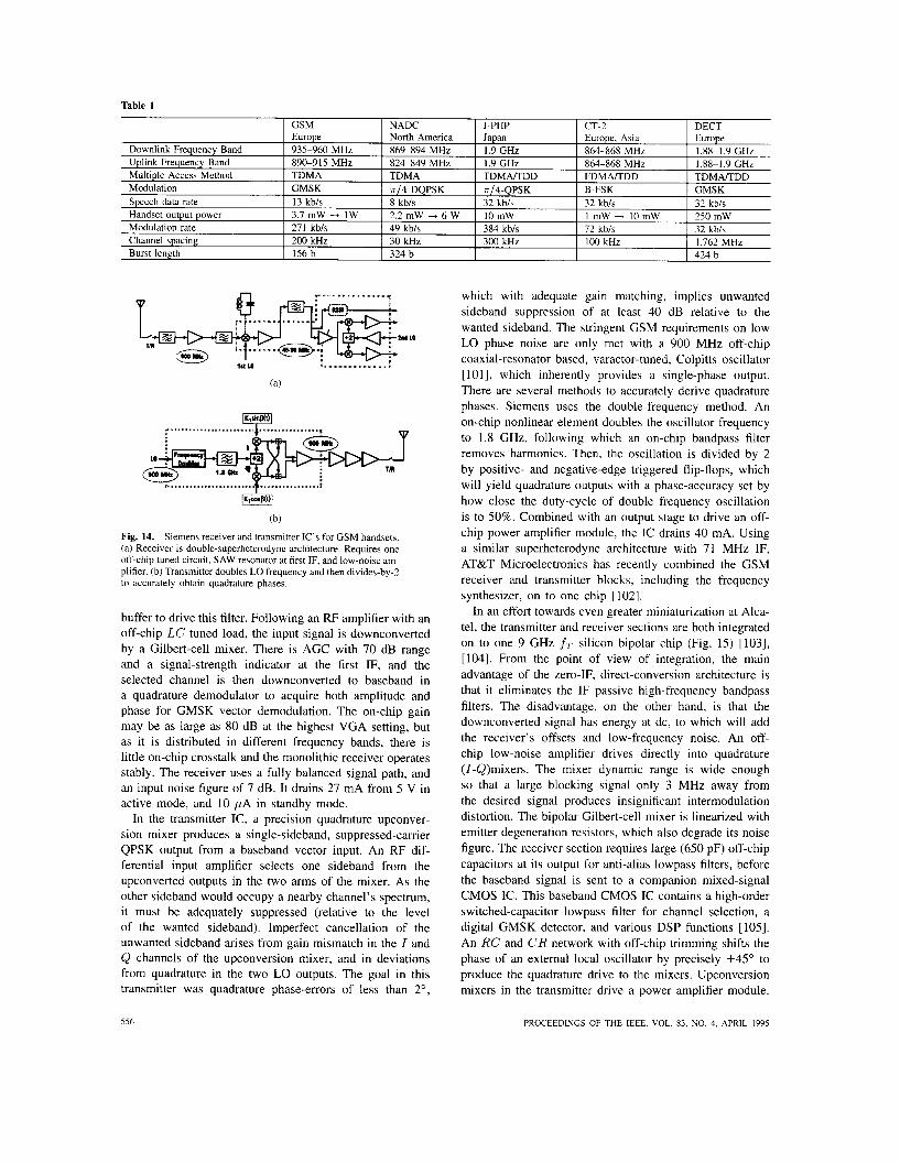
Table 1
I GSM I NADC I J-PHP I CT-2 I DECT
(b)
Fig. 14. Siemens receiver and transmitter IC's for GSM handsets. (a) Receiver is double-superheterodyne architecture. Requires one off-chip tuned circuit, SAW resonator at first IF, and low-noise am- plifier. (b) Transmitter doubles LO frequency and then divides-by-2 to accurately obtain quadrature phases.
buffer to drive this filter. Following an RF amplifier with an off-chip LC tuned load, the input signal is downconverted by a Gilbert-cell mixer. There is AGC with 70 dB range and a signal-strength indicator at the first IF, and the selected channel is then downconverted to baseband in a quadrature demodulator to acquire both amplitude and phase for GMSK vector demodulation. The on-chip gain may be as large as 80 dB at the highest VGA setting, but as it is distributed in different frequency bands, there is little on-chip crosstalk and the monolithic receiver operates stably. The receiver uses a fully balanced signal path, and an input noise figure of 7 dB. It drains 27 mA from 5 V in active mode, and 10 pA in standby mode.
In the transmitter IC, a precision quadrature upconver- sion mixer produces a single-sideband, suppressed-carrier QPSK output from a baseband vector input. An RF dif- ferential input amplifier selects one sideband from the upconverted outputs in the two arms of the mixer. As the other sideband would occupy a nearby channel's spectrum, it must be adequately suppressed (relative to the level of the wanted sideband). Imperfect cancellation of the unwanted sideband arises from gain mismatch in the I and Q channels of the upconversion mixer, and in deviations from quadrature in the two LO outputs. The goal in this transmitter was quadrature phase-errors of less than 2",
which with adequate gain matching, implies unwanted sideband suppression of at least 40 dB relative to the wanted sideband. The stringent GSM requirements on low LO phase noise are only met with a 900 MHz off-chip coaxial-resonator based, varactor-tuned, Colpitts oscillator [ 1011, which inherently provides a single-phase output. There are several methods to accurately derive quadrature phases. Siemens uses the double-frequency method. An on-chip nonlinear element doubles the oscillator frequency to 1.8 GHz, following which an on-chip bandpass filter removes harmonics. Then, the oscillation is divided by 2 by positive- and negative-edge triggered flip-flops, which will yield quadrature outputs with a phase-accuracy set by how close the duty-cycle of double frequency oscillation is to 50%. Combined with an output stage to drive an off- chip power amplifier module, the IC drains 40 mA. Using a similar superheterodyne architecture with 71 MHz IF, AT&T Microelectronics has recently combined the GSM receiver and transmitter blocks, including the frequency synthesizer, on to one chip [102].
In an effort towards even greater miniaturization at Alca- tel, the transmitter and receiver sections are both integrated on to one 9 GHz f~ silicon bipolar chip (Fig. 15) [103], [104]. From the point of view of integration, the main advantage of the zero-IF, direct-conversion architecture is that it eliminates the IF passive high-frequency bandpass filters. The disadvantage, on the other hand, is that the downconverted signal has energy at dc, to which will add the receiver's offsets and low-frequency noise. An off- chip low-noise amplifier drives directly into quadrature (I-Q)mixers. The mixer dynamic range is wide enough so that a large blocking signal only 3 MHz away from the desired signal produces insignificant intermodulation distortion. The bipolar Gilbert-cell mixer is linearized with emitter degeneration resistors, which also degrade its noise figure. The receiver section requires large (650 pF) off-chip capacitors at its output for anti-alias lowpass filters, before the baseband signal is sent to a companion mixed-signal CMOS IC. This baseband CMOS IC contains a high-order switched-capacitor lowpass filter for channel selection, a digital GMSK detector, and various DSP functions [105]. An RC and CR network with off-chip trimming shifts the phase of an external local oscillator by precisely f 4 5 " to produce the quadrature drive to the mixers. Upconversion mixers in the transmitter drive a power amplifier module.
556 PROCEEDINGS OF THE IEEE, VOL. 83. NO. 4, APRIL 1995

. . . .... . b.uL.l* IC
O d h O d
Fig. 15. Alcatel direct-conversion single-chip transceiver. Chan- nel selection done by switched-capactior lowpass filters in compan- ion CMOS mixed-signal baseband IC. On-chip, trimmed RC-CR network generates quadrature phases for mixers.
The chip drains 25 mA from 5 V in the receive mode, and 45 mA in the transmit mode, rather comparable figures to the previously decribed Siemens chip set. The transmitter suppresses the unwanted sideband and carrier by about 40 dB .
There is increasing interest in the 1.9 GHz band for digital cellular telephony. All the current approaches (Table 1) use time-divison duplexed (TDD) receive and transmit frames, wherein users are assigned different time slots. Two-way communications take place over the same frequency band. A host of IC’s is appearing to serve the European DECT standard. The majority cater to a superheterodyne receive- architecture with 110 MHz IF [106]-[109]; some of the literature [ 1071, [ 1091 also describes procedures for system design. The RF sections are usually integrated at small scales, embodying, say, the low-noise amplifier and first mixer on one chip, the quadrature modulator on another, and the exciter and power amplifier on a third and fourth chip. RF-IC’s operating at 1.9-2.5 GHz exist in both GaAs [68], [110]-[112] and silicon [1061, [113]-[115] technologies. Some of these standalone GaAs IC low- noise amplifiers achieve impressive gain and noise figure with 1-2 mA current drain from 3 V [69], [116]. At the system level, though, functionality and overall dynamic range in these short-haul wireless links takes precedence over raw component performance. Thus system-level input noise figures of 10-15 dB are acceptable [109], as are input- referred intercept points of -16 dBm, and a 20 dB power amplifier control range [ 1121. The less than stringent system specifications lead to simplifications in the transmit path, such as direct VCO-modulation by the baseband signal by opening the transmit PLL over the duration of the transmit- frame [ 1071.
The power amplifier continues to be built almost ex- clusively as a separate GaAs IC, and at 1.9 GHz the on-chip wavelength is short enough that it is now possible to integrate distributed matching networks [68], [ 1 171, [I 181. Efficiencies of 50% are attained when delivering almost I W to the load from 3 V. Either the transmitter or the receiver is active in TDD digital transceivers, so fast-switching power-down modes are designed into the various components. In particular, the switching trajectory must be shaped to suppress spurious emissions when the
power amplifier is switched on and off [85]. Finally, the transmit and receive signals are directed to the antenna via a three-port passive circulator, or preferably through a low- loss, monolithic transmitheceive ( T R ) RF switch [ 1121, [119], [120]. A good FET switch must not appreciably distort the RF signal, or incur more than 1-dB insertion loss when ON, yet when OFF it should offer at least 30 dB isolation. Microcell applications, such as the Japanese handy phone, require an average output power of only 10 mW (20 dBm), although the x/4-QPSK modulation requires the power amplifier to handle larger peak powers. An exciter amplifier, power amplifier, and T/R switch have been integrated together [121]. The exciter and power amplifier attain a 44% efficiency at 23 dBm output from a 4.8-V supply, and the on-chip matching network uses LC lumped elements. Although matching networks will eliminate harmonic distortion, they are ineffective in sup- pressing near-carrier spurii produced by intermodulation distortion. Feedback linearization techniques have been proposed which predistort the digitally synthesized exciter input waveform to anticipate the power-amplifier nonlin- earities [122]. Use of these techniques makes a highly nonlinear but efficient power amplifier appear linear. These remain at the experimental stage today, and with the move to microcells and low emitted power levels, they may soon not be necessary in handsets.
The building-block IC’s described so far are important advances in realizing small, relatively low-power transceiv- ers, but the ultimate goal remains to integrate the entire transceiver on to a single-chip. To this end, some early breadboard-level experiments show that direct-conversion receiver architectures seem well suited to the DECT appli- cation [123], [124]. A 16 GHz f~ silicon bipolar IC from Alcatel operating at 1.9 GHz contains a complete direct- conversion DECT transceiver [ 1251. The architecture re- sembles the previously described Alcatel direct-conversion GSM transceiver [ 1031, requiring a separate low-noise amplifier in the receive path, a power amplifier module, and a baseband CMOS mixed-signal signal processor IC. From a 5-V supply, the transceiver drains 50 mA in receive mode and 80 mA in transmit mode. One of the challenges in realizing this system was a fast-switching PLL frequency synthesizer with low phase-noise and low spurious output levels, which was built here with an improved charge-pump and loop filter.
Siemens has extended its dual-conversion GSM transmit- terheceiver chip set [99], [126] to a generalized front-end for digital cellular telephones operating in any part of the RF spectrum from 800 MHz to 2.1 GHz [127]. The 25 GHz fr silicon bipolar chip set ope rates at a supply as low as 2.7-V, the transmitter chip draining 60 mA and the receiver 33 mA. Both have power-down modes. An external power amplifier module is required. A notable low-voltage circuit on this chip is a modified Gilbert-cell mixer, with resistors instead of current sources to the negative supply [31]. To accommodate a wide input dynamic range, the gain of the RF low-noise amplifier in the receiver may be switched from -5 dBm to +15 dBm, a powerful technique
ABIDI: LOW-POWER RADIO-FREQUENCY IC‘S FOR PORTABLE COMMUNICATIONS 551

that has also been used in paging receivers [46]. This assumes that the recever does not instantaneously require a very wide dynamic range, but either receives mostly strong signals or mostly weak ones. The downconversion mixer, with a 13 dB noise figure and -3 dBm input IP3, is followed by an IF variable-gain amplifier with an 80 dB digitally programmable range [ 1261. The on-chip RF oscillator requires an off-chip resonator and varactor, and its phase noise at a 2 kHz offset is -88 dBc/Hz. A balanced signal path is used throughout. One good measure of the quality of on-chip gain matching in the I and Q paths in the direct upconverter, as well as of the quadrature accuracy of the upconversion clocks, is given by the relative levels of spurious emissions from the transmitter IC. The unwanted sideband is suppressed by 48 dB, while the RF camer tone, emitted due to dc offsets in the two paths, is 37 dB down. A 3rd-order modulation tone at -46 dB appears due to mixer nonlinearity. The absolute output noise level at a 25 MHz offset is -141 dBm/Hz.
VII. DIRECT-CONVERSION TRANSCEIVERS AND THEIR PROBLEMS
A receiver with zero-IF is called a direct-conversion receiver. When the local oscillator is synchronized in phase with the incoming carrier frequency, this is also referred to as the homodyne. This architecture is sufficiently promising for single-chip transceivers to warrant a separate section to its study.
The desired channel is translated by the first mixer to a 0 Hz center frequency, and instead of adjacent channel rejection with a bandpass resonator, a more flexible and easier to implement lowpass filter is required-in effect, a bandpass filter centered at dc when the negative frequency axis is included. With zero-IF, there is no image frequency. As early as 1924, radio pioneers had considered homodyne architectures for crude receivers requiring only a single vacuum-tube, but it was in 1947 that a homodyne was first used to full effect, with a high-order lowpass filter for channel-selection, in a measuring instrument for carrier- based telephony [32].
A. Direct-Conversion Single-Sideband Synthesizers For reasons of spectral efficiency, the transmitted signal
in digital communications is always single-sideband with suppressed carrier. This is most often produced with the so- called phasing merhod [ 1281. The modulated signal is first synthesized in quadrature at baseband, directly upconverted into two paths by a quadrature LO centered at the carrier frequency, and added or subtracted to select either the upper or lower sideband (Fig. 16(a)).
The unwanted side band is suppressed to an extent limited by the gain mismatch in the two upconversion paths, and by departures from quadrature in the two LO outputs (Fig. 16(b)). Unequal dc offsets in the paths produce an output signal at the LO frequency. The unwanted sideband and LO leakage are spurious but unavoidable components of the transmitted spectrum. Although on the same IC the
0.1 1 .o 10 100 Phase error (degrees)
(b)
Fig. 16. (a) Single-sideband direct upconverter using the phasing method (also called the quadrature modulator). Extent of sup- pression of unwanted (image) sideband versus gain mismatch and phase-errors from quadrature in two arms of modulator.
two upconversion paths are well matched, a gain mismatch as small as 1% (0.1 dB) will limit suppression of the unwanted sideband to 45 dB. With this gain mismatch, a phase-error of up to 1" may be tolerated between the two LO outputs. These mismatches may be trimmed down at time of transceiver manufacture, or self-calibrated with loopback modes which are activated during idle times to sense and suppress the unwanted spurii.
An off-chip resonator, often connected to an on-chip unbalanced oscillator circuit, may also become a cause of spurious RF leakage if it couples energy into the power amplifier or the antenna. Frequency-offset upconversion schemes have been proposed [ 1291 to combat this coupling problem. Other spurious output tones may arise from par- asitic remixing of the modulated output with the baseband signal, and by intermodulation distortion in the output stage [96]. Balanced circuit topologies, on-chip LO'S requiring no external resonators [ 1301, and lowered transmit power levels in microcells, are all expected to lessen the magnitude of the spurious leakage problem.
558 PROCEEDINGS OF THE IEEE. VOL. 83, NO. 4. APRIL 1995

I LO self-mixing I a Fig. 17. how through self-mixing they create dc offsets.
Sources of leakage in a direct-conversion receiver, and
Cellular wireless systems operate best with tightly reg- ulated power control, the handsets transmitting only the minimum power 'required for reliable reception by the base station, and vice-versa. Whereas in the receiver the front-end is the main source of noise, in a transmitter the upconversion LO phase-noise appears as added noise on the emitted signal. Direct upconversion has the advantage over two-step schemes that only one LO contributes noise.
B. Direct-Conversion Receivers for GSM Digital Cellular Telephones
Among the various RF-IC suppliers for the European GSM digital cellular telephone handset, only Alcatel at present uses a direct-conversion receiver architecture [ 1031, [125], [131]. This results in a relatively small silicon bipolar RF front-end chip, and the remainder of the signal processing, including lowpass channel-select filtering, is at baseband in mixed-mode CMOS. Why are the others reluctant to use direct-conversion in their receivers? Given the many decades of superheterodyne experience, the most likely reason is conservatism. But direct-conversion also suffers from some unique problems.
A well known problem is that spurious LO leakage from the receiver into the antenna becomes an in-band interferer to other nearby receivers tuned to the same band. Superheterodynes, with their frequency-offset LOS, do not suffer from this problem. However, experimental studies suggest that with standard shielding in the receiver, this problem is not so severe as to handicap the use of direct- conversion [ 1321.
A more serious problem is dc offset in the receiver. Offset arises from three sources [ 13 11: transistor mismatch in the signal path; the LO signal leaking to the antenna because of poor reverse isolation through the mixer and RF amplifier, then reflecting off the antenna and self- downconverting to dc through the mixer (Fig. 17); and a large near-channel interferer leaking into the LO port of the mixer, then self-downconverting to dc. Good circuit design may reduce these effects to a certain extent, but they cannot be eliminated.
The spectrum of the GMSK modulation used in GSM has a peak at dc. Offsets will directly add to the spectral peak of the downconverted signal. These offsets are usu- ally much larger than the rms front-end noise, and may therefore significantly degrade the SNR at the detector.
To remove the offsets by ac-coupling the receiver will require impractically large capacitors, if the signal-bearing spectrum around dc is not to be sacrificed. However, they may be compensated with DSP-based self-calibration [ 1051, [ 1331. The baseband signal processor makes long-term measurements on the dc level in the receiver, and subtracts off this level from the downconverted signal. The spectrum loss around dc is only a few hertz, and digital filtering does not distort the midchannel group delay in the receiver.
C. Local Oscillators with Quadrature Outputs A carrier-frequency local oscillator with quadrature out-
puts is a key circuit component in direct-conversion trans- mitters and receivers. Usually this oscillator is tuned by an LC circuit or an off-chip resonator, and inherently produces a single-phase output. Quadrature phases are often derived by passing the oscillator output through a C R and an RC network, whose time constant is equal to the oscillation period. The two resultant outputs are then phase-shifted by +45' and -45", respectively. Inaccuracies in the actual values of R and C will lead to errors in quadrature, and are compensated by some form of on-chip trimming [103], [125].
An alternative method is to divide an oscillation at twice the carrier frequency with positive- and negative- edge triggered flip-flops [99]. The resulting two outputs at the desired frequency are in quadrature. Residual phase errors caused by unequal delays in the two flip-flops, and by departures from 50% duty cycle in the double-frequency oscillation, are found to be less than I". However, the double-frequency portions of the circuit may become a speed bottleneck.
Quadrature outputs may also be derived from a polyphase oscillator, such as a variable-frequency ring oscillator. In a four-delay stage ring oscillator, taps at diametri- cally opposite points will yield quadrature phases at all frequencies [I341 (Fig. 18). In oscillators with an odd- number of unit delays, they may be synthesized from two taps by a voltage-controlled phase-shifter in feedback around a quadrature-sensing circuit [ 1351. Mismatches in transistor characteristics limit the attainable phase accuracy. This type of resonator-less oscillator is practical when the specifications on phase-noise are not too stringent (say up to -80 dBc/Hz at a 100 kHz offset from the carrier). The free-running oscillator must be slaved to a crystal reference in a frequency-locked loop, whose loop gain and bandwidth are specifically designed to suppress phase noise.
When circuit techniques cannot contribute further im- provements to gain- and phase-matching in the two arms of a quadrature modulator or demodulator, digital adaptive al- gorithms may be used at baseband to sense and compensate for these errors [136].
VIII. IC's FOR SPREAD-SPECTRUM WIRELESS TRANSCEIVERS
Spread-spectrum communications offer greater user ca- pacity than narrowband techniques in a given piece of
ABIDI: LOW-POWER RADIO-FREQUENCY IC's FOR PORTABLE COMMUNICATIONS 559

I-.
b 4-Stage
Ring Oscillator - +Q
Fig. 18. A four-phase voltage-controlled ring oscillator. Diamet- rically opposite taps give quadrature phase at any frequency. Unequal loadings and device mismatch set phase errors. VCO must be embedded in PLL whose closed-loop bandwidth is tailored to suppress oscillator noise.
wireless spectrum. Much has been written on this subject [ 1371, Spread-spectrum techniques were developed dur- ing World War I1 as a form of secure communication with low probability-of-intercept and resilience to jamming [138]. Over the years, this technology has been further developed and refined for military communications. With the wireless revolution at hand and the IC technology now available to implement complex transceivers, spread- spectrum has awakened commercial interest [ 1391. Spread- spectrum communications make it easy for users to access the wireless channel. Whereas conventional narrowband wireless communications require a careful discipline, which the FCC or other government agencies enforce by issuing licenses so as to prevent use of the same frequency by nearby operators, for spread-spectrum use the FCC has allocated certain unlicensed bands in the US, referred to as the Instrumentation, Scientific, and Medical (ISM) bands, wherein the user is only required to spread spectrum by a minimum amount, and not to exceed an upper limit on transmitted power. The extent of spectrum spreading may be measured by the amount of processing gain in the receiver required to de-spread and detect the signal [ 1401.
As analog cellular telephones begin to saturate the avail- able radio frequency allocations, spread-spectrum tech- niques are being deployed in cordless telephones and wire- less modems [141]. These devices usually operate in the two lower ISM bands: 902-928 MHz and 2.4-2.48 GHz. A ubiquitous wireless environment is envisioned, in which mobile users, wherever they may be, can access data and communications services through an intricate network of base stations [2]. The greatest hardware challenge in realizing this scenario is the development of a low-power, miniature handset.
There are two different methods to spread the spectrum of a signal: by direct-sequence modulation, or by frequency
(b)
Fig. 19. Front-end GaAs MMlC transceiver for spread spec- trum communications in 2.4 GHz band. Receiver is dou- ble-superhetorodyne. Note use of off-chip filters. (b) Low noise amplifier in transceiver IC (left) reuses bias current in two stages. Clapp voltage-controlled local oscillator (right) combines on-chip LC network with off-chip resonator and varactor.
hopping [ 1401. Direct sequence is conceptually the simpler, as well as the more straightforward to implement. Each data bit (either + I or -1) at the transmitter multiplies a prescribed sequence of bits, or chips as they are called. The chip sequence is selected for very low autocorrelation, and is often referred to as a pseudo-noise, or PN, sequence. Each user is either assigned a unique PN sequence with very low cross correlation with other user sequences, or a time-shifted version of some long PN sequence. The receiver, after an initial acquisition search to align itself with the start of the PN sequence, correlates the incoming sequence with the pattern it knows to be its own. On detection of a correlation peak, the sign of the peak signals the source data bit. The longer the PN sequence for each bit, the greater the spreading factor, and the more reliable the detection. Here, the processing gain is the sequence length per bit. The spectrum of the transmitted data, composed from a concatenation of PN sequences, is noise-like; thus the term spread-spectrum. Several baseband and IF modem IC’s have already appeared to support BPSK and QPSK direct-sequence spread-spectrum transceivers [ 1421-[ 1441.
Whereas direct-sequence modulation spreads the spec- trum by randomizing the waveform, frequency-hopping spreads spectrum by hopping the carrier according to a
S60 PROCEEDINGS OF THE IEEE. VOL. 83, NO. 4. APRIL 1995

I :U” w I ; I
Fig. 20. The UCLA frequency-hopped spread-spectrum trans- ceiver. This uses direct-conversion in both transmit and receive path, and binary-FSK modulation. In the transmitter, the spread-spectrum waveform i synthesized at baseband, and upconverted to RF. During receive mode, the DDFS under control of a synchronization loop hops with the incoming data, and demodulates it to baseband. The entire mixed analog-digital, baseband/RF system is to be integrated on a I-lcm CMOS IC.
prescribed sequence across the entire band. The effect in the frequency-domain is similar to direct-sequence, ex- cept for one fundamental difference: with direct-sequence, spreading across a wide bandwidth requires each data bit to be mapped into a long PN sequence. The resultant high “chip-rate’’ requires high-speed signal processing at the receiver front end. On the other hand, if the carrier frequency is hopped with a wideband synthesizer, the output spectrum may span an arbitrarily wide frequency range, even at low bit rates. Therefore, if a fast and agile frequency synthesizer is readily available, the receiver front-end operates at the actual data rate in frequency- hopped spread-spectrum, rather than at the considerably higher chip-rate in a direct-sequence receiver. The former will very likely lead to a low-power solution.
As a notable recent example of a miniature spread- spectrum transceiver, Plessey has introduced a 700 kb/s frequency-hopped device operating in the 2.4 GHz ISM band. The transceiver is entirely contained on a 2”x 3” PCMCIA card for insertion into notebook computers [ 1091, [145]. FSK data modulates the carrier frequency, and a variable-modulus PLL synthesizer slowly hops the carrier to spread the spectrum across the 80 MHz band. All the active devices in the transceiver are on three IC’s, consisting of a GaAs RF front-end, a silicon bipolar IF receiver, and a CMOS IC for the hopping-frequency synthesis. As in any spread-spectrum two-way communication system, transmission and reception is time-division-duplexed on the same frequency band. The receiver architecture is a conventional double-superheterodyne. In addition, the transceiver requires 50 passive components, including six rather bulky filters, and when transmitting 100 mW RF power it dissipates more than 1 W.
By the norms of GaAs MMIC’s, the single-chip IC front- end in this transceiver is highly integrated (Fig. 19(a)) [146]. It includes the power amplifier, and drivers for
2-GHz passive filters in the transmit and receive paths. Interesting features are the dc series connection of the single-ended two-stage low-noise amplifier, which shares the same bias current in both stages through a bypass inductor; the Clapp VCO; and the four-FET switched mixers in the transmit and receive paths (Fig. 19(b)). In its first version, the IC includes more than 20 on-chip spiral inductors, perhaps the largest number on any MMIC at the time of this design. A second bipolar IC processes the 350 MHz IF signal. In receive mode, the GaAs front- end IC drains 30 mA from a 5 V supply. The receiver selects one of two extemal antennas through an on-chip RF switch to attain spatial diversity. This work has spurred a flurry of similar GaAs IC’s at the same level of integration [147]-[149], all operating at f 5 V supplies, with similar functionality and performance. One of them [149] uses a very high IF of 915 MHz, so that spurious products at the transmitter output lie well in the stopbands of the output filter, and where the IF signal is processed by a 915 MHz cellular-telephone type IC.
Ix. IC’s TO ENABLE FUTURE TRANSCEIVERS What will portable wireless communicators of the fu-
ture look like? We may draw some conclusions from the foregoing summary of RF-IC developments. The crowded spectrum means that future wireless communicators will predominantly use spread-spectrum techniques. Coupled to this is a need for low-power dissipation, which will force architectural innovations and higher levels of integration in the electronics. As an example of such an advanced transceiver, the author with his colleagues and their gradu- ate students at UCLA is investigating the architecture and circuit design of a frequency-hopped, binary frequency-shift keyed, zero-IF, all-CMOS two-chip transceiver capable of delivering up to 160 kb/s (the base ISDN rate) in the 900 MHz ISM band [39], [150]. The transceiver architecture is inspired by the modem paging receiver, a very low energy wireless device widely used today. The transceiver implementation (Fig. 20) will freely mix analog and digital circuits, which makes CMOS the IC technology of choice. Further, to avoid the routing of high-frequency signals off- and on-chip and thereby save the power the buffers would use to drive stray capacitance and off-chip low-impedance lines, it is preferred to integrate all the blocks, including the RF front-end. Finally, it is most desirable to use an unmodified, standard production CMOS process.
Low-power operation requires the entire system to op- erate on a 3 V supply. This supply voltage cannot be any lower because in many places the analog circuits contain stacked cascode transistors, and the FET threshold voltages are about 0.8 V. RF amplifiers are normally tuned with inductor loads, which on silicon IC’s are almost always off-chip passive components [ 1511. However, this is itself wasteful of power, because in addition to the current supplied into the inductor, the circuit must also drive the various parasitic capacitances in off-chip routing the RF signal.
ABIDI: LOW-POWER RADIO-FREQUENCY IC’s FOR PORTABLE COMMUNICATIONS 56 I

Off-Chip L o s s l e s s Matching Network
Balanced Antema Output
(a)
Fig. 21. (a) Balanced input CMOS RF amplifier. Cascode sthge driving on-chip inductor sub- stantially enhances voltage gain. Outputs common-source stages are for measurement only. LNA will directly drive mixer. (b) A microphotograph of a 110 nH spiral inductor suspended over a pit on substrate
Spiral inductors on silicon substrates suffer from a large capacitance to the conducting silicon substrate. However, after many years of the belief that no useful inductors could be made on silicon, it was found that spiral inductors as large as 10 nH with self-resonance beyond 2 GHz, could be fabricated with the standard interconnect metallization. These inductors were used to build passive filters, a tuned amplifier, and an LC voltage-controlled oscillator on a silicon bipolar IC [ 1521-[ 1541. This work has rekindled interest in the design and modelling of small value spiral inductors on silicon (usually bipolar) IC’s, with values in the range of 1-10 nH [155], [ 1561. In some instances, higher inductor Q’s are obtained with thicker metallization, or higher resonant frequencies with thicker oxides. In search of larger value inductors for low-power, high-gain amplifiers, we have developed a fabrication method whereby the silicon substrate is selectively removed under the inductor, substantially reducing the capacitance to the substrate, and thus extending self-resonance to a higher frequency (Fig. 21(b)) [157]. The self-resonant frequency is now almost as high as it is on a semi-insulating GaAs substrate. Using two such inductors as loads in a balanced circuit, a 900 MHz RF amplifier has been built in 1-pm CMOS with a 30 dB gain draining only 3 mA (Fig. 2 1 (a)). The amplifier IP3 is about 0 dBm, owing to the wide linear range of the MOS differential pair.
The front-end mixer in a direct-conversion receiver must be highly linear to suppress unwanted intermodulation produced by interferers. Also, as the local oscillator fre- quency is centered at RF in this direct-conversion receiver, inadequate reverse isolation or shielding may cause this frequency to leak through the antenna and to interfere with other nearby receivers tuned to the same RF. We use an unusual mixer-ne that happens to be particularly well suited to MOS implementation-to circumvent both these problems. The desired signal is downconverted to baseband by sub-sampling the incoming RF [ 1.581. The mixer circuit is a track-and-hold, with such a wide track-
mode bandwidth that it can follow the RF waveform, and a short enough aperture to acquire the instantaneous value of the RF waveform on receipt of the sampling clock edge (Fig. 22). The received RF in our system is a 26 MHz wide spread-spectrum centered on a 915 MHz carrier, so by sub-sampling this waveform at a clock rate of 52 MHz or higher, the spectrum is translated to baseband without aliasing. However, the mixer also acquires wideband noise accompanying the signal from dc up to the gigahertz track bandwidth, and aliases the rms noise into a bandwidth at half the sample-rate, thereby raising the baseband noise spectral density by the ratio of the track-bandwidth to the sample-rate. Sub-sampling mixers therefore have a higher noise figure than conventional mixers. However, as such a mixer tends to be more linear than an analog multiplier, its dynamic range is also large, provided a high-gain, low-noise RF amplifier precedes it. The overall front-end spurious-free dynamic range is jointly set by the individual specifications of the RF amplifier and mixer. In this 1 pm CMOS prototype, the mixer circuit draws 4 mA from 3-V to acquire samples of a 900 MHz modulated waveform at a 50 MHz rate, which it then translates to baseband. The linearity, as measured by a +26 dBm third-order intercept, exceeds that of most continuous-time 900 MHz monolithic mixers, and for the fundamental reasons given above, the noise figure is 18 dB.
A low-power, agile frequency synthesizer with high spectral purity is required in a frequency-hopped trans- ceiver. Conventional synthesizers based on a phase-locked loop with a variable-modulus divider in feedback suffer from limited agility, because the loop bandwidth may limit the speed of frequency switching. It is also difficult to design a VCO which both covers a wide range of frequency spreading, and produces a pure spectrum. The DDFS-DAC combination is an alternative solution to this problem, which so far has only been used by the military in spread-spectrum communication systems. A direct-digital frequency synthesizer (DDFS) [ 1591 consists of an accumu-
562 PROCEEDINGS OF THE IEEk. VOL 83. NO 4, APRIL 1995

lator and ROM, which produces a sequence of digital words representing samples of a sinewave at a frequency set by an input control word. A D/A Converter converts the digital samples into a discrete-time analog sinewave, and a subse- quent analog filter may smooth this into a continuous-time sinewave. Roundoff errors in the DDFS and nonlinearity in the DAC and filter will limit the attainable spectral purity of the synthesized sinewave [159]. In practice, DAC imperfections may contribute the largest nonlinearity in the system. A characteristic feature of digitally synthesized sinewaves is that the major imperfections do not necessarily produce harmonic tones, but instead spurious tones at rational multiples of the fundamental. These spurious tones often cluster around the fundamental and cannot be filtered. The DAC can add spurious tones of its own. We use a highly efficient DDFS combined with a high-speed, low-power charge-redistribution DAC to produce an FSK- modulated, frequency-hopped spread-spectrum at baseband, which a fixed-frequency local oscillator upconverts to RF. A CMOS implementation of a DDFS-DAC at 3 V dissipates only 40 mW when clocked at 50 MHz (of which the quadrature ROM-accumulator accounts for 35 mW), with worst-case spurious levels of -57 dBc or less across the entire spreading range (Fig. 23) [160].
The 915 MHz local oscillator is a four-stage MOS ring oscillator locked in a PLL to a lower frequency crystal reference. The quadrature outputs at 915 MHz for the image-reject mixers are tapped at diametrically opposite points [130], [134] to a phase accuracy of better than 1’. As the local-oscillator operates at a fixed frequency, it is locked to a low-frequency crystal reference in a PLL solely optimized to reduce phase noise. At a 100 kHz offset, a phase noise level of -75 dBc/Hz is measured on a prototype.
The power amplifier is a binary-weighted array of FET’s biased near threshold, which is digitally selected to deliver power levels from -15 dBm to +15 dBm through a matching network to the antenna with a 40% conversion efficiency (Fig. 24) [161].
Fig. 22. A downconversion mixer based on direct sampling of RF. During track mode, switches are closed, and bandwidth of passive circuit is about I GHz. On receipt of sample clock, switches open within very short aperture time, capuring instantaneous value of RF waveform. Op amp removes switch charge injection, and buffers to subsequent circuits.
c__ Charge Redistribution DAC - - Q-to4 Buffer - (b)
Fig. 23. (a) An agile frequency synthesizer. The DDFS produces digital samples of a sine and cosine, at a frequency set by an input word. DAC’s convert these to analog domain, and after quadrature upconversion, either the upper or lower sideband is selected. Thus 0-1 3 MHz at baseband frequency produces output spanning 902-928 MHz. First-order anti-alias filter suffices if DDFSDAC operates at 80 MHz. (b) DAC uses passive, pipelined architecture.
The transceiver achieves spatial diversity with two in- dividual receive channels, which are powered-up contin- uously and connected to two different types of miniature antennas. Data decisions are made on an equally weighted sum of their baseband outputs. A high-order switched- capacitor elliptic lowpass filter selects the desired channel, which the on-board DDFS-based synthesizer has dehopped
ABIDI: LOW-POWER RADIO-FREQUENCY IC’s FOR PORTABLE COMMUNICATIONS 563

-P T 0.7pF
Fig. 24. A digitally controlled power amplifier. The binary-weighted array of output NMOSFET’s drive the antenna load differentially, to deliver up to + 15 dBm from a 3-V supply. Large on-chip inductor used as exciter load gives swings above power supply. PMOSFET’s selectively activate source follower buffers, and thus total delivered power.
to dc in the course of downconversion. The capacitively coupled output is then amplitude-limited to produce a one-bit stream fed to an optimal FSK digital detector [39]. The detector quantizes the zero-crossings in time by oversampling the limited baseband data, and seeks correlations between one-bit representations of the two possible data values. A logarithmic amplifier connected to taps on the limiting amplifier chain measures the received signal-strength [162]. Operating from a 3-V supply, the 1-pm CMOS transceiver is expected to drain 70 mA in receive mode, and 100 mA in transmit mode (the power amplifier is on-chip). Considering that the transceiver communicates on a 26 MHz-wide spectrum, this is indeed a low power dissipation.
This research project is now exploring issues related to the single-chip integration of this transceiver. Such a highly integrated CMOS “VLSI radio” would represent a major step forward in the evolution of the radio integrated circuits described in this paper.
X. CONCLUSIONS This survey has covered some of the key existing
and emerging communication applications which have prompted advances in RF IC’s. The emphasis was on widespread portable consumer applications. This has excluded coverage of integrated television tuners, for instance, which were historically the principal motivation for the development of UHF RF-IC’s by the consumer electronics industry in the mid-1970’s [163]. The fact that about 18 million tuners are produced every year means that there has been a steady stream of innovations in the building-block and architectures for this application [164]-[178]. Then there are emerging areas, such as personal GPS receivers, where RF integration and low- power will be the key for acceptance by consumers [ 1791, [180]. Here, too, RF-IC designers are responding with integrated front ends [ 1811-[ 1841, although the greater challenges to realize a system with an acceptable precision may lie in the baseband signal processing.
% Choke
1 OOR Antenna
The lucrative global wireless market is attracting a great deal of attention from circuit designers across the industry. The RF range of interest spans 400 MHz to 2.5 GHz. There is a multi-pronged industry-wide assault to provide the right solutions. The solution must be low-cost, low-power, and it must give high functionality. MMIC designers bring to RF-IC’s a microwave style derived from small-scale circuits which operated at much higher frequencies. On the other hand, as the frequency range lies within the capability of modem silicon IC technologies, there is a response from this community. Bipolar and BiCMOS RF-IC’s are often extensions of baseband style circuits to high-frequency, often with more functionality than GaAs MMICs offer. A low transistor fT is no longer a handicap, and experience rapidly accumulates on how to solve some of the unique problems of silicon substrates, such as high-frequency losses in the substrate [ 1851 and on-chip coupling problems between circuit blocks. In the not too distant future, as microprocessors and memories drive the linewidths of silicon IC processes to deep submicron, RF-IC’s might be designed as untuned wideband circuits, in the style of IC’s for video applications today.
Small-scale GaAs MMIC’s might sometimes perform better as standalone components, but embedded in a system such as a digital cellular telephone or a spread-spectrum transceiver, they require a large overhead in support cir- cuits, and thereby lose an edge in certain specifications, such as power dissipation. Silicon RF-IC’s offer higher levels of integration, but even within the silicon IC de- sign community there are differing points of view. While integrated silicon bipolar transceivers are to be found in the next generation of products, CMOS RF solutions, albeit at an exploratory stage, now look very promising. They combine elements from well established techniques in voiceband and video IC’s, and are unfettered in partitioning tasks between analog and digital signal processing, while using off-chip passive components when necessary. Digital control components and baseband signal processors are readily integrated with, indeed merged into, the RF and IF
564 PROCEEDINGS OF THE IEEE. VOL. 83. NO. 4. APRIL 1995

sections. This array of competing technologies offers com- munication system designers more creative opportunity, and the best wireless transceiver solutions may well emerge from system design evolving together with architecture, circuits, antennas, and power-allocation plans.
What are the prospects for this multitude of approaches to low-power wireless communications? If we project on the experience gained from baseband and video telecommuni- cations circuits, the future wireless transceiver may be only one BiCMOS or CMOS large-scale, mixed analog-digital IC, requiring one passive filter and a crystal resonator. Baseband digital signal processing may make up for im- perfections in the front-end RF sections. As it will likely be used in a microcell environment at low transmit power levels, the transceiver may be encapsulated in a plastic package. There is no fundamental reason why it should need more than a single 1.5 V battery as the power source. After decades of thinking of it only as science-fiction, the electronics world is prodded forth by the communications explosion into making the two-way wristwatch-size radio a reality. A large community researchers, not trained in the classical radio art, is busy reexamining the conventions, and at time challenging the received wisdom. We are poised at a turning point in the evolution of radio-circuit engineering.
ACKNOWLEDGMENT My own involvement in RF-IC design is considerably en-
riched by collaborations with the many talented colleagues and graduate students participating in the Low-Power Wire- less Transceiver Program in the UCLA Electrical En- gineering Department. Professors Henry Samueli, Greg Pottie, and Yahya Rahmat-Samii have made an exemplary teamwork possible on this project.
The recent financial stringencies at UC have not so far eroded the marvellously rich Engineering Collection and online facilities at the UCLA Science and Engineering Library. It would be impossible to write this paper without ready access to these resources. Karen Andrews and Aggi Raeder, two of the expert librarians there, enthusiastically helped me in using the latest tools to peruse the literature, and amazed me with the ease with which they could track down obscure references from all corners of the world.
I thank Prof. Bob Meyer for a very thorough reading of the draft manuscript and for his thoughtful comments on it, and also Taiwa Okanobu and Mark McDonald who made useful suggestions. I am very grateful to Dr. Ran- Hong Yan, the Guest Editor of the Proceedings of the IEEE who solicited this manuscript, for his extraordinary ability to obtain speedy reviews and patiently absorb delays on my part in bringing this work to completion.
REFERENCES
[ 11 G. H. Heilmeier, “Personal communications: Quo Vadis,” in Int. Solid State Circ. Con$, San Francisco, 1992, pp. 24-26.
[2] D. C. Cox, “Universal digital portable radio communications,” Proc. IEEE, vol. 75, pp. 4 3 W 7 6 , Apr. 1987.
S. Sheng, A. Chandrakasan, and R. W. Brodersen, “A portable multimedia terminal,” IEEE Comm. Magazine, vol. 30, no. 12, pp. 64-75, Dec. 1992. B. A. Beatty, “The IBM personal communicator-Design considerations,” SOUTHEASTCON, Miami, FL, 1994, pp. 432435. A. Matsuzawa, “Low-voltage and low-power circuit design for mixed analogldigital systems in portable equipment,” IEEE J. Solid-state Circ., vol. 29, pp. 4 7 W 8 0 , Apr. 1994. E. A. Vittoz, “Low-power design: Ways to approach the limits,” in Int. Solid State Circ. Con$, San Francisco, 1994, pp. 14-18. F. E. Terman, Radio Engineers’ Handbook. New York: McGraw-Hill, 1943. W. L. Everitt, Ed., Fundamentals of Radio and Electronics, 2nd ed. K. K. Clarke and D. T. Hess, Communication Circuits: Analysis and Design. H. L. Krauss, C. W. Bostian, and F. H. Raab, Solid State Radio Engineering. New York: Wiley, 1980. W. H. Hayward, Introduction to Radio Frequency Design. Englewood Cliffs, NJ: Prentice-Hall, 1982. U. L. Rohde and T. T. N. Bucher, Communications Receivers: Principles & Design. D. 0. Pederson and K. Mayaram, Analog Integrated Circuits for Communications: Principles, Simulation, and Design. Boston: Kluwer, 199 1. M. Ibuka, “How Sony developed electronics for the world market,” IEEE Trans. Eng. Manage.. vol. EM-22, pp. 15-19, Feb. 1975. A. Laundrie and K. Negus, “GPS receiver chip targets low- power commercial markets,” in Microwaves & RF, Aug. 1992, pp. 135-138. N. Camilleri, D. Lovelace, J. Costa, and D. Ngo, “New develop- ment trends for silicon RF device technologies,” in Microwave & Millimeter-Wave Monolithic Circ. Symp., San Diego, CA,
W. Kanow and I. Siewert, “Integrated circuits for hi-fi radios and tuners,” in Electronic Components and Applications, vol. 4, no. 1, pp. 11-27, Nov. 1981. R. M. Warner and J. N. Fordemwalt, Eds., Integrated Circuits: Design Principles and Fabrication. New York: McGraw-Hill, 1965. C. S. Meyer, D. K. Lynn, and D. J. Hamilton, Eds., Analysis and Design of Integrated Circuits. New York: McGraw-Hill, 1968. Y. Hishida and M. Kazama, “Mobile communication system: Its semiconductor technology,” in Hitachi Review, vol. 42, no. 3, pp. 95-100, June 1993. B. Crouch, Ed., Dick Tracy: America’s Most Famous Detective. Secaucus, NJ: Citadel, 1987. L. Blaser and T. Taira, “An a d f m radio subsystem IC,” IEEE Trans. Consumer Electron., vol. CE-23, pp. 129-136, Feb. 1977. W. Peil and R. J. McFayden, “A single chip a d f m integrated circuit radio,” IEEE Trans. Consumer Electron., vol. CE-23, pp. 424-431, Mar. 1977. 0. L. Richards, “A complete a d f m signal processing system,” IEEE Trans. Consumer Electron., vol. CE-24, pp. 34-38, Jan. 1978. W. G. Kasperkovitz, “An integrated fm receiver,” Microelec- tronics Reliabilih., vol. 21, no. 2, pp. 183-189, 1981. A. A. Abidi, “Noise in active resonators and the available dynamic range,” IEEE Trans. Circ. and Syst., vol. 39, pp. 29G299, Apr. 1992. W. G. Kasperkovitz, “Fm receivers for mono and stereo on a single chip,” Philips Tech. Rev., vol. 41, no. 6, pp. 169-182, 1983. W. H. A. van Dooremolen and M. Hufschmidt, “A complete fm radio on a chip,” in Electronic Components and Applications, vol. 5, no. 3, pp. 159-170, 1983. J. Brilka and G. Sieboerger, “A single-chip fm radio,’’ in Int. Con$ on Consumer Electron., pp. 156157, 1984. T. Okanobu, T. Tsuchiya, K. Abe, and Y. Ueki, “A com- plete single-chip a d f m radio integrated circuit,” IEEE Trans. Consumer Electron., vol. CE-28, pp. 393408, Mar. 1982. T. Okanobu, H. Tomiyama, and H. Arimoto, “Advanced low- voltage single chip radio IC,” IEEE Trans. Consumer Electron., vol. 38, pp. 465475, Mar. 1992.
Englewood Cliffs, NJ: Prentice-Hall, 1958.
Reading, MA: Addison-Wesley, 1971.
New York: McGraw-Hill, 1988.
1994, pp. 5-8.
ABIDI: LOW-POWER RADIO-FREQUENCY IC’s FOR PORTABLE COMMUNICATIONS 565

D. G. Tucker, “The history of the homodyne and synchrodyne,” J. Brit. Inst. of Radio Eng., vol. 14, no. 4, pp. 143-154, 1954. D. Mitchell and K. G. van Wynen, “A 150-mc personal radio signaling system,” Bell S y t . Tech. J., vol. XI, no. 5, pp. 1239-1257, 1961. A. E. Kerwien and L. H. Steiff, “Design of a 150-megacycle pocket receiver for the BELLBOY personal signaling system,’’ Bell Syst. Tech. J., vol. XLII, no. 3 , pp. 527-565, 1963. K. Nagata, M. Akahori, T. Mori, and S. Umetsu, “Digital display radio paging system,” in NEC Res. & Devel., no. 68, pp. 1 6 2 3 , Jan. 1983. 1. A. W. Vance, “An integrated circuit VHF radio receiver,” The Radio and Electronic Engineer, vol. 50, no. 4, pp. 158-164, 1980. -, “Fully integrated radio paging receiver,” IEE Proc., vol. 129, pt. F, no. I , pp. 2-6, 1982. R. C. French, “A high technology VHF radio paging receiver,” in Int. Con8 on Mobile Radio Syst. and Tech., York, UK, 1984, pp. 11-15. J. Min, A. Rofougaran, H. Samueli, and A. A. Abidi, “An all-CMOS architecture for a low-power frequency-hopped 900 MHz spread-spectrum transceiver,” in Custom IC Cont. San Diego. CA, 1994, pp. 379-382.
1 K. Holtvoeth, “A fully integrated low-power FSK receiver for VHF and UHF paging,” IEEE Trans. Consumer Electron., vol. 35, pp. 707-713, Mar. 1989.
1 S. Drude and T. Rudolph, “New chip-set reduces power con- sumption of radio pagers,” Electron. Components and Applica- tions, vol. 9, no. 2, pp. 1 12-124, 1989.
[42] J. F. Wilson, R. Youell, T. H. Richards, G. Luff, and R. Pilaski, “A single-chip VHF and UHF receiver for radio paging,” IEEE J . Solid Stare Circ., vol. 26, pp. 1944-1950, Dec. 1991.
[43] K. Nagata, D. Ishii, T. Mori, T. Oyagi, and T. Seo, “Slim digital pagers, in NEC Res. & Develop., no. 74, pp. 55-64, July 1984.
[44] K. Yamasaki, S. Yoshizawa, Y. Minami, T. Asai, Y. Nakano, and M. Kuroda, “Compact size numeric display pager with new receiving system,” in NEC Res. and Develop., vol. 33, no. I , pp. 73-81, Jan. 1992.
[45] A. Burt, “Direct conversion receivers come of age in the paging world,” in GECRev., vol. 7, no. 3 , pp. 156160, 1992.
[46] S. Tanaka, A. Nakajima, J. Nakagawa, and A. Nakagoshi, “High-frequency, low-voltage circuit technology for VHF pag- ing receiver,” IEICE Trans. Fundamentals of Electron., Com- mun. and Comp. Sci., vol. E76-A, no. 2, pp. 156-163, 1993.
[47] B. F. Cambou, “MMIC consumer application and production,” in Microwave & Millimeter- Wave Monolithic Circ. Symp., Al- buquerque, NM, 1992, pp. 1-3.
[48] H. Komatsu, R. Norose, and S. J. Symonds, “The wristwatch as a personal communications device,” in Pacijk Telecommun. Con$, Honolulu, 1993, pp. 242-244.
[49] M. Pardoen, R. Pache, and E. Dijkstra, “Direct-conversion receiver provides CP-FSK operation,” in Microwaves & RF, Mar. 1994, pp. 151-155.
[SO] G . J. Lomer, “Telephoning on the move-Dick Tracy to Captain Kirk,” IEE Proc., vol. 134, pt. F. no. I , pp. 1-8, 1987.
[51] K. Wakino, “Recent developments of dielectric resonator ma- terials and filters in Japan,” Ferroelectrics, vol. 91, pp. 69-86, 1989.
[52] M. Hikita, T. Tabuchi, and A. Sumioka, “Miniaturized SAW devices for radio communication transceivers,” IEEE Trans. Vehic. Tech., vol. 38. pp. 2-8, Jan. 1989.
(531 K. Eda, “Ultra-small SAW filter works in mobile communica- tions,” in J. Electron. Eng., pp. 54-57, May 1992.
[54] Y. Tamura, T. Maru, N. Hirasawa, H. Okuno, M. Komoda, and M. Hotsumi, “Hand-held portable equipment for cellular mobile telephone, in NEC Res. and Devel., no. 87, pp. 3 4 4 3 , Oct. 1987.
[55] D. Anderson and R. J. Zavrel, “RF ICs for portable communi- cations equipment,” in Electron. Components and Appl., vol. 7, no. 1 pp. 3 7 4 4 , 1985.
[56] 1. A. Koullias, S. L. Forgues, and P. C. Davis, “A 100 MHz IF amplifier/quadrature demodulator for GSM cellular radio mobile terminals,” in Bipolar Circ. and Tech. Mtg., Minneapolis,
[57] Y. Mori, H. Yabuki, M. Ohba, M. Sagawa, M. Makimoto, and I. Shibazaki, “Miniaturized RF-circuit modules for land mobile communication equipment,” in IEEE Vehic. Tech. Con$, Orlando, FL, 1990, pp. 65-70.
MN, 1990, pp. 248-25 1.
[58] M. Hikita, A. Yuhara, and K. Oda, “New low-loss, miniature SAW filters,” in Hitachi Rev., vol. 42, no. 3, pp. 119-124, June 1993.
[59] L. Scharf, H. Frank, and T. Pollakowski, “High f~ and low noise,” in Siemens Components, vol. 25, no. 4, pp. 119-122, 1990.
[60] S. Yamada and K. Oguri, “Low-power front-end oriented dis- crete semiconductor devices,” in Hitachi Rev., vol. 42, no. 3, pp. 101-106, June 1993.
[61] C. Huang, “Where do integrated circuits replace discretes?,” in Applied Microwaves & Wireless, pp. 5-6, Summer 1994.
[62] S. P. MacCabe, “GaAs MMICs for cellular telephones, GPS and DBS markets,” in WESCON, San Francisco, 1989, pp.
[63] M. Rocchi, “GaAs & Si MMIC building blocks: A moot point revisited,” Microelectron. Eng., vol. 15, pp. 685492, 1991.
[64] Y. Aoki, K. Kobayashi, and W. Kennan, “Monolithic mi- crowave ICs (MMICs) for telecommunication,” in Fujitsu Sci. & Tech. J., vol. 30, no. I , pp. 32-39, June 1994.
[65] Y. Imai, M. Tokumitsu, A. Minakawa, T. Sugeta, and M. Aikawa, “Very low-current and small size GaAs MMICs for L-band front-end applications,” in GaAs IC Symp., Monterey,
[66] Y. Imai, M. Tokumitsu, and A. Minakawa, “Design and per- formance of low-current GaAs MMICs for L-band front-end applications,” IEEE Trans. Microwave Theory and Tech., vol. 39, pp. 209-215, Feb. 1991.
I671 K. R. Cioffi, “Ultra-low dc power consumptions in monolithic L-band components,” IEEE Trans. Microwave Theory & Techn., vol. 40, pp. 2467-2472, Dec. 1992.
[68] C. Kermarrec, M. Takano, F. McGrath, P. O’Sullivan, G. Dawe, E. Heaney, and G. St. Onge, “High performance, low cost GaAs MMICs for personal phone applications,” in Int. Symp. on GaAs and Related Compounds, Karuizawa, Japan, 1992.
[69] E. Heaney, F. McGrath, P. O’Sullivan, and C. Kermarrec, “Ultra low power low noise amplifiers for wireless communications,” in GaAs IC Symp., San Jose, CA, 1993, pp. 49-51.
[70] S. Hara, K. Osato, A. Yamada. T. Tsukao, and T. Yoshimasu, “Miniaturized low noise variable MMIC amplifiers with low power consumption for L-band portable communication appli- cations.” in Microwave and Millimeter- Wave Monolithic Circ. Symp., Atlanta, GA, 1993, pp. 67-70.
[71] T. Ohgihara, S. Kusunoki, M. Wada, and Y. Murakami, “GaAs JFET front-end MMICs for L-band personal communications,” in Microwave and Millimeter- Wave Monolithic Circ. Symp., Atlanta, GA, 1993, pp. 9-12.
[72] C. Kusano, E. Hase, and K. Sakamoto, “Low-power, low-noise GaAs MMIC,” in Hitachi Rev., vol. 42, no. 3, pp. 107-112, June 1993.
[73] R. E. Lehmann and D. D. Heston, “X-band monolithic series feedback LNA,” IEEE Trans. Microwave Theory and Tech., vol. MTT-33, pp. 1560-1566, Dec. 1985.
[74] H. Sakai, A. Tezuka, Y. Mori, M. Sagawa, T. Katoh, J. Itoh, and K. Fujimoto, “Low-power GaAs ICs for mobile communication equipment,” in Int. Symp. on GaAs and Related Compounds, Karuizawa, Japan, 1992.
[75] V. Nair, R. Vaitkus, D. Scheitlin, J. Kline, and H. Swanson, “Low current GaAs integrated down converter for portable communication applications,” in GaAs IC Symp., San Jose, CA, 1993, pp. 4 1 4 4 .
[76] C. Woo, A. Podell, R. Benton, D. Fisher, and J. Wachsman, “A fully integrated transceiver chip for the 900 MHz communica- tion bands,” in GaAs IC Symp., Miami Beach, FL, 1992, pp.
[77] P. E. Chadwick, “High performance integrated circuit mixers,” in Radio Receivers & Assoc. Sjsr., London, 1981, pp. 1-9.
[78] D. M. Snider, “A theoretical analysis and experimental con- firmation of the optimally loaded and overdriven RF power amplifier,” IEEE Trans. Electron Devices, vol. ED- 14, pp. 851-857, Dec. 1967.
[79] J. J. Komiak, “Design and performance of an octave band 11 watt power amplifier MMIC,” IEEE Trans. Microwave Theoty and Techn., vol. 38 , pp. 2001-2006, Dec. 1990.
[80] T. Takagi, Y. Ikeda, K. Seino, G. Toyoshima, and A. Inoue, “A UHF band 1.3 W monolithic amplifier with efficiency of 63%;’ in Microwave and Millimeter- Wave Monolithic Circ. Sjmp.. Albuquerque, NM, 1992, pp. 35-38.
279-28 I .
CA, 1989, pp. 71-74.
143-1 46.
566 PROCEEDINGS OF THE IEEE. VOL 83, NO. 4. APRIL 1995

[81] M. Gat, D. S. Day, S . Chan, C. Hua, and J. R. Basset, “A 3.0 watt high efficiency C-band power MMIC,” in GaAs IC Symp., Monterey, CA, 1991, pp. 331-334.
[82] 0. Ishikawa, M. Maeda, K. Nishii, M. Yanagihara , T. Yokoyama, Y. Ikeda, and Y. Ota, “Cellular telecommunication GaAs power modules,” in Applied Microwave and Wireless, vol. 4, no. 3, pp. 83-88, Fall 1992.
[83] M. Maeda, M. Nishijima, H. Takehara, C. Adachi, H. Fujimoto, and 0. Ishikawa, “A 3.5 V, 1.3 W GaAs power multi-chip IC for cellular phones,” IEEE J. Solid-State Circ., vol. 29, pp. 1250-1256, Oct. 1994.
[84] I. Yoshida, M. Katsueda, S. Ohtaka, Y. Maruyama, and T. Okabe, “Highly efficient 1 .5 GHz Si power MOSFET for digital cellular front end,” in Int. Symp. on Power Semicond. Devices, Tokyo, 1992, pp. 156-157.
[85] T. Okabe and K. Kobayashi, “Radio-frequency MOS power module,” in Hirachi Rev., vol. 42, no. 3, pp. 113-118, June 1993.
[86] R. G. Meyer and W. D. Mack, “A 1 GHz BiCMOS RF front- end IC,” IEEE J. Solid-State Circ., vol. 29, no. 3, pp. 350-355, 1994.
[87] M. N. Sera, “Chip set addresses North American digital cellular market,” in RF Design, vol. 17, no. 3, pp. 54-62, Mar. 1994.
[88] Y. Funada, “VCO techniques enable compact, high-frequency mobilecom,” in J. Electron. Eng., Dec. 1993, pp. 4 W 3 .
[89] Y. Tamura, A. Yonehatd, S. Miyazaki, F. Kobayasi, Y. Fukuda, and J. Kamishiro, “Development of advanced mobile telephone P3 (personal pocket phone),” in NEC Res. and Develop., no. 98, pp. 60-70, July 1990.
1901 H. Ohmori, “SAW filters hold key to creating small, portable equipment,” in J. Electron. Eng., pp. 6 3 4 7 , May 1992.
[91] G. Kainz, “Microwave ceramics boosts miniaturization,” in Siemens Components, vol. 27, no. 5, pp. 11-14, Sept./Oct. 1992.
1921 Y. Kado, M. Suzuki, K. Koike, and Y. Omura, “A 1 GHz/0.9 mW CMOS/SIMOX divide-by-1 28/129 dual-modulus prescaler using a divide-by-2/3 synchronous counter,” IEEE J. Solid-State Circ., vol. 28, pp. 513-517, Apr. 1993.
[93] T. Seneff, L. McKay, K. Sakamoto, and N. Tracht, “A Sub-1 mA 1.5 GHz silicon bipolar dual modulus prescaler,” IEEE J. Solid-State Circ., vol. 29, pp. 1206-121 1, Oct. 1994.
[94] M. Morishima, “Present and future of mobile communications in Japan,” in Microwave & Millimeter- Wave Monolithic Circ. Con$, Atlanta, CA, 1993, pp. 3 4 .
[95] I. Shimizu, S. Urabe, K. Hirade, K. Nagata, and S. Yuki, “A new pocket-size cellular telephone for N’M high-capacity land mobile communication system,” in Vehic. Tech. Con$, St. Louis, MO, 1991, pp. 114-119.
[96] I. A. Koullias, J. H. Havens, I. G. Post, and P. E. Bronner, “A 900 MHz transceiver chip set for dual-mode cellular radio terminals,” in Int. Solid State Circ. Con$, San Francisco, 1993, pp. 140-141.
[97] L. Longo, R. Halim, B.-R. Homg, K. Hsu, and D. Shamlou, “A cellular analog front end with a 98 dB IF receiver,” in Int. Solid State Circ. Con$. San Francisco, 1994, pp. 36-37.
[98] D. J. Goodman, “Second generation wireless information net- works,’’ IEEE Trans. Vehic. Tech., vol. 40, pp. 366-374, Mar. 1991.
[99] J. Fenk, W. Birth, R. G. Irvine, P. Sehrig, and K. R. Schon, “An RF front-end for digital mobile radio,” in Bipolar Circ. and Tech. Mtg., Minneapolis, MN, 1990, pp. 244-247.
[loo] E. Badura, “New integrated circuits for GSM mobile radio,” in Siemens Components, vol. 26, no. 2, pp. 72-76, 1991.
[ l o l l S. Beyer and G. Lipperer, “Low-current oscillator design for 900 MHz GSM applications,” in Microwave Eng. Europe, Oct. 1991, pp. 3 5 4 1 .
[lo21 R. E. Jenkins, “Transceiver chip simplifies GSM cellular de- sign,” in RF Design, June 1994, pp. 26-35.
[I031 J. Sevenhans, A. Vanwelsenaers, J. Wenin, and J. Baro, “An integrated Si bipolar RF transceiver for a zero IF 900 MHz GSM digital radio front-end of a hand portable phone,” in Custom IC Con$, San Diego, CA, 1991, pp. 7 .7 /14 .
[lo41 J. Sevenhans and A. Vanwelsenaers, “A silicon transceiver for a 900 MHz GSM hand set,” in Microwave Eng. Europe, Dec./Jan. 1992/1993, pp. 5 9 4 3 .
[lo51 D. Haspeslagh, J. Ceuterick, L. Kiss, and J. Wenin, “BBTRX: A baseband transceiver for a zero IF GSM hand portable station,” in Cusrom IC Con$, San Diego, CA, 1992, pp. 10.7.1-10.7.4.
[lo61 M. McDonald, “A DECT transceiver chip set,” in Custom IC Con$, San Diego, CA, 1992, pp. 10.6.1-10.6.4.
11071 B. Madsen and D. E. Fague, “Radios for the future: Designing for DECT,” in RF Design, Apr. 1993, pp. 48-53.
[IO81 M. Eccles, “Gigahertz systems on a chip,” in Electron. World+ Wireless World, Aug. 1993, pp. 662463.
[lo91 I. White, “UHF technology for the cordless revolution,” in Electron. World+ Wireless World, July/Aug. 1993, pp. 542-546 and 657461.
[I101 A. Boveda, G. L. Bonato, and 0. Ripolles, “GaAs monolithic 1.5-2.5 GHz image rejection receiver,” in Int. Symp. on Circ. & Sjstems, San Diego, CA, 1992, pp. 232-235.
[ l 1 I ] A. Boveda, F. Ortigoso, and J. I. Alonso, “A 0.7-3 GHz GaAs QPSWQAM direct modulator,” in Int. Solid State Circ. Con$, San Francisco, 1993, pp. 142-143.
[ 1121 M. Williams, F. Bonn, C. Gong, and T. Quach, “GaAs RF ICs target 2.4 GHz frequency band,” in Microwaves & RF, July 1994, pp. 111-118.
[113] M. D. McDonald, “A 2.5 GHz BiCMOS image reject front- end,” in Inr. Solid State Circ. Con$, San Francisco, 1993, pp. 144- 145.
[ 1141 J. L. Wang, T. Tsuchiya, H. Takeuchi, K. Shirotori, S. Miyazaki, and T. Nakata, “A miniature ultra low-power 2. 5 GHz down- converter IC for wireless communications,” in NEC Res. and Develop., vol. 35, no. 1, pp. 46-50, Jan. 1994.
[115] T. Tsukahara, M. Ishikawa, and M. Muraguchi, “A 2 V 2GHz direct-conversion quadrature modulator,” in Int. Solid State Circ. Con$, San Francisco, 1994, pp. 40-41.
[I161 M. Nakatsugawa, Y. Yamaguchi, and M. Muraguchi, “An L-band ultra low power consumption monolithic low noise amplifier,” in CaAs IC Symp., San Jose, CA, 1993, pp. 4 5 4 8 .
[117] D. Ngo, B. Beckwith, P. O’Neil, and N. Camilleri, “Low voltage GaAs power amplifiers for personal communications at 1.9 GHz,” in MTT-S Int. Microwave Symp., Atlanta, GA, 1993, pp. 146 1-1464.
[118] T. Kunihisa, T. Yokoyama, H. Fujimoto, K. Ishida, H. Take- hara, and 0. Ishikawa, “High efficiency, low adjacent channel leakage GaAs power MMIC for digital cordless telephone,” in Microwave and Millimeter- Wave Monolithic Circ. Symp., San Diego, CA, 1994, pp. 55-58.
[119] T. Tokumitsu, I. Toyoda, and M. Aikawa, “Low voltage, high power T/R switch MMIC using LC resonators,” in Mi- crowave and Millimeter- Wave Monolithic Circ. Symp., Atlanta,
[I201 K. Miyatsuji, S. Nagata, N. Yoshikawa, K. Miyanaga, Y. Ohishi, and D. Ueda, “A GaAs high-power RF single-pole double-throw switch IC for digital mobile communication system,” in Int. Solid State Circ. Con$, San Francisco, 1994, pp. 34-35.
[121] P. O’Sullivan, G. St. Onge, E. Heaney, F. McGrath, and C. Kermarrec, “High performance integrated PA, T/R switch for 1. 9 GHz personal communications handsets,” in GaAs IC Symp., San Jose, CA, 1993, pp. 33-35.
[122] A. Bateman, D. M. Haines, and R. J. Wilkinson, “Linear trans- ceiver architectures,” in IEEE Vehic. Tech. Con$, Philadelphia, 1988, pp. 478484.
11231 G. Schultes, A. L. Scholtz, E. Bonek, and P. Veith, “A new incoherent direct conversion receiver,” in IEEE Vehicle Tech. Conf , Orlando, FL, 1990, pp. 668-674.
[I241 G. Schultes, E. Bonek, P. Weger, and W. Herzog, “Basic performance of a direct conversion DECT receiver,” Electron. Lett., vol. 26, no. 21, pp. 1746-1748, 1990.
11251 J. Sevenhans, D. Haspeslagh, A. Delarbre, L. Kiss, 2. Chang, and J. F. Kukielka, “An analog radio front-end chip set for a 1.9 GHz mobile radio telephone application,” in Int. Solid State Circ. Con$. San Francisco, 1994, pp. 4 4 4 5 .
(1261 V. Thomas, J. Fenk, and S . Beyer, “A one-chip 2 GHz single superhet receiver for 2 Mb/s FSK radio communication,” in Int. Solid State Circ. Con$, San Francisco, 1994, pp. 4 2 4 3 .
11271 W. Veit, J. Fenk, S. Ganser, K. Hadjizada, S. Heinen, H. Henmann, and P. Sehrig, “A 2.7 V 800 MHz-2.1 GHz trans- ceiver chipset for mobile radio applications in 25 GHz f~ Si-bipolar,” in Bipolar Circ. and Tech. Mtg., Minneapolis, 1994,
[I281 D. K. Weaver, “A third method of generation and detection of single-sideband signals,” Proc. IRE, vol. 44, no. 12, pp. 1703-1705, 1956.
[129] K. Negus, B. Koupal, J. Wholey, K. Carter, D. Millicker, C. Snapp, and N. Marion, “Highly integrated transmitter RFIC with
CA, 1993, pp. 27-30.
pp. 175-178.
ABIDI: LOW-POWER RADIO-FREQUENCY IC’s FOR PORTABLE COMMUNIC :ATIONS 567

monolithic narrowband tuning for digital cellular handsets,” in Int. Solid State Circ. Con$, San Francisco, 1994, pp. 38-39.
1301 A. A. Abidi, “Radio-frequency integrated circuits for portable communications,” in Custom IC Con$, San Diego, CA, 1994,
13 I ] J. Wenin, “ICs for digital cellular communication,” in Europe. Solid Stare Circ. Con$, Ulm, Germany, 1994, pp. 1-10.
1321 H. Tsurumi and T. Maeda, “Design study on a direct conversion receiver front-end for 280 MHz, 900 MHz, and 2.6 GHz band radio communication systems,” in IEEE Vehic. Tech. Con$, St. Louis, MO, 1991, pp. 457462.
[ 331 A. Bateman and D. M. Haines, “Direct conversion transceiver design for compact low-cost portable mobile radio terminals,” in IEEE Vehic. Tech. Con&, San Francisco, 1989, pp. 57-62.
[ 341 A. W. Buchwald and K. W. Martin, “High-speed voltage- controlled oscillator with quadrature outputs,” Electron. Lett., vol. 27, no. 4, pp. 309-310, 1991.
[ 351 S. K. Enam and A. A. Abidi, “NMOS ICs for clock and data regeneration in Gb/s optical-fiber receivers,” IEEE J. Solid State Circ., vol. 27, pp. 1763-1774, Dec. 1992.
[I361 J. K. Cavers and M. W. Liao, “Adaptive compensation for imbalance and offset losses in direct conversion transceivers,” IEEE Trans. Vehic. Tech., vol. 42, no. 4, pp. 581-588, 1993.
[I371 J. T. Taylor and J. K. Omura, “Spread spectrum technology: A solution to the personal communications services frequency allocation dilemma,” in IEEE Commun. Magazine, vol. 29, no. 2, pp. 48-51, Feb. 1991.
[138] R. A. Scholtz, “The origins of spread-spectrum communica- tions,” IEEE Trans. Commun.. vol. COM-30, pp. 822-854, Oct. 1982.
[ 1391 D. T. Magill, F. D. Natali, and G. P. Edwards, “Spread-spectrum technology for commercial applications,” Proc. IEEE, vol. 82, pp. 572-584, Apr. 1994.
[I401 R. C. Dixon, Spread Spectrum Systems. New York: Wiley, 1976.
[I411 M. Leonard, ‘‘Wireless data links broaden LAN options,” in Electronic Design, pp. 51-58, Mar. 1992.
[ 1421 D. T. Magill, “A fully-integrated, digital, direct-sequence, spread spectrum modem ASIC,’’ in Int. Synp. on Personal, Indoor and Mobile Radio Commun., Boston, 1992, pp. 4 2 4 6 .
[I431 R. Jain, H. Samueli, P. T. Yang, and C. Chien, “Computer- aided design of a BPSK spread-spectrum chip set,” IEEE J. Solid-State Circ., vol. 27, pp. 44-58, Jan. 1992.
[I441 C. Chien, P. Yang, E. Cohen, R. Jain, and H. Samueli, “A 12.7 Mchipls all-digital BPSK direct sequence spread-spectrum IF transceiver in 1.2 pm CMOS,” in Int. Solid-State Circ. Con$, San Francisco, 1994, pp. 30-31.
[I451 M. Leonard, “PCMCIA-sized radio links portable WLAN ter- minals,” in Electron. Design, pp. 45-50, Aug. 1993.
[146] L. M. Devlin, B. J. Buck, J. C. Clifton, A. W. Dearn, and A. P. Long, “A 2.4 GHz single chip transceiver,” in Microwave & Millimeter-Wave Monolithic Circ. Symp., Atlanta, CA, 1993,
[I471 T. Apel, E. Creviston, S. Ludvik, L. Quist, and B. Tuch, “A GaAs MMIC transceiver for 2.45 GHz wireless commercial products,” in Microhave & Millimeter- Wave Monolithic Circ. Symp., San Diego, CA, 1994, pp. 15-18.
[I481 B. Khabbaz, A. Douglas, J. DeAngelis, L. Hongsmatip, V. Pellicia, W. Fahey, and G. Dawe, “A high performance 2.4 GHz transceiver chip set for high volume commercial applications,” in Microwave & Millimeter- Wave Monolithic Circ. Symp., San Diego, CA, 1994, pp. 11-14.
[I491 M. S. Wang, M. Carriere, P. O’Sullivan, and B. Maoz, “A single-chip MMIC transceiver for 2.4 GHz spread spectrum communication,” in Microwave & Millimeter- Wave Monolithic Circuits Symp., San Diego, CA, 1994, pp. 19-22.
[I501 J. Min, A. Rofougaran, V. Lin, M. Jensen, H. Samueli, A. A. Abidi, G. Pottie, and Y. Rahmat-Samii, “A low-power hand- held frequency-hopped spread spectrum transceiver hardware architecture,” in Virginia Tech’s 3rd Symp. on Wireless Personal Commun., Blacksburg, VA, 1993, pp. 10/1-8.
[151] M. Sakakura and S. Skiest, “Ultra-miniature chip inductors serve at high frequency,” in J. Electron. Eng., pp. 48-51, Dec. 1993.
[152] N. M. Nguyen and R. G. Meyer, “Si IC-compatible inductors and LC passive filters,” IEEE J . Solid-State Circ., vol. 25, pp. 1028-1031, Apr. 1990.
pp. 151-158.
pp. 23-26.
[153] -, “A silicon bipolar monolithic RF bandpass amplifier,” IEEE J. Solid-State Circ.. vol. 27, pp. 123-127, Jan. 1992.
[I541 N. M. Nguyen and R. G. Meyer, “A 1.8 GHz monolithic LC voltage-controlled oscillator,” IEEE J . Solid-State Circ., vol. 27, pp. 444-450, Mar. 1992.
[I551 D. Lovelace, N. Camilleri, and G. Kannell, “Silicon MMIC inductor modeling for high volume, low cost applications,” in Microwave J . , vol. 37, no. 8. pp. 60-71, Aug. 1994.
[I561 K. B. Ashby, W. C. Finley, J. J. Bastek, S. Moinian, and I. A. Koullias, “High Q inductors for wireless applications in a complementary silicon bipolar process,” in Bipolar Circuits and Tech. Mtg., Minneapolis. 1994, pp. 179-182.
[I571 J. Y. -C. Chang, A. A. Abidi, and M. Gaitan, “Large suspended inductors on silicon and their use in a 2 pm CMOS RF amplifier,” IEEE Electron Device Lett., vol. 14, pp. 246248, May 1993.
[158] P. Y. Chan, A. Rofougaran, K. A. Ahmed, and A. A. Abidi, “A highly linear 1 GHz CMOS downconversion mixer,” in Europe. Solid-state Circ. Con$, Sevilla, Spain. 1993, pp. 210-213.
[I591 H. T. Nicholas and H. Samueli, “A 150 MHz direct digital fre- quency synthesizer in 1.25 pm CMOS with -90 dBc spurious response,” IEEE J . Solid-State Circ., vol. 26, pp. 1959-1969, 1991.
[I601 G. Chang, A. Rofougaran. M. K. Ku, A. A. Abidi, and H. Samueli, “A low-power CMOS digitally synthesized 0-13 MHz agile sinewave generator,” in Itit. Solid-State Circ. Con$, San Francisco, 1994, pp. 32-33.
[161] M. Rofougaran, A. Rofougaran, C. Olgaard, and A. A. Abidi, “A 900 MHz CMOS RF power amplifier with programmable output,” in Symp. on VLSI Circ., Honolulu, 1994, pp. 133-134.
[I621 K. Kimura, “A CMOS logarithmic amplifier with unbalanced source-coupled pairs,” IEEE J . Solid-State Circ., vol. 28, pp. 78-83, Jan. 1993.
[ 1631 S. Watanabe, “Technology transfer for high frequency devices for consumer electronics,” IEEE Trans. Microwave Theory and Tech., vol. 40, pp. 2461-2466, Dec. 1992.
[I641 U. Ablassmeier, W. Kellner, and H. Kniepkamp, “GaAs FET upconverter for TV tuner.” IEEE Trans. Electron Devices, vol. ED-27, pp. 1156-1 159, June 1980.
1651 K. Torii, S. Fujimori, S. Komatsu, S. Shimizu, K. Yoshi- hasa, J. Nagai, and Y. Yamagata, “Monolithic integrated VHF TV tuner,” IEEE Trans. Consum. Electron., vol. CE-26, pp. 180-187, 1980.
1661 J.-E. Muller, U. Ablassmeier, J. Schelle. W. Kellner, and H. Kniepkamp, “A double-conversion broad band TV-tuner with GaAs ICs,” in GuAs IC Syrnp., 1984, pp. 97-100.
1671 P. Dautriche, B. Y. Lao, C. Villalon, V. Pauker, M. Bostelmann, and M. Binet, “GaAs monolithic circuits for TV tuners,” in GuAs IC Symp., Monterey, CA, 1985, pp. 165-168.
1681 J. Fenk and R. Tauber, “TV VHF/hyperband tuner ICs,” IEEE Trans. Coiisurn. Electron., vol. CE-32, pp. 723-733, Apr. 1986.
1691 H. van Glabbeek, N. Baars, H. Schreurs, and W. Zwijsen, “VHF, hyperband, and UHF mixer/oscillator sections of a TV tuner on one IC,” IEEE Trans. Consum. Electron., vol. CE-33, pp. 619422, Apr. 1987.
1701 T. Nakatsuka, S. Sakashita, K. Coda, and S. Nambu, “A GaAs RF amplifier IC for UHF TV tuners,” IEEE Trans. Consum. Electron., vol. 34, pp. 366-371, Feb. 1988.
1711 H. Mizukami, K. Sakuta, H. Hatashita, T. Nagashima, and K. Shinkawa, “A high quality GaAs IC tuner for TVNCR re- ceivers,’’ IEEE Truns. Consum. Electron., vol. 34, pp. 649-658, Mar. 1988.
[I721 T. Ducourant, P. Philippe, P. Dautriche, V. Pauker, C. Vil- lalon, M. Pertus, and J.-P. Damour, “A 3-chip GaAs double- conversion TV tuner with 70 dB image rejection,” in Microwave & Millimeter- Wave Monolithic Circ. SFmp., Long Beach, CA,
[I731 H. Yagita, A. Terao, M. Tsuneoka, A. Watanabe, T. Tambo, and S. Nambu, “Low noise and low distortion GaAs mixer-oscillator IC for broadcasting satellite TV tuner,” in GaAs IC Symp., San Diego, CA, 1989, pp. 75-78.
[174] P. Philippe and M. Pertus, “A 2 GHz enhancement-mode GaAs down-converter IC for satellite TV tuner,” in Microwave Theory & Techniques Symp., Boston, MA, 1991, pp. 73-76.
[I751 H. Mizukami, H. Ikedo, K. Ideno, T. Nagashima, and S. Yamada, “Low supply voltage GaAs ICs for a TV tuner,” in
1989, pp. 87-90.
568 PROCEEDINGS OF THE IEEE. VOL. 83. NO 4. APRIL 1995

Int. Symp. on GaAs and Related Compounds, Karuizawa, Japan, 1992.
[ 1761 K. Ideno, H. Mizukami, T. Nagashima, and K. Sakamoto, “A wide band GaAs IC for a DBSRV receiver,” in Int. Synp. on GaAs and Related Compounds, Karuizawa, Japan, 1992.
[I771 K. Washio, T. Okabe, K. Norisue, and T. Nagashima, “An all- band TV tuner IC with 10 GHz 100 V mixed analoddigital Si bipolar technology,” IEEE J. Solid-State Circ., vol. 27, pp. 1264-1269, Sept. 1992.
781 N. Scheinberg, R. Michels, V. Fedoroff, and D. Stoffman, “A GaAs upconverter integrated circuit for a double conversion cable TV set-top tuner,” IEEE J. Solid-State Circ., vol. 29, pp. 688-692, June 1994.
791 J. Hum, GPS: A Guide to the Next Utility. Sunnyvale, CA: Trimble Navigation, 1989.
801 W. 0. Dussell and J. Medina, “Using creative surface mount manufacturing and packaging as a competitive weapon,” in Sugace Mount Int. Con$ & Expo., San Jose, CA, 1993, pp.
811 R. M. Herman, C. H. Mason, H. P. Warren, and R. A. Meier, “A GPS receiver with synthesized local oscillator,” in Int. Solid-State Circ. Con$, New York, 1989, pp. 194-195.
821 R. M. Herman, A. Chao, C. H. Mason, and J. R. Pulver, “An integrated GPS receiver with synthesizer and downcon- version functions,” in Int. Microwave Symp., Boston, 199 1, pp. 883-886.
[I831 R. Benton, M. Nijjar, C. Woo, A. Podell, G. Horvath, E. Wilson, and S. Mitchell, “GaAs MMICs for an integrated GPS front- end,” in GaAs IC Symp., Miami Beach, FL, 1992, pp. 123-126.
[I841 K. J. Negus, R. A. Koupal, D. Millicker, and C. P. Snapp, “3.3 V GPS receiver MMIC implemented on a mixed-signal, silicon
24 1-245.
bipolar array,” in Microwave & Millimeter- Wave Monolithic Circ. Synp., Albuquerque, NM, 1992, pp. 209-212.
[185] N. Camillen, J. Kirschgessner, J. Costa, D. Ngo, and D. Lovelace, “Bonding pad models for silicon VLSI technologies and their effects on the noise figure of RF NPNs,” in Microwave & Millimeter- Wave Monolithic Circ. Symp., San Diego, CA, 1994, pp. 225-228.
Asad A. Abidi (Member, IEEE) was bom in 1956 He received the B.Sc (Hon ) degree from Impenal College, London in 1976 and the M S and Ph D degrees in electncal engineenng from the University of California, Berkeley in 1978 and 1981
From 1981 to 1984, he was at Bell Laborato- nes, Murray Hill, NJ, as a Member of Technical Staff in the Advanced LSI Development Labo- ratory Since 1985, he has been at the Electrical Engineenng Department of the University of
California, Los Angeles, where he is a Professor He wa5 a Visiting Faculty Researcher at Hewlett Packard Laboratories dunng 1989 His research interests are in CMOS RF design, high-speed analog integrated circuit design, data conversion, and other analog signal processing techniques
Dr Abidi served as the Program Secretary for the International Solid State Circuits Conference from 1984 to 1990, and as General Chairman of the Symposium on VLSI Circuits in 1992 He was Secretary of the IEEE Solid State Circuits Council from 1990 to 1991, and is now Editor of the IEEE Joumal of Solid State Circuitr He received the 1988 TRW Award for Innovative Teaching
ABIDI: LOW-POWER RADIO-FREQUENCY IC’s FOR PORTABLE COMMUNICATIONS 569