DIGITAL COMMUNICATIONS
24
1 DIGITAL COMMUNICATIONS III Year II Semester B.Tech ECE UNIT-I PULSE DIGITAL MODULATION Introduction to Digital Communication Data transmission, digital transmission, or digital communications is the physical transfer of data (a digital bit stream or a digitized analogue signal) over a point-to-point or point-to-multipoint communication channel. Ex: optical fibres, wireless channels, computer buses.... Elements of Digital Communication systems: Fig.1: Block diagram of Digital Communication Discrete Information Source: It generates message to be transmitted. Examples are the data from computers, text data or tele type data. Source Encoder: It assigns codes to the symbols (samples) generated from discrete information source. The code word having n number of bits. Each distinct sample having distinct(unique) code word. If code word length is 8 bit(n), we can have 256 distinct symbols(ie.,2^n). Channel Encoder: We know that channel is the major source of notice due to that there are more chance of getting errors while propagating through channel. To avoid that channel encoding is required. In that extra bits are added to the binary sequence generated by the source encoder. These extra bits are called as redundant bits. These bits are defined with proper logic. The redundant will be helpful to detect the errors at the receiver bit sequence.
-
Upload
khangminh22 -
Category
Documents
-
view
0 -
download
0
Transcript of DIGITAL COMMUNICATIONS
1
DIGITAL COMMUNICATIONS
III Year II Semester B.Tech ECE
UNIT-I PULSE DIGITAL MODULATION
Introduction to Digital Communication
Data transmission, digital transmission, or digital communications is the physical transfer of data
(a digital bit stream or a digitized analogue signal) over a point-to-point or point-to-multipoint
communication channel.
Ex: optical fibres, wireless channels, computer buses....
Elements of Digital Communication systems:
Fig.1: Block diagram of Digital Communication
Discrete Information Source: It generates message to be transmitted. Examples are the data
from computers, text data or tele type data.
Source Encoder: It assigns codes to the symbols (samples) generated from discrete information
source. The code word having n number of bits. Each distinct sample having distinct(unique)
code word. If code word length is 8 bit(n), we can have 256 distinct symbols(ie.,2^n).
Channel Encoder: We know that channel is the major source of notice due to that there are
more chance of getting errors while propagating through channel. To avoid that channel
encoding is required. In that extra bits are added to the binary sequence generated by the source
encoder. These extra bits are called as redundant bits. These bits are defined with proper logic.
The redundant will be helpful to detect the errors at the receiver bit sequence.
2
Digital Modulator: In digital modulator the message signal is digital data and carrier is analog
one, in most cases we use sinusoidal waves. Some examples are ASK,FSK,PSK.MRI techniques.
Channel: It provides the link between transmitter and receiver. Channel may be wired or
wireless channel.
Problems associated with channel:
1.Addictive Noise: This noise is occur due to internal solid state devices or resistors used in
channel.
2.Ampltude and Phase Distortion: This noise is occurred due to non-linear characteristics of the
channel.
3.Attenuation: This is due to internal resistance of the channel.
Demodulator: This device is used to detect the digital message signal from the modulated
signal.
Channel Decoder: This is used to detect and correct the errors that occur in the digital message
signal.
Source Decoder: This produces the sampling signal from the given digital message signal.
Destination: The sampled signal is converted into audio signal or video signal or any text signal
depending on the signal.
Fig. 2: Basic block diagram of an A/D converter
Advantages of digital communication systems:
1. Easy way of transmission of signals
2. Connection of more calls through one channel i.e., Multiplexing is possible using Digital
Communication.
3. Source Encoding and Channel Encoding can be used to detect errors at the received
signal.
3
4. Using repeaters between source and destination, we can reproduce the original signal
with less distortions.
5. Security is the major advantage of digital communication compared to Analog
Communication.
6. Transmitting analogue signals digitally allows for greater signal processing capability.
7. Digital communication can be done over large distances through internet and other
things.
8. The messages can be stored in the device for longer times, without being damaged.
9. Advancement in communication is achieved through Digital Communication.
Disadvantages:
1. Sampling Error
2. Digital communications require greater bandwidth than analogue to transmit the same
information.
3. The detection of digital signals requires the communications system to be synchronized,
whereas generally speaking this is not the case with analogue systems.
4. Digital signals are often the approximation of voice signals, ie, we don‟t get the exact
analogue signal.
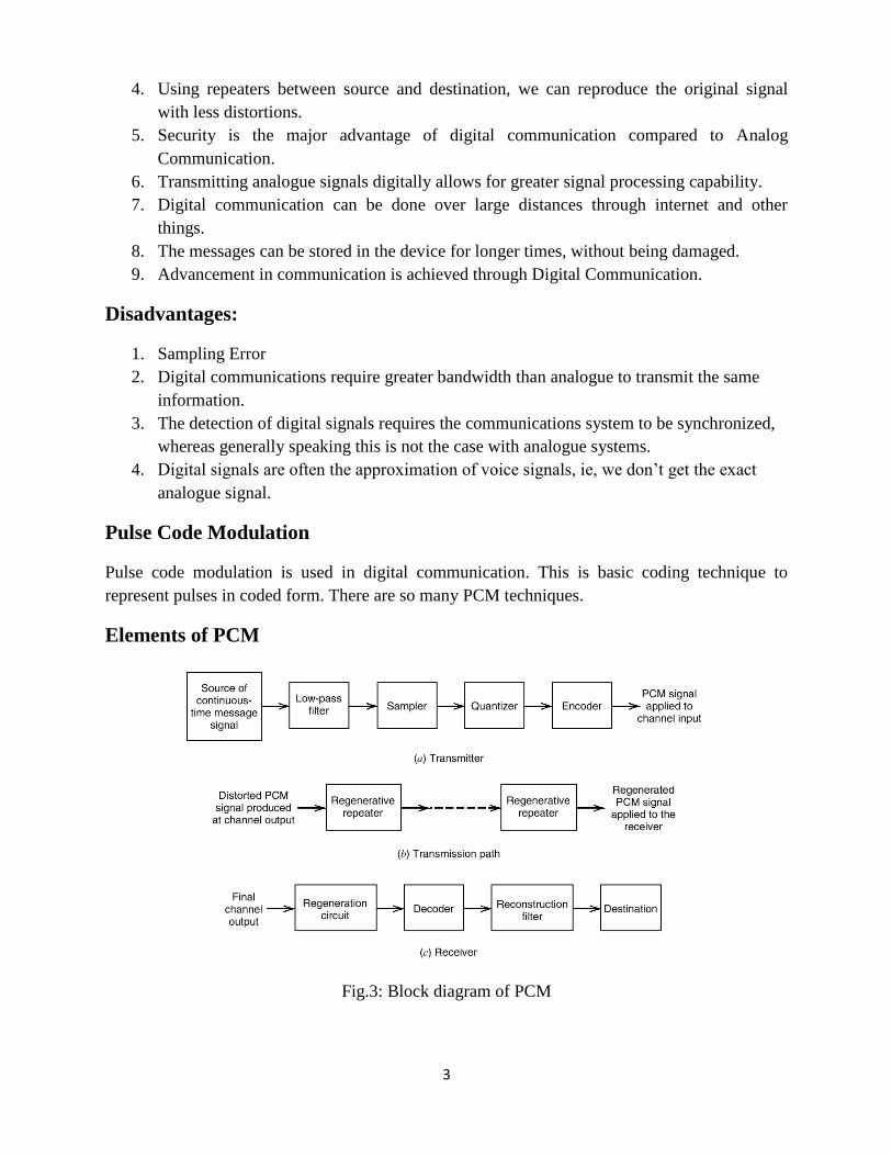
Pulse Code Modulation
Pulse code modulation is used in digital communication. This is basic coding technique to
represent pulses in coded form. There are so many PCM techniques.
Elements of PCM
Fig.3: Block diagram of PCM
4
Low pass filter: A continuous time signal is given to low pass filter it allows frequencies up to
fm range. For the frequencies component greater than fm are attenuated. i.e. low pass filter is band
limited to fm range.
Sampler: Sampler is used to convert analog to discrete time signal. Sampler is a switch this
switch is closed and opened for Ts seconds.
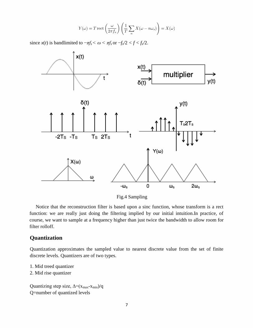
Sampling
The signals we use in the real world, such as our voices, are called "analog" signals. To process
these signals in computers, we need to convert the signals to "digital" form. While an analog
signal is continuous in both time and amplitude, a digital signal is discrete in both time and
amplitude. To convert a signal from continuous time to discrete time, a process called sampling
is used. The value of the signal is measured at certain intervals in time. Each measurement is
referred to as a sample.
Sampling theorem
Due to the increased use of computers in all engineering applications, including signal
processing, it is important to spend some more time examining issues of sampling. In this
chapter we will look at sampling both in the time domain and the frequency domain.
We have already encountered the sampling theorem and, arguing purely from a trigonometric-
identity point of view, have established the Nyquist sampling criterion for sinusoidal signals.
However, we have not fully addressed the sampling of more general signals, nor provided a
general proof. Nor have we indicated how to reconstruct a signal from its samples. With the tools
of Fourier transforms and Fourier series available to us we are now ready to finish the job that
was started months ago.
To begin with, suppose we have a signal x(t) which we wish to sample. Let us suppose further
that the signal is bandlimited to B Hz. This means that its Fourier transform is nonzero for −2πB
< ω < 2πB. Plot spectrum.
We will model the sampling process as multiplication of x(t) by the “picket fence” function
δT(t) = Xδ(t − nT).
We encountered this periodic function when we studied Fourier series. Recall that by its Fourier
series representation we can write
where . The frequency fs = ωs/(2π) = 1/T is the sampling frequency in samples/sec.
Suppose that the sampling frequency is chosen so that fs > 2B, or equivalently, ωs > 4πB.
5
The sampled output is denoted as x(t), where
x(t) = x(t)δT(t)
Using the Fourier series. representation we get
1 jnωst
T Xn
x(t) = x(t)e
Now lets look at the spectrum of the transformed signal. Using the convolution property,
.
Plot the spectrum of the sampled signal with both ω frequency and f frequency. Observe the
following:
1. The spectrum is periodic, with period 2π, because of the multiple copies of the spectrum.
2. The spectrum is scaled down by a factor of 1/T.
3. Note that in this case there is no overlap between the images of the spectrum.
Now consider the effect of reducing the sampling rate to fs < 2B. In this case, the duplicates of
the spectrum overlap each other. The overlap of the spectrum is aliasing.
This demonstration more-or-less proves the sampling theorem for general signals. Provided
that we sample fast enough, the signal spectrum is not distorted by the sampling process. If we
don‟t sample fast enough, there will be distortion. The next question is: given a set of samples,
how do we get the signal back? From the spectrum, the answer is to filter the signal with a
lowpass filter with cutoff ωc ≥ 2πB. This cuts out the images and leaves us with the original
spectrum. This is a sort of idealized point of view, because it assumes that we are filtering a
continuous-time function x(t), which is a sequence of weighted delta functions. In practice, we
have numbers x[n] representing the value of the function x[n] = x(nT) = x(n/fs).
Theorem 1 (The sampling theorem)
If x(t) is bandlimited to B Hz then it can be recovered from signals taken at a sampling rate fs >
2B. The recovery formula is
where
.
Show what the formula means: we are interpolating in time between samples using the sinc
function.
6
We will prove this theorem. Because we are actually lacking a few theoretical tools, it will
take a bit of work. What makes this interesting is we will end up using in a very essential way
most of the transform ideas we have talked about.
1.The first step is to notice that the spectrum of the sampled signal,
is periodic and hence has a Fourier series. The period of the function in frequency is ωs, and the
fundamental frequency is
By the fourier.Series. we can write
where the cn are the F.S. coefficients
But the integral is just the inverse F.T., evaluated at t = −nT:
,
so
.
2.Let g(t) = sinc(πfst). Then
.
3.Let
.
We will show that y(t) = x(t) by showing that Y (ω) = X(ω). We can compute the F.T. of y(t)
using linearity and the shifting property:
Observe that the summation on the right is the same as the F.S. we derived in step 1:
.
Now substituting in the spectrum of the sampled signal (derived above)
7
since x(t) is bandlimited to −πfs < ω < πfs or −fs/2 < f < fs/2.
Fig.4 Sampling
Notice that the reconstruction filter is based upon a sinc function, whose transform is a rect
function: we are really just doing the filtering implied by our initial intuition.In practice, of
course, we want to sample at a frequency higher than just twice the bandwidth to allow room for
filter rolloff.
Quantization
Quantization approximates the sampled value to nearest discrete value from the set of finite
discrete levels. Quantizers are of two types.
1. Mid treed quantizer
2. Mid rise quantizer
Quantizing step size, Δ=(xmax-xmin)/q
Q=number of quantized levels
8
Δ=(xmax-xmin)/2n
Where n is number of bits used to represent each level
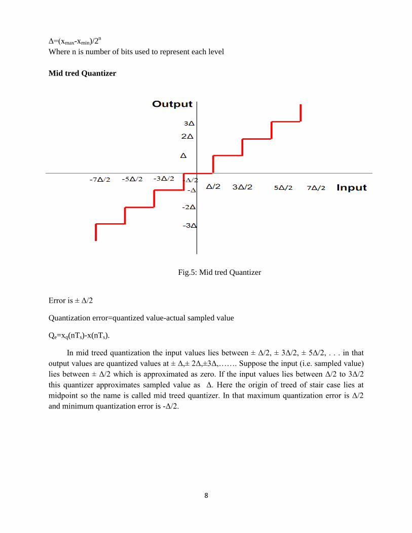
Mid tred Quantizer
Fig.5: Mid tred Quantizer
Error is ± Δ/2
Quantization error=quantized value-actual sampled value
Qe=xq(nTs)-x(nTs).
In mid treed quantization the input values lies between ± Δ/2, ± 3Δ/2, ± 5Δ/2, . . . in that
output values are quantized values at ± Δ,± 2Δ,±3Δ,……. Suppose the input (i.e. sampled value)
lies between ± Δ/2 which is approximated as zero. If the input values lies between Δ/2 to 3Δ/2
this quantizer approximates sampled value as Δ. Here the origin of treed of stair case lies at
midpoint so the name is called mid treed quantizer. In that maximum quantization error is Δ/2
and minimum quantization error is -Δ/2.
9
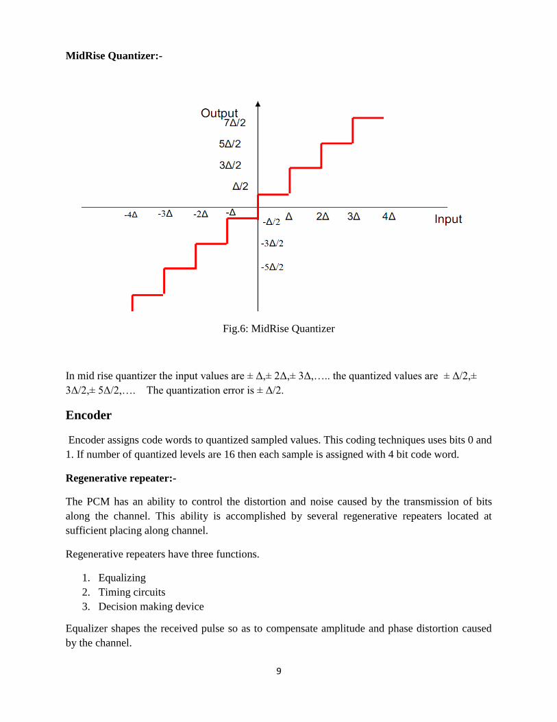
MidRise Quantizer:-
Fig.6: MidRise Quantizer
In mid rise quantizer the input values are ± Δ,± 2Δ,± 3Δ,….. the quantized values are ± Δ/2,±
3Δ/2,± 5Δ/2,…. The quantization error is ± Δ/2.
Encoder
Encoder assigns code words to quantized sampled values. This coding techniques uses bits 0 and
1. If number of quantized levels are 16 then each sample is assigned with 4 bit code word.
Regenerative repeater:-
The PCM has an ability to control the distortion and noise caused by the transmission of bits
along the channel. This ability is accomplished by several regenerative repeaters located at
sufficient placing along channel.
Regenerative repeaters have three functions.
1. Equalizing
2. Timing circuits
3. Decision making device
Equalizer shapes the received pulse so as to compensate amplitude and phase distortion caused
by the channel.
10
Timing circuits provides periodic pulse trains.
Decision making device compares amplitude of equalized pulse plus noise to the pre-defined
threshold levels to make decisions whether the pulse is present or not.
If the pulse is present (i.e. decision is yes), clean new pulse is generated and transmitted through
channel to next regenerative pulse. If the pulse is not present (i.e. the decision is no), it generates
clean base line to next regenerative repeator, provided the noise too large caused bit error by
taking the wrong decision.
Decoder
Decoder reboots all the received bits to make more words then it decodes as quantized PAM
signals.
Reconstruction Filter:
All coded words are passed through low pass filter so that analog signal can be reconstructed
from quantized PAM signal.The cut off frequency of low pass filter is fm Hz which is equal to
band width of message signal.
Destination
It receives the signal from the reconstructive filter output is analog signal.
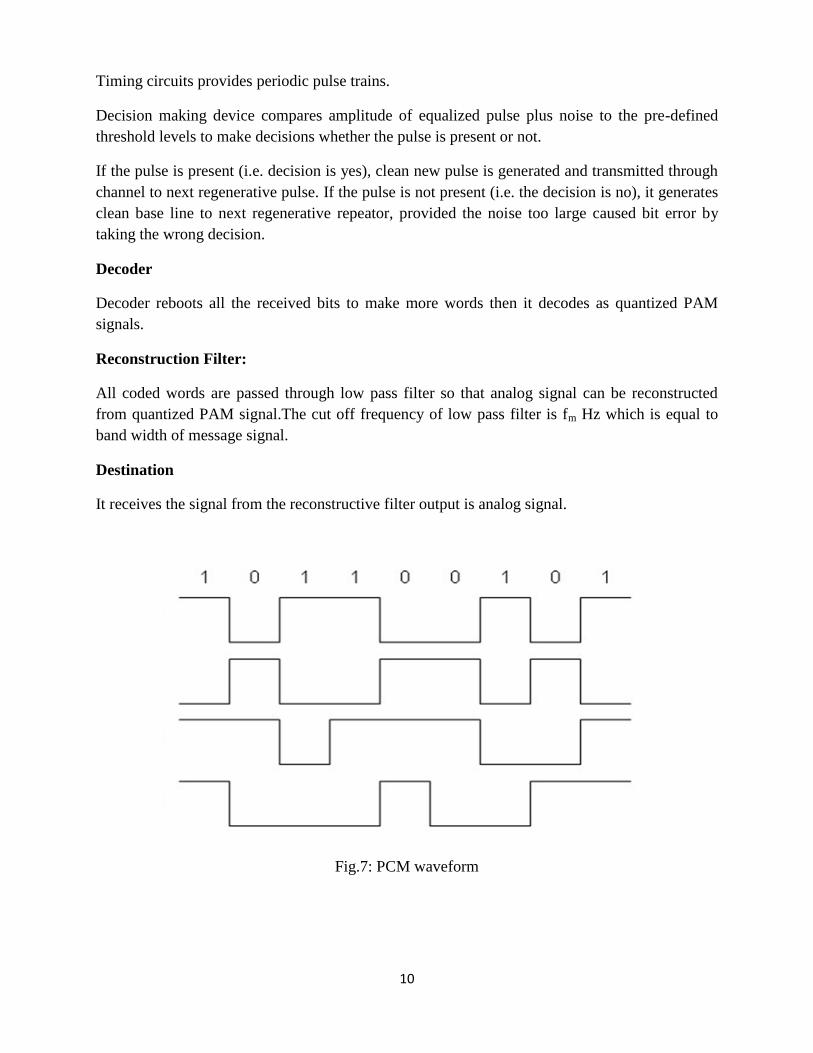
Fig.7: PCM waveform
11
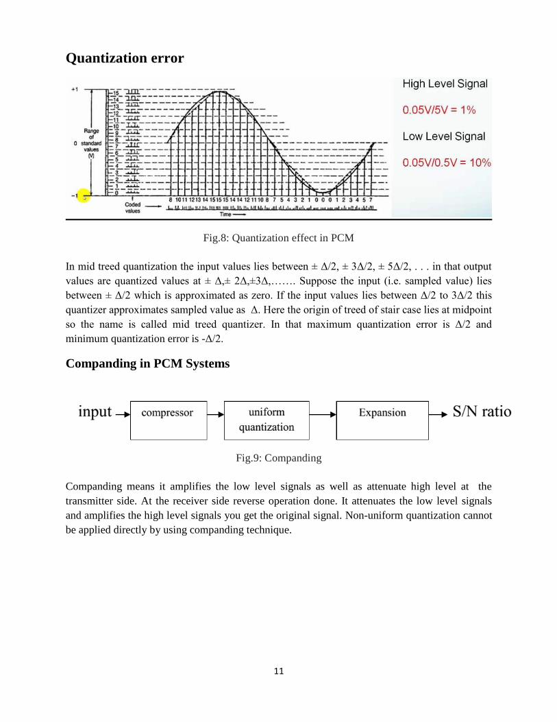
Quantization error
Fig.8: Quantization effect in PCM
In mid treed quantization the input values lies between ± Δ/2, ± 3Δ/2, ± 5Δ/2, . . . in that output
values are quantized values at ± Δ,± 2Δ,±3Δ,……. Suppose the input (i.e. sampled value) lies
between ± Δ/2 which is approximated as zero. If the input values lies between Δ/2 to 3Δ/2 this
quantizer approximates sampled value as Δ. Here the origin of treed of stair case lies at midpoint
so the name is called mid treed quantizer. In that maximum quantization error is Δ/2 and
minimum quantization error is -Δ/2.
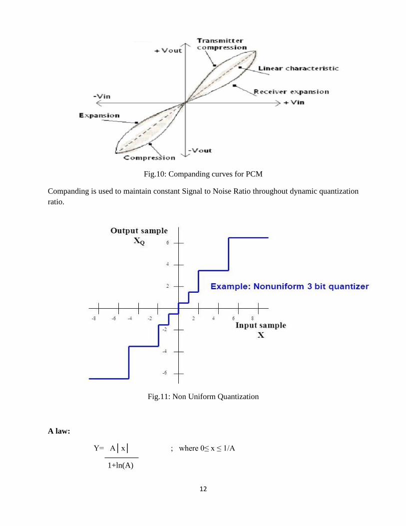
Companding in PCM Systems
Fig.9: Companding
Companding means it amplifies the low level signals as well as attenuate high level at the
transmitter side. At the receiver side reverse operation done. It attenuates the low level signals
and amplifies the high level signals you get the original signal. Non-uniform quantization cannot
be applied directly by using companding technique.
12
Fig.10: Companding curves for PCM
Companding is used to maintain constant Signal to Noise Ratio throughout dynamic quantization
ratio.
Fig.11: Non Uniform Quantization
A law:
Y= A│x│ ; where 0≤ x ≤ 1/A
1+ln(A)
13
= 1+ln A│x│ ; 1/A≤ x ≤ 1
1+ln(A)
practically A=87.56
if A=1 we get uniform quantization
µ law:
Y= ±ln(1+µ│x│) ;│x│≤1
ln(1+µ)
Practically µ value is 256.
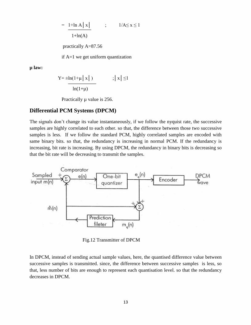
Differential PCM Systems (DPCM)
The signals don‟t change its value instantaneously, if we follow the nyquist rate, the successive
samples are highly correlated to each other. so that, the difference between those two successive
samples is less. If we follow the standard PCM, highly correlated samples are encoded with
same binary bits. so that, the redundancy is increasing in normal PCM. If the redundancy is
increasing, bit rate is increasing. By using DPCM, the redundancy in binary bits is decreasing so
that the bit rate will be decreasing to transmit the samples.
Fig.12 Transmitter of DPCM
In DPCM, instead of sending actual sample values, here, the quantised difference value between
successive samples is transmitted. since, the difference between successive samples is less, so
that, less number of bits are enough to represent each quantisation level. so that the redundancy
decreases in DPCM.
14
Transmitter: In DPCM, the predictor having more importance which predicts the next sample
value. If the predictor is good one, the predictor output is very close to actual sample value. The
comparator gives the difference between actual sample value and predicted sample value. It is
then given to the quantizer . Here, since the difference between those two samples is less, so that
less number of quantization levels are required. Let the quantised output is eq(nTs).
e(nTs)=m(nTs)-m^(nTs ) .........(1)
where, m(nTs) is actual sample value.
m^(nTs) is predicted sample value.
eq(nTs) = e(nTs) + q(nTs)
where, eq(nTs) is quantised error signal.
q(nTs) is quantisation error.
The input to predictor is summation of previous predicted output and quantised
output signal.
Let mq(nTs) is input to predictor.
mq(nTs) = e(nTs) + q(nTs)
= m^(nTs) + e(nTs)) + q(nTs) (......from (1) )
= m(nTs) + q(nTs)
i.e., input of predictor depends on actual sample value and quantisation error
and doesn't depends on characterisation of prediction filter. Quantised error signal is given to the
encoder which assigns binary code words to the quantised error samples which is known as
DPCM.
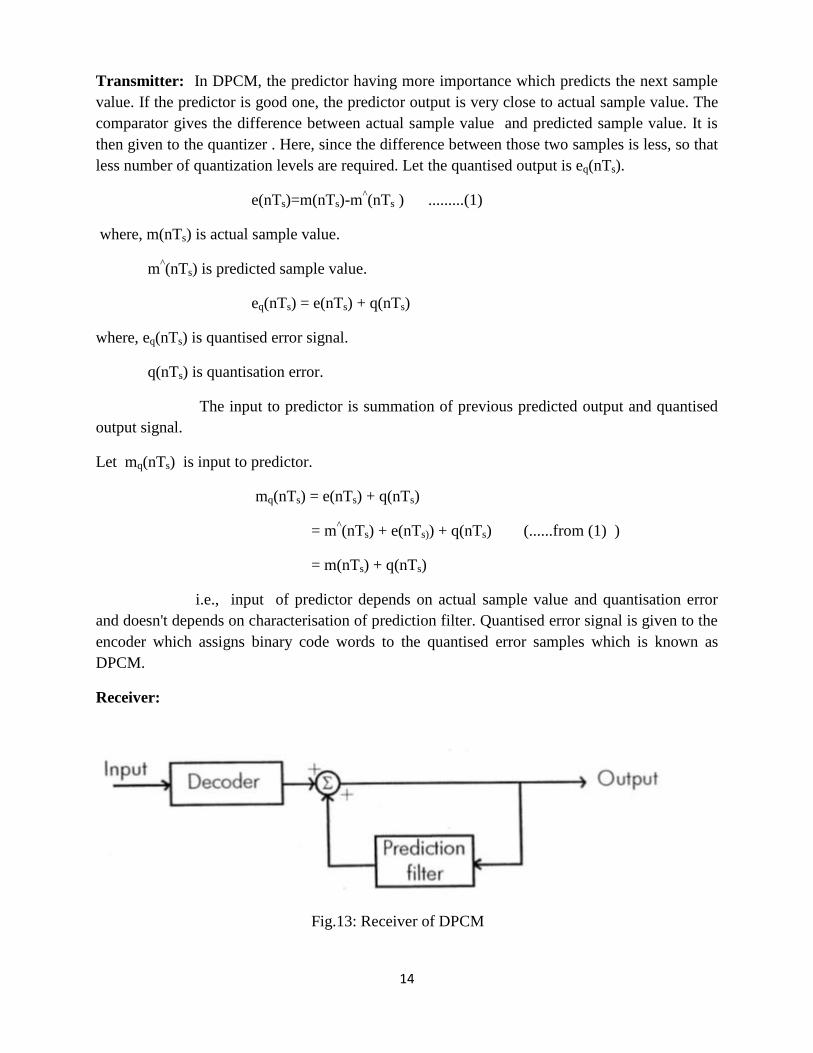
Receiver:
Fig.13: Receiver of DPCM
15
DPCM input is given to decoder which generates quantised error signal which is given to
summation (adder) along with predictor output so that we can get the original sample value
m(nTs) . At receiver output, we have quantisation error which is introduced at transmitted side
that can't be removed.
Advantage: Bit rate is decreased compared to standard PCM.
Drawback: Encoder and decoder design complexity is more.
Delta Modulation
Delta modulation (DM or Δ-modulation) is an analog-to-digital and digital-to-analog signal
conversion technique used for transmission of voice information where quality is not of primary
importance. DM is the simplest form of differential pulse-code modulation (DPCM) where the
difference between successive samples is encoded into n-bit data streams. In delta modulation, the
transmitted data is reduced to a 1-bit data stream.
Working Principle
Rather than quantizing the absolute value of the input analog waveform, delta modulation
quantizes the difference between the current and the previous step, as shown in the block diagram
in Fig. 14.
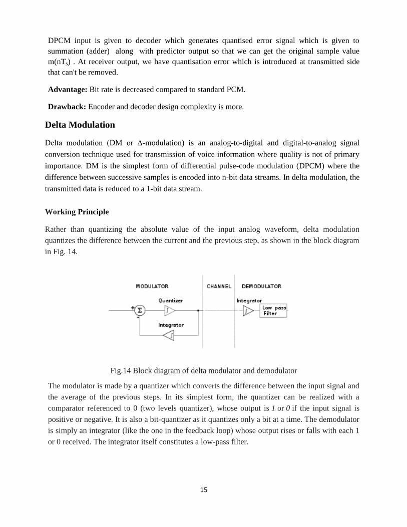
Fig.14 Block diagram of delta modulator and demodulator
The modulator is made by a quantizer which converts the difference between the input signal and
the average of the previous steps. In its simplest form, the quantizer can be realized with a
comparator referenced to 0 (two levels quantizer), whose output is 1 or 0 if the input signal is
positive or negative. It is also a bit-quantizer as it quantizes only a bit at a time. The demodulator
is simply an integrator (like the one in the feedback loop) whose output rises or falls with each 1
or 0 received. The integrator itself constitutes a low-pass filter.
16
Principle of operation
Delta modulation was introduced in the 1940s as a simplified form of pulse code modulation
(PCM), which required a difficult-to-implement analog-to-digital (A/D) converter. The output of
a delta modulator is a bit stream of samples, at a relatively high rate (eg, 100 kbit/s or more for a
speech bandwidth of 4 kHz) the value of each bit being determined according as to whether the
input message sample amplitude has increased or decreased relative to the previous sample. It is
an example of differential pulse code modulation (DPCM).
The operation of a delta modulator is to periodically sample the input message, to make a
comparison of the current sample with that preceding it, and to output a single bit which
indicates the sign of the difference between the two samples. This in principle would require a
sample-and-hold type circuit. De Jager (1952) hit on an idea for dispensing with the need for a
sample and hold circuit. He reasoned that if the system was producing the desired output then
this output could be sent back to the input and the two analog signals compared in a comparator.
The output is a delayed version of the input, and so the comparison is in effect that of the current
bit with the previous bit, as required by the delta modulation principle.
The system is in the form of a feedback loop. This means that its operation is not necessarily
obvious, and its analysis non-trivial. But you can build it, and confirm that it does behave in the
manner a delta modulator should.
The system is a continuous time to discrete time converter. In fact, it is a form of analog to
digital converter, and is the starting point from which more sophisticated delta modulators can be
developed. The sampler block is clocked. The output from the sampler is a bipolar signal, in the
block diagram being either V volts. This is the delta modulated signal, the waveform of which
is shown in Figure 2. It is fed back, in a feedback loop, via an integrator, to a summer. The
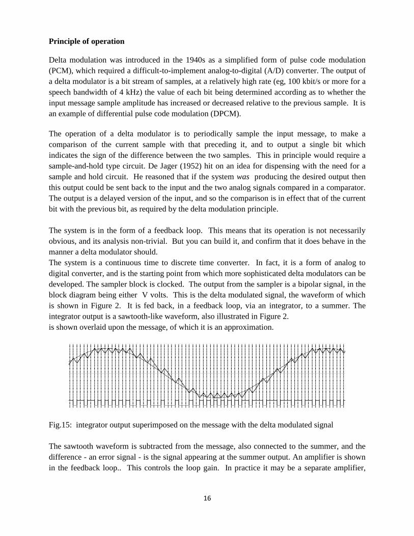
integrator output is a sawtooth-like waveform, also illustrated in Figure 2.
is shown overlaid upon the message, of which it is an approximation.
Fig.15: integrator output superimposed on the message with the delta modulated signal
The sawtooth waveform is subtracted from the message, also connected to the summer, and the
difference - an error signal - is the signal appearing at the summer output. An amplifier is shown
in the feedback loop.. This controls the loop gain. In practice it may be a separate amplifier,
17
part of the integrator, or within the summer. It is used to control the size of the „teeth‟ of the
sawtooth waveform, in conjunction with the integrator time constant.
When analysing the block diagram, it is convenient to think of the summer having unity gain
between both inputs and the output. The message comes in at a fixed amplitude. The signal
from the integrator, which is a sawtooth approximation to the message, is adjusted with the
amplifier to match it as closely
Main features of Delta Modulation
1. The analog signal is approximated with a series of segments
2. Each segment of the approximated signal is compared to the original analog wave to
determine the increase or decrease in relative amplitude
3. The decision process for establishing the state of successive bits is determined by this
comparison
4. Only the change of information is sent, that is, only an increase or decrease of the signal
amplitude from the previous sample is sent whereas a no-change condition causes the
modulated signal to remain at the same 0 or 1 state of the previous sample.
5. To achieve high signal-to-noise ratio, delta modulation must use oversampling
techniques, that is, the analog signal is sampled at a rate several times higher than the
Nyquist rate.
6. Derived forms of delta modulation are continuously variable slope delta modulation,
delta-sigma modulation, and differential modulation. The Differential Pulse Code
Modulation is the super set of DM.
Drawbacks of Delta modulation
The binary waveform illustrated in Fig.15 is the signal transmitted. This is the delta modulated
signal.The integral of the binary waveform is the sawtooth approximation to the message. In the
you will see that this sawtooth wave is the primary output from the demodulator at the receiver.
Lowpass filtering of the sawtooth (from the demodulator) gives a better approximation to the
message. But there will be accompanying noise and distortion, products of the approximation
process at the modulator.
The unwanted products of the modulation process, observed at the receiver, are of two kinds.
These are due to „slope overload‟, and „granularity‟. There are two drawbacks of delta
modulation
1. Slope over Load Distortion
2. Granular Noise
18
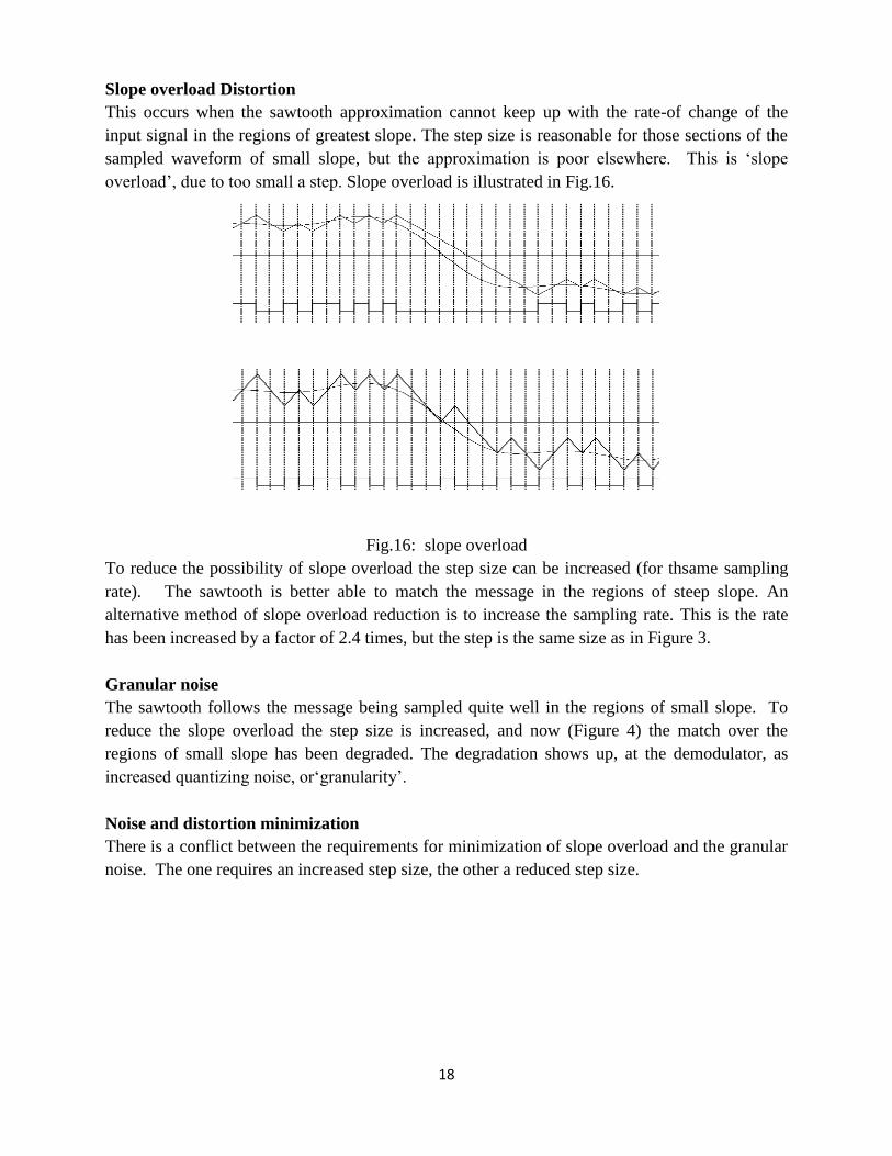
Slope overload Distortion
This occurs when the sawtooth approximation cannot keep up with the rate-of change of the
input signal in the regions of greatest slope. The step size is reasonable for those sections of the
sampled waveform of small slope, but the approximation is poor elsewhere. This is „slope
overload‟, due to too small a step. Slope overload is illustrated in Fig.16.
Fig.16: slope overload
To reduce the possibility of slope overload the step size can be increased (for thsame sampling
rate). The sawtooth is better able to match the message in the regions of steep slope. An
alternative method of slope overload reduction is to increase the sampling rate. This is the rate
has been increased by a factor of 2.4 times, but the step is the same size as in Figure 3.
Granular noise
The sawtooth follows the message being sampled quite well in the regions of small slope. To
reduce the slope overload the step size is increased, and now (Figure 4) the match over the
regions of small slope has been degraded. The degradation shows up, at the demodulator, as
increased quantizing noise, or„granularity‟.
Noise and distortion minimization
There is a conflict between the requirements for minimization of slope overload and the granular
noise. The one requires an increased step size, the other a reduced step size.
19
Adaptive Delta Modulation
A large step size was required when sampling those parts of the input waveform of steep slope.
But a large step size worsened the granularity of the sampled signal when the waveform being
sampled was changing slowly. A small step size is preferred in regions where the message has a
small slope. This suggests the need for a controllable step size - the control being sensitive to the
slope of the sampled signal.
Working Principle
The gain of the amplifier is adjusted in response to a control voltage from the sampler, which
signals the onset of slope overload. The step size is proportional to the amplifier gain. This was
observed in an earlier experiment. Slope overload is indicated by a succession of output pulses of
the same sign. The tims sampler monitors the delta modulated signal, and signals when there is no
change of polarity over 3 or more successive samples. The actual adaptive control signal is +2
volt under „normal‟ conditions, and rises to +4 volt when slope overload is detected. The gain of
the amplifier, and hence the step size, is made proportional to this control voltage. Provided the
slope overload was only moderate the approximation will „catch up‟ with the wave being
sampled. The gain will then return to normal until the sampler again falls behind. Much work has
been done by researchers in this area, and sophisticated algorithms have been developed which
offer significant improvements over the simple system to be examined in this experiment.
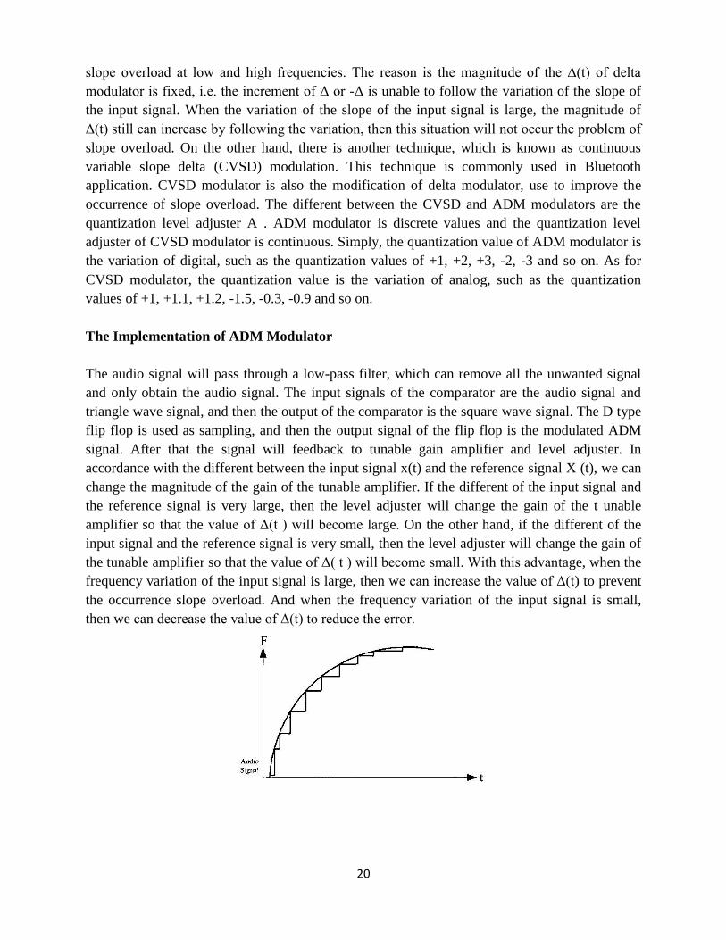
The Operation Theory of ADM Modulation From previous chapter, we know that the
disadvantage of delta modulation is when the input audio signal frequency exceeded the
limitation of delta modulator, i.e. fsΔ ≥𝑑𝑥 (𝑡)/𝑑𝑡.Then this situation will produce the occurrence
of slope overload and cause signal distortion. However, the adaptive delta modulation (ADM) is
the modification of delta modulation to improve the disadvantage of the occurrence of slope
overload
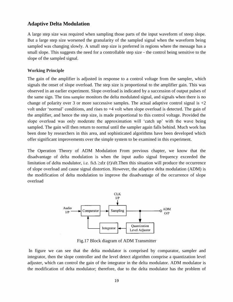
Fig.17 Block diagram of ADM Transmitter
In figure we can see that the delta modulator is comprised by comparator, sampler and
integrator, then the slope controller and the level detect algorithm comprise a quantization level
adjuster, which can control the gain of the integrator in the delta modulator. ADM modulator is
the modification of delta modulator; therefore, due to the delta modulator has the problem of
20
slope overload at low and high frequencies. The reason is the magnitude of the Δ(t) of delta
modulator is fixed, i.e. the increment of Δ or -Δ is unable to follow the variation of the slope of
the input signal. When the variation of the slope of the input signal is large, the magnitude of
Δ(t) still can increase by following the variation, then this situation will not occur the problem of
slope overload. On the other hand, there is another technique, which is known as continuous
variable slope delta (CVSD) modulation. This technique is commonly used in Bluetooth
application. CVSD modulator is also the modification of delta modulator, use to improve the
occurrence of slope overload. The different between the CVSD and ADM modulators are the
quantization level adjuster A . ADM modulator is discrete values and the quantization level
adjuster of CVSD modulator is continuous. Simply, the quantization value of ADM modulator is
the variation of digital, such as the quantization values of +1, +2, +3, -2, -3 and so on. As for
CVSD modulator, the quantization value is the variation of analog, such as the quantization
values of +1, +1.1, +1.2, -1.5, -0.3, -0.9 and so on.
The Implementation of ADM Modulator
The audio signal will pass through a low-pass filter, which can remove all the unwanted signal
and only obtain the audio signal. The input signals of the comparator are the audio signal and
triangle wave signal, and then the output of the comparator is the square wave signal. The D type
flip flop is used as sampling, and then the output signal of the flip flop is the modulated ADM
signal. After that the signal will feedback to tunable gain amplifier and level adjuster. In
accordance with the different between the input signal x(t) and the reference signal X (t), we can
change the magnitude of the gain of the tunable amplifier. If the different of the input signal and
the reference signal is very large, then the level adjuster will change the gain of the t unable
amplifier so that the value of Δ(t ) will become large. On the other hand, if the different of the
input signal and the reference signal is very small, then the level adjuster will change the gain of
the tunable amplifier so that the value of Δ( t ) will become small. With this advantage, when the
frequency variation of the input signal is large, then we can increase the value of Δ(t) to prevent
the occurrence slope overload. And when the frequency variation of the input signal is small,
then we can decrease the value of Δ(t) to reduce the error.
21
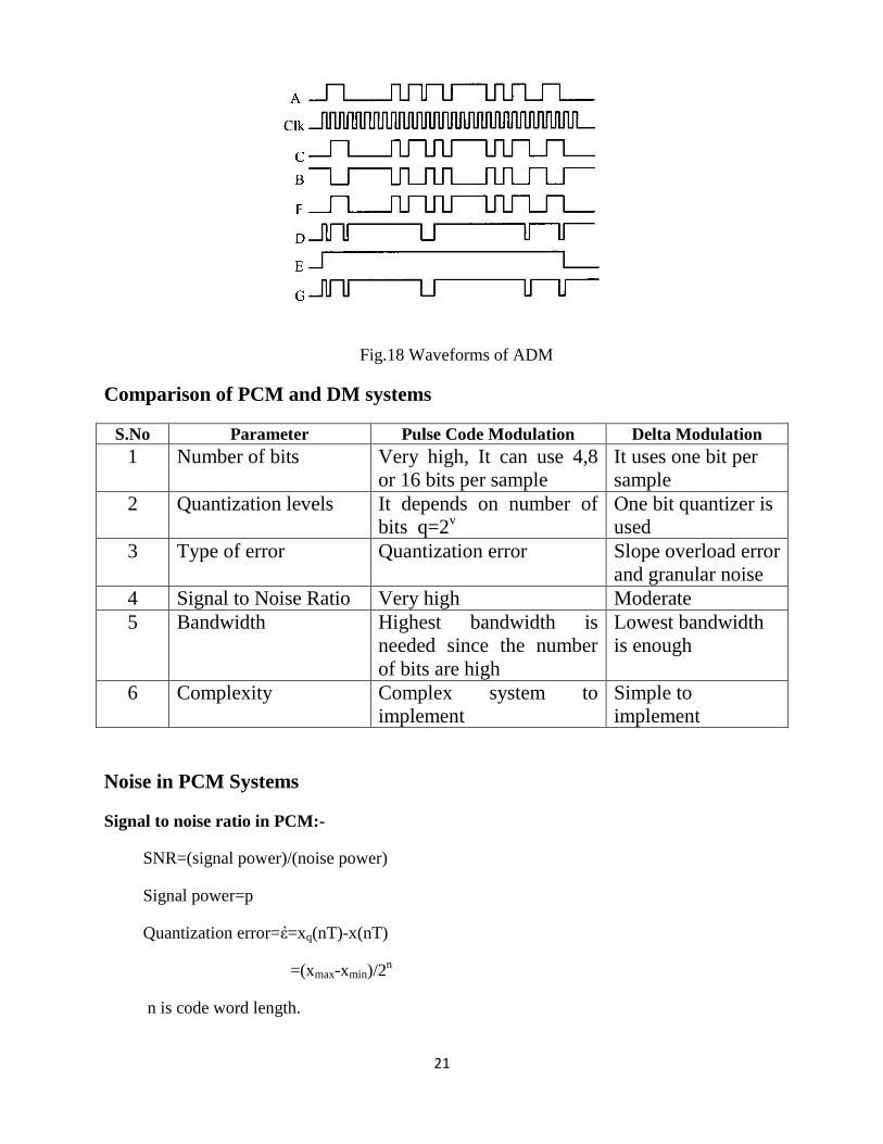
Fig.18 Waveforms of ADM
Comparison of PCM and DM systems
S.No Parameter Pulse Code Modulation Delta Modulation
1 Number of bits Very high, It can use 4,8
or 16 bits per sample
It uses one bit per
sample
2 Quantization levels It depends on number of
bits q=2v
One bit quantizer is
used
3 Type of error Quantization error Slope overload error
and granular noise
4 Signal to Noise Ratio Very high Moderate
5 Bandwidth Highest bandwidth is
needed since the number
of bits are high
Lowest bandwidth
is enough
6 Complexity Complex system to
implement
Simple to
implement
Noise in PCM Systems
Signal to noise ratio in PCM:-
SNR=(signal power)/(noise power)
Signal power=p
Quantization error=ἐ=xq(nT)-x(nT)
=(xmax-xmin)/2n
n is code word length.
22
|e|=Δ/2
Quantization noise power=E[e2]
Noise power=∫ ἐ2f(ἐ)dἐ (limits from -∞ to ∞)
=∫ἐ(1/ Δ)dἐ (limits from -Δ/2 to Δ/2)
=(1/Δ)[ἐ3/3] (limits from -Δ/2 to Δ/2)
=(Δ2/12)
(S/N)PCM=(12p)/(Δ2)
If the signal is defined from –xmax to +xmax then Δ =(2xmax)/2n
(S/N)PCM=(12p)/(2xmax/2n)2
=(12p*22n
)/(4xmax2)
=(3p*22n
)/xmax2
For normalized signal xmax=1 then SNR for normalized signal is slightly less than or equal to
3.1*22n
i.e.(S/N)PCM for normalized signal≤3.1*22n
(S/N)PCM in dB=10log10(3*22n
)
=4.8+6n
For increasing one bit then (S/N)PCB will increase to 6dB.
(S/N) for sinusoidal signal:-
Signal amplitude=Am
Signal power = p =Am2/2
Δ=(2Am)/2n
(S/N)PCM for sinusoidal signal = (1.5Am2)*(2
2n)/(Am
2)
=1.5*22n
=10log(1.5*22n
)
(S/N)PCM for sinusoidal signal in dB =1.8+6n
23
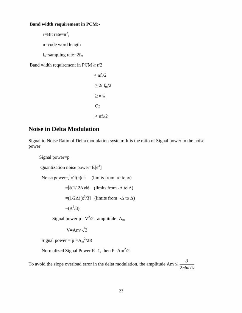
Band width requirement in PCM:-
r=Bit rate=nfs
n=code word length
fs=sampling rate=2fm
Band width requirement in PCM ≥ r/2
≥ nfs/2
≥ 2nfm/2
≥ nfm
Or
≥ nfs/2
Noise in Delta Modulation
Signal to Noise Ratio of Delta modulation system: It is the ratio of Signal power to the noise
power
Signal power=p
Quantization noise power=E[e2]
Noise power=∫ ἐ2f(ἐ)dἐ (limits from -∞ to ∞)
=∫ἐ(1/ 2Δ)dἐ (limits from -Δ to Δ)
=(1/2Δ)[ἐ3/3] (limits from -Δ to Δ)
=(Δ2/3)
Signal power p= V2/2 amplitude=Am
V=Am/ 2
Signal power = p =Am2/2R
Normalized Signal Power R=1, then P=Am2/2
To avoid the slope overload error in the delta modulation, the amplitude Am ≤ fmTs
2
24
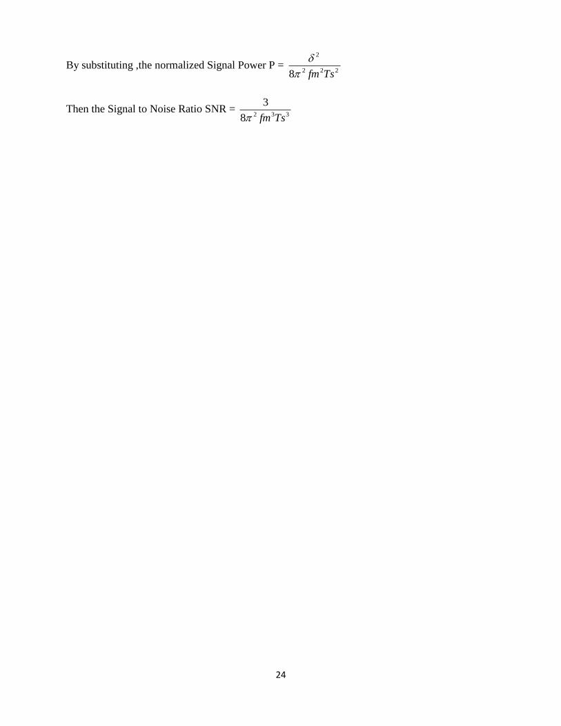
By substituting ,the normalized Signal Power P = 222
2
8 Tsfm
Then the Signal to Noise Ratio SNR = 3328
3
Tsfm