COMMUNICATIONS - cloudfront.net
176
COMMUNICATIONS For INSTRUMENTATION ENGINEERING ELECTRONICS & COMMUNICATION ENGINEERING
-
Upload
khangminh22 -
Category
Documents
-
view
5 -
download
0
Transcript of COMMUNICATIONS - cloudfront.net

COMMUNICATIONS
For INSTRUMENTATION ENGINEERING
ELECTRONICS & COMMUNICATION ENGINEERING


SYLLABUS Random signals and noise: probability, random variables, probability density function, autocorrelation, power spectral density. Analog communication systems: amplitude and angle modulation and demodulation systems, spectral analysis of these operations, super – heterodyne receivers: elements of hardware, realizations of analog communication systems; signal to noise ratio (SNR) calculations for amplitude modulation (AM) and frequency modulation (FM) for low noise conditions. Fundamentals of information theory and channel capacity theorem. Digital communication systems: pulse code modulation (PCM), differential pulse code modulation (DPCM) Digital modulation schemes: amplitude, phase and frequency shift keying schemes (ASK, PSK, FSK), matched filter receivers, bandwidth consideration and probability of error calculations for these schemes. Basics of TDMA, FDMA, CDMA and GSM.
ANALYSIS OF GATE PAPERS
Exam Year 1 Mark Ques. 2 Mark Ques. Total 2003 3 14 31 2004 5 10 25 2005 2 7 16 2006 14 28 2007 3 10 28 2008 1 11 23 2009 3 6 23 2010 3 4 15 2011 2 4 11 2012 4 3 10 2013 1 5 10
2014 Set-1 3 4 11 2014 Set-2 3 4 11 2014 Set-3 3 4 11 2014 Set-4 3 4 11 2015 Set-1 2 4 10 2015 Set-2 1 5 11 2015 Set-3 2 3 8 2016 Set-1 4 4 12 2016 Set-2 2 4 10 2016 Set-3 3 3 9 2017 Set-1 1 1 3 2017 Set-2 3 4 11
2018 3 3 9
COMMUNICATIONS
© Copyright Reserved by Gateflix.in No part of this material should be copied or reproduced without permission
Topics Page No
1. AMPLITUDE MODULATION
1.1 Introduction 01 1.2 Modulation 02 1.3 Types of Modulation 03 1.4 Amplitude Modulation 03 1.5 Power in AM Wave 07 1.6 Efficiency of AM Transmission 07 1.7 Types of AM Modulation 10 1.8 Generation of Amplitude Modulation Wave 16 1.9 Demodulation of Amplitude Modulated Signal 13 1.10 QAM (Quadrature Amplitude Modulation) 15
2. ANGLE MODULATION
2.1 Introduction 16 2.2 Frequency Modulation (FM) 16 2.3 Power in Frequency Modulated Signal 17 2.4 Types of FM 18 2.5 Bandwidth of Signal 19 2.6 FM Generated Method 19 2.7 FM Modulation 20 2.8 Phase Modulation 22 2.9 Capture Effect 23 2.10 Threshold Effect 23 2.11 Pre- Emphasis 23 2.12 De- Emphasis 24
Gate Questions
3. RADIO RECEIVER
3.1 Radio Receiver 43 3.2 Tuned Radio Frequency (TRF) Receiver 44 3.3 Super Heterodyne Receiver 44 3.4 Receiver Characteristics 47 3.5 Image Frequency & Its Rejection 48 3.6 Receiver ratio of CAP. in AM Receiver 49
4. NOISE
4.1 Introduction 51 4.2 Classification of Noise 51 4.3 Noise Temperature 534.4 Noise Factor of Amplifiers In Cascade 54
Gate Questions
25
56
© Copyright Reserved by Gateflix.in No part of this material should be copied or reproduced without permission
5. PULSE DIGITAL MODULATION
5.1 Introduction 80 5.2 Pulse Code Modulation 80 5.3 Delta Modulation 85 5.4 Differential PCM 87
6. COMMUNICATION SYSTEM
6.1 Random Single And Noise 88 6.2 Types of Probability Density Function 896.3 Joint Moment About the Origin 92
7. DIGITAL CARRIER MODULATION
7.1 Introduction 99 7.2 Line Coding 99 7.3 Binary Amplitude-Shift Keying 99 7.4 Binary Phase-Shift Keying (BPSK) 100 7.5 Binary Frequency Shift Keying (BFSK) 101 7.6 Noise Analysis of Digital Communication 102 7.7 Probability of Error Calculation 103
8. DIGITAL MODULATION SCHEMES107 108
8.1 Digital Modulation Schemes 8.2 Binary Phase Shift Keying 8.3 Differential PSK(DPSK)
Gate Questions 109
9. INFORMATION THEORY9.1 Introduction 138 9.2 Information Content of a Symbol 138 9.3 Entropy 140 9.4 Information Rate 1409.5 Channel Capacity 141
Gate Questions
10. MULTIPLEXING
10.1 Introduction 149 10.2 Classification of Multiplexing 149 10.3 Frequency Division Multiplexing 149 10.4 Time Division Multiplexing 150
11. ASSIGNMENT 153
114
142
© Copyright Reserved by Gateflix.in No part of this material should be copied or reproduced without permission
1.1 INTRODUCTION
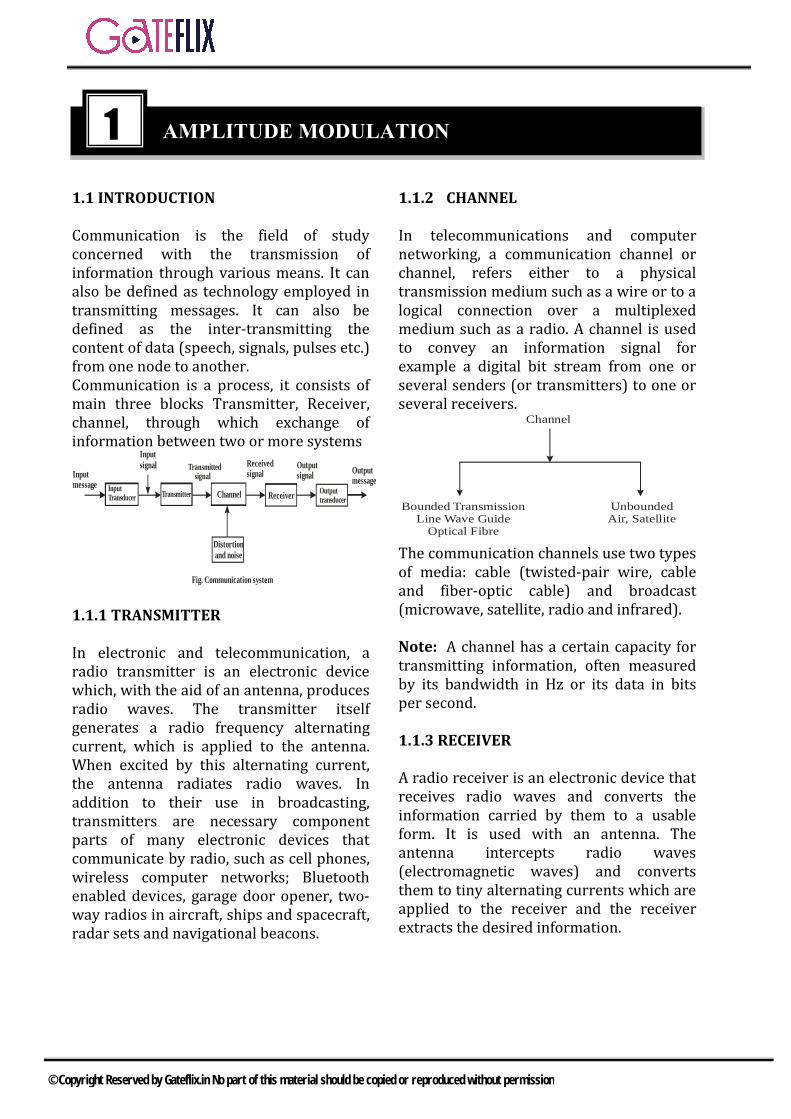
Communication is the field of study concerned with the transmission of information through various means. It can also be defined as technology employed in transmitting messages. It can also be defined as the inter-transmitting the content of data (speech, signals, pulses etc.) from one node to another. Communication is a process, it consists of main three blocks Transmitter, Receiver, channel, through which exchange of information between two or more systems
Inputmessage Input
Transducer
Inputsignal
Transmitter
Transmitted signal
Channel
Distortion and noise
Receivedsignal
Receiver
Outputsignal
Outputtransducer
Outputmessage
Fig. Communication system
1.1.1 TRANSMITTER
In electronic and telecommunication, a radio transmitter is an electronic device which, with the aid of an antenna, produces radio waves. The transmitter itself generates a radio frequency alternating current, which is applied to the antenna. When excited by this alternating current, the antenna radiates radio waves. In addition to their use in broadcasting, transmitters are necessary component parts of many electronic devices that communicate by radio, such as cell phones, wireless computer networks; Bluetooth enabled devices, garage door opener, two-way radios in aircraft, ships and spacecraft, radar sets and navigational beacons.
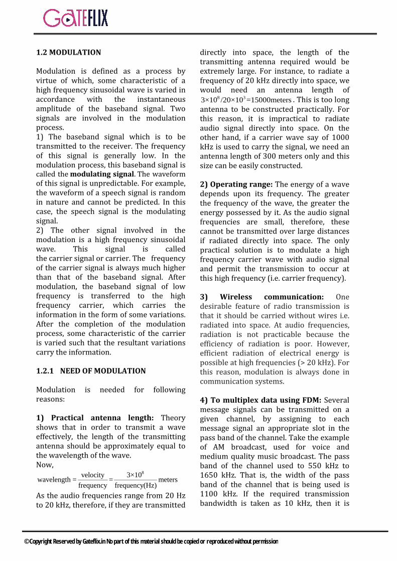
1.1.2 CHANNEL
In telecommunications and computer networking, a communication channel or channel, refers either to a physical transmission medium such as a wire or to a logical connection over a multiplexed medium such as a radio. A channel is used to convey an information signal for example a digital bit stream from one or several senders (or transmitters) to one or several receivers.
Unbounded Air, Satellite
Channel
Bounded Transmission Line Wave Guide
Optical Fibre
The communication channels use two types of media: cable (twisted-pair wire, cable and fiber-optic cable) and broadcast (microwave, satellite, radio and infrared).
Note: A channel has a certain capacity for transmitting information, often measured by its bandwidth in Hz or its data in bits per second.
1.1.3 RECEIVER
A radio receiver is an electronic device that receives radio waves and converts the information carried by them to a usable form. It is used with an antenna. The antenna intercepts radio waves (electromagnetic waves) and converts them to tiny alternating currents which are applied to the receiver and the receiver extracts the desired information.
1 AMPLITUDE MODULATION
© Copyright Reserved by Gateflix.in No part of this material should be copied or reproduced without permission
1.2 MODULATION Modulation is defined as a process by virtue of which, some characteristic of a high frequency sinusoidal wave is varied in accordance with the instantaneous amplitude of the baseband signal. Two signals are involved in the modulation process. 1) The baseband signal which is to be transmitted to the receiver. The frequency of this signal is generally low. In the modulation process, this baseband signal is called the modulating signal. The waveform of this signal is unpredictable. For example, the waveform of a speech signal is random in nature and cannot be predicted. In this case, the speech signal is the modulating signal. 2) The other signal involved in the modulation is a high frequency sinusoidal wave. This signal is called the carrier signal or carrier. The frequency of the carrier signal is always much higher than that of the baseband signal. After modulation, the baseband signal of low frequency is transferred to the high frequency carrier, which carries the information in the form of some variations. After the completion of the modulation process, some characteristic of the carrier is varied such that the resultant variations carry the information. 1.2.1 NEED OF MODULATION Modulation is needed for following reasons: 1) Practical antenna length: Theory shows that in order to transmit a wave effectively, the length of the transmitting antenna should be approximately equal to the wavelength of the wave. Now,
8velocity 3×10wavelength = = metersfrequency frequency(Hz)
As the audio frequencies range from 20 Hz to 20 kHz, therefore, if they are transmitted
directly into space, the length of the transmitting antenna required would be extremely large. For instance, to radiate a frequency of 20 kHz directly into space, we would need an antenna length of
8 33×10 /20×10 =15000meters . This is too long antenna to be constructed practically. For this reason, it is impractical to radiate audio signal directly into space. On the other hand, if a carrier wave say of 1000 kHz is used to carry the signal, we need an antenna length of 300 meters only and this size can be easily constructed. 2) Operating range: The energy of a wave depends upon its frequency. The greater the frequency of the wave, the greater the energy possessed by it. As the audio signal frequencies are small, therefore, these cannot be transmitted over large distances if radiated directly into space. The only practical solution is to modulate a high frequency carrier wave with audio signal and permit the transmission to occur at this high frequency (i.e. carrier frequency). 3) Wireless communication: One desirable feature of radio transmission is that it should be carried without wires i.e. radiated into space. At audio frequencies, radiation is not practicable because the efficiency of radiation is poor. However, efficient radiation of electrical energy is possible at high frequencies (> 20 kHz). For this reason, modulation is always done in communication systems. 4) To multiplex data using FDM: Several message signals can be transmitted on a given channel, by assigning to each message signal an appropriate slot in the pass band of the channel. Take the example of AM broadcast, used for voice and medium quality music broadcast. The pass band of the channel used to 550 kHz to 1650 kHz. That is, the width of the pass band of the channel that is being used is 1100 kHz. If the required transmission bandwidth is taken as 10 kHz, then it is
© Copyright Reserved by Gateflix.in No part of this material should be copied or reproduced without permission
possible for us to multiplex, at least theoretically, 110 distinct message signals on the channel and still be able to separate them individually as and when we desire because the identity of each message is preserved in the frequency domain. 1.3 TYPES OF MODULATION 1.3.1 ANALOG MODULATION
1) Amplitude Modulation (AM), 2) Frequency Modulation (FM), 3) Phase Modulation (PM), 4) Quadrature Amplitude Modulation (QAM) 1.3.2 DIGITAL MODULATION 1) Pulse Code Modulation (PCM), 2) Differential Pulse Code Modulation (DPCM), 3) Delta modulation (DM), 4) Sigma Delta Modulation
1.3.3 PULSE MODULATION 1) Pulse Amplitude Modulation (PAM), 2) Pulse Position Modulation (PPM), 3) Pulse Duration/Width Modulation (PDM/PWM) 1.3.4 DATA TRANSMISSION
1) Amplitude Shift Keying (ASK), 2) Frequency Shift Keying (FSK), 3) Phase Shift Keying (PSK), 4) Differential Phase Shift Keying (DPSK), 5) Quadrature Phase Shift Keying (QPSK), 6) Minimum Shift Keying (MSK), 7) Quadrature Amplitude Phase Shift Keying (QAPSK), 8) Gaussian Minimum Shift Keying (GMSK), 9) M-ray Amplitude Shift Keying, 10) M-ray Phase Shift Keying, 11) M-ray Frequency Shift Keying
1.4 AMPLITUDE MODULATION
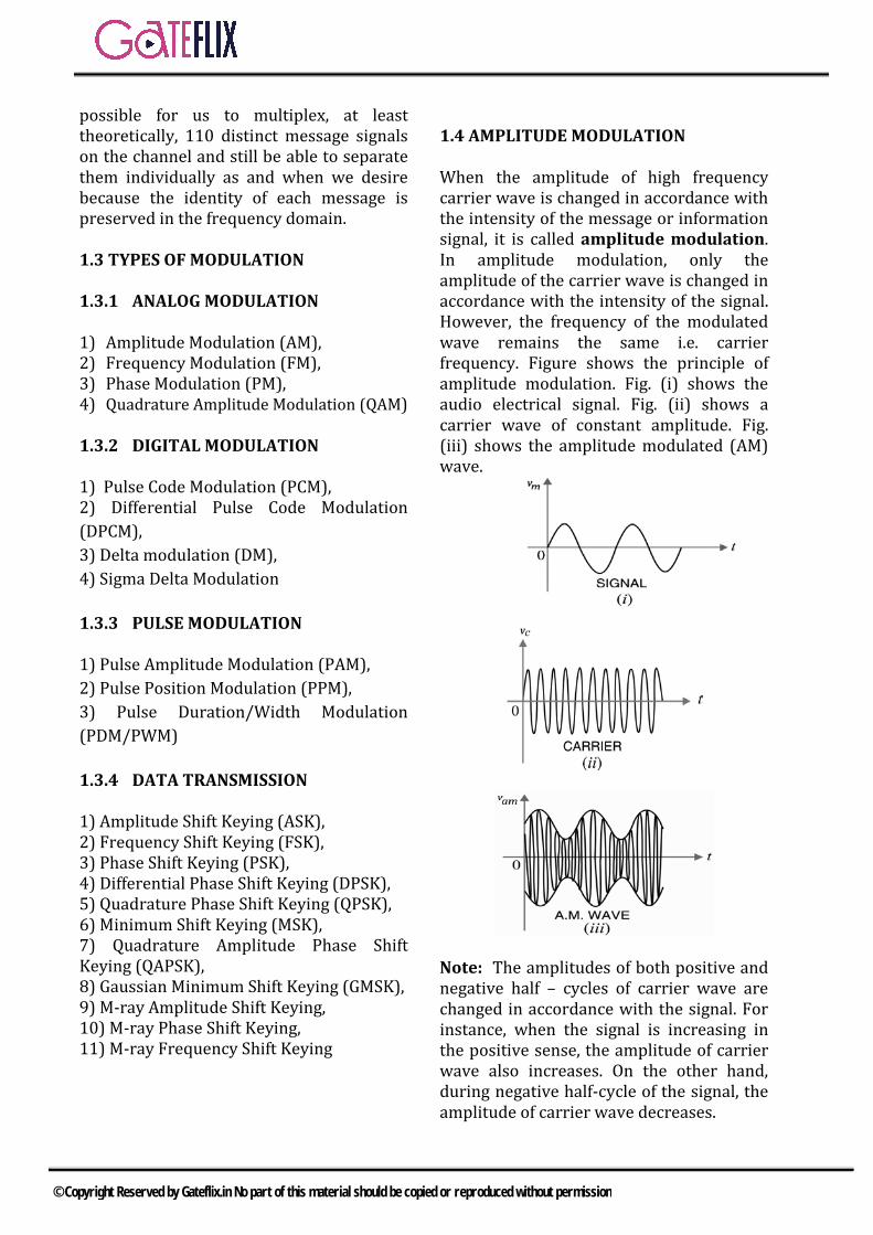
When the amplitude of high frequency carrier wave is changed in accordance with the intensity of the message or information signal, it is called amplitude modulation. In amplitude modulation, only the amplitude of the carrier wave is changed in accordance with the intensity of the signal. However, the frequency of the modulated wave remains the same i.e. carrier frequency. Figure shows the principle of amplitude modulation. Fig. (i) shows the audio electrical signal. Fig. (ii) shows a carrier wave of constant amplitude. Fig. (iii) shows the amplitude modulated (AM) wave.
Note: The amplitudes of both positive and negative half – cycles of carrier wave are changed in accordance with the signal. For instance, when the signal is increasing in the positive sense, the amplitude of carrier wave also increases. On the other hand, during negative half-cycle of the signal, the amplitude of carrier wave decreases.
© Copyright Reserved by Gateflix.in No part of this material should be copied or reproduced without permission
The following points are worth noting in amplitude modulation: 1) The amplitude of the carrier wave
changes according to the intensity ofthe signal.
2) The amplitude variations of the carrierwave are at the signal frequency fm.
3) The frequency of the amplitudemodulated wave remains the same i.e.carrier frequency fc.
1.4.1 MATHEMATICAL EXPRESSION FOR AMPLITUDE MODULATION
Let the modulating signal m(t) be expressed as:
m mm(t) = V cos tω Where, m(t) is instantaneous value of information signal, Vm is peak amplitude of information signal, m mω = 2πf is angular velocity at frequency fm & the carrier wave is represented as:
c c cv (t)=V cos ω tWhere, cv (t) is instantaneous voltage of
carrier cV is amplitude of carrier c cω = 2πf is
angular velocity at carrier frequency cf
In amplitude modulation, the amplitude cVof the carrier wave is varied in accordance with the intensity of the signal as shown in Fig. below. The peak amplitude of carrier after modulation at any instant is given by
c m[V kv (t)]+ . The carrier signal after modulation or the modulated signal is represented by the equation:
am c cv (t)=[V +k m(t)]cos ω t
⇒ m mam c c
c
kV cos v (t)=V [1+ ]cos ω tV
tω
⇒ am c a m cv (t)=V [1+m cos ]cos ω tω t
Where ma
c
Vm kV
= is called modulation
index or modulation factor. Generally k = 1
∴ ma
c
VmV
=
Now expanding the equation of AM wave we get,
a cam c c c m
m Vv (t) V cos ω t cos (ω )2
= + + +ω t
a cc m
m V cos (ω )2
−ω t
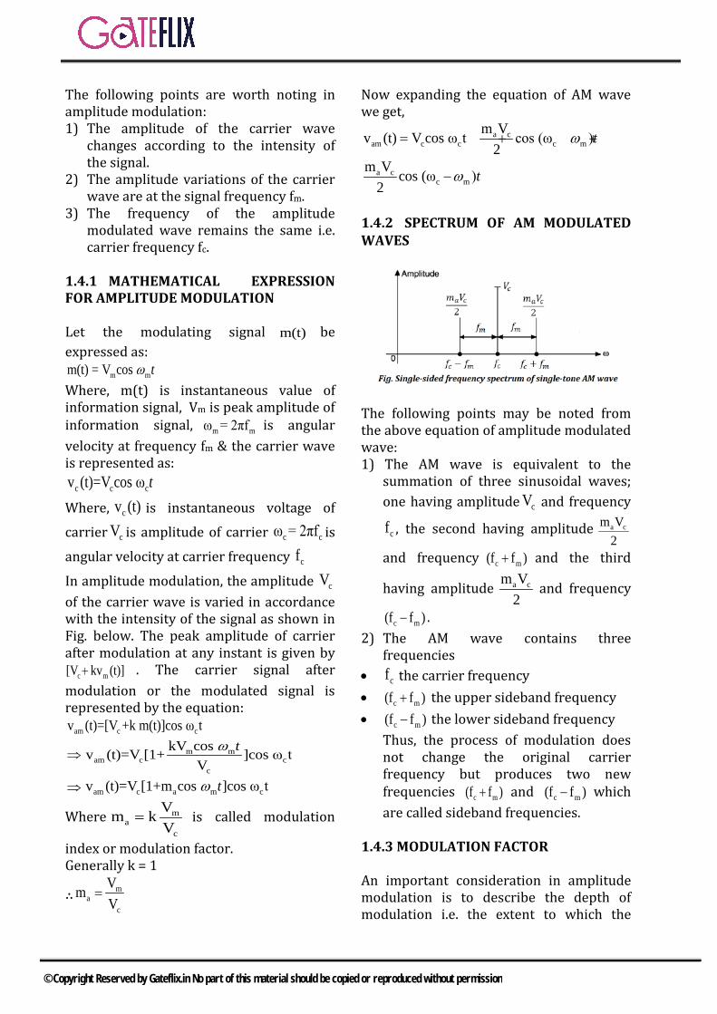
1.4.2 SPECTRUM OF AM MODULATED WAVES
The following points may be noted from the above equation of amplitude modulated wave: 1) The AM wave is equivalent to the
summation of three sinusoidal waves;one having amplitude cV and frequency
cf , the second having amplitude a cm V2
and frequency c m(f f )+ and the third
having amplitude a cm V2
and frequency
c m(f f )− . 2) The AM wave contains three
frequencies• cf the carrier frequency• c m(f f )+ the upper sideband frequency• c m(f f )− the lower sideband frequency
Thus, the process of modulation doesnot change the original carrierfrequency but produces two newfrequencies c m(f f )+ and c m(f f )− which are called sideband frequencies.
1.4.3 MODULATION FACTOR
An important consideration in amplitude modulation is to describe the depth of modulation i.e. the extent to which the
© Copyright Reserved by Gateflix.in No part of this material should be copied or reproduced without permission
amplitude of carrier wave is changed by the signal. This is described by a factor called modulation factor or modulation index which may be defined as the ratio of change of amplitude of carrier wave to the amplitude of normal carrier wave i.e.
aamplitude change of carrier wavemodulation index m =
normal carrier amplitude (unmodulated)
The value of modulation factor depends on signal. The change in carrier amplitude is equal to the amplitude of modulating signal therefore
ma
c
VmV
=
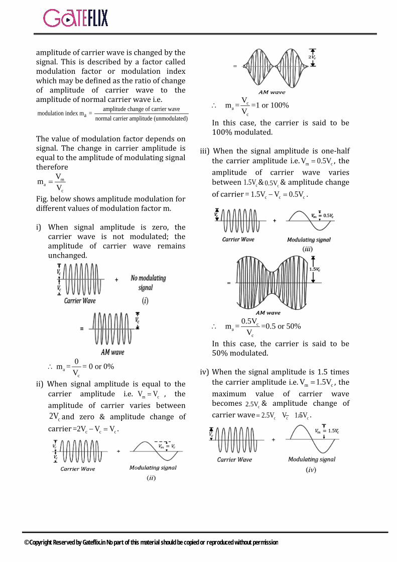
Fig. below shows amplitude modulation for different values of modulation factor m. i) When signal amplitude is zero, the
carrier wave is not modulated; the amplitude of carrier wave remains unchanged.
∴ ac
0m = = 0 or 0%V
ii) When signal amplitude is equal to the carrier amplitude i.e. m cV V= , the amplitude of carrier varies between
c2V and zero & amplitude change of carrier c c c=2V V V− = .
∴ ca
c
Vm = =1 or 100%V
In this case, the carrier is said to be 100% modulated.
iii) When the signal amplitude is one-half
the carrier amplitude i.e. m cV 0.5V= , the amplitude of carrier wave varies between c1.5V & c0.5V & amplitude change of carrier c c c= 1.5V V 0.5V− = .
∴ ca
c
0.5Vm = =0.5 or 50%V
In this case, the carrier is said to be 50% modulated.
iv) When the signal amplitude is 1.5 times
the carrier amplitude i.e. m cV 1.5V= , the maximum value of carrier wave becomes c2.5V & amplitude change of carrier wave c c c2.5V V 1.5V= − = .
© Copyright Reserved by Gateflix.in No part of this material should be copied or reproduced without permission

∴ ca
c
1.5Vm = =1.5 or 150%V
In this case, the carrier is said to be 150% modulated i.e. over-modulated.
Note: 1) When the carrier is modulated to a
small degree (i.e. small m), the amount of carrier amplitude variation is small. Consequently, the audio signal being transmitted will not be very strong. The greater the degree of modulation (i.e. m), the stronger and clearer will be the audio signal. It may be emphasized here that if the carrier is over modulated( )i.e. m > 1 , distortion will occur during reception. The AM waveform is clipped and the envelope is discontinuous. Therefore, degree of modulation should never exceed 100%.
2) The equation for modulation index can
be derived in another for as:
max minm
V VV =2−
And max minc
V VV2+
=
∴
max min
ma
max minc
V VV 2m V VV
2
−
= =+
∴ max mina
max min
V VmV V
−=
+
Example A carrier of 100 V and 1200 kHz is modulated by a 50 V, 1000 Hz sine wave signal. Find the modulation factor. Solution Modulation factor,
ma
c
V 50m 0.5V 100
= = =
Example The maximum peak-to-peak voltage of an AM wave is 16 mV and the minimum peak-to-peak voltage is 4 mV. Calculate the modulation factor. Solution From the figure below
Maximum voltage of AM wave is
max16V = = 8mV2
Minimum voltage of AM wave is
min4V 2mV2
= =
∴ a8 2m 0.68 2−
= =+
© Copyright Reserved by Gateflix.in No part of this material should be copied or reproduced without permission
1.4.4 MODULATION INDEX FOR MULTI-TONE AMPLITUDE MODULATION When more than one modulating signals are used for modulating the carrier wave, it is called multi tone modulation. Let
1 2 2 3 4 nm (t), m (t), m (t), m (t), m (t) - - - - - - - -m (t)are the modulating signal, then the modulated signal is given by
am c 1 2 2 3
4 n c
v (t)=[V m (t) m (t) m (t) m (t)m (t) - - - - - m (t))]cos ω t
+ + + + ++
The modulation index corresponding to each modulating signal is given by
m1a1
c
m2a2
c
m3 mna3 an
c c
Am ,AAm ,A
A Am - - - - - mA A
=
=
= =
The overall or effective modulation index is given by
2 2 2 2a a1 a2 a3 anm m m m .... m= + + +
1.5 POWER IN AM WAVE The equation for AM wave is
am c c
a cc m
a cc m
v (t) V cos ω tm V cos (ω )
2m V cos (ω )
2
=
+ +
+ −
t
t
ω
ω
Equation of AM wave reveals that it has three components of amplitude cV ,
a cm V2
And a cm V2
. Clearly, power output
must be distributed among these components.
1) Power of carrier, 2c
cVP2
=
2) Power in upper sideband, 2 2a c
USBm VP
8= >
3) Power in lower sideband, 2 2a
LSBm VP
8= c
Therefore the total power in an AM signal is
T c USB LSBP P P P= + +
⇒2 2 2 2 2c a c a c
TV m V m VP2 8 8
= + +
⇒2 2 2c a c
TV m VP2 4
= +
⇒2 2 2c a a
T cV m mP 1 P 12 2 2
= + = +
Note: 1) Out of the total power, the power
carried by the sideband is the only useful component.
2) From the equation of total power, 2aT
c
mP 1P 2
= +
If cI and TI are the r.m.s values of un modulated current and total modulated current and R is the resistance through which these current flow, then substituting
2T TP I R= & 2
c cP I R= , we get
T
2 2a
2c
I m1I 2
= +
⇒2a
T cmI I 1+2
=
1.6 EFFICIENCY OF AM TRANSMISSION The efficiency of transmission is the ratio of useful power transmitted (power in sidebands) to total power transmitted i.e.
useful power transmittedefficiency ( ) 100%total power transmitted
= ×η
⇒ SB USB LSB
T T
P P Pη 100%P P
+= = ×
⇒
2 2a c
2a
22 2ac a
m Vm4η 100%
2 mV m12 2
= = ×+
+
© Copyright Reserved by Gateflix.in No part of this material should be copied or reproduced without permission

Note: In AM transmission, the efficiency is maximum when
am 1=2
max 2
1η 100% 33.33%2 1
= × =+
Example A carrier wave of 500 watts is subjected to 100% amplitude modulation. Determine: (i) power in sidebands (ii) power of modulated wave. Solution For 100% modulation am 1= (i)Sideband power,
2a
SB USB LSB cmP P P P2
= + =
∴
2
SB c1P P2
1 500 250watts2
= =
× =
Thus there are 125W in upper sideband and 125W in lower sideband. (ii) Power of AM wave,
2a
T cmP P 12
= +
21500 1 750watts2
= + =
1.7 TYPES OF AM MODULATION
1.7.1 DOUBLE SIDEBAND FULL CARRIER In double sideband full carrier AM (AM-DSBFC) both the sidebands are transmitted along with the carrier. It is also called as conventional AM signal. The mathematical expression for AM-DSB/FC is
a cam c c c m
m Vv (t) V cos ω t cos (ω )t2
= + +ω
a cc m
m V cos (ω )t2
+ −ω
Power saving: In AM-DSB/FC both the sidebands are transmitted along with carrier no power saved during transmission. ∴ Power saving 0%=
Bandwidth: The bandwidth required for transmission of AM-DSB/FC is twice the maximum frequency of modulating signal (In case if modulating signal contains many frequency components, then the bandwidth will be determined by the maximum frequency). ∴ BW 2 mf=
1.7.2 DOUBLE SIDEBAND SUPPRESSED CARRIER
We know that changing the degree of modulation of a particular carrier does not change the amplitude of the carrier component itself. Instead, the amplitude of the sidebands changes, thus altering the amplitude of the composite wave. Since the amplitude of the carrier component remains constant, all the transmitted information is contained in the sidebands. This means that the considerable power transmitted in the carrier is essentially wasted. For improved power efficiency, the carrier component may be suppressed (usually by the use of a balanced modulator circuit), so that the transmitted wave consists only of the upper and lower sidebands. This type of modulation is called double sideband suppressed carrier, or DSB-SC. The carrier must be reinserted at the receiver, however, to recover this modulation. In the time and frequency domains, DSB-SC modulation appears as shown in figure. The mathematical expression for AM-DSB/SC is
am cv (t) v (t).m(t)=
a c a cc m c m
m V m Vcos (ω )t cos (ω )t2 2
= +ω + −ω
Note: An AM-DSB/SC signal can be generated through a Product modulator as shown in fig.
© Copyright Reserved by Gateflix.in No part of this material should be copied or reproduced without permission

Power saving: In AM-DSB/SC both the sidebands are transmitted & carrier is suppressed i.e. carrier power is saved.
( )c
2 2a a
c
P 2Power saving 100%m 2 mP 12
= = × ++
Power saving when am 1= is
( )2Power saving 100% 66.67%
2 1= × =
+ Bandwidth: The bandwidth requirement for AM-DSB/SC is equal to AM-DSB/FC as both the sidebands are transmitted. ∴
BW 2 mf=
1.7.3 SINGLE SIDEBAND FULL CARRIER In single sideband full carrier one of the sidebands is suppressed, written as AM-SSB/FC. Since each sideband is displaced from the carrier by the same frequency, and since the two sidebands have equal amplitudes, it follows that any information contained in one must also be in the other. And, more importantly, halves the transmission bandwidth (frequency spectrum width). Power Saving: Eliminating one of the sidebands cuts the power requirement.
2a
c
2a
c
mP4Power savingmP 12
= +
2a
2a
m4 100%m12
= × +
Power saving when am 1= is
14Power saving 100% 16.67%
112
= × = +
Bandwidth: The bandwidth requirement for AM-SSB/FC is half of double sideband modulated signal as only one sideband is transmitted. ∴
mBW=f
1.7.4 SINGLE SIDEBAND SUPPRESSED CARRIER In SSB-SC (single side band suppressed carrier) one of the side bands & carrier are suppressed. This type of transmission is power efficient & bandwidth efficient. Power Saving: Eliminating one of the sidebands & carrier cuts the power requirement to a large extent.
∴
2 2a a
c
2 2a a
c
m mP 1 14 4
Power saving 100%m mP 1 12 2
+ +
= = × + +
Power saving when am 1= is 54Power saving 100% 83.33%32
= × =
Bandwidth: The bandwidth requirement for AM-SSB/SC is half of double sideband modulated signal as only one sideband is transmitted. ∴
BW mf=
System Transmitted Power
Ps (saved power)
AMDBS/FC
2a
t cmP P 12
= +
-
AM-DSB/SC
2a
cmP2
PC
© Copyright Reserved by Gateflix.in No part of this material should be copied or reproduced without permission
AM-SSB/FC
2a
cmP 14
+
2a
cmP4
AM-SSB/SC
2a
cmP4
2a
cmP 14
+
BW % power Saving Complexity
2ωm - Min. 2ωm 67% ↓ ωm 16% ↓ ωm 83% Max.
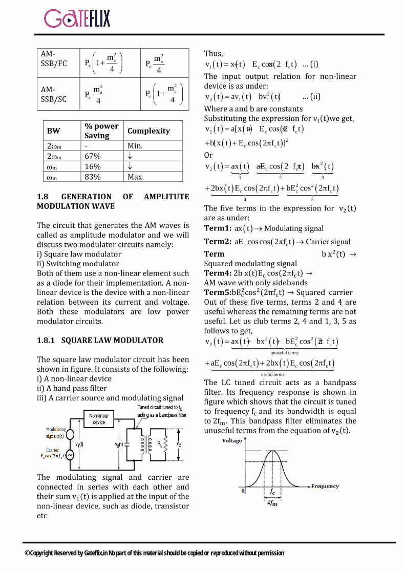
1.8 GENERATION OF AMPLITUTE MODULATION WAVE The circuit that generates the AM waves is called as amplitude modulator and we will discuss two modulator circuits namely: i) Square law modulator ii) Switching modulator Both of them use a non-linear element such as a diode for their implementation. A non-linear device is the device with a non-linear relation between its current and voltage. Both these modulators are low power modulator circuits. 1.8.1 SQUARE LAW MODULATOR The square law modulator circuit has been shown in figure. It consists of the following: i) A non-linear device ii) A band pass filter iii) A carrier source and modulating signal
The modulating signal and carrier are connected in series with each other and their sum v1(t) is applied at the input of the non-linear device, such as diode, transistor etc
Thus, ( ) ( ) ( )1 c cv t x t E cos 2 f t= + π … (i)
The input output relation for non-linear device is as under:
( ) ( ) ( )22 1 1v t av t bv t= + … (ii)
Where a and b are constants Substituting the expression for vt(t)we get,
( ) ( ) ( )( ) ( )
2 c c
2c c
v t a[x t E cos 2 f t
b[x t E cos 2 f t ]
= + π
+ + π
Or ( ) ( )
( ) ( )
( ) ( ) ( )
22 c c
1 2 32 2
c c c c
4 5
v t ax t aE cos 2 f t bx t
2bx t E cos 2 f t bE cos 2 f t
= + π +
+ π + π
The five terms in the expression for v2(t) are as under: Term1: ( )ax t Modulating signal→ Term2: ( )c caE cos cos 2πf t Carrier signal→ Term b x2(t) →Squared modulating signal Term4: 2b x(t)Ec cos(2πfct) → AM wave with only sidebands Term5:bEc2cos2(2πfct) → Squared carrier Out of these five terms, terms 2 and 4 are useful whereas the remaining terms are not useful. Let us club terms 2, 4 and 1, 3, 5 as follows to get,
( ) ( ) ( ) ( )
( ) ( ) ( )
2 2 22 c c
unuseful terms
c c c c
useful terms
v t ax t bx t bE cos 2 f t
aE cos 2 f t 2bx t E cos 2 f t
= + + π
+ π + π
The LC tuned circuit acts as a bandpass filter. Its frequency response is shown in figure which shows that the circuit is tuned to frequency fc and its bandwidth is equal to 2fm. This bandpass filter eliminates the unuseful terms from the equation of v2(t).
© Copyright Reserved by Gateflix.in No part of this material should be copied or reproduced without permission
Hence, the output votage v0(t) contains only the useful terms.
( ) ( ) ( ) ( )0 c c c cV t aE cos 2 f t 2bx t E cos 2 f t= π + π
Or ( ) ( ) ( )0 c c cV t aE 2bx t E cos 2 f t = + π Therefore,
( ) ( ) ( )0 c c2bV t aE 1 x t cos 2 f ta
= + π … (iii)
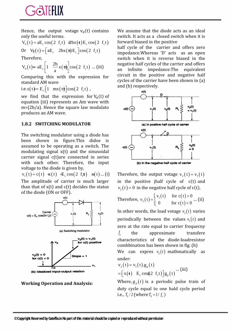
Comparing this with the expression for standard AM wave i.e. ( ) ( ) ( )c cs t E 1 mx t cos 2 f t = + π , we find that the expression for V0(t) of equation (iii) represents an Am wave with m=(2b/a). Hence the square law modulato produces an AM wave. 1.8.2 SWITCHING MODULATOR The switching modulator using a diode has been shown in figure.This didoe is assumed to be operating as a switch. The modulating signal x(t) and the sinusoidal carrier signal c(t)are connected in series with each other. Therefore, the input voltage to the diode is given by,
( ) ( ) ( ) ( ) ( )1 c cv t c t x t E cos 2 f t x t= + = π + … (i) The amplitude of carrier is much larger than that of x(t) and c(t) decides the status of the diode (ON or OFF).
Working Operation and Analysis:
We assume that the diode acts as an ideal switch. It acts as a closed switch when it is forward biased in the positive half cycle of the carrier and offers zero impedance.Whereas ‘D’ acts as an open switch when it is reverse biased in the negative half cycles of the carrier and offers an infinite impedance.The equivalent circuit in the positive and negative half cycles of the carrier have been shown in (a) and (b) respectively.
Therefore, the output votage ( ) ( )2 1v t v t= in the positive jhalf cycle of c(t) and ( )2 0v t = in the negative half cycle of c(t),
Therefore, ( ) ( ) ( )( )
12
v t for c t 0v t
0 for c t 0 >= <
… (ii)
In other words, the load votage ( )2v t varies
periodically between the values ( )1v t and zero at the rate equal to carrier frequecny
cf the approximate transfere characteristics of the diode-loadresistor combbination has been shown in fig. (b) We can expres ( )2v t mathmatically as under:
( ) ( ) ( )( ) ( ) ( )
2 1 p
c c p
v t v t .g t
x t E cos 2 f t g t
=
= + π … (iii)
Where, ( )pg t is a periodic pulse train of duty cycle equal to one hald cycle period i.e., 0 / 2T (where 0 1/ cT f= )
© Copyright Reserved by Gateflix.in No part of this material should be copied or reproduced without permission
Let us express ( )pg t with othe help of Foureier series as under:
( ) ( ) ( )n 1n
p cn 1
11 2g t cos 2 f t 2n 12 2n 1
−=∞
=
− = + π − π −∑
…(iv)
( ) ( )p c1 2g t cos 2 f t odd harmonic components2
= + π +π
… (v) Substituting gp(t) into equation (vi), we get
( ) ( ) ( )2 c cv t x t E cos cos 2 f t = + π
( ) ( )n 1n
cn 1
11 2 cos 2 f t 2n 12 2n 1
−=∞
=
− + π − π − ∑
Therefore, ( ) ( ) ( )2 c cv t x t E cos cos 2 f t = + π
( )c1 2 cos 2 f t odd harmonics2 + π + π
… (vi)
The odd harmonics in this expression are unwanted, and therfore, are assumed to be eliminated.
( ) ( )2
modulating signal
1v t x t2
=
( ) ( ) ( )c c c
AM wave
1 2 E cos 2 f t cos 2 f t x t2
+ π + ππ
( )nd
2c c
2 harmonic of carrier
2 E cos 2 f t+ ππ
In this expression, the firstand the fourth terms are unwanted terms whereas the second and third terms together represent the AM wave. Clubing the second and third terms together , we obtain
( ) ( ) ( )c2 c
c
E 4v t 1 x t cos 2 f t2 E
unwanted terms
= + π π
+
This is the required expression for the AM
wave withc
4mE
= π
. The unwanted terms
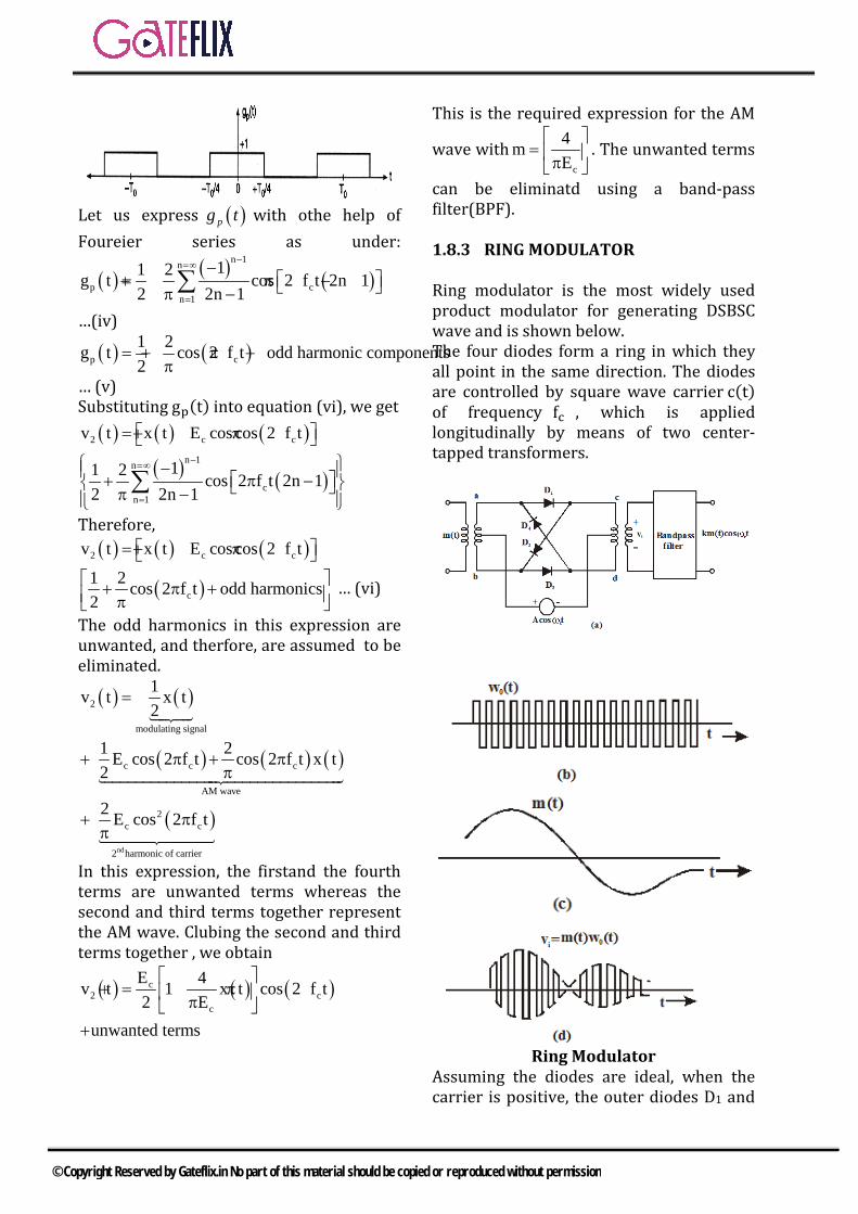
can be eliminatd using a band-pass filter(BPF). 1.8.3 RING MODULATOR Ring modulator is the most widely used product modulator for generating DSBSC wave and is shown below. The four diodes form a ring in which they all point in the same direction. The diodes are controlled by square wave carrier c(t) of frequency fc , which is applied longitudinally by means of two center-tapped transformers.
Ring Modulator
Assuming the diodes are ideal, when the carrier is positive, the outer diodes D1 and
© Copyright Reserved by Gateflix.in No part of this material should be copied or reproduced without permission
D2 are forward biased where as the inner diodes D3 and D4 are reverse biased, so that the modulator multiplies the base band signal m(t) by c(t). When the carrier is negative, the diodes D1 and D2 are reverse biased and D3 and D4 are forward, and the modulator multiplies the base band signal –m (t) by c (t). Thus the ring modulator in its ideal form is a product modulator for square wave carrier and the base signal m (t). The square wave carrier can be expanded using Fourier series as
( ) ( ) ( )n 1
cn 1
14c t cos(2πf t 2n 1 )π 2n 1
−∞
=
−= −
−∑
Therefore the ring modulator output is given by s(t) = m(t)c(t)
( ) ( ) ( )( )n 1
cn 1
14s t m(t) cos cos 2πf t 2n 1π 2n 1
−∞
=
−= −
− ∑
From the above equation it is clear that output from the modulator consists entirely of modulation products. If the message signal m (t) is band limited to the frequency band– w < 𝑓𝑓 < 𝑤𝑤 , the output spectrum consists of side bands centered at fc . 1.8.4 GENERATION OF SSB 1) Filter method (frequency selectivity
filtering) 2) Phase shift method 3) Third Method 1.9 DEMODULATION OF AMPLITUDE MODULATED SIGNAL The process of detection or demodulation is the process of recovering the message signal from the received modulated signal. This means that the process of detection is exactly opposite to that of modulation.
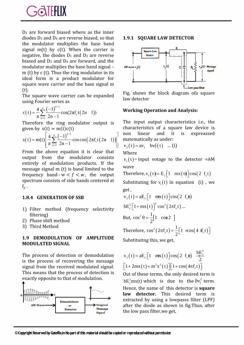
1.9.1 SQUARE LAW DETECTOR
Fig. shows the block diagram ofa square law detector Working Operation and Analysis: The input output characteristics i.e., the characteristics of a square law device is non linear and it is expreassed matematically as under:
( ) ( )22 1 1v t av bv t= + … (i)
Where ( )1v t = input votage to the detector =AM
wave Therefore, ( ) ( ) ( )1 c cv t E 1 mx t cos 2 f t = + π
Substituting for ( )1v t in equation (i) , we get ,
( ) ( ) ( )2 c cv t aE 1 mx t cos 2 f t = + π +
( ) ( )22 2c cbE 1 mx t cos 2 f t + π …
But, [ ]2 1cos 1 cos 22
θ = + θ
Therefore, ( ) ( )2c c
1cos 2 f t 1 cos 4 f t2 π = + π
Substituitng this, we get,
( ) ( ) ( )2c
2 c cbEv t aE 1 mx t cos 2 f t
2 = + π +
( ) ( ) ( )2 2c1 2mx t m x t 1 cos 4 f t + + + π
Out of these terms, the only desired term is 2cbE mx(t) which is due to the 2
1bv term. Hence, the name of this detector is square law detector. This desired term is extracted by using a lowpasss filter (LPF) after the diode as shown in fig.Thus, after the low pass filter,we get,
© Copyright Reserved by Gateflix.in No part of this material should be copied or reproduced without permission
( ) ( ) ( )20 cv t bE m x t= … (iv)
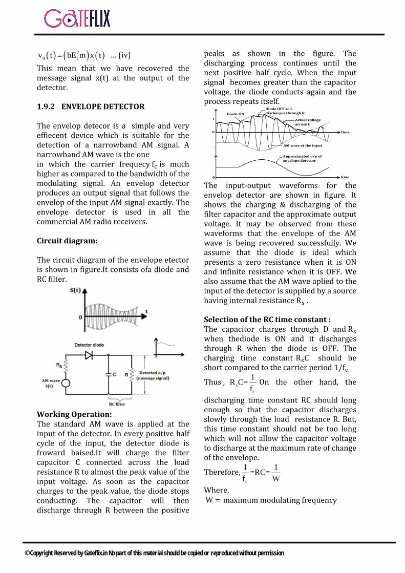
This mean that we have recovered the message signal x(t) at the output of the detector. 1.9.2 ENVELOPE DETECTOR The envelop detecor is a simple and very effiecent device which is suitable for the detection of a narrowband AM signal. A narrowband AM wave is the one in which the carrier frequecy fc is much higher as compared to the bandwidth of the modulating signal. An envelop detector produces an output signal that follows the envelop of the input AM signal exactly. The envelope detector is used in all the commercial AM radio receivers. Circuit diagram: The circuit diagram of the envelope etector is shown in figure.It consists ofa diode and RC filter.
Working Operation: The standard AM wave is applied at the input of the detector. In every positive half cycle of the input, the detector diode is froward baised.It will charge the filter capacitor C connected across the load resistance R to almost the peak value of the input voltage. As soon as the capacitor charges to the peak value, the diode stops conducting. The capacitor will then discharge through R between the positive
peaks as shown in the figure. The discharging process continues until the next positive half cycle. When the input signal becomes greater than the capacitor voltage, the diode conducts again and the process repeats itself.
The input-output waveforms for the envelop detector are shown in figure. It shows the charging & discharging of the filter capacitor and the approximate output voltage. It may be observed from these waveforms that the envelope of the AM wave is being recovered successfully. We assume that the diode is ideal which presents a zero resistance when it is ON and infinite resistance when it is OFF. We also assume that the AM wave aplied to the input of the detector is supplied by a source having internal resistance Rs . Selection of the RC time constant : The capacitor charges through D and Rs when thediode is ON and it discharges through R when the diode is OFF. The charging time constant RsC should be short compared to the carrier period 1/fc
Thus , sc
1R C=f
On the other hand, the
discharging time constant RC should long enough so that the capacitor discharges slowly through the load resistance R. But, this time constant should not be too long which will not allow the capacitor voltage to discharge at the maximum rate of change of the envelope.
Therefore,c
1 1=RC=f W
Where, W = maximum modulating frequency
© Copyright Reserved by Gateflix.in No part of this material should be copied or reproduced without permission
1.9.2.1 DISTORTIONS IN THE ENVELOPE DETECTOR OUTPUT
There are two types of distortions which can occur in the detector output.They are as under: i) Diagonal clipping ii) Negative peak clipping 1) Diagonal cliping: This type of distrotion occurs when the RC time constant of the load circuit is too long. Due to this the RC circuit cannot follow the fast changes in the modulating envelope. The diagonal clipping has been shown in figure.
2) Negative peak clippping: This distortion occurs due to a fact that the modulation index on the output side of the detector is higher than that on its input side, Hence, at higher depths of modulation of the transmitted signal, the over modulation (more than 100% moudlation) may take place at the output of the detector. The negative peak clipping will take place as a result of this over modulation as shown in figure.
Remedy:The only to reduce or eliminate the distrtions is to choose the RC time constants properly as discussed earlier. 1.10 QAM (QUADRATURE AMPLITUDE MODULATION)
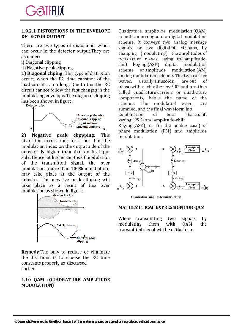
Quadrature amplitude modulation (QAM) is both an analog and a digital modulation scheme. It conveys two analog message signals, or two digital bit streams, by changing (modulating) the amplitudes of two carrier waves, using the amplitude-shift keying (ASK) digital modulation scheme or amplitude modulation (AM) analog modulation scheme. The two carrier waves, usually sinusoids, are out of phase with each other by 90° and are thus called quadrature carriers or quadrature components, hence the name of the scheme. The modulated waves are summed, and the final waveform is a Combination of both phase-shift keying (PSK) and amplitude-shift Keying (ASK), or (in the analog case) of phase modulation (PM) and amplitude modulation.
- /2
~
Low-pass filter
- /2
~
Low-pass filterm (t)2
m (t)1
cos Ct
2sin Ct
2cos Ct
m (t)1
m (t)2
x (t)1
x (t)2
QAM(t)
sin Ct
Quadrature amplitude multiplexing
MATHEMETICAL EXPRESSION FOR QAM When transmitting two signals by modulating them with QAM, the transmitted signal will be of the form.
© Copyright Reserved by Gateflix.in No part of this material should be copied or reproduced without permission
2.1 INTRODUCTION
Angle modulation is a class of analog modulation. These techniques are based on altering the angle (or phase) of a sinusoidal carrier wave to transmit data, as opposed to varying the amplitude, such as in AM transmission. Angle Modulation is modulation in which the angle of a sine-wave carrier is varied by a modulating wave. In this method of modulation the amplitude of the carrier wave is maintained constant. There are two types of angle modulation: 1) Frequency Modulation (FM)2) Phase Modulation (PM)
2.2 FREQUENCY MODULATION (FM)
When the frequency of carrier wave is changed in accordance with the intensity of the signal, it is called frequency modulation (FM).
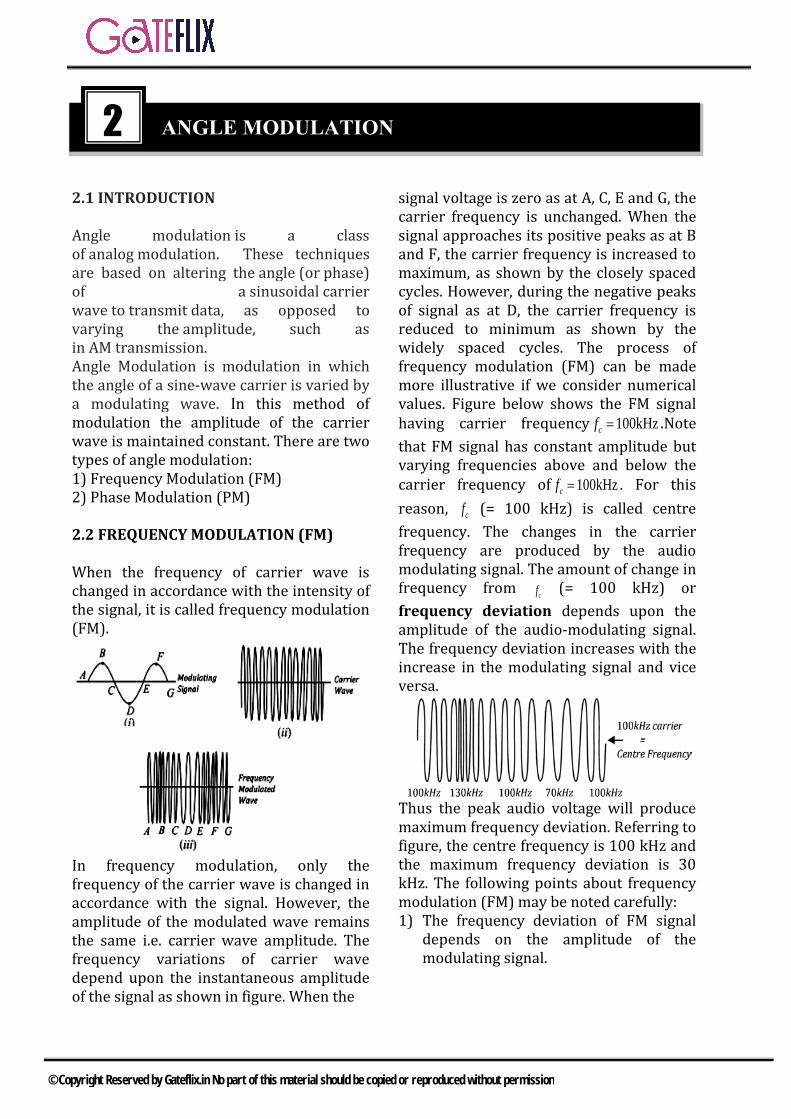
In frequency modulation, only the frequency of the carrier wave is changed in accordance with the signal. However, the amplitude of the modulated wave remains the same i.e. carrier wave amplitude. The frequency variations of carrier wave depend upon the instantaneous amplitude of the signal as shown in figure. When the
signal voltage is zero as at A, C, E and G, the carrier frequency is unchanged. When the signal approaches its positive peaks as at B and F, the carrier frequency is increased to maximum, as shown by the closely spaced cycles. However, during the negative peaks of signal as at D, the carrier frequency is reduced to minimum as shown by the widely spaced cycles. The process of frequency modulation (FM) can be made more illustrative if we consider numerical values. Figure below shows the FM signal having carrier frequency 100kHzcf = .Note that FM signal has constant amplitude but varying frequencies above and below the carrier frequency of 100kHzcf = . For this reason, cf (= 100 kHz) is called centre frequency. The changes in the carrier frequency are produced by the audio modulating signal. The amount of change in frequency from cf (= 100 kHz) or frequency deviation depends upon the amplitude of the audio-modulating signal. The frequency deviation increases with the increase in the modulating signal and vice versa.
Thus the peak audio voltage will produce maximum frequency deviation. Referring to figure, the centre frequency is 100 kHz and the maximum frequency deviation is 30 kHz. The following points about frequency modulation (FM) may be noted carefully: 1) The frequency deviation of FM signal
depends on the amplitude of themodulating signal.
2 ANGLE MODULATION
© Copyright Reserved by Gateflix.in No part of this material should be copied or reproduced without permission

2) The centre frequency is the frequency without modulation or when the modulating voltage is zero.
3) The audio frequency (i.e. frequency of modulating signal) does not determine frequency deviation.
2.2.1 MATHEMATICAL EXPRESSION OF FREQUENCY MODULATED SIGNAL
Suppose a modulating sine-wave signal ( ) m mm t = V cos ω t is used to vary the carrier
frequency cf . Let the change in carrier frequency be km(t) . Where, k is a constant known as the frequency deviation constant. The instantaneous carrier frequency if is given by; i c fkf =f + m(t) ⇒ f mi mc k V cosf = + ωf t
A graph of if versus time is shown in figure above. It is important to note that it is frequency-time curve and not amplitude-time curve. The factor mkV represents the maximum frequency deviation and is denoted by f∆ i.e .Max. frequency deviation, f mVf k∆ = ∴ i c m cos f tf f= + ∆ ω Now, the instantaneous angular frequency of FM is given by;
i c c m cos tω = ω + ∆ω ω Total phase angle θ ωt= so that if ω is variable, then,
t
i0
dtθ = ω∫
⇒t
i c c m0
( cos t) dtθ = ω = ω + ∆ω ω∫
∴ cc m
m
t sin t∆ωθ = ω + ω
ω
The term c
m
ωω∆
is called modulation index fm .
∴ fc mt sin tmθ = ω + ω Now the equation for FM modulated wave is
FM c fc mv (t) V cos t sin t)( mω + ω= Above expression is the general voltage equation of a FM wave. The following points may be noted carefully: 1) The modulation index fm is the ratio of
maximum frequency deviation ( f∆ ) to the frequency mf of the modulating signal i.e.
c
m
ΔωModulation index,ω
m ∆==f
m
ff
2) Unlike amplitude modulation, the modulation index ( fm ) for frequency modulation can be greater than unity & it controls the number of sidebands in an FM signal.
3) In FM modulated signal, there is infinite number of sidebands along with carrier. The frequencies in an FM wave are
c c m c m c m c mf , f f , f 2f , f 3f , f 4f ........± ± ± ±
2.3 POWER IN FREQUENCY MODULATED SIGNAL The amplitude of a FM wave is constant hence the power content is also constant i.e. does not depend on modulation index. The equation for FM signal is
FM c fc mv (t) V cos t sin t)( mω + ω= The power content in this signal is given by
2 2c cV VP
22 = =
Example A frequency modulated voltage wave is given by the equation:
( )8v = 12 cos 6 × 10 t + 5 sin 1250 t Find i) carrier frequency ii) signal frequency
© Copyright Reserved by Gateflix.in No part of this material should be copied or reproduced without permission
iii) modulation index iv) maximum frequency deviation v) power dissipated by the FM wave in 10-
ohm resistor. Solution The given FM voltage wave is
( )8v = 12 cos 6 × 10 t + 5 sin 1250 t The equation of standard FM voltage wave is
c mc fω tv V co ss m t( inω )+= Comparing above equations, we have, 1) Carrier frequency,
86
c6×10f 95.5 10 Hz
2π= = ×
2) Signal frequency, s1250f 199 Hz
2π= =
3) Modulation index, fm =5 4) Max. Frequency deviation,
f mf m f 5 199 995 Hz∆ = × = × = 5) Power dissipated,
2 2cV 12 144P 7.2Watts
2R 2 10 20= = = =
×
2.4 TYPES OF FM 2.4.1 NARROW BAND FM A narrow band FM is the FM wave with a small bandwidth. The modulation index fm of narrow band FM is small as compared to one radian. Hence, the spectrum of narrow band FM consists of the carrier and upper sideband and a lower sideband. For small values of fm the values of the j coefficients are as under:
( )0 fJ m = 1
( )1 f fJ m = m / 2
( )n fJ m = 0 for n > 1 Hence, a narrow band FM wave can be expressed mathematically as under
f cfm c c c m
carrierUSB
m Ev (t) E sin t sin( ) t2
= ω + ω +ω
f cc m
LSB
m E sin( ) t2
− ω −ω
The (-) sign associated with the LSB represents a phase shift of180° . Practically, the narrow band FM system has fm less than 1. The maximum permissible frequency deviation ( )f∆ is restricted to about 5 kHz. This system is used in FM mobile communications such as police wireless, ambulances, taxicabs etc. Note: • Like AM, a narrow band FM also has a
carrier with 2 sidebands. But the sidebands are o180 out of phase.
• Addition of NBFM & AM with same modulation index results in SSB full carrier.
• Subtraction of NBFM & AM with same modulation index results in SSB suppressed carrier.
2.4.1.1 COMPARISON BETWEEN AM AND NBFM
AM NBFM 1) ( ) cc
c
tS t = m(
A cos t) cos t+ ω
ω
1) ( )
−∞
ω
∫t
cc ft+ k m(S t = A co )s t dt
2)
mBW = 2f 2)
mBW = 2f
3) m
ac
Vm =V
3)
fm
fm =f∆
4)
2
T cmP = P 1+2
a
4) T cP = P
2.4.2 WIDEBAND FM For large values of modulation index fm the FM wave ideally contains the carrier and an infinite number of sidebands located symmetrically around the carrier. Such a FM wave has infinite bandwidth and hence called as wideband FM. The modulation index of wideband FM is higher
© Copyright Reserved by Gateflix.in No part of this material should be copied or reproduced without permission
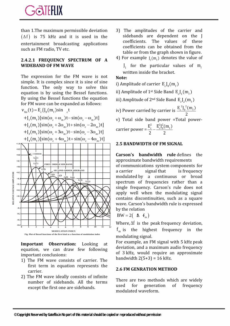
than 1.The maximum permissible deviation( )f∆ is 75 kHz and it is used in the entertainment broadcasting applications such as FM radio, TV etc. 2.4.2.1 FREQUENCY SPECTRUM OF A WIDEBAND OF FM WAVE The expression for the FM wave is not simple. It is complex since it is sine of sine function. The only way to solve this equation is by using the Bessel functions. By using the Bessel functions the equation for FM wave can be expanded as follows:
= ωfm c 0 f cv (t) E J (m )sin t
ω +ω − ω −ωω + ω + ω − ωω + ω − ω − ωω + ω + ω − ω
1 f c m c m
2 f c m c m
3 f c m c m
4 f c m c m
+J (m )[sin( )t sin( )t]+J (m )[sin( 2 )t sin( 2 )t]+J (m )[sin( 3 )t sin( 3 )t]+J (m )[sin( 4 )t sin( 4 )t]
0 1 2 3 4 5 6 7 8 9 10 11 12-0.4
-0.3
-0.2
-0.1
0
+0.1
+0.2
+0.3
+0.4
+0.5
+0.6
+0.7
+0.8
+0.9
+1.0
CARRIER
J ( )0
J ( )1 FIRST ORDER SIDEBAND
SECOND ORDER SIDEBANDJ ( )2
J ( )3 J ( )4 J ( )5 J ( )6
J ( )7 J ( )8
MODULATION INDEX
RELA
TIVE
VO
LTAG
E AM
PLIT
UDE
Fig. Plot of Bessel functions of the first kind as a function of modulation index
Important Observation: Looking at equation, we can draw few following important conclusions: 1) The FM wave consists of carrier. The
first term in equation represents the carrier.
2) The FM wave ideally consists of infinite number of sidebands. All the terms except the first one are sidebands.
3) The amplitudes of the carrier and sidebands are dependent on the J coefficients. The values of these coefficients can be obtained from the table or from the graph shown in figure.
4) For example 1 fJ (m ) denotes the value of
1J for the particular values of fm written inside the bracket.
Note: i) Amplitude of carrier c 0 fE J (m )
ii) Amplitude of 1st Side Band c 1 fE J (m )
iii) Amplitude of 2nd Side Band c 2 fE J (m )
iv) Power carried by carrier is 2 2
c 0 fE J (m )2
v) Total side band power =Total power-
carrier power =2 2 2c c 0 fE E J (m )
2 2−
2.5 BANDWIDTH OF FM SIGNAL Carson's bandwidth rule defines the approximate bandwidth requirements of communications system components for a carrier signal that is frequency modulated by a continuous or broad spectrum of frequencies rather than a single frequency. Carson's rule does not apply well when the modulating signal contains discontinuities, such as a square wave. Carson's bandwidth rule is expressed by the relation
( )m BW 2 f f= ∆ + Where, f∆ is the peak frequency deviation,
mf is the highest frequency in the modulating signal. For example, an FM signal with 5 kHz peak deviation, and a maximum audio frequency of 3 kHz, would require an approximate bandwidth 2(5+3) = 16 kHz. 2.6 FM GENRATION METHOD There are two methods which are widely used for generation of frequency modulated waveform.
© Copyright Reserved by Gateflix.in No part of this material should be copied or reproduced without permission
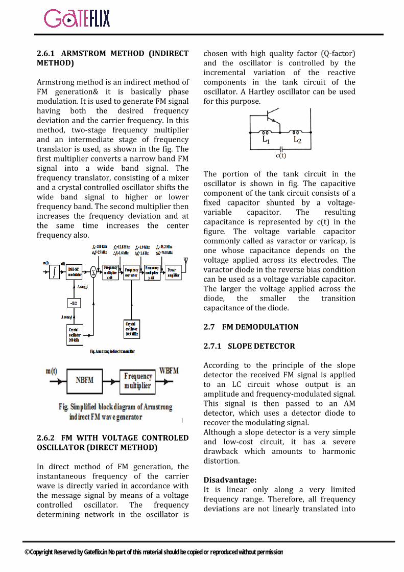
2.6.1 ARMSTROM METHOD (INDIRECT METHOD) Armstrong method is an indirect method of FM generation& it is basically phase modulation. It is used to generate FM signal having both the desired frequency deviation and the carrier frequency. In this method, two-stage frequency multiplier and an intermediate stage of frequency translator is used, as shown in the fig. The first multiplier converts a narrow band FM signal into a wide band signal. The frequency translator, consisting of a mixer and a crystal controlled oscillator shifts the wide band signal to higher or lower frequency band. The second multiplier then increases the frequency deviation and at the same time increases the center frequency also.
2.6.2 FM WITH VOLTAGE CONTROLED OSCILLATOR (DIRECT METHOD) In direct method of FM generation, the instantaneous frequency of the carrier wave is directly varied in accordance with the message signal by means of a voltage controlled oscillator. The frequency determining network in the oscillator is
chosen with high quality factor (Q-factor) and the oscillator is controlled by the incremental variation of the reactive components in the tank circuit of the oscillator. A Hartley oscillator can be used for this purpose.
The portion of the tank circuit in the oscillator is shown in fig. The capacitive component of the tank circuit consists of a fixed capacitor shunted by a voltage-variable capacitor. The resulting capacitance is represented by c(t) in the figure. The voltage variable capacitor commonly called as varactor or varicap, is one whose capacitance depends on the voltage applied across its electrodes. The varactor diode in the reverse bias condition can be used as a voltage variable capacitor. The larger the voltage applied across the diode, the smaller the transition capacitance of the diode.
2.7 FM DEMODULATION 2.7.1 SLOPE DETECTOR
According to the principle of the slope detector the received FM signal is applied to an LC circuit whose output is an amplitude and frequency-modulated signal. This signal is then passed to an AM detector, which uses a detector diode to recover the modulating signal. Although a slope detector is a very simple and low-cost circuit, it has a severe drawback which amounts to harmonic distortion. Disadvantage: It is linear only along a very limited frequency range. Therefore, all frequency deviations are not linearly translated into
© Copyright Reserved by Gateflix.in No part of this material should be copied or reproduced without permission
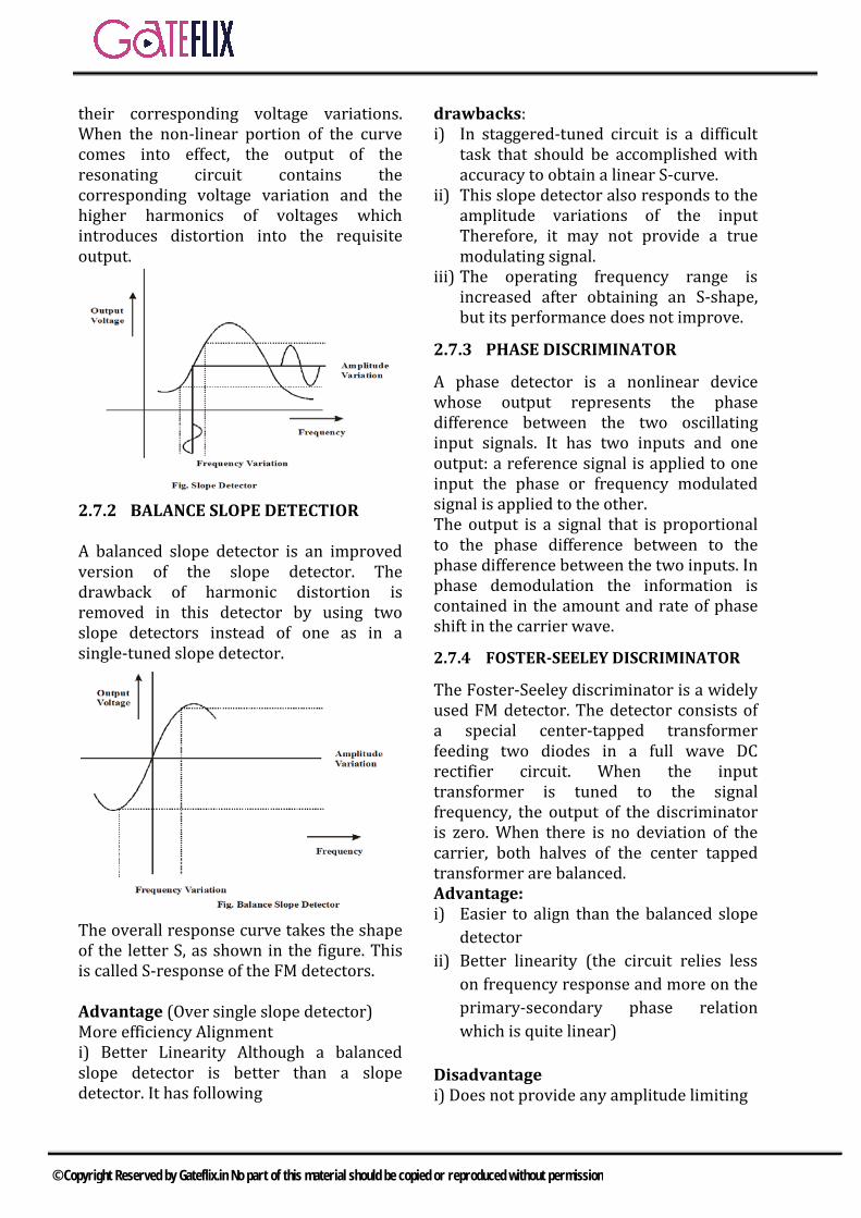
their corresponding voltage variations. When the non-linear portion of the curve comes into effect, the output of the resonating circuit contains the corresponding voltage variation and the higher harmonics of voltages which introduces distortion into the requisite output.
2.7.2 BALANCE SLOPE DETECTIOR A balanced slope detector is an improved version of the slope detector. The drawback of harmonic distortion is removed in this detector by using two slope detectors instead of one as in a single-tuned slope detector.
The overall response curve takes the shape of the letter S, as shown in the figure. This is called S-response of the FM detectors. Advantage (Over single slope detector) More efficiency Alignment i) Better Linearity Although a balanced slope detector is better than a slope detector. It has following
drawbacks: i) In staggered-tuned circuit is a difficult
task that should be accomplished with accuracy to obtain a linear S-curve.
ii) This slope detector also responds to the amplitude variations of the input Therefore, it may not provide a true modulating signal.
iii) The operating frequency range is increased after obtaining an S-shape, but its performance does not improve.
2.7.3 PHASE DISCRIMINATOR
A phase detector is a nonlinear device whose output represents the phase difference between the two oscillating input signals. It has two inputs and one output: a reference signal is applied to one input the phase or frequency modulated signal is applied to the other. The output is a signal that is proportional to the phase difference between to the phase difference between the two inputs. In phase demodulation the information is contained in the amount and rate of phase shift in the carrier wave.
2.7.4 FOSTER-SEELEY DISCRIMINATOR
The Foster-Seeley discriminator is a widely used FM detector. The detector consists of a special center-tapped transformer feeding two diodes in a full wave DC rectifier circuit. When the input transformer is tuned to the signal frequency, the output of the discriminator is zero. When there is no deviation of the carrier, both halves of the center tapped transformer are balanced. Advantage: i) Easier to align than the balanced slope
detector ii) Better linearity (the circuit relies less
on frequency response and more on the primary-secondary phase relation which is quite linear)
Disadvantage i) Does not provide any amplitude limiting
© Copyright Reserved by Gateflix.in No part of this material should be copied or reproduced without permission
2.7.5 RATIO DETECTOR
The ratio detector is a variant of the Foster-Seeley discriminator, but one diode conducts in an opposite direction. It provides stabilization against signal strength variation of frequency modulating signal.
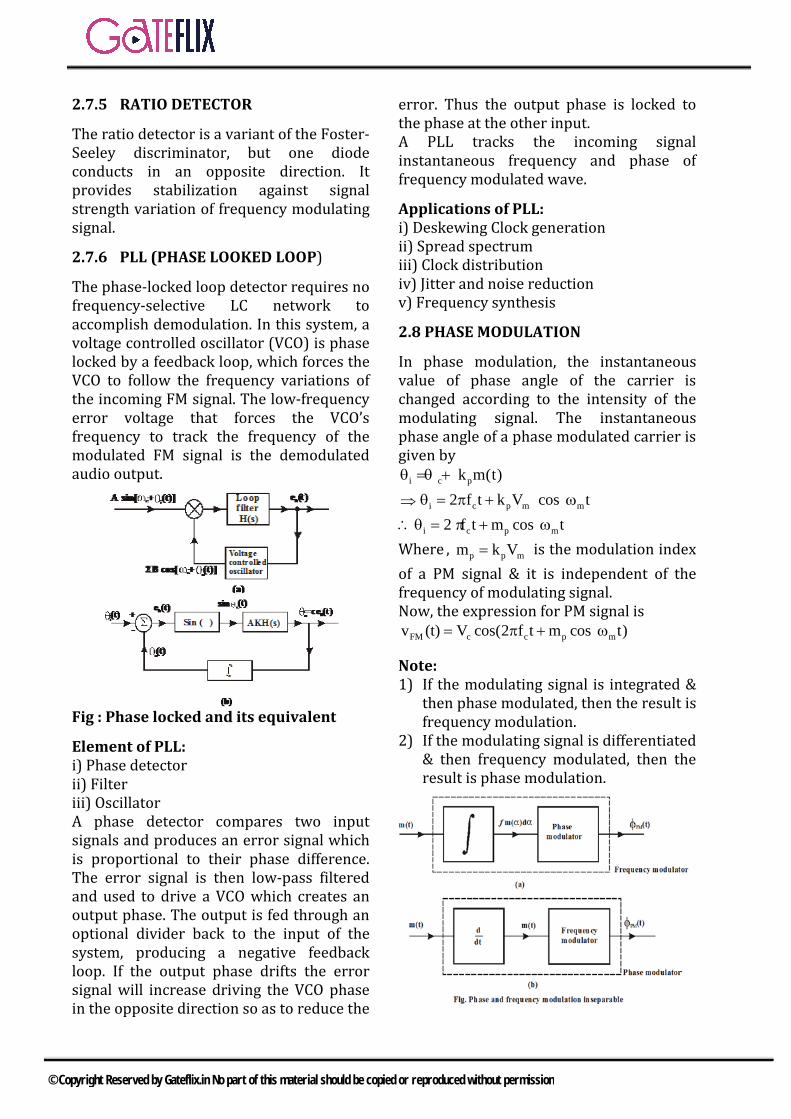
2.7.6 PLL (PHASE LOOKED LOOP)
The phase-locked loop detector requires no frequency-selective LC network to accomplish demodulation. In this system, a voltage controlled oscillator (VCO) is phase locked by a feedback loop, which forces the VCO to follow the frequency variations of the incoming FM signal. The low-frequency error voltage that forces the VCO’s frequency to track the frequency of the modulated FM signal is the demodulated audio output.
Fig : Phase locked and its equivalent
Element of PLL: i) Phase detector ii) Filter iii) Oscillator A phase detector compares two input signals and produces an error signal which is proportional to their phase difference. The error signal is then low-pass filtered and used to drive a VCO which creates an output phase. The output is fed through an optional divider back to the input of the system, producing a negative feedback loop. If the output phase drifts the error signal will increase driving the VCO phase in the opposite direction so as to reduce the
error. Thus the output phase is locked to the phase at the other input. A PLL tracks the incoming signal instantaneous frequency and phase of frequency modulated wave.
Applications of PLL: i) Deskewing Clock generation ii) Spread spectrum iii) Clock distribution iv) Jitter and noise reduction v) Frequency synthesis
2.8 PHASE MODULATION
In phase modulation, the instantaneous value of phase angle of the carrier is changed according to the intensity of the modulating signal. The instantaneous phase angle of a phase modulated carrier is given by
i c pk m(t)θ = θ + ⇒ pc m mi k V co2 f s tt θ π + ω= ∴ i c p mm cos t2 f tθ = π ω+ Where , p p mm k V = is the modulation index of a PM signal & it is independent of the frequency of modulating signal. Now, the expression for PM signal is
FM c pc mv (t) V cos(2 f t )m cos tπ ω+=
Note: 1) If the modulating signal is integrated &
then phase modulated, then the result is frequency modulation.
2) If the modulating signal is differentiated & then frequency modulated, then the result is phase modulation.
© Copyright Reserved by Gateflix.in No part of this material should be copied or reproduced without permission
2.9 CAPTURE EFFECT When two signals are present on the same frequency, it is found that only the stronger signal will be heard at the output. The capture effect is defined as the complete suppression of the weaker signal at the receiver limiter where the weaker signal is not amplified, but attenuated. The capture effect can occur at the signal limiter or in the demodulation stage for circuits that do not require a signal limiter. Some types of radio receiver circuits have a stronger capture effect than others. The measurement of how well a receiver can reject a second signal on the same frequency is called the capture ratio for a specific receiver. It is measured as the lowest ratio of the power of two signals that will result in the suppression of the smaller signal. 2.10 THRESHOLD EFFECT Threshold effect is the phenomenon that occurs when the SNR at the detector input decreases below a critical level. Below this level, the resulting output signal gets severely distorted by noise. Angle modulation systems exhibit such threshold behavior.
The Threshold effect is more serious in FM than in AM, because in FM the input SNR at which threshold effect starts is higher. A system is considered to be better if the threshold level is smaller. Threshold improvement or threshold extension in FM refers to the process of lowering the
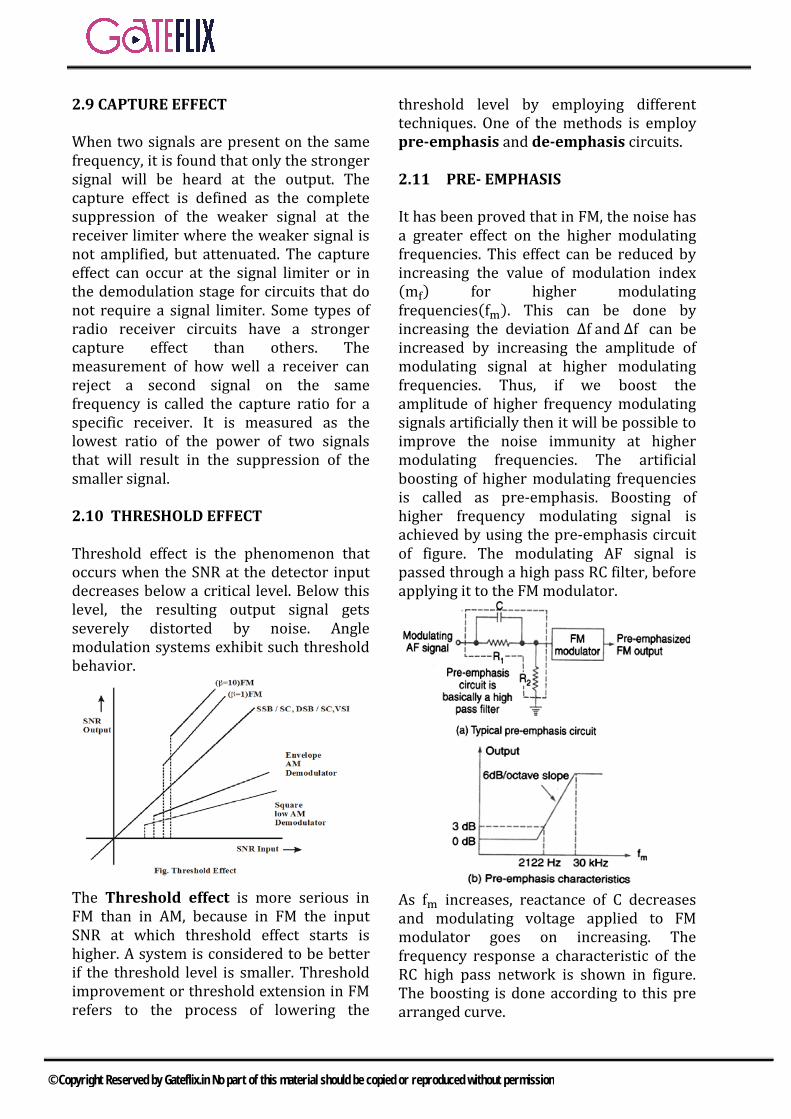
threshold level by employing different techniques. One of the methods is employ pre-emphasis and de-emphasis circuits. 2.11 PRE- EMPHASIS It has been proved that in FM, the noise has a greater effect on the higher modulating frequencies. This effect can be reduced by increasing the value of modulation index (mf) for higher modulating frequencies(fm). This can be done by increasing the deviation ∆f and ∆f can be increased by increasing the amplitude of modulating signal at higher modulating frequencies. Thus, if we boost the amplitude of higher frequency modulating signals artificially then it will be possible to improve the noise immunity at higher modulating frequencies. The artificial boosting of higher modulating frequencies is called as pre-emphasis. Boosting of higher frequency modulating signal is achieved by using the pre-emphasis circuit of figure. The modulating AF signal is passed through a high pass RC filter, before applying it to the FM modulator.
As fm increases, reactance of C decreases and modulating voltage applied to FM modulator goes on increasing. The frequency response a characteristic of the RC high pass network is shown in figure. The boosting is done according to this pre arranged curve.
© Copyright Reserved by Gateflix.in No part of this material should be copied or reproduced without permission
Note: i) The amount of pre emphasis in US FM
transmission and sound transmission in TV has been standardized at 75µsec.
ii) The pre-emphasis is circuit is basically a high pass filter.
iii) The pre emphasis is carried out at the transmitter.
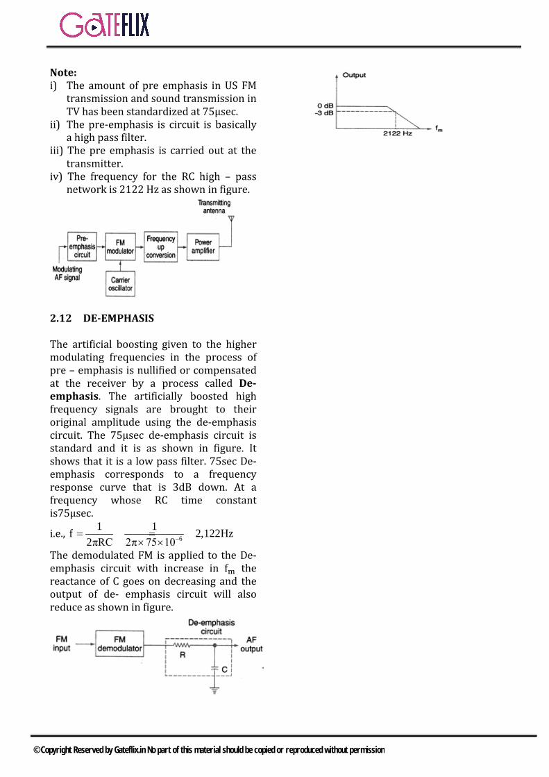
iv) The frequency for the RC high – pass network is 2122 Hz as shown in figure.
2.12 DE-EMPHASIS The artificial boosting given to the higher modulating frequencies in the process of pre – emphasis is nullified or compensated at the receiver by a process called De- emphasis. The artificially boosted high frequency signals are brought to their original amplitude using the de-emphasis circuit. The 75µsec de-emphasis circuit is standard and it is as shown in figure. It shows that it is a low pass filter. 75sec De-emphasis corresponds to a frequency response curve that is 3dB down. At a frequency whose RC time constant is75µsec.
i.e., 6
1 1f 2,122Hz2πRC 2π 75 10−= = =
× ×
The demodulated FM is applied to the De-emphasis circuit with increase in fm the reactance of C goes on decreasing and the output of de- emphasis circuit will also reduce as shown in figure.
© Copyright Reserved by Gateflix.in No part of this material should be copied or reproduced without permission
Q.1 In a FM system, a carrier of 100MHz is modulated by a sinusoidal signal of 5 kHz. The bandwidth by Carson’s approximation is 1MHz. If y(t) = (modulated waveform)3 then by using Carson’s approximation, the bandwidth of 𝑦𝑦(𝑡𝑡) around 300MHz and the spacing of spectral components are respectively. a)3MHz,5kHz b)1MHz,15kHz c) 3MHz, 15kHz d)1 MHz,5 kHz
[GATE-2000]
Q.2 The Hilbert transform of 1 2cos ω t sin ω t+ is
a) 1 2sinω t-cosω t b) 1 2sin ω t cos ω t+c) 1 2cos ω t sin ω t− d) 1 2sin ω t sin ω t+
[GATE-2000]
Q.3 A message m(t) band limited to the frequency fm has a power of Pm The power of the output signal in the figure is.
a) mP cosθ2
b) mP4
c)2
mP sin θ4
d)2
mP cos θ4
[GATE-2000]
Q.4 The amplitude modulated wave form ( ) [ ]C a cs t =A 1+K m(t) cosω t is fedto an ideal envelop detector. The maximum magnitude of Kam(t) is greater than1. Which of the following could be the detector output? a) CA m(t)
b) [ ]22c aA 1 K m(t)+
c) C aA 1 K m(t) +
d) 2C aA 1 K m(t)+
[GATE-2000]
Q.5 A band limited signal is sampled at the Nyquist rate. The signal can be recovered by passing the samples through a) an RC filterb) an envelope detectorc) a PLLd) an ideal low –pass filter with the
appropriate bandwidth[GATE-2001]
Q.6 In the figure m(t) = 2sin 2πtt
( )s t cos 200πt= and n(t) = sin199πtt
The output y(t) will be
a) sin 2πtt
b) sin 2πt sin sin πt cos3πtt t
+
c) sin 2πt sin 0.5sin 0.5πt cos1.5πtt t
+
d) sin 2πt sin sin πt cos 0.75πtt t
+
[GATE-2002]
Q.7 An angle –modulated signal is given by
( )62×10 t+30sin150t+
s t cos2π40cos150t
The maximum frequency and phase deviations of s(t) are
GATE QUESTIONS
© Copyright Reserved by Gateflix.in No part of this material should be copied or reproduced without permission
a) 10.5 kHz, 140π rad b) 6 kHz, 80 π rad
c) 10.5kHz, 1000π rad d) 7.5kHz, 100 π rad
[GATE-2002]
Q.8 A 1 MHz sinusoidal carrier is amplitude modulated by a symmetrical square wave of period 100μsec.Which of the following frequencies will NOT be present in the modulated signal?
a) 990 kHz b) 1010kHz c) 1020 kHz d) 1030 kHz
[GATE-2002]
Common Data for Questions 110 & 111 Let ( ) ( )3m t =cos 4π×10 t be the message
signal & ( ) ( )6c t =5cos 2π×10 t be the
carrier. Q.9 c(t) and m(t) are used to generate
an AM signal. The modulation index of the generated AM signal is 0.5 then the quantity Total sidebands power
Carrier power is
a) 1/2 b) 1/4 c) 1/3 d) 1/8
[GATE-2003]
Q.10 c(t) and m(t) are used to generate an FM signal. If the peak frequency deviation of the generated FM signal is three times the transmission bandwidth of the AM signal, then the coefficient of the term
( )3cos 2π 1008×10 t in the FM signal
(in terms of the Bessel coefficients) is
a) 45J (3) b) 85 J (3)2
c) 85 J (4)2
d) 45J (3)
[GATE-2003]
Q.11 A DSB-SC signal is to be generated with a carrier frequency fc = 1MHz using anon-linear device with the input-output characteristic
30 0 i 1 iV a v a v= + Where a0 and a1 are
constants. The output of the non-linear device can be filtered by an appropriate band –pass filter. Let ( )i i
i c cV A cos 2πf t m(t)= + where m(t) is the message signal .Then the value of i
cf (in MHz) is a) 1.0 b) 0.333 c) 0.5 d) 3.0
[GATE-2003] Q.12 The input to a coherent detector is
DSB-SC signal plus noise. The noise at the detector output is
a) the in-phase component b) the quadrature-component c) zero d) the envelope
[GATE-2003] Q.13 A super heterodyne receiver is to
operate in the frequency range 550 kHz-1650 kHz with the intermediate
frequency of 450 kHz. Let max
min
CRC
=
denote the required capacitance ratio of the local oscillator and I denote the image frequency (in kHz) of the incoming signal. If the receiver is tuned to 700 kHz, then
a) R=4.41, I=1600 b) R=2.10, I =1150 c) R=3.0, I=1600
d) R=9.0, I=1150 [GATE-2003]
Q.14 Choose the correct one from among
the alternative a, b, c, d after matching an item in Group 1 with the most appropriate item is Group 2. Group1
P. Ring modulator
© Copyright Reserved by Gateflix.in No part of this material should be copied or reproduced without permission
Q. VCO R. Foster-Seeley discriminator S. Mixer Group 2 1. Clock recovery 2. Demodulation of FM 3. Frequency conversion 4. Summing the two inputs 5. Generation of FM 6. Generation of DSB-SC a) P-1; Q-3; R-2; S-4
b) P-6; Q-5; R-2; S-3 c) P-6; Q-1; R-3; S-2
d) P-5; Q-6; R-1; S-3 [GATE-2003]
Q.15 Consider a system shown in the
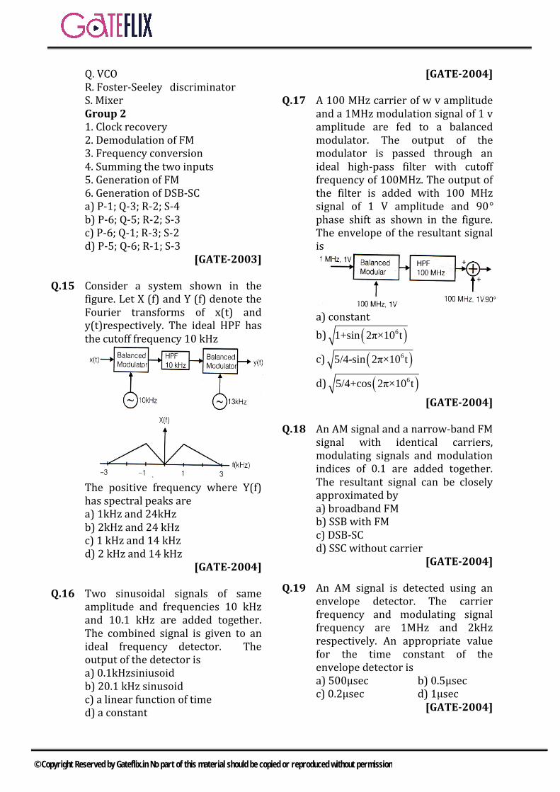
figure. Let X (f) and Y (f) denote the Fourier transforms of x(t) and y(t)respectively. The ideal HPF has the cutoff frequency 10 kHz
The positive frequency where Y(f) has spectral peaks are a) 1kHz and 24kHz
b) 2kHz and 24 kHz c) 1 kHz and 14 kHz
d) 2 kHz and 14 kHz [GATE-2004]
Q.16 Two sinusoidal signals of same
amplitude and frequencies 10 kHz and 10.1 kHz are added together. The combined signal is given to an ideal frequency detector. The output of the detector is
a) 0.1kHzsiniusoid b) 20.1 kHz sinusoid c) a linear function of time d) a constant
[GATE-2004]
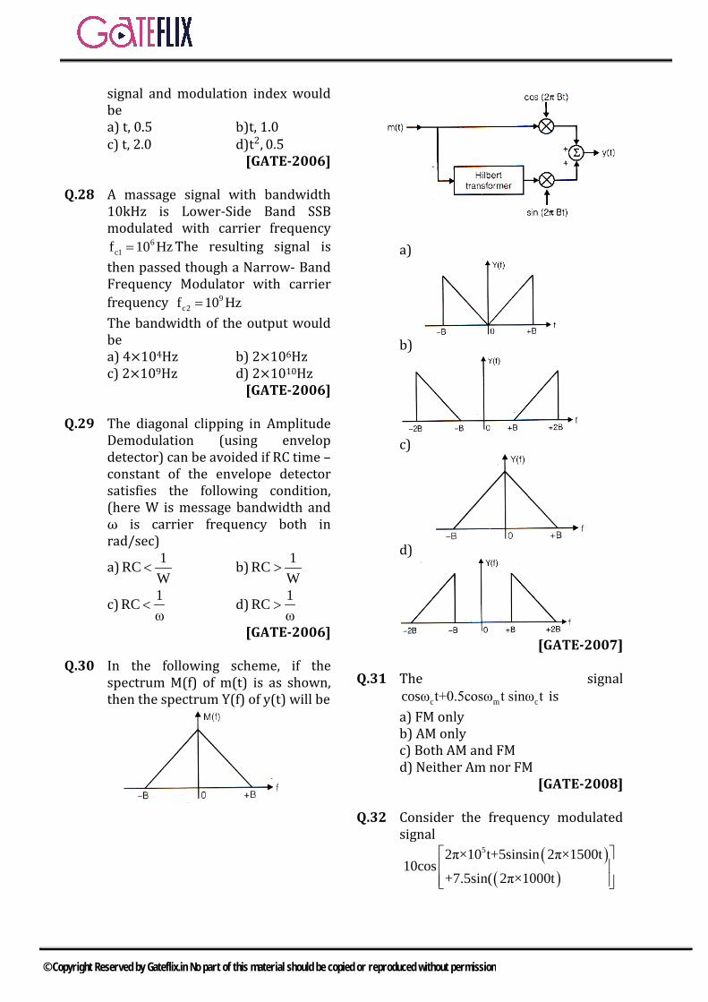
Q.17 A 100 MHz carrier of w v amplitude and a 1MHz modulation signal of 1 v amplitude are fed to a balanced modulator. The output of the modulator is passed through an ideal high-pass filter with cutoff frequency of 100MHz. The output of the filter is added with 100 MHz signal of 1 V amplitude and 90° phase shift as shown in the figure. The envelope of the resultant signal is
a) constant b) ( )61+sin 2π×10 t
c) ( )65/4-sin 2π×10 t
d) ( )65/4+cos 2π×10 t
[GATE-2004]
Q.18 An AM signal and a narrow-band FM signal with identical carriers, modulating signals and modulation indices of 0.1 are added together. The resultant signal can be closely approximated by
a) broadband FM b) SSB with FM c) DSB-SC d) SSC without carrier
[GATE-2004]
Q.19 An AM signal is detected using an envelope detector. The carrier frequency and modulating signal frequency are 1MHz and 2kHz respectively. An appropriate value for the time constant of the envelope detector is
a) 500μsec b) 0.5μsec c) 0.2μsec d) 1μsec
[GATE-2004]
© Copyright Reserved by Gateflix.in No part of this material should be copied or reproduced without permission

Q.20 A carrier is phase modulated (PM) with frequency deviation of 10kHz by a single tone frequency of 1 kHZ. If the single tone frequency is increased to 2kHz, assuming that phase deviation remains unchanged, the bandwidth of the PM signal is
a) 21kHz b) 22kHz c) 42kHz d) 44kHz
[GATE-2005]
Q.21 A device with input x (t) and output y (t) is characterized by 𝑦𝑦(𝑡𝑡) =𝑥𝑥2(𝑡𝑡) An FM signal with frequency deviation of 90 kHz and modulating signal bandwidth of 5 kHz is applied to this device. The bandwidth of the output signal is
a) 370kHz b) 190kHz c) 380 kHz d) 95 kHz
[GATE-2005]
Q.22 Which of the following analog modulation scheme requires the minimum transmitted power and minimum channel bandwidth?
a) VSB b) DSB-SC c) SSB d) AM
[GATE-2005]
Q.23 Find the correct match between group 1 and group 2
Group 1 P. ( ) c1+km t A sin(ω t)
Q. ( ) ckm t A sin(ω t) R. ( ) cA sin ω t+km t
S. ( )t
cA sin ω t k m t dt−∞
+
∫
Group 2 W. Phase modulation
X. Frequency modulation Y. Amplitude modulation Z.DSB-SC modulation a)P-Z,Q-Y,R-X,S-W b)P-W,Q-X,R-Y,S-Z c)P-X,Q-W,R-Z,S-Y d)P-Y,Q-Z,R-W,S-X
[GATE-2005]
Common Data for Questions 24 & 25
Consider the following Amplitude Modulated (AM) signal where
( ) ( )m AM m cf <Bx t =10 1+0.5sin2πf t cos2πf t Q.24 The average side –band power for
the AM signal given above is a) 25 b) 12.5 c) 6.25 d) 3.125
[GATE-2006]
Q.25 The AM signal gets added to a noise with Power Spectral Density nS (f) given in the figure below. The ratio of average sideband power to mean noise power would be:
a)
0
258N B
b)0
254N B
c)0
252N B
d) 0
25N B
[GATE-2006]
Common Data for Questions 26 & 27 Let g(t)=p(t)*p(t) where * denotes convolution & ( ) ( )
xp t u t u(t 1) lim
→∞= − − with u(t) Being the
unit step function Q.26 The impulse response of filter
matched to the signal ( ) ( ) ( )s t =g t -δ t-2 *g(t) is given as:
a) s(1-t) b) -s(1-t) c) -s(t) d) s(t)
[GATE-2006]
Q.27 An Amplitude Modulated signal is given as
( ) ( ) ( )AM cx t =100 p t +0.5g t cosω t in the interval 0 t 1≤ ≤ one set of possible values of the modulating
© Copyright Reserved by Gateflix.in No part of this material should be copied or reproduced without permission
signal and modulation index would be
a) t, 0.5 b)t, 1.0 c) t, 2.0 d)t2, 0.5
[GATE-2006]
Q.28 A massage signal with bandwidth 10kHz is Lower-Side Band SSB modulated with carrier frequency
6c1f 10 Hz= The resulting signal is
then passed though a Narrow- Band Frequency Modulator with carrier frequency 9
c2f 10 Hz= The bandwidth of the output would be a) 4×10⁴Hz b) 2×10⁶Hz c) 2×10⁹Hz d) 2×10¹⁰Hz
[GATE-2006]
Q.29 The diagonal clipping in Amplitude Demodulation (using envelop detector) can be avoided if RC time – constant of the envelope detector satisfies the following condition, (here W is message bandwidth and ω is carrier frequency both in rad/sec)
a) 1RCW
< b) 1RCW
>
c) 1RCω
< d) 1RCω
>
[GATE-2006] Q.30 In the following scheme, if the
spectrum M(f) of m(t) is as shown, then the spectrum Y(f) of y(t) will be
a)
b)
c)
d)
[GATE-2007]
Q.31 The signal c m ccosω t+0.5cosω t sinω t is a) FM only
b) AM only c) Both AM and FM
d) Neither Am nor FM [GATE-2008]
Q.32 Consider the frequency modulated
signal
( )
( )
52π×10 t+5sinsin 2π×1500t10cos
+7.5sin( 2π×1000t
© Copyright Reserved by Gateflix.in No part of this material should be copied or reproduced without permission
With carrier frequency of 105 Hz.The modulation index is
a) 12.5 b) 7.5 c) 10 d) 5
[GATE-2008]
Q.33 Consider the amplitude modulated (AM) signal c c m cA cosω t+2cosω tcosω t. For demodulating the signal using envelope detector, the minimum value of 𝐴𝐴𝑐𝑐 should be
a) 2 b) 1 c) 0.5 d) 0
[GATE-2008]
Q.34 A message signal given by
( ) 1 21 1m t cos ω t sin ω t2 2
= −
is
amplitude- modulated with a carrier of frequency ωc to generate
( ) ( ) cs t =[1+m t ]cosω t What is the power efficiency achieved by this modulation scheme?
a) 8.33% b) 11.11% c) 20% d) 25% [GATE-2009]
Q.35 For a message signal
( ) ( )mm t =cos 2πf t and carrier of frequency fc which of the following represents a single side-band (SSB) signal?
a) ( ) ( )m ccos 2πf t cos 2πf t b) ( )ccos 2πf t
c) ( )c mcos 2π f +f t
d) ( ) ( )m c1+cos 2πf t cos 2πf t [GATE-2009]
Q.36 Consider an angle modulated signal
( ) ( )62π×10 t+2sinsin 8000πtx t =6cos
+4cos(8000πt)
V. The average power of x(t) is
a) 10W b) 18W c) 20W d) 28W
[GATE-2010] Q.37 Suppose that the modulating signal
is ( ) ( )mm t =2cos 2πf t and the carrier signal is ( ) ( )C C cx t =A cos 2πf t.Which one of the following is a conventional AM signal without over- modulation?
a) ( ) ( ) ( )C cx t =A m t cos 2πf t b) ( ) [ ] ( )C cx t =A 1+m(t) cos 2πf t
c) ( ) ( ) ( )cC c c
Ax t =A cos 2πf t + cos 2πf t4
d) ( ) ( ) ( )C m cx t A cos 2πf t cos 2πf t=
( ) ( )C m cA sin 2πf t sin 2πf t+ [GATE-2010]
Q.38 A message signal ( )m t cos 2000πt 4cos 4000πt= +
modulates the carrier c(t)= cos 2πfc t where fc = 1 MHZ to produce an AM signal. For demodulating the generated AM signal using an envelope detector, the time constant RC of the detector, circuit should satisfy
a) 0.5ms<RC<1ms b)1μs=RC<0.5ms c) RC 1μs= d) RC 0.5ms?
[GATE-2011]
Q.39 The List-1 (lists the attributes) and the List – II (lists of the modulation systems.) Match the attribute to the modulation system that best meets it.
List-I A. Power efficient transmission of
signals B. Most bandwidth efficient
transmission of voice signals. C. Simplest receiver structure D. Bandwidth efficient transmission
of signals with significant dc component
List-II 1. Conventional AM 2. FM
© Copyright Reserved by Gateflix.in No part of this material should be copied or reproduced without permission
3. VSB 4. SSB-SC
A B C D a) 4 2 1 3 b) 2 4 1 3 c) 3 2 1 4 d) 2 4 3 1
[GATE-2011] Q.40 The signal m(t) as shown is applied
both to a phase modulator (with 𝑘𝑘𝑝𝑝 as the phase constant) and a frequency modulator with (𝑘𝑘𝑓𝑓 as the frequency constant ) having the same carrier frequency
The ratio kp/kf (in rad/ Hz) for the same maximum phase deviation is
a) 8π b) 4π c) 2π d) π
[GATE-2012]
Q.41 Consider sinusoidal modulation in an AM system. Assuming no over modulation, the modulation index (μ) when the maximum and minimum values of the envelope, respectively, are 3 V & 1 V, is _____.
[GATE-2014]
Q.42. In the figure, M(f) is the Fourier transform of the message signal .m(t) where A = 100 Hz and B = 40 Hz. Given v(t) = cos (2πfct) and w(t) = cos(2π (fc + A) t) , where fc > A The cutoff frequencies of both the filters are fc
The bandwidth of the signal at the output of the modulator (in Hz) is __.
[GATE-2014]
Q.43 A modulated signal is y(t)= m.(t)cos(40000 πt ), where the baseband signal m(t) has frequency components less than 5 kHz only. The minimum required rate (in kHz) at which y(t) should be sampled to recover m(t) is__________.
[GATE-2014] Q.44 Consider an FM signal f(t) = cos[2
πfct +β1 sin 2 πf1t + β2 sin 2 πf2t.] . The maximum deviation of the instantaneous frequency from the carrier frequency fc is a) β1f1+ β2f2 b) β1f2+ β2f1 c) β1+ β2 d) f1+ f2
[GATE-2014] Q.45 In a double side-band (DSB) full
carrier AM transmission system, if the modulation index is doubled, then the ratio of total sideband power to the carrier power increases by a factor of______.
[GATE-2014]
Q.46 Consider the signal ( ) ( ) ( )c cs t =m t cos(2πf t t π+m (2 f) t)
where m(t) denotes the Hilbert transform of m(t) and the bandwidth of m(t) is very small compared to fc . The signal s(t) is a a) high-pass signal b) low-pass signal c) band-pass signal
© Copyright Reserved by Gateflix.in No part of this material should be copied or reproduced without permission

d) double sideband suppressed carrier signal
[GATE-2015]
Q.47 In the system shown in figure (a), m(t) is a low-pass signal with bandwidth W Hz. The frequency response of the band-pass filter H(f) is shown in figure (b). If it is desired that the output signal z(t) = 10x(t), the maximum value of W (in Hz) should be strictly less than ___.
[GATE-2015]
Q.48 A message signal ( ) m mm t = sin(2A πf t)
is used to modulate the phase of a carrier Ac cos(2πfct) to get the modulated signal
( ) ( )c cy t = cos(2 + A πf t m t ). The bandwidth of y(t) a) depends on Am but not on fm b) depends on fm but not on Am c) depends on both Am and fm d) does not depends on Am or fm
[GATE-2015]
Q.49 The block diagram of a frequency synthesizer consisting of a Phase Locked Loop (PLL) and a divide-by-N counter (comprising ÷2, ÷4, ÷8, ÷16 outputs) is sketched below. The synthesizer is excited with a 5 kHz signal (Input 1). The free-running frequency of the PLL is set to20 kHz. Assume that the commutator switch makes contacts repeatedly in the order 1-2-3-4.
The corresponding frequencies synthesized are: a) 10 kHz, 20 kHz, 40 kHz, 80 kHz b) 20 kHz, 40 kHz, 80 kHz, 160 kHz c) 80 kHz, 40 kHz, 20 kHz, 10 kHz d) 160 kHz, 80 kHz, 40 kHz, 20 kHz
[GATE-2016] Q.50 A super heterodyne receiver
operates in the frequency range of 58 MHz – 68MHz. The intermediate frequency f1F and local oscillator frequency fL0 are chosen such that.
lF L0f f≤ It is required that the image frequencies fall outside the 58MHz –68MHz band. The minimum required f1F (in MHz) is _________.
[GATE-2016] Q.51 The amplitude of a sinusoidal
carrier is modulated by a single sinusoid to obtain the amplitude modulated signal s(t) = 5cos1600πt + 20cos1800πt + 5cos2000πt. The value of the modulation index is ___.
[GATE-2016] Q.52 For a super heterodyne receiver, the
intermediate frequency is 15 MHz and the local oscillator frequency is 3.5 GHz. If the frequency of the received signal is greater than the local oscillator frequency, then the image frequency (in MHz) is ____.
[GATE-2016]
© Copyright Reserved by Gateflix.in No part of this material should be copied or reproduced without permission
Q.53 A modulating signal given by ( ) ( )3 3x t 5sin 4 10 t 10 cos 2 10 t V= π − π π is fed
to a phase modulator with phase deviation constant kp = 0.5rad/V. If the carrier frequency is 20 kHz, the instantaneous frequency (in kHz) at t = 0.5 ms is __________ .
[GATE-2017, Set-2]
Q.54 The un-modulated carrier power in an AM transmitter is 5kW. This carrier is modulated by a sinusoidal modulating signal. The maximum percentage of modulation is 50%. If it is reduced to 40%, then the maximum un-modulated carrier power (in kW) that can be used without overloading the transmitter is ___________
[GATE-2017, Set-2]
Q.55 Consider the following amplitude modulated signal: ( ) ( ) ( ) ( )s t cos 2000 t 4cos 2400 t cos 2800 t= π + π + π
The ratio (accurate to three decimal places) of the power of the message signal to the power of the carrier signal is____.
[GATE-2018]
© Copyright Reserved by Gateflix.in No part of this material should be copied or reproduced without permission
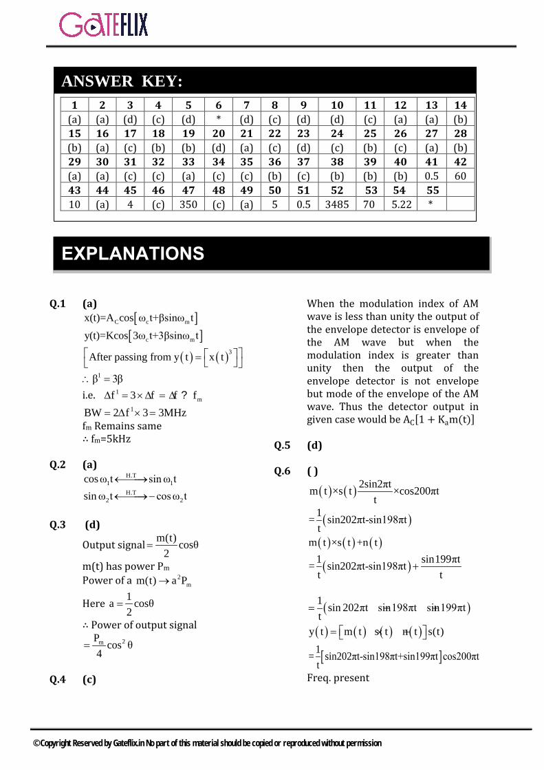
Q.1 (a) [ ]C c mx(t)=A cos ω t+βsinω t
[ ]c my(t)=Kcos 3ω t+3βsinω t
( ) ( )3After passing from y t x t = 1β 3β∴ =
i.e. 1mf 3 f f f∆ = ×∆ = ∆ ?
1BW 2 f 3 3MHz= ∆ × =fm Remains same ∴ fm=5kHz
Q.2 (a) H.T
1 1cos ω t sin ω t←→H.T
2 2sin ω t cos ω t←→−
Q.3 (d)
Output signal m(t) cosθ2
=
m(t) has power Pm
Power of a 2mm(t) a P→
Here 1a cosθ2
=
∴ Power of output signal 2mP cos θ
4=
Q.4 (c)
When the modulation index of AM wave is less than unity the output of the envelope detector is envelope of the AM wave but when the modulation index is greater than unity then the output of the envelope detector is not envelope but mode of the envelope of the AM wave. Thus the detector output in given case would be AC[1 + Kam(t)]
Q.5 (d)
Q.6 ( )
( ) ( ) 2sin2πtm t ×s t ×cos200πtt
( )1= sin202πt-sin198πtt( ) ( ) ( )m t ×s t +n t
( )1 sin199πt= sin202πt-sin198πtt t
+
( )1 sin 202πt sin198πt sin199πtt
= − +
( ) ( ) ( ) ( )y t m t s t n t s(t)= × +
[ ]1= sin202πt-sin198πt+sin199πt cos200πtt
Freq. present
1 2 3 4 5 6 7 8 9 10 11 12 13 14 (a) (a) (d) (c) (d) * (d) (c) (d) (d) (c) (a) (a) (b)15 16 17 18 19 20 21 22 23 24 25 26 27 28 (b) (a) (c) (b) (b) (d) (a) (c) (d) (c) (b) (c) (a) (b) 29 30 31 32 33 34 35 36 37 38 39 40 41 42 (a) (a) (c) (c) (a) (c) (c) (b) (c) (b) (b) (b) 0.5 60 43 44 45 46 47 48 49 50 51 52 53 54 55 10 (a) 4 (c) 350 (c) (a) 5 0.5 3485 70 5.22 *
ANSWER KEY:
EXPLANATIONS
© Copyright Reserved by Gateflix.in No part of this material should be copied or reproduced without permission
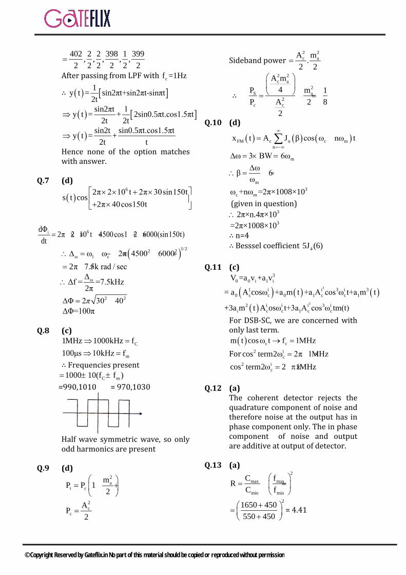
402 2 2 398 1 399, , , , ,2 2 2 2 2 2
=
After passing from LPF with cf =1Hz
∴ ( ) [ ]1y t = sin2πt+sin2πt-sinπt2t
( ) [ ]sin2πt 1y t = + 2sin0.5πt.cos1.5πt2t 2t
⇒
( ) sin2t sin0.5πt.cos1.5πty t = +2t t
⇒
Hence none of the option matches with answer.
Q.7 (d)
( )62π 2 10 t 2π 30sin150t
s t cos2π 40cos150t
× × + × + ×
6idΦ 2π 2 10 t 4500cos1 2 6000(sin150t)
dt= × × + + ×
( )1/22 2
ω 1 cω ω 2π 4500 6000∴∆ = − = +
2π 7.5k rad / sec= ×
ωΔf = =7.5kHz2πΔ
∴
2 2Φ 2 30 40π∆ = + ΔΦ=100π
Q.8 (c) C1MHz 1000kHz f⇒ =
m100μs 10kHz f⇒ = ∴ Frequencies present C m1000 10(f f )= ± ± =990,1010 = 970,1030
Half wave symmetric wave, so only odd harmonics are present
Q.9 (d)
2a
t cmP P 12
= +
2c
cAP2
=
Sideband power 2 2c aA m.
2 2=
∴
2 2c a
2S a
2cc
A m4P m 1
AP 2 82
= = =
Q.10 (d)
( ) ( ) ( )FM c n c mn
x t A J β cos ω nω t∞
=−∞
= +∑
mω 3 BW 6ω∆ = × =
m
ωβ 6ω∆
∴ = =
3c mω +nω =2π×1008×10
(given in question) 32π×n.4π×10∴ 3=2π×1008×10
∴ n=4 ∴ Besssel coefficient 45J (6)
Q.11 (c) 3
0 0 i 1 iV =a v +a v
( ) ( ) ( )31 i i 3 i 30 c c 0 1 c c 1= a A cosω +a m t +a A cos ω t+a m t
( ) 32 i i i 3 ii c c 1 c c+3a m t A osω t+3a A cos ω tm(t)
For DSB-SC, we are concerned with only last term. ( ) c cm t cos ω t f 1MHz→ =
For 2 iccos term2ω 2π 1MHz= ×
2 iccos term2 2 1MHzω = π×
Q.12 (a)
The coherent detector rejects the quadrature component of noise and therefore noise at the output has in phase component only. The in phase component of noise and output are additive at output of detector.
Q.13 (a)
2
max max
min min
C fRC f
= =
21650 450550 450
+ = + = 4.41
© Copyright Reserved by Gateflix.in No part of this material should be copied or reproduced without permission
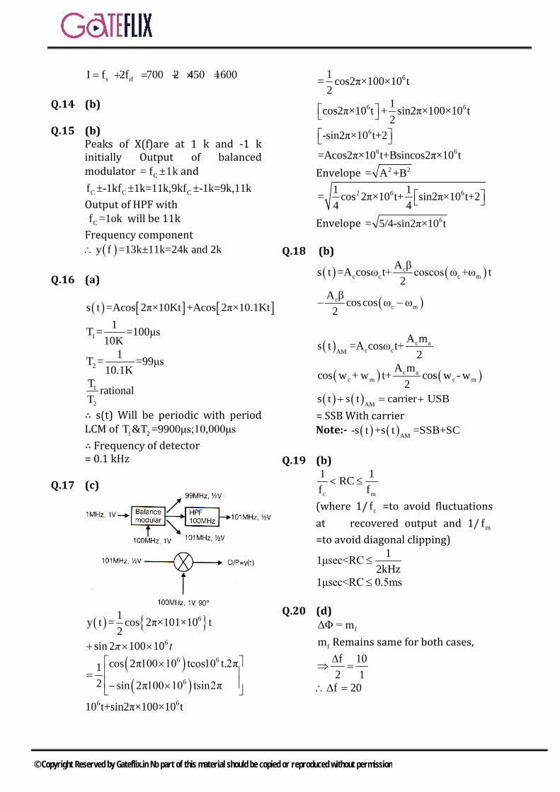
s ifI f 2f 700 2 450 1600= + = + × = Q.14 (b) Q.15 (b)
Peaks of X(f)are at 1 k and -1 k initially Output of balanced modulator C= f ±1k and
C C Cf ±-1kf ±1k=11k,9kf ±-1k=9k,11k Output of HPF with Cf =1ok will be 11k Frequency component
( )y f =13k±11k=24k and 2k∴ Q.16 (a)
( ) [ ] [ ]s t =Acos 2π×10Kt +Acos 2π×10.1Kt
11T = =100μs
10K
21T = =99μs
10.1K
1
2
T rationalT
∴ s(t) Will be periodic with period LCM of 1 2T &T =9900μs;10,000μs ∴ Frequency of detector = 0.1 kHz
Q.17 (c)
( ) 61y t = cos 2π×101×10 t2
6sin 2 100 10+ × ×π t
( )( )
6 6
6
cos 2π100 10 tcos10 t.2π12 sin 2π100 10 tsin2π
× = − ×
6 610 t+sin2π×100×10 t
61= cos2π×100×10 t2
6 61cos2π×10 t + sin2π×100×10 t2
6-sin2π×10 t+2 6 6=Acos2π×10 t+Bsincos2π×10 t
Envelope 2 2= A +B 2 6 61 1= cos 2π×10 t+ sin2π×10 t+2
4 4
Envelope 6= 5/4-sin2π×10 t Q.18 (b)
( ) ( )
( )
cc c c m
cc m
A βs t =A cosω t+ coscos ω +ω t2
A β cos cos ω ω2
− −
( ) c ac cAM
A ms t =A cosω t+2
( ) ( )c ac m c m
A mcos w + w t+ cos w - w2
( ) ( )AMs t s t carrier USB+ = + = SSB With carrier Note:- ( ) ( )AM
-s t +s t =SSB+SC Q.19 (b)
c m
1 1RCf f< ≤
(where 1/ cf =to avoid fluctuations at recovered output and 1/ mf=to avoid diagonal clipping)
11μsec<RC2kHz
≤
1μsec<RC 0.5ms≤
Q.20 (d) fΔΦ = m
fm Remains same for both cases, f 10
2 1∆
⇒ =
f 20∴∆ =
© Copyright Reserved by Gateflix.in No part of this material should be copied or reproduced without permission
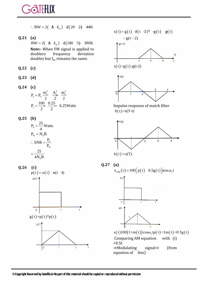
( ) ( )mBW 2 f f 2 20 2 44K∴ = ∆ + = + =
Q.21 (a)
( ) ( )mBW 2 f f 2 180 5 370K= ∆ + = + =
Note:- When FM signal is applied to doublers frequency deviation doubles but fm remains the same.
Q.22 (c) Q.23 (d) Q.24 (c)
2 2 2a c a
s Cm A mP P2 2 2
= = ×
s100 0.25P 6.25Watts
2 2= × =
Q.25 (b)
S25P Watts4
=
N 0P N B=
S
N
PSNRP
∴ =
0
254N B
=
Q.26 (c)
( ) ( )p t u t u(t 1)= − −
( ) ( ) ( )g t =p t *p t
( ) ( ) ( ) ( ) ( )s t g t δ t 2 * g t g t
g(t 2)= − − = =
− −
( ) ( )s t =g t -g(t-2)
Impulse response of match filter ( )h t =s(T-t)
( )h t =-s(T)
Q.27 (a)
( ) ( ) ( )AM cx t 100 p t 0.5g t cos ω t= +
( ) ( )( ) ( ) ( ) ( )cs t 100 1+m t cosω tp t =1m t =0.5g t
Comparing AM equation with (i) =0.5t ⇒Modulating signal=t (from equation of line)
© Copyright Reserved by Gateflix.in No part of this material should be copied or reproduced without permission
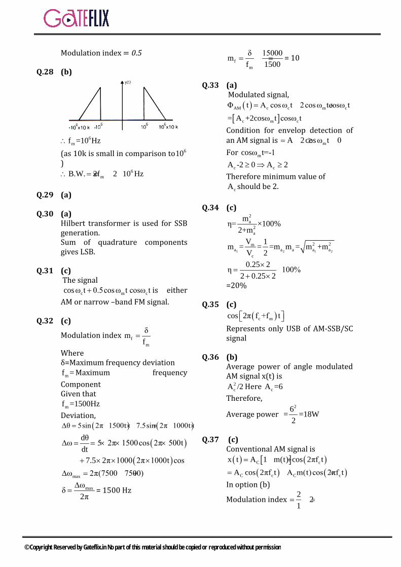
Modulation index = 0.5 Q.28 (b)
6
mf =10 Hz∴ (as 10k is small in comparison to 610)
6mB.W. 2f 2 10 Hz∴ = = ×
Q.29 (a) Q.30 (a)
Hilbert transformer is used for SSB generation. Sum of quadrature components gives LSB.
Q.31 (c) The signal c m ccos ω t 0.5cos ω t cosω t+ is either AM or narrow –band FM signal.
Q.32 (c)
Modulation index fm
δmf
=
Where δ=Maximum frequency deviation
mf = Maximum frequency Component Given that
mf =1500Hz Deviation,
( ) ( )θ 5sin 2π 1500t 7.5sin 2π 1000t∆ = × + ×
( )
( )
dθω 5 2π 1500cos 2π 500tdt
7.5 2π 1000 2π 1000t cos
∆ = = × × ×
+ × × ×
maxω 2π(7500 7500)∆ = +
maxωδ2π
∆= = 1500 Hz
fm
δ 15000mf 1500
= = = 10
Q.33 (a) Modulated signal,
( )AM c c m cΦ t A cos ω t 2cos ω tcosω t= +
[ ]c m c= A +2cosω t cosω t Condition for envelop detection of an AM signal is mA 2cos ω t 0= + ≥ For mcosω t=-1
c cA -2 0 A 2≥ ⇒ ≥ Therefore minimum value of
cA should be 2.
Q.34 (c) 2a
2a
mη= ×100%2+m
1 2 1 2
2 2ma a a a a
c
V 1m = = =m m = m +mV 2
0.25 2η 100%2 0.25 2
×= ×
+ ×
=20%
Q.35 (c) ( )c mcos 2π f +f t
Represents only USB of AM-SSB/SC signal
Q.36 (b) Average power of angle modulated AM signal x(t) is
2cA /2 Here cA =6
Therefore,
Average power 26= =18W
2
Q.37 (c)
Conventional AM signal is ( ) [ ] ( )C cx t A 1 m(t) cos 2πf t= +
( ) ( )C c C cA cos 2πf t A m(t)cos 2πf t= + In option (b)
Modulation index 2 21
= =
© Copyright Reserved by Gateflix.in No part of this material should be copied or reproduced without permission

So, it is conventional AM signal but with over-modulation. In options (c)
( ) ( ) ( )cC c c
Ax t A cos 2πf t cos 2πf t4
= +
Here, Modulation index 2 14 2
= =
Therefore, it is conventional AM signal without over-modulation.
Q.38 (b)
c m
1 1RCf f
= =
I 1RC1MHz 2kHz
= =
⇒ 1μs ≪ RC ≪ 0.5ms Q.39 (b)
AM has simple receiver and VSB is bandwidth efficient transmission of signals with significant dc component. SSB–SC is the most bandwidth efficient transmission of voice signals.
Q.40 (b) For phase modulator ( ) c pΦ t =2πf t+k m(t) Maximum phase deviation is ( ) ( )D p pmax
Φ =k maxmax m t =2k (1) For frequency modulator
( ) ( )c
t
0fΦ t =2πf t+2πk m t dt∫
( ) ( )t
D fmax0 max
Φ' =2πk t m t dt ∫
( )2
D fmax0
Φ' =2πk 2dt ∫
( )D fmaxΦ' =8πk (2)
Given ( ) ( )D Dmax max
Φ' Φ= f p8πk =2k
p
f
k=4π
k
Q.41 0.5
max min
max min
A(t) -A(t)μ=A(t) +A(t)
3-1 1μ= = =0.53+1 2
Q.42 60
Exp: m(t) ↔M(f)
After multiplication with V(t) =cos (2πfct) Let ( ) ( )1w t =m t .V(t)
( ) ( )( )1 1W f specturm of w t is⇒
After high pass filter
After multiplication with
( )c(2π fcos +A t) and low pass filter of cut off 𝑓𝑓𝑐𝑐
Band width =A-B =100-40=60 Q.43 (10)
Since m(t) is a base band signal with maximum frequency 5 KHz, assumed spreads as follows:
© Copyright Reserved by Gateflix.in No part of this material should be copied or reproduced without permission

∴y(t) = m(t) cos(40000πt)
( ) ( )7 f -20k f 201( k*f )2
m +→ δ +δ
y(f) = 12
[M(f ‒ 20k) + M(f+ 20k)]
Thus the spectrum of the modulated signal is as follows:
If y(t) is sampled with a sampling frequency `fs’ then the resultant signal is a periodic extension of successive replica of y(f) with a period ‘fs'. It is observed that 10 KHz and 20 KHz are the two sampling frequencies which causes a replica of M(f) which can be filtered out by a LPF. Thus the minimum sampling frequency (fs) which extracts m(t) from g(f) is 10 KHz.
Q.44 A
Exp: Instantaneous phase( )1 c 1 1 2 2f t =2πf t+β sin2πf +β sin2πf t
Instantaneous frequency fi(t) =
1d 1(t)×dt 2πφ
c 1 1 1 2 2 2=f +β f cos2πf t+β f 2os πfc tInstantaneous frequency deviation
1 1 1 2 2 2=β f cos2πf t+β f 2os πfc t Maximum 1 1 2 2Δf = β f +β f
Q.45 4
2Ratio of total side band power αμCarrier power
If it in doubled, this ratio will be come 4 time
Q.46 (C) Given s(t) is the equation for single side band modulation (lower side band). Thus it is a Band pass signal.
Q.47 350 x(t) = m(t).cos(2400𝜋𝜋𝜋𝜋) Spectrum of x(t)
Y(t) =10x(t) + 2x (t) Let us drawn the spectrum of positive frequencies of y(t) Y(t)=10m(t)
( ) 2 2cos 2400πt m (t)cos (2400πt) =10m(t)
( ) 2 1+cos4800πtcos 2400πt +m (t)2
Y(t)
( ) ( )2 2m (t) m (t)= + cos 2400πt + cos(4800πt)2 2
10m t
⇒2w <700
2400-2w>1700 ⇒w<350
Q.48 (C)
© Copyright Reserved by Gateflix.in No part of this material should be copied or reproduced without permission
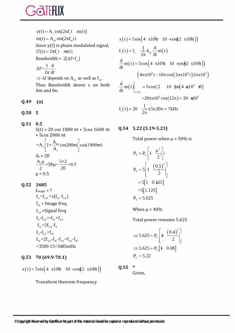
c cy(t) A cos[2πf t m(t)]= + m mm(t) A sin(2πf t)=
Since y(t) is phase modulated signal, c(t) 2πf t m(t)∅ = +
Bandwidth = n2[Δf+f ] 1 dΔf= m(t)
2π dtm mΔ f depends on A as well as f .⇒
Thus Bandwidth deeen s on both Am and fm.
Q.49 (a) Q.50 5 Q.51 0.5
S(t) = 20 cos 1800 πt + 5cos 1600 πt + 5cos 2000 πt
mc
c
A=A 1+ cos200πt cos(1800πt)A
Ac = 20 cA μ 5×2=5Þμ= =0.52 20
μ = 0.5
Q.52 3485 fimage = ?
S LO Si L0f f =±(f -f= )
Sif = Image freq
L0f =Signal freq S L0 Si L0f -f =-f +f
Si L0 Sf =2f -f S L0 IFf -f =f
Si L0 IF L0 L0 IFf =2f -f -f =f -f=3500-15=3485mHz
Q.53 70 (69.9-70.1)
( ) ( )( )3 3x t 5sin 4 x10 t 10 cos 2 x10 t= π − π π
Transform theorem frequency
( ) ( )( )( ) ( )
( ) ( )( )( )( )
( ) ( ) ( )( )
( )
3 3
i c p
3 3
3 3 3
3
t 0.53 3
i
x t 5sin 4 x10 t 10 cos 2 x10 t
1 df t f k . m t2 dt
d m t 5cos 4 x10 t 10 cos 2 x10 tdt 4 x10 t 10 cos 2 x10 t 2 x10
d m t 5cos 2 10 x 4 x10 0dt =20 x10 cos 12 20 x10
1f t 202
=
= π − π π
= +π
= π − π π
π − π π π
= π+ π π +
π π = π
= +π
x5x20 7kHzπ =
Q.54 5.22 (5.19-5.23)
Total power when µ = 50% is
( )
[ ][ ]
2
T C
2
T
T
P P 12
0.5P 5 1
2
5 1 0.125
=5 1.125P 5.625
µ= +
= +
= +
=
When µ = 40%
Total power remains 5.625
( )
[ ]
2
C
C
C
0.45.625 P 1
2
5.625 P 1 0.08P 5.22
⇒ = +
⇒ = +
=
Q.55 * Given,
© Copyright Reserved by Gateflix.in No part of this material should be copied or reproduced without permission
( ) ( ) ( ) ( )
( ) ( ) ( )
( ) ( )
cos 2000 t 4cos 2400 t cos 2800 ts t
side band carrier side band4cos 2400 t 2cos 400 t cos 2400 t
14 1 cos 400 t cos 2400 t2
π π π= + +
= π + π π
= + π π Now at this point, some data is missing, if we compare this with standard AM signal equation
( ) ( ) ( )( ) ( )
( ) ( )
( ) ( )
c a
a
a
a
s t A 1 k m t cos 2400 t
if k =1/2, m t cos 400 t , PM 1/ 21if k =1, m t cos 400 t , PM=1/821if k =2, m t cos 400 t , PM=1/324
= + π = π =
= π
= π
Like this infinite possibilities exist Hence many answers are possible.
© Copyright Reserved by Gateflix.in No part of this material should be copied or reproduced without permission

3.1 RADIO RECEIVER
In radio communications, a radio receiver is an electronic device that receives radio waves and converts the information carried by them to a usable form. It is used with an antenna. The antenna intercepts radio waves (electromagnetic waves) and converts them to tiny alternating currents which are applied to the receiver, and the receiver extracts the desired information. The receiver uses electronic filters to separate the desired radio frequency signal from all the other signals picked up by the antenna, an electronic amplifier to increase the power of the signal for further processing, and finally recovers the desired information through demodulation.
3.1.1 CLASSIFICATION OF RADIO RECEIVERS
1) Depending upon the application, theradio receivers may be classified asfollows:
i) Amplitude Modulation (A.M.)Broadcast Receivers:These receivers are used to receive thebroadcast of speech or musictransmitted from amplitude modulationbroadcast transmitters which operateon long wave, medium wave or shortwave bands.
ii) Frequency Modulation (F.M)iii) Broadcast Receivers:
These receivers are used to receive thebroadcast programs from F.M. broadcast transmitters which operatein VHF or UHF bands
iv) Communication Receivers:
Communication receivers are used for reception of telegraph and short telephone signals. This means that communication receivers are used for various purposes other than broadcast services.
v) Television Receivers:Television receivers are used to receivetelevision broadcast in VHF or in UHFbands.
vi) Radar receivers:Radar receivers are used to receiveradar (i.e., Radio detection and ranging)signals.
2) Depending upon the fundamentalaspects, the radio receivers may also beclassified as under:
vii) Tuned Radio Frequency (TRF)Receivers
viii) Super heterodyne Receivers
In fact, various forms of receivers have been proposed from time to time. However, only two of them became popular for commercial applications. These are Tuned Radio frequency (TRF) receiver and super heterodyne receiver. Presently, the super heterodyne receiver is the most popular and most widely used. The TRF receiver was used earlier in the 1940s. The TRF receiver had some inherent drawbacks which were removed in super heterodyne receiver. Therefore, we shall start our discussion with TRF receiver and then come to the super heterodyne receiver.
3 RADIO RECEIVER
© Copyright Reserved by Gateflix.in No part of this material should be copied or reproduced without permission
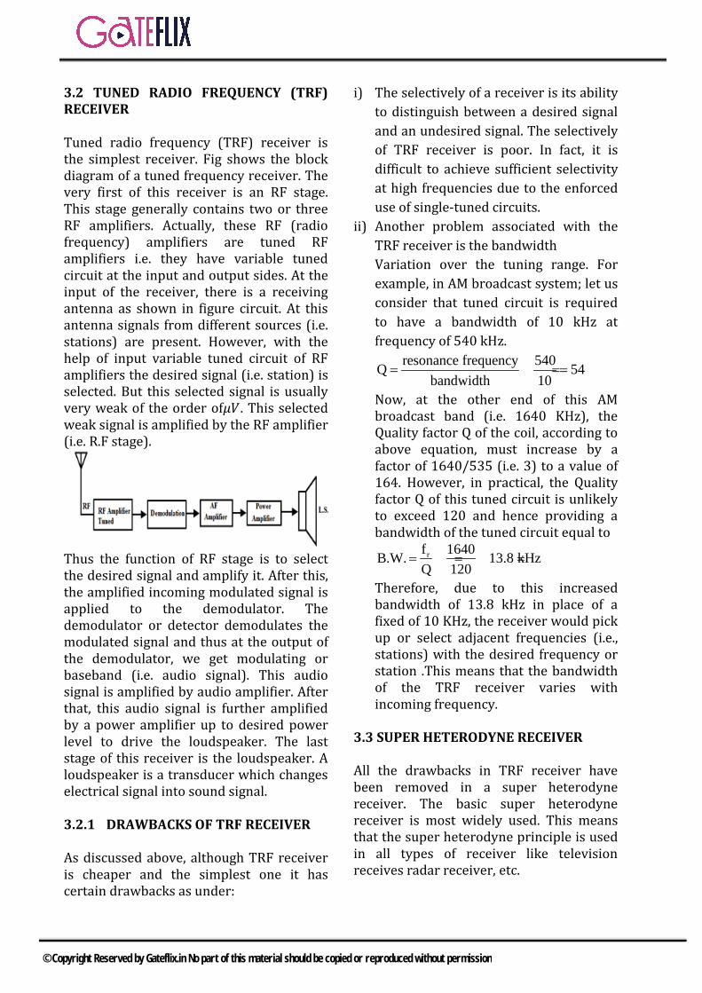
3.2 TUNED RADIO FREQUENCY (TRF) RECEIVER Tuned radio frequency (TRF) receiver is the simplest receiver. Fig shows the block diagram of a tuned frequency receiver. The very first of this receiver is an RF stage. This stage generally contains two or three RF amplifiers. Actually, these RF (radio frequency) amplifiers are tuned RF amplifiers i.e. they have variable tuned circuit at the input and output sides. At the input of the receiver, there is a receiving antenna as shown in figure circuit. At this antenna signals from different sources (i.e. stations) are present. However, with the help of input variable tuned circuit of RF amplifiers the desired signal (i.e. station) is selected. But this selected signal is usually very weak of the order of𝜇𝜇𝑉𝑉. This selected weak signal is amplified by the RF amplifier (i.e. R.F stage).
Thus the function of RF stage is to select the desired signal and amplify it. After this, the amplified incoming modulated signal is applied to the demodulator. The demodulator or detector demodulates the modulated signal and thus at the output of the demodulator, we get modulating or baseband (i.e. audio signal). This audio signal is amplified by audio amplifier. After that, this audio signal is further amplified by a power amplifier up to desired power level to drive the loudspeaker. The last stage of this receiver is the loudspeaker. A loudspeaker is a transducer which changes electrical signal into sound signal. 3.2.1 DRAWBACKS OF TRF RECEIVER As discussed above, although TRF receiver is cheaper and the simplest one it has certain drawbacks as under:
i) The selectively of a receiver is its ability to distinguish between a desired signal and an undesired signal. The selectively of TRF receiver is poor. In fact, it is difficult to achieve sufficient selectivity at high frequencies due to the enforced use of single-tuned circuits.
ii) Another problem associated with the TRF receiver is the bandwidth
Variation over the tuning range. For example, in AM broadcast system; let us consider that tuned circuit is required to have a bandwidth of 10 kHz at frequency of 540 kHz.
resonance frequency 540Q 54bandwidth 10
= = =
Now, at the other end of this AM broadcast band (i.e. 1640 KHz), the Quality factor Q of the coil, according to above equation, must increase by a factor of 1640/535 (i.e. 3) to a value of 164. However, in practical, the Quality factor Q of this tuned circuit is unlikely to exceed 120 and hence providing a bandwidth of the tuned circuit equal to
rf 1640B.W. 13.8 kHz
Q 120= = =
Therefore, due to this increased bandwidth of 13.8 kHz in place of a fixed of 10 KHz, the receiver would pick up or select adjacent frequencies (i.e., stations) with the desired frequency or station .This means that the bandwidth of the TRF receiver varies with incoming frequency.
3.3 SUPER HETERODYNE RECEIVER All the drawbacks in TRF receiver have been removed in a super heterodyne receiver. The basic super heterodyne receiver is most widely used. This means that the super heterodyne principle is used in all types of receiver like television receives radar receiver, etc.
© Copyright Reserved by Gateflix.in No part of this material should be copied or reproduced without permission
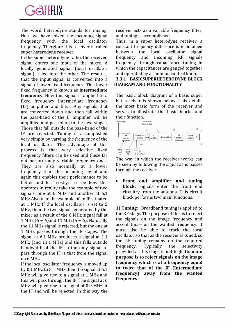
The word heterodyne stands for mixing. Here we have mixed the incoming signal frequency with the local oscillator frequency. Therefore this receiver is called super heterodyne receiver. In the super heterodyne radio, the received signal enters one input of the mixer. A locally generated signal (local oscillator signal) is fed into the other. The result is that the input signal is converted into a signal of lower fixed frequency. This lower fixed frequency is known as intermediate frequency. Now this signal is applied to a fixed frequency intermediate frequency (IF) amplifier and filter. Any signals that are converted down and then fall within the pass-band of the IF amplifier will be amplified and passed on to the next stages. Those that fall outside the pass-band of the IF are rejected. Tuning is accomplished very simply by varying the frequency of the local oscillator. The advantage of this process is that very selective fixed frequency filters can be used and these far out perform any variable frequency ones. They are also normally at a lower frequency than the incoming signal and again this enables their performance to be better and less costly. To see how this operates in reality take the example of two signals, one at 6 MHz and another at 6.1 MHz Also take the example of an IF situated at 1 MHz If the local oscillator is set to 5 MHz, then the two signals generated by the mixer as a result of the 6 MHz signal fall at 1 MHz (6 − 5)and 11 MHz(6 + 5). Naturally the 11 MHz signal is rejected, but the one at 1 MHz passes through the IF stages. The signal at 6.1 MHz produces a signal at 1.1 MHz (and 11.1 MHz) and this falls outside bandwidth of the IF so the only signal to pass through the IF is that from the signal on 6 MHz If the local oscillator frequency is moved up by 0.1 MHz to 5.1 MHz then the signal at 6.1 MHz will give rise to a signal at 1 MHz and this will pass through the IF. The signal at 6 MHz will give rise to a signal of 0.9 MHz at the IF and will be rejected. In this way the
receiver acts as a variable frequency filter, and tuning is accomplished. Thus, in a super heterodyne receiver, a constant frequency difference is maintained between the local oscillator signal frequency and incoming RF signals frequency through capacitance tuning in which the capacitances are ganged together and operated by a common control knob. 3.3.1 BASICSUPERHETERODYNE BLOCK
DIAGRAM AND FUNCTIONALITY The basic block diagram of a basic super het receiver is shown below. This details the most basic form of the receiver and serves to illustrate the basic blocks and their function.
The way in which the receiver works can be seen by following the signal as is passes through the receiver. • Front end amplifier and tuning
block: Signals enter the front end circuitry from the antenna. This circuit block performs two main functions:
1) Tuning: Broadband tuning is applied to the RF stage. The purpose of this is to reject the signals on the image frequency and accept those on the wanted frequency. It must also be able to track the local oscillator so that as the receiver is tuned, so the RF tuning remains on the required frequency. Typically the selectivity provided at this stage is not high. Its main purpose is to reject signals on the image frequency which is at a frequency equal to twice that of the IF (Intermediate frequency) away from the wanted frequency.
© Copyright Reserved by Gateflix.in No part of this material should be copied or reproduced without permission
2) Amplification: In terms of amplification, the level is carefully chosen so that it does not overload the mixer when strong signals are present, but enables the signals to be amplified sufficiently to ensure a good signal to noise ratio is achieved. The amplifier must also be a low noise design. Any noise introduced in this block will be amplified later in the receiver. • Mixer/ frequency translator
block: The tuned and amplified signal then enters one port of the mixer. The local oscillator signal enters the other port. The performance of the mixer is crucial to many elements of the overall receiver performance. It should be as linear as possible. If not, then spurious signals will be generated and these may appear as 'phantom' received signals.
• Local oscillator: The local oscillator may consist of a variable frequency oscillator that can be tuned by altering the setting on a variable capacitor. Alternatively it may be a frequency synthesizer that will enable greater levels of stability and setting accuracy.
• Intermediate frequency amplifier, IF block: Once the signals leave the mixer they enter the IF stages. These stages contain most of the amplification in the receiver as well as the filtering that enables signals on one frequency to be separated from those on the next. Filters may consist simply of LC tuned transformers providing inter-stage coupling, or they may be much higher performance ceramic or even crystal filters, dependent upon what is required. The IF amplifier provides most of the gain (i.e. sensitivity and bandwidth requirements (i.e. selectivity) of the receiver. This means that the IF amplifier determines the sensitivity and selectivity of the super heterodyne receiver. Also, since the characteristics of the IF amplifier are independent of the incoming frequency to which the receiver is tuned, the
selectivity and sensitivity of the super heterodyne receiver are quite uniform throughout its tuning range and not subject to the variations like a TRF receiver.
• Detector / demodulator stage: Once the signals have passed through the IF stages of the super heterodyne receiver, they need to be demodulated. Different demodulators are required for different types of transmission, and as a result some receivers may have a variety of demodulators that can be switched in to accommodate the different types of transmission that are to be encountered.
• Audio amplifier: The output from the demodulator is the recovered audio. This is passed into the audio stages where they are amplified and presented to the headphones or loudspeaker
3.3.2 ADVANTAGE OF SUPER HETERODYNING i) No variation in bandwidth. The BW remains constant over the entire operating range. ii) High sensitivity and selectivity. iii) High adjacent channel rejection. 3.3.3 FREQUENCY PARAMETERS OF AM RECEIVER The AM receiver has the following frequency parameters: i) RF carrier range: 535 kHz to 1605 kHz ii) Intermediate frequency IF: 455 kHz iii) Modulating signal bandwidth: 5 kHz iv) IF bandwidth: 10 kHz 3.3.4 FREQUENCY PARAMETERS OF FM RECEIVER The FM receiver has the following frequency parameters: i) RF carrier range: 88 MHz to 108MHz ii) Intermediate frequency IF: 10MHz iii) Modulating signal bandwidth: 15 kHz iv) IF bandwidth: 200 kHz
© Copyright Reserved by Gateflix.in No part of this material should be copied or reproduced without permission
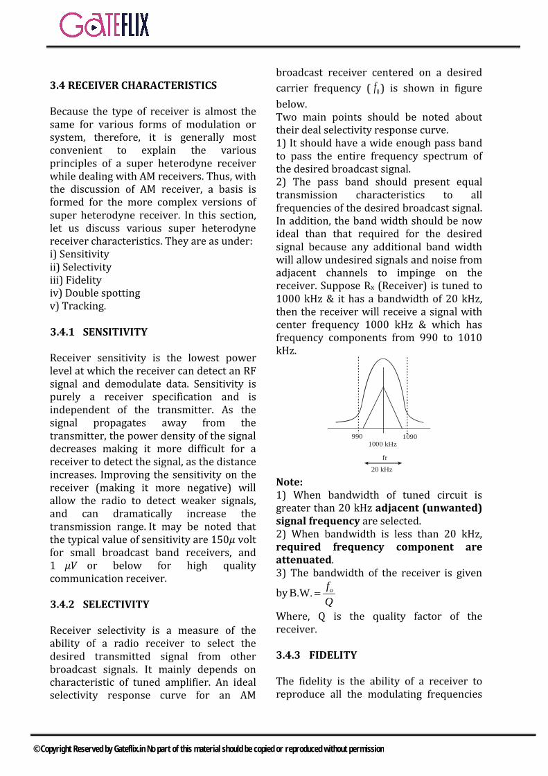
3.4 RECEIVER CHARACTERISTICS Because the type of receiver is almost the same for various forms of modulation or system, therefore, it is generally most convenient to explain the various principles of a super heterodyne receiver while dealing with AM receivers. Thus, with the discussion of AM receiver, a basis is formed for the more complex versions of super heterodyne receiver. In this section, let us discuss various super heterodyne receiver characteristics. They are as under: i) Sensitivity ii) Selectivity iii) Fidelity iv) Double spotting v) Tracking. 3.4.1 SENSITIVITY Receiver sensitivity is the lowest power level at which the receiver can detect an RF signal and demodulate data. Sensitivity is purely a receiver specification and is independent of the transmitter. As the signal propagates away from the transmitter, the power density of the signal decreases making it more difficult for a receiver to detect the signal, as the distance increases. Improving the sensitivity on the receiver (making it more negative) will allow the radio to detect weaker signals, and can dramatically increase the transmission range. It may be noted that the typical value of sensitivity are 150𝜇𝜇 volt for small broadcast band receivers, and 1 𝜇𝜇𝑉𝑉 or below for high quality communication receiver. 3.4.2 SELECTIVITY Receiver selectivity is a measure of the ability of a radio receiver to select the desired transmitted signal from other broadcast signals. It mainly depends on characteristic of tuned amplifier. An ideal selectivity response curve for an AM
broadcast receiver centered on a desired carrier frequency ( 0f ) is shown in figure below. Two main points should be noted about their deal selectivity response curve. 1) It should have a wide enough pass band to pass the entire frequency spectrum of the desired broadcast signal. 2) The pass band should present equal transmission characteristics to all frequencies of the desired broadcast signal. In addition, the band width should be now ideal than that required for the desired signal because any additional band width will allow undesired signals and noise from adjacent channels to impinge on the receiver. Suppose Rx (Receiver) is tuned to 1000 kHz & it has a bandwidth of 20 kHz, then the receiver will receive a signal with center frequency 1000 kHz & which has frequency components from 990 to 1010 kHz.
990 10901000 kHz
fr
20 kHz Note: 1) When bandwidth of tuned circuit is greater than 20 kHz adjacent (unwanted) signal frequency are selected. 2) When bandwidth is less than 20 kHz, required frequency component are attenuated. 3) The bandwidth of the receiver is given
by B.W. = ofQ
Where, Q is the quality factor of the receiver. 3.4.3 FIDELITY The fidelity is the ability of a receiver to reproduce all the modulating frequencies
© Copyright Reserved by Gateflix.in No part of this material should be copied or reproduced without permission
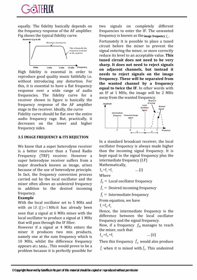
equally. The fidelity basically depends on the frequency response of the AF amplifier. Fig shows the typical fidelity curve.
High fidelity is essential in order to reproduce good quality music faithfully i.e. without introducing any distortion. For this, it is essential to have a flat frequency response over a wide range of audio frequencies. The fidelity curve for a receiver shown in figure is basically the frequency response of the AF amplifier stage in the receiver. Ideally, the curve Fidelity curve should be flat over the entire audio frequency rage. But, practically, it decreases on the lower and higher frequency sides. 3.5 IMAGE FREQUENCY & ITS REJECTION We know that a super heterodyne receiver is a better receiver than a Tuned Radio Frequency (TRF) receiver. However a super heterodyne receiver suffers from a major drawback known as image, arises because of the use of heterodyne principle. In fact, the frequency conversion process carried out by the local oscillator and the mixer often allows an undesired frequency in addition to the desired incoming frequency. Example With the local oscillator set to 5 MHz and with an I.F. ( ) 1 MHzif = it has already been seen that a signal at 6 MHz mixes with the local oscillator to produce a signal at 1 MHz that will pass through the IF filter. However if a signal at 4 MHz enters the mixer it produces two mix products, namely one at the sum frequency which is 10 MHz, whilst the difference frequency appears at1 MHz . This would prove to be a problem because it is perfectly possible for
two signals on completely different frequencies to enter the IF. The unwanted frequency is known as the sifimage frequency . Fortunately it is possible to place a tuned circuit before the mixer to prevent the signal entering the mixer, or more correctly reduce its level to an acceptable value. This tuned circuit does not need to be very sharp. It does not need to reject signals on adjacent channels, but instead it needs to reject signals on the image frequency. These will be separated from the wanted channel by a frequency equal to twice the IF. In other words with an IF at 1 MHz, the image will be 2 MHz away from the wanted frequency.
In a standard broadcast receiver, the local oscillator frequency is always made higher than the incoming signal frequency. It is kept equal to the signal frequency plus the intermediate frequency (I.F) Mathematically,
0 s if =f +f … (i) Where
0f = Local oscillator frequency
sf = Desired incoming frequency
if = Intermediate frequency From equation, we have
i 0 sf =f -f Hence, the intermediate frequency is the difference between the local oscillator frequency and the signal frequency. Now, if a frequency 𝑓𝑓𝑠𝑠𝑠𝑠 manages to reach the mixer, such that
si 0 if =f +f … (ii)
Then this frequency sif would also produce
if when it is mixed with 0f . This undesired
© Copyright Reserved by Gateflix.in No part of this material should be copied or reproduced without permission
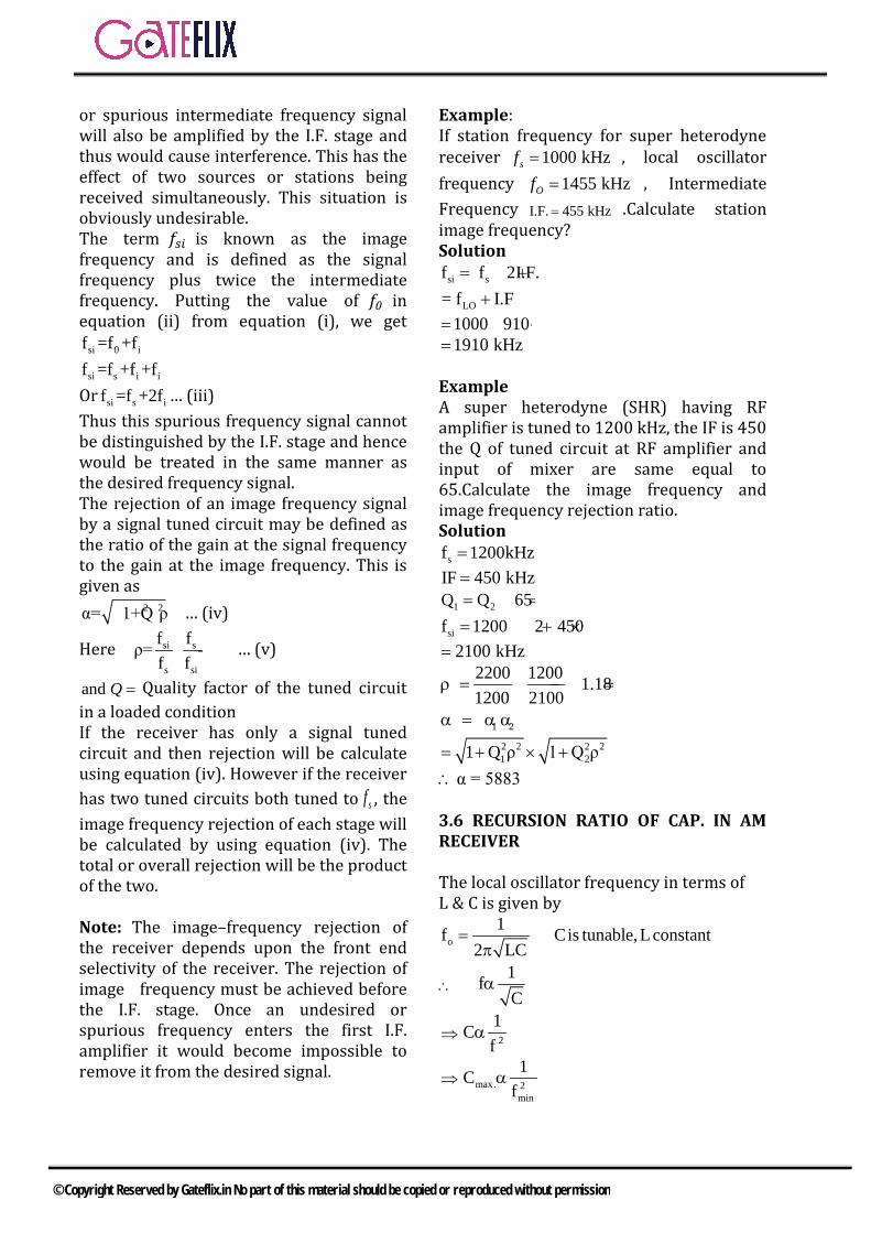
or spurious intermediate frequency signal will also be amplified by the I.F. stage and thus would cause interference. This has the effect of two sources or stations being received simultaneously. This situation is obviously undesirable. The term 𝑓𝑓𝑠𝑠𝑠𝑠 is known as the image frequency and is defined as the signal frequency plus twice the intermediate frequency. Putting the value of 𝑓𝑓0 in equation (ii) from equation (i), we get
si 0 if =f +f
si s i if =f +f +f Or si s if =f +2f … (iii) Thus this spurious frequency signal cannot be distinguished by the I.F. stage and hence would be treated in the same manner as the desired frequency signal. The rejection of an image frequency signal by a signal tuned circuit may be defined as the ratio of the gain at the signal frequency to the gain at the image frequency. This is given as
2 2α= 1+Q ρ … (iv)
Here si s
s si
f fρ= -f f
… (v)
and Q = Quality factor of the tuned circuit in a loaded condition If the receiver has only a signal tuned circuit and then rejection will be calculate using equation (iv). However if the receiver has two tuned circuits both tuned to sf , the image frequency rejection of each stage will be calculated by using equation (iv). The total or overall rejection will be the product of the two. Note: The image–frequency rejection of the receiver depends upon the front end selectivity of the receiver. The rejection of image frequency must be achieved before the I.F. stage. Once an undesired or spurious frequency enters the first I.F. amplifier it would become impossible to remove it from the desired signal.
Example: If station frequency for super heterodyne receiver 1000 kHz=sf , local oscillator frequency 1455 kHz=Of , Intermediate Frequency I.F. 455 kHz= .Calculate station image frequency? Solution
si sf f 2I.F.= +
LO= f I.F+ 1000 910= + 1910 kHz=
Example A super heterodyne (SHR) having RF amplifier is tuned to 1200 kHz, the IF is 450 the Q of tuned circuit at RF amplifier and input of mixer are same equal to 65.Calculate the image frequency and image frequency rejection ratio. Solution
sf 1200kHz= IF 450 kHz=
1 2Q Q 65= =
sif 1200 2 450= + × 2100 kHz=
2200 1200 1.181200 2100
ρ = − =
1 2 α = α α 2 2 2
2121 Q ρ 1 Q ρ+ × +=
∴ α = 5883 3.6 RECURSION RATIO OF CAP. IN AM RECEIVER The local oscillator frequency in terms of L & C is given by
o Cis tunabl1f e,Lc 2 LC
onstant=π
∴1fC
α
⇒ 2
1Cf
α
⇒ max. 2min
1Cf
α
© Copyright Reserved by Gateflix.in No part of this material should be copied or reproduced without permission
⇒ min. 2max
1Cf
α
∴ 2
max. max2
min. min
C fC f
=
For AM the signal frequency ranges from 535 to 1605 kHz Case1 When local oscillator frequency is less than station frequency i.e. if Lo sf <f
min.
max.
f =535–455=80 kHzf =1605–455=1150 kHz
⇒22
max. max2
min. min
C f 1150 206.64C f 80
= = =
Case2 When local oscillator frequency is greater than station frequency i.e. i Lo sf >f
min.
max.
f 535 455 990 kHzf 1605 455 2060 kHz
= + == + =
22max. max
2min. min
C f 2060 4.32C f 990
= = =
Note: As the recursion ratio is only 4.32 iffLo > fs, the local oscillator frequency is always kept greater than signal frequency.
© Copyright Reserved by Gateflix.in No part of this material should be copied or reproduced without permission
4.1 INTRODUCTION
As a matter of fact, noise is an unwanted electrical disturbance which gives rise to audible or visual disturbances in the communication systems, and errors in the digital communication.
4.1.1 SOURCE OF NOISE
The noise can arise from different types of sources. The sources of noise are as under: 1. Natural sources2. Manmade sources3. Fundamental sources (Internal sources)
4.1.2 NATURAL SOURCES OF NOISE
The natural phenomena that give rise to noise are electronic storms, solar flares and radiation in space. The noise received by the receiving antenna from the natural sources can only be reduced by repositioning the antenna. The noise originating from the sun and the outer space is known as Extra-terrestrial Noise. The extra-terrestrial noise can be sub-divided into two groups. (a) Solar noise (b) Cosmic noise.
4.1.3 MAN MADE SOURCES OF NOISE (INDUSTRIAL NOISE)
The man made noise is generated due to the make and break process in a current carrying circuit. The examples are the electrical motors, welding machines, ignition system of the automobiles thyristorised high current circuits, fluorescent lights, switching gears etc.
4.1.4 FUNDAMENTAL OR INTERNAL SOURCES OF NOISE
The fundamental sources of noise are within the electronic equipment. They are called fundamental sources because they are the integral part of the physical nature of the material used for making electronic components. This type of noise follows certain rules. Hence, it can be eliminated by property designing the electronic circuits and equipments.
4.2 CLASSIFICATION OF NOISE
The fundamental noise sources produce different types of noise. They may be listed as under: 1. Thermal noise2. Partition noise3. Shot noise4. Low frequency or flicker noise5. High frequency or transit time, noise
4.2.1 THERMAL NOISE OR JOHNSON NOISE
The free electrons within a conductor are always in random motion. This random motion is due to the thermal energy received by them. The distribution of these free electrons within a conductor at a given instant of time is not uniform. It is possible that an excess number of electrons may appear at one end or the other of the conductor. The average voltage resulting from this non- uniform distribution is zero but the average power is not zero. At this power results from the thermal energy, it is called as the thermal noise power The average thermal noise power is given by, Pn = kTB watts Where, k= Boltzmann’s constant = 1.38 × 10⁻²³Joules /Kelvin B=Bandwidth of the noise spectrum (Hz) T=Temperature of the conductor, °Kelvin
4 NOISE
© Copyright Reserved by Gateflix.in No part of this material should be copied or reproduced without permission
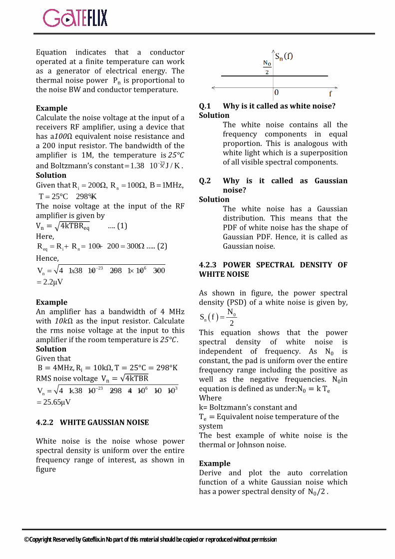
Equation indicates that a conductor operated at a finite temperature can work as a generator of electrical energy. The thermal noise power Pn is proportional to the noise BW and conductor temperature. Example Calculate the noise voltage at the input of a receivers RF amplifier, using a device that has a100Ω equivalent noise resistance and a 200 input resistor. The bandwidth of the amplifier is 1M, the temperature is 25°𝐶𝐶 and Boltzmann’s constant 231.38 10 J / K−= × . Solution Given that iR 200Ω,= nR 100Ω,= B 1MHz,= T 25°C 298°K= = The noise voltage at the input of the RF amplifier is given by Vn = 4kTBReq …. (1) Here,
eq i nR R R 100 200 300== + = + Ω….. (2) Hence,
23 6nV 4 1.38 10 298 1 10 300−= × × × × × × 2.2μV=
Example An amplifier has a bandwidth of 4 MHz with 10𝑘𝑘Ω as the input resistor. Calculate the rms noise voltage at the input to this amplifier if the room temperature is 25°𝐶𝐶. Solution Given that B = 4MHz, Ri = 10kΩ, T = 25°C = 298°K RMS noise voltage Vn = √4kTBR
23 6 3nV 4 1.38 10 298 4 10 10 10−= × × × × × × × 25.65μV=
4.2.2 WHITE GAUSSIAN NOISE White noise is the noise whose power spectral density is uniform over the entire frequency range of interest, as shown in figure
Q.1 Why is it called as white noise? Solution The white noise contains all the
frequency components in equal proportion. This is analogous with white light which is a superposition of all visible spectral components.
Q.2 Why is it called as Gaussian
noise? Solution The white noise has a Gaussian
distribution. This means that the PDF of white noise has the shape of Gaussian PDF. Hence, it is called as Gaussian noise.
4.2.3 POWER SPECTRAL DENSITY OF WHITE NOISE As shown in figure, the power spectral density (PSD) of a white noise is given by,
( ) 0n
NS f2
=
This equation shows that the power spectral density of white noise is independent of frequency. As N0 is constant, the pad is uniform over the entire frequency range including the positive as well as the negative frequencies. N0in equation is defined as under:N0 = k Te Where k= Boltzmann’s constant and Te = Equivalent noise temperature of the system The best example of white noise is the thermal or Johnson noise. Example Derive and plot the auto correlation function of a white Gaussian noise which has a power spectral density of N0/2 .
© Copyright Reserved by Gateflix.in No part of this material should be copied or reproduced without permission

Solution
We know that the power spectral density and auto correlation function form a Fourier transform pair. That means, R(τ)
F↔ S(f)
i.e., FTR(τ) = S(f) Or R(τ) = IFT S(f) Therefore, for the white noise the autocorrelation function 𝑅𝑅(𝜏𝜏) is obtained as under: ( ) n 0R τ IFT S (f ) IFT N / 2 a= =
Hence, ( ) 0NR τ δ(t)2
=
This is the expression for the auto correlation function of white noise. The auto correlation function may be plotted as shown in figure. 4.2.4 NOISE FACTOR The noise factor (F) of an amplifier or any network is defined in terms of the signal to noise ratio at the input and the output of the system. It is defined as,
S/N ratio at the inputFS/N ratio at the output
=
si no
ni so
P PFP P
= ×
Where, si niP and P = Signal and noise power at the
input & so noP and P = Signal and noise power at the output The temperature to calculate the noise power is assumed to be the room temperature. The S/N at the input will always be greater than that at the output. This is due to the noise added by the amplifier. Hence, the noise factor is the means to measure the amount of noise added and it will always be greater than one. The ideal value of the noise factor is unity.
The noise factor F is sometimes frequency dependent. Then its value determined at one frequency is known as the spot noise factor and the frequency must be stated along with the spot noise factor. 4.2.5 NOISE FIGURE (FIGURE OF MERIT) Sometime, the noise factor is expressed in decibels. When noise factor is expressed in decibels, it is known as noise figure. Noise figure dB 10F =10log F Substituting the expression for the noise factor, we get
=
10
S / N at the inputNoise figure 10logS / N at the output
( ) ( )−= 10 10 0i10log S / N 10log S / N
Hence, Noise figure ( ) ( )= −dB i 0F S / N dB S / N dB
Note: The ideal value of noise figure is 0dB 4.3 NOISE TEMPERATURE The concept of noise factor or noise figure is not always the most convenient way of measuring noise. Another way to represent the noise by means of the equivalent noise temperature. The noise temperature is used in dealing with the UHF and microwave low noise antennas, receivers or devices. 4.3.1 Definition The equivalent noise temperature of a system is defined as the temperature at which the noisy resistor has to be maintained so that be connecting this resistor to the input of a noiseless version of the system, it will produce the same amount of noise power at the system output as that produced by the actual system. 4.3.2 Equivalent Noise Temperature 𝐓𝐓𝐞𝐞𝐞𝐞 at amplifier input
© Copyright Reserved by Gateflix.in No part of this material should be copied or reproduced without permission
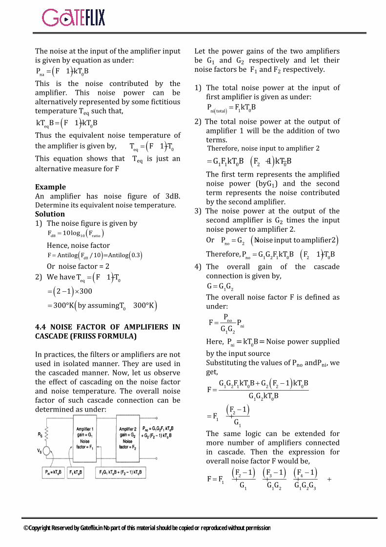
The noise at the input of the amplifier input is given by equation as under:
( )= −na 0P F 1 kT B This is the noise contributed by the amplifier. This noise power can be alternatively represented by some fictitious temperature Teq such that,
( )= −eq 0kT B F 1 kT B Thus the equivalent noise temperature of the amplifier is given by, ( )= −eq 0T F 1 T This equation shows that Teq is just an alternative measure for F Example An amplifier has noise figure of 3dB. Determine its equivalent noise temperature. Solution 1) The noise figure is given by
( )=dB 10 ratioF 10log F
Hence, noise factor
( ) ( )= dBF Antilog F /10 =Antilog 0.3 Or noise factor = 2 2) We have ( )= −eq 0T F 1 T
( )= − ×2 1 300
( )= =0300°K by assumingT 300°K 4.4 NOISE FACTOR OF AMPLIFIERS IN CASCADE (FRIISS FORMULA) In practices, the filters or amplifiers are not used in isolated manner. They are used in the cascaded manner. Now, let us observe the effect of cascading on the noise factor and noise temperature. The overall noise factor of such cascade connection can be determined as under:
Let the power gains of the two amplifiers be G1 and G2 respectively and let their noise factors be F1 and F2 respectively. 1) The total noise power at the input of
first amplifier is given as under:
( ) = 1 0ni totalP F kT B
2) The total noise power at the output of amplifier 1 will be the addition of two terms.
Therefore, noise input to amplifier 2
( )= + −1 1 0 2 0G F kT B F 1 kT B
The first term represents the amplified noise power (byG1) and the second term represents the noise contributed by the second amplifier.
3) The noise power at the output of the second amplifier is G2 times the input noise power to amplifier 2.
Or ( )= ×no 2P G Noise input to amplifier2
Therefore, ( )= + −no 1 2 1 0 2 0P G G F kT B F 1 T B 4) The overall gain of the cascade
connection is given by,
= 1 2G G G The overall noise factor F is defined as
under:
= no
ni1 2
PF P
G G
Here, ni 0P kT= B= Noise power supplied by the input source
Substituting the values of Pno andPni, we get,
( )+ −
= 1 2 1 0 2 2 0
1 2 0
G G F kT B G F 1 kT BF
G G kT B
( )−
= + 21
1
F 1F
G
The same logic can be extended for more number of amplifiers connected in cascade. Then the expression for overall noise factor F would be,
( ) ( ) ( )− − −= + + + +…2 3 4
11 1 2 1 2 3
F 1 F 1 F 1F F
G G G G G G
© Copyright Reserved by Gateflix.in No part of this material should be copied or reproduced without permission
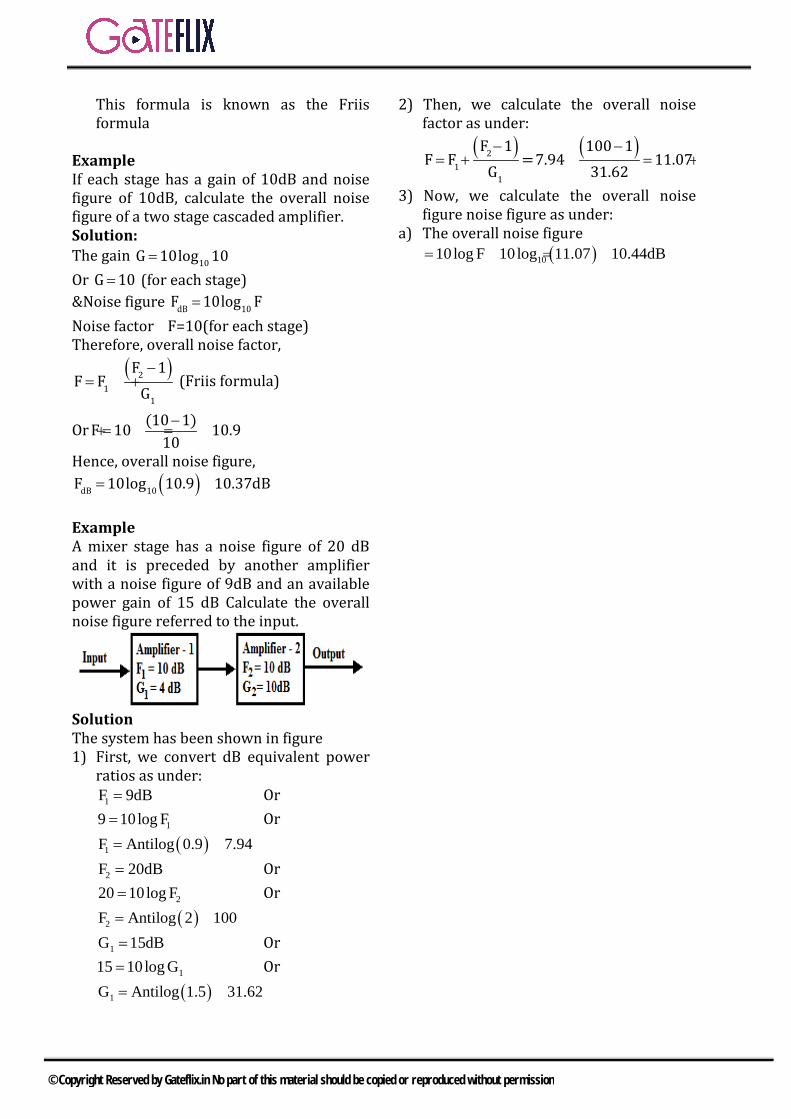
This formula is known as the Friis formula
Example If each stage has a gain of 10dB and noise figure of 10dB, calculate the overall noise figure of a two stage cascaded amplifier. Solution: The gain = 10G 10log 10 Or =G 10 (for each stage) &Noise figure =dB 10F 10log F Noise factor F=10(for each stage) Therefore, overall noise factor,
( )−= + 2
11
F 1F F
G (Friis formula)
Or −= + =
(10 1)F 10 10.910
Hence, overall noise figure, ( )= =dB 10F 10log 10.9 10.37dB
Example A mixer stage has a noise figure of 20 dB and it is preceded by another amplifier with a noise figure of 9dB and an available power gain of 15 dB Calculate the overall noise figure referred to the input.
Solution The system has been shown in figure 1) First, we convert dB equivalent power
ratios as under: 1F 9dB= Or 19 10log F= Or ( )1F Antilog 0.9 7.94= = 2F 20dB= Or 220 10log F= Or
( )2F Antilog 2 100= = 1G 15dB= Or 115 10log G= Or ( )1G Antilog 1.5 31.62= =
2) Then, we calculate the overall noise factor as under:
( ) ( )−= +
−+ =2
11
F 1 100 1F F =7.94 11.07
G 31.62
3) Now, we calculate the overall noise figure noise figure as under:
a) The overall noise figure ( )1010 log F 10log 11.07 10.44dB= = =
© Copyright Reserved by Gateflix.in No part of this material should be copied or reproduced without permission
Q.1 The PSD and the power of a signal g(t) are, respectively Sg(ω) and Pg. The PSD and the power of the signal g(t)are, respectively, a) ( )2 2
g ga S ω and a P
b) ( )2g ga S ω and aP
c) ( ) 2g gaS ω and a P
d) ( )g gaS ω and aP [GATE-2001]
Q.2 The PDF of a Gaussian random variable X is given by
( )( )2x 4
18x
1P x e3 2π
− −
= . The
probability of the event X=4 is
a) 12
b) 13 2π
c)0 d) 14
[GATE-2001]
Q.3 If the variance σx2 of d(n) = x(n) −
x(n − 1) is one-tenth the variance 𝜎𝜎𝑥𝑥2 of a stationary zero- mean discrete –time signal(n) then the normalized autocorrelation function Rxx(k)/σx
2atk = 1 is a) 0.95 b) 0.90c) 0.10 d) 0.05
[GATE-2002]
Common data for question Q.4 & Q.5 Let B be the Gaussian random variable obtained by sampling the process at t = ti
and let ( )2x
2
α
1Q α e dy2π
∞
= −∫Auto correlation function
( ) ( )0.2|τ|xxR τ 4 e 1−= + and mean = 0
Q.4 The probability that [x ≤ 1] is
a)1 Q(0.5)= b) Q(0.5)
c) 1Q2 2
d) 11 Q2 2
−
[GATE-2003]
Q.5 Let Y and Z be the random variables obtained by sampling X (t) at t=2 and t=4 respectively. Let𝑊𝑊 = 𝑌𝑌 − 𝑍𝑍. The variance of W is a) 13.36 b) 9.36c) 2.64 d) 8.00
[GATE-2003]
Q.6 Let X and Y be two statistically independent random variables uniformly distributed in the range (-1, 1) and (-2, 1) respectively. Let Z =X+Y. Then the probability that (𝑍𝑍 ≤−2) is
a) Zero b) 16
c) 13
d) 112
[GATE-2003]
Q.7 The noise at the input to an ideal frequency detector is white. The detector is operation above threshold. The power spectral density of the noise at the output is a) raised –cosine b) flatc) Parabolic d) Gaussian
[GATE-2003]
Q.8 A random variable x with uniform density in the interval 0 to 1 is quantized as follows: If 0 ≤ 𝑋𝑋 ≤ 0.3 𝑥𝑥𝑞𝑞 = 0 If0.3 < 𝑋𝑋 ≤ 1 xq = 0.7 Where, 𝑥𝑥𝑞𝑞 is the quantized value of x. The root-mean square value of thequantization noise is a) 0.573 b) 0.198c) 2.205 d) 0.266
[GATE-2004]
GATE QUESTIONS
© Copyright Reserved by Gateflix.in No part of this material should be copied or reproduced without permission

Q. 9 A 1 mW video signal having a bandwidth of 100 MHz is transmitted to a receiver through a cable that has 40dB loss. If the effective one –sided noise spectral density at the receiver is 10−20 Watt/Hz, then the signal –to noise ratio at the receiver is a) 50dB b) 30dB c) 40dB d) 60dB
[GATE-2004]
Q.10 The distribution function𝐹𝐹𝑥𝑥(𝑥𝑥) of a random variable x is shown in the figure. The probability that X=1 is
a) Zero b) 0.25 c) 0.55 d) 0.30
[GATE-2004]
Common data for question 11 & 12 Asymmetric three-level mid tread quantizer is to be designed assuming equiprobable occurrence of all quantization levels. Q.11 If the probability density function is
divided into three regions as shown in the figure, the value of a in the figure is
a) 1/3 b) 2/3 c) 1/2 d) 1/4
[GATE-2005]
Q.12 The quantization noise power for the quantization region between –a and +a in the figure is
a) 19
b) 481
c) 581
d) 281
[GATE-2005]
Q.13 An output of a communication channel is a random variable v with the probability density function as shown in the figure. The mean square value of v is
a) 4 b) 6 c) 8 d) 9
[GATE-2005]
Q.14 Noise with uniform power spectral density of N0W/Hz is passed through a filter H(ω) =2exp (−jωtd) followed by an ideal low pass filter of bandwidth B Hz. The output noise power in Watts is
a) 2N0B b) 4N0B c) 8N0B d) 16N0B
[GATE-2005] Common data for question 15 & 16 The following two questions refer to wide sense stationary stochastic processes
Q.15 it is desired to generate a stochastic
process (as voltage process) with power spectral density
( ) 216S ω
16 ω=
+
By driving a Linear –Time Invariant system by zero mean which noise
© Copyright Reserved by Gateflix.in No part of this material should be copied or reproduced without permission
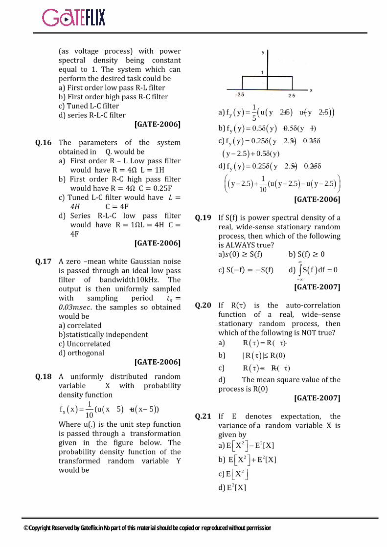
(as voltage process) with power spectral density being constant equal to 1. The system which can perform the desired task could be a) First order low pass R-L filter b) First order high pass R-C filter c) Tuned L-C filter d) series R-L-C filter
[GATE-2006]
Q.16 The parameters of the system obtained in Q. would be a) First order R – L Low pass filter
would have R = 4Ω L = 1H b) First order R-C high pass filter
would have R = 4Ω C = 0.25F c) Tuned L-C filter would have 𝐿𝐿 =
4𝐻𝐻 C = 4F d) Series R-L-C low pass filter
would have R = 1ΩL = 4H C =4F
[GATE-2006]
Q.17 A zero –mean white Gaussian noise is passed through an ideal low pass filter of bandwidth10kHz. The output is then uniformly sampled with sampling period 𝑡𝑡𝑠𝑠 =0.03𝑚𝑚𝑚𝑚𝑚𝑚𝑚𝑚. the samples so obtained would be a) correlated
b)statistically independent c) Uncorrelated d) orthogonal
[GATE-2006]
Q.18 A uniformly distributed random variable X with probability density function
( ) ( ) ( )x1f x (u x 5 u x 5 )
10= + − −
Where u(.) is the unit step function is passed through a transformation given in the figure below. The probability density function of the transformed random variable Y would be
a) ( ) ( ) ( )( )y
1f y u y 2.5 u y 2.55
= + − −
b) ( ) ( )yf y 0.5δ y 0.5δ(y 1)= + − c) ( ) ( )yf y 0.25δ y 2.5 0.25δ= + + ( )y 2.5 0.5δ(y)− + d) ( ) ( )yf y 0.25δ y 2.5 0.25δ= + +
( ) ( ) ( )1y 2.5 (u y 2.5 u y 2.510
− + + − −
[GATE-2006] Q.19 If S(f) is power spectral density of a
real, wide-sense stationary random process, then which of the following is ALWAYS true? a)𝑚𝑚(0) ≥ S(f) b) S(f) ≥ 0
c) S(−f) = −S(f) d) ( )S f df 0−
=∫∞
∞
[GATE-2007]
Q.20 If R(τ) is the auto-correlation function of a real, wide–sense stationary random process, then which of the following is NOT true? a) ( )R τ R( τ)= − b) ( )| R τ | R(0)≤ c) ( )R τ R( τ)= − − d) The mean square value of the process is R(0)
[GATE-2007] Q.21 If E denotes expectation, the
variance of a random variable X is given by a) 2 2E X E [X] −
b) 2 2E X E [X] +
c) 2E X
d) 2E [X]
© Copyright Reserved by Gateflix.in No part of this material should be copied or reproduced without permission
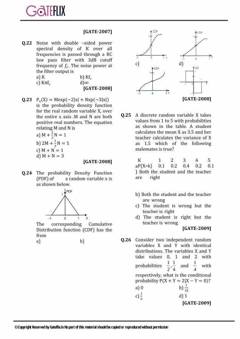
[GATE-2007] Q.22 Noise with double –sided power
spectral density of K over all frequencies is passed through a RC low pass filter with 3dB cutoff frequency of 𝑓𝑓𝑐𝑐 . The noise power at the filter output is a) K b) Kfc c) Kπfc d)∞
[GATE-2008]
Q.23 Px(X) = Mexp(−2|x| + Nxp(−3|x|) is the probability density function for the real random variable X, over the entire x axis .M and N are both positive real numbers. The equation relating M and N is a) M + 2
3N = 1
b) 2M + 13
N = 1 c) M + N = 1
d) M + N = 3 [GATE-2008]
Q.24 The probability Density Function
(PDF) of a random variable x is as shown below.
The corresponding Cumulative Distribution function (CDF) has the from
a) b)
c) d)
[GATE-2008]
Q.25 A discrete random variable X takes values from 1 to 5 with probabilities as shown in the table. A student calculates the mean X as 3.5 and her teacher calculates the variance of X as 1.5 which of the following stalemates is true?
a) Both the student and the teacher are right
b) Both the student and the teacher
are wrong c) The student is wrong but the
teacher is right d) The student is right but the
teacher is wrong [GATE-2009]
Q.26 Consider two independent random
variables X and Y with identical distributions. The variables X and Y take values 0, 1 and 2 with
probabilities 1 1,2 4
and 14
with
respectively, what is the conditional probability P(X + Y = 2|X − Y = 0)? a) 0 b) 1
16
c) 16 d) 1
[GATE-2009]
K 1 2 3 4 5 P(X=k) 0.1 0.2 0.4 0.2 0.1
© Copyright Reserved by Gateflix.in No part of this material should be copied or reproduced without permission
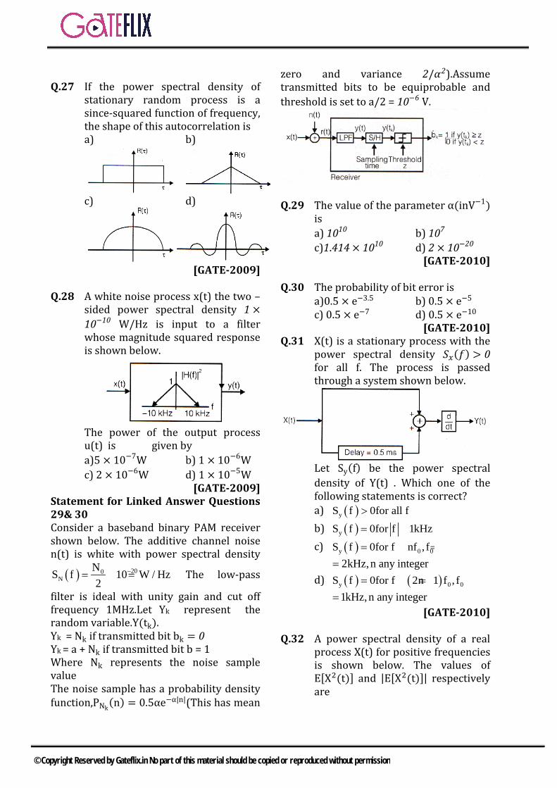
Q.27 If the power spectral density of
stationary random process is a since-squared function of frequency, the shape of this autocorrelation is
a) b)
c) d)
[GATE-2009]
Q.28 A white noise process x(t) the two –
sided power spectral density 1 ×10⁻¹⁰ W/Hz is input to a filter whose magnitude squared response is shown below.
The power of the output process u(t) is given by a)5 × 10⁻⁷W b) 1 × 10⁻⁶W c) 2 × 10⁻⁶W d) 1 × 10⁻⁵W
[GATE-2009] Statement for Linked Answer Questions 29& 30 Consider a baseband binary PAM receiver shown below. The additive channel noise n(t) is white with power spectral density
( ) 200N
NS f 10 W / Hz2
−= = The low-pass
filter is ideal with unity gain and cut off frequency 1MHz.Let Yk represent the random variable.Y(tk). Yk = Nk if transmitted bit bk = 0 Yk = a + Nk if transmitted bit b = 1 Where Nk represents the noise sample value The noise sample has a probability density function,PNk
(n) = 0.5αe−α|n|(This has mean
zero and variance 2/𝛼𝛼2).Assume transmitted bits to be equiprobable and threshold is set to a/2 = 10−6 V.
Q.29 The value of the parameter α(inV−1)
is a) 1010 b) 107 c)1.414 × 10¹⁰ d) 2 × 10⁻²⁰
[GATE-2010] Q.30 The probability of bit error is a)0.5 × e−3.5 b) 0.5 × e−5 c) 0.5 × e−7 d) 0.5 × e−10
[GATE-2010] Q.31 X(t) is a stationary process with the
power spectral density 𝑆𝑆𝑥𝑥(𝑓𝑓) > 0 for all f. The process is passed through a system shown below.
Let Sy(f) be the power spectral density of Y(t) . Which one of the following statements is correct? a) ( )yS f 0for all f> b) ( )yS f 0for f 1kHz= > c) ( )y 0 0S f 0for f nf , f= =
2kHz,n any integer= d) ( ) ( )y 0 0S f 0for f 2n 1 f , f= = + 1kHz,n any integer=
[GATE-2010] Q.32 A power spectral density of a real
process X(t) for positive frequencies is shown below. The values of E[X2(t)] and |E[X2(t)]| respectively are
© Copyright Reserved by Gateflix.in No part of this material should be copied or reproduced without permission
a) 6400/π, 0 b) 6000/π, 0 c) 6400/π, 20/π/√2 d) 6000/π, 20/π/√2
[GATE-2012]
Q.33 Two independent random variables X and Y are uniformly distributed in the interval [-1, 1]. The probability that max [X, Y] is less than ½ is
a) 3/4 b) 9/16 c) 1/4 d) 2/3
[GATE-2012-]
Q.34 X(t) is a stationary random process with autocorrelation function Rx(τ) = exp(−πτ2) This process is passed through the system below. The power spectral density of the output process Y(t)is
a)4π2f2 + 1exp−πf2 b) 4π2f2 − 1exp−πf2 c) 4π2f2 + 1exp(−πf) d) 4π2f2 − 1exp(−πf)
[GATE-2012]
Q.35 Consider two identically zero-mean random variables U and V. Let the cumulative distribution functions of U and 2V be F(x) and G(x) respectively. Then, for all values of x
a)F(x) − G(x) ≤ 0 b) F(x) − G(x) ≥ 0 c) (F(x) − G(x)). x ≤ 0 d) (F(x) − G(x)). x ≥ 0
[GATE-2013]
Q.36 Let U and V be two independent zero mean Gaussian random variables of variances 14 and 1
9 respectively. The probability
p(3 V ≥ 2U) is a) 4/9 b) 1/2 c) 2/3 d) 5/9
[GATE-2013]
Q.37 Let X1, X2, and X3 be independent and identically distributed random variables with the uniform distribution on [0, 1]. The probability PX1 is the largest is___.
[GATE-2014]
Q.38 Let x be a real-valued random variable with E[X] and E[X2] denoting the mean values of X and X2, respectively. The relation which always holds true is
a) (E[X])2 > E[X2] b) E[X2] ≥ (E[X])2
c) E[X2]= (E[X])2 d) E[X2]> (E[X])2 [GATE-2014]
Q.39 Consider a random process X (t) =
√2 sin (2𝜋𝜋𝑡𝑡 +𝜑𝜑), where the random phase 𝜑𝜑) is uniformly distributed in the interval [0,2𝜋𝜋] . The auto-correlation E [X (t1) X (t2)]
a)cos(2𝜋𝜋 (t1+ t2)) b)sin (2𝜋𝜋 (t1+ t2)) c)sin(2𝜋𝜋 (t1+ t2)) d)cos(2𝜋𝜋 (t1+ t2))
[GATE-2014]
Q.40 Let X be a random variable which is uniformly chosen from the set of positive odd numbers less than 100. The expectation E[X]is____.
[GATE-2014]
Q.41 The input to a 1-bit quantizer is a random variable X with pdf fx (x) = 2e-2x for x ≥0 and fx (x) = 0 for x < 0 , for x < 0 For outputs to be of equal probability, the quantizer threshold should be _________.
[GATE-2014]
© Copyright Reserved by Gateflix.in No part of this material should be copied or reproduced without permission
Q.42 The power spectral density of a real
stationary random process .X(t) is
given by x
1 f wS (f ) w
f w0
≤= >
The
value of the expectation 1πX(t) tE
4w −
is _________.
[GATE-2014]
Q.43 A real band-limited random process X(t) has two-sided power spectral density
( ) ( )6
x
10 3000 f watts / Hz for f 3kHzS
0other wisef
− −=
≤
Where f is the frequency expressed in Hz. The signal X(t)modulates a carrier cos 16000 𝜋𝜋t and the resultant signal is passed through an ideal band-pass filter of unity gain with centre frequency of 8 kHz and band-width of 2 kHz. The output power (in Watts) is_______.
[GATE-2014] Q.44 Let X1, X2, and X3 be independent
and identically distributed random variables with the uniform distribution on [0, 1]. The probability PX1+ X≤2 X3 is _________.
[GATE-2014] Q.45 A binary random variable X takes
the value of 1 with probability 1/3. X is input to a cascade of 2 independent identical binary symmetric channels (BSCs) each with crossover probability 1/2. The outputs of BSCs are the random variables Y1 and Y2 as shown in the figure.
The value of H(Y1) + H(Y2) in bits is_________.
[GATE-2014]
Q.46 Let X be a zero mean unit variance Gaussian random variable. E[|X|] is equal to __________.
[GATE-2014]
Q.47 If calls arrive at a telephone exchange such that the time of arrival of any call is independent of the time of arrival of earlier or future calls, the probability distribution function of the total number of calls in a fixed time interval will be
a) Poisson b) Gaussian c) Exponential d) Gamma
[GATE-2014]
Q.48 Consider a communication scheme where the binary valued signal X satisfies PX = + 1 =0.75 and PX = -1= 0.25. The received signal Y = X + Z, where Z is a Gaussian random variable with zero mean and variance σ2. The received signal Y is fed to the threshold detector. The output of the threshold detector X is:
1Y
X1Y τ
+ >= − ≤
τ
To achieve a minimum probability of error PX ≠ X, the threshold τ should be a) Strictly positive b) Zero ) Strictly negative (D) Strictly positive, zero, or strictly negative depending on the nonzero value of σ2
[GATE-2014] Q.49 Consider the Z-channel given in the
figure. The input is 0 or 1 with equal probability.
© Copyright Reserved by Gateflix.in No part of this material should be copied or reproduced without permission
If the output is 0, the probability that the input is also 0 equals _____.
[GATE-2014] Q.50 Consider a discrete-time channel Y =
-X + Z, where the additive noise z is signal-dependent. In particular, given the transmitted symbol X ∈ -a,+a . at any instant, the noise sample Z is chosen independently from a Gaussian distribution with mean βX and unit variance. Assume a threshold detector with zero threshold at the receiver. When β= 0, the BER was found to be Q(a) = 1 × 10⁻⁸
2u /2
v
1Q(v) e du2π
−= ∫∞
, and for v > 1,
use Q(v)≈ e−v2/2 When β= —0.3, the BER is closest to a) 10−7 b) 10−6 c) 10−4 d) 10−2
[GATE-2014]
Q.51 nn nX =
=−∞∞ is an independent and
identically distributed (i,i,d,) random process with 𝑋𝑋𝑛𝑛 equally likely to be +1 or –1. n
n nY ==−∞∞ is
another random process obtained asn n n 1Y X 0.5X −= + . The autocorrelation
function of nn nY =
=−∞∞ denoted by Ry [
k] is a)
b)
c)
d)
[GATE-2015]
Q.52 Let the random variable X represent
the number of times a fair coin needs to be tossed till two consecutive heads appear for the first time. The expectation of X is ____
[GATE-2015] Q.53 Let 𝑋𝑋 ∈ 0,1 and Y ∈ 0,1 be two
independent binary random variables. If P (X = 0) = p and P(Y = 0) = q, then P(X + Y ≥ 1) is equal to a) pq+(1-p)(1-q) b) pq c) p(1- q) d)1- pq
[GATE-2015]
Q.54 A zero mean white Gaussian noise having power spectral density 𝑁𝑁0
2 is
passed through an LTI filter whose impulse response h(t) is shown in the figure. The variance of the filtered noise at t = 4 is
© Copyright Reserved by Gateflix.in No part of this material should be copied or reproduced without permission
a) 20
32
A N b) 20
3 A N4
c) 20A N d) 2
01 A N2
[GATE-2015] Q.55 A random binary wave y(t) is given
by ( ) nn
y X P(t nT )t=−
− −= ∑∞
∞
φ
where p(t)= u(t) ‒u(t‒ T), u(t) is the unit step function and φis an independent random variable with uniform distribution in [0, T]. The sequence Xn consists of independent and identically distributed binary valued random variables with P Xn=+1 = PXn = ‒1 =0.5 for each n. The value of the auto correlation
( )yy3T 3TR E y t y t4 4
− @ equal____.
[GATE-2015] Q.56 A fair die with faces 1, 2, 3, 4, 5, 6
is thrown repeatedly till ‘3’ is observed for the first time. Let X denote the number of times the die is thrown. The expected value of X is __________.
[GATE-2015] Q.57 The variance of the random
variable X with probability density
function ( ) x1 x e2
f x −= is ______.
[GATE-2015] Q.58 An antenna pointing in a certain
direction has a noise temperature of 50K. The ambient temperature is 290 K. The antenna is connected to a pre-amplifier that has a noise figure of 2 dB and an available gain of 40 dB over an effective bandwidth of 12 MHz. The effective input noise temperature Te for the amplifier and the noise power Pa0 at the output of the preamplifier, respectively, are
a) Te=169.36K and Pao =3.73×10⁻¹⁰W b) Te = 1.36K and Pao =3.73×10⁻¹⁰ W c) Te =182.5K and Pao = 3.85×10⁻¹⁰W d) Te =160.62K and Pao=4.6×10⁻¹⁰ W
[GATE-2016] Q.59 An information source generates a
binary sequence na . na can take one of the two possible values land+1 with equal probability and are statistically independent and identically distributed. This sequence is precoded to obtain another sequence nβ , as
n n n 3β a ka −= + . The sequence nβ . is used to modulate a pulse g(t) to generate the baseband signal
( ) ( )nn
X t g t nTβ=−
= −∑∞
∞
, where
( )1, 0 t T0, otherwise
g t≤ ≤
=
If there is a null at f = 13T
the power
spectral density of X(t),then k is ___. [GATE-2016]
Q.60 Consider a random process X (t) =
3V (t) - 8, where V (t) is a zero mean stationary random process with autocorrelation Rv (𝜏𝜏) = 4𝑚𝑚−5|𝑇𝑇|. The power in X(t) is _________.
[GATE-2016]
Q.61 A wide sense stationary random
process X(t) passes through the LTI system shown in the figure. If the autocorrelation function of X(t) is Rx
(𝜏𝜏), then the autocorrelation function Ry (𝜏𝜏) of the output Y(t) is equal to
© Copyright Reserved by Gateflix.in No part of this material should be copied or reproduced without permission
a)2Rx(𝜏𝜏)+Rx(𝜏𝜏–T0)+Rx(𝜏𝜏+T0) b) 2Rx(𝜏𝜏)- Rx (𝜏𝜏–T0)- Rx (𝜏𝜏+T0 ) c)2Rx(𝜏𝜏)+2Rx(𝜏𝜏–2T0) d) 2Rx(𝜏𝜏)-2 Rx (𝜏𝜏–2T0)
[GATE-2016] Q.62 Let X(t) be a wide sense stationary random process with the power spectral density SX(f) as shown in Figure (a), where f is in Hertz (Hz). The random process X(t) is input to an ideal low pass filter with frequency response
( )11, f Hz2H f10, f Hz 2
≤= >
As shown in Figure (b). The output of the lowpass filter is Y(t)
Let E be the expectation operator and consider the following statements.
I.E(X(t)) = E(Y(t))
II.E(X2(t)) = E(Y2(t))
III. E(Y2(t))=2
Select the correct option: a) only I is true b) only II and III are true c) only I and II are true
d) only I and III are true
[GATE-2017, Set-1]
Q.63 Consider the random process X(t) = U + Vt where U is a zero-mean Gaussian random variable and V is a random variable uniformly distributed between 0 and 2. Assume that U and V are statistically independent. The mean value of the random process at t = 2 is ____________
[GATE-2017, Set-2]
Q.64 Passengers try repeatedly to get a seat reservation in any train running between two stations until they are successful. If there is 40% chance of getting reservation in any attempt by a passenger, then the average number of attempts that passengers need to make to get a seat reserved is _________.
[GATE-2017, Set-2]
Q.65 A binary source generates symbols X ∈-1,1 which are transmitted over a noisy channel. The probability of transmitting X = 1 is 0.5. Input to the threshold detector is R = X + N. The probability density function fN(n) of the noise N is shown below.
If the detection threshold is zero, then the probability of error (correct to two decimal places) is____.
[GATE-2018]
© Copyright Reserved by Gateflix.in No part of this material should be copied or reproduced without permission
Q.66 Let X1, X2, X3, X4 be independent normal random variables with zero mean and unit variance. The probability that X4 is the smallest among the four is _____.
[GATE-2018] Q.67 Consider a white Gaussian noise process N(t) with two-sided power spectral density SN(f) = 0.5 W/Hz as input to a filter with impulse response 0.5
2t /2e− (where t is in seconds) resulting in output Y(t). The power in Y(t) in watts is (A) 0.11 (B) 0.22 (C) 0.33 (D) 0.44
[GATE-2018]
© Copyright Reserved by Gateflix.in No part of this material should be copied or reproduced without permission

Q.1 (a) ( ) ( ) ( )x yS ω H ω S ω→ →
( ) ( ) ( )2y xS ω = H ω S ω
Q.2 (c) Probability of a Gaussian random variable is defined for a n interval and not ant a point So at X=4, it is zero.
Q.3 (a)
( ) 22E d (n) E x n x(n 1) = − −
( ) ( )( )
2 22xσ E x n E x n 1
2E x n (n 1)
= + − − × −
22 2xx x xx
σ σ σ 2R (1)10
⇒ = + − →
Auto correlation at k=1
( ) 2xx x
192R 1 σ10
=
( )xx2x
2R 1 19 0.95σ 20
∴ = =
Q.4 (d) ( ) 0.2|τ|
xxR τ 4 e 1− = + ( ) xP X 1 =F (1)≤
X μ1 Q at X 1σ− = − =
μ = 0, given
( ) 2xR 0 σ=
2σ 8=σ 2 2⇒ =
( ) 1P X 1 1 Q2 2
∴ ≤ = −
Q.5 (c) W=Y-Z
2 2 2W E Y E Z 2E[Y.Z] σ = + −
Y is sampled at t=2 & Z at t=4 2 2 2W Y z xxσ =σ +σ -2R (2)∴
0.21218 8 2 4 1e− = + − + 2W=σ =2.64
Q.6 (d)
1 2 3 4 5 6 7 8 9 10 11 12 13 14 (a) (c) (a) (d) (c) (d) (c) (b) (a) (b) (d) (b) (c) (b) 15 16 17 18 19 20 21 22 23 24 25 26 27 28 (a) (a) (b) (c) (b) (c) (a) (c) (a) (a) (b) (c) (b) (b) 29 30 31 32 33 34 35 36 37 38 39 40 41 42 (b) (d) (d) (a) (b) (a) (d) (b) * (b) (d) 50 0.35 443 44 45 46 47 48 49 50 51 52 53 54 55 56 2.5 0.16 2 0.8 (a) (c) 0.8 (c) (b) 1.5 (d) * 0.25 6 57 58 59 60 61 62 63 64 65 66 67 6 (a) -1 100 (b) (a) 2 2.5 0.125 0.25 (b)
ANSWER KEY:
EXPLANATIONS
© Copyright Reserved by Gateflix.in No part of this material should be copied or reproduced without permission

11 1K
6⇒ =
Since it lies in mid of 13
Prob[z -2]∴ ≤ =Area of graph[z -2]≤
1 1 112 6 12
= × × =
Q.7 (c)
The PSD (Power Spectra; Density) of the noise at the output of ideal frequency detectors parabolic, when the detector is operating above the threshold
Q.8 (b)
e qQ =s.v.-q.v=x=x
Mean square value of quantization noise
( )2
q=E x-x
( )1
2
q x0
= x-x f (x)dx∫
( )1
2
q0
= x- x .1dx∫
( ) ( )0.3 1
2 2
0 0.3
= x-0 dx+ x-0.7 dx∫ ∫
=0.039 Root mean square value of the quantization noise = 0.039 = 0.198 Q. 9 (a)
SNR s
o
PN B
=
3
920 6
10 1010 100 10
−
−= =× ×
9dB(SNR) 10log10 90dB= =
Cable loss =40dB ( )xSNR at R = 90-40 dB=50dB∴ Q.10 (d) ( ) ( )+
xP x = 1 = F x = 1
-x-F (x-1 )
0.55 0.25 0.30= − = Q.11 (b)
Prob. of occurrence of each region is
( )a
xa
1f X dx3−
=∫
a
a
1 1xdx4 3−
⇒ =∫
2a 14 3=
2a3
=
Q.12 (b)
a a
2 2 2x
a 0
1E x x f dx 2 x dx4−
= = ∫ ∫
2/32/3 3
2 2x
0 0
1 1 xE x 2 x d4 2 3
= =
∫
2 1 8 4E x6 27 81
= × =
Q.13 (c)
( )4
2 2x
0
E x x f x dx = ∫
© Copyright Reserved by Gateflix.in No part of this material should be copied or reproduced without permission
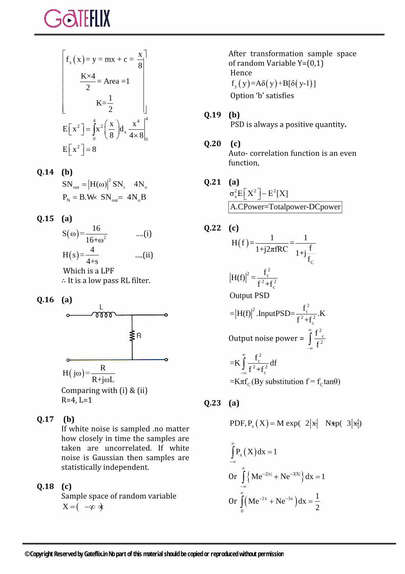
( )xxf x = y = mx + c = 8
K×4 = Area =12
1K=2
44 4
2 2x
0 0
x xE x x d8 4 8
= × ∫
2E x 8 = Q.14 (b) 2
out i oSN H(ω) SN 4N= = N out oP B.W SN 4N B= × = Q.15 (a)
( ) 2
16S ω =16+ω
….(i)
( ) 4H s =4+s
….(ii)
Which is a LPF ∴ It is a low pass RL filter. Q.16 (a)
( ) RH jω =
R+jωL
Comparing with (i) & (ii) R=4, L=1
Q.17 (b)
If white noise is sampled .no matter how closely in time the samples are taken are uncorrelated. If white noise is Gaussian then samples are statistically independent.
Q.18 (c) Sample space of random variable ( )X ,= −∞ ∞
After transformation sample space of random Variable Y=(0,1) Hence ( ) ( ) ( )yf y =Aδ y +B[δ y-1 ]
Option ‘b’ satisfies Q.19 (b) PSD is always a positive quantity. Q.20 (c)
Auto- correlation function is an even function,
Q.21 (a) 2 2 2
xσ E X E [X] −
A.CPower=Totalpower-DCpower Q.22 (c)
( )
C
1 1H f = = f1+j2πfRC 1+jf
2
2 c2 2
c
fH(f) =f +f
Output PSD
2
2 c2 2
c
f= H(f) .InputPSD= .Kf +f
Output noise power = 2
c2
ff
∞
−∞∫
2c
2 2c
f=K dff +f
∞
−∞∫
C C=Kπf (By substitution f = f tanθ) Q.23 (a)
( )xPDF,P X M exp( 2 x Nxp( 3 x )= − + −
( )xP X dx 1∞
−∞
=∫
Or 2|x| 3|X|Me Ne dx 1∞
− −
−∞
+ =∫
Or ( )2x 3x
0
1Me Ne dx2
∞− −+ =∫
© Copyright Reserved by Gateflix.in No part of this material should be copied or reproduced without permission

or M N 12 3 2+ =
or 2NM+ =13
Q.24 (a)
PDF ( ) ( ) ( ) ( ) ( )xf x = t+1 u t+1 -2tu t + t-1 u(t-1)
CDF,
( ) ( )x
x xF x = f x dx−∞∫
Q.25 (b) Mean i i=X= x p(x )∑
( ) ( ) ( )( ) ( )1 0.1 2 0.2 3 0.4
4 0.2 5 0.1 3
= × + × + ×
+ × + × =
21 iX= x p(x )∑
( ) ( ) ( )( ) ( )
1 0.1 4 0.2 9 0.4
16 0.2 25 0.1
= × + × + ×
+ × + ×
=10.2 ( )22 2=σ =X - X =1.2 Q.26 (c)
( ) P(X Y 2, X Y 0)P X Y 2|X Y 0
P(X Y 0)+ = − =
+ = − = =− =
( ) ( )( )
P X Y 0 P X 0,Y 0
P X 1,Y 1 P(X 2,Y 2)
− = = = =
+ = = + = =
( ) ( ) ( ) ( )( )
=P X=0 .P Y=0 +P X=1 .P Y=1
+P X=2 ,P(Y=2)
38
=
( ) ( )( )
P X Y 2,X Y 0 P X 1,Y 1
P X 1).P(Y 1
+ = − = = = =
= = =
116
=
( ) 1 8 1P X Y 2|X Y 016 3 6
∴ + = − = = × =
Q.27 (b) ( )PSD FT[R τ ]=
2sinc function⇒ Q.28 (b) PSD of white noise
-10=1×10 W/Hz(=k) PSD of output
( ) ( )20 iG F = H(f) .G F 2=k. H(f)
Output noise power
( ) ( )0
0
20 0N = f df=k×(areaunder H f curve)
+
−∫f
f
G
o1=k×2 bh =kf ×12
-10 3 -6=1×10 ×10×10 =10 W Q.29 (b)
Output noise power= input noise PSD 2H(f)
2NO NS (F) S f H(f )=
220NOS (f ) 10 H(f )−=
Output noise power
NO= S (f)df∞
−∞∫
-20 6ω=10 ×2×10 HzHz
14=2×10 ω Since mean square value =power
14 72
2 =2×10 α=10α
→
© Copyright Reserved by Gateflix.in No part of this material should be copied or reproduced without permission

Q.30 (d) When a ‘1’ is transmitted: K KY =a+N
Threshold -6aZ= =102
-6a=2×10 For error to occur, -6
KY <10 -6 -6
K2×10 +N <10 -6
KN <-10
( )-6-10
NK-
P(0/1)= P n dn∞∫
610αn 7 -10= 0.5αe dn with α=10 P(0/1)=0.5e
−−
−∞∫
When a ‘0’ is transmitted:
K KY =N For error to occur, 𝑌𝑌𝐾𝐾 > 10−6
( )6
-10NK
10
P(1/0)= P n dn=0.5×e∞
−
−
−
∴ ∫
Since, both bits are equiprobable:
( ) ( ) 1P 0 P 12
= =
The probability of bit error
( ) P(0/1)+P(1/0)=P 1 .P(0/1)+P(0).P(1/0=2
-10=0.5×10 Q.31 (d)
( ) ( ) 3
1Y t x t x(t 0.5 10 )−= + − ×
( ) 3j2πf (0.5 10 )1Y f X(f ) 1 e
−− × = +
( ) ( ) 31 jπf 101
Y fH f 1 e
X(f )−− ×= = +
( ) ( ) ( )1 2H f H f .H f=
( ) 3j(πf 10 )j2πf 1 e−− × = − +
( ) 2 2 2 3H f 4π f 2 2cos(πf 10 )− = + ×
2 2 38π f 1 2cos πf 10− = + ×
( ) ( ) ( )2Y xS f H f S f=
( )2 2 3)8π f 1 cos(πf f10 xS− = + × For f = (2n+1) of ; with of = 1 kHz
πf ×10-3 is an odd multiple of π
( )YS f =0 Q.32 (a)
We know that ( )2E[X t ] represent the total power in random signal. So
( ) ( )3
3
11 102
x9 10
1P E x t 2 S ω dω2π
×
×
= = × ∫
( )2 31 1E x t = 400+ ×6×2×10π 2
( )2 6400E x t =π
At 𝜔𝜔 = 0, there is no any frequency component present , hence dc value of the process is zero.
Q.33 (b) 1 x 1 and -1 y 1− ≤ ≤ ≤ ≤
is the entire rectangle The region in which maximum of
x,y is less than 12
is shown below
as shaded region inside this rectangle.
© Copyright Reserved by Gateflix.in No part of this material should be copied or reproduced without permission

1 Area of shaded regionp max x, y2 Area of entire rectangle
< =
=
3 32 22 2
×
×
916
=
Q.34 (a)
( ) ( )dy t = x t -x(t)dt
( ) ( )FT Y f =j2πfx f -x(f)→ ( ) ( )Y f =[j2πf-1]x f
( ) ( )2y xPSD S f j2πf 1 S f→ = −
( ) ( ) ( )2 2y xS f 4π f 1 S f= +
( ) ( )x xS f FT R τ=
( ) 2πfxS f e−=
∵[Gaussian function FTuur Gaussian function]
( ) 22 2 -πfyS f = 4π f +1 e
Q.35 (d) ( )F x =PX x≤ ( )G x =P2x x≤ =Px x/2≤ For positive values of x,
( )F x -G(x) 0≥ For negative values of x, ( ) ( )F x -G x <0
But ( )F x -G(x) .x 0≥ …. For all values of x
Q.36 (b) The probability ( )P 3V-2u =P(3V-2U 0=P(W 0)≥ ≥
Where W=3V-2U U and V are independent random variables and can be expressed in terms of mean and variance as shown below:
1 1U=N 0, V=N 0,4 9
W=3V-2U1 1W=N 0,9× +4×4 9
∴
Q
=N(0,2.7) Hence W is Gaussian variable with 0 mean having pdf curve as shown below:
( ) 1P W 0 =
2∴ ≥
= Area under the curve from 0 to ∞ Q.37 0.32-0.34
Q.38 (b)
V (x) = E (x2) — E(x)2≥0 i.e., variance cannot be negative .
∴ E(x2) ≥E(x)2
Q.39 (d)
© Copyright Reserved by Gateflix.in No part of this material should be copied or reproduced without permission
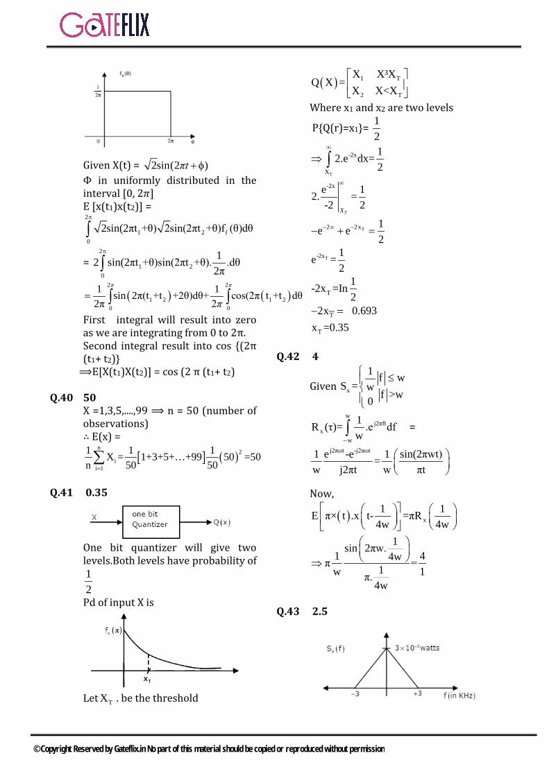
Given X(t) = sin(22 )πt + φ Φ in uniformly distributed in the interval [0, 2𝜋𝜋] E [x(t1)x(t2)] = 2
1 2 f0
2sin(2πt +θ) 2sin(2πt +θ)f (θ)dθπ
∫
= 2
1 20
12 sin(2πt +θ)sin(2πt +θ). .dθ2π
π
∫
( ) ( )2 2
01 2 1 2
0
1 1sin 2π(t +t +2θ)dθ+ cos(2π t +t dθ2π 2
π π
π= ∫ ∫First integral will result into zero as we are integrating from 0 to 2π. Second integral result into cos (2π (t1+ t2)
⟹E[X(t1)X(t2)] = cos (2 π (t1+ t2) Q.40 50
X =1,3,5,....,99 ⟹ n = 50 (number of observations) ∴ E(x) =
[ ] ( )n
2i
i 1
1 1 1X = 1+3+5+…+99 50 =50n 50 50=∑
Q.41 0.35
One bit quantizer will give two levels.Both levels have probability of 12
Pd of input X is
Let TX . be the threshold
( ) 1 T
2 T
X X³XQ X =
X X<X
Where x1 and x2 are two levels
PQ(r)=x1= 12
T
-2x
X
12.e dx=2
∞
⇒ ∫
-2xe 12. =-2 2
∞
TX
T2x2 1e e2
−− ∞− + =
T-2x 1e =2
T1-2x =In2
T2x 0.693− = −
Tx =0.35
Q.42 4
Given x
1 f wS = w
f >w0
≤
j2w
xπft
w
R ( )= 1τ .e dfw−
∫ =
j2πωt -j2πωt1 e -e 1 sin(2πwt)=w j2πt w πt
Now,
( ) x1 1E π× t .x t- =πR
4w 4w
1sin 2πw.1 44wπ =1w 1π.
4w
⇒
Q.43 2.5
© Copyright Reserved by Gateflix.in No part of this material should be copied or reproduced without permission
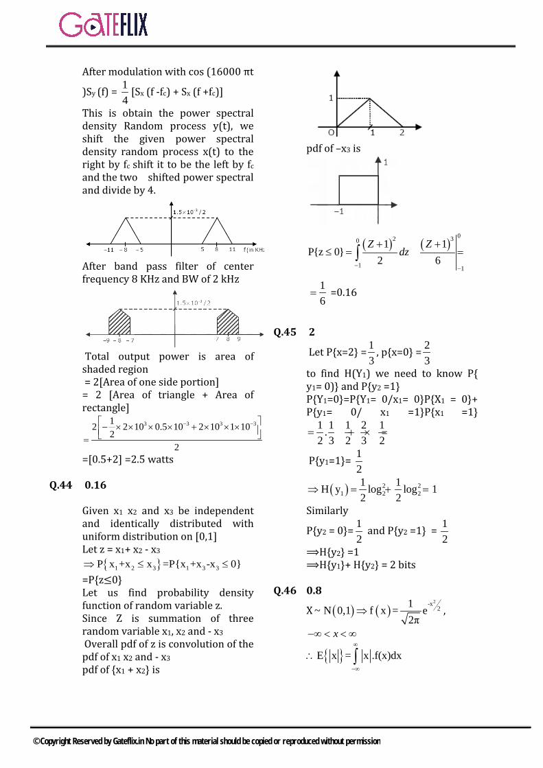
After modulation with cos (16000 πt
)Sy (f) = 14
[Sx (f -fc) + Sx (f +fc)]
This is obtain the power spectral density Random process y(t), we shift the given power spectral density random process x(t) to the right by fc shift it to be the left by fc and the two shifted power spectral and divide by 4.
After band pass filter of center frequency 8 KHz and BW of 2 kHz
Total output power is area of
shaded region = 2[Area of one side portion]
= 2 [Area of triangle + Area of rectangle]
3 3 3 312 2 10 0.5 10 2 10 1 102
2
− − − × × × × + × × × =
=[0.5+2] =2.5 watts Q.44 0.16
Given x1 x2 and x3 be independent and identically distributed with uniform distribution on [0,1]
Let z = x1+ x2 - x3
1 2 3 1 3 3P x +x x =Px +x -x 0⇒ ≤ ≤
=Pz≤0 Let us find probability density function of random variable z. Since Z is summation of three random variable x1, x2 and - x3
Overall pdf of z is convolution of the pdf of x1 x2 and - x3 pdf of x1 + x2 is
pdf of –x3 is
( ) ( )02 30
1 1
1 1Pz 0
2 6Z Z
dz− −
+ +≤ = =∫
16
= =0.16
Q.45 2
Let Px=2 = 13
, px=0 = 23
to find H(Y1) we need to know P y1= 0) and Py2 =1 PY1=0=PY1= 0/x1= 0PX1 = 0+ Py1= 0/ x1 =1Px1 =1
1 1 1 2 1.2 3 2 3 2
= + × =
Py1=1= 12
( ) 2 21 2 2
1 1H y log log 12 2
⇒ = + =
Similarly
Py2 = 0= 12
and Py2 =1 = 12
⟹Hy2 =1 ⟹Hy1+ Hy2 = 2 bits Q.46 0.8
X ( ) ( )2-x
21N 0,1 f x = e2π
⇒~ ,
x−∞ < < ∞
E x = x .f(x)dx∞
−∞
∴ ∫
© Copyright Reserved by Gateflix.in No part of this material should be copied or reproduced without permission
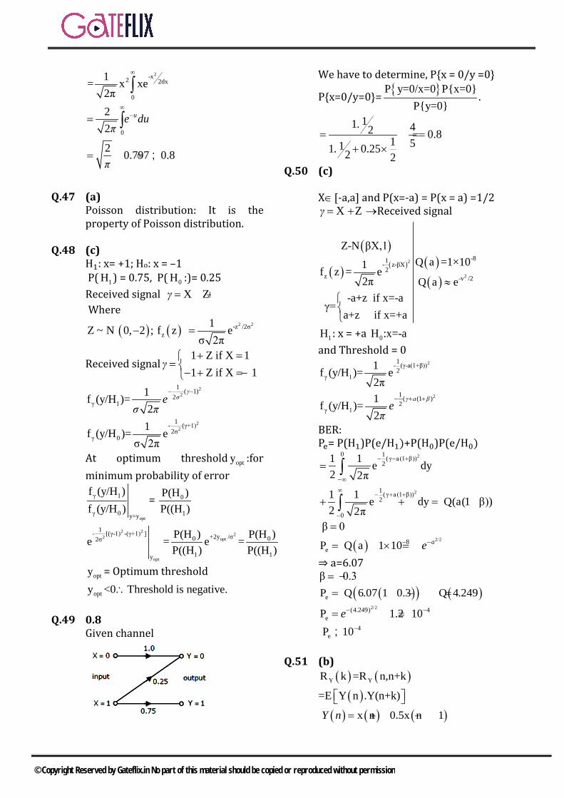
2-x
2
0
2 dx1= x xe2π
∞
∫
0
22
2 0.797 0.8
ue duπ
π
∞−=
= =
∫
;
Q.47 (a)
Poisson distribution: It is the property of Poisson distribution.
Q.48 (c) H1: x= +1; Ho: x = –1 P( 1H ) = 0.75, P( 0H :)= 0.25 Received signal X Zγ = + Where
( ) ( ) 2 2-z /2σzZ ~ N 0, 2 ; f z 1 e
σ 2π− =
Received signal1 Z if X 11 Z if X 1
γ+ =
= − + = −
22
1 ( 1)2
γ 11f H2
(y/ )=γ
σeσ π
− −
22
1- (γ+1)2σ
γ 01f H e
σ 2π(y/ )=
At optimum threshold opty :for minimum probability of error
opt
γ 1
γ 0 y=y
f (y/H )f (y/H )
= 0
1
P(H )P((H )
2 222 opt
opt
1- [(γ-1) -(γ+1) ] +2y /σ0 02σ
1 1y
P(H ) P(H )e = e =P((H ) P((H )
opty = Optimum threshold opty <0 Threshold is negative.∴ Q.49 0.8
Given channel
We have to determine, Px = 0/y =0
Px=0/y=0= P y=0/x=0 Px=0Py=0
.
11 42 0.81 511 0.252 2
.
.= = =
+ ×
Q.50 (c)
X∈[-a,a] and P(x=-a) = P(x = a) =1/2 X Zγ = + →Received signal
( )
( ) ( ) ( )( )
2
2
-81- z-βX2
z -v /2
Z-N βX,1Q a =1×101f z = e
2π Q a e-a+z if x=-a
γ=a+z if x=+a
≈
1H : x = +a 0H :x=-a and Threshold = 0
21- (γ-a(1+β))2
γ 11(y/ )=f H e2π
21 ( (1 )2
γ 11f H2
(y/ )=γ a β
eπ
− + +
BER: Pe= P(H1)P(e/H1)+P(H0)P(e/H0)
2
2
0 1 (γ a(1 β))2
1 (γ a(1 β))2
0
1 1 e2 2π
1 1 e β)
dy
dy Q( (12 2π
a )
− − +
−∞
∞− + +
−
=
+ = +
∫
∫
β 0=
( ) 2/28eP 1 10 Q a ae− −×= = =
⇒ a=6.07 β 0.3= −
( )( ) ( )e Q 6.07 1 0.3 Q 4 249P .= − = 2/2(4.249) 4
eP 1.2 10e− −= = × 4
eP 10−;
Q.51 (b) ( ) ( )Y YR k =R n,n+k
( )=E Y n .Y(n+k)
( ) ( ) ( )x n 0.5x n 1Y n = + −
© Copyright Reserved by Gateflix.in No part of this material should be copied or reproduced without permission
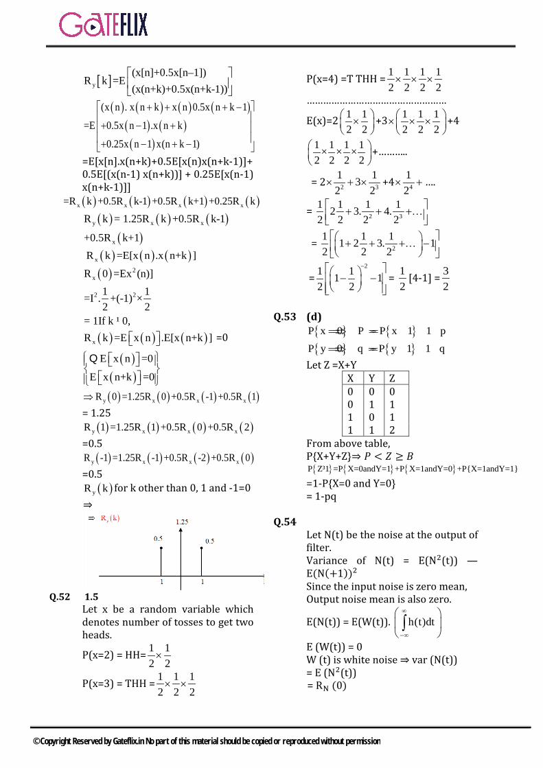
[ ]y
(x[n]+0.5x[n–1])R
(x(n+k)+0.5x(n+k-1)k =E
)
( ) ( ) ( ) ( )( ) ( )( )
(x n . x n k x n 0.5x n k 1
=E 0.5x n 1 .x n k
0.25x n 1 x(n k 1)
+ + + − + − + + − + −
=E[x[n].x(n+k)+0.5E[x(n)x(n+k-1)]+ 0.5E[(x(n-1) x(n+k))] + 0.25E[x(n-1) x(n+k-1)]] ( ) ( ) ( ) ( )x x x x+0.5 0.=R k R k-1 + R k+5 +0.251 R k
( ) ( ) ( )( )
y x x
x
R k R k +0.5R k-1
+0.5R
= 1.25
k+1
( ) ( ) ( )xR k =E[x n .x n+k ]
( ) 2x
2 2
R 0 = x (n)]1 1=I . +(-1)
E
= 1If k
×2 2
¹ 0,
( ) ( ) ( )xR k =E x n .E[x n+k ] =0
( )( )
E x n =0
E x n+k =0
Q
( ) ( ) ( ) ( )y x x xR 0 =1.25R 0 +0.5R -1 +0.5R 1⇒
= 1.25 ( ) ( ) ( ) ( )y x x xR 1 =1.25R 1 +0.5R 0 +0.5R 2
=0.5 ( ) ( ) ( ) ( )y x x xR -1 =1.25R -1 +0.5R -2 +0.5R 0
=0.5 ( )yR k for k other than 0, 1 and -1=0
⇒
Q.52 1.5
Let x be a random variable which denotes number of tosses to get two heads.
P(x=2) = HH= 1 12 2×
P(x=3) = THH = 1 1 12 2 2× ×
P(x=4) =T THH = 1 1 1 12 2 2 2× × ×
……………………………………………
E(x)=2 1 12 2
×
+3 1 1 12 2 2
× × ×
+4
1 1 1 1× × ×2 2 2 2
+………..
= 2 2 3
1 132 2
× + × +4 4
12
× + ….
= 2 3
1 1 1 12 3 42 2 2 2 + + +…
. .
= 2
1 1 11 2 3 12 2 2 + + +… −
.
=21 11 1
2 2
− − −
= 12
[4-1] = 32
Q.53 (d)
P x 0 P P x 1 1 p= = ⇒ = = − P y 0 q P y 1 1 q= = ⇒ = = −
Let Z =X+Y X Y Z 0 0 0 0 1 1 1 0 1 1 1 2
From above table, PX+Y+Z⇒ 𝑃𝑃 < 𝑍𝑍 ≥ 𝐵𝐵 P Z³1 =P X=0andY=1 +P X=1andY=0 +PX=1andY=1
=1-PX=0 and Y=0 = 1-pq
Q.54
Let N(t) be the noise at the output of filter. Variance of N(t) = E(N2(t)) — E(N(+1))2 Since the input noise is zero mean, Output noise mean is also zero.
E(N(t)) = E(W(t)). h(t)dt∞
−∞
∫
E (W(t)) = 0 W (t) is white noise ⇒ var (N(t)) = E (N2(t))
= RN (0)
© Copyright Reserved by Gateflix.in No part of this material should be copied or reproduced without permission
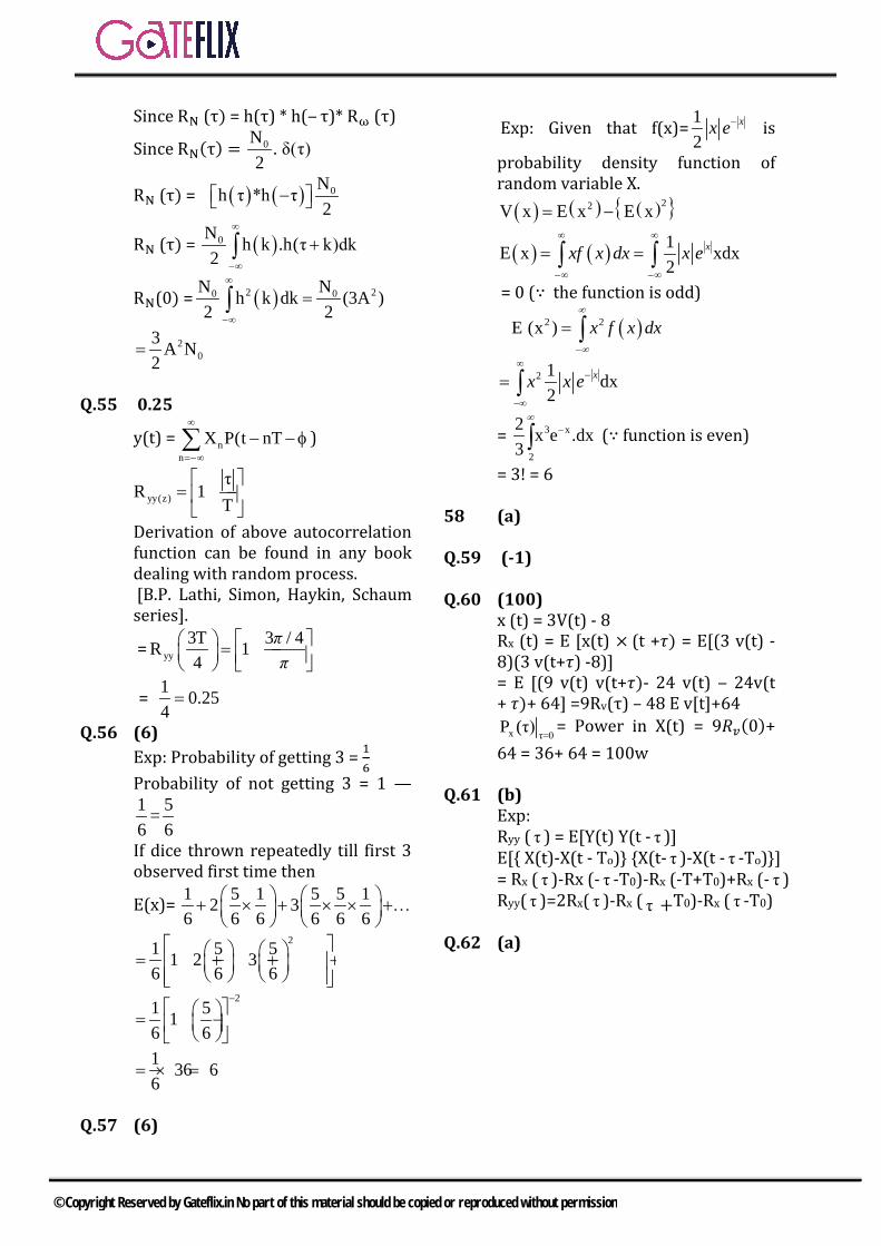
Since RN (τ) = h(τ) * h(‒ τ)* Rω (τ)
Since RN(τ) = 0N . δ(τ)2
RN (τ) = ( ) ( ) 0Nh τ *h τ2
−
RN (τ) = ( )0N h k .h(τ k)dk2
∞
−∞
+∫
RN(0) = ( )2 20 0N Nh k dk A )2 2
(3∞
−∞
=∫
20
3 A N2
=
Q.55 0.25
y(t) = nn
X P(t nT∞
=−∞
− −φ∑ )
yy(z)
τR 1
T
= −
Derivation of above autocorrelation function can be found in any book dealing with random process. [B.P. Lathi, Simon, Haykin, Schaum series].
= yy3T 3 / 4R 14
= − ππ
= 1 0.254=
Q.56 (6) Exp: Probability of getting 3 = 1
6
Probability of not getting 3 = 1 —1 5=6 6
If dice thrown repeatedly till first 3 observed first time then
E(x)= 1 5 1 5 5 12 36 6 6 6 6 6
+ × + × × +…
21 5 51 2 3
6 6 6 = + + +…
2
1 516 6
− = −
1 36 66
= × =
Q.57 (6)
Exp: Given that f(x)= 12
− xx e is
probability density function of random variable X.
( ) ( ) ( ) 22 xE xV x E= −
( ) ( )E x xd12
x∞ ∞
−∞ −∞
== ∫ ∫ xxf x dx x e
= 0 (∵ the function is odd)
( )2 2x )E (−
= ∫∞
∞
x f x dx
2 12
dx∞
−
−∞
= ∫ xx x e
= 3 x
2
2 x e .dx3
−∫∞
(∵ function is even)
= 3! = 6 58 (a) Q.59 (-1) Q.60 (100)
x (t) = 3V(t) - 8 Rx (t) = E [x(t) × (t +𝜏𝜏) = E[(3 v(t) -8)(3 v(t+𝜏𝜏) -8)] = E [(9 v(t) v(t+𝜏𝜏)- 24 v(t) ‒ 24v(t + 𝜏𝜏)+ 64] =9Rv(τ) – 48 E v[t]+64
x τ=0P (τ) = Power in X(t) = 9𝑅𝑅𝑣𝑣(0)+ 64 = 36+ 64 = 100w
Q.61 (b)
Exp: Ryy ( τ ) = E[Y(t) Y(t - τ )] E[ X(t)-X(t - To) X(t- τ )-X(t - τ -To)] = Rx ( τ )-Rx (- τ -T0)-Rx (-T+T0)+Rx (- τ ) Ryy( τ )=2Rx( τ )-Rx ( τ +T0)-Rx ( τ -T0)
Q.62 (a)
© Copyright Reserved by Gateflix.in No part of this material should be copied or reproduced without permission

Since DC components are same in Sx(f) and Sy(f)
( ) ( )( )( ) ( )
( )( ) ( )
( )( ) ( )( )( )( )
2x
f f
0
2y
1/2f 1/2
0
2 2
2
E x t E y t
E x t Area under S f
e df 2 e df 2
E y t Area under S f
2 e df 2 1 e
E x t E y t
E y t 2
∞ ∞− −
−∞
− −
=
=
= = =
=
= −
≠
≠
∫ ∫
∫
Q.63 2
Given x(t) = U+Vt
X(2) = U + 2V
E[x(2)] = E[U + 2V] = E[U] + 2E[V] = 0 + 2 x 1 = 2
Q.64 2.5
Let „X‟ is a random variable which takes number of attempts Given probability of any attempts to be successful,
40 2 2 3p 40% ,q 1100 5 5 5
= = = = = − =
( ) ( )2 3
2 3
2
E X Xp X
2 3 2 3 2 3 21x 2 x 3 4 ...5 5 5 5 5 5 5
2 3 3 31 2 3 4 ...5 5 5 5
2 315 52 25x 2.55 4
−
= ∑
= + + + + = + + + +
= −
= =
Q.65 0.125 Given P x 1 P x 1 0.5= = = − =
threshold is 0V When x =1 is transmitted, error is going to take place if received voltage is less than 0V. When x= -1 is transmitted, error is going is take place if received voltage is greater than 0V.
error x 1 x 1P P R 0 / P x 1 P R 0 / .P x 0=− =⇒ = > = − + < = Given that R= X+M, where M is a Random noise
error x 1 x 1P P x N 0 / P x 1 P R 0 / .P x 0
=P M 1 P x 1 P M 1 P x 1=− =⇒ = + > = − + < =
> = − + < − =
Using pdf figure,
© Copyright Reserved by Gateflix.in No part of this material should be copied or reproduced without permission
Shaded portion represent the PM>1 and PM<-1
e1 1 1 1P x1x0.25x x1x0.25x2 2 2 2
0.125
= +
=
Q.66 0.25
Since X1, X2, X3, X4 are independent normal random variables with zero mean and unit variance, then P(X1 is the smallest) = P(X2 is the smallest) = P(X3 is the smallest) = P(X4 is the smallest) = ¼ = 0.25
Q.67 (b)
Given, SM (t) = 0.5w/Hz
( ) ( ) ( )
( ) ( )
2y M
2y
S t H jt S t
S t 0.5 H t
=
=
Power in y(t) = area under sy (t)
( )
( )
( )
y
2
2
s t dt
0.5 H t dt
0.5 H t dt
∞
−∞
∞
−∞
∞
−∞
=
=
=
∫
∫
∫
Applying parsevals theorem,
( ) ( )2 2H t dt h t
∞ ∞
−∞ −∞
=∫ ∫
Power in y(t)
( )2
2
t /2
t
0.5 0.5e dt
0.5x0.25 e dt
∞−
−∞
∞−
−∞
=
=
∫
∫
2t12x21 10.5x0.25x 2 . e dt12 2a
20.22
−∞
−∞
= π
=
∫
© Copyright Reserved by Gateflix.in No part of this material should be copied or reproduced without permission

5.1 INTRODUCTION
Pulse digital modulation is basically a scheme which converts the analog signal to its corresponding digital form. It is for this reason that the analog-to-digital conversion is sometimes known as pulse digital modulation. The simplest form of pulse digital modulation is called pulse code modulation (PCM). In this system (i.e., P CM), the message signal is first sampled and then amplitude of each sample is rounded off to the nearest one of a finite set of allowable values known as quantization levels, so that both time and amplitude are in the discrete form. This means that in pulse code modulation both parameters i.e., time and amplitude are expressed in discrete form. This process is called discretization in time and amplitude.
5.2 PULSE CODE MODULATION (PCM)
Pulse-code modulation is known as a digital pulse modulations technique. In fact, the pulse-code modulation (PCM) is quite complex compared to the analog pulse modulation techniques (i.e., PAM, PWM and PPM) in the sense that the message signal is subjected to a great number of operations.
5.2.1 BLOCK DIAGRAM OF PCM
Fig. shows the basic elements of a PCM system. It consists of three main parts i.e., transmitter, transmission path and receiver. The essential operations in the transmitter of a PCM system are sampling, quantizing and encoding as shown in figure. As discussed earlier, sampling is the operation in which an analog (i.e., continuous-time)
signal is sampled according to the sampling theorem resulting in a discrete–time signal. The quantizing and encoding operations are usually performed in the same circuit which is known as an analog to digital converter (ADC).Also, the essential operations in the receiver are regeneration of impaired signals, decoding and demodulation of the train of quantized samples. These operations are usually performed in the same circuit which is known as a digital to analog converter (DAC).
Further, at intermediate points, along the transmission route from the transmitter to the receiver, regenerative repeaters are used to reconstruct (i.e., regenerate) the transmitted sequence of coded pulses in order to combat the accumulated effects of signal distortion and noise. The quantization refers to the use of a finite set of amplitude levels and the selection of a level nearest to a particular sampled value of the message signal as the representation for it i.e. quantization is the process of converting a continuous range of values into a finite range of discrete values. In fact, this operation combined with sampling, permits the use of coded pulses for representing the message signal. Thus, it is
5 PULSE DIGITAL MODULATION
© Copyright Reserved by Gateflix.in No part of this material should be copied or reproduced without permission

the combined use of quantizing and coding that distinguishes pulse code modulation from analog modulation techniques. Few Important Points: 1) PCM is a type of pulse modulation like
PAM, PWM or PPM but there is an important difference between them PAM, PWM or PPM is analog pulse modulation systems whereas PCM is a digital pulse modulation system.
2) This means that the PCM output is in the coded digital form. It is in the form of digital pulses of constant amplitude, width and position.
3) The information is transmitted in the form of code words. A PCM system consists of a PCM encoder (transmitter) and a PCM decoder (receiver).
4) The essential operations in the PCM transmitter are sampling, quantizing and encoding.
5) All the operations are usually performed in the same circuit called as analog-to digital converter.
6) It should be understood that the PCM is not modulation in the conventional sense because in modulation, one of the characteristics of the carriers varied in proportion with the amplitude of the modulating signal ¬hing of that sort happens in PCM.
5.2.2 PCM GENERATOR Fig shows a practical block diagram of a PCM generator. In PCM generator of figure the signal x (t) is first passed through the low-pass filter of cut-off frequency mf Hz. This low-pass filter blocks all the frequency components which are lying above mf Hz. This means that now the signal x (t) is band limited to fm Hz. The sample and hold circuit then samples this signal at the rate of sf . Sampling frequency sf is selected sufficiently above Nyquist rate to avoid aliasing i.e. s mf 2f≥
In figure, the output of sample and hold circuit is denoted by ( )sx nT (here time t has been converted to snT where n = 0, 1, 2, 3,…. This signal ( )sx nT is discrete in time and continuous in amplitude. A q-level quantizer compares input ( )sx nT with its fixed digital levels. It assigns any one of the digital level to ( )sx nT which results in minimum distortion or error. This error (difference in actual value & quantized value of the sample) is called quantization error. Thus, output of quantizer is a digital level called ( )q sx nT . Now, the quantized signal level ( )q sx nT is given to binary encoder. This encoder converts input signal into ‘n’ digits binary word. Thus ( )q sx nT is converted to ‘n’ binary bits. This encoder is also known as digitizer. Also, an oscillator generates the clocks for sample and hold circuit and parallel to serial converter. In the pulse code modulation generator discussed above, sample and hold, quantizer and encoder combinely form an analog to digital converter (ADC).
Note: It may be noted that it is not possible to transmit each bit of the binary word separately on transmission line. Therefore ’n’ binary digits are converted to serial bit stream to generate single baseband signal. In a parallel to serial converter, usually a shift register does this job. The output of PCM generator is thus a single baseband signal of binary bits. 5.2.3 PCM TRANSMISSION PATH The path between the PCM transmitter and PCM receiver over which the PCM signal travels is called as PCM transmission path and it is as shown in figure. The most important feature of PCM system lies in its ability to control the effects of distortion and noise when the PCM wave travels on the channel. PCM accomplishes this capacity by means of using a chain of regenerative repeaters as shown in figure.
© Copyright Reserved by Gateflix.in No part of this material should be copied or reproduced without permission
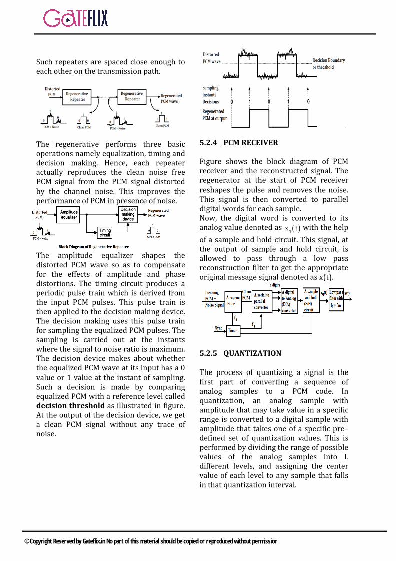
Such repeaters are spaced close enough to each other on the transmission path.
The regenerative performs three basic operations namely equalization, timing and decision making. Hence, each repeater actually reproduces the clean noise free PCM signal from the PCM signal distorted by the channel noise. This improves the performance of PCM in presence of noise.
The amplitude equalizer shapes the distorted PCM wave so as to compensate for the effects of amplitude and phase distortions. The timing circuit produces a periodic pulse train which is derived from the input PCM pulses. This pulse train is then applied to the decision making device. The decision making uses this pulse train for sampling the equalized PCM pulses. The sampling is carried out at the instants where the signal to noise ratio is maximum. The decision device makes about whether the equalized PCM wave at its input has a 0 value or 1 value at the instant of sampling. Such a decision is made by comparing equalized PCM with a reference level called decision threshold as illustrated in figure. At the output of the decision device, we get a clean PCM signal without any trace of noise.
5.2.4 PCM RECEIVER Figure shows the block diagram of PCM receiver and the reconstructed signal. The regenerator at the start of PCM receiver reshapes the pulse and removes the noise. This signal is then converted to parallel digital words for each sample. Now, the digital word is converted to its analog value denoted as ( )qx t with the help of a sample and hold circuit. This signal, at the output of sample and hold circuit, is allowed to pass through a low pass reconstruction filter to get the appropriate original message signal denoted as x(t).
5.2.5 QUANTIZATION The process of quantizing a signal is the first part of converting a sequence of analog samples to a PCM code. In quantization, an analog sample with amplitude that may take value in a specific range is converted to a digital sample with amplitude that takes one of a specific pre–defined set of quantization values. This is performed by dividing the range of possible values of the analog samples into L different levels, and assigning the center value of each level to any sample that falls in that quantization interval.
© Copyright Reserved by Gateflix.in No part of this material should be copied or reproduced without permission
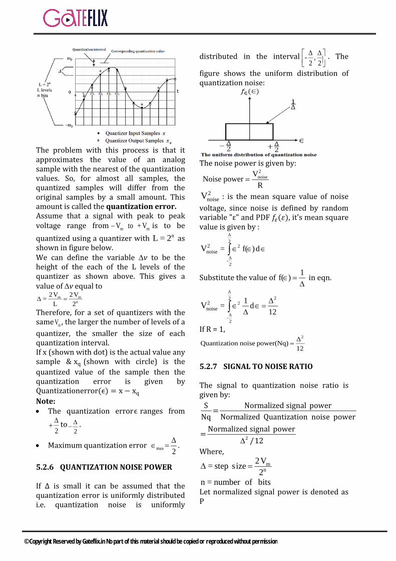
The problem with this process is that it approximates the value of an analog sample with the nearest of the quantization values. So, for almost all samples, the quantized samples will differ from the original samples by a small amount. This amount is called the quantization error. Assume that a signal with peak to peak voltage range from m mV to + V− is to be quantized using a quantizer with nL = 2 as shown in figure below. We can define the variable ∆v to be the height of the each of the L levels of the quantizer as shown above. This gives a value of ∆v equal to
m mn
2V 2V=L 2
∆ =
Therefore, for a set of quantizers with the same mV , the larger the number of levels of a quantizer, the smaller the size of each quantization interval. If x (shown with dot) is the actual value any sample & xq (shown with circle) is the quantized value of the sample then the quantization error is given by Quantizationerror(ϵ) = x − xq Note: • The quantization errorϵ ranges from
2∆
+ to2∆
− .
• Maximum quantization error max 2∆
∈ = . 5.2.6 QUANTIZATION NOISE POWER If Δ is small it can be assumed that the quantization error is uniformly distributed i.e. quantization noise is uniformly
distributed in the interval - , 2 2∆ ∆
. The
figure shows the uniform distribution of quantization noise:
The noise power is given by:
2noiseVNoise powerR
=
2noiseV : is the mean square value of noise
voltage, since noise is defined by random variable "ε" and PDF 𝑓𝑓𝜀𝜀(𝜀𝜀), it's mean square value is given by :
-2
22
2noise = f( )dV
∆
∆
∈ ∈ ∈∫
Substitute the value of 1f( )∈ =∆
in eqn.
2
-2
22
2noise
1= d12
V
∆
∆
∈ ∈∆
=∆∫
If R = 1, 2
Quantization noise power(N )12
q ∆=
5.2.7 SIGNAL TO NOISE RATIO The signal to quantization noise ratio is given by:
S Normalized signal power=Nq Normalized Quantization noise power
∆2
Normalized signal power=/12
Where, m
n2V= step size2
∆ =
n = number of bits Let normalized signal power is denoted as P
© Copyright Reserved by Gateflix.in No part of this material should be copied or reproduced without permission

∴ 2m
n
S P=Nq 1×
122V2
22n
m
3P= ×2V
Now, if we assume that input is normalized i.e. m 1V = Then the signal to noise ratio will be,
2nS 3 PNq
= ×2 ×
Also, if signal power P is normalized P 1≤ Then the signal to noise ratio is given as,
2nS 3Nq
×2≤
In decibels,
( )10 10dB
S 10log 3 2n log 2Nq
≤ +
= 4.8 + 6n (dB) Note: Signal to Noise Ratio in PCM depends on the number of bits used to represent each quantization level. 1) For each bit increment, SNR increases
by approximately 6dB. 2) If the input signal is sinusoidal, then the
signal to noise ratio is given by,
dB
S = 1.76 + 6n (dB)Nq
5.2.8 TRANSMISSION BANDWIDTH
As we discussed in the previous lecture, each quantization level gets a unique binary code which contains n binary digits. Recalling the relationship between the number of quantization levels (L) and the number of binary digits required to represent each quantization level uniquely, nL = 2 Since our message signal is band limited signal to mf Hz, we require a minimum of
m2f samples per second as a sampling rate, according to the sampling theorem we discussed beforei. e. thenumberofsamples/
sec fs = 2fm. Also the number of bits to represent each sample is n.
( )bThe number of bits transmitted or bitrater
sec=
Number of samplesNumber of bitssample sec
×
sb bits/secBit rate r = nf Now, the transmission bandwidth should be at least half of bit rate
∴ b s Hz2 2r nfB.W. = nf=≥ m
Or ( )mins
m Hz2
nfB.W. = nf=
Example A Television signal having a bandwidth of 4.2MHz is transmitted using binary PCM system. Given that the number of quantization levels is 512. Determine: i) Code word length ii) Transmission bandwidth iii) Final bit rate iv)Output signal to quanitzation noise ratio. Solution Given that the bandwidth is 4.2MHz. This means that highest frequecy component will have frequecy of 4.2MHz i.e., fm = 4.2MHz Also,given that Quantization levels, L=512 i) We know that the number of bits and
quantization levels are related in binary PCM as under:L = 2n
i.e., 512 = 2n or 10 10log 512 = nlog 2
or 10
10
log 512n =log 2
Simplifying ,we get, n = 9bits Hence , the code wordlength is 9 bits. ii) We know that the transission channel
bandwidth is given as, 6
mBW nf 9 4.2 10 Hz 37.8MHz= = × × = iii) The final bit rate is equal to singling
rate. We know that the signaling rate is given as, rb = nfs
Here sampling frequency is given as s mf 2f≥
© Copyright Reserved by Gateflix.in No part of this material should be copied or reproduced without permission

Thus, s mf 2 4.2MHz sincef= × 4.2MHz= Or sf 8.4MHz= Substituting this value of ′fs′ in above
equation for signaling rate , we get 6
br 9 8.4 10 bits / sec= × × 675.6 10 bits / sec= × The transmission bandwidth may also
be obtaied as,
61 1BW r 75.6 10 bits / sec2 2
= = × ×
Or BW 37.8MHz= which is same as the value obtained
earlier. iv) The output signal to noise ratio is
expressed as
( )S dB 4.8 6v dBN
= +
But v = 9
Therfore, S dB 4.8 6 9N
≤ + ×
Or
S dB 58.8dBN
≤
5.2.9 DISADVANTAGES OF PCM 1) The channel bandwidth is increased
because of digital coding. 2) PCM systems are complex compared to
analog pulse modulation methods.
5.2.10 MODIFICATIONS OF PCM
1) PCM is modified to delta modulation. It is simpler to implement.
2) The data rate is reduced by reducing the redundancy in the PCM output.
5.3 DELTA MODULATION
As what has been sated before that the disadvantage of PCM is it requires large bandwidth to transmit because of coding each sample. To overcome this problem, Delta modulation is used.
5.3.1 OPERATING PRINCIPLE OF DM
Delta modulation transmits only one bit per sample. In delta modulation the amplitude of previous sample is compared with the amplitude of next sample & accordingly bit ‘1’ or bit ‘0’ is transmitted. 1) If the next sampled value is greater than
the previous one, ‘1’ is transmitted. 2) If the next sampled value is less than
the previous one, ‘0’ is transmitted. We can say that the input signal is approximated to step signal by the delta modulator. This step size is fixed. The difference between the input signal x(t) and the staircase approximated signal confined to two levels, i.e. + ,δ −δ . If the difference is positive then the approximated signal is increased by +δ , if the difference is decreased then the approximated signal is decreased by−δ . A ‘0’ is transmitted for −δ and a ‘1’ is transmitted for +δ .
5.3.2 DM TRANSMITTER Figure shows the modulator diagram. The summer adds quantizer output ( )±δ with the previous sample approximation. The previous sample approximation ( ) su n 1 T− is restored by delaying one sample period
s T . The sampled input signal ( )snTx and staircase approximated signal is subtracted to get the error signal ( )snTe .
© Copyright Reserved by Gateflix.in No part of this material should be copied or reproduced without permission

Depending on the sign of ( )snTe , one bit quantizer produces an output step of +δ or –δ. • If the step size is +δ, binary '1' is
transmitted. • If the step size is -δ, then binary '0' is
transmitted.
5.3.3 DELTA MODULATION RECEIVER
At the receiver, an accumulator and a low pass filter are used. The accumulator generates the staircase approximated signal output and is delayed by one sampling period Ts. It is then added up to the input signal. If the input is '1', then +δ is added to the previous output (which is delayed). If the input is binary '0', then one step is subtracted from the delayed signal. Figure shows the diagram of the receiver.
5.3.4 ADVANTAGES OF DELTA MODULATION The delta modulation has the following advantages over PCM: 1) Delta modulation transmits only one
bit. 2) The transmitter and receiver is very
simple to implement. 5.3.5 DRAWBACKS OF DELTA MODULATION The delta modulation has two major drawbacks as under: (i)Slope overload distortion, (ii)Granular or idel noise Now,let us discuss these two drawbacks in detail.
5.3.5.1 SLOPE OVERLOAD DISTORTION This distortion arise because of largedynamic range of the input signal. As can be observed from figure the rate of rise of input signal x(t) is so high that the staircase signal cannot approximate it, the step size ′𝛿𝛿′ becomes toosmall for staircase signal u(t) to follow the step segment of x(t). Hence there is a lrge error between the staircase appproximated signal and the original input signal x(t) .This error or noise is known as slope overload distortion. To reduce this error, the step size must be increased when solpe of signal x(t)is high or
( )smax
dx tdt T
≤δ
If ( ) mx t = V sin( t)ω , ( )m m m
dx t= V cos( t)
dtω ω
⇒( )
m m m mmax
dx tV V 2 f
dt= ω = × π
∴ m ms
V 2 fTδ
× π ≤
Where, mV peak amplitude of sinusoidal signal=
mf frequency of sinusoidal signa=
ss
1T sampling periodf
= =
step size=δ
5.3.5.2 GRANULAR OR IDLE NOISE Granular or Idle noise occurs when the step size is too large compared to small variations in the input signal. This means
© Copyright Reserved by Gateflix.in No part of this material should be copied or reproduced without permission
that for very small variations in the input signal, the staircase signal is changed by large amout (𝛿𝛿) because of large step size. Figure shows that when the input signal is almost flat, the staircase signal u(t) keeps on oscillating by ±𝛿𝛿 around the signal. The error between the input and approximated signal is called granular noise. The solution to this problem is to make step size small or
( )s
dx tdt T
≥δ
Note: A large step size is required to acccommodate wide dynamicrange of the input signal (to reduceslope overload distortion ) and small steps are required to reduce granular noise. Therefore the to avoid both the distortions
( )s
dx tdt T
=δ
5.3.5.3 BIT RATE(I.E., SIGNALING RATE) OF DELTA MODULATION Delta modulation bit rate (R) = Number of bits transmitted/second = Number of samples/sec × Number of bits/sample = fs × 1 = fs bits/sec Therefore, the delta moduation bit rate is (1/n) times the bit rate of a PCM system, where n is the number of bits per transmitted PCM codeword. Hence, we can say that the channel bandwidth
brB.W. =2
for the Delta modulation
system is reduced to a great extent as compared to that for the PCM system. 5.4 DIFFERENTIAL PCM
According to the Nyquist sampling criterion, a signal must be sampled at a sampling rate that is at least twice the highest frequency in the signal to be able to reconstruct it without aliasing. The samples of a signal that is sampled at that rate or close to generally have little correlation
between each other (knowing a sample does not give much information about the next sample). However, when a signal is highly oversampled (sampled at several times the Nyquist rate, the signal does not change a lot between from one sample to another. Consider, for example, a sine function that is sampled at the Nyquist rate. Consecutive samples of this signal may alternate over the whole range of amplitudes from –1 and 1. However, when this signal is sampled at a rate that is 100 times the Nyquist rate (sampling period is 1/100 of the sampling period in the previous case), consecutive samples will change a little from each other. This fact can be used to improve the performance of quantizers significantly by quantizing a signal that is the difference between consecutive samples instead of quantizing the original signal. This will result in either requiring a quantizer with much less number of bits (less information to transmit) or a quantizer with the same number of bits but much smaller quantization intervals (less quantization noise and much higher SNR). Consider a signal x(t) that is sampled to obtain the samples x(kTs) , where Ts the sampling period and k is is an integer representing the sample number. For simplicity, the samples can be written in the formx[k], where the sample period Ts is implied. Assume that the signal x(t) is sampled at a very high sampling rate. We can define d[k] to be the difference between the present sample of a signal and the previous sample, [ ] [ ] [ ]d k x k x k 1= − − Now this signal d[k] can be quantized instead of x[k] to give the quantized signal dq[k] . As mentioned above, for signals x(t)that are sampled at a rate much higher than the Nyquist rate, the range of values of d[k] will be less than the range of values ofx[k].
© Copyright Reserved by Gateflix.in No part of this material should be copied or reproduced without permission
6.1 RANDOM SINGLE AND NOISE
6.1.1 RANDOM VARIABLE
Random variable is real function of elements of sample space S. Random variable is represented by (W, X or Y) and the values of random variable are represented by (w, x or y). A random variable X is a function of element of sample space S which maps the element of sample space into point on the real line. We have two types of random variable.
(1) Discrete Random Variable If we roll a die, we have 6 outcomes and the sample space is S = 1, 2, 3, 4, 5, 6 X is random variable which will map the elements of sample space by following equation
2X(s)=s The random variable X is X = 1, 4, 9, 16, 25, 36 Random variable X can take only discrete values from 0 to 36 so it is a discrete random variable. This mapping of elements of sample space into points on the real line by random variable X is illustrated in Fig. 6.1
Figure 6.1 Mapping of Elements of Sample Space into Real Line The random variable can map the elements of sample space on finite point only
(2) Continuous Random Variable If we have sample space which can take any value between 0 to 6 or
S = 0 < s < 6 And random variable X is defined as X (s) = s2
Then X (s) = 0 < x < 36 Here random variable X can take any value between 0 to 36 so X is continuous random variable. We can have mixed random variable which is combination of discrete and continuous random variables.
6.1.2 CUMULATIVE DISTRIBUTION FUNCTION
CDF of random variable X is XF (x) PX x= ≤
x is the value of random variable X and −∞ < x < ∞.
PROPERTIES OF CDF 1) XF ( ) PX 0−∞ = ≤ −∞ = 2) XF ( ) PX 1∞ = ≤ ∞ = 3) X0 F (x) 1≤ ≤ CDF is always between 0
and 1. 4) If 2 1x x> then X 2 X 1F (x ) F (x )≥5) 1 2 X 2 X 1Px X x F (x ) F (x )< ≤ = − 6) CDF of discrete random variable is
always in the staircase from.It’s always increasing
6.1.3 PROBABILIT YDENSITY FUNCTION ION (pdf)
The PDF of random variable X is X
XdF (x)f (x)
dx=
Properties of PDF
1) f (x)x .d(x 1 )∞
−∞
=∫ [Area under pdf =1]
6 COMMUNICATION SYSTEM
© Copyright Reserved by Gateflix.in No part of this material should be copied or reproduced without permission
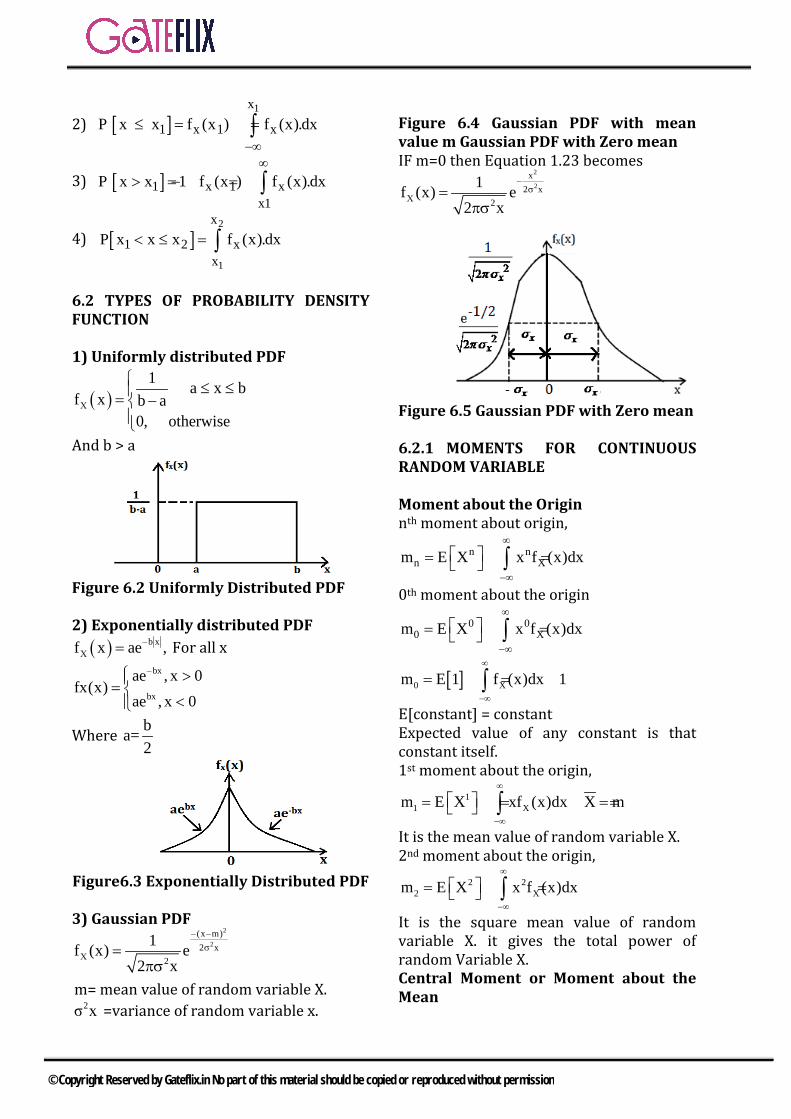
2) [ ]1x
1 x 1 xP x x f (x ) f (x).dx−∞
≤ = = ∫
3) [ ]1 x 1 xx1
P x x 1 f (x ) f (x).dx∞
> = − = ∫
4) [ ]2
1
x
1 2 xx
P x x x f (x).dx< ≤ = ∫
6.2 TYPES OF PROBABILITY DENSITY FUNCTION 1) Uniformly distributed PDF
( )1 a x b
f x b a0,
otherwiseΧ
≤ ≤= −
And b > a
Figure 6.2 Uniformly Distributed PDF 2) Exponentially distributed PDF
( ) b xf x ae ,−Χ = For all x
bx
bx
ae , x 0fx(x)
ae , x 0
− >= <
Where ba=2
Figure6.3 Exponentially Distributed PDF 3) Gaussian PDF
2
2(x m)2 x
2
1f (x) e2 x
− −σ
Χ =πσ
m= mean value of random variable X. 2σ x =variance of random variable x.
Figure 6.4 Gaussian PDF with mean value m Gaussian PDF with Zero mean IF m=0 then Equation 1.23 becomes
2
2x
2 x2
1f (x) e2 x
−σ
Χ =πσ
Figure 6.5 Gaussian PDF with Zero mean 6.2.1 MOMENTS FOR CONTINUOUS RANDOM VARIABLE Moment about the Origin nth moment about origin,
n nn Xm E X x f (x)dx
∞
−∞
= = ∫
0th moment about the origin
0 00 Xm E X x f (x)dx
∞
−∞
= = ∫
[ ]0 Xm E 1 f (x)dx 1∞
−∞
= = =∫
E[constant] = constant Expected value of any constant is that constant itself. 1st moment about the origin,
11 Xm E X xf (x)dx X m
∞
−∞
= = = = ∫
It is the mean value of random variable X. 2nd moment about the origin,
2 22 Xm E X x f (x)dx
∞
−∞
= = ∫
It is the square mean value of random variable X. it gives the total power of random Variable X. Central Moment or Moment about the Mean
© Copyright Reserved by Gateflix.in No part of this material should be copied or reproduced without permission

The mean value of random variable X is m. nth moment about mean,
( ) ( )n nn XE X m x m f (x)dx
∞
−∞
µ = − = − ∫
0th moment about the mean,
( ) ( )0 00 XE X m x m f (x)dx
∞
−∞
µ = − = − ∫
0th moment about the mean
[ ]0 XE 1 f (x)dx 1∞
−∞
µ = = =∫
1st moment about the mean
( ) ( )1 11 XE X m x m f (x)dx
∞
−∞
µ = − = − ∫( ) [ ] [ ]1 E X m E X E mµ = − = −
1μ =m-m=0 2nd moment about the mean,
( ) ( )2 2 22 X xE X m x m f (x)dx
∞
−∞
µ = − = − = σ ∫
It is called the variance of random variable X, ( )22
x E X m σ = − 2 2 2x E X m 2Xm σ = + −
[ ]2 2 2x E X E m E 2Xm σ = + −
[ ]2 2 2x E X m 2mE X σ = + − 2 2 2 2x E X m 2m σ = + − 2 2 2x E X m σ = −
m2 is the dc power of random variable X. 2xσ is the ac power of random variable X.
E [X2] is the total power of random variable X. 6.2.2 MOMENTS FOR DISCRETE RANDOM VARIABLE MOMENT ABOUT THE ORIGIN nth moment about the origin
( )n nn i i
im E X x P x
∞
=−∞
= = ∑
0th moment about the origin
( )0 00 i i
im E X x P x
∞
=−∞
= = ∑
1st moment about the origin,
( )11 i i
im E X x P x X m
∞
=−∞
= = = = ∑
m = X = mean value of random variable X. 2nd moment about the origin,
( )2 22 i i
im E X x P x
∞
=−∞
= = ∑
m2=E[X2] is the square mean value of random variable X. Central Moment or Moment about the Mean The mean value of discrete random variable is m. nth moment about the mean
( ) ( ) ( )n nn i i
iE X m x m P x
∞
=−∞
µ = − = − ∑
0th moment about the mean,
( ) ( ) ( )0 00 i i
iE X m x m P x
∞
=−∞
µ = − = − ∑
[ ]0 E 1 1µ = = 1st moment about the mean,
( ) ( ) ( )1 11 i i
iE X m x m P x
∞
=−∞
µ = − = − ∑[ ] [ ]1 E X E mµ = −
1 m m 0µ = − = 2nd moment about the mean,
( ) ( ) ( )2 2 22 i i x
iE X m x m P x
∞
=−∞
µ = − = − = σ ∑
2xσ is variance of random variable X.
By solving 2µ 2 2 2
2 x E X m µ = σ = − m2 is dc power of random variable X.
2xσ is ac power of random variable X.
2E X is total power of random variable X.
6.2.3 VECTOR RANDOM VARIABLE A set of two or more random variables constitutes a random vector. For example, a random vector with two components,
1
2
XX
X
=
, is a function from the sample
space of an experiment of the (x1, x2) plane.
© Copyright Reserved by Gateflix.in No part of this material should be copied or reproduced without permission
Joint CDF If we have two events A = X ≤ x & B = Y ≤ y then the joint CDF of X and Y is
X,YF (x, y) P X x,Y y= ≤ ≤ ( ) ( ) P X x Y y= ≤ ∩ ≤
Properties of joint CDF 1) ( ) ( ) ( ) X,YF , P X Y−∞ −∞ = ≤ −∞ ∩ ≤ −∞
0= 2) ( ) ( ) ( ) X,YF , y P X Y−∞ = ≤ −∞ ∩ ≤ −∞ 0= 3) ( ) ( ) ( ) X,YF x, P X x Y−∞ = ≤ ∩ ≤ −∞ 0= 4) ( ) ( ) ( ) X,YF , P X Y∞ ∞ = ≤ ∞ ∩ ≤ ∞ 1= 5) ( )X,Y0 F x, y 1≤ ≤ 6) ( ) ( ) ( ) X,YF x, P X x Y∞ = ≤ ∩ ≤ ∞ XP X x F (x)= ≤ =
XF (x) is called marginal distribution function.
7) ( ) ( ) ( ) X,YF , y P X Y y∞ = ≤ ∞ ∩ ≤
YP Y y F (y)= ≤ =
YF (y) Is called marginal distribution function.
For discrete random vectors joint CDF is (6.41)
( ) ( ) ( )( )N M
X,Y n m n mn 1 m 1
F x, y P x , y u x x y y= =
= − −∑∑Where ( )n mP x , y is the probability of the joint event?
n mX x ,Y y= = Joint PDF
2X,Y
X,Y
F (x, y)f (x, y)
x y∂
=∂ ∂
( )yx
X,Y X,YF (x, y) f x, y dxdy−∞ −∞
= ∫ ∫
Properties of Joint PDF 1) X,Yf (x, y) 0≥
2)
( )X,Y X,YF ( , ) f x, y dxdy 1∞ ∞
−∞ −∞
∞ ∞ = =∫ ∫
3) ( )x
X,Y X X,YF (x, ) F (x) f x, y dxdy∞
−∞ −∞
∞ = = ∫ ∫
( )x
Xf x dx−∞
= ∫
4) ( )y
X,Y Y X,YF ( , y) F (y) f x, y dxdy∞
−∞ −∞
∞ = = ∫ ∫
( )y
Yf y dy−∞
= ∫
5) ( ) ( )X,Y Xf x, y dy f x∞
−∞
=∫
( )Xf x Is called marginal density function
6) ( ) ( )X,Y Yf x, y dx f y∞
−∞
=∫
( )Yf y is called marginal density function. 7) 1 2 1 2P x X x , y Y y< ≤ < ≤
( )2 2
1 1
y x
X,Yy x
f x, y dxdy= ∫ ∫ Joint PDF of
discrete random vector is given by
( ) ( ) ( ) ( )N M
X,Y n m n mn 1 m 1
f x, y P x , y x x . y y= =
= δ − δ −∑∑ 6.2.4 INDEPENDENT RANDOM VARIABLE Two random variable X and Y are statistically independent random variable if and only if ( ) ( ) P X x,Y y P X x Y y≤ ≤ = ≤ ∩ ≤
( ) ( ) P X x P Y y≤ ≤ The joint CDF of statistically independent random variable will be
X,Y X YF (x, y) F (x)F (y)= The joint PDF o statistically independent random variable will be
X,Y X YF (x, y) F (x)F (y)=
6.2.5 PDF OF A SUM OF RANDOM VARIABLES Assuming that X and Y are two statistically independent random variable and another random variable Z is defined as
© Copyright Reserved by Gateflix.in No part of this material should be copied or reproduced without permission
Z = X + Y If PDF of random variable X and Y are fX (x) and fY(y) respectively then PDF of random variable Z is
Z X Yf (z) f (x)*f (y)= The PDF of the sum of two statistically independent random variable is the convolution of their individual density functions.
6.3 JOINT MOMENT ABOUT THE ORIGIN Assuming that X and Y are continuous random variable.
i j i jij X,Ym E X Y x y f (x, y)dxdy
∞ ∞
−∞ −∞
= = ∫ ∫
i j i jij X,Ym E X Y x y f (x, y)dxdy
∞ ∞
−∞ −∞
= = ∫ ∫
i+j is called the order of moment. 0 0 0 0
00 X,Ym E X Y x y f (x, y)dxdy∞ ∞
−∞ −∞
= = ∫ ∫
[ ]00m E 1 1= = [ ]00m E 1 1= =
0 1 0 101 X,Ym E X Y x y f (x, y)dxdy
∞ ∞
−∞ −∞
= = ∫ ∫
[ ]01 X,Y ym E Y yf (x, y)dxdy Y m∞ ∞
−∞ −∞
= = = =∫ ∫
1 0 1 010 X,Ym E X Y x y f (x, y)dxdy
∞ ∞
−∞ −∞
= = ∫ ∫
[ ]10 X,Y xm E X xf (x, y)dxdy X m∞ ∞
−∞ −∞
= = = =∫ ∫
1 111 X,Ym E X Y xyf (x, y)dxdy
∞ ∞
−∞ −∞
= = ∫ ∫
11m is the second order moment and it is called the correlation of
[ ]11 XY X,Ym R E XY xyf (x, y)dxdy∞ ∞
−∞ −∞
= = = ∫ ∫
If X and Y are uncorrelated then [ ] [ ]XYR E X .E Y=
If X and Y are statistically independent random variables then they are uncorrelated.
If X and Y are uncorrelated then it is not necessary that X and Y are independent random variables. If X and Y are orthogonal random variables then RXY = 0 Assuming that X and Y are discrete random variables.
( )i j i jij n k n k
n km E X Y x y P x , y
∞ ∞
=−∞ =−∞
= = ∑ ∑
( )0 0 0 000 n k n k
n km E X Y x y P x , y
∞ ∞
=−∞ =−∞
= = ∑ ∑
[ ]00m E 1 1= =
( )0 1 0 101 n k n k
n km E X Y x y P x , y
∞ ∞
=−∞ =−∞
= = ∑ ∑
( )01 k n k yn k
m E Y y P x , y Y m∞ ∞
=−∞ =−∞
= = = = ∑ ∑
( )1 0 1 010 n k n k x
n km E X Y x y P x , y X m
∞ ∞
=−∞ =−∞
= = = = ∑ ∑
( )1 1 1 111 n k n k
n km E X Y x y P x , y
∞ ∞
=−∞ =−∞
= = ∑ ∑
( )11 n k n k XYn k
m E X Y x y P x , y R∞ ∞
=−∞ =−∞
= = = ∑ ∑ P (xn, yk) is the probability of the joint event n kX x ,Y y= = 6.3.1 JOINT CENTRAL MOMENT Assuming X and Y are continuous random variables.
( ) ( ) jiij x yE X m Y m µ = − −
( ) ( ) jix y XYx m y m f (x, y)dxdy
∞ ∞
−∞ −∞
= − −∫ ∫
If X and Y are discrete random variables
( ) ( ) jiij x yE X m Y m µ = − −
( ) ( ) jix y n k
n kx m y m P(x , y )
∞ ∞
=−∞ =−∞
= − −∑ ∑
The second order central moments are ( )2 2
20 x xE X m µ = − = σ
( )2 202 y yE Y m µ = − = σ
© Copyright Reserved by Gateflix.in No part of this material should be copied or reproduced without permission

( )( )11 x y XYE X m Y m C µ = − − = (6.66)
CXY is called covariance of X and Y. XY y x x yC E XY Xm m Y m m = − − + +
[ ] [ ]XY y x x yC E XY E m X E m Y E m m = − − + [ ] [ ] [ ]XY y x x yC E XY m E X m E Y m m= − − +
[ ]XY y x x y x yC E XY m m m m m m= − − +
XY XY x yC R m m= −
[ ] [ ]XY XYC R E X .E Y= − If X and Y are either independent or uncorrelated, then
XYC 0= If X and y are orthogonal random variables then,
[ ] [ ]XYC E X E Y= − Correlation Coefficient The Correlation Coefficient of random variable X and Y is
ll XY
x y20
Cp02
µ= =
σ σµ µ
The value of correlation coefficient lies between –l and 1.
1 p 1.− ≤ ≤ 6.3.2 RANDOM PROCESS A random process is also called stochastic process Random process is a function of elements of sample space and time. Random process is denoted by X (t, s) or x (t). t is typically time, but can also be a spatial dimension, t can be discrete or continuous. The range of t can be finite, but more often is infinite, which means the process, contains an infinite number of random variables. At a fixed time t, (t, s) is a random variable and is called a time sample. For a fixed s, X (t, s) is a deterministic function of t and is called a realization (or sample path or Sample function). A random process represents a random variable when t is fixed and s is a variable At t = t1 ,X (t1,s) = X (t1)=X1
At t = t2, X (t2, s) =X (t2) = X2 X1 and X2 denote the random variable associated with the random process X (t) at time t1 and t2 respectively. The statistical properties of random variable X1 describe the statistical properties of random process at time t1. From a given random process X(t), any number of random variable can be derived at time tn, n =1,2,3….. Xn = X (tn,s) = X(tn) If time t and element of sample space both are fixed then random process X (t, s) is just a number. Predicted from the observation of past values then the process is called nondeterministic random process 6.3.3CLASSIFICATION RANDOM PROCESS a) Continuous Random Process If X is continuous and t is also
continuous then X (t) is continuous random process.
b) Discrete random process If X can take only discrete value while t
is continuous then X (t) is discrete random process.
c) Discrete time random process When t comes from a countable set, the
process is discrete time. We then usually use n to denote the time index instead and write then process as X (n, s).
d) Nondeterministic Random Process If the future values of a random process
cannot be predicted from the observation of past values then the process is called nondeterministic random process
e) Deterministic Random Process If the future of a random process can be
predicted from the observation of past values then the process is called deterministic random process.
© Copyright Reserved by Gateflix.in No part of this material should be copied or reproduced without permission
6.3.4 STATIONARY RANDOM PROCESS If the statistical properties like mean, variance, standard deviation etc. do not change with time. The behaviour is time invariant, even though the process is random. These random process are stationary random process. First Order Stationary Random Process X (t) is random process and X1 and X2 are random variable associated with X (t) at fixed times t1 and t2 respectively. At t = t1, X (t1) = X1 At t = t2, X (t2) = X2 If E[X1] = E[X2] = constant or E [X (t)] = constant If the mean value of random process X (t) is constant then X (t) is first order stationary random process. Second Order stationary random process or wide sense stationary random process X1 and X2 are random variables associate with random process X (t) at fixed times t1 and t2 respectively as defined in Equation 6.74 and 6.75 The autocorrelation function of random process X (t) is
[ ] [ ]1 2 1 2 1 2Rxx( t , t ) E X(t )X(t ) E X X = = Where t2 = t1 + τ τ = t2- t1 = time difference Random process is WSS random process if a) [ ]E X(t) X constant= = Mean value of random process is
constant. b) [ ]xx 1 2 1 1 xxR ( t , t ) E X(t )X(t ) R ( )= + τ = τ The autocorrelation function of random
process X (t) is function of time difference
Strict-sense Stationary A process is nth order stationary if the joint distribution of any set of n times samples is independent of the placement of the time origin. [ ]1 2 nX(t ),X(t ),.......X(t )
[ ]1 2 nX(t ),X(t ),.......X(t )− + τ + τ + τ ∀τ For a discrete random process,
[ ] [ ]1 2 n 1 m 2 m n mX ,X ,....X X ,X ,....X m+ + +− ∀ A process that is nth order stationary for every integer n > 0 is said to be strictly stationary, or just stationary for short. WSS is a much more relaxed condition than strict sense stationary. All stationary random process are WSS. A WSS process is not always strictly stationary. 6.3.5 TIME AVERAGES AND ERGODICITY Sometimes we need to estimate the parameters of a random process through measurement. A quantity obtained from measurement is the ensemble average. For Example, an estimate of the mean is
N
x ii 1
1m (t) X(t,s )N =
= ∑
Where si is the ith outcome of the underlying random experiment. In General, since mx (t) is a function of time, we need to perform N repetitions of the experiment at each t to estimate mx (t). If process is stationary, however, then mx (t) = m for all t. Then we may ask if m can be estimated based on the realization (over time) of single outcome s alone. We define the time average over an interval 2T of a single realization as
T
TT
1X(t) X(t,s)dt2T −
= ∫
6.3.6 ERGODICITY OF A WSS PROCESS Consider a WSS random process X (t) with a mean m. X (t) is mean-ergodic if
T as .X(t) m T→ →∞
It is because of stationary, the expected value of
TX(t) is
T
TT
1E X(t) E X(t)dt 2T −
=
∫
© Copyright Reserved by Gateflix.in No part of this material should be copied or reproduced without permission
[ ]T
T
1 E X(t) dt m2
T −
= =∫
Mean ergodic definition therefore implies that
TX(t) approaches its mean as T .→∞
6.3.7 AUTOCORRELATION FUNCTION AND ITS PROPERTIES If X (t) is WSS then autocorrelation function is
( ) ( ) ( )XX 1 2 XX 1 1 XXR t , t R t , t R= + τ = τ 1) ( ) ( )XX XXR R τ = −τ
Autocorrelation function is even function of time.
2) ( ) 2XXR 0 E x (t) =
The value of autocorrelation function at
τ = 0 gives the square mean value of X (t) or total power of X (t).
3) ( )XX xxR 0 | R ( ) | ≥ τ 4) If E [X (t)] = X 0≠
and X (t) has no
periodic components then
[ ] 2
xx| |lim R ( ) E X( t)τ→∞
τ =
5) If X (t) has a periodic components, then RXX (τ) will have a periodic components with the same period.
6) If X (t) has zero mean and has no periodic components then
xx| |
lim R ) 0(τ→∞
τ =
7) Autocorrelation function cannot take any arbitrary shape.
6.3.8 CROSS CORRELATION FUNCTION AND ITS PROPERTIES If we have two random process X (t) and Y (t) then At t = t1, X (t1) = X At t = t2, Y (t2) = Y t2 = t1 + τ or τ = t2 – t1
X and Y are random variables associated with random process X (t) and Y (t) at fixed times t1 and t2 respectively. The cross correlation function of X (t) and Y (t) is RXX (t1, t2) = E[X (t1) Y (t2)] = E [X Y] If X (t) and Y (t) are at least jointly WSS then RXY (t1, t2) = RXY (τ) When X (t) and Y (t) are orthogonal then RXX (t1, t2) = E[X (t1) Y (t2)] = 0 When X (t) and Y (t) are statistically independent then RXY (t1, t2) = E[X (t1) Y (t2)] = E[X (t1)] E[Y (t2)] If X (t) and Y (t) are at least jointly WSS then 1) RXY (-τ) = RXY (τ) (6.94) 2) |RXY (τ)| ≤ xx YYR (0)R (0) 3) |RXY (τ)| ≤ [ ]XX YY
1 R (0) R (0)2
+
4) [ ]xx YY XX YY1R (0)R (0) R (0) R (0) 2
≤ +
6.3.9 COVARIANCE FUNCTIONS If x (t) is a random process and X (t1) = X1
and X (t2) = X2 are random variables associated with random process at fixed time t1 and t2 Here t2 = t1 + τ The auto covariance function is defined as
Similarly the cross-covariance function for two random process X (t) and Y (t) is defined by
6.3.10 THE POWER SPECTRAL DENSITY OF A WSS PROCESS a) The power spectral density (psd) of a
WSS random process X (t) is given by the Fourier transform (FT) of its autocorrelation function
[ ] [ ] 1 2 1 1 2 2( , ) ( ) ( ) ( ) ( )XXC t t E X t E X t X t E X t = − − [ ] [ ]1 2 1 2 1 2( , ) ( , ) ( ) ( )XX XXC t t R t t E X t E X t= −
[ ] [ ]1 2 1 2 1 2( , ) ( , ) ( ) ( )XY XyC t t R t t E X t E Y t= −
© Copyright Reserved by Gateflix.in No part of this material should be copied or reproduced without permission

j2 fXX XXS (f ) R ( )e d
∞− π τ
−∞
= τ τ∫
b) For a distance-time process Xn, the psd is given by the discrete-time FT (DTFT) of its autocorrelation sequence.
nj2 fn
XX XXn
1 1S (f ) R (n)e , f 2 2
−∞− π
−∞
= − ≤ ≤∫Since the DTFT is periodic in f with period 1, we only need to consider
1| f |2
≤
c) RXX (τ) or RXX (n) can be recovered from SXX (f) by taking the inverse Fourier transform.
( ) j2 fXX XXR S (f )e df
∞− π τ
−∞
τ = ∫
( )1 2
j2 fnXX XX
1 2
R S (n f )e dfπ
−
= ∫
6.3.11 PROPERTIES OF THE POWER SPECTRAL DENSITY 1) SXX (f) is real and even SXX (f) = SXX (-f) (6.105) 2) The area under SXX (f) is the average
power of X (t)
2XX XXS (f )df R (0) E X(t)
∞
−∞
= = ∫
3) SXX (f) is the average power density, hence the average power of X (t) in the frequency band [f1, f2] is
f1 f 2 f 2
XX XX XXf 2 f1 f1
S (f )df S (f )df 2 S (f )df−
+ =∫ ∫ ∫
4) SXX (f) is nonnegative: SXX (f) ≥ - for all f. 5) In General, any function S (f) that is real,
even, and nonnegative and has finite area can be psd function.
6.3.12 WHITE NOISE a) Band-Limited White Noise
A Zero-mean WSS process N (t) which has the psd as a constant within –W ≤ f ≤w and zero elsewhere.
Similar to white light containing all frequencies in equal amounts.
Its average power is
W2 0
0W
NE X(t) df N W2−
= = ∫
Its auto-correlation function is
0
XX 0N sin(2 W )R ( ) N W sin c(2w )
2π τ
τ = = τπτ
For any t, the samples
nX t for n 0,1,2,....
2
W + =
Are
uncorrelated.
Figure 6.6 PSD of White Noise
Figure 6.7 Autocorrelation Function
of White Noise b) White-Noise Process Let W → ∞, we obtain a white noise
process, which has
0
XXNS (f )2
= For all f
0
XXNR ( ) ( )2
τ = δ τ
For a white noise process, all samples are uncorrelated. The process has infinite power and hence not physically realizable. It is an idealization of physical noise. Physically systems usually are band-limited and are affected by the noise within this band.
© Copyright Reserved by Gateflix.in No part of this material should be copied or reproduced without permission
c) If the white noise N (t) is a Gaussian
random process, then power spectral density and autocorrelation function are same and probability density function is Gaussian.
σ2x = variance of Gaussian white noise m = mean value of Gaussian white noise 6.3.13 CROSS-POWER SPECTRAL DENSITY Consider two jointly-WSS random process X (t) and Y (t) a) Their cross-correlation function RXY (τ)
is defined as RXY (τ) = [ ]E X(t )Y(t)+ τ unlike the auto-correlation RX (τ), the cross-correlation RXY (τ) is not necessarily even.
However RXY (τ) = RXY (-τ) b) The cross-power spectral density SXY (f) = fT RXY (τ) In General, SXY (f) is complex even if the
two process are real-valued. Let us take an example of signal plus
white noise, Let the observation be Z (t) = X (t) + N (t) Where X (t) is the wanted signal and N
(t) is white noise. X (t) and N (t) are zero-mean uncorrelated WSS process. Z (t) is also a WSS process.
E [Z (t)] = 0 E[Z (t) Z (t + τ)] = E [X (t) + N (t)X (t + τ) + N (t + τ)] = RXX (τ) + RNN (τ) The psd of Z (t) is the sum of the psd of
X (t) and N (t) SZZ (f) = SXX (f) + SNN (f) Z (t) and X (t) are jointly – WSS E[X (t) Z (t + τ)] = E [X (t + τ) + Z (t)] =
RXX (τ) Thus SXZ (f) = SZX (f) = SXX (f) 6.3.14 RESPONSE OF AN LTI SYSTEM TO WSS RANDOM SIGNALS
Consider an LTI system with impulse response h (t)
Figure 6.8 LTI System
Apply an input X (t) which is a WSS Random process, the output Y (t) then is also WSS.
Y (t) = h( )X(t )d∞
−∞
τ − τ τ∫
E [Y (t)] = E h( )X(t )d∞
−∞
τ − τ τ
∫
E [Y (t)] = [ ]E h( )E X(t ) d∞
−∞
τ − τ τ∫
E [Y (t)] = xh( )m d∞
−∞
τ τ∫
Where mx is mean value of X (t).
E [Y (t)] = x xm h( )d m H(0)∞
−∞
τ τ =∫
H (f) = F.T. h (t)
H (f) = j2 fh( )e d∞
− π τ
−∞
τ τ∫
H (0) = h( )d∞
−∞
τ τ∫
( ) ( ) XXE Y t Y t h(r)h(s)R ( s r)dsdr∞ ∞
−∞ −∞
+ τ = τ + − ∫ ∫Two process X (t) and Y (t) are jointly WSS
RXY (τ) = XX XXh(s)R ( s)ds h( )*R ( )∞
−∞
τ + = −τ τ∫
From these, we also obtain
( )YY XY XYR h(r)R ( r)dr h( )*R ( )∞
−∞
τ = τ − = τ τ∫The results are similar for discrete-time systems. Let the impulse response be h (n). The response of the system to a random input process X (n) is
Y (n) = h(k)X(n k)∞
−∞
−∑
The system transfer function is
© Copyright Reserved by Gateflix.in No part of this material should be copied or reproduced without permission

H (f) = j2 nf
nh(n)e
∞− π
=−∞∑
With a WSS input X (n), the output Y (n) is also WSS my = mx H(0)
RYY (k) = XXj i
h( j)h(i)R (k j i)∞ ∞
=−∞ =−∞
+ −∑ ∑
X (n) and Y (n) are jointly WSS
RXY (k) = XXn
h(n)R (k n)∞
=−∞
+∑
6.3.15 FREQUENCY DOMAIN ANALYSIS Taking the Fourier transforms of the correlation functions, we have SXY (f) = H *(f) SXX (f) SYY (f) = H (f) SXY (f) Where H* (f) is the complex conjugate of H (f). The output-input psd Relation SYY (f) = 2
XX| H(f ) | S (f ) For example taking white noise as the input. Let X (t) have the psd as
SXX (f) = 0N2
for all f
Then the psd of the input is
( ) 2 0YY
NS f | H(f ) | 2
=
Thus the transfer function completely determines the shape of the output psd. This also shows that any psd must be nonnegative. 6.3.16 POWER IN A WSS RANDOM PROCESS Some signals, such as sin (t), may not have finite energy, but can have finite average power. The average power of a random process X (t) is defined as
PXX = T
2
TT
1E lim x (t)dt2T→∞
−
∫
For a WSS process, this becomes
PXX = T
2XXT
T
1lim E X (t)dt R (0)2T→∞
−
= ∫
But RXX (0) is related to the FT of the SXX (f). Thus we have three ways to express the power of a WSS Process.
PX = 2XX XXE X (t) R (0) S (f )df
∞
−∞
= = ∫
The area under the psd function is the average power of the process.
© Copyright Reserved by Gateflix.in No part of this material should be copied or reproduced without permission
7.1 INTRODUCTION
In the modulation process, the baseband signals constitute the modulating signal and the high-frequency carrier signal is a sinusoidal waveform. There are three basic ways of modulating a sine wave carrier. For binary digital modulation, they are called binary amplitude-shift keying (BASK), binary frequency-shift keying (BFSK) and binary phase shift keying (BPSK).
7.2 LINE CODING
It is the process of converting binary data, a sequence of bits to a digital signal. The data, text, numbers, graphical images, audio and video which are stored in computer memory are in the form of sequences of bits. Line coding converts these sequences into digital signals as shown in figure.
7.2.1 CHARACTERISTICS OF LINE CODING
Some of the important characteristics of line coding are: i) Signal level and data levelii) Pulse rate and bit rateiii) DC componentiv) Self synchronization
7.2.2 VARIOUS LINE CODES
Some of the important PAM formats or line coding techniques are as under: i) Non-return to zero (NRZ) and return tozero (RZ) unipolar format ii) NRZ and RZ polar formatiii) Non-return to zero bipolar formativ) Manchester formatv) Polar quaternary NRZ format
7.2.3 UNIPOLAR NRZ
A unipolar NRZ (i.e., not return to zero) format is shown in shown in figure. When symbol ‘1’ is to be transmitted, the signal has ‘A’ volts for full duration. When symbol ‘0’ is to be transmitted, the signal has zero volts (i.e. no signal) for complete symbol duration. Thus, for unipolar NRZ format, i) If symbol‘1’ is transmitted, we have
x(t) = A For 0 ≤ t < Tb(complete interval)
ii) If symbol ‘0’ is transmitted, we have( )x t 0=
For 0 ≤ t < Tb (complete interval)
7.2.4 POLAR NRZ
The polar NRZ is shown in figure. In polar NRZ format, symbol‘1’ is represented by positive polarity whereas symbol ‘0’ is represented by negative polarity. These polarities are maintained over the complete pulse duration i.e., for polar NRZ, we have
i) If symbol ‘1’ is transmitted, then
( ) Ax t2
= + For 0 ≤ t < Tb
ii) If symbol ‘0’ is transmitted, then
( ) Ax t2
= − For 0 ≤ t < Tb
7.3 BINARY AMPLITUDE-SHIFT KEYING (BASK)
7 DIGITAL CARRIER MODULATION
© Copyright Reserved by Gateflix.in No part of this material should be copied or reproduced without permission

Amplitude-shift keying (ASK) is a form of amplitude modulation that represents digital data variations in the amplitude of a carrier wave. In an ASK system, the binary symbol 1 is represented by transmitting a fixed-amplitude carrier wave and fixed frequency for a bit duration of T seconds. If the signal value is 1 then the carrier signal will be transmitted; otherwise, a signal value of 0 will not be transmitted. A binary amplitude-shift keying (BASK) signal can be defined by ( ) ( ) cs t = A m t cos 2 f tπ , b0 < t < T … (1)
Where, A is a constant, m (t) = 1 or 0, Tb is the bit duration.
It has a power2AP =
2, so that A = 2P .
Thus equation (1) can be written as ( ) ( ) cs t = 2P m t cos 2 f tπ , b0 < t < T
( )b cb
2= PT × m t cos 2 f tT
π , b0 < t < T
( )b cb
2= E × m t cos 2 f tT
π b0 < t < T … (2)
Where, Eb = PTb is the energy contained in a bit duration
If ( ) m t 1= ,
( )1 b cb
2s t = E × cos 2 f tT
π
(This wave is transmitted to transmit ‘1’.) & if ( )m t 0= ,
( )2s t = 0 (No wave is transmitted to transmit ‘0’)
7.3.1 CONSTELLATION DIAGRAM The ASK wave form shown in the diagram represented by the equation
( ) b cb
2s t = E × cos 2 f tT
π
There is only 1 carrier function in ASK i.e.
1 cb
2(t) cos 2 f tT
φ = π . The constellation
diagram will have 2 points on 1(t)φ . One will be at zero & other will be at
b bE PT= .
The distance between the two signal points is, b bd E PT= = 7.4 BINARY PHASE SHIFT KEYING (BPSK) In a BPSK system, binary bit ‘1’ is represented by transmitting fixed amplitude & fixed frequency carrier wave & bit ‘0’ is represented by transmitting a similar carrier wave with 180o phase shift. A binary phase-shift keying (BPSK) signal can be defined by ( ) ( ) cs t = A m t cos 2 f tπ , b0 < t < T … (1)
Where, A is a constant, m (t) = +1 or -1,
© Copyright Reserved by Gateflix.in No part of this material should be copied or reproduced without permission
fc is the carrier frequency, and Tb is the bit duration. It has a power 2AP =
2, so that A = 2P .
Thus equation (1) can be written as ( ) cs t = 2P cos 2 f t± π , b0 < t < T
b cb
2= PT × cos 2 f tT
± π , b0 < t < T
b cb
2 = E × cos 2 f tT
± π , b0 < t < T … (2)
Where, b bE PT is the energy contained in a bit duration=
7.4.1 WAVEFORMS
The signal b(t), a bipolar NRZ, directly modulates the carrier signal on behalf of binary bit sequence. The BPSK modulated signal for sequence 10110100 is shown in fig. below.
7.4.2 CONSTELLATION DIAGRAM The BPSK wave form shown in the diagram represented by the equation
( ) b cb
2s t = E × cos 2 f tT
± π
If we take 1 cb
2(t) cos 2 f tT
φ = π as the
ortho-normal basis function, the constellation diagram will have 2 points on
1(t)φ . One will be at b bE PT− = − & other
will be at b bE PT+ = .
The distance between the two signal points is, ( )b b b bd E E 2 E 2 PT− − = ==
7.5 BINARY FREQUENCY SHIFT KEYING (BFSK) Frequency-shift keying (FSK) is a frequency modulation scheme in which digital information transmitted through discrete frequency changes of a carrier wave. The simplest FSK is binary FSK (BFSK). BFSK uses a pair of discrete frequencies to transmit binary (0s and 1s) information. With this scheme, the "1" is called the mark frequency and the "0" is called the space frequency. In frequency-shift keying, the signals transmitted for marks (binary ones) and spaces (binary zeros) are ( )1 c1s t A cos 2 f t= π , b0 < t < T
( )2 c2s t A cos 2 f t= π , b0 < t < T This is called a discontinuous phase FSK system, because the phase of the signal is discontinuous at the switching times.
© Copyright Reserved by Gateflix.in No part of this material should be copied or reproduced without permission
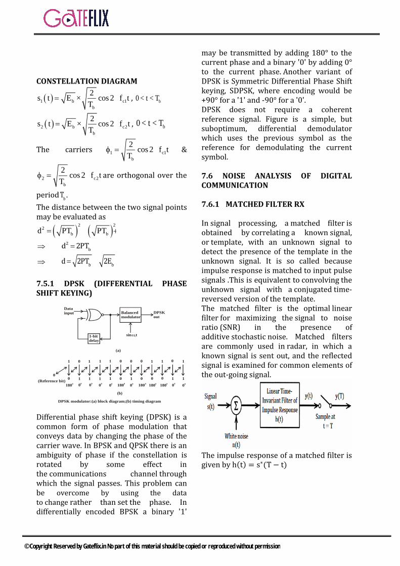
CONSTELLATION DIAGRAM
( )1 b c1b
2s t E × cos 2 f tT
= π , b0 < t < T
( )2 b c2b
2s t E × cos 2 f tT
= π , b0 < t < T
The carriers 1 c1b
2 cos 2 f tT
φ = π &
2 c2b
2 cos 2 f tT
φ = π are orthogonal over the
period bT . The distance between the two signal points may be evaluated as
( ) ( )2 22b bd PT PT= +
⇒ =2bd 2PT
⇒ = =b bd 2PT 2E 7.5.1 DPSK (DIFFERENTIAL PHASE SHIFT KEYING)
Balancedmodulator
1-bitdelay
Datainput DPSK
out
sin tc
0 1
(Reference bit)1800 00
1 1 1 0 0 0 01 1 1
1100010111100
00 00 00 001800 1800 1800 1800 00 00
(a)
(b)
DPSK modulator:(a) block diagram;(b) timing diagram
Differential phase shift keying (DPSK) is a common form of phase modulation that conveys data by changing the phase of the carrier wave. In BPSK and QPSK there is an ambiguity of phase if the constellation is rotated by some effect in the communications channel through which the signal passes. This problem can be overcome by using the data to change rather than set the phase. In differentially encoded BPSK a binary '1'
may be transmitted by adding 180° to the current phase and a binary '0' by adding 0° to the current phase. Another variant of DPSK is Symmetric Differential Phase Shift keying, SDPSK, where encoding would be +90° for a '1' and -90° for a '0'. DPSK does not require a coherent reference signal. Figure is a simple, but suboptimum, differential demodulator which uses the previous symbol as the reference for demodulating the current symbol. 7.6 NOISE ANALYSIS OF DIGITAL COMMUNICATION 7.6.1 MATCHED FILTER RX In signal processing, a matched filter is obtained by correlating a known signal, or template, with an unknown signal to detect the presence of the template in the unknown signal. It is so called because impulse response is matched to input pulse signals .This is equivalent to convolving the unknown signal with a conjugated time-reversed version of the template. The matched filter is the optimal linear filter for maximizing the signal to noise ratio (SNR) in the presence of additive stochastic noise. Matched filters are commonly used in radar, in which a known signal is sent out, and the reflected signal is examined for common elements of the out-going signal.
The impulse response of a matched filter is given by h(t) = s∗(T − t)
© Copyright Reserved by Gateflix.in No part of this material should be copied or reproduced without permission
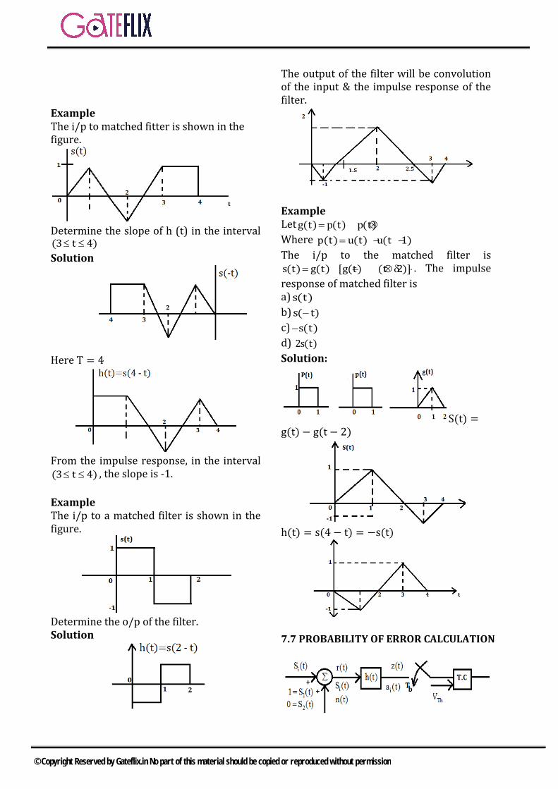
Example The i/p to matched fitter is shown in the figure.
Determine the slope of h (t) in the interval(3 t 4)≤ ≤ Solution
Here T = 4
From the impulse response, in the interval(3 t 4)≤ ≤ , the slope is -1. Example The i/p to a matched filter is shown in the figure.
Determine the o/p of the filter. Solution
The output of the filter will be convolution of the input & the impulse response of the filter.
Example Let g(t) p(t) p(t)= ⊗ Where p(t) u(t) u(t 1)= − − The i/p to the matched filter iss(t) g(t) [g(t) (t 2)]= − ⊗δ − . The impulse response of matched filter is a) s(t) b) s( t)− c) s(t)− d) 2s(t) Solution:
S(t) =g(t) − g(t − 2)
h(t) = s(4 − t) = −s(t)
7.7 PROBABILITY OF ERROR CALCULATION
© Copyright Reserved by Gateflix.in No part of this material should be copied or reproduced without permission
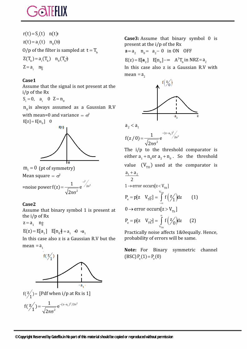
ir(t) S (t) n(t)= + i 0z(t) a (t) n (t)= +
O/p of the filter is sampled at bt T=
b i b 0 bZ(T ) a (T ) n (T )= +
i 0Z a n= + Case1 Assume that the signal is not present at the i/p of the Rx
i iS 0, a 0= = 0Z n=
0n is always assumed as a Gaussian R.V with mean=0 and variance 2= σ
0E[z] E[n ] 0= =
1m 0= (pt of symmetry)
Mean square 2= σ
=noise power−
σ=πσ
2z22
2
1f(z) e2
Case2 Assume that binary symbol 1 is present at the i/p of Rx
1 0z a n= +
1 0E(z) E[a ] E[n ]= + 1 1a 0 a= + = In this case also z is a Gaussian R.V but the mean 1a=
zf( )1 = [Pdf when i/p at Rx is 1]
2 21(z a ) /2
2
1zf( ) e1 2− − σ=
πσ
Case3: Assume that binary symbol 0 is present at the i/p of the Rx = + = −2 0 2z a n a 0 in ON OFF
= + − 22 0 bE(z) E[a ] E[n ] = A T in NRZ 2a=
In this case also z is a Gaussian R.V with mean 2a=
2 1a a<
− −σ=
πσ
22
2(z a )
22
1f(z / 0) e2
The i/p to the threshold comparator is either 1 0 2 0a n or a n+ + . So the threshold
value TH(V ) used at the comparator is
1 2a a2+
TH1 error occurs[z V ]→ <
e THP p[z V ]= < ( )THV
zf dz1−∞
= ∫ (1)
Th0 error occurs[z V ]→ >
= >e ThP p[z V ] ( )THV
zf dz0
∞
= ∫ (2)
Practically noise affects 1&0equally. Hence, probability of errors will be same. Note: For Binary symmetric channel (BSC) =e eP (1) P (0)
© Copyright Reserved by Gateflix.in No part of this material should be copied or reproduced without permission
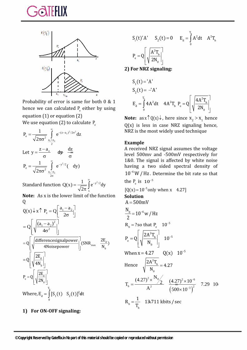
Probability of error is same for both 0 & 1 hence we can calculated eP either by using equation (1) or equation (2) We use equation (2) to calculate eP
2 22
1 2
(z a ) /2e 2
a a2
1P e dz2
∞− − σ
+
=πσ
∫
Let zz a dzy dy−= ⇒ =
σ σ
2
1 2
y /2e 2
a a2
1P e ( dy)2
∞−
−σ
= σπσ
∫
Standard function 2y /2
x
1Q(x) e dy2
∞−=
π ∫
Note: As x is the lower limit of the function Q
Q(x) x↓ ↑ 1 2e
a aP Q2− = σ
21 2
2
(a a )Q4
−=
σ
dmax
0
2EdifferencesignalpowerQ (SNR )4Noisepower N
= =
d
0
2EQ
4N
=
de
0
2EP Q
2N
=
Where, = −∫bT
2d 1 2
0
E [S (t) S (t)] dt
1) For ON-OFF signaling:
iS (t)'A' 2S (t) 0=bT
2 2d b
0
E A dt A T= =∫2
be
0
A TP Q
2N
=
2) For NRZ signaling:
1S (t) 'A'=
2S (t) 'A'= −
bT2 2
d b0
E 4A dt 4A T= =∫2
be
0
4A TP Q
2N
=
Note: as x Q(x)↑ ↓ , here since 2 1x x> hence Q(x) is less in case NRZ signaling hence, NRZ is the most widely used technique Example A received NRZ signal assumes the voltage level 500mv and -500mV respectively for 1&0. The signal is affected by white noise having a two sided spectral density of
−610 W / Hz . Determine the bit rate so that the eP is 510−
5[Q(x) 10 only when x 4.27]−= = Solution A 500mV=
60N10 w / Hz
2−=
5b eR ?so that P 10−= =
25b
e0
2A TP Q 10
N−
= =
When 5x 4.27 Q(x) 10−= =
Hence2
b
0
2A T4.27
N=
( )
2 0 2 6
b 22 3
N(4.27) (4.27) 102T 7.29 10A 500 10
−
−
× ×= = = ×
×
= =bb
1R 13.711 kbits / secT
© Copyright Reserved by Gateflix.in No part of this material should be copied or reproduced without permission
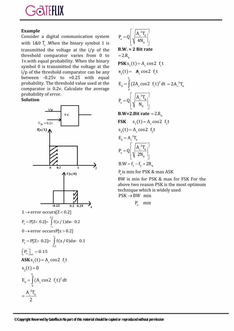
Example Consider a digital communication system with 1&0 xT .When the binary symbol 1 is transmitted the voltage at the i/p of the threshold comparator varies from 0 to 1v.with equal probability. When the binary symbol 0 is transmitted the voltage at the i/p of the threshold comparator can be any between -0.25v to +0.25 with equal probability. The threshold value used at the comparator is 0.2v. Calculate the average probability of error. Solution
→ <1 error occurs[Z 0.2]
0.2
eP P[Z 0.2] f(z /1)dz 0.2−∞
= < = =∫
0 error occursP[z 0.2]→ >
e0.2
P P[Z 0.2] f(z / 0)dz 0.1∞
= > = =∫
= e avP 0.15
ASK 1 c cs (t) A cos2 f t= π
2s (t) 0= bT
2d c c
0
E (A cos2 f t) dt= π∫
2c bA T2
=
2c b
e0
A TP Q
4N
=
B.W. = 2 Bit rate b2.R=
PSK 1 c cs (t) A cos2 f t= π
2 c cs (t) A cos2 f t= − π bT
2d c c
0
E (2A cos2 f t) dt= π∫ 2c b2A T=
2c b
e0
A TP Q
N
=
B.W=2.Bit rate b2.R=
FSK 1 c 1s (t) A cos2 f t= π
2 c 2s (t) A cos2 f t= π
= 2b c bE A T
2c b
e0
A TP Q
2N
=
1 2 bB.W f f 2R= − +
eP is min for PSK & max ASK BW is min for PSK & max for FSK For the above two reason PSK is the most optimum technique which is widely used
e
PSK BW min P min
→
© Copyright Reserved by Gateflix.in No part of this material should be copied or reproduced without permission
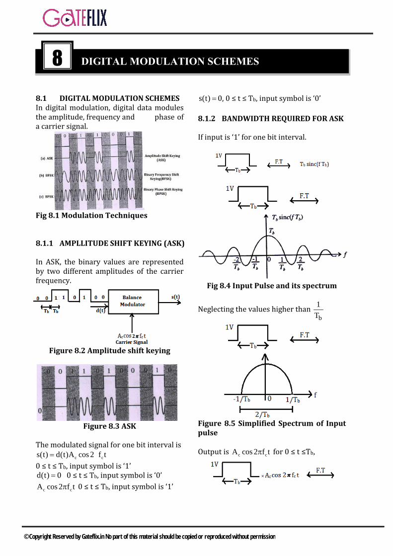
8.1 DIGITAL MODULATION SCHEMES In digital modulation, digital data modules the amplitude, frequency and phase of a carrier signal.
Fig 8.1 Modulation Techniques
8.1.1 AMPLLITUDE SHIFT KEYING (ASK)
In ASK, the binary values are represented by two different amplitudes of the carrier frequency.
Figure 8.2 Amplitude shift keying
Figure 8.3 ASK
The modulated signal for one bit interval is c cs(t) d(t)A cos 2 f t= π
0 ≤ t ≤ Tb, input symbol is ‘1’ d(t) = 0 0 ≤ t ≤ Tb, input symbol is ‘0’
c cA cos 2 f tπ 0 ≤ t ≤ Tb, input symbol is ‘1’
s(t) =0, 0 ≤ t ≤ Tb, input symbol is ‘0’
8.1.2 BANDWIDTH REQUIRED FOR ASK
If input is ‘1’ for one bit interval.
Fig 8.4 Input Pulse and its spectrum
Neglecting the values higher than b
1T
Figure 8.5 Simplified Spectrum of Input pulse
Output is c cA cos 2 f tπ for 0 ≤ t ≤Tb,
8 DIGITAL MODULATION SCHEMES
© Copyright Reserved by Gateflix.in No part of this material should be copied or reproduced without permission

Figure 8.6 Spectrum of Output Signal for Input ‘1’
When inputs is ‘0’ then spectrum of input as well as output is zero. Hence overall spectrum of output is as shown in Fig 10.6 and the bandwidth required is
B.W = b
2T
8.1.3 AVERAGE ENERGY PER BIT In ASK, if input symbol is ‘1’ then output is s1 (t) = c cA cos 2 f tπ , 0 ≤ t ≤ Tb Energy per bit is
2c
1 bAE T2
=
If input symbol is ‘0’ then output is s2 (t) = 0, 0 ≤ t ≤ Tb Energy per bit is E0 = 0 The average energy per bit is
E0 =
2c
b0 1
A0 TE E 22 2
++=
Eb =2
cb
A T4
The energy of difference signal is
Ed = [ ]bT
21 2
0
s (t) s (t) dt−∫
Ed = ( )bT
2c c
0
A cos 2 f t 0 dtπ −∫
Ed = bT 2
2 cc c b
0
AA cos 2 f t dt T2
π =∫
Ed = 2
c4A Tb2
8.1.4 PROBABILITY OF ERROR
d1 2
0
Ea aPe2 n 2
−= = σ η
2c b bA T EPe
4
= = η η
8.2 BINARY PHASE SHIFY KEYING
Figure 8.7 binary Phase Shift Keying
(BPSK)
Fig 8.8 BPSK
The module signal for one bit interval is
c cs(t) d(t)A cos 2 f t= π
b
b
1 0 t T , input symbol is ‘1’1 0 t T , input symbol is
d( ‘0’
t)+ ≤ ≤− ≤
=≤
c c
c
b
bc
A cos 2 f ts(t)
A c, 0 t T input symbol is ‘1’, 0 t T input symbol io ss 2 ‘0’f t
π = π
≤ ≤≤ ≤
If input symbol is ‘1’ for one bit interval then output is
© Copyright Reserved by Gateflix.in No part of this material should be copied or reproduced without permission

Fig 8.9 Spectrum of Output Signal for Input Symbol ‘0’ If we combine the spectrums of Fig 10.9 and 10.10 by taking their magnitude then bandwidth required will be
B.W = b
2T
8.2.1 AVERAGE ENERGY PER BIT In BPSK, if input symbol is ‘1’ then output is s1 (t) = c cA cos 2 f tπ , 0 ≤ t ≤ Tb Energy per bit is
2c
1 bAE T2
=
If input symbol is ‘0’ then output is s2 (t) = c cA cos 2 f t− π , 0 ≤ t ≤ Tb (10.4) Energy per bit is
E0 = 2
cb
A T2
(10.5)
The average energy per bit is
E0 =
2 2c c
b b0 1
A AT TE E 2 22 2
++=
Eb =2
cb
A T2
The energy of difference signal is
Ed = [ ]bT
21 2
0
s (t) s (t) dt−∫
Ed = ( )bT
2c c c c
0
A cos 2 f t A cos 2 f t dtπ − − π ∫
Ed = ( )bT
2c c
0
2A cos 2 f t dtπ∫
Ed = 2
c4A Tb2
Ed = 2A2c Tb 8.2.2 PROBABILITY OF ERROR
d1 2
0
Ea aPe2 n 2
−= = σ η
2 2c b c b2A T A TPe
2
= = η η
b2EPe
= η
8.3 DIFFERENCIAL PSK (DPSK) In DPSK, the phase shift is with reference to the previous bit transmitted, rather than to some constant reference signal. If inputs symbol is ‘0’ then signal burst is with same phase as the previous one. If input symbol is ‘1’ then signal burst is of opposite phase to the preceding one.
Figure 8.10 Differential PSK
8.3.1 BINARY FREQUENCY SHIFT KEYING (BFSK) Two binary values represented by two different frequencies.
b
b
c 1
c 1
0 t T ,input symbol is '1' 0 t T ,input symbol is '0 '
A cos 2 f t,s(t)
A cos 2 f t,≤ ≤≤
π = ≤ π
Here f1 > f2, f1 and f2 are integers multiple o
b
1T
.
Figure 8.11 Binary FSK
© Copyright Reserved by Gateflix.in No part of this material should be copied or reproduced without permission

8.3.2 BINARY REQUIRED FOR BFSK If input symbol is ‘1’ for one bit interval then output is.
Figure 8.12 Spectrum of Output Signal for Input Symbol ‘1’ If input symbol is ‘0’ for one bit interval then output is
Figure 8.13 Spectrum of Output Signal for Input Symbol ‘0’ If we combine the spectrums of Fig 8.13 and 8.14 then bandwidth required will
B.W = 1 2b
2f fT
− +
8.3.3 AVERAGE ENERGY PER BIT In BFSK, if input symbol is ‘1’ then output is s1 (t) = Ac cos 2π f1t, 0 ≤ t ≤ Tb Energy per bit is
E1 = 2
cb
A T2
If input symbol is ‘0’ then output is s2 (t) = Ac cos 2π f2t, 0 ≤ t ≤ Tb
Energy per bit isE0 = 2
cb
A T2
The average energy per bit is
Eb =
2 2c c
b b0 1
A AT TE E 2 22 2
++=
Eb =2
cb
A T2
The energy of difference signal is Ed
= [ ]bT
21 2
0
s (t) s (t) dt−∫
Ed = ( )b
c 2
T2
10
cA cos 2 f t A cos d 2 f tπ − π∫
f1 and f2 are integer multiple of b
1T
Ed = A2c Tb 8.3.4 PROBABILITY OF ERROR
d1 2
0
Ea aPe2 n 2
−= = σ η
2c b bA T EPe
2
= = η η
8.3.5 CONSTELLATION DIAGRAM OR PHASE DIAGRAM 1) ASK
1 c c
2
input symbol is '1' s (t) A cos 2 f t,
s(t)s (t) 0, input symbol is '0 '
= π = =
Average energy per bit is
Eb = 2
cb
A T2
bc
b
EA 2T
=
b1 c
b
2
, for '1'
Es (t
) 2 cos
,
2 f t,s(t) T
s (t) 0, for '0 '
= π =
=
Assuming a basis function
1 cb
2(t) cos 2 f tT
φ π
Then s1 (t) = 0 12E (t)φ for ‘1’ And s2 (t) = 0, for ‘0’
© Copyright Reserved by Gateflix.in No part of this material should be copied or reproduced without permission
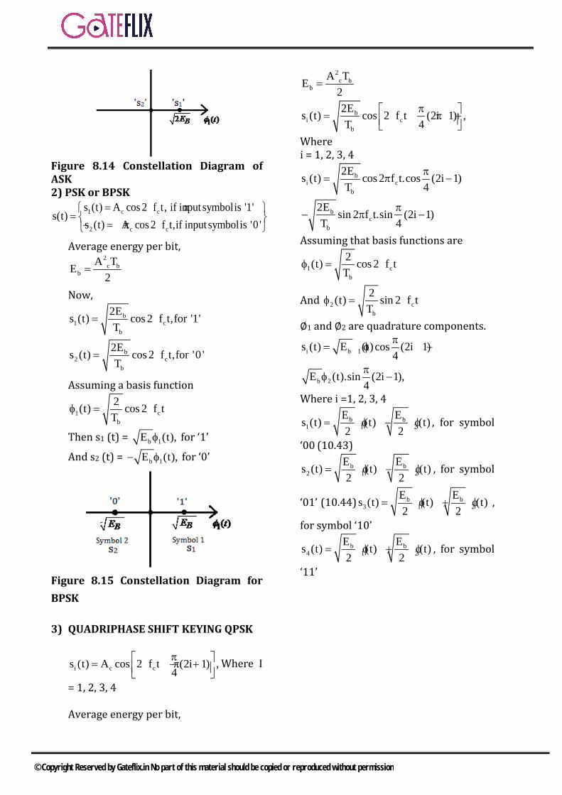
Figure 8.14 Constellation Diagram of ASK 2) PSK or BPSK
1 c c
2 c c
if input symbol is '1' s (t) A cos 2 f t,
s(t)s (t) A cos 2 f t if input symbol is '0 ' ,
= π = = − π
Average energy per bit, 2
c bb
A TE2
=
Now,
b1 c
b
2Es (t) cos 2 fof rt 'T
1, '= π
b2 c
b
2Es (t) cos 2 fof rt 'T
0, '= π
Assuming a basis function
1 cb
2(t) cos 2 f tT
φ = π
Then s1 (t) = b 1E (t),φ for ‘1’
And s2 (t) = b 1E (t),− φ for ‘0’
Figure 8.15 Constellation Diagram for BPSK
3) QUADRIPHASE SHIFT KEYING QPSK
i c cs (t) A cos 2 f t (2i 1) ,4π = π + −
Where I
= 1, 2, 3, 4
Average energy per bit,
2c b
bA TE
2=
bi c
b
2Es (t) cos 2 f t (2i 1) ,T 4
π = π + − Where i = 1, 2, 3, 4
bi c
b
2Es (t) cos 2 f t.cos (2i 1)T 4
π= π −
bc
b
2E sin 2 f t.sin (2i 1)T 4
π− π −
Assuming that basis functions are
1 cb
2(t) cos 2 f tT
φ = π
And 2 cb
2(t) sin 2 f tT
φ = π
∅1 and ∅2 are quadrature components.
i b 1s (t) E (t) cos (2i 1)4π
= φ − −
b 2E (t).sin (2i 1),4π
φ −
Where i =1, 2, 3, 4
b b1 1 2
E Es (t) (t) (t)2 2
= φ − φ , for symbol
‘00 (10.43)
b b2 1 2
E Es (t) (t) (t)2 2
= φ − φ , for symbol
‘01’ (10.44) b b3 1 2
E Es (t) (t) (t)2 2
= φ + φ ,
for symbol ‘10’
b b4 1 2
E Es (t) (t) (t)2 2
= φ + φ , for symbol
‘11’
© Copyright Reserved by Gateflix.in No part of this material should be copied or reproduced without permission
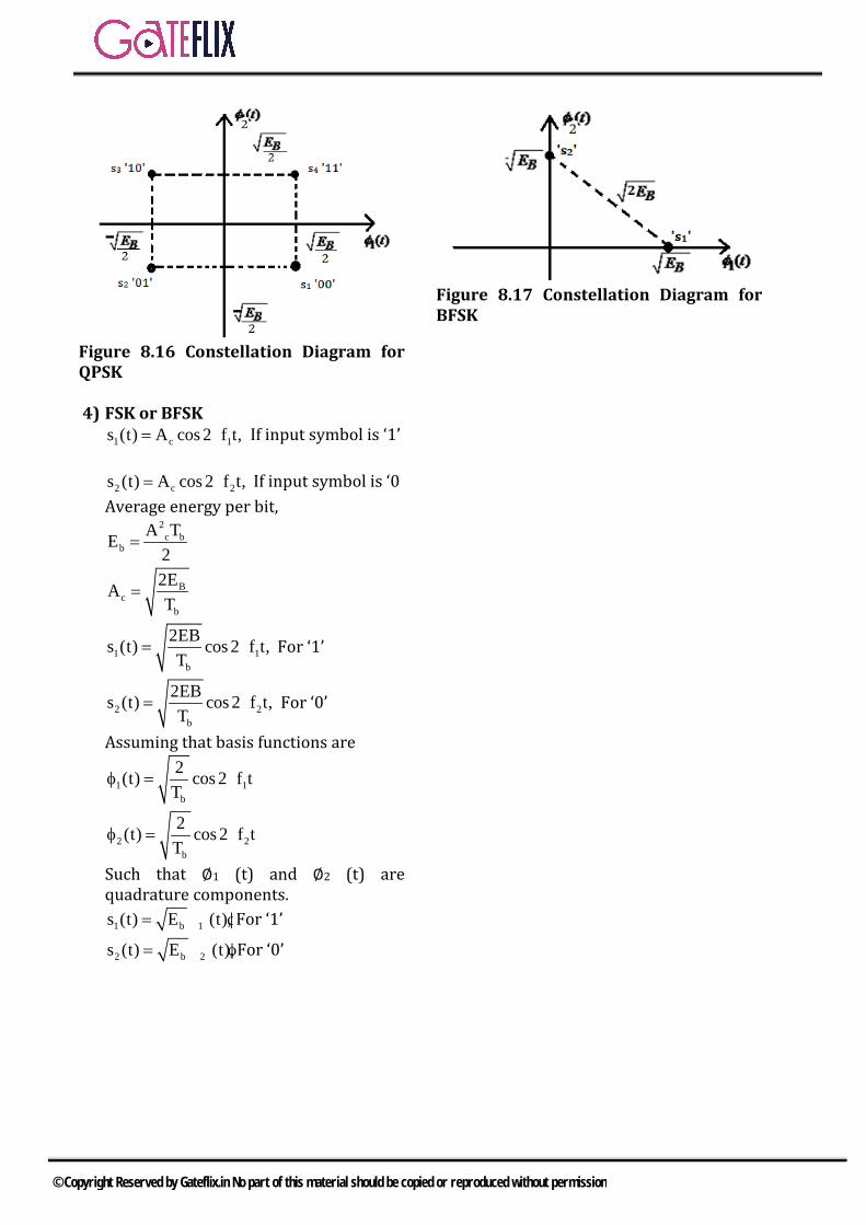
Figure 8.16 Constellation Diagram for QPSK
4) FSK or BFSK1 c 1s (t) A co 2 s f t,= π If input symbol is ‘1’
2 c 2s (t) A co 2 s f t,= π If input symbol is ‘0Average energy per bit,
2c b
bA TE
2=
Bc
b
2EAT
=
1 1b
2EBs (t) cos 2 f T
t,= π For ‘1’
2 2b
2EBs (t) cos 2 f T
t,= π For ‘0’
Assuming that basis functions are
1 1b
2(t) cos 2 f tT
φ = π
2 2b
2(t) cos 2 f tT
φ = π
Such that ∅1 (t) and ∅2 (t) are quadrature components.
1 b 1 s ( t) E (t),= φ For ‘1’
2 b 2 s ( t) E (t),= φ For ‘0’
Figure 8.17 Constellation Diagram for BFSK
© Copyright Reserved by Gateflix.in No part of this material should be copied or reproduced without permission
Q.1 In a digital communication system employing frequency Shift Keying (FSK) , the 0 and 1 bit are represented by sine waves of 10kHz and 25kHz respectively These waveforms will be orthogonal for a bit interval of a)45μsec b) 200μsecc) 50μsec d) 250μsec
[GATE-2000]
Q.2 During transmission over a communication channel, bit errors occur independently with probability p. If a block of n bits is transmitted the probability of at most one bit error is equal to a) ( )n1 1 p− − b) ( )p n 1 (1 p)+ − −
c) ( )n 1np 1 p −− d) ( ) ( )n n 11 p np 1 p −− + −
[GATE-2001]
Q.3 The Nyquist sampling interval for the signal ( ) ( )sinc 700t +sinc 500t is
a) 1350
sec b) π350
sec
c) 1700
sec d) π175
sec
[GATE-2001]
Q.4 A video transmission system transmits 625 picture frames per second. Each frame consists of a 400 × 400 pixel grid with 64 intensity levels per pixel. The data rate of the system is a) 16Mbps b) 100Mbpsc) 600Mbps d) 6.4 Gbps
[GATE-2001]
Q.5 A signal ( ) ( )3x t 100cos 24π 10 t= × isideally sampled with a sampling period of 50μsec and then passed through an ideal low pass filter with
cutoff frequency of 15 kHz. Which of the following frequencies is/are present at the filter output? a) 12kHz onlyb) 8kKz onlyc) 12kHz and 9kHzd) 12kHz and 8kHz
[GATE-2002]
Q.6 For bit–rate of 8Kbps, the best possible values of the transmitted frequencies in a coherent binary FSK system are a) 16kHz and 20kHzb) 20kHz and 32 kHzc) 20kHz and 40kHzd) 32kHz and 40kHz
[GATE-2002]
Q.7 Consider a sample signal
( ) ( )6s
n
y t 5 10 x t δ(t nT )+∞
−
=−∞
= × −∑where ( ) ( )3x t 10cos 8π 10 t= × and
sT 100μsec= When y(t) is passed through an ideal low pass filter with a cutoff frequency of 5 kHz the output of the filter is a) ( )6 35 10 cos 8π 10 t−× × )
b) ( )5 35 10 cos 8π 10 t−× ×
c) ( )1 35 10 cos 8π 10 t−× ×
d) ( )310cos 8π 10 t×
[GATE-2002]
Q.8 A signal is sampled at 8 kHz and is quantized using 8-bit uniform quantizer using 8-bit uniform quantizer. Assuming SNRq for a sinusoidal signal, the correct statement for PCM signal with a bit rate of R is a) qR 32kbps,SNR 25.8dB= =
GATE QUESTIONS
© Copyright Reserved by Gateflix.in No part of this material should be copied or reproduced without permission
b) qR 64kbps,SNR 49.8dB= =
c) qR 64kbps,SNR 55.8dB= =
d) qR 32kbps,SNR 49.8dB= = [GATE-2003]
Q.9 If S represents the carrier synchronization at the receiver and ρ represents the Bandwidth efficiency, then the correct statement for the coherent binary PSK is a) ρ 0.5,S is required=b) ρ 1.0,S is required=c) ρ 0.5,S is not required=d) ρ 1.0,S is not required=
[GATE-2003]
Q.10 The input to a linear delta modulator having a step-size
0.628∆ = is a sine wave with frequency fm and peak amplitude Em .If the sampling frequency
sf 40kHz= the combination of the sine –wave frequency and the peak amplitude, where slope overload will take place is Em fm a) 0.3V8 kHz b) 1.5V4 kHzc) 1.5V 2 kHz d) 3.0V1 KHz
[GATE-2003]
Q.11 If Eb the energy per bit of a binary digital signal is 10−5 watt-sec and the one –sided power spectral density of the white noise, N0 =10−6 W/Hz, and then the output SNR of the matched filter is a) 26dB b) 10dBc) 20dB d) 13dB
[GATE-2003]
Q.12 A sinusoidal signal with peak-to–peak amplitude of 1.536 V is quantized into 128 levels using a mid- rise uniform quantizer. The quantization –noise power is a) 0.768V b) 6 248 10 V−×c) 6 212 10 V−× d) 3.072V
[GATE-2003]
Q.13 Let x(t)=2cos(800πt)+cos(1400πt).x(t) is sampled with the rectangular pulse train shown in the figure. The only spectral components (in kHz) present in the sampled signal in the frequency range 2.5 kHz to 3.5 kHz are.
a) 2.7, 3.4 b) 3.3, 3.6c) 2.6, 3.3, 3.4, 3.6 d) 2.7, 3.3
[GATE-2003]
Q.14 At a given probability of error, binary coherent FSK is inferior to binary coherent PSK by a) 6db b) 3dBc) 2dB d) 0dB
[GATE-2003]
Q.15 Consider the signal x(t) shown in the figure. Let h(t) denote the impulse response of the filter matched to x(t), with h(t) being non zero only in the interval 0 to 4 sec. The slope of h(t) in the interval 3<t<4 sec is
a) 11 sec2
− b) 11sec−−
c) 11 sec2
−− d) 11sec−
[GATE-2004]
Q.16 Three analog signals , having bandwidths 1200Hz, 600Hz and 600Hz are sampled at their
© Copyright Reserved by Gateflix.in No part of this material should be copied or reproduced without permission

respective Nyquist rates , encoded with 12 bit words , and time division multiplexed , The bit rate for the multiplexed signal is a) 115.2kbps b) 28.8kbps c) 57.6kbps d) 38.4 kbps
[GATE-2004]
Q.17 Choose the correct one from among the alternatives a, b, c, d after matching an item from Group 1 with the most appropriate item in Group 2. Group 1 Group 2 1. FM P. Slope overload 2. DM Q. μ-law 3. PSK R. Envelope detector 4. PCM S. Capture effect
T. Hilbert transform U. Matched filter
a) 1-T,2-P, 3-U,4-S b) 1-S,2-U,3-P,4-T
c) 1-S,2-P,3-U,4-Q d) 1-U,2-R,3-S,4-Q
[GATE-2004] Q.18 Consider a binary digital
communication system with equally likely0’s and 1’s.When binary 0 is transmitted the detector input can lie between the levels -0.25V and +0.25V with equal provability. When binary 1 is transmitted, the voltage at the detector can have any value between 0 and 1 with equal probability .If the detector has a threshold of 0.2V (i.e. if the received signal is greater than 0.2V, the bit is taken as 1). The average bit error probability is a) 0.15 b) 0.2 c) 0.05 d) 0.5
[GATE-2004] Q.19 A source produces binary data at the
rate of10kbps. The binary symbols are represented as shown in the figure.
The source output is transmitted using two modulation schemes, namely Binary PSK (BPSK)and Quadrature PSK(QPSK) Let B1 and B2 be the bandwidth requirements of BPSK and QPSK respectively. Assuming that the bandwidth of the above rectangular pulses is 10 kHz, B1 and B2 are a) 1 2B 20kHz,B 20kHz= =
b) 1 2B 10kHz,B 20kHz= = c) 1 2B 20kHz,B 10kHz= =
d) 1 2B 10kHz,B 10kHz= = [GATE-2004]
Q.20 in the output of a DM speech
encoder, the consecutive pulses are of opposite polarity during time interval t1 ≤ t ≤ t2.This indicates that during this interval a) the input to the modular is
essentially constant b) the modulator is going through
slope overload c) the accumulator is in saturation d) the speech signal is being
sampled at the Nyquist rate [GATE-2004]
Q.21 In a PCM system, if the code worked
length is increased from 6 to 8 bits, the signal to quantization noise ratio improves by the factor a) 8/6 b) 12 c) 16 d) 8
[GATE-2004]
© Copyright Reserved by Gateflix.in No part of this material should be copied or reproduced without permission
Q.22 A signal as shown in the figure is applied a matched filter. Which of the following does represent the output of this matched filter?
a)
b)
c)
d)
[GATE-2005]
Q.23 In the following figure the minimum
value of the constant “C”, which is to be added to 𝑦𝑦1(𝑡𝑡) such that 1y (t) and 2y (t) are different is
a) ∆ b) ∆/2 c) ∆2/12 d) ∆/L
[GATE-2006]
Q.24 The minimum step –size required for Delta- Modulator operating at 32K samples/sec to track the signal (here u(t) is the unit step function)( ) ( ) ( )( ) ( )( ) ( )
x t 125t u t u t 1 250 125t
(u t 1 u t 2 )
= − − + −
− − − so that slope overload is avoided m, would be a) 102− b) 82−
c) 62− d) 42− [GATE-2006]
Q.25 The minimum sampling frequency
(in samples/sec) required to reconstruct the following signal from its samples without distortion
( )3 2sin2π1000t sin2π1000tx t =5 +7
πt πt
would be a) 32 10× b) 34 10× c) 36 10× d) 38 10×
[GATE-2006]
Statement for linked Answer Questions 26 & 27 An input to a 6-level quantizer has the probability density function f(x) as shown in the figure. Decision boundaries of the quantizer are chosen so as to maximum the entropy of the quantizer output. It is given that 3 consecutive decision boundaries are ‘-1’,’0’ and ‘1’
Q.26 The values of a and b are a) a = 1/6 and b = 1/12
b) a = 1/5 and b = 3/40
© Copyright Reserved by Gateflix.in No part of this material should be copied or reproduced without permission
c) a = 1/4 and b = 1/16 d) a = 1/3 and b = 1/24
[GATE-2007]
Q.27 Assuming that the reconstruction levels of the quantizer are the mid-points of the decision boundaries, the ratio of signal power to quantization noise power is
a) 1529
b) 643
c) 763
d) 28
[GATE-2007]
Common Data for Question 28 & 29 Two 4-ary signal constellations are shown .It is given that 1Φ and 2Φ constitute an orthonormal basis for the two constellations. Assume that the four symbols in both the constellations are equiprobable .Let N0/2 denote the power spectral density of white Gaussian noise.
Q.28 The ratio of the average energy of
Constellation 1 to the average energy of Constellation 2 is
a) 4a2 b) 4 c) 2 d) 8
[GATE-2007] Q.29 If these constellations are used for
digital communications over an A WGN channel, then which of the following statements is true? a) Probability of symbol error for
Constellation 1 is lower b) Probability of symbol error for
Constellation 1 is higher
c) Probability of symbol error is equal for both the constellations
d) The value of 𝑁𝑁0 will determine which of the two constellation has a lower probability of symbol error
[GATE-2007]
Q.30 In a Direct Sequence CDMA system the chip rate is 1.2288 × 10⁶ chips per second. If the processing gain is desired to be AT LEAST 100, the data rate a) must be less than or equal to
312.288 10× bits per sec b) must be greater than 312.288 10×
bits per sec c) must be exactly equal to
312.288 10× bits per sec d) can take any value less than
3122.288 10× bits per sec [GATE-2007]
Q.31 In a GSM system , 8 channels can co-
exist in 200 kHz bandwidth using TDMA .A GSM based cellular operator is allocated 5 MHz bandwidth. Assuming a frequency reuse factor of 1/5, ie., a five –cell repeat pattern, the maximum number of simultaneous channels that can exist in one cell is a) 200 b) 40 c) 25 d)5
[GATE-2007]
Q.32 During transmission over a certain binary commutation channel, bit errors occur independently with probability p. The probability of AT MOST one bit in error in a block of n bits is given by
a) np b) n1 p− c) ( ) ( )n 1 nnp 1 p 1 p−− + − d) ( )n1 1 p− −
[GATE-2007]
© Copyright Reserved by Gateflix.in No part of this material should be copied or reproduced without permission
Q.33 The raised cosine pulse p(t) is used for zero ISI in digital communications. The expression for p(t) with unity roll-off factor is given
by p(t) = 2 2
sin4πWt4πWt(1-16W t )
. The
value of p(t) at t = 14W
is
a) – 0.5 b )0 c) 0.5 d) ∞
[GATE-2007]
Q.34 In delta modulation, the slope overload distortion can be reduced by a) Decreasing the step size b) Decreasing the granular noise c) Decrease the sampling rate d) Increase the step size
[GATE-2007]
Common Data for Question 35, 36 & 37 A speech signal band limited to 4 kHz and peak voltage varying between +5v an -5V, is sampled at the Nyquist rate. Each sample is quantized and represented by 8 bits.
Q.35 If the bits 0 and 1 are transmitted
using bipolar pulses, the minimum bandwidth required for distortion free transmission is a) 64 kHz b) 32 kHz c) 8 kHz d) 4 kHz
[GATE-2008]
Q.36 Assuming the signal to be uniformly distributed between its peak to peak value, the signal to noise ratio at the quantizer output is a) 16dB b) 32dB c) 48dB d) 64dB
[GATE-2008]
Q.37 The number of quantization level required to reduce the quantization noise by a factor of 4 would be
a) 1024 b) 512 c) 256 d) 64
[GATE-2008]
Q.38 Four message band limited to W,W 2W and 3W respectively are to be multiplexed using Time Division Multiplexing (TDM) The minimum bandwidth required for transmission of this TDM signal is a) W b) 3W c) 6W d) 7W
[GATE-2008]
Q.39 Consider a Binary Symmetric Channel (BSC) with probability of error being p .To transmit a bit, say1, we transmit a sequence of three 1s.The receiver will interpret the received sequence to represent 1 if at least two bits are1. The probability that the transmitted bit will be received in error is a) 3 2p 3p (1 p)+ − b) 3p c) ( )31 p− d) 3 2p p (1 p)+ −
[GATE-2008]
Common Data for Question 40 & 41 The amplitude of a random signal is uniformly distributed between -5V and 5V
Q.40 If the signal to quantization noise ratio required in uniformly quantizing the signal is 43.5 dB, the step size of the quantization is approximately a) 0.0333V b) 0.05V c) 0.0667V d) 0.10V
[GATE-2009]
Q.41 If the positive values of the signal are uniformly quantized with a step size of 0.05V, and the negative values are uniformly quantized with a step size of 0.1V, the resulting signal to quantization noise ratio is approximately a) 46dB b) 43.8dB c) 42dB d) 40dB
[GATE-2009]
Q.42 The Nyquist sampling rate for the
signal ( ) sin(500πt) sin(700πt)s t = ×πt πt
is given by
© Copyright Reserved by Gateflix.in No part of this material should be copied or reproduced without permission

a) 400Hz b) 600Hz c) 1200Hz d) 1400Hz
[GATE-2010]
Q.43 Consider the pulse shape s(t) as shown. The impulse response h(t) of the filter matched to this pulse is
a)
b)
c)
d)
[GATE-2010]
Linked data Question 44 & 45 A four –phase and an eight –phase signal constellation are shown in the figure below.
Q.44 For the constraint that the minimum
distance between pairs of signal points be d for both constellations, the radii r1 and r2 of the circles are
a) 1 2r 0.707d, r 2,782d= = b) 1 2r 0.707d, r 1.932d= =
c) 1 2r 0.707d, r 1.545d= = d) 1 2r 0.707d, r 1.307d= =
[GATE-2011]
Q.45 Assuming high SNR and that all signals are equally problem, the additional average transmitted signal energy required by the 8-PSK signal to achieve the same error probability as the 4-PSK signal is
a) 11.90dB b) 8.73db c) 6.79dB d) 5.33dB
[GATE-2011]
Q.46 An analog signal is band –limited to 4 kHz, sampled at the Nyquist rate and the samples are quantized into 4 levels. The quantized levels are assumed to be independent and equally probable. If we transmit two quantized samples per second, the information rate is
a) 1bit/sec b) 2bits/sec c) 3bits/sec d) 4 bits/sec
[GATE-2011]
Q.47 A BPSK scheme operating over an AWGN channel with noise power spectral density of N0/2, uses equiprobable signals
( ) ( ) ( )1 c 22ES t sin sin ω t andS tT
=
© Copyright Reserved by Gateflix.in No part of this material should be copied or reproduced without permission
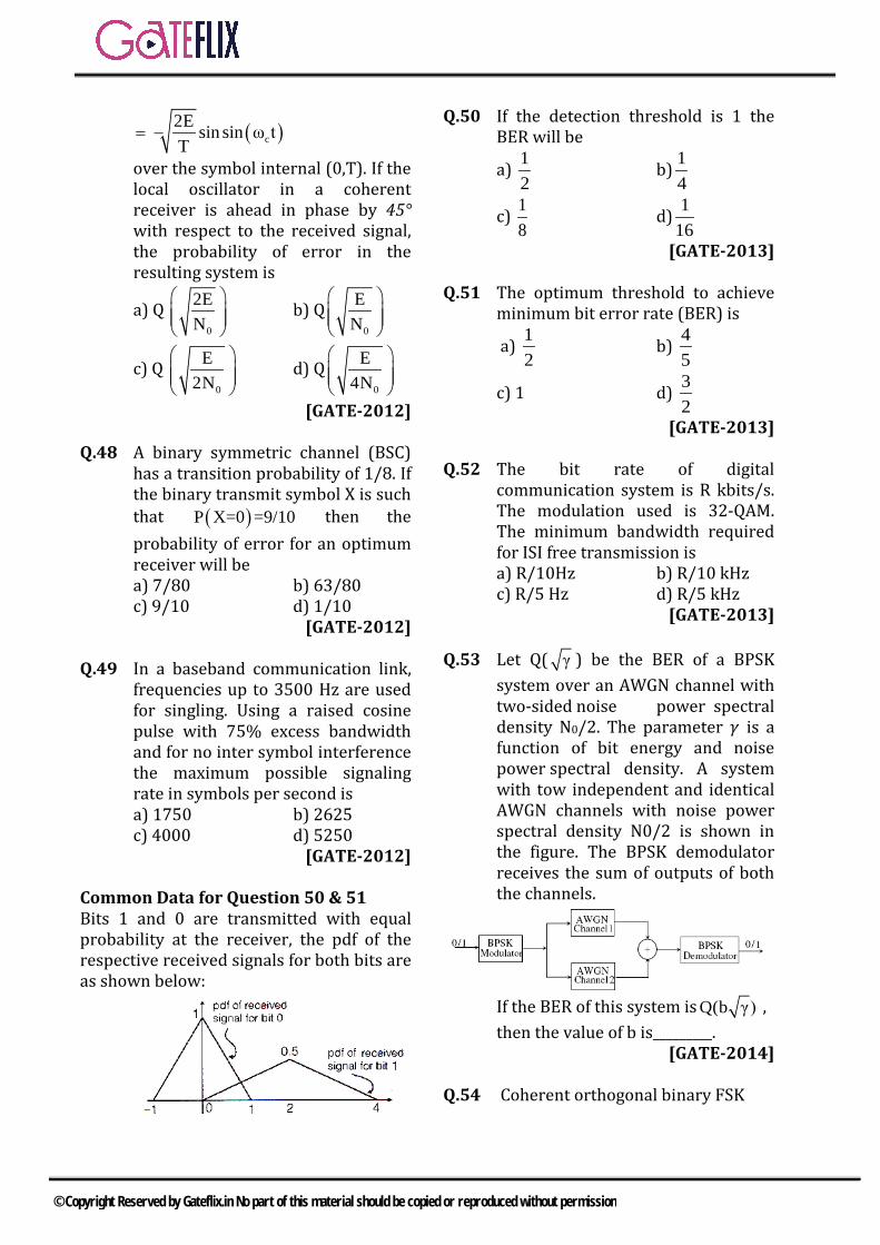
( )c2E sin sin ω tT
= −
over the symbol internal (0,T). If the local oscillator in a coherent receiver is ahead in phase by 45° with respect to the received signal, the probability of error in the resulting system is
a) Q 0
2EN
b) Q0
EN
c) Q 0
E2N
d) Q0
E4N
[GATE-2012]
Q.48 A binary symmetric channel (BSC) has a transition probability of 1/8. If the binary transmit symbol X is such that ( )P X=0 =9/10 then the probability of error for an optimum receiver will be a) 7/80 b) 63/80 c) 9/10 d) 1/10
[GATE-2012]
Q.49 In a baseband communication link, frequencies up to 3500 Hz are used for singling. Using a raised cosine pulse with 75% excess bandwidth and for no inter symbol interference the maximum possible signaling rate in symbols per second is a) 1750 b) 2625 c) 4000 d) 5250
[GATE-2012]
Common Data for Question 50 & 51 Bits 1 and 0 are transmitted with equal probability at the receiver, the pdf of the respective received signals for both bits are as shown below:
Q.50 If the detection threshold is 1 the BER will be
a) 12
b) 14
c) 18
d) 116
[GATE-2013] Q.51 The optimum threshold to achieve minimum bit error rate (BER) is
a) 12
b) 45
c) 1 d) 32
[GATE-2013] Q.52 The bit rate of digital
communication system is R kbits/s. The modulation used is 32-QAM. The minimum bandwidth required for ISI free transmission is
a) R/10Hz b) R/10 kHz c) R/5 Hz d) R/5 kHz
[GATE-2013]
Q.53 Let Q( γ ) be the BER of a BPSK system over an AWGN channel with two-sided noise power spectral density N0/2. The parameter 𝛾𝛾 is a function of bit energy and noise power spectral density. A system with tow independent and identical AWGN channels with noise power spectral density N0/2 is shown in the figure. The BPSK demodulator receives the sum of outputs of both the channels.
If the BER of this system is Q(b γ) , then the value of b is_________.
[GATE-2014] Q.54 Coherent orthogonal binary FSK
© Copyright Reserved by Gateflix.in No part of this material should be copied or reproduced without permission

modulation is used to transmit two equiprobable symbol waveforms ( ) 11 α=cos = s2πft t and
( ) 22 cos2s = πft t , where α = 4mV. Assume an AWGN channel with two-sided noise power spectral density N0
2= 0.5 x 10⁻¹²W / Hz. Using
an optimal receiver and the relation Q(v) = 1
√2𝜋𝜋 ∫ 𝑒𝑒−𝑢𝑢22 ∞
𝑉𝑉 du the bit error probability for a data
rate of 500 kbps is a) Q(2) b) Q2√2 c) Q(4) d) Q(4√2)
[GATE-2014]
Q.55 An analog voltage in the range 0 to 8 V is divided in 16 equal intervals for conversion to 4-bit digital output. The maximum quantization error (in V) is _______.
[GATE-2014]
Q.56 In a PCM system, the signal m(t) = sin (100𝜋𝜋𝑡𝑡) + cos (100 𝜋𝜋𝑡𝑡) V is sampled at the Nyquist rate. The samples are processed by a uniform quantizer with step size 0.75 V. The minimum data rate of the PCM system in bits per second is _____.
[GATE-2014]
Q.57 An M-level PSK modulation scheme is used to transmit independent binary digits over a band-pass channel with bandwidth 100 kHz. The bit rate is 200 kbps and the system characteristic is a raised-cosine spectrum with 100% excess bandwidth. The minimum value of M is __________.
[GATE-2014]
Q.58 A sinusoidal signal of 2 kHz frequency is applied to a delta modulator. The sampling rate and step-size ∆ of the delta modulator are 20,000 samples per second and
0.1V, respectively. To prevent slope overload, the maximum amplitude of the sinusoidal signal (in Volts) is
a) 12π
b) 1π
c) 2π
d) π
[GATE-2015]
Q.59 The input X to the binary symmetric channel (BSC) shown in the figure is ‘1’ with probability 0.8. The cross-over probability is 1/7. If the received bit Y = 0, the conditional probability that ‘1’ was transmitted is _______________
[GATE-2015]
Q.60 The transmitted signal in a GSM
system is of 200 kHz bandwidth and 8 users share a common bandwidth using TDMA. If at a given time 12 users are talking in a cell, the total bandwidth of the signal received by the base station of the cell will be at least (in kHz) _____________.
[GATE-2015] Q.61 A source emits bit 0 with probability
13
and bit 1 with probability 23
. The
emitted bits are communicated to the receiver. The receiver decides for either 0 or 1 based on the received value R. It is given that the conditional density functions of R
are as ( )R /0
1 , 3 x 1f r 4
0,otherwise,
− ≤ ≤=
and
( )R /1
1 , 1 x 5f r 6
0otherwise
− ≤ ≤=
© Copyright Reserved by Gateflix.in No part of this material should be copied or reproduced without permission
The minimum decision error
probability is a) 0 b) 1/12
c) 1/9 d) 1/6 [GATE-2015]
Q.62 A sinusoidal signal of amplitude A is
quantized by a uniform quantizer Assume that the signal utilizes all the representation levels of the quantizer. If the signal to quantization noise ratio is 31.8 dB, the number of levels in the quantizer is __________.
[GATE-2015]
Q.63 Consider a binary, digital communication system which used pulses g(t) and —g(t) for transmitting bits over an AWGN channel. If the receiver uses a matched filter, which one of the following pulses will give the minimum probability of bit error?
a) b)
c) d)
[GATE-2015]
Q.64 The modulation scheme commonly
used for transmission from GSM mobile terminals is a) 4-QAM b) 16-PSK c) Walsh-Hadamard orthogonal
codes d) Gaussian Minimum Shift Keying
(GMSK) [GATE-2015]
Q.65 Consider binary data transmission
at a rate of 56 kbps using baseband binary pulse amplitude modulation (PAM) that is designed to have a raised-cosine spectrum. The transmission bandwidth (in kHz) required for a roll-off factor of 0.25 is __________.
[GATE-2016]
Q.66 An analog pulse s(t) is transmitted over an additive white Gaussian noise (AWGN) channel. The received signal is r(t) = s(t) + n(t), where n(t) is additive white Gaussian noise
with power spectral Density 0N2
.
The received signal is passed through a filter with impulse response h(t). Let Es and Eh denote the energies of the pulse s(t) and the filter h(t), respectively. When the signal -to-noise ratio (SNR) is maximized at the output of the filter (SNRmax), which of the following holds?
a) ss h max
0
2EE E ;SNRN
= =
b) ss h max
0
EE E ;SNR2N
= =
c) ss h max
0
2EE E ;SNRN
> >
d) ss h max
0
2EE E ;SNRN
< =
[GATE-2016] Q.67 An ideal band-pass channel 500 Hz -
2000 Hz is deployed for communication. A modem is designed to transmit bits at the rate of 4800 bits/s using 16-QAM. The roll-off factor of a pulse with a raised cosine spectrum that utilizes the entire frequency band is ______.
[GATE-2016]
© Copyright Reserved by Gateflix.in No part of this material should be copied or reproduced without permission
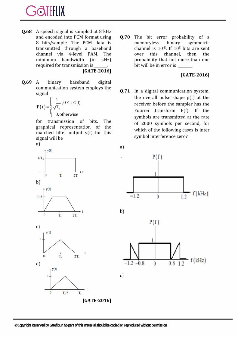
Q.68 A speech signal is sampled at 8 kHz and encoded into PCM format using 8 bits/sample. The PCM data is transmitted through a baseband channel via 4-level PAM. The minimum bandwidth (in kHz) required for transmission is _______.
[GATE-2016] Q.69 A binary baseband digital
communication system employs the signal
( ) ss
1 ,0 t TT0,otherwise
P t
=≤ ≤
for transmission of bits. The graphical representation of the matched filter output y(t) for this signal will be a)
b)
c)
d)
[GATE-2016]
Q.70 The bit error probability of a
memoryless binary symmetric channel is 10-5. If 105 bits are sent over this channel, then the probability that not more than one bit will be in error is ________
[GATE-2016]
Q.71 In a digital communication system, the overall pulse shape p(t) at the receiver before the sampler has the Fourier transform P(f). If the symbols are transmitted at the rate of 2000 symbols per second, for which of the following cases is inter symbol interference zero?
a)
b)
c)
© Copyright Reserved by Gateflix.in No part of this material should be copied or reproduced without permission

d)
[GATE-2017,Set-1]
Q.72 Which one of the following statements about differential pulse code modulation (DPCM) is true? a) The sum of message signal sample with its prediction is quantized b) The message signal sample is directly quantized, and its prediction is not used c) The difference of message signal sample and a random signal is quantized d) The difference of message signal sample with its predictions is quantized
[GATE-2017,Set-1]
Q.73 In binary frequency shift keying (FSK), the given signal waveform are
( ) ( )( ) ( )
0
1
u t 5cos 20000 t ;0 t T
u t 5cos 22000 t ;0 t T
= π ≤ ≤
= π ≤ ≤
Where T is the bit-duration interval and t is in seconds. Both u0(t) and u1(t) are zero outside the interval 0 t T≤ ≤ . With a matched filter (correlator) based receiver, the smallest possible value of T (in milliseconds) required to have u0(t) and u1(t) uncorrelated is
a)0.25ms b)0.5ms
c) 0.75ms d) 1.0ms
[GATE-2017,Set-1]
Q.74 A sinusoidal message signal is converted to a PCM signal using a uniform quantizer. The required signal-to-quantization noise ratio (SQNR) at the output of the quantizer is 40dB. The minimum number of bits per sample needed to achieve the desired SQNR is _______
[GATE-2017,Set-2]
© Copyright Reserved by Gateflix.in No part of this material should be copied or reproduced without permission
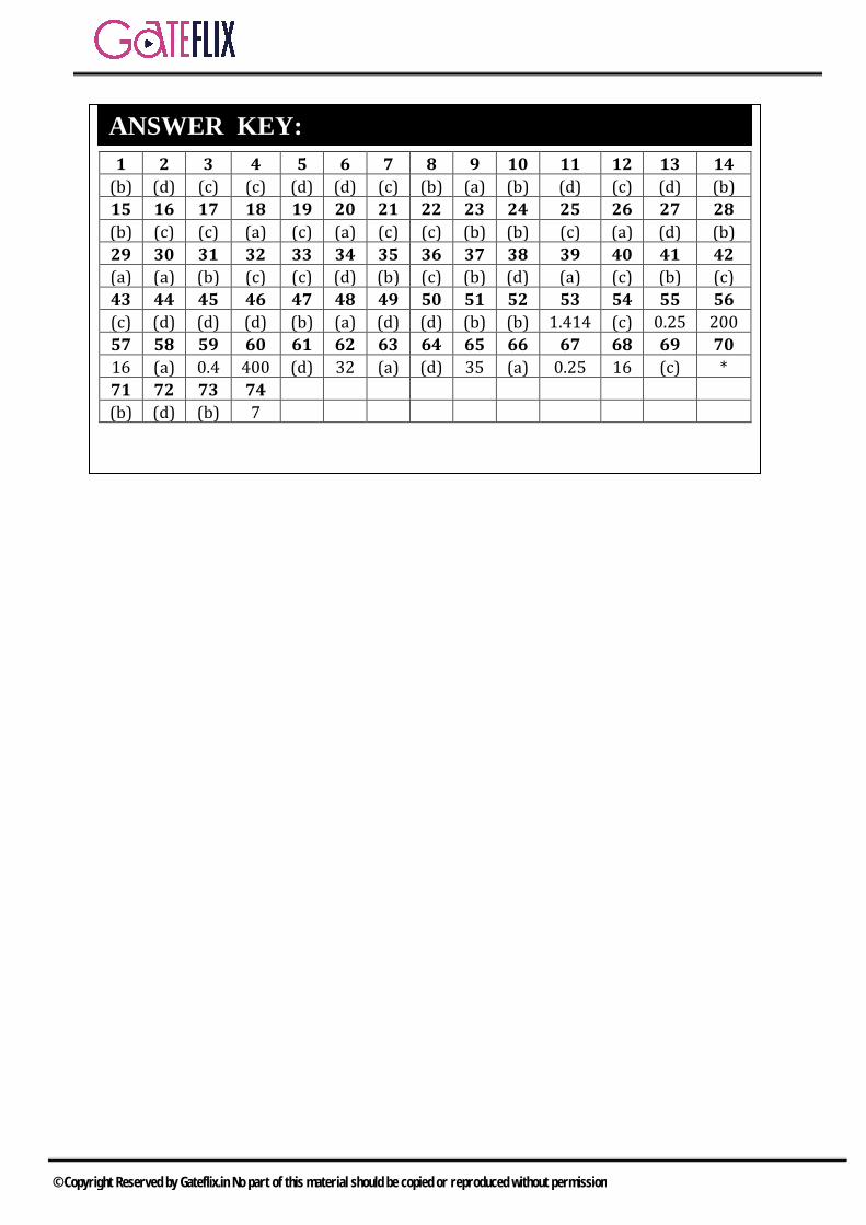
1 2 3 4 5 6 7 8 9 10 11 12 13 14 (b) (d) (c) (c) (d) (d) (c) (b) (a) (b) (d) (c) (d) (b) 15 16 17 18 19 20 21 22 23 24 25 26 27 28 (b) (c) (c) (a) (c) (a) (c) (c) (b) (b) (c) (a) (d) (b) 29 30 31 32 33 34 35 36 37 38 39 40 41 42 (a) (a) (b) (c) (c) (d) (b) (c) (b) (d) (a) (c) (b) (c) 43 44 45 46 47 48 49 50 51 52 53 54 55 56 (c) (d) (d) (d) (b) (a) (d) (d) (b) (b) 1.414 (c) 0.25 200 57 58 59 60 61 62 63 64 65 66 67 68 69 70 16 (a) 0.4 400 (d) 32 (a) (d) 35 (a) 0.25 16 (c) * 71 72 73 74
(b) (d) (b) 7
ANSWER KEY:
© Copyright Reserved by Gateflix.in No part of this material should be copied or reproduced without permission
Q.1 (b) For orthogonality in 𝑇𝑇𝑏𝑏 duration there should be integral multiple of
cycles.0b
1T 100μs10K
= =
1b1T 40μs
25K= =
∴ 200μs is the integral multiple of both
0 1b b(T andT )
Q.2 (d) Probability of error = p Probability of no error = (1-p) For error in at most one bit there should either be no error or error in only one bit.
n n 0 n n 1o 11 n n 1
C (1 p) p C (1 p) p (1 p) np(1 p)
−
−
= − + −
− + −
Q.3 (c) ( ) ( )sinc 700t +sinc 500t
Nyquist sampling rate m2f 700Hz= =
1Sampling rate sec700
∴ =
Q.4 (c) Frame per second =625 Pixels per frame 400 400= × 64 intensity levels per pixel can be represented by 6 bits per pixel
Date rate=625×400×400×6=600Mbps∴
Q.5 (d) 50 μs 20kHz⇒
m sf = 12kHzf = 20ksamples/ sec∴ Frequency at filiter output with cut-off frequency of 15k is 20±12=8k and mf =12kHz
Q.6 (d) Since bit rate is 8Kbps, transmitted frequencies in coherent BFSK
should be integral multiple of 8. i.e. 32K & 40K.
Q.7 (c)
Output of the filter ( )s
y t .x(t)T
=
( )6 3
6
5 10 10cos 8π 10 t100 10
−
−
× × ×=
×( )1 35 10 cos 8π 10 t−= × ×
Q.8 (b) Bit rate s=nf=8×8K=64Kbps SNR =1.76+6n
1.76 48 49.8= + =
Q.9 (a) For BPSK bandwidth efficiency ρ=0.5 for coherent BPSK synchronization is required at the receiver.
Q.10 (b) For slope overload to take place,
3m n
s s
A .ω 0.628 40 10T T
25120 25.12K
≤ = × ×
= =
∆ ∆
Matching with options 2π×1.5×4K=37.7which is greater than s/T∆
Q.11 (d) 5
b6
0
2E 2 10SNR 20N 10
−
−
×= = =
( )dBSNR 10log 20 13dB= =
Q.12 (c) p2M 1.536
L 128∆ = =
EXPLANATIONS
© Copyright Reserved by Gateflix.in No part of this material should be copied or reproduced without permission
2
26 2
N
1.536128P 12 10 V
12 12−
= = ×
∆=
Q.13 (d)
From Fourier series expansion,o
o
o
T6
jnω tn
To6
1 A nπC A.e dt sinT πn 3−
= = ∫
∴ From 𝐶𝐶𝑛𝑛 its clear that 1,2,4,5,7… harmonics are present. Freq of p(t) corr to 1,2,3,4,5,7 …..103 , 3 32 10 ,4 10× × ….. x(t) has frequency components o.7k& 0.4k
p(t)×x(t)∴ gives
( ) ( ) ( )( ) ( )1±0.7 k, 2±0.7 k 4±0.7 k,
1±0.4 k, 2±0.4 k….
Frequency present in range of 2.5k to 3.5k are 2.7, 3.3
Q.14 (b)
Probability of error (in general) is
de
E1P = erfc2 2η
Given that, Pe of FSK & PSK are same hence we can say that dE of FSK & PSK are same.
∴ dFSK dPSKE =E
2dFSK f
2dPSK P
E =A
E =2A
Where fA & PA are the amplitudes of carrier waves of FSK & PSK respectively.
2 2 ff P
P
AA =2A Þ = 2A
Therefore binary coherent FSK is
1020 log 2 3dB= inferior than binary coherent PSK.
Q.15 (b)
Q.16 (c)
( )sf 2 1200 600 600 4.8K= + + =
b sR nf 12 4.8K= = × b
bR 57.6Kbps=
Q.17 (c) Q.18 (a)
Shaded areas show the probability of error.
( )eerror 0.25 2P 0 0.1total 0.25 (0.25)
−= = =
−
( )e0.2 0P 1 0.21 0−
= =−
Since prop. Of occurrence of 0 and 1
are equal ( ) ( )e eP 0 P 1Avg 0.15
2+
= =
Q.19 (c)
b 1 bR 10k B 2R 20k= ∴ = =
1 bB R 10k= =
Q.20 (a) In between the two adjacent sampled values, if the base band
© Copyright Reserved by Gateflix.in No part of this material should be copied or reproduced without permission
signal changes an amount less than the step size. The output of the DM is a sequence of alternate positive and negative pulses. This small change in base band signal indicated that the base band is almost constant.
Q.21 (c) SNR ∝ 4n n = 2 Q.22 (c)
Q.23 (b)
For 1y (t) and 2y (t) to be different minimum step size of / 2∆ is needed else they will be same.
Q.24 (b)
To avoid slope overload
'
s
³m (t) .32×1024³ 125T
∆∆
≥
15.2 125⇒∆ =
7
815
2 22
−∆ ≥ ⇒ ∆ ≥
Q.25 (c)
( )s mf 2f 3= ×
( ) 32 1000 3 6 10= × × = ×
Q.26 (a) To maximize the entropy, all the decision boundaries should be
equiprobable ( )5
x1
1ρ x dx3
=∫
5
1
1bdx3
=∫
51
1b[x]3
=
[ ] 1b 5 13
− =
14b3
=
1b12
=
( )1
x1
1ρ x dx3−
=∫
1
1
1adx3−
=∫
11
1a[x]3− =
( ) 1a 1 13
− − =
12a3
=
© Copyright Reserved by Gateflix.in No part of this material should be copied or reproduced without permission

1a6
=
Q.27 (d)
Signal power =s
( ) ( ) ( )
( )
1 1 52 2 2
x x x5 1 1
52
x1
x ρ X dx x ρ x dx x ρ x dxs
x ρ x dxs
−
− −
= + +
+
∫ ∫ ∫
∫
1 1 52 2 2
5 1 1
x bdx x adx x bdx− −
= + +∫ ∫ ∫
1 1 52 2 2
5 1 1
1 1 1s x dx x dx x bdx12 6 12
−
− −
= + +∫ ∫ ∫
1 1 53 3 3
5 1 1
1 x 1 x 1 xs2 3 6 3 12 3
−
− −
= + +
[ ) [ ) [ ]1 1 1s 1—125 1—1 125 136 18 36
= − + + −
124 2 124 124 2 126s36 18 36 18 18 18
= + + = + = 2s 7volt=
p pVStep size
L−= ∆ =
2
2
5 ( 5) 10 5 QNP QNP6 6 3 12
525 13
12 9 12
− −∆ = = = =
=
∆
= ×
SQNP 0.23 0.25SQNRQNP
= ≅ =
7SQNR 280.25
= =
Q.28 (b)
Average energy of constellation 1 is
2 2 2
21
0 4a 4a 8aE 4a4
+ + += =
Average energy of constellation 2 is 2 2 2 2
22
a a a aE a4
+ + += =
So, 2
12
2
E 4a 4E a
= =
Q.29 (a) The probability of error decreases with increase in average energy. As constellation 1 has more average energy than that of constellation 2. So, the probability of symbol error for constellation 1 is lower.
Q.30 (a)
Processing gain c
b
R=R
c
b
R 100R
≥
cb
RR100
≤ 3
bR 12.288×10 bits persec.≤ Q.31 (b) Allocated bandwidth =5MHz
Frequency reuse factor 15
=
Bandwidth allocated for 1 cell1=5× =1MHz5
Number of simultaneous channels1MHz= ×8=40200kHz
Q.32 (c)
Prob of no error in n bits ( )n1 p= − Prob of one error in n bits
( )( ) ( )
n 1
n 1 n
n.p 1 p
Total probability np 1 p 1 p
−
−
= −
∴ = − + −
Q.33 (c)
p(t) = 2 2sin4πWt
4πWt(116W t )
22
1sin4πW×1 4Wp =1 14W 4πW× 1-16W
4W 16W
© Copyright Reserved by Gateflix.in No part of this material should be copied or reproduced without permission
As it comes in the form of 0/0 so applying LH rule
2 2
d sin4πWt1 dtp = d4W 4πWt(1-16W t )dt
2 2cos 4πWt
1 48W t=
−
Putting 1t4W
=
( ) cosπp t 0.51 3
= =−
Q.34 d)
Condition to avoid slop overload in
DM s
d m(t)T dt∆≥
So, by increasing the step size, slope overload distortion can be avoided.
Q.35 (b)
While using the bipolar pulse to transmit the bits 0 and 1, the minimum bandwidth required for distortion free transmission is four times the theoretical bandwidth (Nyquist bandwidth). mf 4kHz= Nyquist bandwidth
smin mf 2f 8kHz= = Minimum bandwidth in bipolar signaling is smin bBW 4f R / 2= =
4 8 32kHz= × = Q.36 (c)
Signal to noise ratio 0
0 dB
S 6ndBN
≈
Where N= number of bits per sample quantized
0
0 dB
S 6 8 48dBN
≈ × =
Q.37 (b)
Quantization noise 2
qSN12
=
Where S=Step size of quantization
level qq
NN
4=
2 2S' S12 12 4
⇒ =×
' SS2
⇒ =
ppn
VS
2⇒ =
Where ppV = peak to peak value N=no. of bits/ sample n' 92 =2 =512⇒ Therefore, number of quantization levels required to reduce the quantization noise by a factor 4 would be 512
Q.38 (d) 1s
f 2 W 2W= × =
2sf 2 W 2W= × =
3sf 2 2W 4W= × =
4sf 2 3W 6W= × =
1 2 3 4s s s s sf f f f f= + + +
sf 14W= For minimum bandwidth n=1
b sR =nf
bR 1 14W 14W= × =
( ) bmin
RB.W2
=
( )min
14WB.W 7W2
= =
Q.39 (a)
There will be error if all the three received bits are 0 or two of the three received bids are 0. Therefore, probability of error in output 3 3
3 2= C .p.p.p+ C .p.p.(1-p) 3 2=P +3P (1-p)
Q.40 (c)
SNR=43.5 db We know that SNR = 1.761 + 6.02n 43.5 = 1.76 + 6.02n
© Copyright Reserved by Gateflix.in No part of this material should be copied or reproduced without permission
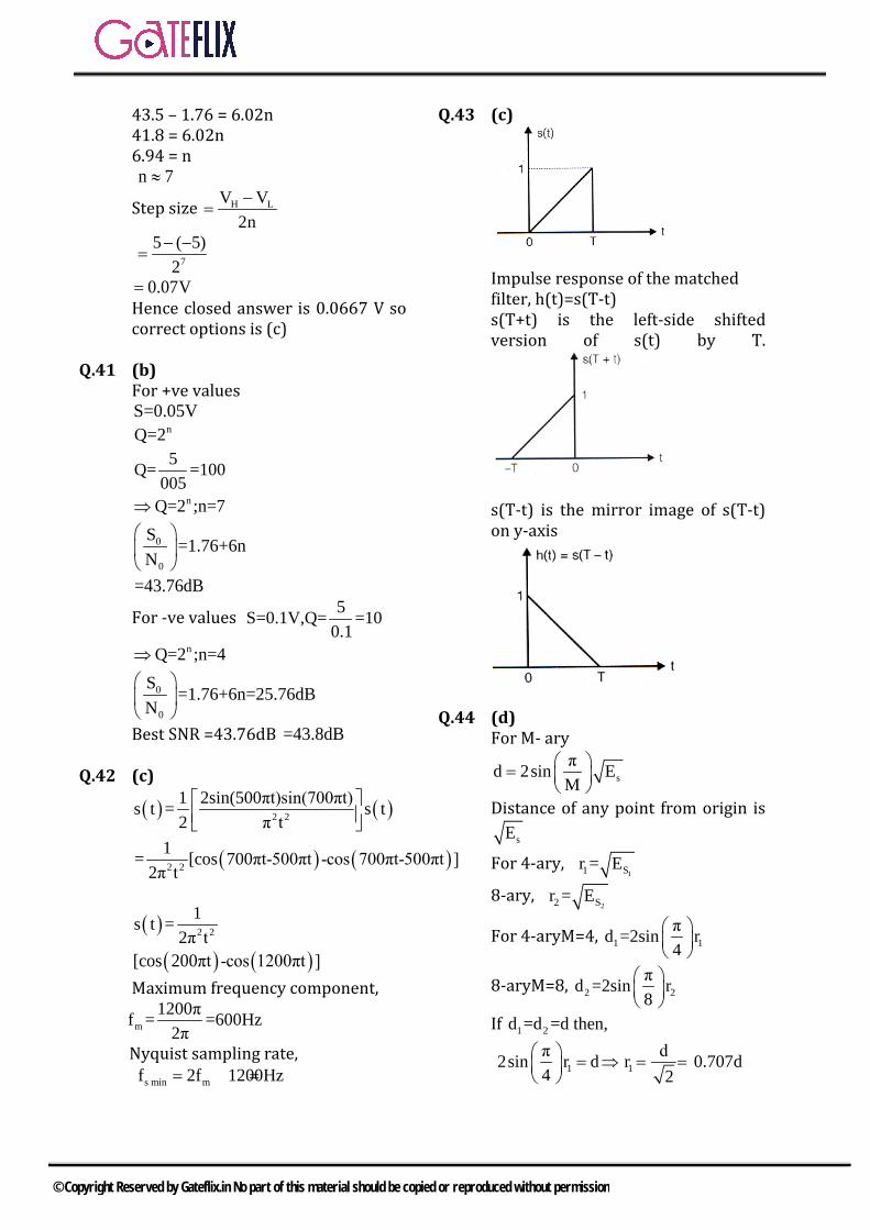
43.5 – 1.76 = 6.02n 41.8 = 6.02n 6.94 = n n 7≈
Step size H LV V2n−
=
75 ( 5)
2− −
=
0.07V= Hence closed answer is 0.0667 V so correct options is (c)
Q.41 (b)
For +ve values S=0.05V
nQ=2 5Q= =100
005
nQ=2 ;n=7⇒
0
0
S =1.76+6nN
=43.76dB
For -ve values 5S=0.1V,Q= =100.1
nQ=2 ;n=4⇒
0
0
S =1.76+6n=25.76dBN
Best SNR =43.76dB =43.8dB Q.42 (c)
( ) ( )
( ) ( )
2 2
2 2
1 2sin(500πt)sin(700πt)s t = s t2 π t
1= [cos 700πt-500πt -cos 700πt-500πt ]2π t
( ) 2 21s t =
2π t
( ) ( )[cos 200πt -cos 1200πt ] Maximum frequency component,
m1200πf = =600Hz
2π
Nyquist sampling rate, s min mf 2f 1200Hz= =
Q.43 (c)
Impulse response of the matched filter, h(t)=s(T-t) s(T+t) is the left-side shifted version of s(t) by T.
s(T-t) is the mirror image of s(T-t) on y-axis
Q.44 (d)
For M- ary
sπd 2sin EM
=
Distance of any point from origin is sE
For 4-ary, 11 Sr = E
8-ary, 22 Sr = E
For 4-aryM=4, 1 1πd =2sin r4
8-aryM=8, 2 2πd =2sin r8
If 1 2d =d =d then,
1 1π d2sin r d r 0.707d4 2
= ⇒ = =
© Copyright Reserved by Gateflix.in No part of this material should be copied or reproduced without permission

2π2sin r =d8
2dr = =1.307d
π2sin8
⇒
Q.45 (d)
e sP E∝ for both cases
So, 1
2
S 1
2S
E r 0.707d= =r 1.307dE
2
1
2S
S
E 1.307=E 0.707
⇒
=3.42
To achieve same error 2nd must have 3.42 times than 1st The value in dB=10log(3.42) = 5.33dB.
Q.46 (d) Quantized levels are equiprobable; hence
2H=log 4=2bits/sampler=2samples/sec Hence information rate R=r. H=2 samples /sec × 2 bits /sample
R=4bits/sec⇒
Q.47 (b) Probability of error in coherent BPSK
2e
o
EP QN
=
Phase difference 45o decreases the signal energy by a factor of
2 1cos 452
o =
∴ eo
EP =QN
Q.48 (a)
[ ] 9P X=0 =10
[ ] [ ]
[ ]
9P X=0 = P X=110
1=1-P x=0 =10
Transition probability 1 0P P 1/ 80 1
= =
So probability of error for optimum receiver will be
[ ]( )e
e
P P X 1 1 transition probability
1 1 7P 110 8 80
= = −
= − =
Q.49 (d)
Frequency used for signaling is f=3500Hz Excess B.W. used is
×fB == 0.75 2625 Hz We know that
if B is the B.W available then bR B2
≤
i.e., if bR is data rate then bR2
is the
minimum B.W. required for transmission.
b bR 2BR 5250≤ ≤ So ( )b max
R 5250 symbols / sec= Q.50 (d)
BER is given as ( ) ( )eP P 0 P(1/ 0) P 1 P(0 /1)= +
If detection threshold
=1 then ( ) ( ) 1P 0 P 12
= =
1
Y 1P f (z / 0)dz 0X 0= = = = ∫
∞
1
Y 0P f (z /1)dzX 1= = = ∫
∞
1 1 114 4 8
= × × =
e1 1 1 1P 02 2 8 16
∴ = × + × =
Q.51 (b)
© Copyright Reserved by Gateflix.in No part of this material should be copied or reproduced without permission

Optimum threshold is given by the point of intersection of two pdf curves. f ( / 0) 1 ;| | 1= − ≤z z z f ( /1) / 4;0 z 2= < <z z The point of intersection which decides optimum threshold
114
− =z
z1=z+4
4z5
⇒ =
Q.52 (b)
( )
n
2 2
2 Mn log m log (32)
=
= =
Q.53 (1.414)
Bit error rate for BPSK =
0
2E EQ . NNO2
Q
0
2EYN
⇒ =
Function of bit energy and noise PSD
oN2
Counterllation diagram of BPSK
Channel is AWGN which implies noise sample as independent Let 2x + n1 + n2 = x1 + n1
where x1 = 2x nl= n1 + n2
Now Bit error rate = 1
1o
2EQN
E1 is energy in x1 1oN is PSD of h1
E1 = 4E [as amplitudes are getting doubled]
1oN = No [independent and identical
channel] ⟹ Bit error rate =
o o
4E 2EQ =Q 2 Þb= 2or1.414N N
Q.54 (c) For Binary FSK
Bit error probability = Q 0
EN
E →Energy per bit [No. of symbols = No. of bits]
2-3
3
A TE= ,A=4×10 ,T21=
500×10 [inverse of data rate]
-120N =1×10
-12
e -1216×10=Q =Q(4)1×10
⇒
P
Q.55 (0.25)
Maximum quantization error is step size
2−
step - size = 8 0 1 0.5V16 2−
= =
Quantization error = 0.25 V Q.56 (200)
Nyquist rate = 2 x 50 Hz =100 samples / sec
max minm(t) m(t) 2 ( 2)LL 0.75− − −
∆ = ⇒ =
2 2L 3.77 40.75
= = =
No. of bits required to encode '4' levels = 2 bits/level
© Copyright Reserved by Gateflix.in No part of this material should be copied or reproduced without permission
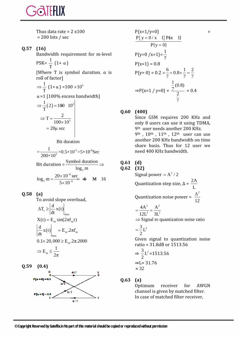
Thus data rate = 2 x100 = 200 bits / sec
Q.57 (16)
Bandwidth requirement for m-level
PSK= 1T
(1+ α )
[Where T is symbol duration. α is roll of factor]
1T
⇒ (1+ α ) =100 310×
α =1 [100% excess bandwidth]
( ) 3
3
1 2 100 10T
2T100 10
20μ sec
⇒ = ×
⇒ =×
=
-5 -63
Bit duration1= =0.5×10 =5×10 Sec
200×10
Bit duration =2
Symbol durationlog m
⇒
6
2 6
20 10 seclog m 4 M 165 10
−
−
×= = ⇒ =
×
Q.58 (a)
To avoid slope overload,
smax
dT x(t)dt
∆ ≥
m mE sin(2πt) )X f( t=
m mmax
d x(t) E .2πfdt
=
m0 20,000 E .2π. 001 .20× ≥
m1E
2π⇒ ≤
Q.59 (0.4)
Px=1/y=0 = P y 0 / x 1 Px 1
Py 0= = =
=
Py=0 /x=1= 17
Px=1 = 0.8
Py= 0 = 0.2 6 1 20.87 7 7
× + × =
⇒Px=1 / y=0 =
1 (0.8)7
27
= 0.4
Q.60 (400)
Since GSM requires 200 KHz and only 8 users can use it using TDMA, 9th user needs another 200 KHz. 9th , 10th , 11th , 12th user can use another 200 KHz bandwidth on time share basis. Thus for 12 user we need 400 KHz bandwidth.
Q.61 (d) Q.62 (32) Signal power 2 2A /=
Quantization step size, ∆ = 2AL
Quantization noise power = 2
12∆
2 2
2 2
4A A12L 3L
==
2
Signal to quantization noise ratio3 L2
⇒
=
Given signal to quantization noise ratio = 31.8dB or 1513.56
⇒ 23 L2
=1513.56
⇒L= 31.76 32≈
Q.63 (a)
Optimum receiver for AWGN channel is given by matched filter. In case of matched filter receiver,
© Copyright Reserved by Gateflix.in No part of this material should be copied or reproduced without permission
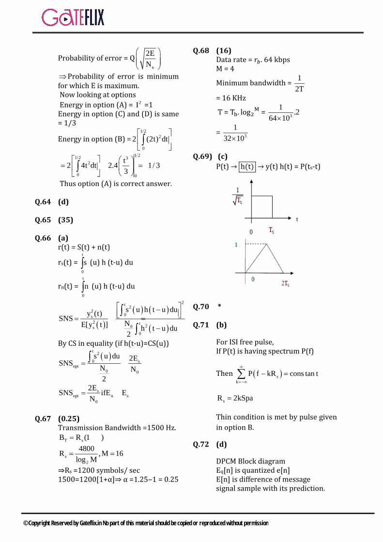
Probability of error = Qu
2EN
⇒Probability of error is minimum for which E is maximum. Now looking at options Energy in option (A) = 2I =1 Energy in option (C) and (D) is same = 1/3
Energy in option (B) =1/2
2
0
(2t) t2 d ∫
1/21/2 3
2
0 0
t2 4t dt 2.4 1/ 33
= = =
∫
Thus option (A) is correct answer. Q.64 (d) Q.65 (35) Q.66 (a)
r(t) = S(t) + n(t)
rs(t) = t
0
s∫ (u) h (t-u) du
rn(t) = t
0
n∫ (u) h (t-u) du
( )( ) ( )
( )
2t 22
0s2 t 20s
0
s u h t u duy (t)SNS NE[y t ] h t u du2
− = =−
∫
∫By CS in equality (if h(t-u)=CS(u))
( )t 2
0 sopt
0 0
s u du 2ESNS N N2
= =∫
sopt n s
0
2ESNS ifE EN
= ≥
Q.67 (0.25)
Transmission Bandwidth =1500 Hz. sT R ( B 1 )= +α
2s
4800 ,M 16log M
R ==
⇒Rs =1200 symbols/ sec 1500=1200[1+α]⇒ α =1.25‒1 = 0.25
Q.68 (16) Data rate = 𝑟𝑟𝑏𝑏. 64 kbps M = 4
Minimum bandwidth = 12T
= 16 KHz
T = Tb. log2M = 3
1 .264 10×
= 3
132 10×
Q.69) (c)
P(t) → h(t) → y(t) h(t) = P(ts-t)
Q.70 * Q.71 (b) For ISI free pulse, If P(t) is having spectrum P(f)
Then ( )sk
P f kR cons tan t∞
=−∞
− =∑
sR 2kSpa=
Thin condition is met by pulse given in option B.
Q.72 (d)
DPCM Block diagram Eq[n] is quantized e[n] E[n] is difference of message signal sample with its prediction.
© Copyright Reserved by Gateflix.in No part of this material should be copied or reproduced without permission

Q.73 (b)
( ) ( )
( ) ( )
0
0
1
1
u t 5cos 20000 tf 10kHzu t 5cos 22000 tf 11kHz
= π
=
= π
=
For u0(t) and u1(t) to be orthogonal , it is necessary that
( ) 3
1 0
3
n 1f f ; 11 10 x102T 2T
1T 0.5msec2x10
− = − =
= =
Q.74 7
For sinusoidal signal
(SNR)Q in dB = 6.0n + 1.75
Given required (SNR)Q = 40dB
( )
6.0n 1.75 40dB6.0n 40 11.75
40 11.75n6.02
n 7 Since 'n' must be an integer
+ ≥≥ −−
≥
=
© Copyright Reserved by Gateflix.in No part of this material should be copied or reproduced without permission

9.1 INTRODUCTION
Information theory is a branch of applied mathematics, electrical engineering, and computer science involving the quantification of information. Information theory was developed by Claude E. Shannon to find fundamental limits on signal processing operations such as compressing data and on reliably storing and communicating data.
9.1.1 INFORMATION SOURCES
An information source may be viewed as an object which produces an event, the outcome of which is selected at random according to a probability distribution. A practical source in a communication system is a device which produces messages, and it can be either analog or discrete. In this chapter, we deal mainly with the discrete sources since analog sources can be transformed to discrete source through the use of sampling and quantization techniques. As a matter of fact, a discrete information source is a source which has only a finite set of symbols as possible outputs. The set of source symbols is called the source alphabet, and the elements of the set are called symbols or letters.
9.1.2 CLASSIFICATION OF INFORMATION SOURCES
Information sources can be classified as having memory or being memory less. A source with memory is one for which a current symbols. A memory less source is one for which each symbol produced is independent of the previous symbols. A discrete memory less source (DMS) can be characterized by the list of the symbols,
the probability assignment to these symbols, and the specification of the rate of generating these symbols by the source.
9.2 INFORMATION CONTENT OF A SYMBOL
9.2.1 DEFINITION
Let us consider a discrete memory less source (DMS) denoted by X and having alphabet 1 2 mx , x x… .The information
content of a symbol ix , denoted by ( )iI x is defined by
( ) ( ) ( )i 2 2 ii
1I x log log P xP x
= = − Where,
( )P ix Is the probability of occurrence of
symbol ix
9.2.2 PROPERTIES OF 𝐈𝐈(𝒙𝒙𝒊𝒊)
The information content of a symbol 𝑥𝑥𝑖𝑖 denoted by I(xi) satisfies the following properties: 1) ( ) ( )i iI x 0 for P x 1= = 2) ( )iI x 0≥
3) ( ) ( ) ( ) ( )i j i jI x I x if P x P x> <
4) ( ) ( ) ( )I , I I= +i j i jx x x x
If ix and jx are independent
9.2.3 UNIT OF 𝐈𝐈(𝐱𝐱𝐢𝐢)
• The unit ( )I ix is the bit (binary unit) if b=2
• Hartley or decit if b=10, and• Nat (natural unit) if b=e.It is standard to use b=2. Here, the unit bit (abbreviated “b”) is a measure of information content and is not to be
9 INFORMATION THEORY
© Copyright Reserved by Gateflix.in No part of this material should be copied or reproduced without permission
confused with the term ‘bit’ meaning binary digit. The conversion of these units to other units can be achieved by the following relationships.
2In a log alog aIn 2 log 2
= =
Example A source produces one of four possible symbols during each interval having
probabilities, ( ) ( )1 21 1P x ,P x ,2 4
= =
( ) ( )3 41P x P x8
= = obtain the information
content of each of these symbols. Solution We know that the information content ( )I ix of a symbol ix is given by
( ) ( )i 2i
1I x logP x
=
Thus, we can write
( ) ( )1 2 21I x log log 2 1 bit12
= = =
( ) 22 2 2
1I x log log 2 2 bits14
= = =
( ) 33 2 2
1I x log log 2 3 bits18
= = =
( ) 34 2 2
1I x log log 2 3 bits18
= = =
Example In a binary PCM if ‘0’ occur with
probability 14
and ‘1’ occur with
probability equal to 34
, then calculate the
amount of information carried by each bit. Solution
Here, given that the bit ‘0’ has ( )11P x4
=
and bit ’1’ has ( )23P x4
=
Then, amount of information is given as:
( ) ( )i 2i
1I x logP x
=
With ( )11P x4
=
We have ( ) 101 2
2
log 4I x log 4 2bitslog 2
= = =
And with ( )23P x4
= ,
We have
( )10
2 22
4log4 3I x log 0.415bits3 log 2
= = =
Example If there are M equally likely and independent symbols, then prove that amount of information carried by each symbol will be, ( )iI x N bits=
Where NM 2= and N is an integer. Solution Since, it is given that all the m symbols are equally likely and independent, therefore, the probability of occurrence of each
symbol must be 1M
.
We know that amount of information ( )iI xof a discrete symbol 𝑥𝑥𝑖𝑖 is given by,
( ) ( )i 2i
1I x logP x
= … (1)
Here, probability of each message is
( )i1P xM
= .
Hence, equation (1) takes the following form: ( )i 2I x log M= … (ii)
Further, it is given that NM 2= Substituting above value of M in equation (ii), we obtain ( ) N
i 2I x log 2=
© Copyright Reserved by Gateflix.in No part of this material should be copied or reproduced without permission
2 2N log=
10
10
log 2N N bitslog 2
= =
Note: Hence, amount of information carried by each symbol will be ‘N’ bits. We know that NM 2= . This means that there are ‘N’ binary digits (binits), in each symbol. This indicates that when the symbols are equally likely and coded with equal number of binary digits (binits), then the information carried by each symbol (measured in bits) is numerically same as the number of binits used for each symbol. 9.3 ENTROPY (i.e., Average Information) 9.3.1 DEFINITION In a practical communication system, we usually transmit long sequences of symbols from an information source. Thus, we are more interested in the average information that a source produces than the information content of a single symbol. In order to get the information content of the symbol, we take notice of the fact that the flow of information in a system can fluctuate widely because of randomness into the selection of the symbols. Thus, we require to talk about the mean or average information content of the symbols in a log message. 9.3.2 MATHEMATICAL EXPRESSION The mean value of ( )iI x over the alphabet of source X with m different symbols is represented by H(X) and given by
( ) ( ) ( ) ( )i m
i i ii 1
H X E I x P x I x=
=
= = ∑
( ) ( )i m
i 2 ii 1
P x log P x bits/symbol=
=
= −∑
The quantity ( )H X is known as the entropy of source X. It is a measure of the average information content per source symbol. The source entropy ( )H X can be
considered as the average amount of uncertainty within source X that is resolved by use of the alphabet. 9.3.3 ENTROPY FOR BINARY SOURCE
It may be noted that for binary source X which generates independent symbols 0 and 1 with equal probability, the source entropy H(X) is
( ) 2 21 1 1 1H X log log 1 bit/symbol2 2 2 2
= − − =
9.3.4 LOWER AND UPPER BOUNDS ON ENTROPY H (X)
The source entropy H(X) satisfies the following relation:
( ) 20 H X log m≤ ≤ Where m is the size (numbers of symbols of the alphabet of source X). The lower bound corresponds to no uncertainty, which occurs when one symbol has probability ( )iP x 1= while ( )iP x 0for j i= ≠ , so X emits
the same symbol ix all the time. The upper bound corresponds to the maximum uncertainty which occurs when ( )iP x 1/ m= for all i, that is when all
symbols are equal likely to be emitted by X.
9.4 INFORMATION RATE
If the time rate at which source X emits symbols is r (symbols/sec), the information rate R of the source is given by
( )R r H X bits/sec= × Where, R is information rate H(X) is Entropy or average information r is rate at which symbols are generated. Information rate r is represented in average number of bits of information per second. It is calculated as under:
( )symbols Information bitsR r in H X in second symbol
= × Or R = Information bits/sec
© Copyright Reserved by Gateflix.in No part of this material should be copied or reproduced without permission

Example The probabilities of the five possible outcomes of an experiment are given as
( ) ( ) ( )1 2 31 1 1P x ,P x ,P x ,2 4 8
= = =
( ) ( )4 51P x P x
16= =
Determine the entropy and information rate if there are 16 outcomes per second. Solution The entropy of the system is given as
( ) ( ) ( )i 5
i 2i 1 i
1H X P x log bits/symbolP x
=
=
=∑
Or
( ) 2 2 21 1 1H X log 2 log 4 log 82 4 8
= + +
2 21 1log 16 log 16
16 16+ +
Or
( ) 1 2 3 4 4H X2 4 8 16 16
= + + + +
1 1 3 1 12 2 8 4 4
= + + + +
Or
( ) 4 4 3 2 2H X8
+ + + +=
15 1.875 bits/outcomes8
= =
Now, rate of outcomes r=16 outcomes/sec Therefore, the rate of information R will be
( ) 15R r×H X 16 30 bits/sec8
= = × =
9.5 CHANNEL CAPACITY By Shannon-Hartley theorme, we get the channnel capacity as under:
2SC B log 1N
= +
Where, C is the channel capacity in Hz B is bandwidth of the channel in Hz SN
is the ratio of transmitted signal power
to noise power
From the equationfor C, it is evident that it depends on two factors, which are the bandwidth B and the S/N ratio. EFFECT OF S/N ON C If the communication channel is noiseless, i.e. N=0, then(𝑆𝑆/𝑁𝑁) → ∞ and,so, C also will tend to ∞. Thus, the noiseless channel will have an infinite capacity.
© Copyright Reserved by Gateflix.in No part of this material should be copied or reproduced without permission
Q.1 A source generates three symbols with probabilities 0.25, 0.25, 0.50 at a rate of 3000 symbols per second. Assuming independent generation of symbols, the most efficient source encoder would have average bit rate is a) 6000bits/sec b)4500bits/sec c) 3000bits/sec d)1500bits/sec
[GATE-2006]
Q.2 A memory less source emits n symbols each with a probability p. The entropy of the source as a function of n is a) increase as log nb)decrease as log(1/n) c) increase as nd) increase as n log n
[GATE-2008]
Q.3 A communication channel with AWGN operating at a signal to noise ratio SNR >> 1 and bandwidth B has capacity𝐶𝐶1. If the SNR is doubled keeping B constant, the resulting capacity 𝐶𝐶2 is given by a) C2 ≈ 2C1 b) C2 ≈ C1 + Bc) C2 ≈ C1 + 2B d) C2 ≈ C1 + 0.3B
[GATE-2009]
Q.4 A source alphabet consists of N with the probability of the first two symbols being the same. A source encoder increases the probability of the first symbol by a small amount 𝜀𝜀 and decreases that of the second by 𝜀𝜀. After encoding the entropy of the source a) Increaseb) remains the samec) Increase only if N = 2d) Decreases
[GATE-2012]
Q.5 Let U and V two independent and identically distributed random variables such the
( ) ( ) 1P U 1 P U 12
= + = = − = The
entropy H(U+V) in bits is a) 3/4 b) 1c) 3/2 d) log23
[GATE-2013]
Q.6 In a code-division multiple access (CDMA) system with N = 8 chips, the maximum number of users who can be assigned mutually orthogonal signature sequences is_____.
[GATE-2014]
Q.7 The capacity of a Binary Symmetric Channel (BSC) with cross-over probability 0.5 is ________.
[GATE-2014]
Q.8 A fair coin is tossed repeatedly until a 'Head' appears for the first time. Let L be the number of tosses to get this first 'Head'. The entropy H(L) in bits is ___________.
[GATE-2014]
Q.9 The capacity of a band-limited additive white Gaussian noise (AWGN) channel is given by
C = Wlog2 2
P1σ w
+
bits per second
(bps), where W is the channel bandwidth, P is the average power received and σ2 is the one-sided power spectral density of the
AWGN. For a fixed 2
Pσ
=1000„ the
channel capacity (in kbps) with infinite bandwidth (W→ ∞) is approximately a) 1.44 b) 1.08c) 0.72 d) 0.36
GATE QUESTIONS
© Copyright Reserved by Gateflix.in No part of this material should be copied or reproduced without permission

[GATE-2014] Q.10 Consider a discrete memoryless
source with alphabet S=so,s1,s2,s3,s4,... and respective probabilities of occurrence
1 1 1 1 1P , , , , ,2 4 8 16 32
= ……
The
entropy of the source (in bits) is ____. [GATE-2016]
Q.11 A digital communication system
uses a repetition code for channel encoding/decoding. During transmission, each bit is repeated three times (0 is transmitted as 000, and 1 is transmitted as 111). It is assumed that the source puts out symbols independently and with equal probability. The decoder operates as follows: In a block of three received bits, if the number of zeros exceeds the number of ones, the decoder decides in favor of a 0, and if the number of one's exceeds the number of zeros, the decoder decides in favor of a 1. Assuming a binary symmetric channel with crossover probability p = 0.1, the average probability of error is ___.
[GATE-2016] Q.12 A discrete memory less source has
an alphabet a1 ,a2 ,a3 ,a4 with corresponding probabilities
1 1 1 1, , ,2 4 8 8
. The minimum required
average code world length in bits to represent this source for error-free reconstruction is ___________.
[GATE-2016] Q.13 A binary communication system
makes use of the symbols "zero" and
"one". There are channel errors. Consider the following events: xo: a "zero" is transmitted x1: a "one" is transmitted yo: a "zero" is received y1: a "one" is received The following probabilities are given:
P(x0)= 12
,P(yo/xo) = 34
and P(yo/x1)=
12
The information in bits that you obtain when you learn which symbol has been received (while you know that a "zero" has been transmitted) is ___________.
[GATE-2016] Q.14 An analog baseband signal, band
limited to 100 Hz, is sampled at the Nyquist rate. The samples are quantized into four message symbols that occur independently with probabilities p1 = p4 = 0.125 and p2 = p3. The information rate (bits/sec) of the message source is _____.
[GATE-2016]
Q.15 A voice-grade AWGN (additive white Gaussian noise) telephone channel has a bandwidth of 4.0 kHz and two-sided noise power spectral density
2η =2.5x10⁻⁵ Watt per Hz. If
information at the rate of 52 kbps is to be transmitted over this channel with arbitrarily small bit error rate, then the minimum bit-energy Eb (in mJ/bit) necessary is ____________.
[GATE-2016]
Q.16 Let (X1,X2) be independent random variables. X1 has mean 0 and variance 1, while X2 has mean 1 and variance 4. The mutual information I(X1; X2) between X1 and X2 in bits is _________.
© Copyright Reserved by Gateflix.in No part of this material should be copied or reproduced without permission
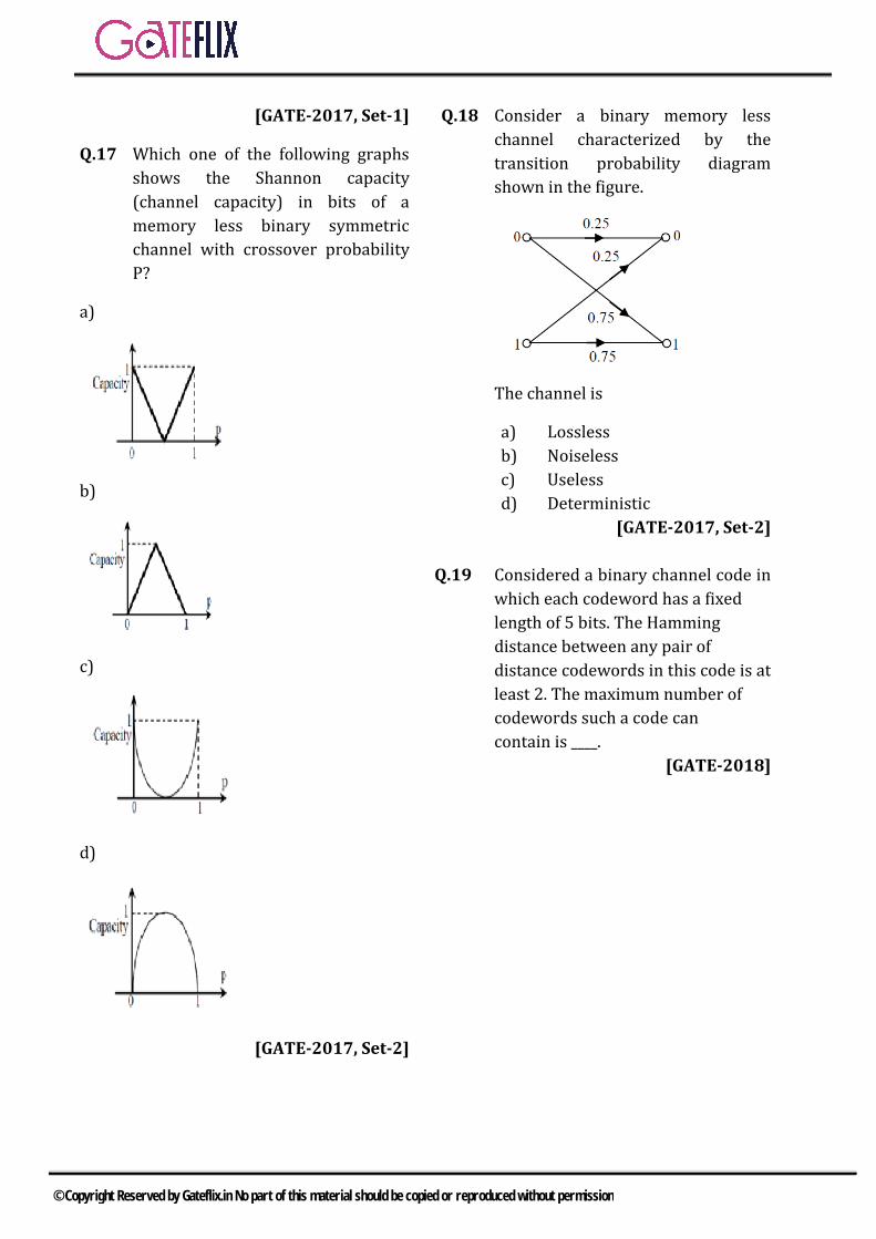
[GATE-2017, Set-1]
Q.17 Which one of the following graphs shows the Shannon capacity (channel capacity) in bits of a memory less binary symmetric channel with crossover probability P?
a)
b)
c)
d)
[GATE-2017, Set-2]
Q.18 Consider a binary memory less channel characterized by the transition probability diagram shown in the figure.
The channel is
a) Lossless b) Noiseless c) Useless d) Deterministic [GATE-2017, Set-2]
Q.19 Considered a binary channel code in which each codeword has a fixed length of 5 bits. The Hamming distance between any pair of distance codewords in this code is at least 2. The maximum number of codewords such a code can contain is ____.
[GATE-2018]
© Copyright Reserved by Gateflix.in No part of this material should be copied or reproduced without permission

1 2 3 4 5 6 7 8 9 10 11 12 13 14 (b) (a) (b) (d) (c) * 0 2 (a) 2 0.028 1.75 0.811 * 15 16 17 18 19
31.5 0 (c) (c) 16
ANSWER KEY:
© Copyright Reserved by Gateflix.in No part of this material should be copied or reproduced without permission

Q.1 (b) Bit rate =H. Rb
1 1 1H 0.25log 0.25log 0.5log0.25 0.25 0.5
= + +
1 1 1 3H 1.52 2 2 2
= + + = =
Bit rate = 1.5 × 3000 = 4500 bits/sec.
Q.2 (a)
Entropy H(m)n
i ii 1
P log Pbits=
=∑
Where Pi =Probability of individual symbol. Since probability of each symbol is same therefore
1 2 n1P P ..Pn
= = =
H(m)n
i 1
1 lognn=
= − =∑
Q.3 (b) SNR >> 1
1 2 2S SC Blog 1 BlogN N
= + ≅
When SNR is doubled
22SC’ BlogN
≅
22SC’ BlogN
≅
22
1
SBlogBlog 2N
C B
= += =
1C B= +
Q.4 (d) We know that entropy is maximum when symbols are equal probable so if probability will change from equal to non equal entropy will decrease.
Q.5 (c) U V (U+V) +1 +1 -1 -1
+1 -1 +1 -1
+2 0 0 -2
( ) 1 1 1P U V 2 ,2 2 4
+ = + = =
( ) 1 1 1P U V 04 4 2
+ = = + =
( ) 1 1 1P U V 2 ,2 2 4
+ = − = =
( ) 2 21 1H U V log 2 2 log 42 4
∴ + = + ×
1 312 2
= + =
Q.6 7.99 to 8.01
Spreading factor(SF)= chip ratesymbol rate
This if a single symbol is represented by a code of 8 chips Chip rate =80xsymbol rate S.F(Spreading Factor)
= 8x symbol ratesymbol rate
= 8
Spread factor (or) process gain and determine to a certain extent the upper limit of the total number of uses supported simultaneously by a station.
Q.7 (0) Capacity of channel is 1-H(p) H(p) is entropy function With cross over probability of 0.5
H(p)=- 2 21 1 1og og 1l l 12 0.5 2 0.5
+ =
⇒Capacity =1-1= 0
Q.8 2
EXPLANATIONS
© Copyright Reserved by Gateflix.in No part of this material should be copied or reproduced without permission
In this problem random variable is L L can be 1,2,… … … ..
1 1PL 1 PL 22 4
= = = =
1PL 38
= =
2 2 2H L log lgo1 1 1 1 1 lgo 11 1 12 4 82 4
...8
= + + +
1 1 12. 3.2 8
1.4
0= + + +
Arithmatic gemometric series summation
=.1
2
12 211 12 1
2
+− −
=2
Q.9 (a)
2 2W
Plim ωlog 1σ ω
C→
= + ∞
2
ω
PωIn 1σ ωlim
In2→
+ =∞
2
2ω
2
PIn 11 Pσ ωlim .Pin2 σ
σ ω→
+ ∞
2
2 ω2
2
This limit is equivalent to
PIn 1P σ ωlim Pσ In
σ ω→
+ =
∞
[ ]ω
In 1 xlim 1
x→
+=
∞
22 22
P PIn e 1.44KGpaσ in σ
= = =
Q.10 (2)
( )i
i2
i 1
1H log 22=
=
∑∞
i2
2i 1
1 log2=
=
∑∞
i
i 1
1i2=
=
∑∞
a= 12
i 1 1 i 1
i 1 i 1
ia a ia− + −
= =
= =∑ ∑∞ ∞
( )i i
i 1 i 1
d da a a ada da= =
= =
∑ ∑∞ ∞
2
a(1 a)
=−
1/ 2 2bits1/ 4
= =
Q.11 (0.028)
Cross over Probability P = 0.1 X = number of errors
( ) ( ) ( )000sent 111sent
1 1P error = P x³2 + P x³22 2
2 1 3 01 3 3=2× (0.1) (0.9) + (0.1) (0.9)2 2 3
( )( ) ( )3=3 0.01 0.9 + 0.1
27 1= +1000 1000
28= =0.0281000
Q.12 (1.75)
The minimum average code word length is also equal to Entropy of source.
( ) 2 2 2 21 1 1 1log 2 log 4 log 8 log 82 4
H8 8
s = + + +
=1.75 bits Q.13 (0.811)
Given Binary communication channel Information content in receiving y it in Given that X0 is transmitted is
02
0 0 0
0
1yy P logx x y)
HP( x
=
+ P 12
0 1
0
1y logx yP x
© Copyright Reserved by Gateflix.in No part of this material should be copied or reproduced without permission
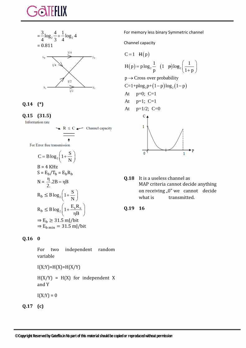
= 2 23 4 1log log 44 3 4
+
= 0.811
Q.14 (*) Q.15 (31.5)
2SlogN
B 1C +
=
B = 4 KHz S = Eb/Tb = EbRb
N = η .2B ηB2.
=
Rb ≤ B 2Slog 1N
+
Rb ≤ B b b2
E Rlog 1ηB
+
⇒ Eb ≥ 31.5 mJ/bit ⇒ Eb min = 31.5 mJ/bit
Q.16 0
For two independent random variable
I(X;Y)=H(X)=H(X/Y)
H(X/Y) = H(X) for independent X and Y
I(X;Y) = 0
Q.17 (c)
For memory less binary Symmetric channel
Channel capacity
( )
( ) ( )
( ) ( )
2 2
2 2
C 1 H p
1 1H p p log 1 p logp 1 p
p Cross over probabilityC=1+plog p+ 1 p log 1 pAt p=0; C=1At p=1; C=1At p=1/2; C=0
= −
= + − +
→
− −
Q.18 It is a useless channel as MAP criteria cannot decide anything on receiving „0‟ we cannot decide what is transmitted.
Q.19 16
© Copyright Reserved by Gateflix.in No part of this material should be copied or reproduced without permission

10.1 INTRODUCTION
Multiplexing is the process of simultaneously transmitting two or more individual signals over a single communication channel. Due to multiplexing it is possible to increase the number of communication channels so that more information can be transmitted. The typical applications of multiplexing are in telemetry and telephony or in the satellite communication.
10.2 CLASSIFICATION OF MULTIPLEXING
The multiplexing techniques can be broadly classified into two categories namely analog and digital. Analog multiplexing can be either FDM or WDM and digital multiplexing is TDM. Figure shows the classification of multiplexing techniques. Generally, the FDM and WDM systems are used to deal with the analog information whereas the TDM systems are used to handle the digital information. In FDM, many signals are transmitted simultaneously where each signal occupies a different frequency slot within a common bandwidth. In TDM, the signals are not transmitted at a time, instead, they are transmitted in different time slots.
10.3 FREQUENCY DIVISION MULTIPLEXING (FDM)
The operation of FDM is based on sharing the available bandwidth of a communication channel among the signals to be transmitted. This means that many
signals are transmitted simultaneously with each signal occupying a different frequency slot within a common bandwidth. Each signal to be transmitted modulates a different carrier. The modulation can be AM, SSB FM or PM. The modulated signals are then added together to form a composite signals which is transmitted over a single channel. The spectrum of composite FDM signal has been shown in figure:
Generally, the FDM systems are used for multiplexing the analog signals. FDM divides the spectrum or carrier bandwidth in logical channels and allocates one user to each channel. Each user can use the channel frequency independently and has exclusive access of it. All channels are divided such a way that they do not overlap with each other. Channels are separated by guard bands. Guard band is a frequency which is not used by either channel.
10.3.1 BANDWIDTH OF CHANNEL
The total available channel bandwidth is sum of bandwidths of all transmitted signal & the guard bands left between two adjacent signals.
1 2 3 4 N GBB.W. B B B B B (n 1)B= + + + + − − − + + −
10 MULTIPLEXING
© Copyright Reserved by Gateflix.in No part of this material should be copied or reproduced without permission
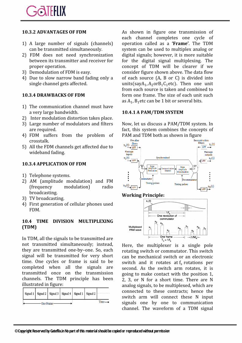
10.3.2 ADVANTAGES OF FDM
1) A large number of signals (channels) can be transmitted simultaneously.
2) FDM does not need synchronization between its transmitter and receiver for proper operation.
3) Demodulation of FDM is easy. 4) Due to slow narrow band fading only a
single channel gets affected. 10.3.4 DRAWBACKS OF FDM
1) The communication channel must have
a very large bandwidth. 2) Inter modulation distortion takes place. 3) Large number of modulators and filters
are required. 4) FDM suffers from the problem of
crosstalk. 5) All the FDM channels get affected due to
wideband fading. 10.3.4 APPLICATION OF FDM
1) Telephone systems. 2) AM (amplitude modulation) and FM
(frequency modulation) radio broadcasting.
3) TV broadcasting. 4) First generation of cellular phones used
FDM. 10.4 TIME DIVISION MULTIPLEXING (TDM) In TDM, all the signals to be transmitted are not transmitted simultaneously; instead, they are transmitted one-by–one. So, each signal will be transmitted for very short time. One cycles or frame is said to be completed when all the signals are transmitted once on the transmission channels. The TDM principle has been illustrated in figure:
As shown in figure one transmission of each channel completes one cycle of operation called as a ‘Frame’. The TDM system can be used to multiplex analog or digital signals; however, it is more suitable for the digital signal multiplexing. The concept of TDM will be clearer if we consider figure shown above. The data flow of each source (A, B or C) is divided into units(sayA1, A2orB1C1etc). Then one unit from each source is taken and combined to form one frame. The size of each unit such as A1, B1etc can be 1 bit or several bits. 10.4.1 A PAM/TDM SYSTEM Now, let us discuss a PAM/TDM system. In fact, this system combines the concepts of PAM and TDM both as shown in figure
Working Principle:
Here, the multiplexer is a single pole rotating switch or commutator. This switch can be mechanical switch or an electronic switch and it rotates at fs rotations per second. As the switch arm rotates, it is going to make contact with the position 1, 2, 3, or N for a short time. There are N analog signals, to be multiplexed, which are connected to these contracts; hence the switch arm will connect these N input signals one by one to communication channel. The waveform of a TDM signal
© Copyright Reserved by Gateflix.in No part of this material should be copied or reproduced without permission

which is being transmitted has been shown in figure. It shows that the rotator switch samples each message during each of its rotations. Since, each rotation corresponds to one frame, therefore, one frame is completed in Ts seconds whereTs = 1/fs . Hence, the function of the commutator is twofold as under 1) To take narrow sample of each input
message at a rate fs which is higher than 2fm.
2) To sequentially interleave the N samples inside the interval Ts = 1/fs
Now, the multiplexed signal at the output of the commutator is applied to a pulse amplitude modulator. It converts the PAM pulses amplitude modulator. It converts the PAM pulses into a form suitable for transmission over the communication channel. The input message signals are passed through low pass filters before applying them to the commutator. These filters are actually the anti aliasing filters which avoid the aliasing. The cut off frequency of each low pass filters (LPF) is fm Hz. At the receiving end of PAM/TDM system, the received signal is applied to a pulse amplitude demodulator which performs the reverse operation of pulse amplitude modulator. At the receiver, there is one more rotating switch or decommutator used for demultiplexing. It will be interesting to know that this switch must rotate at the same speed as that of the commutator at the transmitter and its position must be synchronized with commutator in order to ensure proper demultiplexing. The low pass filters (LPFs) on the receiver side are used for the reconstruction of the original message signals.
10.4.2 SIGNALING RATE IN A PAM/ TDM SYSTEM As a matter of a fact, the signaling rate of a TDM system is defined as the number of
pulses transmitted per second. It is represented by r. 1) Let fm= maximum frequency of all the
input signalsx1to xN. 2) Therefore, as per Nyquist criterion, the
sampling frequency fs ≥ 2fm. hence, the speed of rotation of commutators is fs rotations per second withfs ≥ 2fm.
3) As shown in figure one revolution of commutators corresponding to one frame contains sample from each input signal. Hence, 1 revolution=1 frame=N pulses.
4) One frame period is (1/fs) i.e.,
Tsseconds. Therefore in Ts seconds, N numbers of pulses are transmitted. Hence the pulse to pulse spacing within the frame is given by,
Pulses to pulse spacing s
s
T 1N Nf
= =
5) As the period of one pulse (ON+OFF) is (1/ Nfs) seconds, the number of pulses per seconds is given by,
Number of pulses per second = Nfs Therefore, signaling rate of a TDM
system =r= Nfs pulses/ second. But asfs ≥ 2fm, therefore Signaling rate of a TDM system = r ≥
2 Nfm pulses per second. 10.4.3 TRANSMISSION BANDWIDTH OF A PAM/TDM CHANNEL The minimum transmission bandwidth of a PAM-TDM channel is given by
1BW (signalingrate)2
=
Therefore, minimum transmission
bandwidth m m1BW 2Nf Nf2
= × =
© Copyright Reserved by Gateflix.in No part of this material should be copied or reproduced without permission

Example Two analog signals x1(t) and x2(t) are to be transmitted over a common channel by means of time division multiplexing (TDM). The highest frequency of x1(t) is 4 kHz and that of x2(t) is 4.5 kHz. What will be the minimum value of permissible sampling rate? Solution The highest frequency component of the composite signal consisting of
( ) ( )1 2x t andx t is 4.5 kHz. Therefore the minimum value of permissible sampling rate will be, ( )s minf 2 4.5kHz 9kHz= × = Example A signalx1(t) is band limited to 3 kHz. Therefore are three more signals x2(t),x3(t) and x4(t) which are band limited to 1 kHz each. These signals are to be transmitted by a TDM system. Design a TDM scheme where each signal is sampled at its Nyquist rate. What must be the speed of the commutator? Calculate the minimum transmission bandwidth of the channel. Solution
1) If the sampling commutator rotates at
the 2000rotations per second then the signals x2(t), x3(t)and x4(t) will be sampled at their Nyquist rate. But, we have to sample x1(t) also at its Nyquist rate which is three times higher than that of the other three. In order to achieve this we should sample x1(t) three commutator must have attest 6 poles connected to the signals as shown in figure
2) The speed of rotation of the commutator is 2000 rotations/ sec.
3) Number of samples produced per second is calculated as under:
( )1x t produce3 2000 6000samples / sec× = ( ) ( ) ( )2 3 4x t , x t andx t Produce 2000
samples/sec each Therefore, number of samples per
second =6000 + (3×2000) =12000 samples /sec Hence, signaling rate =12000 samples/sec 4) The minimum channel bandwidth will
be
( )1BW signaling rate2
=
12000 / 2 6000Hz= =
© Copyright Reserved by Gateflix.in No part of this material should be copied or reproduced without permission

Q.1 Which one of the following statements regarding the following signal( ) ( ) ( )3 6x t 5sin 2π 10 t sin 2π 10 t= × ×
is incorrect? a) The upper side band frequency
is 1001000 b) The lower side band frequency is
999000 c) The carrier amplitude is 5d) x(t) is a DSB-SC signal
Q.2 A 10 kW carrier is sinusoidally modulated by two carries corresponding to a modulation index of 30% and 40% respectively. The total radiated power is a) 11.25 kW b) 12.5 kWc) 15 kW d) 17 kW
Q.3 Consider an SSB signal when the modulating signal is X(t). Let X(t) represent the complex conjugate of X(t) and x(t) represent the Hilbert transform of X (t). The envelope of the SSB signal is a) 2 2 1/2[x (t) (x) (t)]+ b) x(t)c) x(t)d) [x2(t) + (x)2(t)]1/2
Q.4 An AM voltage signal s(t), with a carrier frequency of 1.15 GHz has a complex envelope g(t) = AC [1+m(t)], AC = 500V, and the modulation is a 1 kHz sinusoidal test tone described by 𝑚𝑚(𝑡𝑡) = 0.8 𝑠𝑠𝑠𝑠𝑠𝑠 (2π × 103 𝑡𝑡) appears across a 50 Ω resistive load. What is the actual power dissipated in the load? a) 165 kW b) 82.5 Kwc) 2.5 kW d) 6.6 kW
Q.5 A broadcast AM radio transmitter radiates 125 kW when the
modulation percentage is 70. How much of this is carrier power? a) ≈ 25 kW b) ≈ 50 kWc) ≈75 kW d) ≈ 100 kW
Q.6 A given AM broadcast station transmits an average carrier power output of 40 KW and uses a modulation index of 0.707 for sine wave modulation. What is the maximum (peak amplitude of the output if the antenna is represented by a 50 Ω resistive load)? a) 50 KV b) 50Vc) 1.0796 KV d) 28.28 KV
Q.7 Match List I (Signal) with List II (Spectrum) and select the correct answer using the codes given below the lists: List I List II (Signal) (Spectrum)
Codes: A B C D
a) 1 3 2 4 b) 2 4 1 3 c) 2 3 1 4 d) 1 4 2 3
Q.8 The original spectrum of a message contains 100 Hz, 200 Hz frequency
ASSIGNMENT QUESTIONS
© Copyright Reserved by Gateflix.in No part of this material should be copied or reproduced without permission
components. It is amplitude modulated by a carrier of 0.9 kHz. Which frequency components are contained in the amplitude modulated signal spectrum?
a) 900, 1000 and 1100 Hz b) 700, 800 and 900 Hz c) 700, 800, 900 1000 and 1100 Hz d) 100, 200 and 900 Hz Q.9 If two signals modulate the same
carrier with different modulation depths of 0.3 and 0.9, the resulting modulation signal will a) Be over-modulated b) Have the resultant modulation
limited to 1.0 c) Have the resultant modulation
index around 0.82 d) Have the resultant modulation
index around 0.95
Q.10 Match List-I with List-II and select the correct answer using the code given below the lists: [Given mi(t), i =1, 2:base band message signals; fc: carrier frequency, mi(t): Hilbert transform of mi]
List-I (Mathematical Expression)
A. m1(t) cos cω t + m2(t) sin cω t
B. m1(t) cos cω t + m1(t) sin cω t
C. m2(t) cos cω t − m2(t) sin cω t
D. m1(t) cos cω t List-II
(Type of Signal) 1. DSB-SC 2. USB 3. QAM 4. LSB
A B C D a) 3 4 2 1 b) 3 4 1 2 c) 1 2 4 3 d) 1 2 3 4 Q.11 A carrier is amplitude modulated by
4 signals of frequency 10 kHz, 15 kHz, 20 kHz and 25 kHz. What is the bandwidth of the modulated signal?
a) 25 kHz b)50 kHz c) 70 kHz d) 140 kHz Q.12 In an AM system, for satisfactory
operation, carrier frequency must be n times the bandwidth of message – signal. What is the value of n?
a) > 2 b) > 5 c) > 10 d) > 50 Q.13 For an AM signal, the bandwidth is
10 kHz and the highest frequency component present is 705 kHz. What is the carrier frequency used for this AM signal?
a) 695 kHz b) 700 kHz c) 705 kHz d) 710 kHz Q.14 The antenna current of an A.M.
transmitter is 8A when only carrier is sent, but it increases to 8.93 A when the carrier is modulated. Then what is the percentage modulation of the wave?
a) 43.00% b) 70.14% c) 57.00% d) 100.00% Q.15 An AM modulator has output
S(t)20 cos (300πt) +6 cos(320 πt) + 6 cos(280 πt). Then what is the modulation index of the wave?
a) More than 100% b) 0.93 c) 0.3 d) 0.6 Q.16 If a single-tone amplitude
modulated signal at a modulation depth of 100% transmits a total power of 15W, the power in the carrier component is
a) 5W b) 10W c) 12W d) 15W
© Copyright Reserved by Gateflix.in No part of this material should be copied or reproduced without permission

Q.17 Which one of the following is used for the detection of AM-DSB-SC signal?
a) Ratio detector b) Foster-Seeley discriminator c) Product demodulator d) Balanced-slope detector Q.18 Consider amplitude modulated (AM)
wave cm(t) = (Ac + Am cos ωmt) cos ωct . If 𝑃𝑃𝑠𝑠 denotes the power in Ac = 2𝐴𝐴𝑚𝑚 which one of the following is TRUE?
a) PT = 3Ps b) PT = 6Ps c) PT = 9Ps d) PT = 18Ps Q.19 Two carriers 40 MHz and 80 MHz
respectively are frequency modulation by a signal of frequency 4 KHz, such that the band-widths of the FM signal in the two cases are the same. The peak deviations in the two cases are in the ratio of
a) 1 : 4 b) 1 : 2 c) 1 : 1 d) 2 : 1 Q.20 In phase modulation, the frequency
deviation is a) independent of the modulating
signal frequency b) increasely proportional to the
modulating signal frequency c) directly proportional to the
modulating signal frequency d) inversely proportional to the
square root of the modulating frequency
Q.21 Which one of the following is
represented by ( ) 6 6v t 5[cos(10 πt)sin(10 πt)]= ? a) SSB upper sideband signal b) DSB suppressed carrier signal c) AM signal d) Narrow band FM signal Q.22 Match List – I with List – II and
select the correct answer using the code given under the Lists:
List-I (Modulation) A.100% AM B. 50%AM C. 10% AM D. FM List-II (Power Input to Antenna in Watts) 1. 1.5 2. 1.125 3. 1.005 4. 1.00 Code : A B C D a) 1 2 3 4 b) 3 4 1 2 c) 1 4 3 2 d) 3 2 1 4 Q.23 A signal contains components at 400
Hz and 2400 Hz. This signal modulates a carrier of frequency 100 MHz. However, after demodulates it is found that the 400 Hz signal component is present. The channel BW is 15 kHz. What is the reason for the higher frequency signal not to be detected properly? a) Modulation used is FM and BW
is insufficient. b) Modulation used is AM and BW
is insufficient. c) Modulation used is FM but pre-
emphasis is not used d) Modulation used is AM but
detector is for FM
Q.24 Why does an FM radio station n perform better than an AM station radiating the same total power? a) FM is immune to noise b) AM has only two sidebands
while FM has more c) FM uses larger bandwidth for
large modulation depth d) Capture effect appears in FM
Q.25 A carrier signal at frequency 100
© Copyright Reserved by Gateflix.in No part of this material should be copied or reproduced without permission
MHz is frequency modulated with modulation index2 by a signal at 2 kHz. At what frequencies are the sidebands produced? a) 102 MHz and 98 MHz b) 100 MHz + 2 kHz and 100 MHZ –
2 kHz c) 100MHz ± ∆fd, where fd is
frequency deviation d) 100 MHz ± n2 kHz, where n is 1,
2, ….., 5 integer Q.26 If, on doubling the modulating
frequency, the modulation index is halved, and the modulating voltage remains constant, then the system is
a) amplitude modulated b) frequency modulated c) phase modulated d) pulse modulated Q.27 The waveform A 1 2cos( t k cos t)+ is
a) Amplitude modulated b) Frequency modulated c) Phase modulated d) Frequency as well as phase
modulated Q.28 Match List-I (System) with List-II
(Application) and select the correct answer using the codes given below the Lists:
List-I (System) A. Pre-emphasis B. Armstrong Method C. Envelope Detector D. De-emphasis List-II (Application) 1.AM Detector 2.FM Receiver 3.FM Generator 4.FM Transmitter 5. AMTransmitter Codes: A B C D a) 4 3 2 1 b) 3 5 1 2
c) 4 3 1 2 d) 5 3 2 1 Q.29 The types of modulation used
generally in TV transmission for video & audio signals, respectively, are
a) FM and AM b) FM and FM c) AM and AM d) AM and FM Q.30 Which of the following is not a
component of PLL? a) Frequency multiplier b) Phase detector c) VCO d) Loop filter Q.31 Which of the following modulated
signals can be detected by an envelope detector?
a) DSB-suppressed carrier b) DSB-full carrier c) Frequency modulated signal d) SSB-suppressed carrier Q.32 Which one of the following sets
correctly describes the Block I and Block II in the diagram given above?
a) Integrator Phase modulator b) Integrator Frequency modulator c) Differentiator Phase modulator d) Differentiator Frequency modulator Q.33 If two signals modulate the same
carrier with different modulation depths of 0.3 and 0.9, the resulting modulation signal will a) Be over-modulated b) Have the resultant modulation
limited to 1.0 c) Have the resultant modulation
index around 0.82 d) Have the resultant modulation
index around 0.95
© Copyright Reserved by Gateflix.in No part of this material should be copied or reproduced without permission
Q.34 Match List I (Modulation) with List II(Application) and select the correct answer using the code given below the lists:
List I (Modulation) A. Wide band FM B. Narrow band FM C. AM D. VSB-AM List II (Application) 1. Mobile communication 2.Superimposition of binary
waveform on carrier 3.TV video 4.TV audio 5. Medium wave broadcast Code: A B C D a) 4 3 5 1 b) 5 1 2 3 c) 4 1 5 3 d) 5 3 2 1 Q.35 Two independent signals X and Y
are known to be Gaussian with mean values x0 and y0 and variances
2y
2x and σσ . A signal Z = X – Y is
obtained from them. The mean z0, variance 2
zσ and p.d.f. p(z) of the signal Z are given by
a) 2 20 0 x yx ~ y , ~ , Gaussianσ σ
b) Rayleigh , ,x 2200 yxy σσ ++
c) uniform , ,y 2200 xyx σσ −−
d) Gaussian , ,x 2200 yxy σσ +−
Q.36 If the cumulative distribution
functions is Fx(x), then the probability density function fx(x) is given as
a) ( )xF x dx∫ b) xd F (x)
dx
c) xF ( x)dx−∫ d) xd F ( x)
dx−
Q.37 The number of bits per sample of a
PCM system depends upon the
a) sampler type
b) quantizer type c) number of levels of the quantizer d) sampling rate Q.38 A PCM system uses a uniform
quantizer which has a range – V to +V and it is followed by a 7 bit binary encoder. A zero mean signal applied to the quantizer extends over its entire range and has uniform probability density. The ratio of the signal power to the quantization noise power at the output of the quantizer is (Take log10 2≈0.3)
a) 14 dB b) 28 dB c) 42 dB d) 56 dB Q.39 If X is a zero mean Gaussian random
variable, then PX ≤ 0 is a) 0 b) 0.25 c) 0.5 d) 1 Q.40 If E denotes the expectation
operator, then 𝐸𝐸[𝑋𝑋 – 𝐸𝐸𝑋𝑋]3 of a random variable X is
a) EX3 – E3X b) EX3 + 2E3X– 3EX EX2
c) 3EX3 – E3X d) 2EX3 + E3X – 3EX EX2 Q.41 There are two fair coins
( ) ( ) 1P Head P Tail2
= =
and a third
biased coin where 1P(Head)4
= =
and ( ) 3P Tail4
= One coin is picked
at random and tossed once and a Head is obtained. The probability that the coin tossed is one of the fair coins is
a) 56
b) 45
© Copyright Reserved by Gateflix.in No part of this material should be copied or reproduced without permission
c) 34
d) 23
Q.42 A box contains 5 black and 5 red
balls. Two balls are randomly picked one after another from the box, without replacement. The probability for both balls being red is
a) 190
b) 15
c) 1920
d) 92
Q.43 A uniformly distributed random
signal 𝑥𝑥[𝑠𝑠] with mean 𝑚𝑚𝑥𝑥 = 2 and variance 2 3,=xσ is passed through a 3-point moving-average filter having an impulse response h[n]=1/3, 1/3, 1/3. What will be the mean and variance of output?
a) 2y ym 2, 1σ= = b) 2
y ym 2, 3σ= = c) 2
y ym 1, 1σ= = d) 2y ym 3, 3σ= =
Q.44 Four voice signals, each limited to 4
kHz and sampled at Nyquist rate, are converted into binary PCM signal using 256 quantization levels. The bit transmission rate for the time division multiplexing signal will be
a) 8 kbps b) 64 kbps c) 256 kbps d) 5126 kbps
Q.45 Consider the analog signal x(t) =
3cos100πt. If the signal is sampled at 200Hz, the discrete time signal obtained will be
a) 3cos(πn/4) b) 3cos(πn/2) c) 3cos(πn) d) 3cos(πn/3)
Q.46 An anti-aliasing filter is a) An analog filter
b) A digital filter c) Can be analog or digital d) None of the above
Q.47 A message signal band limited to 5 KHz is sampled at the minimum rate as dictated by the sampling theorem. The number of quantization levels is 64. If the samples are encoded in binary form, the transmission rate is
a) 60 kbps b) 50 kbps c) 32 kbps d) 10 kbps
Q.48 In a DM (delta modulation) system,
the granular (idling) noise occurs when the a) modulation signal increases
rapidly b) pulse rate decreases c) modulating signal remains
constant d) pulse amplitude decreases
Q.49 In an ADM transmission system, the
output signal amplitudes for 1’s and 0’s are a) fixed and the repetition rate is
also fixed. b) fixed but the repetition rate is
variable c) variable and the repetition rate
is also variable d) variable but the repetition rate is
fixed. Q.50 Match List-I with List-II and select
the correct answer using the codes given below the Lists:
List-I A. Frequency modulation B. Double sideband suppressed
signal Carrier C. PCM D. Amplitude modulation List-II 1. Envelope detection 2. Companding 3. Balanced modulator 4. Pre-emphasis and De-emphasis Codes: A B C D a) 1 2 3 4
© Copyright Reserved by Gateflix.in No part of this material should be copied or reproduced without permission

b) 1 2 4 3 c) 4 3 1 2 d) 4 3 2 1 Q.51 Four voice signals, each limited to 4
kHz and sampled at Nyquist rate, are converted into binary PCM signal using 256 quantization levels. The bit transmission rate for the-division multiplexed signal will be
a) 8 kbps b) 64 kbps c) 256 kbps d) 512 kbps Q.52 13 dBm is equivalent to a) 2 mW b) 20 W c) 20 mW d) 2 MW Q.53 Consider the following statements
comparing delta modulation with PCM system:DM requires
1. a lower sampling rate 2. a higher sampling rate 3. a larger bandwidth 4. simpler hardware Which of these statements are
correct? a) 1, 2 and 4 b) 1, 2 and 3 c) 1, 3 and 4 d) 2, 3 and 4 Q.54 Match List I (operations) with List II
(Functions) and using the codes given below the Lists:
List I A. Companding B. Squelch C. Pre-emphasis D.Double List II 1.Improving 2.Variation of step rise in
quantization 3. Muting the receiver conversion 4. Booting of higher modulating
frequencyat the transmitter Codes: A B C D a) 2 3 4 1 b) 2 1 4 3 c) 4 3 2 1 d) 4 1 2 3
Q.55 Four signals each band-limited to 5
kHz are sampled at twice the Nyquist rate. The resulting PAM samples are transmitted over a single channel after time division multiplexing. The theoretical minimum transmissions bandwidth of the channel should be equal to
a) 5 kHz b) 20 kHz c) 40 kHz d) 80 kHz Q.56 In delta modulation, hen is the slope
overloading noise absent? (h is the pulse height and sampled
every Ts seconds, f(t) is the input signal, h and T. are step-size of integration and sampling period, respectively)
a) sdf (t) (h / T )
dt≤
b) s
df (t) (h / T )dt
>
c) sdf (t) (h T )
dt≤ ⋅ d) df (t) (h T)
dt> ⋅
Q.57 A continuous signal has voltage
range -2V to + 2V. If this is quantized to 8 bits, what does the resulting signal have? a) 225 levels of step size 4/225 b) 256 levels of step size 4/8 c) 8 bits plus 2 levels at -2 and +2
volts d) 8 bits per sample if properly
sampled Q.58 Four signals 1 2 3g (t),g (t),g (t) & 4g (t) are to be multiplexed and
transmitted. g1(t) and g4(t) have bandwidth of 4 kHz, and the remaining two signals have bandwidth of 8 kHz. Each sample requires 8 bit for encoding. What is the minimum transmission bit rate of the system?
a) 512 kbps b) 16 kbps c) 192 kbps d) 384 kbps
Q.59 Which one of the following signals can be applied to a delta modulator
© Copyright Reserved by Gateflix.in No part of this material should be copied or reproduced without permission

whose step size is 0.1 V and sampling frequency is 20 π kHz so that no slope overload occurs?
a) 2 sin (1200 π t) b) 1 sin (2600 π t) c) 3 sin (1000 π t) d) 4 sin (400 π t) Q.60 Frequency shift keying is used
mostly in a) radio transmission b) telegraphy c) telephony d) none of these Q.61 If carrier modulated by a digital bit
stream had one of the possible phases of 0, 90, 180 and 270 degrees, then the modulation is called
a) BPSK b) QPSK c) QAM d)MSK Q.62 A TDM link has 20 signal channels
and each channel is sampled 8000 times/sec. Each sample is represented by seven binary bits and contains an additional bit for synchronization. The total bit rate for the TDM link is
a) 1180 K bits/sec b) 1280 K bits/sec c) 1128 K bits/sec d) 1280 M bits /sec Q.63 The impulse response of a filter,
matched to a rectangular pulse, is a) an attenuator b) a low-pass filter c) a high-pass filter d) an equalizer
Q.64 The bits rate of a digital communication system is 34 M bit/s. The modulation scheme is QPSK. The baud rate of the system is
a) 68 M bit/s b) 34 M bit/s c) 17 M bit/s d) 8.5 M bit/s
Q.65 If binary PSK modulation is used for transmission, the required minimum bandwidth is 9600 Hz. To reduce the transmission bandwidth to 2400 Hz, the modulation scheme to be adopted should be a) Quadrature phase-shift keying b) Minimum shift keying c) 16-ary quadrature amplitude
modulation d) 8-ray PSK
Q.66 Which one of the following
statements is correct? For coherent detection of digital
signals, the receiver must be a) synchronized in time only b) synchronized in phase only c) synchronized in time and phase
d) unsynchronized Q.67 In case of data transmission, which
one of the following systems will give the maximum probability of error?
a) ASK b) FSK c) PSK d) DPSK Q.68 A digital communication system
uses 8 – PSK modulation and transmits 3600 bps. What is the symbol rate?
a) 10800 symbols/ sec b) 450 symbols/ sec c) 28800 symbols/ sec d) 1200 symbols/ sec Q.69 Which one of the following
statements is incorrect about the matched filter? a) The maximum output SNR
depends on the input signal energy
b) The impulse response is reversed delayed version of the input signal.
c) The error probability depends on the wave shape of the signal.
© Copyright Reserved by Gateflix.in No part of this material should be copied or reproduced without permission

d) Matched filter and correlator gives identical reception performances
Q.70 The bandwidth required for QPSK modulated channel is
a) Twice the BW of BPSK b) Equal to BPSK c) Equal to FSK d) Half of the BW of BPSK Q.71 A discrete zero memory information
source has 40 symbols and each symbol is equally likely. The minimum number of bits required to code the source with uniform length code and the entropy of the source are respectively
a) 5, 5.03 b) 6, 5.83 c) 5, 6.64 d) 6, 5.32
Q.72 The advantage of differential
PSK(DPSK) over coherent PSK is a) DPSK requires less bandwidth
compared coherent PSK b) DPSK receiver design is simple
compared to coherent PSK c) DPSK Bit Error rate is lower than
coherent PSK d) For same bandwidth, DPSK bit
rate is higher compared to coherent PSK
Q.73 Which one of the following can be
used for the detection of the non-coherent BFSK signal?
a) Matched filter b) Phase-locked loop c) Envelope detector d) Product demodulator Q.74 Bits of duration Tb are to be
transmitted using a BPSK modulation with a carrier of frequency fc Hz. The power spectral density of the transmitted signal has the first null at the normalized frequency
a) b| f – fc | T 0= b) b| f – fc | T 1= c) b| f – fc | T 2= d) b| f – fc | T 4=
Q.75 The probability of bit error of a
BFSK modulation scheme, with transmitted signal energy per bit Eb, in an additive white Gaussian noise channel having one – sided power spectral density No, is
a) b
0
E1 erfc2 2N
b) b
0
E1 erfc2 2N
c) b
0
E1 erfc2 N
d) b
0
E1 erfc2 N
Q.76 For a given transmitted pulse p(t), 0
≤ t ≤ T, the impulse response of a filter matched to the received signal is
a) – p(t – T), 0 ≤ t ≤ T b) – p(T – t), 0 ≤ t ≤ T c) p(t – T), 0 ≤ t ≤ T d) p(T – t), 0 ≤ t ≤ T Q.77 A communication system operates
in an AWGN channel and employs BPSK modulation. If Eb
N0= 4(Eb :
signal energy per bit, N0: noise power spectral density) and given that erf(2) = 0.99532, the average BER is
a) 2.34 × 10⁻³ b) 2.34 × 10⁻⁴ c) 4.68 × 10⁻³ d) 4.68 × 10⁻⁴ Q.78 A matched filter having a frequency
response H(f) j2 /T1 e
j2 f
− π−=
πmatches to
a)1, 0 t T
s(t)0, otherwise
≤ ≤=
b)1, 0 t T
s(t)0, otherwise− ≤ ≤
=
c)t1 , 0 t T
s(t) T0, otherwise
− ≤ ≤=
© Copyright Reserved by Gateflix.in No part of this material should be copied or reproduced without permission
d) t1 , 0 t T
s(t) T0, otherwise
− + ≤ ≤=
Q.79 The capacity of an analog
communication channel with 4 KHz bandwidth and 15 dB SNR is approximately
a) 20,000 bps b) 16,000 bps c) 10,000 bps d) 8,000 bps Q.80 What is the advantage ofOffset QPSK
(OQPSK) compared to conventional QPSK?
a) Constant envelop b) Bandwidth efficiency c) Simple demodulator d) All of above Q.81 The channel capacity under the
Gaussian noise environment for a discrete memory cycles channel with a bandwidth of 4 MHz and SNR of 31 is
a) 20 Mbps b) 4 Mbps c) 8 Kbps d) 4 Kbps Q.82 Which one of the following is the
correct statement? If the channel bandwidth is doubled,
the S/N ratio becomes a) double of the former S/N ratio b) square root of the former S/N
ratio c) half of the former S/N ratio d) None of the above
Q.83 Assertion (A): PSK is inferior to
FSK. Reason(R): PSK requires less
bandwidth than FSK. a) Both A and R are true and R is
the correct explanation of A. b) Both A and R are true but R is
not the correct explanation of A. c) A is true but R is false d) A is false but R is true
Q.84 The entropy of a message source
generating four messages with probabilities 0.5, 0.25, 0.125, and 0.125 is
a) 1.0 bit/message b) 1.75 bits/message c) 3.32 bits/message d) 5.93 bits/message Q.85 Two orthogonal signals s1(t) and
s2(t) satisfy the following relation a)
T
1 20s (t)s (t)dt 0=∫
b) T
1 20s (t)s (t)dt 0=∫
c)T
1 20s (t)s (t)dt = ∞∫
d) T
1 20s (t)s (t)dt = π∫
Q.86 The units of the spectrum obtained
by Fourier transforming the covariance function of a stationary stochastic process is
a) Power per Hertz b) Energy per Hertz c) Power per second d) Energy per second Q.87 The covariance function of a band
limited white noise is : a) A Dirac delta function b) An exponentially decreasing
function c) A sinc function d) A sinc2 function
Q.88 Thermal noise is passed through an
ideal low-pass filter having cut-off at fc = ωHz. The autocorrelation value of the noise at the output of the filter is given as a) A delta function at t = 0 b) Gaussian over the range -∞ ≤ t ≤
∞ c) Sinc function over the range -∞ ≤
t ≤ ∞
© Copyright Reserved by Gateflix.in No part of this material should be copied or reproduced without permission
d) Triangular function over the
range 1 1t2 2
− ≤ ≤ω ω
Q.89 A random process obeys Poisson’s
distribution. It is given that the mean of the process is 5. Then the variance of the process is
a) 5 b) 0.5 c) 25 d) 0 Q.90 A source generates four messages.
The entropy of the source will be maximum when a) all probabilities are equal b) one of the probabilities equals
1.0 and others are zero. c) the probabilities are 1/2 , 1/4 ,
1/8 d) two of the probabilities are 1/2
each and others are zero. Q.91 Power spectral density of a signal is a) Complex, even and non-negative b) Real, even and non-negative c) Real, even and negative d) Complex, odd and negative Q.92 In a communication system, a
process for which statistical-averages and time averages are equal, is called
a) Stationary b) Ergodic c) Gaussian d) BIBO stable Q.93 If random process X(t) and Y(t) are
orthogonal then a) SXY(f) = 0 b) SXY(f) = SX(f ) = SY(f) c) RXY(τ) = h (τ) d) H(f) = 0 Q.94 If a random process X(t) is ergodic
then, statistical averages a) And time averages are different b) And time averages are same c) Are greater than time averages d) Are smaller than time averages
Q.95 Match List I (Type of Random Process) with List II (Property of the Random Process) and select the correct answer using the codes given below the lists:
List I (Type of Random Process) A. Stationary Process B. Ergodic Process C. Wide sense stationary D.CyclostationaryProcess List II (Property of the Random Process) 1. Statistical averages are periodic in
time. 2.Statistical averages are
independent of time 3.Mean and autocorrelation are
independent of time. 4.Time average equal corresponding
ensemble average Codes: A B C D
a) 3 1 2 4 b) 2 4 3 1 c) 3 4 2 1 d) 2 1 3 4 Q.96 A sinusoidal signal with a random
phase is given by x(t)=A sin[ / 2 (2 ft )]π − π + θ with the
probability density function
≤
=otherwise
P,0
20,2/1)(
πθπθθ
What is the maximum amplitude of the autocorrelation function of this signal?
a) A b) A/2 c) A2 d) A2/2
Q.97 White noise is passed through an
ideal low-pass filter. Which one of the following is the nature of the auto-correlation function of the filtered output noise? a) Periodic infinite number of zero
crossings b) Periodic but the number of zero
© Copyright Reserved by Gateflix.in No part of this material should be copied or reproduced without permission
crossings depends on the bandwidth of the filter
c) Periodic but does not cross zero d) A delta function
Q.98 When zero mean Gaussian noise of
variance N is applied to an ideal half- wave rectifier, what is the mean square value of the rectified noise?
a) N/4 b) N/2 c) N d) 2N Q.99 If ACF denotes the autocorrelation
function and PSD denotes the power spectral density, then for white noise, ACF is: a) A Gaussian while PSD is uniform b) A delta function while PSD is
uniform c) A delta function while PSD is
exponential d) An exponential while PSD is
uniform Q.100 The auto-correlation function Rx(τ)
of a random process has the property that Rx (0) is equal to a) The square of the mean value of
the process. b) The mean squared value of the
process c) The smallest value of Rx (t)
d) 21 [Rx(t) + Rv(-t)]
Q.101 One decibel represents a power ratio of
a) 1.26 : 1 b) 2 : 1 c) 10 : 1 d) 20 : 1
Q.102 The power spectral density of white noise
a) varies as square root of frequency b) varies as inverse of frequency c) varies as square of frequency d) is constant with frequency Q.103 Consider a low pass random process
with a white noise power spectral
density xS (ω) N / 2= where 2πB ω 2πB− ≤ ≤ 0 elsewhere
The Aut-correction function Rx (τ) is a) 2NBsinc (2πBτ) b) πNBsinc (2πBτ) c) NBsinc (2πBτ) d) None of the above
Q.104 Auto – correlation of a sinusoid s(t) = A sin (ωt) is
a) (A2/2) sin (ωτ) b) (A/2) sin (ωτ)
c) (A2/2) cos (ωτ) d) (A/2) cos (ωτ)
Q.105 A signal x(t) = cos(10 t)cos(100t) is passed through a system whose impulse response is H(ω) = exp(-j100 – j2(ω – 100)). If y(t) is the system output, then
a) 1y(t) cos 10 t cos(100(t 1)2
= − −
b) 1y(t) cos(10(t 1)) cos 100 t2
= − −
c) y(t) cos(10(t 2)) cos(100(t 1))= − − d) y(t) cos(10(t 1)) cos(100(t 2))= − − Q.106 A 8 kHz communication channel has
an SNR of 30 dB. If the channel bandwidth is doubled, keeping the signal power constant, the SNR for the modified channel will be
a) 27 dB b) 30 dB c) 33 dB d) 60 dB Q.107 A telephone channel has bandwidth
B of 3 kHz and SNR
ηBS of 30 dB. It
is connected to a teletype machine having 32 different symbols. The symbol rate required for errorless transmission is nearly.
a) 1800 symbols/s b) 3000 symbol/s c) 5000 symbol/s d) 6000 symbol/s
© Copyright Reserved by Gateflix.in No part of this material should be copied or reproduced without permission
Q.108 To permit the selection of 1 out of 16 equiprobable events, the number of bits required is
a) 2 b) log10 16 c) 8 d) 4 Q.109 Which one of the following
statements is correct? The Shannon’s channel capacity
formula indicates that in theory a) By using proper channel codes,
we can get an error-free transmission on a noisy channel.
b) It is not possible to get an error-free transmission on a noisy channel, since there will always be some error in the detected signal for finite noise on any channel.
c) It is true only for some wired channels and not wireless channels.
d) It works only for analog signals and not for digital signals on any channel.
Q.110 Entropy is basically a measure of
a) rate of information b) average information c) probability of information d) channel capacity for
transmission of information Q.111 The capacity of channel is given by
the a) Number of digits used in coding b) Volume of information it can
take c) Maximum rate of information
transmitted d) Bandwidth required for
information
1 2 3 4 5 6 7 8 9 10 11 12 13 14 (c) (a) (d) (c) (d) (c) (c) (c) (d) (a) (b) (d) (b) (b) 15 16 17 18 19 20 21 22 23 24 25 26 27 28 (d) (b) (c) (d) (c) (a) (d) (a) (c) (d) (d) (b) (d) (c) 29 30 31 32 33 34 35 36 37 38 39 40 41 42 (d) (a) (b) (d) (d) (c) (d) (b) (c) (c) (c) (b) (b) (d) 43 44 45 46 47 48 49 50 51 52 53 54 55 56 (b) (c) (b) (c) (a) (c) (d) (d) (c) (c) (d) (a) (c) (a) 57 58 59 60 61 62 63 64 65 66 67 68 69 70 (b) (d) (d) (b) (b) (c) (b) (c) (c) (c) (a) (d) (c) (d) 71 72 73 74 75 76 77 78 79 80 81 82 83 84 (d) (b) (c) (b) (b) (d) (a) (a) (b) (a) (a) (c) (d) (b) 85 86 87 88 89 90 91 92 93 94 95 96 97 98 (a) (a) (c) (c) (a) (a) (a) (b) (a) (b) (b) (d) (a) (b) 99 100 101 102 103 104 105 106 107 108 109 110 111 (b) (b) (a) (d) (d) (a) (c) (a) (d) (d) (a) (b) (c)
ANSWER KEY:
© Copyright Reserved by Gateflix.in No part of this material should be copied or reproduced without permission
Q.1 (c) ( ) ( )3x t 5sin 2π 10 t= ×
6sin(2π 10 t)× DSB signal is given by ( ) ( ) ( )c m m cx t A A sin 2πf t sin 2πf t=
AcAm = 5 not Ac = 5
Q.2 (a) c 1 2P 10kw,μ 0.3μ 0.4= = =
2 2t 1 2μ μ μ 0.09 0.16= + = +
0.25 0.5= = 2t
t cμP P 12
= +
3 0.2510 10 12
= × +
11.250kw=
Q.3 (d) The time domain equation of SSB is
( ) ( ) $( )c cAc Acs t x t cos 2πf t x t sin 2πf t2 2
= m
The envelop of SSB is given by = ( )2 2x t x (t)+
Q.4 (c) Since µ is not given
m
c
A 0.08μA 500
= =
2 2 2
t cμ Ac μP P 1 12 2R 2
= + = +
500 500 0.8 0.812 50 2 500 500× × = + × × ×
0.8 0.82500 1 2500W2 500 500
× = + = × × = 2.5kW
Q.5 (d)
2
t cμP P 12
= +
t
c 2 2P 125P kw 100.40kwμ 0.71 12 2
= = =+ +
≈ 100kw
Q.6 (c) 2
c c cAcP A 2P R2R
= ⇒ =
32 40 10 50= × × ×= 632.45v
( )max cV A 1 μ= +
632.45 (1 0.707)= + + = 1079.6V = 1.0796kV
Q.7 (c)
Q.8 (c) fm = 100Hz fm = 200Hz fc1 = 900Hz In amplitude modulated wave the frequencies present are fc1 = 900Hz fc1 + fm1 = 1000Hz
fc1 − fm1 = 800Hz fc1 + fm2 = 1100Hz fc1 − fm2 = 700Hz
Q.9 (d) µ1 = 0.3 µ2 = 0.9
2 2t 1μ μ μ 0.948 0.95= + = ≈
Q.10 (a)
Q.11 (b) Bandwidth, Bw = 2fm = 2 × 25kHz = 50kHz
Q.12 (d)
Q.13 (b)
EXPLANATIONS
© Copyright Reserved by Gateflix.in No part of this material should be copied or reproduced without permission

ww m m
BB 2f f2
= ⇒ =
10 5kHz2
= =
fc + fm = 705kHz (given) fc = 700kHz Q.14 (b)
2
t cμP P 12
= +
2
2 2t c
μI I 12
= +
2
2 2 μ8.93 8 12
= +
µ = 0.7014 = 70.14% Q.15 (d) In general AM is given by
( ) ( )c c c mAcμs t A cos 2πf t cos 2π f f t
2= + +
( )c mAcμ cos 2π f f t
2+ −
cAcμ 6A 20
2= =
12μ 0.620
∴ = =
Q.16 (b) µ = 1, Pt = 15w
2
t cμP P 12
= +
tc
P 15P 10w1 3 / 212
⇒ = = =+
Q.17 (c) Q.18 (d) Side band power is
2
cs
P μP4
=
2 2
2Ac Am
2 Ac 4= ×
2Am
4=
Total power
2 2 2
t c 2μ Ac AmP P 1 12 2 2Ac
= + = +
2
2Am1
8Am
= +
2
sAm18 18P
8= =
Q.19 (c) Frequency deviation, ∆f = kfAm Since the modulating signal is same in two cases hence the peak deviation ratio is 1:1 Q.20 (a) For phase modulation Phase deviation,∆Φ = kpAm Q.21 (d) v(t) = 5[cos(106πt) − sin(103πt). sin(106πt)]
( ) ( )6 6 355cos 10 πt cos 10 πt 10 πt2 = − − +
( )6 35 [cos 10 πt 10 πt ]2
+
Which is Narrow Band FM Q.22 (a)
Using 2
t cμP P 12
= +
the answer
can be easily matched. Q.23 (c) Pre-emphasis boosts the strength of high frequency components. Q.24 (d) In FM capture effect only the stronger of two signals at or near same frequency will be demodulated AM is not subjected to this effect. Q.25 (d) The sidebands in FM are produced at
© Copyright Reserved by Gateflix.in No part of this material should be copied or reproduced without permission
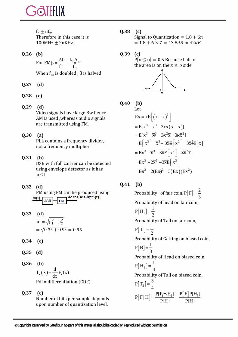
fc ± nfm Therefore in this case it is 100MHz ± 2nKHz Q.26 (b)
For FM f m
m m
k Afβf f∆
= =
When fm is doubled , β is halved Q.27 (d) Q.28 (c) Q.29 (d) Video signals have large Bw hence AM is used ,whereas audio signals are transmitted using FM. Q.30 (a) PLL contains a frequency divider, not a frequency multiplier, Q.31 (b) DSB with full carrier can be detected using envelope detector as it has μ 1≤ Q.32 (d) PM using FM can be produced using
Q.33 (d) 2 2
t 1 2μ μ μ= +
= √0.32 + 0.92 = 0.95 Q.34 (c) Q.35 (d) Q.36 (b)
( )x xdf x F (x)
dx−
Pdf = differentiation (CDF) Q.37 (c) Number of bits per sample depends upon number of quantization level.
Q.38 (c) Signal to Quantization = 1.8 + 6𝑛𝑛 = 1.8 + 6 × 7 = 43.8𝑑𝑑𝑑𝑑 ≈ 42𝑑𝑑𝑑𝑑 Q.39 (c) P[x ≤ o] = 0.5 Because half of the area is on the 𝑥𝑥 ≤ 𝑜𝑜 side.
Q.40 (b) Let ( )3Ex xE x x = −
( )3 3E[x x 3xx x x ]= − − −
3 3 2 2E[x x 3x x 3xx ]= − − + [ ]3 3 2 2E x x 3xE x 3x E x = − − +
3 3 2 2Ex x 3xE x 3x x = − − +
3 3 2Ex 2x 3xE x = + −
( )3 3 2Ex 2(Ex) 3 Ex (Ex )= + − Q.41 (b)
Probability of fair coin, [ ] 2P F3
=
Probability of head on fair coin,
[ ]11P H2
=
Probability of Tail on fair coin,
[ ]11P T2
=
Probability of Getting on biased coin,
[ ] 1P B3
=
Probability of Head on biased coin,
[ ]21P H4
=
Probability of Tail on biased coin,
[ ]23P T4
=
[ ] [ ] 11 P F P[H ]P[F H ]P F | H
P[H] P[H]= =∩
© Copyright Reserved by Gateflix.in No part of this material should be copied or reproduced without permission
[ ] [ ] [ ] [ ] [ ]1 2P H P F P H P B P H= +
2 1 1 1 53 2 4 3 12
= × + × =
[ ]2 1
43 2P F | H 5 512
×∴ = =
Q.42 (d) Probability of black ball,
[ ] 5 1P B10 2
= =
Probability of Red ball,
[ ] 5 1P R10 2
= =
Let x be event of drawing the balls
[ ] 5 4 2P x10 9 9
= × =
Q.43 (b) Q.44 (c) m sN 4f 4kHzf= =
ms
1 2f 8kHzT
= = =
Number of quantization Level, L = 256 We have nL 2 256 n 8= = ⇒ =
Bit rate,3
bs
1R N 8 10 4 8 256kbpsT
= ∩ = × × × =
Q.45 (b) ( )s sx T 3cos(100πnT )∩ =
1 nπ3cos(100π n ) 2cos( )200 2
= × =
Q.46 (c) Q.47 (a) m s mf 5kHz, f 2f 10kHz= = = nL 64 2 n 6= = ⇒ =
bs
1R n 60kbpsT
= × =
Q.48 (c) Q.49 (d) Q.50 (d) Q.51 (c) Q.52 (c) Power in dBm can be expressed as
Px 10log1mW
=
x
10P 1mW1= 1.3 310 10−= × 19.9mW 20mW= ≈ Q.53 (d) Q.54 (a) Q.55 (c)
( )s ms
1 f 2 2f 20kHzN 4T
= = = =
Assuming n=1
[ ] b smin
R nNfBW 40kHz2 2
= = =
Q.56 (a) Slope overload is absent when,
s
h df (t)T dt
≥
Q.57 (b)
max minn 8
V V 4 42252 1 2 1
−∆ = = =
− −
No of quantization levels, L = 2n = 28 = 256 Q.58 (d) If sample the signals at minimum sampling rate i.e. 8kHz
Then N = 6
© Copyright Reserved by Gateflix.in No part of this material should be copied or reproduced without permission
N = 8 (Given)[Rb]min = nNfs = 8 × 6 × 8 × 103 = 384kbps
Q.59 (d)
s
dm(t)T dt
≥∆ for no slope overload
( )d 4sin 400πt 1600πcos(400πt)dt
=
max
dm(t) 1600πdt
=
3
s0.1 20π 10 2000π
T× × =
∆=
Q.60 (b) Q.61 (b) Q.62 (c)
ss
1N 20f 8000samples / secT
= = =
N 7,= Synchronization bit, a=1 ( )b sR nN a f= + ( )20 7 1 8000= × + 1128kbps= Q.63 (b) Q.64 (c) Given, 6
bR 34 10 bits / sec= × QPSk modulation scheme For QPSk, M=4 (no. of symbols) n
2
bitrateBaudratelog M
=
6
2
34 10 17Mbpslog 4×
= =
Q.65 (c) The BW required for QASK is
BPSK4
=
9600 24004
= =
Q.66 (c) Q.67 (a) Q.68 (d) Symbol rate or Baud rate
2
Bitrate 3600log M log8
= =
1200symbols / sec= Q.69 (c) Q.70 (d)
b
1BWNT
=
bR forM aryPSKN
= −
For BPSk, bBW R (N 1forBPSk)= =
For QPSk, bRBW (N 2forQPSk)2
= =
BWofBPSkBWofQPSk2
=
Q.71 (d)
i ii
1Entropy,H P logP
= ∑
log 40 5.32bits / symbol= = It requires minimum 6 bits to code the source Q.72 (b) Q.73 (c) Q.74 (b) Q.75 (b) For BFSk
be
E1P erfc2 2No
=
Q.76 (d) Impulse response of matched filter is h(t) = P(T − t)
© Copyright Reserved by Gateflix.in No part of this material should be copied or reproduced without permission
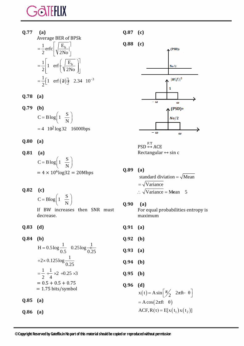
Q.77 (a) Average BER of BPSk
bE1 erfc2 2No
=
bE1 1 erf2 2No
= −
( ) 31 1 erf 2 2.34 102
−= − = ×
Q.78 (a) Q.79 (b)
SC Blog 1N
= +
34 10 log32 16000bps= × = Q.80 (a) Q.81 (a)
SC Blog 1N
= +
= 4 × 10⁶log32 = 20Mbps Q.82 (c)
SC Blog 1N
= +
If BW increases then SNR must decrease. Q.83 (d) Q.84 (b)
1 1H 0.5log 0.25log0.5 0.25
= +
12 0.125log0.25
+ ×
1 1 2 0.25 32 4
= + × + ×
= 0.5 + 0.5 + 0.75 = 1.75 bits/symbol Q.85 (a) Q.86 (a)
Q.87 (c) Q.88 (c)
PSD
F.T ACE
Rectangular ↔ sin c Q.89 (a) standard diviation Mean= Variance= Variance Mean 5∴ = = Q.90 (a) For equal probabilities entropy is maximum Q.91 (a) Q.92 (b) Q.93 (a) Q.94 (b) Q.95 (b) Q.96 (d) ( ) πx t Asin 2πft θ2
= − +
( )A cos 2πft θ= + ( ) ( )1 2ACF, R(τ) E[x t x t ]=
© Copyright Reserved by Gateflix.in No part of this material should be copied or reproduced without permission
( )1 2E[A cos 2πft θ Acos(2πft θ)= + +
2
2 1A cos cos 2πf (t t )2
= −
Q.97 (a) Autocorrelation function of output noise would be since, which has infinite number of zero crossing. Q.98 (b) Mean square value of input = σ2 = N
Mean square value of output N2
=
Q.99 (b)
Q.100 (b) R(t) = E[x(t)x(t − τ)] R(o) = E[x2(t)] Q.101 (a) 10logx 1= 0.1x 10 1.26= = ∴ 1dB Represents a power ratio of 1.26: 1 Q.102 (d)
PSD of white Noise Q.103 (d)
( )xNS ω for 2πB ω 2πB2
= − ≤ ≤
= 0 else where
( ) ( )N 4πBτR τ 4πB sinC2 2
=
= 2πNBsin C(2πBτ) Q.104 (a) R(τ) = E[A sin(ωt)A sinω(t τ]−
2A sin(ωτ)
2=
Q.105 (c) Q.106 (a)
As, SC Blog 1N
= +
If Bandwidth increases SNR has to decrease. Q.107 (d) For error free transmission Symbol rate
= 2fm = 6000synbol /sec Q.108 (d) Number of bits required, n = log216 = 4 Q.109 (a) Q.110 (b) Average amount of information is called Entropy. Q.111 (c) Channel capacity gives max bit rate handle by a system .
© Copyright Reserved by Gateflix.in No part of this material should be copied or reproduced without permission