UNIT-V APPLICATION ICs
33
75 UNIT-V APPLICATION ICs
-
Upload
khangminh22 -
Category
Documents
-
view
5 -
download
0
Transcript of UNIT-V APPLICATION ICs

75
UNIT-V
APPLICATION ICs

76
IC Voltage Regulators
• There are basically two kinds of IC voltage regulators:
– Multipin type, e.g. LM723C
– 3-pin type, e.g. 78/79XX
• Multipin regulators are less popular but they provide the
greatest flexibility and produce the highest quality
voltage regulation
• 3-pin types make regulator circuit design simple

Multipin IC Voltage Regulator
• The LM723 has an
equivalent circuit that
contains most of the parts
of the op-amp voltage
regulator discussed
earlier.
• It has an internal voltage
reference, error amplifier,
pass transistor, and
current limiter all in one
IC package.
LM 723C Schematic 77

78
LM723 Voltage Regulator
• Can be either 14-pin DIP or 10-pin TO-100 can
• May be used for either +ve or -ve, variable or fixed
regulated voltage output
• Using the internal reference (7.15 V), it can operate as a
high-voltage regulator with output from 7.15 V to about
37 V, or as a low-voltage regulator from 2 V to 7.15 V
• Max. output current with heat sink is 150 mA
• Dropout voltage is 3 V (i.e. VCC > Vo(max) + 3)
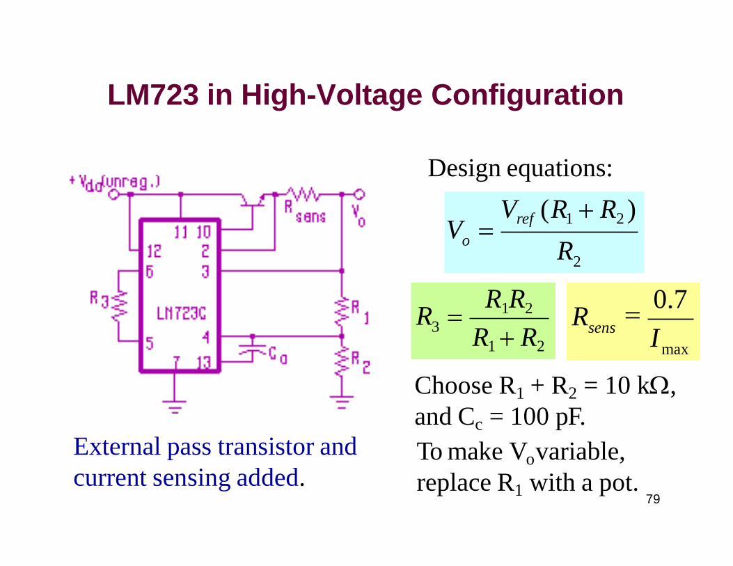
LM723 in High-Voltage Configuration
External pass transistor and
current sensing added.
Design equations:
2 R o
Vref (R1 R2 ) V
3
R1R2
R1 R2
R max
79
I R
sens
0.7
Choose R1 + R2 = 10 k ,
and Cc = 100 pF.
To make Vo variable,
replace R1 with a pot.

80
LM723 in Low-Voltage Configuration
With external pass transistor
and foldback current limiting
5 sens
L(max)
R R I
R 4 V
o 0.7(R
4 R
5 )
5 sens
short
R R I
0.7(R 4 R
5 )
short
o
sens
0.7V R I (V 0.7) 0.7I
o L(max)
o R R R R 5 sens 4 L
V ' 0.7R
L (R
4 R
5 )
Under foldback condition:
2 1
o
R R V
R 2 V
ref

81
Three-Terminal Fixed Voltage Regulators
• Less flexible, but simple to use
• Come in standard TO-3 (20 W) or TO-220 (15 W)
transistor packages
• 78/79XX series regulators are commonly available with
5, 6, 8, 12, 15, 18, or 24 V output
• Max. output current with heat sink is 1 A
• Built-in thermal shutdown protection
• 3-V dropout voltage; max. input of 37 V
• Regulators with lower dropout, higher in/output, and
better regulation are available.

Basic Circuits With 78/79XX Regulators
• Both the 78XX and 79XX regulators can be used to
provide +ve or -ve output voltages
• C1 and C2 are generally optional. C1 is used to cancel
any inductance present, and C2 improves the transient
response. If used, they should preferably be either 1 F
tantalum type or 0.1 F mica type capacitors. 82

Dual-Polarity Output with 78/79XX
Regulators
83

78XX Regulator with Pass Transistor
• Q1 starts to conduct when
VR2 = 0.7 V.
• R2 is typically chosen so
that max. IR2 is 0.1 A.
• Power dissipation of Q1 is
P = (Vi - Vo)IL.
• Q2 is for current limiting
protection. It conducts
when VR1 = 0.7 V.
• Q2 must be able to pass
max. 1 A; but note that max. VCE2 is only 1.4 V.
84
max
1 I
R 0.7
2
R 2 I R
0.7

78XX Floating Regulator
• It is used to obtain an
output > the Vreg
value up to a max.of
37 V.
• R1 is chosen so that
R1 0.1 Vreg/IQ,
where IQ is the
f quiescent current o
the regulator. 2 o reg Q
R
R 1
I Vreg
V V 2
85
Q 1 reg
1 o reg
V I R
R (V V ) R or

86
3-Terminal Variable Regulator
• The floating regulator could be made into a variable
regulator by replacing R2 with a pot. However, there are
several disadvantages:
– Minimum output voltage is Vreg instead of 0 V.
– IQ is relatively large and varies from chip to chip.
– Power dissipation in R2 can in some cases be quite
large resulting in bulky and expensive equipment.
• A variety of 3-terminal variable regulators are available,
e.g. LM317 (for +ve output) or LM 337 (for -ve output).

Basic LM317 Variable Regulator Circuits
(a)
Circuit with capacitors
to improve performance 87
(b)
Circuit with protective
diodes

Notes on Basic LM317 Circuits
• The function of C1 and C2 is similar to those used in the
78/79XX fixed regulators.
• C3 is used to improve ripple rejection.
• Protective diodes in circuit (b) are required for high-
current/high-voltage applications.
V ref
o ref
R1
Iadj R2
V V
where Vref = 1.25 V, and Iadj is
the current flowing into the adj.
terminal (typically 50 A).
R1 = Vref /IL(min), where IL(min)
is typically 10 mA. 2
88
Vref Iadj R1
R1 (Vo Vref ) R

LM317 Regulator Circuits
Circuit with pass transistor
and current limiting
89
Circuit to give 0V min.
output voltage

Block Diagram of Switch-Mode Regulator
It converts an unregulated dc input to a regulated dc
output. Switching regulators are often referred to as
dc to dc converters. 90

91
Comparing Switch-Mode to Linear
Regulators
Advantages:
– 70-90% efficiency (about double that of linear ones)
– can make output voltage > input voltage, if desired
– can invert the input voltage
– considerable weight and size reductions, especially at
high output power
Disadvantages:
– More complex circuitry
– Potential EMI problems unless good shielding, low-
loss ferrite cores and chokes are used

General Notes on Switch-Mode Regulator
The duty cycle of the series transistor (power switch) determines
the average dc output of the regulator. A circuit to control the
duty cycle is the pulse-width modulator shown below:
92
93
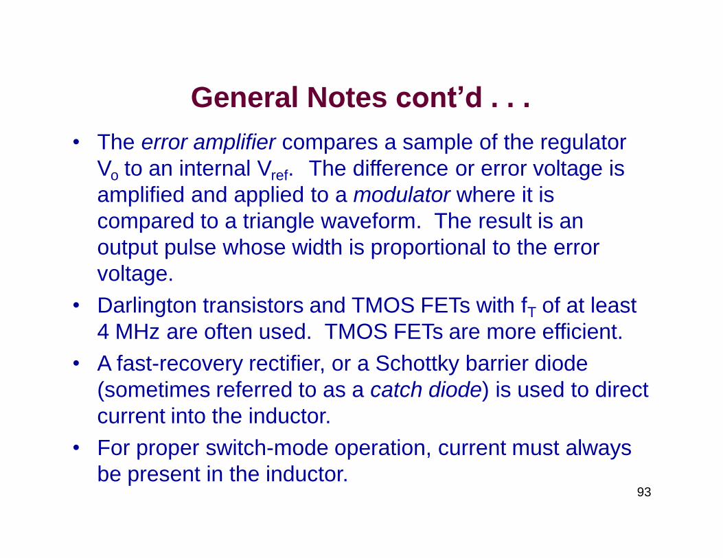
General Notes cont’d . . .
• The error amplifier compares a sample of the regulator
Vo to an internal Vref. The difference or error voltage is
amplified and applied to a modulator where it is
compared to a triangle waveform. The result is an
output pulse whose width is proportional to the error
voltage.
• Darlington transistors and TMOS FETs with fT of at least
4 MHz are often used. TMOS FETs are more efficient.
• A fast-recovery rectifier, or a Schottky barrier diode
(sometimes referred to as a catch diode) is used to direct
current into the inductor.
• For proper switch-mode operation, current must always
be present in the inductor.

ICL8038 Function Generator IC
• Triangle wave at pin10 is
obtained by linear charge
and discharge of C by
two current sources.
• Two comparators trigger
the flip-flop which
provides the square wave
and switches the current
sources.
• Triangle wave becomes
sine wave via the sine
converter . 94

95
ICL8038 Function Generator IC
• To obtain a square wave output, a pull-up resistor
(typically 10 to 15 k ) must be connected between pin 9
and VCC.
• Triangle wave has a linearity of 0.1 % or better and an
amplitude of approx. 0.3(VCC-VEE).
• Sine wave can be adjusted to a distortion of < 1% with
amplitude of 0.2(VCC-VEE). The distortion may vary with f
(from 0.001 Hz to 200 kHz).
• IC can operate from either single supply of 10 to 30 V or
dual supply of 5 to 15 V.

96
ICL8038 Function Generator Circuit
+VCC > Vsweep > Vtotal + VEE + 2
total CC EE where V = V + |V |
o f
1 total 2RC V
3(VCC Vsweep )
where R = RA = RB
If pin 7 is tied to pin 8,
o
R f
2RA RB
3
5RAC1 1 A
For 50 % duty cycle,
1
f o
0.3
RC

97
Isolation Amplifier
• Provides a way to link a fixed ground to a floating
ground.
• Isolates the DSP from the high voltage associated with
the power amplifier.

98
ISOLATION AMPLIFIER
Purposes
• To break ground to permit incompatible circuits
• to be interfaced together while reducing noise
• To amplify signals while passing only low
leakage current to prevent shock to people or damage to
equipment
• To withstand high voltage to protect people,
circuits, and equipment

99
Methods
• Power Supply Isolation : battery, isolated power
• Signal Isolation : opto-isolation, capacitive

100
OPTOCOUPLER
• The optocouplers provide protection switching
and high-speed
• An optocoupler, also known as an opto-isolator, is an integral part of the opto electronics arena. It has fast proven its utility as an electrical isolator or a high-speed switch, and can be used in a variety of applications.
• The basic design for optocouplers involves use of an
LED that produces a light signal to be received by a photodiode to detect the signal. In this way, the output current or current allowed to pass can be varied by the intensity of light.

101
OPTOCOUPLER • A very common application for the opto coupler is a FAX
machine or MODEM, isolating the device from the telephone line to prevent the potentially destructive spike in voltage that would accompany a lightning strike. This protective tool has other uses in the opto electronic area. It can be used as a guard against EMI, removing ground loops and reducing noise.
• This makes the optocoupler ideal for use in switching
power supply and motor control applications. Today as semiconductors are being designed to handle more and more power, isolation protection has become more important than ever before.

102
Optoelectronic Integrated Circuits
Applications
• Inter- and intra-chip optical interconnect and clock
distribution
• Fiber transceivers
• Intelligent sensors
• Smart pixel array parallel processors

103
Optoelectronic Integrated Circuits
Approaches
• Conventional hybrid assembly: multi-chip modules
• Total monolithic process development
• Modular integration on ICs:
• epitaxy-on-electronics
• flip-chip bump bonding w. substrate removal
• self-assembly

104
LM380 Power Amplifier
General Description • The LM380 is a power audio amplifier for consumer
application. In order to hold system cost to a minimum, gain is internally fixed at 34 dB. A unique input stage allows inputs to be ground referenced. The output is automatically self centering to one half the supply voltage. The output is short circuit proof with internal thermal limiting.
• The package outline is standard dual-in-line. A copper
lead frame is used with the center three pins on either side comprising a heat sink. This makes the device easy to use in standard p-c layout.

105
Features
• Wide supply voltage range
• Low quiescent power drain
• Voltage gain fixed at 50
• High peak current capability
• Input referenced to GND
• High input impedance
• Low distortion
• Quiescent output voltage is at one-half of the supply
• voltage
• Standard dual-in-line package

PIN DIAGRAM AND BLOCK DIAGRAM
OF LM380
106

Circuit Diagram for a Simple LM380-
Based Power Amplifier
107