PRO2150 Portable Radio Detailed Service Manual
136
PRO2150 ™ Portable Radio Detailed Service Manual
-
Upload
khangminh22 -
Category
Documents
-
view
7 -
download
0
Transcript of PRO2150 Portable Radio Detailed Service Manual

PRO2150™
Portable Radio
Detailed Service Manual

Table of Contents i
99R85452E01-O August 30, 2002
User Safety, Training, and General Information..........................................v
Chapter 1 Introduction ......................................................................... 1-11.1 Scope of Manual............................................................................................................................ 1-11.2 Warranty and Service Support....................................................................................................... 1-1
1.2.1 Warranty Period and Return Instructions.......................................................................... 1-11.2.2 After Warranty Period ....................................................................................................... 1-11.2.3 Piece Parts ....................................................................................................................... 1-21.2.4 Technical Support ............................................................................................................. 1-21.2.5 Parts Identification ............................................................................................................ 1-2
1.3 Radio Model Information................................................................................................................ 1-31.4 Radio Features .............................................................................................................................. 1-4
Chapter 2 Maintenance ........................................................................ 2-12.1 Introduction .................................................................................................................................... 2-12.2 Preventive Maintenance ................................................................................................................ 2-1
2.2.1 Inspection ......................................................................................................................... 2-12.2.2 Cleaning Procedures ........................................................................................................ 2-1
2.3 Safe Handling of CMOS and LDMOS Devices.............................................................................. 2-22.4 Repair Procedures and Techniques — General............................................................................ 2-2
2.4.1 Parts Replacement and Substitution ................................................................................ 2-22.4.2 Rigid Circuit Boards .......................................................................................................... 2-22.4.3 Flexible Circuits ................................................................................................................ 2-32.4.4 Chip Components ............................................................................................................. 2-32.4.5 Shields .............................................................................................................................. 2-4
2.5 Disassembling and Reassembling the Radio — General.............................................................. 2-42.6 Radio Disassembly — Detailed ..................................................................................................... 2-5
2.6.1 Front Cover from Chassis Disassembly ........................................................................... 2-52.6.2 Control Board Disassembly .............................................................................................. 2-72.6.3 RF Board Disassembly ..................................................................................................... 2-7
2.7 Radio Reassembly — Detailed...................................................................................................... 2-82.7.1 RF Board Reassembly...................................................................................................... 2-82.7.2 Control Board Reassembly............................................................................................... 2-82.7.3 Chassis and Front Cover Reassembly ............................................................................. 2-8
2.8 Mechanical View and Parts List................................................................................................... 2-122.8.1 Exploded View and Parts List ......................................................................................... 2-12
2.9 Service Aids................................................................................................................................. 2-142.10 Test Equipment............................................................................................................................ 2-152.11 Programming Cable (DSK001C706) ........................................................................................... 2-162.12 IF Test Box (DSK001C702) ......................................................................................................... 2-17
ii Table of Contents
August 30, 2002 99R85452E01-O
Chapter 3 Radio Tuning ....................................................................... 3-13.1 Introduction .................................................................................................................................... 3-13.2 Software Tuning Setup .................................................................................................................. 3-13.3 Affixing Antenna Ground Plate....................................................................................................... 3-23.4 Hardware Tuning Setup and Procedure ........................................................................................ 3-3
3.4.1 Audio Modulation Tuning .................................................................................................. 3-33.4.2 Sub-Audio Modulation Tuning........................................................................................... 3-43.4.3 Tuning Frequency ............................................................................................................. 3-4
Chapter 4 Radio Programming............................................................ 4-14.1 Introduction .................................................................................................................................... 4-14.2 Programming Your Radio .............................................................................................................. 4-1
4.2.1 Overview of the Programming Process ............................................................................ 4-14.2.2 Cloning Radio Parameters to User Radios ....................................................................... 4-14.2.3 Parameters Which are Cloned.......................................................................................... 4-14.2.4 Parameters Which are Not Cloned ................................................................................... 4-14.2.5 To Clone a Radio .............................................................................................................. 4-14.2.6 Error Conditions ................................................................................................................ 4-2
4.3 CPS Programming ......................................................................................................................... 4-24.4 Programming ................................................................................................................................. 4-3
4.4.1 PL Frequencies and Codes .............................................................................................. 4-34.4.2 DPL Codes........................................................................................................................ 4-44.4.3 Examples .......................................................................................................................... 4-4
Chapter 5 Error Code Displays............................................................ 5-15.1 Error Codes.................................................................................................................................... 5-1
Chapter 6 Accessories ......................................................................... 6-16.1 Antennas........................................................................................................................................ 6-16.2 Carrying Accessories ..................................................................................................................... 6-16.3 Carry Cases ................................................................................................................................... 6-16.4 Chargers ........................................................................................................................................ 6-16.5 Batteries......................................................................................................................................... 6-16.6 Audio Accessories ......................................................................................................................... 6-16.7 Manuals ......................................................................................................................................... 6-26.8 Software......................................................................................................................................... 6-2
Table of Contents iii
99R85452E01-O August 30, 2002
Chapter 7 VHF Band Information ........................................................ 7-17.1 Model Chart ................................................................................................................................... 7-17.2 Specifications................................................................................................................................. 7-27.3 Theory of Operation....................................................................................................................... 7-3
7.3.1 General Information .......................................................................................................... 7-37.3.2 Power Distribution............................................................................................................. 7-37.3.3 Power up Sequence ......................................................................................................... 7-37.3.4 CPU / Control Section....................................................................................................... 7-47.3.5 VCO / Synthesizer Section ............................................................................................... 7-47.3.6 Transmitter Section........................................................................................................... 7-57.3.7 Receiver Section............................................................................................................... 7-67.3.8 Battery Section ................................................................................................................. 7-7
7.4 Block Diagrams.............................................................................................................................. 7-87.4.1 Complete .......................................................................................................................... 7-87.4.2 Controller .......................................................................................................................... 7-97.4.3 VCO .................................................................................................................................. 7-97.4.4 Transmitter...................................................................................................................... 7-107.4.5 Receiver.......................................................................................................................... 7-10
7.5 Troubleshooting Charts ............................................................................................................... 7-11
Chapter 8 UHF Band Information ........................................................ 8-18.1 Model Charts ................................................................................................................................. 8-18.2 Specifications................................................................................................................................. 8-38.3 Theory of Operation....................................................................................................................... 8-4
8.3.1 General Information .......................................................................................................... 8-48.3.2 Power Distribution............................................................................................................. 8-48.3.3 Power up Sequence ......................................................................................................... 8-48.3.4 CPU / Control Section....................................................................................................... 8-58.3.5 VCO / Synthesizer Section ............................................................................................... 8-58.3.6 Transmitter Section........................................................................................................... 8-68.3.7 Receiver Section............................................................................................................... 8-78.3.8 Battery Section ................................................................................................................. 8-8
8.4 Block Diagrams.............................................................................................................................. 8-98.4.1 Complete .......................................................................................................................... 8-98.4.2 Controller ........................................................................................................................ 8-108.4.3 VCO ................................................................................................................................ 8-108.4.4 Transmitter...................................................................................................................... 8-118.4.5 Receiver.......................................................................................................................... 8-11
8.5 Troubleshooting Charts ............................................................................................................... 8-12
iv Table of Contents
August 30, 2002 99R85452E01-O
This Page Intentionally Left Blank
User Safety, Training, and General Information
Product Safety and RF Exposure Compliance
ATTENTION!This radio is restricted to occupational use only to satisfy FCC RF energy exposure requirements. Before using this product, read the RF energy awareness information and operating instructions in the Product Safety and RF Exposure booklet enclosed with your radio (Motorola Publication part number 68P81095C98) to ensure compliance with RF energy exposure limits.For a list of Motorola-approved antennas, batteries, and other accessories, visit the following web site which lists approved accessories: http://www.motorola.com/cgiss/index.shtml.
CAUTION: Before using this product, read the operating instructions for safe usage contained inthe Product Safety and RF Exposure booklet enclosed with your radio.

August 30, 2002 99R85452E01-O
This Page Intentionally Left Blank
vi : Product Safety and RF Exposure Compliance
Chapter 1 Introduction
1.1 Scope of ManualThis manual is intended for use by service technicians familiar with similar types of equipment. It contains service information required for the equipment described and is current as of the printing date. Changes which occur after the printing date may be incorporated by a complete Manual revision or alternatively as additions.
NOTE: Before operating or testing these units, please read the User Safety, Training and General Information Section in the front of this manual.
1.2 Warranty and Service SupportMotorola offers long term support for its products. This support includes repair of the product during the warranty period, and service/repair or spare parts support out of warranty.
Motorola de Colombia Service Center
Carrera 7 No. 71-52
Torre B, Piso 13
Oficina 1301
Bogota - Colombia
Phone: 571-376-6990
Motorola de Mexico Service Center
Bosques de Alisos #125
Col. Bosques de las Lomas
CP 05120 Mexico D.F.
Phone: 525-257-6700
1.2.1 Warranty Period and Return InstructionsWhere the product is covered under warranty, a check of the product should be performed prior to shipping the unit. This is to ensure that the product has been correctly programmed or has not been subjected to damage outside the terms of the warranty.
Products should be shipped back in the original packaging, or correctly packaged to ensure no damage occurs in transit.
1.2.2 After Warranty PeriodAfter the Warranty period, Motorola continues to support its products in two ways.
1. Motorola’s authorized service centers offer a repair service to both end users and dealers at competitive prices.
2. AAD supplies individual parts and modules that can be purchased by dealers who are technically capable of performing fault analysis and repair.
August 30, 2002 99R85452E01-O
1-2 Introduction: Warranty and Service Support
1.2.3 Piece PartsSome replacement parts, spare parts, and/or product information can be ordered directly. If a complete Motorola part number is assigned to the part, it is available from Motorola’s Accessories and Aftermarket Division (AAD). If no part number is assigned, the part is not normally available from Motorola. If the part number is appended with an asterisk, the part is serviceable by Motorola Depot only. If a parts list is not included, this generally means that no user-serviceable parts are available for that kit or assembly.
All orders for parts/information should include the complete Motorola identification number. All part orders should be directed to your local AAD office. Please refer to your latest price pages.
To order parts in Latin America and the Caribbean:
7:00 a.m. to 7:00 p.m. (Central Standard Time)
Monday through Friday (Chicago, USA)
1-847-538-8023
Motorola Parts (Accessories and Aftermarket Division AAD):
Attention: Order Processing
1313 E. Algonquin Road
Schaumburg, IL 60196
1.2.4 Technical Supporthttps://businessonline.motorola.com
Select: "Contact Us"
1.2.5 Parts Identification1-847-538-0021 (Voice)
1-847-538-8194 (Fax)
99R85452E01-O August 30, 2002
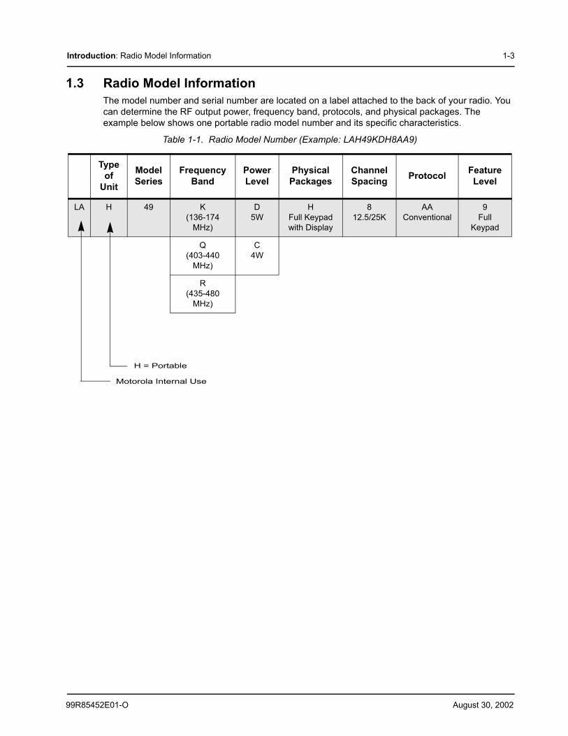
Introduction: Radio Model Information 1-3
1.3 Radio Model InformationThe model number and serial number are located on a label attached to the back of your radio. You can determine the RF output power, frequency band, protocols, and physical packages. The example below shows one portable radio model number and its specific characteristics.
Table 1-1. Radio Model Number (Example: LAH49KDH8AA9)
Type of
Unit
Model Series
FrequencyBand
Power Level
Physical Packages
Channel Spacing Protocol Feature
Level
LA H 49 K(136-174
MHz)
D5W
HFull Keypad with Display
812.5/25K
AAConventional
9Full
Keypad
Q(403-440
MHz)
C4W
R(435-480
MHz)
Motorola Internal Use
H = Portable
August 30, 2002 99R85452E01-O
1-4 Introduction: Radio Features
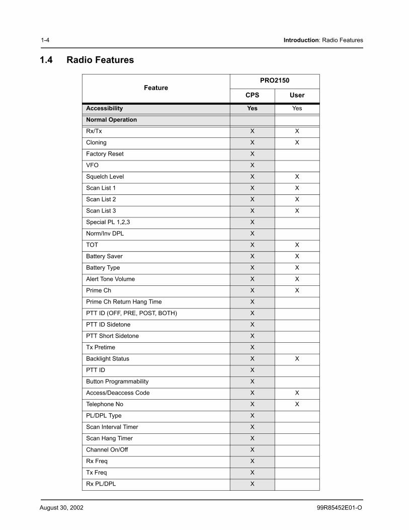
1.4 Radio Features
FeaturePRO2150
CPS User
Accessibility Yes Yes
Normal Operation
Rx/Tx X X
Cloning X X
Factory Reset X
VFO X
Squelch Level X X
Scan List 1 X X
Scan List 2 X X
Scan List 3 X X
Special PL 1,2,3 X
Norm/Inv DPL X
TOT X X
Battery Saver X X
Battery Type X X
Alert Tone Volume X X
Prime Ch X X
Prime Ch Return Hang Time X
PTT ID (OFF, PRE, POST, BOTH) X
PTT ID Sidetone X
PTT Short Sidetone X
Tx Pretime X
Backlight Status X X
PTT ID X
Button Programmability X
Access/Deaccess Code X X
Telephone No X X
PL/DPL Type X
Scan Interval Timer X
Scan Hang Timer X
Channel On/Off X
Rx Freq X
Tx Freq X
Rx PL/DPL X
99R85452E01-O August 30, 2002
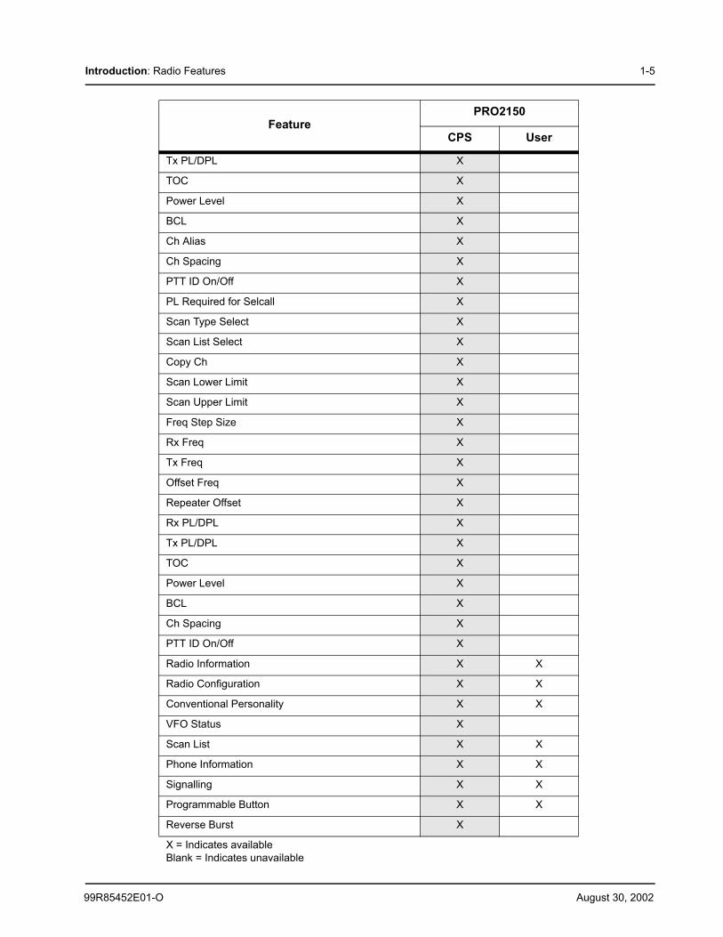
Introduction: Radio Features 1-5
Tx PL/DPL X
TOC X
Power Level X
BCL X
Ch Alias X
Ch Spacing X
PTT ID On/Off X
PL Required for Selcall X
Scan Type Select X
Scan List Select X
Copy Ch X
Scan Lower Limit X
Scan Upper Limit X
Freq Step Size X
Rx Freq X
Tx Freq X
Offset Freq X
Repeater Offset X
Rx PL/DPL X
Tx PL/DPL X
TOC X
Power Level X
BCL X
Ch Spacing X
PTT ID On/Off X
Radio Information X X
Radio Configuration X X
Conventional Personality X X
VFO Status X
Scan List X X
Phone Information X X
Signalling X X
Programmable Button X X
Reverse Burst X
X = Indicates availableBlank = Indicates unavailable
FeaturePRO2150
CPS User
August 30, 2002 99R85452E01-O
This Page Intentionally Left Blank
1-6 Introduction: Radio Features
Chapter 2 Maintenance
2.1 IntroductionThis chapter provides details about the following:
• Preventive Maintenance• Safe Handling of CMOS and LDMOS Devices• General Repair Procedures and Techniques• Disassembling and Reassembling the Radio
2.2 Preventive MaintenanceThe radio does not require a scheduled preventive maintenance program; however, periodic visual inspection and cleaning is recommended.
2.2.1 InspectionCheck that the external surfaces of the radio are clean, and that all external controls and switches are functional. It is not recommended to inspect the interior electronic circuitry.
2.2.2 Cleaning ProceduresThe following procedures describe the recommended cleaning agents and the methods to be used when cleaning the external and internal surfaces of the radio. External surfaces include the front cover, housing assembly and battery case. These surfaces should be cleaned whenever a periodic visual inspection reveals the presence of smudges, grease, and/or grime.
NOTE: Internal surfaces should be cleaned only when the radio is disassembled for service or repair.
The only recommended agent for cleaning external radio surfaces is a 0.5% solution of a mild dishwashing detergent in water. The only factory recommended liquid for cleaning printed circuit boards and their components is isopropyl alcohol (70% by volume).
2.2.2.1 Cleaning External Plastic Surfaces
Apply the 0.5% detergent-water solution sparingly with a stiff, non-metallic, short-bristled brush to work all loose dirt away from the radio. Use a soft, absorbent, lintless cloth or tissue to remove the solution and dry the radio. Make sure that no water remains entrapped near the connectors, cracks, or crevices.
2.2.2.2 Cleaning Internal Circuit Boards and Components
Apply Isopropyl alcohol (70%) with a stiff, non-metallic, short-bristled brush to dislodge embedded or caked materials located in hard-to-reach areas. The brush stroke should direct the dislodged material out and away from the inside of the radio. Make sure that controls or tunable components are not soaked with alcohol. Do not use high-pressure air to hasten the drying process since this could cause the liquid to collect in unwanted places. After completing the cleaning process, use a soft, absorbent, lintless cloth to dry the area. Do not brush or apply any isopropyl alcohol to the frame, front cover, or back cover.
CAUTION: The effects of certain chemicals and their vapors can have harmful results on certainplastics. Avoid using aerosol sprays, tuner cleaners, and other chemicals.
August 30, 2002 99R85452E01-O
2-2 Maintenance: Safe Handling of CMOS and LDMOS Devices
NOTE: Always use a fresh supply of alcohol and a clean container to prevent contamination by dissolved material (from previous usage).
2.3 Safe Handling of CMOS and LDMOS DevicesComplementary metal-oxide semiconductor (CMOS) devices are used in this family of radios, and are susceptible to damage by electrostatic or high voltage charges. Damage can be latent, resulting in failures occurring weeks or months later. Therefore, special precautions must be taken to prevent device damage during disassembly, troubleshooting, and repair.
Handling precautions are mandatory for CMOS circuits and are especially important in low humidity conditions. DO NOT attempt to disassemble the radio without first referring to the following CAUTION statement.
2.4 Repair Procedures and Techniques — General2.4.1 Parts Replacement and Substitution
When damaged parts are replaced, identical parts should be used. If the identical replacement part is not locally available, check the parts list for the proper Motorola part number and order the part from the nearest Motorola Communications parts center listed in the Piece Parts section of this manual.
2.4.2 Rigid Circuit BoardsThis radio uses bonded, multi-layer, printed circuit boards. Since the inner layers are not accessible, some special considerations are required when soldering and unsoldering components. The printed-through holes may interconnect multiple layers of the printed circuit. Therefore, exercise care to avoid pulling the plated circuit out of the hole.
CAUTION: This radio contains static-sensitive devices. Do not open the radio unless you areproperly grounded. Take the following precautions when working on this unit:
• Store and transport all CMOS devices in conductive material so that all exposed leads are shorted together. Do not insert CMOS devices into conventional plastic “snow” trays used for storage and transportation of other semiconductor devices.
• Ground the working surface of the service bench to protect the CMOS device. We recommend using the Motorola Static Protection Assembly (part number 0180386A82), which includes a wrist strap, two ground cords, a table mat, and a floor mat.
• Wear a conductive wrist strap in series with a 100k resistor to ground. (Replacement wrist straps that connect to the bench top covering are Motorola part number RSX-4015.)
• Do not wear nylon clothing while handling CMOS devices.• Do not insert or remove CMOS devices with power applied. Check all power supplies
used for testing CMOS devices to be certain that there are no voltage transients present.
• When straightening CMOS pins, provide ground straps for the apparatus used.• When soldering, use a grounded soldering iron.• If at all possible, handle CMOS devices by the package and not by the leads. Prior to
touching the unit, touch an electrical ground to remove any static charge that you may have accumulated. The package and substrate may be electrically common. If so, the reaction of a discharge to the case would cause the same damage as touching the leads.
99R85452E01-O August 30, 2002
Maintenance: Repair Procedures and Techniques — General 2-3
When soldering near the 20-pin and 40-pin connectors:
• Avoid accidentally getting solder in the connector. • Be careful not to form solder bridges between the connector pins. • Examine your work closely for shorts due to solder bridges.
2.4.3 Flexible CircuitsThe flexible circuits are made from a different material than the rigid boards, and require different soldering techniques. Excessive prolonged heat on a flexible circuit can damage the material. Therefore, avoid excessive heat and excessive bending.
For parts replacement, use the ST-1087 Temperature-Controlled Solder Station with a 600-700 degree F tip, and use small diameter solder such as ST-633. The smaller size solder will melt faster and require less heat to be applied to the circuit.
To replace a component on a flexible circuit:
1. Grasp with seizers (hemostats) the edge of the flexible circuit near the part to be removed. 2. Pull gently.3. Apply the tip of the soldering iron to the component connections while pulling with the seizers.
NOTE: Do not attempt to puddle-out components. Prolonged application of heat may damage the flexible circuit.
2.4.4 Chip ComponentsUse either the RLN-4062 Hot-Air Repair Station or the Motorola 0180381B45 Repair Station for chip component replacement. When using the 0180381B45 Repair Station, select the TJ-65 mini-thermojet hand piece. On either unit, adjust the temperature control to 700 degrees F. (370 degrees C), and adjust the airflow to a minimum setting. Airflow can vary due to component density.
• To remove a chip component, select a hot-air hand piece and position the nozzle of the hand piece approximately 1/8” above the component to be removed. Begin applying hot air. Once the solder reflows, remove the component using a pair of tweezers. Using solder wick and a soldering iron or a power desoldering station, remove the excess solder from the pads.
• To replace a chip component using a soldering iron, select the appropriate micro-tipped soldering iron and apply fresh solder to one of the solder pads. Using a pair of tweezers, position the new chip component in place while heating the fresh solder. Once solder wicks onto the new component, remove the heat from the solder. Heat the remaining pad with the soldering iron and apply solder until it wicks to the component. If necessary, touch up the first side. All solder joints should be smooth and shiny.
• To replace a chip component using hot air, select the hot-air hand piece and reflow the solder on the solder pads to smooth it. Apply a drop of solder paste flux to each pad. using a pair of tweezers, position the new component in place. Position the hot-air hand piece approximately 1/8” above the component and begin applying heat. Once the solder wicks to the component, remove the heat and inspect the repair. All joints should be smooth and shiny.
August 30, 2002 99R85452E01-O
2-4 Maintenance: Disassembling and Reassembling the Radio — General
2.4.5 ShieldsRemoving and replacing shields will be done with the R-1070 station with the temperature control set to approximately 415°F (215°C); 445°F (230°C) max.
• To remove the shield, place the circuit board in the R-1070’s holder. Select the proper heat focus head and attach it to the heater chimney. Add solder paste flux around the base of the shield. Position the shield under the heat-focus head. Lower the vacuum tip and attach it to the shield by turning on the vacuum pump. Lower the focus head until it is approximately 1/8” (0.3cm) above the shield. Turn on the heater and wait until the shield lifts off the circuit board. Once the shield is off, turn off the heat, grab the part with a pair of tweezers, and turn off the vacuum pump. Remove the circuit board from the R-1070’s circuit board holder.
• To replace the shield, add solder to the shield if necessary, using a micro-tipped soldering iron. Next, rub the soldering iron tip along the edge of the shield to smooth out any excess solder. Use solder wick and a soldering iron to remove excess solder from the solder pads on the circuit board. Place the circuit board back in the R1070’s circuit board holder. Place the shield on the circuit board using a pair of tweezers. Position the heat-focus head over the shield and lower it to approximately 1/8” above the shield. Turn on the heater and wait for the solder to reflow.Once complete, turn off the heat, raise the heat-focus head and wait approximately one minute for the part to cool. Remove the circuit board and inspect the repair. No cleaning should be necessary.
2.5 Disassembling and Reassembling the Radio — GeneralSince these radios may be disassembled and reassembled with the use of only four (board to casting) screws, it is important to pay particular attention to the snaps and tabs, and how parts align with each other.
The following tools are required for disassembling the radio:
• Phillips screwdriver• 4mm socket wrench
If a unit requires more complete testing or service than is customarily performed at the basic level, send this unit to a Motorola Authorized Service Center.
99R85452E01-O August 30, 2002
Maintenance: Radio Disassembly — Detailed 2-5
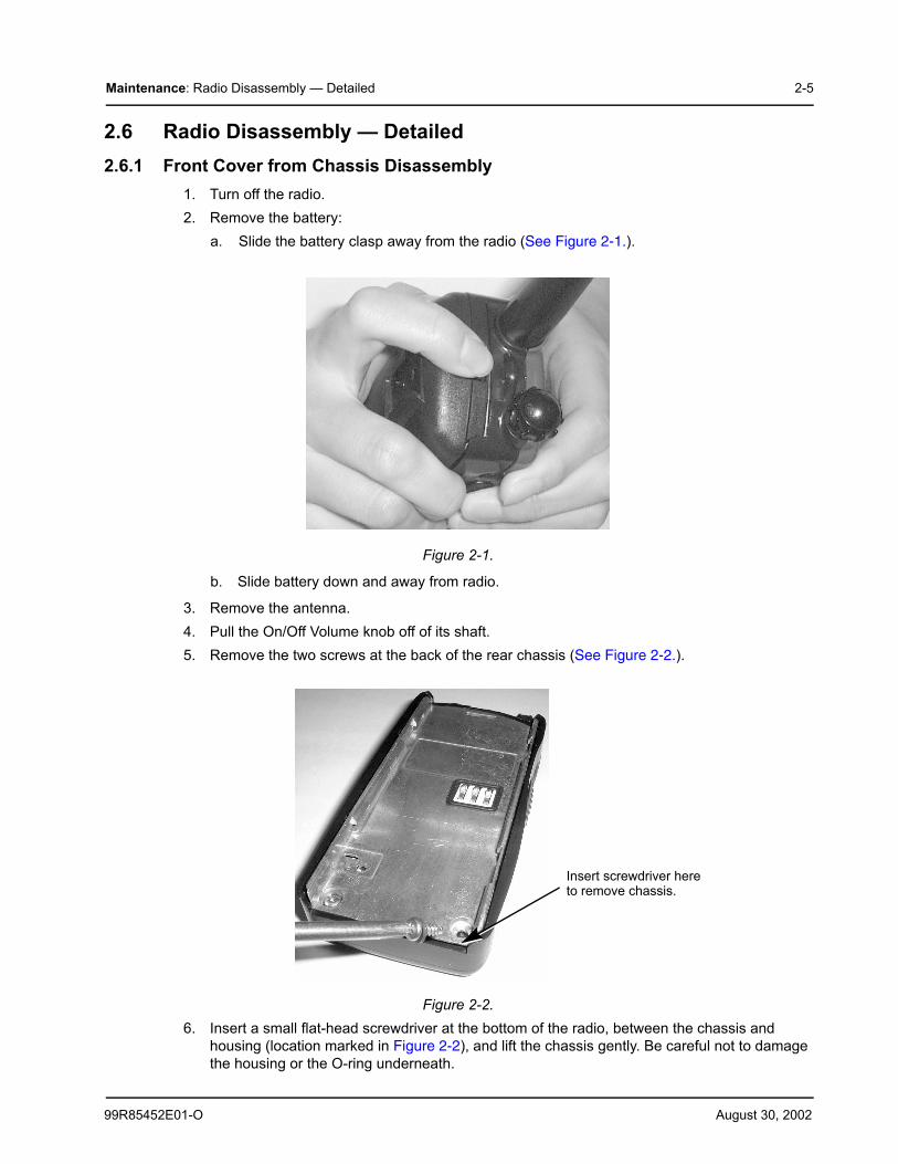
2.6 Radio Disassembly — Detailed2.6.1 Front Cover from Chassis Disassembly
1. Turn off the radio.2. Remove the battery:
a. Slide the battery clasp away from the radio (See Figure 2-1.).
b. Slide battery down and away from radio.
3. Remove the antenna.4. Pull the On/Off Volume knob off of its shaft.5. Remove the two screws at the back of the rear chassis (See Figure 2-2.).
6. Insert a small flat-head screwdriver at the bottom of the radio, between the chassis and housing (location marked in Figure 2-2), and lift the chassis gently. Be careful not to damage the housing or the O-ring underneath.
Figure 2-1.
Figure 2-2.
Insert screwdriver hereto remove chassis.
August 30, 2002 99R85452E01-O
2-6 Maintenance: Radio Disassembly — Detailed
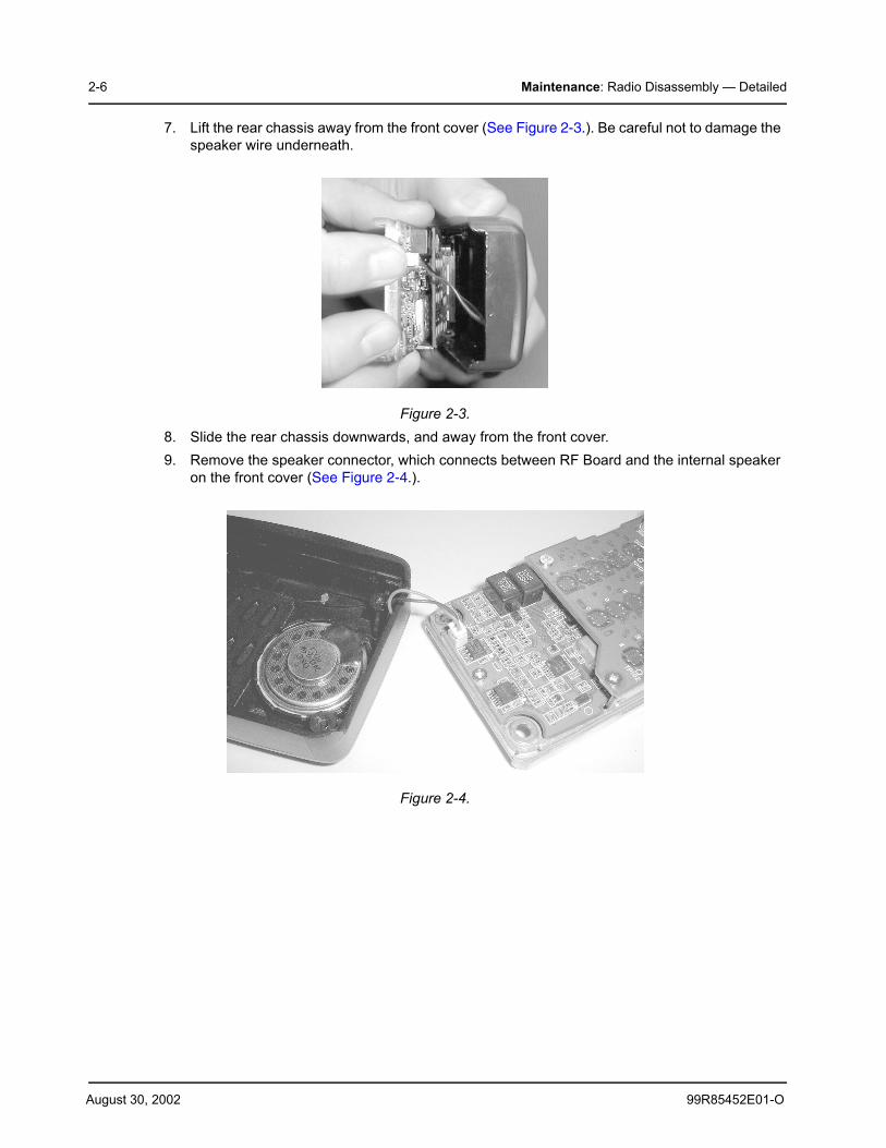
7. Lift the rear chassis away from the front cover (See Figure 2-3.). Be careful not to damage the speaker wire underneath.
8. Slide the rear chassis downwards, and away from the front cover.9. Remove the speaker connector, which connects between RF Board and the internal speaker
on the front cover (See Figure 2-4.).
Figure 2-3.
Figure 2-4.
99R85452E01-O August 30, 2002
Maintenance: Radio Disassembly — Detailed 2-7
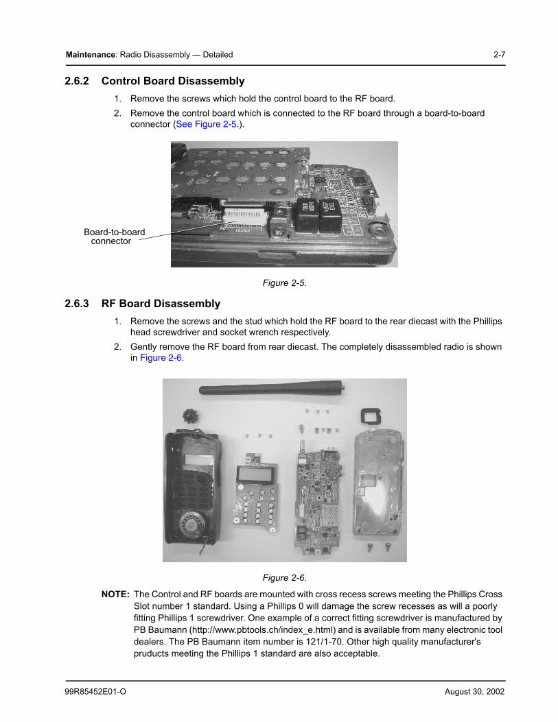
2.6.2 Control Board Disassembly1. Remove the screws which hold the control board to the RF board.2. Remove the control board which is connected to the RF board through a board-to-board
connector (See Figure 2-5.).
2.6.3 RF Board Disassembly1. Remove the screws and the stud which hold the RF board to the rear diecast with the Phillips
head screwdriver and socket wrench respectively.2. Gently remove the RF board from rear diecast. The completely disassembled radio is shown
in Figure 2-6.
NOTE: The Control and RF boards are mounted with cross recess screws meeting the Phillips Cross Slot number 1 standard. Using a Phillips 0 will damage the screw recesses as will a poorly fitting Phillips 1 screwdriver. One example of a correct fitting screwdriver is manufactured by PB Baumann (http://www.pbtools.ch/index_e.html) and is available from many electronic tool dealers. The PB Baumann item number is 121/1-70. Other high quality manufacturer's pruducts meeting the Phillips 1 standard are also acceptable.
Figure 2-5.
Figure 2-6.
Board-to-boardconnector
August 30, 2002 99R85452E01-O
2-8 Maintenance: Radio Reassembly — Detailed
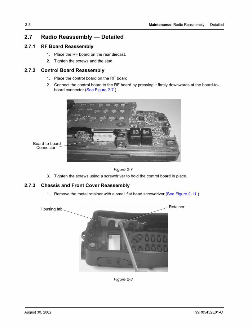
2.7 Radio Reassembly — Detailed2.7.1 RF Board Reassembly
1. Place the RF board on the rear diecast.2. Tighten the screws and the stud.
2.7.2 Control Board Reassembly1. Place the control board on the RF board.2. Connect the control board to the RF board by pressing it firmly downwards at the board-to-
board connector (See Figure 2-7.).
3. Tighten the screws using a screwdriver to hold the control board in place.
2.7.3 Chassis and Front Cover Reassembly1. Remove the metal retainer with a small flat head screwdriver (See Figure 2-11.).
Figure 2-7.
Figure 2-8.
Board-to-boardConnector
Housing tab Retainer
99R85452E01-O August 30, 2002
Maintenance: Radio Reassembly — Detailed 2-9
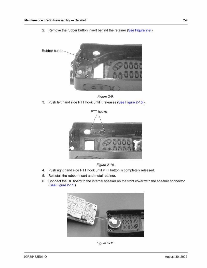
2. Remove the rubber button insert behind the retainer (See Figure 2-9.).
3. Push left hand side PTT hook until it releases (See Figure 2-10.).
4. Push right hand side PTT hook until PTT button is completely released.5. Reinstall the rubber insert and metal retainer.6. Connect the RF board to the internal speaker on the front cover with the speaker connector
(See Figure 2-11.).
Figure 2-9.
Figure 2-10.
Figure 2-11.
Rubber button
PTT hooks
August 30, 2002 99R85452E01-O
2-10 Maintenance: Radio Reassembly — Detailed
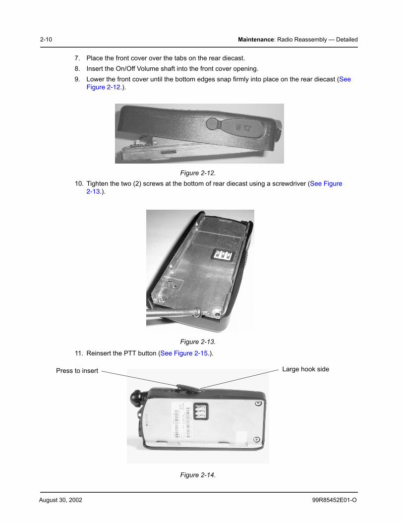
7. Place the front cover over the tabs on the rear diecast.8. Insert the On/Off Volume shaft into the front cover opening.9. Lower the front cover until the bottom edges snap firmly into place on the rear diecast (See
Figure 2-12.).
10. Tighten the two (2) screws at the bottom of rear diecast using a screwdriver (See Figure 2-13.).
11. Reinsert the PTT button (See Figure 2-15.).
Figure 2-12.
Figure 2-13.
Figure 2-14.
Press to insert Large hook side
99R85452E01-O August 30, 2002
Maintenance: Radio Reassembly — Detailed 2-11
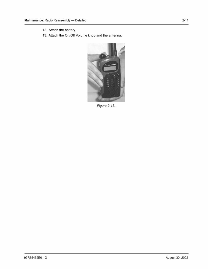
12. Attach the battery.13. Attach the On/Off Volume knob and the antenna.
Figure 2-15.
August 30, 2002 99R85452E01-O
2-12 Maintenance: Mechanical View and Parts List
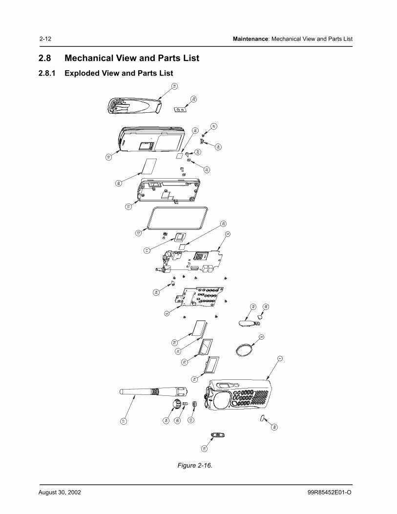
2.8 Mechanical View and Parts List2.8.1 Exploded View and Parts List
Figure 2-16.
1
3a
4a
5
6
9
13
11
12
15
16
2d
2f2e
2g
2c
2b
2a
8a
8b
8c
7d7c
7b
7a
3b
4b
10
14
17
99R85452E01-O August 30, 2002
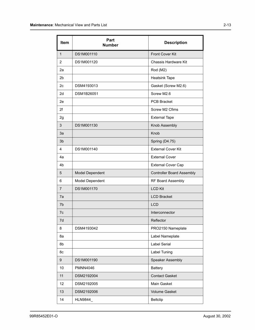
Maintenance: Mechanical View and Parts List 2-13
Item PartNumber Description
1 DS1M001110 Front Cover Kit
2 DS1M001120 Chassis Hardware Kit
2a Rod (M2)
2b Heatsink Tape
2c DSM4193013 Gasket (Screw M2.6)
2d DSM1B26051 Screw M2.6
2e PCB Bracket
2f Screw M2 Cfims
2g External Tape
3 DS1M001130 Knob Assembly
3a Knob
3b Spring (D4.75)
4 DS1M001140 External Cover Kit
4a External Cover
4b External Cover Cap
5 Model Dependent Controller Board Assembly
6 Model Dependent RF Board Assembly
7 DS1M001170 LCD Kit
7a LCD Bracket
7b LCD
7c Interconnector
7d Reflector
8 DSM4193042 PRO2150 Nameplate
8a Label Nameplate
8b Label Serial
8c Label Tuning
9 DS1M001190 Speaker Assembly
10 PMNN4046 Battery
11 DSM2192004 Contact Gasket
12 DSM2192005 Main Gasket
13 DSM2192006 Volume Gasket
14 HLN9844_ Beltclip
August 30, 2002 99R85452E01-O
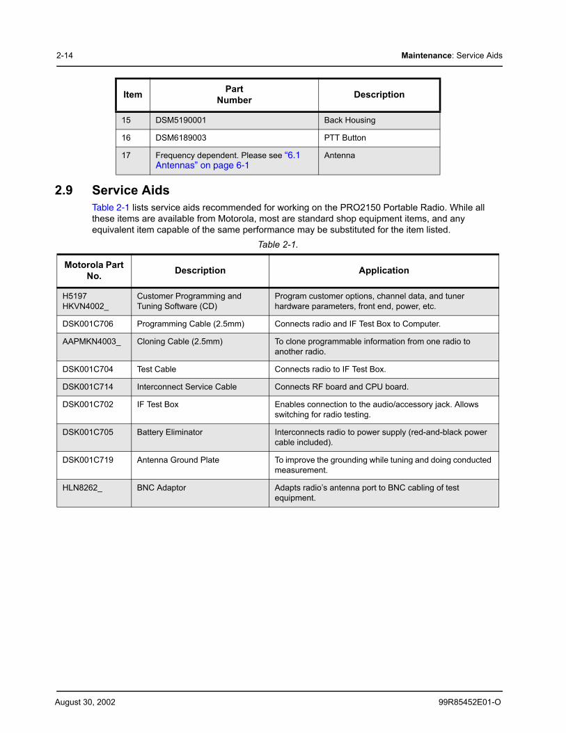
2-14 Maintenance: Service Aids
2.9 Service AidsTable 2-1 lists service aids recommended for working on the PRO2150 Portable Radio. While all these items are available from Motorola, most are standard shop equipment items, and any equivalent item capable of the same performance may be substituted for the item listed.
15 DSM5190001 Back Housing
16 DSM6189003 PTT Button
17 Frequency dependent. Please see “6.1 Antennas” on page 6-1
Antenna
Table 2-1.
Motorola Part No. Description Application
H5197HKVN4002_
Customer Programming and Tuning Software (CD)
Program customer options, channel data, and tuner hardware parameters, front end, power, etc.
DSK001C706 Programming Cable (2.5mm) Connects radio and IF Test Box to Computer.
AAPMKN4003_ Cloning Cable (2.5mm) To clone programmable information from one radio to another radio.
DSK001C704 Test Cable Connects radio to IF Test Box.
DSK001C714 Interconnect Service Cable Connects RF board and CPU board.
DSK001C702 IF Test Box Enables connection to the audio/accessory jack. Allows switching for radio testing.
DSK001C705 Battery Eliminator Interconnects radio to power supply (red-and-black power cable included).
DSK001C719 Antenna Ground Plate To improve the grounding while tuning and doing conducted measurement.
HLN8262_ BNC Adaptor Adapts radio’s antenna port to BNC cabling of test equipment.
Item PartNumber Description
99R85452E01-O August 30, 2002
Maintenance: Test Equipment 2-15
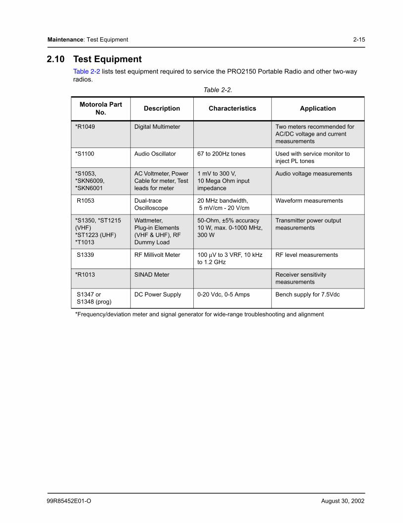
2.10 Test EquipmentTable 2-2 lists test equipment required to service the PRO2150 Portable Radio and other two-way radios.
Table 2-2.
Motorola Part No. Description Characteristics Application
*R1049 Digital Multimeter Two meters recommended for AC/DC voltage and current measurements
*S1100 Audio Oscillator 67 to 200Hz tones Used with service monitor to inject PL tones
*S1053, *SKN6009, *SKN6001
AC Voltmeter, Power Cable for meter, Test leads for meter
1 mV to 300 V, 10 Mega Ohm input impedance
Audio voltage measurements
R1053 Dual-trace Oscilloscope
20 MHz bandwidth, 5 mV/cm - 20 V/cm
Waveform measurements
*S1350, *ST1215 (VHF)*ST1223 (UHF)*T1013
Wattmeter,Plug-in Elements (VHF & UHF), RF Dummy Load
50-Ohm, ±5% accuracy 10 W, max. 0-1000 MHz, 300 W
Transmitter power output measurements
S1339 RF Millivolt Meter 100 µV to 3 VRF, 10 kHz to 1.2 GHz
RF level measurements
*R1013 SINAD Meter Receiver sensitivity measurements
S1347 or S1348 (prog)
DC Power Supply 0-20 Vdc, 0-5 Amps Bench supply for 7.5Vdc
*Frequency/deviation meter and signal generator for wide-range troubleshooting and alignment
August 30, 2002 99R85452E01-O
2-16 Maintenance: Programming Cable (DSK001C706)
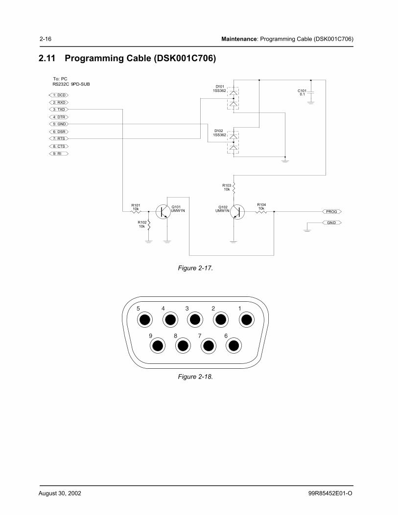
2.11 Programming Cable (DSK001C706)
Figure 2-17.
Figure 2-18.
1: DCD
2: RXD
3: TXD
4: DTR
5: GND
6: DSR
7: RTS
8: CTS
9: RI
D1011SS362
D1021SS362
Q102UMW1N
Q101UMW1N
R10210k
R10410k
R10310k
PROG
GND
To: PCRS232C 9PD-SUB
C1010.1
R10110k
5 4 3 2 1
9 8 7 6
99R85452E01-O August 30, 2002
Maintenance: IF Test Box (DSK001C702) 2-17
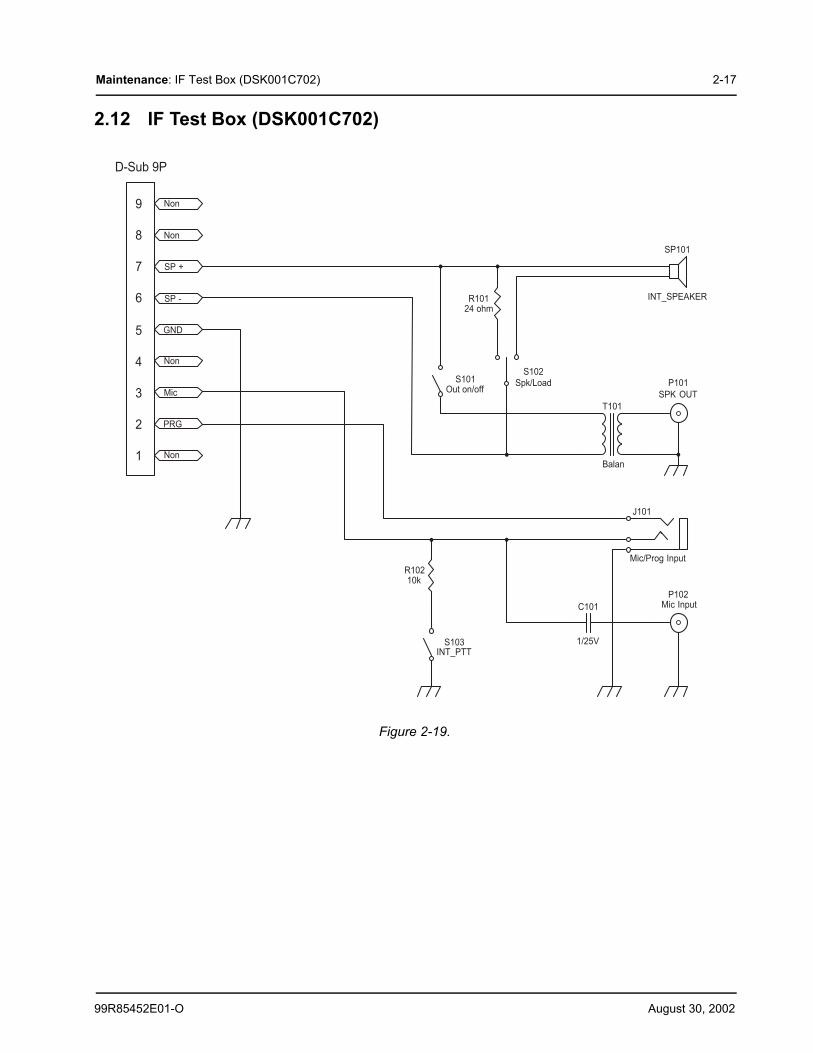
2.12 IF Test Box (DSK001C702)
Figure 2-19.
SP +
SP -
Mic
GND
PRG
SP101
INT_SPEAKERR10124 ohm
T101
Balan
P101SPK OUT
P102Mic Input
S101Out on/off
S103INT_PTT
S102Spk/Load
J101
Mic/Prog InputR10210k
C101
1/25V
Non
Non
Non
Non
D-Sub 9P
1
2
3
4
5
6
7
8
9
August 30, 2002 99R85452E01-O
This Page Intentionally Left Blank
2-18 Maintenance: IF Test Box (DSK001C702)
Chapter 3 Radio Tuning
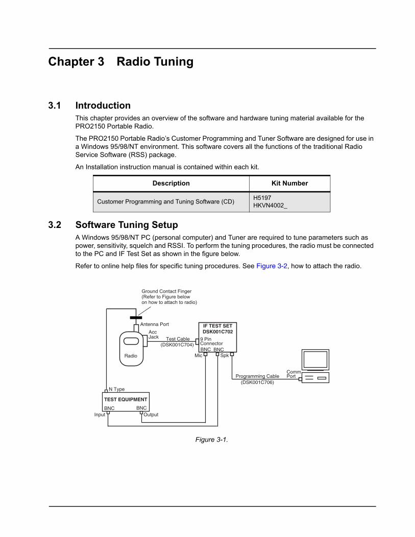
3.1 IntroductionThis chapter provides an overview of the software and hardware tuning material available for the PRO2150 Portable Radio.
The PRO2150 Portable Radio’s Customer Programming and Tuner Software are designed for use in a Windows 95/98/NT environment. This software covers all the functions of the traditional Radio Service Software (RSS) package.
An Installation instruction manual is contained within each kit.
3.2 Software Tuning SetupA Windows 95/98/NT PC (personal computer) and Tuner are required to tune parameters such as power, sensitivity, squelch and RSSI. To perform the tuning procedures, the radio must be connected to the PC and IF Test Set as shown in the figure below.
Refer to online help files for specific tuning procedures. See Figure 3-2, how to attach the radio.
Description Kit Number
Customer Programming and Tuning Software (CD) H5197HKVN4002_
Figure 3-1.
TEST EQUIPMENT
IF TEST SETDSK001C702
Radio
9 PinConnectorBNC BNC
BNCBNC
Mic Spk
CommPortProgramming Cable
(DSK001C706)
Input Output
N Type
AccJack Test Cable
(DSK001C704)
Antenna Port
Ground Contact Finger�(Refer to Figure belowon how to attach to radio)
August 30, 2002 99R85452E01-O
3-2 Radio Tuning: Affixing Antenna Ground Plate
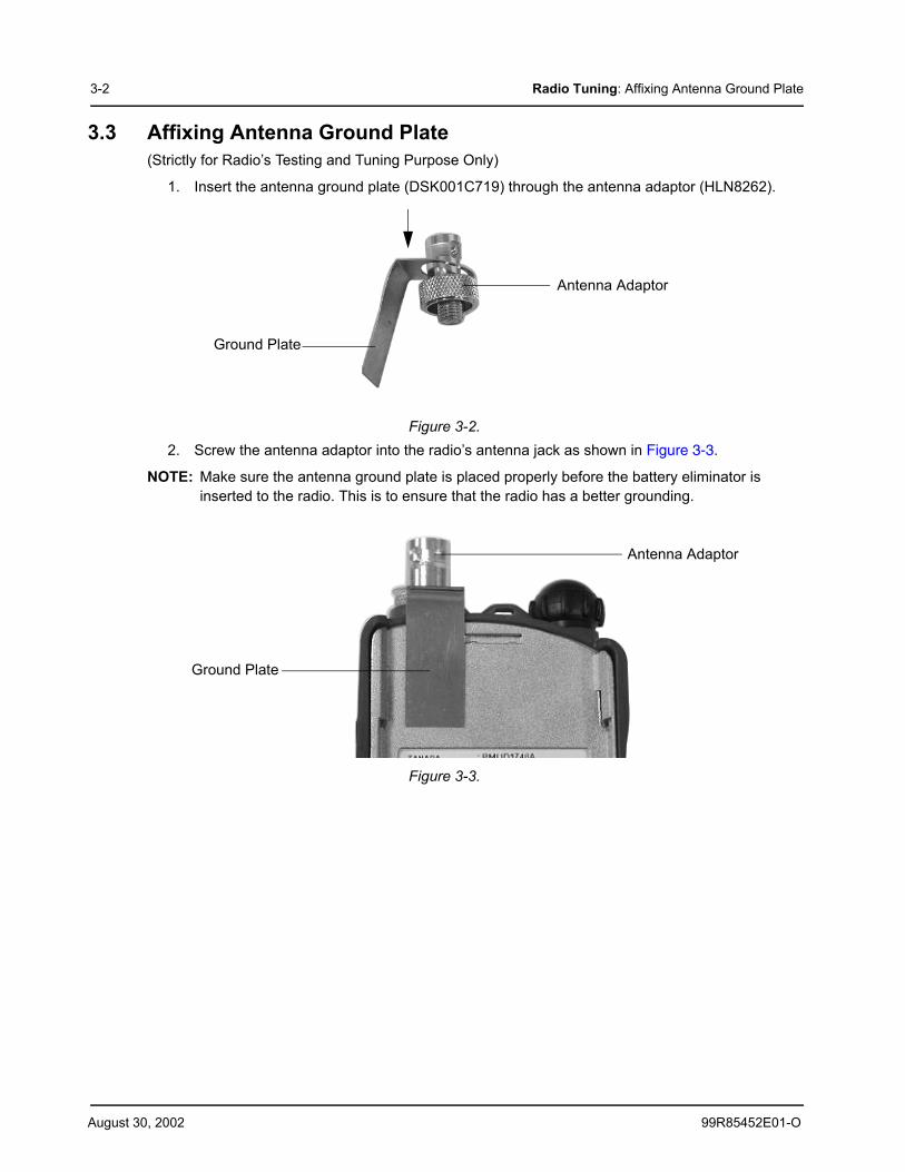
3.3 Affixing Antenna Ground Plate(Strictly for Radio’s Testing and Tuning Purpose Only)
1. Insert the antenna ground plate (DSK001C719) through the antenna adaptor (HLN8262).
Figure 3-2. 2. Screw the antenna adaptor into the radio’s antenna jack as shown in Figure 3-3.
NOTE: Make sure the antenna ground plate is placed properly before the battery eliminator is inserted to the radio. This is to ensure that the radio has a better grounding.
Figure 3-3.
Ground Plate
Antenna Adaptor
Ground Plate
Antenna Adaptor

99R85452E01-O August 30, 2002
Radio Tuning: Hardware Tuning Setup and Procedure 3-3
3.4 Hardware Tuning Setup and ProcedureThere is a silver seal on the bottom left of the radio chassis. Remove the seal to expose the two potentiometers for audio and sub-audio (CTCSS) modulation adjustment. RV601, which is slightly higher, is the trimmer potentiometer for audio modulation tuning. The lower trimmer potentiometer (RV602) is meant for sub-audio modulation tuning.
3.4.1 Audio Modulation Tuning1. Set the radio to transmit at the appropriate tuning frequency (See “Tuning Frequency” in Table
3-1) with low power. Set Channel Spacing to "CS-25.0" for 25kHz (see “Radio Programming” section).
2. On the test equipment, set it to receive at the appropriate tuning frequency (See “Tuning Frequency” on page 3-4) and with the following configurations:
Audio bandwidth: 0.25Hz to 15,000Hz.
De-emphasis: OFF
3. Inject a 60mV 1kHz tone to the radio through the external mic connector.4. Key up the radio.5. Using a ceramic tuning tool, adjust RV601 to tune the audio modulation deviation to settle
between 4.3kHz to 4.5kHz.
Figure 3-4.
RV601
RV602
August 30, 2002 99R85452E01-O
3-4 Radio Tuning: Hardware Tuning Setup and Procedure
3.4.2 Sub-Audio Modulation Tuning1. Set the radio to transmit at the appropriate tuning frequency (See “Tuning Frequency” on
table 3-1) with low power and TX PL frequency of 100.0Hz. Set Channel Spacing to "CS-25.0" for 25kHz (see “Radio Programming” section).
2. On the test equipment, set it to receive at the appropriate tuning frequency (see “PRO2150 Portable Radio Programming” section) and with the following configurations:
Audio bandwidth: 0.25Hz to 3,000Hz.
De-emphasis: OFF
3. Do NOT inject any tone to the radio.4. Key up the radio.5. Using a ceramic tuning tool, adjust RV602 to tune the sub-audio modulation deviation to
settle between 0.65kHz to 0.75kHz.
3.4.3 Tuning FrequencyTable 3-1.
Band Frequency (MHz)
VHF 136-174 MHz 155.025
UHF 403-440 MHz 421.5
UHF 435-480 MHz 457.5
Chapter 4 Radio Programming
4.1 IntroductionThe PRO2150 Portable Radio can be programmed by using the Customer Programming Software (CPS).
4.2 Programming Your Radio4.2.1 Overview of the Programming Process
To prepare properly programmed radios for your customers, you should:
1. Program one radio with all the necessary parameters, as required by your customers.2. Clone these parameters over to all your customer’s radios.
4.2.2 Cloning Radio Parameters to User RadiosCloning duplicates the contents of Radio 1 (master radio) into Radio 2 (slave radio). However, tuning and alignment information are not affected by cloning.
4.2.3 Parameters Which are Cloned• Radio Wide parameters• Channel settings• VFO settings
4.2.4 Parameters Which are Not Cloned• All hardware tuning and alignment parameters• Unit Serial Number
4.2.5 To Clone a RadioCloning duplicates the contents of your radio (master radio) into your customer’s radio (slave radio). Tuning and alignment information are not affected by cloning.
1. Turn off both the master and slave radios (if any of them are turned on).2. Connect both radios with the cloning cable through the Programming Port (lower port of the
Accessory Connector).3. Turn on the slave radio.4. Press and hold the A button, and turn on the master radio.5. The master radio displays CLONE if cloning can proceed, otherwise an error message is
shown.6. The slave radio displays PROG while it is being programmed.7. When cloning is completed, the master radio displays END, and the slave radio resets
automatically.8. Disconnect radios from the cloning cable. They are now ready for operation.

August 30, 2002 99R85452E01-O
4-2 Radio Programming: CPS Programming
4.2.6 Error ConditionsAn error may occur when cloning a radio. When this happens, an error message is displayed. The following is a list of causes and the possible solutions for each error message.
4.3 CPS ProgrammingThe CPS is designed for use in the Windows 95/98/NT environment.
An Installation instruction manual is contained within each CPS kit.
Refer to online help files for the CPS Programming procedures.
Error Message Description
TIME OUT Data communications time-out. Please ensure that the slave radio is switched on, and the cloning cable is properly connected.
BCC ERR Data communications checksum error.
TYPE ERR Mismatch in model numbers. Please ensure that the master and slave radios are of the same model number.
CMD ERR Data communications command error.
Description Kit Number
PRO2150 Customer Programming and Tuning Soft-ware (CD)
H5197HKVN4002_
Figure 4-1.
Radio
Programming Cable (2.5mm)
DSK001C706
CommPort
99R85452E01-O August 30, 2002
Radio Programming: Programming 4-3
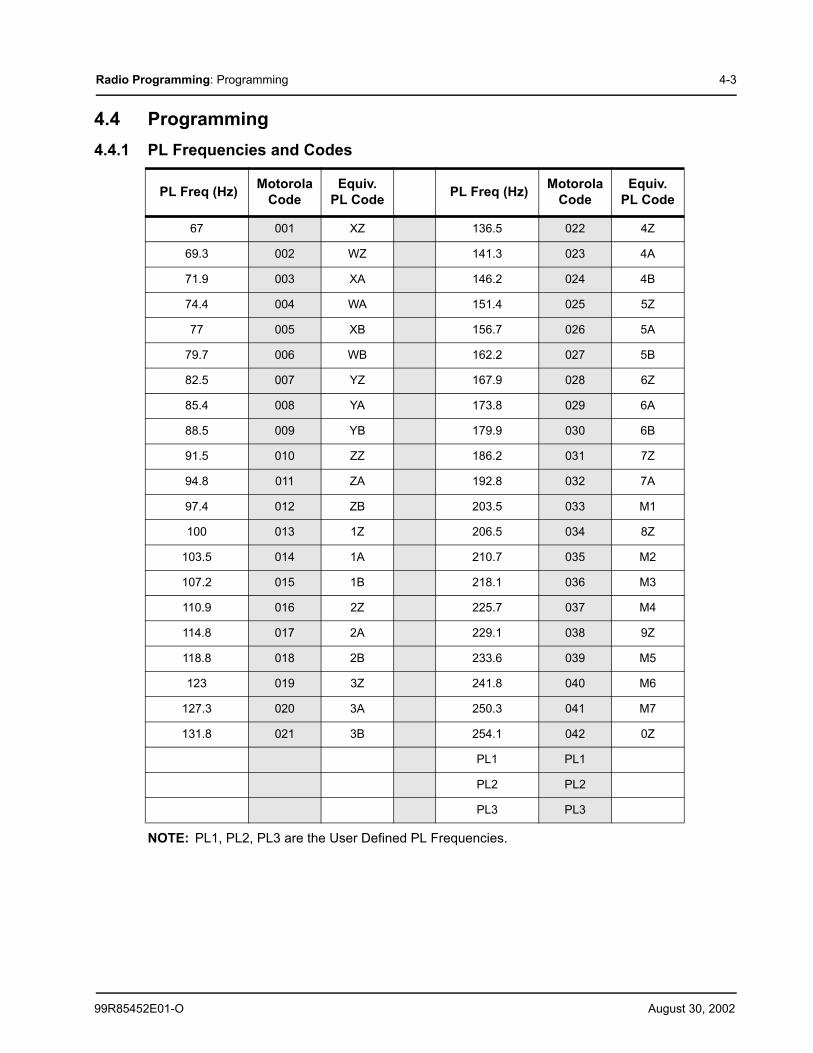
4.4 Programming4.4.1 PL Frequencies and Codes
NOTE: PL1, PL2, PL3 are the User Defined PL Frequencies.
PL Freq (Hz) Motorola Code
Equiv. PL Code PL Freq (Hz) Motorola
CodeEquiv.
PL Code
67 001 XZ 136.5 022 4Z
69.3 002 WZ 141.3 023 4A
71.9 003 XA 146.2 024 4B
74.4 004 WA 151.4 025 5Z
77 005 XB 156.7 026 5A
79.7 006 WB 162.2 027 5B
82.5 007 YZ 167.9 028 6Z
85.4 008 YA 173.8 029 6A
88.5 009 YB 179.9 030 6B
91.5 010 ZZ 186.2 031 7Z
94.8 011 ZA 192.8 032 7A
97.4 012 ZB 203.5 033 M1
100 013 1Z 206.5 034 8Z
103.5 014 1A 210.7 035 M2
107.2 015 1B 218.1 036 M3
110.9 016 2Z 225.7 037 M4
114.8 017 2A 229.1 038 9Z
118.8 018 2B 233.6 039 M5
123 019 3Z 241.8 040 M6
127.3 020 3A 250.3 041 M7
131.8 021 3B 254.1 042 0Z
PL1 PL1
PL2 PL2
PL3 PL3
August 30, 2002 99R85452E01-O
4-4 Radio Programming: Programming
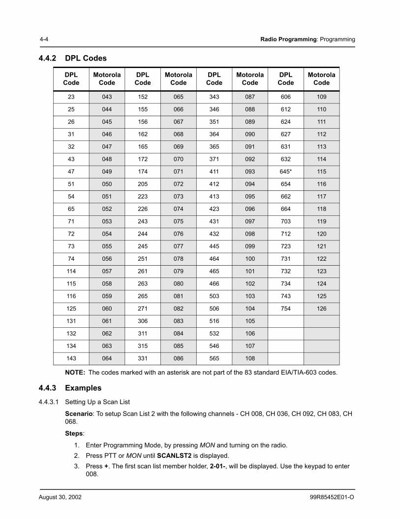
4.4.2 DPL Codes
NOTE: The codes marked with an asterisk are not part of the 83 standard EIA/TIA-603 codes.
4.4.3 Examples4.4.3.1 Setting Up a Scan List
Scenario: To setup Scan List 2 with the following channels - CH 008, CH 036, CH 092, CH 083, CH 068.
Steps:
1. Enter Programming Mode, by pressing MON and turning on the radio.2. Press PTT or MON until SCANLST2 is displayed.3. Press +. The first scan list member holder, 2-01-, will be displayed. Use the keypad to enter
008.
DPL Code
Motorola Code
DPL Code
Motorola Code
DPL Code
Motorola Code
DPL Code
Motorola Code
23 043 152 065 343 087 606 109
25 044 155 066 346 088 612 110
26 045 156 067 351 089 624 111
31 046 162 068 364 090 627 112
32 047 165 069 365 091 631 113
43 048 172 070 371 092 632 114
47 049 174 071 411 093 645* 115
51 050 205 072 412 094 654 116
54 051 223 073 413 095 662 117
65 052 226 074 423 096 664 118
71 053 243 075 431 097 703 119
72 054 244 076 432 098 712 120
73 055 245 077 445 099 723 121
74 056 251 078 464 100 731 122
114 057 261 079 465 101 732 123
115 058 263 080 466 102 734 124
116 059 265 081 503 103 743 125
125 060 271 082 506 104 754 126
131 061 306 083 516 105
132 062 311 084 532 106
134 063 315 085 546 107
143 064 331 086 565 108
99R85452E01-O August 30, 2002
Radio Programming: Programming 4-5
4. Press + again. Enter 036, when 2-02- appears, and subsequently in this manner, enter the other channels.
NOTE: If a mistake is made, use + or - to move to the appropriate scan list member holder and press # to erase the channel number.
5. Press PTT or MON, when all the channel numbers have been entered.6. Turn off your radio, if you have completed the programming, or proceed to the next
parameter.
4.4.3.2 Programming a Phone Number/Access Code/De-Access Code
Scenario: To program the phone number, 9-72886338 (where “-” represents a Pause digit), at memory location 8.
Steps:
1. Enter Programming Mode, by pressing MON and turning on the radio.2. Press PTT or MON until TELNO-8 is displayed.3. Press +. The cursor will be placed on the first character.4. Use the keypad to enter 9.5. Enter a Pause digit, by entering * followed by #. These two characters will be converted into a
Pause, represented by ‘-’.
NOTE: Each Pause digit entered shortens the overall length of the code/number by a digit.
6. Use the keypad to enter the rest of the phone number.
NOTE: If a mistake is made, use + or - to move to the appropriate location and then re-enter the correct character. To erase the complete phone number/code, enter # 16 times.
7. Press PTT or MON, when the complete phone number has been entered.8. Turn off your radio, if you have completed the programming, or proceed to the next
parameter.
August 30, 2002 99R85452E01-O
4-6 Radio Programming: Programming
This Page Intentionally Left Blank
Chapter 5 Error Code Displays
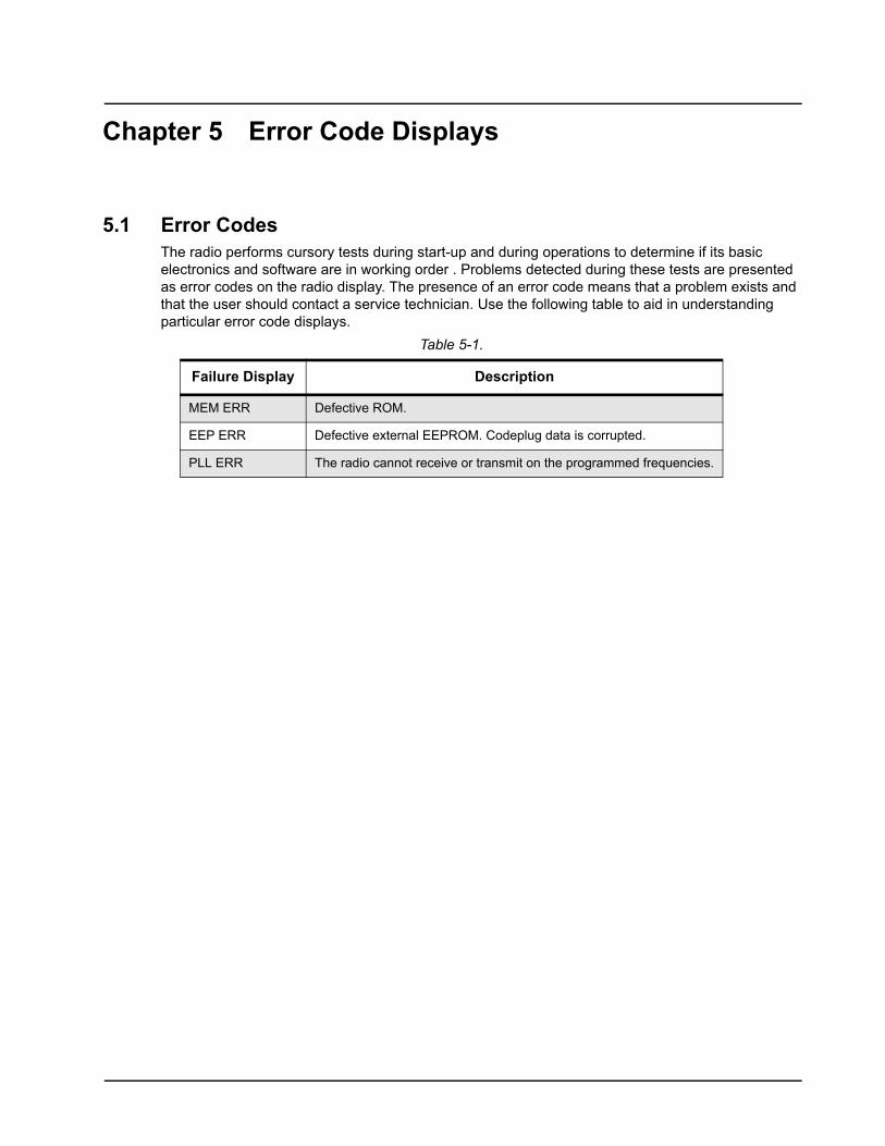
5.1 Error CodesThe radio performs cursory tests during start-up and during operations to determine if its basic electronics and software are in working order . Problems detected during these tests are presented as error codes on the radio display. The presence of an error code means that a problem exists and that the user should contact a service technician. Use the following table to aid in understanding particular error code displays.
Table 5-1.
Failure Display Description
MEM ERR Defective ROM.
EEP ERR Defective external EEPROM. Codeplug data is corrupted.
PLL ERR The radio cannot receive or transmit on the programmed frequencies.

August 30, 2002 99R85452E01-O
This Page Intentionally Left Blank
5-2 Error Code Displays: Error Codes
Chapter 6 Accessories
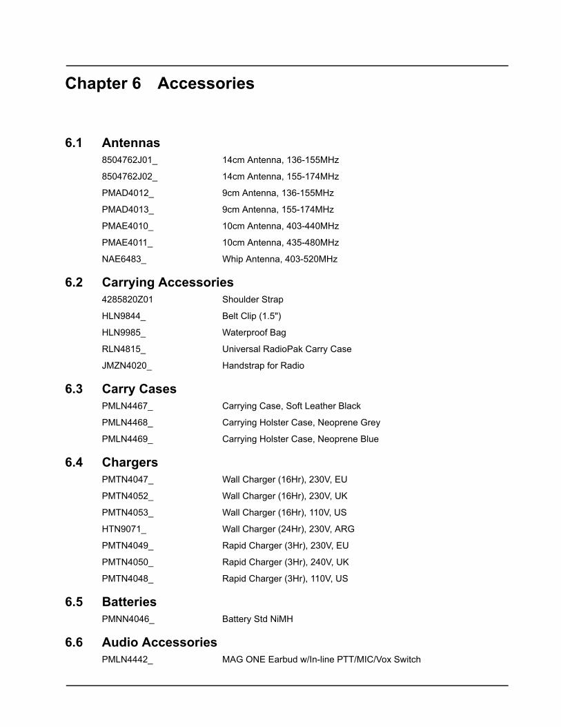
6.1 Antennas8504762J01_ 14cm Antenna, 136-155MHz
8504762J02_ 14cm Antenna, 155-174MHz
PMAD4012_ 9cm Antenna, 136-155MHz
PMAD4013_ 9cm Antenna, 155-174MHz
PMAE4010_ 10cm Antenna, 403-440MHz
PMAE4011_ 10cm Antenna, 435-480MHz
NAE6483_ Whip Antenna, 403-520MHz
6.2 Carrying Accessories4285820Z01 Shoulder Strap
HLN9844_ Belt Clip (1.5")
HLN9985_ Waterproof Bag
RLN4815_ Universal RadioPak Carry Case
JMZN4020_ Handstrap for Radio
6.3 Carry CasesPMLN4467_ Carrying Case, Soft Leather Black
PMLN4468_ Carrying Holster Case, Neoprene Grey
PMLN4469_ Carrying Holster Case, Neoprene Blue
6.4 ChargersPMTN4047_ Wall Charger (16Hr), 230V, EU
PMTN4052_ Wall Charger (16Hr), 230V, UK
PMTN4053_ Wall Charger (16Hr), 110V, US
HTN9071_ Wall Charger (24Hr), 230V, ARG
PMTN4049_ Rapid Charger (3Hr), 230V, EU
PMTN4050_ Rapid Charger (3Hr), 240V, UK
PMTN4048_ Rapid Charger (3Hr), 110V, US
6.5 BatteriesPMNN4046_ Battery Std NiMH
6.6 Audio AccessoriesPMLN4442_ MAG ONE Earbud w/In-line PTT/MIC/Vox Switch
August 30, 2002 99R85452E01-O
6-2 Accessories: Manuals
PMLN4443_ MAG ONE Ear Receiver w/In-line PTT/MIC/Vox Switch
PMLN4444_ MAG ONE Earset Boom Mic w/In-line PTT/Vox Switch
PMLN4445_ MAG ONE Ultra-lightweight Headset w/in-line PTT/Vox
PMMN4008_ MAG ONE Remote Speaker Mic
HMN9030_ Remote Speaker Microphone
PMLN4294_ Ear Set Microphone w/PTT
PMLN4425_ Earset Boom Mic w/Remote Ring PTT
BDN6646_ Ear Mic w/PTT
BDN6647_ Lightweight Single Speaker w/Swivel
BDN6648_ Hvy-duty Hdset w/Noise Canceling Mic
BDN6720_ Flex Rec. Earpiece w/o Volume Control
HMN9022_ Medweight Dual Muff Headset (behind)
HMN9752_ Earpiece w/Volume Control
HMN9787_ Lightweight Headset w/Swivel Boom Mic
HMN9013_ Lightweight Headset w/Swivel Boom Mic
HMN9021_ Medweight Dual Muff Headset (overhead)
HMN9036_ Earbud w/clip Mic and PTT
HMN9727_ Earpiece w/o Volume Control
6.7 ManualsHKLN4197_ PRO2150 Portable Radio User Guide (English, Spanish, and
Portuguese)
HKLN4204_ PRO2150 Portable Radio Detailed Service Manual (English)
6.8 SoftwareH5197 2 Year CPS Subscription
HKVN4002_ PRO2150 Customer Programming and Tuning Software (CD)
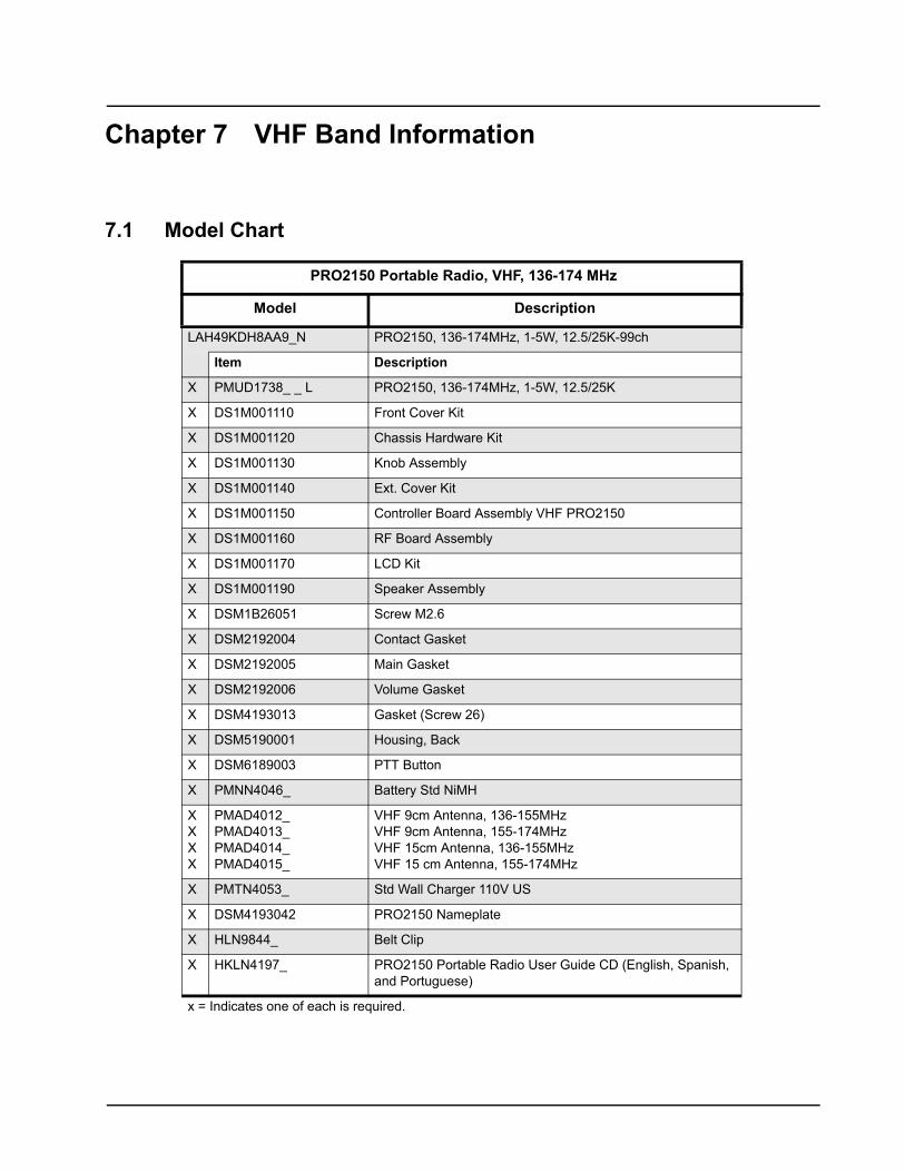
Chapter 7 VHF Band Information
7.1 Model Chart
PRO2150 Portable Radio, VHF, 136-174 MHz
Model Description
LAH49KDH8AA9_N PRO2150, 136-174MHz, 1-5W, 12.5/25K-99ch
Item Description
X PMUD1738_ _ L PRO2150, 136-174MHz, 1-5W, 12.5/25K
X DS1M001110 Front Cover Kit
X DS1M001120 Chassis Hardware Kit
X DS1M001130 Knob Assembly
X DS1M001140 Ext. Cover Kit
X DS1M001150 Controller Board Assembly VHF PRO2150
X DS1M001160 RF Board Assembly
X DS1M001170 LCD Kit
X DS1M001190 Speaker Assembly
X DSM1B26051 Screw M2.6
X DSM2192004 Contact Gasket
X DSM2192005 Main Gasket
X DSM2192006 Volume Gasket
X DSM4193013 Gasket (Screw 26)
X DSM5190001 Housing, Back
X DSM6189003 PTT Button
X PMNN4046_ Battery Std NiMH
XXXX
PMAD4012_PMAD4013_PMAD4014_PMAD4015_
VHF 9cm Antenna, 136-155MHzVHF 9cm Antenna, 155-174MHzVHF 15cm Antenna, 136-155MHzVHF 15 cm Antenna, 155-174MHz
X PMTN4053_ Std Wall Charger 110V US
X DSM4193042 PRO2150 Nameplate
X HLN9844_ Belt Clip
X HKLN4197_ PRO2150 Portable Radio User Guide CD (English, Spanish, and Portuguese)
x = Indicates one of each is required.
7-2 Specifications
August 30, 2002 99R85452E01-O
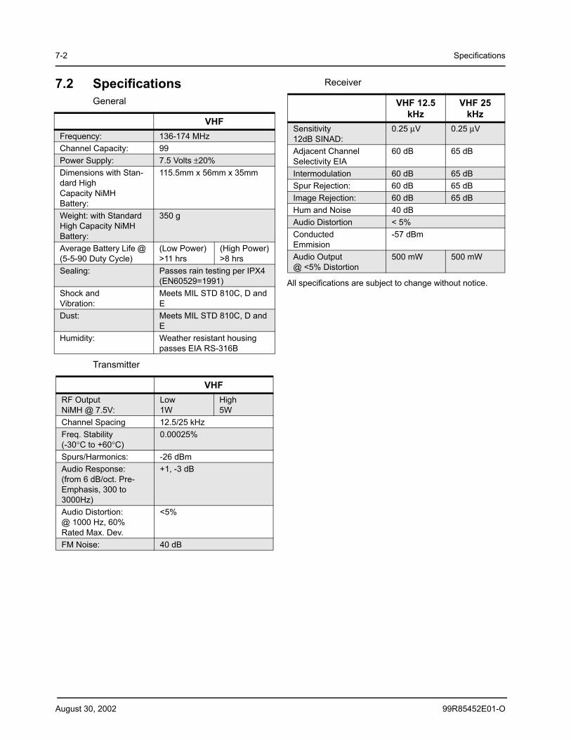
7.2 SpecificationsGeneral
Transmitter
Receiver
All specifications are subject to change without notice.
VHFFrequency: 136-174 MHzChannel Capacity: 99Power Supply: 7.5 Volts ±20%Dimensions with Stan-dard HighCapacity NiMHBattery:
115.5mm x 56mm x 35mm
Weight: with Standard High Capacity NiMH Battery:
350 g
Average Battery Life @ (5-5-90 Duty Cycle)
(Low Power)>11 hrs
(High Power)>8 hrs
Sealing: Passes rain testing per IPX4 (EN60529=1991)
Shock andVibration:
Meets MIL STD 810C, D and E
Dust: Meets MIL STD 810C, D and E
Humidity: Weather resistant housing passes EIA RS-316B
VHFRF OutputNiMH @ 7.5V:
Low1W
High5W
Channel Spacing 12.5/25 kHzFreq. Stability(-30°C to +60°C)
0.00025%
Spurs/Harmonics: -26 dBmAudio Response:(from 6 dB/oct. Pre-Emphasis, 300 to 3000Hz)
+1, -3 dB
Audio Distortion:@ 1000 Hz, 60%Rated Max. Dev.
<5%
FM Noise: 40 dB
VHF 12.5 kHz
VHF 25 kHz
Sensitivity12dB SINAD:
0.25 µV 0.25 µV
Adjacent Channel Selectivity EIA
60 dB 65 dB
Intermodulation 60 dB 65 dBSpur Rejection: 60 dB 65 dBImage Rejection: 60 dB 65 dBHum and Noise 40 dBAudio Distortion < 5%ConductedEmmision
-57 dBm
Audio Output@ <5% Distortion
500 mW 500 mW

99R85452E01-O August 30, 2002
VHF Band Information: Theory of Operation 7-3
7.3 Theory of Operation7.3.1 General Information
Your radio has two printed circuit boards: the Controller board, and the Radio Frequency (RF) board. The Controller board contains the CPU/Control section. The RF board contains the VCO/Synthesizer section, Transmitter section, Receiver section, Transmitter Audio circuitry, Receiver Audio circuitry, and Battery section.
7.3.2 Power Distribution
Figure 7-1. The above figure illustrates the DC distribution throughout the radio board. A battery supplies power directly to the electronic on/off control. Radio power supply is triggered by the Power Switch (On/Off/Volume control) and +SW B is distributed as show in the figure. Regulator output 5V is supplied to the CPU. +SW B continues to support the Audio Power AMP, 5V Regulator, TX Regulator until the radio is turned off.
The radio can be turned off on two ways:
1. Power Switch turned-off2. Low Battery
When a low battery level is detected by the CPU, it stores the radio personality data to EEPROM before turning off the radio.
7.3.3 Power up Sequence1. Power supply is turned on by the On/Off/Volume Control (Power Switch).2. Power from battery is supplied to the regulator through the switch.3. Output (5V) from the regulator is directed to the CPU (Q101).4. Q105 resets the CPU (Q101).5. The CPU loads radio personality data from EEPROM after the reset.6. This personality data is used to initialize the radio.
5V REGQ204
RX SWQ211
TX/RX SWQ208,209
TX REGQ201,202
RF AMPQ404
Local AMPQ416
IF AMPQ408
IF AMPQ506
LPFQ502
HPFQ505
Audio PowerAMPQ702
RF PAQ411
Driver AMPQ412
MIC AMPQ602
Sub AudioLPF Q610
VCO BufferQ308
PLL ICQ323
RF PowerControl
Q419
TX DriverQ413,414
+ SW B SAVE SWQ210 RX +5V
TX +5V
TX/RX SWQ309,310
TX VCOQ325
RX VCOQ324
Battery
DiodeQ126
ResetQ105
CPUQ101
EEPROMQ114
DTMFDecodeQ120
DAConverter
Q121
Divide by 2Q122
Ripple FilterQ330
PowerSwitchSW201

August 30, 2002 99R85452E01-O
7-4 VHF Band Information: Theory of Operation
7. The radio restores last power up state (i.e. state before the radio was turned-off).8. Power is supplied to PLL circuitry.9. Power is supplied to Rx and Rx VCO circuitry.10. CPU sends data to PLL circuitry. If LOCK status is confirmed, radio continues the power-up
sequence. Otherwise, PLL ERR is displayed.11. If the Rx audio level is less than the pre-programmed squelch level, and other unmuting
conditions are met, the radio will open squelch.
7.3.4 CPU / Control SectionWhen the radio is turned ON, the CPU (Q101) reads the radio status from the EEPROM Q114. It also monitors the keypad, the PTT line and other inputs such as the squelch detect, etc. continuously. When there is a channel change, the CPU sends the correct frequency information to the synthesizer via pins 1, 2 and 89. The CPU is clocked by the 8.388608MHz oscillator, which is composed of X101, C101, C106, and R158.
7.3.5 VCO / Synthesizer SectionThis section consists of the Temperature-Compensated Crystal Oscillator (TCXO), Voltage Controlled Oscillator (VCO), Synthesizer and the Loop Filter. These circuits are found on the RF board.
7.3.5.1 Temperature-Compensated Crystal Oscillator (TCXO)
The reference oscillator is a temperature compensated crystal-controlled, Pierce type circuit. It utilizes a logic gate within Q323 as a gain element. C335 is used to adjust the oscillator on frequency (14.4MHz) at room temperature (22°C). Temperature variations cause resistance changes in thermistor R330 and R567, which is on the base of Q320, thus varying the voltage applied to varactor Q322. This changes the impedance across crystal X301 in a manner complementary to the temperature drift characteristic of the crystal. In this way, the reference oscillator is held within the specified ±2.5 PPM from -30 to +60°C.
7.3.5.2 Voltage-Controlled Oscillators
Only one of the VCOs runs at a time, which is controlled by Q310 and Q101. The receive VCO consists of C344-C351, L302, L305, L306, L312-L314, Q311, and Q324. This VCO oscillates at 45.1 MHz above the programmed receive frequency. The VCO’s oscillating frequency is tuned by the varactor Q311. The tuning voltage is supplied from the output of the Loop Filter. The output of the VCO is AC coupled (C352) to the buffer Q308. The output of the VCO buffer Q308 is AC coupled (C308) to the synthesizer and the output buffer Q416 respectively.
When the PTT is pressed, Q101 pin36 goes low (approx. 0V) disabling the receive VCO by the Q310 and biases on Q309 to enable the transmitter VCO. The transmitter VCO consists of C353, C355, C357, C358, L315, L317, L318, Q325, Q326, and Q329. This VCO oscillates on the programmed transmit frequency. The VCO’s oscillating frequency is tuned by the varactor Q326. The tuning voltage is supplied from the output of the Loop Filter. The transmit voltage controlled oscillator is directly frequency-modulated and operates on the carrier frequency. The synthesizer is tuned in 5.00kHz or 6.25kHz steps.
7.3.5.3 Synthesizer
The frequency synthesizer is a large-scale monolithic synthesizer integrated circuit Q323. The synthesizer IC contains a dual modulus prescaler, programmable divide-by-N counter, prescale control (swallow) counter, reference oscillator, reference divider, phase detector, charge pump and lock detector. Also, included in Q323 are shift registers and control circuits for frequency controls and general device control.
99R85452E01-O August 30, 2002
VHF Band Information: Theory of Operation 7-5
RF output from the active VCO is AC coupled to the synthesizer Q323 prescaler input at Pin 8. The divide counter chain in Q323, consisting of the dual-modulus prescaler, swallow counter and programmable counter, divides the VCO signal down to a frequency very close to 5.00kHz or 6.25kHz which is applied to the phase detector. The phase comparator compares the phase with the 5.00kHz or 6.25kHz reference signal from the reference divider and drives the external charge pump (Q314, Q315 and Q316). The synthesizer unlock detector circuit prevents the operation of the transmitter and receiver, when the phase lock loop (PLL) is unlocked. The following discussion assumes the unit has been placed in the transmit mode. Q323 lock detector Pin 7 goes high when the PLL is locked. This high level is applied to Pin 25 of the CPU Q101. A software timing routing brings the RX/TX line low (Pin 36 of Q101). With the RX/TX line goes low, Q209 is cut off and Q208 is biased on passing +5VTX-B to Q202; it biases on Q201 to pass switched TX-B to the transmitter amplifier string which enables transmission.
When the PLL is unlocked, the lock detector at Q323 Pin 7 will begin pulsing low. A RC circuit converts this low pulse to a low level for the CPU. The CPU then changes the RX/TX line to a high, thus signaling the other transistor switches to drive Q201 into cutoff, which disables transmission. Therefore, the transmitter remains disabled while the loop remains out of lock, and “PLL ERR” is displayed.
7.3.5.4 Loop Filter
The Loop Filter, a passive lead-lag filter consisting of R314-R317, R356, C323, C369, and C371, integrates the charge pump output to produce the DC turning voltage for the VCO. One parasitic pole, consisting of RF chokes L306/L318, prevent modulation of the VCOs by the 5.00kHz or 6.25kHz reference energy remaining at the output of the loop filter. Direct FM is obtained for modulating frequencies outside the PLL bandwidth by applying the CTCSS/DCS signals and the pre-emphasized, limited microphone audio to the VCO modulation circuit. The modulation circuit consists of R347 and Q329.
7.3.6 Transmitter Section7.3.6.1 RF Power Amplifier
After the PTT is pressed, the +5VTX-B line switches to approximately 5V. Q309 is turned on, enabling transmit VCO. The VCO buffer, pre-driver, driver and power amplifier are biased on by Q201. Q201 is biased on by the +5VTX-B line switching to 5V. RF output from the transmit VCO(Q325) is applied to the VCO output buffer Q308. Output from Q308 feeds the buffer Q414. The output signal from Q414 feeds the pre-driver amplifier Q413, and feeds the driver amplifier Q412, whose output from the driver stage feeds the final RF power amplifier Q411 to produce the rated output power of 5 watts. The final output is feed to a low-pass filter (C446-C448, C451, C452, L418, and L419) and then to the transmit/receive switch Q410. RF power is then fed to the antenna via the output low-pass filter consisting of C440-C445, L415, and L416.
7.3.6.2 Antenna Switching
Switching of the antenna between the transmitter and the receiver is accomplished by the antenna transmit/receive switch consisting of diodes Q409 and Q410. In the transmit mode, switched TX B+ is applied through R419 and RF choke L417, hard forward biasing the two diodes on Q410, thus permitting the flow of RF power from the output of the low-pass filter. L414 and C445 isolate the receiver circuit from the transmitter power input.
August 30, 2002 99R85452E01-O
7-6 VHF Band Information: Theory of Operation
7.3.6.3 Power Control
Output power is controlled by the CPU (Q101), the D/A converter (Q121), the dual Op-Amp (Q419), which is used as a differential amplifier and comparator. Current is sensed by the voltage drop across R445. When the radio is in high power mode, this voltage is compared to the D/A converter voltage at 5-watt. When the radio is in low power mode, this voltage is compared to the D/A converter voltage at 1-watt. The power output is then reduced or increased by varying the applied voltage to the gate of the power amplifier Q411 and Q412.
7.3.6.4 Transmitter Audio Circuits
The transmitter audio circuits consist of the audio processing circuits, the CTCSS circuits and the DCS circuits.
7.3.6.4.1 Audio Processing
Transmit speech audio is provided by either the internal electric microphone M101 or the external microphone. The audio is pre-emphasized by 6dB per octave by C615 and R655, and then its signal is amplified. The microphone audio is directed to amplifier Q602B, Q602A and low-pass filter Q602C and Q602D. Q602A has limiting function. The modulation adjustment is done by Pot RV601, and directed to a four-pole active low-pass filter. The resulting signal is then limited, and is directed to a low pass filter (18dB per octave roll-off above 3KHz). The audio is then directed through the 25KHz/12.5KHz channel spacing SW Q601 to varactor diode Q329 in transmit VCO. By varying the voltage on the varactor diode Q329 at an audio rate, VCO output is frequency-modulated.
7.3.6.4.2 CTCSS Tone Encoder / Digital Code Squelch (DCS) Encoder
CTCSS signals and DCS signals are synthesized by CPU Q101 and appear as pulse waveform on I/O line Pin 7. This I/O line is connected to a digital-to-analog converter network (consisting of C136, C173, R150, R177 and R182), which produces a pseudo-sine wave at its output. The waveform is smoothed by low pass filters Q610B to produce an acceptable sine wave output. The CTCSS tone signal is adjusted to the proper level by RV602.
7.3.7 Receiver Section7.3.7.1 Receiver Front End
In the receive mode, the RF signal enters thorough the antenna, then through the low-pass filter C439-C445, and L414-L416. The diodes Q409 and Q410 are biased off, so that the output of the low-pass filter is coupled (C437, C438, L413 and R418) to the first band-pass filter C401-C406, C408-C410, L401, L402, PCB_L1, Q401, R401, and to the Front End RF overload protection diode pair Q403. The signal from the band-pass filter is directed to the input of the RF amplifier Q404. The output of the RF amplifier is sent to three stages of band-pass filters, consisting of C415-C429, C486, L404-L406, Q405 and R410. The output from the band-pass filter is directed to the mixer’s Q407/L407.
7.3.7.2 Local Oscillator (LO)
The Receive VCO (C344-C351, L302, L305, L306, L312-L314, Q311, and Q324) provides the LO signal. The VCO is running at 45.1 MHz above the desired receive frequency and is applied to output Buffer Q308/Q416. The output of the buffer is sent through the low-pass filter C430, C431, L409, and to the mixer Q407/L408.
99R85452E01-O August 30, 2002
VHF Band Information: Theory of Operation 7-7
7.3.7.3 Mixer
The mixer is a DBM type (L407, Q407, L408). The mixer LO frequency is 45.1 MHz above the desired receiver frequency. When the receiver frequency is present, the mixer output will be a 45.1MHz signal. The mixer output is peaked for 45.1MHz at L410, C432 and R413, and the signal is filtered by crystal filter F402 and amplified by Q408 before being sent to IF IC Q506. The 45.1MHz IF signal and LO frequency of 44.645 MHz (X501) are mixed in Q506. The 455kHz ceramic filter, F501 or F502, filters the second mixer’s output. The resulting signal is the second IF signal. The mixer’s output is then fed to the internal limiting amplifier, and consequently to the FM decoder.
7.3.7.4 FM Detector and Squelch
The FM detector output is used for squelch, decoding tones and audio output. The squelch amplifier is inside of Q506, and its output is fed to an internal rectifier and squelch detector. The output on Q506 Pin 14 signals the CPU Q101 with a low (~0V) to unmute the radio. The audio is unmuted by the CPU Q101 Pin 41 switching to a high (5V), thus biasing on Q503. The audio is then routed to the audio amplifier Q702 via the volume control SW201.
7.3.7.5 Receiver Audio Circuit
The detector’s audio output also is fed to the tone (CTCSS and DCS) low-pass filter Q505A. Then the output of the low-pass filter is routed to the second stage filter Q505B. The output of Q505B is passed to Q505C. The output of Q505C is directed to the squaring circuit Q505D, and finally to the CPU Q101 Pin22 for decoding.
The detector output feeds the audio high-pass filter Q502. The output of the audio high-pass filter feeds the Volume Control SW201 (VOL). From the wiper arm on the Volume Control, the audio is routed to Pin 4, which is the input to the audio power amplifier Q702. The output of the audio power amplifier is routed through the earphone jack J701 to the internal speaker SP701.
7.3.8 Battery SectionThe battery connects to the contact (CN201). The positive terminal of the battery connects to the ON/OFF Volume control switch (SW201), and the negative terminal connects to PWB ground. Low battery is detected by R127/R128 and voltage regulator Q204.
Battery voltage status is monitored by Pin 19 of the CPU Q101 through R127/R128. When the battery voltage goes below the threshold voltage, “LOW BATT" is displayed on LCD LC101. In the BATTERY SAVER Mode, the CPU Q101 generates a square wave signal on Pin 37. The signal’s duty cycle varies according to what the BATTERY SAVE TIMER is set. When the signal goes high (approximately 5 V), Q210 is biased off, and Q211 is cut off, thus turning the supply off to IF IC Q506.
August 30, 2002 99R85452E01-O
7-8 VHF Band Information: Block Diagrams
7.4 Block Diagrams7.4.1 Complete
Figure 7-2.
SA
VE
5V
RX
5V
5V
DA
CR
X
Key
Pad
Pow
erIn
put
TX
5V
BA
TT
ER
Y
5V DA
C R
X
DA
C T
X
35D
TM
F IN
RC
NE
TW
OR
K
9
RC
NE
TW
OR
K3
MIC
M10
1
CN
701
CN
101
27 31 4 15 16 22 25252215 16343193527
DA
CT
X
+ S
W B
Rip
ple
Filt
erQ
330
5V
SP
KS
P70
1(1
/2)
DT
MF
IND
etec
t
Det
ect
1313
AN
T
Ham
onic
s F
ilter
C44
0-44
5L4
15,L
416
AN
TS
witc
hQ
409,
410
Mat
chin
gN
etw
ork
C44
6-44
8,45
1,45
2L4
18,4
19
2-P
ole
Ban
d P
ass
Filt
erQ
401
RF
AM
PQ
404
2-P
ole
Ban
d P
ass
Filt
erQ
405
Mix
erQ
407
Cou
pler
R44
5
Loca
lB
uffe
rQ
416
2-P
ole
Cry
stal
Filt
erF
402 B
uffe
rA
MP
Q41
4
Pre
Driv
erQ
413
RE
GQ
206
Q20
7
Pow
erC
ontr
olQ
419
Pow
erS
WS
W20
1
5V RE
GQ
204
SA
VE
SW
Q21
0
TX
RE
G/S
WQ
201
Q20
2
Ove
rV
olta
geP
rote
ctQ
707-
710
TX
/RX
SW
Q20
8Q
209
VC
OB
uffe
rQ
308
RX
VC
OQ
311
Q32
4
TX
VC
OQ
325
Q32
6
TX
/RX
SW
Q30
9Q
310
Aud
ioM
odul
ator
Q32
9
Loop
Filt
erQ
314-
316
Pin
15
16
CN
701
Pin
37
38
39
Pin
11
Pin
8 10
9
Pin
1
2 TC
XO
14.4
MH
zX
301
Q32
0Q
322
Sub
Aud
ioM
odul
ator
Q32
2
6 P
ole
Cer
amic
Filt
erF
501
IF AM
PQ
408
De-
emph
asis
Q50
2A
Sub
Aud
ioLP
FQ
505
HP
FQ
502
Aud
ioP
ower
AM
PQ
702
EX
T A
udio
Jack
J701
6 P
ole
Cer
amic
Filt
erF
502
PLL
Q32
3
EE
PR
OM
Q11
4
CP
UQ
101
PT
TS
102
Mon
S10
1LC
DLC
101
Shi
ftQ
102
X,ta
l8.
38M
Hz
X10
1
Div
ide
by 2
Q12
2
DT
MF
Dec
ode
Q12
0
Res
etQ
105
DA
Con
vert
erQ
121
CP
UP
in87
DIO
DE
Q12
6
CP
UP
in21
CP
U P
in22
CP
U P
in36
LPF
(DT
MF
)Q
610A
Lim
itter
AM
PQ
602A
MIC
AM
PQ
602B
VO
XA
MP
Q61
0D
AT
TQ
608
Q60
9
LPF
(Sub
Aud
io)
Q61
0B
N/W SW
Q60
1
LPF
Q60
2C,D
Dev
iatio
nA
djR
V60
1
EX
T M
ICJa
ckJ7
01(1
/2)
DC
AM
PQ
125
IF IC
Q50
6(2
nd M
ix,2
nd L
ocal
,IF A
MP
,DIS
C,N
oise
AM
P)
2nd
Loca
l44
.654
MH
zX
501
RX
SW
Q21
1
DC
/DC
Con
vert
erQ
301
Vol
ume
SW
201
(VR
)
Fin
alA
MP
Q41
1
PA
Q41
2
99R85452E01-O August 30, 2002
VHF Band Information: Block Diagrams 7-9
7.4.2 Controller
Figure 7-3.
7.4.3 VCO
Figure 7-4.
KeyPad
35
RCNETWORK
9
RCNETWORK 3
MICM101
27
31
4
1516
22
25
13EEPROMQ114
CPUQ101
PTTS102
MonS101
LCDLC101
ShiftQ102
Xtal8.38MHz
X101
Divide by 2Q122
DTMFDecodeQ120
ResetQ105
DAConverter
Q121
CPUPin87
DIODEQ126
CPUPin21
CPU Pin22
CPU Pin36
DCAMPQ125
CN101
RX LocalBuffer
TXBuffer
DATA
Audio Sub AudioTX/RX
SW CONTL
Ripple FilterQ330
5V
VCOBufferQ308
RXVCOQ311Q324
TX/RXSW
Q309Q310
AudioModulator
Q329
Sub AudioModulator
Q322
TCXO14.4MHz
X301Q320,322
LoopFilterQ314Q315Q316
PLLQ323 CN701
Pin37 38 39
Pin11 10 9
Pin15 16
Pin 1
Pin 8
2
TXVCOQ325Q326
PowerRegulator
DC/DCConverter
Q301
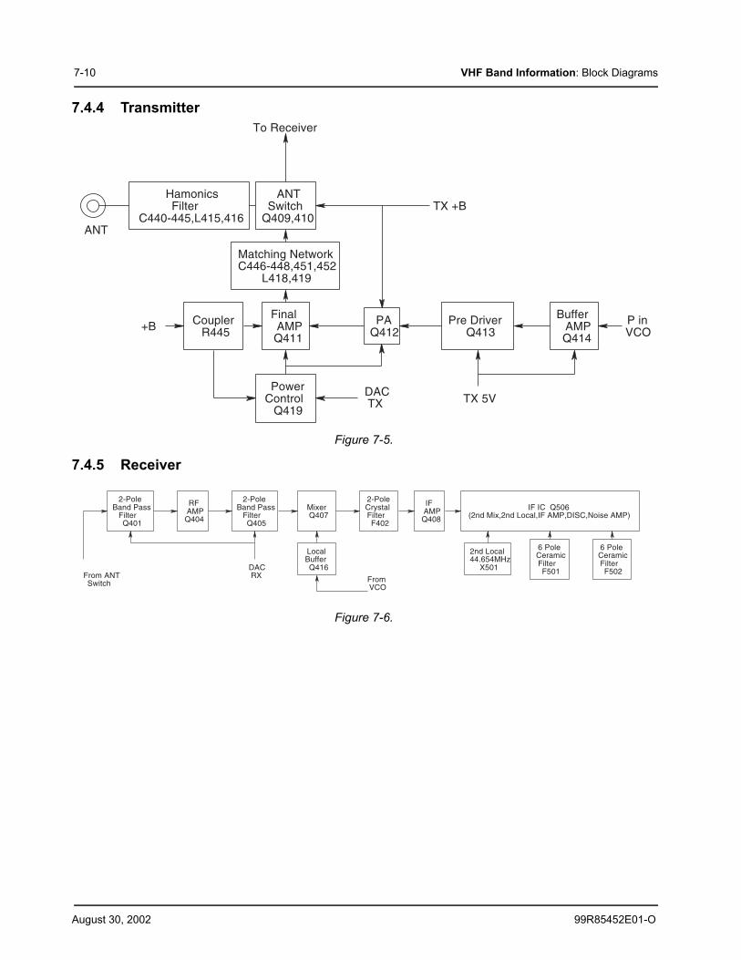
August 30, 2002 99R85452E01-O
7-10 VHF Band Information: Block Diagrams
7.4.4 Transmitter
Figure 7-5.
7.4.5 Receiver
Figure 7-6.
ANT
To Receiver
TX +B
+B
TX 5VDACTX
HamonicsFilter
C440-445,L415,416
Matching NetworkC446-448,451,452
L418,419
PowerControl
Q419
ANTSwitch
Q409,410
BufferAMPQ414
CouplerR445
Pre DriverQ413
P inVCO
FinalAMPQ411
PAQ412
DACRX From
VCO
From ANTSwitch
2-PoleBand Pass
FilterQ401
2-PoleBand Pass
FilterQ405
2-PoleCrystalFilterF402
2nd Local44.654MHz
X501
6 PoleCeramicFilterF501
6 PoleCeramicFilterF502
MixerQ407
RFAMPQ404
LocalBufferQ416
IFAMPQ408
IF IC Q506(2nd Mix,2nd Local,IF AMP,DISC,Noise AMP)
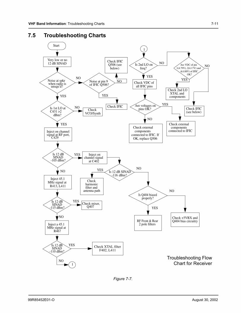
99R85452E01-O August 30, 2002
VHF Band Information: Troubleshooting Charts 7-11
7.5 Troubleshooting Charts
Figure 7-7.
Troubleshooting FlowChart for Receiver
Start
Very low or no 12 dB SINAD
Noise at spkrwhen radio is
unsqu’d?
Is 1st LO atC431 >2
dBm?
Inject on channelsignal at RF port,
C429
Inject a 45.1MHz signal at
R467
SINAD
1
Check IFICQ506 (see
below)
Noise at pin 9of IFIC Q506?
CheckVCO/Synth
Inject onchannel signal
at C402
Check harmonicfilter and
antenna path
Check externalcomponents
connected to IFIC. IfOK, replace Q506
Check mixer,Q407
Is 12 dB SINADdBm?
Check IFIC
RF Front & RearCheck +5VRX andQ404 bias circuitry
1
Is 2nd LO onfreq?
Check VDC ofall IFIC pins
Are VDC of pin1(4.79V), 2(4.17V) and
4(4.88V) of IFICOK?
Are voltages onpins OK?
Check 2nd LOXTAL andcomponents
Check IFIC(see below)
Check externalcomponents
connected to IFIC
NO
NO
YES
YES
NO
YES
YES
NO
YES
YES NO
YES
NO
YES
YES
NO
YES
YES
NO
NO
NO
NO
2 pole filters
Check XTAL filterF402, L411
-116
Is 12 dB
-110 dBm?
SINAD Is 12 dB
-115 dBm?
SINAD Is 12 dB
-105 dBm?
Is Q404 biasedproperly?
Inject 45.1MHz signal at
R413, L411
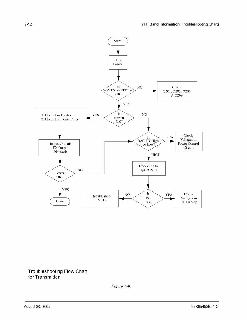
August 30, 2002 99R85452E01-O
7-12 VHF Band Information: Troubleshooting Charts
Figure 7-8.
Troubleshooting Flow Chart for Transmitter
Start
NoPower
Is+5VTX and TXB+
OK?
Iscurrent
OK?
IsDAC TX High
or Low?
Is PinOK?
CheckQ201, Q202, Q206
& Q209
CheckVoltages in
Power ControlCircuit
CheckVoltages inPA Line-up
TroubleshootVCODone
PowerOK?
1. Check Pin Diodes2. Check Harmonic Filter
Inspect/RepairTX OutputNetwork
NO
NO
LOW
HIGH
YESNO
NO
YES
YES
YES
Check Pin toQ419 Pin 1Is
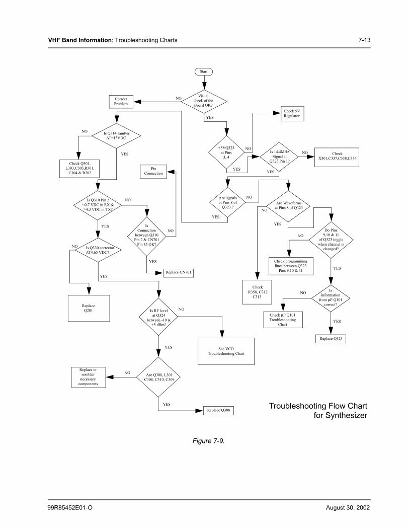
99R85452E01-O August 30, 2002
VHF Band Information: Troubleshooting Charts 7-13
Figure 7-9.
Isinformation
from µP Q101correct?
Is Q330 corrector AT4.65 VDC?
Is Q314 Emitter AT=13VDC
Is Q310 Pin 2<0.7 VDC in RX &>4.3 VDC in TX?
Troubleshooting Flow Chartfor Synthesizer
Start
Visual check of the Board OK?
CorrectProblem
Check 5VRegulator
+5VQ323at Pins
3, 4Is 14.4MHz
Signal atQ323 Pin 1?
CheckX301,C337,C338,C336
Are signalsat Pins 8 of
Q323 ?
Check Q301,L303,C303,R301,
C304 & R302Fix
Connection
IsConnection
between Q310Pin 2 & CN701
Pin 35 OK?
Replace CN701
ReplaceQ201
Replace orresolder
necessarycomponents
Is RF levelat Q324
between -10 &+5 dBm?
Are Q308, L301C308, C310, C309
Replace Q308
See VCOTroubleshooting Chart
Are Waveformsat Pins 8 of Q323
Do Pins9,10 & 11
of Q323 togglewhen channel is
changed?
Check programminglines between Q323
Pins 9,10 & 11
Replace Q323
Check µP Q101Troubleshooting
Chart
NO
YES
NO
NO
NO
NO
YES
YES
NO
YES
YES
NO
YES
NO
YES
YESYES
NONO
NO
YES
NO
YES
YES
NO
CheckR358, C312
C313
YES
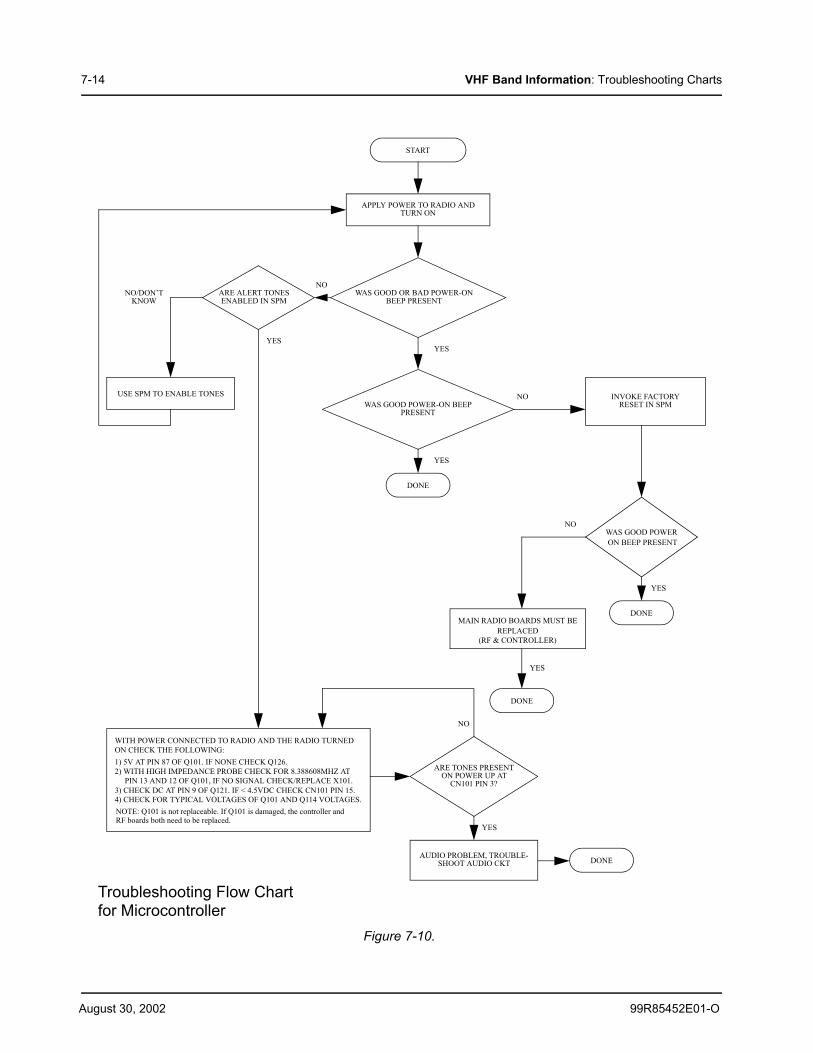
August 30, 2002 99R85452E01-O
7-14 VHF Band Information: Troubleshooting Charts
Figure 7-10.
Troubleshooting Flow Chart for Microcontroller
START
APPLY POWER TO RADIO AND
WAS GOOD OR BAD POWER-ON
YES
DONE
WAS GOOD POWER-ON BEEP
ARE ALERT TONESENABLED IN SPM
USE SPM TO ENABLE TONES INVOKE FACTORYRESET IN SPM
WAS GOOD POWERON BEEP PRESENT
MAIN RADIO BOARDS MUST BEREPLACED
ARE TONES PRESENTON POWER UP AT
CN101 PIN 3?
AUDIO PROBLEM, TROUBLE-SHOOT AUDIO CKT
WITH POWER CONNECTED TO RADIO AND THE RADIO TURNEDON CHECK THE FOLLOWING:1) 5V AT PIN 87 OF Q101. IF NONE CHECK Q126.2) WITH HIGH IMPEDANCE PROBE CHECK FOR 8.388608MHZ AT
PIN 13 AND 12 OF Q101, IF NO SIGNAL CHECK/REPLACE X101.3) CHECK DC AT PIN 9 OF Q121. IF < 4.5VDC CHECK CN101 PIN 15.4) CHECK FOR TYPICAL VOLTAGES OF Q101 AND Q114 VOLTAGES.
BEEP PRESENT
TURN ON
PRESENT
DONE
DONE
DONE
YES
YES
YES
YES
YES
NO/DON’TKNOW
NO
NO
NO
NO
(RF & CONTROLLER)
NOTE: Q101 is not replaceable. If Q101 is damaged, the controller andRF boards both need to be replaced.
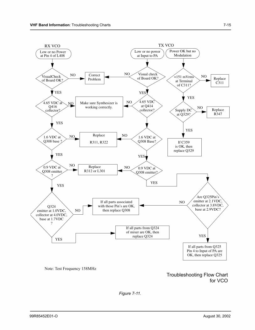
99R85452E01-O August 30, 2002
VHF Band Information: Troubleshooting Charts 7-15
Figure 7-11.
Make sure Synthesizer isworking correctly.
1.6 VDC atQ308 Base?
4.65 VDCat Q414
collector?
=151 mVrmsat Terminalof C311?
Supply DCat Q329?
0.9 VDC atQ308 emitter?
Are Q325Pin’semitter at 2.1VDC,
collector at 3.8VDC, base at 2.9VDC?
Q324 emitter at 1.0VDC,
collector at 4.0VDC,base at 1.7VDC
?
0.9 VDC atQ308 emitter
?
1.6 VDC atQ308 base ?
4.65 VDC atQ416
collector?
Troubleshooting Flow Chartfor VCO
Low or no Powerat Pin 4 of L408
VisualCheckof Board OK?
If all parts from Q324of mixer are OK, then
replace Q324
If all parts associated with those Pin’s are OK,
then replace Q308
If all parts from Q325Pin 4 to Input of PA areOK, then replace Q325
If C359 is OK, then
replace Q329
ReplaceR347
ReplaceC311
Low or no power at Input to PA
Visual check of Board OK?
CorrectProblem
Replace
R311, R322
ReplaceR312 or L301
NO
YES
NO
YES
NO
YES
NO
YES
NO
YESYES
NO
YES
NO
YES
NO
NO
YES
NONO
YES
NO
YES
RX VCO TX VCOPower OK but no
Modulation
Note: Test Frequency 158MHz
August 30, 2002 99R85452E01-O
This Page Intentionally Left Blank
7-16 VHF Band Information: Troubleshooting Charts
7-17
99R85452E01-O August 30, 2002
Chapter 7 VHF 136-174 MHz Circuit Board/Schematic Diagrams and Parts List
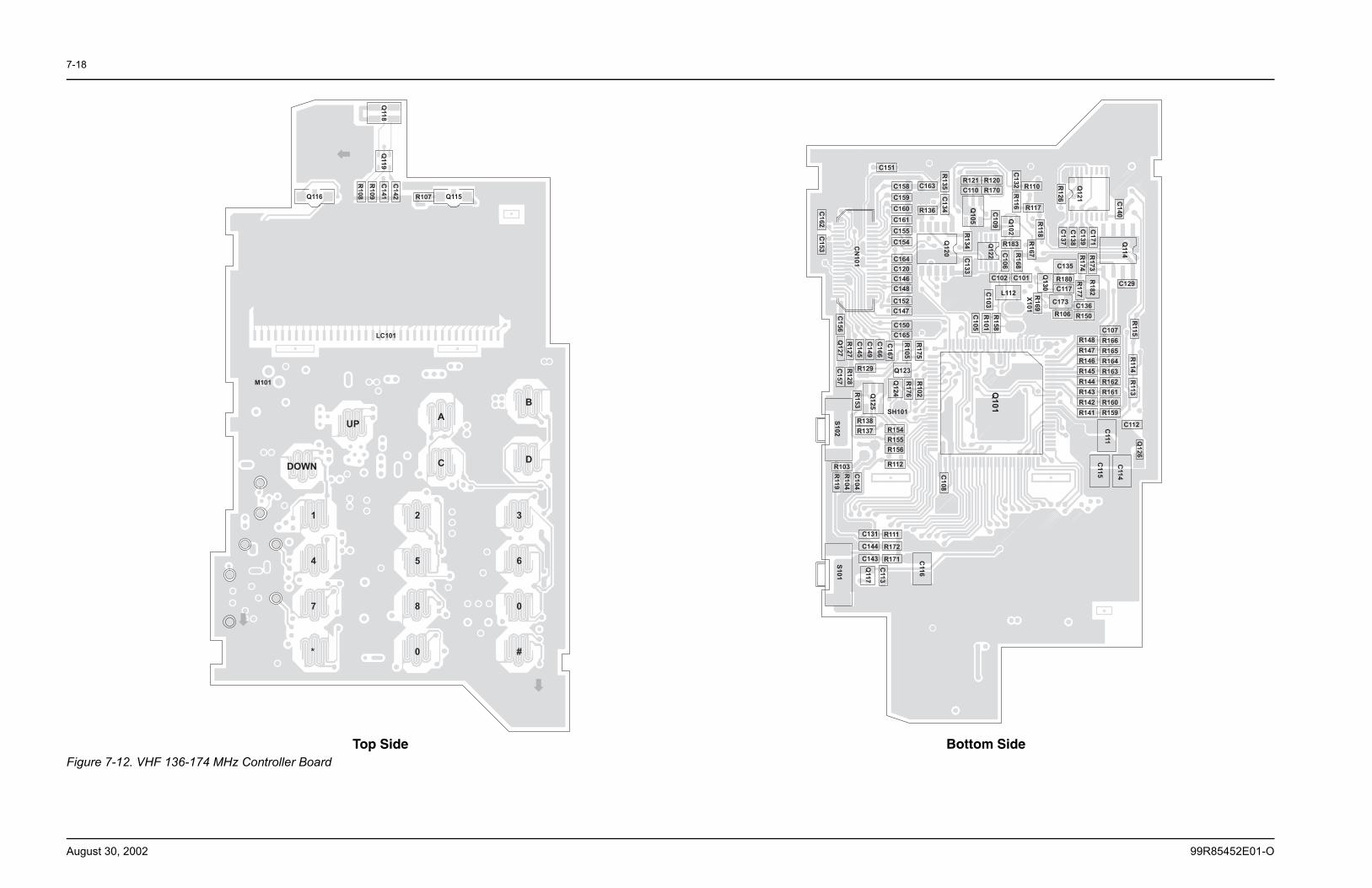
7-18
August 30, 2002 99R85452E01-O
Figure 7-12. VHF 136-174 MHz Controller BoardTop Side Bottom Side
C1
42
C1
41
R1
09
R1
08
Q11
9Q
11
8
Q116 Q115R107
LC101
M101
DOWN
UP
1
4
7
*
2
5
8
0
3
6
0
#
A
C
B
D
C1
40
Q11
4
C1
71
C1
39
C1
38
C1
37
Q1
21
C129R
17
3
R1
74
R1
82
C135
R180 R1
77C117
C173C136
R150R106
R11
5
R1
26
R11
8Q
13
0
R1
69
R110
R117
R1
67
X1
01
L112
C101C102
R1
68
C1
06
R183
Q1
02
R11
6C
13
2
C1
09
R120
R170
R121
C110
Q1
05
Q122
R1
34
C1
33
C1
03
R1
58
R1
01
C1
05
R1
35
C1
34
C163
R136
Q1
20
C151
C158
C159
C160
C161
C155
C154
C164
C120
C146
C148
C152
C147
C150
C165
C1
66
C1
49
C1
45
R1
27
R1
75
R1
05
C1
67
C1
56
Q1
27
C1
62
C1
53 CN
10
1
R148
R147
R146
R145
R144
R143
R142
R141
C107
R166
R165
R164
R163
R162
R161
R160
R159
R11
4R
11
3
C112
Q1
26
C111
C11
4
C11
5
Q101
R154
R155
R156
R112
SH101
C1
08
Q123
R1
02
R1
76
Q1
24Q
12
5
R129R1
28
C1
57
S1
02
R138
R137
R103
C1
04
R1
04
R11
9
R1
53
S1
01
Q11
7
C11
3
C131
C144
C143
R111
R172
R171 C11
6
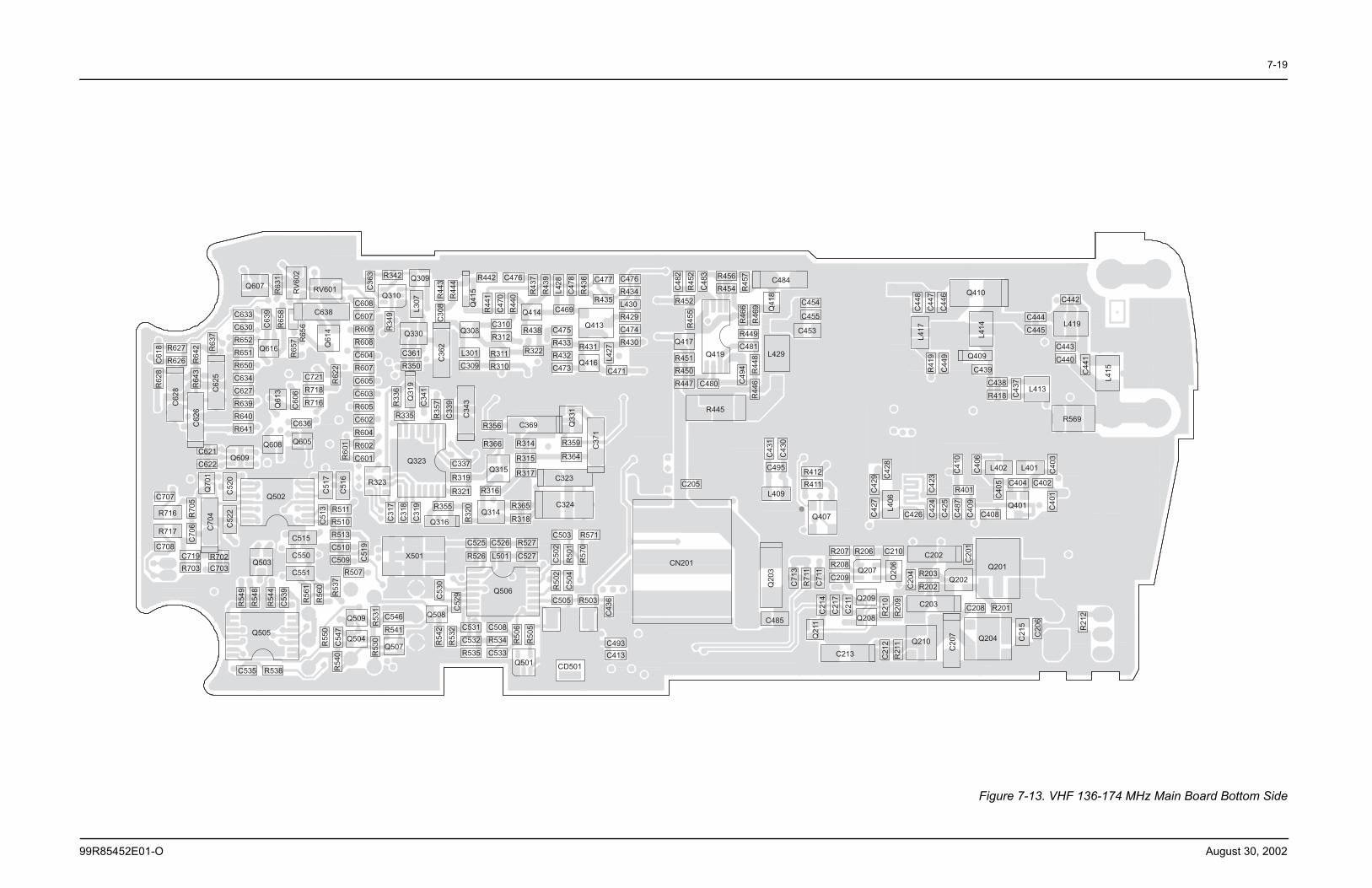
7-19
99R85452E01-O August 30, 2002
Figure 7-13. VHF 136-174 MHz Main Board Bottom Side
C633
C630
R652
R651
R650
C634
C627
R639
R640
R641
C608
C607
R609
R608
C604
R607
C605
C603
R605
C602
R604
R602
C601
R6
28
C621
C622
R6
31
C6
39
R6
58
C6
06
C6
18
C6
26
R6
42
RV601RV
60
2
C638
R627
R626
C6
25
R6
37
R6
43
C6
28
R6
57
Q6
13
Q608
Q607
Q6
14
R6
22
C721
R718
R716
C636
R6
01
Q609
Q605
Q616
R511
R510
R513
C510
C509C719
R703
R702
C703
C515
C550
C551
R716
R717
R5
44
C5
39
R5
49
R5
48
R5
61
R5
60
R5
50
C5
47
C5
17
C5
16
Q502C707
C708
C5
20
C5
22
R7
05
C7
06 C7
04
Q503
Q7
01
Q505
C535 R538
C5
13
C5
19
R507
R5
37
R5
40
Q504
Q509
C3
63
R323
R5
31
R5
30
C476
R434
L430
R429
C474
R430
C475
R433
R432
C473
C310
R312
R311
R310
L301
C309
R314
R315
R317
C361
R350
R4
41
C4
70
R4
40
R4
37
R4
39
L4
28
C4
78
R4
36
R4
43
R4
44
R356
R322
R438
R431
R442 C476 C477
R435
C469
C3
41
Q3
19
R335
C369 Q331
Q413
R342
Q310
Q330 Q308
Q309
Q414L3
07
R359
R364
C3
08
C3
62
Q415
R3
49
R3
36
C3
43
C3
71
L4
27
Q416
C471
Q323 C337
R319
R321
Q315
C323
R451
R450
R447
C454
C455
C453
L429Q419
R456
R454
C484
R445
R4
46
C4
82
R4
52
C4
83
Q417
Q4
18
C4
28
Q410
L4
17 L419
C442
L413
C439
C4
37
C4
48
C4
47
C4
46
R4
19
C4
49
L4
14
Q409
C438
R418
C444
C445
C4
41
L4
15
C443
C440
C4
01
L401
C4
05
C4
06
C4
23
C2
01
R2
12
C2
04
R2
09
R2
10
C2
12
R2
11
C2
15
C2
07
Q202
C4
24
C4
25
C4
87
C4
09
C404
Q401
C4
10
C4
03
C402
C408
L402
Q201
C202C210
R203
R202
C208 R201
C2
06
C203
Q204Q210
Q206
R207
R208
C209
R206
Q207
C485
C213
Q407
L4
06
C7
13
R7
11
C7
11
C2
14
C2
17
C2
11
R412
R411
C4
29
Q211
Q209
Q208
Q203
CN201
C205
L409
C4
31
C4
30
C495
C531
C532
R535
C3
17
C3
18
C3
19
C5
02
R5
01
R5
70
R5
02
C5
04
C525
R526
R5
42
R5
32 C508
R534
C533
C526
L501
R527
C527
R365
R318
C324
X501
Q506
Q314
R316
R355
Q316 R3
20
C503 R571
C505 R503
C493
C413
CD501Q501
R5
06
R5
05
C5
30
Q508C546
R541
Q507
C5
29
C4
36
R6
56
R3
57
C3
39R366
C480
R4
55
R452
R4
57
R4
66
R4
69
R449
C481
R4
48
C4
94
C4
27
C426
R401
R569
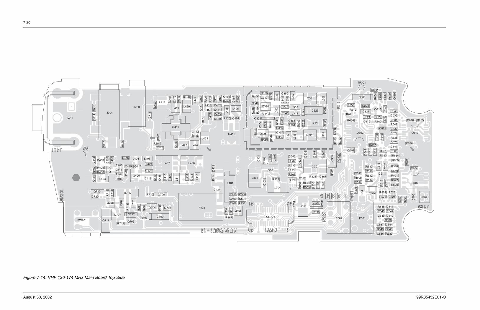
7-20
August 30, 2002 99R85452E01-O
Figure 7-14. VHF 136-174 MHz Main Board Top Side
J401
J703
J704
C7
14
C7
16
C7
15
C7
17
C7
18
R2
05
R204
C218
C1
42
Q403
C4
07
R4
02
R405
R408 Q404
R4
09
C414
L403
R403
C411
R404
R406
C416 L404 L405
C421
C422
C418
Q405
C415 C417
R4
07
L407
C4
19
C4
86
R4
10
C4
20
L4
11
R4
13
C4
32
L408
L410
C4
33
R4
14
C4
58
L422 L424
R4
21
R4
22
L423
Q411
C4
50 L418
L419L420
R420
L4
21
R4
70
C4
51
C4
72
C4
52
C4
56
R4
24
R4
27
R4
28
C4
66
R423
C459
C462
C461
C463
C460
C4
57
C4
89
C4
67
C4
68C465
R426
L426
R425 C464
Q412
F401
Q710
C720
SW201 Q711
Q708
Q707
R712Q709
Q712
R7
09
Q705
R7
15
R7
14
R710 Q706
C709R706
Q704 Q703
R7
08
R7
07L7
02
R7
13
C7
10
F402
C434
R416
C490
R468
C506
C501
L431
R4
59
R4
15
Q408
R467
L4
25
C352
C346
Q324
C349
R3
39
L3
14
L3
12
C350
L3
02
Q311
L3
06
C3
16
C3
60
Q326
L3
18
Q329
C3
53
Q325
R343 R3
46
R338
C347
C359
C357
C355
C3
54
C3
58
R3
63
C3
44
C3
51
R3
47
C3
11
L305
L313
C368
R361 R3
62
C3
27
C3
48
R3
40
L3
17
L3
15
C326
C328
C3
25
C380
R332
R333
R329
R565
R3
02
C3
05
C3
02
C3
01
L303
Q301
C304
R301
C3
03 Q320
Q322
X301
R337R325 C367
R564
R563R5
66
R3
30
R5
67
R5
68
R3
27
C3
38
C3
81
C3
36
C3
35
R5
51
C528
R536
Q511
CN701
R546
R545
C540
C541
R547
C542
C537
R543
C536
C544
C543
R539
C538F501F502
Q510
C5
34
R5
08
R524
R525
R523
C524
C7
02
R7
01
C7
05
J702
R6
54
C6
20
C6
17
R6
29
C6
19
TP301
R632
C366
R3
13
R659
R611
R612
R606
R620
C637Q615
R6
45
R6
55R621
C612
C629
R660
Q602
Q601
C3
13
C3
12
R3
58 C615
R6
10
R6
46
R617
C6
42
R6
16
R6
15
R661
R633
R648
C635
C631
R649
C632
C624
R638
C623
C641
R663
R634
R635
C616 R625
Q610
R636
C7
01
R704
Q702
C512
R509
C511
R517
R516
R512
R514
R518
R519
R521
R522
R520
C514
R5
15
C5
23
C5
18
C5
21
C545
R341
C345
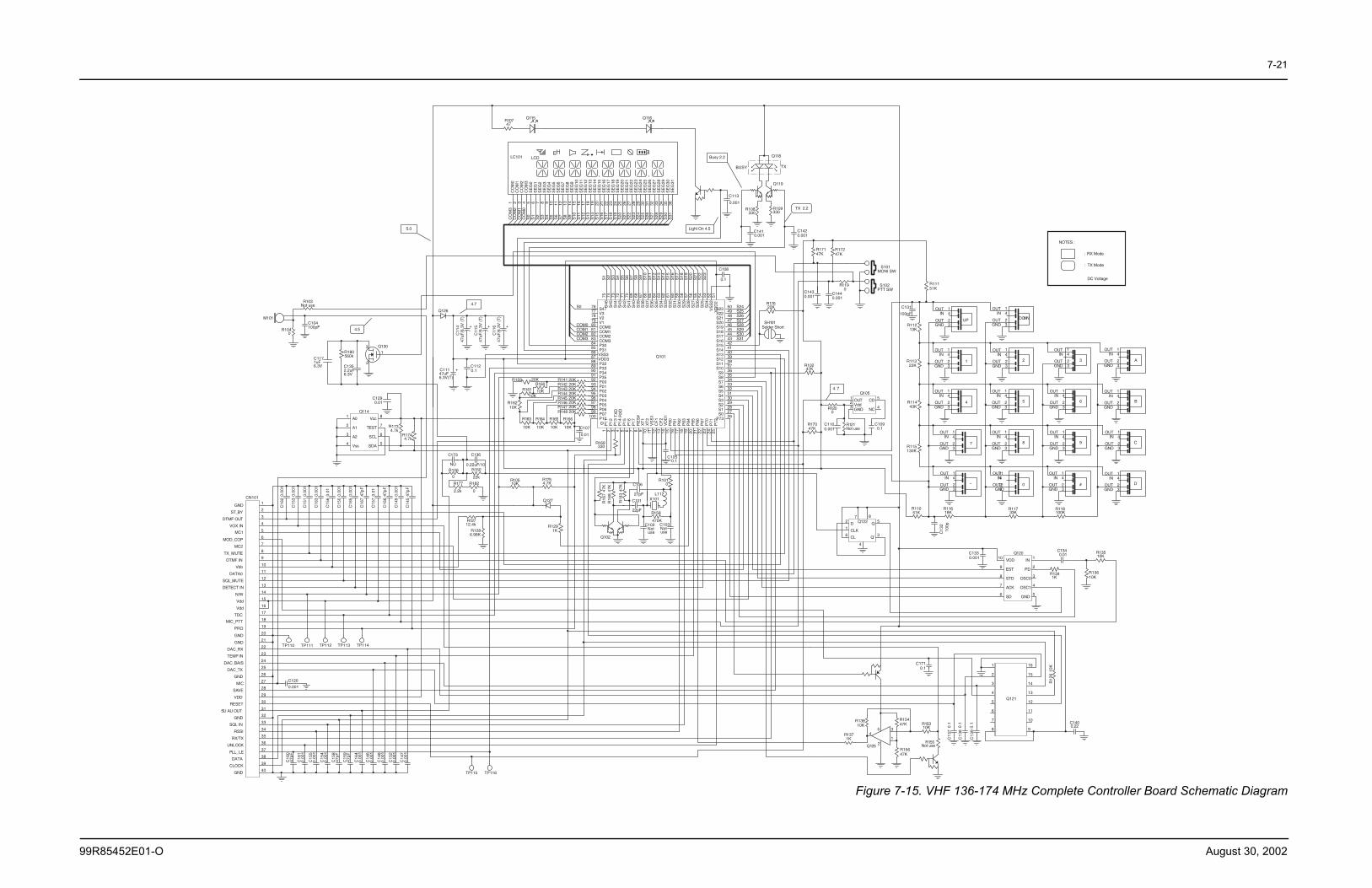
7-21
99R85452E01-O August 30, 2002
Figure 7-15. VHF 136-174 MHz Complete Controller Board Schematic Diagram
R1200
Q115
R109330
R108330
A01
A12
A23
Vss4 SDA 5
SCL 6
TEST 7
Vcc 8Q114
R12712.4k
R1286.98K
C1290.01
R11051K
R11151K
R11213K
R11322K
R11443K
R115130K
R11618K
R11733K
R118100K
C131
100pF
C13
210
0p
A1
B4
7
4
23
OUT 1
OUT
IN
GND*
UP DOWN
2
5
4
23
OUT 1
OUT
IN
GND
4
23
OUT 1
OUT
IN
GND
4
23
OUT 1
OUT
IN
GND
4
23
OUT 1
OUT
IN
GND
4
23
OUT 1
OUT
IN
GND
4
23
OUT 1
OUT
IN
GND
4
23
OUT 1
OUT
IN
GND
4
23
OUT 1
OUT
IN
GND
4
23
OUT 1
OUT
IN
GND
4
23
OUT 1
OUT
IN
GND
4
23
OUT 1
OUT
IN
GND
4
23
OUT 1
OUT
IN
GND
4
23
OUT 1
OUT
IN
GND
4
23
OUT 1
OUT
IN
GND
4
23
OUT 1
OUT
IN
GND
4
23
OUT 1
OUT
IN
GND
8
14
23
OUT1
OUT2
IN
GND0
C
D
3
6
9
#
CO
M0
1
CO
M1
2
CO
M2
3
CO
M3
4
SE
G0
5
SE
G1
6
SE
G2
7
SE
G3
8
SE
G4
9
SE
G5
10
SE
G6
11
SE
G7
12
SE
G8
13
SE
G9
14
SE
G10
15
SE
G11
16
SE
G12
17
SE
G13
18
SE
G14
19
SE
G15
20
SE
G16
21
SE
G17
22
SE
G18
23
SE
G19
24
SE
G20
25
SE
G21
26
SE
G22
27
SE
G23
28
SE
G24
29
SE
G25
30
SE
G26
31
SE
G27
32
SE
G28
33
SE
G29
34
SE
G30
35
SE
G31
36
LC101 LCD
V377 S4776 S46
75
V278
V179
COM080
COM181
COM282
COM383
P3084
P3185
VSS386
VDD387
P3288
P3389
P3490
P3591
P0092
P0193
P0294
P0395
P0496
P0597
P0698
P0799
P10100
P11
1
P12
2
P13
3
P14
4
P15
5
P16
6
P17
7
RE
S#
8
XT
19
XT
210
VS
S1
11
CF
112
CF
213
VD
D1
14
P80
15
P81
16
P82
17
P83
18
P84
19
P85
20
P86
21
P87
22
P70
23
P71
24
P72
25
P73 26S0 27S1 28S2 29S3 30S4 31S5 32S6 33S7 34S8 35S9 36S10 37S11 38S12 39S13 40S14 41S15 42S16 43S17 44S18 45S19 46S20 47S21 48S22 49S23 50
VD
D2
51V
SS
252
S24
53S
2554
S26
55S
2756
S28
57S
2958
S30
59S
3160
S32
61S
3362
S34
63S
3564
S36
65S
3766
S38
67S
3968
S40
69S
4170
S42
71S
4372
S44
73S
4574
Q101
C1120.1
C108
0.1
C1050.1
C1100.001
X101
C103C102Not use
Not use
C101
22pF
BUSY TX
PTT SW
C113
0.001
MONI SW
C107
0.01
IN 1
PD 2
OSC0 3
OSC1 4
GND 5SD6
ACK7
STD8
EST9
VDD10Q120
C1340.01
R1341K
R13610K
R13510K
C1330.001
C1400.22
C13
90.
1
C13
80.
1
C13
70.
1
TX
DR
XD
C1410.001
C1420.001
C1430.001
C1440.001
CLK1D2
CL6
Q 5
Q' 3
4
7 8Q122
3
14
2
5
Q125
R15310K
R15447K
R155Not use
R15647K
VDD
Vbb
Vdd
Vdd
GND
MOD_COP
DATA0
MIC
GND
GND
GND
RESET
GND
GND
CLOCK
DATA
PLL_LE
UNLOCK
DTMF OUT
DTMF IN
SU AU OUT
DETECT IN
TDC
N/W
RSSI
SQL IN
VOX IN
TEMP IN
MC1
MC2
RX/TX
SAVE
TX_MUTE
ST_BY
SQL_MUTE
DAC_RX
DAC_TX
DAC_BAIS
PRO
MIC_PTT
C15
60.
01
C15
70.
01
C15
847
pF
C15
947
pF
C16
047
pF
C16
10.
001
C16
20.
001
C16
30.
001
C16
40.
001
C16
50.
001
C16
647
pF
C16
747
pF
C14
547
pF
C14
60.
001
C14
70.
001
C14
80.
001
C14
90.
001
C15
00.
001
C15
10.
001
C15
20.
001
C15
30.
001
C15
40.
001
C15
50.
001
R150
22k
R158
470K
OUT1
Vdd2
GND3 NC 4
CD 5Q105
C1090.1
R17047K
R17147K
R17247K
R1010
R16
847
K
R1734.7k
R1744.7k
R16210K
R159 20K
R161
10K
R163
10K
R165
10K
R166
10K
R164
10K
R148 20KR147 20K
R145 20KR146 20K
R144 20KR143 20KR142 20KR141 20K
R160
10K
R169330
R16
747
K
COM0COM1COM2COM3
S0
S1
S2
S3
S4
S5
S6
S7
S8
S9
S10
S11
S12
S13
S14
S15
S16
S17
S18
S19
S20
S21
S22
S23
S24S25S26S27S28S29S30S31
CO
M0
CO
M1
CO
M2
CO
M3
S0
S1
S2
S3
S4
S5
S6
S7
S8
S9
S10
S11
S12
S13
S14
S15
S16
S17
S18
S19
S20
S21
S22
S23
S24
S25
S26
S27
S28
S29
S30
S31
Q119
R1291K
Q127
R10247K
S101
S102
M101C104100pF
C120
0.001
Q118
1
2
3
4
5
6
7
8 9
10
11
12
13
14
16
15
Q121
R10747
SH101Solder Short
R1754.7K
Q116
1
2
3
4
5
6
7
8
9
10
11
12
13
14
15
16
17
18
19
20
21
22
23
24
25
26
27
28
29
30
31
32
33
34
35
36
37
38
39
40
CN101
R17622K
C173
NU
Q126
R177
2.2k
C1710.1
C1352.2uF6.3V
C136
0.22uF/10
R180560k
R182
0
Q102
R18
347
K C106
27pF L112
R1190
R121Not use
R12
610
K
R13810K
R1371K
TP111 TP112 TP113 TP114
TP115 TP116
TP110
R106
0
+
C11
447
uF/6
.3V
(T
)
+
C11
547
uF/6
.3V
(T
)
+
C11
647
uF/6
.3V
(T
)
+C11147uF6.3V(T)
R10510K
C1171uF6.3V
R103Not use
R1040
31
2
Q130
5.0
4.5
4.7
Light On 4.5
TX 2.2
Busy 2.2
4. 7
NOTES :
: RX Mode
: TX Mode
DC Voltage
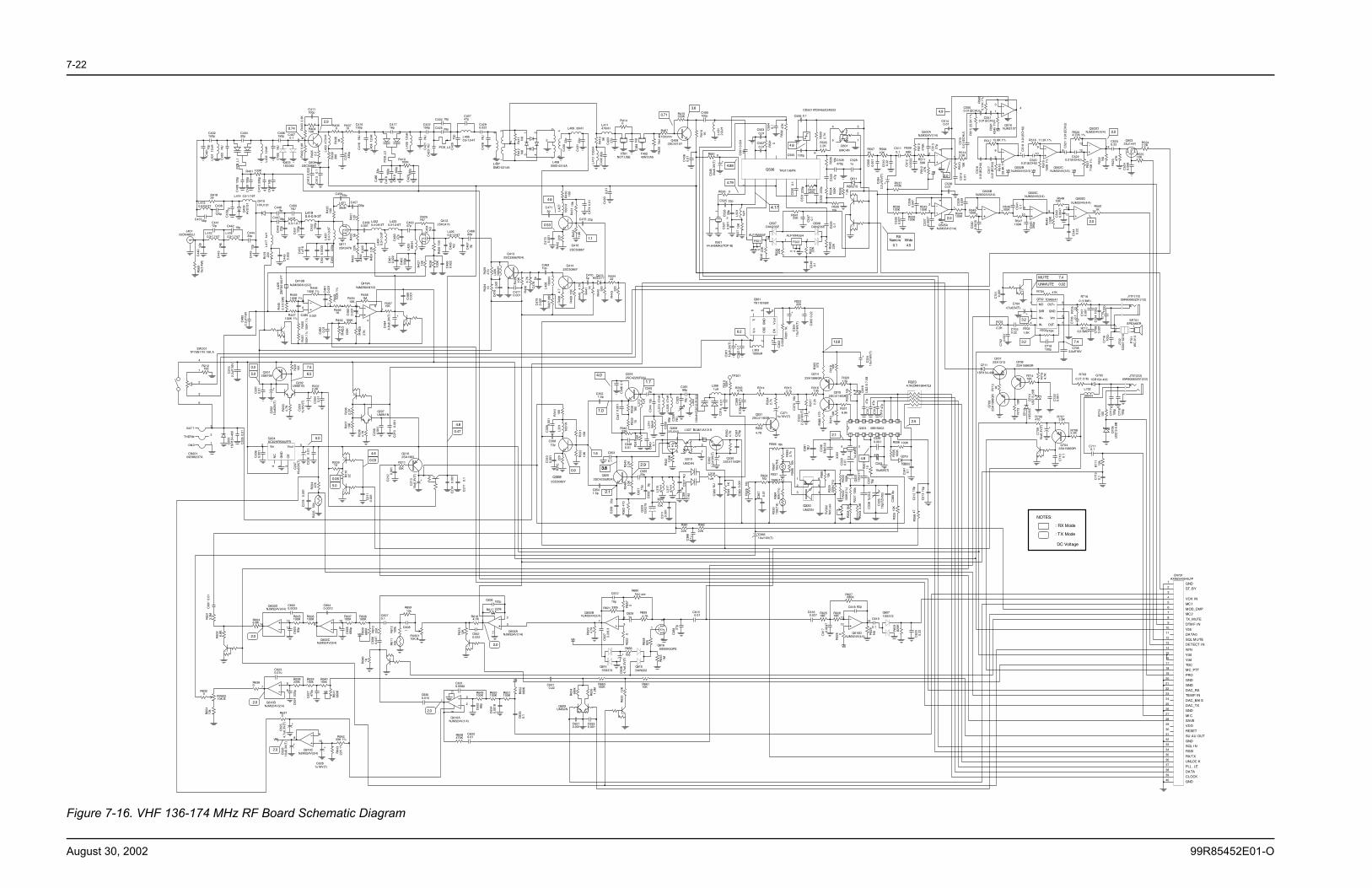
7-22
August 30, 2002 99R85452E01-O
Figure 7-16. VHF 136-174 MHz RF Board Schematic Diagram
C38
08p
C38
1N
U
J40102D04852J
Q711
1SR154-400
R61
150
k
C44
012
p
C6420.022
C44
324
p
R359
4.7K
Q3312SC4116GR
C44112p C442 10p
R65
410
k
C6300.015
Q3152SC4116GR
R36
647
0
C44433p
R36
547
0
C44
512
p
C45
31u
/16
R56
91k
(1/4
W)
Q40
9H
VU
131
C48
52.
2uF
/16V
C43
9 7p
C438
120p
R41839
C43756p
VB
R56
05.
11K
1%
R56
163
4k 1
%
C5500.01(ECHU)
C5510.01(ECHU)
3
14
52
Q510NJM2107
C402150p
C40
1 13p
R32
8N
U
C40
3N
U
C40420p
R56
32.
7k
R566 18k
C40
812
0p
R56
5
15k
C40
910
0p
R56
482
k(1%
)
R401 100K
1
2
3 4
5
6
Q320UMZ2N
R64
61K
C41
033
0p
C40
5N
U
C6410.22
R66110K
R663100K
C406150p
C60
10.
01
Q4031SS362
C4070.1
R40
25.
6KR
403
3.3K
Q4042SC5086Y
R40
52.
2
+
C3711u/16V(T)
R36
42.
7k
R40410K
C37
0N
U
C411100p
C36
90.
22u/
35(T
)
C36
81u
R362
22K
R4060
R40
81K
R40710
C415150p
R36
347
0
R40
939
0
R64
51M
C6291u
C41
433
0p
C41
30.
1
C43
60.
01
C41
20.
022
R7170(1/8W)
C41
6N
U
R7160 (1/8W)
R660Not use
R212100
C41716p
C33
30.
01
C41
810
0p
C41
910
0p
Q70
92S
A15
86G
R
R410100K
13
24
X50144.645MHz(TOP-B)
C42
0 330p
C42
1N
U
C72
00.
001
C422150p
Q71
0U
DZ
S 2
0B
C425 20p
C424 10p
R71
54.
7KR71410K
Q7082SA1586GR
C42
3N
U
R71
310
K
C42
610
p
Q7072SA1313
C42747p
R71
21K
R4661K
C4290.022
C42
8N
U
Vin2
GN
D1
Vout 5
NC
4
CE
3
Q204XC62HR5002PR
3
1
2
Q616SSM3K03FE
R41
1N
UR
412
NU C
434
NU
1 2
3 4
C43
022
p
C43
122
p
R41
356
C43
282
p
C43
327
p
F401NOT USE
1
2
3
4
5
6
7
8
9
10
11
12
13
14
15
16
17
18
19
20
21
22
23
24
25
26
27
28
29
30
31
32
33
34
35
36
37
38
39
40
CN701AXK6S40545J/P
F40245N12A5
R4140
Q4082SC4215Y
GND
GND
R415330K
MI C
GND
GND
MC_PTT
GND
PRO
Q410HVU131
RESET
2
3
8
4
1
Q419ANJM2904V(1/2)
DAC_BAI S
6
57
Q419BNJM2904V(2/2)
DAC_TX
C480 0.001
DAC_RX
SQL MUTE
ST_BY
R446100K 1%
TX_MUTE
R447100K 1%
SAVE
RX/TX
MC2
MC1
R44
50.
1(1/
2W)
TEMP IN
VOX IN
SQL I N
RSSI
R45
010
0K 1
%
W/N
R45
110
0K 1
%
TDC
DETECT IN
SU AU OUT
DTM F IN
DATA0
R44
910
0K 1
%
UNLOC K
C48
10.
001
PLL_ LE
DATA
CLOCK
MOD_CMP
R448100K 1%
GND
Vdd
Vdd
Vbb
VDD
R45410K
C48
30.
001
R4561M
C21
70.
1
C21
80.
001
R45715K
R452 100K
C48
90.
001
R45
527
K
R45
310
0K
+
C48
46.
8u6.
3V(T
)
C54
70.
1
C48
20.
01
R41
922
0
+
C54
533
u6.3
V(T
)
C44
90.
022
C4469p
C44718p
R551 0
C490100p
C44
822
p
C450NU
C54
60.
1
C45
112
0p
C506 0.1
C45
215
0p
R42
010
0
C45622p
4
5
3
2
1
Q501UMC4N
C457330p
C52
90.
1Q508DAN235E
R42
112
0
Q507DAN235E
C4580.001
R42
256
R54
022
K
R42
322
K
C45
90.
022
R42
412
K
C50
40.
1
C46
027
p
R50
247
K
C46347p
C45
522
0p
C45
40.
0033
R5052.2K
R50
32.
7K
C505 100p
CD501 IFD0455C24E03
C46
233
0pC46
10.
022
R50
10
R425NU
C46
4N
U
C5030.01
C5020.01
C50
10.
001
R42
610
0
R42
8
100K
R42
712
K
C46
60.
022
C46
5N
U
R53
122
K
R53
022
K
1 2
3 4 5
F502
ALFYM455H
C46
73p R54
222
K
C46822p
R54122K
1 2
3 4 5
F501
ALFYM455F
R50
610
k
Q4162SC5086Y
R43
010
0
C508470p
C4715p
C53
347
p
R43
115
k
R53
415
0K
R53510k
C475 22p
R43
3
10K
R43
222
0
C53
222
0p
C47
30.
001
C53
122
0p
C47
40.
01
R532560k
R42
947
0R
434
10
C53
00.
1
C47
60.
001
R52
710
K
Q4132SC3356(R24)
C52
70.
001
C52
639
p
R43
510
K
R43
64.
7K
C525 33p
C4770.001
R526 0
1 8916
Q506 TA31136FN
C49
30.
01
R41
61K
C47
85p
C46910p
Q4142SC5086Y
R43
84.
7
R43
768
0
R65
882
0
C47
90.
001
R43
915
K
R44
04.
7K
+
C63
84.
7u6.
3V(T
)
C4705p
R44
1 1K
R656
100
Q415HSC277
Q615DAN222
R44
2 330
R44422
Q6141SS372
R44
3 330
Q2012SB798
R20
110
K
C63
9 27p
R65
70
R20
34.
7K
R6554.7K
+
C20
210
u6.3
V(T
)
C20
10.
01
C636 100p
+
C20
31u
16V
(T)
R2022.2K
C20
40.
01
R65912k
Q609UMG2N
R20
62.
2KR
207
10K
R20
84.
7K C20
90.
001
C21
00.
001
C20
60.
001 +
C20
710
u6.3
V(T
)
C20
80.
01
Q6071SS372
R20910
R21
022
C63
50.
1
C6330.01
C21
10.
001
R648470K
C21
40.
001
+
C21
310
u6.3
V(T
)
Q2102SA1362
C61
70.
0047
R211
10K
R62518K
C21
2 0.00
1
+
C62
54.
7u6.
3V(T
)
R5071K
R6370
R50810K
C62
00.
22
C619
0.1
C50
90.
001
R63
182
0K
C51
00.
22
R62
9N
U
C5110.1
R50968K
C51
20.
0022
C618 82p
R51156K
R627680K
C6160.027
R51
047
0K
R62618K
C51
327
p
R62
8 0
VB
13
1214
Q610DNJM324V(4/4)
VB
R5143.3K
R65
268
0K
C63
40.
0018
R51
310
K
R651100K
C51
60.
01(E
CH
U)
R51
247
K
C6310.0082
C51
90.
01
R650100K
6
57
Q502BNJM324V(2/4)
R649100K
VB
2
31
411
Q502ANJM324V(1/4) R
515
25.5
K 1
%
C63
268
p
C51
70.
01(E
CH
U)
9
108
Q610CNJM324V(3/4)
R517 15.8K 1%
VBR642
33K 1%
R51
629
.4K
1%
R64
322
K 1
%+
C6281u16V(T)
VB
C51
80.
01(E
CH
U)
+
C62
610
u6.3
V(T
)
C5200.01(ECHU)
9
108
Q502CNJM324V(3/4)
2
31
411
Q610ANJM324V(1/4)
R518 11.5K 1%
VB
R64
168
0K
R51
915
0K 1
%
C62
747
0p
VB
R640150k
C52
10.
01(E
CH
U)
C5220.01(ECHU)
C6230.01u
13
1214
Q502DNJM324V(4/4)
R639150k
R5204.22K 1%
R638330k
R52
171
5K 1
%
C62
422
0p
6
57
Q610BNJM324V(2/4)
R6360
VB
C6220.001
C6210.001
C5230.22
R52
3 47K
R63
51.
2M
R63
468
0k
2
31
411
Q505ANJM324V(1/4)
R543100K
R539100K
R538100K
C53
70.
0027
R63
312
K
R6320
RV60210K.B
C53
50.
027
C6150.01
C53
60.
047
VB
C612
10p
R621 330k
R544100K
R62
20R
620
4.7K
C53
90.
039
R545100K
2
31
411
Q602ANJM324V(1/4)
6
57
Q505BNJM324V(2/4)
C54
00.
0015
R617 220k
6
57
Q602BNJM324V(2/4)R616
4.7K
R546100K C
541
0.1
R61
512
K
9
108
Q505CNJM324V(3/4)
RV60110K.B
R547100K
R61
210
0k C608---
C6070.1
C54
239
0p
C60
60.
047
R61
022
K
VB
R54810K
R54
910
0K
R60
968
0K
13
1214
Q505DNJM324V(4/4)
R608100K
C54
30.
0047
R607100K
C54
40.
22
R5501K
C60
568
0p
MO1
SVR2
IN+3
IN-4 OUT- 5
Vcc 6
GND 7
OUT+ 8Q702 TDA8541
C6040.0012
R70
522
C70
70.
001
C70
80.
001
9
108
Q602CNJM324V(3/4)
R703470K
C6020.0033
R7021.5K
R606100K
R605100K
SP701SPEAKER
12
P70
1W
C-0
13
C60
382
p
12
J702
5304
7-02
10
13
1214
Q602DNJM324V(4/4)
R704 47K
R6046.8K
+
C7044.7u6.3V(T)
R60
26.
8K
C7030.22
C70
6 0.1
R60
13.
3M
R45
9N
ot u
se
C70
2 0.00
1
C36
7
0.01
Q3092SJ243
R701
2.2K
2
13 4
6
L408SMD-0314A
2
136
4
L407SMD-0314A
R56
710
k(T
H)
R33
010
K(T
H)
R337
150K(1%)
R32
710
0kR32
922
0k(1
%)
R33
210
0K(1
%)
C33
633
p(U
J)
C33
715
pC
338
7p(U
J)
R33
43.
3K
C719100p
C33
510
p(T
ZV
02)
R32
6N
U
13
24
X30
1
14.4
MH
z
R33
310
0K
Q4122SK3475
Q4112SK3476
C48
7N
U
C3390.001
C343
10u6.3V(T)
C48
633
p
R336 100K
R33
510
0K
1 2 3 4 5 6 7 8
910111213141516
Q323 MB15A02
R3216.8k
C71
610
0p
R31
9 10K
Q3142SA1586GR R320
1.5k
C71
710
0p
R31
810
K
C71
810
0p
Q31
6U
DZ
S 7
.5B
C71
5 100p
+
C32
410
u/16
V(T
)
R3161.5k
C71
410
0p
R31
72.
2k
+
C32
32.
2u16
V(T
)
R3152.7k
R31
310
0K
TP301
C31
60.
01
+
C30
410
u/16
V(T
)
J701(2/2)09R80683Z01(2/2)
J701(1/2)09R80683Z01(1/2)
C31
947
p
Q32
21S
V21
7
C31
847
p
C31
747
p
PCB
_L1
PC
B_L
2
PCB_L3
Q207UMW1N
Q202UMW1N
C30
50.
22
R302220
R32
510
K
Q3082SC5086Y
R32
210
K
C30
30.
022
R31
115
K
R30
11K
R3140
+
C30
110
u6.3
V(T
)
R31
010
0
R3234.7K(CRA168-472J)
C34
10.
1
C30
20.
1
C30810p
R35
5N
U
Vin
1
OSC
2
DK
3V
out
4
GN
D5
TI
6
Q301TK11816M
C35168p
C34
413
p
C35
0 56p
C3455p
Q3242SC4226(R24)
R33
818
0R
339
15
C34
70.
001
R34
1 33K
R34022K
C34
90.
1C3480.01
C34
60.
1
C3521.5p
R34
32.
2K
Q3252SC4226(R24)
R34
210
0K
R34
610
K
C353
0.1
C3541.5p
C35522p
C35
7 15p
C35
833
p C35
99p
Q32
91S
V27
9
R347
10K
R361
22K
L307 BLM21A121S
Q3302SC4116GR
R35
04.
7K
C36
147
0p
+
C36
22.
2u10
V(T
)C
360
NU
R34
91K
C36
30.
001
+ C36610u/10V(T)
R324NU
R35
710
C31
210
pR
358
47
C31
315
p
R31
222
0
C31
00.
001
C31
10.
001
4
5
3
2
1
Q310UMC4N
R3564.7k
R71
010
0
Q70
6U
DZ
S 6
.8B
Q7051SR154-400
R7090.27 (1/8)
R7082.2K
Q7042SA1586GR
R7073.9K
+
C70
910
u6.3
V(T
)
R706470
C71
00.
1
R71
110
kC
713
0.1
Q319
1SS355
C7110.1
C51
50.
01(E
CH
U)
Q5032SJ144Y R524
2.2K
L30
210
0nH
(C20
12-R
10J)
C52
40.
068
R52510K
Q20
31S
R15
4-40
0
C20
50.
01
R20
447
KR
205
50k
C32
8
NU
C32
7N
U
C32
6N
UC
325
NU
3
2
1
BAT T
THERM
GND
CN20109D86237A
C70
10.
001
4
1
2
3
5
SW201TP76N17N 10K.A
C30
9 0.00
1
C5380.01
R537470K
L429
ZB
FS
5105
-PT
C5140.01
C21
52.
2uF
/16V
C7052.2uF/16V
R53
6
1.5k
R56
810
k
Q511
RB521S
C5281u
Q71
2
1SS
355
+C53
42.
2u/1
0V(T
)
R467
100ohm
C63
72.
2/6.
3
L40
112
nH
L40
212
nH
L40
347
0nH
L40
412
nH
L40
512
nH L4060.3-1.0-4T
L409 33nH
L41
015
0nH
L411470nH
L43
12.
2uH
L50
1
1uH
L4130.4-0.9-3T
L414 0.3-1.7-6T
L4150.3-1.7-5T
L4160.3-1.7-5T
L41
71u
H
L418
0.3-1.0-7T
L4190.4-0.9-3T
L42
00.
4-1.
0-5T
L421
39nH
L4220.4-0.9-3T
L4230.3-1.0-6T
L424
0.3-
1.0-
5T
L42
568
nH
L4260.3-1.0-4T
L42
7
100n
H
L43
010
0nH
L42
810
0nH
L30
1
100n
H
L31
456
nH
L31
347
nH
L30
547
nH
L31
2
1uH
L3061uH
L318
1uH
L31
547
nH
L31
747
nH
L3031000uH
L702
390nH
0.74
2.9
0.71
3.6
4.6
0.53
1.1
4.88
4.79
4.8
RXNarrow Wide
0.1 4.5
4.9
2.0
2.0
2.0
2.0
MUTE
UNMUTE
7.4
0.02
6.2
12.8
0.9
1.6
2.1
4.8
2.5
3.2
3.2 7.4
4.8
0.47
4.6
0.03
0.06
5.0
5.0
7.5
6.5
0.0
5.0
2.0
2.0
2.0
2.0
2.0
NOTES:
: RX Mode
: TX Mode
DC Voltage
4.17
1.0
1.7
4.0
3.83.82.9
2.1
RV
302
Not
use
R52
2N
U
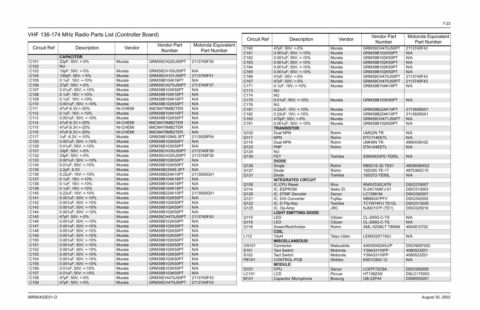
7-23
99R85452E01-O August 30, 2002
VHF 136-174 MHz Radio Parts List (Controller Board)
Circuit Ref Description Vendor Vendor Part Number
Motorola Equivalent Part Number
CAPACITORC101 22pF; 50V; +-5% Murata GRM39CH220J50PT 2113740F35C102 NUC103 10pF; 50V; +-5% Murata GRM39CH100J50PT N/AC104 100pF; 50V; +-5% Murata GRM39CH101J50PT 2113740F51C105 0.1uF; 16V; +-10% Murata GRM39B104K16PT N/AC106 27pF; 50V; +-5% Murata GRM39CH270J50PT 2113740F37C107 0.01uF; 50V; +-10% Murata GRM39B103K50PT N/AC108 0.1uF; 16V; +-10% Murata GRM39B104K16PT N/AC109 0.1uF; 16V; +-10% Murata GRM39B104K16PT N/AC110 0.001uF; 50V; +-10% Murata GRM39B102K50PT N/AC111 47uF;6.3V;+-20% NI-CHEMI 6MCM476MB2TER N/AC112 0.1uF; 16V; +-10% Murata GRM39B104K16PT N/AC113 0.001uF; 50V; +-10% Murata GRM39B102K50PT N/AC114 47uF;6.3V;+-20% NI-CHEMI 6MCM476MB2TER N/AC115 47uF;6.3V;+-20% NI-CHEMI 6MCM476MB2TER N/AC116 47uF;6.3V;+-20% NI-CHEMI 6MCM476MB2TER N/AC117 1uF; 6.3V; +-10% Murata GRM39B105K6.3PT 2113928P04C120 0.001uF; 50V; +-10% Murata GRM39B102K50PT N/AC129 0.01uF; 50V; +-10% Murata GRM39B103K50PT N/AC131 33pF; 50V; +-5% Murata GRM39CH330J50PT 2113740F39C132 33pF; 50V; +-5% Murata GRM39CH330J50PT 2113740F39C133 0.001uF; 50V; +-10% Murata GRM39B102K50PT N/AC134 0.01uF; 50V; +-10% Murata GRM39B103K50PT N/AC135 2.2pF; 6.3V Murata GRM40B225K6.3PT N/AC136 0.22uF; 10V; +-10% Murata GRM39B224K10PT 2113928G01C137 0.1uF; 16V; +-10% Murata GRM39B104K16PT N/AC138 0.1uF; 16V; +-10% Murata GRM39B104K16PT N/AC139 0.1uF; 16V; +-10% Murata GRM39B104K16PT N/AC140 0.22uF; 10V; +-10% Murata GRM39B224K10PT 2113928G01C141 0.001uF; 50V; +-10% Murata GRM39B102K50PT N/AC142 0.001uF; 50V; +-10% Murata GRM39B102K50PT N/AC143 0.001uF; 50V; +-10% Murata GRM39B102K50PT N/AC144 0.001uF; 50V; +-10% Murata GRM39B102K50PT N/AC145 47pF; 50V; +-5% Murata GRM39CH470J50PT 2113740F43C146 0.001uF; 50V; +-10% Murata GRM39B102K50PT N/AC147 0.001uF; 50V; +-10% Murata GRM39B102K50PT N/AC148 0.001uF; 50V; +-10% Murata GRM39B102K50PT N/AC149 0.001uF; 50V; +-10% Murata GRM39B102K50PT N/AC150 0.001uF; 50V; +-10% Murata GRM39B102K50PT N/AC151 0.001uF; 50V; +-10% Murata GRM39B102K50PT N/AC152 0.001uF; 50V; +-10% Murata GRM39B102K50PT N/AC153 0.001uF; 50V; +-10% Murata GRM39B102K50PT N/AC154 0.001uF; 50V; +-10% Murata GRM39B102K50PT N/AC155 0.001uF; 50V; +-10% Murata GRM39B102K50PT N/AC156 0.01uF; 50V; +-10% Murata GRM39B103K50PT N/AC157 0.01uF; 50V; +-10% Murata GRM39B103K50PT N/AC158 47pF; 50V; +-5% Murata GRM39CH470J50PT 2113740F43C159 47pF; 50V; +-5% Murata GRM39CH470J50PT 2113740F43
C160 47pF; 50V; +-5% Murata GRM39CH470J50PT 2113740F43C161 0.001uF; 50V; +-10% Murata GRM39B102K50PT N/AC162 0.001uF; 50V; +-10% Murata GRM39B102K50PT N/AC163 0.001uF; 50V; +-10% Murata GRM39B102K50PT N/AC164 0.001uF; 50V; +-10% Murata GRM39B102K50PT N/AC165 0.001uF; 50V; +-10% Murata GRM39B102K50PT N/AC166 47pF; 50V; +-5% Murata GRM39CH470J50PT 2113740F43C167 47pF; 50V; +-5% Murata GRM39CH470J50PT 2113740F43C171 0.1uF; 16V; +-10% Murata GRM39B104K16PT N/AC173 NUC174 NUC175 0.01uF; 50V; +-10% Murata GRM39B103K50PT N/AC176 NUC181 0.22uF; 10V; +-10% Murata GRM39B224K10PT 2113928G01C182 0.22uF; 10V; +-10% Murata GRM39B224K10PT 2113928G01C183 470pF; 50V; +-5% Murata GRM39CH471J50PT N/AC191 0.001uF; 50V; +-10% Murata GRM39B102K50PT N/A
TRANSISTOR:Q102 Dual NPN Rohm UMG2N TR N/AQ117 NPN Rohm DTC114EETL N/AQ119 Dual NPN Rohm UMH6N TR 4880439V02Q123 PNP Rohm DTA144EETL N/AQ124 NUQ130 FET Toshiba SSM3K03FE-TE85L N/A
DIODE:Q126 Single Rohm RB521S-30 TE61 4805656W22Q127 Diode Rohm 1SS355 TE-17 4870360C15Q131 Diode Toshiba 1SS372-TE85L N/A
INTEGRATED CIRCUIT:Q105 IC,CPU Reset Rico RN5VD30CATR DSIC076007Q114 IC, EEPROM Seiko El. S-24C16AFJ-01 DSIC510003Q120 IC, DTMF Decoder Sanyo LC73881M DSIC092007Q121 IC, D/A Converter Fujitsu MB88347PFV DSIC042002Q122 IC, D Flip-flop Toshiba TC7W74FU TE12L DSIC013029Q125 IC, Op-Amp JRC NJM2107F (TE1) DSIC025016
LIGHT EMITTING DIODE:Q115 LED Citizen CL-200G-C-TS N/AQ116 LED Citizen CL-200G-C-TS N/AQ118 Green/Red/Amber Rohm SML-020MLT T86NN 4804810T02
COIL:L112 10uH Taiyo Uden LEM2520T100J N/A
MISCELLANEOUS:CN101 Connector Matsushita AXK5S40245J/P DSCN097002S101 Tact Switch Motorola Y39A33110FP 4080523Z01S102 Tact Switch Motorola Y39A33110FP 4080523Z01PB101 CONTROL-PCB Shikibo K001C802-12 N/A
MODULE:Q101 CPU Sanyo LC87F72C8A DSIC092009LC101 LCD Picvue HT138ZAS DSLC170003M101 Capacitor Microphone Bosung OB-22P44 DSMI505001
Circuit Ref Description Vendor Vendor Part Number
Motorola Equivalent Part Number
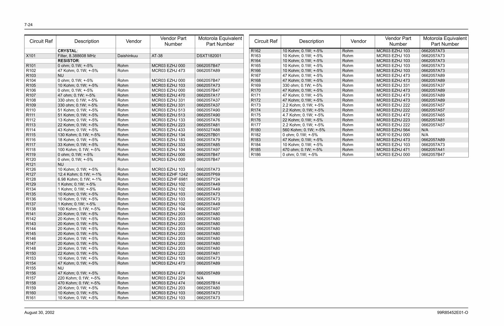
7-24
August 30, 2002 99R85452E01-O
CRYSTAL:X101 Filter, 8.388608 MHz Daishinkuu AT-38 DSXT182001
RESISTOR:R101 0 ohm; 0.1W; +-5% Rohm MCR03 EZHJ 000 0662057B47R102 47 Kohm; 0.1W; +-5% Rohm MCR03 EZHJ 473 0662057A89R103 NUR104 0 ohm; 0.1W; +-5% Rohm MCR03 EZHJ 000 0662057B47R105 10 Kohm; 0.1W; +-5% Rohm MCR03 EZHJ 103 0662057A73R106 0 ohm; 0.1W; +-5% Rohm MCR03 EZHJ 000 0662057B47R107 47 ohm; 0.1W; +-5% Rohm MCR03 EZHJ 470 0662057A17R108 330 ohm; 0.1W; +-5% Rohm MCR03 EZHJ 331 0662057A37R109 330 ohm; 0.1W; +-5% Rohm MCR03 EZHJ 331 0662057A37R110 51 Kohm; 0.1W; +-5% Rohm MCR03 EZHJ 513 0662057A90R111 51 Kohm; 0.1W; +-5% Rohm MCR03 EZHJ 513 0662057A90R112 13 Kohm; 0.1W; +-5% Rohm MCR03 EZHJ 133 0662057A76R113 22 Kohm; 0.1W; +-5% Rohm MCR03 EZHJ 223 0662057A81R114 43 Kohm; 0.1W; +-5% Rohm MCR03 EZHJ 433 0665027A88R115 130 Kohm; 0.1W; +-5% Rohm MCR03 EZHJ 134 0662257B01R116 18 Kohm; 0.1W; +-5% Rohm MCR03 EZHJ 183 0662057A79R117 33 Kohm; 0.1W; +-5% Rohm MCR03 EZHJ 333 0662057A85R118 100 Kohm; 0.1W; +-5% Rohm MCR03 EZHJ 104 0662057A97R119 0 ohm; 0.1W; +-5% Rohm MCR03 EZHJ 000 0662057B47R120 0 ohm; 0.1W; +-5% Rohm MCR03 EZHJ 000 0662057B47R121 NUR126 10 Kohm; 0.1W; +-5% Rohm MCR03 EZHJ 103 0662057A73R127 12.4 Kohm; 0.1W; +-1% Rohm MCR03 EZHF 1242 0662057P69R128 6.98 Kohm; 0.1W; +-1% Rohm MCR03 EZHF 6981 0662057Y24R129 1 Kohm; 0.1W; +-5% Rohm MCR03 EZHJ 102 0662057A49R134 1 Kohm; 0.1W; +-5% Rohm MCR03 EZHJ 102 0662057A49R135 10 Kohm; 0.1W; +-5% Rohm MCR03 EZHJ 103 0662057A73R136 10 Kohm; 0.1W; +-5% Rohm MCR03 EZHJ 103 0662057A73R137 1 Kohm; 0.1W; +-5% Rohm MCR03 EZHJ 102 0662057A49R138 100 Kohm; 0.1W; +-5% Rohm MCR03 EZHJ 104 0662057A97R141 20 Kohm; 0.1W; +-5% Rohm MCR03 EZHJ 203 0662057A80R142 20 Kohm; 0.1W; +-5% Rohm MCR03 EZHJ 203 0662057A80R143 20 Kohm; 0.1W; +-5% Rohm MCR03 EZHJ 203 0662057A80R144 20 Kohm; 0.1W; +-5% Rohm MCR03 EZHJ 203 0662057A80R145 20 Kohm; 0.1W; +-5% Rohm MCR03 EZHJ 203 0662057A80R146 20 Kohm; 0.1W; +-5% Rohm MCR03 EZHJ 203 0662057A80R147 20 Kohm; 0.1W; +-5% Rohm MCR03 EZHJ 203 0662057A80R148 20 Kohm; 0.1W; +-5% Rohm MCR03 EZHJ 203 0662057A80R150 22 Kohm; 0.1W; +-5% Rohm MCR03 EZHJ 223 0662057A81R153 10 Kohm; 0.1W; +-5% Rohm MCR03 EZHJ 103 0662057A73R154 47 Kohm; 0.1W; +-5% Rohm MCR03 EZHJ 473 0662057A89R155 NUR156 47 Kohm; 0.1W; +-5% Rohm MCR03 EZHJ 473 0662057A89R157 220 Kohm; 0.1W; +-5% Rohm MCR03 EZHJ 224 N/AR158 470 Kohm; 0.1W; +-5% Rohm MCR03 EZHJ 474 0662057B14R159 20 Kohm; 0.1W; +-5% Rohm MCR03 EZHJ 203 0662057A80R160 10 Kohm; 0.1W; +-5% Rohm MCR03 EZHJ 103 0662057A73R161 10 Kohm; 0.1W; +-5% Rohm MCR03 EZHJ 103 0662057A73
Circuit Ref Description Vendor Vendor Part Number
Motorola Equivalent Part Number
R162 10 Kohm; 0.1W; +-5% Rohm MCR03 EZHJ 103 0662057A73R163 10 Kohm; 0.1W; +-5% Rohm MCR03 EZHJ 103 0662057A73R164 10 Kohm; 0.1W; +-5% Rohm MCR03 EZHJ 103 0662057A73R165 10 Kohm; 0.1W; +-5% Rohm MCR03 EZHJ 103 0662057A73R166 10 Kohm; 0.1W; +-5% Rohm MCR03 EZHJ 103 0662057A73R167 47 Kohm; 0.1W; +-5% Rohm MCR03 EZHJ 473 0662057A89R168 47 Kohm; 0.1W; +-5% Rohm MCR03 EZHJ 473 0662057A89R169 330 ohm; 0.1W; +-5% Rohm MCR03 EZHJ 331 0662057A37R170 47 Kohm; 0.1W; +-5% Rohm MCR03 EZHJ 473 0662057A89R171 47 Kohm; 0.1W; +-5% Rohm MCR03 EZHJ 473 0662057A89R172 47 Kohm; 0.1W; +-5% Rohm MCR03 EZHJ 473 0662057A89R173 2.2 Kohm; 0.1W; +-5% Rohm MCR03 EZHJ 222 0662057A57R174 2.2 Kohm; 0.1W; +-5% Rohm MCR03 EZHJ 222 0662057A57R175 4.7 Kohm; 0.1W; +-5% Rohm MCR03 EZHJ 472 0662057A65R176 22 Kohm; 0.1W; +-5% Rohm MCR03 EZHJ 223 0662057A81R177 2.2 Kohm; 0.1W; +-5% Rohm MCR03 EZHJ 222 0662057A57R180 560 Kohm; 0.1W; +-5% Rohm MCR03 EZHJ 564 N/AR182 0 ohm; 0.1W; +-5% Rohm MCR10 EZHJ 000 N/AR183 47 Kohm; 0.1W; +-5% Rohm MCR03 EZHJ 473 0662057A89R184 10 Kohm; 0.1W; +-5% Rohm MCR03 EZHJ 103 0662057A73R185 470 ohm; 0.1W; +-5% Rohm MCR03 EZHJ 471 0662057A41R186 0 ohm; 0.1W; +-5% Rohm MCR03 EZHJ 000 0662057B47
Circuit Ref Description Vendor Vendor Part Number
Motorola Equivalent Part Number
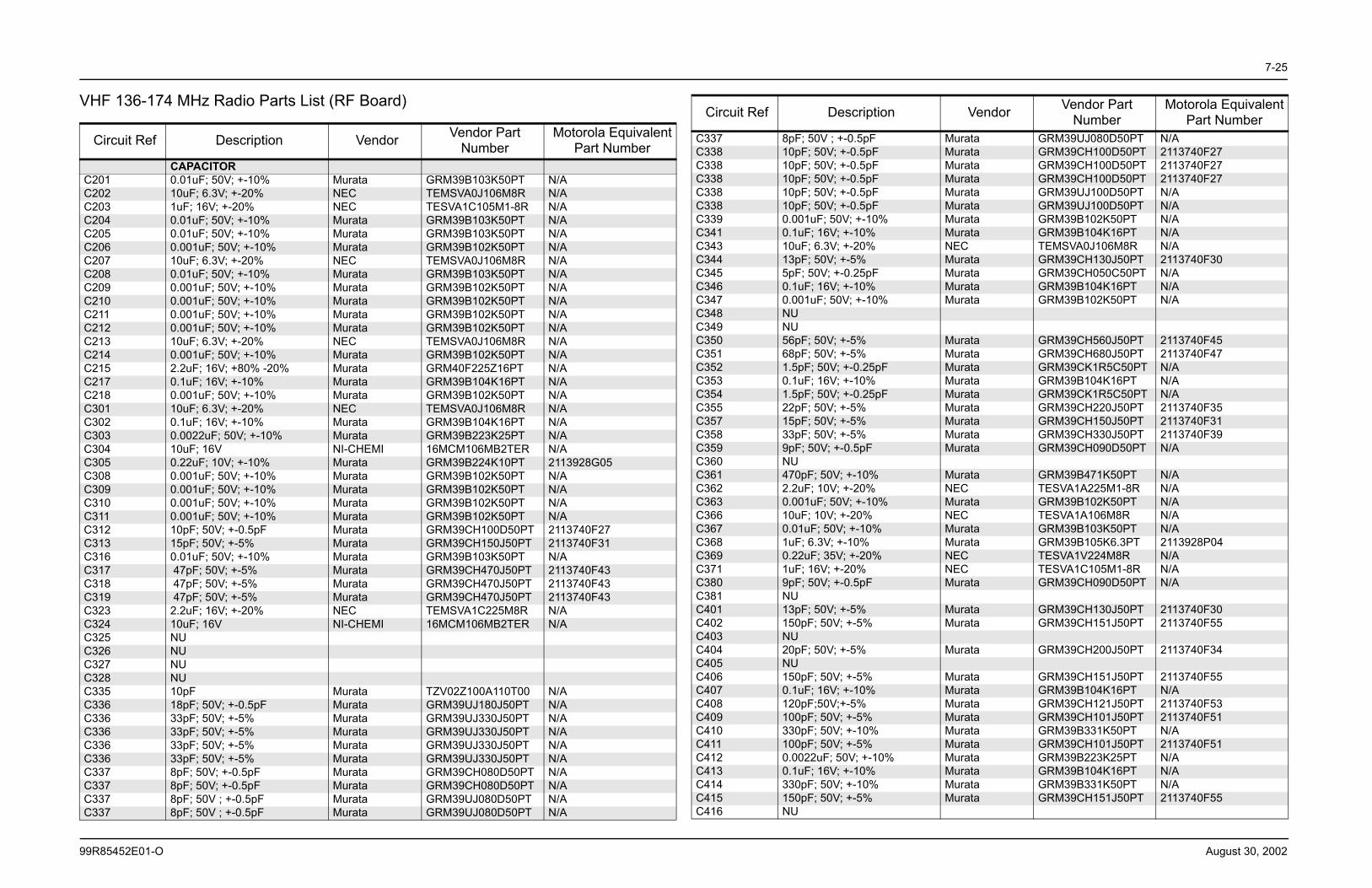
7-25
99R85452E01-O August 30, 2002
VHF 136-174 MHz Radio Parts List (RF Board)
Circuit Ref Description Vendor Vendor Part Number
Motorola Equivalent Part Number
CAPACITORC201 0.01uF; 50V; +-10% Murata GRM39B103K50PT N/AC202 10uF; 6.3V; +-20% NEC TEMSVA0J106M8R N/AC203 1uF; 16V; +-20% NEC TESVA1C105M1-8R N/AC204 0.01uF; 50V; +-10% Murata GRM39B103K50PT N/AC205 0.01uF; 50V; +-10% Murata GRM39B103K50PT N/AC206 0.001uF; 50V; +-10% Murata GRM39B102K50PT N/AC207 10uF; 6.3V; +-20% NEC TEMSVA0J106M8R N/AC208 0.01uF; 50V; +-10% Murata GRM39B103K50PT N/AC209 0.001uF; 50V; +-10% Murata GRM39B102K50PT N/AC210 0.001uF; 50V; +-10% Murata GRM39B102K50PT N/AC211 0.001uF; 50V; +-10% Murata GRM39B102K50PT N/AC212 0.001uF; 50V; +-10% Murata GRM39B102K50PT N/AC213 10uF; 6.3V; +-20% NEC TEMSVA0J106M8R N/AC214 0.001uF; 50V; +-10% Murata GRM39B102K50PT N/AC215 2.2uF; 16V; +80% -20% Murata GRM40F225Z16PT N/AC217 0.1uF; 16V; +-10% Murata GRM39B104K16PT N/AC218 0.001uF; 50V; +-10% Murata GRM39B102K50PT N/AC301 10uF; 6.3V; +-20% NEC TEMSVA0J106M8R N/AC302 0.1uF; 16V; +-10% Murata GRM39B104K16PT N/AC303 0.0022uF; 50V; +-10% Murata GRM39B223K25PT N/AC304 10uF; 16V NI-CHEMI 16MCM106MB2TER N/AC305 0.22uF; 10V; +-10% Murata GRM39B224K10PT 2113928G05C308 0.001uF; 50V; +-10% Murata GRM39B102K50PT N/AC309 0.001uF; 50V; +-10% Murata GRM39B102K50PT N/AC310 0.001uF; 50V; +-10% Murata GRM39B102K50PT N/AC311 0.001uF; 50V; +-10% Murata GRM39B102K50PT N/AC312 10pF; 50V; +-0.5pF Murata GRM39CH100D50PT 2113740F27C313 15pF; 50V; +-5% Murata GRM39CH150J50PT 2113740F31C316 0.01uF; 50V; +-10% Murata GRM39B103K50PT N/AC317 47pF; 50V; +-5% Murata GRM39CH470J50PT 2113740F43C318 47pF; 50V; +-5% Murata GRM39CH470J50PT 2113740F43C319 47pF; 50V; +-5% Murata GRM39CH470J50PT 2113740F43C323 2.2uF; 16V; +-20% NEC TEMSVA1C225M8R N/AC324 10uF; 16V NI-CHEMI 16MCM106MB2TER N/AC325 NUC326 NUC327 NUC328 NUC335 10pF Murata TZV02Z100A110T00 N/AC336 18pF; 50V; +-0.5pF Murata GRM39UJ180J50PT N/AC336 33pF; 50V; +-5% Murata GRM39UJ330J50PT N/AC336 33pF; 50V; +-5% Murata GRM39UJ330J50PT N/AC336 33pF; 50V; +-5% Murata GRM39UJ330J50PT N/AC336 33pF; 50V; +-5% Murata GRM39UJ330J50PT N/AC337 8pF; 50V; +-0.5pF Murata GRM39CH080D50PT N/AC337 8pF; 50V; +-0.5pF Murata GRM39CH080D50PT N/AC337 8pF; 50V ; +-0.5pF Murata GRM39UJ080D50PT N/AC337 8pF; 50V ; +-0.5pF Murata GRM39UJ080D50PT N/A
C337 8pF; 50V ; +-0.5pF Murata GRM39UJ080D50PT N/AC338 10pF; 50V; +-0.5pF Murata GRM39CH100D50PT 2113740F27C338 10pF; 50V; +-0.5pF Murata GRM39CH100D50PT 2113740F27C338 10pF; 50V; +-0.5pF Murata GRM39CH100D50PT 2113740F27C338 10pF; 50V; +-0.5pF Murata GRM39UJ100D50PT N/AC338 10pF; 50V; +-0.5pF Murata GRM39UJ100D50PT N/AC339 0.001uF; 50V; +-10% Murata GRM39B102K50PT N/AC341 0.1uF; 16V; +-10% Murata GRM39B104K16PT N/AC343 10uF; 6.3V; +-20% NEC TEMSVA0J106M8R N/AC344 13pF; 50V; +-5% Murata GRM39CH130J50PT 2113740F30C345 5pF; 50V; +-0.25pF Murata GRM39CH050C50PT N/AC346 0.1uF; 16V; +-10% Murata GRM39B104K16PT N/AC347 0.001uF; 50V; +-10% Murata GRM39B102K50PT N/AC348 NUC349 NUC350 56pF; 50V; +-5% Murata GRM39CH560J50PT 2113740F45C351 68pF; 50V; +-5% Murata GRM39CH680J50PT 2113740F47C352 1.5pF; 50V; +-0.25pF Murata GRM39CK1R5C50PT N/AC353 0.1uF; 16V; +-10% Murata GRM39B104K16PT N/AC354 1.5pF; 50V; +-0.25pF Murata GRM39CK1R5C50PT N/AC355 22pF; 50V; +-5% Murata GRM39CH220J50PT 2113740F35C357 15pF; 50V; +-5% Murata GRM39CH150J50PT 2113740F31C358 33pF; 50V; +-5% Murata GRM39CH330J50PT 2113740F39C359 9pF; 50V; +-0.5pF Murata GRM39CH090D50PT N/AC360 NUC361 470pF; 50V; +-10% Murata GRM39B471K50PT N/AC362 2.2uF; 10V; +-20% NEC TESVA1A225M1-8R N/AC363 0.001uF; 50V; +-10% Murata GRM39B102K50PT N/AC366 10uF; 10V; +-20% NEC TESVA1A106M8R N/AC367 0.01uF; 50V; +-10% Murata GRM39B103K50PT N/AC368 1uF; 6.3V; +-10% Murata GRM39B105K6.3PT 2113928P04C369 0.22uF; 35V; +-20% NEC TESVA1V224M8R N/AC371 1uF; 16V; +-20% NEC TESVA1C105M1-8R N/AC380 9pF; 50V; +-0.5pF Murata GRM39CH090D50PT N/AC381 NUC401 13pF; 50V; +-5% Murata GRM39CH130J50PT 2113740F30C402 150pF; 50V; +-5% Murata GRM39CH151J50PT 2113740F55C403 NUC404 20pF; 50V; +-5% Murata GRM39CH200J50PT 2113740F34C405 NUC406 150pF; 50V; +-5% Murata GRM39CH151J50PT 2113740F55C407 0.1uF; 16V; +-10% Murata GRM39B104K16PT N/AC408 120pF;50V;+-5% Murata GRM39CH121J50PT 2113740F53C409 100pF; 50V; +-5% Murata GRM39CH101J50PT 2113740F51C410 330pF; 50V; +-10% Murata GRM39B331K50PT N/AC411 100pF; 50V; +-5% Murata GRM39CH101J50PT 2113740F51C412 0.0022uF; 50V; +-10% Murata GRM39B223K25PT N/AC413 0.1uF; 16V; +-10% Murata GRM39B104K16PT N/AC414 330pF; 50V; +-10% Murata GRM39B331K50PT N/AC415 150pF; 50V; +-5% Murata GRM39CH151J50PT 2113740F55C416 NU
Circuit Ref Description Vendor Vendor Part Number
Motorola Equivalent Part Number
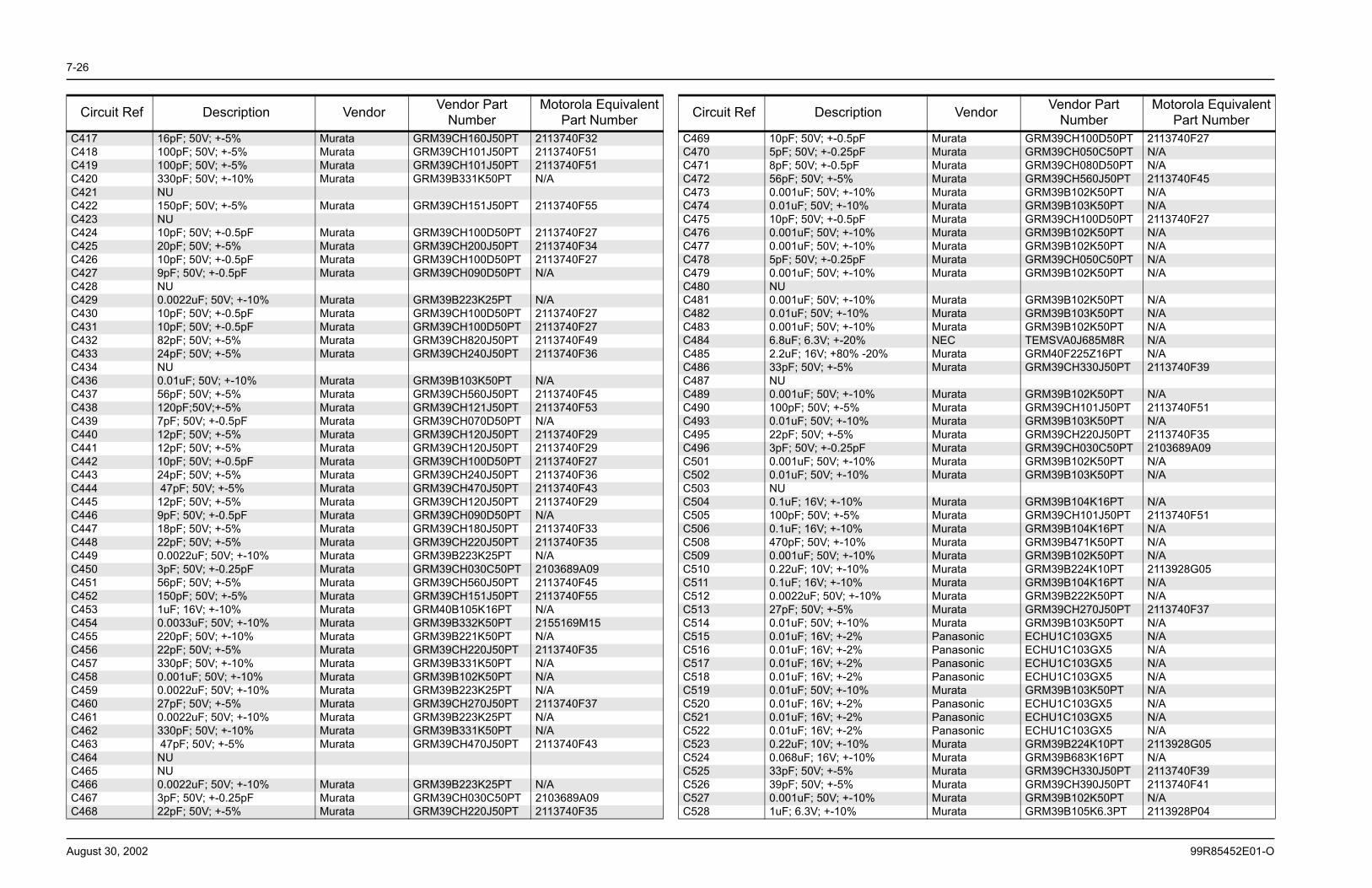
7-26
August 30, 2002 99R85452E01-O
C417 16pF; 50V; +-5% Murata GRM39CH160J50PT 2113740F32C418 100pF; 50V; +-5% Murata GRM39CH101J50PT 2113740F51C419 100pF; 50V; +-5% Murata GRM39CH101J50PT 2113740F51C420 330pF; 50V; +-10% Murata GRM39B331K50PT N/AC421 NUC422 150pF; 50V; +-5% Murata GRM39CH151J50PT 2113740F55C423 NUC424 10pF; 50V; +-0.5pF Murata GRM39CH100D50PT 2113740F27C425 20pF; 50V; +-5% Murata GRM39CH200J50PT 2113740F34C426 10pF; 50V; +-0.5pF Murata GRM39CH100D50PT 2113740F27C427 9pF; 50V; +-0.5pF Murata GRM39CH090D50PT N/AC428 NUC429 0.0022uF; 50V; +-10% Murata GRM39B223K25PT N/AC430 10pF; 50V; +-0.5pF Murata GRM39CH100D50PT 2113740F27C431 10pF; 50V; +-0.5pF Murata GRM39CH100D50PT 2113740F27C432 82pF; 50V; +-5% Murata GRM39CH820J50PT 2113740F49C433 24pF; 50V; +-5% Murata GRM39CH240J50PT 2113740F36C434 NUC436 0.01uF; 50V; +-10% Murata GRM39B103K50PT N/AC437 56pF; 50V; +-5% Murata GRM39CH560J50PT 2113740F45C438 120pF;50V;+-5% Murata GRM39CH121J50PT 2113740F53C439 7pF; 50V; +-0.5pF Murata GRM39CH070D50PT N/AC440 12pF; 50V; +-5% Murata GRM39CH120J50PT 2113740F29C441 12pF; 50V; +-5% Murata GRM39CH120J50PT 2113740F29C442 10pF; 50V; +-0.5pF Murata GRM39CH100D50PT 2113740F27C443 24pF; 50V; +-5% Murata GRM39CH240J50PT 2113740F36C444 47pF; 50V; +-5% Murata GRM39CH470J50PT 2113740F43C445 12pF; 50V; +-5% Murata GRM39CH120J50PT 2113740F29C446 9pF; 50V; +-0.5pF Murata GRM39CH090D50PT N/AC447 18pF; 50V; +-5% Murata GRM39CH180J50PT 2113740F33C448 22pF; 50V; +-5% Murata GRM39CH220J50PT 2113740F35C449 0.0022uF; 50V; +-10% Murata GRM39B223K25PT N/AC450 3pF; 50V; +-0.25pF Murata GRM39CH030C50PT 2103689A09C451 56pF; 50V; +-5% Murata GRM39CH560J50PT 2113740F45C452 150pF; 50V; +-5% Murata GRM39CH151J50PT 2113740F55C453 1uF; 16V; +-10% Murata GRM40B105K16PT N/AC454 0.0033uF; 50V; +-10% Murata GRM39B332K50PT 2155169M15C455 220pF; 50V; +-10% Murata GRM39B221K50PT N/AC456 22pF; 50V; +-5% Murata GRM39CH220J50PT 2113740F35C457 330pF; 50V; +-10% Murata GRM39B331K50PT N/AC458 0.001uF; 50V; +-10% Murata GRM39B102K50PT N/AC459 0.0022uF; 50V; +-10% Murata GRM39B223K25PT N/AC460 27pF; 50V; +-5% Murata GRM39CH270J50PT 2113740F37C461 0.0022uF; 50V; +-10% Murata GRM39B223K25PT N/AC462 330pF; 50V; +-10% Murata GRM39B331K50PT N/AC463 47pF; 50V; +-5% Murata GRM39CH470J50PT 2113740F43C464 NUC465 NUC466 0.0022uF; 50V; +-10% Murata GRM39B223K25PT N/AC467 3pF; 50V; +-0.25pF Murata GRM39CH030C50PT 2103689A09C468 22pF; 50V; +-5% Murata GRM39CH220J50PT 2113740F35
Circuit Ref Description Vendor Vendor Part Number
Motorola Equivalent Part Number
C469 10pF; 50V; +-0.5pF Murata GRM39CH100D50PT 2113740F27C470 5pF; 50V; +-0.25pF Murata GRM39CH050C50PT N/AC471 8pF; 50V; +-0.5pF Murata GRM39CH080D50PT N/AC472 56pF; 50V; +-5% Murata GRM39CH560J50PT 2113740F45C473 0.001uF; 50V; +-10% Murata GRM39B102K50PT N/AC474 0.01uF; 50V; +-10% Murata GRM39B103K50PT N/AC475 10pF; 50V; +-0.5pF Murata GRM39CH100D50PT 2113740F27C476 0.001uF; 50V; +-10% Murata GRM39B102K50PT N/AC477 0.001uF; 50V; +-10% Murata GRM39B102K50PT N/AC478 5pF; 50V; +-0.25pF Murata GRM39CH050C50PT N/AC479 0.001uF; 50V; +-10% Murata GRM39B102K50PT N/AC480 NUC481 0.001uF; 50V; +-10% Murata GRM39B102K50PT N/AC482 0.01uF; 50V; +-10% Murata GRM39B103K50PT N/AC483 0.001uF; 50V; +-10% Murata GRM39B102K50PT N/AC484 6.8uF; 6.3V; +-20% NEC TEMSVA0J685M8R N/AC485 2.2uF; 16V; +80% -20% Murata GRM40F225Z16PT N/AC486 33pF; 50V; +-5% Murata GRM39CH330J50PT 2113740F39C487 NUC489 0.001uF; 50V; +-10% Murata GRM39B102K50PT N/AC490 100pF; 50V; +-5% Murata GRM39CH101J50PT 2113740F51C493 0.01uF; 50V; +-10% Murata GRM39B103K50PT N/AC495 22pF; 50V; +-5% Murata GRM39CH220J50PT 2113740F35C496 3pF; 50V; +-0.25pF Murata GRM39CH030C50PT 2103689A09C501 0.001uF; 50V; +-10% Murata GRM39B102K50PT N/AC502 0.01uF; 50V; +-10% Murata GRM39B103K50PT N/AC503 NUC504 0.1uF; 16V; +-10% Murata GRM39B104K16PT N/AC505 100pF; 50V; +-5% Murata GRM39CH101J50PT 2113740F51C506 0.1uF; 16V; +-10% Murata GRM39B104K16PT N/AC508 470pF; 50V; +-10% Murata GRM39B471K50PT N/AC509 0.001uF; 50V; +-10% Murata GRM39B102K50PT N/AC510 0.22uF; 10V; +-10% Murata GRM39B224K10PT 2113928G05C511 0.1uF; 16V; +-10% Murata GRM39B104K16PT N/AC512 0.0022uF; 50V; +-10% Murata GRM39B222K50PT N/AC513 27pF; 50V; +-5% Murata GRM39CH270J50PT 2113740F37C514 0.01uF; 50V; +-10% Murata GRM39B103K50PT N/AC515 0.01uF; 16V; +-2% Panasonic ECHU1C103GX5 N/AC516 0.01uF; 16V; +-2% Panasonic ECHU1C103GX5 N/AC517 0.01uF; 16V; +-2% Panasonic ECHU1C103GX5 N/AC518 0.01uF; 16V; +-2% Panasonic ECHU1C103GX5 N/AC519 0.01uF; 50V; +-10% Murata GRM39B103K50PT N/AC520 0.01uF; 16V; +-2% Panasonic ECHU1C103GX5 N/AC521 0.01uF; 16V; +-2% Panasonic ECHU1C103GX5 N/AC522 0.01uF; 16V; +-2% Panasonic ECHU1C103GX5 N/AC523 0.22uF; 10V; +-10% Murata GRM39B224K10PT 2113928G05C524 0.068uF; 16V; +-10% Murata GRM39B683K16PT N/AC525 33pF; 50V; +-5% Murata GRM39CH330J50PT 2113740F39C526 39pF; 50V; +-5% Murata GRM39CH390J50PT 2113740F41C527 0.001uF; 50V; +-10% Murata GRM39B102K50PT N/AC528 1uF; 6.3V; +-10% Murata GRM39B105K6.3PT 2113928P04
Circuit Ref Description Vendor Vendor Part Number
Motorola Equivalent Part Number
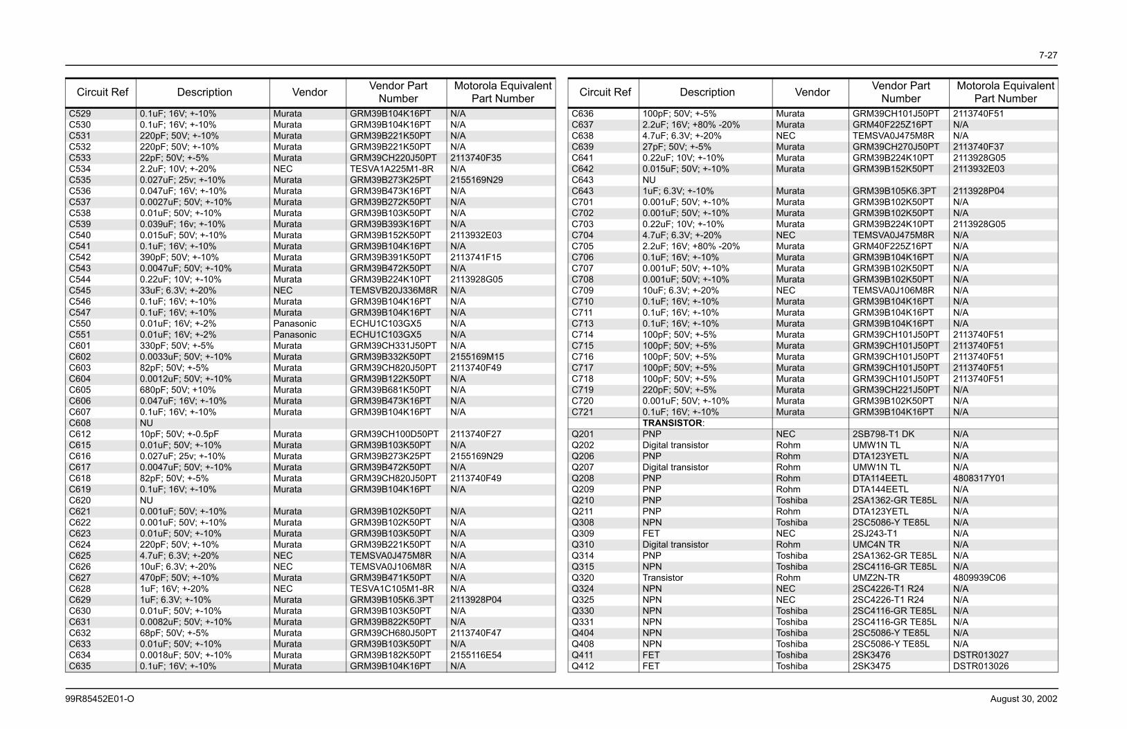
7-27
99R85452E01-O August 30, 2002
C529 0.1uF; 16V; +-10% Murata GRM39B104K16PT N/AC530 0.1uF; 16V; +-10% Murata GRM39B104K16PT N/AC531 220pF; 50V; +-10% Murata GRM39B221K50PT N/AC532 220pF; 50V; +-10% Murata GRM39B221K50PT N/AC533 22pF; 50V; +-5% Murata GRM39CH220J50PT 2113740F35C534 2.2uF; 10V; +-20% NEC TESVA1A225M1-8R N/AC535 0.027uF; 25v; +-10% Murata GRM39B273K25PT 2155169N29C536 0.047uF; 16V; +-10% Murata GRM39B473K16PT N/AC537 0.0027uF; 50V; +-10% Murata GRM39B272K50PT N/AC538 0.01uF; 50V; +-10% Murata GRM39B103K50PT N/AC539 0.039uF; 16v; +-10% Murata GRM39B393K16PT N/AC540 0.015uF; 50V; +-10% Murata GRM39B152K50PT 2113932E03C541 0.1uF; 16V; +-10% Murata GRM39B104K16PT N/AC542 390pF; 50V; +-10% Murata GRM39B391K50PT 2113741F15C543 0.0047uF; 50V; +-10% Murata GRM39B472K50PT N/AC544 0.22uF; 10V; +-10% Murata GRM39B224K10PT 2113928G05C545 33uF; 6.3V; +-20% NEC TEMSVB20J336M8R N/AC546 0.1uF; 16V; +-10% Murata GRM39B104K16PT N/AC547 0.1uF; 16V; +-10% Murata GRM39B104K16PT N/AC550 0.01uF; 16V; +-2% Panasonic ECHU1C103GX5 N/AC551 0.01uF; 16V; +-2% Panasonic ECHU1C103GX5 N/AC601 330pF; 50V; +-5% Murata GRM39CH331J50PT N/AC602 0.0033uF; 50V; +-10% Murata GRM39B332K50PT 2155169M15C603 82pF; 50V; +-5% Murata GRM39CH820J50PT 2113740F49C604 0.0012uF; 50V; +-10% Murata GRM39B122K50PT N/AC605 680pF; 50V; +10% Murata GRM39B681K50PT N/AC606 0.047uF; 16V; +-10% Murata GRM39B473K16PT N/AC607 0.1uF; 16V; +-10% Murata GRM39B104K16PT N/AC608 NUC612 10pF; 50V; +-0.5pF Murata GRM39CH100D50PT 2113740F27C615 0.01uF; 50V; +-10% Murata GRM39B103K50PT N/AC616 0.027uF; 25v; +-10% Murata GRM39B273K25PT 2155169N29C617 0.0047uF; 50V; +-10% Murata GRM39B472K50PT N/AC618 82pF; 50V; +-5% Murata GRM39CH820J50PT 2113740F49C619 0.1uF; 16V; +-10% Murata GRM39B104K16PT N/AC620 NUC621 0.001uF; 50V; +-10% Murata GRM39B102K50PT N/AC622 0.001uF; 50V; +-10% Murata GRM39B102K50PT N/AC623 0.01uF; 50V; +-10% Murata GRM39B103K50PT N/AC624 220pF; 50V; +-10% Murata GRM39B221K50PT N/AC625 4.7uF; 6.3V; +-20% NEC TEMSVA0J475M8R N/AC626 10uF; 6.3V; +-20% NEC TEMSVA0J106M8R N/AC627 470pF; 50V; +-10% Murata GRM39B471K50PT N/AC628 1uF; 16V; +-20% NEC TESVA1C105M1-8R N/AC629 1uF; 6.3V; +-10% Murata GRM39B105K6.3PT 2113928P04C630 0.01uF; 50V; +-10% Murata GRM39B103K50PT N/AC631 0.0082uF; 50V; +-10% Murata GRM39B822K50PT N/AC632 68pF; 50V; +-5% Murata GRM39CH680J50PT 2113740F47C633 0.01uF; 50V; +-10% Murata GRM39B103K50PT N/AC634 0.0018uF; 50V; +-10% Murata GRM39B182K50PT 2155116E54C635 0.1uF; 16V; +-10% Murata GRM39B104K16PT N/A
Circuit Ref Description Vendor Vendor Part Number
Motorola Equivalent Part Number
C636 100pF; 50V; +-5% Murata GRM39CH101J50PT 2113740F51C637 2.2uF; 16V; +80% -20% Murata GRM40F225Z16PT N/AC638 4.7uF; 6.3V; +-20% NEC TEMSVA0J475M8R N/AC639 27pF; 50V; +-5% Murata GRM39CH270J50PT 2113740F37C641 0.22uF; 10V; +-10% Murata GRM39B224K10PT 2113928G05C642 0.015uF; 50V; +-10% Murata GRM39B152K50PT 2113932E03C643 NUC643 1uF; 6.3V; +-10% Murata GRM39B105K6.3PT 2113928P04C701 0.001uF; 50V; +-10% Murata GRM39B102K50PT N/AC702 0.001uF; 50V; +-10% Murata GRM39B102K50PT N/AC703 0.22uF; 10V; +-10% Murata GRM39B224K10PT 2113928G05C704 4.7uF; 6.3V; +-20% NEC TEMSVA0J475M8R N/AC705 2.2uF; 16V; +80% -20% Murata GRM40F225Z16PT N/AC706 0.1uF; 16V; +-10% Murata GRM39B104K16PT N/AC707 0.001uF; 50V; +-10% Murata GRM39B102K50PT N/AC708 0.001uF; 50V; +-10% Murata GRM39B102K50PT N/AC709 10uF; 6.3V; +-20% NEC TEMSVA0J106M8R N/AC710 0.1uF; 16V; +-10% Murata GRM39B104K16PT N/AC711 0.1uF; 16V; +-10% Murata GRM39B104K16PT N/AC713 0.1uF; 16V; +-10% Murata GRM39B104K16PT N/AC714 100pF; 50V; +-5% Murata GRM39CH101J50PT 2113740F51C715 100pF; 50V; +-5% Murata GRM39CH101J50PT 2113740F51C716 100pF; 50V; +-5% Murata GRM39CH101J50PT 2113740F51C717 100pF; 50V; +-5% Murata GRM39CH101J50PT 2113740F51C718 100pF; 50V; +-5% Murata GRM39CH101J50PT 2113740F51C719 220pF; 50V; +-5% Murata GRM39CH221J50PT N/AC720 0.001uF; 50V; +-10% Murata GRM39B102K50PT N/AC721 0.1uF; 16V; +-10% Murata GRM39B104K16PT N/A
TRANSISTOR:Q201 PNP NEC 2SB798-T1 DK N/AQ202 Digital transistor Rohm UMW1N TL N/AQ206 PNP Rohm DTA123YETL N/AQ207 Digital transistor Rohm UMW1N TL N/AQ208 PNP Rohm DTA114EETL 4808317Y01Q209 PNP Rohm DTA144EETL N/AQ210 PNP Toshiba 2SA1362-GR TE85L N/AQ211 PNP Rohm DTA123YETL N/AQ308 NPN Toshiba 2SC5086-Y TE85L N/AQ309 FET NEC 2SJ243-T1 N/AQ310 Digital transistor Rohm UMC4N TR N/AQ314 PNP Toshiba 2SA1362-GR TE85L N/AQ315 NPN Toshiba 2SC4116-GR TE85L N/AQ320 Transistor Rohm UMZ2N-TR 4809939C06Q324 NPN NEC 2SC4226-T1 R24 N/AQ325 NPN NEC 2SC4226-T1 R24 N/AQ330 NPN Toshiba 2SC4116-GR TE85L N/AQ331 NPN Toshiba 2SC4116-GR TE85L N/AQ404 NPN Toshiba 2SC5086-Y TE85L N/AQ408 NPN Toshiba 2SC5086-Y TE85L N/AQ411 FET Toshiba 2SK3476 DSTR013027Q412 FET Toshiba 2SK3475 DSTR013026
Circuit Ref Description Vendor Vendor Part Number
Motorola Equivalent Part Number
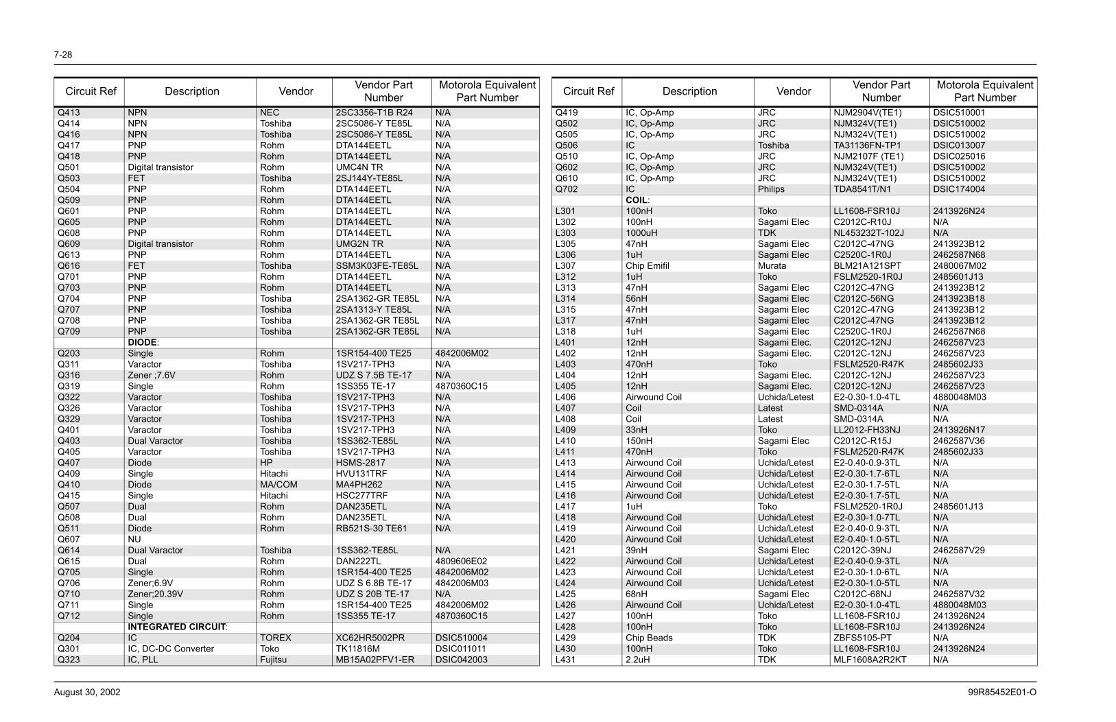
7-28
August 30, 2002 99R85452E01-O
Q413 NPN NEC 2SC3356-T1B R24 N/AQ414 NPN Toshiba 2SC5086-Y TE85L N/AQ416 NPN Toshiba 2SC5086-Y TE85L N/AQ417 PNP Rohm DTA144EETL N/AQ418 PNP Rohm DTA144EETL N/AQ501 Digital transistor Rohm UMC4N TR N/AQ503 FET Toshiba 2SJ144Y-TE85L N/AQ504 PNP Rohm DTA144EETL N/AQ509 PNP Rohm DTA144EETL N/AQ601 PNP Rohm DTA144EETL N/AQ605 PNP Rohm DTA144EETL N/AQ608 PNP Rohm DTA144EETL N/AQ609 Digital transistor Rohm UMG2N TR N/AQ613 PNP Rohm DTA144EETL N/AQ616 FET Toshiba SSM3K03FE-TE85L N/AQ701 PNP Rohm DTA144EETL N/AQ703 PNP Rohm DTA144EETL N/AQ704 PNP Toshiba 2SA1362-GR TE85L N/AQ707 PNP Toshiba 2SA1313-Y TE85L N/AQ708 PNP Toshiba 2SA1362-GR TE85L N/AQ709 PNP Toshiba 2SA1362-GR TE85L N/A
DIODE:Q203 Single Rohm 1SR154-400 TE25 4842006M02Q311 Varactor Toshiba 1SV217-TPH3 N/AQ316 Zener ;7.6V Rohm UDZ S 7.5B TE-17 N/AQ319 Single Rohm 1SS355 TE-17 4870360C15Q322 Varactor Toshiba 1SV217-TPH3 N/AQ326 Varactor Toshiba 1SV217-TPH3 N/AQ329 Varactor Toshiba 1SV217-TPH3 N/AQ401 Varactor Toshiba 1SV217-TPH3 N/AQ403 Dual Varactor Toshiba 1SS362-TE85L N/AQ405 Varactor Toshiba 1SV217-TPH3 N/AQ407 Diode HP HSMS-2817 N/AQ409 Single Hitachi HVU131TRF N/AQ410 Diode MA/COM MA4PH262 N/AQ415 Single Hitachi HSC277TRF N/AQ507 Dual Rohm DAN235ETL N/AQ508 Dual Rohm DAN235ETL N/AQ511 Diode Rohm RB521S-30 TE61 N/AQ607 NUQ614 Dual Varactor Toshiba 1SS362-TE85L N/AQ615 Dual Rohm DAN222TL 4809606E02Q705 Single Rohm 1SR154-400 TE25 4842006M02Q706 Zener;6.9V Rohm UDZ S 6.8B TE-17 4842006M03Q710 Zener;20.39V Rohm UDZ S 20B TE-17 N/AQ711 Single Rohm 1SR154-400 TE25 4842006M02Q712 Single Rohm 1SS355 TE-17 4870360C15
INTEGRATED CIRCUIT:Q204 IC TOREX XC62HR5002PR DSIC510004Q301 IC, DC-DC Converter Toko TK11816M DSIC011011Q323 IC, PLL Fujitsu MB15A02PFV1-ER DSIC042003
Circuit Ref Description Vendor Vendor Part Number
Motorola Equivalent Part Number
Q419 IC, Op-Amp JRC NJM2904V(TE1) DSIC510001Q502 IC, Op-Amp JRC NJM324V(TE1) DSIC510002Q505 IC, Op-Amp JRC NJM324V(TE1) DSIC510002Q506 IC Toshiba TA31136FN-TP1 DSIC013007Q510 IC, Op-Amp JRC NJM2107F (TE1) DSIC025016Q602 IC, Op-Amp JRC NJM324V(TE1) DSIC510002Q610 IC, Op-Amp JRC NJM324V(TE1) DSIC510002Q702 IC Philips TDA8541T/N1 DSIC174004
COIL:L301 100nH Toko LL1608-FSR10J 2413926N24L302 100nH Sagami Elec C2012C-R10J N/AL303 1000uH TDK NL453232T-102J N/AL305 47nH Sagami Elec C2012C-47NG 2413923B12L306 1uH Sagami Elec C2520C-1R0J 2462587N68L307 Chip Emifil Murata BLM21A121SPT 2480067M02L312 1uH Toko FSLM2520-1R0J 2485601J13L313 47nH Sagami Elec C2012C-47NG 2413923B12L314 56nH Sagami Elec C2012C-56NG 2413923B18L315 47nH Sagami Elec C2012C-47NG 2413923B12L317 47nH Sagami Elec C2012C-47NG 2413923B12L318 1uH Sagami Elec C2520C-1R0J 2462587N68L401 12nH Sagami Elec. C2012C-12NJ 2462587V23L402 12nH Sagami Elec. C2012C-12NJ 2462587V23L403 470nH Toko FSLM2520-R47K 2485602J33L404 12nH Sagami Elec. C2012C-12NJ 2462587V23L405 12nH Sagami Elec. C2012C-12NJ 2462587V23L406 Airwound Coil Uchida/Letest E2-0.30-1.0-4TL 4880048M03L407 Coil Latest SMD-0314A N/AL408 Coil Latest SMD-0314A N/AL409 33nH Toko LL2012-FH33NJ 2413926N17L410 150nH Sagami Elec C2012C-R15J 2462587V36L411 470nH Toko FSLM2520-R47K 2485602J33L413 Airwound Coil Uchida/Letest E2-0.40-0.9-3TL N/AL414 Airwound Coil Uchida/Letest E2-0.30-1.7-6TL N/AL415 Airwound Coil Uchida/Letest E2-0.30-1.7-5TL N/AL416 Airwound Coil Uchida/Letest E2-0.30-1.7-5TL N/AL417 1uH Toko FSLM2520-1R0J 2485601J13L418 Airwound Coil Uchida/Letest E2-0.30-1.0-7TL N/AL419 Airwound Coil Uchida/Letest E2-0.40-0.9-3TL N/AL420 Airwound Coil Uchida/Letest E2-0.40-1.0-5TL N/AL421 39nH Sagami Elec C2012C-39NJ 2462587V29L422 Airwound Coil Uchida/Letest E2-0.40-0.9-3TL N/AL423 Airwound Coil Uchida/Letest E2-0.30-1.0-6TL N/AL424 Airwound Coil Uchida/Letest E2-0.30-1.0-5TL N/AL425 68nH Sagami Elec C2012C-68NJ 2462587V32L426 Airwound Coil Uchida/Letest E2-0.30-1.0-4TL 4880048M03L427 100nH Toko LL1608-FSR10J 2413926N24L428 100nH Toko LL1608-FSR10J 2413926N24L429 Chip Beads TDK ZBFS5105-PT N/AL430 100nH Toko LL1608-FSR10J 2413926N24L431 2.2uH TDK MLF1608A2R2KT N/A
Circuit Ref Description Vendor Vendor Part Number
Motorola Equivalent Part Number
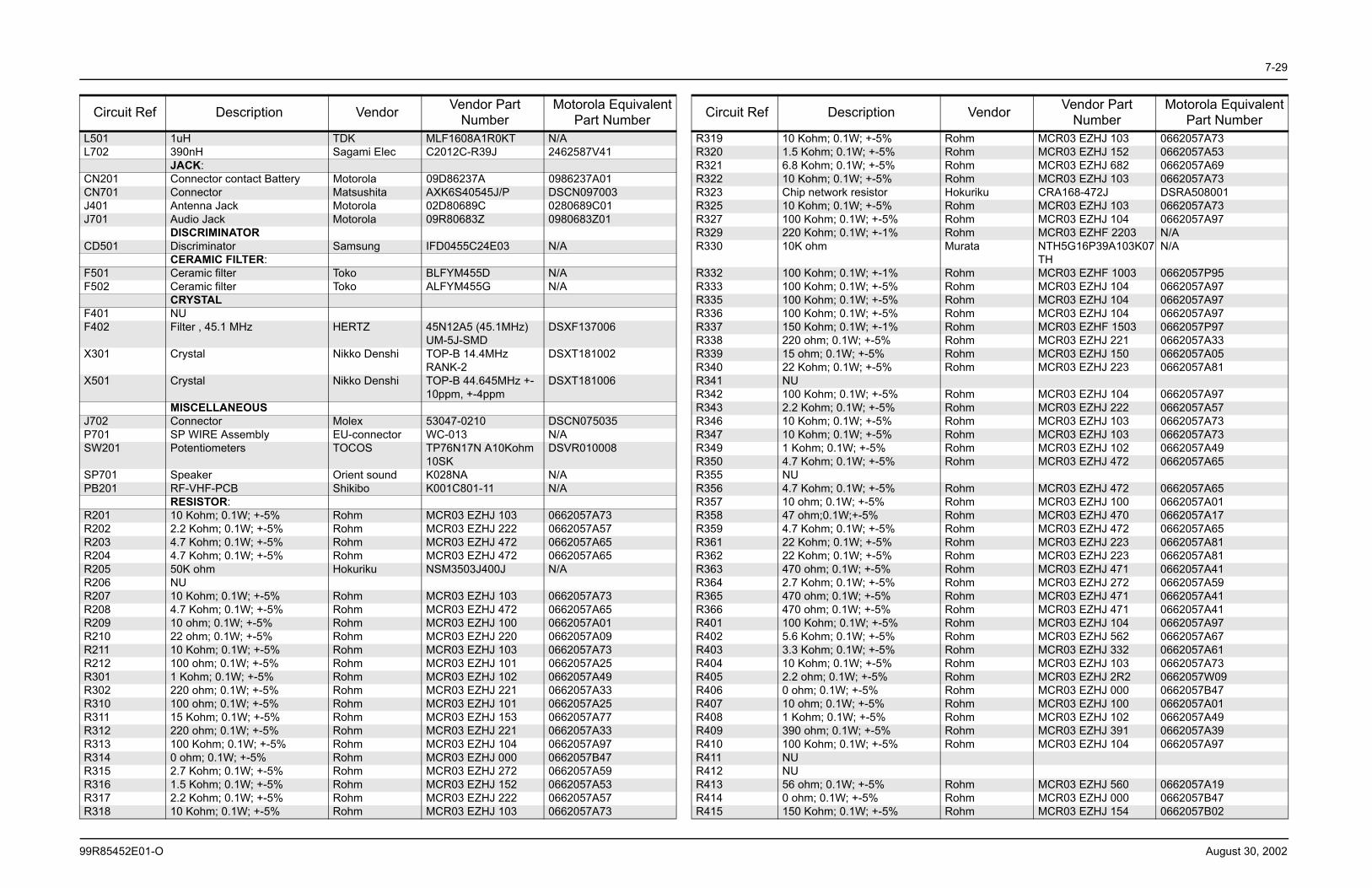
7-29
99R85452E01-O August 30, 2002
L501 1uH TDK MLF1608A1R0KT N/AL702 390nH Sagami Elec C2012C-R39J 2462587V41
JACK:CN201 Connector contact Battery Motorola 09D86237A 0986237A01CN701 Connector Matsushita AXK6S40545J/P DSCN097003J401 Antenna Jack Motorola 02D80689C 0280689C01J701 Audio Jack Motorola 09R80683Z 0980683Z01
DISCRIMINATORCD501 Discriminator Samsung IFD0455C24E03 N/A
CERAMIC FILTER:F501 Ceramic filter Toko BLFYM455D N/AF502 Ceramic filter Toko ALFYM455G N/A
CRYSTALF401 NUF402 Filter , 45.1 MHz HERTZ 45N12A5 (45.1MHz)
UM-5J-SMDDSXF137006
X301 Crystal Nikko Denshi TOP-B 14.4MHz RANK-2
DSXT181002
X501 Crystal Nikko Denshi TOP-B 44.645MHz +-10ppm, +-4ppm
DSXT181006
MISCELLANEOUSJ702 Connector Molex 53047-0210 DSCN075035P701 SP WIRE Assembly EU-connector WC-013 N/ASW201 Potentiometers TOCOS TP76N17N A10Kohm
10SKDSVR010008
SP701 Speaker Orient sound K028NA N/APB201 RF-VHF-PCB Shikibo K001C801-11 N/A
RESISTOR:R201 10 Kohm; 0.1W; +-5% Rohm MCR03 EZHJ 103 0662057A73R202 2.2 Kohm; 0.1W; +-5% Rohm MCR03 EZHJ 222 0662057A57R203 4.7 Kohm; 0.1W; +-5% Rohm MCR03 EZHJ 472 0662057A65R204 4.7 Kohm; 0.1W; +-5% Rohm MCR03 EZHJ 472 0662057A65R205 50K ohm Hokuriku NSM3503J400J N/AR206 NUR207 10 Kohm; 0.1W; +-5% Rohm MCR03 EZHJ 103 0662057A73R208 4.7 Kohm; 0.1W; +-5% Rohm MCR03 EZHJ 472 0662057A65R209 10 ohm; 0.1W; +-5% Rohm MCR03 EZHJ 100 0662057A01R210 22 ohm; 0.1W; +-5% Rohm MCR03 EZHJ 220 0662057A09R211 10 Kohm; 0.1W; +-5% Rohm MCR03 EZHJ 103 0662057A73R212 100 ohm; 0.1W; +-5% Rohm MCR03 EZHJ 101 0662057A25R301 1 Kohm; 0.1W; +-5% Rohm MCR03 EZHJ 102 0662057A49R302 220 ohm; 0.1W; +-5% Rohm MCR03 EZHJ 221 0662057A33R310 100 ohm; 0.1W; +-5% Rohm MCR03 EZHJ 101 0662057A25R311 15 Kohm; 0.1W; +-5% Rohm MCR03 EZHJ 153 0662057A77R312 220 ohm; 0.1W; +-5% Rohm MCR03 EZHJ 221 0662057A33R313 100 Kohm; 0.1W; +-5% Rohm MCR03 EZHJ 104 0662057A97R314 0 ohm; 0.1W; +-5% Rohm MCR03 EZHJ 000 0662057B47R315 2.7 Kohm; 0.1W; +-5% Rohm MCR03 EZHJ 272 0662057A59R316 1.5 Kohm; 0.1W; +-5% Rohm MCR03 EZHJ 152 0662057A53R317 2.2 Kohm; 0.1W; +-5% Rohm MCR03 EZHJ 222 0662057A57R318 10 Kohm; 0.1W; +-5% Rohm MCR03 EZHJ 103 0662057A73
Circuit Ref Description Vendor Vendor Part Number
Motorola Equivalent Part Number
R319 10 Kohm; 0.1W; +-5% Rohm MCR03 EZHJ 103 0662057A73R320 1.5 Kohm; 0.1W; +-5% Rohm MCR03 EZHJ 152 0662057A53R321 6.8 Kohm; 0.1W; +-5% Rohm MCR03 EZHJ 682 0662057A69R322 10 Kohm; 0.1W; +-5% Rohm MCR03 EZHJ 103 0662057A73R323 Chip network resistor Hokuriku CRA168-472J DSRA508001R325 10 Kohm; 0.1W; +-5% Rohm MCR03 EZHJ 103 0662057A73R327 100 Kohm; 0.1W; +-5% Rohm MCR03 EZHJ 104 0662057A97R329 220 Kohm; 0.1W; +-1% Rohm MCR03 EZHF 2203 N/AR330 10K ohm Murata NTH5G16P39A103K07
THN/A
R332 100 Kohm; 0.1W; +-1% Rohm MCR03 EZHF 1003 0662057P95R333 100 Kohm; 0.1W; +-5% Rohm MCR03 EZHJ 104 0662057A97R335 100 Kohm; 0.1W; +-5% Rohm MCR03 EZHJ 104 0662057A97R336 100 Kohm; 0.1W; +-5% Rohm MCR03 EZHJ 104 0662057A97R337 150 Kohm; 0.1W; +-1% Rohm MCR03 EZHF 1503 0662057P97R338 220 ohm; 0.1W; +-5% Rohm MCR03 EZHJ 221 0662057A33R339 15 ohm; 0.1W; +-5% Rohm MCR03 EZHJ 150 0662057A05R340 22 Kohm; 0.1W; +-5% Rohm MCR03 EZHJ 223 0662057A81R341 NUR342 100 Kohm; 0.1W; +-5% Rohm MCR03 EZHJ 104 0662057A97R343 2.2 Kohm; 0.1W; +-5% Rohm MCR03 EZHJ 222 0662057A57R346 10 Kohm; 0.1W; +-5% Rohm MCR03 EZHJ 103 0662057A73R347 10 Kohm; 0.1W; +-5% Rohm MCR03 EZHJ 103 0662057A73R349 1 Kohm; 0.1W; +-5% Rohm MCR03 EZHJ 102 0662057A49R350 4.7 Kohm; 0.1W; +-5% Rohm MCR03 EZHJ 472 0662057A65R355 NUR356 4.7 Kohm; 0.1W; +-5% Rohm MCR03 EZHJ 472 0662057A65R357 10 ohm; 0.1W; +-5% Rohm MCR03 EZHJ 100 0662057A01R358 47 ohm;0.1W;+-5% Rohm MCR03 EZHJ 470 0662057A17R359 4.7 Kohm; 0.1W; +-5% Rohm MCR03 EZHJ 472 0662057A65R361 22 Kohm; 0.1W; +-5% Rohm MCR03 EZHJ 223 0662057A81R362 22 Kohm; 0.1W; +-5% Rohm MCR03 EZHJ 223 0662057A81R363 470 ohm; 0.1W; +-5% Rohm MCR03 EZHJ 471 0662057A41R364 2.7 Kohm; 0.1W; +-5% Rohm MCR03 EZHJ 272 0662057A59R365 470 ohm; 0.1W; +-5% Rohm MCR03 EZHJ 471 0662057A41R366 470 ohm; 0.1W; +-5% Rohm MCR03 EZHJ 471 0662057A41R401 100 Kohm; 0.1W; +-5% Rohm MCR03 EZHJ 104 0662057A97R402 5.6 Kohm; 0.1W; +-5% Rohm MCR03 EZHJ 562 0662057A67R403 3.3 Kohm; 0.1W; +-5% Rohm MCR03 EZHJ 332 0662057A61R404 10 Kohm; 0.1W; +-5% Rohm MCR03 EZHJ 103 0662057A73R405 2.2 ohm; 0.1W; +-5% Rohm MCR03 EZHJ 2R2 0662057W09R406 0 ohm; 0.1W; +-5% Rohm MCR03 EZHJ 000 0662057B47R407 10 ohm; 0.1W; +-5% Rohm MCR03 EZHJ 100 0662057A01R408 1 Kohm; 0.1W; +-5% Rohm MCR03 EZHJ 102 0662057A49R409 390 ohm; 0.1W; +-5% Rohm MCR03 EZHJ 391 0662057A39R410 100 Kohm; 0.1W; +-5% Rohm MCR03 EZHJ 104 0662057A97R411 NUR412 NUR413 56 ohm; 0.1W; +-5% Rohm MCR03 EZHJ 560 0662057A19R414 0 ohm; 0.1W; +-5% Rohm MCR03 EZHJ 000 0662057B47R415 150 Kohm; 0.1W; +-5% Rohm MCR03 EZHJ 154 0662057B02
Circuit Ref Description Vendor Vendor Part Number
Motorola Equivalent Part Number
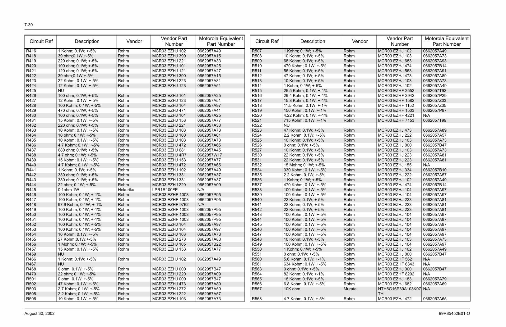
7-30
August 30, 2002 99R85452E01-O
R416 1 Kohm; 0.1W; +-5% Rohm MCR03 EZHJ 102 0662057A49R418 39 ohm;0.1W;+-5% Rohm MCR03 EZHJ 390 0662057A15R419 220 ohm; 0.1W; +-5% Rohm MCR03 EZHJ 221 0662057A33R420 100 ohm; 0.1W; +-5% Rohm MCR03 EZHJ 101 0662057A25R421 120 ohm; 0.1W; +-5% Rohm MCR03 EZHJ 121 0662057A27R422 39 ohm;0.1W;+-5% Rohm MCR03 EZHJ 390 0662057A15R423 22 Kohm; 0.1W; +-5% Rohm MCR03 EZHJ 223 0662057A81R424 12 Kohm; 0.1W; +-5% Rohm MCR03 EZHJ 123 0662057A51R425 NUR426 100 ohm; 0.1W; +-5% Rohm MCR03 EZHJ 101 0662057A25R427 12 Kohm; 0.1W; +-5% Rohm MCR03 EZHJ 123 0662057A51R428 100 Kohm; 0.1W; +-5% Rohm MCR03 EZHJ 104 0662057A97R429 470 ohm; 0.1W; +-5% Rohm MCR03 EZHJ 471 0662057A41R430 100 ohm; 0.1W; +-5% Rohm MCR03 EZHJ 101 0662057A25R431 15 Kohm; 0.1W; +-5% Rohm MCR03 EZHJ 153 0662057A77R432 220 ohm; 0.1W; +-5% Rohm MCR03 EZHJ 221 0662057A33R433 10 Kohm; 0.1W; +-5% Rohm MCR03 EZHJ 103 0662057A73R434 10 ohm; 0.1W; +-5% Rohm MCR03 EZHJ 100 0662057A01R435 10 Kohm; 0.1W; +-5% Rohm MCR03 EZHJ 103 0662057A73R436 4.7 Kohm; 0.1W; +-5% Rohm MCR03 EZHJ 472 0662057A65R437 680 ohm; 0.1W; +-5% Rohm MCR03 EZHJ 681 0662057A45R438 4.7 ohm; 0.1W; +-5% Rohm MCR03 EZHJ 4R7 0662057W17R439 15 Kohm; 0.1W; +-5% Rohm MCR03 EZHJ 153 0662057A77R440 4.7 Kohm; 0.1W; +-5% Rohm MCR03 EZHJ 472 0662057A65R441 1 Kohm; 0.1W; +-5% Rohm MCR03 EZHJ 102 0662057A49R442 330 ohm; 0.1W; +-5% Rohm MCR03 EZHJ 331 0662057A37R443 330 ohm; 0.1W; +-5% Rohm MCR03 EZHJ 331 0662057A37R444 22 ohm; 0.1W; +-5% Rohm MCR03 EZHJ 220 0662057A09R445 0.1ohm 1W Hokuriku LPR1R100FE N/AR446 100 Kohm; 0.1W; +-1% Rohm MCR03 EZHF 1003 0662057P95R447 100 Kohm; 0.1W; +-1% Rohm MCR03 EZHF 1003 0662057P95R448 97.6 Kohm; 0.1W; +-1% Rohm MCR03 EZHF 9762 N/AR449 100 Kohm; 0.1W; +-1% Rohm MCR03 EZHF 1003 0662057P95R450 100 Kohm; 0.1W; +-1% Rohm MCR03 EZHF 1003 0662057P95R451 100 Kohm; 0.1W; +-1% Rohm MCR03 EZHF 1003 0662057P95R452 100 Kohm; 0.1W; +-5% Rohm MCR03 EZHJ 104 0662057A97R453 100 Kohm; 0.1W; +-5% Rohm MCR03 EZHJ 104 0662057A97R454 10 Kohm; 0.1W; +-5% Rohm MCR03 EZHJ 103 0662057A73R455 27 Kohm;0.1W;+-5% Rohm MCR03 EZHJ 273 0662057A83R456 1 Mohm; 0.1W; +-5% Rohm MCR03 EZHJ 105 0662057B22R457 15 Kohm; 0.1W; +-5% Rohm MCR03 EZHJ 153 0662057A77R459 NUR466 1 Kohm; 0.1W; +-5% Rohm MCR03 EZHJ 102 0662057A49R467 NUR468 0 ohm; 0.1W; +-5% Rohm MCR03 EZHJ 000 0662057B47R470 22 ohm; 0.1W; +-5% Rohm MCR03 EZHJ 220 0662057A09R501 0 ohm; 0.1W; +-5% Rohm MCR03 EZHJ 000 0662057B47R502 47 Kohm; 0.1W; +-5% Rohm MCR03 EZHJ 473 0662057A89R503 2.7 Kohm; 0.1W; +-5% Rohm MCR03 EZHJ 272 0662057A59R505 2.2 Kohm; 0.1W; +-5% Rohm MCR03 EZHJ 222 0662057A57R506 10 Kohm; 0.1W; +-5% Rohm MCR03 EZHJ 103 0662057A73
Circuit Ref Description Vendor Vendor Part Number
Motorola Equivalent Part Number
R507 1 Kohm; 0.1W; +-5% Rohm MCR03 EZHJ 102 0662057A49R508 10 Kohm; 0.1W; +-5% Rohm MCR03 EZHJ 103 0662057A73R509 68 Kohm; 0.1W; +-5% Rohm MCR03 EZHJ 683 0662057A93R510 470 Kohm; 0.1W; +-5% Rohm MCR03 EZHJ 474 0662057B14R511 56 Kohm; 0.1W; +-5% Rohm MCR03 EZHJ 563 0662057A91R512 47 Kohm; 0.1W; +-5% Rohm MCR03 EZHJ 473 0662057A89R513 10 Kohm; 0.1W; +-5% Rohm MCR03 EZHJ 103 0662057A73R514 1 Kohm; 0.1W; +-5% Rohm MCR03 EZHJ 102 0662057A49R515 25.5 Kohm; 0.1W; +-1% Rohm MCR03 EZHF 2552 0662057T92R516 29.4 Kohm; 0.1W; +-1% Rohm MCR03 EZHF 2942 0662057P29R517 15.8 Kohm; 0.1W; +-1% Rohm MCR03 EZHF 1582 0662057Z03R518 11.5 Kohm; 0.1W; +-1% Rohm MCR03 EZHF 1152 0662057Z35R519 150 Kohm; 0.1W; +-1% Rohm MCR03 EZHF 1503 0662057P97R520 4.22 Kohm; 0.1W; +-1% Rohm MCR03 EZHF 4221 N/AR521 715 Kohm; 0.1W; +-1% Rohm MCR03 EZHF 7153 0662057T99R522 NUR523 47 Kohm; 0.1W; +-5% Rohm MCR03 EZHJ 473 0662057A89R524 2.2 Kohm; 0.1W; +-5% Rohm MCR03 EZHJ 222 0662057A57R525 10 Kohm; 0.1W; +-5% Rohm MCR03 EZHJ 103 0662057A73R526 0 ohm; 0.1W; +-5% Rohm MCR03 EZHJ 000 0662057B47R527 10 Kohm; 0.1W; +-5% Rohm MCR03 EZHJ 103 0662057A73R530 22 Kohm; 0.1W; +-5% Rohm MCR03 EZHJ 223 0662057A81R531 22 Kohm; 0.1W; +-5% Rohm MCR03 EZHJ 223 0662057A81R532 15 Mohm; 0.1W; +-5% Rohm MCR03 EZHJ 155 N/AR534 330 Kohm; 0.1W; +-5% Rohm MCR03 EZHJ 334 0662057B10R535 2.2 Kohm; 0.1W; +-5% Rohm MCR03 EZHJ 222 0662057A57R536 1 Kohm; 0.1W; +-5% Rohm MCR03 EZHJ 102 0662057A49R537 470 Kohm; 0.1W; +-5% Rohm MCR03 EZHJ 474 0662057B14R538 100 Kohm; 0.1W; +-5% Rohm MCR03 EZHJ 104 0662057A97R539 100 Kohm; 0.1W; +-5% Rohm MCR03 EZHJ 104 0662057A97R540 22 Kohm; 0.1W; +-5% Rohm MCR03 EZHJ 223 0662057A81R541 22 Kohm; 0.1W; +-5% Rohm MCR03 EZHJ 223 0662057A81R542 22 Kohm; 0.1W; +-5% Rohm MCR03 EZHJ 223 0662057A81R543 100 Kohm; 0.1W; +-5% Rohm MCR03 EZHJ 104 0662057A97R544 100 Kohm; 0.1W; +-5% Rohm MCR03 EZHJ 104 0662057A97R545 100 Kohm; 0.1W; +-5% Rohm MCR03 EZHJ 104 0662057A97R546 100 Kohm; 0.1W; +-5% Rohm MCR03 EZHJ 104 0662057A97R547 100 Kohm; 0.1W; +-5% Rohm MCR03 EZHJ 104 0662057A97R548 10 Kohm; 0.1W; +-5% Rohm MCR03 EZHJ 103 0662057A73R549 100 Kohm; 0.1W; +-5% Rohm MCR03 EZHJ 104 0662057A97R550 1 Kohm; 0.1W; +-5% Rohm MCR03 EZHJ 102 0662057A49R551 0 ohm; 0.1W; +-5% Rohm MCR03 EZHJ 000 0662057B47R560 5.6 Kohm; 0.1W; +-1% Rohm MCR03 EZHF 562 N/AR561 634 Kohm; 0.1W; +-5% Rohm MCR03 EZHF 6343 N/AR563 0 ohm; 0.1W; +-5% Rohm MCR03 EZHJ 000 0662057B47R564 82 Kohm; 0.1W; +-1% Rohm MCR03 EZHF 8202 N/AR565 18 Kohm; 0.1W; +-5% Rohm MCR03 EZHJ 183 0662057A79R566 6.8 Kohm; 0.1W; +-5% Rohm MCR03 EZHJ 682 0662057A69R567 10K ohm Murata NTH5G16P39A103K07
THN/A
R568 4.7 Kohm; 0.1W; +-5% Rohm MCR03 EZHJ 472 0662057A65
Circuit Ref Description Vendor Vendor Part Number
Motorola Equivalent Part Number
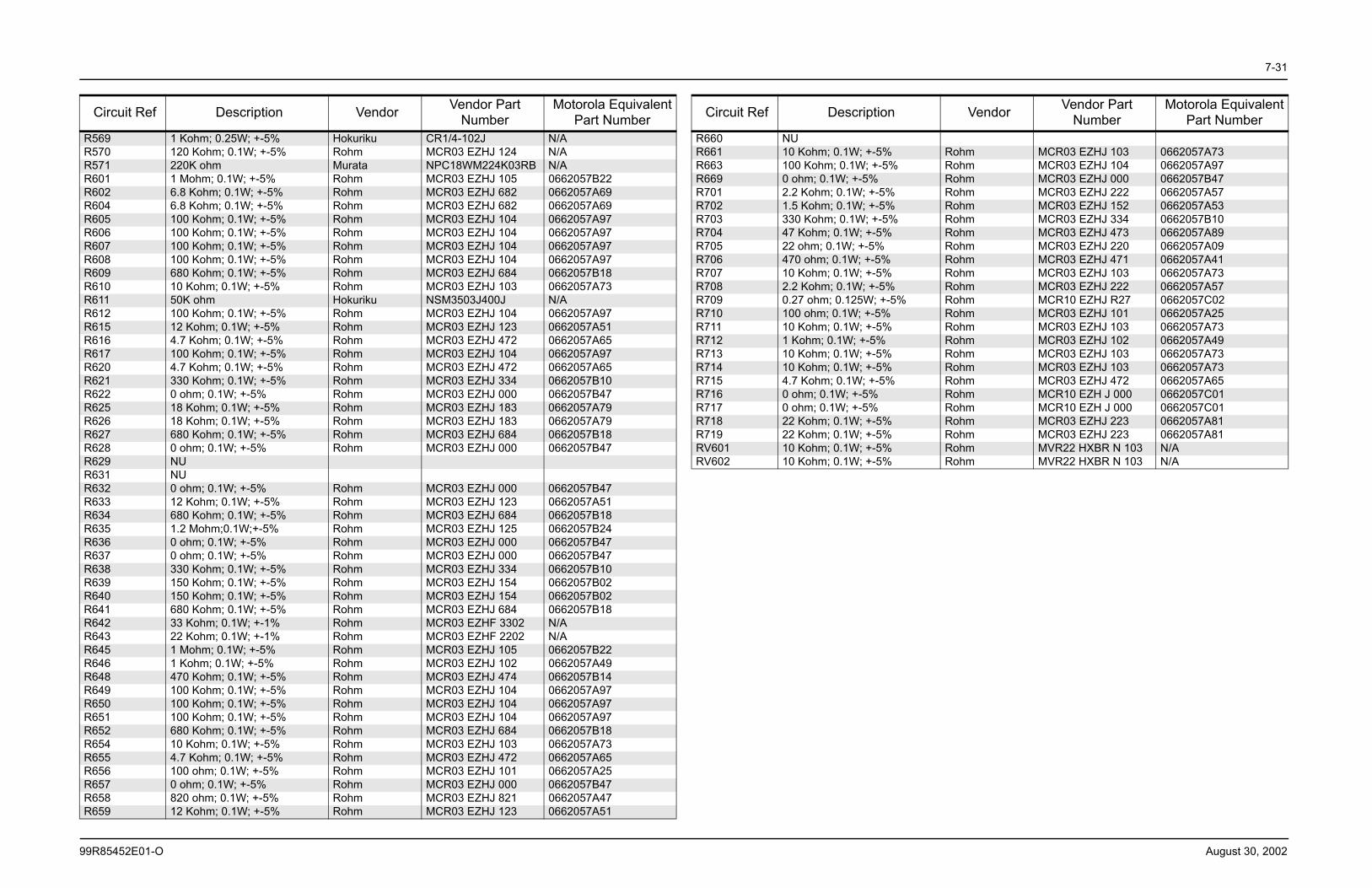
7-31
99R85452E01-O August 30, 2002
R569 1 Kohm; 0.25W; +-5% Hokuriku CR1/4-102J N/AR570 120 Kohm; 0.1W; +-5% Rohm MCR03 EZHJ 124 N/AR571 220K ohm Murata NPC18WM224K03RB N/AR601 1 Mohm; 0.1W; +-5% Rohm MCR03 EZHJ 105 0662057B22R602 6.8 Kohm; 0.1W; +-5% Rohm MCR03 EZHJ 682 0662057A69R604 6.8 Kohm; 0.1W; +-5% Rohm MCR03 EZHJ 682 0662057A69R605 100 Kohm; 0.1W; +-5% Rohm MCR03 EZHJ 104 0662057A97R606 100 Kohm; 0.1W; +-5% Rohm MCR03 EZHJ 104 0662057A97R607 100 Kohm; 0.1W; +-5% Rohm MCR03 EZHJ 104 0662057A97R608 100 Kohm; 0.1W; +-5% Rohm MCR03 EZHJ 104 0662057A97R609 680 Kohm; 0.1W; +-5% Rohm MCR03 EZHJ 684 0662057B18R610 10 Kohm; 0.1W; +-5% Rohm MCR03 EZHJ 103 0662057A73R611 50K ohm Hokuriku NSM3503J400J N/AR612 100 Kohm; 0.1W; +-5% Rohm MCR03 EZHJ 104 0662057A97R615 12 Kohm; 0.1W; +-5% Rohm MCR03 EZHJ 123 0662057A51R616 4.7 Kohm; 0.1W; +-5% Rohm MCR03 EZHJ 472 0662057A65R617 100 Kohm; 0.1W; +-5% Rohm MCR03 EZHJ 104 0662057A97R620 4.7 Kohm; 0.1W; +-5% Rohm MCR03 EZHJ 472 0662057A65R621 330 Kohm; 0.1W; +-5% Rohm MCR03 EZHJ 334 0662057B10R622 0 ohm; 0.1W; +-5% Rohm MCR03 EZHJ 000 0662057B47R625 18 Kohm; 0.1W; +-5% Rohm MCR03 EZHJ 183 0662057A79R626 18 Kohm; 0.1W; +-5% Rohm MCR03 EZHJ 183 0662057A79R627 680 Kohm; 0.1W; +-5% Rohm MCR03 EZHJ 684 0662057B18R628 0 ohm; 0.1W; +-5% Rohm MCR03 EZHJ 000 0662057B47R629 NUR631 NUR632 0 ohm; 0.1W; +-5% Rohm MCR03 EZHJ 000 0662057B47R633 12 Kohm; 0.1W; +-5% Rohm MCR03 EZHJ 123 0662057A51R634 680 Kohm; 0.1W; +-5% Rohm MCR03 EZHJ 684 0662057B18R635 1.2 Mohm;0.1W;+-5% Rohm MCR03 EZHJ 125 0662057B24R636 0 ohm; 0.1W; +-5% Rohm MCR03 EZHJ 000 0662057B47R637 0 ohm; 0.1W; +-5% Rohm MCR03 EZHJ 000 0662057B47R638 330 Kohm; 0.1W; +-5% Rohm MCR03 EZHJ 334 0662057B10R639 150 Kohm; 0.1W; +-5% Rohm MCR03 EZHJ 154 0662057B02R640 150 Kohm; 0.1W; +-5% Rohm MCR03 EZHJ 154 0662057B02R641 680 Kohm; 0.1W; +-5% Rohm MCR03 EZHJ 684 0662057B18R642 33 Kohm; 0.1W; +-1% Rohm MCR03 EZHF 3302 N/AR643 22 Kohm; 0.1W; +-1% Rohm MCR03 EZHF 2202 N/AR645 1 Mohm; 0.1W; +-5% Rohm MCR03 EZHJ 105 0662057B22R646 1 Kohm; 0.1W; +-5% Rohm MCR03 EZHJ 102 0662057A49R648 470 Kohm; 0.1W; +-5% Rohm MCR03 EZHJ 474 0662057B14R649 100 Kohm; 0.1W; +-5% Rohm MCR03 EZHJ 104 0662057A97R650 100 Kohm; 0.1W; +-5% Rohm MCR03 EZHJ 104 0662057A97R651 100 Kohm; 0.1W; +-5% Rohm MCR03 EZHJ 104 0662057A97R652 680 Kohm; 0.1W; +-5% Rohm MCR03 EZHJ 684 0662057B18R654 10 Kohm; 0.1W; +-5% Rohm MCR03 EZHJ 103 0662057A73R655 4.7 Kohm; 0.1W; +-5% Rohm MCR03 EZHJ 472 0662057A65R656 100 ohm; 0.1W; +-5% Rohm MCR03 EZHJ 101 0662057A25R657 0 ohm; 0.1W; +-5% Rohm MCR03 EZHJ 000 0662057B47R658 820 ohm; 0.1W; +-5% Rohm MCR03 EZHJ 821 0662057A47R659 12 Kohm; 0.1W; +-5% Rohm MCR03 EZHJ 123 0662057A51
Circuit Ref Description Vendor Vendor Part Number
Motorola Equivalent Part Number
R660 NUR661 10 Kohm; 0.1W; +-5% Rohm MCR03 EZHJ 103 0662057A73R663 100 Kohm; 0.1W; +-5% Rohm MCR03 EZHJ 104 0662057A97R669 0 ohm; 0.1W; +-5% Rohm MCR03 EZHJ 000 0662057B47R701 2.2 Kohm; 0.1W; +-5% Rohm MCR03 EZHJ 222 0662057A57R702 1.5 Kohm; 0.1W; +-5% Rohm MCR03 EZHJ 152 0662057A53R703 330 Kohm; 0.1W; +-5% Rohm MCR03 EZHJ 334 0662057B10R704 47 Kohm; 0.1W; +-5% Rohm MCR03 EZHJ 473 0662057A89R705 22 ohm; 0.1W; +-5% Rohm MCR03 EZHJ 220 0662057A09R706 470 ohm; 0.1W; +-5% Rohm MCR03 EZHJ 471 0662057A41R707 10 Kohm; 0.1W; +-5% Rohm MCR03 EZHJ 103 0662057A73R708 2.2 Kohm; 0.1W; +-5% Rohm MCR03 EZHJ 222 0662057A57R709 0.27 ohm; 0.125W; +-5% Rohm MCR10 EZHJ R27 0662057C02R710 100 ohm; 0.1W; +-5% Rohm MCR03 EZHJ 101 0662057A25R711 10 Kohm; 0.1W; +-5% Rohm MCR03 EZHJ 103 0662057A73R712 1 Kohm; 0.1W; +-5% Rohm MCR03 EZHJ 102 0662057A49R713 10 Kohm; 0.1W; +-5% Rohm MCR03 EZHJ 103 0662057A73R714 10 Kohm; 0.1W; +-5% Rohm MCR03 EZHJ 103 0662057A73R715 4.7 Kohm; 0.1W; +-5% Rohm MCR03 EZHJ 472 0662057A65R716 0 ohm; 0.1W; +-5% Rohm MCR10 EZH J 000 0662057C01R717 0 ohm; 0.1W; +-5% Rohm MCR10 EZH J 000 0662057C01R718 22 Kohm; 0.1W; +-5% Rohm MCR03 EZHJ 223 0662057A81R719 22 Kohm; 0.1W; +-5% Rohm MCR03 EZHJ 223 0662057A81RV601 10 Kohm; 0.1W; +-5% Rohm MVR22 HXBR N 103 N/ARV602 10 Kohm; 0.1W; +-5% Rohm MVR22 HXBR N 103 N/A
Circuit Ref Description Vendor Vendor Part Number
Motorola Equivalent Part Number
7-32
August 30, 2002 99R85452E01-O
This Page Intentionally Left Blank
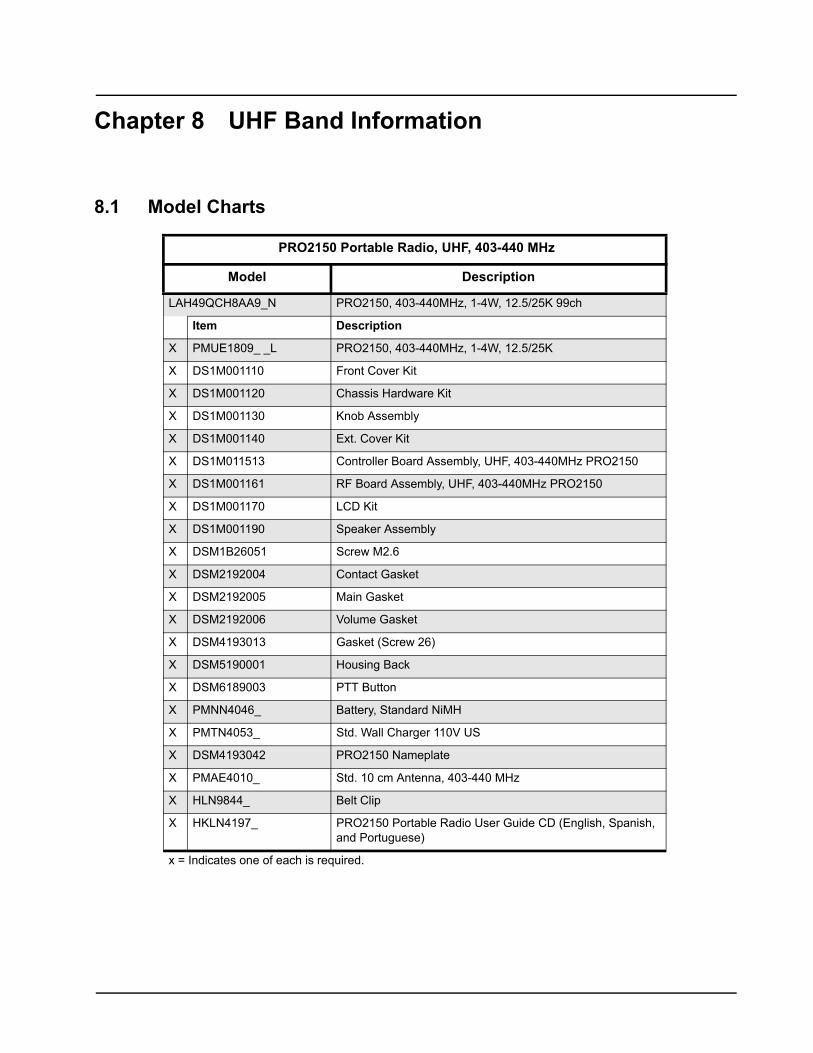
Chapter 8 UHF Band Information
8.1 Model Charts
PRO2150 Portable Radio, UHF, 403-440 MHz
Model Description
LAH49QCH8AA9_N PRO2150, 403-440MHz, 1-4W, 12.5/25K 99ch
Item Description
X PMUE1809_ _L PRO2150, 403-440MHz, 1-4W, 12.5/25K
X DS1M001110 Front Cover Kit
X DS1M001120 Chassis Hardware Kit
X DS1M001130 Knob Assembly
X DS1M001140 Ext. Cover Kit
X DS1M011513 Controller Board Assembly, UHF, 403-440MHz PRO2150
X DS1M001161 RF Board Assembly, UHF, 403-440MHz PRO2150
X DS1M001170 LCD Kit
X DS1M001190 Speaker Assembly
X DSM1B26051 Screw M2.6
X DSM2192004 Contact Gasket
X DSM2192005 Main Gasket
X DSM2192006 Volume Gasket
X DSM4193013 Gasket (Screw 26)
X DSM5190001 Housing Back
X DSM6189003 PTT Button
X PMNN4046_ Battery, Standard NiMH
X PMTN4053_ Std. Wall Charger 110V US
X DSM4193042 PRO2150 Nameplate
X PMAE4010_ Std. 10 cm Antenna, 403-440 MHz
X HLN9844_ Belt Clip
X HKLN4197_ PRO2150 Portable Radio User Guide CD (English, Spanish, and Portuguese)
x = Indicates one of each is required.

August 30, 2002 99R85452E01-O
8-2 UHF Band Information: Model Charts
PRO2150 Portable Radio, UHF, 435-480 MHz
Model Description
LAH49RCH8AA9_N PRO2150, 435-480MHz, 1-4W, 12.5/25K, 99ch
Item Description
X PMUE1813_ _L PRO2150, 435-480MHz, 1-4W, 12.5/25K 99Ch
X DS1M001110 Front Cover Kit
X DS1M001120 Chassis Hardware Kit
X DS1M001130 Knob Assembly
X DS1M001140 Ext. Cover Kit
X DS1M011521 Controller Board Assembly, UHF, 435-480MHz PRO2150
X DS1M001162 RF Board Assembly, UHF, 435-480MHz PRO2150
X DS1M001170 LCD Kit
X DS1M001190 Speaker Assembly
X DSM1B26051 Screw M2.6
X DSM2192004 Contact Gasket
X DSM2192005 Main Gasket
X DSM2192006 Volume Gasket
X DSM4193013 Gasket (Screw 26)
X DSM5190001 Housing, Back
X DSM6189003 PTT Button
X PMNN4046_ Battery, Standard NiMH
X PMTN4053_ Std. Wall Charger 110V US
X PMAE4011_ Std. 10 cm Antenna, 435-480 MHz
X HLN9844_ Belt Clip
X HKLN4197_ PRO2150 Portable Radio User Guide CD (English, Spanish, and Portuguese)
X DSM4193042 Nameplate
x = Indicates one of each is required.
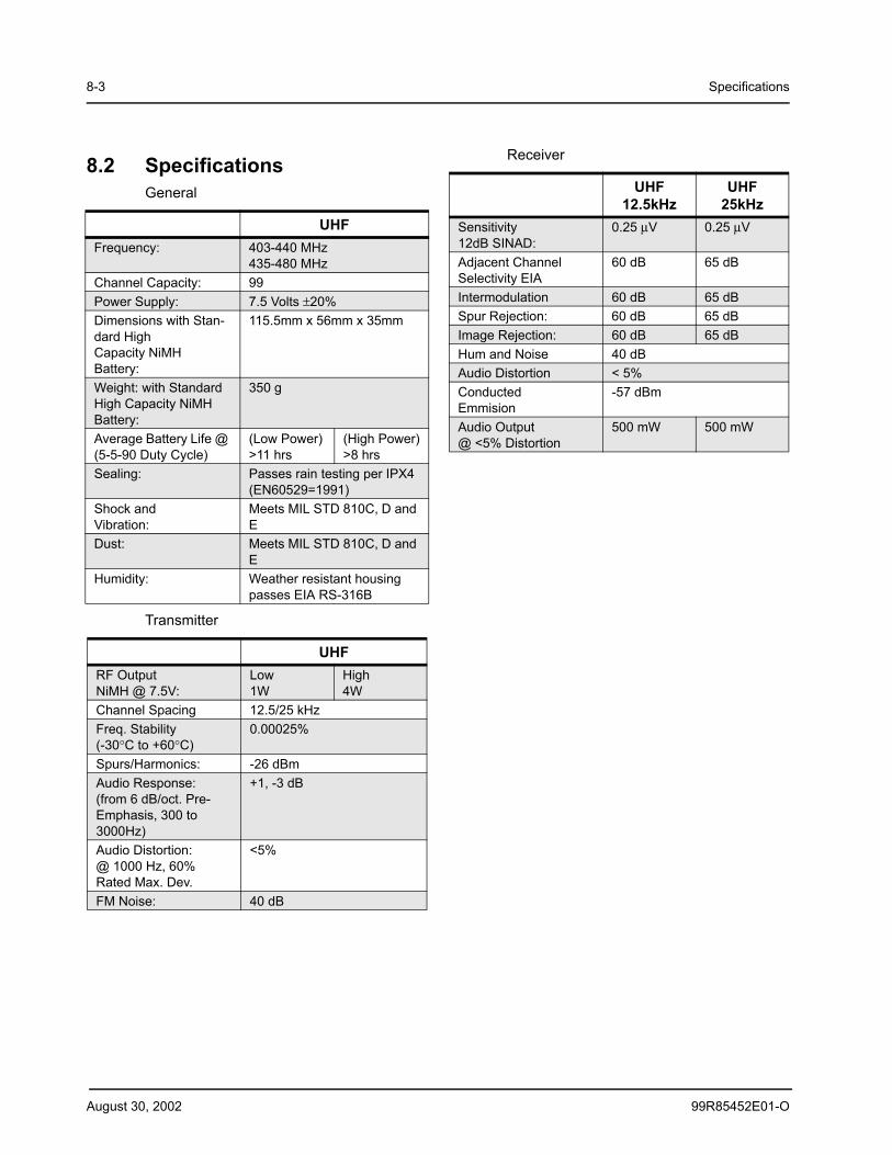
8-3 Specifications
August 30, 2002 99R85452E01-O
8.2 SpecificationsGeneral
Transmitter
Receiver
UHFFrequency: 403-440 MHz
435-480 MHzChannel Capacity: 99Power Supply: 7.5 Volts ±20%Dimensions with Stan-dard HighCapacity NiMHBattery:
115.5mm x 56mm x 35mm
Weight: with Standard High Capacity NiMH Battery:
350 g
Average Battery Life @ (5-5-90 Duty Cycle)
(Low Power)>11 hrs
(High Power)>8 hrs
Sealing: Passes rain testing per IPX4 (EN60529=1991)
Shock andVibration:
Meets MIL STD 810C, D and E
Dust: Meets MIL STD 810C, D and E
Humidity: Weather resistant housing passes EIA RS-316B
UHFRF OutputNiMH @ 7.5V:
Low1W
High4W
Channel Spacing 12.5/25 kHzFreq. Stability(-30°C to +60°C)
0.00025%
Spurs/Harmonics: -26 dBmAudio Response:(from 6 dB/oct. Pre-Emphasis, 300 to 3000Hz)
+1, -3 dB
Audio Distortion:@ 1000 Hz, 60%Rated Max. Dev.
<5%
FM Noise: 40 dB
UHF 12.5kHz
UHF 25kHz
Sensitivity12dB SINAD:
0.25 µV 0.25 µV
Adjacent Channel Selectivity EIA
60 dB 65 dB
Intermodulation 60 dB 65 dBSpur Rejection: 60 dB 65 dBImage Rejection: 60 dB 65 dBHum and Noise 40 dBAudio Distortion < 5%ConductedEmmision
-57 dBm
Audio Output@ <5% Distortion
500 mW 500 mW
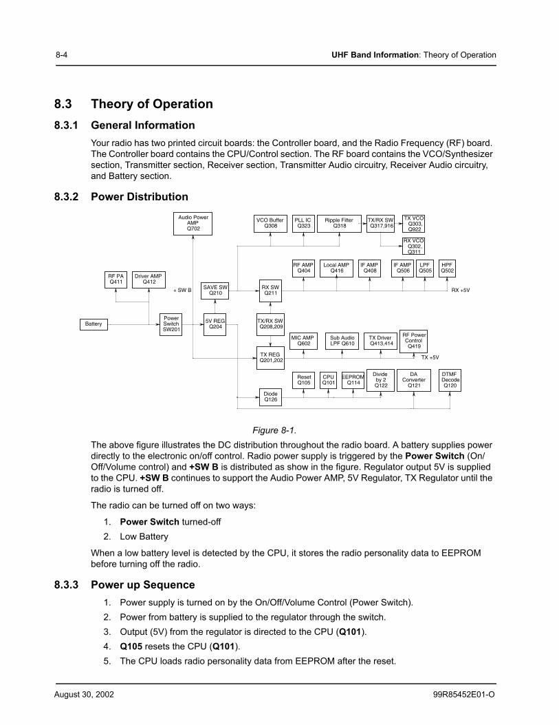
August 30, 2002 99R85452E01-O
This Page Intentionally Left Blank
8-4 UHF Band Information: Theory of Operation
8.3 Theory of Operation8.3.1 General Information
Your radio has two printed circuit boards: the Controller board, and the Radio Frequency (RF) board. The Controller board contains the CPU/Control section. The RF board contains the VCO/Synthesizer section, Transmitter section, Receiver section, Transmitter Audio circuitry, Receiver Audio circuitry, and Battery section.
8.3.2 Power Distribution
Figure 8-1. The above figure illustrates the DC distribution throughout the radio board. A battery supplies power directly to the electronic on/off control. Radio power supply is triggered by the Power Switch (On/Off/Volume control) and +SW B is distributed as show in the figure. Regulator output 5V is supplied to the CPU. +SW B continues to support the Audio Power AMP, 5V Regulator, TX Regulator until the radio is turned off.
The radio can be turned off on two ways:
1. Power Switch turned-off2. Low Battery
When a low battery level is detected by the CPU, it stores the radio personality data to EEPROM before turning off the radio.
8.3.3 Power up Sequence1. Power supply is turned on by the On/Off/Volume Control (Power Switch).2. Power from battery is supplied to the regulator through the switch.3. Output (5V) from the regulator is directed to the CPU (Q101).4. Q105 resets the CPU (Q101).5. The CPU loads radio personality data from EEPROM after the reset.
5V REGQ204
RX SWQ211
TX/RX SWQ208,209
TX REGQ201,202
RF AMPQ404
Local AMPQ416
IF AMPQ408
IF AMPQ506
LPFQ505
HPFQ502
Audio PowerAMPQ702
RF PAQ411
Driver AMPQ412
MIC AMPQ602
Sub AudioLPF Q610
VCO BufferQ308
PLL ICQ323
RF PowerControlQ419
TX DriverQ413,414
+ SW B SAVE SWQ210 RX +5V
TX +5V
Battery
DiodeQ126
ResetQ105
CPUQ101
EEPROMQ114
DTMFDecodeQ120
DAConverter
Q121
Divide by 2Q122
PowerSwitchSW201
Ripple FilterQ318
TX/RX SWQ317,916
TX VCOQ303,Q922
RX VCOQ302,Q311
99R85452E01-O August 30, 2002
UHF Band Information: Theory of Operation 8-5
6. This personality data is used to initialize the radio.7. The radio restores last power up state (i.e. state before the radio was turned-off).8. Power is supplied to PLL circuitry.9. Power is supplied to Rx and Rx VCO circuitry.10. CPU sends data to PLL circuitry. If LOCK status is confirmed, radio continues the power-up
sequence. Otherwise, PLL ERR is displayed.11. If the Rx audio level is less than the pre-programmed squelch level, and other unmuting
conditions are met, the radio will open squelch.
8.3.4 CPU / Control SectionWhen the radio is turned ON, the CPU (Q101) reads the radio status from the EEPROM Q114. It also monitors the keypad, the PTT line and other inputs such as the squelch detect, etc. continuously. When there is a channel change, the CPU sends the correct frequency information to the synthesizer via pins 1, 2 and 89. The CPU is clocked by the 8.388608MHz oscillator, which is composed of X101, C101, C106, and R158.
8.3.5 VCO / Synthesizer SectionThis section consists of the Temperature-Compensated Crystal Oscillator(TCXO), Voltage Controlled Oscillator(VCO), Synthesizer and the Loop Filter. These circuits are found on the RF board.
8.3.5.1 Temperature-Compensated Crystal Oscillator (TCXO)
The reference oscillator is a temperature compensated crystal-controlled, Pierce type circuit. It utilizes a logic gate within Q323 as a gain element. C335 is used to adjust the oscillator on frequency (14.4MHz) at room temperature (22°C). Temperature variations cause resistance changes in thermistor R330 and R567, which is on the base of Q320, thus varying the voltage applied to varactor Q322. This changes the impedance across crystal X301 in a manner complementary to the temperature drift characteristic of the crystal. In this way, the reference oscillator is held within the specified ±2.5 PPM from -30 to +60°C.
8.3.5.2 Voltage-Controlled Oscillators
Only one of the VCOs runs at a time, which is controlled by Q317 and Q101. The receive VCO consists of C311, C314-C316, C913, C940, L302-L306, Q311 and Q302. This VCO oscillates at 45.1 MHz above the programmed receive frequency. The VCO’s oscillating frequency is tuned by the varactor Q311. The tuning voltage is supplied from the output of the Loop Filter. The output of the VCO is AC coupled (C311) to the buffer Q308. The output of the VCO buffer Q308 is AC coupled (C308) to the synthesizer and the output buffer Q416 respectively.
When the PTT is pressed, Q101 pin36 goes low (approx. 0V) disabling the receive VCO by the Q317 and biases on Q916 to enable the transmitter VCO. The transmitter VCO consists of C340, C935-C937, L308-L310, Q303, Q921 and Q922. This VCO oscillates on the programmed transmit frequency. The VCO’s oscillating frequency is tuned by the varactor Q922. The tuning voltage is supplied from the output of the Loop Filter. The transmit voltage controlled oscillator is directly frequency-modulated and operates on the carrier frequency. The synthesizer is tuned in 5.00kHz or 6.25kHz steps.
August 30, 2002 99R85452E01-O
8-6 UHF Band Information: Theory of Operation
8.3.5.3 Synthesizer
The frequency synthesizer is a large-scale monolithic synthesizer integrated circuit Q323. The synthesizer IC contains a dual modulus prescaler, programmable divide-by-N counter, prescale control (swallow) counter, reference oscillator, reference divider, phase detector, charge pump and lock detector. Also, included in Q323 are shift registers and control circuits for frequency controls and general device control.
RF output from the active VCO is AC coupled to the synthesizer Q323 prescaler input at Pin 8. The divide counter chain in Q323, consisting of the dual-modulus prescaler, swallow counter and programmable counter, divides the VCO signal down to a frequency very close to 5.00kHz or 6.25kHz which is applied to the phase detector. The phase comparator compares the phase with the 5.00kHz or 6.25kHz reference signal from the reference divider and drives the external charge pump (Q314, Q315 and Q316). The synthesizer unlock detector circuit prevents the operation of the transmitter and receiver, when the phase lock loop (PLL) is unlocked. The following discussion assumes the unit has been placed in the transmit mode. Q323 lock detector Pin 7 goes high when the PLL is locked. This high level is applied to Pin 25 of the CPU Q101. A software timing routing brings the RX/TX line low (Pin 36 of Q101). With the RX/TX line goes low, Q209 is cut off and Q208 is biased on passing +5VTX-B to Q202; it biases on Q201 to pass switched TX-B to the transmitter amplifier string which enables transmission.
When the PLL is unlocked, the lock detector at Q323 Pin 7 will begin pulsing low. A RC circuit converts this low pulse to a low level for the CPU. The CPU then changes the RX/TX line to a high, thus signaling the other transistor switches to drive Q201 into cutoff, which disables transmission. Therefore, the transmitter remains disabled while the loop remains out of lock, and “PLL ERR” is displayed.
8.3.5.4 Loop Filter
The Loop Filter, a passive lead-lag filter consisting of R314-R317, R356, C323, C369, and C371, integrates the charge pump output to produce the DC turning voltage for the VCO. One parasitic pole, consisting of RF chokes L306 and L310, prevent modulation of the VCOs by the 5.00kHz or 6.25kHz reference energy remaining at the output of the loop filter. Direct FM is obtained for modulating frequencies outside the PLL bandwidth by applying the CTCSS/DCS signals and the pre-emphasized, limited microphone audio to the VCO modulation circuit. The modulation circuit consists of R929 and Q921.
8.3.6 Transmitter Section8.3.6.1 RF Power Amplifier
After the PTT is pressed, the +5VTX-B line switches to approximately 5V. Q916 is turned on, enabling transmit VCO. The VCO buffer, pre-driver, driver and power amplifier are biased on by Q201. Q201 is biased on by the +5VTX-B line switching to 5V. RF output from the transmit VCO(Q303) is applied to the VCO output buffer Q308. Output from Q308 feeds the buffer Q414. The output signal from Q414 feeds the pre-driver amplifier Q413, and feeds the driver amplifier Q412, whose output from the driver stage feeds the final RF power amplifier Q411 to produce the rated output power of 5 watts. The final output is feed to a low-pass filter (C435-438, C491-C493, L418, and L430) and then to the transmit/receive switch Q410. RF power is then fed to the antenna via the output low-pass filter consisting of C439-C444, C475, L414, L415 and L416.
8.3.6.2 Antenna Switching
Switching of the antenna between the transmitter and the receiver is accomplished by the antenna transmit/receive switch consisting of diodes Q409 and Q410. In the transmit mode, switched TX B+ is applied through R417 and RF choke L417, hard forward biasing the two diodes on Q410, thus permitting the flow of RF power from the output of the low-pass filter. L419 and C433 isolate the receiver circuit from the transmitter power input.
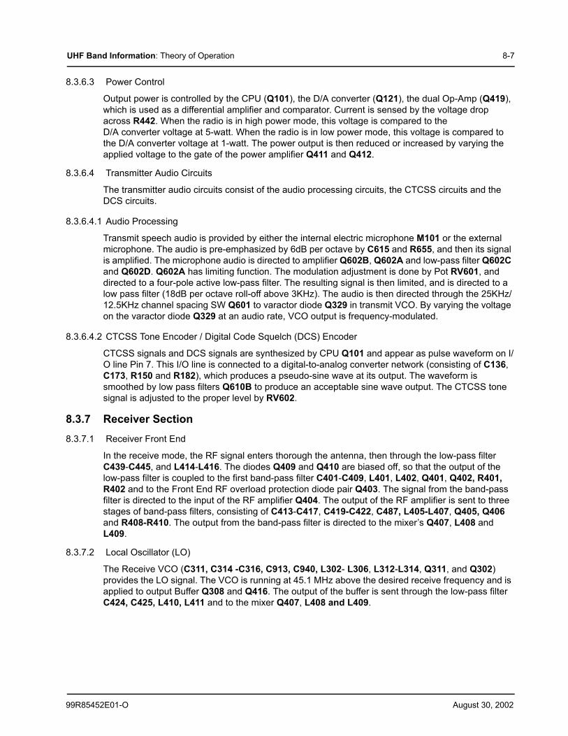
99R85452E01-O August 30, 2002
UHF Band Information: Theory of Operation 8-7
8.3.6.3 Power Control
Output power is controlled by the CPU (Q101), the D/A converter (Q121), the dual Op-Amp (Q419), which is used as a differential amplifier and comparator. Current is sensed by the voltage drop across R442. When the radio is in high power mode, this voltage is compared to the D/A converter voltage at 5-watt. When the radio is in low power mode, this voltage is compared to the D/A converter voltage at 1-watt. The power output is then reduced or increased by varying the applied voltage to the gate of the power amplifier Q411 and Q412.
8.3.6.4 Transmitter Audio Circuits
The transmitter audio circuits consist of the audio processing circuits, the CTCSS circuits and the DCS circuits.
8.3.6.4.1 Audio Processing
Transmit speech audio is provided by either the internal electric microphone M101 or the external microphone. The audio is pre-emphasized by 6dB per octave by C615 and R655, and then its signal is amplified. The microphone audio is directed to amplifier Q602B, Q602A and low-pass filter Q602C and Q602D. Q602A has limiting function. The modulation adjustment is done by Pot RV601, and directed to a four-pole active low-pass filter. The resulting signal is then limited, and is directed to a low pass filter (18dB per octave roll-off above 3KHz). The audio is then directed through the 25KHz/12.5KHz channel spacing SW Q601 to varactor diode Q329 in transmit VCO. By varying the voltage on the varactor diode Q329 at an audio rate, VCO output is frequency-modulated.
8.3.6.4.2 CTCSS Tone Encoder / Digital Code Squelch (DCS) Encoder
CTCSS signals and DCS signals are synthesized by CPU Q101 and appear as pulse waveform on I/O line Pin 7. This I/O line is connected to a digital-to-analog converter network (consisting of C136, C173, R150 and R182), which produces a pseudo-sine wave at its output. The waveform is smoothed by low pass filters Q610B to produce an acceptable sine wave output. The CTCSS tone signal is adjusted to the proper level by RV602.
8.3.7 Receiver Section8.3.7.1 Receiver Front End
In the receive mode, the RF signal enters thorough the antenna, then through the low-pass filter C439-C445, and L414-L416. The diodes Q409 and Q410 are biased off, so that the output of the low-pass filter is coupled to the first band-pass filter C401-C409, L401, L402, Q401, Q402, R401, R402 and to the Front End RF overload protection diode pair Q403. The signal from the band-pass filter is directed to the input of the RF amplifier Q404. The output of the RF amplifier is sent to three stages of band-pass filters, consisting of C413-C417, C419-C422, C487, L405-L407, Q405, Q406 and R408-R410. The output from the band-pass filter is directed to the mixer’s Q407, L408 and L409.
8.3.7.2 Local Oscillator (LO)
The Receive VCO (C311, C314 -C316, C913, C940, L302- L306, L312-L314, Q311, and Q302) provides the LO signal. The VCO is running at 45.1 MHz above the desired receive frequency and is applied to output Buffer Q308 and Q416. The output of the buffer is sent through the low-pass filter C424, C425, L410, L411 and to the mixer Q407, L408 and L409.
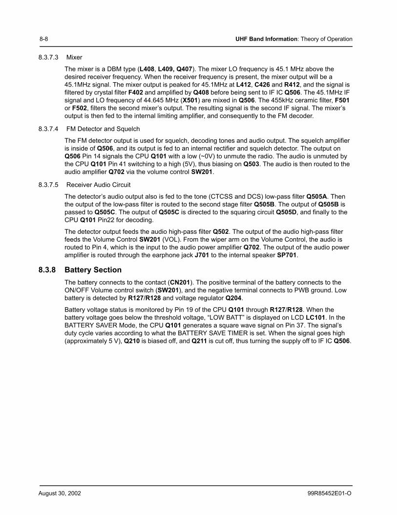
August 30, 2002 99R85452E01-O
8-8 UHF Band Information: Theory of Operation
8.3.7.3 Mixer
The mixer is a DBM type (L408, L409, Q407). The mixer LO frequency is 45.1 MHz above the desired receiver frequency. When the receiver frequency is present, the mixer output will be a 45.1MHz signal. The mixer output is peaked for 45.1MHz at L412, C426 and R412, and the signal is filtered by crystal filter F402 and amplified by Q408 before being sent to IF IC Q506. The 45.1MHz IF signal and LO frequency of 44.645 MHz (X501) are mixed in Q506. The 455kHz ceramic filter, F501 or F502, filters the second mixer’s output. The resulting signal is the second IF signal. The mixer’s output is then fed to the internal limiting amplifier, and consequently to the FM decoder.
8.3.7.4 FM Detector and Squelch
The FM detector output is used for squelch, decoding tones and audio output. The squelch amplifier is inside of Q506, and its output is fed to an internal rectifier and squelch detector. The output on Q506 Pin 14 signals the CPU Q101 with a low (~0V) to unmute the radio. The audio is unmuted by the CPU Q101 Pin 41 switching to a high (5V), thus biasing on Q503. The audio is then routed to the audio amplifier Q702 via the volume control SW201.
8.3.7.5 Receiver Audio Circuit
The detector’s audio output also is fed to the tone (CTCSS and DCS) low-pass filter Q505A. Then the output of the low-pass filter is routed to the second stage filter Q505B. The output of Q505B is passed to Q505C. The output of Q505C is directed to the squaring circuit Q505D, and finally to the CPU Q101 Pin22 for decoding.
The detector output feeds the audio high-pass filter Q502. The output of the audio high-pass filter feeds the Volume Control SW201 (VOL). From the wiper arm on the Volume Control, the audio is routed to Pin 4, which is the input to the audio power amplifier Q702. The output of the audio power amplifier is routed through the earphone jack J701 to the internal speaker SP701.
8.3.8 Battery SectionThe battery connects to the contact (CN201). The positive terminal of the battery connects to the ON/OFF Volume control switch (SW201), and the negative terminal connects to PWB ground. Low battery is detected by R127/R128 and voltage regulator Q204.
Battery voltage status is monitored by Pin 19 of the CPU Q101 through R127/R128. When the battery voltage goes below the threshold voltage, “LOW BATT” is displayed on LCD LC101. In the BATTERY SAVER Mode, the CPU Q101 generates a square wave signal on Pin 37. The signal’s duty cycle varies according to what the BATTERY SAVE TIMER is set. When the signal goes high (approximately 5 V), Q210 is biased off, and Q211 is cut off, thus turning the supply off to IF IC Q506.
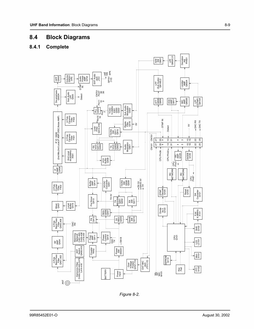
99R85452E01-O August 30, 2002
UHF Band Information: Block Diagrams 8-9
8.4 Block Diagrams8.4.1 Complete
Figure 8-2.
SA
VE
5V
RX
5V
5V
DA
CR
X
Key
Pad
Pow
erIn
put
TX
5V
BA
TT
ER
Y
5V
DA
C R
X
DA
C T
X
35D
TM
F IN
RC
NE
TW
OR
K
9
RC
NE
TW
OR
K3
MIC
M10
1
CN
701
CN
101 27 31 4 15 16 22 25
252215 16343193527
DA
CT
X
+ S
W B
5V
SP
KS
P70
1(1
/2)
DT
MF
IND
etec
t
Det
ect
1313
AN
T
AN
TS
witc
hQ
409,
410
RF
AM
PQ
404
Mix
erQ
407
Loca
lB
uffe
rQ
416
2-P
ole
Cry
stal
Filt
erF
402 B
uffe
rA
MP
Q41
4
Pre
Driv
erQ
413
RE
GQ
206
Q20
7
Pow
erC
ontr
olQ
419
Pow
erS
WS
W20
1
5V RE
GQ
204
SA
VE
SW
Q21
0
TX
RE
G/S
WQ
201
Q20
2
Ove
rV
olta
geP
rote
ctQ
707-
710
TX
/RX
SW
Q20
8Q
209
VC
OB
uffe
rQ
308
Loop
Filt
erQ
314-
316
Pin
15
16
CN
701
Pin
37
38
39
Pin
11
10
9P
in1
2
TC
XO
14.4
MH
zX
301
Q32
0Q
322
Sub
Aud
ioM
odul
ator
Q32
2
6 P
ole
Cer
amic
Filt
erF
501
IFA
MP
Q40
8
De-
emph
asis
Q50
2A
Sub
Aud
ioLP
FQ
505
HP
FQ
502
Aud
ioP
ower
AM
PQ
702
EX
T A
udio
Jack
J701
6 P
ole
Cer
amic
Filt
erF
502
PLL
Q32
3
EE
PR
OM
Q11
4
CP
UQ
101
PT
TS
102
Mon
S10
1LC
DLC
101
Shi
ftQ
102
X,ta
l8.
38M
Hz
X10
1
Div
ide
by 2
Q12
2
DT
MF
Dec
ode
Q12
0
Res
etQ
105
DA
Con
vert
erQ
121
CP
UP
in87
DIO
DE
Q12
6
CP
UP
in21
CP
U P
in22
CP
U P
in36
LPF
(DT
MF
)Q
610A
Lim
itter
AM
PQ
602A
MIC
AM
PQ
602B
AT
TQ
608
Q60
9
N/W SW
Q60
1
LPF
Q60
2C,D
Dev
iatio
nA
djR
V60
1
EX
T M
ICJa
ckJ7
01(1
/2)
DC
AM
PQ
125
IF IC
Q50
6(2
nd M
ix,2
nd L
ocal
,IF A
MP
,DIS
C,N
oise
AM
P)
2nd
Loca
l44
.654
MH
zX
501
RX
SW
Q21
1
DC
/DC
Con
vert
erQ
301
Vol
ume
SW
201
(VR
)
Fin
alA
MP
Q41
1
PA
Q41
2
2-P
ole
Ban
d P
ass
Filt
erQ
401,
402
2-P
ole
Ban
d P
ass
Filt
erQ
405,
406
Ham
onic
s F
ilter
C43
9,C
440-
445,
C47
5L4
14-4
16
Mat
chin
gN
etw
ork
C49
1-49
3,C
435-
438
L418
,430
Cou
pler
R44
2R
XV
CO
Q31
1Q
302
TX
VC
OQ
303
Q92
2
TX
/RX
SW
Q31
7Q
916
Rip
ple
Filt
erQ
318
Aud
ioM
odul
ator
Q92
1
LPF
(Sub
Aud
io)
Q61
0B,D
VO
XA
MP
Q61
7
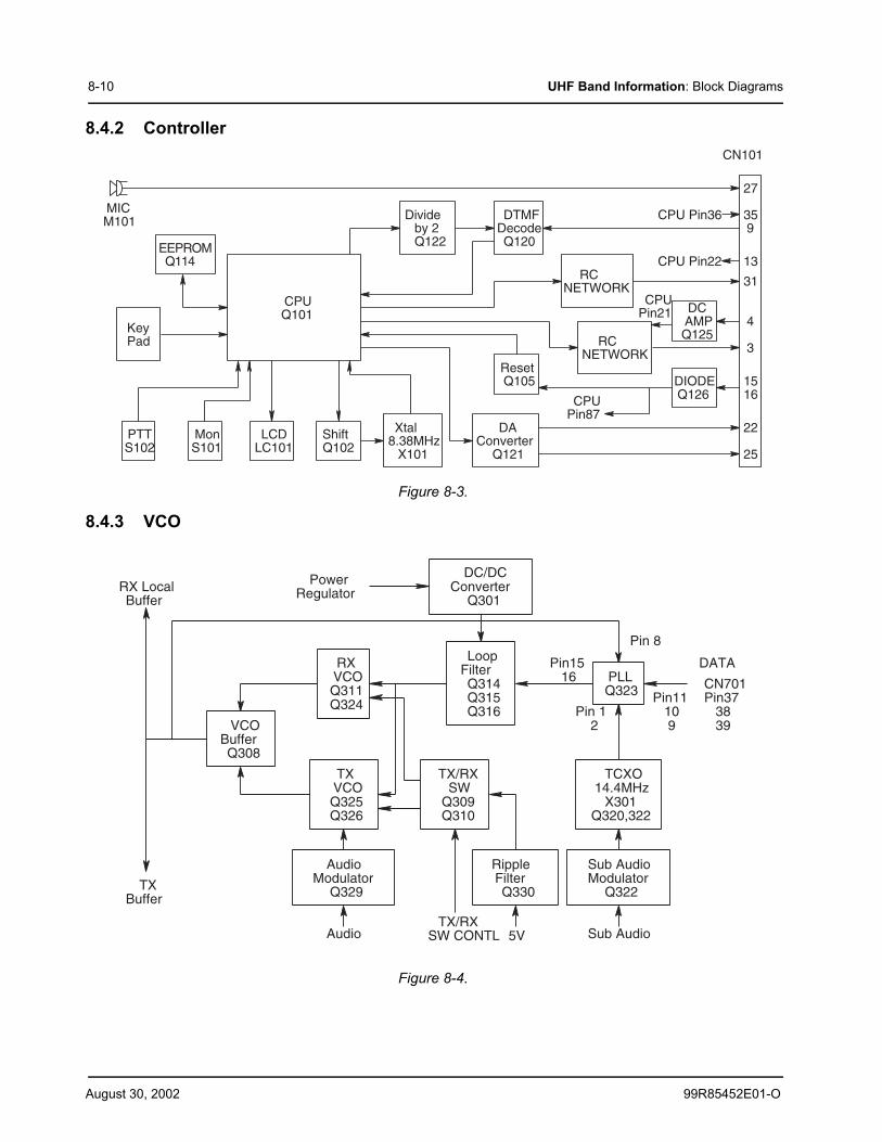
August 30, 2002 99R85452E01-O
8-10 UHF Band Information: Block Diagrams
8.4.2 Controller
Figure 8-3.
8.4.3 VCO
Figure 8-4.
KeyPad
35
RCNETWORK
9
RCNETWORK 3
MICM101
27
31
4
1516
22
25
13EEPROMQ114
CPUQ101
PTTS102
MonS101
LCDLC101
ShiftQ102
Xtal8.38MHz
X101
Divide by 2Q122
DTMFDecodeQ120
ResetQ105
DAConverter
Q121
CPUPin87
DIODEQ126
CPUPin21
CPU Pin22
CPU Pin36
DCAMPQ125
CN101
RX LocalBuffer
TXBuffer
DATA
Audio Sub AudioTX/RX
SW CONTL
Ripple FilterQ330
5V
VCOBufferQ308
RXVCOQ311Q324
TX/RXSW
Q309Q310
AudioModulator
Q329
Sub AudioModulator
Q322
TCXO14.4MHz
X301Q320,322
LoopFilterQ314Q315Q316
PLLQ323 CN701
Pin37 38 39
Pin11 10 9
Pin15 16
Pin 1
Pin 8
2
TXVCOQ325Q326
PowerRegulator
DC/DCConverter
Q301
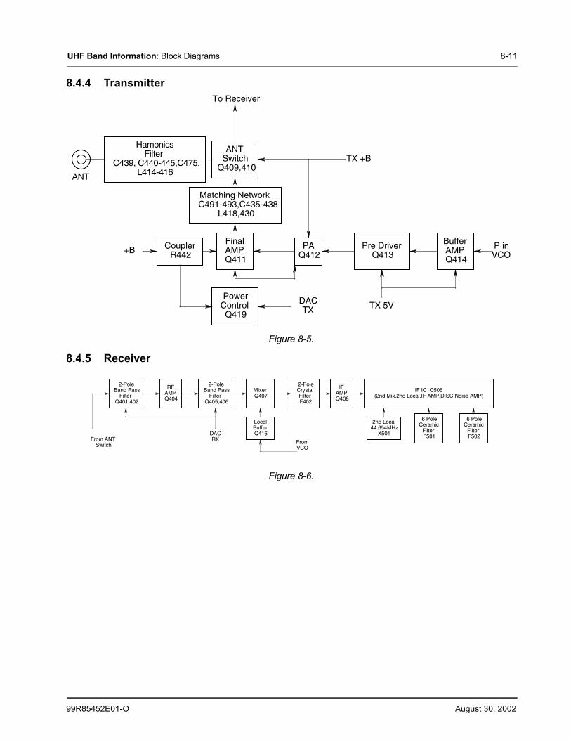
99R85452E01-O August 30, 2002
UHF Band Information: Block Diagrams 8-11
8.4.4 Transmitter
Figure 8-5.
8.4.5 Receiver
Figure 8-6.
ANT
To Receiver
TX +B
+B
TX 5VDACTX
PowerControlQ419
ANTSwitch
Q409,410
BufferAMPQ414
Pre DriverQ413
P inVCO
FinalAMPQ411
PAQ412
HamonicsFilter
C439, C440-445,C475,L414-416
Matching NetworkC491-493,C435-438
L418,430
CouplerR442
DACRX From
VCO
From ANTSwitch
2-PoleCrystalFilterF402
2nd Local44.654MHz
X501
6 PoleCeramic
FilterF501
6 PoleCeramic
FilterF502
MixerQ407
RFAMPQ404
LocalBufferQ416
IFAMPQ408
IF IC Q506(2nd Mix,2nd Local,IF AMP,DISC,Noise AMP)
2-PoleBand Pass
FilterQ401,402
2-PoleBand Pass
FilterQ405,406
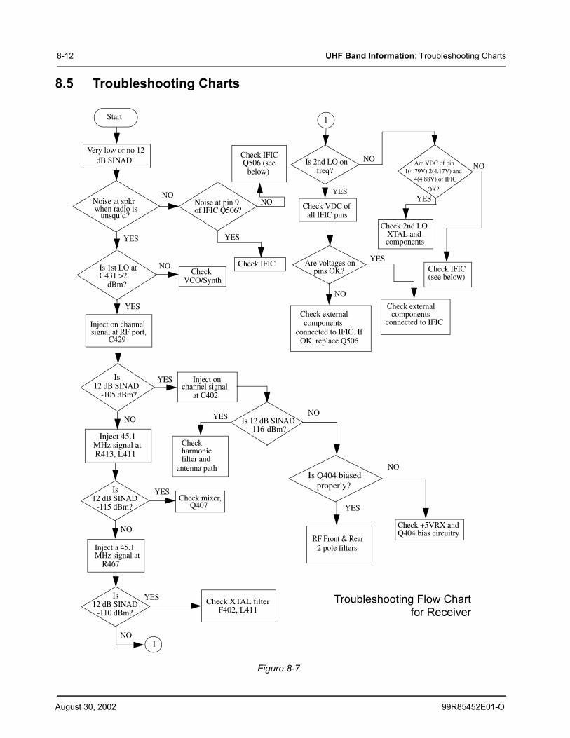
August 30, 2002 99R85452E01-O
8-12 UHF Band Information: Troubleshooting Charts
8.5 Troubleshooting Charts
Figure 8-7.
Troubleshooting Flow Chartfor Receiver
Start
Very low or no 12 dB SINAD
Noise at spkrwhen radio is
unsqu’d?
Is 1st LO atC431 >2
dBm?
Inject on channelsignal at RF port,
C429
12 dB SINAD-105 dBm?
Inject a 45.1MHz signal at
R467
12 dB SINAD
1
Check IFICQ506 (see
below)
Noise at pin 9of IFIC Q506?
CheckVCO/Synth
Inject onchannel signal
at C402
Check harmonicfilter and
antenna path
Check externalcomponents
connected to IFIC. IfOK, replace Q506
Check mixer,Q407
Is 12 dB SINADdBm?
Check IFIC
Is Q404 biasedproperly?
RF Front & Rear
Check +5VRX andQ404 bias circuitry
1
Is 2nd LO onfreq?
Check VDC ofall IFIC pins
Are VDC of pin1(4.79V),2(4.17V) and
4(4.88V) of IFIC
OK?
Are voltages onpins OK?
Check 2nd LOXTAL andcomponents
Check IFIC(see below)
Check externalcomponents
connected to IFIC
NO
NO
YES
YES
NO
YES
YES
NO
YES
YES NO
YES
NO
YES
YES
NO
YES
YES
NO
NO
NO
NO
2 pole filters
Check XTAL filterF402, L411 -110 dBm?
-116
Is
12 dB SINAD -115 dBm?
Is
Inject 45.1MHz signal atR413, L411
Is
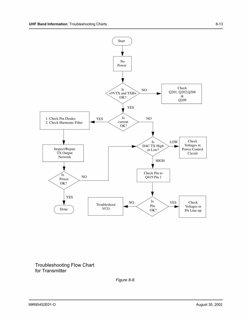
99R85452E01-O August 30, 2002
UHF Band Information: Troubleshooting Charts 8-13
Figure 8-8.
Troubleshooting Flow Chart for Transmitter
Start
NoPower
+5VTX and TXB+OK?
Iscurrent
OK?
IsDAC TX High
or Low?
Is PinOK?
CheckQ201, Q202,Q206
&Q209
CheckVoltages in
Power ControlCircuit
CheckVoltages inPA Line-up
TroubleshootVCODone
IsPowerOK?
1. Check Pin Diodes2. Check Harmonic Filter
Inspect/RepairTX OutputNetwork
NO
NO
LOW
HIGH
YESNO
NO
YES
YES
YES
Is
Check Pin toQ419 Pin 1
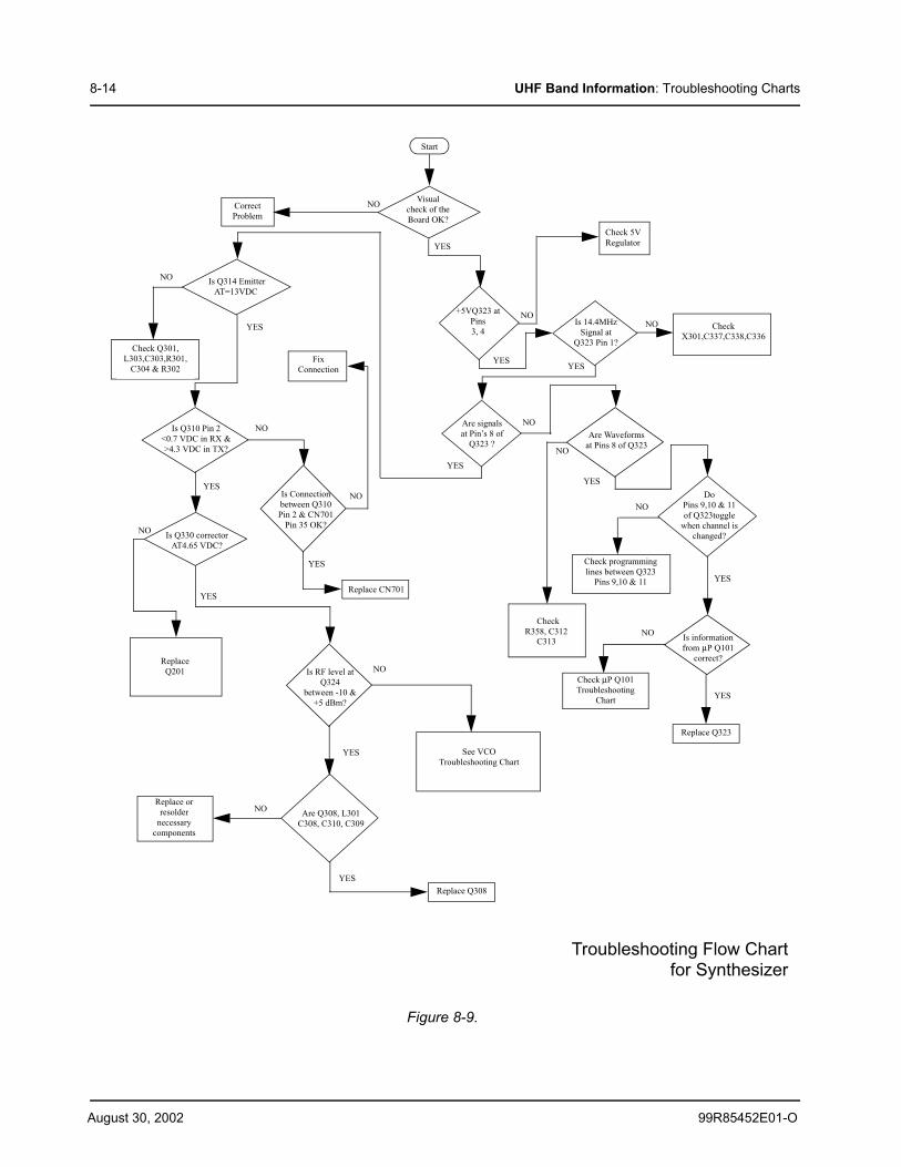
August 30, 2002 99R85452E01-O
8-14 UHF Band Information: Troubleshooting Charts
Figure 8-9.
Is informationfrom µP Q101
correct?
Is Q330 corrector AT4.65 VDC?
Is Q314 Emitter AT=13VDC
Is Q310 Pin 2<0.7 VDC in RX &>4.3 VDC in TX?
Troubleshooting Flow Chartfor Synthesizer
Start
Visual check of the Board OK?
CorrectProblem
Check 5VRegulator
+5VQ323 at Pins3, 4
Is 14.4MHzSignal at
Q323 Pin 1?
CheckX301,C337,C338,C336
Are signalsat Pin’s 8 of
Q323 ?
Check Q301,L303,C303,R301,
C304 & R302Fix
Connection
Is Connectionbetween Q310Pin 2 & CN701
Pin 35 OK?
Replace CN701
ReplaceQ201
Replace orresolder
necessarycomponents
Is RF level atQ324
between -10 &+5 dBm?
Are Q308, L301C308, C310, C309
Replace Q308
See VCOTroubleshooting Chart
Are Waveformsat Pins 8 of Q323
DoPins 9,10 & 11of Q323toggle
when channel ischanged?
Check programminglines between Q323
Pins 9,10 & 11
Replace Q323
Check µP Q101Troubleshooting
Chart
NO
YES
NO
NO
NO
NO
YES
YES
NO
YES
YES
NO
YES
NO
YES
YESYES
NONO
NO
YES
NO
YES
YES
NO
CheckR358, C312
C313
YES
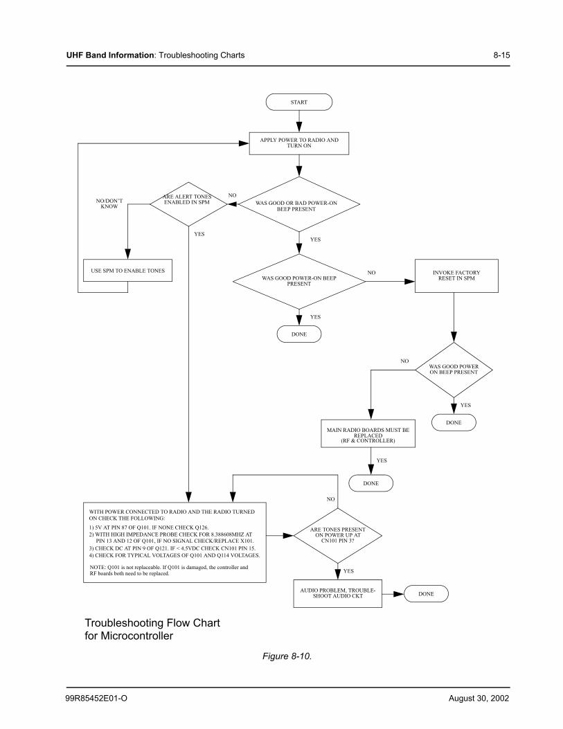
99R85452E01-O August 30, 2002
UHF Band Information: Troubleshooting Charts 8-15
Figure 8-10.
Troubleshooting Flow Chart for Microcontroller
START
APPLY POWER TO RADIO AND
WAS GOOD OR BAD POWER-ON
YES
DONE
WAS GOOD POWER-ON BEEP
ARE ALERT TONESENABLED IN SPM
USE SPM TO ENABLE TONES INVOKE FACTORYRESET IN SPM
WAS GOOD POWERON BEEP PRESENT
MAIN RADIO BOARDS MUST BEREPLACED
ARE TONES PRESENTON POWER UP AT
CN101 PIN 3?
AUDIO PROBLEM, TROUBLE-SHOOT AUDIO CKT
WITH POWER CONNECTED TO RADIO AND THE RADIO TURNEDON CHECK THE FOLLOWING:
1) 5V AT PIN 87 OF Q101. IF NONE CHECK Q126.2) WITH HIGH IMPEDANCE PROBE CHECK FOR 8.388608MHZ AT
PIN 13 AND 12 OF Q101, IF NO SIGNAL CHECK/REPLACE X101.3) CHECK DC AT PIN 9 OF Q121. IF < 4.5VDC CHECK CN101 PIN 15.4) CHECK FOR TYPICAL VOLTAGES OF Q101 AND Q114 VOLTAGES.
BEEP PRESENT
TURN ON
PRESENT
DONE
DONE
DONE
YES
YES
YES
YES
YES
NO/DON’TKNOW
NO
NO
NO
NO
(RF & CONTROLLER)
NOTE: Q101 is not replaceable. If Q101 is damaged, the controller andRF boards both need to be replaced.
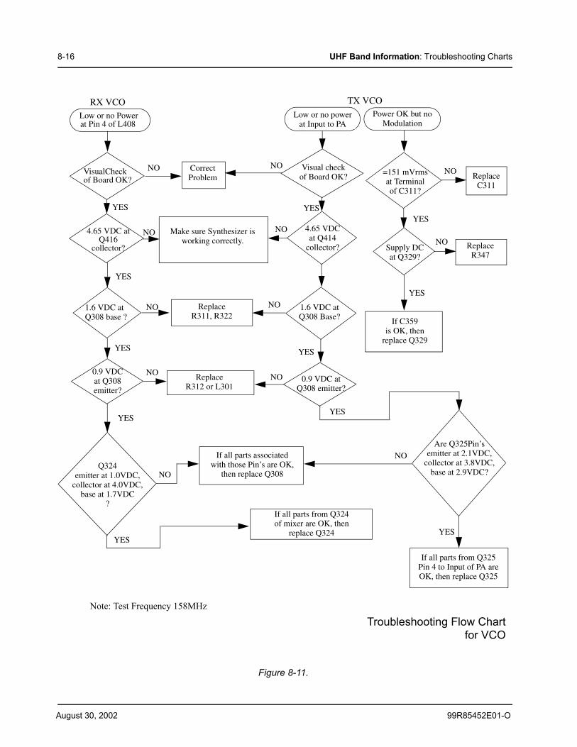
August 30, 2002 99R85452E01-O
8-16 UHF Band Information: Troubleshooting Charts
Figure 8-11.
Make sure Synthesizer isworking correctly.
1.6 VDC atQ308 Base?
4.65 VDCat Q414
collector?
=151 mVrmsat Terminalof C311?
Supply DCat Q329?
0.9 VDC atQ308 emitter?
Are Q325Pin’semitter at 2.1VDC,
collector at 3.8VDC, base at 2.9VDC?
Q324 emitter at 1.0VDC,
collector at 4.0VDC,base at 1.7VDC
?
0.9 VDCat Q308emitter?
1.6 VDC atQ308 base ?
4.65 VDC atQ416
collector?
Troubleshooting Flow Chartfor VCO
Low or no Powerat Pin 4 of L408
VisualCheckof Board OK?
If all parts from Q324of mixer are OK, then
replace Q324
If all parts associated with those Pin’s are OK,
then replace Q308
If all parts from Q325Pin 4 to Input of PA areOK, then replace Q325
If C359 is OK, then
replace Q329
ReplaceR347
ReplaceC311
Low or no power at Input to PA
Visual check of Board OK?
CorrectProblem
ReplaceR311, R322
ReplaceR312 or L301
NO
YES
NO
YES
NO
YES
NO
YES
NO
YESYES
NO
YES
NO
YES
NO
NO
YES
NONO
YES
NO
YES
RX VCO TX VCOPower OK but no
Modulation
Note: Test Frequency 158MHz
8-17
99R85452E01-O August 30, 2002
Chapter 8 UHF 403-440 MHz Circuit Board/Schematic Diagrams and Parts List
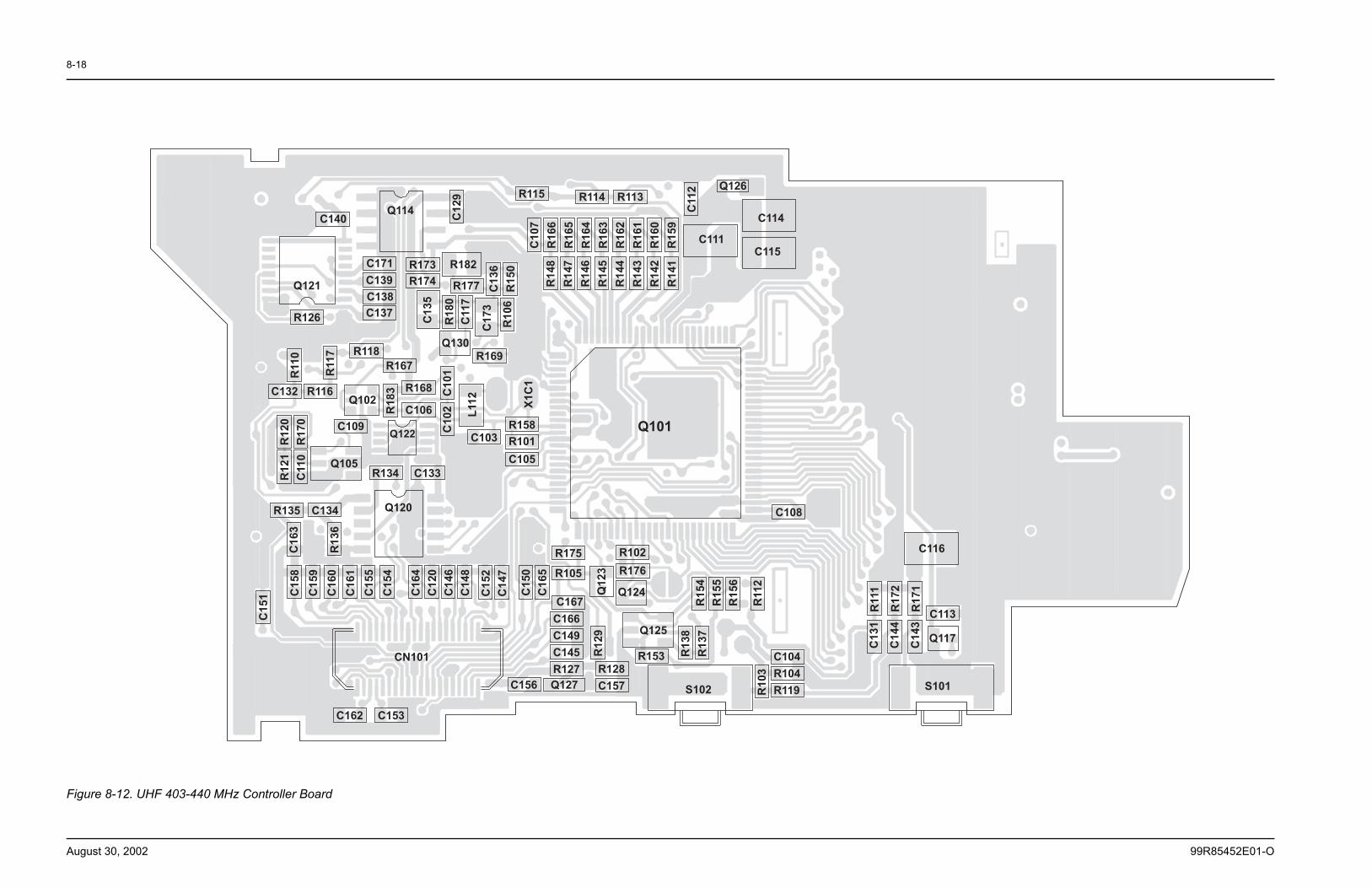
8-18
August 30, 2002 99R85452E01-O
Figure 8-12. UHF 403-440 MHz Controller Board
C140Q114
C171
C139
C138
C137
Q121
C1
29
R173
R174
R182
C1
35
R1
80
R177
C11
7
C1
73
C1
36
R1
50
R1
06
R115
R126
R118Q130
R169
R11
0
R11
7
R167
X1
C1
L11
2C1
01
C1
02
R168
C106R1
83
Q102R116C132
C109
R1
20
R1
70
R1
21
C11
0
Q105
Q122
R134 C133
C103
R158
R101
C105
R135 C134
C1
63
R1
36
Q120
C1
51 C
15
8
C1
59
C1
60
C1
61
C1
55
C1
54
C1
64
C1
20
C1
46
C1
48
C1
52
C1
47
C1
50
C1
65
C166
C149
C145
R127
R175
R105
C167
C156 Q127
C162 C153
CN101
R1
48
R1
47
R1
46
R1
45
R1
44
R1
43
R1
42
R1
41
C1
07
R1
66
R1
65
R1
64
R1
63
R1
62
R1
61
R1
60
R1
59
R114 R113
C11
2 Q126
C111
C114
C115
Q101
R1
54
R1
55
R1
56
R11
2
C108
Q1
23
R102
R176
Q124
Q125
R1
29
R128
C157 S102R
13
8
R1
37
R1
03
C104
R104
R119
R153
S101
Q117
C113
C1
31
C1
44
C1
43
R111
R1
72
R1
71
C116
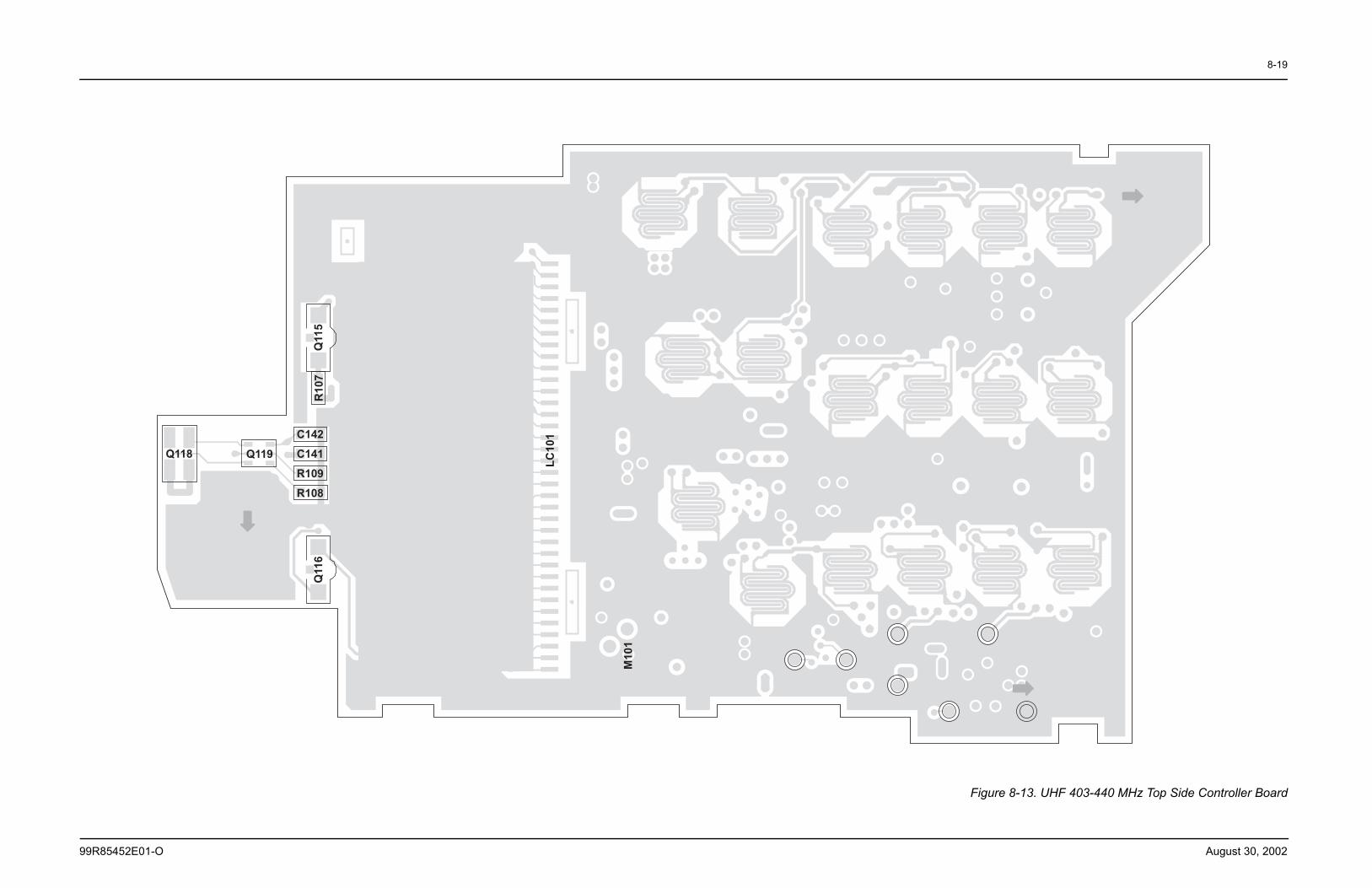
8-19
99R85452E01-O August 30, 2002
Figure 8-13. UHF 403-440 MHz Top Side Controller Board
C142
C141
R109
R108
Q119Q118
Q11
6Q
11
5R
10
7
LC
10
1
M1
01
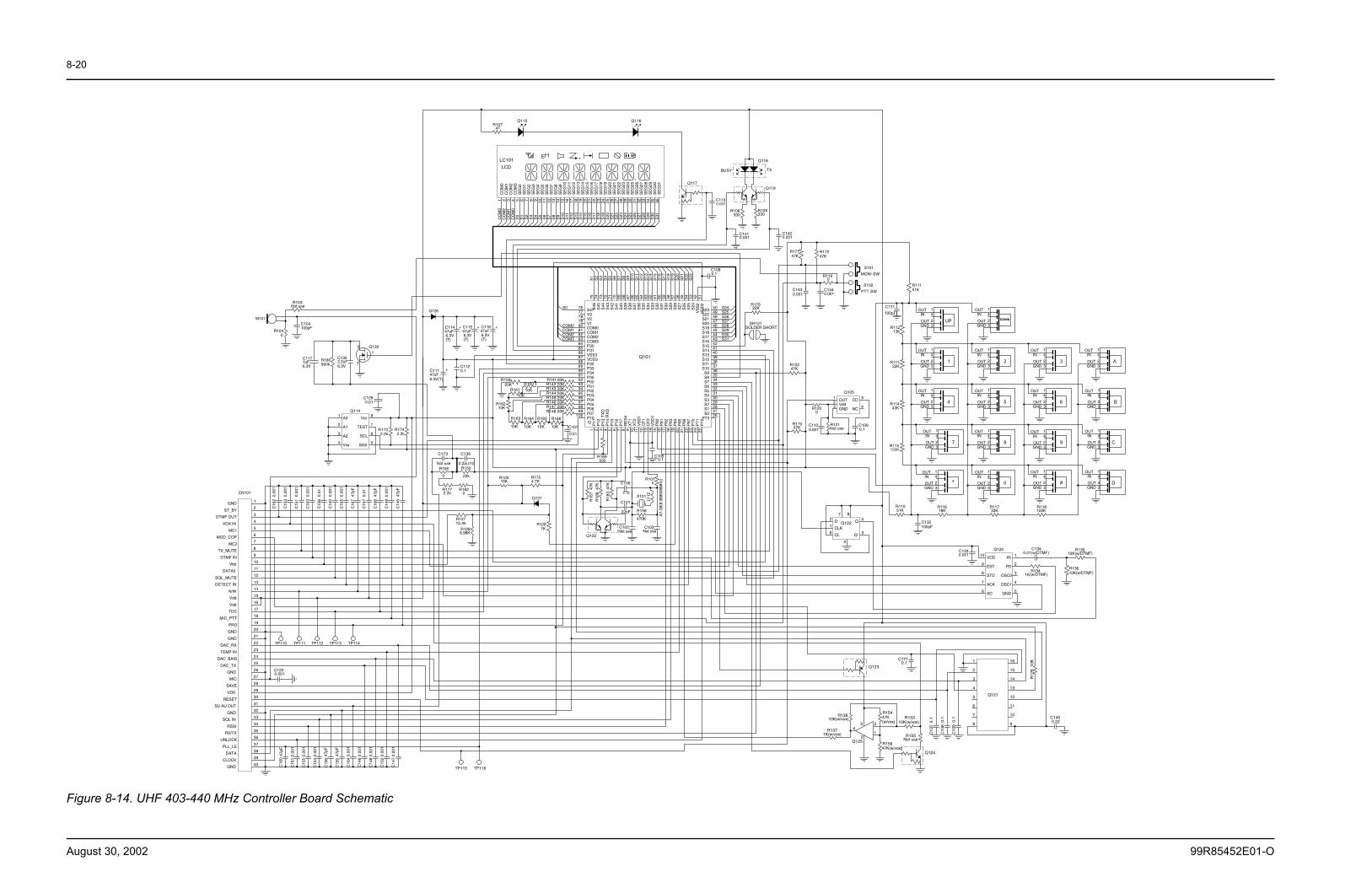
8-20
August 30, 2002 99R85452E01-O
Figure 8-14. UHF 403-440 MHz Controller Board Schematic
Q115R107
47
Q116
CO
M0
1
CO
M1
2
CO
M2
3
CO
M3
4
SE
G0
5
SE
G1
6
SE
G2
7
SE
G3
8
SE
G4
9
SE
G5
10
SE
G6
11
SE
G7
12
SE
G8
13
SE
G9
14
SE
G10
15
SE
G11
16
SE
G12
17
SE
G13
18
SE
G14
19
SE
G15
20
SE
G16
21
SE
G17
22
SE
G18
23
SE
G19
24
SE
G20
25
SE
G21
26
SE
G22
27
SE
G23
28
SE
G24
29
SE
G25
30
SE
G26
31
SE
G27
32
SE
G28
33
SE
G29
34
SE
G30
35
SE
G31
36
CO
M0
CO
M1
CO
M2
CO
M3
S0
S1
S2
S3
S4
S5
S6
S7
S8
S9
S10
S11
S12
S13
S14
S15
S16
S17
S18
S19
S20
S21
S22
S23
S24
S25
S26
S27
S28
S29
S30
S31
R109330
R108330
BUSY TX
Q117
C113
C1410.001
C1420.001
Q119
Q118
R11151KPTT SW
MONI SW
C1430.001
C1440.001
R17147K
R17247K
S101
S102
R1190
R11213K
C131100pF
32
41OUT
OUT
IN
GNDUP
R11322K
132
41OUT
OUT
IN
GND
R11443K
432
41OUT
OUT
IN
GND
R1157
32
41OUT
OUT
IN
GND
R11051K
R11618K
C132100pF
*32
41OUT
OUT
IN
GND
R11733K
32
41OUT
OUT
IN
GND0
32
41OUT
OUT
IN
GND8
32
41OUT
OUT
IN
GND5
32
41OUT
OUT
IN
GND
DOWN
A32
41OUT
OUT
IN
GND 32
41OUT
OUT
IN
GND 32
41OUT
OUT
IN
GND2 3
R118100K
B32
41OUT
OUT
IN
GND
32
41OUT
OUT
IN
GND
32
41OUT
OUT
IN
GND 32
41OUT
OUT
IN
GND
32
41OUT
OUT
IN
GND
32
41OUT
OUT
IN
GND
C
D
6
9
#
IN 1
PD 2
OSC0 3
OSC1 4
GND 5SD6
ACK7
STD8
EST9
VDD10Q120 C134
0.01(w/DTMF)
R1341K(w/DTMF)
R13610K(w/DTMF)
R13510K(w/DTMF)
C1330.001
C1400.22
C13
9 0
.1
C13
8 0
.1
C13
70.
1
1
2
3
4
5
6
7
8 9
10
11
12
13
14
16
15
Q121
R12
610
K
3
14
2
5
Q125
Q123
R15310K(w/vox)
R15447K(w/vox)
R155Not use
R15647K(w/vox)
Q124
C1710.1
R13810K(w/vox)
R1371K(w/vox)
TP115 TP116C15
847
pF
C15
947
pF
C16
047
pF
C16
10.
001
C16
40.
001
C14
60.
001
C14
70.
001
C14
80.
001
C15
20.
001
C15
40.
001
C15
50.
001
VDD
MIC
GND
GND
GND
RESET
GND
GND
CLOCK
DATA
PLL_LE
UNLOCK
SU AU OUT
RSSI
SQL IN
TEMP IN
RX/TX
SAVE
DAC_RX
DAC_TX
DAC_BAIS
PRO
MIC_PTT
C1200.001
18
19
20
21
22
23
24
25
26
27
28
29
30
31
32
33
34
35
36
37
38
39
40
TP110 TP111 TP112 TP113 TP114
Vbb
Vdd
Vdd
GND
MOD_COP
DATA0
DTMF OUT
DTMF IN
DETECT IN
TDC
N/W
VOX IN
MC1
MC2
TX_MUTE
ST_BY
SQL_MUTE
1
2
3
4
5
6
7
8
9
10
11
12
13
14
15
16
17
CN101
C15
60.
01
C15
70.
01
C16
20.
001
C16
30.
001
C16
50.
001
C16
647
pF
C16
747
pF
C14
547
pF
C14
90.
001
C15
00.
001
C15
10.
001
C15
30.
001
A01
A12
A23
Vss4 SDA 5
SCL 6
TEST 7
Vcc 8Q114
C1290.01
R173 2.2k
R174 2.2k
R150
22k
C173
Not use
R1772.2k
C136
0.22u/10
R1820
R106
0
R12712.4k
R1286.98K
R129 1K
Q127
R1754.7K
R10510K
X101
AT
-38(
8.38
8608
MH
z)
C103Not use
C102Not use
C101
22pF R158
470K
R1010
R16
847
K
R16
747
K
Q102
R18
347
K C106
27p
L112
P07P10
P11
1
P12
2
P13
3
P14
4
P15
5
P16
6
P17
7
RE
S#
8
XT
19
XT
210
VS
S1
11
CF
112
CF
213
VD
D1
14
P80
15
P81
16
P82
17
P83
18
P84
19
P85
20
P86
21
P87
22
P70
23
P71
24
P72
25
P73S0
C1050.1
0.01
TX
DR
XD
R169330
2627S1 28S2 29S3 30S4 31S5 32S6 33S7 34S8 35S9 36S10 37S11 38S12 39S13 40S14 41S15 42S16 43S17 44S18 45S19 46S20 47S21 48S22 49S23 50
VD
D2
VS
S2
S24S25S26S27S28S29S30S31
SH101SOLDER SHORT
R17622K
V3S47 S
4675
V2
5152S
2453
S25
54S
2655
S27
56S
2857
S29
58S
3059
S31
60S
3261
S33
62S
3463
S35
64S
3665
S37
66S
3867
S39
68S
4069
S41
70S
4271
S43
72S
4473
S45
74
C1080.1
S1
S2
S3
S4
S5
S6
S7
S8
S9
S10
S11
S12
S13
S14
S15
S16
S17
S18
S19
S20
S21
S22
S23
7776
78
V179
COM080
COM181
COM282
COM383
P3084
P3185
VSS386
VDD387
P3288
P3389
P3490
P3591
P0092
P0193
P0294
P0395
P0496
P0597
P069899
100
Q101
C107
R165
10K
R166
10K
R148 20KR147 20K
R145 20KR146 20K
R144 20KR143 20KR142 20KR141 20K
COM0COM1COM2COM3
S0
R16210K
R15920K
R16110K
R163
10K
R164
10K
R160
10K
C1120.1
Q126
+C11447uF 6.3V (T)
+C11547uF 6.3V (T)
+C11647uF 6.3V (T)
+C11147uF6.3V(T)
M101C104100pF
C1352.2uF6.3V
R180560k
C1171uF6.3V
R103Not use
R104 0
3
1
2
Q130
LC101LCD
R1200
C1100.001
OUT1
Vdd2
GND3 NC 4
CD 5Q105
C1090.1
R17047K
R10247K
R121Not use
CLK1D2
CL6
Q 5
Q' 3
4
7 8
Q122
130K
0.001
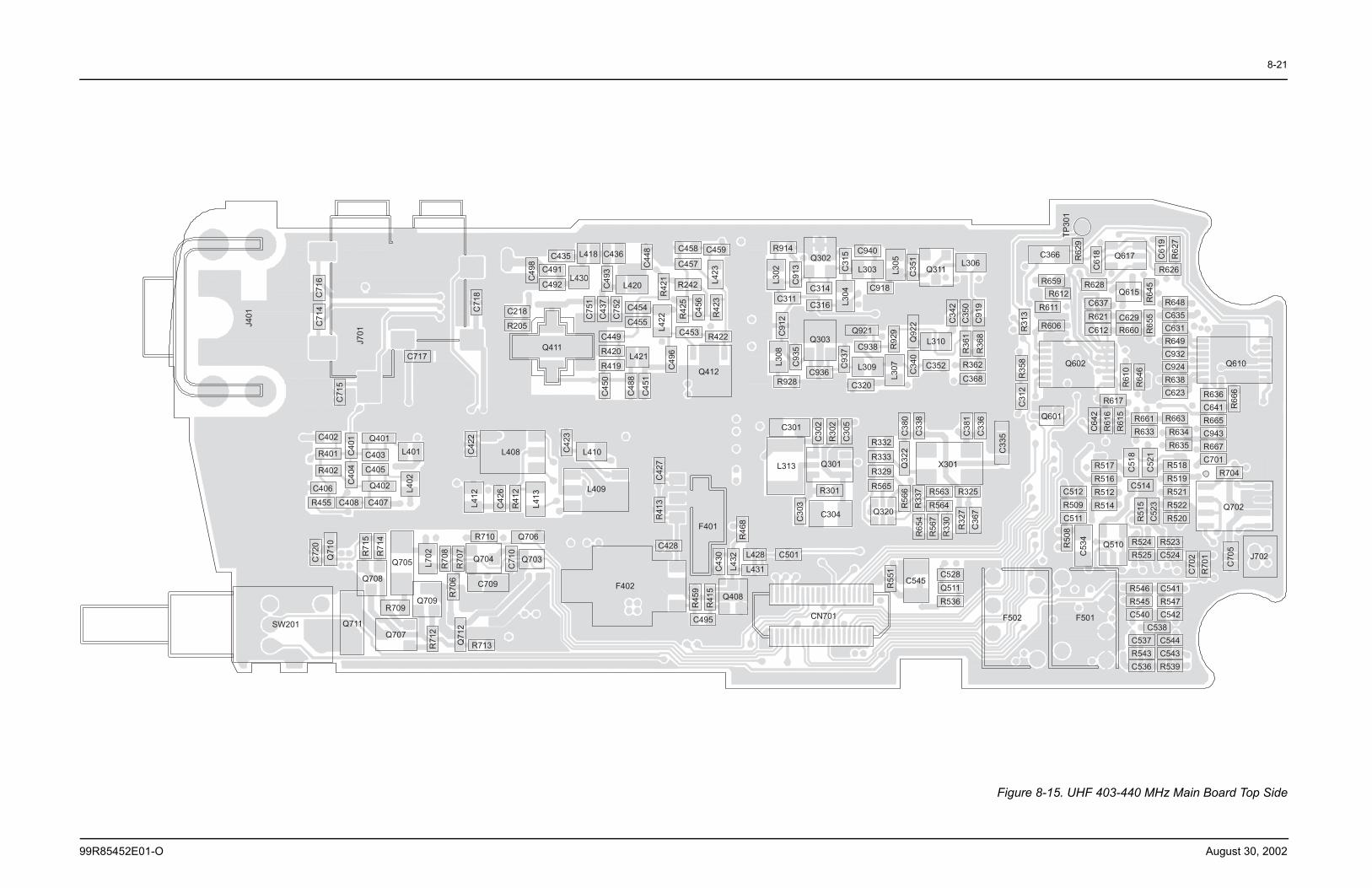
8-21
99R85452E01-O August 30, 2002
Figure 8-15. UHF 403-440 MHz Main Board Top Side
J4
01
C7
14
C7
16
C7
15
J7
01
C7
18
C717
C402
R401
R402
C406
R455
C4
04
C4
01
C408 C407
Q401
C403
C405
Q402
L401
L4
02
C4
22
L408
L4
12
C4
26
R4
12
L4
13
C218
R205
C4
98
C7
20
Q710
R7
15
R7
14
Q708
Q705
R7
08
R7
07
L7
02
R7
06
Q709R709
SW201 Q711
Q707
R710 Q706
Q704
C7
10
Q703
C709
R7
12
Q7
12
R713
C491
C492
C435 L418 C436
L430
C4
93
C7
51
C4
37
C7
52
C4
48
L420
C454
C455
C458
C457
C459
L4
23
R242
R4
21
L4
22 R4
25
C4
56
R4
23
C453R422
Q412
C4
96
L421
C449
R420
R419
Q411
C4
50
C4
88
C4
51
C4
23
L410
L409
F402
C4
27
R4
13
C428
F401
C4
30
L4
32
C495
Q408
R4
68
L428
L431
C501
R4
59
R4
15
CN701
C304
R5
51
C545C528
Q511
R536
R6
54
R5
67
R3
30
R3
27
C3
67
R5
66
R3
37
C3
03
R301
Q320
R563
R564
R325
L313 Q301
C301
R332
R333
R329
R565
C3
02
R3
02
C3
05
C3
80
C3
38
C3
81
C3
36
X301Q3
22 C
33
5
R928
C936
C320
L309
L3
07
C3
40
C352 R362
C368
C3
12
R3
58
R3
61
R3
68
L310Q9
22
R9
29
C938
Q921
C9
37
Q303
C9
35
L3
08
C9
12
R3
13
C3
42
C3
50
C9
19
C311
R914
L3
02
C9
13
Q302
C314
C316
C3
15
L3
04
C940
L303
C918
L3
05
C3
51
Q311L306
R648
C635
C631
R649
C932
C924
R638
C623
C6
19
R6
27
R626
Q617
C6
18
R6
29
C366
TP
30
1
R659
R612
R611
R606
R628
C637
R621
C612
Q615
C629
R660 R6
55
R6
45
Q602
R6
10
R6
46
Q610
R636
C641
R665
C943
R667
C701
R6
66
R661
R633C6
42
R6
16
R6
15Q601
R617
R517
R516
R512
R514
R518
R519
R521
R522
R520
R663
R634
R635
C512
R509
C511
C5
18
C5
21
C514
R704
Q702
R5
15
C5
23
R5
08
C5
34
Q510 R524
R525
R523
C524
C7
02
R7
01
C7
05
J702
F501F502
R546
R545
C540
C541
R547
C542
C537
R543
C536
C544
C543
R539
C538
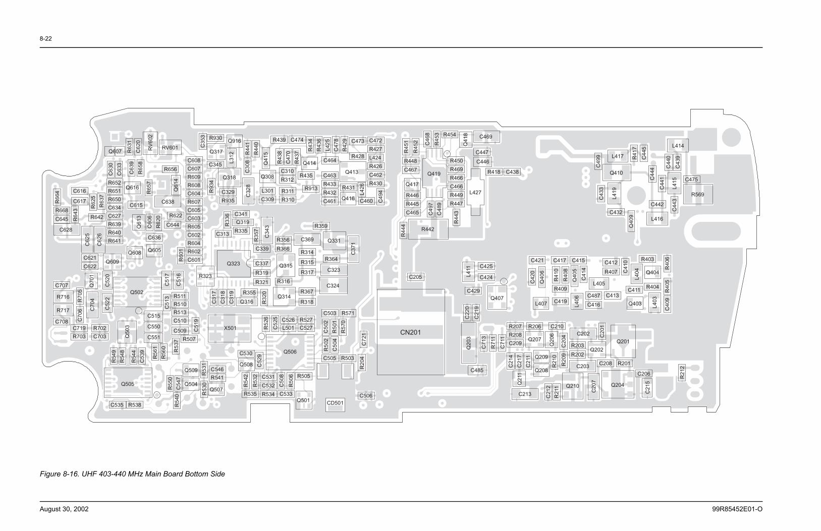
8-22
August 30, 2002 99R85452E01-O
Figure 8-16. UHF 403-440 MHz Main Board Bottom Side
R652R651R650C634C627R639R640R641
C608C607R609R608C604R607C605C603R605C602R604R602C601
R668C645
C621C622
C63
0C
633
R63
1C
620
C63
9R
658
C60
6R
620
C616
C617
C62
5
C62
6
R642
RV601RV6
02
R656
C615R66
4
R62
5R
637
R64
3
C628
R65
7
Q61
3
Q608
Q607
Q61
4
C638
R622
C644
C636
R60
1
Q609
Q605
Q616
R511R510R513
C719 R703
R702 C703
C515
C550
C551
R716
R717
R54
4 C
539
R54
9R
548
R56
1 R
560
R55
0 C
547
C51
7
C51
6
Q502C707
C708
C52
0C
522R70
5C
706 C
704
Q50
3
Q70
1
Q505
C535 R538
C51
3
C51
9
R507
R53
7R
540
Q504
Q509
C35
3
R323
R53
1R
530
C472 R427 L424 R426 C462 R430
C463 R433 R432 C461
C310 R312
R311R310
L301C309
R314
R315
R317
C329 R935
R43
8 C
470
R43
7 R43
4 R
436
L425
C
478
R42
9
R44
1 R
440
R356 R366
R913
R435
R431
R439 C474 C473
R428C464
C341
R335Q319
C313R359
C369 Q331
Q413
R930
Q317
C345
Q318 Q308
Q916
Q414L312
R364
C30
8C
328
Q41
5
R93
4
R33
6
R35
7
C34
3
C37
1
C49
4L426
Q416 C460
Q323
C339
C337
R319
R321
Q315C323
R450 R469 R466 C466 R449 R447
R446 R445 C465
C447
C446R448 C467 R418 C438
L427
Q419
R454 C469
R442
R44
4
C49
7 C
489
R44
3
R45
1
R45
2 C46
8
R45
3
Q417
Q41
8
C421
Q410
L417
L414
C475
R569
L416
C442C432
C49
9C
433
L419
Q40
9R
417
C44
5
C44
0
C43
9
C44
4
C44
1
L415
C44
3R
406
R40
5C
409
L404C
410
C41
4Q
405
R41
0
R40
8
C20
1
R21
2
C20
4R
209
R21
0C
212
R21
1
C21
5
C20
7
Q202
L406
Q404
Q403
C417 C415 C412
R407
R403
R404C411C487 C416
C413
L405
L403
R409
C419
Q201C202
C210
R203 R202
C208 R201
C206C203
Q204Q210
Q20
6
R207 R208 C209
R206
Q207
C485
C213
Q407L407
C71
3
R71
1
C71
1C
214
C21
7 C
211
C22
0
C21
9
C42
0
Q40
6
Q21
1
Q209
Q208
Q20
3
CN201
C205
C429
C425
C424L411
C510
C509
C531 C532 R534
C31
7 C
318
C31
9
C50
2 R
501
R57
0
R50
2 C
504
R52
6
C52
5
R54
2
R53
2
C50
8
R50
6
C526 L501
R527 C527
R367
R318
C324
X501
Q506
Q314
R316
R355Q316 R
320
C503 R571
C505 R503
C506CD501Q501
R505
C533R535
C530
Q508C546 R541
Q507
C52
9
C72
1R
204
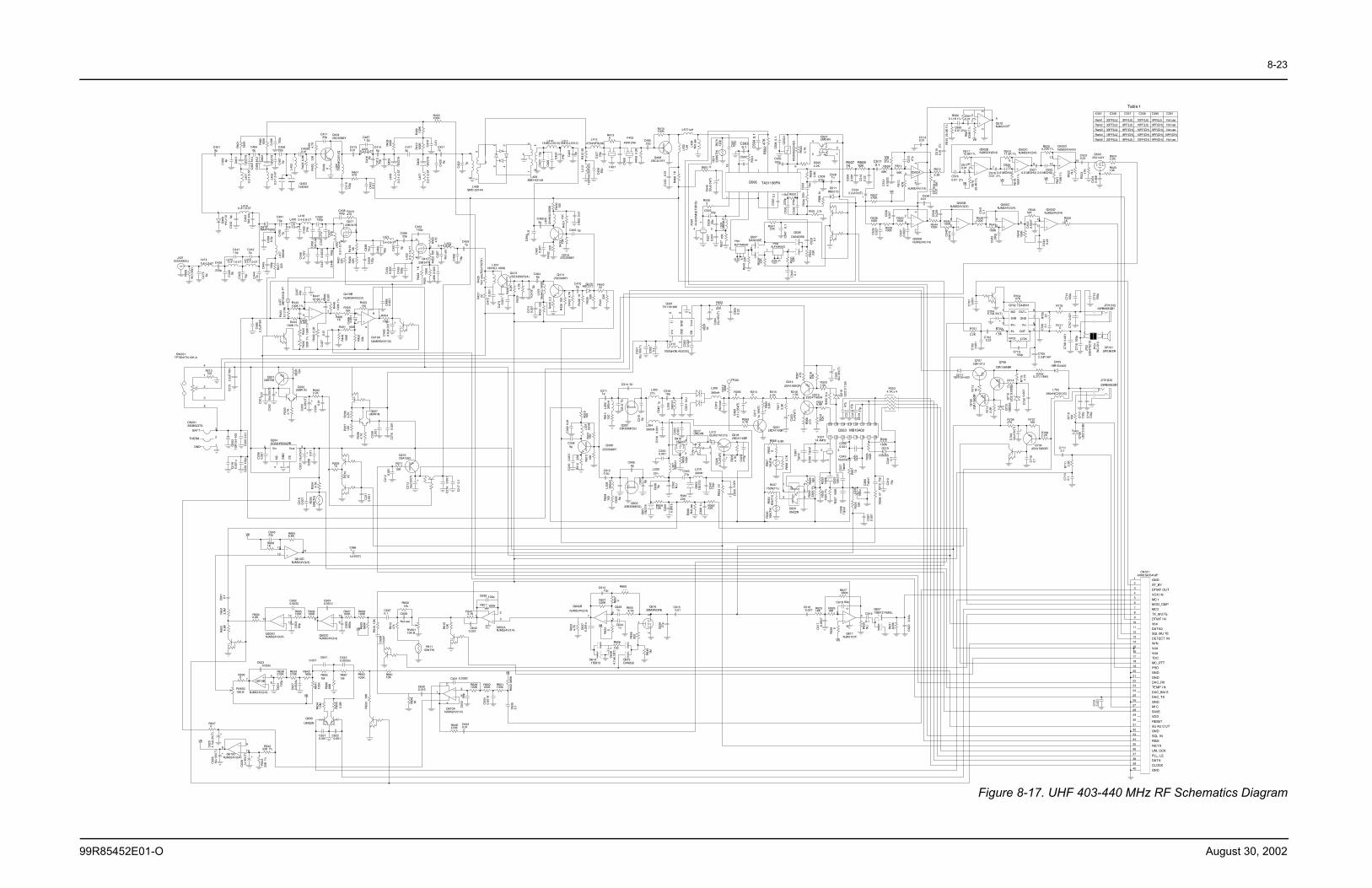
8-23
99R85452E01-O August 30, 2002
Figure 8-17. UHF 403-440 MHz RF Schematics Diagram
J40102D04852J L415
0.4-1.0-5T
C44
09p
C44
3
10p
L4160.4-1.0-5T
C4411.5p
C4422p
C439
220p
C44
47p
L4190.4-1.0-5T
Q40
9H
VU
131
C43
24p
R41
722
0
C43
3N
ot u
se
C4018p
C40
24p Q40
1
1SV
279
Q40
2
1SV
279
L401
0.3-
1.0-
5T
C40
75p
C40822p
Q4031SS362
C4090.01
R40
56.
8K
R40
312
K
Q4042SC5086Y
R40
60
R40
44.
7K
C41133p
L4050.3-1.0-7T
C4130.01
Q40
5
1SV
279
C4146p
Q40
6
1SV
279
C41
510
p
L406
0.3-
1.0-
5T
C4175p
C41
9
0.01
C42
09p
C4217p
C42
2
7p
1 2
3 4
C42
4
24p
L41115nH(LL2012)
C42
5
10p
R41
256
L412
150n
H(C
2012
C)
C42
682
p
L413470nH(FSLM)
C42
724
p
F401- - -
C42
8-
- -
F402
45N12A5
R4130
Q4082SC4215Y
R415150K
C43
00.
01
Q410MA4PH262
2
3
8
4
1
Q419ANJM2904V(1/2)
6
57
Q419BNJM2904V(2/2)
C4650.001
R443100K 1%
R444100K 1%
R44
20.
1(1W
)
R44
510
0K 1
%R
446
100K
1%
R44
910
0K 1
%C46
60.
001
R44797.6K 1%
R45010K
C46
80.
001
R4531M
R454
15K
R451 100K
R45
233
k
R44
810
0K
+
C46
96.
8u6.
3V(T
)
C46
70.
01
L417
390n
H
C44
5
100p
C493150p
C43
524
p
L4180.4-0.8-2T
C49
27p C43
727
p
L420
0.3-
1.0-
7T
R418470
C438100p
C45
0
56p
R41
956
R42
033
K
C44
910
0p
R42
122
K
L421
0.4-0.9-3T
C45
1
5p
C49115p
C44
815
0p
C44
70.
0033
L422
0.3-
1.0-
7T
C45
533
0p
C45
40.
022
R42
247
0
C453100p
R42
310
0
R42
510
0K
R42
41K
C45
60.
022
C45
7
Not
use
L4230.4-0.9-3T
C45
8
18p
C4597p
Q4162SC5086Y
L426
22nH
(LL1
608)
R43
010
0
C4605p
R43
110
K
C463 5p
R43
310
K
R43
222
0
C46
10.
001
C46
20.
01
R42
6N
ot u
se(R
2)47
0(R
1)R
427
22
L42418nH(LL1608)
C47
20.
001
Q4132SC3356(R24)
R42
88.
2K
R42
94.
7K
C47
30.
001
C4648p
L425
18nH
(LL1
608)
Q4142SC5086Y
R43
52.
2
R43
410
0
C47
40.
001
R43
610
K
R43
74.
7K
C4705p
R43
81K
Q415HSC277
R43
9 330
R44022
R44
1 330
Q2012SB798
R20
110
K
R20
34.
7K
+
C20
210
u10V
(T)
C20
1 0.01
+
C20
31u
16V
(T)
R2022.2K
C20
4 0.01
R20
62.
2KR
207
10K
R20
84.
7K C20
90.
001
C21
00.
001
C20
60.
001 +
C20
710
u10V
(T)
C20
80.
01
R20910
R21
022
C21
10.
001
C21
40.
001
+
C21
310
u10V
(T)
Q2102SA1362
R211
10K
C21
2 0.00
1
1 8916
Q506 TA31136FN
R5260
C52533p
C52
639
p
C52
70.
001
L501
1uH
(MLF
)R
527
10K
C53
00.
1 R5321.5M
C53
122
0p
C53
222
0p
R535 2.2k
R53
433
0kC
533
56p
C508470p
R50
63.
3K
1 2
3 4 5
F501BLFYM455D
R54122K
R54
222
K1 2
3 4 5
F502ALFYM455G
R53
022
K
R53
122
K
C50
110
0p
C502- - -
C5030.1
R50
10
CD
501
IFD
0455
C24
E3
C505100p
R50
32.
7K
R5052.2K
R50
247
K
C50
40.
1
R5071K
R50810K
C50
90.
001
C51
00.
22
C5110.1 R509
68K
C51
20.
0022
R511
56K
R51
047
0K
C51
327
p
R51
310
K
C5160.01 2%
R51
247
K
R54
022
K
C51
90.
01
6
57
Q502BNJM324V(2/4)
VB
2
31
411
Q502A
NJM324V(1/4)
C5170.01 2%
R51715.8K 1%
R51
629
.4K
1%
VB
C5180.01 2%
C520
0.01(ECHU)
9
108
Q502CNJM324V(3/4)R518
11.5K 1%
R51
915
0K 1
%
VB
C5210.01(ECHU)
C5220.01(ECHU)
13
1214
Q502DNJM324V(4/4)
R5204.22K 1%
R52
171
5K 1
%
R52
2N
.U
VB
C5230.22
R52
3 47K
2
31
411
Q505ANJM324V(1/4)
R543100K
R539100K
R538100K
C53
70.
0027
C53
50.
027
C53
60.
047
R544100K
C53
90.
039
R545100K
6
57
Q505BNJM324V(2/4)
C54
00.
0015
R546100K
C54
10.
1
9
108
Q505CNJM324V(3/4)
R547
100K
C54
239
0p
R54810K
R54
910
0K
13
1214
Q505DNJM324V(4/4)
C54
30.
0047
C54
40.
22
R5501K
MO1
SVR2
IN+3
IN-4 OUT- 5
Vcc 6
GND 7
OUT+ 8
Q702 TDA8541
R70
522
C70
70.
001
C70
80.
001
R703 470K
R702
1.5K
SP701SPEAKER
12
P701
WC
-013
12
J702
5304
7-02
10
R70447K
+
C7044.7u6.3V(T)
C7030.22
C70
60.
1
C70
20.
001
R701
2.2K
R71
010
0
Q70
6U
DZ
S 6
.8B
Q7111SR154-400
R7090.27( 1/8W)
L702390nH(C2012C)
R7082.2K
Q7042SA1586GR
R70710K
+
C30
110
u10V
(T)
R706470
C71
00.
1
R71
12.
2KC
713
0.1
C7110.1
Q5032SJ144Y R524
2.2K
C52
40.
068
R52510K
Q20
31S
R15
4-40
0
C20
50.
01
R20
44.
7K
R20
550
K(T
H)
C70
10.
001
L427
ZB
FS
5105
-PT
+
C5342.2u10V(T)
C5140.01
VDD
Vbb
Vdd
Vdd
GND
MOD_CMP
CLOCK
DATA
PLL_ LE
UNL OCK
DATA0
DTMF OUT
DTMF IN
SU AU O UT
DETECT IN
TDC
W/N
RSSI
SQL IN
VOX IN
TEMP I N
MC1
MC2
RX/TX
SAVE
TX_MUTE
ST_BY
SQL MU TE
DAC_RX
DAC_TX
DAC_BAI S
RESET
PRO
GND
MC_PTT
GND
GND
MI C
GND
GND
R537470K
C5380.01
4
1
2
3
5
SW201TP76N17N 10K.A
C4046p
L402
0.3-
1.0-
5T
R40
1
100K R
402
100K
C40
6
100p
L403
- -
-
L40
418
0nH(
C20
12C)
R407470
C41
010
0p
C41
20.
01
L407
0.3-
1.0-
5T
R40
810
0K
R41
010
0KR
409
100K
L41015nH(LL2012)
C42
315
p
R455100K
C41
6 6p
C40
3N
.U
C40
5N
.U
Q507DAN235E
Q508
DAN235E
C52
90.
1
4
5
3
2
1
Q501UMC4N
+
C70
910
u10V
(T)
C30
20.
1
Vin
1
OSC
2
DK
3V
out
4
GN
D5
TI
6
Q301TK11816M
L313
1000uH(NL453232)
C30
30.
022
R30
11K
+
C30
410
u16V
(T)
R302
220
C30
50.
22
Q202UMW1N
Q207UMW1N
J701(1/2)09R80683Z01
J701(2/2)
09R80683Z01
C50
60.
1
C71
410
0p
C71
510
0p
C71
610
0pC
717
100p
C71
810
0p
C719100p
2
136
4
L408SMD-0314A
2
13 4
6
L409SMD-0314A
C54
60.
1
C47
85p
C48
8N
.U
C21
70.
1
C4871.5p
R45
93.
3K
C48
90.
001
C21
80.
001
L42
8N
ot u
se
R551 0
+
C54
533
u6.3
V(T
)
C54
70.
1
1
2
3
4
5
6
7
8
9
10
11
12
13
14
15
16
17
18
19
20
21
22
23
24
25
26
27
28
29
30
31
32
33
34
35
36
37
38
39
40
CN701AXK6S40545J/P
Vin2
GN
D1
Vout 5
NC
4
CE
3
Q204XC62HR5002PR
R4661K
R71
21K
Q7072SA1313
R71
32.
2K
Q708
2SA1586GR
R714
2.2K
R71
54.
7K
Q71
0U
DZ
S 2
0B
C72
00.
001
Q70
92S
A15
86GR
13
24
X50
144
.645
MH
z(T
OP-
B)
C49
4 N.U
R212100
C49522p
L4140.4-1.0-5T
C47
56p
C72
10.
001
C42
9-
- -
3
2
1 Q4122SK3475
1
3
2
Q4112SK3476
R60
13.
3MR
602
6.8K
R6046.8K
13
1214
Q602DNJM324V(4/4)
C60
382
p
R605100K
R606100K
C6020.0033
9
108
Q602CNJM324V(3/4)
C6040.0012
C60
568
0p
R607100K
R608100K
R60
968
0K
VB
R61
010
K
C60
60.
047
C6070.1 C608
Not use
R61
247
k
RV60110K.B
R61
512
K
R6164.7K 6
57
Q602B
NJM324V(2/4)
R617 100K
2
31
411 Q602A
NJM324V(1/4) R62
04.
7K
R62
20
R621330K
C61210p
VB
C6150.01
RV60210K.B
R63
318
K
R63
41.
5M
R63
53.
3M
C6210.001
C6220.001
R6360
6
57
Q610B
NJM324V(2/4)
C62
415
0p
R638270K
R639270K
C6230.022u
R640180k
C62
70.
0033
u
R64
110
0K
VB 2
31
411
Q610ANJM324V(1/4)
+
C62
610
u10V
(T)
+
C62
81u
16V
(T)
R64
322
K 1
%
R64233K 1%
VB9
108
Q610CNJM324V(3/4)
C63
268
p
R649100K
R650100K
C631 0.0082
R651100K
C63
40.
0018
R65
268
0K
VB
R63
182
0K
C6430.0033u
C62
00.
22u
R6370
+
C62
54.
7u6.
3V(T
)
R648470K
C6330.01
C63
50.
1
Q6071SS372-TE85L
Q609
UMG2N
R65912k
C636 100p
R6554.7K
R65
70
C63
927
pQ614
1SS372Q615DAN222
R656
100+
C63
84.
7u6.
3V(T
)
R65
882
0
3
1
2
Q616SSM3K03FE
R660- - -
C6291u
R64
51M
C6410.001
R663100K
R66110K
C60
10.
1
C6300.015
R64
61K
C6420.022
R32
710
0K
R32
922
0K 1
%
R33
210
0K 1
%
C33
6T
able
1
C33
7T
able
1C
338
Tab
le1
R33
310
0K
C3390.001
C34310u10V(T)
R336
100K
1 2 3 4 5 6 7 8
910111213141516
Q323 MB15A02
R3216.8K
R31
910
K
Q3152SC4116GR
Q3142SA1586GR
R3201.5K
R31
810
K
Q31
6U
DZ
S 7
.5B
+
C32
410
u16V
(T)
R3161.5K
R31
73.
3K
+
C32
31u
16V(
T)
R3152.7K
R31
310
0K
TP301
C31
947
p
C31
847
p
C31
747
p
R3140
R3234.7K x 4
R35
5N
.U
R36122K
R36222K
R35
710
C31
210
pR
358
47
C31
315
p
C36
81u
R3560
Q319
1SS355
Q32
21S
V21
7
13
24
X30114.4MHz
+
C36
90.
1u 3
5V(T
)
R36
46.
8K
+
C37
11u
16V
(T)
Q3312SC4116GR
R3594.7K R
366
470
R36
747
0
R33
510
0K
C34
10.
1
C33
5
10p
1
2
3 4
5
6
Q320UMZ2N
R56
518
K
R56
710
k(T
H)
R33
010
K(T
H)
R337150K(1%)
C36
7 0
.001
R56
482
k(1%
)
R566 6.8K
R56
30
C91
9N
ot u
se
L306
390nH
Q3082SC5086Y
R91
310
K
L301
22nH
R31
115
K
R31
010
0
C3085p
C91818p
L30327n
L304390nH
C31
60.
001
C314 5p
C91
37p
C3111p
R93
010
0K
C9120.5p
C93
85p
C93
56p
Q92
11S
V27
9
L30
539
0nH
L312BLM21A121S Q318
2SC4116GR
R93
54.
7K
C32
947
0p+
C32
84.
7u16
V(T
)
Q92
21S
V27
0
L310390nH
C34
210
0p
R93
41K
C34
50.
001
R31
222
0
C31
00.
001
4
5
3
2
1
Q317UMC4NC
309
0.01
L30
239
0nH
R91
415
0L
308
390n
H
R92
815
0
C31
55p
C93
7
6p
R92910K
C34027p
C9366p
Q9162SJ243
C35
1N
.U
C35
2N
.UC
353
0.00
1
Q3032SK508(K52)
Q3022SK508(K52)
R32
510
K
L30
739
0nH
L30922n
C3200.001
C35
0
0.00
15
C48
52.
2uF/
16V
C44
61u
16V
R56
9
1K(1
/4W
)
C49633p
R51
525
.5K
1%
C51
50.
01 2
%
3
14
52
Q510NJM2107F
C5510.01 2%
C5500.01 2%
R56
163
4K 1
%
R5605.11K 1%
VB
R514
3.3K
3
2
1
BATT
THERM
GND
CN20109D86237A
R61150k(TH)
C21
52.
2uF
/16V
C7052.2uF/16V
C38
1T
able
1
C38
0T
able
1
Q7051SR154-400
R7160
R7170
Q71
21S
S355
C63
70.
001u
R6671M
R6651M
R66
668
K
L430
0.3-1.0-4T
R56
84.
7K
13
1214
Q610DNJM324V(4/4)
VB
R6681K
R6646.8K
+
C366
1u16V(T)
VB
R62
8 0
R62618K
C6160.027
R627680K
C618 82p
R62
9N
U
C619
0.1
R62518K
C61
70.
0047
3
14
52
Q617NJM2107F
R57
122
0K(T
H)
R57
012
0k
C94
01p
R36
8N
ot u
se
C22
010
0p
C21
90.
001u
C43
6N
ot U
seR
469
2.2K
C49
722
p
R46
81K
L432
1uH
L4311uH
C5281u
Q511RB521S
R53
61k
C6441u
C64522p
Rank1
Rank2
Rank3
Rank4
Rank5
X301 C336 C337 C338 C380 C381
33PF(UJ)
33PF(UJ)
33PF(UJ)
18PF(UJ)
33PF(UJ)
Not use
Not use
Not use
Not use
15PF(CH)
8PF(UJ)
8PF(UJ)
8PF(CH)
8PF(CH)
8PF(UJ)
10PF(UJ)
10PF(UJ)
10PF(CH)
10PF(CH)
10PF(CH)
9PF(UJ)
9PF(CH)
9PF(CH)
9PF(CH)
9PF(CH)
Table 1
C49
80.
5p
C75
227
p
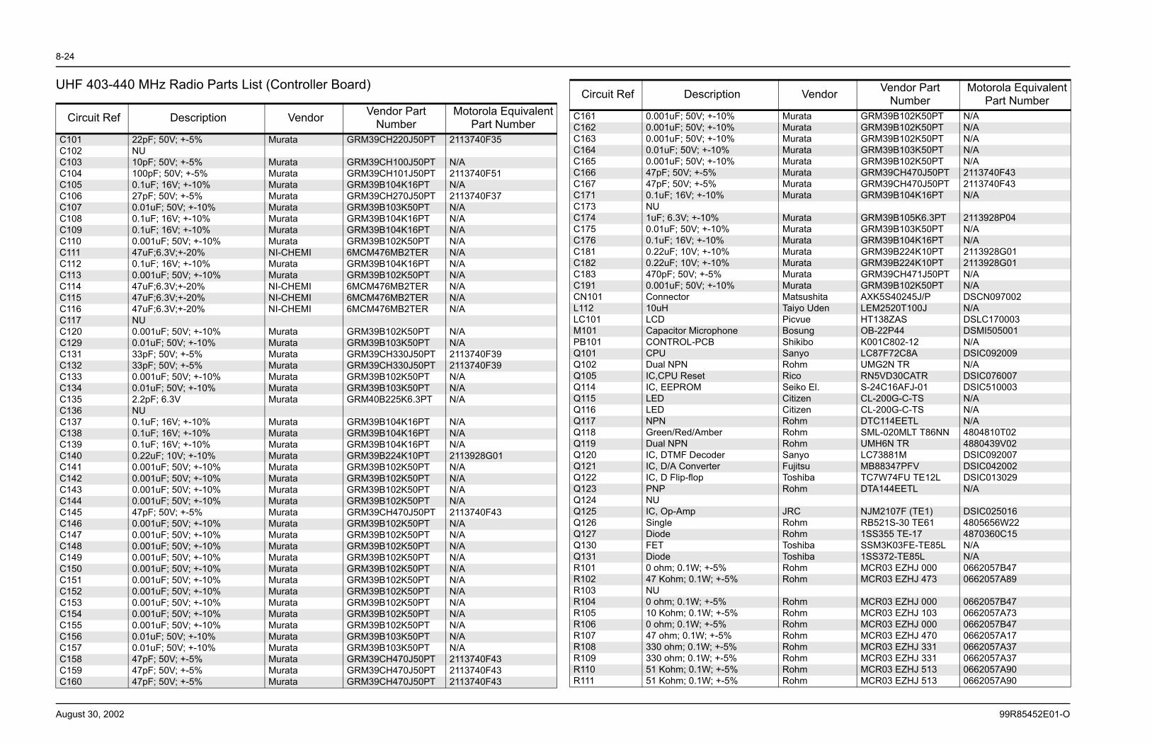
8-24
August 30, 2002 99R85452E01-O
UHF 403-440 MHz Radio Parts List (Controller Board)
Circuit Ref Description Vendor Vendor Part Number
Motorola Equivalent Part Number
C101 22pF; 50V; +-5% Murata GRM39CH220J50PT 2113740F35C102 NUC103 10pF; 50V; +-5% Murata GRM39CH100J50PT N/AC104 100pF; 50V; +-5% Murata GRM39CH101J50PT 2113740F51C105 0.1uF; 16V; +-10% Murata GRM39B104K16PT N/AC106 27pF; 50V; +-5% Murata GRM39CH270J50PT 2113740F37C107 0.01uF; 50V; +-10% Murata GRM39B103K50PT N/AC108 0.1uF; 16V; +-10% Murata GRM39B104K16PT N/AC109 0.1uF; 16V; +-10% Murata GRM39B104K16PT N/AC110 0.001uF; 50V; +-10% Murata GRM39B102K50PT N/AC111 47uF;6.3V;+-20% NI-CHEMI 6MCM476MB2TER N/AC112 0.1uF; 16V; +-10% Murata GRM39B104K16PT N/AC113 0.001uF; 50V; +-10% Murata GRM39B102K50PT N/AC114 47uF;6.3V;+-20% NI-CHEMI 6MCM476MB2TER N/AC115 47uF;6.3V;+-20% NI-CHEMI 6MCM476MB2TER N/AC116 47uF;6.3V;+-20% NI-CHEMI 6MCM476MB2TER N/AC117 NUC120 0.001uF; 50V; +-10% Murata GRM39B102K50PT N/AC129 0.01uF; 50V; +-10% Murata GRM39B103K50PT N/AC131 33pF; 50V; +-5% Murata GRM39CH330J50PT 2113740F39C132 33pF; 50V; +-5% Murata GRM39CH330J50PT 2113740F39C133 0.001uF; 50V; +-10% Murata GRM39B102K50PT N/AC134 0.01uF; 50V; +-10% Murata GRM39B103K50PT N/AC135 2.2pF; 6.3V Murata GRM40B225K6.3PT N/AC136 NUC137 0.1uF; 16V; +-10% Murata GRM39B104K16PT N/AC138 0.1uF; 16V; +-10% Murata GRM39B104K16PT N/AC139 0.1uF; 16V; +-10% Murata GRM39B104K16PT N/AC140 0.22uF; 10V; +-10% Murata GRM39B224K10PT 2113928G01C141 0.001uF; 50V; +-10% Murata GRM39B102K50PT N/AC142 0.001uF; 50V; +-10% Murata GRM39B102K50PT N/AC143 0.001uF; 50V; +-10% Murata GRM39B102K50PT N/AC144 0.001uF; 50V; +-10% Murata GRM39B102K50PT N/AC145 47pF; 50V; +-5% Murata GRM39CH470J50PT 2113740F43C146 0.001uF; 50V; +-10% Murata GRM39B102K50PT N/AC147 0.001uF; 50V; +-10% Murata GRM39B102K50PT N/AC148 0.001uF; 50V; +-10% Murata GRM39B102K50PT N/AC149 0.001uF; 50V; +-10% Murata GRM39B102K50PT N/AC150 0.001uF; 50V; +-10% Murata GRM39B102K50PT N/AC151 0.001uF; 50V; +-10% Murata GRM39B102K50PT N/AC152 0.001uF; 50V; +-10% Murata GRM39B102K50PT N/AC153 0.001uF; 50V; +-10% Murata GRM39B102K50PT N/AC154 0.001uF; 50V; +-10% Murata GRM39B102K50PT N/AC155 0.001uF; 50V; +-10% Murata GRM39B102K50PT N/AC156 0.01uF; 50V; +-10% Murata GRM39B103K50PT N/AC157 0.01uF; 50V; +-10% Murata GRM39B103K50PT N/AC158 47pF; 50V; +-5% Murata GRM39CH470J50PT 2113740F43C159 47pF; 50V; +-5% Murata GRM39CH470J50PT 2113740F43C160 47pF; 50V; +-5% Murata GRM39CH470J50PT 2113740F43
C161 0.001uF; 50V; +-10% Murata GRM39B102K50PT N/AC162 0.001uF; 50V; +-10% Murata GRM39B102K50PT N/AC163 0.001uF; 50V; +-10% Murata GRM39B102K50PT N/AC164 0.01uF; 50V; +-10% Murata GRM39B103K50PT N/AC165 0.001uF; 50V; +-10% Murata GRM39B102K50PT N/AC166 47pF; 50V; +-5% Murata GRM39CH470J50PT 2113740F43C167 47pF; 50V; +-5% Murata GRM39CH470J50PT 2113740F43C171 0.1uF; 16V; +-10% Murata GRM39B104K16PT N/AC173 NUC174 1uF; 6.3V; +-10% Murata GRM39B105K6.3PT 2113928P04C175 0.01uF; 50V; +-10% Murata GRM39B103K50PT N/AC176 0.1uF; 16V; +-10% Murata GRM39B104K16PT N/AC181 0.22uF; 10V; +-10% Murata GRM39B224K10PT 2113928G01C182 0.22uF; 10V; +-10% Murata GRM39B224K10PT 2113928G01C183 470pF; 50V; +-5% Murata GRM39CH471J50PT N/AC191 0.001uF; 50V; +-10% Murata GRM39B102K50PT N/ACN101 Connector Matsushita AXK5S40245J/P DSCN097002L112 10uH Taiyo Uden LEM2520T100J N/ALC101 LCD Picvue HT138ZAS DSLC170003M101 Capacitor Microphone Bosung OB-22P44 DSMI505001PB101 CONTROL-PCB Shikibo K001C802-12 N/AQ101 CPU Sanyo LC87F72C8A DSIC092009Q102 Dual NPN Rohm UMG2N TR N/AQ105 IC,CPU Reset Rico RN5VD30CATR DSIC076007Q114 IC, EEPROM Seiko El. S-24C16AFJ-01 DSIC510003Q115 LED Citizen CL-200G-C-TS N/AQ116 LED Citizen CL-200G-C-TS N/AQ117 NPN Rohm DTC114EETL N/AQ118 Green/Red/Amber Rohm SML-020MLT T86NN 4804810T02Q119 Dual NPN Rohm UMH6N TR 4880439V02Q120 IC, DTMF Decoder Sanyo LC73881M DSIC092007Q121 IC, D/A Converter Fujitsu MB88347PFV DSIC042002Q122 IC, D Flip-flop Toshiba TC7W74FU TE12L DSIC013029Q123 PNP Rohm DTA144EETL N/AQ124 NUQ125 IC, Op-Amp JRC NJM2107F (TE1) DSIC025016Q126 Single Rohm RB521S-30 TE61 4805656W22Q127 Diode Rohm 1SS355 TE-17 4870360C15Q130 FET Toshiba SSM3K03FE-TE85L N/AQ131 Diode Toshiba 1SS372-TE85L N/AR101 0 ohm; 0.1W; +-5% Rohm MCR03 EZHJ 000 0662057B47R102 47 Kohm; 0.1W; +-5% Rohm MCR03 EZHJ 473 0662057A89R103 NUR104 0 ohm; 0.1W; +-5% Rohm MCR03 EZHJ 000 0662057B47R105 10 Kohm; 0.1W; +-5% Rohm MCR03 EZHJ 103 0662057A73R106 0 ohm; 0.1W; +-5% Rohm MCR03 EZHJ 000 0662057B47R107 47 ohm; 0.1W; +-5% Rohm MCR03 EZHJ 470 0662057A17R108 330 ohm; 0.1W; +-5% Rohm MCR03 EZHJ 331 0662057A37R109 330 ohm; 0.1W; +-5% Rohm MCR03 EZHJ 331 0662057A37R110 51 Kohm; 0.1W; +-5% Rohm MCR03 EZHJ 513 0662057A90R111 51 Kohm; 0.1W; +-5% Rohm MCR03 EZHJ 513 0662057A90
Circuit Ref Description Vendor Vendor Part Number
Motorola Equivalent Part Number

8-25
99R85452E01-O August 30, 2002
R112 13 Kohm; 0.1W; +-5% Rohm MCR03 EZHJ 133 0662057A76R113 22 Kohm; 0.1W; +-5% Rohm MCR03 EZHJ 223 0662057A81R114 43 Kohm; 0.1W; +-5% Rohm MCR03 EZHJ 433 0665027A88R115 130 Kohm; 0.1W; +-5% Rohm MCR03 EZHJ 134 0662257B01R116 18 Kohm; 0.1W; +-5% Rohm MCR03 EZHJ 183 0662057A79R117 33 Kohm; 0.1W; +-5% Rohm MCR03 EZHJ 333 0662057A85R118 100 Kohm; 0.1W; +-5% Rohm MCR03 EZHJ 104 0662057A97R119 0 ohm; 0.1W; +-5% Rohm MCR03 EZHJ 000 0662057B47R120 0 ohm; 0.1W; +-5% Rohm MCR03 EZHJ 000 0662057B47R121 NUR126 10 Kohm; 0.1W; +-5% Rohm MCR03 EZHJ 103 0662057A73R127 12.4 Kohm; 0.1W; +-1% Rohm MCR03 EZHF 1242 0662057P69R128 6.98 Kohm; 0.1W; +-1% Rohm MCR03 EZHF 6981 0662057Y24R129 1 Kohm; 0.1W; +-5% Rohm MCR03 EZHJ 102 0662057A49R134 1 Kohm; 0.1W; +-5% Rohm MCR03 EZHJ 102 0662057A49R135 10 Kohm; 0.1W; +-5% Rohm MCR03 EZHJ 103 0662057A73R136 10 Kohm; 0.1W; +-5% Rohm MCR03 EZHJ 103 0662057A73R137 1 Kohm; 0.1W; +-5% Rohm MCR03 EZHJ 102 0662057A49R138 100 Kohm; 0.1W; +-5% Rohm MCR03 EZHJ 104 0662057A97R141 20 Kohm; 0.1W; +-5% Rohm MCR03 EZHJ 203 0662057A80R142 20 Kohm; 0.1W; +-5% Rohm MCR03 EZHJ 203 0662057A80R143 20 Kohm; 0.1W; +-5% Rohm MCR03 EZHJ 203 0662057A80R144 20 Kohm; 0.1W; +-5% Rohm MCR03 EZHJ 203 0662057A80R145 20 Kohm; 0.1W; +-5% Rohm MCR03 EZHJ 203 0662057A80R146 20 Kohm; 0.1W; +-5% Rohm MCR03 EZHJ 203 0662057A80R147 20 Kohm; 0.1W; +-5% Rohm MCR03 EZHJ 203 0662057A80R148 20 Kohm; 0.1W; +-5% Rohm MCR03 EZHJ 203 0662057A80R150 2.2 Kohm; 0.1W; +-5% Rohm MCR03 EZHJ 222 0662057A57R153 10 Kohm; 0.1W; +-5% Rohm MCR03 EZHJ 103 0662057A73R154 47 Kohm; 0.1W; +-5% Rohm MCR03 EZHJ 473 0662057A89R155 NUR156 47 Kohm; 0.1W; +-5% Rohm MCR03 EZHJ 473 0662057A89R157 220 Kohm; 0.1W; +-5% Rohm MCR03 EZHJ 224 N/AR158 470 Kohm; 0.1W; +-5% Rohm MCR03 EZHJ 474 0662057B14R159 20 Kohm; 0.1W; +-5% Rohm MCR03 EZHJ 203 0662057A80R160 10 Kohm; 0.1W; +-5% Rohm MCR03 EZHJ 103 0662057A73R161 10 Kohm; 0.1W; +-5% Rohm MCR03 EZHJ 103 0662057A73R162 10 Kohm; 0.1W; +-5% Rohm MCR03 EZHJ 103 0662057A73R163 10 Kohm; 0.1W; +-5% Rohm MCR03 EZHJ 103 0662057A73R164 10 Kohm; 0.1W; +-5% Rohm MCR03 EZHJ 103 0662057A73R165 10 Kohm; 0.1W; +-5% Rohm MCR03 EZHJ 103 0662057A73R166 10 Kohm; 0.1W; +-5% Rohm MCR03 EZHJ 103 0662057A73R167 47 Kohm; 0.1W; +-5% Rohm MCR03 EZHJ 473 0662057A89R168 47 Kohm; 0.1W; +-5% Rohm MCR03 EZHJ 473 0662057A89R169 330 ohm; 0.1W; +-5% Rohm MCR03 EZHJ 331 0662057A37R170 47 Kohm; 0.1W; +-5% Rohm MCR03 EZHJ 473 0662057A89R171 47 Kohm; 0.1W; +-5% Rohm MCR03 EZHJ 473 0662057A89R172 47 Kohm; 0.1W; +-5% Rohm MCR03 EZHJ 473 0662057A89R173 2.2 Kohm; 0.1W; +-5% Rohm MCR03 EZHJ 222 0662057A57R174 2.2 Kohm; 0.1W; +-5% Rohm MCR03 EZHJ 222 0662057A57R175 4.7 Kohm; 0.1W; +-5% Rohm MCR03 EZHJ 472 0662057A65
Circuit Ref Description Vendor Vendor Part Number
Motorola Equivalent Part Number
R176 22 Kohm; 0.1W; +-5% Rohm MCR03 EZHJ 223 0662057A81R177 NUR180 10 Kohm; 0.1W; +-5% Rohm MCR03 EZHJ 103 0662057A73R182 0 ohm; 0.1W; +-5% Rohm MCR10 EZHJ 000 N/AR183 47 Kohm; 0.1W; +-5% Rohm MCR03 EZHJ 473 0662057A89R184 10 Kohm; 0.1W; +-5% Rohm MCR03 EZHJ 103 0662057A73R185 470 ohm; 0.1W; +-5% Rohm MCR03 EZHJ 471 0662057A41R186 0 ohm; 0.1W; +-5% Rohm MCR03 EZHJ 000 0662057B47S101 Tact Switch Motorola Y39A33110FP 4080523Z01S102 Tact Switch Motorola Y39A33110FP 4080523Z01X101 Filter, 8.388608 MHz Daishinkuu AT-38 DSXT182001
Circuit Ref Description Vendor Vendor Part Number
Motorola Equivalent Part Number
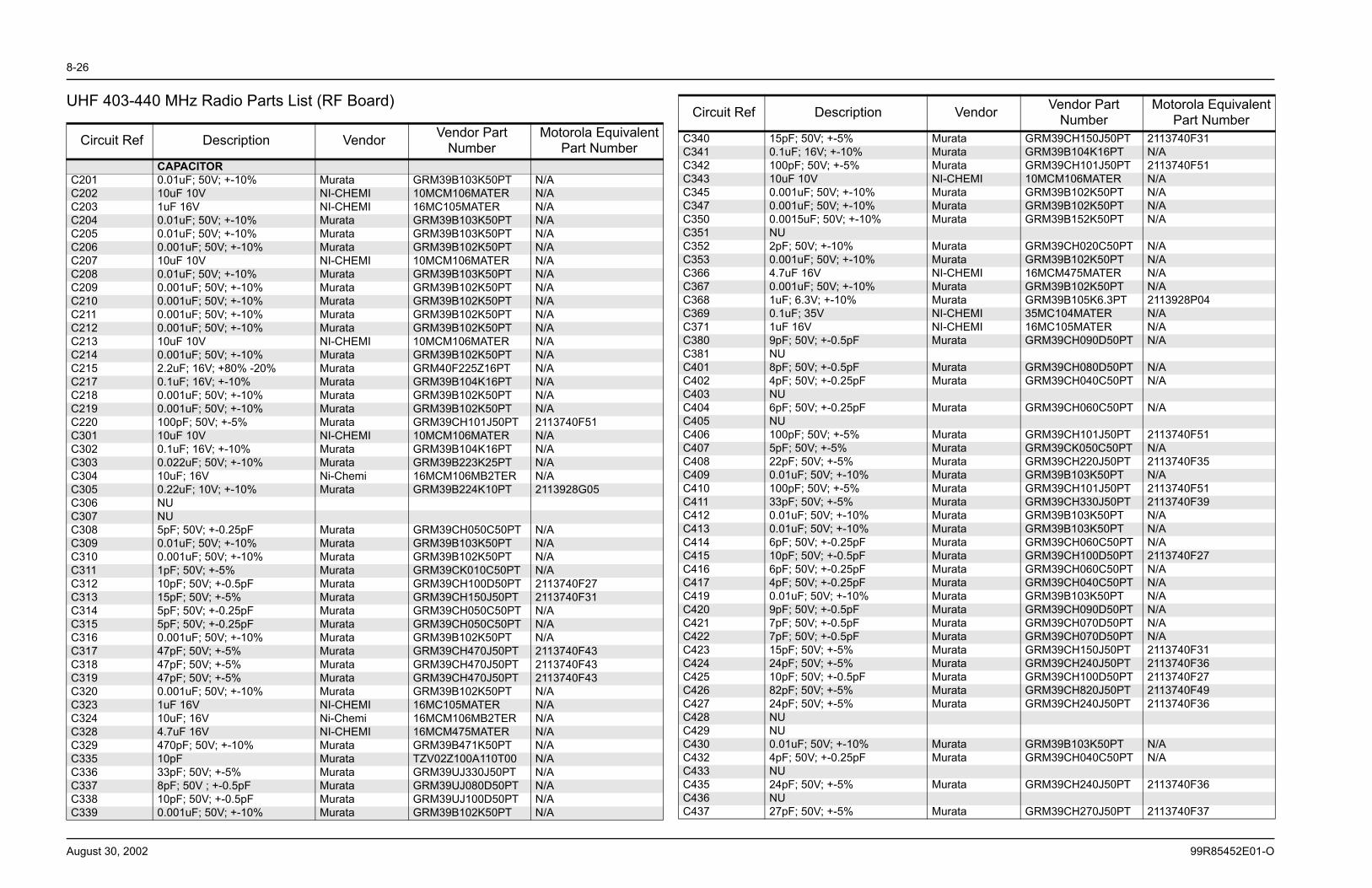
8-26
August 30, 2002 99R85452E01-O
UHF 403-440 MHz Radio Parts List (RF Board)
Circuit Ref Description Vendor Vendor Part Number
Motorola Equivalent Part Number
CAPACITORC201 0.01uF; 50V; +-10% Murata GRM39B103K50PT N/AC202 10uF 10V NI-CHEMI 10MCM106MATER N/AC203 1uF 16V NI-CHEMI 16MC105MATER N/AC204 0.01uF; 50V; +-10% Murata GRM39B103K50PT N/AC205 0.01uF; 50V; +-10% Murata GRM39B103K50PT N/AC206 0.001uF; 50V; +-10% Murata GRM39B102K50PT N/AC207 10uF 10V NI-CHEMI 10MCM106MATER N/AC208 0.01uF; 50V; +-10% Murata GRM39B103K50PT N/AC209 0.001uF; 50V; +-10% Murata GRM39B102K50PT N/AC210 0.001uF; 50V; +-10% Murata GRM39B102K50PT N/AC211 0.001uF; 50V; +-10% Murata GRM39B102K50PT N/AC212 0.001uF; 50V; +-10% Murata GRM39B102K50PT N/AC213 10uF 10V NI-CHEMI 10MCM106MATER N/AC214 0.001uF; 50V; +-10% Murata GRM39B102K50PT N/AC215 2.2uF; 16V; +80% -20% Murata GRM40F225Z16PT N/AC217 0.1uF; 16V; +-10% Murata GRM39B104K16PT N/AC218 0.001uF; 50V; +-10% Murata GRM39B102K50PT N/AC219 0.001uF; 50V; +-10% Murata GRM39B102K50PT N/AC220 100pF; 50V; +-5% Murata GRM39CH101J50PT 2113740F51C301 10uF 10V NI-CHEMI 10MCM106MATER N/AC302 0.1uF; 16V; +-10% Murata GRM39B104K16PT N/AC303 0.022uF; 50V; +-10% Murata GRM39B223K25PT N/AC304 10uF; 16V Ni-Chemi 16MCM106MB2TER N/AC305 0.22uF; 10V; +-10% Murata GRM39B224K10PT 2113928G05C306 NUC307 NUC308 5pF; 50V; +-0.25pF Murata GRM39CH050C50PT N/AC309 0.01uF; 50V; +-10% Murata GRM39B103K50PT N/AC310 0.001uF; 50V; +-10% Murata GRM39B102K50PT N/AC311 1pF; 50V; +-5% Murata GRM39CK010C50PT N/AC312 10pF; 50V; +-0.5pF Murata GRM39CH100D50PT 2113740F27C313 15pF; 50V; +-5% Murata GRM39CH150J50PT 2113740F31C314 5pF; 50V; +-0.25pF Murata GRM39CH050C50PT N/AC315 5pF; 50V; +-0.25pF Murata GRM39CH050C50PT N/AC316 0.001uF; 50V; +-10% Murata GRM39B102K50PT N/AC317 47pF; 50V; +-5% Murata GRM39CH470J50PT 2113740F43C318 47pF; 50V; +-5% Murata GRM39CH470J50PT 2113740F43C319 47pF; 50V; +-5% Murata GRM39CH470J50PT 2113740F43C320 0.001uF; 50V; +-10% Murata GRM39B102K50PT N/AC323 1uF 16V NI-CHEMI 16MC105MATER N/AC324 10uF; 16V Ni-Chemi 16MCM106MB2TER N/AC328 4.7uF 16V NI-CHEMI 16MCM475MATER N/AC329 470pF; 50V; +-10% Murata GRM39B471K50PT N/AC335 10pF Murata TZV02Z100A110T00 N/AC336 33pF; 50V; +-5% Murata GRM39UJ330J50PT N/AC337 8pF; 50V ; +-0.5pF Murata GRM39UJ080D50PT N/AC338 10pF; 50V; +-0.5pF Murata GRM39UJ100D50PT N/AC339 0.001uF; 50V; +-10% Murata GRM39B102K50PT N/A
C340 15pF; 50V; +-5% Murata GRM39CH150J50PT 2113740F31C341 0.1uF; 16V; +-10% Murata GRM39B104K16PT N/AC342 100pF; 50V; +-5% Murata GRM39CH101J50PT 2113740F51C343 10uF 10V NI-CHEMI 10MCM106MATER N/AC345 0.001uF; 50V; +-10% Murata GRM39B102K50PT N/AC347 0.001uF; 50V; +-10% Murata GRM39B102K50PT N/AC350 0.0015uF; 50V; +-10% Murata GRM39B152K50PT N/AC351 NUC352 2pF; 50V; +-10% Murata GRM39CH020C50PT N/AC353 0.001uF; 50V; +-10% Murata GRM39B102K50PT N/AC366 4.7uF 16V NI-CHEMI 16MCM475MATER N/AC367 0.001uF; 50V; +-10% Murata GRM39B102K50PT N/AC368 1uF; 6.3V; +-10% Murata GRM39B105K6.3PT 2113928P04C369 0.1uF; 35V NI-CHEMI 35MC104MATER N/AC371 1uF 16V NI-CHEMI 16MC105MATER N/AC380 9pF; 50V; +-0.5pF Murata GRM39CH090D50PT N/AC381 NUC401 8pF; 50V; +-0.5pF Murata GRM39CH080D50PT N/AC402 4pF; 50V; +-0.25pF Murata GRM39CH040C50PT N/AC403 NUC404 6pF; 50V; +-0.25pF Murata GRM39CH060C50PT N/AC405 NUC406 100pF; 50V; +-5% Murata GRM39CH101J50PT 2113740F51C407 5pF; 50V; +-5% Murata GRM39CK050C50PT N/AC408 22pF; 50V; +-5% Murata GRM39CH220J50PT 2113740F35C409 0.01uF; 50V; +-10% Murata GRM39B103K50PT N/AC410 100pF; 50V; +-5% Murata GRM39CH101J50PT 2113740F51C411 33pF; 50V; +-5% Murata GRM39CH330J50PT 2113740F39C412 0.01uF; 50V; +-10% Murata GRM39B103K50PT N/AC413 0.01uF; 50V; +-10% Murata GRM39B103K50PT N/AC414 6pF; 50V; +-0.25pF Murata GRM39CH060C50PT N/AC415 10pF; 50V; +-0.5pF Murata GRM39CH100D50PT 2113740F27C416 6pF; 50V; +-0.25pF Murata GRM39CH060C50PT N/AC417 4pF; 50V; +-0.25pF Murata GRM39CH040C50PT N/AC419 0.01uF; 50V; +-10% Murata GRM39B103K50PT N/AC420 9pF; 50V; +-0.5pF Murata GRM39CH090D50PT N/AC421 7pF; 50V; +-0.5pF Murata GRM39CH070D50PT N/AC422 7pF; 50V; +-0.5pF Murata GRM39CH070D50PT N/AC423 15pF; 50V; +-5% Murata GRM39CH150J50PT 2113740F31C424 24pF; 50V; +-5% Murata GRM39CH240J50PT 2113740F36C425 10pF; 50V; +-0.5pF Murata GRM39CH100D50PT 2113740F27C426 82pF; 50V; +-5% Murata GRM39CH820J50PT 2113740F49C427 24pF; 50V; +-5% Murata GRM39CH240J50PT 2113740F36C428 NUC429 NUC430 0.01uF; 50V; +-10% Murata GRM39B103K50PT N/AC432 4pF; 50V; +-0.25pF Murata GRM39CH040C50PT N/AC433 NUC435 24pF; 50V; +-5% Murata GRM39CH240J50PT 2113740F36C436 NUC437 27pF; 50V; +-5% Murata GRM39CH270J50PT 2113740F37
Circuit Ref Description Vendor Vendor Part Number
Motorola Equivalent Part Number
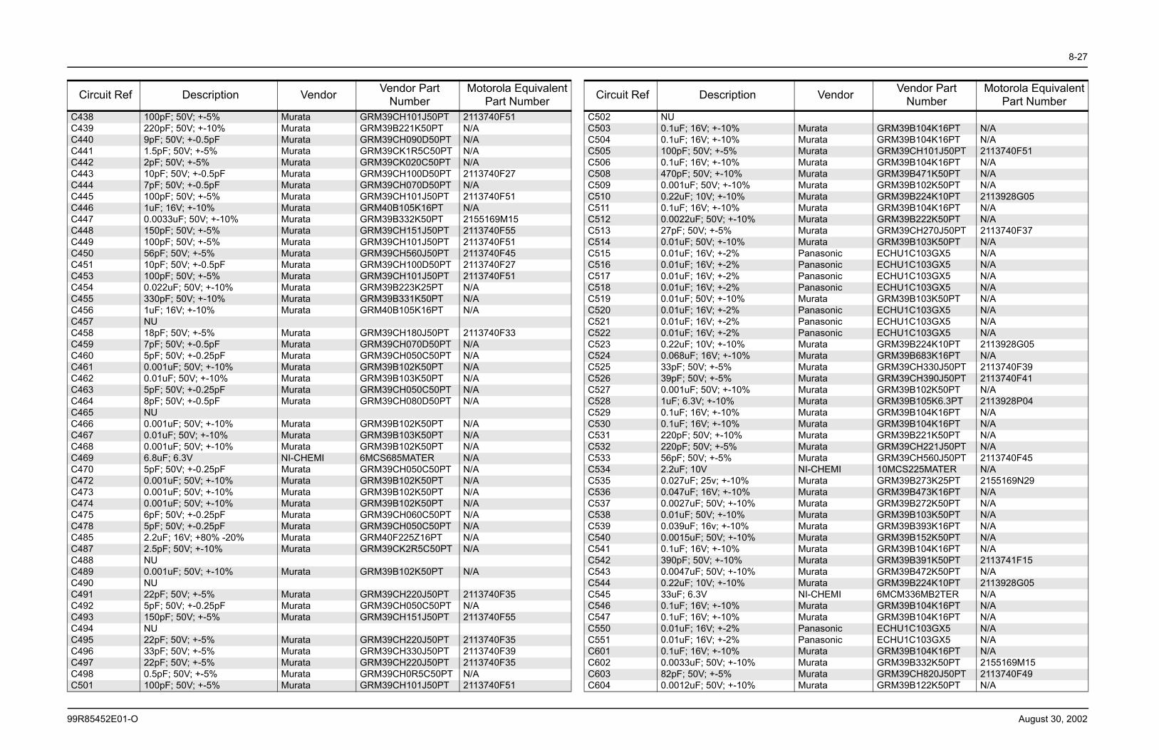
8-27
99R85452E01-O August 30, 2002
C438 100pF; 50V; +-5% Murata GRM39CH101J50PT 2113740F51C439 220pF; 50V; +-10% Murata GRM39B221K50PT N/AC440 9pF; 50V; +-0.5pF Murata GRM39CH090D50PT N/AC441 1.5pF; 50V; +-5% Murata GRM39CK1R5C50PT N/AC442 2pF; 50V; +-5% Murata GRM39CK020C50PT N/AC443 10pF; 50V; +-0.5pF Murata GRM39CH100D50PT 2113740F27C444 7pF; 50V; +-0.5pF Murata GRM39CH070D50PT N/AC445 100pF; 50V; +-5% Murata GRM39CH101J50PT 2113740F51C446 1uF; 16V; +-10% Murata GRM40B105K16PT N/AC447 0.0033uF; 50V; +-10% Murata GRM39B332K50PT 2155169M15C448 150pF; 50V; +-5% Murata GRM39CH151J50PT 2113740F55C449 100pF; 50V; +-5% Murata GRM39CH101J50PT 2113740F51C450 56pF; 50V; +-5% Murata GRM39CH560J50PT 2113740F45C451 10pF; 50V; +-0.5pF Murata GRM39CH100D50PT 2113740F27C453 100pF; 50V; +-5% Murata GRM39CH101J50PT 2113740F51C454 0.022uF; 50V; +-10% Murata GRM39B223K25PT N/AC455 330pF; 50V; +-10% Murata GRM39B331K50PT N/AC456 1uF; 16V; +-10% Murata GRM40B105K16PT N/AC457 NUC458 18pF; 50V; +-5% Murata GRM39CH180J50PT 2113740F33C459 7pF; 50V; +-0.5pF Murata GRM39CH070D50PT N/AC460 5pF; 50V; +-0.25pF Murata GRM39CH050C50PT N/AC461 0.001uF; 50V; +-10% Murata GRM39B102K50PT N/AC462 0.01uF; 50V; +-10% Murata GRM39B103K50PT N/AC463 5pF; 50V; +-0.25pF Murata GRM39CH050C50PT N/AC464 8pF; 50V; +-0.5pF Murata GRM39CH080D50PT N/AC465 NUC466 0.001uF; 50V; +-10% Murata GRM39B102K50PT N/AC467 0.01uF; 50V; +-10% Murata GRM39B103K50PT N/AC468 0.001uF; 50V; +-10% Murata GRM39B102K50PT N/AC469 6.8uF; 6.3V NI-CHEMI 6MCS685MATER N/AC470 5pF; 50V; +-0.25pF Murata GRM39CH050C50PT N/AC472 0.001uF; 50V; +-10% Murata GRM39B102K50PT N/AC473 0.001uF; 50V; +-10% Murata GRM39B102K50PT N/AC474 0.001uF; 50V; +-10% Murata GRM39B102K50PT N/AC475 6pF; 50V; +-0.25pF Murata GRM39CH060C50PT N/AC478 5pF; 50V; +-0.25pF Murata GRM39CH050C50PT N/AC485 2.2uF; 16V; +80% -20% Murata GRM40F225Z16PT N/AC487 2.5pF; 50V; +-10% Murata GRM39CK2R5C50PT N/AC488 NUC489 0.001uF; 50V; +-10% Murata GRM39B102K50PT N/AC490 NUC491 22pF; 50V; +-5% Murata GRM39CH220J50PT 2113740F35C492 5pF; 50V; +-0.25pF Murata GRM39CH050C50PT N/AC493 150pF; 50V; +-5% Murata GRM39CH151J50PT 2113740F55C494 NUC495 22pF; 50V; +-5% Murata GRM39CH220J50PT 2113740F35C496 33pF; 50V; +-5% Murata GRM39CH330J50PT 2113740F39C497 22pF; 50V; +-5% Murata GRM39CH220J50PT 2113740F35C498 0.5pF; 50V; +-5% Murata GRM39CH0R5C50PT N/AC501 100pF; 50V; +-5% Murata GRM39CH101J50PT 2113740F51
Circuit Ref Description Vendor Vendor Part Number
Motorola Equivalent Part Number
C502 NUC503 0.1uF; 16V; +-10% Murata GRM39B104K16PT N/AC504 0.1uF; 16V; +-10% Murata GRM39B104K16PT N/AC505 100pF; 50V; +-5% Murata GRM39CH101J50PT 2113740F51C506 0.1uF; 16V; +-10% Murata GRM39B104K16PT N/AC508 470pF; 50V; +-10% Murata GRM39B471K50PT N/AC509 0.001uF; 50V; +-10% Murata GRM39B102K50PT N/AC510 0.22uF; 10V; +-10% Murata GRM39B224K10PT 2113928G05C511 0.1uF; 16V; +-10% Murata GRM39B104K16PT N/AC512 0.0022uF; 50V; +-10% Murata GRM39B222K50PT N/AC513 27pF; 50V; +-5% Murata GRM39CH270J50PT 2113740F37C514 0.01uF; 50V; +-10% Murata GRM39B103K50PT N/AC515 0.01uF; 16V; +-2% Panasonic ECHU1C103GX5 N/AC516 0.01uF; 16V; +-2% Panasonic ECHU1C103GX5 N/AC517 0.01uF; 16V; +-2% Panasonic ECHU1C103GX5 N/AC518 0.01uF; 16V; +-2% Panasonic ECHU1C103GX5 N/AC519 0.01uF; 50V; +-10% Murata GRM39B103K50PT N/AC520 0.01uF; 16V; +-2% Panasonic ECHU1C103GX5 N/AC521 0.01uF; 16V; +-2% Panasonic ECHU1C103GX5 N/AC522 0.01uF; 16V; +-2% Panasonic ECHU1C103GX5 N/AC523 0.22uF; 10V; +-10% Murata GRM39B224K10PT 2113928G05C524 0.068uF; 16V; +-10% Murata GRM39B683K16PT N/AC525 33pF; 50V; +-5% Murata GRM39CH330J50PT 2113740F39C526 39pF; 50V; +-5% Murata GRM39CH390J50PT 2113740F41C527 0.001uF; 50V; +-10% Murata GRM39B102K50PT N/AC528 1uF; 6.3V; +-10% Murata GRM39B105K6.3PT 2113928P04C529 0.1uF; 16V; +-10% Murata GRM39B104K16PT N/AC530 0.1uF; 16V; +-10% Murata GRM39B104K16PT N/AC531 220pF; 50V; +-10% Murata GRM39B221K50PT N/AC532 220pF; 50V; +-5% Murata GRM39CH221J50PT N/AC533 56pF; 50V; +-5% Murata GRM39CH560J50PT 2113740F45C534 2.2uF; 10V NI-CHEMI 10MCS225MATER N/AC535 0.027uF; 25v; +-10% Murata GRM39B273K25PT 2155169N29C536 0.047uF; 16V; +-10% Murata GRM39B473K16PT N/AC537 0.0027uF; 50V; +-10% Murata GRM39B272K50PT N/AC538 0.01uF; 50V; +-10% Murata GRM39B103K50PT N/AC539 0.039uF; 16v; +-10% Murata GRM39B393K16PT N/AC540 0.0015uF; 50V; +-10% Murata GRM39B152K50PT N/AC541 0.1uF; 16V; +-10% Murata GRM39B104K16PT N/AC542 390pF; 50V; +-10% Murata GRM39B391K50PT 2113741F15C543 0.0047uF; 50V; +-10% Murata GRM39B472K50PT N/AC544 0.22uF; 10V; +-10% Murata GRM39B224K10PT 2113928G05C545 33uF; 6.3V NI-CHEMI 6MCM336MB2TER N/AC546 0.1uF; 16V; +-10% Murata GRM39B104K16PT N/AC547 0.1uF; 16V; +-10% Murata GRM39B104K16PT N/AC550 0.01uF; 16V; +-2% Panasonic ECHU1C103GX5 N/AC551 0.01uF; 16V; +-2% Panasonic ECHU1C103GX5 N/AC601 0.1uF; 16V; +-10% Murata GRM39B104K16PT N/AC602 0.0033uF; 50V; +-10% Murata GRM39B332K50PT 2155169M15C603 82pF; 50V; +-5% Murata GRM39CH820J50PT 2113740F49C604 0.0012uF; 50V; +-10% Murata GRM39B122K50PT N/A
Circuit Ref Description Vendor Vendor Part Number
Motorola Equivalent Part Number
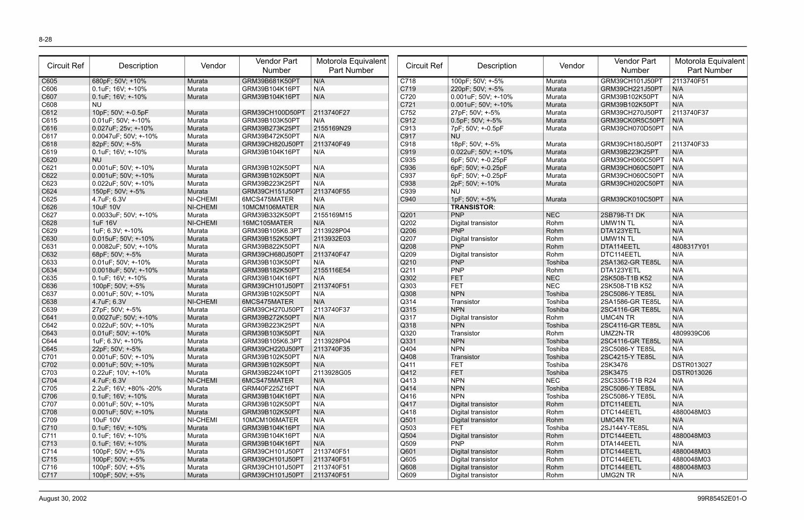
8-28
August 30, 2002 99R85452E01-O
C605 680pF; 50V; +10% Murata GRM39B681K50PT N/AC606 0.1uF; 16V; +-10% Murata GRM39B104K16PT N/AC607 0.1uF; 16V; +-10% Murata GRM39B104K16PT N/AC608 NUC612 10pF; 50V; +-0.5pF Murata GRM39CH100D50PT 2113740F27C615 0.01uF; 50V; +-10% Murata GRM39B103K50PT N/AC616 0.027uF; 25v; +-10% Murata GRM39B273K25PT 2155169N29C617 0.0047uF; 50V; +-10% Murata GRM39B472K50PT N/AC618 82pF; 50V; +-5% Murata GRM39CH820J50PT 2113740F49C619 0.1uF; 16V; +-10% Murata GRM39B104K16PT N/AC620 NUC621 0.001uF; 50V; +-10% Murata GRM39B102K50PT N/AC622 0.001uF; 50V; +-10% Murata GRM39B102K50PT N/AC623 0.022uF; 50V; +-10% Murata GRM39B223K25PT N/AC624 150pF; 50V; +-5% Murata GRM39CH151J50PT 2113740F55C625 4.7uF; 6.3V NI-CHEMI 6MCS475MATER N/AC626 10uF 10V NI-CHEMI 10MCM106MATER N/AC627 0.0033uF; 50V; +-10% Murata GRM39B332K50PT 2155169M15C628 1uF 16V NI-CHEMI 16MC105MATER N/AC629 1uF; 6.3V; +-10% Murata GRM39B105K6.3PT 2113928P04C630 0.015uF; 50V; +-10% Murata GRM39B152K50PT 2113932E03C631 0.0082uF; 50V; +-10% Murata GRM39B822K50PT N/AC632 68pF; 50V; +-5% Murata GRM39CH680J50PT 2113740F47C633 0.01uF; 50V; +-10% Murata GRM39B103K50PT N/AC634 0.0018uF; 50V; +-10% Murata GRM39B182K50PT 2155116E54C635 0.1uF; 16V; +-10% Murata GRM39B104K16PT N/AC636 100pF; 50V; +-5% Murata GRM39CH101J50PT 2113740F51C637 0.001uF; 50V; +-10% Murata GRM39B102K50PT N/AC638 4.7uF; 6.3V NI-CHEMI 6MCS475MATER N/AC639 27pF; 50V; +-5% Murata GRM39CH270J50PT 2113740F37C641 0.0027uF; 50V; +-10% Murata GRM39B272K50PT N/AC642 0.022uF; 50V; +-10% Murata GRM39B223K25PT N/AC643 0.01uF; 50V; +-10% Murata GRM39B103K50PT N/AC644 1uF; 6.3V; +-10% Murata GRM39B105K6.3PT 2113928P04C645 22pF; 50V; +-5% Murata GRM39CH220J50PT 2113740F35C701 0.001uF; 50V; +-10% Murata GRM39B102K50PT N/AC702 0.001uF; 50V; +-10% Murata GRM39B102K50PT N/AC703 0.22uF; 10V; +-10% Murata GRM39B224K10PT 2113928G05C704 4.7uF; 6.3V NI-CHEMI 6MCS475MATER N/AC705 2.2uF; 16V; +80% -20% Murata GRM40F225Z16PT N/AC706 0.1uF; 16V; +-10% Murata GRM39B104K16PT N/AC707 0.001uF; 50V; +-10% Murata GRM39B102K50PT N/AC708 0.001uF; 50V; +-10% Murata GRM39B102K50PT N/AC709 10uF 10V NI-CHEMI 10MCM106MATER N/AC710 0.1uF; 16V; +-10% Murata GRM39B104K16PT N/AC711 0.1uF; 16V; +-10% Murata GRM39B104K16PT N/AC713 0.1uF; 16V; +-10% Murata GRM39B104K16PT N/AC714 100pF; 50V; +-5% Murata GRM39CH101J50PT 2113740F51C715 100pF; 50V; +-5% Murata GRM39CH101J50PT 2113740F51C716 100pF; 50V; +-5% Murata GRM39CH101J50PT 2113740F51C717 100pF; 50V; +-5% Murata GRM39CH101J50PT 2113740F51
Circuit Ref Description Vendor Vendor Part Number
Motorola Equivalent Part Number
C718 100pF; 50V; +-5% Murata GRM39CH101J50PT 2113740F51C719 220pF; 50V; +-5% Murata GRM39CH221J50PT N/AC720 0.001uF; 50V; +-10% Murata GRM39B102K50PT N/AC721 0.001uF; 50V; +-10% Murata GRM39B102K50PT N/AC752 27pF; 50V; +-5% Murata GRM39CH270J50PT 2113740F37C912 0.5pF; 50V; +-5% Murata GRM39CK0R5C50PT N/AC913 7pF; 50V; +-0.5pF Murata GRM39CH070D50PT N/AC917 NUC918 18pF; 50V; +-5% Murata GRM39CH180J50PT 2113740F33C919 0.022uF; 50V; +-10% Murata GRM39B223K25PT N/AC935 6pF; 50V; +-0.25pF Murata GRM39CH060C50PT N/AC936 6pF; 50V; +-0.25pF Murata GRM39CH060C50PT N/AC937 6pF; 50V; +-0.25pF Murata GRM39CH060C50PT N/AC938 2pF; 50V; +-10% Murata GRM39CH020C50PT N/AC939 NUC940 1pF; 50V; +-5% Murata GRM39CK010C50PT N/A
TRANSISTOR:Q201 PNP NEC 2SB798-T1 DK N/AQ202 Digital transistor Rohm UMW1N TL N/AQ206 PNP Rohm DTA123YETL N/AQ207 Digital transistor Rohm UMW1N TL N/AQ208 PNP Rohm DTA114EETL 4808317Y01Q209 Digital transistor Rohm DTC114EETL N/AQ210 PNP Toshiba 2SA1362-GR TE85L N/AQ211 PNP Rohm DTA123YETL N/AQ302 FET NEC 2SK508-T1B K52 N/AQ303 FET NEC 2SK508-T1B K52 N/AQ308 NPN Toshiba 2SC5086-Y TE85L N/AQ314 Transistor Toshiba 2SA1586-GR TE85L N/AQ315 NPN Toshiba 2SC4116-GR TE85L N/AQ317 Digital transistor Rohm UMC4N TR N/AQ318 NPN Toshiba 2SC4116-GR TE85L N/AQ320 Transistor Rohm UMZ2N-TR 4809939C06Q331 NPN Toshiba 2SC4116-GR TE85L N/AQ404 NPN Toshiba 2SC5086-Y TE85L N/AQ408 Transistor Toshiba 2SC4215-Y TE85L N/AQ411 FET Toshiba 2SK3476 DSTR013027Q412 FET Toshiba 2SK3475 DSTR013026Q413 NPN NEC 2SC3356-T1B R24 N/AQ414 NPN Toshiba 2SC5086-Y TE85L N/AQ416 NPN Toshiba 2SC5086-Y TE85L N/AQ417 Digital transistor Rohm DTC114EETL N/AQ418 Digital transistor Rohm DTC144EETL 4880048M03Q501 Digital transistor Rohm UMC4N TR N/AQ503 FET Toshiba 2SJ144Y-TE85L N/AQ504 Digital transistor Rohm DTC144EETL 4880048M03Q509 PNP Rohm DTA144EETL N/AQ601 Digital transistor Rohm DTC144EETL 4880048M03Q605 Digital transistor Rohm DTC144EETL 4880048M03Q608 Digital transistor Rohm DTC144EETL 4880048M03Q609 Digital transistor Rohm UMG2N TR N/A
Circuit Ref Description Vendor Vendor Part Number
Motorola Equivalent Part Number
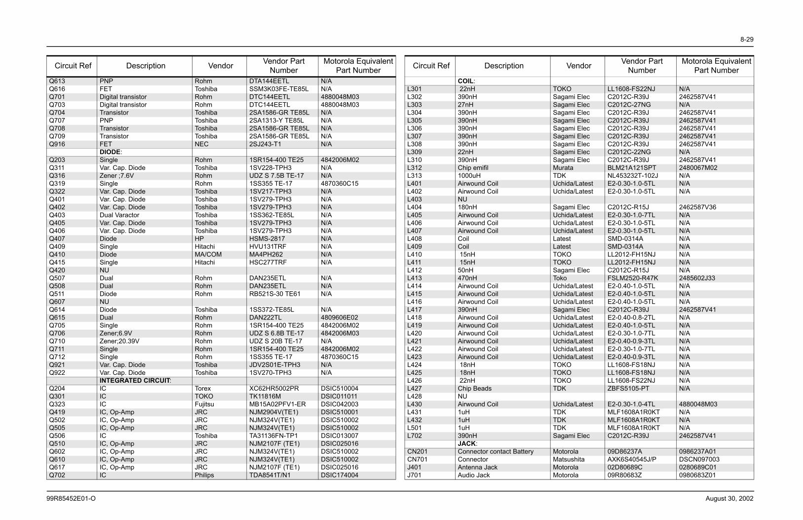
8-29
99R85452E01-O August 30, 2002
Q613 PNP Rohm DTA144EETL N/AQ616 FET Toshiba SSM3K03FE-TE85L N/AQ701 Digital transistor Rohm DTC144EETL 4880048M03Q703 Digital transistor Rohm DTC144EETL 4880048M03Q704 Transistor Toshiba 2SA1586-GR TE85L N/AQ707 PNP Toshiba 2SA1313-Y TE85L N/AQ708 Transistor Toshiba 2SA1586-GR TE85L N/AQ709 Transistor Toshiba 2SA1586-GR TE85L N/AQ916 FET NEC 2SJ243-T1 N/A
DIODE:Q203 Single Rohm 1SR154-400 TE25 4842006M02Q311 Var. Cap. Diode Toshiba 1SV228-TPH3 N/AQ316 Zener ;7.6V Rohm UDZ S 7.5B TE-17 N/AQ319 Single Rohm 1SS355 TE-17 4870360C15Q322 Var. Cap. Diode Toshiba 1SV217-TPH3 N/AQ401 Var. Cap. Diode Toshiba 1SV279-TPH3 N/AQ402 Var. Cap. Diode Toshiba 1SV279-TPH3 N/AQ403 Dual Varactor Toshiba 1SS362-TE85L N/AQ405 Var. Cap. Diode Toshiba 1SV279-TPH3 N/AQ406 Var. Cap. Diode Toshiba 1SV279-TPH3 N/AQ407 Diode HP HSMS-2817 N/AQ409 Single Hitachi HVU131TRF N/AQ410 Diode MA/COM MA4PH262 N/AQ415 Single Hitachi HSC277TRF N/AQ420 NUQ507 Dual Rohm DAN235ETL N/AQ508 Dual Rohm DAN235ETL N/AQ511 Diode Rohm RB521S-30 TE61 N/AQ607 NUQ614 Diode Toshiba 1SS372-TE85L N/AQ615 Dual Rohm DAN222TL 4809606E02Q705 Single Rohm 1SR154-400 TE25 4842006M02Q706 Zener;6.9V Rohm UDZ S 6.8B TE-17 4842006M03Q710 Zener;20.39V Rohm UDZ S 20B TE-17 N/AQ711 Single Rohm 1SR154-400 TE25 4842006M02Q712 Single Rohm 1SS355 TE-17 4870360C15Q921 Var. Cap. Diode Toshiba JDV2S01E-TPH3 N/AQ922 Var. Cap. Diode Toshiba 1SV270-TPH3 N/A
INTEGRATED CIRCUIT:Q204 IC Torex XC62HR5002PR DSIC510004Q301 IC TOKO TK11816M DSIC011011Q323 IC Fujitsu MB15A02PFV1-ER DSIC042003Q419 IC, Op-Amp JRC NJM2904V(TE1) DSIC510001Q502 IC, Op-Amp JRC NJM324V(TE1) DSIC510002Q505 IC, Op-Amp JRC NJM324V(TE1) DSIC510002Q506 IC Toshiba TA31136FN-TP1 DSIC013007Q510 IC, Op-Amp JRC NJM2107F (TE1) DSIC025016Q602 IC, Op-Amp JRC NJM324V(TE1) DSIC510002Q610 IC, Op-Amp JRC NJM324V(TE1) DSIC510002Q617 IC, Op-Amp JRC NJM2107F (TE1) DSIC025016Q702 IC Philips TDA8541T/N1 DSIC174004
Circuit Ref Description Vendor Vendor Part Number
Motorola Equivalent Part Number
COIL:L301 22nH TOKO LL1608-FS22NJ N/AL302 390nH Sagami Elec C2012C-R39J 2462587V41L303 27nH Sagami Elec C2012C-27NG N/AL304 390nH Sagami Elec C2012C-R39J 2462587V41L305 390nH Sagami Elec C2012C-R39J 2462587V41L306 390nH Sagami Elec C2012C-R39J 2462587V41L307 390nH Sagami Elec C2012C-R39J 2462587V41L308 390nH Sagami Elec C2012C-R39J 2462587V41L309 22nH Sagami Elec C2012C-22NG N/AL310 390nH Sagami Elec C2012C-R39J 2462587V41L312 Chip emifil Murata BLM21A121SPT 2480067M02L313 1000uH TDK NL453232T-102J N/AL401 Airwound Coil Uchida/Latest E2-0.30-1.0-5TL N/AL402 Airwound Coil Uchida/Latest E2-0.30-1.0-5TL N/AL403 NUL404 180nH Sagami Elec C2012C-R15J 2462587V36L405 Airwound Coil Uchida/Latest E2-0.30-1.0-7TL N/AL406 Airwound Coil Uchida/Latest E2-0.30-1.0-5TL N/AL407 Airwound Coil Uchida/Latest E2-0.30-1.0-5TL N/AL408 Coil Latest SMD-0314A N/AL409 Coil Latest SMD-0314A N/AL410 15nH TOKO LL2012-FH15NJ N/AL411 15nH TOKO LL2012-FH15NJ N/AL412 50nH Sagami Elec C2012C-R15J N/AL413 470nH Toko FSLM2520-R47K 2485602J33L414 Airwound Coil Uchida/Latest E2-0.40-1.0-5TL N/AL415 Airwound Coil Uchida/Latest E2-0.40-1.0-5TL N/AL416 Airwound Coil Uchida/Latest E2-0.40-1.0-5TL N/AL417 390nH Sagami Elec C2012C-R39J 2462587V41L418 Airwound Coil Uchida/Latest E2-0.40-0.8-2TL N/AL419 Airwound Coil Uchida/Latest E2-0.40-1.0-5TL N/AL420 Airwound Coil Uchida/Latest E2-0.30-1.0-7TL N/AL421 Airwound Coil Uchida/Latest E2-0.40-0.9-3TL N/AL422 Airwound Coil Uchida/Latest E2-0.30-1.0-7TL N/AL423 Airwound Coil Uchida/Latest E2-0.40-0.9-3TL N/AL424 18nH TOKO LL1608-FS18NJ N/AL425 18nH TOKO LL1608-FS18NJ N/AL426 22nH TOKO LL1608-FS22NJ N/AL427 Chip Beads TDK ZBFS5105-PT N/AL428 NUL430 Airwound Coil Uchida/Latest E2-0.30-1.0-4TL 4880048M03L431 1uH TDK MLF1608A1R0KT N/AL432 1uH TDK MLF1608A1R0KT N/AL501 1uH TDK MLF1608A1R0KT N/AL702 390nH Sagami Elec C2012C-R39J 2462587V41
JACK:CN201 Connector contact Battery Motorola 09D86237A 0986237A01CN701 Connector Matsushita AXK6S40545J/P DSCN097003J401 Antenna Jack Motorola 02D80689C 0280689C01J701 Audio Jack Motorola 09R80683Z 0980683Z01
Circuit Ref Description Vendor Vendor Part Number
Motorola Equivalent Part Number
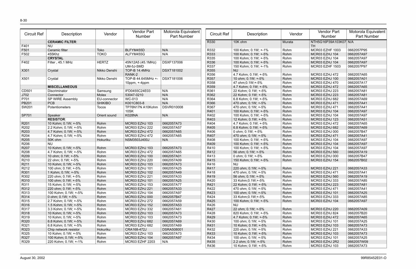
8-30
August 30, 2002 99R85452E01-O
CERAMIC FILTER:F401 NUF501 Ceramic filter Toko BLFYM455D N/AF502 455Khz TOKO ALFYM455G N/A
CRYSTALF402 Filter , 45.1 MHz HERTZ 45N12A5 (45.1MHz)
UM-5J-SMDDSXF137006
X301 Crystal Nikko Denshi TOP-B 14.4MHz RANK-2
DSXT181002
X501 Crystal Nikko Denshi TOP-B 44.645MHz +-10ppm, +-4ppm
DSXT181006
MISCELLANEOUSCD501 Discriminator Samsung IFD0455C24E03 N/AJ702 Connector Molex 53047-0210 N/AP701 SP WIRE Assembly EU-connector WC-013 N/APB201 PCB SHIKIBO K001C803-8 N/ASW201 Potentiometers Tocos TP76N17N A10Kohm
10SKDSVR010008
SP701 Speaker Orient sound K028NA N/ARESISTOR:
R201 10 Kohm; 0.1W; +-5% Rohm MCR03 EZHJ 103 0662057A73R202 2.2 Kohm; 0.1W; +-5% Rohm MCR03 EZHJ 222 0662057A57R203 4.7 Kohm; 0.1W; +-5% Rohm MCR03 EZHJ 472 0662057A65R204 4.7 Kohm; 0.1W; +-5% Rohm MCR03 EZHJ 472 0662057A65R205 50K ohm Hokuriku NSM3503J400J N/AR206 NUR207 10 Kohm; 0.1W; +-5% Rohm MCR03 EZHJ 103 0662057A73R208 4.7 Kohm; 0.1W; +-5% Rohm MCR03 EZHJ 472 0662057A65R209 10 ohm; 0.1W; +-5% Rohm MCR03 EZHJ 100 0662057A01R210 22 ohm; 0.1W; +-5% Rohm MCR03 EZHJ 220 0662057A09R211 10 Kohm; 0.1W; +-5% Rohm MCR03 EZHJ 103 0662057A73R212 100 ohm; 0.1W; +-5% Rohm MCR03 EZHJ 101 0662057A25R301 1 Kohm; 0.1W; +-5% Rohm MCR03 EZHJ 102 0662057A49R302 220 ohm; 0.1W; +-5% Rohm MCR03 EZHJ 221 0662057A33R310 100 ohm; 0.1W; +-5% Rohm MCR03 EZHJ 101 0662057A25R311 15 Kohm; 0.1W; +-5% Rohm MCR03 EZHJ 153 0662057A77R312 220 ohm; 0.1W; +-5% Rohm MCR03 EZHJ 221 0662057A33R313 100 Kohm; 0.1W; +-5% Rohm MCR03 EZHJ 104 0662057A97R314 0 ohm; 0.1W; +-5% Rohm MCR03 EZHJ 000 0662057B47R315 2.7 Kohm; 0.1W; +-5% Rohm MCR03 EZHJ 272 0662057A59R316 1.5 Kohm; 0.1W; +-5% Rohm MCR03 EZHJ 152 0662057A53R317 3.3 Kohm; 0.1W; +-5% Rohm MCR03 EZHJ 332 0662057A61R318 10 Kohm; 0.1W; +-5% Rohm MCR03 EZHJ 103 0662057A73R319 10 Kohm; 0.1W; +-5% Rohm MCR03 EZHJ 103 0662057A73R320 6.8 Kohm; 0.1W; +-5% Rohm MCR03 EZHJ 682 0662057A69R321 6.8 Kohm; 0.1W; +-5% Rohm MCR03 EZHJ 682 0662057A69R323 Chip network resistor Hokuriku CRA168-472J DSRA508001R325 10 Kohm; 0.1W; +-5% Rohm MCR03 EZHJ 103 0662057A73R327 100 Kohm; 0.1W; +-5% Rohm MCR03 EZHJ 104 0662057A97R329 220 Kohm; 0.1W; +-1% Rohm MCR03 EZHF 2203 N/A
Circuit Ref Description Vendor Vendor Part Number
Motorola Equivalent Part Number
R330 10K ohm Murata NTH5G16P39A103K07TH
N/A
R332 100 Kohm; 0.1W; +-1% Rohm MCR03 EZHF 1003 0662057P95R333 100 Kohm; 0.1W; +-5% Rohm MCR03 EZHJ 104 0662057A97R335 100 Kohm; 0.1W; +-5% Rohm MCR03 EZHJ 104 0662057A97R336 100 Kohm; 0.1W; +-5% Rohm MCR03 EZHJ 104 0662057A97R337 150 Kohm; 0.1W; +-1% Rohm MCR03 EZHF 1503 0662057P97R355 NUR356 4.7 Kohm; 0.1W; +-5% Rohm MCR03 EZHJ 472 0662057A65R357 10 ohm; 0.1W; +-5% Rohm MCR03 EZHJ 100 0662057A01R358 47 ohm;0.1W;+-5% Rohm MCR03 EZHJ 470 0662057A17R359 4.7 Kohm; 0.1W; +-5% Rohm MCR03 EZHJ 472 0662057A65R361 22 Kohm; 0.1W; +-5% Rohm MCR03 EZHJ 223 0662057A81R362 22 Kohm; 0.1W; +-5% Rohm MCR03 EZHJ 223 0662057A81R364 6.8 Kohm; 0.1W; +-5% Rohm MCR03 EZHJ 682 0662057A69R366 470 ohm; 0.1W; +-5% Rohm MCR03 EZHJ 471 0662057A41R367 470 ohm; 0.1W; +-5% Rohm MCR03 EZHJ 471 0662057A41R401 100 Kohm; 0.1W; +-5% Rohm MCR03 EZHJ 104 0662057A97R402 100 Kohm; 0.1W; +-5% Rohm MCR03 EZHJ 104 0662057A97R403 12 Kohm; 0.1W; +-5% Rohm MCR03 EZHJ 123 0662057A51R404 4.7 Kohm; 0.1W; +-5% Rohm MCR03 EZHJ 472 0662057A65R405 6.8 Kohm; 0.1W; +-5% Rohm MCR03 EZHJ 682 0662057A69R406 0 ohm; 0.1W; +-5% Rohm MCR03 EZHJ 000 0662057B47R407 470 ohm; 0.1W; +-5% Rohm MCR03 EZHJ 471 0662057A41R408 100 Kohm; 0.1W; +-5% Rohm MCR03 EZHJ 104 0662057A97R409 100 Kohm; 0.1W; +-5% Rohm MCR03 EZHJ 104 0662057A97R410 100 Kohm; 0.1W; +-5% Rohm MCR03 EZHJ 104 0662057A97R412 56 ohm; 0.1W; +-5% Rohm MCR03 EZHJ 560 0662057A19R413 0 ohm; 0.1W; +-5% Rohm MCR03 EZHJ 000 0662057B47R415 150 Kohm; 0.1W; +-5% Rohm MCR03 EZHJ 154 0662057B02R416 NUR417 220 ohm; 0.1W; +-5% Rohm MCR03 EZHJ 221 0662057A33R418 470 ohm; 0.1W; +-5% Rohm MCR03 EZHJ 471 0662057A41R419 56 ohm; 0.1W; +-5% Rohm MCR03 EZHJ 560 0662057A19R420 33 Kohm;0.1W;+-5% Rohm MCR03 EZHJ 333 0662057A85R421 22 Kohm; 0.1W; +-5% Rohm MCR03 EZHJ 223 0662057A81R422 470 ohm; 0.1W; +-5% Rohm MCR03 EZHJ 471 0662057A41R423 100 ohm; 0.1W; +-5% Rohm MCR03 EZHJ 101 0662057A25R424 33 Kohm;0.1W;+-5% Rohm MCR03 EZHJ 333 0662057A85R425 100 Kohm; 0.1W; +-5% Rohm MCR03 EZHJ 104 0662057A97R426 NUR427 22 ohm; 0.1W; +-5% Rohm MCR03 EZHJ 220 0662057A09R428 820 Kohm; 0.1W; +-5% Rohm MCR03 EZHJ 824 0662057B20R429 4.7 Kohm; 0.1W; +-5% Rohm MCR03 EZHJ 472 0662057A65R430 100 ohm; 0.1W; +-5% Rohm MCR03 EZHJ 101 0662057A25R431 10 Kohm; 0.1W; +-5% Rohm MCR03 EZHJ 103 0662057A73R432 220 ohm; 0.1W; +-5% Rohm MCR03 EZHJ 221 0662057A33R433 10 Kohm; 0.1W; +-5% Rohm MCR03 EZHJ 103 0662057A73R434 100 ohm; 0.1W; +-5% Rohm MCR03 EZHJ 101 0662057A25R435 2.2 ohm; 0.1W; +-5% Rohm MCR03 EZHJ 2R2 0662057W09R436 10 Kohm; 0.1W; +-5% Rohm MCR03 EZHJ 103 0662057A73
Circuit Ref Description Vendor Vendor Part Number
Motorola Equivalent Part Number
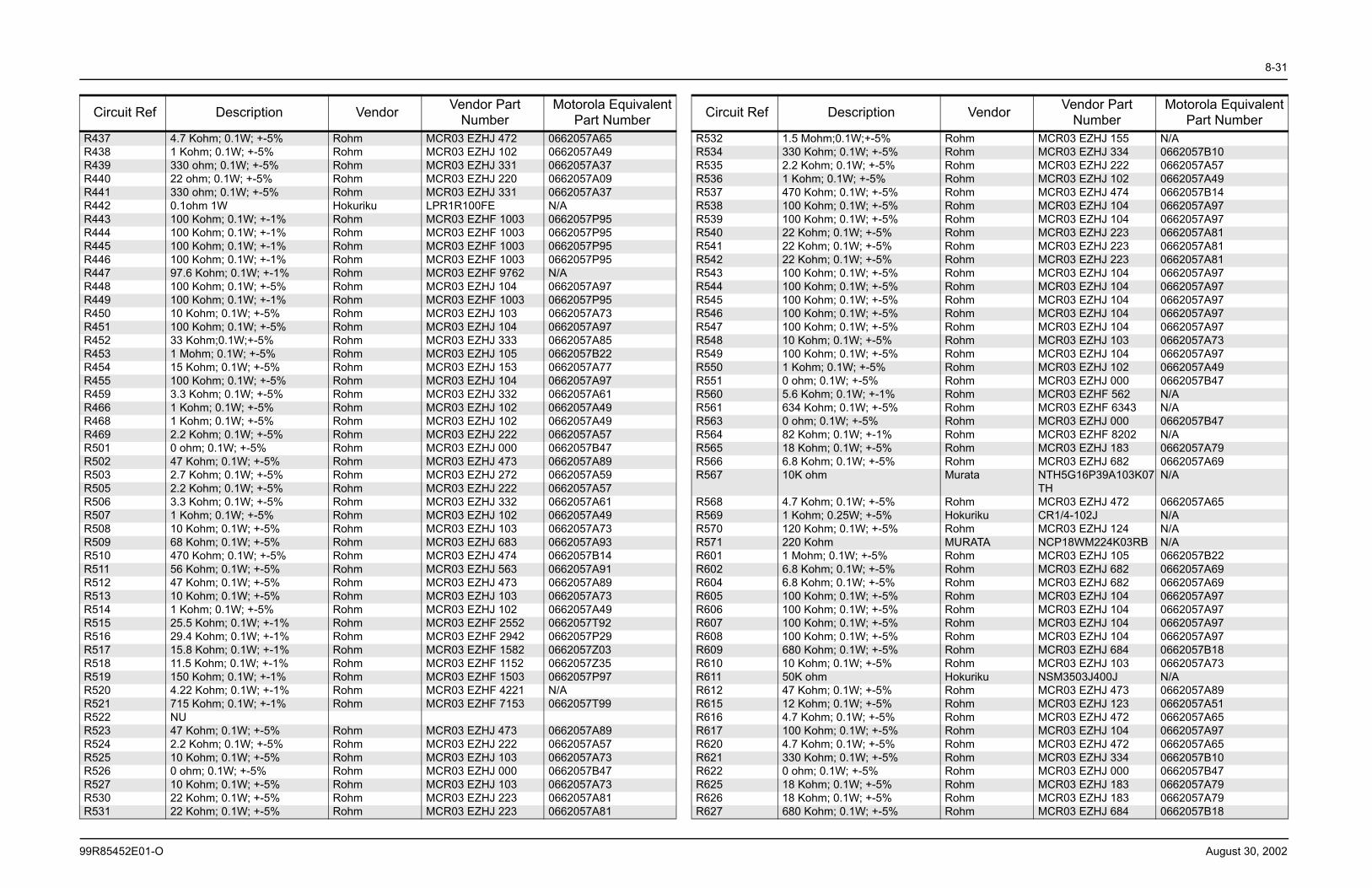
8-31
99R85452E01-O August 30, 2002
R437 4.7 Kohm; 0.1W; +-5% Rohm MCR03 EZHJ 472 0662057A65R438 1 Kohm; 0.1W; +-5% Rohm MCR03 EZHJ 102 0662057A49R439 330 ohm; 0.1W; +-5% Rohm MCR03 EZHJ 331 0662057A37R440 22 ohm; 0.1W; +-5% Rohm MCR03 EZHJ 220 0662057A09R441 330 ohm; 0.1W; +-5% Rohm MCR03 EZHJ 331 0662057A37R442 0.1ohm 1W Hokuriku LPR1R100FE N/AR443 100 Kohm; 0.1W; +-1% Rohm MCR03 EZHF 1003 0662057P95R444 100 Kohm; 0.1W; +-1% Rohm MCR03 EZHF 1003 0662057P95R445 100 Kohm; 0.1W; +-1% Rohm MCR03 EZHF 1003 0662057P95R446 100 Kohm; 0.1W; +-1% Rohm MCR03 EZHF 1003 0662057P95R447 97.6 Kohm; 0.1W; +-1% Rohm MCR03 EZHF 9762 N/AR448 100 Kohm; 0.1W; +-5% Rohm MCR03 EZHJ 104 0662057A97R449 100 Kohm; 0.1W; +-1% Rohm MCR03 EZHF 1003 0662057P95R450 10 Kohm; 0.1W; +-5% Rohm MCR03 EZHJ 103 0662057A73R451 100 Kohm; 0.1W; +-5% Rohm MCR03 EZHJ 104 0662057A97R452 33 Kohm;0.1W;+-5% Rohm MCR03 EZHJ 333 0662057A85R453 1 Mohm; 0.1W; +-5% Rohm MCR03 EZHJ 105 0662057B22R454 15 Kohm; 0.1W; +-5% Rohm MCR03 EZHJ 153 0662057A77R455 100 Kohm; 0.1W; +-5% Rohm MCR03 EZHJ 104 0662057A97R459 3.3 Kohm; 0.1W; +-5% Rohm MCR03 EZHJ 332 0662057A61R466 1 Kohm; 0.1W; +-5% Rohm MCR03 EZHJ 102 0662057A49R468 1 Kohm; 0.1W; +-5% Rohm MCR03 EZHJ 102 0662057A49R469 2.2 Kohm; 0.1W; +-5% Rohm MCR03 EZHJ 222 0662057A57R501 0 ohm; 0.1W; +-5% Rohm MCR03 EZHJ 000 0662057B47R502 47 Kohm; 0.1W; +-5% Rohm MCR03 EZHJ 473 0662057A89R503 2.7 Kohm; 0.1W; +-5% Rohm MCR03 EZHJ 272 0662057A59R505 2.2 Kohm; 0.1W; +-5% Rohm MCR03 EZHJ 222 0662057A57R506 3.3 Kohm; 0.1W; +-5% Rohm MCR03 EZHJ 332 0662057A61R507 1 Kohm; 0.1W; +-5% Rohm MCR03 EZHJ 102 0662057A49R508 10 Kohm; 0.1W; +-5% Rohm MCR03 EZHJ 103 0662057A73R509 68 Kohm; 0.1W; +-5% Rohm MCR03 EZHJ 683 0662057A93R510 470 Kohm; 0.1W; +-5% Rohm MCR03 EZHJ 474 0662057B14R511 56 Kohm; 0.1W; +-5% Rohm MCR03 EZHJ 563 0662057A91R512 47 Kohm; 0.1W; +-5% Rohm MCR03 EZHJ 473 0662057A89R513 10 Kohm; 0.1W; +-5% Rohm MCR03 EZHJ 103 0662057A73R514 1 Kohm; 0.1W; +-5% Rohm MCR03 EZHJ 102 0662057A49R515 25.5 Kohm; 0.1W; +-1% Rohm MCR03 EZHF 2552 0662057T92R516 29.4 Kohm; 0.1W; +-1% Rohm MCR03 EZHF 2942 0662057P29R517 15.8 Kohm; 0.1W; +-1% Rohm MCR03 EZHF 1582 0662057Z03R518 11.5 Kohm; 0.1W; +-1% Rohm MCR03 EZHF 1152 0662057Z35R519 150 Kohm; 0.1W; +-1% Rohm MCR03 EZHF 1503 0662057P97R520 4.22 Kohm; 0.1W; +-1% Rohm MCR03 EZHF 4221 N/AR521 715 Kohm; 0.1W; +-1% Rohm MCR03 EZHF 7153 0662057T99R522 NUR523 47 Kohm; 0.1W; +-5% Rohm MCR03 EZHJ 473 0662057A89R524 2.2 Kohm; 0.1W; +-5% Rohm MCR03 EZHJ 222 0662057A57R525 10 Kohm; 0.1W; +-5% Rohm MCR03 EZHJ 103 0662057A73R526 0 ohm; 0.1W; +-5% Rohm MCR03 EZHJ 000 0662057B47R527 10 Kohm; 0.1W; +-5% Rohm MCR03 EZHJ 103 0662057A73R530 22 Kohm; 0.1W; +-5% Rohm MCR03 EZHJ 223 0662057A81R531 22 Kohm; 0.1W; +-5% Rohm MCR03 EZHJ 223 0662057A81
Circuit Ref Description Vendor Vendor Part Number
Motorola Equivalent Part Number
R532 1.5 Mohm;0.1W;+-5% Rohm MCR03 EZHJ 155 N/AR534 330 Kohm; 0.1W; +-5% Rohm MCR03 EZHJ 334 0662057B10R535 2.2 Kohm; 0.1W; +-5% Rohm MCR03 EZHJ 222 0662057A57R536 1 Kohm; 0.1W; +-5% Rohm MCR03 EZHJ 102 0662057A49R537 470 Kohm; 0.1W; +-5% Rohm MCR03 EZHJ 474 0662057B14R538 100 Kohm; 0.1W; +-5% Rohm MCR03 EZHJ 104 0662057A97R539 100 Kohm; 0.1W; +-5% Rohm MCR03 EZHJ 104 0662057A97R540 22 Kohm; 0.1W; +-5% Rohm MCR03 EZHJ 223 0662057A81R541 22 Kohm; 0.1W; +-5% Rohm MCR03 EZHJ 223 0662057A81R542 22 Kohm; 0.1W; +-5% Rohm MCR03 EZHJ 223 0662057A81R543 100 Kohm; 0.1W; +-5% Rohm MCR03 EZHJ 104 0662057A97R544 100 Kohm; 0.1W; +-5% Rohm MCR03 EZHJ 104 0662057A97R545 100 Kohm; 0.1W; +-5% Rohm MCR03 EZHJ 104 0662057A97R546 100 Kohm; 0.1W; +-5% Rohm MCR03 EZHJ 104 0662057A97R547 100 Kohm; 0.1W; +-5% Rohm MCR03 EZHJ 104 0662057A97R548 10 Kohm; 0.1W; +-5% Rohm MCR03 EZHJ 103 0662057A73R549 100 Kohm; 0.1W; +-5% Rohm MCR03 EZHJ 104 0662057A97R550 1 Kohm; 0.1W; +-5% Rohm MCR03 EZHJ 102 0662057A49R551 0 ohm; 0.1W; +-5% Rohm MCR03 EZHJ 000 0662057B47R560 5.6 Kohm; 0.1W; +-1% Rohm MCR03 EZHF 562 N/AR561 634 Kohm; 0.1W; +-5% Rohm MCR03 EZHF 6343 N/AR563 0 ohm; 0.1W; +-5% Rohm MCR03 EZHJ 000 0662057B47R564 82 Kohm; 0.1W; +-1% Rohm MCR03 EZHF 8202 N/AR565 18 Kohm; 0.1W; +-5% Rohm MCR03 EZHJ 183 0662057A79R566 6.8 Kohm; 0.1W; +-5% Rohm MCR03 EZHJ 682 0662057A69R567 10K ohm Murata NTH5G16P39A103K07
THN/A
R568 4.7 Kohm; 0.1W; +-5% Rohm MCR03 EZHJ 472 0662057A65R569 1 Kohm; 0.25W; +-5% Hokuriku CR1/4-102J N/AR570 120 Kohm; 0.1W; +-5% Rohm MCR03 EZHJ 124 N/AR571 220 Kohm MURATA NCP18WM224K03RB N/AR601 1 Mohm; 0.1W; +-5% Rohm MCR03 EZHJ 105 0662057B22R602 6.8 Kohm; 0.1W; +-5% Rohm MCR03 EZHJ 682 0662057A69R604 6.8 Kohm; 0.1W; +-5% Rohm MCR03 EZHJ 682 0662057A69R605 100 Kohm; 0.1W; +-5% Rohm MCR03 EZHJ 104 0662057A97R606 100 Kohm; 0.1W; +-5% Rohm MCR03 EZHJ 104 0662057A97R607 100 Kohm; 0.1W; +-5% Rohm MCR03 EZHJ 104 0662057A97R608 100 Kohm; 0.1W; +-5% Rohm MCR03 EZHJ 104 0662057A97R609 680 Kohm; 0.1W; +-5% Rohm MCR03 EZHJ 684 0662057B18R610 10 Kohm; 0.1W; +-5% Rohm MCR03 EZHJ 103 0662057A73R611 50K ohm Hokuriku NSM3503J400J N/AR612 47 Kohm; 0.1W; +-5% Rohm MCR03 EZHJ 473 0662057A89R615 12 Kohm; 0.1W; +-5% Rohm MCR03 EZHJ 123 0662057A51R616 4.7 Kohm; 0.1W; +-5% Rohm MCR03 EZHJ 472 0662057A65R617 100 Kohm; 0.1W; +-5% Rohm MCR03 EZHJ 104 0662057A97R620 4.7 Kohm; 0.1W; +-5% Rohm MCR03 EZHJ 472 0662057A65R621 330 Kohm; 0.1W; +-5% Rohm MCR03 EZHJ 334 0662057B10R622 0 ohm; 0.1W; +-5% Rohm MCR03 EZHJ 000 0662057B47R625 18 Kohm; 0.1W; +-5% Rohm MCR03 EZHJ 183 0662057A79R626 18 Kohm; 0.1W; +-5% Rohm MCR03 EZHJ 183 0662057A79R627 680 Kohm; 0.1W; +-5% Rohm MCR03 EZHJ 684 0662057B18
Circuit Ref Description Vendor Vendor Part Number
Motorola Equivalent Part Number
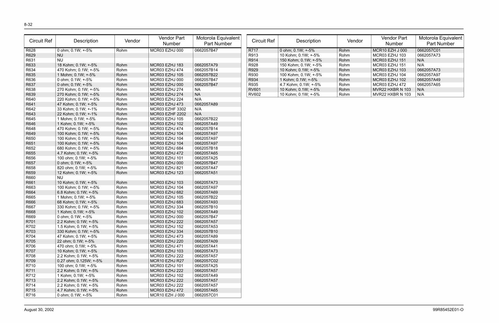
8-32
August 30, 2002 99R85452E01-O
R628 0 ohm; 0.1W; +-5% Rohm MCR03 EZHJ 000 0662057B47R629 NUR631 NUR633 18 Kohm; 0.1W; +-5% Rohm MCR03 EZHJ 183 0662057A79R634 470 Kohm; 0.1W; +-5% Rohm MCR03 EZHJ 474 0662057B14R635 1 Mohm; 0.1W; +-5% Rohm MCR03 EZHJ 105 0662057B22R636 0 ohm; 0.1W; +-5% Rohm MCR03 EZHJ 000 0662057B47R637 0 ohm; 0.1W; +-5% Rohm MCR03 EZHJ 000 0662057B47R638 270 Kohm; 0.1W; +-5% Rohm MCR03 EZHJ 274 NAR639 270 Kohm; 0.1W; +-5% Rohm MCR03 EZHJ 274 NAR640 220 Kohm; 0.1W; +-5% Rohm MCR03 EZHJ 224 N/AR641 47 Kohm; 0.1W; +-5% Rohm MCR03 EZHJ 473 0662057A89R642 33 Kohm; 0.1W; +-1% Rohm MCR03 EZHF 3302 N/AR643 22 Kohm; 0.1W; +-1% Rohm MCR03 EZHF 2202 N/AR645 1 Mohm; 0.1W; +-5% Rohm MCR03 EZHJ 105 0662057B22R646 1 Kohm; 0.1W; +-5% Rohm MCR03 EZHJ 102 0662057A49R648 470 Kohm; 0.1W; +-5% Rohm MCR03 EZHJ 474 0662057B14R649 100 Kohm; 0.1W; +-5% Rohm MCR03 EZHJ 104 0662057A97R650 100 Kohm; 0.1W; +-5% Rohm MCR03 EZHJ 104 0662057A97R651 100 Kohm; 0.1W; +-5% Rohm MCR03 EZHJ 104 0662057A97R652 680 Kohm; 0.1W; +-5% Rohm MCR03 EZHJ 684 0662057B18R655 4.7 Kohm; 0.1W; +-5% Rohm MCR03 EZHJ 472 0662057A65R656 100 ohm; 0.1W; +-5% Rohm MCR03 EZHJ 101 0662057A25R657 0 ohm; 0.1W; +-5% Rohm MCR03 EZHJ 000 0662057B47R658 820 ohm; 0.1W; +-5% Rohm MCR03 EZHJ 821 0662057A47R659 12 Kohm; 0.1W; +-5% Rohm MCR03 EZHJ 123 0662057A51R660 NUR661 10 Kohm; 0.1W; +-5% Rohm MCR03 EZHJ 103 0662057A73R663 100 Kohm; 0.1W; +-5% Rohm MCR03 EZHJ 104 0662057A97R664 6.8 Kohm; 0.1W; +-5% Rohm MCR03 EZHJ 682 0662057A69R665 1 Mohm; 0.1W; +-5% Rohm MCR03 EZHJ 105 0662057B22R666 68 Kohm; 0.1W; +-5% Rohm MCR03 EZHJ 683 0662057A93R667 330 Kohm; 0.1W; +-5% Rohm MCR03 EZHJ 334 0662057B10R668 1 Kohm; 0.1W; +-5% Rohm MCR03 EZHJ 102 0662057A49R669 0 ohm; 0.1W; +-5% Rohm MCR03 EZHJ 000 0662057B47R701 2.2 Kohm; 0.1W; +-5% Rohm MCR03 EZHJ 222 0662057A57R702 1.5 Kohm; 0.1W; +-5% Rohm MCR03 EZHJ 152 0662057A53R703 330 Kohm; 0.1W; +-5% Rohm MCR03 EZHJ 334 0662057B10R704 47 Kohm; 0.1W; +-5% Rohm MCR03 EZHJ 473 0662057A89R705 22 ohm; 0.1W; +-5% Rohm MCR03 EZHJ 220 0662057A09R706 470 ohm; 0.1W; +-5% Rohm MCR03 EZHJ 471 0662057A41R707 10 Kohm; 0.1W; +-5% Rohm MCR03 EZHJ 103 0662057A73R708 2.2 Kohm; 0.1W; +-5% Rohm MCR03 EZHJ 222 0662057A57R709 0.27 ohm; 0.125W; +-5% Rohm MCR10 EZHJ R27 0662057C02R710 100 ohm; 0.1W; +-5% Rohm MCR03 EZHJ 101 0662057A25R711 2.2 Kohm; 0.1W; +-5% Rohm MCR03 EZHJ 222 0662057A57R712 1 Kohm; 0.1W; +-5% Rohm MCR03 EZHJ 102 0662057A49R713 2.2 Kohm; 0.1W; +-5% Rohm MCR03 EZHJ 222 0662057A57R714 2.2 Kohm; 0.1W; +-5% Rohm MCR03 EZHJ 222 0662057A57R715 4.7 Kohm; 0.1W; +-5% Rohm MCR03 EZHJ 472 0662057A65R716 0 ohm; 0.1W; +-5% Rohm MCR10 EZH J 000 0662057C01
Circuit Ref Description Vendor Vendor Part Number
Motorola Equivalent Part Number
R717 0 ohm; 0.1W; +-5% Rohm MCR10 EZH J 000 0662057C01R913 10 Kohm; 0.1W; +-5% Rohm MCR03 EZHJ 103 0662057A73R914 150 Kohm; 0.1W; +-5% Rohm MCR03 EZHJ 151 N/AR928 150 Kohm; 0.1W; +-5% Rohm MCR03 EZHJ 151 N/AR929 10 Kohm; 0.1W; +-5% Rohm MCR03 EZHJ 103 0662057A73R930 100 Kohm; 0.1W; +-5% Rohm MCR03 EZHJ 104 0662057A97R934 1 Kohm; 0.1W; +-5% Rohm MCR03 EZHJ 102 0662057A49R935 4.7 Kohm; 0.1W; +-5% Rohm MCR03 EZHJ 472 0662057A65RV601 10 Kohm; 0.1W; +-5% Rohm MVR22 HXBR N 103 N/ARV602 10 Kohm; 0.1W; +-5% Rohm MVR22 HXBR N 103 N/A
Circuit Ref Description Vendor Vendor Part Number
Motorola Equivalent Part Number

8-33
99R85452E01-O August 30, 2002
Chapter 8 UHF 435-480 MHz Circuit Board/Schematic Diagrams and Parts List
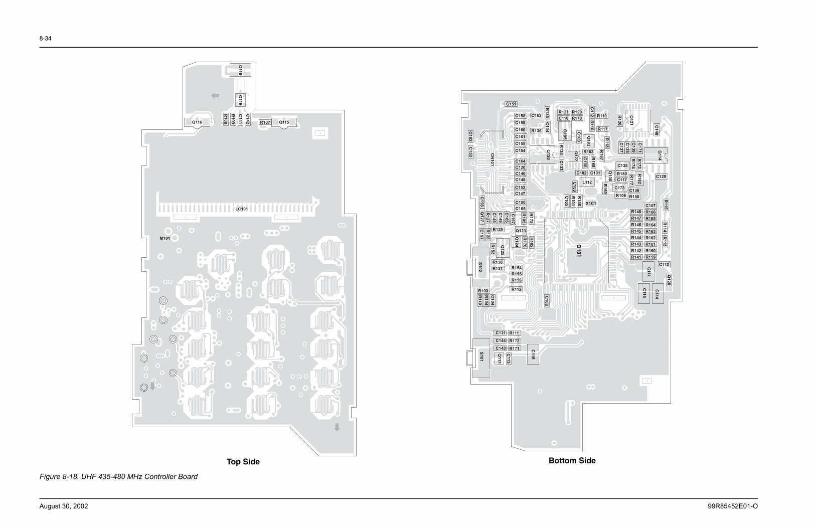
8-34
August 30, 2002 99R85452E01-O
Figure 8-18. UHF 435-480 MHz Controller Board
C142
C141
R109
R108
Q11
9Q
11
8
Q116 Q115R107
LC101
M101
C140
Q11
4
C1
71
C1
39
C1
38
C1
37
Q1
21
C129R
17
3
R1
74
R1
82
C135
R180 R1
77C117
C173C136
R150R106
R11
5
R1
26
R11
8Q
13
0
R1
69
R110
R117
R1
67
X1C1
L112
C101C102
R1
68
C1
06
R183
Q1
02
R11
6C
13
2
C1
09
R120
R170
R121
C110
Q1
05
Q122
R1
34
C1
33
C1
03
R1
58
R101
C1
05
R1
35
C1
34
C163
R136
Q1
20
C151
C158
C159
C160
C161
C155
C154
C164
C120
C146
C148
C152
C147
C150
C165
C1
66
C1
49
C1
45
R1
27
R1
75
R1
05
C1
67
C1
56
Q1
27
C1
62
C1
53 CN
10
1
R148
R147
R146
R145
R144
R143
R142
R141
C107
R166
R165
R164
R163
R162
R161
R160
R159
R11
4R
11
3
C112
Q1
26
C111
C11
4
C11
5
Q101
R154
R155
R156
R112
C1
08
Q123
R1
02
R1
76
Q1
24Q
12
5
R129R1
28
C1
57
S1
02
R138
R137
R103
C104
R1
04
R11
9
R1
53
S101
Q11
7
C11
3
C131
C144
C143
R111
R172
R171 C11
6
Top Side Bottom Side
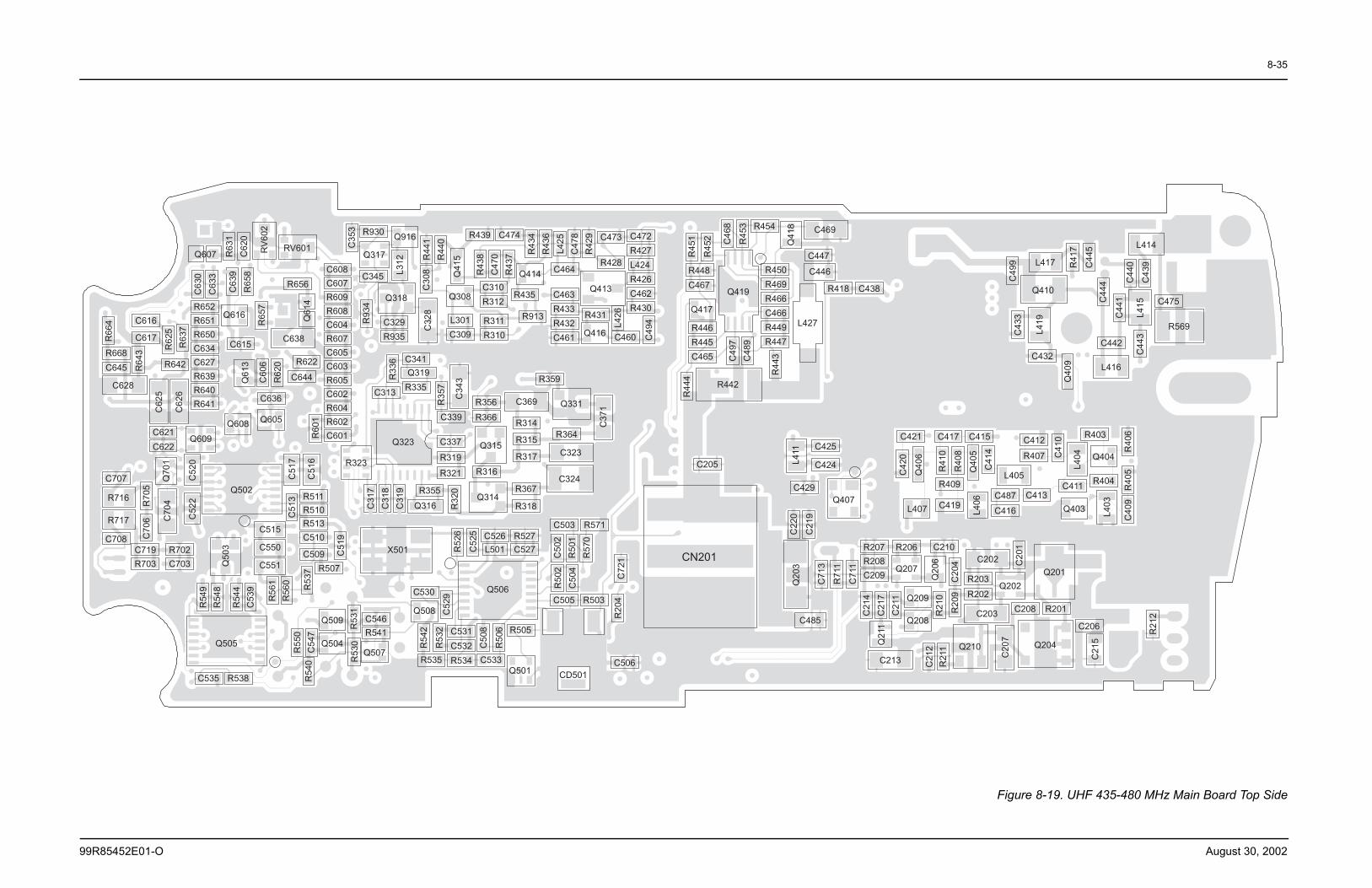
8-35
99R85452E01-O August 30, 2002
Figure 8-19. UHF 435-480 MHz Main Board Top Side
R652R651R650C634C627R639R640R641
C608C607R609R608C604R607C605C603R605C602R604R602C601
R668C645
C621C622
C63
0C
633
R63
1C
620
C63
9R
658
C60
6R
620
C616
C617
C62
5
C62
6
R642
RV601RV6
02
R656
C615R66
4
R62
5R
637
R64
3
C628
R65
7
Q61
3
Q608
Q607
Q61
4
C638
R622
C644
C636
R60
1
Q609
Q605
Q616
R511R510R513
C719 R703
R702 C703
C515
C550
C551
R716
R717
R54
4 C
539
R54
9R
548
R56
1 R
560
R55
0 C
547
C51
7
C51
6
Q502C707
C708
C52
0C
522R70
5C
706 C
704
Q50
3
Q70
1
Q505
C535 R538
C51
3
C51
9
R507
R53
7R
540
Q504
Q509
C35
3
R323
R53
1R
530
C472 R427 L424 R426 C462 R430
C463 R433 R432 C461
C310 R312
R311R310
L301C309
R314
R315
R317
C329 R935
R43
8 C
470
R43
7 R43
4 R
436
L425
C
478
R42
9
R44
1 R
440
R356 R366
R913
R435
R431
R439 C474 C473
R428C464
C341
R335Q319
C313R359
C369 Q331
Q413
R930
Q317
C345
Q318 Q308
Q916
Q414L312
R364C
308
C32
8
Q41
5
R93
4
R33
6
R35
7
C34
3
C37
1
C49
4L426
Q416 C460
Q323
C339
C337
R319
R321
Q315C323
R450 R469 R466 C466 R449 R447
R446 R445 C465
C447
C446R448 C467 R418 C438
L427
Q419
R454 C469
R442
R44
4
C49
7 C
489
R44
3
R45
1
R45
2 C46
8
R45
3
Q417
Q41
8
C421
Q410
L417
L414
C475
R569
L416
C442C432
C49
9C
433
L419
Q40
9R
417
C44
5
C44
0
C43
9
C44
4
C44
1
L415
C44
3R
406
R40
5C
409
L404C
410
C41
4Q
405
R41
0
R40
8
C20
1
R21
2
C20
4R
209
R21
0C
212
R21
1
C21
5
C20
7
Q202
L406
Q404
Q403
C417 C415 C412
R407
R403
R404C411C487 C416
C413
L405
L403
R409
C419
Q201C202
C210
R203 R202
C208 R201
C206C203
Q204Q210
Q20
6
R207 R208 C209
R206
Q207
C485
C213
Q407L407
C71
3
R71
1
C71
1C
214
C21
7 C
211
C22
0
C21
9
C42
0
Q40
6
Q21
1
Q209
Q208
Q20
3
CN201
C205
C429
C425
C424L411
C510
C509
C531 C532 R534
C31
7 C
318
C31
9
C50
2 R
501
R57
0
R50
2 C
504
R52
6
C52
5
R54
2
R53
2
C50
8
R50
6
C526 L501
R527 C527
R367
R318
C324
X501
Q506
Q314
R316
R355Q316 R
320
C503 R571
C505 R503
C506CD501Q501
R505
C533R535
C530
Q508C546 R541
Q507
C52
9
C72
1R
204
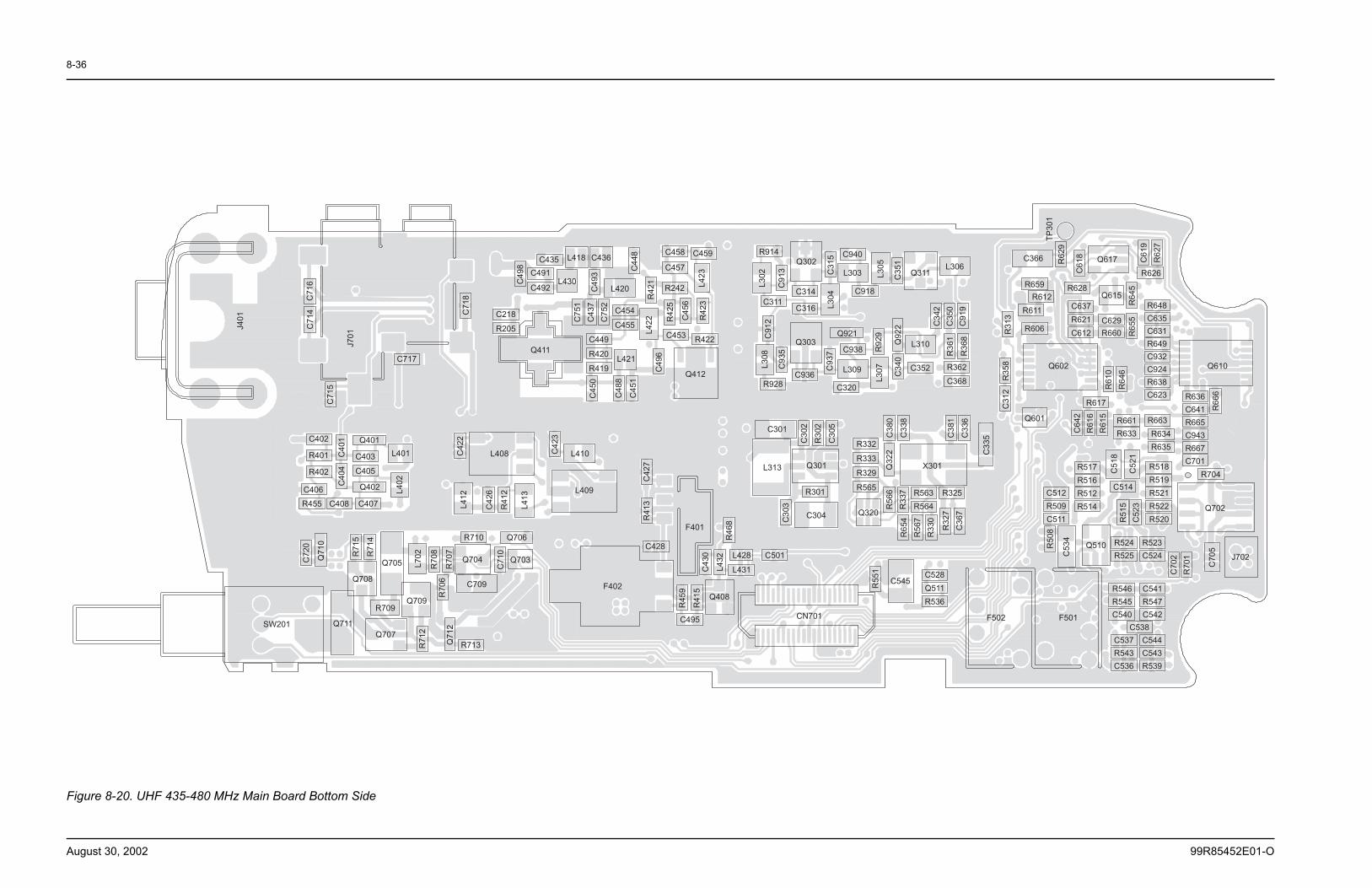
8-36
August 30, 2002 99R85452E01-O
Figure 8-20. UHF 435-480 MHz Main Board Bottom Side
J401
C7
14
C7
16
C7
15
J7
01
C7
18
C717
C402
R401
R402
C406
R455
C4
04
C4
01
C408 C407
Q401
C403
C405
Q402
L401
L4
02
C4
22
L408
L4
12
C4
26
R4
12
L4
13
C218
R205
C4
98
C7
20
Q710
R7
15
R7
14
Q708
Q705
R7
08
R7
07
L7
02
R7
06
Q709R709
SW201 Q711
Q707
R710 Q706
Q704
C7
10
Q703
C709
R7
12
Q7
12
R713
C491
C492
C435 L418 C436
L430
C4
93
C7
51
C4
37
C7
52
C4
48
L420
C454
C455
C458
C457
C459
L4
23
R242
R4
21
L4
22 R4
25
C4
56
R4
23
C453R422
Q412
C4
96
L421
C449
R420
R419
Q411
C4
50
C4
88
C4
51
C4
23
L410
L409
F402
C4
27
R4
13
C428
F401
C4
30
L4
32
C495
Q408
R4
68
L428
L431
C501
R4
59
R4
15
CN701
C304
R5
51
C545C528
Q511
R536
R6
54
R5
67
R3
30
R3
27
C3
67
R5
66
R3
37
C3
03
R301
Q320
R563
R564
R325
L313 Q301
C301
R332
R333
R329
R565
C3
02
R3
02
C3
05
C3
80
C3
38
C3
81
C3
36
X301Q322 C
33
5
R928
C936
C320
L309
L3
07
C3
40
C352 R362
C368
C3
12
R3
58
R3
61
R3
68
L310Q922
R9
29
C938
Q921
C9
37
Q303
C9
35
L3
08
C9
12
R3
13
C3
42
C3
50
C9
19
C311
R914
L3
02
C9
13
Q302
C314
C316
C3
15
L3
04
C940
L303
C918
L3
05
C3
51
Q311L306
R648
C635
C631
R649
C932
C924
R638
C623
C6
19
R6
27
R626
Q617
C6
18
R6
29
C366
TP
301
R659
R612
R611
R606
R628
C637
R621
C612
Q615
C629
R660 R6
55
R6
45
Q602
R6
10
R6
46
Q610
R636
C641
R665
C943
R667
C701
R666
R661
R633C6
42
R6
16
R6
15Q601
R617
R517
R516
R512
R514
R518
R519
R521
R522
R520
R663
R634
R635
C512
R509
C511
C5
18
C5
21
C514
R704
Q702
R5
15
C5
23
R5
08
C5
34
Q510 R524
R525
R523
C524
C7
02
R7
01
C7
05
J702
F501F502
R546
R545
C540
C541
R547
C542
C537
R543
C536
C544
C543
R539
C538
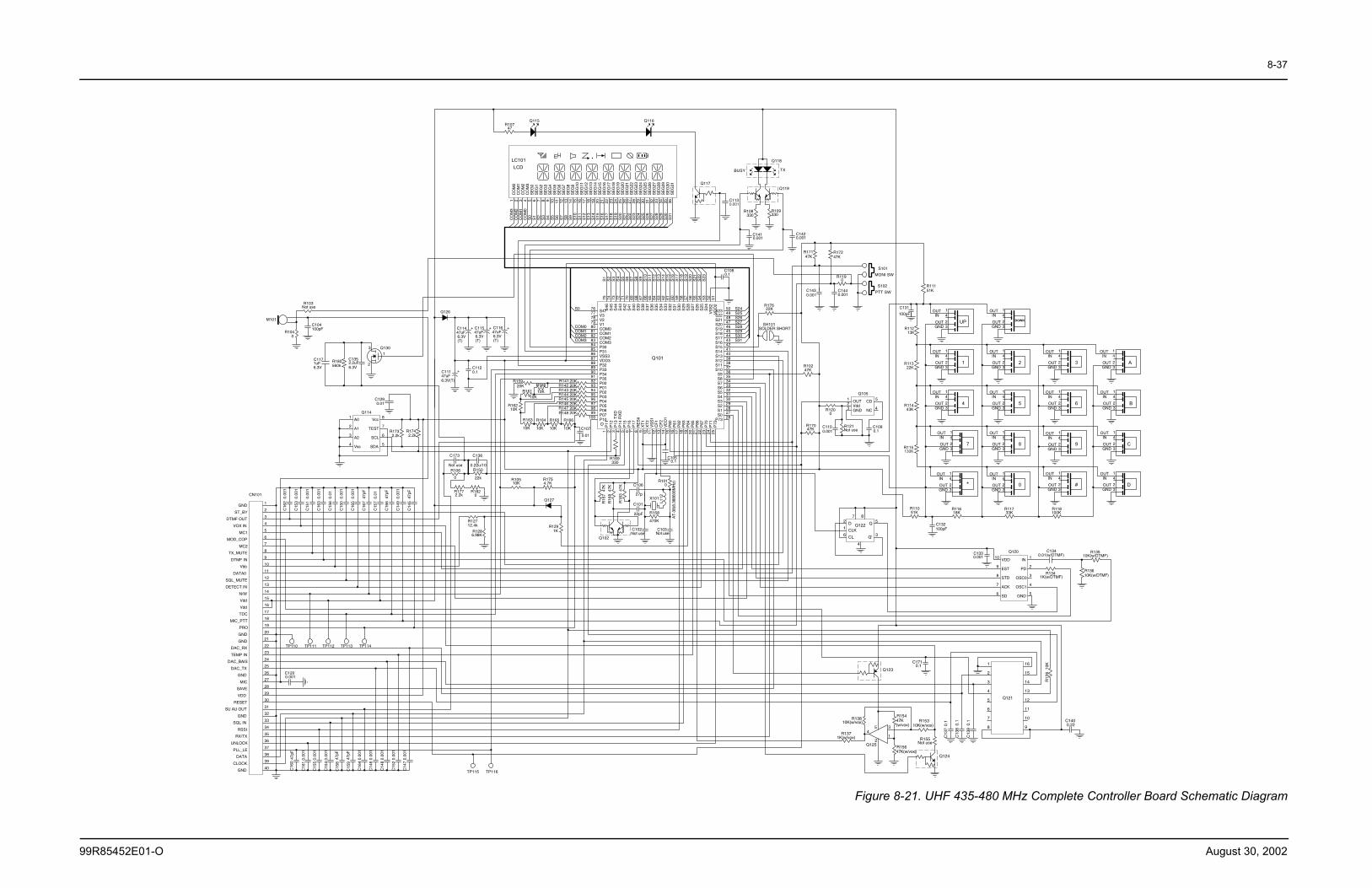
8-37
99R85452E01-O August 30, 2002
Figure 8-21. UHF 435-480 MHz Complete Controller Board Schematic Diagram
Q115R107
47
Q116
CO
M0
1
CO
M1
2
CO
M2
3
CO
M3
4
SE
G0
5
SE
G1
6
SE
G2
7
SE
G3
8
SE
G4
9
SE
G5
10
SE
G6
11
SE
G7
12
SE
G8
13
SE
G9
14
SE
G10
15
SE
G11
16
SE
G12
17
SE
G13
18
SE
G14
19
SE
G15
20
SE
G16
21
SE
G17
22
SE
G18
23
SE
G19
24
SE
G20
25
SE
G21
26
SE
G22
27
SE
G23
28
SE
G24
29
SE
G25
30
SE
G26
31
SE
G27
32
SE
G28
33
SE
G29
34
SE
G30
35
SE
G31
36
CO
M0
CO
M1
CO
M2
CO
M3
S0
S1
S2
S3
S4
S5
S6
S7
S8
S9
S10
S11
S12
S13
S14
S15
S16
S17
S18
S19
S20
S21
S22
S23
S24
S25
S26
S27
S28
S29
S30
S31
R109330
R108330
BUSY TX
Q117
C113
C1410.001
C1420.001
Q119
Q118
R11151KPTT SW
MONI SW
C1430.001
C1440.001
R17147K
R17247K
S101
S102
R1190
R11213K
C131100pF
32
41OUT
OUT
IN
GNDUP
R11322K
132
41OUT
OUT
IN
GND
R11443K
432
41OUT
OUT
IN
GND
R1157
32
41OUT
OUT
IN
GND
R11051K
R11618K
C132100pF
*32
41OUT
OUT
IN
GND
R11733K
32
41OUT
OUT
IN
GND0
32
41OUT
OUT
IN
GND8
32
41OUT
OUT
IN
GND5
32
41OUT
OUT
IN
GND
DOWN
A32
41OUT
OUT
IN
GND 32
41OUT
OUT
IN
GND 32
41OUT
OUT
IN
GND2 3
R118100K
B32
41OUT
OUT
IN
GND
32
41OUT
OUT
IN
GND
32
41OUT
OUT
IN
GND 32
41OUT
OUT
IN
GND
32
41OUT
OUT
IN
GND
32
41OUT
OUT
IN
GND
C
D
6
9
#
IN 1
PD 2
OSC0 3
OSC1 4
GND 5SD6
ACK7
STD8
EST9
VDD10Q120 C134
0.01(w/DTMF)
R1341K(w/DTMF)
R13610K(w/DTMF)
R13510K(w/DTMF)
C1330.001
C1400.22
C13
9 0
.1
C13
8 0
.1
C13
70.
1
1
2
3
4
5
6
7
8 9
10
11
12
13
14
16
15
Q121
R12
610
K
3
14
2
5
Q125
Q123
R15310K(w/vox)
R15447K(w/vox)
R155Not use
R15647K(w/vox)
Q124
C1710.1
R13810K(w/vox)
R1371K(w/vox)
TP115 TP116C15
847
pF
C15
947
pF
C16
047
pF
C16
10.
001
C16
40.
001
C14
60.
001
C14
70.
001
C14
80.
001
C15
20.
001
C15
40.
001
C15
50.
001
VDD
MIC
GND
GND
GND
RESET
GND
GND
CLOCK
DATA
PLL_LE
UNLOCK
SU AU OUT
RSSI
SQL IN
TEMP IN
RX/TX
SAVE
DAC_RX
DAC_TX
DAC_BAIS
PRO
MIC_PTT
C1200.001
18
19
20
21
22
23
24
25
26
27
28
29
30
31
32
33
34
35
36
37
38
39
40
TP110 TP111 TP112 TP113 TP114
Vbb
Vdd
Vdd
GND
MOD_COP
DATA0
DTMF OUT
DTMF IN
DETECT IN
TDC
N/W
VOX IN
MC1
MC2
TX_MUTE
ST_BY
SQL_MUTE
1
2
3
4
5
6
7
8
9
10
11
12
13
14
15
16
17
CN101
C15
60.
01
C15
70.
01
C16
20.
001
C16
30.
001
C16
50.
001
C16
647
pF
C16
747
pF
C14
547
pF
C14
90.
001
C15
00.
001
C15
10.
001
C15
30.
001
A01
A12
A23
Vss4 SDA 5
SCL 6
TEST 7
Vcc 8Q114
C1290.01
R173 2.2k
R174 2.2k
R150
22k
C173
Not use
R1772.2k
C136
0.22u/10
R1820
R106
0
R12712.4k
R1286.98K
R129 1K
Q127
R1754.7K
R10510K
X101
AT
-38(
8.38
8608
MH
z)
C103Not use
C102Not use
C101
22pF R158
470K
R1010
R16
847
K
R16
747
K
Q102
R18
347
K C106
27p
L112
P07P10
P11
1
P12
2
P13
3
P14
4
P15
5
P16
6
P17
7
RE
S#
8
XT
19
XT
210
VS
S1
11
CF
112
CF
213
VD
D1
14
P80
15
P81
16
P82
17
P83
18
P84
19
P85
20
P86
21
P87
22
P70
23
P71
24
P72
25
P73S0
C1050.1
0.01
TX
DR
XD
R169330
2627S1 28S2 29S3 30S4 31S5 32S6 33S7 34S8 35S9 36S10 37S11 38S12 39S13 40S14 41S15 42S16 43S17 44S18 45S19 46S20 47S21 48S22 49S23 50
VD
D2
VS
S2
S24S25S26S27S28S29S30S31
SH101SOLDER SHORT
R17622K
V3S47 S
4675
V2
5152S
2453
S25
54S
2655
S27
56S
2857
S29
58S
3059
S31
60S
3261
S33
62S
3463
S35
64S
3665
S37
66S
3867
S39
68S
4069
S41
70S
4271
S43
72S
4473
S45
74
C1080.1
S1
S2
S3
S4
S5
S6
S7
S8
S9
S10
S11
S12
S13
S14
S15
S16
S17
S18
S19
S20
S21
S22
S23
7776
78
V179
COM080
COM181
COM282
COM383
P3084
P3185
VSS386
VDD387
P3288
P3389
P3490
P3591
P0092
P0193
P0294
P0395
P0496
P0597
P069899
100
Q101
C107
R165
10K
R166
10K
R148 20KR147 20K
R145 20KR146 20K
R144 20KR143 20KR142 20KR141 20K
COM0COM1COM2COM3
S0
R16210K
R15920K
R16110K
R163
10K
R164
10K
R160
10K
C1120.1
Q126
+C11447uF 6.3V (T)
+C11547uF 6.3V (T)
+C11647uF 6.3V (T)
+C11147uF6.3V(T)
M101C104100pF
C1352.2uF6.3V
R180560k
C1171uF6.3V
R103Not use
R104 0
3
1
2
Q130
LC101LCD
R1200
C1100.001
OUT1
Vdd2
GND3 NC 4
CD 5Q105
C1090.1
R17047K
R10247K
R121Not use
CLK1D2
CL6
Q 5
Q' 3
4
7 8
Q122
130K
0.001
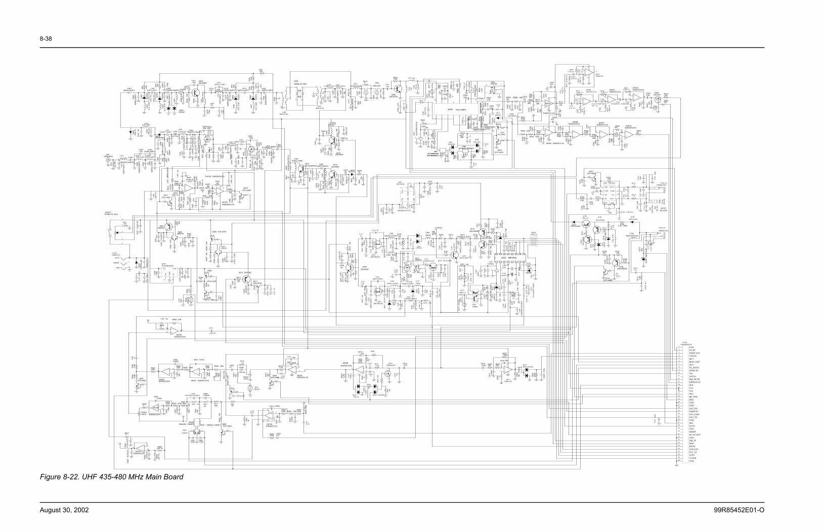
8-38
August 30, 2002 99R85452E01-O
Figure 8-22. UHF 435-480 MHz Main Board
C4018p(R2) 8p(R1)
C40
25p
(R2)
4p(
R1)
Q40
1
1SV2
79
Q40
2
1SV2
79
L401
0.3-
1.0-
5T
C40
72p
(R2)
5p(
R1)
C40822p(R2) 22p(R1)
C4046p(R2) 6p(R1)
L402
0.3-
1.0-
5T
R401
100K R4
0210
0K
C40
6
100p
L403
- - -
C403
N.U
C405
N.U
Q4031SS362
C4090.01
R40
56.
8K
R40
312
K
Q4042SC5086Y
R40
60
R40
44.
7K
C41133p
C4130.01
L404
180n
H(C
2012
C)
R407470
C41
010
0p
L4050.3-1.0-7T
Q40
5
1SV2
79
C4147p(R2) 6p(R1)
C41
56p
(R2)
10p
(R1)
L406
0.3-
1.0-
5T
C4175p(R2) 4p(R1)
C412
0.01
R408
100K
C416
5p(R
2) 6
p(R1
)
C4871p(R2) 1.5p(R1)
Q40
6
1SV2
79C
419
0.01
C42
03p
(R2)
9p(
R1)
C4219p(R2) 7p(R1)
C42
2
7p
L407
0.3-
1.0-
5T
R410
100K
R409 100K
R455100K
136
4
L408SMD-0314A
1 2
3 4
Q407HSMS-2817(B7)
C42
4
20p(
R2)
24p
(R1)
L41115nH(LL2012)
C42
5
10p
L41015nH(LL2012)
C423
15p
2
2
13 4
6
L409SMD-0314A
C429
- - -
R41
256
L412
150n
H(C
2012
C)
C42
682
p
L413470nH(FSLM)
C42
724
p
F401�- - -
C42
8- -
-
F40245N12A5
R4130
R459
3.3K
C49522p
Q4082SC4215Y
R415150K
C43
00.
01
L428
Not
use
R468
1K
L432
1uH
L431 1uH
16
Q506 TA31136FN
C50
110
0p
C502- - -
C5030.1
R50
10 C505
100p
R502
47K
C504
0.1
C506
0.1
R551 0
+
C545
33u6
.3V
(T)
R571
220K
(TH
)R5
70�
120k
9
CD
501
IFD
0455
C24
E3
R50
32.
7K
R5052.2K
4
5
3
2
1
Q501UMC4N
C53
3
22p(
R2) 5
6p(R
1)
C508470p
R50
63.
3K C5281u
Q511RB521S
680(
R2)1
k(R1
)
R5071K
R508�10K
C50
90.
001
C51
00.
22
C5110.1 R509
68K
C51
20.
0022
R511
56K
R51
047
0K
R51
247
K
VBC5342.2u10V(T)
R537470K
C51
327
p
R513
10K
C5160.01 2%
C519
6
5
Q502BNJM324V(2/4)
2
31
411
Q502A
NJM324V(1/4)
C5170.01 2%
R51715.8K 1%
R516
29.4
K 1
%
VB
C5140.01
R515
25.5
K 1
%
C515
0.01
2%
1
2
0.01 2%
C5500.01 2%
R561
634K
1%
5.11K 1%
VB
R514
3.3K
34
5
Q510NJM2107F
C551R560
7
C5180.01 2%
C520
0.01(ECHU)
9
108
Q502CNJM324V(3/4)R518
11.5K 1%
R519
150K
1%
VB
C5210.01(ECHU)
C5220.01(ECHU)
13
1214
Q502DNJM324V(4/4)
R5204.22K 1%
R521
715K
1% R52
2N
.U
VB
C5230.22
R52
3 47K
Q5032SJ144Y R524
2.2K
C52
40.
068
R52510K
9
108
Q505CNJM324V(3/4)
R547
100K
C54
239
0p
R54810K
R54
910
0K
13
1214
Q505DNJM324V(4/4)
C54
30.
0047
C54
40.
22
R5501K
2
31
411
Q505A�NJM324V(1/4)
R543100K
R539�100K
C53
70.
0027
R544100K
C53
90.
039
R545100K
6
57
Q505BNJM324V(2/4)
C54
00.
0015
R546100K
C54
10.
1
C5380.01
R538�100K
C53
50.
027
C53
60.
047
8
C53
00.
1
R53
268
0K(R
2) 1
.5M
(R1)
C53
1 220p
C532180p(R2) 220p(R1)
R5353.9K(R2)2.2k(R1)
R53
415
0K(R
2)33
0k(R
1)
R54122K
R54
222
K2
3 4 5
F502ALFYM455 H(R2)G(R1)
R53
122
K
Q504DTC144EE
+
Q508DAN235E
C529 0.
1
Q509DTA144EE
C546 0.1
C547
0.1
R536
1
R5260
C52533p
C52
639
pC
527
0.00
1
L501
1uH
(MLF
)R
527
10K
1 2
3 4 5
F501ALFYM455F(R2)
1
R53
022
K
R54
022
K
Q507DAN235E
13
24
X50
144
.645
MH
z(TO
P-B)
BLFYM455D(R1)Q416
2SC5086Y
L426
22nH
(LL1
608) R43
010
0
C4605p
R43
110
K
C463 5p
R43
310
K
R43
222
0
C46
10.
001
C46
20.
01
C494
N.U
C45
0
47p(
R2)
56p
(R1)
C44
910
0p
L421
0.4-0.9-3T
C45
1
5p
L422
0.3-
1.0-
7T
C45
5�33
0p
C45
4�0.
022
R42
247
0
C453100p
R42
310
0
R42
510
0K
R42
41K
C45
60.
022
C45
7
Not
use
L4230.4-0.9-3T
C45
815
p(R
2) 1
8p(R
1)
C4596p(R2) 7p(R1)
C488
N.U
3
2
1 Q4122SK3475
C49618p(R2) 33p(R1)
C493150p(R2) 150p(R1)
C43
518
p(R
2) 2
4p(R
1)
L4180.4-0.8-2T
C43
727
p(R
2) 2
7p(R
1)
L420
0.3-
1.0-
7T
R418470
C438100p
R41
956
R42
0�33
K
R42
1�22
K
C44
815
0p
C44
70.
0033
1
3
2
Q4112SK3476
C446
1u16
V
L430
0.3-1.0-4T
C436
�N
ot U
se
C752
27p(
R2) 2
0p(R
1)
R41
722
0
Q410MA4PH262
L417
390n
H
C44
5
100p
C49
22p
(R2)
7p(
R1)
C49115p(R2) 15p(R1)
C49
82p
(R2)
0.5
p(R
1)
L4190.4-1.0-5T
Q40
9H
VU13
1C
432
4p
C43
3N
ot u
se
J40102D04852J L415
0.4-1.0-5T
C44
010
p(R
2) 9
p(R
1)
C44
3
10p
L4160.4-1.0-5T
C4411.5p
C4421p(R2) 2p(R1)
C439
100p(R2) 220p(R1)
C44
46p
(R2)
7p(
R1)
L4140.4-1.0-5T
C475
5p(R
2) 6
p(R1
)
R569
1K(1
/4W
)
6
5
C4650.001
R443100K 1%
R444100K 1%
R44
20.
1(1/
2)
R44
510
0K 1
%R
446
100K
1%
Q417DTC114EE
L427
�ZB
FS51
05-P
T
C485
2.2u
F/16
V
C497
�22
p
2
3
8
4
Q419ANJM2904V(1/2)
7
Q419B�NJM2904V(2/2)
R44
910
0K 1
%C46
60.
001R447
97.6K 1%
R45010K
C46
80.
001
R4531M
R451 100K
R45
233
k
R44
810
0K
C46
70.
01
R4661K
R469
2.2K
1R454
15K +
C46
96.
8u6.
3V(T
)
Q418DTC144EE
C489
�0.
001
R42
6N
ot u
se(R
2)47
0(R
1)R
427
22
L42418nH(LL1608)
C47
20.
001
Q4132SC3356(R24)
R42
88.
2K
R42
94.
7K
C47
30.
001
C4646p(R2) 8p(R1)
L425
18nH
(LL1
608)
Q4142SC5086Y
R43
52.
2
R43
410
0
C47
40.
001
R43
610
K
R43
74.
7KC478
5p
C4705p
R43
81K
Q415HSC277
R43
9 330
R44022
R44
1 330
+
C30
110
u10V
(T)
C302 0.1
Vin
1
OSC
2
DK
3V
out
4
GN
D5
TI6
Q301TK11816M
L313
1000uH(NL453232)
C303
0.02
2
R301
1K
+
C30
410
u16V
(T)
R302
220
C305
0.22 MO1
SVR2
IN+3
IN-4 OUT-
Vcc
GND
OUT+
Q702 TDA8541
R703 470K
R702
1.5K
R70447K
+
C7044.7u6.3V(T)
C7030.22
C70
20.
001
R701
2.2K
Q701DTC144EE
C70
10.
001
C719100p
5
6
7
8
R705 22
C707
0.00
1C7
080.
001
SP701SPEAKER
12
P701
WC-
013
12
J702
5304
7-02
10
C706 0.
1
J701(1/2)09R80683Z01
C714
100p
C715
�10
0p
C716
100p
C705�2.2uF/16V
R7160
R7170
R71
010
0
Q70
6�U
DZ
S 6.
8B
L702390nH(C2012C)
J701(2/2)
09R80683Z01
C717
�10
0pC7
18�
100p
1SR154-400Q705
Q7111SR154-400
R7090.27( 1/8W)
R712
1K
Q7072SA1313
R713
2.2K
Q708
2SA1586GR
R714
2.2K
R715 4.7K
Q71
0U
DZ
S 20
B
C720
0.00
1
Q70
92S
A15
86G
R
Q71
21S
S355
R7082.2K
Q7042SA1586GR
R70710K
R706470
C71
00.
1
Q703DTC144EE R
711
2.2K
C71
3�0.
1
C7110.1
+
C70
910
u10V
(T)
R336
100K
1 2 3 4 5 6 7 8
9101112
Q323 MB15A02
C31
947
p
C31
847
p
R3234.7K x 4
Q319
1SS355
R335
�10
0K
C341 0.
1
13141516
R3216.8K
R31
9�10
K
Q3152SC4116GR
R3201.5K
R31
810
K
Q31
6U
DZ
S 7.
5B
+
C32
410
u16V
(T)
C31
747
pR35
5N
.U
R366
470
470
Q3142SA1586GR
R3161.5K
R31
73.
3K
+
C323
1u16
V(T
)
R3153.3K(R2) 2.7K(R1)
R364
15K
(R2)
6.8
K(R
1)
+
Q3312SC4116GR
R367
R31
310
0K
TP301
R3140
R3560
+
C369
0.1u
35V
(T)
C371
1u 1
6V(T
)
R3594.7K
C91
9N
ot u
se
L306390nHC918
18pL303
22n(R2) 27n(R1)
L305
390n
H
Q3111SV228
C351
N.U
C940
N.U
(R2)
1p(
R1)
L304�390nH
C31
60.
001
C314 5p
C913 6p
(R2)
7p(
R1)
C3111p
L302
390n
HR9
14�
150
C315
5p(R
2)6p
(R1)
Q3022SK508(K52)
Q3082SC5086Y
R91
310
KL3
0122
nHR
311
15K
R31
0�10
0
C3085p
R31
222
0
C31
00.
001
C30
90.
01
Q206�DTA123YE
R20
6�2.
2KR
207�
10K
R20
8�4.
7K
C20
90.
001
C21
00.
001
Q207UMW1N
Q2012SB798
R20
110
K
R20
3�4.
7K
+
C20
210
u10V
(T)
C20
1 0.01
+
C20
31u
16V(
T)
R2022.2K
C20
4 0.01
Q202UMW1N
4
1
2
3
5
SW201TP76N17N 10K.A
R212100
C21
52.
2uF/
16V
Q20
31S
R15
4-40
0
C20
50.
01
3
2
1
BATT
THERM
GND
CN20109D86237A
C220
100p
C219
�0.
001u
C20
60.
001 +
C20
710
u10V
(T)
C20
80.
01
Vin2
GN
D1
Vout 5
NC
4
CE3
Q204XC62HR5002PR
R20
44.
7K
R20
550
K(TH
)
C218
0.00
1
Q208
DTA114EE
R20910
R21
022
Q209DTC114EE C
211
0.00
1
Q211DTA123YE
C21
40.
001
+
C21
310
u10V
(T)
Q210�2SA1362
R211
10K
C21
2 0.00
1
C217
0.1
C9120.5p
C935
4p(R
2) 6
p(R1
)
Q92
1�1S
V27
9
L308
�39
0nH
R928
�15
0
C937
5p(R
2) 6
p(R1
)
C9364p(R2) 6p(R1)
Q3032SK508(K52)
18n(R2) 22n(R1)
R930
100K
4
5
Q9162SJ243
C353
�0.
001
C3200.001
L310390nH
C34039p(R2) 27p(R1)
L307
390n
H
L309
R3616.8K(R2) 22K(R1)
R362�22K
C368
1u
C938
12p(
R2) 5
p(R1
)
Q92
21S
V27
0
C342
100p
R934
1K
C345
0.00
1
R92910K
C352
N.U
C350
0.00
15
R368 Not
use
L312BLM21A121S Q318�2SC4116GR
R935
4.7K
C329
470p+
C328
4.7u
16V
(T)
3
2
1
Q317UMC4N
C336
Tabl
e1
13
4
X30114.4MHz
R567
10k(
TH)
R566 6.8K
R563 0
C381
Tabl
e1
R568
4.7K
R329
220K
1%
1
2
3 4
5
6
Q320UMZ2N
R565 18K
R330
�10
K(T
H)
R337150K(1%)
R564
82k(
1%)
R327
100K
R332
100K
1%
C337
Tabl
e1C3
38Ta
ble1
R333
100K
C3390.001
C34310u10V(T)
R357 10
C312
10p
R358
47
C313
Not
use
(R2)
15p
(R1)
Q32
21S
V21
7
2
C335
10p
C367
0.00
22(R
2) 0
.001
(R1)
R325 10K
C380
�Ta
ble1
���
���
���
���
�����
�� ��
� �� ��
� �� ��
�� � ��
�
���
��� ��
��
��
��� �
� ��
��� �� �
���
��
1
2
3
4
5
6
7
8
9
10
11
12
13
14
15
16
17
18
19
20
CN701AXK6S40545J/P
���
�� �� ��
��� ��
����
����
�� �
������
����
���
���
��
���
���
21
22
23
24
25
26
27
28
29
30
31
32
C721
�0.
001
���
�� �
�����
�����
����
��� ��
��� �
���
33
34
35
36
37
38
39
40
R63
182
0K
C62
00.
22u
Q6071SS372-TE85L
R62
9N
U
C619
0.1
4
VB
R62
8 0
R62618K
C6160.027
R627680K
C618 82p
R62518K
C61
70.
0047
3
1
52
Q617NJM2107F
6
57
Q602BNJM324V(2/4)
R62
04.
7K
R62
20
R621330K
C61210p
VB
C6150.01
R6554.7K
R657 0
C639 27p
Q6141SS372
Q615�DAN222
R656
100+
C638
4.7u
6.3V
(T)
R658
�82
0
3
1
2
Q616SSM3K03FE
R660- - -
C6291u
R645 1M
C637
0.00
1u C6441uR
615
12K
Q605DTC144EE
R6164.7K
R617 100K
2
31
411 Q602A
NJM324V(1/4)
C636 100p
C6420.022R
610
10K
C60
6�0.
047
C6070.1 C608
Not use
R61
247
k
RV60110K.B
Q613�DTA144EE
R65912k
R61150k(TH)
R606�100K
9
108
Q602C�NJM324V(3/4)
C604�0.0012
C60
568
0p
R607100K
R608�100K
R60
968
0K
VB
R6046.8K
13
1214
Q602DNJM324V(4/4)
C60
382
p
R605100K
C6020.0033
R60
13.
3MR
602
6.8K
Q601DTC144EE
C601 0.1
RV60210K.B
R6360
6
57 Q610B
NJM324V(2/4)
C62
415
0p
R638270K
C6230.022u
R639�270KR640
180k
C62
70.
0033
u
R64
1�10
0K
VB
C6430.0033u
C6410.0012(R2) 0.001(R1)
R663100K
R6671M
R665�1M
R666
68K
R634680k(R2) 1.5M(R1) R635�1.5M(R2) 3.3M(R1)
C6210.001
C6220.001
Q609UMG2N
R63
318
K
Q608DTC144EE
R66110K
C6300.015
R646
1K
2
31
411
Q610ANJM324V(1/4)
C63
268
p
R649100K R650�100K
C631 0.0082
R651100K
C63
40.
0018
R65
268
0K
VB
R648470K
C6330.01
C635
0.1
+
C62
6�10
u10V
(T)
+
C62
81u
16V(
T)
R64
322
K 1%
R64233K 1%
VB9
108
Q610CNJM324V(3/4)
R6370
+
C62
54.
7u6.
3V(T
)
13
1214
Q610DNJM324V(4/4)
VB
R6681K
R664�6.8K
+
C366
1u16V(T)
C645�22p
0.01
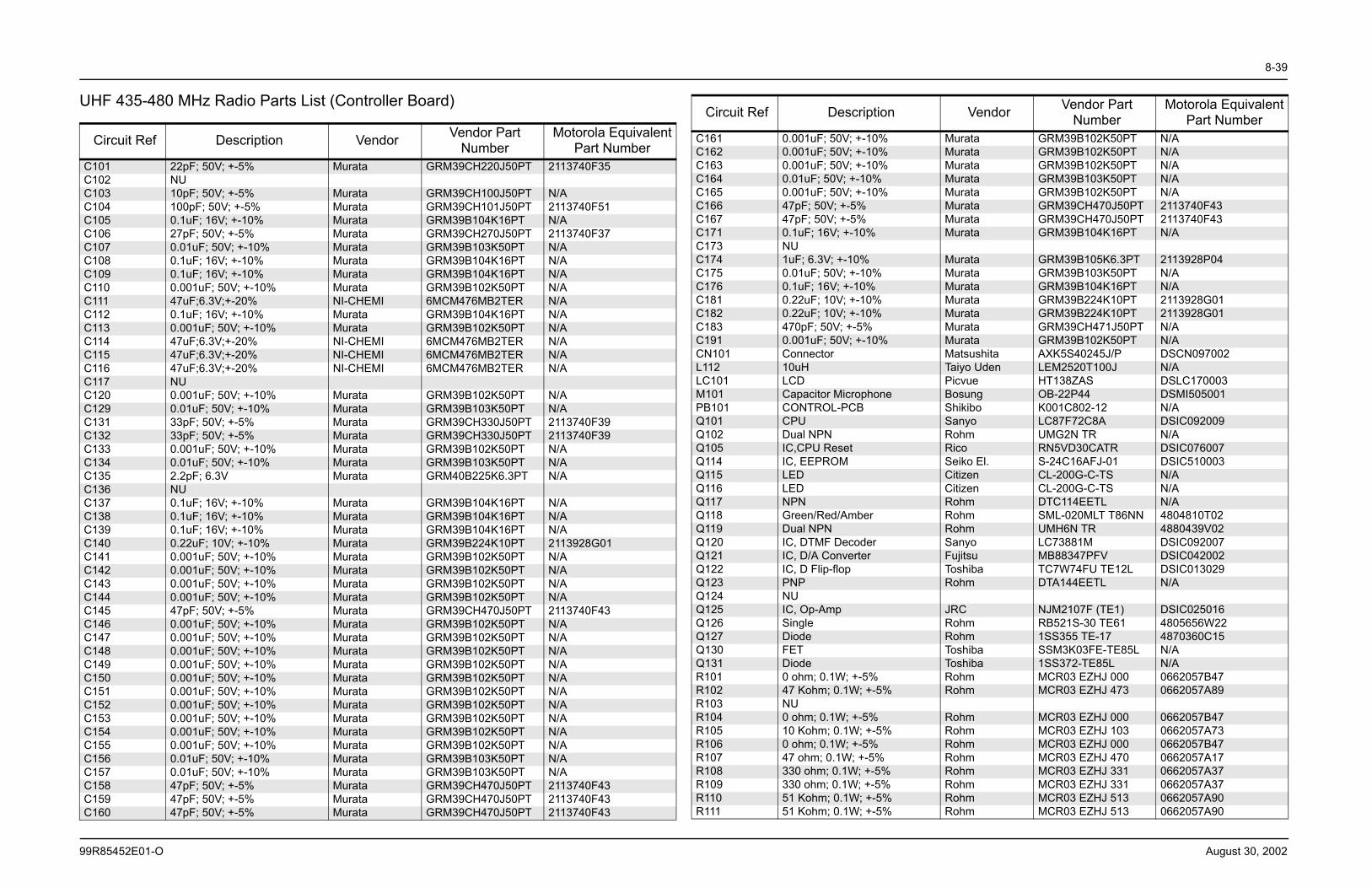
8-39
99R85452E01-O August 30, 2002
UHF 435-480 MHz Radio Parts List (Controller Board)
Circuit Ref Description Vendor Vendor Part Number
Motorola Equivalent Part Number
C101 22pF; 50V; +-5% Murata GRM39CH220J50PT 2113740F35C102 NUC103 10pF; 50V; +-5% Murata GRM39CH100J50PT N/AC104 100pF; 50V; +-5% Murata GRM39CH101J50PT 2113740F51C105 0.1uF; 16V; +-10% Murata GRM39B104K16PT N/AC106 27pF; 50V; +-5% Murata GRM39CH270J50PT 2113740F37C107 0.01uF; 50V; +-10% Murata GRM39B103K50PT N/AC108 0.1uF; 16V; +-10% Murata GRM39B104K16PT N/AC109 0.1uF; 16V; +-10% Murata GRM39B104K16PT N/AC110 0.001uF; 50V; +-10% Murata GRM39B102K50PT N/AC111 47uF;6.3V;+-20% NI-CHEMI 6MCM476MB2TER N/AC112 0.1uF; 16V; +-10% Murata GRM39B104K16PT N/AC113 0.001uF; 50V; +-10% Murata GRM39B102K50PT N/AC114 47uF;6.3V;+-20% NI-CHEMI 6MCM476MB2TER N/AC115 47uF;6.3V;+-20% NI-CHEMI 6MCM476MB2TER N/AC116 47uF;6.3V;+-20% NI-CHEMI 6MCM476MB2TER N/AC117 NUC120 0.001uF; 50V; +-10% Murata GRM39B102K50PT N/AC129 0.01uF; 50V; +-10% Murata GRM39B103K50PT N/AC131 33pF; 50V; +-5% Murata GRM39CH330J50PT 2113740F39C132 33pF; 50V; +-5% Murata GRM39CH330J50PT 2113740F39C133 0.001uF; 50V; +-10% Murata GRM39B102K50PT N/AC134 0.01uF; 50V; +-10% Murata GRM39B103K50PT N/AC135 2.2pF; 6.3V Murata GRM40B225K6.3PT N/AC136 NUC137 0.1uF; 16V; +-10% Murata GRM39B104K16PT N/AC138 0.1uF; 16V; +-10% Murata GRM39B104K16PT N/AC139 0.1uF; 16V; +-10% Murata GRM39B104K16PT N/AC140 0.22uF; 10V; +-10% Murata GRM39B224K10PT 2113928G01C141 0.001uF; 50V; +-10% Murata GRM39B102K50PT N/AC142 0.001uF; 50V; +-10% Murata GRM39B102K50PT N/AC143 0.001uF; 50V; +-10% Murata GRM39B102K50PT N/AC144 0.001uF; 50V; +-10% Murata GRM39B102K50PT N/AC145 47pF; 50V; +-5% Murata GRM39CH470J50PT 2113740F43C146 0.001uF; 50V; +-10% Murata GRM39B102K50PT N/AC147 0.001uF; 50V; +-10% Murata GRM39B102K50PT N/AC148 0.001uF; 50V; +-10% Murata GRM39B102K50PT N/AC149 0.001uF; 50V; +-10% Murata GRM39B102K50PT N/AC150 0.001uF; 50V; +-10% Murata GRM39B102K50PT N/AC151 0.001uF; 50V; +-10% Murata GRM39B102K50PT N/AC152 0.001uF; 50V; +-10% Murata GRM39B102K50PT N/AC153 0.001uF; 50V; +-10% Murata GRM39B102K50PT N/AC154 0.001uF; 50V; +-10% Murata GRM39B102K50PT N/AC155 0.001uF; 50V; +-10% Murata GRM39B102K50PT N/AC156 0.01uF; 50V; +-10% Murata GRM39B103K50PT N/AC157 0.01uF; 50V; +-10% Murata GRM39B103K50PT N/AC158 47pF; 50V; +-5% Murata GRM39CH470J50PT 2113740F43C159 47pF; 50V; +-5% Murata GRM39CH470J50PT 2113740F43C160 47pF; 50V; +-5% Murata GRM39CH470J50PT 2113740F43
C161 0.001uF; 50V; +-10% Murata GRM39B102K50PT N/AC162 0.001uF; 50V; +-10% Murata GRM39B102K50PT N/AC163 0.001uF; 50V; +-10% Murata GRM39B102K50PT N/AC164 0.01uF; 50V; +-10% Murata GRM39B103K50PT N/AC165 0.001uF; 50V; +-10% Murata GRM39B102K50PT N/AC166 47pF; 50V; +-5% Murata GRM39CH470J50PT 2113740F43C167 47pF; 50V; +-5% Murata GRM39CH470J50PT 2113740F43C171 0.1uF; 16V; +-10% Murata GRM39B104K16PT N/AC173 NUC174 1uF; 6.3V; +-10% Murata GRM39B105K6.3PT 2113928P04C175 0.01uF; 50V; +-10% Murata GRM39B103K50PT N/AC176 0.1uF; 16V; +-10% Murata GRM39B104K16PT N/AC181 0.22uF; 10V; +-10% Murata GRM39B224K10PT 2113928G01C182 0.22uF; 10V; +-10% Murata GRM39B224K10PT 2113928G01C183 470pF; 50V; +-5% Murata GRM39CH471J50PT N/AC191 0.001uF; 50V; +-10% Murata GRM39B102K50PT N/ACN101 Connector Matsushita AXK5S40245J/P DSCN097002L112 10uH Taiyo Uden LEM2520T100J N/ALC101 LCD Picvue HT138ZAS DSLC170003M101 Capacitor Microphone Bosung OB-22P44 DSMI505001PB101 CONTROL-PCB Shikibo K001C802-12 N/AQ101 CPU Sanyo LC87F72C8A DSIC092009Q102 Dual NPN Rohm UMG2N TR N/AQ105 IC,CPU Reset Rico RN5VD30CATR DSIC076007Q114 IC, EEPROM Seiko El. S-24C16AFJ-01 DSIC510003Q115 LED Citizen CL-200G-C-TS N/AQ116 LED Citizen CL-200G-C-TS N/AQ117 NPN Rohm DTC114EETL N/AQ118 Green/Red/Amber Rohm SML-020MLT T86NN 4804810T02Q119 Dual NPN Rohm UMH6N TR 4880439V02Q120 IC, DTMF Decoder Sanyo LC73881M DSIC092007Q121 IC, D/A Converter Fujitsu MB88347PFV DSIC042002Q122 IC, D Flip-flop Toshiba TC7W74FU TE12L DSIC013029Q123 PNP Rohm DTA144EETL N/AQ124 NUQ125 IC, Op-Amp JRC NJM2107F (TE1) DSIC025016Q126 Single Rohm RB521S-30 TE61 4805656W22Q127 Diode Rohm 1SS355 TE-17 4870360C15Q130 FET Toshiba SSM3K03FE-TE85L N/AQ131 Diode Toshiba 1SS372-TE85L N/AR101 0 ohm; 0.1W; +-5% Rohm MCR03 EZHJ 000 0662057B47R102 47 Kohm; 0.1W; +-5% Rohm MCR03 EZHJ 473 0662057A89R103 NUR104 0 ohm; 0.1W; +-5% Rohm MCR03 EZHJ 000 0662057B47R105 10 Kohm; 0.1W; +-5% Rohm MCR03 EZHJ 103 0662057A73R106 0 ohm; 0.1W; +-5% Rohm MCR03 EZHJ 000 0662057B47R107 47 ohm; 0.1W; +-5% Rohm MCR03 EZHJ 470 0662057A17R108 330 ohm; 0.1W; +-5% Rohm MCR03 EZHJ 331 0662057A37R109 330 ohm; 0.1W; +-5% Rohm MCR03 EZHJ 331 0662057A37R110 51 Kohm; 0.1W; +-5% Rohm MCR03 EZHJ 513 0662057A90R111 51 Kohm; 0.1W; +-5% Rohm MCR03 EZHJ 513 0662057A90
Circuit Ref Description Vendor Vendor Part Number
Motorola Equivalent Part Number
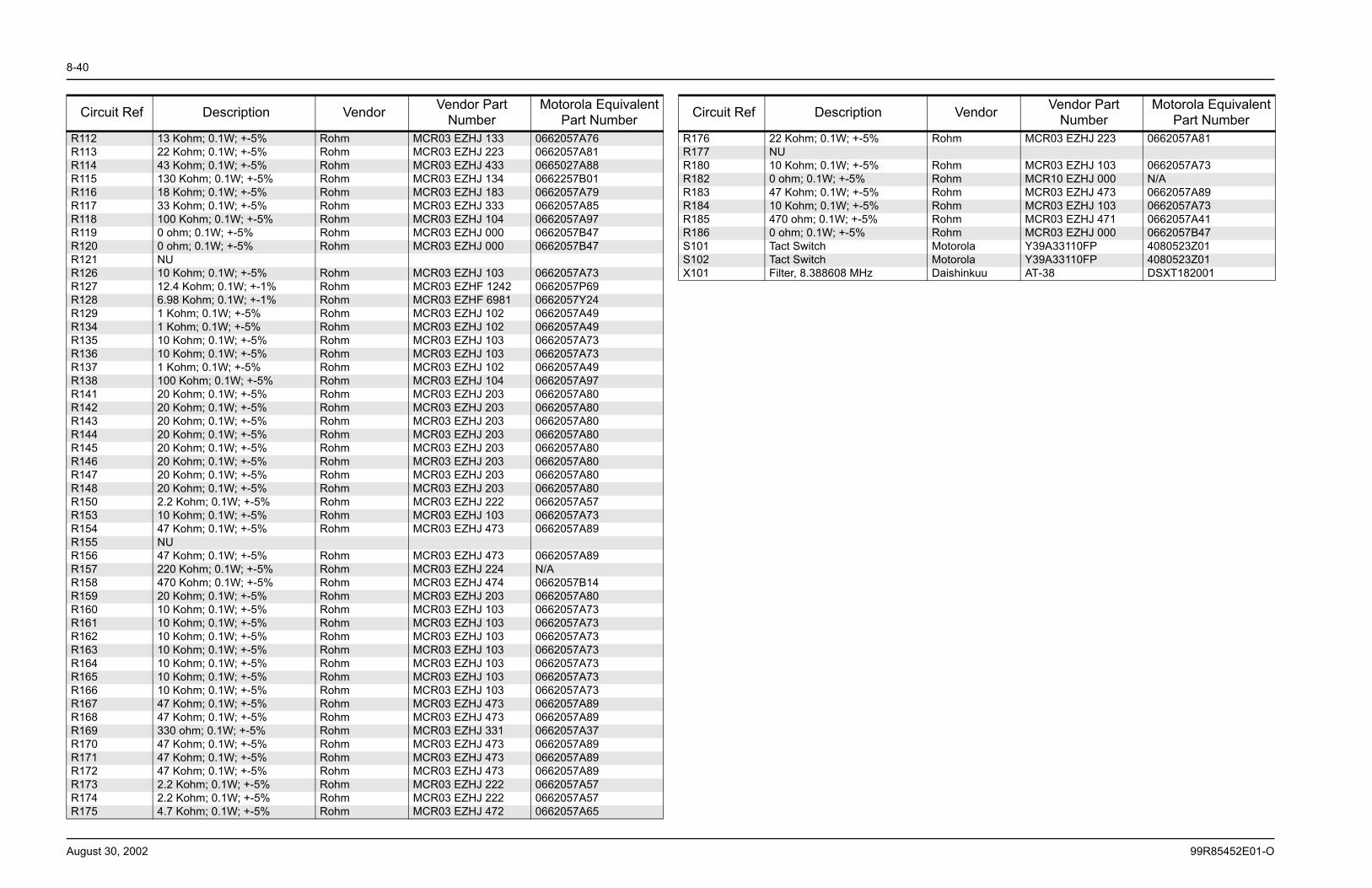
8-40
August 30, 2002 99R85452E01-O
R112 13 Kohm; 0.1W; +-5% Rohm MCR03 EZHJ 133 0662057A76R113 22 Kohm; 0.1W; +-5% Rohm MCR03 EZHJ 223 0662057A81R114 43 Kohm; 0.1W; +-5% Rohm MCR03 EZHJ 433 0665027A88R115 130 Kohm; 0.1W; +-5% Rohm MCR03 EZHJ 134 0662257B01R116 18 Kohm; 0.1W; +-5% Rohm MCR03 EZHJ 183 0662057A79R117 33 Kohm; 0.1W; +-5% Rohm MCR03 EZHJ 333 0662057A85R118 100 Kohm; 0.1W; +-5% Rohm MCR03 EZHJ 104 0662057A97R119 0 ohm; 0.1W; +-5% Rohm MCR03 EZHJ 000 0662057B47R120 0 ohm; 0.1W; +-5% Rohm MCR03 EZHJ 000 0662057B47R121 NUR126 10 Kohm; 0.1W; +-5% Rohm MCR03 EZHJ 103 0662057A73R127 12.4 Kohm; 0.1W; +-1% Rohm MCR03 EZHF 1242 0662057P69R128 6.98 Kohm; 0.1W; +-1% Rohm MCR03 EZHF 6981 0662057Y24R129 1 Kohm; 0.1W; +-5% Rohm MCR03 EZHJ 102 0662057A49R134 1 Kohm; 0.1W; +-5% Rohm MCR03 EZHJ 102 0662057A49R135 10 Kohm; 0.1W; +-5% Rohm MCR03 EZHJ 103 0662057A73R136 10 Kohm; 0.1W; +-5% Rohm MCR03 EZHJ 103 0662057A73R137 1 Kohm; 0.1W; +-5% Rohm MCR03 EZHJ 102 0662057A49R138 100 Kohm; 0.1W; +-5% Rohm MCR03 EZHJ 104 0662057A97R141 20 Kohm; 0.1W; +-5% Rohm MCR03 EZHJ 203 0662057A80R142 20 Kohm; 0.1W; +-5% Rohm MCR03 EZHJ 203 0662057A80R143 20 Kohm; 0.1W; +-5% Rohm MCR03 EZHJ 203 0662057A80R144 20 Kohm; 0.1W; +-5% Rohm MCR03 EZHJ 203 0662057A80R145 20 Kohm; 0.1W; +-5% Rohm MCR03 EZHJ 203 0662057A80R146 20 Kohm; 0.1W; +-5% Rohm MCR03 EZHJ 203 0662057A80R147 20 Kohm; 0.1W; +-5% Rohm MCR03 EZHJ 203 0662057A80R148 20 Kohm; 0.1W; +-5% Rohm MCR03 EZHJ 203 0662057A80R150 2.2 Kohm; 0.1W; +-5% Rohm MCR03 EZHJ 222 0662057A57R153 10 Kohm; 0.1W; +-5% Rohm MCR03 EZHJ 103 0662057A73R154 47 Kohm; 0.1W; +-5% Rohm MCR03 EZHJ 473 0662057A89R155 NUR156 47 Kohm; 0.1W; +-5% Rohm MCR03 EZHJ 473 0662057A89R157 220 Kohm; 0.1W; +-5% Rohm MCR03 EZHJ 224 N/AR158 470 Kohm; 0.1W; +-5% Rohm MCR03 EZHJ 474 0662057B14R159 20 Kohm; 0.1W; +-5% Rohm MCR03 EZHJ 203 0662057A80R160 10 Kohm; 0.1W; +-5% Rohm MCR03 EZHJ 103 0662057A73R161 10 Kohm; 0.1W; +-5% Rohm MCR03 EZHJ 103 0662057A73R162 10 Kohm; 0.1W; +-5% Rohm MCR03 EZHJ 103 0662057A73R163 10 Kohm; 0.1W; +-5% Rohm MCR03 EZHJ 103 0662057A73R164 10 Kohm; 0.1W; +-5% Rohm MCR03 EZHJ 103 0662057A73R165 10 Kohm; 0.1W; +-5% Rohm MCR03 EZHJ 103 0662057A73R166 10 Kohm; 0.1W; +-5% Rohm MCR03 EZHJ 103 0662057A73R167 47 Kohm; 0.1W; +-5% Rohm MCR03 EZHJ 473 0662057A89R168 47 Kohm; 0.1W; +-5% Rohm MCR03 EZHJ 473 0662057A89R169 330 ohm; 0.1W; +-5% Rohm MCR03 EZHJ 331 0662057A37R170 47 Kohm; 0.1W; +-5% Rohm MCR03 EZHJ 473 0662057A89R171 47 Kohm; 0.1W; +-5% Rohm MCR03 EZHJ 473 0662057A89R172 47 Kohm; 0.1W; +-5% Rohm MCR03 EZHJ 473 0662057A89R173 2.2 Kohm; 0.1W; +-5% Rohm MCR03 EZHJ 222 0662057A57R174 2.2 Kohm; 0.1W; +-5% Rohm MCR03 EZHJ 222 0662057A57R175 4.7 Kohm; 0.1W; +-5% Rohm MCR03 EZHJ 472 0662057A65
Circuit Ref Description Vendor Vendor Part Number
Motorola Equivalent Part Number
R176 22 Kohm; 0.1W; +-5% Rohm MCR03 EZHJ 223 0662057A81R177 NUR180 10 Kohm; 0.1W; +-5% Rohm MCR03 EZHJ 103 0662057A73R182 0 ohm; 0.1W; +-5% Rohm MCR10 EZHJ 000 N/AR183 47 Kohm; 0.1W; +-5% Rohm MCR03 EZHJ 473 0662057A89R184 10 Kohm; 0.1W; +-5% Rohm MCR03 EZHJ 103 0662057A73R185 470 ohm; 0.1W; +-5% Rohm MCR03 EZHJ 471 0662057A41R186 0 ohm; 0.1W; +-5% Rohm MCR03 EZHJ 000 0662057B47S101 Tact Switch Motorola Y39A33110FP 4080523Z01S102 Tact Switch Motorola Y39A33110FP 4080523Z01X101 Filter, 8.388608 MHz Daishinkuu AT-38 DSXT182001
Circuit Ref Description Vendor Vendor Part Number
Motorola Equivalent Part Number
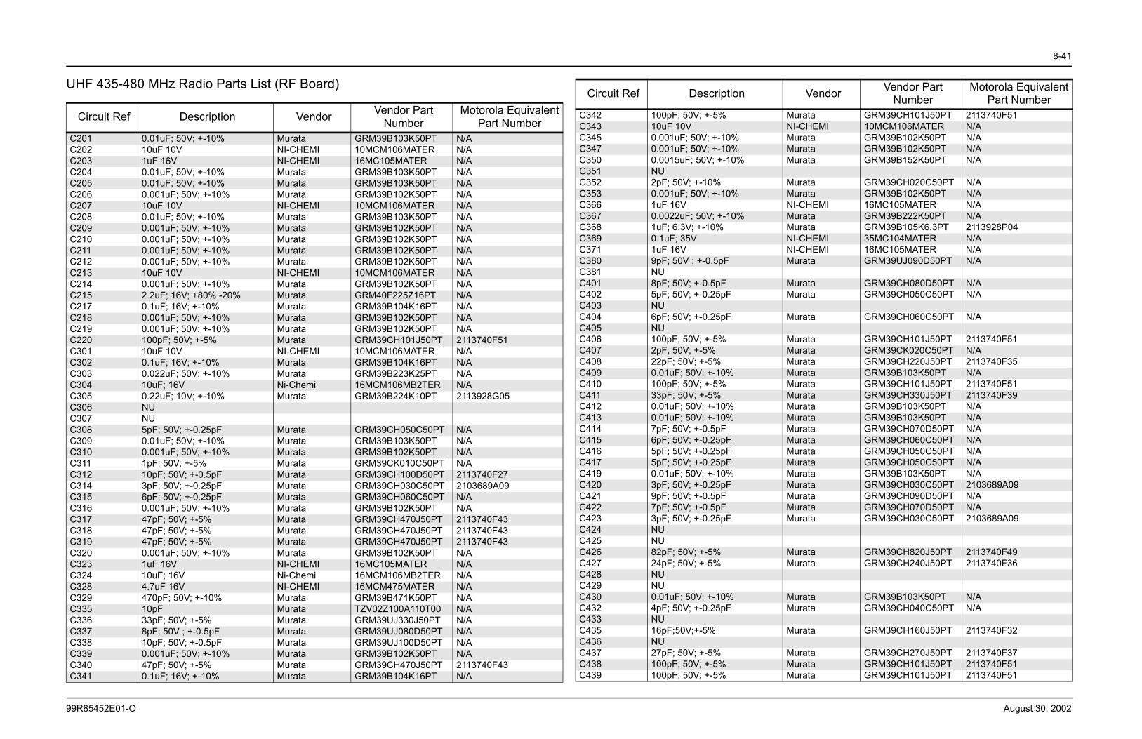
8-41
99R85452E01-O August 30, 2002
UHF 435-480 MHz Radio Parts List (RF Board)
Circuit Ref Description Vendor Vendor Part Number
Motorola Equivalent Part Number
C201 0.01uF; 50V; +-10% Murata GRM39B103K50PT N/AC202 10uF 10V NI-CHEMI 10MCM106MATER N/AC203 1uF 16V NI-CHEMI 16MC105MATER N/AC204 0.01uF; 50V; +-10% Murata GRM39B103K50PT N/AC205 0.01uF; 50V; +-10% Murata GRM39B103K50PT N/AC206 0.001uF; 50V; +-10% Murata GRM39B102K50PT N/AC207 10uF 10V NI-CHEMI 10MCM106MATER N/AC208 0.01uF; 50V; +-10% Murata GRM39B103K50PT N/AC209 0.001uF; 50V; +-10% Murata GRM39B102K50PT N/AC210 0.001uF; 50V; +-10% Murata GRM39B102K50PT N/AC211 0.001uF; 50V; +-10% Murata GRM39B102K50PT N/AC212 0.001uF; 50V; +-10% Murata GRM39B102K50PT N/AC213 10uF 10V NI-CHEMI 10MCM106MATER N/AC214 0.001uF; 50V; +-10% Murata GRM39B102K50PT N/AC215 2.2uF; 16V; +80% -20% Murata GRM40F225Z16PT N/AC217 0.1uF; 16V; +-10% Murata GRM39B104K16PT N/AC218 0.001uF; 50V; +-10% Murata GRM39B102K50PT N/AC219 0.001uF; 50V; +-10% Murata GRM39B102K50PT N/AC220 100pF; 50V; +-5% Murata GRM39CH101J50PT 2113740F51C301 10uF 10V NI-CHEMI 10MCM106MATER N/AC302 0.1uF; 16V; +-10% Murata GRM39B104K16PT N/AC303 0.022uF; 50V; +-10% Murata GRM39B223K25PT N/AC304 10uF; 16V Ni-Chemi 16MCM106MB2TER N/AC305 0.22uF; 10V; +-10% Murata GRM39B224K10PT 2113928G05C306 NUC307 NUC308 5pF; 50V; +-0.25pF Murata GRM39CH050C50PT N/AC309 0.01uF; 50V; +-10% Murata GRM39B103K50PT N/AC310 0.001uF; 50V; +-10% Murata GRM39B102K50PT N/AC311 1pF; 50V; +-5% Murata GRM39CK010C50PT N/AC312 10pF; 50V; +-0.5pF Murata GRM39CH100D50PT 2113740F27C314 3pF; 50V; +-0.25pF Murata GRM39CH030C50PT 2103689A09C315 6pF; 50V; +-0.25pF Murata GRM39CH060C50PT N/AC316 0.001uF; 50V; +-10% Murata GRM39B102K50PT N/AC317 47pF; 50V; +-5% Murata GRM39CH470J50PT 2113740F43C318 47pF; 50V; +-5% Murata GRM39CH470J50PT 2113740F43C319 47pF; 50V; +-5% Murata GRM39CH470J50PT 2113740F43C320 0.001uF; 50V; +-10% Murata GRM39B102K50PT N/AC323 1uF 16V NI-CHEMI 16MC105MATER N/AC324 10uF; 16V Ni-Chemi 16MCM106MB2TER N/AC328 4.7uF 16V NI-CHEMI 16MCM475MATER N/AC329 470pF; 50V; +-10% Murata GRM39B471K50PT N/AC335 10pF Murata TZV02Z100A110T00 N/AC336 33pF; 50V; +-5% Murata GRM39UJ330J50PT N/AC337 8pF; 50V ; +-0.5pF Murata GRM39UJ080D50PT N/AC338 10pF; 50V; +-0.5pF Murata GRM39UJ100D50PT N/AC339 0.001uF; 50V; +-10% Murata GRM39B102K50PT N/AC340 47pF; 50V; +-5% Murata GRM39CH470J50PT 2113740F43C341 0.1uF; 16V; +-10% Murata GRM39B104K16PT N/A
C342 100pF; 50V; +-5% Murata GRM39CH101J50PT 2113740F51C343 10uF 10V NI-CHEMI 10MCM106MATER N/AC345 0.001uF; 50V; +-10% Murata GRM39B102K50PT N/AC347 0.001uF; 50V; +-10% Murata GRM39B102K50PT N/AC350 0.0015uF; 50V; +-10% Murata GRM39B152K50PT N/AC351 NUC352 2pF; 50V; +-10% Murata GRM39CH020C50PT N/AC353 0.001uF; 50V; +-10% Murata GRM39B102K50PT N/AC366 1uF 16V NI-CHEMI 16MC105MATER N/AC367 0.0022uF; 50V; +-10% Murata GRM39B222K50PT N/AC368 1uF; 6.3V; +-10% Murata GRM39B105K6.3PT 2113928P04C369 0.1uF; 35V NI-CHEMI 35MC104MATER N/AC371 1uF 16V NI-CHEMI 16MC105MATER N/AC380 9pF; 50V ; +-0.5pF Murata GRM39UJ090D50PT N/AC381 NUC401 8pF; 50V; +-0.5pF Murata GRM39CH080D50PT N/AC402 5pF; 50V; +-0.25pF Murata GRM39CH050C50PT N/AC403 NUC404 6pF; 50V; +-0.25pF Murata GRM39CH060C50PT N/AC405 NUC406 100pF; 50V; +-5% Murata GRM39CH101J50PT 2113740F51C407 2pF; 50V; +-5% Murata GRM39CK020C50PT N/AC408 22pF; 50V; +-5% Murata GRM39CH220J50PT 2113740F35C409 0.01uF; 50V; +-10% Murata GRM39B103K50PT N/AC410 100pF; 50V; +-5% Murata GRM39CH101J50PT 2113740F51C411 33pF; 50V; +-5% Murata GRM39CH330J50PT 2113740F39C412 0.01uF; 50V; +-10% Murata GRM39B103K50PT N/AC413 0.01uF; 50V; +-10% Murata GRM39B103K50PT N/AC414 7pF; 50V; +-0.5pF Murata GRM39CH070D50PT N/AC415 6pF; 50V; +-0.25pF Murata GRM39CH060C50PT N/AC416 5pF; 50V; +-0.25pF Murata GRM39CH050C50PT N/AC417 5pF; 50V; +-0.25pF Murata GRM39CH050C50PT N/AC419 0.01uF; 50V; +-10% Murata GRM39B103K50PT N/AC420 3pF; 50V; +-0.25pF Murata GRM39CH030C50PT 2103689A09C421 9pF; 50V; +-0.5pF Murata GRM39CH090D50PT N/AC422 7pF; 50V; +-0.5pF Murata GRM39CH070D50PT N/AC423 3pF; 50V; +-0.25pF Murata GRM39CH030C50PT 2103689A09C424 NUC425 NUC426 82pF; 50V; +-5% Murata GRM39CH820J50PT 2113740F49C427 24pF; 50V; +-5% Murata GRM39CH240J50PT 2113740F36C428 NUC429 NUC430 0.01uF; 50V; +-10% Murata GRM39B103K50PT N/AC432 4pF; 50V; +-0.25pF Murata GRM39CH040C50PT N/AC433 NUC435 16pF;50V;+-5% Murata GRM39CH160J50PT 2113740F32C436 NUC437 27pF; 50V; +-5% Murata GRM39CH270J50PT 2113740F37C438 100pF; 50V; +-5% Murata GRM39CH101J50PT 2113740F51C439 100pF; 50V; +-5% Murata GRM39CH101J50PT 2113740F51
Circuit Ref Description Vendor Vendor Part Number
Motorola Equivalent Part Number
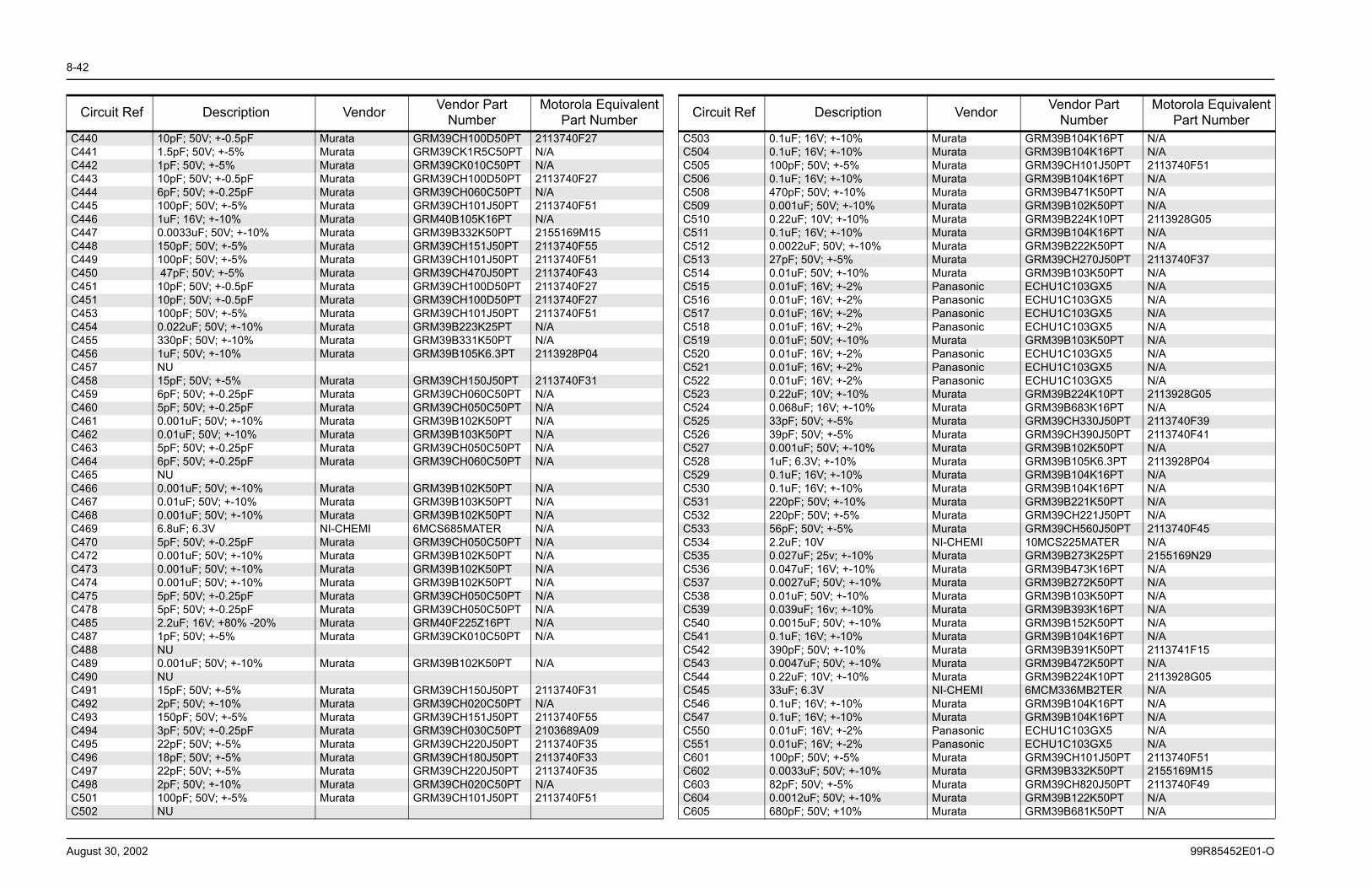
8-42
August 30, 2002 99R85452E01-O
C440 10pF; 50V; +-0.5pF Murata GRM39CH100D50PT 2113740F27C441 1.5pF; 50V; +-5% Murata GRM39CK1R5C50PT N/AC442 1pF; 50V; +-5% Murata GRM39CK010C50PT N/AC443 10pF; 50V; +-0.5pF Murata GRM39CH100D50PT 2113740F27C444 6pF; 50V; +-0.25pF Murata GRM39CH060C50PT N/AC445 100pF; 50V; +-5% Murata GRM39CH101J50PT 2113740F51C446 1uF; 16V; +-10% Murata GRM40B105K16PT N/AC447 0.0033uF; 50V; +-10% Murata GRM39B332K50PT 2155169M15C448 150pF; 50V; +-5% Murata GRM39CH151J50PT 2113740F55C449 100pF; 50V; +-5% Murata GRM39CH101J50PT 2113740F51C450 47pF; 50V; +-5% Murata GRM39CH470J50PT 2113740F43C451 10pF; 50V; +-0.5pF Murata GRM39CH100D50PT 2113740F27C451 10pF; 50V; +-0.5pF Murata GRM39CH100D50PT 2113740F27C453 100pF; 50V; +-5% Murata GRM39CH101J50PT 2113740F51C454 0.022uF; 50V; +-10% Murata GRM39B223K25PT N/AC455 330pF; 50V; +-10% Murata GRM39B331K50PT N/AC456 1uF; 50V; +-10% Murata GRM39B105K6.3PT 2113928P04C457 NUC458 15pF; 50V; +-5% Murata GRM39CH150J50PT 2113740F31C459 6pF; 50V; +-0.25pF Murata GRM39CH060C50PT N/AC460 5pF; 50V; +-0.25pF Murata GRM39CH050C50PT N/AC461 0.001uF; 50V; +-10% Murata GRM39B102K50PT N/AC462 0.01uF; 50V; +-10% Murata GRM39B103K50PT N/AC463 5pF; 50V; +-0.25pF Murata GRM39CH050C50PT N/AC464 6pF; 50V; +-0.25pF Murata GRM39CH060C50PT N/AC465 NUC466 0.001uF; 50V; +-10% Murata GRM39B102K50PT N/AC467 0.01uF; 50V; +-10% Murata GRM39B103K50PT N/AC468 0.001uF; 50V; +-10% Murata GRM39B102K50PT N/AC469 6.8uF; 6.3V NI-CHEMI 6MCS685MATER N/AC470 5pF; 50V; +-0.25pF Murata GRM39CH050C50PT N/AC472 0.001uF; 50V; +-10% Murata GRM39B102K50PT N/AC473 0.001uF; 50V; +-10% Murata GRM39B102K50PT N/AC474 0.001uF; 50V; +-10% Murata GRM39B102K50PT N/AC475 5pF; 50V; +-0.25pF Murata GRM39CH050C50PT N/AC478 5pF; 50V; +-0.25pF Murata GRM39CH050C50PT N/AC485 2.2uF; 16V; +80% -20% Murata GRM40F225Z16PT N/AC487 1pF; 50V; +-5% Murata GRM39CK010C50PT N/AC488 NUC489 0.001uF; 50V; +-10% Murata GRM39B102K50PT N/AC490 NUC491 15pF; 50V; +-5% Murata GRM39CH150J50PT 2113740F31C492 2pF; 50V; +-10% Murata GRM39CH020C50PT N/AC493 150pF; 50V; +-5% Murata GRM39CH151J50PT 2113740F55C494 3pF; 50V; +-0.25pF Murata GRM39CH030C50PT 2103689A09C495 22pF; 50V; +-5% Murata GRM39CH220J50PT 2113740F35C496 18pF; 50V; +-5% Murata GRM39CH180J50PT 2113740F33C497 22pF; 50V; +-5% Murata GRM39CH220J50PT 2113740F35C498 2pF; 50V; +-10% Murata GRM39CH020C50PT N/AC501 100pF; 50V; +-5% Murata GRM39CH101J50PT 2113740F51C502 NU
Circuit Ref Description Vendor Vendor Part Number
Motorola Equivalent Part Number
C503 0.1uF; 16V; +-10% Murata GRM39B104K16PT N/AC504 0.1uF; 16V; +-10% Murata GRM39B104K16PT N/AC505 100pF; 50V; +-5% Murata GRM39CH101J50PT 2113740F51C506 0.1uF; 16V; +-10% Murata GRM39B104K16PT N/AC508 470pF; 50V; +-10% Murata GRM39B471K50PT N/AC509 0.001uF; 50V; +-10% Murata GRM39B102K50PT N/AC510 0.22uF; 10V; +-10% Murata GRM39B224K10PT 2113928G05C511 0.1uF; 16V; +-10% Murata GRM39B104K16PT N/AC512 0.0022uF; 50V; +-10% Murata GRM39B222K50PT N/AC513 27pF; 50V; +-5% Murata GRM39CH270J50PT 2113740F37C514 0.01uF; 50V; +-10% Murata GRM39B103K50PT N/AC515 0.01uF; 16V; +-2% Panasonic ECHU1C103GX5 N/AC516 0.01uF; 16V; +-2% Panasonic ECHU1C103GX5 N/AC517 0.01uF; 16V; +-2% Panasonic ECHU1C103GX5 N/AC518 0.01uF; 16V; +-2% Panasonic ECHU1C103GX5 N/AC519 0.01uF; 50V; +-10% Murata GRM39B103K50PT N/AC520 0.01uF; 16V; +-2% Panasonic ECHU1C103GX5 N/AC521 0.01uF; 16V; +-2% Panasonic ECHU1C103GX5 N/AC522 0.01uF; 16V; +-2% Panasonic ECHU1C103GX5 N/AC523 0.22uF; 10V; +-10% Murata GRM39B224K10PT 2113928G05C524 0.068uF; 16V; +-10% Murata GRM39B683K16PT N/AC525 33pF; 50V; +-5% Murata GRM39CH330J50PT 2113740F39C526 39pF; 50V; +-5% Murata GRM39CH390J50PT 2113740F41C527 0.001uF; 50V; +-10% Murata GRM39B102K50PT N/AC528 1uF; 6.3V; +-10% Murata GRM39B105K6.3PT 2113928P04C529 0.1uF; 16V; +-10% Murata GRM39B104K16PT N/AC530 0.1uF; 16V; +-10% Murata GRM39B104K16PT N/AC531 220pF; 50V; +-10% Murata GRM39B221K50PT N/AC532 220pF; 50V; +-5% Murata GRM39CH221J50PT N/AC533 56pF; 50V; +-5% Murata GRM39CH560J50PT 2113740F45C534 2.2uF; 10V NI-CHEMI 10MCS225MATER N/AC535 0.027uF; 25v; +-10% Murata GRM39B273K25PT 2155169N29C536 0.047uF; 16V; +-10% Murata GRM39B473K16PT N/AC537 0.0027uF; 50V; +-10% Murata GRM39B272K50PT N/AC538 0.01uF; 50V; +-10% Murata GRM39B103K50PT N/AC539 0.039uF; 16v; +-10% Murata GRM39B393K16PT N/AC540 0.0015uF; 50V; +-10% Murata GRM39B152K50PT N/AC541 0.1uF; 16V; +-10% Murata GRM39B104K16PT N/AC542 390pF; 50V; +-10% Murata GRM39B391K50PT 2113741F15C543 0.0047uF; 50V; +-10% Murata GRM39B472K50PT N/AC544 0.22uF; 10V; +-10% Murata GRM39B224K10PT 2113928G05C545 33uF; 6.3V NI-CHEMI 6MCM336MB2TER N/AC546 0.1uF; 16V; +-10% Murata GRM39B104K16PT N/AC547 0.1uF; 16V; +-10% Murata GRM39B104K16PT N/AC550 0.01uF; 16V; +-2% Panasonic ECHU1C103GX5 N/AC551 0.01uF; 16V; +-2% Panasonic ECHU1C103GX5 N/AC601 100pF; 50V; +-5% Murata GRM39CH101J50PT 2113740F51C602 0.0033uF; 50V; +-10% Murata GRM39B332K50PT 2155169M15C603 82pF; 50V; +-5% Murata GRM39CH820J50PT 2113740F49C604 0.0012uF; 50V; +-10% Murata GRM39B122K50PT N/AC605 680pF; 50V; +10% Murata GRM39B681K50PT N/A
Circuit Ref Description Vendor Vendor Part Number
Motorola Equivalent Part Number
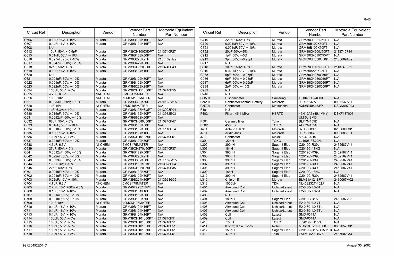
8-43
99R85452E01-O August 30, 2002
C606 0.1uF; 16V; +-10% Murata GRM39B104K16PT N/AC607 0.1uF; 16V; +-10% Murata GRM39B104K16PT N/AC608 NUC612 10pF; 50V; +-0.5pF Murata GRM39CH100D50PT 2113740F27C615 0.01uF; 50V; +-10% Murata GRM39B103K50PT N/AC616 0.027uF; 25v; +-10% Murata GRM39B273K25PT 2155169N29C617 0.0047uF; 50V; +-10% Murata GRM39B472K50PT N/AC618 82pF; 50V; +-5% Murata GRM39CH820J50PT 2113740F49C619 0.1uF; 16V; +-10% Murata GRM39B104K16PT N/AC620 NUC621 0.001uF; 50V; +-10% Murata GRM39B102K50PT N/AC622 0.001uF; 50V; +-10% Murata GRM39B102K50PT N/AC623 0.022uF; 50V; +-10% Murata GRM39B223K25PT N/AC624 150pF; 50V; +-5% Murata GRM39CH151J50PT 2113740F55C625 4.7uF; 6.3V NI-CHEMI 6MCS475MATER N/AC626 10uF 10V NI-CHEMI 10MCM106MATER N/AC627 0.0033uF; 50V; +-10% Murata GRM39B332K50PT 2155169M15C628 1uF 16V NI-CHEMI 16MC105MATER N/AC629 1uF; 6.3V; +-10% Murata GRM39B105K6.3PT 2113928P04C630 0.015uF; 50V; +-10% Murata GRM39B152K50PT 2113932E03C631 0.0082uF; 50V; +-10% Murata GRM39B822K50PT N/AC632 68pF; 50V; +-5% Murata GRM39CH680J50PT 2113740F47C633 0.01uF; 50V; +-10% Murata GRM39B103K50PT N/AC634 0.0018uF; 50V; +-10% Murata GRM39B182K50PT 2155116E54C635 0.1uF; 16V; +-10% Murata GRM39B104K16PT N/AC636 100pF; 50V; +-5% Murata GRM39CH101J50PT 2113740F51C637 0.001uF; 50V; +-10% Murata GRM39B102K50PT N/AC638 4.7uF; 6.3V NI-CHEMI 6MCS475MATER N/AC639 27pF; 50V; +-5% Murata GRM39CH270J50PT 2113740F37C641 0.0012uF; 50V; +-10% Murata GRM39B122K50PT N/AC642 0.022uF; 50V; +-10% Murata GRM39B223K25PT N/AC643 0.0033uF; 50V; +-10% Murata GRM39B332K50PT 2155169M15C644 1uF; 6.3V; +-10% Murata GRM39B105K6.3PT 2113928P04C645 22pF; 50V; +-5% Murata GRM39CH220J50PT 2113740F35C701 0.001uF; 50V; +-10% Murata GRM39B102K50PT N/AC702 0.001uF; 50V; +-10% Murata GRM39B102K50PT N/AC703 0.22uF; 10V; +-10% Murata GRM39B224K10PT 2113928G05C704 4.7uF; 6.3V NI-CHEMI 6MCS475MATER N/AC705 2.2uF; 16V; +80% -20% Murata GRM40F225Z16PT N/AC706 0.1uF; 16V; +-10% Murata GRM39B104K16PT N/AC707 0.001uF; 50V; +-10% Murata GRM39B102K50PT N/AC708 0.001uF; 50V; +-10% Murata GRM39B102K50PT N/AC709 10uF 10V NI-CHEMI 10MCM106MATER N/AC710 0.1uF; 16V; +-10% Murata GRM39B104K16PT N/AC711 0.1uF; 16V; +-10% Murata GRM39B104K16PT N/AC713 0.1uF; 16V; +-10% Murata GRM39B104K16PT N/AC714 100pF; 50V; +-5% Murata GRM39CH101J50PT 2113740F51C715 100pF; 50V; +-5% Murata GRM39CH101J50PT 2113740F51C716 100pF; 50V; +-5% Murata GRM39CH101J50PT 2113740F51C717 100pF; 50V; +-5% Murata GRM39CH101J50PT 2113740F51C718 100pF; 50V; +-5% Murata GRM39CH101J50PT 2113740F51
Circuit Ref Description Vendor Vendor Part Number
Motorola Equivalent Part Number
C719 220pF; 50V; +-5% Murata GRM39CH221J50PT N/AC720 0.001uF; 50V; +-10% Murata GRM39B102K50PT N/AC721 0.001uF; 50V; +-10% Murata GRM39B102K50PT N/AC752 20pF;50V;+-5% Murata GRM39CH200J50PT 2113740F34C912 1pF; 50V; +-5% Murata GRM39CK010C50PT N/AC913 3pF; 50V; +-0.25pF Murata GRM39CH030C50PT 2103689A09C917 NUC918 100pF; 50V; +-5% Murata GRM39CH101J50PT 2113740F51C919 0.022uF; 50V; +-10% Murata GRM39B223K25PT N/AC935 6pF; 50V; +-0.25pF Murata GRM39CH060C50PT N/AC936 6pF; 50V; +-0.25pF Murata GRM39CH060C50PT N/AC937 6pF; 50V; +-0.25pF Murata GRM39CH060C50PT N/AC938 2pF; 50V; +-10% Murata GRM39CH020C50PT N/AC939 NUC940 NUCD501 Discriminator Samsung IFD0455C24E03 N/ACN201 Connector contact Battery Motorola 09D86237A 0986237A01CN701 Connector Matsushita AXK6S40545J/P DSCN097003F401 NUF402 Filter , 45.1 MHz HERTZ 45N12A5 (45.1MHz)
UM-5J-SMDDSXF137006
F501 Ceramic filter Toko BLFYM455D N/AF502 455Khz TOKO ALFYM455G N/AJ401 Antenna Jack Motorola 02D80689C 0280689C01J701 Audio Jack Motorola 09R80683Z 0980683Z01J702 Connector Molex 53047-0210 N/AL301 22nH TOKO LL1608-FS22NJ N/AL302 390nH Sagami Elec C2012C-R39J 2462587V41L303 18nH Sagami Elec C2012C-18NG N/AL304 390nH Sagami Elec C2012C-R39J 2462587V41L305 390nH Sagami Elec C2012C-R39J 2462587V41L306 390nH Sagami Elec C2012C-R39J 2462587V41L307 390nH Sagami Elec C2012C-R39J 2462587V41L308 390nH Sagami Elec C2012C-R39J 2462587V41L309 18nH Sagami Elec C2012C-18NG N/AL310 390nH Sagami Elec C2012C-R39J 2462587V41L312 Chip emifil Murata BLM21A121SPT 2480067M02L313 1000uH TDK NL453232T-102J N/AL401 Airwound Coil Uchida/Latest E2-0.30-1.0-5TL N/AL402 Airwound Coil Uchida/Latest E2-0.30-1.0-5TL N/AL403 NUL404 180nH Sagami Elec C2012C-R15J 2462587V36L405 Airwound Coil Uchida/Latest E2-0.30-1.0-7TL N/AL406 Airwound Coil Uchida/Latest E2-0.30-1.0-5TL N/AL407 Airwound Coil Uchida/Latest E2-0.30-1.0-5TL N/AL408 Coil Latest SMD-0314A N/AL409 Coil Latest SMD-0314A N/AL410 15nH TOKO LL2012-FH15NJ N/AL411 0 ohm; 0.1W; +-5% Rohm MCR10 EZH J 000 0662057C01L412 150nH Sagami Elec C2012C-R15J (150nH) N/AL413 470nH Toko FSLM2520-R47K 2485602J33
Circuit Ref Description Vendor Vendor Part Number
Motorola Equivalent Part Number
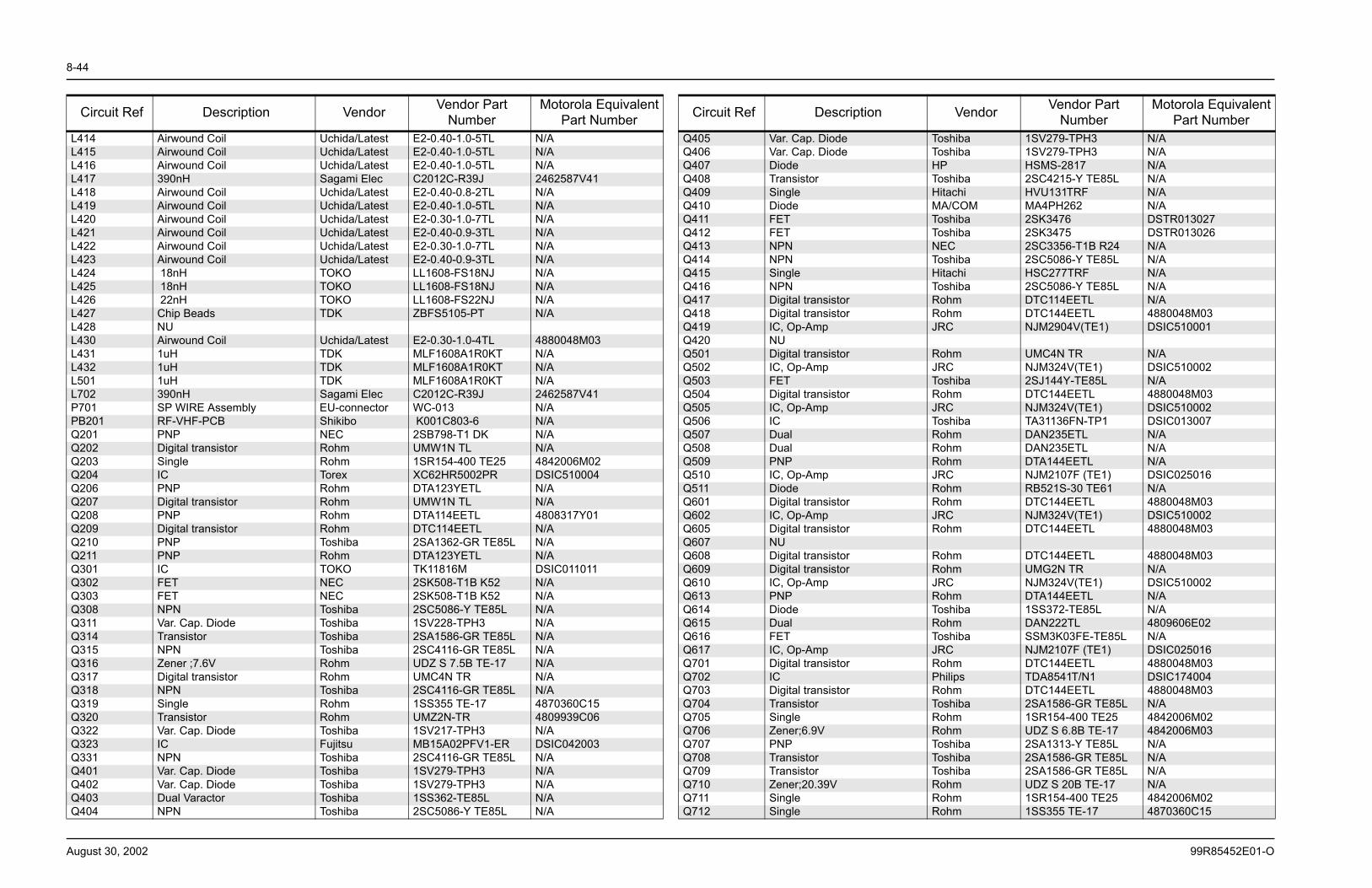
8-44
August 30, 2002 99R85452E01-O
L414 Airwound Coil Uchida/Latest E2-0.40-1.0-5TL N/AL415 Airwound Coil Uchida/Latest E2-0.40-1.0-5TL N/AL416 Airwound Coil Uchida/Latest E2-0.40-1.0-5TL N/AL417 390nH Sagami Elec C2012C-R39J 2462587V41L418 Airwound Coil Uchida/Latest E2-0.40-0.8-2TL N/AL419 Airwound Coil Uchida/Latest E2-0.40-1.0-5TL N/AL420 Airwound Coil Uchida/Latest E2-0.30-1.0-7TL N/AL421 Airwound Coil Uchida/Latest E2-0.40-0.9-3TL N/AL422 Airwound Coil Uchida/Latest E2-0.30-1.0-7TL N/AL423 Airwound Coil Uchida/Latest E2-0.40-0.9-3TL N/AL424 18nH TOKO LL1608-FS18NJ N/AL425 18nH TOKO LL1608-FS18NJ N/AL426 22nH TOKO LL1608-FS22NJ N/AL427 Chip Beads TDK ZBFS5105-PT N/AL428 NUL430 Airwound Coil Uchida/Latest E2-0.30-1.0-4TL 4880048M03L431 1uH TDK MLF1608A1R0KT N/AL432 1uH TDK MLF1608A1R0KT N/AL501 1uH TDK MLF1608A1R0KT N/AL702 390nH Sagami Elec C2012C-R39J 2462587V41P701 SP WIRE Assembly EU-connector WC-013 N/APB201 RF-VHF-PCB Shikibo K001C803-6 N/AQ201 PNP NEC 2SB798-T1 DK N/AQ202 Digital transistor Rohm UMW1N TL N/AQ203 Single Rohm 1SR154-400 TE25 4842006M02Q204 IC Torex XC62HR5002PR DSIC510004Q206 PNP Rohm DTA123YETL N/AQ207 Digital transistor Rohm UMW1N TL N/AQ208 PNP Rohm DTA114EETL 4808317Y01Q209 Digital transistor Rohm DTC114EETL N/AQ210 PNP Toshiba 2SA1362-GR TE85L N/AQ211 PNP Rohm DTA123YETL N/AQ301 IC TOKO TK11816M DSIC011011Q302 FET NEC 2SK508-T1B K52 N/AQ303 FET NEC 2SK508-T1B K52 N/AQ308 NPN Toshiba 2SC5086-Y TE85L N/AQ311 Var. Cap. Diode Toshiba 1SV228-TPH3 N/AQ314 Transistor Toshiba 2SA1586-GR TE85L N/AQ315 NPN Toshiba 2SC4116-GR TE85L N/AQ316 Zener ;7.6V Rohm UDZ S 7.5B TE-17 N/AQ317 Digital transistor Rohm UMC4N TR N/AQ318 NPN Toshiba 2SC4116-GR TE85L N/AQ319 Single Rohm 1SS355 TE-17 4870360C15Q320 Transistor Rohm UMZ2N-TR 4809939C06Q322 Var. Cap. Diode Toshiba 1SV217-TPH3 N/AQ323 IC Fujitsu MB15A02PFV1-ER DSIC042003Q331 NPN Toshiba 2SC4116-GR TE85L N/AQ401 Var. Cap. Diode Toshiba 1SV279-TPH3 N/AQ402 Var. Cap. Diode Toshiba 1SV279-TPH3 N/AQ403 Dual Varactor Toshiba 1SS362-TE85L N/AQ404 NPN Toshiba 2SC5086-Y TE85L N/A
Circuit Ref Description Vendor Vendor Part Number
Motorola Equivalent Part Number
Q405 Var. Cap. Diode Toshiba 1SV279-TPH3 N/AQ406 Var. Cap. Diode Toshiba 1SV279-TPH3 N/AQ407 Diode HP HSMS-2817 N/AQ408 Transistor Toshiba 2SC4215-Y TE85L N/AQ409 Single Hitachi HVU131TRF N/AQ410 Diode MA/COM MA4PH262 N/AQ411 FET Toshiba 2SK3476 DSTR013027Q412 FET Toshiba 2SK3475 DSTR013026Q413 NPN NEC 2SC3356-T1B R24 N/AQ414 NPN Toshiba 2SC5086-Y TE85L N/AQ415 Single Hitachi HSC277TRF N/AQ416 NPN Toshiba 2SC5086-Y TE85L N/AQ417 Digital transistor Rohm DTC114EETL N/AQ418 Digital transistor Rohm DTC144EETL 4880048M03Q419 IC, Op-Amp JRC NJM2904V(TE1) DSIC510001Q420 NUQ501 Digital transistor Rohm UMC4N TR N/AQ502 IC, Op-Amp JRC NJM324V(TE1) DSIC510002Q503 FET Toshiba 2SJ144Y-TE85L N/AQ504 Digital transistor Rohm DTC144EETL 4880048M03Q505 IC, Op-Amp JRC NJM324V(TE1) DSIC510002Q506 IC Toshiba TA31136FN-TP1 DSIC013007Q507 Dual Rohm DAN235ETL N/AQ508 Dual Rohm DAN235ETL N/AQ509 PNP Rohm DTA144EETL N/AQ510 IC, Op-Amp JRC NJM2107F (TE1) DSIC025016Q511 Diode Rohm RB521S-30 TE61 N/AQ601 Digital transistor Rohm DTC144EETL 4880048M03Q602 IC, Op-Amp JRC NJM324V(TE1) DSIC510002Q605 Digital transistor Rohm DTC144EETL 4880048M03Q607 NUQ608 Digital transistor Rohm DTC144EETL 4880048M03Q609 Digital transistor Rohm UMG2N TR N/AQ610 IC, Op-Amp JRC NJM324V(TE1) DSIC510002Q613 PNP Rohm DTA144EETL N/AQ614 Diode Toshiba 1SS372-TE85L N/AQ615 Dual Rohm DAN222TL 4809606E02Q616 FET Toshiba SSM3K03FE-TE85L N/AQ617 IC, Op-Amp JRC NJM2107F (TE1) DSIC025016Q701 Digital transistor Rohm DTC144EETL 4880048M03Q702 IC Philips TDA8541T/N1 DSIC174004Q703 Digital transistor Rohm DTC144EETL 4880048M03Q704 Transistor Toshiba 2SA1586-GR TE85L N/AQ705 Single Rohm 1SR154-400 TE25 4842006M02Q706 Zener;6.9V Rohm UDZ S 6.8B TE-17 4842006M03Q707 PNP Toshiba 2SA1313-Y TE85L N/AQ708 Transistor Toshiba 2SA1586-GR TE85L N/AQ709 Transistor Toshiba 2SA1586-GR TE85L N/AQ710 Zener;20.39V Rohm UDZ S 20B TE-17 N/AQ711 Single Rohm 1SR154-400 TE25 4842006M02Q712 Single Rohm 1SS355 TE-17 4870360C15
Circuit Ref Description Vendor Vendor Part Number
Motorola Equivalent Part Number
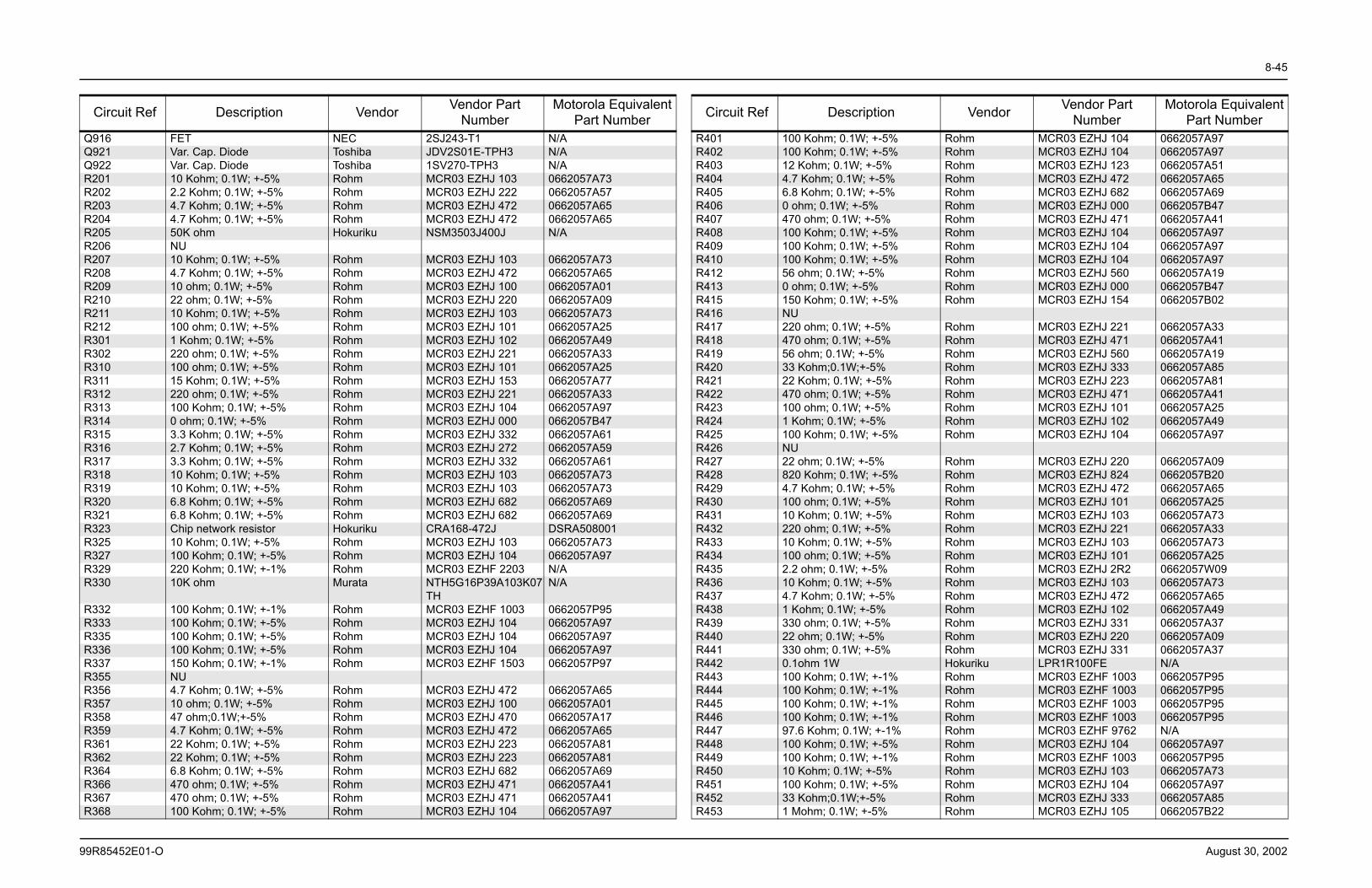
8-45
99R85452E01-O August 30, 2002
Q916 FET NEC 2SJ243-T1 N/AQ921 Var. Cap. Diode Toshiba JDV2S01E-TPH3 N/AQ922 Var. Cap. Diode Toshiba 1SV270-TPH3 N/AR201 10 Kohm; 0.1W; +-5% Rohm MCR03 EZHJ 103 0662057A73R202 2.2 Kohm; 0.1W; +-5% Rohm MCR03 EZHJ 222 0662057A57R203 4.7 Kohm; 0.1W; +-5% Rohm MCR03 EZHJ 472 0662057A65R204 4.7 Kohm; 0.1W; +-5% Rohm MCR03 EZHJ 472 0662057A65R205 50K ohm Hokuriku NSM3503J400J N/AR206 NUR207 10 Kohm; 0.1W; +-5% Rohm MCR03 EZHJ 103 0662057A73R208 4.7 Kohm; 0.1W; +-5% Rohm MCR03 EZHJ 472 0662057A65R209 10 ohm; 0.1W; +-5% Rohm MCR03 EZHJ 100 0662057A01R210 22 ohm; 0.1W; +-5% Rohm MCR03 EZHJ 220 0662057A09R211 10 Kohm; 0.1W; +-5% Rohm MCR03 EZHJ 103 0662057A73R212 100 ohm; 0.1W; +-5% Rohm MCR03 EZHJ 101 0662057A25R301 1 Kohm; 0.1W; +-5% Rohm MCR03 EZHJ 102 0662057A49R302 220 ohm; 0.1W; +-5% Rohm MCR03 EZHJ 221 0662057A33R310 100 ohm; 0.1W; +-5% Rohm MCR03 EZHJ 101 0662057A25R311 15 Kohm; 0.1W; +-5% Rohm MCR03 EZHJ 153 0662057A77R312 220 ohm; 0.1W; +-5% Rohm MCR03 EZHJ 221 0662057A33R313 100 Kohm; 0.1W; +-5% Rohm MCR03 EZHJ 104 0662057A97R314 0 ohm; 0.1W; +-5% Rohm MCR03 EZHJ 000 0662057B47R315 3.3 Kohm; 0.1W; +-5% Rohm MCR03 EZHJ 332 0662057A61R316 2.7 Kohm; 0.1W; +-5% Rohm MCR03 EZHJ 272 0662057A59R317 3.3 Kohm; 0.1W; +-5% Rohm MCR03 EZHJ 332 0662057A61R318 10 Kohm; 0.1W; +-5% Rohm MCR03 EZHJ 103 0662057A73R319 10 Kohm; 0.1W; +-5% Rohm MCR03 EZHJ 103 0662057A73R320 6.8 Kohm; 0.1W; +-5% Rohm MCR03 EZHJ 682 0662057A69R321 6.8 Kohm; 0.1W; +-5% Rohm MCR03 EZHJ 682 0662057A69R323 Chip network resistor Hokuriku CRA168-472J DSRA508001R325 10 Kohm; 0.1W; +-5% Rohm MCR03 EZHJ 103 0662057A73R327 100 Kohm; 0.1W; +-5% Rohm MCR03 EZHJ 104 0662057A97R329 220 Kohm; 0.1W; +-1% Rohm MCR03 EZHF 2203 N/AR330 10K ohm Murata NTH5G16P39A103K07
THN/A
R332 100 Kohm; 0.1W; +-1% Rohm MCR03 EZHF 1003 0662057P95R333 100 Kohm; 0.1W; +-5% Rohm MCR03 EZHJ 104 0662057A97R335 100 Kohm; 0.1W; +-5% Rohm MCR03 EZHJ 104 0662057A97R336 100 Kohm; 0.1W; +-5% Rohm MCR03 EZHJ 104 0662057A97R337 150 Kohm; 0.1W; +-1% Rohm MCR03 EZHF 1503 0662057P97R355 NUR356 4.7 Kohm; 0.1W; +-5% Rohm MCR03 EZHJ 472 0662057A65R357 10 ohm; 0.1W; +-5% Rohm MCR03 EZHJ 100 0662057A01R358 47 ohm;0.1W;+-5% Rohm MCR03 EZHJ 470 0662057A17R359 4.7 Kohm; 0.1W; +-5% Rohm MCR03 EZHJ 472 0662057A65R361 22 Kohm; 0.1W; +-5% Rohm MCR03 EZHJ 223 0662057A81R362 22 Kohm; 0.1W; +-5% Rohm MCR03 EZHJ 223 0662057A81R364 6.8 Kohm; 0.1W; +-5% Rohm MCR03 EZHJ 682 0662057A69R366 470 ohm; 0.1W; +-5% Rohm MCR03 EZHJ 471 0662057A41R367 470 ohm; 0.1W; +-5% Rohm MCR03 EZHJ 471 0662057A41R368 100 Kohm; 0.1W; +-5% Rohm MCR03 EZHJ 104 0662057A97
Circuit Ref Description Vendor Vendor Part Number
Motorola Equivalent Part Number
R401 100 Kohm; 0.1W; +-5% Rohm MCR03 EZHJ 104 0662057A97R402 100 Kohm; 0.1W; +-5% Rohm MCR03 EZHJ 104 0662057A97R403 12 Kohm; 0.1W; +-5% Rohm MCR03 EZHJ 123 0662057A51R404 4.7 Kohm; 0.1W; +-5% Rohm MCR03 EZHJ 472 0662057A65R405 6.8 Kohm; 0.1W; +-5% Rohm MCR03 EZHJ 682 0662057A69R406 0 ohm; 0.1W; +-5% Rohm MCR03 EZHJ 000 0662057B47R407 470 ohm; 0.1W; +-5% Rohm MCR03 EZHJ 471 0662057A41R408 100 Kohm; 0.1W; +-5% Rohm MCR03 EZHJ 104 0662057A97R409 100 Kohm; 0.1W; +-5% Rohm MCR03 EZHJ 104 0662057A97R410 100 Kohm; 0.1W; +-5% Rohm MCR03 EZHJ 104 0662057A97R412 56 ohm; 0.1W; +-5% Rohm MCR03 EZHJ 560 0662057A19R413 0 ohm; 0.1W; +-5% Rohm MCR03 EZHJ 000 0662057B47R415 150 Kohm; 0.1W; +-5% Rohm MCR03 EZHJ 154 0662057B02R416 NUR417 220 ohm; 0.1W; +-5% Rohm MCR03 EZHJ 221 0662057A33R418 470 ohm; 0.1W; +-5% Rohm MCR03 EZHJ 471 0662057A41R419 56 ohm; 0.1W; +-5% Rohm MCR03 EZHJ 560 0662057A19R420 33 Kohm;0.1W;+-5% Rohm MCR03 EZHJ 333 0662057A85R421 22 Kohm; 0.1W; +-5% Rohm MCR03 EZHJ 223 0662057A81R422 470 ohm; 0.1W; +-5% Rohm MCR03 EZHJ 471 0662057A41R423 100 ohm; 0.1W; +-5% Rohm MCR03 EZHJ 101 0662057A25R424 1 Kohm; 0.1W; +-5% Rohm MCR03 EZHJ 102 0662057A49R425 100 Kohm; 0.1W; +-5% Rohm MCR03 EZHJ 104 0662057A97R426 NUR427 22 ohm; 0.1W; +-5% Rohm MCR03 EZHJ 220 0662057A09R428 820 Kohm; 0.1W; +-5% Rohm MCR03 EZHJ 824 0662057B20R429 4.7 Kohm; 0.1W; +-5% Rohm MCR03 EZHJ 472 0662057A65R430 100 ohm; 0.1W; +-5% Rohm MCR03 EZHJ 101 0662057A25R431 10 Kohm; 0.1W; +-5% Rohm MCR03 EZHJ 103 0662057A73R432 220 ohm; 0.1W; +-5% Rohm MCR03 EZHJ 221 0662057A33R433 10 Kohm; 0.1W; +-5% Rohm MCR03 EZHJ 103 0662057A73R434 100 ohm; 0.1W; +-5% Rohm MCR03 EZHJ 101 0662057A25R435 2.2 ohm; 0.1W; +-5% Rohm MCR03 EZHJ 2R2 0662057W09R436 10 Kohm; 0.1W; +-5% Rohm MCR03 EZHJ 103 0662057A73R437 4.7 Kohm; 0.1W; +-5% Rohm MCR03 EZHJ 472 0662057A65R438 1 Kohm; 0.1W; +-5% Rohm MCR03 EZHJ 102 0662057A49R439 330 ohm; 0.1W; +-5% Rohm MCR03 EZHJ 331 0662057A37R440 22 ohm; 0.1W; +-5% Rohm MCR03 EZHJ 220 0662057A09R441 330 ohm; 0.1W; +-5% Rohm MCR03 EZHJ 331 0662057A37R442 0.1ohm 1W Hokuriku LPR1R100FE N/AR443 100 Kohm; 0.1W; +-1% Rohm MCR03 EZHF 1003 0662057P95R444 100 Kohm; 0.1W; +-1% Rohm MCR03 EZHF 1003 0662057P95R445 100 Kohm; 0.1W; +-1% Rohm MCR03 EZHF 1003 0662057P95R446 100 Kohm; 0.1W; +-1% Rohm MCR03 EZHF 1003 0662057P95R447 97.6 Kohm; 0.1W; +-1% Rohm MCR03 EZHF 9762 N/AR448 100 Kohm; 0.1W; +-5% Rohm MCR03 EZHJ 104 0662057A97R449 100 Kohm; 0.1W; +-1% Rohm MCR03 EZHF 1003 0662057P95R450 10 Kohm; 0.1W; +-5% Rohm MCR03 EZHJ 103 0662057A73R451 100 Kohm; 0.1W; +-5% Rohm MCR03 EZHJ 104 0662057A97R452 33 Kohm;0.1W;+-5% Rohm MCR03 EZHJ 333 0662057A85R453 1 Mohm; 0.1W; +-5% Rohm MCR03 EZHJ 105 0662057B22
Circuit Ref Description Vendor Vendor Part Number
Motorola Equivalent Part Number
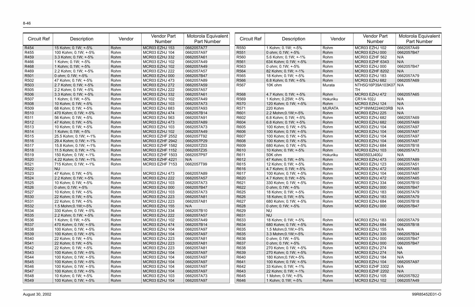
8-46
August 30, 2002 99R85452E01-O
R454 15 Kohm; 0.1W; +-5% Rohm MCR03 EZHJ 153 0662057A77R455 100 Kohm; 0.1W; +-5% Rohm MCR03 EZHJ 104 0662057A97R459 3.3 Kohm; 0.1W; +-5% Rohm MCR03 EZHJ 332 0662057A61R466 1 Kohm; 0.1W; +-5% Rohm MCR03 EZHJ 102 0662057A49R468 1 Kohm; 0.1W; +-5% Rohm MCR03 EZHJ 102 0662057A49R469 2.2 Kohm; 0.1W; +-5% Rohm MCR03 EZHJ 222 0662057A57R501 0 ohm; 0.1W; +-5% Rohm MCR03 EZHJ 000 0662057B47R502 47 Kohm; 0.1W; +-5% Rohm MCR03 EZHJ 473 0662057A89R503 2.7 Kohm; 0.1W; +-5% Rohm MCR03 EZHJ 272 0662057A59R505 2.2 Kohm; 0.1W; +-5% Rohm MCR03 EZHJ 222 0662057A57R506 3.3 Kohm; 0.1W; +-5% Rohm MCR03 EZHJ 332 0662057A61R507 1 Kohm; 0.1W; +-5% Rohm MCR03 EZHJ 102 0662057A49R508 10 Kohm; 0.1W; +-5% Rohm MCR03 EZHJ 103 0662057A73R509 68 Kohm; 0.1W; +-5% Rohm MCR03 EZHJ 683 0662057A93R510 470 Kohm; 0.1W; +-5% Rohm MCR03 EZHJ 474 0662057B14R511 56 Kohm; 0.1W; +-5% Rohm MCR03 EZHJ 563 0662057A91R512 47 Kohm; 0.1W; +-5% Rohm MCR03 EZHJ 473 0662057A89R513 10 Kohm; 0.1W; +-5% Rohm MCR03 EZHJ 103 0662057A73R514 1 Kohm; 0.1W; +-5% Rohm MCR03 EZHJ 102 0662057A49R515 25.5 Kohm; 0.1W; +-1% Rohm MCR03 EZHF 2552 0662057T92R516 29.4 Kohm; 0.1W; +-1% Rohm MCR03 EZHF 2942 0662057P29R517 15.8 Kohm; 0.1W; +-1% Rohm MCR03 EZHF 1582 0662057Z03R518 11.5 Kohm; 0.1W; +-1% Rohm MCR03 EZHF 1152 0662057Z35R519 150 Kohm; 0.1W; +-1% Rohm MCR03 EZHF 1503 0662057P97R520 4.22 Kohm; 0.1W; +-1% Rohm MCR03 EZHF 4221 N/AR521 715 Kohm; 0.1W; +-1% Rohm MCR03 EZHF 7153 0662057T99R522 NUR523 47 Kohm; 0.1W; +-5% Rohm MCR03 EZHJ 473 0662057A89R524 2.2 Kohm; 0.1W; +-5% Rohm MCR03 EZHJ 222 0662057A57R525 10 Kohm; 0.1W; +-5% Rohm MCR03 EZHJ 103 0662057A73R526 0 ohm; 0.1W; +-5% Rohm MCR03 EZHJ 000 0662057B47R527 10 Kohm; 0.1W; +-5% Rohm MCR03 EZHJ 103 0662057A73R530 22 Kohm; 0.1W; +-5% Rohm MCR03 EZHJ 223 0662057A81R531 22 Kohm; 0.1W; +-5% Rohm MCR03 EZHJ 223 0662057A81R532 1.5 Mohm;0.1W;+-5% Rohm MCR03 EZHJ 155 N/AR534 330 Kohm; 0.1W; +-5% Rohm MCR03 EZHJ 334 0662057B10R535 2.2 Kohm; 0.1W; +-5% Rohm MCR03 EZHJ 222 0662057A57R536 1 Kohm; 0.1W; +-5% Rohm MCR03 EZHJ 102 0662057A49R537 470 Kohm; 0.1W; +-5% Rohm MCR03 EZHJ 474 0662057B14R538 100 Kohm; 0.1W; +-5% Rohm MCR03 EZHJ 104 0662057A97R539 100 Kohm; 0.1W; +-5% Rohm MCR03 EZHJ 104 0662057A97R540 22 Kohm; 0.1W; +-5% Rohm MCR03 EZHJ 223 0662057A81R541 22 Kohm; 0.1W; +-5% Rohm MCR03 EZHJ 223 0662057A81R542 22 Kohm; 0.1W; +-5% Rohm MCR03 EZHJ 223 0662057A81R543 100 Kohm; 0.1W; +-5% Rohm MCR03 EZHJ 104 0662057A97R544 100 Kohm; 0.1W; +-5% Rohm MCR03 EZHJ 104 0662057A97R545 100 Kohm; 0.1W; +-5% Rohm MCR03 EZHJ 104 0662057A97R546 100 Kohm; 0.1W; +-5% Rohm MCR03 EZHJ 104 0662057A97R547 100 Kohm; 0.1W; +-5% Rohm MCR03 EZHJ 104 0662057A97R548 10 Kohm; 0.1W; +-5% Rohm MCR03 EZHJ 103 0662057A73R549 100 Kohm; 0.1W; +-5% Rohm MCR03 EZHJ 104 0662057A97
Circuit Ref Description Vendor Vendor Part Number
Motorola Equivalent Part Number
R550 1 Kohm; 0.1W; +-5% Rohm MCR03 EZHJ 102 0662057A49R551 0 ohm; 0.1W; +-5% Rohm MCR03 EZHJ 000 0662057B47R560 5.6 Kohm; 0.1W; +-1% Rohm MCR03 EZHF 562 N/AR561 634 Kohm; 0.1W; +-5% Rohm MCR03 EZHF 6343 N/AR563 0 ohm; 0.1W; +-5% Rohm MCR03 EZHJ 000 0662057B47R564 82 Kohm; 0.1W; +-1% Rohm MCR03 EZHF 8202 N/AR565 18 Kohm; 0.1W; +-5% Rohm MCR03 EZHJ 183 0662057A79R566 6.8 Kohm; 0.1W; +-5% Rohm MCR03 EZHJ 682 0662057A69R567 10K ohm Murata NTH5G16P39A103K07
THN/A
R568 4.7 Kohm; 0.1W; +-5% Rohm MCR03 EZHJ 472 0662057A65R569 1 Kohm; 0.25W; +-5% Hokuriku CR1/4-102J N/AR570 120 Kohm; 0.1W; +-5% Rohm MCR03 EZHJ 124 N/AR571 220 Kohm MURATA NCP18WM224K03RB N/AR601 2.2 Mohm;0.1W;+-5% Rohm MCR03 EZHJ 225 N/AR602 6.8 Kohm; 0.1W; +-5% Rohm MCR03 EZHJ 682 0662057A69R604 6.8 Kohm; 0.1W; +-5% Rohm MCR03 EZHJ 682 0662057A69R605 100 Kohm; 0.1W; +-5% Rohm MCR03 EZHJ 104 0662057A97R606 100 Kohm; 0.1W; +-5% Rohm MCR03 EZHJ 104 0662057A97R607 100 Kohm; 0.1W; +-5% Rohm MCR03 EZHJ 104 0662057A97R608 100 Kohm; 0.1W; +-5% Rohm MCR03 EZHJ 104 0662057A97R609 680 Kohm; 0.1W; +-5% Rohm MCR03 EZHJ 684 0662057B18R610 10 Kohm; 0.1W; +-5% Rohm MCR03 EZHJ 103 0662057A73R611 50K ohm Hokuriku NSM3503J400J N/AR612 47 Kohm; 0.1W; +-5% Rohm MCR03 EZHJ 473 0662057A89R615 12 Kohm; 0.1W; +-5% Rohm MCR03 EZHJ 123 0662057A51R616 4.7 Kohm; 0.1W; +-5% Rohm MCR03 EZHJ 472 0662057A65R617 100 Kohm; 0.1W; +-5% Rohm MCR03 EZHJ 104 0662057A97R620 4.7 Kohm; 0.1W; +-5% Rohm MCR03 EZHJ 472 0662057A65R621 330 Kohm; 0.1W; +-5% Rohm MCR03 EZHJ 334 0662057B10R622 0 ohm; 0.1W; +-5% Rohm MCR03 EZHJ 000 0662057B47R625 18 Kohm; 0.1W; +-5% Rohm MCR03 EZHJ 183 0662057A79R626 18 Kohm; 0.1W; +-5% Rohm MCR03 EZHJ 183 0662057A79R627 680 Kohm; 0.1W; +-5% Rohm MCR03 EZHJ 684 0662057B18R628 0 ohm; 0.1W; +-5% Rohm MCR03 EZHJ 000 0662057B47R629 NUR631 NUR633 18 Kohm; 0.1W; +-5% Rohm MCR03 EZHJ 183 0662057A79R634 680 Kohm; 0.1W; +-5% Rohm MCR03 EZHJ 684 0662057B18R635 1.5 Mohm;0.1W;+-5% Rohm MCR03 EZHJ 155 N/AR635 3.3 Mohm;0.1W;+-5% Rohm MCR03 EZHJ 335 0662057B34R636 0 ohm; 0.1W; +-5% Rohm MCR03 EZHJ 000 0662057B47R637 0 ohm; 0.1W; +-5% Rohm MCR03 EZHJ 000 0662057B47R638 270 Kohm; 0.1W; +-5% Rohm MCR03 EZHJ 274 NAR639 270 Kohm; 0.1W; +-5% Rohm MCR03 EZHJ 274 NAR640 180 Kohm;0.1W;+-5% Rohm MCR03 EZHJ 184 N/AR641 100 Kohm; 0.1W; +-5% Rohm MCR03 EZHJ 104 0662057A97R642 33 Kohm; 0.1W; +-1% Rohm MCR03 EZHF 3302 N/AR643 22 Kohm; 0.1W; +-1% Rohm MCR03 EZHF 2202 N/AR645 1 Mohm; 0.1W; +-5% Rohm MCR03 EZHJ 105 0662057B22R646 1 Kohm; 0.1W; +-5% Rohm MCR03 EZHJ 102 0662057A49
Circuit Ref Description Vendor Vendor Part Number
Motorola Equivalent Part Number
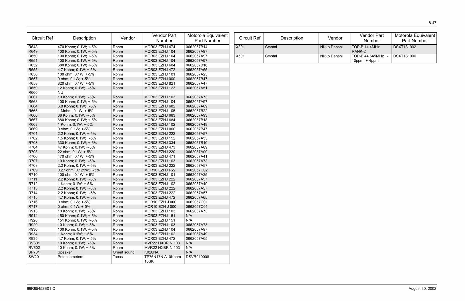
8-47
99R85452E01-O August 30, 2002
R648 470 Kohm; 0.1W; +-5% Rohm MCR03 EZHJ 474 0662057B14R649 100 Kohm; 0.1W; +-5% Rohm MCR03 EZHJ 104 0662057A97R650 100 Kohm; 0.1W; +-5% Rohm MCR03 EZHJ 104 0662057A97R651 100 Kohm; 0.1W; +-5% Rohm MCR03 EZHJ 104 0662057A97R652 680 Kohm; 0.1W; +-5% Rohm MCR03 EZHJ 684 0662057B18R655 4.7 Kohm; 0.1W; +-5% Rohm MCR03 EZHJ 472 0662057A65R656 100 ohm; 0.1W; +-5% Rohm MCR03 EZHJ 101 0662057A25R657 0 ohm; 0.1W; +-5% Rohm MCR03 EZHJ 000 0662057B47R658 820 ohm; 0.1W; +-5% Rohm MCR03 EZHJ 821 0662057A47R659 12 Kohm; 0.1W; +-5% Rohm MCR03 EZHJ 123 0662057A51R660 NUR661 10 Kohm; 0.1W; +-5% Rohm MCR03 EZHJ 103 0662057A73R663 100 Kohm; 0.1W; +-5% Rohm MCR03 EZHJ 104 0662057A97R664 6.8 Kohm; 0.1W; +-5% Rohm MCR03 EZHJ 682 0662057A69R665 1 Mohm; 0.1W; +-5% Rohm MCR03 EZHJ 105 0662057B22R666 68 Kohm; 0.1W; +-5% Rohm MCR03 EZHJ 683 0662057A93R667 680 Kohm; 0.1W; +-5% Rohm MCR03 EZHJ 684 0662057B18R668 1 Kohm; 0.1W; +-5% Rohm MCR03 EZHJ 102 0662057A49R669 0 ohm; 0.1W; +-5% Rohm MCR03 EZHJ 000 0662057B47R701 2.2 Kohm; 0.1W; +-5% Rohm MCR03 EZHJ 222 0662057A57R702 1.5 Kohm; 0.1W; +-5% Rohm MCR03 EZHJ 152 0662057A53R703 330 Kohm; 0.1W; +-5% Rohm MCR03 EZHJ 334 0662057B10R704 47 Kohm; 0.1W; +-5% Rohm MCR03 EZHJ 473 0662057A89R705 22 ohm; 0.1W; +-5% Rohm MCR03 EZHJ 220 0662057A09R706 470 ohm; 0.1W; +-5% Rohm MCR03 EZHJ 471 0662057A41R707 10 Kohm; 0.1W; +-5% Rohm MCR03 EZHJ 103 0662057A73R708 2.2 Kohm; 0.1W; +-5% Rohm MCR03 EZHJ 222 0662057A57R709 0.27 ohm; 0.125W; +-5% Rohm MCR10 EZHJ R27 0662057C02R710 100 ohm; 0.1W; +-5% Rohm MCR03 EZHJ 101 0662057A25R711 2.2 Kohm; 0.1W; +-5% Rohm MCR03 EZHJ 222 0662057A57R712 1 Kohm; 0.1W; +-5% Rohm MCR03 EZHJ 102 0662057A49R713 2.2 Kohm; 0.1W; +-5% Rohm MCR03 EZHJ 222 0662057A57R714 2.2 Kohm; 0.1W; +-5% Rohm MCR03 EZHJ 222 0662057A57R715 4.7 Kohm; 0.1W; +-5% Rohm MCR03 EZHJ 472 0662057A65R716 0 ohm; 0.1W; +-5% Rohm MCR10 EZH J 000 0662057C01R717 0 ohm; 0.1W; +-5% Rohm MCR10 EZH J 000 0662057C01R913 10 Kohm; 0.1W; +-5% Rohm MCR03 EZHJ 103 0662057A73R914 150 Kohm; 0.1W; +-5% Rohm MCR03 EZHJ 151 N/AR928 151 Kohm; 0.1W; +-5% Rohm MCR03 EZHJ 151 N/AR929 10 Kohm; 0.1W; +-5% Rohm MCR03 EZHJ 103 0662057A73R930 100 Kohm; 0.1W; +-5% Rohm MCR03 EZHJ 104 0662057A97R934 1 Kohm; 0.1W; +-5% Rohm MCR03 EZHJ 102 0662057A49R935 4.7 Kohm; 0.1W; +-5% Rohm MCR03 EZHJ 472 0662057A65RV601 10 Kohm; 0.1W; +-5% Rohm MVR22 HXBR N 103 N/ARV602 10 Kohm; 0.1W; +-5% Rohm MVR22 HXBR N 103 N/ASP701 Speaker Orient sound K028NA N/ASW201 Potentiometers Tocos TP76N17N A10Kohm
10SKDSVR010008
Circuit Ref Description Vendor Vendor Part Number
Motorola Equivalent Part Number
X301 Crystal Nikko Denshi TOP-B 14.4MHz RANK-2
DSXT181002
X501 Crystal Nikko Denshi TOP-B 44.645MHz +-10ppm, +-4ppm
DSXT181006
Circuit Ref Description Vendor Vendor Part Number
Motorola Equivalent Part Number
8-48
August 30, 2002 99R85452E01-O
This Page Intentionally Left Blank
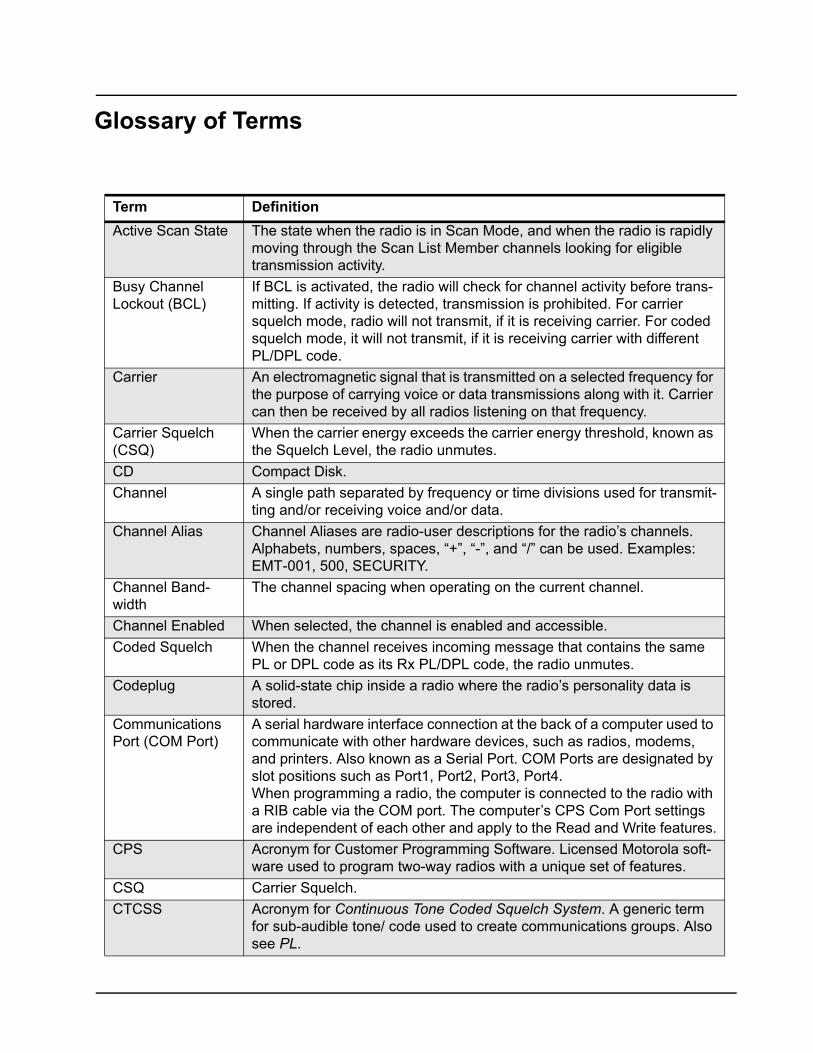
Glossary of Terms Glossary
Term DefinitionActive Scan State The state when the radio is in Scan Mode, and when the radio is rapidly
moving through the Scan List Member channels looking for eligible transmission activity.
Busy Channel Lockout (BCL)
If BCL is activated, the radio will check for channel activity before trans-mitting. If activity is detected, transmission is prohibited. For carrier squelch mode, radio will not transmit, if it is receiving carrier. For coded squelch mode, it will not transmit, if it is receiving carrier with different PL/DPL code.
Carrier An electromagnetic signal that is transmitted on a selected frequency for the purpose of carrying voice or data transmissions along with it. Carrier can then be received by all radios listening on that frequency.
Carrier Squelch (CSQ)
When the carrier energy exceeds the carrier energy threshold, known as the Squelch Level, the radio unmutes.
CD Compact Disk.Channel A single path separated by frequency or time divisions used for transmit-
ting and/or receiving voice and/or data.Channel Alias Channel Aliases are radio-user descriptions for the radio’s channels.
Alphabets, numbers, spaces, “+”, “-”, and “/” can be used. Examples: EMT-001, 500, SECURITY.
Channel Band-width
The channel spacing when operating on the current channel.
Channel Enabled When selected, the channel is enabled and accessible.Coded Squelch When the channel receives incoming message that contains the same
PL or DPL code as its Rx PL/DPL code, the radio unmutes.Codeplug A solid-state chip inside a radio where the radio’s personality data is
stored.Communications Port (COM Port)
A serial hardware interface connection at the back of a computer used to communicate with other hardware devices, such as radios, modems, and printers. Also known as a Serial Port. COM Ports are designated by slot positions such as Port1, Port2, Port3, Port4.When programming a radio, the computer is connected to the radio with a RIB cable via the COM port. The computer’s CPS Com Port settings are independent of each other and apply to the Read and Write features.
CPS Acronym for Customer Programming Software. Licensed Motorola soft-ware used to program two-way radios with a unique set of features.
CSQ Carrier Squelch.CTCSS Acronym for Continuous Tone Coded Squelch System. A generic term
for sub-audible tone/ code used to create communications groups. Also see PL.
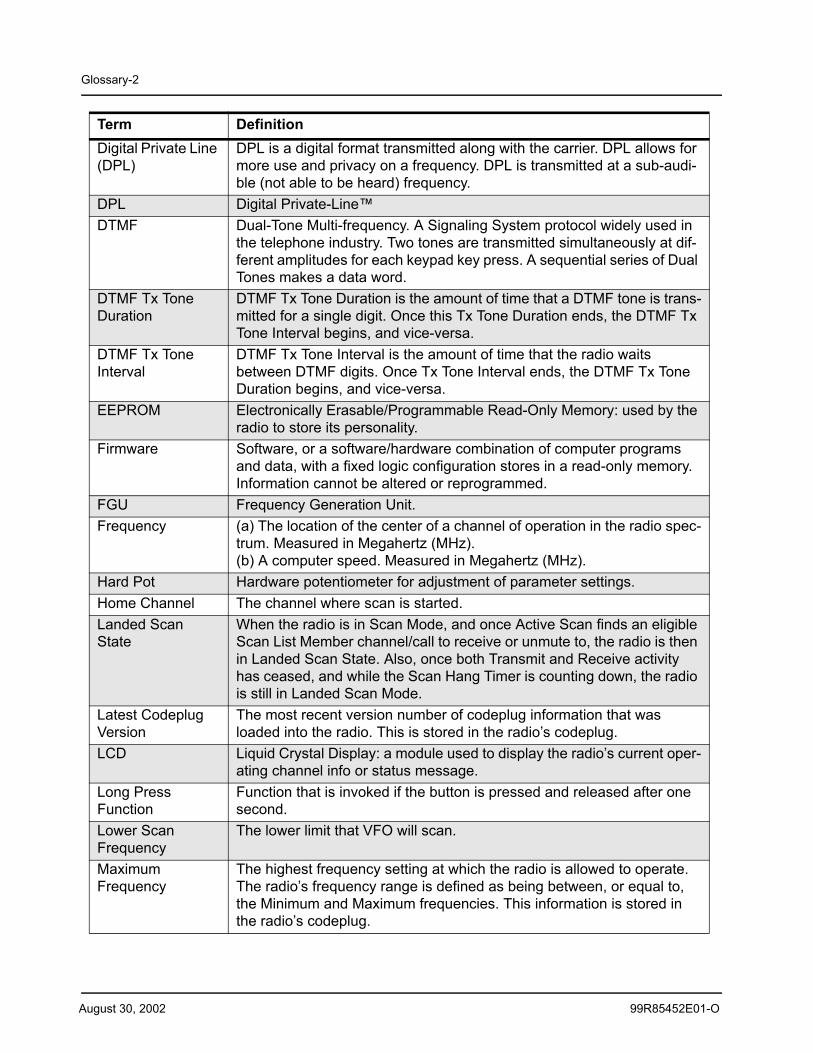
August 30, 2002 99R85452E01-O
Glossary-2
Digital Private Line (DPL)
DPL is a digital format transmitted along with the carrier. DPL allows for more use and privacy on a frequency. DPL is transmitted at a sub-audi-ble (not able to be heard) frequency.
DPL Digital Private-Line™DTMF Dual-Tone Multi-frequency. A Signaling System protocol widely used in
the telephone industry. Two tones are transmitted simultaneously at dif-ferent amplitudes for each keypad key press. A sequential series of Dual Tones makes a data word.
DTMF Tx ToneDuration
DTMF Tx Tone Duration is the amount of time that a DTMF tone is trans-mitted for a single digit. Once this Tx Tone Duration ends, the DTMF Tx Tone Interval begins, and vice-versa.
DTMF Tx ToneInterval
DTMF Tx Tone Interval is the amount of time that the radio waits between DTMF digits. Once Tx Tone Interval ends, the DTMF Tx Tone Duration begins, and vice-versa.
EEPROM Electronically Erasable/Programmable Read-Only Memory: used by the radio to store its personality.
Firmware Software, or a software/hardware combination of computer programs and data, with a fixed logic configuration stores in a read-only memory. Information cannot be altered or reprogrammed.
FGU Frequency Generation Unit.Frequency (a) The location of the center of a channel of operation in the radio spec-
trum. Measured in Megahertz (MHz).(b) A computer speed. Measured in Megahertz (MHz).
Hard Pot Hardware potentiometer for adjustment of parameter settings.Home Channel The channel where scan is started.Landed Scan State
When the radio is in Scan Mode, and once Active Scan finds an eligible Scan List Member channel/call to receive or unmute to, the radio is then in Landed Scan State. Also, once both Transmit and Receive activity has ceased, and while the Scan Hang Timer is counting down, the radio is still in Landed Scan Mode.
Latest Codeplug Version
The most recent version number of codeplug information that was loaded into the radio. This is stored in the radio’s codeplug.
LCD Liquid Crystal Display: a module used to display the radio’s current oper-ating channel info or status message.
Long PressFunction
Function that is invoked if the button is pressed and released after one second.
Lower ScanFrequency
The lower limit that VFO will scan.
MaximumFrequency
The highest frequency setting at which the radio is allowed to operate. The radio’s frequency range is defined as being between, or equal to, the Minimum and Maximum frequencies. This information is stored in the radio’s codeplug.
Term Definition
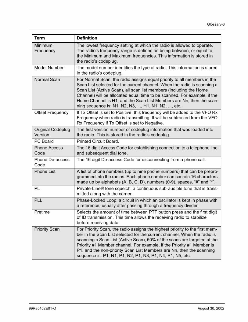
99R85452E01-O August 30, 2002
Glossary-3
MinimumFrequency
The lowest frequency setting at which the radio is allowed to operate. The radio’s frequency range is defined as being between, or equal to, the Minimum and Maximum frequencies. This information is stored in the radio’s codeplug.
Model Number The model number identifies the type of radio. This information is stored in the radio’s codeplug.
Normal Scan For Normal Scan, the radio assigns equal priority to all members in the Scan List selected for the current channel. When the radio is scanning a Scan List (Active Scan), all scan list members (including the Home Channel) will be allocated equal time to be scanned. For example, if the Home Channel is H1, and the Scan List Members are Nn, then the scan-ning sequence is: N1, N2, N3, ..., H1, N1, N2, ..., etc.
Offset Frequency If Tx Offset is set to Positive, this frequency will be added to the VFO Rx Frequency when radio is transmitting. It will be subtracted from the VFO Rx Frequency if Tx Offset is set to Negative.
Original Codeplug Version
The first version number of codeplug information that was loaded into the radio. This is stored in the radio’s codeplug.
PC Board Printed Circuit Board.Phone Access Code
The 16 digit Access Code for establishing connection to a telephone line and subsequent dial tone.
Phone De-access Code
The 16 digit De-access Code for disconnecting from a phone call.
Phone List A list of phone numbers (up to nine phone numbers) that can be prepro-grammed into the radios. Each phone number can contain 16 characters made up by alphabets (A, B, C, D), numbers (0-9), spaces, “#” and “*”.
PL Private-Line® tone squelch: a continuous sub-audible tone that is trans-mitted along with the carrier.
PLL Phase-Locked Loop: a circuit in which an oscillator is kept in phase with a reference, usually after passing through a frequency divider.
Pretime Selects the amount of time between PTT button press and the first digit of ID transmission. This time allows the receiving radio to stabilize before receiving data.
Priority Scan For Priority Scan, the radio assigns the highest priority to the first mem-ber in the Scan List selected for the current channel. When the radio is scanning a Scan List (Active Scan), 50% of the scans are targeted at the Priority #1 Member channel. For example, if the Priority #1 Member is P1, and the non-priority Scan List Members are Nn, then the scanning sequence is: P1, N1, P1, N2, P1, N3, P1, N4, P1, N5, etc.
Term Definition
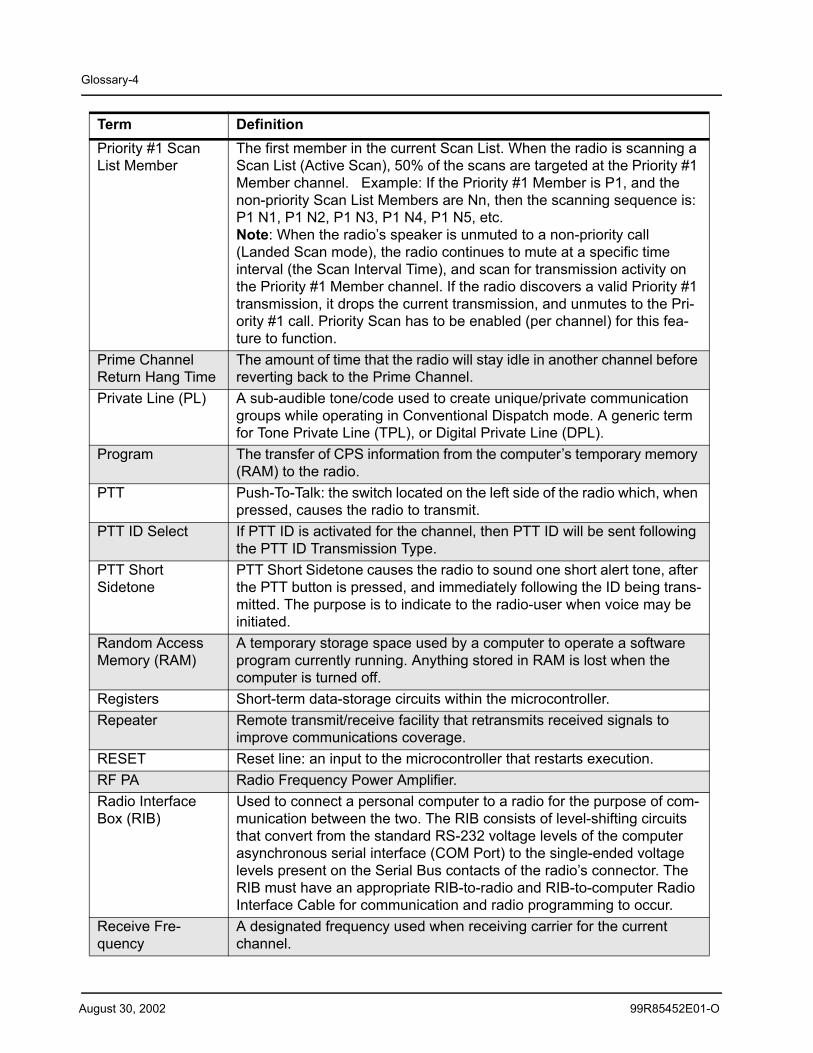
August 30, 2002 99R85452E01-O
Glossary-4
Priority #1 Scan List Member
The first member in the current Scan List. When the radio is scanning a Scan List (Active Scan), 50% of the scans are targeted at the Priority #1 Member channel. Example: If the Priority #1 Member is P1, and the non-priority Scan List Members are Nn, then the scanning sequence is: P1 N1, P1 N2, P1 N3, P1 N4, P1 N5, etc.Note: When the radio’s speaker is unmuted to a non-priority call (Landed Scan mode), the radio continues to mute at a specific time interval (the Scan Interval Time), and scan for transmission activity on the Priority #1 Member channel. If the radio discovers a valid Priority #1 transmission, it drops the current transmission, and unmutes to the Pri-ority #1 call. Priority Scan has to be enabled (per channel) for this fea-ture to function.
Prime ChannelReturn Hang Time
The amount of time that the radio will stay idle in another channel before reverting back to the Prime Channel.
Private Line (PL) A sub-audible tone/code used to create unique/private communication groups while operating in Conventional Dispatch mode. A generic term for Tone Private Line (TPL), or Digital Private Line (DPL).
Program The transfer of CPS information from the computer’s temporary memory (RAM) to the radio.
PTT Push-To-Talk: the switch located on the left side of the radio which, when pressed, causes the radio to transmit.
PTT ID Select If PTT ID is activated for the channel, then PTT ID will be sent following the PTT ID Transmission Type.
PTT Short Sidetone
PTT Short Sidetone causes the radio to sound one short alert tone, after the PTT button is pressed, and immediately following the ID being trans-mitted. The purpose is to indicate to the radio-user when voice may be initiated.
Random Access Memory (RAM)
A temporary storage space used by a computer to operate a software program currently running. Anything stored in RAM is lost when the computer is turned off.
Registers Short-term data-storage circuits within the microcontroller.Repeater Remote transmit/receive facility that retransmits received signals to
improve communications coverage.RESET Reset line: an input to the microcontroller that restarts execution.RF PA Radio Frequency Power Amplifier.Radio Interface Box (RIB)
Used to connect a personal computer to a radio for the purpose of com-munication between the two. The RIB consists of level-shifting circuits that convert from the standard RS-232 voltage levels of the computer asynchronous serial interface (COM Port) to the single-ended voltage levels present on the Serial Bus contacts of the radio’s connector. The RIB must have an appropriate RIB-to-radio and RIB-to-computer Radio Interface Cable for communication and radio programming to occur.
Receive Fre-quency
A designated frequency used when receiving carrier for the current channel.
Term Definition
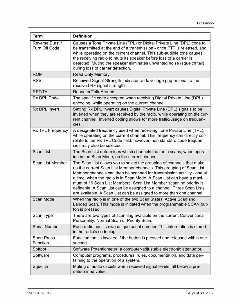
99R85452E01-O August 30, 2002
Glossary-5
Reverse Burst / Turn Off Code
Causes a Tone Private Line (TPL) or Digital Private Line (DPL) code to be transmitted at the end of a transmission - once PTT is released, and while operating on the current channel. This sub-audible tone causes the receiving radio to mute its speaker before loss of a carrier is detected. Muting the speaker eliminates unwanted noise (squelch tail) during loss of carrier detection.
ROM Read Only Memory.RSSI Received Signal-Strength Indicator: a dc voltage proportional to the
received RF signal strength.RPT/TA Repeater/Talk-Around.Rx DPL Code The specific code accepted when receiving Digital Private Line (DPL)
encoding, while operating on the current channel.Rx DPL Invert Setting Rx DPL Invert causes Digital Private Line (DPL) signals to be
inverted when they are received by the radio, while operating on the cur-rent channel. Inverted coding allows for more traffic/usage on frequen-cies.
Rx TPL Frequency A designated frequency used when receiving Tone Private Line (TPL), while operating on the current channel. This frequency can directly cor-relate to the Rx TPL Code field; however, non standard code frequen-cies may also be selected.
Scan List The Scan List determines which channels the radio scans, when operat-ing in the Scan Mode, on the current channel.
Scan List Member The Scan List allows you to select the grouping of channels that make up the current Scan List Member channels. This grouping of Scan List Member channels can then be scanned for transmission activity - one at a time, when the radio is in Scan Mode. A Scan List can have a maxi-mum of 16 Scan List Members. Scan List Member scanning priority is definable. A Scan List can be assigned to a channel. Three Scan Lists are available. A Scan List can be assigned to more than one channel.
Scan Mode When the radio is in one of the two Scan States: Active Scan and Landed Scan. This mode is initiated when the programmable SCAN but-ton is pressed.
Scan Type There are two types of scanning available on the current Conventional Personality: Normal Scan or Priority Scan.
Serial Number Each radio has its own unique serial number. This information is stored in the radio’s codeplug.
Short PressFunction
Function that is invoked if the button is pressed and released within one second.
Softpot Software Potentiometer: a computer-adjustable electronic attenuator.Software Computer programs, procedures, rules, documentation, and data per-
taining to the operation of a system.Squelch Muting of audio circuits when received signal levels fall below a pre-
determined value.
Term Definition
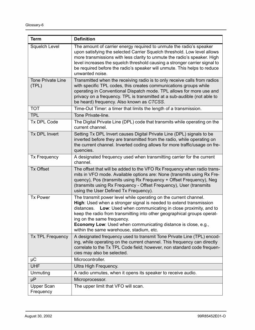
August 30, 2002 99R85452E01-O
Glossary-6
Squelch Level The amount of carrier energy required to unmute the radio’s speaker upon satisfying the selected Carrier Squelch threshold. Low level allows more transmissions with less clarity to unmute the radio’s speaker. High level increases the squelch threshold causing a stronger carrier signal to be required before the radio’s speaker will unmute. This helps to reduce unwanted noise.
Tone Private Line (TPL)
Transmitted when the receiving radio is to only receive calls from radios with specific TPL codes, this creates communications groups while operating in Conventional Dispatch mode. TPL allows for more use and privacy on a frequency. TPL is transmitted at a sub-audible (not able to be heard) frequency. Also known as CTCSS.
TOT Time-Out Timer: a timer that limits the length of a transmission.TPL Tone Private-line.Tx DPL Code The Digital Private Line (DPL) code that transmits while operating on the
current channel.Tx DPL Invert Setting Tx DPL Invert causes Digital Private Line (DPL) signals to be
inverted before they are transmitted from the radio, while operating on the current channel. Inverted coding allows for more traffic/usage on fre-quencies.
Tx Frequency A designated frequency used when transmitting carrier for the current channel.
Tx Offset The offset that will be added to the VFO Rx Frequency when radio trans-mits in VFO mode. Available options are: None (transmits using Rx Fre-quency), Pos (transmits using Rx Frequency + Offset Frequency), Neg (transmits using Rx Frequency - Offset Frequency), User (transmits using the User Defined Tx Frequency).
Tx Power The transmit power level while operating on the current channel.High: Used when a stronger signal is needed to extend transmission distances. Low: Used when communicating in close proximity, and to keep the radio from transmitting into other geographical groups operat-ing on the same frequency.Economy Low: Used when communicating distance is close, e.g., within the same warehouse, stadium, etc.
Tx TPL Frequency A designated frequency used to transmit Tone Private Line (TPL) encod-ing, while operating on the current channel. This frequency can directly correlate to the Tx TPL Code field; however, non standard code frequen-cies may also be selected.
µC Microcontroller.UHF Ultra High Frequency.Unmuting A radio unmutes, when it opens its speaker to receive audio.µP Microprocessor.Upper ScanFrequency
The upper limit that VFO will scan.
Term Definition
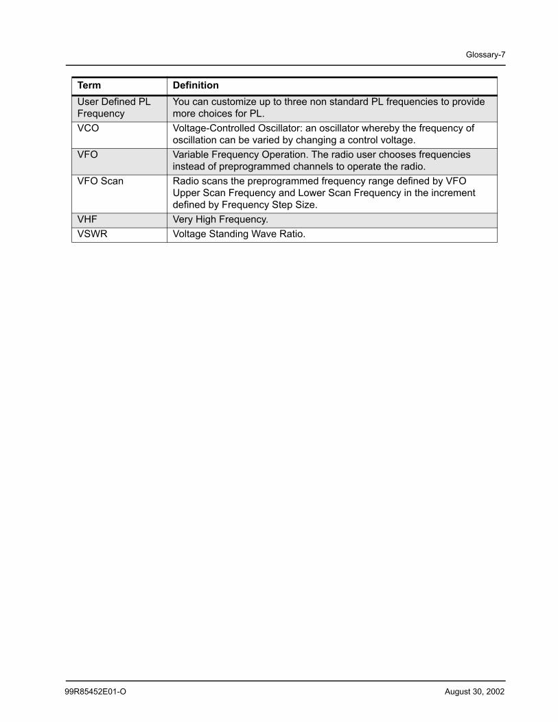
99R85452E01-O August 30, 2002
Glossary-7
User Defined PL Frequency
You can customize up to three non standard PL frequencies to provide more choices for PL.
VCO Voltage-Controlled Oscillator: an oscillator whereby the frequency of oscillation can be varied by changing a control voltage.
VFO Variable Frequency Operation. The radio user chooses frequencies instead of preprogrammed channels to operate the radio.
VFO Scan Radio scans the preprogrammed frequency range defined by VFO Upper Scan Frequency and Lower Scan Frequency in the increment defined by Frequency Step Size.
VHF Very High Frequency.VSWR Voltage Standing Wave Ratio.
Term Definition
August 30, 2002 99R85452E01-O
This Page Intentionally Left Blank
Glossary-8


99R85452E01-O
*9985452E01*
MOTOROLA and the Stylized M Logo are registered in the
U.S. Patent and Trademark Office. All other product or service
names are the property of their respective owners.
© Motorola, Inc. 2002.
All rights reserved. Printed in U.S.A.
Motorola, Inc.
8000 West Sunrise Boulevard
Ft. Lauderdale, FL 33322