JUL 2 0 2004 - DSpace@MIT
103
Predictive Models for Power Dissipation in Optical Transceivers by Katherine Butler Submitted to the Department of Electrical Engineering and Computer Science in Partial Fulfillment of the Requirements for the Degrees of Bachelor of Science in Electrical Science and Engineering and Master of Engineering in Electrical Engineering and Computer Science at the Massachusetts Institute of Technology May 17, 2004 Copyright 2004 Massachusetts Institute of Technology. All rights reserved. The author hereby grants to M.I.T. permission to reproduce and distribute publicly paper and electronic copies of this thesis and to grant others the right to do so. Author- Department of Electrical Engineering and Computer Science May 17, 2004 Certified by_ Rajeev Ram T>&sis Supervisor Accepted by Arthur C. Smith Chairman, Department Committee on Graduate Theses MASSACHUSETTS INSTInrE OFTECHNOLOGY JUL 2 0 2004 LIBRARIES
-
Upload
khangminh22 -
Category
Documents
-
view
0 -
download
0
Transcript of JUL 2 0 2004 - DSpace@MIT

Predictive Models for Power Dissipation
in Optical Transceivers
by
Katherine Butler
Submitted to the Department of Electrical Engineering and Computer Science
in Partial Fulfillment of the Requirements for the Degrees of
Bachelor of Science in Electrical Science and Engineering
and Master of Engineering in Electrical Engineering and Computer Science
at the Massachusetts Institute of Technology
May 17, 2004
Copyright 2004 Massachusetts Institute of Technology. All rights reserved.
The author hereby grants to M.I.T. permission to reproduce anddistribute publicly paper and electronic copies of this thesis
and to grant others the right to do so.
Author-
Department of Electrical Engineering and Computer Science
May 17, 2004
Certified by_Rajeev Ram
T>&sis Supervisor
Accepted by
Arthur C. Smith
Chairman, Department Committee on Graduate Theses
MASSACHUSETTS INSTInrEOFTECHNOLOGY
JUL 2 0 2004
LIBRARIES

Predictive Models for Power Dissipationin Optical Transceivers
byKatherine Butler
Submitted to theDepartment of Electrical Engineering and Computer Science
May 17, 2004
In Partial Fulfillment of the Requirements for the Degree of
Bachelor of Science in Electrical Science and Engineering
and Master of Engineering in Electrical Engineering and Computer Science
ABSTRACT
Power dissipation in optical networks is a significant problem for the telecommunications
industry. The optical transceiver was selected as a representative device of the network,
and a component based power model is developed for it. This model indicates that there
are three key power dissipating elements in an optical transceiver: the electrical
MUX/DEMUX, the thermoelectric cooler (TE cooler), and the modulator driver
amplifier. First, the electrical MUX/DEMUX materials and functionality are
investigated, and a circuit model is developed to simulate the MUX/DEMUX using both
CMOS and MOSFET Current Mode Logic circuit topologies. The SPICE simulations
use future technology generation process cards from the Berkeley Predictive Technology
model, and enable the simulations to predict the power dissipation of the MUXs in the
future. The results of these SPICE simulations show that improvement in technology
generations significantly reduces the power dissipation of the MUX circuits. The TE
cooler is then examined and a MATLAB model is developed to predict the
thermodynamic flow through a packaged laser and TE Cooler. The MATLAB
simulations of this model show that although materials with lower thermal conductivity
result in more cooling power for the TE cooler, they also significantly raise the overall
temperature of the laser. Therefore, lower thermal conductivity is not the best way to
reduce power dissipation in the TE cooler. Together these physical models give a better
understanding of the factors that will most influence the power dissipation optical
transceivers in the future.
Thesis Supervisor: Rajeev RamTitle: Professor, Electrical Engineering
2

Acknowledgements
I would like to thank my advisor, Rajeev Ram, for his immense help on developing and
researching this thesis. His guidance was the foundation for my graduate work. My thanks also
goes to Elizabeth Bruce, for first starting me on this project and for continuing support throughout
the work.
I would also like to thank all the graduate students in the Physical Optics and Electronics group:
Tom Liptay, Pete Mayer, Harry Lee, Matthew Abraham, Dietrich Lueerssen, Xiaoyun Guo, Tauhid
Zaman, and Sonh-ho Cho. I appreciate all the help I received when trying to understand circuit
designs, research papers, and most especially, MATLAB code.
Special thanks also goes out to my family, especially my parents for their continual support of my
project, and to all my friends that helped me by providing humor and food. I greatly appreciate all
of you!
3

4

Contents
Chapter 1 - Pow er Dissipation in Optical Transceivers...................................................... 11
1 .1 In tro d u c tio n .......................................................................................................................... 1 1
1.2 Optical Transceiver Background ...................................................................................... 12
1.3 Transceiver Analysis ........................................................................................................ 13
1.3.1 Validation: 2.5 Gb/s Transceiver............................................................................. 13
1.3.2 Validation: 10 Gb/s Transceiver................................................................................ 14
1.3.3 Scaling of Transceiver Power ................................................................................. 14
1.4 Transceiver Analysis Conclusions.................................................................................... 15
1 .5 T h e s is O v e rv ie w .................................................................................................................. 16
Chapter 2 - Electrical M ultiplexer and Dem ultiplexer........................................................... 17
2.1 Overview of Chapter............................................................................................................ 17
2.2 M UX/DEM UX Background ............................................................................................... 17
2.3 Current Power Dissipation in Com m ercial M UX/DEM UXs ............................................. 19
2 .4 M U X M a te ria ls ..................................................................................................................... 2 0
2 .5 M U X A rc h ite c tu re ................................................................................................................ 2 1
2 .6 C M O S M U X ......................................................................................................................... 2 3
2 .6 .1 L a tc h ............................................................................................................................ 2 3
2 .6 .2 F lip -F lo p ....................................................................................................................... 2 4
2 .6 .3 S e le c to r ........................................................................................................................ 2 4
2.6.4 CM OS 2:1 M UX ........................................................................................................ 25
2 .7 M C M L M U X ......................................................................................................................... 2 6
2 .7 .1 M C M L L a tc h ................................................................................................................. 2 7
2 .7 .2 M C M L F lip -flo p ............................................................................................................. 2 8
2.7.3 M CM L Selector ........................................................................................................ 29
2.7.4 M CM L 2:1 M UX............................................................................................................ 30
2 .8 M o d e lin g T o o ls .................................................................................................................... 3 0
2.8.1 SPICE M odeling...................................................................................................... 31
2.8.2 Berkeley Predictive Technology Model (BPTM ) ...................................................... 31
2 .9 M o d e lin g C irc u its ................................................................................................................. 3 3
2.9.1 CM OS Design Rules ............................................................................................... 33
2.9.2 M CM L Design Rules ............................................................................................... 33
2 .9 .3 S P IC E In p u ts ................................................................................................................ 3 5
2 .9 .4 O u tp u t o f M o d e l............................................................................................................ 3 5
2 .1 0 M o d e l V a lid a tio n ................................................................................................................ 3 5
2.10.1 CM O S Validation.................................................................................................... 35
5

2 .1 1 S im u la tio n s ........................................................................................................................ 3 7
2.11.1 Sim ulation 1: Inverter Com parison......................................................................... 38
2.11.2 Sim ulation 2: Pow er per Stage ............................................................................... 41
2.11.3 Sim ulation 3: M axim um Clock Frequency ............................................................ 42
2.12 Conclusions....................................................................................................................... 46
2.13 Future W ork....................................................................................................................... 47
Chapter 3 - Therm oelectric Cooler......................................................................................... 48
3.1 O verview of Chapter............................................................................................................ 48
3.2 Therm oelectric Cooler Introduction ................................................................................. 48
3.3 TE Cooler Background ................................................................................................... 48
3.4 Previous Work / Approaches to Reduce Power Dissipation of TE Cooler...................... 49
3.4.1 New M aterials .............................................................................................................. 49
3.4.2 A lternative Packaging (M icro Coolers) ..................................................................... 50
3.4.2 Tunable Lasers ........................................................................................................ 50
3.5 M odel for Therm al Cooling ............................................................................................... 51
3 .6 M o d e l In p u ts ........................................................................................................................ 5 3
3.7 M ATLA B Sim ulations ..................................................................................................... 54
3 .8 C o n c lu s io n s ......................................................................................................................... 6 0
3 .9 F u tu re W o rk ......................................................................................................................... 6 1
Chapter 4 - Conclusions and Future W ork........................................................................... 62
4 .1 S u m m a ry ............................................................................................................................. 6 2
4.2 Future W ork......................................................................................................................... 64
4.2.1 Electrical M UX/DEM UX Future W ork...................................................................... 64
4.2.1 Therm oelectric Cooler............................................................................................. 64
4.3.1 M odulator Driver Am plifier ........................................................................................ 64
A ppendix A - Electrical M UX/DEM UX Scaling...................................................................... 68
A ppendix B - References for Figure 2.3 ............................................................................... 69
Appendix C - MATLAB Scripts for CMOS and MCML MUX Inputs ..................................... 71
Appendix D - Spice Files for M UX Circuits........................................................................... 81
A ppendix E - M ATLA B Script for Eye-Diagram .................................................................... 96
A ppendix F - M ATLA B Scripts for TE Cooler...................................................................... 98
A ppendix G - M odulator Driver A m plifier Scaling ............................................................ 100
References.................................................................................................................................. 101
6

List of Figures
Figure 1.2: Power comparison between 2.5 Gb/s, 10 Gb/s, hybrid 40 Gb/s, and 40 Gb/s
transceivers. All transceivers were modeled with TE cooled lasers and 16:1 MUX/DEMUX.
.............................................................................................................................................. 1 5
Figure 2.1: Block diagram of 2:1 MUX on the left. The waveform of a 2:1 MUX is on the right with
C LK, A in, Bin, and O UT signals labeled .......................................................................... 18
Figure 2.2: Diagram of an 8:1 MUX with the CMOS and MCML stages labeled [7]. ................ 19
Figure 2.3: MUX/DEMUX data (both commercial and research) showing power dissipation versus
frequency. The smallest black dot indicates 0.18 micron CMOS. The medium black dot
indicates a 0.15 micron gate length, usually used with 0.35 micron CMOS. The black
diamonds indicates an unspecified CMOS process. All open circles indicate materials other
than CMOS. Open circles labeled with BiCMOS refer to either Si or SiGe BiCMOS. See
Appendix B for references for each data point. ................................................................ 21
Figure 2.4: Block Diagram of the components in a 2:1 MUX. .................................................. 22
Figure 2.5: Schem atic of C M O S Latch ...................................................................................... 23
Figure 2.6: Schem atic of CM O S Flip-Flop................................................................................. 24
Figure 2.7: Schem atic of CM O S Selector.................................................................................. 25
Figure 2.8: Schem atic of C M O S M UX ...................................................................................... 25
Figure 2.9: Schem atic of M C M L Inverter................................................................................. 27
Figure 2.10 Schem atic of M C M L Latch ..................................................................................... 28
Figure 2.11: Schem atic of M C M L Flip-flop ............................................................................... 29
Figure 2.12: Schematic of MCML Selector............................................................................... 29
Figure 2.13: Schem atic of M CM L 2:1 M UX ............................................................................... 30
Figure 2.14: lds versus Vds of the BPTM model compared with published data......................... 32
The left is 0.18um , and right is 0.13um [12]. ............................................................................. 32
Figure 2.15: A comparison between the CMOS model inverter and a reference inverter from [7]36
Figure 2.16: Comparison between the eye diagram of the physical output of the reference MUX at
a clock frequency of 20 GHz (on the left) [20], and the simulated eye diagram of the model
M U X a t 1 2 .3 5 G H z . ............................................................................................................... 3 7
Figure 2.17: Schematics of CMOS inverter (left) and MCML inverter (right) ............................ 38
Figure 2.18: Comparison between CMOS and MCML inverters over frequency and technology
g e n e ra tio n s. .......................................................................................................................... 4 0
Figure 2.19: The power dissipation for each stage in a simulated 16:1 MUX ........................... 41
Figure 2.20: The eye-diagrams from the CMOS maximum clock frequency simulations. Figure
2.20A shows the 0.18Km CMOS MUX with a maximum frequency of 2.78 GHz and power
dissipation of 2.97mW. Figure 2.20B shows the 0.131m CMOS MUX with a maximum
7

frequency of 3.7 GHz and power dissipation of 2.57mW. Figure 2.20C shows the 0.10Dm
CMOS MUX with a maximum frequency of 4.55 GHz and a power dissipation of 2.06mW.
Figure 2.20D shows the 0.07Dm CMOS MUX with a maximum frequency of 5 GHz and a
pow er d issipation of 0.75m W ............................................................................................ . 4 3
Figure 2.21: The MCML eye-diagrams for the maximum clock frequency simulation. Figure 2.21A
shows the 0.18Dm MCML MUX with a maximum frequency of 8.33 GHz and power
dissipation of 88.0mW. Figure 2.21B shows the 0.13Dm MCML MUX with a maximum
frequency of 11.76 GHz and power dissipation of 89.0mW. Figure 2.21C shows the
0.10Dm MCML MUX with a maximum frequency of 16.39 GHz and a power dissipation of
87.74mW. Figure 2.21D shows the 0.07 m MCML MUX with a maximum frequency of
17.86 GHz and a power dissipation of 86.06mW . ........................................................... 44
Figure 2:22: Comparison of simulated results for CMOS and MCML MUXs, compared against
technology generations, power dissipation and maximum frequency. The dotted lines
represent frequency and the solid lines represent power dissipation............................... 45
Figure 3.1: D iagram of a T E cooler. ......................................................................................... 49
Figure 3.2: Micro cooler developed in 1999 with four degrees of temperature difference in 50Dm
s p a c e [2 2 ].............................................................................................................................. 5 0
Figure 3.3: MEM's process-based micro cooler developed in 2003, with 126 TE elements in the
a rra y [2 3 ]. .............................................................................................................................. 5 0
Figure 3.4: Feedback control using tuning current instead of temperature. Graph shows the laser
output when it is not controlled and then when it is controlled using the feedback [24]....... 51
Figure 3.5: The block diagram of the MATLAB model............................................................... 52
Figure 3.6: Sample temperature profile of the model using the PDE Toolbox.......................... 54
Figure 3.7: The laser temperature versus the current though the TE cooler at 300K............... 55
Figure 3.8: The laser temperature versus the current through the TE cooler at varying ambient
temperatures. The ambient temperatures are labeled on the right hand side of the graph. 56
Figure 3.9: The ambient temperature of the laser/TE cooler package versus the power
dissipatio n of the T E coo ler............................................................................................. . . 57
Figure 3.10: This graph plots the laser temperature versus current at 300K, with the dotted line
representing the model with reduced thermal conductivity of 1.5W/mk, and the solid line
representing the model with thermal conductivity of 0.75W/mK........................................ 58
Figure 3.11: Laser temperature versus current at varying ambient temperatures, with thermal
conductivity of the BiTe equal to 0.75 W /m K. .................................................................. 59
Figure 3.12: Ambient temperature versus power of TE cooler. The dashed line represents the
model with thermal conductivity of the BiTe equal to 1.5W/mK, while the solid line
represents the model with thermal conductivity of the BiTe equal to 0.75W/mK.............. 60
8

Figure 4.1: Modulator driver amplifier commercial data comparing power versus bit rate. No
g e n e ra l tre n d s e e n ................................................................................................................ 6 6
Figure 4.2: Modulator driver amplifier commercial data comparing power versus modulator driver
voltage. An upward trend can be seen, where an increase in modulator drive voltage
corresponds to an increase in power............................................................................... 66
Figure 4.3: Bandwidth versus modulator drive voltage [35]. .................................................... 67
9

List of TablesTable 2.1: Widths for the CMOS MUX for each technology generation ................................... 33
Table 2.2: Widths and resistor values for the MCML MUX for each technology generation......... 34
Table 3.1: M aterial values used in MATLAB m odel.................................................................... 53
10

Chapter 1
Power Dissipation in Optical Transceivers
1.1 IntroductionPower consumption is a growing concern in the telecommunications industry. Both data centers
and switching offices have growing power needs that effect carriers' operating expenses. The
cost of this power is directly tied to both the utility cost of power and to the space requirements
defined by the power density of the individual devices [1]. Primary electrical costs are the cost
associated with powering the network equipment. Secondary electrical costs include the cost of
conditioning the environment surrounding the equipment (Heating, Ventilations, Air Conditioning,
HVAC) as well as the cost of backing up the utility when AC electrical power fails (UPS). These
secondary electrical costs come to 40-60% of the total power use and electrical cost of network
equipment [2].
The interplay of primary and secondary electrical costs is directly related to the capital
expenditures (CAPEX) associated with upgrading and building central office space. This
associated CAPEX is sufficiently high to force operators to pack increasing amounts of equipment
into the same square feet of space. A measure of this trend toward higher power densities in
central offices is the distortion of the Network Equipment Building Standards (NEBS) since the
deregulation of the service-provider industry. While NEBS sets limits for dissipated power density
of approximately 2kW in a 7ft. equipment rack, most networking equipment exceeds some NEBS
limits [3] and there are examples of the NEBS limits being exceeded by an order of magnitude.
Since power density is still of critical importance, the total module power consumption is directly
linked to the cost associated with space. Reducing the power density of each device can result in
significant space savings, since more devices could now fit in the same footprint [1]. Industry-
wide efforts to reduce form factors, lower the power requirements of electronic components and
migrate to uncooled optical components are all part of an effort to save power and therefore
central office space.
There is a growing concern in the telecommunications industry that as the bit rate in optical
networks increases in the future, there will be corresponding increases in power consumption in
the network. This thesis investigates the issue of future power dissipation in optical networks by
focusing on a single significant component within the system and analyzing how its power
dissipation is expected to change in future years. The optical transceiver was chosen as a
11

representative device because it is used at every starting and ending terminal throughout the
network, and as such is an important component both in terms of functionality and power
dissipation. The focus of this thesis is to examine the optical transceiver in order to explore
issues of energy consumption in the future. A power dissipation model of the transceiver is
developed and analyzed, and key power dissipating components within the transceiver are
identified. The key elements are then investigated in subsequent chapters, and the analyses are
combined to give a model of the power dissipation of future optical transceivers.
1.2 Optical Transceiver BackgroundA transceiver is used as a starting and ending terminal for all optical connections. Figure 1.1
shows the block diagram of a transceiver. The transmit function of the transceiver takes the end
user's electrical signal, usually at 622 Mb/s, as an input signal and sends it through a first in-first
out (FIFO) circuit combined with a MUX [4]. The MUX speeds up the data rate to 2.5 Gb/s or
higher then outputs the signal to a modulator driver amplifier that increases the signal's amplitude
to the proper range needed by the modulator. The modulator then modulates the output of the
laser using the received electrical signal. The laser itself is driven by a laser driver, and in many
transceivers, is cooled by a thermoelectric (TE) cooler. The TE cooler is required primarily to
maintain the wavelength stability of the laser while the transponder temperature changes and
secondly to keep the components operating in a temperature regime where the component
performance is near optimal. The optical output of the modulator is sent into the fiber optic
network, completing the transmitting function.
The receive function of the transceiver takes incoming optical signals, at 2.5 Gb/s or higher bit
rates, and converts them into electrical signals by using a photodiode. The signal from the
photodiode is amplified by the transimpedance amplifier (TIA) and is sent through the
CDR/DEMUX circuit. The CDR is the clock and data recovery circuit that recovers and corrects
the timing of the electrical signal. The DEMUX slows down the data rate, usually to 622 Mb/s, so
that framers are able to process the bits with protocol information. The CDR is combined with the
DEMUX and outputs the 622 Mb/s signal to the end user's decision-making circuit, terminating
the receive function.
12

Figure 1.1: Block diagram of a optical transceiver
The transceiver is used in the network where an electrical signal needs to be sent into the optical
network, or where an optical signal needs to be received and converted into an electrical signal
that terminates at the end user. The transceiver is used at every optical line terminal and is used
in conjugation with OADMs.
1.3 Transceiver AnalysisIt is possible to establish the power dissipation of a transceiver by analyzing each individual
component within the module. An overall power dissipation model can be constructed from each
of the discrete components' individual power consumption. Data has been collected and
analyzed for the discrete components within 2.5 Gb/s and 10 Gb/s. By adding together the power
dissipation of each component a simple model of each transceiver can be established. It should
be noted that the TE controller and microcontroller are not used in the transceiver models
because they are stable technologies that do not dissipate a significant amount of power. The
calculated estimates of power dissipation in the model are then compared to commercially
available 2.5 Gb/s 10 Gb/s transceivers.
1.3.1 Validation: 2.5 Gb/s TransceiverThe model 2.5 Gb/s transceiver has an uncooled electro-absorption modulated laser that
consumes 0.27-0.33 W [Agere E3500 WM-ILM] and a laser driver that dissipates 0.13W [Analog
Devices ADN2830]. The transceiver uses a photodiode that dissipates 0.022W and a
transimpedance amplifier (TIA) that dissipates 0.135W [Oki OF3603N-F5]. The modulator driver
amplifier dissipates 1-2.2W [Intel GD16578]. The range in power dissipation of the modulator
13
Microcontroller
OUT
-WFIO Mux river Modulator
CW Laser
Laser TEDriver Cnro
CDR INDe- APD/TIAmux Receiver

driver amplifier is due to the range of modulation current that the device can potentially handle.
The electrical 16:1 MUX/DEMUX, the key power dissipating element in the 2.5 Gb/s transceiver,
dissipates 3W [Intel GD16506, 16507]. The total calculated power dissipation of the entire
transceiver is 4.56-5.82W, which is similar to the JDSU 2.5 Gb/s Transponder [JDSU 54TR
Series] that dissipates 4-5.2W.
1.3.2 Validation: 10 Gb/s TransceiverThe model 10 Gb/s transceiver uses a cooled laser that dissipates 1-5W [Agere D2857P] -
primarily in the TE cooler - and a separate modulator that dissipates 0.11-0.74W [JDSU 10 Gb/s
Amplitude Modulator, Agere 2623N]. The laser driver dissipates 0.13W [Analog Devices
AND2830]. The transceiver also uses a PIN and TIA that together consume 0.8W [JDSU ERM
568XCX], and the modulator driver amplifier dissipates 3.2W [Intel GD19901].
In order to compare the discrete component model to a commercially available 10 Gb/s 8-
Channel optical transceiver, an estimate derive of power dissipation for the 8:1 MUX/DEMUX was
derived from actual values of power dissipation for the 16:1 MUX/DEMUX. Analysis presented
later establishes that a 10 Gb/s CMOS 16:1 MUX dissipates 2W, with each of its four individual
stages dissipating approximately 0.5W. Therefore, for a 10 Gb/s CMOS 8:1 MUX, which only has
three stages instead of four, the power dissipation will be approximately 1.5W. A 10 Gb/s CMOS
16:1 DEMUX dissipates 1.3W, making each stage dissipate about 0.325W. By the same logic as
the MUX, a 10 Gb/s CMOS 8:1 DEMUX would dissipate around 1W. Therefore, the power
dissipation of an 8:1 MUX/DEMUX circuit is assumed 2.5W. The total calculated power
dissipation of the entire transceiver is 7.85-12.37W, which is similar to the 12W that was specified
for the Intel 10 Gb/s TXN 135001 8-Channel Optical Transceiver.
In summary, it has been shown that the simple model correctly models commercial transceivers
at 2.5 Gb/s and 10 Gb/s. The following analysis evaluates the power dissipation of each of the
available discrete components to predict the total power dissipation of the 40 Gb/s transceiver.
1.3.3 Scaling of Transceiver PowerThe cooled laser is assumed to dissipate 1-5W, which is the same as the power dissipation of the
10 Gb/s laser [Agere D2587P]. The laser driver is also assumed to dissipate 0.13W, which is the
same as the 2.5 Gb/s and 10 Gb/s laser driver [Analog Devices ADN2830]. According to the
research of D. Caruth et al., at Xindium Technologies a 40 Gb/s integrated PIN and TIA
dissipates between 0.12 to 0.36W [5]. The modulator driver amplifier dissipates between 3.4-
3.5W [Centellax P423R3, Inphi 4311 DZ] and the modulator itself only dissipates 0.25W [Corning
SD-40]. The electrical 16:1 MUX/DEMUX [AMCC S76801, S76802] dissipates a total of 16.75W,
14

and is thereby the largest power consumer in the transceiver. The total predicted power of the 40
Gb/s transceiver ranges between 21.47 to 25.71W.
1.4 Transceiver Analysis ConclusionsFigure 1.2 shows a relative power comparison between the 2.5 Gb/s, 10 Gb/s, and 40 Gb/s
transceivers, all of which are assumed to have a thermoelectric cooler and a 16:1 MUX/DEMUX
circuit. The graph shows that there are three key power dissipating elements in the transceiver:
the electrical MUX/DEMUX, the modulation driver amplifier, and the thermoelectric cooler for the
laser. The electrical 16:1 MUX/DEMUX contributes the most to the overall power scaling of the
transceiver, for it dissipates 3W in the 2.5 Gb/s transceiver, 3.3 W in the 10 Gb/s transceiver, and
16.75W in the 40 Gb/s transceiver. The driver amplifier is the second most important power
consumer in the transceivers, for it dissipates 1 W in the 2.5 Gb/s transceiver, 3.2 W in the 10
Gb/s transceiver, and 3.5W in the 40 Gb/s transceiver. And lastly, the thermoelectric cooler is the
third most important power consumer, for the laser itself dissipates less than 1W while the TE
cooler dissipates around 4W. Together these three elements dissipate the majority of the power
in a transceiver, and as such provide the basis for predicting the overall power dissipation of
future transceivers.
Power Comparison between Transceivers
30 _
Mo 2520 - -2.5 Gb/s
r- 20-.0 s10 Gb/s
15 -S C3 Hybrid 40 Gb/s
U 0 40 Gb/s
5 - -0 0a.
Com ponents
Figure 1.2: Power comparison between 2.5 Gb/s, 10 Gb/s, hybrid 40 Gb/s, and 40 Gb/s transceivers. Alltransceivers were modeled with TE cooled lasers and 16:1 MUX/DEMUX.
15

1.5 Thesis OverviewThe transceiver analysis has shown that there are three key elements that dissipate the majority
of the power in the optical transceiver. The following chapters develop methods to model and
predict the future power dissipation of each of the three components. First, the electrical
MUX/DEMUX's materials and architectures are examined, and then a SPICE model is developed
to predict how the MUX power dissipation will change in the future. Secondly the TE cooler is
investigated, and a MATLAB model is developed to evaluate how factors such as thermal
conductivity will effect its power dissipation. Lastly, the modulator driver amplifier is introduced
and background information is provided for future work. The conclusions from each of the two
models will then be brought together to develop an understanding of the future power dissipation
of the entire optical transceiver.
16

Chapter 2Electrical Multiplexer and Demultiplexer
2.1 Overview of ChapterThis chapter examines the architecture of the electrical MUX/DEMUX to determine which factors
effect its power dissipation. First the functionality of the MUX/DEMUX is explained, and current
commercial power dissipation data for the MUX/DEMUX is analyzed to determine which factors
effect the power dissipation. Then the materials used to create MUX/DEMUX circuits are
examined, leading to the conclusion that silicon MOSFETs are the lowest power technology used
by the circuits. A SPICE model is developed for two specific circuit topologies using MOSFETS,
namely CMOS and MOSFET Current Mode Logic (MCML). The models are used to simulate the
power dissipation of the MUX/DEMUX circuits in future technology generations. There are three
simulations that provide a comparison between the scaling power trends of CMOS and MCML.
The results of the simulations can be used to predict the power dissipation of a 10 Gb/s CMOS
MUX in 70nm. The prediction of power dissipation is almost an order of magnitude lower than a
0.18 tm MUX. This end result shows how the improvement of technology generations will
significantly reduce power dissipation in MUX/DEMU circuits, which in turn, will significantly
reduce the power dissipation of future optical transceivers.
2.2 MUX/DEMUX BackgroundA multiplexer (MUX) is an electrical circuit that takes in any number of parallel data streams and
"multiplexes" them into one serial output stream of data. For example, let's examine a 2:1 MUX,
which is the building block for all larger MUXs. The MUX takes two input signals, A and B, and
uses a clock signal to output an alternating sequence of A and B. Figure 2.1 shows a block
diagram of this example MUX with a corresponding waveform diagram that shows the clock
signal (CLK), the two inputs (A and B), and the output (OUT). The output is dependent on the
level of the clock: the MUX outputs A when the clock is low, and outputs B when the clock is high.
Thus the two signals, A and B, are time multiplexed into one output data stream. The time
multiplexing causes the output signal to be twice as fast as the input signal because there is a
new data bit every half a clock period instead of each whole clock period. Therefore the actual
speed of the output data is now twice that of the clock rate.
17

A OUT
B
CLK
2:1 MUX
01I 11/ qfFLF nV o6 7 8 9 10 11 12 13 14
1.8z;; 0.9 -
1.8
F30.9
6 7 8 9 10 11 12 13 14
1.8 f
o-9-A BA B A A A B B
S 7 8 9 10 11 12 13 14
Figure 2.1: Block diagram of 2:1 MUX on the left. The waveform of a 2:1 MUX is on the right with CLK, Ain,Bin, and OUT signals labeled.
As mentioned, the 2:1 MUX is the fundamental building block used to create much larger MUXs.
Figure 2.2 shows a block diagram for an 8:1 MUX [7]. This diagram shows that the 2:1 MUXs are
arranged in a tree architecture: The first stage has four 2:1 MUXs, the second stage has two, and
the last stage has only one. An important point about this architecture is that it speeds up the
signal at every stage in the tree. The output of each 2:1 MUX carries two data bits for every clock
signal, highlighted by the period T in Figure 2.1, so the bit rate is increased by twice the clock
frequency. Therefore, for each stage in the tree structure, the clock frequency also doubles in
order to keep the timing consistent. For the 8:1 MUX example, the frequency of the input data
and the clock for the first stage is typically 1.25 MHz. For the last stage, the frequency of the
clock is 5 GHz, and the output data frequency is 10 GHz. Therefore, a MUX combines multiple
parallel input data streams into a single, faster, time-multiplexed output.
The demultiplexer (DEMUX) does the reverse operation of the MUX. It takes in a single, fast
input data stream, and slows it down into several parallel data streams. It has the reverse
architecture of the MUX, starting with one 1:2 DEMUX and branching out in a tree structure to
four or eight 1:2 DEMUXs. The clock frequency decreases at every stage in the tree structure,therefore decreasing the speed of the data at every stage. For a 1:8 DEMUX the input data
frequency and the clock frequency at the first stage is 5 GHz, and the last stage has a clock
frequency of 1.25 GHz and the output data frequency of 622 MHz. Therefore the DEMUX
undoes the time multiplexing done by the MUX.
18
6 7 8 9 10 11 12 13 1-4

MCMLCAMDS *CPAOS &"ML
1,25Gbis2.00
D4
02:
sLECT R 10Gb/S
Do
D7VIBERFER
REST
RESETOETECTOR
Figure 2.2: Diagram of an 8:1 MUX with the CMOS and MCML stages labeled [7].
2.3 Current Power Dissipation in Commercial MUX/DEMUXsPower dissipation in the MUX/DEMUX is affected by two important elements: how many stages
are in its tree architecture and the bit rate. The tree architecture of the DEMUX suggests that
every stage in the DEMUX will dissipate about the same amount of power, because at every
stage the number of 1:2 DEMUXs increases as the clock frequency decreases. It is therefore
expected that a 4:1 DEMUX should dissipate two times as much as a 2:1 DEMUX, and a 16:1
DEMUX should dissipate two times as much as a 4:1 DEMUX. This estimate is supported by
commercial data, which shows that a 2.5Gb/s 4:1 DEMUX [Intel GD16543] dissipates 1W, while a
2.5Gb/s 16:1 DEMUX [Intel GD16506] dissipates 2W.
Bit rate also plays an important role in the power dissipation of a MUX/DEMUX. Appendix A is a
table containing commercial and laboratory data of current MUX/DEMUXs, and it shows their
corresponding bit rate, number of stages, material, and power dissipation. From this table
several comparisons regarding power dissipation can be made. First, the power dissipation does
not seem to significantly change between the 2.5 Gb/s and 10 Gb/s circuits, but the power
dissipation does drastically increase between the 10 Gb/s and 40 Gb/s MUX/DEMUX circuits. For
example, the SiGe BiCMOS 40 Gb/s MUX dissipates 7.95W, which is four times greater than the
19

SiGe BiCMOS 10 Gb/s MUX, which only dissipates 1.9W. Similarly the SiGe BiCMOS 40 Gb/s
DEMUX dissipates 8.8W, which is about 6.7 times more than that of the SiGe BiCMOS 10 Gb/s
DEMUX, which dissipates 1.3W. Together the entire 40 Gb/s SiGe BiCMOS MUX/DEMUX circuit
dissipates 16.75W, which is five times the power dissipation of the 10 Gb/s SiGe BiCMOS
MUX/DEMUX.
One current approach to lower power dissipation at 40 Gb/s is to use a hybrid MUX/DEMUX that
combines technologies. The 50 Gb/s InP 4:1 MUX/DEMUX's sole purpose is to be combined
with a 10 Gb/s MUX/DEMUX circuit. The hybrid MUX/DEMUX modeled in Figure 1.2 uses the 50
Gb/s InP 4:1 MUX/DEMUX coupled with four 10 Gb/s CMOS 4:1 MUX/DEMUX circuits. The 10
Gb/s CMOS 4:1 MUX is assumed to dissipate approximately 0.5W, which is half the power of a
10 Gb/s CMOS 16:1 MUX, making the combined MUX dissipates 3.5W. The 10 Gb/s CMOS 4:1
DEMUX is assumed to dissipate approximately 0.65W, which is half the power of a 10 Gb/s
CMOS 16:1 DEMUX, making the combined DEMUX dissipate 3.7W. The entire hybrid 40 Gb/s
MUX/DEMUX circuit would dissipate only 7.2W, which is 9.55W less than the 40 Gb/s SiGe
BiCMOS 16:1 MUX/DEMUX. The comparison between the hybrid 40 Gb/s transceiver that
dissipates 16.26W and the 40 Gb/s transceiver that dissipates 25.81W is illustrated in Figure 1.2.
2.4 MUX MaterialsFigure 2.3 is a chart that plots the power dissipation versus frequency of many different
MUX/DEMUX circuits. Each circle on the graph is labeled with the material used by the circuit,
and the coloring scheme is explained in the label under the graph. The black line represents the
smallest power dissipation versus frequency for all materials other than Si MOSFET, while the
blue line represents the best Si MOSFET. A comparison between these two lines reveals that
there is almost an order of magnitude difference between the power dissipation of all other
materials and Si MOSFET, with Si MOSFET being the lowest power material. Furthermore, each
data point is labeled with a date, which indicates when the MUX/DEMUX circuit was published. It
is seen that initially the MUX/DEMUX circuits were created in materials such as GaAs or bipolar
technology, and then as time progresses, there is a shift to the MUX/DEMUX circuits being made
using Si MOSFET. This shift is attributed to the fact that Si MOSFET circuits are the lowest
power devices, but also tend to be the slowest devices. Since minimal power dissipation is the
focus parameter of this thesis, only the MUX/DEMUX using Si MOSFET will be investigated,
because they have been shown to be the lowest power devices.
20

-2003Si MOS [T]
1995GaAs [B]
2003BiCMOS [W]
1991GaAs [A] 1995
Bipolar [0'
1998Bipolar
1997GaAs[
0
I I I I F I I
S2003BiCMOS [X]
DI
20022003 BiCMOS [N]
[C] SiGe [Y]
,0 20032002 ---0 0nP [Y]2003
SiGe [VM2003 2003
BiCMOS [M]1996
- ~Si MOS [1] 191996 biCMOS [E]
1995 Si MOS [F]Bipolar [Q] 2001 2003
Si MOS [L] Si MOS [Z
- 1997- Si MOS [J]
2000-1996 Si MOS [R]
CHFET [0]
?-
10 10 101
Frequency (Hz)
Figure 2.3: MUX/DEMUX data (both commercial and research) showing power dissipation versus frequency.The smallest black dot indicates 0.18 micron CMOS. The medium black dot indicates a 0.15 micron gate
length, usually used with 0.35 micron CMOS. The black diamonds indicates an unspecified CMOS process.All open circles indicate materials other than CMOS. Open circles labeled with BiCMOS refer to either Si or
SiGe BiCMOS. See Appendix B for references for each data point.
2.5 MUX ArchitectureThe Si MOSFET MUX/DEMUX circuits use two different circuit topologies. The first topology is
CMOS, which is the lowest power topology but which is also the slowest. The second topology is
MOSFET Current Mode Logic (MCML), which dissipates more power but can achieve higher
speeds. Both topologies will be explained in more depth in the next two sections, while this
section gives a general overview of both the MUX and DEMUX circuit architectures.
21
10
1
0.0-i
0CL)
0.1
0.01109
InGaAs [S]

Figure 2.4 shows a block diagram of the building blocks inside a 2:1 MUX. There are two inputs
(A and B) and a clock signal (CLK) that feed into the MUX. Input A goes into a flip-flop, which is
triggered by CLK, and then into the selector. Input B goes into a flip-flop and then into a latch,
both of which are also triggered by the clock, and then into the selector. The latch is introduced
into the path of B to delay the signal by half a clock cycle. This is because the selector outputs or
"selects" A when the selector clock signal (SELCK) is high and outputs B when the SELCK is low.
Therefore since both A and B are sampled at the same time, B must be delayed half a clock cycle
so that it can be selected during the second half of the clock cycle. The selector creates the time-
multiplexed output by alternating A and B on each half period of the SELCK signal.
Flip-flop
t ASelector eer O-- PAr OutA hUT
-- clk -- OutB
Selck
-- --- B Q - D Q-
-- clk -- cLkt
CILK Flip-flop Latch
Figure 2.4: Block Diagram of the components in a 2:1 MUX.
One important point is that a MUX could legitimately be made from just a selector alone, because
the selector is the building block that does the time multiplexing. However, the flip-flops and the
latch are introduced to make the circuit much more robust. The inputs A and B are sampled on
the clock edge of the flip-flop, and are then passed through the circuit. This means that the flip-
flop can sample the bit at any time when it is stable, without changing its output. This introduces
a much higher tolerance to jitter in the input signal. The selector by itself would continuously pass
the signal, and as such, would pass any jitter in the input signal on to the next stage.
22

2.6 CMOS MUX
CMOS, which stands for Complementary MOSFETS, is a circuit architecture that uses both
NMOS and PMOS transistors. Since the MOSFETS are complementary, there is no static power
dissipation (no power dissipation while the transistors maintain their state). The only significant
power dissipation occurs when the transistors change their state (from ON to OFF or OFF to ON).
This is why CMOS is the lowest power architecture. In this section each of the fundamental
building blocks used in the MUX circuit are described using CMOS transistors.
2.6.1 Latch
The first transistor-level building block in a MUX is a latch. A latch passes an input when the clock
is low, and holds the input when the clock is high. The clock signals can be flipped so that it
passes the input for a high clock signal and holds it for a low clock signal. This device is a "level
sensitive" device, because it is dependent on the level of the clock [8].
Figure 2.5 shows a schematic drawing of a CMOS latch that uses transmission gates and CMOS
inverters. The input (IN) is passed through the input transmission gate only when the clock is
low, and it is then passed through an inverter to the output (OUT). This is known as the
"transparent phase" of the latch, because it merely passes the input from IN to OUT [8]. When
the clock transitions from low to high, the input transmission gate turns off and does not allow the
input to pass. The transmission gate between the two inverters is turned on, and it creates a path
between the pair of inverters that holds the value that was sampled when the clock changed. The
inverters hold this value until the clock transitions again, leading to this phase being called the
"holding phase" [8].
clk
IN OUT
bclk
bclk0
clk
Figure 2.5: Schematic of CMOS Latch
23

2.6.2 Flip-Flop
A flip-flop is an edge-triggered device that samples an input on a rising (or falling) edge of the
clock, and then holds that input for an entire clock period. The flip-flop is made from two latches
cascading in a master-slave architecture. Figure 2.6 shows a schematic of the flip-flop with the
master and slave sections labeled. The master section is the latch that was described in section
2.6.1, where it passes the input when the clock is low and holds it when the clock is high. The
slave section is also the same latch from section 2.6.1, but the clock signals are flipped. The
slave section samples and outputs the signal from the master section when the clock is high
(when the master is holding an input), and it holds the signal when the clock is low (when the
master is passing an input). These two latches combined together create a circuit that is
triggered on the clock edge, and which holds that sampled input for a whole clock period.
clk bclk
IN _ OUT
bclk clk
bclk clk
cl k bclk
Master Slave
Figure 2.6: Schematic of CMOS Flip-Flop
2.6.3 Selector
The last building block of the MUX is the selector. The selector takes in two inputs, A and B, and
outputs A and B on different levels of the clock. For example, the selector will output A when the
clock is high, and it will output B when the clock is low. Figure 2.7 shows the schematic of the
selector. The selector is made from two different transmission gates, with the drains connected
together to the output (OUT). When the clock is low the transmission gate for A is on and the
transmission gate for B is off, so A is passed to OUT. When the clock is high, the transmission
gate for A is turned off and the transmission gate for B is turned on, so B is passed to OUT.
The selector introduces a timing issue for the entire MUX, because the moment that its clock
signal switches past the transistor threshold it begins to output the input signal. This could create
glitches in the output signal because the input signals coming from the flip-flop and latches are
24

still transitioning during this period of time. To correct for this glitch, a delay has been introduced
into the clock signal, so that the selector sees the clock transition after the inputs have stabilized.
This signal is designated as SELCK.
SELCK
A
OUTbSELqK
B
SELCK
Figure 2.7: Schematic of CMOS Selector
2.6.4 CMOS 2:1 MUX
All the building blocks are cascaded together to create an entire 2:1 MUX. Figure 2.8 shows the
entire schematic for the CMOS 2:1 MUX.
A 0
-OUT
B
Figure 2.8: Schematic of CMOS MUX
25

2.7 MCML MUXMOSFET Current Mode Logic (MCML) is a hybrid topology that is used to extend the lifetime of
CMOS. As previously mentioned, CMOS is the lowest power dissipating circuit architecture, but it
is relatively slow. This becomes problematic when designing circuits to be used in the high
frequency range, such as high-speed communication circuits. In order to push the speed of
Silicon MOS to allow it to be used in higher speed circuits, MCML was developed to use Silicon
MOS transistors in a different architecture to achieve higher speeds. By using the same
transistors, MCML and CMOS can easily be used on the same chip without need for any different
processing techniques. The downside of MCML is that it has static power dissipations, or in other
words, it constantly consumes power regardless of its state. Therefore MCML is typically used
only for higher speeds and CMOS is used for lower speeds.
The MCML architecture is a differential pair made of two NMOS transistors, with a NMOS current
source and a resistive load. Figure 2.9 shows a schematic of a MCML inverter. The circuit works
by steering the current from the current source from one branch to the other, depending on the
voltage level of the inputs. The output has a reduced voltage swing, typically in the range of
hundreds of mVs [7]. This is very different from CMOS, which has a full output swing from OV to
Vdd (the supply voltage). The output swing is determined by the sizing of the identical two
resistors, which are typically the load on the differential pair. Furthermore, the inputs to the circuit
can have a reduced voltage swing, thus making it easy to cascade cells.
The MCML MUX can reach higher speeds than CMOS because it has smaller voltage swings and
a smaller input capacitance [7]. The smaller voltage swings prevents transistors from turning all
the way off and on, thus making the system faster. The smaller input capacitance in the MCML
architecture is due to the fact that the input only sees the gate capacitance of one NMOS
transistor. In the CMOS structure, the input sees the gate capacitance from both the NMOS and
the PMOS (which is twice the size of the NMOS). The input effectively sees three times the
amount of capacitance in the CMOS structure as the MCML architecture. This lower input
capacitance in MCML results in higher speeds.
The other unique feature of MCML is that it's a complementary architecture, meaning that both
the signal and its complement are always available in the circuit. Figure 2.9 shows that one
branch of the differential pair acts as an inverter to the input, while the other branch acts as a
buffer.
26

bOUT OUT
A HbA
Vbias
Vbias
Figure 2.9: Schematic of MCML Inverter
The power dissipation is constant in the MCML architecture because the current source is always
providing current through the circuit, regardless of its state. This means that the MCML circuit
has the property that its power dissipation does not significantly depend on frequency. This is the
opposite of CMOS, because power dissipation in CMOS is dependent on the frequency of the
circuit. This implies that there exists tradeoffs between using MCML, which can run faster but
has a constant power dissipation, and using CMOS, which is slower but has a power dissipation
dependent on frequency.
The following sections describe each of the MUX building blocks using MCML architecture.
2.7.1 MCML Latch
Figure 2.10 shows a schematic of the MCML Latch. This circuit is similar to the basic MCML cell
because it has a differential input pair, resistors as loads, and a current source. A set of cross-
coupled transistors have also been added, where the source of one is connected to the gate of
the other and vice versa, and the sources are also connected to the load of the differential pair.
Furthermore, a clock transistor has been added between the differential pair and the current
source, and a complementary clock (referred from now on as clockbar) transistor has been added
between the coupled pair and the current source. The output and its compliment are the voltages
at the bottom of the resistors.
When the clock is high, the differential pair passes the input directly to the output. During this
time the coupled pair are inactive because the clockbar transistor is off, thus preventing any
current from flowing up their branches. This phase is the "transparent" mode of the latch [8].
When the clock transitions from high to low, the clockbar transistor turns on and the coupled pair
holds the input value at the output. The clock transistor is turned off so that the differential pair is
no longer sampling the input. This is the "holding" mode of the latch [8]. The coupled pair
continues to hold the input at the output until the clock transitions again.
27

bOUT OUT
A bA
clkH -bclk
VbiasH
Vbias
Figure 2.10 Schematic of MCML Latch
2.7.2 MCML Flip-flop
The MCML flip-flop is an edge-triggered device, constructed from two MCML latches in a master-
slave configuration. Figure 2.11 shows a schematic of the MCML flip-flop. The first latch works
as described in section 2.7.1, where the first latch (master latch) passes the input when the clock
is high, and holds the input when the clock is low. The second latch, known as the slave latch,
passes the output from the master latch when the clock is high, and holds the output from the
master latch when the clock is low. This architecture creates an edge-triggered circuit that
samples the input on the rising edge of the clock and then holds that input for a full clock cycle.
28

bOUT) UT
A_ A
clk bcllk clk _ bcllk
Vbias, Vbias
Vbias, Vbias _
Figure 2.11: Schematic of MCML Flip-flop
2.7.3 MCML Selector
The MCML selector is composed of two sets of differential pairs, two clock transistors with
complementary clock signals, two resistor loads, and one current source. Figure 2.12 shows a
schematic of the MCML selector. Each set of differential pairs is for each of the two inputs, A and
B. When the clock signal is high, current flows through the differential pairs for input A, and
passes A directly to the output. When the clock signal transitions to low, the clock transistor turns
off current into A's differential pair, and the other clock transitions to allow current to flow through
B's differential pair. During this low clock phase, B is passed from input to output. Therefore,
with the periodic clock sequence, A and B are alternating in a time-multiplexed output.
bOU OUT
A bB
clk- bA B [-bclk
Vbia1
Vbias_
Figure 2.12: Schematic of MCML Selector
29

2.7.4 MCML 2:1 MUX
These building blocks are cascaded together to create an entire 2:1 MCML MUX. Figure 2.13
shows the schematic of the MCML 2:1 MUX.
I 7A-I _bA
TT T
boU UT
THH
B- HbB
-H
Figure 2.13: Schematic of MCML 2:1 MUX
2.8 Modeling ToolsThe circuits described in sections 2.5 and 2.6 are modeled using SPICE in order to simulate the
power dissipation of the MUX/DEMUX circuits. The following section discusses the abilities of
SPICE and the specific process cards (from the Berkeley Predictive Technology Model) used to
predict the circuits in future technology generations.
30

2.8.1 SPICE Modeling
There are literally hundreds of different SPICE card models that simulate a wide variety of
transistors. A SPICE model for an AIGaAs/GaAs SHBT has been developed by Feng [9], while
IBM has developed a SPICE model for a SiGe HBT [10]. There have also been developments in
creating an InP HEMT model [11]. SPICE is a very versatile tool that can be used to simulate a
wide variety of circuits using very different technologies. However, even though SPICE has the
ability to simulate many different transistor technologies, this thesis solely focuses on Si
MOSFETS because they have the lowest static power dissipation for each of the technologies.
Therefore only Si MOSFET SPICE decks are used. In particular, the modeling done for this
thesis uses the Berkeley Predictive Technology Model (BPTM), because it has the ability to
simulate Si MOSFETS in different technology generations.
2.8.2 Berkeley Predictive Technology Model (BPTM)
The University of California at Berkeley Device Physics group has developed the Berkeley
Predictive Technology Model (BPTM), which produces SPICE parameter cards for future
generations of transistors, and the BSIM3/4 version of SPICE. Together they allow for modeling
of future generation of circuits. This model is based on several assumptions that enable it to
predict future device characteristics of transistors. The first assumption is that many device
parameters in one particular technology node do not change from technology generation to the
next [12]. Approximately 80 BSIM parameters in this predictive model are kept constant for each
generation of transistor [12]. The model gathered information for each technology node through
published literature, especially the National Technology Roadmap for Semiconductors (NTRS),
as well as through "industry researchers" and commercial 2D simulators [12]. All of these
parameters are used to define each technology node and are kept constant for each generation.
For the parameters that do change from one technology generation to the next, the BPTM
assumes that only four key parameters are necessary inputs to the model. This is because the
changing parameters can be accurately calculated from the four inputs. These parameters are;
the effective gate length (Leff), the gate oxide thickness (Tox), the saturation threshold (Vtsat), and
the drain to source region parasitic resistance (Rdsw) [13]. Using these four inputs the user can
specify many different possible transistors within each of the technology nodes. In order to
effectively model the future transistors, the SPICE cards must be used in conjunction with
BSIM3/4, which is specifically designed to simulate sub-micron transistors.
BSIM is a physical model based on the device physics of MOSFETs. However, the device
physics have significantly been altered by the introduction of sub-micron transistors. BSIM3/4
incorporate several new models that accurately represent these new phenomena and allow for
31

the modeling of advanced sub-micron circuits. These physical models include velocity saturation,
drain-induced barrier lowering (DIBL), channel length modulation, and subthreshold conduction
[14]. Substrate current and tunneling effects are also included, as well as a quantum mechanical
charge (capacitance) model [15]. BSIM3/4 also has implemented a unified model that accurately
represents the transition periods between transistor regions and creates a smooth model for all
the regimes of the transistor [14]. These effects, which do not play an important role in the
representation of micron-scale transistors, become significant in sub-micron transistors and begin
to dominate the operation of the transistor. By including each of these individual models,
BSIM3/4 is able to accurately model sub-micron circuits.
These assumptions, that the technology node parameters don't change from generation to
generation, and that only four key inputs are necessary to determine the device characteristics,
combined with the modeling ability of BSIM3/4, allows the BPTM to accurately simulate future
generations of sub-micron transistors. Currently the BPTM has SPICE cards ranging from 0.18
micron to 7nm for BSIM3 and 65-45nm for BSIM4, enabling significant future prediction of
circuits.
The BPTM has been tested and verified through comparisons with published data for 0.18 and
0.13-micron process [12]. These tests have shown that the model accurately predicts the I-V
curves of the transistors, with less than an average of 10% error in the on current [12]. Figure
2.14 shows the experimental data compared with published data for both the 0.18-micron (on the
left) and the 0.13 micron (on the right) transistors. The Ids versus Vds is an accurate match
between the experimental and published data for these two technologies.
g0 oo.IMEDMM L8V5v
40 1.4 40.211
016V
-1.8-.2 -0.6 0 0.6 1.2 L8-13 -1 -05 0 Q,5 1 1.5Vd (V) Vds (V)
Figure 2.14: Ids versus Vds of the BPTM model compared with published data.The left is 0.18um, and right is 0.13um [12].
Although the model has been proven to be an accurate representation of the transistor, there are
limitations to the model, particularly in application areas of RF and analog design. As Agilent
32

Technologies pointed out in their Advanced Modeling Solutions Presentation, the BSIM3v3
doesn't include gate resistance or substrate resistance [16]. Substrate resistance plays an
especially important role in determining significant S-parameters in the RF applications [17]. It is
possible to expand the BSIM3 models to include this by adding in a resistive network, but BSIM3
alone does not model it [17]. William Lui has indicated in his paper "Model Quality Needs to Be
Job One" that BSIM3 does a good job at modeling both the small signal parameters and the large
signal parameters, but that the cost of including the necessary smoothing functions between
regions of operations is more complexity in the model [18].
2.9 Modeling CircuitsThe BPTM is used to simulate the MUX circuits in SPICE for several technology generations
(0.18[tm, 0.13 pim, 0.10 jm, and 0.07 pm). The following section discusses the design rules and
parameters that were used to model both the CMOS and MCML MUXs. This section also states
the specifics regarding the inputs and outputs of the entire MUX models.
2.9.1 CMOS Design Rules
Basic digital design rules were applied when sizing the CMOS circuits for modeling. PMOS
transistors were sized to twice the widths of the NMOS transistors. Table 2.1 shows the widths
used in each technology generation. For each of the technology generations the widths were
scaled with the same scaling factor as the lengths.
Table 2.1: Widths for the CMOS MUX for each technology generation
0.18 ptm 0.13 pam 0.10 pam 0.07 gmWn 4.5 im 3.25 jm 2.5 m 1.75 mWp 9 m 6.5 m 5 m 3.5 m
2.9.2 MCML Design Rules
MCML design rules differ significantly from CMOS because basic digital design rules do not apply
to differential pair MOSFETs. The widths of the differential pair transistors and the resistor loads
were determined using a numerical analysis by Crain and Perrott [19]. The analysis is based on
optimizing the width of the transistors given inputs of power dissipation (Ibias), voltage swing (Vsw),
and DC voltage gain (IAvi). These inputs are first used to define the current through each branch
of the differential pair. Equation 1 gives the relationship between lbias and 10.
lo = 'bias /2 [1]
33

Equation 2 describes the current density in the circuit.
Iden = lo / W [2]
Using all the input parameters and basic swing and gain relationships, Equation 3 describes the
dependence of gmo (transistor transconductance) on current density, gain and swing.
gmo(lden) = (21Av|Nsw)*lden + [Av3*g]soT den
Equation 3 establishes a relationship between the input parameters (gain, swing, and current)
and the device parameters of the transistor (gmo, gdso) extracted from SPICE. Using this
relationship, it is possible to plot the current density versus gmo and to find the optimized current
density for the gain divided by the swing. From this analysis the optimized width of the transistors
can be extracted. The optimized resistor loads were calculated using Equation 4.
Vsw = 2*10*R [4]
This methodology was used to determine the widths of the differential pair transistors, and for
optimizing the resistor loads in the 0.18ptm process [19]. Once the differential pair's widths had
been determined, then the clock transistors were sized to be about 3/5 larger, as suggest in [20].
The current source was appropriately sized to provide the expected current using minimum length
transistors. Minimum length was used in the current source, although not advised by the
literature, to keep all the lengths consistent in the circuit. Once all of the widths were calculated
for the 0.18 jm process, they were then scaled for each successive technology generation. The
resistor loads were held constant for each technology generation. Table 2 shows all of the widths
and resistor values used in each of the technology generations.
Table 2.2: Widths and resistor values for the MCML MUX for each technology generation
0.18 im 0.13 pim 0.10 pm 0.07 pumWn 52.5 jim 37.9 jim 29.15 Vm 20.41 jimWc 87.5 pm 63.2 jim 48.62 jm 34.03 jimWb 23.54 jim 17 [m 13.08 lm 9.15 pmRes 71 71 71 71
Vbias 1.65 V 1.5 V 1.45 V 1.67 V
34

2.9.3 SPICE Inputs
The inputs to the SPICE model were created using a MATLAB script attached in Appendix C.
There are two scripts, one for the CMOS MUX and one for the MCML MUX. The MATLAB scripts
generate periodic signals for the input clock signals (and SELCK for the CMOS model), and also
generate pseudo-random binary sequences for the data inputs. It should be noted that the
MCML requires both the signal and its complement, and both are generated in the MATLAB
script. The output of the MATLAB script is fed into the SPICE model through a call to a piece-
wise linear functions (PWL) in the SPICE script. The SPICE files for the MUX circuits are found in
Appendix D.
2.9.4 Output of Model
The voltage output of the SPICE model can be fed into a MATLAB script that generates a
corresponding eye-diagram of the output waveform. Eye-diagrams are useful graphics that show
each bit transition in an output waveform, by overlaying every bit on top of each other. The
MATLAB script can be found in Appendix E.
The power of the circuit was determined using the power measurement command found in
SPICE. See Appendix D for the specific command.
2.10 Model ValidationThe following section compares the CMOS and MCML models to current laboratory circuits in
order to calibrate the accuracy of the SPICE modeling.
2.10.1 CMOS Validation
The CMOS MUX is constructed from CMOS inverters and transmission gates. To validate the
circuit, the 0.18pim CMOS inverter is compared to the SPICE simulations of a 0.18tm CMOS
inverter in reference [7]. The inverters were compared by power dissipation for the range of
frequencies between 1 GHz to 5 GHz. In order to match the reference inverter, the widths of the
model inverter were iterated until the proper power dissipation per frequency was found. The
PMOS was scaled to be exactly two times the NMOS in the inverter. Figure 2.15 shows the
comparison between the simulated SPICE CMOS model and the reference data over the range of
frequencies. There is good agreement between the two sets of data, showing that the CMOS
inverter model accurately performs like the reference inverter.
35

Figure 2.15: A comparison between the CMOS model inverter and a reference inverter from [7]
The 0.13pm MCML 2:1 MUX is compared in power dissipation and frequency to a 120-nm
standard CMOS 2:1 MUX in reference [20]. The reference MUX has an overall power dissipation
of 100mW and is operational at a clock frequency of 20 GHz. The model MUX does not use all
the biasing branches that are used in the reference MUX, so the power dissipation of the model
MUX is compared against only the power dissipation in the latches and 2:1 stage, plus one
biasing branch of the reference MUX. Each latch, as well as the final 2:1 stage, has 7mA of
current in the reference MUX. The supply voltage is 1.5V, so each latch should dissipates
10.5mW. Therefore all the 5 latches, 2:1 stage, and one biasing branch should dissipate
73.5mW. The model MUX, which runs at 1.5V and has 5 latches, a 2:1 stage, and a biasing
branch, dissipates 76.084mW. This power dissipation is 2.584mW higher than the reference
MUX.
The reference MUX uses an inductive output network in order to increase its bandwidth. The
model MUX used in the next sections does not employ this network. However, this inductive
output network was added in to the model MUX only for purposes of verification. The reference
MUX operates at a clock frequency of 20 GHz. The maximum clock frequency for the model
MUX is 12.35 GHz, which is about a factor of 1.62 slower than the reference MUX. Figure 2.16
shows the comparison between the eye diagram of the physical output of the reference MUX at a
clock frequency of 20 GHz, and the simulated eye diagram of the model MUX at 12.35 GHz.
36
CMOS Model Validation
1.4
1.2
1.0-E 0.8- - T---This Work
0.6 - -m- - Reference [22]
2 0.40.20.0
1 2 3 4 5
Frequency (GHze)

0.13pm MCML MUX @ 81p, Model Verification
Time (ps)
Figure 2.16: Comparison between the eye diagram of the physical output of the reference MUX at a clockfrequency of 20 GHz (on the left) [20], and the simulated eye diagram of the model MUX at 12.35 GHz.
This comparison shows that the model MCML MUX runs at about a factor of 1.62 slower than the
reference MUX, and that its power dissipation is slightly higher. These differences can be
attributed to differences in the process SPICE cards, as well as other factors such as sizing of the
transistors. Ethan Cramn, a graduate student in MIT Professor Perrot's High Speed Circuits and
Systems (HSCS) group, compared the BPTM O.18pm process file to a TSMC O.18 m process
file. The comparison showed that the BPTM was a more conservative model, in that it had a
lower bandwidth and dissipated slightly more power than the TSMC model. This highlights how
the differences in process files can significantly affect the results in SPICE.
Even though the MCML model does not have excellent agreement with the reference model like
the CMOS model, this comparison gives calibration to the model. The power dissipation and
frequency of the model MCML MUX are now compared to a reference point, and the results from
the following simulations can be calibrated accordingly.
2.11 SimulationsThe purpose of the circuit simulations is to examine the power trends in different technology
generations of MOSFETs. The first simulation compares the CMOS inverter to the MCML
inverter over frequency and technology generations. The second set of simulations evaluates the
power dissipation in each stage of a 16:1 MUX. The third set of simulations determines the
maximum clock frequency and corresponding power dissipation for both the CMOS and MCML
MUXs in each technology generation. Together these simulations give a framework for predicting
the dependence of the MUXs on size and technology generation.
37

2.11.1 Simulation 1: Inverter Comparison
This simulation compares the power dissipation of CMOS inverters to MCML inverters over a
range of frequencies. Figure 2.17 shows schematics of both a CMOS inverter and a MCML
inverter.
bOUT OUT
A- -bA
A OUTVbias
Vbias
Figure 2.17: Schematics of CMOS inverter (left) and MCML inverter (right)
The CMOS inverter is a full swing architecture where the transistors fully turn off and on,
depending on the state. Therefore, the power dissipation of the CMOS inverter is dependent on
the frequency of the circuit, or how fast the transistors turn off and on, as well as the capacitive
load of the inverter and the next stage that has to be charged and discharged. The power
dissipation is also dependent on the supply voltage of the inverter and the number of inverters
that load the output. Equation 5 describes the power dissipation of a CMOS inverter, where N is
the number of load inverters, f is the frequency of the circuit, CL is the capacitance of the load,
and Vdd is the supply voltage.
P = N*f* CL * Vdd2 [5]
To do a brief hand calculation for the power of an inverter, the load capacitance must be
determined. In order to find the load capacitance of the inverter, the propagation delay of the
0.18ptm CMOS inverter loaded with an inverter was measured in SPICE. Using Equation 6, the
capacitance load, CL, was calculated.
CL = (TPHL*l) / AV [6]
The propagation time for a high to low transition of the output, TpHL, was measured in SPICE as
14.55ps. The change in voltage during the transition, AV, was 0.9V. The current of the NMOS, I,
was measured in SPICE to be 3.16mA. Therefore, CL was calculated to be 51.09fF.
38

For accuracy, the calculation was repeated again for an inverter with no inverter load. This was
to account for the power dissipated in only the load inverter, which contributed to the overall
power dissipation but did not drive the same capacitive load as the previous inverter. The
calculation resulted in CL = 24.76fF, with tpHL = 7.6313ps and I = 2.92mA. This CL includes only
the gate-to-drain capacitance as well as the bulk-to-drain capacitance of the inverter, and
represents the self-loading effects of the inverter.
Together, these two load capacitances can be used with Equation 5, to calculate the total power
dissipation of the inverter plus its load. For 1 GHz these calculations predicted the total power
dissipation of 0.246mW, and for 5 GHz these calculations predicted the total power dissipation of
1.229mW. These calculations agree with the simulated results shown in Figure 2.18, where the
0.18mm CMOS inverter at 1 GHz dissipated 0.253mW, and at 5 GHz dissipated 1.316mW.
Therefore, there is good agreement between the hand calculations and simulations, which can be
used to find the power dissipation of the CMOS inverters at any frequency.
The equation for the power dissipation of the MCML inverter is much simpler than the CMOS
equation. Unlike CMOS, where the transistors are constantly turning off and on, the transistors in
MCML constantly stay partially on, and thus always have current flowing through the circuit.
Therefore, the power dissipation is dependent only on the supply voltage and the current. There
is no dependency on frequency or capacitance because the transistors never turn fully off and on,
and they therefore never have to fully charge or discharge any capacitor. Equation 7 shows the
power dissipation of an MCML inverter, where N is the number of inverters, Vdd is the supply
voltage, and I is the current of the inverter.
P = N*Vdd*1 [7]
The power dissipation of the 0.18mm MCML inverters is then calculated to be 25.2mW, where N
= 2, Vdd = 1.8V, and I = 7mA. This agrees with the simulated power dissipation shown in Figure
2.15, where a 0.18ptm MCML inverters dissipated 25.385 at 1 GHz.
39
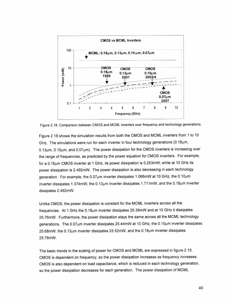
CMOS vs MCML Inverters
100MCML: 0.18pm, 0.1 3pm, 0.10 pm, 0.07pm
10 CMOS CMOS CMOSE 0.18pm 0.13pm 0.10pmJ c 2 01 2 0 014
- -CMOS
- * 0.07pm2007
0.11 2 3 4 5 6 7 8 9 10
Frequency (GHz)
Figure 2.18: Comparison between CMOS and MCML inverters over frequency and technology generations.
Figure 2.18 shows the simulation results from both the CMOS and MCML inverters from 1 to 10
GHz. The simulations were run for each inverter in four technology generations (0.18pm,
0.13pm, 0.10pm, and 0.07pm). The power dissipation for the CMOS inverters is increasing over
the range of frequencies, as predicted by the power equation for CMOS inverters. For example,
for a 0.18pm CMOS inverter at 1 GHz, its power dissipation is 0.253mW, while at 10 GHz its
power dissipation is 2.492mW. The power dissipation is also decreasing in each technology
generation. For example, the 0.07pm inverter dissipates 1.066mW at 10 GHz, the 0.10pm
inverter dissipates 1.374mW, the 0.13im inverter dissipates 1.711mW, and the 0.18ptm inverter
dissipates 2.492mW.
Unlike CMOS, the power dissipation is constant for the MCML inverters across all the
frequencies. At 1 GHz the 0.18pm inverter dissipates 25.39mW and at 10 GHz it dissipates
25.76mW. Furthermore, the power dissipation stays the same across all the MCML technology
generations. The 0.07pm inverter dissipates 25.44mW at 10 GHz, the 0.10lpm inverter dissipates
25.68mW, the 0.13pm inverter dissipates 25.52mW, and the 0.18pm inverter dissipates
25.76mW.
The basic trends in the scaling of power for CMOS and MCML are expressed in figure 2.15.
CMOS is dependent on frequency, so the power dissipation increases as frequency increases.
CMOS is also dependent on load capacitance, which is reduced in each technology generation,
so the power dissipation decreases for each generation. The power dissipation of MCML
40

remains constant over both frequency and changing technology generations, due to its constant
current flow. Therefore, the power dissipation of MCML circuits should not significantly decrease
unless the amount of current in the circuit is decreased. These scaling power trends are seen
throughout the next two simulations.
2.11.2 Simulation 2: Power per Stage
This simulation focuses on the power each stage dissipates in a 16:1 10 Gb/s MUX, using 0.18
pm technology. Each stage of the MUX was simulated separately, loaded by four inverters on
each output of the stage. The power dissipation of each stage and the load inverters was
measured using SPICE, and then the power dissipation of the inverters was subtracted out of the
total power dissipation. The first three stages (16:8, 8:4, 4:2) were simulated using 0.18 pm
CMOS while the last stage (2:1) was simulated using 0.18 pm MCML. The supply voltage was
22.V and the simulation was run for 15ns.
The 16:8 stage had eight CMOS MUXs, each with a clock frequency of 622 MHz and a total
power dissipation of 22.54mW. The 8:4 stage had four CMOS MUXs, with clock frequencies of
1.25 GHZ and a total power dissipation of 23.16mW. The 4:2 stage had two CMOS MUXs with
clock frequencies of 2.5 GHz, and a total power dissipation of 17.91mW. The 2:1 MCML stage
had only one MXML MUX at a clock frequency of 5 GHz and a total power dissipation of
90.66mW. Figure 2.19 shows the power dissipation of each stage.
Power Per Stage for a 16:1 MUX
100-
80-
E 60 60 CMOs40
0020
0-16to8 8to4 4to2 2to1
622 MHz 1.25 GHz 2.5 GHz 5 GHz
Mux Stages and CIk Frequency
Figure 2.19: The power dissipation for each stage in a simulated 16:1 MUX.
41

One conclusion from Figure 2.19 is that the CMOS MUXs' power dissipation stays roughly
constant per each stage of the MUX. This intuitively makes sense because the frequency is
increasing by a factor of two per stage and the number of MUXs is decreasing by a factor of two
per each stage. The power dissipation of CMOS is based on frequency and the number of
circuits, as shown in section 2.10.1, so the same increase in frequency with the same decrease in
number of MUXs results in fairly constant power dissipation per stage.
The MCML MUX's power dissipation, as expected, is much higher than the CMOS power
dissipation per stage. Furthermore, since the power dissipation of MCML is only dependent on
current, voltage, and the number of circuits, the power dissipation scales only according to how
many MUXs are in each stage. There is little to no dependence on frequency or capacitive load
for the MCML MUX, so its' power dissipation will increase only from the addition of more MUXs to
the stage.
2.11.3 Simulation 3: Maximum Clock Frequency
The purpose of this simulation is to determine the maximum frequencies that the model CMOS
and MCML MUXs can obtain in each technology generation and the corresponding power
dissipation. The circuits were run at the highest possible frequency without causing the circuit to
fail, and the power dissipation of the entire circuit was measured at that frequency. Failure is
defined differently for the CMOS and MCML circuits. CMOS is a full-swing architecture, so failure
is defined as an output swing that is less than 10% to 90% of the expected output swing (0.22-
1.98V). The failure point for the MCML is different because it outputs a reduced voltage swing.
Therefore, failure was defined as a specified output swing (200 mVpeak-to-peak). This output swing
was chosen because it is a realistic output swing needed to drive the modulator driver amplifier,
which is the next stage in an optical transceiver.
The supply voltage for the simulation was 2.2V, and the device parameters were the same as
listed in sections 2.8.1 and 2.8.2. All the inputs for the CMOS MUX were buffered using CMOS
inverters, and the 2:1 MUX was loaded with four CMOS inverters of the same sizing. The inputs
for the MCML MUX were buffered using MCML inverters, except for the clock signal that has a
specified swing of 0.5 to 1V. The MCML MUX was also loaded with four MCML inverters. The
power dissipation of the entire circuit was measured using SPICE, and then the power dissipation
of the inverters was subtracted out, so as to compare only the power dissipation of the MUX
circuits themselves.
Figure 2.20 shows the eye diagrams of the CMOS simulations for each technology generation.
For the 0.18ptm generation, the maximum clock frequency is 2.78 GHz and the power dissipation
42

is 2.97mW. In the 0.13ptm generation, the maximum clock frequency is 3.7 GHz and the power
dissipation is 2.57mW. The 0.10pim generation has a maximum clock frequency of 4.55 GHz and
a power dissipation of 2.06mW. Lastly, the 0.07im generation has a maximum clock frequency
of 5.0 GHz and a power dissipation of 0.75mW.
Eye diagram (0.18im MUX @ 2.7 GHz)
.2 -
8
2-
0
0 0.05 0.1 0.15 0.2 0.25 0.3 0.35
Figure 2.20A
Eye diagram (0.10 pm MUX @ 4.5 GHz)
21.9
0.2
21.9
0.2
Eye diagram (0.13pm MUX @ 3.7 GHz)
2
2 -
0 0.05 0.1 0.15
Figure 2.20B
0.2 0.25
2
1.9
0.2
2
1.9
0.2
0 0.05 0.1 0.15 0.2 0 0.02 0.04 0.06 008 01 0.12 0.14 0.16 0.18 0.2
Figure 2.20C Figure 2.20D
Figure 2.20: The eye-diagrams from the CMOS maximum clock frequency simulations. Figure 2.20A showsthe 0.1 8pm CMOS MUX with a maximum frequency of 2.78 GHz and power dissipation of 2.97mW. Figure
2.20B shows the 0.13prm CMOS MUX with a maximum frequency of 3.7 GHz and power dissipation of2.57mW. Figure 2.20C shows the 0.10pm CMOS MUX with a maximum frequency of 4.55 GHz and a
power dissipation of 2.06mW. Figure 2.20D shows the 0.07pm CMOS MUX with a maximum frequency of 5GHz and a power dissipation of 0.75mW.
The MCML eye diagrams for each technology generation are shown in Figure 2.21. The 0.18ptm
generation has a maximum clock frequency of 8.33 GHz and a power dissipation of 88.0mW.
The 0.13pm generation has a maximum clock frequency of 11.76 GHz and has a power
dissipation of 89.0mW. The 0.10pm generation has a maximum clock frequency of 16.39 GHz
43
Eye diagram (0.07um MUX @ 5 GHz)
8
0
.2
2
2
8
2
0

and corresponding power dissipation of 87.74mW. The 0.07ptm generation has a maximum clock
frequency of 17.86 GHz and power dissipation of 86.06mW.
0.18um MCML MUX at 120p, Vosw = 200mV
20 40 60
Figure 2.21A
2.2
2.1
2
1.9
1.8
1.7
80 100 120
0.13um MCML MUX at 85p, Vosw = 200mV
0 10 20 30 40 50 60 70 80 90
Figure 2.21B
0.1Oum MCML MUX at 61 p, Vosw = 200mV
0 10 20 30 4
Figure 2.21 C
2.3
2.1
2
1.8
1.7
1.60 50 60
0.07um MCML MUX at 56p, Vosw = 200mV
0 10 20 30 40
Figure 2.21 D
Figure 2.21: The MCML eye-diagrams for the maximum clock frequency simulation. Figure 2.21A shows the0.18pm MCML MUX with a maximum frequency of 8.33 GHz and power dissipation of 88.0mW. Figure
2.21 B shows the 0.13 pm MCML MUX with a maximum frequency of 11.76 GHz and power dissipation of89.0mW. Figure 2.21C shows the 0.1Opm MCML MUX with a maximum frequency of 16.39 GHz and a
power dissipation of 87.74mW. Figure 2.21 D shows the 0.07pm MCML MUX with a maximum frequency of17.86 GHz and a power dissipation of 86.06mW.
The simulation data for both the CMOS MUX and the MCML MUX is compared in Figure 2.22.
The CMOS MUX tends to have a lower power dissipation for each successive technology
generation. The MCML MUX power dissipation remains fairly constant for the first two
generations (0.18pm and 0.13pim), and then decreases by around 2mW for the last two
technology generations (0.10pm and 0.07ptm). For each technology generation the MCML MUX
power dissipation is significantly higher than the CMOS MUX power dissipation.
44
2.3
2.2
2.1
2
1.9
1.8
1.7
1.6'0
2.3
2.2
2.1
2
1.9
1.8
1.7
1.650 60
------------
2.2-

Although the power dissipation is much higher in the MCML MUX, it can achieve much higher
frequencies in each technology generation than can the CMOS MUX. Furthermore, the trend
lines indicate that MCML scales faster in frequency than CMOS. These trends demonstrate the
tradeoff between low power and low frequencies in CMOS, and high frequency with high power in
MCML.
CMOS and MCML MUX Model Comparison
18
16
14
12
10
N
C:
Li- 8
6
4
2
100
80
-o0
:E
60
40
20
MCML',
W I
..---"" CMOs
| | | |
0.2 0.18 0.16 0.14 0.12 0.1 0.08 0.06
Technology (micrometers)
Figure 2:22: Comparison of simulated results for CMOS and MCML MUXs, compared against technologygenerations, power dissipation and maximum frequency. The dotted lines represent frequency and the solid
lines represent power dissipation.
45
I I I
I n|

2.12 ConclusionsThis chapter analyzed the power scaling trends of the electrical MUX/DEMUX. Silicon MOSFETs
were identified as the lowest power technology used to manufacture MUX circuits, and the two
main circuit topologies used in MUXs are CMOS and MCML. CMOS circuits have low power
dissipation but are relatively slow for the needs of high-speed communication circuits, so MCML
is used to push MOSFET transistors to higher frequencies, but at the cost of having higher power
dissipation. These two circuit topologies were used to simulate MUXs in SPICE, using the
Berkeley Predictive Technology model to evaluate power trends in the several different
technology generations.
The first simulation, a comparison between CMOS and MCML inverters, highlighted the
differences in power dissipation between the two topologies. CMOS power dissipation is
dependent on frequency and load capacitance, while MCML is dependent only on current and
supply voltage. The impact of this was seen in the second simulation, which determined the
power dissipation in each stage of a 10 Gb/s 16:1 MUX. The CMOS stages maintained relatively
constant power dissipation per each stage, due to CMOS dependency on frequency and the
number of circuits. The MCML stage power dissipation is dependent on the number of circuits in
the stage, so the power dissipation would accordingly increase as more stages are added. In the
last simulation, the power dissipation and maximum frequency for the CMOS and MCML MUXs
was determined for each technology generation. This simulation showed that the MCML can
achieve much higher frequencies in each technology generation than CMOS, and that it seems to
scale faster than CMOS. The tradeoff between power dissipation and frequency was shown in
this simulation, as the CMOS MUXs had significantly lower power dissipation that was decreasing
in each generation, while MCML MUXs had high power dissipation that seemed to remain
constant or decrease very slightly.
The results from these simulations can be used to predict how the power dissipation of a MUX
will scale in the future. For example, Simulation 3 showed that a 0.07pm CMOS MUX can run at
5 GHz and dissipates only 0.75mW. From Simulation 2 it is known that CMOS MUXs have the
about the same power dissipation per MUX stage. Therefore a 4 stage, 10 GB/s MUX solely
using CMOS in 0.07ptm will dissipate about 3mW. This is an order of magnitude lower than the
simulated 10 Gb/s MUX in 0.18pm (which is 154.27mW), and is also an order of magnitude lower
than the commercial data (see Appendix A). This example highlights the fact that improving
technology generations will significantly reduce the power dissipation of the MUX/DEMUX
circuits.
46

These simulations have shown that CMOS is the most desirable architecture, because of its very
low power dissipation. As technology generations improve, it is seen that there is a
corresponding improvement in CMOS, in that it is able to both reach higher frequencies and has
constantly decreasing power dissipation. Furthermore, since MCML is more dependent on
current and voltage then on technology generations for power, the sooner CMOS can be used
instead of MCML to achieve the higher frequencies, the sooner there is a significant improvement
in overall power dissipation.
The final conclusion from these simulations is that it is in fact possible to predict future power
dissipation trends for future technology generations. These simulation results have shown that
there is a general trend of decreasing power dissipation in future technology generations of
MUX/DEMUXs. The knowledge that the MUX/DEMUX's power dissipation will decrease with
technology generations signifies that the overall power dissipation in an optical transceiver will
also decrease.
2.13 Future WorkPossible future work would include the continuing evaluation of the next technology generations
after 0.07im, to develop much longer power scaling trend lines. A comparison between the
BPTM and current process files, such as TSMC, should be done to examine the wide variety of
differences across process files and to understand completely how they affect these simulation
results. The MUX simulations should also be extended to evaluate very low power dissipation
MCML MUXs, to identify at what frequencies in which technologies generations the optimization
line is between CMOS and MCML. Furthermore, as transistors scale further, newer physical
models of how transistors act in that regime need to be added into the SPICE process file. Lastly,
these circuit simulation techniques for future technology generations could also be applied to
other circuits in the optical transceiver, such as the CDR and PLL.
47

Chapter 3Thermoelectric Cooler
3.1 Overview of ChapterThe thermoelectric cooler (TE cooler) dissipates the second largest amount of power in the
optical transceiver. This section provides background on the TE cooler and its uses, and
examines possible ways to reduce the power dissipation in the TE cooler. A 2 dimensional model
is developed using MATLAB to model the thermodynamics of a packaged laser and TE cooler.
This model is then used to look at how specific factors, such as ambient temperature and
different thermal conductivities, affect the TE cooler. These simulations conclude that lower
thermal conductivity greatly enhances the cooling power of the TE cooler, but results in overall
higher temperatures in the laser.
3.2 Thermoelectric Cooler IntroductionThe TE cooler's purpose in an optical transceiver is to stabilize the laser diode against changes in
temperature. Changes in temperature can cause unwanted shifts in a laser's wavelength. For
example, a typical DFB laser will have a temperature dependent wavelength shift of 0.09nm per
degree C - or approximately 12 GHz per degree C. For DWDM systems with 50 GHz or 100
GHz channel separations this corresponds to only a few degrees change in temperature before
the wavelength drifts from one ITU grid channel to another. Also, for continuous-wave, externally
modulated lasers discussed in this thesis, the operating current for a given output power
decreases significantly with the laser temperature.
Temperature also effects the lifetime of a laser. A common rule of thumb used in accelerated
aging studies is that a 10 C rise in temperature reduces the lifetime by 50% and increases the
probability of failure in the first year by a factor of 10. Therefore, the TE cooler is extremely
important in order to stabilize the laser against changes in temperature that could drastically
affect both the laser's wavelength and its lifetime.
3.3 TE Cooler BackgroundA thermoelectric cooler (TE cooler) is a device that uses current and two dissimilar materials to
create a temperature difference using the Peltier effect. Figure 3.1 shows a diagram of a TE
cooler with the two materials labeled (n-type and p-type), as well as the hot and cold sides of the
TE cooler labeled. When current is applied to the TE cooler the electrons in the n-type metal
become excited and gather energy from the Tcold side, making the Tcold side cooler. The electrons
48

then carry this energy down towards the Thot side, where they deposit their extra energy and heat
up the Thaot side. The current also causes the holes in the p-type material to become excited and
to carry away energy from the TwOId side, thus contributing to the cooling. The holes, just like the
electrons in the n-type material, carry that energy down to the Thot side, and contribute to the Thot
side becoming warmer. Together, the movement of the holes in the p-type material and the
electrons in the n-type material caused by the current result in a temperature difference between
the TcoI side and the Thot side.
Tcold
N I P
Thot Thot
Figure 3.1: Diagram of a TE cooler.
3.4 Previous Work I Approaches to Reduce Power Dissipation of
TE CoolerThe following section describes work done on several approaches for reducing the power
dissipation in the TE cooler.
3.4.1 New Materials
One method of reducing power dissipation is to use materials that have a higher ZT coefficient,
which would result in coolers that are much more efficient. The Z coefficient is described in
Equation 8, where a is the Seebeck coefficient, a is the electrical conductivity, and k is the
thermal conductivity.
Z = (c 2* a) / k [8]
The coefficient ZT is the Z defined in Equation 8 multiplied by the temperature T. Currently the
ZT for most materials is around 1, and no material has of yet reached a ZT of 2 [21]. There are
many research efforts in this area to identify possible materials and methods of achieving a
higher ZT. Some material examples are skutterudites, clathrates, Half-Heusler alloys, and
chalcogenides [21]. The primary improvement in ZT has been a reduction in the thermal
conductivity.
49

3.4.2 Alternative Packaging (Micro Coolers)
Micro TE Coolers are another method to decrease power dissipation by reducing the cooling to a
more localized area. Figure 3.2 shows an example of a four degree temperature difference
between 50 ptm of space using a micro cooler [22]. Micro TE coolers have also been developed
using a MEMs-like process to create an array of 126 n and p-type elements of size 20plm tall and
60pm in diameter [23]. A diagram of this cooler is show in Figure 3.3.
= 2
10 20 30 40 50 60 70 80 90 100 110
1.5
0.5
a
--1
-1.6
Figure 3.2: Micro cooler developed in 1999 with four degrees of temperature difference in 50pm space [22].
Figure 3.3: MEM's process-based micro cooler developed in 2003, with 126 TE elements in the array [23].
3.4.2 Tunable Lasers
The use of tunable lasers is another option to reducing the effect of temperature on a laser and
thereby reducing the need of a TE cooler. One method was developed to use a feedback control
on the current of the tunable laser to correct for changes in temperature [24]. Figure 3.4 shows a
diagram of the setup and chart showing experimental results concerning the controlled and
uncontrolled tunable laser [24]. The channel spacing in the feedback controlled laser is
approximately 1nm, making it more reasonable for use in WDM systems. The most significant
50
1

drawback to the use of tunable lasers in WDM systems is currently their cost when compared
with normal DFB lasers.
1-%4Computer Control 1563 ------------------------------------
1562 Ucordrolled
- 1561 -------------------------- ---------
S1560 - - - - - - - - -1M90 ------------------- -- ------------
3P ptal1559
3F X11 IF Spectrum ~~ ~ 1558--- -----------
15.56 -- - - - - - - - - - - - - q kQ
-Temnertre Contrl 15520 30 40 50 6D 70
Tenweatwm r C)
Figure 3.4: Feedback control using tuning current instead of temperature. Graph shows the laser outputwhen it is not controlled and then when it is controlled using the feedback [24].
3.5 Model for Thermal CoolingIn order to understand the effects of all these potential methods on the power dissipation of the
TE cooler, a flexible 2D model of the entire packaged laser including the TE cooler has been
developed. The model simulates the thermodynamics of a TE cooler and laser in two
dimensions, using the partial differential equations toolbox within MATLAB. The PDE Toolbox
solves the partial differential equation for heat flow as shown in Equation 9, where K is the
coefficient of heat conduction, T is the temperature, Q is the heat source, h is the convective heat
transfer coefficient, and Text is the external temperature.
-V-.(K*VT) = Q+h* (Text-T) [9]
The graphical model is shown in Figure 3.5, and has a total of 17 layers that simulate an entire
packaged laser. The model can be used to simulate the heat flow caused by the heat dissipation
of the laser and the cooling ability of the TE cooler. Its output shows the temperature distribution
throughout each layer within the model.
The first layer in the MATLAB thermal model is the heat sink, which is made out of copper. The
second layer is the solder that bonds the heat sink to the package of the laser. The solder is
made out of tin/lead and is modeled as 0.025 mm thick. The next layer is the package, which
encases the entire laser. It is modeled as a copper plate, with the same thermal conductivity as
the heat sink. Then there is a layer of solder, whose dimensions and thermal conductivity are the
51

same throughout the entire model. The solder bonds the TE cooler to the packaging of the entire
device.
The TE cooler composes 9 of the 14 layers in the entire model. The first layer is the ceramic
layer, which conducts the heat out of the TE cooler into the packaging and heat sink. The hot
side ceramic is modeled as beryllia ceramic. Touching the hot side ceramic is a small copper
strap. It has the same thermal conductivity as the rest of the copper used throughout the model.
Then there is a layer of solder between the copper and the bismuth telluride. The bismuth
telluride section is modeled horizontally with an n-type material section, an air section, and a p-
type material section that is repeated over its length of 12 mm [25]. The height of each section is
0.55 mm, and there is a 0.05 mm section on the top and bottom of the N and P sections that
models the heat current of each type of bismuth telluride [25,26]. There are only two
thermocouples in the model. Above the bismuth telluride is a layer of solder, and then another
layer of copper. Both layers have the same dimension and thermal conductivity as the layers
below the bismuth telluride. The next layer above the copper is the cold side ceramic plate,
which is modeled as beryllia ceramic. The two ceramic plates (the hot and the cold) act as the
final layers between the TE cooler and the device that it is cooling.
The TE cooler is soldered to the submount that holds the laser. The submount is
modeled as a copper plate. The last layer of the model is the laser, which is above the
submount. Figure 3.5 shows a physical diagram of the model with the materials labeled in each
section. Table 3.1 shows the corresponding material characteristics that were used in the model.
Laser
Submount Solder
Cold Ceramic
N P N P Copper
Hot Ceramic
Package
Heat Sink
Figure 3.5: The block diagram of the MATLAB model
52

Table 3.1: Material values used in MATLAB model
Dimension Thermal(L x W x D) Conductivity
Layer Material (mm) (W/mK)
Laser InP 0.3 x 0.1 x 0.2 [25] 68 [29]
Submount Copper 12 x 0.7 x 6 [25] 386 [27]Ceramics Beryllia Ceramic 12 x 0.6 x 6 [25,26] 230 [27]
Copper Strap Copper 12 x 0.25 x 6 [26] 386 [27]
TE Material Bismuth Telluride 12 x 0.65 x 6 [25,26] 1.5 [27]
Package Copper 30 x 9 x 6 [25] 386 [27]
Heat Sink Copper 12 x 3 x 6 [25,30] 386 [27]
Solder Tin/Lead 12 x 0.025 x 6 48 [27]
3.6 Model InputsThe inputs to the model are the heat sources; the bismuth telluride n-type and p-type materials
and the laser. The bismuth telluride section was modeled with two sections, one representing the
heating and cooling of the material near the edge of the material (Q and Qp), and the second
representing the joule heating in the area between the edges of the material (Qjhn and Qjhp).
Equation 8 describes the first of these two areas, with Qn being the heat generated by current
flowing though the n-type bismuth telluride near the edge of the material.
[8]Qn = (I*7n) / (L*W*D)
The length of the device, L = 1.5mm, the width of the device, W = 0.05mm, and the depth of the
device, D = 6mm. The current, I, is a variable input parameter. The Peltier coefficient is
calculated in Equation 9, where the Seebeck cn = -240pV/K [28].
nn = an * 300K [9]
The calculations are the same for the p-type material, where the Seebeck coefficient ap =
162ptV/K [28].
The second heating source is the joule heating in the bismuth telluride section. The joule heating
for the n-type material (Qjhn) is calculated using Equation 10.
Qjhn = (12*Pn) / (W*D) [10]
53

The width of the material, W = 1.5mm, the depth D = 6mm, and the resistivity for the n-type
material pn = 10 pK2*m [28]. The current, I, is a variable input parameter. The same calculations
were done for the p-type material, where pp = 5.5 pC2*m [28].
The laser heat source, Qiaser, was calculated using Equation 11.
Qiaser = P / (L*W*D) [11]
The power of the laser, P = 300mW, as calculated from laser datasheets. The length of the laser,
L = 0.3mm, the width of the laser, W = 0.1mm, and the depth of the laser, D = 0.2mm.
The entire model was created using the PDE toolbox in MATLAB and its parameters are exported
out into a MATLAB file, which allows the model to be modified and simulated using MATLAB
code outside of the PDE toolbox. The MATLAB file specifies all of the input parameters as
previously explained, and can be found in Appendix F.
3.7 MATLAB Simulations
The MATLAB simulations use a combination of the PDE Toolbox and MATLAB scripts to
generate results. Figure 3.6 shows an example of the model temperature profile that is created
from the PDE Toolbox. These profiles are then modified by the scripts in Appendix F.
Color T
-15 -10 10 15
Figure 3.6: Sample temperature profile of the model using the PDE Toolbox
54

The following simulations evaluate the effect of thermal conductivity and ambient temperature on
the TE cooler. There are many research efforts directed at finding materials that have higher ZT
coefficients. These simulations focus on lowering the thermal conductivity of a material, which
improves the ZT. The first set of simulations are of a packaged laser and TE cooler with the
normal conductivity in the BiTe sections. The second set of simulations show the same
packaged laser and TE cooler, but with half the normal conductivity in the BiTe sections. The
simulations are then compared, and the pros and cons of lower the thermal conductivity are
discussed.
The first simulation is of the packaged laser and TE cooler with the thermal conductivity of the
BiTe sections equal to 1.5 W/mK. The model is simulated over a range of currents (0 to 13A),
and the ambient temperature is held constant by setting the bottom boundary of the heat source
to 300K. The boundary conditions of the model are fixed so there is no heat flux from the surface
of the laser and submount (i.e. there is no thermal convection or conduction to the air). The
laser's heat source, Qiaser, remains fixed at the value determined in Section 3.4. Figure 3.7 shows
the results of the simulation.
Current \s Laser Temp @ 300K424
422 -
2420-
EH 418 -
C,,CU-J
416-
414-
4120 2 4 6 8 10 12 14Current (Amps)
Figure 3.7: The laser temperature versus the current though the TE cooler at 300K.
The impact of the cooler on the laser is seen in Figure 3.7, as the laser temperature decreases
while the current increases from 0 to 6A. The maximum point of cooling is at 6A, with 8.1 K
degrees of cooling. As the current increases past 6A, the impact of the joule heating in the TE
cooler can be seen. The laser temperature starts to rise at this point, indicating that the cooling
power of the TE cooler is being impeded by the joule heating. At 12A the laser temperature is the
same as at OA, indicating that the joule heating is equal to the cooling power of the TE cooler.
55

The simulation was then extended to examine the effects of ambient temperature on the TE
cooler. The ambient temperature is defined as the bottom boundary on the heat sink in the PDE
Toolbox, and this simulation varied the ambient temperature from 300K to 320K in 1 K increments.
Figure 3.8 shows the laser temperature versus the TE cooler current at each of the ambient
temperatures.
Currernt vs Laser Temp at Varying Ambient Temp (300-320K)
44
4-
E 430
4-
0 2 4 6 8 10 12 14
Current (Amp)
Figure 3.8: The laser temperature versus the current through the TE cooler at varying ambienttemperatures. The ambient temperatures are labeled on the right hand side of the graph.
The bottom curve shows the laser temperature versus the TE cooler current at 300K. As the
ambient temperature is increased by 1 K, the entire temperature versus current curve shifts
upward a corresponding degree. The straight line drawn at 420K is used to show a constant
laser temperature across the varying ambient temperature curves. The intersection point
between the 420K line and the ambient temperature curves indicates the current that is
necessary to keep the laser at 420K at that particular ambient temperature. Figure 3.8 shows
that as the ambient temperatures increases, the current needed to maintain a constant laser
temperature also increases.
This trend, where an increase in ambient temperature corresponds to an increase in TE cooler
current, has a profound impact on the power dissipation of the TE cooler. The power dissipation
of the TE cooler is calculated using Equation 12.
P = Rtotaj * 12 [12]
56

The total resistance, Rtotai = 0.02 Q, is calculated from the n-type and p-type resistivity of the BiTe
material. The resistance of the model is extremely low because the model only simulates 2
thermocouples. In general TE coolers have many more thermocouples, which results in the
resistance being much higher. For example, a typical laser has a voltage of 2.6V, with a current
of 1.3A, which implies that the resistance is 2 Q. The current, I, is the current from the
intersection points in Figure 3.7. The power dissipation versus the ambient temperature is shown
in Figure 3.9.
0.5
0.45
0.4
0.35
0.3
00.250a_~~
0.2
0.15
0.1
0.05
Ambient Temperature vs Power of TE cooler
300 301 302 303 304
Ambient Temp (K)305 306 307
Figure 3.9: The ambient temperature of the laser/TE cooler packagecooler.
versus the power dissipation of the TE
Figure 3.9 shows that as the ambient temperature is increases, the power dissipation is
increased. Between 300K to 307K, the power dissipation per thermocouple changes from almost
OW per thermocouple to 0.24W per thermocouple. Therefore, the higher the ambient temperature
the more power that is required by the TE cooler to keep the laser at a constant temperature.
The second set of simulations examines the impact of lowering the thermal conductivity of the
material in the TE cooler. These simulations use the same model as before, but the thermal
conductivity of the BiTe material is divided in half to be 0.75 W/mK. This model is simulated over
the same range of currents (0 to 13A) as before, and the laser temperature versus current is
plotted in Figure 3.10.
57

Current \ Laser Temp @ 300K
53K0= 0.75 W/mK
510 --
500 -
490 -0.E 480 -
9470-a)2460.
450 -
440 -
430 K =1.5 W/mK
420 -- ------------
410
400 'LI0 2 4 6 8 10 12 14
Current (Amps)
Figure 3.10: This graph plots the laser temperature versus current at 300K, with the dotted line representingthe model with reduced thermal conductivity of 1.5W/mk, and the solid line representing the model with
thermal conductivity of 0.75W/mK.
This simulation shows some interesting results when compared with the conclusions of the
previous simulations that had the normal thermal conductivity of BiTe. In this simulation the laser
temperature is almost 100K higher than the simulation with the normal BiTe thermal conductivity.
This can be explained by the fact that lower thermal conductivity prevents heat flow. For
example, at OA the TE cooler acts just as a piece of material with low thermal conductivity, and as
such, it is much harder for the heat of the laser to flow through the TE cooler material into the
heat sink. Therefore the temperature of the laser will be considerably higher with materials that
have lower thermal conductivities than with materials that have higher thermal conductivities.
This observation is
In both simulations the maximum cooling point occurs at 6A. However, with the normal BiTe
thermal conductivity the maximum cooling is 8.1K, while in this simulation, with half the normal
thermal conductivity of BiTe, the maximum cooling is 16.7K. Therefore this shows the trend that
with half the thermal conductivity there is about twice as much cooling power. This conclusion
can be generalized by saying that materials with lower thermal conductivities will be able to
achieve more cooling with the same amount of current through the TE cooler.
The model with the lower thermal conductivity was then simulated at varying ambient
temperatures. Figure 3.11 shows the laser temperature versus the current in the TE for a range
of current (0 to 13A).
58

Current vs Laser Temperature at Varying Ambient Temperatures(BiTe thermal conductivity = 0.75 W/mK)
0 2 4 6 8Current (Amps)
10 12 14
Figure 3.11: Laser temperature versus current at varying ambient temperatures, with thermal conductivity ofthe BiTe equal to 0.75 W/mK.
As in Figure 3.8, the bottom curve represents the laser temperature versus the current at 300K.
As the ambient temperature increases, the laser temperature versus current curve shifts upward.
The horizontal line at 528K represents a constant laser temperature across all the varying
ambient temperature curves. The point of intersection between the 528K and the laser
temperature versus current curve indicates the current necessary to keep the laser at 528K at
that particular ambient temperature. There is the same trend as the first simulation, the higher
the ambient temperature, the more current that is required by the TE cooler to maintain a
constant laser temperature.
Using the same methodology as in the first simulations, a power versus ambient temperature
curve was created using the data points from Figure 3.11. The same resistance of Rtota = 0.02 Q
was used in the power calculations. The plot of power versus ambient temperature is shown in
Figure 3.12.
59
550
545
2-540
E 535
530
525
520
515
510
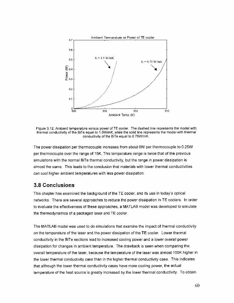
Ambient Temperature vs Power of TE coolerV. /
0.6
0.5 K 1.5 W/mKK 0.75 W/mK
0.4
0a 0.3
0.2
0.1
0300 305 310 315
Ambient Temp (K)
Figure 3.12: Ambient temperature versus power of TE cooler. The dashed line represents the model withthermal conductivity of the BiTe equal to 1.5W/mK, while the solid line represents the model with thermal
conductivity of the BiTe equal to 0.75W/mK.
The power dissipation per thermocouple increases from about OW per thermocouple to 0.25W
per thermocouple over the range of 15K. This temperature range is twice that of the previous
simulations with the normal BiTe thermal conductivity, but the range in power dissipation is
almost the same. This leads to the conclusion that materials with lower thermal conductivities
can cool higher ambient temperatures with less power dissipation.
3.8 ConclusionsThis chapter has examined the background of the TE cooler, and its use in today's optical
networks. There are several approaches to reduce the power dissipation in TE coolers. In order
to evaluate the effectiveness of these approaches, a MATLAB model was developed to simulate
the thermodynamics of a packaged laser and TE cooler.
The MATLAB model was used to do simulations that examine the impact of thermal conductivity
on the temperature of the laser and the power dissipation of the TE cooler. Lower thermal
conductivity in the BiTe sections lead to increased cooling power and a lower overall power
dissipation for changes in ambient temperature. The drawback is seen when comparing the
overall temperature of the laser, because the temperature of the laser was almost 100K higher in
the lower thermal conductivity case than in the higher thermal conductivity case. This indicates
that although the lower thermal conductivity cases have more cooling power, the actual
temperature of the heat source is greatly increased by the lower thermal conductivity. To obtain
60

the exact same temperature in the laser in both the lower and higher thermal conductivity cases,
the lower thermal conductivity TE cooler would have to work much harder. Therefore, the
desirability of lower thermal conductivities, and in general higher ZT, is reduced.
3.9 Future WorkThe future work for the TE cooler would be to implement the model in a 3D solver. This would
allow much more accurate modeling of the cooling in three-dimensions. The model should be
expanded to include a realistic number of thermocouples, so as to accurately model the
resistance and power of the TE cooler. The model should also be verified and compared to
current experimental results.
Furthermore, another model should be developed for a micro cooler. The micro cooler model
could then be used to investigate whether localized cooling does reduce power consumption as
compared to the larger TE cooler. The micro model should also be compared and verified
against current experimental results. Furthermore, both models can be used to investigate the
impact of material changes, such as higher ZT, on the power dissipation of the micro cooler and
the larger cooler model.
61

Chapter 4Conclusions and Future Work
4.1 SummaryThis work has focused on predicting future power dissipation for optical transceivers. The first
chapter provided motivation for power dissipation as a performance metric, and developed a
component based model for predicting the overall power dissipation in an optical transceiver.
This model determined that there are three key components that dissipate the majority of power
in the optical transceiver: the electrical MUX/DEMUX, the thermoelectric cooler, and the
modulator driver amplifier. The following two chapters analyzed the first two devices in-depth,
and developed physical models to help predict their future power dissipation.
The electrical MUX/DEMUX circuits were investigated in Chapter 2. Commercial data for the
MUX/DEMUX circuits was analyzed and resulted in an observation that the power dissipation was
dependent on both the bit rate and the number of stages in the circuit. The materials used to
manufacture MUX/DEMUX circuits were examined and it was seen that Silicon MOSFETS are
the lowest power technology, so the chapter focused on only that technology. The two circuit
topologies that are used in Si MOSFETS MUX circuits are CMOS and MCML. CMOS is used
because it has very low power dissipation, but it is limited in its bandwidth. MCML is used to
push the MOSFETS to higher frequencies, but in return dissipates a much higher amount of
power. These two circuit topologies were modeled using SPICE, and the Berkeley Predictive
Technology process cards were used to simulate the circuits in four technology generations
(0. 1 8pm, 0. 1 3pm, 0. 10 m, 0.07 im).
The SPICE simulations showed that the CMOS and MCML power dissipations scale differently.
CMOS is dependent on frequency and load capacitance, so its power dissipation increases with
frequency and decreases with technology generation. MCML power dissipation depends only on
current and supply voltage, so it's power dissipation stays constant across frequency and mostly
constant across technology generations. Furthermore, the power dissipation in a CMOS MUX
stays constant throughout the different stages, because the frequency increases by two times the
previous stage but the number of MUX circuits decreases by 2 times the previous stage. The
opposite is true for MCML, as its power dissipation only depends on current, so as the number of
MUX circuits increase so will the power dissipation.
Lastly, SPICE simulations were done to predict the power dissipation of future generations of
CMOS and MCML MUXs. The results showed that a 10 Gb/s MUX using only CMOS in 70nm
62

would dissipate 3mW, which is an order of magnitude difference from the 0.18pim MUX that uses
both CMOS and MCML. These simulations show that it is possible to predict the power
dissipation of MUXs in the future, and that improvements in technology generations significantly
reduce the power dissipation of the MUXs.
The third chapter focuses on the thermoelectric cooler (TE cooler), which is the second device
that dissipates the majority of power in the optical transceiver. There are several methods
currently being researched for reducing power dissipation in the TE cooler. Higher ZT materials
would result in more efficient coolers, micro coolers allow for more localized cooling, and tunable
lasers can eliminate the need for a TE cooler. A MATLAB model was developed to help evaluate
these methods fore reducing power dissipation in the TE cooler.
The MATLAB model simulates the thermodynamic flow throughout a packaged laser and TE
cooler. This model was used to simulate the packaged laser and TE cooler at different ambient
temperatures and with different thermal conductivities for the BiTe material. A comparison
between the model with the thermal conductivity of BiTe and the model with half the BiTe thermal
conductivity showed that using lower thermal conductivities increases the cooling power of the TE
cooler. However, using a lower thermal conductivity increases the overall temperature of the
laser. This is because the lower thermal conductivity hinders the flow of heat away from the laser
and into the heat sink. This means that although the lower thermal conductivity has a higher
cooling power, it is much less desirable than the higher thermal conductivity because the overall
heat source temperature is higher. This has greater ramifications, because a lower thermal
conductivity implies a higher ZT coefficient. Therefore, by this analysis lower thermal conductivity
isn't useful for low overall heat source temperature.
These three chapters have shown that the key components that dissipate the majority of power in
the optical transceiver can be individually modeled to understand how each of their power
dissipations scale in the future. The electrical MUX model has shown that each successive
technology generation will bring improvements in the power dissipation of the circuits. The TE
cooler model has shown that possible power reduction techniques can be simulated and
evaluated in order to more fully understand how they will impact the future power dissipation of
TE coolers. Together these physical models give a better understanding of the factors that will
most influence the power dissipation in the future.
63

4.2 Future WorkThe following sections describe the future work for each device examined in this work.
4.2.1 Electrical MUX/DEMUX Future Work
The MUX/DEMUX simulations can be extended by evaluating the impact of different process files
on the SPICE simulations. A comparison should be done between BPTM, TSMC, and other
industry SPICE process files in order to understand what the significant differences between
process files are and how they effect the simulations in terms of power and bandwidth.
Furthermore, as transistors continue to scale further, newer physical models of how the transistor
works in that regime need to be developed and added into the SPICE process files.
Simulations on the DEMUX circuits need to be done in order to verify that it scales like the MUX
circuits. In order to make both the MUX and DEMUX circuits more complete, frequency dividers
and output drivers should be added into the SPICE simulations. A coherent model of a 16:1 MUX
and 1:16 DEMUX, instead of just stages, should be completed and verified. Other circuits
involved in the optical transceiver, such as the CDR unit and the PLL, should be simulated to
ensure the same scalability as the MUX circuits.
4.2.1 Thermoelectric Cooler
The TE cooler MATLAB model should be verified and compared against published experiments.
The model should also be developed in a 3D solver. The number of thermocouples modeled
should be increased to a realistic number similar to that used in current experiments. This should
give a more accurate result regarding current and power dissipation.
A micro cooler model should also be developed, verified, and compared with published
experiments. The micro cooler model should then be used to model localized cooling, and to
examine its effect on cooling and power dissipation. The micro cooler results should be
compared against the conventional TE coolers, and against that of TE coolers using higher ZT
materials. Furthermore, the size of the micro cooler and the number of thermocouples should be
investigated, to find the optimized size and number of TE coolers.
4.3.1 Modulator Driver Amplifier
As the third device that contributes significantly to the power dissipation in an optical transceiver,
the modulator driver amplifier needs to be examined and physically modeled. The following
section provides background on the modulator driver amplifier, some commercial data analysis,
and a description of important future work.
64

The modulator driver amplifier's sole function in a transceiver is to amplify the output of the MUX
to a range acceptable by the modulator. The output of the MUX is usually between 0.4-0.6V
while the electro-absorption modulators usually need 3.5V peak to peak and LiNbO modulators
typically need 6V peak to peak [31]. The modulator driver amplifier must provide sufficient gain
and large enough output swing to drive the modulator, and it should not significantly distort or
degrade the signal [31]. The architecture of the driver amplifier consists of two amplifiers
cascaded together [31,32,33]. The first stage amplifies the incoming signal and the second
amplifier acts as the driving stage [31]. Together these two stages provide high enough gain and
output swing to allow the incoming MUX signal to be received by the modulator.
In order to achieve high frequencies, the modulator driver amplifier is constructed as a traveling
wave amplifier. This circuit architecture uses transmission line theory to connect several
transistors in parallel in order to create an amplifier. Lumped amplifiers are limited in the
bandwidth because they have loss-less elements such as resistors [34]. The traveling wave
amplifier only uses capacitances and inductors, which greatly enhances its ability to achieve
higher bandwidth [34].
Appendix G shows commercial driver amplifier power dissipation with corresponding bit rate and
output voltage swing. Both the bit rate and the level of the output swing effect the power
dissipation of the driver amplifier. There is an increase in power dissipation between the 10 Gb/s
to 40 Gb/s that is 0.4-0.5W. There is a weak scaling of dissipated power with bit rate. However,
large differences in power dissipation can be attributed to the change in output voltage swing.
The 10 Gb/s driver amplifier with an output swing of 2 VPP has a power dissipation of only 0.9W
as compared to other 10 Gb/s driver amplifiers that have output swings of 6-7Vpp and dissipate
around 3W. Appendix G also clearly shows that single-ended output modulator drivers used for
E-A modulators typically dissipate approximately 1 W of electrical power whereas differential
output drivers used for driving E-O modulators dissipate approximately 3W of electrical power
(both trends are approximately independent of bit rate). The lower drive voltages required by E-A
modulators versus E-O modulators results in a factor of three difference in the power dissipation
for the drive electronics.
Figure 4.1 and 4.2 show commercial data for several modulator driver amplifiers. In Figure 4.1,which shows the power dissipation versus the bit rate of the amplifier, it is seen that there is not
an obvious trend relating the power with increasing bit rate. This means that unlike the
MUX/DEMUX circuits, the driver amplifier's power dissipation is not significantly affected by
improvements in transistor technology.
65

3
02
0
CL0
4
* CMOs* GaAs
P InPX
Inphi.5 Intel
* Ihi Centellax3
Agilent
.5-.n el I ruint
Inn CentphleA 1-~
.5- Intel
A.2.5 Gb/s 10 Gb/s 12.5 Gb/s 40 Gb/s
Bit Rate
Figure 4.1: Modulator driver amplifier commercial data comparing power versus bit rate. No general trendseen
However, Figure 4.2 proves that there is a strong trend with increasing driver voltage related to
increasing power dissipation. Figure 4.3 further supports this trend, as it shows that the drive
voltage trend is decreasing with time. Therefore, in order to reduce power dissipation in the
driver amplifiers, methods to reducing the voltage drive of the modulator must be explored.
0.
0
4
3.
3
2.
2
0
* CMOS*GaAsAInP
2.5 3 3.5 4 4.5 5 5.5 6 6.5 7 7.5 8
Modulator Drive Voltage (V)
Figure 4.2: Modulator driver amplifier commercial data comparing power versus modulator driver voltage.An upward trend can be seen, where an increase in modulator drive voltage corresponds to an increase in
power.
66
5- aeaxfbtel
Agilent5
. TriQui
U In hi/entella

20
16
12
C4iso1990 1995 2000 2005
Figure 4.3: Bandwidth versus modulator drive voltage [35].
This analysis of commercial data has shown that the power dissipation of the driver amplifier is
not dependent on bit rate as much as it is dependent on the drive voltage. Therefore the factors
affecting the drive voltage in the modulator need to be investigated. There are physical limits that
play a role in determining what the minimum drive voltage can be, and those limits need to be
explored and understood. A physical model should be developed to fully understand the
modulator, and the model should be used to find ways for reducing the drive voltage. A physical
model of the amplifier should also be built, and the fundamentals of its power dissipation should
be investigated. The physical model should answer the questions of which factors, other than
drive voltage, affect the power dissipation. Using both the physical model for the modulator and
for the amplifier, the scaling of the power dissipation would be understood. The knowledge from
these models would result in predictions for how the power dissipation of the modulator driver
amplifier would scale in the future.
67
7
0
OPOO

Appendix AElectrical MUX/DEMUX Scaling
Device Bit Rate Device Material Power
Intel (GD16557) [T] 2.5 Gb/s 16:1 MUX Silicon (CMOS) 1.3 W
Intel (GD16506) [T] 2.5 Gb/s 1:16 DEMUX Silicon (CMOS) 2.0 W
Research Paper [6] 10 Gb/s 16:1 MUX 0.18um CMOS <0.45 W
Research Paper [6] 10 Gb/s 1:16 DEMUX 0.18um CMOS <0.87 WInfineon Technologies(FOA41001B1) [V] 10 Gb/s 16:1 MUX SiGe 1.2 WInfineon Technologies(FOA51001B1) [V] 10 Gb/s 1:16 DEMUX SiGe 1.3 W
AMCC (S3097) [W] 10 Gb/s 16:1 MUX SiGe BiCMOS 1.9 W
AMCC (S3098) [W] 10 Gb/s 1:16 DEMUX SiGe BiCMOS 1.3 W
AMCC (S76801) [X] 40 Gb/s 16:1 MUX SiGe BiCMOS 7.95 W
AMCC (S76802) [X] 40 Gb/s 1:16 DEMUX SiGe BiCMOS 8.8 WInphi (5080MX) [Y] 50 Gb/s 4:1 MUX InP 1.5 W
Inphi (5081DX) [Y] 50 Gb/s 1:4 DEMUX InP 1.1 W
68

Appendix BReferences for Figure 2.3
[A] Ishida, K., "A 10-GHz 8 B-multiplexer/ demultiplexer chip set for SONET STS-192 system,"
IEEE J. Solid-State Circuits, vol. 26, pp. 1936-1943, Dec. 1991.
[B] Bagheri, M., "10-Gb/s framer/demultiplexer IC for SONET STS192 applications," in Proc.IEEE
C/CC, 1995, pp. 427-429.
[C] Shioiri, S., "A 10-Gb/s SiGe bipolar framer/demultiplexer for SDH systems," in ISSCC Dig
Tech. Papers, 1998, pp. 202-203.
[D] Anderson, L. I., "Silicon bipolar chipset for SON ET/SDH 10-Gb/s fiber-optic communication
links," IEEE J. Solid-State Circuits, vol. 30, pp. 210-218, Mar. 1995.
[E] Hauenschild, J., "A 10-Gb/s BiCMOS clock and data recovering 1:4-demutiplexer in a
standard plastic package with external VCO," in ISSCC Dig. Tech. Papers, 1996, pp. 202-203.
[F] Yoshida, N., "Low-power-consumption 10-Gb/s GaAs 8:1 multiplexer/1:8 demultiplexer," in
IEEE GaAs IC Symp., 1997, pp. 113-116.
[H] Kurisu, M., "2.8-Gb/s 176-mW byte-interleaved and 3.0-Gb/s 118-mW bit-interleaved 8:1
multiplexers," in ISSCC Dig. Tech. Papers, 1996, pp. 122-123.
[1] Tanabe, A., "High-performance CMOS for gigahertz communication IC," in Symp. VLSI Tech.
Dig. Tech. Papers, 1996, p. 134.
[J] Soda, M., "A 2.4-Gb/s CMOS clock recovering 1:8 demultiplexer," in Symp. VLSI Circuits Dig.
Tech. Papers, 1997, pp. 69-70.
[K] Nakamura, K., "A 6-Gb/s CMOS phase-detecting DEMUX module using half-frequency clock,"
in Symp. VLSI Circuits Dig. Tech. Papers, 1998, pp. 196-197.
[L] See Reference [6]
[M] Xu, M. et. al. 'An SFI-5 compliant 16:4 multiplexer for OC-768 systems," Solid-State Circuits
Conference, 2003. Digest of Technical Papers. ISSCC. 2003.
69

[N] Meghelli, M. et. al., "50 Gb/s SiGe BiCMOS 4:1 multiplexer and 1:4 demultiplexer for serial
communication systems," Solid-State Circuits Conference, 2002. Digest of Technical Papers.
ISSCC. 2002.
[0] La Rue, G.S., et. al., "Gigabit complementary HFET communication circuits: 16:1 multiplexer,
1:16 demultiplexer and 16x16 crosspoint switch," Solid-State Circuits Conference, 1996. Digest
of Technical Papers. 43rd ISSCC., 1996.
[Q] Kuroda, T., et. al. "1.65 Gb/s 60 mW 4:1 multiplexer and 1.8 Gb/s 80 mW 1:4 demultiplexer
ICs using 2 V 3-level series-gating ECL circuits," Solid-State Circuits Conference, 1995. Digest of
Technical Papers. 42nd ISSCC, 1995.
[R] Tanabe, A., et. al., "A 10 Gb/s demultiplexer IC in 0.18 pm CMOS using current mode logic
with tolerance to the threshold voltage fluctuation," Solid-State Circuits Conference, 2000. Digest
of Technical Papers. ISSCC. 2000.
[S] Mattia, J.P., et. al., "A 1:4 demultiplexer for 40 Gb/s fiber-optic applications"
Solid-State Circuits Conference, 2000. Digest of Technical Papers. ISSCC. 2000
[Z] Kehrer, D., et. al., "40-Gb/s 2:1 Multiplexer and 1:2 Demultiplexer in 120-nm Standard CMOS,"
IEEE Journal of Solid-State Circuits, Vol 38, No. 11, November 2003.
70

Appendix CMATLAB scripts for CMOS and MCML MUX Inputs
MATLAB Script for CMOS Inputs
%function prbs-cIk-mux(N,T,DTM,BP,BT,sM,sBP,sBT,fname)
% Inputstranstime=1; % rise/fall time for bits (entered as percentage of clk period)CP=0.2; % clock period in units of timetotal=15; % total length of sequence in units of timeBP=CP; % bit period for both of PRBS - same as clk periodfname='mux2_out.txt'; %Output file
%ConversionsDT=(transtime/100)*CP; % Transition time calculationT=CP/2; % Time of 1 flat section and 1 transitionN=total/T; % number of T for entire timeM=floor(total/BP); % number of BP (PRBS) for entire timeBT=DT; % PRBS transition time same as clk
%Making continuous time from 0 to Total (nanoseconds)span=linspace(0,total,(total*100)+1);spanX=span*1 000000;spanY=round(spanX);spanZ=spanY/1 000000;spans=reshape(spanZ, length(spanZ), 1);
%CLK TimeCLK=(0:T:total+1);CLKX=CLK*1 000000;CLKY=round(CLKX);CLKZ=CLKY/1000000;CLKT=(0:T:total+1)+DT;CLKTX=CLKT*1000000;CLKTY=round(CLKTX);CLKTZ=CLKTY/1000000;clk_timeA=reshape([CLKZ;CLKTZ],2*length(CLK),1);clk_time=clk_timeA(2: length(clktimeA));
%Clk Voltagestog=0;count=0;for ind=1:length(clk time)
count=count+1;if (count == 1) 1 (count ==2)
clkvolt(ind) = 0;elseif (count == 3)
clkvolt(ind) = 1;else
clkvolt(ind) = 1;count = 0;
end
71

end
clk_voltA=reshape(clkvolt,length(clkvolt),1); %reshapes to an Xx1 matrixclk_volt=clk voltA(1 :(length(clk-voltA)-1));
%Selector Ck TimeSELCK=(O:T:total+ 1)-DT;SELCKX=SELCK*1 000000;SELCKY=round(SELCKX);SELCKZ=SELCKY/1 000000;SELCKT=(0:T:total+ 1);SELCK_TX=SELCKT*1000000;SELCK_TY=round(SELCKTX);SELCK_TZ=SELCK_TY/1000000;sel_timeA=reshape([SELCKZ;SELCKTZ],2*length(SELCK), 1);sel_time=sel _timeA(2: (length(sel-timeA)));
%Selector Clk Voltagesstog=0;scount=0;for inds=1:length(seltime)
scount=scount+1;if (scount == 1) 1 (scount ==2)
selvolt(inds) = 1;elseif (scount == 3)
selvolt(inds) = 0;else
selvolt(inds) = 0;scount = 0;
endend
selvoltA=reshape(selvolt,length(selvolt),1); %reshapes to an Xx1 matrixselvolt=selvoltA(1: (length(selvoltA)-1));
%First PRBS Time and Bits
s=rand('state');rand('state',sum (1 00*clock));bits = round(rand(1,M+1));t1 = linspace(0,M*BP,M+1)+(CP/4);t1X=tl *1000000;t1Y=round(t1X);t1Z=t1Y/1000000;t2 = linspace(0,M*BP,M+1)+BT+(CP/4);t2X=t2*1 000000;t2Y=round(t2X);t2Z=t2Y/1 000000;
ct=1;for iz=1:length(bits)
if (bits(iz) == 0)bs(ct)=bits(iz);bs(ct+1)=0;ct=ct+2;
else
72

bs(ct)=bits(iz);bs(ct+1)=1;ct=ct+2;
endendt1a = t1Z(1:length(t1)-1);t2a = t2Z(1:length(t2)-1);bsa = bs(1:length(bs)-1);t = [;reshape([tla;t2a],2*M,1)];b = reshape(bsa,length(bsa),1);
%Second PRBS Time and Bitsbits = round(rand(1,M+1));
cts=1;for izs=1:length(bits)
if (bits(izs) == 0)sbs(cts)=bits(izs);sbs(cts+1)=0;cts=cts+2;
elsesbs(cts)=bits(izs);sbs(cts+1)=1;cts=cts+2;
endendsbsa = sbs(1:length(sbs)-1);sb = reshape(sbsa,length(sbsa),1);
%Weaving time strands togethertimenw=[clktime;sel_time;t;spans];timenews=sort(timenw);timesA=unique(timenews);
tlct=1;for xlp=1:length(timesA)
if (timesA(xlp) > total)timeS(tict-1)=timeS(tlct-1);
elsetimeS(tlct)=timesA(xlp);tlct=tlct+1;
end;end;
times=reshape(timeS, length(timeS), 1)
%Generating full clk signalzcount=1;d=1;for y=1:length(times)
if (d+1 > length(clk_volt))voltclk(zcount)=clk-volt(d);
zcount=zcount+1;elseif (times(y) ~= clk-time(d))
voltclk(zcount)=clk-volt(d);
73

zcount=zcount+1;else
voltclk(zcount)=clk-volt(d);d=d+1;zcount=zcount+1;
endendvoltsclk=reshape(voltclk, length(voltclk), 1);
%Clkbar valuesfor idx=1:length(voltclk)
if (voltclk(idx) == 0)bclkvoltA(idx)= 1;
else bclk voltA(idx)= 0;end
endvoltsbclk=reshape(bclk_voltA, length(bclk voltA), 1);
%Generating full Selector Clk signalszcount=1;sd=1;for sy=1:length(times)
if (sd+1 > length(selvolt))voltsel(szcount)=sel-volt(sd);
szcount=szcount+1;elseif (times(sy) ~ sel-time(sd))
voltsel(szcount)=sel-volt(sd);szcount=szcount+1;
elsevoltsel(szcount)=sel-volt(sd);sd=sd+1;szcount=szcount+1;
endendvoltssel=reshape(voltsel, length(voltsel), 1);
%Clkbar valuesfor sidx=1:length(voltsel)
if (voltsel(sidx) == 0)bselvoltA(sidx)= 1;
else bselvoltA(sidx)= 0;end
endvoltsbsel=reshape(bselvoltA, length(bselvoltA), 1);
%Generate first full PRBS signalycount=1;c=1;
for w=1:length(times)if (c+1 > length(b))
voItPRBS(ycount)=b(c);ycount=ycount+1;
elseif (times(w) ~ t(c))voItPRBS(ycount)=b(c);
ycount=ycount+1;
74

elsevoltPRBS(ycount)=b(c);c=c+1;ycount=ycount+1;
endendvoltsPRBS=reshape(voltPRBS, length(voItPRBS), 1);
%Generate Second full PRBS signalsycount=1;sc=1;
for sw=1:length(times)if (sc+1 > length(sb))
svoltPRBS(sycount)=sb(sc);sycount=sycount+1;
elseif (times(sw) ~ t(sc))svoltPRBS(sycount)=sb(sc);
sycount=sycount+1;else
svoltPRBS(sycount)=sb(sc);sc=sc+1;sycount=sycount+1;
endendsvoltsPRBS=reshape(svotPRBS, length(svoltPRBS), 1);
%Change Amplitude of SignalsvoltsclkT=voltsclk*2.2;voltsbclkT=voltsbclk*2.2;voltsselT=voltssel*2.2;voltsbselT=voltsbsel*2.2;voltsPRBST=voltsPRBS*2.2;svoltsPRBST=svoltsPRBS*2.2;
%Output in the form of [Time CLK PRBS]label = ones(size(times))*double('n');fid = fopen(fname,'w');outmat = [times,label,voltsclkTvoltsbclkT,voltsselT,voltsbselT,voltsPRBST,svoltsPRBST].';fprintf(fid,'%3.6f%c %3.6f %3.6f %3.6f %3.6f %3.6f %3.6f\r ',outmat);fclose(fid);
MATLAB Script for MCML Inputs
%This is for MCML MUX inputs%function prbs-clk-mux(N,T,DT,M,BP,BT,sM,sBP,sBT,fname)
% Inputstranstime=1; % rise/fall time for bits (entered as percentage of clk period)CP=81; % clock period in units of timetotal=2430; % total length of sequence in units of timeBP=CP; % bit period for both of PRBS - smae as clk periodfname='mcml2_out.txt'; %Output file
75

%ConversionsDT=(transtime/100)*CP; % Transition time calculationT=CP/2; % Time of 1 flat section and 1 transitionN=total/T; % number of T for entire timeM=total/BP; % number of BP (PRBS) for entire timeBT=DT; % PRBS transition time same as clk
%Making continuous time from 0 to Total (nanoseconds)span=linspace(0,total, (total*1)+ 1);spanX=span*1 000000;spanY=round(spanX);spanZ=spanY/1 000000;spans=reshape(spanZ,length(spanZ), 1);
%CLK TimeCLK=(0:T:total+1);CLKX=CLK*1 000000;CLKY=round(CLKX);CLKZ=CLKY/1000000;CLKT=(0:T:total+1)+DT;CLKTX=CLKT*1000000;CLKTY=round(CLKTX);CLKTZ=CLKTY/1000000;clktimeA=reshape([CLKZ;CLKTZ],2*length(CLK),1);clktime=clk-timeA(2:length(clktimeA));
%Clk Voltagestog=0;count=0;for ind=1:length(clk_time)
count=count+1;if (count == 1) 1 (count ==2)
clkvolt(ind) = 0;elseif (count == 3)
clkvolt(ind) = 1;else
clkvolt(ind) = 1;count = 0;
endend
clkvoltA=reshape(clkvolt,length(clkvolt),1); %reshapes to an Xx1 matrixclk_volt=clk voltA(1: (length(clk voltA)-1));
%Selector Clk TimeSELCK=(0:T:total+1)-DT;SELCKX=SELCK*1 000000;SELCKY=round(SELCKX);SELCKZ=SELCKY/1 000000;SELCK_T=(0:T:total+1);SELCK_TX=SELCKT*1000000;SELCKTY=round(SELCKTX);
76

SELCK_TZ=SELCKTY/1000000;seltimeA=reshape([SELCKZ;SELCKTZ],2*length(SELCK), 1);seltime=seltimeA(2:(length(seltimeA)));
%Selector Clk Voltagesstog=0;scount=0;for inds=1:length(seltime)
scount=scount+1;if (scount == 1) 1 (scount ==2)
selvolt(inds) = 1;elseif (scount == 3)
selvolt(inds) = 0;else
selvolt(inds) = 0;scount = 0;
endend
selvoltA=reshape(selvolt,length(selvolt), 1); %reshapes to an Xx1 matrixselvolt=selvotA(1:(length(selvoltA)-1));
%First PRBS Time and Bitss=rand('state');rand('state', sum (1 00*clock));bits = round(rand(1,M+1));t1 = linspace(0,M*BP,M+1)+(CP/4);tlX=tl*1000000;t1Y=round(tlX);t1 Z=tl Y/1 000000;t2 = linspace(0,M*BPM+1)+BT+(CP/4);t2X=t2*1 000000;t2Y=round(t2X);t2Z=t2Y/1 000000;
ct= 1;for iz=1:length(bits)
if (bits(iz) == 0)bs(ct)=bits(iz);bs(ct+1)=0;ct=ct+2;
elsebs(ct)=bits(iz);bs(ct+1)=1;ct=ct+2;
endendt1a = t1(1:length(t1)-1);t2a = t2(1:length(t2)-1);bsa = bs(1:length(bs)-1);tA = [0;reshape([tla;t2a],2*M,1)];tB = tA*1 000000;tC = round(tB);t = tC/1 000000;b = reshape(bsa,length(bsa),1);
77

%Second PRBS Time and Bitsbits = round(rand(1,M+1));
cts=1;for izs=1:length(bits)
if (bits(izs) == 0)sbs(cts)=bits(izs);sbs(cts+1)=0;cts=cts+2;
elsesbs(cts)=bits(izs);sbs(cts+1)=1;cts=cts+2;
endendsbsa = sbs(1:length(sbs)-1);sb = reshape(sbsa,length(sbsa),1);
%Weaving time strands togethertimenw=[clktime;sel-time;t;spans];timenews=sort(timenw);timesnewsA=timenews*1 000000;timesnewsB=round(timesnewsA);timesnewsC=timesnewsB/1 000000;timesA=unique(timesnewsC);
tlct=1;for xlp=1:length(timesA)
if (timesA(xlp) > total)timeS(tlct-1)=timeS(tlct-1);
elsetimeS(tlct)=timesA(xlp);tlct=tlct+ 1;
end;end;
times=reshape(timeS, length(timeS), 1)
%Generating full clk signalzcount=1;d=1;for y=1:length(times)
if (d+1 > length(clk volt))voltclk(zcount)=clk volt(d);
zcount=zcount+1;elseif (times(y) -= clk-time(d))
voltclk(zcount)=clk volt(d);zcount=zcount+1;
elsevoltclk(zcount)=clk-volt(d);d=d+1;zcount=zcount+1;
endendvoltsclk=reshape(voltclk,length(voltclk),1);
78

%Clkbar valuesfor idx=1 :Iength(voltclk)
if (voltclk(idx) == 0)bclkvoltA(idx)= 1;
else bolk_voltA(idx)= 0;end
endvoltsbclk=reshape(bclk-voltA, length(bclk voltA), 1);
%Generating full Selector Clk signalszcount=1;sd=1;for sy=1:length(times)
if (sd+1 > length(sel volt))voltsel(szcount)=selvolt(sd);
szcount=szcount+1;elseif (times(sy) ~ sel-time(sd))
voltsel(szcount)=sel-volt(sd);szcount=szcount+1;
elsevoltsel(szcount)=sel-volt(sd);sd=sd+1;szcount=szcount+1;
endendvoltssel=reshape(voltsel, length(voltsel), 1);
%Selectorbar valuesfor sidx=1:length(voltsel)
if (voltsel(sidx) == 0)bselvoltA(sidx)= 1;
else bselvoltA(sidx)= 0;end
endvoltsbsel=reshape(bselvoltA, length(bselvoltA), 1);
%Generate first full PRBS signalycount=1;c=1;
for w=1:length(times)if (c+1 > length(b))
voItPRBS(ycount)=b(c);ycount=ycount+1;
elseif (times(w) -= t(c))voItPRBS(ycount)=b(c);
ycount=ycount+1;else
voItPRBS(ycount)=b(c);c=c+1;ycount=ycount+1;
endendvoltsPRBS=reshape(voItPRBS, length(voltPRBS), 1);
79
%PRBS1 bar valuesfor ixnew=1:length(voItPRBS)
if (voItPRBS(ixnew) == 0)bPRBS-voltA(ixnew)= 1;
else bPRBS voltA(ixnew)= 0;end
endvoltsbPRBS=reshape(bPRBSvoltA,length(bPRBSvoltA), 1);
%Generate Second full PRBS signalsycount=1;sc=1;
for sw=1:length(times)if (sc+1 > length(sb))
svoltPRBS(sycount)=sb(sc);sycount=sycount+1;
elseif (times(sw) -= t(sc))svoltPRBS(sycount)=sb(sc);
sycount=sycount+1;else
svoltPRBS(sycount)=sb(sc);sc=sc+1;sycount=sycount+1;
endendsvoltsPRBS=reshape(svoltPRBS, length(svoltPRBS), 1);
%PRBS2bar valuesfor sixnew=1:length(svoltPRBS)
if (svoltPRBS(sixnew) == 0)bsPRBS-voltA(sixnew)= 1;
else bsPRBSvoltA(sixnew)= 0;end
endsvoltsbPRBS=reshape(bsPRBS-voltA,length(bsPRBSvoltA),1);
%Change Amplitude of SignalsvoltsclkT=((voltsclk+1)*(9/10)-0.6);voltsbclkT=((voltsbclk+ 1)*(9/10)-0.6);voltsPRBST=(voltsPRBS+ 1)*(8/10)-0.45;voltsbPRBST=(voltsbPRBS+1)*(8/10)-0.45;svoltsPRBST=(svoltsPRBS+1)*(8/10)-0.45;svoltsbPRBST=(svoltsbPRBS+1)*(8/10)-0.45;
%Output in the form of [Time CLK PRBS]label = ones(size(times))*double('p');fid = fopen(fname,'w');outmat =
[times, label,voltsclkT,voltsbclkT,voltsPRBST,voltsbPRBST,svoltsPRBST,svoltsbPRBST].';fprintf(fid,'%3.6f%c %3.6f %3.6f %3.6f %3.6f %3.6f %3.6f\r ',outmat);fclose(fid);
80

Appendix DSpice Files for MUX Circuits
SPICE File for CMOS Testing Inverter
*This is the future inverter test
.options post
.include '../subckts/model_1 8u.sp'
.include '../subckts/basicsubckts.sp'
*DC Biasing.param pvdd=1.8Vvdd VDD! 0 pvddVvss VSS! 0 0.global VDD! VSS!
Vin in 0 pulse 1.8 0 0 .001n .001n 0.5n 1n
*Input buffered*Xb1 ain in VDD! VSS! buffer
*DeviceXmx1 in out VDD! VSS! inv
*Load*X[1 out load VDD! VSS! inv
*X11 out load1 load2 load3 load4 vd VSS! load
.temp 25
.tran .01n 10n
.measure tran c2qfall trig v(in) val='pvdd/2' rise=2+ targ v(out) val='pvdd/2' fall=2.measure tran c2qrise trig v(in) val='pvdd/2' fall=2+ targ v(out) val='pvdd/2' rise=1
.measure tran avgpwr AVG power from=.1n to=10n
.measure tran peakpwr MAX power from=.1n to=10n
.probe I(Xmxl.Mn2)
.probe I(Xmxl.Mp2)
.end
81

SPICE File for CMOS MUX
*This is the CMOS 2:1 MUX
.include '../subckts/model_07u.sp'
.include '../subckts/basicsubckts_07u.sp'
.include 'prbsout.sp'*.include '../subckts/mux-cmos.sp'
.options nomod post
*DC Biasing.param pvdd=2.2Vvdd VDD! 0 pvddVvss VSS! 0 0.global VDD! VSS!
Vain ainn 0 PWL(TIME, seq1)Vbin binn 0 PWL(TIME, seq2)Vclk clkin 0 PWL(TIME, sclk)Vbclk bclkin 0 PWL(TIME,sbclk)Vselclk selckin 0 PWL(TIME,sel)Vbselclk bselckin 0 PWL(TIME,bsel)
*.subckt mux ain bin mid1 11 mid2 out clk bclk vdd vss*Xff1 ain mid1 clk bclk vdd vss flipflop*Xff2 bin 11 clk bclk vdd vss flipflop*X11 11 mid2 bclk clk vdd vss diatch*Xsl mid1 mid2 out clk bclk vdd vss selector*.ends
*inverter test*Xil clkin clk VDD! VSS! inv
*All inputs bufferedXb1 clkin clk VDD! VSS! buffer*Xb2 bclkin bclk VDD! VSS! buffer*Xb3 ainn ain VDD! VSS! buffer*Xb4 binn bin VDD! VSS! buffer*Xb5 selckin selck VDD! VSS! buffer*Xb6 bselckin bselck VDD! VSS! buffer
*Device*Xmxl ain bin mid1 11 mid2 out clk bclk VDD! VSS! mux
*Xff1 ain mid1 clk bclk VDD! VSS! flipflop*Xff2 bin 11 clk bclk VDD! VSS! flipflop*X11 11 mid2 clk bclk VDD! VSS! dlatch*Xsl mid1 mid2 out bselck selck VDD! VSS! selector
*Load*X11 out load1 VDD! VSS! inv*X12 out load2 VDD! VSS! inv
82

*X13 out load3 VDD! VSS! inv*X14 out load4 VDD! VSS! inv
.temp 25
.tran DATA=prbs
.param per='0.14e-9'.param tsi='0.84n'.probe tran+ eyetimel=+par('.5*(sgn(TIM E-tsi)+abs(sgn(TIME-tsi)))*(TIME-tsi-per*int((TIM E-tsi)/per))').print tran V(out)*.print tran V(clk)*.print tran V(selck)*.print tran V(ain)*.print tran V(bin)*.print tran V(midl)*.print tran V(mid2)
.measure tran avgpwr AVG power from=.1n to=14n
.measure tran peakpwr MAX power from=.ln to=14n
.end
SPICE File for MCML Testinq Inverter
*This is a resistor based inverter*3/29/04
.options post
.include '../subckts/modell 8u.sp'
.include '../subckts/basicsubckts.sp'
.include 'prbsmcml.sp'
*Parameters.param mwn=52.5u.param mwc=87.5u.param mwb=23u.param res=71.param leng=0.18u.param lengvb=0.18u
*DC Biasing.param pvdd=1.8Vvdd VDD! 0 pvddVvss VSS! 0 0.global VDD! VSS!
Vclk clk 0 PWL(TIME sclk)Vbclk bclk 0 PWL(TIME bsclk)Vain ain 0 PWL(TIME sain)Vbain bain 0 PWL(TIME bsain)Vbin bin 0 PWL(TIME sbin)Vbbin bbin 0 PWL(TIME bsbin)
83

Vbias vbias 0 1.5
*Inverter.subckt mcmlinv in bin q bq vdd vss vbiasR1 vdd bq resR2 vdd q resMN1 bq in mid1 vss nmosl =Ieng w=mwnMN2 q bin mid1 vss nmosl I=Ieng w=mwnMN4 mid1 vbias afix vss nmosl I=Iengvb w=mwbMN5 afix vbias vss vss nmosl I=lengvb w=mwb.ends
X11 ain bain out1 bout1 VDD! VSS! vbias mcmlinvX12 out1 bout1 load1 bload1 VDD! VSS! vbias mcmlinv
.temp 25
.tran DATA=prbs
.measure tran avgpwr AVG power from=.ln to=14n
.measure tran peakpwr MAX power from=.ln to=14n*.print V(out1) I(X11.R1).probe I(X11.MN4).end
SPICE File for MCML MUX
*This is a resistor based mux*3/9/04
.options post
.include '../subckts/model_1 3u.sp'*.include '../subckts/basicsubckts.sp'.include 'voltsmcmltesta.sp'
*Parameters.param mwn=37.9u.param mwc=63.2u.param mwb=27u.param res=71.param leng=0.13u.param lengvb=0.13u
Vbias vbias 0 1.5
*DC Biasing.param pvdd=1.5Vvdd VDD! 0 pvddVvss VSS! 0 0.global VDD! VSS!
*Inverter.subckt mcmlinv in bin q bq vdd vss vbiasR1 vdd bq res
84

R2 vdd q resMN1 bq in midi vss nmosl I=Ieng w=mwnMN2 q bin mid1 vss nmosl I=eng w=mwnMN4 mid1 vbias afix vss nmosl I=Iengvb w=mwbMN5 afix vbias vss vss nmosl I=Iengvb w=mwb.ends
*MCML stage.subckt stage din bdin clk bclk q bq vdd vss vbiasR1 vdd bq resR2 vdd q res
*current sourceMN1 7 vbias afix vss nmosl I=Iengvb w=mwbMc3 afix vbias vss vss nmosl I=Iengvb w=mwb
MN2 4 clk 7 vss nmosl I=eng w=mwcMN3 11 bclk 7 vss nmosl I=eng w=mwcMN4 bq din 4 vss nmosl =Ieng w=mwnMN5 q bdin 4 vss nmosl I=eng w=mwnMN6 bq q 11 vss nmosl I=eng w=mwnMN7 q bq 11 vss nmosl I=eng w=mwn.ends
*MCML 2:1 MUX (at the end of the stage).subckt muxstage ain bain bin bbin clk bclk out bout vdd vss vbiasRI vdd out resR2 vdd bout resMnl out ain mid1 vss nmosl =Ieng w=mwnMn2 bout bain mid1 vss nmosl =Ieng w=mwnMn3 mid1 clk mid3 vss nmosl I=eng w=mwcMn4 mid3 vbias afix vss nmosl I=Iengvb w=mwbMnn4 afix vbias vss vss nmosl I=Iengvb w=mwbMn5 out bin mid2 vss nmosl I=eng w=mwnMn6 bout bbin mid2 vss nmosl I=eng w=mwnMn7 mid2 bclk mid3 vss nmosl I=eng w=mwc.ends
*DC Biasing
Vclk clk 0 PWL(TIME sclk)Vbclk bclk 0 PWL(TIME bsclk)Vain ainn 0 PWL(TIME sain)Vbain bainn 0 PWL(TIME bsain)Vbin binn 0 PWL(TIME sbin)Vbbin bbinn 0 PWL(TIME bsbin)
*MCML Buffers*Xb1 clkin bclkin clk bclk VDD! VSS! vbias mcmlinvXb2 ainn bainn ain bain VDD! VSS! vbias mcmlinvXb3 binn bbinn bin bbin VDD! VSS! vbias mcmlinv
*NEW MUXXNH1 ain bain bclk clk q bq VDD! VSS! vbias stage
85

XNH2 q bq clk bclk outa bouta VDD! VSS! vbias stage
XNL1 bin bbin bclk clk mid1 bmidl VDD! VSS! vbias stageXNL2 mid1 bmidl clk bclk mid2 bmid2 VDD! VSS! vbias stageXNL3 mid2 bmid2 bclk clk outb boutb VDD! VSS! vbias stage
Xt1 outa bouta outb boutb bclk clk bout out VDD! VSS! vbias muxstage
*LoadLI out Tout 0.24nL2 bout bTout 0.24n
Rload Tout VSS! 70Rbload bTout VSS! 70
*X11 out bout load1 bload1 VDD! VSS! vbias mcmlinv*X12 out bout load2 bload2 VDD! VSS! vbias mcmlinv*X13 out bout load3 bload3 VDD! VSS! vbias mcmlinv*X14 out bout Ioad4 bload4 VDD! VSS! vbias mcmlinv
*Inital Conditions*.ic V(out)=1.7*.ic V(outa)=1.7*.ic V(outb)=1.7*.ic V(mid2)=1.7
*Enviroment Parameters.temp 25.tran DATA=prbs
*SPICE Eye Diagram.param per='83p'.param tsi='0.2n'.probe tran+ eyetimel=+par('.5*(sgn(TIME-tsi)+abs(sgn(TIME-tsi)))*(TIME-tsi-per*int((TIME-tsi)/per))')
*Output Variables*.print tran V(ain)*.print tran V(bin)*.print tran V(clk)*.print tran V(outa)*.print tran V(outb).print tran V(out)*.probe tran I(XNH1.R2)*.probe tran I(XNH1.MN1)*.probe tran V(XNH1.4)*.probe tran I(Xb2.MN4)*.probe tran I(Rload)
.measure tran avgpwr AVG power from=. 1n to=2.9n
.measure tran peakpwr MAX power from=.1n to=2.9n
.end
86

SPICE File for MCML MUX Input
*TEST GHz Input
*4/3/04.data prbsTIME sclk bsclk sain bsain sbin bsbin
0.000000p 0.300000 1.20.500000p 0.300000 1.21.000000p 0.300000 1.22.000000p 0.300000 1.23.000000p 0.300000 1.24.000000p 0.300000 1.25.000000p 0.300000 1.26.000000p 0.300000 1.27.000000p 0.300000 1.28.000000p 0.300000 1.29.000000p 0.300000 1.210.000000p 0.300000 1.[Shortened for brevity]1497.000000p 1.2000001498.000000p 1.2000001499.000000p 1.2000001499.500000p 1.2000001500.000000p 1.200000
.ENDDATA
00000 0.90000000000 0.90000000000 0.90000000000 0.90000000000 0.90000000000 0.90000000000 0.90000000000 0.90000000000 0.90000000000 0.90000000000 0.900000
1.500000 0.9000001.500000 0.9000001.500000 0.9000001.500000 0.9000001.5000001.5000001.5000001.5000001.5000001.5000001.500000
0.9000000.9000000.9000000.9000000.9000000.9000000.900000
200000 0.900000 1.500000 0.900000 1.500000
0.3000000.3000000.3000000.3000000.300000
1.500000 0.9000001.500000 0.9000001.500000 0.9000001.500000 0.9000001.500000 0.900000
0.9000000.9000000.9000000.9000000.900000
SPICE File for CMOS MUX Input
*PRBS for MUX*1/23/04
.data prbsTIME sclk sbclk sel bsel seq1
0.000000n 0.000000 2.20000010.001000n 0.000000 2.2000000.010000n 0.000000 2.2000000.020000n 0.000000 2.2000000.025000n 0.000000 2.2000000.026000n 0.000000 2.2000000.030000n 0.000000 2.2000000.040000n 0.000000 2.2000000.049000n 0.000000 2.2000000.050000n 0.000000 2.2000000.051000n 2.200000 0.0000000.060000n 2.200000 0.0000000.070000n 2.200000 0.0000000.080000n 2.200000 0.0000000.090000n 2.200000 0.000000[Shortened for brevity]14.940000n14.949000n14.950000n14.951 000n14.960000n14.970000n14.980000n
seq22.200000 0.000000 2.200000 2.2000002.200000 0.0000002.200000 0.0000002.200000 0.0000002.200000 0.0000002.200000 0.0000002.200000 0.0000002.200000 0.0000002.2000000.0000000.0000000.0000000.0000000.0000000.000000
C
222222
0.000000 2.200000 2.2000000.000000 2.200000 2.2000000.000000 2.200000 0.0000002.200000 0.000000 0.0000002.200000 0.000000 0.0000002.200000 0.000000 0.0000002.200000 0.000000 0.000000
.000000
.200000
.200000
.200000
.200000
.200000
.200000
0.000000.000002.200002.200002.200002.200002.20000
2.200000 22.200000 22.200000 22.200000 20.000000 00.000000 00.000000 00.000000 00.000000 00.000000 00.000000 00.000000 00.000000 00.000000 0
0 0.0000000 0.0000000 0.0000000 0.0000000 0.0000000 0.0000000 0.000000
.200000
.200000
.200000
.200000
.000000
.000000
.000000
.000000
.000000
.000000
.000000
.000000
.000000
.000000
0.0000000.0000000.0000000.0000000.0000000.0000000.000000
1.5000001.5000001.5000001.5000001.5000001.5000001.5000001.5000001.5000001.5000001.500000
1.5000001.5000001.5000001.5000001.500000
87

14.990000n 2.200000 0.000000 0.000000 2.200000 0.000000 0.00000014.999000n 2.200000 0.000000 0.000000 2.200000 0.000000 0.00000015.000000n 2.200000 0.000000 2.200000 0.000000 0.000000 0.000000
.ENDDATA
SPICE File for CMOS Subcircuits
*This is the subckt file with*Inverters, Transmission gate*Fliflop, Datch, Selector
.param nw=4.5u
.param pw=9u
*CMOS Switch.subckt cswitch in out nclk pclk vdd vssMp1 in pclk out vdd pmos1 1=0.18u w=pwMn1 in nclk out vss nmosl 1=0.18u w=nw.ends
*CMOS Inverter.subckt inv in out vdd vssMp2 out in vdd vdd pmosl I=0.18u w=pwMn2 out in vss vss nmosl 1=0.18u w=nw.ends
*Flipflop.subckt flipflop din qout ck ckb vdd vssXSw1 din 5 ckb ck vdd vss cswitchXIn1 5 6 vdd vss invXIn2 6 7 vdd vss invXSw2 7 5 ck ckb vdd vss cswitchXSw3 6 12 ck ckb vdd vss cswitchXIn3 12 qout vdd vss invXln4 qout 14 vdd vss invXSw4 14 12 ckb ck vdd vss cswitch.ends
*DLatch.subckt dlatch din qout ck ckb vdd vssXSw1 din 5 ckb ck vdd vss cswitchXIn1 5 6 vdd vss invXIn2 6 qout vdd vss invXSw2 qout 5 ck ckb vdd vss cswitch.ends
*Selector.subckt selector ain bin dout ck ckb vdd vssXsl ain dout ckb ck vdd vss cswitchXs2 bin dout ck ckb vdd vss cswitch.ends
*Buffer.subckt buffer clkin clkout vdd vss
88

Xinl clkin mid1 vdd vss invXin2 midi clkout vdd vss inv.ends
*Load.subckt load out load1 load2 load3 load4 vdd vssX11 out load1 vdd vss invX12 out load2 vdd vss invX13 out load3 vdd vss invX14 out load4 vdd vss inv.ends
SPICE Process File for 0.18pm
*This model is 0.18u.model nmosl nmos Level = 49 Lint = 4.e-08 Tox = 4.e-09 VthO = 0.3999+ Rdsw = 250 Imin=1.8e-7 Imax=1.8e-7 wmin=1.8e-7 wmax=1.Oe-4 Tref=27.0+ version =3.1 Xj= 6.OOOOOOOE-08 Nch= 5.9500000E+17 lln= 1.0000000+ lwn= 1.0000000 wln= 0.00 wwn= 0.00 ll= 0.00 lw= 0.00 lwl= 0.00 wint= 0.00+ wl= 0.00 ww= 0.00 wwl= 0.00 Mobmod= 1 binunit= 2 xl= 0 xw= 0 binflag= 0+ Dwg= 0.00 Dwb= 0.00 K1= 0.5613000 K2= 1.OOOOOOOE-02 K3= 0.00 DvtO= 8.0000000+ Dvtl= 0.7500000 Dvt2= 8.OOOOOOOE-03 Dvt0w= 0.00 Dvtlw= 0.00 Dvt2w= 0.00+ Nix= 1.6500000E-07 WO= 0.00 K3b= 0.00 Ngate= 5.OOOOOOOE+20+ Vsat= 1.3800000E+05 Ua= -7.OOOOOOOE-10 Ub= 3.5000000E-18+ Uc= -5.2500000E-1 1 Prwb= 0.00 Prwg= 0.00 Wr= 1.0000000 UO= 3.5000000E-02+ AO= 1.1000000 Keta= 4.OOOOOOOE-02 A1= 0.00 A2= 1.0000000 Ags= -1.OOOOOOOE-02+ BO= 0.00 B1= 0.00 Voff= -0.12350000 NFactor= 0.9000000 Cit= 0.00+ Cdsc= 0.00 Cdscb= 0.00 Cdscd= 0.00 EtaO= 0.2200000 Etab= 0.00+ Dsub= 0.8000000 Pclm= 5.OOOOOOOE-02 Pdiblcl= 1.2000000E-02+ Pdiblc2= 7.5000000E-03 Pdiblcb= -1.3500000E-02 Drout= 1.7999999E-02+ Pscbel= 8.6600000E+08 Pscbe2= 1.0000000E-20 Pvag= -0.2800000+ Delta= 1.OOOOOOOE-02 AlphaO= 0.00 Beta0= 30.0000000 ktl= -0.3700000+ kt2= -4.OOOOOOOE-02 At= 5.5000000E+04 Ute= -1.4800000 Ual= 9.5829000E-10+ Ubl= -3.3473000E-19 Ucl= 0.00 Kt11= 4.OOOOOOOE-09 Prt= 0.00 Cj= 0.00365+ Mj= 0.54 Pb= 0.982 Cjsw= 7.9E-10 Mjsw= 0.31 Php= 0.841 Cta= 0 Ctp= 0 Pta= 0+ Ptp= 0 JS=1.50E-08 JSW=2.50E-13 N=1.0 Xti=3.0 Cgdo=2.786E-10 Cgso=2.786E-10+ Cgbo=0.OE+00 Capmod= 2 NQSMOD= 0 Elm= 5 Xpart= 1 Cgsl= 1.6E-10+ Cgdl= 1.6E-10 Ckappa= 2.886 Cf= 1.069e-10 Clc= 0.0000001 Cle= 0.6+ Dlc= 4E-08 Dwc= 0 Vfbcv= -1
*This model is 0.18u.model pmosl pmos Level = 49 Lint = 3.e-08 Tox = 4.2e-09 VthO = -0.42+ Rdsw = 450 Imin=1.8e-7 Imax=1.8e-7 wmin=1.8e-7 wmax=1.Oe-4 Tref=27.0+ version =3.1 Xj= 7.OOOOOOOE-08 Nch= 5.9200000E+17 lln= 1.0000000+ lwn= 1.0000000 win= 0.00 wwn= 0.00 11= 0.00 lw= 0.00 lwl= 0.00 wint= 0.00+ wl= 0.00 ww= 0.00 wwl= 0.00 Mobmod= 1 binunit= 2 xl= 0.00 xw= 0.00+ binflag= 0 Dwg= 0.00 Dwb= 0.00 ACM= 0 Idif=0.00 hdif=0.00 rsh= 0 rd= 0 rs= 0+ rsc= 0 rdc= 0 K1 = 0.5560000 K2= 0.00 K3= 0.00 DvtO= 11.2000000+ Dvtl= 0.7200000 Dvt2= -1.OOOOOOOE-02 Dvt0w= 0.00 Dvtlw= 0.00 Dvt2w= 0.00+ Nix= 9.5000000E-08 WO= 0.00 K3b= 0.00 Ngate= 5.OOOOOOOE+20+ Vsat= 1.0500000E+05 Ua= -1.2000000E-10 Ub= 1.00000OOE-18+ Uc= -2.9999999E-1 1 Prwb= 0.00 Prwg= 0.00 Wr= 1.0000000 UO= 8.OOOOOOOE-03+ AO= 2.1199999 Keta= 2.9999999E-02 A1= 0.00 A2= 0.4000000 Ags= -0.1000000+ BO= 0.00 B1= 0.00 Voff= -6.40000000E-02 NFactor= 1.4000000 Cit= 0.00+ Cdsc= 0.00 Cdscb= 0.00 Cdscd= 0.00 EtaO= 8.500000 Etab= 0.00 Dsub= 2.8000000+ Pclm= 2.0000000 Pdiblcl= 0.1200000 Pdiblc2= 8.OOOOOOOE-05
89

+ Pdiblcb= 0.1450000 Drout= 5.OOOOOOOE-02 Pscbel= 1.0000000E-20+ Pscbe2= 1.OOOOOOOE-20 Pvag= -6.OOOOOOOE-02 Delta= 1.OOOOOOOE-02+ AlphaO= 0.00 Beta0= 30.0000000 ktl= -0.3700000 kt2= -4.0000000E-02+ At= 5.5000000E+04 Ute= -1.4800000 Ual= 9.5829000E-10 Ubl= -3.3473000E-19+ Ucl= 0.00 Kt1I= 4.OOOOOOOE-09 Prt= 0.00 Cj= 0.00138 Mj= 1.05 Pb= 1.24+ Cjsw= 1.44E-09 Mjsw= 0.43 Php= 0.841 Cta= 0.00093 Ctp= 0 Pta= 0.00153+ Ptp= 0 JS=1.50E-08 JSW=2.50E-13 N=1.0 Xti=3.0 Cgdo=2.786E-10 Cgso=2.786E-10+ Cgbo=0.OE+00 Capmod= 2 NQSMOD= 0 Elm= 5 Xpart= 1 Cgs= 1.6E-10+ Cgdl= 1.6E-10 Ckappa= 2.886 Cf= 1.058e-10 Clc= 0.0000001 Cle= 0.6+ Dlc= 3E-08 Dwc= 0 Vfbcv= -1
SPICE Process File for 0.13pm
*This is the 0.13u Model
.model nmosl NMOS+Level = 49
+Lint = 2.5e-08 Tox = 3.3e-09+VthO = 0.332 Rdsw = 200+Imin=1.3e-7 Imax=1.3e-7 wmin=1.3e-7 wmax=1.Oe-4 Tref=27.0 version =3.1+Xj= 4.5000000E-08 Nch= 5.6000000E+17+Iln= 1.0000000 Iwn= 0.00 win= 0.00+wwn= 1.0000000 II= 0.00+Iw= 0.00 IwI= 0.00 wint= 0.00+wl= 0.00 ww= 0.00 wwl= 0.00+Mobmod= 1 binunit= 2 xl= 0+xw= 0 binflag= 0+Dwg= 0.00 Dwb= 0.00+K1= 0.3661500 K2= 0.00+K3= 0.00 DvtO= 8.7500000 Dvt1= 0.7000000+Dvt2= 5.OOOOOOOE-02 Dvt0w= 0.00 Dvtlw= 0.00+Dvt2w= 0.00 Nix= 3.5500000E-07 WO= 0.00+K3b= 0.00 Ngate= 5.OOOOOOOE+20+Vsat= 1.3500000E+05 Ua= -1.8000000E-09 Ub= 2.2000000E-18+Uc= -2.9999999E-1 1 Prwb= 0.00+Prwg= 0.00 Wr= 1.0000000 UO= 1.3400000E-02+AO= 2.1199999 Keta= 4.OOOOOOOE-02 A1= 0.00+A2= 0.9900000 Ags= -0.1000000 BO= 0.00+B1= 0.00+Voff= -7.9800000E-02 NFactor= 1.1000000 Cit= 0.00+Cdsc= 0.00 Cdscb= 0.00 Cdscd= 0.00+EtaO= 4.OOOOOOOE-02 Etab= 0.00 Dsub= 0.5200000+Pclm= 0.1000000 Pdiblcl= 1.2000000E-02 Pdiblc2= 7.5000000E-03+Pdiblcb= -1.3500000E-02 Drout= 0.2800000 Pscbel= 8.6600000E+08+Pscbe2= 1.OOOOOOOE-20 Pvag= -0.2800000 Delta= 1.0100000E-02+AlphaO= 0.00+ktl= -0.3400000+Ute= -1.2300000+Ucl= 0.00+Cj= 0.0015+Cjsw= 2E-10+Cta= 9.290391 E-04+Ptp= 1.56325E-03+N=1.0+Cgso=2.75E-1 0
Beta0= 30.0000000kt2= -5.2700000E-02Ual= -8.6300000E-10
Kt 1I= 4.OOOOOOOE-09Mj= 0.7175511 P
Mjsw= 0.3706993Ctp= 7.456211E-04
JS=2.50E-08
At= 0.00Ubl= 2.0000001E-18
Prt= 0.00b= 1.24859
Php= 0.7731149Pta= 1.527748E-03
JSW=4.OOE-13(ti=3.0 Cgdo=2.75E-10
Cgbo=0.OE+00 Capmod= 2
90

+NQSMOD= 0+Cgsl= 1.1155E-10+Cf= 1.113e-10+Dlc= 2E-08
Elm= 5Cgdl= 1.1155E-10
Clc= 5.475E-08Dwc= 0
Xpart= 1Ckappa= 0.8912
Cle= 6.46fbcv= -1
*PMOS MODEL
.model pmosl PMOS+Level = 49
+Lint = 2.e-08 Tox = 3.3e-09+VthO = -0.3499 Rdsw = 400
+lmin=1.3e-7 Imax=1.3e-7 wmin=1.3e-7 wmax=1.0e-4 Tref=27.0 version =3.1+Xj= 4.50000OOE-08 Nch= 6.8500000E+18+iln= 0.00 Iwn= 0.00 wln= 0.00+wwn= 0.00 11= 0.00+lw= 0.00 lwI= 0.00 wint= 0.00+wI= 0.00 ww= 0.00 wwl= 0.00+Mobmod= 1+xw= 0+Dwg= 0.00
binunit= 2binflag= 0
Dwb= 0.00
xl= 0
+K1= 0.4087000 K2= 0.00+K3= 0.00 DvtO= 5.0000000 Dvtl= 0.2600000+Dvt2= -1.OOOOOOOE-02 Dvt0w= 0.00 Dvtlw= 0.00+Dvt2w= 0.00 NIx= 1.6500000E-07 WO= 0.00+K3b= 0.00 Ngate= 5.OOOOOOOE+20
+Vsat= 1.0500000E+05+Uc= -2.9999999E-1 1+Prwg= 0.00 W+AO= 2.1199999+A2= 0.4000000+B1= 0.00
Ua= -1.4000000E-Prwb= 0.00
r= 1.0000000Keta= 3.0300001 E-02Ags= 0.1000000
Ub= 1.9499999E-18
UO= 5.2000000E-03A1= 0.00
BO= 0.00
+Voff= -9.10000000E-02 NFactor=+Cdsc= 0.00 Cdscb= 0.00+EtaO= 80.0000000 Etab= 0.00
0.1250000 Cit= 2.7999999E-03Cdscd= 0.00
Dsub= 1.8500000
+Pclm= 2.5000000 Pdiblcl= 4.8000000E-02+Pdibicb= 0.1432509 Drout= 9.OOOOOOOE-02+Pscbe2= 1.OOOOOOOE-20 Pvag= -6.OOOOOOOE-02+AlphaO= 0.00 Beta0= 30.0000000
Pdiblc2= 5.OOOOOOOE-05Pscbel= 1.OOOOOOOE-20
Delta= 1.0100000E-02
+ktl= -0.3400000+Ute= -1.2300000+Ucl= 0.00
+Cj= 0.0015+Cjsw= 2E-10+Cta= 9.290391 E-04+Ptp= 1.56325E-03+N=1.0+Cgso=2.75E-1 0+NQSMOD= 0
kt2= -5.2700000E-02Ual= -8.6300000E-10
Ktl 1= 4.OOOOOOOE-09
At= 0.00Ubl= 2.0000001E-18
Prt= 0.00
Mj= 0.7175511 Pb= 1.24859Mjsw= 0.3706993 Php= 0.7731149
Ctp= 7.456211E-04 Pta= 1.527748E-03JS=2.50E-08 JSW=4.OOE-13
Xti=3.0 Cgdo=2.75E-10Cgbo=0.OE+00 Capmod= 2Elm= 5 Xpart= 1
91

+Cgsl= 1.1155E-10+Cf= 1.113e-10+DIc= 2E-08
Cgdl= 1.1155E-10Clc= 5.475E-08
Dwc= 0 V
Ckappa= 0.8912Cle= 6.46
fbcv= -1
SPICE Process File for 0.104m
*This is the CMOS 0.1Ou Models
.model nmosl NMOS+Level = 49
+Lint = 2.e-08 Tox = 2.5e-09+VthO = 0.2607 Rdsw = 180
+Imin=1.Oe-7 Imax=1.Oe-7 wmin=1.Oe-7 wmax=1.Oe-4+Tref=27.0 version =3.1+Xj= 4.0000000E-08 Nch= 9.7000000E+17+lln= 1.0000000+wwn= 0.00+lw= 0.00+wl= 0.00+Mobmod= 1+xw= 0.00+Dwg= 0.00
+ACM= 0+rsh= 7+rsc= 0
+K1= 0.3950000+DvtO= 1.0000000+Dvt0w= 0.00
lwn= 1.0000000II= 0.00
lwl= 0.00ww= 0.00
binunit= 2binflag= 0Dwb= 0.00
Idif=0.00rd= 0rdc= 0
wln= 0.00
wint= 0.00wwl= 0.00
xl= 0.00
hdif=0.00rs= 0
K2= 1.OOOOOOOE-02Dvtl= 0.4000000
Dvtlw= 0.00+Nlx= 4.8000000E-08 WO= 0.00+Ngate= 5.0000000E+20
K3= 0.00Dvt2= 0.1500000
Dvt2w= 0.00K3b= 0.00
+Vsat= 1.1000000E+05 Ua= -6.OOOOOOOE-10+Uc= -2.9999999E-11+Prwb= 0.00 Prwg= 0.00 Wr=+UO= 1.7999999E-02 AO= 1.1000000+A1= 0.00 A2= 1.0000000 Ag+BO= 0.00 B1= 0.00
+Voff= -2.9999999E-02 NFactor=+Cdsc= 0.00 Cdscb= 0.00+EtaO= 0.1500000 Etab= 0.00
Ub= 8.0000000E-19
1.0000000Keta= 4.0000000E-02
s= -1.00000001E-02
1.5000000 Cit= 0.00Cdscd= 0.00
Dsub= 0.6000000
+Pclm= 0.1000000 Pdiblcl= 1.2000000E-02+Pdiblcb= -1.3500000E-02 Drout= 2.0000000+Pscbe2= 1.000000E-20 Pvag= -0.2800000+AlphaO= 0.00 Beta0= 30.0000000
PdibIc2= 7.5000000E-03Pscbel= 8.6600000E+08Delta= 1.000000OE-02
+ktl= -0.3700000+Ute= -1.4800000+Uc1= 0.00
+Cj= 0.0015
kt2= -4.OOOOOOOE-02Ua1= 9.5829000E-10
Kt 1I= 4.OOOOOOOE-09
Mj= 0.72
At= 5.5000000E+04Ub1= -3.3473000E-19
Prt= 0.00
Pb= 1.25
92

+Cjsw= 2E-10+Cjgate= 2E-14+Pta= 0+JSW=2.50E-13+Cgdo=3.493E-10+Capmod= 2+Xpart= 1+ckappa= 0.28+cle= 0.6000000
Mjsw= 0.37Cta= 0
Ptp= 0 JSN=1.0Cgso=3.493E-10
NQSMOD= 0cgsl= 0.582E-10
cf= 1.177e-10Dlc= 2E-08
Php= 0.773Ctp= 0
=1.50E-08Xti=3.0
Cgbo=0.OE+00Elm= 5
cgdl= 0.582E-10clc= 1.OOOOOOOE-07Dwc= 0
* PMOS model
.model pmosl PMOS+Level = 49
+Lint = 2.e-08 Tox = 2.5e-09+VthO = -0.303 Rdsw = 300
+Imin=l.Oe-7 Imax=1.Oe-7 wmin=1.Oe-7 wmax=1.Oe-4+Tref=27.0 version =3.1+Xj= 4.OOOOOOOE-08 Nch= 1.0400000E+18+Iln= 1.0000000 lwn= 0.00 wln= 0.00+wwn= 1.0000000 11= 0.00 Iw= 0.00+IwI= 0.00 wint= 0.00 wI= 0.00+ww= 0.00 wwl= 0.00 Mobmod= 1+binunit= 2 xl= 0.00 xw= 0.00+binflag= 0 Dwg= 0.00 Dwb= 0.00
+ACM= 0+rsh= 7+rsc= 0
Idif=0.00rd= 0rdc= 0
hdif=0.00rs= 0
+K1= 0.3910000+DvtO= 2.6700001+Dvt0w= 0.00+Nlx= 7.5000000E-08+Ngate= 5.OOOOOOOE+20
+Vsat= 1.0500000E+05+Uc= -2.9999999E-11+Prwb= 0.00+UO= 5.5000000E-03+A1= 0.00 A+BO= 0.00 B
+Voff= -7.OOOOOOOE-02+Cdsc= 0.00+EtaO= 0.2500000
K2= 1.0000000E-02Dvtl= 0.5300000
Dvtlw= 0.00WO= 0.00
Ua= -5.OOOOOOOE-10
Prwg= 0.00AO= 2.0000000
2= 0.99000001= 0.00
NFactor= 1.5000000Cdscb= 0.00
Etab= 0.00
K3= 0.00Dvt2= 5.OOOOOOOE-02
Dvt2w= 0.00K3b= 0.00
Ub= 1.5000000E-18
Wr= 1.0000000Keta= 4.OOOOOOOE-02
Ags= -0.1000000
Cit= 0.00Cdscd= 0.00
Dsub= 0.8000000
+Pclm= 0.1000000 Pdiblcl= 1.2000000E-02+Pdiblcb= -1.3500000E-02 Drout= 0.9000000+Pscbe2= 1.OOOOOOOE-20 Pvag= -0.2800000+AlphaO= 0.00 BetaO= 30.0000000
+ktl= -0.3400000+Ute= -1.2300000
kt2= -5.2700000E-02Ual= -8.6300000E-10
Pdiblc2= 7.5000000E-03Pscbel= 8.6600000E+08Delta= 1.0100000E-02
At= 0.00Ubl= 2.0000001E-18
93

Ktl1= 4.OOOOOOOE-09 Prt= 0.00
+Cj= 0.0015+Cjsw= 2E-10+Cjgate= 2E-14+Pta= 1.527748E-03+JSW=4.OOE-13+Cgdo=3.49E-1 0+Capmod= 2+Xpart= 1+ckappa= 0.28+cle= 6.4600000
Mj= 0.7175511Mjsw= 0.3706993Cta= 9.290391E-04
Ptp= 1.56325E-03N=1.0Cgso=3.49E-1 0
NQSMOD= 0cgsl= 0.582E-10
cf= 1.177e-10Dlc= 2E-08
Pb= 1.24859Php= 0.7731149Ctp= 7.456211 E-04
JS=2.50E-08Xti=3.0
Cgbo=0.OE+00Elm= 5
cgdl= 0.582E-10clc= 5.4750000E-08Dwc= 0
SPICE Process File for 0.07pm
*This is the CMOS 0.07u Model
.model nmosl NMOS+Level= 49
+Iint=1.6e-8 Tox=1.6e-9+VthO=0.2 Rdsw=150
+lmin=7.0e-8 Imax=7.0e-8 wmin=0.07e-6 wmax=1.Oe-4+Tref=27.0 version =3.1 Xj= 2.9999999E-08 Nch= 1.2000000E+18+Iln= 1.0000000 Iwn= 1.0000000 wln= 0.00 wwn= 0.00+11= 0.00 Iw= 0.00 Iwl= 0.00 wint= 0.00 wl= 0.00+ww= 0.00 wwl= 0.00 Mobmod=1 binunit= 2 xl= 0.00 xw= 0.00+Lmlt= 1 WmIt= 1 binflag= 0 Dwg= 0.00 Dwb= 0.00
+ACM= 0 Idif=0.00 hdif=0.00 rsh= 6 rd= 0 rs= 0 rsc= 0 rdc= 0
+K1= 0.3700000 K2= 1.OOOOOOOE-02 K3= 0.00+DvtO= 1.3000000 Dvt1= 0.5000000 Dvt2= 2.9999999E-02+Dvtlw= 0.00 Dvt2w= 0.00 NIx= 7.OOOOOOOE-08 WO= 0.00+K3b= 0.00 Ngate= 5.OOOOOOOE+20
Dvt0w= 0.00
+Vsat= 1.1500000E+05 Ua= 5.OOOOOOOE-10 Ub= 1.OOOOOOOE-18 Uc= -2.9999999E-11+Prwb= 0.00 Prwg= 0.00 Wr= 1.0000000 UO= 2.5000000E-02 A0= 1.5000000+Keta= 4.OOOOOOOE-02 Al = 0.00 A2= 1.0000000 Ags= -1.OOOOOOOE-02+BO= 0.00 B1= 0.00
+Voff= -0.1500000 NFactor= 1.5000000 Cit= 0.00 Cdsc= 0.00 Cdscb= 0.00+Cdscd= 1.OOOOOOOE-14 EtaO= 0.2000000 Etab= 0.00 Dsub= 1.0000000
+Pclm= 0.2500000 Pdiblcl= 1.2000000E-02 Pdiblc2= 7.5000000E-03+Pdibicb= -1.3500000E-02 Drout= 1.5000000 Pscbel= 8.6600000E+08+Pscbe2= 1.OOOOOOOE-20 Pvag= -0.2800000 Delta= 1.OOOOOOOE-02+AlphaO= 0.00 Beta0= 30.0000000
+ktl= -0.3700000 kt2= -4.OOOOOOOE-02 At= 5.5000000E+04+Ute= -1.4800000 Ua1= 9.5829000E-10 Ub1= -3.3473000E-19+Ucl= 0.00 Kt11= 4.OOOOOOOE-09 Prt= 0.00
+Cj= 0.0015 Mj= 0.72 Pb= 1.25 Cjsw= 2E-10 Mjsw= 0.37+Php= 0.773 Cjgate= 2E-14 Cta= 0 Ctp= 0 Pta= 0 Ptp= 0
94
+Uc1= 0.00

+JS=1.50E-08 JSW=2.50E-13 N=1.0 Xti=3.0+Cgdo=4.094E-10 Cgso=4.094E-10 Cgbo=0.OE+00 Capmod= 2+NQSMOD= 0 Elm= 5 Xpart= 1 cgsl= 1.0010000E-10 cgdl= 1.001OOOOE-10+ckappa= 0.08 cf= 1.28e-10 clc= 1.0000000E-07 cle= 0.6000000+Dlc= 1.6E-08 Dwc= 0
*PMOS MODEL.model pmosl PMOS+Level= 49
+Lint = 1.5e-08 Tox = 1.7e-09+VthO = -0.22 Rdsw = 280
+lmin=7.0e-8 Imax=7.0e-8 wmin=0.07e-6 wmax=1.Oe-4+Tref=27.0 version =3.1 Xj= 2.9999999E-08 Nch= 1.2000000E+18+Iln= 1.0000000 Iwn= 0.00 wln= 0.00 wwn= 1.0000000+11= 0.00 Iw= 0.00 Iwl= 0.00 wint= 0.00 wl= 0.00 ww= 0.00+wwl= 0.00 Mobmod= 1 binunit= 2 xl= 0.00 xw= 0.00+Lmlt= 1 WmIt= 1 binflag= 0 Dwg= 0.00 Dwb= 0.00
+ACM= 0 Idif=0.00 hdif=0.00 rsh= 7 rd= 0 rs= 0 rsc= 0 rdc= 0
+K1= 0.3800000 K2= 1.OOOOOOOE-02 K3= 0.00 DvtO= 2.2000000+Dvtl= 0.6500000 Dvt2= 5.OOOOOOOE-02 Dvt0w= 0.00 Dvtlw= 0.00+Dvt2w= 0.00 NIx= 8.OOOOOOOE-08 WO= 0.00 K3b= 0.00 Ngate= 5.OOOOOOOE+20
+Vsat= 8.5000000E+04 Ua= 1.8000000E-09 Ub= 3.OOOOOOOE-18+Uc= -2.9999999E-1 1 Prwb= 0.00 Prwg= 0.00 Wr= 1.0000000+UO= 1.4500000E-02 AO= 1.2000000 Keta= 4.0000000E-02+A1= 0.00 A2= 0.9900000 Ags= -0.1000000 B0= 0.00 B1= 0.00
+Voff= -0.1500000 NFactor= 1.2000000 Cit= 0.00 Cdsc= 0.00+Cdscb= 0.00 Cdscd= 0.00 EtaO= 0.2700000 Etab= 0.00 Dsub= 0.9500000
+Pclm= 0.5500000 Pdiblcl= 1.2000000E-02 Pdiblc2= 7.5000000E-03+Pdiblcb= -1.3500000E-02 Drout= 0.9000000 Pscbel= 8.6600000E+08+Pscbe2= 1.OOOOOOOE-20 Pvag= -0.2800000 Delta= 1.0100000E-02+AlphaO= 0.00 Beta0= 30.0000000
+ktl= -0.3400000 kt2= -5.2700000E-02 At= 0.00 Ute= -1.2300000+Ual= -8.6300000E-10 Ubl= 2.0000001E-18 Ucl= 0.00+KtlI= 4.OOOOOOOE-09 Prt= 0.00
+Cj= 0.0015 Mj= 0.7175511 Pb= 1.24859 Cjsw= 2E-10 Mjsw= 0.3706993+Php= 0.7731149 Cjgate= 2E-14 Cta= 9.290391E-04 Ctp= 7.456211E-04+Pta= 1.527748E-03 Ptp= 1.56325E-03 JS=2.50E-08 JSW=4.OOE-13+N=1.0 Xti=3.0 Cgdo=3.853E-10 Cgso=3.853E-10 Cgbo=0.OE+00+Capmod= 2 NQSMOD= 0 Elm= 5 Xpart= 1 cgsl= 0.6422E-10+cgdl= 0.6422E-10 ckappa= 0.08 cf= 1.266e-10+clc= 5.4750000E-08 cle= 6.4600000 Dlc= 1.5E-08+Dwc= 0 Vfbcv= -1
95

Appendix EMATLAB Script for eye-diagrams
% Creating an Eye-Diagram%2/05/04
%Variables%cp=0.28 %Clock Period (picoseconds)outper=81; %Output period (picoseconds)total=2430; %Length of entire timespan (picoseconds)eyewidth = 1; % Bits period in eye diagram
numbits = floor(total/outper); %Total number of bitsptsperbit=outper; %Time points per bit (span-1/total)eyeaxis=ptsperbit*eyewidth;timespan=eyeaxis*(numbits/eyewidth);
%Making the output matrixcol=ptsperbit*eyewidth;rw=floor(timespan/col);timeSP=col*rw;
%Reading from Input file[time, labelT,volts, labelV] = textread('test.txt', '%f%c %f%c');
%Converting ps -> nsfor ind= 1:length(labelT)
if (labelT(ind) == 'n')time(ind)=time(ind)*(1 e3);
elseif (labelT(ind) == 'f')time(ind)=time(ind)*(1 e-3);
elsetime(ind)=time(ind);
endend
%Converting mV -> Vfor inx=1:length(labelV)
if (labelV(inx) == 'm')volts(inx)=volts(inx)*(1 e-3);
elseif (labelV(inx) == 'u')volts(inx)=volts(inx)*(1 e-6);
elsevolts(inx)=volts(inx);
endend
%Making even time stepsspanA=Iinspace(O,total,(total*1)+1);spancorrection=length(spanA)-timeSP;span=spanA(1:length(spanA)-spancorrection);spans=reshape(span, length(span), 1);
96

%Deleting repeats in TimeNoltsnewtm=unique(time);ct=1;
for ins=1:length(time)if(time(ins) == newtm(ct))
voltnew(ct)=volts(ins);ct=ct+1;
elsect=ct;
endend
voltsnew=reshape(voltnew, length(voltnew), 1);newvolt = interp1(newtm,voltsnew,spans);
%Time vector for eye diagramteye = spans(1:ptsperbit*eyewidth);
%Eye diagram vectorEye = reshape(newvolt,col,rw);
%Plottingplot(teye, Eye)title('Eye diagram (0.13um MCML MUX @ 81p, Model Verification)')
97

Appendix FMATLAB Scripts for TE Cooler
MATLAB scrip for laser temperature versus current graph
%save pdemodvars b p e t c a f
load pdemodvars;
Qlaser = 50;peltierP=0.0486;peltierN=0.072;resistP=5.5e-3;resistN=10e-3;current = [0:0.5:13];
for IND = 1:length(current)I = current(IND);Qp = (l*peltierP)/(1.5*6*0.05);Qpneg = -(l*peltierP)/(1.5*6*0.05);Qn = (l*peltierN)/(1.5*6*0.05);Qnneg = -(l*peltierN)/(1.5*6*0.05);Qjhp = (A2*resistP)/(1.5*0.5*6);Qjhn = (A2*resistN)/(1.5*0.5*6);
f =strcat('(0)+(0).*(0.0)!(0)+(0).*(0.0)!',num2str(Qlaser),'+(0).*(0.0)!(0)+(0).*(0.0)!(0)+(0).*(0.0)!(0)+(0).*(0.0)!(0)+(0).*(0.0)!(0)+(0).*(0.0)!(0)+(0).*(0.0)!(0)+(0).*(0.0)!(0)+(0).*(0.0)!(0)+(0).*(0.0)!(0)+(0).*(0.0)!',num2str(Qn),'+(0).*(0.0)!',num2str(Qp),'+(0).*(0.0)!',num2str(Qn),'+(0).*(0.0)!',num2str(Qp),'+(0),*(0.0)!',num2str(Qjhn),'+(0).*(O.0)!',num2str(Qjhp),'+(0).*(0.0)!',num2str(Qjhn),'+(0).*(0.0)!',num2str(Qjhp),'+(0).*(0.0)!',num2str(Qpneg),'+(0).*(0.0)!(0)+(0).*(0.0)!',num2str(Qnneg),'+(0).*( 0)!',num2str(Qpneg),'+(0).*(0.0)!',num2str(Qnneg),'+(0).*(0.0)!(0)+(0).*(0.0)!(0)+(0).*(0.0) !()+(Q).*(Q.0
)1(0)+(0).*(0.0)!(0)+(0).*(0.0)!(0)+(0).*(0.0)!(0)+(0).*(0.0)!(0)+(0).*(0.0)');u=assempde(b,p,e,t,c,a,f);
ti=find(p(2,:)>=15.175 & p(2,:)<=15. 2 75 & p(1,:)>=O & p(1,:)<=0.3);tave(IND) = mean(u(ti));
endplot(current,tave);
MATLAB Script for Ambient Temperature versus Power of TE cooler
Rn = 0.0065;Rp = 0.003575;Rtotal = (2*Rn)+(2*Rp);I = [0.33 0.725 1.16 1.65 2.2 2.84 3.64 4.91;
%=[0.23 0.42 0.63 0.84 1.06 1.29 1.52 1.78 2.04 2.34 2.64 2.97 3.353.79 4.31 5.03]
%Ambient tempraturesST =(300:1:315)
98

T = (300:1:307)
for IND = 1:length(T)P(IND) = Rtotal*I(IND)^2;
end
plot (T, P);
99
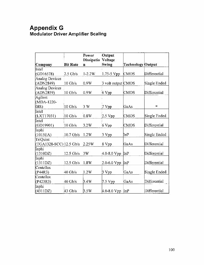
Appendix GModulator Driver Amplifier Scaling
100
Power OutputDissipatio Voltage
Company Bit Rate n Swing Technology OutputIntel(GD16578) 2.5 Gb/s 1-2.2W 1.75-5 Vpp CMOS DifferentialAnalog Devices(ADN2849) 10 Gb/s 0.9W 3 volt output CMOS Single EndedAnalog Devices(ADN2859) 10 Gb/s 0.9W 6 Vpp CMOS DifferentialAgilent(MDA-1220-08S) 10 Gb/s 3 W 7 Vpp GaAs -
Intel(LXT17031) 10 Gb/s 0.8W 2.5 Vpp CMOS Single EndedIntel(GD19901) 10 Gb/s 3.2W 6 Vpp CMOS DifferentialInphi(1015EA) 10.7 Gb/s 1.2W 3 Vpp InP Single EndedTriQuint(TGA1328-SCC) 12.5 Gb/s 2.25W 8 Vpp GaAs DifferentialInphi(13 1ODZ) 12.5 Gb/s 3W 4.0-8.0 Vpp InP DifferentialInphi(1311DZ) 12.5 Gb/s 1.8W 2.0-6.0 Vpp InP DifferentialCentellax(P44R3) 40 Gb/s 1.2W 3 Vpp GaAs Single EndedCentellax(P423R3) 40 Gb/s 3.4W 7.5 Vpp GaAs DifferentialInphi(4311DZ) 43 Gb/s 3.5W 4.0-8.0 Vpp InP Differential

References
[1] S. Schube, "Transponder Savings Lower Network Costs," WDM Solutions 2003, PennWell
Corporation 2003.
[2] King, R.,"Optimizing Data Center Energy Efficiency Results in Cost Savings" TheWHIR.com
June 10, 2002.
http://thewhir.com/features/dce.cfm
[3] "Optical Power Trip" October 5, 2000.
http://www.liqhtreading.com/document.asp?doc id=1975&site=lightreading
[4] http://www.intel.com/design/network/products/optical/phys/lxt16642-53.htm
Retrieved May 2003.
[5] Caruth, D. et. al., "A 40 Gb/s Integrated Differential PIN+TIA with DC Offset Control Using InP
SHBT Technology," Gallium Arsenide Integrated Circuit (GaAs IC) Symposium 2002, 24th Annual
Technical Digest 2002. pp. 59-62.
[6] Cao, J. et al., "OC-192 Transmitter and Receiver in Standard 0.18-um CMOS," IEEE Journal
of Solid-State Circuits, vol. 37, No. 12, December 2002, pp. 1768-1780.
[7] Tanabe, A., et. al., "A 10 Gb/s demultiplexer IC in 0.18 pm CMOS using current mode logic
with tolerance to the threshold voltage fluctuation," Solid-State Circuits Conference, 2000. Digest
of Technical Papers. ISSCC. 2000.
[8] Rabaey, J. et. al., "Digital Integrated Circuits A Design Perspective," Pearson Education, Inc.
Upper Saddle River, New Jersey, 2003.
[9] Feng, J. J. et. al., "A Physics-Based HBT SPICE Model for Large-Signal Applications" IEEE
Transactions on Electron Devices, Vol. 42, No. 1, January 1995.
[10] Walter, K. M., et. al, "A Scalable, Statistical SPICE Gummel-Poon Model for SiGe HBTs"
Solid-State Circuits, IEEE Journal of, Volume: 33 Issue: 9 , Sept. 1998.
[11] Diskus, C. G., et. al., "Approach For Developing A Large Signal Model of A 150 GHz HEMT"
Integrated Nonlinear Microwave and Millimeterwave Circuits, 1994.
101

[12] Cao, Y. et. al., "New Paradigm of Predictive MOSFET and Interconnect Modeling for Early
Circuit Simulations," Custom Integrated Circuits Conference Proceedings of the IEEE May 2000.
[13] Berkeley Predictive Technology Model - Retrieved May 2004.
http://www-device.eecs.berkeley.edu/-ptm/
[14] BSIM3v3.2.2 MOSFET Model Users' Manual. University of California, Berkeley 1999.
[15] Hu, Chenming "BSIM Model for Circuit Design Using Advanced Technologies" Symposium
on VLSI Circuits Digest of Techinical Papers 2001.
[16] Gneiting, Thomas, "BSIM4, BSIM3v3, and BSIMSOI for MOS Modeling" Agilent
Technologies Advanced Modeling Solutions 2001.
http://eesof.tm.agilent.com/pdf/rf cmos Thomas.pdf
[17] "R.F. MOSFET Modeling Accounting for Distributed Substrate and Channel Resistances with
Emphasis on the BSIM3v3 SPICE Model" Electron Devices Meeting, 1997. Technical Digest.,
International , 7-10 Dec. 1997.
[18]Liu, W. "Model Quality Needs to Be Job One," Circuits and Devices Magazine, IEEE,
Volume: 18 Issue: 6, Nov. 2002.
[19] Crain, E., et. aL., "A Numerical Design Approach For High Speed Differential, Resistor-
Loaded, CMOS Amplifiers," Publication pending.
[20] Kehrer, D., et. al., "40-Gb/s 2:1 Multiplexer and 1:2 Demultiplexer in 120-nm Standard
CMOS," IEEE Journal of Solid-State Circuits, Vol 38, No. 11, November 2003.
[21] Goldsmid, H. J., "A Review of the New Thermoelectric Materials," International Conference
on Thermoelectrics 2001.
[22] A. Shakouri, et al. "Thermionic Emission Cooling in Single Barrier Heterostructures," Appl.
Phys. Lett. 74, 88 (1999).
[23] Snyder, J. G., et. al. "Thermoelectric Microdevice Fabricated by a MEMS-like
Electrochemical Process," Nature Letter, Vol 2, August 2003.
102

[24] Davies, Andrew et. Al "Active wavelength control of tunable lasers for use in uncooled WDM
systems" Conference on Lasers and Electro-Optics June 2003.
[25] Xie, L., et. al., "Optimization of Thermal Management Techniques for Low cost
Optoelectronic Packages," IEEE Electronics Packaging Technology Conference 2002.
[26] Melcor Datasheet - Retrieved May 2004
http://www.melcor.com/pdf/melcor telecom coolers.pdf
[27] "Typical Properties of Materials (@ 21 OC)" Melcor, Retrieved May 2004.
http://www.melcor.com/prop21C.html
[28] Rowe, D.M., CRC Thermoelectric Handbook, CRC Press, Fl. 1995
[29] Pearsall, T. P., Properties, Processing and Applications of Indium Phosphide,EMIS Datareviews Series no. 21, Institutions of Electrical Engineers, London 1999.
[30] "Assembly Tips" Melcor. Retrieved May 2004
www.melcor. com/assmtips.htm
[31] Long, A. et al., "Design of an Opto-Electronic Modulator Driver Amplifier for 40 Gb/s Data
Rate System," IEEE Journal of Lightwave Technology, Vol. 20, No. 12, December 2002, pp.
2015-2021.
[32] Mouzannar, W. et al., "40 Gbit/s High Performances GaAs pHEMT High Voltage Modulator
Driver for Long Haul Optical Fiber Communications," Gallium Arsenide Integrated Circuit (GaAs
/C) Symposium 2002, 24th Annual Technical Digest 2002. pp. 163-166.
[33] Agilent Technologies, "Modulator Driver Amplifier for Next Generation 10 Gb/s Long Haul
Communication Systems" Microwave Product Digest, March 2003.
http://www.mpdigest.com/Artices/2003/Mar2003/agilent/DefauIt.htm
[34] Shigematsu, H., "Distributed Amplifier for Fiber-Optic Communication Systems," International
Journal of High Speed Electronics and Systems, World Scientific Publishing Company, Vol. 13,
No. 1.
[35] Sugiyama, M. et. al, Optical Fiber Communication Conference and Exhibit, 2002. 17-22
March 2002 Page(s): FB6-1.
103