Interplay Between Statistical Variability and Reliability in Contemporary pMOSFETs: Measurements...
9
IEEE TRANSACTIONS ON ELECTRON DEVICES, VOL. 61, NO. 9, SEPTEMBER 2014 3265 Interplay Between Statistical Variability and Reliability in Contemporary pMOSFETs: Measurements Versus Simulations Razaidi Hussin, Graduate Student Member, IEEE , Salvatore Maria Amoroso, Member, IEEE, Louis Gerrer, Ben Kaczer, Pieter Weckx, Jacopo Franco, Member, IEEE, Annelies Vanderheyden, Danielle Vanhaeren, Naoto Horiguchi, and Asen Asenov, Fellow, IEEE Abstract— This paper presents an extensive study of the interplay between as-fabricated (time-zero) variability and gate oxide reliability (time-dependent variability) in contemporary pMOSFETs. We compare physical simulation results using the atomistic simulator GARAND with experimental measurements. The TCAD simulations are accurately calibrated to repro- duce the average transistor behavior. When random discrete dopants, line edge roughness, and gate polysilicon granularity are considered, the simulations accurately reproduce time-zero (as-fabricated) statistical variability, as well as time-dependent variability data, represented by threshold voltage shift distrib- utions. The calibrated simulations are then used to predict the reliability behavior at different bias conditions and for different device dimensions. Index Terms— Atomistic doping, random telegraph noise (RTN), reliability, statistical simulations. I. I NTRODUCTION W ITH transistor scaling, the gate oxide integrity has become a major concern for MOSFETs reliabil- ity [1]–[3]. Indeed, it has been demonstrated that the defects in the atomistic structure of the (amorphous or crystalline) gate dielectric material act as charge trapping centers governing the behavior of several reliability related phenomena, such as ran- dom telegraph noise (RTN) [4]–[11], bias temperature insta- bilities (BTI) [12]–[19], and trap assisted tunneling [20], [21]. Manuscript received May 2, 2014; revised June 25, 2014; accepted June 29, 2014. Date of publication July 22, 2014; date of current version August 19, 2014. This work was supported by the European Commission through the FP7 Programme under Project 261868 MORDRED. The review of this paper was arranged by Editor R. M. Todi. R. Hussin is with the Device Modeling Group, University of Glasgow, Glasgow G12 8LT, U.K., and also with the School of Microelectronic Engineering, University Malaysia Perlis, Perlis 01000, Malaysia (e-mail: [email protected]). S. M. Amoroso and L. Gerrer are with the Device Modeling Group, Univer- sity of Glasgow, Glasgow G12 8LT, U.K. (e-mail: [email protected]; [email protected]). B. Kaczer, P. Weckx, J. Franco, A. Vanderheyden, D. Vanhaeren, and N. Horiguchi are with the imec, Leuven 3001, Belgium (e-mail: [email protected]; [email protected]; [email protected]; annelies. [email protected]; [email protected]; naoto.horiguchi@ imec.be). A. Asenov is with the Device Modeling Group, University of Glasgow, Glasgow G12 8LT, U.K.,Gold Standard Simulations Ltd., Glasgow G12 8LT, U.K., and also with the Device Modeling Group, University of Glasgow, Glasgow G12 8LT, U.K. (e-mail: [email protected]). Color versions of one or more of the figures in this paper are available online at http://ieeexplore.ieee.org. Digital Object Identifier 10.1109/TED.2014.2336698 In addition, the stochastic nature of these phenomena com- plicates the transistor lifetime projections and the design rules [22], [23]. In the last few years, a large number of experimental and simulation studies have been published aiming to improve the understanding of reliability behavior of nanoscale MOSFETs [4]–[24]. In this paper, we present comprehensive statistical analysis of variability and reliability in nanometer scale p-channel MOSFETs comparing measurements with atomistic simulation results. We demonstrate that the thorough quantitative under- standing of these phenomena necessitates the combination of: 1) accurate structural device characterization [transmis- sion electron microscopy (TEM) imaging, doping profiling]; 2) extensive electrical measurements; and 3) statistical atom- istic 3-D TCAD simulations. In specific, the calibrated simulations are shown to excellently reproduce time-zero (as-fabricated) data, as well as time-dependent variability data, represented by threshold voltage shifts distributions. The calibrated simulations are then used to predict the reli- ability behavior at different bias conditions and for different device dimensions. This paper is organized as follows. In Section II, we describe the accurate experimental and computational approaches adopted to study the variability and reliability in nanoscale transistors. Section III describes the experimental and sim- ulation results, highlighting the interplay between statistical variability and reliability dictated by the discrete nature of dopants and traps. The reliability projections for scaled transistors are presented in Section IV considering several electrical stressing conditions. Finally, conclusions are drawn in Section V. II. METHODOLOGY In this paper, both experimental and simulation results are presented. A planar 70-nm technology generation pMOSFET transistors featuring a 2.2-nm SiON gate oxide has been fabricated by IMEC. The large oxide thickness has been chosen to increase the impact of sources of variability, such as discrete dopants [25] and trapped charges in the oxide. For advanced scaled technology generation, a reduction of oxide thickness will result in a lowering of variability, while the reduction of channel area will increase the performance 0018-9383 © 2014 IEEE. Personal use is permitted, but republication/redistribution requires IEEE permission. See http://www.ieee.org/publications_standards/publications/rights/index.html for more information.
-
Upload
independent -
Category
Documents
-
view
0 -
download
0
Transcript of Interplay Between Statistical Variability and Reliability in Contemporary pMOSFETs: Measurements...

IEEE TRANSACTIONS ON ELECTRON DEVICES, VOL. 61, NO. 9, SEPTEMBER 2014 3265
Interplay Between Statistical Variability andReliability in Contemporary pMOSFETs:
Measurements Versus SimulationsRazaidi Hussin, Graduate Student Member, IEEE, Salvatore Maria Amoroso, Member, IEEE, Louis Gerrer,
Ben Kaczer, Pieter Weckx, Jacopo Franco, Member, IEEE, Annelies Vanderheyden,Danielle Vanhaeren, Naoto Horiguchi, and Asen Asenov, Fellow, IEEE
Abstract— This paper presents an extensive study of theinterplay between as-fabricated (time-zero) variability and gateoxide reliability (time-dependent variability) in contemporarypMOSFETs. We compare physical simulation results using theatomistic simulator GARAND with experimental measurements.The TCAD simulations are accurately calibrated to repro-duce the average transistor behavior. When random discretedopants, line edge roughness, and gate polysilicon granularityare considered, the simulations accurately reproduce time-zero(as-fabricated) statistical variability, as well as time-dependentvariability data, represented by threshold voltage shift distrib-utions. The calibrated simulations are then used to predict thereliability behavior at different bias conditions and for differentdevice dimensions.
Index Terms— Atomistic doping, random telegraph noise(RTN), reliability, statistical simulations.
I. INTRODUCTION
W ITH transistor scaling, the gate oxide integrityhas become a major concern for MOSFETs reliabil-
ity [1]–[3]. Indeed, it has been demonstrated that the defectsin the atomistic structure of the (amorphous or crystalline) gatedielectric material act as charge trapping centers governing thebehavior of several reliability related phenomena, such as ran-dom telegraph noise (RTN) [4]–[11], bias temperature insta-bilities (BTI) [12]–[19], and trap assisted tunneling [20], [21].
Manuscript received May 2, 2014; revised June 25, 2014; accepted June 29,2014. Date of publication July 22, 2014; date of current version August 19,2014. This work was supported by the European Commission through theFP7 Programme under Project 261868 MORDRED. The review of this paperwas arranged by Editor R. M. Todi.
R. Hussin is with the Device Modeling Group, University of Glasgow,Glasgow G12 8LT, U.K., and also with the School of MicroelectronicEngineering, University Malaysia Perlis, Perlis 01000, Malaysia (e-mail:[email protected]).
S. M. Amoroso and L. Gerrer are with the Device Modeling Group, Univer-sity of Glasgow, Glasgow G12 8LT, U.K. (e-mail: [email protected];[email protected]).
B. Kaczer, P. Weckx, J. Franco, A. Vanderheyden, D. Vanhaeren,and N. Horiguchi are with the imec, Leuven 3001, Belgium(e-mail: [email protected]; [email protected]; [email protected]; [email protected]; [email protected]; [email protected]).
A. Asenov is with the Device Modeling Group, University of Glasgow,Glasgow G12 8LT, U.K., Gold Standard Simulations Ltd., Glasgow G12 8LT,U.K., and also with the Device Modeling Group, University of Glasgow,Glasgow G12 8LT, U.K. (e-mail: [email protected]).
Color versions of one or more of the figures in this paper are availableonline at http://ieeexplore.ieee.org.
Digital Object Identifier 10.1109/TED.2014.2336698
In addition, the stochastic nature of these phenomena com-plicates the transistor lifetime projections and the designrules [22], [23]. In the last few years, a large number ofexperimental and simulation studies have been publishedaiming to improve the understanding of reliability behaviorof nanoscale MOSFETs [4]–[24].
In this paper, we present comprehensive statistical analysisof variability and reliability in nanometer scale p-channelMOSFETs comparing measurements with atomistic simulationresults. We demonstrate that the thorough quantitative under-standing of these phenomena necessitates the combinationof: 1) accurate structural device characterization [transmis-sion electron microscopy (TEM) imaging, doping profiling];2) extensive electrical measurements; and 3) statistical atom-istic 3-D TCAD simulations. In specific, the calibratedsimulations are shown to excellently reproduce time-zero(as-fabricated) data, as well as time-dependent variabilitydata, represented by threshold voltage shifts distributions.The calibrated simulations are then used to predict the reli-ability behavior at different bias conditions and for differentdevice dimensions.
This paper is organized as follows. In Section II, we describethe accurate experimental and computational approachesadopted to study the variability and reliability in nanoscaletransistors. Section III describes the experimental and sim-ulation results, highlighting the interplay between statisticalvariability and reliability dictated by the discrete natureof dopants and traps. The reliability projections for scaledtransistors are presented in Section IV considering severalelectrical stressing conditions. Finally, conclusions are drawnin Section V.
II. METHODOLOGY
In this paper, both experimental and simulation results arepresented. A planar 70-nm technology generation pMOSFETtransistors featuring a 2.2-nm SiON gate oxide has beenfabricated by IMEC. The large oxide thickness has beenchosen to increase the impact of sources of variability, suchas discrete dopants [25] and trapped charges in the oxide.For advanced scaled technology generation, a reduction ofoxide thickness will result in a lowering of variability, whilethe reduction of channel area will increase the performance
0018-9383 © 2014 IEEE. Personal use is permitted, but republication/redistribution requires IEEE permission.See http://www.ieee.org/publications_standards/publications/rights/index.html for more information.

3266 IEEE TRANSACTIONS ON ELECTRON DEVICES, VOL. 61, NO. 9, SEPTEMBER 2014
Fig. 1. Experimental BTI relaxation traces measured on several 70-nmdevices. Device-to-device statistical variability and discreteness of thresholdvoltage steps due to individual de/trapping events are clearly manifested. Samemechanism is also responsible for the distinct RTN visible in some traces.
statistical dispersion [5]–[7]. The device has been charac-terized electrically at time-zero and after NBTI stress atlow-drain biases (VD = 0.1 V). Fig. 1 shows the BTIrelaxation traces experimentally measured on several devices.It clearly manifests the statistical variability from device todevice and the discreteness of threshold voltage steps �VT dueto individual and trap charging and discharging events [13].Since our previous experimental [26] and simulationstudies [27] have demonstrated that the impact of each singletrapped charge is typically not affected by the presence ofother traps in the same device, we focus here on the studyof the statistical distribution of single trapped charge-inducedthreshold voltage shifts.
The accurate structural characterization of the fabricatedand measured pMOSFETs is based on TEM imaging, whilethe doping profile has been estimated by means of scanningspreading resistance microscopy (SSRM) [28].
On the simulation side, both process and device simulationshave been carried out by means of the gold standard simulationprocess simulator ANADOPE [29], [30] and device simulatorGARAND [31].
Fig. 2 shows the flow chart of the characterization andsimulation methodology adopted in this paper. There aresix stages consisting of: 1) defining the device geometrybased on TEM images (Fig. 3); 2) fitting the device dopingprofile with the help of SSR images (Fig. 4); 3) matchingsimulated and experimental device characteristics and extract-ing threshold voltage (VT ) roll-off behavior; 4) matchingsimulated and experimental device response to body bias;5) matching simulated and experimental VT variability; and6) matching simulated and experimental �VT variability-induced by trapped charges. The simulation of VT and �VT
is carried on using statistical ensembles of 1000 atomistictransistors. It is worth pointing out that identifying the correctdoping profile, in particular the HALO pockets doses andpositions, is of vital importance for a reliable simulation ofthe transistor electrical behavior and its variability. Therefore,significant efforts have been invested in calibrating the device
Fig. 2. Process and device simulation procedure adopted in this paper.
Fig. 3. TEM image of the 70-nm pMOSFET transistor.
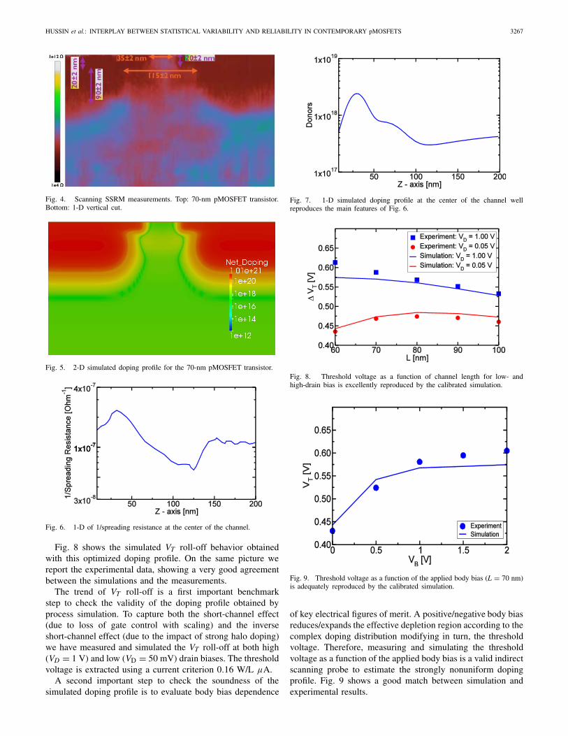
doping profile not only using the electrical transcharacteris-tics as benchmark test, but also the SSRM measurements.Figs. 4–7 show the very good agreement achieved betweenprocess simulation results and SSRM measurements.
Fig. 6 shows the 1-D plot of the inverse of spread resistanceat the center of the channel. This is proportional to the dopingvalue, but a proper conversion factor would require a carefulexperimental calibration procedure, as reported in [32].
HUSSIN et al.: INTERPLAY BETWEEN STATISTICAL VARIABILITY AND RELIABILITY IN CONTEMPORARY pMOSFETS 3267
Fig. 4. Scanning SSRM measurements. Top: 70-nm pMOSFET transistor.Bottom: 1-D vertical cut.
Fig. 5. 2-D simulated doping profile for the 70-nm pMOSFET transistor.
Fig. 6. 1-D of 1/spreading resistance at the center of the channel.
Fig. 8 shows the simulated VT roll-off behavior obtainedwith this optimized doping profile. On the same picture wereport the experimental data, showing a very good agreementbetween the simulations and the measurements.
The trend of VT roll-off is a first important benchmarkstep to check the validity of the doping profile obtained byprocess simulation. To capture both the short-channel effect(due to loss of gate control with scaling) and the inverseshort-channel effect (due to the impact of strong halo doping)we have measured and simulated the VT roll-off at both high(VD = 1 V) and low (VD = 50 mV) drain biases. The thresholdvoltage is extracted using a current criterion 0.16 W/L μA.
A second important step to check the soundness of thesimulated doping profile is to evaluate body bias dependence
Fig. 7. 1-D simulated doping profile at the center of the channel wellreproduces the main features of Fig. 6.
Fig. 8. Threshold voltage as a function of channel length for low- andhigh-drain bias is excellently reproduced by the calibrated simulation.
Fig. 9. Threshold voltage as a function of the applied body bias (L = 70 nm)is adequately reproduced by the calibrated simulation.
of key electrical figures of merit. A positive/negative body biasreduces/expands the effective depletion region according to thecomplex doping distribution modifying in turn, the thresholdvoltage. Therefore, measuring and simulating the thresholdvoltage as a function of the applied body bias is a valid indirectscanning probe to estimate the strongly nonuniform dopingprofile. Fig. 9 shows a good match between simulation andexperimental results.

3268 IEEE TRANSACTIONS ON ELECTRON DEVICES, VOL. 61, NO. 9, SEPTEMBER 2014
Fig. 10. Normal distribution of threshold voltage for simulation andexperimental result.
Fig. 11. Impact of several variability sources on threshold voltage statisticaldispersion.
A third final step to close this simulation loop is to use theextracted doping profile to evaluate the variability of thresholdvoltage and charge-trapping-induced threshold voltage shift.The statistical dispersion of these two important statisticalfigures of merit is strongly ruled by the channel doping [33].Therefore, a doping profile that provides simulations resultsreproducing not only the transistor average electrical behavior,but also its statistical dispersion from device to device canbe highly trusted as very good representative of the realdevice doping. We will address the variability and reliabilitysimulations and measurements in Section III.
III. INTERPLAY OF VARIABILITY AND RELIABILITY
Fig. 10 compares the time-zero VT distribution obtainedby means of 3-D TCAD atomistic simulation of 1000statistical instances of the nominal 70-nm transistor with theexperimental data measured on an ensemble of 100 transistorson the same wafer. Random discrete dopants (RDD) accountsfor the major part of variability and it does not involve fittingparameters, line edge roughness (LER), and gate polysilicongranularity (PSG) parameters are the same used in previouspublications [34]–[40]. The relative contributions of the single
Fig. 12. Complementary cumulative distribution of threshold voltage shiftsdue to single charge traps extracted from measurements (see Fig. 1) isexcellently matched by simulations.
Fig. 13. Electron concentration at threshold voltage conditions for the caseof empty trap (back) and filled trap (front). Main percolative conduction pathblocked by the trap is shown in zoomed-in view.
variability sources are shown in Fig. 11, where we report alsothe standard deviations of each distribution. The simulationresults featuring all variability sources show very good matchwith the experiments, corroborating the correctness of thesimulated device doping profile.
Once the VT variability has been assessed, we evaluatedthe single trapped charge-induced �VT variability. Simulationsfeature a discrete trapped hole for each device randomlyplaced at the channel interface according to a uniform dis-tribution. Experiments confirm that charge trapping has notpreferential location over the channel area under BTI stressconditions [41]. This may not hold for hot carrier injectionstress conditions, where the oxide region close to drain can beaffected majorly by charge trapping.
Fig. 12 shows the �VT complementary cumulative dis-tribution for 100 simulated devices, compared with resultsof time-dependent defect spectroscopy measurements [42].These measurements give the distribution of �VT due toindividual trapped holes in the gate oxide. The good matchobtained between simulations and experiments is further indi-cation of the correctness of the simulated device dopingobtained through the abovementioned methodology. Note thatnot only the average experimental value (2.33 mV), but also

HUSSIN et al.: INTERPLAY BETWEEN STATISTICAL VARIABILITY AND RELIABILITY IN CONTEMPORARY pMOSFETS 3269
Fig. 14. Corresponding VT and �VT pairs are observed to be uncorrelated.
Fig. 15. Simulated distributions of threshold voltage at different drainvoltages.
the dispersion (2.55 mV) of the �VT distribution are wellreproduced by simulation. 3-D atomistic simulation can reachthis high level of accuracy because they physically and accu-rately capture interplay between reliability and variability innanoscale MOSFETs, which is related to the percolative natureof the source-to-drain conduction arising from the potentialvariations associated with RDD, LER, and PSG. The devicereliability is ruled by the trap formation and the subsequentcharge-trapping phenomena in the gate oxide. It is clear that acharge trapped over a percolative conduction path will have alarge impact on the device VT , while the impact will be muchless if the charge is trapped over a region with low-currentdensity.
This is clearly exemplified in Fig. 13, where the3-D simulated carrier density is shown for a random instanceof the 70-nm pMOSFET transistor, highlighting the percola-tive nature of conduction between source and drain and theimpact of a trap located over the preferential conduction path.In addition, Fig. 14 shows that the stochastic VT and �VT
values are completely uncorrelated. This is confirmed by thesimulation results reported here, but also by experimentalmeasurements as in [43].
IV. VARIABILITY AND RELIABILITY PROJECTIONS
Given the confirmed accuracy of both the time-zero andthe time-dependent statistical simulations, we can confidently
Fig. 16. Simulated complementary cumulative distributions of thresholdvoltage shifts due to a single trapped charge at different drain voltages.
Fig. 17. Simulated single-trap �VT as a function of the trap position alongthe channel length, for several applied drain biases.
predict the stochastic behavior at different biasing condi-tions and for different device dimensions, bearing in mindthat the simulations are faster and easier compared withlarge scale statistical measurements. First of all, we extendedthe simulations range to evaluate the impact of drain biasvoltage on variability and reliability of the 70-nm technology.Fig. 15 shows the VT distribution at different drain biases(VD = 0.1 V, VD = VT , and VD = 1.0 V). It is clear thatan increase in the applied drain bias results in a decrease ofthe average VT due to DIBL effect. On the other hand, the VT
dispersion increases with VD, mainly because of the reductionof the effective channel length.
Fig. 16 shows the complementary cumulative distribution of�VT for each drain bias setup. As the drain bias is increased,

3270 IEEE TRANSACTIONS ON ELECTRON DEVICES, VOL. 61, NO. 9, SEPTEMBER 2014
Fig. 18. Simulated distributions of initial threshold voltage at different biasvoltages.
Fig. 19. Simulated complementary cumulative distributions of thresholdvoltage due to a single trapped charge at different bias voltages.
both the average and the dispersion of �VT increase. This isagain due to reduction of effective channel length after thepinchoff is established.
This effect is confirmed in Fig. 17 where we plot the �VT
due to each single trapped charge as a function of the trapposition along the channel length for different drain biases.Note that, at low-drain biases, the most effective traps arelocated in the middle of the channel with a nearly symmetricdistribution between source and drain. In contrast to that, athigher drain biases, the electrostatic impact of traps located bythe drain side is reduced and the peak of the �VT distributionis moved toward the source.
Next, we investigated the transistor variability and reliabilitysensitivity to body bias variations. We expect from Fig. 8, anincrease of the average VT with VB. This is confirmed by theVT cumulative distributions shown in Fig. 18, and it is a directeffect of the depletion region width modulation. For the samereason, the VT dispersion also increases with increasing VB.Fig. 19 shows the cumulative distribution of �VT for severalbody biases. The �VT dispersion increases with VB [44], whilethe average is barely affected.
Fig. 20 summarizes the VT and �VT dispersion trends withrespect to VD, VB, and transistor physical channel lengths.Note that the nonlinearity in the Pelgrom plot is due to theinfluence of halo doping implantations [45]. The relationship
Fig. 20. VT and �VT dispersion as a function of (a) VD, (b) VB, and (c) L.
Fig. 21. σ�VT as a function of σ VT , for several VD, VB, and L values.
between σ VT and σ�VT in all three cases is highlighted inFig. 21, where we report a nearly universal trend that departsfrom linearity only for very large body biases.
The results stress the dramatic increase of the transistorperformance dispersion that is forcing the departure fromplanar bulk technology toward multigate solutions with CMOStransistor scaling [46]–[49].
V. CONCLUSION
This paper has presented systematic methodology for aquantitative assessment of variability and reliability in scalepMOS transistor using 3-D TCAD simulation combinedwith physical and electrical characterization. The calibrated

HUSSIN et al.: INTERPLAY BETWEEN STATISTICAL VARIABILITY AND RELIABILITY IN CONTEMPORARY pMOSFETS 3271
simulations are shown to excellently reproduce time-zerovariability, as well as time-dependent variability-induced bydynamic charge-trapping. The calibrated simulation tools havebeen employed to quantitatively assess the interplay betweenvariability and reliability for different bias conditions and fordifferent device dimensions.
ACKNOWLEDGMENT
The authors would like to thank Dr. P. Eyben andDr. A. Nazir for their useful discussion.
REFERENCES
[1] B. Kaczer et al., “The relevance of deeply-scaled FET thresholdvoltage shifts for operation life times,” in Proc. IEEE Int. Rel. Phys.Symp. (IRPS), Apr. 2012, pp. 5A.2.1–5A.2.6.
[2] T. Nagumo, K. Takeuchi, T. Hase, and Y. Hayasi, “Statistical character-ization of trap position, energy, amplitude and time constants by RTNmeasurement of multiple individual traps,” in Proc. IEEE Int. ElectronDevices Meeting (IEDM), Dec. 2010, pp. 28.3.1–28.3.4.
[3] S. V. Kumar, C. H. Kim, and S. S. Sapatnekar, “Impact of NBTI onSRAM read stability and design for reliability,” in Proc. 7th Int. Symp.Qual. Electron. Design (ISQED), Mar. 2006, p. 218.
[4] M. Kirton and M. Uren, “Noise in solid-state microstructures: A newperspective on individual defects, interface states and low-frequency (1/f)noise,” Adv. Phys., vol. 38, no. 4, pp. 367–468, 1989.
[5] A. Asenov, R. Balasubramaniam, A. R. Brown, and J. H. Davies, “RTSamplitudes in decananometer MOSFETs: 3-D simulation study,” IEEETrans. Electron Devices, vol. 50, no. 3, pp. 334–336, Mar. 2003.
[6] J. P. Campbell et al., “Random telegraph noise in highly scalednMOSFETs,” in Proc. IEEE Int. Rel. Phys. Symp. (IRPS), Apr. 2009,pp. 382–388.
[7] A. Ghetti, C. M. Compagnoni, A. S. Spinelli, and A. Visconti, “Compre-hensive analysis of random telegraph noise instability and its scaling indeca-nanometer flash memories,” IEEE Trans. Electron Devices, vol. 56,no. 8, pp. 1746–1752, Aug. 2009.
[8] K. Sonoda, K. Ishikawa, T. Eimori, and O. Tsuchiya, “Discrete dopanteffects on statistical variation of random telegraph signal magnitude,”IEEE Trans. Electron Devices, vol. 54, no. 8, pp. 1918–1925, Aug. 2007.
[9] K. Takeuchi, T. Nagumo, S. Yokogawa, K. Imai, and Y. Hayashi,“Single-charge-based modelling of transistor characteristics fluctuationsbased on statistical measurement of RTN amplitude,” in Proc. Symp.Very Large Scale Integr. Technol. (VLSI), Jun. 2009, pp. 54–55.
[10] S. M. Amoroso, F. Adamu-Lema, S. Markov, L. Gerrer, and A. Asenov,“3D dynamic RTN simulation of a 25 nm MOSFET: The importance ofvariability in reliability evaluation of decananometer devices,” in Proc.15th Int. Conf. Comput. Electron. (IWCE), May 2012, pp. 1–4.
[11] F. Adamu-Lema et al., “Accuracy and issues of the spectroscopicanalysis of RTN traps in nanoscale MOSFETs,” IEEE Trans. ElectronDevices, vol. 60, no. 2, pp. 833–839, Feb. 2013.
[12] M. A. Alam and S. Mohapatra, “A comprehensive model of PMOSNBTI degradation,” J. Microelectron. Rel., vol. 45, no. 1, pp. 71–81,Jan. 2005.
[13] B. Kaczer et al., “Origin of NBTI variability in deeply scaled pFETs,”in Proc. IEEE Int. Rel. Phys. Symp. (IRPS), May 2010, pp. 26–32.
[14] H. Reisinger, T. Grasser, W. Gustin, and C. Schlunder, “The statisti-cal analysis of individual defects constituting NBTI and its implica-tions for modeling DC-and AC-stress,” in Proc. IEEE Int. Rel. Phys.Symp. (IRPS), May 2010, pp. 7–15.
[15] T. Grasser et al., “The paradigm shift in understanding the bias tempera-ture instability: From reaction diffusion to switching oxide traps,” IEEETrans. Electron Devices, vol. 58, no. 11, pp. 3652–3666, Nov. 2011.
[16] J. Franco et al., “Impact of single charged gate oxide defects on theperformance and scaling of nanoscaled FETs,” in Proc. IEEE Int. Rel.Phys. Symp. (IRPS), Apr. 2012, pp. 1–6.
[17] B. Cheng, A. R. Brown, and A. Asenov, “Impact of NBTI/PBTI onSRAM stability degradation,” IEEE Electron Device Lett., vol. 32, no. 6,pp. 740–742, Jun. 2011.
[18] G. D. Panagopoulos and K. Roy, “A three-dimensional physical modelfor Vth variations considering the combined effect of NBTI and RDF,”IEEE Trans. Electron Device, vol. 58, no. 8, pp. 2337–2346, Aug. 2011.
[19] M. Toledano-Luque et al., “From mean values to distributions of BTIlifetime of deeply scaled FETs through atomistic understanding of thedegradation,” in Proc. Symp. Very Large Scale Integr. Technol. (VLSIT),Jun. 2011, pp. 152–153.
[20] M. Toledano-Luque et al., “Correlation of single trapping and detrappingeffects in drain and gate currents of nanoscaled nFETs and pFETs,” inProc. IEEE Int. Rel. Phys. Symp. (IRPS), Apr. 2012, pp. XT.5.1–XT.5.6.
[21] M. Mikolasek et al., “A new model of trap assisted band-to-bandtunnelling,” in Proc. 8th Int. Conf. Adv. Semicond. Device Microsyst.,Oct. 2010, pp. 195–198.
[22] L. Gerrer et al., “Interplay between statistical reliability and variability:A comprehensive transistor-to-circuit simulation technology,” in Proc.IEEE Int. Rel. Phys. Symp. (IRPS), Apr. 2013, pp. 3A.2.1–3A.2.5.
[23] M. A. Alam, K. Roy, and C. Augustine, “Reliability-and process-variation aware design of integrated circuits—A broader perspec-tive,” in Proc. IEEE Int. Rel. Phys. Symp. (IRPS), Apr. 2011,pp. 4A.1.1–4A.1.11.
[24] S. M. Amoroso, L. Gerrer, S. Markov, F. Adamu-Lema, and A. Asenov,“RTN and BTI in nanoscale MOSFETs: A comprehensive statisticalsimulation study,” Solid-State Electron., vol. 84, pp. 120–126, Jun. 2013.
[25] K. J. Kuhn et al., “Process technology variation,” IEEE Trans. ElectronDevices, vol. 58, no. 8, pp. 2197–2208, Aug. 2011.
[26] B. Kaczer, P. J. Roussel, T. Grasser, and G. Groeseneken, “Statistics ofmultiple trapped charges in the gate oxide of deeply scaled MOSFETdevices—Application to NBTI,” IEEE Electron Device Lett., vol. 31,no. 5, pp. 411–413, May 2010.
[27] S. Markov, S. M. Amoroso, L. Gerrer, F. Adamu-Lema, and A. Asenov,“Statistical interactions of multiple oxide traps under BTI stress ofnanoscale MOSFETs,” IEEE Electron Device Lett., vol. 34, no. 5,pp. 686–688, May 2013.
[28] P. De Wolf, R. Stephenson, T. Trenkler, T. Clarysse, T. Hantschel,and W. Vandervorst, “Status and review of two-dimensional carrier anddopant profiling using scanning probe microscopy,” J. Vac. Sci. Technol.B, vol. 18, no. 1, pp. 361–368, 2000.
[29] L. Wang, A. R. Brown, B. Cheng, and A. Asenov, “Simulation of 3DFinFET doping profiles by ion implantation,” in Proc. 9th Int. Conf. IonImplantation Technol., vol. 1496. 2012, pp. 217-220.
[30] L. Wang, A. Brown, B. Cheng, and A. Asenov, “Analytical modelsfor three-dimensional ion implantation profiles in FinFETs,” IEEETrans. Comput.-Aided Design Integr. Circuits Syst., vol. 32, no. 12,pp. 2004–2008, Dec. 2013.
[31] (2013). GARAND v.2.0. [Online]. Available:http://www.GoldStandardSimulations.com
[32] W. Treberspurg, T. Bergauer, M. Dragicevic, J. Hrubec, M. Krammer,and M. Valentan, “Measuring doping profiles of silicon detectors with acustom-designed probe station,” J. Instrum., vol. 7, p. 11009, Nov. 2012.
[33] G. Iannaccone and E. Amirante, “Quantum and semiclassical modelingof the threshold voltage dispersion due to random dopants in deepsubmicron MOSFETs,” in Proc. 2nd IEEE Conf. Nanotechnol., 2002,pp. 197–200.
[34] A. Asenov, A. R. Brown, J. H. Davies, S. Kaya, and G. Slavcheva,“Simulation of intrinsic parameter fluctuations in decananometer andnanometer-scale MOSFETs,” IEEE Trans. Electron Devices, vol. 50,no. 9, pp. 1837–1852, Sep. 2003.
[35] A. R. Brown, S. Kaya, A. Asenov, J. H. Davies, and T. Linton, “Statis-tical 3D simulation of line edge roughness in decanano MOSFETs,” inProc. Silicon Nanoelectron. Workshop, Kyoto, Japan, Jun. 2001.
[36] G. Roy, A. Ghetti, A. Benvenuti, A. Erlebach, and A. Asenov, “Compar-ative simulation study of the different sources of statistical variability incontemporary floating-gate nonvolatile memory,” IEEE Trans. ElectronDevices, vol. 58, no. 12, pp. 4155–4163, Dec. 2011.
[37] S. Kaya, A. R. Brown, A. Asenov, D. Magot, and T. Linton, “Analysisof statistical fluctuations due to line edge roughness in sub-0.1 μmMOSFETs,” in Proc. Simul. Semicond. Processes Devices (SISPAD),2001, pp. 78–81.
[38] D. Reid, C. Millar, G. Roy, S. Roy, and A. Asenov, “UnderstandingLER-induced statistical variability: A 35,000 sample 3D simulationstudy,” in Proc. Eur. Solid-State Device Res. Conf. (ESSDERC),Sep. 2009, pp. 423–426.
[39] D. Reid, C. Millar, S. Roy, and A. Asenov, “Understanding LER-inducedMOSFET VT variability—Part I: Three-dimensional simulation of largestatistical samples,” IEEE Trans. Electron Devices, vol. 57, no. 11,pp. 2801–2807, Nov. 2010.
[40] S. M. Amoroso, L. Gerrer, F. Adamu-Lema, S. Markov, and A. Asenov,“Impact of statistical variability and 3D electrostatics on post-cyclinganomalous charge loss in nanoscale flash memories,” in Proc. IEEE Int.Rel. Phys. Symp. (IRPS), Apr. 2013, pp. 3B.4.1–3B.4.6.

3272 IEEE TRANSACTIONS ON ELECTRON DEVICES, VOL. 61, NO. 9, SEPTEMBER 2014
[41] T. Grasser, K. Rott, H. Reisinger, M. Waltl, J. Franco, and B. Kaczer,“A unified perspective of RTN and BTI,” in Proc. IEEE Int. Rel. Phys.Symp. (IRPS), Jun. 2014, pp. 4A.5.1–4A.5.7.
[42] T. Grasser, H. Reisinger, P.-J. Wagner, F. Schanovsky, W. Goes, andB. Kaczer, “The time dependent defect spectroscopy (TDDS) for thecharacterization of the bias temperature instability,” in Proc. IEEE Int.Rel. Phys. Symp. (IRPS), May 2010, pp. 2A.2.1–2A.2.10.
[43] M. Toledano-Luque et al., “Degradation of time dependent variabilitydue to interface state generation,” in Proc. Symp. Very Large Scale Integr.Technol. (VLSIT), Jun. 2013, pp. T190–T191.
[44] J. Franco et al., “Reduction of the BTI time-dependent variability innanoscaled MOSFETs by body bias,” in Proc. IEEE Int. Rel. Phys.Symp. (IRPS), Apr. 2013, pp. 2D.3.1–2D.3.6.
[45] T. B. Hook, J. B. Johnson, J.-P. Han, A. Pond, T. Shimizu, andG. Tsutsui, “Channel length and threshold voltage dependence of tran-sistor mismatch in a 32-nm HKMG technology,” IEEE Trans. ElectronDevices, vol. 57, no. 10, pp. 2440–2447, Oct. 2010.
[46] D. A. Antoniadis and A. Khakifirooz, “MOSFET performance scaling:Limitations and future options,” in Proc. IEEE Int. Electron DevicesMeeting (IEDM), Dec. 2008, pp. 1–4.
[47] H. Fukutome et al., “Comprehensive extensibility of 20 nmlow power/high performance technology platform featuring scalablehigh-k/metal gate planar transistors with reduced design corner,” in Proc.IEEE IEDM Tech. Dig., Dec. 2012, pp. 3.5.1–3.5.4.
[48] M. Bohr, “The evolution of scaling from the homogeneous erato the heterogeneous era,” in Proc. IEEE Int. Electron DevicesMeeting (IEDM), Dec. 2011, pp. 1.1.1–1.1.4.
[49] C. Auth et al., “A 22 nm high performance and low-power CMOS tech-nology featuring fully-depleted tri-gate transistors, self-aligned contactsand high density MIM capacitors,” in Proc. Symp. Very Large ScaleIntegr. Technol. (VLSIT), Jun. 2012, pp. 131–132.
Razaidi Hussin (GSM’13) received the M.Sc.degree in microelectronic engineering from Univer-sity Malaysia Perlis, Arau, Malaysia. He is currentlypursuing the Ph.D. degree with the University ofGlasgow, Glasgow, U.K.
He is involved in oxide reliability issues in com-plementary metal–oxide–semiconductor nanoscaledevices with the University of Glasgow.
Salvatore Maria Amoroso (S’10–M’12) receivedthe Ph.D. degree in electronics engineering fromPolitecnico di Milano, Milan, Italy, in 2012.
He has been an Associate Researcher with theDepartment of Electronics, University of Glasgow,Glasgow, U.K., since 2012.
Louis Gerrer was born in Amiens, France, in 1983.He received the M.Sc. (Ing.) degree in Strasbourg,and the Ph.D. degree from Minatec, Grenoble,France.
He is currently developing a reliability simulatorwith the Device Modelling Group, University ofGlasgow, Glasgow, U.K.
Ben Kaczer received the Ph.D. degree in physicsfrom Ohio State University, Columbus, OH, USA,in 1998.
He joined the Reliability Group, InteruniversityMicroelectronics Center, Leuven, Belgium, in 1998,where he is a Principal Scientist of advanced elec-trical characterization and reliability.
Pieter Weckx is currently pursuing the Ph.D. degreewith the Reliability Group, Interuniversity Micro-electronics Center, Leuven, Belgium, and KatholiekeUniversiteit Leuven, Leuven, with a focus on mod-eling and simulation of time-dependent variabilityproblems in nanoscaled electronic devices.
Jacopo Franco (S’10–M’13) received the Ph.D.degree from Katholieke Universiteit Leuven, Leu-ven, Belgium, in 2013.
He is currently with the CMOS Device Reliabil-ity Group, Interuniversity Microelectronics Center,Leuven, where he is involved in interface stabilityand reliability of Ge and SiGe transistors for futureCMOS applications.
Annelies Vanderheyden received the B.Sc.C.degree from Katholieke Universiteit Leuven, Leu-ven, Belgium.
She joined the Materials and Components Analy-sis Group with the Interuniversity MicroelectronicsCenter, Leuven, in 2010, where she is involved in theelectrical characterization technique and scanningspreading resistance microscopy.
Danielle Vanhaeren received the B.Sc.C degreefrom Katholieke Universiteit Leuven, Leuven, Bel-gium.
She joined the Materials and Components Analy-sis Group with the Interuniversity MicroelectronicsCenter, Leuven, in 1985. She has been a MetrologyEngineer on several techniques such as SRP, E-CV,Profilometry, and AFM. She is currently involved inscanning spreading resistance measurements.
HUSSIN et al.: INTERPLAY BETWEEN STATISTICAL VARIABILITY AND RELIABILITY IN CONTEMPORARY pMOSFETS 3273
Naoto Horiguchi received the M.S. degree inapplied physics from Tokyo University, Tokyo,Japan, in 1992.
He is currently a Logic Program Manager withthe Interuniversity Microelectronics Center, Leuven,Belgium, where he is leading a process integrationteam for 16–7 nanometer CMOS technology devel-opment.
Asen Asenov (M’96–SM’05–F’11) received thePh.D. degree in solid-state physics from the Bulgar-ian Academy of Science, Sofia, Bulgaria, in 1989.
He is currently a CEO with the Gold StandardSimulations Ltd., Glasgow, U.K., and a James WattProfessor of Electrical Engineering with the Univer-sity of Glasgow, Glasgow.