
Advancing Regenerative Cellular Therapies in Non-Scarring ...

408 IEEE TRANSACTIONS ON INDUSTRIAL ELECTRONICS, VOL. 56, NO. 2, FEBRUARY 2009
Input Current Harmonics in a Regenerative MulticellInverter With Single-Phase PWM Rectifiers
Pablo Lezana, Member, IEEE, José Rodríguez, Senior Member, IEEE,Marcelo A. Pérez, Member, IEEE, and José Espinoza, Member, IEEE
Abstract—Harmonics are a very important issue in the designand operation of medium-voltage inverter drives, due to restric-tions imposed by regulations. This paper studies the harmonicsgenerated by a three-phase multicell cascade inverter, with single-phase pulsewidth modulation rectifiers at the input side of eachcell; thus, the entire topology is able to regenerate power tothe net. This paper identifies accurately the harmonic generationprocess in the dc-link voltage, the input current of each cell, and,therefore, at the input side of the inverter. Moreover, this paperproposes a method to reduce and, in some cases, eliminate theinput current harmonics, reaching a very high input power factorfor any operation condition. Simulation and experimental resultsare provided to validate the theoretical analysis.
Index Terms—Harmonic analysis, power electronics, voltagecontrol.
NOMENCLATURE
Vdc DC-link voltage reference.l Maximum number of levels.m Number of cells.Tx, Tx Inverter complementary switches.Sx, Sx Rectifier complementary switches.vdc Total dc-link voltage.vdcx Voltage on each dc-link capacitor.Is Cell input current.vs Cell input voltage.Zs Source impedance.ωs Source frequency.ps Cell input instantaneous power.Io Cell output current.vo Cell output voltage.io Cell output peak current.vo Cell output peak voltage.ωo Cell output fundamental frequency.po Cell output instantaneous power.φo Cell output displacement angle.i∗s Cell input current reference.
Manuscript received October 25, 2007; revised March 3, 2008. First pub-lished November 11, 2008; current version published January 30, 2009. Thiswork was supported in part by the Chilean Research Fund (FONDECYT) underGrant 1060427 and in part by the Millennium Nucleus on Industrial Electronicsand Mechatronics P07-087-F.
P. Lezana is with the Departamento de Electricidad, Universidad TécnicaFederico Santa María, Valparaíso 110, Chile (e-mail: [email protected]).
J. Rodríguez and M. A. Pérez are with the Departamento de Electrónica,Universidad Técnica Federico Santa María, Valparaíso 110, Chile (e-mail:[email protected]; [email protected]).
J. Espinoza is with the Departamento de Electricidad, Universidad deConcepción, Concepción 160, Chile (e-mail: [email protected]).
Digital Object Identifier 10.1109/TIE.2008.2009200
Fig. 1. CM Inverter.
v∗r Rectifier input voltage reference.
pc Total capacitor instantaneous power.pcx Individual capacitor instantaneous power.vx x = U , V , W . Input phase voltage.ix x = U , V , W . Input line current.ix x = u, v, w. Input phase current.vxj x = A, B, C. Output voltages of cell j.ixj x = A, B, C. Output currents of cell j.
I. INTRODUCTION
MULTILEVEL inverters have experienced important de-velopment in the last few years, with increasing ap-
plications in medium voltage drives [1]–[4]. One of the mostattractive topologies is the cascade multicell (CM) converter,which uses several cells connected in series [5]–[8], as shownin Fig. 1, to generate a low-harmonic high output voltage.
Some applications, as downhill conveyors and traction, notonly require to supply energy to the load but also need to takeenergy from the load to the net (regeneration). The regenera-tion is achieved by introducing pulsewidth modulated (PWM)rectifiers at the input side of each converter [9]–[11].
As a CM converter requires a dc-link source for each cell, allcells need a PWM rectifier to allow a reversion of energy flow.In [12], the use of a three-phase PWM rectifier on each cellis proposed; this allows the reduction of the dc-link capacitorby adding low order harmonics in the input current in orderto instantaneously compensate the pulsating power required bythe H-bridge output inverter.
An alternative approach is presented in [13] and [14], wheresingle-phase PWM rectifiers are used. These topologies requireless semiconductors; thus, the converter is simplified. However,
0278-0046/$25.00 © 2009 IEEE
Authorized licensed use limited to: Universidad Tecnica Federico Santa Maria. Downloaded on March 18, 2009 at 13:59 from IEEE Xplore. Restrictions apply.

LEZANA et al.: INPUT CURRENT HARMONICS IN A MULTICELL INVERTER WITH PWM RECTIFIERS 409
Fig. 2. Single-phase H-H cell.
due to the configuration, low order harmonics are transferredfrom the output to the input side of the cell, introducing anadditional complexity in the design process. Fortunately, thoselow order harmonics can be cancelled at the input transformerby a proper interconnection of the different cells, reaching avery high input power factor for any load operation condition.
This paper presents an iterative process that allows one toidentify the low order harmonics in the input current and thedc-link voltage of each cell, and to understand the way theseharmonics are generated. Simulation and experimental resultsare provided to confirm the analytical results.
II. CASCADED MULTICELL INVERTER
The original topology presented by Hammond in [7] usesa three-phase diode bridge to feed the dc-link voltages of thecells, as shown in Fig. 1. This does not allow one to regeneratepower to the load; moreover, a low input power factor isreached, unless a complex multisecondary input transformeris used.
On the output side, an H-bridge inverter, built with fourswitches T1, T2, T 1, and T 2, generates up to three voltage levelsaccording with
vax = Vdc(T1 − T2), T1, T2 = 0, 1. (1)
As the H-bridges of each output phase are connected inseries, the total output voltage per phase is given by
vyn =m∑
x=1
vyx, y = a, b, c (2)
where m is the number of cells per phase; thus, the maximumnumber of levels that this topology can reach is
l = 2m + 1. (3)
III. REGENERATIVE CELLS
A. Topologies
1) H-H Cell: The H-H cell proposed in [13] uses two single-phase three-level H-bridges, one of them operating as a PWMrectifier, as shown in Fig. 2.
The single-phase input voltage vs is generated by a mul-tisecondary input transformer, which, for this kind of cells,has a three-phase input but single-phase secondaries, as shownin Fig. 3. The input impedance Zs is highly inductive, givenmainly by the transformer impedance.
2) Semireduced Cell: The semireduced cell presented in[14] uses a two-level half-bridge PWM rectifier [15] insteadof an H-bridge; thus, the number of semiconductors per cellis reduced from eight (H-H bridge) to six, as shown in Fig. 4.
Fig. 3. Input transformer for a seven-level CM converter with single-phasecells.
Fig. 4. Single-phase semireduced cell.
An additional advantage is that each cell can be directly imple-mented in a standard six-pack module. The topology requires amidpoint connection into the dc-link, so that two capacitors arenecessary; however, the voltage on each one is half of the volt-age required for the equivalent capacitor of an H-H cell [14].
B. Control Schemes
The control scheme for both cells is almost the same, and itis shown in Fig. 5. The only difference is that the unbalancecontrol loop (driven by Cb) is not necessary for the H-H cells.
1) Voltage Controllers: The main voltage controller Cv con-trols the total dc-link voltage vdc. The output signal of Cv
corresponds to the maximum value of the input current is(is),which is multiplied by a sinusoidal waveform with the samefrequency and phase than the input voltage vs, generating thereference for the current control loop is. Under this condition,the average voltage in the dc-link capacitor is controlled by theinput power
ps(t) = vs sin(ωst) × is sin(ωst)
=vs × is
2[1 − cos(2ωst)] . (4)
Note that the instantaneous input power has two components,namely, a constant one (active power) and a pulsating one at 2ωs
(reactive power), both of the same magnitude; therefore, the dc-link voltage will have a ripple component at 2ωs, which cannotbe compensated. For this reason, a narrow bandstop filter at thisfrequency is included in the voltage control path, e.g., a secondorder Butterworth filter with cutoff frequencies of 2ωs ± π/18.The importance of this point will be discussed in Section IV.
An unbalance controller Cb for the semireduced cell isnecessary to keep both capacitors (C1 and C2) at the samevoltage level. The unbalance can be generated by many factorssuch as any offset of the controllers, the tolerance of the capac-itors, and the initial voltage on them, as reported in [16]–[19].
Authorized licensed use limited to: Universidad Tecnica Federico Santa Maria. Downloaded on March 18, 2009 at 13:59 from IEEE Xplore. Restrictions apply.

410 IEEE TRANSACTIONS ON INDUSTRIAL ELECTRONICS, VOL. 56, NO. 2, FEBRUARY 2009
Fig. 5. General control scheme for a single-phase PWM rectifier.
The balancing current ib generated by Cb adds an offset levelto the sinusoidal signal is generated by Cv , compensatingthe effects previously described. Whereas most of the workssuggest the use of a simple proportional (P) controller, in [14],a P–integrative (PI) controller and a bandstop filter centered atωs are proposed, improving the balance of the capacitors andreducing the phase-shift effect of ib in i∗s, as will be discussedin Section IV.
2) Current Controller: The current controller sets the de-sired rectifier voltage value v∗
r, which is modulated to generatevr, the real voltage seen from the net, which handles the inputcurrent. A simple way to implement the current controller Cc
is to use a PI controller; however, as the current referencei∗s is, in essence, a sinusoidal, there will always be a steady-state tracking error. Alternative approaches are to implementa rotating frame [20] or to use a resonant controller with aresonant frequency at ωs [21]–[23], which guarantees a zerosteady-state error.
IV. HARMONIC ANALYSIS FOR ONE CELL
The interaction between the single-phase inverter and thecontrolled single-phase rectifier on each cell generates a widerange of input current and dc-link voltage harmonics. To deter-mine the location of these harmonic components, an iterativeanalysis [24] will be used, based on the following hypotheses.
1) At the startup, the input current is is a pure sinusoidalsignal of frequency ωs, and it is in phase with the inputvoltage vs.
2) The input current controller (Cc) guarantees a perfectfollowing of the current reference i∗s.
3) The dc-link voltage controllers (Cv and Cb) guarantee azero steady-state error on the capacitor average voltages.
4) The output current io is a pure sinusoidal signal offrequency ωo.
Using 4), the instantaneous output power is
po(t) = vo sin(ωot + φo) × io sin(ωot)
=vo × io
2[cos(φo) − cos(2ωot + φo)] (5)
thus, as in (4), the output power has two components: a contin-uous and a pulsating one, this time at 2ωo. Then, according to3), the constant terms in (4) and (5) must be equal; otherwise,the capacitor power, defined as
pc(t) = ps(t) − po(t) (6)
will have an active power component, so the average dc-linkvoltage value will increase/decrease. On the other hand, theinstantaneous power in a capacitor can be defined as
pc(t) =C
2dvc(t)2
dt(7)
thus,
vc(t) =
√√√√√ 2C
t∫0
pc(τ) dτ + v2c (0) (8)
where vc(0) is the operation point, which, in this case, the dc-link reference value Vdc. Then, using the first term of the Taylorsequence and replacing (6) in (8)
vc(t) ≈ Vdc +1
Vdc
1C
t∫0
ps(τ) − po(τ) dτ. (9)
By replacing (5) in (9) and using 1), a first approximation forvdc can be obtained
vαdc(t)= Vdc+
1Vdc
1C
[1
2ωosin(2ωot + φo) −
12ωs
sin(2ωst)]
(10)
thus, harmonics at 2ωo and 2ωs will be present in the entiredc-link voltage (superscript in Greek fonts, e.g., α, has beenincluded to identify the electrical quantities at different itera-tions). This voltage is fed back through the dc-link controllerCv which can be considered as a low-pass filter, changing themagnitude and phase of the harmonics; therefore, the expres-sion for the controller output is
iαs (t) = idc + iα1 sin(2ωst + α1) + iα2 sin(2ωot + α2) (11)
where iα1 , iα2 , α1, and α2 depend on the controller characteris-tics. Then, the controller output is multiplied by the sinusoidalwaveform to obtain the signal is
iαs (t) = iαs × sin(ωst)
= idc sin(ωst)+iα12
[sin(ωst−α1)−sin(3ωst+α1)]
+iα22
[sin((2ωo−ωs)t+α2)−sin((2ωo+ωs)t+α2)] .
(12)
Authorized licensed use limited to: Universidad Tecnica Federico Santa Maria. Downloaded on March 18, 2009 at 13:59 from IEEE Xplore. Restrictions apply.
LEZANA et al.: INPUT CURRENT HARMONICS IN A MULTICELL INVERTER WITH PWM RECTIFIERS 411
This signal is not pure sinusoidal but presents at least threeother components. Moreover, the component at ωs is not inphase with the input voltage due to the term
iα12
sin(ωst − α1).
Fortunately, this term is generated by the effect of the dc-linkvoltage harmonic at 2ωs, whose frequency does not changeand is well known; thus, it can be easily removed from thecontrol path by using a bandstop filter centered at 2ωs at themeasurement point. If this is done, (11) and (12) change to
iαs (t) = idc + iα2 sin(2ωot + α2) (13)
iαs (t) = idc sin(ωst) +iα22
sin ((2ωo − ωs)t + α2)
− iα22
sin ((2ωo + ωs)t + α2) (14)
respectively, reducing the harmonic content and restoring thephase of is.
For the following sections, it will be assumed that the filteris used.
A. H-H Cell
The unbalance controller is not required for the H-H cell;then, the current reference is defined by
i∗s(t) = is(t). (15)
According to 2), the current reference is perfectly followedby the input rectifier; therefore, is corresponds to (14). Thus,the new input current is not a pure sinusoidal signal but havethree low frequency components—one in phase with the inputvoltage and the other two at 2ωo ± ωs. Under this condition, thenew instantaneous input power at iteration β is
pβs (t) = is(t) × vs sin(ωst)
= p1 [1 − cos(2ωst)]
+ p2 [cos (2(ωo − ωs)t + β2) − cos(2ωot + β2)]
+ p2 [cos(2ωot + β2) − cos (2(ωo + ωs)t + β2)] .
(16)
Then, using (9), the voltage at the dc-link capacitor is
vβdc(t) =Vdc + vβ
1 sin(2ωot + φo) − vβ2 sin(2ωst)
+ vβ3 sin (2(ωo − ωs)t + β2)
− vβ4 sin (2(ωo + ωs)t + β2) . (17)
The measured voltage is fed back and filtered, first by thebandstop filter and then by the PI controller; thus, a new valuefor is is obtained after multiplying the controller output bythe sine waveform, leading to (18), where two extra harmonicsappear in the input current at 2ωo ± 3ωs.
It can be considered that the new harmonics in vdc at 2(ωo ±2ωs) are high frequency enough to be highly attenuated by the
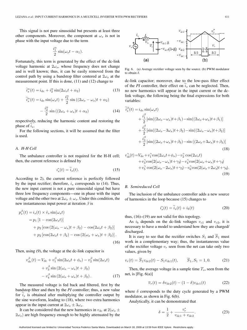
Fig. 6. (a) Average rectifier voltage seen by the source. (b) PWM modulatorto obtain δ.
dc-link capacitor; moreover, due to the low-pass filter effectof the PI controller, their effect on is can be neglected. Then,no new harmonics will appear in the input current or the dc-link voltage, the following being the final expressions for bothvariables:
iβs (t) = idc sin(ωst)
+iβ12
[sin((2ωo−ωs)t+β1)−sin((2ωo+ωs)t+β1)]
+iβ22
[sin((2ωo−3ωs)t+β2)−sin((2ωo−ωs)t+β2)]
+iβ32
[sin((2ωo+ωs)t+β3)−sin ((2ωo+3ωs)t+β3)]
(18)
vγdc(t)=Vdc+vγ
1 cos(2ωot+φo)−vγ2 cos(2ωst)
+vγ3 cos(2(ωo−ωs)t+γ3)−vγ
4 cos(2(ωo+ωs)t+γ4)+vγ
5 cos(2(ωo−2ωs)t+γ5)−vγ6 cos(2(ωo+2ωs)t+γ6).
(19)
B. Semireduced Cell
The inclusion of the unbalance controller adds a new sourceof harmonics in the loop because (15) changes to
i∗s(t) = is(t) + ib(t) (20)
thus, (16)–(19) are not valid for this topology.As ib depends on the dc-link voltages vc1 and vc2, it is
necessary to have a model to understand how they are charged/discharged.
It is easy to see that the rectifier switches S1 and S1 mustwork in a complementary way; thus, the instantaneous valueof the rectifier voltage vr seen from the net can take only twovalues, given by
vr(t) = S1vdc2(t) − S1vdc1(t), S1, S1 = 1, 0. (21)
Then, the average voltage in a sample time Ts, seen from thenet, is [Fig. 6(a)]
vr(t) = δvdc2(t) − (1 − δ)vdc1(t) (22)
where δ corresponds to the duty cycle generated by a PWMmodulator, as shown in Fig. 6(b).
Analytically, it can be demonstrated that
δ =12
+v∗
r
vdc1 + vdc2. (23)
Authorized licensed use limited to: Universidad Tecnica Federico Santa Maria. Downloaded on March 18, 2009 at 13:59 from IEEE Xplore. Restrictions apply.

412 IEEE TRANSACTIONS ON INDUSTRIAL ELECTRONICS, VOL. 56, NO. 2, FEBRUARY 2009
On the other hand, to accomplish with the hypothesis 1),the rectifier voltage reference v∗
r must be a sinusoidal signal offrequency ωs, which magnitude vr and phase φs are calculatedby the current controller Cc to follow the current reference.
Then, the instantaneous power on each dc-link capacitor isgiven by
pεc2(t) = vdc2δ×is (24)
= vdc2
(12
+v sin(ωst+φs)
vdc1+vdc2
)is sin(ωst)
= vdc2
(isv
∗r
2vdc[cos(φs)−cos(2ωst−φs)]+
is sin(ωst)2
).
(25)
In a similar way,
pεc1(t)= − vdc1(1−δ) × is (26)
= vdc1
(isv
∗r
2vdc[cos(φs)−cos(2ωst−φs)]−
is sin(ωst)2
).
(27)
Using (9) for each capacitor, an expression for the voltage oneach one can be obtained
vεdc1(t) ≈
Vdc
2+
vε1
2cos(2ωst + ε1) +
vε2
2cos(2ωot + ε2)
+vε3
2cos(ωst + ε3) (28)
vεdc2(t) ≈
Vdc
2+
vε1
2cos(2ωst + ε1) +
vε2
2cos(2ωot + ε2)
− vε3
2cos(ωst + ε3). (29)
Note that the reference voltage values given by hypothesis 3)are used as operation point for the Taylor sequence.
Then, using (28) and (29), the total dc-link voltage vdc andthe unbalance feedback control signal Δvdc can be calculated
vεdc = vε
dc1 + vεdc2
=Vdc+vε1 cos(2ωst+ε1)+vε
2 cos(2ωot+ε2) (30)
Δvεdc = vε
dc1 + vεdc2
= vε3 cos(ωst + ε3). (31)
It is possible to see that (30) is almost identical than (10);thus, (13) and (14) hold. Note also that, even if both capacitorvoltages are balanced, a component of frequency ωs is in Δvs
and is then fed back to the control loop through the unbalancecontroller. It is important to remark that this component is notpresent in vdc.
If a pure P or even a PI controller is used in Cb, the com-ponent of frequency ωs will pass through it; thus, ib will be
ib(t)ε = iεb1 sin(ωs + γ1). (32)
Replacing (14) and (32) in (20),
i∗εs = iεb1 sin(ωs + γ1) + idc sin(ωst)
+iε22
[sin ((2ωo − ωs)t + ε2) − sin ((2ωo + ωs)t + ε2)]
= iεs1 sin(ωst + θ) + iεs2 sin ((2ωo − ωs)t + ε2)
− iεs2 sin ((2ωo + ωs)t + ε2) . (33)
Then, the current reference component of frequency ωs willbe no longer in phase with the input voltage, decreasing theinput power factor of the system. This can be easily correctedby removing the ωs component from the unbalance controllerpath by using a bandstop filter centered at this frequency; then,the term θ in (33) will be zero, obtaining an expression identicalto (14). For further analysis, it will be considered that this filteris being used.
The new input current generates new power harmonics ac-cording to (24) and (26); then, new capacitor voltage expres-sions are obtained
vϕdc1(t) =
Vdc
2+
vϕ1
2cos(2ωst + ϕ1) +
vϕ2
2cos(2ωot + ϕ2)
+vϕ3
2cos(ωst + ϕ3) +
vϕ4
2cos ((2ωo + ωs)t + ϕ4)
+vϕ5
2cos ((2ωo − ωs)t + ϕ5)
+vϕ6
2cos (2(ωo + ωs)t + ϕ6)
+vϕ7
2cos (2(ωo − ωs)t + ϕ7) (34)
vϕdc2(t) =
Vdc
2+
vϕ1
2cos(2ωst + ϕ1) +
vϕ2
2cos(2ωot + ϕ2)
− vϕ3
2cos(ωst + ϕ3) −
vϕ4
2cos ((2ωo + ωs)t + ϕ4)
− vϕ5
2cos ((2ωo − ωs)t + ϕ5)
+vϕ6
2cos (2(ωo + ωs)t + ϕ6)
+vϕ7
2cos (2(ωo − ωs)t + ϕ7) . (35)
Then, the feedback voltage signals are as follows:
vϕdc = Vdc + vϕ
1 cos(2ωst + ϕ1) + vϕ2 cos(2ωot + ϕ2)
+ vϕ6 cos (2(ωo + ωs)t + ϕ6)
+ vϕ7 cos (2(ωo − ωs)t + ϕ7) (36)
Δvϕdc = vϕ
3 cos(ωst + ϕ3) + vϕ4 cos ((2ωo + ωs)t + ϕ4)
+ vϕ5 cos ((2ωo − ωs)t + ϕ5) . (37)
Note that, once again, the total dc-link voltages of the H-Hcell and the semireduced cell are the same [see (19) and (36)];then, the output of Cv will be the same for both cases. Aftermultiplying the main voltage controller output by the sinusoidal
Authorized licensed use limited to: Universidad Tecnica Federico Santa Maria. Downloaded on March 18, 2009 at 13:59 from IEEE Xplore. Restrictions apply.

LEZANA et al.: INPUT CURRENT HARMONICS IN A MULTICELL INVERTER WITH PWM RECTIFIERS 413
waveform and reordering the resulting terms, the new value iϕsis obtained
iϕs (t) = idc sin(ωst) + iϕ1 sin ((2ωo − ωs)t + ϕ1)
+ iϕ2 sin ((2ωo + ωs)t + ϕ2)
+ iϕ3 sin ((2ωo − 3ωs)t + ϕ3)
+ iϕ4 sin ((2ωo + 3ωs)t + ϕ4) . (38)
Note that all the harmonics of Δvϕdc are already present
in iϕs . Then, iϕb will not add new components to the currentreference i∗ϕs ; it just will change the magnitude and phase ofthe components of (38).
Finally, the input current will generate new power harmon-ics in the dc-link capacitor voltages, following the previouslyexplained process, leading to the following:
vτdc1(t) =
Vdc
2+
vτ1
2cos(2ωst + τ1) +
vτ2
2cos(2ωot + τ2)
+vτ3
2cos(ωst + τ3) +
vτ4
2cos ((2ωo + ωs)t + τ4)
+vτ5
2cos ((2ωo − ωs)t + τ5)
+vτ6
2cos (2(ωo + ωs)t + τ6)
+vτ7
2cos (2(ωo − ωs)t + τ7)
+vτ8
2cos (2ωo − 3ωs)t + τ8)
+vτ9
2cos (2ωo + 3ωs)t + τ9)
+vτ10
2cos (2(ωo + 2ωs)t + τ10)
+vτ11
2cos (2(ωo − 2ωs)t + τ11) (39)
vτdc2(t) =
Vdc
2+
vτ1
2cos(2ωst + τ1) +
vτ2
2cos(2ωot + τ2)
− vτ3
2cos(ωst + τ3) −
vτ4
2cos ((2ωo + ωs)t + τ4)
− vτ5
2cos ((2ωo − ωs)t + τ5)
+vτ6
2cos (2(ωo + ωs)t + τ6)
+vτ7
2cos (2(ωo − ωs)t + τ7)
− vτ8
2cos (2ωo − 3ωs)t + τ8)
− vτ9
2cos (2ωo + 3ωs)t + τ9)
+vτ10
2cos (2(ωo + 2ωs)t + τ10)
+vτ11
2cos (2(ωo − 2ωs)t + τ11) (40)
TABLE IDC-LINK VOLTAGES AND INPUT CURRENT HARMONICS
FOR H-H AND SEMIREDUCED CELLS
vτdc(t) = Vdc + vτ
1 cos(2ωot + τ1) + vτ2 cos(2ωst + τ2)
+ vτ6 cos (2(ωo + ωs)t + τ6)
+ vτ7 cos (2(ωo − ωs)t + τ7)
+ vτ10 cos (2(ωo + 2ωs)t + τ10)
+ vτ11 cos (2(ωo − 2ωs)t + τ11) . (41)
As the new harmonics are around 3ωs, it will be considered thatthey are highly attenuated by the capacitors and the controllersCv and Cb; thus, their influence in the harmonic generation canbe neglected. This finishes the analysis at this point.
Table I summarizes the harmonics in the input current and thedc-link capacitors for the analyzed cells. The harmonic contentsin is and vdc are exactly the same for both cells; therefore, fromthe load and net points of view, they are equivalent. Neverthe-less, the high number of harmonics in the dc-link capacitorsof the semireduced cell must be considered to calculate anappropriate capacitor value.
It is also important to remark that, in real implementation,there will always be an unbalance between both capacitors ofthe semireduced cell. Then, there is no perfect cancellation ofthe common harmonics of vdc1 and vdc2; thus, some additionalharmonics of low amplitude should be expected in the inputcurrent is, due to the effect of the balancing control loop,through ib.
In the previous analysis, the term 4ωo was neglected in (9);however, this harmonic can be important if the output frequencyis very low (<10 Hz). In such a case, this harmonic is propa-gated to the feedback loop, generating additional harmonics inthe input current and the dc-link voltages.
V. CANCELLATION OF HARMONICS BY INTERCONNECTION
As was explained in the previous section, the input currentof each single-phase cell of the CM converter has many lowfrequency harmonics, which location depends on the H-bridgeinverter frequency operation ωo. This implies that the inputpower factor of each cell is very low, even if the currentcomponent at ωs is in phase with the input voltage.
Fortunately, most of the low frequency harmonics can bereduced or even eliminated with a proper interconnection at
Authorized licensed use limited to: Universidad Tecnica Federico Santa Maria. Downloaded on March 18, 2009 at 13:59 from IEEE Xplore. Restrictions apply.

414 IEEE TRANSACTIONS ON INDUSTRIAL ELECTRONICS, VOL. 56, NO. 2, FEBRUARY 2009
the input transformer. According to Fig. 3, the following rela-tions hold:
iu = iA1 + iB1 + iC1 (42)
iw = iA2 + iB2 + iC2 (43)
iv = iA3 + iB3 + iC3. (44)
Assuming that the analysis in Section IV was related to cella1, then iA1 corresponds to (18) or equivalently to (38). Similarexpressions can be obtained for iB1 and iC1 [(46) and (47)] byreplacing the term ωot in (5) with (ωot − 2π/3) and (ωot +2π/3), respectively, due to the required phase shift between theoutput currents for a proper operation, obtaining:
iA1(t) = idc sin(ωst) + i1 sin ((2ωo − ωs)t + ρ1)+ i2 sin ((2ωo + ωs)t + ρ2)+ i3 sin ((2ωo − 3ωs)t + ρ3)+ i4 sin ((2ωo + 3ωs)t + ρ4) (45)
iB1(t) = idc sin(ωst) + i1 sin[(2ωo − ωs)t + ρ1 − 2
2π
3
]+ i2 sin
[(2ωo + ωs)t + ρ2 − 2
2π
3
]+ i3 sin
[(2ωo − 3ωs)t + ρ3 − 2
2π
3
]+ i4 sin
[(2ωo + 3ωs)t + ρ4 − 2
2π
3
](46)
iC1(t) = idc sin(ωst) + i1 sin[(2ωo − ωs)t + ρ1 + 2
2π
3
]+ i2 sin
[(2ωo + ωs)t + ρ2 + 2
2π
3
]+ i3 sin
[(2ωo − 3ωs)t + ρ3 + 2
2π
3
]+ i4 sin
[(2ωo + 3ωs)t + ρ4 + 2
2π
3
]. (47)
Then, replacing (45)–(47) in (42), a final expression for thecurrent at the primary side is obtained
iu(t) = 3idc sin(ωst). (48)
Then, a pure sinusoidal signal can be obtained at the primaryside of the converter. The same analysis can be easily extendedto iw and iv , by using the proper phase shift between the inputvoltages. As the delta winding currents do not present any lowfrequency harmonics, the input phase currents iU , iV , and iWdo not present either.
Note that, in this cancellation, it is only possible when thenumber of cells per phase is a multiple of three; otherwise,unbalanced and/or distorted primary input currents will beobtained.
VI. EXPERIMENTAL RESULTS
A prototype based in the converter in Fig. 3 was constructedto check the analytical results of the previous sections. Cells
Fig. 7. DC-link voltages for (a) H-H and (b) semireduced cells.
based on IPM PM20CSJ060 modules were used, one for eachsemireduced cell and two for each H-H cell. In both cases, thecells operate with a total dc-link voltage of 120 V, reaching amaximum output phase voltage of 720 Vpp, feeding an R–Lload of 70 Ω–15 mH. Capacitors of 1500 μF were used for bothtopologies.
The modulation for the whole converter was generated bya Xilinx FPGA XC2s150, which internally implements a setof triangular carriers of 2.5 kHz, while the control loops wereresolved by a TMS320C6711 DSP, which requires an averagetime of 9 μs to calculate the actuation for one cell.
Fig. 7(a) and (b) shows the dc-link voltages of both typesof cells operating with an output frequency of 30 Hz and amodulation index of 0.8.
As expected, the total dc-link voltages in both cells are verysimilar. To appreciate, in a better way, the characteristics ofthese variables, the spectra of them are shown in Fig. 8.
The spectra of the total dc-link voltages of both cells confirmthat they have a similar behavior. However, the semireduced cellpresents some low magnitude harmonics at 40 and 50 Hz, whichcan be explained using Fig. 8(c). As predicted in (39) and (40),the most important harmonic is at 50 Hz (which correspondsto ωs), while there are other new minor harmonics at 10, 40,and 110 Hz. As the dc-link capacitors are not identical, thecancellation is not ideal. For this reason, some of these newharmonics are present in vdc but with a small magnitude.
The input current of a cell is shown in Fig. 9 for bothtopologies. It can be seen that the input current of the H-Hcell has a lower magnitude and larger low frequency harmonicsthan the input current of the semireduced cell. This is explainedbecause the input voltage of a semireduced cell is half of thevoltage of an H-H cell, due to its doubler effect; thus, if bothcells operate at the same power rating, the component of isin phase with the input voltage must be two times higher ina semireduced cell than in an H-H cell. This is shown in a more
Authorized licensed use limited to: Universidad Tecnica Federico Santa Maria. Downloaded on March 18, 2009 at 13:59 from IEEE Xplore. Restrictions apply.

LEZANA et al.: INPUT CURRENT HARMONICS IN A MULTICELL INVERTER WITH PWM RECTIFIERS 415
Fig. 8. Spectra of the dc-link voltages. (a) vdc of an H-H cell. (b) vdc
of a semireduced cell. (c) One of the dc-link capacitors on a semireducedcell (vdc1).
Fig. 9. Input current of cell a1. (a) H-H topology. (b) Semireduced topology.
clear way in Fig. 10, where the spectra of the input current areshown.
The harmonic magnitudes are, in proportion, almost twotimes higher for an H-H cell than for a semireduced cell. Notethat most of the predicted harmonics are present in the input
Fig. 10. Spectra of the input current of cell a1. (a) H-H topology.(b) Semireduced topology.
Fig. 11. Input current at the primary side. (a) In time domain. (b) In frequencydomain.
currents; just the harmonic at 210 Hz, which corresponds to2ωo + 3ωs, is not present due to its relatively high frequency.Note also that 3rd and 5th input frequency harmonics are in theinput currents due to the distorted input voltage.
As explained in Section V, the low frequency harmonicsrelated with the converter output frequency can be cancelledby a proper interconnection at the input transformer. This isshown in Fig. 11, where the input current at the primary side ofa converter, using the semireduced cell, is presented. The inputcurrent iU has a very low harmonic distortion and is in phasewith the input voltage vU , reaching a high input power factor.
Finally, Fig. 12 shows the output signals of the converter.Due to the high modulation index used, the maximum number
Authorized licensed use limited to: Universidad Tecnica Federico Santa Maria. Downloaded on March 18, 2009 at 13:59 from IEEE Xplore. Restrictions apply.

416 IEEE TRANSACTIONS ON INDUSTRIAL ELECTRONICS, VOL. 56, NO. 2, FEBRUARY 2009
Fig. 12. Converter output signals. (a) Voltages. (b) Currents.
of voltage levels, namely, seven, is obtained, as can be seenin Fig. 12(a). As the load has a low-pass filter characteristic,the output currents are almost pure sinusoidal, as shown inFig. 12(b).
VII. CONCLUSION
A method to calculate the location of the harmonics in the dc-link voltages and the input current of single-phase regenerativecells for an MC converter has been proposed. The analyticalresults have been satisfactory contrasted with experimentalresults.
The method also allows one to understand, in a better way,how the harmonics propagate through the system; this is impor-tant in designing the controllers or/and filters in the control loopto reduce their effects.
It has been demonstrated that the use of single-phase re-generative rectifiers, at the input side of the cells of an MCconverter, allows one to operate with a very high input powerfactor for any output condition if a proper number of cells andinput transformer interconnection are used. Moreover, it hasbeen shown that the H-H and semireduced cells are equivalentfrom the load and source points of view.
The dc-link capacitors of the semireduced cell operate witha half of the voltage of an equivalent H-H cell. However, thevoltages on those capacitors have a larger harmonic content;thus, their capacitance must be greater than the capacitor of theH-H cell to obtain a good voltage regulation.
REFERENCES
[1] J. Rodríguez, J. S. Lai, and F. Z. Peng, “Multilevel inverters: A surveyof topologies, controls, and applications,” IEEE Trans. Ind. Electron.,vol. 49, no. 49, pp. 724–738, Aug. 2002.
[2] S. Alepuz, S. Busquets-Monge, J. Bordonau, J. Gago, D. Gonzalez, andJ. Balcells, “Interfacing renewable energy sources to the utility grid us-ing a three-level inverter,” IEEE Trans. Ind. Electron., vol. 53, no. 5,pp. 1504–1511, Oct. 2006.
[3] Q. Song, W. Liu, and Z. Yuan, “Multilevel optimal modulation anddynamic control strategies for STATCOMs using cascaded multilevelinverters,” IEEE Trans. Power Del., vol. 22, no. 3, pp. 1937–1946,Jun. 2007.
[4] Y. Cheng, C. Qian, M. L. Crow, S. Pekarek, and S. Atcitty, “A com-parison of diode-clamped and cascaded multilevel converters for aSTATCOM with energy storage,” IEEE Trans. Ind. Electron., vol. 53,no. 5, pp. 1512–1521, Oct. 2006.
[5] M. Marchesoni, M. Mazzucchelli, and S. Tenconi, “A nonconventionalpower converter for plasma stabilization,” IEEE Trans. Power Electron.,vol. 5, no. 2, pp. 212–219, Apr. 1990.
[6] T. Ghiara, M. Marchesoni, L. Puglisi, and G. Sciutto, “A modularapproach to converter design for high power AC drives,” in Proc. 4thEur. Conf. Power Electron. Appl. EPE, Florence, Italy, Sep. 3–6, 1991,pp. 477–482.
[7] P. W. Hammond, “A new approach to enhance power quality for mediumvoltage drives,” IEEE Trans. Ind. Appl., vol. 33, no. 1, pp. 202–208,Jan./Feb. 1997.
[8] C. Rech and J. R. Pinheiro, “Hybrid multilevel converters: Unifiedanalysis and design considerations,” IEEE Trans. Ind. Electron., vol. 54,no. 2, pp. 1092–1104, Apr. 2007.
[9] R. Jakob and G. Beinhold, “Medium voltage drive system for test benchand high speed applications,” in Proc. 10th EPE Conf., Toulouse, France,Sep. 2–4, 2003. CD-ROM.
[10] J. Rodríguez, J. Dixon, J. Espinoza, J. Pontt, and P. Lezana, “PWMregenerative rectifiers: State of the art,” IEEE Trans. Ind. Electron.,vol. 52, no. 1, pp. 5–22, Feb. 2005.
[11] J. Pontt, J. Rodríguez, R. Huerta, P. Newman, W. Michel, andC. L. Argandona, “High-power regenerative converter for ore transporta-tion under failure conditions,” IEEE Trans. Ind. Appl., vol. 41, no. 6,pp. 1411–1419, Nov./Dec. 2005.
[12] J. Espinoza, M. Pérez, J. Rodríguez, and P. Lezana, “Regenerativemedium-voltage AC drive based on a multi-cell arrangement withminimum energy storage requirements,” IEEE Trans. Ind. Electron.,vol. 52, no. 1, pp. 171–180, Feb. 2005.
[13] J. Rodríguez, L. Morán, J. Pontt, J. L. Hernández, L. Silva, C. Silva,and P. Lezana, “High-voltage multilevel converter with regenerationcapability,” IEEE Trans. Ind. Electron., vol. 49, no. 4, pp. 839–846,Aug. 2002.
[14] P. Lezana, J. Rodríguez, and D. A. Oyarzun, “Cascaded multilevel inverterwith regeneration capability and reduced number of switches,” IEEETrans. Ind. Electron., vol. 55, no. 3, pp. 1059–1066, Mar. 2008.
[15] C. Chen and D. Divan, “Simple topologies for single phase AC lineconditioning,” IEEE Trans. Ind. Appl., vol. 30, no. 2, pp. 406–412,Mar./Apr. 1994.
[16] R. Srinivasan and R. Oruganti, “A unity power factor converter usinghalf-bridge boost topology,” IEEE Trans. Power Electron., vol. 13, no. 3,pp. 487–500, May 1998.
[17] Y. Lo, T. Song, and H. Chiu, “Analysis and elimination of volt-age imbalance between the split capacitors in half-bridge boost rec-tifiers,” IEEE Trans. Ind. Electron., vol. 49, no. 5, pp. 1175–1177,Oct. 2002.
[18] J. T. Boys and A. W. Green, “Current-forced single-phase reversiblerectifier,” Proc. Inst. Elect. Eng., vol. 136, no. 5, pp. 205–211,Sep. 1989.
[19] D. Lee and Y. Kim, “Control of single-phase-to-three-phase AC/DC/ACPWM converters for induction motor drives,” IEEE Trans. Ind. Electron.,vol. 54, no. 2, pp. 797–804, Apr. 2007.
[20] M. Saitou, N. Matsui, and T. Shimizu, “A control strategy of single-phaseactive filter using a novel d–q transformation,” in Conf. Rec. 38th Annu.Meeting IEEE Ind. Appl. Conf., Salt Lake City, UT, Oct. 12–16, 2003,vol. 2, pp. 1222–1227.
[21] Y. Sato, T. Ishizuka, K. Nezu, and T. Kataoka, “A new control strategyfor voltage-type PWM rectifiers to realize zero steady-state control errorin input current,” IEEE Trans. Ind. Appl., vol. 34, no. 3, pp. 480–486,May/Jun. 1998.
[22] D. N. Zmood and D. G. Holmes, “Stationary frame current regulationof PWM inverters with zero steady-state error,” IEEE Trans. PowerElectron., vol. 18, no. 3, pp. 814–822, May 2003.
[23] P. Lezana, C. Silva, J. Rodríguez, and M. Pérez, “Zero-steady-state-error input-current controller for regenerative multilevel converters basedon single-phase cells,” IEEE Trans. Ind. Electron., vol. 54, no. 2, pp. 733–740, Apr. 2007.
[24] J. Rodríguez, P. Lezana, J. Espinoza, M. Pérez, and J. Pontt, “Input currentharmonics in a regenerative multicell inverter with single phase activerectifiers,” in Proc. 28th Annu. Conf. IEEE Ind. Electron. Soc. IECON,Sevilla, Spain, Nov. 5–8, 2002, pp. 170–175.
Authorized licensed use limited to: Universidad Tecnica Federico Santa Maria. Downloaded on March 18, 2009 at 13:59 from IEEE Xplore. Restrictions apply.

LEZANA et al.: INPUT CURRENT HARMONICS IN A MULTICELL INVERTER WITH PWM RECTIFIERS 417
Pablo Lezana (S’06–M’07) was born in Temuco,Chile, in 1977. He received the M.Sc. and Doctor de-grees in electronic engineering from the UniversidadTécnica Federico Santa María (UTFSM), Valparaíso,Chile, in 2005 and 2006, respectively.
From 2005 to 2006, he was a Research Assis-tant with the Departamento de Electrónica, UTFSM.Since 2007, he has been a Researcher with the De-partamento de Electricidad, UTFSM. He contributedto one chapter in the Power Electronics Handbook(Academic, 2007). His research interests include
power converters and modern digital control devices (DSPs and FPGAs).
José Rodríguez (M’81–SM’94) received the Engi-neer degree in electrical engineering from the Uni-versidad Técnica Federico Santa María (UTFSM),Valparaíso, Chile, in 1977, and the Dr.Ing. degreein electrical engineering from the University ofErlangen, Erlangen, Germany, in 1985.
Since 1977, he has been a Professor with theDepartamento de Electrónica, UTFSM, where he hasbeen Rector since 2005. During his sabbatical leavein 1996, he was responsible for the Mining Divisionof Siemens Corporation, Santiago, Chile. He has
extensive consulting experience in the mining industry, particularly in theapplication of large drives. He has coauthored over 250 journal and conferencepapers, and contributed to one book chapter. His main research interests includemultilevel inverters, new converter topologies, and adjustable-speed drives.
Marcelo A. Pérez (M’07) was born in Concepción,Chile, in 1976. He received the Engineer degree inelectronic engineering and the M.Sc. and D.Sc. de-grees in electrical engineering from the University ofConcepción, Concepción, in 2000, 2003, and 2006,respectively.
Currently he holds a postdoctoral position at theDepartamento de Electrónica, Universidad TécnicaFederico Santa María, Valparaíso, Chile.
José Espinoza (S’92–M’97) was born inConcepción, Chile, in 1965. He received theEngineer degree in electronic engineering andthe M.Sc. degree in electrical engineering fromthe University of Concepción, Concepción, in 1989and 1992, respectively, and the Ph.D. degree inelectrical engineering from Concordia University,Montreal, QC, Canada, in 1997.
Since January 2006, he has been a Professor withthe Departamento de Electricidad, Universidad deConcepción, where he is engaged in teaching and
research in the areas of automatic control and power electronics. He hasauthored or coauthored more than 100 refereed journal and conference papersand contributed to one chapter in the Power Electronics Handbook (Academic,2007).
Dr. Espinoza is currently an Associate Editor of the IEEE TRANSACTIONS
ON INDUSTRIAL ELECTRONICS and IEEE TRANSACTIONS ON POWER
ELECTRONICS.
Authorized licensed use limited to: Universidad Tecnica Federico Santa Maria. Downloaded on March 18, 2009 at 13:59 from IEEE Xplore. Restrictions apply.
Copyright © 2022 FDOKUMEN