UNIT -II RECTIFIERS, FILTERS AND REGULATORS Introduction
48
Department of Electronics and Communication Engineering ________________________________________________________________________ ___________________________________________________________________________________________________________ VARDHAMAN COLLEGE OF ENGINEERING, SHAMSHABAD, HYDERABAD 97 UNIT - II RECTIFIERS, FILTERS AND REGULATORS Introduction: For the operation of most of the electronics devices and circuits, a d.c. source is requi So it is advantageous to convert domestic a.c. supply into d.c. voltages. The process of convert a.c. voltage into d.c. voltage is called as rectification.This is achieved with i) Step-down Transformer, ii) Rectifier, iii) Filter and iv) Voltage regulator circuits. These elements constitute d.c. regulated power supply shown in the figure below. Fig. Block diagram of Regulated D.C. Power Supply The block diagram of a regulated D.C. power supply consists of step-down transformer, rectifier, filter, voltage regulator and load. An ideal regulated power supply is an electronics circuit designed to provide a predetermined d.c. voltage Vo which is independent of the load current and variations in the inp voltage ad temperature. If the output of a regulator circuit is a AC voltage then it is termed as voltage stabili whereas if the output is a DC voltage then it is termed as voltage regulator. The elements of the regulated DC power supply are discussed as follows: TRANSFORMER: A transformer is a static device which transfers the energy from primary wind secondary winding through the mutual induction principle, without changing the frequen transformer winding to which the supply source is connected is called the primary, winding connected to the load is called secondary. If N 1 ,N 2 are the number of turns of the primary and secondary of the transfor 2 1 N N α= is called the turns ratio of the transformer. The different types of the transformers are 1) Step-Up Transformer 2) Step-Down Transformer 3) Centre-tapped Transformer www.jntuworld.com www.jntuworld.com www.jwjobs.ne
-
Upload
jiraachuufnyaachuu -
Category
Documents
-
view
3 -
download
0
Transcript of UNIT -II RECTIFIERS, FILTERS AND REGULATORS Introduction

Department of Electronics and Communication Engineering UNIT-III -EDC ___________________________________________________________________________
_____________________________________________________________________________________________________________ VARDHAMAN COLLEGE OF ENGINEERING, SHAMSHABAD, HYDERABAD
97
UNIT - II RECTIFIERS, FILTERS AND REGULATORS
Introduction:
For the operation of most of the electronics devices and circuits, a d.c. source is required. So it is advantageous to convert domestic a.c. supply into d.c. voltages. The process of converting a.c. voltage into d.c. voltage is called as rectification.This is achieved with i) Step-down Transformer, ii) Rectifier, iii) Filter and iv) Voltage regulator circuits. These elements constitute d.c. regulated power supply shown in the figure below.
Fig. Block diagram of Regulated D.C. Power Supply
The block diagram of a regulated D.C. power supply consists of step-down transformer, rectifier, filter, voltage regulator and load.
An ideal regulated power supply is an electronics circuit designed to provide a predetermined d.c. voltage Vo which is independent of the load current and variations in the input voltage ad temperature.
If the output of a regulator circuit is a AC voltage then it is termed as voltage stabilizer, whereas if the output is a DC voltage then it is termed as voltage regulator. The elements of the regulated DC power supply are discussed as follows:
TRANSFORMER: A transformer is a static device which transfers the energy from primary winding to secondary winding through the mutual induction principle, without changing the frequency. The transformer winding to which the supply source is connected is called the primary, while the winding connected to the load is called secondary.
If N1,N2 are the number of turns of the primary and secondary of the transformer then 21
NNα= is called the turns ratio of the transformer.
The different types of the transformers are
1) Step-Up Transformer 2) Step-Down Transformer 3) Centre-tapped Transformer
www.jntuworld.com
www.jntuworld.com
www.jwjobs.net
Department of Electronics and Communication Engineering UNIT-III -EDC ___________________________________________________________________________
_____________________________________________________________________________________________________________ VARDHAMAN COLLEGE OF ENGINEERING, SHAMSHABAD, HYDERABAD
98
The voltage, current and impedance transformation ratios are related to the turns ratio of the transformer by the following expressions.
Voltage transformation ratio : 2 21 1
V NV N=
Current transformation ratio : 2 11 2
I NI N=
Impedance transformation ratio : 2
21
L
in
Z NZ N
=
RECTIFIER: Any electrical device which offers a low resistance to the current in one direction but a high resistance to the current in the opposite direction is called rectifier. Such a device is capable of converting a sinusoidal input waveform, whose average value is zero, into a unidirectional waveform, with a non-zero average component. A rectifier is a device which converts a.c. voltage (bi-directional) to pulsating d.c. voltage (Uni-directional). Important characteristics of a Rectifier Circuit:
1. Load currents: They are two types of output current. They are average or d.c. current and RMS currents.
i) Average or DC current: The average current of a periodic function is
defined as the area of one cycle of the curve divided by the base.
It is expressed mathematically as2
0
1 ( )2dcI id tπ
ωπ= ∫ ; where mI sini tω=
ii) Effective (or) R.M.S. current: The effective (or) R.M.S. current squared of a periodic function of time is given by the area of one cycle of the curve which represents the square of the function divided by the base.
It is expressed mathematically as
12
22
0
1 ( )2rmsI i d tπ
ωπ
= ∫
2. Load Voltages: There are two types of output voltages. They are average or D.C. voltage and R.M.S. voltage.
i) Average or DC Voltage: The average voltage of a periodic function is defined as the areas of one cycle of the curve divided by the base. It is expressed mathematically as
2
0
1 ( )2dcV Vd tπ
ωπ= ∫ ; Where m sinV V tω=
(or) Ldc dcV I R= × ii) Effective (or) R.M.S Voltage: The effective (or) R.M.S voltage squared of
a periodic function of time is given by the area of one cycle of the curve which represents the square of the function divided by the base.
www.jntuworld.com
www.jntuworld.com
www.jwjobs.net
Department of Electronics and Communication Engineering UNIT-III -EDC ___________________________________________________________________________
_____________________________________________________________________________________________________________ VARDHAMAN COLLEGE OF ENGINEERING, SHAMSHABAD, HYDERABAD
99
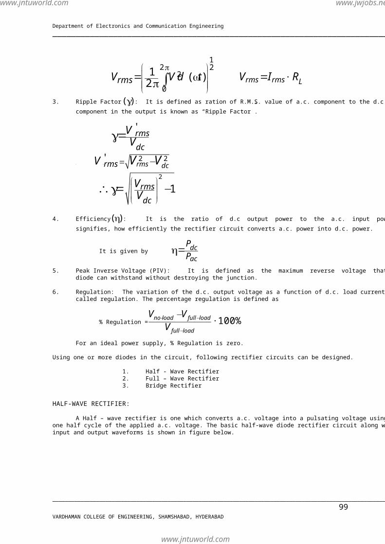
1
2 22
0
1 ( )2rmsV V d tπ
ωπ
= ∫ rms rms LV I R= ×
3. Ripple Factor ( )γ : It is defined as ration of R.M.S. value of a.c. component to the d.c. component in the output is known as “Ripple Factor”.
'rmsdc
VVγ=
W here
2 2'rms dcrmsV V V= −
2
1rmsdc
VVγ
−∴ =
4. Efficiency ( )η : It is the ratio of d.c output power to the a.c. input power. It
signifies, how efficiently the rectifier circuit converts a.c. power into d.c. power.
It is given by dcac
PPη=
5. Peak Inverse Voltage (PIV): It is defined as the maximum reverse voltage that a
diode can withstand without destroying the junction. 6. Regulation: The variation of the d.c. output voltage as a function of d.c. load current is
called regulation. The percentage regulation is defined as
% Regulation = 100%no load full load
full load
V VV
− −
−
− ×
For an ideal power supply, % Regulation is zero. Using one or more diodes in the circuit, following rectifier circuits can be designed.
1. Half - Wave Rectifier 2. Full – Wave Rectifier 3. Bridge Rectifier
HALF-WAVE RECTIFIER:
A Half – wave rectifier is one which converts a.c. voltage into a pulsating voltage using only one half cycle of the applied a.c. voltage. The basic half-wave diode rectifier circuit along with its input and output waveforms is shown in figure below.
www.jntuworld.com
www.jntuworld.com
www.jwjobs.net

Department of Electronics and Communication Engineering UNIT-III -EDC ___________________________________________________________________________
_____________________________________________________________________________________________________________ VARDHAMAN COLLEGE OF ENGINEERING, SHAMSHABAD, HYDERABAD
100
The half-wave rectifier circuit shown in above figure consists of a resistive load; a rectifying
element i.e., p-n junction diode and the source of a.c. voltage, all connected is series. The a.c. voltage is applied to the rectifier circuit using step-down transformer.
The input to the rectifier circuit, m sinV V tω= Where Vm is the peak value of secondary a.c. voltage Operation:
For the positive half-cycle of input a.c. voltage, the diode D is forward biased and hence it
conducts. Now a current flows in the circuit and there is a voltage drop across RL. The waveform of the diode current (or) load current is shown in figure.
For the negative half-cycle of input, the diode D is reverse biased and hence it does not
conduct. Now no current flows in the circuit i.e., i=0 and Vo=0. Thus for the negative half-cycle no power is delivered to the load.
Analysis: In the analysis of a HWR, the following parameters are to be analyzed. i) DC output current ii) DC Output voltage iii) R.M.S. Current iv) R.M.S. voltage v) Rectifier Efficiency ( )η vi) Ripple factor ( )γ vii) Regulation viii) Transformer Utilization Factor (TUF) ix) Peak Factor (P) Let a sinusoidal voltage Vi be applied to the input of the rectifier. Then m sinV V tω= Where Vm is the maximum value of the secondary voltage.
www.jntuworld.com
www.jntuworld.com
www.jwjobs.net

Department of Electronics and Communication Engineering UNIT-III -EDC ___________________________________________________________________________
_____________________________________________________________________________________________________________ VARDHAMAN COLLEGE OF ENGINEERING, SHAMSHABAD, HYDERABAD
101
Let the diode be idealized to piece-wise linear approximation with resistance Rf in the forward direction i.e., in the ON state and Rr (=∞) in the reverse direction i.e., in the OFF state. Now the current ‘i’ in the diode (or) in the load resistance RL is given by
mI sini tω= for 0 tω π≤ ≤
i=0 for 2tπ ω π≤ ≤
where mI m
Lf
VR R=
+
i) Average (or) DC Output Current (Iav or Idc): The average dc current Idc is given by
dcI
2
01 ( )2 id t
πωπ= ∫
m2
0sin ( )1 0 ( )2 I td t d t
π
π
πω ω ωπ
= ×+ ∫∫
m 01 I ( cos )2 t πωπ
= −
m1 I ( 1 ( 1))2π
= + − −
mIπ= , = 0.318 mI
Substituting the value of mI , we get ( )
ILf
mdc R R
Vπ +
=
If RL>>R f then I mdc
L
VRπ= = 0.318 m
L
VR
ii) Average (or) DC Output Voltage (Vav or Vdc): The average dc voltage is given by
Ldc dcV I R= × = mILRπ× = ( )Lf
m LR RV R
π +
( )Lf
m Ldc R R
V RVπ +
⇒ =
If RL>>R f then mdc
VVπ
= = 0.318 mI mdc
VVπ
∴ =
iii) R.M.S. Output Current (Irms ):
www.jntuworld.com
www.jntuworld.com
www.jwjobs.net

Department of Electronics and Communication Engineering UNIT-III -EDC ___________________________________________________________________________
_____________________________________________________________________________________________________________ VARDHAMAN COLLEGE OF ENGINEERING, SHAMSHABAD, HYDERABAD
102
The value of the R.M.S. current is given by
rmsI
21
22
01 ( )2 i d t
πωπ
= ∫
12
222
0sin ( )1 0 ( )2
1I 2.m t d t d tπ
π
πω ω ωπ π • •
= + ∫∫
122
0
1 cos ( )2I2
m t d tπ ω ωπ
−= ∫
122
0
I 1( ) sin4 2m t t
π
ω ωπ
−=
12 2
sin 0I sin 204 2m πππ
+− −=
12 2I4m
=
mI2=
mI2rmsI =∴ (or)
( )2 Lf
mrms R RVI+
=
iv) R.M.S. Output Voltage (Vrms ):
R.M.S. voltage across the load is given by
rms rms LV I R= × = ( )2 Lf
m LR RV R
+ =
2 1 f
L
mRR
V +
If RL >> R f then 2m
rmsVV =
v) Rectifier efficiency( )η : The rectifier efficiency is defined as the ration of d.c. output power to the a.c. input power i.e.,
dcac
PPη∴ =
www.jntuworld.com
www.jntuworld.com
www.jwjobs.net

Department of Electronics and Communication Engineering UNIT-III -EDC ___________________________________________________________________________
_____________________________________________________________________________________________________________ VARDHAMAN COLLEGE OF ENGINEERING, SHAMSHABAD, HYDERABAD
103
22
2m L
LdcdcI RI RPπ
= =
( ) ( )224rmsm
L Lf facII R R R RP = + = +
( )2
2 224 4m
m
L L
L fL f
dcac
R RR RR R
P IP Iπ π
η =
× =++
∴ =
21 0.406
114
ffLL
RRRR
πη ×
++=⇒ =
% 40.61 f
L
RR
η+
⇒ =
Theoretically the maximum value of rectifier efficiency of a half-wave rectifier is 40.6%
when f
L
RR = 0.
vi) Ripple Factor ( )γ : The ripple factor γ is given by
2
1rmsdc
IIγ
−= (or)
2
1rmsdc
VVγ
−=
22// 1m
mII π
γ
−∴ = =
212
π
− = 1.21
1.21γ⇒ = vii) Regulation: The variation of d.c. output voltage as a function of d.c. load current is called regulation. The variation of Vdc with Idc for a half-wave rectifier is obtained as follows:
mI /I mdc
Lf
VR R
ππ= +=
www.jntuworld.com
www.jntuworld.com
www.jwjobs.net

Department of Electronics and Communication Engineering UNIT-III -EDC ___________________________________________________________________________
_____________________________________________________________________________________________________________ VARDHAMAN COLLEGE OF ENGINEERING, SHAMSHABAD, HYDERABAD
104
But Ldc dcV I R= ×
dcV
m LLf
RVR Rπ
= + 1 fmLf
RVR Rπ
= − +
dc fm RV Iπ= −
dc dc fmV RV Iπ∴ = −
This result shows that Vdc equals mVπ
at no load and that the dc voltage decreases linearly
with an increase in dc output current. The larger the magnitude of the diode forward resistance, the greater is this decrease for a given current change. viii) Transformer Utilization Factor (UTF): The d.c. power to be delivered to the load in a rectifier circuit decides the rating of the transformer used in the circuit. So, transformer utilization factor is defined as
( )dc
ac rated
PTUF P∴ =
The factor which indicates how much is the utilization of the transformer in the circuit is called Transformer Utilization Factor (TUF). The a.c. power rating of transformer = Vrms Irms
The secondary voltage is purely sinusoidal hence its rms value is 12 times maximum while the
current is half sinusoidal hence its rms value is 12 of the maximum.
( )ac ratedP∴ mI22
mV= × mI
2 2mV=
The d.c. power delivered to the load 2dc LI R= m
2ILRπ
=
( )dc
ac rated
PTUF P∴ =
m2I
LRπ
=m
2 2ImV=
2
222 2I
Im
mL
L
RRπ •
• •
•
= ( )mIm LV R≈Q
www.jntuworld.com
www.jntuworld.com
www.jwjobs.net

Department of Electronics and Communication Engineering UNIT-III -EDC ___________________________________________________________________________
_____________________________________________________________________________________________________________ VARDHAMAN COLLEGE OF ENGINEERING, SHAMSHABAD, HYDERABAD
105
= 0.287
TUF∴ 0.287= The value of TUF is low which shows that in half-wave circuit, the transformer is not fully utilized. If the transformer rating is 1 KVA (1000VA) then the half-wave rectifier can deliver 1000 X 0.287 = 287 watts to resistance load. ix) Peak Inverse Voltage (PIV): It is defined as the maximum reverse voltage that a diode can withstand without destroying the junction. The peak inverse voltage across a diode is the peak of the negative half-cycle. For half-wave rectifier, PIV is Vm . x) Form factor (F): The Form Factor F is defined as F = rms value / average value
Im/ 2Im/F
π=
0.5 Im0.318 Im1.57F = =
xi) Peak Factor (P): The peak factor P is defined as
P= Peak Value / rms value / 2m
m
VV= = 2 P = 2
Disadvantages of Half-Wave Rectifier:
1. The ripple factor is high. 2. The efficiency is low. 3. The Transformer Utilization factor is low.
Because of all these disadvantages, the half-wave rectifier circuit is normally not used as a
power rectifier circuit.
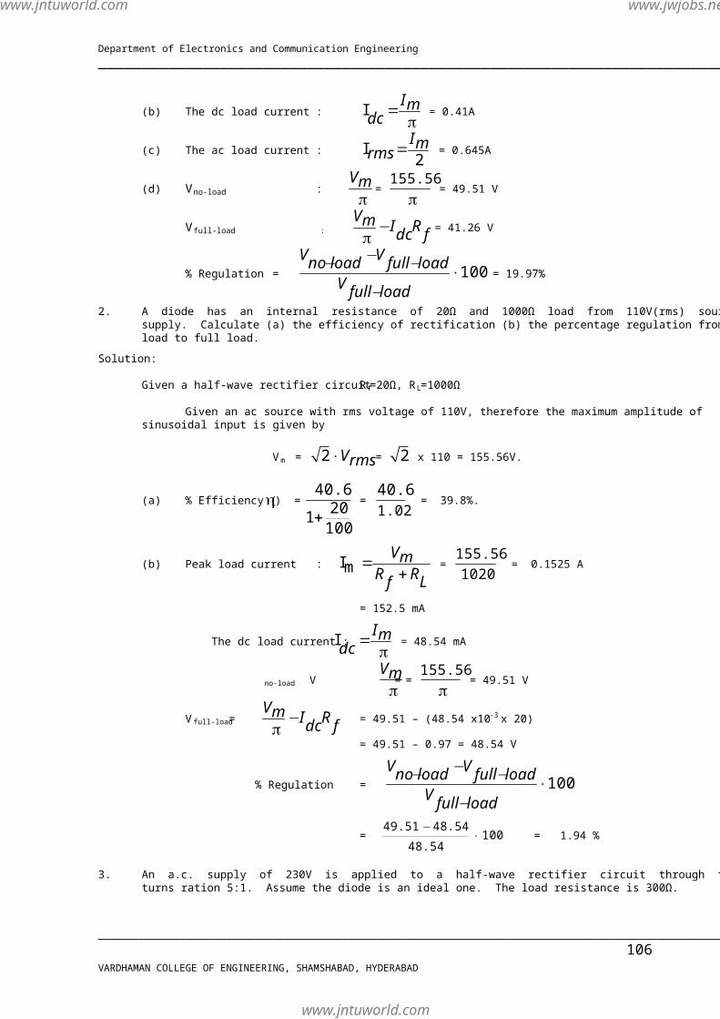
Problems from previous external question paper: 1. A diode whose internal resistance is 20Ω is to supply power to a 100Ω load from 110V(rms)
source pf supply. Calculate (a) peak load current (b) the dc load current (c) the ac load current (d) the percentage regulation from no load to full load.
Solution:
Given a half-wave rectifier circuit Rf=20Ω, RL=100Ω
Given an ac source with rms voltage of 110V, therefore the maximum amplitude of sinusoidal input is given by
V m = 2 Vrms× = 2 x 110 = 155.56V.
(a) Peak load current : ImVm
R RLf=
+
155.56120Im⇒ = = 1.29A
www.jntuworld.com
www.jntuworld.com
www.jwjobs.net
Department of Electronics and Communication Engineering UNIT-III -EDC ___________________________________________________________________________
_____________________________________________________________________________________________________________ VARDHAMAN COLLEGE OF ENGINEERING, SHAMSHABAD, HYDERABAD
106
(b) The dc load current : I Imdc π
= = 0.41A
(c) The ac load current : I 2Imrms= = 0.645A
(d) Vno-load : Vmπ
= 155.56
π = 49.51 V
Vfull-load : Vm I Rdc fπ
− = 41.26 V
% Regulation = 100V Vno load full load
V full load
−− − ×−
= 19.97%
2. A diode has an internal resistance of 20Ω and 1000Ω load from 110V(rms) source pf supply. Calculate (a) the efficiency of rectification (b) the percentage regulation from no load to full load.
Solution: Given a half-wave rectifier circuit Rf=20Ω, RL=1000Ω Given an ac source with rms voltage of 110V, therefore the maximum amplitude of
sinusoidal input is given by V m = 2 Vrms× = 2 x 110 = 155.56V.
(a) % Efficiency (η) = 40.6201 100+ = 1.02
40.6 = 39.8%.
(b) Peak load current : ImVm
R RLf=
+ =
155.561020 = 0.1525 A
= 152.5 mA
The dc load current : I Imdc π
= = 48.54 mA
Vno-load = Vmπ
= 155.56
π = 49.51 V
V full-load = Vm I Rdc fπ
− = 49.51 – (48.54 x10-3 x 20)
= 49.51 – 0.97 = 48.54 V
% Regulation = 100V Vno load full load
V full load
−− − ×−
= −×
49.51 48.54 10048.54
= 1.94 %
3. An a.c. supply of 230V is applied to a half-wave rectifier circuit through transformer of turns ration 5:1. Assume the diode is an ideal one. The load resistance is 300Ω.
www.jntuworld.com
www.jntuworld.com
www.jwjobs.net

Department of Electronics and Communication Engineering UNIT-III -EDC ___________________________________________________________________________
_____________________________________________________________________________________________________________ VARDHAMAN COLLEGE OF ENGINEERING, SHAMSHABAD, HYDERABAD
107
Find (a) dc output voltage (b) PIV (c) maximum, and (d) average values of power delivered to the load.
Solution: (a) The transformer secondary voltage = 230/5 = 46V. Maximum value of secondary voltage, Vm = 2 x 46 = 65V.
Therefore, dc output voltage, 65VmVdc π π
= = = 20.7 V
(b) PIV of a diode : Vm = 65V
(c) Maximum value of load current, ImVmRL
= = 65300 = 0.217 A
Therefore, maximum value of power delivered to the load,
P m = Im 2 x RL = (0.217)2 x 300 = 14.1W
(d) The average value of load current, 20.7I = 300Vdc
dc RL= = 0.069A
Therefore, average value of power delivered to the load, P dc = Idc2 x RL = (0.069)2 x 300 = 1.43W
FULL – WAVE RECTIFIER
A full-wave rectifier converts an ac voltage into a pulsating dc voltage using both half cycles of the applied ac voltage. In order to rectify both the half cycles of ac input, two diodes are used in this circuit. The diodes feed a common load RL with the help of a center-tap transformer.
A center-tap transformer is the one which produces two sinusoidal waveforms of same
magnitude and frequency but out of phase with respect to the ground in the secondary winding of the transformer. The full wave rectifier is shown in the figure below.
Fig. Full-Wave Rectifier.
The individual diode currents and the load current waveforms are shown in figure below:
www.jntuworld.com
www.jntuworld.com
www.jwjobs.net

Department of Electronics and Communication Engineering UNIT-III -EDC ___________________________________________________________________________
_____________________________________________________________________________________________________________ VARDHAMAN COLLEGE OF ENGINEERING, SHAMSHABAD, HYDERABAD
108
Fig. The input voltage, the individual diode currents and the load current waveforms.
Operation: During positive half of the input signal, anode of diode D1 becomes positive and at the same time the anode of diode D2 becomes negative. Hence D1 conducts and D2 does not conduct. The load current flows through D1 and the voltage drop across RL will be equal to the input voltage. During the negative half cycle of the input, the anode of D1 becomes negative and the anode of D2 becomes positive. Hence, D1 does not conduct and D2 conducts. The load current flows through D2 and the voltage drop across RL will be equal to the input voltage. It is noted that the load current flows in the both the half cycles of ac voltage and in the same direction through the load resistance. Analysis: Let a sinusoidal voltage Vi be applied to the input of a rectifier. It is given by Vi=V m sinωt The current i1 though D1 and load resistor RL is given by
I sinm1i tω= for 0 tω π≤ ≤
01i = for 2tπ ω π≤ ≤ Where ImVm
R RLf=
+
Similarly, the current i2 through diode D2 and load resistor RL is given by
2 0i = for 0 tω π≤ ≤
I sinm2i tω= for 2tπ ω π≤ ≤ Therefore, the total current flowing through RL is the sum of the two currents i1 and i2.
i.e., iL = i1 + i2. i) Average (or) DC Output Current (Iav or Idc): The average dc current Idc is given by
www.jntuworld.com
www.jntuworld.com
www.jwjobs.net
Department of Electronics and Communication Engineering UNIT-III -EDC ___________________________________________________________________________
_____________________________________________________________________________________________________________ VARDHAMAN COLLEGE OF ENGINEERING, SHAMSHABAD, HYDERABAD
109
dcI 12
01 ( )2 i d t
πωπ= ∫ + 2
2
01 ( )2 i d t
πωπ∫
m2
m0
sin ( )1 I sin ( )2 I 0 0td t td tπ
π
πω ω ω ωπ
= + + + ∫∫
mIπ= +
mIπ
m2Iπ= = 0.318 mI
dcI∴ m2Iπ=
Substituting the value of mI , we get ( )2I
Lf
mdc R R
Vπ +
=
This is double that of a Half-Wave Rectifier. ii) Average (or) DC Output Voltage (Vav or Vdc): The dc output voltage is given by
Ldc dcV I R= × = 2 Im RL
π
2 V Rm LVdc R RLfπ
⇒ =+
If RL>>R f then 2 m
dcVVπ
=
iii) R.M.S. Output Current (Irms ): The value of the R.M.S. current is given by
rmsI
12 21 2 ( )2 0
i d tL
πω
π
= ∫
12 21 12 2( ) ( )1 22 20
i d t i d tπ π
ω ωπ π π
= +∫ ∫
12 21 12 2 2 2sin . ( ) sin . ( )2 20
I t d t I t d tm mπ π
ω ω ω ωπ π π
= +∫ ∫
www.jntuworld.com
www.jntuworld.com
www.jwjobs.net

Department of Electronics and Communication Engineering UNIT-III -EDC ___________________________________________________________________________
_____________________________________________________________________________________________________________ VARDHAMAN COLLEGE OF ENGINEERING, SHAMSHABAD, HYDERABAD
110
12 2 2I I 21 cos 2 1 cos 2( ) ( )2 2 2 20
t tm md t d tπ πω ωω ω
π π π
− −= +∫ ∫
12 2 22I Isin 2 sin 24 40
t tm mt tt tπ πω ωω ω
π ω π ω π
= − + −
[ ] [ ]
12 2 2I I
( 0) (0) (2 0) ( 0)4 4m mπ π ππ π
= − − + − − −
12 2 2I I4 4m mπ ππ π
= × ×+
12 2I
2 4m
= ×Im2=
Im2Irms∴ = (or)
2VmIrms
R RLf
=+
iv) R.M.S. Output Voltage (Vrms ):
R.M.S. voltage across the load is given by
rms rms LV I R= × = 2
Vm RLR RLf
+×
2 1
VmVrms R fRL
⇒ =
+
If RL >> R f then 2VmVrms=
v) Rectifier efficiency( )η :
The rectifier efficiency is defined as the ration of d.c. output power to the a.c. input power
i.e., PdcPac
η∴ =
www.jntuworld.com
www.jntuworld.com
www.jwjobs.net

Department of Electronics and Communication Engineering UNIT-III -EDC ___________________________________________________________________________
_____________________________________________________________________________________________________________ VARDHAMAN COLLEGE OF ENGINEERING, SHAMSHABAD, HYDERABAD
111
2422
I RLmP I RLdc dc π= =
2
22
ImP I R R R Rac L Lrms f f
= + = +
24 22 2
P I RLdc mPac I R RLm f
ηπ
∴ = = ×+
82
RLR RL fπ
=+
8
2 1R fRL
π
=
+
0.812
1R fRL
=
+
⇒ 81.2%1
R fRL
η=
+
Theoretically the maximum value of rectifier efficiency of a full-wave rectifier is 81.2%
when f
L
RR = 0. Thus full-wave rectifier has efficiency twice that of half-wave rectifier.
vi) Ripple Factor( )γ : The ripple factor, γ is given by
21Irms
Idcγ
∴ = − (or)
21Vrms
Vdcγ
∴ = −
2Im 12 I2 mπγ
∴ = × − = 2
12 2π
− = 0.48
0.48γ⇒ = vii) Regulation: The variation of Vdc with Idc for a full-wave rectifier is obtained as follows: Vdc I RLdc= ×
2Im RLπ=
2ImIdc π
=Q
www.jntuworld.com
www.jntuworld.com
www.jwjobs.net

Department of Electronics and Communication Engineering UNIT-III -EDC ___________________________________________________________________________
_____________________________________________________________________________________________________________ VARDHAMAN COLLEGE OF ENGINEERING, SHAMSHABAD, HYDERABAD
112
2V Rm LR RL fπ
=+
2 1RV fm
R RLfπ
= −+
2Vm I Rdc fπ= −
2VmV I Rdc dc fπ∴ = −
The percentage regulation of the Full-wave rectifier is given by
% Regulation = 100V Vno load full load
V full load
−− − ×−
=
2 21002
V Vm m I Rdc fVm I Rdc f
π π
π
− −×
− = 100
I Rdc fI RLdc
×
⇒ % Regulation = 100R fRL
×
viii) Transformer Utilization Factor (UTF):
The average TUF in full-wave rectifying circuit is determined by considering the primary and secondary winding separately. There are two secondaries here. Each secondary is associated with one diode. This is just similar to secondary of half-wave rectifier. Each secondary has TUF as 0.287. TUF of primary = Pdc / Volt-Amp rating of primary
( )TUF P∴ =
2 .Im .2 2
I RLdcVm
=
2Im2 .Im2
RLVmπ
24 I 2.2 2
Rm LI R Rm Lfπ
=+
8 121
R fRL
π
=
+
If RL >>R f then (TUF)p = 82π= 0.812.
www.jntuworld.com
www.jntuworld.com
www.jwjobs.net

Department of Electronics and Communication Engineering UNIT-III -EDC ___________________________________________________________________________
_____________________________________________________________________________________________________________ VARDHAMAN COLLEGE OF ENGINEERING, SHAMSHABAD, HYDERABAD
113
( )TUF av∴ = Pdc / V-A rating of transformer
= ( ) ( ) ( )
3TUF p TUF s TUF s+ +
= 0.8120.2870.287
3+ +
= 0.693
( )TUF∴ = 0.693 ix) Peak Inverse Voltage (PIV):
Peak Inverse Voltage is the maximum possible voltage across a diode when it is reverse biased. Consider that diode D1 is in the forward biased i.e., conducting and diode D2 is reverse biased i.e., non-conducting. In this case a voltage Vm is developed across the load resistor RL. Now the voltage across diode D2 is the sum of the voltages across load resistor RL and voltage across the lower half of transformer secondary Vm . Hence PIV of diode D2 = Vm + Vm = 2Vm .
Similarly PIV of diode D1 is 2Vm .
x) Form factor (F): The Form Factor F is defined as F = rms value / average value
F = Im/ 22 Im/π =
0.707 Im0.63Im
= 1.12 F=1.12
xi) Peak Factor (P): The peak factor P is defined as
P= Peak Value / rms value / 2Im
Im= = 2 = 1.414 P = 1.414
Problems from previous External Question Paper: 4) A Full-Wave rectifier circuit is fed from a transformer having a center-tapped secondary
winding. The rms voltage from wither end of secondary to center tap is 30V. if the diode forward resistance is 5Ω and that of the secondary is 10Ω for a load of 900Ω,
Calculate: i) Power delivered to load, ii) % regulation at full-load, iii) Efficiency at full-load and iv) TUF of secondary.
Solution: Given Vrms = 30V, Rf =5Ω, Rs=10Ω, RL=900Ω
But 2
VmVrms= 30 2Vm⇒ = × = 42.426 V.
ImVm
R R RLSf=
+ + =
30 25 10 900+ +
= 46.36 mA.
2 ImIdc π
= = 2 46.36
π×
= 29.5mA
i) Power delivered to the load = 2I RLdc = ( )2329.5 10 900−× × = 0.783W
www.jntuworld.com
www.jntuworld.com
www.jwjobs.net

Department of Electronics and Communication Engineering UNIT-III -EDC ___________________________________________________________________________
_____________________________________________________________________________________________________________ VARDHAMAN COLLEGE OF ENGINEERING, SHAMSHABAD, HYDERABAD
114
ii) % Regulation at full-load = 100V Vno load full load
V full load
−− − ×−
2VmVno load π
=− = 2 42.426
π×
= 27.02 V.
V I RLfull load dc=− = 29.5 x 10-3 x 900 = 26.5 V
% Regulation =27.0226.510026.5
− × = 1.96 %
iii) Efficiency of Rectification = 81.2
1R RSf
RL
++
= 15900
81.21+
= 79.8%
iv) TUF of secondary = DC power output / secondary ac rating
Transformer secondary rating = Vrms Irms = 46.36 330 102
−× × W
Pdc = 2I RLdc
TUF∴ = 0.78346.36 330 102
−× × = 0.796
5) A Full-wave rectifier circuit uses two silicon diodes with a forward resistance of 20Ω each. A dc voltmeter connected across the load of 1kΩ reads 55.4volts. Calculate
i) IRMS , ii) Average voltage across each diode, iii) Ripple factor, and iv) Transformer secondary voltage rating.
Solution: Given Rf =20Ω, RL=1kΩ, Vdc = 55.4V
For a FWR 2VmVdc π
= 55.4
2Vmπ×∴ = = 86.9 V
ImVm
R RLf=
+ =0.08519A
i) I 2Imrms= = 0.06024A
ii) V= 86.9/2 = 43.45V
iii) Ripple factor
www.jntuworld.com
www.jntuworld.com
www.jwjobs.net

Department of Electronics and Communication Engineering UNIT-III -EDC ___________________________________________________________________________
_____________________________________________________________________________________________________________ VARDHAMAN COLLEGE OF ENGINEERING, SHAMSHABAD, HYDERABAD
115
21Irms
Idcγ
= − , 2ImIdc π
= =0.05423A I 2Imrms= =0.06024A
0.48γ∴ =
iv) Transformer secondary voltage rating: Vrms 2Vm=
86.92= = 61.49 Volts.
6) A 230V, 60Hz voltage is applied to the primary of a 5:1 step down, center tapped transformer used in the Full-wave rectifier having a load of 900Ω. If the diode resistance and the secondary coil resistance together has a resistance of 100Ω. Determine: i) dc voltage across the load, ii) dc current flowing through the load, iii) dc power delivered to the load, and iv) ripple voltage and its frequency.
Solution: Given Vp(rms) = 230V
2
1
NN
2 ( )
( )
VS rmsVP rms
= 15⇒
2 ( )230
VS rms=
( )VS rms⇒ = 23V
Given RL =900Ω, Rf + Rs =100Ω
ImVsm
R R RLSf=
+ + =
2 ( )Vs rmsR R RLSf + +
= 2 23
900 100×+
= 0.03252 Amp.
2 ImIdc π
∴ = = 2 0.03252
π×
= 0.0207 Amp.
i) VDC = IDC RL = 0.0207 X 100 = 18.6365 Volts.
ii) IDC = 0.0207 Amp.
iii) Pdc= 2I RLdc
(or) VDC IDC = 0.3857 Watts.
iv) PIV = 2Vsm = 2 X 2 X 23 = 65.0538 Volts
v) Ripple factor = 0.482 = ( )Vr rms
VDC
Therefore, ripple voltage = Vr(rms) = 0.482 x 18.6365 = 8.9827 Volts. Frequency of ripple = 2f = 2x60 = 120 Hz
Bridge Rectifier
The full-wave rectifier circuit requires a center tapped transformer where only one half of the total ac voltage of the transformer secondary winding is utilized to convert into dc output. The need of the center tapped transformer in a Full-wave rectifier is eliminated in the bridge rectifier.
www.jntuworld.com
www.jntuworld.com
www.jwjobs.net
Department of Electronics and Communication Engineering UNIT-III -EDC ___________________________________________________________________________
_____________________________________________________________________________________________________________ VARDHAMAN COLLEGE OF ENGINEERING, SHAMSHABAD, HYDERABAD
116
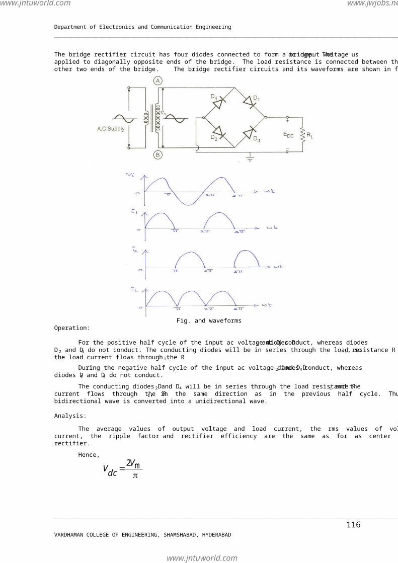
The bridge rectifier circuit has four diodes connected to form a bridge. The ac input voltage us applied to diagonally opposite ends of the bridge. The load resistance is connected between the other two ends of the bridge. The bridge rectifier circuits and its waveforms are shown in figure.
Fig. and waveforms
Operation: For the positive half cycle of the input ac voltage diodes D1 and D3 conduct, whereas diodes
D 2 and D4 do not conduct. The conducting diodes will be in series through the load resistance RL, so the load current flows through the RL.
During the negative half cycle of the input ac voltage diodes D2 and D4 conduct, whereas diodes D1 and D3 do not conduct.
The conducting diodes D2 and D4 will be in series through the load resistance RL and the current flows through the RL, in the same direction as in the previous half cycle. Thus a bidirectional wave is converted into a unidirectional wave. Analysis: The average values of output voltage and load current, the rms values of voltage and current, the ripple factor and rectifier efficiency are the same as for as center tapped full-wave rectifier.
Hence,
2 mVVdc π
=
www.jntuworld.com
www.jntuworld.com
www.jwjobs.net

Department of Electronics and Communication Engineering UNIT-III -EDC ___________________________________________________________________________
_____________________________________________________________________________________________________________ VARDHAMAN COLLEGE OF ENGINEERING, SHAMSHABAD, HYDERABAD
117
2 ImIdc π
= ImVm
R RLf=
+
m2
VVrms= m2
IIrms=
Since the each half cycle two diodes conduct simultaneously 0.48γ=
81.22
1R fRL
η=
+
The transformer utilization factor (TUF) of primary and secondary will be the same as there is always through primary and secondary. TUF of secondary = Pdc / V-A rating of secondary
2Idc
V Irms rms=
22 Im
2 2
RLV Im mπ
= = 0.812
TUF in case of secondary of primary of FWR is 0.812
( )TUF av∴ ( ) ( )
2TUF p TUF s+
=
0.8120.812
2+= = 0.812
TUF∴ = 0.812 The reverse voltage appearing across the reverse biased diodes is 2Vm , but two diodes are sharing it, therefore the PIV rating of the diodes is Vm . Advantages of Bridge rectifier circuit:
1) No center-tapped transformer is required. 2) The TUF is considerably high. 3) PIV is reduced across the diode.
Disadvantages of Bridge rectifier circuit: The only disadvantage of bridge rectifier is the use of four diodes as compared to two diodes for center-tapped FWR. This reduces the output voltage. Problems: 7. A bridge rectifier uses four identical diodes having forward resistance of 5Ω and the
secondary voltage of 30V(rms). Determine the dc output voltage for IDC =200mA and the value of the ripple voltage.
Solution: Vs(rms)=30V, RS=5Ω, Rf=5Ω, IDC =200mA
Now IDC = Im2π
www.jntuworld.com
www.jntuworld.com
www.jwjobs.net
Department of Electronics and Communication Engineering UNIT-III -EDC ___________________________________________________________________________
_____________________________________________________________________________________________________________ VARDHAMAN COLLEGE OF ENGINEERING, SHAMSHABAD, HYDERABAD
118
Im∴ = 3200 10
2π−× × = 0.3415 Amp.
But Im 2Vsm
R R RLS f=
+ + =
2 ( )2Vs rms
R R RLS f+ +
0.3415⇒ = ( )2 30
5 2 5 RL×
+ × +
⇒RL = 120.051Ω ≈120Ω VDC =IDC RL = 200 x10-3 x120 = 24Volts
Ripple factor = ( )Vr rmsVdc
For Bridge rectifier, ripple factor = 0.482
( )Vr rms∴ = rms value of ripple voltage
= Vdcx0.482 = 24x0.482 =11.568 Volts
8. In a bridge rectifier the transformer is connected to 220V, 60Hz mains and the turns ratio
of the step down transformer is 11:1. Assuming the diode to be ideal, find: i) Idc ii) voltage across the load iii) PIV assume load resistance to be 1kΩ
Solution: 21
NN =
111, Vp(rms) = 220V, f=60Hz, RL= 1kΩ
21
NN =
( )( )
VS rmsVP rms
111⇒ =
( )220
VS rms ⇒ ( )VS rms =
22011 = 20V
Vsm 2 ( )Vs rms=
i) Im VsmRL
= = 28.2842
31 10−× = 28.2842 mA
Idc∴ 2 Imπ
= = 18 mA
ii) Vdc = Idc RL = 18x10-3Xx10 -3 = 18 Volts
iv) PIV = Vsm = 28.2842 Volts Comparison of Rectifier circuits:
www.jntuworld.com
www.jntuworld.com
www.jwjobs.net

Department of Electronics and Communication Engineering UNIT-III -EDC ___________________________________________________________________________
_____________________________________________________________________________________________________________ VARDHAMAN COLLEGE OF ENGINEERING, SHAMSHABAD, HYDERABAD
119
Sl. No. Parameter Half-Wave
Rectifier Full-Wave Rectifier Bridge Rectifier
1. Number of diodes 1 2 4
2. Average dc current, Idc Imπ
2Imπ
2Imπ
3. Average dc voltage, Vdc Vsmπ
2Vsmπ
2Vsmπ
4. RMS current, Irms 2Im 2
Im 2Im
5. DC Power output, Pdc 22
I RLmπ
242
I RLmπ
242
I RLmπ
6. AC Power input, PAC ( )2
4
I R R RL Sfm + +
( )2
2
I R R RLSfm + + +
( )2 2
2
I R R RLSfm + + +
7. Max. rectifier efficiency (η) 40.6% 81.2% 81.2%
8. Ripple factor (γ) 1.21 0.482 0.482
9. PIV Vm 2Vm 2V m
10. TUF 0.287 0.693 0.812
11. Max. load current (Im ) Vsm
R R RLS f+ +
VsmR R RLS f+ +
2Vsm
R R RLS f+ +
The Harmonic components in Rectifier circuits: An analytical representation of the output current wave in a rectifier is obtained by means of a Fourier series. The result of such an analysis for the half-wave rectifier circuit leads to the following expression for the current waveform.
( ) ( )2,4,6.....
1 1 2 cosI sinm 2 1 1K
ti t K Kωωπ π =
= + −+ −∑
The lowest angular frequency present in this expression is that of the primary source of the a.c. power. Except for this single term of angular frequency (ω), all other terms in the above expression are even harmonics of the power frequency. We know that the full-wave circuit consists essentially of two half-wave circuits which are so arranged that one circuit conducts during one half cycle and the second operates during the second half cycle. That is, the currents are functionally related by the expression ( ) ( )1 2i iα α π= + .
www.jntuworld.com
www.jntuworld.com
www.jwjobs.net

Department of Electronics and Communication Engineering UNIT-III -EDC ___________________________________________________________________________
_____________________________________________________________________________________________________________ VARDHAMAN COLLEGE OF ENGINEERING, SHAMSHABAD, HYDERABAD
120
Therefore the total load current is i=i1+i2. The expression for the output current waveform of the full wave rectifier circuit is of the form
( ) ( )2,4,6.....
2 4Imcos1 1K
i K tK Kπ π
ω=
= −+ −∑
In the above equation, we observe that the fundamental angular frequency (ω) has been eliminated from the equation. The lowest frequency in the output is being 2ω, which is a second harmonic term. This offers a definite advantage in the effectiveness of filtering of the output.
FILTERS The output of a half-wave (or) full-wave rectifier circuit is not pure d.c., but it contains fluctuations (or) ripple, which are undesired. To minimize the ripple content in the output, filter circuits are used. These circuits are connected between the rectifier and load. Ideally, the output of the filter should be pure d.c. practically, the filter circuit will try to minimize the ripple at the output, as far as possible. Basically, the ripple is ac, i.e., varying with time, while dc is a constant w.r.t. time.
Hence in order to separate dc from ripple, the filter circuit should use components which
have widely different impedance for ac and dc. Two such components are inductance and capacitance. Ideally, the inductance acts as a short circuit for dc, but it has large impedance for ac.
Similarly, the capacitor acts as open for dc if the value of capacitance is sufficiently large
enough. Hence, in a filter circuit, the inductance is always connected in series with the load, and the capacitance is connected in parallel to the load. Definition of a Filter: Filter is an electronic circuit composed of a capacitor, inductor (or) combination of both and connected between the rectifier and the load so as to convert pulsating dc to pure dc. The different types of filters are:
1) Inductor Filter, 2) Capacitor Filter, 3) LC (or) L-Section Filter, and 4) CLC (or) -section Filter. ∏
Inductor Filter: Half-Wave rectifier with series Inductor Filter: The Inductor filter for half-wave rectifier is shown in figure below.
Fig. Series Inductor filter for HWR.
www.jntuworld.com
www.jntuworld.com
www.jwjobs.net

Department of Electronics and Communication Engineering UNIT-III -EDC ___________________________________________________________________________
_____________________________________________________________________________________________________________ VARDHAMAN COLLEGE OF ENGINEERING, SHAMSHABAD, HYDERABAD
121
In this filter the inductor (choke) is connected in series with the load. The operation of the inductor filter depends upon the property of the inductance to oppose any change of current that may flow through it.
Expression for ripple factor: For a half-wave rectifier, the output current is given by,
( ) ( )
0
1 1 2 cosI sinm 2 1 1K evenK
ti t K Kωωπ π
= ≠
= + −+ −∑
I I 2 I cos 2 cos 4m m msin .......2 3 15
t ti t ω ωωπ π
= + − + + …………… (1)
Neglecting the higher order terms, we have
Im VmIdc RLπ π
= = ……………… (2)
If I1 be the rms value of fundamental component of current, then
( ) ( )2 2 2
12
Im2 2 2 2 2 2
L
V Vm mIdc R j LL R j Lωω
= = =+
+
………….(3)
At operating frequency, the reactance offered by inductance ‘L’ is very large compared to RL (i.e., ωL >> RL) and hence RL can be neglected.
1 2 2VmI
Lω∴ = …………..(4)
If I2 be rms value of second harmonic,
Then 32
2 2ImIπ
∴ = = 122 2 2
2
3 2 4L
Vm
R Lπ ω
+
= 3 2Vm
Lπω ( )R LL ω<<Q ……. (5)
If Iac be the rms value of all current components, then 2 21 2I I Iac = +
Now, I RV Iacac acL
V I R ILdc dc dcγ= ≈ =
2 22 2 2 2
V Vm mL L
VmRL
ω πω
π
+=
1 128 18
VmL
VmRL
ω π
π
+=
1 128 18
RLL
πω π
= +
www.jntuworld.com
www.jntuworld.com
www.jwjobs.net

Department of Electronics and Communication Engineering UNIT-III -EDC ___________________________________________________________________________
_____________________________________________________________________________________________________________ VARDHAMAN COLLEGE OF ENGINEERING, SHAMSHABAD, HYDERABAD
122
1.13RL
Lω=
1.13RLLωγ=∴ …………(6)
Full-wave rectifier with series inductor filter:
A FWR with series inductor filter is shown in figure.
FIG. FWR with series inductor filter.
The inductor offers high impedance to a.c. variations. The inductor blocks the a.c. component and allows only t he dc component to reach the load.
To analyze the inductor filter for a FWR, the Fourier series can be written as
2 4 1 1cos 2 cos 6 .......3 15OV Vm mV t tω ωπ π
= − + + ………………..(1)
The dc component is 2Vmπ
Assuming the third and higher terms contribute little output voltage is 2 4 cos 23OV Vm mV tωπ π
= − …………………(2)
For the sake of simplicity, the diode drop and diode resistance are neglected because they
introduce a little error. Thus for dc component, the current ImVmRL
= . For ac component, the
impedance of L and RL will be in series and is given by,
( )22 2LZ R Lω= + , frequency of ac component = 2ω
= 2 2 24LR Lω+
Thus for ac component 2 2 2Im 4L
VmR Lω
=+
The current flowing in a FWR is given by, 2 4 cos 23
I Im mi tωπ π
= − ……………..(3)
Substituting the value of Im for dc and ac equation (3), we get,
( )2 2 22 4 cos 2
3 4L
V Vm mi tR R LLω φ
π π ω= − −
+ …………….(4)
Where Ф is the angle by which the load current lags behind the voltage. This is given by
www.jntuworld.com
www.jntuworld.com
www.jwjobs.net

Department of Electronics and Communication Engineering UNIT-III -EDC ___________________________________________________________________________
_____________________________________________________________________________________________________________ VARDHAMAN COLLEGE OF ENGINEERING, SHAMSHABAD, HYDERABAD
123
21tan LRLωφ
−= …………….(5)
Expression for Ripple Factor:
,Ir rmsIdc
γ=
From equation (4), 2VmIdc RLπ
= , 2 2 2
4, 3 2 4L
VmIr rmsR Lπ ω
=+
2 2 2
13 24
42
L
VmR LVmRL
π ω
π
γ+
=∴ 2 22
2 13 2 41
L
LRω
γ
=
+
∴
If 2 22
4L
LRω >>1, then
13 2
RLL
γω
= = 0.236RL
Lω.
3 2RL
Lγ
ω∴ = ……………….. (6)
The expression shows that ripple varies inversely as the magnitude of the inductance, Also, the ripple is smaller for smaller values of RL i.e., for high currents.
When RL → ∞ the value of γis given by 23 2γ= = 0.471 (close to the value 0.482 of
rectifier). Thus the inductor filter should be used when RL is consistently small. Problems: 9. A full-wave rectifier with a load resistance of 15kΩ uses an inductor filter of 15H. The peak
value of the applied voltage is 250V and the frequency is 50 cycles/second. Calculate the dc load current, ripple factor and dc output voltage.
Solution: The rectified output voltage across load resistance RL up to second harmonic is
2 2 cosOV Vm mV tωπ π
= −
Therefore, DC component of output voltage is given by 2VmVdc π
=
2V Vdc mIdc R RL Lπ
∴ = =
2 250
315 10π×= −× ×
= 10.6 x 10⁻³ A = 10.6 mA
Vdc = Idc RL = (2.12x10⁻³) (15x103) = 31.8 V.
www.jntuworld.com
www.jntuworld.com
www.jwjobs.net

Department of Electronics and Communication Engineering UNIT-III -EDC ___________________________________________________________________________
_____________________________________________________________________________________________________________ VARDHAMAN COLLEGE OF ENGINEERING, SHAMSHABAD, HYDERABAD
124
Peak value of ripple voltage = 43Vmπ
4132VmVac π
∴ =
Now ( )22
41322L
VmIac
R Lπ
ω=
+
( )222 2
3 2L
VmR Lπ ω
=+
( ) ( )23
2 1.4142503 3.14 15 10 4 3.1450 15
× ×=× × + × × ×
= 4.24x10⁻³ A = 4.24 mA
So, ripple factor, IacIdc
γ= = 4.2410.6
mAmA = 0.4
10. A dc voltage of 380 volt with a peak ripple voltage not exceeding 7volt is required to supply
a 500Ω load. Find out if only inductor is used for filtering purpose in full-wave rectifier circuit,
i) inductance required and ii) input voltage required, if transformer ratio is 1:1.
Solution:
i) Given that peak ripple = 7V
Therefore, 7= 2Vrms 72
Vrms⇒ = = 4.95V
Now VrmsVdc
γ= 4.95380= = 0.013
In case of inductor filter
1
3 2RL
Lγ
ω= 1
3 2RLLωγ
⇒ =
1
1335RLLωγ
⇒ = × (∴f=50Hz)
500
1335 0.013L⇒ =×
= 28.8 Henry
ii) 2VmVdc π
= = 0.636Vm
0.636VdcVm∴ =
3800.636= = 597.4 V
This is maximum voltage on half secondary. So, the voltage across complete secondary = 2x 597.4 = 1195V ∴ Input voltage = 1195V because turns ratio is 1:1.
www.jntuworld.com
www.jntuworld.com
www.jwjobs.net

Department of Electronics and Communication Engineering UNIT-III -EDC ___________________________________________________________________________
_____________________________________________________________________________________________________________ VARDHAMAN COLLEGE OF ENGINEERING, SHAMSHABAD, HYDERABAD
125
Capacitor Filter: Half-wave rectifier wit capacitor filter: The half-wave rectifier with capacitor input filter is shown in figure below:
Fig. HWR with capacitor filter.
The filter uses a single capacitor connected in parallel with the load RL. In order to minimize the ripple in the output, the capacitor C used in the filter circuit is quite large of the order of tens of microfarads.
The operation of the capacitor filter depends upon the fact that the capacitor stores energy during the conduction period and delivers this energy to the load during non-conduction period. Operation: During, the positive quarter cycle of the ac input signal, the diode D is forward biased and hence it conducts. This quickly charges the capacitor C to peak value of input voltage Vm . Practically the capacitor charge (Vm -Vγ) due to diode forward voltage drop. When the input starts decreasing below its peak value, the capacitor remains charged at Vm and the ideal diode gets reverse biased. This is because the capacitor voltage which is cathode voltage of diode becomes more positive than anode. Therefore, during the entire negative half cycle and some part of the next positive half cycle, capacitor discharges through RL. The discharging of capacitor is decided by RLC, time constant which is very large and hence the capacitor discharge very little from Vm . In the next positive half cycle, when the input signal becomes more than the capacitor voltage, he diode becomes forward biased and charges the capacitor C back to Vm . The output waveform is shown in figure below:
Fig. HWR output with capacitor filter.
The discharging if the capacitor is from A to B, the diode remains non-conducting. The diode conducts only from B to C and the capacitor charges.
www.jntuworld.com
www.jntuworld.com
www.jwjobs.net
Department of Electronics and Communication Engineering UNIT-III -EDC ___________________________________________________________________________
_____________________________________________________________________________________________________________ VARDHAMAN COLLEGE OF ENGINEERING, SHAMSHABAD, HYDERABAD
126
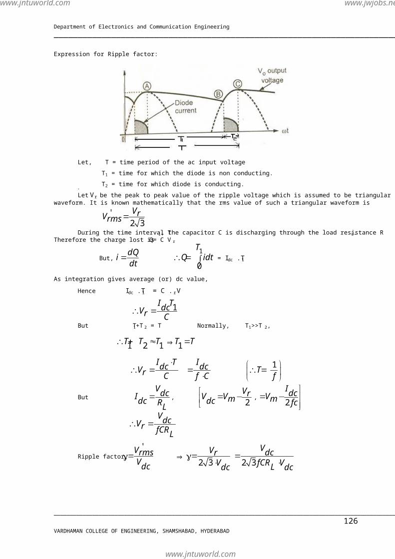
Expression for Ripple factor:
Let, T = time period of the ac input voltage T1 = time for which the diode is non conducting. T2 = time for which diode is conducting. <
Let Vr be the peak to peak value of the ripple voltage which is assumed to be triangular waveform. It is known mathematically that the rms value of such a triangular waveform is
'2 3VrVrms=
During the time interval T1, the capacitor C is discharging through the load resistance RL. Therefore the charge lost is Q= C V r
But, dQi dt=
1
0
TQ idt∴ = ∫ = Idc .T1
As integration gives average (or) dc value,
Hence Idc .T1 = C . Vr
1I TdcVr C∴ =
But T1+T 2 = T Normally, T1>>T 2,
1 2 1 1T T T T T∴ + ≈ ⇒ =
I TdcVr C
⋅∴ =
Idcf C=⋅
1T f
∴ =
But VdcIdc RL
= , 2VrV Vmdc
= − , 2IdcVm fc
= −
VdcVr fCRL
∴ =
Ripple factor, 'Vrms
Vdcγ= 2 3
VrVdc
γ⇒ =⋅
2 3Vdc
fCR VL dc=
⋅
www.jntuworld.com
www.jntuworld.com
www.jwjobs.net

Department of Electronics and Communication Engineering UNIT-III -EDC ___________________________________________________________________________
_____________________________________________________________________________________________________________ VARDHAMAN COLLEGE OF ENGINEERING, SHAMSHABAD, HYDERABAD
127
12 3 fCRL
γ⇒
The product of CRL is the time constant of the filter circuit.
Surge current in Half-wave rectifier using capacitor filter:
Fig. Surge current in HWR using capacitor filter
In half-wave rectifier, the diode is forward biased only for short period of time and conducts only during this time interval to charge the filter capacitance. The instant at which the diode gets forward biased, the capacitor instantaneously acts as short circuit and a surge current flow through a diode.
When the diode is non-conducting, the capacitor discharges through load resistance RL. Thus total amount of charge that flows through conducting diode (or) diodes to recharge the capacitor must be equal to the amount of charge lost during the period when the diode (or) diodes are non-conducting and capacitor is discharging through load resistance RL.
It can be seen that conduction period T1 is very small compared to time period T, for the diode. Let, Idc = average dc current
Ip(surge) = peak value of the surge current.
Assume the current pulse to be rectangular assuming peak surge current flows for the entire conduction period of diode which is T1.
Then Q (discharge) = Q (charge)
, 1( )I T I Tdc P surge∴ = ( ) 1TI IP surge dc T
∴ =
As T1 << T, it can be observed that Ip(surge) can be many times larger than the average dc current supplied to the load. Problem from previous External examinations:
10. A HWR circuit has filter capacitor of 1200µF and is connected to a load of 400Ω. The rectifier is connected to a 50Hz, 120V rms source. It takes 2msec for the capacitor to recharge during each cycle. Calculate the minimum value of the repetitive surge current for which the diode should be rated.
Solution: Given C=1200µF, RL=400Ω, f=50Hz, Vrms=120V
Conduction period of the diode, T1=1ms
2 ( )V Vsm S rms= × = 2 120= × V
www.jntuworld.com
www.jntuworld.com
www.jwjobs.net

Department of Electronics and Communication Engineering UNIT-III -EDC ___________________________________________________________________________
_____________________________________________________________________________________________________________ VARDHAMAN COLLEGE OF ENGINEERING, SHAMSHABAD, HYDERABAD
128
2IdcV Vsmdc fC= −
⇒ 2VdcV Vsmdc fCRL
= −
11 2
VsmVdcfCRL
⇒ =+
120 2
11 62 50 1200 10 400
=+ −× × × ×
= 3.46 V
VdcIdc RL
∴ = 3.46400= =8.658mA
Now IdcT = Ip(surge)T1
( ) 1TI IP surge dc T
= =8.658mA x 1
350 10−×
( )IP surge∴ = 0.17316 A
Full-wave rectifier with capacitor filter:
The full-wave rectifier with capacitor filter is shown in the figure below:
Fig. Full-wave rectifier with capacitor filter
Operation: During the positive quarter cycle of the ac input signal, the diode D1 is forward biased, the capacitor C gets charges through forward bias diode D1 to the peak value of input voltage Vm .
In the next quarter cycle from 2π to π the capacitor starts discharging through RL,
because once the capacitor gets charges to Vm , the diode D1 gets reverse biased and stops
conducting, so during the period from 2π to π the capacitor C supplies the load current.
In the next quarter half cycle, that is, π to 32πof the rectified output voltage, if the input
voltage exceeds the capacitor voltage, making D2 forward biased, this charges the capacitor back to Vm .
www.jntuworld.com
www.jntuworld.com
www.jwjobs.net

Department of Electronics and Communication Engineering UNIT-III -EDC ___________________________________________________________________________
_____________________________________________________________________________________________________________ VARDHAMAN COLLEGE OF ENGINEERING, SHAMSHABAD, HYDERABAD
129
In the next quarter half cycle, that is, from 32π to 2π, the diode gets reverse biased and
the capacitor supplies the load current. In FWR, as the time required by the capacitor to charge is very small and it discharges very
little due to large time constant, hence ripple in the output gets reduced considerably. The output waveform is shown in figure below:
Fig. FWR output with capacitor filter.
Expression for Ripple factor:
Let, T = time period of the ac input voltage
2T
= half of the time period
T1 = time for which diode is conducting T2 = time for which diode is non-conducting
During time T1, capacitor gets charged and this process is quick. During time T2, capacitor gets discharged through RL. As time constant RLC is very large, discharging process is very slow and hence T2>>T 1.
Let Vr be the peak to peak value of ripple voltage, which is assumed to be triangular as
shown in the figure below:
www.jntuworld.com
www.jntuworld.com
www.jwjobs.net

Department of Electronics and Communication Engineering UNIT-III -EDC ___________________________________________________________________________
_____________________________________________________________________________________________________________ VARDHAMAN COLLEGE OF ENGINEERING, SHAMSHABAD, HYDERABAD
130
Fig. Triangular approximation of ripple
It is known mathematically that the rms value of such a triangular waveform is,
2 3VrVrms=
During the time interval T2, the capacitor C is discharging through the load resistance RL.
The charge lost is, Q = CVr But dQi dt=
2
20 DC
TQ idt I T∴ = =∫
As integration gives average (or) dc value, hence Idc .T2 = C . Vr
2I TdcVr C∴ = But 1 2 2TT T+ =
Normally, T2 >> T 1,
1 2 1 2TT T T∴ + ≈ = where
1T f=
2DCI TVr C
∴ = 2DCI T
C×
= 2IDC
fC=
But DCDC
VI RL= , 2
DCVVr fCRL∴ = = peak to peak ripple voltage
Ripple factor, VrmsVdc
= 2 12 3
VdcfCRL
Vdc= × 2 3
VrVrms ∴ =
∴Ripple factor 134 fCRL
=
L-Section Filter (or) LC Filter: The series inductor filter and shunt capacitor filter are not much efficient to provide low ripple at all loads. The capacitor filter has low ripple at heavy loads while inductor filter at small loads. A combination of these two filters may be selected to make the ripple independent of load resistance. The resulting filter is called L-Section filter (or) LC filter (or) Choke input filter. This
www.jntuworld.com
www.jntuworld.com
www.jwjobs.net

Department of Electronics and Communication Engineering UNIT-III -EDC ___________________________________________________________________________
_____________________________________________________________________________________________________________ VARDHAMAN COLLEGE OF ENGINEERING, SHAMSHABAD, HYDERABAD
131
name is due to the fact that the inductor and capacitor are connected as an inverted L. A full-wave rectifier with choke input filter is shown in figure below:
Fig. Full-wave rectifier with choke input filter.
The action of choke input filter is like a low pass filter. The capacitor shunting the load bypasses the harmonic currents because it offers very low reactance to a.c. ripple current while it appears as an open circuit to dc current. On the other hand the inductor offers high impedance to the harmonic terms. In this way, most of the ripple voltage is eliminated from the load voltage. Regulation:
The output voltage of the rectifier is given by, 2 4 cos 23V Vm m tωπ π
υ= −
The dc voltage at no load condition is 2VmVdc π
=
The dc voltage on load is 2VmV I Rdc dcπ
= −
Where R R R RC Sf= + +
, ,R R RC Sf are resistances of diode, choke an secondary winding.
Ripple Factor: The main aim of the filter is to suppress the harmonic components. So the reactance of the choke must be large as compared with the combined parallel impedance of capacitor and resistor. The parallel impedance of capacitor and resistor can be made small by making the reactance of the capacitor much smaller than the resistance of the load. Now the ripple current which has passed through L will not develop much ripple voltage across RL because the reactance of C at the ripple frequency is very small as compared with RL. Thus for LC filter, XL >> XC at 2ω = 4Πf and RL >> XC
Under these conditions, the a.c. current through L is determined primarily by XL= 2ωL (the reactance of the inductor at second harmonic frequency). The rms value of the ripple current is
4 1.( ) 3 2VmIr rms X Lπ
= 22
3 2Vm
X L π
= ( )23 VdcX L
=
Always it was stated that XC is small as compared with RL, but it is not zero. The a.c. voltage across the load (the ripple voltage) is the voltage across the capacitor. Hence ( ) ( )V I Xr rms r rms C= ×
www.jntuworld.com
www.jntuworld.com
www.jwjobs.net

Department of Electronics and Communication Engineering UNIT-III -EDC ___________________________________________________________________________
_____________________________________________________________________________________________________________ VARDHAMAN COLLEGE OF ENGINEERING, SHAMSHABAD, HYDERABAD
132
2
3 V X CdcX L
=
We know that ripple factor γ is given by
( )Vr rmsVdc
γ= 23
X CX L
=
But 1
2X C Cω= and XL = 2ωL
( )2 1
3 2 2L Cω ωγ∴ = × 2
16 2 LCω
=
126 2 LC
γω
∴ =
This shows that ω is independent of RL. The necessity of Bleeder Resistance RB: The basic requirement of this filter circuit is that the current through the choke must be continuous and not interrupted. An interrupted current through the choke may develop a large back e.m.f which may be in excess of PIV rating of the diodes and/or maximum voltage rating of the capacitor C. Thus this back e.m.f is harmful to the diodes and capacitor. To eliminate the back e.m.f. developed across the choke, the current through it must be maintained continuous. This is assured by connecting a bleeder resistance, RB across the output terminals.
The full-wave rectifier with LC filter and bleeder resistance is shown in the figure below:
Fig. filter with Bleeder resistance
We know,2
DCC
VsmI R Rπ=
+ where RC is choke terminal resistance , R is R RB L
4
2 3 2VsmI m Lπ ω
=
www.jntuworld.com
www.jntuworld.com
www.jwjobs.net

Department of Electronics and Communication Engineering UNIT-III -EDC ___________________________________________________________________________
_____________________________________________________________________________________________________________ VARDHAMAN COLLEGE OF ENGINEERING, SHAMSHABAD, HYDERABAD
133
Thus IDC is seen to depend on load resistance R R RB L = while I2m does not. I2m is constant, independent of RL. The second harmonic terminal I2m is superimposed on IDC , as shown in figure. If the load resistance is increased, IDC will decrease, but I2m will not. If the load resistance is still further increased, a stage may come where IDC may become less than I2m . In such situation, for a certain period of time in each cycle, the net current in the circuit will be zero. In other words, the current will be interrupted and not continuous. This interruption of current, producing large back emf is harmful to both the diodes and filter capacitor C. To avoid such situation, certain minimum load current has to be drawn. For this purpose, the bleeder resistance RB is so selected that it draws, a minimum current through choke. The condition is IDC ≥ I2m
2DC
C
VsmI R Rπ=
+ ≥
42 3 2
VsmI m Lπ ω=
3CR R Lω⇒ + ≥ Usually RC << R, then 3R Lω≥
Since R = R RB L , considering the worst case that the load resistance RL is not
connected, then R=RB 3R LB ω∴ ≥
6R fLB π∴ ≥ ( )2 fω π=Q
If f=50Hz then 943R LB ≥ Practically, RB is selected to be equal to 900L. Critical Inductance: We have assumed that the current flows through the circuit all the times. For this, the value of inductance L must be kept above certain minimum value which is called critical Inductance. This value of inductance depends on load resistance RL and supply frequency ω.
The required value of critical inductance for 50Hz supply frequency is 943CRLL ≥
www.jntuworld.com
www.jntuworld.com
www.jwjobs.net

Department of Electronics and Communication Engineering UNIT-III -EDC ___________________________________________________________________________
_____________________________________________________________________________________________________________ VARDHAMAN COLLEGE OF ENGINEERING, SHAMSHABAD, HYDERABAD
134
Problem from previous External examination: 12. A full-wave rectifier supplies a load requiring 300V at 200mA. Calculate the transformer
secondary voltage for i) a capacitor input filter using a capacitor of 10µF. ii) a choke input filter using a choke of 10H and a capacitance of 10µF. Neglect the resistance of choke. Solution:
www.jntuworld.com
www.jntuworld.com
www.jwjobs.net
Department of Electronics and Communication Engineering UNIT-III -EDC ___________________________________________________________________________
_____________________________________________________________________________________________________________ VARDHAMAN COLLEGE OF ENGINEERING, SHAMSHABAD, HYDERABAD
135
Multiple L-Section filters:
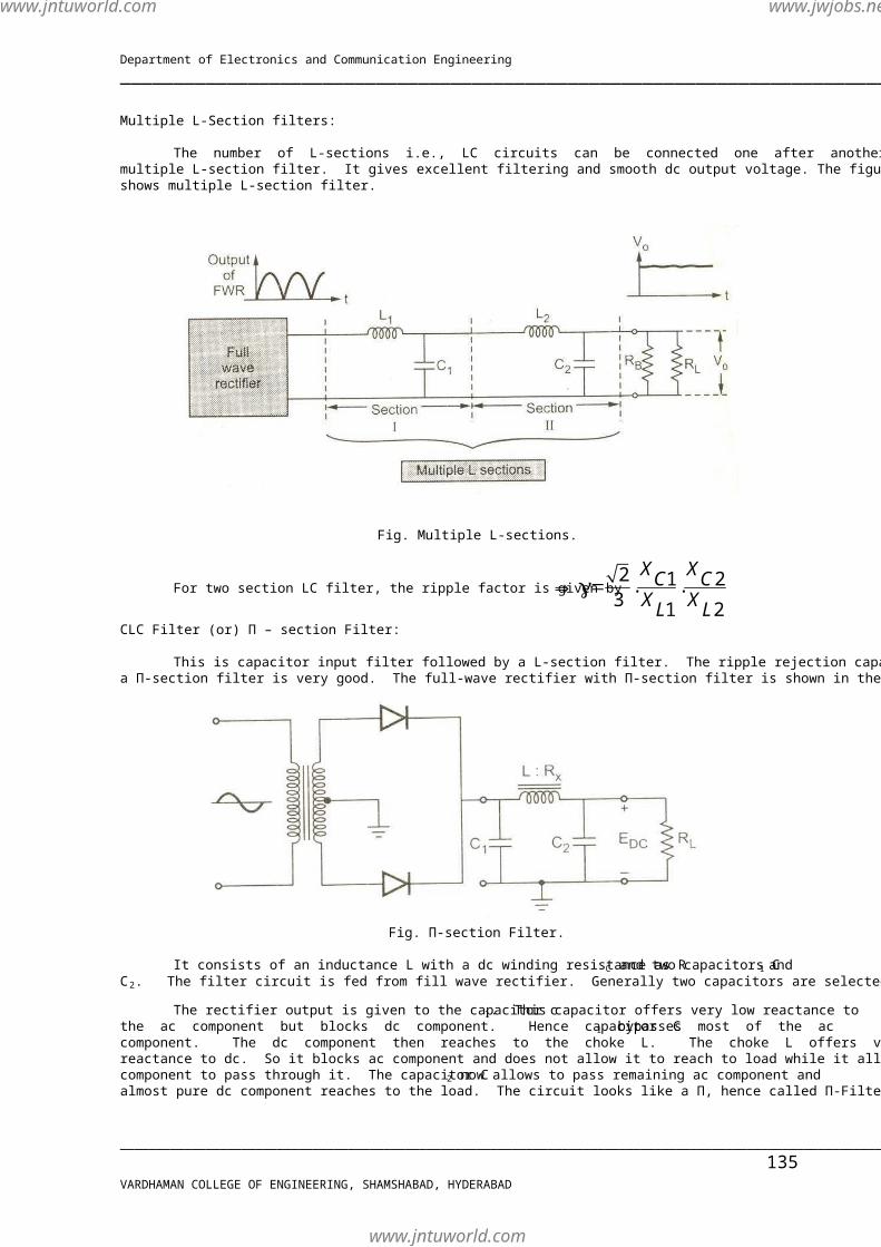
The number of L-sections i.e., LC circuits can be connected one after another to obtain multiple L-section filter. It gives excellent filtering and smooth dc output voltage. The figure below shows multiple L-section filter.
Fig. Multiple L-sections.
For two section LC filter, the ripple factor is given by 2 1 2. .3 1 2
X XC CX XL L
γ=⇒
CLC Filter (or) Π – section Filter: This is capacitor input filter followed by a L-section filter. The ripple rejection capability of a Π-section filter is very good. The full-wave rectifier with Π-section filter is shown in the figure.
Fig. Π-section Filter.
It consists of an inductance L with a dc winding resistance as RC and two capacitors C1 and C2. The filter circuit is fed from fill wave rectifier. Generally two capacitors are selected equal. The rectifier output is given to the capacitor c1. This capacitor offers very low reactance to the ac component but blocks dc component. Hence capacitor C1 bypasses most of the ac component. The dc component then reaches to the choke L. The choke L offers very high reactance to dc. So it blocks ac component and does not allow it to reach to load while it allows dc component to pass through it. The capacitor C2 now allows to pass remaining ac component and almost pure dc component reaches to the load. The circuit looks like a Π, hence called Π-Filter.
www.jntuworld.com
www.jntuworld.com
www.jwjobs.net

Department of Electronics and Communication Engineering UNIT-III -EDC ___________________________________________________________________________
_____________________________________________________________________________________________________________ VARDHAMAN COLLEGE OF ENGINEERING, SHAMSHABAD, HYDERABAD
136
Ripple Factor: The Fourier analysis of a triangular wave is given by
sin 4 sin 6sin ....2 3
V t trV tdcω ωυ ω
π
= − − + ……………(1)
In case of full wave rectifier with capacitor filter, we have proved that
12 2I Idc dcV fC fCγ= = ( )1C C here∴ = ……………(2)
The rms second harmonic voltage is
( ) 2VrVr rms = ………….(3)
Substituting the value of Vr from equation (2) in equation (3), we get
( ) 11
2 .2 2IdcV I XCr rms dcfCπ
= = …………(4)
Where 11 1
1 12 4XC C fCω π
= = = reactance of C1 at second harmonic frequency.
The voltage Vr(rms) is impressed on L-section.
Now, the ripple voltage V’r(rms) can be obtained by multiplying Vr(rms) by 2XCX L
i.e.,
( ) ( )' 1XCV Vr r rms Xrms L
= ×
(or) ( )' 22 .1XC
V I XCr dc Xrms L= …………(5)
( )'Vr rms
Vdcγ=∴
22 .1XC
I XCdc X LVdc
=
2. .1 2
.XC XC
R XL Lγ=⇒
1IdcV RLdc
=Q
2. .1 2
.XC XC
R XL Lγ∴ =
Here all reactances are calculated at second harmonic frequency. Substituting the values,
we get 2
38 1 2C C LR Lωγ=
At f= 50Hz, 57001 2LC C R L
γ=
Where C1 and C2 are in µF, L in henrys and RL in ohms.
www.jntuworld.com
www.jntuworld.com
www.jwjobs.net

Department of Electronics and Communication Engineering UNIT-III -EDC ___________________________________________________________________________
_____________________________________________________________________________________________________________ VARDHAMAN COLLEGE OF ENGINEERING, SHAMSHABAD, HYDERABAD
137
Multiple Π-Section Filter: To obtain almost pure dc to the load, more Π-sections may be used one after another. Such a filter using more than one Π-section is called multiple Π-section filter. The figure shows multiple Π-section filters.
Fig. Multiple Π-section Filter.
The ripple factor of two section Π-filter is given by 11 12 222. . .1 2
X X XC C CR X XL
γ=
Problems: 14. Design a CLC (or) Π-section filter for Vdc=10V, IL=200mA and γ=2% Solution:
VdcRL IL
= 10
3200 10= −×
= 50Ω
57001 2LC C R L
γ= 57000.021 2LC C R L
⇒ = 1141 2LC C=
If we assume L=10H and C1=C 2=C, we have
1140.02 2LC
⇒ = 11.42C
=
C2 = 750 570⇒ = 24µF
Voltage Regulators: A voltage regulator is an electronic device which produces constant output voltage irrespective of variations in the input voltage and load variations.
A voltage regulator is an electronic circuit that produces a stable dc voltage independent of the load current, temperature and ac line voltage variations. Factors determining the stability:
The output voltage VO depends on the input unregulated dc voltage Vin, load current IL and temperature T. Hence the change in output voltage of power supply can be expressed as follows:
O O OO
V V VV V I Tin LV I Tin L
∂ ∂ ∂∆ = ∆ + ∆ + ∆
∂ ∂ ∂
www.jntuworld.com
www.jntuworld.com
www.jwjobs.net

Department of Electronics and Communication Engineering UNIT-III -EDC ___________________________________________________________________________
_____________________________________________________________________________________________________________ VARDHAMAN COLLEGE OF ENGINEERING, SHAMSHABAD, HYDERABAD
138
V L TO OV S V R I S Tin∆ = ∆ + ∆ + ∆ Where the three coefficients are defined as
Input regulation factor, ; 00OVSV V TV inin
∆= ∆ ∆ =∆ =
Output resistance, ; 00O
OVR V TI inL
∆= ∆ ∆ =∆ =
Temperature coefficient, ; 00OVST V IT Lin
∆= ∆ ∆ =∆ =
Smaller the value of the three coefficients, better the regulation of power supply. Load Regulation: Load regulation is expressed as
Load regulation = V Vno load full load
Vno load
−− −
−
(or)
Load regulation = V Vno load full load
V full load
−− −
−
Where Vno-load is the output voltage at zero load current and Vfull-load is the output voltage at related load current. This is usually denoted in percentage. Zener diode voltage regulator:
Fig. Zener Regulator.
Zener voltage regulator is shown in figure above, in which a zener diode is connected in parallel to the load resistance RL. The resistance RS is a current limiting resistor. V i, RS and RL fixed:
The analysis can be carried out into two steps. i) Determining the state of the zener diode by removing it from the network and
calculating the voltage across the resulting open circuit.
R V iLV Vo R RLS= =
+
if V ≥ VZ the zener diode is ‘ON’ if V < VZ the zener diode is ‘OFF’.
www.jntuworld.com
www.jntuworld.com
www.jwjobs.net

Department of Electronics and Communication Engineering UNIT-III -EDC ___________________________________________________________________________
_____________________________________________________________________________________________________________ VARDHAMAN COLLEGE OF ENGINEERING, SHAMSHABAD, HYDERABAD
139
ii) Substitute the appropriate equivalent circuit and solve for the desired unknowns.
V VZO =
I I IZ R L= −
VZIL RL=
VRIR RS=
V V ViR Z= −
P V IZ Z Z= Problem: For the zener diode network of below figure determine VO, VR, VZ and PZ. Repeat the same with RL=3kΩ
Solution: To find the diode status, replace the diode by open circuit and by finding the voltage across the open circuit.
16 1.21 1.2V kVo k× Ω=
+ Ω
16 1.22.2Vo×= = 8.72 Volts
,V Vo Z∴ < the zener diode is in ‘OFF’ state 0IZ∴ =
8.721.2
VLIL R kL= = = 7.27 mA
16 7.271
V V VoiRIR R R k− −= = =
Ω = 8.72 mA
With RL = 3KΩ:
16 34Vo×= = 12Volts.
VO > VZ ∴ The zener diode is ‘ON’.
www.jntuworld.com
www.jntuworld.com
www.jwjobs.net

Department of Electronics and Communication Engineering UNIT-III -EDC ___________________________________________________________________________
_____________________________________________________________________________________________________________ VARDHAMAN COLLEGE OF ENGINEERING, SHAMSHABAD, HYDERABAD
140
The equivalent circuit is replacing the zener by its equivalent voltage, to determine all the parameters are shown below.
16 34VL×= = 12 Volts
Zener is ON 10V V Vo Z∴ = =
10 3.333VZI mAL R kL
= = =Ω
16 10 6 61 1V V ViR ZI mAR R R k k
− −= = = = =Ω Ω
I I IR Z L= +
I I IZ R L= − = 6-3.33 = 2.667 mA
.P V IZ Z Z= = 10x2.667 = 2.66 mW. Fixed Vi, R and variable RL:
R V iLV Vo Z R RS= =
+
Solving for RL
minR Vi ZRL V Vi Z
=−
max min
VZIL RL=
Once the diode is in ‘ON’ state V V ViR Z= −
VRIR R= I I IZ R L= −
minI I IR ZML = − max min
VZRL IL=
Problem: For the network shown below, determine the range of RL and IL that will result in VL being maintained at 10V.
www.jntuworld.com
www.jntuworld.com
www.jwjobs.net

Department of Electronics and Communication Engineering UNIT-III -EDC ___________________________________________________________________________
_____________________________________________________________________________________________________________ VARDHAMAN COLLEGE OF ENGINEERING, SHAMSHABAD, HYDERABAD
141
Solution: . 1 10 10 0.25min 50 10 40
RV k V kZR kL V Vi ZΩ× Ω= = = = Ω
− −
10 40max 0.25min
VZI mAL R kL= = =
V V ViR Z= −
50 10 40VR = − =
40 401
VRI mAR R k= = =Ω
minI I IR ZML = −
= 40-32 = 8mA 10 1.25max 8min
VZR kL I mAL= = = Ω
Fixed R, RL and variable Vi:
R V iLV Vo Z R RL= =
+
( )min
R R VL ZVi RL
+=
maxI I IR ZM L= +
VZIZ RL
=
max maxV V Vi R Z= +
( ).max maxV I RR R=
Problem:
Determine the range of values of Vi, that will maintain the zener diode of figure below is in the ‘ON’ state. Solution: Vimin = 23.67V Vimax = 36.87V
( )min
R R VL ZVi RL
+=
( )220 1200 20 23.671200 V+
= =
www.jntuworld.com
www.jntuworld.com
www.jwjobs.net

Department of Electronics and Communication Engineering UNIT-III -EDC ___________________________________________________________________________
_____________________________________________________________________________________________________________ VARDHAMAN COLLEGE OF ENGINEERING, SHAMSHABAD, HYDERABAD
142
max maxV V Vi R Z= +
( )maxI R VR Z= +
( )I I R VZM L Z= + +
( )2060 220 201.2mA k
= + +
=36.87 Volts Basic Voltage Regulator: The basic voltage regulator in its simplest form consists of,
i) Voltage reference, VR ii) Error amplifier iii) Feedback network iv) Active series (or) shunt control element.
The voltage reference generally a voltage level which is applied to the comparator circuit,
which is generally error amplifier. The second input to the error amplifier is obtained through feedback network. Generally using the potential divider, the feedback signal is derived by sampling the output voltage. The error amplifier converts the difference between the output sample and the reference voltage into an error signal. This error signal in turn controls the active element of the regulator circuit, in order to compensate the change in the output voltage. Such an active element is generally a transistor. Thus the output voltage of the regulator is maintained constant. Types of voltage Regulators: There are two types of voltage regulators available namely,
i) Shunt voltage regulator ii) Series voltage regulator
Each type provides a constant dc output voltage which is regulated. Shunt Voltage Regulator: The heart of any voltage regulator circuit is a control element. If such a control element is connected in shunt with the load, the regulator circuit is called shunt voltage regulator.
The figure shows the block diagram of shunt voltage regulator circuit.
Fig. Block diagram of shunt voltage regulator.
www.jntuworld.com
www.jntuworld.com
www.jwjobs.net

Department of Electronics and Communication Engineering UNIT-III -EDC ___________________________________________________________________________
_____________________________________________________________________________________________________________ VARDHAMAN COLLEGE OF ENGINEERING, SHAMSHABAD, HYDERABAD
143
The unregulated input voltage Vin, tries to provide the load current. But part of the current is taken by the control element, to maintain the constant voltage across the load. If there is any change in the load voltage, the sampling circuit provides a feedback signal to the comparator circuit.
The comparator circuit compares the feedback signal with the reference voltage and generates a control signal which decides the amount of current required to be shunted to keep the load voltage constant.
For example, if load voltage increases then comparator circuit decides the control signal based on the feedback information, which draws increased shunt current Ish value.
Due to this, the load current IL deceases and hence the load voltage decreases to its normal.
Thus control element maintains the constant output voltage by shunting the current; hence the regulator circuit is called voltage shunt regulator circuit. Series Voltage Regulator:
If in a voltage regulator circuit, the control element is connected in series with the load, the circuit is called series voltage regulator circuit.
Figure shows the block diagram of series voltage regulator circuit.
The unregulated dc voltage is the input to the circuit.
Fig. Block diagram of series voltage regulator.
The control element controls the amount of the input voltage that gets to the output. The sampling circuit provides the necessary feedback signal. The comparator circuit compares the feedback with the reference voltage to generate the appropriate control signal.
For example, if the load voltage tries to increase, the comparator generates a control signal
based on the feedback information. This control signal causes the control element to decrease the amount of the output voltage. Thus the output voltage is maintained constant.
Thus, the control element which regulates the load voltage, based on the control signal is in
series with the load and hence the circuit is called series voltage regulator circuit.
www.jntuworld.com
www.jntuworld.com
www.jwjobs.net

Department of Electronics and Communication Engineering UNIT-III -EDC ___________________________________________________________________________
_____________________________________________________________________________________________________________ VARDHAMAN COLLEGE OF ENGINEERING, SHAMSHABAD, HYDERABAD
144
Comparison of Shunt and Series voltage regulators:
Sl. No. Shunt Regulator Series Regulator
1. The control element is in parallel with the load.
The control element is in series with the load.
2. Only small current passes through the control element which is required to be diverted to keep output constant
The entire load current IL always passes through the control element.
3. Any change in output voltage is compensated by changing the current Ish through the control element as per the control signal.
Any change in output voltage is compensated by adjusting the voltage across the control element as per the control signal.
4. The control element is low current, high voltage rating component.
The control element is high current, low voltage rating component.
5. The regulation is poor. The regulation is good.
6. Efficiency depends on the load current. Efficiency depends on the output voltage.
7. Not suitable for varying load conditions. Preferred for fixed voltage applications.
Preferred for fixed as well as variable.
8. Simple to design. Complicated to design as compared to shunt regulators.
9. Examples: Zener Shunt regulators, transistorized shunt regulator etc.,
Examples: Series feedback type regulator, series regulator with pre-regulator and feedback limiting etc.,
www.jntuworld.com
www.jntuworld.com
www.jwjobs.net