FILTERS AND ATTENUATORS - World Radio History
93
ELECTRONIC TECHNOLOGY SERIES a FILTERS AND ATTENUATORS .... •',,'. ' \ ·. . · ... ' . ·\c:;-/_. ;,',:_ •' .~ ;· . . '~ .. . , . publication l•
-
Upload
khangminh22 -
Category
Documents
-
view
1 -
download
0
Transcript of FILTERS AND ATTENUATORS - World Radio History

ELECTRONIC TECHNOLOGY SERIES
a
FILTERS AND ATTENUATORS
.... •',,'. ' \ ·. . ~ · ... '
. ·\c:;-/_. ;,',:_ •' .~ ;· . . '~ .. . , .
publication
l •

FILTERS AND ATTENUATORS
edited by
Alexander Schure Ph.D., Ed.D.
JOHN F. RIDER PUBLISHER, INC., NEW YORK a division of HAYDEN PUBLISHING COMPANY, INC.

COPYRIGHT APRIL 1961 BY JOHN F. RIDER PUBLISHER, INC.
All rights reserved. This book or any parts thereof may not be reproduced in any form or any language without permission of the publisher.
LIBRARY OF CONGRESS CATALOG CARD NUMBER 61-7326 Printed in the United States of America
Reprinted, 1964
PREFACE
This hook deals with the major factors and new techniques in filters and attenuators. The problems inherent in this field are discussed fully, step-by-step, as a technician would encounter them on the job.
Detailed attention is given to the general characteristics of low-pass filters, choke-input filter systems, capacitor-input filter systems, tuned low-pass filters, graded filters and cancellation filters.
The problems of audio filters and radio and television filters receive special attention, with special emphasis on decoupling filters, tone controls, speech clipping, high-fidelity filters, Scott filters and high- and low-frequency compensation filters. The prolems of traps in television receivers, transmission filters, noise filters, crystal filters and interference filters are also fully discussed.
We have covered large areas such as wave filters and attenuators and equalizers and given special treatment to filter classifications, characteristic impedance, filter configurations, constant-k and derived-m filters, and a host of others dealing with configurations. Bridged-T and parallel-T networks and their applications are fully dealt with.
Attenuators and equalizers are discussed, ranging from definitions and examples of fixed attenuators through amplitude equalizers, phase equalizers and resistance pads, noting their types and design.
Through these discussions the eal'nest reader will establish a foundation for advanced concepts.
Grateful acknowledgment is made to the staff of the New York Institute of Technology for their assistance and cooperation.
New York, New York April, 1961
V
A.S.

CONTENTS
Chapter I
INTRODUCTION TO FILTERS AND ATTENUATORS
The function of a Filter • Types of Filters
Chapter 2
SMOOTHING FILTERS FOR POWER SUPPLIES
Chapter 3
Genera/ Characteristics of Power Supply Fillers • Ripple Voltage, Capacitor-Input Filler • Oufpuf Voltage and Voltage Regulation, Capacitor Input • Rectifier Considerations in Capacitor-Input Filters • Choice-Input Fi/fer • Ripple Voltage al Choice-Input Fi/fer Systems • Voltage Regulation of Choice-Input Filters • The Oufpuf Capacitor • Swinging Choice • Tuned Low-Pou Filters • R-C Filters for Power
Supplies • Graded Filters • Cancellation Filters.
AUDIO FILTERS
Chapter 4
Genera/ Information • Decoupling Filters • Tone Control Considerations • Resonant Tone Compensation • Nonresononf Tone Compensation • SpHch Clipping • Crossover Nefworlcs • Presence Confro/ • Rumble
and Scratch Filters • High Fidelity Equalizer • Scoff Fi/fer.
VIDEO FILTERS
The Need for Video Filters • High-Frequency Compensation - Shunt Peolcing • High-Frequency Compensation - Series Peolcing • High-Fr•• quency Compensation - Combination Peolcing • low-frequency Compensation Fi/fer • Rejection Filters • Sideband Suppression filters in
Television
1
7
26
43
Chapter 5
WA VE FILTERS
Chapter 6
Filter Classifications • Effectiveness of Attenuation and Transmission • Characteristic Impedance • Basic Filter Configurations • Characteristic Impedances of Filter Sections • Constant-le Filters Defined • low-Pass Constant-le Filter • High-Pass Constant-le Filter • Bandpass Constant-le Filter • Band-Elimination Constant-le Filter • m-Derived Filters Defined • m-Derived T-Sedions • Examples of m-Derived Filter Sections • Bridged-T
and Parallel-T Configurations • Frequency-Selective Amplifier
ATTENUATORS AND EQUALIZERS
Definition of an Attenuator • Fundamentals of Fixed Attenuators • Determination of RI, R2, and R3 in Fixed Attenuators • Variable Attenuator Requirements • Types of Variable Pads • Fundamentals of
Equalizers • Equalizer Types • Phase Equalizers •
INDEX ...
viii
52
68
85
Chapter 1
INTRODUalON TO FILTERS AND ATTENUATORS
1. The Fundion of a Filter
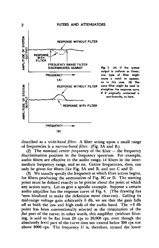
Like many technical words coined initially to describe a specialized function, the word filter has broadened in scope with the passing years. Despite the many phases of electricity and electronics in which it occurs, however, the word has retained its original core meaning. Any filter, whether in a power supply, a high-fidelity amplifier, a radiotelephone transmitter, a keying system, an antenna, or a transmission line, is a frequency-sensitive device discriminating against certain frequencies in favor of others. In most filters discrimination is accomplished by weakening a preselected range of frequencies while others are untouched, causing the system response curve to undergo a reduction in amplitude for the filtered range. This does not lead to a depression in the response curve (Fig. IA) if the plot of amplitude vs frequency possesses a non-linearity in the form of a raised bump, (Fig. IB) . A filter of this type may be employed to straighten out the curve.
Certain filter arrangements may produce frequency discrimination by boosting rather than weakening ·a selected group or range of frequencies. Here again, the result of such peaking may raise a bump in the response curve which was not there initially (Fig. 2A) , or may straighten out a curve that has an undesirable depression in it(Fig. 2B) .
In discussing the action of any filter network or group of filter components working together to consummate the desired frequency discrimination, we must consider several factors. Broadly outlined, these are:
(l) The range of frequencies covered. If the filter is designed to weaken, or attenuate, a relatively large range, it may be generally
2 FILTERS AND ATTENUATORS
:::E
~ RESPONSE WITHOUT FILTER
liil- / ~~1----~f~,-~-,---l&J I- RESPONSE /' -- _/ l g5 WITH -I- FILTER ~ :::E
"'
:::E II.I
Iii ~
FREQUENCY RANGE FILTER DISCRIMINATES AGAINST
FREQUENCY
(A)
RESPONSE WITHOUT FILTER
/ 11.. I-
~ ~ f----------·--\-:ESPONSE WITH FILTER
1-:J Q. :::E
"' FREQUENCY
(8)
Fig. 1. (A) If the system output is uniform or linear, one type of filter might cause a notch to appear, as in this case. (B) The same filter might be used to straighten the response curve if it originolly contained a
non-linearity, as here.
described as a wide-band filter. A filter acting upon a small range of frequencies is a narrow-band filter. (Fig. 3A and B.)
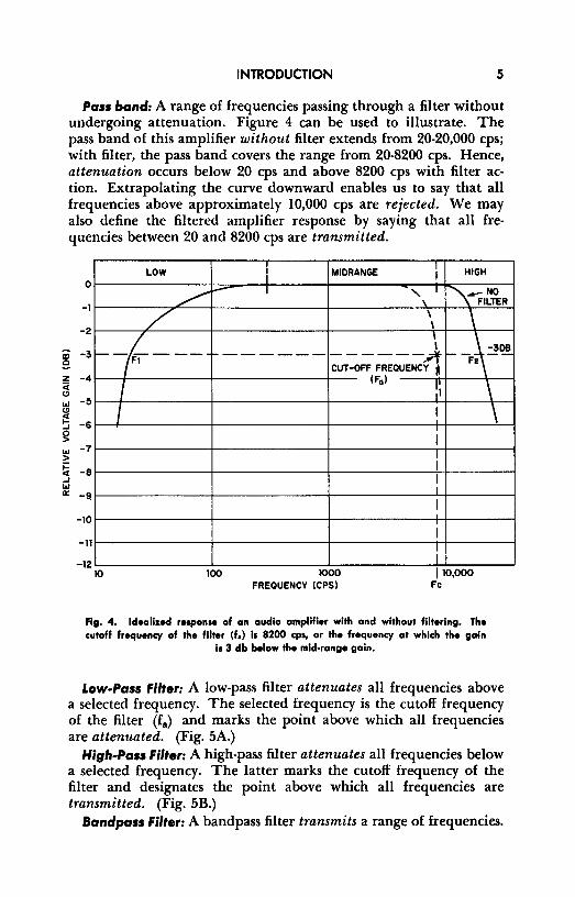
(2) The nominal center frequency of the filter - the frequency discrimination position in the frequency spectrum. For example, audio filters are effective in the audio range, i-f filters in the intermediate frequency range, and so on. Center frequencies, then, can only be given for filters like Fig. 3A and B, and not C and D.
(3) We usually specify the frequency at which filter action begins, for filters producing the attenuation of Fig. 3C or D. The starting point must be defined exactly to be precise about the point at which any action starts. Let us give a specific example. Suppose a certain audio amplifier has the response curve of Fig. 4. (The drawing has '>een idealized to make the definition more clear-cut). Calling its mid-range voltage gain arbitrarily O db, we see that the gain falls off at both the low and high ends of the audio band. The -3 db point has been conventionally selected as the termination of the flat part of the curve; in other words, this amplifier (without filtering, is said to be flat from 20 cps to 20,000 cps, even though the absolutely level part of the curve does not extend below 300 cps nor above 8000 cps. The frequency fl is, therefore, termed the lower

INTRODUCTION 3
cutoff frequency of the amplifier and f2 the upper cutoff frequency. Assume now that a filter is introduced to attenuate the response
at the high end of the band. Using the same -3 db level as for the amplifier cutoff frequencies, we say that the cutoff frequency of the filter (symbolized f0 ) is that frequency at which the amplifier gain is brought down 3 db below the mid-range gain. Hence, the starting point for filter action, or f0 in this example, is 8200 cps.
(4) Filters are sometimes classified in terms of the slope of their ·characteristic below f11 • The curve of Fig. 3C might be termed
/WITH FILTER
w /~ 0 / \ :> , \ I- ,, '
Q.:J 1----------1'---:-'---t i-... ~WITHOUT ;'i I FILTER
FILTER RANGE
FREQUENCY----
(A)
~ /WITH FILTER
:J t--..--------------- ~--Q. :E C(
WITHOUT FIL'fER
FREQUENCY ----o•
(Bl
Fig. 2. (A) A peaking filter will produce a bump in an otherwise linear response curve. (B) The action of the same filter on a non-linear curve having a corresponding
depression.
gradual cutoff to distinguish it from that of 3D, which is a much sharper cutoff type of curve.
2. Types of Filters - Filter Vocabulary
The descriptive terms used in the chapters that follow, although not solely associated with filters have common and specific technical meanings. It would be helpful to know the basic definitions of the

FILTERS AND ATTENUATORS
WIDE BAND l&.I ATTENUATION 0 ::) I I- I
~ \ I , .. _______ .,
2 t c(
CENTER
FREQUENCY ---(Al
1&.1 UNFILTERED Oi.---------~ ......... - ..... i ,,, ... __ _ ~ FILTERED
FREQUENCY--
( Cl
NARROW BAND
l&.I ATTENUATION
0 ' , ::) I / I-
'I :i Q. u 2 c( t
CENTER
FREQUENCY-
(Bl
1&.1 UNFILTERED @ 1-------, -----~ \ ~ '-7-----
FILTERED
FREQUENCY --( D)
Fig. 3. (A) A wide-band filter attenuates a broad range of frequencies on either side of Its center frequency. (B) A narrow-band filter attenuates a small range an either side of the center. (C) This filtering action Is gradual. (D) A sharp cutoff
filter In action.
more important of these terms. Their exact significance will be fully treated in context.
Transmission: As specifically applied to filters, transmission implies the act of carrying a frequency or a range of frequencies from the input to the output of the filter without weakening it significantly. The -3 db point, as previously discussed, is generally taken as the point at which significant weakening begins.
Attenuation: This term is the opposite of transmission. When a signal is reduced in amplitude to the extent of a 3 db drop, as compared with its original value, attenuation is said to begin. Any further diminution of amplitude may be described in terms of attenuation in db.
Re;ection: A specific frequency or range of frequencies is said to be rejected if it has been attenuated sufficiently to meet predetermined specifications. For instance, if a given radio signal interfering with a desired frequency is reduced to a value which makes it inaudible in a specific receiver, it is considered rejected.
INTRODUCTION 5
Pass band: A range of frequencies passing through a filter without undergoing attenuation. Figure 4 can be used to illustrate. The pass band of this amplifier without filter extends from 20-20,000 cps; with filter, the pass band covers the range from 20-8200 cps. Hence, attenuation occurs below 20 cps and above 8200 cps with filter action. Extrapolating the curve downward enables us to say that all frequencies above approximately 10,000 cps are rejected. We may also define the filtered amplifier response by saying that all frequencies between 20 and 8200 cps are transmitted.
0
-1
-2
iii -3 e z -4 ci Cl w -5 ~ ~ -6 ~ w -7 > ~ -8 .j w a: -9
-10
-11
-12
LOW I MIDRANGE I
HIGH I I
~ ..... I -"' I \-NO
\ FILTER
/ \ \ \ I I --f--- -------------..,...--,. ,~-3DB i- -F --
I I
lO 100
CUT-OFF FREQUENCY -(Fal I:
IOOO FREQUENCY (CPS)
11
I I I
I I I I I
I I
I
: 110,000
Fe
\ \
Fig. 4. Idealized response of on audio amplifier with and without filtering. The cutoff frequency of the filter (fa) Is 8200 cps, or the frequency at which the gain
is 3 db below the mid-range gain.
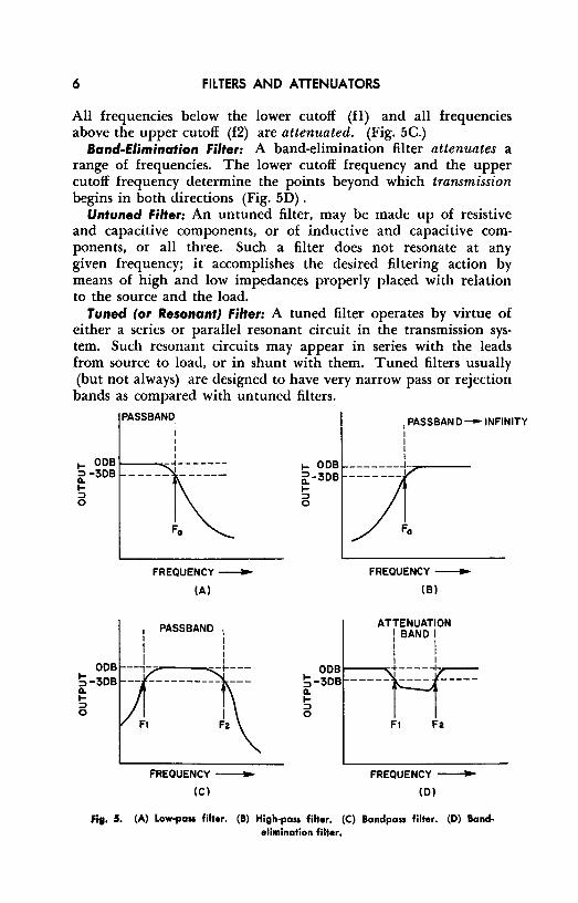
I.ow-Pass FIiter: A low-pass filter attenuates all frequencies above a selected frequency. The selected frequency is the cutoff frequency of the filter (fa) and marks the point above which all frequencies are attenuated. (Fig. 5A.)
High-Pass Filter: A high-pass filter attenuates all frequencies below a selected frequency. The latter marks the cutoff frequency of the filter and designates the point above which all frequencies are transmitted. (Fig. 5B.)
Bandpass Filter: A bandpass filter transmits a range of frequencies.
6 FILTERS AND ATTENUATORS
All frequencies below the lower cutoff (fl) and all frequencies above the upper cutoff (f2) are attenuated. (Fig. 5C.)
Sand-Elimination Filter: A band-elimination filter attenuates a range of frequencies. The lower cutoff frequency and the upper cutoff frequency determine the points beyond which transmission begins in both directions (Fig. 5D) .
Untuned Filter: An untuned filter, may be made up of resistive and capacitive components, or of inductive and capacitive components, or all three. Such a filter does not resonate at any given frequency; it accomplishes the desired filtering action by means of high and low impedances properly placed with relation to the source and the load.
Tuned (or Resonant) Filter: A tuned filter operates by virtue of either a series or parallel resonant circuit in the transmission system. Such resonant circuits may appear in series with the leads from source to load, or in shunt with them. Tuned filters usually (but not always) are designed to have very narrow pass or rejection bands as compared with untuned filters.
PASSBAND I I I I
~ 00Bi-----...,--~------~-30B ~ ::, 0
OOB ~-30B 0.. ~ ::, 0
FREQUENCY
(A)
PASSBAND
FREQUENCY -
(Cl
~ ODB ~-3DB ~ ::, 0
1 PASSBAND- INFINITY
I I I I _______ j __ ,__ __ _
FREQUENCY_
(Bl
ATTENUATION I BAND I I I I I I I
OOBt---~+----+. ~-3DB 0.. ~ ::, 0
F1 F2
FREQUENCY --
(0)
fit. 5. (A) Low-poss filter. (B) H;gh•pass filter. (C) Bandpass filter. (0) Bandelimination filter.
Chapter 2
SMOOTHING FILTERS FOR POWER SUPPLIES
3. General Charaderistics of Power Supply Filters
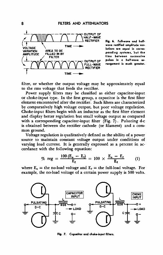
The output voltage from a rectifier device has a pulsating waveform which must be smoothed to prevent the supply from introducing hum into the equipment it supplies with power. Although the voltage amplitude variations from a full-wave system are just as severe as those obtained by half-wave rectification, full-wave output is easier to filter because the gaps that require filling in are much smaller (Fig. 6) .
A practical filter network generally contains a combination of capacitors and resistors, or capacitors and inductors. In some cases, all three circuit elements are found in the same filter system. Generally L-C circuits are used when the current flowing through the load is fairly large and where good voltage regulation is demanded. In power supplies provided for small, constant-current electronic devices, it is often possible to eliminate the inductor entirely, and to use a resistor in its place. Such networks are known as R-C filters and may be found in small table-top radios, portable a-c phonographs, and similar low-power devices.
The design and construction of a practical power supply requires consideration of:
(a) The maximum tolerable hum or ripple content of the d-c output.
(b) The desired voltage regulation. (c) The maximum load current anticipated. (d) The output voltage desired. That is, whether the designer
wishes to make use of the peak value of pulsating voltage fed to the
7
8 FILTERS AND ATTENUATORS
_j_~-n--rs ~~F~~A~ r-r .___....~.___.__,...__.__,...__. RECTIFIER
VOLTAGE \ TIME __.. VARIATION AREA TO BE AMPLITUDE FILLED IN BY
~_L / FILTER
~OUTPUTOF FULL-WAVE
T ._____..._....__,.____..._.J.-__,.___. RECTIFIER
TIME__..
Fig. 6. Full-wave and halfwave rectified amplitude variations are equal In corresponding systems, but the time between successive pulses in a half-wave arrangement is much greater.
filter, or whether the output voltage may be approximately equal to the rms voltage that feeds the rectifier.
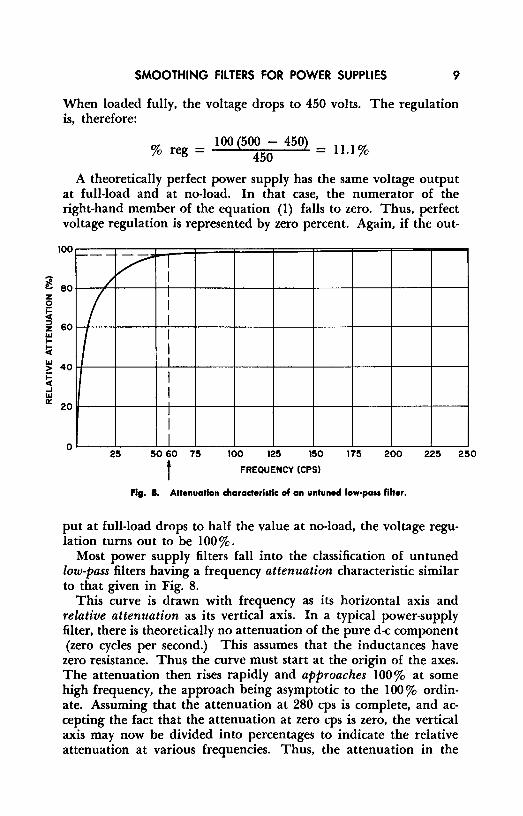
Power supply filters may be classified as either capacitor-input or choke-input type. In the first group, a capacitor is the first filter element encountered after the rectifier. Such filters are characterized by comparatively high voltage output, but poor voltage regulation. Choke-input filters begin with an inductor as the first filter element and display better regulation but small voltage output as compared with a corresponding capacitor-input filter (Fig. 7) . Pulsating d-c is obtained between the rectifier cathode (or filament) and a common ground.
Voltage regulation is qualitatively defined as the ability of a power source to maintain constant voltage output under conditions of varying load current. It is generally expressed as a percent in accordance with the following equation:
01. _ 100 (En - Et) _ 100 En - Et ;oreg- Et - X Et (1)
where En = the no-load voltage and Et = the full-load voltage. For example, the no-load voltage of a certain power supply is 500 volts.
CAPACITOR INPUT
+ -LOAD
r Fig. 7. Capacitor and choke-input filters.
[CHOKEl ~
;e !.,.
z 0
fi ::> z l&I I-
~ l&I > 5 .J l&I Q:
SMOOTHING FILTERS FOR POWER SUPPLIES 9
When loaded fully, the voltage drops to 450 volts. The regulation is, therefore:
ct_ _ 100 (500 - 450) _ I I I ct_ 1o reg -
450 - . 10
A theoretically perfect power supply has the same voltage output at full-load and at no-load. In that case, the numerator of the right-hand member of the equation (1) falls to zero. Thus, perfect voltage regulation is represented by zero percent. Again, if the out-
100
80
60
- -
V I / I
I I I I
I I I
40 I
I I
20 I
I 0 I
25 50 60 75 100 125 150 175 200 225 250
t FREQUENCY (CPS)
Fl9. 8. Attenuation charaderistic of an untuned law-pass filter.
put at full-load drops to half the value at no-load, the voltage regulation turns out to be 100%.
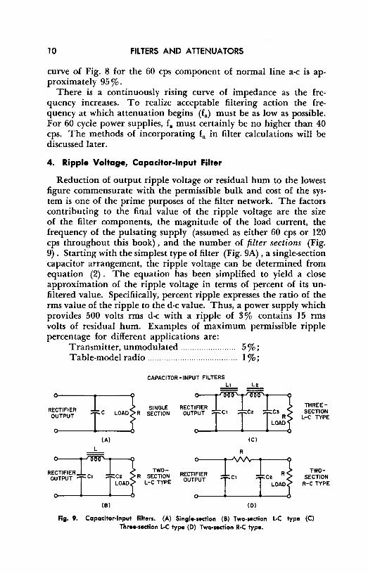
Most power supply filters fall into the classification of untuned low-pass filters having a frequency attenuation characteristic similar to that given in Fig. 8.
This curve is drawn with frequency as its horizontal axis and relative attenuation as its vertical axis. In a typical power-supply filter, there is theoretically no attenuation of the pure d-c component (zero cycles per second.) This assumes that the inductances have
zero resistance. Thus the curve must start at the origin of the axes. The attenuation then rises rapidly and approaches 100% at some high frequency, the approach being asymptotic to the 100% ordinate. Assuming that the attenuation at 280 cps is complete, and accepting the fact that the attenuation at zero cps is zero, the vertical axis may now be divided into percentages to indicate the relative attenuation at various frequencies. Thus, the attenuation in the
10 FILTERS AND ATTENUATORS
curve of Fig. 8 for the 60 cps component of normal line a-c is approximately 95 % .
There is a continuously rising curve of impedance as the frequency increases. To realize acceptable filtering action the frequency at which attenuation begins (fa) must be as low as possible. For 60 cycle power supplies, fa must certainly be no higher than 40 cps. The methods of incorporating fa in filter calculations will be discussed later.
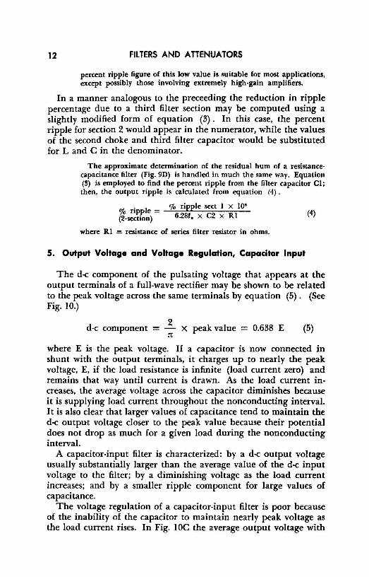
4. Ripple Voltage, Capacitor-Input Filter
Reduction of output ripple voltage or residual hum to the lowest figure commensurate with the permissible bulk and cost of the system is one of the prime purposes of the filter network. The factors contributing to the final value of the ripple voltage are the size of the filter components, the magnitude of the load current, the frequency of the pulsating supply (assumed as either 60 cps or 120 cps throughout this book) , and the number of filter sections (Fig. 9) . Starting with the simplest type of filter (Fig. 9A) , a single-section capacitor arrangement, the ripple voltage can be determined from equation (2) . The equation has been simplified to yield a close approximation of the ripple voltage in terms of percent of its unfiltered value. Specifiically, percent ripple expresses the ratio of the rms value of the ripple to the d-c value. Thus, a power supply which provides 500 volts rms d-c with a ripple of 3% contains 15 rms volts of residual hum. Examples of maximum permissible ripple percentage for different applications are:
Transmitter, unmodulated . . .. . . . . . . .. .. .. . . . . . .. 5 % ; Table-model radio . . . . . . . . . . . . . . . . . .. . . . . . . . . . 1 % ;
RECTIFIER OUTPUT
RECTIFIER OUTPUT
L
IA)
C2 R LOAD
(Bl
CAPACITOR-INPUT FILTERS L1
SINGLE RECTIFIER SECTION OUTPUT Cl
TWO-RECTIFIER SECTION
OUTPUT L-C TYPE
C2
IC)
R
Cl
ID)
Cs R
LOAD
C2 R
LOAD
THREESECTION
L-C TYPE
TWO-SECTION
R-C TYPE
Fig. 9. Capacitor-input filters. (A) Single-section (B) Two-section L-C type (C) Three-section L-C type (D) Two-section R-C type.

SMOOTHING FILTERS FOR POWER SUPPLIES
Voice transmitters. High-fidelity amplifiers
. 2245 X 104
% ripple = f R Cl R L
0.25%; less than 0.1 % .
11
(2)
where f. = pulsating supply frequency, cps. Rr. = load resistance, ohms, Cl = capacitance, µ.f
Example: Find the percent ripple of a single-section filter of the capacitor-input type used after a full-wave recifier if the load resistance is 10,000 ohms and the filter capacitor has a value of 20 µf. Assume a 60 cps line frequency.
Solution: Since the rectifier is full-wave, the ripple frequency is 120 cps. Substituting the values given in equation (2) :
. 2245 X 10' % npple = 120 X 10,000 X 20
% ripple = 0.94%
As shown in equation (2) , when the supply frequency is fixed, the ripple percentage can be reduced by increasing the load resistance or the capacitance of the filter section, or both. Although it is possible to obtain low ripple by making the capacitance increasingly larger, it is not economical, as large capacitors are expensive. Further, if the load varies over an appreciable range, such a filter arrangement displays poor voltage regulation. The preferred alternative is adding one or more filter sections.
Equation (2) is equally valid for finding the ripple percentage output of the first filter section of a multi-section network. Assuming that an inductor and a second capacitor are added as in Fig. 9B, the ripple percentage may now he found from equation (3).
. _ % ripple sect. 1 % n~ple - J[I0-6 (2 f) 2L C2} - 1 L (3) (2-secuon) , n: r
where L is the inductance of the choke in henries and C2 is the capacitance of the second capacitor in µf.
Example: Assume that a IO-henry choke and a second 20-µf capacitor are added to the filter system of the previous example. Find the percent ripple output from this section.
Solution: The percent ripple as previously obtained was 0.94%, Thus:
0.94 % ripple = -----------------(2-section) -( [IO .. (6.28 x 120) 2 x 10 x 20) - I}-
0.94 % ripple = [ IO·• (5.67 X 10⁵) (2 X 10²) - I]
= 0.0085%
The efficacy of the second filter section is thus easily established. A
12 FILTERS AND ATTENUATORS
percent ripple figure of this low value is suitable for most applications, except possibly those involving extremely high-gain amplifiers.
In a manner analogous to the preceeding the reduction in ripple percentage due to a third filter section may be computed using a slightly modified form of equation (3) . In this case, the percent ripple for section 2 would appear in the numerator, while the values of the second choke and third filter capacitor would be substituted for Land C in the denominator.
The approximate determination of the residual hum of a resistancecapacitance filter (Fig. 9D) is handled in much the same way. Equation (ll) is employed to find the percent ripple from the filter capacitor Cl; then, the output ripple is calculated from equation (4) .
ot. • 1 % ripple sect I x 10• , 0 npp e = (2•section) 6.28£, X C2 X RI (4)
where RI = resistance of series filter resistor in ohms.
5. Output Voltage and Voltage Regulation, Capacitor Input
The d-c component of the pulsating voltage that appears at the output terminals of a full-wave rectifier may be shown to be related to the peak voltage across the same terminals by equation (5). (See Fig. 10.)
2 d-c component = - X peak value = 0.638 E (5)
n:
where E is the peak voltage. If a capacitor is now connected in shunt with the output terminals, it charges up to nearly the peak voltage, E, if the load resistance is infinite (load current zero) and remains that way until current is drawn. As the load current increases, the average voltage across the capacitor diminishes because it is supplying load current throughout the nonconducting interval. It is also clear that larger values of capacitance tend to maintain the d-c output voltage closer to the peak value because their potential does not drop as much for a given load during the nonconducting interval.
A capacitor-input filter is characterized: by a d-c output voltage usually substantially larger than the average value of the d-c input voltage to the filter; by a diminishing voltage as the load current increases; and by a smaller ripple component for large values of capacitance.
The voltage regulation of a capacitor-input filter is poor because of the inability of the capacitor to maintain nearly peak voltage as the load current rises. In Fig. IOC the average output voltage with

SMOOTHING Fil TERS FOR POWER SUPPLIES 13
A-C
(Al D-C
l NONCONDUCTING COMPONENT -- L INTERVAL l E ..:._~2E/-r
f TIME- t (Bl
INPUT CAPACITOR
TIME - LOW LOAD RESISTANCE
(Cl
Fig. 10. (A) Full-wave circuit, no filter. (B) Output waveform of full-wave rectifier. (C) Capacitor charge and discharge curves for large and small load cur•
rents.
larger load currents is smaller than it is for small load currents. The output voltage vs load current curve of a typical capacitor-input filter power supply is illustrated in Fig 11. It is important to recognize that the ripple voltage must increase as the d-c output component decreases. Hence, capacitor-input filter systems are afflicted by increasing hum voltages with larger load currents.
Capacitor-input filter systems are used in small receivers, publicaddress systems, and low-powered transmitter power supplies. When the amount of power required is large, choke-input filters are generally preferred. If regulation is important, as in power supplies that feed class-B amplifiers, capacitor-input is usually unsatisfactory.
6. Redifier Considerations in Capacitor Input Filters
Filter systems introduce a peak current factor in the selection of a rectifier which does not enter into design considerations when

14
() I
0
(/)
~ 0 > I-:::, Q. I-:::, 0
a:: w I-..J ...
FILTERS AND ATTENUATORS
400 RECTIFIER - 5U4GA A-C ( RMS PER PLATE)
-240 VOLTS CAPACITOR - 4 p.F
200
\
\ I \
100 _CHO~-lNPUT I
CRITICAL CURRENT
0'---'25--'50--7~5--10~0--12~5-1~5~0__.175
LOAD CURRENT (MA)
Fig. 11. Curve put voltage vs
showing out-load current.
filters are not used. Rectifier tubes are normally rated in terms of both d-c output current and peak current per plate. For example, the 5U4-GA has a d-c output current rating of 225 ma and a peak plate current rating per plate of 675 ma.
During operation, the plate current in the rectifier flows in short pulses. The flow occurs only during the period when the input capacitor must be brought back to peak charge, after having discharged a portion of its energy into the load. The peak current that flows
w (!)
~ ..J 0 >
1-z w a:: a:: ::,
0
() 0
,,,,- CHARGING INTERVAL
,- \ "
TUBE CURRENT
_....., TIME
___.. TIME
Fig. 12. The relationship between current through a rectifier tube and the voltage across the input capacitor in a capacitor-input type of fil-
ter network.
SMOOTHING FILTERS FOR POWER SUPPLIES 15
during this interval is a function of the load resistance particularly, and of the transformer secondary impedance to a somewhat lesser degree. A low value of load resistance discharges the input capacitor during the non-conducting portion of the cycle to a much greater extent than a high load resistance. Hence, the charging current fl.owing through the rectifier to restore the capacitor fo its peak potential is also large. The only factor that limits the peak value of the charging current is the input impedance (transformer secondary impedance) to the rectifier.
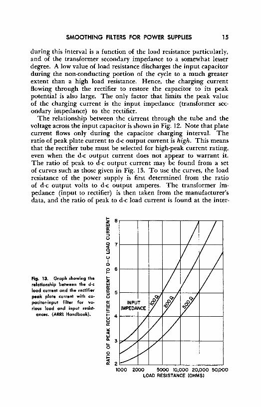
The relationship between the current through the tube and the voltage across the input capacitor is shown in Fig. 12. Note that plate current flows only during the capacitor charging interval. The ratio of peak plate current to d-c output current is high. This means that the rectifier tube must be selected for high-peak current rating, even when the d-c output current does not appear to warrant it. The ratio of peak to d-c output current may be found from a set of curves such as those given in Fig. 13. To use the curves, the load resistance of the power supply is first determined from the ratio of d-c output volts to d-c output amperes. The transformer impedance (input to rectifier) is then taken from the manufacturer's data, and the ratio of peak to d-c load current is found at the inter-
Fig. 13. Graph showing the relationship between the d-c load current and the rectifier peak plate current with ca• pacitor-input filter for va• rious load and input resist-
ances. (ARRL Handbook).
~ 8.-----r-...,......-...,......-~--~-~~ ILi a: a: ~ u 0 7t---+--+--+---+--+--+-.,_-----I
9 u I
0
~ 6 1-z ILi a: ~ 51----+-+-~#---+l---+-------I u a: ILi ii'. t 41----+-,'l-~-------+-------I l&.I a: ~ <(
~ 31-,,,'---,t<-+---,,C.+---+---+-------I L,.
0 0
~ a: 2~-~-~--'---'---~---'
1000 2000 5000 10,000 20,000 50,000 LOAD RESISTANCE (OHMS)

16 FILTERS AND ATTENUATORS
section of the input impedance curve and the load resistance coordinate. Three curves are given to permit interpolation for any value of input impedance between 100 and 500 ohms.
Example: A transformer having an input impedance of 100 ohms provides a d-c output from the rectifier filter system of 400 volts. If the total load current is 125 ma, find the peak rectifier plate current.
Solution: First determine the load resistance.
400 RL = .125
Rt = 3200 ohms
Referring to the curves in Fig. 13, we find that a load resistance intersects the 100 ohm input impedance curve at a ratio of 4.25 to I.
Thus, for a load current of 125 ma, the peak rectifier current rating for this example must be at least 4.25 x 125 = 532 ma. A check through the tube manual tables discloses that the 5Y3-GT, for example, has a full-load d-c output current rating of 125 ma, but its peak plate current per plate rating is only 400 ma. A tube like the 5U4-GA with a peak current per plate rating of 675 ma would have to be used here.
7. Choke-Input Filter - Critical and Optimum Inductance
A choke-input filter system utilizes an inductance between the cathode of the rectifier and the first filter capacitor. Such filter networks may be a single choke and one capacitor, or two chokes and two capacitors, as shown in Fig. 14. It is possible to select the input choke L of such value as to cause the current through it to be continuous when the rectifier is a full-wave type. That is, the current through the choke never drops to zero. It is sustained by the collapsing field of the inductor during the nonconduction portion of the a-c cycle. If the load resistance is so large that the load current cannot produce a sizable magnetic field in the choke, this condition cannot be realized. The filter system behaves, then, very much like a capacitor-input type. Only after the load current rises above a definite critical value with relation to the choke used, can the condition of continuous current be obtained.
For a given power supply, there exists a value of inductance which insures that the current into the filter does not go to zero during any portion of the cycle. Its value is a function of the load current (or load resistance) and is given by the approximate equation (6). This equation applies to the important 60 cps case in which a fullwave rectifier is used.
(6)
where RL is the total load resistance consisting of the device being

A-C INPUT
SMOOTHING FILTERS FOR POWER SUPPLIES
L
+ C LOAD
L1 L2
c, + C2
+ LOAD
17
Fig. 14. Chok•lnput filter configurations normally encountered In power supplies.
powered, the bleeder, the leakage of the filter capacitors and the resistance of the choke itself.
In practice, a minimum inductance safety factor of 100% is employed. That is, the optimum inductance for a filter choke is considered to be twice the critical inductance required.
Example: Find the optimum inductance for a single-phase, full-wave, chokeinput filter system in a power supply with these characteristics (60 cps supply) :
D-c output voltage .......................................... 300 volts; Minimum load current .................................. 100 ma; Choke resistance ............................ .................. 100 ohms; Bleeder resistance ........................................... 20,000 ohms.
Solution: First find the external load resistance by dividing the output voltage by the minimum load current:
R = 300 volts = 3000 ohms 0.1 amp
The external load is in parallel with the bleeder resistance, hence, the equivalent load is:
3000 X 20,000 Load = 3000 + 20,000 = 2610 ohms

18 FILTERS AND ATTENUATORS
Since the choke is in series with the net load, the actual load resistance is the sum of the choke resistance and the equivalent load or: Actual load = 100 + 2610 = 2710 ohms. Equation (6) determines the critical inductance.
2710 . L. =
1130 and L 0 = 2.4 hennes
Finally, the optimum inductance is twice the critical inductance, so that:
L0 = L0 X 2 = 2.4 X 2 = 4.8 henries
8. Ripple Voltage of Choke-Input Filter Systems
Two fundamental equations are generally used for determining the ripple voltage (in percent) that can be expected from chokeinput filters. These equations are approximate, but practical. The solutions obtained with them are adequate approximations for circuit design purposes.
For a single-section, choke-input filter consisting of one inductance LI (henries) and one capacitance CI (µf) used with a full-wave rectifier on a 60 cps line, the ripple percentage is given by:
where LI is in henries, and CI in µf
01. • I 100 10 npp e = LI CI (7)
Example: Determine the percent ripple expected from a single-section chokeinput filter that uses a IO-henry choke and an 8-µf capacitor.
Solution: Substitution in equation (7) yields:
% ripple = 101~ 8 = 1.25%
When the filter network contains two chokes and two capacitors and is used at 120 cycles, the equation for ripple percentage becomes:
where LI and L2 are expressed in henries, and Cl and C2 in µf
. l 650 % npp e = LI L2 (Cl + C2) • (8)
Example: In a full-wave power supply used on 60 cps, the filter consists of an input choke of 5 henries, a first filter capacitor of 8 µf, a second filter choke of 30 henries, and a second filter capacitor of 8 µf. Find the o/o ripple.
Solution: Substituting in equation (8) .
°' · I 650
0017"' 70 npp e = 5 x 30 (8 + 8) • -= . 70
9. Voltage Regulation of Choke-Input Filters
The regulation of a choke-input filter is superior to that of a capacitor-input filter. Calculations for voltage regulation percent-

SMOOTHING FILTERS FOR POWER SUPPLIES 19
age are handled by the same equation that was employed for capacitor-input filters (equation I). Referring to Figure II, it is seen that the output voltage drops sharply for small load currents until the critical current is reached. For this value, the inductance of the choke becomes critical and the regulation immediately improves. Note that although the output voltage for output current between about 50 ma and 175 ma is lower than for the equivalent capacitorinput filter, it is maintained at a fairly constant value. Choke-input filters are used in applications where voltage regulation of this order is required.
Choke-input filters possess another positive advantage in that their peak-to-average plate current ratio is appreciably small. If the load resistance and input choke inductance are related approximately as given in equation (9) , the rectifier peak plate current does not exceed the d-c load current by more than 10%. This is much smaller than the margin allowed in any modern rectifier, hence it is quite safe. Note that this value of choke inductance is approximately the same as the optimum inductance as previously defined.
• . 1 f LI Total load resistance m1mmum va ue o = 500 (9)
Example: The total load resistance on a power supply, taking all components into account, is 10,000 ohms. What is the minimum acceptable value for the input choke in the filter?
Solution: Using equation (9)
I 10,000
L (min)= 500
= 20 henries
Example: A 5Y!I-GT rectifier has a d-c current rating of 125 ma and a peak plate current rating per plate of 400 ma maximum. If the tube is used before a choke-input filter in which LI excoeds the optimum inductance at 125 ma, what is the maximum peak current to be expected on full load?
Solution: The peak current will then be 125 ma + 10% of 125 ma = 1!17.5 ma which is well below the peak current rating of the tube.
10. The Output Capacitor
The output capacitor of any type of power supply, as viewed by the load, is in parallel with the filter choke and rectifier components. At audio frequencies, or at other high frequencies, the output impedance of the power supply is essentially the same as the reactance of the last capacitor. To prevent instability and positive feedback problems in audio systems, the maximum output impedance of the power supply must be very low. Usually, this maximum impedance
20 FILTERS AND ATTENUATORS
is specified for the lowest frequency to be reproduced in the audio amplifier. In this case, the minimum permissible value for the output capacitor in µf is obtained from equation (10).
C . 159,000
omm = Zf (10)
where Z (ohms) is the specified output impedance maximum and f (cps) is the lowest frequency to be reproduced in the amplifier.
Example: The lowest frequency to be handled by a high-fidelity amplifier is 20 cps. The specified maximum output impedance is 500 ohms at this frequency. Find the minimum output capacitance.
Solution: Use equation (10) .
159,000 C0 min =
500 X
20 = 15.9 µf
11. Swinging Choke
Equation (6) points out that the value required for the critical inductance in a choke-input power supply depends upon the load resistance value, hence, upon the load current. Since the relation between the required choke inductance and the current is an inverse proportion, an appreciable improvement may be made in voltage regulation characteristics by utilizing this fact in power supplies that handle class-B amplifiers, or similar systems in which large variations of load current are anticipated.
Swinging chokes are usually rated in terms of the maximum d-c current they carry, and the range of inductances over which they swing for various load currents. Thus, a typical swinging choke might be rated as 5 to 30 henries, 200 ma. This means that the inductance of the choke is 30 henries at zero load current and 5 henries at a current of 200 ma. At small values of load current, the inductance of the choke is therefore between 30 henries and 5 henries, but closer to the larger figure. In designing swinging chokes, manufacturers calculate their construction specifications on this basis: the choke must have optimum inductance at small values of load current and critical inductance at the larger values of load current.
12. Tuned Low-Pass FIiters
Figure 8 shows the superior attenuation characteristics of a tuned low-pass filter1 in contrast with an untuned type at the frequency
1Schure, A., Resonant Circuits. New York, John F. Rider Publisher, Inc., 1957
SMOOTHING FILTERS FOR POWER SUPPLIES 21
of resonance. Since the alternating supply frequency in virtually all places where a-c is used is now maintained sufficiently constant for synchronous clock motors, it is possible to design a tuned filter system economically. However, close design limits are imposed by the nature of the system, and so tuned filters are not as popular as their advantages appear to warrant.
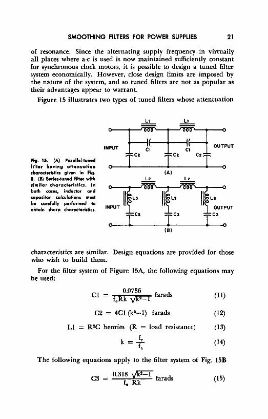
Figure 15 illustrates two types of tuned filters whose attentuation
L1 LI
,.:-UT _h____.; I ti OUT
0
~T
0
__ J_c_z ____ J ___ c_z ___ c_z_J __ 0
(Al
Fig. 15. (A) Parallel-tuned filter having attenuation characteristics given In Fig. 8. (B) S.rles-tuned filter with similar characteristics. In
both cases, indudor and II capacitor calculations must be carefully performed to INPUT obtain sharp charaderistics.
Lz Lz
(Bl
characteristics are similar. Design equations are provided for those who wish to build them.
For the filter system of Figure 15A, the following equations may he used:
LI
0.0786 Cl = faRk y1.Lf farads
C2 = 4Cl (k2-l) farads
R2C henries (R = load resistance)
k - £. -r
(II)
(12)
(13)
(14)
The following equations apply to the filter system of Fig. 15B
0.318 yP=r° C3 = f Rk farads
8
(15)

22 FILTERS AND ATTENUATORS
L2 = R 2C3 henries
L3 __ L2 h . ennes 4 (k2-l)
k = .!r_ f ..
(16)
(17)
(18)
where k = fr/fa in which fr = resonant or line frequency, and fa is the frequency at which attenuation begins (Fig. 8.)
13. R-C Filters for Power Supplies
Resistance-capacitance R-C filters have become extremely popular in recent years because they provide adequate filtering when correctly designed, and represent a compromise between cost and bulk on the one hand, and performance on the other. Low-gain audio amplifiers, public-address systems, high-voltage power supplies for television receivers, and table-top radio receivers are a few examples of their wide application.
A typical R-C filter appears in Fig. 16. Its operation is approximately as follows: Cl charges nearly to the peak voltage of the power supply on the conduction portion of the cycle. It is discharged through RI and R2, the latter being the bleeder resistance in parallel with the load. Since R2 is much larger than RI, most of the output voltage develops across it and is applied to C2. Although this
Fig. 16. A representative R-C filter system used in the high voltage power supply
of a television receiver.
RECTIFIER c,
R1
Rz LOAD
(BLEEDER)
capacitor can discharge through either RI or R2, the polarity of the voltage across RI discourages the discharge through this resistor. Hence, most of the discharge occurs through R2. Typical values for television high-voltage supplies are 0.05 µf for Cl and C2, 500,000 ohms for RI, and 5 megohms for R2.
In radio receivers the bleeder is usually omitted, the plate and screen current drain of the power amplifier serving as the principal load. In such power supplies, the capacitors are of the order of 40 to 60 µf, while RI is made approximately 1000 ohms.
R-C filters have very poor regulation, due to the substitution of a resistor for a choke. For this reason, R-C filters are never used

SMOOTHING FILTERS FOR POWER SUPPLIES 23
where the power requirements are high, because the power loss in the filter resistor may become prohibitive under these conditions, and the regulation is bad.
14. Graded Filters
Various stages in multisection electronic equipment often require different filtering. For example, the high-gain stages following a microphone or playback in a high-fidelity amplifier system demand
TO PLATES AND SCREENS OF LOW-LEVEL
{HIGH-GAIN) STAGES
TO PLATES AND SCREENS OF
DRIVERS
PUSH-PULL OUTPUT STAGE
L RI
Fig. 17. A graded filter consisting of one L-C and one R-C section. Such filters are economical and tend to produce decoupling which stabilizes the performance of the equipment.
---FROM RECTIFIER
C3 Rz
(BLEEDER)
extremely low ripple if intolerable hum is to be avoided; in the same system, however, the power output stage - usually push-pull - may be supplied with plate and screen power having considerably more hum-voltage contact. It would be unwise and uneconomical to supply all the stages with the same, well-filtered d-c because this procedure increases bulk and cost, and because advantage is not taken of the isolation characteristics inherent in a graded filter (Fig. 17) to suppress regeneration.
In the example of Fig. 17, the power supply provides voltages for the plates and screens of two high-gain voltage amplifiers, a class-A driver stage, and a push-pull class-AB! power output section. The last obtains its d-c power directly from the filter capacitor, since no
24 FILTERS AND ATTENUATORS
more filtering than this is needed for a stage operating at this high level. The driver stage obtains power at a point where a substantial amount of filtering has been accomplished (after the filter choke), thus making use of Cl, L, and C2 as filter components. The lowlevel, high-gain voltage amplifiers, are supplied d-c from a point that receives maximum filtration and where the ripple voltage is down to an acceptably reduced figure.
The graded filter used in the example makes it possible to select a choke of much smaller current rating, since the largest part of the circuit current flows in the push-pull output stage which is not fed through the choke. Similarly, the filter resistor may be made very low in wattage rating since the high-gain stages demand very little current. Note, that the resistor RI decouples the high-gain stages from the driver and that choke L does the same thing for the driver and output stage.
15. Cancellation Filters
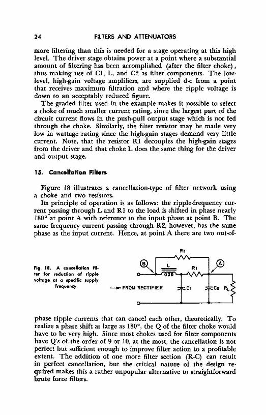
Figure 18 illustrates a cancellation-type of filter network using a choke and two resistors.
Its principle of operation is as follows: the ripple-frequency current passing through Land RI to the load is shifted in phase nearly 180° at point A with reference to the input phase at point B. The same frequency current passing through R2, however, has the same phase as the input current. Hence, at point A there are two out-of-
Fig. 18. A cancellation filter for reduction of rlpple voltage at a specific supply
frequency. - FROM RECTIFIER
Rz
RI
phase ripple currents that can cancel each other, theoretically. To realize a phase shift as large as 180°, the Q of the filter choke would have to be very high. Since most chokes used for filter components have Q's of the order of 9 or IO, at the most, the cancellation is not perfect but sufficient enough to improve filter action to a profitable extent. The addition of one more filter section (R-C) can result in perfect cancellation, but the critical nature of the design required makes this a rather unpopular alternative to straightforward brute force filters.
SMOOTHING FILTERS FOR POWER SUPPLIES 25
16. Review Questions
I. Explain why smaller filter components are needed for full-wave power supplies than for half-wave supplies at the same line frequency.
2. Define voltage regulation. Describe the steps in filter design that are taken to obtain the best possible voltage regulation.
!I. Discuss and compare capacitor- and choke-input filter systems from the point of view of output voltage and voltage regulation.
4. Find the percent ripple in a full-wave power supply of the capacitor-input type in which the load resistance is 20,000 ohms and the filter components have the values given below. The line frequency is 60 cps.
Cl = 60 µf C2=20µf L = 9 henries
5. Explain why a smaller rectifier tube may be used with a choke-input filter having the same input and impedance characteristics as an equivalent capacitor-input filter.
6. A transformer having an input impedance of 50 ohms is used to supply !100 volts d-c to its load at 200 ma. Find the peak rectifier plate current.
7. Define critical inductance, optimum inductance. 8. Determine the percentage ripple from a filter system in which the following
apply:
Type: choke-input Rectification: half-wave Line frequency: 60 cps Ll, L2: 15 henries each Cl: IO µf C2: 4 µf
9. Describe the nature and operation of a swinging choke. 10. With the aid of a diagram, explain the operation of a cancellation filter.
Chapter 3
AUDIO FILTERS
17. General Information
Wide use is made of filters in audio circuits to perform highly specialized functions. Among the simplest of such filters are those intended to isolate one amplifier stage from another to prevent degenerative or regenerative coupling. Such filters are usually classed at decoupling filters.
Radio receivers and public address systems utilize filter networks for the control of tone - usually circuits which produce attenuation of either high- or low-audio frequencies. These are the familiar tone controls. In more expensive equipment, both treble and bass boost circuits may be encountered, as well as attenuation components.
High-fidelity amplifiers and speaker systems consistently make use of filters as crossover networks, i.e., arrangements in which frequencies below a predetermined value are passed on to the lowfrequency speaker (woofer) , while those above this limit activate the high-frequency speaker (tweeter) . Such items as presence controls, rumble filters, and scratch filters also are becoming common in hi-fi design.
In radio transmission, other types of audio filters, such as speech clippers, have become popular recently. Understanding of the function and limitations of audio filters is, therefore, extremely important to any technician who plans to work with, repair, or design audio-frequency equipment.
18. Decoupling Filters
When two circuits that operate at the same frequency have an impedance common to both, there is coupling between them. If the phase relationships are such as to bring the two circuits into the
26
AUDIO FILTERS 27
same phase, the coupling is regenerative and leads to possible instability. Degenerative feedback occurs when the common impedance is between two stages in which the phase differs by 180°.
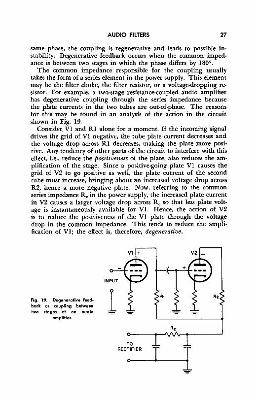
The common impedance responsible for the coupling usually takes the form of a series element in the power supply. This element may be the filter choke, the filter resistor, or a voltage-dropping resistor. For example, a two-stage resistance-coupled audio amplifier has degenerative coupling through the series impedance because the plate currents in the two tubes are out-of-phase. The reasons for this may be found in an analysis of the action in the circuit shown in Fig. 19.
Consider_ VI and RI alone for a moment. I£ the incoming signal drives the grid of VI negative, the tube plate current decreases and the voltage drop across RI decreases, making the plate more positive. Any tendency of other parts of the circuit to interfere with this effect, i.e., reduce the positiveness of the plate, also reduces the amplification of the stage. Since a positive-going plate VI causes the grid of V2 to go positive as well, the plate current of the second tube must increase, bringing about an increased voltage drop across R2, hence a more negative plate. Now, referring to the common series impedance Re in the power supply, the increased plate current in V2 causes a larger voltage drop across Re so that less plate voltage is instantaneously available for Vl. Hence, the action of V2 is to reduce the positiveness of the VI plate through the voltage drop in the common impedance. This tends to reduce the amplification of VI; the effect is, therefore, degenerative.
Fig. 19. Degenerative feedback or coupling between two stages of an audio
amplifier. l
TO RECTIFIER
0
R2
Re
I I

28 FILTERS AND ATTENUATORS
If a third stage is added to the circuit of Fig. 19, the plate current phase relationships bring Vl and V3 into phase. The effect will be opposite to that of the two-stage amplifier: the coupling will be regenerative and may lead to serious instability in the form of selfoscillation. The decoupling filter is designed to minimize such coupling and restore stability to the multistage amplifier.
The application of decoupling is shown in Figure 20. V is the first
(- ---RL
INPUT @
l c~ Rd Fig. 20. The decoupling fil-ter consists of Rd and Cd
- acting together.
Re TO PLATES FROM OF RECTIFIER
SUCCEEDING
J J STAGES
of the three amplifier stages, RL is the normal load resistance, Rd is the decoupling resistance, and Cd is the decoupling capacitance. Such a filter maintains the voltage at point A constant regardless of the variations in the voltage drop produced across Re by the following stages. In this way, the fluctuations in plate voltage that might cause degenerative or regenerative feedback are eliminated or minimized.
If the reactance of Cd at any frequency to which the amplifier is expected to respond is substantially less than Rd plus Re, the decoupling is effective. The factor by which the undesirable coupling is reduced is given by:
(19)
where Xe is the reactance of the decoupling capacitor, ~ is the resistance of the decoupling resistor, and Re is the resistance of the common impedance in the power supply. In most decoupling filters, Rd is generally made about 1/5 the value of the load resistor while Cd is seldom less than 8 to IO µf. A decoupling circuit also acts to reduce hum since it appears as an additional power supply filter section.
AUDIO FILTERS 29
19. Tone Control Considerations
An ideal audio-amplifier system, encompassing the input transducer, the amplifier itself, and the final reproduction device, must have a frequency response that is linear and level over the whole audio spectrum. Since pickup devices such as microphones, phonograph cartridges, phototubes, photocells, and other transducers seldom have the desired linearity, it is often best to control the frequency response of the amplifier proper so as to compensate for these defects. Reproducers, such as loudspeakers, also contribute to the need for frequency compensation.
Telephone engineers, broadcast and television designers, and recording engineers make use of highly complex electrical networks for frequency compensation. Comparatively simple combinations of resistance, capacitance, and inductance, however, are more than adequate for the usual applications; we are confining our discussion to these simpler forms.
Basic tone compensation arrangements may be divided into two classes: resonant and nonresonant circuits. Such circuits are not confined to simple tone control applications in audio amplifier work, they are also in speech clippers, crossover networks, presence controls, rumble filters, scratch filters, et al.
20. Resonant Tone Compensation
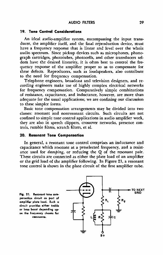
In general, a resonant tone control comprises an inductance and capacitance which resonate at a preselected frequency, and a resistance used for damping, or reducing the Q of the resonant pair. These circuits are connected as either the plate load of an amplifier or the grid load of the amplifier following. In Figure 21, a resonant tone control is shown in the plate circuit of the first amplifier tube.
Fig. 21. Resonant tone compensation circuit as part of amplifier plate load. Such a circuit provides either treble or bass boost depending upon the frequency chosen for
resonance. L
TTOG~Fc,XT
RL
.----... C
B+
30 FILTERS AND ATTENUATORS
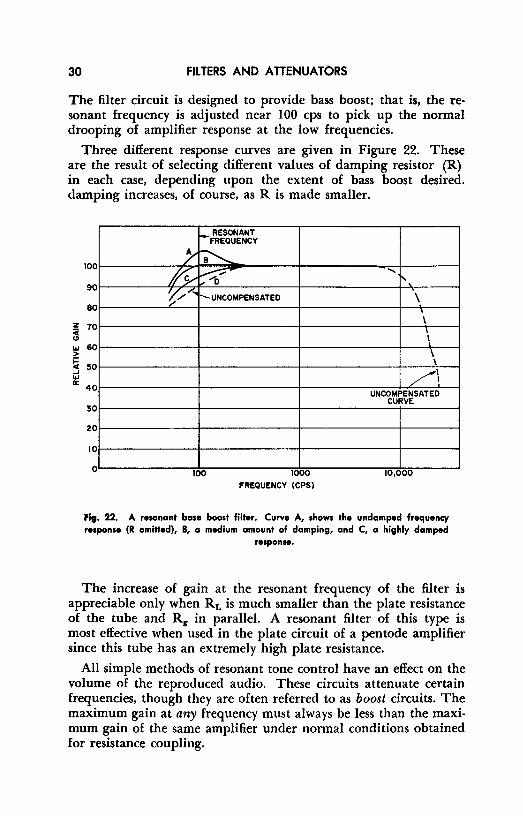
The filter circuit is designed to provide bass boost; that is, the resonant frequency is adjusted near 100 cps to pick up the normal drooping of amplifier response at the low frequencies.
Three different response curves are given in Figure 22. These are the result of selecting different values of damping resistor (R) in each case, depending upon the extent of bass boost desired. damping increases, of course, as R is made smaller.
100
90
80
z 70 ~ 1u 60 > 3 50
"' a: 40
30
20
10
0
-~~so~lN~TY
7 ?--,....
If§,, ....-:? ,,. ,,..D
1/.,,.-,; /
-._ UNCOMPENSATED
100 1000
FREQUENCY (CPS)
..... I'
\ ' \
I
\ \ \
/\ UNCOMPENSATED
CURVE
10,000
Fig. 22. A resonant base boast filter. Curve A, shows the undamped frequency response (R omitted), B, a medium amount of damping, and C, a highly damped
response.
The increase of gain at the resonant frequency of the filter is appreciable only when RL is much smaller than the plate resistance of the tube and R1 in parallel. A resonant filter of this type is most effective when used in the plate circuit of a pentode amplifier since this tube has an extremely high plate resistance.
All simple methods of resonant tone control have an effect on the volume of the reproduced audio. These circuits attenuate certain frequencies, though they are often referred to as boost circuits. The maximum gain at any frequency must always be less than the maximum gain of the same amplifier under normal conditions obtained for resistance coupling.

AUDIO FILTERS 31
21. Nonresonant Tone Compensation
Although nonresonant tone control circuits using inductances are encountered, they are unpopular as inductance costs are high, un• desirable resonance of the inductor with stray capacitance often brings peaks of response at undesirable points, and inductances are often responsible for hum due to stray pickup. Most nonresonant compensation circuits use only resistors and capacitors.
Figure 23 represents one of the most successful modern R-C tone compensation circuits, found in many high-fidelity kits and factorywired audio amplifiers, and available in printed circuits (shown inside dashes). As it is a modified bridged-T compensation network, its analysis requires specialized mathematical treatment which is not attempted here. A qualitative description of its operation can be briefly presented, however.
The 0.1 µf capacitor from the plate of the amplifier tube is a source of negative feedback. Since its reactance is small even for low-audio frequencies, the entire audio range is fed back to terminal A of the filter network.
When the two potentiometers (treble and bass) are centered, the phase relationships for both ranges result in a flat response (i.e., treble and bass portions of the signal are applied to the amplifier grid from the input with neither attenuation nor boost) . As either
B+
TREBLE
0.2 B 500K A o-~111--------.JV'./\r---...--11--+-----1(----o
INPUT 2.2 MEG
B lMEG BASS
A
Fig. 23. A prevalent form of tone compensation network providing for bass and treble baost and attenuation. The section inside the dashed lines Is generally in
the form of a printed circuit.

32 FILTERS AND ATTENUATORS
control is shifted from its central position, the input and feedback phases are shifted so that either attenuation or boost occurs, depending upon the direction of wiper motion. For example, when the treble control wiper is moved all the way to the left (to point B) , full treble boost is obtained. The phase relationships between input and fed-back voltages increase the treble response. When the wiper is rotated to point A, the fed-back voltage tends to cancel the trebles, providing full attenuation. Similarly, the bass-control potentiometer in position B provides full boost, while in position A it provides bass attenuation. Obviously, great care must be taken in the design of such a network, particularly for boost purposes, because the in-phase condition of the input and fed-back voltages tend to produce instability.
In less elaborate equipment, simpler methods are usually employed for attenuation of bass, treble, or both. The treble range may be controlled by shunting the plate circuit of a tube by a capacitance in series with a tone-control potentiometer (Fig. 24) . With the tone control resistance at maximum, very little high-frequency shunting takes place since the impedance of the series components (C and R) is high, even for the high frequencies. As the resistance is decreased, more and more shunting occurs, starting with the highest frequencies and working down toward the lower ones. A measure of control is established, permitting the operator to select the frequency at which attenuation begins to become audible.
Bass attenuation in similar equipment usually takes one or more of three forms. The capacitance of the grid coupling capacitor is reduced to present higher coupling impedance to the bass range. The capacitance of the cathode by-pass capacitor is reduced in any amplifier stage to provide a limited amount of bass attenuation. The capacitance of the screen by-pass capacitor is reduced to provide bass attenuation, particularly when the screen supply current is fed to the tube through a high value of dropping resistor.
INPUT
r--h-7 ~ I TONE CONTROL I R II
COMPONENTS ~ ____ J
Fig. 24. Simple tone control system found In Inex
pensive audio equipment.

AUDIO FILTERS 33
22. Speech Clipping
In the transmission of radiotelephone signals involving only speech waveforms, an amplituded-modulated radio-frequency carrier carries the modulation power in its sidebands, the percentage modulation being determined by the relative peak amplitudes present in the speech waveform. Unfortunately, the average power content in a speech waveform is quite low when compared to a sine wave. As
----------------100% {\ fl fl MODULATION
" I\ ,J\ 1J o. ,.al\ 11 L' A• .11 A SPEECH
v 0 (1·· -vu O v ... 1/~AVEFORM
-------------~-'-----100% MODULATION
Fig. 25. Speech waveforms and sine waves compared for power content. The power present In a sine wave averages much more than a speech wave because it reaches peak value In every
cycle.
shown in Fig. 25, a sine wave reaches peak value during every cycle, but a speech wave does this only occasionally. Yet both waveforms represent the conditions for 100% modulation of a given r-f amplifier as the peak values are the same.
It is possible to increase the modulator power in either the speech amplifier system or modulator itself so that the power content begins to approach the sine wave value. If, at the same time, all peaks producing overmodulation are clipped at the 100% point (Fig. 26), overmodulation cannot occur due to excessive peak values. However, clipping produces many rectangular peaks having the same high-order harmonics as produced by overmodulation, so that a signal clipped in this manner tends to splatter, or occupy too-wide a slice of the r-f spectrum. This is prevented by filtering all audio
Fig. 26. The speech waveform of Fig. 25 amplified to approach power content of sine wove but clipped to
prevent overmodulation.
CLIPPED SPEECH WAVEFORM 100% MODULATION
34 FILTERS AND ATTENUATORS
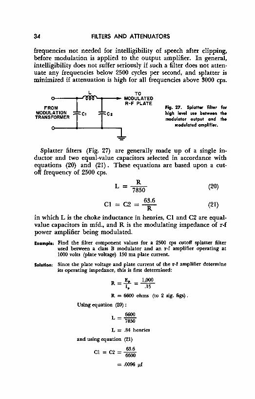
frequencies not needed for intelligibility of speech after clipping, before modulation is applied to the output amplifier. In general, intelligibility does not suffer seriously if such a filter does not attenuate any frequencies below 2500 cycles per second, and splatter is minimized if attenuation is high for all frequencies above 3000 cps.
L TO
o.----1-'lnnl"'1--~•• MODULATED R-F PLATE
FROM MODULATION C C
TRANS:O~R_M_E_R_J __ 1
__ J __ z--,
-!-
Fig. 27. Splatter filter far high level use between the modulator output and the
modulated amplifier.
Splatter filters (Fig. 27) are generally made up of a single inductor and two equal-value capacitors selected in accordance with equations (20) and (21). These equations are based upon a cutoff frequency of 2500 cps.
R L = 7850
Cl = C2 = 63·6
R
(20)
(21)
in which Lis the choke inductance in henries, Cl and C2 are equalvalue capacitors in mfd., and R is the modulating impedance of r-f power amplifier being modulated.
Example: Find the filter component values for a 2500 cps cutoff splatter filter used between a class B modulator and an r-f amplifier operating at 1000 volts (plate voltage) 150 ma plate current.
Solution: Since the plate voltage and plate current of the r-f amplifier determine its operating impedance, this is first determined:
R = !E- = 1,000 1. .15
R = 6600 ohms (to 2 sig. figs) .
Using equation (20):
6600 L = 7850
L = .84 henries
and using equation (21)
Cl= C2 = ::! = .0096 µf
AUDIO FILTERS 35
In practice, of course, the capacitor value would be selected as .01 µf and the value of the choke adjusted accordingly to realize a cutoff frequency of 2500 cps.
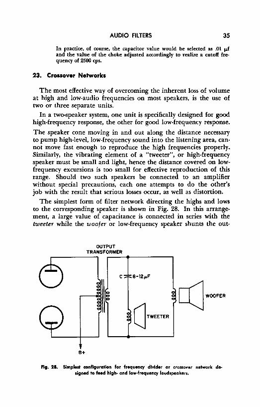
23. Crossover Networks
The most effective way of overcoming the inherent loss of volume at high and low-audio frequencies on most speakers, is the use of two or three separate units.
In a two-speaker system, one unit is specifically designed for good high-frequency response, the other for good low-frequency response.
The speaker cone moving in and out along the distance necessary to pump high-level, low-frequency sound into the listening area, cannot move fast enough to reproduce the high frequencies properly .. Similarly, the vibrating element of a "tweeter", or high-frequency speaker must be small and light, hence the distance covered on lowfrequency excursions is too small for effective reproduction of this range. Should two such speakers be connected to an amplifier without special precautions, each one attempts to do the other's job with the result that serious losses occur, as well as distortion.
The simplest form of filter network directing the highs and lows to the corresponding speaker is shown in Fig. 28. In this arrangement, a large value of capacitance is connected in series with the tweeter while the woofer or low-frequency speaker shunts the out-
B+
OUTPUT TRANSFORMER
C 8-12,.F
dTWEETER
[(]WOOFER
Fig. 28. Simplest configuration for frequency divider or crossover network designed to fnd high- and law-frequency loudspeakers.

36 FILTERS AND ATTENUATORS
put transformer directly. The capacitance required depends upon the desired response characteristics and the impedances of the two speakers. High frequencies are shunted through the tweeter unit since the capacitive reactance of C at these frequencies is relatively low. Low frequencies appear as power in the voice coil of the woofer as the inductive reactance of the voice coil is considerably lower for the low frequencies than for the highs, making it possible for low-frequency currents to flow through this voice coil with little impedance. This simple arrangement is not as satisfactory as circuits that utilize inductors and capacitors.
Figure 29 illustrates a basic, high-performance two-speaker crossover network. In the design of such a network, the crossover frequency is first selected (usually from 400 cps to 1000 cps) and then the components chosen so that resonance is obtained at the crossover frequency. Ll and C2 constitute a series resonant circuit at the crossover frequency, so do L2 and Cl. The constants given in Fig. 24 were selected for a crossover frequency of approximately 450 cps, using speakers with 8-ohm voice coil impedances.
B+
L1 (3MH)
Cl eo,.F
Cz so,.F
WOOFER
TWEETER
VOICE-COIL IMPEDANCE
8OHMS
CROSSOVER FREQUENCY 450 CPS
Fig. 29. An L-C two-speaker crossaver network with resonant elements.
At the crossover frequency the voltages available across the speaker source components (Cl and L2) are equal, as these units are in resonance. The impedance match at the crossover frequency is maintained substantially constant by action of the series resonant circuit containing LI, C2, and the two voice-coil windings. At high frequencies the voltage drop across Cl becomes small, while the

AUDIO FILTERS 37
drop across L2 increases, bringing the tweeter into play. The opposite occurs at low frequencies.
An idealized response characteristic for a two-speaker crossover network is shown in Fig. 30. The crossover frequency is 850 cps. The total available sound energy is 72 db. At the crossover frequency half the total energy is applied to each speaker. At other frequencies the proportion varies, one speaker getting less power, the
54
48
42
:!l 36
30
24
18
--...... .........._
..,....- ..,....-
850'v
---i---.. 1"----
~1'-r-,.
..,. ........ v .... v ..,
CROSSOVER 111
I I '~v..1•~~ ~~:::-
~l'E.6 ~~~¢.,;,-
~•<;i'llE.I'
~ ~ £°Fi -4~i;-;:,,.
Ppl.1£" :-,... 0 8,
Ss S1>~ r 'ft, ~;::,
i 100 200 400 600 800 lKC 2KC 4KC 6KC 8KC lOKC
FREQUENCY(CPS)
Fig. 30. Idealized response of a two-speaker, 850 cps crossover network with a total sound power input of 72 db. (Electronic Experimenters Handboo/c, 1958).
other speaker more, but the sum of 72 db is constant. A frequency division network fot a three-speaker system is given
in Fig. 31. The same general rules apply to the selection of these components. Most crossover networks are primarily designed for resonance, as described, and are then adjusted experimentally to match the speakers used as well as the wishes of the listener.
24. Presence Control
This is the filter system in audio-frequency reproduction in which the middle range of frequencies is accentuated. Since the human voice operates essentially in the mid-range frequencies, increased mid-range emphasis for vocal performances lends realism to the reproduction and an increased sense of presence to the vocalist.
A presence control is usually inserted between the preamplifier and power amplifier section of the system. Since it has an insertion loss, the system should have a reserve of gain of at least 12 db. Since most amplifiers are operated conservatively, this reserve is generally available.

38 FILTERS AND ATTENUATORS
B+
WOOFER
MIDRANGE (SQUAWKER)
TWEETER
Fig. 31. Three-speaker crossover network. Exact values of components are gener• ally obtained experimentally, although approximate values are determined from
resonance considerations.
A practical circuit for a presence control appears in Fig. 32. An accentuation of 6 db occurs at approximately 2500 cps. Since tastes vary as to the extent and frequency of presence, other frequencies may be obtained by varying C, and additional accentuation may be realized by increasing the resistance of R3.
The circuit action is easy to see. L and C form a parallel-resonant circuit and are selected to resonate at the center presence frequency. The frequencies in the vicinity of 2500 cps are accentuated because the voltage drop across the L-C combination is greatest in this region. With the wiper of R3 at the ground end of the potentiometer, full accentuation occurs. When moved to the upper end, the resonant circuit is shorted out so that the shunt load becomes merely R2. This produces zero accentuation, but accounts for the insertion loss.
RI
INPUT FROM lOOK PREAMPLIFIER
l R2 22K
CI.0033 p.F
OUTPUT TO AMPLIFIER
l Fig. 32. A practical presence control circuit. The extent of presence is governed by R3.
AUDIO FILTERS 39
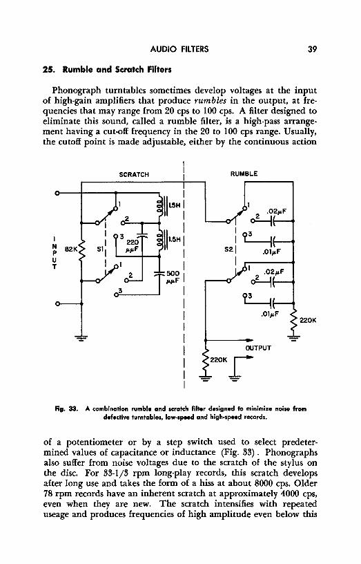
25. Rumble and Scratch Filters
Phonograph turntables sometimes develop voltages at the input of high-gain amplifiers that produce rumbles in the output, at frequencies that may range from 20 cps to 100 cps. A filter designed to eliminate this sound, called a rumble filter, is a high-pass arrangement having a cut-off frequency in the 20 to 100 cps range. Usually, the cutoff point is made adjustable, either by the continuous action
SCRATCH RUMBLE
1 .02,.F
2 ~ I ~ N 82K p .01,.F u T 1 .021&F 2 500 T ""F ~
03
~ 220K
=- -OUTPUT
-220Kr
Fig. 33. A combination rumble and scratch filter designed fo minimize noise from defedive turntables, low-speed and high-speed records.
of a potentiometer or by a step switch used to select predetermined values of capacitance or inductance (Fig. 33) . Phonographs also suffer from noise voltages due to the scratch of the stylus on the disc. For 33-1/3 rpm long-play records, this scratch develops after long use and takes the form of a hiss at about 8000 cps. Older 78 rpm records have an inherent scratch at approximately 4000 cps, even when they are new. The scratch intensifies with repeated useage and produces frequencies of high amplitude even below this

40 FILTERS AND ATTENUATORS
figure. In Fig. 33, the scratch filter consists of SI and its associated resistors, capactiors, and inductors while S2 with the associated resistors and capacitors is the rumble filter. Table I provides information on the cutoff frequencies in the various switch positions.
1500 2 ll----+-..J'\l',l'\---1f------<>
INPUT
.041 \ 4 \
10K (-A OUTPUT
-1-..._ ___ ---j,___, I
\ \ I \ I I
1500 4
\..,_ ________ ---
.015-=1=-
+
Fig. 34. Turnover and roll-off filter for equalizing any recording to match the RIAA response of modern ompllfiers. The filter accomplishes this odding or sub
troctlng from the standard RIAA curve.
The attenuation rate is approximately 12 db per octave. Thus, if the scratch filter switch (SI) is set for attenuation at 4000 cps, the response of the filter will be relatively flat up to this frequency, whereas at 8000 cps the scratch will be reduced by about 4 to I. The rumble filter would be used on the No. 2 position of S2 for very low frequency rumble (50 cps) and on No. 3 position for rumble of frequencies in the vicinity of 100 cps.
TABLE 1
SWITCH POSITIONS
(S2) Rumble (S 1) Scratch
1 Flat Flat 2 50 cps 8,000 cps 3 100 cps 4,000 cps

AUDIO FILTERS
26. High Fidelity Equalizer
.41
Before 1953, standards were not established for record equalization curves. Record manufacturers adopted individual response patterns according to their own lights, so that any amplifier had to be equipped with many equalization settings. All records made after 1953, are standardized in accordance with the specifications of the Record Industry Association of America (RIAA) . (This response is called Orthophonic by RCA and associated companies) .
Many people own excellent recordings made before 1953. To render these properly, the standard RIAA response can be modified by a filter network as illustrated in Fig. 34. Provisions have been made in the design of this circuit to incorporate four positions of low-frequency equalization (often called turnover) and four positions of high-frequency equalization (de-emphasis or roll-off). Since the two selector switches operate independently, the filter can produce 16 different equalization settings so that it accommodates virtually any recording.
The insertion loss of the network is about 6 db. For reasons given previously, this is easily offset by any modem amplifier's reserve gain.
27. Scott Filter
An R-C filter for small currents that notches the audio response of an amplifier system is shown in Fig. 35. Designed by H. H. Scott in I 939, the filter system bears his name and is claimed to provide
Fig. 35. A resistance-capacitance notching filter that provides sharp attenuation
of one frequency.
Ra
FREQUENCY
42 FILTERS AND ATTENUATORS
almost complete attenuation at any desired frequency. For example, the Scott filter may be nicely applied for the removal of scratch noise that peaks at 8000 cps, such as the hiss that develops in the older of LP records; it is quite effective for minimizing 78-rpm scratch at 4000 cps and the surrounding frequencies.
The action of the Scott filter depends upon feedback of one frequency to the input 180° out of phase with the incoming signal. The capacitors and resistors are all of the same values except Ra. By selecting them carefully, the phase of the input signal can be inverted 180° by the R-C pairs for the frequency to be notched from the response. Further fine control is provided by adjusting the tap on the last resistor. Since the final values of the R and C components depend upon the input and output inpedances, as well as the frequency to be notched, design formulae are not easily provided. A typical response curve is given in the insert in Fig. 35. Note that the Scott filter does attenuate frequencies higher than the notched frequency but the extent of the attenuation is small, and in most cases is barely noticeable.
28. Review Questions
1. What is the function of a decoupling filter? 2. Under what conditions are decoupling filters required? Draw an amplifier
circuit consisting of three stages of amplification, showing a practical decoupling network.
3. Explain, with the aid of diagrams, how a resonant tone control filter operates. 4. What are the underlying principles of nonresonant tone compensation
systems? 5. Draw a two-stage amplifier circuit showing a simple type of tone control.
Explain its operation. 6. Explain the advantages of speech-clipping in the transmission of speech by
radiotelephone. Why can't clipping be used in the transmission of music? 7. Why are crossover networks used in high-fidelity sound reproduction? Draw
a diagram showing the basic principles of two-speaker crossover networks. 8. Determine the values necessary to make up a speech-clipper splatter filter
having a cutoff at 3000 cps, the filter being placed between the modulator and an r-f amplifier operating at 1500 volts (plate) and 200 ma.
9. Distinguish between the following filters in terms of function and frequencies affected: (a) roll-off filter, (b) presence control, (c) turnover filter, (d) rumble filter, (e) scratch filter, (f) curve equalizer.
10. Explain the operation of the Scott notching filter. Use a diagram to help.
Chapter 4
VIDEO FILTERS
29. The Need for Video Filters
Equipment for transmitting and receiving signals containing video components, as in television and radar, must meet certain requirements. The amplifiers must respond to frequencies lying within an extended range, the lower limit approximately equal to the framerepetition rate in television, the upper limit at least one-half the rate of transmitting picture elements. In American television practice, these limits are 30 cps and approximately 4,000,000 cps. Amplifiers must pass components within this frequency range with a minimum of amplitude distortion and time-delay discrimination.
A standard R-C coupled amplifier tends to favor the middle-range of frequencies, discriminating against the highs and lows. Shunt capacitances consisting of input and output capacitances reduce the high-frequency gain. Similarly, series impedances such as the coupling capacitor cause a diminution of low-frequency gain. Particularly at low frequencies, the phase response (time-delay characteristics) of an uncompensated amplifier may be quite troublesome. The reason is that a very small phase shift in the amplifier circuit measured in degrees is a very large time delay in seconds when the frequency is low.1
Thus, for extended frequency range coverage, an uncompensated amplifier is unsatisfactory. Although frequency compensation circuits are not ordinarily viewed as filters, their selective behavior earns them a brief discussion in this book.
1Schure, A., Video Amplifiers. New York, John F. Rider Publisher, Inc., 1959
.43

44 FILTERS AND ATTENUATORS
Cc
r- I I I I L
I I J_ Rg +C; Teo I
RL I
I I I I I _J
- B+ - -Fig. 36. Fundamental R-C video amplifier showing the position of the shunt peaking coil Ll. Co and C, are tube and stray capacitance which are referred to as C,
in the text.
30. High-Frequency Compensation - Shunt Peaking
The principal cause of loss of gain at high frequencies is the shunting effect of tube and stray capacitances going into C0 and C1
in Fig. 36. Taken together the total shunting capacitance is referred to as Ct. If a coil having the proper inductance L, is connected in series with the load resistor RL, a substantial improvement can he affected in the response curve, the high-frequency gain being boosted to an extent determined by the inductance L and Q of the shunt peaking coil. In practice, the inductance of the coil is calculated first from equation (22) and then trimmed until the desired response is obtained.
(22)
in which Ct = C0 + C1 and RL is plate load resistance of the first amplifier tube. Ct is best found by measurement, although it may be calculated from the known capacitances with corrections for the Miller effect.
When Ll is obtained from equation (22), the resonant frequency for this coil and Ct is 1.414 times as great as the highest frequency to he amplified in the video range. For validity, the value of RL used in equation (22) should he found from:
I RL = --,--- (23)
2n: fo ct in which f0 is the highest frequency to he amplified. For these conditions, the values of RL and LI are fixed. Other values may be

VIDEO FILTERS 45
used with success but the ones obtained this way represent a good compromise between linearity of amplitude response and available gain from the amplifier.
31. High-Frequency Compensation - Series Peaking
Another method of high-frequency compensation which gives higher and more linear phase response is shown in Fig. 37. The filter element consists of output capacitance C0 , the following input impedance C1, and the coupling inductance L which isolates C0
from C1• The filter is terminated at the point of entry by impedance RL and at the remote end by Rg. The effect of the coupling capacitor Ce may be ignored since it is effectively a short-circuit at high frequency.
The value of the filter coil and the plate load resistance is determined first by measuring capacitances C0 and C1 to determine Ct. Then L is determined for a given high-frequency limit, f0 , by equation (24) .
L (24)
This equation is obtained because the resonant frequency of L and C0 is chosen 1.41 times as great as f0 •
The plate load resistance is selected on the basis of equation (25) .
Fig. 37. Series peaking system lnvolvlng the use of a series peaking coil between the plate of the first amplier and the coupling capacitor
to the next amplifler.
R - 1.5 L - 2:n: fo Ct
B+
I I I I
....L. ~c, I I
-:!:-
(25)
32. High-Frequency Compensation - Combination Peaking
Equation (23) shows that the load resistance for the first amplifier tube (RL) must be made equal to the reactance of Ct for

46 FILTERS AND ATTENUATORS
effective action at the highest frequency for which compensation is to he obtained. Equation (25) indicates why the gain of the series peaking method of compensation is greater: the value of RL may he made 1.5 times as great as the reactance of Ci, increasing the gain of the stage. When both series and shunt peaking are used together, a further increase of gain can he realized because, as anaiysis now shows, RL can be raised in value to 1.8 times the reactance of Ct. The design equations for combination peaking are:
RL 1.8
(26) = 2:n: fo ct
Ll = 0.12 ct RL2 (27)
L2 = o.52 ct RL2 (28)
33. Low-Frequency Compensation Filter
At low frequencies, the shunt capacitance Ct has a very high reactance so that its effect is negligible. The increasing reactances of the coupling and by-pass capacitors as 30 cps is approached, however, begin to introduce amplitude and phase distortion. Impractically large values of coupling capacitance and grid resistance are required
B+
Fig. 38. A low-frequency compensation filter that im• proves amplitude and phase
response.
for proper performance of the amplifier at frequencies in this low range. Should these be employed, the high-frequency response suffers and the amplifier tends to he unstable, often producing relaxation oscillations or motorboating.
It is customary to use a low-frequency compensation filter in series with the output resistor RL as illustrated in Fig. 38. This combination produces a phase shift that compensates for the time delay introduced by coupling components Cc and R1, and acts as

VIDEO FILTERS 47
a decoupling filter, preventing the amplified signal from developing a voltage drop across the power supply impedance, thus discouraging instability.
In practice, R is often made as large as possible without causing an uneconomical reduction of plate voltage; then the value of C is selected to provide effective decoupling without producing oscillation.
It also turns out that the low-frequency response of an amplifier is affected by the cathode impedance, RkCk. If this is a serious factor, the decoupling filter may be designed in accordance with equations (29) and (30) . With values obtained this way, the cathode reactance will be cancelled out as a source of low-frequency distortion. The filter will continue to serve in its decoupling role.
Rf = Rk gm RL (29)
(30)
in which gm = transconductance of the first tube and RL is the plate load resistor. Rk and Ck are the cathode components shown in Fig. 38.
I OUTPUT OF ..L l·F ,,...ct AMPLIFIER I
0 ' (Al
INPUT
Lw
CwT
INPUT TO NEXT
I·F GRID
0
I ...L 'ct
I
0
' ~ I 0
OUTPUT I Lw I INPUT TO OF J_ J_ NEXT l·F I-F 1"" ,,... AMPLIFIER I GRID
I 0 ' l 0
(Bl
L LI OUTPUT ABSORPTION
TRAP
(Cl
Fig. 39. (A) Serles resonant wave trap shunts the grid-Input circuit (8) Parallel resonant circuit Is In series with following grid circuit. (C) Absorption trap is not
conneded In the circuit eledrically.
34. Reiectlon Filters
In television signal reception, the sound tends to produce voltages that disturb the picture. So does the sound in the lower adjacent channel, but not to the same degree.
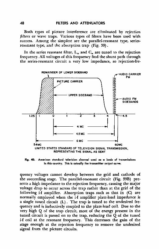
48 FILTERS AND ATTENUATORS
Both types of picture interference are eliminated by rejection filters or wave traps. Various types of filters have been used with success. Among the simplest are the parallel-resonant type, seriesresonant type, and the absorption trap (Fig. 39) .
In the series resonant filter, Lw and Cw are tuned to the rejection frequency. All voltages of this frequency find the shunt path through the series-resonant circuit a very low impedance, so rejection-fre-
1.25
REMAINDER OF LOWER SIDEBAND
PICTURE CARRIER
4 MC
4.5MC
6MC
.-AUDIO CARRIER FM
.--AUDIO FM SIDEBANDS
4.5
54MC 6OMC UNITED STATES STANDARD OF TELEVISION SIGNAL TRANSMISSION,
REPRESENTING THE SIGNAL AS SENT
Fig. 40. American standard televisian channel used as a basis of transmissions In this country. This is actually the transmitter output curve.
quency voltages cannot develop between the grid and cathode of the succeeding stage. The parallel-resonant circuit (Fig. 39B) presents a high impedance to the rejection frequency, causing the major voltage drop to occur across the trap rather than at the grid of the following i-f amplifier. Absorption traps such as that in (C) are normally employed when the i-f amplifier plate-load impedance is a single tuned circuit (L) . The trap is tuned to the undesired frequency and is inductively coupled to the plate-load coil. Due to the very high Q of the trap circuit, most of the energy present in the tuned circuit is passed on to the trap, reducing the Q of the tuned i-£ coil at the resonant frequency. This decreases the gain of the stage enough at the rejection frequency to remove the undesired signal from the picture circuits.

VIDEO FILTERS 49
35. Sideband Suppression Filters in Television
Normal amplitude modulation, such as that used in video modulation of the television carrier, always results in two sidebands, one above and one below the carrier. Since the signal components in the two sidebands contain the identical information, the double sideband system of transmission is wasteful of spectrum space. In view of this, standard television transmission practice now uses a system called vestigial sideband operation, in which the lower sideband components are partially removed. Removal of the lower sideband, theoretically more economical than vestigial sideband operation, is impractical because it presents severe technical problems.
C2 TRANSMITTER
-----------
L2
Fig. 41. Vestigial sideband filter shown with lumped constant elements rather than a, sections of coaxial trans-
mission line.
The band-elimination filter, used does not have ideal cutoff characteristics, and attempting to remove all the components of the undesired sideband inevitably results in phase shifts. Vestigial sideband operation compromises by completely removing the unwanted components only at a relatively great frequency separation from the carrier. Adjacent to the carrier, the unwanted frequency components are left undisturbed.
The band-rejection filter required to produce the output curve shown in Fig. 40 must have attenuation characteristics like those shown in Fig. 42. In practice the elements of such a filter are made up of segments of coaxial transmission lines. Figure 41 shows the filter sections as containing lumped constants to facilitate analysis.
The upper branch of this two branch filter contains C2, LI, and Cl. C2 represents a low impedance path for the high-frequency
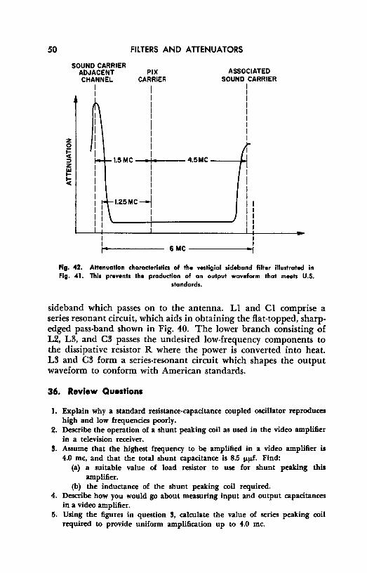
50
z 0
fi ::::, z ~ ~
FILTERS AND ATTENUATORS
SOUND CARRIER ADJACENT CHANNEL
I I
PIX CARRIER
I
1.25MC-j I I
ASSOCIATED SOUND CARRIER
I I I I I I I I I
I
I I I I I I I I I I I
I
6 MC --------i
Fig. 42. Attenuation characteristics af the vestigial sideband filter Illustrated in Fig. 41. This prevents the production of an output waveform that meets U.S.
standards.
sideband which passes on to the antenna. LI and Cl comprise a series resonant circuit, which aids in obtaining the flat-topped, sharpedged pass-band shown in Fig. 40. The lower branch consisting of L2, L3, and C3 passes the undesired low-frequency components to the dissipative resistor R where the power is converted into heat. L3 and C3 form a series-resonant circuit which shapes the output waveform to conform with American standards.
36. Review Questions
1. Explain why a standard resistance-capacitance coupled oscillator reproduces high and low frequencies poorly.
2. Describe the operation of a shunt peaking coil as used in the video amplifier in a television receiver.
!I. Assume that the highest frequency to be amplified in a video amplifier is 4.0 me, and that the total shunt capacitance is 8.5 µµf. Find:
(a) a suitable value of load resistor to use for shunt peaking this amplifier.
(b) the inductance of the shunt peaking coil required. 4. Describe how you would go about measuring input and output capacitances
in a video amplifier. 5. Using the figures in question S, calculate the value of series peaking coil
required to provide uniform amplification up to 4.0 me.

VIDEO FILTERS 51
6. Determine the load resistance that would best suit the series peaking coil of question 5.
7. A television monitor contains a video amplifier that must provide uniform amplification up to 6.0 me. Its input capacitance is 3.6 µµf and its output capacitance is 3.2 µiif.
(a) Which compensation method would you use? Why? (b) Determine the values of all components required to compensate the
the amplifier properly. 8. What are the two functions of a low-frequency compensation filter such as
that given in Fig. 38. How are these functions realized? 9. Draw diagrams illustrating three types of rejection filters or traps used in
television. With the aid of these diagrams explain how the traps operate. 10. How does the band-rejection filter of Fig. 41 accomplish the desired objective?
Chapter 5
WAVE FILTERS
37. Filter Classifications
Wave filters, sometimes known as Zobel filters1, are generally described as constant-k or m-derived filters and represent a unique family. Many of the filters described in previous chapters are basically either constant-k or m-derived types and may he analyzed with techniques used for generalized wave filters. Design procedures for wave filters are based upon complex mathematics and will not he dealt with in this chapter. The technician can derive substantial benefit from a discussion of filter types and filter structures, using the minimum mathematics needed for comprehension, and bypassing study of the derivations of the equations and charts needed for design work.
The same is true of bridged-T and parallel-T networks. We shall study the general principles of their functioning rather than the development of design techniques. For those interested in design of any type wave filter, this chapter is recommended as a preliminary step, followed by a thorough study of design procedures that can he found in any of the numerous modern electrical engineering texts.
Constant-k and m-derived filters may be placed in roughly four classifications:
Low-pass filter: This has a pass (or transmission) band theoretically starting from zero frequency to the frequency at which cutoff
'"Theory and Design of Electric Wave Filters", Otto Zobel, Bell Tech J, vol. II, p. I., Jan. 1923
52
WA VE FILTERS 53
is desired, and an attenuation band from the cutoff frequency to infinity.
High-pass lilter: The reverse characteristics obtain attenuationband from zero to the cutoff frequency and a passband from cutoff to infinity.
Bandpass lilter: Two cutoff frequencies are specified, high and low. Transmission will occur between these frequencies and attenuation on either side of them.
Band-elimination lilter: Again, two cutoff frequencies with attenuation between them and transmission on either side of the cutoff frequencies.
Bridged-T and parallel-T networks will be discussed later, as they are of specialized design.
38. Effectiveness of Attenuation and Transmission
In the attenuation-band of a given filter, the characteristic impedance of the filter is a pure reactance. If the load that terminates the filter is equal to the characteristic impedance of the filter, the generator at the input will see a pure reactance. For this condition, no power is transmitted to the load, hence, attenuation is perfect. This ideal situation is modified in practice because filters are often terminated in pure resistances and an impedance mismatch exists between the filter and load. This is reflected back so that the input impedance of the filter becomes slightly resistive. Thus, some power will be transmitted by the filter into the load even in the attenuation band.
In the transmission band of the same filter, however, the characteristic impedance is a pure resistance and, if the load is equal to the filter's characteristic impedance, the input generator will be working into a pure resistance. Since an ideal filter contains only reactive or nondissipative elements, in the theoretical situation all of the generator power is transmitted to the resistive load. In actual practice, of course, the filter components contain resistance so that some power dissipation occurs here as well as in the load. Hence, a practical filter transmits most, but not all, of the generator power to the load in its transmission band.
39. Characteristic Impedance
If a filter is terminated by a load having an impedance such that the filter is caused to have the same input impedance, the filter is said to be terminated by its characteristic impedance. Sometimes

54 FILTERS AND ATTENUATORS
known as surge impedance, the characteristic impedance of a filter may be found from:
(31)
where Z0 = characteristic impedance of the filter Za = input impedance with output terminals open-circuited Zb = input impedance with output terminals short-circuited.
The term surge impedance is often used with reference to transmission lines and has a similar significance. If a transmission line is terminated by a load equal to the surge impedance of the line, all the energy will be transferred to the load and there will be no reflections of energy back along the line. It is helpful to view filter sections as portions of an infinite line drawn to show its various impedance elements as lumped components. We will use this approach in the forthcoming paragraphs.
40. Basic Filter Configurations
Transmission lines are recurrent structures having continuously distributed impedances. Two wires in space have, besides their ohmic resistance, shunt capacitance and series inductance along the line. Signifying any type of impedance with the resistor symbol, a long line may be drawn as shown in Fig. 43. Each series element is labeled Zl and each shunt element Z2. The basis of filter design is a full L section consisting of series element Zl and shunt element Z2, shown between the labeled broken lines in Fig. 43.
SYMMETRICAL T-SECTION
t r---"----,. I I I I
Zl Zl
I I I I Z2 I I
BASIC FILTER SECTION
,-----A---., I I I Zl I
SYMMETRICAL 11'-SECTION
t ~ I I I I
Zl I Zl I
Z2
Fig. 43. Symbolic representotion of a long transmission line, showing its distributed impedances as lumped elements of recurring nature.

WA VE FILTERS
(Cl (Dl
Fig. 44. (A) Symmetrical T-sedion type of filter configuration, mid-series terminated. (B) Symmetrical it-sedion configuration, mid-shunt terminated. (C) Sym• metrical T-sedion divided into two half-sedions by replacing Z2 with two impedances in parallel, each being evaluated as 2Z2. (D) Symmetrical it-sedlon similarly
divided, each Zl being replaced by Zf/2.
55
A wave filter normally makes use of small, symmetrical sections because the number of sections is finite rather than infinite, like the line. One section, called the symmetrical T-section, is obtained by dividing each of two adjacent series elements in half and including between them one shunt element. Thus, the value of each series element (or half-element) is now designated as Zl/2 while the shunt element remains Z2. (Fig. 44A). Because the symmetrical Tsection is cut from the infinite line by bisecting each of two series elements, it is known as mid-series terminated.
The symmetrical ;re-section configuration is obtained by cutting down the centers of two successive shunt elements of the infinite line, including one series element between them (Fig. 44B) . Since a shunt impedance thus bisected has a resulting impedance of twice the initial value, the filter configuration shows an evaluation of 222 for each shunt element and ZJ for the series element. Such a section is said to be mid-shunt terminated.
For design and analysis purposes, either type of configuration may be divided into half-sections as shown in Fig. 44 (C) and (D) .
41. Charaderistlc Impedances of Filter Sedlons
The characteristic impedances of symmetrical T and :n:-sections

56 FILTERS AND ATTENUATORS
are given by the following equations:
2T-sect = /z1 22 ( 1 + : 2~ )
2:rt.sect = 21 22 21
I + 422
(32)
(33)
Examination of these equations shows that the characteristic impedances of the two networks depend upon frequency. It is difficult to terminate either one with a simple network.
As a special case, if a filter is terminated in a pure resistance R which is made equal to yZr"l:l, it may be shown that equations (32) and (33) may be written:
2t = R /1 + 4~~ (34)
2:rt = R (35)
/1 ZI
+ 422
The significance of the expression -J21 22 will become more evident in the next section.
42. Constant-k Filters Defined
The simplest and most common type of filter section is that in which the shunt and series impedances are intentionally selected so that
-Ji,I Z2 = constant = k (36)
for all frequencies. Furthermore, the terminating resistance for the filter is chosen to be equal to k, that is R = k so that the equations (34) and (35) are applicable. In constant-k filters, each inductance in the shunt and series arms is associated with a capacitor in the series and shunt arms, respectively. In an ideal filter the shunt and series arms are made of non-dissipative elements wherever possible. Assigning the No. I to series elements and the No. 2 to shunt elements, as before, the required relation between the elements for a constant-k filter (that is, to maintain the product of 21 and 22 constant) is:
(37)

WAVE FILTERS 57
Constant-k filters may be set up in any one of the four major classifications (high-pass, low-pass, bandpass, and band-elimination) . In the paragraphs that follow, we shall examine the transmission characteristics of each of these classifications, with applicable equations. Remember in each case that equation (37) is adhered to exactly, so that the product of Zl and Z2 is always a constant and is always equal to the terminating impedance of the filter.
43. Low-Pass Constant-k Filter
A low-pass constant-k filter contains an inductive series element (LI) and a capacitive shunt element (C2). Its transmission curve is given in Fig. 45 with its schematic diagram. This is an idealized
L1
~ o __ J_--uo
z ci Cl>
z 0
~ 2 II)
~ 0:: I-
Fz FREQUENCY--
Fig. 45. Sch-atic diagram and transmission curve of a low-pass constant•k filter. Note that the elements are nondlsslpatlve.
drawing in which the filter elements are nondissipative and there are no reflection losses at the terminals. In a practical filter, where there is some power dissipation in the elements and where impedances are not perfectly matched, the cutoff is somewhat more gradual than the curve indicates.
The values of the elements are found from equations (38) and (39).
R LI = ,i: f2
1 C2 = ,i: f2R
(38)
(39)
where f2 = frequency where attenuation begins. The reader should

58 FILTERS AND ATTENUATORS
Cl
o--1'-----------o
L2
z ~ z 0 iii 1/)
i ~ 0:: I-
Fl FREQUENCY ---
Fig. 46. Schematic diagram and transmission curve af a high-pass constant-k filter.
test the constant-k quality of these values by setting up the ratio as given in equation (37) to show that the square root of L2 over Cl comes out equal to R.
44. High-Pass Constant-k Filter
As illustrated in Fig. 46, a high-pass constant-k filter contains a capacitive series element and an inductive shunt element. In this case, the frequency at which full transmission begins is denoted by fl. The same idealization assumptions are made for the high-pass filter as for the preceding filter and for others that follow, unless otherwise noted. Element values may be determined from equations (40) and (41).
I Cl = 4x £IR (40)
R L2 = 41t fl (41)
45. Bandpass Constant-k Filter
The bandpass constant-k filter (Fig. 47) is considerably more complex than the high- or low-pass types. Containing an inductive and capacitive element in the shunt and series legs, four equations are required to determine the constants. Frequencies fl and f2 are the lower and upper limits respectively of the transmission band. The design equations are given in (42) through (45). It is again suggested that the reader test these equations against the ratios given in equation (37) to ascertain for himself that the constant-k

WAVE FILTERS 59
relationship between elements is maintained, regardless of the filter's complexity.
LI R
(42) = ,i: (f2 - fl)
L2 (f2 - fl) R
(43) 4,i: f2 fl
Cl = {f2 - fl~ (44)
4,i: f2 fl R
C2 I
(45) ,i: (f2 - fl) R
46. B.and-Elimination Constant-k Filter
In the band-elimination constant-k filter, the series leg contains an inductance and capacitance in parallel while the shunt leg contains these elements in series. Figure 48 presents the schematic diagram and transmission characteristics of this filter. The applicable equations are given in (46) through (49).
LI=
L2
Cl
C2 =
L2 Cz
(fl - fo) R 3t fo fl
R 4,i: (fo - fl)
I 4,i: (fl - fo)
(fl - fo) ,i:Rfofl
z ci C)
z 0 in II)
:ii II) z ct 0:: I-
R
F1 F2
FREQUENCY
(46)
(47)
(48)
(49)
Fig. 47. Bandpau filter of the constant-k type, showing an idealized transmission curve.

60
0
0
FILTERS AND ATTENUATORS
LI
G;J z
f· 0 ci
I:>
z 0
Cz iii VI
i Jez VI z
0 "' a: ...
Fo Fl FREQUENCY---
Fig. 48. Band-elimination filter of the constant-k type showing Idealized transmission curve.
47. m-Derived Filters Defined
Even the idealized transmission curves of the constant-k filters demonstrate a gradual cutoff characteristic that is unsatisfactory for many applications. Sharper cutoff may be realized by incorporating additional impedances in the shunt or series arms so that infinite attenuation occurs at some frequency beyond cutoff. With the constant-k type of filter used as a prototype, for example, the addition of another impedance in one of the arms can produce the kind of modified response shown in Fig. 49. In this case a T-section low-pass filter (A) is altered by adding L2, a shunting impedance, in series with C2B. This filter has a very high attenuation (low impedance) at the frequency where L2/C2 resonates; ideally, the L2/C2 combination can shunt a zero impedance across the line, causing infinite attenuation. When the two components are properly selected, this frequency of infinite attenuation (foo) can be placed anywhere in the attenuation band.
Since the filter in Fig. 49B, is derived from the constant-k prototype as we shall show in the next section, the impedances are related by a constant ( called m) , the network in (B) is known as an mderived filter.
48. m-Derived T-Sectlons
It would be desirable to be able to join different filter sections of the general type shown in Fig. 49 with each section having an infinite attenuation frequency at a different point in the attenuating band. In this manner, a high value of attenuation could be realized and maintained through the entire region.
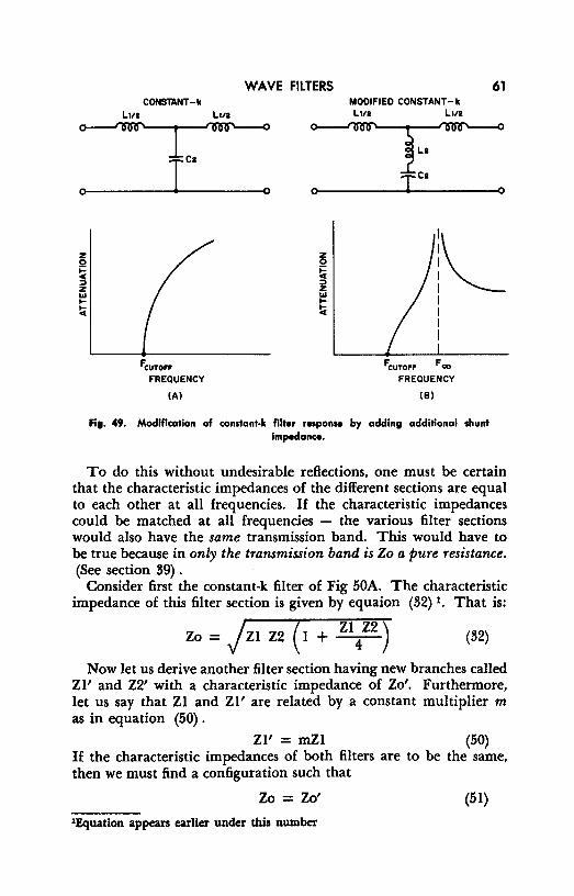
z Q ~ ::> z "' I-
~
L111
WAVE FILTERS 61 CONSTANT-k MOOIFIED CONSTANT-k
LIIZ L111
FCUTOF?
FREQUENCY
(Al
L111
\_ I I I I
FCUTOff Fa,
FREQUENCY
(Bl
Fig. 49. Modification of constant-k filter response by adding additional shunt Impedance.
To do this without undesirable reflections, one must be certain that the characteristic impedances of the different sections are equal to each other at all frequencies. If the characteristic impedances could be matched at all frequencies - the various filter sections would also have the same transmission band. This would have to be true because in only the transmission band is Zo a pure resistance. (See section 39) .
Consider first the constant-k filter of Fig 50A. The characteristic impedance of this filter section is given by equaion (32) 1. That is:
Zo = jz1 Z2 ( I + 2\
22) (32)
Now let us derive another filter section having new branches called Zl' and Z2' with a characteristic impedance of Zo'. Furthermore, let us say that Zl and ZI' are related by a constant multiplier m as in equation (50) .
Zl' = mZI (50) If the characteristic impedances of both filters are to be the same, then we must find a configuration such that
Zo = Zo' (51) 1Equation appears earlier under this number
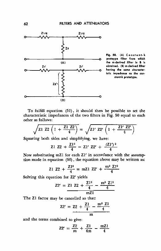
62 FILTERS AND ATTENUATORS
Z112 Z112
:_'V\/'v=tZ• _W.,......--: Fig. 50. (A) Constont-k protoype filter from which the m-derived filter In B is obtained. (B) m-derived filter having the same characteristic impedance as the can•
(Al z,· z,•
stant-k prototype.
(Bl
To fulfill equation (51), it should then be possible to set the characteristic impedances of the two filters in Fig. 50 equal to each other as follows:
jz1 Z2 ( 1 + Zl 4z2) = jz1' Z2' ( 1 + Zl'/
2')
Squaring both sides and simplifying, we have:
Zl Z2 + zt = Zl' Z2' + (Z~) 2
Now substituting mZl for each Zl' in accordance with the assumption made in equation (50) , the equation above may be written as:
Zl Z2 + Zl2
- mZl Z2' + m2
Zl2
4 - 4 Solving this equation for Z2' yields
Z2' = Zl Z2 + zt m2 Zl 2
4 mZl
The Zl factor may be cancelled so that:
Z2 + ~ _ m2 Zl
Z2'= 4 4
m and the terms combined to give:
Z2'=~+~ m 4m
mZl --4-

WAVE FILTERS 63
more simply written as:
22, = ~ + (1 - m2) Zl
m 4m (52)
Equation (52) , therefore, implies that if the impedance Z2' in Fig. 50B is given the configuration specified by the right members of the equation, the characteristic impedance of the constant-k filter in (A) will be identical with the characteristic impedance of the derived filter in (B) . The development above also demands that the series arms be given the value of mZI as provided in equation (50). Thus, the series arms contain one component each (mZI). The shunt arm must contain two components, one with an impedance of 22/m and the other with an impedance of (l-m2) Zl/4m. Since the filter has been derived from a constant-k type in which each series arm is Zl/2 (Fig. 50A), then each series arm in the derived filter is mZl/2. Thus, the complete filter appears as shown in Fig. 51.
By using equations (50) and (52) and varying the value of m, any number of sections can be designed, differing in respects but having the same characteristic impedance. Such filters can be linked
Fig. 51, m-derived filter contoining proper impedonce volues os compored with constant-k prototype so that its characteristic impedance equals that of the prototype.
mZ112 mZ112
(1-m2 )z1
4m
.ll m
without reflections between them to obtain virtually any attenuation characteristic desired. The question arises as to the order of value that m may assume. The upper portion of the shunt impedance having the value:
(I - m2) Zl 4m
provides the answer to this question. In order that this value maintain the proper relationship at all frequencies, the numerator must not be permitted to become negative. Hence, m may vary only between zero and +1.

64 FILTERS AND ATTENUATORS
49. Examples of m-Derived Filter Sections
To illustrate the design of simple m-derived filter sections from constant-k prototypes, we might examine a common low-pass and high-pass filter configuration. For example, the constant-k prototype of a symmetrical T-section, mid-series terminated (see Fig. 44A) arranged for low-pass characteristics appears in Fig. 52A.
t t o---'lff''-----1-c----'lff'---o
I Fig. 52. (A) Symmetrical T-o------------------,0 section mid-series terminated
(Al low-pan filter (con1tant-k). (B) m-derlved low-pan filter
~L '!!.h obtained by applying equa-o---'lff''----1-+------'rir------o tions (50) and (52) to the prototype .
..l.!:.!!l!lb. •m
Imc
0--------------------0 (Bl
In the m-derived filter of Fig. 52B, note that the capacitive element is mC (rather than C/m) because of the inverse relationship between impedance and capacitance. Since L and Z are related directly, the inductive component values have the same form as in equation (50) and (52) .
A symmetrical T-section high-pass filter, first in its prototype form, then in its m-derived form, is illustrated in Fig. 5S. Note the application of equations (50) and (52) to the derivation of the values of the series and shunt arms.
Constant-k prototypes may also be used to construct m-derived :n:-sections. The same general procedure obtains the relevant equations. Repeat: it is not our purpose to discuss design details, but you may follow through with specific filter forms based on general principles and examples in this chapter.
Bandpass and band-elimination filter configurations in both constant-k and m-derived forms can also be designed, using similar mathematical approaches. Design formulae and equation deriva-

Fig. 53. Symmetrlcal-T highpens filters of the constant-k prototype and the m-derlved
forms.
WAVE FILTERS 65
2C 2C o--~1,.---+------1~(--o
L PROTOTYPE
(A) 2C !£ iii m
o---~•----+-
0-------------
I( l 4mC I( 0
I~ m-DERIVED FORM
0 (Bl
tions may be found in any of the excellent electronic handbooks now available in the public libraries.
50. Bridged-T and Parallel-T Configurations
Figure 54 illustrates two other types of filter networks of specialized design. In general, these systems are used as band-elimina-
L RI
C1 Ct
( f~ )
0 0 Fig. 54. (A) Brldged-T net•
(A) work consisting of LCR com• ponents. (B) Parallel-T net•
RI R2 work containing R-C campan-ents, only.
(Bl

66 FILTERS AND ATTENUATORS
tion filters, feedback networks for frequency-selective amplifiers and oscillators, and calibrated bridges for measuring devices. They are characterized by their ability to produce high attenuation for a single frequency or group of adjacent frequencies over as narrow a band as desired. They are also capable of producing large phase shifts - either lagging or leading as the design dictates. With the proper selection of components, the maximum phase shift can be as much as 180°. It is also comparatively easy to build bridged-T and parallel-T networks with a negative transfer function (i.e., output voltage 180° out-of-phase with the input voltage). Such a network can be applied to the construction of a single-stage vacuum tube oscillator having exceptional frequency stability) .
The bridged-T network in Fig. 54A is unique in that there is no theoretical limit to the minimum width of the attenuation band it can introduce. Actually, the practical limitation is set by the Q of the inductor in the bridging leg. Because of its sharp, narrow attenuation properties, the bridged-T network is often applied where a truly null feedback loop is needed. To illustrate, we shall briefly consider the general structure of a frequency-selective amplifier.
51. Frequency-Selective Amplifier
If a negative feedback amplifier is set up with a null network in the feedback loop (Fig. 55) , an amplifier having sharp frequencyselective characteristics can be designed. The amount of feedback at the null frequency theoretically is zero, so that the gain of the amplifier at the null frequency is the same as its gain without feedback. On either side of the null frequency, the attenuation of the
AMPLIFIER
NULL NETWORK
Fig. 55. General plan of a frequency-selective amplifier, using a null network in the
feedback loop.
filter drops sharply, causing a greater effective negative feedback and consequently far less amplifier gain.
Bandpass-selective amplifiers, having a flat passband rather than a single peak, as is obtained with resonant circuits, can be designed by using several independent feedback stages, staggered in frequency. The frequency to which each feedback stage is tuned may be determined as are staggered tuned circuits.
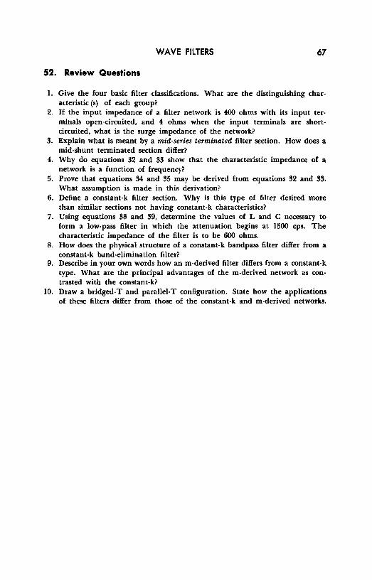
WA VE FILTERS 67
52. Review Questions
I. Give the four basic filter classifications. What are the distinguishing characteristic (s) of each group?
2. If the input impedance of a filter network is 400 ohms with its input terminals open-circuited, and 4 ohms when the input terminals are shortcircuited, what is the surge impedance of the network?
3. Explain what is meant by a mid-series terminated filter section. How does a mid-shunt terminated section differ?
4. Why do equations 32 and 33 show that the characteristic impedance of a network is a function of frequency?
5. Prove that equations 34 and 35 may be derived from equations 32 and 33. What assumption is made in this derivation?
6. Define a constant-k filter section. Why is this type of filter desired more than similar sections not having constant-k characteristics?
7. Using equations 38 and 39, determine the values of L and C necessary to form a low-pass filter in which the attenuation begins at 1500 cps. The characteristic impedance of the filter is to be 600 ohms.
8. How does the physical structure of a constant-k bandpass filter differ from a constant-k band-elimination filter?
9. Describe in your own words how an m-derived filter differs from a constant-k type. What are the principal advantages of the m-derived network as contrasted with the constant-k?
IO. Draw a bridged-T and parallel-T configuration. State how the applications of these filters differ from those of the constant-k and m-derived networks.

Chapter 6
ATTENUATORS AND EQUALIZERS
53. Definition of an Attenuator
A network that introduces an intentional loss in the transmission of a signal from one point to another, regardless of frequency, is called an attenuator. Generally, a device used for attenuation purposes maintains a fixed impedance at both its input and output ends regardless of the manner in which it is varied.
Attenuators can be designed to have equal or unequal input and output impedances, and to provide varying degrees of attenuation. They may be balanced or unbalanced, depending upon the requirements of the application. They may be fixed or variable; for example, the T-pad, used to control the level of a remote speaker is a variable attenuator which maintains constant input and output impedance at all frequencies. Fixed attenuators introduce a fixed loss - as in making a short and long telephone line deliver the same signal to a broadcasting studio - or they may match impedances between a source and load.
Attenuators are designed to work with particular input and output impedances. If worked between sources and loads which differ from the attenuator values, the transmission loss increases. In addition, the design of an attenuator is based on resistive sources and loads, hence an inductive or capacitive load will alter the frequency response.
54. Fundamentals of Fixed Attenuators
Fixed attenuators normally take the T or ,,,. form and may be unbalanced or balanced (Fig. 56) . In the development that follows, Zl will always be taken as the larger impedance while Z2 is the
68

ATTENUATORS AND EQUALIZERS 69
smaller. Either may be the input or output impedance of the net· work.
The loss ratio of an attenuator is normally discussed in terms of power and is defined as:
(53)
in which K is the loss ratio, P1 = power input to attenuator, and PO = power taken out of network. In studying the balanced and unbalanced types, note that half the resistance of a given element is transferred to the opposite line to achieve balance.
Assuming that the input and output impedances are not to be equal - such as in an impedance-matching pad - the ratio of Zl
A, ___ ___. Rz
=I .. = Zl
(Al
Z1
(Cl
l.R, 2
(Bl
½Rs
(DI
.l.Rz 2
Fl9. 56. (A) Unbalanced-T attenuator. (B) Balanced-T attenuator. (C) Unbalanced-,.; attenuator. (D) Balanced-n attenuator.
Za
Zz
to Z2 will exceed unity since Zl is considered the larger of the two impedances. For every ratio of Zl/Z2, there is an associated minimum K that can be realized from the attenuator. This means that in designing an attenuator in which the input and output impedances are fixed by other circuit requirements, a definite minimum loss ratio must be anticipated. This can be determined from the equation:
Minimum K = 2;; - 1 + 2 j ~~ ( ~~ - I ) (54)
Equation (54) is solved graphically in Fig. 57 where the minimum
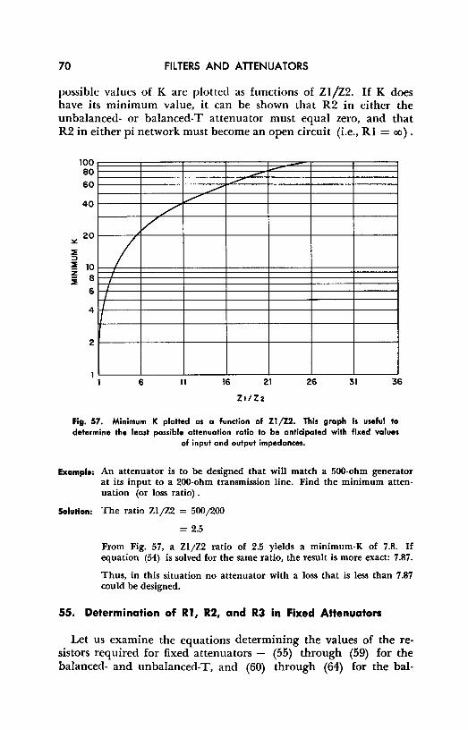
70 FILTERS AND ATTENUATORS
possible values of K are plotted as functions of Z I /22. If K does have its minimum value, it can be shown that R2 in either the unbalanced- or balanced-T attenuator must equal zero, and that R2 in either pi network must become an open circuit (i.e., RI = oo) .
100 80 60
40
:le: 20
:Iii ::, :Iii 10 z 2 8 I
6 I I
4 I
2
1 1
--/ V
I
6 11
~
16 21
Z1/Z2
26 31 36
Fig. 57. Minimum K plotted as a function of Zl /Z2. This graph is useful to determine the least possible attenuation ratio to be anticipated with fixed values
of input and output impedances.
Example: An attenuator is to be designed that will match a 500-ohm generator at its input to a 200-ohm transmission line. Find the minimum attenuation (or loss ratio) .
Solution: The ratio Zl/Z2 = 500/200
= 2.5
From Fig. 57, a Zl/Z2 ratio of 2.5 yields a minimum-K of 7.8. If equation (54) is solved for the same ratio, the result is more exact: 7.87.
Thus, in this situation no attenuator with a loss that is less than 7.87 could be designed.
55. Determination of Rl, R2, and R3 in Fixed Attenuators
Let us examine the equations determining the values of the resistors required for fixed attenuators - (55) through (59) for the balanced- and unbalanced-T, and (60) through (64) for the bal-

ATTENUATORS AND EQUALIZERS 71
anced- and unbalanced-pi network. For the T-type of attenuator we have
RI = Zl (K + I) - 2v'KZI Z2 (55)
K-1
R2 = Z2 (K + I) - 2v'KZI Z2 (56)
K - I
R3 = 2-yKZI 22 (57)
K-1
If Zl = Z2, the foregoing equations may be reduced to the following forms:
(~+-11) RI = R2 = Zl yJr+T
R 3 _ 2Zl yf( - K - I
The pi-attenuator network equations are as follows:
RI
R2
R3 =
(K - I) Zl yi2 (K + I) ,Jz2 - 2 \fKZI
(K - I) Z2 ~ (K + I) yli - 2KZ2 K-1 ~
2 vi{
(58)
(59)
(60)
(61)
(62)
The preceding equations reduce to simpler form if Zl = Z2 as shown below:
RI = R2 = Zl ( ~) (63)
R3
_ Zl (K - I) - 2yft" (64)
Example: Using an unbalanced-T network, determine the component values of an attenuator that matches a 500-ohm generator to a 200-ohm load with the minimum possible loss ratio.
Solution: Since the loss ratio is to be a minimum, the value of K must be 7.87 as determined in the previous example for the same input and output impedances. Furthermore, with K = minimum, R2 may be taken as zero, hence this calculation may be omitted. Thus, the determination of RI and R3 are necessary. From equations (55) and (57)
RI _ 500 (7.87 + 1) - 2-./7.87 X 500 X 200 - 7.87 - 1
Rl = 387 ohms

72 FILTERS AND ATTENUATORS
and
R!I _ 2y7 .87 X 500 X200 - 7.87 - 1
R!I = 258 ohms
Rt• 3870
Z2•2000 R2•2580
Fig. 58. The unbalanced-T network is calculated In this example. Note that R1 = zero and Is therefore omitted
from the diagram.·
The complete filter thus has the form and values shown in Fig. 58. Since K is the ratio of power input to power output, the actual network loss in db may be calculated from equation (65)
Loss = IO log1• K db
So that in this example the loss is
Loss = IO log10 7.87
= IO X 0.896
= 8.96 db
(65)
Example: A balanced-pi network for the same generator and load as the previous example is to be designed with an actual loss of 20 db. Determine the values of the components required in the network.
Solution: It is necessary to first determine the value of K. Solving equation (65) for K:
20 log,0K = IO
log10K = 2
K = 100
Substituting and solving equations (60), (61), and (62)
(100.=...!.2·5~ RI = (100 + 1) vJ.('if - 2'jiM X 500 RI = 7!15 ohms
R _ (100 - ~!} 200~ 2 - (100 + 1) -../500 - 2vfuf X WO
R2 = 2!10 ohms
R!I = 100 - 1 2
✓ 200 X 500 X 100
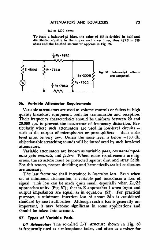
ATTENUATORS AND EQUALIZERS 73
R3 = 1570 ohms
To form a balanced-pi filter, the value of R3 is divided in half and distributed equally in the upper and lower lines, thus ½R3 = 785 ohms and the finished attenuator appears in Fig. 59.
R1•735n
z1•2oon
Rz•23on
56. Variable Attenuator Requirements
Fig. 59 Balanced-pl attenuator computed.
Variable attenuators are used as volume controls or faders in high quality broadcast equipment, both for transmission and reception. Their frequency characteristics should be uniform between 20 and 20,000 cps, to prevent the occurrence of frequency distortion. Particularly where such attenuators are used in low-level circuits -such as the output of microphones or preamplifiers - their noise level must be very low. Unless the noise level is below -150 db, objectionable scratching sounds will be introduced by such low-level attenuators.
Variable attenuators are known as variable pads, constant-impedance gain controls, and faders. Where noise requirements are rigorous, the structure must be protected against dust and stray fields. For this reason, proper shielding and hermetically-sealed enclosures are necessary.
The last factor we shall introduce is insertion loss. Even when set at minimum attenuation, a variable pad introduces a loss of signal. This loss can be made quite small, especially when Zl /Z2 approaches unity (Fig. 57) ; that is, K approaches I when input and output impedances are equal, as in equation (53). For practical purposes, a minimum insertion loss of about 2db is considered standard by most authorities. Although such a loss is generally unimportant, it may become significant in some applications and should be taken into account.
57. Types of Variable Pads.
L-1 Attenuator: The so-called L-T structure shown in Fig. 60 is frequently used as a microphone fader, and often as a mixer for
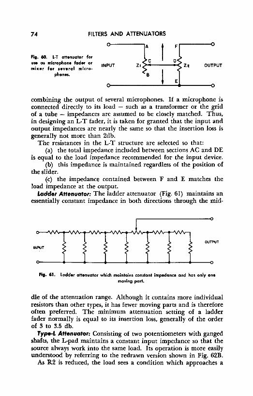
74 FILTERS AND ATTENUATORS
Fig. 60. L-T attenuator for UH as microphone fader or mixer for several micro-
phones.
INPUT OUTPUT
combining the output of several microphones. If a microphone is connected directly to its load - such as a transformer or the grid of a tube - impedances are assumed to be closely matched. Thus, in designing an L-T fader, it is taken for granted that the input and output impedances are nearly the same so that the insertion loss is generally not more than 2db.
The resistances in the L-T structure are selected so that: (a) the total impedance included between sections AC and DE
is equal to the load impedance recommended for the input device. (b) this impedance is maintained regardless of the position of
the slider. (c) the impedance contained between F and E matches the
load impedance at the output. ladder Attenuator: The ladder attenuator (Fig. 61) maintains an
essentially constant impedance in both directions through the mid-
OUTPUT
INPUT
Fig. 61. Ladder attenuator which maintains constant impedance and has only one moving part.
die of the attenuation range. Although it contains more individual resistors than other types, it has fewer moving parts and is therefore often preferred. The minimum attenuation setting of a ladder fader normally is equal to its insertion loss, generally of the order of 3 to 3.5 db.
Type-L Attenuator: Consisting of two potentiometers with ganged shafts, the L-pad maintains a constant input impedance so that the source always work into the same load. Its operation is more easily understood by referring to the redrawn version shown in Fig. 62B.
As R2 is reduced, the load sees a condition which approaches a
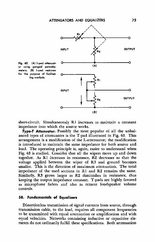
ATTENUATORS AND EQUALIZERS
Fig. 62. (A) L-pad attenuator using ganged potentiometers. (B) L-pad redrawn far the purpose of faciltat-
ing analysis.
R1
INPUT
INPUT
/'., / '
/ ' / '
(Al
(Bl
' '
Rz
R1
R2
75
OUTPUT
OUTPUT
short-circuit. Simultaneously RI increases to maintain a constant impedance into which the source works.
Type-T Attenuator: Possibly the most popular of all the unbalanced types of attenuators is the T-pad illustrated in Fig. 63. This arrangement is a modification of the L-attenuator; the modification is introduced to maintain the same impedance for both source and load. The operating principle is, again, easier to understand when Fig. 63 is studied. Consider that all the wipers move up and down together. As RI increases in resistance, R2 decreases so that the voltage applied between the wiper of R3 and ground becomes smaller. This is the direction of maximum attenuation. The total impedance of the used sections in RI and R2 remains the same. Similarly, R3 grows larger as R2 diminishes in resistance, thus keeping the output impedance constant. T-pads are highly favored as microphone faders and also as remote loudspeaker volume controls.
58. fundamentals of Equalizers
Distortionless transmission of signal currents from source, through transmission cable, to the load, requires all component frequencies to be transmitted with equal attenuation or amplification and with equal velocities. Networks containing inductive or capacitive elements do not ordinarily fulfill these specifications. Both attenuation

76 FILTERS AND ATTENUATORS
and velocity in such networks are affected by the frequency of the component.
An often used method of correcting frequency distortion in a transmission system is to incorporate an additional network with an attenuation characteristic so related to frequency that the net atteQ.uation of the two will be essentially independent of frequency.
INPUT Rz OUTPUT
Fig. 63. (A) Conventional (A) drawing of T-pad attenuator.
(B) T-pad redrawn to illus-trate the principle of opera•
tion. RI
INPUT Rs OUTPUT
(B)
The same procedure may be used to compensate for delay (or phase) distortion. A combination of transmission and compensation network is used in which the total time of transmission is made independent of component frequency. The wide use of telephone lines in all phases of wired and wireless communication has made equalizer engineering virtually a profession in itself. It is often found that attenuation equalization is sufficient and that delay distortion may be ignored.
Figure 64 illustrates graphically the function of an attenuation equalizer. This is idealized and shows what could be accomplished with a perfect equalizer. In practice, actual equalizers can be made to approach the ideal only over a limited frequency band. The total loss of the combination at all frequencies is greater than the maximum loss of the original system, which explains why equalizers are always associated with amplifiers that can compensate for the loss introduced by equalization.

6
C
5 r---~
4
2
--y
2
ATTENUATORS AND EQUALIZERS n
V '---r-.. I
"r-,_ r-,, !/ 'I\
,/,I \ .,,.v V
V \ \
\
4 6 8 1 2
FREQUENCY--
Fig. 64. Ideal equallzer performance. Curve A, shows the attenuation vs frequency charaderlstlc of the transmission system. Curve B, is the corrective attenuation aplied by the equalizer. Curve C, represenh the r• sultant curve over the fr•
quency band.
59. Equalizer Types
Amplitude equalizer design has been developed to a high order of perfection, largely by the Bell Laboratories and the Research Council of the Academy of Motion Picture Arts and Sciences.1 For the reader who is interested in equalizer mathematics and design, there are excellent papers and articles, as well as special engineering texts, devoted to this subject.
For the purposes of this book, some mention should be made of the various types of equalizers in use, without attempting to investigate quantitatively the applicable equations.
It is generally assumed that an amplitude equalizer operates from a source impedance that is equal in magnitude to the load impedance. On this basis, it is possible to design several equalizers having different configurations but which offer exactly the same transmission and attenuation characteristics as a function of frequency. Kimball presents design information for seven of these configurations, each with eight different categories of attenuation characteristics. The configurations are:
1H. Kimball, Motion Picture Sound Engineering, Princeton, 1938. (An excellent treatment of equalizer engineering design.)

78 FILTERS AND ATTENUATORS
(A) Shunt-impedance type (B) Series-impedance type (C) Full-shunt type (D) Full-series type (E) T-configuration (F) Bridged-T configuration (G) Lattice configuration
Figure 65 presents the general pattern of each configuration for an equalizer that has an insertion loss characteristic (attenuation
0 0
I - -I 0 0 SHUNT-IMPEDANCE TYPE
(Al
=°T o_J,
FULL-SERIES TYPE
(Dl
0 'lW 0
--- -SERIES-IMPEDANCE TYPE
(Bl
0----------0 T- CONFIGURATION
(El
~ - I -0 0 FULL-SHUNT TYPE
(Cl
0 I 0 BRIDGED-T CONFIGURATION
(Fl
Fig. 65. Equalizer configurations.
characteristic) like that shown in Fig. 66. One may well ask why seven different configurations should be described if each duplicates the others in performance. The answer is that one of the seven generally yields component values which are most easily obtained in practical work.

ATTENUATORS AND EQUALIZERS
Fig. 66. Any of the seven configurations shown in Fig. 65 can be designed to have an insertion loss charaderistic similar to this.
m 0
FREQUENCY
79
Because of the eight different categories of attenuation characteristics, each of the configurations can be altered to produce any of the curves given in Fig. 67. Above each curve, the series impedance configuration that produces it is shown. Remembering that each configuration can be similarly modified to yield each of these curves, we get 56 possible arrangements. Thus, the equalizer design engineer has a wide field from which to select. It is inconceivable that any practical transmission system could develop frequency distortion characteristics that could not be corrected by one or more of the equalizers illustrated.
60. Phase Equalizers
Phase equalizers are intended to compensate for velocity errors in propagation; that is, a phase equalizer reduces the phase differences between various components of the transmitted signal to a minimum as they arrive at the load. Theoretically, phase equalizers do not affect the amplitude of the signal at all, or do so in a fixed manner, regardless of frequency, so they can be added to existing circuits for phase correction without changing the gain characteristics.
A phase equalizer must be a network in which the phase characteristics can be controlled. Equal transmission times for different frequency components requires that the circuit introduce either no phase shift or an amount of shift that is directly proportional to frequency. This is tantamount to saying that the transmission time must be either zero or constant at all frequencies.

80 FILTERS AND ATTENUATORS
~ -- -- - --- - ---o-----o o------o o------o o------o
I
DB DB i~ F F F
o-----o o-----o o-----o o-----o
F F
Fig, 67, Possible equalizer insertion loss curves. Although the series impedance equalizer for each curve is illustrated, any one of the other six configurations can
be designed for the same characteristic.
Although several types of phase equalizer networks are suitable, the most common - and perhaps the simplest - is the lattice type shown in Fig. 68. This network has a zero attenuation characteristic and phase characteristics are shown in the curve of Fig. 69. Before we attempt to utilize the curve, we must define the applicable terms and state the pertinent equations.
As a start, let us define certain symbols of importance: f = the frequency at which a certain, known phase shift is de
sired. As will be shown, f may have several values where the desired phase shift is different for each.
10 = the frequency at which the lattice-compensator's phase shift is-90°.

ATTENUATORS AND EQUALIZERS
Fig. 68. Lattlc•type phase compensation network with zero attenuation character-
istic.
a = the reciprocal of £0 = I /f0
------~-----L
81
z = in the input impedance = the output impedance of the lattice. 0 = phase shift of the lattice in degrees Using these symbols, the applicable equations for determining
L and C of the lattice are:
(66)
(67)
Obviously, these equations cannot be used without first determining the factor a as defined above. Further, the equations have no meaning unless related to a specific situation in which phase distortion is occurring and requires correction. After the necessary
-~o.-------T"""------.------....... --------.
-2001-------+-------+-------+-------I ---------- ----------- ----------- .... ·--=:;;::::;:=---, 1eo•
fil -150 l-------+---------1-----.,,,e.,__.::__---1-----------I
ffi 7 l&I
e c» -100 1-------+-------+,,<--------+--------l --------· -----7~--------- ---------- 90°
-50 ~v .01 .1 1.0
F/Fo
10 100
Fig. 69. Phase characteristic of the network shown in Fig. 68. Refer to example for clarification of Its application.

82 FILTERS AND ATTENUATORS
correction is determined, the phase characteristic curve of the lattice is used to determine a. Then the values of L and C may be determined from equations (66) and (67) .
The technique used is best illustrated by example. The figures have been selected so that the curve will yield exact answers. Usually the engineer is forced to accept approximate information from the curve and correct the values by aligning the actual phase equalizer after it has been installed. When properly handled however, the correction required is small and amounts to slight trimming of the Lor C values.
Example: A transmission line, handling frequencies between IO kc and 20 kc, introduces phase distortion by producing phase shifts at various frequencies as follows:
At IO kc, the phase shift = -27°
At 15 kc, the phase shift = -43.5°
At 20 kc, the phase shift = -63°
As shown in the solution, a phase equalizer is required. Determine the lattice components needed to form a network having a characteristic impedance of 100 ohms.
Solution: (1) First, let us show that a phase equalizer is necessary. If the time delay of a transmission line is linearly porportional to frequency, no phase distortion will occur.1 In this case, the phase shift at 15 kc would have to be ¾ x -63° if this linear relationship applied since 15 kc is ¾ of 20 kc where the phase shift is -63°. But the actual phase shift at 15 kc is -43.5° rather than ¾ x -63 = -47.25°. Thus, there is a phase error of +3.75°. Similarly, at 10 kc the phase shift should be half that at 20 kc, or ½ (-63) = -31.5° instead of the shift of -27° which actually exists at this frequency. For 10 kc, therefore, the phase error of +4.5°. Obviously, compensation is required to eliminate these errors. To equalize the phase througho1i"t this range, a compensating network having errors the inverse of these must be designed. That is,
Designer Equalizer Error
-4.50
-3.75° 08
Frequency
IO kc 15 kc 20 kc
(2) Now let us study the characteristics of the curve (Fig. 64) to determine whether there are three values along the f/f0 axis bearing same relationship numerically as 10: 15:20, and which intersect the curve at the correct equalizer error points, as given above. Several trials must be made to approach closest to the desired conditions. In this example, the three suitable points are encircled on the curve. Note
1For a more extended treatment of time delay concepts, see R-F Amplifiers by A. Schure, New York, John F. Rider Publisher, Inc., 1959

ATTENUATORS AND EQUALIZERS 83
that these occur at f/f0 equal respectively to .4, .6, and .8 and that these numbers are related as 10 is to 15 is to 20. Further, the phase shifts at these values of f/f0 are -43°, -61.5°, and -77°. (3) It must now be shown that the phase shifts produced by the
equalizer introduce the right corrective error. If the phase shift of the equalizer at f/f0 = 0.8 -77°, then for a linear phase characteristic, the phase shift of the equalizer at f/f0 = 0.6 should by ¾ x (-77) = -57.75°. Actually, the shift is -61.5° and since this differs from -57.75° by -3.75° (see preceding table), the phase error of the equalizer is exactly the figure desired. Similarly, we analyze the shift at f/f0 = 0.4. For a linear characteristic, the shift should be ½ (-77) = -38.5°. Its actual phase shift, however, is -43°. The equalizer error is then -43° - (-38.5°) = -4.5°. This phase error also corresponds with the desired value given in the table. We now have all the factors required to calculate the necessary values of L and C for the lattice equalizer. (4) The value of f0 is next determined. Since this is the frequency at which the phase shift of the equalizer is -90°, and since f/fo = 0.8 at f = 20 kc, then f0 must be 25 kc. This follows from the fact that f/f0
at a phase shift of 906 is unity, hence:
0.8 20 kc
l = fo and thus f0 = 25 kc.
(5) The value of L may now be determined from the definition of a and equation (66) given on page 81. Since a = l/f0 , then a = 1;25000 = 4.0 X l0-•. Substituting in equation (66) :
4 X 10-• X 102 L = 6.28
(Note: the impedance characteristic of this equalizer was specified as 100 ohms. Hence, the factor 102 in the numerator) .
L = 0.64 millihenries
(6) C is determined from equation (67)
0.64 X 10-• C = 10'
C = 0.064 X 10-• farad
o-------'Til"-------o Fig. 70. The lattice phase equalizer computed for the example. Note that this network ls symmetrical and therefore may be used In
either direction.
0.64MH

84 FILTERS AND ATTENUATORS
C = 0.064 microfarad.
The complete lattice, with values is given in Fig. 70.
61. Review Questions
I. Describe the function of an attenuator. Specifically, what function is served by a fixed attenuator in contrast to a variable type.
2. What is meant by the loss ratio of an attenuator? !J. How can one determine the minimum possible loss ratio of a fixed attenu•
ator? 4. Derive equation (58) from the equations that precede it. 5. What is the loss ratio (K) of an attenuator having equal input and output
impedances of, say, 500 ohms? 6. What is the minimum loss ratio of an attenuator that matches a 200-ohm
transmission line to a 400-ohm load? Find the actual loss in db of this attenuator.
7. Describe four types of variable attenuators and describe the characteristics of each.
8. What is an equalizer? What kinds of equalizers are there? 9. How does an amplitude equalizer differ from a phase equalizer?
10. What essential characteristics must a phase equalizer possess to be effective?
Absorption traps, 48 Amplitude distortion, 43, 46 Amplitude equalizer, 77 Attenuate, 1 Attenuation, 4 Attenuator, definition of, 68
Balanced-T attenuator, 70 Band-elimination:
constant-k filter, 59 filter, 6, 49, 53
Bandpass: constant-k filter, 58 filter, 5, 53 -selective amplifiers, 66
Band-rejection filter, 49 Basic filter configurations, 54, 55 Boost circuits, 30 Bridged-T:
compensation network, 31 configuration equalizer, 78 configurations, 65 networks, 52
Cancellation filters, 24 Capacitance, 11 Capacitor-input filter, 7, 10, 11, 12 Center frequency, 2 Characteristic impedance, 53, 54
of filter sections, 55 Choke-input filters, 8, 16, 17 Compensation network, 76 Complex networks, 29 Constant-impedance gain controls,
73 Constant-k filters defined, 56, 57
INDEX
Critical and optimum inductance, 16
Crossover frequency, 36 Crossover networks, 26, 35, 36, 37 Cutoff frequency, 3
Damping,29 Decoupling filters, 26, 27, 28, 47 De-emphasis, 41 Degenerative, 27
feedback, 27 Delay distortion, 76 Determination of RI, R2 and R3 in
fixed attenuators, 70, 71, 72 Distributed impedances, 54
Effectiveness of attenuation and transmission, 53
Equalizer: fundamentals, 75, 76 types, 77, 78, 79
Examples of m-derived filter sections, 64
Filter, 1 classifications, 52, 53 network, 1 vocabulary, 3
Fixed attenuator fundamentals, 68 Flat passband, 66 Frequency, 11
85
characteristics, 7 3 compensation, 29 discrimination, 1 distortion, 73 -selective amplifier, 66 -sensitive, 1
86
Full-series equalizer, 78 Full-shunt equalizers, 78 Function of a filter, I, 2, 3
Graded filters, 23, 24
High-fidelity: amplifiers, 26 equalizer, 41
High-frequency compensation: combination peaking, 45, 46 series peaking, 45 shunt peaking, 44, 45
High-frequency response, 35 High-pass:
constant-k filter, 58 filter, 5, 53
High-voltage power supplies, 22 Hum-voltage contact, 23
Insertion loss, 37, 73
Ladder attenuator, 74 L-attenuator, 75 Lattice configuration equalizer, 78 L-C circuits, 7 Linearity, 29 Load:
current, 7 resistance, l l
Loudspeaker volume controls, 75 Low-frequei;icy:
compensation filter, 46 gain, 43 response, 35, 47
Low-pass: constant-k filter, 57, 58 filter, 5, 52
Maximum impedance, 19 m-derived:
filters, 52 defined, 60 t-sections, 60, 61
Microphone faders, 75 Mid-range gain, 3 Mid-series terminated, 55 Multi-section network, II
INDEX
Narrow-band filter, 2 Need for video filters, 43 Noise level, 73 Non-resonant tone compensation,
31,32
Orthophonic, 41 Output:
capacitor, 19, 20 voltage and voltage regulation,
12, 13
Parallel-resonant circuit, 38, 48 Parallel-t configurations, 65 Pass band, 5 Peak current, 13
rating, 15 Percent ripple, IO Perfect equalizer, 76 Permissible ripple, lO Phase:
characteristics, 80 distortion, 46 equalizer, 79 relationship, 31
Positiveness, 27 Power supply filters characteristics,
7,8,9 Presence controls, 26, 37, 38 Pulsating supply, II Pure reactance, 53
R-C: coupled amplifier, 43
for power supplies, 22, 23 filters, 7
Record Industry Association of America, 41
Rectifier: considerations in capacitor-input
filters, 13, 14, 15, 16 tubes, 14
Regenerative, 28 Rejection, 4 Rejection filters, 47, 48 Relative attenuation, 9 Resonant filter, 6 Resonant tone compensation, 29, 30 Response curve, I, 2, Ripple percentage, 18
Ripple voltage: filter, IO, II, 12 of choke-input filter systems, 18
Review questions, 25, 42, 50, 51, 67,84
Rumble and scratch filters, 39, 40 Rumble filters, 26
Scott filter, 41, 42 Scratch filters, 26 Series-impedance equalizer, 78 Series-resonant filter, 48 Shunt-capacitances, 43 Shunt-impedance equalizer, 78 Sidebands, 49 Sideband suppression filters in TV,
49,50 Speech clippers, 26 Speech clipping, 33, 34 Splatter, 33
filters, 34 Surge impedance, 54 Swinging choke, 20 Symmetrical-a sections, 55 Symmetrical-T sections, 55
Table-top radio receivers, 22 Television:
high-voltage supplies, 22 practice, 43
T-configuration equalizer, 78 T-section, low-pass filter, 60
INDEX
Time-delay discrimination, 43 Tone controls, 26
considerations, 29 potentiometer, 32
Transmission, 4 band,53 characteristics, 57 lines, 54
Tuned filter, 6 system, 21
Tuned low-pass filters, 20, 21, 22 Turnover, 41 Tweeter, 35 Type-L attenuator, 74 Types of filters, 3, 4, 5, 6 Types of variable pads, 73 Type-T attenuator, 75
Unbalanced attenuator, 70 Uncompensated amplifier, 43 t:ntuned filter, 6 Untuned low-pass filters, 9
Variable attenuator requirements, 73
Variable pads, 73 Velocity errors, 79 Vestigial sideband, 49 Video modulation, 49 Voltage regulation, 7, 8, 12
of choke-input filters, 18, 19 Volume controls, 73
Wave filters, 52 Wave traps, 48 Wide-band filter, 2
87