Influence of reactive oxygen ambience on the structural, morphological and optical properties of...
6
Influence of reactive oxygen ambience on the structural, morphological and optical properties of pulsed laser ablated potassium lithium niobate thin films V. Jayasree a , R. Ratheesh b , V. Ganesan c , V.R. Reddy c , C. Sudarsanakumar d , V.P. Mahadevan Pillai a, ⁎, V.U. Nayar a a Department of Optoelectronics, University of Kerala, Kariavattom, Thiruvananthapuram 695 581, Kerala, India b Centre for Materials for Electronics Technology, Athani P. O, Thrissur, Kerala, India c UGC-DAE Consortium for Scientific Research, Indore Centre, Madhya Pradesh, India d School of Pure and Applied Physics, Mahatma Gandhi University, Kottayam, Kerala, India abstract article info Article history: Received 10 October 2007 Received in revised form 7 June 2008 Accepted 6 July 2008 Available online 17 July 2008 Keywords: Potassium lithium niobate Nonlinear optic materials Ferroelectric Tungsten bronze materials Electro-optic materials Pulsed laser deposition Transmittance spectra Optical band gap The effect of oxygen ambience on the structure and properties of potassium lithium niobate (K 3 Li 2 Nb 5 O 15 : KLN) films prepared on glass substrates by pulsed laser ablation technique (PLD) are studied. The influence of annealing on the properties of vacuum deposited films is also investigated. The Gracing Incidence X-ray Diffraction (GIXRD) data suggests the tetragonal structure for the KLN film whose grain sizes increase on thermal annealing. The Atomic Force Microscopic (AFM) analysis reveals the four-fold symmetric nature of the grains in the films. Self assembly of grains in the form of rings and rods are observed in AFM images of the films deposited in an oxygen ambience of 2 Pa. The films deposited at higher oxygen ambience show a blue shift in optical band gap. The direct current (DC) resistance measurement on the films deposited at non-reactive ambience reveals resistivity in the range of kΩ m. © 2008 Elsevier B.V. All rights reserved. 1. Introduction As a class of compounds, ferroelectric oxides have very attractive and potential properties such as wide band gap (N 3 eV), large electro- optic and nonlinear optic coefficients and have the possibility of sustaining the spontaneous polarizations [1]. Ferroelectric tungsten– bronze crystals with general formula (A 1 ) 2 (A 2 ) 4 C 4 (B 1 ) 2 (B 2 ) 8 O 30 have generated much interest, especially for nonlinear optical applications and for their large optical damage threshold originating from their crystal structure [2]. Potassium lithium niobate (K 3 Li 2 Nb 5 O 15 : KLN) with a completely filled tungsten–bronze type structure is a very promising material for various optical applications owing to its large electro-optic, nonlinear optic, piezoelectric and pyroelectric proper- ties [3] However the growth of large single crystals of KLN is still a challenging problem as they crack easily while cooling down through paraelectric to ferroelectric phase. Moreover the crystallographic and dielectric properties are severely affected by the Nb 2 O 5 content in the melt. Hence, the growth of epitaxial thin films of KLN is of particular interest, as high quality thin films of KLN are suitable for many of its applications. Different thin film depositions technique such as epitaxial growth by melting [4], RF magnetron sputtering [5,6] on substrates like potassium bismuth niobate [5] and sapphire have been used for the epitaxial or polycrystalline growth of KLN thin films. However, preparation of KLN thin film using pulsed laser deposition technique has not yet been reported. Pulsed laser deposition (PLD) is an effective tool for the growth of quantum structures with high chemical purity and controlled stoichiometry. In PLD, one can control size distribution in nanocrystals by varying the parameters like target to substrate distance, laser fluence, background gas pressure etc. This paper presents a report of preparation of KLN thin film using pulsed laser deposition technique in non-reactive and reactive atmosphere. The as-deposited films prepared under vacuum condition, the films annealed in air atmosphere and the as-deposited films prepared under different reactive oxygen pressures, are characterised using Gracing Incidence X-Ray Diffraction (GIXRD), Atomic Force Micro- scopy (AFM), UV–Vis spectroscopy and direct current (DC) resistance measurements to study the effect of annealing and that of background oxygen pressure on the properties of the films. 2. Experiment 2.1. Preparation of stoichiometric target for PLD operation Stoichiometric composition of K 2 CO 3 , Li 2 CO 3 and Nb 2 O 5 (Aldrich, purity 99.99%) is mixed well in an agate mortar for an hour using Thin Solid Films 517 (2008) 603–608 ⁎ Corresponding author. E-mail address: [email protected] (V.P.M. Pillai). 0040-6090/$ – see front matter © 2008 Elsevier B.V. All rights reserved. doi:10.1016/j.tsf.2008.07.004 Contents lists available at ScienceDirect Thin Solid Films journal homepage: www.elsevier.com/locate/tsf
-
Upload
independent -
Category
Documents
-
view
2 -
download
0
Transcript of Influence of reactive oxygen ambience on the structural, morphological and optical properties of...
Thin Solid Films 517 (2008) 603–608
Contents lists available at ScienceDirect
Thin Solid Films
j ourna l homepage: www.e lsev ie r.com/ locate / ts f
Influence of reactive oxygen ambience on the structural, morphological and opticalproperties of pulsed laser ablated potassium lithium niobate thin films
V. Jayasree a, R. Ratheesh b, V. Ganesan c, V.R. Reddy c, C. Sudarsanakumar d,V.P. Mahadevan Pillai a,⁎, V.U. Nayar a
a Department of Optoelectronics, University of Kerala, Kariavattom, Thiruvananthapuram 695 581, Kerala, Indiab Centre for Materials for Electronics Technology, Athani P. O, Thrissur, Kerala, Indiac UGC-DAE Consortium for Scientific Research, Indore Centre, Madhya Pradesh, Indiad School of Pure and Applied Physics, Mahatma Gandhi University, Kottayam, Kerala, India
⁎ Corresponding author.E-mail address: [email protected] (V.P.M. P
0040-6090/$ – see front matter © 2008 Elsevier B.V. Aldoi:10.1016/j.tsf.2008.07.004
a b s t r a c t
a r t i c l e i n f oArticle history:
The effect of oxygen ambien Received 10 October 2007Received in revised form 7 June 2008Accepted 6 July 2008Available online 17 July 2008Keywords:Potassium lithium niobateNonlinear optic materialsFerroelectricTungsten bronze materialsElectro-optic materialsPulsed laser depositionTransmittance spectraOptical band gap
ce on the structure and properties of potassium lithiumniobate (K3Li2Nb5O15: KLN)films prepared on glass substrates by pulsed laser ablation technique (PLD) are studied. The influence ofannealing on the properties of vacuum deposited films is also investigated. The Gracing Incidence X-rayDiffraction (GIXRD) data suggests the tetragonal structure for the KLN film whose grain sizes increase onthermal annealing. The Atomic ForceMicroscopic (AFM) analysis reveals the four-fold symmetric nature of thegrains in the films. Self assembly of grains in the form of rings and rods are observed in AFM images of the filmsdeposited in an oxygen ambience of 2 Pa. The films deposited at higher oxygen ambience show a blue shift inoptical band gap. The direct current (DC) resistance measurement on the films deposited at non-reactiveambience reveals resistivity in the range of kΩ m.
© 2008 Elsevier B.V. All rights reserved.
1. Introduction
As a class of compounds, ferroelectric oxides have very attractiveand potential properties such as wide band gap (N3 eV), large electro-optic and nonlinear optic coefficients and have the possibility ofsustaining the spontaneous polarizations [1]. Ferroelectric tungsten–bronze crystals with general formula (A1)2(A2)4C4(B1)2(B2)8O30 havegenerated much interest, especially for nonlinear optical applicationsand for their large optical damage threshold originating from theircrystal structure [2]. Potassium lithium niobate (K3Li2Nb5O15: KLN)with a completely filled tungsten–bronze type structure is a verypromising material for various optical applications owing to its largeelectro-optic, nonlinear optic, piezoelectric and pyroelectric proper-ties [3] However the growth of large single crystals of KLN is still achallenging problem as they crack easily while cooling down throughparaelectric to ferroelectric phase. Moreover the crystallographic anddielectric properties are severely affected by the Nb2O5 content in themelt. Hence, the growth of epitaxial thin films of KLN is of particularinterest, as high quality thin films of KLN are suitable for many of itsapplications. Different thin film depositions technique such asepitaxial growth by melting [4], RF magnetron sputtering [5,6] on
illai).
l rights reserved.
substrates like potassium bismuth niobate [5] and sapphire have beenused for the epitaxial or polycrystalline growth of KLN thin films.However, preparation of KLN thin film using pulsed laser depositiontechnique has not yet been reported. Pulsed laser deposition (PLD) isan effective tool for the growth of quantum structures with highchemical purity and controlled stoichiometry. In PLD, one can controlsize distribution in nanocrystals by varying the parameters like targetto substrate distance, laser fluence, background gas pressure etc. Thispaper presents a report of preparation of KLN thin film using pulsedlaser deposition technique in non-reactive and reactive atmosphere.The as-deposited films prepared under vacuum condition, the filmsannealed in air atmosphere and the as-deposited films preparedunder different reactive oxygen pressures, are characterised usingGracing Incidence X-Ray Diffraction (GIXRD), Atomic Force Micro-scopy (AFM), UV–Vis spectroscopy and direct current (DC) resistancemeasurements to study the effect of annealing and that of backgroundoxygen pressure on the properties of the films.
2. Experiment
2.1. Preparation of stoichiometric target for PLD operation
Stoichiometric composition of K2CO3, Li2CO3 and Nb2O5 (Aldrich,purity 99.99%) is mixed well in an agate mortar for an hour using
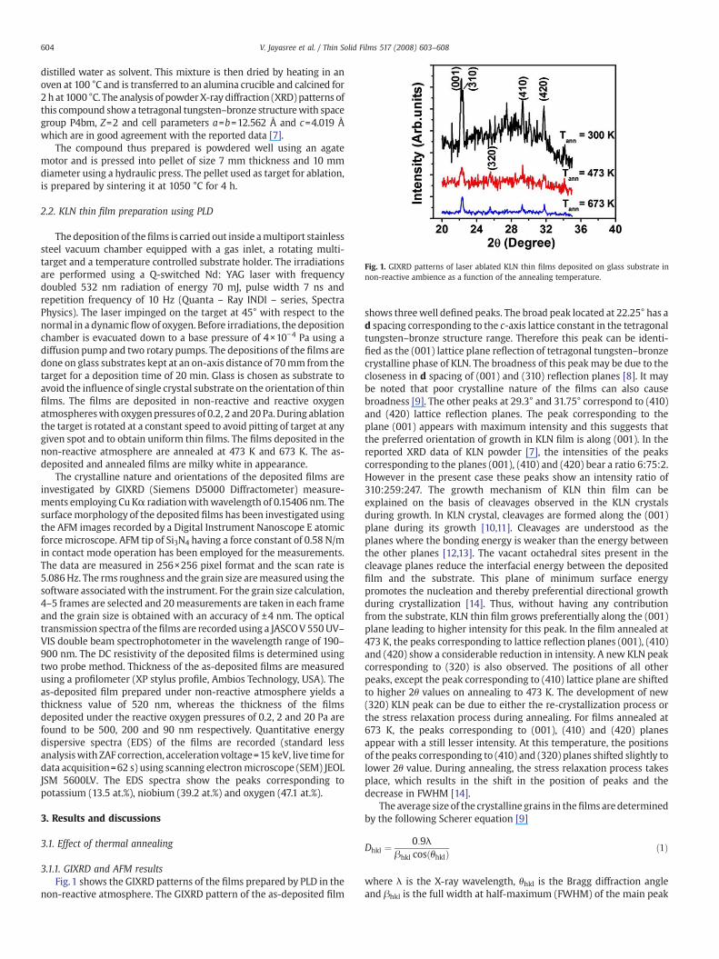
Fig. 1. GIXRD patterns of laser ablated KLN thin films deposited on glass substrate innon-reactive ambience as a function of the annealing temperature.
604 V. Jayasree et al. / Thin Solid Films 517 (2008) 603–608
distilled water as solvent. This mixture is then dried by heating in anoven at 100 °C and is transferred to an alumina crucible and calcined for2 h at 1000 °C. The analysis of powderX-ray diffraction (XRD) patterns ofthis compound showa tetragonal tungsten–bronze structurewith spacegroup P4bm, Z=2 and cell parameters a=b=12.562 Å and c=4.019 Åwhich are in good agreement with the reported data [7].
The compound thus prepared is powdered well using an agatemotor and is pressed into pellet of size 7 mm thickness and 10 mmdiameter using a hydraulic press. The pellet used as target for ablation,is prepared by sintering it at 1050 °C for 4 h.
2.2. KLN thin film preparation using PLD
The deposition of thefilms is carried out inside amultiport stainlesssteel vacuum chamber equipped with a gas inlet, a rotating multi-target and a temperature controlled substrate holder. The irradiationsare performed using a Q-switched Nd: YAG laser with frequencydoubled 532 nm radiation of energy 70 mJ, pulse width 7 ns andrepetition frequency of 10 Hz (Quanta – Ray INDI – series, SpectraPhysics). The laser impinged on the target at 45° with respect to thenormal in a dynamicflowof oxygen. Before irradiations, the depositionchamber is evacuated down to a base pressure of 4×10⁻⁴ Pa using adiffusion pump and two rotary pumps. The depositions of the films aredone on glass substrates kept at an on-axis distance of 70mm from thetarget for a deposition time of 20 min. Glass is chosen as substrate toavoid the influence of single crystal substrate on the orientation of thinfilms. The films are deposited in non-reactive and reactive oxygenatmosphereswith oxygenpressures of 0.2, 2 and 20 Pa. During ablationthe target is rotated at a constant speed to avoid pitting of target at anygiven spot and to obtain uniform thin films. The films deposited in thenon-reactive atmosphere are annealed at 473 K and 673 K. The as-deposited and annealed films are milky white in appearance.
The crystalline nature and orientations of the deposited films areinvestigated by GIXRD (Siemens D5000 Diffractometer) measure-ments employing Cu Kα radiationwithwavelength of 0.15406 nm. Thesurfacemorphology of the deposited films has been investigated usingthe AFM images recorded by a Digital Instrument Nanoscope E atomicforce microscope. AFM tip of Si3N4 having a force constant of 0.58 N/min contact mode operation has been employed for the measurements.The data are measured in 256×256 pixel format and the scan rate is5.086Hz. The rms roughness and the grain size aremeasured using thesoftware associatedwith the instrument. For the grain size calculation,4–5 frames are selected and 20measurements are taken in each frameand the grain size is obtained with an accuracy of ±4 nm. The opticaltransmission spectra of the films are recorded using a JASCOV 550UV–VIS double beam spectrophotometer in the wavelength range of 190–900 nm. The DC resistivity of the deposited films is determined usingtwo probe method. Thickness of the as-deposited films are measuredusing a profilometer (XP stylus profile, Ambios Technology, USA). Theas-deposited film prepared under non-reactive atmosphere yields athickness value of 520 nm, whereas the thickness of the filmsdeposited under the reactive oxygen pressures of 0.2, 2 and 20 Pa arefound to be 500, 200 and 90 nm respectively. Quantitative energydispersive spectra (EDS) of the films are recorded (standard lessanalysiswith ZAF correction, acceleration voltage=15 keV, live time fordata acquisition=62 s) using scanning electronmicroscope (SEM) JEOLJSM 5600LV. The EDS spectra show the peaks corresponding topotassium (13.5 at.%), niobium (39.2 at.%) and oxygen (47.1 at.%).
3. Results and discussions
3.1. Effect of thermal annealing
3.1.1. GIXRD and AFM resultsFig. 1 shows the GIXRD patterns of the films prepared by PLD in the
non-reactive atmosphere. The GIXRD pattern of the as-deposited film
shows threewell defined peaks. The broad peak located at 22.25° has ad spacing corresponding to the c-axis lattice constant in the tetragonaltungsten–bronze structure range. Therefore this peak can be identi-fied as the (001) lattice plane reflection of tetragonal tungsten–bronzecrystalline phase of KLN. The broadness of this peak may be due to thecloseness in d spacing of (001) and (310) reflection planes [8]. It maybe noted that poor crystalline nature of the films can also causebroadness [9]. The other peaks at 29.3° and 31.75° correspond to (410)and (420) lattice reflection planes. The peak corresponding to theplane (001) appears with maximum intensity and this suggests thatthe preferred orientation of growth in KLN film is along (001). In thereported XRD data of KLN powder [7], the intensities of the peakscorresponding to the planes (001), (410) and (420) bear a ratio 6:75:2.However in the present case these peaks show an intensity ratio of310:259:247. The growth mechanism of KLN thin film can beexplained on the basis of cleavages observed in the KLN crystalsduring growth. In KLN crystal, cleavages are formed along the (001)plane during its growth [10,11]. Cleavages are understood as theplanes where the bonding energy is weaker than the energy betweenthe other planes [12,13]. The vacant octahedral sites present in thecleavage planes reduce the interfacial energy between the depositedfilm and the substrate. This plane of minimum surface energypromotes the nucleation and thereby preferential directional growthduring crystallization [14]. Thus, without having any contributionfrom the substrate, KLN thin film grows preferentially along the (001)plane leading to higher intensity for this peak. In the film annealed at473 K, the peaks corresponding to lattice reflection planes (001), (410)and (420) show a considerable reduction in intensity. A new KLN peakcorresponding to (320) is also observed. The positions of all otherpeaks, except the peak corresponding to (410) lattice plane are shiftedto higher 2θ values on annealing to 473 K. The development of new(320) KLN peak can be due to either the re-crystallization process orthe stress relaxation process during annealing. For films annealed at673 K, the peaks corresponding to (001), (410) and (420) planesappear with a still lesser intensity. At this temperature, the positionsof the peaks corresponding to (410) and (320) planes shifted slightly tolower 2θ value. During annealing, the stress relaxation process takesplace, which results in the shift in the position of peaks and thedecrease in FWHM [14].
The average size of the crystalline grains in thefilms aredeterminedby the following Scherer equation [9]
Dhkl ¼0:9λ
βhkl cos θhklð Þ ð1Þ
where λ is the X-ray wavelength, θhkl is the Bragg diffraction angleand βhkl is the full width at half-maximum (FWHM) of the main peak
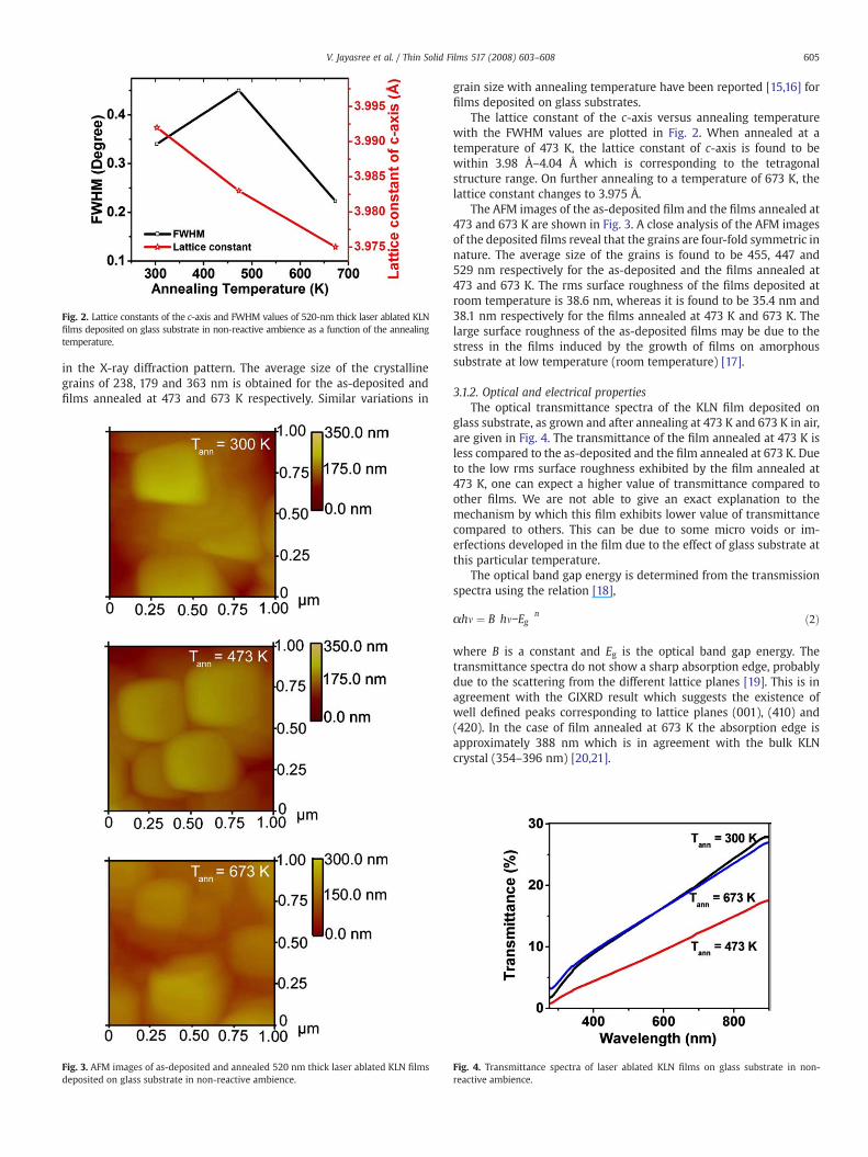
Fig. 2. Lattice constants of the c-axis and FWHM values of 520-nm thick laser ablated KLNfilms deposited on glass substrate in non-reactive ambience as a function of the annealingtemperature.
605V. Jayasree et al. / Thin Solid Films 517 (2008) 603–608
in the X-ray diffraction pattern. The average size of the crystallinegrains of 238, 179 and 363 nm is obtained for the as-deposited andfilms annealed at 473 and 673 K respectively. Similar variations in
Fig. 3. AFM images of as-deposited and annealed 520 nm thick laser ablated KLN filmsdeposited on glass substrate in non-reactive ambience.
grain size with annealing temperature have been reported [15,16] forfilms deposited on glass substrates.
The lattice constant of the c-axis versus annealing temperaturewith the FWHM values are plotted in Fig. 2. When annealed at atemperature of 473 K, the lattice constant of c-axis is found to bewithin 3.98 Å–4.04 Å which is corresponding to the tetragonalstructure range. On further annealing to a temperature of 673 K, thelattice constant changes to 3.975 Å.
The AFM images of the as-deposited film and the films annealed at473 and 673 K are shown in Fig. 3. A close analysis of the AFM imagesof the deposited films reveal that the grains are four-fold symmetric innature. The average size of the grains is found to be 455, 447 and529 nm respectively for the as-deposited and the films annealed at473 and 673 K. The rms surface roughness of the films deposited atroom temperature is 38.6 nm, whereas it is found to be 35.4 nm and38.1 nm respectively for the films annealed at 473 K and 673 K. Thelarge surface roughness of the as-deposited films may be due to thestress in the films induced by the growth of films on amorphoussubstrate at low temperature (room temperature) [17].
3.1.2. Optical and electrical propertiesThe optical transmittance spectra of the KLN film deposited on
glass substrate, as grown and after annealing at 473 K and 673 K in air,are given in Fig. 4. The transmittance of the film annealed at 473 K isless compared to the as-deposited and the film annealed at 673 K. Dueto the low rms surface roughness exhibited by the film annealed at473 K, one can expect a higher value of transmittance compared toother films. We are not able to give an exact explanation to themechanism by which this film exhibits lower value of transmittancecompared to others. This can be due to some micro voids or im-erfections developed in the film due to the effect of glass substrate atthis particular temperature.
The optical band gap energy is determined from the transmissionspectra using the relation [18],
αhm ¼ B hm−Eg� �n ð2Þ
where B is a constant and Eg is the optical band gap energy. Thetransmittance spectra do not show a sharp absorption edge, probablydue to the scattering from the different lattice planes [19]. This is inagreement with the GIXRD result which suggests the existence ofwell defined peaks corresponding to lattice planes (001), (410) and(420). In the case of film annealed at 673 K the absorption edge isapproximately 388 nm which is in agreement with the bulk KLNcrystal (354–396 nm) [20,21].
Fig. 4. Transmittance spectra of laser ablated KLN films on glass substrate in non-reactive ambience.
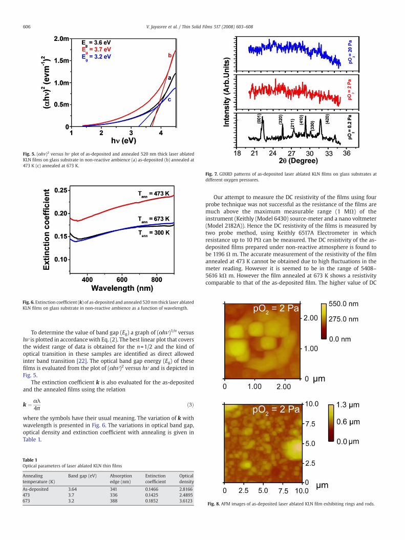
Fig. 6. Extinction coefficient (k) of as-deposited and annealed 520 nm thick laser ablatedKLN films on glass substrate in non-reactive ambience as a function of wavelength.
Fig. 7. GIXRD patterns of as-deposited laser ablated KLN films on glass substrates atdifferent oxygen pressures.
Fig. 5. (αhv)2 versus hν plot of as-deposited and annealed 520 nm thick laser ablatedKLN films on glass substrate in non-reactive ambience (a) as-deposited (b) annealed at473 K (c) annealed at 673 K.
606 V. Jayasree et al. / Thin Solid Films 517 (2008) 603–608
To determine the value of band gap (Eg) a graph of (αhν)1/n versushν is plotted in accordancewith Eq. (2). The best linear plot that coversthe widest range of data is obtained for the n=1/2 and the kind ofoptical transition in these samples are identified as direct allowedinter band transition [22]. The optical band gap energy (Eg) of thesefilms is evaluated from the plot of (αhν)2 versus hν and is depicted inFig. 5.
The extinction coefficient k is also evaluated for the as-depositedand the annealed films using the relation
k ¼ αλ4π
ð3Þ
where the symbols have their usual meaning. The variation of k withwavelength is presented in Fig. 6. The variations in optical band gap,optical density and extinction coefficient with annealing is given inTable 1.
Table 1Optical parameters of laser ablated KLN thin films
Annealingtemperature (K)
Band gap (eV) Absorptionedge (nm)
Extinctioncoefficient
Opticaldensity
As-deposited 3.64 341 0.1466 2.8166473 3.7 336 0.1425 2.4895673 3.2 388 0.1852 3.6123
Our attempt to measure the DC resistivity of the films using fourprobe technique was not successful as the resistance of the films aremuch above the maximum measurable range (1 MΩ) of theinstrument (Keithly (Model 6430) source-meter and a nano voltmeter(Model 2182A)). Hence the DC resistivity of the films is measured bytwo probe method, using Keithly 6517A Electrometer in whichresistance up to 10 PΩ can be measured. The DC resistivity of the as-deposited films prepared under non-reactive atmosphere is found tobe 1196 Ω m. The accurate measurement of the resistivity of the filmannealed at 473 K cannot be obtained due to high fluctuations in themeter reading. However it is seemed to be in the range of 5408–5616 kΩ m. However the film annealed at 673 K shows a resistivitycomparable to that of the as-deposited film. The higher value of DC
Fig. 8. AFM images of as-deposited laser ablated KLN film exhibiting rings and rods.

Fig. 9. Optical transmittance spectra of as-deposited laser ablated KLN thin films onglass substrate at different background oxygen pressures.
607V. Jayasree et al. / Thin Solid Films 517 (2008) 603–608
resistivity observed for the films annealed at 473 K, compared to otherfilms, can be due to the presence of voids or imperfections in the filmand is supporting the earlier prediction drawn from the opticaltransmittance spectra.
3.2. Effect of reactive oxygen pressure
3.2.1. GIXRD and AFM resultsFig. 7 shows the GIXRD patterns of the films deposited at oxygen
pressures 0.2, 2, 20 Pa. The film deposited at an oxygen pressure of0.2 Pa is polycrystalline in nature as indicated by the presence of welldefined XRD peaks. The diffraction peaks observed at (001), (320),(211), (410), (330), and (420) are in good agreement with the dif-fraction pattern observed in the powder diffraction file [7]. The peakcorresponding to (410) lattice reflection plane shows the maximumintensity. The films deposited at oxygen pressures 2 Pa and 20 Pa showno prominent XRD peaks suggesting that the crystalline properties ofthese films are not good. Structural and optical properties of KLNstrongly depend on Li content in the material. At a given temperature,the incorporation of volatile atoms such as Li and K into the filmgreatly depends on the reactive atmosphere [23]. From the XRDanalysis, it can be inferred that a slight background oxygen pressure(0.2 Pa) improves the crystalline property of the films considerably, asit can suppress re-evaporation of volatile elements such as K and Li inthe film [14]. But a considerable increase in the background oxygenpressure makes the mean free path shorter. This result in enhancedscattering of the ejected particles in the laser produced plasma by theoxygen gas molecules and prevents them from reaching the substrate.
Fig. 10. Extinction coefficient (k) of as-deposited laser ablated KLN thin films on glasssubstrate at different background oxygen pressures as a function of wavelength.
As a result, there is no efficient material transformation on the filmsdeposited at high oxygen pressures which can be the cause of the poorcrystalline quality of these films.
The investigations on the AFM images of the films deposited atvarious oxygen pressures show a decrease in rms surface roughnessand grain sizewith increase in oxygen pressures. The poor crystallinityof the films prepared at oxygen ambience of 2 and 20 Pa as observedfrom XRD data, and smaller grain size obtained from AFM images, areassociated with the kinetics of atomic arrangements during deposi-tion. It is also noted that AFM images (Fig. 8) of the films deposited atoxygen pressure of 2 Pa shows the self assembly of grains in the formof rings and rods. The diameters of the rings vary from 890 nm to1453 nm. Long rod like structures are also observed which vary inlength from 1330 to 1549 nm and breadth from 563 nm to 633 nm.However, AFM images of the films deposited at oxygen pressures0.2 Pa and 20 Pa do not exhibit any ring or rod like structures. The self
Fig. 11. Optical band gap (Eg) of as-deposited laser ablated KLN thin films on glasssubstrate at different background oxygen pressures as a function of photon energy.
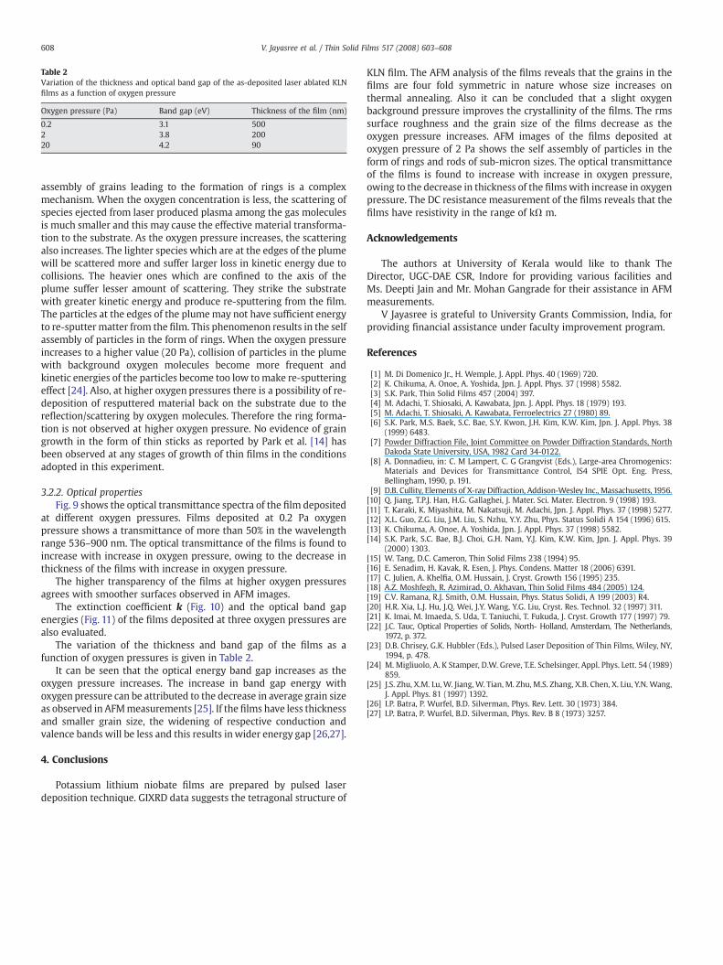
Table 2Variation of the thickness and optical band gap of the as-deposited laser ablated KLNfilms as a function of oxygen pressure
Oxygen pressure (Pa) Band gap (eV) Thickness of the film (nm)
0.2 3.1 5002 3.8 20020 4.2 90
608 V. Jayasree et al. / Thin Solid Films 517 (2008) 603–608
assembly of grains leading to the formation of rings is a complexmechanism. When the oxygen concentration is less, the scattering ofspecies ejected from laser produced plasma among the gas moleculesis much smaller and this may cause the effective material transforma-tion to the substrate. As the oxygen pressure increases, the scatteringalso increases. The lighter species which are at the edges of the plumewill be scattered more and suffer larger loss in kinetic energy due tocollisions. The heavier ones which are confined to the axis of theplume suffer lesser amount of scattering. They strike the substratewith greater kinetic energy and produce re-sputtering from the film.The particles at the edges of the plumemay not have sufficient energyto re-sputter matter from the film. This phenomenon results in the selfassembly of particles in the form of rings. When the oxygen pressureincreases to a higher value (20 Pa), collision of particles in the plumewith background oxygen molecules become more frequent andkinetic energies of the particles become too low tomake re-sputteringeffect [24]. Also, at higher oxygen pressures there is a possibility of re-deposition of resputtered material back on the substrate due to thereflection/scattering by oxygen molecules. Therefore the ring forma-tion is not observed at higher oxygen pressure. No evidence of graingrowth in the form of thin sticks as reported by Park et al. [14] hasbeen observed at any stages of growth of thin films in the conditionsadopted in this experiment.
3.2.2. Optical propertiesFig. 9 shows the optical transmittance spectra of the film deposited
at different oxygen pressures. Films deposited at 0.2 Pa oxygenpressure shows a transmittance of more than 50% in the wavelengthrange 536–900 nm. The optical transmittance of the films is found toincrease with increase in oxygen pressure, owing to the decrease inthickness of the films with increase in oxygen pressure.
The higher transparency of the films at higher oxygen pressuresagrees with smoother surfaces observed in AFM images.
The extinction coefficient k (Fig. 10) and the optical band gapenergies (Fig. 11) of the films deposited at three oxygen pressures arealso evaluated.
The variation of the thickness and band gap of the films as afunction of oxygen pressures is given in Table 2.
It can be seen that the optical energy band gap increases as theoxygen pressure increases. The increase in band gap energy withoxygen pressure can be attributed to the decrease in average grain sizeas observed in AFMmeasurements [25]. If the films have less thicknessand smaller grain size, the widening of respective conduction andvalence bands will be less and this results inwider energy gap [26,27].
4. Conclusions
Potassium lithium niobate films are prepared by pulsed laserdeposition technique. GIXRD data suggests the tetragonal structure of
KLN film. The AFM analysis of the films reveals that the grains in thefilms are four fold symmetric in nature whose size increases onthermal annealing. Also it can be concluded that a slight oxygenbackground pressure improves the crystallinity of the films. The rmssurface roughness and the grain size of the films decrease as theoxygen pressure increases. AFM images of the films deposited atoxygen pressure of 2 Pa shows the self assembly of particles in theform of rings and rods of sub-micron sizes. The optical transmittanceof the films is found to increase with increase in oxygen pressure,owing to the decrease in thickness of the filmswith increase in oxygenpressure. The DC resistance measurement of the films reveals that thefilms have resistivity in the range of kΩ m.
Acknowledgements
The authors at University of Kerala would like to thank TheDirector, UGC-DAE CSR, Indore for providing various facilities andMs. Deepti Jain and Mr. Mohan Gangrade for their assistance in AFMmeasurements.
V Jayasree is grateful to University Grants Commission, India, forproviding financial assistance under faculty improvement program.
References
[1] M. Di Domenico Jr., H. Wemple, J. Appl. Phys. 40 (1969) 720.[2] K. Chikuma, A. Onoe, A. Yoshida, Jpn. J. Appl. Phys. 37 (1998) 5582.[3] S.K. Park, Thin Solid Films 457 (2004) 397.[4] M. Adachi, T. Shiosaki, A. Kawabata, Jpn. J. Appl. Phys. 18 (1979) 193.[5] M. Adachi, T. Shiosaki, A. Kawabata, Ferroelectrics 27 (1980) 89.[6] S.K. Park, M.S. Baek, S.C. Bae, S.Y. Kwon, J.H. Kim, K.W. Kim, Jpn. J. Appl. Phys. 38
(1999) 6483.[7] Powder Diffraction File, Joint Committee on Powder Diffraction Standards, North
Dakoda State University, USA, 1982 Card 34-0122.[8] A. Donnadieu, in: C. M Lampert, C. G Grangvist (Eds.), Large-area Chromogenics:
Materials and Devices for Transmittance Control, IS4 SPIE Opt. Eng. Press,Bellingham, 1990, p. 191.
[9] D.B. Cullity, Elements of X-ray Diffraction, Addison-Wesley Inc., Massachusetts, 1956.[10] Q. Jiang, T.P.J. Han, H.G. Gallaghei, J. Mater. Sci. Mater. Electron. 9 (1998) 193.[11] T. Karaki, K. Miyashita, M. Nakatsuji, M. Adachi, Jpn. J. Appl. Phys. 37 (1998) 5277.[12] X.L. Guo, Z.G. Liu, J.M. Liu, S. Nzhu, Y.Y. Zhu, Phys. Status Solidi A 154 (1996) 615.[13] K. Chikuma, A. Onoe, A. Yoshida, Jpn. J. Appl. Phys. 37 (1998) 5582.[14] S.K. Park, S.C. Bae, B.J. Choi, G.H. Nam, Y.J. Kim, K.W. Kim, Jpn. J. Appl. Phys. 39
(2000) 1303.[15] W. Tang, D.C. Cameron, Thin Solid Films 238 (1994) 95.[16] E. Senadim, H. Kavak, R. Esen, J. Phys. Condens. Matter 18 (2006) 6391.[17] C. Julien, A. Khelfia, O.M. Hussain, J. Cryst. Growth 156 (1995) 235.[18] A.Z. Moshfegh, R. Azimirad, O. Akhavan, Thin Solid Films 484 (2005) 124.[19] C.V. Ramana, R.J. Smith, O.M. Hussain, Phys. Status Solidi, A 199 (2003) R4.[20] H.R. Xia, L.J. Hu, J.Q. Wei, J.Y. Wang, Y.G. Liu, Cryst. Res. Technol. 32 (1997) 311.[21] K. Imai, M. Imaeda, S. Uda, T. Taniuchi, T. Fukuda, J. Cryst. Growth 177 (1997) 79.[22] J.C. Tauc, Optical Properties of Solids, North- Holland, Amsterdam, The Netherlands,
1972, p. 372.[23] D.B. Chrisey, G.K. Hubbler (Eds.), Pulsed Laser Deposition of Thin Films, Wiley, NY,
1994, p. 478.[24] M. Migliuolo, A. K Stamper, D.W. Greve, T.E. Schelsinger, Appl. Phys. Lett. 54 (1989)
859.[25] J.S. Zhu, X.M. Lu, W. Jiang, W. Tian, M. Zhu, M.S. Zhang, X.B. Chen, X. Liu, Y.N. Wang,
J. Appl. Phys. 81 (1997) 1392.[26] I.P. Batra, P. Wurfel, B.D. Silverman, Phys. Rev. Lett. 30 (1973) 384.[27] I.P. Batra, P. Wurfel, B.D. Silverman, Phys. Rev. B 8 (1973) 3257.