Impedance Spectroscopy Analysis of the Effect of TiO 2 Blocking Layers on the Efficiency of Dye...
7
Impedance Spectroscopy Analysis of the Effect of TiO 2 Blocking Layers on the Efficiency of Dye Sensitized Solar Cells Ma ́ rcio Sousa Gó es,* ,† Ednan Joanni, ‡ Elaine C. Muniz, † Raluca Savu, § Thomas R. Habeck, † Paulo R. Bueno, † and Francisco Fabregat-Santiago* ,∥ † Instituto de Química, Depto. Físico-Química, Universidade Estadual Paulista - UNESP, R. Prof. Francisco Degni, n. 55, 14800-900, Araraquara SP, Brazil ‡ Centro de Tecnologia da Informaç ã o Renato Archer (CTI), Rod. Dom Pedro I km 143.6, 13069-901, Campinas, SP, Brazil § Centro de Componentes Semicondutores - CCS, Universidade de Campinas - UNICAMP, C.P. 6061, Rua Joã o Pandia Caló geras, 90, 13083-870, Campinas, SP, Brazil ∥ Grup de Dispositius Fotovotaics i Optoelectrò nics, Departament de Física, Universitat Jaume I, Av. SosBaynat, s/n, 12071, Castelló de la Plana, Spain * S Supporting Information ABSTRACT: The introduction of a dense TiO 2 layer between the mesoporous TiO 2 network and the charge collector in dye-sensitized solar cell anodes has been claimed to improve the performance of solar cell devices. Two mechanisms have been proposed to explain this behavior, a decrease in the electron−hole recombination at substrate/electrolyte interface and an enhancement in the electronic contact between the mesoporous TiO 2 network and the charge collecting electrode. In this work the effect of sputtered TiO 2 blocking layers (BLs) on the performance of dye-sensitized solar cells electrodes has been analyzed. It has been shown that the electron injection efficiency governed changes observed in cell efficiency. The thicker the BL, the poorer the photocurrent, and therefore, only thin BLs leaded to an increase in energy conversion efficiencies. The thickness of the BL also affected the internal series resistance of the solar cells, influencing their fill factor. 1. INTRODUCTION Dye-sensitized solar cells 1 have been the focus of intense research worldwide, mainly due to their potential as low cost energy production technology. 2,3 Up to now, the highest energy conversion efficiencies reported for DSCs are around 11− 12%. 4−6 Many variants for these devices are being explored with the aim of increasing their performance to compete with conventional silicon-based solar cells (p−n junctions). 7 A great deal of this research has been focused on the optimization of the device performance after understanding the mechanisms responsible for the efficiency losses. The main back-reactions limiting the photocurrent and photopotential of the cell are: radiationless relaxation of the excited state of the dye, recombination of the electrons with the oxidized dye and electron recombination with the tri-iodide in the electro- lyte. 8−10 In high performance DSCs, the first two mechanisms have little impact, with the TiO 2 /electrolyte and electrode/ electrolyte interfaces being responsible for most of the electron losses. These interface losses and the mismatches between the energy levels of the different components of the device impose the limits on the maximum achievable photopotential and photocurrent. 11 Further performance losses, affecting the fill factor, are associated to the presence of series resistances in the cell. 12,13 At the point of maximum power efficiency of DSCs, electron recombination losses are generally greater in the bulk of the sensitized layer than close to the FTO substrate. 8,14 However, under short circuit conditions, the TiO 2 conduction band is far from the Fermi level while in the FTO it is aligned with the redox Fermi level, yielding a recombination governed by the FTO/electrolyte interface rather than by TiO 2 . 8,14,15 Therefore, to obtain high efficiency devices, both routes of interface recombination, TiO 2 /electrolyte and FTO/electrolyte, need to be optimized to prevent the loss of electrons by back reactions. The application of barrier layers at these interfaces has been proposed as a viable approach toward this goal. These barrier layers can be dense films at the FTO surface (the “blocking layer” or BL) 14−16 or a thin layer over the TiO 2 nanoparticles (the so-called “core-shell” configuration). 17−19 Recent research in the use of BLs coating the FTO substrate and interfacing it with the nanostructured TiO 2 matrix has shown improvements in the overall conversion efficiency of DSCs. 20−22 In the present work we investigate the effect of the thickness of sputtered TiO 2 BLs in the performance of DSCs. These layers were either obtained in situ from an oxide target or by Received: February 21, 2012 Revised: May 14, 2012 Published: May 21, 2012 Article pubs.acs.org/JPCC © 2012 American Chemical Society 12415 dx.doi.org/10.1021/jp301694r | J. Phys. Chem. C 2012, 116, 12415−12421
-
Upload
independent -
Category
Documents
-
view
1 -
download
0
Transcript of Impedance Spectroscopy Analysis of the Effect of TiO 2 Blocking Layers on the Efficiency of Dye...
Impedance Spectroscopy Analysis of the Effect of TiO2 BlockingLayers on the Efficiency of Dye Sensitized Solar CellsMarcio Sousa Goes,*,† Ednan Joanni,‡ Elaine C. Muniz,† Raluca Savu,§ Thomas R. Habeck,†
Paulo R. Bueno,† and Francisco Fabregat-Santiago*,∥
†Instituto de Química, Depto. Físico-Química, Universidade Estadual Paulista - UNESP, R. Prof. Francisco Degni, n. 55, 14800-900,Araraquara SP, Brazil‡Centro de Tecnologia da Informacao Renato Archer (CTI), Rod. Dom Pedro I km 143.6, 13069-901, Campinas, SP, Brazil§Centro de Componentes Semicondutores - CCS, Universidade de Campinas - UNICAMP, C.P. 6061, Rua Joao Pandia Calogeras,90, 13083-870, Campinas, SP, Brazil∥Grup de Dispositius Fotovotaics i Optoelectronics, Departament de Física, Universitat Jaume I, Av. SosBaynat, s/n, 12071, Castello de la Plana, Spain
*S Supporting Information
ABSTRACT: The introduction of a dense TiO2 layer between the mesoporous TiO2network and the charge collector in dye-sensitized solar cell anodes has been claimedto improve the performance of solar cell devices. Two mechanisms have beenproposed to explain this behavior, a decrease in the electron−hole recombination atsubstrate/electrolyte interface and an enhancement in the electronic contact betweenthe mesoporous TiO2 network and the charge collecting electrode. In this work theeffect of sputtered TiO2 blocking layers (BLs) on the performance of dye-sensitizedsolar cells electrodes has been analyzed. It has been shown that the electron injectionefficiency governed changes observed in cell efficiency. The thicker the BL, the poorerthe photocurrent, and therefore, only thin BLs leaded to an increase in energyconversion efficiencies. The thickness of the BL also affected the internal seriesresistance of the solar cells, influencing their fill factor.
1. INTRODUCTIONDye-sensitized solar cells1 have been the focus of intenseresearch worldwide, mainly due to their potential as low costenergy production technology.2,3 Up to now, the highest energyconversion efficiencies reported for DSCs are around 11−12%.4−6 Many variants for these devices are being exploredwith the aim of increasing their performance to compete withconventional silicon-based solar cells (p−n junctions).7
A great deal of this research has been focused on theoptimization of the device performance after understanding themechanisms responsible for the efficiency losses. The mainback-reactions limiting the photocurrent and photopotential ofthe cell are: radiationless relaxation of the excited state of thedye, recombination of the electrons with the oxidized dye andelectron recombination with the tri-iodide in the electro-lyte.8−10 In high performance DSCs, the first two mechanismshave little impact, with the TiO2/electrolyte and electrode/electrolyte interfaces being responsible for most of the electronlosses. These interface losses and the mismatches between theenergy levels of the different components of the device imposethe limits on the maximum achievable photopotential andphotocurrent.11 Further performance losses, affecting the fillfactor, are associated to the presence of series resistances in thecell.12,13
At the point of maximum power efficiency of DSCs, electronrecombination losses are generally greater in the bulk of thesensitized layer than close to the FTO substrate.8,14 However,under short circuit conditions, the TiO2 conduction band is farfrom the Fermi level while in the FTO it is aligned with theredox Fermi level, yielding a recombination governed by theFTO/electrolyte interface rather than by TiO2.
8,14,15 Therefore,to obtain high efficiency devices, both routes of interfacerecombination, TiO2/electrolyte and FTO/electrolyte, need tobe optimized to prevent the loss of electrons by back reactions.The application of barrier layers at these interfaces has been
proposed as a viable approach toward this goal. These barrierlayers can be dense films at the FTO surface (the “blockinglayer” or BL)14−16 or a thin layer over the TiO2 nanoparticles(the so-called “core-shell” configuration).17−19 Recent researchin the use of BLs coating the FTO substrate and interfacing itwith the nanostructured TiO2 matrix has shown improvementsin the overall conversion efficiency of DSCs.20−22
In the present work we investigate the effect of the thicknessof sputtered TiO2 BLs in the performance of DSCs. Theselayers were either obtained in situ from an oxide target or by
Received: February 21, 2012Revised: May 14, 2012Published: May 21, 2012
Article
pubs.acs.org/JPCC
© 2012 American Chemical Society 12415 dx.doi.org/10.1021/jp301694r | J. Phys. Chem. C 2012, 116, 12415−12421
deposition using a metal target followed by heat treatment inair. The electron recombination and accumulation at theinterfaces were analyzed by impedance spectroscopy (IS). Thistechnique has been proved to be very powerful to discriminatethe charge transfer processes in the different interfaces of theDSCs.23,24 We observed clear performance improvements forsome of the applied barrier layers. A strong dependence ofphotocurrent on BL thickness was found which limits the sizeof BL to be used in DSCs.
2. EXPERIMENTAL DETAILS2.1. Deposition of Blocking Layers. The TiO2 and Ti
films were deposited using radio frequency (RF) and directcurrent (DC) sputtering, respectively. In both cases,borosilicate glass substrates covered with a layer of about 500nm FTO (Solaronix 10 Ω□−1, 5 cm2) were used. Aftercleaning the substrates with isopropyl alcohol, the layers weredeposited using shadow masks placed on one edge of eachsubstrate, preventing the deposition of material in these regionsand allowing the electrodes to remain exposed for the electricalmeasurements. Before the onset of film deposition, thechamber was evacuated to pressures below 10−5 Torr. Alldepositions were carried out in 2 × 10⁻² Torr argon using 150W sputtering power and 2 inch diameter targets. The TiO2layers were either obtained directly from oxide targets orindirectly, using Ti targets followed by thermal treatment in air(during the subsequent treatment of the mesoporous TiO2deposit). The deposition rate was 0.9 Å·s−1 for the TiO2 layersand 0.2 Å·s−1 for the Ti films. The oxide layers (henceforthcalled oxide series, OS) were deposited with thicknesses of 50,85, and 120 nm, while the titanium films (called metallic series,MS) had thicknesses of 40, 70, and 100 nm. The differentelectrodes studied and their nomenclatures are summarized inTable 1. To have all of the samples with approximately thesame thicknesses, the metal films were made thinner, takinginto account the subsequent volume increase during oxidation.
2.2. DSC Fabrication. All DSCs in this work werefabricated using a TiO2 paste from Dyesol (DSL-90-T). Thepaste was applied by doctor blade on the substrates prepared bysputtering (uncoated FTO substrates were used as reference/standard) and sintered in air at 450 °C for 30 min. The metallicTi films were oxidized to TiO2 during this heat treatment, andthe mesoporous films obtained through this process had athickness between 7.5 and 8.0 μm and an active area of 0.36cm2. After cooling to 80 °C, the TiO2 electrodes wereimmersed for 15 h in a 0.5 mmol·L−1 cis-bis(isothiocyanato)-bis(2,2′-bipyridyl-4,4′-dicarboxylato)-Ru(II) (N3, Solaronix)solution in absolute ethanol. The iodide-based redox shuttlesolution (50 mmol·L−1 of tri-iodide in acetonitrile, IodolyteAN-50, Solaronix) was dripped between the FTO/TiO2/dye
working electrode and the Pt-coated FTO-glass counter-electrode. The counter-electrode was prepared by depositionof Pt onto FTO-coated glass (Xopglass, 8 Ω□−1) via thermaldecomposition of H2PtCl6 solution (2 mg of Pt in 1 mL ofethanol) at 450 °C for 30 min. The dye-covered TiO2electrodes and Pt counter electrodes were assembled into asandwich-type cell and sealed with a Surlyn 1702 hotmeltgasket 50 μm thick. Finally, the assembled cell was filled withthe electrolyte containing the I−/I3
− redox couple.2.3. Characterization. Current−voltage (j−V), cyclic
voltammetry (CV) and IS measurements were performedboth in two- and three-electrode configurations. The electro-chemical experiments were conducted using a three-electrodeconfiguration with Ag/AgCl (3 mol·L−1 in KCl) as a reference,platinum as a counter electrode, and FTO with and withoutBLs as working electrodes. These samples were not loaded withthe nanocolloidal TiO2, thus having the optimal configurationFTO/BL for analyzing the processes occurring at the substrate/electrolyte interface. The samples were called T and TO,denoting the metallic series and oxide series, respectively, asindicated in Table 1. The CV was performed at the scan rate of10 mV·s−1, and the IS measurements were recorded (AutolabPGSTAT30) over a frequency range of 5 mHz to 400 kHz withan AC amplitude of 20 mV in the range between 0 and −0.8 Vwith steps of 50 mV. The electrolyte used in these experimentswas Iodolyte AN-50 (Solaronix).For two electrode measurements, complete devices prepared
with the different substrates were called DT and DTO, todenote the cells built from metallic and oxide series substrates,respectively. Impedance measurements were carried out underdifferent bias potentials (in the range between 0 and −0.85 V)in the dark and under illumination (1 sun, AM1.5 solarradiation). For the photovoltaic measurements, the DSCs wereilluminated with an AM1.5 solar light simulator (SolarLightXPS400) at 100 mW·cm−2, and their current density−voltage(j−V) characteristics were registered with a Solartron 1287potentiostat/galvanostat. Electrochemical characterization (CVand IS) was performed with a Solartron 1260 impedance/gain-phase analyzer. The amplitude of the AC signal used in IS was20 mV, and the frequency was varied between 10 mHz and 1MHz.The Zview equivalent circuit modeling software was
employed for data fitting, using a built-in extended elementor RC circuit. A Varian Cary 300 Bio UV−vis spectropho-tometer was used to obtain the transmittance spectra, in therange from 200 to 800 nm, of the FTO substrates with andwithout BLs.
3. RESULTS AND DISCUSSION3.1. Electrochemical Analysis (Three-Electrode Con-
figuration). The first step in this study is the analysis of theeffect of the BLs over the FTO substrate in the absence of theTiO2 mesoporous matrix and sensitizer. The IS measurementsof the FTO substrates with and without BLs, immersed in asolution containing the I−/I3
− redox couple, were performed atpotentials ranging from 0.15 to −0.7 V versus I−/I3
− redoxcouple, using a three-electrode configuration. These values wereobtained taking iodide−triiodide as a reference with formalpotential of +0.35 V versus a normal hydrogen electrode(NHE).22 Note that small variations from formal potential dueto the difference in concentration between iodide and triiodidemay produce. This shift was estimated to be lower than 20 mVusing the Nernst equation. Representative spectra obtained at
Table 1. Thickness and Materials Deposited on FTO forBuilding the Blocking Layers
series sample code material layer thickness (nm)
oxide TO5 TiO2 50TO8 TiO2 85TO12 TiO2 120
metallic T4 Ti 40T7 Ti 70T10 Ti 100
bare FTO F
The Journal of Physical Chemistry C Article
dx.doi.org/10.1021/jp301694r | J. Phys. Chem. C 2012, 116, 12415−1242112416
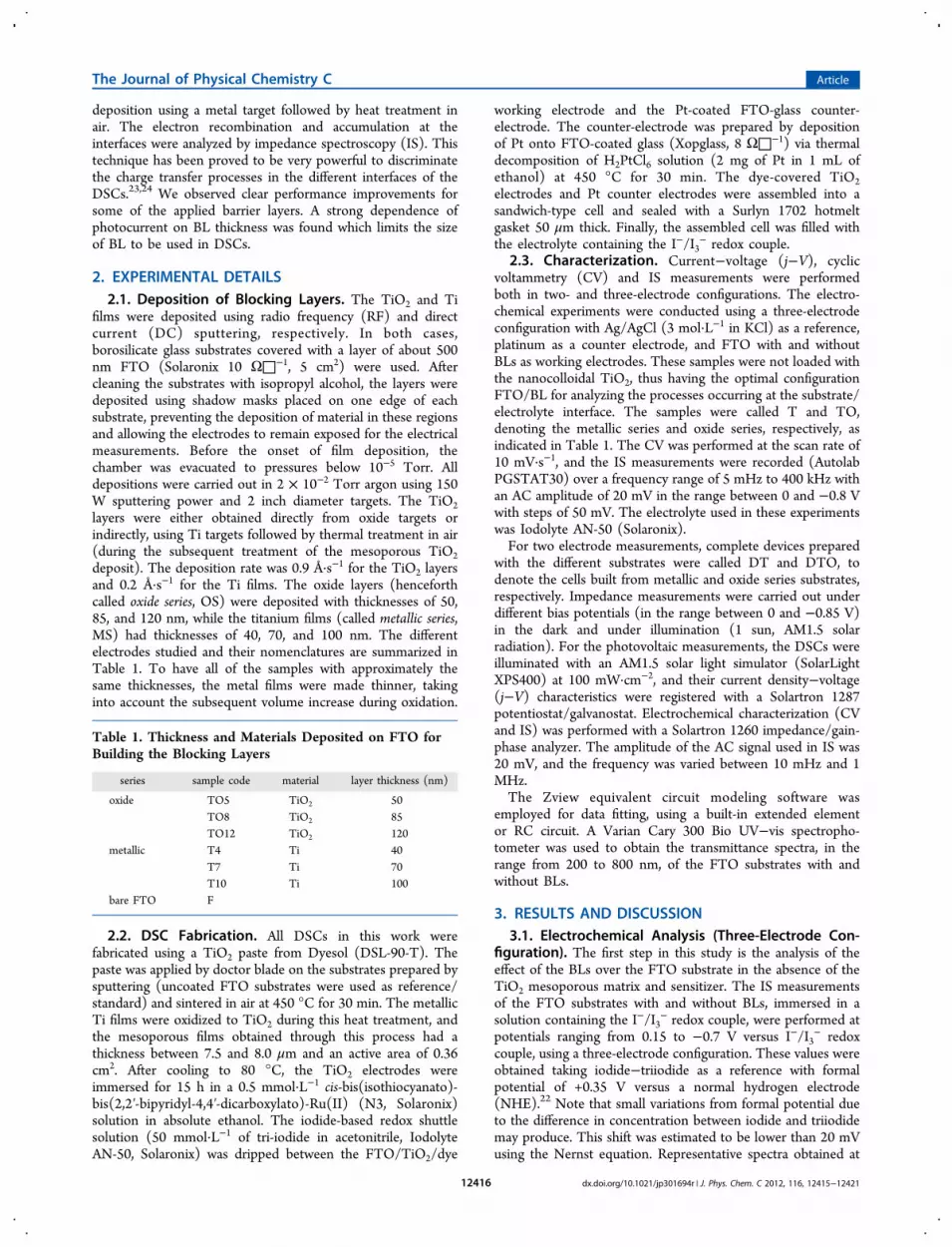
−0.1 V are shown in Figure 1. From the two arcs appearing inthe spectra, the most important contribution is a large low
frequency semicircle, which corresponds to electron transfer atthe substrate/electrolyte interface.Figure 2 shows the results of capacitance and charge transfer
resistance values for FTO with and without BLs, obtained from
the fittings of impedance data at all of the potentials measured.The measured capacitance (Figures 2a,c) is attributed to thecharge accumulation at the electrode surface. In the bare FTOsample, the value of capacitance, near 10 μF·cm−2, is due to theHelmholtz layer at the surface of the electrode combined withthe depletion layer of the highly doped FTO. The highercapacitance values observed for both MS and OS samplessuggest that the BL is not just behaving as a simple dielectric. Ifthis were the case, given the dimensions of the layer, the resultwould have been a reduction in the overall measuredcapacitance.25 Instead data suggest that the BL presents ahigh enough conductivity to allow a strong influence of theHelmholtz layer in the total capacitance of the electrolyte. Inthis situation, the increase in the value of film capacitance(Cfilm) indicates an increase of the effective surface area ofelectrode in contact with the electrolyte for the cells with BL or,in other words, that the films is somewhat porous.
Charge transference resistance (in this case, recombinationresistance) data presented in Figure 2b,d confirm the film'sporosity. In the samples with larger capacitance (T4 for MS andTO12 for OS) present the lowest charge transferenceresistances (Rct) of their series, while both T7 and T10 (athigh potentials) for MS and TO5 and TO8 for OS showedsimilar recombination resistances and the same capacitances.When compared to FTO (black curve), OS samples presentlower Rct, while MS samples exhibit larger values. Thesedifferences may be attributed to the different methods ofpreparation of the BLs and the different charge transfermechanisms of FTO and TiO2. Therefore, it appears that themetallic films can be more effective as BLs than the ones fromthe oxide series.Data from cyclic voltammetry performed without illumina-
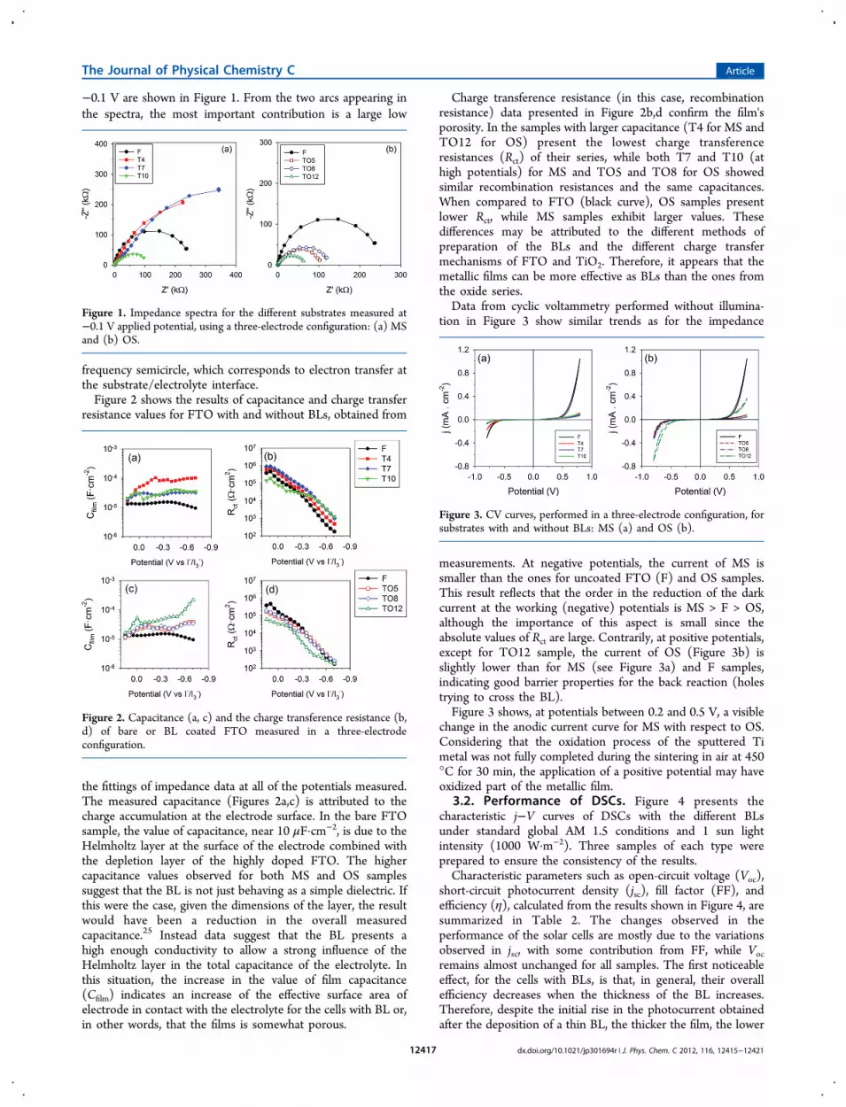
tion in Figure 3 show similar trends as for the impedance
measurements. At negative potentials, the current of MS issmaller than the ones for uncoated FTO (F) and OS samples.This result reflects that the order in the reduction of the darkcurrent at the working (negative) potentials is MS > F > OS,although the importance of this aspect is small since theabsolute values of Rct are large. Contrarily, at positive potentials,except for TO12 sample, the current of OS (Figure 3b) isslightly lower than for MS (see Figure 3a) and F samples,indicating good barrier properties for the back reaction (holestrying to cross the BL).Figure 3 shows, at potentials between 0.2 and 0.5 V, a visible
change in the anodic current curve for MS with respect to OS.Considering that the oxidation process of the sputtered Timetal was not fully completed during the sintering in air at 450°C for 30 min, the application of a positive potential may haveoxidized part of the metallic film.
3.2. Performance of DSCs. Figure 4 presents thecharacteristic j−V curves of DSCs with the different BLsunder standard global AM 1.5 conditions and 1 sun lightintensity (1000 W·m−2). Three samples of each type wereprepared to ensure the consistency of the results.Characteristic parameters such as open-circuit voltage (Voc),
short-circuit photocurrent density (jsc), fill factor (FF), andefficiency (η), calculated from the results shown in Figure 4, aresummarized in Table 2. The changes observed in theperformance of the solar cells are mostly due to the variationsobserved in jsc, with some contribution from FF, while Vocremains almost unchanged for all samples. The first noticeableeffect, for the cells with BLs, is that, in general, their overallefficiency decreases when the thickness of the BL increases.Therefore, despite the initial rise in the photocurrent obtainedafter the deposition of a thin BL, the thicker the film, the lower
Figure 1. Impedance spectra for the different substrates measured at−0.1 V applied potential, using a three-electrode configuration: (a) MSand (b) OS.
Figure 2. Capacitance (a, c) and the charge transference resistance (b,d) of bare or BL coated FTO measured in a three-electrodeconfiguration.
Figure 3. CV curves, performed in a three-electrode configuration, forsubstrates with and without BLs: MS (a) and OS (b).
The Journal of Physical Chemistry C Article
dx.doi.org/10.1021/jp301694r | J. Phys. Chem. C 2012, 116, 12415−1242112417
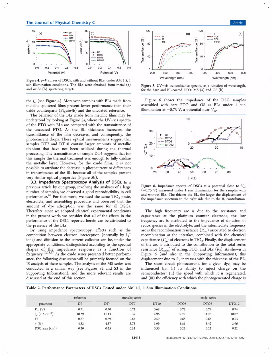
the jsc (see Figure 4). Moreover, samples with BLs made frommetallic sputtered films present lower performance than theiroxide counterparts (Figure4b) and the uncoated reference.The behavior of the BLs made from metallic films may be
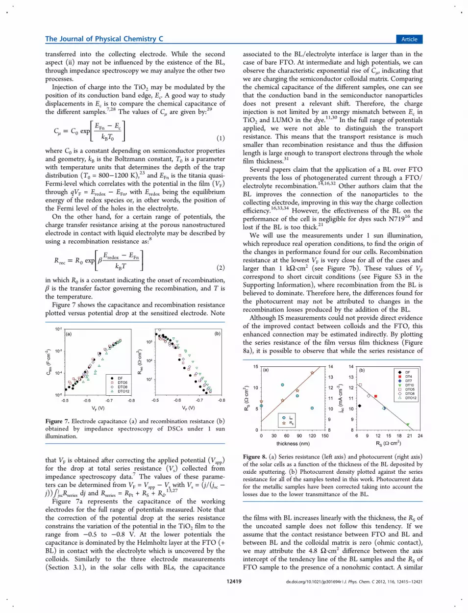
understood by looking at Figure 5a, where the UV−vis spectraof the FTO with BLs are compared with the transmittance ofthe uncoated FTO. As the BL thickness increases, thetransmittance of the film decreases, and consequently, thephotocurrent drops. These optical measurements suggest thatsamples DT7 and DT10 contain larger amounts of metallictitanium that have not been oxidized during the thermalprocessing. The transmittance of sample DT4 suggests that forthis sample the thermal treatment was enough to fully oxidizethe metallic layer. However, for the oxide films, it is notpossible to attribute the decrease in photocurrent to differencesin transmittance of the BL because all of the samples presentvery similar optical properties (Figure 5b).3.3. Impedance Spectroscopy Analysis of DSCs. In a
previous article by our group, involving the analyses of a largenumber of samples, we observed a good reproducibility in cellperformance.26 For that work, we used the same TiO2 paste,electrolyte, and assembling procedure and observed that theamount of dye adsorption was the same for all DSCs.Therefore, since we adopted identical experimental conditionsin the present work, we consider that all of the effects in theperformance of the DSCs reported herein can be attributed tothe presence of the BLs.By using impedance spectroscopy, effects such as the
competition between electron interception (normally by I3−
ions) and diffusion to the current collector can be, under theappropriate conditions, distinguished according to the spectralshapes of the impedance response as a function offrequency.10,23,27 As the oxide series presented better perform-ance, the following discussion will be primarily focused on theIS analysis of these samples. The analysis of the MS series wasconducted in a similar way (see Figures S2 and S3 in theSupporting Information), and the more relevant results arediscussed at the end of this section.
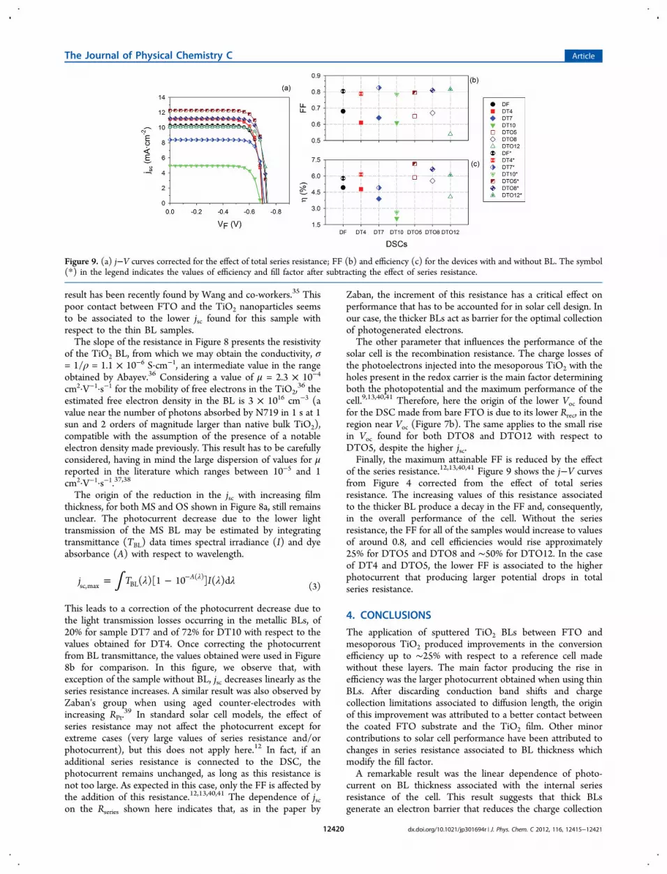
Figure 6 shows the impedance of the DSC samplesassembled with bare FTO and OS as BLs under 1 sunillumination at −0.75 V, a potential near Voc.
The high frequency arc is due to the resistance andcapacitance at the platinum counter electrode, the lowfrequency arc is attributed to the impedance of diffusion ofredox species in the electrolyte, and the intermediate frequencyarc is the recombination resistance (Rrec) associated to electronrecombination at the interface, combined with the chemicalcapacitance (Cμ) of electrons in TiO2. Finally, the displacementof the arc is attributed to the contribution to the total seriesresistance (Rseries) of wiring, FTO, and BLs (RS). As shown inFigure 6 (and also in the Supporting Information), thisdisplacement due to RS increases with the thickness of the BL.The short circuit photocurrent, for a given dye, may be
influenced by: (i) its ability to inject charge on thesemiconductor; (ii) the speed with which it is regenerated,and (iii) the efficiency with which the photogenerated charge is
Figure 4. j−V curves of DSCs, with and without BLs, under AM 1.5, 1sun illumination conditions. The BLs were obtained from metal (a)and oxide (b) sputtering targets.
Table 2. Performance Parameters of DSCs Tested under AM 1.5, 1 Sun Illumination Conditions
reference metallic series oxide series
parameter DF DT4 DT7 DT10 DTO5 DTO8 DTO12
Voc (V) 0.71 0.70 0.72 0.68 0.73 0.74 0.74jsc (mA·cm
−2) 10.29 11.13 8.39 4.96 12.27 11.23 10.07FF 0.67 0.59 0.62 0.59 0.65 0.66 0.53η (%) 4.83 4.57 3.75 1.99 5.81 5.42 3.96DSC area (cm2) 0.20 0.25 0.33 0.30 0.23 0.22 0.22
Figure 5. UV−vis transmittance spectra, as a function of wavelength,for the bare and BL-coated FTO: MS (a) and OS (b).
Figure 6. Impedance spectra of DSCs at a potential close to Voc(−0.75 V) measured under 1 sun illumination for the samples withand without BLs. The thicker the BL, the larger the displacement ofthe impedance spectrum to the right side due to the RS contribution.
The Journal of Physical Chemistry C Article
dx.doi.org/10.1021/jp301694r | J. Phys. Chem. C 2012, 116, 12415−1242112418
transferred into the collecting electrode. While the secondaspect (ii) may not be influenced by the existence of the BL,through impedance spectroscopy we may analyze the other twoprocesses.Injection of charge into the TiO2 may be modulated by the
position of its conduction band edge, Ec. A good way to studydisplacements in Ec is to compare the chemical capacitance ofthe different samples.7,28 The values of Cμ are given by:29
=−
μ
⎡⎣⎢
⎤⎦⎥C C
E Ek T
exp0Fn c
B 0 (1)
where C0 is a constant depending on semiconductor propertiesand geometry, kB is the Boltzmann constant, T0 is a parameterwith temperature units that determines the depth of the trapdistribution (T0 = 800−1200 K),23 and EFn is the titania quasi-Fermi-level which correlates with the potential in the film (VF)through qVF = Eredox − EFn, with Eredox being the equilibriumenergy of the redox species or, in other words, the position ofthe Fermi level of the holes in the electrolyte.On the other hand, for a certain range of potentials, the
charge transfer resistance arising at the porous nanostructuredelectrode in contact with liquid electrolyte may be described byusing a recombination resistance as:8
β=−⎡
⎣⎢⎤⎦⎥R R
E Ek T
exprec 0redox Fn
B (2)
in which R0 is a constant indicating the onset of recombination,β is the transfer factor governing the recombination, and T isthe temperature.Figure 7 shows the capacitance and recombination resistance
plotted versus potential drop at the sensitized electrode. Note
that VF is obtained after correcting the applied potential (Vapp)for the drop at total series resistance (Vs) collected fromimpedance spectroscopy data.7 The values of these parame-ters can be determined from VF = Vapp − Vs with Vs = (j/(jsc −j))∫ jsc
j Rseries dj and Rseries = RPt + RS + Rd.13,27
Figure 7a represents the capacitance of the workingelectrodes for the full range of potentials measured. Note thatthe correction of the potential drop at the series resistanceconstrains the variation of the potential in the TiO2 film to therange from −0.5 to −0.8 V. At the lower potentials thecapacitance is dominated by the Helmholtz layer at the FTO (+BL) in contact with the electrolyte which is uncovered by thecolloids. Similarly to the three electrode measurements(Section 3.1), in the solar cells with BLs, the capacitance
associated to the BL/electrolyte interface is larger than in thecase of bare FTO. At intermediate and high potentials, we canobserve the characteristic exponential rise of Cμ, indicating thatwe are charging the semiconductor colloidal matrix. Comparingthe chemical capacitance of the different samples, one can seethat the conduction band in the semiconductor nanoparticlesdoes not present a relevant shift. Therefore, the chargeinjection is not limited by an energy mismatch between Ec inTiO2 and LUMO in the dye.11,30 In the full range of potentialsapplied, we were not able to distinguish the transportresistance. This means that the transport resistance is muchsmaller than recombination resistance and thus the diffusionlength is large enough to transport electrons through the wholefilm thickness.31
Several papers claim that the application of a BL over FTOprevents the loss of photogenerated current through a FTO/electrolyte recombination.14,16,32 Other authors claim that theBL improves the connection of the nanoparticles to thecollecting electrode, improving in this way the charge collectionefficiency.16,33,34 However, the effectiveness of the BL on theperformance of the cell is negligible for dyes such N71916 andlost if the BL is too thick.21
We will use the measurements under 1 sun illumination,which reproduce real operation conditions, to find the origin ofthe changes in performance found for our cells. Recombinationresistance at the lowest VF is very close for all of the cases andlarger than 1 kΩ·cm2 (see Figure 7b). These values of VFcorrespond to short circuit conditions (see Figure S3 in theSupporting Information), where recombination from the BL isbelieved to dominate. Therefore here, the differences found forthe photocurrent may not be attributed to changes in therecombination losses produced by the addition of the BL.Although IS measurements could not provide direct evidence
of the improved contact between colloids and the FTO, thisenhanced connection may be estimated indirectly. By plottingthe series resistance of the film versus film thickness (Figure8a), it is possible to observe that while the series resistance of
the films with BL increases linearly with the thickness, the RS ofthe uncoated sample does not follow this tendency. If weassume that the contact resistance between FTO and BL andbetween BL and the colloidal matrix is zero (ohmic contact),we may attribute the 4.8 Ω·cm2 difference between the axisintercept of the tendency line of the BL samples and the RS ofFTO sample to the presence of a nonohmic contact. A similar
Figure 7. Electrode capacitance (a) and recombination resistance (b)obtained by impedance spectroscopy of DSCs under 1 sunillumination.
Figure 8. (a) Series resistance (left axis) and photocurrent (right axis)of the solar cells as a function of the thickness of the BL deposited byoxide sputtering. (b) Photocurrent density plotted against the seriesresistance for all of the samples tested in this work. Photocurrent datafor the metallic samples have been corrected taking into account thelosses due to the lower transmittance of the BL.
The Journal of Physical Chemistry C Article
dx.doi.org/10.1021/jp301694r | J. Phys. Chem. C 2012, 116, 12415−1242112419
result has been recently found by Wang and co-workers.35 Thispoor contact between FTO and the TiO2 nanoparticles seemsto be associated to the lower jsc found for this sample withrespect to the thin BL samples.The slope of the resistance in Figure 8 presents the resistivity
of the TiO2 BL, from which we may obtain the conductivity, σ= 1/ρ = 1.1 × 10⁻⁶ S·cm−1, an intermediate value in the rangeobtained by Abayev.36 Considering a value of μ = 2.3 × 10⁻⁴
cm2·V−1·s−1 for the mobility of free electrons in the TiO2,36 the
estimated free electron density in the BL is 3 × 1016 cm−3 (avalue near the number of photons absorbed by N719 in 1 s at 1sun and 2 orders of magnitude larger than native bulk TiO2),compatible with the assumption of the presence of a notableelectron density made previously. This result has to be carefullyconsidered, having in mind the large dispersion of values for μreported in the literature which ranges between 10−5 and 1cm2·V−1·s−1.37,38
The origin of the reduction in the jsc with increasing filmthickness, for both MS and OS shown in Figure 8a, still remainsunclear. The photocurrent decrease due to the lower lighttransmission of the MS BL may be estimated by integratingtransmittance (TBL) data times spectral irradiance (I) and dyeabsorbance (A) with respect to wavelength.
∫ λ λ λ= − λ−j T I( )[1 10 ] ( )dAsc,max BL
( )(3)
This leads to a correction of the photocurrent decrease due tothe light transmission losses occurring in the metallic BLs, of20% for sample DT7 and of 72% for DT10 with respect to thevalues obtained for DT4. Once correcting the photocurrentfrom BL transmittance, the values obtained were used in Figure8b for comparison. In this figure, we observe that, withexception of the sample without BL, jsc decreases linearly as theseries resistance increases. A similar result was also observed byZaban's group when using aged counter-electrodes withincreasing RPt.
39 In standard solar cell models, the effect ofseries resistance may not affect the photocurrent except forextreme cases (very large values of series resistance and/orphotocurrent), but this does not apply here.12 In fact, if anadditional series resistance is connected to the DSC, thephotocurrent remains unchanged, as long as this resistance isnot too large. As expected in this case, only the FF is affected bythe addition of this resistance.12,13,40,41 The dependence of jscon the Rseries shown here indicates that, as in the paper by
Zaban, the increment of this resistance has a critical effect onperformance that has to be accounted for in solar cell design. Inour case, the thicker BLs act as barrier for the optimal collectionof photogenerated electrons.The other parameter that influences the performance of the
solar cell is the recombination resistance. The charge losses ofthe photoelectrons injected into the mesoporous TiO2 with theholes present in the redox carrier is the main factor determiningboth the photopotential and the maximum performance of thecell.9,13,40,41 Therefore, here the origin of the lower Voc foundfor the DSC made from bare FTO is due to its lower Rrec, in theregion near Voc (Figure 7b). The same applies to the small risein Voc found for both DTO8 and DTO12 with respect toDTO5, despite the higher jsc.Finally, the maximum attainable FF is reduced by the effect
of the series resistance.12,13,40,41 Figure 9 shows the j−V curvesfrom Figure 4 corrected from the effect of total seriesresistance. The increasing values of this resistance associatedto the thicker BL produce a decay in the FF and, consequently,in the overall performance of the cell. Without the seriesresistance, the FF for all of the samples would increase to valuesof around 0.8, and cell efficiencies would rise approximately25% for DTO5 and DTO8 and ∼50% for DTO12. In the caseof DT4 and DTO5, the lower FF is associated to the higherphotocurrent that producing larger potential drops in totalseries resistance.
4. CONCLUSIONS
The application of sputtered TiO2 BLs between FTO andmesoporous TiO2 produced improvements in the conversionefficiency up to ∼25% with respect to a reference cell madewithout these layers. The main factor producing the rise inefficiency was the larger photocurrent obtained when using thinBLs. After discarding conduction band shifts and chargecollection limitations associated to diffusion length, the originof this improvement was attributed to a better contact betweenthe coated FTO substrate and the TiO2 film. Other minorcontributions to solar cell performance have been attributed tochanges in series resistance associated to BL thickness whichmodify the fill factor.A remarkable result was the linear dependence of photo-
current on BL thickness associated with the internal seriesresistance of the cell. This result suggests that thick BLsgenerate an electron barrier that reduces the charge collection
Figure 9. (a) j−V curves corrected for the effect of total series resistance; FF (b) and efficiency (c) for the devices with and without BL. The symbol(*) in the legend indicates the values of efficiency and fill factor after subtracting the effect of series resistance.
The Journal of Physical Chemistry C Article
dx.doi.org/10.1021/jp301694r | J. Phys. Chem. C 2012, 116, 12415−1242112420

efficiency. Therefore, the advantage gained by using BLs, due toimproved contact, is lost if the thickness of these layers is toolarge.
■ ASSOCIATED CONTENT*S Supporting InformationCyclic voltammetry of the BLs in semilogarithmic scale,impedance spectra, and data of DSC samples with BL madefrom metallic depositions and the variation of photocurrentwith BL thickness. This material is available free of charge viathe Internet at http://pubs.acs.org.
■ AUTHOR INFORMATIONCorresponding Author*Tel.: +34964 387537. E-mail: [email protected] (F.F.S.)and [email protected] (M.S.G.).
NotesThe authors declare no competing financial interest.
■ ACKNOWLEDGMENTSThis work was carried out with the financial support ofFAPESP, CAPES, and CNPq (Brasil). M.S.G. thanks FAPESP(2009/14713-3) and CAPES (BEX3135/10-1) for the post-doctoral fellowship. The Spanish team acknowledges thesupport given by Generalitat Valenciana under projectPROMETEO/2009/058 and Ministerio de Ciencia e Innova-cion under projects PHB-2008-040-PC, MAT2010-19827, andHOPECSD2007-00007.
■ REFERENCES(1) O'Regan, B.; Gratzel, M. Nature 1991, 353, 737.(2) Barbe, C. J.; Arendse, F.; Comte, P.; Jirousek, M.; Lenzmann, F.;Shklover, V.; Gratzel, M. J. Am. Ceram. Soc. 1997, 80, 3157.(3) de Almeida, P.; van Deelen, J.; Catry, C.; Sneyers, H.; Pataki, T.;Andriessen, R.; Van Roost, C.; Kroon, J. M. Appl. Phys. A: Mater. Sci.Process. 2004, 79, 1819.(4) Cao, Y.; Bai, Y.; Yu, Q.; Cheng, Y.; Liu, S.; Shi, D.; Gao, F.;Wang, P. J. Phys. Chem. C 2009, 113, 6290.(5) Yu, Q.; Wang, Y.; Yi, Z.; Zu, N.; Zhang, J.; Zhang, M.; Wang, P.ACS Nano 2010, 4, 6032.(6) Bessho, T.; Zakeeruddin, S. M.; Yeh, C.-Y.; Diau, E. W.-G.;Gratzel, M. Angew. Chem., Int. Ed. 2010, 49, 6646.(7) Mora-Sero, I.; Bisquert, J. J. Phys. Chem. Lett. 2010, 1, 3046.(8) Fabregat-Santiago, F.; Bisquert, J.; Garcia-Belmonte, G.;Boschloo, G.; Hagfeldt, A. Sol. Energy Mater. Sol. Cells 2005, 87, 117.(9) Fabregat-Santiago, F.; Bisquert, J.; Palomares, E.; Otero, L.;Kuang, D.; Zakeeruddin, S. M.; Gratzel, M. J. Phys. Chem. C 2007, 111,6550.(10) Lee, B.; Hwang, D.-K.; Guo, P.; Ho, S.-T.; Buchholtz, D. B.;Wang, C.-Y.; Chang, R. P. H. J. Phys. Chem. B 2010, 114, 14582.(11) Barea, E. M.; Ortiz, J.; Paya, F. J.; Fernandez-Lazaro, F.;Fabregat-Santiago, F.; Sastre-Santos, A.; Bisquert, J. Energy Environ. Sci.2010, 3, 1985.(12) Sze, S. M. Physics of Semiconductor Devices, 2nd ed.; John Wileyand Sons: New York, 1981.(13) Fabregat-Santiago, F.; Garcia-Belmonte, G.; Mora-Sero, I.;Bisquert, J. Phys. Chem. Chem. Phys. 2011, 13, 9083.(14) Cameron, P. J.; Peter, L. M. J. Phys. Chem. B 2003, 107, 14394.(15) Cameron, P. J.; Peter, L. M. J. Phys. Chem. B 2005, 109, 7392.(16) Ito, S.; Liska, P.; Comte, P.; Charvet, R.; Pechy, P.; Bach, U.;Schmidt-Mende, L.; Zakeeruddin, S. M.; Kay, A.; Nazeeruddin, M. K.;Gratzel, M. Chem. Commun. 2005, 4351.(17) Kay, A.; Gratzel, M. Chem. Mater. 2002, 14, 2930.(18) Menzies, D. B.; Bourgeois, L.; Cheng, Y. B.; Simon, G. P.; Brack,N.; Spiccia, L. Surf. Coat. Technol. 2005, 198, 118.
(19) Li, T. C.; Goes, M. S.; Fabregat-Santiago, F.; Bisquert, J.; Bueno,P. R.; Prasittichai, C.; Hupp, J. T.; Marks, T. J. J. Phys. Chem. C 2009,113, 18385.(20) Patrocínio, A. O. T.; Paterno, L. G.; Murakami Iha, N. Y. J.Photochem. Photobiol., A 2009, 205, 23.(21) Yoo, B.; Kim, K.-J.; Bang, S.-Y.; Ko, M. J.; Kim, K.; Park, N.-G. J.Electroanal. Chem. 2010, 638, 161.(22) Boschloo, G.; Hagfeldt, A. Acc. Chem. Res. 2009, 42, 1819.(23) Wang, Q.; Ito, S.; Gratzel, M.; Fabregat-Santiago, F.; Mora-Sero,I.; Bisquert, J.; Bessho, T.; Imai, H. J. Phys. Chem. B 2006, 110, 25210.(24) He, C.; Zheng, Z.; Tang, H.; Zhao, L.; Lu, F. J. Phys. Chem. C2009, 113, 10322.(25) Fabregat-Santiago, F.; Garcia-Belmonte, G.; Bisquert, J.; Zaban,A.; Salvador, P. J. Phys. Chem. B 2002, 106, 334.(26) Muniz, E. C.; Goes, M. S.; Silva, J. J.; Varela, J. A.; Joanni, E.;Parra, R.; Bueno, P. R. Ceram. Int. 2011, 37, 1017.(27) Wang, Q.; Moser, J.-E.; Gratzel, M. J. Phys. Chem. B 2005, 109,14945.(28) Bisquert, J.; Cahen, D.; Hodes, G.; Ruhle, S.; Zaban, A. J. Phys.Chem. B 2004, 108, 8106.(29) Bisquert, J. Phys. Chem. Chem. Phys. 2003, 5, 5360.(30) Liu, Y.; Hagfeldt, A.; Xiao, X.-R.; Lindquist, S.-E. Sol. EnergyMater. Sol. Cells 1998, 55, 267.(31) Bisquert, J. J. Phys. Chem. B 2002, 106, 325.(32) Hattori, R.; Goto, H. Thin Solid Films 2007, 515, 8045.(33) Zeng, L.-Y.; Dai, S.-Y.; Wang, K.-J.; Pan, X.; Shi, C.-W.; Guo, L.Chin. Phys. Lett. 2004, 21, 1835.(34) Xia, J.; Masaki, N.; Jiang, K.; Yanagida, S. J. Phys. Chem. B 2006,110, 25222.(35) Jennings, J. R.; Liu, Y.; Safari-Alamuti, F.; Wang, Q. J. Phys.Chem. C 2012, 116, 1556−1562.(36) Abayev, I.; Zaban, A.; Fabregat-Santiago, F.; Bisquert, J. Phys.Status Solidi A 2003, 196, R4.(37) Dittrich, T.; Lebedev, E. A.; Weidmann, J. Phys. Status Solidi A1998, 165, R5.(38) Forro, L.; Chauvet, O.; Emin, D.; Zuppiroli, L.; Berger, H.;Levy, F. J. Appl. Phys. 1994, 75, 633.(39) Hod, I.; Tachan, Z.; Shalom, M.; Zaban, A. J. Phys. Chem. Lett.2011, 2, 1032.(40) Adachi, M.; Murata, Y.; Takao, J.; Jiu, J.; Sakamoto, M.; Wang,F. J. Am. Chem. Soc. 2004, 126, 14943.(41) Nakade, S.; Saito, Y.; Kubo, W.; Kitamura, T.; Wada, Y.;Yanagida, S. J. Phys. Chem. B 2003, 107, 8607.
The Journal of Physical Chemistry C Article
dx.doi.org/10.1021/jp301694r | J. Phys. Chem. C 2012, 116, 12415−1242112421